Kinetis K12 - SEGGER Embedded Studio Reference Manual
1161
K12 Sub-Family Reference Manual Supports: MK12DX128VMC5, MK12DX256VMC5, MK12DN512VMC5 Document Number: K12P121M50SF4RM Rev. 4, February 2013
-
Upload
khangminh22 -
Category
Documents
-
view
0 -
download
0
Transcript of Kinetis K12 - SEGGER Embedded Studio Reference Manual
K12 Sub-Family Reference ManualSupports: MK12DX128VMC5, MK12DX256VMC5, MK12DN512VMC5
Document Number: K12P121M50SF4RMRev. 4, February 2013

K12 Sub-Family Reference Manual, Rev. 4, February 2013
2 Freescale Semiconductor, Inc.
Contents
Section number Title Page
Chapter 1About This Document
1.1 Overview.......................................................................................................................................................................45
1.1.1 Purpose.........................................................................................................................................................45
1.1.2 Audience......................................................................................................................................................45
1.2 Conventions..................................................................................................................................................................45
1.2.1 Numbering systems......................................................................................................................................45
1.2.2 Typographic notation...................................................................................................................................46
1.2.3 Special terms................................................................................................................................................46
Chapter 2Introduction
2.1 Overview.......................................................................................................................................................................47
2.2 Module Functional Categories......................................................................................................................................47
2.2.1 ARM® Cortex™-M4 Core Modules...........................................................................................................48
2.2.2 System Modules...........................................................................................................................................49
2.2.3 Memories and Memory Interfaces...............................................................................................................50
2.2.4 Clocks...........................................................................................................................................................50
2.2.5 Security and Integrity modules....................................................................................................................51
2.2.6 Analog modules...........................................................................................................................................51
2.2.7 Timer modules.............................................................................................................................................51
2.2.8 Communication interfaces...........................................................................................................................53
2.2.9 Human-machine interfaces..........................................................................................................................53
2.3 Orderable part numbers.................................................................................................................................................53
Chapter 3Chip Configuration
3.1 Introduction...................................................................................................................................................................55
K12 Sub-Family Reference Manual, Rev. 4, February 2013
Freescale Semiconductor, Inc. 3
Section number Title Page
3.2 Core modules................................................................................................................................................................55
3.2.1 ARM Cortex-M4 Core Configuration..........................................................................................................55
3.2.2 Nested Vectored Interrupt Controller (NVIC) Configuration......................................................................57
3.2.3 Asynchronous Wake-up Interrupt Controller (AWIC) Configuration.........................................................62
3.2.4 JTAG Controller Configuration...................................................................................................................64
3.3 System modules............................................................................................................................................................64
3.3.1 SIM Configuration.......................................................................................................................................64
3.3.2 System Mode Controller (SMC) Configuration...........................................................................................65
3.3.3 PMC Configuration......................................................................................................................................66
3.3.4 Low-Leakage Wake-up Unit (LLWU) Configuration.................................................................................66
3.3.5 MCM Configuration....................................................................................................................................68
3.3.6 Crossbar-Light Switch Configuration..........................................................................................................69
3.3.7 Peripheral Bridge Configuration..................................................................................................................70
3.3.8 DMA request multiplexer configuration......................................................................................................71
3.3.9 DMA Controller Configuration...................................................................................................................74
3.3.10 External Watchdog Monitor (EWM) Configuration....................................................................................75
3.3.11 Watchdog Configuration..............................................................................................................................77
3.4 Clock modules..............................................................................................................................................................78
3.4.1 MCG Configuration.....................................................................................................................................78
3.4.2 OSC Configuration......................................................................................................................................79
3.4.3 RTC OSC configuration...............................................................................................................................80
K12 Sub-Family Reference Manual, Rev. 4, February 2013
4 Freescale Semiconductor, Inc.

Section number Title Page
3.5 Memories and memory interfaces.................................................................................................................................80
3.5.1 Flash Memory Configuration.......................................................................................................................80
3.5.2 Flash Memory Controller Configuration.....................................................................................................84
3.5.3 SRAM Configuration...................................................................................................................................85
3.5.4 System Register File Configuration.............................................................................................................87
3.5.5 VBAT Register File Configuration..............................................................................................................88
3.5.6 EzPort Configuration...................................................................................................................................89
3.6 Security.........................................................................................................................................................................90
3.6.1 CRC Configuration......................................................................................................................................90
K12 Sub-Family Reference Manual, Rev. 4, February 2013
Freescale Semiconductor, Inc. 5

Section number Title Page
3.7 Analog...........................................................................................................................................................................91
3.7.1 16-bit SAR ADC Configuration..................................................................................................................91
3.7.2 CMP Configuration......................................................................................................................................95
3.7.3 12-bit DAC Configuration...........................................................................................................................96
3.7.4 VREF Configuration....................................................................................................................................97
3.8 Timers...........................................................................................................................................................................98
3.8.1 PDB Configuration......................................................................................................................................99
3.8.2 FlexTimer Configuration.............................................................................................................................101
3.8.3 PIT Configuration........................................................................................................................................105
3.8.4 Low-power timer configuration...................................................................................................................106
3.8.5 CMT Configuration......................................................................................................................................107
3.8.6 RTC configuration.......................................................................................................................................108
3.9 Communication interfaces............................................................................................................................................109
3.9.1 SPI configuration.........................................................................................................................................110
3.9.2 I2C Configuration........................................................................................................................................113
3.9.3 UART Configuration...................................................................................................................................113
3.9.4 I2S configuration..........................................................................................................................................116
3.10 Human-machine interfaces...........................................................................................................................................119
3.10.1 GPIO configuration......................................................................................................................................119
Chapter 4Memory Map
4.1 Introduction...................................................................................................................................................................121
4.2 System memory map.....................................................................................................................................................121
4.2.1 Aliased bit-band regions..............................................................................................................................122
4.3 Flash Memory Map.......................................................................................................................................................123
4.3.1 Alternate Non-Volatile IRC User Trim Description....................................................................................124
4.4 SRAM memory map.....................................................................................................................................................124
4.5 Peripheral bridge (AIPS-Lite) memory map.................................................................................................................125
4.5.1 Read-after-write sequence and required serialization of memory operations..............................................125
K12 Sub-Family Reference Manual, Rev. 4, February 2013
6 Freescale Semiconductor, Inc.

Section number Title Page
4.5.2 Peripheral Bridge 0 (AIPS-Lite 0) Memory Map........................................................................................125
4.6 Private Peripheral Bus (PPB) memory map..................................................................................................................129
Chapter 5Clock Distribution
5.1 Introduction...................................................................................................................................................................131
5.2 Programming model......................................................................................................................................................131
5.3 High-Level device clocking diagram............................................................................................................................131
5.4 Clock definitions...........................................................................................................................................................132
5.4.1 Device clock summary.................................................................................................................................133
5.5 Internal clocking requirements.....................................................................................................................................134
5.5.1 Clock divider values after reset....................................................................................................................135
5.5.2 VLPR mode clocking...................................................................................................................................135
5.6 Clock Gating.................................................................................................................................................................136
5.7 Module clocks...............................................................................................................................................................136
5.7.1 PMC 1-kHz LPO clock................................................................................................................................137
5.7.2 WDOG clocking..........................................................................................................................................138
5.7.3 Debug trace clock.........................................................................................................................................138
5.7.4 PORT digital filter clocking.........................................................................................................................139
5.7.5 LPTMR clocking..........................................................................................................................................139
5.7.6 UART clocking............................................................................................................................................140
5.7.7 I2S/SAI clocking..........................................................................................................................................140
Chapter 6Reset and Boot
6.1 Introduction...................................................................................................................................................................141
6.2 Reset..............................................................................................................................................................................142
6.2.1 Power-on reset (POR)..................................................................................................................................142
6.2.2 System reset sources....................................................................................................................................142
6.2.3 MCU Resets.................................................................................................................................................146
6.2.4 Reset Pin .....................................................................................................................................................148
K12 Sub-Family Reference Manual, Rev. 4, February 2013
Freescale Semiconductor, Inc. 7
Section number Title Page
6.2.5 Debug resets.................................................................................................................................................148
6.3 Boot...............................................................................................................................................................................149
6.3.1 Boot sources.................................................................................................................................................149
6.3.2 Boot options.................................................................................................................................................149
6.3.3 FOPT boot options.......................................................................................................................................150
6.3.4 Boot sequence..............................................................................................................................................151
Chapter 7Power Management
7.1 Introduction...................................................................................................................................................................153
7.2 Power modes.................................................................................................................................................................153
7.3 Entering and exiting power modes...............................................................................................................................155
7.4 Power mode transitions.................................................................................................................................................156
7.5 Power modes shutdown sequencing.............................................................................................................................157
7.6 Module Operation in Low Power Modes......................................................................................................................158
7.7 Clock Gating.................................................................................................................................................................161
Chapter 8Security
8.1 Introduction...................................................................................................................................................................163
8.2 Flash Security...............................................................................................................................................................163
8.3 Security Interactions with other Modules.....................................................................................................................164
8.3.1 Security Interactions with EzPort................................................................................................................164
8.3.2 Security Interactions with Debug.................................................................................................................164
Chapter 9Debug
9.1 Introduction...................................................................................................................................................................165
9.1.1 References....................................................................................................................................................167
9.2 The Debug Port.............................................................................................................................................................167
9.2.1 JTAG-to-SWD change sequence.................................................................................................................168
9.2.2 JTAG-to-cJTAG change sequence...............................................................................................................168
9.3 Debug Port Pin Descriptions.........................................................................................................................................169
K12 Sub-Family Reference Manual, Rev. 4, February 2013
8 Freescale Semiconductor, Inc.
Section number Title Page
9.4 System TAP connection................................................................................................................................................169
9.4.1 IR Codes.......................................................................................................................................................169
9.5 JTAG status and control registers.................................................................................................................................170
9.5.1 MDM-AP Control Register..........................................................................................................................171
9.5.2 MDM-AP Status Register............................................................................................................................173
9.6 Debug Resets................................................................................................................................................................174
9.7 AHB-AP........................................................................................................................................................................175
9.8 ITM...............................................................................................................................................................................175
9.9 Core Trace Connectivity...............................................................................................................................................176
9.10 Embedded Trace Macrocell v3.5 (ETM)......................................................................................................................176
9.11 TPIU..............................................................................................................................................................................176
9.12 DWT.............................................................................................................................................................................177
9.13 Debug in Low Power Modes........................................................................................................................................177
9.13.1 Debug Module State in Low Power Modes.................................................................................................178
9.14 Debug & Security.........................................................................................................................................................179
Chapter 10Signal Multiplexing and Signal Descriptions
10.1 Introduction...................................................................................................................................................................181
10.2 Signal Multiplexing Integration....................................................................................................................................181
10.2.1 Port control and interrupt module features..................................................................................................182
10.2.2 PCRn reset values for port A.......................................................................................................................182
10.2.3 Clock gating.................................................................................................................................................182
10.2.4 Signal multiplexing constraints....................................................................................................................182
10.3 Pinout............................................................................................................................................................................183
10.3.1 K12 Signal Multiplexing and Pin Assignments...........................................................................................183
10.3.2 K12 Pinouts..................................................................................................................................................187
10.4 Module Signal Description Tables................................................................................................................................188
10.4.1 Core Modules...............................................................................................................................................188
10.4.2 System Modules...........................................................................................................................................189
K12 Sub-Family Reference Manual, Rev. 4, February 2013
Freescale Semiconductor, Inc. 9
Section number Title Page
10.4.3 Clock Modules.............................................................................................................................................190
10.4.4 Memories and Memory Interfaces...............................................................................................................190
10.4.5 Analog..........................................................................................................................................................190
10.4.6 Timer Modules.............................................................................................................................................191
10.4.7 Communication Interfaces...........................................................................................................................193
10.4.8 Human-Machine Interfaces (HMI)..............................................................................................................195
Chapter 11Port control and interrupts (PORT)
11.1 Introduction...................................................................................................................................................................197
11.2 Overview.......................................................................................................................................................................197
11.2.1 Features........................................................................................................................................................197
11.2.2 Modes of operation......................................................................................................................................198
11.3 External signal description............................................................................................................................................199
11.4 Detailed signal description............................................................................................................................................199
11.5 Memory map and register definition.............................................................................................................................199
11.5.1 Pin Control Register n (PORTx_PCRn).......................................................................................................206
11.5.2 Global Pin Control Low Register (PORTx_GPCLR)..................................................................................208
11.5.3 Global Pin Control High Register (PORTx_GPCHR).................................................................................209
11.5.4 Interrupt Status Flag Register (PORTx_ISFR)............................................................................................210
11.5.5 Digital Filter Enable Register (PORTx_DFER)...........................................................................................210
11.5.6 Digital Filter Clock Register (PORTx_DFCR)............................................................................................211
11.5.7 Digital Filter Width Register (PORTx_DFWR)..........................................................................................211
11.6 Functional description...................................................................................................................................................212
11.6.1 Pin control....................................................................................................................................................212
11.6.2 Global pin control........................................................................................................................................213
11.6.3 External interrupts........................................................................................................................................213
11.6.4 Digital filter..................................................................................................................................................214
K12 Sub-Family Reference Manual, Rev. 4, February 2013
10 Freescale Semiconductor, Inc.
Section number Title Page
Chapter 12System Integration Module (SIM)
12.1 Introduction...................................................................................................................................................................215
12.1.1 Features........................................................................................................................................................215
12.2 Memory map and register definition.............................................................................................................................216
12.2.1 System Options Register 1 (SIM_SOPT1)..................................................................................................217
12.2.2 System Options Register 2 (SIM_SOPT2)..................................................................................................218
12.2.3 System Options Register 4 (SIM_SOPT4)..................................................................................................220
12.2.4 System Options Register 5 (SIM_SOPT5)..................................................................................................222
12.2.5 System Options Register 7 (SIM_SOPT7)..................................................................................................224
12.2.6 System Device Identification Register (SIM_SDID)...................................................................................225
12.2.7 System Clock Gating Control Register 4 (SIM_SCGC4)............................................................................226
12.2.8 System Clock Gating Control Register 5 (SIM_SCGC5)............................................................................228
12.2.9 System Clock Gating Control Register 6 (SIM_SCGC6)............................................................................230
12.2.10 System Clock Gating Control Register 7 (SIM_SCGC7)............................................................................233
12.2.11 System Clock Divider Register 1 (SIM_CLKDIV1)...................................................................................233
12.2.12 System Clock Divider Register 2 (SIM_CLKDIV2)...................................................................................235
12.2.13 Flash Configuration Register 1 (SIM_FCFG1)...........................................................................................236
12.2.14 Flash Configuration Register 2 (SIM_FCFG2)...........................................................................................239
12.2.15 Unique Identification Register High (SIM_UIDH).....................................................................................240
12.2.16 Unique Identification Register Mid-High (SIM_UIDMH)..........................................................................241
12.2.17 Unique Identification Register Mid Low (SIM_UIDML)...........................................................................241
12.2.18 Unique Identification Register Low (SIM_UIDL)......................................................................................242
12.3 Functional description...................................................................................................................................................242
Chapter 13Reset Control Module (RCM)
13.1 Introduction...................................................................................................................................................................243
13.2 Reset memory map and register descriptions...............................................................................................................243
13.2.1 System Reset Status Register 0 (RCM_SRS0)............................................................................................244
K12 Sub-Family Reference Manual, Rev. 4, February 2013
Freescale Semiconductor, Inc. 11
Section number Title Page
13.2.2 System Reset Status Register 1 (RCM_SRS1)............................................................................................245
13.2.3 Reset Pin Filter Control register (RCM_RPFC)..........................................................................................247
13.2.4 Reset Pin Filter Width register (RCM_RPFW)...........................................................................................248
13.2.5 Mode Register (RCM_MR).........................................................................................................................249
Chapter 14System Mode Controller (SMC)
14.1 Introduction...................................................................................................................................................................251
14.2 Modes of operation.......................................................................................................................................................251
14.3 Memory map and register descriptions.........................................................................................................................253
14.3.1 Power Mode Protection register (SMC_PMPROT).....................................................................................254
14.3.2 Power Mode Control register (SMC_PMCTRL).........................................................................................255
14.3.3 VLLS Control register (SMC_VLLSCTRL)...............................................................................................257
14.3.4 Power Mode Status register (SMC_PMSTAT)...........................................................................................258
14.4 Functional description...................................................................................................................................................259
14.4.1 Power mode transitions................................................................................................................................259
14.4.2 Power mode entry/exit sequencing..............................................................................................................261
14.4.3 Run modes....................................................................................................................................................263
14.4.4 Wait modes..................................................................................................................................................265
14.4.5 Stop modes...................................................................................................................................................266
14.4.6 Debug in low power modes.........................................................................................................................269
Chapter 15Power Management Controller (PMC)
15.1 Introduction...................................................................................................................................................................271
15.2 Features.........................................................................................................................................................................271
15.3 Low-voltage detect (LVD) system................................................................................................................................271
15.3.1 LVD reset operation.....................................................................................................................................272
15.3.2 LVD interrupt operation...............................................................................................................................272
15.3.3 Low-voltage warning (LVW) interrupt operation.......................................................................................272
15.4 I/O retention..................................................................................................................................................................273
K12 Sub-Family Reference Manual, Rev. 4, February 2013
12 Freescale Semiconductor, Inc.
Section number Title Page
15.5 Memory map and register descriptions.........................................................................................................................273
15.5.1 Low Voltage Detect Status And Control 1 register (PMC_LVDSC1)........................................................274
15.5.2 Low Voltage Detect Status And Control 2 register (PMC_LVDSC2)........................................................275
15.5.3 Regulator Status And Control register (PMC_REGSC)..............................................................................276
Chapter 16Low-Leakage Wakeup Unit (LLWU)
16.1 Introduction...................................................................................................................................................................279
16.1.1 Features........................................................................................................................................................279
16.1.2 Modes of operation......................................................................................................................................280
16.1.3 Block diagram..............................................................................................................................................281
16.2 LLWU signal descriptions............................................................................................................................................282
16.3 Memory map/register definition...................................................................................................................................283
16.3.1 LLWU Pin Enable 1 register (LLWU_PE1)................................................................................................284
16.3.2 LLWU Pin Enable 2 register (LLWU_PE2)................................................................................................285
16.3.3 LLWU Pin Enable 3 register (LLWU_PE3)................................................................................................286
16.3.4 LLWU Pin Enable 4 register (LLWU_PE4)................................................................................................287
16.3.5 LLWU Module Enable register (LLWU_ME)............................................................................................288
16.3.6 LLWU Flag 1 register (LLWU_F1).............................................................................................................290
16.3.7 LLWU Flag 2 register (LLWU_F2).............................................................................................................291
16.3.8 LLWU Flag 3 register (LLWU_F3).............................................................................................................293
16.3.9 LLWU Pin Filter 1 register (LLWU_FILT1)..............................................................................................295
16.3.10 LLWU Pin Filter 2 register (LLWU_FILT2)..............................................................................................296
16.3.11 LLWU Reset Enable register (LLWU_RST)...............................................................................................297
16.4 Functional description...................................................................................................................................................298
16.4.1 LLS mode.....................................................................................................................................................298
16.4.2 VLLS modes................................................................................................................................................298
16.4.3 Initialization.................................................................................................................................................299
K12 Sub-Family Reference Manual, Rev. 4, February 2013
Freescale Semiconductor, Inc. 13
Section number Title Page
Chapter 17Miscellaneous Control Module (MCM)
17.1 Introduction...................................................................................................................................................................301
17.1.1 Features........................................................................................................................................................301
17.2 Memory map/register descriptions...............................................................................................................................301
17.2.1 Crossbar Switch (AXBS) Slave Configuration (MCM_PLASC)................................................................302
17.2.2 Crossbar Switch (AXBS) Master Configuration (MCM_PLAMC)............................................................302
17.2.3 Crossbar Switch (AXBS) Control Register (MCM_PLACR).....................................................................303
Chapter 18Crossbar Switch Lite (AXBS-Lite)
18.1 Introduction...................................................................................................................................................................305
18.1.1 Features........................................................................................................................................................305
18.2 Memory Map / Register Definition...............................................................................................................................305
18.3 Functional Description..................................................................................................................................................306
18.3.1 General operation.........................................................................................................................................306
18.3.2 Arbitration....................................................................................................................................................307
18.4 Initialization/application information...........................................................................................................................308
Chapter 19Peripheral Bridge (AIPS-Lite)
19.1 Introduction...................................................................................................................................................................309
19.1.1 Features........................................................................................................................................................309
19.1.2 General operation.........................................................................................................................................309
19.2 Functional description...................................................................................................................................................310
19.2.1 Access support.............................................................................................................................................310
Chapter 20Direct Memory Access Multiplexer (DMAMUX)
20.1 Introduction...................................................................................................................................................................311
20.1.1 Overview......................................................................................................................................................311
20.1.2 Features........................................................................................................................................................312
20.1.3 Modes of operation......................................................................................................................................312
K12 Sub-Family Reference Manual, Rev. 4, February 2013
14 Freescale Semiconductor, Inc.
Section number Title Page
20.2 External signal description............................................................................................................................................313
20.3 Memory map/register definition...................................................................................................................................313
20.3.1 Channel Configuration register (DMAMUX_CHCFGn)............................................................................314
20.4 Functional description...................................................................................................................................................315
20.4.1 DMA channels with periodic triggering capability......................................................................................315
20.4.2 DMA channels with no triggering capability...............................................................................................317
20.4.3 Always-enabled DMA sources....................................................................................................................317
20.5 Initialization/application information...........................................................................................................................319
20.5.1 Reset.............................................................................................................................................................319
20.5.2 Enabling and configuring sources................................................................................................................319
Chapter 21Direct Memory Access Controller (eDMA)
21.1 Introduction...................................................................................................................................................................323
21.1.1 Block diagram..............................................................................................................................................323
21.1.2 Block parts...................................................................................................................................................324
21.1.3 Features........................................................................................................................................................325
21.2 Modes of operation.......................................................................................................................................................327
21.3 Memory map/register definition...................................................................................................................................327
21.3.1 Control Register (DMA_CR).......................................................................................................................339
21.3.2 Error Status Register (DMA_ES)................................................................................................................341
21.3.3 Enable Request Register (DMA_ERQ).......................................................................................................343
21.3.4 Enable Error Interrupt Register (DMA_EEI)...............................................................................................345
21.3.5 Clear Enable Error Interrupt Register (DMA_CEEI)..................................................................................347
21.3.6 Set Enable Error Interrupt Register (DMA_SEEI)......................................................................................348
21.3.7 Clear Enable Request Register (DMA_CERQ)...........................................................................................349
21.3.8 Set Enable Request Register (DMA_SERQ)...............................................................................................350
21.3.9 Clear DONE Status Bit Register (DMA_CDNE)........................................................................................351
21.3.10 Set START Bit Register (DMA_SSRT)......................................................................................................352
21.3.11 Clear Error Register (DMA_CERR)............................................................................................................353
K12 Sub-Family Reference Manual, Rev. 4, February 2013
Freescale Semiconductor, Inc. 15
Section number Title Page
21.3.12 Clear Interrupt Request Register (DMA_CINT).........................................................................................354
21.3.13 Interrupt Request Register (DMA_INT)......................................................................................................355
21.3.14 Error Register (DMA_ERR)........................................................................................................................357
21.3.15 Hardware Request Status Register (DMA_HRS)........................................................................................360
21.3.16 Channel n Priority Register (DMA_DCHPRIn)..........................................................................................362
21.3.17 TCD Source Address (DMA_TCDn_SADDR)...........................................................................................363
21.3.18 TCD Signed Source Address Offset (DMA_TCDn_SOFF)........................................................................363
21.3.19 TCD Transfer Attributes (DMA_TCDn_ATTR).........................................................................................364
21.3.20 TCD Minor Byte Count (Minor Loop Disabled) (DMA_TCDn_NBYTES_MLNO).................................365
21.3.21 TCD Signed Minor Loop Offset (Minor Loop Enabled and Offset Disabled)
(DMA_TCDn_NBYTES_MLOFFNO).......................................................................................................365
21.3.22 TCD Signed Minor Loop Offset (Minor Loop and Offset Enabled)
(DMA_TCDn_NBYTES_MLOFFYES).....................................................................................................367
21.3.23 TCD Last Source Address Adjustment (DMA_TCDn_SLAST).................................................................368
21.3.24 TCD Destination Address (DMA_TCDn_DADDR)...................................................................................368
21.3.25 TCD Signed Destination Address Offset (DMA_TCDn_DOFF)................................................................369
21.3.26 TCD Current Minor Loop Link, Major Loop Count (Channel Linking Enabled)
(DMA_TCDn_CITER_ELINKYES)...........................................................................................................369
21.3.27 TCD Current Minor Loop Link, Major Loop Count (Channel Linking Disabled)
(DMA_TCDn_CITER_ELINKNO)............................................................................................................371
21.3.28 TCD Last Destination Address Adjustment/Scatter Gather Address (DMA_TCDn_DLASTSGA)..........372
21.3.29 TCD Control and Status (DMA_TCDn_CSR)............................................................................................372
21.3.30 TCD Beginning Minor Loop Link, Major Loop Count (Channel Linking Enabled)
(DMA_TCDn_BITER_ELINKYES)...........................................................................................................375
21.3.31 TCD Beginning Minor Loop Link, Major Loop Count (Channel Linking Disabled)
(DMA_TCDn_BITER_ELINKNO)............................................................................................................376
21.4 Functional description...................................................................................................................................................377
21.4.1 eDMA basic data flow.................................................................................................................................377
21.4.2 Error reporting and handling........................................................................................................................380
21.4.3 Channel preemption.....................................................................................................................................381
K12 Sub-Family Reference Manual, Rev. 4, February 2013
16 Freescale Semiconductor, Inc.
Section number Title Page
21.4.4 Performance.................................................................................................................................................382
21.5 Initialization/application information...........................................................................................................................386
21.5.1 eDMA initialization.....................................................................................................................................386
21.5.2 Programming errors.....................................................................................................................................388
21.5.3 Arbitration mode considerations..................................................................................................................389
21.5.4 Performing DMA transfers (examples)........................................................................................................389
21.5.5 Monitoring transfer descriptor status...........................................................................................................393
21.5.6 Channel Linking...........................................................................................................................................395
21.5.7 Dynamic programming................................................................................................................................396
Chapter 22External Watchdog Monitor (EWM)
22.1 Introduction...................................................................................................................................................................401
22.1.1 Features........................................................................................................................................................401
22.1.2 Modes of Operation.....................................................................................................................................402
22.1.3 Block Diagram.............................................................................................................................................403
22.2 EWM Signal Descriptions............................................................................................................................................404
22.3 Memory Map/Register Definition.................................................................................................................................404
22.3.1 Control Register (EWM_CTRL).................................................................................................................404
22.3.2 Service Register (EWM_SERV)..................................................................................................................405
22.3.3 Compare Low Register (EWM_CMPL)......................................................................................................405
22.3.4 Compare High Register (EWM_CMPH).....................................................................................................406
22.4 Functional Description..................................................................................................................................................407
22.4.1 The EWM_out Signal..................................................................................................................................407
22.4.2 The EWM_in Signal....................................................................................................................................408
22.4.3 EWM Counter..............................................................................................................................................408
22.4.4 EWM Compare Registers............................................................................................................................408
22.4.5 EWM Refresh Mechanism...........................................................................................................................409
22.4.6 EWM Interrupt.............................................................................................................................................409
K12 Sub-Family Reference Manual, Rev. 4, February 2013
Freescale Semiconductor, Inc. 17

Section number Title Page
Chapter 23Watchdog Timer (WDOG)
23.1 Introduction...................................................................................................................................................................411
23.2 Features.........................................................................................................................................................................411
23.3 Functional overview......................................................................................................................................................413
23.3.1 Unlocking and updating the watchdog.........................................................................................................414
23.3.2 Watchdog configuration time (WCT)..........................................................................................................415
23.3.3 Refreshing the watchdog..............................................................................................................................416
23.3.4 Windowed mode of operation......................................................................................................................416
23.3.5 Watchdog disabled mode of operation.........................................................................................................416
23.3.6 Low-power modes of operation...................................................................................................................417
23.3.7 Debug modes of operation...........................................................................................................................417
23.4 Testing the watchdog....................................................................................................................................................418
23.4.1 Quick test.....................................................................................................................................................418
23.4.2 Byte test........................................................................................................................................................419
23.5 Backup reset generator..................................................................................................................................................420
23.6 Generated resets and interrupts.....................................................................................................................................420
23.7 Memory map and register definition.............................................................................................................................421
23.7.1 Watchdog Status and Control Register High (WDOG_STCTRLH)...........................................................422
23.7.2 Watchdog Status and Control Register Low (WDOG_STCTRLL)............................................................423
23.7.3 Watchdog Time-out Value Register High (WDOG_TOVALH).................................................................424
23.7.4 Watchdog Time-out Value Register Low (WDOG_TOVALL)..................................................................424
23.7.5 Watchdog Window Register High (WDOG_WINH)..................................................................................425
23.7.6 Watchdog Window Register Low (WDOG_WINL)...................................................................................425
23.7.7 Watchdog Refresh register (WDOG_REFRESH).......................................................................................426
23.7.8 Watchdog Unlock register (WDOG_UNLOCK).........................................................................................426
23.7.9 Watchdog Timer Output Register High (WDOG_TMROUTH).................................................................426
23.7.10 Watchdog Timer Output Register Low (WDOG_TMROUTL)..................................................................427
23.7.11 Watchdog Reset Count register (WDOG_RSTCNT)..................................................................................427
K12 Sub-Family Reference Manual, Rev. 4, February 2013
18 Freescale Semiconductor, Inc.
Section number Title Page
23.7.12 Watchdog Prescaler register (WDOG_PRESC)..........................................................................................428
23.8 Watchdog operation with 8-bit access..........................................................................................................................428
23.8.1 General guideline.........................................................................................................................................428
23.8.2 Refresh and unlock operations with 8-bit access.........................................................................................428
23.9 Restrictions on watchdog operation..............................................................................................................................429
Chapter 24Multipurpose Clock Generator (MCG)
24.1 Introduction...................................................................................................................................................................433
24.1.1 Features........................................................................................................................................................433
24.1.2 Modes of Operation.....................................................................................................................................436
24.2 External Signal Description..........................................................................................................................................437
24.3 Memory Map/Register Definition.................................................................................................................................437
24.3.1 MCG Control 1 Register (MCG_C1)...........................................................................................................438
24.3.2 MCG Control 2 Register (MCG_C2)...........................................................................................................439
24.3.3 MCG Control 3 Register (MCG_C3)...........................................................................................................440
24.3.4 MCG Control 4 Register (MCG_C4)...........................................................................................................441
24.3.5 MCG Control 5 Register (MCG_C5)...........................................................................................................442
24.3.6 MCG Control 6 Register (MCG_C6)...........................................................................................................443
24.3.7 MCG Status Register (MCG_S)..................................................................................................................445
24.3.8 MCG Status and Control Register (MCG_SC)............................................................................................446
24.3.9 MCG Auto Trim Compare Value High Register (MCG_ATCVH)............................................................448
24.3.10 MCG Auto Trim Compare Value Low Register (MCG_ATCVL)..............................................................448
24.3.11 MCG Control 7 Register (MCG_C7)...........................................................................................................448
24.3.12 MCG Control 8 Register (MCG_C8)...........................................................................................................449
24.3.13 MCG Control 9 Register (MCG_C9)...........................................................................................................450
24.3.14 MCG Control 10 Register (MCG_C10).......................................................................................................450
24.4 Functional Description..................................................................................................................................................451
24.4.1 MCG mode state diagram............................................................................................................................451
24.4.2 Low Power Bit Usage..................................................................................................................................455
K12 Sub-Family Reference Manual, Rev. 4, February 2013
Freescale Semiconductor, Inc. 19
Section number Title Page
24.4.3 MCG Internal Reference Clocks..................................................................................................................455
24.4.4 External Reference Clock............................................................................................................................456
24.4.5 MCG Fixed frequency clock .......................................................................................................................456
24.4.6 MCG PLL clock ..........................................................................................................................................457
24.4.7 MCG Auto TRIM (ATM)............................................................................................................................457
24.5 Initialization / Application information........................................................................................................................458
24.5.1 MCG module initialization sequence...........................................................................................................458
24.5.2 Using a 32.768 kHz reference......................................................................................................................461
24.5.3 MCG mode switching..................................................................................................................................461
Chapter 25Oscillator (OSC)
25.1 Introduction...................................................................................................................................................................471
25.2 Features and Modes......................................................................................................................................................471
25.3 Block Diagram..............................................................................................................................................................472
25.4 OSC Signal Descriptions..............................................................................................................................................472
25.5 External Crystal / Resonator Connections....................................................................................................................473
25.6 External Clock Connections.........................................................................................................................................474
25.7 Memory Map/Register Definitions...............................................................................................................................475
25.7.1 OSC Memory Map/Register Definition.......................................................................................................475
25.8 Functional Description..................................................................................................................................................476
25.8.1 OSC Module States......................................................................................................................................476
25.8.2 OSC Module Modes.....................................................................................................................................478
25.8.3 Counter.........................................................................................................................................................480
25.8.4 Reference Clock Pin Requirements.............................................................................................................480
25.9 Reset..............................................................................................................................................................................480
25.10 Low Power Modes Operation.......................................................................................................................................481
25.11 Interrupts.......................................................................................................................................................................481
K12 Sub-Family Reference Manual, Rev. 4, February 2013
20 Freescale Semiconductor, Inc.

Section number Title Page
Chapter 26RTC Oscillator (OSC32K)
26.1 Introduction...................................................................................................................................................................483
26.1.1 Features and Modes.....................................................................................................................................483
26.1.2 Block Diagram.............................................................................................................................................483
26.2 RTC Signal Descriptions..............................................................................................................................................484
26.2.1 EXTAL32 — Oscillator Input.....................................................................................................................484
26.2.2 XTAL32 — Oscillator Output.....................................................................................................................484
26.3 External Crystal Connections.......................................................................................................................................485
26.4 Memory Map/Register Descriptions.............................................................................................................................485
26.5 Functional Description..................................................................................................................................................485
26.6 Reset Overview.............................................................................................................................................................486
26.7 Interrupts.......................................................................................................................................................................486
Chapter 27Flash Memory Controller (FMC)
27.1 Introduction...................................................................................................................................................................487
27.1.1 Overview......................................................................................................................................................487
27.1.2 Features........................................................................................................................................................488
27.2 Modes of operation.......................................................................................................................................................488
27.3 External signal description............................................................................................................................................488
27.4 Memory map and register descriptions.........................................................................................................................489
27.4.1 Flash Access Protection Register (FMC_PFAPR).......................................................................................491
27.4.2 Flash Bank 0 Control Register (FMC_PFB0CR)........................................................................................494
27.4.3 Flash Bank 1 Control Register (FMC_PFB1CR)........................................................................................497
27.4.4 Cache Tag Storage (FMC_TAGVDW0Sn).................................................................................................499
27.4.5 Cache Tag Storage (FMC_TAGVDW1Sn).................................................................................................500
27.4.6 Cache Tag Storage (FMC_TAGVDW2Sn).................................................................................................501
27.4.7 Cache Tag Storage (FMC_TAGVDW3Sn).................................................................................................502
27.4.8 Cache Data Storage (upper word) (FMC_DATAW0SnU)..........................................................................502
K12 Sub-Family Reference Manual, Rev. 4, February 2013
Freescale Semiconductor, Inc. 21

Section number Title Page
27.4.9 Cache Data Storage (lower word) (FMC_DATAW0SnL)..........................................................................503
27.4.10 Cache Data Storage (upper word) (FMC_DATAW1SnU)..........................................................................503
27.4.11 Cache Data Storage (lower word) (FMC_DATAW1SnL)..........................................................................504
27.4.12 Cache Data Storage (upper word) (FMC_DATAW2SnU)..........................................................................504
27.4.13 Cache Data Storage (lower word) (FMC_DATAW2SnL)..........................................................................505
27.4.14 Cache Data Storage (upper word) (FMC_DATAW3SnU)..........................................................................505
27.4.15 Cache Data Storage (lower word) (FMC_DATAW3SnL)..........................................................................506
27.5 Functional description...................................................................................................................................................506
27.5.1 Default configuration...................................................................................................................................506
27.5.2 Configuration options..................................................................................................................................507
27.5.3 Wait states....................................................................................................................................................507
27.5.4 Speculative reads..........................................................................................................................................508
27.6 Initialization and application information.....................................................................................................................509
Chapter 28Flash Memory Module (FTFL)
28.1 Introduction...................................................................................................................................................................511
28.1.1 Features........................................................................................................................................................512
28.1.2 Block Diagram.............................................................................................................................................514
28.1.3 Glossary.......................................................................................................................................................515
28.2 External Signal Description..........................................................................................................................................517
28.3 Memory Map and Registers..........................................................................................................................................517
28.3.1 Flash Configuration Field Description.........................................................................................................518
28.3.2 Program Flash IFR Map...............................................................................................................................518
28.3.3 Data Flash IFR Map.....................................................................................................................................519
28.3.4 Register Descriptions...................................................................................................................................521
28.4 Functional Description..................................................................................................................................................534
28.4.1 Program Flash Memory Swap......................................................................................................................534
28.4.2 Flash Protection............................................................................................................................................534
K12 Sub-Family Reference Manual, Rev. 4, February 2013
22 Freescale Semiconductor, Inc.

Section number Title Page
28.4.3 FlexNVM Description..................................................................................................................................536
28.4.4 Interrupts......................................................................................................................................................540
28.4.5 Flash Operation in Low-Power Modes........................................................................................................541
28.4.6 Functional Modes of Operation...................................................................................................................541
28.4.7 Flash Reads and Ignored Writes..................................................................................................................541
28.4.8 Read While Write (RWW)...........................................................................................................................542
28.4.9 Flash Program and Erase..............................................................................................................................542
28.4.10 Flash Command Operations.........................................................................................................................543
28.4.11 Margin Read Commands.............................................................................................................................551
28.4.12 Flash Command Description........................................................................................................................552
28.4.13 Security........................................................................................................................................................580
28.4.14 Reset Sequence............................................................................................................................................582
Chapter 29EzPort
29.1 Overview.......................................................................................................................................................................583
29.1.1 Introduction..................................................................................................................................................583
29.1.2 Features........................................................................................................................................................584
29.1.3 Modes of operation......................................................................................................................................584
29.2 External signal description............................................................................................................................................585
29.2.1 EzPort Clock (EZP_CK)..............................................................................................................................585
29.2.2 EzPort Chip Select (EZP_CS)......................................................................................................................585
29.2.3 EzPort Serial Data In (EZP_D)....................................................................................................................586
29.2.4 EzPort Serial Data Out (EZP_Q).................................................................................................................586
29.3 Command definition.....................................................................................................................................................586
29.3.1 Command descriptions.................................................................................................................................587
29.4 Flash memory map for EzPort access...........................................................................................................................593
K12 Sub-Family Reference Manual, Rev. 4, February 2013
Freescale Semiconductor, Inc. 23
Section number Title Page
Chapter 30Cyclic Redundancy Check (CRC)
30.1 Introduction...................................................................................................................................................................595
30.1.1 Features........................................................................................................................................................595
30.1.2 Block diagram..............................................................................................................................................595
30.1.3 Modes of operation......................................................................................................................................596
30.2 Memory map and register descriptions.........................................................................................................................596
30.2.1 CRC Data register (CRC_DATA)...............................................................................................................597
30.2.2 CRC Polynomial register (CRC_GPOLY)..................................................................................................598
30.2.3 CRC Control register (CRC_CTRL)............................................................................................................598
30.3 Functional description...................................................................................................................................................599
30.3.1 CRC initialization/reinitialization................................................................................................................599
30.3.2 CRC calculations..........................................................................................................................................600
30.3.3 Transpose feature.........................................................................................................................................601
30.3.4 CRC result complement...............................................................................................................................603
Chapter 31Analog-to-Digital Converter (ADC)
31.1 Introduction...................................................................................................................................................................605
31.1.1 Features........................................................................................................................................................605
31.1.2 Block diagram..............................................................................................................................................606
31.2 ADC Signal Descriptions..............................................................................................................................................607
31.2.1 Analog Power (VDDA)...............................................................................................................................608
31.2.2 Analog Ground (VSSA)...............................................................................................................................608
31.2.3 Voltage Reference Select.............................................................................................................................608
31.2.4 Analog Channel Inputs (ADx).....................................................................................................................609
31.2.5 Differential Analog Channel Inputs (DADx)...............................................................................................609
31.3 Register definition.........................................................................................................................................................609
31.3.1 ADC Status and Control Registers 1 (ADCx_SC1n)...................................................................................610
31.3.2 ADC Configuration Register 1 (ADCx_CFG1)...........................................................................................613
K12 Sub-Family Reference Manual, Rev. 4, February 2013
24 Freescale Semiconductor, Inc.
Section number Title Page
31.3.3 ADC Configuration Register 2 (ADCx_CFG2)...........................................................................................615
31.3.4 ADC Data Result Register (ADCx_Rn).......................................................................................................616
31.3.5 Compare Value Registers (ADCx_CVn).....................................................................................................617
31.3.6 Status and Control Register 2 (ADCx_SC2)................................................................................................618
31.3.7 Status and Control Register 3 (ADCx_SC3)................................................................................................620
31.3.8 ADC Offset Correction Register (ADCx_OFS)...........................................................................................622
31.3.9 ADC Plus-Side Gain Register (ADCx_PG).................................................................................................622
31.3.10 ADC Minus-Side Gain Register (ADCx_MG)............................................................................................623
31.3.11 ADC Plus-Side General Calibration Value Register (ADCx_CLPD).........................................................623
31.3.12 ADC Plus-Side General Calibration Value Register (ADCx_CLPS)..........................................................624
31.3.13 ADC Plus-Side General Calibration Value Register (ADCx_CLP4)..........................................................624
31.3.14 ADC Plus-Side General Calibration Value Register (ADCx_CLP3)..........................................................625
31.3.15 ADC Plus-Side General Calibration Value Register (ADCx_CLP2)..........................................................625
31.3.16 ADC Plus-Side General Calibration Value Register (ADCx_CLP1)..........................................................626
31.3.17 ADC Plus-Side General Calibration Value Register (ADCx_CLP0)..........................................................626
31.3.18 ADC Minus-Side General Calibration Value Register (ADCx_CLMD).....................................................627
31.3.19 ADC Minus-Side General Calibration Value Register (ADCx_CLMS).....................................................627
31.3.20 ADC Minus-Side General Calibration Value Register (ADCx_CLM4).....................................................628
31.3.21 ADC Minus-Side General Calibration Value Register (ADCx_CLM3).....................................................628
31.3.22 ADC Minus-Side General Calibration Value Register (ADCx_CLM2).....................................................629
31.3.23 ADC Minus-Side General Calibration Value Register (ADCx_CLM1).....................................................629
31.3.24 ADC Minus-Side General Calibration Value Register (ADCx_CLM0).....................................................630
31.4 Functional description...................................................................................................................................................630
31.4.1 Clock select and divide control....................................................................................................................631
31.4.2 Voltage reference selection..........................................................................................................................631
31.4.3 Hardware trigger and channel selects..........................................................................................................632
31.4.4 Conversion control.......................................................................................................................................633
31.4.5 Automatic compare function........................................................................................................................641
31.4.6 Calibration function.....................................................................................................................................642
K12 Sub-Family Reference Manual, Rev. 4, February 2013
Freescale Semiconductor, Inc. 25
Section number Title Page
31.4.7 User-defined offset function........................................................................................................................643
31.4.8 Temperature sensor......................................................................................................................................645
31.4.9 MCU wait mode operation...........................................................................................................................645
31.4.10 MCU Normal Stop mode operation.............................................................................................................646
31.4.11 MCU Low-Power Stop mode operation......................................................................................................647
31.5 Initialization information..............................................................................................................................................647
31.5.1 ADC module initialization example............................................................................................................647
31.6 Application information................................................................................................................................................649
31.6.1 External pins and routing.............................................................................................................................649
31.6.2 Sources of error............................................................................................................................................651
Chapter 32Comparator (CMP)
32.1 Introduction...................................................................................................................................................................657
32.2 CMP features................................................................................................................................................................657
32.3 6-bit DAC key features.................................................................................................................................................658
32.4 ANMUX key features...................................................................................................................................................659
32.5 CMP, DAC and ANMUX diagram...............................................................................................................................659
32.6 CMP block diagram......................................................................................................................................................660
32.7 Memory map/register definitions..................................................................................................................................662
32.7.1 CMP Control Register 0 (CMPx_CR0).......................................................................................................662
32.7.2 CMP Control Register 1 (CMPx_CR1).......................................................................................................663
32.7.3 CMP Filter Period Register (CMPx_FPR)...................................................................................................665
32.7.4 CMP Status and Control Register (CMPx_SCR).........................................................................................665
32.7.5 DAC Control Register (CMPx_DACCR)....................................................................................................666
32.7.6 MUX Control Register (CMPx_MUXCR)..................................................................................................667
32.8 Functional description...................................................................................................................................................668
32.8.1 CMP functional modes.................................................................................................................................668
32.8.2 Power modes................................................................................................................................................677
32.8.3 Startup and operation...................................................................................................................................678
K12 Sub-Family Reference Manual, Rev. 4, February 2013
26 Freescale Semiconductor, Inc.

Section number Title Page
32.8.4 Low-pass filter.............................................................................................................................................679
32.9 CMP interrupts..............................................................................................................................................................681
32.10 DMA support................................................................................................................................................................681
32.11 Digital-to-analog converter...........................................................................................................................................682
32.12 DAC functional description..........................................................................................................................................682
32.12.1 Voltage reference source select....................................................................................................................682
32.13 DAC resets....................................................................................................................................................................683
32.14 DAC clocks...................................................................................................................................................................683
32.15 DAC interrupts..............................................................................................................................................................683
Chapter 3312-bit Digital-to-Analog Converter (DAC)
33.1 Introduction...................................................................................................................................................................685
33.2 Features.........................................................................................................................................................................685
33.3 Block diagram...............................................................................................................................................................685
33.4 Memory map/register definition...................................................................................................................................686
33.4.1 DAC Data Low Register (DACx_DATnL).................................................................................................688
33.4.2 DAC Data High Register (DACx_DATnH)................................................................................................688
33.4.3 DAC Status Register (DACx_SR)...............................................................................................................688
33.4.4 DAC Control Register (DACx_C0).............................................................................................................689
33.4.5 DAC Control Register 1 (DACx_C1)..........................................................................................................690
33.4.6 DAC Control Register 2 (DACx_C2)..........................................................................................................691
33.5 Functional description...................................................................................................................................................692
33.5.1 DAC data buffer operation...........................................................................................................................692
33.5.2 DMA operation............................................................................................................................................693
33.5.3 Resets...........................................................................................................................................................693
33.5.4 Low-Power mode operation.........................................................................................................................693
K12 Sub-Family Reference Manual, Rev. 4, February 2013
Freescale Semiconductor, Inc. 27
Section number Title Page
Chapter 34Voltage Reference (VREFV1)
34.1 Introduction...................................................................................................................................................................695
34.1.1 Overview......................................................................................................................................................696
34.1.2 Features........................................................................................................................................................696
34.1.3 Modes of Operation.....................................................................................................................................697
34.1.4 VREF Signal Descriptions...........................................................................................................................697
34.2 Memory Map and Register Definition..........................................................................................................................698
34.2.1 VREF Trim Register (VREF_TRM)............................................................................................................698
34.2.2 VREF Status and Control Register (VREF_SC)..........................................................................................699
34.3 Functional Description..................................................................................................................................................700
34.3.1 Voltage Reference Disabled, SC[VREFEN] = 0.........................................................................................700
34.3.2 Voltage Reference Enabled, SC[VREFEN] = 1..........................................................................................701
34.4 Initialization/Application Information..........................................................................................................................702
Chapter 35Programmable Delay Block (PDB)
35.1 Introduction...................................................................................................................................................................703
35.1.1 Features........................................................................................................................................................703
35.1.2 Implementation............................................................................................................................................704
35.1.3 Back-to-back acknowledgment connections................................................................................................705
35.1.4 DAC External Trigger Input Connections...................................................................................................705
35.1.5 Block diagram..............................................................................................................................................705
35.1.6 Modes of operation......................................................................................................................................707
35.2 PDB signal descriptions................................................................................................................................................707
35.3 Memory map and register definition.............................................................................................................................707
35.3.1 Status and Control Register (PDBx_SC).....................................................................................................709
35.3.2 Modulus Register (PDBx_MOD).................................................................................................................711
35.3.3 Counter Register (PDBx_CNT)...................................................................................................................712
35.3.4 Interrupt Delay Register (PDBx_IDLY)......................................................................................................712
K12 Sub-Family Reference Manual, Rev. 4, February 2013
28 Freescale Semiconductor, Inc.
Section number Title Page
35.3.5 Channel n Control Register 1 (PDBx_CHnC1)...........................................................................................713
35.3.6 Channel n Status Register (PDBx_CHnS)...................................................................................................714
35.3.7 Channel n Delay 0 Register (PDBx_CHnDLY0)........................................................................................714
35.3.8 Channel n Delay 1 Register (PDBx_CHnDLY1)........................................................................................715
35.3.9 DAC Interval Trigger n Control Register (PDBx_DACINTCn).................................................................715
35.3.10 DAC Interval n Register (PDBx_DACINTn)..............................................................................................716
35.3.11 Pulse-Out n Enable Register (PDBx_POEN)...............................................................................................716
35.3.12 Pulse-Out n Delay Register (PDBx_POnDLY)...........................................................................................717
35.4 Functional description...................................................................................................................................................717
35.4.1 PDB pre-trigger and trigger outputs.............................................................................................................717
35.4.2 PDB trigger input source selection..............................................................................................................719
35.4.3 Pulse-Out's...................................................................................................................................................719
35.4.4 Updating the delay registers.........................................................................................................................720
35.4.5 Interrupts......................................................................................................................................................721
35.4.6 DMA............................................................................................................................................................721
35.5 Application information................................................................................................................................................722
35.5.1 Impact of using the prescaler and multiplication factor on timing resolution.............................................722
Chapter 36FlexTimer Module (FTM)
36.1 Introduction...................................................................................................................................................................723
36.1.1 FlexTimer philosophy..................................................................................................................................723
36.1.2 Features........................................................................................................................................................724
36.1.3 Modes of operation......................................................................................................................................725
36.1.4 Block diagram..............................................................................................................................................726
36.2 FTM signal descriptions...............................................................................................................................................728
36.3 Memory map and register definition.............................................................................................................................728
36.3.1 Memory map................................................................................................................................................728
36.3.2 Register descriptions....................................................................................................................................729
36.3.3 Status And Control (FTMx_SC)..................................................................................................................734
K12 Sub-Family Reference Manual, Rev. 4, February 2013
Freescale Semiconductor, Inc. 29
Section number Title Page
36.3.4 Counter (FTMx_CNT).................................................................................................................................735
36.3.5 Modulo (FTMx_MOD)................................................................................................................................736
36.3.6 Channel (n) Status And Control (FTMx_CnSC)..........................................................................................737
36.3.7 Channel (n) Value (FTMx_CnV).................................................................................................................739
36.3.8 Counter Initial Value (FTMx_CNTIN)........................................................................................................740
36.3.9 Capture And Compare Status (FTMx_STATUS)........................................................................................740
36.3.10 Features Mode Selection (FTMx_MODE)..................................................................................................742
36.3.11 Synchronization (FTMx_SYNC).................................................................................................................744
36.3.12 Initial State For Channels Output (FTMx_OUTINIT).................................................................................747
36.3.13 Output Mask (FTMx_OUTMASK).............................................................................................................748
36.3.14 Function For Linked Channels (FTMx_COMBINE)...................................................................................750
36.3.15 Deadtime Insertion Control (FTMx_DEADTIME).....................................................................................755
36.3.16 FTM External Trigger (FTMx_EXTTRIG).................................................................................................756
36.3.17 Channels Polarity (FTMx_POL)..................................................................................................................758
36.3.18 Fault Mode Status (FTMx_FMS).................................................................................................................760
36.3.19 Input Capture Filter Control (FTMx_FILTER)...........................................................................................762
36.3.20 Fault Control (FTMx_FLTCTRL)...............................................................................................................763
36.3.21 Quadrature Decoder Control And Status (FTMx_QDCTRL)......................................................................765
36.3.22 Configuration (FTMx_CONF).....................................................................................................................767
36.3.23 FTM Fault Input Polarity (FTMx_FLTPOL)...............................................................................................768
36.3.24 Synchronization Configuration (FTMx_SYNCONF)..................................................................................770
36.3.25 FTM Inverting Control (FTMx_INVCTRL)................................................................................................772
36.3.26 FTM Software Output Control (FTMx_SWOCTRL)..................................................................................773
36.3.27 FTM PWM Load (FTMx_PWMLOAD).....................................................................................................775
36.4 Functional description...................................................................................................................................................776
36.4.1 Clock source.................................................................................................................................................777
36.4.2 Prescaler.......................................................................................................................................................778
K12 Sub-Family Reference Manual, Rev. 4, February 2013
30 Freescale Semiconductor, Inc.

Section number Title Page
36.4.3 Counter.........................................................................................................................................................778
36.4.4 Input Capture mode......................................................................................................................................783
36.4.5 Output Compare mode.................................................................................................................................786
36.4.6 Edge-Aligned PWM (EPWM) mode...........................................................................................................787
36.4.7 Center-Aligned PWM (CPWM) mode........................................................................................................789
36.4.8 Combine mode.............................................................................................................................................791
36.4.9 Complementary mode..................................................................................................................................799
36.4.10 Registers updated from write buffers...........................................................................................................800
36.4.11 PWM synchronization..................................................................................................................................802
36.4.12 Inverting.......................................................................................................................................................818
36.4.13 Software output control................................................................................................................................819
36.4.14 Deadtime insertion.......................................................................................................................................821
36.4.15 Output mask.................................................................................................................................................824
36.4.16 Fault control.................................................................................................................................................825
36.4.17 Polarity control.............................................................................................................................................828
36.4.18 Initialization.................................................................................................................................................829
36.4.19 Features priority...........................................................................................................................................829
36.4.20 Channel trigger output.................................................................................................................................830
36.4.21 Initialization trigger......................................................................................................................................831
36.4.22 Capture Test mode.......................................................................................................................................833
36.4.23 DMA............................................................................................................................................................834
36.4.24 Dual Edge Capture mode.............................................................................................................................835
36.4.25 Quadrature Decoder mode...........................................................................................................................842
36.4.26 BDM mode...................................................................................................................................................847
36.4.27 Intermediate load..........................................................................................................................................848
36.4.28 Global time base (GTB)...............................................................................................................................850
36.5 Reset overview..............................................................................................................................................................851
36.6 FTM Interrupts..............................................................................................................................................................853
36.6.1 Timer Overflow Interrupt.............................................................................................................................853
K12 Sub-Family Reference Manual, Rev. 4, February 2013
Freescale Semiconductor, Inc. 31
Section number Title Page
36.6.2 Channel (n) Interrupt....................................................................................................................................853
36.6.3 Fault Interrupt..............................................................................................................................................853
Chapter 37Periodic Interrupt Timer (PIT-RTI)
37.1 Introduction...................................................................................................................................................................855
37.1.1 Block diagram..............................................................................................................................................855
37.1.2 Features........................................................................................................................................................856
37.2 Modes of operation.......................................................................................................................................................856
37.3 Signal description..........................................................................................................................................................857
37.4 Memory map/register description.................................................................................................................................857
37.4.1 PIT Module Control Register (PIT_MCR)..................................................................................................858
37.4.2 Timer Load Value Register (PIT_LDVALn)...............................................................................................859
37.4.3 Current Timer Value Register (PIT_CVALn).............................................................................................859
37.4.4 Timer Control Register (PIT_TCTRLn)......................................................................................................860
37.4.5 Timer Flag Register (PIT_TFLGn)..............................................................................................................861
37.5 Functional description...................................................................................................................................................861
37.5.1 General operation.........................................................................................................................................861
37.5.2 Interrupts......................................................................................................................................................863
37.5.3 Chained timers.............................................................................................................................................863
37.6 Initialization and application information.....................................................................................................................863
37.7 Example configuration for chained timers....................................................................................................................864
Chapter 38Low-Power Timer (LPTMR)
38.1 Introduction...................................................................................................................................................................867
38.1.1 Features........................................................................................................................................................867
38.1.2 Modes of operation......................................................................................................................................867
38.2 LPTMR signal descriptions..........................................................................................................................................868
38.2.1 Detailed signal descriptions.........................................................................................................................868
K12 Sub-Family Reference Manual, Rev. 4, February 2013
32 Freescale Semiconductor, Inc.
Section number Title Page
38.3 Memory map and register definition.............................................................................................................................869
38.3.1 Low Power Timer Control Status Register (LPTMRx_CSR)......................................................................869
38.3.2 Low Power Timer Prescale Register (LPTMRx_PSR)................................................................................871
38.3.3 Low Power Timer Compare Register (LPTMRx_CMR).............................................................................872
38.3.4 Low Power Timer Counter Register (LPTMRx_CNR)...............................................................................873
38.4 Functional description...................................................................................................................................................873
38.4.1 LPTMR power and reset..............................................................................................................................873
38.4.2 LPTMR clocking..........................................................................................................................................873
38.4.3 LPTMR prescaler/glitch filter......................................................................................................................874
38.4.4 LPTMR compare..........................................................................................................................................875
38.4.5 LPTMR counter...........................................................................................................................................875
38.4.6 LPTMR hardware trigger.............................................................................................................................876
38.4.7 LPTMR interrupt..........................................................................................................................................876
Chapter 39Carrier Modulator Transmitter (CMT)
39.1 Introduction...................................................................................................................................................................879
39.2 Features.........................................................................................................................................................................879
39.3 Block diagram...............................................................................................................................................................880
39.4 Modes of operation.......................................................................................................................................................881
39.4.1 Wait mode operation....................................................................................................................................882
39.4.2 Stop mode operation....................................................................................................................................883
39.5 CMT external signal descriptions.................................................................................................................................883
39.5.1 CMT_IRO — Infrared Output.....................................................................................................................883
39.6 Memory map/register definition...................................................................................................................................884
39.6.1 CMT Carrier Generator High Data Register 1 (CMT_CGH1)....................................................................885
39.6.2 CMT Carrier Generator Low Data Register 1 (CMT_CGL1).....................................................................886
39.6.3 CMT Carrier Generator High Data Register 2 (CMT_CGH2)....................................................................886
39.6.4 CMT Carrier Generator Low Data Register 2 (CMT_CGL2).....................................................................887
39.6.5 CMT Output Control Register (CMT_OC).................................................................................................887
K12 Sub-Family Reference Manual, Rev. 4, February 2013
Freescale Semiconductor, Inc. 33

Section number Title Page
39.6.6 CMT Modulator Status and Control Register (CMT_MSC).......................................................................888
39.6.7 CMT Modulator Data Register Mark High (CMT_CMD1)........................................................................890
39.6.8 CMT Modulator Data Register Mark Low (CMT_CMD2).........................................................................891
39.6.9 CMT Modulator Data Register Space High (CMT_CMD3).......................................................................891
39.6.10 CMT Modulator Data Register Space Low (CMT_CMD4)........................................................................892
39.6.11 CMT Primary Prescaler Register (CMT_PPS)............................................................................................892
39.6.12 CMT Direct Memory Access Register (CMT_DMA).................................................................................893
39.7 Functional description...................................................................................................................................................894
39.7.1 Clock divider................................................................................................................................................894
39.7.2 Carrier generator..........................................................................................................................................894
39.7.3 Modulator.....................................................................................................................................................897
39.7.4 Extended space operation.............................................................................................................................901
39.8 CMT interrupts and DMA............................................................................................................................................903
Chapter 40Real Time Clock (RTC)
40.1 Introduction...................................................................................................................................................................905
40.1.1 Features........................................................................................................................................................905
40.1.2 Modes of operation......................................................................................................................................905
40.1.3 RTC Signal Descriptions.............................................................................................................................906
40.2 Register definition.........................................................................................................................................................906
40.2.1 RTC Time Seconds Register (RTC_TSR)...................................................................................................907
40.2.2 RTC Time Prescaler Register (RTC_TPR)..................................................................................................907
40.2.3 RTC Time Alarm Register (RTC_TAR).....................................................................................................908
40.2.4 RTC Time Compensation Register (RTC_TCR).........................................................................................908
40.2.5 RTC Control Register (RTC_CR)................................................................................................................910
40.2.6 RTC Status Register (RTC_SR)..................................................................................................................912
40.2.7 RTC Lock Register (RTC_LR)....................................................................................................................913
40.2.8 RTC Interrupt Enable Register (RTC_IER).................................................................................................915
40.2.9 RTC Tamper Time Seconds Register (RTC_TTSR)...................................................................................916
K12 Sub-Family Reference Manual, Rev. 4, February 2013
34 Freescale Semiconductor, Inc.
Section number Title Page
40.2.10 RTC Monotonic Enable Register (RTC_MER)...........................................................................................916
40.2.11 RTC Monotonic Counter Low Register (RTC_MCLR)..............................................................................917
40.2.12 RTC Monotonic Counter High Register (RTC_MCHR).............................................................................917
40.2.13 RTC Write Access Register (RTC_WAR)..................................................................................................918
40.2.14 RTC Read Access Register (RTC_RAR)....................................................................................................920
40.3 Functional description...................................................................................................................................................922
40.3.1 Power, clocking, and reset...........................................................................................................................922
40.3.2 Time counter................................................................................................................................................923
40.3.3 Compensation...............................................................................................................................................923
40.3.4 Time alarm...................................................................................................................................................924
40.3.5 Update mode................................................................................................................................................925
40.3.6 Monotonic counter.......................................................................................................................................925
40.3.7 Register lock................................................................................................................................................925
40.3.8 Access control..............................................................................................................................................926
40.3.9 Interrupt........................................................................................................................................................926
Chapter 41Serial Peripheral Interface (SPI)
41.1 Introduction...................................................................................................................................................................927
41.1.1 Block Diagram.............................................................................................................................................927
41.1.2 Features........................................................................................................................................................928
41.1.3 SPI Configuration........................................................................................................................................929
41.1.4 Modes of Operation.....................................................................................................................................930
41.2 Module signal descriptions...........................................................................................................................................932
41.2.1 PCS0/SS — Peripheral Chip Select/Slave Select........................................................................................932
41.2.2 PCS1 – PCS3 — Peripheral Chip Selects 1 – 3...........................................................................................932
41.2.3 PCS4 — Peripheral Chip Select 4................................................................................................................932
41.2.4 SIN — Serial Input......................................................................................................................................933
41.2.5 SOUT — Serial Output................................................................................................................................933
41.2.6 SCK — Serial Clock....................................................................................................................................933
K12 Sub-Family Reference Manual, Rev. 4, February 2013
Freescale Semiconductor, Inc. 35
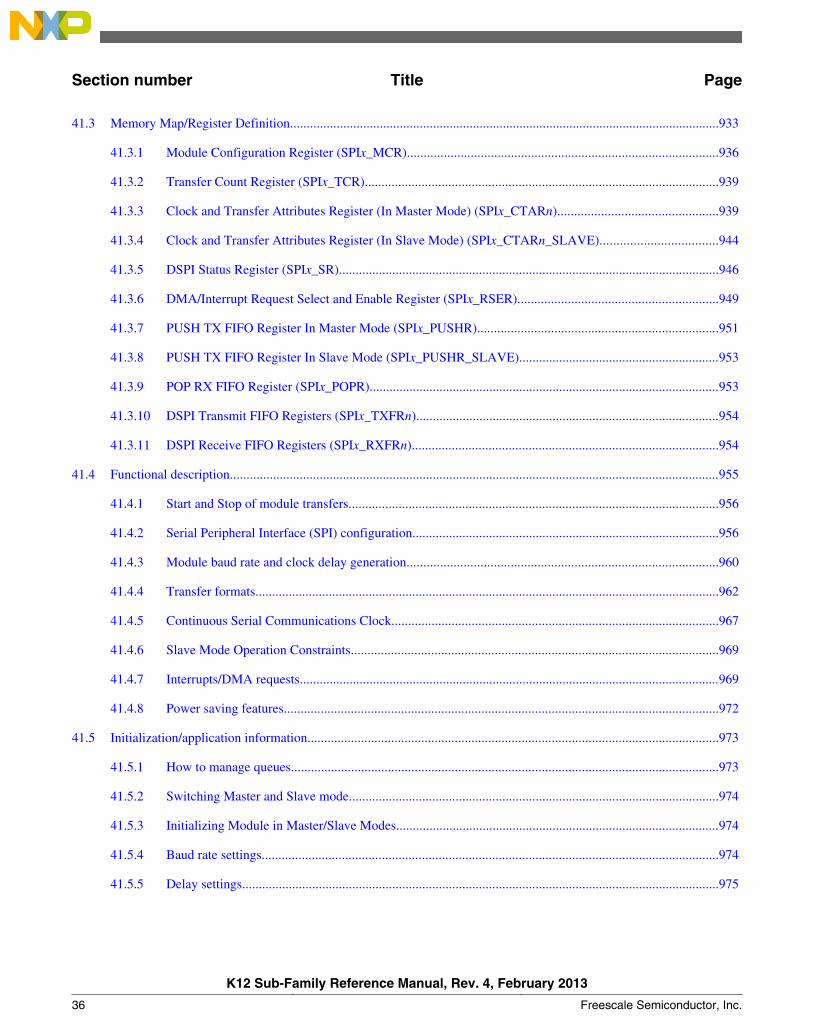
Section number Title Page
41.3 Memory Map/Register Definition.................................................................................................................................933
41.3.1 Module Configuration Register (SPIx_MCR).............................................................................................936
41.3.2 Transfer Count Register (SPIx_TCR)..........................................................................................................939
41.3.3 Clock and Transfer Attributes Register (In Master Mode) (SPIx_CTARn)................................................939
41.3.4 Clock and Transfer Attributes Register (In Slave Mode) (SPIx_CTARn_SLAVE)...................................944
41.3.5 DSPI Status Register (SPIx_SR)..................................................................................................................946
41.3.6 DMA/Interrupt Request Select and Enable Register (SPIx_RSER)............................................................949
41.3.7 PUSH TX FIFO Register In Master Mode (SPIx_PUSHR)........................................................................951
41.3.8 PUSH TX FIFO Register In Slave Mode (SPIx_PUSHR_SLAVE)............................................................953
41.3.9 POP RX FIFO Register (SPIx_POPR).........................................................................................................953
41.3.10 DSPI Transmit FIFO Registers (SPIx_TXFRn)...........................................................................................954
41.3.11 DSPI Receive FIFO Registers (SPIx_RXFRn)............................................................................................954
41.4 Functional description...................................................................................................................................................955
41.4.1 Start and Stop of module transfers...............................................................................................................956
41.4.2 Serial Peripheral Interface (SPI) configuration............................................................................................956
41.4.3 Module baud rate and clock delay generation.............................................................................................960
41.4.4 Transfer formats...........................................................................................................................................962
41.4.5 Continuous Serial Communications Clock..................................................................................................967
41.4.6 Slave Mode Operation Constraints..............................................................................................................969
41.4.7 Interrupts/DMA requests..............................................................................................................................969
41.4.8 Power saving features..................................................................................................................................972
41.5 Initialization/application information...........................................................................................................................973
41.5.1 How to manage queues................................................................................................................................973
41.5.2 Switching Master and Slave mode...............................................................................................................974
41.5.3 Initializing Module in Master/Slave Modes.................................................................................................974
41.5.4 Baud rate settings.........................................................................................................................................974
41.5.5 Delay settings...............................................................................................................................................975
K12 Sub-Family Reference Manual, Rev. 4, February 2013
36 Freescale Semiconductor, Inc.

Section number Title Page
41.5.6 Calculation of FIFO pointer addresses.........................................................................................................976
Chapter 42Inter-Integrated Circuit (I2C)
42.1 Introduction...................................................................................................................................................................979
42.1.1 Features........................................................................................................................................................979
42.1.2 Modes of operation......................................................................................................................................980
42.1.3 Block diagram..............................................................................................................................................980
42.2 I2C signal descriptions..................................................................................................................................................981
42.3 Memory map and register descriptions.........................................................................................................................981
42.3.1 I2C Address Register 1 (I2Cx_A1)..............................................................................................................982
42.3.2 I2C Frequency Divider register (I2Cx_F)....................................................................................................983
42.3.3 I2C Control Register 1 (I2Cx_C1)...............................................................................................................984
42.3.4 I2C Status register (I2Cx_S)........................................................................................................................986
42.3.5 I2C Data I/O register (I2Cx_D)...................................................................................................................987
42.3.6 I2C Control Register 2 (I2Cx_C2)...............................................................................................................988
42.3.7 I2C Programmable Input Glitch Filter register (I2Cx_FLT).......................................................................989
42.3.8 I2C Range Address register (I2Cx_RA)......................................................................................................990
42.3.9 I2C SMBus Control and Status register (I2Cx_SMB).................................................................................990
42.3.10 I2C Address Register 2 (I2Cx_A2)..............................................................................................................992
42.3.11 I2C SCL Low Timeout Register High (I2Cx_SLTH)..................................................................................992
42.3.12 I2C SCL Low Timeout Register Low (I2Cx_SLTL)...................................................................................993
42.4 Functional description...................................................................................................................................................993
42.4.1 I2C protocol.................................................................................................................................................993
42.4.2 10-bit address...............................................................................................................................................998
42.4.3 Address matching.........................................................................................................................................1000
42.4.4 System management bus specification........................................................................................................1001
42.4.5 Resets...........................................................................................................................................................1003
42.4.6 Interrupts......................................................................................................................................................1003
42.4.7 Programmable input glitch filter..................................................................................................................1005
K12 Sub-Family Reference Manual, Rev. 4, February 2013
Freescale Semiconductor, Inc. 37
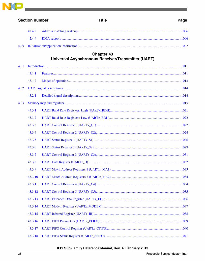
Section number Title Page
42.4.8 Address matching wakeup...........................................................................................................................1006
42.4.9 DMA support...............................................................................................................................................1006
42.5 Initialization/application information...........................................................................................................................1007
Chapter 43Universal Asynchronous Receiver/Transmitter (UART)
43.1 Introduction...................................................................................................................................................................1011
43.1.1 Features........................................................................................................................................................1011
43.1.2 Modes of operation......................................................................................................................................1013
43.2 UART signal descriptions.............................................................................................................................................1014
43.2.1 Detailed signal descriptions.........................................................................................................................1014
43.3 Memory map and registers............................................................................................................................................1015
43.3.1 UART Baud Rate Registers: High (UARTx_BDH)....................................................................................1021
43.3.2 UART Baud Rate Registers: Low (UARTx_BDL).....................................................................................1022
43.3.3 UART Control Register 1 (UARTx_C1).....................................................................................................1022
43.3.4 UART Control Register 2 (UARTx_C2).....................................................................................................1024
43.3.5 UART Status Register 1 (UARTx_S1)........................................................................................................1026
43.3.6 UART Status Register 2 (UARTx_S2)........................................................................................................1029
43.3.7 UART Control Register 3 (UARTx_C3).....................................................................................................1031
43.3.8 UART Data Register (UARTx_D)...............................................................................................................1032
43.3.9 UART Match Address Registers 1 (UARTx_MA1)....................................................................................1033
43.3.10 UART Match Address Registers 2 (UARTx_MA2)....................................................................................1034
43.3.11 UART Control Register 4 (UARTx_C4).....................................................................................................1034
43.3.12 UART Control Register 5 (UARTx_C5).....................................................................................................1035
43.3.13 UART Extended Data Register (UARTx_ED)............................................................................................1036
43.3.14 UART Modem Register (UARTx_MODEM).............................................................................................1037
43.3.15 UART Infrared Register (UARTx_IR)........................................................................................................1038
43.3.16 UART FIFO Parameters (UARTx_PFIFO).................................................................................................1039
43.3.17 UART FIFO Control Register (UARTx_CFIFO)........................................................................................1040
43.3.18 UART FIFO Status Register (UARTx_SFIFO)...........................................................................................1041
K12 Sub-Family Reference Manual, Rev. 4, February 2013
38 Freescale Semiconductor, Inc.
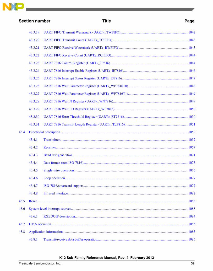
Section number Title Page
43.3.19 UART FIFO Transmit Watermark (UARTx_TWFIFO).............................................................................1042
43.3.20 UART FIFO Transmit Count (UARTx_TCFIFO).......................................................................................1043
43.3.21 UART FIFO Receive Watermark (UARTx_RWFIFO)...............................................................................1043
43.3.22 UART FIFO Receive Count (UARTx_RCFIFO)........................................................................................1044
43.3.23 UART 7816 Control Register (UARTx_C7816).........................................................................................1044
43.3.24 UART 7816 Interrupt Enable Register (UARTx_IE7816)..........................................................................1046
43.3.25 UART 7816 Interrupt Status Register (UARTx_IS7816)............................................................................1047
43.3.26 UART 7816 Wait Parameter Register (UARTx_WP7816T0).....................................................................1048
43.3.27 UART 7816 Wait Parameter Register (UARTx_WP7816T1).....................................................................1049
43.3.28 UART 7816 Wait N Register (UARTx_WN7816)......................................................................................1049
43.3.29 UART 7816 Wait FD Register (UARTx_WF7816)....................................................................................1050
43.3.30 UART 7816 Error Threshold Register (UARTx_ET7816)..........................................................................1050
43.3.31 UART 7816 Transmit Length Register (UARTx_TL7816)........................................................................1051
43.4 Functional description...................................................................................................................................................1052
43.4.1 Transmitter...................................................................................................................................................1052
43.4.2 Receiver.......................................................................................................................................................1057
43.4.3 Baud rate generation....................................................................................................................................1071
43.4.4 Data format (non ISO-7816)........................................................................................................................1073
43.4.5 Single-wire operation...................................................................................................................................1076
43.4.6 Loop operation.............................................................................................................................................1077
43.4.7 ISO-7816/smartcard support........................................................................................................................1077
43.4.8 Infrared interface..........................................................................................................................................1082
43.5 Reset..............................................................................................................................................................................1083
43.6 System level interrupt sources......................................................................................................................................1083
43.6.1 RXEDGIF description..................................................................................................................................1084
43.7 DMA operation.............................................................................................................................................................1085
43.8 Application information................................................................................................................................................1085
43.8.1 Transmit/receive data buffer operation........................................................................................................1085
K12 Sub-Family Reference Manual, Rev. 4, February 2013
Freescale Semiconductor, Inc. 39
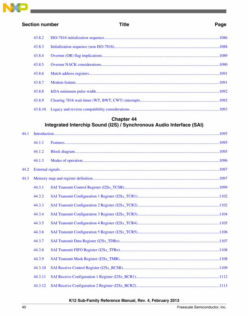
Section number Title Page
43.8.2 ISO-7816 initialization sequence.................................................................................................................1086
43.8.3 Initialization sequence (non ISO-7816).......................................................................................................1088
43.8.4 Overrun (OR) flag implications...................................................................................................................1089
43.8.5 Overrun NACK considerations....................................................................................................................1090
43.8.6 Match address registers................................................................................................................................1091
43.8.7 Modem feature.............................................................................................................................................1091
43.8.8 IrDA minimum pulse width.........................................................................................................................1092
43.8.9 Clearing 7816 wait timer (WT, BWT, CWT) interrupts..............................................................................1092
43.8.10 Legacy and reverse compatibility considerations........................................................................................1093
Chapter 44Integrated Interchip Sound (I2S) / Synchronous Audio Interface (SAI)
44.1 Introduction...................................................................................................................................................................1095
44.1.1 Features........................................................................................................................................................1095
44.1.2 Block diagram..............................................................................................................................................1095
44.1.3 Modes of operation......................................................................................................................................1096
44.2 External signals.............................................................................................................................................................1097
44.3 Memory map and register definition.............................................................................................................................1097
44.3.1 SAI Transmit Control Register (I2Sx_TCSR).............................................................................................1099
44.3.2 SAI Transmit Configuration 1 Register (I2Sx_TCR1)................................................................................1102
44.3.3 SAI Transmit Configuration 2 Register (I2Sx_TCR2)................................................................................1102
44.3.4 SAI Transmit Configuration 3 Register (I2Sx_TCR3)................................................................................1104
44.3.5 SAI Transmit Configuration 4 Register (I2Sx_TCR4)................................................................................1105
44.3.6 SAI Transmit Configuration 5 Register (I2Sx_TCR5)................................................................................1106
44.3.7 SAI Transmit Data Register (I2Sx_TDRn)..................................................................................................1107
44.3.8 SAI Transmit FIFO Register (I2Sx_TFRn).................................................................................................1108
44.3.9 SAI Transmit Mask Register (I2Sx_TMR)..................................................................................................1108
44.3.10 SAI Receive Control Register (I2Sx_RCSR)...............................................................................................1109
44.3.11 SAI Receive Configuration 1 Register (I2Sx_RCR1)..................................................................................1112
44.3.12 SAI Receive Configuration 2 Register (I2Sx_RCR2)..................................................................................1113
K12 Sub-Family Reference Manual, Rev. 4, February 2013
40 Freescale Semiconductor, Inc.
Section number Title Page
44.3.13 SAI Receive Configuration 3 Register (I2Sx_RCR3)..................................................................................1114
44.3.14 SAI Receive Configuration 4 Register (I2Sx_RCR4)..................................................................................1115
44.3.15 SAI Receive Configuration 5 Register (I2Sx_RCR5)..................................................................................1117
44.3.16 SAI Receive Data Register (I2Sx_RDRn)...................................................................................................1117
44.3.17 SAI Receive FIFO Register (I2Sx_RFRn)...................................................................................................1118
44.3.18 SAI Receive Mask Register (I2Sx_RMR)...................................................................................................1118
44.3.19 SAI MCLK Control Register (I2Sx_MCR).................................................................................................1119
44.3.20 SAI MCLK Divide Register (I2Sx_MDR)..................................................................................................1120
44.4 Functional description...................................................................................................................................................1121
44.4.1 SAI clocking................................................................................................................................................1121
44.4.2 SAI resets.....................................................................................................................................................1123
44.4.3 Synchronous modes.....................................................................................................................................1123
44.4.4 Frame sync configuration.............................................................................................................................1124
44.4.5 Data FIFO....................................................................................................................................................1125
44.4.6 Word mask register......................................................................................................................................1126
44.4.7 Interrupts and DMA requests.......................................................................................................................1127
Chapter 45General-Purpose Input/Output (GPIO)
45.1 Introduction...................................................................................................................................................................1129
45.1.1 Features........................................................................................................................................................1129
45.1.2 Modes of operation......................................................................................................................................1129
45.1.3 GPIO signal descriptions.............................................................................................................................1130
45.2 Memory map and register definition.............................................................................................................................1131
45.2.1 Port Data Output Register (GPIOx_PDOR).................................................................................................1133
45.2.2 Port Set Output Register (GPIOx_PSOR)....................................................................................................1133
45.2.3 Port Clear Output Register (GPIOx_PCOR)................................................................................................1134
45.2.4 Port Toggle Output Register (GPIOx_PTOR).............................................................................................1134
45.2.5 Port Data Input Register (GPIOx_PDIR).....................................................................................................1135
45.2.6 Port Data Direction Register (GPIOx_PDDR).............................................................................................1135
K12 Sub-Family Reference Manual, Rev. 4, February 2013
Freescale Semiconductor, Inc. 41
Section number Title Page
45.3 Functional description...................................................................................................................................................1136
45.3.1 General-purpose input..................................................................................................................................1136
45.3.2 General-purpose output................................................................................................................................1136
Chapter 46JTAG Controller (JTAGC)
46.1 Introduction...................................................................................................................................................................1139
46.1.1 Block diagram..............................................................................................................................................1139
46.1.2 Features........................................................................................................................................................1140
46.1.3 Modes of operation......................................................................................................................................1140
46.2 External signal description............................................................................................................................................1142
46.2.1 TCK—Test clock input................................................................................................................................1142
46.2.2 TDI—Test data input...................................................................................................................................1142
46.2.3 TDO—Test data output................................................................................................................................1142
46.2.4 TMS—Test mode select...............................................................................................................................1142
46.3 Register description......................................................................................................................................................1143
46.3.1 Instruction register.......................................................................................................................................1143
46.3.2 Bypass register.............................................................................................................................................1143
46.3.3 Device identification register.......................................................................................................................1143
46.3.4 Boundary scan register.................................................................................................................................1144
46.4 Functional description...................................................................................................................................................1145
46.4.1 JTAGC reset configuration..........................................................................................................................1145
46.4.2 IEEE 1149.1-2001 (JTAG) Test Access Port..............................................................................................1145
46.4.3 TAP controller state machine.......................................................................................................................1145
46.4.4 JTAGC block instructions............................................................................................................................1147
46.4.5 Boundary scan..............................................................................................................................................1150
46.5 Initialization/Application information..........................................................................................................................1150
Chapter 47Release Notes for Revision 4
47.1 General changes throughout document ........................................................................................................................1153
K12 Sub-Family Reference Manual, Rev. 4, February 2013
42 Freescale Semiconductor, Inc.
Section number Title Page
47.2 About This Document chapter changes........................................................................................................................1153
47.3 Introduction chapter changes........................................................................................................................................1153
47.4 Chip Configuration chapter changes.............................................................................................................................1153
47.5 Memory Map chapter changes......................................................................................................................................1153
47.6 Clock Distribution chapter changes..............................................................................................................................1154
47.7 Reset and Boot chapter changes...................................................................................................................................1154
47.8 Power Management chapter changes............................................................................................................................1154
47.9 Security chapter changes...............................................................................................................................................1154
47.10 Debug chapter changes.................................................................................................................................................1154
47.11 Signal Multiplexing and Signal Descriptions chapter changes.....................................................................................1154
47.12 PORT changes..............................................................................................................................................................1154
47.13 SIM changes..................................................................................................................................................................1155
47.14 RCM changes................................................................................................................................................................1155
47.15 SMC changes................................................................................................................................................................1155
47.16 PMC changes................................................................................................................................................................1155
47.17 LLWU changes.............................................................................................................................................................1155
47.18 MCM changes...............................................................................................................................................................1155
47.19 Crossbar switch module changes..................................................................................................................................1155
47.20 AIPS-Lite changes........................................................................................................................................................1156
47.21 DMAMUX module changes.........................................................................................................................................1156
47.22 DMA module changes..................................................................................................................................................1156
47.23 EWM changes...............................................................................................................................................................1156
47.24 WDOG changes............................................................................................................................................................1156
47.25 MCG changes................................................................................................................................................................1156
47.26 OSC changes.................................................................................................................................................................1156
47.27 RTC Oscillator changes................................................................................................................................................1157
47.28 FMC changes................................................................................................................................................................1157
47.29 FTFL changes...............................................................................................................................................................1157
47.30 EzPort changes..............................................................................................................................................................1157
K12 Sub-Family Reference Manual, Rev. 4, February 2013
Freescale Semiconductor, Inc. 43
Section number Title Page
47.31 CRC changes.................................................................................................................................................................1157
47.32 RNGA chapter changes.................................................................................................................................................1157
47.33 ADC changes................................................................................................................................................................1157
47.34 CMP changes................................................................................................................................................................1158
47.35 DAC changes................................................................................................................................................................1158
47.36 VREF changes..............................................................................................................................................................1158
47.37 PDB changes.................................................................................................................................................................1158
47.38 FTM changes................................................................................................................................................................1158
47.39 PIT module changes......................................................................................................................................................1158
47.40 LPTMR changes...........................................................................................................................................................1158
47.41 CMT changes................................................................................................................................................................1159
47.42 RTC changes.................................................................................................................................................................1159
47.43 DSPI chapter changes...................................................................................................................................................1159
47.44 I2C changes...................................................................................................................................................................1159
47.45 UART changes..............................................................................................................................................................1159
47.46 GPIO changes...............................................................................................................................................................1159
47.47 JTAGC module changes...............................................................................................................................................1159
K12 Sub-Family Reference Manual, Rev. 4, February 2013
44 Freescale Semiconductor, Inc.
Chapter 1About This Document
1.1 Overview
1.1.1 Purpose
This document describes the features, architecture, and programming model of theFreescale K12 microcontroller.
1.1.2 Audience
This document is primarily for system architects and software application developerswho are using or considering using the microcontroller in a system.
1.2 Conventions
1.2.1 Numbering systems
The following suffixes identify different numbering systems:
This suffix Identifies a
b Binary number. For example, the binary equivalent of thenumber 5 is written 101b. In some cases, binary numbers areshown with the prefix 0b.
d Decimal number. Decimal numbers are followed by this suffixonly when the possibility of confusion exists. In general,decimal numbers are shown without a suffix.
h Hexadecimal number. For example, the hexadecimalequivalent of the number 60 is written 3Ch. In some cases,hexadecimal numbers are shown with the prefix 0x.
K12 Sub-Family Reference Manual, Rev. 4, February 2013
Freescale Semiconductor, Inc. 45
1.2.2 Typographic notation
The following typographic notation is used throughout this document:
Example Description
placeholder, x Items in italics are placeholders for information that you provide. Italicized text is also used forthe titles of publications and for emphasis. Plain lowercase letters are also used asplaceholders for single letters and numbers.
code Fixed-width type indicates text that must be typed exactly as shown. It is used for instructionmnemonics, directives, symbols, subcommands, parameters, and operators. Fixed-width typeis also used for example code. Instruction mnemonics and directives in text and tables areshown in all caps; for example, BSR.
SR[SCM] A mnemonic in brackets represents a named field in a register. This example refers to theScaling Mode (SCM) field in the Status Register (SR).
REVNO[6:4], XAD[7:0] Numbers in brackets and separated by a colon represent either:• A subset of a register's named field
For example, REVNO[6:4] refers to bits 6–4 that are part of the COREREV field thatoccupies bits 6–0 of the REVNO register.
• A continuous range of individual signals of a bus
For example, XAD[7:0] refers to signals 7–0 of the XAD bus.
1.2.3 Special terms
The following terms have special meanings:
Term Meaning
asserted Refers to the state of a signal as follows:• An active-high signal is asserted when high (1).• An active-low signal is asserted when low (0).
deasserted Refers to the state of a signal as follows:• An active-high signal is deasserted when low (0).• An active-low signal is deasserted when high (1).
In some cases, deasserted signals are described as negated.
reserved Refers to a memory space, register, or field that is eitherreserved for future use or for which, when written to, themodule or chip behavior is unpredictable.
w1c Write 1 to clear: Refers to a register bitfield that must bewritten as 1 to be "cleared."
Conventions
K12 Sub-Family Reference Manual, Rev. 4, February 2013
46 Freescale Semiconductor, Inc.
Chapter 2Introduction
2.1 OverviewThis chapter provides high-level descriptions of the modules available on the devicescovered by this document.
2.2 Module Functional CategoriesThe modules on this device are grouped into functional categories. The followingsections describe the modules assigned to each category in more detail.
Table 2-1. Module functional categories
Module category Description
ARM Cortex-M4 core • 32-bit MCU core from ARM’s Cortex-M class adding DSP instructions, 1.25DMIPS/MHz, based on ARMv7 architecture
System • System integration module• Power management and mode controllers
• Multiple power modes available based on run, wait, stop, and power-down modes
• Low-leakage wakeup unit• Miscellaneous control module• Crossbar switch• Peripheral bridge• Direct memory access (DMA) controller with multiplexer to increase available
DMA requests• External watchdog monitor• Watchdog
Memories • Internal memories include:• Program flash memory• On devices with FlexMemory: FlexMemory
• FlexNVM• FlexRAM
• On devices with program flash only: Programming acceleration RAM• SRAM
• Serial programming interface: EzPort
Table continues on the next page...
K12 Sub-Family Reference Manual, Rev. 4, February 2013
Freescale Semiconductor, Inc. 47
Table 2-1. Module functional categories (continued)
Module category Description
Clocks • Multiple clock generation options available from internally- and externally-generated clocks
• System oscillator to provide clock source for the MCU• RTC oscillator to provide clock source for the RTC
Security • Cyclic Redundancy Check module for error detection
Analog • High speed analog-to-digital converter• Comparator• Digital-to-analog converter• Internal voltage reference
Timers • Programmable delay block• FlexTimers• Periodic interrupt timer• Low power timer• Carrier modulator transmitter• Independent real time clock
Communications • Serial peripheral interface• Inter-integrated circuit (I2C)• UART• Integrated interchip sound (I2S)
Human-Machine Interfaces (HMI) • General purpose input/output controller
2.2.1 ARM® Cortex™-M4 Core Modules
The following core modules are available on this device.
Table 2-2. Core modules
Module Description
ARM Cortex-M4 The ARM Cortex-M4 is the newest member of the Cortex M Series of processorstargeting microcontroller cores focused on very cost sensitive, deterministic,interrupt driven environments. The Cortex M4 processor is based on the ARMv7Architecture and Thumb®-2 ISA and is upward compatible with the Cortex M3,Cortex M1, and Cortex M0 architectures. Cortex M4 improvements include anARMv7 Thumb-2 DSP (ported from the ARMv7-A/R profile architectures) providing32-bit instructions with SIMD (single instruction multiple data) DSP style multiply-accumulates and saturating arithmetic.
NVIC The ARMv7-M exception model and nested-vectored interrupt controller (NVIC)implement a relocatable vector table supporting many external interrupts, a singlenon-maskable interrupt (NMI), and priority levels.
The NVIC replaces shadow registers with equivalent system and simplifiedprogrammability. The NVIC contains the address of the function to execute for aparticular handler. The address is fetched via the instruction port allowing parallelregister stacking and look-up. The first sixteen entries are allocated to ARMinternal sources with the others mapping to MCU-defined interrupts.
Table continues on the next page...
Module Functional Categories
K12 Sub-Family Reference Manual, Rev. 4, February 2013
48 Freescale Semiconductor, Inc.
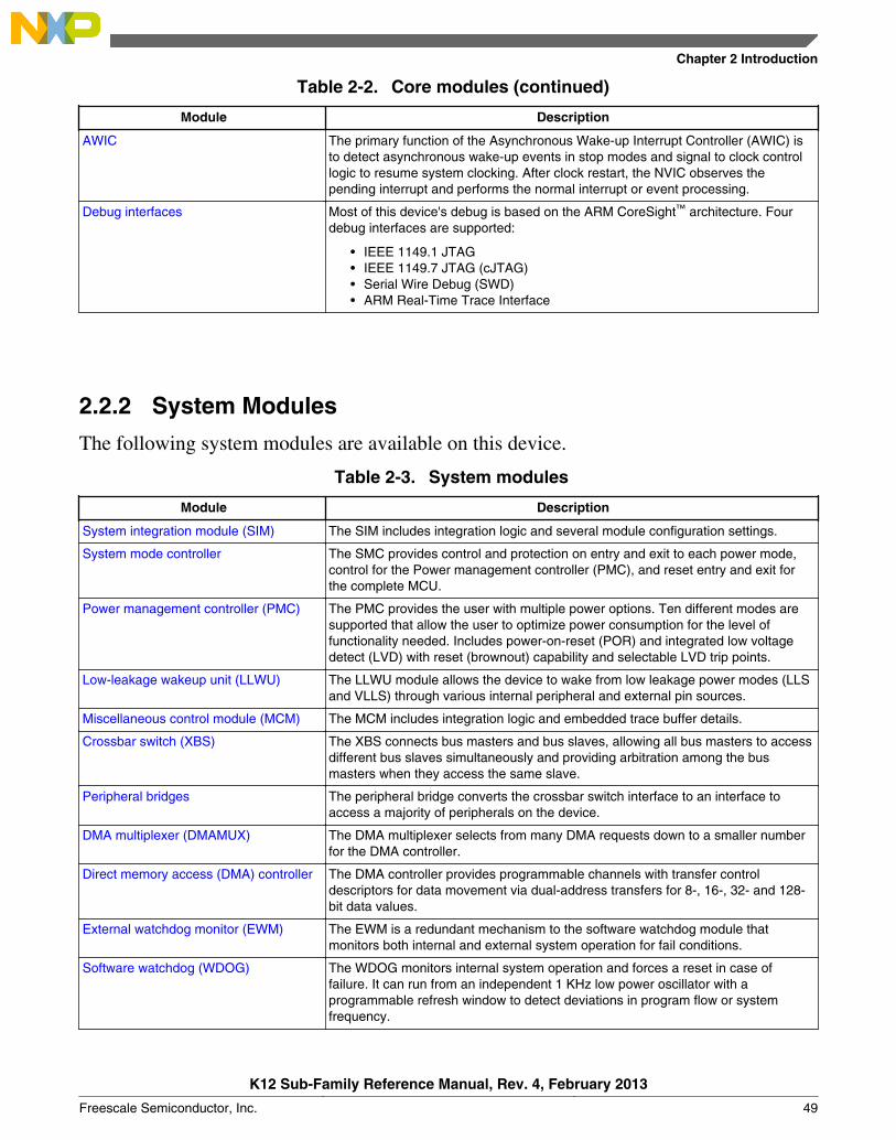
Table 2-2. Core modules (continued)
Module Description
AWIC The primary function of the Asynchronous Wake-up Interrupt Controller (AWIC) isto detect asynchronous wake-up events in stop modes and signal to clock controllogic to resume system clocking. After clock restart, the NVIC observes thepending interrupt and performs the normal interrupt or event processing.
Debug interfaces Most of this device's debug is based on the ARM CoreSight™ architecture. Fourdebug interfaces are supported:
• IEEE 1149.1 JTAG• IEEE 1149.7 JTAG (cJTAG)• Serial Wire Debug (SWD)• ARM Real-Time Trace Interface
2.2.2 System Modules
The following system modules are available on this device.
Table 2-3. System modules
Module Description
System integration module (SIM) The SIM includes integration logic and several module configuration settings.
System mode controller The SMC provides control and protection on entry and exit to each power mode,control for the Power management controller (PMC), and reset entry and exit forthe complete MCU.
Power management controller (PMC) The PMC provides the user with multiple power options. Ten different modes aresupported that allow the user to optimize power consumption for the level offunctionality needed. Includes power-on-reset (POR) and integrated low voltagedetect (LVD) with reset (brownout) capability and selectable LVD trip points.
Low-leakage wakeup unit (LLWU) The LLWU module allows the device to wake from low leakage power modes (LLSand VLLS) through various internal peripheral and external pin sources.
Miscellaneous control module (MCM) The MCM includes integration logic and embedded trace buffer details.
Crossbar switch (XBS) The XBS connects bus masters and bus slaves, allowing all bus masters to accessdifferent bus slaves simultaneously and providing arbitration among the busmasters when they access the same slave.
Peripheral bridges The peripheral bridge converts the crossbar switch interface to an interface toaccess a majority of peripherals on the device.
DMA multiplexer (DMAMUX) The DMA multiplexer selects from many DMA requests down to a smaller numberfor the DMA controller.
Direct memory access (DMA) controller The DMA controller provides programmable channels with transfer controldescriptors for data movement via dual-address transfers for 8-, 16-, 32- and 128-bit data values.
External watchdog monitor (EWM) The EWM is a redundant mechanism to the software watchdog module thatmonitors both internal and external system operation for fail conditions.
Software watchdog (WDOG) The WDOG monitors internal system operation and forces a reset in case offailure. It can run from an independent 1 KHz low power oscillator with aprogrammable refresh window to detect deviations in program flow or systemfrequency.
Chapter 2 Introduction
K12 Sub-Family Reference Manual, Rev. 4, February 2013
Freescale Semiconductor, Inc. 49
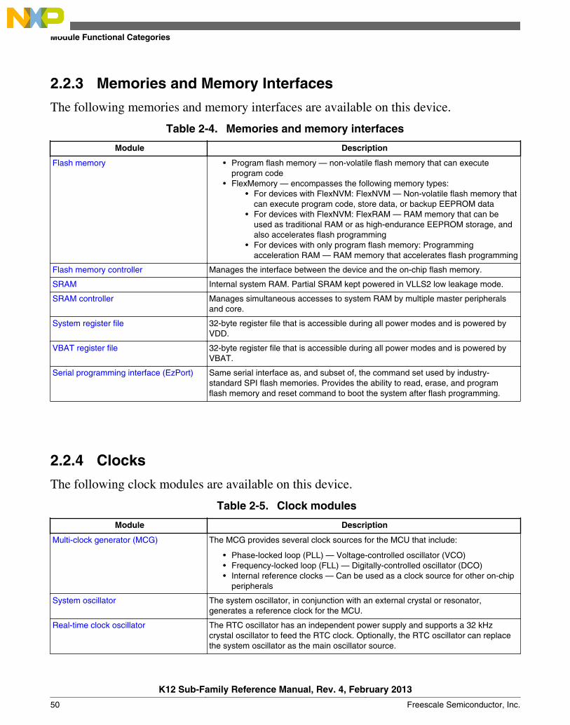
2.2.3 Memories and Memory Interfaces
The following memories and memory interfaces are available on this device.
Table 2-4. Memories and memory interfaces
Module Description
Flash memory • Program flash memory — non-volatile flash memory that can executeprogram code
• FlexMemory — encompasses the following memory types:• For devices with FlexNVM: FlexNVM — Non-volatile flash memory that
can execute program code, store data, or backup EEPROM data• For devices with FlexNVM: FlexRAM — RAM memory that can be
used as traditional RAM or as high-endurance EEPROM storage, andalso accelerates flash programming
• For devices with only program flash memory: Programmingacceleration RAM — RAM memory that accelerates flash programming
Flash memory controller Manages the interface between the device and the on-chip flash memory.
SRAM Internal system RAM. Partial SRAM kept powered in VLLS2 low leakage mode.
SRAM controller Manages simultaneous accesses to system RAM by multiple master peripheralsand core.
System register file 32-byte register file that is accessible during all power modes and is powered byVDD.
VBAT register file 32-byte register file that is accessible during all power modes and is powered byVBAT.
Serial programming interface (EzPort) Same serial interface as, and subset of, the command set used by industry-standard SPI flash memories. Provides the ability to read, erase, and programflash memory and reset command to boot the system after flash programming.
2.2.4 Clocks
The following clock modules are available on this device.
Table 2-5. Clock modules
Module Description
Multi-clock generator (MCG) The MCG provides several clock sources for the MCU that include:
• Phase-locked loop (PLL) — Voltage-controlled oscillator (VCO)• Frequency-locked loop (FLL) — Digitally-controlled oscillator (DCO)• Internal reference clocks — Can be used as a clock source for other on-chip
peripherals
System oscillator The system oscillator, in conjunction with an external crystal or resonator,generates a reference clock for the MCU.
Real-time clock oscillator The RTC oscillator has an independent power supply and supports a 32 kHzcrystal oscillator to feed the RTC clock. Optionally, the RTC oscillator can replacethe system oscillator as the main oscillator source.
Module Functional Categories
K12 Sub-Family Reference Manual, Rev. 4, February 2013
50 Freescale Semiconductor, Inc.
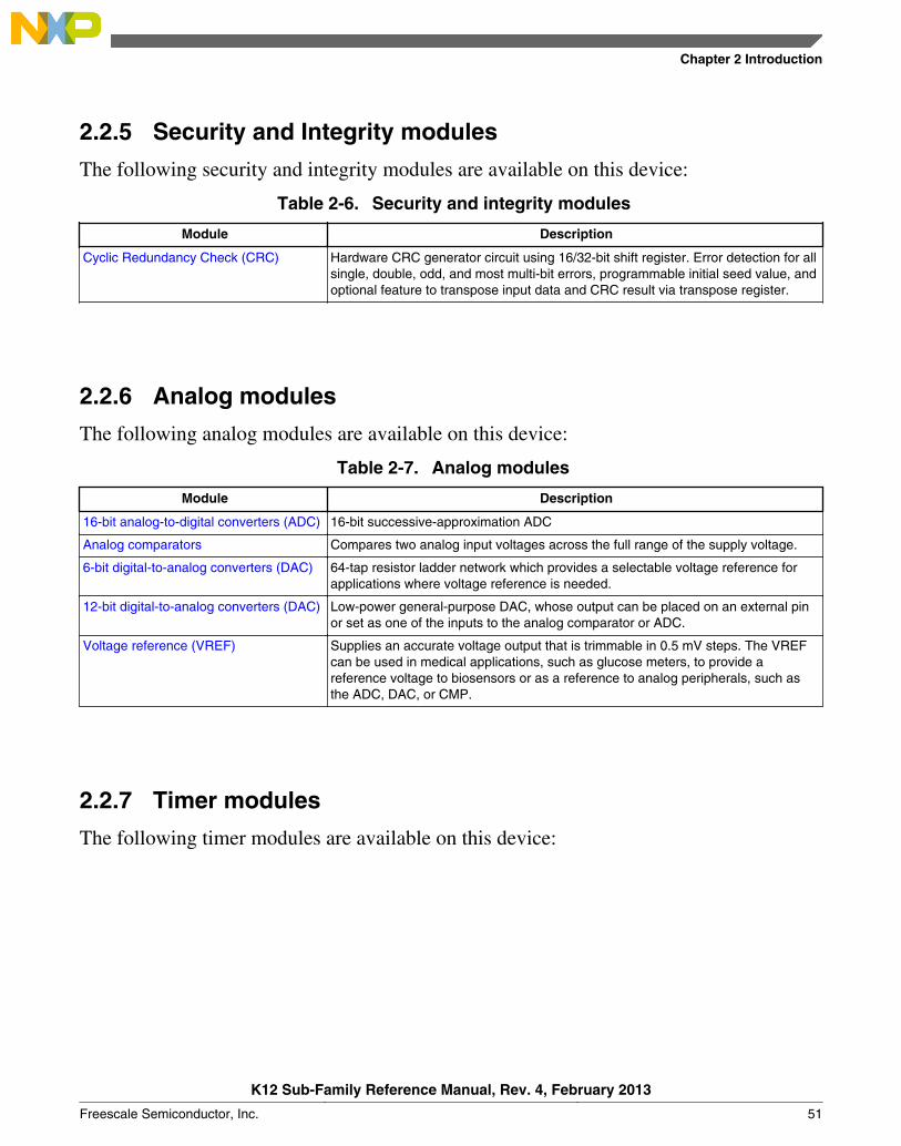
2.2.5 Security and Integrity modules
The following security and integrity modules are available on this device:
Table 2-6. Security and integrity modules
Module Description
Cyclic Redundancy Check (CRC) Hardware CRC generator circuit using 16/32-bit shift register. Error detection for allsingle, double, odd, and most multi-bit errors, programmable initial seed value, andoptional feature to transpose input data and CRC result via transpose register.
2.2.6 Analog modules
The following analog modules are available on this device:
Table 2-7. Analog modules
Module Description
16-bit analog-to-digital converters (ADC) 16-bit successive-approximation ADC
Analog comparators Compares two analog input voltages across the full range of the supply voltage.
6-bit digital-to-analog converters (DAC) 64-tap resistor ladder network which provides a selectable voltage reference forapplications where voltage reference is needed.
12-bit digital-to-analog converters (DAC) Low-power general-purpose DAC, whose output can be placed on an external pinor set as one of the inputs to the analog comparator or ADC.
Voltage reference (VREF) Supplies an accurate voltage output that is trimmable in 0.5 mV steps. The VREFcan be used in medical applications, such as glucose meters, to provide areference voltage to biosensors or as a reference to analog peripherals, such asthe ADC, DAC, or CMP.
2.2.7 Timer modules
The following timer modules are available on this device:
Chapter 2 Introduction
K12 Sub-Family Reference Manual, Rev. 4, February 2013
Freescale Semiconductor, Inc. 51
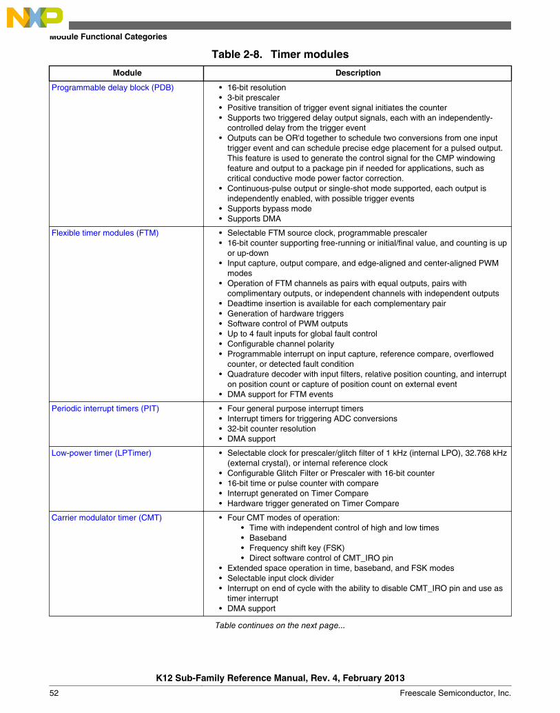
Table 2-8. Timer modules
Module Description
Programmable delay block (PDB) • 16-bit resolution• 3-bit prescaler• Positive transition of trigger event signal initiates the counter• Supports two triggered delay output signals, each with an independently-
controlled delay from the trigger event• Outputs can be OR'd together to schedule two conversions from one input
trigger event and can schedule precise edge placement for a pulsed output.This feature is used to generate the control signal for the CMP windowingfeature and output to a package pin if needed for applications, such ascritical conductive mode power factor correction.
• Continuous-pulse output or single-shot mode supported, each output isindependently enabled, with possible trigger events
• Supports bypass mode• Supports DMA
Flexible timer modules (FTM) • Selectable FTM source clock, programmable prescaler• 16-bit counter supporting free-running or initial/final value, and counting is up
or up-down• Input capture, output compare, and edge-aligned and center-aligned PWM
modes• Operation of FTM channels as pairs with equal outputs, pairs with
complimentary outputs, or independent channels with independent outputs• Deadtime insertion is available for each complementary pair• Generation of hardware triggers• Software control of PWM outputs• Up to 4 fault inputs for global fault control• Configurable channel polarity• Programmable interrupt on input capture, reference compare, overflowed
counter, or detected fault condition• Quadrature decoder with input filters, relative position counting, and interrupt
on position count or capture of position count on external event• DMA support for FTM events
Periodic interrupt timers (PIT) • Four general purpose interrupt timers• Interrupt timers for triggering ADC conversions• 32-bit counter resolution• DMA support
Low-power timer (LPTimer) • Selectable clock for prescaler/glitch filter of 1 kHz (internal LPO), 32.768 kHz(external crystal), or internal reference clock
• Configurable Glitch Filter or Prescaler with 16-bit counter• 16-bit time or pulse counter with compare• Interrupt generated on Timer Compare• Hardware trigger generated on Timer Compare
Carrier modulator timer (CMT) • Four CMT modes of operation:• Time with independent control of high and low times• Baseband• Frequency shift key (FSK)• Direct software control of CMT_IRO pin
• Extended space operation in time, baseband, and FSK modes• Selectable input clock divider• Interrupt on end of cycle with the ability to disable CMT_IRO pin and use as
timer interrupt• DMA support
Table continues on the next page...
Module Functional Categories
K12 Sub-Family Reference Manual, Rev. 4, February 2013
52 Freescale Semiconductor, Inc.
Table 2-8. Timer modules (continued)
Module Description
Real-time clock (RTC) • Independent power supply, POR, and 32 kHz Crystal Oscillator• 32-bit seconds counter with 32-bit Alarm• 16-bit Prescaler with compensation that can correct errors between 0.12 ppm
and 3906 ppm
2.2.8 Communication interfaces
The following communication interfaces are available on this device:
Table 2-9. Communication modules
Module Description
USB Device Charger Detect (USBDCD) The USBDCD monitors the USB data lines to detect a smart charger meeting theUSB Battery Charging Specification Rev1.1. This information allows the MCU tobetter manage the battery charging IC in a portable device.
Serial peripheral interface (SPI) Synchronous serial bus for communication to an external device
Inter-integrated circuit (I2C) Allows communication between a number of devices. Also supports the SystemManagement Bus (SMBus) Specification, version 2.
Universal asynchronous receiver/transmitters (UART)
Asynchronous serial bus communication interface with programmable 8- or 9-bitdata format and support of ISO 7816 smart card interface
I2S The I2S is a full-duplex, serial port that allows the chip to communicate with avariety of serial devices, such as standard codecs, digital signal processors(DSPs), microprocessors, peripherals, and audio codecs that implement the inter-IC sound bus (I2S) and the Intel® AC97 standards
2.2.9 Human-machine interfaces
The following human-machine interfaces (HMI) are available on this device:
Table 2-10. HMI modules
Module Description
General purpose input/output (GPIO) All general purpose input or output (GPIO) pins are capable of interrupt and DMArequest generation. All GPIO pins have 3.3 V tolerance.
2.3 Orderable part numbersThe following table summarizes the part numbers of the devices covered by thisdocument.
Chapter 2 Introduction
K12 Sub-Family Reference Manual, Rev. 4, February 2013
Freescale Semiconductor, Inc. 53
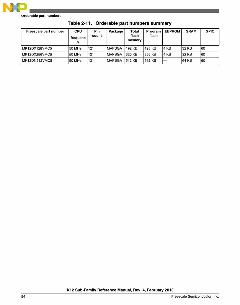
Table 2-11. Orderable part numbers summary
Freescale part number CPU
frequency
Pincount
Package Totalflash
memory
Programflash
EEPROM SRAM GPIO
MK12DX128VMC5 50 MHz 121 MAPBGA 192 KB 128 KB 4 KB 32 KB 60
MK12DX256VMC5 50 MHz 121 MAPBGA 320 KB 256 KB 4 KB 32 KB 60
MK12DN512VMC5 50 MHz 121 MAPBGA 512 KB 512 KB — 64 KB 60
Orderable part numbers
K12 Sub-Family Reference Manual, Rev. 4, February 2013
54 Freescale Semiconductor, Inc.
Chapter 3Chip Configuration
3.1 IntroductionThis chapter provides details on the individual modules of the microcontroller. Itincludes:
• module block diagrams showing immediate connections within the device,• specific module-to-module interactions not necessarily discussed in the individual
module chapters, and• links for more information.
3.2 Core modules
3.2.1 ARM Cortex-M4 Core Configuration
This section summarizes how the module has been configured in the chip. Fulldocumentation for this module is provided by ARM and can be found at www.arm.com.
K12 Sub-Family Reference Manual, Rev. 4, February 2013
Freescale Semiconductor, Inc. 55
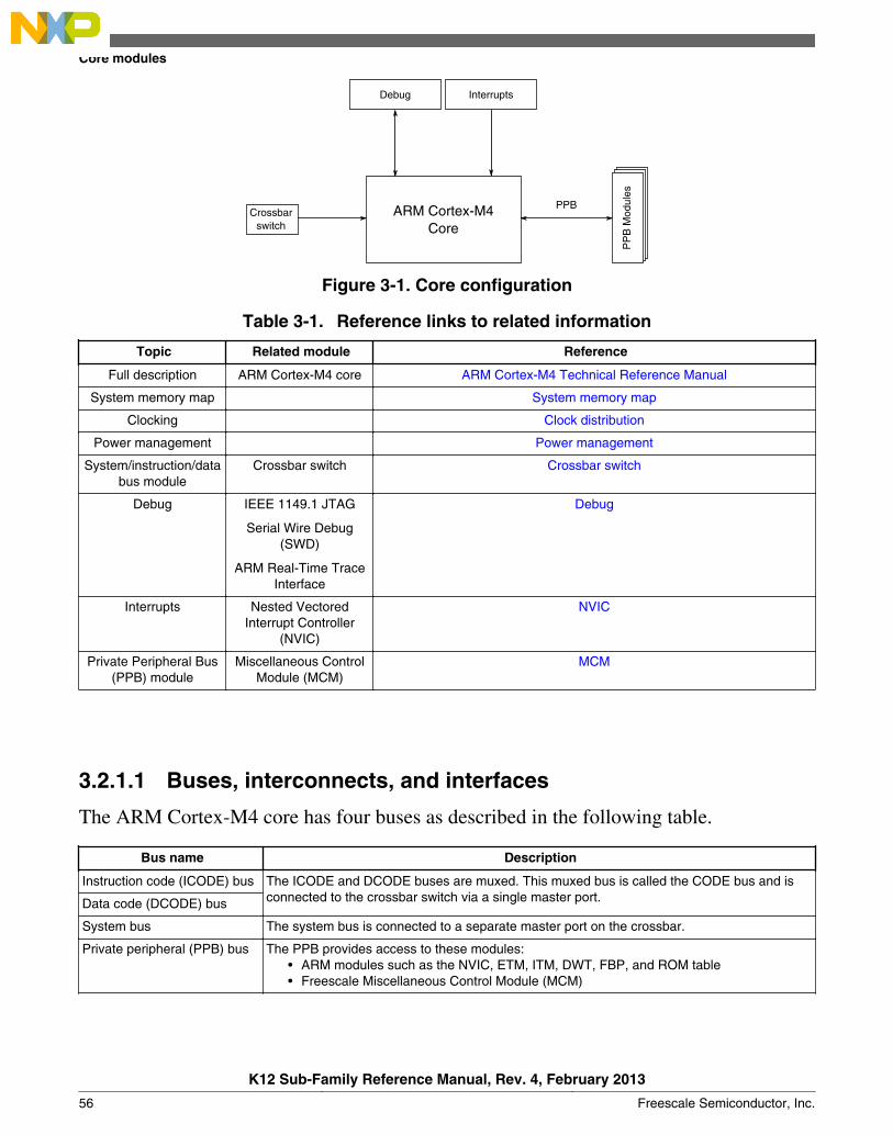
PP
B M
odul
es
PPBARM Cortex-M4Core
Debug Interrupts
Crossbarswitch
Figure 3-1. Core configuration
Table 3-1. Reference links to related information
Topic Related module Reference
Full description ARM Cortex-M4 core ARM Cortex-M4 Technical Reference Manual
System memory map System memory map
Clocking Clock distribution
Power management Power management
System/instruction/databus module
Crossbar switch Crossbar switch
Debug IEEE 1149.1 JTAG
Serial Wire Debug(SWD)
ARM Real-Time TraceInterface
Debug
Interrupts Nested VectoredInterrupt Controller
(NVIC)
NVIC
Private Peripheral Bus(PPB) module
Miscellaneous ControlModule (MCM)
MCM
3.2.1.1 Buses, interconnects, and interfaces
The ARM Cortex-M4 core has four buses as described in the following table.
Bus name Description
Instruction code (ICODE) bus The ICODE and DCODE buses are muxed. This muxed bus is called the CODE bus and isconnected to the crossbar switch via a single master port.Data code (DCODE) bus
System bus The system bus is connected to a separate master port on the crossbar.
Private peripheral (PPB) bus The PPB provides access to these modules:• ARM modules such as the NVIC, ETM, ITM, DWT, FBP, and ROM table• Freescale Miscellaneous Control Module (MCM)
Core modules
K12 Sub-Family Reference Manual, Rev. 4, February 2013
56 Freescale Semiconductor, Inc.
3.2.1.2 System Tick Timer
The System Tick Timer's clock source is always the core clock, FCLK. This results in thefollowing:
• The CLKSOURCE bit in SysTick Control and Status register is always set to selectthe core clock.
• Because the timing reference (FCLK) is a variable frequency, the TENMS bit in theSysTick Calibration Value Register is always zero.
• The NOREF bit in SysTick Calibration Value Register is always set, implying thatFCLK is the only available source of reference timing.
3.2.1.3 Debug facilities
This device has extensive debug capabilities including run control and tracingcapabilities. The standard ARM debug port that supports JTAG and SWD interfaces.Also the cJTAG interface is supported on this device.
3.2.1.4 Core privilege levels
The ARM documentation uses different terms than this document to distinguish betweenprivilege levels.
If you see this term... it also means this term...
Privileged Supervisor
Unprivileged or user User
3.2.2 Nested Vectored Interrupt Controller (NVIC) Configuration
This section summarizes how the module has been configured in the chip. Fulldocumentation for this module is provided by ARM and can be found at www.arm.com.
Chapter 3 Chip Configuration
K12 Sub-Family Reference Manual, Rev. 4, February 2013
Freescale Semiconductor, Inc. 57
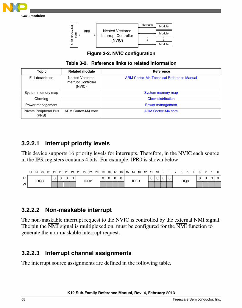
Nested VectoredInterrupt Controller
(NVIC)
AR
M C
orte
x-M
4co
re
InterruptsModule
Module
Module
PPB
Figure 3-2. NVIC configuration
Table 3-2. Reference links to related information
Topic Related module Reference
Full description Nested VectoredInterrupt Controller
(NVIC)
ARM Cortex-M4 Technical Reference Manual
System memory map System memory map
Clocking Clock distribution
Power management Power management
Private Peripheral Bus(PPB)
ARM Cortex-M4 core ARM Cortex-M4 core
3.2.2.1 Interrupt priority levels
This device supports 16 priority levels for interrupts. Therefore, in the NVIC each sourcein the IPR registers contains 4 bits. For example, IPR0 is shown below:
31 30 29 28 27 26 25 24 23 22 21 20 19 18 17 16 15 14 13 12 11 10 9 8 7 6 5 4 3 2 1 0
RIRQ3
0 0 0 0IRQ2
0 0 0 0IRQ1
0 0 0 0IRQ0
0 0 0 0
W
3.2.2.2 Non-maskable interrupt
The non-maskable interrupt request to the NVIC is controlled by the external NMI signal.The pin the NMI signal is multiplexed on, must be configured for the NMI function togenerate the non-maskable interrupt request.
3.2.2.3 Interrupt channel assignments
The interrupt source assignments are defined in the following table.
Core modules
K12 Sub-Family Reference Manual, Rev. 4, February 2013
58 Freescale Semiconductor, Inc.
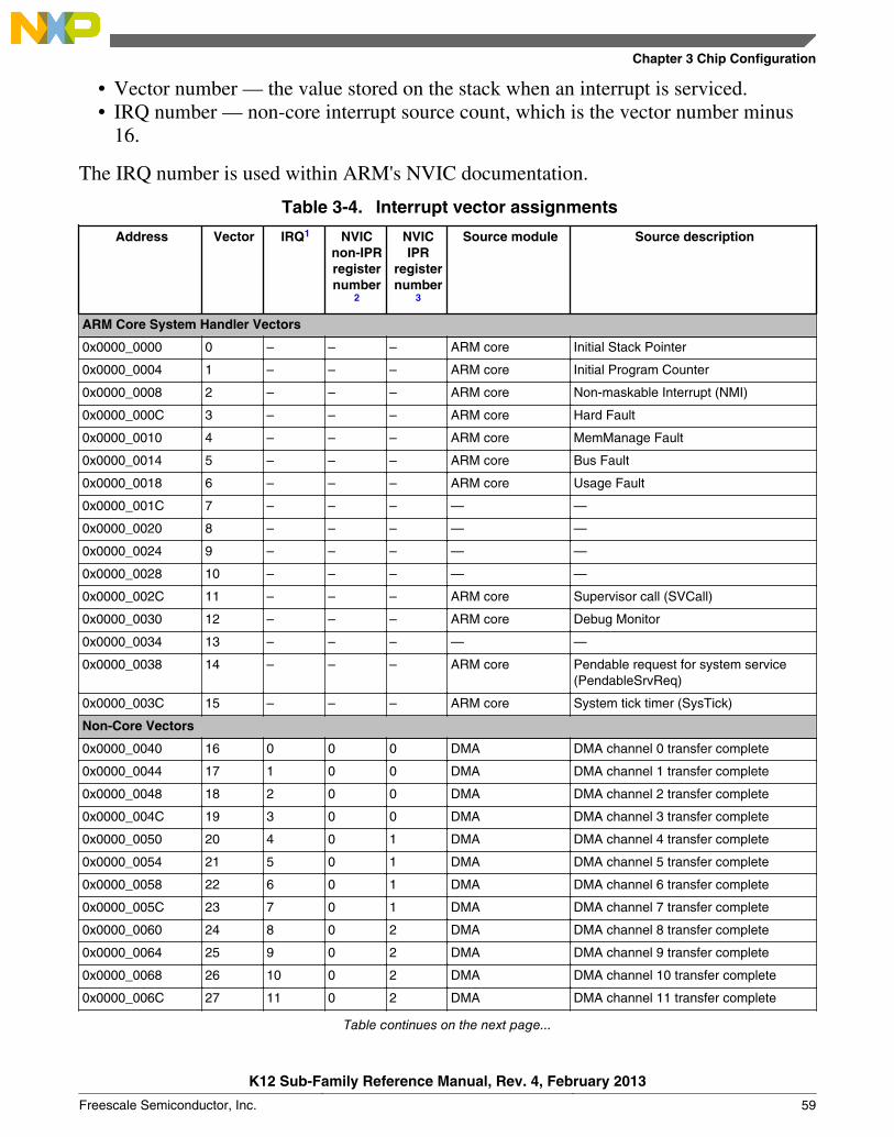
• Vector number — the value stored on the stack when an interrupt is serviced.• IRQ number — non-core interrupt source count, which is the vector number minus
16.
The IRQ number is used within ARM's NVIC documentation.
Table 3-4. Interrupt vector assignments
Address Vector IRQ1 NVICnon-IPRregisternumber
2
NVICIPR
registernumber
3
Source module Source description
ARM Core System Handler Vectors
0x0000_0000 0 – – – ARM core Initial Stack Pointer
0x0000_0004 1 – – – ARM core Initial Program Counter
0x0000_0008 2 – – – ARM core Non-maskable Interrupt (NMI)
0x0000_000C 3 – – – ARM core Hard Fault
0x0000_0010 4 – – – ARM core MemManage Fault
0x0000_0014 5 – – – ARM core Bus Fault
0x0000_0018 6 – – – ARM core Usage Fault
0x0000_001C 7 – – – — —
0x0000_0020 8 – – – — —
0x0000_0024 9 – – – — —
0x0000_0028 10 – – – — —
0x0000_002C 11 – – – ARM core Supervisor call (SVCall)
0x0000_0030 12 – – – ARM core Debug Monitor
0x0000_0034 13 – – – — —
0x0000_0038 14 – – – ARM core Pendable request for system service(PendableSrvReq)
0x0000_003C 15 – – – ARM core System tick timer (SysTick)
Non-Core Vectors
0x0000_0040 16 0 0 0 DMA DMA channel 0 transfer complete
0x0000_0044 17 1 0 0 DMA DMA channel 1 transfer complete
0x0000_0048 18 2 0 0 DMA DMA channel 2 transfer complete
0x0000_004C 19 3 0 0 DMA DMA channel 3 transfer complete
0x0000_0050 20 4 0 1 DMA DMA channel 4 transfer complete
0x0000_0054 21 5 0 1 DMA DMA channel 5 transfer complete
0x0000_0058 22 6 0 1 DMA DMA channel 6 transfer complete
0x0000_005C 23 7 0 1 DMA DMA channel 7 transfer complete
0x0000_0060 24 8 0 2 DMA DMA channel 8 transfer complete
0x0000_0064 25 9 0 2 DMA DMA channel 9 transfer complete
0x0000_0068 26 10 0 2 DMA DMA channel 10 transfer complete
0x0000_006C 27 11 0 2 DMA DMA channel 11 transfer complete
Table continues on the next page...
Chapter 3 Chip Configuration
K12 Sub-Family Reference Manual, Rev. 4, February 2013
Freescale Semiconductor, Inc. 59
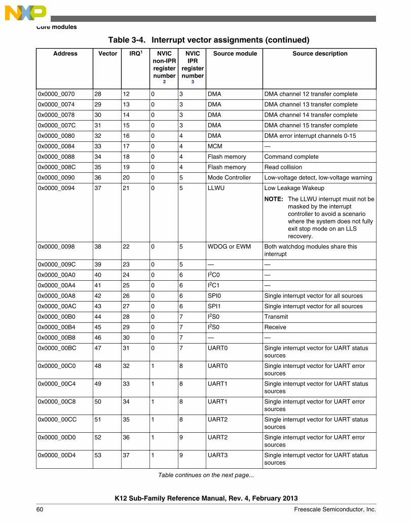
Table 3-4. Interrupt vector assignments (continued)
Address Vector IRQ1 NVICnon-IPRregisternumber
2
NVICIPR
registernumber
3
Source module Source description
0x0000_0070 28 12 0 3 DMA DMA channel 12 transfer complete
0x0000_0074 29 13 0 3 DMA DMA channel 13 transfer complete
0x0000_0078 30 14 0 3 DMA DMA channel 14 transfer complete
0x0000_007C 31 15 0 3 DMA DMA channel 15 transfer complete
0x0000_0080 32 16 0 4 DMA DMA error interrupt channels 0-15
0x0000_0084 33 17 0 4 MCM —
0x0000_0088 34 18 0 4 Flash memory Command complete
0x0000_008C 35 19 0 4 Flash memory Read collision
0x0000_0090 36 20 0 5 Mode Controller Low-voltage detect, low-voltage warning
0x0000_0094 37 21 0 5 LLWU Low Leakage Wakeup
NOTE: The LLWU interrupt must not bemasked by the interruptcontroller to avoid a scenariowhere the system does not fullyexit stop mode on an LLSrecovery.
0x0000_0098 38 22 0 5 WDOG or EWM Both watchdog modules share thisinterrupt
0x0000_009C 39 23 0 5 — —
0x0000_00A0 40 24 0 6 I2C0 —
0x0000_00A4 41 25 0 6 I2C1 —
0x0000_00A8 42 26 0 6 SPI0 Single interrupt vector for all sources
0x0000_00AC 43 27 0 6 SPI1 Single interrupt vector for all sources
0x0000_00B0 44 28 0 7 I2S0 Transmit
0x0000_00B4 45 29 0 7 I2S0 Receive
0x0000_00B8 46 30 0 7 — —
0x0000_00BC 47 31 0 7 UART0 Single interrupt vector for UART statussources
0x0000_00C0 48 32 1 8 UART0 Single interrupt vector for UART errorsources
0x0000_00C4 49 33 1 8 UART1 Single interrupt vector for UART statussources
0x0000_00C8 50 34 1 8 UART1 Single interrupt vector for UART errorsources
0x0000_00CC 51 35 1 8 UART2 Single interrupt vector for UART statussources
0x0000_00D0 52 36 1 9 UART2 Single interrupt vector for UART errorsources
0x0000_00D4 53 37 1 9 UART3 Single interrupt vector for UART statussources
Table continues on the next page...
Core modules
K12 Sub-Family Reference Manual, Rev. 4, February 2013
60 Freescale Semiconductor, Inc.
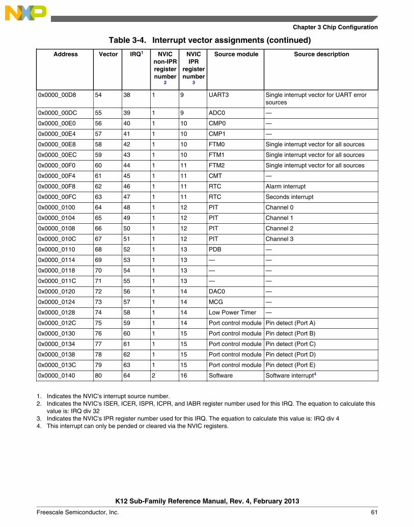
Table 3-4. Interrupt vector assignments (continued)
Address Vector IRQ1 NVICnon-IPRregisternumber
2
NVICIPR
registernumber
3
Source module Source description
0x0000_00D8 54 38 1 9 UART3 Single interrupt vector for UART errorsources
0x0000_00DC 55 39 1 9 ADC0 —
0x0000_00E0 56 40 1 10 CMP0 —
0x0000_00E4 57 41 1 10 CMP1 —
0x0000_00E8 58 42 1 10 FTM0 Single interrupt vector for all sources
0x0000_00EC 59 43 1 10 FTM1 Single interrupt vector for all sources
0x0000_00F0 60 44 1 11 FTM2 Single interrupt vector for all sources
0x0000_00F4 61 45 1 11 CMT —
0x0000_00F8 62 46 1 11 RTC Alarm interrupt
0x0000_00FC 63 47 1 11 RTC Seconds interrupt
0x0000_0100 64 48 1 12 PIT Channel 0
0x0000_0104 65 49 1 12 PIT Channel 1
0x0000_0108 66 50 1 12 PIT Channel 2
0x0000_010C 67 51 1 12 PIT Channel 3
0x0000_0110 68 52 1 13 PDB —
0x0000_0114 69 53 1 13 — —
0x0000_0118 70 54 1 13 — —
0x0000_011C 71 55 1 13 — —
0x0000_0120 72 56 1 14 DAC0 —
0x0000_0124 73 57 1 14 MCG —
0x0000_0128 74 58 1 14 Low Power Timer —
0x0000_012C 75 59 1 14 Port control module Pin detect (Port A)
0x0000_0130 76 60 1 15 Port control module Pin detect (Port B)
0x0000_0134 77 61 1 15 Port control module Pin detect (Port C)
0x0000_0138 78 62 1 15 Port control module Pin detect (Port D)
0x0000_013C 79 63 1 15 Port control module Pin detect (Port E)
0x0000_0140 80 64 2 16 Software Software interrupt4
1. Indicates the NVIC's interrupt source number.2. Indicates the NVIC's ISER, ICER, ISPR, ICPR, and IABR register number used for this IRQ. The equation to calculate this
value is: IRQ div 323. Indicates the NVIC's IPR register number used for this IRQ. The equation to calculate this value is: IRQ div 44. This interrupt can only be pended or cleared via the NVIC registers.
Chapter 3 Chip Configuration
K12 Sub-Family Reference Manual, Rev. 4, February 2013
Freescale Semiconductor, Inc. 61

3.2.2.3.1 Determining the bitfield and register location for configuring aparticular interrupt
Suppose you need to configure the low-power timer (LPTMR) interrupt. The followingtable is an excerpt of the LPTMR row from Interrupt channel assignments.
Table 3-5. LPTMR interrupt vector assignment
Address Vector IRQ1 NVICnon-IPRregisternumber
2
NVICIPR
registernumber
3
Source module Source description
0x0000_0128 74 58 1 14 Low Power Timer —
1. Indicates the NVIC's interrupt source number.2. Indicates the NVIC's ISER, ICER, ISPR, ICPR, and IABR register number used for this IRQ. The equation to calculate this
value is: IRQ div 323. Indicates the NVIC's IPR register number used for this IRQ. The equation to calculate this value is: IRQ div 4
• The NVIC registers you would use to configure the interrupt are:• NVICISER1• NVICICER1• NVICISPR1• NVICICPR1• NVICIABR1• NVICIPR14
• To determine the particular IRQ's bitfield location within these particular registers:• NVICISER1, NVICICER1, NVICISPR1, NVICICPR1, NVICIABR1 bit
location = IRQ mod 32 = 26• NVICIPR14 bitfield starting location = 8 * (IRQ mod 4) + 4 = 20
Since the NVICIPR bitfields are 4-bit wide (16 priority levels), the NVICIPR14bitfield range is 20-23
Therefore, the following bitfield locations are used to configure the LPTMR interrupts:
• NVICISER1[26]• NVICICER1[26]• NVICISPR1[26]• NVICICPR1[26]• NVICIABR1[26]• NVICIPR14[23:20]
Core modules
K12 Sub-Family Reference Manual, Rev. 4, February 2013
62 Freescale Semiconductor, Inc.
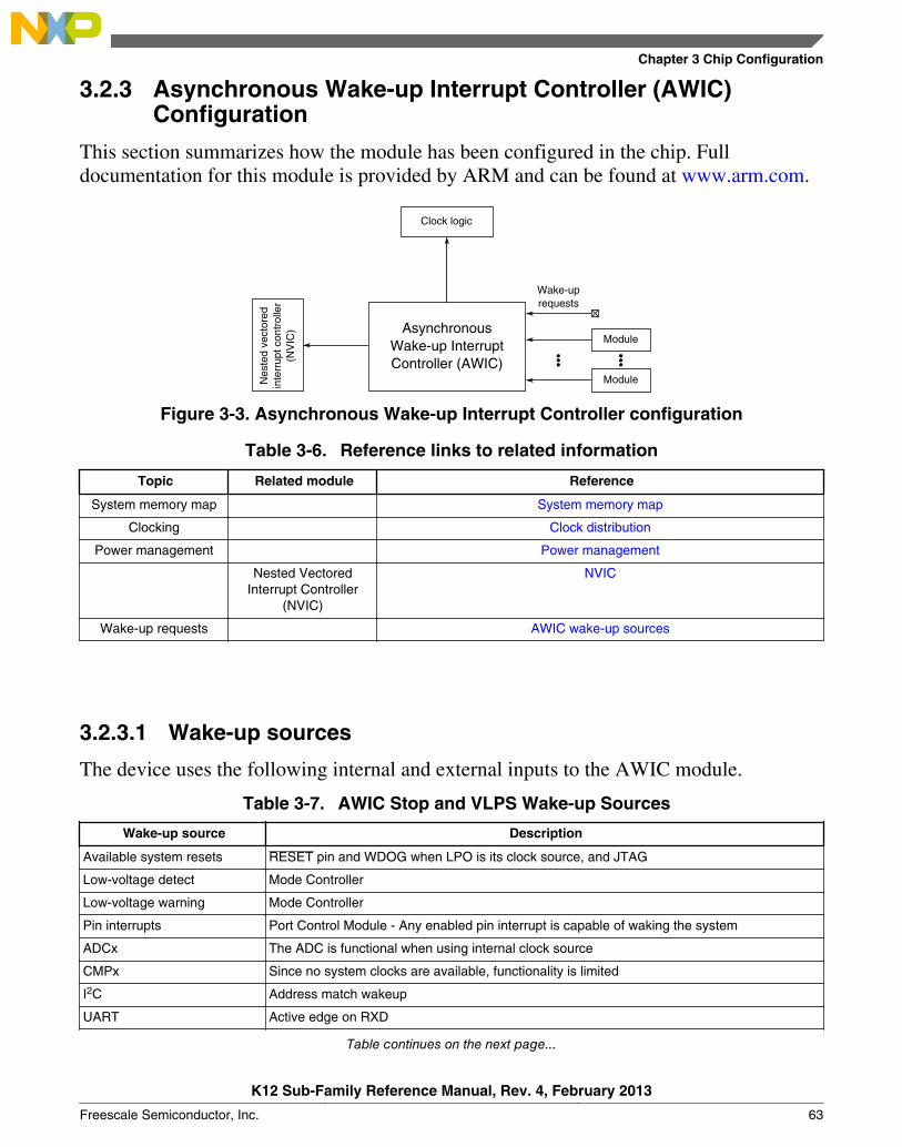
3.2.3 Asynchronous Wake-up Interrupt Controller (AWIC)Configuration
This section summarizes how the module has been configured in the chip. Fulldocumentation for this module is provided by ARM and can be found at www.arm.com.
AsynchronousWake-up InterruptController (AWIC)
Nes
ted
vect
ored
inte
rrup
t con
trol
ler
(NV
IC)
Wake-uprequests
Module
Module
Clock logic
Figure 3-3. Asynchronous Wake-up Interrupt Controller configuration
Table 3-6. Reference links to related information
Topic Related module Reference
System memory map System memory map
Clocking Clock distribution
Power management Power management
Nested VectoredInterrupt Controller
(NVIC)
NVIC
Wake-up requests AWIC wake-up sources
3.2.3.1 Wake-up sources
The device uses the following internal and external inputs to the AWIC module.
Table 3-7. AWIC Stop and VLPS Wake-up Sources
Wake-up source Description
Available system resets RESET pin and WDOG when LPO is its clock source, and JTAG
Low-voltage detect Mode Controller
Low-voltage warning Mode Controller
Pin interrupts Port Control Module - Any enabled pin interrupt is capable of waking the system
ADCx The ADC is functional when using internal clock source
CMPx Since no system clocks are available, functionality is limited
I2C Address match wakeup
UART Active edge on RXD
Table continues on the next page...
Chapter 3 Chip Configuration
K12 Sub-Family Reference Manual, Rev. 4, February 2013
Freescale Semiconductor, Inc. 63
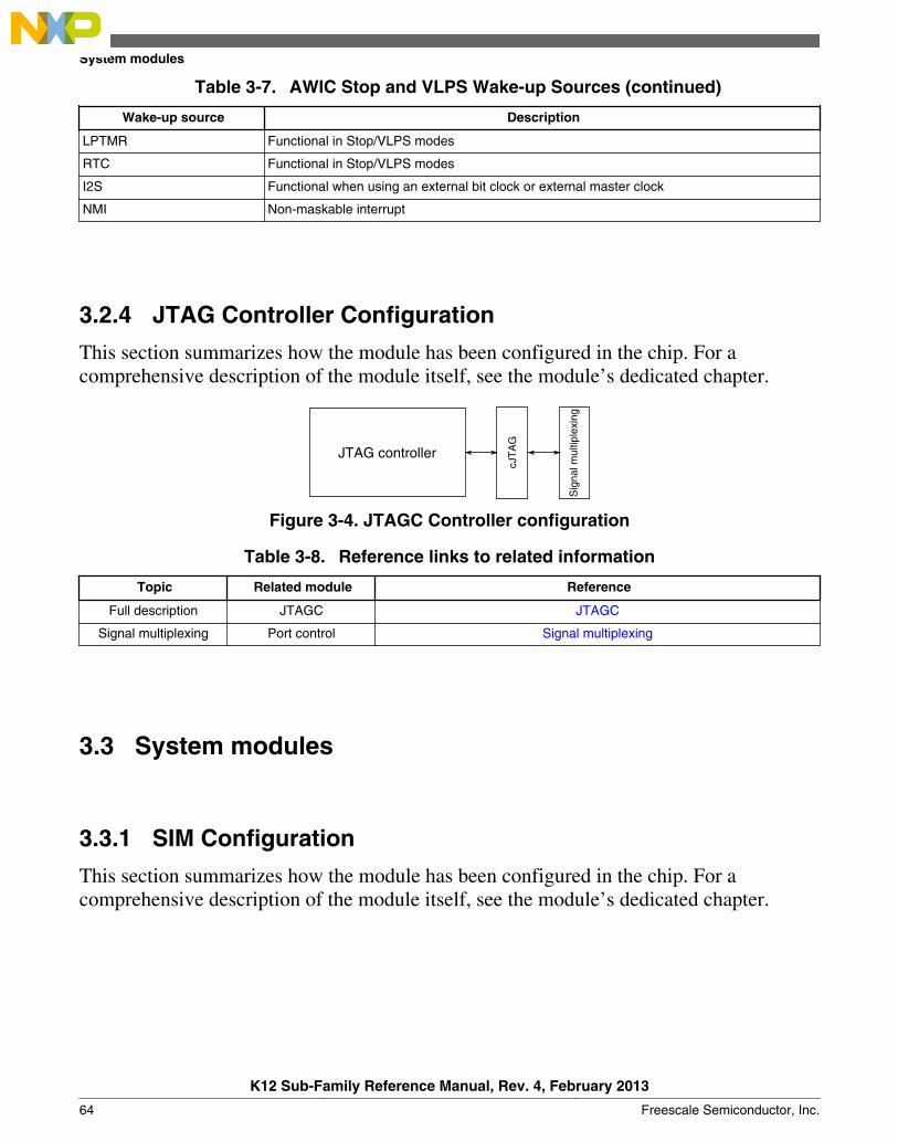
Table 3-7. AWIC Stop and VLPS Wake-up Sources (continued)
Wake-up source Description
LPTMR Functional in Stop/VLPS modes
RTC Functional in Stop/VLPS modes
I2S Functional when using an external bit clock or external master clock
NMI Non-maskable interrupt
3.2.4 JTAG Controller Configuration
This section summarizes how the module has been configured in the chip. For acomprehensive description of the module itself, see the module’s dedicated chapter.
Sig
nal m
ultip
lexi
ng
JTAG controller
cJT
AG
Figure 3-4. JTAGC Controller configuration
Table 3-8. Reference links to related information
Topic Related module Reference
Full description JTAGC JTAGC
Signal multiplexing Port control Signal multiplexing
3.3 System modules
3.3.1 SIM Configuration
This section summarizes how the module has been configured in the chip. For acomprehensive description of the module itself, see the module’s dedicated chapter.
System modules
K12 Sub-Family Reference Manual, Rev. 4, February 2013
64 Freescale Semiconductor, Inc.

Registeraccess
Peripheralbridge
System integrationmodule (SIM)
Figure 3-5. SIM configuration
Table 3-9. Reference links to related information
Topic Related module Reference
Full description SIM SIM
System memory map System memory map
Clocking Clock distribution
Power management Power management
3.3.2 System Mode Controller (SMC) Configuration
This section summarizes how the module has been configured in the chip. For acomprehensive description of the module itself, see the module’s dedicated chapter.
Pow
er M
anag
emen
tC
ontr
olle
r (P
MC
)
Registeraccess
Peripheralbridge
System ModeController (SMC)
Resets
Figure 3-6. System Mode Controller configuration
Table 3-10. Reference links to related information
Topic Related module Reference
Full description System ModeController (SMC)
SMC
System memory map System memory map
Power management Power management
Table continues on the next page...
Chapter 3 Chip Configuration
K12 Sub-Family Reference Manual, Rev. 4, February 2013
Freescale Semiconductor, Inc. 65
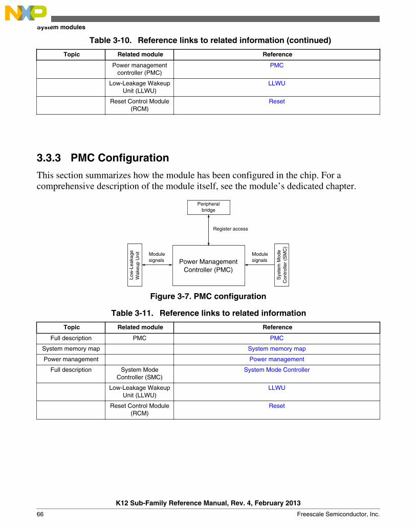
Table 3-10. Reference links to related information (continued)
Topic Related module Reference
Power managementcontroller (PMC)
PMC
Low-Leakage WakeupUnit (LLWU)
LLWU
Reset Control Module(RCM)
Reset
3.3.3 PMC Configuration
This section summarizes how the module has been configured in the chip. For acomprehensive description of the module itself, see the module’s dedicated chapter.
Register access
Power ManagementController (PMC)
Modulesignals
Peripheralbridge
Modulesignals
Sys
tem
Mod
eC
ontr
olle
r (S
MC
)
Low
-Lea
kage
Wak
eup
Uni
t
Figure 3-7. PMC configuration
Table 3-11. Reference links to related information
Topic Related module Reference
Full description PMC PMC
System memory map System memory map
Power management Power management
Full description System ModeController (SMC)
System Mode Controller
Low-Leakage WakeupUnit (LLWU)
LLWU
Reset Control Module(RCM)
Reset
System modules
K12 Sub-Family Reference Manual, Rev. 4, February 2013
66 Freescale Semiconductor, Inc.

3.3.4 Low-Leakage Wake-up Unit (LLWU) Configuration
This section summarizes how the module has been configured in the chip. For acomprehensive description of the module itself, see the module’s dedicated chapter.
Low-Leakage Wake-upUnit (LLWU)
Pow
er M
anag
emen
tC
ontr
olle
r (P
MC
)
Peripheralbridge 0
Registeraccess
Wake-uprequests
Module
Module
Figure 3-8. Low-Leakage Wake-up Unit configuration
Table 3-12. Reference links to related information
Topic Related module Reference
Full description LLWU LLWU
System memory map System memory map
Clocking Clock distribution
Power management Power management chapter
Power ManagementController (PMC)
Power Management Controller (PMC)
Mode Controller Mode Controller
Wake-up requests LLWU wake-up sources
3.3.4.1 Wake-up Sources
This chip uses the following internal peripheral and external pin inputs as wakeupsources to the LLWU module:
• LLWU_P0-15 are external pin inputs. Any digital function multiplexed on the pincan be selected as the wakeup source. See the chip's signal multiplexing table for thedigital signal options.
• LLWU_M0IF-M7IF are connections to the internal peripheral interrupt flags.
NOTERESET is also a wakeup source, depending on the bit setting inthe LLWU_RST register. On devices where RESET is not adedicated pin, it must also be enabled in the explicit port muxcontrol.
Chapter 3 Chip Configuration
K12 Sub-Family Reference Manual, Rev. 4, February 2013
Freescale Semiconductor, Inc. 67
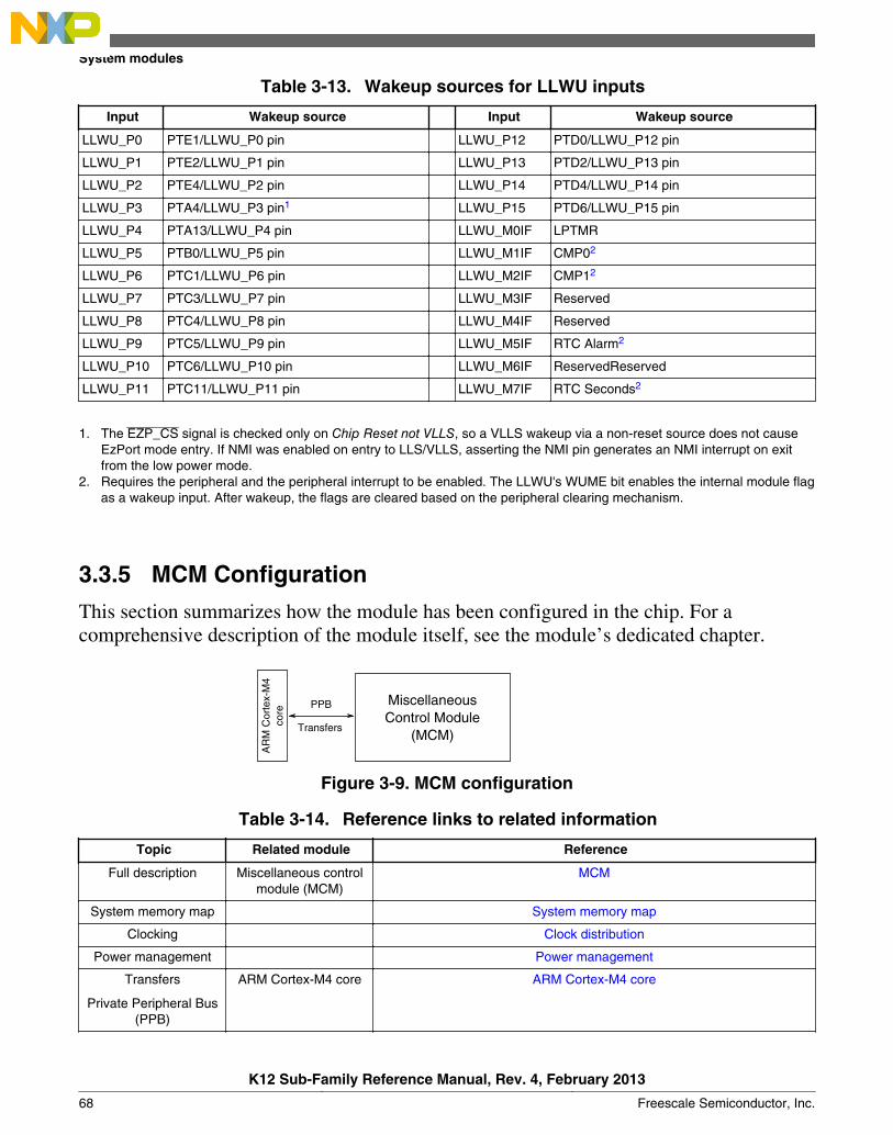
Table 3-13. Wakeup sources for LLWU inputs
Input Wakeup source Input Wakeup source
LLWU_P0 PTE1/LLWU_P0 pin LLWU_P12 PTD0/LLWU_P12 pin
LLWU_P1 PTE2/LLWU_P1 pin LLWU_P13 PTD2/LLWU_P13 pin
LLWU_P2 PTE4/LLWU_P2 pin LLWU_P14 PTD4/LLWU_P14 pin
LLWU_P3 PTA4/LLWU_P3 pin1 LLWU_P15 PTD6/LLWU_P15 pin
LLWU_P4 PTA13/LLWU_P4 pin LLWU_M0IF LPTMR
LLWU_P5 PTB0/LLWU_P5 pin LLWU_M1IF CMP02
LLWU_P6 PTC1/LLWU_P6 pin LLWU_M2IF CMP12
LLWU_P7 PTC3/LLWU_P7 pin LLWU_M3IF Reserved
LLWU_P8 PTC4/LLWU_P8 pin LLWU_M4IF Reserved
LLWU_P9 PTC5/LLWU_P9 pin LLWU_M5IF RTC Alarm2
LLWU_P10 PTC6/LLWU_P10 pin LLWU_M6IF ReservedReserved
LLWU_P11 PTC11/LLWU_P11 pin LLWU_M7IF RTC Seconds2
1. The EZP_CS signal is checked only on Chip Reset not VLLS, so a VLLS wakeup via a non-reset source does not causeEzPort mode entry. If NMI was enabled on entry to LLS/VLLS, asserting the NMI pin generates an NMI interrupt on exitfrom the low power mode.
2. Requires the peripheral and the peripheral interrupt to be enabled. The LLWU's WUME bit enables the internal module flagas a wakeup input. After wakeup, the flags are cleared based on the peripheral clearing mechanism.
3.3.5 MCM Configuration
This section summarizes how the module has been configured in the chip. For acomprehensive description of the module itself, see the module’s dedicated chapter.
MiscellaneousControl Module
(MCM)Transfers
AR
M C
orte
x-M
4co
re
PPB
Figure 3-9. MCM configuration
Table 3-14. Reference links to related information
Topic Related module Reference
Full description Miscellaneous controlmodule (MCM)
MCM
System memory map System memory map
Clocking Clock distribution
Power management Power management
Transfers
Private Peripheral Bus(PPB)
ARM Cortex-M4 core ARM Cortex-M4 core
System modules
K12 Sub-Family Reference Manual, Rev. 4, February 2013
68 Freescale Semiconductor, Inc.

3.3.6 Crossbar-Light Switch Configuration
This section summarizes how the module has been configured in the chip. For acomprehensive description of the module itself, see the module’s dedicated chapter.
Crossbar Switch
Slave ModulesMaster Modules
M2
M0
M1
S0
S3
ARM corecode bus
ARM coresystem bus
DMA
EzPort
Mux
Flash controller
S1 SRAM
controller_L
S2
Mux
Peripheralbridge 0
GPIOcontroller
SRAM controller_U
Figure 3-10. Crossbar-Light switch integration
Table 3-15. Reference links to related information
Topic Related module Reference
Full description Crossbar switch Crossbar Switch
System memory map System memory map
Clocking Clock Distribution
Crossbar switch master ARM Cortex-M4 core ARM Cortex-M4 core
Crossbar switch master DMA controller DMA controller
Crossbar switch master EzPort EzPort
Table continues on the next page...
Chapter 3 Chip Configuration
K12 Sub-Family Reference Manual, Rev. 4, February 2013
Freescale Semiconductor, Inc. 69

Table 3-15. Reference links to related information (continued)
Topic Related module Reference
Crossbar switch slave Flash Flash
Crossbar switch slaves SRAM controllers SRAM configuration
Crossbar switch slave Peripheral bridges Peripheral bridge
Crossbar switch slave GPIO controller GPIO controller
3.3.6.1 Crossbar-Light Switch Master Assignments
The masters connected to the crossbar switch are assigned as follows:
Master module Master port number
ARM core code bus 0
ARM core system bus 1
DMA/EzPort 2
NOTEThe DMA and EzPort share a master port. Since these modulesnever operate at the same time, no configuration or arbitrationexplanations are necessary.
3.3.6.2 Crossbar-Light Switch Slave Assignments
The slaves connected to the crossbar switch are assigned as follows:
Slave module Slave port number
Flash memory controller 0
SRAM controllers 1,2
Peripheral bridge 0/GPIO 3
3.3.7 Peripheral Bridge Configuration
This section summarizes how the module has been configured in the chip. For acomprehensive description of the module itself, see the module’s dedicated chapter.
System modules
K12 Sub-Family Reference Manual, Rev. 4, February 2013
70 Freescale Semiconductor, Inc.

Per
iphe
rals
TransfersAIPS-Liteperipheral bridge
Transfers
Cro
ssba
r sw
itch
Figure 3-11. Peripheral bridge configuration
Table 3-16. Reference links to related information
Topic Related module Reference
Full description Peripheral bridge(AIPS-Lite)
Peripheral bridge (AIPS-Lite)
System memory map System memory map
Clocking Clock Distribution
Crossbar switch Crossbar switch Crossbar switch
3.3.7.1 Number of peripheral bridges
This device contains one peripheral bridge.
3.3.7.2 Memory maps
The peripheral bridges are used to access the registers of most of the modules on thisdevice. See AIPS0 Memory Map for the memory slot assignment for each module.
3.3.8 DMA request multiplexer configuration
This section summarizes how the module has been configured in the chip. For acomprehensive description of the module itself, see the module’s dedicated chapter.
Chapter 3 Chip Configuration
K12 Sub-Family Reference Manual, Rev. 4, February 2013
Freescale Semiconductor, Inc. 71

DMA RequestMultiplexer
DM
A c
ontr
olle
r
RequestsModule
Module
Module
Peripheralbridge 0
Registeraccess
Channelrequest
Figure 3-12. DMA request multiplexer configuration
Table 3-17. Reference links to related information
Topic Related module Reference
Full description DMA requestmultiplexer
DMA Mux
System memory map System memory map
Clocking Clock distribution
Power management Power management
Channel request DMA controller DMA Controller
Requests DMA request sources
3.3.8.1 DMA MUX request sources
Because of the mux there is not a hard correlation between any of the DMA requestsources and a specific DMA channel.
Table 3-18. DMA request sources - MUX 0
Sourcenumber
Source module Source description
0 — Channel disabled1
1 Reserved Not used
2 UART0 Receive
3 UART0 Transmit
4 UART1 Receive
5 UART1 Transmit
6 UART2 Receive
7 UART2 Transmit
8 UART3 Receive
9 UART3 Transmit
10 Reserved Receive
Table continues on the next page...
System modules
K12 Sub-Family Reference Manual, Rev. 4, February 2013
72 Freescale Semiconductor, Inc.
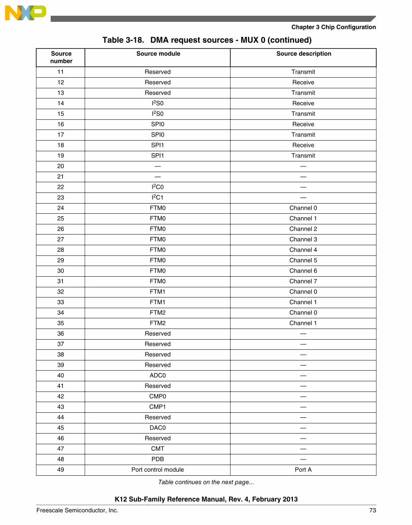
Table 3-18. DMA request sources - MUX 0 (continued)
Sourcenumber
Source module Source description
11 Reserved Transmit
12 Reserved Receive
13 Reserved Transmit
14 I2S0 Receive
15 I2S0 Transmit
16 SPI0 Receive
17 SPI0 Transmit
18 SPI1 Receive
19 SPI1 Transmit
20 — —
21 — —
22 I2C0 —
23 I2C1 —
24 FTM0 Channel 0
25 FTM0 Channel 1
26 FTM0 Channel 2
27 FTM0 Channel 3
28 FTM0 Channel 4
29 FTM0 Channel 5
30 FTM0 Channel 6
31 FTM0 Channel 7
32 FTM1 Channel 0
33 FTM1 Channel 1
34 FTM2 Channel 0
35 FTM2 Channel 1
36 Reserved —
37 Reserved —
38 Reserved —
39 Reserved —
40 ADC0 —
41 Reserved —
42 CMP0 —
43 CMP1 —
44 Reserved —
45 DAC0 —
46 Reserved —
47 CMT —
48 PDB —
49 Port control module Port A
Table continues on the next page...
Chapter 3 Chip Configuration
K12 Sub-Family Reference Manual, Rev. 4, February 2013
Freescale Semiconductor, Inc. 73
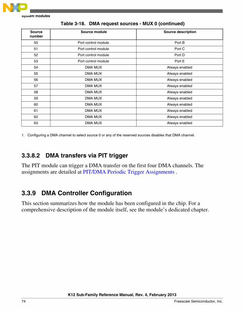
Table 3-18. DMA request sources - MUX 0 (continued)
Sourcenumber
Source module Source description
50 Port control module Port B
51 Port control module Port C
52 Port control module Port D
53 Port control module Port E
54 DMA MUX Always enabled
55 DMA MUX Always enabled
56 DMA MUX Always enabled
57 DMA MUX Always enabled
58 DMA MUX Always enabled
59 DMA MUX Always enabled
60 DMA MUX Always enabled
61 DMA MUX Always enabled
62 DMA MUX Always enabled
63 DMA MUX Always enabled
1. Configuring a DMA channel to select source 0 or any of the reserved sources disables that DMA channel.
3.3.8.2 DMA transfers via PIT trigger
The PIT module can trigger a DMA transfer on the first four DMA channels. Theassignments are detailed at PIT/DMA Periodic Trigger Assignments .
3.3.9 DMA Controller Configuration
This section summarizes how the module has been configured in the chip. For acomprehensive description of the module itself, see the module’s dedicated chapter.
System modules
K12 Sub-Family Reference Manual, Rev. 4, February 2013
74 Freescale Semiconductor, Inc.
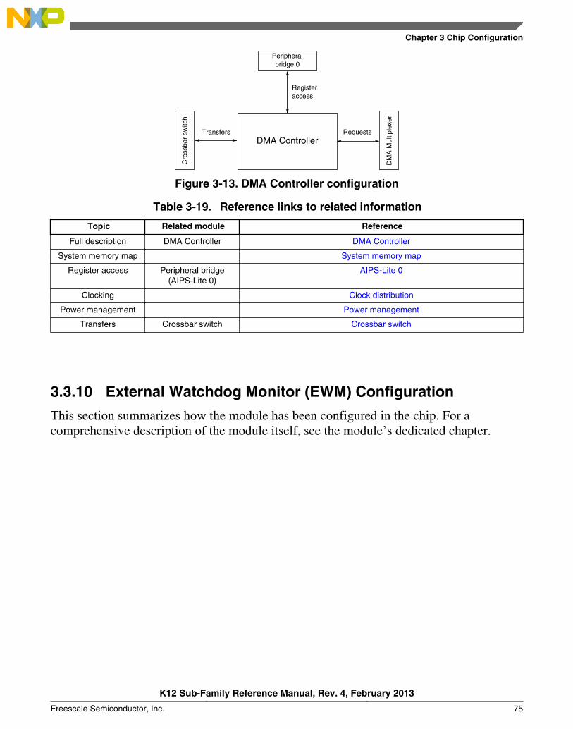
DMA Controller
Cro
ssba
r sw
itch
Requests
Peripheralbridge 0
Registeraccess
Transfers
DM
A M
ultip
lexe
r
Figure 3-13. DMA Controller configuration
Table 3-19. Reference links to related information
Topic Related module Reference
Full description DMA Controller DMA Controller
System memory map System memory map
Register access Peripheral bridge(AIPS-Lite 0)
AIPS-Lite 0
Clocking Clock distribution
Power management Power management
Transfers Crossbar switch Crossbar switch
3.3.10 External Watchdog Monitor (EWM) Configuration
This section summarizes how the module has been configured in the chip. For acomprehensive description of the module itself, see the module’s dedicated chapter.
Chapter 3 Chip Configuration
K12 Sub-Family Reference Manual, Rev. 4, February 2013
Freescale Semiconductor, Inc. 75

External WatchdogMonitor (EWM)
Peripheralbridge 0
Registeraccess
Sig
nal m
ultip
lexi
ng
Module signals
Figure 3-14. External Watchdog Monitor configuration
Table 3-20. Reference links to related information
Topic Related module Reference
Full description External WatchdogMonitor (EWM)
EWM
System memory map System memory map
Clocking Clock distribution
Power management Power management
Signal multiplexing Port Control Module Signal multiplexing
3.3.10.1 EWM clocks
This table shows the EWM clocks and the corresponding chip clocks.
Table 3-21. EWM clock connections
Module clock Chip clock
Low Power Clock 1 kHz LPO Clock
3.3.10.2 EWM low-power modes
This table shows the EWM low-power modes and the corresponding chip low-powermodes.
Table 3-22. EWM low-power modes
Module mode Chip mode
Wait Wait, VLPW
Stop Stop, VLPS, LLS
System modules
K12 Sub-Family Reference Manual, Rev. 4, February 2013
76 Freescale Semiconductor, Inc.

3.3.10.3 EWM_OUT pin state in low power modes
During Wait, Stop, and Power Down modes the EWM_OUT pin preserve its state beforeentering Wait or Stop mode. When the CPU enters a Run mode from Wait or Stoprecovery, the pin resumes its previous state before entering Wait or Stop mode. When theCPU enters Run mode from Power Down, the pin returns to its reset state.
3.3.11 Watchdog Configuration
This section summarizes how the module has been configured in the chip. For acomprehensive description of the module itself, see the module’s dedicated chapter.
WDOG
Mod
e C
ontr
olle
r
Peripheralbridge 0
Registeraccess
Figure 3-15. Watchdog configuration
Table 3-23. Reference links to related information
Topic Related module Reference
Full description Watchdog Watchdog
System memory map System memory map
Clocking Clock distribution
Power management Power management
Mode Controller (MC)
3.3.11.1 WDOG clocks
This table shows the WDOG module clocks and the corresponding chip clocks.
Chapter 3 Chip Configuration
K12 Sub-Family Reference Manual, Rev. 4, February 2013
Freescale Semiconductor, Inc. 77
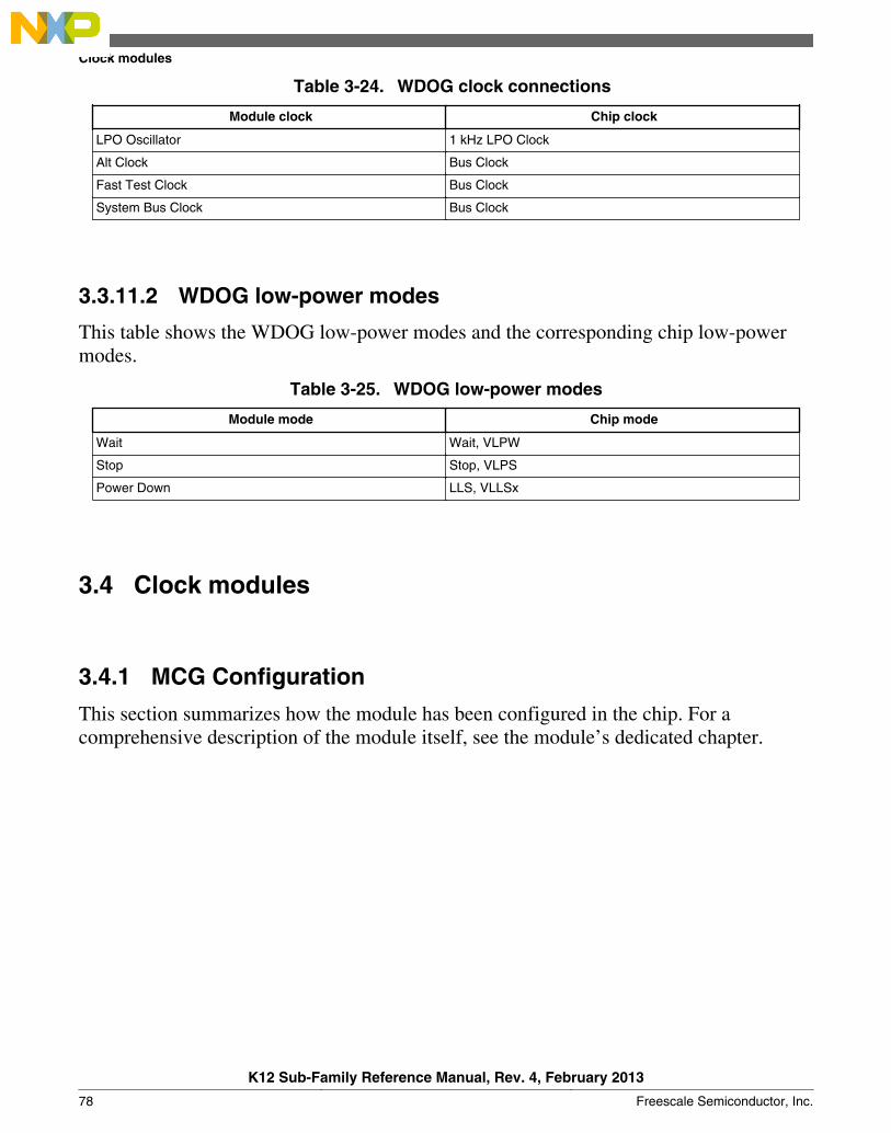
Table 3-24. WDOG clock connections
Module clock Chip clock
LPO Oscillator 1 kHz LPO Clock
Alt Clock Bus Clock
Fast Test Clock Bus Clock
System Bus Clock Bus Clock
3.3.11.2 WDOG low-power modes
This table shows the WDOG low-power modes and the corresponding chip low-powermodes.
Table 3-25. WDOG low-power modes
Module mode Chip mode
Wait Wait, VLPW
Stop Stop, VLPS
Power Down LLS, VLLSx
3.4 Clock modules
3.4.1 MCG Configuration
This section summarizes how the module has been configured in the chip. For acomprehensive description of the module itself, see the module’s dedicated chapter.
Clock modules
K12 Sub-Family Reference Manual, Rev. 4, February 2013
78 Freescale Semiconductor, Inc.
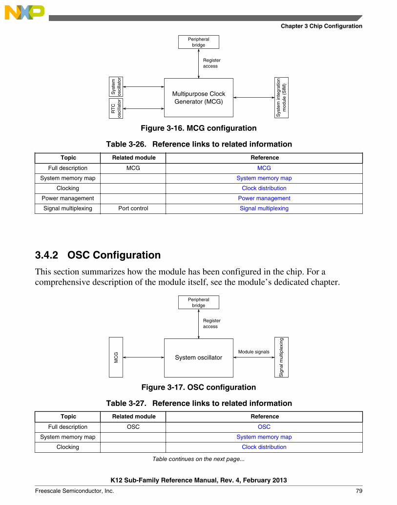
Registeraccess
Peripheralbridge
Multipurpose ClockGenerator (MCG)
RT
Cos
cilla
tor
Sys
tem
osci
llato
r
Sys
tem
inte
grat
ion
mod
ule
(SIM
)
Figure 3-16. MCG configuration
Table 3-26. Reference links to related information
Topic Related module Reference
Full description MCG MCG
System memory map System memory map
Clocking Clock distribution
Power management Power management
Signal multiplexing Port control Signal multiplexing
3.4.2 OSC Configuration
This section summarizes how the module has been configured in the chip. For acomprehensive description of the module itself, see the module’s dedicated chapter.
Sig
nal m
ultip
lexi
ng
Registeraccess
Peripheralbridge
System oscillator
MC
G Module signals
Figure 3-17. OSC configuration
Table 3-27. Reference links to related information
Topic Related module Reference
Full description OSC OSC
System memory map System memory map
Clocking Clock distribution
Table continues on the next page...
Chapter 3 Chip Configuration
K12 Sub-Family Reference Manual, Rev. 4, February 2013
Freescale Semiconductor, Inc. 79
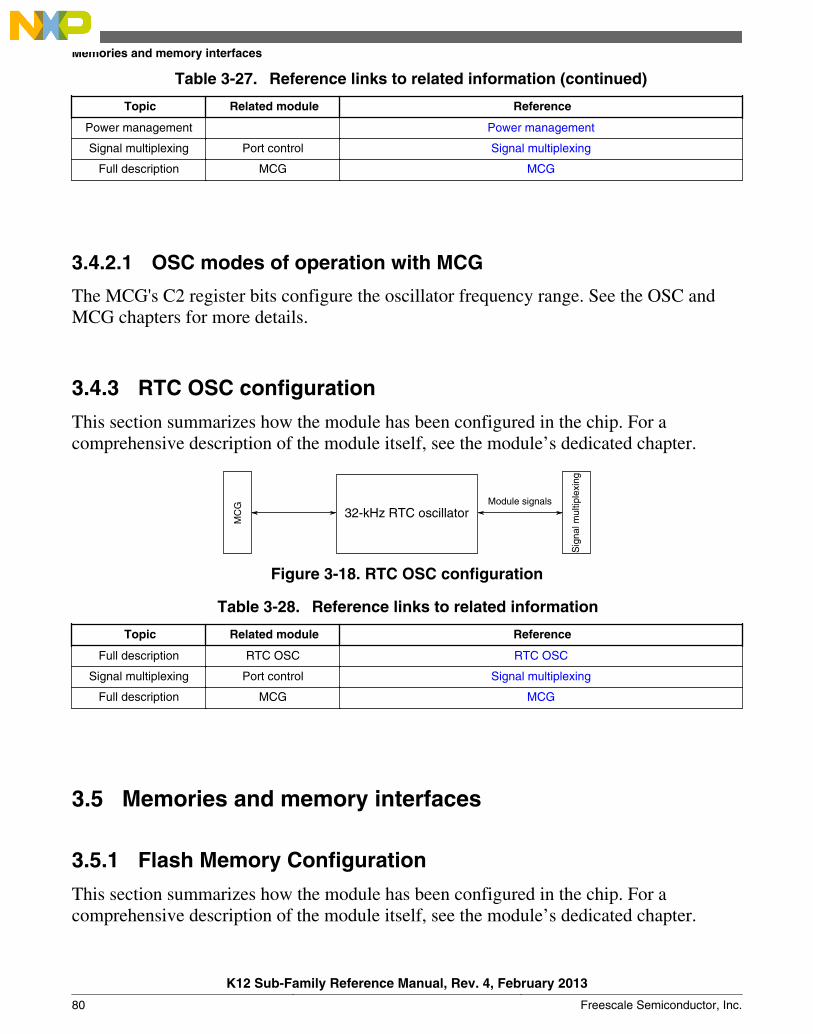
Table 3-27. Reference links to related information (continued)
Topic Related module Reference
Power management Power management
Signal multiplexing Port control Signal multiplexing
Full description MCG MCG
3.4.2.1 OSC modes of operation with MCG
The MCG's C2 register bits configure the oscillator frequency range. See the OSC andMCG chapters for more details.
3.4.3 RTC OSC configuration
This section summarizes how the module has been configured in the chip. For acomprehensive description of the module itself, see the module’s dedicated chapter.
Sig
nal m
ultip
lexi
ng
32-kHz RTC oscillator
MC
G Module signals
Figure 3-18. RTC OSC configuration
Table 3-28. Reference links to related information
Topic Related module Reference
Full description RTC OSC RTC OSC
Signal multiplexing Port control Signal multiplexing
Full description MCG MCG
3.5 Memories and memory interfaces
3.5.1 Flash Memory Configuration
This section summarizes how the module has been configured in the chip. For acomprehensive description of the module itself, see the module’s dedicated chapter.
Memories and memory interfaces
K12 Sub-Family Reference Manual, Rev. 4, February 2013
80 Freescale Semiconductor, Inc.

Registeraccess
Flash memoryTransfers
Fla
sh m
emor
yco
ntro
ller
Peripheral buscontroller 0
Figure 3-19. Flash memory configuration
Table 3-29. Reference links to related information
Topic Related module Reference
Full description Flash memory Flash memory
System memory map System memory map
Clocking Clock Distribution
Transfers Flash memorycontroller
Flash memory controller
Register access Peripheral bridge Peripheral bridge
3.5.1.1 Flash memory types
This device contains the following types of flash memory:
• Program flash memory — non-volatile flash memory that can execute program code• FlexMemory — encompasses the following memory types:
• For devices with FlexNVM: FlexNVM — Non-volatile flash memory that canexecute program code, store data, or backup EEPROM data
• For devices with FlexNVM: FlexRAM — RAM memory that can be used astraditional RAM or as high-endurance EEPROM storage, and also acceleratesflash programming
• For devices with only program flash memory: Programming acceleration RAM— RAM memory that accelerates flash programming
3.5.1.2 Flash Memory Sizes
The devices covered in this document contain:
• For devices with program flash only: 2 blocks of program flash consisting of 2 KBsectors
Chapter 3 Chip Configuration
K12 Sub-Family Reference Manual, Rev. 4, February 2013
Freescale Semiconductor, Inc. 81

• For devices that contain FlexNVM: 1 block of program flash consisting of 2 KBsectors
• For devices that contain FlexNVM: 1 block of FlexNVM consisting of 2 KB sectors• For devices that contain FlexNVM: 1 block of FlexRAM
The amounts of flash memory for the devices covered in this document are:
Device Programflash (KB)
Block 0 (P-Flash)
addressrange
FlexNVM(KB)
Block 1(FlexNVM/ P-
Flash)addressrange1
FlexRAM/ProgrammingAcceleration
RAM (KB)
FlexRAM/ProgrammingAccelerationRAM address
range
MK12DX128VMC5
128 0x0000_0000–0x0001_FFFF
64 0x1000_0000–0x1000_FFFF
4 0x1400_0000–0x1400_0FFF
MK12DX256VMC5
256 0x0000_0000–0x0003_FFFF
64 0x1000_0000–0x1000_FFFF
4 0x1400_0000–0x1400_0FFF
MK12DN512VMC5
512 0x0000_0000–0x0003_FFFF
— 0x0004_0000–0x0007_FFFF
4 0x1400_0000–0x1400_0FFF
3.5.1.3 Flash Memory Size Considerations
Since this document covers devices that contain program flash only and devices thatcontain program flash and FlexNVM, there are some items to consider when reading theflash memory chapter.
• The flash memory chapter shows a mixture of information depending on the deviceyou are using.
• For the program flash only devices:• The programming acceleration RAM is used for the Program Section command.
• For the devices containing program flash and FlexNVM:• Since there is only one program flash block, the program flash swap feature is
not available.
3.5.1.4 Flash Memory Map
The various flash memories and the flash registers are located at different base addressesas shown in the following figure. The base address for each is specified in Systemmemory map.
Memories and memory interfaces
K12 Sub-Family Reference Manual, Rev. 4, February 2013
82 Freescale Semiconductor, Inc.

Program flash
Flash configuration fieldProgram flash base address
Flash memory base addressRegisters
RAM
Programming acceleration RAM base address
Figure 3-20. Flash memory map for devices containing only program flash
Program flash
Flash configuration field
FlexNVM base address
Program flash base address
Flash memory base addressRegisters
FlexNVM
FlexRAM
FlexRAM base address
Figure 3-21. Flash memory map for devices containing FlexNVM
3.5.1.5 Flash Security
How flash security is implemented on this device is described in Chip Security.
3.5.1.6 Flash Modes
The flash memory operates in NVM normal and NVM special modes. The flash memoryenters NVM special mode when the EzPort is enabled (EZP_CS asserted during reset).Otherwise, flash memory operates in NVM normal mode.
3.5.1.7 Erase All Flash Contents
In addition to software, the entire flash memory may be erased external to the flashmemory in two ways:
Chapter 3 Chip Configuration
K12 Sub-Family Reference Manual, Rev. 4, February 2013
Freescale Semiconductor, Inc. 83

1. Via the EzPort by issuing a bulk erase (BE) command. See the EzPort chapter formore details.
2. Via the SWJ-DP debug port by setting DAP_CONTROL[0]. DAP_STATUS[0] is setto indicate the mass erase command has been accepted. DAP_STATUS[0] is clearedwhen the mass erase completes.
3.5.1.8 FTFL_FOPT Register
The flash memory's FTFL_FOPT register allows the user to customize the operation ofthe MCU at boot time. See FOPT boot options for details of its definition.
3.5.2 Flash Memory Controller Configuration
This section summarizes how the module has been configured in the chip. For acomprehensive description of the module itself, see the module’s dedicated chapter.
Registeraccess
Flash memorycontroller
Transfers
Peripheral buscontroller 0
TransfersF
lash
mem
ory
Cro
ssba
r sw
itch
Figure 3-22. Flash memory controller configuration
Table 3-30. Reference links to related information
Topic Related module Reference
Full description Flash memorycontroller
Flash memory controller
System memory map System memory map
Clocking Clock Distribution
Transfers Flash memory Flash memory
Transfers Crossbar switch Crossbar Switch
Register access Peripheral bridge Peripheral bridge
Memories and memory interfaces
K12 Sub-Family Reference Manual, Rev. 4, February 2013
84 Freescale Semiconductor, Inc.
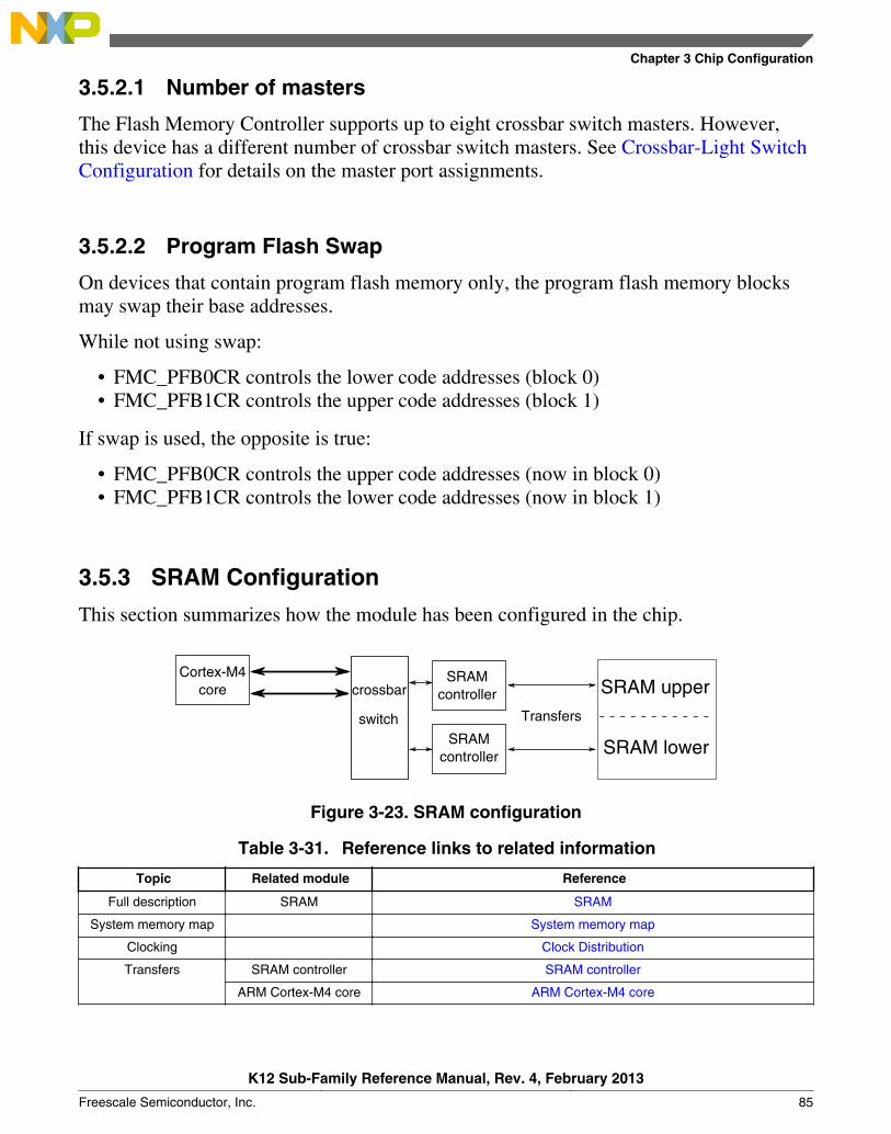
3.5.2.1 Number of masters
The Flash Memory Controller supports up to eight crossbar switch masters. However,this device has a different number of crossbar switch masters. See Crossbar-Light SwitchConfiguration for details on the master port assignments.
3.5.2.2 Program Flash Swap
On devices that contain program flash memory only, the program flash memory blocksmay swap their base addresses.
While not using swap:
• FMC_PFB0CR controls the lower code addresses (block 0)• FMC_PFB1CR controls the upper code addresses (block 1)
If swap is used, the opposite is true:
• FMC_PFB0CR controls the upper code addresses (now in block 0)• FMC_PFB1CR controls the lower code addresses (now in block 1)
3.5.3 SRAM Configuration
This section summarizes how the module has been configured in the chip.
SRAM upperTransfers
Cortex-M4core
switch
SRAM lower
crossbarSRAM
controller
SRAM controller
Figure 3-23. SRAM configuration
Table 3-31. Reference links to related information
Topic Related module Reference
Full description SRAM SRAM
System memory map System memory map
Clocking Clock Distribution
Transfers SRAM controller SRAM controller
ARM Cortex-M4 core ARM Cortex-M4 core
Chapter 3 Chip Configuration
K12 Sub-Family Reference Manual, Rev. 4, February 2013
Freescale Semiconductor, Inc. 85
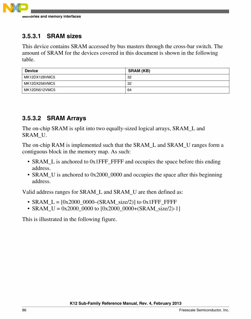
3.5.3.1 SRAM sizes
This device contains SRAM accessed by bus masters through the cross-bar switch. Theamount of SRAM for the devices covered in this document is shown in the followingtable.
Device SRAM (KB)
MK12DX128VMC5 32
MK12DX256VMC5 32
MK12DN512VMC5 64
3.5.3.2 SRAM Arrays
The on-chip SRAM is split into two equally-sized logical arrays, SRAM_L andSRAM_U.
The on-chip RAM is implemented such that the SRAM_L and SRAM_U ranges form acontiguous block in the memory map. As such:
• SRAM_L is anchored to 0x1FFF_FFFF and occupies the space before this endingaddress.
• SRAM_U is anchored to 0x2000_0000 and occupies the space after this beginningaddress.
Valid address ranges for SRAM_L and SRAM_U are then defined as:
• SRAM_L = [0x2000_0000–(SRAM_size/2)] to 0x1FFF_FFFF• SRAM_U = 0x2000_0000 to [0x2000_0000+(SRAM_size/2)-1]
This is illustrated in the following figure.
Memories and memory interfaces
K12 Sub-Family Reference Manual, Rev. 4, February 2013
86 Freescale Semiconductor, Inc.
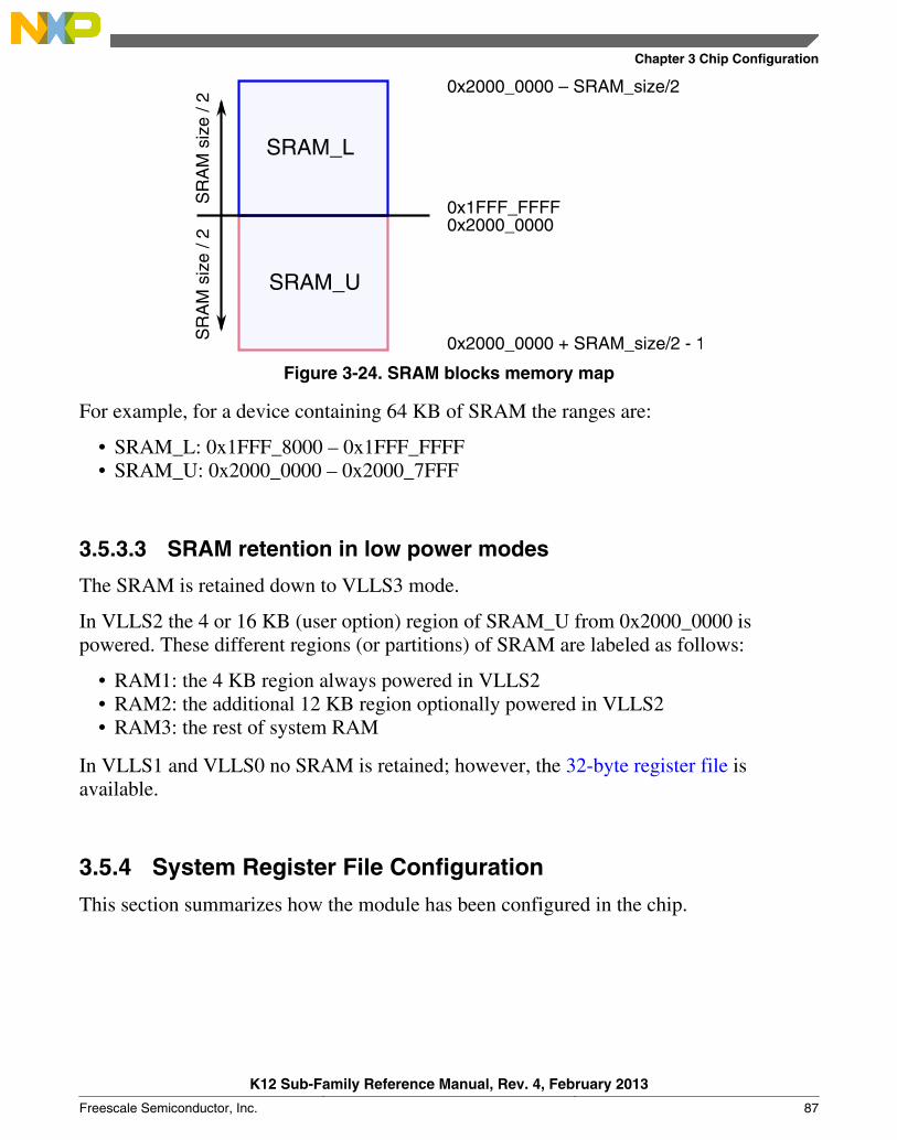
SRAM_U
0x2000_0000S
RA
M s
ize
/ 2
SRAM_L
0x1FFF_FFFFS
RA
M s
ize
/ 2
0x2000_0000 – SRAM_size/2
0x2000_0000 + SRAM_size/2 - 1
Figure 3-24. SRAM blocks memory map
For example, for a device containing 64 KB of SRAM the ranges are:
• SRAM_L: 0x1FFF_8000 – 0x1FFF_FFFF• SRAM_U: 0x2000_0000 – 0x2000_7FFF
3.5.3.3 SRAM retention in low power modes
The SRAM is retained down to VLLS3 mode.
In VLLS2 the 4 or 16 KB (user option) region of SRAM_U from 0x2000_0000 ispowered. These different regions (or partitions) of SRAM are labeled as follows:
• RAM1: the 4 KB region always powered in VLLS2• RAM2: the additional 12 KB region optionally powered in VLLS2• RAM3: the rest of system RAM
In VLLS1 and VLLS0 no SRAM is retained; however, the 32-byte register file isavailable.
3.5.4 System Register File Configuration
This section summarizes how the module has been configured in the chip.
Chapter 3 Chip Configuration
K12 Sub-Family Reference Manual, Rev. 4, February 2013
Freescale Semiconductor, Inc. 87
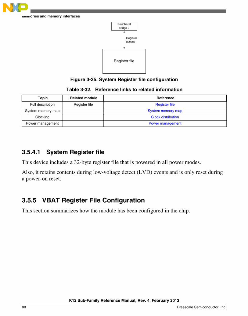
Register file
Peripheralbridge 0
Registeraccess
Figure 3-25. System Register file configuration
Table 3-32. Reference links to related information
Topic Related module Reference
Full description Register file Register file
System memory map System memory map
Clocking Clock distribution
Power management Power management
3.5.4.1 System Register file
This device includes a 32-byte register file that is powered in all power modes.
Also, it retains contents during low-voltage detect (LVD) events and is only reset duringa power-on reset.
3.5.5 VBAT Register File Configuration
This section summarizes how the module has been configured in the chip.
Memories and memory interfaces
K12 Sub-Family Reference Manual, Rev. 4, February 2013
88 Freescale Semiconductor, Inc.
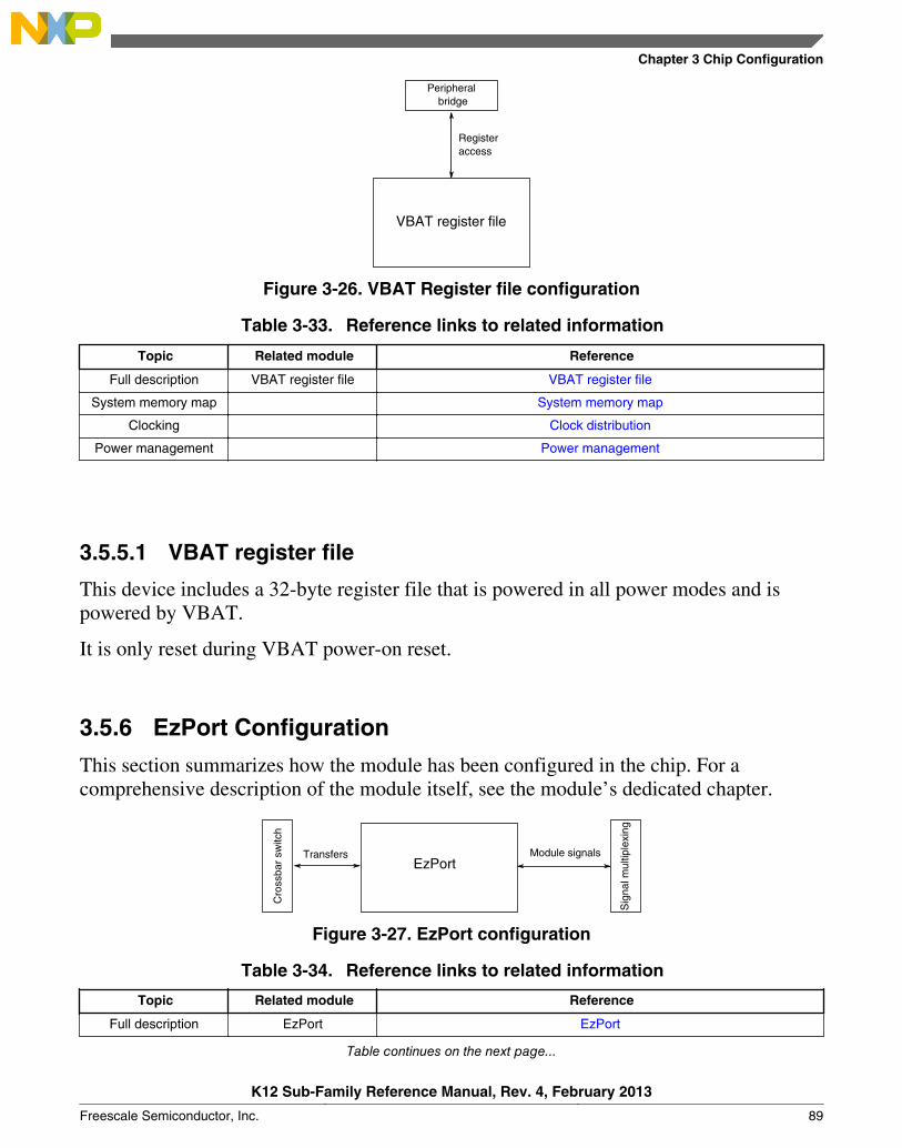
VBAT register file
Peripheralbridge
Registeraccess
Figure 3-26. VBAT Register file configuration
Table 3-33. Reference links to related information
Topic Related module Reference
Full description VBAT register file VBAT register file
System memory map System memory map
Clocking Clock distribution
Power management Power management
3.5.5.1 VBAT register file
This device includes a 32-byte register file that is powered in all power modes and ispowered by VBAT.
It is only reset during VBAT power-on reset.
3.5.6 EzPort Configuration
This section summarizes how the module has been configured in the chip. For acomprehensive description of the module itself, see the module’s dedicated chapter.
Sig
nal m
ultip
lexi
ng
Module signalsEzPort
Transfers
Cro
ssba
r sw
itch
Figure 3-27. EzPort configuration
Table 3-34. Reference links to related information
Topic Related module Reference
Full description EzPort EzPort
Table continues on the next page...
Chapter 3 Chip Configuration
K12 Sub-Family Reference Manual, Rev. 4, February 2013
Freescale Semiconductor, Inc. 89
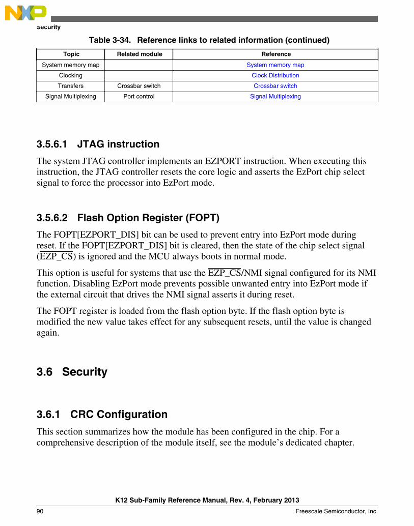
Table 3-34. Reference links to related information (continued)
Topic Related module Reference
System memory map System memory map
Clocking Clock Distribution
Transfers Crossbar switch Crossbar switch
Signal Multiplexing Port control Signal Multiplexing
3.5.6.1 JTAG instruction
The system JTAG controller implements an EZPORT instruction. When executing thisinstruction, the JTAG controller resets the core logic and asserts the EzPort chip selectsignal to force the processor into EzPort mode.
3.5.6.2 Flash Option Register (FOPT)
The FOPT[EZPORT_DIS] bit can be used to prevent entry into EzPort mode duringreset. If the FOPT[EZPORT_DIS] bit is cleared, then the state of the chip select signal(EZP_CS) is ignored and the MCU always boots in normal mode.
This option is useful for systems that use the EZP_CS/NMI signal configured for its NMIfunction. Disabling EzPort mode prevents possible unwanted entry into EzPort mode ifthe external circuit that drives the NMI signal asserts it during reset.
The FOPT register is loaded from the flash option byte. If the flash option byte ismodified the new value takes effect for any subsequent resets, until the value is changedagain.
3.6 Security
3.6.1 CRC Configuration
This section summarizes how the module has been configured in the chip. For acomprehensive description of the module itself, see the module’s dedicated chapter.
Security
K12 Sub-Family Reference Manual, Rev. 4, February 2013
90 Freescale Semiconductor, Inc.
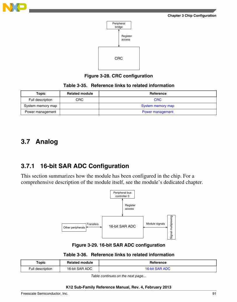
Registeraccess
Peripheralbridge
CRC
Figure 3-28. CRC configuration
Table 3-35. Reference links to related information
Topic Related module Reference
Full description CRC CRC
System memory map System memory map
Power management Power management
3.7 Analog
3.7.1 16-bit SAR ADC Configuration
This section summarizes how the module has been configured in the chip. For acomprehensive description of the module itself, see the module’s dedicated chapter.
Sig
nal m
ultip
lexi
ng
Module signals
Registeraccess
16-bit SAR ADC
Peripheral buscontroller 0
Other peripheralsTransfers
Figure 3-29. 16-bit SAR ADC configuration
Table 3-36. Reference links to related information
Topic Related module Reference
Full description 16-bit SAR ADC 16-bit SAR ADC
Table continues on the next page...
Chapter 3 Chip Configuration
K12 Sub-Family Reference Manual, Rev. 4, February 2013
Freescale Semiconductor, Inc. 91
Table 3-36. Reference links to related information (continued)
Topic Related module Reference
System memory map System memory map
Clocking Clock distribution
Power management Power management
Signal multiplexing Port control Signal multiplexing
3.7.1.1 ADC instantiation information
This device contains one ADC.
3.7.1.1.1 Number of ADC channels
The number of ADC channels present on the device is determined by the pinout of thespecific device package. For details regarding the number of ADC channel available on aparticular package, refer to the signal multiplexing chapter of this MCU.
3.7.1.2 DMA Support on ADC
Applications may require continuous sampling of the ADC (4K samples/sec) that mayhave considerable load on the CPU. Though using PDB to trigger ADC may reduce someCPU load, the ADC supports DMA request functionality for higher performance whenthe ADC is sampled at a very high rate or cases where PDB is bypassed. The ADC cantrigger the DMA (via DMA req) on conversion completion.
3.7.1.3 Connections/channel assignment
3.7.1.3.1 ADC0 Connections/Channel Assignment
NOTEAs indicated by the following sections, each ADCx_DPx inputand certain ADCx_DMx inputs may operate as single-endedADC channels in single-ended mode.
Analog
K12 Sub-Family Reference Manual, Rev. 4, February 2013
92 Freescale Semiconductor, Inc.

3.7.1.3.1.1 ADC0 Channel Assignment for 121-Pin Packages
ADC Channel(SC1n[ADCH])
Channel Input signal(SC1n[DIFF]= 1)
Input signal(SC1n[DIFF]= 0)
00000 DAD0 ADC0_DP0 and ADC0_DM0 ADC0_DP0
00001 DAD1 ADC0_DP1 and ADC0_DM1 ADC0_DP1
00010 DAD2 Reserved Reserved
00011 DAD3 ADC0_DP3 and ADC0_DM3 ADC0_DP3
00100 AD4a Reserved ADC0_SE4a
001011 AD5a Reserved ADC0_SE5a
001101 AD6a Reserved ADC0_SE6a
001111 AD7a Reserved ADC0_SE7a
001001 AD4b Reserved ADC0_SE4b
001011 AD5b Reserved ADC0_SE5b
001101 AD6b Reserved ADC0_SE6b
001111 AD7b Reserved ADC0_SE7b
01000 AD8 Reserved ADC0_SE8
01001 AD9 Reserved ADC0_SE9
01010 AD10 Reserved ADC0_SE10
01011 AD11 Reserved ADC0_SE11
01100 AD12 Reserved ADC0_SE12
01101 AD13 Reserved ADC0_SE13
01110 AD14 Reserved ADC0_SE14
01111 AD15 Reserved ADC0_SE15
10000 AD16 Reserved Reserved
10001 AD17 Reserved Reserved
10010 AD18 Reserved Reserved
10011 AD19 Reserved ADC0_DM0
10100 AD20 Reserved ADC0_DM1
10101 AD21 Reserved ADC0_SE21
10110 AD22 Reserved ADC0_SE22
10111 AD23 Reserved 12-bit Output/ADC0_SE23
11000 AD24 Reserved Reserved
11001 AD25 Reserved Reserved
11010 AD26 Temperature Sensor (Diff) Temperature Sensor (S.E)
11011 AD27 Bandgap (Diff) Bandgap (S.E) 2
11100 AD28 Reserved Reserved
11101 AD29 VREFH (Diff) VREFH (S.E)
11110 AD30 Reserved VREFL
11111 AD31 Module Disabled Module Disabled
Chapter 3 Chip Configuration
K12 Sub-Family Reference Manual, Rev. 4, February 2013
Freescale Semiconductor, Inc. 93

3.7.1.4 ADC Channels MUX Selection
The following figure shows the assignment of ADCx_SEn channels a and b through aMUX selection to ADC. To select between alternate set of channels, refer toADCx_CFG2[MUXSEL] bit settings for more details.
AD5 [00101]
ADCx_SE4aADCx_SE5aADCx_SE6aADCx_SE7aADCx_SE4bADCx_SE5bADCx_SE6bADCx_SE7b
AD4 [00100]
AD6 [00110]
AD7 [00111]
ADC
Figure 3-30. ADCx_SEn channels a and b selection
3.7.1.5 ADC Reference Options
The ADC supports the following references:
• VREFH/VREFL - connected as the primary reference option• 1.2 V VREF_OUT - connected as the VALT reference option
ADCx_SC2[REFSEL] bit selects the voltage reference sources for ADC. Refer toREFSEL description in ADC chapter for more details.
3.7.1.6 ADC triggers
The ADC supports both software and hardware triggers. The primary hardwaremechanism for triggering the ADC is the PDB. The PDB itself can be triggered by otherperipherals. For example: RTC (Alarm, Seconds) signal is connected to the PDB. ThePDB trigger can receive the RTC (alarm/seconds) trigger input forcing ADC conversionsin run mode (where PDB is enabled). On the other hand, the ADC can conductconversions in low power modes, not triggered by PDB. This allows the ADC to doconversions in low power mode and store the output in the result register. The ADCgenerates interrupt when the data is ready in the result register that wakes the systemfrom low power mode. The PDB can also be bypassed by using the ADCxTRGSEL bitsin the SOPT7 register.
For operation of triggers in different modes, refer to Power Management chapter.
Analog
K12 Sub-Family Reference Manual, Rev. 4, February 2013
94 Freescale Semiconductor, Inc.
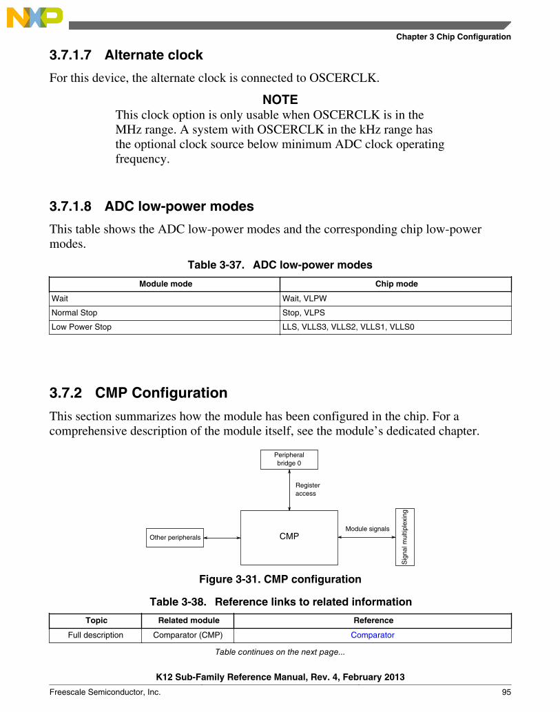
3.7.1.7 Alternate clock
For this device, the alternate clock is connected to OSCERCLK.
NOTEThis clock option is only usable when OSCERCLK is in theMHz range. A system with OSCERCLK in the kHz range hasthe optional clock source below minimum ADC clock operatingfrequency.
3.7.1.8 ADC low-power modes
This table shows the ADC low-power modes and the corresponding chip low-powermodes.
Table 3-37. ADC low-power modes
Module mode Chip mode
Wait Wait, VLPW
Normal Stop Stop, VLPS
Low Power Stop LLS, VLLS3, VLLS2, VLLS1, VLLS0
3.7.2 CMP Configuration
This section summarizes how the module has been configured in the chip. For acomprehensive description of the module itself, see the module’s dedicated chapter.
Sig
nal m
ultip
lexi
ng
Module signals
Registeraccess
CMP
Peripheralbridge 0
Other peripherals
Figure 3-31. CMP configuration
Table 3-38. Reference links to related information
Topic Related module Reference
Full description Comparator (CMP) Comparator
Table continues on the next page...
Chapter 3 Chip Configuration
K12 Sub-Family Reference Manual, Rev. 4, February 2013
Freescale Semiconductor, Inc. 95
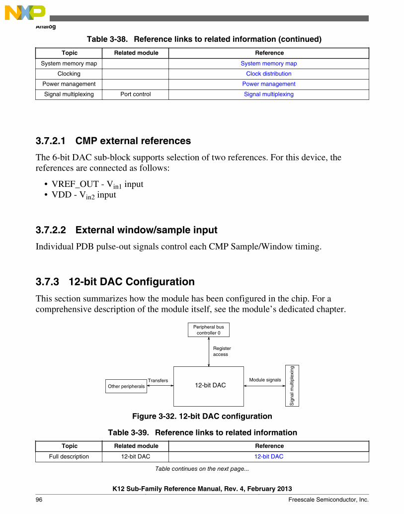
Table 3-38. Reference links to related information (continued)
Topic Related module Reference
System memory map System memory map
Clocking Clock distribution
Power management Power management
Signal multiplexing Port control Signal multiplexing
3.7.2.1 CMP external references
The 6-bit DAC sub-block supports selection of two references. For this device, thereferences are connected as follows:
• VREF_OUT - Vin1 input• VDD - Vin2 input
3.7.2.2 External window/sample input
Individual PDB pulse-out signals control each CMP Sample/Window timing.
3.7.3 12-bit DAC Configuration
This section summarizes how the module has been configured in the chip. For acomprehensive description of the module itself, see the module’s dedicated chapter.
Sig
nal m
ultip
lexi
ng
Module signals
Registeraccess
12-bit DAC
Peripheral buscontroller 0
Other peripheralsTransfers
Figure 3-32. 12-bit DAC configuration
Table 3-39. Reference links to related information
Topic Related module Reference
Full description 12-bit DAC 12-bit DAC
Table continues on the next page...
Analog
K12 Sub-Family Reference Manual, Rev. 4, February 2013
96 Freescale Semiconductor, Inc.

Table 3-39. Reference links to related information (continued)
Topic Related module Reference
System memory map System memory map
Clocking Clock distribution
Power management Power management
Signal multiplexing Port control Signal multiplexing
3.7.3.1 12-bit DAC Overview
This device contains one 12-bit digital-to-analog converter (DAC) with programmablereference generator output. The DAC includes a FIFO for DMA support.
3.7.3.2 12-bit DAC Output
The output of the DAC can be placed on an external pin or set as one of the inputs to theanalog comparator or ADC.
3.7.3.3 12-bit DAC Reference
For this device VREF_OUT and VDDA are selectable as the DAC reference.VREF_OUT is connected to the DACREF_1 input and VDDA is connected to theDACREF_2 input. Use DACx_C0[DACRFS] control bit to select between these twooptions.
Be aware that if the DAC and ADC use the VREF_OUT reference simultaneously, somedegradation of ADC accuracy is to be expected due to DAC switching.
3.7.4 VREF Configuration
This section summarizes how the module has been configured in the chip. For acomprehensive description of the module itself, see the module’s dedicated chapter.
Chapter 3 Chip Configuration
K12 Sub-Family Reference Manual, Rev. 4, February 2013
Freescale Semiconductor, Inc. 97

Sig
nal m
ultip
lexi
ng
Module signals
Registeraccess
VREF
Peripheral buscontroller 0
Other peripheralsTransfers
Figure 3-33. VREF configuration
Table 3-40. Reference links to related information
Topic Related module Reference
Full description VREF VREF
System memory map System memory map
Clocking Clock distribution
Power management Power management
Signal multiplexing Port control Signal multiplexing
3.7.4.1 VREF Overview
This device includes a voltage reference (VREF) to supply an accurate 1.2 V voltageoutput.
The voltage reference can provide a reference voltage to external peripherals or areference to analog peripherals, such as the ADC, DAC, or CMP.
NOTEPMC_REGSC[BGEN] bit must be set if the VREF regulator isrequired to remain operating in VLPx modes.
NOTEFor either an internal or external reference if the VREF_OUTfunctionality is being used, VREF_OUT signal must beconnected to an output load capacitor. Refer the device datasheet for more details.
3.8 Timers
Timers
K12 Sub-Family Reference Manual, Rev. 4, February 2013
98 Freescale Semiconductor, Inc.

3.8.1 PDB Configuration
This section summarizes how the module has been configured in the chip. For acomprehensive description of the module itself, see the module’s dedicated chapter.
Sig
nal m
ultip
lexi
ng
Module signals
Registeraccess
PDB
Peripheral buscontroller 0
Other peripheralsTransfers
Figure 3-34. PDB configuration
Table 3-41. Reference links to related information
Topic Related module Reference
Full description PDB PDB
System memory map System memory map
Clocking Clock distribution
Power management Power management
Signal multiplexing Port control Signal multiplexing
3.8.1.1 PDB Instantiation
3.8.1.1.1 PDB Output TriggersTable 3-42. PDB output triggers
Number of PDB channels for ADC trigger 1
Number of PDB channels to inter-connect with FTM0 11
Number of pre-triggers per PDB channel 2
Number of DAC triggers 1
Number of PulseOut 2
1. The PDB output trigger to FTM0 will occur only once. To have a reoccurring FTM0 trigger, disable and enablePDB_CH1C1[EN] or PDB_SC[PDBEN], after a trigger is sent to FTM0.
Chapter 3 Chip Configuration
K12 Sub-Family Reference Manual, Rev. 4, February 2013
Freescale Semiconductor, Inc. 99
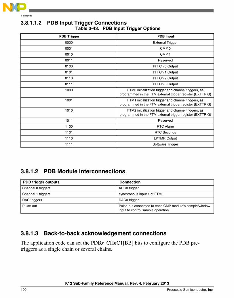
3.8.1.1.2 PDB Input Trigger ConnectionsTable 3-43. PDB Input Trigger Options
PDB Trigger PDB Input
0000 External Trigger
0001 CMP 0
0010 CMP 1
0011 Reserved
0100 PIT Ch 0 Output
0101 PIT Ch 1 Output
0110 PIT Ch 2 Output
0111 PIT Ch 3 Output
1000 FTM0 initialization trigger and channel triggers, asprogrammed in the FTM external trigger register (EXTTRIG)
1001 FTM1 initialization trigger and channel triggers, asprogrammed in the FTM external trigger register (EXTTRIG)
1010 FTM2 initialization trigger and channel triggers, asprogrammed in the FTM external trigger register (EXTTRIG)
1011 Reserved
1100 RTC Alarm
1101 RTC Seconds
1110 LPTMR Output
1111 Software Trigger
3.8.1.2 PDB Module Interconnections
PDB trigger outputs Connection
Channel 0 triggers ADC0 trigger
Channel 1 triggers synchronous input 1 of FTM0
DAC triggers DAC0 trigger
Pulse-out Pulse-out connected to each CMP module's sample/windowinput to control sample operation
3.8.1.3 Back-to-back acknowledgement connections
The application code can set the PDBx_CHnC1[BB] bits to configure the PDB pre-triggers as a single chain or several chains.
Timers
K12 Sub-Family Reference Manual, Rev. 4, February 2013
100 Freescale Semiconductor, Inc.
3.8.1.4 PDB Interval Trigger Connections to DAC
In this MCU, PDB interval trigger connections to DAC are implemented as follows.
• PDB interval trigger 0 connects to DAC0 hardware trigger input.
3.8.1.5 DAC External Trigger Input Connections
In this MCU, the following DAC external trigger inputs are implemented.
• DAC external trigger input 0: ADC0SC1A_COCO
3.8.1.6 Pulse-Out Connection
3.8.1.7 Pulse-Out Enable Register Implementation
The following table shows the comparison of pulse-out enable register at the module andchip level.
Table 3-44. PDB pulse-out enable register
Register Module implementation Chip implementation
POnEN 7:0 - POEN
31:8 - Reserved
0 - POEN[0] for CMP0
1 - POEN[1] for CMP1
31:2 - Reserved
3.8.2 FlexTimer Configuration
This section summarizes how the module has been configured in the chip. For acomprehensive description of the module itself, see the module’s dedicated chapter.
Chapter 3 Chip Configuration
K12 Sub-Family Reference Manual, Rev. 4, February 2013
Freescale Semiconductor, Inc. 101
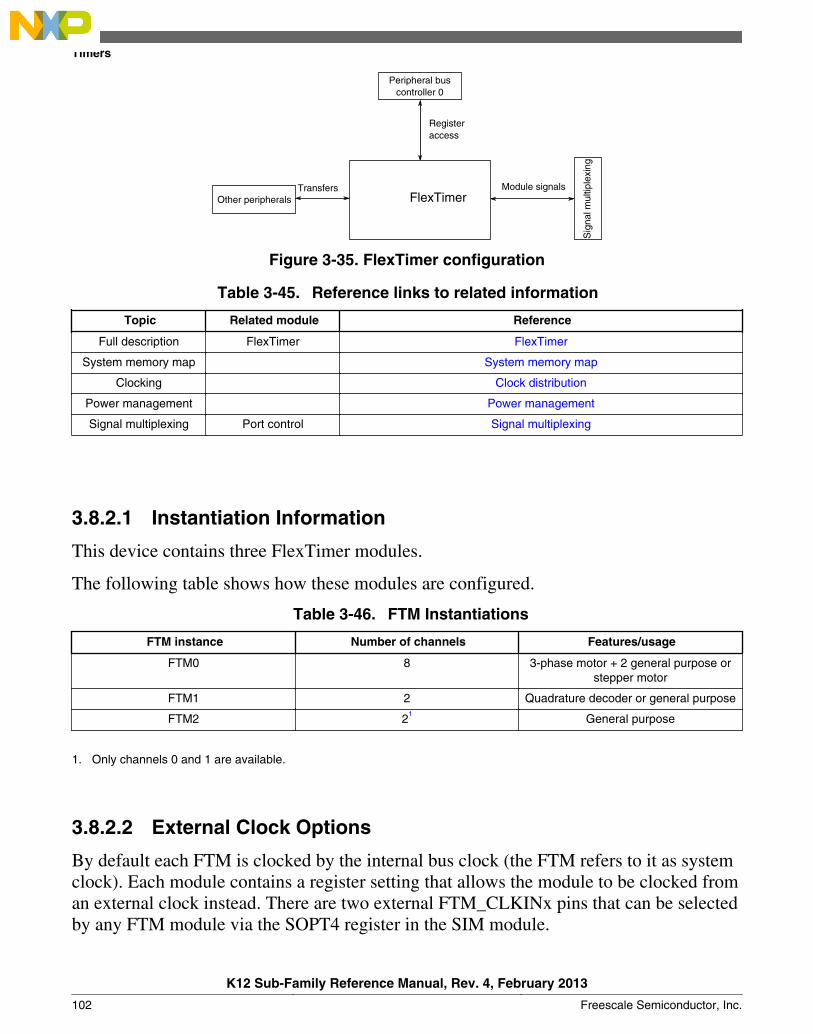
Sig
nal m
ultip
lexi
ng
Module signals
Registeraccess
FlexTimer
Peripheral buscontroller 0
Other peripheralsTransfers
Figure 3-35. FlexTimer configuration
Table 3-45. Reference links to related information
Topic Related module Reference
Full description FlexTimer FlexTimer
System memory map System memory map
Clocking Clock distribution
Power management Power management
Signal multiplexing Port control Signal multiplexing
3.8.2.1 Instantiation Information
This device contains three FlexTimer modules.
The following table shows how these modules are configured.
Table 3-46. FTM Instantiations
FTM instance Number of channels Features/usage
FTM0 8 3-phase motor + 2 general purpose orstepper motor
FTM1 2 Quadrature decoder or general purpose
FTM2 21
General purpose
1. Only channels 0 and 1 are available.
3.8.2.2 External Clock Options
By default each FTM is clocked by the internal bus clock (the FTM refers to it as systemclock). Each module contains a register setting that allows the module to be clocked froman external clock instead. There are two external FTM_CLKINx pins that can be selectedby any FTM module via the SOPT4 register in the SIM module.
Timers
K12 Sub-Family Reference Manual, Rev. 4, February 2013
102 Freescale Semiconductor, Inc.

3.8.2.3 Fixed frequency clock
The fixed frequency clock for each FTM is MCGFFCLK.
3.8.2.4 FTM Interrupts
The FlexTimer has multiple sources of interrupt. However, these sources are OR'dtogether to generate a single interrupt request to the interrupt controller. When an FTMinterrupt occurs, read the FTM status registers (FMS, SC, and STATUS) to determine theexact interrupt source.
3.8.2.5 FTM Fault Detection Inputs
The following fault detection input options for the FTM modules are selected via theSOPT4 register in the SIM module. The external pin option is selected by default.
• FTM0 FAULT0 = FTM0_FLT0 pin or CMP0 output• FTM0 FAULT1 = FTM0_FLT1 pin or CMP1 output• FTM0 FAULT2 = FTM0_FLT2 pin• FTM0 FAULT3 = FTM0_FLT3 pin
• FTM1 FAULT0 = FTM1_FLT0 pin or CMP0 output• FTM1 FAULT1 = CMP1 output
• FTM2 FAULT0 = FTM2_FLT0 pin or CMP0 output• FTM2 FAULT1 = CMP1 output
3.8.2.6 FTM Hardware Triggers
The FTM synchronization hardware triggers are connected in the chip as follows:
• FTM0 hardware trigger 0 = CMP0 Output or FTM1 Match (when enabled in theFTM1 External Trigger (EXTTRIG) register)
• FTM0 hardware trigger 1 = PDB channel 1 Trigger Output or FTM2 Match (whenenabled in the FTM2 External Trigger (EXTTRIG) register)
• FTM0 hardware trigger 2 = FTM0_FLT0 pin
• FTM1 hardware trigger 0 = CMP0 Output• FTM1 hardware trigger 1 = CMP1 Output• FTM1 hardware trigger 2 = FTM1_FLT0 pin
Chapter 3 Chip Configuration
K12 Sub-Family Reference Manual, Rev. 4, February 2013
Freescale Semiconductor, Inc. 103
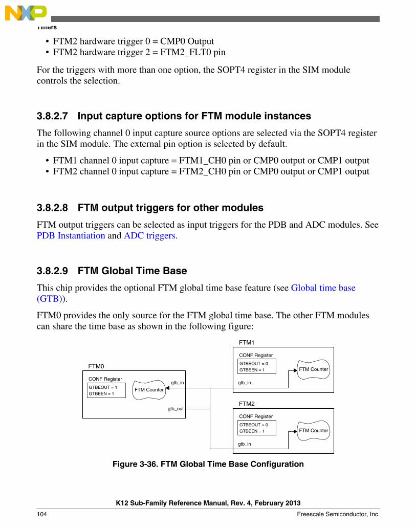
• FTM2 hardware trigger 0 = CMP0 Output• FTM2 hardware trigger 2 = FTM2_FLT0 pin
For the triggers with more than one option, the SOPT4 register in the SIM modulecontrols the selection.
3.8.2.7 Input capture options for FTM module instances
The following channel 0 input capture source options are selected via the SOPT4 registerin the SIM module. The external pin option is selected by default.
• FTM1 channel 0 input capture = FTM1_CH0 pin or CMP0 output or CMP1 output • FTM2 channel 0 input capture = FTM2_CH0 pin or CMP0 output or CMP1 output
3.8.2.8 FTM output triggers for other modules
FTM output triggers can be selected as input triggers for the PDB and ADC modules. SeePDB Instantiation and ADC triggers.
3.8.2.9 FTM Global Time Base
This chip provides the optional FTM global time base feature (see Global time base(GTB)).
FTM0 provides the only source for the FTM global time base. The other FTM modulescan share the time base as shown in the following figure:
gtb_in
FTM1
GTBEEN = 1 FTM Counter
CONF Register
GTBEOUT = 0FTM0
GTBEEN = 1FTM Counter
CONF Register
GTBEOUT = 1
gtb_out
gtb_in
gtb_in
FTM2
GTBEEN = 1 FTM Counter
CONF Register
GTBEOUT = 0
Figure 3-36. FTM Global Time Base Configuration
Timers
K12 Sub-Family Reference Manual, Rev. 4, February 2013
104 Freescale Semiconductor, Inc.
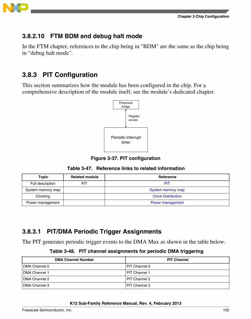
3.8.2.10 FTM BDM and debug halt mode
In the FTM chapter, references to the chip being in "BDM" are the same as the chip beingin “debug halt mode".
3.8.3 PIT Configuration
This section summarizes how the module has been configured in the chip. For acomprehensive description of the module itself, see the module’s dedicated chapter.
Registeraccess
Peripheralbridge
Periodic interrupttimer
Figure 3-37. PIT configuration
Table 3-47. Reference links to related information
Topic Related module Reference
Full description PIT PIT
System memory map System memory map
Clocking Clock Distribution
Power management Power management
3.8.3.1 PIT/DMA Periodic Trigger Assignments
The PIT generates periodic trigger events to the DMA Mux as shown in the table below.
Table 3-48. PIT channel assignments for periodic DMA triggering
DMA Channel Number PIT Channel
DMA Channel 0 PIT Channel 0
DMA Channel 1 PIT Channel 1
DMA Channel 2 PIT Channel 2
DMA Channel 3 PIT Channel 3
Chapter 3 Chip Configuration
K12 Sub-Family Reference Manual, Rev. 4, February 2013
Freescale Semiconductor, Inc. 105
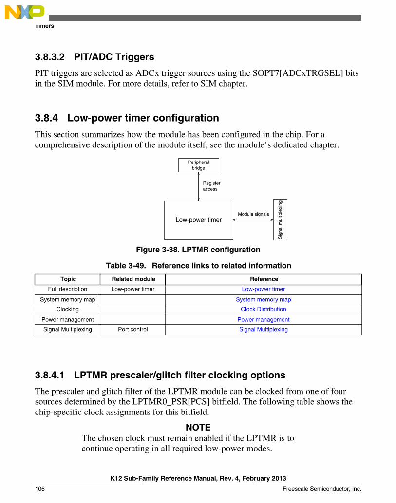
3.8.3.2 PIT/ADC Triggers
PIT triggers are selected as ADCx trigger sources using the SOPT7[ADCxTRGSEL] bitsin the SIM module. For more details, refer to SIM chapter.
3.8.4 Low-power timer configuration
This section summarizes how the module has been configured in the chip. For acomprehensive description of the module itself, see the module’s dedicated chapter.
Sig
nal m
ultip
lexi
ng
Registeraccess
Peripheralbridge
Module signalsLow-power timer
Figure 3-38. LPTMR configuration
Table 3-49. Reference links to related information
Topic Related module Reference
Full description Low-power timer Low-power timer
System memory map System memory map
Clocking Clock Distribution
Power management Power management
Signal Multiplexing Port control Signal Multiplexing
3.8.4.1 LPTMR prescaler/glitch filter clocking options
The prescaler and glitch filter of the LPTMR module can be clocked from one of foursources determined by the LPTMR0_PSR[PCS] bitfield. The following table shows thechip-specific clock assignments for this bitfield.
NOTEThe chosen clock must remain enabled if the LPTMR is tocontinue operating in all required low-power modes.
Timers
K12 Sub-Family Reference Manual, Rev. 4, February 2013
106 Freescale Semiconductor, Inc.

LPTMR0_PSR[PCS] Prescaler/glitch filter clocknumber
Chip clock
00 0 MCGIRCLK — internal reference clock(not available in VLPS/LLS/VLLSmodes)
01 1 LPO — 1 kHz clock (not available inVLLS0 mode)
10 2 ERCLK32K — secondary externalreference clock
11 3 OSCERCLK — external reference clock(not available in VLLS0 mode)
See Clock Distribution for more details on these clocks.
3.8.4.2 LPTMR pulse counter input options
The LPTMR_CSR[TPS] bitfield configures the input source used in pulse counter mode.The following table shows the chip-specific input assignments for this bitfield.
LPTMR_CSR[TPS] Pulse counter input number Chip input
00 0 CMP0 output
01 1 LPTMR_ALT1 pin
10 2 LPTMR_ALT2 pin
11 3 LPTMR_ALT3 pin
3.8.5 CMT Configuration
This section summarizes how the module has been configured in the chip. For acomprehensive description of the module itself, see the module’s dedicated chapter.
Chapter 3 Chip Configuration
K12 Sub-Family Reference Manual, Rev. 4, February 2013
Freescale Semiconductor, Inc. 107

Sig
nal m
ultip
lexi
ng
Module signals
Registeraccess
CMT
Peripheral buscontroller 0
Figure 3-39. CMT configuration
Table 3-50. Reference links to related information
Topic Related module Reference
Full description Carrier modulatortransmitter (CMT)
CMT
System memory map System memory map
Clocking Clock distribution
Power management Power management
Signal multiplexing Port control Signal multiplexing
3.8.5.1 Instantiation Information
This device contains one CMT module.
3.8.5.2 IRO Drive Strength
The IRO pad requires higher current drive than can be obtained from a single pad. Forthis device, the pin associated with the CMT_IRO signal is doubled bonded to two pads.
The SOPT2[PTD7PAD] field in SIM module can be used to configure the pin associatedwith the CMT_IRO signal as a higher current output port pin.
3.8.6 RTC configuration
This section summarizes how the module has been configured in the chip. For acomprehensive description of the module itself, see the module’s dedicated chapter.
Timers
K12 Sub-Family Reference Manual, Rev. 4, February 2013
108 Freescale Semiconductor, Inc.
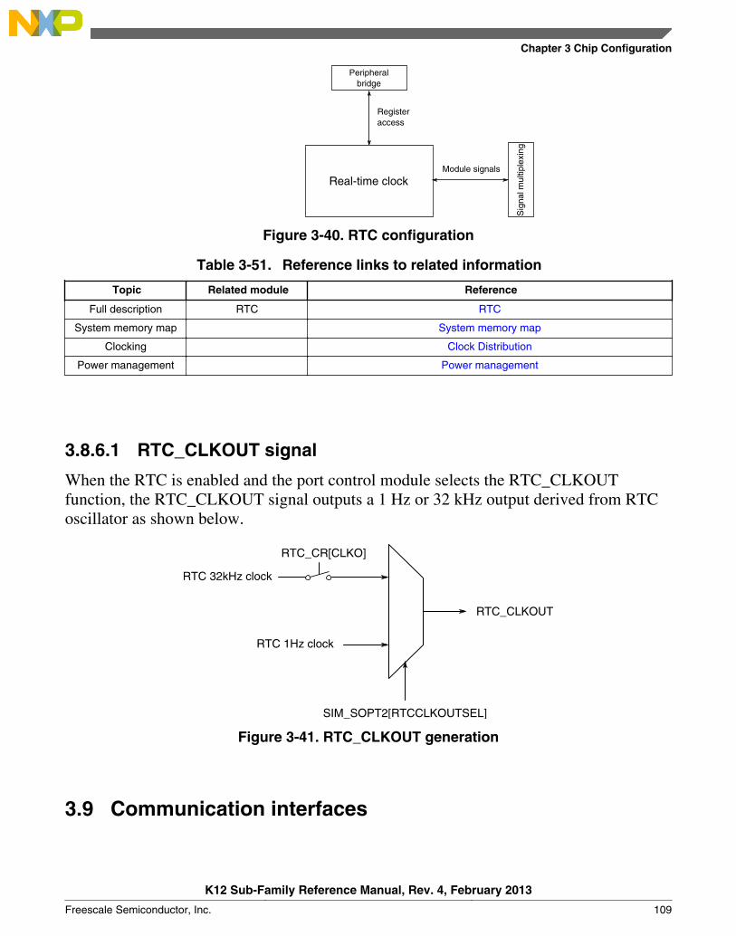
Sig
nal m
ultip
lexi
ng
Registeraccess
Peripheralbridge
Module signals
Real-time clock
Figure 3-40. RTC configuration
Table 3-51. Reference links to related information
Topic Related module Reference
Full description RTC RTC
System memory map System memory map
Clocking Clock Distribution
Power management Power management
3.8.6.1 RTC_CLKOUT signal
When the RTC is enabled and the port control module selects the RTC_CLKOUTfunction, the RTC_CLKOUT signal outputs a 1 Hz or 32 kHz output derived from RTCoscillator as shown below.
SIM_SOPT2[RTCCLKOUTSEL]
RTC_CLKOUT
RTC 1Hz clock
RTC 32kHz clock
RTC_CR[CLKO]
Figure 3-41. RTC_CLKOUT generation
3.9 Communication interfaces
Chapter 3 Chip Configuration
K12 Sub-Family Reference Manual, Rev. 4, February 2013
Freescale Semiconductor, Inc. 109
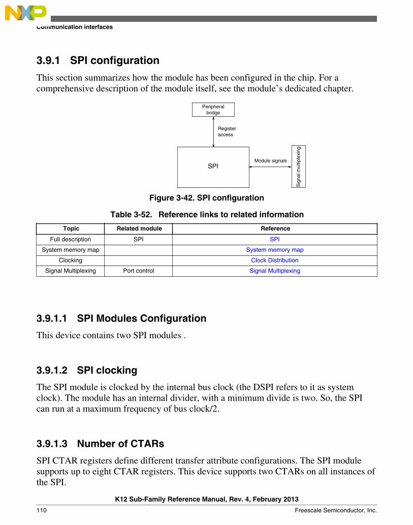
3.9.1 SPI configuration
This section summarizes how the module has been configured in the chip. For acomprehensive description of the module itself, see the module’s dedicated chapter.
Sig
nal m
ultip
lexi
ng
Registeraccess
SPI
Peripheralbridge
Module signals
Figure 3-42. SPI configuration
Table 3-52. Reference links to related information
Topic Related module Reference
Full description SPI SPI
System memory map System memory map
Clocking Clock Distribution
Signal Multiplexing Port control Signal Multiplexing
3.9.1.1 SPI Modules Configuration
This device contains two SPI modules .
3.9.1.2 SPI clocking
The SPI module is clocked by the internal bus clock (the DSPI refers to it as systemclock). The module has an internal divider, with a minimum divide is two. So, the SPIcan run at a maximum frequency of bus clock/2.
3.9.1.3 Number of CTARs
SPI CTAR registers define different transfer attribute configurations. The SPI modulesupports up to eight CTAR registers. This device supports two CTARs on all instances ofthe SPI.
Communication interfaces
K12 Sub-Family Reference Manual, Rev. 4, February 2013
110 Freescale Semiconductor, Inc.
In master mode, the CTAR registers define combinations of transfer attributes, such asframe size, clock phase, clock polarity, data bit ordering, baud rate, and various delays. Inslave mode only CTAR0 is used, and a subset of its bitfields sets the slave transferattributes.
3.9.1.4 TX FIFO sizeTable 3-53. SPI transmit FIFO size
SPI Module Transmit FIFO size
SPI0 4
SPI1 4
3.9.1.5 RX FIFO Size
SPI supports up to 16-bit frame size during reception.
Table 3-54. SPI receive FIFO size
SPI Module Receive FIFO size
SPI0 4
SPI1 4
3.9.1.6 Number of PCS signals
The following table shows the number of peripheral chip select signals available per SPImodule.
Table 3-55. SPI PCS signals
SPI Module PCS Signals
SPI0 SPI_PCS[4:0]
SPI1 SPI_PCS[2:0]
Chapter 3 Chip Configuration
K12 Sub-Family Reference Manual, Rev. 4, February 2013
Freescale Semiconductor, Inc. 111
3.9.1.7 SPI Operation in Low Power Modes
In VLPR and VLPW modes the SPI is functional; however, the reduced systemfrequency also reduces the max frequency of operation for the SPI. In VLPR and VLPWmodes the max SPI_CLK frequency is 2MHz.
In stop and VLPS modes, the clocks to the SPI module are disabled. The module is notfunctional, but it is powered so that it retains state.
There is one way to wake from stop mode via the SPI, which is explained in thefollowing section.
3.9.1.7.1 Using GPIO Interrupt to Wake from stop mode
Here are the steps to use a GPIO to create a wakeup upon reception of SPI data in slavemode:
1. Point the GPIO interrupt vector to the desired interrupt handler.2. Enable the GPIO input to generate an interrupt on either the rising or falling edge
(depending on the polarity of the chip select signal).3. Enter Stop or VLPS mode and Wait for the GPIO interrupt.
NOTEIt is likely that in using this approach the first word of data fromthe SPI host might not be received correctly. This is dependenton the transfer rate used for the SPI, the delay between chipselect assertion and presentation of data, and the systeminterrupt latency.
3.9.1.8 SPI Doze Mode
The Doze mode for the SPI module is the same as the Wait and VLPW modes for thechip.
3.9.1.9 SPI Interrupts
The SPI has multiple sources of interrupt requests. However, these sources are OR'dtogether to generate a single interrupt request per SPI module to the interrupt controller.When an SPI interrupt occurs, read the SPI_SR to determine the exact interrupt source.
Communication interfaces
K12 Sub-Family Reference Manual, Rev. 4, February 2013
112 Freescale Semiconductor, Inc.
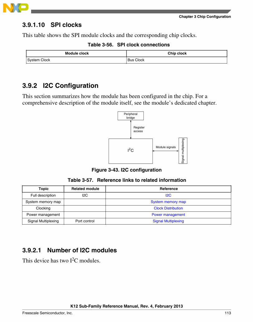
3.9.1.10 SPI clocks
This table shows the SPI module clocks and the corresponding chip clocks.
Table 3-56. SPI clock connections
Module clock Chip clock
System Clock Bus Clock
3.9.2 I2C Configuration
This section summarizes how the module has been configured in the chip. For acomprehensive description of the module itself, see the module’s dedicated chapter.
Sig
nal m
ultip
lexi
ng
Registeraccess
Peripheralbridge
Module signals2I C
Figure 3-43. I2C configuration
Table 3-57. Reference links to related information
Topic Related module Reference
Full description I2C I2C
System memory map System memory map
Clocking Clock Distribution
Power management Power management
Signal Multiplexing Port control Signal Multiplexing
3.9.2.1 Number of I2C modules
This device has two I2C modules.
Chapter 3 Chip Configuration
K12 Sub-Family Reference Manual, Rev. 4, February 2013
Freescale Semiconductor, Inc. 113

3.9.3 UART Configuration
This section summarizes how the module has been configured in the chip. For acomprehensive description of the module itself, see the module’s dedicated chapter.
Sig
nal m
ultip
lexi
ng
Registeraccess
Peripheralbridge
Module signals
UART
Figure 3-44. UART configuration
Table 3-58. Reference links to related information
Topic Related module Reference
Full description UART UART
System memory map System memory map
Clocking Clock Distribution
Power management Power management
Signal Multiplexing Port control Signal Multiplexing
3.9.3.1 UART configuration information
This device contains four UART modules. This section describes how each module isconfigured on this device.
1. Standard features of all UARTs:• RS-485 support• Hardware flow control (RTS/CTS)• 9-bit UART to support address mark with parity• MSB/LSB configuration on data
2. UART0 and UART1 are clocked from the core clock, the remaining UARTs areclocked on the bus clock. The maximum baud rate is 1/16 of related source clockfrequency.
3. IrDA is available on all UARTs4. UART0 contains the standard features plus ISO78165. UART0 contain 8-entry transmit and 8-entry receive FIFOs6. All other UARTs contain a 1-entry transmit and receive FIFOs
Communication interfaces
K12 Sub-Family Reference Manual, Rev. 4, February 2013
114 Freescale Semiconductor, Inc.

3.9.3.2 UART wakeup
The UART can be configured to generate an interrupt/wakeup on the first active edge thatit receives.
3.9.3.3 UART interrupts
The UART has multiple sources of interrupt requests. However, some of these sourcesare OR'd together to generate a single interrupt request. See below for the mapping of theindividual interrupt sources to the interrupt request:
The status interrupt combines the following interrupt sources:
Source UART 0 UART 1 UART 2 UART 3
Transmit data empty x x x x
Transmit complete x x x x
Idle line x x x x
Receive data full x x x x
LIN break detect x x x x
RxD pin active edge x x x x
Initial character detect x — — —
The error interrupt combines the following interrupt sources:
Source UART 0 UART 1 UART 2 UART 3
Receiver overrun x x x x
Noise flag x x x x
Framing error x x x x
Parity error x x x x
Transmitter bufferoverflow
x x x x
Receiver bufferoverflow
x x x x
Receiver bufferunderflow
x x x x
Transmit threshold(ISO7816)
x — — —
Receiver threshold(ISO7816)
x — — —
Wait timer (ISO7816) x — — —
Table continues on the next page...
Chapter 3 Chip Configuration
K12 Sub-Family Reference Manual, Rev. 4, February 2013
Freescale Semiconductor, Inc. 115

Source UART 0 UART 1 UART 2 UART 3
Character wait timer(ISO7816)
x — — —
Block wait timer(ISO7816)
x — — —
Guard time violation(ISO7816)
x — — —
3.9.4 I2S configuration
This section summarizes how the module has been configured in the chip. For acomprehensive description of the module itself, see the module’s dedicated chapter.
Sig
nal m
ultip
lexi
ng
Registeraccess
Peripheralbridge
Module signals2I S
Figure 3-45. I2S configuration
Table 3-59. Reference links to related information
Topic Related module Reference
Full description I2S I2S
System memory map System memory map
Clocking Clock Distribution
Power management Power management
Signal multiplexing Port control Signal Multiplexing
3.9.4.1 Instantiation information
This device contains one I2S module.
As configured on the device, module features include:• TX data lines: 1• RX data lines: 1• FIFO size (words): 8
Communication interfaces
K12 Sub-Family Reference Manual, Rev. 4, February 2013
116 Freescale Semiconductor, Inc.
• Maximum words per frame: 16• Maximum bit clock divider: 512
3.9.4.2 I2S/SAI clocking
3.9.4.2.1 Audio Master Clock
The audio master clock (MCLK) is used to generate the bit clock when the receiver ortransmitter is configured for an internally generated bit clock. The audio master clock canalso be output to or input from a pin. The transmitter and receiver have the same audiomaster clock inputs.
3.9.4.2.2 Bit Clock
The I2S/SAI transmitter and receiver support asynchronous bit clocks (BCLKs) that canbe generated internally from the audio master clock or supplied externally. The modulealso supports the option for synchronous operation between the receiver and transmitterproduct.
3.9.4.2.3 Bus Clock
The bus clock is used by the control registers and to generate synchronous interrupts andDMA requests.
3.9.4.2.4 I2S/SAI clock generation
Each SAI peripheral can control the input clock selection, pin direction and divide ratioof one audio master clock.
The MCLK Input Clock Select bit of the MCLK Control Register (MCR[MICS]) selectsthe clock input to the I2S/SAI module’s MCLK divider.
The module's MCLK Divide Register (MDR) configures the MCLK divide ratio.
The module's MCLK Output Enable bit of the MCLK Control Register (MCR[MOE])controls the direction of the MCLK pin. The pin is the input from the pin when MOE is 0,and the pin is the output from the clock divider when MOE is 1.
The transmitter and receiver can independently select between the bus clock and theaudio master clock to generate the bit clock. Each module's Clocking Mode field of theTransmit Configuration 2 Register and Receive Configuration 2 Register (TCR2[MSEL]and RCR2[MSEL]) selects the master clock.
Chapter 3 Chip Configuration
K12 Sub-Family Reference Manual, Rev. 4, February 2013
Freescale Semiconductor, Inc. 117
3.9.4.2.5 Clock gating and I2S/SAI initialization
The clock to the I2S/SAI module can be gated using a bit in the SIM. To minimize powerconsumption, these bits are cleared after any reset, which disables the clock to thecorresponding module. The clock enable bit should be set by software at the beginning ofthe module initialization routine to enable the module clock before initialization of any ofthe I2S/SAI registers.
3.9.4.3 I2S/SAI operation in low power modes
3.9.4.3.1 Stop and very low power modes
In Stop mode, the SAI transmitter and/or receiver can continue operating provided theappropriate Stop Enable bit is set (TCSR[STOPE] and/or RCSR[STOPE], respectively),and provided the transmitter and/or receiver is/are using an externally generated bit clockor an Audio Master Clock that remains operating in Stop mode. The SAI transmitter and/or receiver can generate an asynchronous interrupt to wake the CPU from Stop mode.
In VLPS mode, the module behaves as it does in stop mode if VLPS mode is enteredfrom run mode. However, if VLPS mode is entered from VLPR mode, the FIFO mightunderflow or overflow before wakeup from stop mode due to the limits in bus bandwidth.In VLPW and VLPR modes, the module is limited by the maximum bus clockfrequencies.
When operating from an internally generated bit clock or Audio Master Clock that isdisabled in stop modes:
In Stop mode, if the Transmitter Stop Enable (TCSR[STOPE]) bit is clear, the transmitteris disabled after completing the current transmit frame, and, if the Receiver Stop Enable(RCSR[STOPE]) bit is clear, the receiver is disabled after completing the current receiveframe. Entry into Stop mode is prevented–not acknowledged–while waiting for thetransmitter and receiver to be disabled at the end of the current frame.
3.9.4.3.2 Low-leakage modes
When entering low-leakage modes, the Stop Enable (TCSR[STOPE] andRCSR[STOPE]) bits are ignored and the SAI is disabled after completing the currenttransmit and receive Frames. Entry into stop mode is prevented (not acknowledged)while waiting for the transmitter and receiver to be disabled at the end of the currentframe.
Communication interfaces
K12 Sub-Family Reference Manual, Rev. 4, February 2013
118 Freescale Semiconductor, Inc.

3.10 Human-machine interfaces
3.10.1 GPIO configuration
This section summarizes how the module has been configured in the chip. For acomprehensive description of the module itself, see the module’s dedicated chapter.
Sig
nal m
ultip
lexi
ng
Registeraccess
Peripheralbridge
Module signals
GPIO controller
Cro
ssba
r sw
itch
Transfers
Figure 3-46. GPIO configuration
Table 3-60. Reference links to related information
Topic Related module Reference
Full description GPIO GPIO
System memory map System memory map
Clocking Clock Distribution
Power management Power management
Transfers Crossbar switch Clock Distribution
Signal Multiplexing Port control Signal Multiplexing
3.10.1.1 GPIO access protection
The GPIO module does not have access protection because it is not connected to aperipheral bridge slot.
3.10.1.2 Number of GPIO signals
The number of GPIO signals available on the devices covered by this document aredetailed in Orderable part numbers .
Chapter 3 Chip Configuration
K12 Sub-Family Reference Manual, Rev. 4, February 2013
Freescale Semiconductor, Inc. 119

Human-machine interfaces
K12 Sub-Family Reference Manual, Rev. 4, February 2013
120 Freescale Semiconductor, Inc.
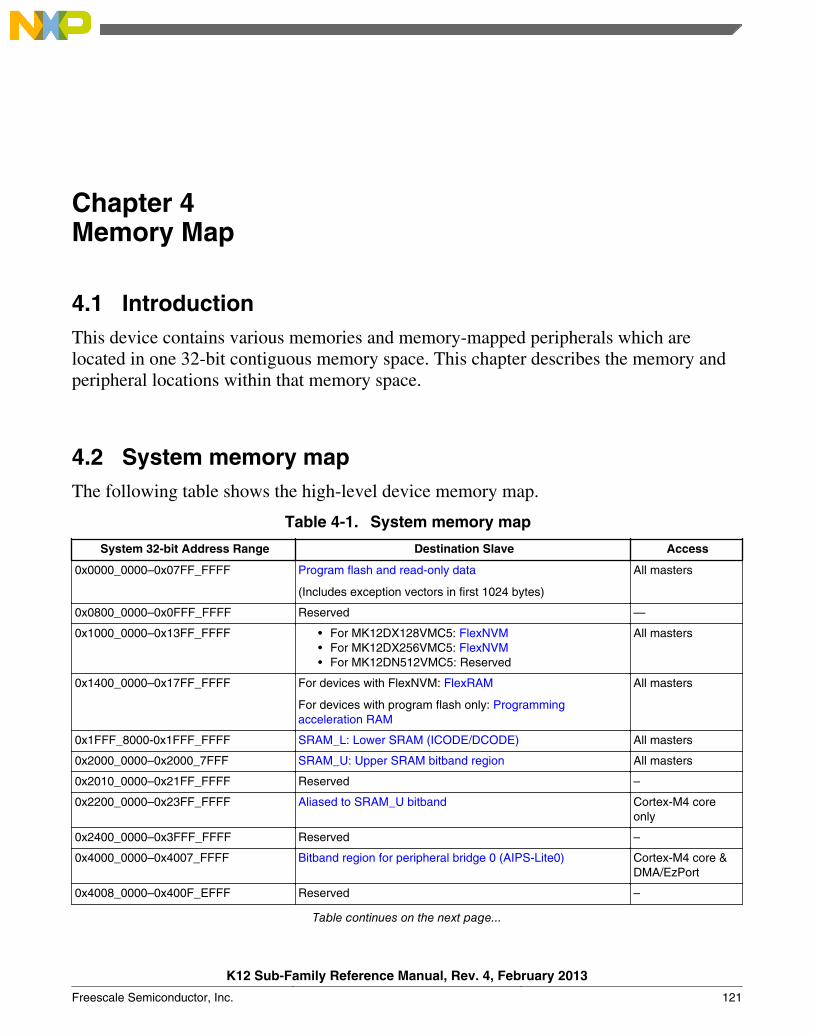
Chapter 4Memory Map
4.1 IntroductionThis device contains various memories and memory-mapped peripherals which arelocated in one 32-bit contiguous memory space. This chapter describes the memory andperipheral locations within that memory space.
4.2 System memory mapThe following table shows the high-level device memory map.
Table 4-1. System memory map
System 32-bit Address Range Destination Slave Access
0x0000_0000–0x07FF_FFFF Program flash and read-only data
(Includes exception vectors in first 1024 bytes)
All masters
0x0800_0000–0x0FFF_FFFF Reserved —
0x1000_0000–0x13FF_FFFF • For MK12DX128VMC5: FlexNVM• For MK12DX256VMC5: FlexNVM• For MK12DN512VMC5: Reserved
All masters
0x1400_0000–0x17FF_FFFF For devices with FlexNVM: FlexRAM
For devices with program flash only: Programmingacceleration RAM
All masters
0x1FFF_8000-0x1FFF_FFFF SRAM_L: Lower SRAM (ICODE/DCODE) All masters
0x2000_0000–0x2000_7FFF SRAM_U: Upper SRAM bitband region All masters
0x2010_0000–0x21FF_FFFF Reserved –
0x2200_0000–0x23FF_FFFF Aliased to SRAM_U bitband Cortex-M4 coreonly
0x2400_0000–0x3FFF_FFFF Reserved –
0x4000_0000–0x4007_FFFF Bitband region for peripheral bridge 0 (AIPS-Lite0) Cortex-M4 core &DMA/EzPort
0x4008_0000–0x400F_EFFF Reserved –
Table continues on the next page...
K12 Sub-Family Reference Manual, Rev. 4, February 2013
Freescale Semiconductor, Inc. 121

Table 4-1. System memory map (continued)
System 32-bit Address Range Destination Slave Access
0x400F_F000–0x400F_FFFF Bitband region for general purpose input/output (GPIO) Cortex-M4 core &DMA/EzPort
0x4010_0000–0x41FF_FFFF Reserved –
0x4200_0000–0x43FF_FFFF Aliased to peripheral bridge (AIPS-Lite) and general purposeinput/output (GPIO) bitband
Cortex-M4 coreonly
0x4400_0000–0xDFFF_FFFF Reserved –
0xE000_0000–0xE00F_FFFF Private peripherals Cortex-M4 coreonly
0xE010_0000–0xFFFF_FFFF Reserved –
NOTE1. EzPort master port is statically muxed with DMA master
port. Access rights to AIPS-Lite peripheral bridge andgeneral purpose input/output (GPIO) module address spaceis limited to the core, DMA, and EzPort.
2. ARM Cortex-M4 core access privileges also includesaccesses via the debug interface.
4.2.1 Aliased bit-band regions
The SRAM_U, AIPS-Lite, and general purpose input/output (GPIO) module resourcesreside in the Cortex-M4 processor bit-band regions.
The processor also includes two 32 MB aliased bit-band regions associated with the two1 MB bit-band spaces. Each 32-bit location in the 32 MB space maps to an individual bitin the bit-band region. A 32-bit write in the alias region has the same effect as a read-modify-write operation on the targeted bit in the bit-band region.
Bit 0 of the value written to the alias region determines what value is written to the targetbit:
• Writing a value with bit 0 set writes a 1 to the target bit.• Writing a value with bit 0 clear writes a 0 to the target bit.
A 32-bit read in the alias region returns either:
• a value of 0x0000_0000 to indicate the target bit is clear• a value of 0x0000_0001 to indicate the target bit is set
System memory map
K12 Sub-Family Reference Manual, Rev. 4, February 2013
122 Freescale Semiconductor, Inc.
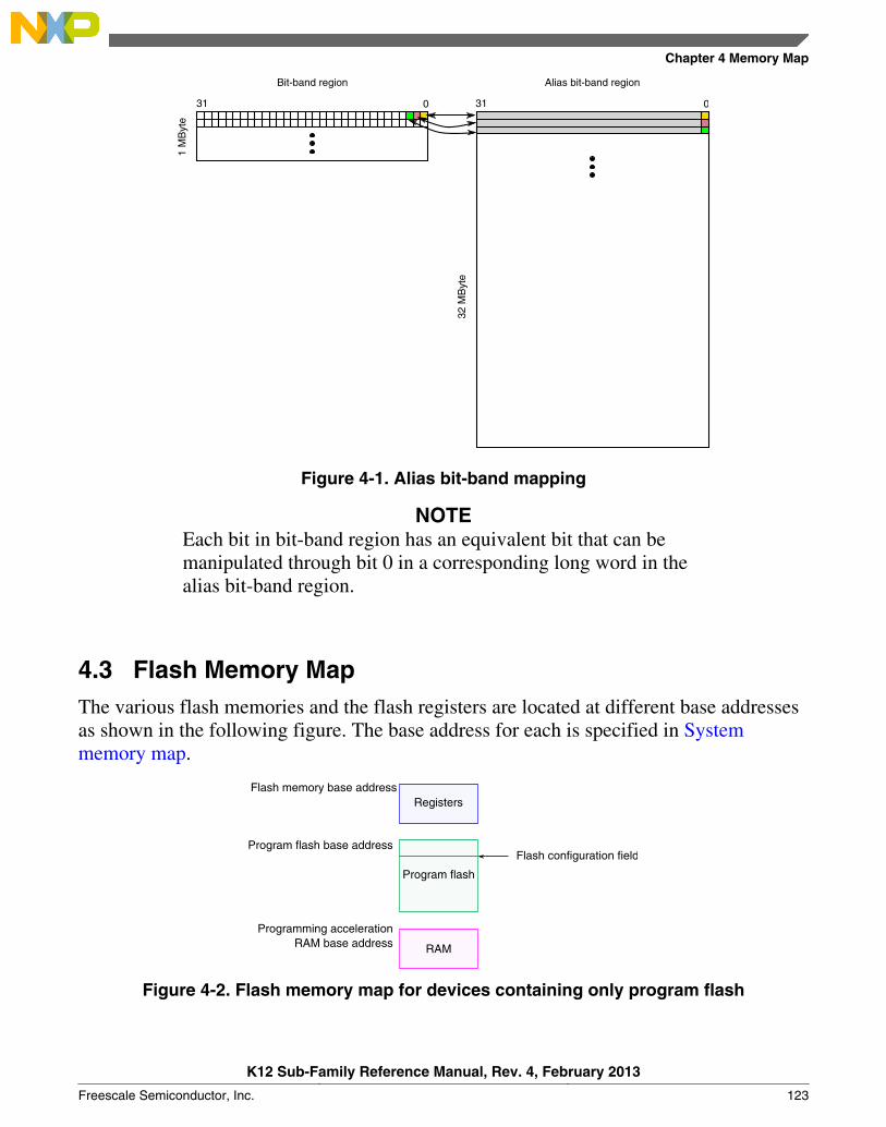
31 0 031
Bit-band region Alias bit-band region
1 M
Byt
e
32 M
Byt
e
Figure 4-1. Alias bit-band mapping
NOTEEach bit in bit-band region has an equivalent bit that can bemanipulated through bit 0 in a corresponding long word in thealias bit-band region.
4.3 Flash Memory MapThe various flash memories and the flash registers are located at different base addressesas shown in the following figure. The base address for each is specified in Systemmemory map.
Program flash
Flash configuration fieldProgram flash base address
Flash memory base addressRegisters
RAM
Programming acceleration RAM base address
Figure 4-2. Flash memory map for devices containing only program flash
Chapter 4 Memory Map
K12 Sub-Family Reference Manual, Rev. 4, February 2013
Freescale Semiconductor, Inc. 123
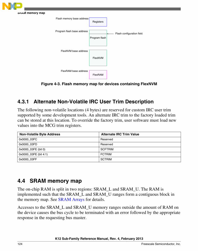
Program flash
Flash configuration field
FlexNVM base address
Program flash base address
Flash memory base addressRegisters
FlexNVM
FlexRAM
FlexRAM base address
Figure 4-3. Flash memory map for devices containing FlexNVM
4.3.1 Alternate Non-Volatile IRC User Trim Description
The following non-volatile locations (4 bytes) are reserved for custom IRC user trimsupported by some development tools. An alternate IRC trim to the factory loaded trimcan be stored at this location. To override the factory trim, user software must load newvalues into the MCG trim registers.
Non-Volatile Byte Address Alternate IRC Trim Value
0x0000_03FC Reserved
0x0000_03FD Reserved
0x0000_03FE (bit 0) SCFTRIM
0x0000_03FE (bit 4:1) FCTRIM
0x0000_03FF SCTRIM
4.4 SRAM memory mapThe on-chip RAM is split in two regions: SRAM_L and SRAM_U. The RAM isimplemented such that the SRAM_L and SRAM_U ranges form a contiguous block inthe memory map. See SRAM Arrays for details.
Accesses to the SRAM_L and SRAM_U memory ranges outside the amount of RAM onthe device causes the bus cycle to be terminated with an error followed by the appropriateresponse in the requesting bus master.
SRAM memory map
K12 Sub-Family Reference Manual, Rev. 4, February 2013
124 Freescale Semiconductor, Inc.

4.5 Peripheral bridge (AIPS-Lite) memory mapThe peripheral memory map is accessible via one slave port on the crossbar in the0x4000_0000–0x4007_FFFF region. The device implements one peripheral bridge thatdefines a 512 KB address space.
Modules that are disabled via their clock gate control bits in the SIM registers disable theassociated AIPS slots. Access to any address within an unimplemented or disabledperipheral bridge slot results in a transfer error termination.
For programming model accesses via the peripheral bridges, there is generally only asmall range within the 4 KB slots that is implemented. Accessing an address that is notimplemented in the peripheral results in a transfer error termination.
4.5.1 Read-after-write sequence and required serialization ofmemory operations
In some situations, a write to a peripheral must be completed fully before a subsequentaction can occur. Examples of such situations include:
• Exiting an interrupt service routine (ISR)• Changing a mode• Configuring a function
In these situations, application software must perform a read-after-write sequence toguarantee the required serialization of the memory operations:
1. Write the peripheral register.2. Read the written peripheral register to verify the write.3. Continue with subsequent operations.
4.5.2 Peripheral Bridge 0 (AIPS-Lite 0) Memory MapTable 4-2. Peripheral bridge 0 slot assignments
System 32-bit base address Slotnumber
Module
0x4000_0000 0 Peripheral bridge 0 (AIPS-Lite 0)
0x4000_1000 1 —
0x4000_2000 2 —
0x4000_3000 3 —
Table continues on the next page...
Chapter 4 Memory Map
K12 Sub-Family Reference Manual, Rev. 4, February 2013
Freescale Semiconductor, Inc. 125

Table 4-2. Peripheral bridge 0 slot assignments (continued)
System 32-bit base address Slotnumber
Module
0x4000_4000 4 —
0x4000_5000 5 —
0x4000_6000 6 —
0x4000_7000 7 —
0x4000_8000 8 DMA controller
0x4000_9000 9 DMA controller transfer control descriptors
0x4000_A000 10 —
0x4000_B000 11 —
0x4000_C000 12 —
0x4000_D000 13 —
0x4000_E000 14 —
0x4000_F000 15 —
0x4001_0000 16 —
0x4001_1000 17 —
0x4001_2000 18 —
0x4001_3000 19 —
0x4001_4000 20 —
0x4001_5000 21 —
0x4001_6000 22 —
0x4001_7000 23 —
0x4001_8000 24 —
0x4001_9000 25 —
0x4001_A000 26 —
0x4001_B000 27 —
0x4001_C000 28 —
0x4001_D000 29 —
0x4001_E000 30 —
0x4001_F000 31 Flash memory controller
0x4002_0000 32 Flash memory
0x4002_1000 33 DMA channel mutiplexer 0
0x4002_2000 34 —
0x4002_3000 35 —
0x4002_4000 36 —
0x4002_5000 37 —
0x4002_6000 38 —
0x4002_7000 39 —
0x4002_8000 40 —
0x4002_9000 41 Random Number Generator (RNGA)
0x4002_A000 42 —
Table continues on the next page...
Peripheral bridge (AIPS-Lite) memory map
K12 Sub-Family Reference Manual, Rev. 4, February 2013
126 Freescale Semiconductor, Inc.
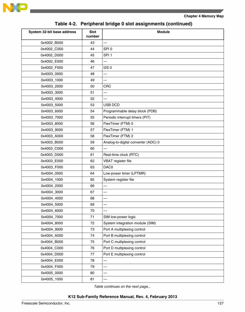
Table 4-2. Peripheral bridge 0 slot assignments (continued)
System 32-bit base address Slotnumber
Module
0x4002_B000 43 —
0x4002_C000 44 SPI 0
0x4002_D000 45 SPI 1
0x4002_E000 46 —
0x4002_F000 47 I2S 0
0x4003_0000 48 —
0x4003_1000 49 —
0x4003_2000 50 CRC
0x4003_3000 51 —
0x4003_4000 52 —
0x4003_5000 53 USB DCD
0x4003_6000 54 Programmable delay block (PDB)
0x4003_7000 55 Periodic interrupt timers (PIT)
0x4003_8000 56 FlexTimer (FTM) 0
0x4003_9000 57 FlexTimer (FTM) 1
0x4003_A000 58 FlexTimer (FTM) 2
0x4003_B000 59 Analog-to-digital converter (ADC) 0
0x4003_C000 60 —
0x4003_D000 61 Real-time clock (RTC)
0x4003_E000 62 VBAT register file
0x4003_F000 63 DAC0
0x4004_0000 64 Low-power timer (LPTMR)
0x4004_1000 65 System register file
0x4004_2000 66 —
0x4004_3000 67 —
0x4004_4000 68 —
0x4004_5000 69 —
0x4004_6000 70 —
0x4004_7000 71 SIM low-power logic
0x4004_8000 72 System integration module (SIM)
0x4004_9000 73 Port A multiplexing control
0x4004_A000 74 Port B multiplexing control
0x4004_B000 75 Port C multiplexing control
0x4004_C000 76 Port D multiplexing control
0x4004_D000 77 Port E multiplexing control
0x4004_E000 78 —
0x4004_F000 79 —
0x4005_0000 80 —
0x4005_1000 81 —
Table continues on the next page...
Chapter 4 Memory Map
K12 Sub-Family Reference Manual, Rev. 4, February 2013
Freescale Semiconductor, Inc. 127
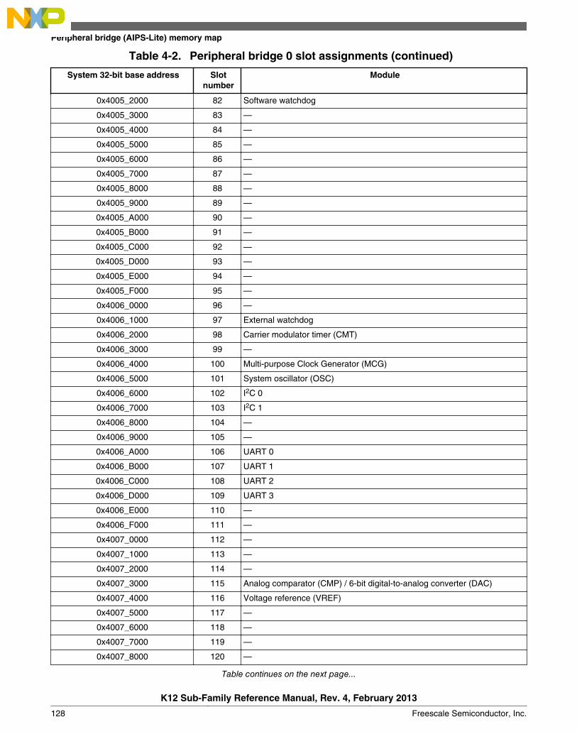
Table 4-2. Peripheral bridge 0 slot assignments (continued)
System 32-bit base address Slotnumber
Module
0x4005_2000 82 Software watchdog
0x4005_3000 83 —
0x4005_4000 84 —
0x4005_5000 85 —
0x4005_6000 86 —
0x4005_7000 87 —
0x4005_8000 88 —
0x4005_9000 89 —
0x4005_A000 90 —
0x4005_B000 91 —
0x4005_C000 92 —
0x4005_D000 93 —
0x4005_E000 94 —
0x4005_F000 95 —
0x4006_0000 96 —
0x4006_1000 97 External watchdog
0x4006_2000 98 Carrier modulator timer (CMT)
0x4006_3000 99 —
0x4006_4000 100 Multi-purpose Clock Generator (MCG)
0x4006_5000 101 System oscillator (OSC)
0x4006_6000 102 I2C 0
0x4006_7000 103 I2C 1
0x4006_8000 104 —
0x4006_9000 105 —
0x4006_A000 106 UART 0
0x4006_B000 107 UART 1
0x4006_C000 108 UART 2
0x4006_D000 109 UART 3
0x4006_E000 110 —
0x4006_F000 111 —
0x4007_0000 112 —
0x4007_1000 113 —
0x4007_2000 114 —
0x4007_3000 115 Analog comparator (CMP) / 6-bit digital-to-analog converter (DAC)
0x4007_4000 116 Voltage reference (VREF)
0x4007_5000 117 —
0x4007_6000 118 —
0x4007_7000 119 —
0x4007_8000 120 —
Table continues on the next page...
Peripheral bridge (AIPS-Lite) memory map
K12 Sub-Family Reference Manual, Rev. 4, February 2013
128 Freescale Semiconductor, Inc.
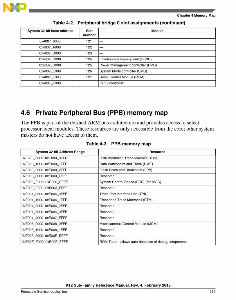
Table 4-2. Peripheral bridge 0 slot assignments (continued)
System 32-bit base address Slotnumber
Module
0x4007_9000 121 —
0x4007_A000 122 —
0x4007_B000 123 —
0x4007_C000 124 Low-leakage wakeup unit (LLWU)
0x4007_D000 125 Power management controller (PMC)
0x4007_E000 126 System Mode controller (SMC)
0x4007_F000 127 Reset Control Module (RCM)
0x400F_F000 GPIO controller
4.6 Private Peripheral Bus (PPB) memory mapThe PPB is part of the defined ARM bus architecture and provides access to selectprocessor-local modules. These resources are only accessible from the core; other systemmasters do not have access to them.
Table 4-3. PPB memory map
System 32-bit Address Range Resource
0xE000_0000–0xE000_0FFF Instrumentation Trace Macrocell (ITM)
0xE000_1000–0xE000_1FFF Data Watchpoint and Trace (DWT)
0xE000_2000–0xE000_2FFF Flash Patch and Breakpoint (FPB)
0xE000_3000–0xE000_DFFF Reserved
0xE000_E000–0xE000_EFFF System Control Space (SCS) (for NVIC)
0xE000_F000–0xE003_FFFF Reserved
0xE004_0000–0xE004_0FFF Trace Port Interface Unit (TPIU)
0xE004_1000–0xE004_1FFF Embedded Trace Macrocell (ETM)
0xE004_2000–0xE004_2FFF Reserved
0xE004_3000–0xE004_3FFF Reserved
0xE004_4000–0xE007_FFFF Reserved
0xE008_0000–0xE008_0FFF Miscellaneous Control Module (MCM)
0xE008_1000–0xE008_1FFF Reserved
0xE008_2000–0xE00F_EFFF Reserved
0xE00F_F000–0xE00F_FFFF ROM Table - allows auto-detection of debug components
Chapter 4 Memory Map
K12 Sub-Family Reference Manual, Rev. 4, February 2013
Freescale Semiconductor, Inc. 129

Private Peripheral Bus (PPB) memory map
K12 Sub-Family Reference Manual, Rev. 4, February 2013
130 Freescale Semiconductor, Inc.
Chapter 5Clock Distribution
5.1 IntroductionThe MCG module controls which clock source is used to derive the system clocks. Theclock generation logic divides the selected clock source into a variety of clock domains,including the clocks for the system bus masters, system bus slaves, and flash memory .The clock generation logic also implements module-specific clock gating to allowgranular shutoff of modules.
The primary clocks for the system are generated from the MCGOUTCLK clock. Theclock generation circuitry provides several clock dividers that allow different portions ofthe device to be clocked at different frequencies. This allows for trade-offs betweenperformance and power dissipation.
Various modules have module-specific clocks that can be generated from theMCGPLLCLK or MCGFLLCLK clock. In addition, there are various other module-specific clocks that have other alternate sources. Clock selection for most modules iscontrolled by the SOPT registers in the SIM module.
5.2 Programming modelThe selection and multiplexing of system clock sources is controlled and programmed viathe MCG module. The setting of clock dividers and module clock gating for the systemare programmed via the SIM module. Reference those sections for detailed register andbit descriptions.
5.3 High-Level device clocking diagramThe following system oscillator, MCG, and SIM module registers control themultiplexers, dividers, and clock gates shown in the below figure:
K12 Sub-Family Reference Manual, Rev. 4, February 2013
Freescale Semiconductor, Inc. 131
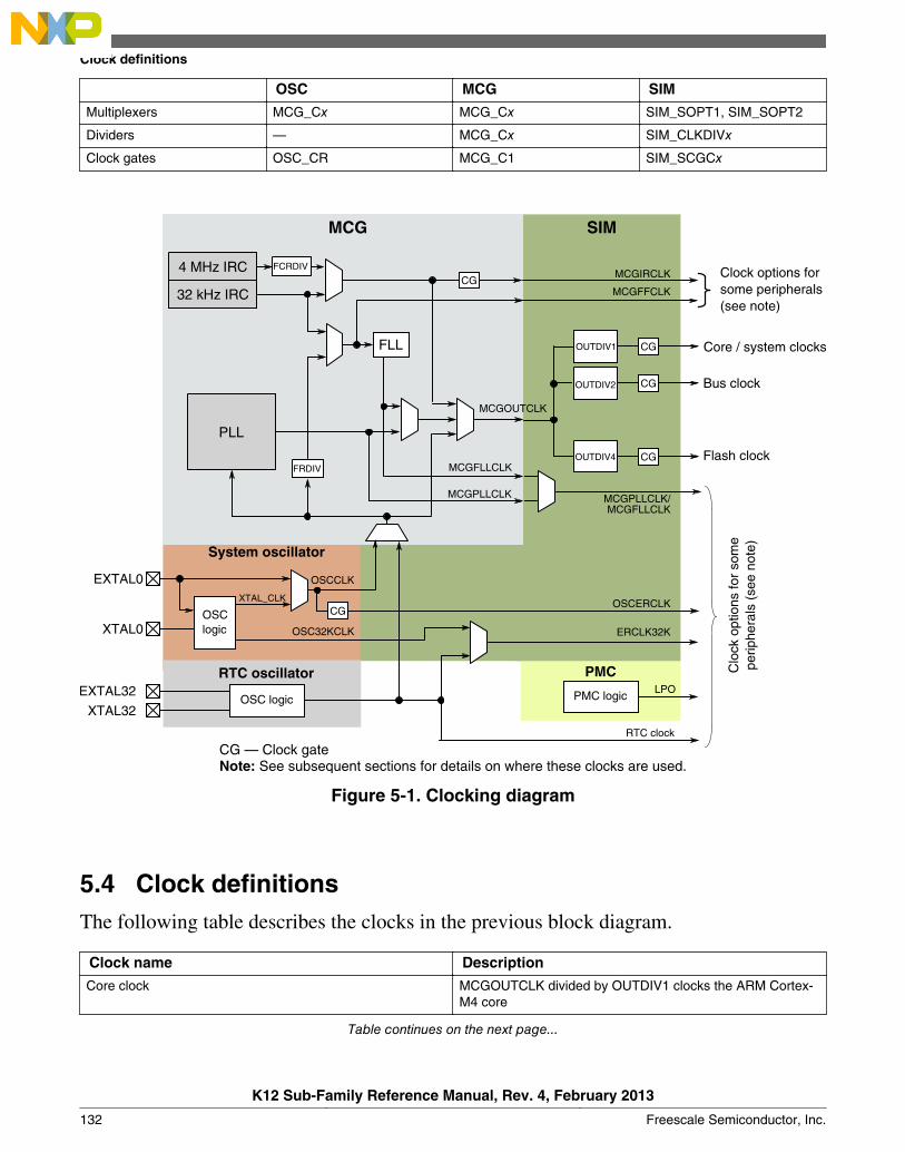
OSC MCG SIM
Multiplexers MCG_Cx MCG_Cx SIM_SOPT1, SIM_SOPT2
Dividers — MCG_Cx SIM_CLKDIVx
Clock gates OSC_CR MCG_C1 SIM_SCGCx
32 kHz IRC
PLL
FLL
MCGOUTCLK
MCGPLLCLK
MCG
MCGFLLCLK
OUTDIV1 Core / system clocks
4 MHz IRC
OUTDIV4 Flash clock
OUTDIV2 Bus clock
RTC oscillatorEXTAL32
XTAL32
EXTAL0
XTAL0
System oscillator
SIM
FRDIV
MCGIRCLK
ERCLK32KOSC32KCLK
XTAL_CLK
MCGFFCLK
OSCERCLKOSC logic
OSC logic
Clock options for some peripherals (see note)
MCGFLLCLKMCGPLLCLK/
Note: See subsequent sections for details on where these clocks are used.
PMC logic
PMCLPO
RTC clockC
lock
opt
ions
for
som
e pe
riphe
rals
(se
e no
te)
OSCCLK
CG
CG
CG
CG
CG
CG — Clock gate
FCRDIV
Figure 5-1. Clocking diagram
5.4 Clock definitionsThe following table describes the clocks in the previous block diagram.
Clock name Description
Core clock MCGOUTCLK divided by OUTDIV1 clocks the ARM Cortex-M4 core
Table continues on the next page...
Clock definitions
K12 Sub-Family Reference Manual, Rev. 4, February 2013
132 Freescale Semiconductor, Inc.
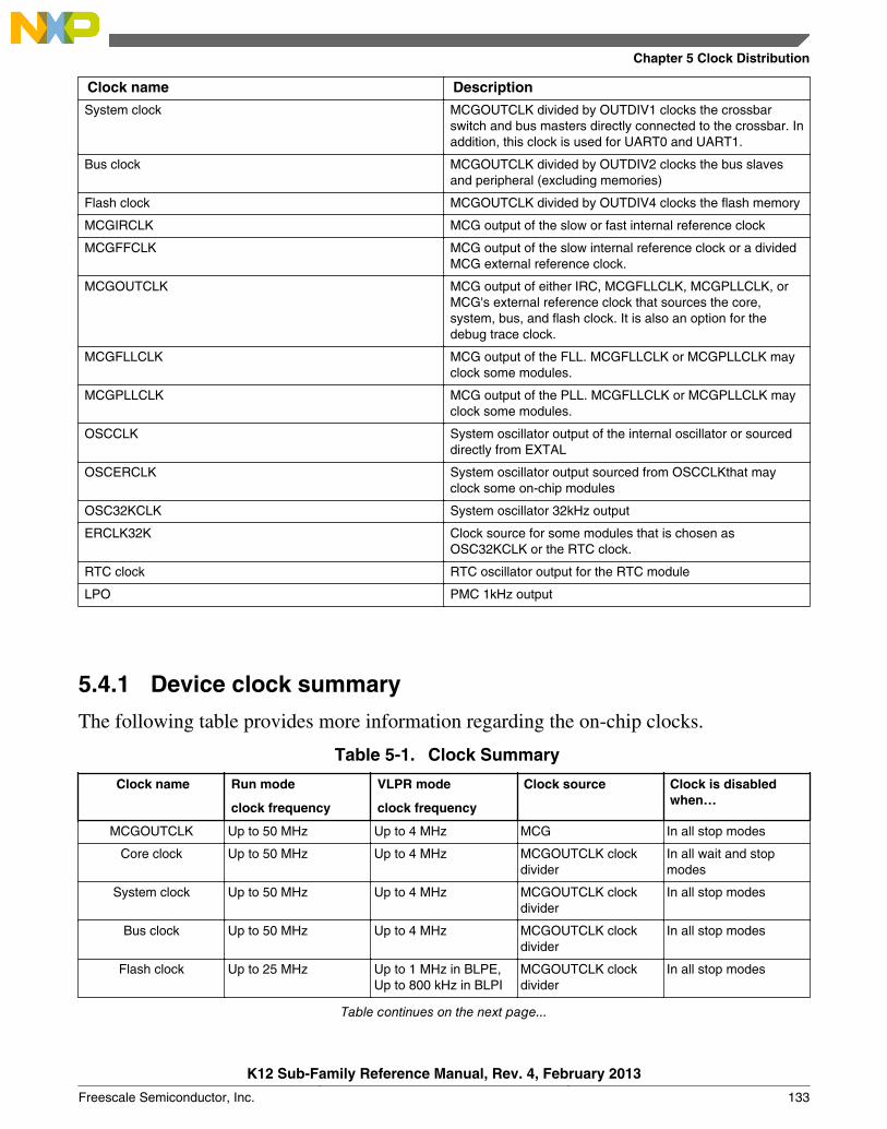
Clock name Description
System clock MCGOUTCLK divided by OUTDIV1 clocks the crossbarswitch and bus masters directly connected to the crossbar. Inaddition, this clock is used for UART0 and UART1.
Bus clock MCGOUTCLK divided by OUTDIV2 clocks the bus slavesand peripheral (excluding memories)
Flash clock MCGOUTCLK divided by OUTDIV4 clocks the flash memory
MCGIRCLK MCG output of the slow or fast internal reference clock
MCGFFCLK MCG output of the slow internal reference clock or a dividedMCG external reference clock.
MCGOUTCLK MCG output of either IRC, MCGFLLCLK, MCGPLLCLK, orMCG's external reference clock that sources the core,system, bus, and flash clock. It is also an option for thedebug trace clock.
MCGFLLCLK MCG output of the FLL. MCGFLLCLK or MCGPLLCLK mayclock some modules.
MCGPLLCLK MCG output of the PLL. MCGFLLCLK or MCGPLLCLK mayclock some modules.
OSCCLK System oscillator output of the internal oscillator or sourceddirectly from EXTAL
OSCERCLK System oscillator output sourced from OSCCLKthat mayclock some on-chip modules
OSC32KCLK System oscillator 32kHz output
ERCLK32K Clock source for some modules that is chosen asOSC32KCLK or the RTC clock.
RTC clock RTC oscillator output for the RTC module
LPO PMC 1kHz output
5.4.1 Device clock summary
The following table provides more information regarding the on-chip clocks.
Table 5-1. Clock Summary
Clock name Run mode
clock frequency
VLPR mode
clock frequency
Clock source Clock is disabledwhen…
MCGOUTCLK Up to 50 MHz Up to 4 MHz MCG In all stop modes
Core clock Up to 50 MHz Up to 4 MHz MCGOUTCLK clockdivider
In all wait and stopmodes
System clock Up to 50 MHz Up to 4 MHz MCGOUTCLK clockdivider
In all stop modes
Bus clock Up to 50 MHz Up to 4 MHz MCGOUTCLK clockdivider
In all stop modes
Flash clock Up to 25 MHz Up to 1 MHz in BLPE,Up to 800 kHz in BLPI
MCGOUTCLK clockdivider
In all stop modes
Table continues on the next page...
Chapter 5 Clock Distribution
K12 Sub-Family Reference Manual, Rev. 4, February 2013
Freescale Semiconductor, Inc. 133
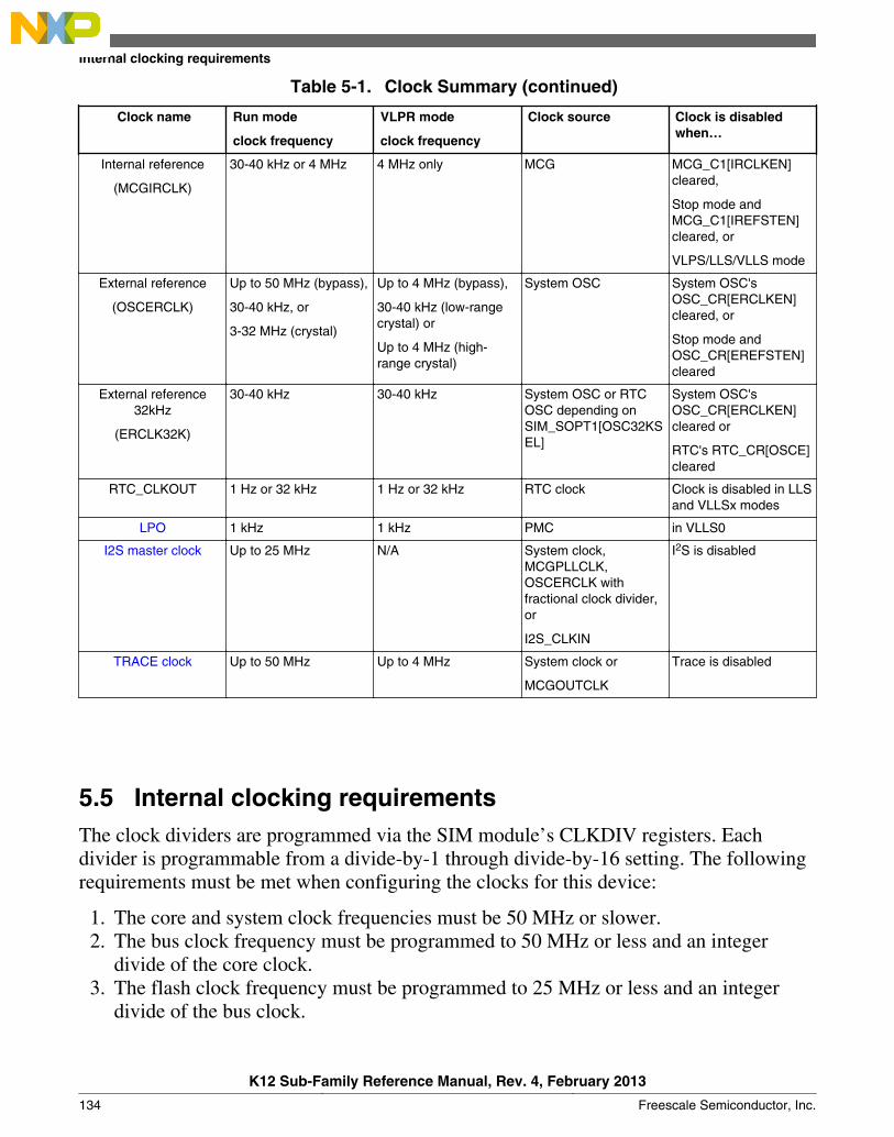
Table 5-1. Clock Summary (continued)
Clock name Run mode
clock frequency
VLPR mode
clock frequency
Clock source Clock is disabledwhen…
Internal reference
(MCGIRCLK)
30-40 kHz or 4 MHz 4 MHz only MCG MCG_C1[IRCLKEN]cleared,
Stop mode andMCG_C1[IREFSTEN]cleared, or
VLPS/LLS/VLLS mode
External reference
(OSCERCLK)
Up to 50 MHz (bypass),
30-40 kHz, or
3-32 MHz (crystal)
Up to 4 MHz (bypass),
30-40 kHz (low-rangecrystal) or
Up to 4 MHz (high-range crystal)
System OSC System OSC'sOSC_CR[ERCLKEN]cleared, or
Stop mode andOSC_CR[EREFSTEN]cleared
External reference32kHz
(ERCLK32K)
30-40 kHz 30-40 kHz System OSC or RTCOSC depending onSIM_SOPT1[OSC32KSEL]
System OSC'sOSC_CR[ERCLKEN]cleared or
RTC's RTC_CR[OSCE]cleared
RTC_CLKOUT 1 Hz or 32 kHz 1 Hz or 32 kHz RTC clock Clock is disabled in LLSand VLLSx modes
LPO 1 kHz 1 kHz PMC in VLLS0
I2S master clock Up to 25 MHz N/A System clock,MCGPLLCLK,OSCERCLK withfractional clock divider,or
I2S_CLKIN
I2S is disabled
TRACE clock Up to 50 MHz Up to 4 MHz System clock or
MCGOUTCLK
Trace is disabled
5.5 Internal clocking requirementsThe clock dividers are programmed via the SIM module’s CLKDIV registers. Eachdivider is programmable from a divide-by-1 through divide-by-16 setting. The followingrequirements must be met when configuring the clocks for this device:
1. The core and system clock frequencies must be 50 MHz or slower.2. The bus clock frequency must be programmed to 50 MHz or less and an integer
divide of the core clock.3. The flash clock frequency must be programmed to 25 MHz or less and an integer
divide of the bus clock.
Internal clocking requirements
K12 Sub-Family Reference Manual, Rev. 4, February 2013
134 Freescale Semiconductor, Inc.
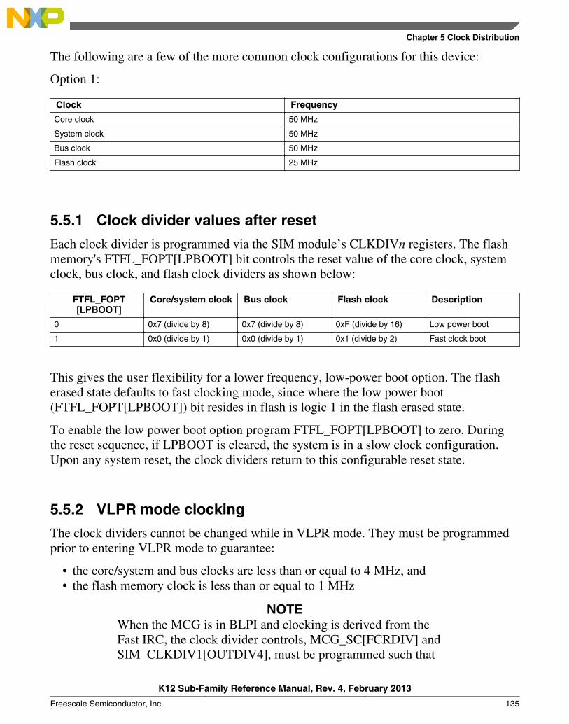
The following are a few of the more common clock configurations for this device:
Option 1:
Clock Frequency
Core clock 50 MHz
System clock 50 MHz
Bus clock 50 MHz
Flash clock 25 MHz
5.5.1 Clock divider values after reset
Each clock divider is programmed via the SIM module’s CLKDIVn registers. The flashmemory's FTFL_FOPT[LPBOOT] bit controls the reset value of the core clock, systemclock, bus clock, and flash clock dividers as shown below:
FTFL_FOPT[LPBOOT]
Core/system clock Bus clock Flash clock Description
0 0x7 (divide by 8) 0x7 (divide by 8) 0xF (divide by 16) Low power boot
1 0x0 (divide by 1) 0x0 (divide by 1) 0x1 (divide by 2) Fast clock boot
This gives the user flexibility for a lower frequency, low-power boot option. The flasherased state defaults to fast clocking mode, since where the low power boot(FTFL_FOPT[LPBOOT]) bit resides in flash is logic 1 in the flash erased state.
To enable the low power boot option program FTFL_FOPT[LPBOOT] to zero. Duringthe reset sequence, if LPBOOT is cleared, the system is in a slow clock configuration.Upon any system reset, the clock dividers return to this configurable reset state.
5.5.2 VLPR mode clocking
The clock dividers cannot be changed while in VLPR mode. They must be programmedprior to entering VLPR mode to guarantee:
• the core/system and bus clocks are less than or equal to 4 MHz, and• the flash memory clock is less than or equal to 1 MHz
NOTEWhen the MCG is in BLPI and clocking is derived from theFast IRC, the clock divider controls, MCG_SC[FCRDIV] andSIM_CLKDIV1[OUTDIV4], must be programmed such that
Chapter 5 Clock Distribution
K12 Sub-Family Reference Manual, Rev. 4, February 2013
Freescale Semiconductor, Inc. 135

the resulting flash clock nominal frequency is 800 kHz or less.In this case, one example of correct configuration isMCG_SC[FCRDIV]=000b andSIM_CLKDIV1[OUTDIV4]=0100b, resulting in a divide by 5setting.
5.6 Clock GatingThe clock to each module can be individually gated on and off using the SIM module'sSCGCx registers. These bits are cleared after any reset, which disables the clock to thecorresponding module to conserve power. Prior to initializing a module, set thecorresponding bit in SCGCx register to enable the clock. Before turning off the clock,make sure to disable the module.
Any bus access to a peripheral that has its clock disabled generates an error termination.
5.7 Module clocksThe following table summarizes the clocks associated with each module.
Table 5-2. Module clocks
Module Bus interface clock Internal clocks I/O interface clocks
Core modules
ARM Cortex-M4 core System clock Core clock —
NVIC System clock — —
DAP System clock — —
ITM System clock — —
ETM System clock TRACE clock TRACE_CLKOUT
cJTAG, JTAGC — — JTAG_CLK
System modules
DMA System clock — —
DMA Mux Bus clock — —
Port control Bus clock LPO —
Crossbar Switch System clock — —
Peripheral bridges System clock Bus clock, Flash clock —
LLWU, PMC, SIM, RCM Flash clock LPO —
Mode controller Flash clock — —
MCM System clock — —
EWM Bus clock LPO —
Table continues on the next page...
Clock Gating
K12 Sub-Family Reference Manual, Rev. 4, February 2013
136 Freescale Semiconductor, Inc.

Table 5-2. Module clocks (continued)
Module Bus interface clock Internal clocks I/O interface clocks
Watchdog timer Bus clock LPO —
Clocks
MCG Bus clock MCGOUTCLK, MCGPLLCLK,MCGFLLCLK, MCGIRCLK,
OSCERCLK
—
OSC Bus clock OSCERCLK —
Memory and memory interfaces
Flash Controller System clock Flash clock —
Flash memory Flash clock — —
EzPort System clock — EZP_CLK
Security
CRC Bus clock — —
Analog
ADC Bus clock OSCERCLK —
CMP Bus clock — —
VREF Bus clock — —
Timers
PDB Bus clock — —
FlexTimers Bus clock MCGFFCLK FTM_CLKINx
PIT Bus clock — —
LPTMR Flash clock LPO, OSCERCLK,MCGIRCLK, ERCLK32K
—
CMT Bus clock — —
RTC Flash clock EXTAL32 —
Communication interfaces
USB DCD Bus clock — —
DSPI Bus clock — DSPI_SCK
I2C Bus clock — I2C_SCL
UART0, UART1 System clock — —
UART2-3 Bus clock — —
I2S Bus clock I2S master clock I2S_TX_BCLK,I2S_RX_BCLK
Human-machine interfaces
GPIO System clock — —
Chapter 5 Clock Distribution
K12 Sub-Family Reference Manual, Rev. 4, February 2013
Freescale Semiconductor, Inc. 137
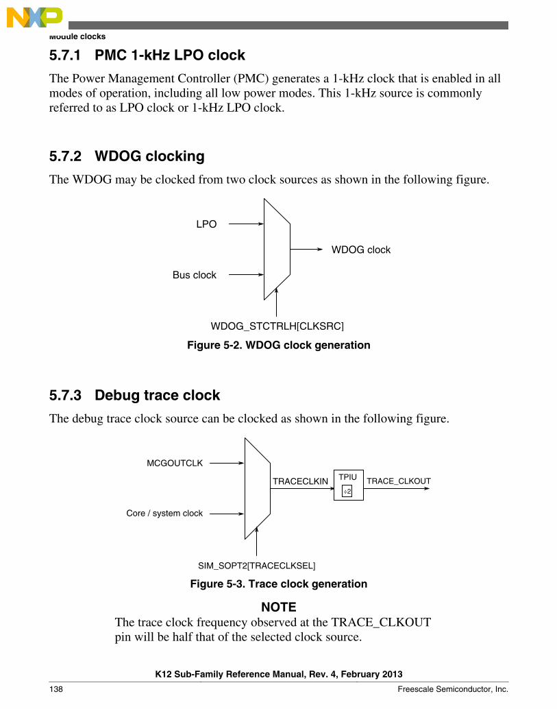
5.7.1 PMC 1-kHz LPO clock
The Power Management Controller (PMC) generates a 1-kHz clock that is enabled in allmodes of operation, including all low power modes. This 1-kHz source is commonlyreferred to as LPO clock or 1-kHz LPO clock.
5.7.2 WDOG clocking
The WDOG may be clocked from two clock sources as shown in the following figure.
WDOG_STCTRLH[CLKSRC]
WDOG clock
Bus clock
LPO
Figure 5-2. WDOG clock generation
5.7.3 Debug trace clock
The debug trace clock source can be clocked as shown in the following figure.
SIM_SOPT2[TRACECLKSEL]
TRACECLKIN
Core / system clock
MCGOUTCLK
TPIU
÷2
TRACE_CLKOUT
Figure 5-3. Trace clock generation
NOTEThe trace clock frequency observed at the TRACE_CLKOUTpin will be half that of the selected clock source.
Module clocks
K12 Sub-Family Reference Manual, Rev. 4, February 2013
138 Freescale Semiconductor, Inc.
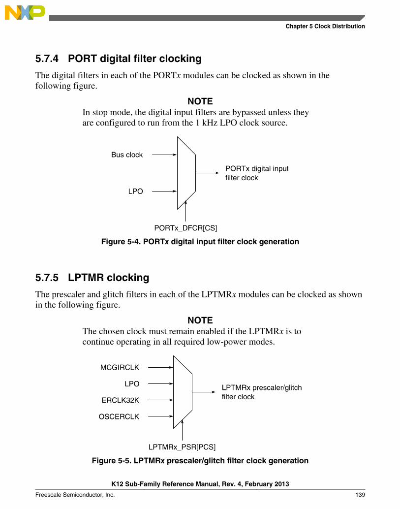
5.7.4 PORT digital filter clocking
The digital filters in each of the PORTx modules can be clocked as shown in thefollowing figure.
NOTEIn stop mode, the digital input filters are bypassed unless theyare configured to run from the 1 kHz LPO clock source.
PORTx_DFCR[CS]
PORTx digital input filter clock
Bus clock
LPO
Figure 5-4. PORTx digital input filter clock generation
5.7.5 LPTMR clocking
The prescaler and glitch filters in each of the LPTMRx modules can be clocked as shownin the following figure.
NOTEThe chosen clock must remain enabled if the LPTMRx is tocontinue operating in all required low-power modes.
LPTMRx_PSR[PCS]
LPTMRx prescaler/glitch filter clock
MCGIRCLK
OSCERCLK
ERCLK32K
LPO
Figure 5-5. LPTMRx prescaler/glitch filter clock generation
Chapter 5 Clock Distribution
K12 Sub-Family Reference Manual, Rev. 4, February 2013
Freescale Semiconductor, Inc. 139
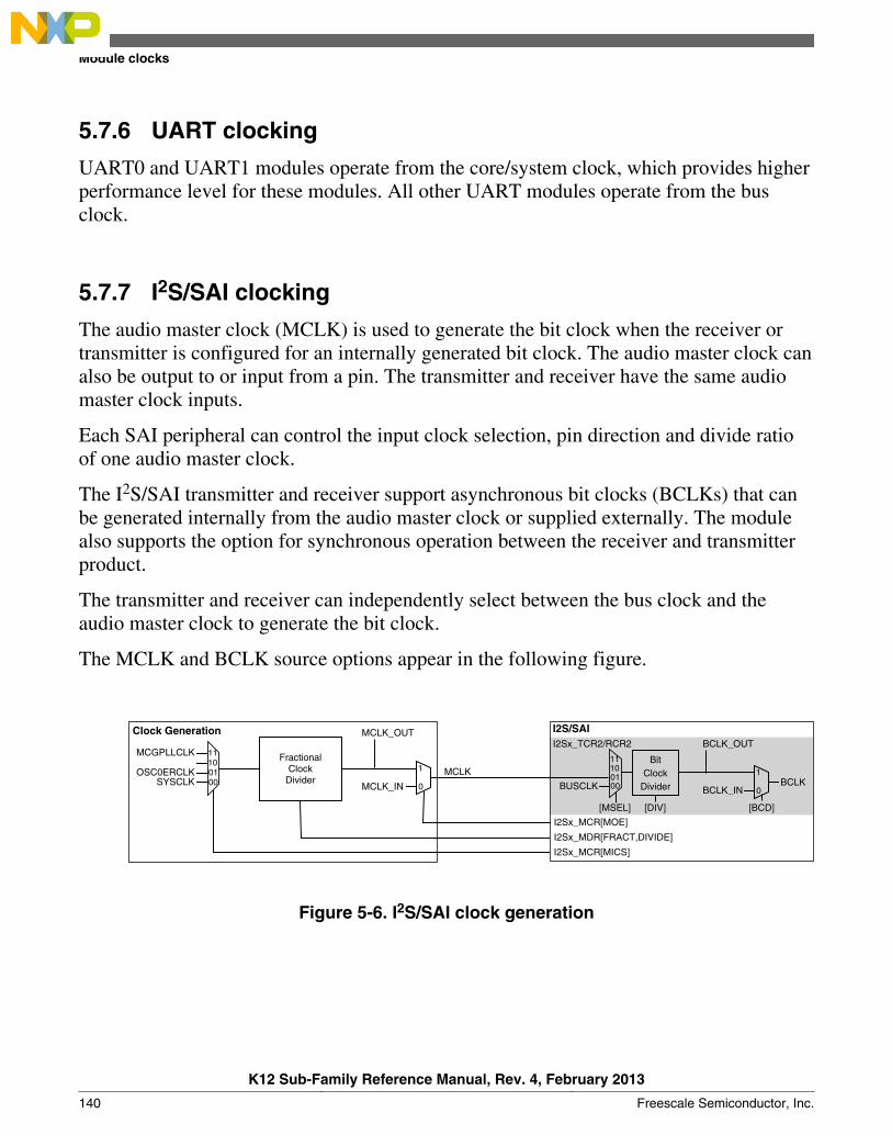
5.7.6 UART clocking
UART0 and UART1 modules operate from the core/system clock, which provides higherperformance level for these modules. All other UART modules operate from the busclock.
5.7.7 I2S/SAI clocking
The audio master clock (MCLK) is used to generate the bit clock when the receiver ortransmitter is configured for an internally generated bit clock. The audio master clock canalso be output to or input from a pin. The transmitter and receiver have the same audiomaster clock inputs.
Each SAI peripheral can control the input clock selection, pin direction and divide ratioof one audio master clock.
The I2S/SAI transmitter and receiver support asynchronous bit clocks (BCLKs) that canbe generated internally from the audio master clock or supplied externally. The modulealso supports the option for synchronous operation between the receiver and transmitterproduct.
The transmitter and receiver can independently select between the bus clock and theaudio master clock to generate the bit clock.
The MCLK and BCLK source options appear in the following figure.
Fractional Clock
Divider1
0
11
0110
00OSC0ERCLK
MCGPLLCLK
SYSCLK
I2Sx_MCR[MOE]
MCLK
MCLK_OUT
MCLK_IN
11
0110
00BUSCLK
[MSEL]
Bit Clock
Divider
1
0BCLK_IN
I2S/SAIBCLK_OUT
[BCD]
BCLK
I2Sx_MDR[FRACT,DIVIDE]
I2Sx_MCR[MICS]
Clock Generation
[DIV]
I2Sx_TCR2/RCR2
Figure 5-6. I2S/SAI clock generation
Module clocks
K12 Sub-Family Reference Manual, Rev. 4, February 2013
140 Freescale Semiconductor, Inc.
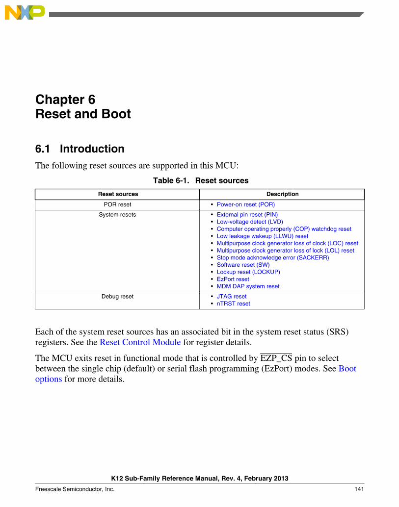
Chapter 6Reset and Boot
6.1 IntroductionThe following reset sources are supported in this MCU:
Table 6-1. Reset sources
Reset sources Description
POR reset • Power-on reset (POR)
System resets • External pin reset (PIN)• Low-voltage detect (LVD)• Computer operating properly (COP) watchdog reset• Low leakage wakeup (LLWU) reset• Multipurpose clock generator loss of clock (LOC) reset• Multipurpose clock generator loss of lock (LOL) reset• Stop mode acknowledge error (SACKERR)• Software reset (SW)• Lockup reset (LOCKUP)• EzPort reset• MDM DAP system reset
Debug reset • JTAG reset• nTRST reset
Each of the system reset sources has an associated bit in the system reset status (SRS)registers. See the Reset Control Module for register details.
The MCU exits reset in functional mode that is controlled by EZP_CS pin to selectbetween the single chip (default) or serial flash programming (EzPort) modes. See Bootoptions for more details.
K12 Sub-Family Reference Manual, Rev. 4, February 2013
Freescale Semiconductor, Inc. 141
6.2 ResetThis section discusses basic reset mechanisms and sources. Some modules that causeresets can be configured to cause interrupts instead. Consult the individual peripheralchapters for more information.
6.2.1 Power-on reset (POR)
When power is initially applied to the MCU or when the supply voltage drops below thepower-on reset re-arm voltage level (VPOR), the POR circuit causes a POR resetcondition.
As the supply voltage rises, the LVD circuit holds the MCU in reset until the supply hasrisen above the LVD low threshold (VLVDL). The POR and LVD bits in SRS0 register areset following a POR.
6.2.2 System reset sourcesResetting the MCU provides a way to start processing from a known set of initialconditions. System reset begins with the on-chip regulator in full regulation and systemclocking generation from an internal reference. When the processor exits reset, itperforms the following:
• Reads the start SP (SP_main) from vector-table offset 0• Reads the start PC from vector-table offset 4• LR is set to 0xFFFF_FFFF
The on-chip peripheral modules are disabled and the non-analog I/O pins are initiallyconfigured as disabled. The pins with analog functions assigned to them default to theiranalog function after reset.
During and following a reset, the JTAG pins have their associated input pins configuredas:
• TDI in pull-up (PU)• TCK in pull-down (PD)• TMS in PU
and associated output pin configured as:
• TDO with no pull-down or pull-up
Reset
K12 Sub-Family Reference Manual, Rev. 4, February 2013
142 Freescale Semiconductor, Inc.

Note that the nTRST signal is initially configured as disabled, however once configuredto its JTAG functionality its associated input pin is configured as:
• nTRST in PU
6.2.2.1 External pin reset (PIN)
On this device, RESET is a dedicated pin. This pin is open drain and has an internalpullup device. Asserting RESET wakes the device from any mode. During a pin reset, theRCM's SRS0[PIN] bit is set.
6.2.2.1.1 Reset pin filter
The RESET pin filter supports filtering from both the 1 kHz LPO clock and the busclock. A separate filter is implemented for each clock source. In stop and VLPS modeoperation, this logic either switches to bypass operation or has continued filteringoperation depending on the filtering mode selected. In low leakage stop modes, a separateLPO filter in the LLWU can continue filtering the RESET pin.
The RPFC[RSTFLTSS], RPFC[RSTFLTSRW], and RPFW[RSTFLTSEL] fields in thereset control (RCM) register set control this functionality; see the RCM chapter. Thefilters are asynchronously reset by Chip POR. The reset value for each filter assumes theRESET pin is negated.
The two clock options for the RESET pin filter when the chip is not in low leakagemodes are the LPO (1 kHz) and bus clock. For low leakage modes VLLS3, VLLS2,VLLS1, VLLS0, the LLWU provides control (in the LLWU_RST register) of an optionalfixed digital filter running the LPO. When entering VLLS0, the RESET pin filter isdisabled and bypassed.
The LPO filter has a fixed filter value of 3. Due to a synchronizer on the input data, thereis also some associated latency (2 cycles). As a result, 5 cycles are required to complete atransition from low to high or high to low.
The bus filter initializes to off (logic 1) when the bus filter is not enabled. The bus clockis used when the filter selects bus clock, and the number of counts is controlled by theRCM's RPFW[RSTFLTSEL] field.
Chapter 6 Reset and Boot
K12 Sub-Family Reference Manual, Rev. 4, February 2013
Freescale Semiconductor, Inc. 143
6.2.2.2 Low-voltage detect (LVD)
The chip includes a system for managing low voltage conditions to protect memorycontents and control MCU system states during supply voltage variations. The systemconsists of a power-on reset (POR) circuit and an LVD circuit with a user-selectable tripvoltage. The LVD system is always enabled in normal run, wait, or stop mode. The LVDsystem is disabled when entering VLPx, LLS, or VLLSx modes.
The LVD can be configured to generate a reset upon detection of a low voltage conditionby setting the PMC's LVDSC1[LVDRE] bit to 1. The low voltage detection threshold isdetermined by the PMC's LVDSC1[LVDV] field. After an LVD reset has occurred, theLVD system holds the MCU in reset until the supply voltage has risen above the lowvoltage detection threshold. The RCM's SRS0[LVD] bit is set following either an LVDreset or POR.
6.2.2.3 Computer operating properly (COP) watchdog timer
The computer operating properly (COP) watchdog timer (WDOG) monitors the operationof the system by expecting periodic communication from the software. Thiscommunication is generally known as servicing (or refreshing) the COP watchdog. If thisperiodic refreshing does not occur, the watchdog issues a system reset. The COP resetcauses the RCM's SRS0[WDOG] bit to set.
6.2.2.4 Low leakage wakeup (LLWU)
The LLWU module provides the means for a number of external pins, the RESET pin,and a number of internal peripherals to wake the MCU from low leakage power modes.The LLWU module is functional only in low leakage power modes.
• In LLS mode, only the RESET pin via the LLWU can generate a system reset.• In VLLSx modes, all enabled inputs to the LLWU can generate a system reset.
After a system reset, the LLWU retains the flags indicating the input source of the lastwakeup until the user clears them.
NOTESome flags are cleared in the LLWU and some flags arerequired to be cleared in the peripheral module. Refer to theindividual peripheral chapters for more information.
Reset
K12 Sub-Family Reference Manual, Rev. 4, February 2013
144 Freescale Semiconductor, Inc.
6.2.2.5 Multipurpose clock generator loss-of-clock (LOC)
The MCG module supports an external reference clock.
If the C6[CME] bit in the MCG module is set, the clock monitor is enabled. If theexternal reference falls below floc_low or floc_high, as controlled by the C2[RANGE] fieldin the MCG module, the MCU resets. The RCM's SRS0[LOC] bit is set to indicate thisreset source.
NOTETo prevent unexpected loss of clock reset events, all clockmonitors should be disabled before entering any low powermodes, including VLPR and VLPW.
6.2.2.6 MCG loss-of-lock (LOL) reset
The MCG includes a PLL loss-of-lock detector. The detector is enabled when configuredfor PEE and lock has been achieved. If the MCG_C8[LOLRE] bit in the MCG module isset and the PLL lock status bit (MCG_S[LOLS0]) becomes set, the MCU resets. TheRCM_SRS0[LOL] bit is set to indicate this reset source.
NOTEThis reset source does not cause a reset if the chip is in any stopmode.
6.2.2.7 Stop mode acknowledge error (SACKERR)
This reset is generated if the core attempts to enter stop mode, but not all modulesacknowledge stop mode within 1025 cycles of the 1 kHz LPO clock.
A module might not acknowledge the entry to stop mode if an error condition occurs. Theerror can be caused by a failure of an external clock input to a module.
6.2.2.8 Software reset (SW)
The SYSRESETREQ bit in the NVIC application interrupt and reset control register canbe set to force a software reset on the device. (See ARM's NVIC documentation for thefull description of the register fields, especially the VECTKEY field requirements.)Setting SYSRESETREQ generates a software reset request. This reset forces a systemreset of all major components except for the debug module. A software reset causes theRCM's SRS1[SW] bit to set.
Chapter 6 Reset and Boot
K12 Sub-Family Reference Manual, Rev. 4, February 2013
Freescale Semiconductor, Inc. 145
6.2.2.9 Lockup reset (LOCKUP)
The LOCKUP gives immediate indication of seriously errant kernel software. This is theresult of the core being locked because of an unrecoverable exception following theactivation of the processor’s built in system state protection hardware.
The LOCKUP condition causes a system reset and also causes the RCM'sSRS1[LOCKUP] bit to set.
6.2.2.10 EzPort reset
The EzPort supports a system reset request via EzPort signaling. The EzPort generates asystem reset request following execution of a Reset Chip (RESET) command via theEzPort interface. This method of reset allows the chip to boot from flash memory after ithas been programmed by an external source. The EzPort is enabled or disabled by theEZP_CS pin.
An EzPort reset causes the RCM's SRS1[EZPT] bit to set.
6.2.2.11 MDM-AP system reset request
Set the system reset request bit in the MDM-AP control register to initiate a system reset.This is the primary method for resets via the JTAG/SWD interface. The system reset isheld until this bit is cleared.
Set the core hold reset bit in the MDM-AP control register to hold the core in reset as therest of the chip comes out of system reset.
6.2.3 MCU Resets
A variety of resets are generated by the MCU to reset different modules.
6.2.3.1 VBAT POR
The VBAT POR asserts on a VBAT POR reset source. It affects only the modules withinthe VBAT power domain: RTC and VBAT Register File. These modules are not affectedby the other reset types.
Reset
K12 Sub-Family Reference Manual, Rev. 4, February 2013
146 Freescale Semiconductor, Inc.
6.2.3.2 POR Only
The POR Only reset asserts on the POR reset source only. It resets the PMC and SystemRegister File.
The POR Only reset also causes all other reset types (except VBAT POR) to occur.
6.2.3.3 Chip POR not VLLS
The Chip POR not VLLS reset asserts on POR and LVD reset sources. It resets parts ofthe SMC and SIM. It also resets the LPTMR.
The Chip POR not VLLS reset also causes these resets to occur: Chip POR, Chip Resetnot VLLS, and Chip Reset (including Early Chip Reset).
6.2.3.4 Chip POR
The Chip POR asserts on POR, LVD, and VLLS Wakeup reset sources. It resets theReset Pin Filter registers and parts of the SIM and MCG.
The Chip POR also causes the Chip Reset (including Early Chip Reset) to occur.
6.2.3.5 Chip Reset not VLLS
The Chip Reset not VLLS reset asserts on all reset sources except a VLLS Wakeup thatdoes not occur via the RESET pin. It resets parts of the SMC, LLWU, and other modulesthat remain powered during VLLS mode.
The Chip Reset not VLLS reset also causes the Chip Reset (including Early Chip Reset)to occur.
6.2.3.6 Early Chip Reset
The Early Chip Reset asserts on all reset sources. It resets only the flash memory module.It negates before flash memory initialization begins ("earlier" than when the Chip Resetnegates).
Chapter 6 Reset and Boot
K12 Sub-Family Reference Manual, Rev. 4, February 2013
Freescale Semiconductor, Inc. 147

6.2.3.7 Chip Reset
Chip Reset asserts on all reset sources and only negates after flash initialization hascompleted and the RESET pin has also negated. It resets the remaining modules (themodules not reset by other reset types).
6.2.4 Reset Pin
For all reset sources except a VLLS Wakeup that does not occur via the RESET pin, theRESET pin is driven low by the MCU for at least 128 bus clock cycles and until flashinitialization has completed.
After flash initialization has completed, the RESET pin is released, and the internal ChipReset negates after the RESET pin is pulled high. Keeping the RESET pin assertedexternally delays the negation of the internal Chip Reset.
6.2.5 Debug resets
The following sections detail the debug resets available on the device.
6.2.5.1 JTAG reset
The JTAG module generate a system reset when certain IR codes are selected. Thisfunctional reset is asserted when EzPort, EXTEST, HIGHZ and CLAMP instructions areactive. The reset source from the JTAG module is released when any other IR code isselected. A JTAG reset causes the RCM's SRS1[JTAG] bit to set.
6.2.5.2 nTRST reset
The nTRST pin causes a reset of the JTAG logic when asserted. Asserting the nTRST pinallows the debugger to gain control of the TAP controller state machine (after exitingLLS or VLLSx) without resetting the state of the debug modules.
The nTRST pin does not cause a system reset.
Reset
K12 Sub-Family Reference Manual, Rev. 4, February 2013
148 Freescale Semiconductor, Inc.
6.2.5.3 Resetting the Debug subsystem
Use the CDBGRSTREQ bit within the SWJ-DP CTRL/STAT register to reset the debugmodules. However, as explained below, using the CDBGRSTREQ bit does not reset alldebug-related registers.
CDBGRSTREQ resets the debug-related registers within the following modules:
• SWJ-DP• AHB-AP• ETM• TPIU• MDM-AP (MDM control and status registers)
CDBGRSTREQ does not reset the debug-related registers within the following modules:
• CM4 core (core debug registers: DHCSR, DCRSR, DCRDR, DEMCR)• FPB• DWT• ITM• NVIC• Crossbar bus switch• AHB-AP
1
• Private peripheral bus1
6.3 BootThis section describes the boot sequence, including sources and options.
6.3.1 Boot sources
This device only supports booting from internal flash. Any secondary boot must gothrough an initialization sequence in flash.
6.3.2 Boot options
The device's functional mode is controlled by the state of the EzPort chip select(EZP_CS) pin during reset.
1. CDBGRSTREQ does not affect AHB resources so that debug resources on the private peripheral bus are availableduring System Reset.
Chapter 6 Reset and Boot
K12 Sub-Family Reference Manual, Rev. 4, February 2013
Freescale Semiconductor, Inc. 149
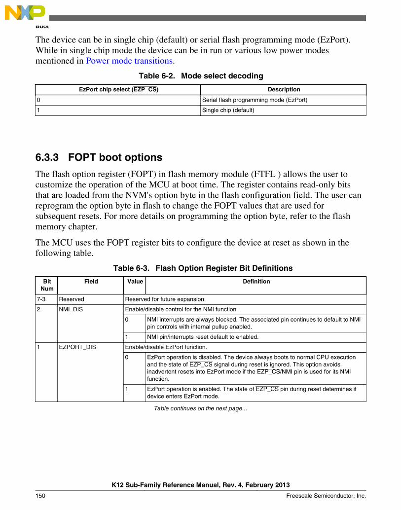
The device can be in single chip (default) or serial flash programming mode (EzPort).While in single chip mode the device can be in run or various low power modesmentioned in Power mode transitions.
Table 6-2. Mode select decoding
EzPort chip select (EZP_CS) Description
0 Serial flash programming mode (EzPort)
1 Single chip (default)
6.3.3 FOPT boot options
The flash option register (FOPT) in flash memory module (FTFL ) allows the user tocustomize the operation of the MCU at boot time. The register contains read-only bitsthat are loaded from the NVM's option byte in the flash configuration field. The user canreprogram the option byte in flash to change the FOPT values that are used forsubsequent resets. For more details on programming the option byte, refer to the flashmemory chapter.
The MCU uses the FOPT register bits to configure the device at reset as shown in thefollowing table.
Table 6-3. Flash Option Register Bit Definitions
BitNum
Field Value Definition
7-3 Reserved Reserved for future expansion.
2 NMI_DIS Enable/disable control for the NMI function.
0 NMI interrupts are always blocked. The associated pin continues to default to NMIpin controls with internal pullup enabled.
1 NMI pin/interrupts reset default to enabled.
1 EZPORT_DIS Enable/disable EzPort function.
0 EzPort operation is disabled. The device always boots to normal CPU executionand the state of EZP_CS signal during reset is ignored. This option avoidsinadvertent resets into EzPort mode if the EZP_CS/NMI pin is used for its NMIfunction.
1 EzPort operation is enabled. The state of EZP_CS pin during reset determines ifdevice enters EzPort mode.
Table continues on the next page...
Boot
K12 Sub-Family Reference Manual, Rev. 4, February 2013
150 Freescale Semiconductor, Inc.
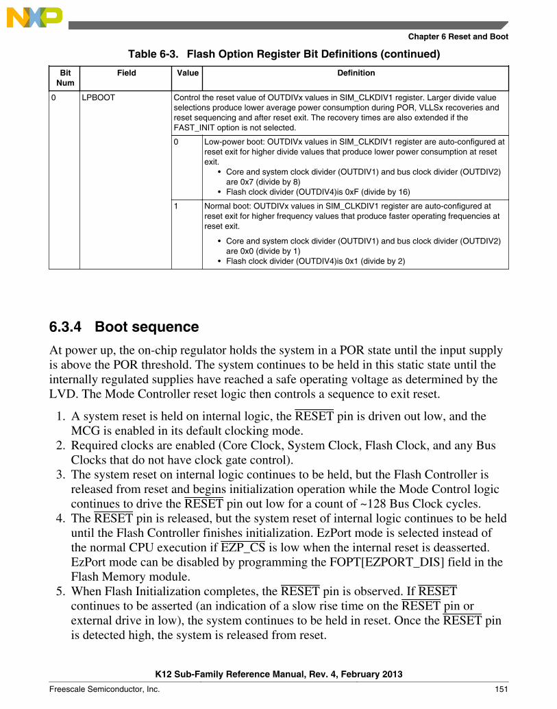
Table 6-3. Flash Option Register Bit Definitions (continued)
BitNum
Field Value Definition
0 LPBOOT Control the reset value of OUTDIVx values in SIM_CLKDIV1 register. Larger divide valueselections produce lower average power consumption during POR, VLLSx recoveries andreset sequencing and after reset exit. The recovery times are also extended if theFAST_INIT option is not selected.
0 Low-power boot: OUTDIVx values in SIM_CLKDIV1 register are auto-configured atreset exit for higher divide values that produce lower power consumption at resetexit.
• Core and system clock divider (OUTDIV1) and bus clock divider (OUTDIV2)are 0x7 (divide by 8)
• Flash clock divider (OUTDIV4)is 0xF (divide by 16)
1 Normal boot: OUTDIVx values in SIM_CLKDIV1 register are auto-configured atreset exit for higher frequency values that produce faster operating frequencies atreset exit.
• Core and system clock divider (OUTDIV1) and bus clock divider (OUTDIV2)are 0x0 (divide by 1)
• Flash clock divider (OUTDIV4)is 0x1 (divide by 2)
6.3.4 Boot sequence
At power up, the on-chip regulator holds the system in a POR state until the input supplyis above the POR threshold. The system continues to be held in this static state until theinternally regulated supplies have reached a safe operating voltage as determined by theLVD. The Mode Controller reset logic then controls a sequence to exit reset.
1. A system reset is held on internal logic, the RESET pin is driven out low, and theMCG is enabled in its default clocking mode.
2. Required clocks are enabled (Core Clock, System Clock, Flash Clock, and any BusClocks that do not have clock gate control).
3. The system reset on internal logic continues to be held, but the Flash Controller isreleased from reset and begins initialization operation while the Mode Control logiccontinues to drive the RESET pin out low for a count of ~128 Bus Clock cycles.
4. The RESET pin is released, but the system reset of internal logic continues to be helduntil the Flash Controller finishes initialization. EzPort mode is selected instead ofthe normal CPU execution if EZP_CS is low when the internal reset is deasserted.EzPort mode can be disabled by programming the FOPT[EZPORT_DIS] field in theFlash Memory module.
5. When Flash Initialization completes, the RESET pin is observed. If RESETcontinues to be asserted (an indication of a slow rise time on the RESET pin orexternal drive in low), the system continues to be held in reset. Once the RESET pinis detected high, the system is released from reset.
Chapter 6 Reset and Boot
K12 Sub-Family Reference Manual, Rev. 4, February 2013
Freescale Semiconductor, Inc. 151

6. At release of system reset, clocking is switched to a slow clock if theFOPT[LPBOOT] field in the Flash Memory module is configured for Low PowerBoot
7. When the system exits reset, the processor sets up the stack, program counter (PC),and link register (LR). The processor reads the start SP (SP_main) from vector-tableoffset 0. The core reads the start PC from vector-table offset 4. LR is set to0xFFFF_FFFF. What happens next depends on the NMI input and theFOPT[NMI_DIS] field in the Flash Memory module:
• If the NMI input is high or the NMI function is disabled in the NMI_DIS field,the CPU begins execution at the PC location.
• If the NMI input is low and the NMI function is enabled in the NMI_DIS field,this results in an NMI interrupt. The processor executes an Exception Entry andreads the NMI interrupt handler address from vector-table offset 8. The CPUbegins execution at the NMI interrupt handler.
8. If FlexNVM is enabled, the flash controller continues to restore the FlexNVM data.This data is not available immediately out of reset and the system should not accessthis data until the flash controller completes this initialization step as indicated by theEEERDY flag.
Subsequent system resets follow this reset flow beginning with the step where systemclocks are enabled.
Boot
K12 Sub-Family Reference Manual, Rev. 4, February 2013
152 Freescale Semiconductor, Inc.

Chapter 7Power Management
7.1 IntroductionThis chapter describes the various chip power modes and functionality of the individualmodules in these modes.
7.2 Power modesThe power management controller (PMC) provides multiple power options to allow theuser to optimize power consumption for the level of functionality needed.
Depending on the stop requirements of the user application, a variety of stop modes areavailable that provide state retention, partial power down or full power down of certainlogic and/or memory. I/O states are held in all modes of operation. The following tablecompares the various power modes available.
For each run mode there is a corresponding wait and stop mode. Wait modes are similarto ARM sleep modes. Stop modes (VLPS, STOP) are similar to ARM sleep deep mode.The very low power run (VLPR) operating mode can drastically reduce runtime powerwhen the maximum bus frequency is not required to handle the application needs.
The three primary modes of operation are run, wait and stop. The WFI instructioninvokes both wait and stop modes for the chip. The primary modes are augmented in anumber of ways to provide lower power based on application needs.
Table 7-1. Chip power modes
Chip mode Description Core mode Normalrecoverymethod
Normal run Allows maximum performance of chip. Default mode out of reset; on-chip voltage regulator is on.
Run -
Table continues on the next page...
K12 Sub-Family Reference Manual, Rev. 4, February 2013
Freescale Semiconductor, Inc. 153
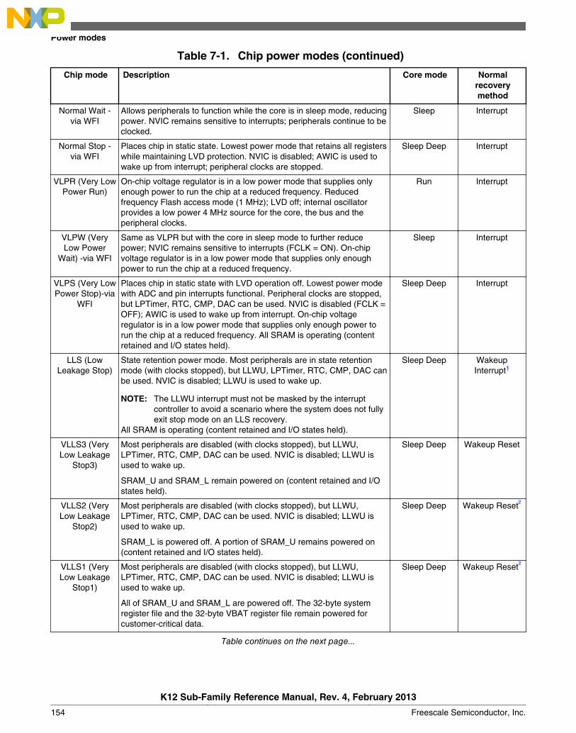
Table 7-1. Chip power modes (continued)
Chip mode Description Core mode Normalrecoverymethod
Normal Wait -via WFI
Allows peripherals to function while the core is in sleep mode, reducingpower. NVIC remains sensitive to interrupts; peripherals continue to beclocked.
Sleep Interrupt
Normal Stop -via WFI
Places chip in static state. Lowest power mode that retains all registerswhile maintaining LVD protection. NVIC is disabled; AWIC is used towake up from interrupt; peripheral clocks are stopped.
Sleep Deep Interrupt
VLPR (Very LowPower Run)
On-chip voltage regulator is in a low power mode that supplies onlyenough power to run the chip at a reduced frequency. Reducedfrequency Flash access mode (1 MHz); LVD off; internal oscillatorprovides a low power 4 MHz source for the core, the bus and theperipheral clocks.
Run Interrupt
VLPW (VeryLow Power
Wait) -via WFI
Same as VLPR but with the core in sleep mode to further reducepower; NVIC remains sensitive to interrupts (FCLK = ON). On-chipvoltage regulator is in a low power mode that supplies only enoughpower to run the chip at a reduced frequency.
Sleep Interrupt
VLPS (Very LowPower Stop)-via
WFI
Places chip in static state with LVD operation off. Lowest power modewith ADC and pin interrupts functional. Peripheral clocks are stopped,but LPTimer, RTC, CMP, DAC can be used. NVIC is disabled (FCLK =OFF); AWIC is used to wake up from interrupt. On-chip voltageregulator is in a low power mode that supplies only enough power torun the chip at a reduced frequency. All SRAM is operating (contentretained and I/O states held).
Sleep Deep Interrupt
LLS (LowLeakage Stop)
State retention power mode. Most peripherals are in state retentionmode (with clocks stopped), but LLWU, LPTimer, RTC, CMP, DAC canbe used. NVIC is disabled; LLWU is used to wake up.
NOTE: The LLWU interrupt must not be masked by the interruptcontroller to avoid a scenario where the system does not fullyexit stop mode on an LLS recovery.
All SRAM is operating (content retained and I/O states held).
Sleep Deep WakeupInterrupt1
VLLS3 (VeryLow Leakage
Stop3)
Most peripherals are disabled (with clocks stopped), but LLWU,LPTimer, RTC, CMP, DAC can be used. NVIC is disabled; LLWU isused to wake up.
SRAM_U and SRAM_L remain powered on (content retained and I/Ostates held).
Sleep Deep Wakeup Reset
VLLS2 (VeryLow Leakage
Stop2)
Most peripherals are disabled (with clocks stopped), but LLWU,LPTimer, RTC, CMP, DAC can be used. NVIC is disabled; LLWU isused to wake up.
SRAM_L is powered off. A portion of SRAM_U remains powered on(content retained and I/O states held).
Sleep Deep Wakeup Reset2
VLLS1 (VeryLow Leakage
Stop1)
Most peripherals are disabled (with clocks stopped), but LLWU,LPTimer, RTC, CMP, DAC can be used. NVIC is disabled; LLWU isused to wake up.
All of SRAM_U and SRAM_L are powered off. The 32-byte systemregister file and the 32-byte VBAT register file remain powered forcustomer-critical data.
Sleep Deep Wakeup Reset2
Table continues on the next page...
Power modes
K12 Sub-Family Reference Manual, Rev. 4, February 2013
154 Freescale Semiconductor, Inc.
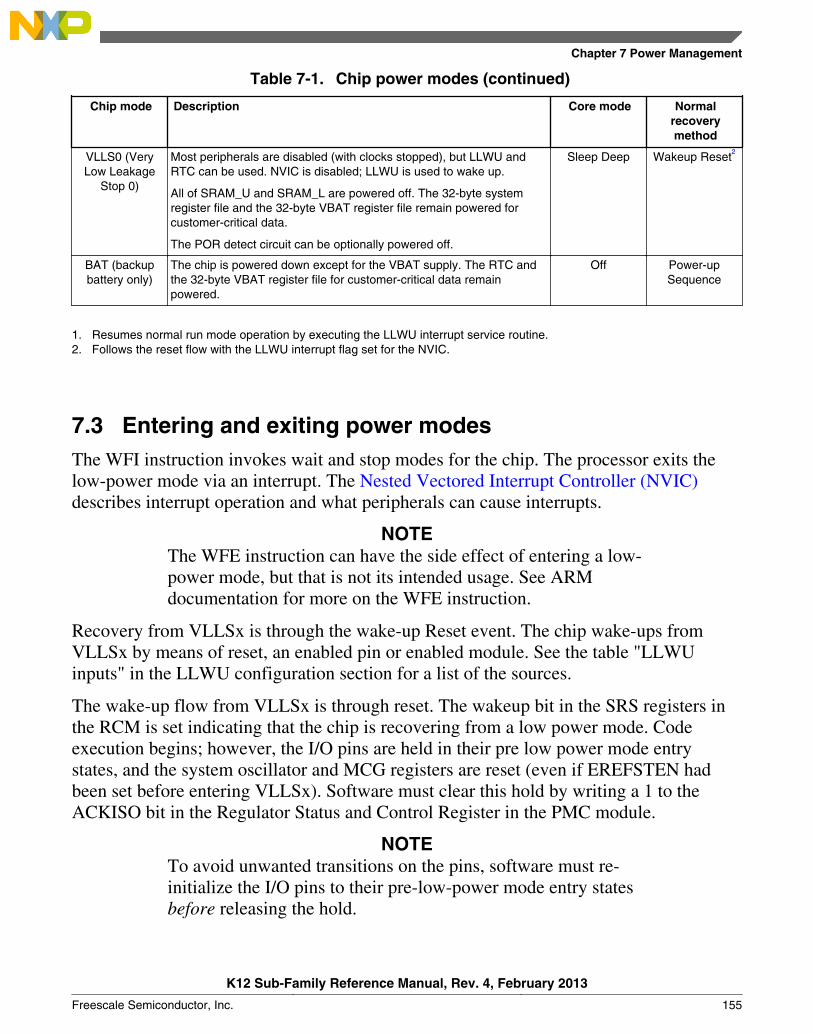
Table 7-1. Chip power modes (continued)
Chip mode Description Core mode Normalrecoverymethod
VLLS0 (VeryLow Leakage
Stop 0)
Most peripherals are disabled (with clocks stopped), but LLWU andRTC can be used. NVIC is disabled; LLWU is used to wake up.
All of SRAM_U and SRAM_L are powered off. The 32-byte systemregister file and the 32-byte VBAT register file remain powered forcustomer-critical data.
The POR detect circuit can be optionally powered off.
Sleep Deep Wakeup Reset2
BAT (backupbattery only)
The chip is powered down except for the VBAT supply. The RTC andthe 32-byte VBAT register file for customer-critical data remainpowered.
Off Power-upSequence
1. Resumes normal run mode operation by executing the LLWU interrupt service routine.2. Follows the reset flow with the LLWU interrupt flag set for the NVIC.
7.3 Entering and exiting power modesThe WFI instruction invokes wait and stop modes for the chip. The processor exits thelow-power mode via an interrupt. The Nested Vectored Interrupt Controller (NVIC)describes interrupt operation and what peripherals can cause interrupts.
NOTEThe WFE instruction can have the side effect of entering a low-power mode, but that is not its intended usage. See ARMdocumentation for more on the WFE instruction.
Recovery from VLLSx is through the wake-up Reset event. The chip wake-ups fromVLLSx by means of reset, an enabled pin or enabled module. See the table "LLWUinputs" in the LLWU configuration section for a list of the sources.
The wake-up flow from VLLSx is through reset. The wakeup bit in the SRS registers inthe RCM is set indicating that the chip is recovering from a low power mode. Codeexecution begins; however, the I/O pins are held in their pre low power mode entrystates, and the system oscillator and MCG registers are reset (even if EREFSTEN hadbeen set before entering VLLSx). Software must clear this hold by writing a 1 to theACKISO bit in the Regulator Status and Control Register in the PMC module.
NOTETo avoid unwanted transitions on the pins, software must re-initialize the I/O pins to their pre-low-power mode entry statesbefore releasing the hold.
Chapter 7 Power Management
K12 Sub-Family Reference Manual, Rev. 4, February 2013
Freescale Semiconductor, Inc. 155

If the oscillator was configured to continue running during VLLSx modes, it must be re-configured before the ACKISO bit is cleared. The oscillator configuration within theMCG is cleared after VLLSx recovery and the oscillator will stop when ACKISO iscleared unless the register is re-configured.
7.4 Power mode transitionsThe following figure shows the power mode transitions. Any reset always brings the chipback to the normal run state. In run, wait, and stop modes active power regulation isenabled. The VLPx modes offer a lower power operating mode than normal modes.VLPR and VLPW are limited in frequency. The LLS and VLLSx modes are the lowestpower stop modes based on amount of logic or memory that is required to be retained bythe application.
Power mode transitions
K12 Sub-Family Reference Manual, Rev. 4, February 2013
156 Freescale Semiconductor, Inc.

Wait
Stop
Run
LLS VLLS3, 2, 1, 0
VLPS
VLPR
VLPW
Any reset
4
6
7
3
1
2
810
11
9
5
Figure 7-1. Power mode state transition diagram
7.5 Power modes shutdown sequencingWhen entering stop or other low-power modes, the clocks are shut off in an orderlysequence to safely place the chip in the targeted low-power state. All low-power entrysequences are initiated by the core executing an WFI instruction. The ARM core'soutputs, SLEEPDEEP and SLEEPING, trigger entry to the various low-power modes:
• System level wait and VLPW modes equate to: SLEEPING & SLEEPDEEP• All other low power modes equate to: SLEEPING & SLEEPDEEP
When entering the non-wait modes, the chip performs the following sequence:
Chapter 7 Power Management
K12 Sub-Family Reference Manual, Rev. 4, February 2013
Freescale Semiconductor, Inc. 157
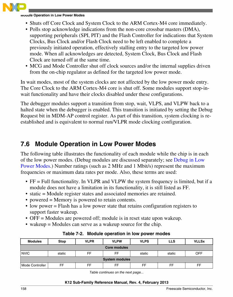
• Shuts off Core Clock and System Clock to the ARM Cortex-M4 core immediately.• Polls stop acknowledge indications from the non-core crossbar masters (DMA),
supporting peripherals (SPI, PIT) and the Flash Controller for indications that SystemClocks, Bus Clock and/or Flash Clock need to be left enabled to complete apreviously initiated operation, effectively stalling entry to the targeted low powermode. When all acknowledges are detected, System Clock, Bus Clock and FlashClock are turned off at the same time.
• MCG and Mode Controller shut off clock sources and/or the internal supplies drivenfrom the on-chip regulator as defined for the targeted low power mode.
In wait modes, most of the system clocks are not affected by the low power mode entry.The Core Clock to the ARM Cortex-M4 core is shut off. Some modules support stop-in-wait functionality and have their clocks disabled under these configurations.
The debugger modules support a transition from stop, wait, VLPS, and VLPW back to ahalted state when the debugger is enabled. This transition is initiated by setting the DebugRequest bit in MDM-AP control register. As part of this transition, system clocking is re-established and is equivalent to normal run/VLPR mode clocking configuration.
7.6 Module Operation in Low Power ModesThe following table illustrates the functionality of each module while the chip is in eachof the low power modes. (Debug modules are discussed separately; see Debug in LowPower Modes.) Number ratings (such as 2 MHz and 1 Mbit/s) represent the maximumfrequencies or maximum data rates per mode. Also, these terms are used:
• FF = Full functionality. In VLPR and VLPW the system frequency is limited, but if amodule does not have a limitation in its functionality, it is still listed as FF.
• static = Module register states and associated memories are retained.• powered = Memory is powered to retain contents.• low power = Flash has a low power state that retains configuration registers to
support faster wakeup.• OFF = Modules are powered off; module is in reset state upon wakeup.• wakeup = Modules can serve as a wakeup source for the chip.
Table 7-2. Module operation in low power modes
Modules Stop VLPR VLPW VLPS LLS VLLSx
Core modules
NVIC static FF FF static static OFF
System modules
Mode Controller FF FF FF FF FF FF
Table continues on the next page...
Module Operation in Low Power Modes
K12 Sub-Family Reference Manual, Rev. 4, February 2013
158 Freescale Semiconductor, Inc.
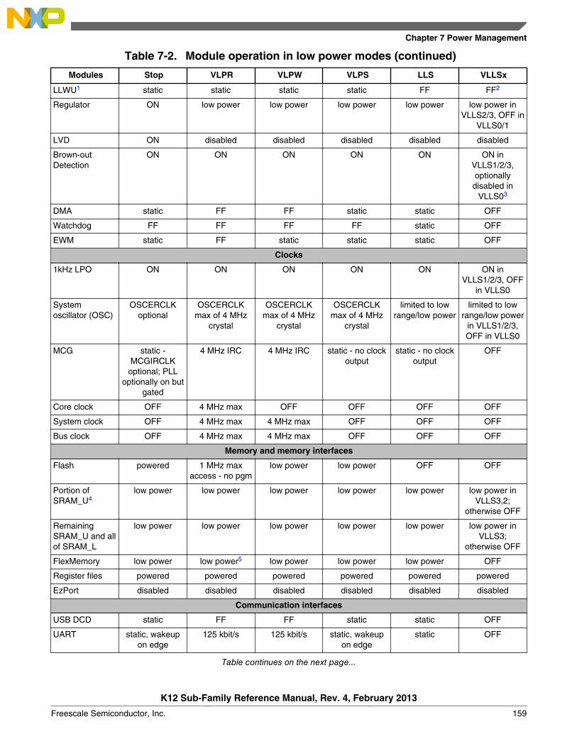
Table 7-2. Module operation in low power modes (continued)
Modules Stop VLPR VLPW VLPS LLS VLLSx
LLWU1 static static static static FF FF2
Regulator ON low power low power low power low power low power inVLLS2/3, OFF in
VLLS0/1
LVD ON disabled disabled disabled disabled disabled
Brown-outDetection
ON ON ON ON ON ON inVLLS1/2/3,optionally
disabled inVLLS03
DMA static FF FF static static OFF
Watchdog FF FF FF FF static OFF
EWM static FF static static static OFF
Clocks
1kHz LPO ON ON ON ON ON ON inVLLS1/2/3, OFF
in VLLS0
Systemoscillator (OSC)
OSCERCLKoptional
OSCERCLKmax of 4 MHz
crystal
OSCERCLKmax of 4 MHz
crystal
OSCERCLKmax of 4 MHz
crystal
limited to lowrange/low power
limited to lowrange/low power
in VLLS1/2/3,OFF in VLLS0
MCG static -MCGIRCLK
optional; PLLoptionally on but
gated
4 MHz IRC 4 MHz IRC static - no clockoutput
static - no clockoutput
OFF
Core clock OFF 4 MHz max OFF OFF OFF OFF
System clock OFF 4 MHz max 4 MHz max OFF OFF OFF
Bus clock OFF 4 MHz max 4 MHz max OFF OFF OFF
Memory and memory interfaces
Flash powered 1 MHz maxaccess - no pgm
low power low power OFF OFF
Portion ofSRAM_U4
low power low power low power low power low power low power inVLLS3,2;
otherwise OFF
RemainingSRAM_U and allof SRAM_L
low power low power low power low power low power low power inVLLS3;
otherwise OFF
FlexMemory low power low power5 low power low power low power OFF
Register files powered powered powered powered powered powered
EzPort disabled disabled disabled disabled disabled disabled
Communication interfaces
USB DCD static FF FF static static OFF
UART static, wakeupon edge
125 kbit/s 125 kbit/s static, wakeupon edge
static OFF
Table continues on the next page...
Chapter 7 Power Management
K12 Sub-Family Reference Manual, Rev. 4, February 2013
Freescale Semiconductor, Inc. 159

Table 7-2. Module operation in low power modes (continued)
Modules Stop VLPR VLPW VLPS LLS VLLSx
SPI static 1 Mbit/s 1 Mbit/s static static OFF
I2C static, addressmatch wakeup
100 kbit/s 100 kbit/s static, addressmatch wakeup
static OFF
I2S FF with externalclock
FF FF FF with externalclock
7static OFF
Security
CRC static FF FF static static OFF
Timers
FTM static FF FF static static OFF
PIT static FF FF static static OFF
PDB static FF FF static static OFF
LPTMR FF FF FF FF FF FF8
RTC - 32kHzOSC
6FF FF FF FF FF FF
9
CMT static FF FF static static OFF
Analog
16-bit ADC ADC internalclock only
FF FF ADC internalclock only
static OFF
CMP10 HS or LS levelcompare
FF FF HS or LS levelcompare
LS levelcompare
LS levelcompare in
VLLS1/2/3, OFFin VLLS0
6-bit DAC static FF FF static static static
VREF FF FF FF FF static OFF
12-bit DAC static FF FF static static static
Human-machine interfaces
GPIO wakeup FF FF wakeup static, pinslatched
OFF, pinslatched
1. Using the LLWU module, the external pins available for this chip do not require the associated peripheral function to beenabled. It only requires the function controlling the pin (GPIO or peripheral) to be configured as an input to allow atransition to occur to the LLWU.
2. Since LPO clock source is disabled, filters will be bypassed during VLLS03. The VLLSCTRL[PORPO] bit in the SMC module controls this option.4. A KB portion of SRAM_U block is left powered on in low power mode VLLS2.5. FlexRAM enabled as EEPROM is not writable in VLPR and writes are ignored. Read accesses to FlexRAM as EEPROM
while in VLPR are allowed. There are no access restrictions for FlexRAM configured as traditional RAM.6. These components remain powered in BAT power mode.7. Use an externally generated bit clock or an externally generated audio master clock (including EXTAL).8. System OSC and LPO clock sources are not available in VLLS09. RTC_CLKOUT is not available.10. CMP in stop or VLPS supports high speed or low speed external pin to pin or external pin to DAC compares. CMP in LLS
or VLLSx only supports low speed external pin to pin or external pin to DAC compares. Windowed, sampled & filteredmodes of operation are not available while in stop, VLPS, LLS, or VLLSx modes.
Module Operation in Low Power Modes
K12 Sub-Family Reference Manual, Rev. 4, February 2013
160 Freescale Semiconductor, Inc.
7.7 Clock GatingTo conserve power, the clocks to most modules can be turned off using the SCGCxregisters in the SIM module. These bits are cleared after any reset, which disables theclock to the corresponding module. Prior to initializing a module, set the correspondingbit in the SCGCx register to enable the clock. Before turning off the clock, make sure todisable the module. For more details, refer to the clock distribution and SIM chapters.
Chapter 7 Power Management
K12 Sub-Family Reference Manual, Rev. 4, February 2013
Freescale Semiconductor, Inc. 161

Clock Gating
K12 Sub-Family Reference Manual, Rev. 4, February 2013
162 Freescale Semiconductor, Inc.

Chapter 8Security
8.1 IntroductionThis device implements security based on the mode selected from the flash module. Thefollowing sections provide an overview of flash security and details the effects of securityon non-flash modules.
8.2 Flash SecurityThe flash module provides security information to the MCU based on the state held bythe FSEC[SEC] bits. The MCU, in turn, confirms the security request and limits access toflash resources. During reset, the flash module initializes the FSEC register using dataread from the security byte of the flash configuration field.
NOTEThe security features apply only to external accesses: debug andEzPort. CPU accesses to the flash are not affected by the statusof FSEC.
In the unsecured state all flash commands are available to the programming interfaces(JTAG and EzPort), as well as user code execution of Flash Controller commands. Whenthe flash is secured (FSEC[SEC] = 00, 01, or 11), programmer interfaces are onlyallowed to launch mass erase operations and have no access to memory locations.
Further information regarding the flash security options and enabling/disabling flashsecurity is available in the Flash Memory Module.
K12 Sub-Family Reference Manual, Rev. 4, February 2013
Freescale Semiconductor, Inc. 163

8.3 Security Interactions with other ModulesThe flash security settings are used by the SoC to determine what resources are available.The following sections describe the interactions between modules and the flash securitysettings or the impact that the flash security has on non-flash modules.
8.3.1 Security Interactions with EzPort
When flash security is active the MCU can still boot in EzPort mode. The EzPort holdsthe flash logic in NVM special mode and thus limits flash operation when flash securityis active. While in EzPort mode and security is active, flash bulk erase (BE) can still beexecuted. The write FCCOB registers (WRFCCOB) command is limited to the masserase (Erase All Blocks) and verify all 1s (Read 1s All Blocks) commands. Read accessesto internal memories via the EzPort are blocked when security is enabled.
The mass erase can be used to disable flash security, but all of the flash contents are lostin the process. A mass erase via the EzPort is allowed even when some memory locationsare protected.
When mass erase has been disabled, mass erase via the EzPort is blocked and cannot bedefeated.
8.3.2 Security Interactions with Debug
When flash security is active the JTAG port cannot access the memory resources of theMCU. Boundary scan chain operations work, but debugging capabilities are disabled sothat the debug port cannot read flash contents.
Although most debug functions are disabled, the debugger can write to the Flash MassErase in Progress bit in the MDM-AP Control register to trigger a mass erase (Erase AllBlocks) command. A mass erase via the debugger is allowed even when some memorylocations are protected.
When mass erase is disabled, mass erase via the debugger is blocked.
Security Interactions with other Modules
K12 Sub-Family Reference Manual, Rev. 4, February 2013
164 Freescale Semiconductor, Inc.
Chapter 9Debug
9.1 IntroductionThis device's debug is based on the ARM coresight architecture and is configured in eachdevice to provide the maximum flexibility as allowed by the restrictions of the pinout andother available resources.
Four debug interfaces are supported:
• IEEE 1149.1 JTAG• IEEE 1149.7 JTAG (cJTAG)• Serial Wire Debug (SWD)• ARM Real-Time Trace Interface
The basic Cortex-M4 debug architecture is very flexible. The following diagram showsthe topology of the core debug architecture and its components.
K12 Sub-Family Reference Manual, Rev. 4, February 2013
Freescale Semiconductor, Inc. 165

Private Peripheral Bus (internal)
Trigger
ITM
TPIU
Core
FPB
AHB-AP
NVIC
SWJ-DP
Bus Matrix
APB i/f
Trace port (serial wire or multi-pin)
Cortex-M4
SW/ JTAG
Debug
Sleep InterruptsINTNMI
SLEEPING
SLEEPDEEP
INTISR[239:0]
AWIC
DWT
ROMTable
ETM
Instr. Data
MCM
I-code bus
D-code bus
System bus
Code bus
MDM-AP
Figure 9-1. Cortex-M4 Debug Topology
The following table presents a brief description of each one of the debug components.
Table 9-1. Debug Components Description
Module Description
SWJ-DP+ cJTAG Modified Debug Port with support for SWD, JTAG, cJTAG
AHB-AP AHB Master Interface from JTAG to debug module and SOCsystem memory maps
MDM-AP Provides centralized control and status registers for anexternal debugger to control the device.
ROM Table Identifies which debug IP is available.
Core Debug Singlestep, Register Access, Run, Core Status
ETM (Embedded Trace Macrocell) ETMv3.5 Architecture
ITM S/W Instrumentation Messaging + Simple Data TraceMessaging + Watchpoint Messaging
DWT (Data and Address Watchpoints) 4 data and address watchpoints
Table continues on the next page...
Introduction
K12 Sub-Family Reference Manual, Rev. 4, February 2013
166 Freescale Semiconductor, Inc.

Table 9-1. Debug Components Description (continued)
Module Description
FPB (Flash Patch and Breakpoints) The FPB implements hardware breakpoints and patches codeand data from code space to system space.
The FPB unit contains two literal comparators for matchingagainst literal loads from Code space, and remapping to acorresponding area in System space.
The FBP also contains six instruction comparators formatching against instruction fetches from Code space, andremapping to a corresponding area in System space.Alternatively, the six instruction comparators can individuallyconfigure the comparators to return a Breakpoint Instruction(BKPT) to the processor core on a match, so providinghardware breakpoint capability.
TPIU (Trace Port Inteface Unit) Synchronous Mode (5-pin) = TRACE_D[3:0] +TRACE_CLKOUT
Synchronous Mode (3-pin) = TRACE_D[1:0] +TRACE_CLKOUT
Asynchronous Mode (1-pin) = TRACE_SWO (available onJTAG_TDO)
9.1.1 References
For more information on ARM debug components, see these documents:
• ARMv7-M Architecture Reference Manual• ARM Debug Interface v5.1• ARM CoreSight Architecture Specification• ARM ETM Architecture Specification v3.5
9.2 The Debug PortThe configuration of the cJTAG module, JTAG controller, and debug port is illustrated inthe following figure:
Chapter 9 Debug
K12 Sub-Family Reference Manual, Rev. 4, February 2013
Freescale Semiconductor, Inc. 167
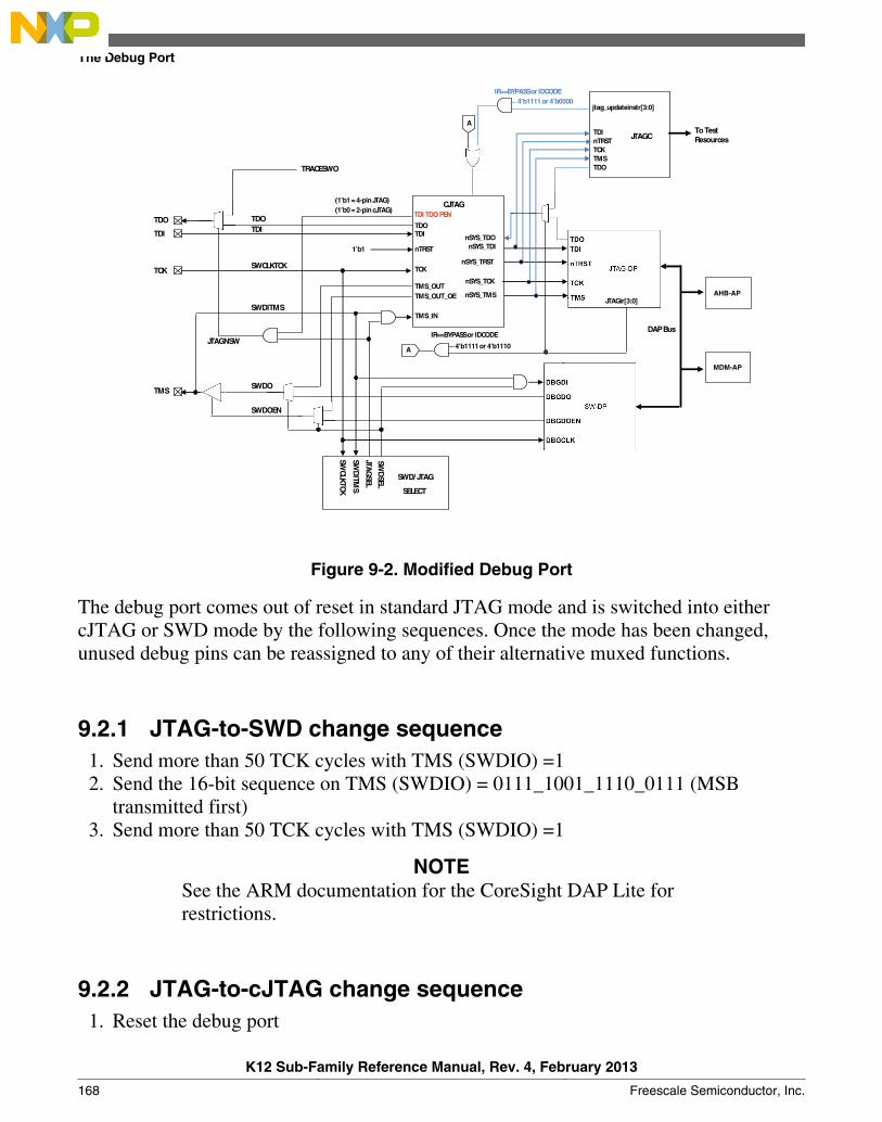
CJTAG
DAP Bus
TDO
TRACESWO
TDO
TDI
TCK
TDI
nSYS_TRST
nSYS_TDOnSYS_TDI
nSYS_TCK
nSYS_TMS
nTRST
TCK
TMS_OUT
TMS_IN
TMS_OUT_OE
TMS
TDOTDI
SWCLKTCK
SWDITMS
SWDO
SWDOEN
SWD/ JTAG
SELECT
SWCLKTCK
SWD
ITMS
JTAG
SEL
SWD
SEL
4’b1111 or 4’b0000
TDI TDO PEN
JTAGNSW
JTAGC
TDO
TDInTRSTTCKTMS
jtag_updateinstr[3:0]
4’b1111 or 4’b1110
JTAGir[3:0]
IR==BYPASS or IDCODE
IR==BYPASS or IDCODE
A
A
(1’b0 = 2-pin cJTAG)(1’b1 = 4-pin JTAG)
To TestResources
1’b1
MDM-AP
AHB-AP
Figure 9-2. Modified Debug Port
The debug port comes out of reset in standard JTAG mode and is switched into eithercJTAG or SWD mode by the following sequences. Once the mode has been changed,unused debug pins can be reassigned to any of their alternative muxed functions.
9.2.1 JTAG-to-SWD change sequence1. Send more than 50 TCK cycles with TMS (SWDIO) =12. Send the 16-bit sequence on TMS (SWDIO) = 0111_1001_1110_0111 (MSB
transmitted first)3. Send more than 50 TCK cycles with TMS (SWDIO) =1
NOTESee the ARM documentation for the CoreSight DAP Lite forrestrictions.
9.2.2 JTAG-to-cJTAG change sequence1. Reset the debug port
The Debug Port
K12 Sub-Family Reference Manual, Rev. 4, February 2013
168 Freescale Semiconductor, Inc.

2. Set the control level to 2 via zero-bit scans3. Execute the Store Format (STFMT) command (00011) to set the scan format register
to 1149.7 scan format
9.3 Debug Port Pin DescriptionsThe debug port pins default after POR to their JTAG functionality with the exception ofJTAG_TRST_b and can be later reassigned to their alternate functionalities. In cJTAGand SWD modes JTAG_TDI and JTAG_TRST_b can be configured to alternate GPIOfunctions.
Table 9-2. Debug port pins
Pin Name JTAG Debug Port cJTAG Debug Port SWD Debug Port Internal Pull-up\Down
Type Description Type Description Type Description
JTAG_TMS/SWD_DIO
I/O JTAG TestModeSelection
I/O cJTAG Data I/O Serial WireData
Pull-up
JTAG_TCLK/SWD_CLK
I JTAG TestClock
I cJTAG Clock I Serial WireClock
Pull-down
JTAG_TDI I JTAG TestData Input
- - - - Pull-up
JTAG_TDO/TRACE_SWO
O JTAG TestData Output
O Trace outputover a singlepin
O Trace outputover a singlepin
N/C
JTAG_TRST_b
I JTAG Reset I cJTAG Reset - - Pull-up
9.4 System TAP connectionThe system JTAG controller is connected in parallel to the ARM TAP controller. Thesystem JTAG controller IR codes overlay the ARM JTAG controller IR codes withoutconflict. Refer to the IR codes table for a list of the available IR codes. The output of theTAPs (TDO) are muxed based on the IR code which is selected. This design is fullyJTAG compliant and appears to the JTAG chain as a single TAP. At power on reset,ARM's IDCODE (IR=4'b1110) is selected.
Chapter 9 Debug
K12 Sub-Family Reference Manual, Rev. 4, February 2013
Freescale Semiconductor, Inc. 169

9.4.1 IR CodesTable 9-3. JTAG Instructions
Instruction Code[3:0] Instruction Summary
IDCODE 0000 Selects device identification register for shift
SAMPLE/PRELOAD 0010 Selects boundary scan register for shifting, sampling, andpreloading without disturbing functional operation
SAMPLE 0011 Selects boundary scan register for shifting and samplingwithout disturbing functional operation
EXTEST 0100 Selects boundary scan register while applying preloadedvalues to output pins and asserting functional reset
HIGHZ 1001 Selects bypass register while three-stating all output pins andasserting functional reset
CLAMP 1100 Selects bypass register while applying preloaded values tooutput pins and asserting functional reset
EZPORT 1101 Enables the EZPORT function for the SoC and assertsfunctional reset.
ARM_IDCODE 1110 ARM JTAG-DP Instruction
BYPASS 1111 Selects bypass register for data operations
Factory debug reserved 0101, 0110, 0111 Intended for factory debug only
ARM JTAG-DP Reserved 1000, 1010, 1011, 1110 These instructions will go the ARM JTAG-DP controller.Please look at ARM JTAG-DP documentation for moreinformation on these instructions.
Reserved 3 All other opcodes Decoded to select bypass register
3. The manufacturer reserves the right to change the decoding of reserved instruction codes in the future
9.5 JTAG status and control registersThrough the ARM Debug Access Port (DAP), the debugger has access to the status andcontrol elements, implemented as registers on the DAP bus as shown in the followingfigure. These registers provide additional control and status for low power mode recoveryand typical run-control scenarios. The status register bits also provide a means for thedebugger to get updated status of the core without having to initiate a bus transactionacross the crossbar switch, thus remaining less intrusive during a debug session.
It is important to note that these DAP control and status registers are not memory mappedwithin the system memory map and are only accessible via the Debug Access Port (DAP)using JTAG, cJTAG, or SWD. The MDM-AP is accessible as Debug Access Port 1 withthe available registers shown in the table below.
Table 9-4. MDM-AP Register Summary
Address Register Description
Table continues on the next page...
JTAG status and control registers
K12 Sub-Family Reference Manual, Rev. 4, February 2013
170 Freescale Semiconductor, Inc.

Table 9-4. MDM-AP Register Summary (continued)
0x0100_0000 Status See MDM-AP Status Register
0x0100_0004 Control See MDM-AP Control Register
0x0100_00FC ID Read-only identification register thatalways reads as 0x001C_0000
SWJ-DP
SELECT[31:24] (APSEL) selects the AP
SELECT[7:4] (APBANKSEL) selects the bank
A[3:2] from the APACC selects the register within the bank
AHB Access Port
(AHB-AP) MDM-AP
Stat
us0x
00
Cont
rol
0x01
IDR
0x3F
AHB-APSELECT[31:24] = 0x00 selects the AHB-APSee ARM documentation for further details
MDM-APSELECT[31:24] = 0x01 selects the MDM-AP
SELECT[7:4] = 0x0 selects the bank with Status and CtrlA[3:2] = 2’b00 selects the Status RegisterA[3:2] = 2’b01 selects the Control Register
SELECT[7:4] = 0xF selects the bank with IDRA[3:2] = 2’b11 selects the IDR Register(IDR register reads 0x001C_0000)
Bus MatrixSee Control and Status Register
Descriptions
Deb
ug P
ort
Inte
rnal
Bus
Acc
ess
Port
Data[31:0] A[7:4] A[3:2] RnWAPSELDecode
Deb
ug P
ort I
D R
egis
ter
(DP
IDR
)
Con
trol
/Sta
tus
(CT
RL/
ST
AT
)
AP
Sel
ect (
SE
LEC
T)
Rea
d B
uffe
r (R
EB
UF
F)
DP
Reg
iste
rs
0x00
0x04
0x08
0x0C
Data[31:0] A[3:2] RnW
DPACC
Data[31:0] A[3:2] RnW
APACC
Debug Port(DP)
Generic
See the ARM Debug Interface v5p1 Supplement.
Figure 9-3. MDM AP Addressing
Chapter 9 Debug
K12 Sub-Family Reference Manual, Rev. 4, February 2013
Freescale Semiconductor, Inc. 171
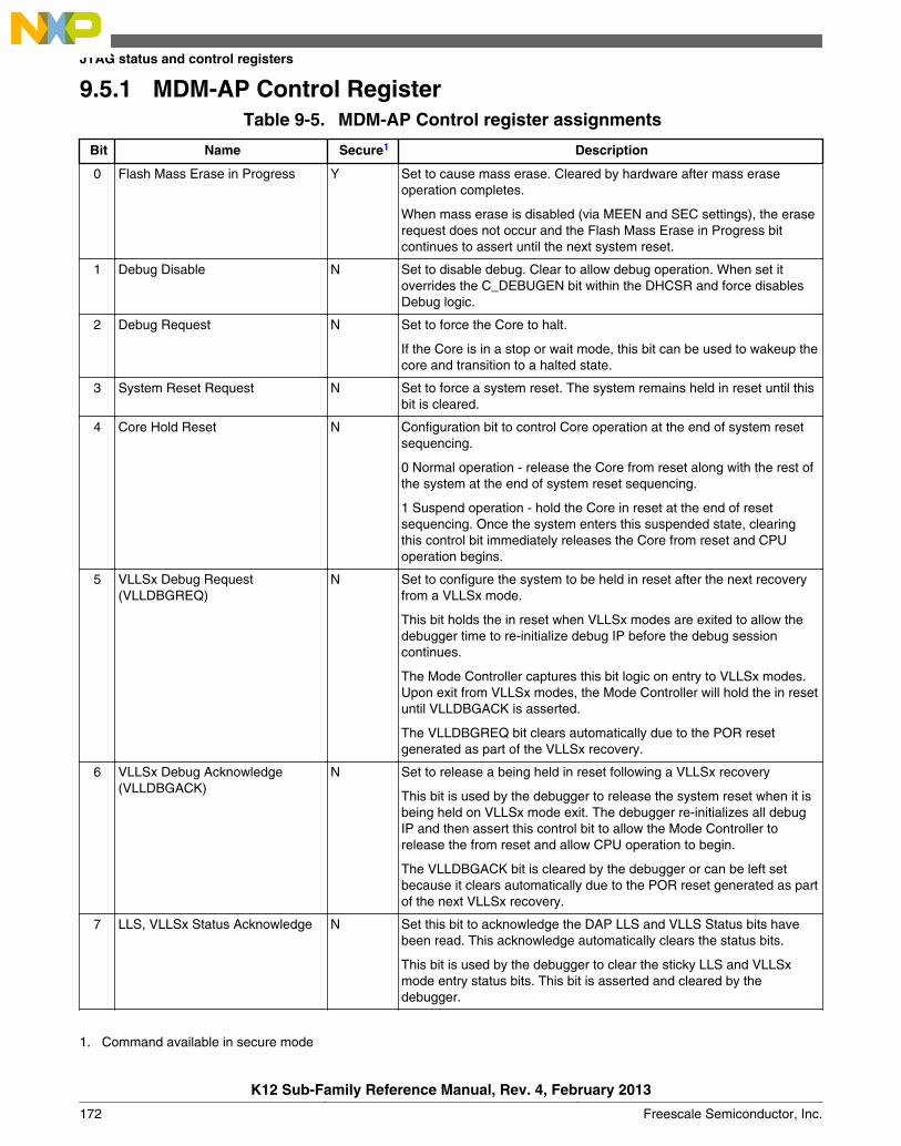
9.5.1 MDM-AP Control RegisterTable 9-5. MDM-AP Control register assignments
Bit Name Secure1 Description
0 Flash Mass Erase in Progress Y Set to cause mass erase. Cleared by hardware after mass eraseoperation completes.
When mass erase is disabled (via MEEN and SEC settings), the eraserequest does not occur and the Flash Mass Erase in Progress bitcontinues to assert until the next system reset.
1 Debug Disable N Set to disable debug. Clear to allow debug operation. When set itoverrides the C_DEBUGEN bit within the DHCSR and force disablesDebug logic.
2 Debug Request N Set to force the Core to halt.
If the Core is in a stop or wait mode, this bit can be used to wakeup thecore and transition to a halted state.
3 System Reset Request N Set to force a system reset. The system remains held in reset until thisbit is cleared.
4 Core Hold Reset N Configuration bit to control Core operation at the end of system resetsequencing.
0 Normal operation - release the Core from reset along with the rest ofthe system at the end of system reset sequencing.
1 Suspend operation - hold the Core in reset at the end of resetsequencing. Once the system enters this suspended state, clearingthis control bit immediately releases the Core from reset and CPUoperation begins.
5 VLLSx Debug Request(VLLDBGREQ)
N Set to configure the system to be held in reset after the next recoveryfrom a VLLSx mode.
This bit holds the in reset when VLLSx modes are exited to allow thedebugger time to re-initialize debug IP before the debug sessioncontinues.
The Mode Controller captures this bit logic on entry to VLLSx modes.Upon exit from VLLSx modes, the Mode Controller will hold the in resetuntil VLLDBGACK is asserted.
The VLLDBGREQ bit clears automatically due to the POR resetgenerated as part of the VLLSx recovery.
6 VLLSx Debug Acknowledge(VLLDBGACK)
N Set to release a being held in reset following a VLLSx recovery
This bit is used by the debugger to release the system reset when it isbeing held on VLLSx mode exit. The debugger re-initializes all debugIP and then assert this control bit to allow the Mode Controller torelease the from reset and allow CPU operation to begin.
The VLLDBGACK bit is cleared by the debugger or can be left setbecause it clears automatically due to the POR reset generated as partof the next VLLSx recovery.
7 LLS, VLLSx Status Acknowledge N Set this bit to acknowledge the DAP LLS and VLLS Status bits havebeen read. This acknowledge automatically clears the status bits.
This bit is used by the debugger to clear the sticky LLS and VLLSxmode entry status bits. This bit is asserted and cleared by thedebugger.
1. Command available in secure mode
JTAG status and control registers
K12 Sub-Family Reference Manual, Rev. 4, February 2013
172 Freescale Semiconductor, Inc.
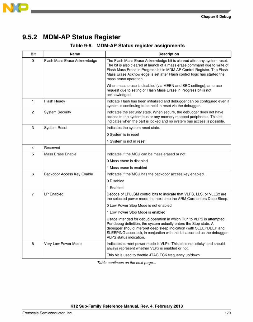
9.5.2 MDM-AP Status RegisterTable 9-6. MDM-AP Status register assignments
Bit Name Description
0 Flash Mass Erase Acknowledge The Flash Mass Erase Acknowledge bit is cleared after any system reset.The bit is also cleared at launch of a mass erase command due to write ofFlash Mass Erase in Progress bit in MDM AP Control Register. The FlashMass Erase Acknowledge is set after Flash control logic has started themass erase operation.
When mass erase is disabled (via MEEN and SEC settings), an eraserequest due to seting of Flash Mass Erase in Progress bit is notacknowledged.
1 Flash Ready Indicate Flash has been initialized and debugger can be configured even ifsystem is continuing to be held in reset via the debugger.
2 System Security Indicates the security state. When secure, the debugger does not haveaccess to the system bus or any memory mapped peripherals. This bitindicates when the part is locked and no system bus access is possible.
3 System Reset Indicates the system reset state.
0 System is in reset
1 System is not in reset
4 Reserved
5 Mass Erase Enable Indicates if the MCU can be mass erased or not
0 Mass erase is disabled
1 Mass erase is enabled
6 Backdoor Access Key Enable Indicates if the MCU has the backdoor access key enabled.
0 Disabled
1 Enabled
7 LP Enabled Decode of LPLLSM control bits to indicate that VLPS, LLS, or VLLSx arethe selected power mode the next time the ARM Core enters Deep Sleep.
0 Low Power Stop Mode is not enabled
1 Low Power Stop Mode is enabled
Usage intended for debug operation in which Run to VLPS is attempted.Per debug definition, the system actually enters the Stop state. Adebugger should interpret deep sleep indication (with SLEEPDEEP andSLEEPING asserted), in conjuntion with this bit asserted as the debugger-VLPS status indication.
8 Very Low Power Mode Indicates current power mode is VLPx. This bit is not ‘sticky’ and shouldalways represent whether VLPx is enabled or not.
This bit is used to throttle JTAG TCK frequency up/down.
Table continues on the next page...
Chapter 9 Debug
K12 Sub-Family Reference Manual, Rev. 4, February 2013
Freescale Semiconductor, Inc. 173

Table 9-6. MDM-AP Status register assignments (continued)
Bit Name Description
9 LLS Mode Exit This bit indicates an exit from LLS mode has occurred. The debugger willlose communication while the system is in LLS (including access to thisregister). Once communication is reestablished, this bit indicates that thesystem had been in LLS. Since the debug modules held their state duringLLS, they do not need to be reconfigured.
This bit is set during the LLS recovery sequence. The LLS Mode Exit bit isheld until the debugger has had a chance to recognize that LLS was exitedand is cleared by a write of 1 to the LLS, VLLSx Status Acknowledge bit inMDM AP Control register.
10 VLLSx Modes Exit This bit indicates an exit from VLLSx mode has occurred. The debuggerwill lose communication while the system is in VLLSx (including access tothis register). Once communication is reestablished, this bit indicates thatthe system had been in VLLSx. Since the debug modules lose their stateduring VLLSx modes, they need to be reconfigured.
This bit is set during the VLLSx recovery sequence. The VLLSx Mode Exitbit is held until the debugger has had a chance to recognize that a VLLSmode was exited and is cleared by a write of 1 to the LLS, VLLSx StatusAcknowledge bit in MDM AP Control register.
11 – 15 Reserved for future use Always read 0.
16 Core Halted Indicates the Core has entered debug halt mode
17 Core SLEEPDEEP Indicates the Core has entered a low power mode
SLEEPING==1 and SLEEPDEEP==0 indicates wait or VLPW mode.
SLEEPING==1 and SLEEPDEEP==1 indicates stop or VLPS mode.
18 Core SLEEPING
19 – 31 Reserved for future use Always read 0.
9.6 Debug ResetsThe debug system receives the following sources of reset:
• JTAG_TRST_b from an external signal. This signal is optional and may not beavailable in all packages.
• Debug reset (CDBGRSTREQ bit within the SWJ-DP CTRL/STAT register) in theTCLK domain that allows the debugger to reset the debug logic.
• TRST asserted via the cJTAG escape command.• System POR reset
Conversely the debug system is capable of generating system reset using the followingmechanism:
• A system reset in the DAP control register which allows the debugger to hold thesystem in reset.
Debug Resets
K12 Sub-Family Reference Manual, Rev. 4, February 2013
174 Freescale Semiconductor, Inc.

• SYSRESETREQ bit in the NVIC application interrupt and reset control register• A system reset in the DAP control register which allows the debugger to hold the
Core in reset.
9.7 AHB-APAHB-AP provides the debugger access to all memory and registers in the system,including processor registers through the NVIC. System access is independent of theprocessor status. AHB-AP does not do back-to-back transactions on the bus, so alltransactions are non-sequential. AHB-AP can perform unaligned and bit-bandtransactions. AHB-AP transactions bypass the FPB, so the FPB cannot remap AHB-APtransactions. SWJ/SW-DP-initiated transaction aborts drive an AHB-AP-supportedsideband signal called HABORT. This signal is driven into the Bus Matrix, which resetsthe Bus Matrix state, so that AHB-AP can access the Private Peripheral Bus for last ditchdebugging such as read/stop/reset the core. AHB-AP transactions are little endian.
For a short period at the start of a system reset event the system security status is beingdetermined and debugger access to all AHB-AP transactions is blocked. The MDM-APStatus register is accessible and can be monitored to determine when this initial period iscompleted. After this initial period, if system reset is held via assertion of the RESET pin,the debugger has access via the bus matrix to the private peripheral bus to configure thedebug IP even while system reset is asserted. While in system reset, access to othermemory and register resources, accessed over the Crossbar Switch, is blocked.
9.8 ITMThe ITM is an application-driven trace source that supports printf style debugging totrace Operating System (OS) and application events, and emits diagnostic systeminformation. The ITM emits trace information as packets. There are four sources that cangenerate packets. If multiple sources generate packets at the same time, the ITMarbitrates the order in which packets are output. The four sources in decreasing order ofpriority are:
1. Software trace -- Software can write directly to ITM stimulus registers. This emitspackets.
2. Hardware trace -- The DWT generates these packets, and the ITM emits them.3. Time stamping -- Timestamps are emitted relative to packets. The ITM contains a
21-bit counter to generate the timestamp. The Cortex-M4 clock or the bitclock rate ofthe Serial Wire Viewer (SWV) output clocks the counter.
Chapter 9 Debug
K12 Sub-Family Reference Manual, Rev. 4, February 2013
Freescale Semiconductor, Inc. 175
4. Global system timestamping. Timestamps can optionally be generated using asystem-wide 48-bit count value. The same count value can be used to inserttimestamps in the ETM trace stream, allowing coarse-grain correlation.
9.9 Core Trace ConnectivityThe ETM and ITM can route its data to the ETB or the TPIU. (See the MCM(Miscellaneous Control Module) for controlling the routing to the TPIU.) Thisconfiguration enables the use of trace with low cost tools while maintaining thecompatibility with trace probes. The arbitration between the ETM and ITM is performedinside the TPIU.
9.10 Embedded Trace Macrocell v3.5 (ETM)The Cortex-M4 Embedded Trace Macrocell (ETM-M4) is a debug component thatenables a debugger to reconstruct program execution. The CoreSight ETM-M4 supportsonly instruction trace. You can use it either with the Cortex-M4 Trace Port Interface Unit(M4-TPIU).
The main features of an ETM are:
• tracing of 16-bit and 32-bit Thumb instructions• four EmbeddedICE watchpoint inputs• a Trace Start/Stop block with EmbeddedICE inputs• one reduced function counter• two external inputs• a 24-byte FIFO queue• global timestamping
9.11 TPIUThe TPIU acts as a bridge between the on-chip trace data from the Embedded TraceMacrocell (ETM) and the Instrumentation Trace Macrocell (ITM), with separate IDs, to adata stream, encapsulating IDs where required, that is then captured by a Trace PortAnalyzer (TPA). The TPIU is specially designed for low-cost debug.
Core Trace Connectivity
K12 Sub-Family Reference Manual, Rev. 4, February 2013
176 Freescale Semiconductor, Inc.
9.12 DWTThe DWT is a unit that performs the following debug functionality:
• It contains four comparators that you can configure as a hardware watchpoint, anETM trigger, a PC sampler event trigger, or a data address sampler event trigger. Thefirst comparator, DWT_COMP0, can also compare against the clock cycle counter,CYCCNT. The second comparator, DWT_COMP1, can also be used as a datacomparator.
• The DWT contains counters for:• Clock cycles (CYCCNT)• Folded instructions• Load store unit (LSU) operations• Sleep cycles• CPI (all instruction cycles except for the first cycle)• Interrupt overhead
NOTEAn event is emitted each time a counter overflows.
• The DWT can be configured to emit PC samples at defined intervals, and to emitinterrupt event information.
9.13 Debug in Low Power ModesIn low power modes in which the debug modules are kept static or powered off, thedebugger cannot gather any debug data for the duration of the low power mode. In thecase that the debugger is held static, the debug port returns to full functionality as soon asthe low power mode exits and the system returns to a state with active debug. In the casethat the debugger logic is powered off, the debugger is reset on recovery and must bereconfigured once the low power mode is exited.
Power mode entry logic monitors Debug Power Up and System Power Up signals fromthe debug port as indications that a debugger is active. These signals can be changed inRUN, VLPR, WAIT and VLPW. If the debug signal is active and the system attempts toenter stop or VLPS, FCLK continues to run to support core register access. In thesemodes in which FCLK is left active the debug modules have access to core registers butnot to system memory resources accessed via the crossbar.
Chapter 9 Debug
K12 Sub-Family Reference Manual, Rev. 4, February 2013
Freescale Semiconductor, Inc. 177
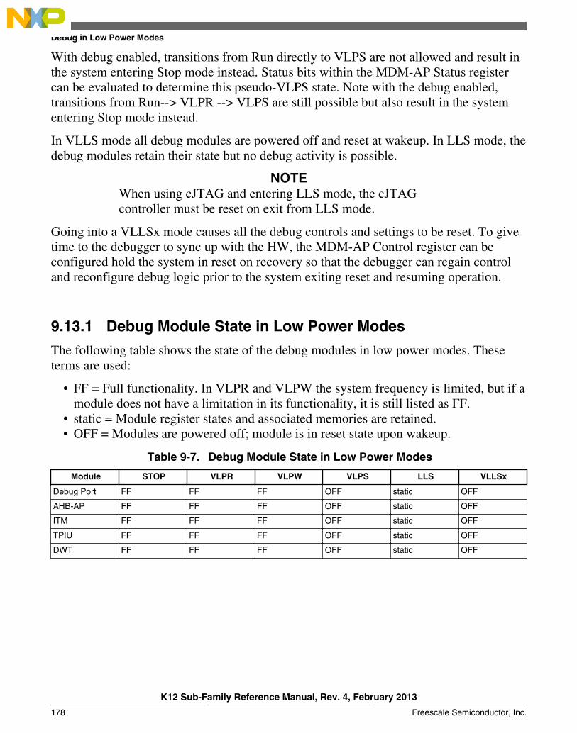
With debug enabled, transitions from Run directly to VLPS are not allowed and result inthe system entering Stop mode instead. Status bits within the MDM-AP Status registercan be evaluated to determine this pseudo-VLPS state. Note with the debug enabled,transitions from Run--> VLPR --> VLPS are still possible but also result in the systementering Stop mode instead.
In VLLS mode all debug modules are powered off and reset at wakeup. In LLS mode, thedebug modules retain their state but no debug activity is possible.
NOTEWhen using cJTAG and entering LLS mode, the cJTAGcontroller must be reset on exit from LLS mode.
Going into a VLLSx mode causes all the debug controls and settings to be reset. To givetime to the debugger to sync up with the HW, the MDM-AP Control register can beconfigured hold the system in reset on recovery so that the debugger can regain controland reconfigure debug logic prior to the system exiting reset and resuming operation.
9.13.1 Debug Module State in Low Power Modes
The following table shows the state of the debug modules in low power modes. Theseterms are used:
• FF = Full functionality. In VLPR and VLPW the system frequency is limited, but if amodule does not have a limitation in its functionality, it is still listed as FF.
• static = Module register states and associated memories are retained.• OFF = Modules are powered off; module is in reset state upon wakeup.
Table 9-7. Debug Module State in Low Power Modes
Module STOP VLPR VLPW VLPS LLS VLLSx
Debug Port FF FF FF OFF static OFF
AHB-AP FF FF FF OFF static OFF
ITM FF FF FF OFF static OFF
TPIU FF FF FF OFF static OFF
DWT FF FF FF OFF static OFF
Debug in Low Power Modes
K12 Sub-Family Reference Manual, Rev. 4, February 2013
178 Freescale Semiconductor, Inc.
9.14 Debug & SecurityWhen security is enabled (FSEC[SEC] != 10), the debug port capabilities are limited inorder to prevent exploitation of secure data. In the secure state the debugger still hasaccess to the MDM-AP Status Register and can determine the current security state of thedevice. In the case of a secure device, the debugger also has the capability of performinga mass erase operation via writes to the MDM-AP Control Register. In the case of asecure device that has mass erase disabled (FSEC[MEEN] = 10), attempts to mass erasevia the debug interface are blocked.
Chapter 9 Debug
K12 Sub-Family Reference Manual, Rev. 4, February 2013
Freescale Semiconductor, Inc. 179

Debug & Security
K12 Sub-Family Reference Manual, Rev. 4, February 2013
180 Freescale Semiconductor, Inc.
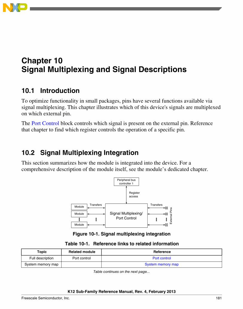
Chapter 10Signal Multiplexing and Signal Descriptions
10.1 IntroductionTo optimize functionality in small packages, pins have several functions available viasignal multiplexing. This chapter illustrates which of this device's signals are multiplexedon which external pin.
The Port Control block controls which signal is present on the external pin. Referencethat chapter to find which register controls the operation of a specific pin.
10.2 Signal Multiplexing IntegrationThis section summarizes how the module is integrated into the device. For acomprehensive description of the module itself, see the module’s dedicated chapter.
Registeraccess
Signal Multiplexing/Port Control
TransfersModule
Peripheral buscontroller 1
Module
Module Ext
erna
l Pin
s
Transfers
Figure 10-1. Signal multiplexing integration
Table 10-1. Reference links to related information
Topic Related module Reference
Full description Port control Port control
System memory map System memory map
Table continues on the next page...
K12 Sub-Family Reference Manual, Rev. 4, February 2013
Freescale Semiconductor, Inc. 181
Table 10-1. Reference links to related information (continued)
Topic Related module Reference
Clocking Clock Distribution
Register access Peripheral buscontroller
Peripheral bridge
10.2.1 Port control and interrupt module features• 32-pin ports
NOTENot all pins are available on the device. See the followingsection for details.
• Each 32-pin port is assigned one interrupt.• The digital filter option has two clock source options: bus clock and 1-kHz LPO. The
1-kHz LPO option gives users this feature in low power modes.• The digital filter is configurable from 1 to 32 clock cycles when enabled.
10.2.2 PCRn reset values for port A
PCRn bit reset values for port A are 1 for the following bits:
• For PCR0: bits 1, 6, 8, 9, and 10.• For PCR1 to PCR4: bits 0, 1, 6, 8, 9, and 10.• For PCR5 : bits 0, 1, and 6.
All other PCRn bit reset values for port A are 0.
10.2.3 Clock gating
The clock to the port control module can be gated on and off using the SCGC5[PORTx]bits in the SIM module. These bits are cleared after any reset, which disables the clock tothe corresponding module to conserve power. Prior to initializing the correspondingmodule, set SCGC5[PORTx] in the SIM module to enable the clock. Before turning offthe clock, make sure to disable the module. For more details, refer to the clockdistribution chapter.
Signal Multiplexing Integration
K12 Sub-Family Reference Manual, Rev. 4, February 2013
182 Freescale Semiconductor, Inc.

10.2.4 Signal multiplexing constraints1. A given peripheral function must be assigned to a maximum of one package pin. Do
not program the same function to more than one pin.2. To ensure the best signal timing for a given peripheral's interface, choose the pins in
closest proximity to each other.
10.3 Pinout
10.3.1 K12 Signal Multiplexing and Pin Assignments
The following table shows the signals available on each pin and the locations of thesepins on the devices supported by this document. The Port Control Module is responsiblefor selecting which ALT functionality is available on each pin.
NOTE• The analog input signals ADC0_SE10, ADC0_SE11,
ADC0_DP1, and ADC0_DM1 are available only for K11,K12, K21, and K22 devices and are not present on K10 andK20 devices.
• The TRACE signals on PTE0, PTE1, PTE2, PTE3, andPTE4 are available only for K11, K12, K21, and K22devices and are not present on K10 and K20 devices.
• If the VBAT pin is not used, the VBAT pin should be leftfloating. Do not connect VBAT pin to VSS.
• The FTM_CLKIN signals on PTB16 and PTB17 areavailable only for K11, K12, K21, and K22 devices and isnot present on K10 and K20 devices. For K22D devicesthis signal is on ALT4, and for K22F devices, this signal ison ALT7.
• The FTM signals are available only for K11, K12, K21,and K22 devices and are not present on K10 and K20devices.
• The I2C signals are available only for K11, K12, K21, andK22 devices and are not present on K10 and K20 devices.
121MAPBGA
Pin Name Default ALT0 ALT1 ALT2 ALT3 ALT4 ALT5 ALT6 ALT7 EzPort
E4 PTE0 ADC0_SE10 ADC0_SE10 PTE0 SPI1_PCS1 UART1_TX TRACE_CLKOUT
I2C1_SDA RTC_CLKOUT
Chapter 10 Signal Multiplexing and Signal Descriptions
K12 Sub-Family Reference Manual, Rev. 4, February 2013
Freescale Semiconductor, Inc. 183
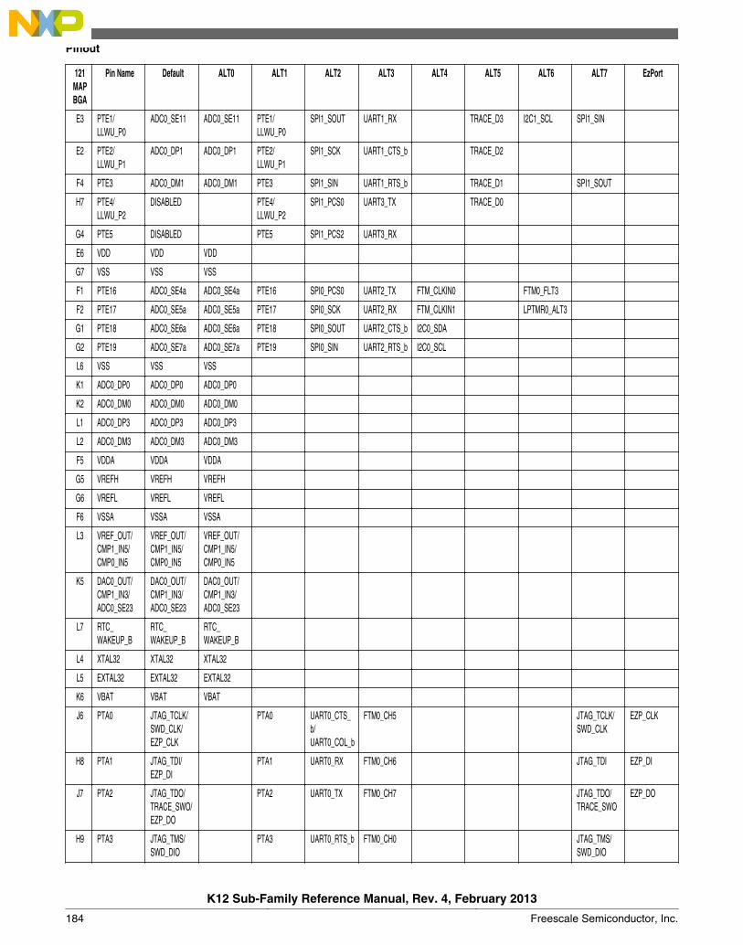
121MAPBGA
Pin Name Default ALT0 ALT1 ALT2 ALT3 ALT4 ALT5 ALT6 ALT7 EzPort
E3 PTE1/LLWU_P0
ADC0_SE11 ADC0_SE11 PTE1/LLWU_P0
SPI1_SOUT UART1_RX TRACE_D3 I2C1_SCL SPI1_SIN
E2 PTE2/LLWU_P1
ADC0_DP1 ADC0_DP1 PTE2/LLWU_P1
SPI1_SCK UART1_CTS_b TRACE_D2
F4 PTE3 ADC0_DM1 ADC0_DM1 PTE3 SPI1_SIN UART1_RTS_b TRACE_D1 SPI1_SOUT
H7 PTE4/LLWU_P2
DISABLED PTE4/LLWU_P2
SPI1_PCS0 UART3_TX TRACE_D0
G4 PTE5 DISABLED PTE5 SPI1_PCS2 UART3_RX
E6 VDD VDD VDD
G7 VSS VSS VSS
F1 PTE16 ADC0_SE4a ADC0_SE4a PTE16 SPI0_PCS0 UART2_TX FTM_CLKIN0 FTM0_FLT3
F2 PTE17 ADC0_SE5a ADC0_SE5a PTE17 SPI0_SCK UART2_RX FTM_CLKIN1 LPTMR0_ALT3
G1 PTE18 ADC0_SE6a ADC0_SE6a PTE18 SPI0_SOUT UART2_CTS_b I2C0_SDA
G2 PTE19 ADC0_SE7a ADC0_SE7a PTE19 SPI0_SIN UART2_RTS_b I2C0_SCL
L6 VSS VSS VSS
K1 ADC0_DP0 ADC0_DP0 ADC0_DP0
K2 ADC0_DM0 ADC0_DM0 ADC0_DM0
L1 ADC0_DP3 ADC0_DP3 ADC0_DP3
L2 ADC0_DM3 ADC0_DM3 ADC0_DM3
F5 VDDA VDDA VDDA
G5 VREFH VREFH VREFH
G6 VREFL VREFL VREFL
F6 VSSA VSSA VSSA
L3 VREF_OUT/CMP1_IN5/CMP0_IN5
VREF_OUT/CMP1_IN5/CMP0_IN5
VREF_OUT/CMP1_IN5/CMP0_IN5
K5 DAC0_OUT/CMP1_IN3/ADC0_SE23
DAC0_OUT/CMP1_IN3/ADC0_SE23
DAC0_OUT/CMP1_IN3/ADC0_SE23
L7 RTC_WAKEUP_B
RTC_WAKEUP_B
RTC_WAKEUP_B
L4 XTAL32 XTAL32 XTAL32
L5 EXTAL32 EXTAL32 EXTAL32
K6 VBAT VBAT VBAT
J6 PTA0 JTAG_TCLK/SWD_CLK/EZP_CLK
PTA0 UART0_CTS_b/UART0_COL_b
FTM0_CH5 JTAG_TCLK/SWD_CLK
EZP_CLK
H8 PTA1 JTAG_TDI/EZP_DI
PTA1 UART0_RX FTM0_CH6 JTAG_TDI EZP_DI
J7 PTA2 JTAG_TDO/TRACE_SWO/EZP_DO
PTA2 UART0_TX FTM0_CH7 JTAG_TDO/TRACE_SWO
EZP_DO
H9 PTA3 JTAG_TMS/SWD_DIO
PTA3 UART0_RTS_b FTM0_CH0 JTAG_TMS/SWD_DIO
Pinout
K12 Sub-Family Reference Manual, Rev. 4, February 2013
184 Freescale Semiconductor, Inc.
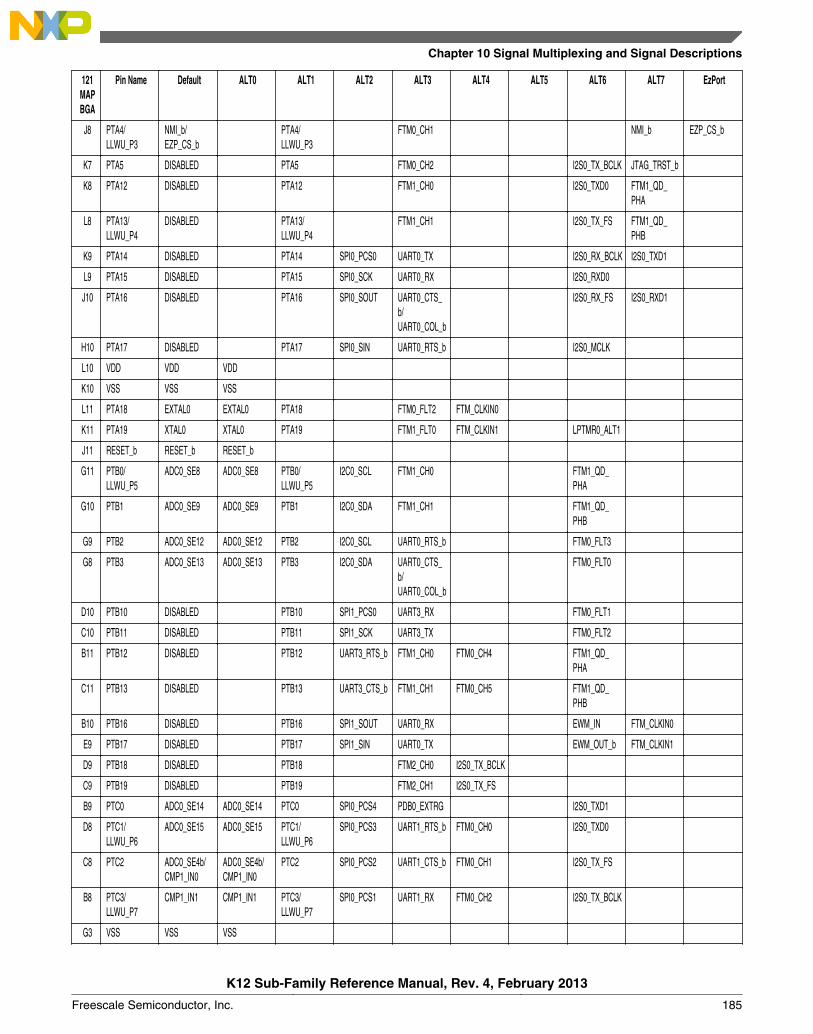
121MAPBGA
Pin Name Default ALT0 ALT1 ALT2 ALT3 ALT4 ALT5 ALT6 ALT7 EzPort
J8 PTA4/LLWU_P3
NMI_b/EZP_CS_b
PTA4/LLWU_P3
FTM0_CH1 NMI_b EZP_CS_b
K7 PTA5 DISABLED PTA5 FTM0_CH2 I2S0_TX_BCLK JTAG_TRST_b
K8 PTA12 DISABLED PTA12 FTM1_CH0 I2S0_TXD0 FTM1_QD_PHA
L8 PTA13/LLWU_P4
DISABLED PTA13/LLWU_P4
FTM1_CH1 I2S0_TX_FS FTM1_QD_PHB
K9 PTA14 DISABLED PTA14 SPI0_PCS0 UART0_TX I2S0_RX_BCLK I2S0_TXD1
L9 PTA15 DISABLED PTA15 SPI0_SCK UART0_RX I2S0_RXD0
J10 PTA16 DISABLED PTA16 SPI0_SOUT UART0_CTS_b/UART0_COL_b
I2S0_RX_FS I2S0_RXD1
H10 PTA17 DISABLED PTA17 SPI0_SIN UART0_RTS_b I2S0_MCLK
L10 VDD VDD VDD
K10 VSS VSS VSS
L11 PTA18 EXTAL0 EXTAL0 PTA18 FTM0_FLT2 FTM_CLKIN0
K11 PTA19 XTAL0 XTAL0 PTA19 FTM1_FLT0 FTM_CLKIN1 LPTMR0_ALT1
J11 RESET_b RESET_b RESET_b
G11 PTB0/LLWU_P5
ADC0_SE8 ADC0_SE8 PTB0/LLWU_P5
I2C0_SCL FTM1_CH0 FTM1_QD_PHA
G10 PTB1 ADC0_SE9 ADC0_SE9 PTB1 I2C0_SDA FTM1_CH1 FTM1_QD_PHB
G9 PTB2 ADC0_SE12 ADC0_SE12 PTB2 I2C0_SCL UART0_RTS_b FTM0_FLT3
G8 PTB3 ADC0_SE13 ADC0_SE13 PTB3 I2C0_SDA UART0_CTS_b/UART0_COL_b
FTM0_FLT0
D10 PTB10 DISABLED PTB10 SPI1_PCS0 UART3_RX FTM0_FLT1
C10 PTB11 DISABLED PTB11 SPI1_SCK UART3_TX FTM0_FLT2
B11 PTB12 DISABLED PTB12 UART3_RTS_b FTM1_CH0 FTM0_CH4 FTM1_QD_PHA
C11 PTB13 DISABLED PTB13 UART3_CTS_b FTM1_CH1 FTM0_CH5 FTM1_QD_PHB
B10 PTB16 DISABLED PTB16 SPI1_SOUT UART0_RX EWM_IN FTM_CLKIN0
E9 PTB17 DISABLED PTB17 SPI1_SIN UART0_TX EWM_OUT_b FTM_CLKIN1
D9 PTB18 DISABLED PTB18 FTM2_CH0 I2S0_TX_BCLK
C9 PTB19 DISABLED PTB19 FTM2_CH1 I2S0_TX_FS
B9 PTC0 ADC0_SE14 ADC0_SE14 PTC0 SPI0_PCS4 PDB0_EXTRG I2S0_TXD1
D8 PTC1/LLWU_P6
ADC0_SE15 ADC0_SE15 PTC1/LLWU_P6
SPI0_PCS3 UART1_RTS_b FTM0_CH0 I2S0_TXD0
C8 PTC2 ADC0_SE4b/CMP1_IN0
ADC0_SE4b/CMP1_IN0
PTC2 SPI0_PCS2 UART1_CTS_b FTM0_CH1 I2S0_TX_FS
B8 PTC3/LLWU_P7
CMP1_IN1 CMP1_IN1 PTC3/LLWU_P7
SPI0_PCS1 UART1_RX FTM0_CH2 I2S0_TX_BCLK
G3 VSS VSS VSS
Chapter 10 Signal Multiplexing and Signal Descriptions
K12 Sub-Family Reference Manual, Rev. 4, February 2013
Freescale Semiconductor, Inc. 185

121MAPBGA
Pin Name Default ALT0 ALT1 ALT2 ALT3 ALT4 ALT5 ALT6 ALT7 EzPort
E5 VDD VDD VDD
A8 PTC4/LLWU_P8
DISABLED PTC4/LLWU_P8
SPI0_PCS0 UART1_TX FTM0_CH3 CMP1_OUT
D7 PTC5/LLWU_P9
DISABLED PTC5/LLWU_P9
SPI0_SCK LPTMR0_ALT2 I2S0_RXD0 CMP0_OUT FTM0_CH2
C7 PTC6/LLWU_P10
CMP0_IN0 CMP0_IN0 PTC6/LLWU_P10
SPI0_SOUT PDB0_EXTRG I2S0_RX_BCLK I2S0_MCLK
B7 PTC7 CMP0_IN1 CMP0_IN1 PTC7 SPI0_SIN I2S0_RX_FS
A7 PTC8 CMP0_IN2 CMP0_IN2 PTC8 I2S0_MCLK
D6 PTC9 CMP0_IN3 CMP0_IN3 PTC9 I2S0_RX_BCLK FTM2_FLT0
C6 PTC10 DISABLED PTC10 I2C1_SCL I2S0_RX_FS
C5 PTC11/LLWU_P11
DISABLED PTC11/LLWU_P11
I2C1_SDA I2S0_RXD1
B6 PTC12 DISABLED PTC12
A6 PTC13 DISABLED PTC13
D5 PTC16 DISABLED PTC16 UART3_RX
C4 PTC17 DISABLED PTC17 UART3_TX
D4 PTD0/LLWU_P12
DISABLED PTD0/LLWU_P12
SPI0_PCS0 UART2_RTS_b
D3 PTD1 ADC0_SE5b ADC0_SE5b PTD1 SPI0_SCK UART2_CTS_b
C3 PTD2/LLWU_P13
DISABLED PTD2/LLWU_P13
SPI0_SOUT UART2_RX I2C0_SCL
B3 PTD3 DISABLED PTD3 SPI0_SIN UART2_TX I2C0_SDA
A3 PTD4/LLWU_P14
ADC0_SE21 ADC0_SE21 PTD4/LLWU_P14
SPI0_PCS1 UART0_RTS_b FTM0_CH4 EWM_IN
A2 PTD5 ADC0_SE6b ADC0_SE6b PTD5 SPI0_PCS2 UART0_CTS_b/UART0_COL_b
FTM0_CH5 EWM_OUT_b
B2 PTD6/LLWU_P15
ADC0_SE7b ADC0_SE7b PTD6/LLWU_P15
SPI0_PCS3 UART0_RX FTM0_CH6 FTM0_FLT0
A1 PTD7 ADC0_SE22 ADC0_SE22 PTD7 CMT_IRO UART0_TX FTM0_CH7 FTM0_FLT1
A11 NC NC NC
K3 NC NC NC
H4 NC NC NC
F3 NC NC NC
H1 NC NC NC
H2 NC NC NC
J1 NC NC NC
J2 NC NC NC
J3 NC NC NC
H3 NC NC NC
K4 NC NC NC
H5 NC NC NC
Pinout
K12 Sub-Family Reference Manual, Rev. 4, February 2013
186 Freescale Semiconductor, Inc.

121MAPBGA
Pin Name Default ALT0 ALT1 ALT2 ALT3 ALT4 ALT5 ALT6 ALT7 EzPort
J5 NC NC NC
H6 NC NC NC
J9 NC NC NC
J4 NC NC NC
H11 NC NC NC
F11 NC NC NC
E11 NC NC NC
D11 NC NC NC
E10 NC NC NC
F10 NC NC NC
F9 NC NC NC
F8 NC NC NC
E8 NC NC NC
E7 NC NC NC
F7 NC NC NC
A5 NC NC NC
B5 NC NC NC
B4 NC NC NC
A4 NC NC NC
A10 NC NC NC
A9 NC NC NC
B1 NC NC NC
C2 NC NC NC
C1 NC NC NC
D2 NC NC NC
D1 NC NC NC
E1 NC NC NC
10.3.2 K12 Pinouts
The below figure shows the pinout diagram for the devices supported by this document.Many signals may be multiplexed onto a single pin. To determine what signals can beused on which pin, see the previous section.
Chapter 10 Signal Multiplexing and Signal Descriptions
K12 Sub-Family Reference Manual, Rev. 4, February 2013
Freescale Semiconductor, Inc. 187

1
A PTD7
B NC
C NC
D NC
E NC
F PTE16
G PTE18
H NC
J NC
K ADC0_DP0
1
L ADC0_DP3
2
PTD5
PTD6/LLWU_P15
NC
NC
PTE2/LLWU_P1
PTE17
PTE19
NC
NC
ADC0_DM0
2
ADC0_DM3
3
PTD4/LLWU_P14
PTD3
PTD2/LLWU_P13
PTD1
PTE1/LLWU_P0
NC
VSS
NC
NC
NC
3
VREF_OUT/CMP1_IN5/CMP0_IN5
4
NC
NC
PTC17
PTD0/LLWU_P12
PTE0
PTE3
PTE5
NC
NC
NC
4
XTAL32
5
NC
NC
PTC11/LLWU_P11
PTC16
VDD
VDDA
VREFH
NC
NC
DAC0_OUT/CMP1_IN3/ADC0_SE23
5
EXTAL32
6
PTC13
PTC12
PTC10
PTC9
VDD
VSSA
VREFL
NC
PTA0
VBAT
6
VSS
7
PTC8
PTC7
PTC6/LLWU_P10
PTC5/LLWU_P9
NC
NC
VSS
PTE4/LLWU_P2
PTA2
PTA5
7
RTC_WAKEUP_B
8
PTC4/LLWU_P8
PTC3/LLWU_P7
PTC2
PTC1/LLWU_P6
NC
NC
PTB3
PTA1
PTA4/LLWU_P3
PTA12
8
PTA13/LLWU_P4
9
NC
PTC0
PTB19
PTB18
PTB17
NC
PTB2
PTA3
NC
PTA14
9
PTA15
10
NC
PTB16
PTB11
PTB10
NC
NC
PTB1
PTA17
PTA16
VSS
10
VDD
11
ANC
BPTB12
CPTB13
DNC
ENC
FNC
GPTB0/LLWU_P5
HNC
JRESET_b
KPTA19
11
LPTA18
Figure 10-2. K12 121 MAPBGA Pinout Diagram
10.4 Module Signal Description TablesThe following sections correlate the chip-level signal name with the signal name used inthe module's chapter. They also briefly describe the signal function and direction.
Module Signal Description Tables
K12 Sub-Family Reference Manual, Rev. 4, February 2013
188 Freescale Semiconductor, Inc.
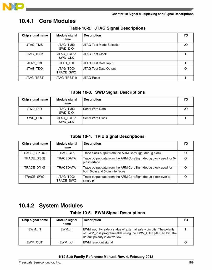
10.4.1 Core ModulesTable 10-2. JTAG Signal Descriptions
Chip signal name Module signalname
Description I/O
JTAG_TMS JTAG_TMS/SWD_DIO
JTAG Test Mode Selection I/O
JTAG_TCLK JTAG_TCLK/SWD_CLK
JTAG Test Clock I
JTAG_TDI JTAG_TDI JTAG Test Data Input I
JTAG_TDO JTAG_TDO/TRACE_SWO
JTAG Test Data Output O
JTAG_TRST JTAG_TRST_b JTAG Reset I
Table 10-3. SWD Signal Descriptions
Chip signal name Module signalname
Description I/O
SWD_DIO JTAG_TMS/SWD_DIO
Serial Wire Data I/O
SWD_CLK JTAG_TCLK/SWD_CLK
Serial Wire Clock I
Table 10-4. TPIU Signal Descriptions
Chip signal name Module signalname
Description I/O
TRACE_CLKOUT TRACECLK Trace clock output from the ARM CoreSight debug block O
TRACE_D[3:2] TRACEDATA Trace output data from the ARM CoreSight debug block used for 5-pin interface
O
TRACE_D[1:0] TRACEDATA Trace output data from the ARM CoreSight debug block used forboth 5-pin and 3-pin interfaces
O
TRACE_SWO JTAG_TDO/TRACE_SWO
Trace output data from the ARM CoreSight debug block over asingle pin
O
10.4.2 System ModulesTable 10-5. EWM Signal Descriptions
Chip signal name Module signalname
Description I/O
EWM_IN EWM_in EWM input for safety status of external safety circuits. The polarityof EWM_in is programmable using the EWM_CTRL[ASSIN] bit. Thedefault polarity is active-low.
I
EWM_OUT EWM_out EWM reset out signal O
Chapter 10 Signal Multiplexing and Signal Descriptions
K12 Sub-Family Reference Manual, Rev. 4, February 2013
Freescale Semiconductor, Inc. 189

10.4.3 Clock ModulesTable 10-6. OSC Signal Descriptions
Chip signal name Module signalname
Description I/O
EXTAL0 EXTAL External clock/Oscillator input I
XTAL0 XTAL Oscillator output O
Table 10-7. RTC OSC Signal Descriptions
Chip signal name Module signalname
Description I/O
EXTAL32 EXTAL32 32.768 kHz oscillator input I
XTAL32 XTAL32 32.768 kHz oscillator output O
10.4.4 Memories and Memory InterfacesTable 10-8. EzPort Signal Descriptions
Chip signal name Module signalname
Description I/O
EZP_CLK EZP_CK EzPort Clock Input
EZP_CS EZP_CS EzPort Chip Select Input
EZP_DI EZP_D EzPort Serial Data In Input
EZP_DO EZP_Q EzPort Serial Data Out Output
10.4.5 AnalogTable 10-9. ADC 0 Signal Descriptions
Chip signal name Module signalname
Description I/O
ADC0_DP1 DADP3–DADP0 Differential Analog Channel Inputs I
ADC0_DM1 DADM3–DADM0 Differential Analog Channel Inputs I
ADC0_SE[23:21,15:4]
ADn Single-Ended Analog Channel Inputs I
VREFH VREFSH Voltage Reference Select High I
VREFL VREFSL Voltage Reference Select Low I
Table continues on the next page...
Module Signal Description Tables
K12 Sub-Family Reference Manual, Rev. 4, February 2013
190 Freescale Semiconductor, Inc.
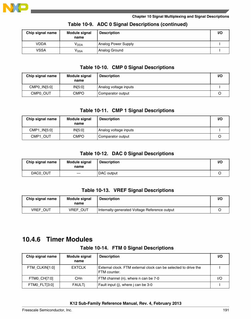
Table 10-9. ADC 0 Signal Descriptions (continued)
Chip signal name Module signalname
Description I/O
VDDA VDDA Analog Power Supply I
VSSA VSSA Analog Ground I
Table 10-10. CMP 0 Signal Descriptions
Chip signal name Module signalname
Description I/O
CMP0_IN[5:0] IN[5:0] Analog voltage inputs I
CMP0_OUT CMPO Comparator output O
Table 10-11. CMP 1 Signal Descriptions
Chip signal name Module signalname
Description I/O
CMP1_IN[5:0] IN[5:0] Analog voltage inputs I
CMP1_OUT CMPO Comparator output O
Table 10-12. DAC 0 Signal Descriptions
Chip signal name Module signalname
Description I/O
DAC0_OUT — DAC output O
Table 10-13. VREF Signal Descriptions
Chip signal name Module signalname
Description I/O
VREF_OUT VREF_OUT Internally-generated Voltage Reference output O
10.4.6 Timer ModulesTable 10-14. FTM 0 Signal Descriptions
Chip signal name Module signalname
Description I/O
FTM_CLKIN[1:0] EXTCLK External clock. FTM external clock can be selected to drive theFTM counter.
I
FTM0_CH[7:0] CHn FTM channel (n), where n can be 7-0 I/O
FTM0_FLT[3:0] FAULTj Fault input (j), where j can be 3-0 I
Chapter 10 Signal Multiplexing and Signal Descriptions
K12 Sub-Family Reference Manual, Rev. 4, February 2013
Freescale Semiconductor, Inc. 191
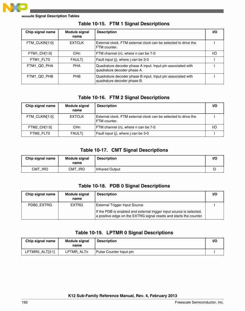
Table 10-15. FTM 1 Signal Descriptions
Chip signal name Module signalname
Description I/O
FTM_CLKIN[1:0] EXTCLK External clock. FTM external clock can be selected to drive theFTM counter.
I
FTM1_CH[1:0] CHn FTM channel (n), where n can be 7-0 I/O
FTM1_FLT0 FAULTj Fault input (j), where j can be 3-0 I
FTM1_QD_PHA PHA Quadrature decoder phase A input. Input pin associated withquadrature decoder phase A.
I
FTM1_QD_PHB PHB Quadrature decoder phase B input. Input pin associated withquadrature decoder phase B.
I
Table 10-16. FTM 2 Signal Descriptions
Chip signal name Module signalname
Description I/O
FTM_CLKIN[1:0] EXTCLK External clock. FTM external clock can be selected to drive theFTM counter.
I
FTM2_CH[1:0] CHn FTM channel (n), where n can be 7-0 I/O
FTM2_FLT0 FAULTj Fault input (j), where j can be 3-0 I
Table 10-17. CMT Signal Descriptions
Chip signal name Module signalname
Description I/O
CMT_IRO CMT_IRO Infrared Output O
Table 10-18. PDB 0 Signal Descriptions
Chip signal name Module signalname
Description I/O
PDB0_EXTRG EXTRG External Trigger Input Source
If the PDB is enabled and external trigger input source is selected,a positive edge on the EXTRG signal resets and starts the counter.
I
Table 10-19. LPTMR 0 Signal Descriptions
Chip signal name Module signalname
Description I/O
LPTMR0_ALT[3:1] LPTMR_ALTn Pulse Counter Input pin I
Module Signal Description Tables
K12 Sub-Family Reference Manual, Rev. 4, February 2013
192 Freescale Semiconductor, Inc.
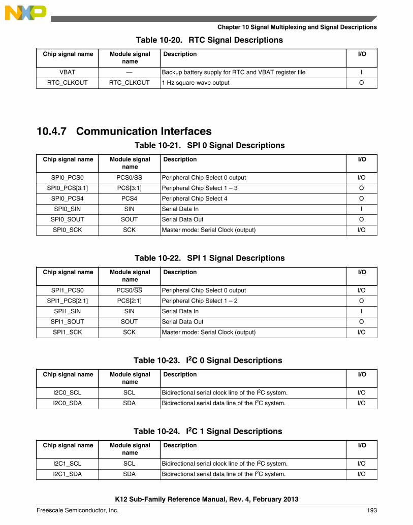
Table 10-20. RTC Signal Descriptions
Chip signal name Module signalname
Description I/O
VBAT — Backup battery supply for RTC and VBAT register file I
RTC_CLKOUT RTC_CLKOUT 1 Hz square-wave output O
10.4.7 Communication InterfacesTable 10-21. SPI 0 Signal Descriptions
Chip signal name Module signalname
Description I/O
SPI0_PCS0 PCS0/SS Peripheral Chip Select 0 output I/O
SPI0_PCS[3:1] PCS[3:1] Peripheral Chip Select 1 – 3 O
SPI0_PCS4 PCS4 Peripheral Chip Select 4 O
SPI0_SIN SIN Serial Data In I
SPI0_SOUT SOUT Serial Data Out O
SPI0_SCK SCK Master mode: Serial Clock (output) I/O
Table 10-22. SPI 1 Signal Descriptions
Chip signal name Module signalname
Description I/O
SPI1_PCS0 PCS0/SS Peripheral Chip Select 0 output I/O
SPI1_PCS[2:1] PCS[2:1] Peripheral Chip Select 1 – 2 O
SPI1_SIN SIN Serial Data In I
SPI1_SOUT SOUT Serial Data Out O
SPI1_SCK SCK Master mode: Serial Clock (output) I/O
Table 10-23. I2C 0 Signal Descriptions
Chip signal name Module signalname
Description I/O
I2C0_SCL SCL Bidirectional serial clock line of the I2C system. I/O
I2C0_SDA SDA Bidirectional serial data line of the I2C system. I/O
Table 10-24. I2C 1 Signal Descriptions
Chip signal name Module signalname
Description I/O
I2C1_SCL SCL Bidirectional serial clock line of the I2C system. I/O
I2C1_SDA SDA Bidirectional serial data line of the I2C system. I/O
Chapter 10 Signal Multiplexing and Signal Descriptions
K12 Sub-Family Reference Manual, Rev. 4, February 2013
Freescale Semiconductor, Inc. 193
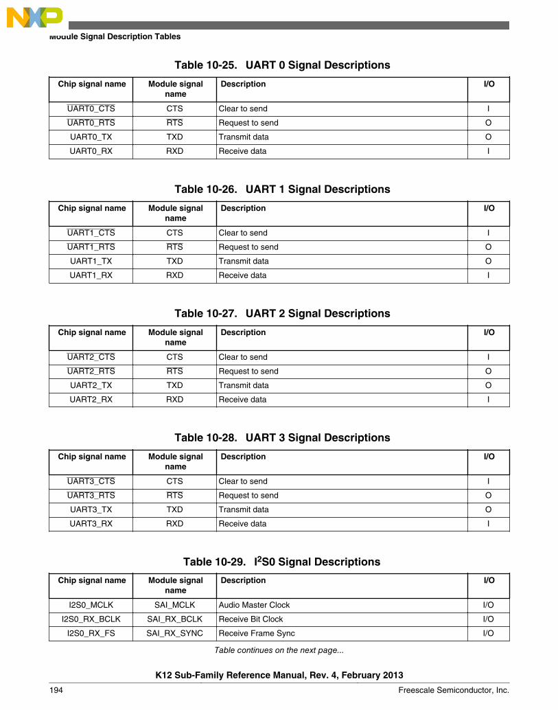
Table 10-25. UART 0 Signal Descriptions
Chip signal name Module signalname
Description I/O
UART0_CTS CTS Clear to send I
UART0_RTS RTS Request to send O
UART0_TX TXD Transmit data O
UART0_RX RXD Receive data I
Table 10-26. UART 1 Signal Descriptions
Chip signal name Module signalname
Description I/O
UART1_CTS CTS Clear to send I
UART1_RTS RTS Request to send O
UART1_TX TXD Transmit data O
UART1_RX RXD Receive data I
Table 10-27. UART 2 Signal Descriptions
Chip signal name Module signalname
Description I/O
UART2_CTS CTS Clear to send I
UART2_RTS RTS Request to send O
UART2_TX TXD Transmit data O
UART2_RX RXD Receive data I
Table 10-28. UART 3 Signal Descriptions
Chip signal name Module signalname
Description I/O
UART3_CTS CTS Clear to send I
UART3_RTS RTS Request to send O
UART3_TX TXD Transmit data O
UART3_RX RXD Receive data I
Table 10-29. I2S0 Signal Descriptions
Chip signal name Module signalname
Description I/O
I2S0_MCLK SAI_MCLK Audio Master Clock I/O
I2S0_RX_BCLK SAI_RX_BCLK Receive Bit Clock I/O
I2S0_RX_FS SAI_RX_SYNC Receive Frame Sync I/O
Table continues on the next page...
Module Signal Description Tables
K12 Sub-Family Reference Manual, Rev. 4, February 2013
194 Freescale Semiconductor, Inc.
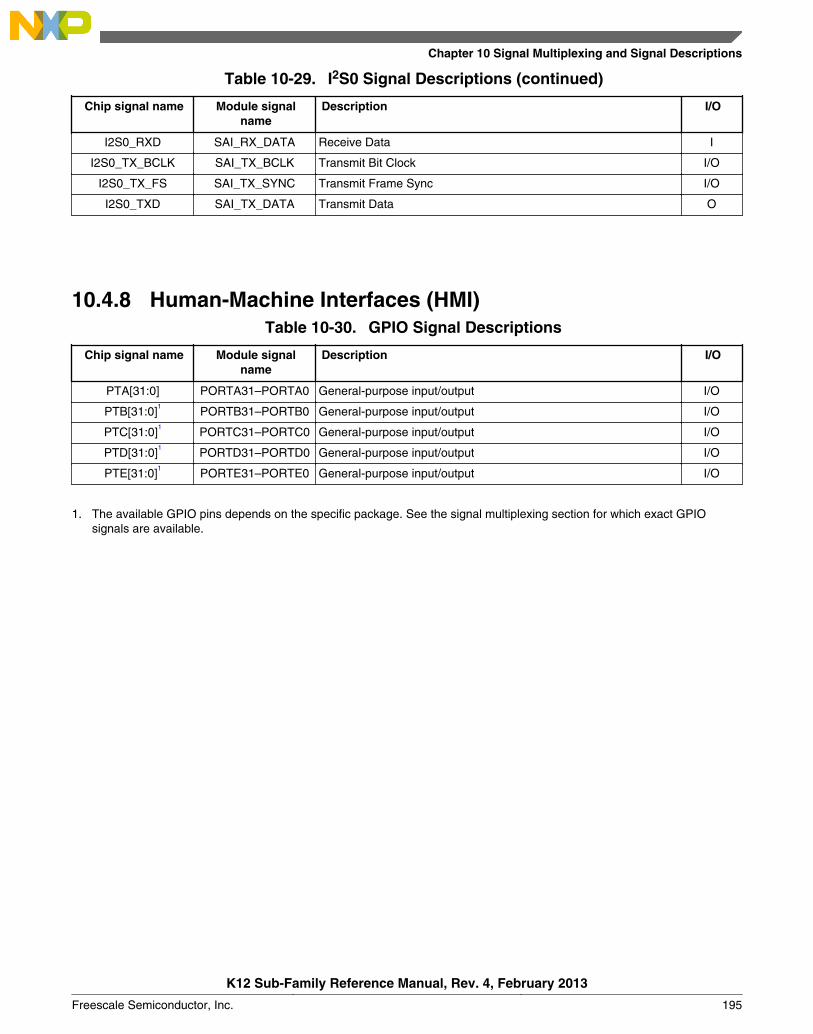
Table 10-29. I2S0 Signal Descriptions (continued)
Chip signal name Module signalname
Description I/O
I2S0_RXD SAI_RX_DATA Receive Data I
I2S0_TX_BCLK SAI_TX_BCLK Transmit Bit Clock I/O
I2S0_TX_FS SAI_TX_SYNC Transmit Frame Sync I/O
I2S0_TXD SAI_TX_DATA Transmit Data O
10.4.8 Human-Machine Interfaces (HMI)Table 10-30. GPIO Signal Descriptions
Chip signal name Module signalname
Description I/O
PTA[31:0] PORTA31–PORTA0 General-purpose input/output I/O
PTB[31:0]1
PORTB31–PORTB0 General-purpose input/output I/O
PTC[31:0]1
PORTC31–PORTC0 General-purpose input/output I/O
PTD[31:0]1
PORTD31–PORTD0 General-purpose input/output I/O
PTE[31:0]1
PORTE31–PORTE0 General-purpose input/output I/O
1. The available GPIO pins depends on the specific package. See the signal multiplexing section for which exact GPIOsignals are available.
Chapter 10 Signal Multiplexing and Signal Descriptions
K12 Sub-Family Reference Manual, Rev. 4, February 2013
Freescale Semiconductor, Inc. 195

Module Signal Description Tables
K12 Sub-Family Reference Manual, Rev. 4, February 2013
196 Freescale Semiconductor, Inc.
Chapter 11Port control and interrupts (PORT)
11.1 IntroductionNOTE
For the chip-specific implementation details of this module'sinstances see the chip configuration information.
11.2 OverviewThe port control and interrupt (PORT) module provides support for port control, digitalfiltering, and external interrupt functions. Most functions can be configuredindependently for each pin in the 32-bit port and affect the pin regardless of its pinmuxing state.
There is one instance of the PORT module for each port. Not all pins within each port areimplemented on a specific device.
11.2.1 Features
The PORT module has the following features:
• Pin interrupt• Interrupt flag and enable registers for each pin• Support for edge sensitive (rising, falling, both) or level sensitive (low, high)
configured per pin• Support for interrupt or DMA request configured per pin• Asynchronous wakeup in Low-Power modes• Pin interrupt is functional in all digital Pin Muxing modes
• Digital input filter on selected pins
K12 Sub-Family Reference Manual, Rev. 4, February 2013
Freescale Semiconductor, Inc. 197

• Digital input filter for each pin, usable by any digital peripheral muxed onto thepin
• Individual enable or bypass control field per pin• Selectable clock source for digital input filter with a five bit resolution on filter
size• Functional in all digital Pin Muxing modes
• Port control• Individual pull control fields with pullup, pulldown, and pull-disablesupport• Individual drive strength field supporting high and low drive strength• Individual slew rate field supporting fast and slow slew rates• Individual input passive filter field supporting enable and disable of the
individual input passive filter• Individual open drain field supporting enable and disable of the individual open
drain output• Individual mux control field supporting analog or pin disabled, GPIO, and up to
six chip-specific digital functions• Pad configuration fields are functional in all digital Pin Muxing modes
11.2.2 Modes of operation
11.2.2.1 Run mode
In Run mode, the PORT operates normally.
11.2.2.2 Wait mode
In Wait mode, PORT continues to operate normally and may be configured to exit theLow-Power mode if an enabled interrupt is detected. DMA requests are still generatedduring the Wait mode, but do not cause an exit from the Low-Power mode.
11.2.2.3 Stop mode
In Stop mode, the PORT can be configured to exit the Low-Power mode via anasynchronous wakeup signal if an enabled interrupt is detected.
In Stop mode, the digital input filters are bypassed unless they are configured to run fromthe 1 kHz LPO clock source.
Overview
K12 Sub-Family Reference Manual, Rev. 4, February 2013
198 Freescale Semiconductor, Inc.
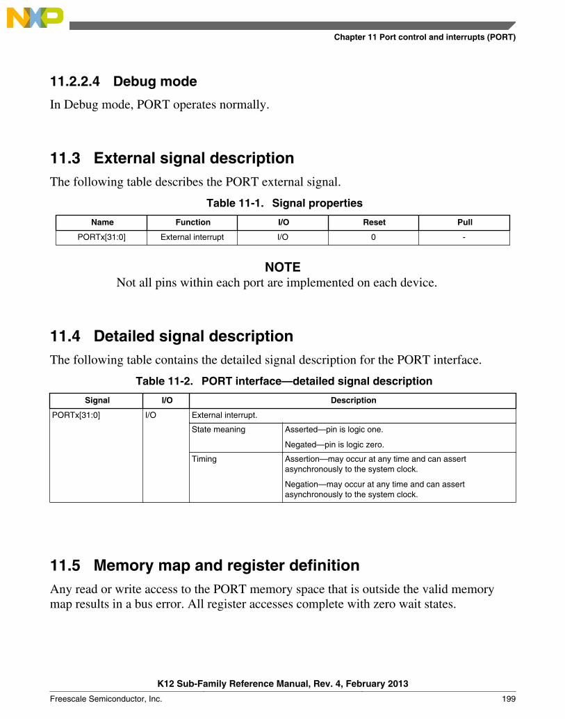
11.2.2.4 Debug mode
In Debug mode, PORT operates normally.
11.3 External signal descriptionThe following table describes the PORT external signal.
Table 11-1. Signal properties
Name Function I/O Reset Pull
PORTx[31:0] External interrupt I/O 0 -
NOTENot all pins within each port are implemented on each device.
11.4 Detailed signal descriptionThe following table contains the detailed signal description for the PORT interface.
Table 11-2. PORT interface—detailed signal description
Signal I/O Description
PORTx[31:0] I/O External interrupt.
State meaning Asserted—pin is logic one.
Negated—pin is logic zero.
Timing Assertion—may occur at any time and can assertasynchronously to the system clock.
Negation—may occur at any time and can assertasynchronously to the system clock.
11.5 Memory map and register definitionAny read or write access to the PORT memory space that is outside the valid memorymap results in a bus error. All register accesses complete with zero wait states.
Chapter 11 Port control and interrupts (PORT)
K12 Sub-Family Reference Manual, Rev. 4, February 2013
Freescale Semiconductor, Inc. 199
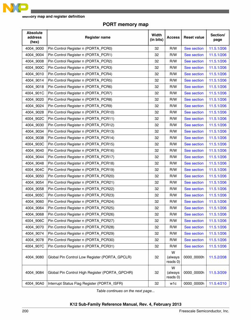
PORT memory map
Absoluteaddress
(hex)Register name
Width(in bits)
Access Reset valueSection/
page
4004_9000 Pin Control Register n (PORTA_PCR0) 32 R/W See section 11.5.1/206
4004_9004 Pin Control Register n (PORTA_PCR1) 32 R/W See section 11.5.1/206
4004_9008 Pin Control Register n (PORTA_PCR2) 32 R/W See section 11.5.1/206
4004_900C Pin Control Register n (PORTA_PCR3) 32 R/W See section 11.5.1/206
4004_9010 Pin Control Register n (PORTA_PCR4) 32 R/W See section 11.5.1/206
4004_9014 Pin Control Register n (PORTA_PCR5) 32 R/W See section 11.5.1/206
4004_9018 Pin Control Register n (PORTA_PCR6) 32 R/W See section 11.5.1/206
4004_901C Pin Control Register n (PORTA_PCR7) 32 R/W See section 11.5.1/206
4004_9020 Pin Control Register n (PORTA_PCR8) 32 R/W See section 11.5.1/206
4004_9024 Pin Control Register n (PORTA_PCR9) 32 R/W See section 11.5.1/206
4004_9028 Pin Control Register n (PORTA_PCR10) 32 R/W See section 11.5.1/206
4004_902C Pin Control Register n (PORTA_PCR11) 32 R/W See section 11.5.1/206
4004_9030 Pin Control Register n (PORTA_PCR12) 32 R/W See section 11.5.1/206
4004_9034 Pin Control Register n (PORTA_PCR13) 32 R/W See section 11.5.1/206
4004_9038 Pin Control Register n (PORTA_PCR14) 32 R/W See section 11.5.1/206
4004_903C Pin Control Register n (PORTA_PCR15) 32 R/W See section 11.5.1/206
4004_9040 Pin Control Register n (PORTA_PCR16) 32 R/W See section 11.5.1/206
4004_9044 Pin Control Register n (PORTA_PCR17) 32 R/W See section 11.5.1/206
4004_9048 Pin Control Register n (PORTA_PCR18) 32 R/W See section 11.5.1/206
4004_904C Pin Control Register n (PORTA_PCR19) 32 R/W See section 11.5.1/206
4004_9050 Pin Control Register n (PORTA_PCR20) 32 R/W See section 11.5.1/206
4004_9054 Pin Control Register n (PORTA_PCR21) 32 R/W See section 11.5.1/206
4004_9058 Pin Control Register n (PORTA_PCR22) 32 R/W See section 11.5.1/206
4004_905C Pin Control Register n (PORTA_PCR23) 32 R/W See section 11.5.1/206
4004_9060 Pin Control Register n (PORTA_PCR24) 32 R/W See section 11.5.1/206
4004_9064 Pin Control Register n (PORTA_PCR25) 32 R/W See section 11.5.1/206
4004_9068 Pin Control Register n (PORTA_PCR26) 32 R/W See section 11.5.1/206
4004_906C Pin Control Register n (PORTA_PCR27) 32 R/W See section 11.5.1/206
4004_9070 Pin Control Register n (PORTA_PCR28) 32 R/W See section 11.5.1/206
4004_9074 Pin Control Register n (PORTA_PCR29) 32 R/W See section 11.5.1/206
4004_9078 Pin Control Register n (PORTA_PCR30) 32 R/W See section 11.5.1/206
4004_907C Pin Control Register n (PORTA_PCR31) 32 R/W See section 11.5.1/206
4004_9080 Global Pin Control Low Register (PORTA_GPCLR) 32W
(alwaysreads 0)
0000_0000h 11.5.2/208
4004_9084 Global Pin Control High Register (PORTA_GPCHR) 32W
(alwaysreads 0)
0000_0000h 11.5.3/209
4004_90A0 Interrupt Status Flag Register (PORTA_ISFR) 32 w1c 0000_0000h 11.5.4/210
Table continues on the next page...
Memory map and register definition
K12 Sub-Family Reference Manual, Rev. 4, February 2013
200 Freescale Semiconductor, Inc.

PORT memory map (continued)
Absoluteaddress
(hex)Register name
Width(in bits)
Access Reset valueSection/
page
4004_90C0 Digital Filter Enable Register (PORTA_DFER) 32 R/W 0000_0000h 11.5.5/210
4004_90C4 Digital Filter Clock Register (PORTA_DFCR) 32 R/W 0000_0000h 11.5.6/211
4004_90C8 Digital Filter Width Register (PORTA_DFWR) 32 R/W 0000_0000h 11.5.7/211
4004_A000 Pin Control Register n (PORTB_PCR0) 32 R/W See section 11.5.1/206
4004_A004 Pin Control Register n (PORTB_PCR1) 32 R/W See section 11.5.1/206
4004_A008 Pin Control Register n (PORTB_PCR2) 32 R/W See section 11.5.1/206
4004_A00C Pin Control Register n (PORTB_PCR3) 32 R/W See section 11.5.1/206
4004_A010 Pin Control Register n (PORTB_PCR4) 32 R/W See section 11.5.1/206
4004_A014 Pin Control Register n (PORTB_PCR5) 32 R/W See section 11.5.1/206
4004_A018 Pin Control Register n (PORTB_PCR6) 32 R/W See section 11.5.1/206
4004_A01C Pin Control Register n (PORTB_PCR7) 32 R/W See section 11.5.1/206
4004_A020 Pin Control Register n (PORTB_PCR8) 32 R/W See section 11.5.1/206
4004_A024 Pin Control Register n (PORTB_PCR9) 32 R/W See section 11.5.1/206
4004_A028 Pin Control Register n (PORTB_PCR10) 32 R/W See section 11.5.1/206
4004_A02C Pin Control Register n (PORTB_PCR11) 32 R/W See section 11.5.1/206
4004_A030 Pin Control Register n (PORTB_PCR12) 32 R/W See section 11.5.1/206
4004_A034 Pin Control Register n (PORTB_PCR13) 32 R/W See section 11.5.1/206
4004_A038 Pin Control Register n (PORTB_PCR14) 32 R/W See section 11.5.1/206
4004_A03C Pin Control Register n (PORTB_PCR15) 32 R/W See section 11.5.1/206
4004_A040 Pin Control Register n (PORTB_PCR16) 32 R/W See section 11.5.1/206
4004_A044 Pin Control Register n (PORTB_PCR17) 32 R/W See section 11.5.1/206
4004_A048 Pin Control Register n (PORTB_PCR18) 32 R/W See section 11.5.1/206
4004_A04C Pin Control Register n (PORTB_PCR19) 32 R/W See section 11.5.1/206
4004_A050 Pin Control Register n (PORTB_PCR20) 32 R/W See section 11.5.1/206
4004_A054 Pin Control Register n (PORTB_PCR21) 32 R/W See section 11.5.1/206
4004_A058 Pin Control Register n (PORTB_PCR22) 32 R/W See section 11.5.1/206
4004_A05C Pin Control Register n (PORTB_PCR23) 32 R/W See section 11.5.1/206
4004_A060 Pin Control Register n (PORTB_PCR24) 32 R/W See section 11.5.1/206
4004_A064 Pin Control Register n (PORTB_PCR25) 32 R/W See section 11.5.1/206
4004_A068 Pin Control Register n (PORTB_PCR26) 32 R/W See section 11.5.1/206
4004_A06C Pin Control Register n (PORTB_PCR27) 32 R/W See section 11.5.1/206
4004_A070 Pin Control Register n (PORTB_PCR28) 32 R/W See section 11.5.1/206
4004_A074 Pin Control Register n (PORTB_PCR29) 32 R/W See section 11.5.1/206
4004_A078 Pin Control Register n (PORTB_PCR30) 32 R/W See section 11.5.1/206
4004_A07C Pin Control Register n (PORTB_PCR31) 32 R/W See section 11.5.1/206
4004_A080 Global Pin Control Low Register (PORTB_GPCLR) 32W
(alwaysreads 0)
0000_0000h 11.5.2/208
Table continues on the next page...
Chapter 11 Port control and interrupts (PORT)
K12 Sub-Family Reference Manual, Rev. 4, February 2013
Freescale Semiconductor, Inc. 201

PORT memory map (continued)
Absoluteaddress
(hex)Register name
Width(in bits)
Access Reset valueSection/
page
4004_A084 Global Pin Control High Register (PORTB_GPCHR) 32W
(alwaysreads 0)
0000_0000h 11.5.3/209
4004_A0A0 Interrupt Status Flag Register (PORTB_ISFR) 32 w1c 0000_0000h 11.5.4/210
4004_A0C0 Digital Filter Enable Register (PORTB_DFER) 32 R/W 0000_0000h 11.5.5/210
4004_A0C4 Digital Filter Clock Register (PORTB_DFCR) 32 R/W 0000_0000h 11.5.6/211
4004_A0C8 Digital Filter Width Register (PORTB_DFWR) 32 R/W 0000_0000h 11.5.7/211
4004_B000 Pin Control Register n (PORTC_PCR0) 32 R/W See section 11.5.1/206
4004_B004 Pin Control Register n (PORTC_PCR1) 32 R/W See section 11.5.1/206
4004_B008 Pin Control Register n (PORTC_PCR2) 32 R/W See section 11.5.1/206
4004_B00C Pin Control Register n (PORTC_PCR3) 32 R/W See section 11.5.1/206
4004_B010 Pin Control Register n (PORTC_PCR4) 32 R/W See section 11.5.1/206
4004_B014 Pin Control Register n (PORTC_PCR5) 32 R/W See section 11.5.1/206
4004_B018 Pin Control Register n (PORTC_PCR6) 32 R/W See section 11.5.1/206
4004_B01C Pin Control Register n (PORTC_PCR7) 32 R/W See section 11.5.1/206
4004_B020 Pin Control Register n (PORTC_PCR8) 32 R/W See section 11.5.1/206
4004_B024 Pin Control Register n (PORTC_PCR9) 32 R/W See section 11.5.1/206
4004_B028 Pin Control Register n (PORTC_PCR10) 32 R/W See section 11.5.1/206
4004_B02C Pin Control Register n (PORTC_PCR11) 32 R/W See section 11.5.1/206
4004_B030 Pin Control Register n (PORTC_PCR12) 32 R/W See section 11.5.1/206
4004_B034 Pin Control Register n (PORTC_PCR13) 32 R/W See section 11.5.1/206
4004_B038 Pin Control Register n (PORTC_PCR14) 32 R/W See section 11.5.1/206
4004_B03C Pin Control Register n (PORTC_PCR15) 32 R/W See section 11.5.1/206
4004_B040 Pin Control Register n (PORTC_PCR16) 32 R/W See section 11.5.1/206
4004_B044 Pin Control Register n (PORTC_PCR17) 32 R/W See section 11.5.1/206
4004_B048 Pin Control Register n (PORTC_PCR18) 32 R/W See section 11.5.1/206
4004_B04C Pin Control Register n (PORTC_PCR19) 32 R/W See section 11.5.1/206
4004_B050 Pin Control Register n (PORTC_PCR20) 32 R/W See section 11.5.1/206
4004_B054 Pin Control Register n (PORTC_PCR21) 32 R/W See section 11.5.1/206
4004_B058 Pin Control Register n (PORTC_PCR22) 32 R/W See section 11.5.1/206
4004_B05C Pin Control Register n (PORTC_PCR23) 32 R/W See section 11.5.1/206
4004_B060 Pin Control Register n (PORTC_PCR24) 32 R/W See section 11.5.1/206
4004_B064 Pin Control Register n (PORTC_PCR25) 32 R/W See section 11.5.1/206
4004_B068 Pin Control Register n (PORTC_PCR26) 32 R/W See section 11.5.1/206
4004_B06C Pin Control Register n (PORTC_PCR27) 32 R/W See section 11.5.1/206
4004_B070 Pin Control Register n (PORTC_PCR28) 32 R/W See section 11.5.1/206
4004_B074 Pin Control Register n (PORTC_PCR29) 32 R/W See section 11.5.1/206
4004_B078 Pin Control Register n (PORTC_PCR30) 32 R/W See section 11.5.1/206
Table continues on the next page...
Memory map and register definition
K12 Sub-Family Reference Manual, Rev. 4, February 2013
202 Freescale Semiconductor, Inc.

PORT memory map (continued)
Absoluteaddress
(hex)Register name
Width(in bits)
Access Reset valueSection/
page
4004_B07C Pin Control Register n (PORTC_PCR31) 32 R/W See section 11.5.1/206
4004_B080 Global Pin Control Low Register (PORTC_GPCLR) 32W
(alwaysreads 0)
0000_0000h 11.5.2/208
4004_B084 Global Pin Control High Register (PORTC_GPCHR) 32W
(alwaysreads 0)
0000_0000h 11.5.3/209
4004_B0A0 Interrupt Status Flag Register (PORTC_ISFR) 32 w1c 0000_0000h 11.5.4/210
4004_B0C0 Digital Filter Enable Register (PORTC_DFER) 32 R/W 0000_0000h 11.5.5/210
4004_B0C4 Digital Filter Clock Register (PORTC_DFCR) 32 R/W 0000_0000h 11.5.6/211
4004_B0C8 Digital Filter Width Register (PORTC_DFWR) 32 R/W 0000_0000h 11.5.7/211
4004_C000 Pin Control Register n (PORTD_PCR0) 32 R/W See section 11.5.1/206
4004_C004 Pin Control Register n (PORTD_PCR1) 32 R/W See section 11.5.1/206
4004_C008 Pin Control Register n (PORTD_PCR2) 32 R/W See section 11.5.1/206
4004_C00C Pin Control Register n (PORTD_PCR3) 32 R/W See section 11.5.1/206
4004_C010 Pin Control Register n (PORTD_PCR4) 32 R/W See section 11.5.1/206
4004_C014 Pin Control Register n (PORTD_PCR5) 32 R/W See section 11.5.1/206
4004_C018 Pin Control Register n (PORTD_PCR6) 32 R/W See section 11.5.1/206
4004_C01C Pin Control Register n (PORTD_PCR7) 32 R/W See section 11.5.1/206
4004_C020 Pin Control Register n (PORTD_PCR8) 32 R/W See section 11.5.1/206
4004_C024 Pin Control Register n (PORTD_PCR9) 32 R/W See section 11.5.1/206
4004_C028 Pin Control Register n (PORTD_PCR10) 32 R/W See section 11.5.1/206
4004_C02C Pin Control Register n (PORTD_PCR11) 32 R/W See section 11.5.1/206
4004_C030 Pin Control Register n (PORTD_PCR12) 32 R/W See section 11.5.1/206
4004_C034 Pin Control Register n (PORTD_PCR13) 32 R/W See section 11.5.1/206
4004_C038 Pin Control Register n (PORTD_PCR14) 32 R/W See section 11.5.1/206
4004_C03C Pin Control Register n (PORTD_PCR15) 32 R/W See section 11.5.1/206
4004_C040 Pin Control Register n (PORTD_PCR16) 32 R/W See section 11.5.1/206
4004_C044 Pin Control Register n (PORTD_PCR17) 32 R/W See section 11.5.1/206
4004_C048 Pin Control Register n (PORTD_PCR18) 32 R/W See section 11.5.1/206
4004_C04C Pin Control Register n (PORTD_PCR19) 32 R/W See section 11.5.1/206
4004_C050 Pin Control Register n (PORTD_PCR20) 32 R/W See section 11.5.1/206
4004_C054 Pin Control Register n (PORTD_PCR21) 32 R/W See section 11.5.1/206
4004_C058 Pin Control Register n (PORTD_PCR22) 32 R/W See section 11.5.1/206
4004_C05C Pin Control Register n (PORTD_PCR23) 32 R/W See section 11.5.1/206
4004_C060 Pin Control Register n (PORTD_PCR24) 32 R/W See section 11.5.1/206
4004_C064 Pin Control Register n (PORTD_PCR25) 32 R/W See section 11.5.1/206
4004_C068 Pin Control Register n (PORTD_PCR26) 32 R/W See section 11.5.1/206
4004_C06C Pin Control Register n (PORTD_PCR27) 32 R/W See section 11.5.1/206
Table continues on the next page...
Chapter 11 Port control and interrupts (PORT)
K12 Sub-Family Reference Manual, Rev. 4, February 2013
Freescale Semiconductor, Inc. 203

PORT memory map (continued)
Absoluteaddress
(hex)Register name
Width(in bits)
Access Reset valueSection/
page
4004_C070 Pin Control Register n (PORTD_PCR28) 32 R/W See section 11.5.1/206
4004_C074 Pin Control Register n (PORTD_PCR29) 32 R/W See section 11.5.1/206
4004_C078 Pin Control Register n (PORTD_PCR30) 32 R/W See section 11.5.1/206
4004_C07C Pin Control Register n (PORTD_PCR31) 32 R/W See section 11.5.1/206
4004_C080 Global Pin Control Low Register (PORTD_GPCLR) 32W
(alwaysreads 0)
0000_0000h 11.5.2/208
4004_C084 Global Pin Control High Register (PORTD_GPCHR) 32W
(alwaysreads 0)
0000_0000h 11.5.3/209
4004_C0A0 Interrupt Status Flag Register (PORTD_ISFR) 32 w1c 0000_0000h 11.5.4/210
4004_C0C0 Digital Filter Enable Register (PORTD_DFER) 32 R/W 0000_0000h 11.5.5/210
4004_C0C4 Digital Filter Clock Register (PORTD_DFCR) 32 R/W 0000_0000h 11.5.6/211
4004_C0C8 Digital Filter Width Register (PORTD_DFWR) 32 R/W 0000_0000h 11.5.7/211
4004_D000 Pin Control Register n (PORTE_PCR0) 32 R/W See section 11.5.1/206
4004_D004 Pin Control Register n (PORTE_PCR1) 32 R/W See section 11.5.1/206
4004_D008 Pin Control Register n (PORTE_PCR2) 32 R/W See section 11.5.1/206
4004_D00C Pin Control Register n (PORTE_PCR3) 32 R/W See section 11.5.1/206
4004_D010 Pin Control Register n (PORTE_PCR4) 32 R/W See section 11.5.1/206
4004_D014 Pin Control Register n (PORTE_PCR5) 32 R/W See section 11.5.1/206
4004_D018 Pin Control Register n (PORTE_PCR6) 32 R/W See section 11.5.1/206
4004_D01C Pin Control Register n (PORTE_PCR7) 32 R/W See section 11.5.1/206
4004_D020 Pin Control Register n (PORTE_PCR8) 32 R/W See section 11.5.1/206
4004_D024 Pin Control Register n (PORTE_PCR9) 32 R/W See section 11.5.1/206
4004_D028 Pin Control Register n (PORTE_PCR10) 32 R/W See section 11.5.1/206
4004_D02C Pin Control Register n (PORTE_PCR11) 32 R/W See section 11.5.1/206
4004_D030 Pin Control Register n (PORTE_PCR12) 32 R/W See section 11.5.1/206
4004_D034 Pin Control Register n (PORTE_PCR13) 32 R/W See section 11.5.1/206
4004_D038 Pin Control Register n (PORTE_PCR14) 32 R/W See section 11.5.1/206
4004_D03C Pin Control Register n (PORTE_PCR15) 32 R/W See section 11.5.1/206
4004_D040 Pin Control Register n (PORTE_PCR16) 32 R/W See section 11.5.1/206
4004_D044 Pin Control Register n (PORTE_PCR17) 32 R/W See section 11.5.1/206
4004_D048 Pin Control Register n (PORTE_PCR18) 32 R/W See section 11.5.1/206
4004_D04C Pin Control Register n (PORTE_PCR19) 32 R/W See section 11.5.1/206
4004_D050 Pin Control Register n (PORTE_PCR20) 32 R/W See section 11.5.1/206
4004_D054 Pin Control Register n (PORTE_PCR21) 32 R/W See section 11.5.1/206
4004_D058 Pin Control Register n (PORTE_PCR22) 32 R/W See section 11.5.1/206
4004_D05C Pin Control Register n (PORTE_PCR23) 32 R/W See section 11.5.1/206
4004_D060 Pin Control Register n (PORTE_PCR24) 32 R/W See section 11.5.1/206
Table continues on the next page...
Memory map and register definition
K12 Sub-Family Reference Manual, Rev. 4, February 2013
204 Freescale Semiconductor, Inc.
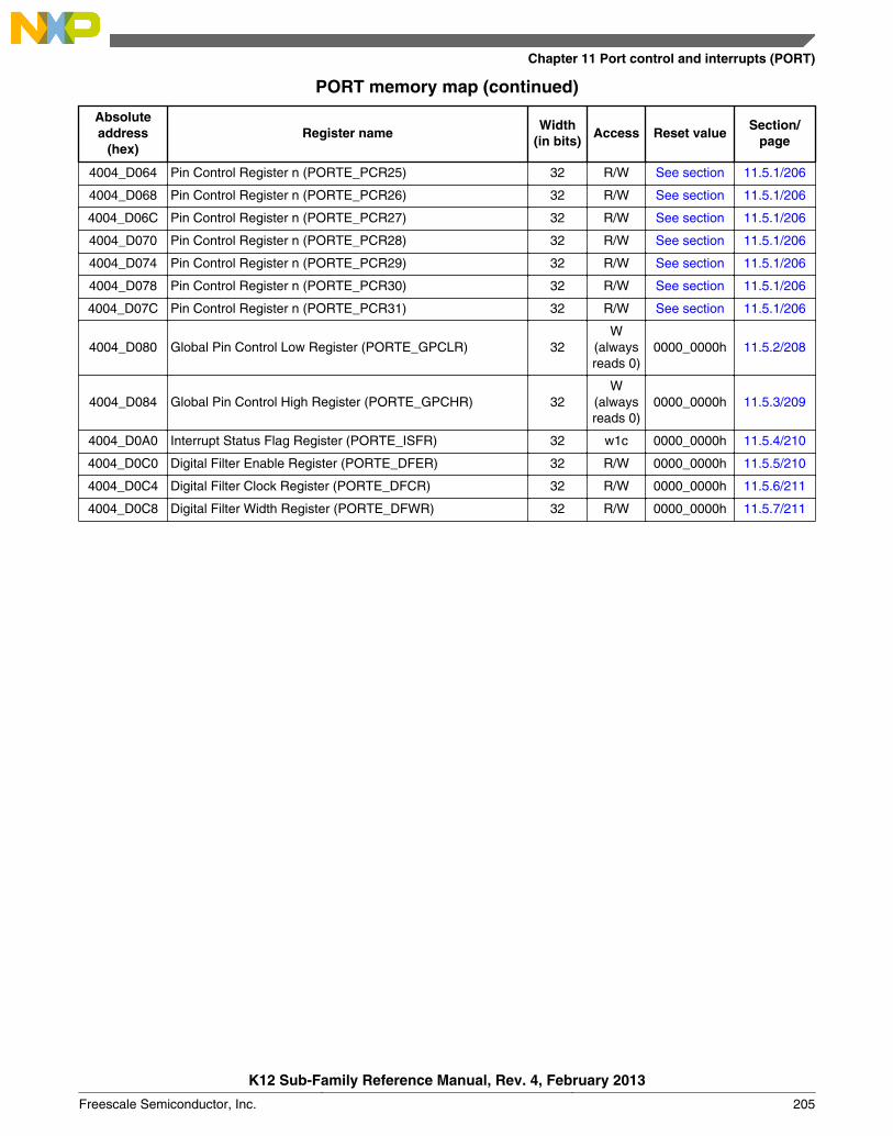
PORT memory map (continued)
Absoluteaddress
(hex)Register name
Width(in bits)
Access Reset valueSection/
page
4004_D064 Pin Control Register n (PORTE_PCR25) 32 R/W See section 11.5.1/206
4004_D068 Pin Control Register n (PORTE_PCR26) 32 R/W See section 11.5.1/206
4004_D06C Pin Control Register n (PORTE_PCR27) 32 R/W See section 11.5.1/206
4004_D070 Pin Control Register n (PORTE_PCR28) 32 R/W See section 11.5.1/206
4004_D074 Pin Control Register n (PORTE_PCR29) 32 R/W See section 11.5.1/206
4004_D078 Pin Control Register n (PORTE_PCR30) 32 R/W See section 11.5.1/206
4004_D07C Pin Control Register n (PORTE_PCR31) 32 R/W See section 11.5.1/206
4004_D080 Global Pin Control Low Register (PORTE_GPCLR) 32W
(alwaysreads 0)
0000_0000h 11.5.2/208
4004_D084 Global Pin Control High Register (PORTE_GPCHR) 32W
(alwaysreads 0)
0000_0000h 11.5.3/209
4004_D0A0 Interrupt Status Flag Register (PORTE_ISFR) 32 w1c 0000_0000h 11.5.4/210
4004_D0C0 Digital Filter Enable Register (PORTE_DFER) 32 R/W 0000_0000h 11.5.5/210
4004_D0C4 Digital Filter Clock Register (PORTE_DFCR) 32 R/W 0000_0000h 11.5.6/211
4004_D0C8 Digital Filter Width Register (PORTE_DFWR) 32 R/W 0000_0000h 11.5.7/211
Chapter 11 Port control and interrupts (PORT)
K12 Sub-Family Reference Manual, Rev. 4, February 2013
Freescale Semiconductor, Inc. 205

11.5.1 Pin Control Register n (PORTx_PCRn)
NOTE
Refer to the Signal Multiplexing and Pin Assignment chapterfor the reset value of this device.
See the GPIO Configuration section for details on the availablefunctions for each pin.
Do not modify pin configuration registers associated with pinsnot available in your selected package. All un-bonded pins notavailable in your package will default to DISABLE state forlowest power consumption.
Address: Base address + 0h offset + (4d × i), where i=0d to 31d
Bit 31 30 29 28 27 26 25 24 23 22 21 20 19 18 17 16
R 0 ISF 0IRQC
W w1c
Reset 0 0 0 0 0 0 0 0 0 0 0 0 0 0 0 0
Bit 15 14 13 12 11 10 9 8 7 6 5 4 3 2 1 0
RLK
0MUX
0DSE ODE PFE
0SRE PE PS
W
Reset 0 0 0 0 0 * * * 0 * 0 * 0 * * *
* Notes:MUX field: Varies by port. See Signal Multiplexing and Signal Descriptions chapter for reset values per port.•DSE field: Varies by port. See Signal Multiplexing and Signal Descriptions chapter for reset values per port.•PFE field: Varies by port. See Signal Multiplexing and Signal Descriptions chapter for reset values per port.•SRE field: Varies by port. See Signal Multiplexing and Signal Descriptions chapter for reset values per port.•PE field: Varies by port. See Signal Multiplexing and Signal Descriptions chapter for reset values per port.•PS field: Varies by port. See Signal Multiplexing and Signal Descriptions chapter for reset values per port.•
PORTx_PCRn field descriptions
Field Description
31–25Reserved
This field is reserved.This read-only field is reserved and always has the value 0.
24ISF
Interrupt Status Flag
The pin interrupt configuration is valid in all digital pin muxing modes.
Table continues on the next page...
Memory map and register definition
K12 Sub-Family Reference Manual, Rev. 4, February 2013
206 Freescale Semiconductor, Inc.
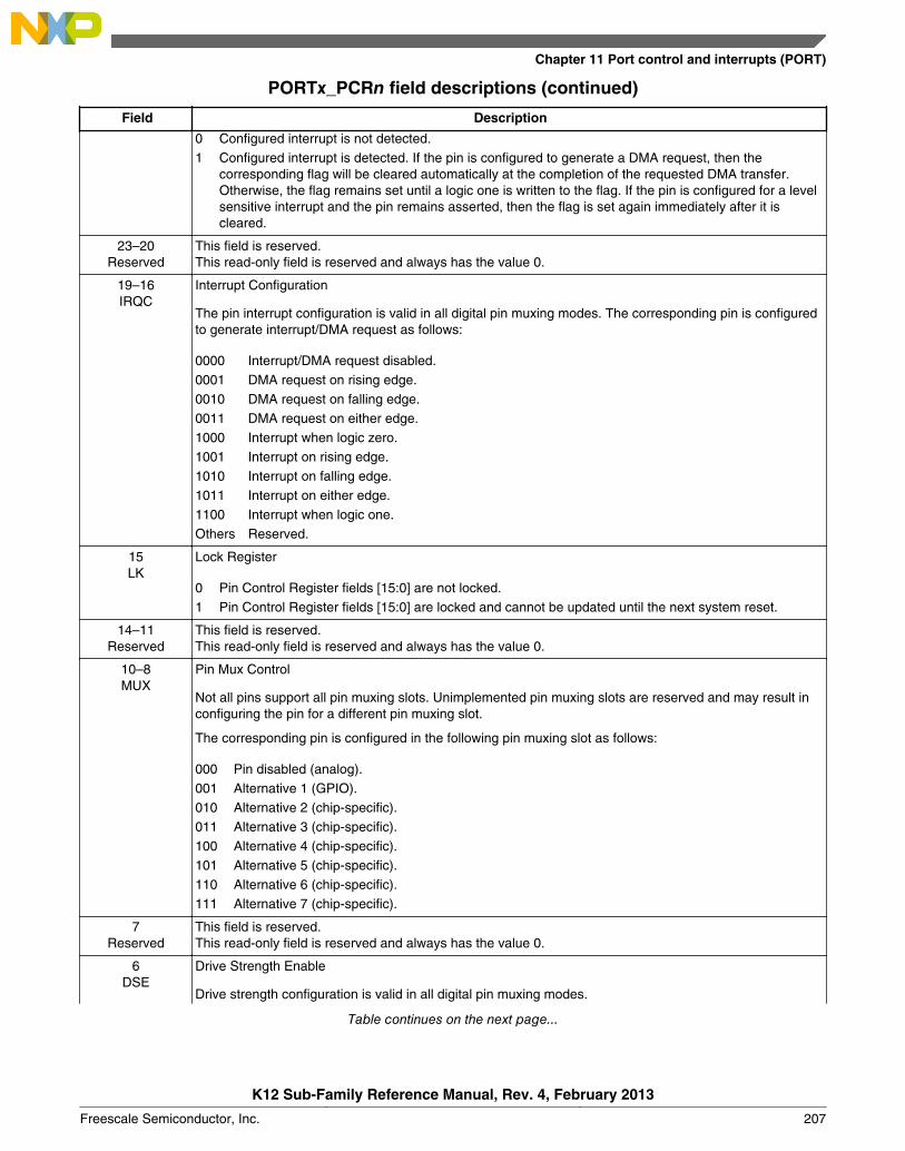
PORTx_PCRn field descriptions (continued)
Field Description
0 Configured interrupt is not detected.1 Configured interrupt is detected. If the pin is configured to generate a DMA request, then the
corresponding flag will be cleared automatically at the completion of the requested DMA transfer.Otherwise, the flag remains set until a logic one is written to the flag. If the pin is configured for a levelsensitive interrupt and the pin remains asserted, then the flag is set again immediately after it iscleared.
23–20Reserved
This field is reserved.This read-only field is reserved and always has the value 0.
19–16IRQC
Interrupt Configuration
The pin interrupt configuration is valid in all digital pin muxing modes. The corresponding pin is configuredto generate interrupt/DMA request as follows:
0000 Interrupt/DMA request disabled.0001 DMA request on rising edge.0010 DMA request on falling edge.0011 DMA request on either edge.1000 Interrupt when logic zero.1001 Interrupt on rising edge.1010 Interrupt on falling edge.1011 Interrupt on either edge.1100 Interrupt when logic one.Others Reserved.
15LK
Lock Register
0 Pin Control Register fields [15:0] are not locked.1 Pin Control Register fields [15:0] are locked and cannot be updated until the next system reset.
14–11Reserved
This field is reserved.This read-only field is reserved and always has the value 0.
10–8MUX
Pin Mux Control
Not all pins support all pin muxing slots. Unimplemented pin muxing slots are reserved and may result inconfiguring the pin for a different pin muxing slot.
The corresponding pin is configured in the following pin muxing slot as follows:
000 Pin disabled (analog).001 Alternative 1 (GPIO).010 Alternative 2 (chip-specific).011 Alternative 3 (chip-specific).100 Alternative 4 (chip-specific).101 Alternative 5 (chip-specific).110 Alternative 6 (chip-specific).111 Alternative 7 (chip-specific).
7Reserved
This field is reserved.This read-only field is reserved and always has the value 0.
6DSE
Drive Strength Enable
Drive strength configuration is valid in all digital pin muxing modes.
Table continues on the next page...
Chapter 11 Port control and interrupts (PORT)
K12 Sub-Family Reference Manual, Rev. 4, February 2013
Freescale Semiconductor, Inc. 207
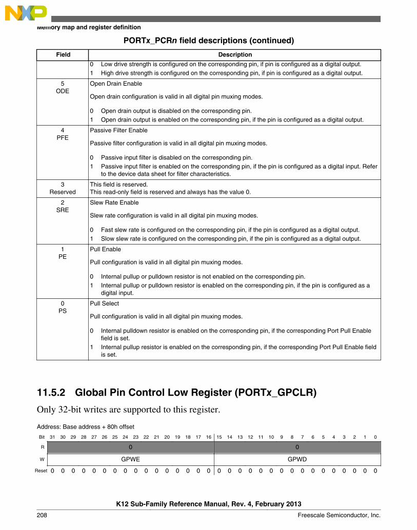
PORTx_PCRn field descriptions (continued)
Field Description
0 Low drive strength is configured on the corresponding pin, if pin is configured as a digital output.1 High drive strength is configured on the corresponding pin, if pin is configured as a digital output.
5ODE
Open Drain Enable
Open drain configuration is valid in all digital pin muxing modes.
0 Open drain output is disabled on the corresponding pin.1 Open drain output is enabled on the corresponding pin, if the pin is configured as a digital output.
4PFE
Passive Filter Enable
Passive filter configuration is valid in all digital pin muxing modes.
0 Passive input filter is disabled on the corresponding pin.1 Passive input filter is enabled on the corresponding pin, if the pin is configured as a digital input. Refer
to the device data sheet for filter characteristics.
3Reserved
This field is reserved.This read-only field is reserved and always has the value 0.
2SRE
Slew Rate Enable
Slew rate configuration is valid in all digital pin muxing modes.
0 Fast slew rate is configured on the corresponding pin, if the pin is configured as a digital output.1 Slow slew rate is configured on the corresponding pin, if the pin is configured as a digital output.
1PE
Pull Enable
Pull configuration is valid in all digital pin muxing modes.
0 Internal pullup or pulldown resistor is not enabled on the corresponding pin.1 Internal pullup or pulldown resistor is enabled on the corresponding pin, if the pin is configured as a
digital input.
0PS
Pull Select
Pull configuration is valid in all digital pin muxing modes.
0 Internal pulldown resistor is enabled on the corresponding pin, if the corresponding Port Pull Enablefield is set.
1 Internal pullup resistor is enabled on the corresponding pin, if the corresponding Port Pull Enable fieldis set.
11.5.2 Global Pin Control Low Register (PORTx_GPCLR)
Only 32-bit writes are supported to this register.
Address: Base address + 80h offset
Bit 31 30 29 28 27 26 25 24 23 22 21 20 19 18 17 16 15 14 13 12 11 10 9 8 7 6 5 4 3 2 1 0
R 0 0
W GPWE GPWD
Reset 0 0 0 0 0 0 0 0 0 0 0 0 0 0 0 0 0 0 0 0 0 0 0 0 0 0 0 0 0 0 0 0
Memory map and register definition
K12 Sub-Family Reference Manual, Rev. 4, February 2013
208 Freescale Semiconductor, Inc.
PORTx_GPCLR field descriptions
Field Description
31–16GPWE
Global Pin Write Enable
Selects which Pin Control Registers (15 through 0) bits [15:0] update with the value in GPWD. If aselected Pin Control Register is locked then the write to that register is ignored.
0 Corresponding Pin Control Register is not updated with the value in GPWD.1 Corresponding Pin Control Register is updated with the value in GPWD.
15–0GPWD
Global Pin Write Data
Write value that is written to all Pin Control Registers bits [15:0] that are selected by GPWE.
11.5.3 Global Pin Control High Register (PORTx_GPCHR)
Only 32-bit writes are supported to this register.
Address: Base address + 84h offset
Bit 31 30 29 28 27 26 25 24 23 22 21 20 19 18 17 16 15 14 13 12 11 10 9 8 7 6 5 4 3 2 1 0
R 0 0
W GPWE GPWD
Reset 0 0 0 0 0 0 0 0 0 0 0 0 0 0 0 0 0 0 0 0 0 0 0 0 0 0 0 0 0 0 0 0
PORTx_GPCHR field descriptions
Field Description
31–16GPWE
Global Pin Write Enable
Selects which Pin Control Registers (31 through 16) bits [15:0] update with the value in GPWD. If aselected Pin Control Register is locked then the write to that register is ignored.
0 Corresponding Pin Control Register is not updated with the value in GPWD.1 Corresponding Pin Control Register is updated with the value in GPWD.
15–0GPWD
Global Pin Write Data
Write value that is written to all Pin Control Registers bits [15:0] that are selected by GPWE.
Chapter 11 Port control and interrupts (PORT)
K12 Sub-Family Reference Manual, Rev. 4, February 2013
Freescale Semiconductor, Inc. 209
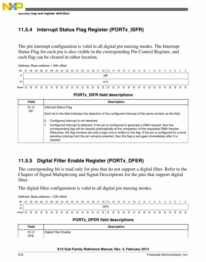
11.5.4 Interrupt Status Flag Register (PORTx_ISFR)
The pin interrupt configuration is valid in all digital pin muxing modes. The InterruptStatus Flag for each pin is also visible in the corresponding Pin Control Register, andeach flag can be cleared in either location.
Address: Base address + A0h offset
Bit 31 30 29 28 27 26 25 24 23 22 21 20 19 18 17 16 15 14 13 12 11 10 9 8 7 6 5 4 3 2 1 0
R ISF
W w1c
Reset 0 0 0 0 0 0 0 0 0 0 0 0 0 0 0 0 0 0 0 0 0 0 0 0 0 0 0 0 0 0 0 0
PORTx_ISFR field descriptions
Field Description
31–0ISF
Interrupt Status Flag
Each bit in the field indicates the detection of the configured interrupt of the same number as the field.
0 Configured interrupt is not detected.1 Configured interrupt is detected. If the pin is configured to generate a DMA request, then the
corresponding flag will be cleared automatically at the completion of the requested DMA transfer.Otherwise, the flag remains set until a logic one is written to the flag. If the pin is configured for a levelsensitive interrupt and the pin remains asserted, then the flag is set again immediately after it iscleared.
11.5.5 Digital Filter Enable Register (PORTx_DFER)
The corresponding bit is read only for pins that do not support a digital filter. Refer to theChapter of Signal Multiplexing and Signal Descriptions for the pins that support digitalfilter.
The digital filter configuration is valid in all digital pin muxing modes.
Address: Base address + C0h offset
Bit 31 30 29 28 27 26 25 24 23 22 21 20 19 18 17 16 15 14 13 12 11 10 9 8 7 6 5 4 3 2 1 0
R DFEW
Reset 0 0 0 0 0 0 0 0 0 0 0 0 0 0 0 0 0 0 0 0 0 0 0 0 0 0 0 0 0 0 0 0
PORTx_DFER field descriptions
Field Description
31–0DFE
Digital Filter Enable
Memory map and register definition
K12 Sub-Family Reference Manual, Rev. 4, February 2013
210 Freescale Semiconductor, Inc.
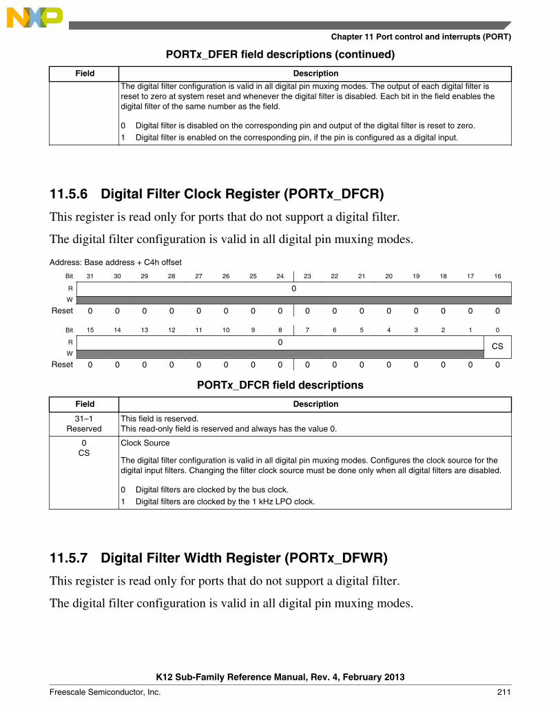
PORTx_DFER field descriptions (continued)
Field Description
The digital filter configuration is valid in all digital pin muxing modes. The output of each digital filter isreset to zero at system reset and whenever the digital filter is disabled. Each bit in the field enables thedigital filter of the same number as the field.
0 Digital filter is disabled on the corresponding pin and output of the digital filter is reset to zero.1 Digital filter is enabled on the corresponding pin, if the pin is configured as a digital input.
11.5.6 Digital Filter Clock Register (PORTx_DFCR)
This register is read only for ports that do not support a digital filter.
The digital filter configuration is valid in all digital pin muxing modes.
Address: Base address + C4h offset
Bit 31 30 29 28 27 26 25 24 23 22 21 20 19 18 17 16
R 0W
Reset 0 0 0 0 0 0 0 0 0 0 0 0 0 0 0 0
Bit 15 14 13 12 11 10 9 8 7 6 5 4 3 2 1 0
R 0 CSW
Reset 0 0 0 0 0 0 0 0 0 0 0 0 0 0 0 0
PORTx_DFCR field descriptions
Field Description
31–1Reserved
This field is reserved.This read-only field is reserved and always has the value 0.
0CS
Clock Source
The digital filter configuration is valid in all digital pin muxing modes. Configures the clock source for thedigital input filters. Changing the filter clock source must be done only when all digital filters are disabled.
0 Digital filters are clocked by the bus clock.1 Digital filters are clocked by the 1 kHz LPO clock.
11.5.7 Digital Filter Width Register (PORTx_DFWR)
This register is read only for ports that do not support a digital filter.
The digital filter configuration is valid in all digital pin muxing modes.
Chapter 11 Port control and interrupts (PORT)
K12 Sub-Family Reference Manual, Rev. 4, February 2013
Freescale Semiconductor, Inc. 211
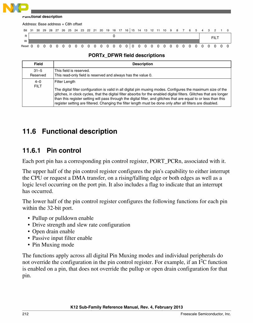
Address: Base address + C8h offset
Bit 31 30 29 28 27 26 25 24 23 22 21 20 19 18 17 16 15 14 13 12 11 10 9 8 7 6 5 4 3 2 1 0
R 0 FILTW
Reset 0 0 0 0 0 0 0 0 0 0 0 0 0 0 0 0 0 0 0 0 0 0 0 0 0 0 0 0 0 0 0 0
PORTx_DFWR field descriptions
Field Description
31–5Reserved
This field is reserved.This read-only field is reserved and always has the value 0.
4–0FILT
Filter Length
The digital filter configuration is valid in all digital pin muxing modes. Configures the maximum size of theglitches, in clock cycles, that the digital filter absorbs for the enabled digital filters. Glitches that are longerthan this register setting will pass through the digital filter, and glitches that are equal to or less than thisregister setting are filtered. Changing the filter length must be done only after all filters are disabled.
11.6 Functional description
11.6.1 Pin control
Each port pin has a corresponding pin control register, PORT_PCRn, associated with it.
The upper half of the pin control register configures the pin's capability to either interruptthe CPU or request a DMA transfer, on a rising/falling edge or both edges as well as alogic level occurring on the port pin. It also includes a flag to indicate that an interrupthas occurred.
The lower half of the pin control register configures the following functions for each pinwithin the 32-bit port.
• Pullup or pulldown enable• Drive strength and slew rate configuration• Open drain enable• Passive input filter enable• Pin Muxing mode
The functions apply across all digital Pin Muxing modes and individual peripherals donot override the configuration in the pin control register. For example, if an I2C functionis enabled on a pin, that does not override the pullup or open drain configuration for thatpin.
Functional description
K12 Sub-Family Reference Manual, Rev. 4, February 2013
212 Freescale Semiconductor, Inc.

When the Pin Muxing mode is configured for analog or is disabled, all the digitalfunctions on that pin are disabled. This includes the pullup and pulldown enables, digitaloutput buffer enable, digital input buffer enable, and passive filter enable.
A lock field also exists that allows the configuration for each pin to be locked until thenext system reset. When locked, writes to the lower half of that pin control register areignored, although a bus error is not generated on an attempted write to a locked register.
The configuration of each pin control register is retained when the PORT module isdisabled.
11.6.2 Global pin control
The two global pin control registers allow a single register write to update the lower halfof the pin control register on up to sixteen pins, all with the same value. Registers that arelocked cannot be written using the global pin control registers.
The global pin control registers are designed to enable software to quickly configuremultiple pins within the one port for the same peripheral function. However, the interruptfunctions cannot be configured using the global pin control registers.
The global pin control registers are write-only registers, that always read as zero.
11.6.3 External interrupts
The external interrupt capability of the PORT module is available in all digital pinmuxing modes provided the PORT module is enabled.
Each pin can be individually configured for any of the following external interruptmodes:
• Interrupt disabled, default out of reset• Active high level sensitive interrupt• Active low level sensitive interrupt• Rising edge sensitive interrupt• Falling edge sensitive interrupt• Rising and falling edge sensitive interrupt• Rising edge sensitive DMA request• Falling edge sensitive DMA request• Rising and falling edge sensitive DMA request
Chapter 11 Port control and interrupts (PORT)
K12 Sub-Family Reference Manual, Rev. 4, February 2013
Freescale Semiconductor, Inc. 213
The interrupt status flag is set when the configured edge or level is detected on the outputof the pin or digital input filter, if the digital input digital filter is enabled. When not inStop mode, the input is first synchronized to the bus clock to detect the configured levelor edge transition.
The PORT module generates a single interrupt that asserts when the interrupt status flagis set for any enabled interrupt for that port. The interrupt negates after the interrupt statusflags for all enabled interrupts have been cleared by writing a logic 1 to the ISF flag ineither the PORT_ISFR or PORT_PCRn registers.
The PORT module generates a single DMA request that asserts when the interrupt statusflag is set for any enabled DMA request in that port. The DMA request negates after theDMA transfer is completed, because that clears the interrupt status flags for all enabledDMA requests.
During Stop mode, the interrupt status flag for any enabled interrupt is asynchronouslyset if the required level or edge is detected. This also generates an asynchronous wakeupsignal to exit the Low-Power mode.
11.6.4 Digital filter
The digital filter capabilities of the PORT module are available in all digital Pin Muxingmodes if the PORT module is enabled.
The clock used for all digital filters within one port can be configured between the busclock or the 1 kHz LPO clock. This selection must be changed only when all digitalfilters for that port are disabled. If the digital filters for a port are configured to use thebus clock, then the digital filters are bypassed for the duration of Stop mode. While thedigital filters are bypassed, the output of each digital filter always equals the input pin,but the internal state of the digital filters remains static and does not update due to anychange on the input pin.
The filter width in clock size is the same for all enabled digital filters within one port andmust be changed only when all digital filters for that port are disabled.
The output of each digital filter is logic zero after system reset and whenever a digitalfilter is disabled. After a digital filter is enabled, the input is synchronized to the filterclock, either the bus clock or the 1 kHz LPO clock. If the synchronized input and theoutput of the digital filter remain different for a number of filter clock cycles equal to thefilter width register configuration, then the output of the digital filter updates to equal thesynchronized filter input.
The minimum latency through a digital filter equals two or three filter clock cycles plusthe filter width configuration register.
Functional description
K12 Sub-Family Reference Manual, Rev. 4, February 2013
214 Freescale Semiconductor, Inc.

Chapter 12System Integration Module (SIM)
12.1 IntroductionNOTE
For the chip-specific implementation details of this module'sinstances see the chip configuration information.
The System Integration Module (SIM) provides system control and chip configurationregisters.
12.1.1 Features
Features of the SIM include:
• System clocking configuration• System clock divide values• Architectural clock gating control
• Flash and system RAM size configuration• FlexTimer external clock, hardware trigger, and fault source selection• UART0 and UART1 receive/transmit source selection/configuration
K12 Sub-Family Reference Manual, Rev. 4, February 2013
Freescale Semiconductor, Inc. 215
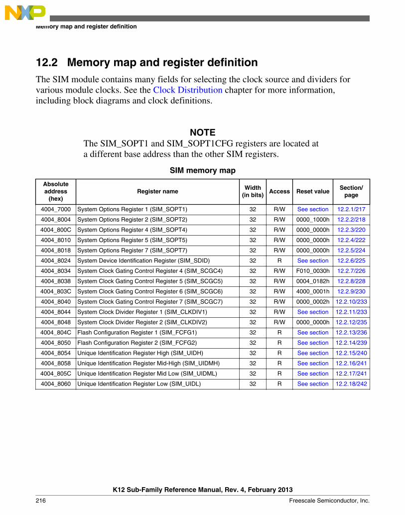
12.2 Memory map and register definitionThe SIM module contains many fields for selecting the clock source and dividers forvarious module clocks. See the Clock Distribution chapter for more information,including block diagrams and clock definitions.
NOTEThe SIM_SOPT1 and SIM_SOPT1CFG registers are located ata different base address than the other SIM registers.
SIM memory map
Absoluteaddress
(hex)Register name
Width(in bits)
Access Reset valueSection/
page
4004_7000 System Options Register 1 (SIM_SOPT1) 32 R/W See section 12.2.1/217
4004_8004 System Options Register 2 (SIM_SOPT2) 32 R/W 0000_1000h 12.2.2/218
4004_800C System Options Register 4 (SIM_SOPT4) 32 R/W 0000_0000h 12.2.3/220
4004_8010 System Options Register 5 (SIM_SOPT5) 32 R/W 0000_0000h 12.2.4/222
4004_8018 System Options Register 7 (SIM_SOPT7) 32 R/W 0000_0000h 12.2.5/224
4004_8024 System Device Identification Register (SIM_SDID) 32 R See section 12.2.6/225
4004_8034 System Clock Gating Control Register 4 (SIM_SCGC4) 32 R/W F010_0030h 12.2.7/226
4004_8038 System Clock Gating Control Register 5 (SIM_SCGC5) 32 R/W 0004_0182h 12.2.8/228
4004_803C System Clock Gating Control Register 6 (SIM_SCGC6) 32 R/W 4000_0001h 12.2.9/230
4004_8040 System Clock Gating Control Register 7 (SIM_SCGC7) 32 R/W 0000_0002h 12.2.10/233
4004_8044 System Clock Divider Register 1 (SIM_CLKDIV1) 32 R/W See section 12.2.11/233
4004_8048 System Clock Divider Register 2 (SIM_CLKDIV2) 32 R/W 0000_0000h 12.2.12/235
4004_804C Flash Configuration Register 1 (SIM_FCFG1) 32 R See section 12.2.13/236
4004_8050 Flash Configuration Register 2 (SIM_FCFG2) 32 R See section 12.2.14/239
4004_8054 Unique Identification Register High (SIM_UIDH) 32 R See section 12.2.15/240
4004_8058 Unique Identification Register Mid-High (SIM_UIDMH) 32 R See section 12.2.16/241
4004_805C Unique Identification Register Mid Low (SIM_UIDML) 32 R See section 12.2.17/241
4004_8060 Unique Identification Register Low (SIM_UIDL) 32 R See section 12.2.18/242
Memory map and register definition
K12 Sub-Family Reference Manual, Rev. 4, February 2013
216 Freescale Semiconductor, Inc.
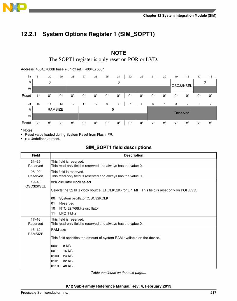
12.2.1 System Options Register 1 (SIM_SOPT1)
NOTEThe SOPT1 register is only reset on POR or LVD.
Address: 4004_7000h base + 0h offset = 4004_7000h
Bit 31 30 29 28 27 26 25 24 23 22 21 20 19 18 17 16
R 0 0OSC32KSEL
0
W
Reset 1* 0* 0* 0* 0* 0* 0* 0* 0* 0* 0* 0* 0* 0* 0* 0*
Bit 15 14 13 12 11 10 9 8 7 6 5 4 3 2 1 0
R RAMSIZE 0Reserved
W
Reset x* x* x* x* 0* 0* 0* 0* 0* 0* x* x* x* x* x* x*
* Notes:Reset value loaded during System Reset from Flash IFR.•x = Undefined at reset.•
SIM_SOPT1 field descriptions
Field Description
31–29Reserved
This field is reserved.This read-only field is reserved and always has the value 0.
28–20Reserved
This field is reserved.This read-only field is reserved and always has the value 0.
19–18OSC32KSEL
32K oscillator clock select
Selects the 32 kHz clock source (ERCLK32K) for LPTMR. This field is reset only on POR/LVD.
00 System oscillator (OSC32KCLK)01 Reserved10 RTC 32.768kHz oscillator11 LPO 1 kHz
17–16Reserved
This field is reserved.This read-only field is reserved and always has the value 0.
15–12RAMSIZE
RAM size
This field specifies the amount of system RAM available on the device.
0001 8 KB0011 16 KB0100 24 KB0101 32 KB0110 48 KB
Table continues on the next page...
Chapter 12 System Integration Module (SIM)
K12 Sub-Family Reference Manual, Rev. 4, February 2013
Freescale Semiconductor, Inc. 217
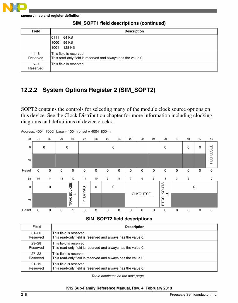
SIM_SOPT1 field descriptions (continued)
Field Description
0111 64 KB1000 96 KB1001 128 KB
11–6Reserved
This field is reserved.This read-only field is reserved and always has the value 0.
5–0Reserved
This field is reserved.
12.2.2 System Options Register 2 (SIM_SOPT2)
SOPT2 contains the controls for selecting many of the module clock source options onthis device. See the Clock Distribution chapter for more information including clockingdiagrams and definitions of device clocks.
Address: 4004_7000h base + 1004h offset = 4004_8004h
Bit 31 30 29 28 27 26 25 24 23 22 21 20 19 18 17 16
R 0 0 0 0 0 0
PLL
FLL
SE
L
W
Reset 0 0 0 0 0 0 0 0 0 0 0 0 0 0 0 0
Bit 15 14 13 12 11 10 9 8 7 6 5 4 3 2 1 0
R 0
TR
AC
EC
LKS
EL
PT
D7P
AD 0 0
CLKOUTSEL
RT
CC
LKO
UT
SE
L
0
W
Reset 0 0 0 1 0 0 0 0 0 0 0 0 0 0 0 0
SIM_SOPT2 field descriptions
Field Description
31–30Reserved
This field is reserved.This read-only field is reserved and always has the value 0.
29–28Reserved
This field is reserved.This read-only field is reserved and always has the value 0.
27–22Reserved
This field is reserved.This read-only field is reserved and always has the value 0.
21–19Reserved
This field is reserved.This read-only field is reserved and always has the value 0.
Table continues on the next page...
Memory map and register definition
K12 Sub-Family Reference Manual, Rev. 4, February 2013
218 Freescale Semiconductor, Inc.
SIM_SOPT2 field descriptions (continued)
Field Description
18Reserved
This field is reserved.This read-only field is reserved and always has the value 0.
17Reserved
This field is reserved.This read-only field is reserved and always has the value 0.
16PLLFLLSEL
PLL/FLL clock select
Selects the MCGPLLCLK or MCGFLLCLK clock for various peripheral clocking options.
0 MCGFLLCLK clock1 MCGPLLCLK clock
15–13Reserved
This field is reserved.This read-only field is reserved and always has the value 0.
12TRACECLKSEL
Debug trace clock select
Selects the core/system clock or MCG output clock (MCGOUTCLK) as the trace clock source.
0 MCGOUTCLK1 Core/system clock
11PTD7PAD
PTD7 pad drive strength
Controls the output drive strength of the PTD7 pin by selecting either one or two pads to drive it.
0 Single-pad drive strength for PTD7.1 Double pad drive strength for PTD7.
10Reserved
This field is reserved.This read-only field is reserved and always has the value 0.
9–8Reserved
This field is reserved.This read-only field is reserved and always has the value 0.
7–5CLKOUTSEL
CLKOUT select
Selects the clock to output on the CLKOUT pin.
000 Reserved001 Reserved010 Flash clock011 LPO clock (1 kHz)100 MCGIRCLK101 RTC 32.768kHz clock110 OSCERCLK0111 Reserved
4RTCCLKOUTSEL
RTC clock out select
Selects either the RTC 1 Hz clock or the 32.768kHz clock to be output on the RTC_CLKOUT pin.
0 RTC 1 Hz clock is output on the RTC_CLKOUT pin.1 RTC 32.768kHz clock is output on the RTC_CLKOUT pin.
3–0Reserved
This field is reserved.This read-only field is reserved and always has the value 0.
Chapter 12 System Integration Module (SIM)
K12 Sub-Family Reference Manual, Rev. 4, February 2013
Freescale Semiconductor, Inc. 219

12.2.3 System Options Register 4 (SIM_SOPT4)
Address: 4004_7000h base + 100Ch offset = 4004_800Ch
Bit 31 30 29 28 27 26 25 24 23 22 21 20 19 18 17 16
R 0F
TM
0TR
G1S
RC
FT
M0T
RG
0SR
C
0
FT
M2C
LKS
EL
FT
M1C
LKS
EL
FT
M0C
LKS
EL
0
FT
M2C
H0S
RC
FT
M1C
H0S
RC
0
W
Reset 0 0 0 0 0 0 0 0 0 0 0 0 0 0 0 0
Bit 15 14 13 12 11 10 9 8 7 6 5 4 3 2 1 0
R 0
FT
M2F
LT0 0
FT
M1F
LT0 0 0
FT
M0F
LT1
FT
M0F
LT0
W
Reset 0 0 0 0 0 0 0 0 0 0 0 0 0 0 0 0
SIM_SOPT4 field descriptions
Field Description
31–30Reserved
This field is reserved.This read-only field is reserved and always has the value 0.
29FTM0TRG1SRC
FlexTimer 0 Hardware Trigger 1 Source Select
Selects the source of FTM0 hardware trigger 1.
0 PDB output trigger 1 drives FTM0 hardware trigger 11 FTM2 channel match drives FTM0 hardware trigger 1
28FTM0TRG0SRC
FlexTimer 0 Hardware Trigger 0 Source Select
Selects the source of FTM0 hardware trigger 0.
0 HSCMP0 output drives FTM0 hardware trigger 01 FTM1 channel match drives FTM0 hardware trigger 0
27Reserved
This field is reserved.This read-only field is reserved and always has the value 0.
26FTM2CLKSEL
FlexTimer 2 External Clock Pin Select
Selects the external pin used to drive the clock to the FTM2 module.
NOTE: The selected pin must also be configured for the FTM2 module external clock function throughthe appropriate pin control register in the port control module.
0 FTM2 external clock driven by FTM_CLK0 pin.1 FTM2 external clock driven by FTM_CLK1 pin.
25FTM1CLKSEL
FTM1 External Clock Pin Select
Selects the external pin used to drive the clock to the FTM1 module.
Table continues on the next page...
Memory map and register definition
K12 Sub-Family Reference Manual, Rev. 4, February 2013
220 Freescale Semiconductor, Inc.
SIM_SOPT4 field descriptions (continued)
Field Description
NOTE: The selected pin must also be configured for the FTM external clock function through theappropriate pin control register in the port control module.
0 FTM_CLK0 pin1 FTM_CLK1 pin
24FTM0CLKSEL
FlexTimer 0 External Clock Pin Select
Selects the external pin used to drive the clock to the FTM0 module.
NOTE: The selected pin must also be configured for the FTM external clock function through theappropriate pin control register in the port control module.
0 FTM_CLK0 pin1 FTM_CLK1 pin
23–22Reserved
This field is reserved.This read-only field is reserved and always has the value 0.
21–20FTM2CH0SRC
FTM2 channel 0 input capture source select
Selects the source for FTM2 channel 0 input capture.
NOTE: When the FTM is not in input capture mode, clear this field.
00 FTM2_CH0 signal01 CMP0 output10 CMP1 output11 Reserved
19–18FTM1CH0SRC
FTM1 channel 0 input capture source select
Selects the source for FTM1 channel 0 input capture.
NOTE: When the FTM is not in input capture mode, clear this field.
00 FTM1_CH0 signal01 CMP0 output10 CMP1 output11 Reserved
17–9Reserved
This field is reserved.This read-only field is reserved and always has the value 0.
8FTM2FLT0
FTM2 Fault 0 Select
Selects the source of FTM2 fault 0.
NOTE: The pin source for fault 0 must be configured for the FTM module fault function through theappropriate PORTx pin control register.
0 FTM2_FLT0 pin1 CMP0 out
7–5Reserved
This field is reserved.This read-only field is reserved and always has the value 0.
4FTM1FLT0
FTM1 Fault 0 Select
Selects the source of FTM1 fault 0.
Table continues on the next page...
Chapter 12 System Integration Module (SIM)
K12 Sub-Family Reference Manual, Rev. 4, February 2013
Freescale Semiconductor, Inc. 221
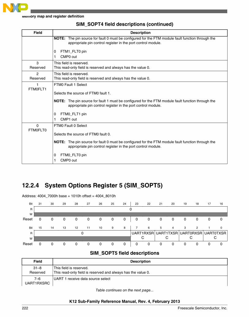
SIM_SOPT4 field descriptions (continued)
Field Description
NOTE: The pin source for fault 0 must be configured for the FTM module fault function through theappropriate pin control register in the port control module.
0 FTM1_FLT0 pin1 CMP0 out
3Reserved
This field is reserved.This read-only field is reserved and always has the value 0.
2Reserved
This field is reserved.This read-only field is reserved and always has the value 0.
1FTM0FLT1
FTM0 Fault 1 Select
Selects the source of FTM0 fault 1.
NOTE: The pin source for fault 1 must be configured for the FTM module fault function through theappropriate pin control register in the port control module.
0 FTM0_FLT1 pin1 CMP1 out
0FTM0FLT0
FTM0 Fault 0 Select
Selects the source of FTM0 fault 0.
NOTE: The pin source for fault 0 must be configured for the FTM module fault function through theappropriate pin control register in the port control module.
0 FTM0_FLT0 pin1 CMP0 out
12.2.4 System Options Register 5 (SIM_SOPT5)
Address: 4004_7000h base + 1010h offset = 4004_8010h
Bit 31 30 29 28 27 26 25 24 23 22 21 20 19 18 17 16
R 0W
Reset 0 0 0 0 0 0 0 0 0 0 0 0 0 0 0 0
Bit 15 14 13 12 11 10 9 8 7 6 5 4 3 2 1 0
R 0 UART1RXSRC
UART1TXSRC
UART0RXSRC
UART0TXSRCW
Reset 0 0 0 0 0 0 0 0 0 0 0 0 0 0 0 0
SIM_SOPT5 field descriptions
Field Description
31–8Reserved
This field is reserved.This read-only field is reserved and always has the value 0.
7–6UART1RXSRC
UART 1 receive data source select
Table continues on the next page...
Memory map and register definition
K12 Sub-Family Reference Manual, Rev. 4, February 2013
222 Freescale Semiconductor, Inc.
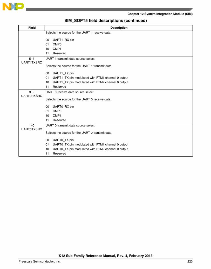
SIM_SOPT5 field descriptions (continued)
Field Description
Selects the source for the UART 1 receive data.
00 UART1_RX pin01 CMP010 CMP111 Reserved
5–4UART1TXSRC
UART 1 transmit data source select
Selects the source for the UART 1 transmit data.
00 UART1_TX pin01 UART1_TX pin modulated with FTM1 channel 0 output10 UART1_TX pin modulated with FTM2 channel 0 output11 Reserved
3–2UART0RXSRC
UART 0 receive data source select
Selects the source for the UART 0 receive data.
00 UART0_RX pin01 CMP010 CMP111 Reserved
1–0UART0TXSRC
UART 0 transmit data source select
Selects the source for the UART 0 transmit data.
00 UART0_TX pin01 UART0_TX pin modulated with FTM1 channel 0 output10 UART0_TX pin modulated with FTM2 channel 0 output11 Reserved
Chapter 12 System Integration Module (SIM)
K12 Sub-Family Reference Manual, Rev. 4, February 2013
Freescale Semiconductor, Inc. 223

12.2.5 System Options Register 7 (SIM_SOPT7)
Address: 4004_7000h base + 1018h offset = 4004_8018h
Bit 31 30 29 28 27 26 25 24 23 22 21 20 19 18 17 16
R 0
W
Reset 0 0 0 0 0 0 0 0 0 0 0 0 0 0 0 0
Bit 15 14 13 12 11 10 9 8 7 6 5 4 3 2 1 0
R 0
AD
C0A
LTT
RG
EN
0
AD
C0P
RE
TR
GS
EL ADC0TRGSEL
W
Reset 0 0 0 0 0 0 0 0 0 0 0 0 0 0 0 0
SIM_SOPT7 field descriptions
Field Description
31–16Reserved
This field is reserved.This read-only field is reserved and always has the value 0.
15–8Reserved
This field is reserved.This read-only field is reserved and always has the value 0.
7ADC0ALTTRGEN
ADC0 alternate trigger enable
Enable alternative conversion triggers for ADC0.
0 PDB trigger selected for ADC0.1 Alternate trigger selected for ADC0.
6–5Reserved
This field is reserved.This read-only field is reserved and always has the value 0.
4ADC0PRETRGSEL
ADC0 pretrigger select
Selects the ADC0 pre-trigger source when alternative triggers are enabled through ADC0ALTTRGEN.
0 Pre-trigger A1 Pre-trigger B
3–0ADC0TRGSEL
ADC0 trigger select
Selects the ADC0 trigger source when alternative triggers are functional in stop and VLPS modes. .
0000 PDB external trigger pin input (PDB0_EXTRG)0001 High speed comparator 0 output0010 High speed comparator 1 output0011 Reserved
Table continues on the next page...
Memory map and register definition
K12 Sub-Family Reference Manual, Rev. 4, February 2013
224 Freescale Semiconductor, Inc.

SIM_SOPT7 field descriptions (continued)
Field Description
0100 PIT trigger 00101 PIT trigger 10110 PIT trigger 20111 PIT trigger 31000 FTM0 trigger1001 FTM1 trigger1010 FTM2 trigger1011 Reserved1100 RTC alarm1101 RTC seconds1110 Low-power timer trigger1111 Reserved
12.2.6 System Device Identification Register (SIM_SDID)
Address: 4004_7000h base + 1024h offset = 4004_8024h
Bit 31 30 29 28 27 26 25 24 23 22 21 20 19 18 17 16 15 14 13 12 11 10 9 8 7 6 5 4 3 2 1 0
R 0 REVID DIEID FAMID PINID
W
Reset 0 0 0 0 0 0 0 0 0 0 0 0 0 0 0 0 x* x* x* x* 0 0 1 0 0 x* x* x* x* x* x* x*
* Notes:x = Undefined at reset.•
SIM_SDID field descriptions
Field Description
31–16Reserved
This field is reserved.This read-only field is reserved and always has the value 0.
15–12REVID
Device revision number
Specifies the silicon implementation number for the device.
11–7DIEID
Device die number
Specifies the silicon implementation number for the device.
6–4FAMID
Kinetis family identification
Specifies the Kinetis family of the device.
000 K10 or K12 Family001 K20 or K22 Family010 K30 Family or K11 Family or K61 Family011 K40 Family or K21 Family100 K60 or K62 Family101 K70 Family
Table continues on the next page...
Chapter 12 System Integration Module (SIM)
K12 Sub-Family Reference Manual, Rev. 4, February 2013
Freescale Semiconductor, Inc. 225

SIM_SDID field descriptions (continued)
Field Description
110 KW24 Family111 Reserved
3–0PINID
Pincount identification
Specifies the pincount of the device.
0000 Reserved0001 Reserved0010 32-pin0011 Reserved0100 48-pin0101 64-pin0110 80-pin0111 81-pin or 121-pin1000 100-pin1001 121-pin1010 144-pin1011 Reserved1100 196-pin1101 Reserved1110 256-pin1111 Reserved
12.2.7 System Clock Gating Control Register 4 (SIM_SCGC4)
Address: 4004_7000h base + 1034h offset = 4004_8034h
Bit 31 30 29 28 27 26 25 24 23 22 21 20 19 18 17 16
R 1 0
VREF CMP
0 0
W
Reset 1 1 1 1 0 0 0 0 0 0 0 1 0 0 0 0
Bit 15 14 13 12 11 10 9 8 7 6 5 4 3 2 1 0
R 0
UA
RT
3
UA
RT
2
UA
RT
1
UA
RT
0 0
I2C1 I2C0
1 0
CMT EWM
0
W
Reset 0 0 0 0 0 0 0 0 0 0 1 1 0 0 0 0
Memory map and register definition
K12 Sub-Family Reference Manual, Rev. 4, February 2013
226 Freescale Semiconductor, Inc.

SIM_SCGC4 field descriptions
Field Description
31–28Reserved
This field is reserved.This read-only field is reserved and always has the value 1.
27–21Reserved
This field is reserved.This read-only field is reserved and always has the value 0.
20VREF
VREF Clock Gate Control
This bit controls the clock gate to the VREF module.
0 Clock disabled1 Clock enabled
19CMP
Comparator Clock Gate Control
This bit controls the clock gate to the comparator module.
0 Clock disabled1 Clock enabled
18Reserved
This field is reserved.This read-only field is reserved and always has the value 0.
17–14Reserved
This field is reserved.This read-only field is reserved and always has the value 0.
13UART3
UART3 Clock Gate Control
This bit controls the clock gate to the UART3 module.
0 Clock disabled1 Clock enabled
12UART2
UART2 Clock Gate Control
This bit controls the clock gate to the UART2 module.
0 Clock disabled1 Clock enabled
11UART1
UART1 Clock Gate Control
This bit controls the clock gate to the UART1 module.
0 Clock disabled1 Clock enabled
10UART0
UART0 Clock Gate Control
This bit controls the clock gate to the UART0 module.
0 Clock disabled1 Clock enabled
9–8Reserved
This field is reserved.This read-only field is reserved and always has the value 0.
7I2C1
I2C1 Clock Gate Control
This bit controls the clock gate to the I 2 C1 module.
Table continues on the next page...
Chapter 12 System Integration Module (SIM)
K12 Sub-Family Reference Manual, Rev. 4, February 2013
Freescale Semiconductor, Inc. 227
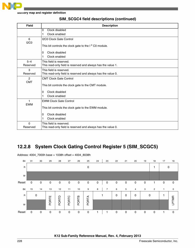
SIM_SCGC4 field descriptions (continued)
Field Description
0 Clock disabled1 Clock enabled
6I2C0
I2C0 Clock Gate Control
This bit controls the clock gate to the I 2 C0 module.
0 Clock disabled1 Clock enabled
5–4Reserved
This field is reserved.This read-only field is reserved and always has the value 1.
3Reserved
This field is reserved.This read-only field is reserved and always has the value 0.
2CMT
CMT Clock Gate Control
This bit controls the clock gate to the CMT module.
0 Clock disabled1 Clock enabled
1EWM
EWM Clock Gate Control
This bit controls the clock gate to the EWM module.
0 Clock disabled1 Clock enabled
0Reserved
This field is reserved.This read-only field is reserved and always has the value 0.
12.2.8 System Clock Gating Control Register 5 (SIM_SCGC5)
Address: 4004_7000h base + 1038h offset = 4004_8038h
Bit 31 30 29 28 27 26 25 24 23 22 21 20 19 18 17 16
R 0 1 0
W
Reset 0 0 0 0 0 0 0 0 0 0 0 0 0 1 0 0
Bit 15 14 13 12 11 10 9 8 7 6 5 4 3 2 1 0
R 0
PO
RT
E
PO
RT
D
PO
RT
C
PO
RT
B
PO
RT
A 1 0 0 0 0 1
LPT
MR
W
Reset 0 0 0 0 0 0 0 1 1 0 0 0 0 0 1 0
Memory map and register definition
K12 Sub-Family Reference Manual, Rev. 4, February 2013
228 Freescale Semiconductor, Inc.
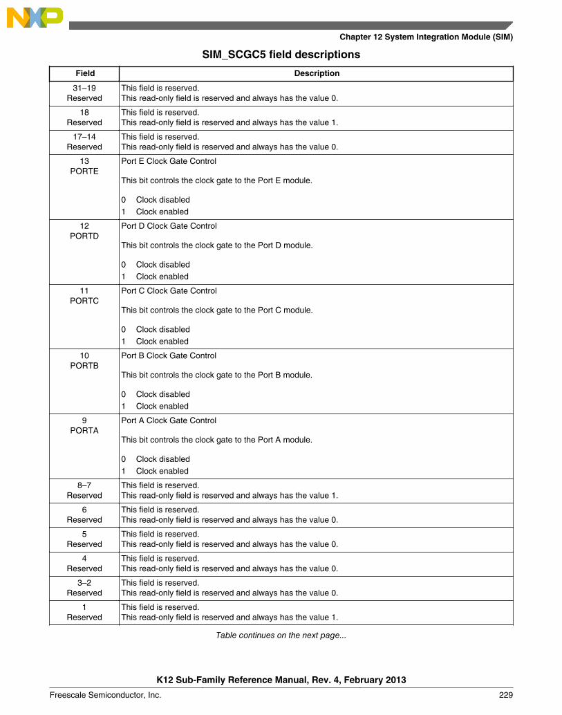
SIM_SCGC5 field descriptions
Field Description
31–19Reserved
This field is reserved.This read-only field is reserved and always has the value 0.
18Reserved
This field is reserved.This read-only field is reserved and always has the value 1.
17–14Reserved
This field is reserved.This read-only field is reserved and always has the value 0.
13PORTE
Port E Clock Gate Control
This bit controls the clock gate to the Port E module.
0 Clock disabled1 Clock enabled
12PORTD
Port D Clock Gate Control
This bit controls the clock gate to the Port D module.
0 Clock disabled1 Clock enabled
11PORTC
Port C Clock Gate Control
This bit controls the clock gate to the Port C module.
0 Clock disabled1 Clock enabled
10PORTB
Port B Clock Gate Control
This bit controls the clock gate to the Port B module.
0 Clock disabled1 Clock enabled
9PORTA
Port A Clock Gate Control
This bit controls the clock gate to the Port A module.
0 Clock disabled1 Clock enabled
8–7Reserved
This field is reserved.This read-only field is reserved and always has the value 1.
6Reserved
This field is reserved.This read-only field is reserved and always has the value 0.
5Reserved
This field is reserved.This read-only field is reserved and always has the value 0.
4Reserved
This field is reserved.This read-only field is reserved and always has the value 0.
3–2Reserved
This field is reserved.This read-only field is reserved and always has the value 0.
1Reserved
This field is reserved.This read-only field is reserved and always has the value 1.
Table continues on the next page...
Chapter 12 System Integration Module (SIM)
K12 Sub-Family Reference Manual, Rev. 4, February 2013
Freescale Semiconductor, Inc. 229

SIM_SCGC5 field descriptions (continued)
Field Description
0LPTMR
Low Power Timer Access Control
This bit controls software access to the Low Power Timer module.
0 Access disabled1 Access enabled
12.2.9 System Clock Gating Control Register 6 (SIM_SCGC6)
Address: 4004_7000h base + 103Ch offset = 4004_803Ch
Bit 31 30 29 28 27 26 25 24 23 22 21 20 19 18 17 16
R
DA
C0
1
RTC
0
AD
C0
FT
M2
FT
M1
FT
M0
PIT PDB
0 0
CRC
0
W
Reset 0 1 0 0 0 0 0 0 0 0 0 0 0 0 0 0
Bit 15 14 13 12 11 10 9 8 7 6 5 4 3 2 1 0
R
I2S
0
SPI1 SPI0
0 0 0 0 0 0 0 0
DM
AM
UX
FTFLW
Reset 0 0 0 0 0 0 0 0 0 0 0 0 0 0 0 1
SIM_SCGC6 field descriptions
Field Description
31DAC0
DAC0 Clock Gate Control
This bit controls the clock gate to the DAC0 module.
0 Clock disabled1 Clock enabled
30Reserved
This field is reserved.This read-only field is reserved and always has the value 1.
29RTC
RTC Access Control
This bit controls software access and interrupts to the RTC module.
0 Access and interrupts disabled1 Access and interrupts enabled
28Reserved
This field is reserved.This read-only field is reserved and always has the value 0.
27ADC0
ADC0 Clock Gate Control
This bit controls the clock gate to the ADC0 module.
Table continues on the next page...
Memory map and register definition
K12 Sub-Family Reference Manual, Rev. 4, February 2013
230 Freescale Semiconductor, Inc.

SIM_SCGC6 field descriptions (continued)
Field Description
0 Clock disabled1 Clock enabled
26FTM2
FTM2 Clock Gate Control
This bit controls the clock gate to the FTM2 module.
0 Clock disabled1 Clock enabled
25FTM1
FTM1 Clock Gate Control
This bit controls the clock gate to the FTM1 module.
0 Clock disabled1 Clock enabled
24FTM0
FTM0 Clock Gate Control
This bit controls the clock gate to the FTM0 module.
0 Clock disabled1 Clock enabled
23PIT
PIT Clock Gate Control
This bit controls the clock gate to the PIT module.
0 Clock disabled1 Clock enabled
22PDB
PDB Clock Gate Control
This bit controls the clock gate to the PDB module.
0 Clock disabled1 Clock enabled
21Reserved
This field is reserved.This read-only field is reserved and always has the value 0.
20–19Reserved
This field is reserved.This read-only field is reserved and always has the value 0.
18CRC
CRC Clock Gate Control
This bit controls the clock gate to the CRC module.
0 Clock disabled1 Clock enabled
17–16Reserved
This field is reserved.This read-only field is reserved and always has the value 0.
15I2S
I2S Clock Gate Control
This bit controls the clock gate to the I 2 S module.
0 Clock disabled1 Clock enabled
Table continues on the next page...
Chapter 12 System Integration Module (SIM)
K12 Sub-Family Reference Manual, Rev. 4, February 2013
Freescale Semiconductor, Inc. 231
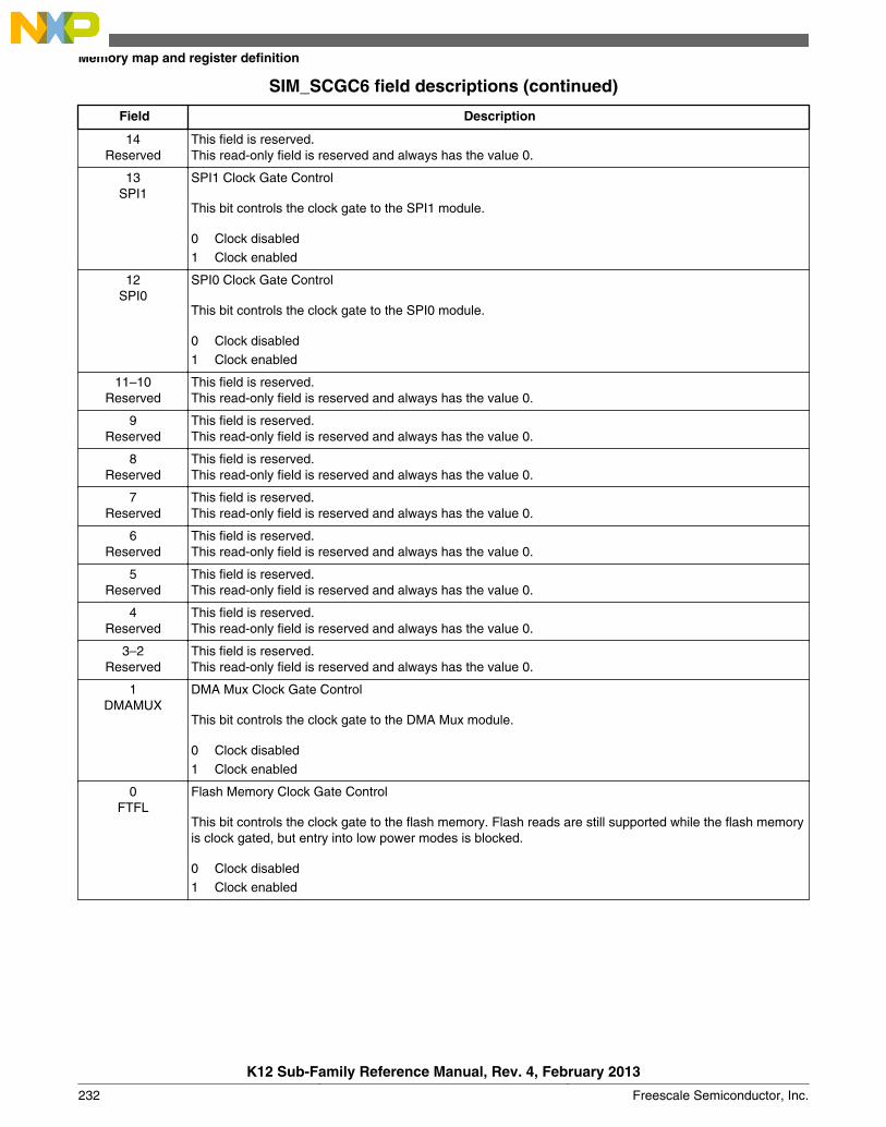
SIM_SCGC6 field descriptions (continued)
Field Description
14Reserved
This field is reserved.This read-only field is reserved and always has the value 0.
13SPI1
SPI1 Clock Gate Control
This bit controls the clock gate to the SPI1 module.
0 Clock disabled1 Clock enabled
12SPI0
SPI0 Clock Gate Control
This bit controls the clock gate to the SPI0 module.
0 Clock disabled1 Clock enabled
11–10Reserved
This field is reserved.This read-only field is reserved and always has the value 0.
9Reserved
This field is reserved.This read-only field is reserved and always has the value 0.
8Reserved
This field is reserved.This read-only field is reserved and always has the value 0.
7Reserved
This field is reserved.This read-only field is reserved and always has the value 0.
6Reserved
This field is reserved.This read-only field is reserved and always has the value 0.
5Reserved
This field is reserved.This read-only field is reserved and always has the value 0.
4Reserved
This field is reserved.This read-only field is reserved and always has the value 0.
3–2Reserved
This field is reserved.This read-only field is reserved and always has the value 0.
1DMAMUX
DMA Mux Clock Gate Control
This bit controls the clock gate to the DMA Mux module.
0 Clock disabled1 Clock enabled
0FTFL
Flash Memory Clock Gate Control
This bit controls the clock gate to the flash memory. Flash reads are still supported while the flash memoryis clock gated, but entry into low power modes is blocked.
0 Clock disabled1 Clock enabled
Memory map and register definition
K12 Sub-Family Reference Manual, Rev. 4, February 2013
232 Freescale Semiconductor, Inc.

12.2.10 System Clock Gating Control Register 7 (SIM_SCGC7)
Address: 4004_7000h base + 1040h offset = 4004_8040h
Bit 31 30 29 28 27 26 25 24 23 22 21 20 19 18 17 16
R 0W
Reset 0 0 0 0 0 0 0 0 0 0 0 0 0 0 0 0
Bit 15 14 13 12 11 10 9 8 7 6 5 4 3 2 1 0
R 0 0 DMA 0W
Reset 0 0 0 0 0 0 0 0 0 0 0 0 0 0 1 0
SIM_SCGC7 field descriptions
Field Description
31–3Reserved
This field is reserved.This read-only field is reserved and always has the value 0.
2Reserved
This field is reserved.This read-only field is reserved and always has the value 0.
1DMA
DMA Clock Gate Control
This bit controls the clock gate to the DMA module.
0 Clock disabled1 Clock enabled
0Reserved
This field is reserved.This read-only field is reserved and always has the value 0.
12.2.11 System Clock Divider Register 1 (SIM_CLKDIV1)
NOTEThe CLKDIV1 register cannot be written to when the device isin VLPR mode.
Address: 4004_7000h base + 1044h offset = 4004_8044h
Bit 31 30 29 28 27 26 25 24 23 22 21 20 19 18 17 16 15 14 13 12 11 10 9 8 7 6 5 4 3 2 1 0
R OUTDIV1 OUTDIV2 0 OUTDIV4 0W
Reset 0* 0* 0* 0* 0* 0* 0* 0* 0* 0* 0* 0* 0* 0* 0* 1* 0* 0* 0* 0* 0* 0* 0* 0* 0* 0* 0* 0* 0* 0* 0* 0*
* Notes:Reset value loaded during Syetem Reset from FTFL_FOPT[LPBOOT].•
Chapter 12 System Integration Module (SIM)
K12 Sub-Family Reference Manual, Rev. 4, February 2013
Freescale Semiconductor, Inc. 233
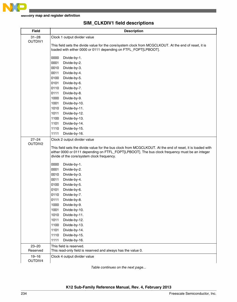
SIM_CLKDIV1 field descriptions
Field Description
31–28OUTDIV1
Clock 1 output divider value
This field sets the divide value for the core/system clock from MCGCLKOUT. At the end of reset, it isloaded with either 0000 or 0111 depending on FTFL_FOPT[LPBOOT].
0000 Divide-by-1.0001 Divide-by-2.0010 Divide-by-3.0011 Divide-by-4.0100 Divide-by-5.0101 Divide-by-6.0110 Divide-by-7.0111 Divide-by-8.1000 Divide-by-9.1001 Divide-by-10.1010 Divide-by-11.1011 Divide-by-12.1100 Divide-by-13.1101 Divide-by-14.1110 Divide-by-15.1111 Divide-by-16.
27–24OUTDIV2
Clock 2 output divider value
This field sets the divide value for the bus clock from MCGCLKOUT. At the end of reset, it is loaded witheither 0000 or 0111 depending on FTFL_FOPT[LPBOOT]. The bus clock frequency must be an integerdivide of the core/system clock frequency.
0000 Divide-by-1.0001 Divide-by-2.0010 Divide-by-3.0011 Divide-by-4.0100 Divide-by-5.0101 Divide-by-6.0110 Divide-by-7.0111 Divide-by-8.1000 Divide-by-9.1001 Divide-by-10.1010 Divide-by-11.1011 Divide-by-12.1100 Divide-by-13.1101 Divide-by-14.1110 Divide-by-15.1111 Divide-by-16.
23–20Reserved
This field is reserved.This read-only field is reserved and always has the value 0.
19–16OUTDIV4
Clock 4 output divider value
Table continues on the next page...
Memory map and register definition
K12 Sub-Family Reference Manual, Rev. 4, February 2013
234 Freescale Semiconductor, Inc.

SIM_CLKDIV1 field descriptions (continued)
Field Description
This field sets the divide value for the flash clock from MCGCLKOUT. At the end of reset, it is loaded witheither 0001 or 1111 depending on FTFL_FOPT[LPBOOT]. The flash clock frequency must be an integerdivide of the system clock frequency.
0000 Divide-by-1.0001 Divide-by-2.0010 Divide-by-3.0011 Divide-by-4.0100 Divide-by-5.0101 Divide-by-6.0110 Divide-by-7.0111 Divide-by-8.1000 Divide-by-9.1001 Divide-by-10.1010 Divide-by-11.1011 Divide-by-12.1100 Divide-by-13.1101 Divide-by-14.1110 Divide-by-15.1111 Divide-by-16.
15–0Reserved
This field is reserved.This read-only field is reserved and always has the value 0.
12.2.12 System Clock Divider Register 2 (SIM_CLKDIV2)
Address: 4004_7000h base + 1048h offset = 4004_8048h
Bit 31 30 29 28 27 26 25 24 23 22 21 20 19 18 17 16
R 0W
Reset 0 0 0 0 0 0 0 0 0 0 0 0 0 0 0 0
Bit 15 14 13 12 11 10 9 8 7 6 5 4 3 2 1 0
R 0 0 0W
Reset 0 0 0 0 0 0 0 0 0 0 0 0 0 0 0 0
SIM_CLKDIV2 field descriptions
Field Description
31–4Reserved
This field is reserved.This read-only field is reserved and always has the value 0.
3–1Reserved
This field is reserved.This read-only field is reserved and always has the value 0.
0Reserved
This field is reserved.This read-only field is reserved and always has the value 0.
Chapter 12 System Integration Module (SIM)
K12 Sub-Family Reference Manual, Rev. 4, February 2013
Freescale Semiconductor, Inc. 235
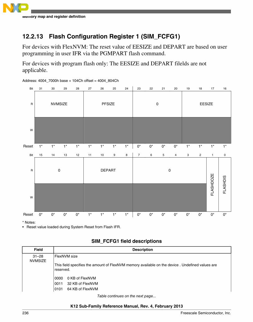
12.2.13 Flash Configuration Register 1 (SIM_FCFG1)
For devices with FlexNVM: The reset value of EESIZE and DEPART are based on userprogramming in user IFR via the PGMPART flash command.
For devices with program flash only: The EESIZE and DEPART filelds are notapplicable.
Address: 4004_7000h base + 104Ch offset = 4004_804Ch
Bit 31 30 29 28 27 26 25 24 23 22 21 20 19 18 17 16
R NVMSIZE PFSIZE 0 EESIZE
W
Reset 1* 1* 1* 1* 1* 1* 1* 1* 0* 0* 0* 0* 1* 1* 1* 1*
Bit 15 14 13 12 11 10 9 8 7 6 5 4 3 2 1 0
R 0 DEPART 0
FLA
SH
DO
ZE
FLA
SH
DIS
W
Reset 0* 0* 0* 0* 1* 1* 1* 1* 0* 0* 0* 0* 0* 0* 0* 0*
* Notes:Reset value loaded during System Reset from Flash IFR.•
SIM_FCFG1 field descriptions
Field Description
31–28NVMSIZE
FlexNVM size
This field specifies the amount of FlexNVM memory available on the device . Undefined values arereserved.
0000 0 KB of FlexNVM0011 32 KB of FlexNVM0101 64 KB of FlexNVM
Table continues on the next page...
Memory map and register definition
K12 Sub-Family Reference Manual, Rev. 4, February 2013
236 Freescale Semiconductor, Inc.
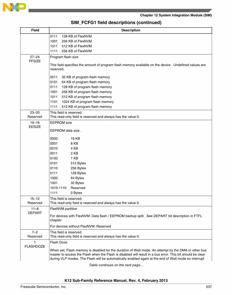
SIM_FCFG1 field descriptions (continued)
Field Description
0111 128 KB of FlexNVM1001 256 KB of FlexNVM1011 512 KB of FlexNVM1111 256 KB of FlexNVM
27–24PFSIZE
Program flash size
This field specifies the amount of program flash memory available on the device . Undefined values arereserved.
0011 32 KB of program flash memory0101 64 KB of program flash memory0111 128 KB of program flash memory1001 256 KB of program flash memory1011 512 KB of program flash memory1101 1024 KB of program flash memory1111 512 KB of program flash memory
23–20Reserved
This field is reserved.This read-only field is reserved and always has the value 0.
19–16EESIZE
EEPROM size
EEPROM data size .
0000 16 KB0001 8 KB0010 4 KB0011 2 KB0100 1 KB0101 512 Bytes0110 256 Bytes0111 128 Bytes1000 64 Bytes1001 32 Bytes1010-1110 Reserved1111 0 Bytes
15–12Reserved
This field is reserved.This read-only field is reserved and always has the value 0.
11–8DEPART
FlexNVM partition
For devices with FlexNVM: Data flash / EEPROM backup split . See DEPART bit description in FTFLchapter.
For devices without FlexNVM: Reserved
7–2Reserved
This field is reserved.This read-only field is reserved and always has the value 0.
1FLASHDOZE
Flash Doze
When set, Flash memory is disabled for the duration of Wait mode. An attempt by the DMA or other busmaster to access the Flash when the Flash is disabled will result in a bus error. This bit should be clearduring VLP modes. The Flash will be automatically enabled again at the end of Wait mode so interrupt
Table continues on the next page...
Chapter 12 System Integration Module (SIM)
K12 Sub-Family Reference Manual, Rev. 4, February 2013
Freescale Semiconductor, Inc. 237
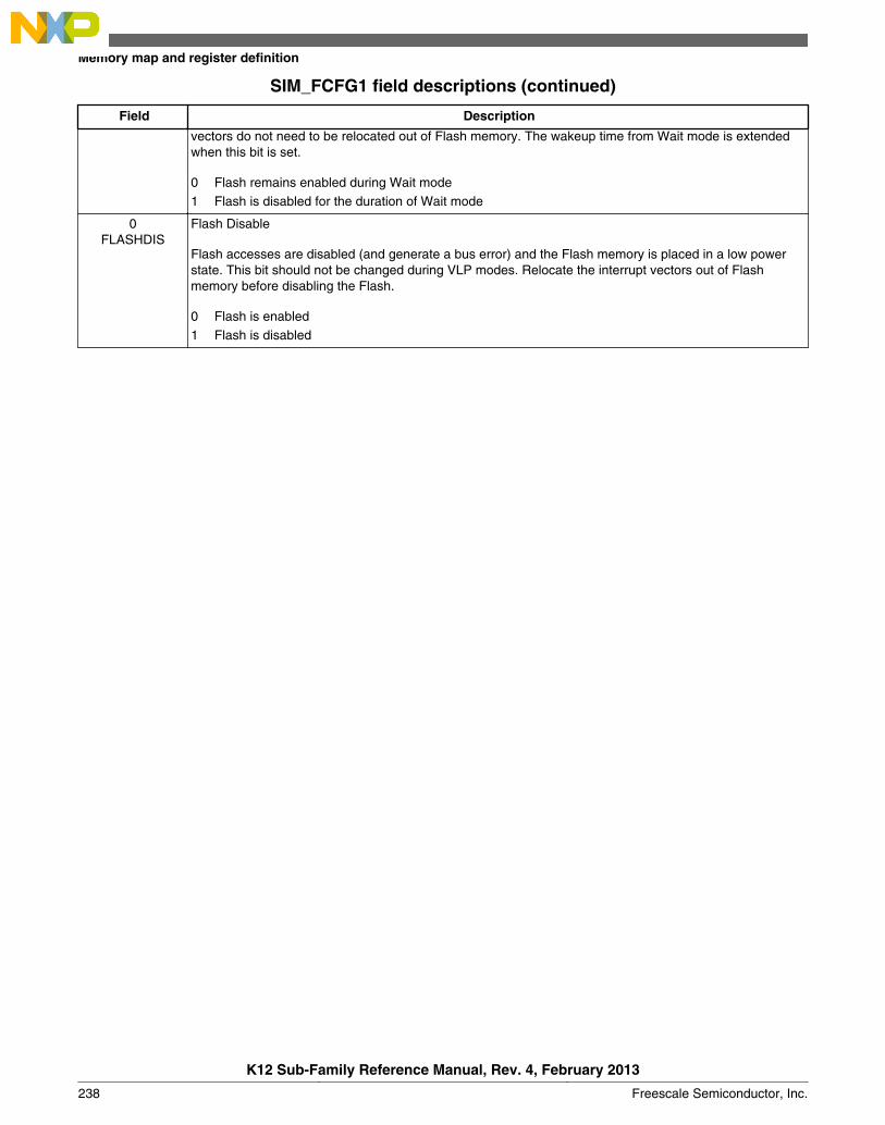
SIM_FCFG1 field descriptions (continued)
Field Description
vectors do not need to be relocated out of Flash memory. The wakeup time from Wait mode is extendedwhen this bit is set.
0 Flash remains enabled during Wait mode1 Flash is disabled for the duration of Wait mode
0FLASHDIS
Flash Disable
Flash accesses are disabled (and generate a bus error) and the Flash memory is placed in a low powerstate. This bit should not be changed during VLP modes. Relocate the interrupt vectors out of Flashmemory before disabling the Flash.
0 Flash is enabled1 Flash is disabled
Memory map and register definition
K12 Sub-Family Reference Manual, Rev. 4, February 2013
238 Freescale Semiconductor, Inc.
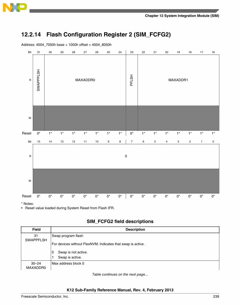
12.2.14 Flash Configuration Register 2 (SIM_FCFG2)
Address: 4004_7000h base + 1050h offset = 4004_8050h
Bit 31 30 29 28 27 26 25 24 23 22 21 20 19 18 17 16
R
SW
AP
PF
LSH
MAXADDR0
PF
LSH
MAXADDR1
W
Reset 0* 1* 1* 1* 1* 1* 1* 1* 0* 1* 1* 1* 1* 1* 1* 1*
Bit 15 14 13 12 11 10 9 8 7 6 5 4 3 2 1 0
R 0
W
Reset 0* 0* 0* 0* 0* 0* 0* 0* 0* 0* 0* 0* 0* 0* 0* 0*
* Notes:Reset value loaded during System Reset from Flash IFR.•
SIM_FCFG2 field descriptions
Field Description
31SWAPPFLSH
Swap program flash
For devices without FlexNVM: Indicates that swap is active .
0 Swap is not active.1 Swap is active.
30–24MAXADDR0
Max address block 0
Table continues on the next page...
Chapter 12 System Integration Module (SIM)
K12 Sub-Family Reference Manual, Rev. 4, February 2013
Freescale Semiconductor, Inc. 239
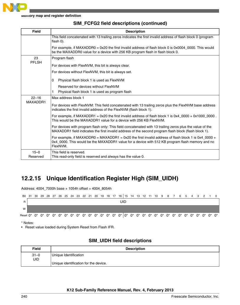
SIM_FCFG2 field descriptions (continued)
Field Description
This field concatenated with 13 trailing zeros indicates the first invalid address of flash block 0 (programflash 0).
For example, if MAXADDR0 = 0x20 the first invalid address of flash block 0 is 0x0004_0000. This wouldbe the MAXADDR0 value for a device with 256 KB program flash in flash block 0.
23PFLSH
Program flash
For devices with FlexNVM, this bit is always clear.
For devices without FlexNVM, this bit is always set.
0 Physical flash block 1 is used as FlexNVM
Reserved for devices without FlexNVM1 Physical flash block 1 is used as program flash
22–16MAXADDR1
Max address block 1
For devices with FlexNVM: This field concatenated with 13 trailing zeros plus the FlexNVM base addressindicates the first invalid address of the FlexNVM (flash block 1).
For example, if MAXADDR1 = 0x20 the first invalid address of flash block 1 is 0x4_0000 + 0x1000_0000 .This would be the MAXADDR1 value for a device with 256 KB FlexNVM.
For devices with program flash only: This field concatenated with 13 trailing zeros plus the value of theMAXADDR1 field indicates the first invalid address of the second program flash block (flash block 1).
For example, if MAXADDR0 = MAXADDR1 = 0x20 the first invalid address of flash block 1 is 0x4_0000 +0x4_0000. This would be the MAXADDR1 value for a device with 512 KB program flash memory and noFlexNVM.
15–0Reserved
This field is reserved.This read-only field is reserved and always has the value 0.
12.2.15 Unique Identification Register High (SIM_UIDH)
Address: 4004_7000h base + 1054h offset = 4004_8054h
Bit 31 30 29 28 27 26 25 24 23 22 21 20 19 18 17 16 15 14 13 12 11 10 9 8 7 6 5 4 3 2 1 0
R UID
W
Reset 0* 0* 0* 0* 0* 0* 0* 0* 0* 0* 0* 0* 0* 0* 0* 0* 0* 0* 0* 0* 0* 0* 0* 0* 0* 0* 0* 0* 0* 0* 0* 0*
* Notes:Reset value loaded during System Reset from Flash IFR.•
SIM_UIDH field descriptions
Field Description
31–0UID
Unique Identification
Unique identification for the device.
Memory map and register definition
K12 Sub-Family Reference Manual, Rev. 4, February 2013
240 Freescale Semiconductor, Inc.

12.2.16 Unique Identification Register Mid-High (SIM_UIDMH)
Address: 4004_7000h base + 1058h offset = 4004_8058h
Bit 31 30 29 28 27 26 25 24 23 22 21 20 19 18 17 16 15 14 13 12 11 10 9 8 7 6 5 4 3 2 1 0
R UID
W
Reset 0* 0* 0* 0* 0* 0* 0* 0* 0* 0* 0* 0* 0* 0* 0* 0* 0* 0* 0* 0* 0* 0* 0* 0* 0* 0* 0* 0* 0* 0* 0* 0*
* Notes:Reset value loaded during System Reset from Flash IFR.•
SIM_UIDMH field descriptions
Field Description
31–0UID
Unique Identification
Unique identification for the device.
12.2.17 Unique Identification Register Mid Low (SIM_UIDML)
Address: 4004_7000h base + 105Ch offset = 4004_805Ch
Bit 31 30 29 28 27 26 25 24 23 22 21 20 19 18 17 16 15 14 13 12 11 10 9 8 7 6 5 4 3 2 1 0
R UID
W
Reset 0* 0* 0* 0* 0* 0* 0* 0* 0* 0* 0* 0* 0* 0* 0* 0* 0* 0* 0* 0* 0* 0* 0* 0* 0* 0* 0* 0* 0* 0* 0* 0*
* Notes:Reset value loaded during System Reset from Flash IFR.•
SIM_UIDML field descriptions
Field Description
31–0UID
Unique Identification
Unique identification for the device.
Chapter 12 System Integration Module (SIM)
K12 Sub-Family Reference Manual, Rev. 4, February 2013
Freescale Semiconductor, Inc. 241

12.2.18 Unique Identification Register Low (SIM_UIDL)
Address: 4004_7000h base + 1060h offset = 4004_8060h
Bit 31 30 29 28 27 26 25 24 23 22 21 20 19 18 17 16 15 14 13 12 11 10 9 8 7 6 5 4 3 2 1 0
R UID
W
Reset 0* 0* 0* 0* 0* 0* 0* 0* 0* 0* 0* 0* 0* 0* 0* 0* 0* 0* 0* 0* 0* 0* 0* 0* 0* 0* 0* 0* 0* 0* 0* 0*
* Notes:Reset value loaded during System Reset from Flash IFR.•
SIM_UIDL field descriptions
Field Description
31–0UID
Unique Identification
Unique identification for the device.
12.3 Functional descriptionFor more information about the functions of SIM, see the Introduction section.
Functional description
K12 Sub-Family Reference Manual, Rev. 4, February 2013
242 Freescale Semiconductor, Inc.
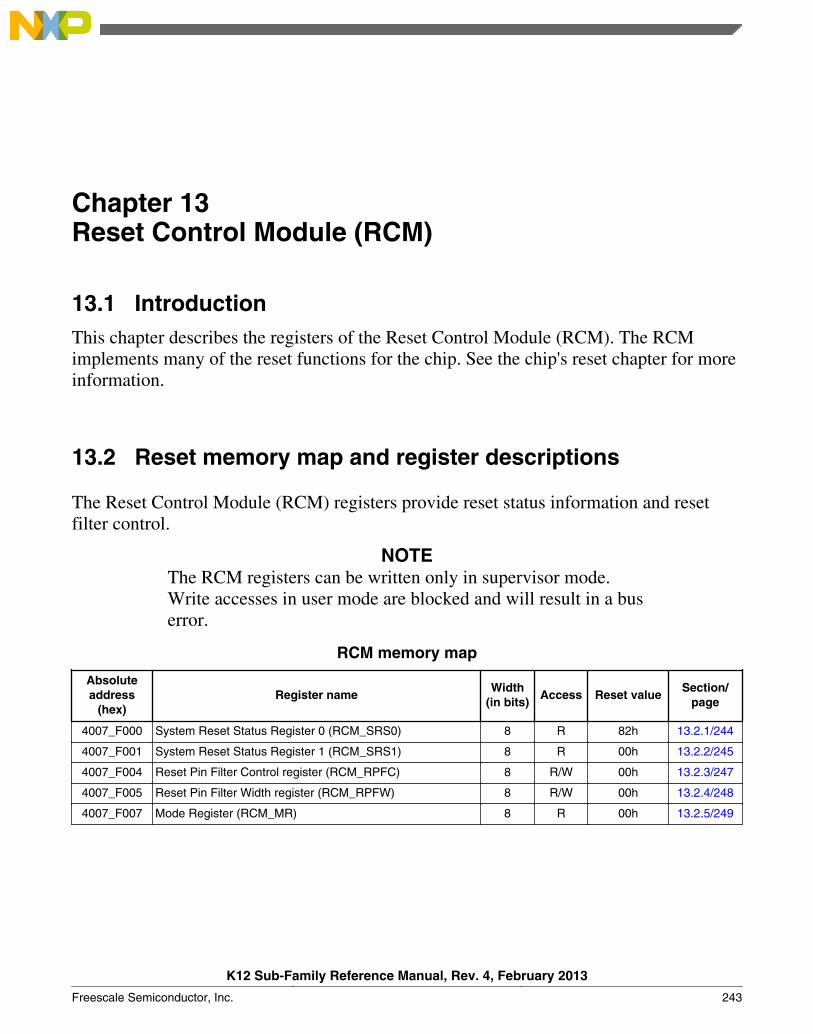
Chapter 13Reset Control Module (RCM)
13.1 IntroductionThis chapter describes the registers of the Reset Control Module (RCM). The RCMimplements many of the reset functions for the chip. See the chip's reset chapter for moreinformation.
13.2 Reset memory map and register descriptions
The Reset Control Module (RCM) registers provide reset status information and resetfilter control.
NOTEThe RCM registers can be written only in supervisor mode.Write accesses in user mode are blocked and will result in a buserror.
RCM memory map
Absoluteaddress
(hex)Register name
Width(in bits)
Access Reset valueSection/
page
4007_F000 System Reset Status Register 0 (RCM_SRS0) 8 R 82h 13.2.1/244
4007_F001 System Reset Status Register 1 (RCM_SRS1) 8 R 00h 13.2.2/245
4007_F004 Reset Pin Filter Control register (RCM_RPFC) 8 R/W 00h 13.2.3/247
4007_F005 Reset Pin Filter Width register (RCM_RPFW) 8 R/W 00h 13.2.4/248
4007_F007 Mode Register (RCM_MR) 8 R 00h 13.2.5/249
K12 Sub-Family Reference Manual, Rev. 4, February 2013
Freescale Semiconductor, Inc. 243
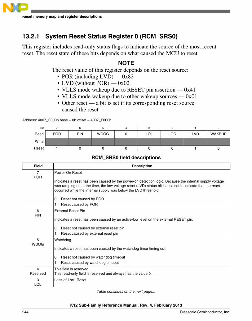
13.2.1 System Reset Status Register 0 (RCM_SRS0)
This register includes read-only status flags to indicate the source of the most recentreset. The reset state of these bits depends on what caused the MCU to reset.
NOTEThe reset value of this register depends on the reset source:
• POR (including LVD) — 0x82• LVD (without POR) — 0x02• VLLS mode wakeup due to RESET pin assertion — 0x41• VLLS mode wakeup due to other wakeup sources — 0x01• Other reset — a bit is set if its corresponding reset source
caused the reset
Address: 4007_F000h base + 0h offset = 4007_F000h
Bit 7 6 5 4 3 2 1 0
Read POR PIN WDOG 0 LOL LOC LVD WAKEUP
Write
Reset 1 0 0 0 0 0 1 0
RCM_SRS0 field descriptions
Field Description
7POR
Power-On Reset
Indicates a reset has been caused by the power-on detection logic. Because the internal supply voltagewas ramping up at the time, the low-voltage reset (LVD) status bit is also set to indicate that the resetoccurred while the internal supply was below the LVD threshold.
0 Reset not caused by POR1 Reset caused by POR
6PIN
External Reset Pin
Indicates a reset has been caused by an active-low level on the external RESET pin.
0 Reset not caused by external reset pin1 Reset caused by external reset pin
5WDOG
Watchdog
Indicates a reset has been caused by the watchdog timer timing out.
0 Reset not caused by watchdog timeout1 Reset caused by watchdog timeout
4Reserved
This field is reserved.This read-only field is reserved and always has the value 0.
3LOL
Loss-of-Lock Reset
Table continues on the next page...
Reset memory map and register descriptions
K12 Sub-Family Reference Manual, Rev. 4, February 2013
244 Freescale Semiconductor, Inc.

RCM_SRS0 field descriptions (continued)
Field Description
Indicates a reset has been caused by a loss of lock in the MCG PLL. See the MCG description forinformation on the loss-of-clock event.
0 Reset not caused by a loss of lock in the PLL1 Reset caused by a loss of lock in the PLL
2LOC
Loss-of-Clock Reset
Indicates a reset has been caused by a loss of external clock. The MCG clock monitor must be enabledfor a loss of clock to be detected. Refer to the detailed MCG description for information on enabling theclock monitor.
0 Reset not caused by a loss of external clock.1 Reset caused by a loss of external clock.
1LVD
Low-Voltage Detect Reset
If the LVDRE bit is set and the supply drops below the LVD trip voltage, an LVD reset occurs. This bit isalso set by POR.
0 Reset not caused by LVD trip or POR1 Reset caused by LVD trip or POR
0WAKEUP
Low Leakage Wakeup Reset
Indicates a reset has been caused by an enabled LLWU module wakeup source while the chip was in alow leakage mode. In LLS mode, the RESET pin is the only wakeup source that can cause this reset. Anyenabled wakeup source in a VLLSx mode causes a reset. This bit is cleared by any reset exceptWAKEUP.
0 Reset not caused by LLWU module wakeup source1 Reset caused by LLWU module wakeup source
13.2.2 System Reset Status Register 1 (RCM_SRS1)
This register includes read-only status flags to indicate the source of the most recentreset. The reset state of these bits depends on what caused the MCU to reset.
NOTEThe reset value of this register depends on the reset source:
• POR (including LVD) — 0x00• LVD (without POR) — 0x00• VLLS mode wakeup — 0x00• Other reset — a bit is set if its corresponding reset source
caused the reset
Chapter 13 Reset Control Module (RCM)
K12 Sub-Family Reference Manual, Rev. 4, February 2013
Freescale Semiconductor, Inc. 245
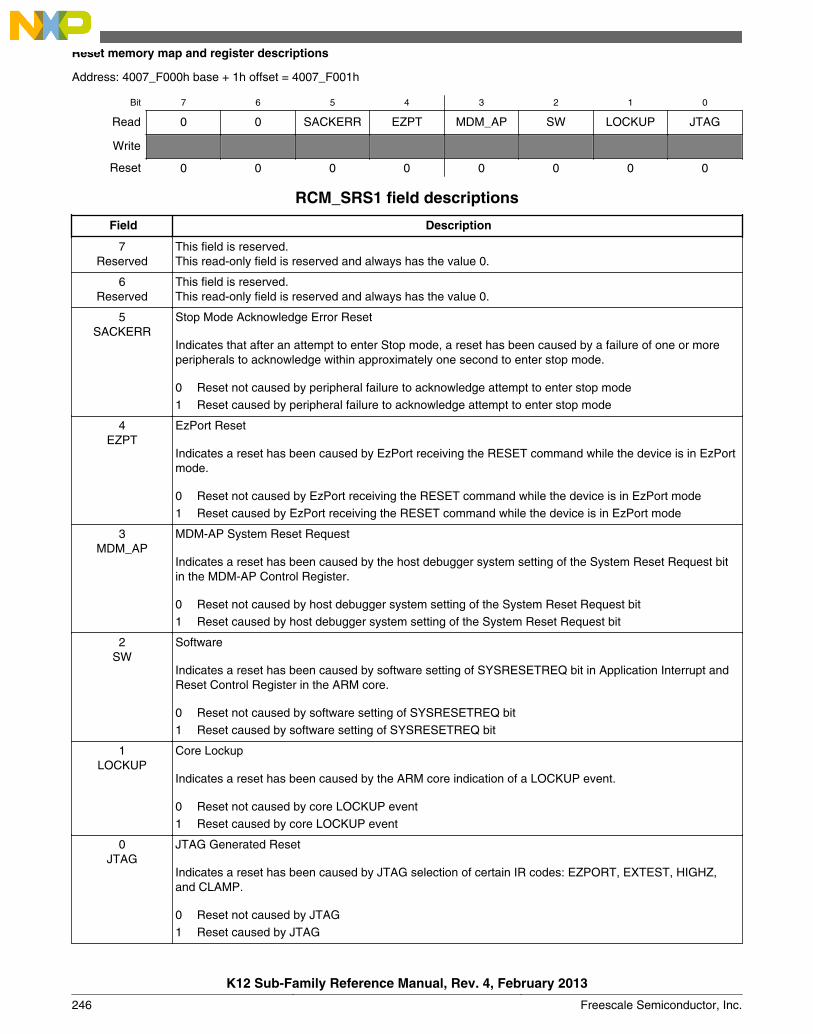
Address: 4007_F000h base + 1h offset = 4007_F001h
Bit 7 6 5 4 3 2 1 0
Read 0 0 SACKERR EZPT MDM_AP SW LOCKUP JTAG
Write
Reset 0 0 0 0 0 0 0 0
RCM_SRS1 field descriptions
Field Description
7Reserved
This field is reserved.This read-only field is reserved and always has the value 0.
6Reserved
This field is reserved.This read-only field is reserved and always has the value 0.
5SACKERR
Stop Mode Acknowledge Error Reset
Indicates that after an attempt to enter Stop mode, a reset has been caused by a failure of one or moreperipherals to acknowledge within approximately one second to enter stop mode.
0 Reset not caused by peripheral failure to acknowledge attempt to enter stop mode1 Reset caused by peripheral failure to acknowledge attempt to enter stop mode
4EZPT
EzPort Reset
Indicates a reset has been caused by EzPort receiving the RESET command while the device is in EzPortmode.
0 Reset not caused by EzPort receiving the RESET command while the device is in EzPort mode1 Reset caused by EzPort receiving the RESET command while the device is in EzPort mode
3MDM_AP
MDM-AP System Reset Request
Indicates a reset has been caused by the host debugger system setting of the System Reset Request bitin the MDM-AP Control Register.
0 Reset not caused by host debugger system setting of the System Reset Request bit1 Reset caused by host debugger system setting of the System Reset Request bit
2SW
Software
Indicates a reset has been caused by software setting of SYSRESETREQ bit in Application Interrupt andReset Control Register in the ARM core.
0 Reset not caused by software setting of SYSRESETREQ bit1 Reset caused by software setting of SYSRESETREQ bit
1LOCKUP
Core Lockup
Indicates a reset has been caused by the ARM core indication of a LOCKUP event.
0 Reset not caused by core LOCKUP event1 Reset caused by core LOCKUP event
0JTAG
JTAG Generated Reset
Indicates a reset has been caused by JTAG selection of certain IR codes: EZPORT, EXTEST, HIGHZ,and CLAMP.
0 Reset not caused by JTAG1 Reset caused by JTAG
Reset memory map and register descriptions
K12 Sub-Family Reference Manual, Rev. 4, February 2013
246 Freescale Semiconductor, Inc.
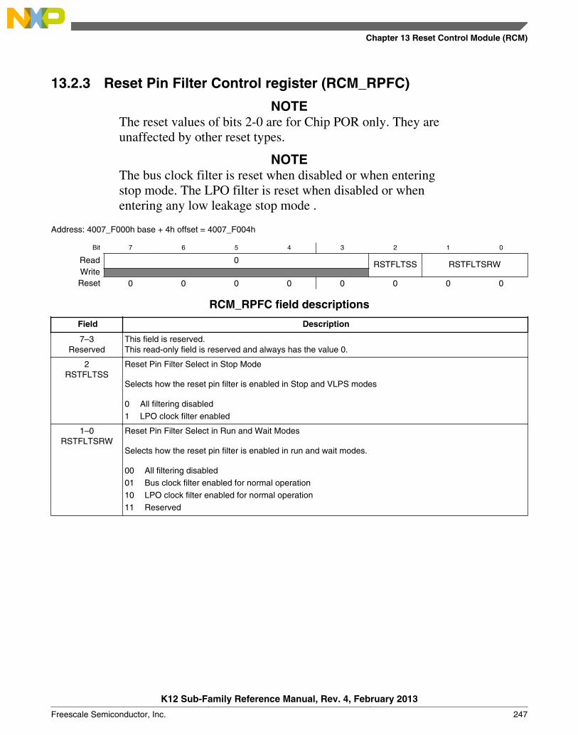
13.2.3 Reset Pin Filter Control register (RCM_RPFC)
NOTEThe reset values of bits 2-0 are for Chip POR only. They areunaffected by other reset types.
NOTEThe bus clock filter is reset when disabled or when enteringstop mode. The LPO filter is reset when disabled or whenentering any low leakage stop mode .
Address: 4007_F000h base + 4h offset = 4007_F004h
Bit 7 6 5 4 3 2 1 0
Read 0 RSTFLTSS RSTFLTSRWWriteReset 0 0 0 0 0 0 0 0
RCM_RPFC field descriptions
Field Description
7–3Reserved
This field is reserved.This read-only field is reserved and always has the value 0.
2RSTFLTSS
Reset Pin Filter Select in Stop Mode
Selects how the reset pin filter is enabled in Stop and VLPS modes
0 All filtering disabled1 LPO clock filter enabled
1–0RSTFLTSRW
Reset Pin Filter Select in Run and Wait Modes
Selects how the reset pin filter is enabled in run and wait modes.
00 All filtering disabled01 Bus clock filter enabled for normal operation10 LPO clock filter enabled for normal operation11 Reserved
Chapter 13 Reset Control Module (RCM)
K12 Sub-Family Reference Manual, Rev. 4, February 2013
Freescale Semiconductor, Inc. 247
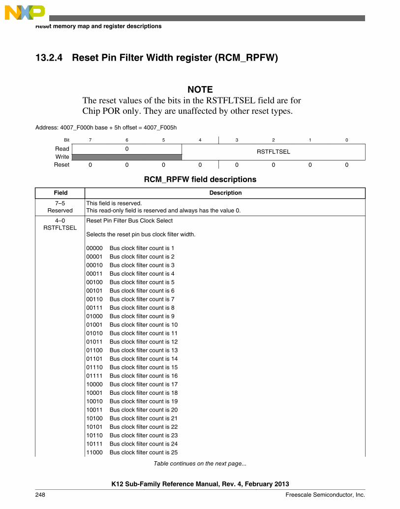
13.2.4 Reset Pin Filter Width register (RCM_RPFW)
NOTEThe reset values of the bits in the RSTFLTSEL field are forChip POR only. They are unaffected by other reset types.
Address: 4007_F000h base + 5h offset = 4007_F005h
Bit 7 6 5 4 3 2 1 0
Read 0 RSTFLTSELWriteReset 0 0 0 0 0 0 0 0
RCM_RPFW field descriptions
Field Description
7–5Reserved
This field is reserved.This read-only field is reserved and always has the value 0.
4–0RSTFLTSEL
Reset Pin Filter Bus Clock Select
Selects the reset pin bus clock filter width.
00000 Bus clock filter count is 100001 Bus clock filter count is 200010 Bus clock filter count is 300011 Bus clock filter count is 400100 Bus clock filter count is 500101 Bus clock filter count is 600110 Bus clock filter count is 700111 Bus clock filter count is 801000 Bus clock filter count is 901001 Bus clock filter count is 1001010 Bus clock filter count is 1101011 Bus clock filter count is 1201100 Bus clock filter count is 1301101 Bus clock filter count is 1401110 Bus clock filter count is 1501111 Bus clock filter count is 1610000 Bus clock filter count is 1710001 Bus clock filter count is 1810010 Bus clock filter count is 1910011 Bus clock filter count is 2010100 Bus clock filter count is 2110101 Bus clock filter count is 2210110 Bus clock filter count is 2310111 Bus clock filter count is 2411000 Bus clock filter count is 25
Table continues on the next page...
Reset memory map and register descriptions
K12 Sub-Family Reference Manual, Rev. 4, February 2013
248 Freescale Semiconductor, Inc.

RCM_RPFW field descriptions (continued)
Field Description
11001 Bus clock filter count is 2611010 Bus clock filter count is 2711011 Bus clock filter count is 2811100 Bus clock filter count is 2911101 Bus clock filter count is 3011110 Bus clock filter count is 3111111 Bus clock filter count is 32
13.2.5 Mode Register (RCM_MR)
This register includes read-only status flags to indicate the state of the mode pins duringthe last Chip Reset.
Address: 4007_F000h base + 7h offset = 4007_F007h
Bit 7 6 5 4 3 2 1 0
Read 0 EZP_MS 0
Write
Reset 0 0 0 0 0 0 0 0
RCM_MR field descriptions
Field Description
7–2Reserved
This field is reserved.This read-only field is reserved and always has the value 0.
1EZP_MS
EZP_MS_B pin state
Reflects the state of the EZP_MS pin during the last Chip Reset
0 Pin deasserted (logic 1)1 Pin asserted (logic 0)
0Reserved
This field is reserved.This read-only field is reserved and always has the value 0.
Chapter 13 Reset Control Module (RCM)
K12 Sub-Family Reference Manual, Rev. 4, February 2013
Freescale Semiconductor, Inc. 249

Reset memory map and register descriptions
K12 Sub-Family Reference Manual, Rev. 4, February 2013
250 Freescale Semiconductor, Inc.
Chapter 14System Mode Controller (SMC)
14.1 IntroductionNOTE
For the chip-specific implementation details of this module'sinstances see the chip configuration information.
The system mode controller (SMC) is responsible for sequencing the system into and outof all low power stop and run modes. Specifically, it monitors events to trigger transitionsbetween power modes while controlling the power, clocks, and memories of the systemto achieve the power consumption and functionality of that mode.
This chapter describes all the available low power modes, the sequence followed to enter/exit each mode, and the functionality available while in each of the modes.
The SMC is able to function during even the deepest low power modes.
14.2 Modes of operationThe ARM CPU has three primary modes of operation:
• Run• Sleep• Deep Sleep
The WFI or WFE instruction is used to invoke Sleep and Deep Sleep modes. Run, waitand stop are the common terms used for the primary operating modes of Freescalemicrocontrollers. The following table shows the translation between the ARM CPUmodes and the Freescale MCU power modes.
K12 Sub-Family Reference Manual, Rev. 4, February 2013
Freescale Semiconductor, Inc. 251
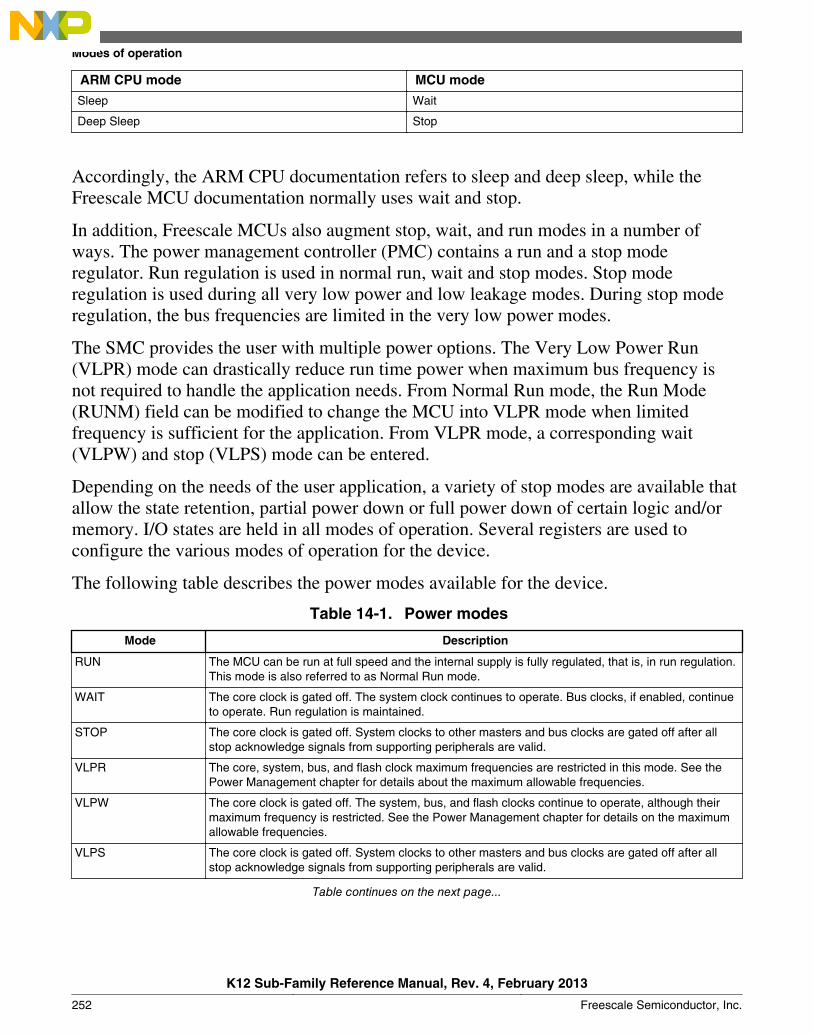
ARM CPU mode MCU mode
Sleep Wait
Deep Sleep Stop
Accordingly, the ARM CPU documentation refers to sleep and deep sleep, while theFreescale MCU documentation normally uses wait and stop.
In addition, Freescale MCUs also augment stop, wait, and run modes in a number ofways. The power management controller (PMC) contains a run and a stop moderegulator. Run regulation is used in normal run, wait and stop modes. Stop moderegulation is used during all very low power and low leakage modes. During stop moderegulation, the bus frequencies are limited in the very low power modes.
The SMC provides the user with multiple power options. The Very Low Power Run(VLPR) mode can drastically reduce run time power when maximum bus frequency isnot required to handle the application needs. From Normal Run mode, the Run Mode(RUNM) field can be modified to change the MCU into VLPR mode when limitedfrequency is sufficient for the application. From VLPR mode, a corresponding wait(VLPW) and stop (VLPS) mode can be entered.
Depending on the needs of the user application, a variety of stop modes are available thatallow the state retention, partial power down or full power down of certain logic and/ormemory. I/O states are held in all modes of operation. Several registers are used toconfigure the various modes of operation for the device.
The following table describes the power modes available for the device.
Table 14-1. Power modes
Mode Description
RUN The MCU can be run at full speed and the internal supply is fully regulated, that is, in run regulation.This mode is also referred to as Normal Run mode.
WAIT The core clock is gated off. The system clock continues to operate. Bus clocks, if enabled, continueto operate. Run regulation is maintained.
STOP The core clock is gated off. System clocks to other masters and bus clocks are gated off after allstop acknowledge signals from supporting peripherals are valid.
VLPR The core, system, bus, and flash clock maximum frequencies are restricted in this mode. See thePower Management chapter for details about the maximum allowable frequencies.
VLPW The core clock is gated off. The system, bus, and flash clocks continue to operate, although theirmaximum frequency is restricted. See the Power Management chapter for details on the maximumallowable frequencies.
VLPS The core clock is gated off. System clocks to other masters and bus clocks are gated off after allstop acknowledge signals from supporting peripherals are valid.
Table continues on the next page...
Modes of operation
K12 Sub-Family Reference Manual, Rev. 4, February 2013
252 Freescale Semiconductor, Inc.

Table 14-1. Power modes (continued)
Mode Description
LLS3 The core clock is gated off. System clocks to other masters and bus clocks are gated off after allstop acknowledge signals from supporting peripherals are valid. The MCU is placed in a lowleakage mode by reducing the voltage to internal logic. All system RAM contents, internal logic andI/O states are retained.
LLS2 The core clock is gated off. System clocks to other masters and bus clocks are gated off after allstop acknowledge signals from supporting peripherals are valid.The MCU is placed in a low leakagemode by reducing the voltage to internal logic and powering down the system RAM3 partition. Thesystem RAM2 partition can be optionally retained using VLLSCTRL[RAM2PO]. The system RAM1partition, internal logic and I/O states are retained.1
VLLS3 The core clock is gated off. System clocks to other masters and bus clocks are gated off after allstop acknowledge signals from supporting peripherals are valid. The MCU is placed in a lowleakage mode by powering down the internal logic. All system RAM contents are retained and I/Ostates are held. Internal logic states are not retained.
VLLS2 The core clock is gated off. System clocks to other masters and bus clocks are gated off after allstop acknowledge signals from supporting peripherals are valid.The MCU is placed in a low leakagemode by powering down the internal logic and the system RAM3 partition. The system RAM2partition can be optionally retained using VLLSCTRL[RAM2PO]. The system RAM1 partitioncontents are retained in this mode. Internal logic states are not retained.
VLLS1 The core clock is gated off. System clocks to other masters and bus clocks are gated off after allstop acknowledge signals from supporting peripherals are valid. The MCU is placed in a lowleakage mode by powering down the internal logic and all system RAM. I/O states are held. Internallogic states are not retained.
VLLS0 The core clock is gated off. System clocks to other masters and bus clocks are gated off after allstop acknowledge signals from supporting peripherals are valid. The MCU is placed in a lowleakage mode by powering down the internal logic and all system RAM. I/O states are held. Internallogic states are not retained. The 1kHz LPO clock is disabled and the power on reset (POR) circuitcan be optionally enabled using VLLSCTRL[PORPO].
1. See the devices' chip configuration details for the size and location of the system RAM partitions.2. See the devices' chip configuration details for the size and location of the system RAM partitions.
14.3 Memory map and register descriptionsDetails follow about the registers related to the system mode controller.
Different SMC registers reset on different reset types. Each register's description providesdetails. For more information about the types of reset on this chip, refer to the Resetsection details.
NOTEThe SMC registers can be written only in supervisor mode.Write accesses in user mode are blocked and will result in a buserror.
Chapter 14 System Mode Controller (SMC)
K12 Sub-Family Reference Manual, Rev. 4, February 2013
Freescale Semiconductor, Inc. 253
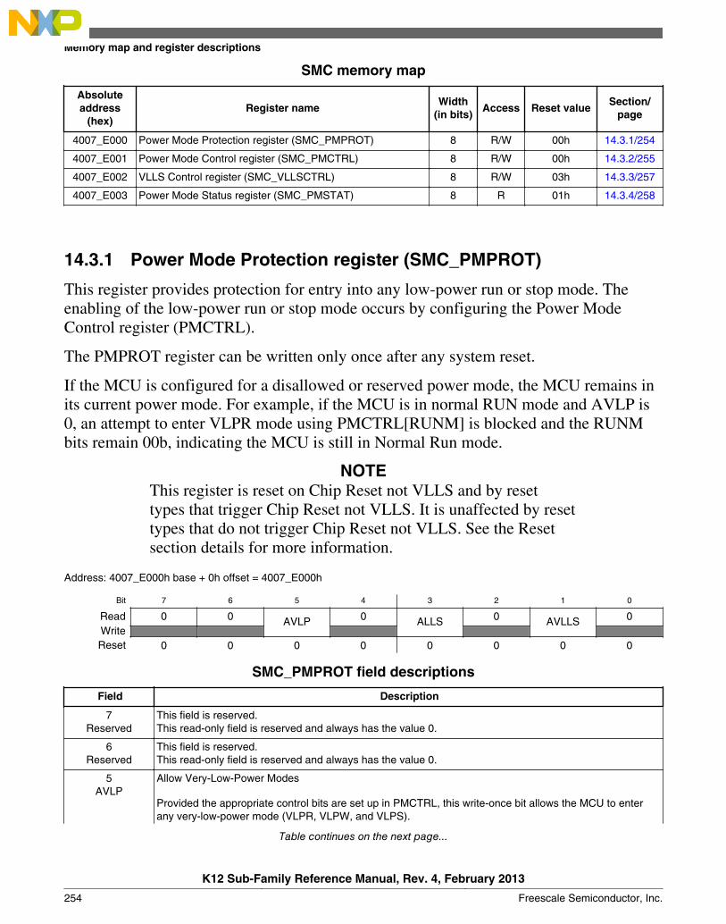
SMC memory map
Absoluteaddress
(hex)Register name
Width(in bits)
Access Reset valueSection/
page
4007_E000 Power Mode Protection register (SMC_PMPROT) 8 R/W 00h 14.3.1/254
4007_E001 Power Mode Control register (SMC_PMCTRL) 8 R/W 00h 14.3.2/255
4007_E002 VLLS Control register (SMC_VLLSCTRL) 8 R/W 03h 14.3.3/257
4007_E003 Power Mode Status register (SMC_PMSTAT) 8 R 01h 14.3.4/258
14.3.1 Power Mode Protection register (SMC_PMPROT)
This register provides protection for entry into any low-power run or stop mode. Theenabling of the low-power run or stop mode occurs by configuring the Power ModeControl register (PMCTRL).
The PMPROT register can be written only once after any system reset.
If the MCU is configured for a disallowed or reserved power mode, the MCU remains inits current power mode. For example, if the MCU is in normal RUN mode and AVLP is0, an attempt to enter VLPR mode using PMCTRL[RUNM] is blocked and the RUNMbits remain 00b, indicating the MCU is still in Normal Run mode.
NOTEThis register is reset on Chip Reset not VLLS and by resettypes that trigger Chip Reset not VLLS. It is unaffected by resettypes that do not trigger Chip Reset not VLLS. See the Resetsection details for more information.
Address: 4007_E000h base + 0h offset = 4007_E000h
Bit 7 6 5 4 3 2 1 0
Read 0 0 AVLP 0 ALLS 0 AVLLS 0WriteReset 0 0 0 0 0 0 0 0
SMC_PMPROT field descriptions
Field Description
7Reserved
This field is reserved.This read-only field is reserved and always has the value 0.
6Reserved
This field is reserved.This read-only field is reserved and always has the value 0.
5AVLP
Allow Very-Low-Power Modes
Provided the appropriate control bits are set up in PMCTRL, this write-once bit allows the MCU to enterany very-low-power mode (VLPR, VLPW, and VLPS).
Table continues on the next page...
Memory map and register descriptions
K12 Sub-Family Reference Manual, Rev. 4, February 2013
254 Freescale Semiconductor, Inc.
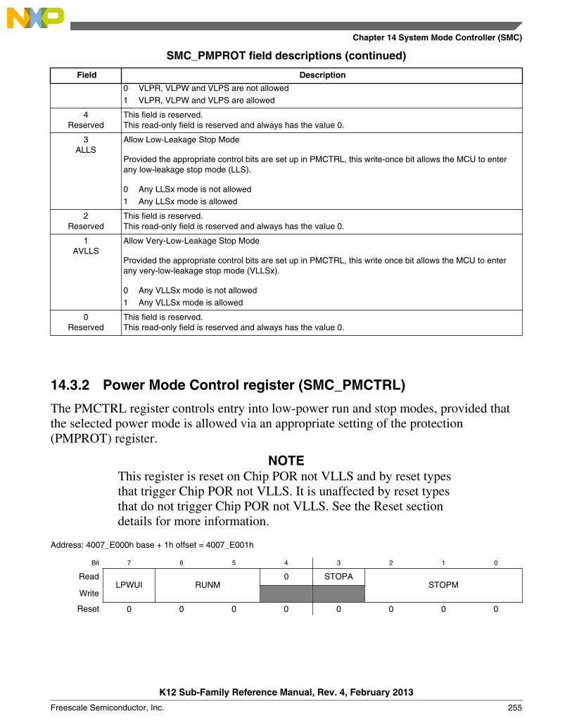
SMC_PMPROT field descriptions (continued)
Field Description
0 VLPR, VLPW and VLPS are not allowed1 VLPR, VLPW and VLPS are allowed
4Reserved
This field is reserved.This read-only field is reserved and always has the value 0.
3ALLS
Allow Low-Leakage Stop Mode
Provided the appropriate control bits are set up in PMCTRL, this write-once bit allows the MCU to enterany low-leakage stop mode (LLS).
0 Any LLSx mode is not allowed1 Any LLSx mode is allowed
2Reserved
This field is reserved.This read-only field is reserved and always has the value 0.
1AVLLS
Allow Very-Low-Leakage Stop Mode
Provided the appropriate control bits are set up in PMCTRL, this write once bit allows the MCU to enterany very-low-leakage stop mode (VLLSx).
0 Any VLLSx mode is not allowed1 Any VLLSx mode is allowed
0Reserved
This field is reserved.This read-only field is reserved and always has the value 0.
14.3.2 Power Mode Control register (SMC_PMCTRL)
The PMCTRL register controls entry into low-power run and stop modes, provided thatthe selected power mode is allowed via an appropriate setting of the protection(PMPROT) register.
NOTEThis register is reset on Chip POR not VLLS and by reset typesthat trigger Chip POR not VLLS. It is unaffected by reset typesthat do not trigger Chip POR not VLLS. See the Reset sectiondetails for more information.
Address: 4007_E000h base + 1h offset = 4007_E001h
Bit 7 6 5 4 3 2 1 0
ReadLPWUI RUNM
0 STOPASTOPM
Write
Reset 0 0 0 0 0 0 0 0
Chapter 14 System Mode Controller (SMC)
K12 Sub-Family Reference Manual, Rev. 4, February 2013
Freescale Semiconductor, Inc. 255
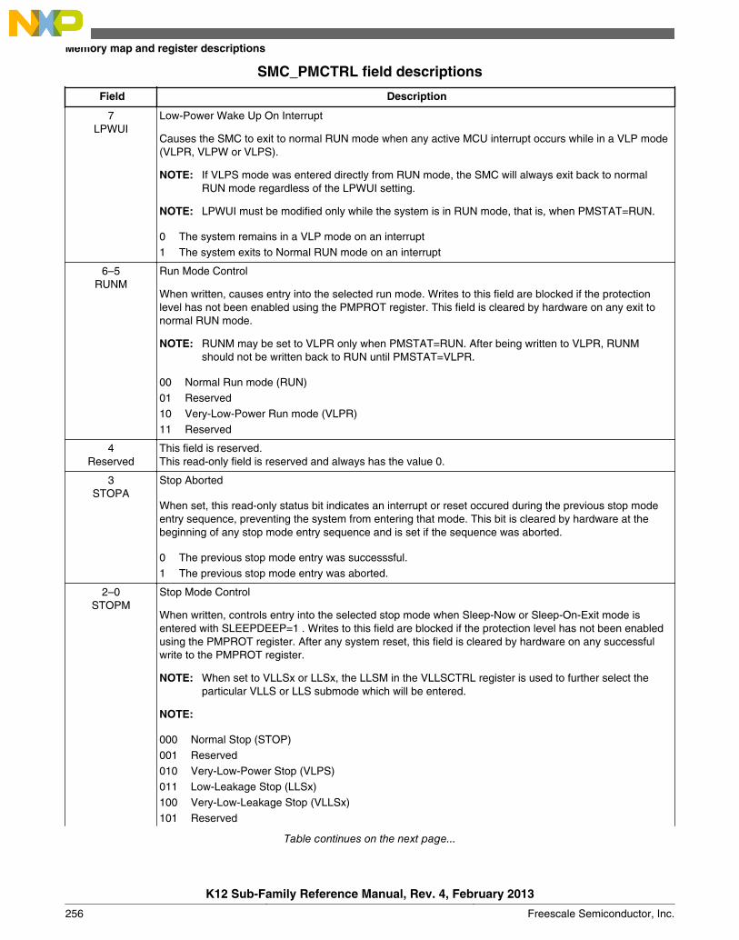
SMC_PMCTRL field descriptions
Field Description
7LPWUI
Low-Power Wake Up On Interrupt
Causes the SMC to exit to normal RUN mode when any active MCU interrupt occurs while in a VLP mode(VLPR, VLPW or VLPS).
NOTE: If VLPS mode was entered directly from RUN mode, the SMC will always exit back to normalRUN mode regardless of the LPWUI setting.
NOTE: LPWUI must be modified only while the system is in RUN mode, that is, when PMSTAT=RUN.
0 The system remains in a VLP mode on an interrupt1 The system exits to Normal RUN mode on an interrupt
6–5RUNM
Run Mode Control
When written, causes entry into the selected run mode. Writes to this field are blocked if the protectionlevel has not been enabled using the PMPROT register. This field is cleared by hardware on any exit tonormal RUN mode.
NOTE: RUNM may be set to VLPR only when PMSTAT=RUN. After being written to VLPR, RUNMshould not be written back to RUN until PMSTAT=VLPR.
00 Normal Run mode (RUN)01 Reserved10 Very-Low-Power Run mode (VLPR)11 Reserved
4Reserved
This field is reserved.This read-only field is reserved and always has the value 0.
3STOPA
Stop Aborted
When set, this read-only status bit indicates an interrupt or reset occured during the previous stop modeentry sequence, preventing the system from entering that mode. This bit is cleared by hardware at thebeginning of any stop mode entry sequence and is set if the sequence was aborted.
0 The previous stop mode entry was successsful.1 The previous stop mode entry was aborted.
2–0STOPM
Stop Mode Control
When written, controls entry into the selected stop mode when Sleep-Now or Sleep-On-Exit mode isentered with SLEEPDEEP=1 . Writes to this field are blocked if the protection level has not been enabledusing the PMPROT register. After any system reset, this field is cleared by hardware on any successfulwrite to the PMPROT register.
NOTE: When set to VLLSx or LLSx, the LLSM in the VLLSCTRL register is used to further select theparticular VLLS or LLS submode which will be entered.
NOTE:
000 Normal Stop (STOP)001 Reserved010 Very-Low-Power Stop (VLPS)011 Low-Leakage Stop (LLSx)100 Very-Low-Leakage Stop (VLLSx)101 Reserved
Table continues on the next page...
Memory map and register descriptions
K12 Sub-Family Reference Manual, Rev. 4, February 2013
256 Freescale Semiconductor, Inc.
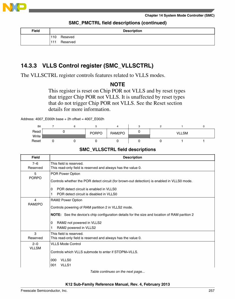
SMC_PMCTRL field descriptions (continued)
Field Description
110 Reseved111 Reserved
14.3.3 VLLS Control register (SMC_VLLSCTRL)
The VLLSCTRL register controls features related to VLLS modes.
NOTEThis register is reset on Chip POR not VLLS and by reset typesthat trigger Chip POR not VLLS. It is unaffected by reset typesthat do not trigger Chip POR not VLLS. See the Reset sectiondetails for more information.
Address: 4007_E000h base + 2h offset = 4007_E002h
Bit 7 6 5 4 3 2 1 0
Read 0 PORPO RAM2PO 0 VLLSMWriteReset 0 0 0 0 0 0 1 1
SMC_VLLSCTRL field descriptions
Field Description
7–6Reserved
This field is reserved.This read-only field is reserved and always has the value 0.
5PORPO
POR Power Option
Controls whether the POR detect circuit (for brown-out detection) is enabled in VLLS0 mode.
0 POR detect circuit is enabled in VLLS01 POR detect circuit is disabled in VLLS0
4RAM2PO
RAM2 Power Option
Controls powering of RAM partition 2 in VLLS2 mode.
NOTE: See the device's chip configuration details for the size and location of RAM parition 2
0 RAM2 not powered in VLLS21 RAM2 powered in VLLS2
3Reserved
This field is reserved.This read-only field is reserved and always has the value 0.
2–0VLLSM
VLLS Mode Control
Controls which VLLS submode to enter if STOPM=VLLS.
000 VLLS0001 VLLS1
Table continues on the next page...
Chapter 14 System Mode Controller (SMC)
K12 Sub-Family Reference Manual, Rev. 4, February 2013
Freescale Semiconductor, Inc. 257

SMC_VLLSCTRL field descriptions (continued)
Field Description
010 VLLS2011 VLLS3100 Reserved101 Reserved110 Reserved111 Reserved
14.3.4 Power Mode Status register (SMC_PMSTAT)
PMSTAT is a read-only, one-hot register which indicates the current power mode of thesystem.
NOTEThis register is reset on Chip POR not VLLS and by reset typesthat trigger Chip POR not VLLS. It is unaffected by reset typesthat do not trigger Chip POR not VLLS. See the Reset sectiondetails for more information.
Address: 4007_E000h base + 3h offset = 4007_E003h
Bit 7 6 5 4 3 2 1 0
Read 0 PMSTAT
Write
Reset 0 0 0 0 0 0 0 1
SMC_PMSTAT field descriptions
Field Description
7Reserved
This field is reserved.This read-only field is reserved and always has the value 0.
6–0PMSTAT NOTE: When debug is enabled, the PMSTAT will not update to STOP or VLPS
000_0001 Current power mode is RUN000_0010 Current power mode is STOP000_0100 Current power mode is VLPR000_1000 Current power mode is VLPW001_0000 Current power mode is VLPS010_0000 Current power mode is LLS100_0000 Current power mode is VLLS
Memory map and register descriptions
K12 Sub-Family Reference Manual, Rev. 4, February 2013
258 Freescale Semiconductor, Inc.

14.4 Functional description
14.4.1 Power mode transitions
The following figure shows the power mode state transitions available on the chip. Anyreset always brings the MCU back to the normal run state.
WAIT
STOP
RUN
LLS VLLS3, 2, 1, 0
VLPS
VLPR
VLPW
Any RESET
4
6
7
3
1
2
810
119
5
Figure 14-5. Power mode state diagram
The following table defines triggers for the various state transitions shown in the previousfigure.
Chapter 14 System Mode Controller (SMC)
K12 Sub-Family Reference Manual, Rev. 4, February 2013
Freescale Semiconductor, Inc. 259

Table 14-7. Power mode transition triggers
Transition # From To Trigger conditions
1 RUN WAIT Sleep-now or sleep-on-exit modes entered with SLEEPDEEPclear, controlled in System Control Register in ARM core.
See note.
WAIT RUN Interrupt or Reset
2 RUN STOP PMCTRL[RUNM]=00, PMCTRL[STOPM]=000
Sleep-now or sleep-on-exit modes entered with SLEEPDEEPset, which is controlled in System Control Register in ARMcore.
See note.1
STOP RUN Interrupt or Reset
3 RUN VLPR The core, system, bus and flash clock frequencies and MCGclocking mode are restricted in this mode. See the PowerManagement chapter for the maximum allowable frequenciesand MCG modes supported.
Set PMPROT[AVLP]=1, PMCTRL[RUNM]=10.
VLPR RUN Set PMCTRL[RUNM]=00 or
Interrupt with PMCTRL[LPWUI] =1 or
Reset.
4 VLPR VLPW Sleep-now or sleep-on-exit modes entered with SLEEPDEEPclear, which is controlled in System Control Register in ARMcore.
See note.1
VLPW VLPR Interrupt with PMCTRL[LPWUI]=0
5 VLPW RUN Interrupt with PMCTRL[LPWUI]=1 or
Reset
6 VLPR VLPS PMCTRL[STOPM]=000 or 010,
Sleep-now or sleep-on-exit modes entered with SLEEPDEEPset, which is controlled in System Control Register in ARMcore.
See note.1
VLPS VLPR Interrupt with PMCTRL[LPWUI]=0
NOTE: If VLPS was entered directly from RUN, hardwarewill not allow this transition and will force exit back toRUN
7 RUN VLPS PMPROT[AVLP]=1, PMCTRL[STOPM]=010,
Sleep-now or sleep-on-exit modes entered with SLEEPDEEPset, which is controlled in System Control Register in ARMcore.
See note.1
VLPS RUN Interrupt with PMCTRL[LPWUI]=1 or
Interrupt with PMCTRL[LPWUI]=0 and VLPS mode wasentered directly from RUN or
Reset
Table continues on the next page...
Functional description
K12 Sub-Family Reference Manual, Rev. 4, February 2013
260 Freescale Semiconductor, Inc.
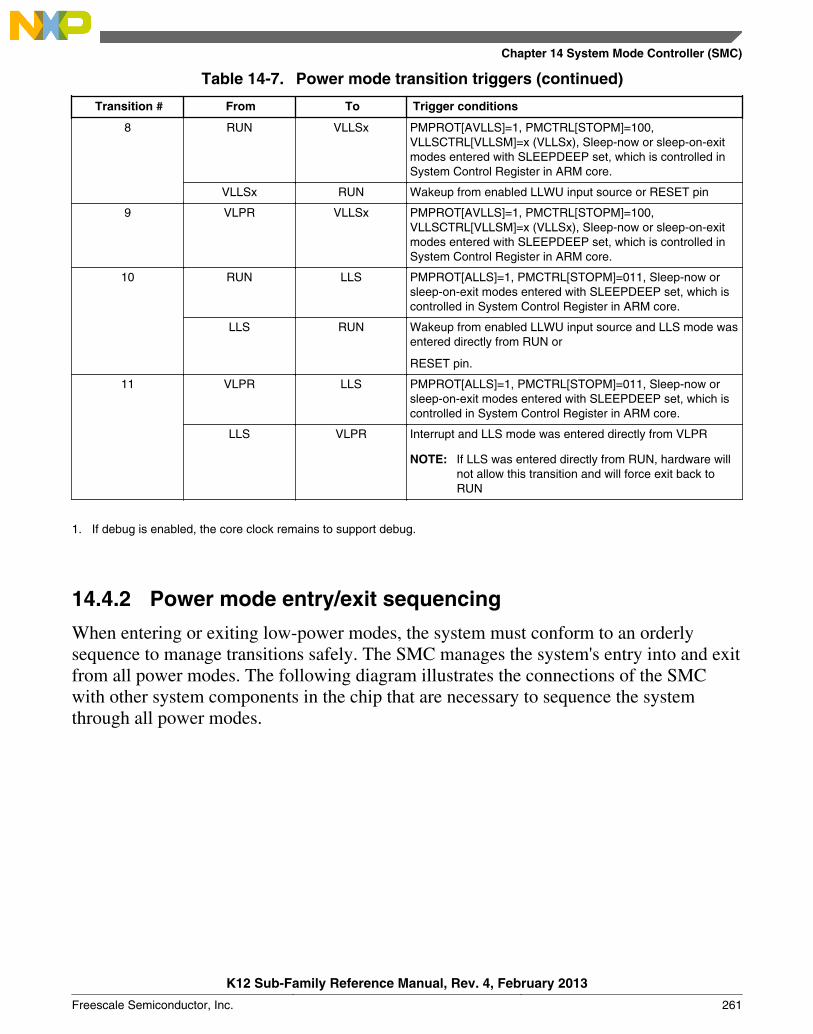
Table 14-7. Power mode transition triggers (continued)
Transition # From To Trigger conditions
8 RUN VLLSx PMPROT[AVLLS]=1, PMCTRL[STOPM]=100,VLLSCTRL[VLLSM]=x (VLLSx), Sleep-now or sleep-on-exitmodes entered with SLEEPDEEP set, which is controlled inSystem Control Register in ARM core.
VLLSx RUN Wakeup from enabled LLWU input source or RESET pin
9 VLPR VLLSx PMPROT[AVLLS]=1, PMCTRL[STOPM]=100,VLLSCTRL[VLLSM]=x (VLLSx), Sleep-now or sleep-on-exitmodes entered with SLEEPDEEP set, which is controlled inSystem Control Register in ARM core.
10 RUN LLS PMPROT[ALLS]=1, PMCTRL[STOPM]=011, Sleep-now orsleep-on-exit modes entered with SLEEPDEEP set, which iscontrolled in System Control Register in ARM core.
LLS RUN Wakeup from enabled LLWU input source and LLS mode wasentered directly from RUN or
RESET pin.
11 VLPR LLS PMPROT[ALLS]=1, PMCTRL[STOPM]=011, Sleep-now orsleep-on-exit modes entered with SLEEPDEEP set, which iscontrolled in System Control Register in ARM core.
LLS VLPR Interrupt and LLS mode was entered directly from VLPR
NOTE: If LLS was entered directly from RUN, hardware willnot allow this transition and will force exit back toRUN
1. If debug is enabled, the core clock remains to support debug.
14.4.2 Power mode entry/exit sequencing
When entering or exiting low-power modes, the system must conform to an orderlysequence to manage transitions safely. The SMC manages the system's entry into and exitfrom all power modes. The following diagram illustrates the connections of the SMCwith other system components in the chip that are necessary to sequence the systemthrough all power modes.
Chapter 14 System Mode Controller (SMC)
K12 Sub-Family Reference Manual, Rev. 4, February 2013
Freescale Semiconductor, Inc. 261
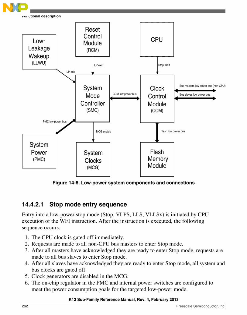
System Mode
Controller(SMC)
System Power(PMC)
Low-LeakageWakeup
(LLWU)
System Clocks(MCG)
LP exit
Flash
CPU
LP exit
Clock ControlModule
(CCM)
ModuleMemory
Bus masters low power bus (non-CPU)
Bus slaves low power bus
Stop/Wait
CCM low power bus
MCG enable
PMC low power bus
Flash low power bus
Reset Control
(RCM)Module
Figure 14-6. Low-power system components and connections
14.4.2.1 Stop mode entry sequence
Entry into a low-power stop mode (Stop, VLPS, LLS, VLLSx) is initiated by CPUexecution of the WFI instruction. After the instruction is executed, the followingsequence occurs:
1. The CPU clock is gated off immediately.2. Requests are made to all non-CPU bus masters to enter Stop mode.3. After all masters have acknowledged they are ready to enter Stop mode, requests are
made to all bus slaves to enter Stop mode.4. After all slaves have acknowledged they are ready to enter Stop mode, all system and
bus clocks are gated off.5. Clock generators are disabled in the MCG.6. The on-chip regulator in the PMC and internal power switches are configured to
meet the power consumption goals for the targeted low-power mode.
Functional description
K12 Sub-Family Reference Manual, Rev. 4, February 2013
262 Freescale Semiconductor, Inc.
14.4.2.2 Stop mode exit sequenceExit from a low-power stop mode is initiated either by a reset or an interrupt event. Thefollowing sequence then executes to restore the system to a run mode (RUN or VLPR):
1. The on-chip regulator in the PMC and internal power switches are restored.2. Clock generators are enabled in the MCG.3. System and bus clocks are enabled to all masters and slaves.4. The CPU clock is enabled and the CPU begins servicing the reset or interrupt that
initiated the exit from the low-power stop mode.
14.4.2.3 Aborted stop mode entry
If an interrupt or a reset occurs during a stop entry sequence, the SMC can abort thetransition early and return to RUN mode without completely entering the stop mode. Anaborted entry is possible only if the reset or interrupt occurs before the PMC begins thetransition to stop mode regulation. After this point, the interrupt or reset is ignored untilthe PMC has completed its transition to stop mode regulation. When an aborted stopmode entry sequence occurs, the SMC's PMCTRL[STOPA] is set to 1.
14.4.2.4 Transition to wait modes
For wait modes (WAIT and VLPW), the CPU clock is gated off while all other clockingcontinues, as in RUN and VLPR mode operation. Some modules that support stop-in-wait functionality have their clocks disabled in these configurations.
14.4.2.5 Transition from stop modes to Debug mode
The debugger module supports a transition from STOP, WAIT, VLPS, and VLPW backto a Halted state when the debugger has been enabled, that is, ENBDM is 1. As part ofthis transition, system clocking is re-established and is equivalent to the normal RUN andVLPR mode clocking configuration.
14.4.3 Run modes
The device supports the following run modes:
• Run• Very Low-Power Run (VLPR)
Chapter 14 System Mode Controller (SMC)
K12 Sub-Family Reference Manual, Rev. 4, February 2013
Freescale Semiconductor, Inc. 263
14.4.3.1 RUN mode
This is the normal operating mode for the device.
This mode is selected after any reset. When the ARM processor exits reset, it sets up thestack, program counter (PC), and link register (LR):
• The processor reads the start SP (SP_main) from vector-table offset 0x000• The processor reads the start PC from vector-table offset 0x004• LR is set to 0xFFFF_FFFF.
To reduce power in this mode, disable the clocks to unused modules using theircorresponding clock gating control bits in the SIM's registers.
14.4.3.2 Very-Low Power Run (VLPR) mode
In VLPR mode, the on-chip voltage regulator is put into a stop mode regulation state. Inthis state, the regulator is designed to supply enough current to the MCU over a reducedfrequency. To further reduce power in this mode, disable the clocks to unused modulesusing their corresponding clock gating control bits in the SIM's registers.
Before entering this mode, the following conditions must be met:
• The MCG must be configured in a mode which is supported during VLPR. See thePower Management details for information about these MCG modes.
• All clock monitors in the MCG must be disabled.• The maximum frequencies of the system, bus, flash, and core are restricted. See the
Power Management details about which frequencies are supported.• Mode protection must be set to allow VLP modes, that is, PMPROT[AVLP] is 1.• PMCTRL[RUNM] is set to 10b to enter VLPR.• Flash programming/erasing is not allowed.
NOTEDo not change the clock frequency while in VLPR mode,because the regulator is slow responding and cannot managefast load transitions. In addition, do not modify the clock sourcein the MCG module, the module clock enables in the SIM, orany clock divider registers.
Functional description
K12 Sub-Family Reference Manual, Rev. 4, February 2013
264 Freescale Semiconductor, Inc.
To reenter Normal Run mode, clear RUNM. The PMSTAT register is a read-only statusregister that can be used to determine when the system has completed an exit to RUNmode. When PMSTAT=RUN, the system is in run regulation and the MCU can run atfull speed in any clock mode. If a higher execution frequency is desired, poll thePMSTAT register until it is set to RUN when returning from VLPR mode.
VLPR mode also provides the option to return to run regulation if any interrupt occurs.Implement this option by setting Low-Power Wakeup On Interrupt (LPWUI) in thePMCTRL register. Any reset always causes an exit from VLPR and returns the device toRUN mode after the MCU exits its reset flow. The RUNM bits are cleared by hardwareon any interrupt when LPWUI is set or on any reset.
14.4.4 Wait modes
This device contains two different wait modes:
• Wait• Very-Low Power Wait (VLPW)
14.4.4.1 WAIT mode
WAIT mode is entered when the ARM core enters the Sleep-Now or Sleep-On-Exitmodes while SLEEDEEP is cleared. The ARM CPU enters a low-power state in which itis not clocked, but peripherals continue to be clocked provided they are enabled. Clockgating to the peripheral is enabled via the SIM..
When an interrupt request occurs, the CPU exits WAIT mode and resumes processing inRUN mode, beginning with the stacking operations leading to the interrupt serviceroutine.
A system reset will cause an exit from WAIT mode, returning the device to normal RUNmode.
14.4.4.2 Very-Low-Power Wait (VLPW) mode
VLPW is entered by the entering the Sleep-Now or Sleep-On-Exit mode whileSLEEPDEEP is cleared and the MCU is in VLPR mode.
Chapter 14 System Mode Controller (SMC)
K12 Sub-Family Reference Manual, Rev. 4, February 2013
Freescale Semiconductor, Inc. 265
In VLPW, the on-chip voltage regulator remains in its stop regulation state. In this state,the regulator is designed to supply enough current to the MCU over a reduced frequency.To further reduce power in this mode, disable the clocks to unused modules by clearingthe peripherals' corresponding clock gating control bits in the SIM.
VLPR mode restrictions also apply to VLPW.
VLPW mode provides the option to return to fully-regulated normal RUN mode if anyenabled interrupt occurs. This is done by setting PMCTRL[LPWUI]. Wait for thePMSTAT register to set to RUN before increasing the frequency.
If the LPWUI bit is clear, when an interrupt from VLPW occurs, the device returns toVLPR mode to execute the interrupt service routine.
A system reset will cause an exit from VLPW mode, returning the device to normal RUNmode.
14.4.5 Stop modes
This device contains a variety of stop modes to meet your application needs. The stopmodes range from:
• a stopped CPU, with all I/O, logic, and memory states retained, and certainasynchronous mode peripherals operating
to:
• a powered down CPU, with only I/O and a small register file retained, very fewasynchronous mode peripherals operating, while the remainder of the MCU ispowered down.
The choice of stop mode depends upon the user's application, and how power usage andstate retention versus functional needs may be traded off.
NOTEAll clock monitors must be disabled before entering these low-power modes: Stop, VLPS, VLPR, VLPW, LLS, and VLLSx.
The various stop modes are selected by setting the appropriate fields in PMPROT andPMCTRL. The selected stop mode mode is entered during the sleep-now or sleep-on-exitentry with the SLEEPDEEP bit set in the System Control Register in the ARM core.
The available stop modes are:
• Normal Stop (STOP)• Very-Low Power Stop (VLPS)
Functional description
K12 Sub-Family Reference Manual, Rev. 4, February 2013
266 Freescale Semiconductor, Inc.

• Low-Leakage Stop (LLS)• Very-Low-Leakage Stop (VLLSx)
14.4.5.1 STOP mode
STOP mode is entered via the sleep-now or sleep-on-exit with the SLEEPDEEP bit set inthe System Control Register in the ARM core.
The MCG module can be configured to leave the reference clocks running.
A module capable of providing an asynchronous interrupt to the device takes the deviceout of STOP mode and returns the device to normal RUN mode. Refer to the device'sPower Management chapter for peripheral, I/O, and memory operation in STOP mode.When an interrupt request occurs, the CPU exits STOP mode and resumes processing,beginning with the stacking operations leading to the interrupt service routine.
A system reset will cause an exit from STOP mode, returning the device to normal RUNmode via an MCU reset.
14.4.5.2 Very-Low-Power Stop (VLPS) mode
VLPS mode can be entered in one of two ways:
• Entry into stop via the sleep-now or sleep-on-exit with the SLEEPDEEP bit set in theSystem Control Register in the ARM core while the MCU is in VLPR mode andSTOPM=010 or 000 in the PMCTRL register.
• Entry into stop via the sleep-now or sleep-on-exit with the SLEEPDEEP bit set in theSystem Control Register in the ARM core while the MCU is in normal RUN modeand STOPM=010 in the PMCTRL register. When VLPS is entered directly fromRUN mode, exit to VLPR is disabled by hardware and the system will always exitback to RUN.
In VLPS, the on-chip voltage regulator remains in its stop regulation state as in VLPR.
A module capable of providing an asynchronous interrupt to the device takes the deviceout of VLPS and returns the device to VLPR mode, provided LPWUI is clear.
If LPWUI is set, the device returns to normal RUN mode upon an interrupt request.PMSTAT must be set to RUN before allowing the system to return to a frequency higherthan that allowed in VLPR mode.
A system reset will also cause a VLPS exit, returning the device to normal RUN mode.
Chapter 14 System Mode Controller (SMC)
K12 Sub-Family Reference Manual, Rev. 4, February 2013
Freescale Semiconductor, Inc. 267
14.4.5.3 Low-Leakage Stop (LLSx) modesThe MCU enters LLS mode if:
• In Sleep-Now or Sleep-On-Exit mode, SLEEPDEEP is set in the System ControlRegister in the ARM core, and
• The device is configured as shown in Table 14-7.
In LLS, the on-chip voltage regulator is in stop regulation. Most of the peripherals are putin a state-retention mode that does not allow them to operate while in LLS.
Before entering LLS mode, the user should configure the low-leakage wakeup (LLWU)module to enable the desired wakeup sources. The available wakeup sources in LLS aredetailed in the chip configuration details for this device.
After wakeup from LLS, the device returns to the run mode from which LLS was entered(either normal RUN or VLPR) with a pending LLWU module interrupt. In the LLWUinterrupt service routine (ISR), the user can poll the LLWU module wakeup flags todetermine the source of the wakeup.
NOTEThe LLWU interrupt must not be masked by the interruptcontroller to avoid a scenario where the system does not fullyexit stop mode on an LLS recovery.
An asserted RESET pin will cause an exit from LLS mode, returning the device tonormal RUN mode. When LLS is exiting via the RESET pin, the PIN and WAKEUP bitsare set in the SRS0 register of the reset control module (RCM).
14.4.5.4 Very-Low-Leakage Stop (VLLSx) modes
This device contains these very low leakage modes:
• VLLS3• VLLS2• VLLS1• VLLS0
VLLSx is often used in this document to refer to all of these modes.
All VLLSx modes can be entered from normal RUN or VLPR modes.
The MCU enters the configured VLLS mode if:
Functional description
K12 Sub-Family Reference Manual, Rev. 4, February 2013
268 Freescale Semiconductor, Inc.
• In Sleep-Now or Sleep-On-Exit mode, the SLEEPDEEP bit is set in the SystemControl Register in the ARM core, and
• The device is configured as shown in Table 14-7.
In VLLS, the on-chip voltage regulator is in its stop-regulation state while most digitallogic is powered off.
Before entering VLLS mode, the user should configure the low-leakage wakeup (LLWU)module to enable the desired wakeup sources. The available wakeup sources in VLLS aredetailed in the chip configuration details for this device.
After wakeup from VLLS, the device returns to normal RUN mode with a pendingLLWU interrupt. In the LLWU interrupt service routine (ISR), the user can poll theLLWU module wakeup flags to determine the source of the wakeup.
When entering VLLS, each I/O pin is latched as configured before executing VLLS.Because all digital logic in the MCU is powered off, all port and peripheral data is lostduring VLLS. This information must be restored before the ACKISO bit in the PMC isset.
An asserted RESET pin will cause an exit from any VLLS mode, returning the device tonormal RUN mode. When exiting VLLS via the RESET pin, the PIN and WAKEUP bitsare set in the SRS0 register of the reset control module (RCM).
14.4.6 Debug in low power modes
When the MCU is secure, the device disables/limits debugger operation. When the MCUis unsecure, the ARM debugger can assert two power-up request signals:
• System power up, via SYSPWR in the Debug Port Control/Stat register• Debug power up, via CDBGPWRUPREQ in the Debug Port Control/Stat register
When asserted while in RUN, WAIT, VLPR, or VLPW, the mode controller drives acorresponding acknowledge for each signal, that is, both CDBGPWRUPACK andCSYSPWRUPACK. When both requests are asserted, the mode controller handlesattempts to enter STOP and VLPS by entering an emulated stop state. In this emulatedstop state:
• the regulator is in run regulation,• the MCG-generated clock source is enabled,• all system clocks, except the core clock, are disabled,• the debug module has access to core registers, and• access to the on-chip peripherals is blocked.
Chapter 14 System Mode Controller (SMC)
K12 Sub-Family Reference Manual, Rev. 4, February 2013
Freescale Semiconductor, Inc. 269
No debug is available while the MCU is in LLS or VLLS modes. LLS is a state-retentionmode and all debug operation can continue after waking from LLS, even in cases wheresystem wakeup is due to a system reset event.
Entering into a VLLS mode causes all of the debug controls and settings to be poweredoff. To give time to the debugger to sync with the MCU, the MDM AP Control Registerincludes a Very-Low-Leakage Debug Request (VLLDBGREQ) bit that is set to configurethe Reset Controller logic to hold the system in reset after the next recovery from a VLLSmode. This bit allows the debugger time to reinitialize the debug module before thedebug session continues.
The MDM AP Control Register also includes a Very Low Leakage Debug Acknowledge(VLLDBGACK) bit that is set to release the ARM core being held in reset following aVLLS recovery. The debugger reinitializes all debug IP, and then asserts theVLLDBGACK control bit to allow the RCM to release the ARM core from reset andallow CPU operation to begin.
The VLLDBGACK bit is cleared by the debugger (or can be left set as is) or clearsautomatically due to the reset generated as part of the next VLLS recovery.
Functional description
K12 Sub-Family Reference Manual, Rev. 4, February 2013
270 Freescale Semiconductor, Inc.
Chapter 15Power Management Controller (PMC)
15.1 IntroductionNOTE
For the chip-specific implementation details of this module'sinstances see the chip configuration information.
The power management controller (PMC) contains the internal voltage regulator, poweron reset (POR), and low voltage detect system.
15.2 FeaturesThe PMC features include:
• Internal voltage regulator• Active POR providing brown-out detect• Low-voltage detect supporting two low-voltage trip points with four warning levels
per trip point
15.3 Low-voltage detect (LVD) systemThis device includes a system to guard against low-voltage conditions. This protectsmemory contents and controls MCU system states during supply voltage variations. Thesystem is comprised of a power-on reset (POR) circuit and a LVD circuit with a user-selectable trip voltage: high (VLVDH) or low (VLVDL). The trip voltage is selected by theLVDSC1[LVDV] bits. The LVD is disabled upon entering VLPx, LLS, and VLLSxmodes.
Two flags are available to indicate the status of the low-voltage detect system:
K12 Sub-Family Reference Manual, Rev. 4, February 2013
Freescale Semiconductor, Inc. 271

• The low voltage detect flag (LVDF) operates in a level sensitive manner. The LVDFbit is set when the supply voltage falls below the selected trip point (VLVD). TheLVDF bit is cleared by writing one to the LVDACK bit, but only if the internalsupply has returned above the trip point; otherwise, the LVDF bit remains set.
• The low voltage warning flag (LVWF) operates in a level sensitive manner. TheLVWF bit is set when the supply voltage falls below the selected monitor trip point(VLVW). The LVWF bit is cleared by writing one to the LVWACK bit, but only ifthe internal supply has returned above the trip point; otherwise, the LVWF bitremains set.
15.3.1 LVD reset operation
By setting the LVDRE bit, the LVD generates a reset upon detection of a low voltagecondition. The low voltage detection threshold is determined by the LVDV bits. After anLVD reset occurs, the LVD system holds the MCU in reset until the supply voltage risesabove this threshold. The LVD bit in the SRS register is set following an LVD or power-on reset.
15.3.2 LVD interrupt operation
By configuring the LVD circuit for interrupt operation (LVDIE set and LVDRE clear),LVDSC1[LVDF] is set and an LVD interrupt request occurs upon detection of a lowvoltage condition. The LVDF bit is cleared by writing one to the LVDSC1[LVDACK]bit.
15.3.3 Low-voltage warning (LVW) interrupt operation
The LVD system contains a low-voltage warning flag (LVWF) to indicate that the supplyvoltage is approaching, but is above, the LVD voltage. The LVW also has an interrupt,which is enabled by setting the LVDSC2[LVWIE] bit. If enabled, an LVW interruptrequest occurs when the LVWF is set. LVWF is cleared by writing one to theLVDSC2[LVWACK] bit.
The LVDSC2[LVWV] bits select one of four trip voltages:
• Highest: VLVW4• Two mid-levels: VLVW3 and VLVW2• Lowest: VLVW1
Low-voltage detect (LVD) system
K12 Sub-Family Reference Manual, Rev. 4, February 2013
272 Freescale Semiconductor, Inc.

15.4 I/O retentionWhen in LLS mode, the I/O pins are held in their input or output state. Upon wakeup, thePMC is re-enabled, goes through a power up sequence to full regulation, and releases thelogic from state retention mode. The I/O are released immediately after a wakeup or resetevent. In the case of LLS exit via a RESET pin, the I/O default to their reset state.
When in VLLS modes, the I/O states are held on a wakeup event (with the exception ofwakeup by reset event) until the wakeup has been acknowledged via a write to theACKISO bit. In the case of VLLS exit via a RESET pin, the I/O are released and defaultto their reset state. In this case, no write to the ACKISO is needed.
15.5 Memory map and register descriptionsPMC register details follow.
NOTEDifferent portions of PMC registers are reset only by particularreset types. Each register's description provides details. Formore information about the types of reset on this chip, refer tothe Reset section details.
The PMC registers can be written only in supervisor mode.Write accesses in user mode are blocked and will result in a buserror.
PMC memory map
Absoluteaddress
(hex)Register name
Width(in bits)
Access Reset valueSection/
page
4007_D000Low Voltage Detect Status And Control 1 register(PMC_LVDSC1)
8 R/W 10h 15.5.1/274
4007_D001Low Voltage Detect Status And Control 2 register(PMC_LVDSC2)
8 R/W 00h 15.5.2/275
4007_D002 Regulator Status And Control register (PMC_REGSC) 8 R/W 04h 15.5.3/276
Chapter 15 Power Management Controller (PMC)
K12 Sub-Family Reference Manual, Rev. 4, February 2013
Freescale Semiconductor, Inc. 273
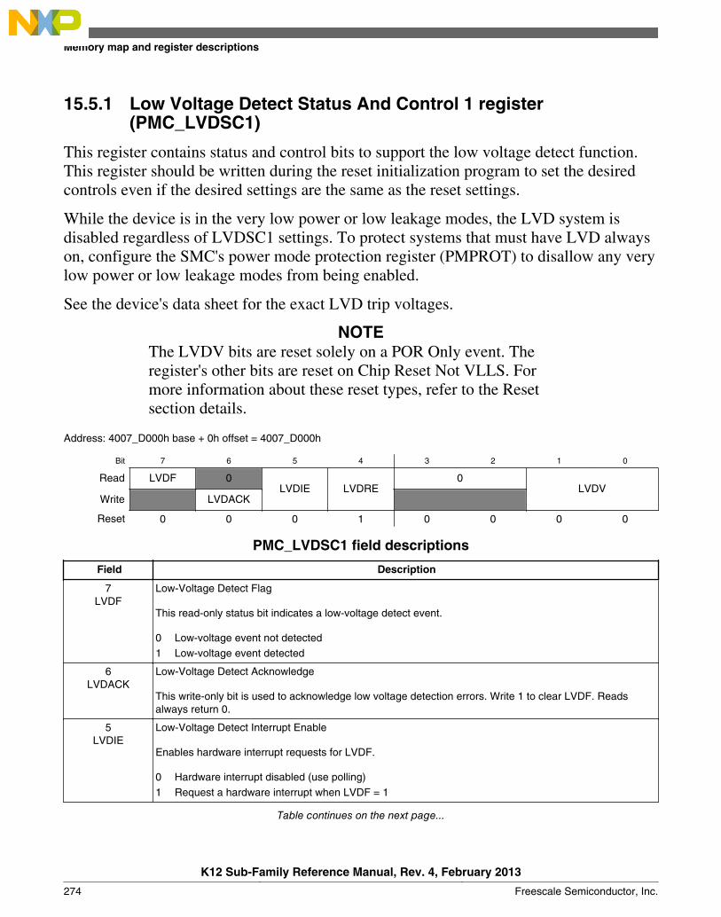
15.5.1 Low Voltage Detect Status And Control 1 register(PMC_LVDSC1)
This register contains status and control bits to support the low voltage detect function.This register should be written during the reset initialization program to set the desiredcontrols even if the desired settings are the same as the reset settings.
While the device is in the very low power or low leakage modes, the LVD system isdisabled regardless of LVDSC1 settings. To protect systems that must have LVD alwayson, configure the SMC's power mode protection register (PMPROT) to disallow any verylow power or low leakage modes from being enabled.
See the device's data sheet for the exact LVD trip voltages.
NOTEThe LVDV bits are reset solely on a POR Only event. Theregister's other bits are reset on Chip Reset Not VLLS. Formore information about these reset types, refer to the Resetsection details.
Address: 4007_D000h base + 0h offset = 4007_D000h
Bit 7 6 5 4 3 2 1 0
Read LVDF 0LVDIE LVDRE
0LVDV
Write LVDACK
Reset 0 0 0 1 0 0 0 0
PMC_LVDSC1 field descriptions
Field Description
7LVDF
Low-Voltage Detect Flag
This read-only status bit indicates a low-voltage detect event.
0 Low-voltage event not detected1 Low-voltage event detected
6LVDACK
Low-Voltage Detect Acknowledge
This write-only bit is used to acknowledge low voltage detection errors. Write 1 to clear LVDF. Readsalways return 0.
5LVDIE
Low-Voltage Detect Interrupt Enable
Enables hardware interrupt requests for LVDF.
0 Hardware interrupt disabled (use polling)1 Request a hardware interrupt when LVDF = 1
Table continues on the next page...
Memory map and register descriptions
K12 Sub-Family Reference Manual, Rev. 4, February 2013
274 Freescale Semiconductor, Inc.
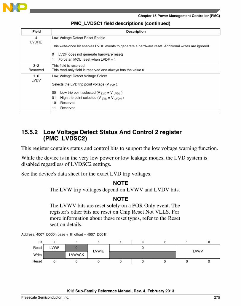
PMC_LVDSC1 field descriptions (continued)
Field Description
4LVDRE
Low-Voltage Detect Reset Enable
This write-once bit enables LVDF events to generate a hardware reset. Additional writes are ignored.
0 LVDF does not generate hardware resets1 Force an MCU reset when LVDF = 1
3–2Reserved
This field is reserved.This read-only field is reserved and always has the value 0.
1–0LVDV
Low-Voltage Detect Voltage Select
Selects the LVD trip point voltage (V LVD ).
00 Low trip point selected (V LVD = V LVDL )01 High trip point selected (V LVD = V LVDH )10 Reserved11 Reserved
15.5.2 Low Voltage Detect Status And Control 2 register(PMC_LVDSC2)
This register contains status and control bits to support the low voltage warning function.
While the device is in the very low power or low leakage modes, the LVD system isdisabled regardless of LVDSC2 settings.
See the device's data sheet for the exact LVD trip voltages.
NOTEThe LVW trip voltages depend on LVWV and LVDV bits.
NOTEThe LVWV bits are reset solely on a POR Only event. Theregister's other bits are reset on Chip Reset Not VLLS. Formore information about these reset types, refer to the Resetsection details.
Address: 4007_D000h base + 1h offset = 4007_D001h
Bit 7 6 5 4 3 2 1 0
Read LVWF 0LVWIE
0LVWV
Write LVWACK
Reset 0 0 0 0 0 0 0 0
Chapter 15 Power Management Controller (PMC)
K12 Sub-Family Reference Manual, Rev. 4, February 2013
Freescale Semiconductor, Inc. 275
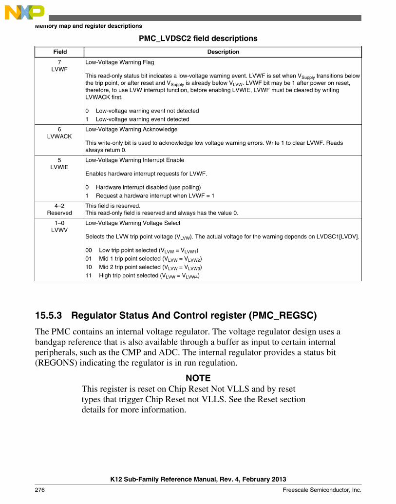
PMC_LVDSC2 field descriptions
Field Description
7LVWF
Low-Voltage Warning Flag
This read-only status bit indicates a low-voltage warning event. LVWF is set when VSupply transitions belowthe trip point, or after reset and VSupply is already below VLVW. LVWF bit may be 1 after power on reset,therefore, to use LVW interrupt function, before enabling LVWIE, LVWF must be cleared by writingLVWACK first.
0 Low-voltage warning event not detected1 Low-voltage warning event detected
6LVWACK
Low-Voltage Warning Acknowledge
This write-only bit is used to acknowledge low voltage warning errors. Write 1 to clear LVWF. Readsalways return 0.
5LVWIE
Low-Voltage Warning Interrupt Enable
Enables hardware interrupt requests for LVWF.
0 Hardware interrupt disabled (use polling)1 Request a hardware interrupt when LVWF = 1
4–2Reserved
This field is reserved.This read-only field is reserved and always has the value 0.
1–0LVWV
Low-Voltage Warning Voltage Select
Selects the LVW trip point voltage (VLVW). The actual voltage for the warning depends on LVDSC1[LVDV].
00 Low trip point selected (VLVW = VLVW1)01 Mid 1 trip point selected (VLVW = VLVW2)10 Mid 2 trip point selected (VLVW = VLVW3)11 High trip point selected (VLVW = VLVW4)
15.5.3 Regulator Status And Control register (PMC_REGSC)
The PMC contains an internal voltage regulator. The voltage regulator design uses abandgap reference that is also available through a buffer as input to certain internalperipherals, such as the CMP and ADC. The internal regulator provides a status bit(REGONS) indicating the regulator is in run regulation.
NOTEThis register is reset on Chip Reset Not VLLS and by resettypes that trigger Chip Reset not VLLS. See the Reset sectiondetails for more information.
Memory map and register descriptions
K12 Sub-Family Reference Manual, Rev. 4, February 2013
276 Freescale Semiconductor, Inc.
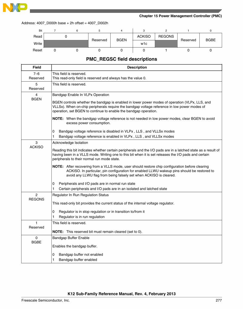
Address: 4007_D000h base + 2h offset = 4007_D002h
Bit 7 6 5 4 3 2 1 0
Read 0Reserved BGEN
ACKISO REGONSReserved BGBE
Write w1c
Reset 0 0 0 0 0 1 0 0
PMC_REGSC field descriptions
Field Description
7–6Reserved
This field is reserved.This read-only field is reserved and always has the value 0.
5Reserved
This field is reserved.
4BGEN
Bandgap Enable In VLPx Operation
BGEN controls whether the bandgap is enabled in lower power modes of operation (VLPx, LLS, andVLLSx). When on-chip peripherals require the bandgap voltage reference in low power modes ofoperation, set BGEN to continue to enable the bandgap operation.
NOTE: When the bandgap voltage reference is not needed in low power modes, clear BGEN to avoidexcess power consumption.
0 Bandgap voltage reference is disabled in VLPx , LLS , and VLLSx modes1 Bandgap voltage reference is enabled in VLPx , LLS , and VLLSx modes
3ACKISO
Acknowledge Isolation
Reading this bit indicates whether certain peripherals and the I/O pads are in a latched state as a result ofhaving been in a VLLS mode. Writing one to this bit when it is set releases the I/O pads and certainperipherals to their normal run mode state.
NOTE: After recovering from a VLLS mode, user should restore chip configuration before clearingACKISO. In particular, pin configuration for enabled LLWU wakeup pins should be restored toavoid any LLWU flag from being falsely set when ACKISO is cleared.
0 Peripherals and I/O pads are in normal run state1 Certain peripherals and I/O pads are in an isolated and latched state
2REGONS
Regulator In Run Regulation Status
This read-only bit provides the current status of the internal voltage regulator.
0 Regulator is in stop regulation or in transition to/from it1 Regulator is in run regulation
1Reserved
This field is reserved.
NOTE: This reserved bit must remain cleared (set to 0).
0BGBE
Bandgap Buffer Enable
Enables the bandgap buffer.
0 Bandgap buffer not enabled1 Bandgap buffer enabled
Chapter 15 Power Management Controller (PMC)
K12 Sub-Family Reference Manual, Rev. 4, February 2013
Freescale Semiconductor, Inc. 277

Memory map and register descriptions
K12 Sub-Family Reference Manual, Rev. 4, February 2013
278 Freescale Semiconductor, Inc.
Chapter 16Low-Leakage Wakeup Unit (LLWU)
16.1 IntroductionNOTE
For the chip-specific implementation details of this module'sinstances see the chip configuration information.
The LLWU module allows the user to select up to 16 external pin sources and up to 8internal modules as a wakeup source from low-leakage power modes. The input sourcesare described in the device's chip configuration details. Each of the available wakeupsources can be individually enabled.
The RESET pin is an additional source for triggering an exit from low-leakage powermodes, and causes the MCU to exit both LLS and VLLS through a reset flow. TheLLWU_RST[LLRSTE] bit must be set to allow an exit from low-leakage modes via theRESET pin. On a device where the RESET pin is shared with other functions, the explicitport mux control register must be set for the RESET pin before the RESET pin can beused as a low-leakage reset source.
The LLWU module also includes three optional digital pin filters: two for the externalwakeup pins and one for the RESET pin.
16.1.1 Features
The LLWU module features include:
• Support for up to 16 external input pins and up to 8 internal modules with individualenable bits
• Input sources may be external pins or from internal peripherals capable of running inLLS or VLLS. See the chip configuration information for wakeup input sources forthis device.
K12 Sub-Family Reference Manual, Rev. 4, February 2013
Freescale Semiconductor, Inc. 279
• External pin wakeup inputs, each of which is programmable as falling-edge, rising-edge, or any change
• Wakeup inputs that are activated if enabled after MCU enters a low-leakage powermode
• Optional digital filters provided to qualify an external pin detect and RESET pindetect. When entering VLLS0, the filters are disabled and bypassed.
16.1.2 Modes of operation
The LLWU module becomes functional on entry into a low-leakage power mode. Afterrecovery from LLS, the LLWU is immediately disabled. After recovery from VLLS, theLLWU continues to detect wakeup events until the user has acknowledged the wakeupvia a write to the PMC_REGSC[ACKISO] bit.
16.1.2.1 LLS mode
The LLWU module provides up to 16 external wakeup inputs and up to 8 internal modulewakeup inputs. An LLS reset event can be initiated via assertion of the RESET pin.
Wakeup events due to external wakeup inputs and internal module wakeup inputs resultin an interrupt flow when exiting LLS. A reset event due to RESET pin assertion resultsin a reset flow when exiting LLS.
NOTEThe LLWU interrupt must not be masked by the interruptcontroller to avoid a scenario where the system does not fullyexit Stop mode on an LLS recovery.
16.1.2.2 VLLS modes
The LLWU module provides up to 16 external wakeup inputs and up to 8 internal modulewakeup inputs. A VLLS reset event can be initiated via assertion of the RESET pin. Allwakeup and reset events result in VLLS exit via a reset flow.
16.1.2.3 Non-low leakage modes
The LLWU is not active in all non-low leakage modes where detection and control logicare in a static state. The LLWU registers are accessible in non-low leakage modes and areavailable for configuring and reading status when bus transactions are possible.
Introduction
K12 Sub-Family Reference Manual, Rev. 4, February 2013
280 Freescale Semiconductor, Inc.
When theRESET pin filter or wakeup pin filters are enabled, filter operation beginsimmediately. If a low leakage mode is entered within 5 LPO clock cycles of an activeedge, the edge event will be detected by the LLWU. For RESET pin filtering, this meansthat there is no restart to the minimum LPO cycle duration as the filtering transitionsfrom a non-low leakage filter, which is implemented in the RCM, to the LLWU filter.
16.1.2.4 Debug mode
When the chip is in Debug mode and then enters LLS or a VLLSx mode, no debug logicworks in the fully-functional low-leakage mode. Upon an exit from the LLS or VLLSxmode, the LLWU becomes inactive.
16.1.3 Block diagram
The following figure is the block diagram for the LLWU module.
Chapter 16 Low-Leakage Wakeup Unit (LLWU)
K12 Sub-Family Reference Manual, Rev. 4, February 2013
Freescale Semiconductor, Inc. 281
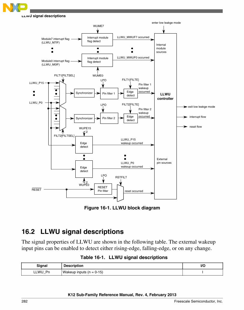
Module0 interrupt flag(LLWU_M0IF)
WUME0
LLWU_MWUF0 occurred
Internalmodulesources
LLWUcontroller
Externalpin sources
exit low leakge mode
interrupt flow
reset flow
reset occurred
RSTFILT
RESET
LLWU_P0
LLWU_P15 Pin filter 1wakeupoccurred
Interrupt moduleflag detect
WUPE152
Edgedetect
enter low leakge mode
WUPE0
Edgedetect
Module7 interrupt flag(LLWU_M7IF)
WUME7
LLWU_MWUF7 occurredInterrupt moduleflag detect
LPO
Pin filter 2
LPO FILT1[FILTE]
Pin filter 1
Synchronizer
Synchronizer Edgedetect
LLWU_P15 wakeup occurred
Edgedetect
Pin filter 2wakeupoccurred
2
LLWU_P0 wakeup occurred
RESETPin filter
LPO
FILT2[FILTSEL]
FILT1[FILTSEL]
FILT2[FILTE]
Figure 16-1. LLWU block diagram
16.2 LLWU signal descriptionsThe signal properties of LLWU are shown in the following table. The external wakeupinput pins can be enabled to detect either rising-edge, falling-edge, or on any change.
Table 16-1. LLWU signal descriptions
Signal Description I/O
LLWU_Pn Wakeup inputs (n = 0-15) I
LLWU signal descriptions
K12 Sub-Family Reference Manual, Rev. 4, February 2013
282 Freescale Semiconductor, Inc.
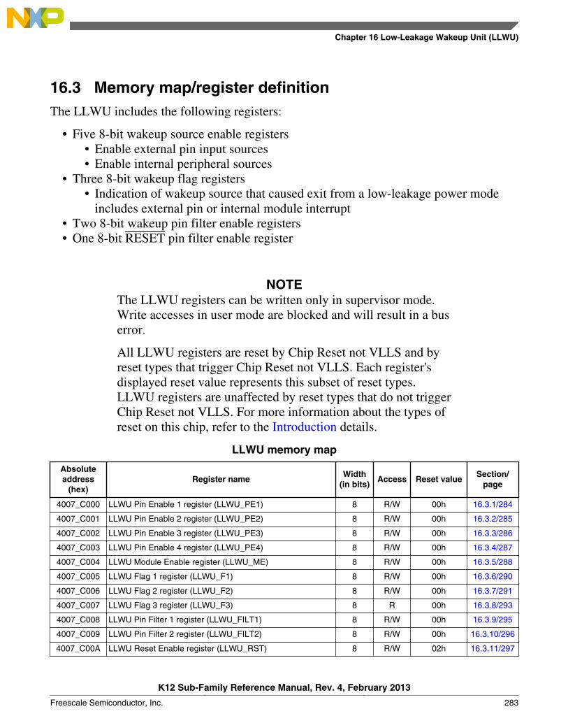
16.3 Memory map/register definitionThe LLWU includes the following registers:
• Five 8-bit wakeup source enable registers• Enable external pin input sources• Enable internal peripheral sources
• Three 8-bit wakeup flag registers• Indication of wakeup source that caused exit from a low-leakage power mode
includes external pin or internal module interrupt• Two 8-bit wakeup pin filter enable registers• One 8-bit RESET pin filter enable register
NOTEThe LLWU registers can be written only in supervisor mode.Write accesses in user mode are blocked and will result in a buserror.
All LLWU registers are reset by Chip Reset not VLLS and byreset types that trigger Chip Reset not VLLS. Each register'sdisplayed reset value represents this subset of reset types.LLWU registers are unaffected by reset types that do not triggerChip Reset not VLLS. For more information about the types ofreset on this chip, refer to the Introduction details.
LLWU memory map
Absoluteaddress
(hex)Register name
Width(in bits)
Access Reset valueSection/
page
4007_C000 LLWU Pin Enable 1 register (LLWU_PE1) 8 R/W 00h 16.3.1/284
4007_C001 LLWU Pin Enable 2 register (LLWU_PE2) 8 R/W 00h 16.3.2/285
4007_C002 LLWU Pin Enable 3 register (LLWU_PE3) 8 R/W 00h 16.3.3/286
4007_C003 LLWU Pin Enable 4 register (LLWU_PE4) 8 R/W 00h 16.3.4/287
4007_C004 LLWU Module Enable register (LLWU_ME) 8 R/W 00h 16.3.5/288
4007_C005 LLWU Flag 1 register (LLWU_F1) 8 R/W 00h 16.3.6/290
4007_C006 LLWU Flag 2 register (LLWU_F2) 8 R/W 00h 16.3.7/291
4007_C007 LLWU Flag 3 register (LLWU_F3) 8 R 00h 16.3.8/293
4007_C008 LLWU Pin Filter 1 register (LLWU_FILT1) 8 R/W 00h 16.3.9/295
4007_C009 LLWU Pin Filter 2 register (LLWU_FILT2) 8 R/W 00h 16.3.10/296
4007_C00A LLWU Reset Enable register (LLWU_RST) 8 R/W 02h 16.3.11/297
Chapter 16 Low-Leakage Wakeup Unit (LLWU)
K12 Sub-Family Reference Manual, Rev. 4, February 2013
Freescale Semiconductor, Inc. 283
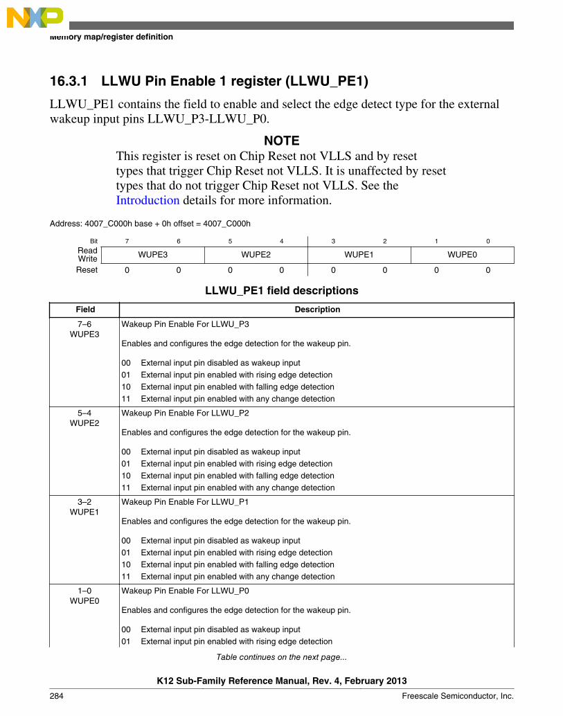
16.3.1 LLWU Pin Enable 1 register (LLWU_PE1)
LLWU_PE1 contains the field to enable and select the edge detect type for the externalwakeup input pins LLWU_P3-LLWU_P0.
NOTEThis register is reset on Chip Reset not VLLS and by resettypes that trigger Chip Reset not VLLS. It is unaffected by resettypes that do not trigger Chip Reset not VLLS. See theIntroduction details for more information.
Address: 4007_C000h base + 0h offset = 4007_C000h
Bit 7 6 5 4 3 2 1 0
Read WUPE3 WUPE2 WUPE1 WUPE0WriteReset 0 0 0 0 0 0 0 0
LLWU_PE1 field descriptions
Field Description
7–6WUPE3
Wakeup Pin Enable For LLWU_P3
Enables and configures the edge detection for the wakeup pin.
00 External input pin disabled as wakeup input01 External input pin enabled with rising edge detection10 External input pin enabled with falling edge detection11 External input pin enabled with any change detection
5–4WUPE2
Wakeup Pin Enable For LLWU_P2
Enables and configures the edge detection for the wakeup pin.
00 External input pin disabled as wakeup input01 External input pin enabled with rising edge detection10 External input pin enabled with falling edge detection11 External input pin enabled with any change detection
3–2WUPE1
Wakeup Pin Enable For LLWU_P1
Enables and configures the edge detection for the wakeup pin.
00 External input pin disabled as wakeup input01 External input pin enabled with rising edge detection10 External input pin enabled with falling edge detection11 External input pin enabled with any change detection
1–0WUPE0
Wakeup Pin Enable For LLWU_P0
Enables and configures the edge detection for the wakeup pin.
00 External input pin disabled as wakeup input01 External input pin enabled with rising edge detection
Table continues on the next page...
Memory map/register definition
K12 Sub-Family Reference Manual, Rev. 4, February 2013
284 Freescale Semiconductor, Inc.

LLWU_PE1 field descriptions (continued)
Field Description
10 External input pin enabled with falling edge detection11 External input pin enabled with any change detection
16.3.2 LLWU Pin Enable 2 register (LLWU_PE2)
LLWU_PE2 contains the field to enable and select the edge detect type for the externalwakeup input pins LLWU_P7-LLWU_P4.
NOTEThis register is reset on Chip Reset not VLLS and by resettypes that trigger Chip Reset not VLLS. It is unaffected by resettypes that do not trigger Chip Reset not VLLS. See theIntroduction details for more information.
Address: 4007_C000h base + 1h offset = 4007_C001h
Bit 7 6 5 4 3 2 1 0
Read WUPE7 WUPE6 WUPE5 WUPE4WriteReset 0 0 0 0 0 0 0 0
LLWU_PE2 field descriptions
Field Description
7–6WUPE7
Wakeup Pin Enable For LLWU_P7
Enables and configures the edge detection for the wakeup pin.
00 External input pin disabled as wakeup input01 External input pin enabled with rising edge detection10 External input pin enabled with falling edge detection11 External input pin enabled with any change detection
5–4WUPE6
Wakeup Pin Enable For LLWU_P6
Enables and configures the edge detection for the wakeup pin.
00 External input pin disabled as wakeup input01 External input pin enabled with rising edge detection10 External input pin enabled with falling edge detection11 External input pin enabled with any change detection
3–2WUPE5
Wakeup Pin Enable For LLWU_P5
Enables and configures the edge detection for the wakeup pin.
00 External input pin disabled as wakeup input01 External input pin enabled with rising edge detection
Table continues on the next page...
Chapter 16 Low-Leakage Wakeup Unit (LLWU)
K12 Sub-Family Reference Manual, Rev. 4, February 2013
Freescale Semiconductor, Inc. 285
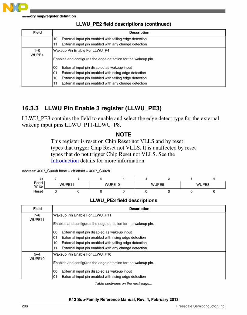
LLWU_PE2 field descriptions (continued)
Field Description
10 External input pin enabled with falling edge detection11 External input pin enabled with any change detection
1–0WUPE4
Wakeup Pin Enable For LLWU_P4
Enables and configures the edge detection for the wakeup pin.
00 External input pin disabled as wakeup input01 External input pin enabled with rising edge detection10 External input pin enabled with falling edge detection11 External input pin enabled with any change detection
16.3.3 LLWU Pin Enable 3 register (LLWU_PE3)
LLWU_PE3 contains the field to enable and select the edge detect type for the externalwakeup input pins LLWU_P11-LLWU_P8.
NOTEThis register is reset on Chip Reset not VLLS and by resettypes that trigger Chip Reset not VLLS. It is unaffected by resettypes that do not trigger Chip Reset not VLLS. See theIntroduction details for more information.
Address: 4007_C000h base + 2h offset = 4007_C002h
Bit 7 6 5 4 3 2 1 0
Read WUPE11 WUPE10 WUPE9 WUPE8WriteReset 0 0 0 0 0 0 0 0
LLWU_PE3 field descriptions
Field Description
7–6WUPE11
Wakeup Pin Enable For LLWU_P11
Enables and configures the edge detection for the wakeup pin.
00 External input pin disabled as wakeup input01 External input pin enabled with rising edge detection10 External input pin enabled with falling edge detection11 External input pin enabled with any change detection
5–4WUPE10
Wakeup Pin Enable For LLWU_P10
Enables and configures the edge detection for the wakeup pin.
00 External input pin disabled as wakeup input01 External input pin enabled with rising edge detection
Table continues on the next page...
Memory map/register definition
K12 Sub-Family Reference Manual, Rev. 4, February 2013
286 Freescale Semiconductor, Inc.
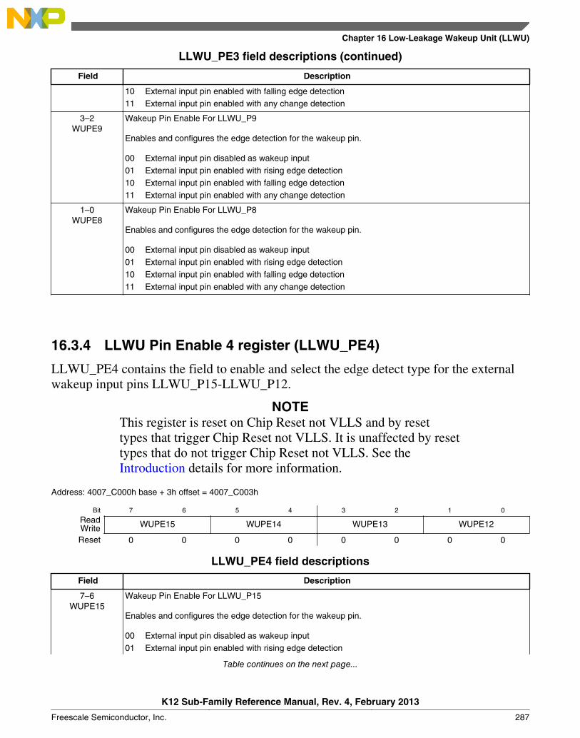
LLWU_PE3 field descriptions (continued)
Field Description
10 External input pin enabled with falling edge detection11 External input pin enabled with any change detection
3–2WUPE9
Wakeup Pin Enable For LLWU_P9
Enables and configures the edge detection for the wakeup pin.
00 External input pin disabled as wakeup input01 External input pin enabled with rising edge detection10 External input pin enabled with falling edge detection11 External input pin enabled with any change detection
1–0WUPE8
Wakeup Pin Enable For LLWU_P8
Enables and configures the edge detection for the wakeup pin.
00 External input pin disabled as wakeup input01 External input pin enabled with rising edge detection10 External input pin enabled with falling edge detection11 External input pin enabled with any change detection
16.3.4 LLWU Pin Enable 4 register (LLWU_PE4)
LLWU_PE4 contains the field to enable and select the edge detect type for the externalwakeup input pins LLWU_P15-LLWU_P12.
NOTEThis register is reset on Chip Reset not VLLS and by resettypes that trigger Chip Reset not VLLS. It is unaffected by resettypes that do not trigger Chip Reset not VLLS. See theIntroduction details for more information.
Address: 4007_C000h base + 3h offset = 4007_C003h
Bit 7 6 5 4 3 2 1 0
Read WUPE15 WUPE14 WUPE13 WUPE12WriteReset 0 0 0 0 0 0 0 0
LLWU_PE4 field descriptions
Field Description
7–6WUPE15
Wakeup Pin Enable For LLWU_P15
Enables and configures the edge detection for the wakeup pin.
00 External input pin disabled as wakeup input01 External input pin enabled with rising edge detection
Table continues on the next page...
Chapter 16 Low-Leakage Wakeup Unit (LLWU)
K12 Sub-Family Reference Manual, Rev. 4, February 2013
Freescale Semiconductor, Inc. 287

LLWU_PE4 field descriptions (continued)
Field Description
10 External input pin enabled with falling edge detection11 External input pin enabled with any change detection
5–4WUPE14
Wakeup Pin Enable For LLWU_P14
Enables and configures the edge detection for the wakeup pin.
00 External input pin disabled as wakeup input01 External input pin enabled with rising edge detection10 External input pin enabled with falling edge detection11 External input pin enabled with any change detection
3–2WUPE13
Wakeup Pin Enable For LLWU_P13
Enables and configures the edge detection for the wakeup pin.
00 External input pin disabled as wakeup input01 External input pin enabled with rising edge detection10 External input pin enabled with falling edge detection11 External input pin enabled with any change detection
1–0WUPE12
Wakeup Pin Enable For LLWU_P12
Enables and configures the edge detection for the wakeup pin.
00 External input pin disabled as wakeup input01 External input pin enabled with rising edge detection10 External input pin enabled with falling edge detection11 External input pin enabled with any change detection
16.3.5 LLWU Module Enable register (LLWU_ME)
LLWU_ME contains the bits to enable the internal module flag as a wakeup input sourcefor inputs MWUF7-MWUF0.
NOTEThis register is reset on Chip Reset not VLLS and by resettypes that trigger Chip Reset not VLLS. It is unaffected by resettypes that do not trigger Chip Reset not VLLS. See theIntroduction details for more information.
Address: 4007_C000h base + 4h offset = 4007_C004h
Bit 7 6 5 4 3 2 1 0
Read WUME7 WUME6 WUME5 WUME4 WUME3 WUME2 WUME1 WUME0WriteReset 0 0 0 0 0 0 0 0
Memory map/register definition
K12 Sub-Family Reference Manual, Rev. 4, February 2013
288 Freescale Semiconductor, Inc.
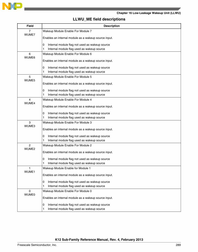
LLWU_ME field descriptions
Field Description
7WUME7
Wakeup Module Enable For Module 7
Enables an internal module as a wakeup source input.
0 Internal module flag not used as wakeup source1 Internal module flag used as wakeup source
6WUME6
Wakeup Module Enable For Module 6
Enables an internal module as a wakeup source input.
0 Internal module flag not used as wakeup source1 Internal module flag used as wakeup source
5WUME5
Wakeup Module Enable For Module 5
Enables an internal module as a wakeup source input.
0 Internal module flag not used as wakeup source1 Internal module flag used as wakeup source
4WUME4
Wakeup Module Enable For Module 4
Enables an internal module as a wakeup source input.
0 Internal module flag not used as wakeup source1 Internal module flag used as wakeup source
3WUME3
Wakeup Module Enable For Module 3
Enables an internal module as a wakeup source input.
0 Internal module flag not used as wakeup source1 Internal module flag used as wakeup source
2WUME2
Wakeup Module Enable For Module 2
Enables an internal module as a wakeup source input.
0 Internal module flag not used as wakeup source1 Internal module flag used as wakeup source
1WUME1
Wakeup Module Enable for Module 1
Enables an internal module as a wakeup source input.
0 Internal module flag not used as wakeup source1 Internal module flag used as wakeup source
0WUME0
Wakeup Module Enable For Module 0
Enables an internal module as a wakeup source input.
0 Internal module flag not used as wakeup source1 Internal module flag used as wakeup source
Chapter 16 Low-Leakage Wakeup Unit (LLWU)
K12 Sub-Family Reference Manual, Rev. 4, February 2013
Freescale Semiconductor, Inc. 289
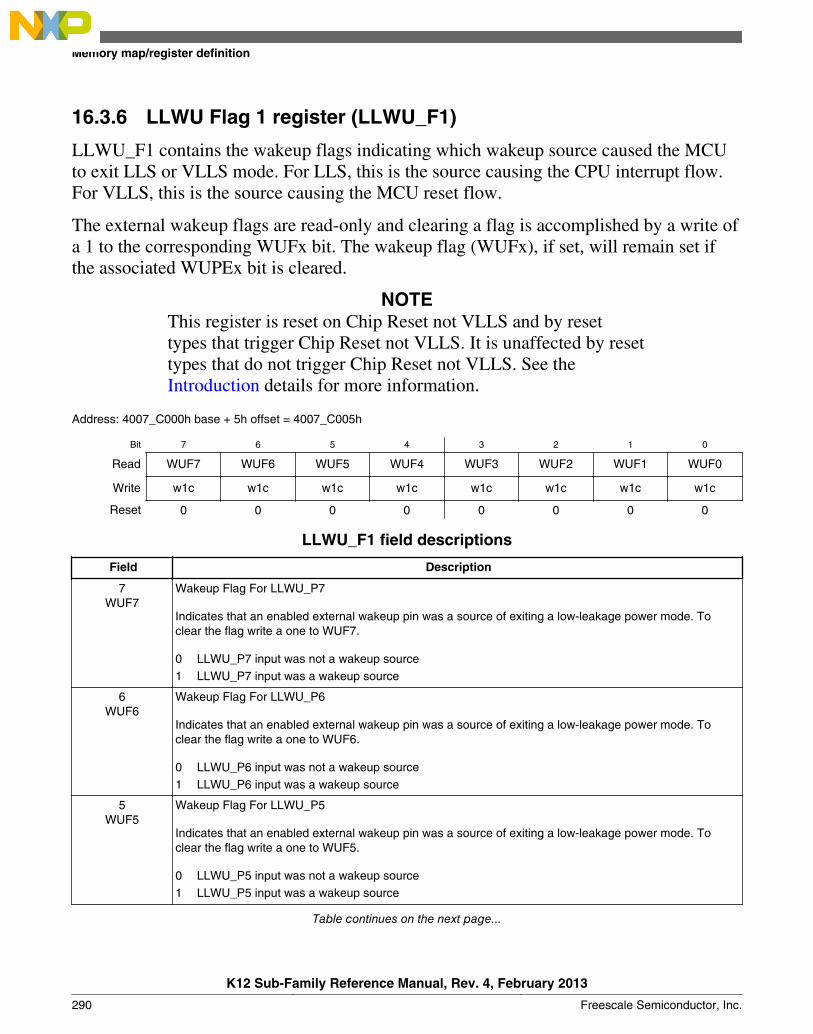
16.3.6 LLWU Flag 1 register (LLWU_F1)
LLWU_F1 contains the wakeup flags indicating which wakeup source caused the MCUto exit LLS or VLLS mode. For LLS, this is the source causing the CPU interrupt flow.For VLLS, this is the source causing the MCU reset flow.
The external wakeup flags are read-only and clearing a flag is accomplished by a write ofa 1 to the corresponding WUFx bit. The wakeup flag (WUFx), if set, will remain set ifthe associated WUPEx bit is cleared.
NOTEThis register is reset on Chip Reset not VLLS and by resettypes that trigger Chip Reset not VLLS. It is unaffected by resettypes that do not trigger Chip Reset not VLLS. See theIntroduction details for more information.
Address: 4007_C000h base + 5h offset = 4007_C005h
Bit 7 6 5 4 3 2 1 0
Read WUF7 WUF6 WUF5 WUF4 WUF3 WUF2 WUF1 WUF0
Write w1c w1c w1c w1c w1c w1c w1c w1c
Reset 0 0 0 0 0 0 0 0
LLWU_F1 field descriptions
Field Description
7WUF7
Wakeup Flag For LLWU_P7
Indicates that an enabled external wakeup pin was a source of exiting a low-leakage power mode. Toclear the flag write a one to WUF7.
0 LLWU_P7 input was not a wakeup source1 LLWU_P7 input was a wakeup source
6WUF6
Wakeup Flag For LLWU_P6
Indicates that an enabled external wakeup pin was a source of exiting a low-leakage power mode. Toclear the flag write a one to WUF6.
0 LLWU_P6 input was not a wakeup source1 LLWU_P6 input was a wakeup source
5WUF5
Wakeup Flag For LLWU_P5
Indicates that an enabled external wakeup pin was a source of exiting a low-leakage power mode. Toclear the flag write a one to WUF5.
0 LLWU_P5 input was not a wakeup source1 LLWU_P5 input was a wakeup source
Table continues on the next page...
Memory map/register definition
K12 Sub-Family Reference Manual, Rev. 4, February 2013
290 Freescale Semiconductor, Inc.
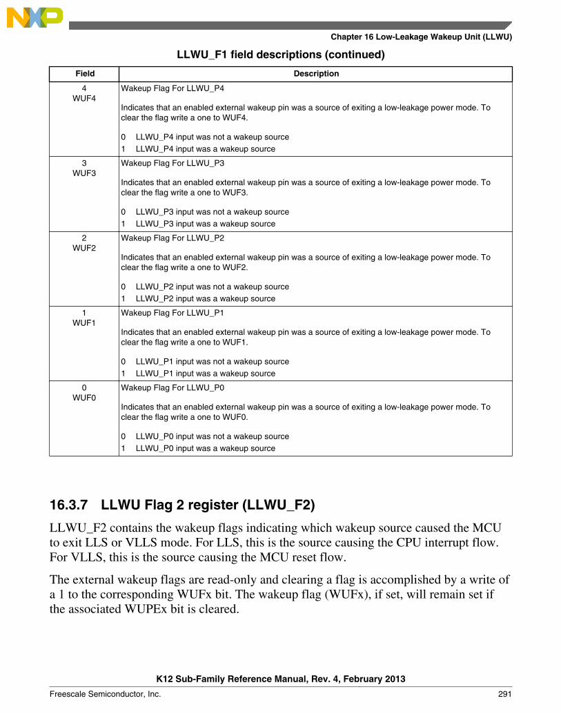
LLWU_F1 field descriptions (continued)
Field Description
4WUF4
Wakeup Flag For LLWU_P4
Indicates that an enabled external wakeup pin was a source of exiting a low-leakage power mode. Toclear the flag write a one to WUF4.
0 LLWU_P4 input was not a wakeup source1 LLWU_P4 input was a wakeup source
3WUF3
Wakeup Flag For LLWU_P3
Indicates that an enabled external wakeup pin was a source of exiting a low-leakage power mode. Toclear the flag write a one to WUF3.
0 LLWU_P3 input was not a wakeup source1 LLWU_P3 input was a wakeup source
2WUF2
Wakeup Flag For LLWU_P2
Indicates that an enabled external wakeup pin was a source of exiting a low-leakage power mode. Toclear the flag write a one to WUF2.
0 LLWU_P2 input was not a wakeup source1 LLWU_P2 input was a wakeup source
1WUF1
Wakeup Flag For LLWU_P1
Indicates that an enabled external wakeup pin was a source of exiting a low-leakage power mode. Toclear the flag write a one to WUF1.
0 LLWU_P1 input was not a wakeup source1 LLWU_P1 input was a wakeup source
0WUF0
Wakeup Flag For LLWU_P0
Indicates that an enabled external wakeup pin was a source of exiting a low-leakage power mode. Toclear the flag write a one to WUF0.
0 LLWU_P0 input was not a wakeup source1 LLWU_P0 input was a wakeup source
16.3.7 LLWU Flag 2 register (LLWU_F2)
LLWU_F2 contains the wakeup flags indicating which wakeup source caused the MCUto exit LLS or VLLS mode. For LLS, this is the source causing the CPU interrupt flow.For VLLS, this is the source causing the MCU reset flow.
The external wakeup flags are read-only and clearing a flag is accomplished by a write ofa 1 to the corresponding WUFx bit. The wakeup flag (WUFx), if set, will remain set ifthe associated WUPEx bit is cleared.
Chapter 16 Low-Leakage Wakeup Unit (LLWU)
K12 Sub-Family Reference Manual, Rev. 4, February 2013
Freescale Semiconductor, Inc. 291
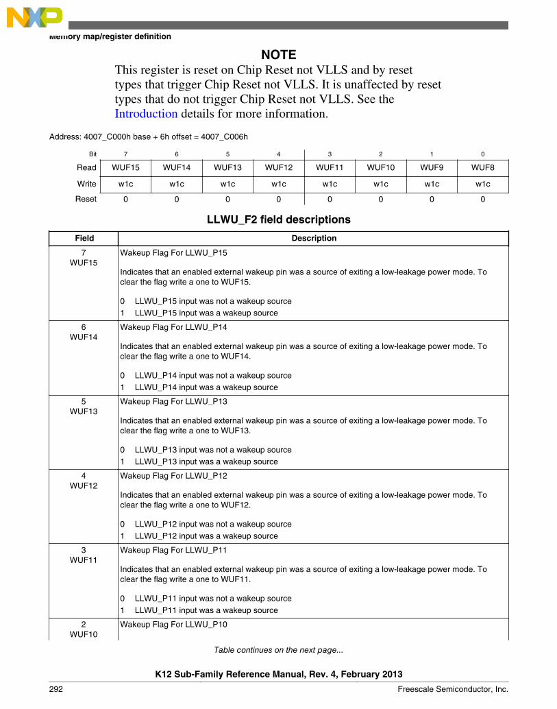
NOTEThis register is reset on Chip Reset not VLLS and by resettypes that trigger Chip Reset not VLLS. It is unaffected by resettypes that do not trigger Chip Reset not VLLS. See theIntroduction details for more information.
Address: 4007_C000h base + 6h offset = 4007_C006h
Bit 7 6 5 4 3 2 1 0
Read WUF15 WUF14 WUF13 WUF12 WUF11 WUF10 WUF9 WUF8
Write w1c w1c w1c w1c w1c w1c w1c w1c
Reset 0 0 0 0 0 0 0 0
LLWU_F2 field descriptions
Field Description
7WUF15
Wakeup Flag For LLWU_P15
Indicates that an enabled external wakeup pin was a source of exiting a low-leakage power mode. Toclear the flag write a one to WUF15.
0 LLWU_P15 input was not a wakeup source1 LLWU_P15 input was a wakeup source
6WUF14
Wakeup Flag For LLWU_P14
Indicates that an enabled external wakeup pin was a source of exiting a low-leakage power mode. Toclear the flag write a one to WUF14.
0 LLWU_P14 input was not a wakeup source1 LLWU_P14 input was a wakeup source
5WUF13
Wakeup Flag For LLWU_P13
Indicates that an enabled external wakeup pin was a source of exiting a low-leakage power mode. Toclear the flag write a one to WUF13.
0 LLWU_P13 input was not a wakeup source1 LLWU_P13 input was a wakeup source
4WUF12
Wakeup Flag For LLWU_P12
Indicates that an enabled external wakeup pin was a source of exiting a low-leakage power mode. Toclear the flag write a one to WUF12.
0 LLWU_P12 input was not a wakeup source1 LLWU_P12 input was a wakeup source
3WUF11
Wakeup Flag For LLWU_P11
Indicates that an enabled external wakeup pin was a source of exiting a low-leakage power mode. Toclear the flag write a one to WUF11.
0 LLWU_P11 input was not a wakeup source1 LLWU_P11 input was a wakeup source
2WUF10
Wakeup Flag For LLWU_P10
Table continues on the next page...
Memory map/register definition
K12 Sub-Family Reference Manual, Rev. 4, February 2013
292 Freescale Semiconductor, Inc.
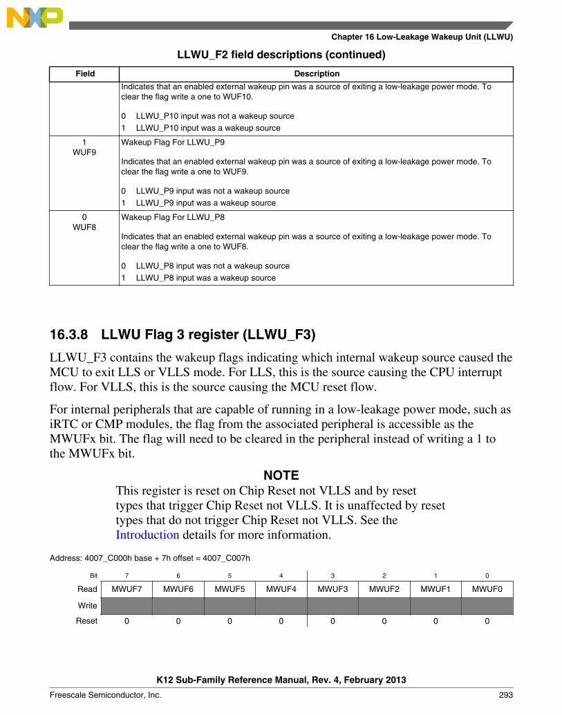
LLWU_F2 field descriptions (continued)
Field Description
Indicates that an enabled external wakeup pin was a source of exiting a low-leakage power mode. Toclear the flag write a one to WUF10.
0 LLWU_P10 input was not a wakeup source1 LLWU_P10 input was a wakeup source
1WUF9
Wakeup Flag For LLWU_P9
Indicates that an enabled external wakeup pin was a source of exiting a low-leakage power mode. Toclear the flag write a one to WUF9.
0 LLWU_P9 input was not a wakeup source1 LLWU_P9 input was a wakeup source
0WUF8
Wakeup Flag For LLWU_P8
Indicates that an enabled external wakeup pin was a source of exiting a low-leakage power mode. Toclear the flag write a one to WUF8.
0 LLWU_P8 input was not a wakeup source1 LLWU_P8 input was a wakeup source
16.3.8 LLWU Flag 3 register (LLWU_F3)
LLWU_F3 contains the wakeup flags indicating which internal wakeup source caused theMCU to exit LLS or VLLS mode. For LLS, this is the source causing the CPU interruptflow. For VLLS, this is the source causing the MCU reset flow.
For internal peripherals that are capable of running in a low-leakage power mode, such asiRTC or CMP modules, the flag from the associated peripheral is accessible as theMWUFx bit. The flag will need to be cleared in the peripheral instead of writing a 1 tothe MWUFx bit.
NOTEThis register is reset on Chip Reset not VLLS and by resettypes that trigger Chip Reset not VLLS. It is unaffected by resettypes that do not trigger Chip Reset not VLLS. See theIntroduction details for more information.
Address: 4007_C000h base + 7h offset = 4007_C007h
Bit 7 6 5 4 3 2 1 0
Read MWUF7 MWUF6 MWUF5 MWUF4 MWUF3 MWUF2 MWUF1 MWUF0
Write
Reset 0 0 0 0 0 0 0 0
Chapter 16 Low-Leakage Wakeup Unit (LLWU)
K12 Sub-Family Reference Manual, Rev. 4, February 2013
Freescale Semiconductor, Inc. 293
LLWU_F3 field descriptions
Field Description
7MWUF7
Wakeup flag For module 7
Indicates that an enabled internal peripheral was a source of exiting a low-leakage power mode. To clearthe flag, follow the internal peripheral flag clearing mechanism.
0 Module 7 input was not a wakeup source1 Module 7 input was a wakeup source
6MWUF6
Wakeup flag For module 6
Indicates that an enabled internal peripheral was a source of exiting a low-leakage power mode. To clearthe flag, follow the internal peripheral flag clearing mechanism.
0 Module 6 input was not a wakeup source1 Module 6 input was a wakeup source
5MWUF5
Wakeup flag For module 5
Indicates that an enabled internal peripheral was a source of exiting a low-leakage power mode. To clearthe flag, follow the internal peripheral flag clearing mechanism.
0 Module 5 input was not a wakeup source1 Module 5 input was a wakeup source
4MWUF4
Wakeup flag For module 4
Indicates that an enabled internal peripheral was a source of exiting a low-leakage power mode. To clearthe flag, follow the internal peripheral flag clearing mechanism.
0 Module 4 input was not a wakeup source1 Module 4 input was a wakeup source
3MWUF3
Wakeup flag For module 3
Indicates that an enabled internal peripheral was a source of exiting a low-leakage power mode. To clearthe flag, follow the internal peripheral flag clearing mechanism.
0 Module 3 input was not a wakeup source1 Module 3 input was a wakeup source
2MWUF2
Wakeup flag For module 2
Indicates that an enabled internal peripheral was a source of exiting a low-leakage power mode. To clearthe flag, follow the internal peripheral flag clearing mechanism.
0 Module 2 input was not a wakeup source1 Module 2 input was a wakeup source
1MWUF1
Wakeup flag For module 1
Indicates that an enabled internal peripheral was a source of exiting a low-leakage power mode. To clearthe flag, follow the internal peripheral flag clearing mechanism.
0 Module 1 input was not a wakeup source1 Module 1 input was a wakeup source
0MWUF0
Wakeup flag For module 0
Table continues on the next page...
Memory map/register definition
K12 Sub-Family Reference Manual, Rev. 4, February 2013
294 Freescale Semiconductor, Inc.
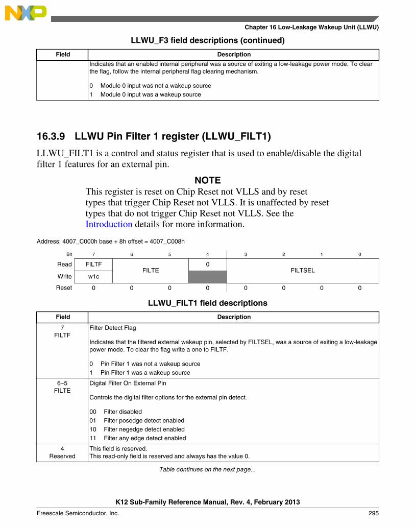
LLWU_F3 field descriptions (continued)
Field Description
Indicates that an enabled internal peripheral was a source of exiting a low-leakage power mode. To clearthe flag, follow the internal peripheral flag clearing mechanism.
0 Module 0 input was not a wakeup source1 Module 0 input was a wakeup source
16.3.9 LLWU Pin Filter 1 register (LLWU_FILT1)
LLWU_FILT1 is a control and status register that is used to enable/disable the digitalfilter 1 features for an external pin.
NOTEThis register is reset on Chip Reset not VLLS and by resettypes that trigger Chip Reset not VLLS. It is unaffected by resettypes that do not trigger Chip Reset not VLLS. See theIntroduction details for more information.
Address: 4007_C000h base + 8h offset = 4007_C008h
Bit 7 6 5 4 3 2 1 0
Read FILTFFILTE
0FILTSEL
Write w1c
Reset 0 0 0 0 0 0 0 0
LLWU_FILT1 field descriptions
Field Description
7FILTF
Filter Detect Flag
Indicates that the filtered external wakeup pin, selected by FILTSEL, was a source of exiting a low-leakagepower mode. To clear the flag write a one to FILTF.
0 Pin Filter 1 was not a wakeup source1 Pin Filter 1 was a wakeup source
6–5FILTE
Digital Filter On External Pin
Controls the digital filter options for the external pin detect.
00 Filter disabled01 Filter posedge detect enabled10 Filter negedge detect enabled11 Filter any edge detect enabled
4Reserved
This field is reserved.This read-only field is reserved and always has the value 0.
Table continues on the next page...
Chapter 16 Low-Leakage Wakeup Unit (LLWU)
K12 Sub-Family Reference Manual, Rev. 4, February 2013
Freescale Semiconductor, Inc. 295
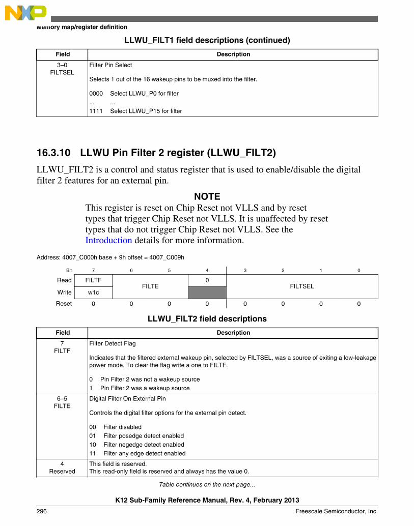
LLWU_FILT1 field descriptions (continued)
Field Description
3–0FILTSEL
Filter Pin Select
Selects 1 out of the 16 wakeup pins to be muxed into the filter.
0000 Select LLWU_P0 for filter... ...1111 Select LLWU_P15 for filter
16.3.10 LLWU Pin Filter 2 register (LLWU_FILT2)
LLWU_FILT2 is a control and status register that is used to enable/disable the digitalfilter 2 features for an external pin.
NOTEThis register is reset on Chip Reset not VLLS and by resettypes that trigger Chip Reset not VLLS. It is unaffected by resettypes that do not trigger Chip Reset not VLLS. See theIntroduction details for more information.
Address: 4007_C000h base + 9h offset = 4007_C009h
Bit 7 6 5 4 3 2 1 0
Read FILTFFILTE
0FILTSEL
Write w1c
Reset 0 0 0 0 0 0 0 0
LLWU_FILT2 field descriptions
Field Description
7FILTF
Filter Detect Flag
Indicates that the filtered external wakeup pin, selected by FILTSEL, was a source of exiting a low-leakagepower mode. To clear the flag write a one to FILTF.
0 Pin Filter 2 was not a wakeup source1 Pin Filter 2 was a wakeup source
6–5FILTE
Digital Filter On External Pin
Controls the digital filter options for the external pin detect.
00 Filter disabled01 Filter posedge detect enabled10 Filter negedge detect enabled11 Filter any edge detect enabled
4Reserved
This field is reserved.This read-only field is reserved and always has the value 0.
Table continues on the next page...
Memory map/register definition
K12 Sub-Family Reference Manual, Rev. 4, February 2013
296 Freescale Semiconductor, Inc.
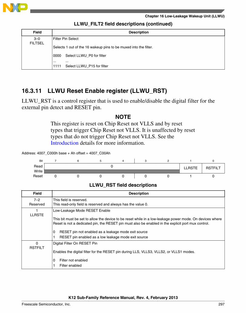
LLWU_FILT2 field descriptions (continued)
Field Description
3–0FILTSEL
Filter Pin Select
Selects 1 out of the 16 wakeup pins to be muxed into the filter.
0000 Select LLWU_P0 for filter... ...1111 Select LLWU_P15 for filter
16.3.11 LLWU Reset Enable register (LLWU_RST)
LLWU_RST is a control register that is used to enable/disable the digital filter for theexternal pin detect and RESET pin.
NOTEThis register is reset on Chip Reset not VLLS and by resettypes that trigger Chip Reset not VLLS. It is unaffected by resettypes that do not trigger Chip Reset not VLLS. See theIntroduction details for more information.
Address: 4007_C000h base + Ah offset = 4007_C00Ah
Bit 7 6 5 4 3 2 1 0
Read 0 LLRSTE RSTFILTWriteReset 0 0 0 0 0 0 1 0
LLWU_RST field descriptions
Field Description
7–2Reserved
This field is reserved.This read-only field is reserved and always has the value 0.
1LLRSTE
Low-Leakage Mode RESET Enable
This bit must be set to allow the device to be reset while in a low-leakage power mode. On devices whereReset is not a dedicated pin, the RESET pin must also be enabled in the explicit port mux control.
0 RESET pin not enabled as a leakage mode exit source1 RESET pin enabled as a low leakage mode exit source
0RSTFILT
Digital Filter On RESET Pin
Enables the digital filter for the RESET pin during LLS, VLLS3, VLLS2, or VLLS1 modes.
0 Filter not enabled1 Filter enabled
Chapter 16 Low-Leakage Wakeup Unit (LLWU)
K12 Sub-Family Reference Manual, Rev. 4, February 2013
Freescale Semiconductor, Inc. 297

16.4 Functional descriptionThis on-chip peripheral module is called a low-leakage wakeup unit (LLWU) modulebecause it allows internal peripherals and external input pins as a source of wakeup fromlow-leakage modes. It is operational only in LLS and VLLSx modes.
The LLWU module contains pin enables for each external pin and internal module. Foreach external pin, the user can disable or select the edge type for the wakeup. Typeoptions are:
• Falling-edge• Rising-edge• Either-edge
When an external pin is enabled as a wakeup source, the pin must be configured as aninput pin.
The LLWU implements optional 3-cycle glitch filters, based on the LPO clock. Adetected external pin, either wakeup or RESET, is required to remain asserted until theenabled glitch filter times out. Additional latency of up to 2 cycles is due tosynchronization, which results in a total of up to 5 cycles of delay before the detectcircuit alerts the system to the wakeup or reset event when the filter function is enabled.Two wakeup detect filters are available to detect up to two external pins. A separate resetfilter is on the RESET pin. Glitch filtering is not provided on the internal modules.
For internal module wakeup operation, the WUMEx bit enables the associated module asa wakeup source.
16.4.1 LLS mode
Wakeup events triggered from either an external pin input or an internal module inputresult in a CPU interrupt flow to begin user code execution.
An LLS reset event due to RESET pin assertion causes an exit via a system reset. Stateretention data is lost, and the I/O states return to their reset state. TheRCM_SRS[WAKEUP] and RCM_SRS[PIN] bits are set and the system executes a resetflow before CPU operation begins with a reset vector fetch.
Functional description
K12 Sub-Family Reference Manual, Rev. 4, February 2013
298 Freescale Semiconductor, Inc.
16.4.2 VLLS modes
In the case of a wakeup due to external pin or internal module wakeup, recovery isalways via a reset flow and the RCM_SRS[WAKEUP] is set indicating the low-leakagemode was active. State retention data is lost and I/O will be restored afterPMC_REGSC[ACKISO] has been written.
A VLLS exit event due to RESET pin assertion causes an exit via a system reset. Stateretention data is lost and the I/O states immediately return to their reset state. TheRCM_SRS[WAKEUP] and RCM_SRS[PIN] bits are set and the system executes a resetflow before CPU operation begins with a reset vector fetch.
16.4.3 Initialization
For an enabled peripheral wakeup input, the peripheral flag must be cleared by softwarebefore entering LLS or VLLSx mode to avoid an immediate exit from the mode.
Flags associated with external input pins, filtered and unfiltered, must also be cleared bysoftware prior to entry to LLS or VLLSx mode.
After enabling an external pin filter or changing the source pin, wait at least 5 LPO clockcycles before entering LLS or VLLSx mode to allow the filter to initialize.
NOTE
After recovering from a VLLS mode, user must restore chipconfiguration before clearing ACKISO. In particular, pinconfiguration for enabled LLWU wakeup pins must be restoredto avoid any LLWU flag from being falsely set when ACKISOis cleared.
The signal selected as a wakeup source pin must be a digitalpin, as selected in the pin mux control.
Chapter 16 Low-Leakage Wakeup Unit (LLWU)
K12 Sub-Family Reference Manual, Rev. 4, February 2013
Freescale Semiconductor, Inc. 299

Functional description
K12 Sub-Family Reference Manual, Rev. 4, February 2013
300 Freescale Semiconductor, Inc.
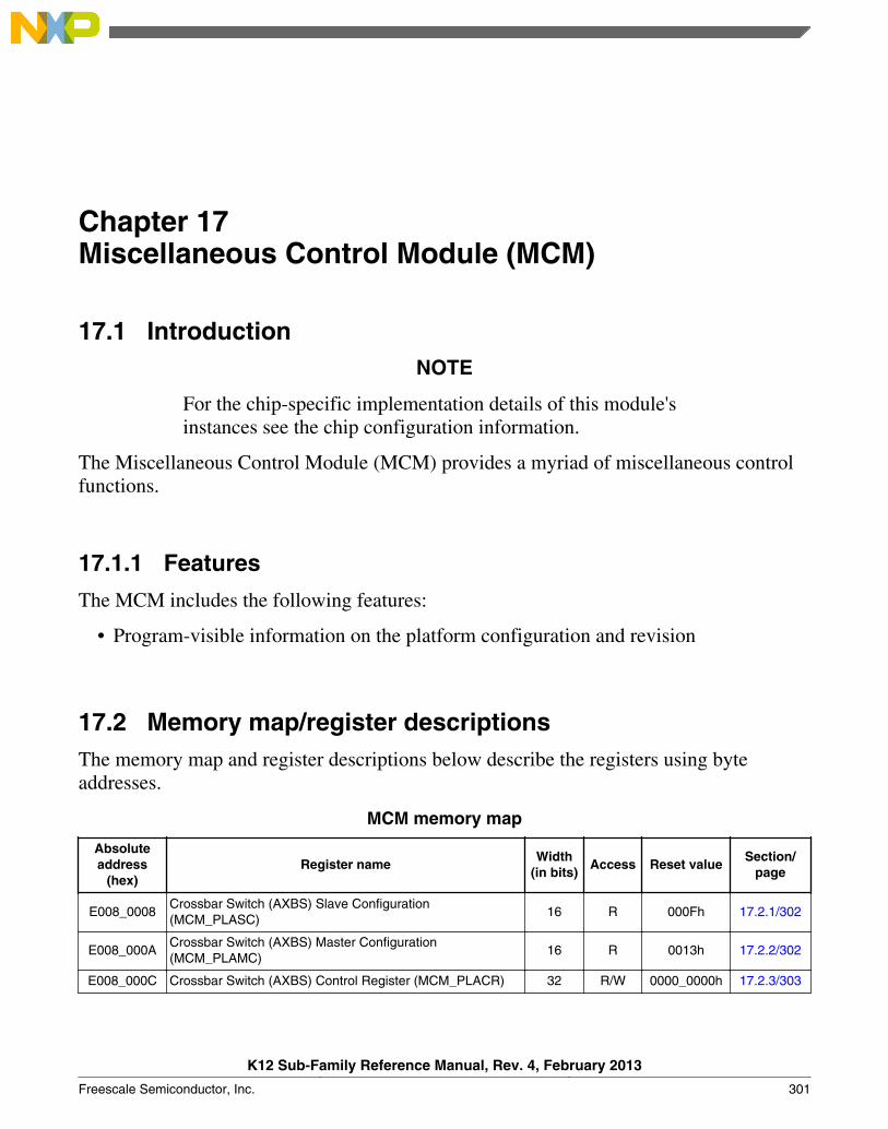
Chapter 17Miscellaneous Control Module (MCM)
17.1 IntroductionNOTE
For the chip-specific implementation details of this module'sinstances see the chip configuration information.
The Miscellaneous Control Module (MCM) provides a myriad of miscellaneous controlfunctions.
17.1.1 Features
The MCM includes the following features:
• Program-visible information on the platform configuration and revision
17.2 Memory map/register descriptionsThe memory map and register descriptions below describe the registers using byteaddresses.
MCM memory map
Absoluteaddress
(hex)Register name
Width(in bits)
Access Reset valueSection/
page
E008_0008Crossbar Switch (AXBS) Slave Configuration(MCM_PLASC)
16 R 000Fh 17.2.1/302
E008_000ACrossbar Switch (AXBS) Master Configuration(MCM_PLAMC)
16 R 0013h 17.2.2/302
E008_000C Crossbar Switch (AXBS) Control Register (MCM_PLACR) 32 R/W 0000_0000h 17.2.3/303
K12 Sub-Family Reference Manual, Rev. 4, February 2013
Freescale Semiconductor, Inc. 301
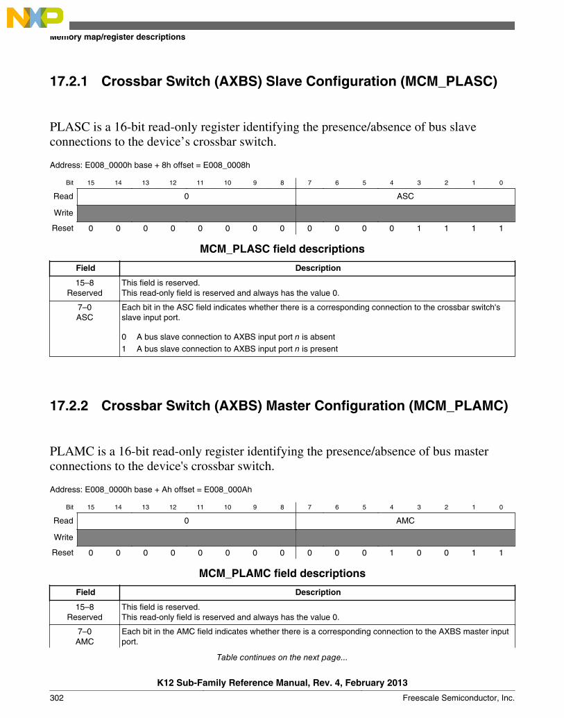
17.2.1 Crossbar Switch (AXBS) Slave Configuration (MCM_PLASC)
PLASC is a 16-bit read-only register identifying the presence/absence of bus slaveconnections to the device’s crossbar switch.
Address: E008_0000h base + 8h offset = E008_0008h
Bit 15 14 13 12 11 10 9 8 7 6 5 4 3 2 1 0
Read 0 ASC
Write
Reset 0 0 0 0 0 0 0 0 0 0 0 0 1 1 1 1
MCM_PLASC field descriptions
Field Description
15–8Reserved
This field is reserved.This read-only field is reserved and always has the value 0.
7–0ASC
Each bit in the ASC field indicates whether there is a corresponding connection to the crossbar switch'sslave input port.
0 A bus slave connection to AXBS input port n is absent1 A bus slave connection to AXBS input port n is present
17.2.2 Crossbar Switch (AXBS) Master Configuration (MCM_PLAMC)
PLAMC is a 16-bit read-only register identifying the presence/absence of bus masterconnections to the device's crossbar switch.
Address: E008_0000h base + Ah offset = E008_000Ah
Bit 15 14 13 12 11 10 9 8 7 6 5 4 3 2 1 0
Read 0 AMC
Write
Reset 0 0 0 0 0 0 0 0 0 0 0 1 0 0 1 1
MCM_PLAMC field descriptions
Field Description
15–8Reserved
This field is reserved.This read-only field is reserved and always has the value 0.
7–0AMC
Each bit in the AMC field indicates whether there is a corresponding connection to the AXBS master inputport.
Table continues on the next page...
Memory map/register descriptions
K12 Sub-Family Reference Manual, Rev. 4, February 2013
302 Freescale Semiconductor, Inc.
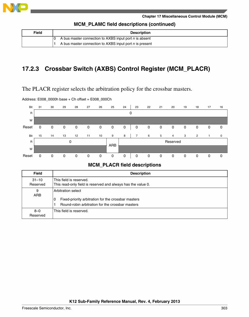
MCM_PLAMC field descriptions (continued)
Field Description
0 A bus master connection to AXBS input port n is absent1 A bus master connection to AXBS input port n is present
17.2.3 Crossbar Switch (AXBS) Control Register (MCM_PLACR)
The PLACR register selects the arbitration policy for the crossbar masters.
Address: E008_0000h base + Ch offset = E008_000Ch
Bit 31 30 29 28 27 26 25 24 23 22 21 20 19 18 17 16
R 0
W
Reset 0 0 0 0 0 0 0 0 0 0 0 0 0 0 0 0
Bit 15 14 13 12 11 10 9 8 7 6 5 4 3 2 1 0
R 0ARB
Reserved
W
Reset 0 0 0 0 0 0 0 0 0 0 0 0 0 0 0 0
MCM_PLACR field descriptions
Field Description
31–10Reserved
This field is reserved.This read-only field is reserved and always has the value 0.
9ARB
Arbitration select
0 Fixed-priority arbitration for the crossbar masters1 Round-robin arbitration for the crossbar masters
8–0Reserved
This field is reserved.
Chapter 17 Miscellaneous Control Module (MCM)
K12 Sub-Family Reference Manual, Rev. 4, February 2013
Freescale Semiconductor, Inc. 303

Memory map/register descriptions
K12 Sub-Family Reference Manual, Rev. 4, February 2013
304 Freescale Semiconductor, Inc.

Chapter 18Crossbar Switch Lite (AXBS-Lite)
18.1 IntroductionNOTE
For the chip-specific implementation details of this module'sinstances see the chip configuration information.
This chapter provides information on the layout, configuration, and programming of thecrossbar switch. The crossbar switch connects bus masters and bus slaves using acrossbar switch structure. This structure allows up to four bus masters to access differentbus slaves simultaneously, while providing arbitration among the bus masters when theyaccess the same slave.
18.1.1 Features
The crossbar switch includes these features:
• Symmetric crossbar bus switch implementation
• Allows concurrent accesses from different masters to different slaves
• 32-bit data bus
• Operation at a 1-to-1 clock frequency with the bus masters
• Programmable configuration for fixed-priority or round-robin slave port arbitration
18.2 Memory Map / Register DefinitionThis crossbar switch is designed for minimal gate count. It, therefore, has no memory-mapped configuration registers.
K12 Sub-Family Reference Manual, Rev. 4, February 2013
Freescale Semiconductor, Inc. 305
18.3 Functional Description
18.3.1 General operation
When a master accesses the crossbar switch the access is immediately taken. If thetargeted slave port of the access is available, then the access is immediately presented onthe slave port. Single-clock or zero-wait-state accesses are possible through the crossbar.If the targeted slave port of the access is busy or parked on a different master port, therequesting master simply sees wait states inserted until the targeted slave port can servicethe master's request. The latency in servicing the request depends on each master'spriority level and the responding slave's access time.
Because the crossbar switch appears to be just another slave to the master device, themaster device has no knowledge of whether it actually owns the slave port it is targeting.While the master does not have control of the slave port it is targeting, it simply waits.
A master is given control of the targeted slave port only after a previous access to adifferent slave port completes, regardless of its priority on the newly targeted slave port.This prevents deadlock from occurring when:
• A higher priority master has:• An outstanding request to one slave port that has a long response time and• A pending access to a different slave port, and
• A lower priority master is also making a request to the same slave port as the pendingaccess of the higher priority master.
After the master has control of the slave port it is targeting, the master remains in controlof the slave port until it relinquishes the slave port by running an IDLE cycle or bytargeting a different slave port for its next access.
The master can also lose control of the slave port if another higher-priority master makesa request to the slave port.
The crossbar terminates all master IDLE transfers, as opposed to allowing the terminationto come from one of the slave buses. Additionally, when no master is requesting access toa slave port, the crossbar drives IDLE transfers onto the slave bus, even though a defaultmaster may be granted access to the slave port.
When a slave bus is being idled by the crossbar, it remains parked with the last master touse the slave port. This is done to save the initial clock of arbitration delay that otherwisewould be seen if the master had to arbitrate to gain control of the slave port.
Functional Description
K12 Sub-Family Reference Manual, Rev. 4, February 2013
306 Freescale Semiconductor, Inc.
18.3.2 Arbitration
The crossbar switch supports two arbitration algorithms:
• Fixed priority• Round robin
The selection of the global slave port arbitration is controlled by MCM_PLACR[ARB].For fixed priority, set ARB to 0. For round robin, set ARB to 1. This arbitration settingapplies to all slave ports.
18.3.2.1 Fixed-priority operation
When operating in fixed-priority mode, each master is assigned a unique priority levelwith the highest numbered master having the highest priority (master 1 has lower prioritythan master 3). If two masters request access to the same slave port, the master with thehighest priority gains control over the slave port.
NOTEIn this arbitration mode, a higher-priority master canmonopolize a slave port, preventing accesses from any lower-priority master to the port.
When a master makes a request to a slave port, the slave port checks whether the newrequesting master's priority level is higher than that of the master that currently hascontrol over the slave port, unless the slave port is in a parked state. The slave portperforms an arbitration check at every clock edge to ensure that the proper master, if any,has control of the slave port.
The following table describes possible scenarios based on the requesting master port:
Table 18-1. How AXBS grants control of a slave port to a master
When Then AXBS grants control to the requesting master
Both of the following are true:• The current master is not running a transfer.• The new requesting master's priority level is higher than
that of the current master.
At the next clock edge
Both of the following are true:• The current master is running an undefined length burst
transfer.• The requesting master's priority level is higher than that
of the current master.
At the next arbitration point for the undefined length bursttransfer
NOTE: Arbitration points for an undefined length burst aredefined in the MGPCR for each master.
Table continues on the next page...
Chapter 18 Crossbar Switch Lite (AXBS-Lite)
K12 Sub-Family Reference Manual, Rev. 4, February 2013
Freescale Semiconductor, Inc. 307
Table 18-1. How AXBS grants control of a slave port to a master (continued)
When Then AXBS grants control to the requesting master
The requesting master's priority level is lower than the currentmaster.
At the conclusion of one of the following cycles:• An IDLE cycle• A non-IDLE cycle to a location other than the current
slave port
18.3.2.2 Round-robin priority operation
When operating in round-robin mode, each master is assigned a relative priority based onthe master port number. This relative priority is compared to the master port number (ID)of the last master to perform a transfer on the slave bus. The highest priority requestingmaster becomes owner of the slave bus at the next transfer boundary. Priority is based onhow far ahead the ID of the requesting master is to the ID of the last master.
After granted access to a slave port, a master may perform as many transfers as desired tothat port until another master makes a request to the same slave port. The next master inline is granted access to the slave port at the next transfer boundary, or possibly on thenext clock cycle if the current master has no pending access request.
As an example of arbitration in round-robin mode, assume the crossbar is implementedwith master ports 0, 1, 4, and 5. If the last master of the slave port was master 1, andmaster 0, 4, and 5 make simultaneous requests, they are serviced in the order: 4 then 5then 0.
The round-robin arbitration mode generally provides a more fair allocation of theavailable slave-port bandwidth (compared to fixed priority) as the fixed master prioritydoes not affect the master selection.
18.4 Initialization/application informationNo initialization is required for the crossbar switch. See the AXBS section of theconfiguration chapter for the reset state of the arbitration scheme.
Initialization/application information
K12 Sub-Family Reference Manual, Rev. 4, February 2013
308 Freescale Semiconductor, Inc.
Chapter 19Peripheral Bridge (AIPS-Lite)
19.1 IntroductionNOTE
For the chip-specific implementation details of this module'sinstances see the chip configuration information.
The peripheral bridge converts the crossbar switch interface to an interface that canaccess most of the slave peripherals on this chip.
The peripheral bridge occupies 64 MB of the address space, which is divided into 4-KBperipheral slots. (Not all peripheral slots might be used. See the memory map chapter fordetails on slot assignments.) The bridge includes separate clock enable inputs for each ofthe slots to accommodate slower peripherals.
19.1.1 Features
Key features of the peripheral bridge are:
• Supports peripheral slots with 8-, 16-, and 32-bit datapath width
19.1.2 General operationThe slave devices connected to the peripheral bridge are modules which contain aprogramming model of control and status registers. The system masters read and writethese registers through the peripheral bridge. The peripheral bridge performs a busprotocol conversion of the master transactions and generates the following as inputs tothe peripherals:
• Module enables• Module addresses
K12 Sub-Family Reference Manual, Rev. 4, February 2013
Freescale Semiconductor, Inc. 309

• Transfer attributes• Byte enables• Write data
The peripheral bridge selects and captures read data from the peripheral interface andreturns it to the crossbar switch.
The register maps of the peripherals are located on 4-KB boundaries. Each peripheral isallocated one or more 4-KB block(s) of the memory map.
The AIPS-Lite module uses the accessed peripheral's data width to perform proper databyte lane routing; no bus decomposition (bus sizing) is performed.
19.2 Functional descriptionThe peripheral bridge functions as a bus protocol translator between the crossbar switchand the slave peripheral bus.
The peripheral bridge manages all transactions destined for the attached slave devices andgenerates select signals for modules on the peripheral bus by decoding accesses withinthe attached address space.
19.2.1 Access support
Aligned and misaligned 32-bit, 16-bit, and byte accesses are supported for 32-bitperipherals. Misaligned accesses are supported to allow memory to be placed on the slaveperipheral bus. Peripheral registers must not be misaligned, although no explicit checkingis performed by the peripheral bridge. All accesses are performed with a single transfer.
All accesses to the peripheral slots must be sized less than or equal to the designatedperipheral slot size. If an access is attempted that is larger than the targeted port, an errorresponse is generated.
Functional description
K12 Sub-Family Reference Manual, Rev. 4, February 2013
310 Freescale Semiconductor, Inc.
Chapter 20Direct Memory Access Multiplexer (DMAMUX)
20.1 IntroductionNOTE
For the chip-specific implementation details of this module'sinstances see the chip configuration information.
20.1.1 Overview
The direct memory access multiplexer (DMAMUX) routes DMA sources, called slots, toany of the 16 DMA channels. This process is illustrated in the following figure.
K12 Sub-Family Reference Manual, Rev. 4, February 2013
Freescale Semiconductor, Inc. 311

DMA channel #0Source #1
Source #2
Source #3
Always #1
DMA channel #n
Always #y
Source #x
Trigger #1
Trigger #z
DMA channel #1DMAMUX
Figure 20-1. DMAMUX block diagram
20.1.2 Features
The DMAMUX module provides these features:
• Up to 52 peripheral slots and up to 10 always-on slots can be routed to 16 channels.
• 16 independently selectable DMA channel routers.
• The first 4 channels additionally provide a trigger functionality.
• Each channel router can be assigned to one of the 52 possible peripheral DMA slotsor to one of the 10 always-on slots.
20.1.3 Modes of operation
The following operating modes are available:
• Disabled mode
Introduction
K12 Sub-Family Reference Manual, Rev. 4, February 2013
312 Freescale Semiconductor, Inc.
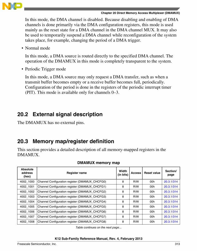
In this mode, the DMA channel is disabled. Because disabling and enabling of DMAchannels is done primarily via the DMA configuration registers, this mode is usedmainly as the reset state for a DMA channel in the DMA channel MUX. It may alsobe used to temporarily suspend a DMA channel while reconfiguration of the systemtakes place, for example, changing the period of a DMA trigger.
• Normal mode
In this mode, a DMA source is routed directly to the specified DMA channel. Theoperation of the DMAMUX in this mode is completely transparent to the system.
• Periodic Trigger mode
In this mode, a DMA source may only request a DMA transfer, such as when atransmit buffer becomes empty or a receive buffer becomes full, periodically.Configuration of the period is done in the registers of the periodic interrupt timer(PIT). This mode is available only for channels 0–3.
20.2 External signal descriptionThe DMAMUX has no external pins.
20.3 Memory map/register definitionThis section provides a detailed description of all memory-mapped registers in theDMAMUX.
DMAMUX memory map
Absoluteaddress
(hex)Register name
Width(in bits)
Access Reset valueSection/
page
4002_1000 Channel Configuration register (DMAMUX_CHCFG0) 8 R/W 00h 20.3.1/314
4002_1001 Channel Configuration register (DMAMUX_CHCFG1) 8 R/W 00h 20.3.1/314
4002_1002 Channel Configuration register (DMAMUX_CHCFG2) 8 R/W 00h 20.3.1/314
4002_1003 Channel Configuration register (DMAMUX_CHCFG3) 8 R/W 00h 20.3.1/314
4002_1004 Channel Configuration register (DMAMUX_CHCFG4) 8 R/W 00h 20.3.1/314
4002_1005 Channel Configuration register (DMAMUX_CHCFG5) 8 R/W 00h 20.3.1/314
4002_1006 Channel Configuration register (DMAMUX_CHCFG6) 8 R/W 00h 20.3.1/314
4002_1007 Channel Configuration register (DMAMUX_CHCFG7) 8 R/W 00h 20.3.1/314
4002_1008 Channel Configuration register (DMAMUX_CHCFG8) 8 R/W 00h 20.3.1/314
Table continues on the next page...
Chapter 20 Direct Memory Access Multiplexer (DMAMUX)
K12 Sub-Family Reference Manual, Rev. 4, February 2013
Freescale Semiconductor, Inc. 313
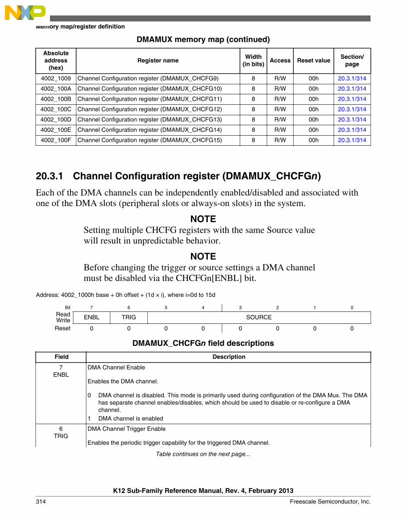
DMAMUX memory map (continued)
Absoluteaddress
(hex)Register name
Width(in bits)
Access Reset valueSection/
page
4002_1009 Channel Configuration register (DMAMUX_CHCFG9) 8 R/W 00h 20.3.1/314
4002_100A Channel Configuration register (DMAMUX_CHCFG10) 8 R/W 00h 20.3.1/314
4002_100B Channel Configuration register (DMAMUX_CHCFG11) 8 R/W 00h 20.3.1/314
4002_100C Channel Configuration register (DMAMUX_CHCFG12) 8 R/W 00h 20.3.1/314
4002_100D Channel Configuration register (DMAMUX_CHCFG13) 8 R/W 00h 20.3.1/314
4002_100E Channel Configuration register (DMAMUX_CHCFG14) 8 R/W 00h 20.3.1/314
4002_100F Channel Configuration register (DMAMUX_CHCFG15) 8 R/W 00h 20.3.1/314
20.3.1 Channel Configuration register (DMAMUX_CHCFGn)
Each of the DMA channels can be independently enabled/disabled and associated withone of the DMA slots (peripheral slots or always-on slots) in the system.
NOTESetting multiple CHCFG registers with the same Source valuewill result in unpredictable behavior.
NOTEBefore changing the trigger or source settings a DMA channelmust be disabled via the CHCFGn[ENBL] bit.
Address: 4002_1000h base + 0h offset + (1d × i), where i=0d to 15d
Bit 7 6 5 4 3 2 1 0
Read ENBL TRIG SOURCEWriteReset 0 0 0 0 0 0 0 0
DMAMUX_CHCFGn field descriptions
Field Description
7ENBL
DMA Channel Enable
Enables the DMA channel.
0 DMA channel is disabled. This mode is primarily used during configuration of the DMA Mux. The DMAhas separate channel enables/disables, which should be used to disable or re-configure a DMAchannel.
1 DMA channel is enabled
6TRIG
DMA Channel Trigger Enable
Enables the periodic trigger capability for the triggered DMA channel.
Table continues on the next page...
Memory map/register definition
K12 Sub-Family Reference Manual, Rev. 4, February 2013
314 Freescale Semiconductor, Inc.
DMAMUX_CHCFGn field descriptions (continued)
Field Description
0 Triggering is disabled. If triggering is disabled, and the ENBL bit is set, the DMA Channel will simplyroute the specified source to the DMA channel. (Normal mode)
1 Triggering is enabled. If triggering is enabled, and the ENBL bit is set, the DMAMUX is in PeriodicTrigger mode.
5–0SOURCE
DMA Channel Source (Slot)
Specifies which DMA source, if any, is routed to a particular DMA channel. See your device's chipconfiguration details for information about the peripherals and their slot numbers.
20.4 Functional descriptionThe primary purpose of the DMAMUX is to provide flexibility in the system's use of theavailable DMA channels. As such, configuration of the DMAMUX is intended to be astatic procedure done during execution of the system boot code. However, if theprocedure outlined in Enabling and configuring sources is followed, the configuration ofthe DMAMUX may be changed during the normal operation of the system.
Functionally, the DMAMUX channels may be divided into two classes:
• Channels which implement the normal routing functionality plus periodic triggeringcapability
• Channels which implement only the normal routing functionality
20.4.1 DMA channels with periodic triggering capability
Besides the normal routing functionality, the first 4 channels of the DMAMUX provide aspecial periodic triggering capability that can be used to provide an automatic mechanismto transmit bytes, frames, or packets at fixed intervals without the need for processorintervention. The trigger is generated by the periodic interrupt timer (PIT); as such, theconfiguration of the periodic triggering interval is done via configuration registers in thePIT. See the section on periodic interrupt timer for more information on this topic.
Note
Because of the dynamic nature of the system (due to DMAchannel priorities, bus arbitration, interrupt service routinelengths, etc.), the number of clock cycles between a trigger andthe actual DMA transfer cannot be guaranteed.
Chapter 20 Direct Memory Access Multiplexer (DMAMUX)
K12 Sub-Family Reference Manual, Rev. 4, February 2013
Freescale Semiconductor, Inc. 315
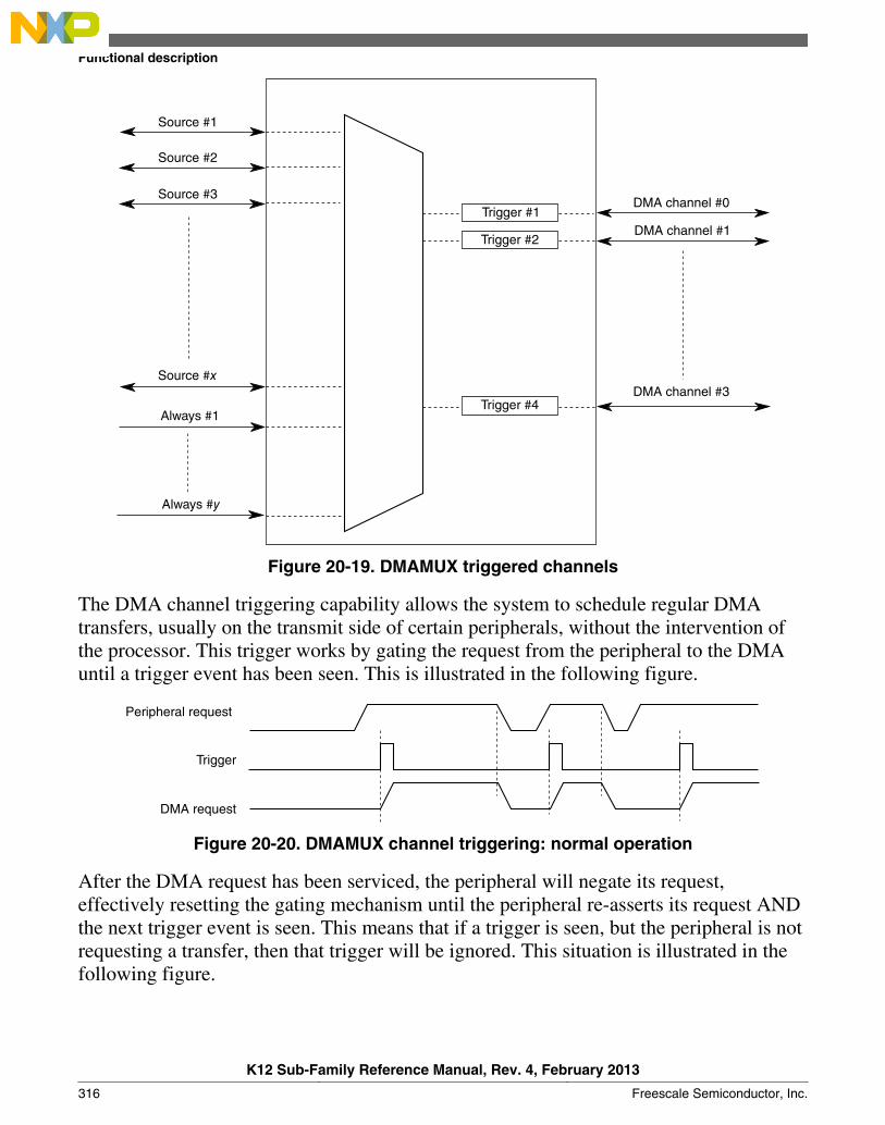
DMA channel #0
Trigger #2
Source #1
Source #2
Source #3
Always #1
DMA channel #3
Always #y
Trigger #4
Source #x
Trigger #1DMA channel #1
Figure 20-19. DMAMUX triggered channels
The DMA channel triggering capability allows the system to schedule regular DMAtransfers, usually on the transmit side of certain peripherals, without the intervention ofthe processor. This trigger works by gating the request from the peripheral to the DMAuntil a trigger event has been seen. This is illustrated in the following figure.
DMA request
Peripheral request
Trigger
Figure 20-20. DMAMUX channel triggering: normal operation
After the DMA request has been serviced, the peripheral will negate its request,effectively resetting the gating mechanism until the peripheral re-asserts its request ANDthe next trigger event is seen. This means that if a trigger is seen, but the peripheral is notrequesting a transfer, then that trigger will be ignored. This situation is illustrated in thefollowing figure.
Functional description
K12 Sub-Family Reference Manual, Rev. 4, February 2013
316 Freescale Semiconductor, Inc.
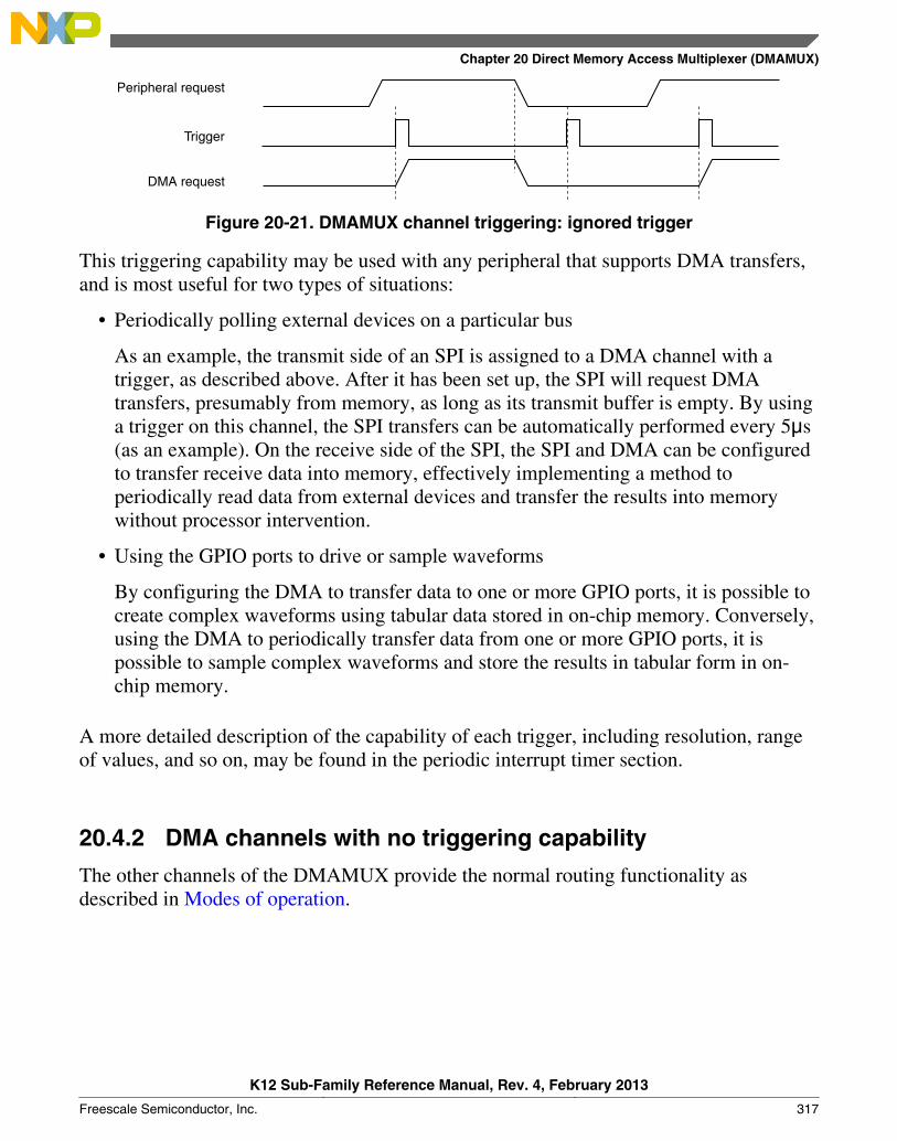
DMA request
Peripheral request
Trigger
Figure 20-21. DMAMUX channel triggering: ignored trigger
This triggering capability may be used with any peripheral that supports DMA transfers,and is most useful for two types of situations:
• Periodically polling external devices on a particular bus
As an example, the transmit side of an SPI is assigned to a DMA channel with atrigger, as described above. After it has been set up, the SPI will request DMAtransfers, presumably from memory, as long as its transmit buffer is empty. By usinga trigger on this channel, the SPI transfers can be automatically performed every 5μs(as an example). On the receive side of the SPI, the SPI and DMA can be configuredto transfer receive data into memory, effectively implementing a method toperiodically read data from external devices and transfer the results into memorywithout processor intervention.
• Using the GPIO ports to drive or sample waveforms
By configuring the DMA to transfer data to one or more GPIO ports, it is possible tocreate complex waveforms using tabular data stored in on-chip memory. Conversely,using the DMA to periodically transfer data from one or more GPIO ports, it ispossible to sample complex waveforms and store the results in tabular form in on-chip memory.
A more detailed description of the capability of each trigger, including resolution, rangeof values, and so on, may be found in the periodic interrupt timer section.
20.4.2 DMA channels with no triggering capability
The other channels of the DMAMUX provide the normal routing functionality asdescribed in Modes of operation.
Chapter 20 Direct Memory Access Multiplexer (DMAMUX)
K12 Sub-Family Reference Manual, Rev. 4, February 2013
Freescale Semiconductor, Inc. 317
20.4.3 Always-enabled DMA sources
In addition to the peripherals that can be used as DMA sources, there are 10 additionalDMA sources that are always enabled. Unlike the peripheral DMA sources, where theperipheral controls the flow of data during DMA transfers, the sources that are alwaysenabled provide no such "throttling" of the data transfers. These sources are most usefulin the following cases:
• Performing DMA transfers to/from GPIO—Moving data from/to one or more GPIOpins, either unthrottled (that is as fast as possible), or periodically (using the DMAtriggering capability).
• Performing DMA transfers from memory to memory—Moving data from memory tomemory, typically as fast as possible, sometimes with software activation.
• Performing DMA transfers from memory to the external bus, or vice-versa—Similarto memory to memory transfers, this is typically done as quickly as possible.
• Any DMA transfer that requires software activation—Any DMA transfer that shouldbe explicitly started by software.
In cases where software should initiate the start of a DMA transfer, an always-enabledDMA source can be used to provide maximum flexibility. When activating a DMAchannel via software, subsequent executions of the minor loop require that a new startevent be sent. This can either be a new software activation, or a transfer request from theDMA channel MUX. The options for doing this are:
• Transfer all data in a single minor loop.
By configuring the DMA to transfer all of the data in a single minor loop (that is,major loop counter = 1), no reactivation of the channel is necessary. Thedisadvantage to this option is the reduced granularity in determining the load that theDMA transfer will impose on the system. For this option, the DMA channel must bedisabled in the DMA channel MUX.
• Use explicit software reactivation.
In this option, the DMA is configured to transfer the data using both minor and majorloops, but the processor is required to reactivate the channel by writing to the DMAregisters after every minor loop. For this option, the DMA channel must be disabledin the DMA channel MUX.
• Use an always-enabled DMA source.
Functional description
K12 Sub-Family Reference Manual, Rev. 4, February 2013
318 Freescale Semiconductor, Inc.
In this option, the DMA is configured to transfer the data using both minor and majorloops, and the DMA channel MUX does the channel reactivation. For this option, theDMA channel should be enabled and pointing to an "always enabled" source. Notethat the reactivation of the channel can be continuous (DMA triggering is disabled)or can use the DMA triggering capability. In this manner, it is possible to executeperiodic transfers of packets of data from one source to another, without processorintervention.
20.5 Initialization/application informationThis section provides instructions for initializing the DMA channel MUX.
20.5.1 Reset
The reset state of each individual bit is shown in Memory map/register definition. Insummary, after reset, all channels are disabled and must be explicitly enabled before use.
20.5.2 Enabling and configuring sources
To enable a source with periodic triggering:
1. Determine with which DMA channel the source will be associated. Note that only thefirst 4 DMA channels have periodic triggering capability.
2. Clear the CHCFG[ENBL] and CHCFG[TRIG] fields of the DMA channel.3. Ensure that the DMA channel is properly configured in the DMA. The DMA channel
may be enabled at this point.4. Configure the corresponding timer.5. Select the source to be routed to the DMA channel. Write to the corresponding
CHCFG register, ensuring that the CHCFG[ENBL] and CHCFG[TRIG] fields areset.
NOTEThe following is an example. See the chip configuration detailsfor the number of this device's DMA channels that havetriggering capability.
To configure source #5 transmit for use with DMA channel 2, with periodic triggeringcapability:
1. Write 0x00 to CHCFG2 (base address + 0x02).
Chapter 20 Direct Memory Access Multiplexer (DMAMUX)
K12 Sub-Family Reference Manual, Rev. 4, February 2013
Freescale Semiconductor, Inc. 319

2. Configure channel 2 in the DMA, including enabling the channel.3. Configure a timer for the desired trigger interval.4. Write 0xC5 to CHCFG2 (base address + 0x02).
The following code example illustrates steps 1 and 4 above:
In File registers.h:#define DMAMUX_BASE_ADDR 0xFC084000/* Example only ! *//* Following example assumes char is 8-bits */volatile unsigned char *CHCONFIG0 = (volatile unsigned char *) (DMAMUX_BASE_ADDR+0x0000);volatile unsigned char *CHCONFIG1 = (volatile unsigned char *) (DMAMUX_BASE_ADDR+0x0001);volatile unsigned char *CHCONFIG2 = (volatile unsigned char *) (DMAMUX_BASE_ADDR+0x0002);volatile unsigned char *CHCONFIG3 = (volatile unsigned char *) (DMAMUX_BASE_ADDR+0x0003);volatile unsigned char *CHCONFIG4 = (volatile unsigned char *) (DMAMUX_BASE_ADDR+0x0004);volatile unsigned char *CHCONFIG5 = (volatile unsigned char *) (DMAMUX_BASE_ADDR+0x0005);volatile unsigned char *CHCONFIG6 = (volatile unsigned char *) (DMAMUX_BASE_ADDR+0x0006);volatile unsigned char *CHCONFIG7 = (volatile unsigned char *) (DMAMUX_BASE_ADDR+0x0007);volatile unsigned char *CHCONFIG8 = (volatile unsigned char *) (DMAMUX_BASE_ADDR+0x0008);volatile unsigned char *CHCONFIG9 = (volatile unsigned char *) (DMAMUX_BASE_ADDR+0x0009);volatile unsigned char *CHCONFIG10= (volatile unsigned char *) (DMAMUX_BASE_ADDR+0x000A);volatile unsigned char *CHCONFIG11= (volatile unsigned char *) (DMAMUX_BASE_ADDR+0x000B);volatile unsigned char *CHCONFIG12= (volatile unsigned char *) (DMAMUX_BASE_ADDR+0x000C);volatile unsigned char *CHCONFIG13= (volatile unsigned char *) (DMAMUX_BASE_ADDR+0x000D);volatile unsigned char *CHCONFIG14= (volatile unsigned char *) (DMAMUX_BASE_ADDR+0x000E);volatile unsigned char *CHCONFIG15= (volatile unsigned char *) (DMAMUX_BASE_ADDR+0x000F);
In File main.c:#include "registers.h"::*CHCONFIG2 = 0x00;*CHCONFIG2 = 0xC5;
To enable a source without periodic triggering:
1. Determine with which DMA channel the source will be associated. Note that only thefirst 4 DMA channels have periodic triggering capability.
2. Clear the CHCFG[ENBL] and CHCFG[TRIG] fields of the DMA channel.3. Ensure that the DMA channel is properly configured in the DMA. The DMA channel
may be enabled at this point.4. Select the source to be routed to the DMA channel. Write to the corresponding
CHCFG register, ensuring that CHCFG[ENBL] is set while CHCFG[TRIG] iscleared.
NOTEThe following is an example. See the chip configuration detailsfor the number of this device's DMA channels that havetriggering capability.
To configure source #5 transmit for use with DMA channel 2, with no periodic triggeringcapability:
1. Write 0x00 to CHCFG2 (base address + 0x02).2. Configure channel 2 in the DMA, including enabling the channel.3. Write 0x85 to CHCFG2 (base address + 0x02).
Initialization/application information
K12 Sub-Family Reference Manual, Rev. 4, February 2013
320 Freescale Semiconductor, Inc.

The following code example illustrates steps 1 and 3 above:
In File registers.h:#define DMAMUX_BASE_ADDR 0xFC084000/* Example only ! *//* Following example assumes char is 8-bits */volatile unsigned char *CHCONFIG0 = (volatile unsigned char *) (DMAMUX_BASE_ADDR+0x0000);volatile unsigned char *CHCONFIG1 = (volatile unsigned char *) (DMAMUX_BASE_ADDR+0x0001);volatile unsigned char *CHCONFIG2 = (volatile unsigned char *) (DMAMUX_BASE_ADDR+0x0002);volatile unsigned char *CHCONFIG3 = (volatile unsigned char *) (DMAMUX_BASE_ADDR+0x0003);volatile unsigned char *CHCONFIG4 = (volatile unsigned char *) (DMAMUX_BASE_ADDR+0x0004);volatile unsigned char *CHCONFIG5 = (volatile unsigned char *) (DMAMUX_BASE_ADDR+0x0005);volatile unsigned char *CHCONFIG6 = (volatile unsigned char *) (DMAMUX_BASE_ADDR+0x0006);volatile unsigned char *CHCONFIG7 = (volatile unsigned char *) (DMAMUX_BASE_ADDR+0x0007);volatile unsigned char *CHCONFIG8 = (volatile unsigned char *) (DMAMUX_BASE_ADDR+0x0008);volatile unsigned char *CHCONFIG9 = (volatile unsigned char *) (DMAMUX_BASE_ADDR+0x0009);volatile unsigned char *CHCONFIG10= (volatile unsigned char *) (DMAMUX_BASE_ADDR+0x000A);volatile unsigned char *CHCONFIG11= (volatile unsigned char *) (DMAMUX_BASE_ADDR+0x000B);volatile unsigned char *CHCONFIG12= (volatile unsigned char *) (DMAMUX_BASE_ADDR+0x000C);volatile unsigned char *CHCONFIG13= (volatile unsigned char *) (DMAMUX_BASE_ADDR+0x000D);volatile unsigned char *CHCONFIG14= (volatile unsigned char *) (DMAMUX_BASE_ADDR+0x000E);volatile unsigned char *CHCONFIG15= (volatile unsigned char *) (DMAMUX_BASE_ADDR+0x000F);
In File main.c:#include "registers.h"::*CHCONFIG2 = 0x00;*CHCONFIG2 = 0x85;
To disable a source:
A particular DMA source may be disabled by not writing the corresponding source valueinto any of the CHCFG registers. Additionally, some module-specific configuration maybe necessary. See the appropriate section for more details.
To switch the source of a DMA channel:
1. Disable the DMA channel in the DMA and re-configure the channel for the newsource.
2. Clear the CHCFG[ENBL] and CHCFG[TRIG] bits of the DMA channel.3. Select the source to be routed to the DMA channel. Write to the corresponding
CHCFG register, ensuring that the CHCFG[ENBL] and CHCFG[TRIG] fields areset.
To switch DMA channel 8 from source #5 transmit to source #7 transmit:1. In the DMA configuration registers, disable DMA channel 8 and reconfigure it to
handle the transfers to peripheral slot 7. This example assumes channel 8 doesn'thave triggering capability.
2. Write 0x00 to CHCFG8 (base address + 0x08).3. Write 0x87 to CHCFG8 (base address + 0x08). (In this example, setting
CHCFG[TRIG] would have no effect, due to the assumption that channel 8 does notsupport the periodic triggering functionality).
The following code example illustrates steps 2 and 3 above:
Chapter 20 Direct Memory Access Multiplexer (DMAMUX)
K12 Sub-Family Reference Manual, Rev. 4, February 2013
Freescale Semiconductor, Inc. 321
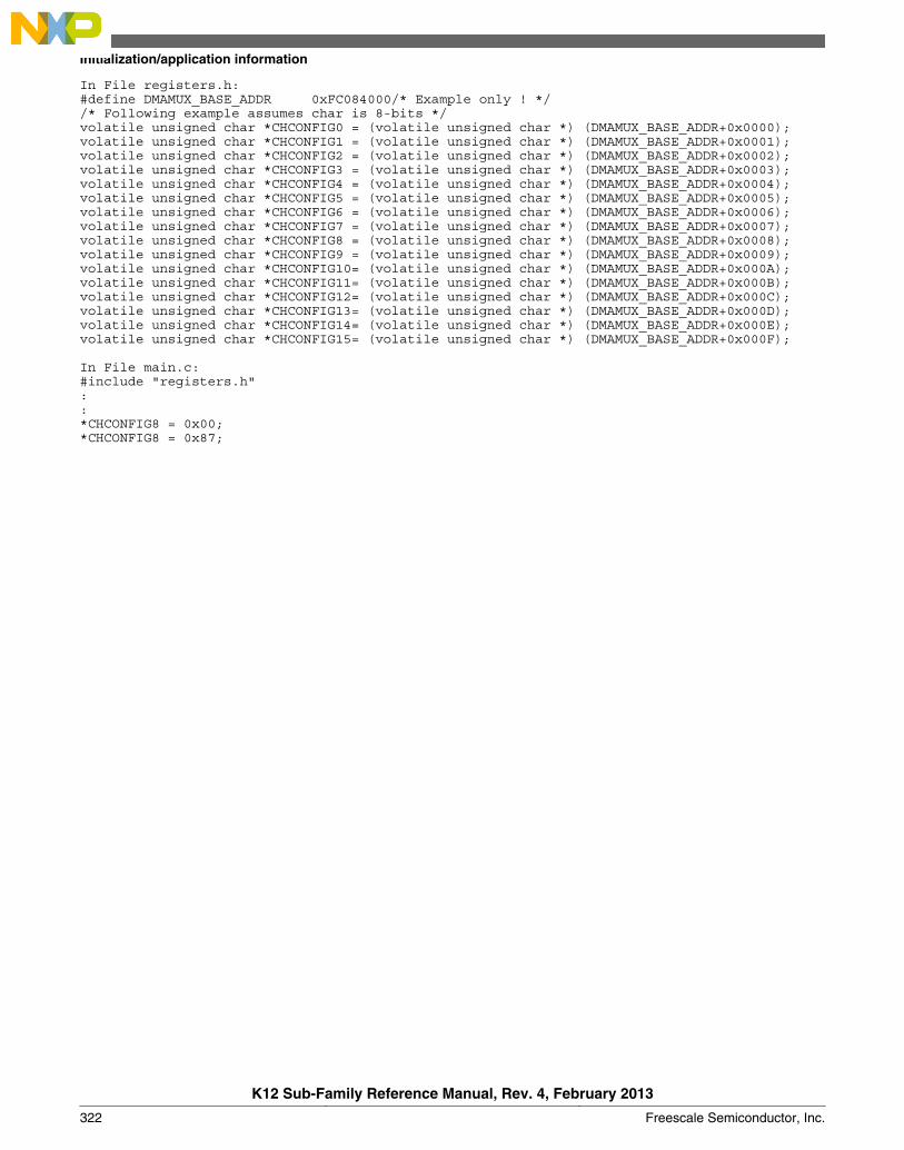
In File registers.h:#define DMAMUX_BASE_ADDR 0xFC084000/* Example only ! *//* Following example assumes char is 8-bits */volatile unsigned char *CHCONFIG0 = (volatile unsigned char *) (DMAMUX_BASE_ADDR+0x0000);volatile unsigned char *CHCONFIG1 = (volatile unsigned char *) (DMAMUX_BASE_ADDR+0x0001);volatile unsigned char *CHCONFIG2 = (volatile unsigned char *) (DMAMUX_BASE_ADDR+0x0002);volatile unsigned char *CHCONFIG3 = (volatile unsigned char *) (DMAMUX_BASE_ADDR+0x0003);volatile unsigned char *CHCONFIG4 = (volatile unsigned char *) (DMAMUX_BASE_ADDR+0x0004);volatile unsigned char *CHCONFIG5 = (volatile unsigned char *) (DMAMUX_BASE_ADDR+0x0005);volatile unsigned char *CHCONFIG6 = (volatile unsigned char *) (DMAMUX_BASE_ADDR+0x0006);volatile unsigned char *CHCONFIG7 = (volatile unsigned char *) (DMAMUX_BASE_ADDR+0x0007);volatile unsigned char *CHCONFIG8 = (volatile unsigned char *) (DMAMUX_BASE_ADDR+0x0008);volatile unsigned char *CHCONFIG9 = (volatile unsigned char *) (DMAMUX_BASE_ADDR+0x0009);volatile unsigned char *CHCONFIG10= (volatile unsigned char *) (DMAMUX_BASE_ADDR+0x000A);volatile unsigned char *CHCONFIG11= (volatile unsigned char *) (DMAMUX_BASE_ADDR+0x000B);volatile unsigned char *CHCONFIG12= (volatile unsigned char *) (DMAMUX_BASE_ADDR+0x000C);volatile unsigned char *CHCONFIG13= (volatile unsigned char *) (DMAMUX_BASE_ADDR+0x000D);volatile unsigned char *CHCONFIG14= (volatile unsigned char *) (DMAMUX_BASE_ADDR+0x000E);volatile unsigned char *CHCONFIG15= (volatile unsigned char *) (DMAMUX_BASE_ADDR+0x000F);
In File main.c:#include "registers.h"::*CHCONFIG8 = 0x00;*CHCONFIG8 = 0x87;
Initialization/application information
K12 Sub-Family Reference Manual, Rev. 4, February 2013
322 Freescale Semiconductor, Inc.

Chapter 21Direct Memory Access Controller (eDMA)
21.1 IntroductionNOTE
For the chip-specific implementation details of this module'sinstances see the chip configuration information.
The enhanced direct memory access (eDMA) controller is a second-generation modulecapable of performing complex data transfers with minimal intervention from a hostprocessor. The hardware microarchitecture includes:
• A DMA engine that performs:• Source- and destination-address calculations• Data-movement operations
• Local memory containing transfer control descriptors for each of the 16 channels
21.1.1 Block diagram
This diagram illustrates the eDMA module.
K12 Sub-Family Reference Manual, Rev. 4, February 2013
Freescale Semiconductor, Inc. 323

1
Transfer Control Descriptor (TCD)
eDMA Engine
Data Path
eDMA
0
Program Model/
64
Control
n-1
To/
Fro
m C
ross
bar
Sw
itch
2
Channel Arbitration
Address Path
Read Data
Write Data
Address
Read Data
Write Data
Write Address
Inte
rnal
Per
iphe
ral B
us
eDMA PeripheralRequest eDMA Done
Figure 21-1. eDMA block diagram
21.1.2 Block parts
The eDMA module is partitioned into two major modules: the eDMA engine and thetransfer-control descriptor local memory.
The eDMA engine is further partitioned into four submodules:
Introduction
K12 Sub-Family Reference Manual, Rev. 4, February 2013
324 Freescale Semiconductor, Inc.
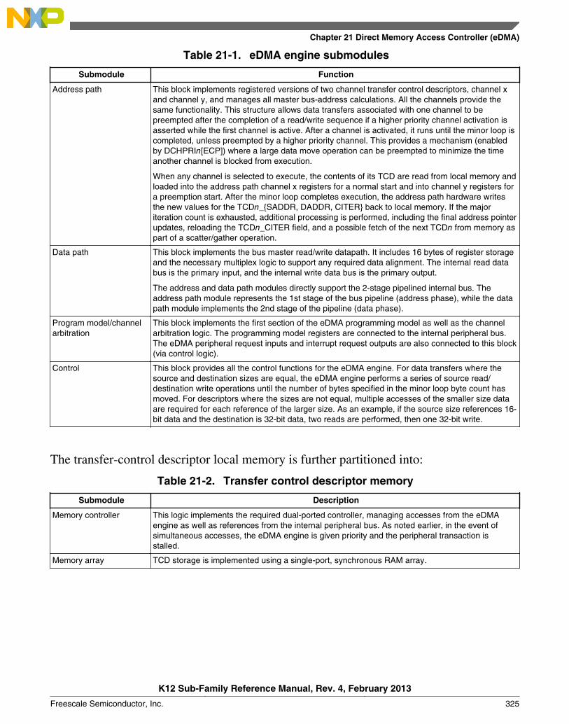
Table 21-1. eDMA engine submodules
Submodule Function
Address path This block implements registered versions of two channel transfer control descriptors, channel xand channel y, and manages all master bus-address calculations. All the channels provide thesame functionality. This structure allows data transfers associated with one channel to bepreempted after the completion of a read/write sequence if a higher priority channel activation isasserted while the first channel is active. After a channel is activated, it runs until the minor loop iscompleted, unless preempted by a higher priority channel. This provides a mechanism (enabledby DCHPRIn[ECP]) where a large data move operation can be preempted to minimize the timeanother channel is blocked from execution.
When any channel is selected to execute, the contents of its TCD are read from local memory andloaded into the address path channel x registers for a normal start and into channel y registers fora preemption start. After the minor loop completes execution, the address path hardware writesthe new values for the TCDn_{SADDR, DADDR, CITER} back to local memory. If the majoriteration count is exhausted, additional processing is performed, including the final address pointerupdates, reloading the TCDn_CITER field, and a possible fetch of the next TCDn from memory aspart of a scatter/gather operation.
Data path This block implements the bus master read/write datapath. It includes 16 bytes of register storageand the necessary multiplex logic to support any required data alignment. The internal read databus is the primary input, and the internal write data bus is the primary output.
The address and data path modules directly support the 2-stage pipelined internal bus. Theaddress path module represents the 1st stage of the bus pipeline (address phase), while the datapath module implements the 2nd stage of the pipeline (data phase).
Program model/channelarbitration
This block implements the first section of the eDMA programming model as well as the channelarbitration logic. The programming model registers are connected to the internal peripheral bus.The eDMA peripheral request inputs and interrupt request outputs are also connected to this block(via control logic).
Control This block provides all the control functions for the eDMA engine. For data transfers where thesource and destination sizes are equal, the eDMA engine performs a series of source read/destination write operations until the number of bytes specified in the minor loop byte count hasmoved. For descriptors where the sizes are not equal, multiple accesses of the smaller size dataare required for each reference of the larger size. As an example, if the source size references 16-bit data and the destination is 32-bit data, two reads are performed, then one 32-bit write.
The transfer-control descriptor local memory is further partitioned into:
Table 21-2. Transfer control descriptor memory
Submodule Description
Memory controller This logic implements the required dual-ported controller, managing accesses from the eDMAengine as well as references from the internal peripheral bus. As noted earlier, in the event ofsimultaneous accesses, the eDMA engine is given priority and the peripheral transaction isstalled.
Memory array TCD storage is implemented using a single-port, synchronous RAM array.
Chapter 21 Direct Memory Access Controller (eDMA)
K12 Sub-Family Reference Manual, Rev. 4, February 2013
Freescale Semiconductor, Inc. 325
21.1.3 Features
The eDMA is a highly programmable data-transfer engine optimized to minimize therequired intervention from the host processor. It is intended for use in applications wherethe data size to be transferred is statically known and not defined within the data packetitself. The eDMA module features:
• All data movement via dual-address transfers: read from source, write to destination
• Programmable source and destination addresses and transfer size
• Support for enhanced addressing modes• 16-channel implementation that performs complex data transfers with minimal
intervention from a host processor
• Internal data buffer, used as temporary storage to support 16- and 32-bytetransfers
• Connections to the crossbar switch for bus mastering the data movement
• Transfer control descriptor (TCD) organized to support two-deep, nested transferoperations
• 32-byte TCD stored in local memory for each channel
• An inner data transfer loop defined by a minor byte transfer count
• An outer data transfer loop defined by a major iteration count
• Channel activation via one of three methods:
• Explicit software initiation
• Initiation via a channel-to-channel linking mechanism for continuous transfers
• Peripheral-paced hardware requests, one per channel
• Fixed-priority and round-robin channel arbitration
• Channel completion reported via optional interrupt requests
• One interrupt per channel, optionally asserted at completion of major iterationcount
• Optional error terminations per channel and logically summed together to formone error interrupt to the interrupt controller
• Optional support for scatter/gather DMA processing
Introduction
K12 Sub-Family Reference Manual, Rev. 4, February 2013
326 Freescale Semiconductor, Inc.

• Support for complex data structures
• Support to cancel transfers via software
In the discussion of this module, n is used to reference the channel number.
21.2 Modes of operationThe eDMA operates in the following modes:
Table 21-3. Modes of operation
Mode Description
Normal In Normal mode, the eDMA transfers data between a source and a destination. The source anddestination can be a memory block or an I/O block capable of operation with the eDMA.
A service request initiates a transfer of a specific number of bytes (NBYTES) as specified in thetransfer control descriptor (TCD). The minor loop is the sequence of read-write operations thattransfers these NBYTES per service request. Each service request executes one iteration of themajor loop, which transfers NBYTES of data.
Debug DMA operation is configurable in Debug mode via the control register:
• If CR[EDBG] is cleared, the DMA continues to operate.• If CR[EDBG] is set, the eDMA stops transferring data. If Debug mode is entered while a
channel is active, the eDMA continues operation until the channel retires.
Wait Before entering Wait mode, the DMA attempts to complete its current transfer. After the transfercompletes, the device enters Wait mode.
21.3 Memory map/register definitionThe eDMA's programming model is partitioned into two regions:
• The first region defines a number of registers providing control functions
• The second region corresponds to the local transfer control descriptor (TCD)memory
Each channel requires a 32-byte transfer control descriptor for defining the desireddata movement operation. The channel descriptors are stored in the local memory insequential order: channel 0, channel 1,... channel 15 . Each TCDn definition ispresented as 11 registers of 16 or 32 bits.
TCD Initialization: Prior to activating a channel, you must initialize its TCD with theappropriate transfer profile.
Chapter 21 Direct Memory Access Controller (eDMA)
K12 Sub-Family Reference Manual, Rev. 4, February 2013
Freescale Semiconductor, Inc. 327

Here is the TCD structure:
31 02627282930 25 2021222324 19 1415161718 13 89101112 7 6 12345
DMA Basics: TCD Structure• One DMA engine has a number of channels to react to DMA requests• Each channel has its own TCD
SM
LOE
1
DM
LOE
1
0x8
0x0008
0x0004
0x0000
MLOFF or NBYTES1 NBYTES1
NBYTES1
SMOD SSIZE DMOD DSIZE SOFF
WordOffset 31 02627282930 25 2021222324 19 1415161718 13 89101112 7 6 12345
0x0010
0x000C SLAST
DADDR
CITER orCITER.LINKCH
CIT
ER
.E_L
INK
0x0014 CITER DOFF
0x0018
1 The fields implemented in Word 2 depend on whether EDMA_CR(EMLM) is set to 0 or 1. See Table 15-2.
DLAST_SGA
0x001C BITER orBITER.LINKCH
BIT
ER
.E_L
INK
BITER BWC MAJOR LINKCH
DO
NE
AC
TIV
E
MA
JOR
.E_L
INK
E_S
G
D_R
EQ
INT
_MA
J
ST
AR
T
INT
_HA
LF
SADDR
Reserved memory and bit fields:• Reading reserved bits in a register returns the value of zero.• Writes to reserved bits in a register are ignored.• Reading or writing a reserved memory location generates a bus error.
DMA memory map
Absoluteaddress
(hex)Register name
Width(in bits)
Access Reset valueSection/
page
4000_8000 Control Register (DMA_CR) 32 R/W 0000_0000h 21.3.1/339
4000_8004 Error Status Register (DMA_ES) 32 R 0000_0000h 21.3.2/341
4000_800C Enable Request Register (DMA_ERQ) 32 R/W 0000_0000h 21.3.3/343
4000_8014 Enable Error Interrupt Register (DMA_EEI) 32 R/W 0000_0000h 21.3.4/345
4000_8018 Clear Enable Error Interrupt Register (DMA_CEEI) 8W
(alwaysreads 0)
00h 21.3.5/347
Table continues on the next page...
Memory map/register definition
K12 Sub-Family Reference Manual, Rev. 4, February 2013
328 Freescale Semiconductor, Inc.

DMA memory map (continued)
Absoluteaddress
(hex)Register name
Width(in bits)
Access Reset valueSection/
page
4000_8019 Set Enable Error Interrupt Register (DMA_SEEI) 8W
(alwaysreads 0)
00h 21.3.6/348
4000_801A Clear Enable Request Register (DMA_CERQ) 8W
(alwaysreads 0)
00h 21.3.7/349
4000_801B Set Enable Request Register (DMA_SERQ) 8W
(alwaysreads 0)
00h 21.3.8/350
4000_801C Clear DONE Status Bit Register (DMA_CDNE) 8W
(alwaysreads 0)
00h 21.3.9/351
4000_801D Set START Bit Register (DMA_SSRT) 8W
(alwaysreads 0)
00h 21.3.10/352
4000_801E Clear Error Register (DMA_CERR) 8W
(alwaysreads 0)
00h 21.3.11/353
4000_801F Clear Interrupt Request Register (DMA_CINT) 8W
(alwaysreads 0)
00h 21.3.12/354
4000_8024 Interrupt Request Register (DMA_INT) 32 R/W 0000_0000h 21.3.13/355
4000_802C Error Register (DMA_ERR) 32 R/W 0000_0000h 21.3.14/357
4000_8034 Hardware Request Status Register (DMA_HRS) 32 R/W 0000_0000h 21.3.15/360
4000_8100 Channel n Priority Register (DMA_DCHPRI3) 8 R/W See section 21.3.16/362
4000_8101 Channel n Priority Register (DMA_DCHPRI2) 8 R/W See section 21.3.16/362
4000_8102 Channel n Priority Register (DMA_DCHPRI1) 8 R/W See section 21.3.16/362
4000_8103 Channel n Priority Register (DMA_DCHPRI0) 8 R/W See section 21.3.16/362
4000_8104 Channel n Priority Register (DMA_DCHPRI7) 8 R/W See section 21.3.16/362
4000_8105 Channel n Priority Register (DMA_DCHPRI6) 8 R/W See section 21.3.16/362
4000_8106 Channel n Priority Register (DMA_DCHPRI5) 8 R/W See section 21.3.16/362
4000_8107 Channel n Priority Register (DMA_DCHPRI4) 8 R/W See section 21.3.16/362
4000_8108 Channel n Priority Register (DMA_DCHPRI11) 8 R/W See section 21.3.16/362
4000_8109 Channel n Priority Register (DMA_DCHPRI10) 8 R/W See section 21.3.16/362
4000_810A Channel n Priority Register (DMA_DCHPRI9) 8 R/W See section 21.3.16/362
4000_810B Channel n Priority Register (DMA_DCHPRI8) 8 R/W See section 21.3.16/362
4000_810C Channel n Priority Register (DMA_DCHPRI15) 8 R/W See section 21.3.16/362
4000_810D Channel n Priority Register (DMA_DCHPRI14) 8 R/W See section 21.3.16/362
4000_810E Channel n Priority Register (DMA_DCHPRI13) 8 R/W See section 21.3.16/362
4000_810F Channel n Priority Register (DMA_DCHPRI12) 8 R/W See section 21.3.16/362
4000_9000 TCD Source Address (DMA_TCD0_SADDR) 32 R/W Undefined 21.3.17/363
4000_9004 TCD Signed Source Address Offset (DMA_TCD0_SOFF) 16 R/W Undefined 21.3.18/363
Table continues on the next page...
Chapter 21 Direct Memory Access Controller (eDMA)
K12 Sub-Family Reference Manual, Rev. 4, February 2013
Freescale Semiconductor, Inc. 329

DMA memory map (continued)
Absoluteaddress
(hex)Register name
Width(in bits)
Access Reset valueSection/
page
4000_9006 TCD Transfer Attributes (DMA_TCD0_ATTR) 16 R/W Undefined 21.3.19/364
4000_9008TCD Minor Byte Count (Minor Loop Disabled)(DMA_TCD0_NBYTES_MLNO)
32 R/W Undefined 21.3.20/365
4000_9008TCD Signed Minor Loop Offset (Minor Loop Enabled andOffset Disabled) (DMA_TCD0_NBYTES_MLOFFNO)
32 R/W Undefined 21.3.21/365
4000_9008TCD Signed Minor Loop Offset (Minor Loop and OffsetEnabled) (DMA_TCD0_NBYTES_MLOFFYES)
32 R/W Undefined 21.3.22/367
4000_900CTCD Last Source Address Adjustment(DMA_TCD0_SLAST)
32 R/W Undefined 21.3.23/368
4000_9010 TCD Destination Address (DMA_TCD0_DADDR) 32 R/W Undefined 21.3.24/368
4000_9014TCD Signed Destination Address Offset(DMA_TCD0_DOFF)
16 R/W Undefined 21.3.25/369
4000_9016TCD Current Minor Loop Link, Major Loop Count (ChannelLinking Enabled) (DMA_TCD0_CITER_ELINKYES)
16 R/W Undefined 21.3.26/369
4000_9016 DMA_TCD0_CITER_ELINKNO 16 R/W Undefined 21.3.27/371
4000_9018TCD Last Destination Address Adjustment/Scatter GatherAddress (DMA_TCD0_DLASTSGA)
32 R/W Undefined 21.3.28/372
4000_901C TCD Control and Status (DMA_TCD0_CSR) 16 R/W Undefined 21.3.29/372
4000_901ETCD Beginning Minor Loop Link, Major Loop Count(Channel Linking Enabled)(DMA_TCD0_BITER_ELINKYES)
16 R/W Undefined 21.3.30/375
4000_901ETCD Beginning Minor Loop Link, Major Loop Count(Channel Linking Disabled) (DMA_TCD0_BITER_ELINKNO)
16 R/W Undefined 21.3.31/376
4000_9020 TCD Source Address (DMA_TCD1_SADDR) 32 R/W Undefined 21.3.17/363
4000_9024 TCD Signed Source Address Offset (DMA_TCD1_SOFF) 16 R/W Undefined 21.3.18/363
4000_9026 TCD Transfer Attributes (DMA_TCD1_ATTR) 16 R/W Undefined 21.3.19/364
4000_9028TCD Minor Byte Count (Minor Loop Disabled)(DMA_TCD1_NBYTES_MLNO)
32 R/W Undefined 21.3.20/365
4000_9028TCD Signed Minor Loop Offset (Minor Loop Enabled andOffset Disabled) (DMA_TCD1_NBYTES_MLOFFNO)
32 R/W Undefined 21.3.21/365
4000_9028TCD Signed Minor Loop Offset (Minor Loop and OffsetEnabled) (DMA_TCD1_NBYTES_MLOFFYES)
32 R/W Undefined 21.3.22/367
4000_902CTCD Last Source Address Adjustment(DMA_TCD1_SLAST)
32 R/W Undefined 21.3.23/368
4000_9030 TCD Destination Address (DMA_TCD1_DADDR) 32 R/W Undefined 21.3.24/368
4000_9034TCD Signed Destination Address Offset(DMA_TCD1_DOFF)
16 R/W Undefined 21.3.25/369
4000_9036TCD Current Minor Loop Link, Major Loop Count (ChannelLinking Enabled) (DMA_TCD1_CITER_ELINKYES)
16 R/W Undefined 21.3.26/369
4000_9036 DMA_TCD1_CITER_ELINKNO 16 R/W Undefined 21.3.27/371
4000_9038TCD Last Destination Address Adjustment/Scatter GatherAddress (DMA_TCD1_DLASTSGA)
32 R/W Undefined 21.3.28/372
4000_903C TCD Control and Status (DMA_TCD1_CSR) 16 R/W Undefined 21.3.29/372
Table continues on the next page...
Memory map/register definition
K12 Sub-Family Reference Manual, Rev. 4, February 2013
330 Freescale Semiconductor, Inc.
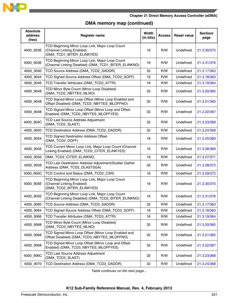
DMA memory map (continued)
Absoluteaddress
(hex)Register name
Width(in bits)
Access Reset valueSection/
page
4000_903ETCD Beginning Minor Loop Link, Major Loop Count(Channel Linking Enabled)(DMA_TCD1_BITER_ELINKYES)
16 R/W Undefined 21.3.30/375
4000_903ETCD Beginning Minor Loop Link, Major Loop Count(Channel Linking Disabled) (DMA_TCD1_BITER_ELINKNO)
16 R/W Undefined 21.3.31/376
4000_9040 TCD Source Address (DMA_TCD2_SADDR) 32 R/W Undefined 21.3.17/363
4000_9044 TCD Signed Source Address Offset (DMA_TCD2_SOFF) 16 R/W Undefined 21.3.18/363
4000_9046 TCD Transfer Attributes (DMA_TCD2_ATTR) 16 R/W Undefined 21.3.19/364
4000_9048TCD Minor Byte Count (Minor Loop Disabled)(DMA_TCD2_NBYTES_MLNO)
32 R/W Undefined 21.3.20/365
4000_9048TCD Signed Minor Loop Offset (Minor Loop Enabled andOffset Disabled) (DMA_TCD2_NBYTES_MLOFFNO)
32 R/W Undefined 21.3.21/365
4000_9048TCD Signed Minor Loop Offset (Minor Loop and OffsetEnabled) (DMA_TCD2_NBYTES_MLOFFYES)
32 R/W Undefined 21.3.22/367
4000_904CTCD Last Source Address Adjustment(DMA_TCD2_SLAST)
32 R/W Undefined 21.3.23/368
4000_9050 TCD Destination Address (DMA_TCD2_DADDR) 32 R/W Undefined 21.3.24/368
4000_9054TCD Signed Destination Address Offset(DMA_TCD2_DOFF)
16 R/W Undefined 21.3.25/369
4000_9056TCD Current Minor Loop Link, Major Loop Count (ChannelLinking Enabled) (DMA_TCD2_CITER_ELINKYES)
16 R/W Undefined 21.3.26/369
4000_9056 DMA_TCD2_CITER_ELINKNO 16 R/W Undefined 21.3.27/371
4000_9058TCD Last Destination Address Adjustment/Scatter GatherAddress (DMA_TCD2_DLASTSGA)
32 R/W Undefined 21.3.28/372
4000_905C TCD Control and Status (DMA_TCD2_CSR) 16 R/W Undefined 21.3.29/372
4000_905ETCD Beginning Minor Loop Link, Major Loop Count(Channel Linking Enabled)(DMA_TCD2_BITER_ELINKYES)
16 R/W Undefined 21.3.30/375
4000_905ETCD Beginning Minor Loop Link, Major Loop Count(Channel Linking Disabled) (DMA_TCD2_BITER_ELINKNO)
16 R/W Undefined 21.3.31/376
4000_9060 TCD Source Address (DMA_TCD3_SADDR) 32 R/W Undefined 21.3.17/363
4000_9064 TCD Signed Source Address Offset (DMA_TCD3_SOFF) 16 R/W Undefined 21.3.18/363
4000_9066 TCD Transfer Attributes (DMA_TCD3_ATTR) 16 R/W Undefined 21.3.19/364
4000_9068TCD Minor Byte Count (Minor Loop Disabled)(DMA_TCD3_NBYTES_MLNO)
32 R/W Undefined 21.3.20/365
4000_9068TCD Signed Minor Loop Offset (Minor Loop Enabled andOffset Disabled) (DMA_TCD3_NBYTES_MLOFFNO)
32 R/W Undefined 21.3.21/365
4000_9068TCD Signed Minor Loop Offset (Minor Loop and OffsetEnabled) (DMA_TCD3_NBYTES_MLOFFYES)
32 R/W Undefined 21.3.22/367
4000_906CTCD Last Source Address Adjustment(DMA_TCD3_SLAST)
32 R/W Undefined 21.3.23/368
4000_9070 TCD Destination Address (DMA_TCD3_DADDR) 32 R/W Undefined 21.3.24/368
Table continues on the next page...
Chapter 21 Direct Memory Access Controller (eDMA)
K12 Sub-Family Reference Manual, Rev. 4, February 2013
Freescale Semiconductor, Inc. 331
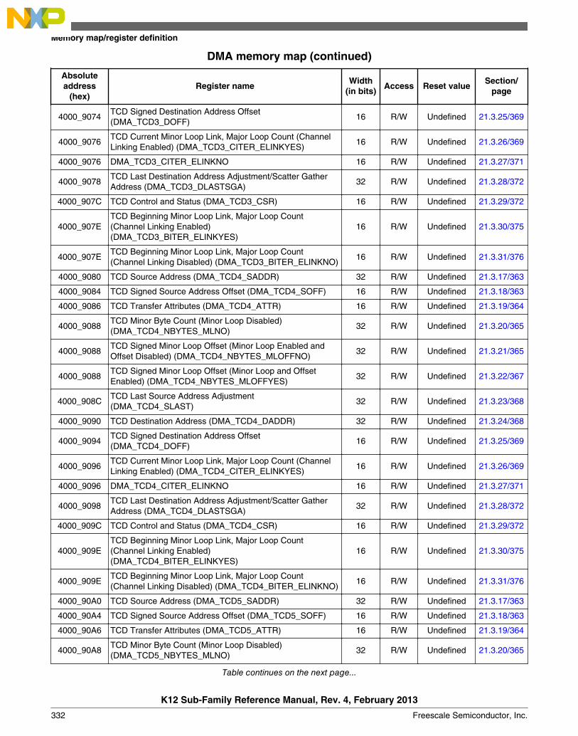
DMA memory map (continued)
Absoluteaddress
(hex)Register name
Width(in bits)
Access Reset valueSection/
page
4000_9074TCD Signed Destination Address Offset(DMA_TCD3_DOFF)
16 R/W Undefined 21.3.25/369
4000_9076TCD Current Minor Loop Link, Major Loop Count (ChannelLinking Enabled) (DMA_TCD3_CITER_ELINKYES)
16 R/W Undefined 21.3.26/369
4000_9076 DMA_TCD3_CITER_ELINKNO 16 R/W Undefined 21.3.27/371
4000_9078TCD Last Destination Address Adjustment/Scatter GatherAddress (DMA_TCD3_DLASTSGA)
32 R/W Undefined 21.3.28/372
4000_907C TCD Control and Status (DMA_TCD3_CSR) 16 R/W Undefined 21.3.29/372
4000_907ETCD Beginning Minor Loop Link, Major Loop Count(Channel Linking Enabled)(DMA_TCD3_BITER_ELINKYES)
16 R/W Undefined 21.3.30/375
4000_907ETCD Beginning Minor Loop Link, Major Loop Count(Channel Linking Disabled) (DMA_TCD3_BITER_ELINKNO)
16 R/W Undefined 21.3.31/376
4000_9080 TCD Source Address (DMA_TCD4_SADDR) 32 R/W Undefined 21.3.17/363
4000_9084 TCD Signed Source Address Offset (DMA_TCD4_SOFF) 16 R/W Undefined 21.3.18/363
4000_9086 TCD Transfer Attributes (DMA_TCD4_ATTR) 16 R/W Undefined 21.3.19/364
4000_9088TCD Minor Byte Count (Minor Loop Disabled)(DMA_TCD4_NBYTES_MLNO)
32 R/W Undefined 21.3.20/365
4000_9088TCD Signed Minor Loop Offset (Minor Loop Enabled andOffset Disabled) (DMA_TCD4_NBYTES_MLOFFNO)
32 R/W Undefined 21.3.21/365
4000_9088TCD Signed Minor Loop Offset (Minor Loop and OffsetEnabled) (DMA_TCD4_NBYTES_MLOFFYES)
32 R/W Undefined 21.3.22/367
4000_908CTCD Last Source Address Adjustment(DMA_TCD4_SLAST)
32 R/W Undefined 21.3.23/368
4000_9090 TCD Destination Address (DMA_TCD4_DADDR) 32 R/W Undefined 21.3.24/368
4000_9094TCD Signed Destination Address Offset(DMA_TCD4_DOFF)
16 R/W Undefined 21.3.25/369
4000_9096TCD Current Minor Loop Link, Major Loop Count (ChannelLinking Enabled) (DMA_TCD4_CITER_ELINKYES)
16 R/W Undefined 21.3.26/369
4000_9096 DMA_TCD4_CITER_ELINKNO 16 R/W Undefined 21.3.27/371
4000_9098TCD Last Destination Address Adjustment/Scatter GatherAddress (DMA_TCD4_DLASTSGA)
32 R/W Undefined 21.3.28/372
4000_909C TCD Control and Status (DMA_TCD4_CSR) 16 R/W Undefined 21.3.29/372
4000_909ETCD Beginning Minor Loop Link, Major Loop Count(Channel Linking Enabled)(DMA_TCD4_BITER_ELINKYES)
16 R/W Undefined 21.3.30/375
4000_909ETCD Beginning Minor Loop Link, Major Loop Count(Channel Linking Disabled) (DMA_TCD4_BITER_ELINKNO)
16 R/W Undefined 21.3.31/376
4000_90A0 TCD Source Address (DMA_TCD5_SADDR) 32 R/W Undefined 21.3.17/363
4000_90A4 TCD Signed Source Address Offset (DMA_TCD5_SOFF) 16 R/W Undefined 21.3.18/363
4000_90A6 TCD Transfer Attributes (DMA_TCD5_ATTR) 16 R/W Undefined 21.3.19/364
4000_90A8TCD Minor Byte Count (Minor Loop Disabled)(DMA_TCD5_NBYTES_MLNO)
32 R/W Undefined 21.3.20/365
Table continues on the next page...
Memory map/register definition
K12 Sub-Family Reference Manual, Rev. 4, February 2013
332 Freescale Semiconductor, Inc.
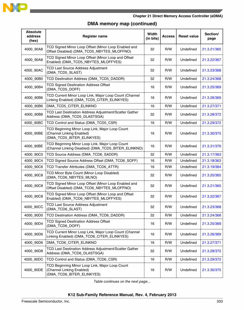
DMA memory map (continued)
Absoluteaddress
(hex)Register name
Width(in bits)
Access Reset valueSection/
page
4000_90A8TCD Signed Minor Loop Offset (Minor Loop Enabled andOffset Disabled) (DMA_TCD5_NBYTES_MLOFFNO)
32 R/W Undefined 21.3.21/365
4000_90A8TCD Signed Minor Loop Offset (Minor Loop and OffsetEnabled) (DMA_TCD5_NBYTES_MLOFFYES)
32 R/W Undefined 21.3.22/367
4000_90ACTCD Last Source Address Adjustment(DMA_TCD5_SLAST)
32 R/W Undefined 21.3.23/368
4000_90B0 TCD Destination Address (DMA_TCD5_DADDR) 32 R/W Undefined 21.3.24/368
4000_90B4TCD Signed Destination Address Offset(DMA_TCD5_DOFF)
16 R/W Undefined 21.3.25/369
4000_90B6TCD Current Minor Loop Link, Major Loop Count (ChannelLinking Enabled) (DMA_TCD5_CITER_ELINKYES)
16 R/W Undefined 21.3.26/369
4000_90B6 DMA_TCD5_CITER_ELINKNO 16 R/W Undefined 21.3.27/371
4000_90B8TCD Last Destination Address Adjustment/Scatter GatherAddress (DMA_TCD5_DLASTSGA)
32 R/W Undefined 21.3.28/372
4000_90BC TCD Control and Status (DMA_TCD5_CSR) 16 R/W Undefined 21.3.29/372
4000_90BETCD Beginning Minor Loop Link, Major Loop Count(Channel Linking Enabled)(DMA_TCD5_BITER_ELINKYES)
16 R/W Undefined 21.3.30/375
4000_90BETCD Beginning Minor Loop Link, Major Loop Count(Channel Linking Disabled) (DMA_TCD5_BITER_ELINKNO)
16 R/W Undefined 21.3.31/376
4000_90C0 TCD Source Address (DMA_TCD6_SADDR) 32 R/W Undefined 21.3.17/363
4000_90C4 TCD Signed Source Address Offset (DMA_TCD6_SOFF) 16 R/W Undefined 21.3.18/363
4000_90C6 TCD Transfer Attributes (DMA_TCD6_ATTR) 16 R/W Undefined 21.3.19/364
4000_90C8TCD Minor Byte Count (Minor Loop Disabled)(DMA_TCD6_NBYTES_MLNO)
32 R/W Undefined 21.3.20/365
4000_90C8TCD Signed Minor Loop Offset (Minor Loop Enabled andOffset Disabled) (DMA_TCD6_NBYTES_MLOFFNO)
32 R/W Undefined 21.3.21/365
4000_90C8TCD Signed Minor Loop Offset (Minor Loop and OffsetEnabled) (DMA_TCD6_NBYTES_MLOFFYES)
32 R/W Undefined 21.3.22/367
4000_90CCTCD Last Source Address Adjustment(DMA_TCD6_SLAST)
32 R/W Undefined 21.3.23/368
4000_90D0 TCD Destination Address (DMA_TCD6_DADDR) 32 R/W Undefined 21.3.24/368
4000_90D4TCD Signed Destination Address Offset(DMA_TCD6_DOFF)
16 R/W Undefined 21.3.25/369
4000_90D6TCD Current Minor Loop Link, Major Loop Count (ChannelLinking Enabled) (DMA_TCD6_CITER_ELINKYES)
16 R/W Undefined 21.3.26/369
4000_90D6 DMA_TCD6_CITER_ELINKNO 16 R/W Undefined 21.3.27/371
4000_90D8TCD Last Destination Address Adjustment/Scatter GatherAddress (DMA_TCD6_DLASTSGA)
32 R/W Undefined 21.3.28/372
4000_90DC TCD Control and Status (DMA_TCD6_CSR) 16 R/W Undefined 21.3.29/372
4000_90DETCD Beginning Minor Loop Link, Major Loop Count(Channel Linking Enabled)(DMA_TCD6_BITER_ELINKYES)
16 R/W Undefined 21.3.30/375
Table continues on the next page...
Chapter 21 Direct Memory Access Controller (eDMA)
K12 Sub-Family Reference Manual, Rev. 4, February 2013
Freescale Semiconductor, Inc. 333
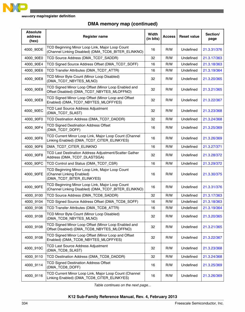
DMA memory map (continued)
Absoluteaddress
(hex)Register name
Width(in bits)
Access Reset valueSection/
page
4000_90DETCD Beginning Minor Loop Link, Major Loop Count(Channel Linking Disabled) (DMA_TCD6_BITER_ELINKNO)
16 R/W Undefined 21.3.31/376
4000_90E0 TCD Source Address (DMA_TCD7_SADDR) 32 R/W Undefined 21.3.17/363
4000_90E4 TCD Signed Source Address Offset (DMA_TCD7_SOFF) 16 R/W Undefined 21.3.18/363
4000_90E6 TCD Transfer Attributes (DMA_TCD7_ATTR) 16 R/W Undefined 21.3.19/364
4000_90E8TCD Minor Byte Count (Minor Loop Disabled)(DMA_TCD7_NBYTES_MLNO)
32 R/W Undefined 21.3.20/365
4000_90E8TCD Signed Minor Loop Offset (Minor Loop Enabled andOffset Disabled) (DMA_TCD7_NBYTES_MLOFFNO)
32 R/W Undefined 21.3.21/365
4000_90E8TCD Signed Minor Loop Offset (Minor Loop and OffsetEnabled) (DMA_TCD7_NBYTES_MLOFFYES)
32 R/W Undefined 21.3.22/367
4000_90ECTCD Last Source Address Adjustment(DMA_TCD7_SLAST)
32 R/W Undefined 21.3.23/368
4000_90F0 TCD Destination Address (DMA_TCD7_DADDR) 32 R/W Undefined 21.3.24/368
4000_90F4TCD Signed Destination Address Offset(DMA_TCD7_DOFF)
16 R/W Undefined 21.3.25/369
4000_90F6TCD Current Minor Loop Link, Major Loop Count (ChannelLinking Enabled) (DMA_TCD7_CITER_ELINKYES)
16 R/W Undefined 21.3.26/369
4000_90F6 DMA_TCD7_CITER_ELINKNO 16 R/W Undefined 21.3.27/371
4000_90F8TCD Last Destination Address Adjustment/Scatter GatherAddress (DMA_TCD7_DLASTSGA)
32 R/W Undefined 21.3.28/372
4000_90FC TCD Control and Status (DMA_TCD7_CSR) 16 R/W Undefined 21.3.29/372
4000_90FETCD Beginning Minor Loop Link, Major Loop Count(Channel Linking Enabled)(DMA_TCD7_BITER_ELINKYES)
16 R/W Undefined 21.3.30/375
4000_90FETCD Beginning Minor Loop Link, Major Loop Count(Channel Linking Disabled) (DMA_TCD7_BITER_ELINKNO)
16 R/W Undefined 21.3.31/376
4000_9100 TCD Source Address (DMA_TCD8_SADDR) 32 R/W Undefined 21.3.17/363
4000_9104 TCD Signed Source Address Offset (DMA_TCD8_SOFF) 16 R/W Undefined 21.3.18/363
4000_9106 TCD Transfer Attributes (DMA_TCD8_ATTR) 16 R/W Undefined 21.3.19/364
4000_9108TCD Minor Byte Count (Minor Loop Disabled)(DMA_TCD8_NBYTES_MLNO)
32 R/W Undefined 21.3.20/365
4000_9108TCD Signed Minor Loop Offset (Minor Loop Enabled andOffset Disabled) (DMA_TCD8_NBYTES_MLOFFNO)
32 R/W Undefined 21.3.21/365
4000_9108TCD Signed Minor Loop Offset (Minor Loop and OffsetEnabled) (DMA_TCD8_NBYTES_MLOFFYES)
32 R/W Undefined 21.3.22/367
4000_910CTCD Last Source Address Adjustment(DMA_TCD8_SLAST)
32 R/W Undefined 21.3.23/368
4000_9110 TCD Destination Address (DMA_TCD8_DADDR) 32 R/W Undefined 21.3.24/368
4000_9114TCD Signed Destination Address Offset(DMA_TCD8_DOFF)
16 R/W Undefined 21.3.25/369
4000_9116TCD Current Minor Loop Link, Major Loop Count (ChannelLinking Enabled) (DMA_TCD8_CITER_ELINKYES)
16 R/W Undefined 21.3.26/369
Table continues on the next page...
Memory map/register definition
K12 Sub-Family Reference Manual, Rev. 4, February 2013
334 Freescale Semiconductor, Inc.

DMA memory map (continued)
Absoluteaddress
(hex)Register name
Width(in bits)
Access Reset valueSection/
page
4000_9116 DMA_TCD8_CITER_ELINKNO 16 R/W Undefined 21.3.27/371
4000_9118TCD Last Destination Address Adjustment/Scatter GatherAddress (DMA_TCD8_DLASTSGA)
32 R/W Undefined 21.3.28/372
4000_911C TCD Control and Status (DMA_TCD8_CSR) 16 R/W Undefined 21.3.29/372
4000_911ETCD Beginning Minor Loop Link, Major Loop Count(Channel Linking Enabled)(DMA_TCD8_BITER_ELINKYES)
16 R/W Undefined 21.3.30/375
4000_911ETCD Beginning Minor Loop Link, Major Loop Count(Channel Linking Disabled) (DMA_TCD8_BITER_ELINKNO)
16 R/W Undefined 21.3.31/376
4000_9120 TCD Source Address (DMA_TCD9_SADDR) 32 R/W Undefined 21.3.17/363
4000_9124 TCD Signed Source Address Offset (DMA_TCD9_SOFF) 16 R/W Undefined 21.3.18/363
4000_9126 TCD Transfer Attributes (DMA_TCD9_ATTR) 16 R/W Undefined 21.3.19/364
4000_9128TCD Minor Byte Count (Minor Loop Disabled)(DMA_TCD9_NBYTES_MLNO)
32 R/W Undefined 21.3.20/365
4000_9128TCD Signed Minor Loop Offset (Minor Loop Enabled andOffset Disabled) (DMA_TCD9_NBYTES_MLOFFNO)
32 R/W Undefined 21.3.21/365
4000_9128TCD Signed Minor Loop Offset (Minor Loop and OffsetEnabled) (DMA_TCD9_NBYTES_MLOFFYES)
32 R/W Undefined 21.3.22/367
4000_912CTCD Last Source Address Adjustment(DMA_TCD9_SLAST)
32 R/W Undefined 21.3.23/368
4000_9130 TCD Destination Address (DMA_TCD9_DADDR) 32 R/W Undefined 21.3.24/368
4000_9134TCD Signed Destination Address Offset(DMA_TCD9_DOFF)
16 R/W Undefined 21.3.25/369
4000_9136TCD Current Minor Loop Link, Major Loop Count (ChannelLinking Enabled) (DMA_TCD9_CITER_ELINKYES)
16 R/W Undefined 21.3.26/369
4000_9136 DMA_TCD9_CITER_ELINKNO 16 R/W Undefined 21.3.27/371
4000_9138TCD Last Destination Address Adjustment/Scatter GatherAddress (DMA_TCD9_DLASTSGA)
32 R/W Undefined 21.3.28/372
4000_913C TCD Control and Status (DMA_TCD9_CSR) 16 R/W Undefined 21.3.29/372
4000_913ETCD Beginning Minor Loop Link, Major Loop Count(Channel Linking Enabled)(DMA_TCD9_BITER_ELINKYES)
16 R/W Undefined 21.3.30/375
4000_913ETCD Beginning Minor Loop Link, Major Loop Count(Channel Linking Disabled) (DMA_TCD9_BITER_ELINKNO)
16 R/W Undefined 21.3.31/376
4000_9140 TCD Source Address (DMA_TCD10_SADDR) 32 R/W Undefined 21.3.17/363
4000_9144 TCD Signed Source Address Offset (DMA_TCD10_SOFF) 16 R/W Undefined 21.3.18/363
4000_9146 TCD Transfer Attributes (DMA_TCD10_ATTR) 16 R/W Undefined 21.3.19/364
4000_9148TCD Minor Byte Count (Minor Loop Disabled)(DMA_TCD10_NBYTES_MLNO)
32 R/W Undefined 21.3.20/365
4000_9148TCD Signed Minor Loop Offset (Minor Loop Enabled andOffset Disabled) (DMA_TCD10_NBYTES_MLOFFNO)
32 R/W Undefined 21.3.21/365
4000_9148TCD Signed Minor Loop Offset (Minor Loop and OffsetEnabled) (DMA_TCD10_NBYTES_MLOFFYES)
32 R/W Undefined 21.3.22/367
Table continues on the next page...
Chapter 21 Direct Memory Access Controller (eDMA)
K12 Sub-Family Reference Manual, Rev. 4, February 2013
Freescale Semiconductor, Inc. 335
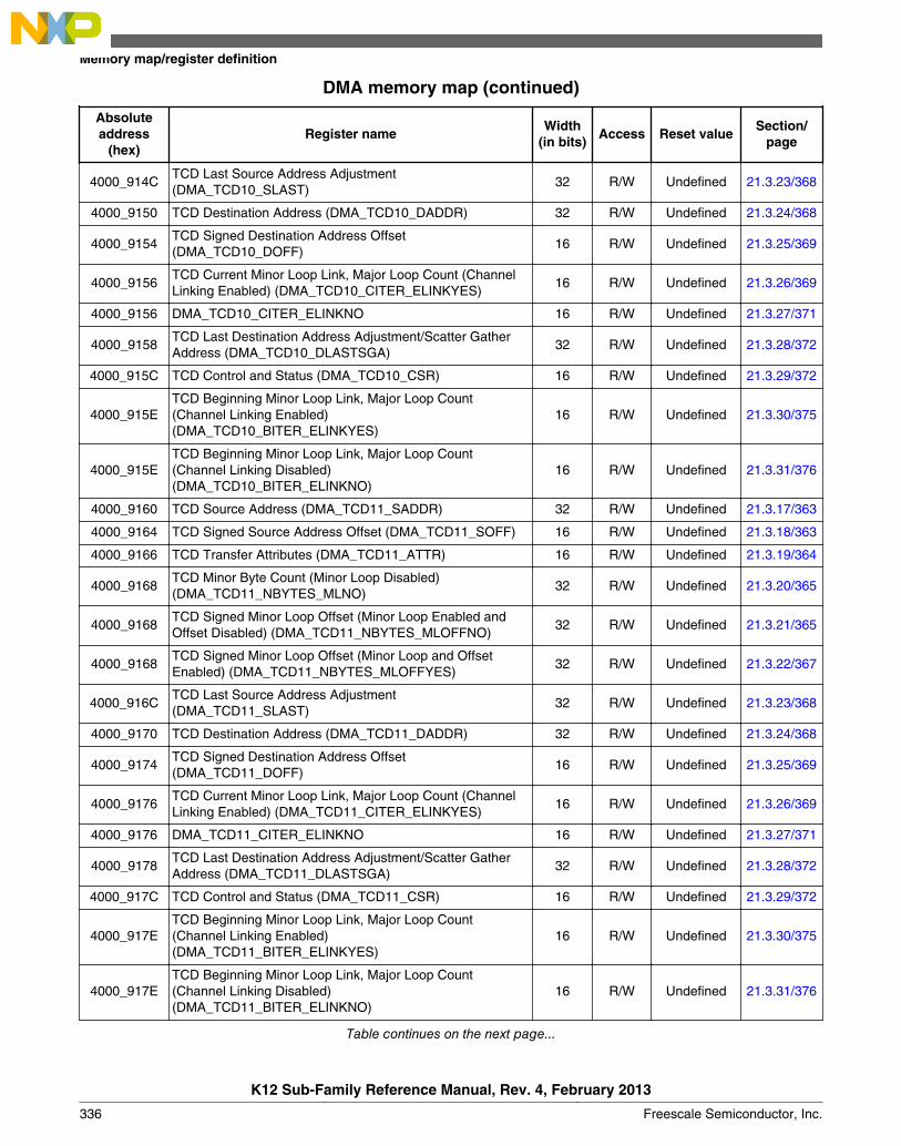
DMA memory map (continued)
Absoluteaddress
(hex)Register name
Width(in bits)
Access Reset valueSection/
page
4000_914CTCD Last Source Address Adjustment(DMA_TCD10_SLAST)
32 R/W Undefined 21.3.23/368
4000_9150 TCD Destination Address (DMA_TCD10_DADDR) 32 R/W Undefined 21.3.24/368
4000_9154TCD Signed Destination Address Offset(DMA_TCD10_DOFF)
16 R/W Undefined 21.3.25/369
4000_9156TCD Current Minor Loop Link, Major Loop Count (ChannelLinking Enabled) (DMA_TCD10_CITER_ELINKYES)
16 R/W Undefined 21.3.26/369
4000_9156 DMA_TCD10_CITER_ELINKNO 16 R/W Undefined 21.3.27/371
4000_9158TCD Last Destination Address Adjustment/Scatter GatherAddress (DMA_TCD10_DLASTSGA)
32 R/W Undefined 21.3.28/372
4000_915C TCD Control and Status (DMA_TCD10_CSR) 16 R/W Undefined 21.3.29/372
4000_915ETCD Beginning Minor Loop Link, Major Loop Count(Channel Linking Enabled)(DMA_TCD10_BITER_ELINKYES)
16 R/W Undefined 21.3.30/375
4000_915ETCD Beginning Minor Loop Link, Major Loop Count(Channel Linking Disabled)(DMA_TCD10_BITER_ELINKNO)
16 R/W Undefined 21.3.31/376
4000_9160 TCD Source Address (DMA_TCD11_SADDR) 32 R/W Undefined 21.3.17/363
4000_9164 TCD Signed Source Address Offset (DMA_TCD11_SOFF) 16 R/W Undefined 21.3.18/363
4000_9166 TCD Transfer Attributes (DMA_TCD11_ATTR) 16 R/W Undefined 21.3.19/364
4000_9168TCD Minor Byte Count (Minor Loop Disabled)(DMA_TCD11_NBYTES_MLNO)
32 R/W Undefined 21.3.20/365
4000_9168TCD Signed Minor Loop Offset (Minor Loop Enabled andOffset Disabled) (DMA_TCD11_NBYTES_MLOFFNO)
32 R/W Undefined 21.3.21/365
4000_9168TCD Signed Minor Loop Offset (Minor Loop and OffsetEnabled) (DMA_TCD11_NBYTES_MLOFFYES)
32 R/W Undefined 21.3.22/367
4000_916CTCD Last Source Address Adjustment(DMA_TCD11_SLAST)
32 R/W Undefined 21.3.23/368
4000_9170 TCD Destination Address (DMA_TCD11_DADDR) 32 R/W Undefined 21.3.24/368
4000_9174TCD Signed Destination Address Offset(DMA_TCD11_DOFF)
16 R/W Undefined 21.3.25/369
4000_9176TCD Current Minor Loop Link, Major Loop Count (ChannelLinking Enabled) (DMA_TCD11_CITER_ELINKYES)
16 R/W Undefined 21.3.26/369
4000_9176 DMA_TCD11_CITER_ELINKNO 16 R/W Undefined 21.3.27/371
4000_9178TCD Last Destination Address Adjustment/Scatter GatherAddress (DMA_TCD11_DLASTSGA)
32 R/W Undefined 21.3.28/372
4000_917C TCD Control and Status (DMA_TCD11_CSR) 16 R/W Undefined 21.3.29/372
4000_917ETCD Beginning Minor Loop Link, Major Loop Count(Channel Linking Enabled)(DMA_TCD11_BITER_ELINKYES)
16 R/W Undefined 21.3.30/375
4000_917ETCD Beginning Minor Loop Link, Major Loop Count(Channel Linking Disabled)(DMA_TCD11_BITER_ELINKNO)
16 R/W Undefined 21.3.31/376
Table continues on the next page...
Memory map/register definition
K12 Sub-Family Reference Manual, Rev. 4, February 2013
336 Freescale Semiconductor, Inc.

DMA memory map (continued)
Absoluteaddress
(hex)Register name
Width(in bits)
Access Reset valueSection/
page
4000_9180 TCD Source Address (DMA_TCD12_SADDR) 32 R/W Undefined 21.3.17/363
4000_9184 TCD Signed Source Address Offset (DMA_TCD12_SOFF) 16 R/W Undefined 21.3.18/363
4000_9186 TCD Transfer Attributes (DMA_TCD12_ATTR) 16 R/W Undefined 21.3.19/364
4000_9188TCD Minor Byte Count (Minor Loop Disabled)(DMA_TCD12_NBYTES_MLNO)
32 R/W Undefined 21.3.20/365
4000_9188TCD Signed Minor Loop Offset (Minor Loop Enabled andOffset Disabled) (DMA_TCD12_NBYTES_MLOFFNO)
32 R/W Undefined 21.3.21/365
4000_9188TCD Signed Minor Loop Offset (Minor Loop and OffsetEnabled) (DMA_TCD12_NBYTES_MLOFFYES)
32 R/W Undefined 21.3.22/367
4000_918CTCD Last Source Address Adjustment(DMA_TCD12_SLAST)
32 R/W Undefined 21.3.23/368
4000_9190 TCD Destination Address (DMA_TCD12_DADDR) 32 R/W Undefined 21.3.24/368
4000_9194TCD Signed Destination Address Offset(DMA_TCD12_DOFF)
16 R/W Undefined 21.3.25/369
4000_9196TCD Current Minor Loop Link, Major Loop Count (ChannelLinking Enabled) (DMA_TCD12_CITER_ELINKYES)
16 R/W Undefined 21.3.26/369
4000_9196 DMA_TCD12_CITER_ELINKNO 16 R/W Undefined 21.3.27/371
4000_9198TCD Last Destination Address Adjustment/Scatter GatherAddress (DMA_TCD12_DLASTSGA)
32 R/W Undefined 21.3.28/372
4000_919C TCD Control and Status (DMA_TCD12_CSR) 16 R/W Undefined 21.3.29/372
4000_919ETCD Beginning Minor Loop Link, Major Loop Count(Channel Linking Enabled)(DMA_TCD12_BITER_ELINKYES)
16 R/W Undefined 21.3.30/375
4000_919ETCD Beginning Minor Loop Link, Major Loop Count(Channel Linking Disabled)(DMA_TCD12_BITER_ELINKNO)
16 R/W Undefined 21.3.31/376
4000_91A0 TCD Source Address (DMA_TCD13_SADDR) 32 R/W Undefined 21.3.17/363
4000_91A4 TCD Signed Source Address Offset (DMA_TCD13_SOFF) 16 R/W Undefined 21.3.18/363
4000_91A6 TCD Transfer Attributes (DMA_TCD13_ATTR) 16 R/W Undefined 21.3.19/364
4000_91A8TCD Minor Byte Count (Minor Loop Disabled)(DMA_TCD13_NBYTES_MLNO)
32 R/W Undefined 21.3.20/365
4000_91A8TCD Signed Minor Loop Offset (Minor Loop Enabled andOffset Disabled) (DMA_TCD13_NBYTES_MLOFFNO)
32 R/W Undefined 21.3.21/365
4000_91A8TCD Signed Minor Loop Offset (Minor Loop and OffsetEnabled) (DMA_TCD13_NBYTES_MLOFFYES)
32 R/W Undefined 21.3.22/367
4000_91ACTCD Last Source Address Adjustment(DMA_TCD13_SLAST)
32 R/W Undefined 21.3.23/368
4000_91B0 TCD Destination Address (DMA_TCD13_DADDR) 32 R/W Undefined 21.3.24/368
4000_91B4TCD Signed Destination Address Offset(DMA_TCD13_DOFF)
16 R/W Undefined 21.3.25/369
4000_91B6TCD Current Minor Loop Link, Major Loop Count (ChannelLinking Enabled) (DMA_TCD13_CITER_ELINKYES)
16 R/W Undefined 21.3.26/369
4000_91B6 DMA_TCD13_CITER_ELINKNO 16 R/W Undefined 21.3.27/371
Table continues on the next page...
Chapter 21 Direct Memory Access Controller (eDMA)
K12 Sub-Family Reference Manual, Rev. 4, February 2013
Freescale Semiconductor, Inc. 337
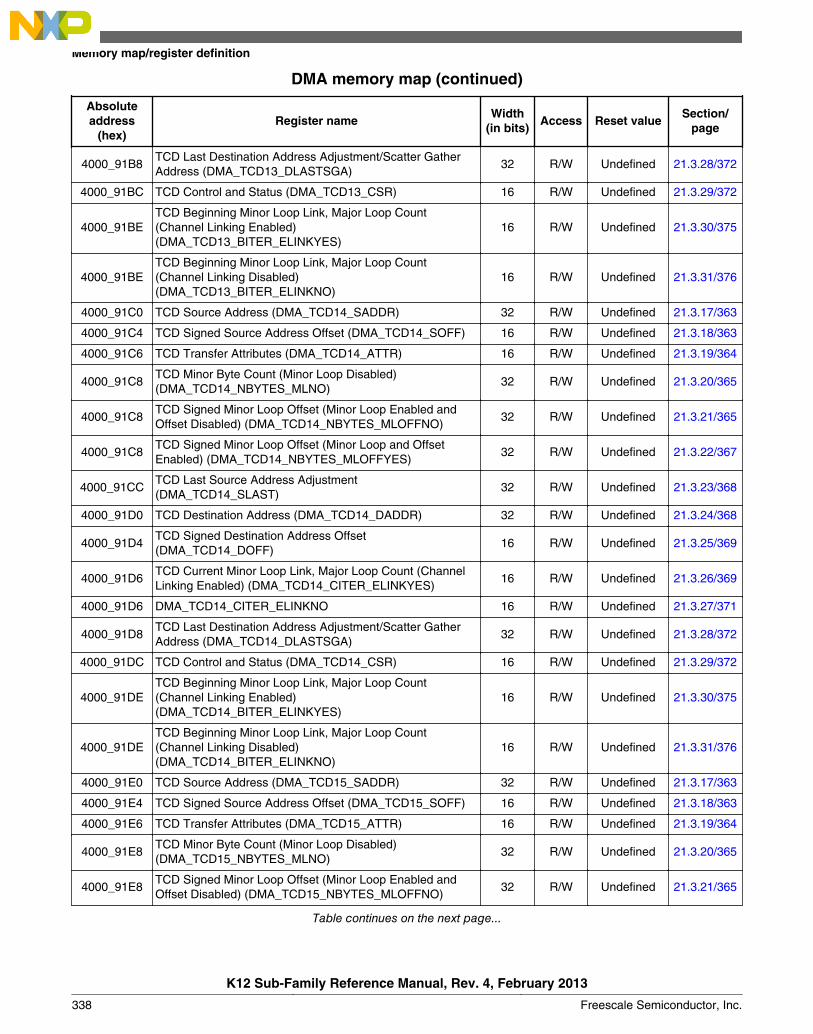
DMA memory map (continued)
Absoluteaddress
(hex)Register name
Width(in bits)
Access Reset valueSection/
page
4000_91B8TCD Last Destination Address Adjustment/Scatter GatherAddress (DMA_TCD13_DLASTSGA)
32 R/W Undefined 21.3.28/372
4000_91BC TCD Control and Status (DMA_TCD13_CSR) 16 R/W Undefined 21.3.29/372
4000_91BETCD Beginning Minor Loop Link, Major Loop Count(Channel Linking Enabled)(DMA_TCD13_BITER_ELINKYES)
16 R/W Undefined 21.3.30/375
4000_91BETCD Beginning Minor Loop Link, Major Loop Count(Channel Linking Disabled)(DMA_TCD13_BITER_ELINKNO)
16 R/W Undefined 21.3.31/376
4000_91C0 TCD Source Address (DMA_TCD14_SADDR) 32 R/W Undefined 21.3.17/363
4000_91C4 TCD Signed Source Address Offset (DMA_TCD14_SOFF) 16 R/W Undefined 21.3.18/363
4000_91C6 TCD Transfer Attributes (DMA_TCD14_ATTR) 16 R/W Undefined 21.3.19/364
4000_91C8TCD Minor Byte Count (Minor Loop Disabled)(DMA_TCD14_NBYTES_MLNO)
32 R/W Undefined 21.3.20/365
4000_91C8TCD Signed Minor Loop Offset (Minor Loop Enabled andOffset Disabled) (DMA_TCD14_NBYTES_MLOFFNO)
32 R/W Undefined 21.3.21/365
4000_91C8TCD Signed Minor Loop Offset (Minor Loop and OffsetEnabled) (DMA_TCD14_NBYTES_MLOFFYES)
32 R/W Undefined 21.3.22/367
4000_91CCTCD Last Source Address Adjustment(DMA_TCD14_SLAST)
32 R/W Undefined 21.3.23/368
4000_91D0 TCD Destination Address (DMA_TCD14_DADDR) 32 R/W Undefined 21.3.24/368
4000_91D4TCD Signed Destination Address Offset(DMA_TCD14_DOFF)
16 R/W Undefined 21.3.25/369
4000_91D6TCD Current Minor Loop Link, Major Loop Count (ChannelLinking Enabled) (DMA_TCD14_CITER_ELINKYES)
16 R/W Undefined 21.3.26/369
4000_91D6 DMA_TCD14_CITER_ELINKNO 16 R/W Undefined 21.3.27/371
4000_91D8TCD Last Destination Address Adjustment/Scatter GatherAddress (DMA_TCD14_DLASTSGA)
32 R/W Undefined 21.3.28/372
4000_91DC TCD Control and Status (DMA_TCD14_CSR) 16 R/W Undefined 21.3.29/372
4000_91DETCD Beginning Minor Loop Link, Major Loop Count(Channel Linking Enabled)(DMA_TCD14_BITER_ELINKYES)
16 R/W Undefined 21.3.30/375
4000_91DETCD Beginning Minor Loop Link, Major Loop Count(Channel Linking Disabled)(DMA_TCD14_BITER_ELINKNO)
16 R/W Undefined 21.3.31/376
4000_91E0 TCD Source Address (DMA_TCD15_SADDR) 32 R/W Undefined 21.3.17/363
4000_91E4 TCD Signed Source Address Offset (DMA_TCD15_SOFF) 16 R/W Undefined 21.3.18/363
4000_91E6 TCD Transfer Attributes (DMA_TCD15_ATTR) 16 R/W Undefined 21.3.19/364
4000_91E8TCD Minor Byte Count (Minor Loop Disabled)(DMA_TCD15_NBYTES_MLNO)
32 R/W Undefined 21.3.20/365
4000_91E8TCD Signed Minor Loop Offset (Minor Loop Enabled andOffset Disabled) (DMA_TCD15_NBYTES_MLOFFNO)
32 R/W Undefined 21.3.21/365
Table continues on the next page...
Memory map/register definition
K12 Sub-Family Reference Manual, Rev. 4, February 2013
338 Freescale Semiconductor, Inc.

DMA memory map (continued)
Absoluteaddress
(hex)Register name
Width(in bits)
Access Reset valueSection/
page
4000_91E8TCD Signed Minor Loop Offset (Minor Loop and OffsetEnabled) (DMA_TCD15_NBYTES_MLOFFYES)
32 R/W Undefined 21.3.22/367
4000_91ECTCD Last Source Address Adjustment(DMA_TCD15_SLAST)
32 R/W Undefined 21.3.23/368
4000_91F0 TCD Destination Address (DMA_TCD15_DADDR) 32 R/W Undefined 21.3.24/368
4000_91F4TCD Signed Destination Address Offset(DMA_TCD15_DOFF)
16 R/W Undefined 21.3.25/369
4000_91F6TCD Current Minor Loop Link, Major Loop Count (ChannelLinking Enabled) (DMA_TCD15_CITER_ELINKYES)
16 R/W Undefined 21.3.26/369
4000_91F6 DMA_TCD15_CITER_ELINKNO 16 R/W Undefined 21.3.27/371
4000_91F8TCD Last Destination Address Adjustment/Scatter GatherAddress (DMA_TCD15_DLASTSGA)
32 R/W Undefined 21.3.28/372
4000_91FC TCD Control and Status (DMA_TCD15_CSR) 16 R/W Undefined 21.3.29/372
4000_91FETCD Beginning Minor Loop Link, Major Loop Count(Channel Linking Enabled)(DMA_TCD15_BITER_ELINKYES)
16 R/W Undefined 21.3.30/375
4000_91FETCD Beginning Minor Loop Link, Major Loop Count(Channel Linking Disabled)(DMA_TCD15_BITER_ELINKNO)
16 R/W Undefined 21.3.31/376
21.3.1 Control Register (DMA_CR)
The CR defines the basic operating configuration of the DMA.
Arbitration can be configured to use either a fixed-priority or a round-robin scheme. Forfixed-priority arbitration, the highest priority channel requesting service is selected toexecute. The channel priority registers assign the priorities; see the DCHPRIn registers.For round-robin arbitration, the channel priorities are ignored and channels are cycledthrough (from high to low channel number) without regard to priority.
NOTEFor proper operation, writes to the CR register must beperformed only when the DMA channels are inactive; that is,when TCDn_CSR[ACTIVE] bits are cleared.
Address: 4000_8000h base + 0h offset = 4000_8000h
Bit 31 30 29 28 27 26 25 24 23 22 21 20 19 18 17 16
R 0
CX ECXW
Reset 0 0 0 0 0 0 0 0 0 0 0 0 0 0 0 0
Chapter 21 Direct Memory Access Controller (eDMA)
K12 Sub-Family Reference Manual, Rev. 4, February 2013
Freescale Semiconductor, Inc. 339

Bit 15 14 13 12 11 10 9 8 7 6 5 4 3 2 1 0
R 0
EM
LM CLM
HA
LT HOE
0
ER
CA
ED
BG
0
W
Reset 0 0 0 0 0 0 0 0 0 0 0 0 0 0 0 0
DMA_CR field descriptions
Field Description
31–18Reserved
This field is reserved.This read-only field is reserved and always has the value 0.
17CX
Cancel Transfer
0 Normal operation1 Cancel the remaining data transfer. Stop the executing channel and force the minor loop to finish. The
cancel takes effect after the last write of the current read/write sequence. The CX bit clears itself afterthe cancel has been honored. This cancel retires the channel normally as if the minor loop wascompleted.
16ECX
Error Cancel Transfer
0 Normal operation1 Cancel the remaining data transfer in the same fashion as the CX bit. Stop the executing channel and
force the minor loop to finish. The cancel takes effect after the last write of the current read/writesequence. The ECX bit clears itself after the cancel is honored. In addition to cancelling the transfer,ECX treats the cancel as an error condition, thus updating the Error Status register (DMAx_ES) andgenerating an optional error interrupt.
15–8Reserved
This field is reserved.This read-only field is reserved and always has the value 0.
7EMLM
Enable Minor Loop Mapping
0 Disabled. TCDn.word2 is defined as a 32-bit NBYTES field.1 Enabled. TCDn.word2 is redefined to include individual enable fields, an offset field, and the NBYTES
field. The individual enable fields allow the minor loop offset to be applied to the source address, thedestination address, or both. The NBYTES field is reduced when either offset is enabled.
6CLM
Continuous Link Mode
0 A minor loop channel link made to itself goes through channel arbitration before being activated again.1 A minor loop channel link made to itself does not go through channel arbitration before being activated
again. Upon minor loop completion, the channel activates again if that channel has a minor loopchannel link enabled and the link channel is itself. This effectively applies the minor loop offsets andrestarts the next minor loop.
5HALT
Halt DMA Operations
0 Normal operation1 Stall the start of any new channels. Executing channels are allowed to complete. Channel execution
resumes when this bit is cleared.
4HOE
Halt On Error
0 Normal operation1 Any error causes the HALT bit to set. Subsequently, all service requests are ignored until the HALT bit
is cleared.
Table continues on the next page...
Memory map/register definition
K12 Sub-Family Reference Manual, Rev. 4, February 2013
340 Freescale Semiconductor, Inc.

DMA_CR field descriptions (continued)
Field Description
3Reserved
This field is reserved.This read-only field is reserved and always has the value 0.
2ERCA
Enable Round Robin Channel Arbitration
0 Fixed priority arbitration is used for channel selection .1 Round robin arbitration is used for channel selection .
1EDBG
Enable Debug
0 When in debug mode, the DMA continues to operate.1 When in debug mode, the DMA stalls the start of a new channel. Executing channels are allowed to
complete. Channel execution resumes when the system exits debug mode or the EDBG bit is cleared.
0Reserved
This field is reserved.This read-only field is reserved and always has the value 0.
21.3.2 Error Status Register (DMA_ES)
The ES provides information concerning the last recorded channel error. Channel errorscan be caused by:
• A configuration error, that is:• An illegal setting in the transfer-control descriptor, or• An illegal priority register setting in fixed-arbitration
• An error termination to a bus master read or write cycle
See the Error Reporting and Handling section for more details.
Address: 4000_8000h base + 4h offset = 4000_8004h
Bit 31 30 29 28 27 26 25 24 23 22 21 20 19 18 17 16
R VLD 0 ECX
W
Reset 0 0 0 0 0 0 0 0 0 0 0 0 0 0 0 0
Bit 15 14 13 12 11 10 9 8 7 6 5 4 3 2 1 0
R 0 CPE 0 ERRCHN SAE SOE DAE DOE NCE SGE SBE DBE
W
Reset 0 0 0 0 0 0 0 0 0 0 0 0 0 0 0 0
DMA_ES field descriptions
Field Description
31VLD
Logical OR of all ERR status bits
Table continues on the next page...
Chapter 21 Direct Memory Access Controller (eDMA)
K12 Sub-Family Reference Manual, Rev. 4, February 2013
Freescale Semiconductor, Inc. 341
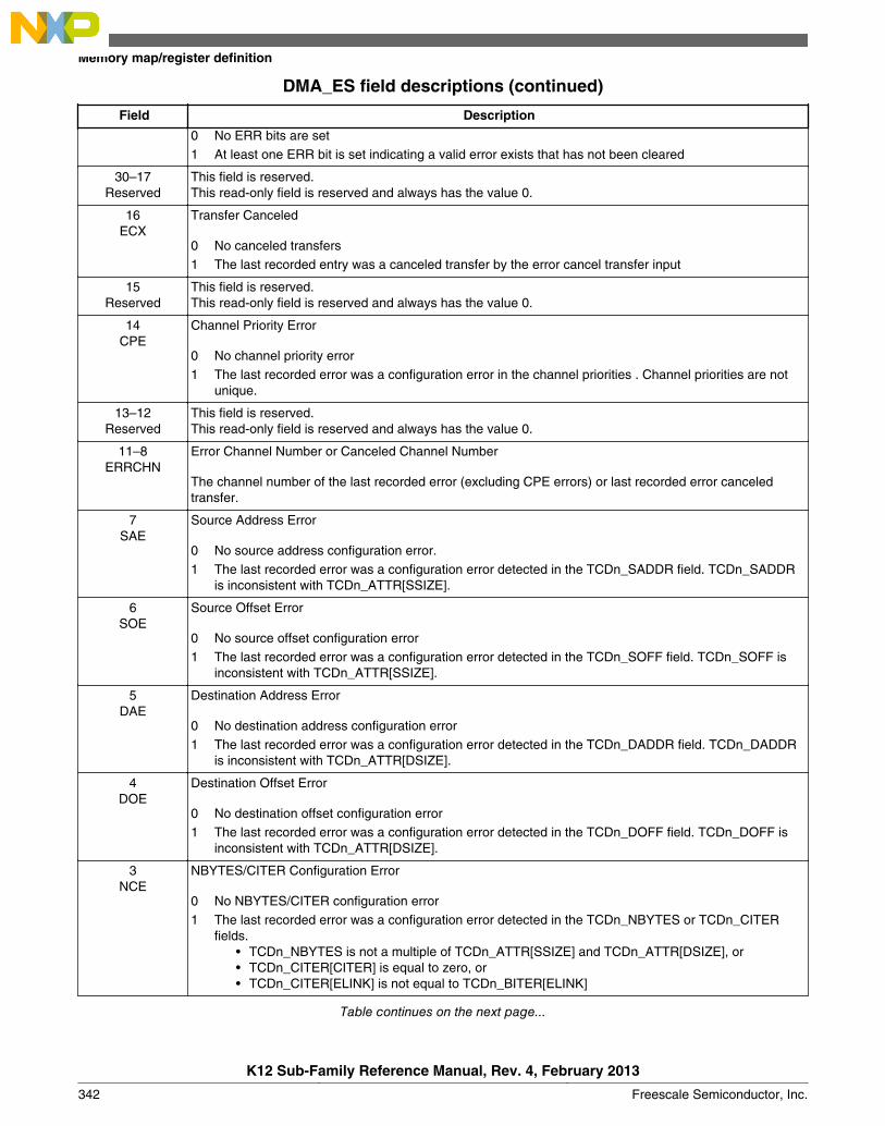
DMA_ES field descriptions (continued)
Field Description
0 No ERR bits are set1 At least one ERR bit is set indicating a valid error exists that has not been cleared
30–17Reserved
This field is reserved.This read-only field is reserved and always has the value 0.
16ECX
Transfer Canceled
0 No canceled transfers1 The last recorded entry was a canceled transfer by the error cancel transfer input
15Reserved
This field is reserved.This read-only field is reserved and always has the value 0.
14CPE
Channel Priority Error
0 No channel priority error1 The last recorded error was a configuration error in the channel priorities . Channel priorities are not
unique.
13–12Reserved
This field is reserved.This read-only field is reserved and always has the value 0.
11–8ERRCHN
Error Channel Number or Canceled Channel Number
The channel number of the last recorded error (excluding CPE errors) or last recorded error canceledtransfer.
7SAE
Source Address Error
0 No source address configuration error.1 The last recorded error was a configuration error detected in the TCDn_SADDR field. TCDn_SADDR
is inconsistent with TCDn_ATTR[SSIZE].
6SOE
Source Offset Error
0 No source offset configuration error1 The last recorded error was a configuration error detected in the TCDn_SOFF field. TCDn_SOFF is
inconsistent with TCDn_ATTR[SSIZE].
5DAE
Destination Address Error
0 No destination address configuration error1 The last recorded error was a configuration error detected in the TCDn_DADDR field. TCDn_DADDR
is inconsistent with TCDn_ATTR[DSIZE].
4DOE
Destination Offset Error
0 No destination offset configuration error1 The last recorded error was a configuration error detected in the TCDn_DOFF field. TCDn_DOFF is
inconsistent with TCDn_ATTR[DSIZE].
3NCE
NBYTES/CITER Configuration Error
0 No NBYTES/CITER configuration error1 The last recorded error was a configuration error detected in the TCDn_NBYTES or TCDn_CITER
fields.• TCDn_NBYTES is not a multiple of TCDn_ATTR[SSIZE] and TCDn_ATTR[DSIZE], or• TCDn_CITER[CITER] is equal to zero, or• TCDn_CITER[ELINK] is not equal to TCDn_BITER[ELINK]
Table continues on the next page...
Memory map/register definition
K12 Sub-Family Reference Manual, Rev. 4, February 2013
342 Freescale Semiconductor, Inc.

DMA_ES field descriptions (continued)
Field Description
2SGE
Scatter/Gather Configuration Error
0 No scatter/gather configuration error1 The last recorded error was a configuration error detected in the TCDn_DLASTSGA field. This field is
checked at the beginning of a scatter/gather operation after major loop completion if TCDn_CSR[ESG]is enabled. TCDn_DLASTSGA is not on a 32 byte boundary.
1SBE
Source Bus Error
0 No source bus error1 The last recorded error was a bus error on a source read
0DBE
Destination Bus Error
0 No destination bus error1 The last recorded error was a bus error on a destination write
21.3.3 Enable Request Register (DMA_ERQ)
The ERQ register provides a bit map for the 16 implemented channels to enable therequest signal for each channel. The state of any given channel enable is directly affectedby writes to this register; it is also affected by writes to the SERQ and CERQ. The{S,C}ERQ registers are provided so the request enable for a single channel can easily bemodified without needing to perform a read-modify-write sequence to the ERQ.
DMA request input signals and this enable request flag must be asserted before achannel’s hardware service request is accepted. The state of the DMA enable request flagdoes not affect a channel service request made explicitly through software or a linkedchannel request.
Address: 4000_8000h base + Ch offset = 4000_800Ch
Bit 31 30 29 28 27 26 25 24 23 22 21 20 19 18 17 16
R 0
W
Reset 0 0 0 0 0 0 0 0 0 0 0 0 0 0 0 0
Bit 15 14 13 12 11 10 9 8 7 6 5 4 3 2 1 0
R
ER
Q15
ER
Q14
ER
Q13
ER
Q12
ER
Q11
ER
Q10
ERQ9 ERQ8 ERQ7 ERQ6 ERQ5 ERQ4 ERQ3 ERQ2 ERQ1 ERQ0W
Reset 0 0 0 0 0 0 0 0 0 0 0 0 0 0 0 0
Chapter 21 Direct Memory Access Controller (eDMA)
K12 Sub-Family Reference Manual, Rev. 4, February 2013
Freescale Semiconductor, Inc. 343
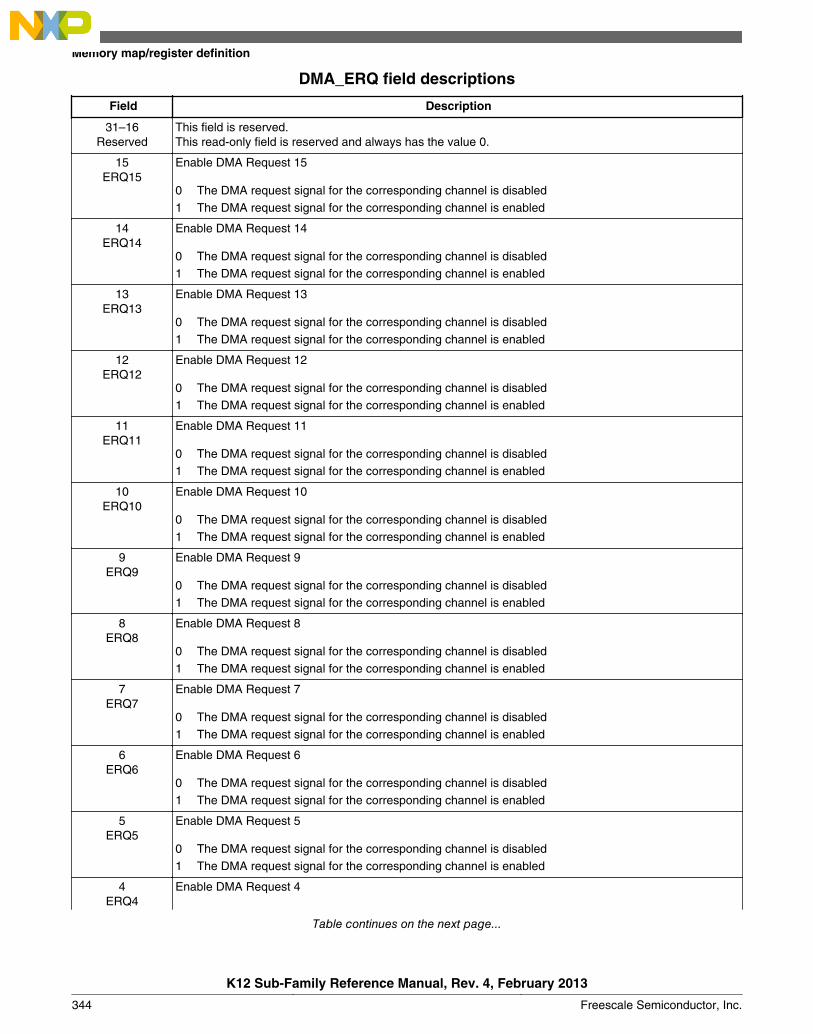
DMA_ERQ field descriptions
Field Description
31–16Reserved
This field is reserved.This read-only field is reserved and always has the value 0.
15ERQ15
Enable DMA Request 15
0 The DMA request signal for the corresponding channel is disabled1 The DMA request signal for the corresponding channel is enabled
14ERQ14
Enable DMA Request 14
0 The DMA request signal for the corresponding channel is disabled1 The DMA request signal for the corresponding channel is enabled
13ERQ13
Enable DMA Request 13
0 The DMA request signal for the corresponding channel is disabled1 The DMA request signal for the corresponding channel is enabled
12ERQ12
Enable DMA Request 12
0 The DMA request signal for the corresponding channel is disabled1 The DMA request signal for the corresponding channel is enabled
11ERQ11
Enable DMA Request 11
0 The DMA request signal for the corresponding channel is disabled1 The DMA request signal for the corresponding channel is enabled
10ERQ10
Enable DMA Request 10
0 The DMA request signal for the corresponding channel is disabled1 The DMA request signal for the corresponding channel is enabled
9ERQ9
Enable DMA Request 9
0 The DMA request signal for the corresponding channel is disabled1 The DMA request signal for the corresponding channel is enabled
8ERQ8
Enable DMA Request 8
0 The DMA request signal for the corresponding channel is disabled1 The DMA request signal for the corresponding channel is enabled
7ERQ7
Enable DMA Request 7
0 The DMA request signal for the corresponding channel is disabled1 The DMA request signal for the corresponding channel is enabled
6ERQ6
Enable DMA Request 6
0 The DMA request signal for the corresponding channel is disabled1 The DMA request signal for the corresponding channel is enabled
5ERQ5
Enable DMA Request 5
0 The DMA request signal for the corresponding channel is disabled1 The DMA request signal for the corresponding channel is enabled
4ERQ4
Enable DMA Request 4
Table continues on the next page...
Memory map/register definition
K12 Sub-Family Reference Manual, Rev. 4, February 2013
344 Freescale Semiconductor, Inc.
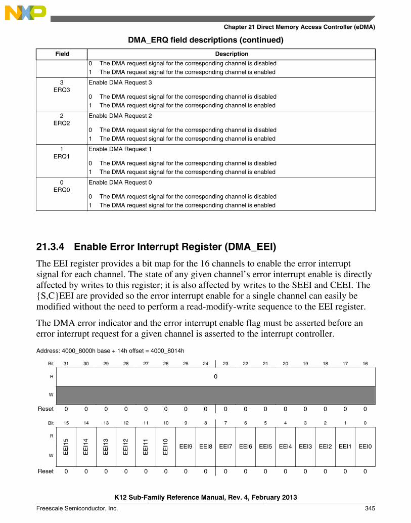
DMA_ERQ field descriptions (continued)
Field Description
0 The DMA request signal for the corresponding channel is disabled1 The DMA request signal for the corresponding channel is enabled
3ERQ3
Enable DMA Request 3
0 The DMA request signal for the corresponding channel is disabled1 The DMA request signal for the corresponding channel is enabled
2ERQ2
Enable DMA Request 2
0 The DMA request signal for the corresponding channel is disabled1 The DMA request signal for the corresponding channel is enabled
1ERQ1
Enable DMA Request 1
0 The DMA request signal for the corresponding channel is disabled1 The DMA request signal for the corresponding channel is enabled
0ERQ0
Enable DMA Request 0
0 The DMA request signal for the corresponding channel is disabled1 The DMA request signal for the corresponding channel is enabled
21.3.4 Enable Error Interrupt Register (DMA_EEI)
The EEI register provides a bit map for the 16 channels to enable the error interruptsignal for each channel. The state of any given channel’s error interrupt enable is directlyaffected by writes to this register; it is also affected by writes to the SEEI and CEEI. The{S,C}EEI are provided so the error interrupt enable for a single channel can easily bemodified without the need to perform a read-modify-write sequence to the EEI register.
The DMA error indicator and the error interrupt enable flag must be asserted before anerror interrupt request for a given channel is asserted to the interrupt controller.
Address: 4000_8000h base + 14h offset = 4000_8014h
Bit 31 30 29 28 27 26 25 24 23 22 21 20 19 18 17 16
R 0
W
Reset 0 0 0 0 0 0 0 0 0 0 0 0 0 0 0 0
Bit 15 14 13 12 11 10 9 8 7 6 5 4 3 2 1 0
R
EE
I15
EE
I14
EE
I13
EE
I12
EE
I11
EE
I10
EEI9 EEI8 EEI7 EEI6 EEI5 EEI4 EEI3 EEI2 EEI1 EEI0W
Reset 0 0 0 0 0 0 0 0 0 0 0 0 0 0 0 0
Chapter 21 Direct Memory Access Controller (eDMA)
K12 Sub-Family Reference Manual, Rev. 4, February 2013
Freescale Semiconductor, Inc. 345
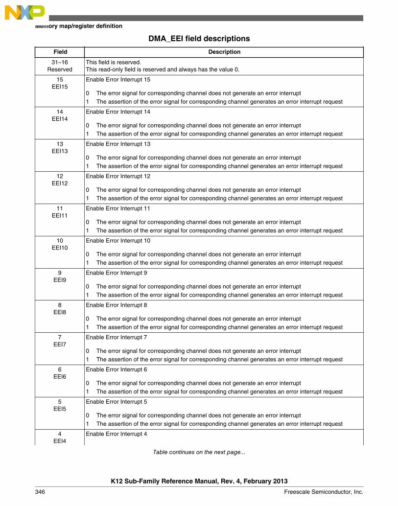
DMA_EEI field descriptions
Field Description
31–16Reserved
This field is reserved.This read-only field is reserved and always has the value 0.
15EEI15
Enable Error Interrupt 15
0 The error signal for corresponding channel does not generate an error interrupt1 The assertion of the error signal for corresponding channel generates an error interrupt request
14EEI14
Enable Error Interrupt 14
0 The error signal for corresponding channel does not generate an error interrupt1 The assertion of the error signal for corresponding channel generates an error interrupt request
13EEI13
Enable Error Interrupt 13
0 The error signal for corresponding channel does not generate an error interrupt1 The assertion of the error signal for corresponding channel generates an error interrupt request
12EEI12
Enable Error Interrupt 12
0 The error signal for corresponding channel does not generate an error interrupt1 The assertion of the error signal for corresponding channel generates an error interrupt request
11EEI11
Enable Error Interrupt 11
0 The error signal for corresponding channel does not generate an error interrupt1 The assertion of the error signal for corresponding channel generates an error interrupt request
10EEI10
Enable Error Interrupt 10
0 The error signal for corresponding channel does not generate an error interrupt1 The assertion of the error signal for corresponding channel generates an error interrupt request
9EEI9
Enable Error Interrupt 9
0 The error signal for corresponding channel does not generate an error interrupt1 The assertion of the error signal for corresponding channel generates an error interrupt request
8EEI8
Enable Error Interrupt 8
0 The error signal for corresponding channel does not generate an error interrupt1 The assertion of the error signal for corresponding channel generates an error interrupt request
7EEI7
Enable Error Interrupt 7
0 The error signal for corresponding channel does not generate an error interrupt1 The assertion of the error signal for corresponding channel generates an error interrupt request
6EEI6
Enable Error Interrupt 6
0 The error signal for corresponding channel does not generate an error interrupt1 The assertion of the error signal for corresponding channel generates an error interrupt request
5EEI5
Enable Error Interrupt 5
0 The error signal for corresponding channel does not generate an error interrupt1 The assertion of the error signal for corresponding channel generates an error interrupt request
4EEI4
Enable Error Interrupt 4
Table continues on the next page...
Memory map/register definition
K12 Sub-Family Reference Manual, Rev. 4, February 2013
346 Freescale Semiconductor, Inc.
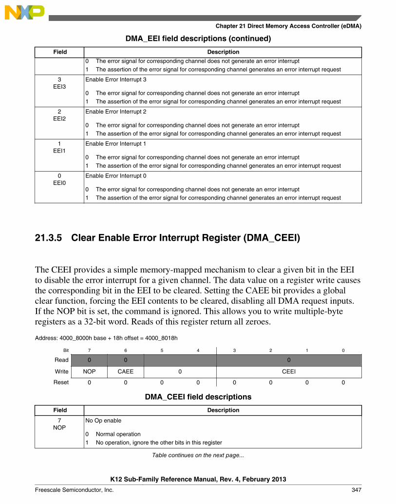
DMA_EEI field descriptions (continued)
Field Description
0 The error signal for corresponding channel does not generate an error interrupt1 The assertion of the error signal for corresponding channel generates an error interrupt request
3EEI3
Enable Error Interrupt 3
0 The error signal for corresponding channel does not generate an error interrupt1 The assertion of the error signal for corresponding channel generates an error interrupt request
2EEI2
Enable Error Interrupt 2
0 The error signal for corresponding channel does not generate an error interrupt1 The assertion of the error signal for corresponding channel generates an error interrupt request
1EEI1
Enable Error Interrupt 1
0 The error signal for corresponding channel does not generate an error interrupt1 The assertion of the error signal for corresponding channel generates an error interrupt request
0EEI0
Enable Error Interrupt 0
0 The error signal for corresponding channel does not generate an error interrupt1 The assertion of the error signal for corresponding channel generates an error interrupt request
21.3.5 Clear Enable Error Interrupt Register (DMA_CEEI)
The CEEI provides a simple memory-mapped mechanism to clear a given bit in the EEIto disable the error interrupt for a given channel. The data value on a register write causesthe corresponding bit in the EEI to be cleared. Setting the CAEE bit provides a globalclear function, forcing the EEI contents to be cleared, disabling all DMA request inputs.If the NOP bit is set, the command is ignored. This allows you to write multiple-byteregisters as a 32-bit word. Reads of this register return all zeroes.
Address: 4000_8000h base + 18h offset = 4000_8018h
Bit 7 6 5 4 3 2 1 0
Read 0 0 0
Write NOP CAEE 0 CEEI
Reset 0 0 0 0 0 0 0 0
DMA_CEEI field descriptions
Field Description
7NOP
No Op enable
0 Normal operation1 No operation, ignore the other bits in this register
Table continues on the next page...
Chapter 21 Direct Memory Access Controller (eDMA)
K12 Sub-Family Reference Manual, Rev. 4, February 2013
Freescale Semiconductor, Inc. 347
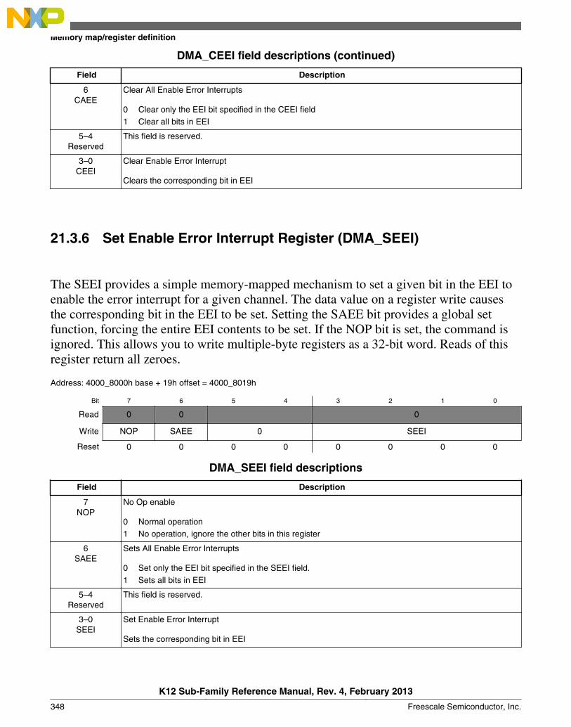
DMA_CEEI field descriptions (continued)
Field Description
6CAEE
Clear All Enable Error Interrupts
0 Clear only the EEI bit specified in the CEEI field1 Clear all bits in EEI
5–4Reserved
This field is reserved.
3–0CEEI
Clear Enable Error Interrupt
Clears the corresponding bit in EEI
21.3.6 Set Enable Error Interrupt Register (DMA_SEEI)
The SEEI provides a simple memory-mapped mechanism to set a given bit in the EEI toenable the error interrupt for a given channel. The data value on a register write causesthe corresponding bit in the EEI to be set. Setting the SAEE bit provides a global setfunction, forcing the entire EEI contents to be set. If the NOP bit is set, the command isignored. This allows you to write multiple-byte registers as a 32-bit word. Reads of thisregister return all zeroes.
Address: 4000_8000h base + 19h offset = 4000_8019h
Bit 7 6 5 4 3 2 1 0
Read 0 0 0
Write NOP SAEE 0 SEEI
Reset 0 0 0 0 0 0 0 0
DMA_SEEI field descriptions
Field Description
7NOP
No Op enable
0 Normal operation1 No operation, ignore the other bits in this register
6SAEE
Sets All Enable Error Interrupts
0 Set only the EEI bit specified in the SEEI field.1 Sets all bits in EEI
5–4Reserved
This field is reserved.
3–0SEEI
Set Enable Error Interrupt
Sets the corresponding bit in EEI
Memory map/register definition
K12 Sub-Family Reference Manual, Rev. 4, February 2013
348 Freescale Semiconductor, Inc.
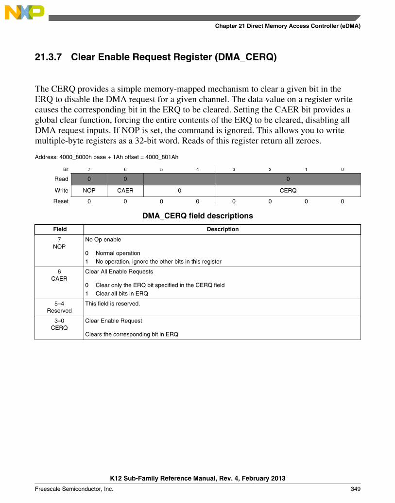
21.3.7 Clear Enable Request Register (DMA_CERQ)
The CERQ provides a simple memory-mapped mechanism to clear a given bit in theERQ to disable the DMA request for a given channel. The data value on a register writecauses the corresponding bit in the ERQ to be cleared. Setting the CAER bit provides aglobal clear function, forcing the entire contents of the ERQ to be cleared, disabling allDMA request inputs. If NOP is set, the command is ignored. This allows you to writemultiple-byte registers as a 32-bit word. Reads of this register return all zeroes.
Address: 4000_8000h base + 1Ah offset = 4000_801Ah
Bit 7 6 5 4 3 2 1 0
Read 0 0 0
Write NOP CAER 0 CERQ
Reset 0 0 0 0 0 0 0 0
DMA_CERQ field descriptions
Field Description
7NOP
No Op enable
0 Normal operation1 No operation, ignore the other bits in this register
6CAER
Clear All Enable Requests
0 Clear only the ERQ bit specified in the CERQ field1 Clear all bits in ERQ
5–4Reserved
This field is reserved.
3–0CERQ
Clear Enable Request
Clears the corresponding bit in ERQ
Chapter 21 Direct Memory Access Controller (eDMA)
K12 Sub-Family Reference Manual, Rev. 4, February 2013
Freescale Semiconductor, Inc. 349
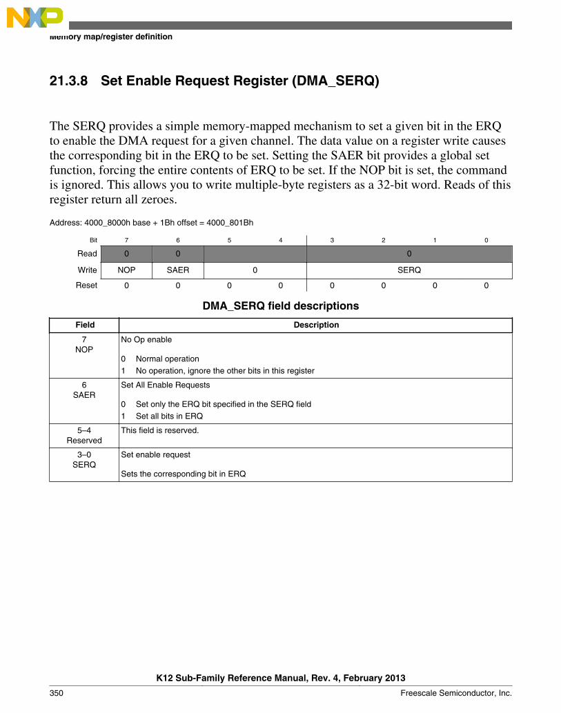
21.3.8 Set Enable Request Register (DMA_SERQ)
The SERQ provides a simple memory-mapped mechanism to set a given bit in the ERQto enable the DMA request for a given channel. The data value on a register write causesthe corresponding bit in the ERQ to be set. Setting the SAER bit provides a global setfunction, forcing the entire contents of ERQ to be set. If the NOP bit is set, the commandis ignored. This allows you to write multiple-byte registers as a 32-bit word. Reads of thisregister return all zeroes.
Address: 4000_8000h base + 1Bh offset = 4000_801Bh
Bit 7 6 5 4 3 2 1 0
Read 0 0 0
Write NOP SAER 0 SERQ
Reset 0 0 0 0 0 0 0 0
DMA_SERQ field descriptions
Field Description
7NOP
No Op enable
0 Normal operation1 No operation, ignore the other bits in this register
6SAER
Set All Enable Requests
0 Set only the ERQ bit specified in the SERQ field1 Set all bits in ERQ
5–4Reserved
This field is reserved.
3–0SERQ
Set enable request
Sets the corresponding bit in ERQ
Memory map/register definition
K12 Sub-Family Reference Manual, Rev. 4, February 2013
350 Freescale Semiconductor, Inc.
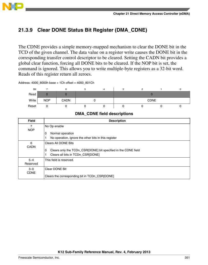
21.3.9 Clear DONE Status Bit Register (DMA_CDNE)
The CDNE provides a simple memory-mapped mechanism to clear the DONE bit in theTCD of the given channel. The data value on a register write causes the DONE bit in thecorresponding transfer control descriptor to be cleared. Setting the CADN bit provides aglobal clear function, forcing all DONE bits to be cleared. If the NOP bit is set, thecommand is ignored. This allows you to write multiple-byte registers as a 32-bit word.Reads of this register return all zeroes.
Address: 4000_8000h base + 1Ch offset = 4000_801Ch
Bit 7 6 5 4 3 2 1 0
Read 0 0 0
Write NOP CADN 0 CDNE
Reset 0 0 0 0 0 0 0 0
DMA_CDNE field descriptions
Field Description
7NOP
No Op enable
0 Normal operation1 No operation, ignore the other bits in this register
6CADN
Clears All DONE Bits
0 Clears only the TCDn_CSR[DONE] bit specified in the CDNE field1 Clears all bits in TCDn_CSR[DONE]
5–4Reserved
This field is reserved.
3–0CDNE
Clear DONE Bit
Clears the corresponding bit in TCDn_CSR[DONE]
Chapter 21 Direct Memory Access Controller (eDMA)
K12 Sub-Family Reference Manual, Rev. 4, February 2013
Freescale Semiconductor, Inc. 351
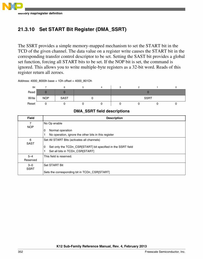
21.3.10 Set START Bit Register (DMA_SSRT)
The SSRT provides a simple memory-mapped mechanism to set the START bit in theTCD of the given channel. The data value on a register write causes the START bit in thecorresponding transfer control descriptor to be set. Setting the SAST bit provides a globalset function, forcing all START bits to be set. If the NOP bit is set, the command isignored. This allows you to write multiple-byte registers as a 32-bit word. Reads of thisregister return all zeroes.
Address: 4000_8000h base + 1Dh offset = 4000_801Dh
Bit 7 6 5 4 3 2 1 0
Read 0 0 0
Write NOP SAST 0 SSRT
Reset 0 0 0 0 0 0 0 0
DMA_SSRT field descriptions
Field Description
7NOP
No Op enable
0 Normal operation1 No operation, ignore the other bits in this register
6SAST
Set All START Bits (activates all channels)
0 Set only the TCDn_CSR[START] bit specified in the SSRT field1 Set all bits in TCDn_CSR[START]
5–4Reserved
This field is reserved.
3–0SSRT
Set START Bit
Sets the corresponding bit in TCDn_CSR[START]
Memory map/register definition
K12 Sub-Family Reference Manual, Rev. 4, February 2013
352 Freescale Semiconductor, Inc.
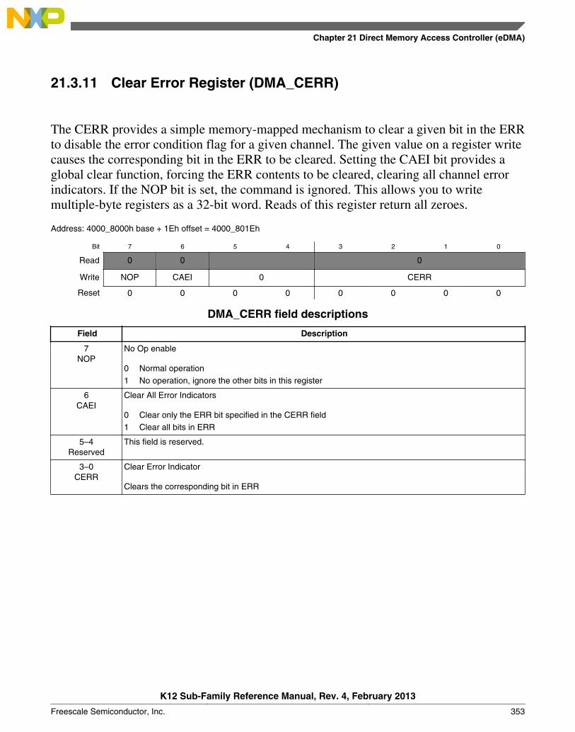
21.3.11 Clear Error Register (DMA_CERR)
The CERR provides a simple memory-mapped mechanism to clear a given bit in the ERRto disable the error condition flag for a given channel. The given value on a register writecauses the corresponding bit in the ERR to be cleared. Setting the CAEI bit provides aglobal clear function, forcing the ERR contents to be cleared, clearing all channel errorindicators. If the NOP bit is set, the command is ignored. This allows you to writemultiple-byte registers as a 32-bit word. Reads of this register return all zeroes.
Address: 4000_8000h base + 1Eh offset = 4000_801Eh
Bit 7 6 5 4 3 2 1 0
Read 0 0 0
Write NOP CAEI 0 CERR
Reset 0 0 0 0 0 0 0 0
DMA_CERR field descriptions
Field Description
7NOP
No Op enable
0 Normal operation1 No operation, ignore the other bits in this register
6CAEI
Clear All Error Indicators
0 Clear only the ERR bit specified in the CERR field1 Clear all bits in ERR
5–4Reserved
This field is reserved.
3–0CERR
Clear Error Indicator
Clears the corresponding bit in ERR
Chapter 21 Direct Memory Access Controller (eDMA)
K12 Sub-Family Reference Manual, Rev. 4, February 2013
Freescale Semiconductor, Inc. 353
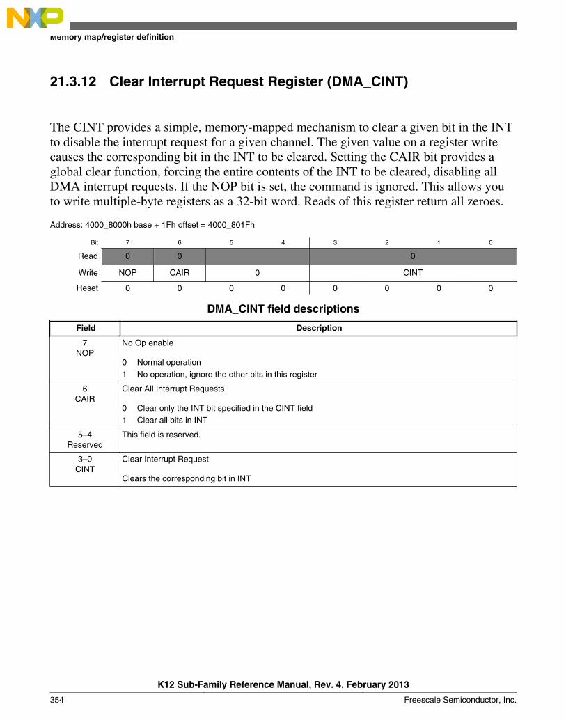
21.3.12 Clear Interrupt Request Register (DMA_CINT)
The CINT provides a simple, memory-mapped mechanism to clear a given bit in the INTto disable the interrupt request for a given channel. The given value on a register writecauses the corresponding bit in the INT to be cleared. Setting the CAIR bit provides aglobal clear function, forcing the entire contents of the INT to be cleared, disabling allDMA interrupt requests. If the NOP bit is set, the command is ignored. This allows youto write multiple-byte registers as a 32-bit word. Reads of this register return all zeroes.
Address: 4000_8000h base + 1Fh offset = 4000_801Fh
Bit 7 6 5 4 3 2 1 0
Read 0 0 0
Write NOP CAIR 0 CINT
Reset 0 0 0 0 0 0 0 0
DMA_CINT field descriptions
Field Description
7NOP
No Op enable
0 Normal operation1 No operation, ignore the other bits in this register
6CAIR
Clear All Interrupt Requests
0 Clear only the INT bit specified in the CINT field1 Clear all bits in INT
5–4Reserved
This field is reserved.
3–0CINT
Clear Interrupt Request
Clears the corresponding bit in INT
Memory map/register definition
K12 Sub-Family Reference Manual, Rev. 4, February 2013
354 Freescale Semiconductor, Inc.
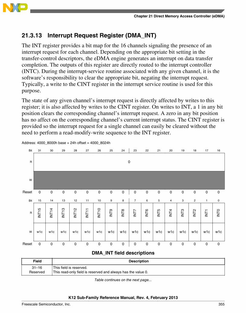
21.3.13 Interrupt Request Register (DMA_INT)
The INT register provides a bit map for the 16 channels signaling the presence of aninterrupt request for each channel. Depending on the appropriate bit setting in thetransfer-control descriptors, the eDMA engine generates an interrupt on data transfercompletion. The outputs of this register are directly routed to the interrupt controller(INTC). During the interrupt-service routine associated with any given channel, it is thesoftware’s responsibility to clear the appropriate bit, negating the interrupt request.Typically, a write to the CINT register in the interrupt service routine is used for thispurpose.
The state of any given channel’s interrupt request is directly affected by writes to thisregister; it is also affected by writes to the CINT register. On writes to INT, a 1 in any bitposition clears the corresponding channel’s interrupt request. A zero in any bit positionhas no affect on the corresponding channel’s current interrupt status. The CINT register isprovided so the interrupt request for a single channel can easily be cleared without theneed to perform a read-modify-write sequence to the INT register.
Address: 4000_8000h base + 24h offset = 4000_8024h
Bit 31 30 29 28 27 26 25 24 23 22 21 20 19 18 17 16
R 0
W
Reset 0 0 0 0 0 0 0 0 0 0 0 0 0 0 0 0
Bit 15 14 13 12 11 10 9 8 7 6 5 4 3 2 1 0
R
INT
15
INT
14
INT
13
INT
12
INT
11
INT
10
INT
9
INT
8
INT
7
INT
6
INT
5
INT
4
INT
3
INT
2
INT
1
INT
0
W w1c w1c w1c w1c w1c w1c w1c w1c w1c w1c w1c w1c w1c w1c w1c w1c
Reset 0 0 0 0 0 0 0 0 0 0 0 0 0 0 0 0
DMA_INT field descriptions
Field Description
31–16Reserved
This field is reserved.This read-only field is reserved and always has the value 0.
Table continues on the next page...
Chapter 21 Direct Memory Access Controller (eDMA)
K12 Sub-Family Reference Manual, Rev. 4, February 2013
Freescale Semiconductor, Inc. 355
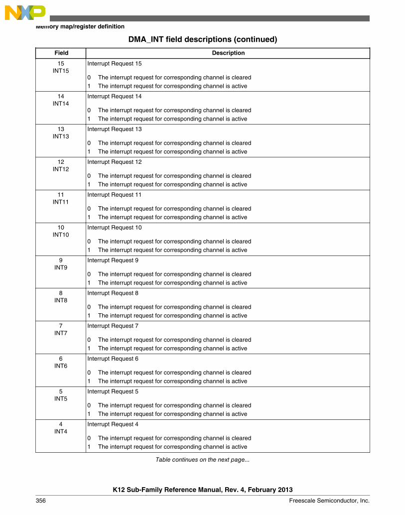
DMA_INT field descriptions (continued)
Field Description
15INT15
Interrupt Request 15
0 The interrupt request for corresponding channel is cleared1 The interrupt request for corresponding channel is active
14INT14
Interrupt Request 14
0 The interrupt request for corresponding channel is cleared1 The interrupt request for corresponding channel is active
13INT13
Interrupt Request 13
0 The interrupt request for corresponding channel is cleared1 The interrupt request for corresponding channel is active
12INT12
Interrupt Request 12
0 The interrupt request for corresponding channel is cleared1 The interrupt request for corresponding channel is active
11INT11
Interrupt Request 11
0 The interrupt request for corresponding channel is cleared1 The interrupt request for corresponding channel is active
10INT10
Interrupt Request 10
0 The interrupt request for corresponding channel is cleared1 The interrupt request for corresponding channel is active
9INT9
Interrupt Request 9
0 The interrupt request for corresponding channel is cleared1 The interrupt request for corresponding channel is active
8INT8
Interrupt Request 8
0 The interrupt request for corresponding channel is cleared1 The interrupt request for corresponding channel is active
7INT7
Interrupt Request 7
0 The interrupt request for corresponding channel is cleared1 The interrupt request for corresponding channel is active
6INT6
Interrupt Request 6
0 The interrupt request for corresponding channel is cleared1 The interrupt request for corresponding channel is active
5INT5
Interrupt Request 5
0 The interrupt request for corresponding channel is cleared1 The interrupt request for corresponding channel is active
4INT4
Interrupt Request 4
0 The interrupt request for corresponding channel is cleared1 The interrupt request for corresponding channel is active
Table continues on the next page...
Memory map/register definition
K12 Sub-Family Reference Manual, Rev. 4, February 2013
356 Freescale Semiconductor, Inc.
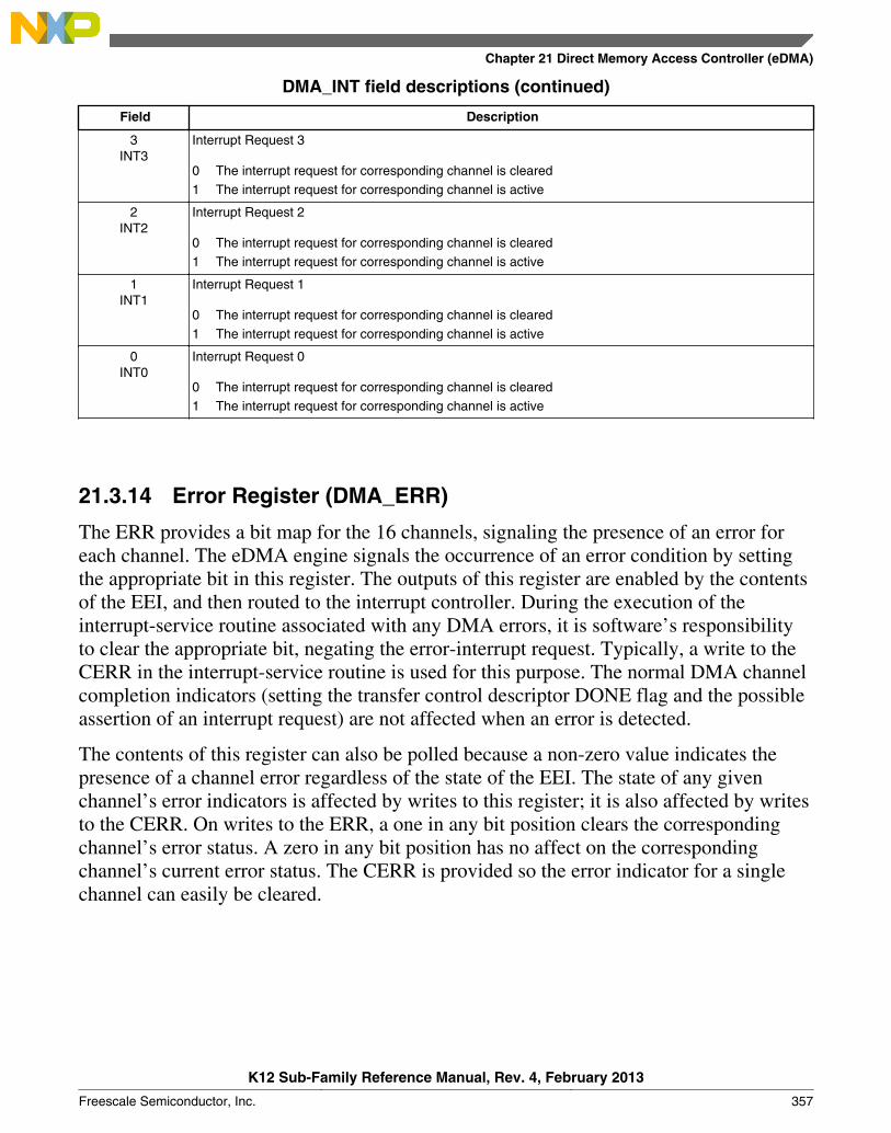
DMA_INT field descriptions (continued)
Field Description
3INT3
Interrupt Request 3
0 The interrupt request for corresponding channel is cleared1 The interrupt request for corresponding channel is active
2INT2
Interrupt Request 2
0 The interrupt request for corresponding channel is cleared1 The interrupt request for corresponding channel is active
1INT1
Interrupt Request 1
0 The interrupt request for corresponding channel is cleared1 The interrupt request for corresponding channel is active
0INT0
Interrupt Request 0
0 The interrupt request for corresponding channel is cleared1 The interrupt request for corresponding channel is active
21.3.14 Error Register (DMA_ERR)
The ERR provides a bit map for the 16 channels, signaling the presence of an error foreach channel. The eDMA engine signals the occurrence of an error condition by settingthe appropriate bit in this register. The outputs of this register are enabled by the contentsof the EEI, and then routed to the interrupt controller. During the execution of theinterrupt-service routine associated with any DMA errors, it is software’s responsibilityto clear the appropriate bit, negating the error-interrupt request. Typically, a write to theCERR in the interrupt-service routine is used for this purpose. The normal DMA channelcompletion indicators (setting the transfer control descriptor DONE flag and the possibleassertion of an interrupt request) are not affected when an error is detected.
The contents of this register can also be polled because a non-zero value indicates thepresence of a channel error regardless of the state of the EEI. The state of any givenchannel’s error indicators is affected by writes to this register; it is also affected by writesto the CERR. On writes to the ERR, a one in any bit position clears the correspondingchannel’s error status. A zero in any bit position has no affect on the correspondingchannel’s current error status. The CERR is provided so the error indicator for a singlechannel can easily be cleared.
Chapter 21 Direct Memory Access Controller (eDMA)
K12 Sub-Family Reference Manual, Rev. 4, February 2013
Freescale Semiconductor, Inc. 357
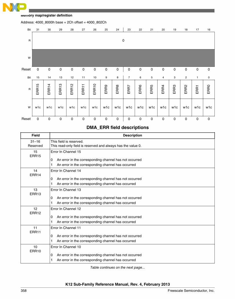
Address: 4000_8000h base + 2Ch offset = 4000_802Ch
Bit 31 30 29 28 27 26 25 24 23 22 21 20 19 18 17 16
R 0
W
Reset 0 0 0 0 0 0 0 0 0 0 0 0 0 0 0 0
Bit 15 14 13 12 11 10 9 8 7 6 5 4 3 2 1 0
R
ER
R15
ER
R14
ER
R13
ER
R12
ER
R11
ER
R10
ER
R9
ER
R8
ER
R7
ER
R6
ER
R5
ER
R4
ER
R3
ER
R2
ER
R1
ER
R0
W w1c w1c w1c w1c w1c w1c w1c w1c w1c w1c w1c w1c w1c w1c w1c w1c
Reset 0 0 0 0 0 0 0 0 0 0 0 0 0 0 0 0
DMA_ERR field descriptions
Field Description
31–16Reserved
This field is reserved.This read-only field is reserved and always has the value 0.
15ERR15
Error In Channel 15
0 An error in the corresponding channel has not occurred1 An error in the corresponding channel has occurred
14ERR14
Error In Channel 14
0 An error in the corresponding channel has not occurred1 An error in the corresponding channel has occurred
13ERR13
Error In Channel 13
0 An error in the corresponding channel has not occurred1 An error in the corresponding channel has occurred
12ERR12
Error In Channel 12
0 An error in the corresponding channel has not occurred1 An error in the corresponding channel has occurred
11ERR11
Error In Channel 11
0 An error in the corresponding channel has not occurred1 An error in the corresponding channel has occurred
10ERR10
Error In Channel 10
0 An error in the corresponding channel has not occurred1 An error in the corresponding channel has occurred
Table continues on the next page...
Memory map/register definition
K12 Sub-Family Reference Manual, Rev. 4, February 2013
358 Freescale Semiconductor, Inc.
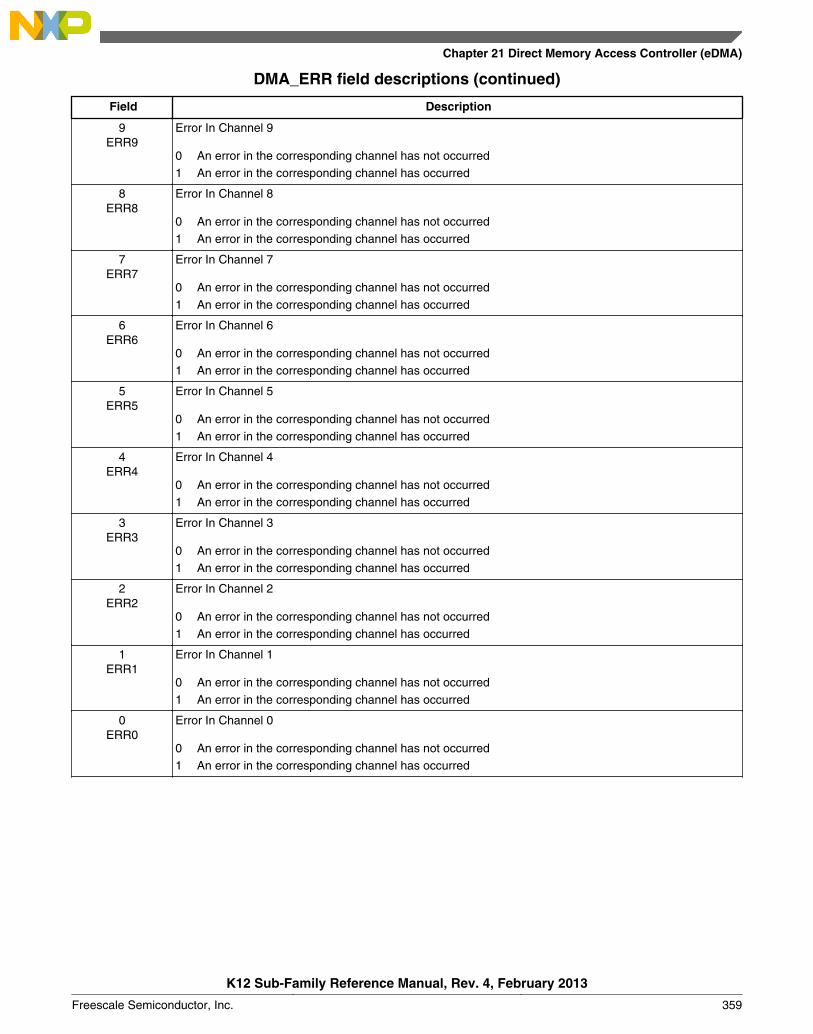
DMA_ERR field descriptions (continued)
Field Description
9ERR9
Error In Channel 9
0 An error in the corresponding channel has not occurred1 An error in the corresponding channel has occurred
8ERR8
Error In Channel 8
0 An error in the corresponding channel has not occurred1 An error in the corresponding channel has occurred
7ERR7
Error In Channel 7
0 An error in the corresponding channel has not occurred1 An error in the corresponding channel has occurred
6ERR6
Error In Channel 6
0 An error in the corresponding channel has not occurred1 An error in the corresponding channel has occurred
5ERR5
Error In Channel 5
0 An error in the corresponding channel has not occurred1 An error in the corresponding channel has occurred
4ERR4
Error In Channel 4
0 An error in the corresponding channel has not occurred1 An error in the corresponding channel has occurred
3ERR3
Error In Channel 3
0 An error in the corresponding channel has not occurred1 An error in the corresponding channel has occurred
2ERR2
Error In Channel 2
0 An error in the corresponding channel has not occurred1 An error in the corresponding channel has occurred
1ERR1
Error In Channel 1
0 An error in the corresponding channel has not occurred1 An error in the corresponding channel has occurred
0ERR0
Error In Channel 0
0 An error in the corresponding channel has not occurred1 An error in the corresponding channel has occurred
Chapter 21 Direct Memory Access Controller (eDMA)
K12 Sub-Family Reference Manual, Rev. 4, February 2013
Freescale Semiconductor, Inc. 359

21.3.15 Hardware Request Status Register (DMA_HRS)
The HRS register provides a bit map for the DMA channels, signaling the presence of ahardware request for each channel. The hardware request status bits reflect the currentstate of the register and qualified (via the ERQ fields) DMA request signals as seen bythe DMA’s arbitration logic. This view into the hardware request signals may be used fordebug purposes.
NOTEThese bits reflect the state of the request as seen by thearbitration logic. Therefore, this status is affected by the ERQbits.
Address: 4000_8000h base + 34h offset = 4000_8034h
Bit 31 30 29 28 27 26 25 24 23 22 21 20 19 18 17 16
R 0
W
Reset 0 0 0 0 0 0 0 0 0 0 0 0 0 0 0 0
Bit 15 14 13 12 11 10 9 8 7 6 5 4 3 2 1 0
R
HR
S15
HR
S14
HR
S13
HR
S12
HR
S11
HR
S10
HRS9 HRS8 HRS7 HRS6 HRS5 HRS4 HRS3 HRS2 HRS1 HRS0W
Reset 0 0 0 0 0 0 0 0 0 0 0 0 0 0 0 0
DMA_HRS field descriptions
Field Description
31–16Reserved
This field is reserved.This read-only field is reserved and always has the value 0.
15HRS15
Hardware Request Status Channel 15
0 A hardware service request for the corresponding channel is not present1 A hardware service request for the corresponding channel is present
14HRS14
Hardware Request Status Channel 14
0 A hardware service request for the corresponding channel is not present1 A hardware service request for the corresponding channel is present
13HRS13
Hardware Request Status Channel 13
0 A hardware service request for the corresponding channel is not present1 A hardware service request for the corresponding channel is present
Table continues on the next page...
Memory map/register definition
K12 Sub-Family Reference Manual, Rev. 4, February 2013
360 Freescale Semiconductor, Inc.
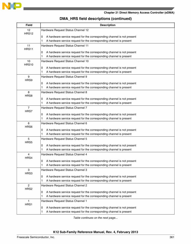
DMA_HRS field descriptions (continued)
Field Description
12HRS12
Hardware Request Status Channel 12
0 A hardware service request for the corresponding channel is not present1 A hardware service request for the corresponding channel is present
11HRS11
Hardware Request Status Channel 11
0 A hardware service request for the corresponding channel is not present1 A hardware service request for the corresponding channel is present
10HRS10
Hardware Request Status Channel 10
0 A hardware service request for the corresponding channel is not present1 A hardware service request for the corresponding channel is present
9HRS9
Hardware Request Status Channel 9
0 A hardware service request for the corresponding channel is not present1 A hardware service request for the corresponding channel is present
8HRS8
Hardware Request Status Channel 8
0 A hardware service request for the corresponding channel is not present1 A hardware service request for the corresponding channel is present
7HRS7
Hardware Request Status Channel 7
0 A hardware service request for the corresponding channel is not present1 A hardware service request for the corresponding channel is present
6HRS6
Hardware Request Status Channel 6
0 A hardware service request for the corresponding channel is not present1 A hardware service request for the corresponding channel is present
5HRS5
Hardware Request Status Channel 5
0 A hardware service request for the corresponding channel is not present1 A hardware service request for the corresponding channel is present
4HRS4
Hardware Request Status Channel 4
0 A hardware service request for the corresponding channel is not present1 A hardware service request for the corresponding channel is present
3HRS3
Hardware Request Status Channel 3
0 A hardware service request for the corresponding channel is not present1 A hardware service request for the corresponding channel is present
2HRS2
Hardware Request Status Channel 2
0 A hardware service request for the corresponding channel is not present1 A hardware service request for the corresponding channel is present
1HRS1
Hardware Request Status Channel 1
0 A hardware service request for the corresponding channel is not present1 A hardware service request for the corresponding channel is present
Table continues on the next page...
Chapter 21 Direct Memory Access Controller (eDMA)
K12 Sub-Family Reference Manual, Rev. 4, February 2013
Freescale Semiconductor, Inc. 361
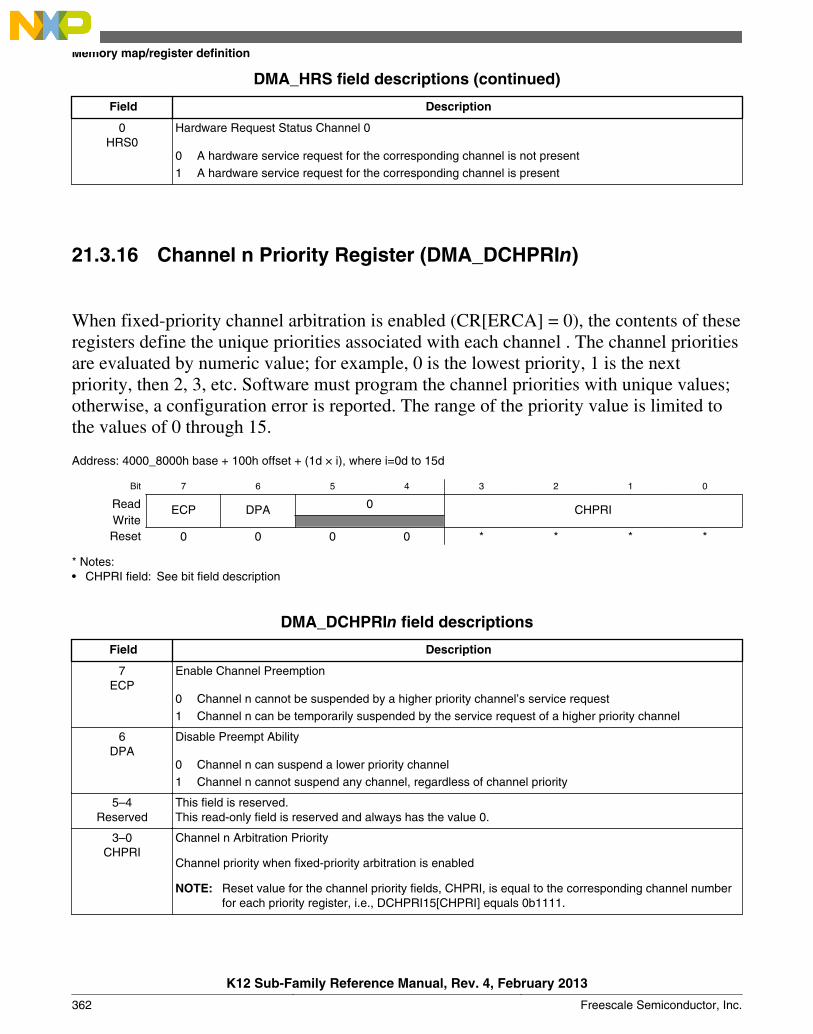
DMA_HRS field descriptions (continued)
Field Description
0HRS0
Hardware Request Status Channel 0
0 A hardware service request for the corresponding channel is not present1 A hardware service request for the corresponding channel is present
21.3.16 Channel n Priority Register (DMA_DCHPRIn)
When fixed-priority channel arbitration is enabled (CR[ERCA] = 0), the contents of theseregisters define the unique priorities associated with each channel . The channel prioritiesare evaluated by numeric value; for example, 0 is the lowest priority, 1 is the nextpriority, then 2, 3, etc. Software must program the channel priorities with unique values;otherwise, a configuration error is reported. The range of the priority value is limited tothe values of 0 through 15.
Address: 4000_8000h base + 100h offset + (1d × i), where i=0d to 15d
Bit 7 6 5 4 3 2 1 0
Read ECP DPA 0 CHPRIWriteReset 0 0 0 0 * * * *
* Notes:CHPRI field: See bit field description•
DMA_DCHPRIn field descriptions
Field Description
7ECP
Enable Channel Preemption
0 Channel n cannot be suspended by a higher priority channel’s service request1 Channel n can be temporarily suspended by the service request of a higher priority channel
6DPA
Disable Preempt Ability
0 Channel n can suspend a lower priority channel1 Channel n cannot suspend any channel, regardless of channel priority
5–4Reserved
This field is reserved.This read-only field is reserved and always has the value 0.
3–0CHPRI
Channel n Arbitration Priority
Channel priority when fixed-priority arbitration is enabled
NOTE: Reset value for the channel priority fields, CHPRI, is equal to the corresponding channel numberfor each priority register, i.e., DCHPRI15[CHPRI] equals 0b1111.
Memory map/register definition
K12 Sub-Family Reference Manual, Rev. 4, February 2013
362 Freescale Semiconductor, Inc.
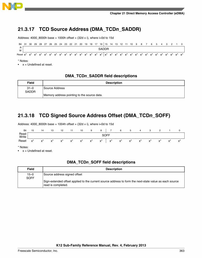
21.3.17 TCD Source Address (DMA_TCDn_SADDR)
Address: 4000_8000h base + 1000h offset + (32d × i), where i=0d to 15d
Bit 31 30 29 28 27 26 25 24 23 22 21 20 19 18 17 16 15 14 13 12 11 10 9 8 7 6 5 4 3 2 1 0
R SADDRW
Reset x* x* x* x* x* x* x* x* x* x* x* x* x* x* x* x* x* x* x* x* x* x* x* x* x* x* x* x* x* x* x* x*
* Notes:x = Undefined at reset.•
DMA_TCDn_SADDR field descriptions
Field Description
31–0SADDR
Source Address
Memory address pointing to the source data.
21.3.18 TCD Signed Source Address Offset (DMA_TCDn_SOFF)
Address: 4000_8000h base + 1004h offset + (32d × i), where i=0d to 15d
Bit 15 14 13 12 11 10 9 8 7 6 5 4 3 2 1 0
Read SOFFWriteReset x* x* x* x* x* x* x* x* x* x* x* x* x* x* x* x*
* Notes:x = Undefined at reset.•
DMA_TCDn_SOFF field descriptions
Field Description
15–0SOFF
Source address signed offset
Sign-extended offset applied to the current source address to form the next-state value as each sourceread is completed.
Chapter 21 Direct Memory Access Controller (eDMA)
K12 Sub-Family Reference Manual, Rev. 4, February 2013
Freescale Semiconductor, Inc. 363
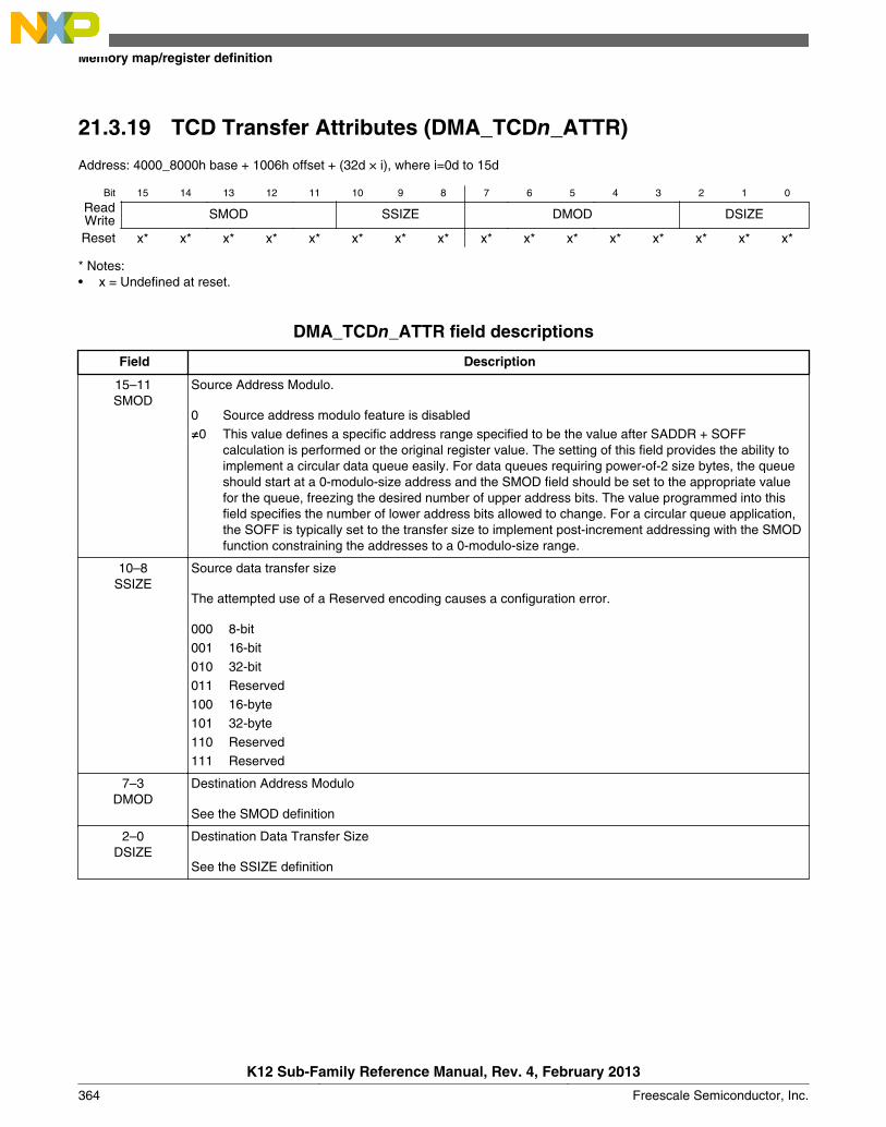
21.3.19 TCD Transfer Attributes (DMA_TCDn_ATTR)
Address: 4000_8000h base + 1006h offset + (32d × i), where i=0d to 15d
Bit 15 14 13 12 11 10 9 8 7 6 5 4 3 2 1 0
Read SMOD SSIZE DMOD DSIZEWriteReset x* x* x* x* x* x* x* x* x* x* x* x* x* x* x* x*
* Notes:x = Undefined at reset.•
DMA_TCDn_ATTR field descriptions
Field Description
15–11SMOD
Source Address Modulo.
0 Source address modulo feature is disabled≠0 This value defines a specific address range specified to be the value after SADDR + SOFF
calculation is performed or the original register value. The setting of this field provides the ability toimplement a circular data queue easily. For data queues requiring power-of-2 size bytes, the queueshould start at a 0-modulo-size address and the SMOD field should be set to the appropriate valuefor the queue, freezing the desired number of upper address bits. The value programmed into thisfield specifies the number of lower address bits allowed to change. For a circular queue application,the SOFF is typically set to the transfer size to implement post-increment addressing with the SMODfunction constraining the addresses to a 0-modulo-size range.
10–8SSIZE
Source data transfer size
The attempted use of a Reserved encoding causes a configuration error.
000 8-bit001 16-bit010 32-bit011 Reserved100 16-byte101 32-byte110 Reserved111 Reserved
7–3DMOD
Destination Address Modulo
See the SMOD definition
2–0DSIZE
Destination Data Transfer Size
See the SSIZE definition
Memory map/register definition
K12 Sub-Family Reference Manual, Rev. 4, February 2013
364 Freescale Semiconductor, Inc.
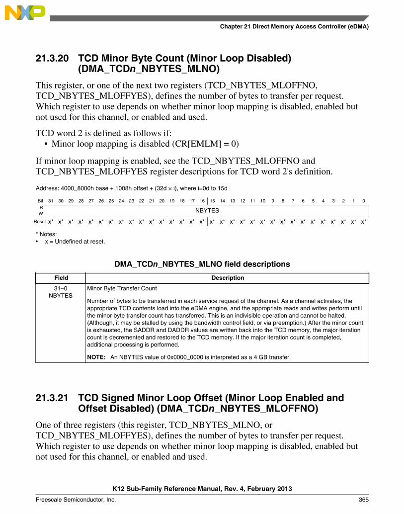
21.3.20 TCD Minor Byte Count (Minor Loop Disabled)(DMA_TCDn_NBYTES_MLNO)
This register, or one of the next two registers (TCD_NBYTES_MLOFFNO,TCD_NBYTES_MLOFFYES), defines the number of bytes to transfer per request.Which register to use depends on whether minor loop mapping is disabled, enabled butnot used for this channel, or enabled and used.
TCD word 2 is defined as follows if:• Minor loop mapping is disabled (CR[EMLM] = 0)
If minor loop mapping is enabled, see the TCD_NBYTES_MLOFFNO andTCD_NBYTES_MLOFFYES register descriptions for TCD word 2's definition.
Address: 4000_8000h base + 1008h offset + (32d × i), where i=0d to 15d
Bit 31 30 29 28 27 26 25 24 23 22 21 20 19 18 17 16 15 14 13 12 11 10 9 8 7 6 5 4 3 2 1 0
R NBYTESW
Reset x* x* x* x* x* x* x* x* x* x* x* x* x* x* x* x* x* x* x* x* x* x* x* x* x* x* x* x* x* x* x* x*
* Notes:x = Undefined at reset.•
DMA_TCDn_NBYTES_MLNO field descriptions
Field Description
31–0NBYTES
Minor Byte Transfer Count
Number of bytes to be transferred in each service request of the channel. As a channel activates, theappropriate TCD contents load into the eDMA engine, and the appropriate reads and writes perform untilthe minor byte transfer count has transferred. This is an indivisible operation and cannot be halted.(Although, it may be stalled by using the bandwidth control field, or via preemption.) After the minor countis exhausted, the SADDR and DADDR values are written back into the TCD memory, the major iterationcount is decremented and restored to the TCD memory. If the major iteration count is completed,additional processing is performed.
NOTE: An NBYTES value of 0x0000_0000 is interpreted as a 4 GB transfer.
21.3.21 TCD Signed Minor Loop Offset (Minor Loop Enabled andOffset Disabled) (DMA_TCDn_NBYTES_MLOFFNO)
One of three registers (this register, TCD_NBYTES_MLNO, orTCD_NBYTES_MLOFFYES), defines the number of bytes to transfer per request.Which register to use depends on whether minor loop mapping is disabled, enabled butnot used for this channel, or enabled and used.
Chapter 21 Direct Memory Access Controller (eDMA)
K12 Sub-Family Reference Manual, Rev. 4, February 2013
Freescale Semiconductor, Inc. 365

TCD word 2 is defined as follows if:
• Minor loop mapping is enabled (CR[EMLM] = 1) and• SMLOE = 0 and DMLOE = 0
If minor loop mapping is enabled and SMLOE or DMLOE is set, then refer to theTCD_NBYTES_MLOFFYES register description. If minor loop mapping is disabled,then refer to the TCD_NBYTES_MLNO register description.
Address: 4000_8000h base + 1008h offset + (32d × i), where i=0d to 15d
Bit 31 30 29 28 27 26 25 24 23 22 21 20 19 18 17 16
R
SM
LOE
DM
LOE
NBYTESW
Reset x* x* x* x* x* x* x* x* x* x* x* x* x* x* x* x*
Bit 15 14 13 12 11 10 9 8 7 6 5 4 3 2 1 0
R
NBYTESW
Reset x* x* x* x* x* x* x* x* x* x* x* x* x* x* x* x*
* Notes:x = Undefined at reset.•
DMA_TCDn_NBYTES_MLOFFNO field descriptions
Field Description
31SMLOE
Source Minor Loop Offset Enable
Selects whether the minor loop offset is applied to the source address upon minor loop completion.
0 The minor loop offset is not applied to the SADDR1 The minor loop offset is applied to the SADDR
30DMLOE
Destination Minor Loop Offset enable
Selects whether the minor loop offset is applied to the destination address upon minor loop completion.
0 The minor loop offset is not applied to the DADDR1 The minor loop offset is applied to the DADDR
29–0NBYTES
Minor Byte Transfer Count
Number of bytes to be transferred in each service request of the channel.
As a channel activates, the appropriate TCD contents load into the eDMA engine, and the appropriatereads and writes perform until the minor byte transfer count has transferred. This is an indivisible operationand cannot be halted; although, it may be stalled by using the bandwidth control field, or via preemption.After the minor count is exhausted, the SADDR and DADDR values are written back into the TCDmemory, the major iteration count is decremented and restored to the TCD memory. If the major iterationcount is completed, additional processing is performed.
Memory map/register definition
K12 Sub-Family Reference Manual, Rev. 4, February 2013
366 Freescale Semiconductor, Inc.
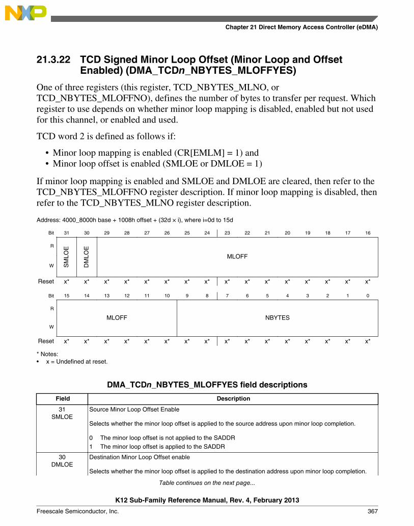
21.3.22 TCD Signed Minor Loop Offset (Minor Loop and OffsetEnabled) (DMA_TCDn_NBYTES_MLOFFYES)
One of three registers (this register, TCD_NBYTES_MLNO, orTCD_NBYTES_MLOFFNO), defines the number of bytes to transfer per request. Whichregister to use depends on whether minor loop mapping is disabled, enabled but not usedfor this channel, or enabled and used.
TCD word 2 is defined as follows if:
• Minor loop mapping is enabled (CR[EMLM] = 1) and• Minor loop offset is enabled (SMLOE or DMLOE = 1)
If minor loop mapping is enabled and SMLOE and DMLOE are cleared, then refer to theTCD_NBYTES_MLOFFNO register description. If minor loop mapping is disabled, thenrefer to the TCD_NBYTES_MLNO register description.
Address: 4000_8000h base + 1008h offset + (32d × i), where i=0d to 15d
Bit 31 30 29 28 27 26 25 24 23 22 21 20 19 18 17 16
R
SM
LOE
DM
LOE
MLOFFW
Reset x* x* x* x* x* x* x* x* x* x* x* x* x* x* x* x*
Bit 15 14 13 12 11 10 9 8 7 6 5 4 3 2 1 0
R
MLOFF NBYTESW
Reset x* x* x* x* x* x* x* x* x* x* x* x* x* x* x* x*
* Notes:x = Undefined at reset.•
DMA_TCDn_NBYTES_MLOFFYES field descriptions
Field Description
31SMLOE
Source Minor Loop Offset Enable
Selects whether the minor loop offset is applied to the source address upon minor loop completion.
0 The minor loop offset is not applied to the SADDR1 The minor loop offset is applied to the SADDR
30DMLOE
Destination Minor Loop Offset enable
Selects whether the minor loop offset is applied to the destination address upon minor loop completion.
Table continues on the next page...
Chapter 21 Direct Memory Access Controller (eDMA)
K12 Sub-Family Reference Manual, Rev. 4, February 2013
Freescale Semiconductor, Inc. 367
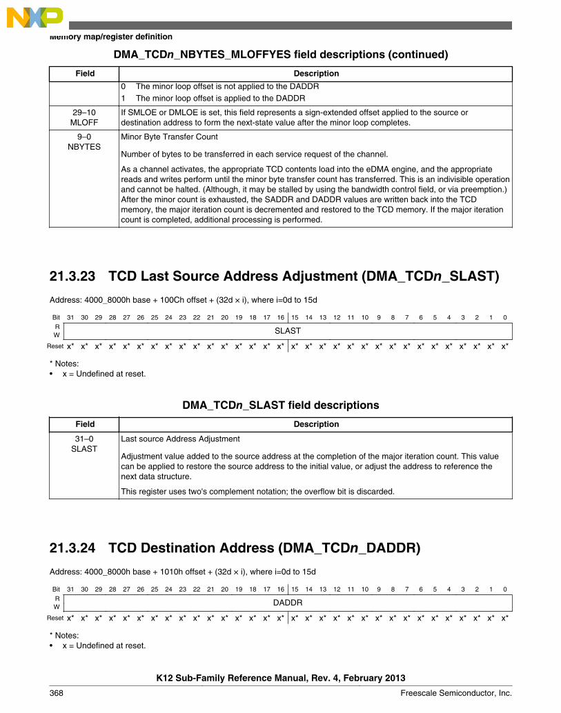
DMA_TCDn_NBYTES_MLOFFYES field descriptions (continued)
Field Description
0 The minor loop offset is not applied to the DADDR1 The minor loop offset is applied to the DADDR
29–10MLOFF
If SMLOE or DMLOE is set, this field represents a sign-extended offset applied to the source ordestination address to form the next-state value after the minor loop completes.
9–0NBYTES
Minor Byte Transfer Count
Number of bytes to be transferred in each service request of the channel.
As a channel activates, the appropriate TCD contents load into the eDMA engine, and the appropriatereads and writes perform until the minor byte transfer count has transferred. This is an indivisible operationand cannot be halted. (Although, it may be stalled by using the bandwidth control field, or via preemption.)After the minor count is exhausted, the SADDR and DADDR values are written back into the TCDmemory, the major iteration count is decremented and restored to the TCD memory. If the major iterationcount is completed, additional processing is performed.
21.3.23 TCD Last Source Address Adjustment (DMA_TCDn_SLAST)
Address: 4000_8000h base + 100Ch offset + (32d × i), where i=0d to 15d
Bit 31 30 29 28 27 26 25 24 23 22 21 20 19 18 17 16 15 14 13 12 11 10 9 8 7 6 5 4 3 2 1 0
R SLASTW
Reset x* x* x* x* x* x* x* x* x* x* x* x* x* x* x* x* x* x* x* x* x* x* x* x* x* x* x* x* x* x* x* x*
* Notes:x = Undefined at reset.•
DMA_TCDn_SLAST field descriptions
Field Description
31–0SLAST
Last source Address Adjustment
Adjustment value added to the source address at the completion of the major iteration count. This valuecan be applied to restore the source address to the initial value, or adjust the address to reference thenext data structure.
This register uses two's complement notation; the overflow bit is discarded.
21.3.24 TCD Destination Address (DMA_TCDn_DADDR)
Address: 4000_8000h base + 1010h offset + (32d × i), where i=0d to 15d
Bit 31 30 29 28 27 26 25 24 23 22 21 20 19 18 17 16 15 14 13 12 11 10 9 8 7 6 5 4 3 2 1 0
R DADDRW
Reset x* x* x* x* x* x* x* x* x* x* x* x* x* x* x* x* x* x* x* x* x* x* x* x* x* x* x* x* x* x* x* x*
* Notes:x = Undefined at reset.•
Memory map/register definition
K12 Sub-Family Reference Manual, Rev. 4, February 2013
368 Freescale Semiconductor, Inc.
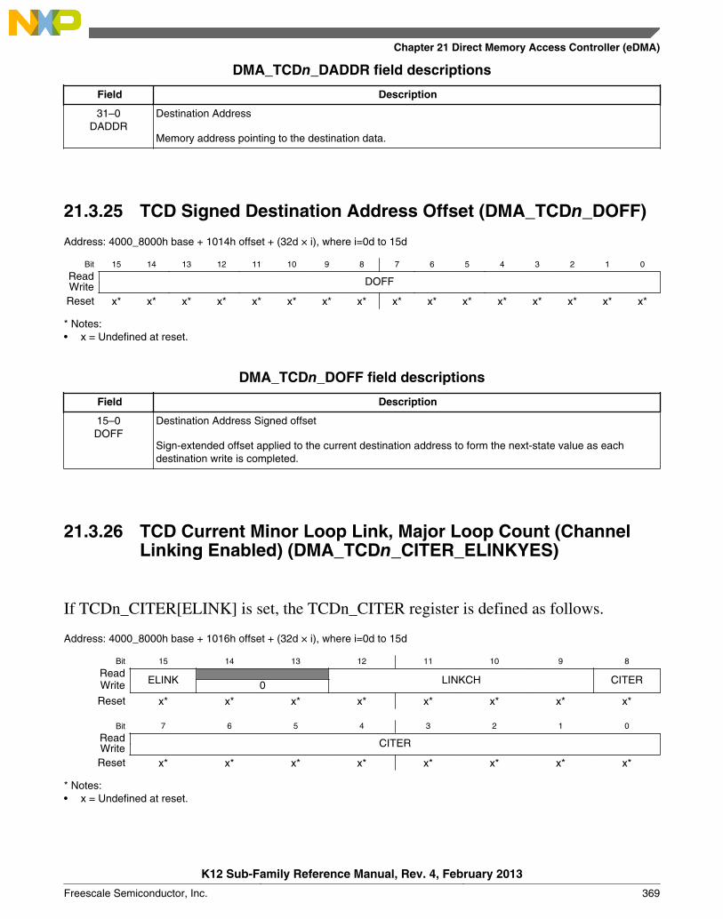
DMA_TCDn_DADDR field descriptions
Field Description
31–0DADDR
Destination Address
Memory address pointing to the destination data.
21.3.25 TCD Signed Destination Address Offset (DMA_TCDn_DOFF)
Address: 4000_8000h base + 1014h offset + (32d × i), where i=0d to 15d
Bit 15 14 13 12 11 10 9 8 7 6 5 4 3 2 1 0
Read DOFFWriteReset x* x* x* x* x* x* x* x* x* x* x* x* x* x* x* x*
* Notes:x = Undefined at reset.•
DMA_TCDn_DOFF field descriptions
Field Description
15–0DOFF
Destination Address Signed offset
Sign-extended offset applied to the current destination address to form the next-state value as eachdestination write is completed.
21.3.26 TCD Current Minor Loop Link, Major Loop Count (ChannelLinking Enabled) (DMA_TCDn_CITER_ELINKYES)
If TCDn_CITER[ELINK] is set, the TCDn_CITER register is defined as follows.
Address: 4000_8000h base + 1016h offset + (32d × i), where i=0d to 15d
Bit 15 14 13 12 11 10 9 8
ReadELINK LINKCH CITERWrite 0
Reset x* x* x* x* x* x* x* x*
Bit 7 6 5 4 3 2 1 0
Read CITERWriteReset x* x* x* x* x* x* x* x*
* Notes:x = Undefined at reset.•
Chapter 21 Direct Memory Access Controller (eDMA)
K12 Sub-Family Reference Manual, Rev. 4, February 2013
Freescale Semiconductor, Inc. 369
DMA_TCDn_CITER_ELINKYES field descriptions
Field Description
15ELINK
Enable channel-to-channel linking on minor-loop complete
As the channel completes the minor loop, this flag enables linking to another channel, defined by theLINKCH field. The link target channel initiates a channel service request via an internal mechanism thatsets the TCDn_CSR[START] bit of the specified channel.
If channel linking is disabled, the CITER value is extended to 15 bits in place of a link channel number. Ifthe major loop is exhausted, this link mechanism is suppressed in favor of the MAJORELINK channellinking.
NOTE: This bit must be equal to the BITER[ELINK] bit; otherwise, a configuration error is reported.
0 The channel-to-channel linking is disabled1 The channel-to-channel linking is enabled
14–13Reserved
This field is reserved.
12–9LINKCH
Link Channel Number
If channel-to-channel linking is enabled (ELINK = 1), then after the minor loop is exhausted, the eDMAengine initiates a channel service request to the channel defined by these four bits by setting thatchannel’s TCDn_CSR[START] bit.
8–0CITER
Current Major Iteration Count
This 9-bit (ELINK = 1) or 15-bit (ELINK = 0) count represents the current major loop count for the channel.It is decremented each time the minor loop is completed and updated in the transfer control descriptormemory. After the major iteration count is exhausted, the channel performs a number of operations (e.g.,final source and destination address calculations), optionally generating an interrupt to signal channelcompletion before reloading the CITER field from the beginning iteration count (BITER) field.
NOTE: When the CITER field is initially loaded by software, it must be set to the same value as thatcontained in the BITER field.
NOTE: If the channel is configured to execute a single service request, the initial values of BITER andCITER should be 0x0001.
Memory map/register definition
K12 Sub-Family Reference Manual, Rev. 4, February 2013
370 Freescale Semiconductor, Inc.

21.3.27 TCD Current Minor Loop Link, Major Loop Count (ChannelLinking Disabled) (DMA_TCDn_CITER_ELINKNO)
If TCDn_CITER[ELINK] is cleared, the TCDn_CITER register is defined as follows.
Address: 4000_8000h base + 1016h offset + (32d × i), where i=0d to 15d
Bit 15 14 13 12 11 10 9 8
Read ELINK CITERWriteReset x* x* x* x* x* x* x* x*
Bit 7 6 5 4 3 2 1 0
Read CITERWriteReset x* x* x* x* x* x* x* x*
* Notes:x = Undefined at reset.•
DMA_TCDn_CITER_ELINKNO field descriptions
Field Description
15ELINK
Enable channel-to-channel linking on minor-loop complete
As the channel completes the minor loop, this flag enables linking to another channel, defined by theLINKCH field. The link target channel initiates a channel service request via an internal mechanism thatsets the TCDn_CSR[START] bit of the specified channel.
If channel linking is disabled, the CITER value is extended to 15 bits in place of a link channel number. Ifthe major loop is exhausted, this link mechanism is suppressed in favor of the MAJORELINK channellinking.
NOTE: This bit must be equal to the BITER[ELINK] bit; otherwise, a configuration error is reported.
0 The channel-to-channel linking is disabled1 The channel-to-channel linking is enabled
14–0CITER
Current Major Iteration Count
This 9-bit (ELINK = 1) or 15-bit (ELINK = 0) count represents the current major loop count for the channel.It is decremented each time the minor loop is completed and updated in the transfer control descriptormemory. After the major iteration count is exhausted, the channel performs a number of operations (e.g.,final source and destination address calculations), optionally generating an interrupt to signal channelcompletion before reloading the CITER field from the beginning iteration count (BITER) field.
NOTE: When the CITER field is initially loaded by software, it must be set to the same value as thatcontained in the BITER field.
NOTE: If the channel is configured to execute a single service request, the initial values of BITER andCITER should be 0x0001.
Chapter 21 Direct Memory Access Controller (eDMA)
K12 Sub-Family Reference Manual, Rev. 4, February 2013
Freescale Semiconductor, Inc. 371

21.3.28 TCD Last Destination Address Adjustment/Scatter GatherAddress (DMA_TCDn_DLASTSGA)
Address: 4000_8000h base + 1018h offset + (32d × i), where i=0d to 15d
Bit 31 30 29 28 27 26 25 24 23 22 21 20 19 18 17 16 15 14 13 12 11 10 9 8 7 6 5 4 3 2 1 0
R DLASTSGAW
Reset x* x* x* x* x* x* x* x* x* x* x* x* x* x* x* x* x* x* x* x* x* x* x* x* x* x* x* x* x* x* x* x*
* Notes:x = Undefined at reset.•
DMA_TCDn_DLASTSGA field descriptions
Field Description
31–0DLASTSGA
Destination last address adjustment or the memory address for the next transfer control descriptor to beloaded into this channel (scatter/gather).
If (TCDn_CSR[ESG] = 0), then:
• Adjustment value added to the destination address at the completion of the major iteration count.This value can apply to restore the destination address to the initial value or adjust the address toreference the next data structure.
• This field uses two's complement notation for the final destination address adjustment.
Otherwise:
• This address points to the beginning of a 0-modulo-32-byte region containing the next transfercontrol descriptor to be loaded into this channel. This channel reload is performed as the majoriteration count completes. The scatter/gather address must be 0-modulo-32-byte, else aconfiguration error is reported.
21.3.29 TCD Control and Status (DMA_TCDn_CSR)
Address: 4000_8000h base + 101Ch offset + (32d × i), where i=0d to 15d
Bit 15 14 13 12 11 10 9 8
ReadBWC MAJORLINKCHWrite 0
Reset x* x* x* x* x* x* x* x*
Bit 7 6 5 4 3 2 1 0
ReadDONE ACTIVE
MAJORELINK
ESG DREQ INTHALF INTMAJOR STARTWrite
Reset 0 0 x* x* x* x* x* 0
* Notes:x = Undefined at reset.•
Memory map/register definition
K12 Sub-Family Reference Manual, Rev. 4, February 2013
372 Freescale Semiconductor, Inc.
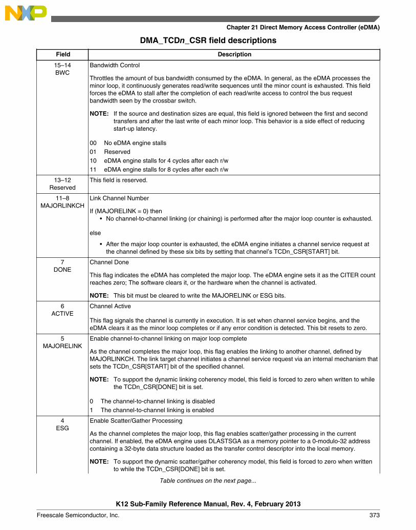
DMA_TCDn_CSR field descriptions
Field Description
15–14BWC
Bandwidth Control
Throttles the amount of bus bandwidth consumed by the eDMA. In general, as the eDMA processes theminor loop, it continuously generates read/write sequences until the minor count is exhausted. This fieldforces the eDMA to stall after the completion of each read/write access to control the bus requestbandwidth seen by the crossbar switch.
NOTE: If the source and destination sizes are equal, this field is ignored between the first and secondtransfers and after the last write of each minor loop. This behavior is a side effect of reducingstart-up latency.
00 No eDMA engine stalls01 Reserved10 eDMA engine stalls for 4 cycles after each r/w11 eDMA engine stalls for 8 cycles after each r/w
13–12Reserved
This field is reserved.
11–8MAJORLINKCH
Link Channel Number
If (MAJORELINK = 0) then• No channel-to-channel linking (or chaining) is performed after the major loop counter is exhausted.
else
• After the major loop counter is exhausted, the eDMA engine initiates a channel service request atthe channel defined by these six bits by setting that channel’s TCDn_CSR[START] bit.
7DONE
Channel Done
This flag indicates the eDMA has completed the major loop. The eDMA engine sets it as the CITER countreaches zero; The software clears it, or the hardware when the channel is activated.
NOTE: This bit must be cleared to write the MAJORELINK or ESG bits.
6ACTIVE
Channel Active
This flag signals the channel is currently in execution. It is set when channel service begins, and theeDMA clears it as the minor loop completes or if any error condition is detected. This bit resets to zero.
5MAJORELINK
Enable channel-to-channel linking on major loop complete
As the channel completes the major loop, this flag enables the linking to another channel, defined byMAJORLINKCH. The link target channel initiates a channel service request via an internal mechanism thatsets the TCDn_CSR[START] bit of the specified channel.
NOTE: To support the dynamic linking coherency model, this field is forced to zero when written to whilethe TCDn_CSR[DONE] bit is set.
0 The channel-to-channel linking is disabled1 The channel-to-channel linking is enabled
4ESG
Enable Scatter/Gather Processing
As the channel completes the major loop, this flag enables scatter/gather processing in the currentchannel. If enabled, the eDMA engine uses DLASTSGA as a memory pointer to a 0-modulo-32 addresscontaining a 32-byte data structure loaded as the transfer control descriptor into the local memory.
NOTE: To support the dynamic scatter/gather coherency model, this field is forced to zero when writtento while the TCDn_CSR[DONE] bit is set.
Table continues on the next page...
Chapter 21 Direct Memory Access Controller (eDMA)
K12 Sub-Family Reference Manual, Rev. 4, February 2013
Freescale Semiconductor, Inc. 373
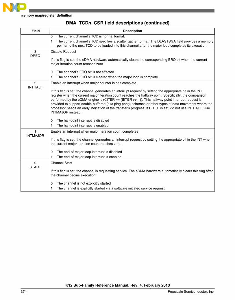
DMA_TCDn_CSR field descriptions (continued)
Field Description
0 The current channel’s TCD is normal format.1 The current channel’s TCD specifies a scatter gather format. The DLASTSGA field provides a memory
pointer to the next TCD to be loaded into this channel after the major loop completes its execution.
3DREQ
Disable Request
If this flag is set, the eDMA hardware automatically clears the corresponding ERQ bit when the currentmajor iteration count reaches zero.
0 The channel’s ERQ bit is not affected1 The channel’s ERQ bit is cleared when the major loop is complete
2INTHALF
Enable an interrupt when major counter is half complete.
If this flag is set, the channel generates an interrupt request by setting the appropriate bit in the INTregister when the current major iteration count reaches the halfway point. Specifically, the comparisonperformed by the eDMA engine is (CITER == (BITER >> 1)). This halfway point interrupt request isprovided to support double-buffered (aka ping-pong) schemes or other types of data movement where theprocessor needs an early indication of the transfer’s progress. If BITER is set, do not use INTHALF. UseINTMAJOR instead.
0 The half-point interrupt is disabled1 The half-point interrupt is enabled
1INTMAJOR
Enable an interrupt when major iteration count completes
If this flag is set, the channel generates an interrupt request by setting the appropriate bit in the INT whenthe current major iteration count reaches zero.
0 The end-of-major loop interrupt is disabled1 The end-of-major loop interrupt is enabled
0START
Channel Start
If this flag is set, the channel is requesting service. The eDMA hardware automatically clears this flag afterthe channel begins execution.
0 The channel is not explicitly started1 The channel is explicitly started via a software initiated service request
Memory map/register definition
K12 Sub-Family Reference Manual, Rev. 4, February 2013
374 Freescale Semiconductor, Inc.
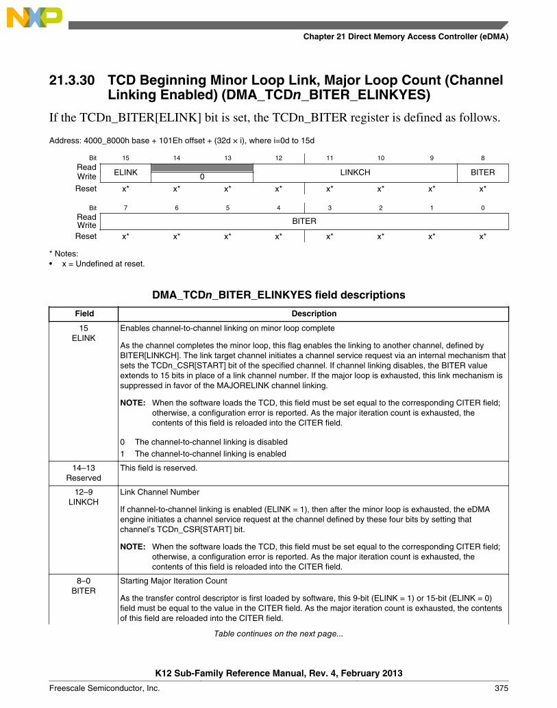
21.3.30 TCD Beginning Minor Loop Link, Major Loop Count (ChannelLinking Enabled) (DMA_TCDn_BITER_ELINKYES)
If the TCDn_BITER[ELINK] bit is set, the TCDn_BITER register is defined as follows.
Address: 4000_8000h base + 101Eh offset + (32d × i), where i=0d to 15d
Bit 15 14 13 12 11 10 9 8
ReadELINK LINKCH BITERWrite 0
Reset x* x* x* x* x* x* x* x*
Bit 7 6 5 4 3 2 1 0
Read BITERWriteReset x* x* x* x* x* x* x* x*
* Notes:x = Undefined at reset.•
DMA_TCDn_BITER_ELINKYES field descriptions
Field Description
15ELINK
Enables channel-to-channel linking on minor loop complete
As the channel completes the minor loop, this flag enables the linking to another channel, defined byBITER[LINKCH]. The link target channel initiates a channel service request via an internal mechanism thatsets the TCDn_CSR[START] bit of the specified channel. If channel linking disables, the BITER valueextends to 15 bits in place of a link channel number. If the major loop is exhausted, this link mechanism issuppressed in favor of the MAJORELINK channel linking.
NOTE: When the software loads the TCD, this field must be set equal to the corresponding CITER field;otherwise, a configuration error is reported. As the major iteration count is exhausted, thecontents of this field is reloaded into the CITER field.
0 The channel-to-channel linking is disabled1 The channel-to-channel linking is enabled
14–13Reserved
This field is reserved.
12–9LINKCH
Link Channel Number
If channel-to-channel linking is enabled (ELINK = 1), then after the minor loop is exhausted, the eDMAengine initiates a channel service request at the channel defined by these four bits by setting thatchannel’s TCDn_CSR[START] bit.
NOTE: When the software loads the TCD, this field must be set equal to the corresponding CITER field;otherwise, a configuration error is reported. As the major iteration count is exhausted, thecontents of this field is reloaded into the CITER field.
8–0BITER
Starting Major Iteration Count
As the transfer control descriptor is first loaded by software, this 9-bit (ELINK = 1) or 15-bit (ELINK = 0)field must be equal to the value in the CITER field. As the major iteration count is exhausted, the contentsof this field are reloaded into the CITER field.
Table continues on the next page...
Chapter 21 Direct Memory Access Controller (eDMA)
K12 Sub-Family Reference Manual, Rev. 4, February 2013
Freescale Semiconductor, Inc. 375
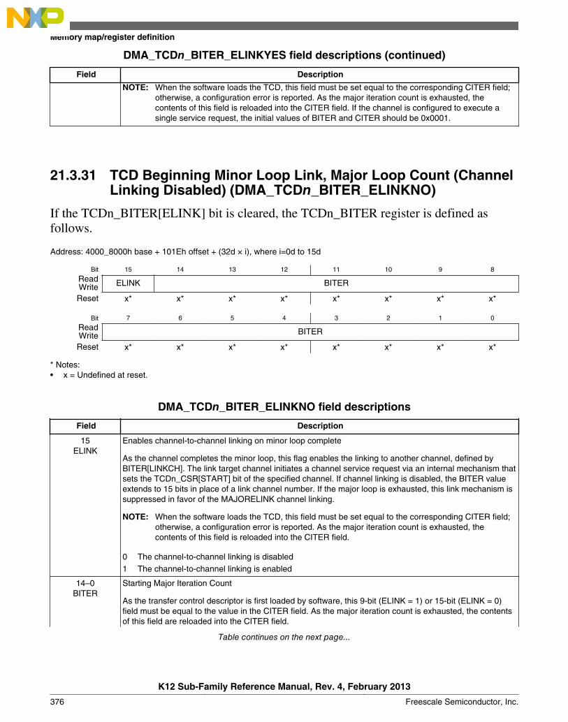
DMA_TCDn_BITER_ELINKYES field descriptions (continued)
Field Description
NOTE: When the software loads the TCD, this field must be set equal to the corresponding CITER field;otherwise, a configuration error is reported. As the major iteration count is exhausted, thecontents of this field is reloaded into the CITER field. If the channel is configured to execute asingle service request, the initial values of BITER and CITER should be 0x0001.
21.3.31 TCD Beginning Minor Loop Link, Major Loop Count (ChannelLinking Disabled) (DMA_TCDn_BITER_ELINKNO)
If the TCDn_BITER[ELINK] bit is cleared, the TCDn_BITER register is defined asfollows.
Address: 4000_8000h base + 101Eh offset + (32d × i), where i=0d to 15d
Bit 15 14 13 12 11 10 9 8
Read ELINK BITERWriteReset x* x* x* x* x* x* x* x*
Bit 7 6 5 4 3 2 1 0
Read BITERWriteReset x* x* x* x* x* x* x* x*
* Notes:x = Undefined at reset.•
DMA_TCDn_BITER_ELINKNO field descriptions
Field Description
15ELINK
Enables channel-to-channel linking on minor loop complete
As the channel completes the minor loop, this flag enables the linking to another channel, defined byBITER[LINKCH]. The link target channel initiates a channel service request via an internal mechanism thatsets the TCDn_CSR[START] bit of the specified channel. If channel linking is disabled, the BITER valueextends to 15 bits in place of a link channel number. If the major loop is exhausted, this link mechanism issuppressed in favor of the MAJORELINK channel linking.
NOTE: When the software loads the TCD, this field must be set equal to the corresponding CITER field;otherwise, a configuration error is reported. As the major iteration count is exhausted, thecontents of this field is reloaded into the CITER field.
0 The channel-to-channel linking is disabled1 The channel-to-channel linking is enabled
14–0BITER
Starting Major Iteration Count
As the transfer control descriptor is first loaded by software, this 9-bit (ELINK = 1) or 15-bit (ELINK = 0)field must be equal to the value in the CITER field. As the major iteration count is exhausted, the contentsof this field are reloaded into the CITER field.
Table continues on the next page...
Memory map/register definition
K12 Sub-Family Reference Manual, Rev. 4, February 2013
376 Freescale Semiconductor, Inc.

DMA_TCDn_BITER_ELINKNO field descriptions (continued)
Field Description
NOTE: When the software loads the TCD, this field must be set equal to the corresponding CITER field;otherwise, a configuration error is reported. As the major iteration count is exhausted, thecontents of this field is reloaded into the CITER field. If the channel is configured to execute asingle service request, the initial values of BITER and CITER should be 0x0001.
21.4 Functional description
21.4.1 eDMA basic data flow
The basic flow of a data transfer can be partitioned into three segments.
As shown in the following diagram, the first segment involves the channel activation:
1
eDMA Engine
Data Path
eDMA
0
Program Model/
64
Control
n-1
To/
Fro
m C
ross
bar
Sw
itch
2
Channel Arbitration
Address Path
Read Data
Write Data
Address
Read Data
Write Data
Write Address
Inte
rnal
Per
iphe
ral B
us
eDMA PeripheralRequest eDMA Done
TransferControlDescriptor (TCD)
Figure 21-289. eDMA operation, part 1
Chapter 21 Direct Memory Access Controller (eDMA)
K12 Sub-Family Reference Manual, Rev. 4, February 2013
Freescale Semiconductor, Inc. 377

This example uses the assertion of the eDMA peripheral request signal to request servicefor channel n. Channel activation via software and the TCDn_CSR[START] bit followsthe same basic flow as peripheral requests. The eDMA request input signal is registeredinternally and then routed through the eDMA engine: first through the control module,then into the program model and channel arbitration. In the next cycle, the channelarbitration performs, using the fixed-priority or round-robin algorithm. After arbitration iscomplete, the activated channel number is sent through the address path and convertedinto the required address to access the local memory for TCDn. Next, the TCD memoryis accessed and the required descriptor read from the local memory and loaded into theeDMA engine address path channel x or y registers. The TCD memory is 64 bits wide tominimize the time needed to fetch the activated channel descriptor and load it into theaddress path channel x or y registers.
The following diagram illustrates the second part of the basic data flow:
1
eDMA Engine
Data Path
eDMA
0
Program Model/
64
Control
n-1
To/
Fro
m C
ross
bar
Sw
itch
2
Channel Arbitration
Address Path
Read Data
Write Data
Address
Read Data
Write Data
Write Address
eDMA PeripheralRequest eDMA Done
TransferControlDescriptor (TCD)
Inte
rnal
Per
iphe
ral B
us
Figure 21-290. eDMA operation, part 2
Functional description
K12 Sub-Family Reference Manual, Rev. 4, February 2013
378 Freescale Semiconductor, Inc.

The modules associated with the data transfer (address path, data path, and control)sequence through the required source reads and destination writes to perform the actualdata movement. The source reads are initiated and the fetched data is temporarily storedin the data path block until it is gated onto the internal bus during the destination write.This source read/destination write processing continues until the minor byte count hastransferred.
After the minor byte count has moved, the final phase of the basic data flow is performed.In this segment, the address path logic performs the required updates to certain fields inthe appropriate TCD, e.g., SADDR, DADDR, CITER. If the major iteration count isexhausted, additional operations are performed. These include the final addressadjustments and reloading of the BITER field into the CITER. Assertion of an optionalinterrupt request also occurs at this time, as does a possible fetch of a new TCD frommemory using the scatter/gather address pointer included in the descriptor (if scatter/gather is enabled). The updates to the TCD memory and the assertion of an interruptrequest are shown in the following diagram.
1
eDMA Engine
Data Path
eDMA
0
Program Model/
64
Control
n-1
To/
Fro
m C
ross
bar
Sw
itch
2
Channel Arbitration
Address Path
Read Data
Write Data
Address
Read Data
Write Data
Write Address
eDMA PeripheralRequest eDMA Done
TransferControlDescriptor (TCD)
Inte
rnal
Per
iphe
ral B
us
Figure 21-291. eDMA operation, part 3
Chapter 21 Direct Memory Access Controller (eDMA)
K12 Sub-Family Reference Manual, Rev. 4, February 2013
Freescale Semiconductor, Inc. 379
21.4.2 Error reporting and handling
Channel errors are reported in the Error Status register (DMAx_ES) and can be causedby:
• A configuration error, which is an illegal setting in the transfer-control descriptor oran illegal priority register setting in Fixed-Arbitration mode, or
• An error termination to a bus master read or write cycle
A configuration error is reported when the starting source or destination address, sourceor destination offsets, minor loop byte count, or the transfer size represent an inconsistentstate. Each of these possible causes are detailed below:
• The addresses and offsets must be aligned on 0-modulo-transfer-size boundaries.• The minor loop byte count must be a multiple of the source and destination transfer
sizes.• All source reads and destination writes must be configured to the natural boundary of
the programmed transfer size respectively.• In fixed arbitration mode, a configuration error is caused by any two channel
priorities being equal. All channel priority levels must be unique when fixedarbitration mode is enabled.
• If a scatter/gather operation is enabled upon channel completion, a configurationerror is reported if the scatter/gather address (DLAST_SGA) is not aligned on a 32-byte boundary.
• If minor loop channel linking is enabled upon channel completion, a configurationerror is reported when the link is attempted if the TCDn_CITER[E_LINK] bit doesnot equal the TCDn_BITER[E_LINK] bit.
If enabled, all configuration error conditions, except the scatter/gather and minor-looplink errors, report as the channel activates and asserts an error interrupt request. A scatter/gather configuration error is reported when the scatter/gather operation begins at majorloop completion when properly enabled. A minor loop channel link configuration error isreported when the link operation is serviced at minor loop completion.
If a system bus read or write is terminated with an error, the data transfer is stopped andthe appropriate bus error flag set. In this case, the state of the channel's transfer controldescriptor is updated by the eDMA engine with the current source address, destinationaddress, and current iteration count at the point of the fault. When a system bus erroroccurs, the channel terminates after the next transfer. Due to pipeline effect, the nexttransfer is already in progress when the bus error is received by the eDMA. If a bus erroroccurs on the last read prior to beginning the write sequence, the write executes using the
Functional description
K12 Sub-Family Reference Manual, Rev. 4, February 2013
380 Freescale Semiconductor, Inc.
data captured during the bus error. If a bus error occurs on the last write prior toswitching to the next read sequence, the read sequence executes before the channelterminates due to the destination bus error.
A transfer may be cancelled by software with the CR[CX] bit. When a cancel transferrequest is recognized, the DMA engine stops processing the channel. The current read-write sequence is allowed to finish. If the cancel occurs on the last read-write sequence ofa major or minor loop, the cancel request is discarded and the channel retires normally.
The error cancel transfer is the same as a cancel transfer except the Error Status register(DMAx_ES) is updated with the cancelled channel number and ECX is set. The TCD of acancelled channel contains the source and destination addresses of the last transfer savedin the TCD. If the channel needs to be restarted, you must re-initialize the TCD becausethe aforementioned fields no longer represent the original parameters. When a transfer iscancelled by the error cancel transfer mechanism, the channel number is loaded intoDMA_ES[ERRCHN] and ECX and VLD are set. In addition, an error interrupt may begenerated if enabled.
The occurrence of any error causes the eDMA engine to stop normal processing of theactive channel immediately (it goes to its error processing states and the transaction to thesystem bus still has peipeline effect), and the appropriate channel bit in the eDMA errorregister is asserted. At the same time, the details of the error condition are loaded into theError Status register (DMAx_ES). The major loop complete indicators, setting thetransfer control descriptor DONE flag and the possible assertion of an interrupt request,are not affected when an error is detected. After the error status has been updated, theeDMA engine continues operating by servicing the next appropriate channel. A channelthat experiences an error condition is not automatically disabled. If a channel isterminated by an error and then issues another service request before the error is fixed,that channel executes and terminates with the same error condition.
21.4.3 Channel preemption
Channel preemption is enabled on a per-channel basis by setting the DCHPRIn[ECP] bit.Channel preemption allows the executing channel’s data transfers to temporarily suspendin favor of starting a higher priority channel. After the preempting channel has completedall its minor loop data transfers, the preempted channel is restored and resumesexecution. After the restored channel completes one read/write sequence, it is againeligible for preemption. If any higher priority channel is requesting service, the restoredchannel is suspended and the higher priority channel is serviced. Nested preemption, thatis, attempting to preempt a preempting channel, is not supported. After a preemptingchannel begins execution, it cannot be preempted. Preemption is available only whenfixed arbitration is selected.
Chapter 21 Direct Memory Access Controller (eDMA)
K12 Sub-Family Reference Manual, Rev. 4, February 2013
Freescale Semiconductor, Inc. 381
A channel’s ability to preempt another channel can be disabled by settingDCHPRIn[DPA]. When a channel’s preempt ability is disabled, that channel cannotsuspend a lower priority channel’s data transfer, regardless of the lower priority channel’sECP setting. This allows for a pool of low priority, large data-moving channels to bedefined. These low priority channels can be configured to not preempt each other, thuspreventing a low priority channel from consuming the preempt slot normally available toa true, high priority channel.
21.4.4 Performance
This section addresses the performance of the eDMA module, focusing on two separatemetrics:
• In the traditional data movement context, performance is best expressed as the peakdata transfer rates achieved using the eDMA. In most implementations, this transferrate is limited by the speed of the source and destination address spaces.
• In a second context where device-paced movement of single data values to/fromperipherals is dominant, a measure of the requests that can be serviced in a fixed timeis a more relevant metric. In this environment, the speed of the source and destinationaddress spaces remains important. However, the microarchitecture of the eDMA alsofactors significantly into the resulting metric.
21.4.4.1 Peak transfer rates
The peak transfer rates for several different source and destination transfers are shown inthe following tables. These tables assume:
• Internal SRAM can be accessed with zero wait-states when viewed from the systembus data phase
• All internal peripheral bus reads require two wait-states, and internal peripheral buswrites three wait-states, when viewed from the system bus data phase
• All internal peripheral bus accesses are 32-bits in size
This table compares peak transfer rates based n different possible system speeds. Specificchips/devices may not support all system speeds listed.
Functional description
K12 Sub-Family Reference Manual, Rev. 4, February 2013
382 Freescale Semiconductor, Inc.
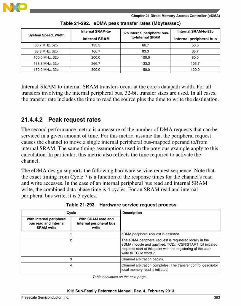
Table 21-292. eDMA peak transfer rates (Mbytes/sec)
System Speed, WidthInternal SRAM-to-
Internal SRAM
32b internal peripheral bus-to-Internal SRAM
Internal SRAM-to-32b
internal peripheral bus
66.7 MHz, 32b 133.3 66.7 53.3
83.3 MHz, 32b 166.7 83.3 66.7
100.0 MHz, 32b 200.0 100.0 80.0
133.3 MHz, 32b 266.7 133.3 106.7
150.0 MHz, 32b 300.0 150.0 120.0
Internal-SRAM-to-internal-SRAM transfers occur at the core's datapath width. For alltransfers involving the internal peripheral bus, 32-bit transfer sizes are used. In all cases,the transfer rate includes the time to read the source plus the time to write the destination.
21.4.4.2 Peak request rates
The second performance metric is a measure of the number of DMA requests that can beserviced in a given amount of time. For this metric, assume that the peripheral requestcauses the channel to move a single internal peripheral bus-mapped operand to/frominternal SRAM. The same timing assumptions used in the previous example apply to thiscalculation. In particular, this metric also reflects the time required to activate thechannel.
The eDMA design supports the following hardware service request sequence. Note thatthe exact timing from Cycle 7 is a function of the response times for the channel's readand write accesses. In the case of an internal peripheral bus read and internal SRAMwrite, the combined data phase time is 4 cycles. For an SRAM read and internalperipheral bus write, it is 5 cycles.
Table 21-293. Hardware service request process
Cycle Description
With internal peripheralbus read and internal
SRAM write
With SRAM read andinternal peripheral bus
write
1 eDMA peripheral request is asserted.
2 The eDMA peripheral request is registered locally in theeDMA module and qualified. TCDn_CSR[START] bit initiatedrequests start at this point with the registering of the userwrite to TCDn word 7.
3 Channel arbitration begins.
4 Channel arbitration completes. The transfer control descriptorlocal memory read is initiated.
Table continues on the next page...
Chapter 21 Direct Memory Access Controller (eDMA)
K12 Sub-Family Reference Manual, Rev. 4, February 2013
Freescale Semiconductor, Inc. 383
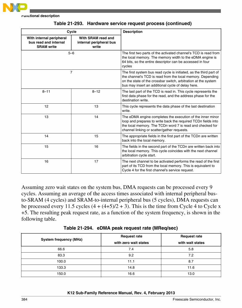
Table 21-293. Hardware service request process (continued)
Cycle Description
With internal peripheralbus read and internal
SRAM write
With SRAM read andinternal peripheral bus
write
5–6 The first two parts of the activated channel's TCD is read fromthe local memory. The memory width to the eDMA engine is64 bits, so the entire descriptor can be accessed in fourcycles
7 The first system bus read cycle is initiated, as the third part ofthe channel's TCD is read from the local memory. Dependingon the state of the crossbar switch, arbitration at the systembus may insert an additional cycle of delay here.
8–11 8–12 The last part of the TCD is read in. This cycle represents thefirst data phase for the read, and the address phase for thedestination write.
12 13 This cycle represents the data phase of the last destinationwrite.
13 14 The eDMA engine completes the execution of the inner minorloop and prepares to write back the required TCDn fields intothe local memory. The TCDn word 7 is read and checked forchannel linking or scatter/gather requests.
14 15 The appropriate fields in the first part of the TCDn are writtenback into the local memory.
15 16 The fields in the second part of the TCDn are written back intothe local memory. This cycle coincides with the next channelarbitration cycle start.
16 17 The next channel to be activated performs the read of the firstpart of its TCD from the local memory. This is equivalent toCycle 4 for the first channel's service request.
Assuming zero wait states on the system bus, DMA requests can be processed every 9cycles. Assuming an average of the access times associated with internal peripheral bus-to-SRAM (4 cycles) and SRAM-to-internal peripheral bus (5 cycles), DMA requests canbe processed every 11.5 cycles (4 + (4+5)/2 + 3). This is the time from Cycle 4 to Cycle x+5. The resulting peak request rate, as a function of the system frequency, is shown in thefollowing table.
Table 21-294. eDMA peak request rate (MReq/sec)
System frequency (MHz)Request rate
with zero wait states
Request rate
with wait states
66.6 7.4 5.8
83.3 9.2 7.2
100.0 11.1 8.7
133.3 14.8 11.6
150.0 16.6 13.0
Functional description
K12 Sub-Family Reference Manual, Rev. 4, February 2013
384 Freescale Semiconductor, Inc.

A general formula to compute the peak request rate with overlapping requests is:
PEAKreq = freq / [ entry + (1 + read_ws) + (1 + write_ws) + exit ]
where:
Table 21-295. Peak request formula operands
Operand Description
PEAKreq Peak request rate
freq System frequency
entry Channel startup (4 cycles)
read_ws Wait states seen during the system bus read data phase
write_ws Wait states seen during the system bus write data phase
exit Channel shutdown (3 cycles)
21.4.4.3 eDMA performance example
Consider a system with the following characteristics:
• Internal SRAM can be accessed with one wait-state when viewed from the systembus data phase
• All internal peripheral bus reads require two wait-states, and internal peripheral buswrites three wait-states viewed from the system bus data phase
• System operates at 150 MHz
For an SRAM to internal peripheral bus transfer,
PEAKreq = 150 MHz / [ 4 + (1 + 1) + (1 + 3) + 3 ] cycles = 11.5 Mreq/sec
For an internal peripheral bus to SRAM transfer,
PEAKreq = 150 MHz / [ 4 + (1 + 2) + (1 + 1) + 3 ] cycles = 12.5 Mreq/sec
Assuming an even distribution of the two transfer types, the average peak request ratewould be:
PEAKreq = (11.5 Mreq/sec + 12.5 Mreq/sec) / 2 = 12.0 Mreq/sec
The minimum number of cycles to perform a single read/write, zero wait states on thesystem bus, from a cold start where no channel is executing and eDMA is idle are:
Chapter 21 Direct Memory Access Controller (eDMA)
K12 Sub-Family Reference Manual, Rev. 4, February 2013
Freescale Semiconductor, Inc. 385

• 11 cycles for a software, that is, a TCDn_CSR[START] bit, request
• 12 cycles for a hardware, that is, an eDMA peripheral request signal, request
Two cycles account for the arbitration pipeline and one extra cycle on the hardwarerequest resulting from the internal registering of the eDMA peripheral request signals.For the peak request rate calculations above, the arbitration and request registering isabsorbed in or overlaps the previous executing channel.
NoteWhen channel linking or scatter/gather is enabled, a two cycledelay is imposed on the next channel selection and startup. Thisallows the link channel or the scatter/gather channel to beeligible and considered in the arbitration pool for next channelselection.
21.5 Initialization/application informationThe following sections discuss initialization of the eDMA and programmingconsiderations.
21.5.1 eDMA initialization
To initialize the eDMA:
1. Write to the CR if a configuration other than the default is desired.
2. Write the channel priority levels to the DCHPRIn registers if a configuration otherthan the default is desired.
3. Enable error interrupts in the EEI register if so desired.
4. Write the 32-byte TCD for each channel that may request service.
5. Enable any hardware service requests via the ERQ register.
6. Request channel service via either:• Software: setting the TCDn_CSR[START]• Hardware: slave device asserting its eDMA peripheral request signal
Initialization/application information
K12 Sub-Family Reference Manual, Rev. 4, February 2013
386 Freescale Semiconductor, Inc.

After any channel requests service, a channel is selected for execution based on thearbitration and priority levels written into the programmer's model. The eDMA enginereads the entire TCD, including the TCD control and status fields, as shown in thefollowing table, for the selected channel into its internal address path module.
As the TCD is read, the first transfer is initiated on the internal bus, unless aconfiguration error is detected. Transfers from the source, as defined by TCDn_SADDR,to the destination, as defined by TCDn_DADDR, continue until the number of bytesspecified by TCDn_NBYTES are transferred.
When the transfer is complete, the eDMA engine's local TCDn_SADDR,TCDn_DADDR, and TCDn_CITER are written back to the main TCD memory and anyminor loop channel linking is performed, if enabled. If the major loop is exhausted,further post processing executes, such as interrupts, major loop channel linking, andscatter/gather operations, if enabled.
Table 21-296. TCD Control and Status fields
TCDn_CSR fieldname
Description
START Control bit to start channel explicitly when using a software initiated DMA service (Automaticallycleared by hardware)
ACTIVE Status bit indicating the channel is currently in execution
DONE Status bit indicating major loop completion (cleared by software when using a software initiatedDMA service)
D_REQ Control bit to disable DMA request at end of major loop completion when using a hardware initiatedDMA service
BWC Control bits for throttling bandwidth control of a channel
E_SG Control bit to enable scatter-gather feature
INT_HALF Control bit to enable interrupt when major loop is half complete
INT_MAJ Control bit to enable interrupt when major loop completes
The following figure shows how each DMA request initiates one minor-loop transfer, oriteration, without CPU intervention. DMA arbitration can occur after each minor loop,and one level of minor loop DMA preemption is allowed. The number of minor loops ina major loop is specified by the beginning iteration count (BITER).
Chapter 21 Direct Memory Access Controller (eDMA)
K12 Sub-Family Reference Manual, Rev. 4, February 2013
Freescale Semiconductor, Inc. 387
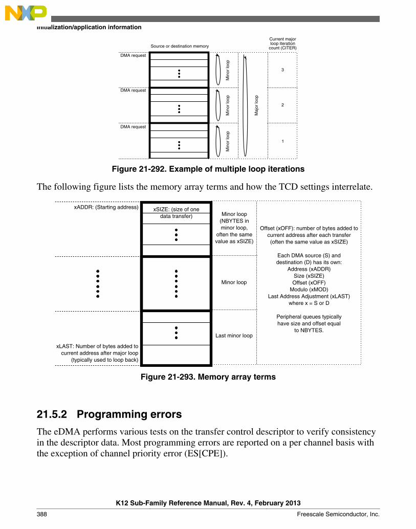
DMA request
DMA request
DMA request
Min
or lo
opM
inor
loop
Min
or lo
op
Maj
or lo
op
Current majorloop iteration
count (CITER)
3
2
1
Source or destination memory
Figure 21-292. Example of multiple loop iterations
The following figure lists the memory array terms and how the TCD settings interrelate.
xADDR: (Starting address)
xLAST: Number of bytes added tocurrent address after major loop
(typically used to loop back)
Minor loop(NBYTES inminor loop,
often the samevalue as xSIZE)
Minor loop
Last minor loop
Offset (xOFF): number of bytes added tocurrent address after each transfer(often the same value as xSIZE)
Each DMA source (S) and destination (D) has its own:
Address (xADDR)Size (xSIZE)Offset (xOFF)
Modulo (xMOD)Last Address Adjustment (xLAST)
where x = S or D
Peripheral queues typically have size and offset equal
to NBYTES.
xSIZE: (size of onedata transfer)
Figure 21-293. Memory array terms
21.5.2 Programming errors
The eDMA performs various tests on the transfer control descriptor to verify consistencyin the descriptor data. Most programming errors are reported on a per channel basis withthe exception of channel priority error (ES[CPE]).
Initialization/application information
K12 Sub-Family Reference Manual, Rev. 4, February 2013
388 Freescale Semiconductor, Inc.

For all error types other than channel priority error, the channel number causing the erroris recorded in the Error Status register (DMAx_ES). If the error source is not removedbefore the next activation of the problem channel, the error is detected and recordedagain.
If priority levels are not unique, when any channel requests service, a channel priorityerror is reported. The highest channel priority with an active request is selected, but thelowest numbered channel with that priority is selected by arbitration and executed by theeDMA engine. The hardware service request handshake signals, error interrupts, anderror reporting is associated with the selected channel.
21.5.3 Arbitration mode considerations
21.5.3.1 Fixed channel arbitration
In this mode, the channel service request from the highest priority channel is selected toexecute.
21.5.3.2 Round-robin channel arbitration
Channels are serviced starting with the highest channel number and rotating through tothe lowest channel number without regard to the channel priority levels.
21.5.4 Performing DMA transfers (examples)
21.5.4.1 Single request
To perform a simple transfer of n bytes of data with one activation, set the major loop toone (TCDn_CITER = TCDn_BITER = 1). The data transfer begins after the channelservice request is acknowledged and the channel is selected to execute. After the transferis complete, the TCDn_CSR[DONE] bit is set and an interrupt generates if properlyenabled.
For example, the following TCD entry is configured to transfer 16 bytes of data. TheeDMA is programmed for one iteration of the major loop transferring 16 bytes periteration. The source memory has a byte wide memory port located at 0x1000. Thedestination memory has a 32-bit port located at 0x2000. The address offsets are
Chapter 21 Direct Memory Access Controller (eDMA)
K12 Sub-Family Reference Manual, Rev. 4, February 2013
Freescale Semiconductor, Inc. 389
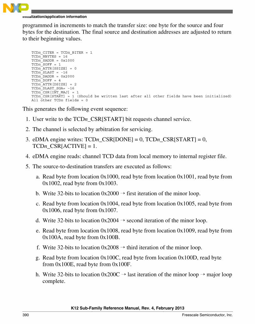
programmed in increments to match the transfer size: one byte for the source and fourbytes for the destination. The final source and destination addresses are adjusted to returnto their beginning values.
TCDn_CITER = TCDn_BITER = 1 TCDn_NBYTES = 16 TCDn_SADDR = 0x1000 TCDn_SOFF = 1 TCDn_ATTR[SSIZE] = 0 TCDn_SLAST = -16 TCDn_DADDR = 0x2000 TCDn_DOFF = 4 TCDn_ATTR[DSIZE] = 2 TCDn_DLAST_SGA= –16 TCDn_CSR[INT_MAJ] = 1 TCDn_CSR[START] = 1 (Should be written last after all other fields have been initialized) All other TCDn fields = 0
This generates the following event sequence:
1. User write to the TCDn_CSR[START] bit requests channel service.
2. The channel is selected by arbitration for servicing.
3. eDMA engine writes: TCDn_CSR[DONE] = 0, TCDn_CSR[START] = 0,TCDn_CSR[ACTIVE] = 1.
4. eDMA engine reads: channel TCD data from local memory to internal register file.
5. The source-to-destination transfers are executed as follows:
a. Read byte from location 0x1000, read byte from location 0x1001, read byte from0x1002, read byte from 0x1003.
b. Write 32-bits to location 0x2000 → first iteration of the minor loop.
c. Read byte from location 0x1004, read byte from location 0x1005, read byte from0x1006, read byte from 0x1007.
d. Write 32-bits to location 0x2004 → second iteration of the minor loop.
e. Read byte from location 0x1008, read byte from location 0x1009, read byte from0x100A, read byte from 0x100B.
f. Write 32-bits to location 0x2008 → third iteration of the minor loop.
g. Read byte from location 0x100C, read byte from location 0x100D, read bytefrom 0x100E, read byte from 0x100F.
h. Write 32-bits to location 0x200C → last iteration of the minor loop → major loopcomplete.
Initialization/application information
K12 Sub-Family Reference Manual, Rev. 4, February 2013
390 Freescale Semiconductor, Inc.

6. The eDMA engine writes: TCDn_SADDR = 0x1000, TCDn_DADDR = 0x2000,TCDn_CITER = 1 (TCDn_BITER).
7. The eDMA engine writes: TCDn_CSR[ACTIVE] = 0, TCDn_CSR[DONE] = 1,INT[n] = 1.
8. The channel retires and the eDMA goes idle or services the next channel.
21.5.4.2 Multiple requests
The following example transfers 32 bytes via two hardware requests, but is otherwise thesame as the previous example. The only fields that change are the major loop iterationcount and the final address offsets. The eDMA is programmed for two iterations of themajor loop transferring 16 bytes per iteration. After the channel's hardware requests areenabled in the ERQ register, the slave device initiates channel service requests.
TCDn_CITER = TCDn_BITER = 2 TCDn_SLAST = –32 TCDn_DLAST_SGA = –32
This would generate the following sequence of events:
1. First hardware, that is, eDMA peripheral, request for channel service.
2. The channel is selected by arbitration for servicing.
3. eDMA engine writes: TCDn_CSR[DONE] = 0, TCDn_CSR[START] = 0,TCDn_CSR[ACTIVE] = 1.
4. eDMA engine reads: channel TCDn data from local memory to internal register file.
5. The source to destination transfers are executed as follows:
a. Read byte from location 0x1000, read byte from location 0x1001, read byte from0x1002, read byte from 0x1003.
b. Write 32-bits to location 0x2000 → first iteration of the minor loop.
c. Read byte from location 0x1004, read byte from location 0x1005, read byte from0x1006, read byte from 0x1007.
d. Write 32-bits to location 0x2004 → second iteration of the minor loop.
e. Read byte from location 0x1008, read byte from location 0x1009, read byte from0x100A, read byte from 0x100B.
f. Write 32-bits to location 0x2008 → third iteration of the minor loop.
Chapter 21 Direct Memory Access Controller (eDMA)
K12 Sub-Family Reference Manual, Rev. 4, February 2013
Freescale Semiconductor, Inc. 391
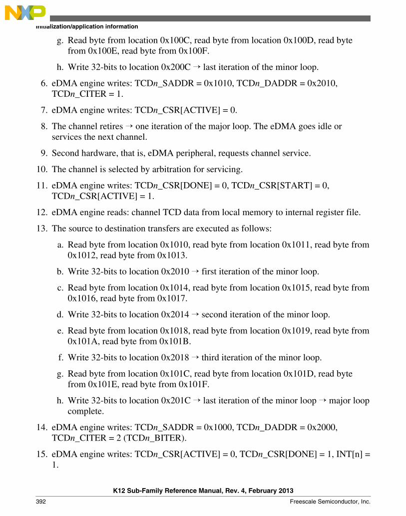
g. Read byte from location 0x100C, read byte from location 0x100D, read bytefrom 0x100E, read byte from 0x100F.
h. Write 32-bits to location 0x200C → last iteration of the minor loop.
6. eDMA engine writes: TCDn_SADDR = 0x1010, TCDn_DADDR = 0x2010,TCDn_CITER = 1.
7. eDMA engine writes: TCDn_CSR[ACTIVE] = 0.
8. The channel retires → one iteration of the major loop. The eDMA goes idle orservices the next channel.
9. Second hardware, that is, eDMA peripheral, requests channel service.
10. The channel is selected by arbitration for servicing.
11. eDMA engine writes: TCDn_CSR[DONE] = 0, TCDn_CSR[START] = 0,TCDn_CSR[ACTIVE] = 1.
12. eDMA engine reads: channel TCD data from local memory to internal register file.
13. The source to destination transfers are executed as follows:
a. Read byte from location 0x1010, read byte from location 0x1011, read byte from0x1012, read byte from 0x1013.
b. Write 32-bits to location 0x2010 → first iteration of the minor loop.
c. Read byte from location 0x1014, read byte from location 0x1015, read byte from0x1016, read byte from 0x1017.
d. Write 32-bits to location 0x2014 → second iteration of the minor loop.
e. Read byte from location 0x1018, read byte from location 0x1019, read byte from0x101A, read byte from 0x101B.
f. Write 32-bits to location 0x2018 → third iteration of the minor loop.
g. Read byte from location 0x101C, read byte from location 0x101D, read bytefrom 0x101E, read byte from 0x101F.
h. Write 32-bits to location 0x201C → last iteration of the minor loop → major loopcomplete.
14. eDMA engine writes: TCDn_SADDR = 0x1000, TCDn_DADDR = 0x2000,TCDn_CITER = 2 (TCDn_BITER).
15. eDMA engine writes: TCDn_CSR[ACTIVE] = 0, TCDn_CSR[DONE] = 1, INT[n] =1.
Initialization/application information
K12 Sub-Family Reference Manual, Rev. 4, February 2013
392 Freescale Semiconductor, Inc.
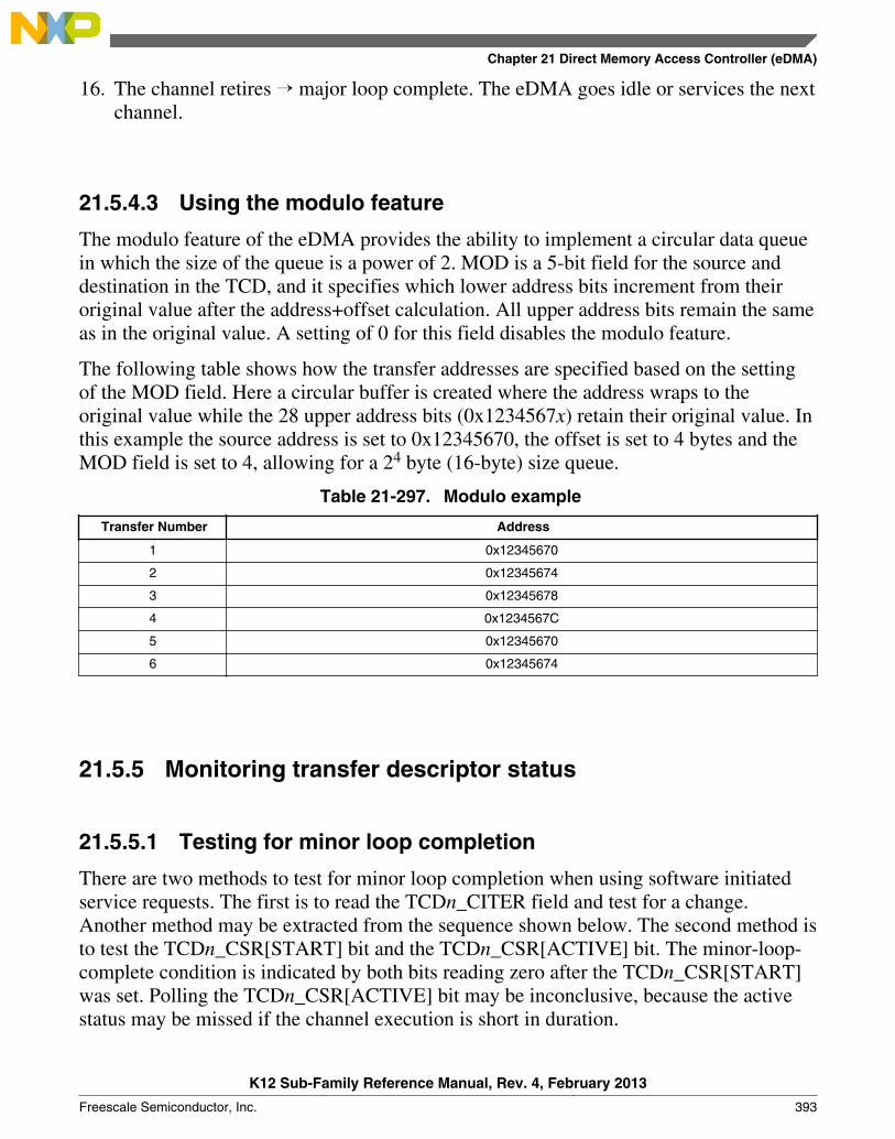
16. The channel retires → major loop complete. The eDMA goes idle or services the nextchannel.
21.5.4.3 Using the modulo feature
The modulo feature of the eDMA provides the ability to implement a circular data queuein which the size of the queue is a power of 2. MOD is a 5-bit field for the source anddestination in the TCD, and it specifies which lower address bits increment from theiroriginal value after the address+offset calculation. All upper address bits remain the sameas in the original value. A setting of 0 for this field disables the modulo feature.
The following table shows how the transfer addresses are specified based on the settingof the MOD field. Here a circular buffer is created where the address wraps to theoriginal value while the 28 upper address bits (0x1234567x) retain their original value. Inthis example the source address is set to 0x12345670, the offset is set to 4 bytes and theMOD field is set to 4, allowing for a 24 byte (16-byte) size queue.
Table 21-297. Modulo example
Transfer Number Address
1 0x12345670
2 0x12345674
3 0x12345678
4 0x1234567C
5 0x12345670
6 0x12345674
21.5.5 Monitoring transfer descriptor status
21.5.5.1 Testing for minor loop completion
There are two methods to test for minor loop completion when using software initiatedservice requests. The first is to read the TCDn_CITER field and test for a change.Another method may be extracted from the sequence shown below. The second method isto test the TCDn_CSR[START] bit and the TCDn_CSR[ACTIVE] bit. The minor-loop-complete condition is indicated by both bits reading zero after the TCDn_CSR[START]was set. Polling the TCDn_CSR[ACTIVE] bit may be inconclusive, because the activestatus may be missed if the channel execution is short in duration.
Chapter 21 Direct Memory Access Controller (eDMA)
K12 Sub-Family Reference Manual, Rev. 4, February 2013
Freescale Semiconductor, Inc. 393

The TCD status bits execute the following sequence for a software activated channel:
StageTCDn_CSR bits
StateSTART ACTIVE DONE
1 1 0 0 Channel service request via software
2 0 1 0 Channel is executing
3a 0 0 0 Channel has completed the minor loop and is idle
3b 0 0 1 Channel has completed the major loop and is idle
The best method to test for minor-loop completion when using hardware, that is,peripheral, initiated service requests is to read the TCDn_CITER field and test for achange. The hardware request and acknowledge handshake signals are not visible in theprogrammer's model.
The TCD status bits execute the following sequence for a hardware-activated channel:
StageTCDn_CSR bits
StateSTART ACTIVE DONE
1 0 0 0Channel service request via hardware (peripheralrequest asserted)
2 0 1 0 Channel is executing
3a 0 0 0 Channel has completed the minor loop and is idle
3b 0 0 1 Channel has completed the major loop and is idle
For both activation types, the major-loop-complete status is explicitly indicated via theTCDn_CSR[DONE] bit.
The TCDn_CSR[START] bit is cleared automatically when the channel begins executionregardless of how the channel activates.
21.5.5.2 Reading the transfer descriptors of active channels
The eDMA reads back the true TCDn_SADDR, TCDn_DADDR, and TCDn_NBYTESvalues if read while a channel executes. The true values of the SADDR, DADDR, andNBYTES are the values the eDMA engine currently uses in its internal register file andnot the values in the TCD local memory for that channel. The addresses, SADDR andDADDR, and NBYTES, which decrement to zero as the transfer progresses, can give anindication of the progress of the transfer. All other values are read back from the TCDlocal memory.
Initialization/application information
K12 Sub-Family Reference Manual, Rev. 4, February 2013
394 Freescale Semiconductor, Inc.

21.5.5.3 Checking channel preemption status
Preemption is available only when fixed arbitration is selected as the channel arbitrationmode. A preemptive situation is one in which a preempt-enabled channel runs and ahigher priority request becomes active. When the eDMA engine is not operating in fixedchannel arbitration mode, the determination of the actively running relative priorityoutstanding requests become undefined. Channel priorities are treated as equal, that is,constantly rotating, when Round-Robin Arbitration mode is selected.
The TCDn_CSR[ACTIVE] bit for the preempted channel remains asserted throughoutthe preemption. The preempted channel is temporarily suspended while the preemptingchannel executes one major loop iteration. If two TCDn_CSR[ACTIVE] bits are setsimultaneously in the global TCD map, a higher priority channel is actively preempting alower priority channel.
21.5.6 Channel Linking
Channel linking (or chaining) is a mechanism where one channel sets theTCDn_CSR[START] bit of another channel (or itself), therefore initiating a servicerequest for that channel. When properly enabled, the EDMA engine automaticallyperforms this operation at the major or minor loop completion.
The minor loop channel linking occurs at the completion of the minor loop (or oneiteration of the major loop). The TCDn_CITER[E_LINK] field determines whether aminor loop link is requested. When enabled, the channel link is made after each iterationof the major loop except for the last. When the major loop is exhausted, only the majorloop channel link fields are used to determine if a channel link should be made. Forexample, the initial fields of:
TCDn_CITER[E_LINK] = 1 TCDn_CITER[LINKCH] = 0xC TCDn_CITER[CITER] value = 0x4 TCDn_CSR[MAJOR_E_LINK] = 1 TCDn_CSR[MAJOR_LINKCH] = 0x7
executes as:
1. Minor loop done → set TCD12_CSR[START] bit
2. Minor loop done → set TCD12_CSR[START] bit
3. Minor loop done → set TCD12_CSR[START] bit
4. Minor loop done, major loop done→ set TCD7_CSR[START] bit
Chapter 21 Direct Memory Access Controller (eDMA)
K12 Sub-Family Reference Manual, Rev. 4, February 2013
Freescale Semiconductor, Inc. 395

When minor loop linking is enabled (TCDn_CITER[E_LINK] = 1), theTCDn_CITER[CITER] field uses a nine bit vector to form the current iteration count.When minor loop linking is disabled (TCDn_CITER[E_LINK] = 0), theTCDn_CITER[CITER] field uses a 15-bit vector to form the current iteration count. Thebits associated with the TCDn_CITER[LINKCH] field are concatenated onto the CITERvalue to increase the range of the CITER.
Note
The TCDn_CITER[E_LINK] bit and theTCDn_BITER[E_LINK] bit must equal or a configuration erroris reported. The CITER and BITER vector widths must beequal to calculate the major loop, half-way done interrupt point.
The following table summarizes how a DMA channel can link to another DMA channel,i.e, use another channel's TCD, at the end of a loop.
Table 21-298. Channel Linking Parameters
Desired LinkBehavior
TCD Control Field Name Description
Link at end ofMinor Loop
CITER[E_LINK]Enable channel-to-channel linking on minor loop completion (currentiteration)
CITER[LINKCH] Link channel number when linking at end of minor loop (current iteration)
Link at end ofMajor Loop
CSR[MAJOR_E_LINK] Enable channel-to-channel linking on major loop completion
CSR[MAJOR_LINKCH] Link channel number when linking at end of major loop
21.5.7 Dynamic programming
21.5.7.1 Dynamically changing the channel priority
The following two options are recommended for dynamically changing channel prioritylevels:
1. Switch to Round-Robin Channel Arbitration mode, change the channel priorities,then switch back to Fixed Arbitration mode,
2. Disable all the channels, change the channel priorities, then enable the appropriatechannels.
Initialization/application information
K12 Sub-Family Reference Manual, Rev. 4, February 2013
396 Freescale Semiconductor, Inc.

21.5.7.2 Dynamic channel linking
Dynamic channel linking is the process of setting the TCD.major.e_link bit duringchannel execution. This bit is read from the TCD local memory at the end of channelexecution, thus allowing the user to enable the feature during channel execution.
Because the user is allowed to change the configuration during execution, a coherencymodel is needed. Consider the scenario where the user attempts to execute a dynamicchannel link by enabling the TCD.major.e_link bit at the same time the eDMA engine isretiring the channel. The TCD.major.e_link would be set in the programmer’s model, butit would be unclear whether the actual link was made before the channel retired.
The following coherency model is recommended when executing a dynamic channel linkrequest.
1. Write 1 to the TCD.major.e_link bit.2. Read back the TCD.major.e_link bit.3. Test the TCD.major.e_link request status:
• If TCD.major.e_link = 1, the dynamic link attempt was successful.• If TCD.major.e_link = 0, the attempted dynamic link did not succeed (the
channel was already retiring).
For this request, the TCD local memory controller forces the TCD.major.e_link bit tozero on any writes to a channel’s TCD.word7 after that channel’s TCD.done bit is set,indicating the major loop is complete.
NOTEThe user must clear the TCD.done bit before writing theTCD.major.e_link bit. The TCD.done bit is clearedautomatically by the eDMA engine after a channel beginsexecution.
21.5.7.3 Dynamic scatter/gather
Scatter/gather is the process of automatically loading a new TCD into a channel. It allowsa DMA channel to use multiple TCDs; this enables a DMA channel to scatter the DMAdata to multiple destinations or gather it from multiple sources.When scatter/gather isenabled and the channel has finished its major loop, a new TCD is fetched from systemmemory and loaded into that channel’s descriptor location in eDMA programmer’smodel, thus replacing the current descriptor.
Because the user is allowed to change the configuration during execution, a coherencymodel is needed. Consider the scenario where the user attempts to execute a dynamicscatter/gather operation by enabling the TCD.e_sg bit at the same time the eDMA engine
Chapter 21 Direct Memory Access Controller (eDMA)
K12 Sub-Family Reference Manual, Rev. 4, February 2013
Freescale Semiconductor, Inc. 397
is retiring the channel. The TCD.e_sg would be set in the programmer’s model, but itwould be unclear whether the actual scatter/gather request was honored before thechannel retired.
Two methods for this coherency model are shown in the following subsections. Method 1has the advantage of reading the major.linkch field and the e_sg bit with a single read.For both dynamic channel linking and scatter/gather requests, the TCD local memorycontroller forces the TCD.major.e_link and TCD.e_sg bits to zero on any writes to achannel’s TCD.word7 if that channel’s TCD.done bit is set indicating the major loop iscomplete.
NOTEThe user must clear the TCD.done bit before writing theTCD.major.e_link or TCD.e_sg bits. The TCD.done bit iscleared automatically by the eDMA engine after a channelbegins execution.
21.5.7.3.1 Method 1 (channel not using major loop channel linking)
For a channel not using major loop channel linking, the coherency model described heremay be used for a dynamic scatter/gather request.
When the TCD.major.e_link bit is zero, the TCD.major.linkch field is not used by theeDMA. In this case, the TCD.major.linkch bits may be used for other purposes. Thismethod uses the TCD.major.linkch field as a TCD indentification (ID).
1. When the descriptors are built, write a unique TCD ID in the TCD.major.linkch fieldfor each TCD associated with a channel using dynamic scatter/gather.
2. Write 1b to the TCD.d_req bit.
Should a dynamic scatter/gather attempt fail, setting the TCD.d_req bit will prevent afuture hardware activation of this channel. This stops the channel from executingwith a destination address (daddr) that was calculated using a scatter/gather address(written in the next step) instead of a dlast final offest value.
3. Write the TCD.dlast_sga field with the scatter/gather address.4. Write 1b to the TCD.e_sg bit.5. Read back the 16 bit TCD control/status field.6. Test the TCD.e_sg request status and TCD.major.linkch value:
If e_sg = 1b, the dynamic link attempt was successful.
Initialization/application information
K12 Sub-Family Reference Manual, Rev. 4, February 2013
398 Freescale Semiconductor, Inc.
If e_sg = 0b and the major.linkch (ID) did not change, the attempted dynamic linkdid not succeed (the channel was already retiring).
If e_sg = 0b and the major.linkch (ID) changed, the dynamic link attempt wassuccessful (the new TCD’s e_sg value cleared the e_sg bit).
21.5.7.3.2 Method 2 (channel using major loop channel linking)
For a channel using major loop channel linking, the coherency model described here maybe used for a dynamic scatter/gather request. This method uses the TCD.dlast_sga field asa TCD indentification (ID).
1. Write 1b to the TCD.d_req bit.
Should a dynamic scatter/gather attempt fail, setting the d_req bit will prevent afuture hardware activation of this channel. This stops the channel from executingwith a destination address (daddr) that was calculated using a scatter/gather address(written in the next step) instead of a dlast final offest value.
2. Write theTCD.dlast_sga field with the scatter/gather address.3. Write 1b to the TCD.e_sg bit.4. Read back the TCD.e_sg bit.5. Test the TCD.e_sg request status:
If e_sg = 1b, the dynamic link attempt was successful.
If e_sg = 0b, read the 32 bit TCD dlast_sga field.
If e_sg = 0b and the dlast_sga did not change, the attempted dynamic link did notsucceed (the channel was already retiring).
If e_sg = 0b and the dlast_sga changed, the dynamic link attempt was successful (thenew TCD’s e_sg value cleared the e_sg bit).
Chapter 21 Direct Memory Access Controller (eDMA)
K12 Sub-Family Reference Manual, Rev. 4, February 2013
Freescale Semiconductor, Inc. 399

Initialization/application information
K12 Sub-Family Reference Manual, Rev. 4, February 2013
400 Freescale Semiconductor, Inc.

Chapter 22External Watchdog Monitor (EWM)
22.1 IntroductionNOTE
For the chip-specific implementation details of this module'sinstances see the chip configuration information.
The watchdog is generally used to monitor the flow and execution of embedded softwarewithin an MCU. The watchdog consists of a counter that if allowed to overflow, forces aninternal reset (asynchronous) to all on-chip peripherals and optionally assert the RESETpin to reset external devices/circuits. The overflow of the watchdog counter must notoccur if the software code works well and services the watchdog to re-start the actualcounter.
For safety, a redundant watchdog system, External Watchdog Monitor (EWM), isdesigned to monitor external circuits, as well as the MCU software flow. This provides aback-up mechanism to the internal watchdog that resets the MCU's CPU and peripherals.
The EWM differs from the internal watchdog in that it does not reset the MCU's CPUand peripherals. The EWM if allowed to time-out, provides an independent EWM_outpin that when asserted resets or places an external circuit into a safe mode. The CPUresets the EWM counter that is logically ANDed with an external digital input pin. Thispin allows an external circuit to influence the reset_out signal.
22.1.1 Features
Features of EWM module include:
• Independent LPO clock source
• Programmable time-out period specified in terms of number of EWM LPO clockcycles.
K12 Sub-Family Reference Manual, Rev. 4, February 2013
Freescale Semiconductor, Inc. 401
• Windowed refresh option
• Provides robust check that program flow is faster than expected.
• Programmable window.
• Refresh outside window leads to assertion of EWM_out.
• Robust refresh mechanism
• Write values of 0xB4 and 0x2C to EWM Refresh Register within 15(EWM_service_time) peripheral bus clock cycles.
• One output port, EWM_out, when asserted is used to reset or place the externalcircuit into safe mode.
• One Input port, EWM_in, allows an external circuit to control the EWM_out signal.
22.1.2 Modes of Operation
This section describes the module's operating modes.
22.1.2.1 Stop Mode
When the EWM is in stop mode, the CPU services to the EWM cannot occur. On entry tostop mode, the EWM’s counter freezes.
There are two possible ways to exit from Stop mode:
• On exit from stop mode through a reset, the EWM remains disabled.
• On exit from stop mode by an interrupt, the EWM is re-enabled, and the countercontinues to be clocked from the same value prior to entry to stop mode.
Note the following if the EWM enters the stop mode during CPU service mechanism: Atthe exit from stop mode by an interrupt, refresh mechanism state machine starts from theprevious state which means, if first service command is written correctly and EWMenters the stop mode immediately, the next command has to be written within the next 15(EWM_service_time) peripheral bus clocks after exiting from stop mode. User must maskall interrupts prior to executing EWM service instructions.
Introduction
K12 Sub-Family Reference Manual, Rev. 4, February 2013
402 Freescale Semiconductor, Inc.
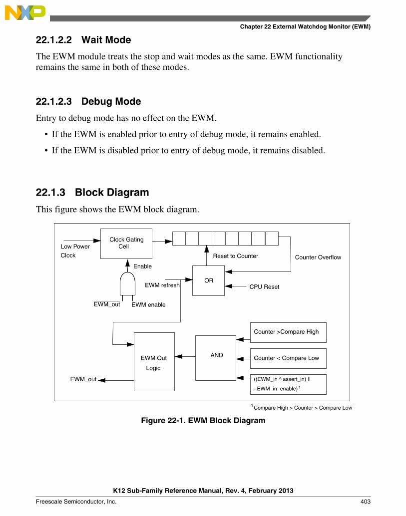
22.1.2.2 Wait Mode
The EWM module treats the stop and wait modes as the same. EWM functionalityremains the same in both of these modes.
22.1.2.3 Debug Mode
Entry to debug mode has no effect on the EWM.
• If the EWM is enabled prior to entry of debug mode, it remains enabled.
• If the EWM is disabled prior to entry of debug mode, it remains disabled.
22.1.3 Block Diagram
This figure shows the EWM block diagram.
Clock Gating Cell
EWM_out
EWM Out Logic
EWM_out
OR
Low Power Clock
Enable Counter Overflow
CPU Reset
Reset to Counter
EWM refresh
EWM enable
Counter >Compare High
Counter < Compare Low AND
((EWM_in ^ assert_in) ||
~EWM_in_enable)
Compare High > Counter > Compare Low1
1
Figure 22-1. EWM Block Diagram
Chapter 22 External Watchdog Monitor (EWM)
K12 Sub-Family Reference Manual, Rev. 4, February 2013
Freescale Semiconductor, Inc. 403
22.2 EWM Signal DescriptionsThe EWM has two external signals, as shown in the following table.
Table 22-1. EWM Signal Descriptions
Signal Description I/O
EWM_in EWM input for safety status of external safety circuits. The polarity ofEWM_in is programmable using the EWM_CTRL[ASSIN] bit. The defaultpolarity is active-low.
I
EWM_out EWM reset out signal O
22.3 Memory Map/Register DefinitionThis section contains the module memory map and registers.
EWM memory map
Absoluteaddress
(hex)Register name
Width(in bits)
Access Reset valueSection/
page
4006_1000 Control Register (EWM_CTRL) 8 R/W 00h 22.3.1/404
4006_1001 Service Register (EWM_SERV) 8W
(alwaysreads 0)
00h 22.3.2/405
4006_1002 Compare Low Register (EWM_CMPL) 8 R/W 00h 22.3.3/405
4006_1003 Compare High Register (EWM_CMPH) 8 R/W FFh 22.3.4/406
22.3.1 Control Register (EWM_CTRL)The CTRL register is cleared by any reset.
NOTEINEN, ASSIN and EWMEN bits can be written once after aCPU reset. Modifying these bits more than once, generates abus transfer error.
Address: 4006_1000h base + 0h offset = 4006_1000h
Bit 7 6 5 4 3 2 1 0
Read 0 INTEN INEN ASSIN EWMENWriteReset 0 0 0 0 0 0 0 0
EWM Signal Descriptions
K12 Sub-Family Reference Manual, Rev. 4, February 2013
404 Freescale Semiconductor, Inc.
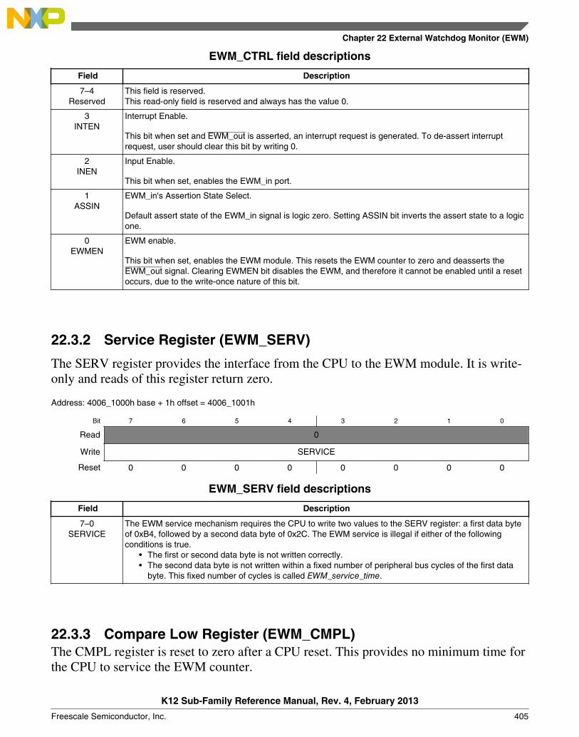
EWM_CTRL field descriptions
Field Description
7–4Reserved
This field is reserved.This read-only field is reserved and always has the value 0.
3INTEN
Interrupt Enable.
This bit when set and EWM_out is asserted, an interrupt request is generated. To de-assert interruptrequest, user should clear this bit by writing 0.
2INEN
Input Enable.
This bit when set, enables the EWM_in port.
1ASSIN
EWM_in's Assertion State Select.
Default assert state of the EWM_in signal is logic zero. Setting ASSIN bit inverts the assert state to a logicone.
0EWMEN
EWM enable.
This bit when set, enables the EWM module. This resets the EWM counter to zero and deasserts theEWM_out signal. Clearing EWMEN bit disables the EWM, and therefore it cannot be enabled until a resetoccurs, due to the write-once nature of this bit.
22.3.2 Service Register (EWM_SERV)
The SERV register provides the interface from the CPU to the EWM module. It is write-only and reads of this register return zero.
Address: 4006_1000h base + 1h offset = 4006_1001h
Bit 7 6 5 4 3 2 1 0
Read 0
Write SERVICE
Reset 0 0 0 0 0 0 0 0
EWM_SERV field descriptions
Field Description
7–0SERVICE
The EWM service mechanism requires the CPU to write two values to the SERV register: a first data byteof 0xB4, followed by a second data byte of 0x2C. The EWM service is illegal if either of the followingconditions is true.
• The first or second data byte is not written correctly.• The second data byte is not written within a fixed number of peripheral bus cycles of the first data
byte. This fixed number of cycles is called EWM_service_time.
22.3.3 Compare Low Register (EWM_CMPL)The CMPL register is reset to zero after a CPU reset. This provides no minimum time forthe CPU to service the EWM counter.
Chapter 22 External Watchdog Monitor (EWM)
K12 Sub-Family Reference Manual, Rev. 4, February 2013
Freescale Semiconductor, Inc. 405
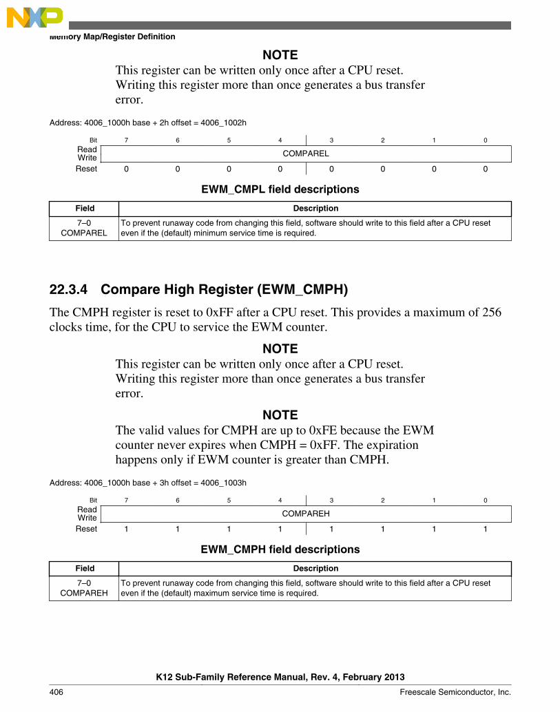
NOTEThis register can be written only once after a CPU reset.Writing this register more than once generates a bus transfererror.
Address: 4006_1000h base + 2h offset = 4006_1002h
Bit 7 6 5 4 3 2 1 0
Read COMPARELWriteReset 0 0 0 0 0 0 0 0
EWM_CMPL field descriptions
Field Description
7–0COMPAREL
To prevent runaway code from changing this field, software should write to this field after a CPU reseteven if the (default) minimum service time is required.
22.3.4 Compare High Register (EWM_CMPH)
The CMPH register is reset to 0xFF after a CPU reset. This provides a maximum of 256clocks time, for the CPU to service the EWM counter.
NOTEThis register can be written only once after a CPU reset.Writing this register more than once generates a bus transfererror.
NOTEThe valid values for CMPH are up to 0xFE because the EWMcounter never expires when CMPH = 0xFF. The expirationhappens only if EWM counter is greater than CMPH.
Address: 4006_1000h base + 3h offset = 4006_1003h
Bit 7 6 5 4 3 2 1 0
Read COMPAREHWriteReset 1 1 1 1 1 1 1 1
EWM_CMPH field descriptions
Field Description
7–0COMPAREH
To prevent runaway code from changing this field, software should write to this field after a CPU reseteven if the (default) maximum service time is required.
Memory Map/Register Definition
K12 Sub-Family Reference Manual, Rev. 4, February 2013
406 Freescale Semiconductor, Inc.
22.4 Functional DescriptionThe following sections describe functional details of the EWM module.
22.4.1 The EWM_out Signal
The EWM_out is a digital output signal used to gate an external circuit (applicationspecific) that controls critical safety functions. For example, the EWM_out could beconnected to the high voltage transistors circuits that control an AC motor in a largeappliance.
The EWM_out signal remains deasserted when the EWM is being regularly serviced bythe CPU within the programmable service window, indicating that the application code isexecuted as expected.
The EWM_out signal is asserted in any of the following conditions:
• Servicing the EWM when the counter value is less than CMPL value.
• If the EWM counter value reaches the CMPH value, and no EWM service hasoccurred.
• Servicing the EWM when the counter value is more than CMPL and less than CMPHvalues and EWM_in signal is asserted.
• If functionality of EWM_in pin is enabled and EWM_in pin is asserted whileservicing the EWM.
• After any reset (by the virtue of the external pull-down mechanism on the EWM_outpin)
On a normal reset, the EWM_out is asserted. To deassert the EWM_out, set EWMEN bitin the CTRL register to enable the EWM.
If the EWM_out signal shares its pad with a digital I/O pin, on reset this actual pad defersto being an input signal. It takes the EWM_out output condition only after you enable theEWM by the EWMEN bit in the CTRL register.
When the EWM_out pin is asserted, it can only be deasserted by forcing a MCU reset.
Note
EWM_out pad must be in pull down state when EWMfunctionality is used and when EWM is under Reset.
Chapter 22 External Watchdog Monitor (EWM)
K12 Sub-Family Reference Manual, Rev. 4, February 2013
Freescale Semiconductor, Inc. 407
22.4.2 The EWM_in Signal
The EWM_in is a digital input signal that allows an external circuit to control theEWM_out signal. For example, in the application, an external circuit monitors a criticalsafety function, and if there is fault with this circuit's behavior, it can then actively initiatethe EWM_out signal that controls the gating circuit.
The EWM_in signal is ignored if the EWM is disabled, or if INEN bit of CTRL registeris cleared, as after any reset.
On enabling the EWM (setting the CTRL[EWMEN] bit) and enabling EWM_infunctionality (setting the CTRL[INEN] bit), the EWM_in signal must be in the deassertedstate prior to the CPU servicing the EWM. This ensures that the EWM_out stays in thedeasserted state; otherwise, the EWM_out pin is asserted.
Note
You must update the CMPH and CMPL registers prior toenabling the EWM. After enabling the EWM, the counter resetsto zero, therefore providing a reasonable time after a power-onreset for the external monitoring circuit to stabilize and ensurethat the EWM_in pin is deasserted.
22.4.3 EWM Counter
It is an 8-bit ripple counter fed from a clock source that is independent of the peripheralbus clock source. As the preferred time-out is between 1 ms and 100 ms the actual clocksource should be in the kHz range.
The counter is reset to zero, after a CPU reset, or a EWM refresh cycle. The countervalue is not accessible to the CPU.
22.4.4 EWM Compare Registers
The compare registers CMPL and CMPH are write-once after a CPU reset and cannot bemodified until another CPU reset occurs.
The EWM compare registers are used to create a service window, which is used by theCPU to service/refresh the EWM module.
Functional Description
K12 Sub-Family Reference Manual, Rev. 4, February 2013
408 Freescale Semiconductor, Inc.
• If the CPU services the EWM when the counter value lies between CMPL value andCMPH value, the counter is reset to zero. This is a legal service operation.
• If the CPU executes a EWM service/refresh action outside the legal service window,EWM_out is asserted.
It is illegal to program CMPL and CMPH with same value. In this case, as soon ascounter reaches (CMPL + 1), EWM_out is asserted.
22.4.5 EWM Refresh Mechanism
Other than the initial configuration of the EWM, the CPU can only access the EWM bythe EWM Service Register. The CPU must access the EWM service register with correctwrite of unique data within the windowed time frame as determined by the CMPL andCMPH registers. Therefore, three possible conditions can occur:
Table 22-7. EWM Refresh Mechanisms
Condition Mechanism
A unique EWM service occurs when CMPL< Counter < CMPH.
The software behaves as expected and the counter of the EWM is reset to zero,and EWM_out pin remains in the deasserted state.
Note: EWM_in pin is also assumed to be in the deasserted state.
A unique EWM service occurs whenCounter < CMPL
The software services the EWM and therefore resets the counter to zero andasserts the EWM_out pin (irrespective of the EWM_in pin). The EWM_out pin isexpected to gate critical safety circuits.
Counter value reaches CMPH prior to aunique EWM service
The counter value reaches the CMPH value and no service of the EWM resetsthe counter to zero and assert the EWM_out pin (irrespective of the EWM_inpin). The EWM_out pin is expected to gate critical safety circuits.
Any illegal service on EWM has no effect on EWM_out.
22.4.6 EWM Interrupt
When EWM_out is asserted, an interrupt request is generated to indicate the assertion ofthe EWM reset out signal. This interrupt is enabled when CTRL[INTEN] is set. Clearingthis bit clears the interrupt request but does not affect EWM_out. The EWM_out signalcan be deasserted only by forcing a system reset.
Chapter 22 External Watchdog Monitor (EWM)
K12 Sub-Family Reference Manual, Rev. 4, February 2013
Freescale Semiconductor, Inc. 409

Functional Description
K12 Sub-Family Reference Manual, Rev. 4, February 2013
410 Freescale Semiconductor, Inc.

Chapter 23Watchdog Timer (WDOG)
23.1 IntroductionNOTE
For the chip-specific implementation details of this module'sinstances see the chip configuration information.
The Watchdog Timer (WDOG) keeps a watch on the system functioning and resets it incase of its failure. Reasons for failure include run-away software code and the stoppageof the system clock that in a safety critical system can lead to serious consequences. Insuch cases, the watchdog brings the system into a safe state of operation. The watchdogmonitors the operation of the system by expecting periodic communication from thesoftware, generally known as servicing or refreshing the watchdog. If this periodicrefreshing does not occur, the watchdog resets the system.
23.2 FeaturesThe features of the Watchdog Timer (WDOG) include:
• Clock source input independent from CPU/bus clock. Choice between two clocksources:
• Low-power oscillator (LPO)
• External system clock
• Unlock sequence for allowing updates to write-once WDOG control/configurationbits.
• All WDOG control/configuration bits are writable once only within 256 bus clockcycles of being unlocked.
K12 Sub-Family Reference Manual, Rev. 4, February 2013
Freescale Semiconductor, Inc. 411
• You need to always update these bits after unlocking within 256 bus clockcycles. Failure to update these bits resets the system.
• Programmable time-out period specified in terms of number of WDOG clock cycles.
• Ability to test WDOG timer and reset with a flag indicating watchdog test.
• Quick test—Small time-out value programmed for quick test.
• Byte test—Individual bytes of timer tested one at a time.
• Read-only access to the WDOG timer—Allows dynamic check that WDOGtimer is operational.
NOTEReading the watchdog timer counter while running thewatchdog on the bus clock might not give the accuratecounter value.
• Windowed refresh option
• Provides robust check that program flow is faster than expected.
• Programmable window.
• Refresh outside window leads to reset.
• Robust refresh mechanism
• Write values of 0xA602 and 0xB480 to WDOG Refresh Register within 20 busclock cycles.
• Count of WDOG resets as they occur.
• Configurable interrupt on time-out to provide debug breadcrumbs. This is followedby a reset after 256 bus clock cycles.
Features
K12 Sub-Family Reference Manual, Rev. 4, February 2013
412 Freescale Semiconductor, Inc.
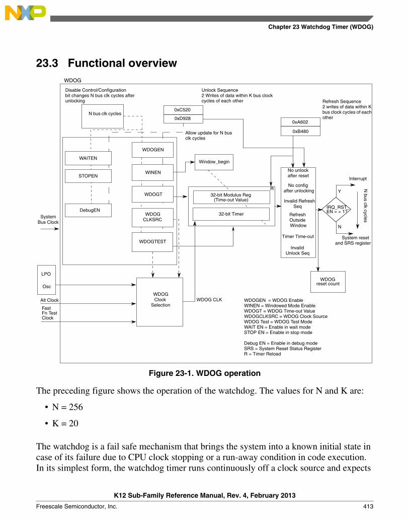
23.3 Functional overview
0xC520 0xD928
Fast Fn Test Clock
Allow update for N bus clk cycles
N bus clk cycles
LPO
N bus clk cycles
Refresh Sequence 2 writes of data within K bus clock cycles of each other
Unlock Sequence 2 Writes of data within K bus clock cycles of each other
Disable Control/Configuration bit changes N bus clk cycles after unlocking
WDOGEN = WDOG Enable WINEN = Windowed Mode Enable WDOGT = WDOG Time-out Value WDOGCLKSRC = WDOG Clock Source WDOG Test = WDOG Test Mode WAIT EN = Enable in wait mode STOP EN = Enable in stop mode Debug EN = Enable in debug mode SRS = System Reset Status Register R = Timer Reload
WDOG reset count
Alt Clock
Osc
WDOG Clock
Selection
WDOG CLK
R
System reset and SRS register
Interrupt
IRQ_RST_ EN = = 1?
Invalid Unlock Seq
32-bit Timer
Timer Time-out
Refresh Outside Window
Invalid Refresh Seq
No config after unlocking
No unlock after reset
0xB480
0xA602
System Bus Clock
32-bit Modulus Reg (Time-out Value)
DebugEN
Window_begin
WDOGTEST
STOPEN
WAITEN
WDOGT
WDOG CLKSRC
WINEN
WDOGEN
WDOG
Y
N
Figure 23-1. WDOG operation
The preceding figure shows the operation of the watchdog. The values for N and K are:
• N = 256
• K = 20
The watchdog is a fail safe mechanism that brings the system into a known initial state incase of its failure due to CPU clock stopping or a run-away condition in code execution.In its simplest form, the watchdog timer runs continuously off a clock source and expects
Chapter 23 Watchdog Timer (WDOG)
K12 Sub-Family Reference Manual, Rev. 4, February 2013
Freescale Semiconductor, Inc. 413
to be serviced periodically, failing which it resets the system. This ensures that thesoftware is executing correctly and has not run away in an unintended direction. Softwarecan adjust the period of servicing or the time-out value for the watchdog timer to meet theneeds of the application.
You can select a windowed mode of operation that expects the servicing to be done onlyin a particular window of the time-out period. An attempted servicing of the watchdogoutside this window results in a reset. By operating in this mode, you can get anindication of whether the code is running faster than expected. The window length is alsouser programmable.
If a system fails to update/refresh the watchdog due to an unknown and persistent cause,it will be caught in an endless cycle of resets from the watchdog. To analyze the cause ofsuch conditions, you can program the watchdog to first issue an interrupt, followed by areset. In the interrupt service routine, the software can analyze the system stack to aiddebugging.
To enhance the independence of watchdog from the system, it runs off an independentLPO oscillator clock. You can also switch over to an alternate clock source if required,through a control register bit.
23.3.1 Unlocking and updating the watchdog
As long as ALLOW_UPDATE in the watchdog control register is set, you can unlockand modify the write-once-only control and configuration registers:
1. Write 0xC520 followed by 0xD928 within 20 bus clock cycles to a specific unlockregister (WDOG_UNLOCK).
2. Wait one bus clock cycle. You cannot update registers on the bus clock cycleimmediately following the write of the unlock sequence.
3. An update window equal in length to the watchdog configuration time (WCT) opens.Within this window, you can update the configuration and control register bits.
These register bits can be modified only once after unlocking.
If none of the configuration and control registers is updated within the update window,the watchdog issues a reset, that is, interrupt-then-reset, to the system. Trying to unlockthe watchdog within the WCT after an initial unlock has no effect. During the updateoperation, the watchdog timer is not paused and continues running in the background.After the update window closes, the watchdog timer restarts and the watchdog functionsaccording to the new configuration.
Functional overview
K12 Sub-Family Reference Manual, Rev. 4, February 2013
414 Freescale Semiconductor, Inc.
The update feature is useful for applications that have an initial, non-safety critical part,where the watchdog is kept disabled or with a conveniently long time-out period. Thismeans the application coder does not have to frequently service the watchdog. After thecritical part of the application begins, the watchdog can be reconfigured as needed.
The watchdog issues a reset, that is, interrupt-then-reset if enabled, to the system for anyof these invalid unlock sequences:
• Write any value other than 0xC520 or 0xD928 to the unlock register.• ALLOW_UPDATE is set and a gap of more than 20 bus clock cycles is inserted
between the writing of the unlock sequence values.
An attempted refresh operation between the two writes of the unlock sequence and in theWCT time following a successful unlock, goes undetected. Also, see WatchdogOperation with 8-bit access for guidelines related to 8-bit accesses to the unlock register.
Note
A context switch during unlocking and refreshing may lead to awatchdog reset.
23.3.2 Watchdog configuration time (WCT)
To prevent unintended modification of the watchdog's control and configuration registerbits, you are allowed to update them only within a period of 256 bus clock cycles afterunlocking. This period is known as the watchdog configuration time (WCT). In addition,these register bits can be modified only once after unlocking them for editing, even afterreset.
You must unlock the registers within WCT after system reset, failing which the WDOGissues a reset to the system. In other words, you must write at least the first word of theunlocking sequence within the WCT after reset. After this is done, you have a further 20bus clock cycles, the maximum allowed gap between the words of the unlock sequence,to complete the unlocking operation. Thereafter, to make sure that you do not forget toconfigure the watchdog, the watchdog issues a reset if none of the WDOG control andconfiguration registers is updated in the WCT after unlock. After the close of thiswindow or after the first write, these register bits are locked out from any furtherchanges.
The watchdog timer keeps running according to its default configuration throughunlocking and update operations that can extend up to a maximum total of 2xWCT + 20bus clock cycles. Therefore, it must be ensured that the time-out value for the watchdogis always greater than 2xWCT time + 20 bus clock cycles.
Chapter 23 Watchdog Timer (WDOG)
K12 Sub-Family Reference Manual, Rev. 4, February 2013
Freescale Semiconductor, Inc. 415
Updates in the write-once registers take effect only after the WCT window closes withthe following exceptions for which changes take effect immediately:
• Stop, Wait, and Debug mode enable
• IRQ_RST_EN
The operations of refreshing the watchdog goes undetected during the WCT.
23.3.3 Refreshing the watchdog
A robust refreshing mechanism has been chosen for the watchdog. A valid refresh is awrite of 0xA602 followed by 0xB480 within 20 bus clock cycles to watchdog refreshregister. If these two values are written more than 20 bus cycles apart or if somethingother than these two values is written to the register, a watchdog reset, or interrupt-then-reset if enabled, is issued to the system. A valid refresh makes the watchdog timer restarton the next bus clock. Also, an attempted unlock operation in between the two writes ofthe refresh sequence goes undetected. See Watchdog Operation with 8-bit access forguidelines related to 8-bit accesses to the refresh register.
23.3.4 Windowed mode of operation
In this mode of operation, a restriction is placed on the point in time within the time-outperiod at which the watchdog can be refreshed. The refresh is considered valid only whenthe watchdog timer increments beyond a certain count as specified by the watchdogwindow register. This is known as refreshing the watchdog within a window of the totaltime-out period. If a refresh is attempted before the timer reaches the window value, thewatchdog generates a reset, or interrupt-then-reset if enabled. If there is no refresh at all,the watchdog times out and generates a reset or interrupt-then-reset if enabled.
23.3.5 Watchdog disabled mode of operation
When the watchdog is disabled through the WDOG_EN bit in the watchdog status andcontrol register, the watchdog timer is reset to zero and is disabled from counting untilyou enable it or it is enabled again by the system reset. In this mode, the watchdog timercannot be refreshed–there is no requirement to do so while the timer is disabled.However, the watchdog still generates a reset, or interrupt-then-reset if enabled, on a non-
Functional overview
K12 Sub-Family Reference Manual, Rev. 4, February 2013
416 Freescale Semiconductor, Inc.
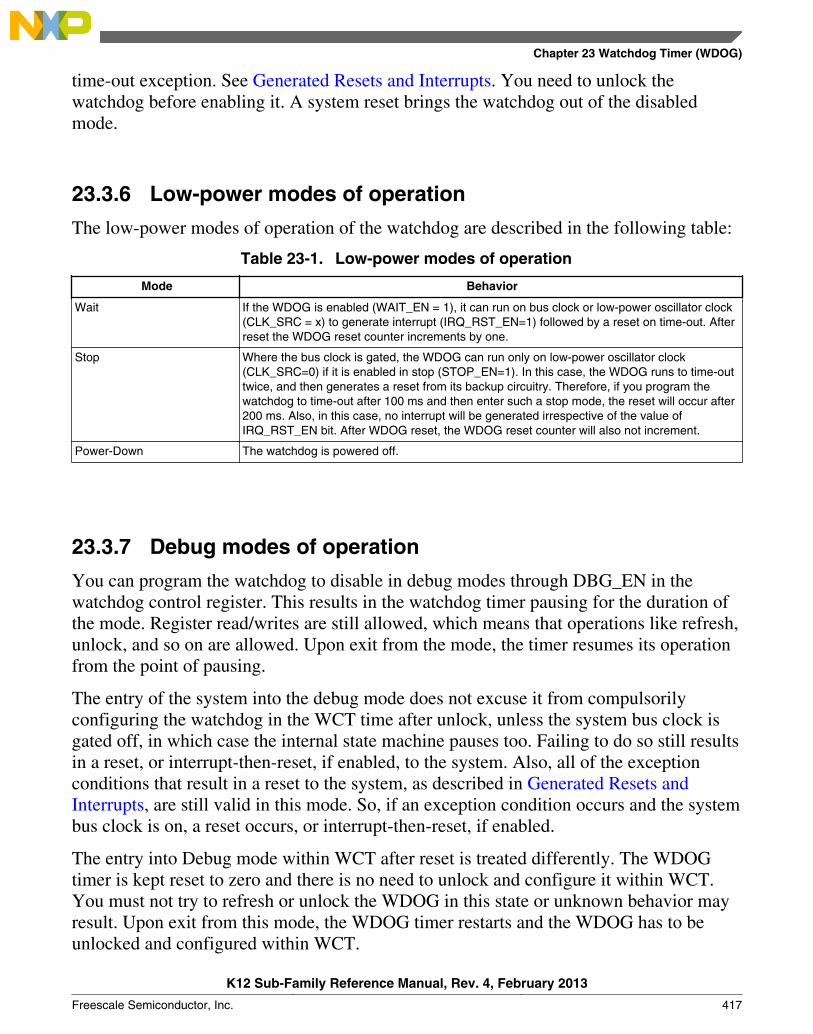
time-out exception. See Generated Resets and Interrupts. You need to unlock thewatchdog before enabling it. A system reset brings the watchdog out of the disabledmode.
23.3.6 Low-power modes of operation
The low-power modes of operation of the watchdog are described in the following table:
Table 23-1. Low-power modes of operation
Mode Behavior
Wait If the WDOG is enabled (WAIT_EN = 1), it can run on bus clock or low-power oscillator clock(CLK_SRC = x) to generate interrupt (IRQ_RST_EN=1) followed by a reset on time-out. Afterreset the WDOG reset counter increments by one.
Stop Where the bus clock is gated, the WDOG can run only on low-power oscillator clock(CLK_SRC=0) if it is enabled in stop (STOP_EN=1). In this case, the WDOG runs to time-outtwice, and then generates a reset from its backup circuitry. Therefore, if you program thewatchdog to time-out after 100 ms and then enter such a stop mode, the reset will occur after200 ms. Also, in this case, no interrupt will be generated irrespective of the value ofIRQ_RST_EN bit. After WDOG reset, the WDOG reset counter will also not increment.
Power-Down The watchdog is powered off.
23.3.7 Debug modes of operation
You can program the watchdog to disable in debug modes through DBG_EN in thewatchdog control register. This results in the watchdog timer pausing for the duration ofthe mode. Register read/writes are still allowed, which means that operations like refresh,unlock, and so on are allowed. Upon exit from the mode, the timer resumes its operationfrom the point of pausing.
The entry of the system into the debug mode does not excuse it from compulsorilyconfiguring the watchdog in the WCT time after unlock, unless the system bus clock isgated off, in which case the internal state machine pauses too. Failing to do so still resultsin a reset, or interrupt-then-reset, if enabled, to the system. Also, all of the exceptionconditions that result in a reset to the system, as described in Generated Resets andInterrupts, are still valid in this mode. So, if an exception condition occurs and the systembus clock is on, a reset occurs, or interrupt-then-reset, if enabled.
The entry into Debug mode within WCT after reset is treated differently. The WDOGtimer is kept reset to zero and there is no need to unlock and configure it within WCT.You must not try to refresh or unlock the WDOG in this state or unknown behavior mayresult. Upon exit from this mode, the WDOG timer restarts and the WDOG has to beunlocked and configured within WCT.
Chapter 23 Watchdog Timer (WDOG)
K12 Sub-Family Reference Manual, Rev. 4, February 2013
Freescale Semiconductor, Inc. 417

23.4 Testing the watchdogFor IEC 60730 and other safety standards, the expectation is that anything that monitors asafety function must be tested, and this test is required to be fault tolerant. To test thewatchdog, its main timer and its associated compare and reset logic must be tested. Tothis end, two tests are implemented for the watchdog, as described in Quick Test andByte Test. A control bit is provided to put the watchdog into functional test mode. Thereis also an overriding test-disable control bit which allows the functional test mode to bedisabled permanently. After it is set, this test-disable bit can only be cleared by a reset.
These two tests achieve the overall aim of testing the counter functioning and thecompare and reset logic.
Note
Do not enable the watchdog interrupt during these tests. Ifrequired, you must ensure that the effective time-out value isgreater than WCT time. See Generated Resets and Interrupts formore details.
To run a particular test:
1. Select either quick test or byte test..2. Set a certain test mode bit to put the watchdog in the functional test mode. Setting
this bit automatically switches the watchdog timer to a fast clock source. Theswitching of the clock source is done to achieve a faster time-out and hence a fastertest.
In a successful test, the timer times out after reaching the programmed time-out value andgenerates a system reset.
Note
After emerging from a reset due to a watchdog test, unlock andconfigure the watchdog. The refresh and unlock operations andinterrupt are not automatically disabled in the test mode.
Testing the watchdog
K12 Sub-Family Reference Manual, Rev. 4, February 2013
418 Freescale Semiconductor, Inc.

23.4.1 Quick test
In this test, the time-out value of watchdog timer is programmed to a very low value toachieve quick time-out. The only difference between the quick test and the normal modeof the watchdog is that TESTWDOG is set for the quick test. This allows for a faster testof the watchdog reset mechanism.
23.4.2 Byte test
The byte test is a more thorough a test of the watchdog timer. In this test, the timer is splitup into its constituent byte-wide stages that are run independently and tested for time-outagainst the corresponding byte of the time-out value register. The following figureexplains the splitting concept:
CLK
WDOG
en
Mod = = Timer?Test
32-bit Timer
Modulus Register (Time-out Value)
WDOG Reset
Nth Stage Overflow Enables N + 1th Stage
en en
Reset Value (Hardwired)
Byte Stage 4
Equality Comparison
Byte 4
Byte 2
Byte 1 Byte 3
Byte Stage 3
Byte Stage 2
Byte Stage 1
Figure 23-2. Watchdog timer byte splitting
Each stage is an 8-bit synchronous counter followed by combinational logic thatgenerates an overflow signal. The overflow signal acts as an enable to the N + 1th stage.
In the test mode, when an individual byte, N, is tested, byte N – 1 is loaded forcefullywith 0xFF, and both these bytes are allowed to run off the clock source. By doing so, theoverflow signal from stage N – 1 is generated immediately, enabling counter stage N.The Nth stage runs and compares with the Nth byte of the time-out value register. In thisway, the byte N is also tested along with the link between it and the preceding stage. No
Chapter 23 Watchdog Timer (WDOG)
K12 Sub-Family Reference Manual, Rev. 4, February 2013
Freescale Semiconductor, Inc. 419
other stages, N – 2, N – 3... and N + 1, N + 2... are enabled for the test on byte N. Thesedisabled stages, except the most significant stage of the counter, are loaded with a valueof 0xFF.
23.5 Backup reset generatorThe backup reset generator generates the final reset which goes out to the system. It has abackup mechanism which ensures that in case the bus clock stops and prevents the mainstate machine from generating a reset exception/interrupt, the watchdog timer's time-outis separately routed out as a reset to the system. Two successive timer time-outs withoutan intervening system reset result in the backup reset generator routing out the time-outsignal as a reset to the system.
23.6 Generated resets and interruptsThe watchdog generates a reset in the following events, also referred to as exceptions:
• A watchdog time-out
• Failure to unlock the watchdog within WCT time after system reset deassertion
• No update of the control and configuration registers within the WCT window afterunlocking. At least one of the following registers must be written to within the WCTwindow to avoid reset:
• WDOG_ST_CTRL_H, WDOG_ST_CTRL_L
• WDOG_TO_VAL_H, WDOG_TO_VAL_L
• WDOG_WIN_H, WDOG_WIN_L
• WDOG_PRESCALER
• A value other than the unlock sequence or the refresh sequence is written to theunlock and/or refresh registers, respectively.
• A gap of more than 20 bus cycles exists between the writes of two values of theunlock sequence.
• A gap of more than 20 bus cycles exists between the writes of two values of therefresh sequence.
Backup reset generator
K12 Sub-Family Reference Manual, Rev. 4, February 2013
420 Freescale Semiconductor, Inc.
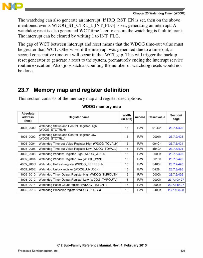
The watchdog can also generate an interrupt. If IRQ_RST_EN is set, then on the abovementioned events WDOG_ST_CTRL_L[INT_FLG] is set, generating an interrupt. Awatchdog reset is also generated WCT time later to ensure the watchdog is fault tolerant.The interrupt can be cleared by writing 1 to INT_FLG.
The gap of WCT between interrupt and reset means that the WDOG time-out value mustbe greater than WCT. Otherwise, if the interrupt was generated due to a time-out, asecond consecutive time-out will occur in that WCT gap. This will trigger the backupreset generator to generate a reset to the system, prematurely ending the interrupt serviceroutine execution. Also, jobs such as counting the number of watchdog resets would notbe done.
23.7 Memory map and register definitionThis section consists of the memory map and register descriptions.
WDOG memory map
Absoluteaddress
(hex)Register name
Width(in bits)
Access Reset valueSection/
page
4005_2000Watchdog Status and Control Register High(WDOG_STCTRLH)
16 R/W 01D3h 23.7.1/422
4005_2002Watchdog Status and Control Register Low(WDOG_STCTRLL)
16 R/W 0001h 23.7.2/423
4005_2004 Watchdog Time-out Value Register High (WDOG_TOVALH) 16 R/W 004Ch 23.7.3/424
4005_2006 Watchdog Time-out Value Register Low (WDOG_TOVALL) 16 R/W 4B4Ch 23.7.4/424
4005_2008 Watchdog Window Register High (WDOG_WINH) 16 R/W 0000h 23.7.5/425
4005_200A Watchdog Window Register Low (WDOG_WINL) 16 R/W 0010h 23.7.6/425
4005_200C Watchdog Refresh register (WDOG_REFRESH) 16 R/W B480h 23.7.7/426
4005_200E Watchdog Unlock register (WDOG_UNLOCK) 16 R/W D928h 23.7.8/426
4005_2010 Watchdog Timer Output Register High (WDOG_TMROUTH) 16 R/W 0000h 23.7.9/426
4005_2012 Watchdog Timer Output Register Low (WDOG_TMROUTL) 16 R/W 0000h 23.7.10/427
4005_2014 Watchdog Reset Count register (WDOG_RSTCNT) 16 R/W 0000h 23.7.11/427
4005_2016 Watchdog Prescaler register (WDOG_PRESC) 16 R/W 0400h 23.7.12/428
Chapter 23 Watchdog Timer (WDOG)
K12 Sub-Family Reference Manual, Rev. 4, February 2013
Freescale Semiconductor, Inc. 421
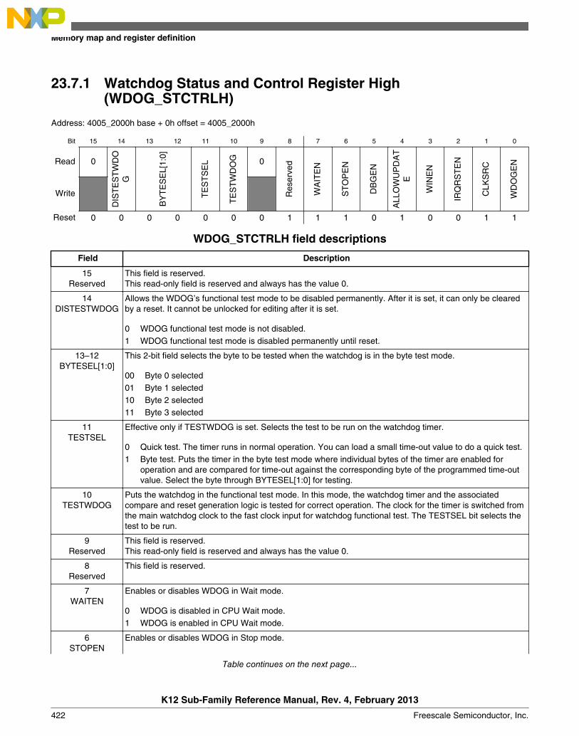
23.7.1 Watchdog Status and Control Register High(WDOG_STCTRLH)
Address: 4005_2000h base + 0h offset = 4005_2000h
Bit 15 14 13 12 11 10 9 8 7 6 5 4 3 2 1 0
Read 0
DIS
TE
ST
WD
OG
BY
TE
SE
L[1:
0]
TE
ST
SE
L
TE
ST
WD
OG 0
Res
erve
d
WA
ITE
N
ST
OP
EN
DB
GE
N
ALL
OW
UP
DA
TE
WIN
EN
IRQ
RS
TE
N
CLK
SR
C
WD
OG
EN
Write
Reset 0 0 0 0 0 0 0 1 1 1 0 1 0 0 1 1
WDOG_STCTRLH field descriptions
Field Description
15Reserved
This field is reserved.This read-only field is reserved and always has the value 0.
14DISTESTWDOG
Allows the WDOG’s functional test mode to be disabled permanently. After it is set, it can only be clearedby a reset. It cannot be unlocked for editing after it is set.
0 WDOG functional test mode is not disabled.1 WDOG functional test mode is disabled permanently until reset.
13–12BYTESEL[1:0]
This 2-bit field selects the byte to be tested when the watchdog is in the byte test mode.
00 Byte 0 selected01 Byte 1 selected10 Byte 2 selected11 Byte 3 selected
11TESTSEL
Effective only if TESTWDOG is set. Selects the test to be run on the watchdog timer.
0 Quick test. The timer runs in normal operation. You can load a small time-out value to do a quick test.1 Byte test. Puts the timer in the byte test mode where individual bytes of the timer are enabled for
operation and are compared for time-out against the corresponding byte of the programmed time-outvalue. Select the byte through BYTESEL[1:0] for testing.
10TESTWDOG
Puts the watchdog in the functional test mode. In this mode, the watchdog timer and the associatedcompare and reset generation logic is tested for correct operation. The clock for the timer is switched fromthe main watchdog clock to the fast clock input for watchdog functional test. The TESTSEL bit selects thetest to be run.
9Reserved
This field is reserved.This read-only field is reserved and always has the value 0.
8Reserved
This field is reserved.
7WAITEN
Enables or disables WDOG in Wait mode.
0 WDOG is disabled in CPU Wait mode.1 WDOG is enabled in CPU Wait mode.
6STOPEN
Enables or disables WDOG in Stop mode.
Table continues on the next page...
Memory map and register definition
K12 Sub-Family Reference Manual, Rev. 4, February 2013
422 Freescale Semiconductor, Inc.
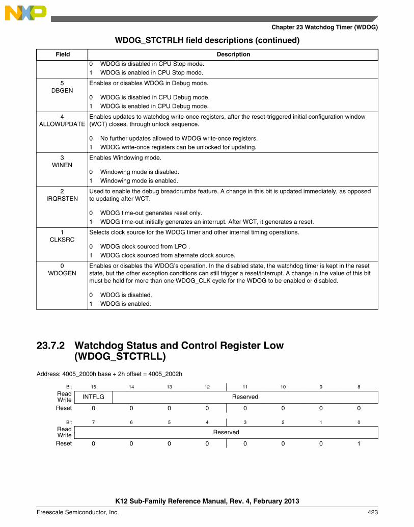
WDOG_STCTRLH field descriptions (continued)
Field Description
0 WDOG is disabled in CPU Stop mode.1 WDOG is enabled in CPU Stop mode.
5DBGEN
Enables or disables WDOG in Debug mode.
0 WDOG is disabled in CPU Debug mode.1 WDOG is enabled in CPU Debug mode.
4ALLOWUPDATE
Enables updates to watchdog write-once registers, after the reset-triggered initial configuration window(WCT) closes, through unlock sequence.
0 No further updates allowed to WDOG write-once registers.1 WDOG write-once registers can be unlocked for updating.
3WINEN
Enables Windowing mode.
0 Windowing mode is disabled.1 Windowing mode is enabled.
2IRQRSTEN
Used to enable the debug breadcrumbs feature. A change in this bit is updated immediately, as opposedto updating after WCT.
0 WDOG time-out generates reset only.1 WDOG time-out initially generates an interrupt. After WCT, it generates a reset.
1CLKSRC
Selects clock source for the WDOG timer and other internal timing operations.
0 WDOG clock sourced from LPO .1 WDOG clock sourced from alternate clock source.
0WDOGEN
Enables or disables the WDOG’s operation. In the disabled state, the watchdog timer is kept in the resetstate, but the other exception conditions can still trigger a reset/interrupt. A change in the value of this bitmust be held for more than one WDOG_CLK cycle for the WDOG to be enabled or disabled.
0 WDOG is disabled.1 WDOG is enabled.
23.7.2 Watchdog Status and Control Register Low(WDOG_STCTRLL)
Address: 4005_2000h base + 2h offset = 4005_2002h
Bit 15 14 13 12 11 10 9 8
Read INTFLG ReservedWriteReset 0 0 0 0 0 0 0 0
Bit 7 6 5 4 3 2 1 0
Read ReservedWriteReset 0 0 0 0 0 0 0 1
Chapter 23 Watchdog Timer (WDOG)
K12 Sub-Family Reference Manual, Rev. 4, February 2013
Freescale Semiconductor, Inc. 423

WDOG_STCTRLL field descriptions
Field Description
15INTFLG
Interrupt flag. It is set when an exception occurs. IRQRSTEN = 1 is a precondition to set this flag. INTFLG= 1 results in an interrupt being issued followed by a reset, WCT later. The interrupt can be cleared bywriting 1 to this bit. It also gets cleared on a system reset.
14–0Reserved
This field is reserved.
NOTE: Do not modify this field value.
23.7.3 Watchdog Time-out Value Register High (WDOG_TOVALH)
Address: 4005_2000h base + 4h offset = 4005_2004h
Bit 15 14 13 12 11 10 9 8 7 6 5 4 3 2 1 0
Read TOVALHIGHWriteReset 0 0 0 0 0 0 0 0 0 1 0 0 1 1 0 0
WDOG_TOVALH field descriptions
Field Description
15–0TOVALHIGH
Defines the upper 16 bits of the 32-bit time-out value for the watchdog timer. It is defined in terms of cyclesof the watchdog clock.
23.7.4 Watchdog Time-out Value Register Low (WDOG_TOVALL)
The time-out value of the watchdog must be set to a minimum of four watchdog clockcycles. This is to take into account the delay in new settings taking effect in the watchdogclock domain.
Address: 4005_2000h base + 6h offset = 4005_2006h
Bit 15 14 13 12 11 10 9 8 7 6 5 4 3 2 1 0
Read TOVALLOWWriteReset 0 1 0 0 1 0 1 1 0 1 0 0 1 1 0 0
WDOG_TOVALL field descriptions
Field Description
15–0TOVALLOW
Defines the lower 16 bits of the 32-bit time-out value for the watchdog timer. It is defined in terms of cyclesof the watchdog clock.
Memory map and register definition
K12 Sub-Family Reference Manual, Rev. 4, February 2013
424 Freescale Semiconductor, Inc.
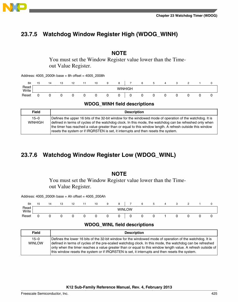
23.7.5 Watchdog Window Register High (WDOG_WINH)
NOTEYou must set the Window Register value lower than the Time-out Value Register.
Address: 4005_2000h base + 8h offset = 4005_2008h
Bit 15 14 13 12 11 10 9 8 7 6 5 4 3 2 1 0
Read WINHIGHWriteReset 0 0 0 0 0 0 0 0 0 0 0 0 0 0 0 0
WDOG_WINH field descriptions
Field Description
15–0WINHIGH
Defines the upper 16 bits of the 32-bit window for the windowed mode of operation of the watchdog. It isdefined in terms of cycles of the watchdog clock. In this mode, the watchdog can be refreshed only whenthe timer has reached a value greater than or equal to this window length. A refresh outside this windowresets the system or if IRQRSTEN is set, it interrupts and then resets the system.
23.7.6 Watchdog Window Register Low (WDOG_WINL)
NOTEYou must set the Window Register value lower than the Time-out Value Register.
Address: 4005_2000h base + Ah offset = 4005_200Ah
Bit 15 14 13 12 11 10 9 8 7 6 5 4 3 2 1 0
Read WINLOWWriteReset 0 0 0 0 0 0 0 0 0 0 0 1 0 0 0 0
WDOG_WINL field descriptions
Field Description
15–0WINLOW
Defines the lower 16 bits of the 32-bit window for the windowed mode of operation of the watchdog. It isdefined in terms of cycles of the pre-scaled watchdog clock. In this mode, the watchdog can be refreshedonly when the timer reaches a value greater than or equal to this window length value. A refresh outside ofthis window resets the system or if IRQRSTEN is set, it interrupts and then resets the system.
Chapter 23 Watchdog Timer (WDOG)
K12 Sub-Family Reference Manual, Rev. 4, February 2013
Freescale Semiconductor, Inc. 425
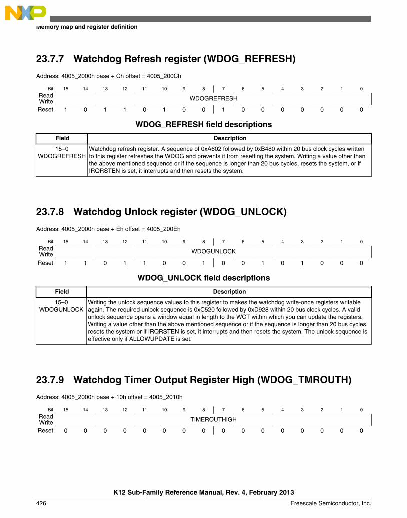
23.7.7 Watchdog Refresh register (WDOG_REFRESH)
Address: 4005_2000h base + Ch offset = 4005_200Ch
Bit 15 14 13 12 11 10 9 8 7 6 5 4 3 2 1 0
Read WDOGREFRESHWriteReset 1 0 1 1 0 1 0 0 1 0 0 0 0 0 0 0
WDOG_REFRESH field descriptions
Field Description
15–0WDOGREFRESH
Watchdog refresh register. A sequence of 0xA602 followed by 0xB480 within 20 bus clock cycles writtento this register refreshes the WDOG and prevents it from resetting the system. Writing a value other thanthe above mentioned sequence or if the sequence is longer than 20 bus cycles, resets the system, or ifIRQRSTEN is set, it interrupts and then resets the system.
23.7.8 Watchdog Unlock register (WDOG_UNLOCK)
Address: 4005_2000h base + Eh offset = 4005_200Eh
Bit 15 14 13 12 11 10 9 8 7 6 5 4 3 2 1 0
Read WDOGUNLOCKWriteReset 1 1 0 1 1 0 0 1 0 0 1 0 1 0 0 0
WDOG_UNLOCK field descriptions
Field Description
15–0WDOGUNLOCK
Writing the unlock sequence values to this register to makes the watchdog write-once registers writableagain. The required unlock sequence is 0xC520 followed by 0xD928 within 20 bus clock cycles. A validunlock sequence opens a window equal in length to the WCT within which you can update the registers.Writing a value other than the above mentioned sequence or if the sequence is longer than 20 bus cycles,resets the system or if IRQRSTEN is set, it interrupts and then resets the system. The unlock sequence iseffective only if ALLOWUPDATE is set.
23.7.9 Watchdog Timer Output Register High (WDOG_TMROUTH)
Address: 4005_2000h base + 10h offset = 4005_2010h
Bit 15 14 13 12 11 10 9 8 7 6 5 4 3 2 1 0
Read TIMEROUTHIGHWriteReset 0 0 0 0 0 0 0 0 0 0 0 0 0 0 0 0
Memory map and register definition
K12 Sub-Family Reference Manual, Rev. 4, February 2013
426 Freescale Semiconductor, Inc.
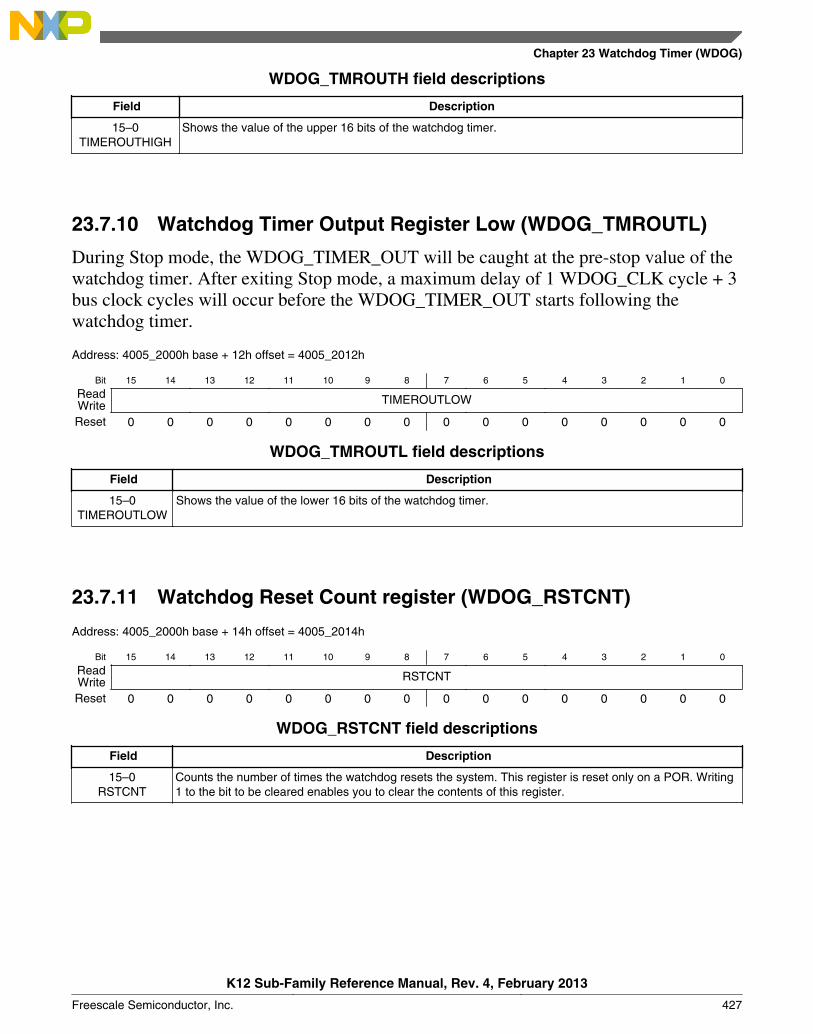
WDOG_TMROUTH field descriptions
Field Description
15–0TIMEROUTHIGH
Shows the value of the upper 16 bits of the watchdog timer.
23.7.10 Watchdog Timer Output Register Low (WDOG_TMROUTL)
During Stop mode, the WDOG_TIMER_OUT will be caught at the pre-stop value of thewatchdog timer. After exiting Stop mode, a maximum delay of 1 WDOG_CLK cycle + 3bus clock cycles will occur before the WDOG_TIMER_OUT starts following thewatchdog timer.
Address: 4005_2000h base + 12h offset = 4005_2012h
Bit 15 14 13 12 11 10 9 8 7 6 5 4 3 2 1 0
Read TIMEROUTLOWWriteReset 0 0 0 0 0 0 0 0 0 0 0 0 0 0 0 0
WDOG_TMROUTL field descriptions
Field Description
15–0TIMEROUTLOW
Shows the value of the lower 16 bits of the watchdog timer.
23.7.11 Watchdog Reset Count register (WDOG_RSTCNT)
Address: 4005_2000h base + 14h offset = 4005_2014h
Bit 15 14 13 12 11 10 9 8 7 6 5 4 3 2 1 0
Read RSTCNTWriteReset 0 0 0 0 0 0 0 0 0 0 0 0 0 0 0 0
WDOG_RSTCNT field descriptions
Field Description
15–0RSTCNT
Counts the number of times the watchdog resets the system. This register is reset only on a POR. Writing1 to the bit to be cleared enables you to clear the contents of this register.
Chapter 23 Watchdog Timer (WDOG)
K12 Sub-Family Reference Manual, Rev. 4, February 2013
Freescale Semiconductor, Inc. 427

23.7.12 Watchdog Prescaler register (WDOG_PRESC)
Address: 4005_2000h base + 16h offset = 4005_2016h
Bit 15 14 13 12 11 10 9 8 7 6 5 4 3 2 1 0
Read 0 PRESCVAL 0WriteReset 0 0 0 0 0 1 0 0 0 0 0 0 0 0 0 0
WDOG_PRESC field descriptions
Field Description
15–11Reserved
This field is reserved.This read-only field is reserved and always has the value 0.
10–8PRESCVAL
3-bit prescaler for the watchdog clock source. A value of zero indicates no division of the input WDOGclock. The watchdog clock is divided by (PRESCVAL + 1) to provide the prescaled WDOG_CLK.
7–0Reserved
This field is reserved.This read-only field is reserved and always has the value 0.
23.8 Watchdog operation with 8-bit access
23.8.1 General guideline
When performing 8-bit accesses to the watchdog's 16-bit registers where the intention isto access both the bytes of a register, place the two 8-bit accesses one after the other inyour code.
23.8.2 Refresh and unlock operations with 8-bit access
One exception condition that generates a reset to the system is the write of any valueother than those required for a legal refresh/update sequence to the respective refresh andunlock registers.
For an 8-bit access to these registers, writing a correct value requires at least two busclock cycles, resulting in an invalid value in the registers for one cycle. Therefore, thesystem is reset even if the intention is to write a correct value to the refresh/unlockregister. Keeping this in mind, the exception condition for 8-bit accesses is slightlymodified.
Watchdog operation with 8-bit access
K12 Sub-Family Reference Manual, Rev. 4, February 2013
428 Freescale Semiconductor, Inc.
Whereas the match for a correct value for a refresh/unlock sequence is as according to theoriginal definition, the match for an incorrect value is done byte-wise on the refresh/unlock rather than for the whole 16-bit value. This means that if the high byte of therefresh/unlock register contains any value other than high bytes of the two values thatmake up the sequence, it is treated as an exception condition, leading to a reset orinterrupt-then-reset. The same holds true for the lower byte of the refresh or unlockregister. Take the refresh operation that expects a write of 0xA602 followed by 0xB480to the refresh register, as an example.
Table 23-15. Refresh for 8-bit access
WDOG_REFRESH[15:8] WDOG_REFRESH[7:0]Sequence value1 or
value2 matchMismatchexception
Current Value 0xB4 0x80 Value2 match No
Write 1 0xB4 0x02 No match No
Write 2 0xA6 0x02 Value1 match No
Write 3 0xB4 0x02 No match No
Write 4 0xB4 0x80 Value2 match.Sequence complete.
No
Write 5 0x02 0x80 No match Yes
As shown in the preceding table, the refresh register holds its reset value initially.Thereafter, two 8-bit accesses are performed on the register to write the first value of therefresh sequence. No mismatch exception is registered on the intermediate write, Write1.The sequence is completed by performing two more 8-bit accesses, writing in the secondvalue of the sequence for a successful refresh. It must be noted that the match of value2takes place only when the complete 16-bit value is correctly written, write4. Hence, therequirement of writing value2 of the sequence within 20 bus clock cycles of value1 ischecked by measuring the gap between write2 and write4.
It is reiterated that the condition for matching values 1 and 2 of the refresh or unlocksequence remains unchanged. The difference for 8-bit accesses is that the criterion fordetecting a mismatch is less strict. Any 16-bit access still needs to adhere to the originalguidelines, mentioned in the sections Refreshing the Watchdog.
23.9 Restrictions on watchdog operationThis section mentions some exceptions to the watchdog operation that may not beapparent to you.
Chapter 23 Watchdog Timer (WDOG)
K12 Sub-Family Reference Manual, Rev. 4, February 2013
Freescale Semiconductor, Inc. 429
• Restriction on unlock/refresh operations—In the period between the closure of theWCT window after unlock and the actual reload of the watchdog timer, unlock andrefresh operations need not be attempted.
• The update and reload of the watchdog timer happens two to three watchdog clocksafter WCT window closes, following a successful configuration on unlock.
• Clock Switching Delay—The watchdog uses glitch-free multiplexers at two places –one to choose between the LPO oscillator input and alternate clock input, and theother to choose between the watchdog functional clock and fast clock input forwatchdog functional test. A maximum time period of ~2 clock A cycles plus ~2clock B cycles elapses from the time a switch is requested to the occurrence of theactual clock switch, where clock A and B are the two input clocks to the clock mux.
• For the windowed mode, there is a two to three bus clock latency between thewatchdog counter going past the window value and the same registering in the busclock domain.
• For proper operation of the watchdog, the watchdog clock must be at least five timesslower than the system bus clock at all times. An exception is when the watchdogclock is synchronous to the bus clock wherein the watchdog clock can be as fast asthe bus clock.
• WCT must be equivalent to at least three watchdog clock cycles. If not ensured, thismeans that even after the close of the WCT window, you have to wait for thesynchronized system reset to deassert in the watchdog clock domain, beforeexpecting the configuration updates to take effect.
• The time-out value of the watchdog should be set to a minimum of four watchdogclock cycles. This is to take into account the delay in new settings taking effect in thewatchdog clock domain.
• You must take care not only to refresh the watchdog within the watchdog timer'sactual time-out period, but also provide enough allowance for the time it takes for therefresh sequence to be detected by the watchdog timer, on the watchdog clock.
• Updates cannot be made in the bus clock cycle immediately following the write ofthe unlock sequence, but one bus clock cycle later.
• It should be ensured that the time-out value for the watchdog is always greater than2xWCT time + 20 bus clock cycles.
• An attempted refresh operation, in between the two writes of the unlock sequenceand in the WCT time following a successful unlock, will go undetected.
Restrictions on watchdog operation
K12 Sub-Family Reference Manual, Rev. 4, February 2013
430 Freescale Semiconductor, Inc.
• Trying to unlock the watchdog within the WCT time after an initial unlock has noeffect.
• The refresh and unlock operations and interrupt are not automatically disabled in thewatchdog functional test mode.
• After emerging from a reset due to a watchdog functional test, you are still expectedto go through the mandatory steps of unlocking and configuring the watchdog. Thewatchdog continues to be in its functional test mode and therefore you should pullthe watchdog out of the functional test mode within WCT time of reset.
• After emerging from a reset due to a watchdog functional test, you still need to gothrough the mandatory steps of unlocking and configuring the watchdog.
• You must ensure that both the clock inputs to the glitchless clock multiplexers arealive during the switching of clocks. Failure to do so results in a loss of clock at theiroutputs.
• There is a gap of two to three watchdog clock cycles from the point that stop mode isentered to the watchdog timer actually pausing, due to synchronization. The sameholds true for an exit from the stop mode, this time resulting in a two to threewatchdog clock cycle delay in the timer restarting. In case the duration of the stopmode is less than one watchdog clock cycle, the watchdog timer is not guaranteed topause.
• Consider the case when the first refresh value is written, following which the systementers stop mode with system bus clk still on. If the second refresh value is notwritten within 20 bus cycles of the first value, the system is reset, or interrupt-then-reset if enabled.
Chapter 23 Watchdog Timer (WDOG)
K12 Sub-Family Reference Manual, Rev. 4, February 2013
Freescale Semiconductor, Inc. 431

Restrictions on watchdog operation
K12 Sub-Family Reference Manual, Rev. 4, February 2013
432 Freescale Semiconductor, Inc.
Chapter 24Multipurpose Clock Generator (MCG)
24.1 IntroductionNOTE
For the chip-specific implementation details of this module'sinstances see the chip configuration information.
The multipurpose clock generator (MCG) module provides several clock source choicesfor the MCU. The module contains a frequency-locked loop (FLL) and a phase-lockedloop (PLL). The FLL is controllable by either an internal or an external reference clock.The PLL is controllable by the external reference clock. The module can select either ofthe FLL or PLL output clocks, or either of the internal or external reference clocks as asource for the MCU system clock. The MCG operates in conjuction with a crystaloscillator, which allows an external crystal, ceramic resonator, or another external clocksource to produce the external reference clock.
24.1.1 Features
Key features of the MCG module are:
• Frequency-locked loop (FLL):
• Digitally-controlled oscillator (DCO)
• DCO frequency range is programmable for up to four different frequency ranges.
• Option to program and maximize DCO output frequency for a low frequencyexternal reference clock source.
• Option to prevent FLL from resetting its current locked frequency whenswitching clock modes if FLL reference frequency is not changed.
K12 Sub-Family Reference Manual, Rev. 4, February 2013
Freescale Semiconductor, Inc. 433

• Internal or external reference clock can be used as the FLL source.
• Can be used as a clock source for other on-chip peripherals.
• Phase-locked loop (PLL):
• Voltage-controlled oscillator (VCO)
• External reference clock is used as the PLL source.
• Modulo VCO frequency divider
• Phase/Frequency detector
• Integrated loop filter
• Can be used as a clock source for other on-chip peripherals.
• Internal reference clock generator:
• Slow clock with nine trim bits for accuracy
• Fast clock with four trim bits
• Can be used as source clock for the FLL. In FEI mode, only the slow InternalReference Clock (IRC) can be used as the FLL source.
• Either the slow or the fast clock can be selected as the clock source for the MCU.
• Can be used as a clock source for other on-chip peripherals.
• Control signals for the MCG external reference low power oscillator clock generatorsare provided:
• HGO0, RANGE0, EREFS0
• External clock from the Crystal Oscillator :
• Can be used as a source for the FLL and/or the PLL.
• Can be selected as the clock source for the MCU.
• External clock from the Real Time Counter (RTC):
• Can only be used as a source for the FLL.
• Can be selected as the clock source for the MCU.
• External clock monitor with reset and interrupt request capability to check forexternal clock failure when running in FBE, PEE, BLPE, or FEE modes
• Lock detector with interrupt request capability for use with the PLL
Introduction
K12 Sub-Family Reference Manual, Rev. 4, February 2013
434 Freescale Semiconductor, Inc.
• Internal Reference Clocks Auto Trim Machine (ATM) capability using an externalclock as a reference
• Reference dividers for both the FLL and the PLL are provided
• Reference dividers for the Fast Internal Reference Clock are provided
• MCG PLL Clock (MCGPLLCLK) is provided as a clock source for other on-chipperipherals
• MCG FLL Clock (MCGFLLCLK) is provided as a clock source for other on-chipperipherals
• MCG Fixed Frequency Clock (MCGFFCLK) is provided as a clock source for otheron-chip peripherals
• MCG Internal Reference Clock (MCGIRCLK) is provided as a clock source for otheron-chip peripherals
Chapter 24 Multipurpose Clock Generator (MCG)
K12 Sub-Family Reference Manual, Rev. 4, February 2013
Freescale Semiconductor, Inc. 435
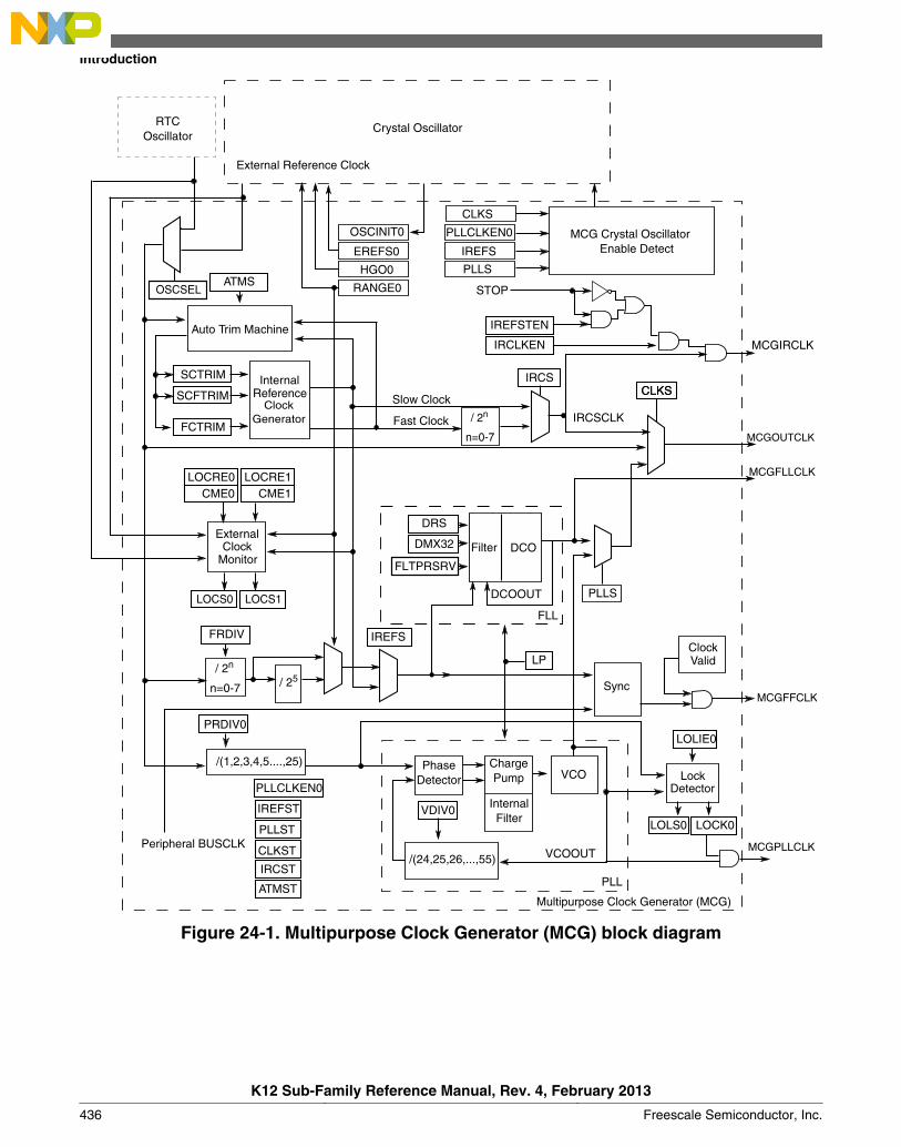
MCGOUTCLK
MCGIRCLK
MCGFFCLK
DCOOUT
/(24,25,26,...,55)
PhaseDetector
ChargePump
InternalFilter
VCO
VCOOUT
PLL
Multipurpose Clock Generator (MCG)
VDIV0
Lock
IRCLKEN
PLLS
LOLS0 LOCK0
Detector
/ 25
IREFST
FLL
DMX32
MCGFLLCLK
Crystal Oscillator
FRDIV
n=0-7
/ 2n
InternalReference Slow Clock
Fast ClockClock
Generator
PRDIV0LOLIE0
Sync
Auto Trim Machine
IRCST
PLLST
CLKST
ATMS
SCTRIM
SCFTRIM
FCTRIM
ATMST
IREFSTEN
OSCINIT0
EREFS0
HGO0
RANGE0
DRS
ClockValid
Peripheral BUSCLK
PLLCLKEN0
IRCSCLK
IRCSCLKSCLKS
DCO
LP
Filter
/(1,2,3,4,5....,25)
IREFS
STOP
CLKS
PLLCLKEN0
IREFS
PLLS
MCG Crystal Oscillator Enable Detect
External Reference Clock
RTCOscillator
OSCSEL
n=0-7
/ 2n
FLTPRSRV
MCGPLLCLK
ClockExternal
CME0LOCRE0
CME1LOCRE1
LOCS0 LOCS1
Monitor
Figure 24-1. Multipurpose Clock Generator (MCG) block diagram
Introduction
K12 Sub-Family Reference Manual, Rev. 4, February 2013
436 Freescale Semiconductor, Inc.
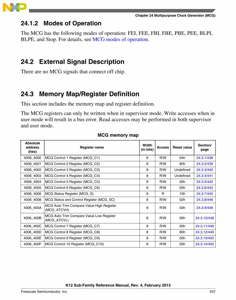
24.1.2 Modes of Operation
The MCG has the following modes of operation: FEI, FEE, FBI, FBE, PBE, PEE, BLPI,BLPE, and Stop. For details, see MCG modes of operation.
24.2 External Signal DescriptionThere are no MCG signals that connect off chip.
24.3 Memory Map/Register DefinitionThis section includes the memory map and register definition.
The MCG registers can only be written when in supervisor mode. Write accesses when inuser mode will result in a bus error. Read accesses may be performed in both supervisorand user mode.
MCG memory map
Absoluteaddress
(hex)Register name
Width(in bits)
Access Reset valueSection/
page
4006_4000 MCG Control 1 Register (MCG_C1) 8 R/W 04h 24.3.1/438
4006_4001 MCG Control 2 Register (MCG_C2) 8 R/W 80h 24.3.2/439
4006_4002 MCG Control 3 Register (MCG_C3) 8 R/W Undefined 24.3.3/440
4006_4003 MCG Control 4 Register (MCG_C4) 8 R/W Undefined 24.3.4/441
4006_4004 MCG Control 5 Register (MCG_C5) 8 R/W 00h 24.3.5/442
4006_4005 MCG Control 6 Register (MCG_C6) 8 R/W 00h 24.3.6/443
4006_4006 MCG Status Register (MCG_S) 8 R 10h 24.3.7/445
4006_4008 MCG Status and Control Register (MCG_SC) 8 R/W 02h 24.3.8/446
4006_400AMCG Auto Trim Compare Value High Register(MCG_ATCVH)
8 R/W 00h 24.3.9/448
4006_400BMCG Auto Trim Compare Value Low Register(MCG_ATCVL)
8 R/W 00h 24.3.10/448
4006_400C MCG Control 7 Register (MCG_C7) 8 R/W 00h 24.3.11/448
4006_400D MCG Control 8 Register (MCG_C8) 8 R/W 80h 24.3.12/449
4006_400E MCG Control 9 Register (MCG_C9) 8 R/W 00h 24.3.13/450
4006_400F MCG Control 10 Register (MCG_C10) 8 R/W 00h 24.3.14/450
Chapter 24 Multipurpose Clock Generator (MCG)
K12 Sub-Family Reference Manual, Rev. 4, February 2013
Freescale Semiconductor, Inc. 437
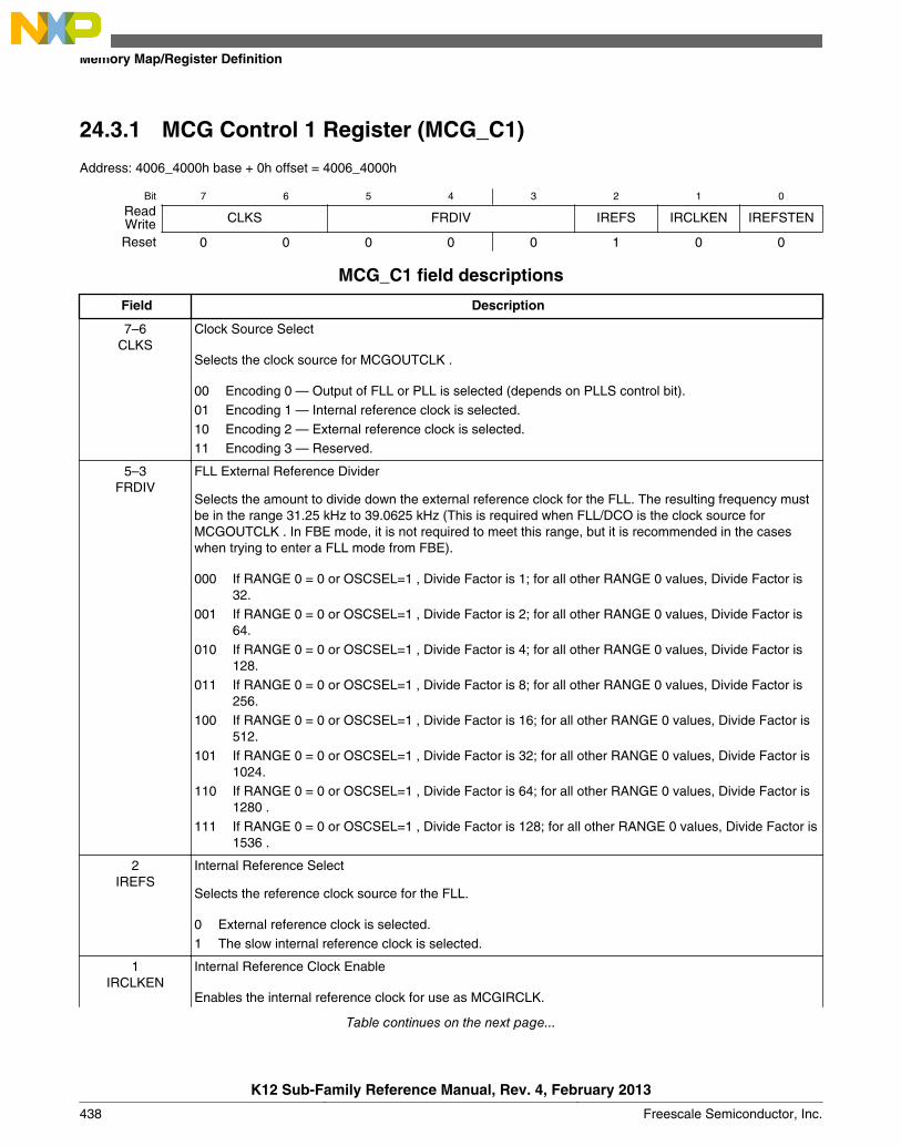
24.3.1 MCG Control 1 Register (MCG_C1)
Address: 4006_4000h base + 0h offset = 4006_4000h
Bit 7 6 5 4 3 2 1 0
Read CLKS FRDIV IREFS IRCLKEN IREFSTENWriteReset 0 0 0 0 0 1 0 0
MCG_C1 field descriptions
Field Description
7–6CLKS
Clock Source Select
Selects the clock source for MCGOUTCLK .
00 Encoding 0 — Output of FLL or PLL is selected (depends on PLLS control bit).01 Encoding 1 — Internal reference clock is selected.10 Encoding 2 — External reference clock is selected.11 Encoding 3 — Reserved.
5–3FRDIV
FLL External Reference Divider
Selects the amount to divide down the external reference clock for the FLL. The resulting frequency mustbe in the range 31.25 kHz to 39.0625 kHz (This is required when FLL/DCO is the clock source forMCGOUTCLK . In FBE mode, it is not required to meet this range, but it is recommended in the caseswhen trying to enter a FLL mode from FBE).
000 If RANGE 0 = 0 or OSCSEL=1 , Divide Factor is 1; for all other RANGE 0 values, Divide Factor is32.
001 If RANGE 0 = 0 or OSCSEL=1 , Divide Factor is 2; for all other RANGE 0 values, Divide Factor is64.
010 If RANGE 0 = 0 or OSCSEL=1 , Divide Factor is 4; for all other RANGE 0 values, Divide Factor is128.
011 If RANGE 0 = 0 or OSCSEL=1 , Divide Factor is 8; for all other RANGE 0 values, Divide Factor is256.
100 If RANGE 0 = 0 or OSCSEL=1 , Divide Factor is 16; for all other RANGE 0 values, Divide Factor is512.
101 If RANGE 0 = 0 or OSCSEL=1 , Divide Factor is 32; for all other RANGE 0 values, Divide Factor is1024.
110 If RANGE 0 = 0 or OSCSEL=1 , Divide Factor is 64; for all other RANGE 0 values, Divide Factor is1280 .
111 If RANGE 0 = 0 or OSCSEL=1 , Divide Factor is 128; for all other RANGE 0 values, Divide Factor is1536 .
2IREFS
Internal Reference Select
Selects the reference clock source for the FLL.
0 External reference clock is selected.1 The slow internal reference clock is selected.
1IRCLKEN
Internal Reference Clock Enable
Enables the internal reference clock for use as MCGIRCLK.
Table continues on the next page...
Memory Map/Register Definition
K12 Sub-Family Reference Manual, Rev. 4, February 2013
438 Freescale Semiconductor, Inc.
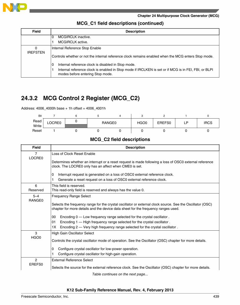
MCG_C1 field descriptions (continued)
Field Description
0 MCGIRCLK inactive.1 MCGIRCLK active.
0IREFSTEN
Internal Reference Stop Enable
Controls whether or not the internal reference clock remains enabled when the MCG enters Stop mode.
0 Internal reference clock is disabled in Stop mode.1 Internal reference clock is enabled in Stop mode if IRCLKEN is set or if MCG is in FEI, FBI, or BLPI
modes before entering Stop mode.
24.3.2 MCG Control 2 Register (MCG_C2)
Address: 4006_4000h base + 1h offset = 4006_4001h
Bit 7 6 5 4 3 2 1 0
Read LOCRE0 0 RANGE0 HGO0 EREFS0 LP IRCSWriteReset 1 0 0 0 0 0 0 0
MCG_C2 field descriptions
Field Description
7LOCRE0
Loss of Clock Reset Enable
Determines whether an interrupt or a reset request is made following a loss of OSC0 external referenceclock. The LOCRE0 only has an affect when CME0 is set.
0 Interrupt request is generated on a loss of OSC0 external reference clock.1 Generate a reset request on a loss of OSC0 external reference clock.
6Reserved
This field is reserved.This read-only field is reserved and always has the value 0.
5–4RANGE0
Frequency Range Select
Selects the frequency range for the crystal oscillator or external clock source. See the Oscillator (OSC)chapter for more details and the device data sheet for the frequency ranges used.
00 Encoding 0 — Low frequency range selected for the crystal oscillator .01 Encoding 1 — High frequency range selected for the crystal oscillator .1X Encoding 2 — Very high frequency range selected for the crystal oscillator .
3HGO0
High Gain Oscillator Select
Controls the crystal oscillator mode of operation. See the Oscillator (OSC) chapter for more details.
0 Configure crystal oscillator for low-power operation.1 Configure crystal oscillator for high-gain operation.
2EREFS0
External Reference Select
Selects the source for the external reference clock. See the Oscillator (OSC) chapter for more details.
Table continues on the next page...
Chapter 24 Multipurpose Clock Generator (MCG)
K12 Sub-Family Reference Manual, Rev. 4, February 2013
Freescale Semiconductor, Inc. 439

MCG_C2 field descriptions (continued)
Field Description
0 External reference clock requested.1 Oscillator requested.
1LP
Low Power Select
Controls whether the FLL or PLL is disabled in BLPI and BLPE modes. In FBE or PBE modes, setting thisbit to 1 will transition the MCG into BLPE mode; in FBI mode, setting this bit to 1 will transition the MCGinto BLPI mode. In any other MCG mode, LP bit has no affect.
0 FLL or PLL is not disabled in bypass modes.1 FLL or PLL is disabled in bypass modes (lower power)
0IRCS
Internal Reference Clock Select
Selects between the fast or slow internal reference clock source.
0 Slow internal reference clock selected.1 Fast internal reference clock selected.
24.3.3 MCG Control 3 Register (MCG_C3)
Address: 4006_4000h base + 2h offset = 4006_4002h
Bit 7 6 5 4 3 2 1 0
Read SCTRIMWriteReset x* x* x* x* x* x* x* x*
* Notes:x = Undefined at reset.•
MCG_C3 field descriptions
Field Description
7–0SCTRIM
Slow Internal Reference Clock Trim Setting
SCTRIM controls the slow internal reference clock frequency by controlling the slow internal referenceclock period. The SCTRIM bits are binary weighted, that is, bit 1 adjusts twice as much as bit 0. Increasingthe binary value increases the period, and decreasing the value decreases the period.
An additional fine trim bit is available in C4 register as the SCFTRIM bit. Upon reset, this value is loadedwith a factory trim value.
If an SCTRIM value stored in nonvolatile memory is to be used, it is your responsibility to copy that valuefrom the nonvolatile memory location to this register.
1. A value for SCTRIM is loaded during reset from a factory programmed location.
Memory Map/Register Definition
K12 Sub-Family Reference Manual, Rev. 4, February 2013
440 Freescale Semiconductor, Inc.

24.3.4 MCG Control 4 Register (MCG_C4)
NOTE
Reset values for DRST and DMX32 bits are 0.
Address: 4006_4000h base + 3h offset = 4006_4003h
Bit 7 6 5 4 3 2 1 0
Read DMX32 DRST_DRS FCTRIM SCFTRIMWriteReset 0 0 0 x* x* x* x* x*
* Notes:x = Undefined at reset.•
A value for FCTRIM is loaded during reset from a factory programmed location. x = Undefined at reset.•
MCG_C4 field descriptions
Field Description
7DMX32
DCO Maximum Frequency with 32.768 kHz Reference
The DMX32 bit controls whether the DCO frequency range is narrowed to its maximum frequency with a32.768 kHz reference.
The following table identifies settings for the DCO frequency range.
NOTE: The system clocks derived from this source should not exceed their specified maximums.
DRST_DRS DMX32 Reference Range FLL Factor DCO Range
00 0 31.25–39.0625 kHz 640 20–25 MHz
1 32.768 kHz 732 24 MHz
01 0 31.25–39.0625 kHz 1280 40–50 MHz
1 32.768 kHz 1464 48 MHz
10 0 31.25–39.0625 kHz 1920 60–75 MHz
1 32.768 kHz 2197 72 MHz
11 0 31.25–39.0625 kHz 2560 80–100 MHz
1 32.768 kHz 2929 96 MHz
0 DCO has a default range of 25%.1 DCO is fine-tuned for maximum frequency with 32.768 kHz reference.
6–5DRST_DRS
DCO Range Select
The DRS bits select the frequency range for the FLL output, DCOOUT. When the LP bit is set, writes tothe DRS bits are ignored. The DRST read field indicates the current frequency range for DCOOUT. TheDRST field does not update immediately after a write to the DRS field due to internal synchronizationbetween clock domains. See the DCO Frequency Range table for more details.
00 Encoding 0 — Low range (reset default).
Table continues on the next page...
Chapter 24 Multipurpose Clock Generator (MCG)
K12 Sub-Family Reference Manual, Rev. 4, February 2013
Freescale Semiconductor, Inc. 441

MCG_C4 field descriptions (continued)
Field Description
01 Encoding 1 — Mid range.10 Encoding 2 — Mid-high range.11 Encoding 3 — High range.
4–1FCTRIM
Fast Internal Reference Clock Trim Setting
FCTRIM controls the fast internal reference clock frequency by controlling the fast internal reference clockperiod. The FCTRIM bits are binary weighted, that is, bit 1 adjusts twice as much as bit 0. Increasing thebinary value increases the period, and decreasing the value decreases the period.
If an FCTRIM[3:0] value stored in nonvolatile memory is to be used, it is your responsibility to copy thatvalue from the nonvolatile memory location to this register.
0SCFTRIM
Slow Internal Reference Clock Fine Trim
SCFTRIM controls the smallest adjustment of the slow internal reference clock frequency. SettingSCFTRIM increases the period and clearing SCFTRIM decreases the period by the smallest amountpossible.
If an SCFTRIM value stored in nonvolatile memory is to be used, it is your responsibility to copy that valuefrom the nonvolatile memory location to this bit.
1. A value for FCTRIM is loaded during reset from a factory programmed location.
2. A value for SCFTRIM is loaded during reset from a factory programmed location .
24.3.5 MCG Control 5 Register (MCG_C5)
Address: 4006_4000h base + 4h offset = 4006_4004h
Bit 7 6 5 4 3 2 1 0
Read 0 PLLCLKEN0 PLLSTEN0 PRDIV0WriteReset 0 0 0 0 0 0 0 0
MCG_C5 field descriptions
Field Description
7Reserved
This field is reserved.This read-only field is reserved and always has the value 0.
6PLLCLKEN0
PLL Clock Enable
Enables the PLL independent of PLLS and enables the PLL clock for use as MCGPLLCLK. (PRDIV 0needs to be programmed to the correct divider to generate a PLL reference clock in the range of 2 - 4 MHzrange prior to setting the PLLCLKEN 0 bit). Setting PLLCLKEN 0 will enable the external oscillator if notalready enabled. Whenever the PLL is being enabled by means of the PLLCLKEN 0 bit, and the externaloscillator is being used as the reference clock, the OSCINIT 0 bit should be checked to make sure it is set.
0 MCGPLLCLK is inactive.1
MCGPLLCLK is active.
5PLLSTEN0
PLL Stop Enable
Table continues on the next page...
Memory Map/Register Definition
K12 Sub-Family Reference Manual, Rev. 4, February 2013
442 Freescale Semiconductor, Inc.

MCG_C5 field descriptions (continued)
Field Description
Enables the PLL Clock during Normal Stop. In Low Power Stop mode, the PLL clock gets disabled even ifPLLSTEN 0 =1. All other power modes, PLLSTEN 0 bit has no affect and does not enable the PLL Clockto run if it is written to 1.
0 MCGPLLCLK is disabled in any of the Stop modes.1
MCGPLLCLK is enabled if system is in Normal Stop mode.
4–0PRDIV0
PLL External Reference Divider
Selects the amount to divide down the external reference clock for the PLL. The resulting frequency mustbe in the range of 2 MHz to 4 MHz. After the PLL is enabled (by setting either PLLCLKEN 0 or PLLS), thePRDIV 0 value must not be changed when LOCK0 is zero.
Table 24-7. PLL External Reference Divide Factor
PRDIV0
DivideFactor
PRDIV0
DivideFactor
PRDIV0
DivideFactor
PRDIV0
DivideFactor
00000 1 01000 9 10000 17 11000 25
00001 2 01001 10 10001 18 11001 Reserved
00010 3 01010 11 10010 19 11010 Reserved
00011 4 01011 12 10011 20 11011 Reserved
00100 5 01100 13 10100 21 11100 Reserved
00101 6 01101 14 10101 22 11101 Reserved
00110 7 01110 15 10110 23 11110 Reserved
00111 8 01111 16 10111 24 11111 Reserved
24.3.6 MCG Control 6 Register (MCG_C6)
Address: 4006_4000h base + 5h offset = 4006_4005h
Bit 7 6 5 4 3 2 1 0
Read LOLIE0 PLLS CME0 VDIV0WriteReset 0 0 0 0 0 0 0 0
MCG_C6 field descriptions
Field Description
7LOLIE0
Loss of Lock Interrrupt Enable
Table continues on the next page...
Chapter 24 Multipurpose Clock Generator (MCG)
K12 Sub-Family Reference Manual, Rev. 4, February 2013
Freescale Semiconductor, Inc. 443
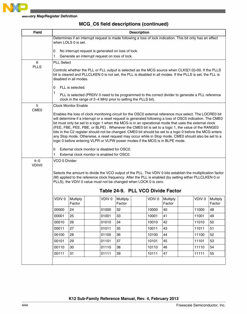
MCG_C6 field descriptions (continued)
Field Description
Determines if an interrupt request is made following a loss of lock indication. This bit only has an effectwhen LOLS 0 is set.
0 No interrupt request is generated on loss of lock.1 Generate an interrupt request on loss of lock.
6PLLS
PLL Select
Controls whether the PLL or FLL output is selected as the MCG source when CLKS[1:0]=00. If the PLLSbit is cleared and PLLCLKEN 0 is not set, the PLL is disabled in all modes. If the PLLS is set, the FLL isdisabled in all modes.
0 FLL is selected.1
PLL is selected (PRDIV 0 need to be programmed to the correct divider to generate a PLL referenceclock in the range of 2–4 MHz prior to setting the PLLS bit).
5CME0
Clock Monitor Enable
Enables the loss of clock monitoring circuit for the OSC0 external reference mux select. The LOCRE0 bitwill determine if a interrupt or a reset request is generated following a loss of OSC0 indication. The CME0bit must only be set to a logic 1 when the MCG is in an operational mode that uses the external clock(FEE, FBE, PEE, PBE, or BLPE) . Whenever the CME0 bit is set to a logic 1, the value of the RANGE0bits in the C2 register should not be changed. CME0 bit should be set to a logic 0 before the MCG entersany Stop mode. Otherwise, a reset request may occur while in Stop mode. CME0 should also be set to alogic 0 before entering VLPR or VLPW power modes if the MCG is in BLPE mode.
0 External clock monitor is disabled for OSC0.1 External clock monitor is enabled for OSC0.
4–0VDIV0
VCO 0 Divider
Selects the amount to divide the VCO output of the PLL. The VDIV 0 bits establish the multiplication factor(M) applied to the reference clock frequency. After the PLL is enabled (by setting either PLLCLKEN 0 orPLLS), the VDIV 0 value must not be changed when LOCK 0 is zero.
Table 24-9. PLL VCO Divide Factor
VDIV 0 MultiplyFactor
VDIV 0 MultiplyFactor
VDIV 0 MultiplyFactor
VDIV 0 MultiplyFactor
00000 24 01000 32 10000 40 11000 48
00001 25 01001 33 10001 41 11001 49
00010 26 01010 34 10010 42 11010 50
00011 27 01011 35 10011 43 11011 51
00100 28 01100 36 10100 44 11100 52
00101 29 01101 37 10101 45 11101 53
00110 30 01110 38 10110 46 11110 54
00111 31 01111 39 10111 47 11111 55
Memory Map/Register Definition
K12 Sub-Family Reference Manual, Rev. 4, February 2013
444 Freescale Semiconductor, Inc.
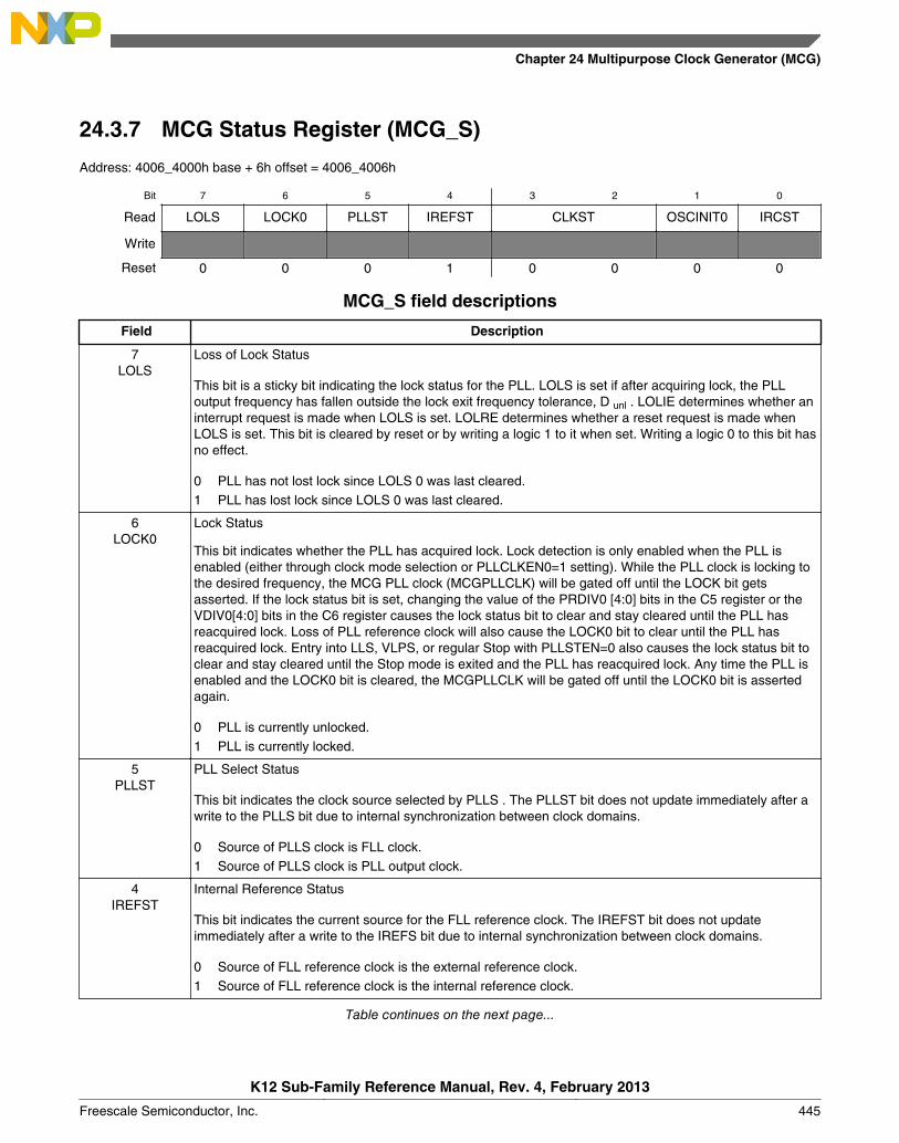
24.3.7 MCG Status Register (MCG_S)
Address: 4006_4000h base + 6h offset = 4006_4006h
Bit 7 6 5 4 3 2 1 0
Read LOLS LOCK0 PLLST IREFST CLKST OSCINIT0 IRCST
Write
Reset 0 0 0 1 0 0 0 0
MCG_S field descriptions
Field Description
7LOLS
Loss of Lock Status
This bit is a sticky bit indicating the lock status for the PLL. LOLS is set if after acquiring lock, the PLLoutput frequency has fallen outside the lock exit frequency tolerance, D unl . LOLIE determines whether aninterrupt request is made when LOLS is set. LOLRE determines whether a reset request is made whenLOLS is set. This bit is cleared by reset or by writing a logic 1 to it when set. Writing a logic 0 to this bit hasno effect.
0 PLL has not lost lock since LOLS 0 was last cleared.1 PLL has lost lock since LOLS 0 was last cleared.
6LOCK0
Lock Status
This bit indicates whether the PLL has acquired lock. Lock detection is only enabled when the PLL isenabled (either through clock mode selection or PLLCLKEN0=1 setting). While the PLL clock is locking tothe desired frequency, the MCG PLL clock (MCGPLLCLK) will be gated off until the LOCK bit getsasserted. If the lock status bit is set, changing the value of the PRDIV0 [4:0] bits in the C5 register or theVDIV0[4:0] bits in the C6 register causes the lock status bit to clear and stay cleared until the PLL hasreacquired lock. Loss of PLL reference clock will also cause the LOCK0 bit to clear until the PLL hasreacquired lock. Entry into LLS, VLPS, or regular Stop with PLLSTEN=0 also causes the lock status bit toclear and stay cleared until the Stop mode is exited and the PLL has reacquired lock. Any time the PLL isenabled and the LOCK0 bit is cleared, the MCGPLLCLK will be gated off until the LOCK0 bit is assertedagain.
0 PLL is currently unlocked.1 PLL is currently locked.
5PLLST
PLL Select Status
This bit indicates the clock source selected by PLLS . The PLLST bit does not update immediately after awrite to the PLLS bit due to internal synchronization between clock domains.
0 Source of PLLS clock is FLL clock.1 Source of PLLS clock is PLL output clock.
4IREFST
Internal Reference Status
This bit indicates the current source for the FLL reference clock. The IREFST bit does not updateimmediately after a write to the IREFS bit due to internal synchronization between clock domains.
0 Source of FLL reference clock is the external reference clock.1 Source of FLL reference clock is the internal reference clock.
Table continues on the next page...
Chapter 24 Multipurpose Clock Generator (MCG)
K12 Sub-Family Reference Manual, Rev. 4, February 2013
Freescale Semiconductor, Inc. 445
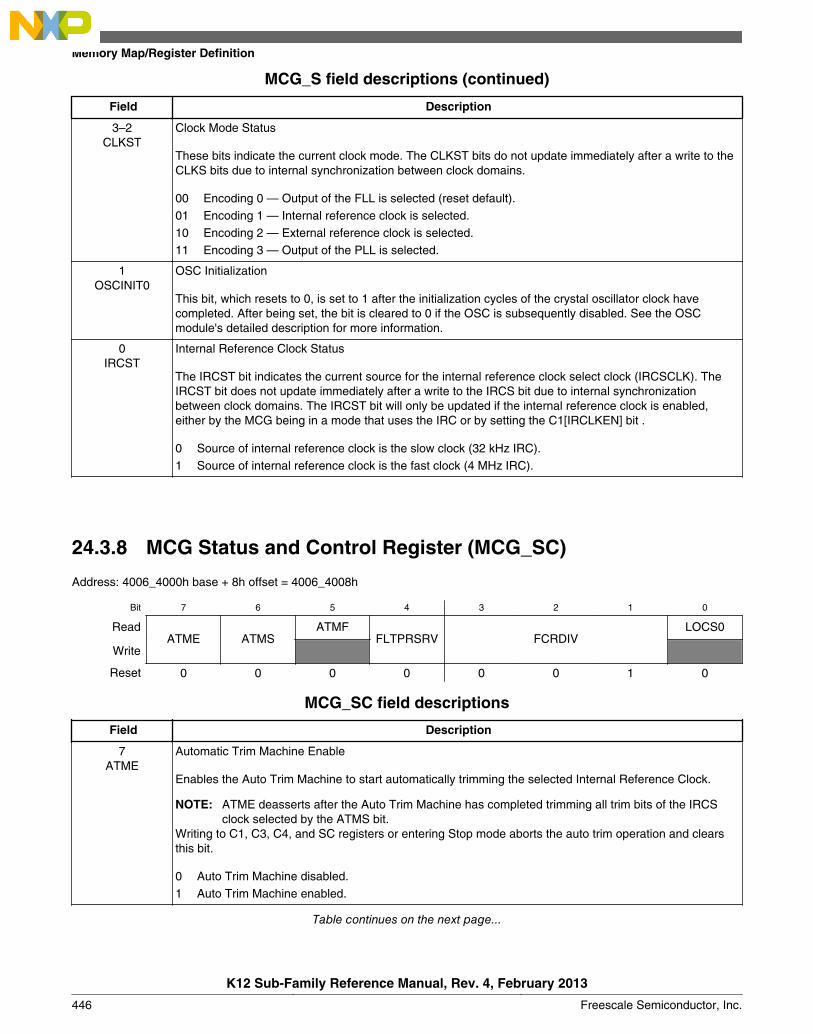
MCG_S field descriptions (continued)
Field Description
3–2CLKST
Clock Mode Status
These bits indicate the current clock mode. The CLKST bits do not update immediately after a write to theCLKS bits due to internal synchronization between clock domains.
00 Encoding 0 — Output of the FLL is selected (reset default).01 Encoding 1 — Internal reference clock is selected.10 Encoding 2 — External reference clock is selected.11 Encoding 3 — Output of the PLL is selected.
1OSCINIT0
OSC Initialization
This bit, which resets to 0, is set to 1 after the initialization cycles of the crystal oscillator clock havecompleted. After being set, the bit is cleared to 0 if the OSC is subsequently disabled. See the OSCmodule's detailed description for more information.
0IRCST
Internal Reference Clock Status
The IRCST bit indicates the current source for the internal reference clock select clock (IRCSCLK). TheIRCST bit does not update immediately after a write to the IRCS bit due to internal synchronizationbetween clock domains. The IRCST bit will only be updated if the internal reference clock is enabled,either by the MCG being in a mode that uses the IRC or by setting the C1[IRCLKEN] bit .
0 Source of internal reference clock is the slow clock (32 kHz IRC).1 Source of internal reference clock is the fast clock (4 MHz IRC).
24.3.8 MCG Status and Control Register (MCG_SC)
Address: 4006_4000h base + 8h offset = 4006_4008h
Bit 7 6 5 4 3 2 1 0
ReadATME ATMS
ATMFFLTPRSRV FCRDIV
LOCS0
Write
Reset 0 0 0 0 0 0 1 0
MCG_SC field descriptions
Field Description
7ATME
Automatic Trim Machine Enable
Enables the Auto Trim Machine to start automatically trimming the selected Internal Reference Clock.
NOTE: ATME deasserts after the Auto Trim Machine has completed trimming all trim bits of the IRCSclock selected by the ATMS bit.
Writing to C1, C3, C4, and SC registers or entering Stop mode aborts the auto trim operation and clearsthis bit.
0 Auto Trim Machine disabled.1 Auto Trim Machine enabled.
Table continues on the next page...
Memory Map/Register Definition
K12 Sub-Family Reference Manual, Rev. 4, February 2013
446 Freescale Semiconductor, Inc.
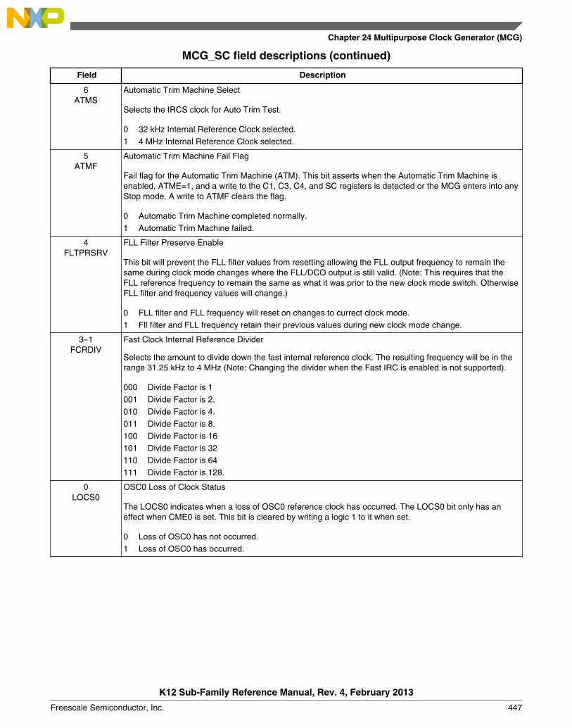
MCG_SC field descriptions (continued)
Field Description
6ATMS
Automatic Trim Machine Select
Selects the IRCS clock for Auto Trim Test.
0 32 kHz Internal Reference Clock selected.1 4 MHz Internal Reference Clock selected.
5ATMF
Automatic Trim Machine Fail Flag
Fail flag for the Automatic Trim Machine (ATM). This bit asserts when the Automatic Trim Machine isenabled, ATME=1, and a write to the C1, C3, C4, and SC registers is detected or the MCG enters into anyStop mode. A write to ATMF clears the flag.
0 Automatic Trim Machine completed normally.1 Automatic Trim Machine failed.
4FLTPRSRV
FLL Filter Preserve Enable
This bit will prevent the FLL filter values from resetting allowing the FLL output frequency to remain thesame during clock mode changes where the FLL/DCO output is still valid. (Note: This requires that theFLL reference frequency to remain the same as what it was prior to the new clock mode switch. OtherwiseFLL filter and frequency values will change.)
0 FLL filter and FLL frequency will reset on changes to currect clock mode.1 Fll filter and FLL frequency retain their previous values during new clock mode change.
3–1FCRDIV
Fast Clock Internal Reference Divider
Selects the amount to divide down the fast internal reference clock. The resulting frequency will be in therange 31.25 kHz to 4 MHz (Note: Changing the divider when the Fast IRC is enabled is not supported).
000 Divide Factor is 1001 Divide Factor is 2.010 Divide Factor is 4.011 Divide Factor is 8.100 Divide Factor is 16101 Divide Factor is 32110 Divide Factor is 64111 Divide Factor is 128.
0LOCS0
OSC0 Loss of Clock Status
The LOCS0 indicates when a loss of OSC0 reference clock has occurred. The LOCS0 bit only has aneffect when CME0 is set. This bit is cleared by writing a logic 1 to it when set.
0 Loss of OSC0 has not occurred.1 Loss of OSC0 has occurred.
Chapter 24 Multipurpose Clock Generator (MCG)
K12 Sub-Family Reference Manual, Rev. 4, February 2013
Freescale Semiconductor, Inc. 447
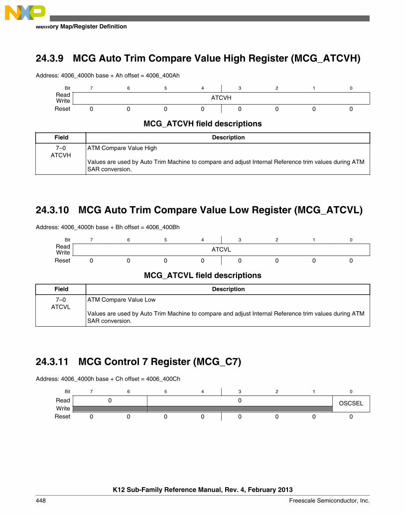
24.3.9 MCG Auto Trim Compare Value High Register (MCG_ATCVH)
Address: 4006_4000h base + Ah offset = 4006_400Ah
Bit 7 6 5 4 3 2 1 0
Read ATCVHWriteReset 0 0 0 0 0 0 0 0
MCG_ATCVH field descriptions
Field Description
7–0ATCVH
ATM Compare Value High
Values are used by Auto Trim Machine to compare and adjust Internal Reference trim values during ATMSAR conversion.
24.3.10 MCG Auto Trim Compare Value Low Register (MCG_ATCVL)
Address: 4006_4000h base + Bh offset = 4006_400Bh
Bit 7 6 5 4 3 2 1 0
Read ATCVLWriteReset 0 0 0 0 0 0 0 0
MCG_ATCVL field descriptions
Field Description
7–0ATCVL
ATM Compare Value Low
Values are used by Auto Trim Machine to compare and adjust Internal Reference trim values during ATMSAR conversion.
24.3.11 MCG Control 7 Register (MCG_C7)
Address: 4006_4000h base + Ch offset = 4006_400Ch
Bit 7 6 5 4 3 2 1 0
Read 0 0 OSCSELWriteReset 0 0 0 0 0 0 0 0
Memory Map/Register Definition
K12 Sub-Family Reference Manual, Rev. 4, February 2013
448 Freescale Semiconductor, Inc.

MCG_C7 field descriptions
Field Description
7–6Reserved
This field is reserved.This read-only field is reserved and always has the value 0.
5–1Reserved
Reserved
This field is reserved.This read-only field is reserved and always has the value 0.
0OSCSEL
MCG OSC Clock Select
Selects the MCG FLL external reference clock
0 Selects System Oscillator (OSCCLK).1 Selects 32 kHz RTC Oscillator.
24.3.12 MCG Control 8 Register (MCG_C8)
Address: 4006_4000h base + Dh offset = 4006_400Dh
Bit 7 6 5 4 3 2 1 0
ReadLOCRE1 LOLRE CME1
0 LOCS1
Write
Reset 1 0 0 0 0 0 0 0
MCG_C8 field descriptions
Field Description
7LOCRE1
Loss of Clock Reset Enable
Determines if a interrupt or a reset request is made following a loss of RTC external reference clock. TheLOCRE1 only has an affect when CME1 is set.
0 Interrupt request is generated on a loss of RTC external reference clock.1 Generate a reset request on a loss of RTC external reference clock
6LOLRE
PLL Loss of Lock Reset Enable
Determines if a interrupt or a reset request is made following a PLL loss of lock.
0 Interrupt request is generated on a PLL loss of lock indication. The PLL loss of lock interrupt enable bitmust also be set to generate the interrupt request.
1 Generate a reset request on a PLL loss of lock indication.
5CME1
Clock Monitor Enable1
Enables the loss of clock monitoring circuit for the output of the RTC external reference clock. TheLOCRE1 bit will determine whether an interrupt or a reset request is generated following a loss of RTCclock indication. The CME1 bit should be set to a logic 1 when the MCG is in an operational mode thatuses the RTC as its external reference clock or if the RTC is operational. CME1 bit must be set to a logic 0before the MCG enters any Stop mode. Otherwise, a reset request may occur when in Stop mode. CME1should also be set to a logic 0 before entering VLPR or VLPW power modes.
Table continues on the next page...
Chapter 24 Multipurpose Clock Generator (MCG)
K12 Sub-Family Reference Manual, Rev. 4, February 2013
Freescale Semiconductor, Inc. 449
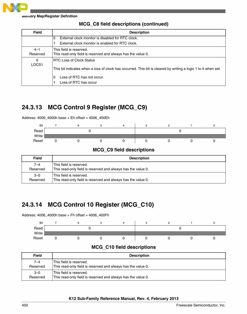
MCG_C8 field descriptions (continued)
Field Description
0 External clock monitor is disabled for RTC clock.1 External clock monitor is enabled for RTC clock.
4–1Reserved
This field is reserved.This read-only field is reserved and always has the value 0.
0LOCS1
RTC Loss of Clock Status
This bit indicates when a loss of clock has occurred. This bit is cleared by writing a logic 1 to it when set.
0 Loss of RTC has not occur.1 Loss of RTC has occur
24.3.13 MCG Control 9 Register (MCG_C9)
Address: 4006_4000h base + Eh offset = 4006_400Eh
Bit 7 6 5 4 3 2 1 0
Read 0 0WriteReset 0 0 0 0 0 0 0 0
MCG_C9 field descriptions
Field Description
7–4Reserved
This field is reserved.This read-only field is reserved and always has the value 0.
3–0Reserved
This field is reserved.This read-only field is reserved and always has the value 0.
24.3.14 MCG Control 10 Register (MCG_C10)
Address: 4006_4000h base + Fh offset = 4006_400Fh
Bit 7 6 5 4 3 2 1 0
Read 0 0WriteReset 0 0 0 0 0 0 0 0
MCG_C10 field descriptions
Field Description
7–4Reserved
This field is reserved.This read-only field is reserved and always has the value 0.
3–0Reserved
This field is reserved.This read-only field is reserved and always has the value 0.
Memory Map/Register Definition
K12 Sub-Family Reference Manual, Rev. 4, February 2013
450 Freescale Semiconductor, Inc.

Functional Description
24.4.1 MCG mode state diagram
The nine states of the MCG are shown in the following figure and are described in Table24-18. The arrows indicate the permitted MCG mode transitions.
FEEFEIReset
BLPI
FBI FBE
BLPE
PBE
PEE
Stop
Returns to the state that was active before the MCU entered Stop mode, unless a reset occurs while in Stop mode.
Entered from any state when the MCU enters Stop mode
Figure 24-16. MCG mode state diagram
NOTE• During exits from LLS or VLPS when the MCG is in PEE
mode, the MCG will reset to PBE clock mode and theC1[CLKS] and S[CLKST] will automatically be set to2’b10.
• If entering Normal Stop mode when the MCG is in PEEmode with C5[PLLSTEN]=0, the MCG will reset to PBEclock mode and C1[CLKS] and S[CLKST] willautomatically be set to 2’b10.
24.4
Chapter 24 Multipurpose Clock Generator (MCG)
K12 Sub-Family Reference Manual, Rev. 4, February 2013
Freescale Semiconductor, Inc. 451
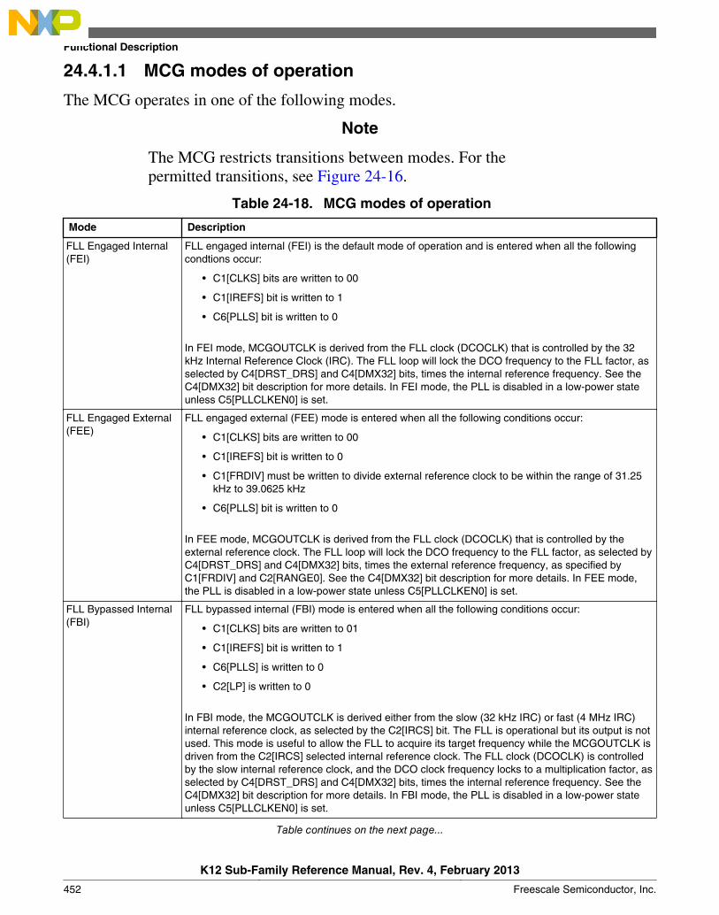
24.4.1.1 MCG modes of operation
The MCG operates in one of the following modes.
Note
The MCG restricts transitions between modes. For thepermitted transitions, see Figure 24-16.
Table 24-18. MCG modes of operation
Mode Description
FLL Engaged Internal(FEI)
FLL engaged internal (FEI) is the default mode of operation and is entered when all the followingcondtions occur:
• C1[CLKS] bits are written to 00
• C1[IREFS] bit is written to 1
• C6[PLLS] bit is written to 0
In FEI mode, MCGOUTCLK is derived from the FLL clock (DCOCLK) that is controlled by the 32kHz Internal Reference Clock (IRC). The FLL loop will lock the DCO frequency to the FLL factor, asselected by C4[DRST_DRS] and C4[DMX32] bits, times the internal reference frequency. See theC4[DMX32] bit description for more details. In FEI mode, the PLL is disabled in a low-power stateunless C5[PLLCLKEN0] is set.
FLL Engaged External(FEE)
FLL engaged external (FEE) mode is entered when all the following conditions occur:
• C1[CLKS] bits are written to 00
• C1[IREFS] bit is written to 0
• C1[FRDIV] must be written to divide external reference clock to be within the range of 31.25kHz to 39.0625 kHz
• C6[PLLS] bit is written to 0
In FEE mode, MCGOUTCLK is derived from the FLL clock (DCOCLK) that is controlled by theexternal reference clock. The FLL loop will lock the DCO frequency to the FLL factor, as selected byC4[DRST_DRS] and C4[DMX32] bits, times the external reference frequency, as specified byC1[FRDIV] and C2[RANGE0]. See the C4[DMX32] bit description for more details. In FEE mode,the PLL is disabled in a low-power state unless C5[PLLCLKEN0] is set.
FLL Bypassed Internal(FBI)
FLL bypassed internal (FBI) mode is entered when all the following conditions occur:
• C1[CLKS] bits are written to 01
• C1[IREFS] bit is written to 1
• C6[PLLS] is written to 0
• C2[LP] is written to 0
In FBI mode, the MCGOUTCLK is derived either from the slow (32 kHz IRC) or fast (4 MHz IRC)internal reference clock, as selected by the C2[IRCS] bit. The FLL is operational but its output is notused. This mode is useful to allow the FLL to acquire its target frequency while the MCGOUTCLK isdriven from the C2[IRCS] selected internal reference clock. The FLL clock (DCOCLK) is controlledby the slow internal reference clock, and the DCO clock frequency locks to a multiplication factor, asselected by C4[DRST_DRS] and C4[DMX32] bits, times the internal reference frequency. See theC4[DMX32] bit description for more details. In FBI mode, the PLL is disabled in a low-power stateunless C5[PLLCLKEN0] is set.
Table continues on the next page...
Functional Description
K12 Sub-Family Reference Manual, Rev. 4, February 2013
452 Freescale Semiconductor, Inc.

Table 24-18. MCG modes of operation (continued)
Mode Description
FLL Bypassed External(FBE)
FLL bypassed external (FBE) mode is entered when all the following conditions occur:
• C1[CLKS] bits are written to 10
• C1[IREFS] bit is written to 0
• C1[FRDIV] must be written to divide external reference clock to be within the range of 31.25kHz to 39.0625 kHz.
• C6[PLLS] bit is written to 0
• C2[LP] is written to 0
In FBE mode, the MCGOUTCLK is derived from the OSCSEL external reference clock. The FLL isoperational but its output is not used. This mode is useful to allow the FLL to acquire its targetfrequency while the MCGOUTCLK is driven from the external reference clock. The FLL clock(DCOCLK) is controlled by the external reference clock, and the DCO clock frequency locks to amultiplication factor, as selected by C4[DRST_DRS] and C4[DMX32] bits, times the divided externalreference frequency. See the C4[DMX32] bit description for more details. In FBI mode the PLL isdisabled in a low-power state unless C5[PLLCLKEN0] is set.
PLL Engaged External(PEE)
PLL Engaged External (PEE) mode is entered when all the following conditions occur:
• C1[CLKS] bits are written to 00
• C1[IREFS] bit is written to 0
• C6[PLLS] bit is written to 1
In PEE mode, the MCGOUTCLK is derived from the PLL clock, which is controlled by the externalreference clock. The PLL clock frequency locks to a multiplication factor, as specified by C6[VDIV0],times the external reference frequency, as specified by C5[PRDIV0]. The PLL's programmablereference divider must be configured to produce a valid PLL reference clock. The FLL is disabled ina low-power state.
PLL Bypassed External(PBE)
PLL Bypassed External (PBE) mode is entered when all the following conditions occur:
• C1[CLKS] bits are written to 10
• C1[IREFS] bit is written to 0
• C6[PLLS] bit is written to 1
• C2[LP] bit is written to 0
In PBE mode, MCGOUTCLK is derived from the OSCSEL external reference clock; the PLL isoperational, but its output clock is not used. This mode is useful to allow the PLL to acquire its targetfrequency while MCGOUTCLK is driven from the external reference clock. The PLL clock frequencylocks to a multiplication factor, as specified by its [VDIV], times the PLL reference frequency, asspecified by its [PRDIV]. In preparation for transition to PEE, the PLL's programmable referencedivider must be configured to produce a valid PLL reference clock. The FLL is disabled in a low-power state.
Table continues on the next page...
Chapter 24 Multipurpose Clock Generator (MCG)
K12 Sub-Family Reference Manual, Rev. 4, February 2013
Freescale Semiconductor, Inc. 453
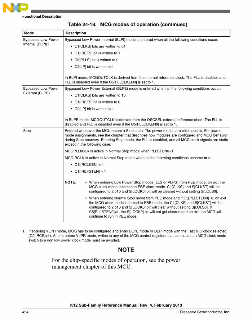
Table 24-18. MCG modes of operation (continued)
Mode Description
Bypassed Low PowerInternal (BLPI)1
Bypassed Low Power Internal (BLPI) mode is entered when all the following conditions occur:
• C1[CLKS] bits are written to 01
• C1[IREFS] bit is written to 1
• C6[PLLS] bit is written to 0
• C2[LP] bit is written to 1
In BLPI mode, MCGOUTCLK is derived from the internal reference clock. The FLL is disabled andPLL is disabled even if the C5[PLLCLKEN0] is set to 1.
Bypassed Low PowerExternal (BLPE)
Bypassed Low Power External (BLPE) mode is entered when all the following conditions occur:
• C1[CLKS] bits are written to 10
• C1[IREFS] bit is written to 0
• C2[LP] bit is written to 1
In BLPE mode, MCGOUTCLK is derived from the OSCSEL external reference clock. The FLL isdisabled and PLL is disabled even if the C5[PLLCLKEN0] is set to 1.
Stop Entered whenever the MCU enters a Stop state. The power modes are chip specific. For powermode assignments, see the chapter that describes how modules are configured and MCG behaviorduring Stop recovery. Entering Stop mode, the FLL is disabled, and all MCG clock signals are staticexcept in the following case:
MCGPLL0CLK is active in Normal Stop mode when PLLSTEN0=1
MCGIRCLK is active in Normal Stop mode when all the following conditions become true:
• C1[IRCLKEN] = 1
• C1[IREFSTEN] = 1
NOTE: • When entering Low Power Stop modes (LLS or VLPS) from PEE mode, on exit theMCG clock mode is forced to PBE clock mode. C1[CLKS] and S[CLKST] will beconfigured to 2’b10 and S[LOCK0] bit will be cleared without setting S[LOLS0].
• When entering Normal Stop mode from PEE mode and if C5[PLLSTEN0]=0, on exitthe MCG clock mode is forced to PBE mode, the C1[CLKS] and S[CLKST] will beconfigured to 2’b10 and S[LOCK0] bit will clear without setting S[LOLS0]. IfC5[PLLSTEN0]=1, the S[LOCK0] bit will not get cleared and on exit the MCG willcontinue to run in PEE mode.
1. If entering VLPR mode, MCG has to be configured and enter BLPE mode or BLPI mode with the Fast IRC clock selected(C2[IRCS]=1). After it enters VLPR mode, writes to any of the MCG control registers that can cause an MCG clock modeswitch to a non low power clock mode must be avoided.
NOTE
For the chip-specific modes of operation, see the powermanagement chapter of this MCU.
Functional Description
K12 Sub-Family Reference Manual, Rev. 4, February 2013
454 Freescale Semiconductor, Inc.

24.4.1.2 MCG mode switching
The C1[IREFS] bit can be changed at any time, but the actual switch to the newlyselected reference clocks is shown by the S[IREFST] bit. When switching betweenengaged internal and engaged external modes, the FLL will begin locking again after theswitch is completed.
The C1[CLKS] bits can also be changed at any time, but the actual switch to the newlyselected clock is shown by the S[CLKST] bits. If the newly selected clock is notavailable, the previous clock will remain selected.
The C4[DRST_DRS] write bits can be changed at any time except when C2[LP] bit is 1.If the C4[DRST_DRS] write bits are changed while in FLL engaged internal (FEI) orFLL engaged external (FEE), the MCGOUTCLK will switch to the new selected DCOrange within three clocks of the selected DCO clock. After switching to the new DCO,the FLL remains unlocked for several reference cycles. DCO startup time is equal to theFLL acquisition time. After the selected DCO startup time is over, the FLL is locked. Thecompletion of the switch is shown by the C4[DRST_DRS] read bits.
24.4.2 Low Power Bit Usage
The C2[LP] bit is provided to allow the FLL or PLL to be disabled and thus conservepower when these systems are not being used. The C4[DRST_DRS] can not be writtenwhile C2[LP] bit is 1. However, in some applications, it may be desirable to enable theFLL or PLL and allow it to lock for maximum accuracy before switching to an engagedmode. Do this by writing C2[LP] to 0.
24.4.3 MCG Internal Reference Clocks
This module supports two internal reference clocks with nominal frequencies of 32 kHz(slow IRC) and 4 MHz (fast IRC). The fast IRC frequency can be divided down byprogramming of the FCRDIV to produce a frequency range of 32 kHz to 4 MHz.
24.4.3.1 MCG Internal Reference Clock
The MCG Internal Reference Clock (MCGIRCLK) provides a clock source for other on-chip peripherals and is enabled when C1[IRCLKEN]=1. When enabled, MCGIRCLK isdriven by either the fast internal reference clock (4 MHz IRC which can be divided downby the FRDIV factors) or the slow internal reference clock (32 kHz IRC). The IRCSclock frequency can be re-targeted by trimming the period of its IRCS selected internal
Chapter 24 Multipurpose Clock Generator (MCG)
K12 Sub-Family Reference Manual, Rev. 4, February 2013
Freescale Semiconductor, Inc. 455
reference clock. This can be done by writing a new trim value to theC3[SCTRIM]:C4[SCFTRIM] bits when the slow IRC clock is selected or by writing anew trim value to the C4[FCTRIM] bits when the fast IRC clock is selected. The internalreference clock period is proportional to the trim value written.C3[SCTRIM]:C4[SCFTRIM] (if C2[IRCS]=0) and C4[FCTRIM] (if C2[IRCS]=1) bitsaffect the MCGOUTCLK frequency if the MCG is in FBI or BLPI modes.C3[SCTRIM]:C4[SCFTRIM] (if C2[IRCS]=0) bits also affect the MCGOUTCLKfrequency if the MCG is in FEI mode.
Additionally, this clock can be enabled in Stop mode by setting C1[IRCLKEN] andC1[IREFSTEN], otherwise this clock is disabled in Stop mode.
24.4.4 External Reference Clock
The MCG module can support an external reference clock in all modes. See the devicedatasheet for external reference frequency range. When C1[IREFS] is set, the externalreference clock will not be used by the FLL or PLL. In these modes, the frequency can beequal to the maximum frequency the chip-level timing specifications will support.
If any of the CME bits are asserted the slow internal reference clock is enabled alongwith the enabled external clock monitor. For the case when C6[CME0]=1, a loss of clockis detected if the OSC0 external reference falls below a minimum frequency (floc_high orfloc_low depending on C2[RANGE0]). For the case when C8[CME1]=1, a loss of clock isdetected if the RTC external reference falls below a minimum frequency (floc_low).
NOTEAll clock monitors must be disabled before entering these low-power modes: Stop, VLPS, VLPR, VLPW, LLS, and VLLSx.
Upon detect of a loss of clock event, the MCU generates a system reset if the respectiveLOCRE bit is set. Otherwise the MCG sets the respective LOCS bit and the MCGgenerates a LOCS interrupt request. In the case where a OSC0 loss of clock is detected,the PLL LOCK status bit is cleared if the OSC clock that is lost was selected as the PLLreference clock.
24.4.5 MCG Fixed frequency clock
The MCG Fixed Frequency Clock (MCGFFCLK) provides a fixed frequency clocksource for other on-chip peripherals; see the block diagram. This clock is driven by eitherthe slow clock from the internal reference clock generator or the external reference clockfrom the Crystal Oscillator, divided by the FLL reference clock divider. The source ofMCGFFCLK is selected by C1[IREFS].
Functional Description
K12 Sub-Family Reference Manual, Rev. 4, February 2013
456 Freescale Semiconductor, Inc.
This clock is synchronized to the peripheral bus clock and is valid only when itsfrequency is not more than 1/8 of the MCGOUTCLK frequency. When it is not valid, it isdisabled and held high. The MCGFFCLK is not available when the MCG is in BLPImode. This clock is also disabled in Stop mode. The FLL reference clock must be setwithin the valid frequency range for the MCGFFCLK.
24.4.6 MCG PLL clock
The MCG PLL Clock (MCGPLLCLK) is available depending on the device'sconfiguration of the MCG module. For more details, see the clock distribution chapter ofthis MCU. The MCGPLLCLK is prevented from coming out of the MCG until it isenabled and S[LOCK0] is set.
24.4.7 MCG Auto TRIM (ATM)
The MCG Auto Trim (ATM) is a MCG feature that when enabled, it configures the MCGhardware to automatically trim the MCG Internal Reference Clocks using an externalclock as a reference. The selection between which MCG IRC clock gets tested andenabled is controlled by the ATC[ATMS] control bit (ATC[ATMS]=0 selects the 32 kHzIRC and ATC[ATMS]=1 selects the 4 MHz IRC). If 4 MHz IRC is selected for the ATM,a divide by 128 is enabled to divide down the 4 MHz IRC to a range of 31.250 kHz.
When MCG ATM is enabled by writing ATC[ATME] bit to 1, The ATM machine willstart auto trimming the selected IRC clock. During the autotrim process, ATC[ATME]will remain asserted and will deassert after ATM is completed or an abort occurs. TheMCG ATM is aborted if a write to any of the following control registers is detected : C1,C3, C4, or ATC or if Stop mode is entered. If an abort occurs, ATC[ATMF] fail flag isasserted.
The ATM machine uses the bus clock as the external reference clock to perform the IRCauto-trim. Therefore, it is required that the MCG is configured in a clock mode where thereference clock used to generate the system clock is the external reference clock such asFBE clock mode. The MCG must not be configured in a clock mode where selected IRCATM clock is used to generate the system clock. The bus clock is also required to berunning with in the range of 8–16 MHz.
To perform the ATM on the selected IRC, the ATM machine uses the successiveapproximation technique to adjust the IRC trim bits to generate the desired IRC trimmedfrequency. The ATM SARs each of the ATM IRC trim bits starting with the MSB. Foreach trim bit test, the ATM uses a pulse that is generated by the ATM selected IRC clockto enable a counter that counts number of ATM external clocks. At end of each trim bit,
Chapter 24 Multipurpose Clock Generator (MCG)
K12 Sub-Family Reference Manual, Rev. 4, February 2013
Freescale Semiconductor, Inc. 457

the ATM external counter value is compared to the ATCV[15:0] register value. Based onthe comparison result, the ATM trim bit under test will get cleared or stay asserted. Thisis done until all trim bits have been tested by ATM SAR machine.
Before the ATM can be enabled, the ATM expected count needs to be derived and storedinto the ATCV register. The ATCV expected count is derived based on the requiredtarget Internal Reference Clock (IRC) frequency, and the frequency of the externalreference clock using the following formula:
ATCV• Fr = Target Internal Reference Clock (IRC) Trimmed Frequency
• Fe = External Clock Frequency
If the auto trim is being performed on the 4 MHz IRC, the calculated expected countvalue must be multiplied by 128 before storing it in the ATCV register. Therefore, theATCV Expected Count Value for trimming the 4 MHz IRC is calculated using thefollowing formula.
(128)
24.5 Initialization / Application informationThis section describes how to initialize and configure the MCG module in an application.The following sections include examples on how to initialize the MCG and properlyswitch between the various available modes.
24.5.1 MCG module initialization sequence
The MCG comes out of reset configured for FEI mode. The internal reference willstabilize in tirefsts microseconds before the FLL can acquire lock. As soon as the internalreference is stable, the FLL will acquire lock in tfll_acquire milliseconds.
24.5.1.1 Initializing the MCG
Because the MCG comes out of reset in FEI mode, the only MCG modes that can bedirectly switched to upon reset are FEE, FBE, and FBI modes (see Figure 24-16).Reaching any of the other modes requires first configuring the MCG for one of thesethree intermediate modes. Care must be taken to check relevant status bits in the MCGstatus register reflecting all configuration changes within each mode.
Initialization / Application information
K12 Sub-Family Reference Manual, Rev. 4, February 2013
458 Freescale Semiconductor, Inc.
To change from FEI mode to FEE or FBE modes, follow this procedure:
1. Enable the external clock source by setting the appropriate bits in C2 register.
2. Write to C1 register to select the clock mode.
• If entering FEE mode, set C1[FRDIV] appropriately, clear the C1[IREFS] bit toswitch to the external reference, and leave the C1[CLKS] bits at 2'b00 so that theoutput of the FLL is selected as the system clock source.
• If entering FBE, clear the C1[IREFS] bit to switch to the external reference andchange the C1[CLKS] bits to 2'b10 so that the external reference clock isselected as the system clock source. The C1[FRDIV] bits should also be setappropriately here according to the external reference frequency to keep the FLLreference clock in the range of 31.25 kHz to 39.0625 kHz. Although the FLL isbypassed, it is still on in FBE mode.
• The internal reference can optionally be kept running by setting theC1[IRCLKEN] bit. This is useful if the application will switch back and forthbetween internal and external modes. For minimum power consumption, leavethe internal reference disabled while in an external clock mode.
3. Once the proper configuration bits have been set, wait for the affected bits in theMCG status register to be changed appropriately, reflecting that the MCG has movedinto the proper mode.
• If the MCG is in FEE, FBE, PEE, PBE, or BLPE mode, and C2[EREFS0] wasalso set in step 1, wait here for S[OSCINIT0] bit to become set indicating thatthe external clock source has finished its initialization cycles and stabilized.
• If in FEE mode, check to make sure the S[IREFST] bit is cleared before movingon.
• If in FBE mode, check to make sure the S[IREFST] bit is cleared and S[CLKST]bits have changed to 2'b10 indicating the external reference clock has beenappropriately selected. Although the FLL is bypassed, it is still on in FBE mode.
4. Write to the C4 register to determine the DCO output (MCGFLLCLK) frequencyrange.
• By default, with C4[DMX32] cleared to 0, the FLL multiplier for the DCOoutput is 640. For greater flexibility, if a mid-low-range FLL multiplier of 1280is desired instead, set C4[DRST_DRS] bits to 2'b01 for a DCO output frequencyof 40 MHz. If a mid high-range FLL multiplier of 1920 is desired instead, set the
Chapter 24 Multipurpose Clock Generator (MCG)
K12 Sub-Family Reference Manual, Rev. 4, February 2013
Freescale Semiconductor, Inc. 459
C4[DRST_DRS] bits to 2'b10 for a DCO output frequency of 60 MHz. If a high-range FLL multiplier of 2560 is desired instead, set the C4[DRST_DRS] bits to2'b11 for a DCO output frequency of 80 MHz.
• When using a 32.768 kHz external reference, if the maximum low-range DCOfrequency that can be achieved with a 32.768 kHz reference is desired, setC4[DRST_DRS] bits to 2'b00 and set C4[DMX32] bit to 1. The resulting DCOoutput (MCGOUTCLK) frequency with the new multiplier of 732 will be 24MHz.
• When using a 32.768 kHz external reference, if the maximum mid-range DCOfrequency that can be achieved with a 32.768 kHz reference is desired, setC4[DRST_DRS] bits to 2'b01 and set C4[DMX32] bit to 1. The resulting DCOoutput (MCGOUTCLK) frequency with the new multiplier of 1464 will be 48MHz.
• When using a 32.768 kHz external reference, if the maximum mid high-rangeDCO frequency that can be achieved with a 32.768 kHz reference is desired, setC4[DRST_DRS] bits to 2'b10 and set C4[DMX32] bit to 1. The resulting DCOoutput (MCGOUTCLK) frequency with the new multiplier of 2197 will be 72MHz.
• When using a 32.768 kHz external reference, if the maximum high-range DCOfrequency that can be achieved with a 32.768 kHz reference is desired, setC4[DRST_DRS] bits to 2'b11 and set C4[DMX32] bit to 1. The resulting DCOoutput (MCGOUTCLK) frequency with the new multiplier of 2929 will be 96MHz.
5. Wait for the FLL lock time to guarantee FLL is running at new C4[DRST_DRS] andC4[DMX32] programmed frequency.
To change from FEI clock mode to FBI clock mode, follow this procedure:
1. Change C1[CLKS] bits in C1 register to 2'b01 so that the internal reference clock isselected as the system clock source.
2. Wait for S[CLKST] bits in the MCG status register to change to 2'b01, indicatingthat the internal reference clock has been appropriately selected.
3. Write to the C2 register to determine the IRCS output (IRCSCLK) frequency range.
• By default, with C2[IRCS] cleared to 0, the IRCS selected output clock is theslow internal reference clock (32 kHz IRC). If the faster IRC is desired, setC2[IRCS] bit to 1 for a IRCS clock derived from the 4 MHz IRC source.
Initialization / Application information
K12 Sub-Family Reference Manual, Rev. 4, February 2013
460 Freescale Semiconductor, Inc.
24.5.2 Using a 32.768 kHz reference
In FEE and FBE modes, if using a 32.768 kHz external reference, at the default FLLmultiplication factor of 640, the DCO output (MCGFLLCLK) frequency is 20.97 MHz atlow-range. If C4[DRST_DRS] bits are set to 2'b01, the multiplication factor is doubled to1280, and the resulting DCO output frequency is 41.94 MHz at mid-low-range. IfC4[DRST_DRS] bits are set to 2'b10, the multiplication factor is set to 1920, and theresulting DCO output frequency is 62.91 MHz at mid high-range. If C4[DRST_DRS] bitsare set to 2'b11, the multiplication factor is set to 2560, and the resulting DCO outputfrequency is 83.89 MHz at high-range.
In FBI and FEI modes, setting C4[DMX32] bit is not recommended. If the internalreference is trimmed to a frequency above 32.768 kHz, the greater FLL multiplicationfactor could potentially push the microcontroller system clock out of specification anddamage the part.
24.5.3 MCG mode switching
When switching between operational modes of the MCG, certain configuration bits mustbe changed in order to properly move from one mode to another. Each time any of thesebits are changed (C6[PLLS], C1[IREFS], C1[CLKS], C2[IRCS], or C2[EREFS0]), thecorresponding bits in the MCG status register (PLLST, IREFST, CLKST, IRCST, orOSCINIT) must be checked before moving on in the application software.
Additionally, care must be taken to ensure that the reference clock divider (C1[FRDIV]and C5[PRDIV0]) is set properly for the mode being switched to. For instance, in PEEmode, if using a 4 MHz crystal, C5[PRDIV0] must be set to 5'b000 (divide-by-1) or5'b001 (divide-by-2) to divide the external reference down to the required frequencybetween 2 and 4 MHz.
In FBE, FEE, FBI, and FEI modes, at any time, the application can switch the FLLmultiplication factor between 640, 1280, 1920, and 2560 with C4[DRST_DRS] bits.Writes to C4[DRST_DRS] bits will be ignored if C2[LP]=1.
The table below shows MCGOUTCLK frequency calculations using C1[FRDIV],C5[PRDIV0], and C6[VDIV0] settings for each clock mode.
Chapter 24 Multipurpose Clock Generator (MCG)
K12 Sub-Family Reference Manual, Rev. 4, February 2013
Freescale Semiconductor, Inc. 461
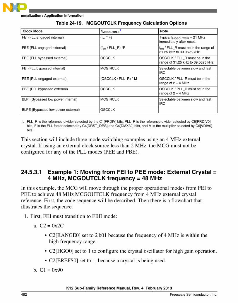
Table 24-19. MCGOUTCLK Frequency Calculation Options
Clock Mode fMCGOUTCLK1 Note
FEI (FLL engaged internal) (fint * F) Typical fMCGOUTCLK = 21 MHzimmediately after reset.
FEE (FLL engaged external) (fext / FLL_R) *F fext / FLL_R must be in the range of31.25 kHz to 39.0625 kHz
FBE (FLL bypassed external) OSCCLK OSCCLK / FLL_R must be in therange of 31.25 kHz to 39.0625 kHz
FBI (FLL bypassed internal) MCGIRCLK Selectable between slow and fastIRC
PEE (PLL engaged external) (OSCCLK / PLL_R) * M OSCCLK / PLL_R must be in therange of 2 – 4 MHz
PBE (PLL bypassed external) OSCCLK OSCCLK / PLL_R must be in therange of 2 – 4 MHz
BLPI (Bypassed low power internal) MCGIRCLK Selectable between slow and fastIRC
BLPE (Bypassed low power external) OSCCLK
1. FLL_R is the reference divider selected by the C1[FRDIV] bits, PLL_R is the reference divider selected by C5[PRDIV0]bits, F is the FLL factor selected by C4[DRST_DRS] and C4[DMX32] bits, and M is the multiplier selected by C6[VDIV0]bits.
This section will include three mode switching examples using an 4 MHz externalcrystal. If using an external clock source less than 2 MHz, the MCG must not beconfigured for any of the PLL modes (PEE and PBE).
24.5.3.1 Example 1: Moving from FEI to PEE mode: External Crystal =4 MHz, MCGOUTCLK frequency = 48 MHz
In this example, the MCG will move through the proper operational modes from FEI toPEE to achieve 48 MHz MCGOUTCLK frequency from 4 MHz external crystalreference. First, the code sequence will be described. Then there is a flowchart thatillustrates the sequence.
1. First, FEI must transition to FBE mode:
a. C2 = 0x2C
• C2[RANGE0] set to 2'b01 because the frequency of 4 MHz is within thehigh frequency range.
• C2[HGO0] set to 1 to configure the crystal oscillator for high gain operation.
• C2[EREFS0] set to 1, because a crystal is being used.
b. C1 = 0x90
Initialization / Application information
K12 Sub-Family Reference Manual, Rev. 4, February 2013
462 Freescale Semiconductor, Inc.

• C1[CLKS] set to 2'b10 to select external reference clock as system clocksource
• C1[FRDIV] set to 3'b010, or divide-by-128 because 4 MHz / 128 = 31.25kHz which is in the 31.25 kHz to 39.0625 kHz range required by the FLL
• C1[IREFS] cleared to 0, selecting the external reference clock and enablingthe external oscillator.
c. Loop until S[OSCINIT0] is 1, indicating the crystal selected by C2[EREFS0] hasbeen initialized.
d. Loop until S[IREFST] is 0, indicating the external reference is the current sourcefor the reference clock.
e. Loop until S[CLKST] is 2'b10, indicating that the external reference clock isselected to feed MCGOUTCLK.
2. Then configure C5[PRDIV0] to generate correct PLL reference frequency.
a. C5 = 0x01
• C5[PRDIV0] set to 5'b001, or divide-by-2 resulting in a pll referencefrequency of 4 MHz/2 = 2 MHz.
3. Then, FBE must transition either directly to PBE mode or first through BLPE modeand then to PBE mode:
a. BLPE: If a transition through BLPE mode is desired, first set C2[LP] to 1.
b. BLPE/PBE: C6 = 0x4E
• C6[PLLS] set to 1, selects the PLL. At this time, with a C1[PRDIV] value of2'b001, the PLL reference divider is 2 (see PLL External Reference DivideFactor table), resulting in a reference frequency of 4 MHz/ 2 = 2 MHz. InBLPE mode, changing the C6[PLLS] bit only prepares the MCG for PLLusage in PBE mode.
• C6[VDIV0] set to 5'b01110, or multiply-by-24 because 2 MHz reference *24 = 48 MHz. This is the MCGPLL0CLK2X frequency, which is thefrequency of the VCO. This is divided by 2 to achieve the MCGPLL0CLKfrequency of 120 MHz which is later used as the MCGOUTCLK frequency.In BLPE mode, the configuration of the VDIV bits does not matter becausethe PLL is disabled. Changing them only sets up the multiply value for PLLusage in PBE mode.
Chapter 24 Multipurpose Clock Generator (MCG)
K12 Sub-Family Reference Manual, Rev. 4, February 2013
Freescale Semiconductor, Inc. 463
c. BLPE: If transitioning through BLPE mode, clear C2[LP] to 0 here to switch toPBE mode.
d. PBE: Loop until S[PLLST] is set, indicating that the current source for the PLLSclock is the PLL.
e. PBE: Then loop until S[LOCK0] is set, indicating that the PLL has acquiredlock.
4. Lastly, PBE mode transitions into PEE mode:
a. C1 = 0x10
• C1[CLKS] set to 2'b00 to select the output of the PLL as the system clocksource.
b. Loop until S[CLKST] are 2'b11, indicating that the PLL output is selected tofeed MCGOUTCLK in the current clock mode.
• Now, with PRDIV0 of divide-by-2, and C6[VDIV0] of multiply-by-24,MCGOUTCLK = [(4 MHz / 2) * 24] = 48 MHz.
Initialization / Application information
K12 Sub-Family Reference Manual, Rev. 4, February 2013
464 Freescale Semiconductor, Inc.
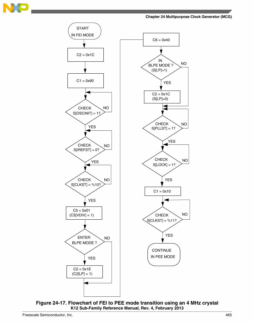
C2 = 0x1C(S[LP]=0)
INBLPE MODE ?
C6 = 0x40
C2 = 0x1C
START
IN FEI MODE
NO
NO
NO
NO
NO
NO
NO
NO
YES
YES
YES
YES
YES
YES
YES
YES
CHECK
C1 = 0x90
CHECK
CHECK
ENTERBLPE MODE ?
C2 = 0x1E(C2[LP] = 1)
CHECK
CHECK
C1 = 0x10
CHECK
CONTINUE
IN PEE MODE
S[PLLST] = 1?
S[LOCK] = 1?
S[CLKST] = %10?
S[CLKST] = %11?
(S[LP]=1)
S[IREFST] = 0?
S[OSCINIT] = 1?
C5 = 0x01(C5[VDIV] = 1)
Figure 24-17. Flowchart of FEI to PEE mode transition using an 4 MHz crystal
Chapter 24 Multipurpose Clock Generator (MCG)
K12 Sub-Family Reference Manual, Rev. 4, February 2013
Freescale Semiconductor, Inc. 465
24.5.3.2 Example 2: Moving from PEE to BLPI mode: MCGOUTCLKfrequency =32 kHz
In this example, the MCG will move through the proper operational modes from PEEmode with a 4 MHz crystal configured for a 48 MHz MCGOUTCLK frequency (seeprevious example) to BLPI mode with a 32 kHz MCGOUTCLK frequency. First, thecode sequence will be described. Then there is a flowchart that illustrates the sequence.
1. First, PEE must transition to PBE mode:
a. C1 = 0x90
• C1[CLKS] set to 2'b10 to switch the system clock source to the externalreference clock.
b. Loop until S[CLKST] are 2'b10, indicating that the external reference clock isselected to feed MCGOUTCLK.
2. Then, PBE must transition either directly to FBE mode or first through BLPE modeand then to FBE mode:
a. BLPE: If a transition through BLPE mode is desired, first set C2[LP] to 1.
b. BLPE/FBE: C6 = 0x00
• C6[PLLS] clear to 0 to select the FLL. At this time, with C1[FRDIV] valueof 3'b010, the FLL divider is set to 128, resulting in a reference frequency of4 MHz / 128 = 31.25 kHz. If C1[FRDIV] was not previously set to 3'b010(necessary to achieve required 31.25–39.06 kHz FLL reference frequencywith an 4 MHz external source frequency), it must be changed prior toclearing C6[PLLS] bit. In BLPE mode,changing this bit only prepares theMCG for FLL usage in FBE mode. With C6[PLLS] = 0, the C6[VDIV0]value does not matter.
c. BLPE: If transitioning through BLPE mode, clear C2[LP] to 0 here to switch toFBE mode.
d. FBE: Loop until S[PLLST] is cleared, indicating that the current source for thePLLS clock is the FLL.
3. Next, FBE mode transitions into FBI mode:
a. C1 = 0x54
• C1[CLKS] set to 2'b01 to switch the system clock to the internal referenceclock.
Initialization / Application information
K12 Sub-Family Reference Manual, Rev. 4, February 2013
466 Freescale Semiconductor, Inc.
• C1[IREFS] set to 1 to select the internal reference clock as the referenceclock source.
• C1[FRDIV] remain unchanged because the reference divider does not affectthe internal reference.
b. Loop until S[IREFST] is 1, indicating the internal reference clock has beenselected as the reference clock source.
c. Loop until S[CLKST] are 2'b01, indicating that the internal reference clock isselected to feed MCGOUTCLK.
4. Lastly, FBI transitions into BLPI mode.
a. C2 = 0x02
• C2[LP] is 1
• C2[RANGE0], C2[HGO0], C2[EREFS0], C1[IRCLKEN], andC1[IREFSTEN] bits are ignored when the C1[IREFS] bit is set. They canremain set, or be cleared at this point.
Chapter 24 Multipurpose Clock Generator (MCG)
K12 Sub-Family Reference Manual, Rev. 4, February 2013
Freescale Semiconductor, Inc. 467

START
IN PEE MODE
C1 = 0x90
CHECKS[CLKST] = %10 ?
NO
NO
NO
NO
YES
C2 = 0x02
CONTINUE
IN BLPI MODE
YES
YES
CHECKS[PLLST] = 0?
C1 = 0x54
CHECKS[IREFST] = 0?
CHECKS[CLKST] = %01?
YES
NO
YES
(C2[LP] = 1)
C6 = 0x00
INBLPE MODE ?
INBLPE MODE ?
NO
YES
C2 = 0x1C(C2[LP] = 0)
C2 = 0x1E
ENTER
BLPE MODE ?
(C2[LP]=1)
Figure 24-18. Flowchart of PEE to BLPI mode transition using an 4 MHz crystal
Initialization / Application information
K12 Sub-Family Reference Manual, Rev. 4, February 2013
468 Freescale Semiconductor, Inc.

24.5.3.3 Example 3: Moving from BLPI to FEE mode
In this example, the MCG will move through the proper operational modes from BLPImode at a 32 kHz MCGOUTCLK frequency running off the internal reference clock (seeprevious example) to FEE mode using a 4 MHz crystal configured for a 20 MHzMCGOUTCLK frequency. First, the code sequence will be described. Then there is aflowchart that illustrates the sequence.
1. First, BLPI must transition to FBI mode.
a. C2 = 0x00
• C2[LP] is 0
2. Next, FBI will transition to FEE mode.
a. C2 = 0x1C
• C2[RANGE0] set to 2'b01 because the frequency of 4 MHz is within thehigh frequency range.
• C2[HGO0] set to 1 to configure the crystal oscillator for high gain operation.
• C2[EREFS0] set to 1, because a crystal is being used.
b. C1 = 0x10
• C1[CLKS] set to 2'b00 to select the output of the FLL as system clocksource.
• C1[FRDIV] remain at 3'b010, or divide-by-128 for a reference of 4 MHz /128 = 31.25 kHz.
• C1[IREFS] cleared to 0, selecting the external reference clock.
c. Loop until S[OSCINIT0] is 1, indicating the crystal selected by the C2[EREFS0]bit has been initialized.
d. Loop until S[IREFST] is 0, indicating the external reference clock is the currentsource for the reference clock.
e. Loop until S[CLKST] are 2'b00, indicating that the output of the FLL is selectedto feed MCGOUTCLK.
f. Now, with a 31.25 kHz reference frequency, a fixed DCO multiplier of 640,MCGOUTCLK = 31.25 kHz * 640 / 1 = 20 MHz.
g. At this point, by default, the C4[DRST_DRS] bits are set to 2'b00 andC4[DMX32] is cleared to 0. If the MCGOUTCLK frequency of 40 MHz isdesired instead, set the C4[DRST_DRS] bits to 0x01 to switch the FLL
Chapter 24 Multipurpose Clock Generator (MCG)
K12 Sub-Family Reference Manual, Rev. 4, February 2013
Freescale Semiconductor, Inc. 469
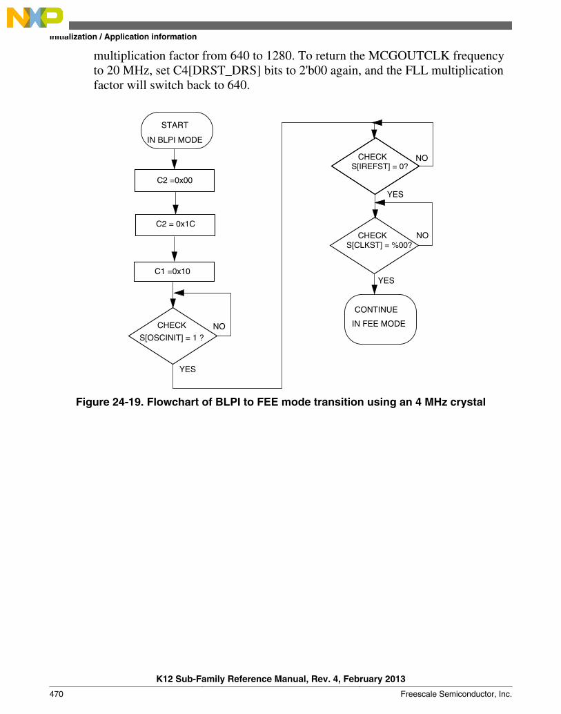
multiplication factor from 640 to 1280. To return the MCGOUTCLK frequencyto 20 MHz, set C4[DRST_DRS] bits to 2'b00 again, and the FLL multiplicationfactor will switch back to 640.
C1 = 0x10
C2 = 0x00
C2 = 0x1C
CHECK
CHECK
CHECK
S[OSCINIT] = 1 ?
CONTINUE
IN FEE MODENO
NO
NO
YES
YES
YES
START
IN BLPI MODE
S[IREFST] = 0?
S[CLKST] = %00?
Figure 24-19. Flowchart of BLPI to FEE mode transition using an 4 MHz crystal
Initialization / Application information
K12 Sub-Family Reference Manual, Rev. 4, February 2013
470 Freescale Semiconductor, Inc.
Chapter 25Oscillator (OSC)
25.1 IntroductionNOTE
For the chip-specific implementation details of this module'sinstances see the chip configuration information.
The OSC module is a crystal oscillator. The module, in conjunction with an externalcrystal or resonator, generates a reference clock for the MCU.
25.2 Features and ModesKey features of the module are:
• Supports 32 kHz crystals (Low Range mode)
• Supports 3–8 MHz crystals and resonators (High Range mode)
• Automatic Gain Control (AGC) to optimize power consumption in high frequencyranges 3–8 MHz using low-power mode
• High gain option in frequency ranges: 32 kHz, 3–8 MHz
• Voltage and frequency filtering to guarantee clock frequency and stability
• Optionally external input bypass clock from EXTAL signal directly
• One clock for MCU clock system
• Two clocks for on-chip peripherals that can work in Stop modes
Functional Description describes the module's operation in more detail.
K12 Sub-Family Reference Manual, Rev. 4, February 2013
Freescale Semiconductor, Inc. 471

25.3 Block DiagramThe OSC module uses a crystal or resonator to generate three filtered oscillator clocksignals. Three clocks are output from OSC module: OSCCLK for MCU system,OSCERCLK for on-chip peripherals, and OSC32KCLK. The OSCCLK can only work inrun mode. OSCERCLK and OSC32KCLK can work in low power modes. For the clocksource assignments, refer to the clock distribution information of this MCU.
Refer to the chip configuration chapter for the external reference clock source in thisMCU.
The following figure shows the block diagram of the OSC module.
XTALEXTAL
XTL_CLK
CNT_DONE_4096
OSC_CLK_OUT Mux
4096 Counter
OSC Clock Enable
STOP
OSC clock selection
OSCERCLKERCLKEN
OSCCLK
Range selectionsLow Power config
OSC32KCLK
Oscillator Circuits E N
Control and Decoding logic
ERCLKEN EREFSTEN OSC_EN
Figure 25-1. OSC Module Block Diagram
25.4 OSC Signal DescriptionsThe following table shows the user-accessible signals available for the OSC module.Refer to signal multiplexing information for this MCU for more details.
Block Diagram
K12 Sub-Family Reference Manual, Rev. 4, February 2013
472 Freescale Semiconductor, Inc.
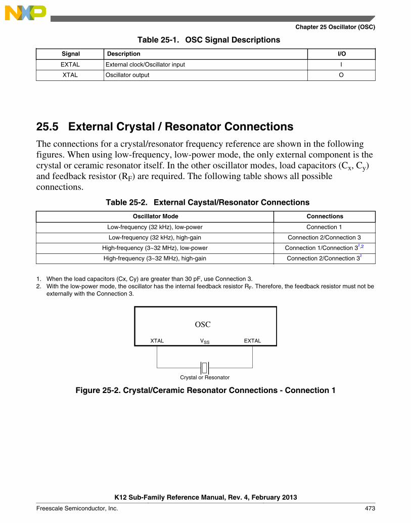
Table 25-1. OSC Signal Descriptions
Signal Description I/O
EXTAL External clock/Oscillator input I
XTAL Oscillator output O
25.5 External Crystal / Resonator ConnectionsThe connections for a crystal/resonator frequency reference are shown in the followingfigures. When using low-frequency, low-power mode, the only external component is thecrystal or ceramic resonator itself. In the other oscillator modes, load capacitors (Cx, Cy)and feedback resistor (RF) are required. The following table shows all possibleconnections.
Table 25-2. External Caystal/Resonator Connections
Oscillator Mode Connections
Low-frequency (32 kHz), low-power Connection 1
Low-frequency (32 kHz), high-gain Connection 2/Connection 3
High-frequency (3~32 MHz), low-power Connection 1/Connection 32,2
High-frequency (3~32 MHz), high-gain Connection 2/Connection 32
1. When the load capacitors (Cx, Cy) are greater than 30 pF, use Connection 3.2. With the low-power mode, the oscillator has the internal feedback resistor RF. Therefore, the feedback resistor must not be
externally with the Connection 3.
OSC
EXTAL
Crystal or Resonator
VSSXTAL
Figure 25-2. Crystal/Ceramic Resonator Connections - Connection 1
Chapter 25 Oscillator (OSC)
K12 Sub-Family Reference Manual, Rev. 4, February 2013
Freescale Semiconductor, Inc. 473
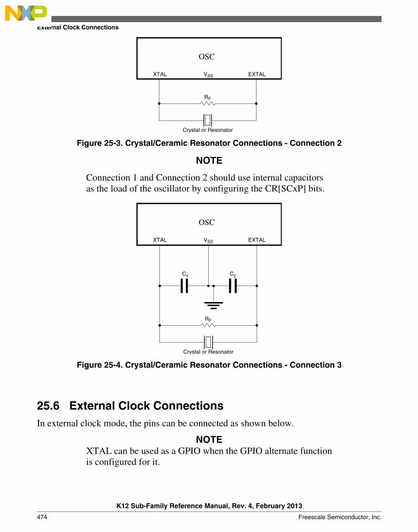
OSC
VSS
RF
Crystal or Resonator
XTAL EXTAL
Figure 25-3. Crystal/Ceramic Resonator Connections - Connection 2
NOTE
Connection 1 and Connection 2 should use internal capacitorsas the load of the oscillator by configuring the CR[SCxP] bits.
OSC
VSS
Cx Cy
RF
Crystal or Resonator
XTAL EXTAL
Figure 25-4. Crystal/Ceramic Resonator Connections - Connection 3
25.6 External Clock ConnectionsIn external clock mode, the pins can be connected as shown below.
NOTEXTAL can be used as a GPIO when the GPIO alternate functionis configured for it.
External Clock Connections
K12 Sub-Family Reference Manual, Rev. 4, February 2013
474 Freescale Semiconductor, Inc.
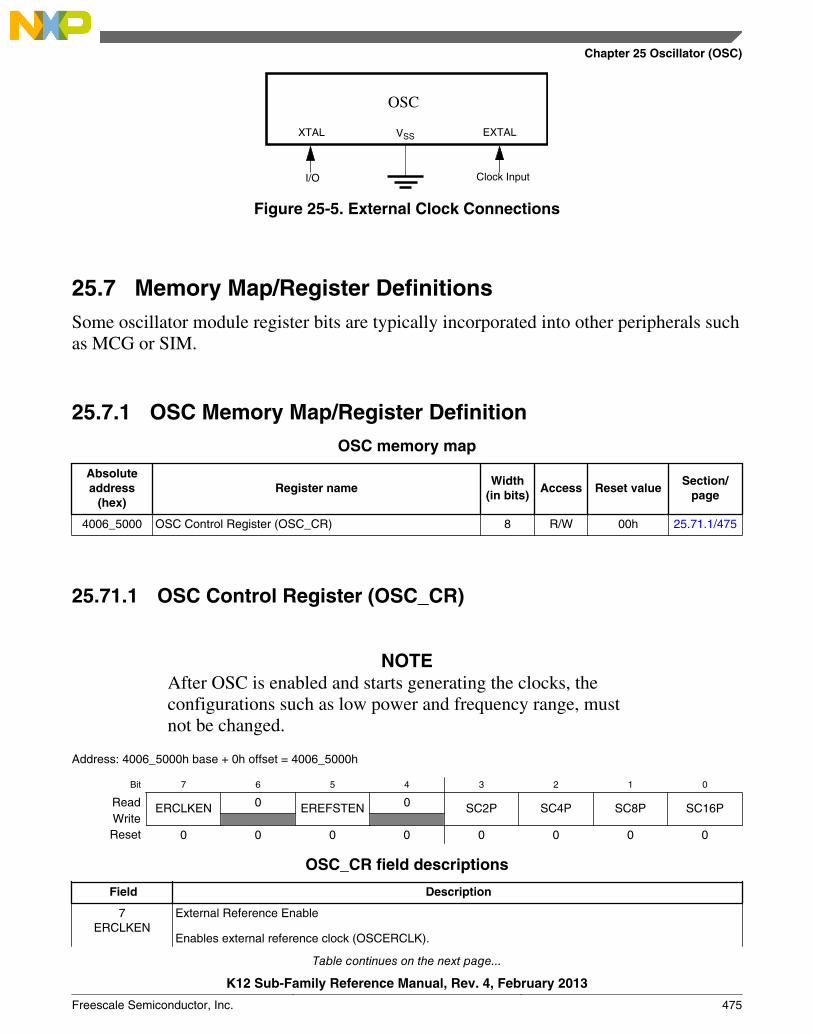
OSC
VSS
Clock Input I/O
XTAL EXTAL
Figure 25-5. External Clock Connections
25.7 Memory Map/Register DefinitionsSome oscillator module register bits are typically incorporated into other peripherals suchas MCG or SIM.
OSC Memory Map/Register Definition
OSC memory map
Absoluteaddress
(hex)Register name
Width(in bits)
Access Reset valueSection/
page
4006_5000 OSC Control Register (OSC_CR) 8 R/W 00h 25.71.1/475
25.71.1 OSC Control Register (OSC_CR)
NOTEAfter OSC is enabled and starts generating the clocks, theconfigurations such as low power and frequency range, mustnot be changed.
Address: 4006_5000h base + 0h offset = 4006_5000h
Bit 7 6 5 4 3 2 1 0
Read ERCLKEN 0 EREFSTEN 0 SC2P SC4P SC8P SC16PWriteReset 0 0 0 0 0 0 0 0
OSC_CR field descriptions
Field Description
7ERCLKEN
External Reference Enable
Enables external reference clock (OSCERCLK).
Table continues on the next page...
25.7.1
Chapter 25 Oscillator (OSC)
K12 Sub-Family Reference Manual, Rev. 4, February 2013
Freescale Semiconductor, Inc. 475
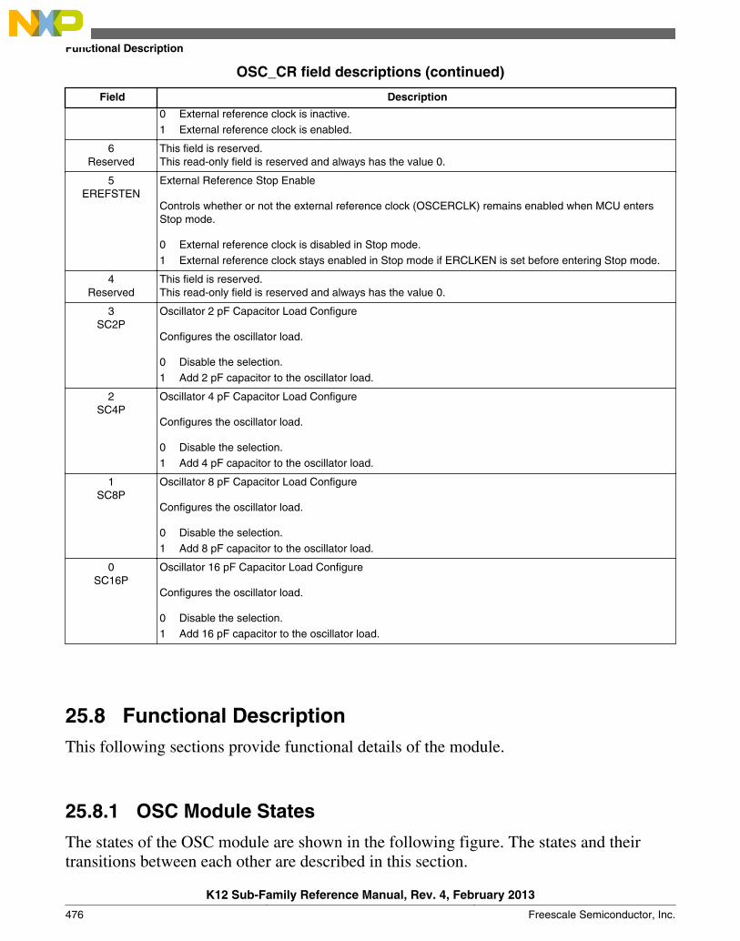
OSC_CR field descriptions (continued)
Field Description
0 External reference clock is inactive.1 External reference clock is enabled.
6Reserved
This field is reserved.This read-only field is reserved and always has the value 0.
5EREFSTEN
External Reference Stop Enable
Controls whether or not the external reference clock (OSCERCLK) remains enabled when MCU entersStop mode.
0 External reference clock is disabled in Stop mode.1 External reference clock stays enabled in Stop mode if ERCLKEN is set before entering Stop mode.
4Reserved
This field is reserved.This read-only field is reserved and always has the value 0.
3SC2P
Oscillator 2 pF Capacitor Load Configure
Configures the oscillator load.
0 Disable the selection.1 Add 2 pF capacitor to the oscillator load.
2SC4P
Oscillator 4 pF Capacitor Load Configure
Configures the oscillator load.
0 Disable the selection.1 Add 4 pF capacitor to the oscillator load.
1SC8P
Oscillator 8 pF Capacitor Load Configure
Configures the oscillator load.
0 Disable the selection.1 Add 8 pF capacitor to the oscillator load.
0SC16P
Oscillator 16 pF Capacitor Load Configure
Configures the oscillator load.
0 Disable the selection.1 Add 16 pF capacitor to the oscillator load.
25.8 Functional DescriptionThis following sections provide functional details of the module.
25.8.1 OSC Module States
The states of the OSC module are shown in the following figure. The states and theirtransitions between each other are described in this section.
Functional Description
K12 Sub-Family Reference Manual, Rev. 4, February 2013
476 Freescale Semiconductor, Inc.

Stable
Off
OSCCLK
CNT_DONE_4096
Start-Up
OSCCLK requested
External Clock Mode
Oscillator ON, Stable
Oscillator OFF
Oscillator ON, not yet stable Oscillator ON
OSC_CLK_OUT = Static
OSC_CLK_OUT = Static OSC_CLK_OUT = EXTAL
OSC_CLK_OUT = XTL_CLK
not requested
&&Select OSC internal clock
OSCCLK requested
&&Select clock from EXTAL signal
Figure 25-7. OSC Module State Diagram
NOTE
XTL_CLK is the clock generated internally from OSC circuits.
25.8.1.1 Off
The OSC enters the Off state when the system does not require OSC clocks. Uponentering this state, XTL_CLK is static unless OSC is configured to select the clock fromthe EXTAL pad by clearing the external reference clock selection bit. For detailsregarding the external reference clock source in this MCU, refer to the chip configurationchapter. The EXTAL and XTAL pins are also decoupled from all other oscillatorcircuitry in this state. The OSC module circuitry is configured to draw minimal current.
Chapter 25 Oscillator (OSC)
K12 Sub-Family Reference Manual, Rev. 4, February 2013
Freescale Semiconductor, Inc. 477

25.8.1.2 Oscillator Start-Up
The OSC enters start-up state when it is configured to generate clocks (internally theOSC_EN transitions high) using the internal oscillator circuits by setting the externalreference clock selection bit. In this state, the OSC module is enabled and oscillations arestarting up, but have not yet stabilized. When the oscillation amplitude becomes largeenough to pass through the input buffer, XTL_CLK begins clocking the counter. Whenthe counter reaches 4096 cycles of XTL_CLK, the oscillator is considered stable andXTL_CLK is passed to the output clock OSC_CLK_OUT.
25.8.1.3 Oscillator Stable
The OSC enters stable state when it is configured to generate clocks (internally theOSC_EN transitions high) using the internal oscillator circuits by setting the externalreference clock selection bit and the counter reaches 4096 cycles of XTL_CLK (whenCNT_DONE_4096 is high). In this state, the OSC module is producing a stable outputclock on OSC_CLK_OUT. Its frequency is determined by the external components beingused.
25.8.1.4 External Clock Mode
The OSC enters external clock state when it is enabled and external reference clockselection bit is cleared. For details regarding external reference clock source in this MCU,refer to the chip configuration chapter. In this state, the OSC module is set to buffer (withhysteresis) a clock from EXTAL onto the OSC_CLK_OUT. Its frequency is determinedby the external clock being supplied.
25.8.2 OSC Module Modes
The OSC is a Pierce-type oscillator that supports external crystals or resonators operatingover the frequency ranges shown in Table 25-5. These modes assume the followingconditions: OSC is enabled to generate clocks (OSC_EN=1), configured to generateclocks internally (MCG_C2[EREFS] = 1), and some or one of the other peripherals(MCG, Timer, and so on) is configured to use the oscillator output clock(OSC_CLK_OUT).
Table 25-5. Oscillator Modes
Mode Frequency Range
Low-frequency, high-gain fosc_lo (1 kHz) up to fosc_lo (32.768 kHz)
Table continues on the next page...
Functional Description
K12 Sub-Family Reference Manual, Rev. 4, February 2013
478 Freescale Semiconductor, Inc.
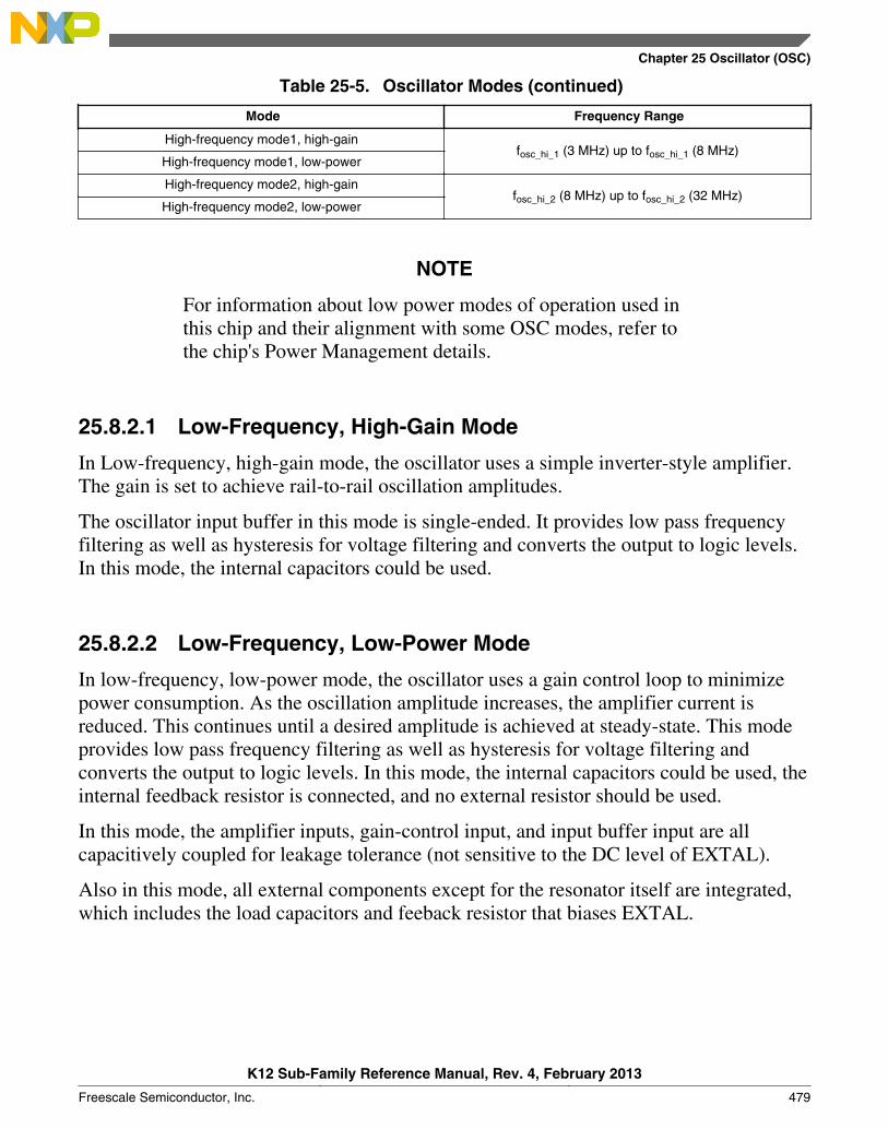
Table 25-5. Oscillator Modes (continued)
Mode Frequency Range
High-frequency mode1, high-gainfosc_hi_1 (3 MHz) up to fosc_hi_1 (8 MHz)
High-frequency mode1, low-power
High-frequency mode2, high-gainfosc_hi_2 (8 MHz) up to fosc_hi_2 (32 MHz)
High-frequency mode2, low-power
NOTE
For information about low power modes of operation used inthis chip and their alignment with some OSC modes, refer tothe chip's Power Management details.
25.8.2.1 Low-Frequency, High-Gain Mode
In Low-frequency, high-gain mode, the oscillator uses a simple inverter-style amplifier.The gain is set to achieve rail-to-rail oscillation amplitudes.
The oscillator input buffer in this mode is single-ended. It provides low pass frequencyfiltering as well as hysteresis for voltage filtering and converts the output to logic levels.In this mode, the internal capacitors could be used.
25.8.2.2 Low-Frequency, Low-Power Mode
In low-frequency, low-power mode, the oscillator uses a gain control loop to minimizepower consumption. As the oscillation amplitude increases, the amplifier current isreduced. This continues until a desired amplitude is achieved at steady-state. This modeprovides low pass frequency filtering as well as hysteresis for voltage filtering andconverts the output to logic levels. In this mode, the internal capacitors could be used, theinternal feedback resistor is connected, and no external resistor should be used.
In this mode, the amplifier inputs, gain-control input, and input buffer input are allcapacitively coupled for leakage tolerance (not sensitive to the DC level of EXTAL).
Also in this mode, all external components except for the resonator itself are integrated,which includes the load capacitors and feeback resistor that biases EXTAL.
Chapter 25 Oscillator (OSC)
K12 Sub-Family Reference Manual, Rev. 4, February 2013
Freescale Semiconductor, Inc. 479
25.8.2.3 High-Frequency, High-Gain Mode
In high-frequency, high-gain mode, the oscillator uses a simple inverter-style amplifier.The gain is set to achieve rail-to-rail oscillation amplitudes. This mode provides low passfrequency filtering as well as hysteresis for voltage filtering and converts the output tologic levels. In this mode, the internal capacitors could be used.
25.8.2.4 High-Frequency, Low-Power Mode
In high-frequency, low-power mode, the oscillator uses a gain control loop to minimizepower consumption. As the oscillation amplitude increases, the amplifier current isreduced. This continues until a desired amplitude is achieved at steady-state. In thismode, the internal capacitors could be used, the internal feedback resistor is connected,and no external resistor should be used.
The oscillator input buffer in this mode is differential. It provides low pass frequencyfiltering as well as hysteresis for voltage filtering and converts the output to logic levels.
25.8.3 Counter
The oscillator output clock (OSC_CLK_OUT) is gated off until the counter has detected4096 cycles of its input clock (XTL_CLK). After 4096 cycles are completed, the counterpasses XTL_CLK onto OSC_CLK_OUT. This counting time-out is used to guaranteeoutput clock stability.
25.8.4 Reference Clock Pin Requirements
The OSC module requires use of both the EXTAL and XTAL pins to generate an outputclock in Oscillator mode, but requires only the EXTAL pin in External clock mode. TheEXTAL and XTAL pins are available for I/O. For the implementation of these pins onthis device, refer to the Signal Multiplexing chapter.
25.9 ResetThere is no reset state associated with the OSC module. The counter logic is reset whenthe OSC is not configured to generate clocks.
There are no sources of reset requests for the OSC module.
Reset
K12 Sub-Family Reference Manual, Rev. 4, February 2013
480 Freescale Semiconductor, Inc.
25.10 Low Power Modes OperationWhen the MCU enters Stop modes, the OSC is functional depending on ERCLKEN andEREFSETN bit settings. If both these bits are set, the OSC is in operation. In LowLeakage Stop (LLS) modes, the OSC holds all register settings. If ERCLKEN andEREFSTEN bits are set before entry to Low Leakage Stop modes, the OSC is stillfunctional in these modes. After waking up from Very Low Leakage Stop (VLLSx)modes, all OSC register bits are reset and initialization is required through software.
25.11 InterruptsThe OSC module does not generate any interrupts.
Chapter 25 Oscillator (OSC)
K12 Sub-Family Reference Manual, Rev. 4, February 2013
Freescale Semiconductor, Inc. 481

Interrupts
K12 Sub-Family Reference Manual, Rev. 4, February 2013
482 Freescale Semiconductor, Inc.
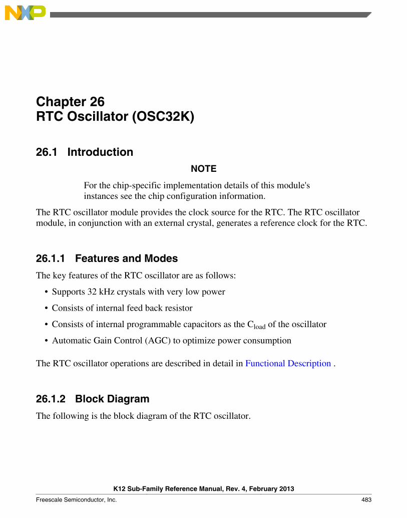
Chapter 26RTC Oscillator (OSC32K)
26.1 IntroductionNOTE
For the chip-specific implementation details of this module'sinstances see the chip configuration information.
The RTC oscillator module provides the clock source for the RTC. The RTC oscillatormodule, in conjunction with an external crystal, generates a reference clock for the RTC.
26.1.1 Features and Modes
The key features of the RTC oscillator are as follows:
• Supports 32 kHz crystals with very low power
• Consists of internal feed back resistor
• Consists of internal programmable capacitors as the Cload of the oscillator
• Automatic Gain Control (AGC) to optimize power consumption
The RTC oscillator operations are described in detail in Functional Description .
26.1.2 Block Diagram
The following is the block diagram of the RTC oscillator.
K12 Sub-Family Reference Manual, Rev. 4, February 2013
Freescale Semiconductor, Inc. 483
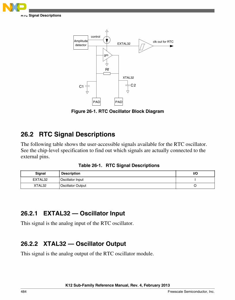
gm
control
clk out for RTC
PAD PAD
XTAL32
C2
AmplitudeEXTAL32
Rf
C1
detector
Figure 26-1. RTC Oscillator Block Diagram
26.2 RTC Signal DescriptionsThe following table shows the user-accessible signals available for the RTC oscillator.See the chip-level specification to find out which signals are actually connected to theexternal pins.
Table 26-1. RTC Signal Descriptions
Signal Description I/O
EXTAL32 Oscillator Input I
XTAL32 Oscillator Output O
26.2.1 EXTAL32 — Oscillator Input
This signal is the analog input of the RTC oscillator.
26.2.2 XTAL32 — Oscillator Output
This signal is the analog output of the RTC oscillator module.
RTC Signal Descriptions
K12 Sub-Family Reference Manual, Rev. 4, February 2013
484 Freescale Semiconductor, Inc.
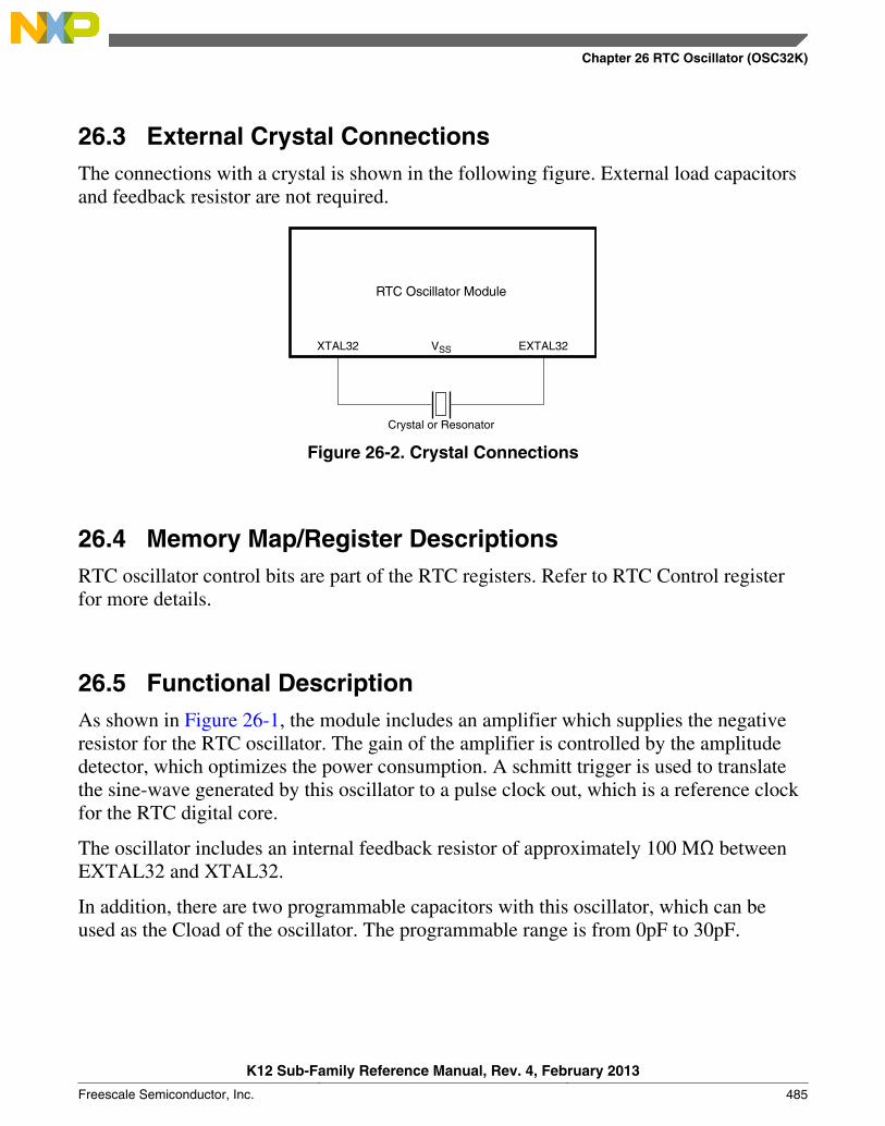
26.3 External Crystal ConnectionsThe connections with a crystal is shown in the following figure. External load capacitorsand feedback resistor are not required.
RTC Oscillator Module
EXTAL32
Crystal or Resonator
XTAL32 VSS
Figure 26-2. Crystal Connections
26.4 Memory Map/Register DescriptionsRTC oscillator control bits are part of the RTC registers. Refer to RTC Control registerfor more details.
26.5 Functional DescriptionAs shown in Figure 26-1, the module includes an amplifier which supplies the negativeresistor for the RTC oscillator. The gain of the amplifier is controlled by the amplitudedetector, which optimizes the power consumption. A schmitt trigger is used to translatethe sine-wave generated by this oscillator to a pulse clock out, which is a reference clockfor the RTC digital core.
The oscillator includes an internal feedback resistor of approximately 100 MΩ betweenEXTAL32 and XTAL32.
In addition, there are two programmable capacitors with this oscillator, which can beused as the Cload of the oscillator. The programmable range is from 0pF to 30pF.
Chapter 26 RTC Oscillator (OSC32K)
K12 Sub-Family Reference Manual, Rev. 4, February 2013
Freescale Semiconductor, Inc. 485

26.6 Reset OverviewThere is no reset state associated with the RTC oscillator.
26.7 InterruptsThe RTC oscillator does not generate any interrupts.
Reset Overview
K12 Sub-Family Reference Manual, Rev. 4, February 2013
486 Freescale Semiconductor, Inc.
Chapter 27Flash Memory Controller (FMC)
27.1 IntroductionNOTE
For the chip-specific implementation details of this module'sinstances see the chip configuration information.
The Flash Memory Controller (FMC) is a memory acceleration unit that provides:• an interface between the device and the dual-bank nonvolatile memory. Bank 0
consists of program flash memory, and bank 1 consists of FlexNVM.• buffers that can accelerate flash memory and FlexNVM data transfers.
27.1.1 OverviewThe Flash Memory Controller manages the interface between the device and the dual-bank flash memory. The FMC receives status information detailing the configuration ofthe memory and uses this information to ensure a proper interface. The following tableshows the supported read/write operations.
Flash memory type Read Write
Program flash memory 8-bit, 16-bit, and 32-bit reads —
FlexNVM used as Data flash memory 8-bit, 16-bit, and 32-bit reads —1
FlexNVM and FlexRAM used asEEPROM
8-bit, 16-bit, and 32-bit reads 8-bit, 16-bit, and 32-bit writes
In addition, for bank 0 and bank 1, the FMC provides three separate mechanisms foraccelerating the interface between the device and the flash memory. A 64-bit speculationbuffer can prefetch the next 64-bit flash memory location, and both a 4-way, 2-set cacheand a single-entry 64-bit buffer can store previously accessed flash memory or FlexNVMdata for quick access times.
K12 Sub-Family Reference Manual, Rev. 4, February 2013
Freescale Semiconductor, Inc. 487

27.1.2 FeaturesThe FMC's features include:
• Interface between the device and the dual-bank flash memory and FlexMemory:• 8-bit, 16-bit, and 32-bit read operations to program flash memory and FlexNVM
used as data flash memory.• 8-bit, 16-bit, and 32-bit read and write operations to FlexNVM and FlexRAM
used as EEPROM.• For bank 0 and bank 1: Read accesses to consecutive 32-bit spaces in memory
return the second read data with no wait states. The memory returns 64 bits viathe 32-bit bus access.
• Crossbar master access protection for setting no access, read-only access, write-only access, or read/write access for each crossbar master.
• For bank 0 and bank 1: Acceleration of data transfer from program flash memory andFlexMemory to the device:
• 64-bit prefetch speculation buffer with controls for instruction/data access permaster and bank
• 4-way, 2-set, 64-bit line size cache for a total of eight 64-bit entries with controlsfor replacement algorithm and lock per way for each bank
• Single-entry buffer with enable per bank• Invalidation control for the speculation buffer and the single-entry buffer
27.2 Modes of operationThe FMC only operates when the device accesses the flash memory or FlexMemory.
In terms of device power modes, the FMC only operates in run and wait modes, includingVLPR and VLPW modes.
For any device power mode where the flash memory or FlexMemory cannot be accessed,the FMC is disabled.
27.3 External signal descriptionThe FMC has no external signals.
Modes of operation
K12 Sub-Family Reference Manual, Rev. 4, February 2013
488 Freescale Semiconductor, Inc.
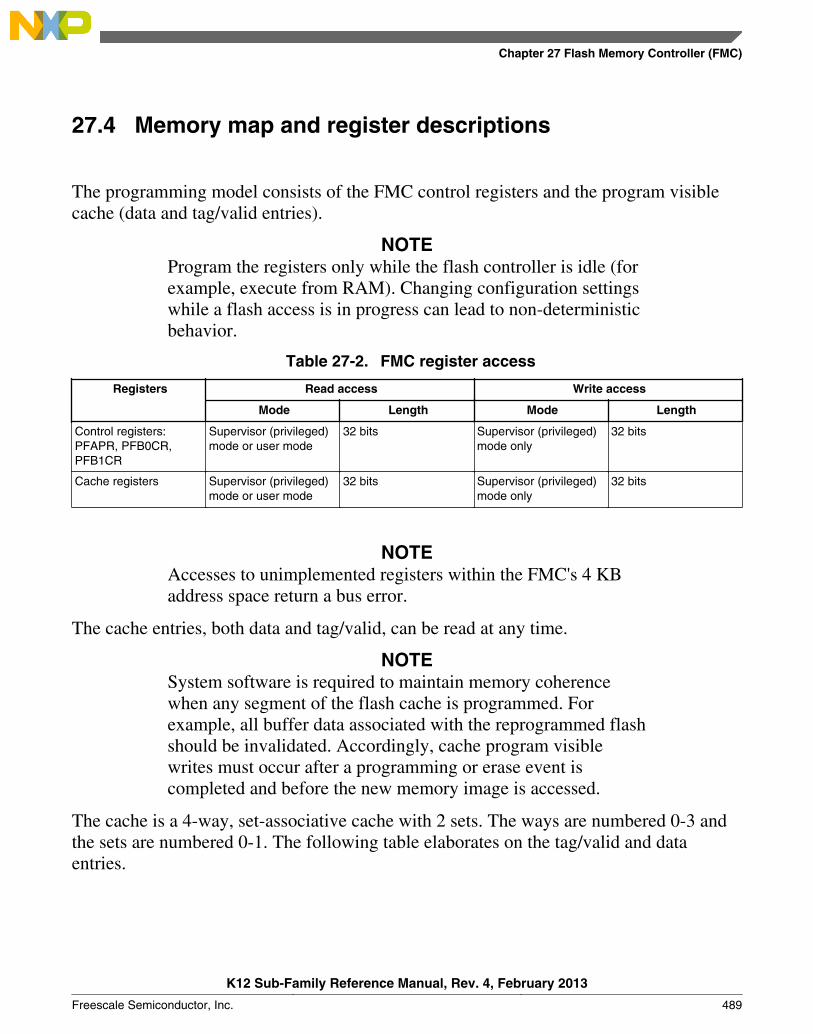
27.4 Memory map and register descriptions
The programming model consists of the FMC control registers and the program visiblecache (data and tag/valid entries).
NOTEProgram the registers only while the flash controller is idle (forexample, execute from RAM). Changing configuration settingswhile a flash access is in progress can lead to non-deterministicbehavior.
Table 27-2. FMC register access
Registers Read access Write access
Mode Length Mode Length
Control registers:PFAPR, PFB0CR,PFB1CR
Supervisor (privileged)mode or user mode
32 bits Supervisor (privileged)mode only
32 bits
Cache registers Supervisor (privileged)mode or user mode
32 bits Supervisor (privileged)mode only
32 bits
NOTEAccesses to unimplemented registers within the FMC's 4 KBaddress space return a bus error.
The cache entries, both data and tag/valid, can be read at any time.
NOTESystem software is required to maintain memory coherencewhen any segment of the flash cache is programmed. Forexample, all buffer data associated with the reprogrammed flashshould be invalidated. Accordingly, cache program visiblewrites must occur after a programming or erase event iscompleted and before the new memory image is accessed.
The cache is a 4-way, set-associative cache with 2 sets. The ways are numbered 0-3 andthe sets are numbered 0-1. The following table elaborates on the tag/valid and dataentries.
Chapter 27 Flash Memory Controller (FMC)
K12 Sub-Family Reference Manual, Rev. 4, February 2013
Freescale Semiconductor, Inc. 489
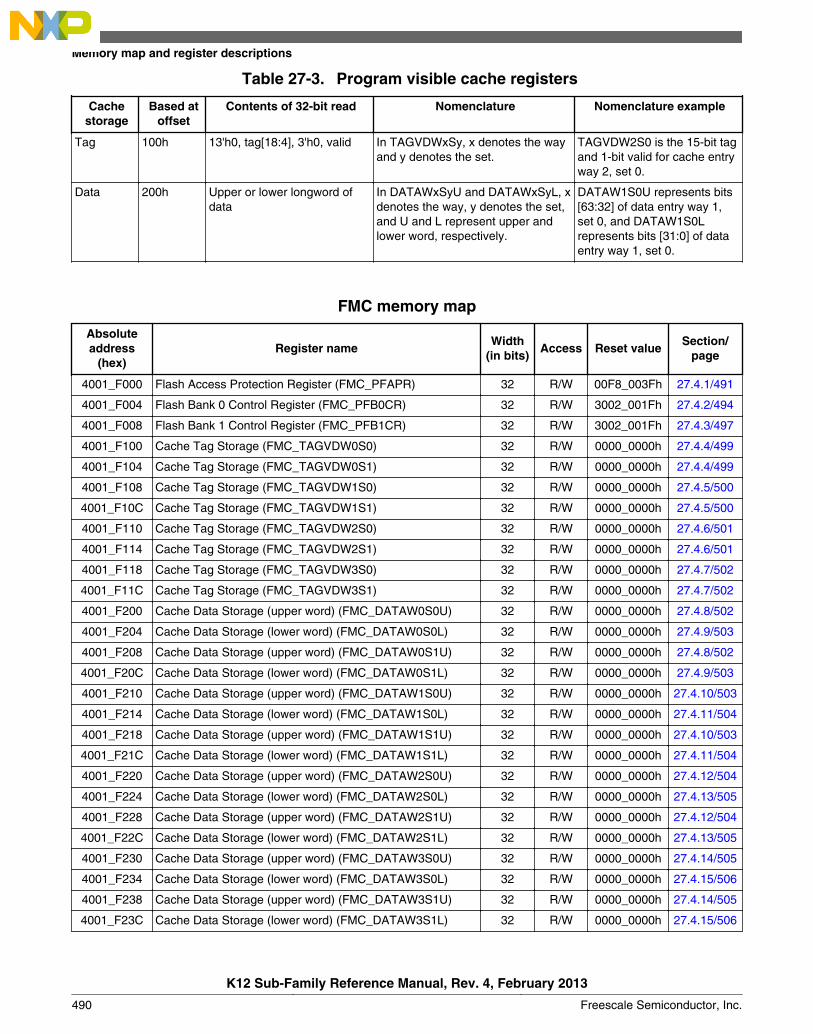
Table 27-3. Program visible cache registers
Cachestorage
Based atoffset
Contents of 32-bit read Nomenclature Nomenclature example
Tag 100h 13'h0, tag[18:4], 3'h0, valid In TAGVDWxSy, x denotes the wayand y denotes the set.
TAGVDW2S0 is the 15-bit tagand 1-bit valid for cache entryway 2, set 0.
Data 200h Upper or lower longword ofdata
In DATAWxSyU and DATAWxSyL, xdenotes the way, y denotes the set,and U and L represent upper andlower word, respectively.
DATAW1S0U represents bits[63:32] of data entry way 1,set 0, and DATAW1S0Lrepresents bits [31:0] of dataentry way 1, set 0.
FMC memory map
Absoluteaddress
(hex)Register name
Width(in bits)
Access Reset valueSection/
page
4001_F000 Flash Access Protection Register (FMC_PFAPR) 32 R/W 00F8_003Fh 27.4.1/491
4001_F004 Flash Bank 0 Control Register (FMC_PFB0CR) 32 R/W 3002_001Fh 27.4.2/494
4001_F008 Flash Bank 1 Control Register (FMC_PFB1CR) 32 R/W 3002_001Fh 27.4.3/497
4001_F100 Cache Tag Storage (FMC_TAGVDW0S0) 32 R/W 0000_0000h 27.4.4/499
4001_F104 Cache Tag Storage (FMC_TAGVDW0S1) 32 R/W 0000_0000h 27.4.4/499
4001_F108 Cache Tag Storage (FMC_TAGVDW1S0) 32 R/W 0000_0000h 27.4.5/500
4001_F10C Cache Tag Storage (FMC_TAGVDW1S1) 32 R/W 0000_0000h 27.4.5/500
4001_F110 Cache Tag Storage (FMC_TAGVDW2S0) 32 R/W 0000_0000h 27.4.6/501
4001_F114 Cache Tag Storage (FMC_TAGVDW2S1) 32 R/W 0000_0000h 27.4.6/501
4001_F118 Cache Tag Storage (FMC_TAGVDW3S0) 32 R/W 0000_0000h 27.4.7/502
4001_F11C Cache Tag Storage (FMC_TAGVDW3S1) 32 R/W 0000_0000h 27.4.7/502
4001_F200 Cache Data Storage (upper word) (FMC_DATAW0S0U) 32 R/W 0000_0000h 27.4.8/502
4001_F204 Cache Data Storage (lower word) (FMC_DATAW0S0L) 32 R/W 0000_0000h 27.4.9/503
4001_F208 Cache Data Storage (upper word) (FMC_DATAW0S1U) 32 R/W 0000_0000h 27.4.8/502
4001_F20C Cache Data Storage (lower word) (FMC_DATAW0S1L) 32 R/W 0000_0000h 27.4.9/503
4001_F210 Cache Data Storage (upper word) (FMC_DATAW1S0U) 32 R/W 0000_0000h 27.4.10/503
4001_F214 Cache Data Storage (lower word) (FMC_DATAW1S0L) 32 R/W 0000_0000h 27.4.11/504
4001_F218 Cache Data Storage (upper word) (FMC_DATAW1S1U) 32 R/W 0000_0000h 27.4.10/503
4001_F21C Cache Data Storage (lower word) (FMC_DATAW1S1L) 32 R/W 0000_0000h 27.4.11/504
4001_F220 Cache Data Storage (upper word) (FMC_DATAW2S0U) 32 R/W 0000_0000h 27.4.12/504
4001_F224 Cache Data Storage (lower word) (FMC_DATAW2S0L) 32 R/W 0000_0000h 27.4.13/505
4001_F228 Cache Data Storage (upper word) (FMC_DATAW2S1U) 32 R/W 0000_0000h 27.4.12/504
4001_F22C Cache Data Storage (lower word) (FMC_DATAW2S1L) 32 R/W 0000_0000h 27.4.13/505
4001_F230 Cache Data Storage (upper word) (FMC_DATAW3S0U) 32 R/W 0000_0000h 27.4.14/505
4001_F234 Cache Data Storage (lower word) (FMC_DATAW3S0L) 32 R/W 0000_0000h 27.4.15/506
4001_F238 Cache Data Storage (upper word) (FMC_DATAW3S1U) 32 R/W 0000_0000h 27.4.14/505
4001_F23C Cache Data Storage (lower word) (FMC_DATAW3S1L) 32 R/W 0000_0000h 27.4.15/506
Memory map and register descriptions
K12 Sub-Family Reference Manual, Rev. 4, February 2013
490 Freescale Semiconductor, Inc.

27.4.1 Flash Access Protection Register (FMC_PFAPR)
Address: 4001_F000h base + 0h offset = 4001_F000h
Bit 31 30 29 28 27 26 25 24 23 22 21 20 19 18 17 16
R 0
M7P
FD
M6P
FD
M5P
FD
M4P
FD
M3P
FD
M2P
FD
M1P
FD
M0P
FD
W
Reset 0 0 0 0 0 0 0 0 1 1 1 1 1 0 0 0
Bit 15 14 13 12 11 10 9 8 7 6 5 4 3 2 1 0
R
M7AP[1:0] M6AP[1:0] M5AP[1:0] M4AP[1:0] M3AP[1:0] M2AP[1:0] M1AP[1:0] M0AP[1:0]W
Reset 0 0 0 0 0 0 0 0 0 0 1 1 1 1 1 1
FMC_PFAPR field descriptions
Field Description
31–24Reserved
This field is reserved.This read-only field is reserved and always has the value 0.
23M7PFD
Master 7 Prefetch Disable
These bits control whether prefetching is enabled based on the logical number of the requesting crossbarswitch master. This field is further qualified by the PFBnCR[BxDPE,BxIPE] bits.
0 Prefetching for this master is enabled.1 Prefetching for this master is disabled.
22M6PFD
Master 6 Prefetch Disable
These bits control whether prefetching is enabled based on the logical number of the requesting crossbarswitch master. This field is further qualified by the PFBnCR[BxDPE,BxIPE] bits.
0 Prefetching for this master is enabled.1 Prefetching for this master is disabled.
21M5PFD
Master 5 Prefetch Disable
These bits control whether prefetching is enabled based on the logical number of the requesting crossbarswitch master. This field is further qualified by the PFBnCR[BxDPE,BxIPE] bits.
0 Prefetching for this master is enabled.1 Prefetching for this master is disabled.
20M4PFD
Master 4 Prefetch Disable
These bits control whether prefetching is enabled based on the logical number of the requesting crossbarswitch master. This field is further qualified by the PFBnCR[BxDPE,BxIPE] bits.
0 Prefetching for this master is enabled.1 Prefetching for this master is disabled.
Table continues on the next page...
Chapter 27 Flash Memory Controller (FMC)
K12 Sub-Family Reference Manual, Rev. 4, February 2013
Freescale Semiconductor, Inc. 491
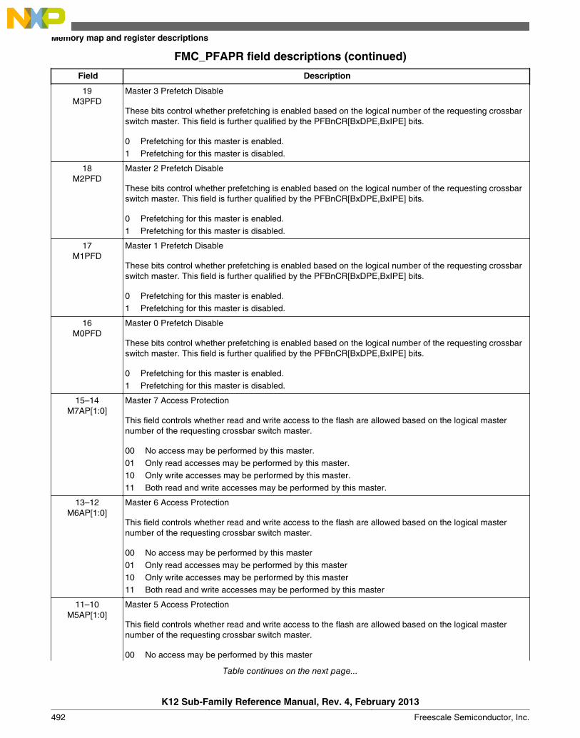
FMC_PFAPR field descriptions (continued)
Field Description
19M3PFD
Master 3 Prefetch Disable
These bits control whether prefetching is enabled based on the logical number of the requesting crossbarswitch master. This field is further qualified by the PFBnCR[BxDPE,BxIPE] bits.
0 Prefetching for this master is enabled.1 Prefetching for this master is disabled.
18M2PFD
Master 2 Prefetch Disable
These bits control whether prefetching is enabled based on the logical number of the requesting crossbarswitch master. This field is further qualified by the PFBnCR[BxDPE,BxIPE] bits.
0 Prefetching for this master is enabled.1 Prefetching for this master is disabled.
17M1PFD
Master 1 Prefetch Disable
These bits control whether prefetching is enabled based on the logical number of the requesting crossbarswitch master. This field is further qualified by the PFBnCR[BxDPE,BxIPE] bits.
0 Prefetching for this master is enabled.1 Prefetching for this master is disabled.
16M0PFD
Master 0 Prefetch Disable
These bits control whether prefetching is enabled based on the logical number of the requesting crossbarswitch master. This field is further qualified by the PFBnCR[BxDPE,BxIPE] bits.
0 Prefetching for this master is enabled.1 Prefetching for this master is disabled.
15–14M7AP[1:0]
Master 7 Access Protection
This field controls whether read and write access to the flash are allowed based on the logical masternumber of the requesting crossbar switch master.
00 No access may be performed by this master.01 Only read accesses may be performed by this master.10 Only write accesses may be performed by this master.11 Both read and write accesses may be performed by this master.
13–12M6AP[1:0]
Master 6 Access Protection
This field controls whether read and write access to the flash are allowed based on the logical masternumber of the requesting crossbar switch master.
00 No access may be performed by this master01 Only read accesses may be performed by this master10 Only write accesses may be performed by this master11 Both read and write accesses may be performed by this master
11–10M5AP[1:0]
Master 5 Access Protection
This field controls whether read and write access to the flash are allowed based on the logical masternumber of the requesting crossbar switch master.
00 No access may be performed by this master
Table continues on the next page...
Memory map and register descriptions
K12 Sub-Family Reference Manual, Rev. 4, February 2013
492 Freescale Semiconductor, Inc.
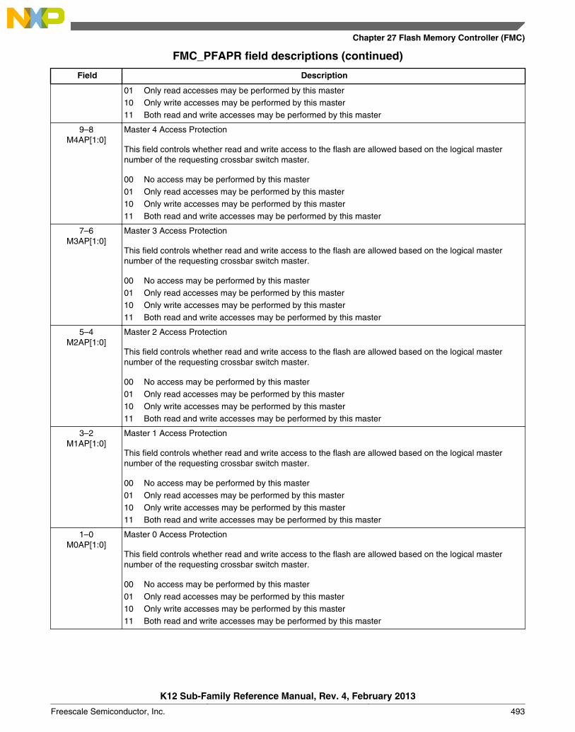
FMC_PFAPR field descriptions (continued)
Field Description
01 Only read accesses may be performed by this master10 Only write accesses may be performed by this master11 Both read and write accesses may be performed by this master
9–8M4AP[1:0]
Master 4 Access Protection
This field controls whether read and write access to the flash are allowed based on the logical masternumber of the requesting crossbar switch master.
00 No access may be performed by this master01 Only read accesses may be performed by this master10 Only write accesses may be performed by this master11 Both read and write accesses may be performed by this master
7–6M3AP[1:0]
Master 3 Access Protection
This field controls whether read and write access to the flash are allowed based on the logical masternumber of the requesting crossbar switch master.
00 No access may be performed by this master01 Only read accesses may be performed by this master10 Only write accesses may be performed by this master11 Both read and write accesses may be performed by this master
5–4M2AP[1:0]
Master 2 Access Protection
This field controls whether read and write access to the flash are allowed based on the logical masternumber of the requesting crossbar switch master.
00 No access may be performed by this master01 Only read accesses may be performed by this master10 Only write accesses may be performed by this master11 Both read and write accesses may be performed by this master
3–2M1AP[1:0]
Master 1 Access Protection
This field controls whether read and write access to the flash are allowed based on the logical masternumber of the requesting crossbar switch master.
00 No access may be performed by this master01 Only read accesses may be performed by this master10 Only write accesses may be performed by this master11 Both read and write accesses may be performed by this master
1–0M0AP[1:0]
Master 0 Access Protection
This field controls whether read and write access to the flash are allowed based on the logical masternumber of the requesting crossbar switch master.
00 No access may be performed by this master01 Only read accesses may be performed by this master10 Only write accesses may be performed by this master11 Both read and write accesses may be performed by this master
Chapter 27 Flash Memory Controller (FMC)
K12 Sub-Family Reference Manual, Rev. 4, February 2013
Freescale Semiconductor, Inc. 493

27.4.2 Flash Bank 0 Control Register (FMC_PFB0CR)
Address: 4001_F000h base + 4h offset = 4001_F004h
Bit 31 30 29 28 27 26 25 24 23 22 21 20 19 18 17 16
R B0RWSC[3:0]
CLCK_WAY[3:0]
0 0 B0MW[1:0] 0
W CINV_WAY[3:0]S_B_INV
Reset 0 0 1 1 0 0 0 0 0 0 0 0 0 0 1 0
Bit 15 14 13 12 11 10 9 8 7 6 5 4 3 2 1 0
R 0
CRC[2:0]
B0D
CE
B0I
CE
B0D
PE
B0I
PE
B0S
EB
E
W
Reset 0 0 0 0 0 0 0 0 0 0 0 1 1 1 1 1
FMC_PFB0CR field descriptions
Field Description
31–28B0RWSC[3:0]
Bank 0 Read Wait State Control
This read-only field defines the number of wait states required to access the bank 0 flash memory.
The relationship between the read access time of the flash array (expressed in system clock cycles) andRWSC is defined as:
Access time of flash array [system clocks] = RWSC + 1
The FMC automatically calculates this value based on the ratio of the system clock speed to the flashclock speed. For example, when this ratio is 4:1, the field's value is 3h.
27–24CLCK_WAY[3:0]
Cache Lock Way x
These bits determine if the given cache way is locked such that its contents will not be displaced by futuremisses.
The bit setting definitions are for each bit in the field.
0 Cache way is unlocked and may be displaced1 Cache way is locked and its contents are not displaced
23–20CINV_WAY[3:0]
Cache Invalidate Way x
Table continues on the next page...
Memory map and register descriptions
K12 Sub-Family Reference Manual, Rev. 4, February 2013
494 Freescale Semiconductor, Inc.
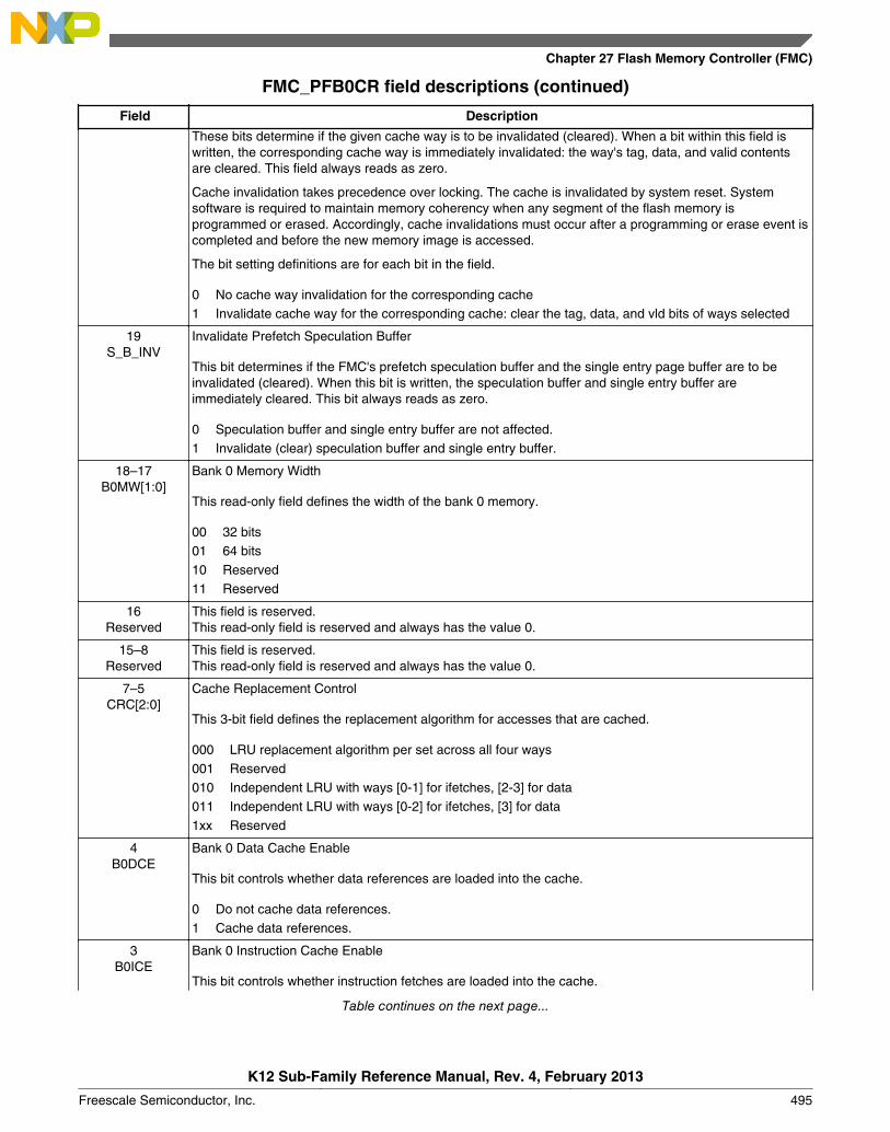
FMC_PFB0CR field descriptions (continued)
Field Description
These bits determine if the given cache way is to be invalidated (cleared). When a bit within this field iswritten, the corresponding cache way is immediately invalidated: the way's tag, data, and valid contentsare cleared. This field always reads as zero.
Cache invalidation takes precedence over locking. The cache is invalidated by system reset. Systemsoftware is required to maintain memory coherency when any segment of the flash memory isprogrammed or erased. Accordingly, cache invalidations must occur after a programming or erase event iscompleted and before the new memory image is accessed.
The bit setting definitions are for each bit in the field.
0 No cache way invalidation for the corresponding cache1 Invalidate cache way for the corresponding cache: clear the tag, data, and vld bits of ways selected
19S_B_INV
Invalidate Prefetch Speculation Buffer
This bit determines if the FMC's prefetch speculation buffer and the single entry page buffer are to beinvalidated (cleared). When this bit is written, the speculation buffer and single entry buffer areimmediately cleared. This bit always reads as zero.
0 Speculation buffer and single entry buffer are not affected.1 Invalidate (clear) speculation buffer and single entry buffer.
18–17B0MW[1:0]
Bank 0 Memory Width
This read-only field defines the width of the bank 0 memory.
00 32 bits01 64 bits10 Reserved11 Reserved
16Reserved
This field is reserved.This read-only field is reserved and always has the value 0.
15–8Reserved
This field is reserved.This read-only field is reserved and always has the value 0.
7–5CRC[2:0]
Cache Replacement Control
This 3-bit field defines the replacement algorithm for accesses that are cached.
000 LRU replacement algorithm per set across all four ways001 Reserved010 Independent LRU with ways [0-1] for ifetches, [2-3] for data011 Independent LRU with ways [0-2] for ifetches, [3] for data1xx Reserved
4B0DCE
Bank 0 Data Cache Enable
This bit controls whether data references are loaded into the cache.
0 Do not cache data references.1 Cache data references.
3B0ICE
Bank 0 Instruction Cache Enable
This bit controls whether instruction fetches are loaded into the cache.
Table continues on the next page...
Chapter 27 Flash Memory Controller (FMC)
K12 Sub-Family Reference Manual, Rev. 4, February 2013
Freescale Semiconductor, Inc. 495

FMC_PFB0CR field descriptions (continued)
Field Description
0 Do not cache instruction fetches.1 Cache instruction fetches.
2B0DPE
Bank 0 Data Prefetch Enable
This bit controls whether prefetches (or speculative accesses) are initiated in response to data references.
0 Do not prefetch in response to data references.1 Enable prefetches in response to data references.
1B0IPE
Bank 0 Instruction Prefetch Enable
This bit controls whether prefetches (or speculative accesses) are initiated in response to instructionfetches.
0 Do not prefetch in response to instruction fetches.1 Enable prefetches in response to instruction fetches.
0B0SEBE
Bank 0 Single Entry Buffer Enable
This bit controls whether the single entry page buffer is enabled in response to flash read accesses. Itsoperation is independent from bank 1's cache.
A high-to-low transition of this enable forces the page buffer to be invalidated.
0 Single entry buffer is disabled.1 Single entry buffer is enabled.
Memory map and register descriptions
K12 Sub-Family Reference Manual, Rev. 4, February 2013
496 Freescale Semiconductor, Inc.
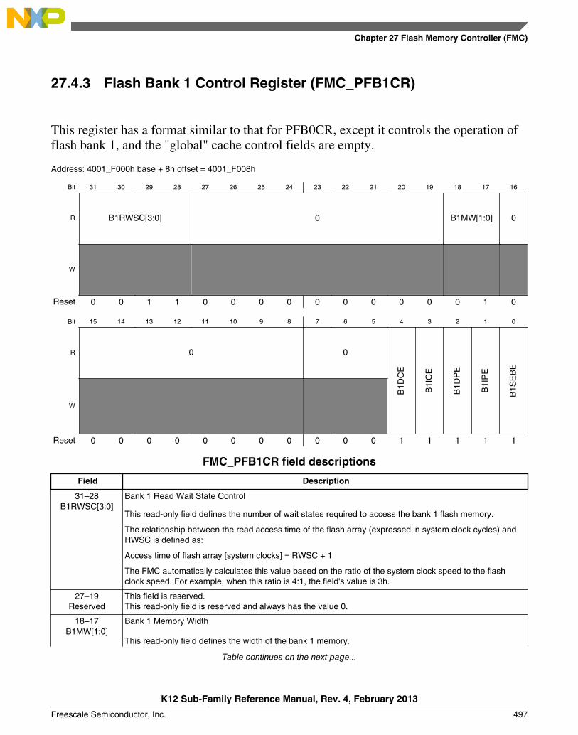
27.4.3 Flash Bank 1 Control Register (FMC_PFB1CR)
This register has a format similar to that for PFB0CR, except it controls the operation offlash bank 1, and the "global" cache control fields are empty.
Address: 4001_F000h base + 8h offset = 4001_F008h
Bit 31 30 29 28 27 26 25 24 23 22 21 20 19 18 17 16
R B1RWSC[3:0] 0 B1MW[1:0] 0
W
Reset 0 0 1 1 0 0 0 0 0 0 0 0 0 0 1 0
Bit 15 14 13 12 11 10 9 8 7 6 5 4 3 2 1 0
R 0 0
B1D
CE
B1I
CE
B1D
PE
B1I
PE
B1S
EB
E
W
Reset 0 0 0 0 0 0 0 0 0 0 0 1 1 1 1 1
FMC_PFB1CR field descriptions
Field Description
31–28B1RWSC[3:0]
Bank 1 Read Wait State Control
This read-only field defines the number of wait states required to access the bank 1 flash memory.
The relationship between the read access time of the flash array (expressed in system clock cycles) andRWSC is defined as:
Access time of flash array [system clocks] = RWSC + 1
The FMC automatically calculates this value based on the ratio of the system clock speed to the flashclock speed. For example, when this ratio is 4:1, the field's value is 3h.
27–19Reserved
This field is reserved.This read-only field is reserved and always has the value 0.
18–17B1MW[1:0]
Bank 1 Memory Width
This read-only field defines the width of the bank 1 memory.
Table continues on the next page...
Chapter 27 Flash Memory Controller (FMC)
K12 Sub-Family Reference Manual, Rev. 4, February 2013
Freescale Semiconductor, Inc. 497
FMC_PFB1CR field descriptions (continued)
Field Description
00 32 bits01 64 bits10 Reserved11 Reserved
16Reserved
This field is reserved.This read-only field is reserved and always has the value 0.
15–8Reserved
This field is reserved.This read-only field is reserved and always has the value 0.
7–5Reserved
This field is reserved.This read-only field is reserved and always has the value 0.
4B1DCE
Bank 1 Data Cache Enable
This bit controls whether data references are loaded into the cache.
0 Do not cache data references.1 Cache data references.
3B1ICE
Bank 1 Instruction Cache Enable
This bit controls whether instruction fetches are loaded into the cache.
0 Do not cache instruction fetches.1 Cache instruction fetches.
2B1DPE
Bank 1 Data Prefetch Enable
This bit controls whether prefetches (or speculative accesses) are initiated in response to data references.
0 Do not prefetch in response to data references.1 Enable prefetches in response to data references.
1B1IPE
Bank 1 Instruction Prefetch Enable
This bit controls whether prefetches (or speculative accesses) are initiated in response to instructionfetches.
0 Do not prefetch in response to instruction fetches.1 Enable prefetches in response to instruction fetches.
0B1SEBE
Bank 1 Single Entry Buffer Enable
This bit controls whether the single entry buffer is enabled in response to flash read accesses. Itsoperation is independent from bank 0's cache.
A high-to-low transition of this enable forces the page buffer to be invalidated.
0 Single entry buffer is disabled.1 Single entry buffer is enabled.
Memory map and register descriptions
K12 Sub-Family Reference Manual, Rev. 4, February 2013
498 Freescale Semiconductor, Inc.
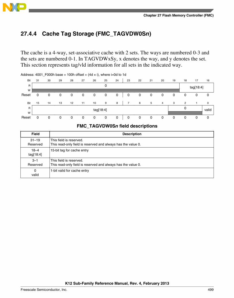
27.4.4 Cache Tag Storage (FMC_TAGVDW0Sn)
The cache is a 4-way, set-associative cache with 2 sets. The ways are numbered 0-3 andthe sets are numbered 0-1. In TAGVDWxSy, x denotes the way, and y denotes the set.This section represents tag/vld information for all sets in the indicated way.
Address: 4001_F000h base + 100h offset + (4d × i), where i=0d to 1d
Bit 31 30 29 28 27 26 25 24 23 22 21 20 19 18 17 16
R 0 tag[18:4]W
Reset 0 0 0 0 0 0 0 0 0 0 0 0 0 0 0 0
Bit 15 14 13 12 11 10 9 8 7 6 5 4 3 2 1 0
R tag[18:4] 0 validW
Reset 0 0 0 0 0 0 0 0 0 0 0 0 0 0 0 0
FMC_TAGVDW0Sn field descriptions
Field Description
31–19Reserved
This field is reserved.This read-only field is reserved and always has the value 0.
18–4tag[18:4]
15-bit tag for cache entry
3–1Reserved
This field is reserved.This read-only field is reserved and always has the value 0.
0valid
1-bit valid for cache entry
Chapter 27 Flash Memory Controller (FMC)
K12 Sub-Family Reference Manual, Rev. 4, February 2013
Freescale Semiconductor, Inc. 499
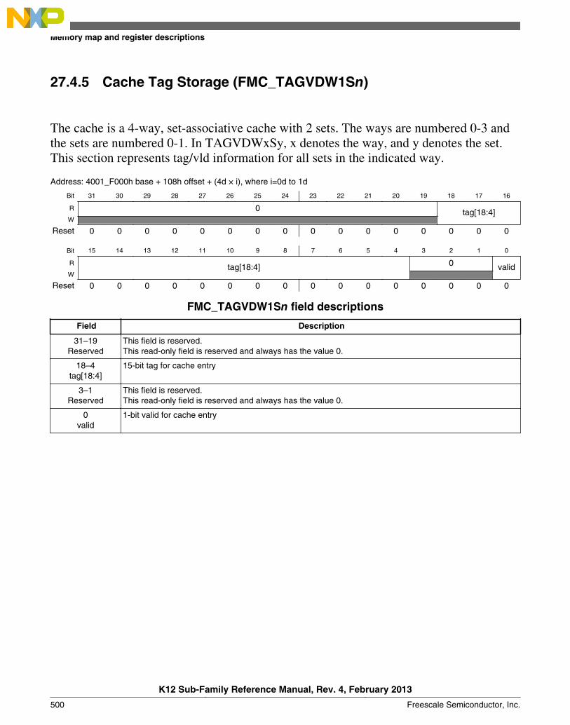
27.4.5 Cache Tag Storage (FMC_TAGVDW1Sn)
The cache is a 4-way, set-associative cache with 2 sets. The ways are numbered 0-3 andthe sets are numbered 0-1. In TAGVDWxSy, x denotes the way, and y denotes the set.This section represents tag/vld information for all sets in the indicated way.
Address: 4001_F000h base + 108h offset + (4d × i), where i=0d to 1d
Bit 31 30 29 28 27 26 25 24 23 22 21 20 19 18 17 16
R 0 tag[18:4]W
Reset 0 0 0 0 0 0 0 0 0 0 0 0 0 0 0 0
Bit 15 14 13 12 11 10 9 8 7 6 5 4 3 2 1 0
R tag[18:4] 0 validW
Reset 0 0 0 0 0 0 0 0 0 0 0 0 0 0 0 0
FMC_TAGVDW1Sn field descriptions
Field Description
31–19Reserved
This field is reserved.This read-only field is reserved and always has the value 0.
18–4tag[18:4]
15-bit tag for cache entry
3–1Reserved
This field is reserved.This read-only field is reserved and always has the value 0.
0valid
1-bit valid for cache entry
Memory map and register descriptions
K12 Sub-Family Reference Manual, Rev. 4, February 2013
500 Freescale Semiconductor, Inc.

27.4.6 Cache Tag Storage (FMC_TAGVDW2Sn)
The cache is a 4-way, set-associative cache with 2 sets. The ways are numbered 0-3 andthe sets are numbered 0-1. In TAGVDWxSy, x denotes the way, and y denotes the set.This section represents tag/vld information for all sets in the indicated way.
Address: 4001_F000h base + 110h offset + (4d × i), where i=0d to 1d
Bit 31 30 29 28 27 26 25 24 23 22 21 20 19 18 17 16
R 0 tag[18:4]W
Reset 0 0 0 0 0 0 0 0 0 0 0 0 0 0 0 0
Bit 15 14 13 12 11 10 9 8 7 6 5 4 3 2 1 0
R tag[18:4] 0 validW
Reset 0 0 0 0 0 0 0 0 0 0 0 0 0 0 0 0
FMC_TAGVDW2Sn field descriptions
Field Description
31–19Reserved
This field is reserved.This read-only field is reserved and always has the value 0.
18–4tag[18:4]
15-bit tag for cache entry
3–1Reserved
This field is reserved.This read-only field is reserved and always has the value 0.
0valid
1-bit valid for cache entry
Chapter 27 Flash Memory Controller (FMC)
K12 Sub-Family Reference Manual, Rev. 4, February 2013
Freescale Semiconductor, Inc. 501

27.4.7 Cache Tag Storage (FMC_TAGVDW3Sn)
The cache is a 4-way, set-associative cache with 2 sets. The ways are numbered 0-3 andthe sets are numbered 0-1. In TAGVDWxSy, x denotes the way, and y denotes the set.This section represents tag/vld information for all sets in the indicated way.
Address: 4001_F000h base + 118h offset + (4d × i), where i=0d to 1d
Bit 31 30 29 28 27 26 25 24 23 22 21 20 19 18 17 16
R 0 tag[18:4]W
Reset 0 0 0 0 0 0 0 0 0 0 0 0 0 0 0 0
Bit 15 14 13 12 11 10 9 8 7 6 5 4 3 2 1 0
R tag[18:4] 0 validW
Reset 0 0 0 0 0 0 0 0 0 0 0 0 0 0 0 0
FMC_TAGVDW3Sn field descriptions
Field Description
31–19Reserved
This field is reserved.This read-only field is reserved and always has the value 0.
18–4tag[18:4]
15-bit tag for cache entry
3–1Reserved
This field is reserved.This read-only field is reserved and always has the value 0.
0valid
1-bit valid for cache entry
27.4.8 Cache Data Storage (upper word) (FMC_DATAW0SnU)
The cache of 64-bit entries is a 4-way, set-associative cache with 2 sets. The ways arenumbered 0-3 and the sets are numbered 0-1. In DATAWxSyU and DATAWxSyL, xdenotes the way, y denotes the set, and U and L represent upper and lower word,respectively. This section represents data for the upper word (bits [63:32]) of all sets inthe indicated way.
Address: 4001_F000h base + 200h offset + (8d × i), where i=0d to 1d
Bit 31 30 29 28 27 26 25 24 23 22 21 20 19 18 17 16 15 14 13 12 11 10 9 8 7 6 5 4 3 2 1 0
R data[63:32]W
Reset 0 0 0 0 0 0 0 0 0 0 0 0 0 0 0 0 0 0 0 0 0 0 0 0 0 0 0 0 0 0 0 0
Memory map and register descriptions
K12 Sub-Family Reference Manual, Rev. 4, February 2013
502 Freescale Semiconductor, Inc.
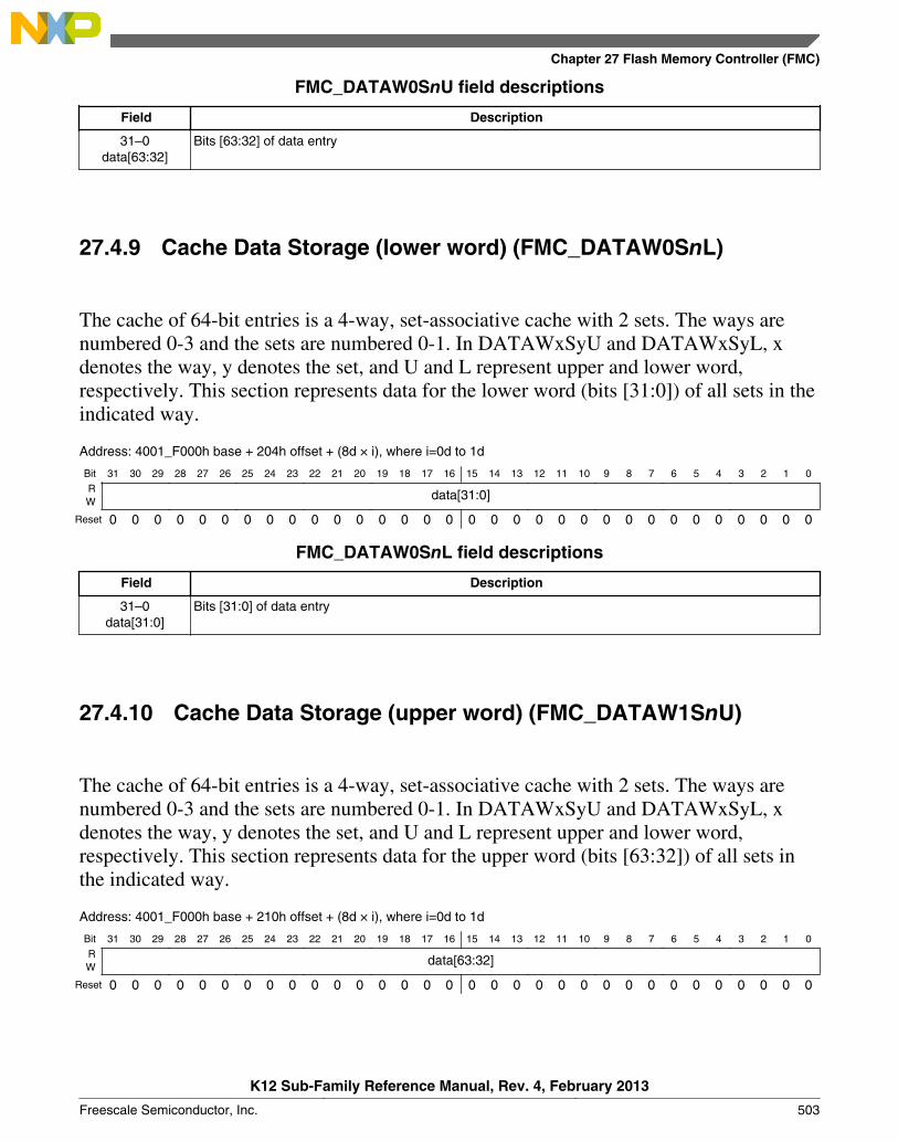
FMC_DATAW0SnU field descriptions
Field Description
31–0data[63:32]
Bits [63:32] of data entry
27.4.9 Cache Data Storage (lower word) (FMC_DATAW0SnL)
The cache of 64-bit entries is a 4-way, set-associative cache with 2 sets. The ways arenumbered 0-3 and the sets are numbered 0-1. In DATAWxSyU and DATAWxSyL, xdenotes the way, y denotes the set, and U and L represent upper and lower word,respectively. This section represents data for the lower word (bits [31:0]) of all sets in theindicated way.
Address: 4001_F000h base + 204h offset + (8d × i), where i=0d to 1d
Bit 31 30 29 28 27 26 25 24 23 22 21 20 19 18 17 16 15 14 13 12 11 10 9 8 7 6 5 4 3 2 1 0
R data[31:0]W
Reset 0 0 0 0 0 0 0 0 0 0 0 0 0 0 0 0 0 0 0 0 0 0 0 0 0 0 0 0 0 0 0 0
FMC_DATAW0SnL field descriptions
Field Description
31–0data[31:0]
Bits [31:0] of data entry
27.4.10 Cache Data Storage (upper word) (FMC_DATAW1SnU)
The cache of 64-bit entries is a 4-way, set-associative cache with 2 sets. The ways arenumbered 0-3 and the sets are numbered 0-1. In DATAWxSyU and DATAWxSyL, xdenotes the way, y denotes the set, and U and L represent upper and lower word,respectively. This section represents data for the upper word (bits [63:32]) of all sets inthe indicated way.
Address: 4001_F000h base + 210h offset + (8d × i), where i=0d to 1d
Bit 31 30 29 28 27 26 25 24 23 22 21 20 19 18 17 16 15 14 13 12 11 10 9 8 7 6 5 4 3 2 1 0
R data[63:32]W
Reset 0 0 0 0 0 0 0 0 0 0 0 0 0 0 0 0 0 0 0 0 0 0 0 0 0 0 0 0 0 0 0 0
Chapter 27 Flash Memory Controller (FMC)
K12 Sub-Family Reference Manual, Rev. 4, February 2013
Freescale Semiconductor, Inc. 503
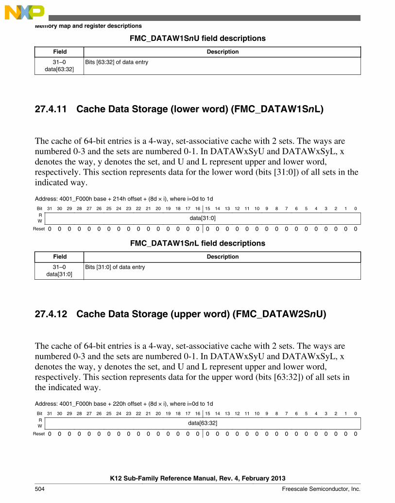
FMC_DATAW1SnU field descriptions
Field Description
31–0data[63:32]
Bits [63:32] of data entry
27.4.11 Cache Data Storage (lower word) (FMC_DATAW1SnL)
The cache of 64-bit entries is a 4-way, set-associative cache with 2 sets. The ways arenumbered 0-3 and the sets are numbered 0-1. In DATAWxSyU and DATAWxSyL, xdenotes the way, y denotes the set, and U and L represent upper and lower word,respectively. This section represents data for the lower word (bits [31:0]) of all sets in theindicated way.
Address: 4001_F000h base + 214h offset + (8d × i), where i=0d to 1d
Bit 31 30 29 28 27 26 25 24 23 22 21 20 19 18 17 16 15 14 13 12 11 10 9 8 7 6 5 4 3 2 1 0
R data[31:0]W
Reset 0 0 0 0 0 0 0 0 0 0 0 0 0 0 0 0 0 0 0 0 0 0 0 0 0 0 0 0 0 0 0 0
FMC_DATAW1SnL field descriptions
Field Description
31–0data[31:0]
Bits [31:0] of data entry
27.4.12 Cache Data Storage (upper word) (FMC_DATAW2SnU)
The cache of 64-bit entries is a 4-way, set-associative cache with 2 sets. The ways arenumbered 0-3 and the sets are numbered 0-1. In DATAWxSyU and DATAWxSyL, xdenotes the way, y denotes the set, and U and L represent upper and lower word,respectively. This section represents data for the upper word (bits [63:32]) of all sets inthe indicated way.
Address: 4001_F000h base + 220h offset + (8d × i), where i=0d to 1d
Bit 31 30 29 28 27 26 25 24 23 22 21 20 19 18 17 16 15 14 13 12 11 10 9 8 7 6 5 4 3 2 1 0
R data[63:32]W
Reset 0 0 0 0 0 0 0 0 0 0 0 0 0 0 0 0 0 0 0 0 0 0 0 0 0 0 0 0 0 0 0 0
Memory map and register descriptions
K12 Sub-Family Reference Manual, Rev. 4, February 2013
504 Freescale Semiconductor, Inc.

FMC_DATAW2SnU field descriptions
Field Description
31–0data[63:32]
Bits [63:32] of data entry
27.4.13 Cache Data Storage (lower word) (FMC_DATAW2SnL)
The cache of 64-bit entries is a 4-way, set-associative cache with 2 sets. The ways arenumbered 0-3 and the sets are numbered 0-1. In DATAWxSyU and DATAWxSyL, xdenotes the way, y denotes the set, and U and L represent upper and lower word,respectively. This section represents data for the lower word (bits [31:0]) of all sets in theindicated way.
Address: 4001_F000h base + 224h offset + (8d × i), where i=0d to 1d
Bit 31 30 29 28 27 26 25 24 23 22 21 20 19 18 17 16 15 14 13 12 11 10 9 8 7 6 5 4 3 2 1 0
R data[31:0]W
Reset 0 0 0 0 0 0 0 0 0 0 0 0 0 0 0 0 0 0 0 0 0 0 0 0 0 0 0 0 0 0 0 0
FMC_DATAW2SnL field descriptions
Field Description
31–0data[31:0]
Bits [31:0] of data entry
27.4.14 Cache Data Storage (upper word) (FMC_DATAW3SnU)
The cache of 64-bit entries is a 4-way, set-associative cache with 2 sets. The ways arenumbered 0-3 and the sets are numbered 0-1. In DATAWxSyU and DATAWxSyL, xdenotes the way, y denotes the set, and U and L represent upper and lower word,respectively. This section represents data for the upper word (bits [63:32]) of all sets inthe indicated way.
Address: 4001_F000h base + 230h offset + (8d × i), where i=0d to 1d
Bit 31 30 29 28 27 26 25 24 23 22 21 20 19 18 17 16 15 14 13 12 11 10 9 8 7 6 5 4 3 2 1 0
R data[63:32]W
Reset 0 0 0 0 0 0 0 0 0 0 0 0 0 0 0 0 0 0 0 0 0 0 0 0 0 0 0 0 0 0 0 0
Chapter 27 Flash Memory Controller (FMC)
K12 Sub-Family Reference Manual, Rev. 4, February 2013
Freescale Semiconductor, Inc. 505
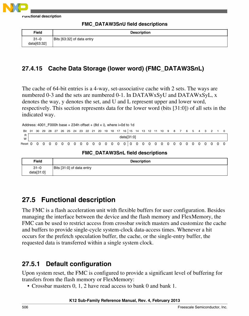
FMC_DATAW3SnU field descriptions
Field Description
31–0data[63:32]
Bits [63:32] of data entry
27.4.15 Cache Data Storage (lower word) (FMC_DATAW3SnL)
The cache of 64-bit entries is a 4-way, set-associative cache with 2 sets. The ways arenumbered 0-3 and the sets are numbered 0-1. In DATAWxSyU and DATAWxSyL, xdenotes the way, y denotes the set, and U and L represent upper and lower word,respectively. This section represents data for the lower word (bits [31:0]) of all sets in theindicated way.
Address: 4001_F000h base + 234h offset + (8d × i), where i=0d to 1d
Bit 31 30 29 28 27 26 25 24 23 22 21 20 19 18 17 16 15 14 13 12 11 10 9 8 7 6 5 4 3 2 1 0
R data[31:0]W
Reset 0 0 0 0 0 0 0 0 0 0 0 0 0 0 0 0 0 0 0 0 0 0 0 0 0 0 0 0 0 0 0 0
FMC_DATAW3SnL field descriptions
Field Description
31–0data[31:0]
Bits [31:0] of data entry
27.5 Functional descriptionThe FMC is a flash acceleration unit with flexible buffers for user configuration. Besidesmanaging the interface between the device and the flash memory and FlexMemory, theFMC can be used to restrict access from crossbar switch masters and customize the cacheand buffers to provide single-cycle system-clock data-access times. Whenever a hitoccurs for the prefetch speculation buffer, the cache, or the single-entry buffer, therequested data is transferred within a single system clock.
27.5.1 Default configurationUpon system reset, the FMC is configured to provide a significant level of buffering fortransfers from the flash memory or FlexMemory:
• Crossbar masters 0, 1, 2 have read access to bank 0 and bank 1.
Functional description
K12 Sub-Family Reference Manual, Rev. 4, February 2013
506 Freescale Semiconductor, Inc.
• These masters have write access to a portion of bank 1 when FlexNVM is used withFlexRAM as EEPROM.
• For bank 0 and bank 1:• Prefetch support for data and instructions is enabled for crossbar masters 0, 1, 2.• The cache is configured for least recently used (LRU) replacement for all four
ways.• The cache is configured for data or instruction replacement.• The single-entry buffer is enabled.
27.5.2 Configuration options
Though the default configuration provides a high degree of flash acceleration, advancedusers may desire to customize the FMC buffer configurations to maximize throughput fortheir use cases. When reconfiguring the FMC for custom use cases, do not program theFMC's control registers while the flash memory or FlexMemory is being accessed.Instead, change the control registers with a routine executing from RAM in supervisormode.
The FMC's cache and buffering controls within PFB0CR and PFB1CR allow the tuningof resources to suit particular applications' needs. The cache and two buffers are eachcontrolled individually. The register controls enable buffering and prefetching permemory bank and access type (instruction fetch or data reference). The cache alsosupports three types of LRU replacement algorithms:
• LRU per set across all four ways,• LRU with ways [0-1] for instruction fetches and ways [2-3] for data fetches, and• LRU with ways [0-2] for instruction fetches and way [3] for data fetches.
As an application example: if both instruction fetches and data references are accessingbank 0, control is available to send instruction fetches, data references, or both to thecache or the single-entry buffer. Likewise, speculation can be enabled or disabled foreither type of access. If both instruction fetches and data references are cached, thecache's way resources may be divided in several ways between the instruction fetches anddata references.
In another application example, the cache can be configured for replacement from bank0, while the single-entry buffer can be enabled for bank 1 only. This configuration isideal for applications that use bank 0 for program space and bank 1 for data space.
Chapter 27 Flash Memory Controller (FMC)
K12 Sub-Family Reference Manual, Rev. 4, February 2013
Freescale Semiconductor, Inc. 507

27.5.3 Wait statesBecause the core, crossbar switch, and bus masters can be clocked at a higher frequencythan the flash clock, flash memory accesses that do not hit in the speculation buffer orcache usually require wait states. The number of wait states depends on both of thefollowing:
1. the ratio of the core clock to the flash clock, and2. the phase relationship of the core clock and flash clock at the time the read is
requested.
The ratio of the core clock to the flash clock is equal to the value of PFB0CR[B0RWSC]+ 1 for bank 0 and to the value of PFB1CR[B1RWSC] + 1 for bank 1.
For example, in a system with a 4:1 core-to-flash clock ratio, a read that does not hit inthe speculation buffer or the cache can take between 4 and 7 core clock cycles tocomplete.
• The best-case scenario is a period of 4 core clock cycles because a read from theflash memory takes 1 flash clock, which translates to 4 core clocks.
• The worst-case scenario is a period of 7 core clock cycles, consisting of 4 cycles forthe read operation and 3 cycles of delay to align the core and flash clocks.
• A delay to align the core and flash clocks might occur because you can request aread cycle on any core clock edge, but that edge does not necessarily align with aflash clock edge where the read can start.
• In this case, the read operation is delayed by a number of core clocks equal to thecore-to-flash clock ratio minus one: 4 - 1 = 3. That is, 3 additional core clockcycles are required to synchronize the clocks before the read operation can start.
All wait states and synchronization delays are handled automatically by the FlashMemory Controller. No direct user configuration is required or even allowed to set up theflash wait states.
27.5.4 Speculative reads
The FMC has a single buffer that reads ahead to the next word in the flash memory ifthere is an idle cycle. Speculative prefetching is programmable for each bank forinstruction and/or data accesses using the B0DPE and B0IPE fields of PFB0CR and theB1DPE and B1IPE fields of PFB1CR. Because many code accesses are sequential, usingthe speculative prefetch buffer improves performance in most cases.
When speculative reads are enabled, the FMC immediately requests the next sequentialaddress after a read completes. By requesting the next word immediately, speculativereads can help to reduce or even eliminate wait states when accessing sequential codeand/or data.
Functional description
K12 Sub-Family Reference Manual, Rev. 4, February 2013
508 Freescale Semiconductor, Inc.
For example, consider the following scenario:• Assume a system with a 4:1 core-to-flash clock ratio and with speculative reads
enabled.• The core requests four sequential longwords in back-to-back requests, meaning there
are no core cycle delays except for stalls waiting for flash memory data to bereturned.
• None of the data is already stored in the cache or speculation buffer.
In this scenario, the sequence of events for accessing the four longwords is as follows:1. The first longword read requires 4 to 7 core clocks. See Wait states for more
information.2. Due to the 64-bit data bus of the flash memory, the second longword read takes only
1 core clock because the data is already available inside the FMC. While the data forthe second longword is being returned to the core, the FMC also starts reading thethird and fourth longwords from the flash memory.
3. Accessing the third longword requires 3 core clock cycles. The flash memory readitself takes 4 clocks, but the first clock overlaps with the second longword read.
4. Reading the fourth longword, like the second longword, takes only 1 clock due to the64-bit flash memory data bus.
27.6 Initialization and application informationThe FMC does not require user initialization. Flash acceleration features are enabled bydefault.
The FMC has no visibility into flash memory erase and program cycles because the FlashMemory module manages them directly. As a result, if an application is executing flashmemory commands, the FMC's cache might need to be disabled and/or flushed to preventthe possibility of returning stale data. Use the PFB0CR[CINV_WAY] field to invalidatethe cache in this manner.
Chapter 27 Flash Memory Controller (FMC)
K12 Sub-Family Reference Manual, Rev. 4, February 2013
Freescale Semiconductor, Inc. 509

Initialization and application information
K12 Sub-Family Reference Manual, Rev. 4, February 2013
510 Freescale Semiconductor, Inc.
Chapter 28Flash Memory Module (FTFL)
28.1 IntroductionNOTE
For the chip-specific implementation details of this module'sinstances see the chip configuration information.
The flash memory module includes the following accessible memory regions:
• Program flash memory for vector space and code store• For FlexNVM devices: FlexNVM for data store and additional code store• For FlexNVM devices: FlexRAM for high-endurance data store or traditional RAM• For program flash only devices: Programming acceleration RAM to speed flash
programming
Flash memory is ideal for single-supply applications, permitting in-the-field erase andreprogramming operations without the need for any external high voltage power sources.
The flash memory module includes a memory controller that executes commands tomodify flash memory contents. An erased bit reads '1' and a programmed bit reads '0'.The programming operation is unidirectional; it can only move bits from the '1' state(erased) to the '0' state (programmed). Only the erase operation restores bits from '0' to'1'; bits cannot be programmed from a '0' to a '1'.
CAUTION
A flash memory location must be in the erased state beforebeing programmed. Cumulative programming of bits (back-to-back program operations without an intervening erase) within aflash memory location is not allowed. Re-programming ofexisting 0s to 0 is not allowed as this overstresses the device.
K12 Sub-Family Reference Manual, Rev. 4, February 2013
Freescale Semiconductor, Inc. 511
The standard shipping condition for flash memory is erasedwith security disabled. Data loss over time may occur due todegradation of the erased ('1') states and/or programmed ('0')states. Therefore, it is recommended that each flash block orsector be re-erased immediately prior to factory programmingto ensure that the full data retention capability is achieved.
28.1.1 Features
The flash memory module includes the following features.
NOTESee the device's Chip Configuration details for the exactamount of flash memory available on your device.
28.1.1.1 Program Flash Memory Features• Sector size of 2 KB
• Program flash protection scheme prevents accidental program or erase of stored data
• Automated, built-in, program and erase algorithms with verify
• Section programming for faster bulk programming times
• For devices containing only program flash memory: Read access to one logicalprogram flash block is possible while programming or erasing data in the otherlogical program flash block
• For devices containing FlexNVM memory: Read access to program flash memorypossible while programming or erasing data in the data flash memory or FlexRAM
28.1.1.2 FlexNVM Memory Features
When FlexNVM is partitioned for data flash memory (on devices that contain FlexNVMmemory):
• Sector size of 2 KB
• Protection scheme prevents accidental program or erase of stored data
• Automated, built-in program and erase algorithms with verify
Introduction
K12 Sub-Family Reference Manual, Rev. 4, February 2013
512 Freescale Semiconductor, Inc.

• Section programming for faster bulk programming times
• Read access to data flash memory possible while programming or erasing data in theprogram flash memory
28.1.1.3 Programming Acceleration RAM Features• For devices with only program flash memory: RAM to support section programming
28.1.1.4 FlexRAM Features
For devices with FlexNVM memory:
• Memory that can be used as traditional RAM or as high-endurance EEPROM storage
• Up to 4 KB of FlexRAM configured for EEPROM or traditional RAM operations
• When configured for EEPROM:
• Protection scheme prevents accidental program or erase of data written forEEPROM
• Built-in hardware emulation scheme to automate EEPROM record maintenancefunctions
• Programmable EEPROM data set size and FlexNVM partition code facilitatingEEPROM memory endurance trade-offs
• Supports FlexRAM aligned writes of 1, 2, or 4 bytes at a time
• Read access to FlexRAM possible while programming or erasing data in theprogram or data flash memory
• When configured for traditional RAM:
• Read and write access possible to the FlexRAM while programming or erasingdata in the program or data flash memory
28.1.1.5 Other Flash Memory Module Features• Internal high-voltage supply generator for flash memory program and erase
operations
Chapter 28 Flash Memory Module (FTFL)
K12 Sub-Family Reference Manual, Rev. 4, February 2013
Freescale Semiconductor, Inc. 513
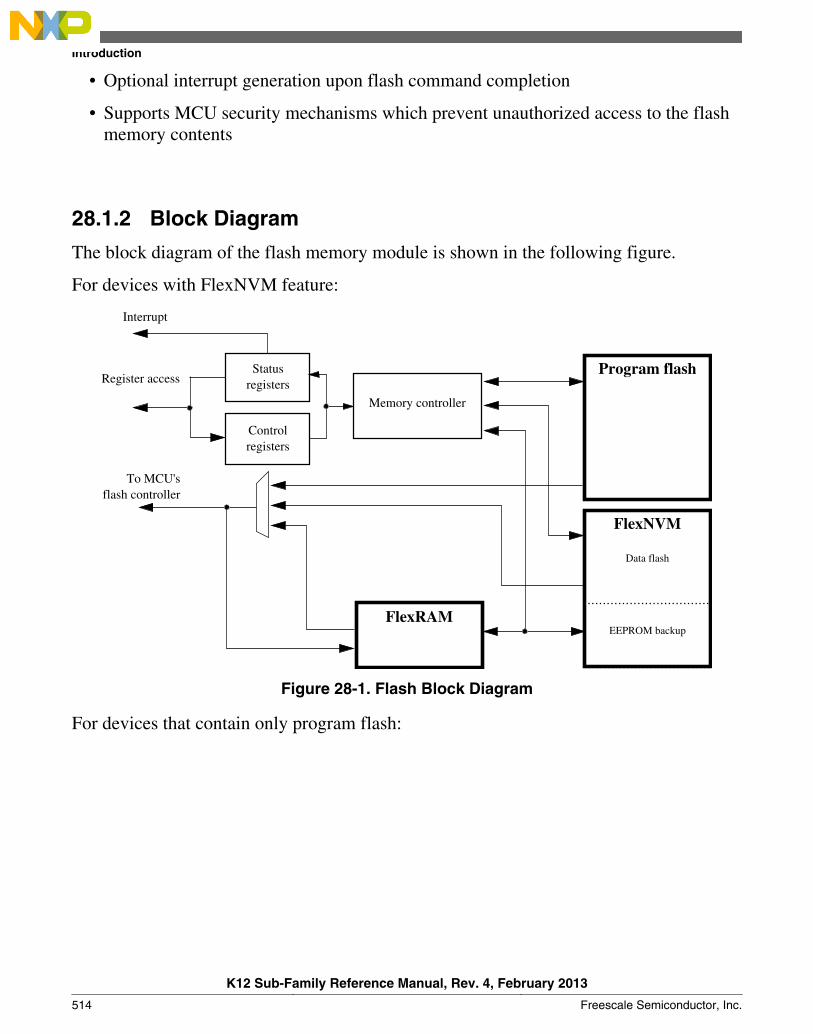
• Optional interrupt generation upon flash command completion
• Supports MCU security mechanisms which prevent unauthorized access to the flashmemory contents
28.1.2 Block Diagram
The block diagram of the flash memory module is shown in the following figure.
For devices with FlexNVM feature:
FlexNVM
FlexRAM
Program flash
EEPROM backup
To MCU's flash controller
Interrupt
Control registers
Status registersRegister access
Data flash
Memory controller
Figure 28-1. Flash Block Diagram
For devices that contain only program flash:
Introduction
K12 Sub-Family Reference Manual, Rev. 4, February 2013
514 Freescale Semiconductor, Inc.
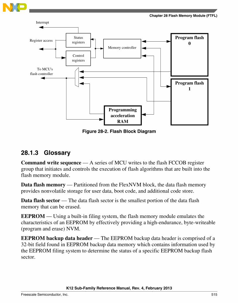
Program flash 1
Programming acceleration
RAM
Program flash 0
To MCU's flash controller
Interrupt
Control registers
Status registersRegister access
Memory controller
Figure 28-2. Flash Block Diagram
28.1.3 Glossary
Command write sequence — A series of MCU writes to the flash FCCOB registergroup that initiates and controls the execution of flash algorithms that are built into theflash memory module.
Data flash memory — Partitioned from the FlexNVM block, the data flash memoryprovides nonvolatile storage for user data, boot code, and additional code store.
Data flash sector — The data flash sector is the smallest portion of the data flashmemory that can be erased.
EEPROM — Using a built-in filing system, the flash memory module emulates thecharacteristics of an EEPROM by effectively providing a high-endurance, byte-writeable(program and erase) NVM.
EEPROM backup data header — The EEPROM backup data header is comprised of a32-bit field found in EEPROM backup data memory which contains information used bythe EEPROM filing system to determine the status of a specific EEPROM backup flashsector.
Chapter 28 Flash Memory Module (FTFL)
K12 Sub-Family Reference Manual, Rev. 4, February 2013
Freescale Semiconductor, Inc. 515
EEPROM backup data record — The EEPROM backup data record is comprised of a2-bit status field, a 14-bit address field, and a 16-bit data field found in EEPROM backupdata memory which is used by the EEPROM filing system. If the status field indicates arecord is valid, the data field is mirrored in the FlexRAM at a location determined by theaddress field.
EEPROM backup data memory — Partitioned from the FlexNVM block, EEPROMbackup data memory provides nonvolatile storage for the EEPROM filing systemrepresenting data written to the FlexRAM requiring highest endurance.
EEPROM backup data sector — The EEPROM backup data sector contains oneEEPROM backup data header and up to 255 EEPROM backup data records, which areused by the EEPROM filing system.
Endurance — The number of times that a flash memory location can be erased andreprogrammed.
FCCOB (Flash Common Command Object) — A group of flash registers that are usedto pass command, address, data, and any associated parameters to the memory controllerin the flash memory module.
Flash block — A macro within the flash memory module which provides the nonvolatilememory storage.
FlexMemory — Flash configuration that supports data flash, EEPROM, and FlexRAM.
FlexNVM Block — The FlexNVM block can be configured to be used as data flashmemory, EEPROM backup flash memory, or a combination of both.
FlexRAM — The FlexRAM refers to a RAM, dedicated to the flash memory module,that can be configured to store EEPROM data or as traditional RAM. When configuredfor EEPROM, valid writes to the FlexRAM generate new EEPROM backup data recordsstored in the EEPROM backup flash memory.
Flash Memory Module — All flash blocks plus a flash management unit providinghigh-level control and an interface to MCU buses.
IFR — Nonvolatile information register found in each flash block, separate from themain memory array.
NVM — Nonvolatile memory. A memory technology that maintains stored data duringpower-off. The flash array is an NVM using NOR-type flash memory technology.
NVM Normal Mode — An NVM mode that provides basic user access to flash memorymodule resources. The CPU or other bus masters initiate flash program and eraseoperations (or other flash commands) using writes to the FCCOB register group in theflash memory module.
Introduction
K12 Sub-Family Reference Manual, Rev. 4, February 2013
516 Freescale Semiconductor, Inc.
NVM Special Mode — An NVM mode enabling external, off-chip access to the memoryresources in the flash memory module. A reduced flash command set is available whenthe MCU is secured. See the Chip Configuration details for information on when thismode is used.
Phrase — 64 bits of data with an aligned phrase having byte-address[2:0] = 000.
Longword — 32 bits of data with an aligned longword having byte-address[1:0] = 00.
Word — 16 bits of data with an aligned word having byte-address[0] = 0.
Program flash — The program flash memory provides nonvolatile storage for vectorsand code store.
Program flash Sector — The smallest portion of the program flash memory(consecutive addresses) that can be erased.
Retention — The length of time that data can be kept in the NVM without experiencingerrors upon readout. Since erased (1) states are subject to degradation just likeprogrammed (0) states, the data retention limit may be reached from the last eraseoperation (not from the programming time).
RWW— Read-While-Write. The ability to simultaneously read from one memoryresource while commanded operations are active in another memory resource.
Section Program Buffer — Lower half of the programming acceleration RAM orFlexRAM allocated for storing large amounts of data for programming via the ProgramSection command.
Secure — An MCU state conveyed to the flash memory module as described in the ChipConfiguration details for this device. In the secure state, reading and changing NVMcontents is restricted.
28.2 External Signal DescriptionThe flash memory module contains no signals that connect off-chip.
28.3 Memory Map and RegistersThis section describes the memory map and registers for the flash memory module. Dataread from unimplemented memory space in the flash memory module is undefined.Writes to unimplemented or reserved memory space (registers) in the flash memorymodule are ignored.
Chapter 28 Flash Memory Module (FTFL)
K12 Sub-Family Reference Manual, Rev. 4, February 2013
Freescale Semiconductor, Inc. 517

28.3.1 Flash Configuration Field Description
The program flash memory contains a 16-byte flash configuration field that stores defaultprotection settings (loaded on reset) and security information that allows the MCU torestrict access to the flash memory module.
Flash Configuration Field ByteAddress
Size (Bytes) Field Description
0x0_0400 - 0x0_0407 8 Backdoor Comparison Key. Refer toVerify Backdoor Access Key Commandand Unsecuring the Chip UsingBackdoor Key Access.
0x0_0408 - 0x0_040B 4 Program flash protection bytes. Refer tothe description of the Program FlashProtection Registers (FPROT0-3).
0x0_040F 1 Program flash only devices: Reserved
FlexNVM devices: Data flash protectionbyte. Refer to the description of theData Flash Protection Register(FDPROT).
0x0_040E 1 Program flash only devices: Reserved
FlexNVM devices: EEPROM protectionbyte. Refer to the description of theEEPROM Protection Register(FEPROT).
0x0_040D 1 Flash nonvolatile option byte. Refer tothe description of the Flash OptionRegister (FOPT).
0x0_040C 1 Flash security byte. Refer to thedescription of the Flash SecurityRegister (FSEC).
28.3.2 Program Flash IFR Map
The program flash IFR is nonvolatile information memory that can be read freely, but theuser has no erase and limited program capabilities (see the Read Once, Program Once,and Read Resource commands in Read Once Command, Program Once Command andRead Resource Command). The contents of the program flash IFR are summarized in thefollowing table and further described in the subsequent paragraphs.
The program flash IFR is located within the program flash 0 memory block for devicesthat only contain program flash.
Memory Map and Registers
K12 Sub-Family Reference Manual, Rev. 4, February 2013
518 Freescale Semiconductor, Inc.
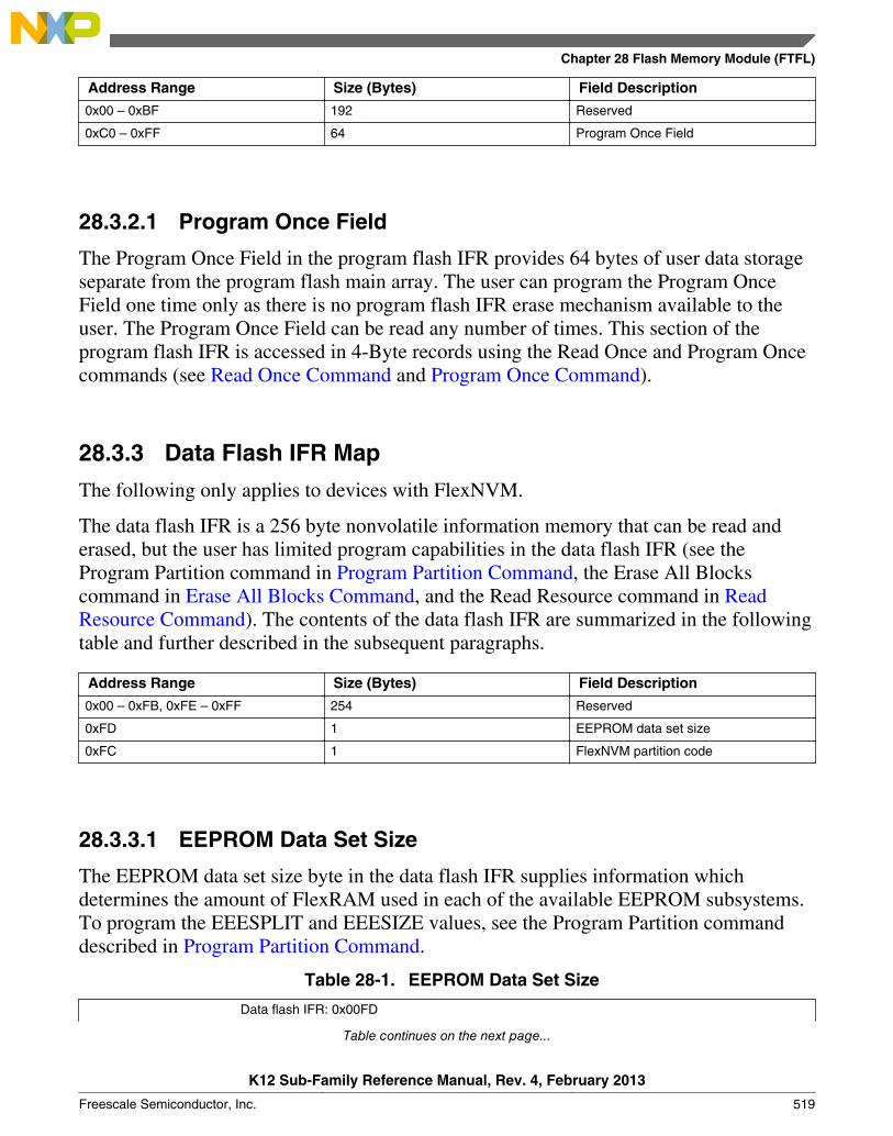
Address Range Size (Bytes) Field Description
0x00 – 0xBF 192 Reserved
0xC0 – 0xFF 64 Program Once Field
28.3.2.1 Program Once Field
The Program Once Field in the program flash IFR provides 64 bytes of user data storageseparate from the program flash main array. The user can program the Program OnceField one time only as there is no program flash IFR erase mechanism available to theuser. The Program Once Field can be read any number of times. This section of theprogram flash IFR is accessed in 4-Byte records using the Read Once and Program Oncecommands (see Read Once Command and Program Once Command).
28.3.3 Data Flash IFR Map
The following only applies to devices with FlexNVM.
The data flash IFR is a 256 byte nonvolatile information memory that can be read anderased, but the user has limited program capabilities in the data flash IFR (see theProgram Partition command in Program Partition Command, the Erase All Blockscommand in Erase All Blocks Command, and the Read Resource command in ReadResource Command). The contents of the data flash IFR are summarized in the followingtable and further described in the subsequent paragraphs.
Address Range Size (Bytes) Field Description
0x00 – 0xFB, 0xFE – 0xFF 254 Reserved
0xFD 1 EEPROM data set size
0xFC 1 FlexNVM partition code
28.3.3.1 EEPROM Data Set Size
The EEPROM data set size byte in the data flash IFR supplies information whichdetermines the amount of FlexRAM used in each of the available EEPROM subsystems.To program the EEESPLIT and EEESIZE values, see the Program Partition commanddescribed in Program Partition Command.
Table 28-1. EEPROM Data Set Size
Data flash IFR: 0x00FD
Table continues on the next page...
Chapter 28 Flash Memory Module (FTFL)
K12 Sub-Family Reference Manual, Rev. 4, February 2013
Freescale Semiconductor, Inc. 519
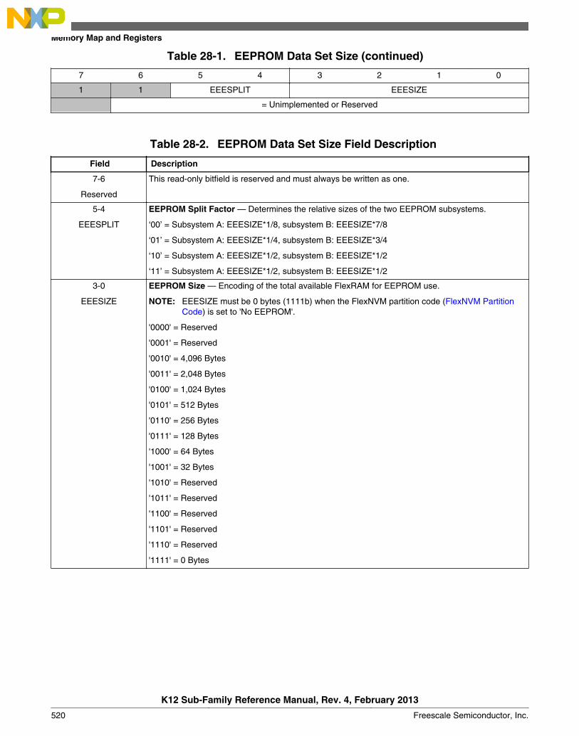
Table 28-1. EEPROM Data Set Size (continued)
7 6 5 4 3 2 1 0
1 1 EEESPLIT EEESIZE
= Unimplemented or Reserved
Table 28-2. EEPROM Data Set Size Field Description
Field Description
7-6
Reserved
This read-only bitfield is reserved and must always be written as one.
5-4
EEESPLIT
EEPROM Split Factor — Determines the relative sizes of the two EEPROM subsystems.
‘00’ = Subsystem A: EEESIZE*1/8, subsystem B: EEESIZE*7/8
‘01’ = Subsystem A: EEESIZE*1/4, subsystem B: EEESIZE*3/4
‘10’ = Subsystem A: EEESIZE*1/2, subsystem B: EEESIZE*1/2
‘11’ = Subsystem A: EEESIZE*1/2, subsystem B: EEESIZE*1/2
3-0
EEESIZE
EEPROM Size — Encoding of the total available FlexRAM for EEPROM use.
NOTE: EEESIZE must be 0 bytes (1111b) when the FlexNVM partition code (FlexNVM PartitionCode) is set to 'No EEPROM'.
'0000' = Reserved
'0001' = Reserved
'0010' = 4,096 Bytes
'0011' = 2,048 Bytes
'0100' = 1,024 Bytes
'0101' = 512 Bytes
'0110' = 256 Bytes
'0111' = 128 Bytes
'1000' = 64 Bytes
'1001' = 32 Bytes
'1010' = Reserved
'1011' = Reserved
'1100' = Reserved
'1101' = Reserved
'1110' = Reserved
'1111' = 0 Bytes
Memory Map and Registers
K12 Sub-Family Reference Manual, Rev. 4, February 2013
520 Freescale Semiconductor, Inc.

28.3.3.2 FlexNVM Partition Code
The FlexNVM Partition Code byte in the data flash IFR supplies a code which specifieshow to split the FlexNVM block between data flash memory and EEPROM backupmemory supporting EEPROM functions. To program the DEPART value, see theProgram Partition command described in Program Partition Command.
Table 28-3. FlexNVM Partition Code
Data Flash IFR: 0x00FC
7 6 5 4 3 2 1 0
1 1 1 1 DEPART
= Unimplemented or Reserved
Table 28-4. FlexNVM Partition Code Field Description
Field Description
7-4
Reserved
This read-only bitfield is reserved and must always be written as one.
3-0
DEPART
FlexNVM Partition Code — Encoding of the data flash / EEPROM backup split within the FlexNVMmemory block. FlexNVM memory not partitioned for data flash will be used to store EEPROMrecords.
DEPART Data flash (KB) EEPROM backup (KB)
0000 64 0
0001 Reserved Reserved
0010 Reserved Reserved
0011 32 32
0100 0 64
0101 Reserved Reserved
0110 Reserved Reserved
0111 Reserved Reserved
1000 0 64
1001 Reserved Reserved
1010 Reserved Reserved
1011 32 32
1100 64 0
1101 Reserved Reserved
1110 Reserved Reserved
1111 Reserved (defaults to 64) Reserved (defaults to 0)
Chapter 28 Flash Memory Module (FTFL)
K12 Sub-Family Reference Manual, Rev. 4, February 2013
Freescale Semiconductor, Inc. 521

28.3.4 Register Descriptions
The flash memory module contains a set of memory-mapped control and status registers.
NOTEWhile a command is running (FSTAT[CCIF]=0), registerwrites are not accepted to any register except FCNFG andFSTAT. The no-write rule is relaxed during the start-up resetsequence, prior to the initial rise of CCIF. During thisinitialization period the user may write any register. All registerwrites are also disabled (except for registers FCNFG andFSTAT) whenever an erase suspend request is active(FCNFG[ERSSUSP]=1).
FTFL memory map
Absoluteaddress
(hex)Register name
Width(in bits)
Access Reset valueSection/
page
4002_0000 Flash Status Register (FTFL_FSTAT) 8 R/W 00h28.34.1/
523
4002_0001 Flash Configuration Register (FTFL_FCNFG) 8 R/W See section28.34.2/
525
4002_0002 Flash Security Register (FTFL_FSEC) 8 R Undefined28.34.3/
527
4002_0003 Flash Option Register (FTFL_FOPT) 8 R Undefined28.34.4/
528
4002_0004Flash Common Command Object Registers(FTFL_FCCOB3)
8 R/W 00h28.34.5/
529
4002_0005Flash Common Command Object Registers(FTFL_FCCOB2)
8 R/W 00h28.34.5/
529
4002_0006Flash Common Command Object Registers(FTFL_FCCOB1)
8 R/W 00h28.34.5/
529
4002_0007Flash Common Command Object Registers(FTFL_FCCOB0)
8 R/W 00h28.34.5/
529
4002_0008Flash Common Command Object Registers(FTFL_FCCOB7)
8 R/W 00h28.34.5/
529
4002_0009Flash Common Command Object Registers(FTFL_FCCOB6)
8 R/W 00h28.34.5/
529
4002_000AFlash Common Command Object Registers(FTFL_FCCOB5)
8 R/W 00h28.34.5/
529
4002_000BFlash Common Command Object Registers(FTFL_FCCOB4)
8 R/W 00h28.34.5/
529
4002_000CFlash Common Command Object Registers(FTFL_FCCOBB)
8 R/W 00h28.34.5/
529
4002_000DFlash Common Command Object Registers(FTFL_FCCOBA)
8 R/W 00h28.34.5/
529
Table continues on the next page...
Memory Map and Registers
K12 Sub-Family Reference Manual, Rev. 4, February 2013
522 Freescale Semiconductor, Inc.

FTFL memory map (continued)
Absoluteaddress
(hex)Register name
Width(in bits)
Access Reset valueSection/
page
4002_000EFlash Common Command Object Registers(FTFL_FCCOB9)
8 R/W 00h28.34.5/
529
4002_000FFlash Common Command Object Registers(FTFL_FCCOB8)
8 R/W 00h28.34.5/
529
4002_0010 Program Flash Protection Registers (FTFL_FPROT3) 8 R/W Undefined28.34.6/
530
4002_0011 Program Flash Protection Registers (FTFL_FPROT2) 8 R/W Undefined28.34.6/
530
4002_0012 Program Flash Protection Registers (FTFL_FPROT1) 8 R/W Undefined28.34.6/
530
4002_0013 Program Flash Protection Registers (FTFL_FPROT0) 8 R/W Undefined28.34.6/
530
4002_0016 EEPROM Protection Register (FTFL_FEPROT) 8 R/W Undefined28.34.7/
532
4002_0017 Data Flash Protection Register (FTFL_FDPROT) 8 R/W Undefined28.34.8/
533
28.34.1 Flash Status Register (FTFL_FSTAT)
The FSTAT register reports the operational status of the flash memory module.
The CCIF, RDCOLERR, ACCERR, and FPVIOL bits are readable and writable. TheMGSTAT0 bit is read only. The unassigned bits read 0 and are not writable.
NOTEWhen set, the Access Error (ACCERR) and Flash ProtectionViolation (FPVIOL) bits in this register prevent the launch ofany more commands or writes to the FlexRAM (whenEEERDY is set) until the flag is cleared (by writing a one to it).
Address: 4002_0000h base + 0h offset = 4002_0000h
Bit 7 6 5 4 3 2 1 0
Read CCIF RDCOLERR ACCERR FPVIOL 0 MGSTAT0
Write w1c w1c w1c w1c
Reset 0 0 0 0 0 0 0 0
FTFL_FSTAT field descriptions
Field Description
7CCIF
Command Complete Interrupt Flag
The CCIF flag indicates that a flash command or EEPROM file system operation has completed. TheCCIF flag is cleared by writing a 1 to CCIF to launch a command, and CCIF stays low until command
Table continues on the next page...
Chapter 28 Flash Memory Module (FTFL)
K12 Sub-Family Reference Manual, Rev. 4, February 2013
Freescale Semiconductor, Inc. 523

FTFL_FSTAT field descriptions (continued)
Field Description
completion or command violation. The CCIF flag is also cleared by a successful write to FlexRAM whileenabled for EEE, and CCIF stays low until the EEPROM file system has created the associated EEPROMdata record.
The CCIF bit is reset to 0 but is set to 1 by the memory controller at the end of the reset initializationsequence. Depending on how quickly the read occurs after reset release, the user may or may not see the0 hardware reset value.
0 Flash command or EEPROM file system operation in progress1 Flash command or EEPROM file system operation has completed
6RDCOLERR
Flash Read Collision Error Flag
The RDCOLERR error bit indicates that the MCU attempted a read from a flash memory resource thatwas being manipulated by a flash command (CCIF=0). Any simultaneous access is detected as a collisionerror by the block arbitration logic. The read data in this case cannot be guaranteed. The RDCOLERR bitis cleared by writing a 1 to it. Writing a 0 to RDCOLERR has no effect.
0 No collision error detected1 Collision error detected
5ACCERR
Flash Access Error Flag
The ACCERR error bit indicates an illegal access has occurred to a flash memory resource caused by aviolation of the command write sequence or issuing an illegal flash command. While ACCERR is set, theCCIF flag cannot be cleared to launch a command. The ACCERR bit is cleared by writing a 1 to it. Writinga 0 to the ACCERR bit has no effect.
0 No access error detected1 Access error detected
4FPVIOL
Flash Protection Violation Flag
The FPVIOL error bit indicates an attempt was made to program or erase an address in a protected areaof program flash or data flash memory during a command write sequence or a write was attempted to aprotected area of the FlexRAM while enabled for EEPROM. While FPVIOL is set, the CCIF flag cannot becleared to launch a command. The FPVIOL bit is cleared by writing a 1 to it. Writing a 0 to the FPVIOL bithas no effect.
0 No protection violation detected1 Protection violation detected
3–1Reserved
This field is reserved.This read-only field is reserved and always has the value 0.
0MGSTAT0
Memory Controller Command Completion Status Flag
The MGSTAT0 status flag is set if an error is detected during execution of a flash command or during theflash reset sequence. As a status flag, this bit cannot (and need not) be cleared by the user like the othererror flags in this register.
The value of the MGSTAT0 bit for "command-N" is valid only at the end of the "command-N" executionwhen CCIF=1 and before the next command has been launched. At some point during the execution of"command-N+1," the previous result is discarded and any previous error is cleared.
Memory Map and Registers
K12 Sub-Family Reference Manual, Rev. 4, February 2013
524 Freescale Semiconductor, Inc.

28.34.2 Flash Configuration Register (FTFL_FCNFG)
This register provides information on the current functional state of the flash memorymodule.
The erase control bits (ERSAREQ and ERSSUSP) have write restrictions.SWAP,PFLSH, RAMRDY, and EEERDY are read-only status bits . The unassigned bitsread as noted and are not writable. The reset values for the SWAP, PFLASH,RAMRDY , and EEERDY bits are determined during the reset sequence.
Address: 4002_0000h base + 1h offset = 4002_0001h
Bit 7 6 5 4 3 2 1 0
ReadCCIE RDCOLLIE
ERSAREQERSSUSP
SWAP PFLSH RAMRDY EEERDY
Write
Reset 0 0 0 0 * * * *
* Notes:SWAP field: Device specific value•PFLSH field: Device specific value•RAMRDY field: Device specific value•EEERDY field: Device specific value•
FTFL_FCNFG field descriptions
Field Description
7CCIE
Command Complete Interrupt Enable
The CCIE bit controls interrupt generation when a flash command completes.
0 Command complete interrupt disabled1 Command complete interrupt enabled. An interrupt request is generated whenever the FSTAT[CCIF]
flag is set.
6RDCOLLIE
Read Collision Error Interrupt Enable
The RDCOLLIE bit controls interrupt generation when a flash memory read collision error occurs.
0 Read collision error interrupt disabled1 Read collision error interrupt enabled. An interrupt request is generated whenever a flash memory
read collision error is detected (see the description of FSTAT[RDCOLERR]).
5ERSAREQ
Erase All Request
This bit issues a request to the memory controller to execute the Erase All Blocks command and releasesecurity. ERSAREQ is not directly writable but is under indirect user control. Refer to the device's ChipConfiguration details on how to request this command.
The ERSAREQ bit sets when an erase all request is triggered external to the flash memory module andCCIF is set (no command is currently being executed). ERSAREQ is cleared by the flash memory modulewhen the operation completes.
Table continues on the next page...
Chapter 28 Flash Memory Module (FTFL)
K12 Sub-Family Reference Manual, Rev. 4, February 2013
Freescale Semiconductor, Inc. 525

FTFL_FCNFG field descriptions (continued)
Field Description
0 No request or request complete1 Request to:
1. run the Erase All Blocks command,2. verify the erased state,3. program the security byte in the Flash Configuration Field to the unsecure state, and4. release MCU security by setting the FSEC[SEC] field to the unsecure state.
4ERSSUSP
Erase Suspend
The ERSSUSP bit allows the user to suspend (interrupt) the Erase Flash Sector command while it isexecuting.
0 No suspend requested1 Suspend the current Erase Flash Sector command execution.
3SWAP
Swap
For program flash only configurations, the SWAP flag indicates which physical program flash block islocated at relative address 0x0000. The state of the SWAP flag is set by the flash memory module duringthe reset sequence. See the Swap Control command section for information on swap management.
0 Physical program flash 0 is located at relative address 0x00001 If the PFLSH flag is set, physical program flash 1 is located at relative address 0x0000. If the PFLSH
flag is not set, physical program flash 0 is located at relative address 0x0000
2PFLSH
Flash memory configuration
0 For devices with FlexNVM: Flash memory module configured for FlexMemory that supports data flashand/or EEPROM. For devices with program flash only: Reserved
1 For devices with FlexNVM: Reserved. For devices with program flash only: Flash memory moduleconfigured for program flash only, without support for data flash and/or EEPROM
1RAMRDY
RAM Ready
This flag indicates the current status of the FlexRAM/programming acceleration RAM.
For devices with FlexNVM: The state of the RAMRDY flag is normally controlled by the Set FlexRAMFunction command. During the reset sequence, the RAMRDY flag is cleared if the FlexNVM block ispartitioned for EEPROM and is set if the FlexNVM block is not partitioned for EEPROM. The RAMRDYflag is cleared if the Program Partition command is run to partition the FlexNVM block for EEPROM. TheRAMRDY flag sets after completion of the Erase All Blocks command or execution of the erase-alloperation triggered external to the flash memory module.
For devices without FlexNVM: This bit should always be set.
0 For devices with FlexNVM: FlexRAM is not available for traditional RAM access. For devices withoutFlexNVM: Programming acceleration RAM is not available.
1 For devices with FlexNVM: FlexRAM is available as traditional RAM only; writes to the FlexRAM donot trigger EEPROM operations. For devices without FlexNVM: Programming acceleration RAM isavailable.
0EEERDY
For devices with FlexNVM: This flag indicates if the EEPROM backup data has been copied to theFlexRAM and is therefore available for read access. During the reset sequence, the EEERDY flag willremain cleared while CCIF is clear and will only set if the FlexNVM block is partitioned for EEPROM.
For devices without FlexNVM: This field is reserved.
0 For devices with FlexNVM: FlexRAM is not available for EEPROM operation.1 For devices with FlexNVM: FlexRAM is available for EEPROM operations where:
Table continues on the next page...
Memory Map and Registers
K12 Sub-Family Reference Manual, Rev. 4, February 2013
526 Freescale Semiconductor, Inc.
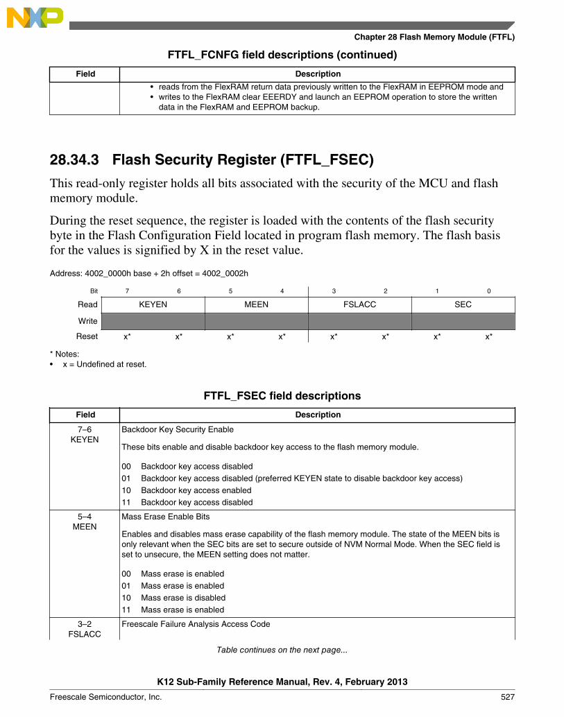
FTFL_FCNFG field descriptions (continued)
Field Description
• reads from the FlexRAM return data previously written to the FlexRAM in EEPROM mode and• writes to the FlexRAM clear EEERDY and launch an EEPROM operation to store the written
data in the FlexRAM and EEPROM backup.
28.34.3 Flash Security Register (FTFL_FSEC)
This read-only register holds all bits associated with the security of the MCU and flashmemory module.
During the reset sequence, the register is loaded with the contents of the flash securitybyte in the Flash Configuration Field located in program flash memory. The flash basisfor the values is signified by X in the reset value.
Address: 4002_0000h base + 2h offset = 4002_0002h
Bit 7 6 5 4 3 2 1 0
Read KEYEN MEEN FSLACC SEC
Write
Reset x* x* x* x* x* x* x* x*
* Notes:x = Undefined at reset.•
FTFL_FSEC field descriptions
Field Description
7–6KEYEN
Backdoor Key Security Enable
These bits enable and disable backdoor key access to the flash memory module.
00 Backdoor key access disabled01 Backdoor key access disabled (preferred KEYEN state to disable backdoor key access)10 Backdoor key access enabled11 Backdoor key access disabled
5–4MEEN
Mass Erase Enable Bits
Enables and disables mass erase capability of the flash memory module. The state of the MEEN bits isonly relevant when the SEC bits are set to secure outside of NVM Normal Mode. When the SEC field isset to unsecure, the MEEN setting does not matter.
00 Mass erase is enabled01 Mass erase is enabled10 Mass erase is disabled11 Mass erase is enabled
3–2FSLACC
Freescale Failure Analysis Access Code
Table continues on the next page...
Chapter 28 Flash Memory Module (FTFL)
K12 Sub-Family Reference Manual, Rev. 4, February 2013
Freescale Semiconductor, Inc. 527
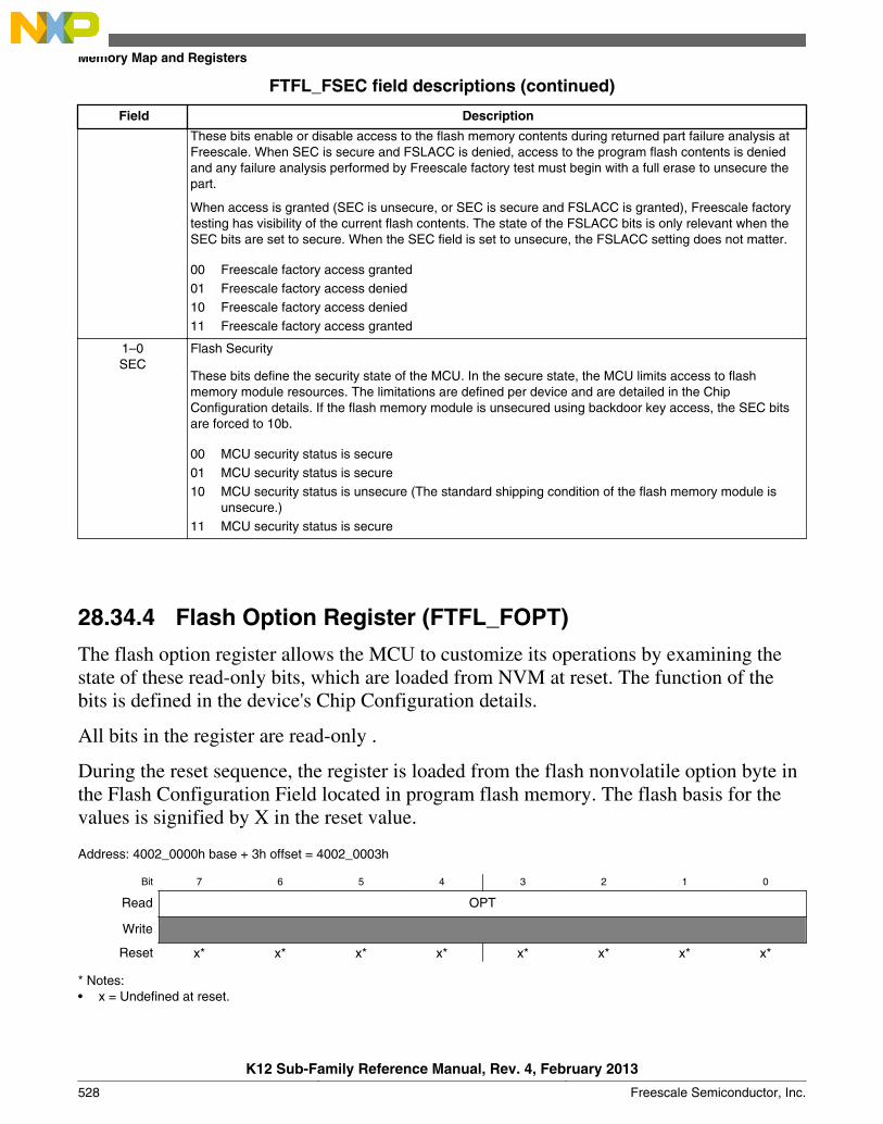
FTFL_FSEC field descriptions (continued)
Field Description
These bits enable or disable access to the flash memory contents during returned part failure analysis atFreescale. When SEC is secure and FSLACC is denied, access to the program flash contents is deniedand any failure analysis performed by Freescale factory test must begin with a full erase to unsecure thepart.
When access is granted (SEC is unsecure, or SEC is secure and FSLACC is granted), Freescale factorytesting has visibility of the current flash contents. The state of the FSLACC bits is only relevant when theSEC bits are set to secure. When the SEC field is set to unsecure, the FSLACC setting does not matter.
00 Freescale factory access granted01 Freescale factory access denied10 Freescale factory access denied11 Freescale factory access granted
1–0SEC
Flash Security
These bits define the security state of the MCU. In the secure state, the MCU limits access to flashmemory module resources. The limitations are defined per device and are detailed in the ChipConfiguration details. If the flash memory module is unsecured using backdoor key access, the SEC bitsare forced to 10b.
00 MCU security status is secure01 MCU security status is secure10 MCU security status is unsecure (The standard shipping condition of the flash memory module is
unsecure.)11 MCU security status is secure
28.34.4 Flash Option Register (FTFL_FOPT)
The flash option register allows the MCU to customize its operations by examining thestate of these read-only bits, which are loaded from NVM at reset. The function of thebits is defined in the device's Chip Configuration details.
All bits in the register are read-only .
During the reset sequence, the register is loaded from the flash nonvolatile option byte inthe Flash Configuration Field located in program flash memory. The flash basis for thevalues is signified by X in the reset value.
Address: 4002_0000h base + 3h offset = 4002_0003h
Bit 7 6 5 4 3 2 1 0
Read OPT
Write
Reset x* x* x* x* x* x* x* x*
* Notes:x = Undefined at reset.•
Memory Map and Registers
K12 Sub-Family Reference Manual, Rev. 4, February 2013
528 Freescale Semiconductor, Inc.

FTFL_FOPT field descriptions
Field Description
7–0OPT
Nonvolatile Option
These bits are loaded from flash to this register at reset. Refer to the device's Chip Configuration detailsfor the definition and use of these bits.
28.34.5 Flash Common Command Object Registers(FTFL_FCCOBn)
The FCCOB register group provides 12 bytes for command codes and parameters. Theindividual bytes within the set append a 0-B hex identifier to the FCCOB register name:FCCOB0, FCCOB1, ..., FCCOBB.
Address: 4002_0000h base + 4h offset + (1d × i), where i=0d to 11d
Bit 7 6 5 4 3 2 1 0
Read CCOBnWriteReset 0 0 0 0 0 0 0 0
FTFL_FCCOBn field descriptions
Field Description
7–0CCOBn
The FCCOB register provides a command code and relevant parameters to the memory controller. Theindividual registers that compose the FCCOB data set can be written in any order, but you must provide allneeded values, which vary from command to command. First, set up all required FCCOB fields and theninitiate the command’s execution by writing a 1 to the FSTAT[CCIF] bit. This clears the CCIF bit, whichlocks all FCCOB parameter fields and they cannot be changed by the user until the command completes(CCIF returns to 1). No command buffering or queueing is provided; the next command can be loadedonly after the current command completes.
Some commands return information to the FCCOB registers. Any values returned to FCCOB are availablefor reading after the FSTAT[CCIF] flag returns to 1 by the memory controller.
The following table shows a generic flash command format. The first FCCOB register, FCCOB0, alwayscontains the command code. This 8-bit value defines the command to be executed. The command code isfollowed by the parameters required for this specific flash command, typically an address and/or datavalues.
NOTE: The command parameter table is written in terms of FCCOB Number (which is equivalent to thebyte number). This number is a reference to the FCCOB register name and is not the registeraddress.
FCCOB Number Typical Command Parameter Contents [7:0]
0 FCMD (a code that defines the flash command)
1 Flash address [23:16]
2 Flash address [15:8]
3 Flash address [7:0]
Chapter 28 Flash Memory Module (FTFL)
K12 Sub-Family Reference Manual, Rev. 4, February 2013
Freescale Semiconductor, Inc. 529
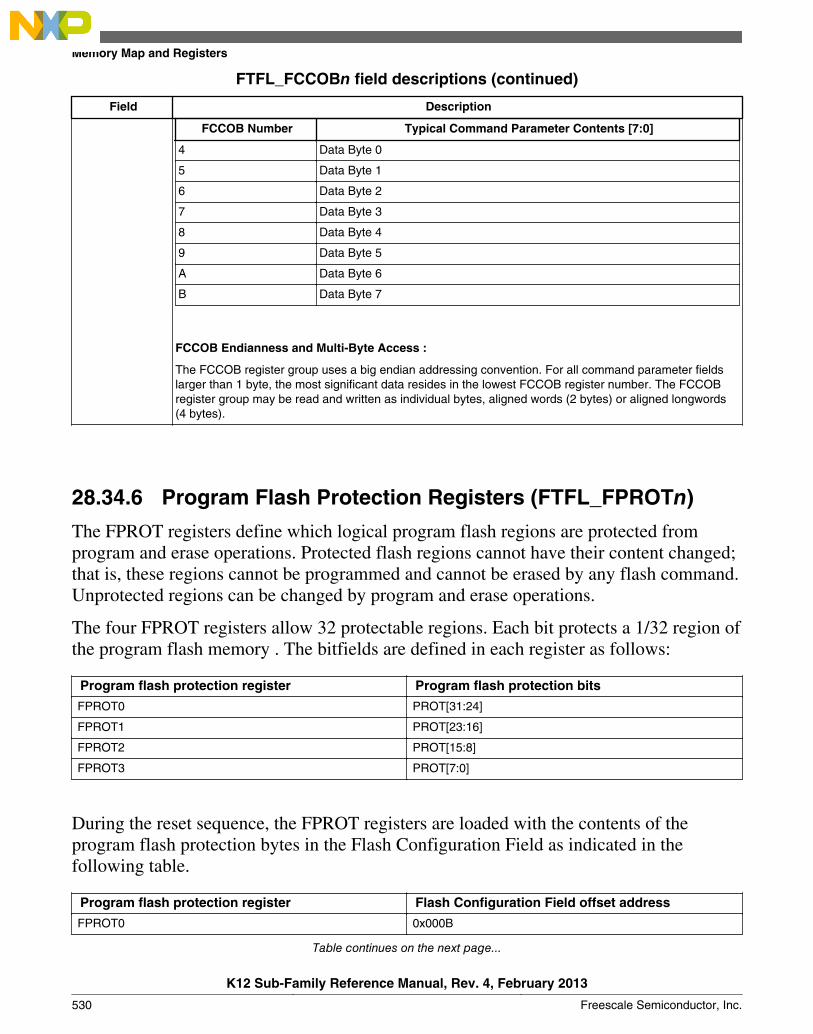
FTFL_FCCOBn field descriptions (continued)
Field Description
FCCOB Number Typical Command Parameter Contents [7:0]
4 Data Byte 0
5 Data Byte 1
6 Data Byte 2
7 Data Byte 3
8 Data Byte 4
9 Data Byte 5
A Data Byte 6
B Data Byte 7
FCCOB Endianness and Multi-Byte Access :
The FCCOB register group uses a big endian addressing convention. For all command parameter fieldslarger than 1 byte, the most significant data resides in the lowest FCCOB register number. The FCCOBregister group may be read and written as individual bytes, aligned words (2 bytes) or aligned longwords(4 bytes).
28.34.6 Program Flash Protection Registers (FTFL_FPROTn)
The FPROT registers define which logical program flash regions are protected fromprogram and erase operations. Protected flash regions cannot have their content changed;that is, these regions cannot be programmed and cannot be erased by any flash command.Unprotected regions can be changed by program and erase operations.
The four FPROT registers allow 32 protectable regions. Each bit protects a 1/32 region ofthe program flash memory . The bitfields are defined in each register as follows:
Program flash protection register Program flash protection bits
FPROT0 PROT[31:24]
FPROT1 PROT[23:16]
FPROT2 PROT[15:8]
FPROT3 PROT[7:0]
During the reset sequence, the FPROT registers are loaded with the contents of theprogram flash protection bytes in the Flash Configuration Field as indicated in thefollowing table.
Program flash protection register Flash Configuration Field offset address
FPROT0 0x000B
Table continues on the next page...
Memory Map and Registers
K12 Sub-Family Reference Manual, Rev. 4, February 2013
530 Freescale Semiconductor, Inc.
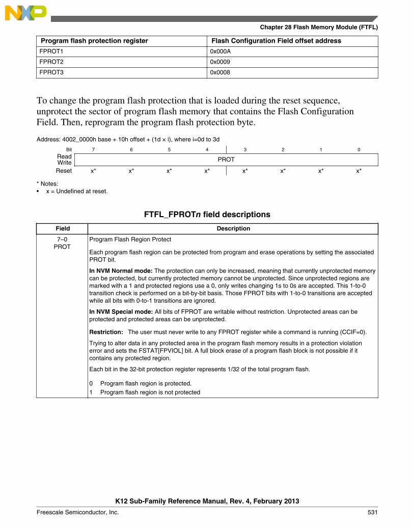
Program flash protection register Flash Configuration Field offset address
FPROT1 0x000A
FPROT2 0x0009
FPROT3 0x0008
To change the program flash protection that is loaded during the reset sequence,unprotect the sector of program flash memory that contains the Flash ConfigurationField. Then, reprogram the program flash protection byte.
Address: 4002_0000h base + 10h offset + (1d × i), where i=0d to 3d
Bit 7 6 5 4 3 2 1 0
Read PROTWriteReset x* x* x* x* x* x* x* x*
* Notes:x = Undefined at reset.•
FTFL_FPROTn field descriptions
Field Description
7–0PROT
Program Flash Region Protect
Each program flash region can be protected from program and erase operations by setting the associatedPROT bit.
In NVM Normal mode: The protection can only be increased, meaning that currently unprotected memorycan be protected, but currently protected memory cannot be unprotected. Since unprotected regions aremarked with a 1 and protected regions use a 0, only writes changing 1s to 0s are accepted. This 1-to-0transition check is performed on a bit-by-bit basis. Those FPROT bits with 1-to-0 transitions are acceptedwhile all bits with 0-to-1 transitions are ignored.
In NVM Special mode: All bits of FPROT are writable without restriction. Unprotected areas can beprotected and protected areas can be unprotected.
Restriction: The user must never write to any FPROT register while a command is running (CCIF=0).
Trying to alter data in any protected area in the program flash memory results in a protection violationerror and sets the FSTAT[FPVIOL] bit. A full block erase of a program flash block is not possible if itcontains any protected region.
Each bit in the 32-bit protection register represents 1/32 of the total program flash.
0 Program flash region is protected.1 Program flash region is not protected
Chapter 28 Flash Memory Module (FTFL)
K12 Sub-Family Reference Manual, Rev. 4, February 2013
Freescale Semiconductor, Inc. 531
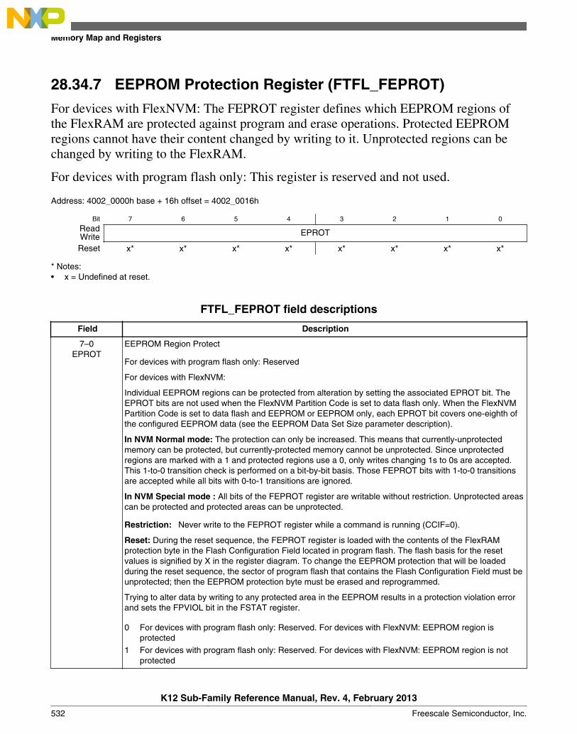
28.34.7 EEPROM Protection Register (FTFL_FEPROT)
For devices with FlexNVM: The FEPROT register defines which EEPROM regions ofthe FlexRAM are protected against program and erase operations. Protected EEPROMregions cannot have their content changed by writing to it. Unprotected regions can bechanged by writing to the FlexRAM.
For devices with program flash only: This register is reserved and not used.
Address: 4002_0000h base + 16h offset = 4002_0016h
Bit 7 6 5 4 3 2 1 0
Read EPROTWriteReset x* x* x* x* x* x* x* x*
* Notes:x = Undefined at reset.•
FTFL_FEPROT field descriptions
Field Description
7–0EPROT
EEPROM Region Protect
For devices with program flash only: Reserved
For devices with FlexNVM:
Individual EEPROM regions can be protected from alteration by setting the associated EPROT bit. TheEPROT bits are not used when the FlexNVM Partition Code is set to data flash only. When the FlexNVMPartition Code is set to data flash and EEPROM or EEPROM only, each EPROT bit covers one-eighth ofthe configured EEPROM data (see the EEPROM Data Set Size parameter description).
In NVM Normal mode: The protection can only be increased. This means that currently-unprotectedmemory can be protected, but currently-protected memory cannot be unprotected. Since unprotectedregions are marked with a 1 and protected regions use a 0, only writes changing 1s to 0s are accepted.This 1-to-0 transition check is performed on a bit-by-bit basis. Those FEPROT bits with 1-to-0 transitionsare accepted while all bits with 0-to-1 transitions are ignored.
In NVM Special mode : All bits of the FEPROT register are writable without restriction. Unprotected areascan be protected and protected areas can be unprotected.
Restriction: Never write to the FEPROT register while a command is running (CCIF=0).
Reset: During the reset sequence, the FEPROT register is loaded with the contents of the FlexRAMprotection byte in the Flash Configuration Field located in program flash. The flash basis for the resetvalues is signified by X in the register diagram. To change the EEPROM protection that will be loadedduring the reset sequence, the sector of program flash that contains the Flash Configuration Field must beunprotected; then the EEPROM protection byte must be erased and reprogrammed.
Trying to alter data by writing to any protected area in the EEPROM results in a protection violation errorand sets the FPVIOL bit in the FSTAT register.
0 For devices with program flash only: Reserved. For devices with FlexNVM: EEPROM region isprotected
1 For devices with program flash only: Reserved. For devices with FlexNVM: EEPROM region is notprotected
Memory Map and Registers
K12 Sub-Family Reference Manual, Rev. 4, February 2013
532 Freescale Semiconductor, Inc.
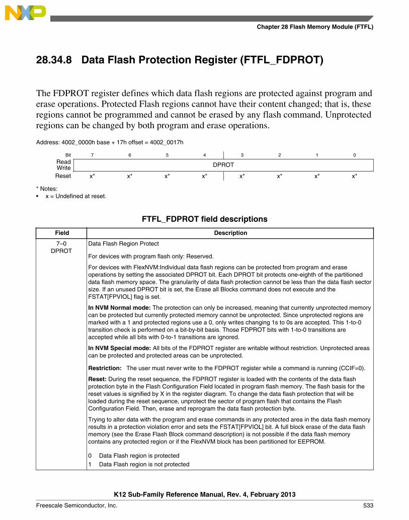
28.34.8 Data Flash Protection Register (FTFL_FDPROT)
The FDPROT register defines which data flash regions are protected against program anderase operations. Protected Flash regions cannot have their content changed; that is, theseregions cannot be programmed and cannot be erased by any flash command. Unprotectedregions can be changed by both program and erase operations.
Address: 4002_0000h base + 17h offset = 4002_0017h
Bit 7 6 5 4 3 2 1 0
Read DPROTWriteReset x* x* x* x* x* x* x* x*
* Notes:x = Undefined at reset.•
FTFL_FDPROT field descriptions
Field Description
7–0DPROT
Data Flash Region Protect
For devices with program flash only: Reserved.
For devices with FlexNVM:Individual data flash regions can be protected from program and eraseoperations by setting the associated DPROT bit. Each DPROT bit protects one-eighth of the partitioneddata flash memory space. The granularity of data flash protection cannot be less than the data flash sectorsize. If an unused DPROT bit is set, the Erase all Blocks command does not execute and theFSTAT[FPVIOL] flag is set.
In NVM Normal mode: The protection can only be increased, meaning that currently unprotected memorycan be protected but currently protected memory cannot be unprotected. Since unprotected regions aremarked with a 1 and protected regions use a 0, only writes changing 1s to 0s are accepted. This 1-to-0transition check is performed on a bit-by-bit basis. Those FDPROT bits with 1-to-0 transitions areaccepted while all bits with 0-to-1 transitions are ignored.
In NVM Special mode: All bits of the FDPROT register are writable without restriction. Unprotected areascan be protected and protected areas can be unprotected.
Restriction: The user must never write to the FDPROT register while a command is running (CCIF=0).
Reset: During the reset sequence, the FDPROT register is loaded with the contents of the data flashprotection byte in the Flash Configuration Field located in program flash memory. The flash basis for thereset values is signified by X in the register diagram. To change the data flash protection that will beloaded during the reset sequence, unprotect the sector of program flash that contains the FlashConfiguration Field. Then, erase and reprogram the data flash protection byte.
Trying to alter data with the program and erase commands in any protected area in the data flash memoryresults in a protection violation error and sets the FSTAT[FPVIOL] bit. A full block erase of the data flashmemory (see the Erase Flash Block command description) is not possible if the data flash memorycontains any protected region or if the FlexNVM block has been partitioned for EEPROM.
0 Data Flash region is protected1 Data Flash region is not protected
Chapter 28 Flash Memory Module (FTFL)
K12 Sub-Family Reference Manual, Rev. 4, February 2013
Freescale Semiconductor, Inc. 533
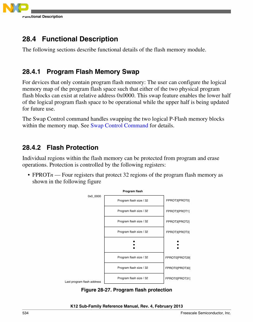
28.4 Functional DescriptionThe following sections describe functional details of the flash memory module.
28.4.1 Program Flash Memory Swap
For devices that only contain program flash memory: The user can configure the logicalmemory map of the program flash space such that either of the two physical programflash blocks can exist at relative address 0x0000. This swap feature enables the lower halfof the logical program flash space to be operational while the upper half is being updatedfor future use.
The Swap Control command handles swapping the two logical P-Flash memory blockswithin the memory map. See Swap Control Command for details.
28.4.2 Flash Protection
Individual regions within the flash memory can be protected from program and eraseoperations. Protection is controlled by the following registers:
• FPROTn — Four registers that protect 32 regions of the program flash memory asshown in the following figure
Program flash size / 32
Program flash size / 32
Program flash size / 32
Program flash size / 32
Program flash size / 32
Program flash size / 32
Program flash size / 32
FPROT3[PROT0]0x0_0000
FPROT3[PROT1]
FPROT3[PROT2]
FPROT3[PROT3]
FPROT0[PROT29]
FPROT0[PROT31]
FPROT0[PROT30]
Program flash
Last program flash address
Figure 28-27. Program flash protection
Functional Description
K12 Sub-Family Reference Manual, Rev. 4, February 2013
534 Freescale Semiconductor, Inc.
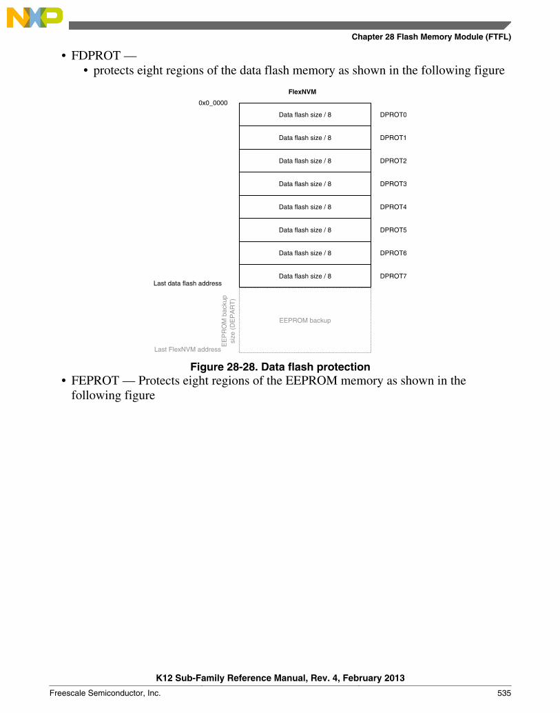
• FDPROT —• protects eight regions of the data flash memory as shown in the following figure
Data flash size / 8 DPROT0
0x0_0000
DPROT1
DPROT2
DPROT3
DPROT5
DPROT7
DPROT6
FlexNVM
Last data flash addressData flash size / 8
Data flash size / 8
Data flash size / 8
Data flash size / 8
Data flash size / 8
Data flash size / 8
Data flash size / 8
DPROT4
EEPROM backup
EE
PR
OM
bac
kup
size
(D
EP
AR
T)
Last FlexNVM address
Figure 28-28. Data flash protection• FEPROT — Protects eight regions of the EEPROM memory as shown in the
following figure
Chapter 28 Flash Memory Module (FTFL)
K12 Sub-Family Reference Manual, Rev. 4, February 2013
Freescale Semiconductor, Inc. 535
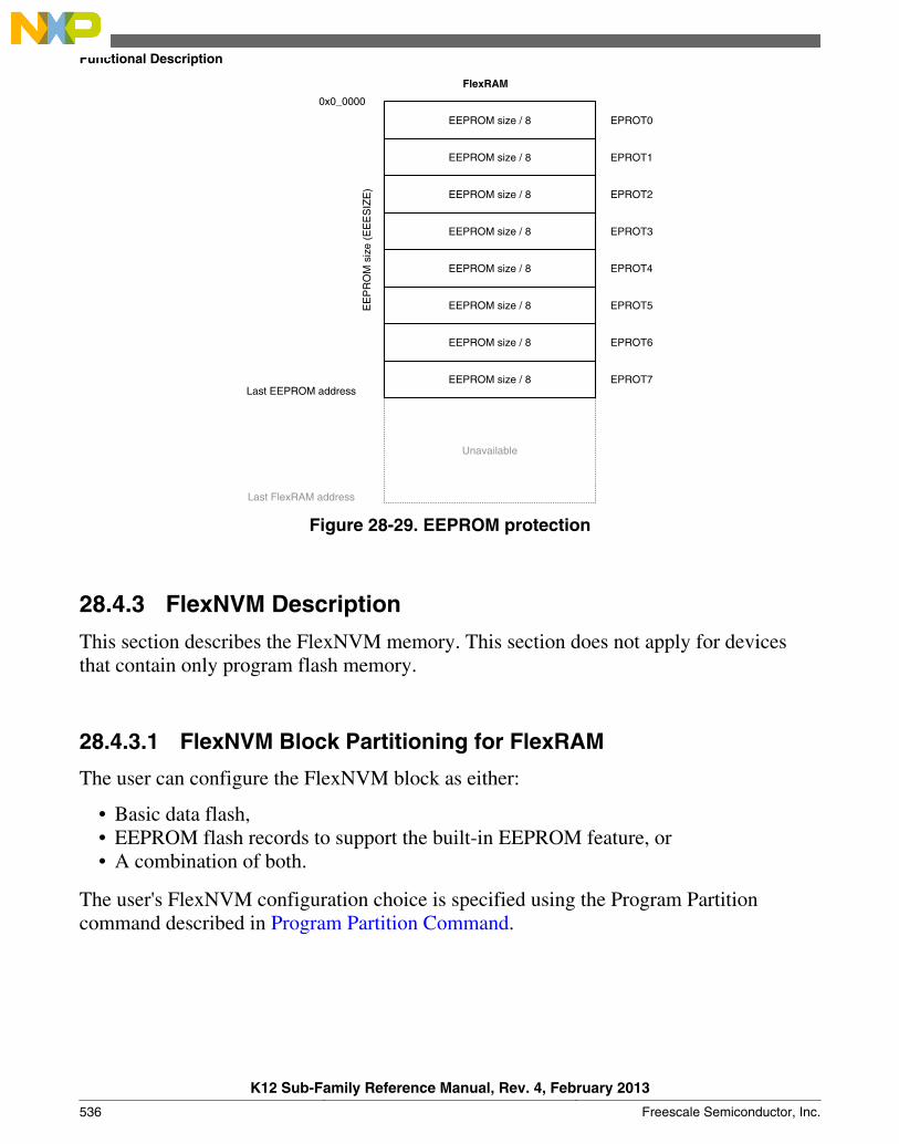
EEPROM size / 8 EPROT0
0x0_0000
EPROT1
EPROT2
EPROT5
EPROT7
EPROT6
FlexRAM
Last EEPROM addressEEPROM size / 8
EEPROM size / 8
EEPROM size / 8
EEPROM size / 8
EEPROM size / 8
EEPROM size / 8
EEPROM size / 8
EPROT3
EPROT4
Unavailable
EE
PR
OM
siz
e (E
EE
SIZ
E)
Last FlexRAM address
Figure 28-29. EEPROM protection
28.4.3 FlexNVM Description
This section describes the FlexNVM memory. This section does not apply for devicesthat contain only program flash memory.
28.4.3.1 FlexNVM Block Partitioning for FlexRAM
The user can configure the FlexNVM block as either:
• Basic data flash,• EEPROM flash records to support the built-in EEPROM feature, or• A combination of both.
The user's FlexNVM configuration choice is specified using the Program Partitioncommand described in Program Partition Command.
Functional Description
K12 Sub-Family Reference Manual, Rev. 4, February 2013
536 Freescale Semiconductor, Inc.

CAUTION
While different partitions of the FlexNVM block are available,the intention is that a single partition choice is used throughoutthe entire lifetime of a given application. The FlexNVMpartition code choices affect the endurance and data retentioncharacteristics of the device.
28.4.3.2 EEPROM User Perspective
The EEPROM system is shown in the following figure.
File system handler
User access (effective EEPROM)
FlexRAM EEPROM backupwith 1KByte
erase sectors
Figure 28-30. Top Level EEPROM Architecture
To handle varying customer requirements, the FlexRAM and FlexNVM blocks can besplit into partitions as shown in the figure below.
1. EEPROM partition (EEESIZE) — The amount of FlexRAM used for EEPROMcan be set from 0 Bytes (no EEPROM) to the maximum FlexRAM size (see Table28-2). The remainder of the FlexRAM is not accessible while the FlexRAM isconfigured for EEPROM (see Set FlexRAM Function Command). The EEPROMpartition grows upward from the bottom of the FlexRAM address space.
2. Data flash partition (DEPART) — The amount of FlexNVM memory used for dataflash can be programmed from 0 bytes (all of the FlexNVM block is available forEEPROM backup) to the maximum size of the FlexNVM block (see Table 28-4).
3. FlexNVM EEPROM partition — The amount of FlexNVM memory used forEEPROM backup, which is equal to the FlexNVM block size minus the data flashmemory partition size. The EEPROM backup size must be at least 16 times theEEPROM partition size in FlexRAM.
4. EEPROM split factor (EEESPLIT) — The FlexRAM partitioned for EEPROM canbe divided into two subsystems, each backed by half of the partitioned EEPROMbackup. One subsystem (A) is 1/8, 1/4, or 1/2 of the partitioned FlexRAM with theremainder belonging to the other subsystem (B).
Chapter 28 Flash Memory Module (FTFL)
K12 Sub-Family Reference Manual, Rev. 4, February 2013
Freescale Semiconductor, Inc. 537
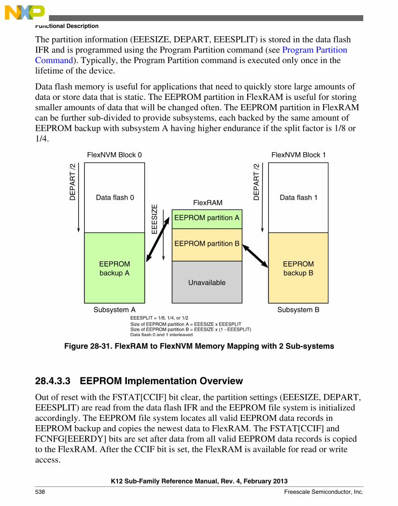
The partition information (EEESIZE, DEPART, EEESPLIT) is stored in the data flashIFR and is programmed using the Program Partition command (see Program PartitionCommand). Typically, the Program Partition command is executed only once in thelifetime of the device.
Data flash memory is useful for applications that need to quickly store large amounts ofdata or store data that is static. The EEPROM partition in FlexRAM is useful for storingsmaller amounts of data that will be changed often. The EEPROM partition in FlexRAMcan be further sub-divided to provide subsystems, each backed by the same amount ofEEPROM backup with subsystem A having higher endurance if the split factor is 1/8 or1/4.
FlexRAMData flash 1D
EP
AR
T /2
FlexNVM Block 1
Subsystem B
EE
ES
IZE
Unavailable
EEPROM partition A
DE
PA
RT
/2
FlexNVM Block 0
Subsystem A
Size of EEPROM partition A = EEESIZE x EEESPLIT
Data flash 0 and 1 interleaved
Data flash 0
EEPROM partition B
EEPROM backup A
EEESPLIT = 1/8, 1/4, or 1/2
Size of EEPROM partition B = EEESIZE x (1 - EEESPLIT)
EEPROM backup B
Figure 28-31. FlexRAM to FlexNVM Memory Mapping with 2 Sub-systems
28.4.3.3 EEPROM Implementation Overview
Out of reset with the FSTAT[CCIF] bit clear, the partition settings (EEESIZE, DEPART,EEESPLIT) are read from the data flash IFR and the EEPROM file system is initializedaccordingly. The EEPROM file system locates all valid EEPROM data records inEEPROM backup and copies the newest data to FlexRAM. The FSTAT[CCIF] andFCNFG[EEERDY] bits are set after data from all valid EEPROM data records is copiedto the FlexRAM. After the CCIF bit is set, the FlexRAM is available for read or writeaccess.
Functional Description
K12 Sub-Family Reference Manual, Rev. 4, February 2013
538 Freescale Semiconductor, Inc.
When configured for EEPROM use, writes to an unprotected location in FlexRAMinvokes the EEPROM file system to program a new EEPROM data record in theEEPROM backup memory in a round-robin fashion. As needed, the EEPROM filesystem identifies the EEPROM backup sector that is being erased for future use andpartially erases that EEPROM backup sector. After a write to the FlexRAM, theFlexRAM is not accessible until the FSTAT[CCIF] bit is set. The FCNFG[EEERDY] bitwill also be set. If enabled, the interrupt associated with the FSTAT[CCIF] bit can beused to determine when the FlexRAM is available for read or write access.
After a sector in EEPROM backup is full of EEPROM data records, EEPROM datarecords from the sector holding the oldest data are gradually copied over to a previously-erased EEPROM backup sector. When the sector copy completes, the EEPROM backupsector holding the oldest data is tagged for erase.
28.4.3.4 Write endurance to FlexRAM for EEPROM
When the FlexNVM partition code is not set to full data flash, the EEPROM data set sizecan be set to any of several non-zero values.
The bytes not assigned to data flash via the FlexNVM partition code are used by the flashmemory module to obtain an effective endurance increase for the EEPROM data. Thebuilt-in EEPROM record management system raises the number of program/erase cyclesthat can be attained prior to device wear-out by cycling the EEPROM data through alarger EEPROM NVM storage space.
While different partitions of the FlexNVM are available, the intention is that a singlechoice for the FlexNVM partition code and EEPROM data set size is used throughout theentire lifetime of a given application. The EEPROM endurance equation and graphshown below assume that only one configuration is ever used.
Writes_subsystem = × Write_efficiency × nEEPROM – 2 × EEESPLIT × EEESIZE
EEESPLIT × EEESIZEnvmcycd
where
• Writes_subsystem — minimum number of writes to each FlexRAM location forsubsystem (each subsystem can have different endurance)
• EEPROM — allocated FlexNVM for each EEPROM subsystem based on DEPART;entered with the Program Partition command
• EEESPLIT — FlexRAM split factor for subsystem; entered with the ProgramPartition command
• EEESIZE — allocated FlexRAM based on DEPART; entered with the ProgramPartition command
Chapter 28 Flash Memory Module (FTFL)
K12 Sub-Family Reference Manual, Rev. 4, February 2013
Freescale Semiconductor, Inc. 539
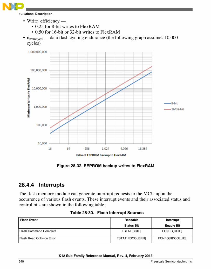
• Write_efficiency —• 0.25 for 8-bit writes to FlexRAM• 0.50 for 16-bit or 32-bit writes to FlexRAM
• nnvmcycd — data flash cycling endurance (the following graph assumes 10,000cycles)
Figure 28-32. EEPROM backup writes to FlexRAM
28.4.4 Interrupts
The flash memory module can generate interrupt requests to the MCU upon theoccurrence of various flash events. These interrupt events and their associated status andcontrol bits are shown in the following table.
Table 28-30. Flash Interrupt Sources
Flash Event Readable
Status Bit
Interrupt
Enable Bit
Flash Command Complete FSTAT[CCIF] FCNFG[CCIE]
Flash Read Collision Error FSTAT[RDCOLERR] FCNFG[RDCOLLIE]
Functional Description
K12 Sub-Family Reference Manual, Rev. 4, February 2013
540 Freescale Semiconductor, Inc.
Note
Vector addresses and their relative interrupt priority aredetermined at the MCU level.
Some devices also generate a bus error response as a result of a Read Collision Errorevent. See the chip configuration information to determine if a bus error response is alsosupported.
28.4.5 Flash Operation in Low-Power Modes
28.4.5.1 Wait Mode
When the MCU enters wait mode, the flash memory module is not affected. The flashmemory module can recover the MCU from wait via the command complete interrupt(see Interrupts).
28.4.5.2 Stop Mode
When the MCU requests stop mode, if a flash command is active (CCIF = 0) thecommand execution completes before the MCU is allowed to enter stop mode.
CAUTIONThe MCU should never enter stop mode while any flashcommand is running (CCIF = 0).
NOTEWhile the MCU is in very-low-power modes (VLPR, VLPW,VLPS), the flash memory module does not accept flashcommands.
28.4.6 Functional Modes of Operation
The flash memory module has two operating modes: NVM Normal and NVM Special.The operating mode affects the command set availability (see Table 28-31). Refer to theChip Configuration details of this device for how to activate each mode.
Chapter 28 Flash Memory Module (FTFL)
K12 Sub-Family Reference Manual, Rev. 4, February 2013
Freescale Semiconductor, Inc. 541
28.4.7 Flash Reads and Ignored Writes
The flash memory module requires only the flash address to execute a flash memoryread.
The MCU must not read from the flash memory while commands are running (asevidenced by CCIF=0) on that block. Read data cannot be guaranteed from a flash blockwhile any command is processing within that block. The block arbitration logic detectsany simultaneous access and reports this as a read collision error (see theFSTAT[RDCOLERR] bit).
28.4.8 Read While Write (RWW)
The following simultaneous accesses are allowed for devices with FlexNVM:
• The user may read from the program flash memory while commands (typicallyprogram and erase operations) are active in the data flash and FlexRAM memoryspace.
• The MCU can fetch instructions from program flash during both data flash programand erase operations and while EEPROM backup data is maintained by theEEPROM commands.
• Conversely, the user may read from data flash and FlexRAM while program anderase commands are executing on the program flash.
• When configured as traditional RAM, writes to the FlexRAM are allowed duringprogram and data flash operations.
Simultaneous data flash operations and FlexRAM writes, when FlexRAM is used forEEPROM, are not possible.
The following simultaneous accesses are allowed for devices with program flash only:
• The user may read from one logical program flash memory space while flashcommands are active in the other logical program flash memory space.
Simultaneous operations are further discussed in Allowed Simultaneous FlashOperations.
28.4.9 Flash Program and Erase
All flash functions except read require the user to setup and launch a flash commandthrough a series of peripheral bus writes. The user cannot initiate any further flashcommands until notified that the current command has completed. The flash commandstructure and operation are detailed in Flash Command Operations.
Functional Description
K12 Sub-Family Reference Manual, Rev. 4, February 2013
542 Freescale Semiconductor, Inc.
28.4.10 Flash Command Operations
Flash command operations are typically used to modify flash memory contents. The nextsections describe:
• The command write sequence used to set flash command parameters and launchexecution
• A description of all flash commands available
28.4.10.1 Command Write Sequence
Flash commands are specified using a command write sequence illustrated in Figure28-33. The flash memory module performs various checks on the command (FCCOB)content and continues with command execution if all requirements are fulfilled.
Before launching a command, the ACCERR and FPVIOL bits in the FSTAT registermust be zero and the CCIF flag must read 1 to verify that any previous command hascompleted. If CCIF is zero, the previous command execution is still active, a newcommand write sequence cannot be started, and all writes to the FCCOB registers areignored.
28.4.10.1.1 Load the FCCOB Registers
The user must load the FCCOB registers with all parameters required by the desired flashcommand. The individual registers that make up the FCCOB data set can be written inany order.
28.4.10.1.2 Launch the Command by Clearing CCIF
Once all relevant command parameters have been loaded, the user launches the commandby clearing the FSTAT[CCIF] bit by writing a '1' to it. The CCIF flag remains zero untilthe flash command completes.
The FSTAT register contains a blocking mechanism that prevents a new command fromlaunching (can't clear CCIF) if the previous command resulted in an access error(FSTAT[ACCERR]=1) or a protection violation (FSTAT[FPVIOL]=1). In errorscenarios, two writes to FSTAT are required to initiate the next command: the first writeclears the error flags, the second write clears CCIF.
Chapter 28 Flash Memory Module (FTFL)
K12 Sub-Family Reference Manual, Rev. 4, February 2013
Freescale Semiconductor, Inc. 543
28.4.10.1.3 Command Execution and Error Reporting
The command processing has several steps:
1. The flash memory module reads the command code and performs a series ofparameter checks and protection checks, if applicable, which are unique to eachcommand.
If the parameter check fails, the FSTAT[ACCERR] (access error) flag is set.ACCERR reports invalid instruction codes and out-of bounds addresses. Usually,access errors suggest that the command was not set-up with valid parameters in theFCCOB register group.
Program and erase commands also check the address to determine if the operation isrequested to execute on protected areas. If the protection check fails, theFSTAT[FPVIOL] (protection error) flag is set.
Command processing never proceeds to execution when the parameter or protectionstep fails. Instead, command processing is terminated after setting the FSTAT[CCIF]bit.
2. If the parameter and protection checks pass, the command proceeds to execution.Run-time errors, such as failure to erase verify, may occur during the executionphase. Run-time errors are reported in the FSTAT[MGSTAT0] bit. A command mayhave access errors, protection errors, and run-time errors, but the run-time errors arenot seen until all access and protection errors have been corrected.
3. Command execution results, if applicable, are reported back to the user via theFCCOB and FSTAT registers.
4. The flash memory module sets the FSTAT[CCIF] bit signifying that the commandhas completed.
The flow for a generic command write sequence is illustrated in the following figure.
Functional Description
K12 Sub-Family Reference Manual, Rev. 4, February 2013
544 Freescale Semiconductor, Inc.

Clear the CCIF to launch the command Write 0x80 to FSTAT register
Clear the old errorsAccess Error and Protection ViolationCheck
FCCOB
ACCERR/ FPVIOL Set?
EXIT
Write to the FCCOB registers to load the required command parameter.
More Parameters?
Availability Check
Results from previous command
Read: FSTAT register
Write 0x30 to FSTAT register
no
yes
no
yes
Previous command complete?no
CCIF = ‘1’?
yes
START
Figure 28-33. Generic Flash Command Write Sequence Flowchart
28.4.10.2 Flash Commands
The following table summarizes the function of all flash commands. If the program flash,data flash, or FlexRAM column is marked with an 'X', the flash command is relevant tothat particular memory resource.
Chapter 28 Flash Memory Module (FTFL)
K12 Sub-Family Reference Manual, Rev. 4, February 2013
Freescale Semiconductor, Inc. 545
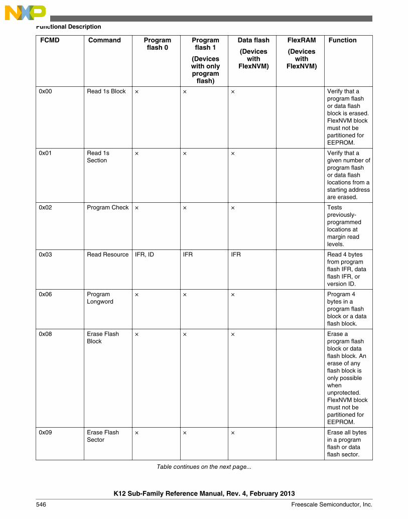
FCMD Command Programflash 0
Programflash 1
(Deviceswith onlyprogram
flash)
Data flash
(Deviceswith
FlexNVM)
FlexRAM
(Deviceswith
FlexNVM)
Function
0x00 Read 1s Block × × × Verify that aprogram flashor data flashblock is erased.FlexNVM blockmust not bepartitioned forEEPROM.
0x01 Read 1sSection
× × × Verify that agiven number ofprogram flashor data flashlocations from astarting addressare erased.
0x02 Program Check × × × Testspreviously-programmedlocations atmargin readlevels.
0x03 Read Resource IFR, ID IFR IFR Read 4 bytesfrom programflash IFR, dataflash IFR, orversion ID.
0x06 ProgramLongword
× × × Program 4bytes in aprogram flashblock or a dataflash block.
0x08 Erase FlashBlock
× × × Erase aprogram flashblock or dataflash block. Anerase of anyflash block isonly possiblewhenunprotected.FlexNVM blockmust not bepartitioned forEEPROM.
0x09 Erase FlashSector
× × × Erase all bytesin a programflash or dataflash sector.
Table continues on the next page...
Functional Description
K12 Sub-Family Reference Manual, Rev. 4, February 2013
546 Freescale Semiconductor, Inc.

FCMD Command Programflash 0
Programflash 1
(Deviceswith onlyprogram
flash)
Data flash
(Deviceswith
FlexNVM)
FlexRAM
(Deviceswith
FlexNVM)
Function
0x0B ProgramSection
× × × × Program datafrom theSectionProgram Bufferto a programflash or dataflash block.
0x40 Read 1s AllBlocks
× × × Verify that allprogram flash,data flashblocks,EEPROMbackup datarecords, anddata flash IFRare erased thenrelease MCUsecurity.
0x41 Read Once IFR Read 4 bytes ofa dedicated 64byte field in theprogram flash 0IFR.
0x43 Program Once IFR One-timeprogram of 4bytes of adedicated 64-byte field in theprogram flash 0IFR.
Table continues on the next page...
Chapter 28 Flash Memory Module (FTFL)
K12 Sub-Family Reference Manual, Rev. 4, February 2013
Freescale Semiconductor, Inc. 547

FCMD Command Programflash 0
Programflash 1
(Deviceswith onlyprogram
flash)
Data flash
(Deviceswith
FlexNVM)
FlexRAM
(Deviceswith
FlexNVM)
Function
0x44 Erase All Blocks × × × × Erase allprogram flashblocks, programflash swap IFR,data flashblocks,FlexRAM,EEPROMbackup datarecords, anddata flash IFR.Then, verify-erase andrelease MCUsecurity.
NOTE:An erase is onlypossible whenall memorylocations areunprotected.
0x45 Verify BackdoorAccess Key
× × Release MCUsecurity aftercomparing a setof user-suppliedsecurity keys tothose stored inthe programflash.
0x46 Swap Control × × Handles swap-related activities
0x80 ProgramPartition
IFR × Program theFlexNVMPartition Codeand EEPROMData Set Sizeinto the dataflash IFR.Format allEEPROMbackup datasectorsallocated forEEPROM.Initialize theFlexRAM.
Table continues on the next page...
Functional Description
K12 Sub-Family Reference Manual, Rev. 4, February 2013
548 Freescale Semiconductor, Inc.
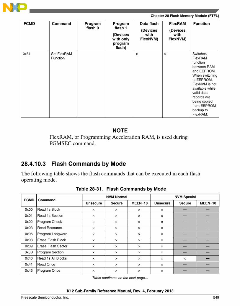
FCMD Command Programflash 0
Programflash 1
(Deviceswith onlyprogram
flash)
Data flash
(Deviceswith
FlexNVM)
FlexRAM
(Deviceswith
FlexNVM)
Function
0x81 Set FlexRAMFunction
x × SwitchesFlexRAMfunctionbetween RAMand EEPROM.When switchingto EEPROM,FlexNVM is notavailable whilevalid datarecords arebeing copiedfrom EEPROMbackup toFlexRAM.
NOTEFlexRAM, or Programming Acceleration RAM, is used duringPGMSEC command.
28.4.10.3 Flash Commands by Mode
The following table shows the flash commands that can be executed in each flashoperating mode.
Table 28-31. Flash Commands by Mode
FCMD CommandNVM Normal NVM Special
Unsecure Secure MEEN=10 Unsecure Secure MEEN=10
0x00 Read 1s Block × × × × — —
0x01 Read 1s Section × × × × — —
0x02 Program Check × × × × — —
0x03 Read Resource × × × × — —
0x06 Program Longword × × × × — —
0x08 Erase Flash Block × × × × — —
0x09 Erase Flash Sector × × × × — —
0x0B Program Section × × × × — —
0x40 Read 1s All Blocks × × × × × —
0x41 Read Once × × × × — —
0x43 Program Once × × × × — —
Table continues on the next page...
Chapter 28 Flash Memory Module (FTFL)
K12 Sub-Family Reference Manual, Rev. 4, February 2013
Freescale Semiconductor, Inc. 549

Table 28-31. Flash Commands by Mode (continued)
FCMD CommandNVM Normal NVM Special
Unsecure Secure MEEN=10 Unsecure Secure MEEN=10
0x44 Erase All Blocks × × × × × —
0x45Verify Backdoor AccessKey
× × × × — —
0x46 Swap Control × × × × — —
0x80 Program Partition × × × × — —
0x81 Set FlexRAM Function × × × × — —
28.4.10.4 Allowed Simultaneous Flash Operations
Only the operations marked 'OK' in the following table are permitted to runsimultaneously on the program flash, data flash, and FlexRAM memories. Someoperations cannot be executed simultaneously because certain hardware resources areshared by the memories. The priority has been placed on permitting program flash readswhile program and erase operations execute on the FlexNVM and FlexRAM. Thisprovides read (program flash) while write (FlexNVM, FlexRAM) functionality.
For devices containing FlexNVM:
Table 28-32. Allowed Simultaneous Memory Operations
Program Flash Data Flash FlexRAM
Read ProgramSectorErase
Read ProgramSectorErase
Read E-Write R-Write
Programflash
Read — OK OK OK
Program — OK OK OK3
SectorErase
— OK OK OK
Dataflash
Read OK OK —
Program OK — OK OK
SectorErase
OK — OK OK
FlexRAM
Read OK OK OK OK —
E-Write1OK —
R-Write2OK OK OK OK —
1. When FlexRAM configured for EEPROM (writes are effectively multi-cycle operations).2. When FlexRAM configured as traditional RAM (writes are single-cycle operations).3. When FlexRAM configured as traditional RAM, writes to the RAM are ignored while the Program Section command is
active (CCIF = 0).
For devices containing program flash only:
Functional Description
K12 Sub-Family Reference Manual, Rev. 4, February 2013
550 Freescale Semiconductor, Inc.

Table 28-33. Allowed Simultaneous Memory Operations
Program Flash 0 Program Flash 1
Read Program Sector Erase Read Program Sector Erase
Programflash 0
Read — OK OK
Program — OK
Sector Erase — OK
Programflash 1
Read OK OK —
Program OK —
Sector Erase OK —
28.4.11 Margin Read Commands
The Read-1s commands (Read 1s All Blocks, Read 1s Block, and Read 1s Section) andthe Program Check command have a margin choice parameter that allows the user toapply non-standard read reference levels to the program flash and data flash array readsperformed by these commands. Using the preset 'user' and 'factory' margin levels, thesecommands perform their associated read operations at tighter tolerances than a 'normal'read. These non-standard read levels are applied only during the command execution. Allsimple (uncommanded) flash array reads to the MCU always use the standard, un-margined, read reference level.
Only the 'normal' read level should be employed during normal flash usage. The non-standard, 'user' and 'factory' margin levels should be employed only in special cases.They can be used during special diagnostic routines to gain confidence that the device isnot suffering from the end-of-life data loss customary of flash memory devices.
Erased ('1') and programmed ('0') bit states can degrade due to elapsed time and datacycling (number of times a bit is erased and re-programmed). The lifetime of the erasedstates is relative to the last erase operation. The lifetime of the programmed states ismeasured from the last program time.
The 'user' and 'factory' levels become, in effect, a minimum safety margin; i.e. if the readspass at the tighter tolerances of the 'user' and 'factory' margins, then the 'normal' readshave at least this much safety margin before they experience data loss.
The 'user' margin is a small delta to the normal read reference level. 'User' margin levelscan be employed to check that flash memory contents have adequate margin for normallevel read operations. If unexpected read results are encountered when checking flashmemory contents at the 'user' margin levels, loss of information might soon occur during'normal' readout.
Chapter 28 Flash Memory Module (FTFL)
K12 Sub-Family Reference Manual, Rev. 4, February 2013
Freescale Semiconductor, Inc. 551
The 'factory' margin is a bigger deviation from the norm, a more stringent read criteriathat should only be attempted immediately (or very soon) after completion of an erase orprogram command, early in the cycling life. 'Factory' margin levels can be used to checkthat flash memory contents have adequate margin for long-term data retention at thenormal level setting. If unexpected results are encountered when checking flash memorycontents at 'factory' margin levels, the flash memory contents should be erased andreprogrammed.
CAUTION
Factory margin levels must only be used during verify of theinitial factory programming.
28.4.12 Flash Command Description
This section describes all flash commands that can be launched by a command writesequence. The flash memory module sets the FSTAT[ACCERR] bit and aborts thecommand execution if any of the following illegal conditions occur:
• There is an unrecognized command code in the FCCOB FCMD field.
• There is an error in a FCCOB field for the specific commands. Refer to the errorhandling table provided for each command.
Ensure that the ACCERR and FPVIOL bits in the FSTAT register are cleared prior tostarting the command write sequence. As described in Launch the Command by ClearingCCIF, a new command cannot be launched while these error flags are set.
Do not attempt to read a flash block while the flash memory module is running acommand (CCIF = 0) on that same block. The flash memory module may return invaliddata to the MCU with the collision error flag (FSTAT[RDCOLERR]) set.
When required by the command, address bit 23 selects between:
• program flash (=0)• data flash (=1)
CAUTION
Flash data must be in the erased state before beingprogrammed. Cumulative programming of bits (adding morezeros) is not allowed.
Functional Description
K12 Sub-Family Reference Manual, Rev. 4, February 2013
552 Freescale Semiconductor, Inc.

28.4.12.1 Read 1s Block Command
The Read 1s Block command checks to see if an entire program flash or data flash blockhas been erased to the specified margin level. The FCCOB flash address bits determinewhich logical block is erase-verified.
Table 28-34. Read 1s Block Command FCCOB Requirements
FCCOB Number FCCOB Contents [7:0]
0 0x00 (RD1BLK)
1 Flash address [23:16] in the flash block to be verified
2 Flash address [15:8] in the flash block to be verified
3 Flash address [7:0]1 in the flash block to be verified
4 Read-1 Margin Choice
1. Must be longword aligned (Flash address [1:0] = 00).
After clearing CCIF to launch the Read 1s Block command, the flash memory modulesets the read margin for 1s according to Table 28-35 and then reads all locations withinthe selected program flash or data flash block.
When the data flash is targeted, DEPART must be set for no EEPROM, else the Read 1sBlock command aborts setting the FSTAT[ACCERR] bit. If the flash memory modulefails to read all 1s (i.e. the flash block is not fully erased), the FSTAT[MGSTAT0] bit isset. The CCIF flag sets after the Read 1s Block operation has completed.
Table 28-35. Margin Level Choices for Read 1s Block
Read Margin Choice Margin Level Description
0x00 Use the 'normal' read level for 1s
0x01 Apply the 'User' margin to the normal read-1 level
0x02 Apply the 'Factory' margin to the normal read-1 level
Table 28-36. Read 1s Block Command Error Handling
Error Condition Error Bit
Command not available in current mode/security FSTAT[ACCERR]
An invalid margin choice is specified FSTAT[ACCERR]
Program flash is selected and the address is out of program flash range FSTAT[ACCERR]
Data flash is selected and the address is out of data flash range FSTAT[ACCERR]
Data flash is selected with EEPROM enabled FSTAT[ACCERR]
Flash address is not longword aligned FSTAT[ACCERR]
Read-1s fails FSTAT[MGSTAT0]
Chapter 28 Flash Memory Module (FTFL)
K12 Sub-Family Reference Manual, Rev. 4, February 2013
Freescale Semiconductor, Inc. 553
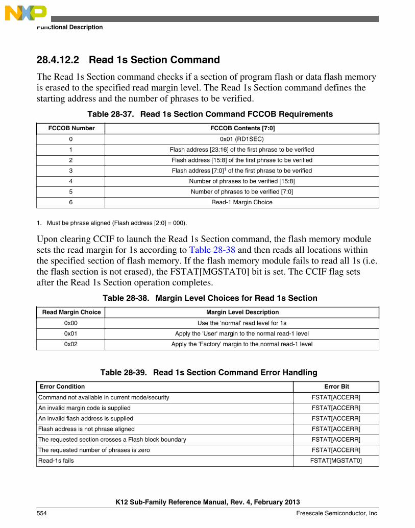
28.4.12.2 Read 1s Section Command
The Read 1s Section command checks if a section of program flash or data flash memoryis erased to the specified read margin level. The Read 1s Section command defines thestarting address and the number of phrases to be verified.
Table 28-37. Read 1s Section Command FCCOB Requirements
FCCOB Number FCCOB Contents [7:0]
0 0x01 (RD1SEC)
1 Flash address [23:16] of the first phrase to be verified
2 Flash address [15:8] of the first phrase to be verified
3 Flash address [7:0]1 of the first phrase to be verified
4 Number of phrases to be verified [15:8]
5 Number of phrases to be verified [7:0]
6 Read-1 Margin Choice
1. Must be phrase aligned (Flash address [2:0] = 000).
Upon clearing CCIF to launch the Read 1s Section command, the flash memory modulesets the read margin for 1s according to Table 28-38 and then reads all locations withinthe specified section of flash memory. If the flash memory module fails to read all 1s (i.e.the flash section is not erased), the FSTAT[MGSTAT0] bit is set. The CCIF flag setsafter the Read 1s Section operation completes.
Table 28-38. Margin Level Choices for Read 1s Section
Read Margin Choice Margin Level Description
0x00 Use the 'normal' read level for 1s
0x01 Apply the 'User' margin to the normal read-1 level
0x02 Apply the 'Factory' margin to the normal read-1 level
Table 28-39. Read 1s Section Command Error Handling
Error Condition Error Bit
Command not available in current mode/security FSTAT[ACCERR]
An invalid margin code is supplied FSTAT[ACCERR]
An invalid flash address is supplied FSTAT[ACCERR]
Flash address is not phrase aligned FSTAT[ACCERR]
The requested section crosses a Flash block boundary FSTAT[ACCERR]
The requested number of phrases is zero FSTAT[ACCERR]
Read-1s fails FSTAT[MGSTAT0]
Functional Description
K12 Sub-Family Reference Manual, Rev. 4, February 2013
554 Freescale Semiconductor, Inc.
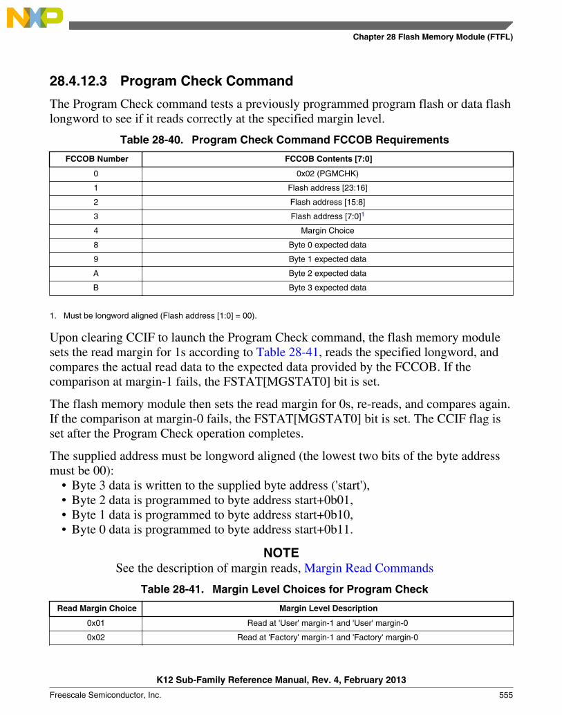
28.4.12.3 Program Check Command
The Program Check command tests a previously programmed program flash or data flashlongword to see if it reads correctly at the specified margin level.
Table 28-40. Program Check Command FCCOB Requirements
FCCOB Number FCCOB Contents [7:0]
0 0x02 (PGMCHK)
1 Flash address [23:16]
2 Flash address [15:8]
3 Flash address [7:0]1
4 Margin Choice
8 Byte 0 expected data
9 Byte 1 expected data
A Byte 2 expected data
B Byte 3 expected data
1. Must be longword aligned (Flash address [1:0] = 00).
Upon clearing CCIF to launch the Program Check command, the flash memory modulesets the read margin for 1s according to Table 28-41, reads the specified longword, andcompares the actual read data to the expected data provided by the FCCOB. If thecomparison at margin-1 fails, the FSTAT[MGSTAT0] bit is set.
The flash memory module then sets the read margin for 0s, re-reads, and compares again.If the comparison at margin-0 fails, the FSTAT[MGSTAT0] bit is set. The CCIF flag isset after the Program Check operation completes.
The supplied address must be longword aligned (the lowest two bits of the byte addressmust be 00):
• Byte 3 data is written to the supplied byte address ('start'),• Byte 2 data is programmed to byte address start+0b01,• Byte 1 data is programmed to byte address start+0b10,• Byte 0 data is programmed to byte address start+0b11.
NOTESee the description of margin reads, Margin Read Commands
Table 28-41. Margin Level Choices for Program Check
Read Margin Choice Margin Level Description
0x01 Read at 'User' margin-1 and 'User' margin-0
0x02 Read at 'Factory' margin-1 and 'Factory' margin-0
Chapter 28 Flash Memory Module (FTFL)
K12 Sub-Family Reference Manual, Rev. 4, February 2013
Freescale Semiconductor, Inc. 555
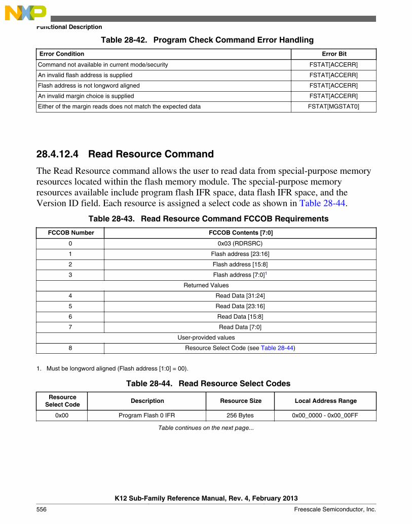
Table 28-42. Program Check Command Error Handling
Error Condition Error Bit
Command not available in current mode/security FSTAT[ACCERR]
An invalid flash address is supplied FSTAT[ACCERR]
Flash address is not longword aligned FSTAT[ACCERR]
An invalid margin choice is supplied FSTAT[ACCERR]
Either of the margin reads does not match the expected data FSTAT[MGSTAT0]
28.4.12.4 Read Resource Command
The Read Resource command allows the user to read data from special-purpose memoryresources located within the flash memory module. The special-purpose memoryresources available include program flash IFR space, data flash IFR space, and theVersion ID field. Each resource is assigned a select code as shown in Table 28-44.
Table 28-43. Read Resource Command FCCOB Requirements
FCCOB Number FCCOB Contents [7:0]
0 0x03 (RDRSRC)
1 Flash address [23:16]
2 Flash address [15:8]
3 Flash address [7:0]1
Returned Values
4 Read Data [31:24]
5 Read Data [23:16]
6 Read Data [15:8]
7 Read Data [7:0]
User-provided values
8 Resource Select Code (see Table 28-44)
1. Must be longword aligned (Flash address [1:0] = 00).
Table 28-44. Read Resource Select Codes
ResourceSelect Code
Description Resource Size Local Address Range
0x00 Program Flash 0 IFR 256 Bytes 0x00_0000 - 0x00_00FF
Table continues on the next page...
Functional Description
K12 Sub-Family Reference Manual, Rev. 4, February 2013
556 Freescale Semiconductor, Inc.
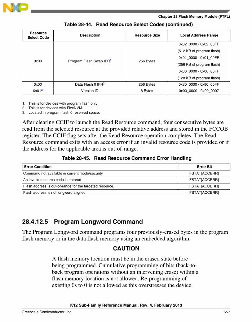
Table 28-44. Read Resource Select Codes (continued)
ResourceSelect Code
Description Resource Size Local Address Range
0x00 Program Flash Swap IFR1 256 Bytes
0x02_0000 - 0x02_00FF
(512 KB of program flash)
0x01_0000 - 0x01_00FF
(256 KB of program flash)
0x00_8000 - 0x00_80FF
(128 KB of program flash)
0x00 Data Flash 0 IFR2 256 Bytes 0x80_0000 - 0x80_00FF
0x013 Version ID 8 Bytes 0x00_0000 - 0x00_0007
1. This is for devices with program flash only.2. This is for devices with FlexNVM.3. Located in program flash 0 reserved space.
After clearing CCIF to launch the Read Resource command, four consecutive bytes areread from the selected resource at the provided relative address and stored in the FCCOBregister. The CCIF flag sets after the Read Resource operation completes. The ReadResource command exits with an access error if an invalid resource code is provided or ifthe address for the applicable area is out-of-range.
Table 28-45. Read Resource Command Error Handling
Error Condition Error Bit
Command not available in current mode/security FSTAT[ACCERR]
An invalid resource code is entered FSTAT[ACCERR]
Flash address is out-of-range for the targeted resource. FSTAT[ACCERR]
Flash address is not longword aligned FSTAT[ACCERR]
28.4.12.5 Program Longword Command
The Program Longword command programs four previously-erased bytes in the programflash memory or in the data flash memory using an embedded algorithm.
CAUTION
A flash memory location must be in the erased state beforebeing programmed. Cumulative programming of bits (back-to-back program operations without an intervening erase) within aflash memory location is not allowed. Re-programming ofexisting 0s to 0 is not allowed as this overstresses the device.
Chapter 28 Flash Memory Module (FTFL)
K12 Sub-Family Reference Manual, Rev. 4, February 2013
Freescale Semiconductor, Inc. 557
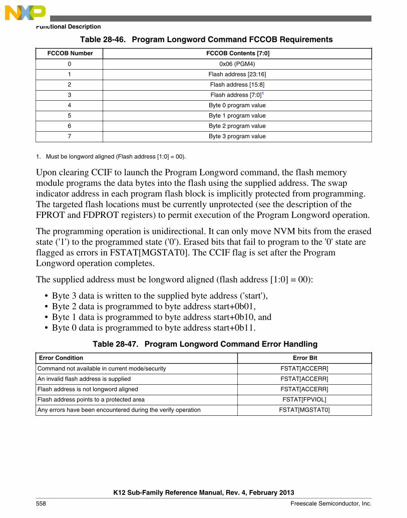
Table 28-46. Program Longword Command FCCOB Requirements
FCCOB Number FCCOB Contents [7:0]
0 0x06 (PGM4)
1 Flash address [23:16]
2 Flash address [15:8]
3 Flash address [7:0]1
4 Byte 0 program value
5 Byte 1 program value
6 Byte 2 program value
7 Byte 3 program value
1. Must be longword aligned (Flash address [1:0] = 00).
Upon clearing CCIF to launch the Program Longword command, the flash memorymodule programs the data bytes into the flash using the supplied address. The swapindicator address in each program flash block is implicitly protected from programming.The targeted flash locations must be currently unprotected (see the description of theFPROT and FDPROT registers) to permit execution of the Program Longword operation.
The programming operation is unidirectional. It can only move NVM bits from the erasedstate ('1') to the programmed state ('0'). Erased bits that fail to program to the '0' state areflagged as errors in FSTAT[MGSTAT0]. The CCIF flag is set after the ProgramLongword operation completes.
The supplied address must be longword aligned (flash address [1:0] = 00):
• Byte 3 data is written to the supplied byte address ('start'),• Byte 2 data is programmed to byte address start+0b01,• Byte 1 data is programmed to byte address start+0b10, and• Byte 0 data is programmed to byte address start+0b11.
Table 28-47. Program Longword Command Error Handling
Error Condition Error Bit
Command not available in current mode/security FSTAT[ACCERR]
An invalid flash address is supplied FSTAT[ACCERR]
Flash address is not longword aligned FSTAT[ACCERR]
Flash address points to a protected area FSTAT[FPVIOL]
Any errors have been encountered during the verify operation FSTAT[MGSTAT0]
Functional Description
K12 Sub-Family Reference Manual, Rev. 4, February 2013
558 Freescale Semiconductor, Inc.
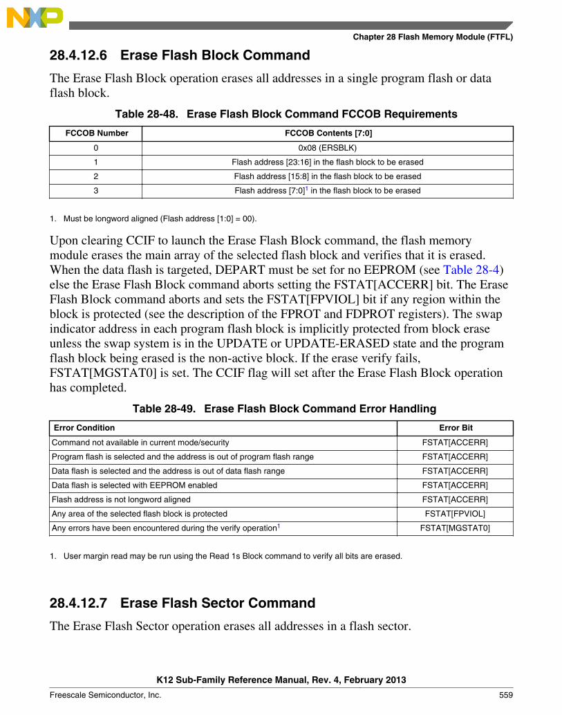
28.4.12.6 Erase Flash Block Command
The Erase Flash Block operation erases all addresses in a single program flash or dataflash block.
Table 28-48. Erase Flash Block Command FCCOB Requirements
FCCOB Number FCCOB Contents [7:0]
0 0x08 (ERSBLK)
1 Flash address [23:16] in the flash block to be erased
2 Flash address [15:8] in the flash block to be erased
3 Flash address [7:0]1 in the flash block to be erased
1. Must be longword aligned (Flash address [1:0] = 00).
Upon clearing CCIF to launch the Erase Flash Block command, the flash memorymodule erases the main array of the selected flash block and verifies that it is erased.When the data flash is targeted, DEPART must be set for no EEPROM (see Table 28-4)else the Erase Flash Block command aborts setting the FSTAT[ACCERR] bit. The EraseFlash Block command aborts and sets the FSTAT[FPVIOL] bit if any region within theblock is protected (see the description of the FPROT and FDPROT registers). The swapindicator address in each program flash block is implicitly protected from block eraseunless the swap system is in the UPDATE or UPDATE-ERASED state and the programflash block being erased is the non-active block. If the erase verify fails,FSTAT[MGSTAT0] is set. The CCIF flag will set after the Erase Flash Block operationhas completed.
Table 28-49. Erase Flash Block Command Error Handling
Error Condition Error Bit
Command not available in current mode/security FSTAT[ACCERR]
Program flash is selected and the address is out of program flash range FSTAT[ACCERR]
Data flash is selected and the address is out of data flash range FSTAT[ACCERR]
Data flash is selected with EEPROM enabled FSTAT[ACCERR]
Flash address is not longword aligned FSTAT[ACCERR]
Any area of the selected flash block is protected FSTAT[FPVIOL]
Any errors have been encountered during the verify operation1 FSTAT[MGSTAT0]
1. User margin read may be run using the Read 1s Block command to verify all bits are erased.
28.4.12.7 Erase Flash Sector Command
The Erase Flash Sector operation erases all addresses in a flash sector.
Chapter 28 Flash Memory Module (FTFL)
K12 Sub-Family Reference Manual, Rev. 4, February 2013
Freescale Semiconductor, Inc. 559
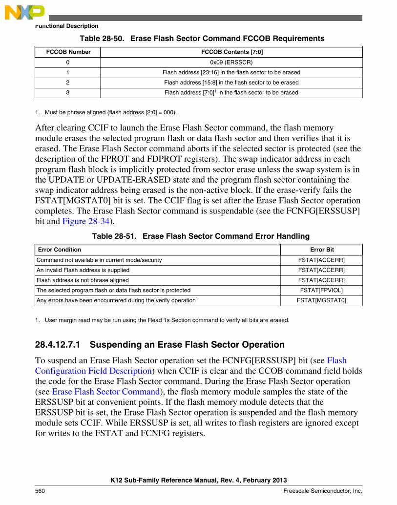
Table 28-50. Erase Flash Sector Command FCCOB Requirements
FCCOB Number FCCOB Contents [7:0]
0 0x09 (ERSSCR)
1 Flash address [23:16] in the flash sector to be erased
2 Flash address [15:8] in the flash sector to be erased
3 Flash address [7:0]1 in the flash sector to be erased
1. Must be phrase aligned (flash address [2:0] = 000).
After clearing CCIF to launch the Erase Flash Sector command, the flash memorymodule erases the selected program flash or data flash sector and then verifies that it iserased. The Erase Flash Sector command aborts if the selected sector is protected (see thedescription of the FPROT and FDPROT registers). The swap indicator address in eachprogram flash block is implicitly protected from sector erase unless the swap system is inthe UPDATE or UPDATE-ERASED state and the program flash sector containing theswap indicator address being erased is the non-active block. If the erase-verify fails theFSTAT[MGSTAT0] bit is set. The CCIF flag is set after the Erase Flash Sector operationcompletes. The Erase Flash Sector command is suspendable (see the FCNFG[ERSSUSP]bit and Figure 28-34).
Table 28-51. Erase Flash Sector Command Error Handling
Error Condition Error Bit
Command not available in current mode/security FSTAT[ACCERR]
An invalid Flash address is supplied FSTAT[ACCERR]
Flash address is not phrase aligned FSTAT[ACCERR]
The selected program flash or data flash sector is protected FSTAT[FPVIOL]
Any errors have been encountered during the verify operation1 FSTAT[MGSTAT0]
1. User margin read may be run using the Read 1s Section command to verify all bits are erased.
28.4.12.7.1 Suspending an Erase Flash Sector Operation
To suspend an Erase Flash Sector operation set the FCNFG[ERSSUSP] bit (see FlashConfiguration Field Description) when CCIF is clear and the CCOB command field holdsthe code for the Erase Flash Sector command. During the Erase Flash Sector operation(see Erase Flash Sector Command), the flash memory module samples the state of theERSSUSP bit at convenient points. If the flash memory module detects that theERSSUSP bit is set, the Erase Flash Sector operation is suspended and the flash memorymodule sets CCIF. While ERSSUSP is set, all writes to flash registers are ignored exceptfor writes to the FSTAT and FCNFG registers.
Functional Description
K12 Sub-Family Reference Manual, Rev. 4, February 2013
560 Freescale Semiconductor, Inc.
If an Erase Flash Sector operation effectively completes before the flash memory moduledetects that a suspend request has been made, the flash memory module clears theERSSUSP bit prior to setting CCIF. When an Erase Flash Sector operation has beensuccessfully suspended, the flash memory module sets CCIF and leaves the ERSSUSP bitset. While CCIF is set, the ERSSUSP bit can only be cleared to prevent the withdrawal ofa suspend request before the flash memory module has acknowledged it.
28.4.12.7.2 Resuming a Suspended Erase Flash Sector Operation
If the ERSSUSP bit is still set when CCIF is cleared to launch the next command, theprevious Erase Flash Sector operation resumes. The flash memory module acknowledgesthe request to resume a suspended operation by clearing the ERSSUSP bit. A newsuspend request can then be made by setting ERSSUSP. A single Erase Flash Sectoroperation can be suspended and resumed multiple times.
There is a minimum elapsed time limit between the request to resume the Erase FlashSector operation (CCIF is cleared) and the request to suspend the operation again(ERSSUSP is set). This minimum time period is required to ensure that the Erase FlashSector operation will eventually complete. If the minimum period is continually violated,i.e. the suspend requests come repeatedly and too quickly, no forward progress is madeby the Erase Flash Sector algorithm. The resume/suspend sequence runs indefinitelywithout completing the erase.
28.4.12.7.3 Aborting a Suspended Erase Flash Sector Operation
The user may choose to abort a suspended Erase Flash Sector operation by clearing theERSSUSP bit prior to clearing CCIF for the next command launch. When a suspendedoperation is aborted, the flash memory module starts the new command using the newFCCOB contents.
While FCNFG[ERSSUSP] is set, a write to the FlexRAM while FCNFG[EEERDY] is setclears ERSSUSP and aborts the suspended operation. The FlexRAM write operation isexecuted by the flash memory module.
Note
Aborting the erase leaves the bitcells in an indeterminate,partially-erased state. Data in this sector is not reliable until anew erase command fully completes.
The following figure shows how to suspend and resume the Erase Flash Sector operation.
Chapter 28 Flash Memory Module (FTFL)
K12 Sub-Family Reference Manual, Rev. 4, February 2013
Freescale Semiconductor, Inc. 561

Restore Erase Algo Clear SUSPACK = 0
ERSSCR Command (Write FCCOB)
Launch/Resume Command (Clear CCIF)
CCIF = 1?
Request Suspend (Set ERSSUSP)
Interrupt?
CCIF = 1?
Service Interrupt (Read Flash)
ERSSUSP=0?
Next Command (Write FCCOB)
Clear ERSSUSP
Enter with CCIF = 1
Resume ERSSCR
No
Memory Controller Command Processing
SUSPACK=1
Clear ERSSUSP
Execute
Yes
DONE?
No
ERSSUSP=1?
Save Erase Algo
Set CCIF
No
Yes
Start New
Resume Erase?
No, Abort
User Cmd Interrupt/Suspend
Set SUSPACK = 1
ERSSCR Suspended
Command Initiation
Yes
No
Yes
Yes
ERSSCR Completed
ERSSCR Suspended ERSSUSP=1
ERSSUSP: Bit in FCNFG register SUSPACK: Internal Suspend Acknowledge
No
Yes
Yes
No
Yes
No
ERSSCR Completed ERSSUSP=0
Figure 28-34. Suspend and Resume of Erase Flash Sector Operation
Functional Description
K12 Sub-Family Reference Manual, Rev. 4, February 2013
562 Freescale Semiconductor, Inc.
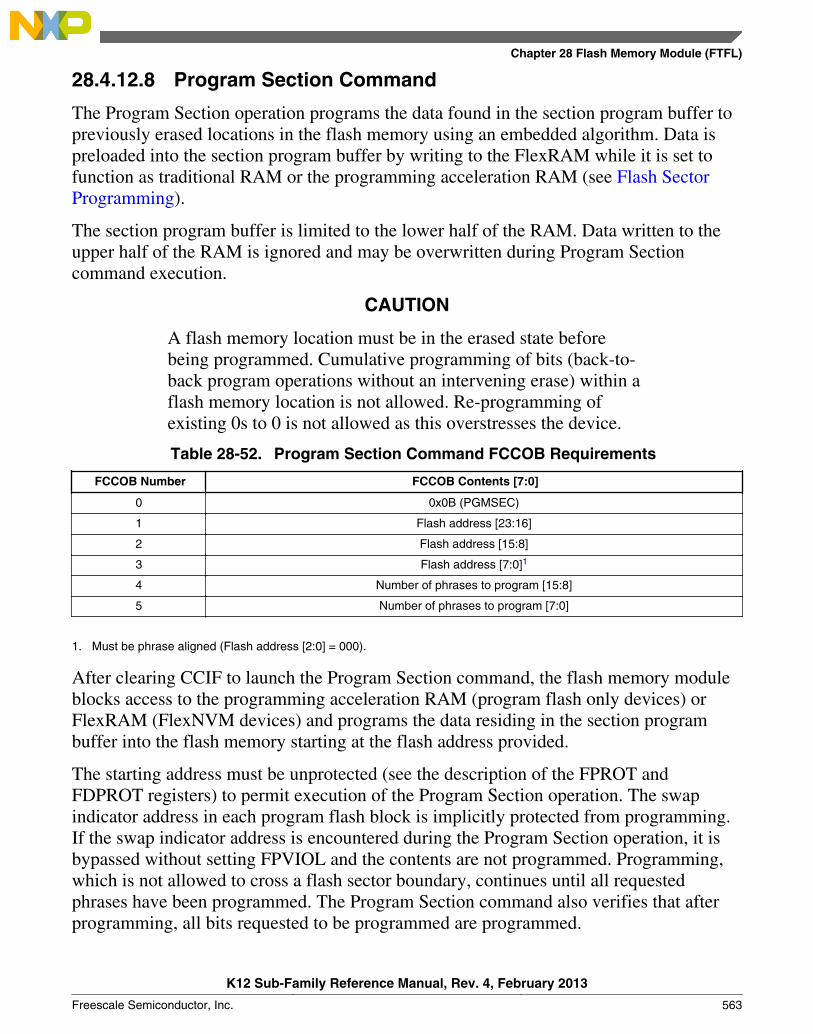
28.4.12.8 Program Section Command
The Program Section operation programs the data found in the section program buffer topreviously erased locations in the flash memory using an embedded algorithm. Data ispreloaded into the section program buffer by writing to the FlexRAM while it is set tofunction as traditional RAM or the programming acceleration RAM (see Flash SectorProgramming).
The section program buffer is limited to the lower half of the RAM. Data written to theupper half of the RAM is ignored and may be overwritten during Program Sectioncommand execution.
CAUTION
A flash memory location must be in the erased state beforebeing programmed. Cumulative programming of bits (back-to-back program operations without an intervening erase) within aflash memory location is not allowed. Re-programming ofexisting 0s to 0 is not allowed as this overstresses the device.
Table 28-52. Program Section Command FCCOB Requirements
FCCOB Number FCCOB Contents [7:0]
0 0x0B (PGMSEC)
1 Flash address [23:16]
2 Flash address [15:8]
3 Flash address [7:0]1
4 Number of phrases to program [15:8]
5 Number of phrases to program [7:0]
1. Must be phrase aligned (Flash address [2:0] = 000).
After clearing CCIF to launch the Program Section command, the flash memory moduleblocks access to the programming acceleration RAM (program flash only devices) orFlexRAM (FlexNVM devices) and programs the data residing in the section programbuffer into the flash memory starting at the flash address provided.
The starting address must be unprotected (see the description of the FPROT andFDPROT registers) to permit execution of the Program Section operation. The swapindicator address in each program flash block is implicitly protected from programming.If the swap indicator address is encountered during the Program Section operation, it isbypassed without setting FPVIOL and the contents are not programmed. Programming,which is not allowed to cross a flash sector boundary, continues until all requestedphrases have been programmed. The Program Section command also verifies that afterprogramming, all bits requested to be programmed are programmed.
Chapter 28 Flash Memory Module (FTFL)
K12 Sub-Family Reference Manual, Rev. 4, February 2013
Freescale Semiconductor, Inc. 563
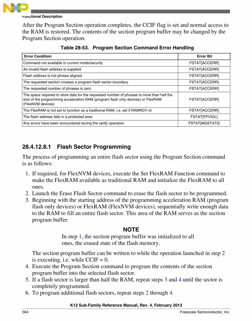
After the Program Section operation completes, the CCIF flag is set and normal access tothe RAM is restored. The contents of the section program buffer may be changed by theProgram Section operation.
Table 28-53. Program Section Command Error Handling
Error Condition Error Bit
Command not available in current mode/security FSTAT[ACCERR]
An invalid flash address is supplied FSTAT[ACCERR]
Flash address is not phrase aligned FSTAT[ACCERR]
The requested section crosses a program flash sector boundary FSTAT[ACCERR]
The requested number of phrases is zero FSTAT[ACCERR]
The space required to store data for the requested number of phrases is more than half thesize of the programming acceleration RAM (program flash only devices) or FlexRAM(FlexNVM devices)
FSTAT[ACCERR]
The FlexRAM is not set to function as a traditional RAM, i.e. set if RAMRDY=0 FSTAT[ACCERR]
The flash address falls in a protected area FSTAT[FPVIOL]
Any errors have been encountered during the verify operation FSTAT[MGSTAT0]
28.4.12.8.1 Flash Sector Programming
The process of programming an entire flash sector using the Program Section commandis as follows:
1. If required, for FlexNVM devices, execute the Set FlexRAM Function command tomake the FlexRAM available as traditional RAM and initialize the FlexRAM to allones.
2. Launch the Erase Flash Sector command to erase the flash sector to be programmed.3. Beginning with the starting address of the programming acceleration RAM (program
flash only devices) or FlexRAM (FlexNVM devices), sequentially write enough datato the RAM to fill an entire flash sector. This area of the RAM serves as the sectionprogram buffer.
NOTEIn step 1, the section program buffer was initialized to allones, the erased state of the flash memory.
The section program buffer can be written to while the operation launched in step 2is executing, i.e. while CCIF = 0.
4. Execute the Program Section command to program the contents of the sectionprogram buffer into the selected flash sector.
5. If a flash sector is larger than half the RAM, repeat steps 3 and 4 until the sector iscompletely programmed.
6. To program additional flash sectors, repeat steps 2 through 4.
Functional Description
K12 Sub-Family Reference Manual, Rev. 4, February 2013
564 Freescale Semiconductor, Inc.
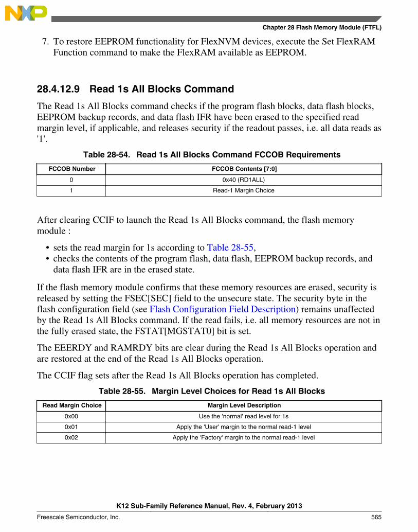
7. To restore EEPROM functionality for FlexNVM devices, execute the Set FlexRAMFunction command to make the FlexRAM available as EEPROM.
28.4.12.9 Read 1s All Blocks Command
The Read 1s All Blocks command checks if the program flash blocks, data flash blocks,EEPROM backup records, and data flash IFR have been erased to the specified readmargin level, if applicable, and releases security if the readout passes, i.e. all data reads as'1'.
Table 28-54. Read 1s All Blocks Command FCCOB Requirements
FCCOB Number FCCOB Contents [7:0]
0 0x40 (RD1ALL)
1 Read-1 Margin Choice
After clearing CCIF to launch the Read 1s All Blocks command, the flash memorymodule :
• sets the read margin for 1s according to Table 28-55,• checks the contents of the program flash, data flash, EEPROM backup records, and
data flash IFR are in the erased state.
If the flash memory module confirms that these memory resources are erased, security isreleased by setting the FSEC[SEC] field to the unsecure state. The security byte in theflash configuration field (see Flash Configuration Field Description) remains unaffectedby the Read 1s All Blocks command. If the read fails, i.e. all memory resources are not inthe fully erased state, the FSTAT[MGSTAT0] bit is set.
The EEERDY and RAMRDY bits are clear during the Read 1s All Blocks operation andare restored at the end of the Read 1s All Blocks operation.
The CCIF flag sets after the Read 1s All Blocks operation has completed.
Table 28-55. Margin Level Choices for Read 1s All Blocks
Read Margin Choice Margin Level Description
0x00 Use the 'normal' read level for 1s
0x01 Apply the 'User' margin to the normal read-1 level
0x02 Apply the 'Factory' margin to the normal read-1 level
Chapter 28 Flash Memory Module (FTFL)
K12 Sub-Family Reference Manual, Rev. 4, February 2013
Freescale Semiconductor, Inc. 565
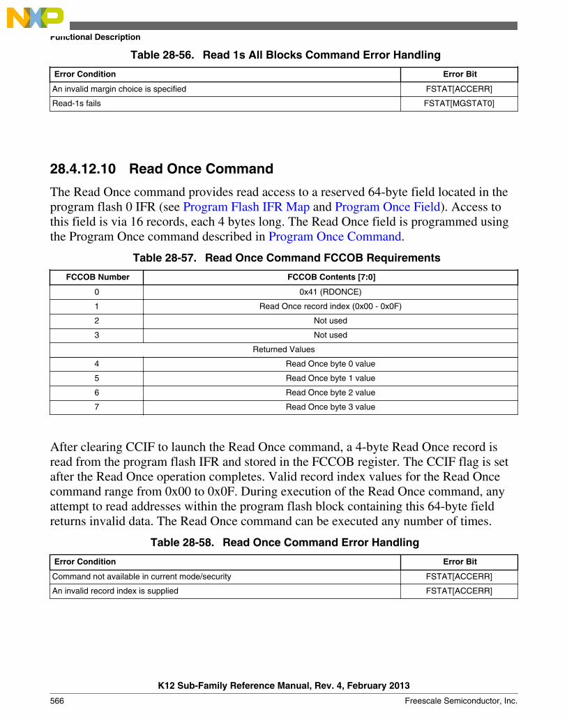
Table 28-56. Read 1s All Blocks Command Error Handling
Error Condition Error Bit
An invalid margin choice is specified FSTAT[ACCERR]
Read-1s fails FSTAT[MGSTAT0]
28.4.12.10 Read Once Command
The Read Once command provides read access to a reserved 64-byte field located in theprogram flash 0 IFR (see Program Flash IFR Map and Program Once Field). Access tothis field is via 16 records, each 4 bytes long. The Read Once field is programmed usingthe Program Once command described in Program Once Command.
Table 28-57. Read Once Command FCCOB Requirements
FCCOB Number FCCOB Contents [7:0]
0 0x41 (RDONCE)
1 Read Once record index (0x00 - 0x0F)
2 Not used
3 Not used
Returned Values
4 Read Once byte 0 value
5 Read Once byte 1 value
6 Read Once byte 2 value
7 Read Once byte 3 value
After clearing CCIF to launch the Read Once command, a 4-byte Read Once record isread from the program flash IFR and stored in the FCCOB register. The CCIF flag is setafter the Read Once operation completes. Valid record index values for the Read Oncecommand range from 0x00 to 0x0F. During execution of the Read Once command, anyattempt to read addresses within the program flash block containing this 64-byte fieldreturns invalid data. The Read Once command can be executed any number of times.
Table 28-58. Read Once Command Error Handling
Error Condition Error Bit
Command not available in current mode/security FSTAT[ACCERR]
An invalid record index is supplied FSTAT[ACCERR]
Functional Description
K12 Sub-Family Reference Manual, Rev. 4, February 2013
566 Freescale Semiconductor, Inc.
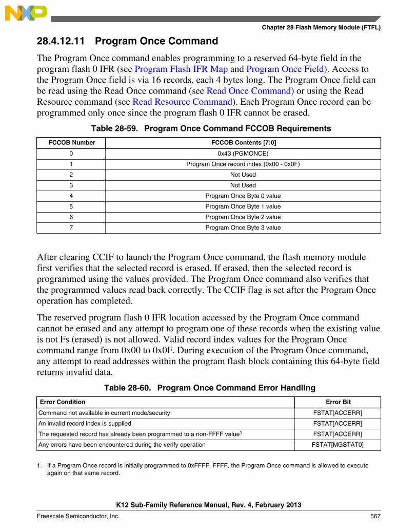
28.4.12.11 Program Once Command
The Program Once command enables programming to a reserved 64-byte field in theprogram flash 0 IFR (see Program Flash IFR Map and Program Once Field). Access tothe Program Once field is via 16 records, each 4 bytes long. The Program Once field canbe read using the Read Once command (see Read Once Command) or using the ReadResource command (see Read Resource Command). Each Program Once record can beprogrammed only once since the program flash 0 IFR cannot be erased.
Table 28-59. Program Once Command FCCOB Requirements
FCCOB Number FCCOB Contents [7:0]
0 0x43 (PGMONCE)
1 Program Once record index (0x00 - 0x0F)
2 Not Used
3 Not Used
4 Program Once Byte 0 value
5 Program Once Byte 1 value
6 Program Once Byte 2 value
7 Program Once Byte 3 value
After clearing CCIF to launch the Program Once command, the flash memory modulefirst verifies that the selected record is erased. If erased, then the selected record isprogrammed using the values provided. The Program Once command also verifies thatthe programmed values read back correctly. The CCIF flag is set after the Program Onceoperation has completed.
The reserved program flash 0 IFR location accessed by the Program Once commandcannot be erased and any attempt to program one of these records when the existing valueis not Fs (erased) is not allowed. Valid record index values for the Program Oncecommand range from 0x00 to 0x0F. During execution of the Program Once command,any attempt to read addresses within the program flash block containing this 64-byte fieldreturns invalid data.
Table 28-60. Program Once Command Error Handling
Error Condition Error Bit
Command not available in current mode/security FSTAT[ACCERR]
An invalid record index is supplied FSTAT[ACCERR]
The requested record has already been programmed to a non-FFFF value1 FSTAT[ACCERR]
Any errors have been encountered during the verify operation FSTAT[MGSTAT0]
1. If a Program Once record is initially programmed to 0xFFFF_FFFF, the Program Once command is allowed to executeagain on that same record.
Chapter 28 Flash Memory Module (FTFL)
K12 Sub-Family Reference Manual, Rev. 4, February 2013
Freescale Semiconductor, Inc. 567

28.4.12.12 Erase All Blocks Command
The Erase All Blocks operation erases all flash memory, initializes the FlexRAM, verifiesall memory contents, and releases MCU security.
Table 28-61. Erase All Blocks Command FCCOB Requirements
FCCOB Number FCCOB Contents [7:0]
0 0x44 (ERSALL)
After clearing CCIF to launch the Erase All Blocks command, the flash memory moduleerases all program flash memory, program flash swap IFR space, data flash memory, dataflash IFR space, EEPROM backup memory, and FlexRAM, then verifies that all areerased.
If the flash memory module verifies that all flash memories and the FlexRAM wereproperly erased, security is released by setting the FSEC[SEC] field to the unsecure stateand the FCNFG[RAMRDY] bit is set. The Erase All Blocks command aborts if any flashor FlexRAM region is protected. The swap indicator address in each program flash blockis not implicitly protected from the Erase All Blocks operation. The security byte and allother contents of the flash configuration field (see Flash Configuration Field Description)are erased by the Erase All Blocks command. If the erase-verify fails, theFSTAT[MGSTAT0] bit is set. The CCIF flag is set after the Erase All Blocks operationcompletes.
Table 28-62. Erase All Blocks Command Error Handling
Error Condition Error Bit
Command not available in current mode/security FSTAT[ACCERR]
Any region of the program flash memory, data flash memory, or FlexRAM is protected FSTAT[FPVIOL]
Any errors have been encountered during the verify operation1 FSTAT[MGSTAT0]
1. User margin read may be run using the Read 1s All Blocks command to verify all bits are erased.
28.4.12.12.1 Triggering an Erase All External to the Flash Memory Module
The functionality of the Erase All Blocks command is also available in an uncommandedfashion outside of the flash memory. Refer to the device's Chip Configuration details forinformation on this functionality.
Before invoking the external erase all function, the FSTAT[ACCERR and PVIOL] flagsmust be cleared and the FCCOB0 register must not contain 0x44. When invoked, theerase-all function erases all program flash memory, program flash swap IFR space, data
Functional Description
K12 Sub-Family Reference Manual, Rev. 4, February 2013
568 Freescale Semiconductor, Inc.

flash memory, data flash IFR space, EEPROM backup, and FlexRAM regardless of theprotection settings or if the swap system has been initialized. If the post-erase verifypasses, the routine then releases security by setting the FSEC[SEC] field register to theunsecure state and the FCNFG[RAMRDY] bit sets. The security byte in the FlashConfiguration Field is also programmed to the unsecure state. The status of the erase-allrequest is reflected in the FCNFG[ERSAREQ] bit. The FCNFG[ERSAREQ] bit iscleared once the operation completes and the normal FSTAT error reporting is availableas described in Erase All Blocks Command.
CAUTION
Since the IFR Swap Field in the program flash swap IFRcontaining the swap indicator address is erased during the EraseAll Blocks command operation, the swap system becomesuninitialized. The Swap Control command must be run with theinitialization code to set the swap indicator address andinitialize the swap system.
28.4.12.13 Verify Backdoor Access Key Command
The Verify Backdoor Access Key command only executes if the mode and securityconditions are satisfied (see Flash Commands by Mode). Execution of the VerifyBackdoor Access Key command is further qualified by the FSEC[KEYEN] bits. TheVerify Backdoor Access Key command releases security if user-supplied keys in theFCCOB match those stored in the Backdoor Comparison Key bytes of the FlashConfiguration Field (see Flash Configuration Field Description). The column labelledFlash Configuration Field offset address shows the location of the matching byte in theFlash Configuration Field.
Table 28-63. Verify Backdoor Access Key Command FCCOB Requirements
FCCOB Number FCCOB Contents [7:0] Flash Configuration Field Offset Address
0 0x45 (VFYKEY)
1-3 Not Used
4 Key Byte 0 0x0_0000
5 Key Byte 1 0x0_0001
6 Key Byte 2 0x0_0002
7 Key Byte 3 0x0_0003
8 Key Byte 4 0x0_0004
9 Key Byte 5 0x0_0005
A Key Byte 6 0x0_0006
B Key Byte 7 0x0_0007
Chapter 28 Flash Memory Module (FTFL)
K12 Sub-Family Reference Manual, Rev. 4, February 2013
Freescale Semiconductor, Inc. 569
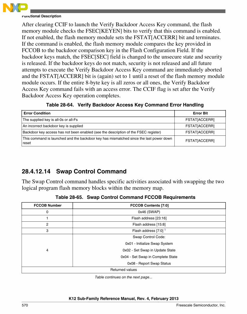
After clearing CCIF to launch the Verify Backdoor Access Key command, the flashmemory module checks the FSEC[KEYEN] bits to verify that this command is enabled.If not enabled, the flash memory module sets the FSTAT[ACCERR] bit and terminates.If the command is enabled, the flash memory module compares the key provided inFCCOB to the backdoor comparison key in the Flash Configuration Field. If thebackdoor keys match, the FSEC[SEC] field is changed to the unsecure state and securityis released. If the backdoor keys do not match, security is not released and all futureattempts to execute the Verify Backdoor Access Key command are immediately abortedand the FSTAT[ACCERR] bit is (again) set to 1 until a reset of the flash memory modulemodule occurs. If the entire 8-byte key is all zeros or all ones, the Verify BackdoorAccess Key command fails with an access error. The CCIF flag is set after the VerifyBackdoor Access Key operation completes.
Table 28-64. Verify Backdoor Access Key Command Error Handling
Error Condition Error Bit
The supplied key is all-0s or all-Fs FSTAT[ACCERR]
An incorrect backdoor key is supplied FSTAT[ACCERR]
Backdoor key access has not been enabled (see the description of the FSEC register) FSTAT[ACCERR]
This command is launched and the backdoor key has mismatched since the last power downreset
FSTAT[ACCERR]
28.4.12.14 Swap Control Command
The Swap Control command handles specific activities associated with swapping the twological program flash memory blocks within the memory map.
Table 28-65. Swap Control Command FCCOB Requirements
FCCOB Number FCCOB Contents [7:0]
0 0x46 (SWAP)
1 Flash address [23:16]
2 Flash address [15:8]
3 Flash address [7:0] 1
4
Swap Control Code:
0x01 - Initialize Swap System
0x02 - Set Swap in Update State
0x04 - Set Swap in Complete State
0x08 - Report Swap Status
Returned values
Table continues on the next page...
Functional Description
K12 Sub-Family Reference Manual, Rev. 4, February 2013
570 Freescale Semiconductor, Inc.
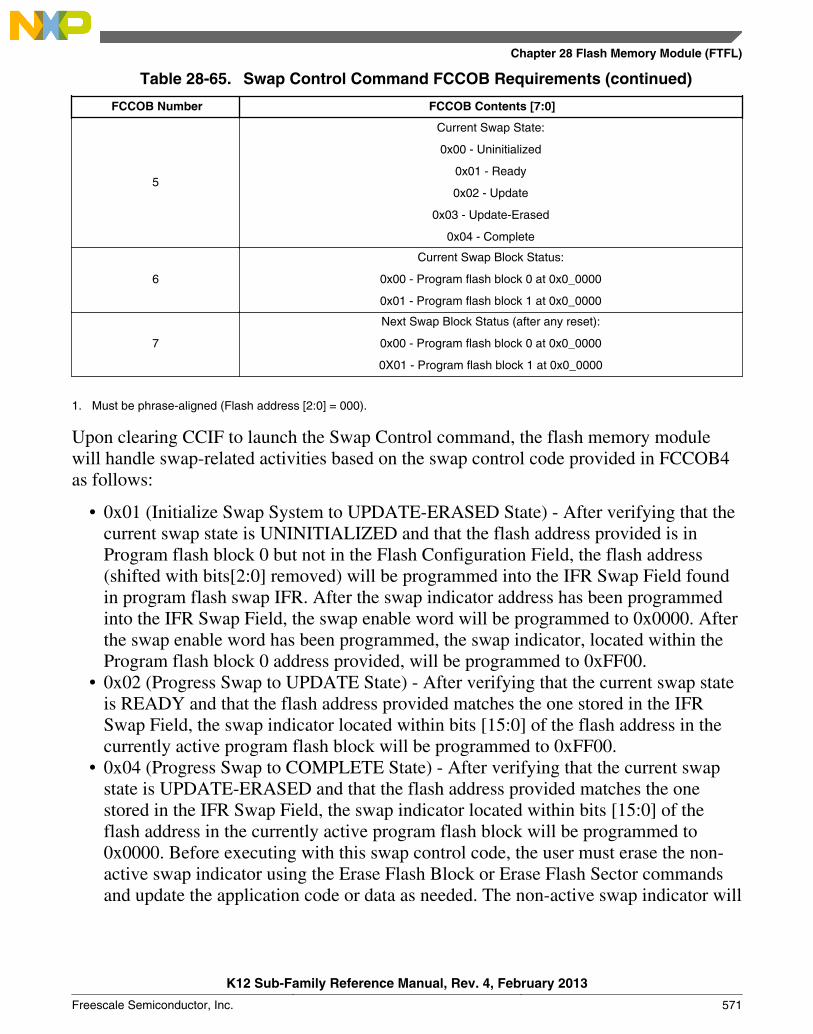
Table 28-65. Swap Control Command FCCOB Requirements (continued)
FCCOB Number FCCOB Contents [7:0]
5
Current Swap State:
0x00 - Uninitialized
0x01 - Ready
0x02 - Update
0x03 - Update-Erased
0x04 - Complete
6
Current Swap Block Status:
0x00 - Program flash block 0 at 0x0_0000
0x01 - Program flash block 1 at 0x0_0000
7
Next Swap Block Status (after any reset):
0x00 - Program flash block 0 at 0x0_0000
0X01 - Program flash block 1 at 0x0_0000
1. Must be phrase-aligned (Flash address [2:0] = 000).
Upon clearing CCIF to launch the Swap Control command, the flash memory modulewill handle swap-related activities based on the swap control code provided in FCCOB4as follows:
• 0x01 (Initialize Swap System to UPDATE-ERASED State) - After verifying that thecurrent swap state is UNINITIALIZED and that the flash address provided is inProgram flash block 0 but not in the Flash Configuration Field, the flash address(shifted with bits[2:0] removed) will be programmed into the IFR Swap Field foundin program flash swap IFR. After the swap indicator address has been programmedinto the IFR Swap Field, the swap enable word will be programmed to 0x0000. Afterthe swap enable word has been programmed, the swap indicator, located within theProgram flash block 0 address provided, will be programmed to 0xFF00.
• 0x02 (Progress Swap to UPDATE State) - After verifying that the current swap stateis READY and that the flash address provided matches the one stored in the IFRSwap Field, the swap indicator located within bits [15:0] of the flash address in thecurrently active program flash block will be programmed to 0xFF00.
• 0x04 (Progress Swap to COMPLETE State) - After verifying that the current swapstate is UPDATE-ERASED and that the flash address provided matches the onestored in the IFR Swap Field, the swap indicator located within bits [15:0] of theflash address in the currently active program flash block will be programmed to0x0000. Before executing with this swap control code, the user must erase the non-active swap indicator using the Erase Flash Block or Erase Flash Sector commandsand update the application code or data as needed. The non-active swap indicator will
Chapter 28 Flash Memory Module (FTFL)
K12 Sub-Family Reference Manual, Rev. 4, February 2013
Freescale Semiconductor, Inc. 571
be checked at the erase verify level and if the check fails, the current swap state willbe changed to UPDATE with FSTAT[ACCERR] set.
• 0x08 (Report Swap System Status) - After verifying that the flash address providedmatches the one stored in the IFR Swap Field, the status of the swap system will bereported as follows:
• FCCOB5 (Current Swap State) - indicates the current swap state based on thestatus of the swap enable word and the swap indicators. If theFSTAT[MGSTAT0] flag is set after command completion, the swap statereturned was not successfully transitioned from and the appropriate swapcommand code must be attempted again. If the current swap state is UPDATEand the non-active swap indicator is 0xFFFF, the current swap state is changedto UPDATE-ERASED.
• FCCOB6 (Current Swap Block Status) - indicates which program flash block iscurrently located at relative flash address 0x0_0000.
• FCCOB7 (Next Swap Block Status) - indicates which program flash block willbe located at relative flash address 0x0_0000 after the next reset of the flashmemory module.
NOTEIt is recommended that the user execute the Swap Controlcommand to report swap status (code 0x08) after any reset todetermine if issues with the swap system were detected duringthe swap state determination procedure.
NOTEIt is recommended that the user write 0xFF to FCCOB5,FCCOB6, and FCCOB7 since the Swap Control command willnot always return the swap state and status fields when anaccess error is detected.
The swap indicators are implicitly protected from being programmed during ProgramLongword or Program Section command operations and are implicitly unprotected duringSwap Control command operations. The swap indicators are implicitly protected frombeing erased during Erase Flash Block and Erase Flash Sector command operationsunless the swap indicator being erased is in the non-active program flash block and theswap system is in the UPDATE or UPDATE-ERASED state. Once the swap system hasbeen initialized, the Erase All Blocks command can be used to uninitialize the swapsystem.
Functional Description
K12 Sub-Family Reference Manual, Rev. 4, February 2013
572 Freescale Semiconductor, Inc.

Table 28-66. Swap Control Command Error Handling
Error ConditionSwap
ControlCode
Error Bit
Command not available in current mode/security1 All FSTAT[ACCERR]
Flash address is not in program flash block 0 All FSTAT[ACCERR]
Flash address is in the Flash Configuration Field All FSTAT[ACCERR]
Flash address is not phrase aligned All FSTAT[ACCERR]
Flash address does not match the swap indicator address in the IFR 2, 4 FSTAT[ACCERR]
Swap initialize requested when swap system is not in the uninitialized state 1 FSTAT[ACCERR]
Swap update requested when swap system is not in the ready state 2 FSTAT[ACCERR]
Swap complete requested when swap system is not in the update-erasedstate
4 FSTAT[ACCERR]
An undefined swap control code is provided - FSTAT[ACCERR]
Any errors have been encountered during the swap determination andprogram-verify operations
1, 2, 4 FSTAT[MGSTAT0]
Any brownouts were detected during the swap determination procedure 8 FSTAT[MGSTAT0]
1. Returned fields will not be updated, i.e. no swap state or status reporting
Chapter 28 Flash Memory Module (FTFL)
K12 Sub-Family Reference Manual, Rev. 4, February 2013
Freescale Semiconductor, Inc. 573

Reset
2
Erase
4
Erase
Reset
Block0 Active States Block1 Active States
Ready0
Update0
Complete0 Ready1
UpErs1
Complete1
1
0xFFFF 0x0000
0xFF00 0x0000
0x0000 0xFFFF
0x0000 0xFFFF
0xFFFF 0xFF00
0xFFFF 0x0000
Swap State Indicator0 Indicator1
Legend
Swap Control Code
4
UpErs0 0xFF00 0xFFFF
2
Update1 0x0000 0xFF00
Erase: ERSBLK or ERSSCR commands Reset: POR, VLLSx exit, warm/system reset
Uninitialized0 0xFFFF 0xFFFF
Figure 28-35. Valid Swap State Sequencing
Functional Description
K12 Sub-Family Reference Manual, Rev. 4, February 2013
574 Freescale Semiconductor, Inc.

Table 28-67. Swap State Report Mapping
Case Swap EnableField
Swap Indicator01
Swap Indicator11
Swap State2 StateCode
MGSTAT0
ActiveBlock
1 0xFFFF - - Uninitialized 0 0 0
2 0x0000 0xFF00 0x0000 Update 2 0 0
3 0x0000 0xFF00- 0xFFFF Update-Erased 3 0 0
4 0x0000 0x0000 0xFFFF Complete 4 0 0
5 0x0000 0x0000 0xFFFF Ready 1 0 1
6 0x0000 0x0000 0xFF00 Update 2 0 1
7 0x0000 0xFFFF 0xFF00 Update-Erased 3 0 1
8 0x0000 0xFFFF3
0x0000 Complete4
4 0 1
9 0x0000 0xFFFF 0x0000 Ready5
1 0 0
10 0xXXXX - - Uninitialized 0 1 0
11 0x0000 0xFFFF 0xFFFF Uninitialized 0 1 0
12 0x0000 0xFFXX 0xFFFF Ready 1 1 0
13 0x0000 0xFFXX 0x0000 Ready 1 1 0
14 0x0000 0xXXXX 0x0000 Ready 1 1 0
156
0x0000 0xFFFF 0xFFXX Ready 1 1 1
16 0x0000 0x0000 0xFFXX Ready 1 1 1
176
0x0000 0x0000 0xXXXX Ready 1 1 1
18 0x0000 0xFF00 0xFFFF Update 2 1 0
19 0x0000 0xFF00 0xXXXX Update 2 1 0
20 0x0000 0xFF(00) 0xFFXX Update 2 1 0
216
0x0000 0x0000 0x0000 Update 2 1 0
226
0x0000 0xXXXX 0xXXXX Update 2 1 0
23 0x0000 0xFFFF7
0xFF00 Update 2 1 1
24 0x0000 0xXXXX 0xFF00 Update 2 1 1
25 0x0000 0xFFXX 0xFF(00) Update 2 1 1
26 0x0000 0xXX00 0xFFFF Update-Erased 3 1 0
27 0x0000 0xXXXX 0xFFFF Update-Erased 3 1 0
28 0x0000 0xFFFF 0xXX00 Update-Erased 3 1 1
29 0x0000 0xFFFF 0xXXXX Update-Erased 3 1 1
1. 0xXXXX, 0xFFXX, 0xXX00 indicates a non-valid value was read; 0xFF(00) indicates more 0’s than other indicator (if samenumber of 0’s, then swap system defaults to block 0 active)
2. Cases 10-29 due to brownout (abort) detected during program or erase steps related to swap3. Must read 0xFFFF with erase verify level before transition to Complete allowed4. No reset since successful Swap Complete execution5. Reset after successful Swap Complete execution6. Not a valid case7. Fails to read 0xFFFF at erase verify level
Chapter 28 Flash Memory Module (FTFL)
K12 Sub-Family Reference Manual, Rev. 4, February 2013
Freescale Semiconductor, Inc. 575
28.4.12.14.1 Swap State Determination
During the reset sequence, the state of the swap system is determined by evaluating theIFR Swap Field in the program flash swap IFR and the swap indicators located in each ofthe program flash blocks at the swap indicator address stored in the IFR Swap Field.
Table 28-68. Program Flash Swap IFR Fields
Address Range Size (Bytes) Field Description
0x00 – 0x01 2 Swap Enable Word
0x02 – 0x03 2 Swap Indicator Address
0x04 – 0xFF 252 Reserved
28.4.12.15 Program Partition Command
The Program Partition command prepares the FlexNVM block for use as data flash,EEPROM backup, or a combination of both and initializes the FlexRAM. The ProgramPartition command must not be launched from flash memory, since flash memoryresources are not accessible during Program Partition command execution.
CAUTION
While different partitions of the FlexNVM are available, theintention is that a single partition choice is used throughout theentire lifetime of a given application. The FlexNVM PartitionCode choices affect the endurance and data retentioncharacteristics of the device.
Table 28-69. Program Partition Command FCCOB Requirements
FCCOB Number FCCOB Contents [7:0]
0 0x80 (PGMPART)
1 Not Used
2 Not Used
3 Not Used
4 EEPROM Data Size Code1
5 FlexNVM Partition Code2
1. See Table 2 and EEPROM Data Set Size2. See Table 3
Functional Description
K12 Sub-Family Reference Manual, Rev. 4, February 2013
576 Freescale Semiconductor, Inc.
Table 28-70. Valid EEPROM Data Set Size Codes
EEPROM Data Size Code (FCCOB4)1 EEPROM Data Set Size (Bytes)
Subsystem A + BFCCOB4[EEESPLIT] FCCOB4[EEESIZE]
11 0xF 02
00 0x9 4 + 28
01 0x9 8 + 24
10 0x9 16 + 16
11 0x9 16 + 16
00 0x8 8 + 56
01 0x8 16 + 48
10 0x8 32 + 32
11 0x8 32 + 32
00 0x7 16 + 112
01 0x7 32 + 96
10 0x7 64 + 64
11 0x7 64 + 64
00 0x6 32 + 224
01 0x6 64 + 192
10 0x6 128 + 128
11 0x6 128 + 128
00 0x5 64 + 448
01 0x5 128 + 384
10 0x5 256 + 256
11 0x5 256 + 256
00 0x4 128 + 896
01 0x4 256 + 768
10 0x4 512 + 512
11 0x4 512 + 512
00 0x3 256 + 1,792
01 0x3 512 + 1,536
10 0x3 1,024 + 1,024
11 0x3 1,024 + 1,024
00 0x2 512 + 3,584
01 0x2 1,024 + 3,072
10 0x2 2,048 + 2,048
11 0x2 2,048 + 2,048
1. FCCOB4[7:6] = 002. EEPROM Data Set Size must be set to 0 bytes when the FlexNVM Partition Code is set for no EEPROM.
Chapter 28 Flash Memory Module (FTFL)
K12 Sub-Family Reference Manual, Rev. 4, February 2013
Freescale Semiconductor, Inc. 577
Table 28-71. Valid FlexNVM Partition Codes
FlexNVM Partition Code(FCCOB5[DEPART])1
Data flash Size (KB) EEPROM backup Size (KB)
0000 64 0
0011 32 32
0100 0 64
1000 0 64
1011 32 32
1100 64 0
1. FCCOB5[7:4] = 0000
After clearing CCIF to launch the Program Partition command, the flash memory modulefirst verifies that the EEPROM Data Size Code and FlexNVM Partition Code in the dataflash IFR are erased. If erased, the Program Partition command erases the contents of theFlexNVM memory. If the FlexNVM is to be partitioned for EEPROM backup, theallocated EEPROM backup sectors are formatted for EEPROM use. Finally, the partitioncodes are programmed into the data flash IFR using the values provided. The ProgramPartition command also verifies that the partition codes read back correctly afterprogramming. If the FlexNVM is partitioned for EEPROM backup, the EEERDY flagwill set with RAMRDY clear. If the FlexNVM is not partitioned for EEPROM backup,the RAMRDY flag will set with EEERDY clear. The CCIF flag is set after the ProgramPartition operation completes.
Prior to launching the Program Partition command, the data flash IFR must be in anerased state, which can be accomplished by executing the Erase All Blocks command orby an external request (see Erase All Blocks Command). The EEPROM Data Size Codeand FlexNVM Partition Code are read using the Read Resource command (see ReadResource Command).
Table 28-72. Program Partition Command Error Handling
Error Condition Error Bit
Command not available in current mode/security FSTAT[ACCERR]
The EEPROM data size and FlexNVM partition code bytes are not initially 0xFFFF FSTAT[ACCERR]
Invalid EEPROM Data Size Code is entered (see Table 28-70 for valid codes) FSTAT[ACCERR]
Invalid FlexNVM Partition Code is entered (see Table 28-71 for valid codes) FSTAT[ACCERR]
FlexNVM Partition Code = full data flash (no EEPROM) and EEPROM Data Size Codeallocates FlexRAM for EEPROM
FSTAT[ACCERR]
FlexNVM Partition Code allocates space for EEPROM backup, but EEPROM Data Size Codeallocates no FlexRAM for EEPROM
FSTAT[ACCERR]
FCCOB4[7:6] != 00 FSTAT[ACCERR]
FCCOB5[7:4] != 0000 FSTAT[ACCERR]
Any errors have been encountered during the verify operation FSTAT[MGSTAT0]
Functional Description
K12 Sub-Family Reference Manual, Rev. 4, February 2013
578 Freescale Semiconductor, Inc.
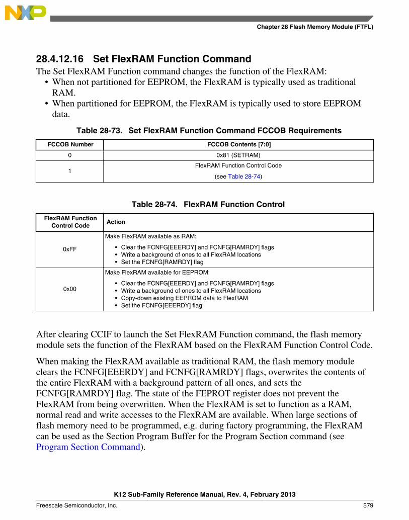
28.4.12.16 Set FlexRAM Function CommandThe Set FlexRAM Function command changes the function of the FlexRAM:
• When not partitioned for EEPROM, the FlexRAM is typically used as traditionalRAM.
• When partitioned for EEPROM, the FlexRAM is typically used to store EEPROMdata.
Table 28-73. Set FlexRAM Function Command FCCOB Requirements
FCCOB Number FCCOB Contents [7:0]
0 0x81 (SETRAM)
1FlexRAM Function Control Code
(see Table 28-74)
Table 28-74. FlexRAM Function Control
FlexRAM FunctionControl Code
Action
0xFF
Make FlexRAM available as RAM:
• Clear the FCNFG[EEERDY] and FCNFG[RAMRDY] flags• Write a background of ones to all FlexRAM locations• Set the FCNFG[RAMRDY] flag
0x00
Make FlexRAM available for EEPROM:
• Clear the FCNFG[EEERDY] and FCNFG[RAMRDY] flags• Write a background of ones to all FlexRAM locations• Copy-down existing EEPROM data to FlexRAM• Set the FCNFG[EEERDY] flag
After clearing CCIF to launch the Set FlexRAM Function command, the flash memorymodule sets the function of the FlexRAM based on the FlexRAM Function Control Code.
When making the FlexRAM available as traditional RAM, the flash memory moduleclears the FCNFG[EEERDY] and FCNFG[RAMRDY] flags, overwrites the contents ofthe entire FlexRAM with a background pattern of all ones, and sets theFCNFG[RAMRDY] flag. The state of the FEPROT register does not prevent theFlexRAM from being overwritten. When the FlexRAM is set to function as a RAM,normal read and write accesses to the FlexRAM are available. When large sections offlash memory need to be programmed, e.g. during factory programming, the FlexRAMcan be used as the Section Program Buffer for the Program Section command (seeProgram Section Command).
Chapter 28 Flash Memory Module (FTFL)
K12 Sub-Family Reference Manual, Rev. 4, February 2013
Freescale Semiconductor, Inc. 579
When making the FlexRAM available for EEPROM, the flash memory module clears theFCNFG[EEERDY] and FCNFG[RAMRDY] flags, overwrites the contents of theFlexRAM allocated for EEPROM with a background pattern of all ones, and copies theexisting EEPROM data from the EEPROM backup record space to the FlexRAM. Aftercompletion of the EEPROM copy-down, the FCNFG[EEERDY] flag is set. When theFlexRAM is set to function as EEPROM, normal read and write access to the FlexRAMis available, but writes to the FlexRAM also invoke EEPROM activity. The CCIF flag isset after the Set FlexRAM Function operation completes.
Table 28-75. Set FlexRAM Function Command Error Handling
Error Condition Error Bit
Command not available in current mode/security FSTAT[ACCERR]
FlexRAM Function Control Code is not defined FSTAT[ACCERR]
FlexRAM Function Control Code is set to make the FlexRAM available for EEPROM, butFlexNVM is not partitioned for EEPROM
FSTAT[ACCERR]
28.4.13 Security
The flash memory module provides security information to the MCU based on contentsof the FSEC security register. The MCU then limits access to flash memory resources asdefined in the device's Chip Configuration details. During reset, the flash memorymodule initializes the FSEC register using data read from the security byte of the FlashConfiguration Field (see Flash Configuration Field Description).
The following fields are available in the FSEC register. The settings are described in theFlash Security Register (FTFL_FSEC) details.
Table 28-76. FSEC register fields
FSEC field Description
KEYEN Backdoor Key Access
MEEN Mass Erase Capability
FSLACC Freescale Factory Access
SEC MCU security
28.4.13.1 Flash Memory Access by Mode and Security
The following table summarizes how access to the flash memory module is affected bysecurity and operating mode.
Functional Description
K12 Sub-Family Reference Manual, Rev. 4, February 2013
580 Freescale Semiconductor, Inc.
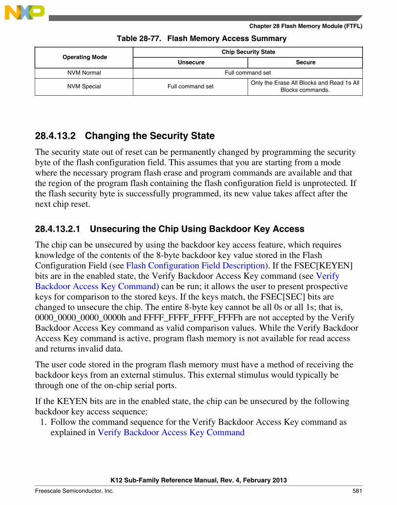
Table 28-77. Flash Memory Access Summary
Operating ModeChip Security State
Unsecure Secure
NVM Normal Full command set
NVM Special Full command setOnly the Erase All Blocks and Read 1s All
Blocks commands.
28.4.13.2 Changing the Security State
The security state out of reset can be permanently changed by programming the securitybyte of the flash configuration field. This assumes that you are starting from a modewhere the necessary program flash erase and program commands are available and thatthe region of the program flash containing the flash configuration field is unprotected. Ifthe flash security byte is successfully programmed, its new value takes affect after thenext chip reset.
28.4.13.2.1 Unsecuring the Chip Using Backdoor Key Access
The chip can be unsecured by using the backdoor key access feature, which requiresknowledge of the contents of the 8-byte backdoor key value stored in the FlashConfiguration Field (see Flash Configuration Field Description). If the FSEC[KEYEN]bits are in the enabled state, the Verify Backdoor Access Key command (see VerifyBackdoor Access Key Command) can be run; it allows the user to present prospectivekeys for comparison to the stored keys. If the keys match, the FSEC[SEC] bits arechanged to unsecure the chip. The entire 8-byte key cannot be all 0s or all 1s; that is,0000_0000_0000_0000h and FFFF_FFFF_FFFF_FFFFh are not accepted by the VerifyBackdoor Access Key command as valid comparison values. While the Verify BackdoorAccess Key command is active, program flash memory is not available for read accessand returns invalid data.
The user code stored in the program flash memory must have a method of receiving thebackdoor keys from an external stimulus. This external stimulus would typically bethrough one of the on-chip serial ports.
If the KEYEN bits are in the enabled state, the chip can be unsecured by the followingbackdoor key access sequence:
1. Follow the command sequence for the Verify Backdoor Access Key command asexplained in Verify Backdoor Access Key Command
Chapter 28 Flash Memory Module (FTFL)
K12 Sub-Family Reference Manual, Rev. 4, February 2013
Freescale Semiconductor, Inc. 581

2. If the Verify Backdoor Access Key command is successful, the chip is unsecured andthe FSEC[SEC] bits are forced to the unsecure state
An illegal key provided to the Verify Backdoor Access Key command prohibits furtheruse of the Verify Backdoor Access Key command. A reset of the chip is the only methodto re-enable the Verify Backdoor Access Key command when a comparison fails.
After the backdoor keys have been correctly matched, the chip is unsecured by changingthe FSEC[SEC] bits. A successful execution of the Verify Backdoor Access Keycommand changes the security in the FSEC register only. It does not alter the securitybyte or the keys stored in the Flash Configuration Field (Flash Configuration FieldDescription). After the next reset of the chip, the security state of the flash memorymodule reverts back to the flash security byte in the Flash Configuration Field. TheVerify Backdoor Access Key command sequence has no effect on the program and eraseprotections defined in the program flash protection registers.
If the backdoor keys successfully match, the unsecured chip has full control of thecontents of the Flash Configuration Field. The chip may erase the sector containing theFlash Configuration Field and reprogram the flash security byte to the unsecure state andchange the backdoor keys to any desired value.
28.4.14 Reset Sequence
On each system reset the flash memory module executes a sequence which establishesinitial values for the flash block configuration parameters, FPROT, FDPROT, FEPROT,FOPT, and FSEC registers and the FCNFG[SWAP, PFLSH, RAMRDY, EEERDY] bits.
FSTAT[CCIF] is cleared throughout the reset sequence. The flash memory module holdsoff CPU access during the reset sequence. Flash reads are possible when the hold isremoved. Completion of the reset sequence is marked by setting CCIF which enablesflash user commands.
If a reset occurs while any flash command is in progress, that command is immediatelyaborted. The state of the word being programmed or the sector/block being erased is notguaranteed. Commands and operations do not automatically resume after exiting reset.
Functional Description
K12 Sub-Family Reference Manual, Rev. 4, February 2013
582 Freescale Semiconductor, Inc.
Chapter 29EzPort
29.1 OverviewNOTE
For the chip-specific implementation details of this module'sinstances see the chip configuration information.
The EzPort module is a serial flash programming interface that allows In-SystemProgramming (ISP) of flash memory contents on a 32 bit general-purposemicrocontroller. Memory contents can be read, erased, and programmed from an externalsource in a format that is compatible with many stand-alone flash memory chips, withoutnecessitating the removal of the microcontroller from the system.
29.1.1 Introduction
The following figure is a high level block diagram of the EzPort.
K12 Sub-Family Reference Manual, Rev. 4, February 2013
Freescale Semiconductor, Inc. 583
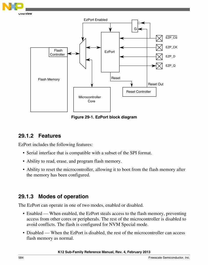
Flash Controller
EzPort
Flash Memory
Microcontroller Core
EzPort Enabled
G
Reset Controller
Reset
Reset Out
EZP_CS
EZP_CK
EZP_D
EZP_Q
Figure 29-1. EzPort block diagram
29.1.2 Features
EzPort includes the following features:
• Serial interface that is compatible with a subset of the SPI format.
• Ability to read, erase, and program flash memory.
• Ability to reset the microcontroller, allowing it to boot from the flash memory afterthe memory has been configured.
29.1.3 Modes of operation
The EzPort can operate in one of two modes, enabled or disabled.
• Enabled — When enabled, the EzPort steals access to the flash memory, preventingaccess from other cores or peripherals. The rest of the microcontroller is disabled toavoid conflicts. The flash is configured for NVM Special mode.
• Disabled — When the EzPort is disabled, the rest of the microcontroller can accessflash memory as normal.
Overview
K12 Sub-Family Reference Manual, Rev. 4, February 2013
584 Freescale Semiconductor, Inc.
The EzPort provides a simple interface to connect an external device to the flash memoryon board a 32 bit microcontroller. The interface itself is compatible with the SPIinterface, with the EzPort operating as a slave, running in either of the two followingmodes. The data is transmitted with the most significant bit first.
• CPOL = 0, CPHA = 0
• CPOL = 1, CPHA = 1
Commands are issued by the external device to erase, program, or read the contents of theflash memory. The serial data out from the EzPort is tri-stated unless data is being driven.This allows the signal to be shared among several different EzPort (or compatible)devices in parallel, as long as they have different chip-selects.
29.2 External signal descriptionThe following table contains a list of EzPort external signals, and the following sectionsexplain the signals in detail.
Table 29-1. EzPort external signal description
Name Description I/O
EZP_CK EzPort Clock Input
EZP_CS EzPort Chip Select Input
EZP_D EzPort Serial Data In Input
EZP_Q EzPort Serial Data Out Output
29.2.1 EzPort Clock (EZP_CK)
EZP_CK is the serial clock for data transfers. The serial data in (EZP_D) and chip select(EZP_CS) are registered on the rising edge of EZP_CK, while serial data out (EZP_Q) isdriven on the falling edge of EZP_CK.
The maximum frequency of the EzPort clock is half the system clock frequency for allcommands except when executing the Read Data or Read FlexRAM commands. Whenexecuting these commands, the EzPort clock has a maximum frequency of one-eighth thesystem clock frequency.
Chapter 29 EzPort
K12 Sub-Family Reference Manual, Rev. 4, February 2013
Freescale Semiconductor, Inc. 585
29.2.2 EzPort Chip Select (EZP_CS)
EZP_CS is the chip select for signaling the start and end of serial transfers. If, whileEZP_CS is asserted, the microcontroller's reset out signal is negated, EzPort is enabledout of reset; otherwise it is disabled. After EzPort is enabled, asserting EZP_CScommences a serial data transfer, which continues until EZP_CS is negated again. Thenegation of EZP_CS indicates the current command is finished and resets the EzPort statemachine so that it is ready to receive the next command.
29.2.3 EzPort Serial Data In (EZP_D)
EZP_D is the serial data in for data transfers. EZP_D is registered on the rising edge ofEZP_CK. All commands, addresses, and data are shifted in most significant bit first.When the EzPort is driving output data on EZP_Q, the data shifted in EZP_D is ignored.
29.2.4 EzPort Serial Data Out (EZP_Q)
EZP_Q is the serial data out for data transfers. EZP_Q is driven on the falling edge ofEZP_CK. It is tri-stated unless EZP_CS is asserted and the EzPort is driving data out. Alldata is shifted out most significant bit first.
29.3 Command definitionThe EzPort receives commands from an external device and translates the commands intoflash memory accesses. The following table lists the supported commands.
Table 29-2. EzPort commands
Command Description CodeAddress
BytesData Bytes
Accepted whensecure?
WREN Write Enable 0x06 0 0 Yes
WRDI Write Disable 0x04 0 0 Yes
RDSR Read Status Register 0x05 0 1 Yes
READ Flash Read Data 0x03 3 1+ No
FAST_READ Flash Read Data at High Speed 0x0B 31
1+ No
SP Flash Section Program 0x02 3 8 - SECTION4 No
SE Flash Sector Erase 0xD8 33
0 No
BE Flash Bulk Erase 0xC7 0 0 Yes5
RESET Reset Chip 0xB9 0 0 Yes
WRFCCOB Write FCCOB Registers 0xBA 0 12 Yes6
Table continues on the next page...
Command definition
K12 Sub-Family Reference Manual, Rev. 4, February 2013
586 Freescale Semiconductor, Inc.
Table 29-2. EzPort commands (continued)
Command Description CodeAddress
BytesData Bytes
Accepted whensecure?
FAST_RDFCCOBRead FCCOB registers at high
speed0xBB 0 1 - 12
2No
WRFLEXRAM Write FlexRAM 0xBC 31
4 No
RDFLEXRAM Read FlexRAM 0xBD 31
1+ No
FAST_RDFLEXRAM Read FlexRAM at high speed 0xBE 31
1+2
No
1. Address must be 32-bit aligned (two LSBs must be zero).2. One byte of dummy data must be shifted in before valid data is shifted out.3. Address must be 64-bit aligned (three LSBs must be zero).4. Please see the Flash Memory chapter for a definition of section size. Total number of data bytes programmed must be a
multiple of 8.5. Bulk Erase is accepted when security is set and only when the BEDIS status field is not set.6. The flash will be in NVM Special mode, restricting the type of commands that can be executed through WRITE_FCCOB
when security is enabled.
29.3.1 Command descriptions
This section describes the module commands.
29.3.1.1 Write Enable
The Write Enable (WREN) command sets the write enable register field in the EzPortstatus register. The write enable field must be set for a write command (SP, SE, BE,WRFCCOB, or WRFLEXRAM) to be accepted. The write enable register field clears onreset, on a Write Disable command, and at the completion of write command. Thiscommand must not be used if a write is already in progress.
29.3.1.2 Write Disable
The Write Disable (WRDI) command clears the write enable register field in the statusregister. This command must not be used if a write is already in progress.
29.3.1.3 Read Status Register
The Read Status Register (RDSR) command returns the contents of the EzPort statusregister.
Chapter 29 EzPort
K12 Sub-Family Reference Manual, Rev. 4, February 2013
Freescale Semiconductor, Inc. 587
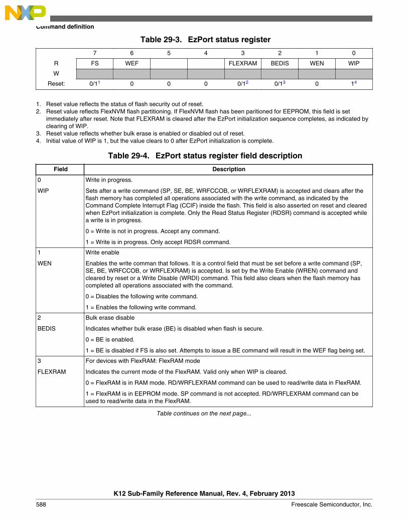
Table 29-3. EzPort status register
7 6 5 4 3 2 1 0
R FS WEF FLEXRAM BEDIS WEN WIP
W
Reset: 0/11 0 0 0 0/12 0/13 0 14
1. Reset value reflects the status of flash security out of reset.2. Reset value reflects FlexNVM flash partitioning. If FlexNVM flash has been paritioned for EEPROM, this field is set
immediately after reset. Note that FLEXRAM is cleared after the EzPort initialization sequence completes, as indicated byclearing of WIP.
3. Reset value reflects whether bulk erase is enabled or disabled out of reset.4. Initial value of WIP is 1, but the value clears to 0 after EzPort initialization is complete.
Table 29-4. EzPort status register field description
Field Description
0
WIP
Write in progress.
Sets after a write command (SP, SE, BE, WRFCCOB, or WRFLEXRAM) is accepted and clears after theflash memory has completed all operations associated with the write command, as indicated by theCommand Complete Interrupt Flag (CCIF) inside the flash. This field is also asserted on reset and clearedwhen EzPort initialization is complete. Only the Read Status Register (RDSR) command is accepted whilea write is in progress.
0 = Write is not in progress. Accept any command.
1 = Write is in progress. Only accept RDSR command.
1
WEN
Write enable
Enables the write comman that follows. It is a control field that must be set before a write command (SP,SE, BE, WRFCCOB, or WRFLEXRAM) is accepted. Is set by the Write Enable (WREN) command andcleared by reset or a Write Disable (WRDI) command. This field also clears when the flash memory hascompleted all operations associated with the command.
0 = Disables the following write command.
1 = Enables the following write command.
2
BEDIS
Bulk erase disable
Indicates whether bulk erase (BE) is disabled when flash is secure.
0 = BE is enabled.
1 = BE is disabled if FS is also set. Attempts to issue a BE command will result in the WEF flag being set.
3
FLEXRAM
For devices with FlexRAM: FlexRAM mode
Indicates the current mode of the FlexRAM. Valid only when WIP is cleared.
0 = FlexRAM is in RAM mode. RD/WRFLEXRAM command can be used to read/write data in FlexRAM.
1 = FlexRAM is in EEPROM mode. SP command is not accepted. RD/WRFLEXRAM command can beused to read/write data in the FlexRAM.
Table continues on the next page...
Command definition
K12 Sub-Family Reference Manual, Rev. 4, February 2013
588 Freescale Semiconductor, Inc.

Table 29-4. EzPort status register field description (continued)
Field Description
6
WEF
Write error flag
Indicates whether there has been an error while executing a write command (SP, SE, BE, WRFCCOB, orWRFLEXRAM). The WEF flag will set if Flash Access Error Flag (ACCERR), Flash Protection Violation(FPVIOL), or Memory Controller Command Completion Status (MGSTAT0) inside the flash memory is setat the completion of the write command. See the flash memory chapter for further description of these flagsand their sources. The WEF flag clears after a Read Status Register (RDSR) command.
0 = No error on previous write command.
1 = Error on previous write command.
7
FS
Flash security
Indicates whether the flash is secure. See Table 29-2 for the list of commands that will be accepted whenflash is secure. Flash security can be disabled by performing a BE command.
0 = Flash is not secure.
1 = Flash is secure.
29.3.1.4 Read Data
The Read Data (READ) command returns data from the flash memory or FlexNVM,depending on the initial address specified in the command word. The initial address mustbe 32-bit aligned with the two LSBs being zero.
Data continues being returned for as long as the EzPort chip select (EZP_CS) is asserted,with the address automatically incrementing. In this way, the entire contents of flash canbe returned by one command. Attempts to read from an address which does not fallwithin the valid address range for the flash memory regions returns unknown data. SeeFlash memory map for EzPort access.
For this command to return the correct data, the EzPort clock (EZP_CK) must run at theinternal system clock divided by eight or slower. This command is not accepted if theWEF, WIP, or FS field in the EzPort status register is set.
29.3.1.5 Read Data at High Speed
The Read Data at High Speed (FAST_READ) command is identical to the READcommand, except for the inclusion of a dummy byte following the address bytes andbefore the first data byte is returned.
This command can be run with an EzPort clock (EZP_CK) frequency of half the internalsystem clock frequency of the microcontroller or slower. This command is not accepted ifthe WEF, WIP, or FS field in the EzPort status register is set.
Chapter 29 EzPort
K12 Sub-Family Reference Manual, Rev. 4, February 2013
Freescale Semiconductor, Inc. 589

29.3.1.6 Section Program
The Section Program (SP) command programs up to one section of flash memory that haspreviously been erased. Please see the Flash Memory chapter for a definition of sectionsize. The starting address of the memory to program is sent after the command word andmust be a 64-bit aligned address with the three LSBs being zero).
As data is shifted in, the EzPort buffers the data in FlexRAM/Programming AccelerationRAM before executing an SP command within the flash. For this reason, the number ofbytes to be programmed must be a multiple of 8 and up to one flash section can beprogrammed at a time. For more details, see the Flash Block Guide.
Attempts to program more than one section, across a sector boundary or from an initialaddress which does not fall within the valid address range for the flash causes the WEFflag to set. See Flash memory map for EzPort access.
For devices with FlexRAM: This command requires the FlexRAM to be configured fortraditional RAM operation. By default, after entering EzPort mode, the FlexRAM isconfigured for traditional RAM operation. If the user reconfigures FlexRAM forEEPROM operation, then the user should use the WRFCCOB command to configureFlexRAM back to traditional RAM operation before issuing an SP command. See theFlash Memory chapter for details on how the FlexRAM function is modified.
This command is not accepted if the WEF, WIP, FLEXRAM, or FS field is set or if theWEN field is not set in the EzPort status register.
29.3.1.7 Sector Erase
The Sector Erase (SE) command erases the contents of one sector of flash memory. Thethree byte address sent after the command byte can be any address within the sector toerase, but must be a 64-bit aligned address (the three LSBs must be zero). Attempts toerase from an initial address which does not fall within the valid address range (see Flashmemory map for EzPort access) for the flash results in the WEF flag being set.
This command is not accepted if the WEF, WIP or FS field is set or if the WEN field isnot set in the EzPort status register.
Command definition
K12 Sub-Family Reference Manual, Rev. 4, February 2013
590 Freescale Semiconductor, Inc.
29.3.1.8 Bulk Erase
The Bulk Erase (BE) command erases the entire contents of flash memory, ignoring anyprotected sectors or flash security. Flash security is disabled upon successful completionof the BE command.
Attempts to issue a BE command while the BEDIS and FS fields are set results in theWEF flag being set in the EzPort status register. Also, this command is not accepted ifthe WEF or WIP field is set or if the WEN field is not set in the EzPort status register.
29.3.1.9 EzPort Reset Chip
The Reset Chip (RESET) command forces the chip into the reset state. If the EzPort chipselect (EZP_CS) pin is asserted at the end of the reset period, EzPort is enabled;otherwise, it is disabled. This command allows the chip to boot up from flash memoryafter being programmed by an external source.
This command is not accepted if the WIP field is set in the EzPort status register.
29.3.1.10 Write FCCOB Registers
The Write FCCOB Registers (WRFCCOB) command allows the user to write to the flashcommon command object registers and execute any command allowed by the flash.
NOTEWhen security is enabled, the flash is configured in NVMSpecial mode, restricting the commands that can be executed bythe flash.
After receiving 12 bytes of data, EzPort writes the data to the FCCOB 0-B registers in theflash and then automatically launches the command within the flash. If greater or lessthan 12 bytes of data is received, this command has unexpected results and may result inthe WEF flag being set.
This command is not accepted if the WEF or WIP field is set or if the WEN field is notset in the EzPort status register.
Chapter 29 EzPort
K12 Sub-Family Reference Manual, Rev. 4, February 2013
Freescale Semiconductor, Inc. 591
29.3.1.11 Read FCCOB Registers at High Speed
The Read FCCOB Registers at High Speed (FAST_RDFCCOB) command allows theuser to read the contents of the flash common command object registers. After receivingthe command, EzPort waits for one dummy byte of data before returning FCCOB registerdata starting at FCCOB 0 and ending with FCCOB B.
This command can be run with an EzPort clock (EZP_CK) frequency half the internalsystem clock frequency of the microcontroller or slower. Attempts to read greater than 12bytes of data returns unknown data. This command is not accepted if the WEF, WIP, orFS fields in the EzPort status register are 1.
29.3.1.12 Write FlexRAM
This command is only applicable for devices with FlexRAM.
The Write FlexRAM (WRFLEXRAM) command allows the user to write four bytes ofdata to the FlexRAM. If the FlexRAM is configured for EEPROM operation, theWRFLEXRAM command can effectively be used to create data records in the EEPROMflash memory.
By default, after entering EzPort mode, the FlexRAM is configured for traditional RAMoperation and functions as direct RAM. The user can alter the FlexRAM configuration byusing WRFCCOB to execute a Set FlexRAM or Program Partition command within theflash.
The address of the FlexRAM location to be written is sent after the command word andmust be a 32-bit aligned address (the two LSBs must be zero). Attempts to write anaddress which does not fall within the valid address range for the FlexRAM results in thevalue of the WEF flag being 1. See Flash memory map for EzPort access for moreinformation.
After receiving four bytes of data, EzPort writes the data to the FlexRAM. If greater orless than four bytes of data is received, this command has unexpected results and mayresult in the value of the WEF flag being 1.
This command is not accepted if the WEF, WIP or FS fields are 1 or if the WEN field is0 in the EzPort status register.
29.3.1.13 Read FlexRAM
This command is only applicable for devices with FlexRAM.
Command definition
K12 Sub-Family Reference Manual, Rev. 4, February 2013
592 Freescale Semiconductor, Inc.
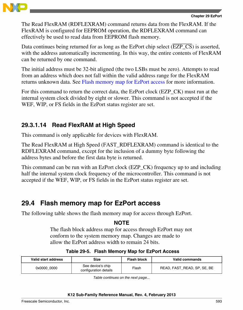
The Read FlexRAM (RDFLEXRAM) command returns data from the FlexRAM. If theFlexRAM is configured for EEPROM operation, the RDFLEXRAM command caneffectively be used to read data from EEPROM flash memory.
Data continues being returned for as long as the EzPort chip select (EZP_CS) is asserted,with the address automatically incrementing. In this way, the entire contents of FlexRAMcan be returned by one command.
The initial address must be 32-bit aligned (the two LSBs must be zero). Attempts to readfrom an address which does not fall within the valid address range for the FlexRAMreturns unknown data. See Flash memory map for EzPort access for more information.
For this command to return the correct data, the EzPort clock (EZP_CK) must run at theinternal system clock divided by eight or slower. This command is not accepted if theWEF, WIP, or FS fields in the EzPort status register are set.
29.3.1.14 Read FlexRAM at High Speed
This command is only applicable for devices with FlexRAM.
The Read FlexRAM at High Speed (FAST_RDFLEXRAM) command is identical to theRDFLEXRAM command, except for the inclusion of a dummy byte following theaddress bytes and before the first data byte is returned.
This command can be run with an EzPort clock (EZP_CK) frequency up to and includinghalf the internal system clock frequency of the microcontroller. This command is notaccepted if the WEF, WIP, or FS fields in the EzPort status register are set.
29.4 Flash memory map for EzPort accessThe following table shows the flash memory map for access through EzPort.
NOTEThe flash block address map for access through EzPort may notconform to the system memory map. Changes are made toallow the EzPort address width to remain 24 bits.
Table 29-5. Flash Memory Map for EzPort Access
Valid start address Size Flash block Valid commands
0x0000_0000See device's chip
configuration detailsFlash READ, FAST_READ, SP, SE, BE
Table continues on the next page...
Chapter 29 EzPort
K12 Sub-Family Reference Manual, Rev. 4, February 2013
Freescale Semiconductor, Inc. 593

Table 29-5. Flash Memory Map for EzPort Access (continued)
Valid start address Size Flash block Valid commands
0x0080_0000See device's chip
configuration detailsFlexNVM READ, FAST_READ, SP, SE, BE
0x0000_0000See device's chip
configuration detailsFlexRAM
RDFLEXRAM, FAST_RDFLEXRAM,WRFLEXRAM, BE
Flash memory map for EzPort access
K12 Sub-Family Reference Manual, Rev. 4, February 2013
594 Freescale Semiconductor, Inc.

Chapter 30Cyclic Redundancy Check (CRC)
30.1 IntroductionNOTE
For the chip-specific implementation details of this module'sinstances see the chip configuration information.
The cyclic redundancy check (CRC) module generates 16/32-bit CRC code for errordetection.
The CRC module provides a programmable polynomial, WAS, and other parametersrequired to implement a 16-bit or 32-bit CRC standard.
The 16/32-bit code is calculated for 32 bits of data at a time.
30.1.1 FeaturesFeatures of the CRC module include:
• Hardware CRC generator circuit using a 16-bit or 32-bit programmable shift register
• Programmable initial seed value and polynomial
• Option to transpose input data or output data (the CRC result) bitwise or bytewise.This option is required for certain CRC standards. A bytewise transpose operation isnot possible when accessing the CRC data register via 8-bit accesses. In this case, theuser's software must perform the bytewise transpose function.
• Option for inversion of final CRC result
• 32-bit CPU register programming interface
K12 Sub-Family Reference Manual, Rev. 4, February 2013
Freescale Semiconductor, Inc. 595

30.1.2 Block diagram
The following is a block diagram of the CRC.
WAS
[31:24]
Polynomial
MU
X
CRC Engine
NOT Logic
Reverse Logic
Reverse Logic
[23:16] [15:8] [7:0] CRC Data
Seed
Data
Checksum
TOT TOTRFXOR
Combine Logic
TCRC
16-/32-bit Select
CRC Data Register
CRC Polynomial Register
[31:24] [23:16]
[15:8] [7:0]
[31:24] [23:16] [15:8] [7:0]
CRC Data Register
Figure 30-1. Programmable cyclic redundancy check (CRC) block diagram
30.1.3 Modes of operation
Various MCU modes affect the CRC module's functionality.
30.1.3.1 Run mode
This is the basic mode of operation.
30.1.3.2 Low-power modes (Wait or Stop)
Any CRC calculation in progress stops when the MCU enters a low-power mode thatdisables the module clock. It resumes after the clock is enabled or via the system reset forexiting the low-power mode. Clock gating for this module is MCU dependent.
30.2 Memory map and register descriptionsCRC memory map
Absoluteaddress
(hex)Register name
Width(in bits)
Access Reset valueSection/
page
4003_2000 CRC Data register (CRC_DATA) 32 R/W FFFF_FFFFh 30.2.1/597
4003_2004 CRC Polynomial register (CRC_GPOLY) 32 R/W 0000_1021h 30.2.2/598
4003_2008 CRC Control register (CRC_CTRL) 32 R/W 0000_0000h 30.2.3/598
Memory map and register descriptions
K12 Sub-Family Reference Manual, Rev. 4, February 2013
596 Freescale Semiconductor, Inc.
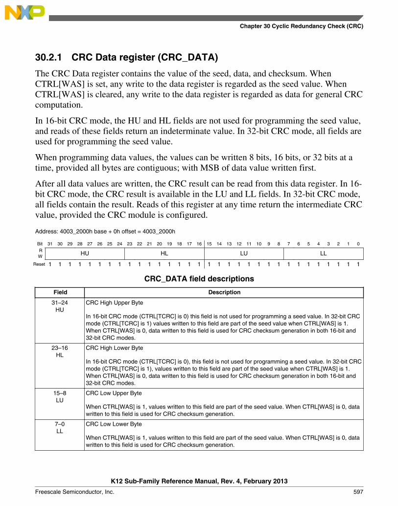
30.2.1 CRC Data register (CRC_DATA)
The CRC Data register contains the value of the seed, data, and checksum. WhenCTRL[WAS] is set, any write to the data register is regarded as the seed value. WhenCTRL[WAS] is cleared, any write to the data register is regarded as data for general CRCcomputation.
In 16-bit CRC mode, the HU and HL fields are not used for programming the seed value,and reads of these fields return an indeterminate value. In 32-bit CRC mode, all fields areused for programming the seed value.
When programming data values, the values can be written 8 bits, 16 bits, or 32 bits at atime, provided all bytes are contiguous; with MSB of data value written first.
After all data values are written, the CRC result can be read from this data register. In 16-bit CRC mode, the CRC result is available in the LU and LL fields. In 32-bit CRC mode,all fields contain the result. Reads of this register at any time return the intermediate CRCvalue, provided the CRC module is configured.
Address: 4003_2000h base + 0h offset = 4003_2000h
Bit 31 30 29 28 27 26 25 24 23 22 21 20 19 18 17 16 15 14 13 12 11 10 9 8 7 6 5 4 3 2 1 0
R HU HL LU LLW
Reset 1 1 1 1 1 1 1 1 1 1 1 1 1 1 1 1 1 1 1 1 1 1 1 1 1 1 1 1 1 1 1 1
CRC_DATA field descriptions
Field Description
31–24HU
CRC High Upper Byte
In 16-bit CRC mode (CTRL[TCRC] is 0) this field is not used for programming a seed value. In 32-bit CRCmode (CTRL[TCRC] is 1) values written to this field are part of the seed value when CTRL[WAS] is 1.When CTRL[WAS] is 0, data written to this field is used for CRC checksum generation in both 16-bit and32-bit CRC modes.
23–16HL
CRC High Lower Byte
In 16-bit CRC mode (CTRL[TCRC] is 0), this field is not used for programming a seed value. In 32-bit CRCmode (CTRL[TCRC] is 1), values written to this field are part of the seed value when CTRL[WAS] is 1.When CTRL[WAS] is 0, data written to this field is used for CRC checksum generation in both 16-bit and32-bit CRC modes.
15–8LU
CRC Low Upper Byte
When CTRL[WAS] is 1, values written to this field are part of the seed value. When CTRL[WAS] is 0, datawritten to this field is used for CRC checksum generation.
7–0LL
CRC Low Lower Byte
When CTRL[WAS] is 1, values written to this field are part of the seed value. When CTRL[WAS] is 0, datawritten to this field is used for CRC checksum generation.
Chapter 30 Cyclic Redundancy Check (CRC)
K12 Sub-Family Reference Manual, Rev. 4, February 2013
Freescale Semiconductor, Inc. 597
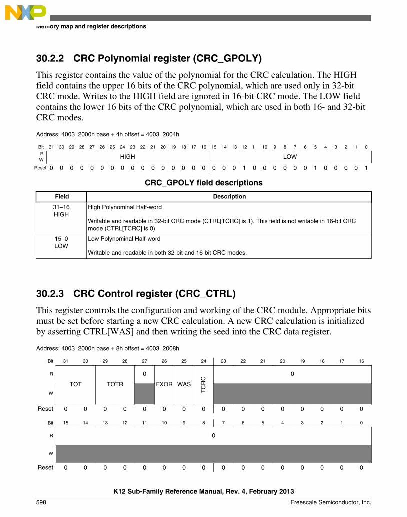
30.2.2 CRC Polynomial register (CRC_GPOLY)
This register contains the value of the polynomial for the CRC calculation. The HIGHfield contains the upper 16 bits of the CRC polynomial, which are used only in 32-bitCRC mode. Writes to the HIGH field are ignored in 16-bit CRC mode. The LOW fieldcontains the lower 16 bits of the CRC polynomial, which are used in both 16- and 32-bitCRC modes.
Address: 4003_2000h base + 4h offset = 4003_2004h
Bit 31 30 29 28 27 26 25 24 23 22 21 20 19 18 17 16 15 14 13 12 11 10 9 8 7 6 5 4 3 2 1 0
R HIGH LOWW
Reset 0 0 0 0 0 0 0 0 0 0 0 0 0 0 0 0 0 0 0 1 0 0 0 0 0 0 1 0 0 0 0 1
CRC_GPOLY field descriptions
Field Description
31–16HIGH
High Polynominal Half-word
Writable and readable in 32-bit CRC mode (CTRL[TCRC] is 1). This field is not writable in 16-bit CRCmode (CTRL[TCRC] is 0).
15–0LOW
Low Polynominal Half-word
Writable and readable in both 32-bit and 16-bit CRC modes.
30.2.3 CRC Control register (CRC_CTRL)
This register controls the configuration and working of the CRC module. Appropriate bitsmust be set before starting a new CRC calculation. A new CRC calculation is initializedby asserting CTRL[WAS] and then writing the seed into the CRC data register.
Address: 4003_2000h base + 8h offset = 4003_2008h
Bit 31 30 29 28 27 26 25 24 23 22 21 20 19 18 17 16
R
TOT TOTR
0
FXOR WAS
TC
RC
0
W
Reset 0 0 0 0 0 0 0 0 0 0 0 0 0 0 0 0
Bit 15 14 13 12 11 10 9 8 7 6 5 4 3 2 1 0
R 0
W
Reset 0 0 0 0 0 0 0 0 0 0 0 0 0 0 0 0
Memory map and register descriptions
K12 Sub-Family Reference Manual, Rev. 4, February 2013
598 Freescale Semiconductor, Inc.
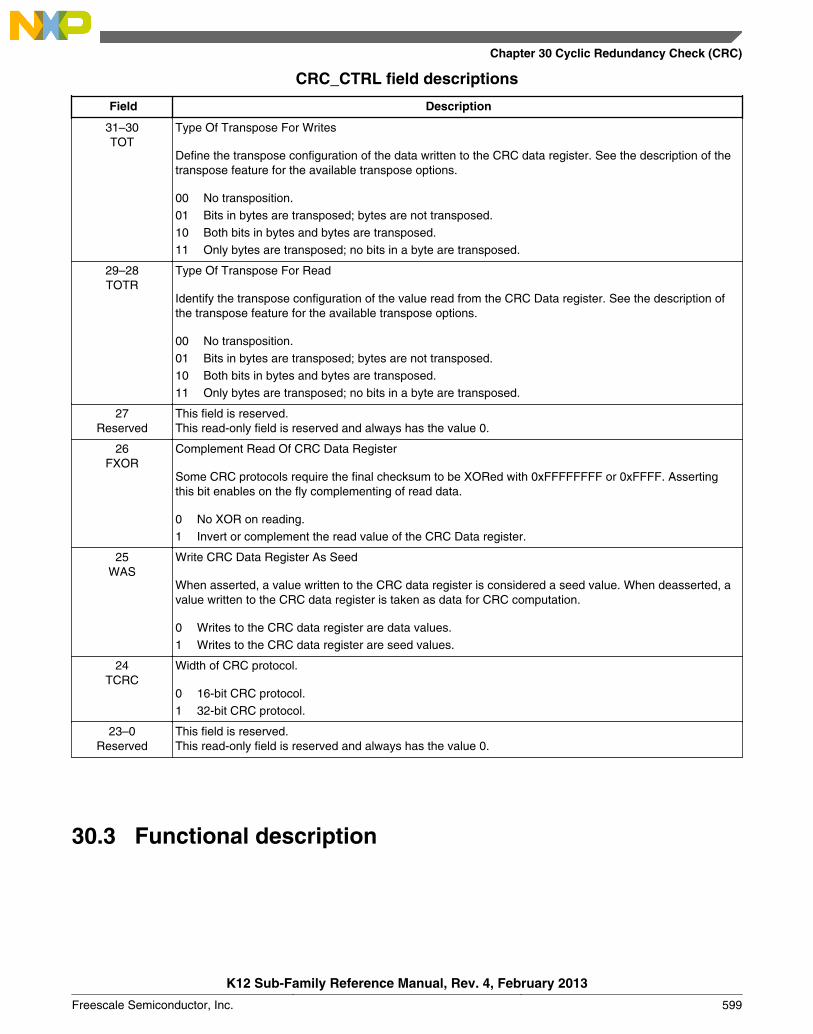
CRC_CTRL field descriptions
Field Description
31–30TOT
Type Of Transpose For Writes
Define the transpose configuration of the data written to the CRC data register. See the description of thetranspose feature for the available transpose options.
00 No transposition.01 Bits in bytes are transposed; bytes are not transposed.10 Both bits in bytes and bytes are transposed.11 Only bytes are transposed; no bits in a byte are transposed.
29–28TOTR
Type Of Transpose For Read
Identify the transpose configuration of the value read from the CRC Data register. See the description ofthe transpose feature for the available transpose options.
00 No transposition.01 Bits in bytes are transposed; bytes are not transposed.10 Both bits in bytes and bytes are transposed.11 Only bytes are transposed; no bits in a byte are transposed.
27Reserved
This field is reserved.This read-only field is reserved and always has the value 0.
26FXOR
Complement Read Of CRC Data Register
Some CRC protocols require the final checksum to be XORed with 0xFFFFFFFF or 0xFFFF. Assertingthis bit enables on the fly complementing of read data.
0 No XOR on reading.1 Invert or complement the read value of the CRC Data register.
25WAS
Write CRC Data Register As Seed
When asserted, a value written to the CRC data register is considered a seed value. When deasserted, avalue written to the CRC data register is taken as data for CRC computation.
0 Writes to the CRC data register are data values.1 Writes to the CRC data register are seed values.
24TCRC
Width of CRC protocol.
0 16-bit CRC protocol.1 32-bit CRC protocol.
23–0Reserved
This field is reserved.This read-only field is reserved and always has the value 0.
30.3 Functional description
Chapter 30 Cyclic Redundancy Check (CRC)
K12 Sub-Family Reference Manual, Rev. 4, February 2013
Freescale Semiconductor, Inc. 599
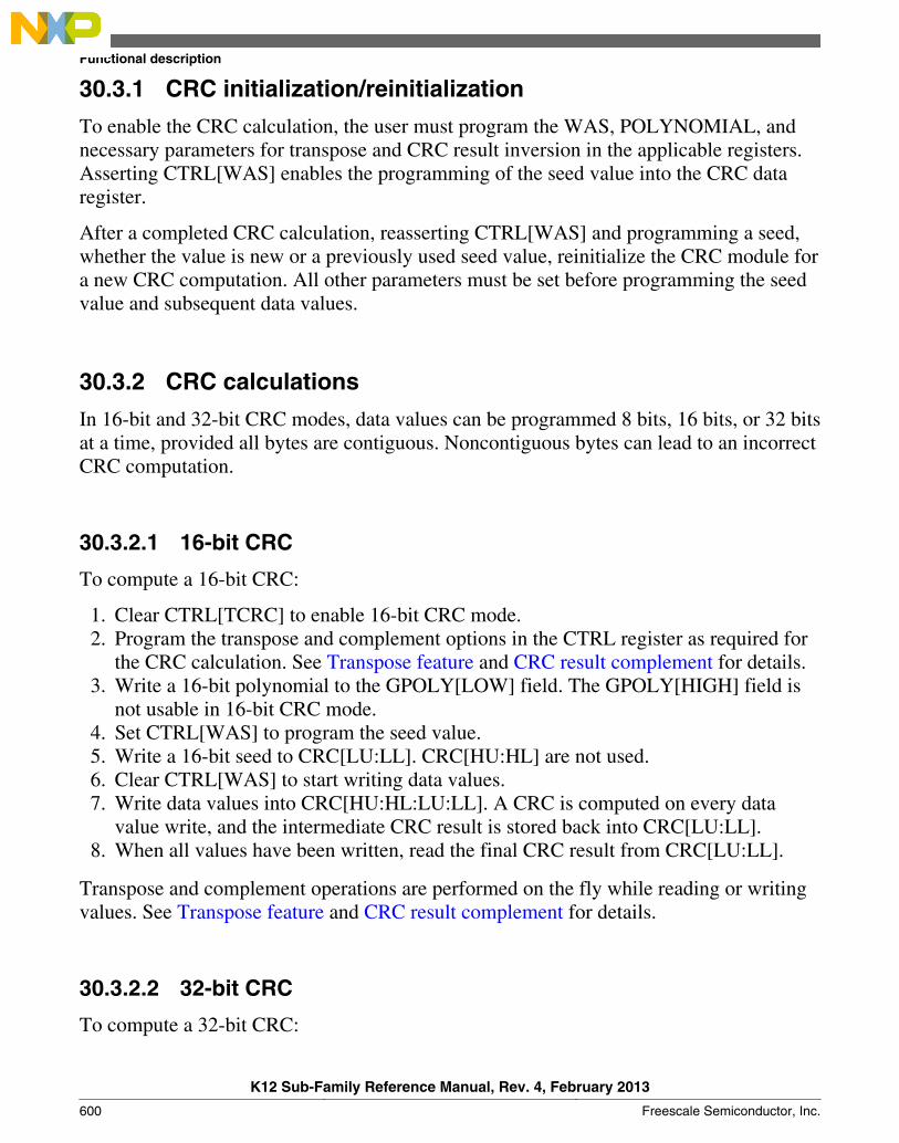
30.3.1 CRC initialization/reinitialization
To enable the CRC calculation, the user must program the WAS, POLYNOMIAL, andnecessary parameters for transpose and CRC result inversion in the applicable registers.Asserting CTRL[WAS] enables the programming of the seed value into the CRC dataregister.
After a completed CRC calculation, reasserting CTRL[WAS] and programming a seed,whether the value is new or a previously used seed value, reinitialize the CRC module fora new CRC computation. All other parameters must be set before programming the seedvalue and subsequent data values.
30.3.2 CRC calculations
In 16-bit and 32-bit CRC modes, data values can be programmed 8 bits, 16 bits, or 32 bitsat a time, provided all bytes are contiguous. Noncontiguous bytes can lead to an incorrectCRC computation.
30.3.2.1 16-bit CRC
To compute a 16-bit CRC:
1. Clear CTRL[TCRC] to enable 16-bit CRC mode.2. Program the transpose and complement options in the CTRL register as required for
the CRC calculation. See Transpose feature and CRC result complement for details.3. Write a 16-bit polynomial to the GPOLY[LOW] field. The GPOLY[HIGH] field is
not usable in 16-bit CRC mode.4. Set CTRL[WAS] to program the seed value.5. Write a 16-bit seed to CRC[LU:LL]. CRC[HU:HL] are not used.6. Clear CTRL[WAS] to start writing data values.7. Write data values into CRC[HU:HL:LU:LL]. A CRC is computed on every data
value write, and the intermediate CRC result is stored back into CRC[LU:LL].8. When all values have been written, read the final CRC result from CRC[LU:LL].
Transpose and complement operations are performed on the fly while reading or writingvalues. See Transpose feature and CRC result complement for details.
30.3.2.2 32-bit CRC
To compute a 32-bit CRC:
Functional description
K12 Sub-Family Reference Manual, Rev. 4, February 2013
600 Freescale Semiconductor, Inc.

1. Set CTRL[TCRC] to enable 32-bit CRC mode.2. Program the transpose and complement options in the CTRL register as required for
the CRC calculation. See Transpose feature and CRC result complement for details.3. Write a 32-bit polynomial to GPOLY[HIGH:LOW].4. Set CTRL[WAS] to program the seed value.5. Write a 32-bit seed to CRC[HU:HL:LU:LL].6. Clear CTRL[WAS] to start writing data values.7. Write data values into CRC[HU:HL:LU:LL]. A CRC is computed on every data
value write, and the intermediate CRC result is stored back intoCRC[HU:HL:LU:LL].
8. When all values have been written, read the final CRC result fromCRC[HU:HL:LU:LL]. The CRC is calculated bytewise, and two clocks are requiredto complete one CRC calculation.
Transpose and complement operations are performed on the fly while reading or writingvalues. See Transpose feature and CRC result complement for details.
30.3.3 Transpose feature
By default, the transpose feature is not enabled. However, some CRC standards requirethe input data and/or the final checksum to be transposed. The user software has theoption to configure each transpose operation separately, as desired by the CRC standard.The data is transposed on the fly while being read or written.
Some protocols use little endian format for the data stream to calculate a CRC. In thiscase, the transpose feature usefully flips the bits. This transpose option is one of the typessupported by the CRC module.
30.3.3.1 Types of transpose
The CRC module provides several types of transpose functions to flip the bits and/orbytes, for both writing input data and reading the CRC result, separately using theCTRL[TOT] or CTRL[TOTR] fields, according to the CRC calculation being used.
The following types of transpose functions are available for writing to and reading fromthe CRC data register:
1. CTRL[TOT] or CTRL[TOTR] is 00
No transposition occurs.
2. CTRL[TOT] or CTRL[TOTR] is 01
Chapter 30 Cyclic Redundancy Check (CRC)
K12 Sub-Family Reference Manual, Rev. 4, February 2013
Freescale Semiconductor, Inc. 601

Bits in a byte are transposed, while bytes are not transposed.
reg[31:0] becomes {reg[24:31], reg[16:23], reg[8:15], reg[0:7]}
15
158
7
0
0
7
831
3124
23
16
16
23
24
Figure 30-5. Transpose type 013. CTRL[TOT] or CTRL[TOTR] is 10
Both bits in bytes and bytes are transposed.
reg[31:0] becomes = {reg[0:7], reg[8:15],reg[16:23], reg[24:31]}
31
31 0
0
Figure 30-6. Transpose type 104. CTRL[TOT] or CTRL[TOTR] is 11
Bytes are transposed, but bits are not transposed.
reg[31:0] becomes {reg[7:0], reg[15:8], reg[23:16], reg[31:24]}
15
2416
0
3123
7831
80
16
157
2324
Figure 30-7. Transpose type 11
Functional description
K12 Sub-Family Reference Manual, Rev. 4, February 2013
602 Freescale Semiconductor, Inc.
NOTEFor 8-bit and 16-bit write accesses to the CRC data register, thedata is transposed with zeros on the unused byte or bytes(taking 32 bits as a whole), but the CRC is calculated on thevalid byte(s) only. When reading the CRC data register for a16-bit CRC result and using transpose options 10 and 11, theresulting value after transposition resides in the CRC[HU:HL]fields. The user software must account for this situation whenreading the 16-bit CRC result, so reading 32 bits is preferred.
30.3.4 CRC result complement
When CTRL[FXOR] is set, the checksum is complemented. The CRC result complementfunction outputs the complement of the checksum value stored in the CRC data registerevery time the CRC data register is read. When CTRL[FXOR] is cleared, reading theCRC data register accesses the raw checksum value.
Chapter 30 Cyclic Redundancy Check (CRC)
K12 Sub-Family Reference Manual, Rev. 4, February 2013
Freescale Semiconductor, Inc. 603

Functional description
K12 Sub-Family Reference Manual, Rev. 4, February 2013
604 Freescale Semiconductor, Inc.
Chapter 31Analog-to-Digital Converter (ADC)
31.1 IntroductionNOTE
For the chip-specific implementation details of this module'sinstances see the chip configuration information.
The 16-bit analog-to-digital converter (ADC) is a successive approximation ADCdesigned for operation within an integrated microcontroller system-on-chip.
NOTE
For the chip specific modes of operation, see the powermanagement information of the device.
31.1.1 Features
Features of the ADC module include:
• Linear successive approximation algorithm with up to 16-bit resolution
• Up to four pairs of differential and 24 single-ended external analog inputs
• Output modes:
• differential 16-bit, 13-bit, 11-bit, and 9-bit modes• single-ended 16-bit, 12-bit, 10-bit, and 8-bit modes
• Output format in 2's complement 16-bit sign extended for differential modes
• Output in right-justified unsigned format for single-ended
• Single or continuous conversion, that is, automatic return to idle after singleconversion
K12 Sub-Family Reference Manual, Rev. 4, February 2013
Freescale Semiconductor, Inc. 605
• Configurable sample time and conversion speed/power
• Conversion complete/hardware average complete flag and interrupt
• Input clock selectable from up to four sources
• Operation in Low-Power modes for lower noise
• Asynchronous clock source for lower noise operation with option to output the clock
• Selectable hardware conversion trigger with hardware channel select
• Automatic compare with interrupt for less-than, greater-than or equal-to, withinrange, or out-of-range, programmable value
• Temperature sensor
• Hardware average function
• Selectable voltage reference: external or alternate
• Self-Calibration mode
31.1.2 Block diagram
The following figure is the ADC module block diagram.
Introduction
K12 Sub-Family Reference Manual, Rev. 4, February 2013
606 Freescale Semiconductor, Inc.
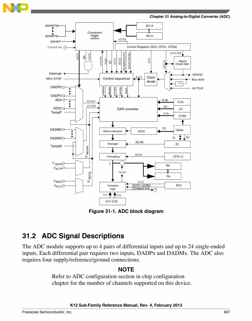
SC1AADHWTSA
ADHWTSn
C o m p a re t r u e
ADC
H
com
plet
e
A D T R G
ADC
O
Control Registers
SC1n
ADIV
ADIC
LK Async Clock Gen
A D A C K E N
2
ALTCLK
ADACKA D C K
M O D E
t r a n s fe r
C V 2
CV1:CV2
TempM
DADM3
DADM0
DADP3
DADP0
Interrupt
1
A D V IN P
A D V IN M
A C F E
1SC2
Rn
RA
CFG1,2
C L M xCLMx
Compare true
MCU STOP
ADHWT
AD4
AD23TempP
V REFH VALTH
VREFL VALTL
AIEN
CO
CO
trigg
er
DIFF
MO
DE
CLPx
PG, MGPG, MG
CLPx
CalibrationOFS
CALFCAL
SC3
C V1
ACFGT, ACREN
D
AVGE, AVGS
ADCOFS
V R
EF
SH
V R
EF
SL
(SC2, CFG1, CFG2)
Conversion trigger control
Clockdivide
Control sequencer Bus clock
SAR converter
Comparelogic
Offset subtractor
Averager
Formatting
AD
LSM
P/A
DLS
TS
AD
LPC
/AD
HS
C
initi
aliz
e
sam
ple
conv
ert
tran
sfer
abor
t
Figure 31-1. ADC block diagram
31.2 ADC Signal DescriptionsThe ADC module supports up to 4 pairs of differential inputs and up to 24 single-endedinputs. Each differential pair requires two inputs, DADPx and DADMx. The ADC alsorequires four supply/reference/ground connections.
NOTERefer to ADC configuration section in chip configurationchapter for the number of channels supported on this device.
Chapter 31 Analog-to-Digital Converter (ADC)
K12 Sub-Family Reference Manual, Rev. 4, February 2013
Freescale Semiconductor, Inc. 607
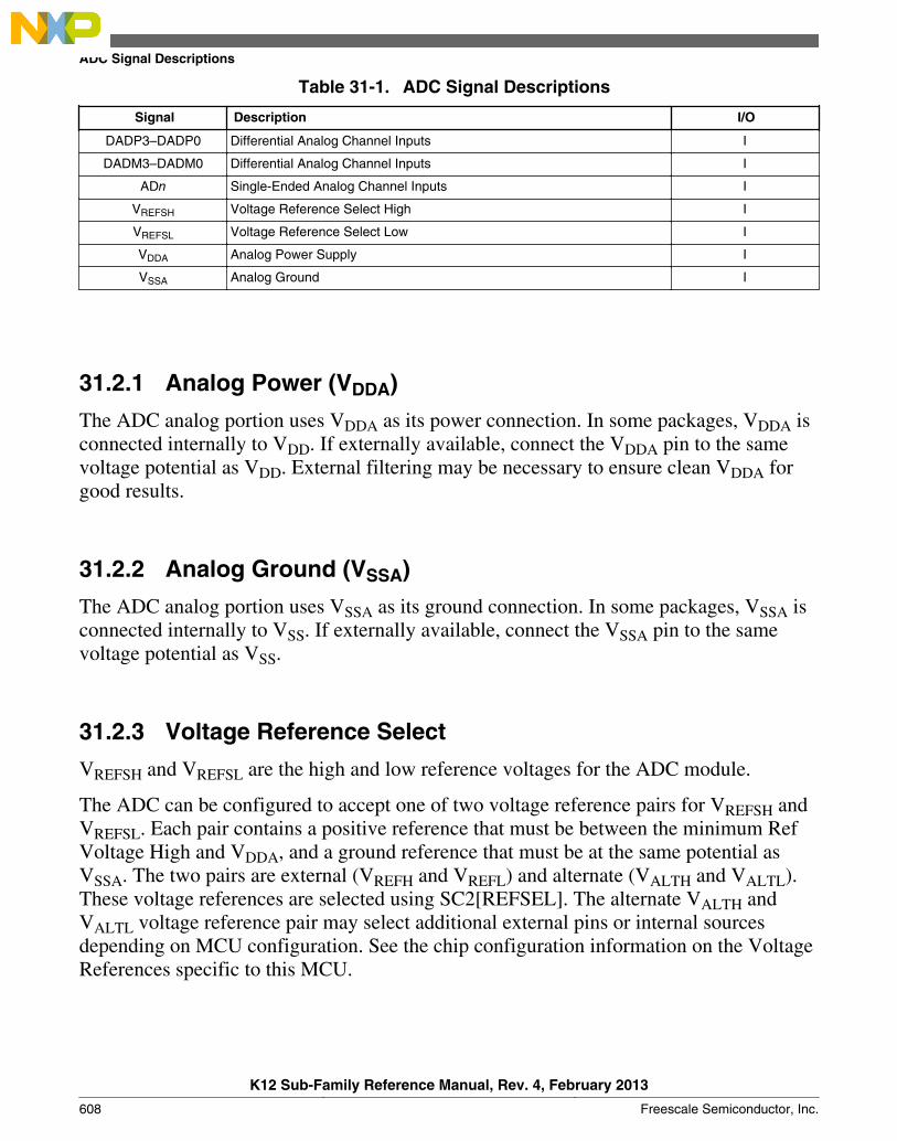
Table 31-1. ADC Signal Descriptions
Signal Description I/O
DADP3–DADP0 Differential Analog Channel Inputs I
DADM3–DADM0 Differential Analog Channel Inputs I
ADn Single-Ended Analog Channel Inputs I
VREFSH Voltage Reference Select High I
VREFSL Voltage Reference Select Low I
VDDA Analog Power Supply I
VSSA Analog Ground I
31.2.1 Analog Power (VDDA)
The ADC analog portion uses VDDA as its power connection. In some packages, VDDA isconnected internally to VDD. If externally available, connect the VDDA pin to the samevoltage potential as VDD. External filtering may be necessary to ensure clean VDDA forgood results.
31.2.2 Analog Ground (VSSA)
The ADC analog portion uses VSSA as its ground connection. In some packages, VSSA isconnected internally to VSS. If externally available, connect the VSSA pin to the samevoltage potential as VSS.
31.2.3 Voltage Reference Select
VREFSH and VREFSL are the high and low reference voltages for the ADC module.
The ADC can be configured to accept one of two voltage reference pairs for VREFSH andVREFSL. Each pair contains a positive reference that must be between the minimum RefVoltage High and VDDA, and a ground reference that must be at the same potential asVSSA. The two pairs are external (VREFH and VREFL) and alternate (VALTH and VALTL).These voltage references are selected using SC2[REFSEL]. The alternate VALTH andVALTL voltage reference pair may select additional external pins or internal sourcesdepending on MCU configuration. See the chip configuration information on the VoltageReferences specific to this MCU.
ADC Signal Descriptions
K12 Sub-Family Reference Manual, Rev. 4, February 2013
608 Freescale Semiconductor, Inc.

In some packages, VREFH is connected in the package to VDDA and VREFL to VSSA. Ifexternally available, the positive reference(s) may be connected to the same potential asVDDA or may be driven by an external source to a level between the minimum RefVoltage High and the VDDA potential. VREFH must never exceed VDDA. Connect theground references to the same voltage potential as VSSA.
31.2.4 Analog Channel Inputs (ADx)
The ADC module supports up to 24 single-ended analog inputs. A single-ended input isselected for conversion through the SC1[ADCH] channel select bits when SC1n[DIFF] islow.
31.2.5 Differential Analog Channel Inputs (DADx)
The ADC module supports up to four differential analog channel inputs. Each differentialanalog input is a pair of external pins, DADPx and DADMx, referenced to each other toprovide the most accurate analog to digital readings. A differential input is selected forconversion through SC1[ADCH] when SC1n[DIFF] is high. All DADPx inputs may beused as single-ended inputs if SC1n[DIFF] is low. In certain MCU configurations, someDADMx inputs may also be used as single-ended inputs if SC1n[DIFF] is low. See thechip configuration chapter for ADC connections specific to this MCU.
31.3 Register definitionThis section describes the ADC registers.
ADC memory map
Absoluteaddress
(hex)Register name
Width(in bits)
Access Reset valueSection/
page
4003_B000 ADC Status and Control Registers 1 (ADC0_SC1A) 32 R/W 0000_001Fh 31.3.1/610
4003_B004 ADC Status and Control Registers 1 (ADC0_SC1B) 32 R/W 0000_001Fh 31.3.1/610
4003_B008 ADC Configuration Register 1 (ADC0_CFG1) 32 R/W 0000_0000h 31.3.2/613
4003_B00C ADC Configuration Register 2 (ADC0_CFG2) 32 R/W 0000_0000h 31.3.3/615
4003_B010 ADC Data Result Register (ADC0_RA) 32 R 0000_0000h 31.3.4/616
4003_B014 ADC Data Result Register (ADC0_RB) 32 R 0000_0000h 31.3.4/616
4003_B018 Compare Value Registers (ADC0_CV1) 32 R/W 0000_0000h 31.3.5/617
4003_B01C Compare Value Registers (ADC0_CV2) 32 R/W 0000_0000h 31.3.5/617
Table continues on the next page...
Chapter 31 Analog-to-Digital Converter (ADC)
K12 Sub-Family Reference Manual, Rev. 4, February 2013
Freescale Semiconductor, Inc. 609
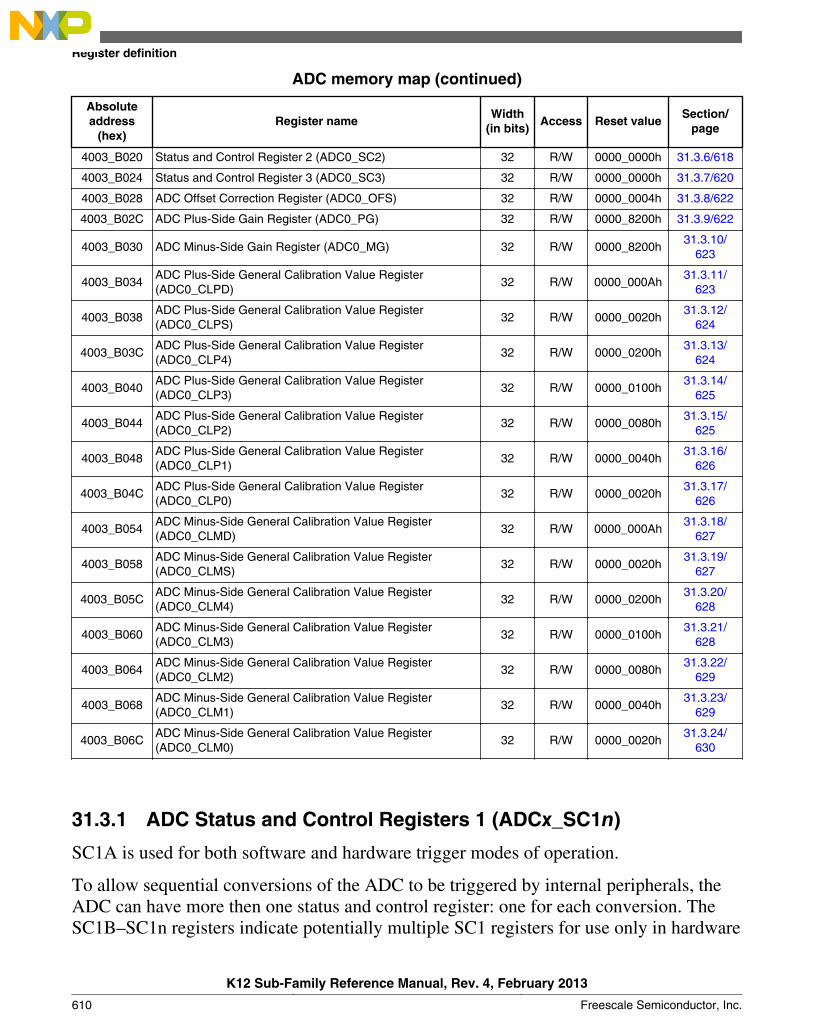
ADC memory map (continued)
Absoluteaddress
(hex)Register name
Width(in bits)
Access Reset valueSection/
page
4003_B020 Status and Control Register 2 (ADC0_SC2) 32 R/W 0000_0000h 31.3.6/618
4003_B024 Status and Control Register 3 (ADC0_SC3) 32 R/W 0000_0000h 31.3.7/620
4003_B028 ADC Offset Correction Register (ADC0_OFS) 32 R/W 0000_0004h 31.3.8/622
4003_B02C ADC Plus-Side Gain Register (ADC0_PG) 32 R/W 0000_8200h 31.3.9/622
4003_B030 ADC Minus-Side Gain Register (ADC0_MG) 32 R/W 0000_8200h31.3.10/
623
4003_B034ADC Plus-Side General Calibration Value Register(ADC0_CLPD)
32 R/W 0000_000Ah31.3.11/
623
4003_B038ADC Plus-Side General Calibration Value Register(ADC0_CLPS)
32 R/W 0000_0020h31.3.12/
624
4003_B03CADC Plus-Side General Calibration Value Register(ADC0_CLP4)
32 R/W 0000_0200h31.3.13/
624
4003_B040ADC Plus-Side General Calibration Value Register(ADC0_CLP3)
32 R/W 0000_0100h31.3.14/
625
4003_B044ADC Plus-Side General Calibration Value Register(ADC0_CLP2)
32 R/W 0000_0080h31.3.15/
625
4003_B048ADC Plus-Side General Calibration Value Register(ADC0_CLP1)
32 R/W 0000_0040h31.3.16/
626
4003_B04CADC Plus-Side General Calibration Value Register(ADC0_CLP0)
32 R/W 0000_0020h31.3.17/
626
4003_B054ADC Minus-Side General Calibration Value Register(ADC0_CLMD)
32 R/W 0000_000Ah31.3.18/
627
4003_B058ADC Minus-Side General Calibration Value Register(ADC0_CLMS)
32 R/W 0000_0020h31.3.19/
627
4003_B05CADC Minus-Side General Calibration Value Register(ADC0_CLM4)
32 R/W 0000_0200h31.3.20/
628
4003_B060ADC Minus-Side General Calibration Value Register(ADC0_CLM3)
32 R/W 0000_0100h31.3.21/
628
4003_B064ADC Minus-Side General Calibration Value Register(ADC0_CLM2)
32 R/W 0000_0080h31.3.22/
629
4003_B068ADC Minus-Side General Calibration Value Register(ADC0_CLM1)
32 R/W 0000_0040h31.3.23/
629
4003_B06CADC Minus-Side General Calibration Value Register(ADC0_CLM0)
32 R/W 0000_0020h31.3.24/
630
31.3.1 ADC Status and Control Registers 1 (ADCx_SC1n)
SC1A is used for both software and hardware trigger modes of operation.
To allow sequential conversions of the ADC to be triggered by internal peripherals, theADC can have more then one status and control register: one for each conversion. TheSC1B–SC1n registers indicate potentially multiple SC1 registers for use only in hardware
Register definition
K12 Sub-Family Reference Manual, Rev. 4, February 2013
610 Freescale Semiconductor, Inc.
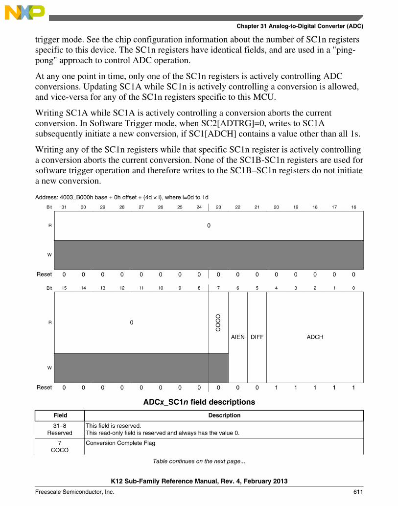
trigger mode. See the chip configuration information about the number of SC1n registersspecific to this device. The SC1n registers have identical fields, and are used in a "ping-pong" approach to control ADC operation.
At any one point in time, only one of the SC1n registers is actively controlling ADCconversions. Updating SC1A while SC1n is actively controlling a conversion is allowed,and vice-versa for any of the SC1n registers specific to this MCU.
Writing SC1A while SC1A is actively controlling a conversion aborts the currentconversion. In Software Trigger mode, when SC2[ADTRG]=0, writes to SC1Asubsequently initiate a new conversion, if SC1[ADCH] contains a value other than all 1s.
Writing any of the SC1n registers while that specific SC1n register is actively controllinga conversion aborts the current conversion. None of the SC1B-SC1n registers are used forsoftware trigger operation and therefore writes to the SC1B–SC1n registers do not initiatea new conversion.
Address: 4003_B000h base + 0h offset + (4d × i), where i=0d to 1d
Bit 31 30 29 28 27 26 25 24 23 22 21 20 19 18 17 16
R 0
W
Reset 0 0 0 0 0 0 0 0 0 0 0 0 0 0 0 0
Bit 15 14 13 12 11 10 9 8 7 6 5 4 3 2 1 0
R 0
CO
CO
AIEN DIFF ADCH
W
Reset 0 0 0 0 0 0 0 0 0 0 0 1 1 1 1 1
ADCx_SC1n field descriptions
Field Description
31–8Reserved
This field is reserved.This read-only field is reserved and always has the value 0.
7COCO
Conversion Complete Flag
Table continues on the next page...
Chapter 31 Analog-to-Digital Converter (ADC)
K12 Sub-Family Reference Manual, Rev. 4, February 2013
Freescale Semiconductor, Inc. 611

ADCx_SC1n field descriptions (continued)
Field Description
This is a read-only field that is set each time a conversion is completed when the compare function isdisabled, or SC2[ACFE]=0 and the hardware average function is disabled, or SC3[AVGE]=0. When thecompare function is enabled, or SC2[ACFE]=1, COCO is set upon completion of a conversion only if thecompare result is true. When the hardware average function is enabled, or SC3[AVGE]=1, COCO is setupon completion of the selected number of conversions (determined by AVGS). COCO in SC1A is also setat the completion of a calibration sequence. COCO is cleared when the respective SC1n register is writtenor when the respective Rn register is read.
0 Conversion is not completed.1 Conversion is completed.
6AIEN
Interrupt Enable
Enables conversion complete interrupts. When COCO becomes set while the respective AIEN is high, aninterrupt is asserted.
0 Conversion complete interrupt is disabled.1 Conversion complete interrupt is enabled.
5DIFF
Differential Mode Enable
Configures the ADC to operate in differential mode. When enabled, this mode automatically selects fromthe differential channels, and changes the conversion algorithm and the number of cycles to complete aconversion.
0 Single-ended conversions and input channels are selected.1 Differential conversions and input channels are selected.
4–0ADCH
Input channel select
Selects one of the input channels. The input channel decode depends on the value of DIFF. DAD0-DAD3are associated with the input pin pairs DADPx and DADMx.
NOTE: Some of the input channel options in the bitfield-setting descriptions might not be available foryour device. For the actual ADC channel assignments for your device, see the Chip Configurationdetails.
The successive approximation converter subsystem is turned off when the channel select bits are all set,that is, ADCH = 11111. This feature allows explicit disabling of the ADC and isolation of the input channelfrom all sources. Terminating continuous conversions this way prevents an additional single conversionfrom being performed. It is not necessary to set ADCH to all 1s to place the ADC in a low-power statewhen continuous conversions are not enabled because the module automatically enters a low-power statewhen a conversion completes.
00000 When DIFF=0, DADP0 is selected as input; when DIFF=1, DAD0 is selected as input.00001 When DIFF=0, DADP1 is selected as input; when DIFF=1, DAD1 is selected as input.00010 When DIFF=0, DADP2 is selected as input; when DIFF=1, DAD2 is selected as input.00011 When DIFF=0, DADP3 is selected as input; when DIFF=1, DAD3 is selected as input.00100 When DIFF=0, AD4 is selected as input; when DIFF=1, it is reserved.00101 When DIFF=0, AD5 is selected as input; when DIFF=1, it is reserved.00110 When DIFF=0, AD6 is selected as input; when DIFF=1, it is reserved.00111 When DIFF=0, AD7 is selected as input; when DIFF=1, it is reserved.01000 When DIFF=0, AD8 is selected as input; when DIFF=1, it is reserved.01001 When DIFF=0, AD9 is selected as input; when DIFF=1, it is reserved.01010 When DIFF=0, AD10 is selected as input; when DIFF=1, it is reserved.01011 When DIFF=0, AD11 is selected as input; when DIFF=1, it is reserved.
Table continues on the next page...
Register definition
K12 Sub-Family Reference Manual, Rev. 4, February 2013
612 Freescale Semiconductor, Inc.
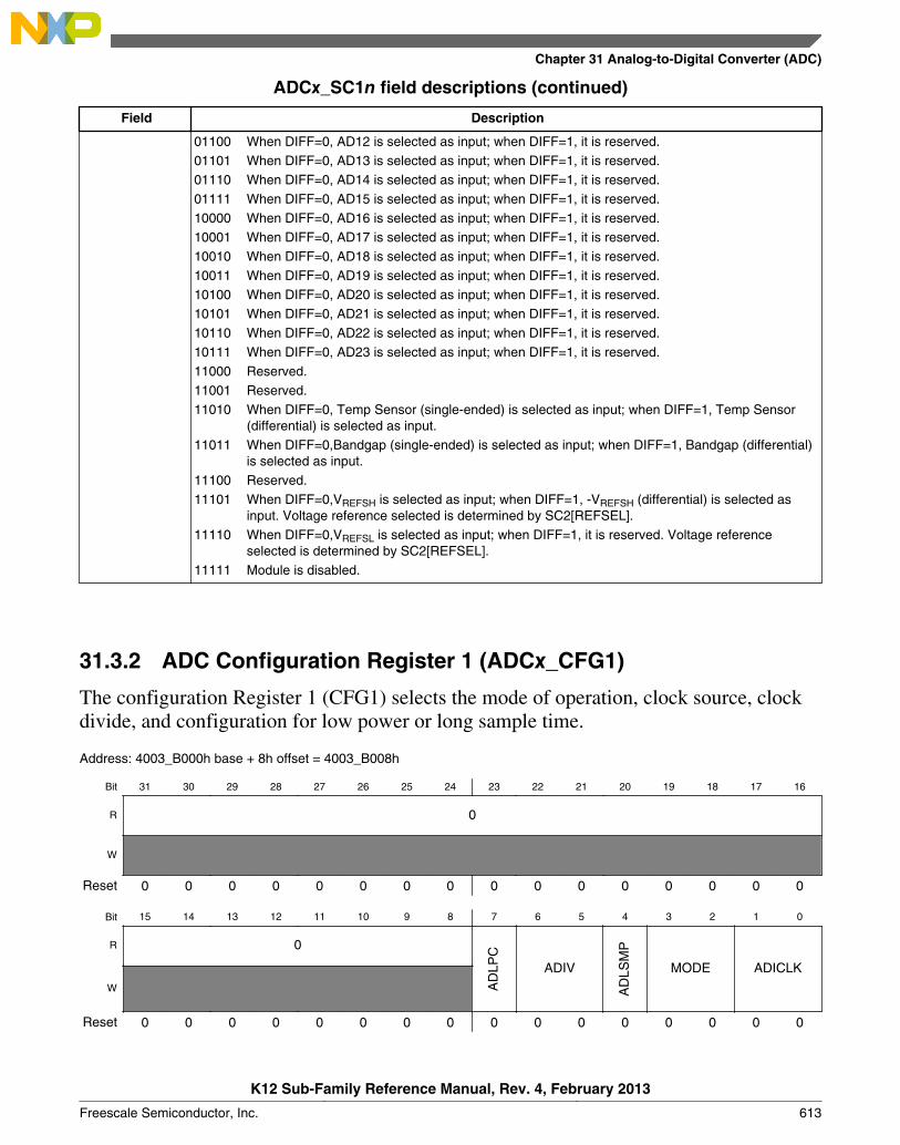
ADCx_SC1n field descriptions (continued)
Field Description
01100 When DIFF=0, AD12 is selected as input; when DIFF=1, it is reserved.01101 When DIFF=0, AD13 is selected as input; when DIFF=1, it is reserved.01110 When DIFF=0, AD14 is selected as input; when DIFF=1, it is reserved.01111 When DIFF=0, AD15 is selected as input; when DIFF=1, it is reserved.10000 When DIFF=0, AD16 is selected as input; when DIFF=1, it is reserved.10001 When DIFF=0, AD17 is selected as input; when DIFF=1, it is reserved.10010 When DIFF=0, AD18 is selected as input; when DIFF=1, it is reserved.10011 When DIFF=0, AD19 is selected as input; when DIFF=1, it is reserved.10100 When DIFF=0, AD20 is selected as input; when DIFF=1, it is reserved.10101 When DIFF=0, AD21 is selected as input; when DIFF=1, it is reserved.10110 When DIFF=0, AD22 is selected as input; when DIFF=1, it is reserved.10111 When DIFF=0, AD23 is selected as input; when DIFF=1, it is reserved.11000 Reserved.11001 Reserved.11010 When DIFF=0, Temp Sensor (single-ended) is selected as input; when DIFF=1, Temp Sensor
(differential) is selected as input.11011 When DIFF=0,Bandgap (single-ended) is selected as input; when DIFF=1, Bandgap (differential)
is selected as input.11100 Reserved.11101 When DIFF=0,VREFSH is selected as input; when DIFF=1, -VREFSH (differential) is selected as
input. Voltage reference selected is determined by SC2[REFSEL].11110 When DIFF=0,VREFSL is selected as input; when DIFF=1, it is reserved. Voltage reference
selected is determined by SC2[REFSEL].11111 Module is disabled.
31.3.2 ADC Configuration Register 1 (ADCx_CFG1)
The configuration Register 1 (CFG1) selects the mode of operation, clock source, clockdivide, and configuration for low power or long sample time.
Address: 4003_B000h base + 8h offset = 4003_B008h
Bit 31 30 29 28 27 26 25 24 23 22 21 20 19 18 17 16
R 0
W
Reset 0 0 0 0 0 0 0 0 0 0 0 0 0 0 0 0
Bit 15 14 13 12 11 10 9 8 7 6 5 4 3 2 1 0
R 0
AD
LPC
ADIV
AD
LSM
P
MODE ADICLKW
Reset 0 0 0 0 0 0 0 0 0 0 0 0 0 0 0 0
Chapter 31 Analog-to-Digital Converter (ADC)
K12 Sub-Family Reference Manual, Rev. 4, February 2013
Freescale Semiconductor, Inc. 613
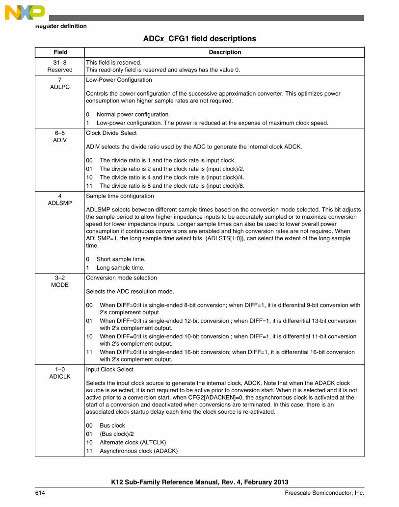
ADCx_CFG1 field descriptions
Field Description
31–8Reserved
This field is reserved.This read-only field is reserved and always has the value 0.
7ADLPC
Low-Power Configuration
Controls the power configuration of the successive approximation converter. This optimizes powerconsumption when higher sample rates are not required.
0 Normal power configuration.1 Low-power configuration. The power is reduced at the expense of maximum clock speed.
6–5ADIV
Clock Divide Select
ADIV selects the divide ratio used by the ADC to generate the internal clock ADCK.
00 The divide ratio is 1 and the clock rate is input clock.01 The divide ratio is 2 and the clock rate is (input clock)/2.10 The divide ratio is 4 and the clock rate is (input clock)/4.11 The divide ratio is 8 and the clock rate is (input clock)/8.
4ADLSMP
Sample time configuration
ADLSMP selects between different sample times based on the conversion mode selected. This bit adjuststhe sample period to allow higher impedance inputs to be accurately sampled or to maximize conversionspeed for lower impedance inputs. Longer sample times can also be used to lower overall powerconsumption if continuous conversions are enabled and high conversion rates are not required. WhenADLSMP=1, the long sample time select bits, (ADLSTS[1:0]), can select the extent of the long sampletime.
0 Short sample time.1 Long sample time.
3–2MODE
Conversion mode selection
Selects the ADC resolution mode.
00 When DIFF=0:It is single-ended 8-bit conversion; when DIFF=1, it is differential 9-bit conversion with2's complement output.
01 When DIFF=0:It is single-ended 12-bit conversion ; when DIFF=1, it is differential 13-bit conversionwith 2's complement output.
10 When DIFF=0:It is single-ended 10-bit conversion ; when DIFF=1, it is differential 11-bit conversionwith 2's complement output.
11 When DIFF=0:It is single-ended 16-bit conversion; when DIFF=1, it is differential 16-bit conversionwith 2's complement output.
1–0ADICLK
Input Clock Select
Selects the input clock source to generate the internal clock, ADCK. Note that when the ADACK clocksource is selected, it is not required to be active prior to conversion start. When it is selected and it is notactive prior to a conversion start, when CFG2[ADACKEN]=0, the asynchronous clock is activated at thestart of a conversion and deactivated when conversions are terminated. In this case, there is anassociated clock startup delay each time the clock source is re-activated.
00 Bus clock01 (Bus clock)/210 Alternate clock (ALTCLK)11 Asynchronous clock (ADACK)
Register definition
K12 Sub-Family Reference Manual, Rev. 4, February 2013
614 Freescale Semiconductor, Inc.
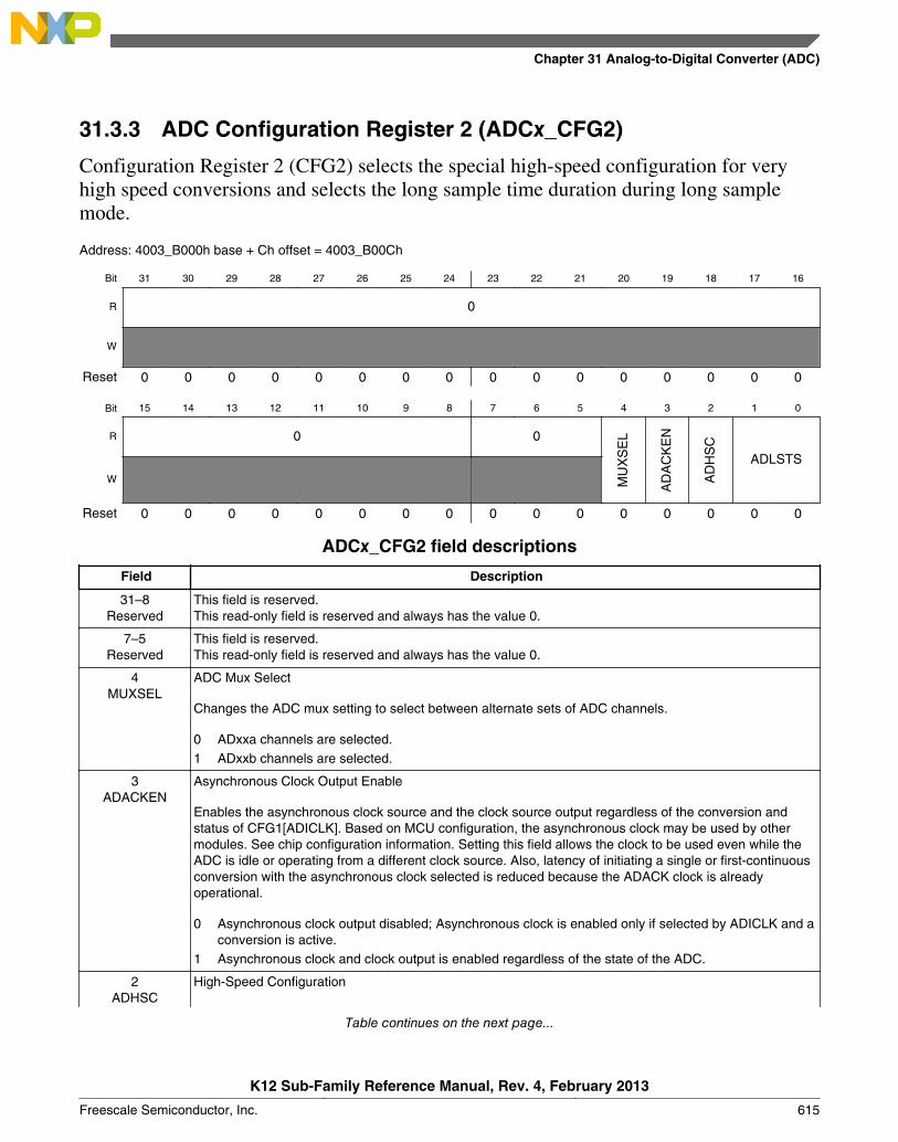
31.3.3 ADC Configuration Register 2 (ADCx_CFG2)
Configuration Register 2 (CFG2) selects the special high-speed configuration for veryhigh speed conversions and selects the long sample time duration during long samplemode.
Address: 4003_B000h base + Ch offset = 4003_B00Ch
Bit 31 30 29 28 27 26 25 24 23 22 21 20 19 18 17 16
R 0
W
Reset 0 0 0 0 0 0 0 0 0 0 0 0 0 0 0 0
Bit 15 14 13 12 11 10 9 8 7 6 5 4 3 2 1 0
R 0 0
MU
XS
EL
AD
AC
KE
N
AD
HS
C
ADLSTSW
Reset 0 0 0 0 0 0 0 0 0 0 0 0 0 0 0 0
ADCx_CFG2 field descriptions
Field Description
31–8Reserved
This field is reserved.This read-only field is reserved and always has the value 0.
7–5Reserved
This field is reserved.This read-only field is reserved and always has the value 0.
4MUXSEL
ADC Mux Select
Changes the ADC mux setting to select between alternate sets of ADC channels.
0 ADxxa channels are selected.1 ADxxb channels are selected.
3ADACKEN
Asynchronous Clock Output Enable
Enables the asynchronous clock source and the clock source output regardless of the conversion andstatus of CFG1[ADICLK]. Based on MCU configuration, the asynchronous clock may be used by othermodules. See chip configuration information. Setting this field allows the clock to be used even while theADC is idle or operating from a different clock source. Also, latency of initiating a single or first-continuousconversion with the asynchronous clock selected is reduced because the ADACK clock is alreadyoperational.
0 Asynchronous clock output disabled; Asynchronous clock is enabled only if selected by ADICLK and aconversion is active.
1 Asynchronous clock and clock output is enabled regardless of the state of the ADC.
2ADHSC
High-Speed Configuration
Table continues on the next page...
Chapter 31 Analog-to-Digital Converter (ADC)
K12 Sub-Family Reference Manual, Rev. 4, February 2013
Freescale Semiconductor, Inc. 615
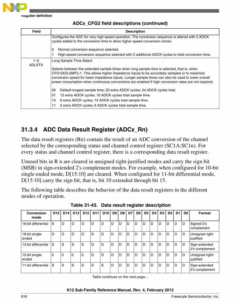
ADCx_CFG2 field descriptions (continued)
Field Description
Configures the ADC for very high-speed operation. The conversion sequence is altered with 2 ADCKcycles added to the conversion time to allow higher speed conversion clocks.
0 Normal conversion sequence selected.1 High-speed conversion sequence selected with 2 additional ADCK cycles to total conversion time.
1–0ADLSTS
Long Sample Time Select
Selects between the extended sample times when long sample time is selected, that is, whenCFG1[ADLSMP]=1. This allows higher impedance inputs to be accurately sampled or to maximizeconversion speed for lower impedance inputs. Longer sample times can also be used to lower overallpower consumption when continuous conversions are enabled if high conversion rates are not required.
00 Default longest sample time; 20 extra ADCK cycles; 24 ADCK cycles total.01 12 extra ADCK cycles; 16 ADCK cycles total sample time.10 6 extra ADCK cycles; 10 ADCK cycles total sample time.11 2 extra ADCK cycles; 6 ADCK cycles total sample time.
31.3.4 ADC Data Result Register (ADCx_Rn)
The data result registers (Rn) contain the result of an ADC conversion of the channelselected by the corresponding status and channel control register (SC1A:SC1n). Forevery status and channel control register, there is a corresponding data result register.
Unused bits in R n are cleared in unsigned right-justified modes and carry the sign bit(MSB) in sign-extended 2's complement modes. For example, when configured for 10-bitsingle-ended mode, D[15:10] are cleared. When configured for 11-bit differential mode,D[15:10] carry the sign bit, that is, bit 10 extended through bit 15.
The following table describes the behavior of the data result registers in the differentmodes of operation.
Table 31-43. Data result register description
Conversionmode
D15 D14 D13 D12 D11 D10 D9 D8 D7 D6 D5 D4 D3 D2 D1 D0 Format
16-bit differential S D D D D D D D D D D D D D D D Signed 2'scomplement
16-bit single-ended
D D D D D D D D D D D D D D D D Unsigned rightjustified
13-bit differential S S S S D D D D D D D D D D D D Sign-extended2's complement
12-bit single-ended
0 0 0 0 D D D D D D D D D D D D Unsigned right-justified
11-bit differential S S S S S S D D D D D D D D D D Sign-extended2's complement
Table continues on the next page...
Register definition
K12 Sub-Family Reference Manual, Rev. 4, February 2013
616 Freescale Semiconductor, Inc.
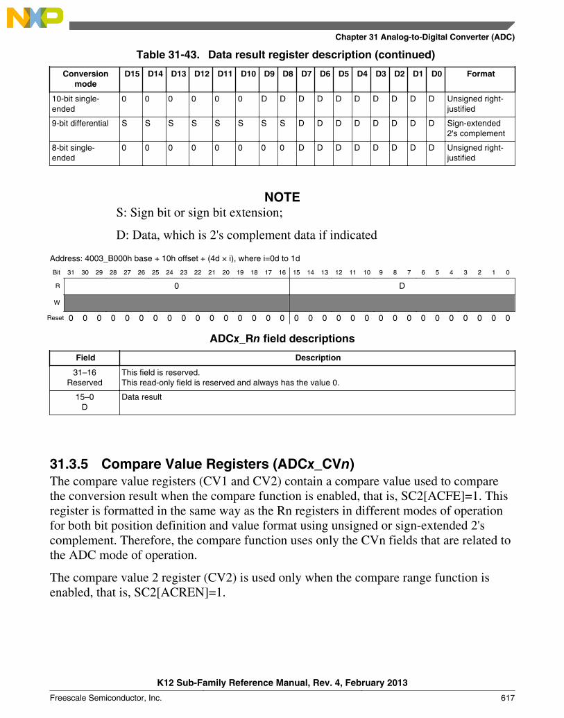
Table 31-43. Data result register description (continued)
Conversionmode
D15 D14 D13 D12 D11 D10 D9 D8 D7 D6 D5 D4 D3 D2 D1 D0 Format
10-bit single-ended
0 0 0 0 0 0 D D D D D D D D D D Unsigned right-justified
9-bit differential S S S S S S S S D D D D D D D D Sign-extended2's complement
8-bit single-ended
0 0 0 0 0 0 0 0 D D D D D D D D Unsigned right-justified
NOTES: Sign bit or sign bit extension;
D: Data, which is 2's complement data if indicated
Address: 4003_B000h base + 10h offset + (4d × i), where i=0d to 1d
Bit 31 30 29 28 27 26 25 24 23 22 21 20 19 18 17 16 15 14 13 12 11 10 9 8 7 6 5 4 3 2 1 0
R 0 D
W
Reset 0 0 0 0 0 0 0 0 0 0 0 0 0 0 0 0 0 0 0 0 0 0 0 0 0 0 0 0 0 0 0 0
ADCx_Rn field descriptions
Field Description
31–16Reserved
This field is reserved.This read-only field is reserved and always has the value 0.
15–0D
Data result
31.3.5 Compare Value Registers (ADCx_CVn)The compare value registers (CV1 and CV2) contain a compare value used to comparethe conversion result when the compare function is enabled, that is, SC2[ACFE]=1. Thisregister is formatted in the same way as the Rn registers in different modes of operationfor both bit position definition and value format using unsigned or sign-extended 2'scomplement. Therefore, the compare function uses only the CVn fields that are related tothe ADC mode of operation.
The compare value 2 register (CV2) is used only when the compare range function isenabled, that is, SC2[ACREN]=1.
Chapter 31 Analog-to-Digital Converter (ADC)
K12 Sub-Family Reference Manual, Rev. 4, February 2013
Freescale Semiconductor, Inc. 617
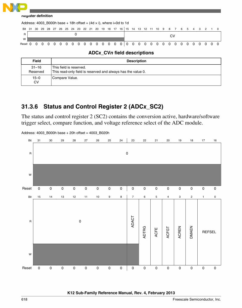
Address: 4003_B000h base + 18h offset + (4d × i), where i=0d to 1d
Bit 31 30 29 28 27 26 25 24 23 22 21 20 19 18 17 16 15 14 13 12 11 10 9 8 7 6 5 4 3 2 1 0
R 0 CVW
Reset 0 0 0 0 0 0 0 0 0 0 0 0 0 0 0 0 0 0 0 0 0 0 0 0 0 0 0 0 0 0 0 0
ADCx_CVn field descriptions
Field Description
31–16Reserved
This field is reserved.This read-only field is reserved and always has the value 0.
15–0CV
Compare Value.
31.3.6 Status and Control Register 2 (ADCx_SC2)
The status and control register 2 (SC2) contains the conversion active, hardware/softwaretrigger select, compare function, and voltage reference select of the ADC module.
Address: 4003_B000h base + 20h offset = 4003_B020h
Bit 31 30 29 28 27 26 25 24 23 22 21 20 19 18 17 16
R 0
W
Reset 0 0 0 0 0 0 0 0 0 0 0 0 0 0 0 0
Bit 15 14 13 12 11 10 9 8 7 6 5 4 3 2 1 0
R 0
AD
AC
T
AD
TR
G
AC
FE
AC
FG
T
AC
RE
N
DM
AE
N
REFSEL
W
Reset 0 0 0 0 0 0 0 0 0 0 0 0 0 0 0 0
Register definition
K12 Sub-Family Reference Manual, Rev. 4, February 2013
618 Freescale Semiconductor, Inc.
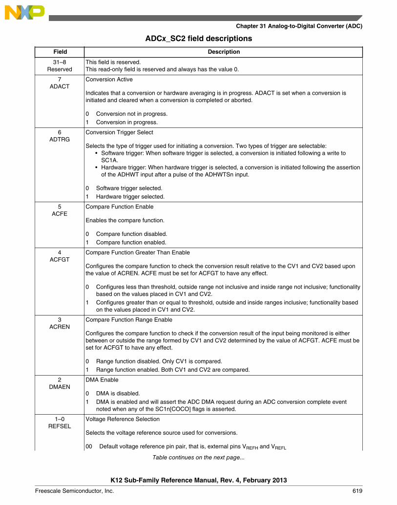
ADCx_SC2 field descriptions
Field Description
31–8Reserved
This field is reserved.This read-only field is reserved and always has the value 0.
7ADACT
Conversion Active
Indicates that a conversion or hardware averaging is in progress. ADACT is set when a conversion isinitiated and cleared when a conversion is completed or aborted.
0 Conversion not in progress.1 Conversion in progress.
6ADTRG
Conversion Trigger Select
Selects the type of trigger used for initiating a conversion. Two types of trigger are selectable:• Software trigger: When software trigger is selected, a conversion is initiated following a write to
SC1A.• Hardware trigger: When hardware trigger is selected, a conversion is initiated following the assertion
of the ADHWT input after a pulse of the ADHWTSn input.
0 Software trigger selected.1 Hardware trigger selected.
5ACFE
Compare Function Enable
Enables the compare function.
0 Compare function disabled.1 Compare function enabled.
4ACFGT
Compare Function Greater Than Enable
Configures the compare function to check the conversion result relative to the CV1 and CV2 based uponthe value of ACREN. ACFE must be set for ACFGT to have any effect.
0 Configures less than threshold, outside range not inclusive and inside range not inclusive; functionalitybased on the values placed in CV1 and CV2.
1 Configures greater than or equal to threshold, outside and inside ranges inclusive; functionality basedon the values placed in CV1 and CV2.
3ACREN
Compare Function Range Enable
Configures the compare function to check if the conversion result of the input being monitored is eitherbetween or outside the range formed by CV1 and CV2 determined by the value of ACFGT. ACFE must beset for ACFGT to have any effect.
0 Range function disabled. Only CV1 is compared.1 Range function enabled. Both CV1 and CV2 are compared.
2DMAEN
DMA Enable
0 DMA is disabled.1 DMA is enabled and will assert the ADC DMA request during an ADC conversion complete event
noted when any of the SC1n[COCO] flags is asserted.
1–0REFSEL
Voltage Reference Selection
Selects the voltage reference source used for conversions.
00 Default voltage reference pin pair, that is, external pins VREFH and VREFL
Table continues on the next page...
Chapter 31 Analog-to-Digital Converter (ADC)
K12 Sub-Family Reference Manual, Rev. 4, February 2013
Freescale Semiconductor, Inc. 619
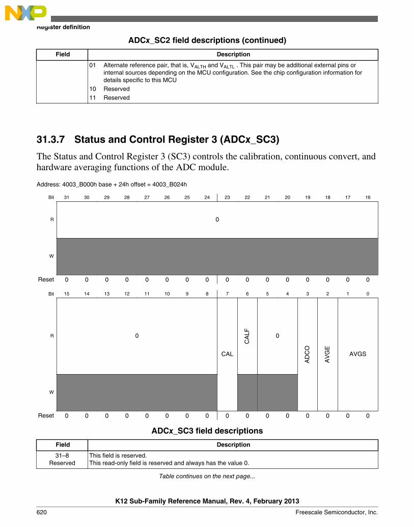
ADCx_SC2 field descriptions (continued)
Field Description
01 Alternate reference pair, that is, VALTH and VALTL . This pair may be additional external pins orinternal sources depending on the MCU configuration. See the chip configuration information fordetails specific to this MCU
10 Reserved11 Reserved
31.3.7 Status and Control Register 3 (ADCx_SC3)
The Status and Control Register 3 (SC3) controls the calibration, continuous convert, andhardware averaging functions of the ADC module.
Address: 4003_B000h base + 24h offset = 4003_B024h
Bit 31 30 29 28 27 26 25 24 23 22 21 20 19 18 17 16
R 0
W
Reset 0 0 0 0 0 0 0 0 0 0 0 0 0 0 0 0
Bit 15 14 13 12 11 10 9 8 7 6 5 4 3 2 1 0
R 0
CAL
CA
LF 0
AD
CO
AV
GE
AVGS
W
Reset 0 0 0 0 0 0 0 0 0 0 0 0 0 0 0 0
ADCx_SC3 field descriptions
Field Description
31–8Reserved
This field is reserved.This read-only field is reserved and always has the value 0.
Table continues on the next page...
Register definition
K12 Sub-Family Reference Manual, Rev. 4, February 2013
620 Freescale Semiconductor, Inc.
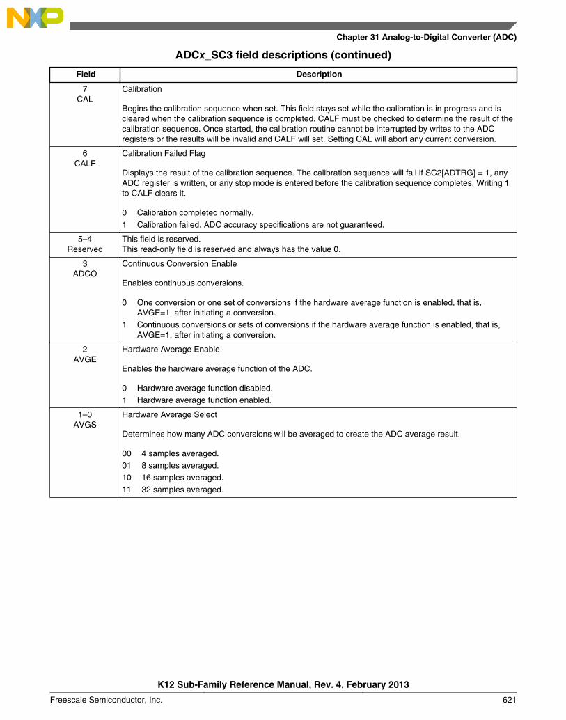
ADCx_SC3 field descriptions (continued)
Field Description
7CAL
Calibration
Begins the calibration sequence when set. This field stays set while the calibration is in progress and iscleared when the calibration sequence is completed. CALF must be checked to determine the result of thecalibration sequence. Once started, the calibration routine cannot be interrupted by writes to the ADCregisters or the results will be invalid and CALF will set. Setting CAL will abort any current conversion.
6CALF
Calibration Failed Flag
Displays the result of the calibration sequence. The calibration sequence will fail if SC2[ADTRG] = 1, anyADC register is written, or any stop mode is entered before the calibration sequence completes. Writing 1to CALF clears it.
0 Calibration completed normally.1 Calibration failed. ADC accuracy specifications are not guaranteed.
5–4Reserved
This field is reserved.This read-only field is reserved and always has the value 0.
3ADCO
Continuous Conversion Enable
Enables continuous conversions.
0 One conversion or one set of conversions if the hardware average function is enabled, that is,AVGE=1, after initiating a conversion.
1 Continuous conversions or sets of conversions if the hardware average function is enabled, that is,AVGE=1, after initiating a conversion.
2AVGE
Hardware Average Enable
Enables the hardware average function of the ADC.
0 Hardware average function disabled.1 Hardware average function enabled.
1–0AVGS
Hardware Average Select
Determines how many ADC conversions will be averaged to create the ADC average result.
00 4 samples averaged.01 8 samples averaged.10 16 samples averaged.11 32 samples averaged.
Chapter 31 Analog-to-Digital Converter (ADC)
K12 Sub-Family Reference Manual, Rev. 4, February 2013
Freescale Semiconductor, Inc. 621
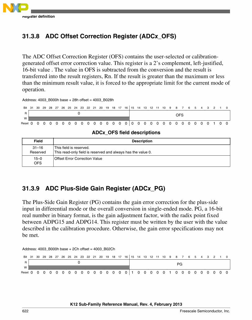
31.3.8 ADC Offset Correction Register (ADCx_OFS)
The ADC Offset Correction Register (OFS) contains the user-selected or calibration-generated offset error correction value. This register is a 2’s complement, left-justified,16-bit value . The value in OFS is subtracted from the conversion and the result istransferred into the result registers, Rn. If the result is greater than the maximum or lessthan the minimum result value, it is forced to the appropriate limit for the current mode ofoperation.
Address: 4003_B000h base + 28h offset = 4003_B028h
Bit 31 30 29 28 27 26 25 24 23 22 21 20 19 18 17 16 15 14 13 12 11 10 9 8 7 6 5 4 3 2 1 0
R 0 OFSW
Reset 0 0 0 0 0 0 0 0 0 0 0 0 0 0 0 0 0 0 0 0 0 0 0 0 0 0 0 0 0 1 0 0
ADCx_OFS field descriptions
Field Description
31–16Reserved
This field is reserved.This read-only field is reserved and always has the value 0.
15–0OFS
Offset Error Correction Value
31.3.9 ADC Plus-Side Gain Register (ADCx_PG)
The Plus-Side Gain Register (PG) contains the gain error correction for the plus-sideinput in differential mode or the overall conversion in single-ended mode. PG, a 16-bitreal number in binary format, is the gain adjustment factor, with the radix point fixedbetween ADPG15 and ADPG14. This register must be written by the user with the valuedescribed in the calibration procedure. Otherwise, the gain error specifications may notbe met.
Address: 4003_B000h base + 2Ch offset = 4003_B02Ch
Bit 31 30 29 28 27 26 25 24 23 22 21 20 19 18 17 16 15 14 13 12 11 10 9 8 7 6 5 4 3 2 1 0
R 0 PGW
Reset 0 0 0 0 0 0 0 0 0 0 0 0 0 0 0 0 1 0 0 0 0 0 1 0 0 0 0 0 0 0 0 0
Register definition
K12 Sub-Family Reference Manual, Rev. 4, February 2013
622 Freescale Semiconductor, Inc.
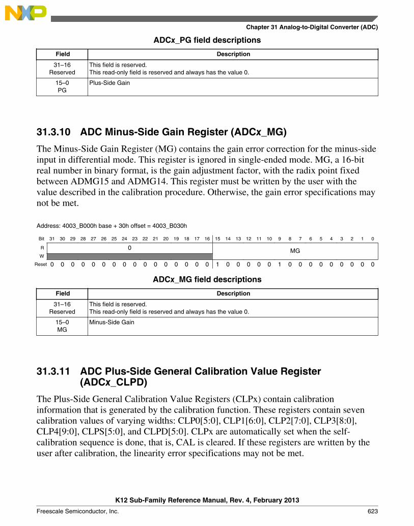
ADCx_PG field descriptions
Field Description
31–16Reserved
This field is reserved.This read-only field is reserved and always has the value 0.
15–0PG
Plus-Side Gain
31.3.10 ADC Minus-Side Gain Register (ADCx_MG)
The Minus-Side Gain Register (MG) contains the gain error correction for the minus-sideinput in differential mode. This register is ignored in single-ended mode. MG, a 16-bitreal number in binary format, is the gain adjustment factor, with the radix point fixedbetween ADMG15 and ADMG14. This register must be written by the user with thevalue described in the calibration procedure. Otherwise, the gain error specifications maynot be met.
Address: 4003_B000h base + 30h offset = 4003_B030h
Bit 31 30 29 28 27 26 25 24 23 22 21 20 19 18 17 16 15 14 13 12 11 10 9 8 7 6 5 4 3 2 1 0
R 0 MGW
Reset 0 0 0 0 0 0 0 0 0 0 0 0 0 0 0 0 1 0 0 0 0 0 1 0 0 0 0 0 0 0 0 0
ADCx_MG field descriptions
Field Description
31–16Reserved
This field is reserved.This read-only field is reserved and always has the value 0.
15–0MG
Minus-Side Gain
31.3.11 ADC Plus-Side General Calibration Value Register(ADCx_CLPD)
The Plus-Side General Calibration Value Registers (CLPx) contain calibrationinformation that is generated by the calibration function. These registers contain sevencalibration values of varying widths: CLP0[5:0], CLP1[6:0], CLP2[7:0], CLP3[8:0],CLP4[9:0], CLPS[5:0], and CLPD[5:0]. CLPx are automatically set when the self-calibration sequence is done, that is, CAL is cleared. If these registers are written by theuser after calibration, the linearity error specifications may not be met.
Chapter 31 Analog-to-Digital Converter (ADC)
K12 Sub-Family Reference Manual, Rev. 4, February 2013
Freescale Semiconductor, Inc. 623
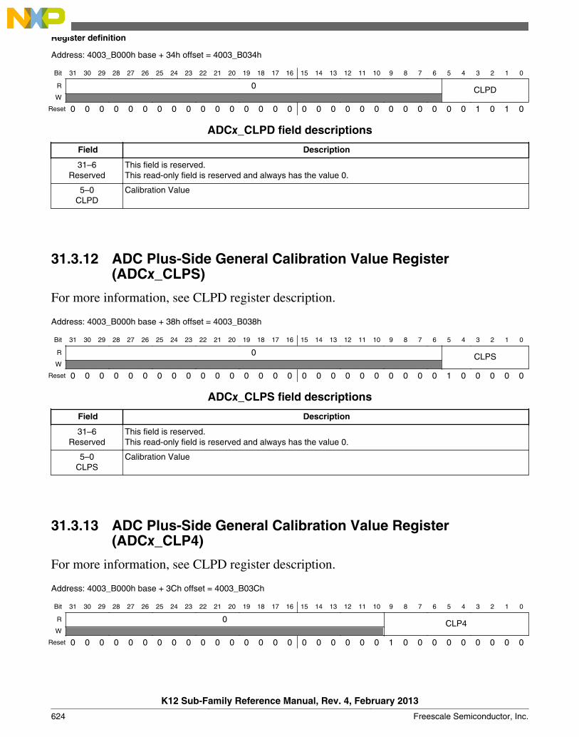
Address: 4003_B000h base + 34h offset = 4003_B034h
Bit 31 30 29 28 27 26 25 24 23 22 21 20 19 18 17 16 15 14 13 12 11 10 9 8 7 6 5 4 3 2 1 0
R 0 CLPDW
Reset 0 0 0 0 0 0 0 0 0 0 0 0 0 0 0 0 0 0 0 0 0 0 0 0 0 0 0 0 1 0 1 0
ADCx_CLPD field descriptions
Field Description
31–6Reserved
This field is reserved.This read-only field is reserved and always has the value 0.
5–0CLPD
Calibration Value
31.3.12 ADC Plus-Side General Calibration Value Register(ADCx_CLPS)
For more information, see CLPD register description.
Address: 4003_B000h base + 38h offset = 4003_B038h
Bit 31 30 29 28 27 26 25 24 23 22 21 20 19 18 17 16 15 14 13 12 11 10 9 8 7 6 5 4 3 2 1 0
R 0 CLPSW
Reset 0 0 0 0 0 0 0 0 0 0 0 0 0 0 0 0 0 0 0 0 0 0 0 0 0 0 1 0 0 0 0 0
ADCx_CLPS field descriptions
Field Description
31–6Reserved
This field is reserved.This read-only field is reserved and always has the value 0.
5–0CLPS
Calibration Value
31.3.13 ADC Plus-Side General Calibration Value Register(ADCx_CLP4)
For more information, see CLPD register description.
Address: 4003_B000h base + 3Ch offset = 4003_B03Ch
Bit 31 30 29 28 27 26 25 24 23 22 21 20 19 18 17 16 15 14 13 12 11 10 9 8 7 6 5 4 3 2 1 0
R 0 CLP4W
Reset 0 0 0 0 0 0 0 0 0 0 0 0 0 0 0 0 0 0 0 0 0 0 1 0 0 0 0 0 0 0 0 0
Register definition
K12 Sub-Family Reference Manual, Rev. 4, February 2013
624 Freescale Semiconductor, Inc.
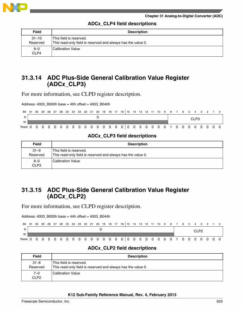
ADCx_CLP4 field descriptions
Field Description
31–10Reserved
This field is reserved.This read-only field is reserved and always has the value 0.
9–0CLP4
Calibration Value
31.3.14 ADC Plus-Side General Calibration Value Register(ADCx_CLP3)
For more information, see CLPD register description.
Address: 4003_B000h base + 40h offset = 4003_B040h
Bit 31 30 29 28 27 26 25 24 23 22 21 20 19 18 17 16 15 14 13 12 11 10 9 8 7 6 5 4 3 2 1 0
R 0 CLP3W
Reset 0 0 0 0 0 0 0 0 0 0 0 0 0 0 0 0 0 0 0 0 0 0 0 1 0 0 0 0 0 0 0 0
ADCx_CLP3 field descriptions
Field Description
31–9Reserved
This field is reserved.This read-only field is reserved and always has the value 0.
8–0CLP3
Calibration Value
31.3.15 ADC Plus-Side General Calibration Value Register(ADCx_CLP2)
For more information, see CLPD register description.
Address: 4003_B000h base + 44h offset = 4003_B044h
Bit 31 30 29 28 27 26 25 24 23 22 21 20 19 18 17 16 15 14 13 12 11 10 9 8 7 6 5 4 3 2 1 0
R 0 CLP2W
Reset 0 0 0 0 0 0 0 0 0 0 0 0 0 0 0 0 0 0 0 0 0 0 0 0 1 0 0 0 0 0 0 0
ADCx_CLP2 field descriptions
Field Description
31–8Reserved
This field is reserved.This read-only field is reserved and always has the value 0.
7–0CLP2
Calibration Value
Chapter 31 Analog-to-Digital Converter (ADC)
K12 Sub-Family Reference Manual, Rev. 4, February 2013
Freescale Semiconductor, Inc. 625
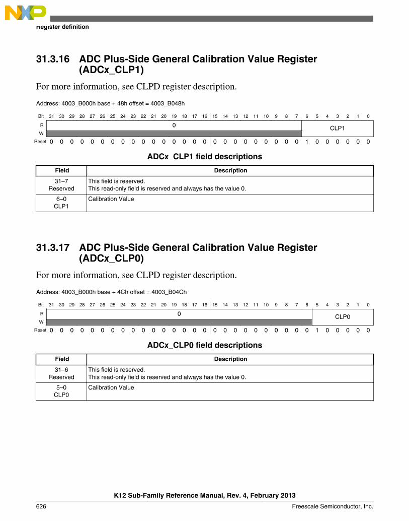
31.3.16 ADC Plus-Side General Calibration Value Register(ADCx_CLP1)
For more information, see CLPD register description.
Address: 4003_B000h base + 48h offset = 4003_B048h
Bit 31 30 29 28 27 26 25 24 23 22 21 20 19 18 17 16 15 14 13 12 11 10 9 8 7 6 5 4 3 2 1 0
R 0 CLP1W
Reset 0 0 0 0 0 0 0 0 0 0 0 0 0 0 0 0 0 0 0 0 0 0 0 0 0 1 0 0 0 0 0 0
ADCx_CLP1 field descriptions
Field Description
31–7Reserved
This field is reserved.This read-only field is reserved and always has the value 0.
6–0CLP1
Calibration Value
31.3.17 ADC Plus-Side General Calibration Value Register(ADCx_CLP0)
For more information, see CLPD register description.
Address: 4003_B000h base + 4Ch offset = 4003_B04Ch
Bit 31 30 29 28 27 26 25 24 23 22 21 20 19 18 17 16 15 14 13 12 11 10 9 8 7 6 5 4 3 2 1 0
R 0 CLP0W
Reset 0 0 0 0 0 0 0 0 0 0 0 0 0 0 0 0 0 0 0 0 0 0 0 0 0 0 1 0 0 0 0 0
ADCx_CLP0 field descriptions
Field Description
31–6Reserved
This field is reserved.This read-only field is reserved and always has the value 0.
5–0CLP0
Calibration Value
Register definition
K12 Sub-Family Reference Manual, Rev. 4, February 2013
626 Freescale Semiconductor, Inc.

31.3.18 ADC Minus-Side General Calibration Value Register(ADCx_CLMD)
The Minus-Side General Calibration Value (CLMx) registers contain calibrationinformation that is generated by the calibration function. These registers contain sevencalibration values of varying widths: CLM0[5:0], CLM1[6:0], CLM2[7:0], CLM3[8:0],CLM4[9:0], CLMS[5:0], and CLMD[5:0]. CLMx are automatically set when the self-calibration sequence is done, that is, CAL is cleared. If these registers are written by theuser after calibration, the linearity error specifications may not be met.
Address: 4003_B000h base + 54h offset = 4003_B054h
Bit 31 30 29 28 27 26 25 24 23 22 21 20 19 18 17 16 15 14 13 12 11 10 9 8 7 6 5 4 3 2 1 0
R 0 CLMDW
Reset 0 0 0 0 0 0 0 0 0 0 0 0 0 0 0 0 0 0 0 0 0 0 0 0 0 0 0 0 1 0 1 0
ADCx_CLMD field descriptions
Field Description
31–6Reserved
This field is reserved.This read-only field is reserved and always has the value 0.
5–0CLMD
Calibration Value
31.3.19 ADC Minus-Side General Calibration Value Register(ADCx_CLMS)
For more information, see CLMD register description.
Address: 4003_B000h base + 58h offset = 4003_B058h
Bit 31 30 29 28 27 26 25 24 23 22 21 20 19 18 17 16 15 14 13 12 11 10 9 8 7 6 5 4 3 2 1 0
R 0 CLMSW
Reset 0 0 0 0 0 0 0 0 0 0 0 0 0 0 0 0 0 0 0 0 0 0 0 0 0 0 1 0 0 0 0 0
ADCx_CLMS field descriptions
Field Description
31–6Reserved
This field is reserved.This read-only field is reserved and always has the value 0.
5–0CLMS
Calibration Value
Chapter 31 Analog-to-Digital Converter (ADC)
K12 Sub-Family Reference Manual, Rev. 4, February 2013
Freescale Semiconductor, Inc. 627
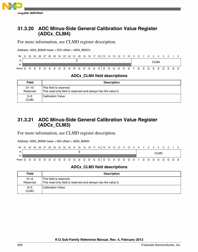
31.3.20 ADC Minus-Side General Calibration Value Register(ADCx_CLM4)
For more information, see CLMD register description.
Address: 4003_B000h base + 5Ch offset = 4003_B05Ch
Bit 31 30 29 28 27 26 25 24 23 22 21 20 19 18 17 16 15 14 13 12 11 10 9 8 7 6 5 4 3 2 1 0
R 0 CLM4W
Reset 0 0 0 0 0 0 0 0 0 0 0 0 0 0 0 0 0 0 0 0 0 0 1 0 0 0 0 0 0 0 0 0
ADCx_CLM4 field descriptions
Field Description
31–10Reserved
This field is reserved.This read-only field is reserved and always has the value 0.
9–0CLM4
Calibration Value
31.3.21 ADC Minus-Side General Calibration Value Register(ADCx_CLM3)
For more information, see CLMD register description.
Address: 4003_B000h base + 60h offset = 4003_B060h
Bit 31 30 29 28 27 26 25 24 23 22 21 20 19 18 17 16 15 14 13 12 11 10 9 8 7 6 5 4 3 2 1 0
R 0 CLM3W
Reset 0 0 0 0 0 0 0 0 0 0 0 0 0 0 0 0 0 0 0 0 0 0 0 1 0 0 0 0 0 0 0 0
ADCx_CLM3 field descriptions
Field Description
31–9Reserved
This field is reserved.This read-only field is reserved and always has the value 0.
8–0CLM3
Calibration Value
Register definition
K12 Sub-Family Reference Manual, Rev. 4, February 2013
628 Freescale Semiconductor, Inc.
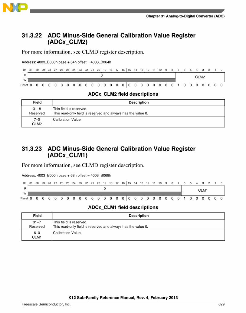
31.3.22 ADC Minus-Side General Calibration Value Register(ADCx_CLM2)
For more information, see CLMD register description.
Address: 4003_B000h base + 64h offset = 4003_B064h
Bit 31 30 29 28 27 26 25 24 23 22 21 20 19 18 17 16 15 14 13 12 11 10 9 8 7 6 5 4 3 2 1 0
R 0 CLM2W
Reset 0 0 0 0 0 0 0 0 0 0 0 0 0 0 0 0 0 0 0 0 0 0 0 0 1 0 0 0 0 0 0 0
ADCx_CLM2 field descriptions
Field Description
31–8Reserved
This field is reserved.This read-only field is reserved and always has the value 0.
7–0CLM2
Calibration Value
31.3.23 ADC Minus-Side General Calibration Value Register(ADCx_CLM1)
For more information, see CLMD register description.
Address: 4003_B000h base + 68h offset = 4003_B068h
Bit 31 30 29 28 27 26 25 24 23 22 21 20 19 18 17 16 15 14 13 12 11 10 9 8 7 6 5 4 3 2 1 0
R 0 CLM1W
Reset 0 0 0 0 0 0 0 0 0 0 0 0 0 0 0 0 0 0 0 0 0 0 0 0 0 1 0 0 0 0 0 0
ADCx_CLM1 field descriptions
Field Description
31–7Reserved
This field is reserved.This read-only field is reserved and always has the value 0.
6–0CLM1
Calibration Value
Chapter 31 Analog-to-Digital Converter (ADC)
K12 Sub-Family Reference Manual, Rev. 4, February 2013
Freescale Semiconductor, Inc. 629
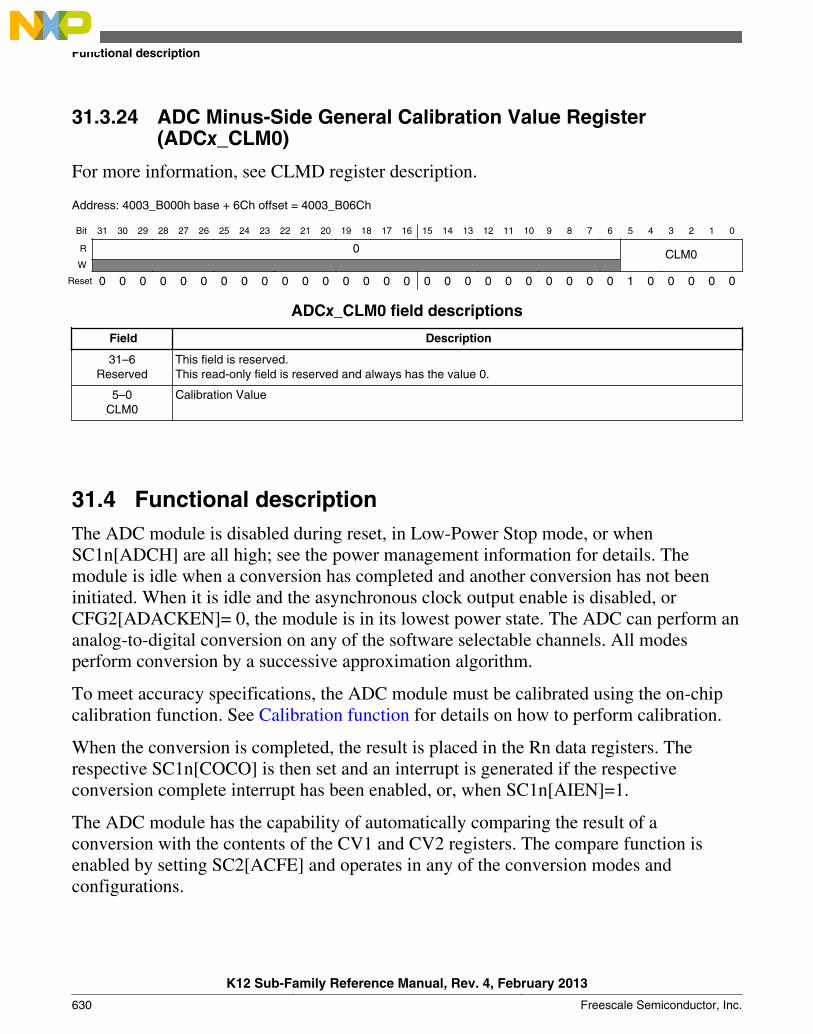
31.3.24 ADC Minus-Side General Calibration Value Register(ADCx_CLM0)
For more information, see CLMD register description.
Address: 4003_B000h base + 6Ch offset = 4003_B06Ch
Bit 31 30 29 28 27 26 25 24 23 22 21 20 19 18 17 16 15 14 13 12 11 10 9 8 7 6 5 4 3 2 1 0
R 0 CLM0W
Reset 0 0 0 0 0 0 0 0 0 0 0 0 0 0 0 0 0 0 0 0 0 0 0 0 0 0 1 0 0 0 0 0
ADCx_CLM0 field descriptions
Field Description
31–6Reserved
This field is reserved.This read-only field is reserved and always has the value 0.
5–0CLM0
Calibration Value
31.4 Functional descriptionThe ADC module is disabled during reset, in Low-Power Stop mode, or whenSC1n[ADCH] are all high; see the power management information for details. Themodule is idle when a conversion has completed and another conversion has not beeninitiated. When it is idle and the asynchronous clock output enable is disabled, orCFG2[ADACKEN]= 0, the module is in its lowest power state. The ADC can perform ananalog-to-digital conversion on any of the software selectable channels. All modesperform conversion by a successive approximation algorithm.
To meet accuracy specifications, the ADC module must be calibrated using the on-chipcalibration function. See Calibration function for details on how to perform calibration.
When the conversion is completed, the result is placed in the Rn data registers. Therespective SC1n[COCO] is then set and an interrupt is generated if the respectiveconversion complete interrupt has been enabled, or, when SC1n[AIEN]=1.
The ADC module has the capability of automatically comparing the result of aconversion with the contents of the CV1 and CV2 registers. The compare function isenabled by setting SC2[ACFE] and operates in any of the conversion modes andconfigurations.
Functional description
K12 Sub-Family Reference Manual, Rev. 4, February 2013
630 Freescale Semiconductor, Inc.
The ADC module has the capability of automatically averaging the result of multipleconversions. The hardware average function is enabled by setting SC3[AVGE] andoperates in any of the conversion modes and configurations.
NOTE
For the chip specific modes of operation, see the powermanagement information of this MCU.
31.4.1 Clock select and divide control
One of four clock sources can be selected as the clock source for the ADC module. Thisclock source is then divided by a configurable value to generate the input clock ADCK,to the module. The clock is selected from one of the following sources by means ofCFG1[ADICLK].
• Bus clock. This is the default selection following reset.
• Bus clock divided by two. For higher bus clock rates, this allows a maximum divide-by-16 of the bus clock using CFG1[ADIV].
• ALTCLK: As defined for this MCU. See the chip configuration information.
• Asynchronous clock (ADACK): This clock is generated from a clock source withinthe ADC module. When the ADACK clock source is selected, it is not required to beactive prior to conversion start. When it is selected and it is not active prior to aconversion start CFG2[ADACKEN]=0, ADACK is activated at the start of aconversion and deactivated when conversions are terminated. In this case, there is anassociated clock startup delay each time the clock source is re-activated. To avoid theconversion time variability and latency associated with the ADACK clock startup, setCFG2[ADACKEN]=1 and wait the worst-case startup time of 5 µs prior to initiatingany conversions using the ADACK clock source. Conversions are possible usingADACK as the input clock source while the MCU is in Normal Stop mode. SeePower Control for more information.
Whichever clock is selected, its frequency must fall within the specified frequency rangefor ADCK. If the available clocks are too slow, the ADC may not perform according tospecifications. If the available clocks are too fast, the clock must be divided to theappropriate frequency. This divider is specified by CFG1[ADIV] and can be divide-by 1,2, 4, or 8.
Chapter 31 Analog-to-Digital Converter (ADC)
K12 Sub-Family Reference Manual, Rev. 4, February 2013
Freescale Semiconductor, Inc. 631
31.4.2 Voltage reference selection
The ADC can be configured to accept one of the two voltage reference pairs as thereference voltage (VREFSH and VREFSL) used for conversions. Each pair contains apositive reference that must be between the minimum Ref Voltage High and VDDA, and aground reference that must be at the same potential as VSSA. The two pairs are external(VREFH and VREFL) and alternate (VALTH and VALTL). These voltage references areselected using SC2[REFSEL]. The alternate (VALTH and VALTL) voltage reference pairmay select additional external pins or internal sources depending on MCU configuration.See the chip configuration information on the voltage references specific to this MCU.
31.4.3 Hardware trigger and channel selects
The ADC module has a selectable asynchronous hardware conversion trigger, ADHWT,that is enabled when SC2[ADTRG] is set and a hardware trigger select event,ADHWTSn, has occurred. This source is not available on all MCUs. See the ChipConfiguration chapter for information on the ADHWT source and the ADHWTSnconfigurations specific to this MCU.
When an ADHWT source is available and hardware trigger is enabled, that isSC2[ADTRG]=1, a conversion is initiated on the rising-edge of ADHWT after ahardware trigger select event, that is, ADHWTSn, has occurred. If a conversion is inprogress when a rising-edge of a trigger occurs, the rising-edge is ignored. In continuousconvert configuration, only the initial rising-edge to launch continuous conversions isobserved, and until conversion is aborted, the ADC continues to do conversions on thesame SCn register that initiated the conversion. The hardware trigger function operates inconjunction with any of the conversion modes and configurations.
The hardware trigger select event, that is, ADHWTSn, must be set prior to the receipt ofthe ADHWT signal. If these conditions are not met, the converter may ignore the triggeror use the incorrect configuration. If a hardware trigger select event is asserted during aconversion, it must stay asserted until the end of current conversion and remain set untilthe receipt of the ADHWT signal to trigger a new conversion. The channel and statusfields selected for the conversion depend on the active trigger select signal:
• ADHWTSA active selects SC1A• ADHWTSn active selects SC1n
Note
Asserting more than one hardware trigger select signal(ADHWTSn) at the same time results in unknown results. Toavoid this, select only one hardware trigger select signal(ADHWTSn) prior to the next intended conversion.
Functional description
K12 Sub-Family Reference Manual, Rev. 4, February 2013
632 Freescale Semiconductor, Inc.
When the conversion is completed, the result is placed in the Rn registers associated withthe ADHWTSn received. For example:
• ADHWTSA active selects RA register• ADHWTSn active selects Rn register
The conversion complete flag associated with the ADHWTSn received, that is,SC1n[COCO], is then set and an interrupt is generated if the respective conversioncomplete interrupt has been enabled, that is, SC1[AIEN]=1.
31.4.4 Conversion control
Conversions can be performed as determined by CFG1[MODE] and SC1n[DIFF] asshown in the description of CFG1[MODE].
Conversions can be initiated by a software or hardware trigger. In addition, the ADCmodule can be configured for:
• Low-power operation• Long sample time• Continuous conversion• Hardware average• Automatic compare of the conversion result to a software determined compare value
31.4.4.1 Initiating conversions
A conversion is initiated:
• Following a write to SC1A, with SC1n[ADCH] not all 1's, if software triggeredoperation is selected, that is, when SC2[ADTRG]=0.
• Following a hardware trigger, or ADHWT event, if hardware triggered operation isselected, that is, SC2[ADTRG]=1, and a hardware trigger select event, ADHWTSn,has occurred. The channel and status fields selected depend on the active triggerselect signal:
• ADHWTSA active selects SC1A• ADHWTSn active selects SC1n• if neither is active, the off condition is selected
Chapter 31 Analog-to-Digital Converter (ADC)
K12 Sub-Family Reference Manual, Rev. 4, February 2013
Freescale Semiconductor, Inc. 633
Note
Selecting more than one ADHWTSn prior to a conversioncompletion will result in unknown results. To avoid this,select only one ADHWTSn prior to a conversioncompletion.
• Following the transfer of the result to the data registers when continuous conversionis enabled, that is, when ADCO=1.
If continuous conversions are enabled, a new conversion is automatically initiated afterthe completion of the current conversion, by:. In software triggered operation, that is,when ADTRG=0, continuous conversions begin after SC1A is written and continue untilaborted. In hardware triggered operation, that is, when ADTRG=1 and one ADHWTSnevent has occurred, continuous conversions begin after a hardware trigger event andcontinue until aborted.
If hardware averaging is enabled, a new conversion is automatically initiated after thecompletion of the current conversion until the correct number of conversions arecompleted. In software triggered operation, conversions begin after SC1A is written. Inhardware triggered operation, conversions begin after a hardware trigger. If continuousconversions are also enabled, a new set of conversions to be averaged are initiatedfollowing the last of the selected number of conversions.
31.4.4.2 Completing conversions
A conversion is completed when the result of the conversion is transferred into the dataresult registers, Rn. If the compare functions are disabled, this is indicated by setting ofSC1n[COCO]. If hardware averaging is enabled, the respective SC1n[COCO] sets only ifthe last of the selected number of conversions is completed. If the compare function isenabled, the respective SC1n[COCO] sets and conversion result data is transferred only ifthe compare condition is true. If both hardware averaging and compare functions areenabled, then the respective SC1n[COCO] sets only if the last of the selected number ofconversions is completed and the compare condition is true. An interrupt is generated ifthe respective SC1n[AIEN] is high at the time that the respective SC1n[COCO] is set.
31.4.4.3 Aborting conversions
Any conversion in progress is aborted when:
Functional description
K12 Sub-Family Reference Manual, Rev. 4, February 2013
634 Freescale Semiconductor, Inc.
• Writing to SC1A while it is actively controlling a conversion, aborts the currentconversion. In Software Trigger mode, when SC2[ADTRG]=0, a write to SC1Ainitiates a new conversion if SC1A[ADCH] is equal to a value other than all 1s.Writing to any of the SC1B–SC1n registers while that specific SC1B–SC1n registeris actively controlling a conversion aborts the current conversion. The SC1(B-n)registers are not used for software trigger operation and therefore writes to theSC1(B-n) registers do not initiate a new conversion.
• A write to any ADC register besides the SC1A-SC1n registers occurs. This indicatesthat a change in mode of operation has occurred and the current conversion istherefore invalid.
• The MCU is reset or enters Low-Power Stop modes.
• The MCU enters Normal Stop mode with ADACK not enabled.
When a conversion is aborted, the contents of the data registers, Rn, are not altered. Thedata registers continue to be the values transferred after the completion of the lastsuccessful conversion. If the conversion was aborted by a reset or Low-Power Stopmodes, RA and Rn return to their reset states.
31.4.4.4 Power control
The ADC module remains in its idle state until a conversion is initiated. If ADACK isselected as the conversion clock source, but the asynchronous clock output is disabled,that is CFG2[ADACKEN]=0, the ADACK clock generator also remains in its idle state(disabled) until a conversion is initiated. If the asynchronous clock output is enabled, thatis, CFG2[ADACKEN]=1, it remains active regardless of the state of the ADC or theMCU power mode.
Power consumption when the ADC is active can be reduced by setting CFG1[ADLPC].This results in a lower maximum value for fADCK.
31.4.4.5 Sample time and total conversion time
For short sample, that is, when CFG1[ADLSMP]=0, there is a 2-cycle adder for firstconversion over the base sample time of four ADCK cycles. For high speed conversions,that is, when CFG2[ADHSC]=1, there is an additional 2-cycle adder on any conversion.The table below summarizes sample times for the possible ADC configurations.
Chapter 31 Analog-to-Digital Converter (ADC)
K12 Sub-Family Reference Manual, Rev. 4, February 2013
Freescale Semiconductor, Inc. 635
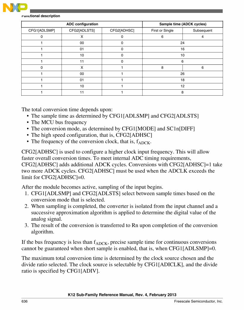
ADC configuration Sample time (ADCK cycles)
CFG1[ADLSMP] CFG2[ADLSTS] CFG2[ADHSC] First or Single Subsequent
0 X 0 6 4
1 00 0 24
1 01 0 16
1 10 0 10
1 11 0 6
0 X 1 8 6
1 00 1 26
1 01 1 18
1 10 1 12
1 11 1 8
The total conversion time depends upon:• The sample time as determined by CFG1[ADLSMP] and CFG2[ADLSTS]• The MCU bus frequency• The conversion mode, as determined by CFG1[MODE] and SC1n[DIFF]• The high speed configuration, that is, CFG2[ADHSC]• The frequency of the conversion clock, that is, fADCK.
CFG2[ADHSC] is used to configure a higher clock input frequency. This will allowfaster overall conversion times. To meet internal ADC timing requirements,CFG2[ADHSC] adds additional ADCK cycles. Conversions with CFG2[ADHSC]=1 taketwo more ADCK cycles. CFG2[ADHSC] must be used when the ADCLK exceeds thelimit for CFG2[ADHSC]=0.
After the module becomes active, sampling of the input begins.1. CFG1[ADLSMP] and CFG2[ADLSTS] select between sample times based on the
conversion mode that is selected.2. When sampling is completed, the converter is isolated from the input channel and a
successive approximation algorithm is applied to determine the digital value of theanalog signal.
3. The result of the conversion is transferred to Rn upon completion of the conversionalgorithm.
If the bus frequency is less than fADCK, precise sample time for continuous conversionscannot be guaranteed when short sample is enabled, that is, when CFG1[ADLSMP]=0.
The maximum total conversion time is determined by the clock source chosen and thedivide ratio selected. The clock source is selectable by CFG1[ADICLK], and the divideratio is specified by CFG1[ADIV].
Functional description
K12 Sub-Family Reference Manual, Rev. 4, February 2013
636 Freescale Semiconductor, Inc.
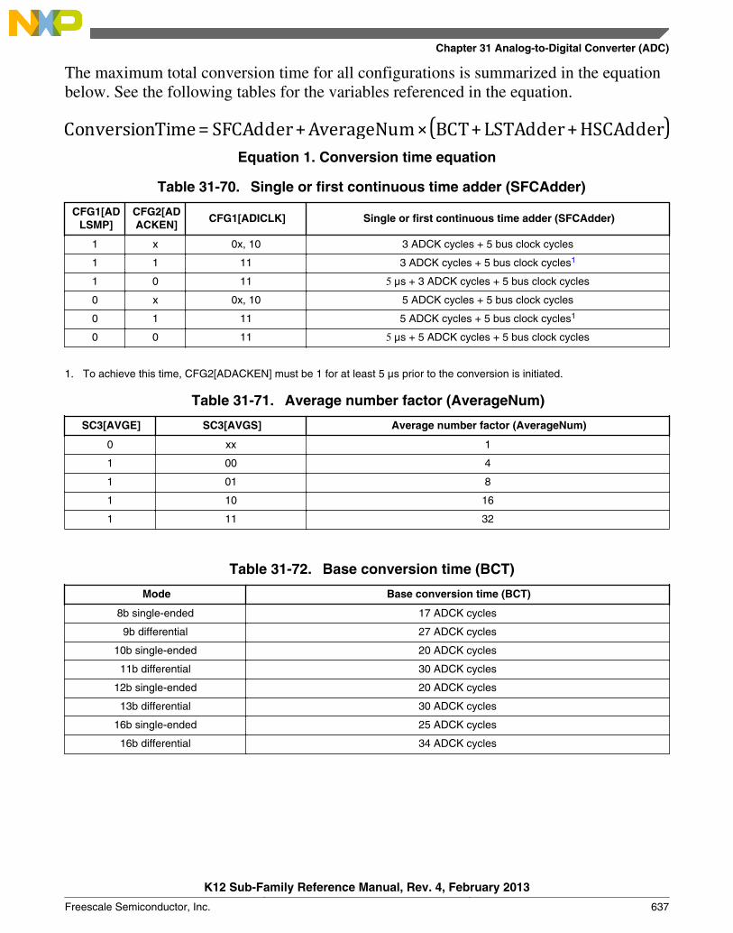
The maximum total conversion time for all configurations is summarized in the equationbelow. See the following tables for the variables referenced in the equation.
Equation 1. Conversion time equation
Table 31-70. Single or first continuous time adder (SFCAdder)
CFG1[ADLSMP]
CFG2[ADACKEN]
CFG1[ADICLK] Single or first continuous time adder (SFCAdder)
1 x 0x, 10 3 ADCK cycles + 5 bus clock cycles
1 1 11 3 ADCK cycles + 5 bus clock cycles1
1 0 11 5 μs + 3 ADCK cycles + 5 bus clock cycles
0 x 0x, 10 5 ADCK cycles + 5 bus clock cycles
0 1 11 5 ADCK cycles + 5 bus clock cycles1
0 0 11 5 μs + 5 ADCK cycles + 5 bus clock cycles
1. To achieve this time, CFG2[ADACKEN] must be 1 for at least 5 μs prior to the conversion is initiated.
Table 31-71. Average number factor (AverageNum)
SC3[AVGE] SC3[AVGS] Average number factor (AverageNum)
0 xx 1
1 00 4
1 01 8
1 10 16
1 11 32
Table 31-72. Base conversion time (BCT)
Mode Base conversion time (BCT)
8b single-ended 17 ADCK cycles
9b differential 27 ADCK cycles
10b single-ended 20 ADCK cycles
11b differential 30 ADCK cycles
12b single-ended 20 ADCK cycles
13b differential 30 ADCK cycles
16b single-ended 25 ADCK cycles
16b differential 34 ADCK cycles
Chapter 31 Analog-to-Digital Converter (ADC)
K12 Sub-Family Reference Manual, Rev. 4, February 2013
Freescale Semiconductor, Inc. 637

Table 31-73. Long sample time adder (LSTAdder)
CFG1[ADLSMP] CFG2[ADLSTS]Long sample time adder
(LSTAdder)
0 xx 0 ADCK cycles
1 00 20 ADCK cycles
1 01 12 ADCK cycles
1 10 6 ADCK cycles
1 11 2 ADCK cycles
Table 31-74. High-speed conversion time adder (HSCAdder)
CFG2[ADHSC] High-speed conversion time adder (HSCAdder)
0 0 ADCK cycles
1 2 ADCK cycles
Note
The ADCK frequency must be between fADCK minimum andfADCK maximum to meet ADC specifications.
31.4.4.6 Conversion time examples
The following examples use the Equation 1 on page 637, and the information provided inTable 31-70 through Table 31-74.
31.4.4.6.1 Typical conversion time configurationA typical configuration for ADC conversion is:
• 10-bit mode, with the bus clock selected as the input clock source• The input clock divide-by-1 ratio selected• Bus frequency of 8 MHz• Long sample time disabled• High-speed conversion disabled
The conversion time for a single conversion is calculated by using the Equation 1 on page637, and the information provided in Table 31-70 through Table 31-74. The table belowlists the variables of Equation 1 on page 637.
Table 31-75. Typical conversion time
Variable Time
SFCAdder 5 ADCK cycles + 5 bus clock cycles
Table continues on the next page...
Functional description
K12 Sub-Family Reference Manual, Rev. 4, February 2013
638 Freescale Semiconductor, Inc.
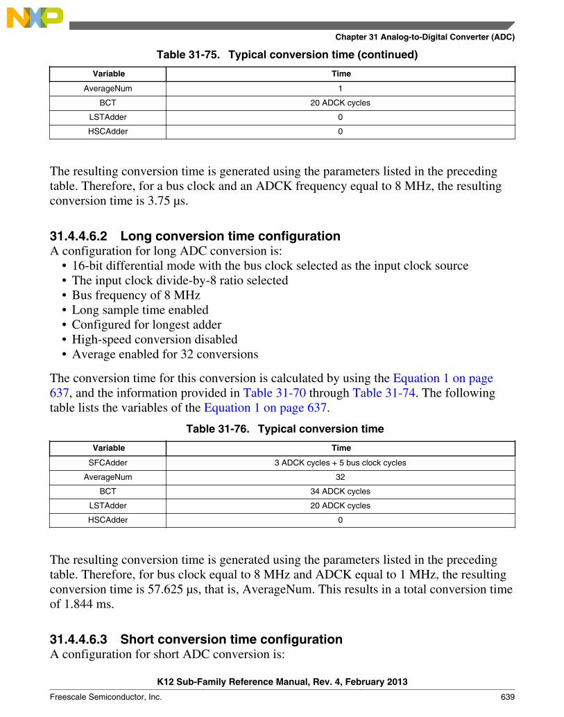
Table 31-75. Typical conversion time (continued)
Variable Time
AverageNum 1
BCT 20 ADCK cycles
LSTAdder 0
HSCAdder 0
The resulting conversion time is generated using the parameters listed in the precedingtable. Therefore, for a bus clock and an ADCK frequency equal to 8 MHz, the resultingconversion time is 3.75 µs.
31.4.4.6.2 Long conversion time configurationA configuration for long ADC conversion is:
• 16-bit differential mode with the bus clock selected as the input clock source• The input clock divide-by-8 ratio selected• Bus frequency of 8 MHz• Long sample time enabled• Configured for longest adder• High-speed conversion disabled• Average enabled for 32 conversions
The conversion time for this conversion is calculated by using the Equation 1 on page637, and the information provided in Table 31-70 through Table 31-74. The followingtable lists the variables of the Equation 1 on page 637.
Table 31-76. Typical conversion time
Variable Time
SFCAdder 3 ADCK cycles + 5 bus clock cycles
AverageNum 32
BCT 34 ADCK cycles
LSTAdder 20 ADCK cycles
HSCAdder 0
The resulting conversion time is generated using the parameters listed in the precedingtable. Therefore, for bus clock equal to 8 MHz and ADCK equal to 1 MHz, the resultingconversion time is 57.625 µs, that is, AverageNum. This results in a total conversion timeof 1.844 ms.
31.4.4.6.3 Short conversion time configurationA configuration for short ADC conversion is:
Chapter 31 Analog-to-Digital Converter (ADC)
K12 Sub-Family Reference Manual, Rev. 4, February 2013
Freescale Semiconductor, Inc. 639
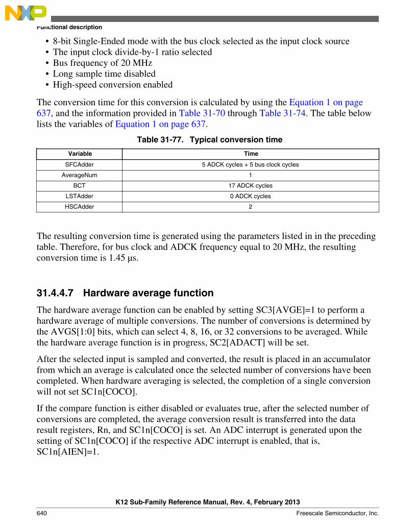
• 8-bit Single-Ended mode with the bus clock selected as the input clock source• The input clock divide-by-1 ratio selected• Bus frequency of 20 MHz• Long sample time disabled• High-speed conversion enabled
The conversion time for this conversion is calculated by using the Equation 1 on page637, and the information provided in Table 31-70 through Table 31-74. The table belowlists the variables of Equation 1 on page 637.
Table 31-77. Typical conversion time
Variable Time
SFCAdder 5 ADCK cycles + 5 bus clock cycles
AverageNum 1
BCT 17 ADCK cycles
LSTAdder 0 ADCK cycles
HSCAdder 2
The resulting conversion time is generated using the parameters listed in in the precedingtable. Therefore, for bus clock and ADCK frequency equal to 20 MHz, the resultingconversion time is 1.45 µs.
31.4.4.7 Hardware average function
The hardware average function can be enabled by setting SC3[AVGE]=1 to perform ahardware average of multiple conversions. The number of conversions is determined bythe AVGS[1:0] bits, which can select 4, 8, 16, or 32 conversions to be averaged. Whilethe hardware average function is in progress, SC2[ADACT] will be set.
After the selected input is sampled and converted, the result is placed in an accumulatorfrom which an average is calculated once the selected number of conversions have beencompleted. When hardware averaging is selected, the completion of a single conversionwill not set SC1n[COCO].
If the compare function is either disabled or evaluates true, after the selected number ofconversions are completed, the average conversion result is transferred into the dataresult registers, Rn, and SC1n[COCO] is set. An ADC interrupt is generated upon thesetting of SC1n[COCO] if the respective ADC interrupt is enabled, that is,SC1n[AIEN]=1.
Functional description
K12 Sub-Family Reference Manual, Rev. 4, February 2013
640 Freescale Semiconductor, Inc.
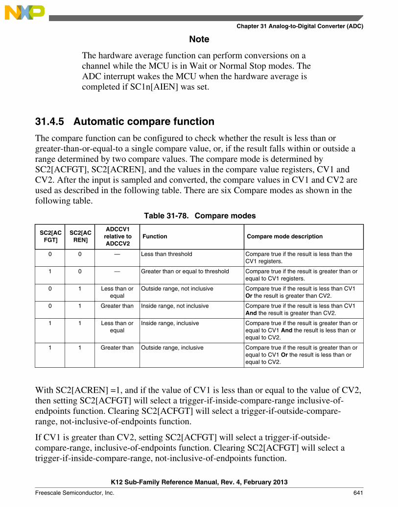
Note
The hardware average function can perform conversions on achannel while the MCU is in Wait or Normal Stop modes. TheADC interrupt wakes the MCU when the hardware average iscompleted if SC1n[AIEN] was set.
31.4.5 Automatic compare function
The compare function can be configured to check whether the result is less than orgreater-than-or-equal-to a single compare value, or, if the result falls within or outside arange determined by two compare values. The compare mode is determined bySC2[ACFGT], SC2[ACREN], and the values in the compare value registers, CV1 andCV2. After the input is sampled and converted, the compare values in CV1 and CV2 areused as described in the following table. There are six Compare modes as shown in thefollowing table.
Table 31-78. Compare modes
SC2[ACFGT]
SC2[ACREN]
ADCCV1relative toADCCV2
Function Compare mode description
0 0 — Less than threshold Compare true if the result is less than theCV1 registers.
1 0 — Greater than or equal to threshold Compare true if the result is greater than orequal to CV1 registers.
0 1 Less than orequal
Outside range, not inclusive Compare true if the result is less than CV1Or the result is greater than CV2.
0 1 Greater than Inside range, not inclusive Compare true if the result is less than CV1And the result is greater than CV2.
1 1 Less than orequal
Inside range, inclusive Compare true if the result is greater than orequal to CV1 And the result is less than orequal to CV2.
1 1 Greater than Outside range, inclusive Compare true if the result is greater than orequal to CV1 Or the result is less than orequal to CV2.
With SC2[ACREN] =1, and if the value of CV1 is less than or equal to the value of CV2,then setting SC2[ACFGT] will select a trigger-if-inside-compare-range inclusive-of-endpoints function. Clearing SC2[ACFGT] will select a trigger-if-outside-compare-range, not-inclusive-of-endpoints function.
If CV1 is greater than CV2, setting SC2[ACFGT] will select a trigger-if-outside-compare-range, inclusive-of-endpoints function. Clearing SC2[ACFGT] will select atrigger-if-inside-compare-range, not-inclusive-of-endpoints function.
Chapter 31 Analog-to-Digital Converter (ADC)
K12 Sub-Family Reference Manual, Rev. 4, February 2013
Freescale Semiconductor, Inc. 641
If the condition selected evaluates true, SC1n[COCO] is set.
Upon completion of a conversion while the compare function is enabled, if the comparecondition is not true, SC1n[COCO] is not set and the conversion result data will not betransferred to the result register, Rn. If the hardware averaging function is enabled, thecompare function compares the averaged result to the compare values. The same comparefunction definitions apply. An ADC interrupt is generated when SC1n[COCO] is set andthe respective ADC interrupt is enabled, that is, SC1n[AIEN]=1.
Note
The compare function can monitor the voltage on a channelwhile the MCU is in Wait or Normal Stop modes. The ADCinterrupt wakes the MCU when the compare condition is met.
31.4.6 Calibration function
The ADC contains a self-calibration function that is required to achieve the specifiedaccuracy. Calibration must be run, or valid calibration values written, after any reset andbefore a conversion is initiated. The calibration function sets the offset calibration value,the minus-side calibration values, and the plus-side calibration values. The offsetcalibration value is automatically stored in the ADC offset correction register (OFS), andthe plus-side and minus-side calibration values are automatically stored in the ADC plus-side and minus-side calibration registers, CLPx and CLMx. The user must configure theADC correctly prior to calibration, and must generate the plus-side and minus-side gaincalibration results and store them in the ADC plus-side gain register (PG) after thecalibration function completes.
Prior to calibration, the user must configure the ADC's clock source and frequency, lowpower configuration, voltage reference selection, sample time, and high speedconfiguration according to the application's clock source availability and needs. If theapplication uses the ADC in a wide variety of configurations, the configuration for whichthe highest accuracy is required should be selected, or multiple calibrations can be donefor the different configurations. For best calibration results:
• Set hardware averaging to maximum, that is, SC3[AVGE]=1 and SC3[AVGS]=11for an average of 32
• Set ADC clock frequency fADCK less than or equal to 4 MHz• VREFH=VDDA
• Calibrate at nominal voltage and temperature
The input channel, conversion mode continuous function, compare function, resolutionmode, and differential/single-ended mode are all ignored during the calibration function.
Functional description
K12 Sub-Family Reference Manual, Rev. 4, February 2013
642 Freescale Semiconductor, Inc.
To initiate calibration, the user sets SC3[CAL] and the calibration will automaticallybegin if the SC2[ADTRG] is 0. If SC2[ADTRG] is 1, SC3[CAL] will not get set andSC3[CALF] will be set. While calibration is active, no ADC register can be written andno stop mode may be entered, or the calibration routine will be aborted causingSC3[CAL] to clear and SC3[CALF] to set. At the end of a calibration sequence,SC1n[COCO] will be set. SC1n[AIEN] can be used to allow an interrupt to occur at theend of a calibration sequence. At the end of the calibration routine, if SC3[CALF] is notset, the automatic calibration routine is completed successfully.
To complete calibration, the user must generate the gain calibration values using thefollowing procedure:
1. Initialize or clear a 16-bit variable in RAM.
2. Add the plus-side calibration results CLP0, CLP1, CLP2, CLP3, CLP4, and CLPS tothe variable.
3. Divide the variable by two.
4. Set the MSB of the variable.
5. The previous two steps can be achieved by setting the carry bit, rotating to the rightthrough the carry bit on the high byte and again on the low byte.
6. Store the value in the plus-side gain calibration register PG.
7. Repeat the procedure for the minus-side gain calibration value.
When calibration is complete, the user may reconfigure and use the ADC as desired. Asecond calibration may also be performed, if desired, by clearing and again settingSC3[CAL].
Overall, the calibration routine may take as many as 14k ADCK cycles and 100 buscycles, depending on the results and the clock source chosen. For an 8 MHz clock source,this length amounts to about 1.7 ms. To reduce this latency, the calibration values, whichare offset, plus-side and minus-side gain, and plus-side and minus-side calibration values,may be stored in flash memory after an initial calibration and recovered prior to the firstADC conversion. This method can reduce the calibration latency to 20 register storeoperations on all subsequent power, reset, or Low-Power Stop mode recoveries.
Chapter 31 Analog-to-Digital Converter (ADC)
K12 Sub-Family Reference Manual, Rev. 4, February 2013
Freescale Semiconductor, Inc. 643

31.4.7 User-defined offset function
OFS contains the user-selected or calibration-generated offset error correction value. Thisregister is a 2’s complement, left-justified. The value in OFS is subtracted from theconversion and the result is transferred into the result registers, Rn. If the result is greaterthan the maximum or less than the minimum result value, it is forced to the appropriatelimit for the current mode of operation.
The formatting of the OFS is different from the data result register, Rn, to preserve theresolution of the calibration value regardless of the conversion mode selected. Lowerorder bits are ignored in lower resolution modes. For example, in 8-bit single-endedmode, OFS[14:7] are subtracted from D[7:0]; OFS[15] indicates the sign (negativenumbers are effectively added to the result) and OFS[6:0] are ignored. The same bits areused in 9-bit differential mode because OFS[15] indicates the sign bit, which maps toD[8]. For 16-bit differential mode, OFS[15:0] are directly subtracted from the conversionresult data D[15:0]. In 16-bit single-ended mode, there is no field in the OFScorresponding to the least significant result D[0], so odd values, such as -1 or +1, cannotbe subtracted from the result.
OFS is automatically set according to calibration requirements once the self-calibrationsequence is done, that is, SC3[CAL] is cleared. The user may write to OFS to overridethe calibration result if desired. If the OFS is written by the user to a value that isdifferent from the calibration value, the ADC error specifications may not be met. Storingthe value generated by the calibration function in memory before overwriting with a user-specified value is recommended.
Note
There is an effective limit to the values of offset that can be setby the user. If the magnitude of the offset is too high, the resultsof the conversions will cap off at the limits.
The offset calibration function may be employed by the user to remove applicationoffsets or DC bias values. OFS may be written with a number in 2's complement formatand this offset will be subtracted from the result, or hardware averaged value. To add anoffset, store the negative offset in 2's complement format and the effect will be anaddition. An offset correction that results in an out-of-range value will be forced to theminimum or maximum value. The minimum value for single-ended conversions is0x0000; for a differential conversion it is 0x8000.
To preserve accuracy, the calibrated offset value initially stored in OFS must be added tothe user-defined offset. For applications that may change the offset repeatedly duringoperation, store the initial offset calibration value in flash so it can be recovered andadded to any user offset adjustment value and the sum stored in OFS.
Functional description
K12 Sub-Family Reference Manual, Rev. 4, February 2013
644 Freescale Semiconductor, Inc.
31.4.8 Temperature sensor
The ADC module includes a temperature sensor whose output is connected to one of theADC analog channel inputs. The following equation provides an approximate transferfunction of the temperature sensor.
m
Equation 2. Approximate transfer function of the temperature sensor
where:
• VTEMP is the voltage of the temperature sensor channel at the ambient temperature.
• VTEMP25 is the voltage of the temperature sensor channel at 25 °C.
• m is referred as temperature sensor slope in the device data sheet. It is the hot or coldvoltage versus temperature slope in V/°C.
For temperature calculations, use the VTEMP25 and temperature sensor slope values fromthe ADC Electricals table.
In application code, the user reads the temperature sensor channel, calculates VTEMP, andcompares to VTEMP25. If VTEMP is greater than VTEMP25 the cold slope value is applied inthe preceding equation. If VTEMP is less than VTEMP25, the hot slope value is applied inthe preceding equation. ADC Electricals table may only specify one temperature sensorslope value. In that case, the user could use the same slope for the calculation across theoperational temperature range.
For more information on using the temperature sensor, see the application note titledTemperature Sensor for the HCS08 Microcontroller Family (document AN3031).
31.4.9 MCU wait mode operation
Wait mode is a lower-power consumption Standby mode from which recovery is fastbecause the clock sources remain active. If a conversion is in progress when the MCUenters Wait mode, it continues until completion. Conversions can be initiated while theMCU is in Wait mode by means of the hardware trigger or if continuous conversions areenabled.
Chapter 31 Analog-to-Digital Converter (ADC)
K12 Sub-Family Reference Manual, Rev. 4, February 2013
Freescale Semiconductor, Inc. 645

The bus clock, bus clock divided by two, and ADACK are available as conversion clocksources while in Wait mode. The use of ALTCLK as the conversion clock source in Waitis dependent on the definition of ALTCLK for this MCU. See the Chip Configurationinformation on ALTCLK specific to this MCU.
If the compare and hardware averaging functions are disabled, a conversion completeevent sets SC1n[COCO] and generates an ADC interrupt to wake the MCU from Waitmode if the respective ADC interrupt is enabled, that is, when SC1n[AIEN]=1. If thehardware averaging function is enabled, SC1n[COCO] will set, and generate an interruptif enabled, when the selected number of conversions are completed. If the comparefunction is enabled, SC1n[COCO] will set, and generate an interrupt if enabled, only ifthe compare conditions are met. If a single conversion is selected and the compare triggeris not met, the ADC will return to its idle state and cannot wake the MCU from Waitmode unless a new conversion is initiated by the hardware trigger.
31.4.10 MCU Normal Stop mode operation
Stop mode is a low-power consumption Standby mode during which most or all clocksources on the MCU are disabled.
31.4.10.1 Normal Stop mode with ADACK disabled
If the asynchronous clock, ADACK, is not selected as the conversion clock, executing astop instruction aborts the current conversion and places the ADC in its Idle state. Thecontents of the ADC registers, including Rn, are unaffected by Normal Stop mode. Afterexiting from Normal Stop mode, a software or hardware trigger is required to resumeconversions.
31.4.10.2 Normal Stop mode with ADACK enabled
If ADACK is selected as the conversion clock, the ADC continues operation duringNormal Stop mode. See the chip configuration chapter for configuration information forthis MCU.
If a conversion is in progress when the MCU enters Normal Stop mode, it continues untilcompletion. Conversions can be initiated while the MCU is in Normal Stop mode bymeans of the hardware trigger or if continuous conversions are enabled.
Functional description
K12 Sub-Family Reference Manual, Rev. 4, February 2013
646 Freescale Semiconductor, Inc.
If the compare and hardware averaging functions are disabled, a conversion completeevent sets SC1n[COCO] and generates an ADC interrupt to wake the MCU from NormalStop mode if the respective ADC interrupt is enabled, that is, when SC1n[AIEN]=1. Theresult register, Rn, will contain the data from the first completed conversion that occurredduring Normal Stop mode. If the hardware averaging function is enabled, SC1n[COCO]will set, and generate an interrupt if enabled, when the selected number of conversionsare completed. If the compare function is enabled, SC1n[COCO] will set, and generate aninterrupt if enabled, only if the compare conditions are met. If a single conversion isselected and the compare is not true, the ADC will return to its Idle state and cannot wakethe MCU from Normal Stop mode unless a new conversion is initiated by anotherhardware trigger.
31.4.11 MCU Low-Power Stop mode operation
The ADC module is automatically disabled when the MCU enters Low-Power Stopmode. All module registers contain their reset values following exit from Low-PowerStop mode. Therefore, the module must be re-enabled and re-configured following exitfrom Low-Power Stop mode.
NOTEFor the chip specific modes of operation, see the powermanagement information for the device.
31.5 Initialization informationThis section gives an example that provides some basic direction on how to initialize andconfigure the ADC module. The user can configure the module for 16-bit, 12-bit, 10-bit,or 8-bit single-ended resolution or 16-bit, 13-bit, 11-bit, or 9-bit differential resolution,single or continuous conversion, and a polled or interrupt approach, among many otheroptions. For information used in this example, refer to Table 31-73, Table 31-74, andTable 31-75.
Note
Hexadecimal values are designated by a preceding 0x, binaryvalues designated by a preceding %, and decimal values haveno preceding character.
31.5.1 ADC module initialization example
Chapter 31 Analog-to-Digital Converter (ADC)
K12 Sub-Family Reference Manual, Rev. 4, February 2013
Freescale Semiconductor, Inc. 647

31.5.1.1 Initialization sequence
Before the ADC module can be used to complete conversions, an initialization proceduremust be performed. A typical sequence is:
1. Calibrate the ADC by following the calibration instructions in Calibration function.
2. Update CFG to select the input clock source and the divide ratio used to generateADCK. This register is also used for selecting sample time and low-powerconfiguration.
3. Update SC2 to select the conversion trigger, hardware or software, and comparefunction options, if enabled.
4. Update SC3 to select whether conversions will be continuous or completed only once(ADCO) and whether to perform hardware averaging.
5. Update SC1:SC1n registers to select whether conversions will be single-ended ordifferential and to enable or disable conversion complete interrupts. Also, select theinput channel which can be used to perform conversions.
31.5.1.2 Pseudo-code example
In this example, the ADC module is set up with interrupts enabled to perform a single 10-bit conversion at low-power with a long sample time on input channel 1, where ADCK isderived from the bus clock divided by 1.
CFG1 = 0x98 (%10011000)
Bit 7 ADLPC 1 Configures for low power, lowers maximum clock speed. Bit 6:5 ADIV 00 Sets the ADCK to the input clock ÷ 1. Bit 4 ADLSMP 1 Configures for long sample time. Bit 3:2 MODE 10 Selects the single-ended 10-bit conversion, differential 11-bit conversion. Bit 1:0 ADICLK 00 Selects the bus clock.
SC2 = 0x00 (%00000000)
Bit 7 ADACT 0 Flag indicates if a conversion is in progress. Bit 6 ADTRG 0 Software trigger selected. Bit 5 ACFE 0 Compare function disabled. Bit 4 ACFGT 0 Not used in this example. Bit 3 ACREN 0 Compare range disabled. Bit 2 DMAEN 0 DMA request disabled. Bit 1:0 REFSEL 00 Selects default voltage reference pin pair (External pins VREFH and VREFL).
SC1A = 0x41 (%01000001)
Initialization information
K12 Sub-Family Reference Manual, Rev. 4, February 2013
648 Freescale Semiconductor, Inc.
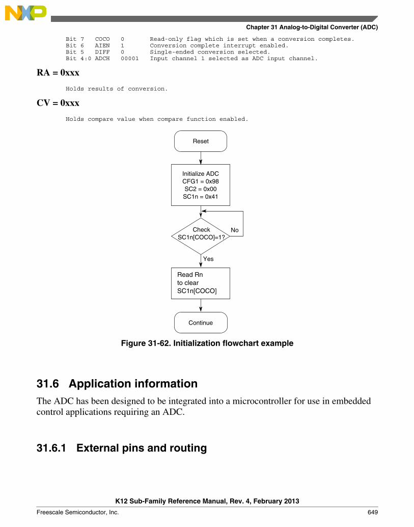
Bit 7 COCO 0 Read-only flag which is set when a conversion completes. Bit 6 AIEN 1 Conversion complete interrupt enabled. Bit 5 DIFF 0 Single-ended conversion selected. Bit 4:0 ADCH 00001 Input channel 1 selected as ADC input channel.
RA = 0xxx
Holds results of conversion.
CV = 0xxx
Holds compare value when compare function enabled.
Reset
No
Yes
CheckSC1n[COCO]=1?
Initialize ADCCFG1 = 0x98SC2 = 0x00SC1n = 0x41
Continue
Read Rnto clearSC1n[COCO]
Figure 31-62. Initialization flowchart example
31.6 Application informationThe ADC has been designed to be integrated into a microcontroller for use in embeddedcontrol applications requiring an ADC.
31.6.1 External pins and routing
Chapter 31 Analog-to-Digital Converter (ADC)
K12 Sub-Family Reference Manual, Rev. 4, February 2013
Freescale Semiconductor, Inc. 649
31.6.1.1 Analog supply pinsDepending on the device, the analog power and ground supplies, VDDA and VSSA, of theADC module are available as:
• VDDA and VSSA available as separate pins—When available on a separate pin, bothVDDA and VSSA must be connected to the same voltage potential as theircorresponding MCU digital supply, VDD and VSS, and must be routed carefully formaximum noise immunity and bypass capacitors placed as near as possible to thepackage.
• VSSA is shared on the same pin as the MCU digital VSS.• VSSA and VDDA are shared with the MCU digital supply pins—In these cases, there
are separate pads for the analog supplies bonded to the same pin as the correspondingdigital supply so that some degree of isolation between the supplies is maintained.
If separate power supplies are used for analog and digital power, the ground connectionbetween these supplies must be at the VSSA pin. This must be the only ground connectionbetween these supplies, if possible. VSSA makes a good single point ground location.
31.6.1.2 Analog voltage reference pinsIn addition to the analog supplies, the ADC module has connections for two referencevoltage inputs used by the converter:
• VREFSH is the high reference voltage for the converter.• VREFSL is the low reference voltage for the converter.
The ADC can be configured to accept one of two voltage reference pairs for VREFSH andVREFSL. Each pair contains a positive reference and a ground reference. The two pairs areexternal, VREFH and VREFL and alternate, VALTH and VALTL. These voltage references areselected using SC2[REFSEL]. The alternate voltage reference pair, VALTH and VALTL,may select additional external pins or internal sources based on MCU configuration. Seethe chip configuration information on the voltage references specific to this MCU.
In some packages, the external or alternate pairs are connected in the package to VDDAand VSSA, respectively. One of these positive references may be shared on the same pinas VDDA on some devices. One of these ground references may be shared on the same pinas VSSA on some devices.
If externally available, the positive reference may be connected to the same potential asVDDA or may be driven by an external source to a level between the minimum RefVoltage High and the VDDA potential. The positive reference must never exceed VDDA. Ifexternally available, the ground reference must be connected to the same voltagepotential as VSSA. The voltage reference pairs must be routed carefully for maximumnoise immunity and bypass capacitors placed as near as possible to the package.
Application information
K12 Sub-Family Reference Manual, Rev. 4, February 2013
650 Freescale Semiconductor, Inc.
AC current in the form of current spikes required to supply charge to the capacitor arrayat each successive approximation step is drawn through the VREFH and VREFL loop. Thebest external component to meet this current demand is a 0.1 μF capacitor with goodhigh-frequency characteristics. This capacitor is connected between VREFH and VREFLand must be placed as near as possible to the package pins. Resistance in the path is notrecommended because the current causes a voltage drop that could result in conversionerrors. Inductance in this path must be minimum, that is, parasitic only.
31.6.1.3 Analog input pins
The external analog inputs are typically shared with digital I/O pins on MCU devices.
Empirical data shows that capacitors on the analog inputs improve performance in thepresence of noise or when the source impedance is high. Use of 0.01 μF capacitors withgood high-frequency characteristics is sufficient. These capacitors are not necessary in allcases, but when used, they must be placed as near as possible to the package pins and bereferenced to VSSA.
For proper conversion, the input voltage must fall between VREFH and VREFL. If the inputis equal to or exceeds VREFH, the converter circuit converts the signal to 0xFFF, which isfull scale 12-bit representation, 0x3FF, which is full scale 10-bit representation, or 0xFF,which is full scale 8-bit representation. If the input is equal to or less than VREFL, theconverter circuit converts it to 0x000. Input voltages between VREFH and VREFL arestraight-line linear conversions. There is a brief current associated with VREFL when thesampling capacitor is charging.
For minimal loss of accuracy due to current injection, pins adjacent to the analog inputpins must not be transitioning during conversions.
31.6.2 Sources of error
31.6.2.1 Sampling error
For proper conversions, the input must be sampled long enough to achieve the properaccuracy.
RAS + RADIN =SC / (FMAX * NUMTAU * CADIN)
Figure 31-63. Sampling equation
Where:
Chapter 31 Analog-to-Digital Converter (ADC)
K12 Sub-Family Reference Manual, Rev. 4, February 2013
Freescale Semiconductor, Inc. 651

RAS = External analog source resistance
SC = Number of ADCK cycles used during sample window
CADIN = Internal ADC input capacitance
NUMTAU = -ln(LSBERR / 2N)
LSBERR = value of acceptable sampling error in LSBs
N = 8 in 8-bit mode, 10 in 10-bit mode, 12 in 12-bit mode or 16 in 16-bit mode
Higher source resistances or higher-accuracy sampling is possible by settingCFG1[ADLSMP] and changing CFG2[ADLSTS] to increase the sample window, ordecreasing ADCK frequency to increase sample time.
31.6.2.2 Pin leakage error
Leakage on the I/O pins can cause conversion error if the external analog sourceresistance, RAS, is high. If this error cannot be tolerated by the application, keep RASlower than VREFH / (4 × ILEAK × 2N) for less than 1/4 LSB leakage error, where N = 8 in8-bit mode, 10 in 10-bit mode, 12 in 12-bit mode, or 16 in 16-bit mode.
31.6.2.3 Noise-induced errors
System noise that occurs during the sample or conversion process can affect the accuracyof the conversion. The ADC accuracy numbers are guaranteed as specified only if thefollowing conditions are met:
• There is a 0.1 μF low-ESR capacitor from VREFH to VREFL.
• There is a 0.1 μF low-ESR capacitor from VDDA to VSSA.
• If inductive isolation is used from the primary supply, an additional 1 μF capacitor isplaced from VDDA to VSSA.
• VSSA, and VREFL, if connected, is connected to VSS at a quiet point in the groundplane.
• Operate the MCU in Wait or Normal Stop mode before initiating (hardware-triggeredconversions) or immediately after initiating (hardware- or software-triggeredconversions) the ADC conversion.
Application information
K12 Sub-Family Reference Manual, Rev. 4, February 2013
652 Freescale Semiconductor, Inc.
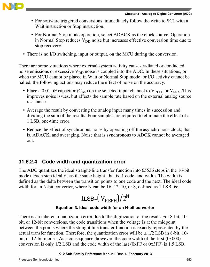
• For software triggered conversions, immediately follow the write to SC1 with aWait instruction or Stop instruction.
• For Normal Stop mode operation, select ADACK as the clock source. Operationin Normal Stop reduces VDD noise but increases effective conversion time due tostop recovery.
• There is no I/O switching, input or output, on the MCU during the conversion.
There are some situations where external system activity causes radiated or conductednoise emissions or excessive VDD noise is coupled into the ADC. In these situations, orwhen the MCU cannot be placed in Wait or Normal Stop mode, or I/O activity cannot behalted, the following actions may reduce the effect of noise on the accuracy:
• Place a 0.01 μF capacitor (CAS) on the selected input channel to VREFL or VSSA. Thisimproves noise issues, but affects the sample rate based on the external analog sourceresistance.
• Average the result by converting the analog input many times in succession anddividing the sum of the results. Four samples are required to eliminate the effect of a1 LSB, one-time error.
• Reduce the effect of synchronous noise by operating off the asynchronous clock, thatis, ADACK, and averaging. Noise that is synchronous to ADCK cannot be averagedout.
31.6.2.4 Code width and quantization error
The ADC quantizes the ideal straight-line transfer function into 65536 steps in the 16-bitmode). Each step ideally has the same height, that is, 1 code, and width. The width isdefined as the delta between the transition points to one code and the next. The ideal codewidth for an N-bit converter, where N can be 16, 12, 10, or 8, defined as 1 LSB, is:
LSB
Equation 3. Ideal code width for an N-bit converter
There is an inherent quantization error due to the digitization of the result. For 8-bit, 10-bit, or 12-bit conversions, the code transitions when the voltage is at the midpointbetween the points where the straight line transfer function is exactly represented by theactual transfer function. Therefore, the quantization error will be ± 1/2 LSB in 8-bit, 10-bit, or 12-bit modes. As a consequence, however, the code width of the first (0x000)conversion is only 1/2 LSB and the code width of the last (0xFF or 0x3FF) is 1.5 LSB.
Chapter 31 Analog-to-Digital Converter (ADC)
K12 Sub-Family Reference Manual, Rev. 4, February 2013
Freescale Semiconductor, Inc. 653
For 16-bit conversions, the code transitions only after the full code width is present, sothe quantization error is -1 LSB to 0 LSB and the code width of each step is 1 LSB.
31.6.2.5 Linearity errors
The ADC may also exhibit non-linearity of several forms. Every effort has been made toreduce these errors, but the system designers must be aware of these errors because theyaffect overall accuracy:
• Zero-scale error (EZS), sometimes called offset: This error is defined as the differencebetween the actual code width of the first conversion and the ideal code width. Thisis 1/2 LSB in 8-bit, 10-bit, or 12-bit modes and 1 LSB in 16-bit mode. If the firstconversion is 0x001, the difference between the actual 0x001 code width and its ideal(1 LSB) is used.
• Full-scale error (EFS): This error is defined as the difference between the actual codewidth of the last conversion and the ideal code width. This is 1.5 LSB in 8-bit, 10-bit,or 12-bit modes and 1 LSB in 16-bit mode. If the last conversion is 0x3FE, thedifference between the actual 0x3FE code width and its ideal (1 LSB) is used.
• Differential non-linearity (DNL): This error is defined as the worst-case differencebetween the actual code width and the ideal code width for all conversions.
• Integral non-linearity (INL): This error is defined as the highest-value or absolutevalue that the running sum of DNL achieves. More simply, this is the worst-casedifference of the actual transition voltage to a given code and its corresponding idealtransition voltage, for all codes.
• Total unadjusted error (TUE): This error is defined as the difference between theactual transfer function and the ideal straight-line transfer function and includes allforms of error.
31.6.2.6 Code jitter, non-monotonicity, and missing codesAnalog-to-digital converters are susceptible to three special forms of error:
• Code jitter: Code jitter is when, at certain points, a given input voltage converts toone of the two values when sampled repeatedly. Ideally, when the input voltage isinfinitesimally smaller than the transition voltage, the converter yields the lowercode, and vice-versa. However, even small amounts of system noise can cause theconverter to be indeterminate, between two codes, for a range of input voltagesaround the transition voltage.
Application information
K12 Sub-Family Reference Manual, Rev. 4, February 2013
654 Freescale Semiconductor, Inc.

This error may be reduced by repeatedly sampling the input and averaging the result.Additionally, the techniques discussed in Noise-induced errors reduces this error.
• Non-monotonicity: Non-monotonicity is defined as when, except for code jitter, theconverter converts to a lower code for a higher input voltage.
• Missing codes: Missing codes are those values never converted for any input value.
In 8-bit or 10-bit mode, the ADC is guaranteed to be monotonic and have no missingcodes.
Chapter 31 Analog-to-Digital Converter (ADC)
K12 Sub-Family Reference Manual, Rev. 4, February 2013
Freescale Semiconductor, Inc. 655

Application information
K12 Sub-Family Reference Manual, Rev. 4, February 2013
656 Freescale Semiconductor, Inc.
Chapter 32Comparator (CMP)
32.1 IntroductionNOTE
For the chip-specific implementation details of this module'sinstances see the chip configuration information.
The comparator (CMP) module provides a circuit for comparing two analog inputvoltages. The comparator circuit is designed to operate across the full range of the supplyvoltage, known as rail-to-rail operation.
The Analog MUX (ANMUX) provides a circuit for selecting an analog input signal fromeight channels. One signal is provided by the 6-bit digital-to-analog converter (DAC).The mux circuit is designed to operate across the full range of the supply voltage.
The 6-bit DAC is 64-tap resistor ladder network which provides a selectable voltagereference for applications where voltage reference is needed. The 64-tap resistor laddernetwork divides the supply reference Vin into 64 voltage levels. A 6-bit digital signalinput selects the output voltage level, which varies from Vin to Vin/64. Vin can be selectedfrom two voltage sources, Vin1 and Vin2. The 6-bit DAC from a comparator is availableas an on-chip internal signal only and is not available externally to a pin.
32.2 CMP featuresThe CMP has the following features:
• Operational over the entire supply range
• Inputs may range from rail to rail
• Programmable hysteresis control
K12 Sub-Family Reference Manual, Rev. 4, February 2013
Freescale Semiconductor, Inc. 657
• Selectable interrupt on rising-edge, falling-edge, or both rising or falling edges of thecomparator output
• Selectable inversion on comparator output
• Capability to produce a wide range of outputs such as:
• Sampled
• Windowed, which is ideal for certain PWM zero-crossing-detection applications
• Digitally filtered:
• Filter can be bypassed
• Can be clocked via external SAMPLE signal or scaled bus clock
• External hysteresis can be used at the same time that the output filter is used forinternal functions
• Two software selectable performance levels:
• Shorter propagation delay at the expense of higher power
• Low power, with longer propagation delay
• DMA transfer support• A comparison event can be selected to trigger a DMA transfer
• Functional in all modes of operation
• The window and filter functions are not available in the following modes:• Stop• VLPS• LLS• VLLSx
32.3 6-bit DAC key features• 6-bit resolution• Selectable supply reference source• Power Down mode to conserve power when not in use• Option to route the output to internal comparator input
6-bit DAC key features
K12 Sub-Family Reference Manual, Rev. 4, February 2013
658 Freescale Semiconductor, Inc.
32.4 ANMUX key features• Two 8-to-1 channel mux
• Operational over the entire supply range
32.5 CMP, DAC and ANMUX diagramThe following figure shows the block diagram for the High-Speed Comparator, DAC,and ANMUX modules.
Chapter 32 Comparator (CMP)
K12 Sub-Family Reference Manual, Rev. 4, February 2013
Freescale Semiconductor, Inc. 659

VRSEL
VOSEL[5:0]
MUX
64-le
vel
PSEL[2:0]
DACM
UX
MU
X
IRQANMUX
MSEL[2:0]
CMP
CMP
MU
X DAC output
DACEN
Vin1 Vin2
Window and filter control
CMPO
Reference Input 0Reference Input 1Reference Input 2
Reference Input 3Reference Input 4Reference Input 5Reference Input 6
INP
INM
Sample input
Figure 32-1. CMP, DAC and ANMUX block diagram
32.6 CMP block diagramThe following figure shows the block diagram for the CMP module.
CMP block diagram
K12 Sub-Family Reference Manual, Rev. 4, February 2013
660 Freescale Semiconductor, Inc.
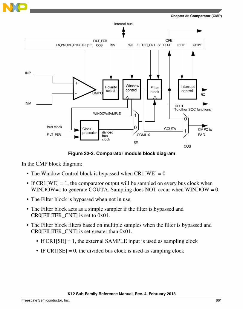
IRQ
INP
INM
FILTER_CNTINV
COUT
COUTOPE
SE
CMPO to PAD
COUTA 1
WE
0
SE
CGMUX
COSFILT_PER
+
-
FILT_PER
bus clock
COS
IER/F CFR/F
WINDOW/SAMPLE 1 0
EN,PMODE,HYSCTRL[1:0]
Interrupt control
Filter block
Window control
Polarity select
Clock prescaler divided
bus clock
CMPO
To other SOC functions
Internal bus
Figure 32-2. Comparator module block diagram
In the CMP block diagram:
• The Window Control block is bypassed when CR1[WE] = 0
• If CR1[WE] = 1, the comparator output will be sampled on every bus clock whenWINDOW=1 to generate COUTA. Sampling does NOT occur when WINDOW = 0.
• The Filter block is bypassed when not in use.
• The Filter block acts as a simple sampler if the filter is bypassed andCR0[FILTER_CNT] is set to 0x01.
• The Filter block filters based on multiple samples when the filter is bypassed andCR0[FILTER_CNT] is set greater than 0x01.
• If CR1[SE] = 1, the external SAMPLE input is used as sampling clock
• IF CR1[SE] = 0, the divided bus clock is used as sampling clock
Chapter 32 Comparator (CMP)
K12 Sub-Family Reference Manual, Rev. 4, February 2013
Freescale Semiconductor, Inc. 661
• If enabled, the Filter block will incur up to one bus clock additional latency penaltyon COUT due to the fact that COUT, which is crossing clock domain boundaries,must be resynchronized to the bus clock.
• CR1[WE] and CR1[SE] are mutually exclusive.
32.7 Memory map/register definitionsCMP memory map
Absoluteaddress
(hex)Register name
Width(in bits)
Access Reset valueSection/
page
4007_3000 CMP Control Register 0 (CMP0_CR0) 8 R/W 00h 32.7.1/662
4007_3001 CMP Control Register 1 (CMP0_CR1) 8 R/W 00h 32.7.2/663
4007_3002 CMP Filter Period Register (CMP0_FPR) 8 R/W 00h 32.7.3/665
4007_3003 CMP Status and Control Register (CMP0_SCR) 8 R/W 00h 32.7.4/665
4007_3004 DAC Control Register (CMP0_DACCR) 8 R/W 00h 32.7.5/666
4007_3005 MUX Control Register (CMP0_MUXCR) 8 R/W 00h 32.7.6/667
4007_3008 CMP Control Register 0 (CMP1_CR0) 8 R/W 00h 32.7.1/662
4007_3009 CMP Control Register 1 (CMP1_CR1) 8 R/W 00h 32.7.2/663
4007_300A CMP Filter Period Register (CMP1_FPR) 8 R/W 00h 32.7.3/665
4007_300B CMP Status and Control Register (CMP1_SCR) 8 R/W 00h 32.7.4/665
4007_300C DAC Control Register (CMP1_DACCR) 8 R/W 00h 32.7.5/666
4007_300D MUX Control Register (CMP1_MUXCR) 8 R/W 00h 32.7.6/667
32.7.1 CMP Control Register 0 (CMPx_CR0)
Address: Base address + 0h offset
Bit 7 6 5 4 3 2 1 0
Read 0 FILTER_CNT 0 0 HYSTCTRWriteReset 0 0 0 0 0 0 0 0
CMPx_CR0 field descriptions
Field Description
7Reserved
This field is reserved.This read-only field is reserved and always has the value 0.
6–4FILTER_CNT
Filter Sample Count
Table continues on the next page...
Memory map/register definitions
K12 Sub-Family Reference Manual, Rev. 4, February 2013
662 Freescale Semiconductor, Inc.
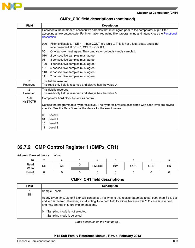
CMPx_CR0 field descriptions (continued)
Field Description
Represents the number of consecutive samples that must agree prior to the comparator ouput filteraccepting a new output state. For information regarding filter programming and latency, see the Functionaldescription.
000 Filter is disabled. If SE = 1, then COUT is a logic 0. This is not a legal state, and is notrecommended. If SE = 0, COUT = COUTA.
001 One sample must agree. The comparator output is simply sampled.010 2 consecutive samples must agree.011 3 consecutive samples must agree.100 4 consecutive samples must agree.101 5 consecutive samples must agree.110 6 consecutive samples must agree.111 7 consecutive samples must agree.
3Reserved
This field is reserved.This read-only field is reserved and always has the value 0.
2Reserved
This field is reserved.This read-only field is reserved and always has the value 0.
1–0HYSTCTR
Comparator hard block hysteresis control
Defines the programmable hysteresis level. The hysteresis values associated with each level are device-specific. See the Data Sheet of the device for the exact values.
00 Level 001 Level 110 Level 211 Level 3
32.7.2 CMP Control Register 1 (CMPx_CR1)
Address: Base address + 1h offset
Bit 7 6 5 4 3 2 1 0
Read SE WE 0 PMODE INV COS OPE ENWriteReset 0 0 0 0 0 0 0 0
CMPx_CR1 field descriptions
Field Description
7SE
Sample Enable
At any given time, either SE or WE can be set. If a write to this register attempts to set both, then SE is setand WE is cleared. However, avoid writing 1s to both field locations because this "11" case is reservedand may change in future implementations.
0 Sampling mode is not selected.1 Sampling mode is selected.
Table continues on the next page...
Chapter 32 Comparator (CMP)
K12 Sub-Family Reference Manual, Rev. 4, February 2013
Freescale Semiconductor, Inc. 663
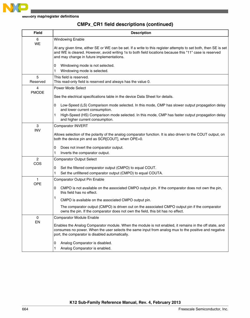
CMPx_CR1 field descriptions (continued)
Field Description
6WE
Windowing Enable
At any given time, either SE or WE can be set. If a write to this register attempts to set both, then SE is setand WE is cleared. However, avoid writing 1s to both field locations because this "11" case is reservedand may change in future implementations.
0 Windowing mode is not selected.1 Windowing mode is selected.
5Reserved
This field is reserved.This read-only field is reserved and always has the value 0.
4PMODE
Power Mode Select
See the electrical specifications table in the device Data Sheet for details.
0 Low-Speed (LS) Comparison mode selected. In this mode, CMP has slower output propagation delayand lower current consumption.
1 High-Speed (HS) Comparison mode selected. In this mode, CMP has faster output propagation delayand higher current consumption.
3INV
Comparator INVERT
Allows selection of the polarity of the analog comparator function. It is also driven to the COUT output, onboth the device pin and as SCR[COUT], when OPE=0.
0 Does not invert the comparator output.1 Inverts the comparator output.
2COS
Comparator Output Select
0 Set the filtered comparator output (CMPO) to equal COUT.1 Set the unfiltered comparator output (CMPO) to equal COUTA.
1OPE
Comparator Output Pin Enable
0 CMPO is not available on the associated CMPO output pin. If the comparator does not own the pin,this field has no effect.
1CMPO is available on the associated CMPO output pin.
The comparator output (CMPO) is driven out on the associated CMPO output pin if the comparatorowns the pin. If the comparator does not own the field, this bit has no effect.
0EN
Comparator Module Enable
Enables the Analog Comparator module. When the module is not enabled, it remains in the off state, andconsumes no power. When the user selects the same input from analog mux to the positive and negativeport, the comparator is disabled automatically.
0 Analog Comparator is disabled.1 Analog Comparator is enabled.
Memory map/register definitions
K12 Sub-Family Reference Manual, Rev. 4, February 2013
664 Freescale Semiconductor, Inc.
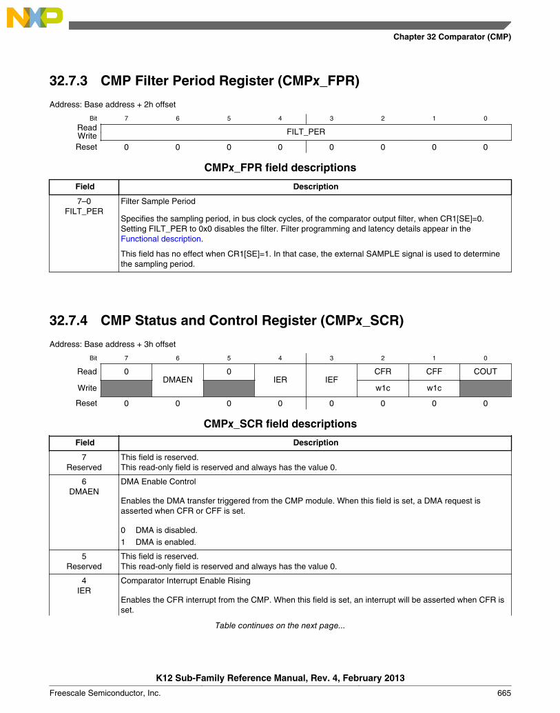
32.7.3 CMP Filter Period Register (CMPx_FPR)
Address: Base address + 2h offset
Bit 7 6 5 4 3 2 1 0
Read FILT_PERWriteReset 0 0 0 0 0 0 0 0
CMPx_FPR field descriptions
Field Description
7–0FILT_PER
Filter Sample Period
Specifies the sampling period, in bus clock cycles, of the comparator output filter, when CR1[SE]=0.Setting FILT_PER to 0x0 disables the filter. Filter programming and latency details appear in theFunctional description.
This field has no effect when CR1[SE]=1. In that case, the external SAMPLE signal is used to determinethe sampling period.
32.7.4 CMP Status and Control Register (CMPx_SCR)
Address: Base address + 3h offset
Bit 7 6 5 4 3 2 1 0
Read 0DMAEN
0IER IEF
CFR CFF COUT
Write w1c w1c
Reset 0 0 0 0 0 0 0 0
CMPx_SCR field descriptions
Field Description
7Reserved
This field is reserved.This read-only field is reserved and always has the value 0.
6DMAEN
DMA Enable Control
Enables the DMA transfer triggered from the CMP module. When this field is set, a DMA request isasserted when CFR or CFF is set.
0 DMA is disabled.1 DMA is enabled.
5Reserved
This field is reserved.This read-only field is reserved and always has the value 0.
4IER
Comparator Interrupt Enable Rising
Enables the CFR interrupt from the CMP. When this field is set, an interrupt will be asserted when CFR isset.
Table continues on the next page...
Chapter 32 Comparator (CMP)
K12 Sub-Family Reference Manual, Rev. 4, February 2013
Freescale Semiconductor, Inc. 665

CMPx_SCR field descriptions (continued)
Field Description
0 Interrupt is disabled.1 Interrupt is enabled.
3IEF
Comparator Interrupt Enable Falling
Enables the CFF interrupt from the CMP. When this field is set, an interrupt will be asserted when CFF isset.
0 Interrupt is disabled.1 Interrupt is enabled.
2CFR
Analog Comparator Flag Rising
Detects a rising-edge on COUT, when set, during normal operation. CFR is cleared by writing 1 to it.During Stop modes, CFR is level sensitive .
0 Rising-edge on COUT has not been detected.1 Rising-edge on COUT has occurred.
1CFF
Analog Comparator Flag Falling
Detects a falling-edge on COUT, when set, during normal operation. CFF is cleared by writing 1 to it.During Stop modes, CFF is level senstive .
0 Falling-edge on COUT has not been detected.1 Falling-edge on COUT has occurred.
0COUT
Analog Comparator Output
Returns the current value of the Analog Comparator output, when read. The field is reset to 0 and will readas CR1[INV] when the Analog Comparator module is disabled, that is, when CR1[EN] = 0. Writes to thisfield are ignored.
32.7.5 DAC Control Register (CMPx_DACCR)
Address: Base address + 4h offset
Bit 7 6 5 4 3 2 1 0
Read DACEN VRSEL VOSELWriteReset 0 0 0 0 0 0 0 0
CMPx_DACCR field descriptions
Field Description
7DACEN
DAC Enable
Enables the DAC. When the DAC is disabled, it is powered down to conserve power.
0 DAC is disabled.1 DAC is enabled.
6VRSEL
Supply Voltage Reference Source Select
Table continues on the next page...
Memory map/register definitions
K12 Sub-Family Reference Manual, Rev. 4, February 2013
666 Freescale Semiconductor, Inc.
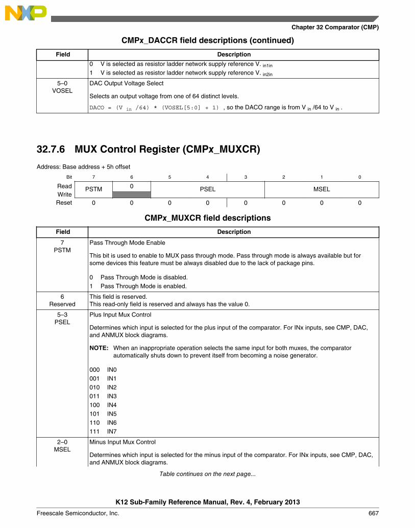
CMPx_DACCR field descriptions (continued)
Field Description
0 V is selected as resistor ladder network supply reference V. in1in
1 V is selected as resistor ladder network supply reference V. in2in
5–0VOSEL
DAC Output Voltage Select
Selects an output voltage from one of 64 distinct levels.
DACO = (V in /64) * (VOSEL[5:0] + 1) , so the DACO range is from V in /64 to V in .
32.7.6 MUX Control Register (CMPx_MUXCR)
Address: Base address + 5h offset
Bit 7 6 5 4 3 2 1 0
Read PSTM 0 PSEL MSELWriteReset 0 0 0 0 0 0 0 0
CMPx_MUXCR field descriptions
Field Description
7PSTM
Pass Through Mode Enable
This bit is used to enable to MUX pass through mode. Pass through mode is always available but forsome devices this feature must be always disabled due to the lack of package pins.
0 Pass Through Mode is disabled.1 Pass Through Mode is enabled.
6Reserved
This field is reserved.This read-only field is reserved and always has the value 0.
5–3PSEL
Plus Input Mux Control
Determines which input is selected for the plus input of the comparator. For INx inputs, see CMP, DAC,and ANMUX block diagrams.
NOTE: When an inappropriate operation selects the same input for both muxes, the comparatorautomatically shuts down to prevent itself from becoming a noise generator.
000 IN0001 IN1010 IN2011 IN3100 IN4101 IN5110 IN6111 IN7
2–0MSEL
Minus Input Mux Control
Determines which input is selected for the minus input of the comparator. For INx inputs, see CMP, DAC,and ANMUX block diagrams.
Table continues on the next page...
Chapter 32 Comparator (CMP)
K12 Sub-Family Reference Manual, Rev. 4, February 2013
Freescale Semiconductor, Inc. 667
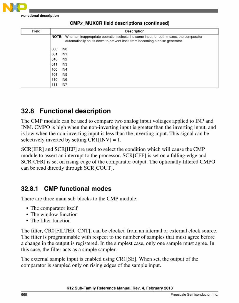
CMPx_MUXCR field descriptions (continued)
Field Description
NOTE: When an inappropriate operation selects the same input for both muxes, the comparatorautomatically shuts down to prevent itself from becoming a noise generator.
000 IN0001 IN1010 IN2011 IN3100 IN4101 IN5110 IN6111 IN7
32.8 Functional descriptionThe CMP module can be used to compare two analog input voltages applied to INP andINM. CMPO is high when the non-inverting input is greater than the inverting input, andis low when the non-inverting input is less than the inverting input. This signal can beselectively inverted by setting CR1[INV] = 1.
SCR[IER] and SCR[IEF] are used to select the condition which will cause the CMPmodule to assert an interrupt to the processor. SCR[CFF] is set on a falling-edge andSCR[CFR] is set on rising-edge of the comparator output. The optionally filtered CMPOcan be read directly through SCR[COUT].
32.8.1 CMP functional modes
There are three main sub-blocks to the CMP module:
• The comparator itself• The window function• The filter function
The filter, CR0[FILTER_CNT], can be clocked from an internal or external clock source.The filter is programmable with respect to the number of samples that must agree beforea change in the output is registered. In the simplest case, only one sample must agree. Inthis case, the filter acts as a simple sampler.
The external sample input is enabled using CR1[SE]. When set, the output of thecomparator is sampled only on rising edges of the sample input.
Functional description
K12 Sub-Family Reference Manual, Rev. 4, February 2013
668 Freescale Semiconductor, Inc.
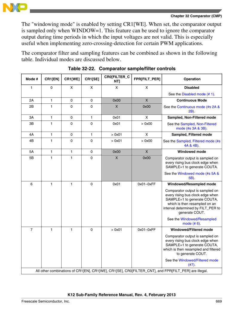
The "windowing mode" is enabled by setting CR1[WE]. When set, the comparator outputis sampled only when WINDOW=1. This feature can be used to ignore the comparatoroutput during time periods in which the input voltages are not valid. This is especiallyuseful when implementing zero-crossing-detection for certain PWM applications.
The comparator filter and sampling features can be combined as shown in the followingtable. Individual modes are discussed below.
Table 32-22. Comparator sample/filter controls
Mode # CR1[EN] CR1[WE] CR1[SE]CR0[FILTER_C
NT]FPR[FILT_PER] Operation
1 0 X X X X Disabled
See the Disabled mode (# 1).
2A 1 0 0 0x00 X Continuous Mode
See the Continuous mode (#s 2A &2B).
2B 1 0 0 X 0x00
3A 1 0 1 0x01 X Sampled, Non-Filtered mode
See the Sampled, Non-Filteredmode (#s 3A & 3B).
3B 1 0 0 0x01 > 0x00
4A 1 0 1 > 0x01 X Sampled, Filtered mode
See the Sampled, Filtered mode (#s4A & 4B).
4B 1 0 0 > 0x01 > 0x00
5A 1 1 0 0x00 X Windowed mode
Comparator output is sampled onevery rising bus clock edge whenSAMPLE=1 to generate COUTA.
See the Windowed mode (#s 5A &5B).
5B 1 1 0 X 0x00
6 1 1 0 0x01 0x01–0xFF Windowed/Resampled mode
Comparator output is sampled onevery rising bus clock edge whenSAMPLE=1 to generate COUTA,which is then resampled on an
interval determined by FILT_PER togenerate COUT.
See the Windowed/Resampledmode (# 6).
7 1 1 0 > 0x01 0x01–0xFF Windowed/Filtered mode
Comparator output is sampled onevery rising bus clock edge whenSAMPLE=1 to generate COUTA,
which is then resampled and filteredto generate COUT.
See the Windowed/Filtered mode(#7).
All other combinations of CR1[EN], CR1[WE], CR1[SE], CR0[FILTER_CNT], and FPR[FILT_PER] are illegal.
Chapter 32 Comparator (CMP)
K12 Sub-Family Reference Manual, Rev. 4, February 2013
Freescale Semiconductor, Inc. 669
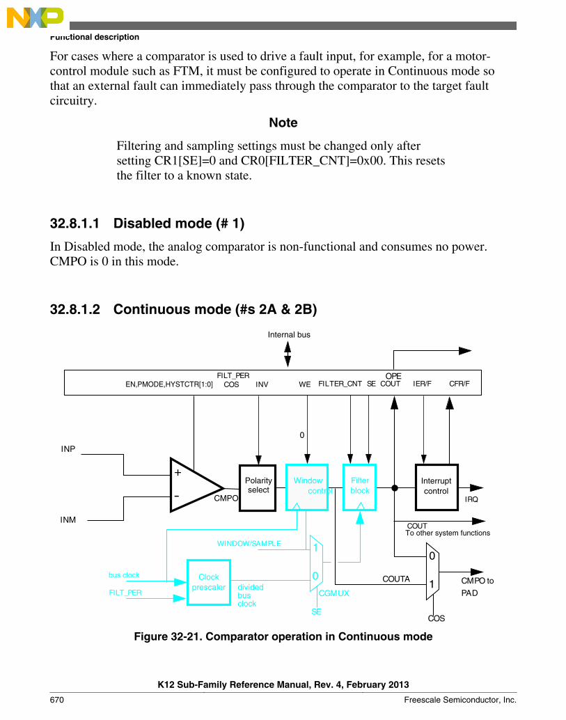
For cases where a comparator is used to drive a fault input, for example, for a motor-control module such as FTM, it must be configured to operate in Continuous mode sothat an external fault can immediately pass through the comparator to the target faultcircuitry.
Note
Filtering and sampling settings must be changed only aftersetting CR1[SE]=0 and CR0[FILTER_CNT]=0x00. This resetsthe filter to a known state.
32.8.1.1 Disabled mode (# 1)
In Disabled mode, the analog comparator is non-functional and consumes no power.CMPO is 0 in this mode.
32.8.1.2 Continuous mode (#s 2A & 2B)
IRQ
Internal bus
INP
INM
FILTER_CNTINV
COUT
COUTOPE
SE
CMPO to PAD
COUTA 1
WE
0
SE
CGMUX
COSFILT_PER
0
+
-
FILT_PER
COS
IER/F CFR/F
WINDOW/SAMPLE 1 0
EN,PMODE,HYSTCTR[1:0]
divided bus clock
CMPO
bus clock
To other system functions
Polarityselect
Windowcontrol
Filterblock
Interruptcontrol
Clockprescaler
Figure 32-21. Comparator operation in Continuous mode
Functional description
K12 Sub-Family Reference Manual, Rev. 4, February 2013
670 Freescale Semiconductor, Inc.

NOTESee the chip configuration section for the source of sample/window input.
The analog comparator block is powered and active. CMPO may be optionally inverted,but is not subject to external sampling or filtering. Both window control and filter blocksare completely bypassed. SCR[COUT] is updated continuously. The path fromcomparator input pins to output pin is operating in combinational unclocked mode.COUT and COUTA are identical.
For control configurations which result in disabling the filter block, see the Filter BlockBypass Logic diagram.
32.8.1.3 Sampled, Non-Filtered mode (#s 3A & 3B)
+
- IRQ
INP
INM
FILTER_CNTINV
COUT
COUTOPE
SE
CMPO to PAD
COUTA 1
WE
0
SE=1
CGMUX
COSFILT_PER
10
+
-
FILT_PER
COS
0x01
IER/F CFR/F
WINDOW/SAMPLE 1 0
EN,PMODE,HYSTCTR[1:0]
divided bus clock
CMPO
bus clock
Internal bus
Polarityselect
Windowcontrol
Filterblock
Interruptcontrol
To other SOC functions
Clockprescaler
Figure 32-22. Sampled, Non-Filtered (# 3A): sampling point externally driven
In Sampled, Non-Filtered mode, the analog comparator block is powered and active. Thepath from analog inputs to COUTA is combinational unclocked. Windowing control iscompletely bypassed. COUTA is sampled whenever a rising-edge is detected on the filterblock clock input.
Chapter 32 Comparator (CMP)
K12 Sub-Family Reference Manual, Rev. 4, February 2013
Freescale Semiconductor, Inc. 671
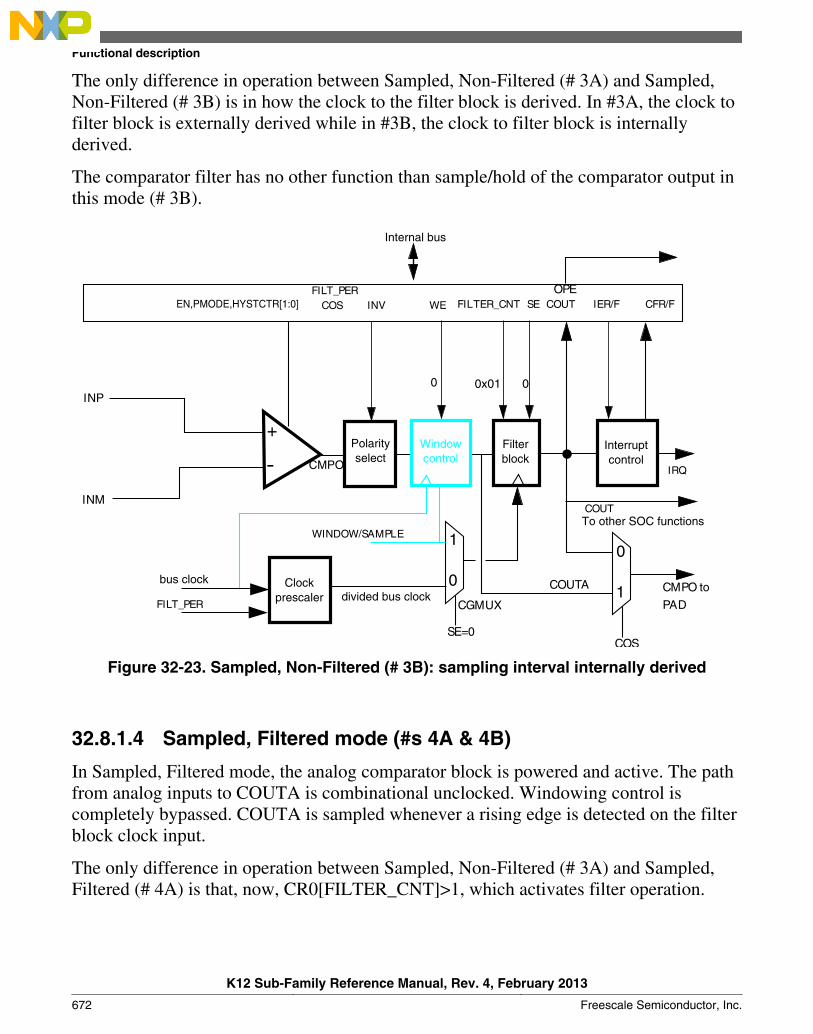
The only difference in operation between Sampled, Non-Filtered (# 3A) and Sampled,Non-Filtered (# 3B) is in how the clock to the filter block is derived. In #3A, the clock tofilter block is externally derived while in #3B, the clock to filter block is internallyderived.
The comparator filter has no other function than sample/hold of the comparator output inthis mode (# 3B).
IRQ
INP
INM
FILTER_CNTINV
COUT
COUTOPE
SE
CMPO to PAD
COUTA 1
WE
0
SE=0
CGMUX
COSFILT_PER
00
+
-
FILT_PER
COS
0x01
IER/F CFR/F
WINDOW/SAMPLE 1 0
EN,PMODE,HYSTCTR[1:0]
divided bus clock
CMPO
bus clock
Internal bus
Polarityselect
Windowcontrol
Filterblock
Interruptcontrol
To other SOC functions
Clockprescaler
Figure 32-23. Sampled, Non-Filtered (# 3B): sampling interval internally derived
32.8.1.4 Sampled, Filtered mode (#s 4A & 4B)
In Sampled, Filtered mode, the analog comparator block is powered and active. The pathfrom analog inputs to COUTA is combinational unclocked. Windowing control iscompletely bypassed. COUTA is sampled whenever a rising edge is detected on the filterblock clock input.
The only difference in operation between Sampled, Non-Filtered (# 3A) and Sampled,Filtered (# 4A) is that, now, CR0[FILTER_CNT]>1, which activates filter operation.
Functional description
K12 Sub-Family Reference Manual, Rev. 4, February 2013
672 Freescale Semiconductor, Inc.
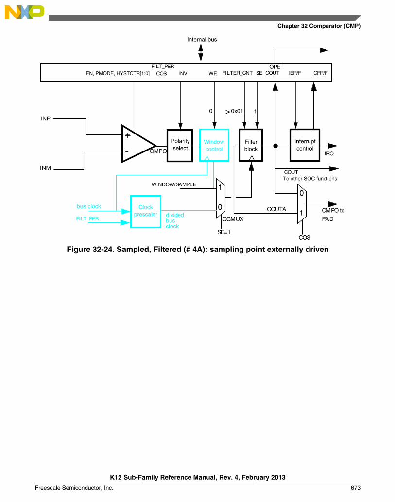
+
- IRQ
INP
INM
FILTER_CNTINV
COUT
COUTOPE
SE
CMPO to PAD
COUTA 1
WE
0
SE=1
CGMUX
COSFILT_PER
10
+
-
FILT_PER
bus clock
COS
>
IER/F CFR/F
WINDOW/SAMPLE 1 0
EN, PMODE, HYSTCTR[1:0]
divided bus clock
CMPO
0x01
Internal bus
Polarityselect
Windowcontrol
Filterblock
Interruptcontrol
Clockprescaler
To other SOC functions
Figure 32-24. Sampled, Filtered (# 4A): sampling point externally driven
Chapter 32 Comparator (CMP)
K12 Sub-Family Reference Manual, Rev. 4, February 2013
Freescale Semiconductor, Inc. 673
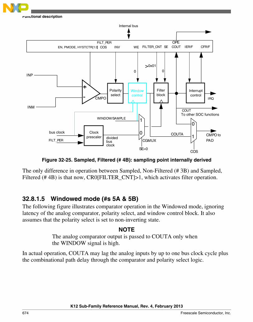
+
- IRQ
INP
INM
FILTER_CNTINV
COUT
COUTOPE
SE
CMPO to PAD
COUTA
0
1
WE
1
0
SE=0
CGMUX
COSFILT_PER
0
+
-
FILT_PER
bus clock
COS
>
IER/F CFR/F
WINDOW/SAMPLE
EN, PMODE, HYSTCTR[1:0]
divided bus clock
CMPO
0x01
Internal bus
Polarityselect
Windowcontrol
Filter block
Interruptcontrol
Clockprescaler
To other SOC functions
0
Figure 32-25. Sampled, Filtered (# 4B): sampling point internally derived
The only difference in operation between Sampled, Non-Filtered (# 3B) and Sampled,Filtered (# 4B) is that now, CR0[FILTER_CNT]>1, which activates filter operation.
32.8.1.5 Windowed mode (#s 5A & 5B)The following figure illustrates comparator operation in the Windowed mode, ignoringlatency of the analog comparator, polarity select, and window control block. It alsoassumes that the polarity select is set to non-inverting state.
NOTEThe analog comparator output is passed to COUTA only whenthe WINDOW signal is high.
In actual operation, COUTA may lag the analog inputs by up to one bus clock cycle plusthe combinational path delay through the comparator and polarity select logic.
Functional description
K12 Sub-Family Reference Manual, Rev. 4, February 2013
674 Freescale Semiconductor, Inc.
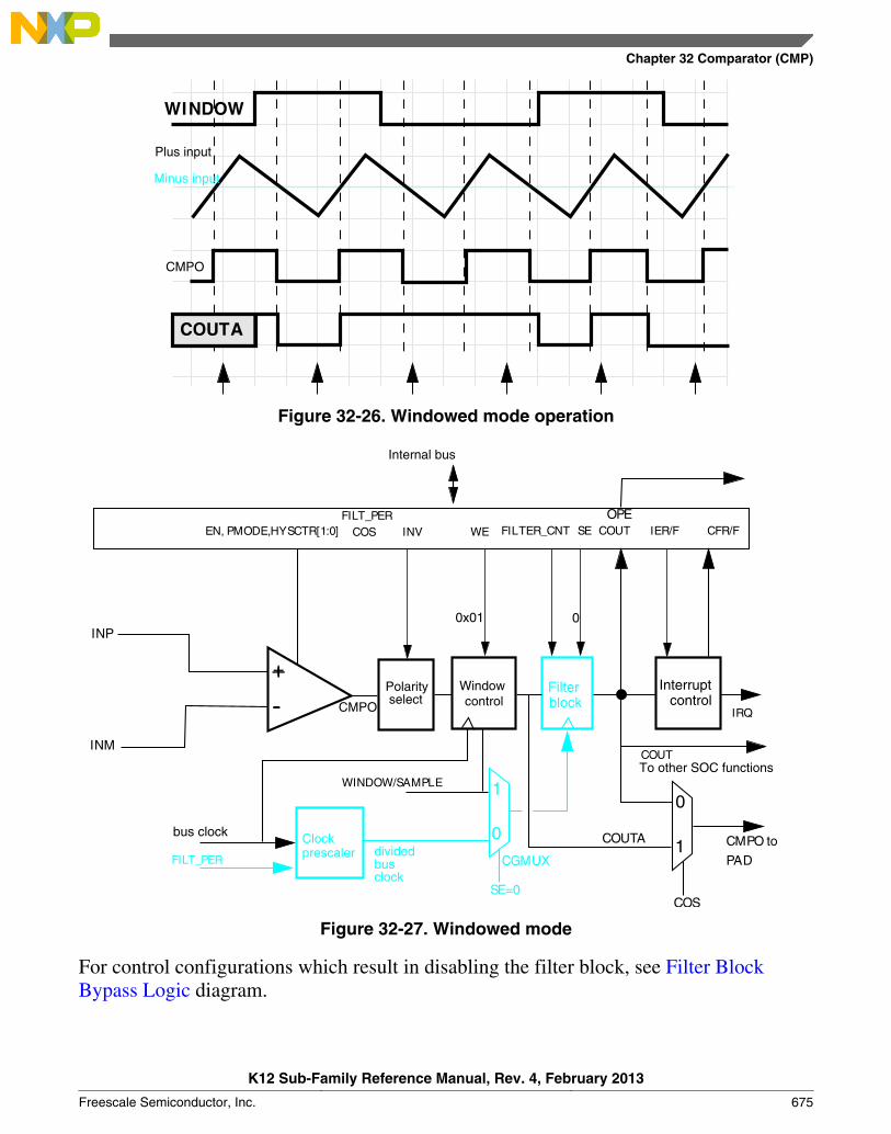
WINDOW
COUTA
CMPO
Minus input
Plus input
Figure 32-26. Windowed mode operation
+
- IRQ
EN, PMODE,HYSCTR[1:0]
INP
INM
FILTER_CNTINV
COUT
COUTOPE
SE
CMPO to PAD
COUTA
0
1
WE
1
0
SE=0
CGMUX
COSFILT_PER
0
+
-
FILT_PER
bus clock
COS
0x01
IER/F CFR/F
WINDOW/SAMPLE
Polarity select
Window control
Filter block
Interrupt control
divided bus clock
Clock prescaler
CMPO
Internal bus
To other SOC functions
Figure 32-27. Windowed mode
For control configurations which result in disabling the filter block, see Filter BlockBypass Logic diagram.
Chapter 32 Comparator (CMP)
K12 Sub-Family Reference Manual, Rev. 4, February 2013
Freescale Semiconductor, Inc. 675
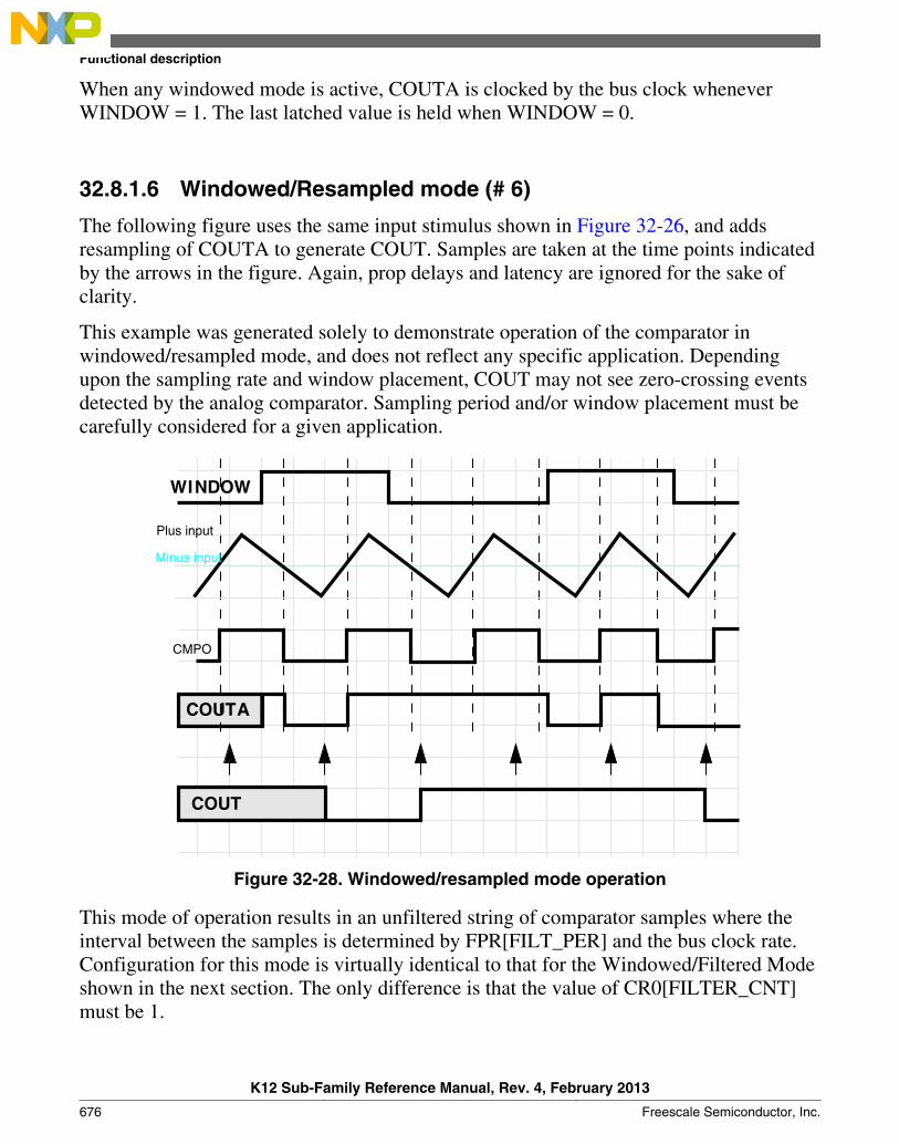
When any windowed mode is active, COUTA is clocked by the bus clock wheneverWINDOW = 1. The last latched value is held when WINDOW = 0.
32.8.1.6 Windowed/Resampled mode (# 6)
The following figure uses the same input stimulus shown in Figure 32-26, and addsresampling of COUTA to generate COUT. Samples are taken at the time points indicatedby the arrows in the figure. Again, prop delays and latency are ignored for the sake ofclarity.
This example was generated solely to demonstrate operation of the comparator inwindowed/resampled mode, and does not reflect any specific application. Dependingupon the sampling rate and window placement, COUT may not see zero-crossing eventsdetected by the analog comparator. Sampling period and/or window placement must becarefully considered for a given application.
WINDOW
COUTA
COUT
CMPO
Minus input
Plus input
Figure 32-28. Windowed/resampled mode operation
This mode of operation results in an unfiltered string of comparator samples where theinterval between the samples is determined by FPR[FILT_PER] and the bus clock rate.Configuration for this mode is virtually identical to that for the Windowed/Filtered Modeshown in the next section. The only difference is that the value of CR0[FILTER_CNT]must be 1.
Functional description
K12 Sub-Family Reference Manual, Rev. 4, February 2013
676 Freescale Semiconductor, Inc.

32.8.1.7 Windowed/Filtered mode (#7)
This is the most complex mode of operation for the comparator block, as it uses bothwindowing and filtering features. It also has the highest latency of any of the modes. Thiscan be approximated: up to 1 bus clock synchronization in the window function +((CR0[FILTER_CNT] * FPR[FILT_PER]) + 1) * bus clock for the filter function.
When any windowed mode is active, COUTA is clocked by the bus clock wheneverWINDOW = 1. The last latched value is held when WINDOW = 0.
+
- IRQ
EN, PMODE,HYSCTR[1:0]
INP
INM
FILTER_CNTINV
COUT
COUTOPE
SE
CMPO to PAD
COUTA
0
1
WE
1
0
SE=0
CGMUX
COSFILT_PER
01
+
-
FILT_PER
bus clock
COS
>
IER/F CFR/F
WINDOW/SAMPLE
Polarity select
Window control
Filter block
Interrupt control
divided bus clock
Clock prescaler
CMPO
0x01
To other SOC functions
Internal bus
Figure 32-29. Windowed/Filtered mode
32.8.2 Power modes
32.8.2.1 Wait mode operation
During Wait and VLPW modes, the CMP, if enabled, continues to operate normally anda CMP interrupt can wake the MCU.
Chapter 32 Comparator (CMP)
K12 Sub-Family Reference Manual, Rev. 4, February 2013
Freescale Semiconductor, Inc. 677
32.8.2.2 Stop mode operation
Depending on clock restrictions related to the MCU core or core peripherals, the MCU isbrought out of stop when a compare event occurs and the corresponding interrupt isenabled. Similarly, if CR1[OPE] is enabled, the comparator output operates as in thenormal operating mode and comparator output is placed onto the external pin. In Stopmodes, the comparator can be operational in both:
• High-Speed (HS) Comparison mode when CR1[PMODE] = 1• Low-Speed (LS) Comparison mode when CR1[PMODE] = 0
It is recommended to use the LS mode to minimize power consumption.
If stop is exited with a reset, all comparator registers are put into their reset state.
32.8.2.3 Low-Leakage mode operation
When the chip is in Low-Leakage modes:
• The CMP module is partially functional and is limited to Low-Speed mode,regardless of CR1[PMODE] setting
• Windowed, Sampled, and Filtered modes are not supported• The CMP output pin is latched and does not reflect the compare output state.
The positive- and negative-input voltage can be supplied from external pins or the DACoutput. The MCU can be brought out of the Low-Leakage mode if a compare eventoccurs and the CMP interrupt is enabled. After wakeup from low-leakage modes, theCMP module is in the reset state except for SCR[CFF] and SCR[CFR].
32.8.3 Startup and operation
A typical startup sequence is as follows.
The time required to stabilize COUT will be the power-on delay of the comparators plusthe largest propagation delay from a selected analog source through the analogcomparator, windowing function and filter. See the Data Sheets for power-on delays ofthe comparators. The windowing function has a maximum of one bus clock period delay.The filter delay is specified in the Low-pass filter.
Functional description
K12 Sub-Family Reference Manual, Rev. 4, February 2013
678 Freescale Semiconductor, Inc.

During operation, the propagation delay of the selected data paths must always beconsidered. It may take many bus clock cycles for COUT and SCR[CFR]/SCR[CFF] toreflect an input change or a configuration change to one of the components involved inthe data path.
When programmed for filtering modes, COUT will initially be equal to 0, until sufficientclock cycles have elapsed to fill all stages of the filter. This occurs even if COUTA is at alogic 1.
32.8.4 Low-pass filter
The low-pass filter operates on the unfiltered and unsynchronized and optionally invertedcomparator output COUTA and generates the filtered and synchronized output COUT.Both COUTA and COUT can be configured as module outputs and are used for differentpurposes within the system.
Synchronization and edge detection are always used to determine status register bitvalues. They also apply to COUT for all sampling and windowed modes. Filtering can beperformed using an internal timebase defined by FPR[FILT_PER], or using an externalSAMPLE input to determine sample time.
The need for digital filtering and the amount of filtering is dependent on userrequirements. Filtering can become more useful in the absence of an external hysteresiscircuit. Without external hysteresis, high-frequency oscillations can be generated atCOUTA when the selected INM and INP input voltages differ by less than the offsetvoltage of the differential comparator.
32.8.4.1 Enabling filter modes
Filter modes can be enabled by:
• Setting CR0[FILTER_CNT] > 0x01 and• Setting FPR[FILT_PER] to a nonzero value or setting CR1[SE]=1
If using the divided bus clock to drive the filter, it will take samples of COUTA everyFPR[FILT_PER] bus clock cycles.
The filter output will be at logic 0 when first initalized, and will subsequently changewhen all the consecutive CR0[FILTER_CNT] samples agree that the output value haschanged. In other words, SCR[COUT] will be 0 for some initial period, even whenCOUTA is at logic 1.
Chapter 32 Comparator (CMP)
K12 Sub-Family Reference Manual, Rev. 4, February 2013
Freescale Semiconductor, Inc. 679
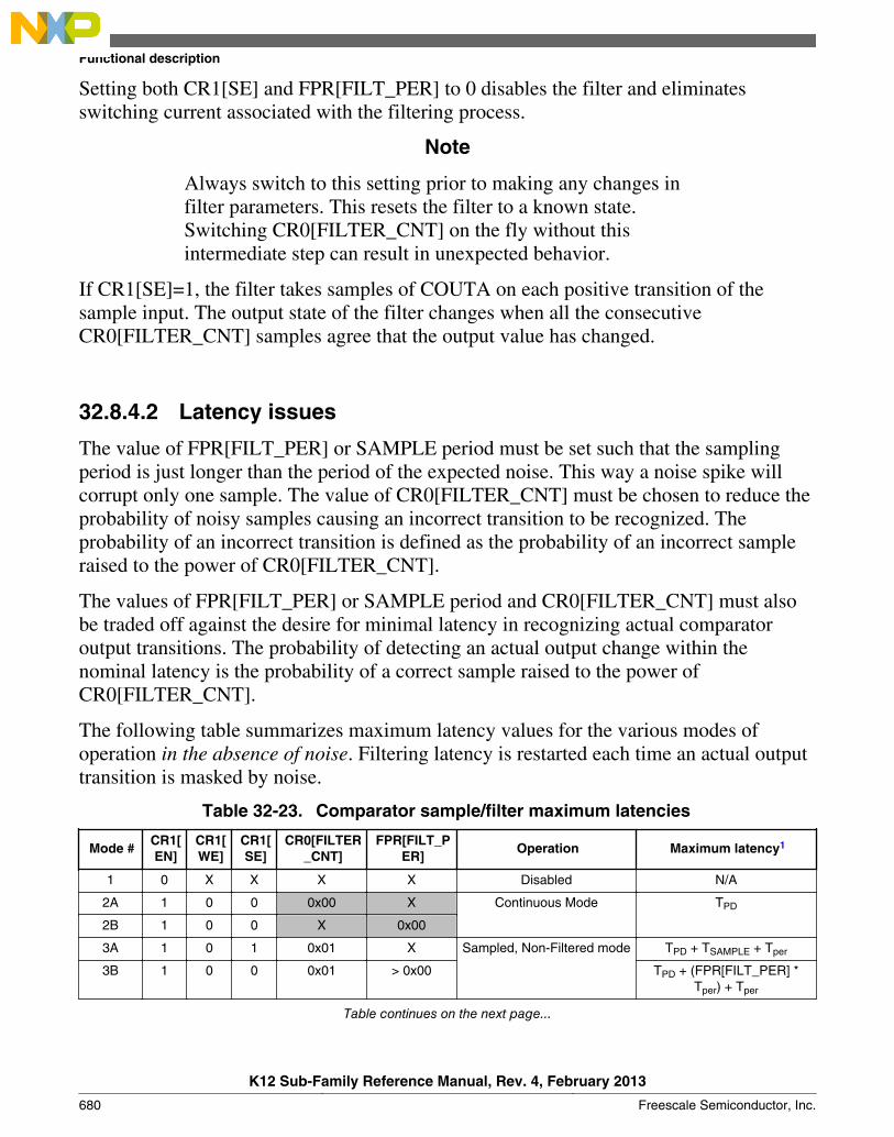
Setting both CR1[SE] and FPR[FILT_PER] to 0 disables the filter and eliminatesswitching current associated with the filtering process.
Note
Always switch to this setting prior to making any changes infilter parameters. This resets the filter to a known state.Switching CR0[FILTER_CNT] on the fly without thisintermediate step can result in unexpected behavior.
If CR1[SE]=1, the filter takes samples of COUTA on each positive transition of thesample input. The output state of the filter changes when all the consecutiveCR0[FILTER_CNT] samples agree that the output value has changed.
32.8.4.2 Latency issues
The value of FPR[FILT_PER] or SAMPLE period must be set such that the samplingperiod is just longer than the period of the expected noise. This way a noise spike willcorrupt only one sample. The value of CR0[FILTER_CNT] must be chosen to reduce theprobability of noisy samples causing an incorrect transition to be recognized. Theprobability of an incorrect transition is defined as the probability of an incorrect sampleraised to the power of CR0[FILTER_CNT].
The values of FPR[FILT_PER] or SAMPLE period and CR0[FILTER_CNT] must alsobe traded off against the desire for minimal latency in recognizing actual comparatoroutput transitions. The probability of detecting an actual output change within thenominal latency is the probability of a correct sample raised to the power ofCR0[FILTER_CNT].
The following table summarizes maximum latency values for the various modes ofoperation in the absence of noise. Filtering latency is restarted each time an actual outputtransition is masked by noise.
Table 32-23. Comparator sample/filter maximum latencies
Mode #CR1[EN]
CR1[WE]
CR1[SE]
CR0[FILTER_CNT]
FPR[FILT_PER]
Operation Maximum latency1
1 0 X X X X Disabled N/A
2A 1 0 0 0x00 X Continuous Mode TPD
2B 1 0 0 X 0x00
3A 1 0 1 0x01 X Sampled, Non-Filtered mode TPD + TSAMPLE + Tper
3B 1 0 0 0x01 > 0x00 TPD + (FPR[FILT_PER] *Tper) + Tper
Table continues on the next page...
Functional description
K12 Sub-Family Reference Manual, Rev. 4, February 2013
680 Freescale Semiconductor, Inc.
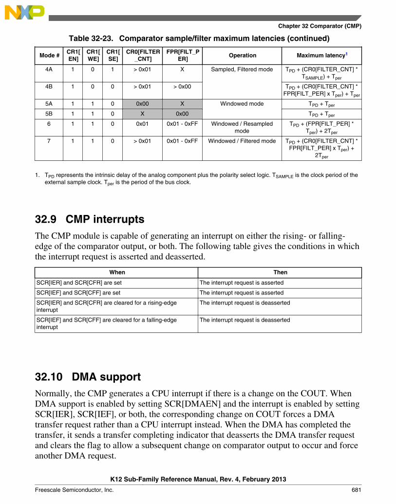
Table 32-23. Comparator sample/filter maximum latencies (continued)
Mode #CR1[EN]
CR1[WE]
CR1[SE]
CR0[FILTER_CNT]
FPR[FILT_PER]
Operation Maximum latency1
4A 1 0 1 > 0x01 X Sampled, Filtered mode TPD + (CR0[FILTER_CNT] *TSAMPLE) + Tper
4B 1 0 0 > 0x01 > 0x00 TPD + (CR0[FILTER_CNT] *FPR[FILT_PER] x Tper) + Tper
5A 1 1 0 0x00 X Windowed mode TPD + Tper
5B 1 1 0 X 0x00 TPD + Tper
6 1 1 0 0x01 0x01 - 0xFF Windowed / Resampledmode
TPD + (FPR[FILT_PER] *Tper) + 2Tper
7 1 1 0 > 0x01 0x01 - 0xFF Windowed / Filtered mode TPD + (CR0[FILTER_CNT] *FPR[FILT_PER] x Tper) +
2Tper
1. TPD represents the intrinsic delay of the analog component plus the polarity select logic. TSAMPLE is the clock period of theexternal sample clock. Tper is the period of the bus clock.
32.9 CMP interruptsThe CMP module is capable of generating an interrupt on either the rising- or falling-edge of the comparator output, or both. The following table gives the conditions in whichthe interrupt request is asserted and deasserted.
When Then
SCR[IER] and SCR[CFR] are set The interrupt request is asserted
SCR[IEF] and SCR[CFF] are set The interrupt request is asserted
SCR[IER] and SCR[CFR] are cleared for a rising-edgeinterrupt
The interrupt request is deasserted
SCR[IEF] and SCR[CFF] are cleared for a falling-edgeinterrupt
The interrupt request is deasserted
32.10 DMA supportNormally, the CMP generates a CPU interrupt if there is a change on the COUT. WhenDMA support is enabled by setting SCR[DMAEN] and the interrupt is enabled by settingSCR[IER], SCR[IEF], or both, the corresponding change on COUT forces a DMAtransfer request rather than a CPU interrupt instead. When the DMA has completed thetransfer, it sends a transfer completing indicator that deasserts the DMA transfer requestand clears the flag to allow a subsequent change on comparator output to occur and forceanother DMA request.
Chapter 32 Comparator (CMP)
K12 Sub-Family Reference Manual, Rev. 4, February 2013
Freescale Semiconductor, Inc. 681
The comparator can remain functional in STOP modes. When DMA support is enabledby setting SCR[DMAEN] and the interrupt is enabled by setting SCR[IER], SCR[IEF], orboth, the corresponding change on COUT forces a DMA transfer request to wake up thesystem from STOP modes. After the data transfer has finished, system will go back toSTOP modes. Refer to DMA chapters in the device reference manual for theasynchronous DMA function for details.
32.11 Digital-to-analog converterThe following figure shows the block diagram of the DAC module. It contains a 64-tapresistor ladder network and a 64-to-1 multiplexer, which selects an output voltage fromone of 64 distinct levels that outputs from DACO. It is controlled through the DACControl Register (DACCR). Its supply reference source can be selected from two sourcesVin1 and Vin2. The module can be powered down or disabled when not in use. When inDisabled mode, DACO is connected to the analog ground.
VOSEL[5:0]
DACO
MUX
MU
X
DACEN
Vin
VRSEL
Vin1 Vin2
Figure 32-30. 6-bit DAC block diagram
32.12 DAC functional descriptionThis section provides DAC functional description.
Digital-to-analog converter
K12 Sub-Family Reference Manual, Rev. 4, February 2013
682 Freescale Semiconductor, Inc.
32.12.1 Voltage reference source select• Vin1 connects to the primary voltage source as supply reference of 64 tap resistor
ladder
• Vin2 connects to an alternate voltage source
32.13 DAC resetsThis module has a single reset input, corresponding to the chip-wide peripheral reset.
32.14 DAC clocksThis module has a single clock input, the bus clock.
32.15 DAC interruptsThis module has no interrupts.
Chapter 32 Comparator (CMP)
K12 Sub-Family Reference Manual, Rev. 4, February 2013
Freescale Semiconductor, Inc. 683

DAC interrupts
K12 Sub-Family Reference Manual, Rev. 4, February 2013
684 Freescale Semiconductor, Inc.

Chapter 3312-bit Digital-to-Analog Converter (DAC)
33.1 IntroductionNOTE
For the chip-specific implementation details of this module'sinstances see the chip configuration information.
The 12-bit digital-to-analog converter (DAC) is a low-power, general-purpose DAC. Theoutput of the DAC can be placed on an external pin or set as one of the inputs to theanalog comparator, op-amps, or ADC.
33.2 FeaturesThe features of the DAC module include:
• On-chip programmable reference generator output. The voltage output range is from1⁄4096 Vin to Vin, and the step is 1⁄4096 Vin, where Vin is the input voltage.
• Vin can be selected from two reference sources
• Static operation in Normal Stop mode
• 16-word data buffer supported with configurable watermark and multiple operationmodes
• DMA support
33.3 Block diagramThe block diagram of the DAC module is as follows:
K12 Sub-Family Reference Manual, Rev. 4, February 2013
Freescale Semiconductor, Inc. 685

-
+M
UX
4096
-leve
lDACEN
DACDAT[11:0]
MUX
DACREF_2
DACRFS
V
Vout
VDD
AMP buffer
12
DACBFMD
DACSWTRG
DACBFEN
DACBFUP
DACBFWM
DACBFRP
Hardware trigger DACBFWMF
DACBWIEN
DACBFRPTF
DACBTIEN
DACBFRPBF
DACBBIEN
ORdac_interrupt
DACTRGSE
LPEN
DACRFS
DACREF_1
Vin
Vo
&
&
&
DataBuffer
Figure 33-1. DAC block diagram
33.4 Memory map/register definitionThe DAC has registers to control analog comparator and programmable voltage dividerto perform the digital-to-analog functions.
Memory map/register definition
K12 Sub-Family Reference Manual, Rev. 4, February 2013
686 Freescale Semiconductor, Inc.
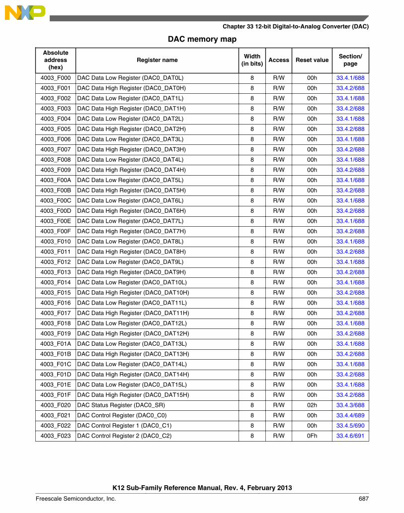
DAC memory map
Absoluteaddress
(hex)Register name
Width(in bits)
Access Reset valueSection/
page
4003_F000 DAC Data Low Register (DAC0_DAT0L) 8 R/W 00h 33.4.1/688
4003_F001 DAC Data High Register (DAC0_DAT0H) 8 R/W 00h 33.4.2/688
4003_F002 DAC Data Low Register (DAC0_DAT1L) 8 R/W 00h 33.4.1/688
4003_F003 DAC Data High Register (DAC0_DAT1H) 8 R/W 00h 33.4.2/688
4003_F004 DAC Data Low Register (DAC0_DAT2L) 8 R/W 00h 33.4.1/688
4003_F005 DAC Data High Register (DAC0_DAT2H) 8 R/W 00h 33.4.2/688
4003_F006 DAC Data Low Register (DAC0_DAT3L) 8 R/W 00h 33.4.1/688
4003_F007 DAC Data High Register (DAC0_DAT3H) 8 R/W 00h 33.4.2/688
4003_F008 DAC Data Low Register (DAC0_DAT4L) 8 R/W 00h 33.4.1/688
4003_F009 DAC Data High Register (DAC0_DAT4H) 8 R/W 00h 33.4.2/688
4003_F00A DAC Data Low Register (DAC0_DAT5L) 8 R/W 00h 33.4.1/688
4003_F00B DAC Data High Register (DAC0_DAT5H) 8 R/W 00h 33.4.2/688
4003_F00C DAC Data Low Register (DAC0_DAT6L) 8 R/W 00h 33.4.1/688
4003_F00D DAC Data High Register (DAC0_DAT6H) 8 R/W 00h 33.4.2/688
4003_F00E DAC Data Low Register (DAC0_DAT7L) 8 R/W 00h 33.4.1/688
4003_F00F DAC Data High Register (DAC0_DAT7H) 8 R/W 00h 33.4.2/688
4003_F010 DAC Data Low Register (DAC0_DAT8L) 8 R/W 00h 33.4.1/688
4003_F011 DAC Data High Register (DAC0_DAT8H) 8 R/W 00h 33.4.2/688
4003_F012 DAC Data Low Register (DAC0_DAT9L) 8 R/W 00h 33.4.1/688
4003_F013 DAC Data High Register (DAC0_DAT9H) 8 R/W 00h 33.4.2/688
4003_F014 DAC Data Low Register (DAC0_DAT10L) 8 R/W 00h 33.4.1/688
4003_F015 DAC Data High Register (DAC0_DAT10H) 8 R/W 00h 33.4.2/688
4003_F016 DAC Data Low Register (DAC0_DAT11L) 8 R/W 00h 33.4.1/688
4003_F017 DAC Data High Register (DAC0_DAT11H) 8 R/W 00h 33.4.2/688
4003_F018 DAC Data Low Register (DAC0_DAT12L) 8 R/W 00h 33.4.1/688
4003_F019 DAC Data High Register (DAC0_DAT12H) 8 R/W 00h 33.4.2/688
4003_F01A DAC Data Low Register (DAC0_DAT13L) 8 R/W 00h 33.4.1/688
4003_F01B DAC Data High Register (DAC0_DAT13H) 8 R/W 00h 33.4.2/688
4003_F01C DAC Data Low Register (DAC0_DAT14L) 8 R/W 00h 33.4.1/688
4003_F01D DAC Data High Register (DAC0_DAT14H) 8 R/W 00h 33.4.2/688
4003_F01E DAC Data Low Register (DAC0_DAT15L) 8 R/W 00h 33.4.1/688
4003_F01F DAC Data High Register (DAC0_DAT15H) 8 R/W 00h 33.4.2/688
4003_F020 DAC Status Register (DAC0_SR) 8 R/W 02h 33.4.3/688
4003_F021 DAC Control Register (DAC0_C0) 8 R/W 00h 33.4.4/689
4003_F022 DAC Control Register 1 (DAC0_C1) 8 R/W 00h 33.4.5/690
4003_F023 DAC Control Register 2 (DAC0_C2) 8 R/W 0Fh 33.4.6/691
Chapter 33 12-bit Digital-to-Analog Converter (DAC)
K12 Sub-Family Reference Manual, Rev. 4, February 2013
Freescale Semiconductor, Inc. 687
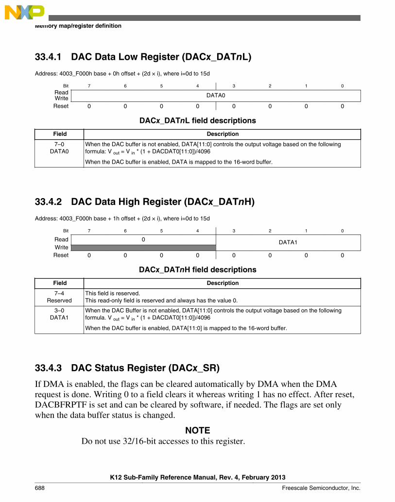
33.4.1 DAC Data Low Register (DACx_DATnL)
Address: 4003_F000h base + 0h offset + (2d × i), where i=0d to 15d
Bit 7 6 5 4 3 2 1 0
Read DATA0WriteReset 0 0 0 0 0 0 0 0
DACx_DATnL field descriptions
Field Description
7–0DATA0
When the DAC buffer is not enabled, DATA[11:0] controls the output voltage based on the followingformula: V out = V in * (1 + DACDAT0[11:0])/4096
When the DAC buffer is enabled, DATA is mapped to the 16-word buffer.
33.4.2 DAC Data High Register (DACx_DATnH)
Address: 4003_F000h base + 1h offset + (2d × i), where i=0d to 15d
Bit 7 6 5 4 3 2 1 0
Read 0 DATA1WriteReset 0 0 0 0 0 0 0 0
DACx_DATnH field descriptions
Field Description
7–4Reserved
This field is reserved.This read-only field is reserved and always has the value 0.
3–0DATA1
When the DAC Buffer is not enabled, DATA[11:0] controls the output voltage based on the followingformula. V out = V in * (1 + DACDAT0[11:0])/4096
When the DAC buffer is enabled, DATA[11:0] is mapped to the 16-word buffer.
33.4.3 DAC Status Register (DACx_SR)
If DMA is enabled, the flags can be cleared automatically by DMA when the DMArequest is done. Writing 0 to a field clears it whereas writing 1 has no effect. After reset,DACBFRPTF is set and can be cleared by software, if needed. The flags are set onlywhen the data buffer status is changed.
NOTEDo not use 32/16-bit accesses to this register.
Memory map/register definition
K12 Sub-Family Reference Manual, Rev. 4, February 2013
688 Freescale Semiconductor, Inc.
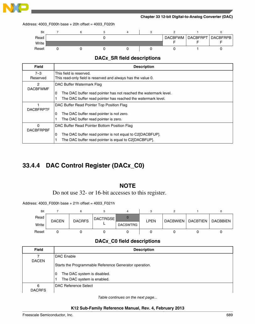
Address: 4003_F000h base + 20h offset = 4003_F020h
Bit 7 6 5 4 3 2 1 0
Read 0 DACBFWMF
DACBFRPTF
DACBFRPBFWrite
Reset 0 0 0 0 0 0 1 0
DACx_SR field descriptions
Field Description
7–3Reserved
This field is reserved.This read-only field is reserved and always has the value 0.
2DACBFWMF
DAC Buffer Watermark Flag
0 The DAC buffer read pointer has not reached the watermark level.1 The DAC buffer read pointer has reached the watermark level.
1DACBFRPTF
DAC Buffer Read Pointer Top Position Flag
0 The DAC buffer read pointer is not zero.1 The DAC buffer read pointer is zero.
0DACBFRPBF
DAC Buffer Read Pointer Bottom Position Flag
0 The DAC buffer read pointer is not equal to C2[DACBFUP].1 The DAC buffer read pointer is equal to C2[DACBFUP].
33.4.4 DAC Control Register (DACx_C0)
NOTEDo not use 32- or 16-bit accesses to this register.
Address: 4003_F000h base + 21h offset = 4003_F021h
Bit 7 6 5 4 3 2 1 0
ReadDACEN DACRFS
DACTRGSEL
0LPEN DACBWIEN DACBTIEN DACBBIEN
Write DACSWTRG
Reset 0 0 0 0 0 0 0 0
DACx_C0 field descriptions
Field Description
7DACEN
DAC Enable
Starts the Programmable Reference Generator operation.
0 The DAC system is disabled.1 The DAC system is enabled.
6DACRFS
DAC Reference Select
Table continues on the next page...
Chapter 33 12-bit Digital-to-Analog Converter (DAC)
K12 Sub-Family Reference Manual, Rev. 4, February 2013
Freescale Semiconductor, Inc. 689
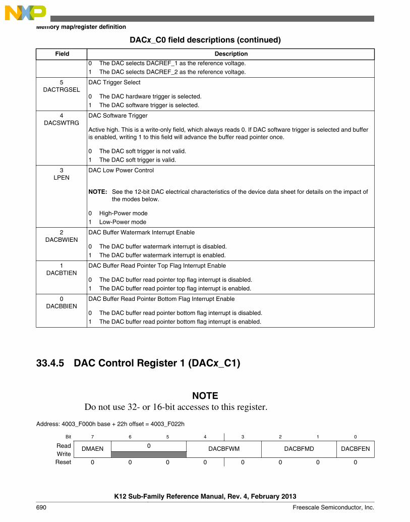
DACx_C0 field descriptions (continued)
Field Description
0 The DAC selects DACREF_1 as the reference voltage.1 The DAC selects DACREF_2 as the reference voltage.
5DACTRGSEL
DAC Trigger Select
0 The DAC hardware trigger is selected.1 The DAC software trigger is selected.
4DACSWTRG
DAC Software Trigger
Active high. This is a write-only field, which always reads 0. If DAC software trigger is selected and bufferis enabled, writing 1 to this field will advance the buffer read pointer once.
0 The DAC soft trigger is not valid.1 The DAC soft trigger is valid.
3LPEN
DAC Low Power Control
NOTE: See the 12-bit DAC electrical characteristics of the device data sheet for details on the impact ofthe modes below.
0 High-Power mode1 Low-Power mode
2DACBWIEN
DAC Buffer Watermark Interrupt Enable
0 The DAC buffer watermark interrupt is disabled.1 The DAC buffer watermark interrupt is enabled.
1DACBTIEN
DAC Buffer Read Pointer Top Flag Interrupt Enable
0 The DAC buffer read pointer top flag interrupt is disabled.1 The DAC buffer read pointer top flag interrupt is enabled.
0DACBBIEN
DAC Buffer Read Pointer Bottom Flag Interrupt Enable
0 The DAC buffer read pointer bottom flag interrupt is disabled.1 The DAC buffer read pointer bottom flag interrupt is enabled.
33.4.5 DAC Control Register 1 (DACx_C1)
NOTEDo not use 32- or 16-bit accesses to this register.
Address: 4003_F000h base + 22h offset = 4003_F022h
Bit 7 6 5 4 3 2 1 0
Read DMAEN 0 DACBFWM DACBFMD DACBFENWriteReset 0 0 0 0 0 0 0 0
Memory map/register definition
K12 Sub-Family Reference Manual, Rev. 4, February 2013
690 Freescale Semiconductor, Inc.
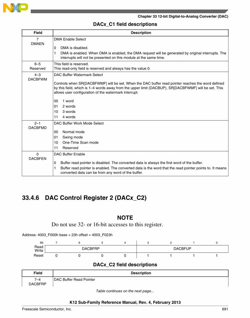
DACx_C1 field descriptions
Field Description
7DMAEN
DMA Enable Select
0 DMA is disabled.1 DMA is enabled. When DMA is enabled, the DMA request will be generated by original interrupts. The
interrupts will not be presented on this module at the same time.
6–5Reserved
This field is reserved.This read-only field is reserved and always has the value 0.
4–3DACBFWM
DAC Buffer Watermark Select
Controls when SR[DACBFWMF] will be set. When the DAC buffer read pointer reaches the word definedby this field, which is 1–4 words away from the upper limit (DACBUP), SR[DACBFWMF] will be set. Thisallows user configuration of the watermark interrupt.
00 1 word01 2 words10 3 words11 4 words
2–1DACBFMD
DAC Buffer Work Mode Select
00 Normal mode01 Swing mode10 One-Time Scan mode11 Reserved
0DACBFEN
DAC Buffer Enable
0 Buffer read pointer is disabled. The converted data is always the first word of the buffer.1 Buffer read pointer is enabled. The converted data is the word that the read pointer points to. It means
converted data can be from any word of the buffer.
33.4.6 DAC Control Register 2 (DACx_C2)
NOTEDo not use 32- or 16-bit accesses to this register.
Address: 4003_F000h base + 23h offset = 4003_F023h
Bit 7 6 5 4 3 2 1 0
Read DACBFRP DACBFUPWriteReset 0 0 0 0 1 1 1 1
DACx_C2 field descriptions
Field Description
7–4DACBFRP
DAC Buffer Read Pointer
Table continues on the next page...
Chapter 33 12-bit Digital-to-Analog Converter (DAC)
K12 Sub-Family Reference Manual, Rev. 4, February 2013
Freescale Semiconductor, Inc. 691
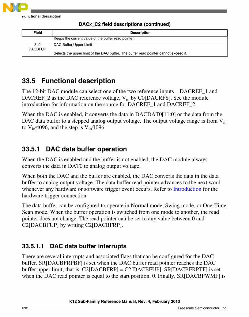
DACx_C2 field descriptions (continued)
Field Description
Keeps the current value of the buffer read pointer.
3–0DACBFUP
DAC Buffer Upper Limit
Selects the upper limit of the DAC buffer. The buffer read pointer cannot exceed it.
33.5 Functional descriptionThe 12-bit DAC module can select one of the two reference inputs—DACREF_1 andDACREF_2 as the DAC reference voltage, Vin by C0[DACRFS]. See the moduleintroduction for information on the source for DACREF_1 and DACREF_2.
When the DAC is enabled, it converts the data in DACDAT0[11:0] or the data from theDAC data buffer to a stepped analog output voltage. The output voltage range is from Vinto Vin∕4096, and the step is Vin∕4096.
33.5.1 DAC data buffer operation
When the DAC is enabled and the buffer is not enabled, the DAC module alwaysconverts the data in DAT0 to analog output voltage.
When both the DAC and the buffer are enabled, the DAC converts the data in the databuffer to analog output voltage. The data buffer read pointer advances to the next wordwhenever any hardware or software trigger event occurs. Refer to Introduction for thehardware trigger connection.
The data buffer can be configured to operate in Normal mode, Swing mode, or One-TimeScan mode. When the buffer operation is switched from one mode to another, the readpointer does not change. The read pointer can be set to any value between 0 andC2[DACBFUP] by writing C2[DACBFRP].
33.5.1.1 DAC data buffer interrupts
There are several interrupts and associated flags that can be configured for the DACbuffer. SR[DACBFRPBF] is set when the DAC buffer read pointer reaches the DACbuffer upper limit, that is, C2[DACBFRP] = C2[DACBFUP]. SR[DACBFRPTF] is setwhen the DAC read pointer is equal to the start position, 0. Finally, SR[DACBFWMF] is
Functional description
K12 Sub-Family Reference Manual, Rev. 4, February 2013
692 Freescale Semiconductor, Inc.
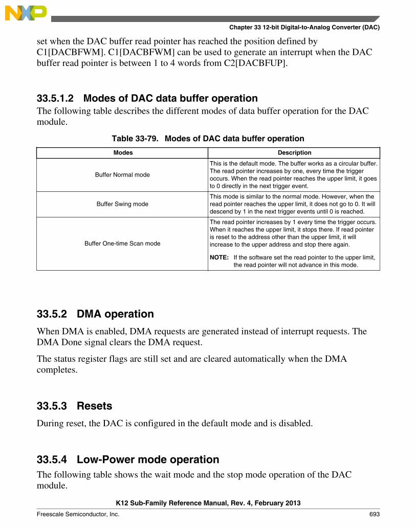
set when the DAC buffer read pointer has reached the position defined byC1[DACBFWM]. C1[DACBFWM] can be used to generate an interrupt when the DACbuffer read pointer is between 1 to 4 words from C2[DACBFUP].
33.5.1.2 Modes of DAC data buffer operationThe following table describes the different modes of data buffer operation for the DACmodule.
Table 33-79. Modes of DAC data buffer operation
Modes Description
Buffer Normal mode
This is the default mode. The buffer works as a circular buffer.The read pointer increases by one, every time the triggeroccurs. When the read pointer reaches the upper limit, it goesto 0 directly in the next trigger event.
Buffer Swing modeThis mode is similar to the normal mode. However, when theread pointer reaches the upper limit, it does not go to 0. It willdescend by 1 in the next trigger events until 0 is reached.
Buffer One-time Scan mode
The read pointer increases by 1 every time the trigger occurs.When it reaches the upper limit, it stops there. If read pointeris reset to the address other than the upper limit, it willincrease to the upper address and stop there again.
NOTE: If the software set the read pointer to the upper limit,the read pointer will not advance in this mode.
33.5.2 DMA operation
When DMA is enabled, DMA requests are generated instead of interrupt requests. TheDMA Done signal clears the DMA request.
The status register flags are still set and are cleared automatically when the DMAcompletes.
33.5.3 Resets
During reset, the DAC is configured in the default mode and is disabled.
33.5.4 Low-Power mode operationThe following table shows the wait mode and the stop mode operation of the DACmodule.
Chapter 33 12-bit Digital-to-Analog Converter (DAC)
K12 Sub-Family Reference Manual, Rev. 4, February 2013
Freescale Semiconductor, Inc. 693

Table 33-80. Modes of operation
Modes of operation Description
Wait mode The DAC will operate normally, if enabled.
Stop mode
If enabled, the DAC module continues to operatein Normal Stop mode and the output voltage willhold the value before stop.
In low-power stop modes, the DAC is fully shut down.
NOTEThe assignment of module modes to core modes is chip-specific. For module-to-core mode assignments, see the chapterthat describes how modules are configured.
Functional description
K12 Sub-Family Reference Manual, Rev. 4, February 2013
694 Freescale Semiconductor, Inc.

Chapter 34Voltage Reference (VREFV1)
34.1 IntroductionNOTE
For the chip-specific implementation details of this module'sinstances see the chip configuration information.
The Voltage Reference(VREF) is intended to supply an accurate voltage output that canbe trimmed in 0.5 mV steps. The VREF can be used in applications to provide a referencevoltage to external devices or used internally as a reference to analog peripherals such asthe ADC, DAC, or CMP. The voltage reference has three operating modes that providedifferent levels of supply rejection and power consumption..
The following figure is a block diagram of the Voltage Reference.
K12 Sub-Family Reference Manual, Rev. 4, February 2013
Freescale Semiconductor, Inc. 695
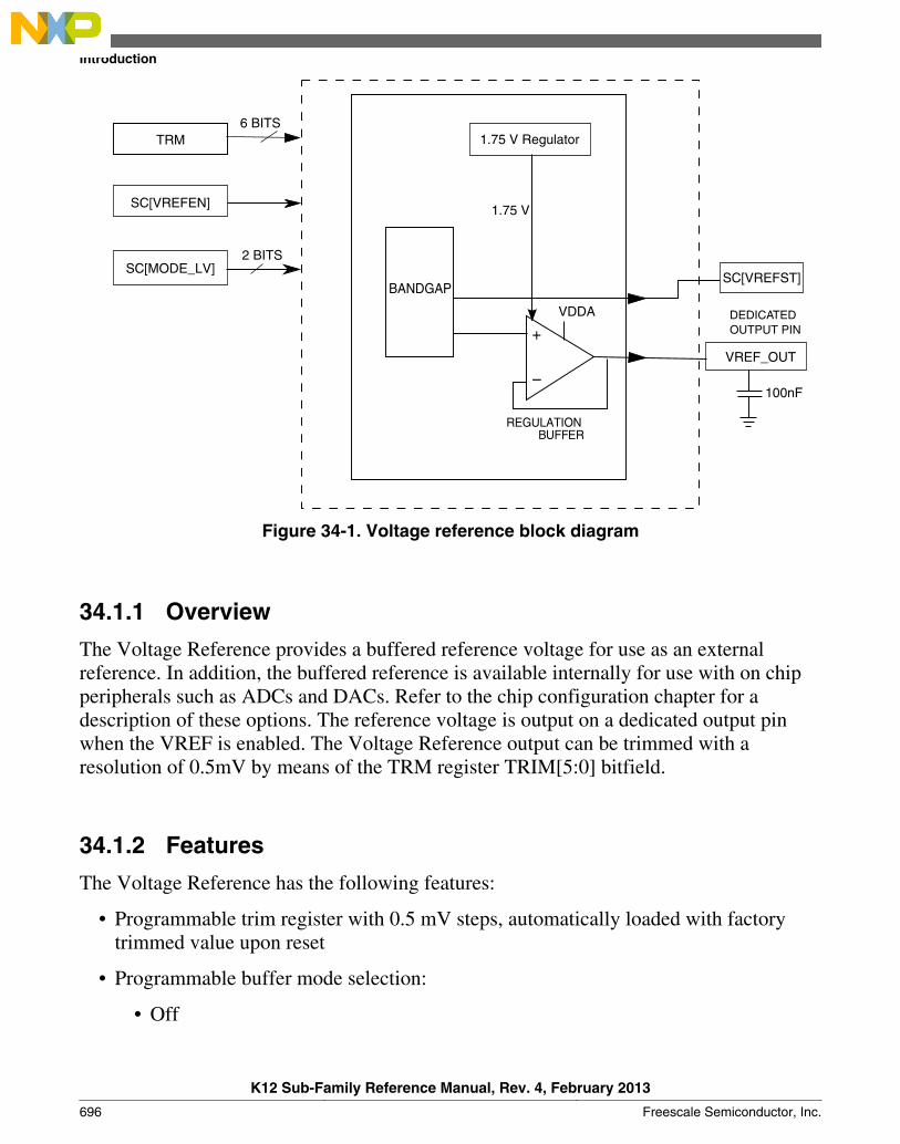
6 BITSTRM
SC[VREFEN]
2 BITSSC[MODE_LV]
REGULATION BUFFER
BANDGAP
100 nF
VREF_OUT
DEDICATED OUTPUT PIN
SC[VREFST]
1.75 V Regulator
1.75 V
VDDA
Figure 34-1. Voltage reference block diagram
34.1.1 Overview
The Voltage Reference provides a buffered reference voltage for use as an externalreference. In addition, the buffered reference is available internally for use with on chipperipherals such as ADCs and DACs. Refer to the chip configuration chapter for adescription of these options. The reference voltage is output on a dedicated output pinwhen the VREF is enabled. The Voltage Reference output can be trimmed with aresolution of 0.5mV by means of the TRM register TRIM[5:0] bitfield.
34.1.2 Features
The Voltage Reference has the following features:
• Programmable trim register with 0.5 mV steps, automatically loaded with factorytrimmed value upon reset
• Programmable buffer mode selection:
• Off
Introduction
K12 Sub-Family Reference Manual, Rev. 4, February 2013
696 Freescale Semiconductor, Inc.
• Bandgap enabled/standby (output buffer disabled)
• Low power buffer mode (output buffer enabled)
• High power buffer mode (output buffer enabled)
• 1.2 V output at room temperature
• Dedicated output pin, VREF_OUT
34.1.3 Modes of Operation
The Voltage Reference continues normal operation in Run, Wait, and Stop modes. TheVoltage Reference can also run in Very Low Power Run (VLPR), Very Low Power Wait(VLPW) and Very Low Power Stop (VLPS). If it is desired to use the VREF regulator inthe very low power modes, the system reference voltage must be enabled in these modes.Refer to the chip configuration chapter for information on enabling this mode ofoperation. Having the VREF regulator enabled does increase current consumption. Invery low power modes it may be desirable to disable the VREF regulator to minimizecurrent consumption. Note however that the accuracy of the output voltage will bereduced (by as much as several mVs) when the VREF regulator is not used. .
NOTE
The assignment of module modes to core modes is chip-specific. For module-to-core mode assignments, see the chapterthat describes how modules are configured.
34.1.4 VREF Signal Descriptions
The following table shows the Voltage Reference signals properties.
Table 34-1. VREF Signal Descriptions
Signal Description I/O
VREF_OUT Internally-generated Voltage Reference output O
NOTE
When the VREF output buffer is disabled, the status of theVREF_OUT signal is high-impedence.
Chapter 34 Voltage Reference (VREFV1)
K12 Sub-Family Reference Manual, Rev. 4, February 2013
Freescale Semiconductor, Inc. 697
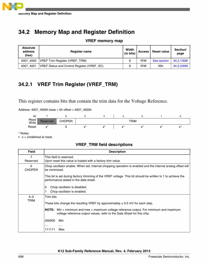
Memory Map and Register DefinitionVREF memory map
Absoluteaddress
(hex)Register name
Width(in bits)
Access Reset valueSection/
page
4007_4000 VREF Trim Register (VREF_TRM) 8 R/W See section 34.2.1/698
4007_4001 VREF Status and Control Register (VREF_SC) 8 R/W 00h 34.2.2/699
34.2.1 VREF Trim Register (VREF_TRM)
This register contains bits that contain the trim data for the Voltage Reference.
Address: 4007_4000h base + 0h offset = 4007_4000h
Bit 7 6 5 4 3 2 1 0
Read Reserved CHOPEN TRIMWriteReset x* 0 x* x* x* x* x* x*
* Notes:x = Undefined at reset.•
VREF_TRM field descriptions
Field Description
7Reserved
This field is reserved.Upon reset this value is loaded with a factory trim value.
6CHOPEN
Chop oscillator enable. When set, internal chopping operation is enabled and the internal analog offset willbe minimized.
This bit is set during factory trimming of the VREF voltage. This bit should be written to 1 to achieve theperformance stated in the data sheet.
0 Chop oscillator is disabled.1 Chop oscillator is enabled.
5–0TRIM
Trim bits
These bits change the resulting VREF by approximately ± 0.5 mV for each step.
NOTE: Min = minimum and max = maximum voltage reference output. For minimum and maximumvoltage reference output values, refer to the Data Sheet for this chip.
000000 Min.... ....111111 Max
34.2
Memory Map and Register Definition
K12 Sub-Family Reference Manual, Rev. 4, February 2013
698 Freescale Semiconductor, Inc.
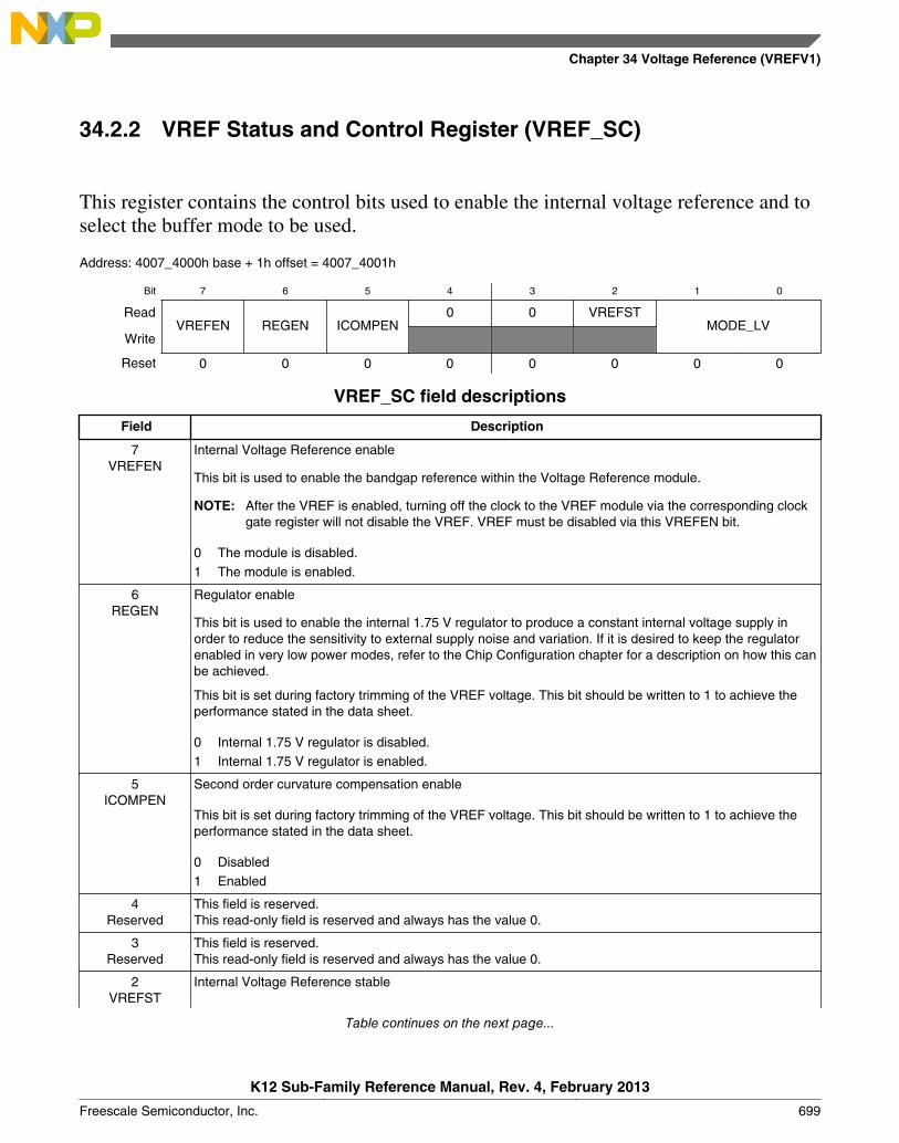
34.2.2 VREF Status and Control Register (VREF_SC)
This register contains the control bits used to enable the internal voltage reference and toselect the buffer mode to be used.
Address: 4007_4000h base + 1h offset = 4007_4001h
Bit 7 6 5 4 3 2 1 0
ReadVREFEN REGEN ICOMPEN
0 0 VREFSTMODE_LV
Write
Reset 0 0 0 0 0 0 0 0
VREF_SC field descriptions
Field Description
7VREFEN
Internal Voltage Reference enable
This bit is used to enable the bandgap reference within the Voltage Reference module.
NOTE: After the VREF is enabled, turning off the clock to the VREF module via the corresponding clockgate register will not disable the VREF. VREF must be disabled via this VREFEN bit.
0 The module is disabled.1 The module is enabled.
6REGEN
Regulator enable
This bit is used to enable the internal 1.75 V regulator to produce a constant internal voltage supply inorder to reduce the sensitivity to external supply noise and variation. If it is desired to keep the regulatorenabled in very low power modes, refer to the Chip Configuration chapter for a description on how this canbe achieved.
This bit is set during factory trimming of the VREF voltage. This bit should be written to 1 to achieve theperformance stated in the data sheet.
0 Internal 1.75 V regulator is disabled.1 Internal 1.75 V regulator is enabled.
5ICOMPEN
Second order curvature compensation enable
This bit is set during factory trimming of the VREF voltage. This bit should be written to 1 to achieve theperformance stated in the data sheet.
0 Disabled1 Enabled
4Reserved
This field is reserved.This read-only field is reserved and always has the value 0.
3Reserved
This field is reserved.This read-only field is reserved and always has the value 0.
2VREFST
Internal Voltage Reference stable
Table continues on the next page...
Chapter 34 Voltage Reference (VREFV1)
K12 Sub-Family Reference Manual, Rev. 4, February 2013
Freescale Semiconductor, Inc. 699
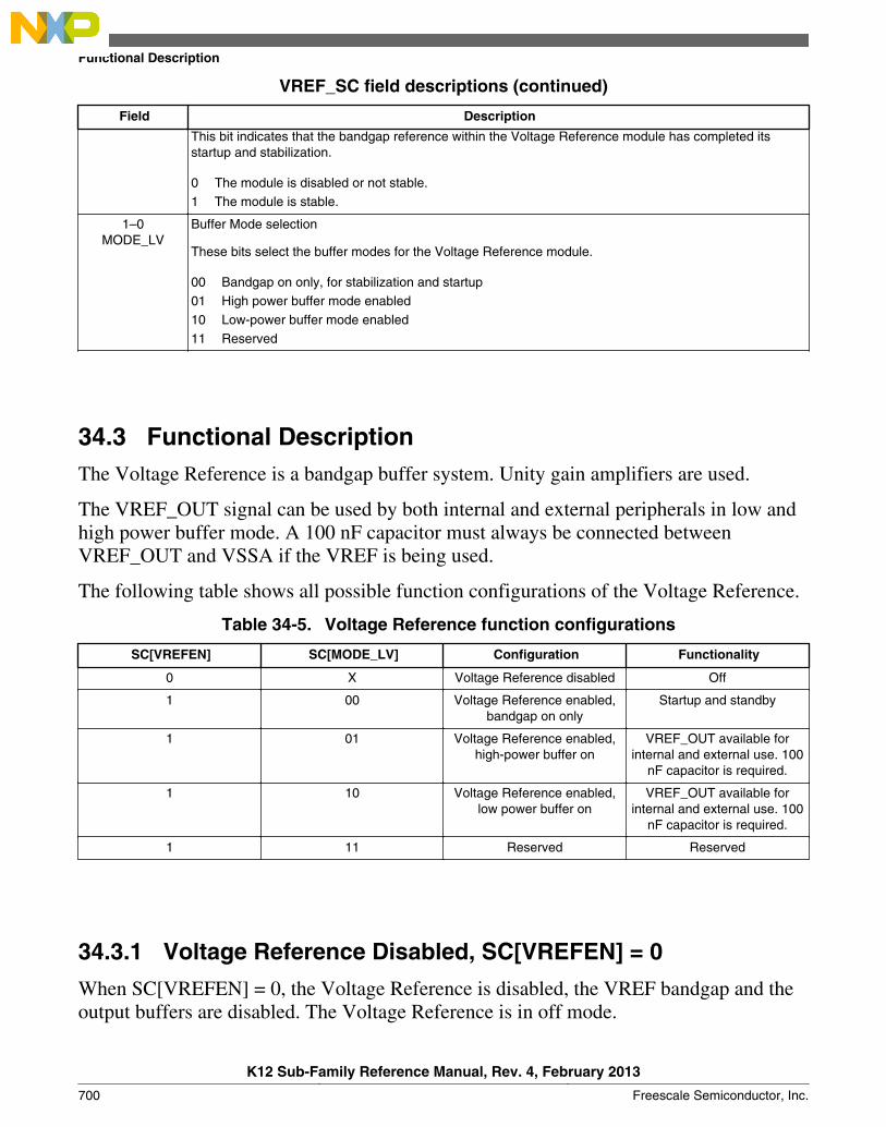
VREF_SC field descriptions (continued)
Field Description
This bit indicates that the bandgap reference within the Voltage Reference module has completed itsstartup and stabilization.
0 The module is disabled or not stable.1 The module is stable.
1–0MODE_LV
Buffer Mode selection
These bits select the buffer modes for the Voltage Reference module.
00 Bandgap on only, for stabilization and startup01 High power buffer mode enabled10 Low-power buffer mode enabled11 Reserved
34.3 Functional DescriptionThe Voltage Reference is a bandgap buffer system. Unity gain amplifiers are used.
The VREF_OUT signal can be used by both internal and external peripherals in low andhigh power buffer mode. A 100 nF capacitor must always be connected betweenVREF_OUT and VSSA if the VREF is being used.
The following table shows all possible function configurations of the Voltage Reference.
Table 34-5. Voltage Reference function configurations
SC[VREFEN] SC[MODE_LV] Configuration Functionality
0 X Voltage Reference disabled Off
1 00 Voltage Reference enabled,bandgap on only
Startup and standby
1 01 Voltage Reference enabled,high-power buffer on
VREF_OUT available forinternal and external use. 100
nF capacitor is required.
1 10 Voltage Reference enabled,low power buffer on
VREF_OUT available forinternal and external use. 100
nF capacitor is required.
1 11 Reserved Reserved
34.3.1 Voltage Reference Disabled, SC[VREFEN] = 0
When SC[VREFEN] = 0, the Voltage Reference is disabled, the VREF bandgap and theoutput buffers are disabled. The Voltage Reference is in off mode.
Functional Description
K12 Sub-Family Reference Manual, Rev. 4, February 2013
700 Freescale Semiconductor, Inc.

34.3.2 Voltage Reference Enabled, SC[VREFEN] = 1
When SC[VREFEN] = 1, the Voltage Reference is enabled, and different modes shouldbe set by the SC[MODE_LV] bits.
34.3.2.1 SC[MODE_LV]=00
The internal VREF bandgap is enabled to generate an accurate 1.2 V output that can betrimmed with the TRM register's TRIM[5:0] bitfield. The bandgap requires some time forstartup and stabilization. SC[VREFST] can be monitored to determine if the stabilizationand startup is complete.
The output buffer is disabled in this mode, and there is no buffered voltage output. TheVoltage Reference is in standby mode. If this mode is first selected and the low power orhigh power buffer mode is subsequently enabled, there will be a delay before the bufferoutput is settled at the final value. This is the buffer start up delay (Tstup) and the value isspecified in the appropriate device data sheet.
34.3.2.2 SC[MODE_LV] = 01
The internal VREF bandgap is on. The high power buffer is enabled to generate abuffered 1.2 V voltage to VREF_OUT. It can also be used as a reference to internalanalog peripherals such as an ADC channel or analog comparator input.
If this mode is entered from the standby mode (SC[MODE_LV] = 00, SC[VREFEN] = 1)there will be a delay before the buffer output is settled at the final value. This is the bufferstart up delay (Tstup) and the value is specified in the appropriate device data sheet. Ifthis mode is entered when the VREF module is enabled then you must wait the longer ofTstup or until SC[VREFST] = 1.
In this mode, a 100 nF capacitor is required to connect between the VREF_OUT pin andVSSA.
34.3.2.3 SC[MODE_LV] = 10
The internal VREF bandgap is on. The low power buffer is enabled to generate a buffered1.2 V voltage to VREF_OUT. It can also be used as a reference to internal analogperipherals such as an ADC channel or analog comparator input.
Chapter 34 Voltage Reference (VREFV1)
K12 Sub-Family Reference Manual, Rev. 4, February 2013
Freescale Semiconductor, Inc. 701

If this mode is entered from the standby mode (SC[MODE_LV] = 00, SC[VREFEN] = 1)there will be a delay before the buffer output is settled at the final value. This is the bufferstart up delay (Tstup) and the value is specified in the appropriate device data sheet. Ifthis mode is entered when the VREF module is enabled then you must wait the longer ofTstup or until SC[VREFST] = 1.
In this mode, a 100 nF capacitor is required to connect between the VREF_OUT pin andVSSA.
34.3.2.4 SC[MODE_LV] = 11
Reserved
34.4 Initialization/Application InformationThe Voltage Reference requires some time for startup and stabilization. AfterSC[VREFEN] = 1, SC[VREFST] can be monitored to determine if the stabilization andstartup is completed. The settling time of internal bandgap reference is typically 35ms,which means there is 35ms delay after the bandgap is enabled, the SC[VREFST] can onlybe useful after the bandgap is stable after the settling time.
When the Voltage Reference is already enabled and stabilized, changing SC[MODE_LV]will not clear SC[VREFST] but there will be some startup time before the output voltageat the VREF_OUT pin has settled. This is the buffer start up delay (Tstup) and the valueis specified in the appropriate device data sheet. Also, there will be some settling timewhen a step change of the load current is applied to the VREF_OUT pin. When the 1.75VVREF regulator is disabled, the VREF_OUT voltage will be more sensitive to supplyvoltage variation. It is recommended to use this regulator to achieve optimumVREF_OUT performance.
The TRM[CHOPEN], SC[REGEN] and SC[ICOMPEN] bits are written to 1 duringfactory trimming of the VREF voltage. These bits should be written to 1 to achieve theperfromance stated in the device data sheet.
Initialization/Application Information
K12 Sub-Family Reference Manual, Rev. 4, February 2013
702 Freescale Semiconductor, Inc.
Chapter 35Programmable Delay Block (PDB)
35.1 IntroductionNOTE
For the chip-specific implementation details of this module'sinstances see the chip configuration information.
The Programmable Delay Block (PDB) provides controllable delays from either aninternal or an external trigger, or a programmable interval tick, to the hardware triggerinputs of ADCs and/or generates the interval triggers to DACs, so that the precise timingbetween ADC conversions and/or DAC updates can be achieved. The PDB canoptionally provide pulse outputs (Pulse-Out's) that are used as the sample window in theCMP block.
35.1.1 Features• Up to 15 trigger input sources and one software trigger source
• Up to eight configurable PDB channels for ADC hardware trigger
• One PDB channel is associated with one ADC.
• One trigger output for ADC hardware trigger and up to eight pre-trigger outputsfor ADC trigger select per PDB channel
• Trigger outputs can be enabled or disabled independently.
• One 16-bit delay register per pre-trigger output
• Optional bypass of the delay registers of the pre-trigger outputs
• Operation in One-Shot or Continuous modes
K12 Sub-Family Reference Manual, Rev. 4, February 2013
Freescale Semiconductor, Inc. 703
• Optional back-to-back mode operation, which enables the ADC conversionscomplete to trigger the next PDB channel
• One programmable delay interrupt
• One sequence error interrupt
• One channel flag and one sequence error flag per pre-trigger
• DMA support• Up to eight pulse outputs (pulse-out's)
• Pulse-out's can be enabled or disabled independently.
• Programmable pulse width
NOTE
The number of PDB input and output triggers are chip-specific.See the chip configuration information for details.
35.1.2 Implementation
In this section, the following letters refer to the number of output triggers:
• N — Total available number of PDB channels.
• n — PDB channel number, valid from 0 to N-1.
• M — Total available pre-trigger per PDB channel.
• m — Pre-trigger number, valid from 0 to M-1.
• X — Total number of DAC interval triggers.
• x — DAC interval trigger output number, valid from 0 to X-1.
• Y — Total number of Pulse-Out's.
• y — Pulse-Out number, valid value is from 0 to Y-1.
NOTE
The number of module output triggers to core is chip-specific.For module to core output triggers implementation, see the chipconfiguration information.
Introduction
K12 Sub-Family Reference Manual, Rev. 4, February 2013
704 Freescale Semiconductor, Inc.

35.1.3 Back-to-back acknowledgment connections
PDB back-to-back operation acknowledgment connections are chip-specific. Forimplementation, see the chip configuration information.
35.1.4 DAC External Trigger Input Connections
The implementation of DAC external trigger inputs is chip-specific. See the chipconfiguration information for details.
35.1.5 Block diagram
This diagram illustrates the major components of the PDB.
Chapter 35 Programmable Delay Block (PDB)
K12 Sub-Family Reference Manual, Rev. 4, February 2013
Freescale Semiconductor, Inc. 705
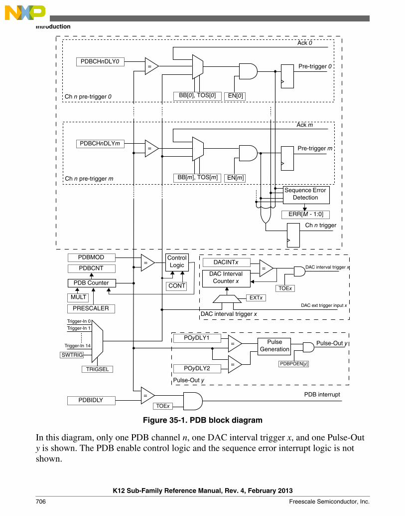
Ch n trigger
PDBCHnDLY0
PDBCHnDLYm
=
Ack 0
Pre-trigger 0
Ch n pre-trigger 0
Ch n pre-trigger m
=
BB[m], TOS[m]
BB[0], TOS[0] EN[0]
EN[m]
MULT
Ack m
Pre-trigger m
Trigger-In 0
DAC interval trigger x
Sequence Error Detection
ERR[M - 1:0]
PRESCALER
PDB Counter
PDBCNT
PDBMOD=
Control Logic
CONT
Trigger-In 1
Trigger-In 14
SWTRIG
TRIGSEL
DACINTx
DAC Interval Counter x
EXTxDAC ext trigger input x
= DAC interval trigger x
TOEx
PDBIDLY= PDB interrupt
TOEx
=
=POyDLY2
POyDLY1Pulse
GenerationPulse-Out y
PDBPOEN[y]
Pulse-Out y
Figure 35-1. PDB block diagram
In this diagram, only one PDB channel n, one DAC interval trigger x, and one Pulse-Outy is shown. The PDB enable control logic and the sequence error interrupt logic is notshown.
Introduction
K12 Sub-Family Reference Manual, Rev. 4, February 2013
706 Freescale Semiconductor, Inc.
35.1.6 Modes of operation
PDB ADC trigger operates in the following modes.
Disabled: Counter is off, all pre-trigger and trigger outputs are low if PDB is not in back-to-back operation of Bypass mode.
Debug: Counter is paused when processor is in Debug mode, and the counter for dactrigger is also paused in Debug mode.
Enabled One-Shot: Counter is enabled and restarted at count zero upon receiving apositive edge on the selected trigger input source or software trigger is selected andSC[SWTRIG] is written with 1. In each PDB channel, an enabled pre-trigger asserts onceper trigger input event. The trigger output asserts whenever any of the pre-triggers isasserted.
Enabled Continuous: Counter is enabled and restarted at count zero. The counter isrolled over to zero again when the count reaches the value specified in the modulusregister, and the counting is restarted. This enables a continuous stream of pre-triggers/trigger outputs as a result of a single trigger input event.
Enabled Bypassed: The pre-trigger and trigger outputs assert immediately after apositive edge on the selected trigger input source or software trigger is selected andSC[SWTRIG] is written with 1, that is the delay registers are bypassed. It is possible tobypass any one or more of the delay registers; therefore, this mode can be used inconjunction with One-Shot or Continuous mode.
35.2 PDB signal descriptionsThis table shows the detailed description of the external signal.
Table 35-1. PDB signal descriptions
Signal Description I/O
EXTRG External Trigger Input Source
If the PDB is enabled and external trigger input source is selected, apositive edge on the EXTRG signal resets and starts the counter.
I
35.3 Memory map and register definition
Chapter 35 Programmable Delay Block (PDB)
K12 Sub-Family Reference Manual, Rev. 4, February 2013
Freescale Semiconductor, Inc. 707
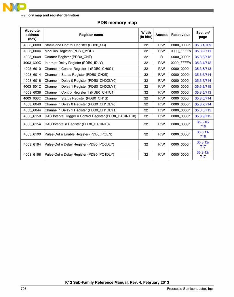
PDB memory map
Absoluteaddress
(hex)Register name
Width(in bits)
Access Reset valueSection/
page
4003_6000 Status and Control Register (PDB0_SC) 32 R/W 0000_0000h 35.3.1/709
4003_6004 Modulus Register (PDB0_MOD) 32 R/W 0000_FFFFh 35.3.2/711
4003_6008 Counter Register (PDB0_CNT) 32 R 0000_0000h 35.3.3/712
4003_600C Interrupt Delay Register (PDB0_IDLY) 32 R/W 0000_FFFFh 35.3.4/712
4003_6010 Channel n Control Register 1 (PDB0_CH0C1) 32 R/W 0000_0000h 35.3.5/713
4003_6014 Channel n Status Register (PDB0_CH0S) 32 R/W 0000_0000h 35.3.6/714
4003_6018 Channel n Delay 0 Register (PDB0_CH0DLY0) 32 R/W 0000_0000h 35.3.7/714
4003_601C Channel n Delay 1 Register (PDB0_CH0DLY1) 32 R/W 0000_0000h 35.3.8/715
4003_6038 Channel n Control Register 1 (PDB0_CH1C1) 32 R/W 0000_0000h 35.3.5/713
4003_603C Channel n Status Register (PDB0_CH1S) 32 R/W 0000_0000h 35.3.6/714
4003_6040 Channel n Delay 0 Register (PDB0_CH1DLY0) 32 R/W 0000_0000h 35.3.7/714
4003_6044 Channel n Delay 1 Register (PDB0_CH1DLY1) 32 R/W 0000_0000h 35.3.8/715
4003_6150 DAC Interval Trigger n Control Register (PDB0_DACINTC0) 32 R/W 0000_0000h 35.3.9/715
4003_6154 DAC Interval n Register (PDB0_DACINT0) 32 R/W 0000_0000h35.3.10/
716
4003_6190 Pulse-Out n Enable Register (PDB0_POEN) 32 R/W 0000_0000h35.3.11/
716
4003_6194 Pulse-Out n Delay Register (PDB0_PO0DLY) 32 R/W 0000_0000h35.3.12/
717
4003_6198 Pulse-Out n Delay Register (PDB0_PO1DLY) 32 R/W 0000_0000h35.3.12/
717
Memory map and register definition
K12 Sub-Family Reference Manual, Rev. 4, February 2013
708 Freescale Semiconductor, Inc.
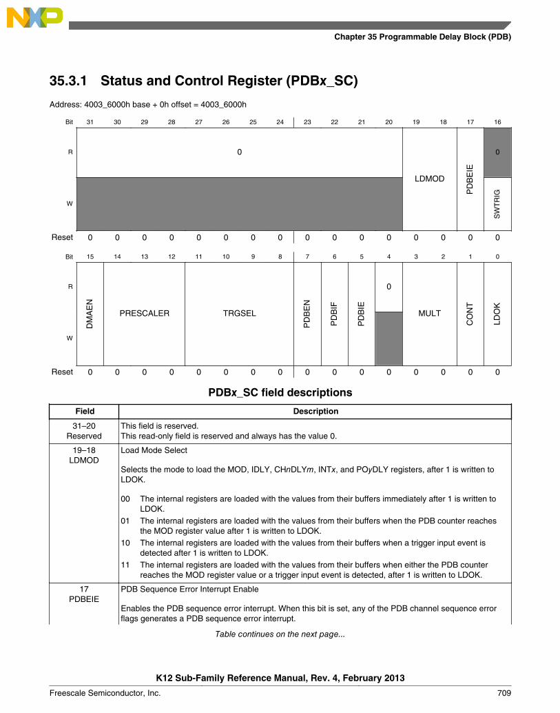
35.3.1 Status and Control Register (PDBx_SC)
Address: 4003_6000h base + 0h offset = 4003_6000h
Bit 31 30 29 28 27 26 25 24 23 22 21 20 19 18 17 16
R 0
LDMOD
PD
BE
IE
0
W
SW
TR
IG
Reset 0 0 0 0 0 0 0 0 0 0 0 0 0 0 0 0
Bit 15 14 13 12 11 10 9 8 7 6 5 4 3 2 1 0
R
DM
AE
N
PRESCALER TRGSELP
DB
EN
PD
BIF
PD
BIE
0
MULT
CO
NT
LDO
K
W
Reset 0 0 0 0 0 0 0 0 0 0 0 0 0 0 0 0
PDBx_SC field descriptions
Field Description
31–20Reserved
This field is reserved.This read-only field is reserved and always has the value 0.
19–18LDMOD
Load Mode Select
Selects the mode to load the MOD, IDLY, CHnDLYm, INTx, and POyDLY registers, after 1 is written toLDOK.
00 The internal registers are loaded with the values from their buffers immediately after 1 is written toLDOK.
01 The internal registers are loaded with the values from their buffers when the PDB counter reachesthe MOD register value after 1 is written to LDOK.
10 The internal registers are loaded with the values from their buffers when a trigger input event isdetected after 1 is written to LDOK.
11 The internal registers are loaded with the values from their buffers when either the PDB counterreaches the MOD register value or a trigger input event is detected, after 1 is written to LDOK.
17PDBEIE
PDB Sequence Error Interrupt Enable
Enables the PDB sequence error interrupt. When this bit is set, any of the PDB channel sequence errorflags generates a PDB sequence error interrupt.
Table continues on the next page...
Chapter 35 Programmable Delay Block (PDB)
K12 Sub-Family Reference Manual, Rev. 4, February 2013
Freescale Semiconductor, Inc. 709
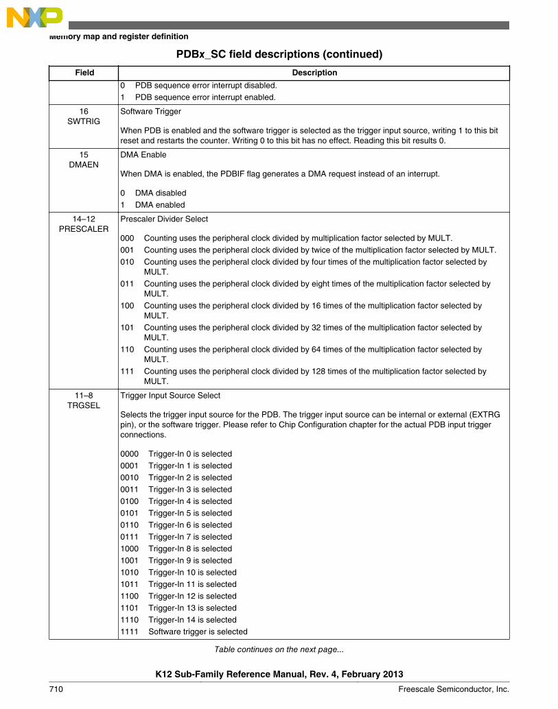
PDBx_SC field descriptions (continued)
Field Description
0 PDB sequence error interrupt disabled.1 PDB sequence error interrupt enabled.
16SWTRIG
Software Trigger
When PDB is enabled and the software trigger is selected as the trigger input source, writing 1 to this bitreset and restarts the counter. Writing 0 to this bit has no effect. Reading this bit results 0.
15DMAEN
DMA Enable
When DMA is enabled, the PDBIF flag generates a DMA request instead of an interrupt.
0 DMA disabled1 DMA enabled
14–12PRESCALER
Prescaler Divider Select
000 Counting uses the peripheral clock divided by multiplication factor selected by MULT.001 Counting uses the peripheral clock divided by twice of the multiplication factor selected by MULT.010 Counting uses the peripheral clock divided by four times of the multiplication factor selected by
MULT.011 Counting uses the peripheral clock divided by eight times of the multiplication factor selected by
MULT.100 Counting uses the peripheral clock divided by 16 times of the multiplication factor selected by
MULT.101 Counting uses the peripheral clock divided by 32 times of the multiplication factor selected by
MULT.110 Counting uses the peripheral clock divided by 64 times of the multiplication factor selected by
MULT.111 Counting uses the peripheral clock divided by 128 times of the multiplication factor selected by
MULT.
11–8TRGSEL
Trigger Input Source Select
Selects the trigger input source for the PDB. The trigger input source can be internal or external (EXTRGpin), or the software trigger. Please refer to Chip Configuration chapter for the actual PDB input triggerconnections.
0000 Trigger-In 0 is selected0001 Trigger-In 1 is selected0010 Trigger-In 2 is selected0011 Trigger-In 3 is selected0100 Trigger-In 4 is selected0101 Trigger-In 5 is selected0110 Trigger-In 6 is selected0111 Trigger-In 7 is selected1000 Trigger-In 8 is selected1001 Trigger-In 9 is selected1010 Trigger-In 10 is selected1011 Trigger-In 11 is selected1100 Trigger-In 12 is selected1101 Trigger-In 13 is selected1110 Trigger-In 14 is selected1111 Software trigger is selected
Table continues on the next page...
Memory map and register definition
K12 Sub-Family Reference Manual, Rev. 4, February 2013
710 Freescale Semiconductor, Inc.

PDBx_SC field descriptions (continued)
Field Description
7PDBEN
PDB Enable
0 PDB disabled. Counter is off.1 PDB enabled.
6PDBIF
PDB Interrupt Flag
This bit is set when the counter value is equal to the IDLY register. Writing zero clears this bit.
5PDBIE
PDB Interrupt Enable.
Enables the PDB interrupt. When this bit is set and DMAEN is cleared, PDBIF generates a PDB interrupt.
0 PDB interrupt disabled1 PDB interrupt enabled
4Reserved
This field is reserved.This read-only field is reserved and always has the value 0.
3–2MULT
Multiplication Factor Select for Prescaler
This bit selects the multiplication factor of the prescaler divider for the counter clock.
00 Multiplication factor is 101 Multiplication factor is 1010 Multiplication factor is 2011 Multiplication factor is 40
1CONT
Continuous Mode Enable
Enables the PDB operation in Continuous mode.
0 PDB operation in One-Shot mode1 PDB operation in Continuous mode
0LDOK
Load OK
Writing 1 to this bit updates the internal registers of MOD, IDLY, CHnDLYm, DACINTx,and POyDLY withthe values written to their buffers. The MOD, IDLY, CHnDLYm, DACINTx, and POyDLY will take effectaccording to the LDMOD.
After 1 is written to LDOK bit, the values in the buffers of above registers are not effective and the bufferscannot be written until the values in buffers are loaded into their internal registers.
LDOK can be written only when PDBEN is set or it can be written at the same time with PDBEN beingwritten to 1. It is automatically cleared when the values in buffers are loaded into the internal registers orthe PDBEN is cleared. Writing 0 to it has no effect.
35.3.2 Modulus Register (PDBx_MOD)
Address: 4003_6000h base + 4h offset = 4003_6004h
Bit 31 30 29 28 27 26 25 24 23 22 21 20 19 18 17 16 15 14 13 12 11 10 9 8 7 6 5 4 3 2 1 0
R 0 MODW
Reset 0 0 0 0 0 0 0 0 0 0 0 0 0 0 0 0 1 1 1 1 1 1 1 1 1 1 1 1 1 1 1 1
Chapter 35 Programmable Delay Block (PDB)
K12 Sub-Family Reference Manual, Rev. 4, February 2013
Freescale Semiconductor, Inc. 711
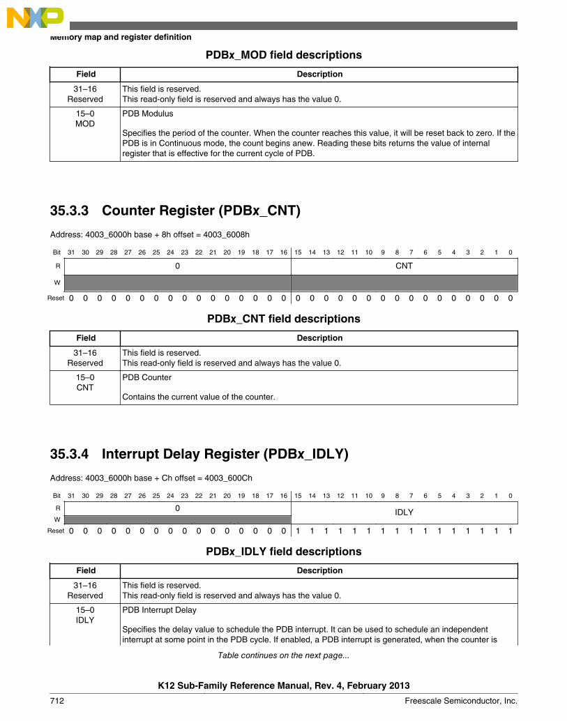
PDBx_MOD field descriptions
Field Description
31–16Reserved
This field is reserved.This read-only field is reserved and always has the value 0.
15–0MOD
PDB Modulus
Specifies the period of the counter. When the counter reaches this value, it will be reset back to zero. If thePDB is in Continuous mode, the count begins anew. Reading these bits returns the value of internalregister that is effective for the current cycle of PDB.
35.3.3 Counter Register (PDBx_CNT)
Address: 4003_6000h base + 8h offset = 4003_6008h
Bit 31 30 29 28 27 26 25 24 23 22 21 20 19 18 17 16 15 14 13 12 11 10 9 8 7 6 5 4 3 2 1 0
R 0 CNT
W
Reset 0 0 0 0 0 0 0 0 0 0 0 0 0 0 0 0 0 0 0 0 0 0 0 0 0 0 0 0 0 0 0 0
PDBx_CNT field descriptions
Field Description
31–16Reserved
This field is reserved.This read-only field is reserved and always has the value 0.
15–0CNT
PDB Counter
Contains the current value of the counter.
35.3.4 Interrupt Delay Register (PDBx_IDLY)
Address: 4003_6000h base + Ch offset = 4003_600Ch
Bit 31 30 29 28 27 26 25 24 23 22 21 20 19 18 17 16 15 14 13 12 11 10 9 8 7 6 5 4 3 2 1 0
R 0 IDLYW
Reset 0 0 0 0 0 0 0 0 0 0 0 0 0 0 0 0 1 1 1 1 1 1 1 1 1 1 1 1 1 1 1 1
PDBx_IDLY field descriptions
Field Description
31–16Reserved
This field is reserved.This read-only field is reserved and always has the value 0.
15–0IDLY
PDB Interrupt Delay
Specifies the delay value to schedule the PDB interrupt. It can be used to schedule an independentinterrupt at some point in the PDB cycle. If enabled, a PDB interrupt is generated, when the counter is
Table continues on the next page...
Memory map and register definition
K12 Sub-Family Reference Manual, Rev. 4, February 2013
712 Freescale Semiconductor, Inc.
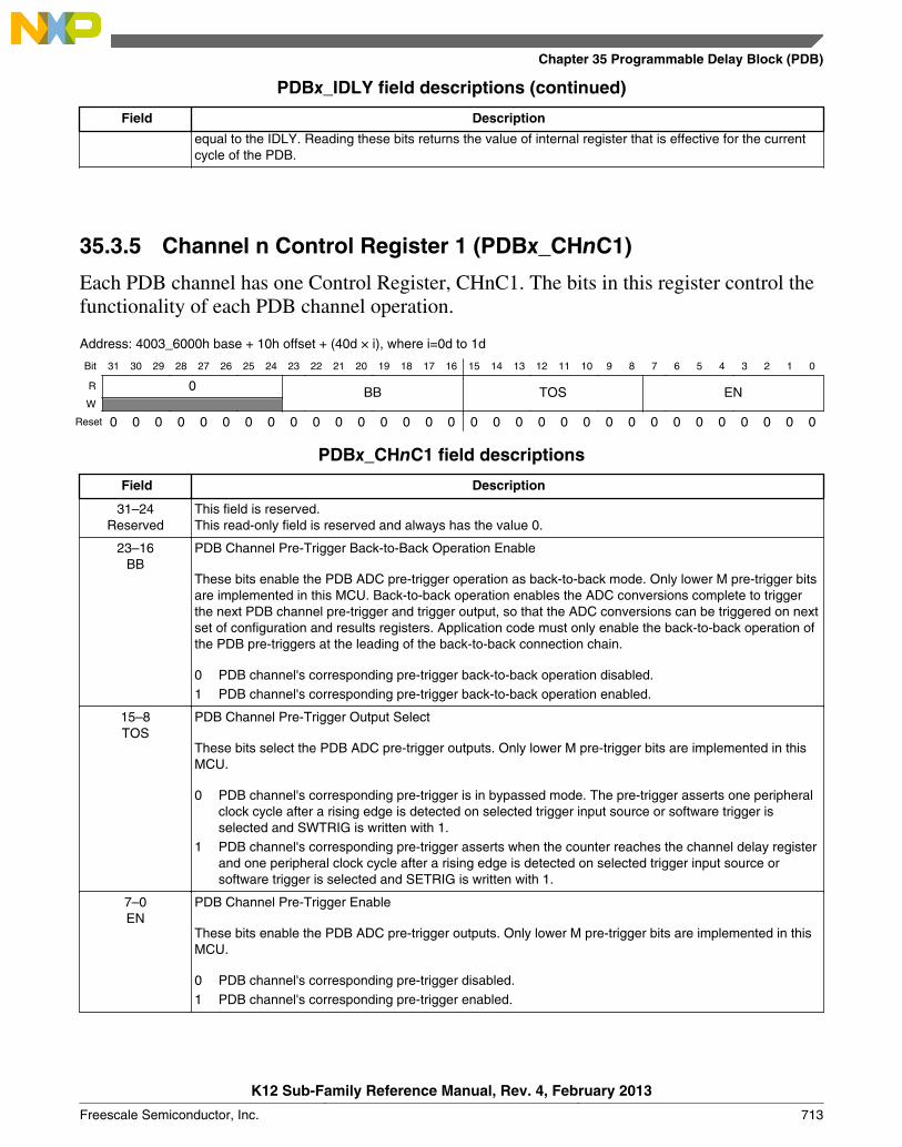
PDBx_IDLY field descriptions (continued)
Field Description
equal to the IDLY. Reading these bits returns the value of internal register that is effective for the currentcycle of the PDB.
35.3.5 Channel n Control Register 1 (PDBx_CHnC1)
Each PDB channel has one Control Register, CHnC1. The bits in this register control thefunctionality of each PDB channel operation.
Address: 4003_6000h base + 10h offset + (40d × i), where i=0d to 1d
Bit 31 30 29 28 27 26 25 24 23 22 21 20 19 18 17 16 15 14 13 12 11 10 9 8 7 6 5 4 3 2 1 0
R 0 BB TOS ENW
Reset 0 0 0 0 0 0 0 0 0 0 0 0 0 0 0 0 0 0 0 0 0 0 0 0 0 0 0 0 0 0 0 0
PDBx_CHnC1 field descriptions
Field Description
31–24Reserved
This field is reserved.This read-only field is reserved and always has the value 0.
23–16BB
PDB Channel Pre-Trigger Back-to-Back Operation Enable
These bits enable the PDB ADC pre-trigger operation as back-to-back mode. Only lower M pre-trigger bitsare implemented in this MCU. Back-to-back operation enables the ADC conversions complete to triggerthe next PDB channel pre-trigger and trigger output, so that the ADC conversions can be triggered on nextset of configuration and results registers. Application code must only enable the back-to-back operation ofthe PDB pre-triggers at the leading of the back-to-back connection chain.
0 PDB channel's corresponding pre-trigger back-to-back operation disabled.1 PDB channel's corresponding pre-trigger back-to-back operation enabled.
15–8TOS
PDB Channel Pre-Trigger Output Select
These bits select the PDB ADC pre-trigger outputs. Only lower M pre-trigger bits are implemented in thisMCU.
0 PDB channel's corresponding pre-trigger is in bypassed mode. The pre-trigger asserts one peripheralclock cycle after a rising edge is detected on selected trigger input source or software trigger isselected and SWTRIG is written with 1.
1 PDB channel's corresponding pre-trigger asserts when the counter reaches the channel delay registerand one peripheral clock cycle after a rising edge is detected on selected trigger input source orsoftware trigger is selected and SETRIG is written with 1.
7–0EN
PDB Channel Pre-Trigger Enable
These bits enable the PDB ADC pre-trigger outputs. Only lower M pre-trigger bits are implemented in thisMCU.
0 PDB channel's corresponding pre-trigger disabled.1 PDB channel's corresponding pre-trigger enabled.
Chapter 35 Programmable Delay Block (PDB)
K12 Sub-Family Reference Manual, Rev. 4, February 2013
Freescale Semiconductor, Inc. 713

35.3.6 Channel n Status Register (PDBx_CHnS)
Address: 4003_6000h base + 14h offset + (40d × i), where i=0d to 1d
Bit 31 30 29 28 27 26 25 24 23 22 21 20 19 18 17 16 15 14 13 12 11 10 9 8 7 6 5 4 3 2 1 0
R 0 CF 0 ERRW
Reset 0 0 0 0 0 0 0 0 0 0 0 0 0 0 0 0 0 0 0 0 0 0 0 0 0 0 0 0 0 0 0 0
PDBx_CHnS field descriptions
Field Description
31–24Reserved
This field is reserved.This read-only field is reserved and always has the value 0.
23–16CF
PDB Channel Flags
The CF[m] bit is set when the PDB counter matches the CHnDLYm. Write 0 to clear these bits.
15–8Reserved
This field is reserved.This read-only field is reserved and always has the value 0.
7–0ERR
PDB Channel Sequence Error Flags
Only the lower M bits are implemented in this MCU.
0 Sequence error not detected on PDB channel's corresponding pre-trigger.1 Sequence error detected on PDB channel's corresponding pre-trigger. ADCn block can be triggered
for a conversion by one pre-trigger from PDB channel n. When one conversion, which is triggered byone of the pre-triggers from PDB channel n, is in progress, new trigger from PDB channel'scorresponding pre-trigger m cannot be accepted by ADCn, and ERR[m] is set. Writing 0’s to clear thesequence error flags.
35.3.7 Channel n Delay 0 Register (PDBx_CHnDLY0)
Address: 4003_6000h base + 18h offset + (40d × i), where i=0d to 1d
Bit 31 30 29 28 27 26 25 24 23 22 21 20 19 18 17 16 15 14 13 12 11 10 9 8 7 6 5 4 3 2 1 0
R 0 DLYW
Reset 0 0 0 0 0 0 0 0 0 0 0 0 0 0 0 0 0 0 0 0 0 0 0 0 0 0 0 0 0 0 0 0
PDBx_CHnDLY0 field descriptions
Field Description
31–16Reserved
This field is reserved.This read-only field is reserved and always has the value 0.
15–0DLY
PDB Channel Delay
These bits specify the delay value for the channel's corresponding pre-trigger. The pre-trigger assertswhen the counter is equal to DLY. Reading these bits returns the value of internal register that is effectivefor the current PDB cycle.
Memory map and register definition
K12 Sub-Family Reference Manual, Rev. 4, February 2013
714 Freescale Semiconductor, Inc.
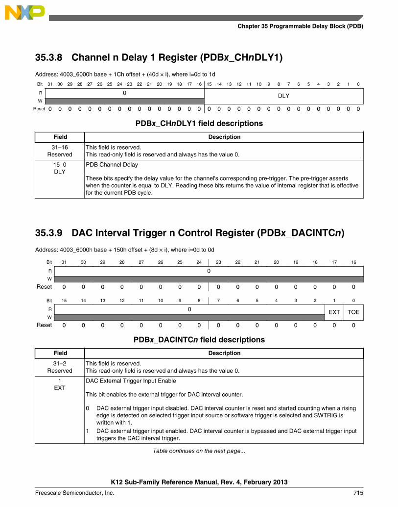
35.3.8 Channel n Delay 1 Register (PDBx_CHnDLY1)
Address: 4003_6000h base + 1Ch offset + (40d × i), where i=0d to 1d
Bit 31 30 29 28 27 26 25 24 23 22 21 20 19 18 17 16 15 14 13 12 11 10 9 8 7 6 5 4 3 2 1 0
R 0 DLYW
Reset 0 0 0 0 0 0 0 0 0 0 0 0 0 0 0 0 0 0 0 0 0 0 0 0 0 0 0 0 0 0 0 0
PDBx_CHnDLY1 field descriptions
Field Description
31–16Reserved
This field is reserved.This read-only field is reserved and always has the value 0.
15–0DLY
PDB Channel Delay
These bits specify the delay value for the channel's corresponding pre-trigger. The pre-trigger assertswhen the counter is equal to DLY. Reading these bits returns the value of internal register that is effectivefor the current PDB cycle.
35.3.9 DAC Interval Trigger n Control Register (PDBx_DACINTCn)
Address: 4003_6000h base + 150h offset + (8d × i), where i=0d to 0d
Bit 31 30 29 28 27 26 25 24 23 22 21 20 19 18 17 16
R 0W
Reset 0 0 0 0 0 0 0 0 0 0 0 0 0 0 0 0
Bit 15 14 13 12 11 10 9 8 7 6 5 4 3 2 1 0
R 0 EXT TOEW
Reset 0 0 0 0 0 0 0 0 0 0 0 0 0 0 0 0
PDBx_DACINTCn field descriptions
Field Description
31–2Reserved
This field is reserved.This read-only field is reserved and always has the value 0.
1EXT
DAC External Trigger Input Enable
This bit enables the external trigger for DAC interval counter.
0 DAC external trigger input disabled. DAC interval counter is reset and started counting when a risingedge is detected on selected trigger input source or software trigger is selected and SWTRIG iswritten with 1.
1 DAC external trigger input enabled. DAC interval counter is bypassed and DAC external trigger inputtriggers the DAC interval trigger.
Table continues on the next page...
Chapter 35 Programmable Delay Block (PDB)
K12 Sub-Family Reference Manual, Rev. 4, February 2013
Freescale Semiconductor, Inc. 715
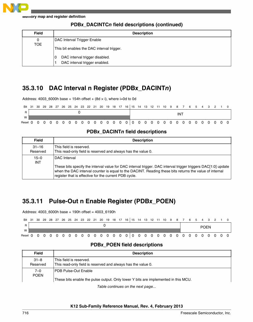
PDBx_DACINTCn field descriptions (continued)
Field Description
0TOE
DAC Interval Trigger Enable
This bit enables the DAC interval trigger.
0 DAC interval trigger disabled.1 DAC interval trigger enabled.
35.3.10 DAC Interval n Register (PDBx_DACINTn)
Address: 4003_6000h base + 154h offset + (8d × i), where i=0d to 0d
Bit 31 30 29 28 27 26 25 24 23 22 21 20 19 18 17 16 15 14 13 12 11 10 9 8 7 6 5 4 3 2 1 0
R 0 INTW
Reset 0 0 0 0 0 0 0 0 0 0 0 0 0 0 0 0 0 0 0 0 0 0 0 0 0 0 0 0 0 0 0 0
PDBx_DACINTn field descriptions
Field Description
31–16Reserved
This field is reserved.This read-only field is reserved and always has the value 0.
15–0INT
DAC Interval
These bits specify the interval value for DAC interval trigger. DAC interval trigger triggers DAC[1:0] updatewhen the DAC interval counter is equal to the DACINT. Reading these bits returns the value of internalregister that is effective for the current PDB cycle.
35.3.11 Pulse-Out n Enable Register (PDBx_POEN)
Address: 4003_6000h base + 190h offset = 4003_6190h
Bit 31 30 29 28 27 26 25 24 23 22 21 20 19 18 17 16 15 14 13 12 11 10 9 8 7 6 5 4 3 2 1 0
R 0 POENW
Reset 0 0 0 0 0 0 0 0 0 0 0 0 0 0 0 0 0 0 0 0 0 0 0 0 0 0 0 0 0 0 0 0
PDBx_POEN field descriptions
Field Description
31–8Reserved
This field is reserved.This read-only field is reserved and always has the value 0.
7–0POEN
PDB Pulse-Out Enable
These bits enable the pulse output. Only lower Y bits are implemented in this MCU.
Table continues on the next page...
Memory map and register definition
K12 Sub-Family Reference Manual, Rev. 4, February 2013
716 Freescale Semiconductor, Inc.
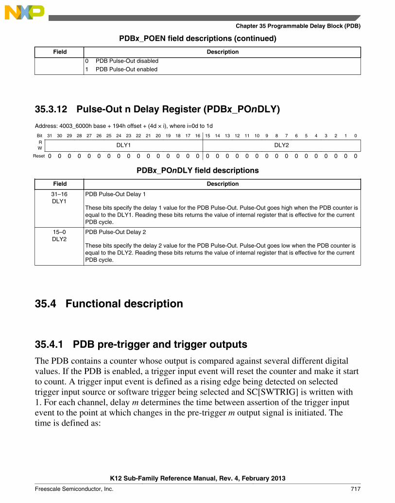
PDBx_POEN field descriptions (continued)
Field Description
0 PDB Pulse-Out disabled1 PDB Pulse-Out enabled
35.3.12 Pulse-Out n Delay Register (PDBx_POnDLY)
Address: 4003_6000h base + 194h offset + (4d × i), where i=0d to 1d
Bit 31 30 29 28 27 26 25 24 23 22 21 20 19 18 17 16 15 14 13 12 11 10 9 8 7 6 5 4 3 2 1 0
R DLY1 DLY2W
Reset 0 0 0 0 0 0 0 0 0 0 0 0 0 0 0 0 0 0 0 0 0 0 0 0 0 0 0 0 0 0 0 0
PDBx_POnDLY field descriptions
Field Description
31–16DLY1
PDB Pulse-Out Delay 1
These bits specify the delay 1 value for the PDB Pulse-Out. Pulse-Out goes high when the PDB counter isequal to the DLY1. Reading these bits returns the value of internal register that is effective for the currentPDB cycle.
15–0DLY2
PDB Pulse-Out Delay 2
These bits specify the delay 2 value for the PDB Pulse-Out. Pulse-Out goes low when the PDB counter isequal to the DLY2. Reading these bits returns the value of internal register that is effective for the currentPDB cycle.
35.4 Functional description
35.4.1 PDB pre-trigger and trigger outputs
The PDB contains a counter whose output is compared against several different digitalvalues. If the PDB is enabled, a trigger input event will reset the counter and make it startto count. A trigger input event is defined as a rising edge being detected on selectedtrigger input source or software trigger being selected and SC[SWTRIG] is written with1. For each channel, delay m determines the time between assertion of the trigger inputevent to the point at which changes in the pre-trigger m output signal is initiated. Thetime is defined as:
Chapter 35 Programmable Delay Block (PDB)
K12 Sub-Family Reference Manual, Rev. 4, February 2013
Freescale Semiconductor, Inc. 717

• Trigger input event to pre-trigger m = (prescaler X multiplication factor X delay m) +2 peripheral clock cycles
• Add one additional peripheral clock cycle to determine the time at which the channeltrigger output change.
Each channel is associated with one ADC block. PDB channel n pre-trigger outputs 0 toM and trigger output is connected to ADC hardware trigger select and hardware triggerinputs. The pre-triggers are used to precondition the ADC block prior to the actualtrigger. The ADC contains M sets of configuration and result registers, allowing it tooperate in a ping-pong fashion, alternating conversions between M different analogsources. The pre-trigger outputs are used to specify which signal will be sampled next.When pre-trigger m is asserted, the ADC conversion is triggered with set m of theconfiguration and result registers.
The waveforms shown in the following diagram illustrate the pre-trigger and triggeroutputs of PDB channel n. The delays can be independently set via the CHnDLYmregisters. And the pre-triggers can be enabled or disabled in CHnC1[EN[m]].
Trigger input event
Ch n pre-trigger 0
Ch n pre-trigger 1
Ch n pre-trigger M
Ch n trigger
... ... ... ...
Figure 35-50. Pre-trigger and trigger outputs
The delay in CHnDLYm register can be optionally bypassed, if CHnC1[TOS[m]] iscleared. In this case, when the trigger input event occurs, the pre-trigger m is assertedafter two peripheral clock cycles.
The PDB can be configured in back-to-back operation. Back-to-back operation enablesthe ADC conversions complete to trigger the next PDB channel pre-trigger and triggeroutputs, so that the ADC conversions can be triggered on next set of configuration andresults registers. When back-to-back is enabled by setting CHnC1[BB[m]], the delay m isignored and the pre-trigger m is asserted two peripheral cycles after the acknowledgmentm is received. The acknowledgment connections in this MCU is described in Back-to-back acknowledgment connections.
Functional description
K12 Sub-Family Reference Manual, Rev. 4, February 2013
718 Freescale Semiconductor, Inc.
When an ADC conversion, which is triggered by one of the pre-triggers from PDBchannel n, is in progress and ADCnSC1[COCO] is not set, a new trigger from PDBchannel n pre-trigger m cannot be accepted by ADCn. Therefore every time when onePDB channel n pre-trigger and trigger output starts an ADC conversion, an internal lockassociated with the corresponding pre-trigger is activated. The lock becomes inactivewhen the corresponding ADCnSC1[COCO] is set, or the corresponding PDB pre-triggeris disabled, or the PDB is disabled. The channel n trigger output is suppressed when anyof the locks of the pre-triggers in channel n is active. If a new pre-trigger m asserts whenthere is active lock in the PDB channel n, a register flag bit, CHnS[ERR[m]], associatedwith the pre-trigger m is set. If SC[PDBEIE] is set, the sequence error interrupt isgenerated. Sequence error is typically happened because the delay m is set too short andthe pre-trigger m asserts before the previously triggered ADC conversion is completed.
When the PDB counter reaches the value set in IDLY register, the SC[PDBIF] flag is set.A PDB interrupt can be generated if SC[PDBIE] is set and SC[DMAEN] is cleared. IfSC[DMAEN] is set, PDB requests a DMA transfer when SC[PDBIF] is set.
The modulus value in MOD register, is used to reset the counter back to zero at the endof the count. If SC[CONT] bit is set, the counter will then resume a new count.Otherwise, the counter operation will cease until the next trigger input event occurs.
35.4.2 PDB trigger input source selection
The PDB has up to 15 trigger input sources, namely Trigger-In 0 to 14. They areconnected to on-chip or off-chip event sources. The PDB can be triggered by softwarethrough the SC[SWTRIG]. SC[TRIGSEL] bits select the active trigger input source orsoftware trigger.
For the trigger input sources implemented in this MCU, see chip configurationinformation.
35.4.3 Pulse-Out's
PDB can generate pulse outputs of configurable width. When PDB counter reaches thevalue set in POyDLY[DLY1], the Pulse-Out goes high; when the counter reachesPOyDLY[DLY2], it goes low. POyDLY[DLY2] can be set either greater or less thanPOyDLY[DLY1].
Because the PDB counter is shared by both ADC pre-trigger/trigger outputs and Pulse-Out generation, they have the same time base.
Chapter 35 Programmable Delay Block (PDB)
K12 Sub-Family Reference Manual, Rev. 4, February 2013
Freescale Semiconductor, Inc. 719
The pulse-out connections implemented in this MCU are described in the device's chipconfiguration details.
35.4.4 Updating the delay registers
The following registers control the timing of the PDB operation; and in some of theapplications, they may need to become effective at the same time.
• PDB Modulus Register (MOD)
• PDB Interrupt Delay Register (IDLY)
• PDB Channel n Delay m Register (CHnDLYm)
• DAC Interval x Register (DACINTx)
• PDB Pulse-Out y Delay Register (POyDLY)
The internal registers of them are buffered and any values written to them are written firstto their buffers. The circumstances that cause their internal registers to be updated withthe values from the buffers are summarized as shown in the table below.
Table 35-52. Circumstances of update to the delay registers
SC[LDMOD] Update to the delay registers
00 The internal registers are loaded with the values from their buffers immediately after 1 is written toSC[LDOK].
01 The PDB counter reaches the MOD register value after 1 is written to SC[LDOK].
10 A trigger input event is detected after 1 is written to SC[LDOK].
11 Either the PDB counter reaches the MOD register value, or a trigger input event is detected, after 1 iswritten to SC[LDOK].
After 1 is written to SC[LDOK], the buffers cannot be written until the values in buffersare loaded into their internal registers. SC[LDOK] is self-cleared when the internalregisters are loaded, so the application code can read it to determine the updates to theinternal registers.
The following diagrams show the cases of the internal registers being updated withSC[LDMOD] is 00 and x1.
Functional description
K12 Sub-Family Reference Manual, Rev. 4, February 2013
720 Freescale Semiconductor, Inc.
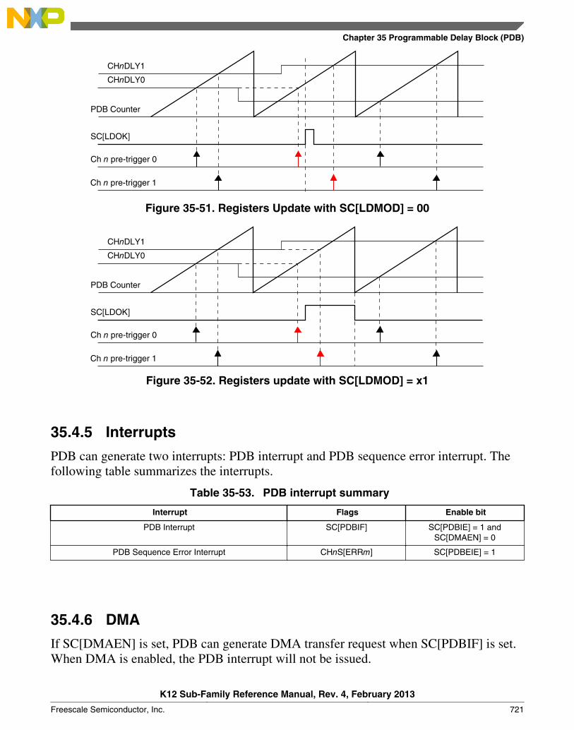
PDB Counter
Ch n pre-trigger 0
Ch n pre-trigger 1
CHnDLY1
CHnDLY0
SC[LDOK]
Figure 35-51. Registers Update with SC[LDMOD] = 00
PDB Counter
Ch n pre-trigger 0
Ch n pre-trigger 1
CHnDLY1
CHnDLY0
SC[LDOK]
Figure 35-52. Registers update with SC[LDMOD] = x1
35.4.5 Interrupts
PDB can generate two interrupts: PDB interrupt and PDB sequence error interrupt. Thefollowing table summarizes the interrupts.
Table 35-53. PDB interrupt summary
Interrupt Flags Enable bit
PDB Interrupt SC[PDBIF] SC[PDBIE] = 1 andSC[DMAEN] = 0
PDB Sequence Error Interrupt CHnS[ERRm] SC[PDBEIE] = 1
35.4.6 DMA
If SC[DMAEN] is set, PDB can generate DMA transfer request when SC[PDBIF] is set.When DMA is enabled, the PDB interrupt will not be issued.
Chapter 35 Programmable Delay Block (PDB)
K12 Sub-Family Reference Manual, Rev. 4, February 2013
Freescale Semiconductor, Inc. 721
35.5 Application information
35.5.1 Impact of using the prescaler and multiplication factor ontiming resolution
Use of prescaler and multiplication factor greater than 1 limits the count/delay accuracyin terms of peripheral clock cycles (to the modulus of the prescaler X multiplicationfactor). If the multiplication factor is set to 1 and the prescaler is set to 2 then the onlyvalues of total peripheral clocks that can be detected are even values; if prescaler is set to4 then the only values of total peripheral clocks that can be decoded as detected aremod(4) and so forth. If the applications need a really long delay value and use 128, thenthe resolution would be limited to 128 peripheral clock cycles.
Therefore, use the lowest possible prescaler and multiplication factor for a givenapplication.
Application information
K12 Sub-Family Reference Manual, Rev. 4, February 2013
722 Freescale Semiconductor, Inc.
Chapter 36FlexTimer Module (FTM)
36.1 IntroductionNOTE
For the chip-specific implementation details of this module'sinstances see the chip configuration information.
The FlexTimer module (FTM) is a two-to-eight channel timer that supports input capture,output compare, and the generation of PWM signals to control electric motor and powermanagement applications. The FTM time reference is a 16-bit counter that can be used asan unsigned or signed counter.
36.1.1 FlexTimer philosophy
The FlexTimer is built upon a simple timer, the HCS08 Timer PWM Module – TPM,used for many years on Freescale's 8-bit microcontrollers. The FlexTimer extends thefunctionality to meet the demands of motor control, digital lighting solutions, and powerconversion, while providing low cost and backwards compatibility with the TPM module.
Several key enhancements are made:
• Signed up counter• Deadtime insertion hardware• Fault control inputs• Enhanced triggering functionality• Initialization and polarity control
All of the features common with the TPM have fully backwards compatible registerassignments. The FlexTimer can also use code on the same core platform without changeto perform the same functions.
K12 Sub-Family Reference Manual, Rev. 4, February 2013
Freescale Semiconductor, Inc. 723

Motor control and power conversion features have been added through a dedicated set ofregisters and defaults turn off all new features. The new features, such as hardwaredeadtime insertion, polarity, fault control, and output forcing and masking, greatly reduceloading on the execution software and are usually each controlled by a group of registers.
FlexTimer input triggers can be from comparators, ADC, or other submodules to initiatetimer functions automatically. These triggers can be linked in a variety of ways duringintegration of the sub modules so please note the options available for used FlexTimerconfiguration.
Several FlexTimers may be synchronized to provide a larger timer with their countersincrementing in unison, assuming the initialization, the input clocks, the initial and finalcounting values are the same in each FlexTimer.
All main user access registers are buffered to ease the load on the executing software. Anumber of trigger options exist to determine which registers are updated with this userdefined data.
36.1.2 Features
The FTM features include:
• FTM source clock is selectable
• Source clock can be the system clock, the fixed frequency clock, or an externalclock
• Fixed frequency clock is an additional clock input to allow the selection of an onchip clock source other than the system clock
• Selecting external clock connects FTM clock to a chip level input pin thereforeallowing to synchronize the FTM counter with an off chip clock source
• Prescaler divide-by 1, 2, 4, 8, 16, 32, 64, or 128
• 16-bit counter
• It can be a free-running counter or a counter with initial and final value
• The counting can be up or up-down
• Each channel can be configured for input capture, output compare, or edge-alignedPWM mode
• In Input Capture mode:
Introduction
K12 Sub-Family Reference Manual, Rev. 4, February 2013
724 Freescale Semiconductor, Inc.
• The capture can occur on rising edges, falling edges or both edges
• An input filter can be selected for some channels
• In Output Compare mode the output signal can be set, cleared, or toggled on match
• All channels can be configured for center-aligned PWM mode
• Each pair of channels can be combined to generate a PWM signal with independentcontrol of both edges of PWM signal
• The FTM channels can operate as pairs with equal outputs, pairs withcomplementary outputs, or independent channels with independent outputs
• The deadtime insertion is available for each complementary pair
• Generation of match triggers
• Software control of PWM outputs
• Up to 4 fault inputs for global fault control
• The polarity of each channel is configurable
• The generation of an interrupt per channel
• The generation of an interrupt when the counter overflows
• The generation of an interrupt when the fault condition is detected
• Synchronized loading of write buffered FTM registers
• Write protection for critical registers
• Backwards compatible with TPM
• Testing of input captures for a stuck at zero and one conditions
• Dual edge capture for pulse and period width measurement
• Quadrature decoder with input filters, relative position counting, and interrupt onposition count or capture of position count on external event
36.1.3 Modes of operation
When the MCU is in an active BDM mode, the FTM temporarily suspends all countinguntil the MCU returns to normal user operating mode. During Stop mode, all FTM inputclocks are stopped, so the FTM is effectively disabled until clocks resume. During Waitmode, the FTM continues to operate normally. If the FTM does not need to produce a
Chapter 36 FlexTimer Module (FTM)
K12 Sub-Family Reference Manual, Rev. 4, February 2013
Freescale Semiconductor, Inc. 725
real time reference or provide the interrupt sources needed to wake the MCU from Waitmode, the power can then be saved by disabling FTM functions before entering Waitmode.
36.1.4 Block diagram
The FTM uses one input/output (I/O) pin per channel, CHn (FTM channel (n)) where n isthe channel number (0–7).
The following figure shows the FTM structure. The central component of the FTM is the16-bit counter with programmable initial and final values and its counting can be up orup-down.
Introduction
K12 Sub-Family Reference Manual, Rev. 4, February 2013
726 Freescale Semiconductor, Inc.
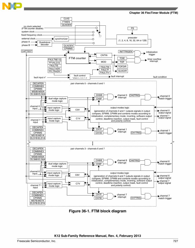
CAPTEST
no clock selected(FTM counter disable)system clock
fixed frequency clock
external clockphase A
phase B
CLKS
FTMENQUADEN
synchronizer
Quadraturedecoder QUADEN
CPWMS
PS
INITTRIGEN
TOIE
TOF
TOFDIR
QUADIR
CNTIN
MOD
FAULTINFAULTF
FAULTFn*
FTM counterFAULTM[1:0]FFVAL[3:0]FAULTIE
FAULTnEN*FFLTRnEN*
fault input n*fault control
*where n = 3, 2, 1, 0
initializationtrigger
timer overflowinterrupt
fault conditionfault interrupt
pair channels 0 - channels 0 and 1DECAPENCOMBINE0
CPWMSMS0B:MS0A
ELS0B:ELS0A
dual edge capturemode logic
input capturemode logic
input capturemode logic
channel 0input
channel 1input
DECAPENCOMBINE0
CPWMSMS1B:MS1A
ELS1B:ELS1A
DECAPENCOMBINE3
CPWMSMS6B:MS6A
ELS6B:ELS6A
channel 6input
channel 7input
DECAPENCOMBINE3
CPWMSMS7B:MS7A
ELS7B:ELS7A
dual edge capturemode logic
input capturemode logic
input capturemode logic
C0V
C1V
C6V
C7V
CH6IE
CH6F
CH1IE
CH0IE
CH7IE
CH7F
CH1F
CH0F
channel 0interrupt
channel 1interrupt
channel 6interrupt
channel 7interrupt channel 7
match trigger
channel 6output signal
channel 6match trigger
channel 1match trigger
channel 0output signal
channel 0match trigger
channel 1output signal
channel 7output signal
CH7TRIG
CH6TRIG
CH1TRIG
CH0TRIG
pair channels 3 - channels 6 and 7
(generation of channels 0 and 1 outputs signals in outputcompare, EPWM, CPWM and combine modes according toinitialization, complementary mode, inverting, software output
control, deadtime insertion, output mask, fault controland polarity control)
output modes logic
(generation of channels 6 and 7 outputs signals in outputcompare, EPWM, CPWM and combine modes according toinitialization, complementary mode, inverting, software output
control, deadtime insertion, output mask, fault controland polarity control)
output modes logic
prescaler(1, 2, 4, 8, 16, 32, 64 or 128)
Figure 36-1. FTM block diagram
Chapter 36 FlexTimer Module (FTM)
K12 Sub-Family Reference Manual, Rev. 4, February 2013
Freescale Semiconductor, Inc. 727
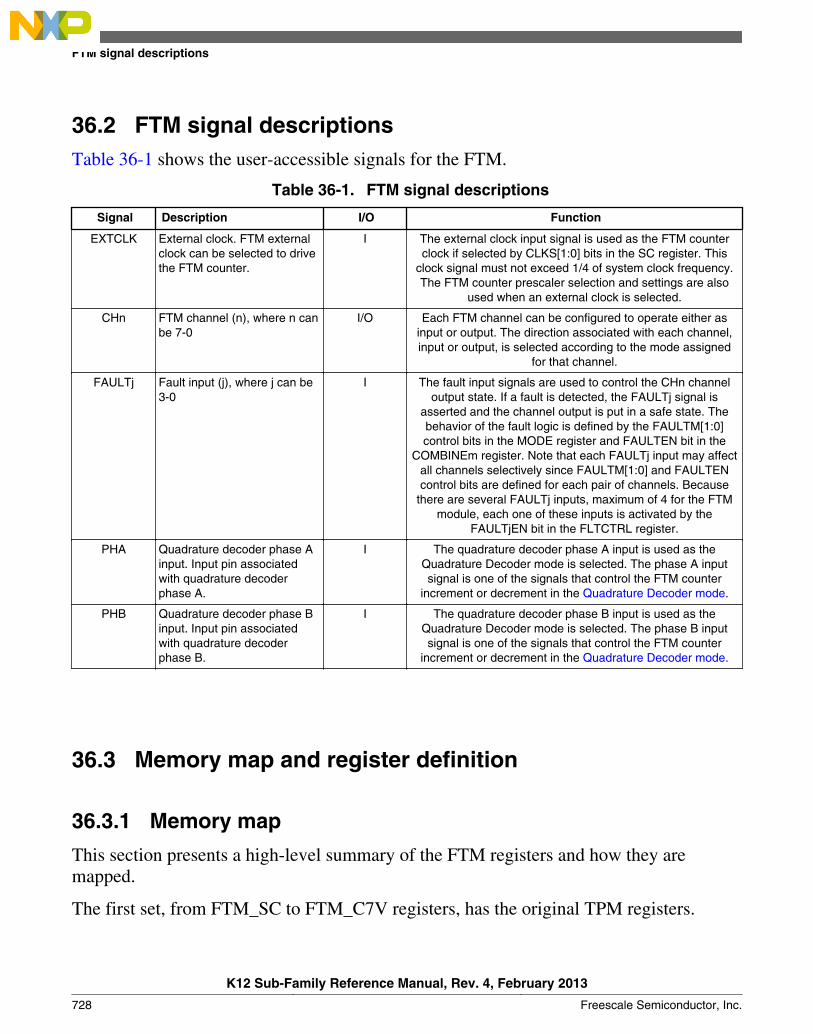
36.2 FTM signal descriptionsTable 36-1 shows the user-accessible signals for the FTM.
Table 36-1. FTM signal descriptions
Signal Description I/O Function
EXTCLK External clock. FTM externalclock can be selected to drivethe FTM counter.
I The external clock input signal is used as the FTM counterclock if selected by CLKS[1:0] bits in the SC register. This
clock signal must not exceed 1/4 of system clock frequency.The FTM counter prescaler selection and settings are also
used when an external clock is selected.
CHn FTM channel (n), where n canbe 7-0
I/O Each FTM channel can be configured to operate either asinput or output. The direction associated with each channel,input or output, is selected according to the mode assigned
for that channel.
FAULTj Fault input (j), where j can be3-0
I The fault input signals are used to control the CHn channeloutput state. If a fault is detected, the FAULTj signal is
asserted and the channel output is put in a safe state. Thebehavior of the fault logic is defined by the FAULTM[1:0]control bits in the MODE register and FAULTEN bit in the
COMBINEm register. Note that each FAULTj input may affectall channels selectively since FAULTM[1:0] and FAULTENcontrol bits are defined for each pair of channels. Because
there are several FAULTj inputs, maximum of 4 for the FTMmodule, each one of these inputs is activated by the
FAULTjEN bit in the FLTCTRL register.
PHA Quadrature decoder phase Ainput. Input pin associatedwith quadrature decoderphase A.
I The quadrature decoder phase A input is used as theQuadrature Decoder mode is selected. The phase A inputsignal is one of the signals that control the FTM counter
increment or decrement in the Quadrature Decoder mode.
PHB Quadrature decoder phase Binput. Input pin associatedwith quadrature decoderphase B.
I The quadrature decoder phase B input is used as theQuadrature Decoder mode is selected. The phase B inputsignal is one of the signals that control the FTM counter
increment or decrement in the Quadrature Decoder mode.
36.3 Memory map and register definition
36.3.1 Memory map
This section presents a high-level summary of the FTM registers and how they aremapped.
The first set, from FTM_SC to FTM_C7V registers, has the original TPM registers.
FTM signal descriptions
K12 Sub-Family Reference Manual, Rev. 4, February 2013
728 Freescale Semiconductor, Inc.
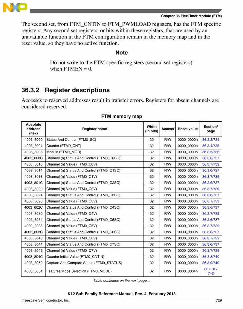
The second set, from FTM_CNTIN to FTM_PWMLOAD registers, has the FTM specificregisters. Any second set registers, or bits within these registers, that are used by anunavailable function in the FTM configuration remain in the memory map and in thereset value, so they have no active function.
Note
Do not write to the FTM specific registers (second set registers)when FTMEN = 0.
36.3.2 Register descriptions
Accesses to reserved addresses result in transfer errors. Registers for absent channels areconsidered reserved.
FTM memory map
Absoluteaddress
(hex)Register name
Width(in bits)
Access Reset valueSection/
page
4003_8000 Status And Control (FTM0_SC) 32 R/W 0000_0000h 36.3.3/734
4003_8004 Counter (FTM0_CNT) 32 R/W 0000_0000h 36.3.4/735
4003_8008 Modulo (FTM0_MOD) 32 R/W 0000_0000h 36.3.5/736
4003_800C Channel (n) Status And Control (FTM0_C0SC) 32 R/W 0000_0000h 36.3.6/737
4003_8010 Channel (n) Value (FTM0_C0V) 32 R/W 0000_0000h 36.3.7/739
4003_8014 Channel (n) Status And Control (FTM0_C1SC) 32 R/W 0000_0000h 36.3.6/737
4003_8018 Channel (n) Value (FTM0_C1V) 32 R/W 0000_0000h 36.3.7/739
4003_801C Channel (n) Status And Control (FTM0_C2SC) 32 R/W 0000_0000h 36.3.6/737
4003_8020 Channel (n) Value (FTM0_C2V) 32 R/W 0000_0000h 36.3.7/739
4003_8024 Channel (n) Status And Control (FTM0_C3SC) 32 R/W 0000_0000h 36.3.6/737
4003_8028 Channel (n) Value (FTM0_C3V) 32 R/W 0000_0000h 36.3.7/739
4003_802C Channel (n) Status And Control (FTM0_C4SC) 32 R/W 0000_0000h 36.3.6/737
4003_8030 Channel (n) Value (FTM0_C4V) 32 R/W 0000_0000h 36.3.7/739
4003_8034 Channel (n) Status And Control (FTM0_C5SC) 32 R/W 0000_0000h 36.3.6/737
4003_8038 Channel (n) Value (FTM0_C5V) 32 R/W 0000_0000h 36.3.7/739
4003_803C Channel (n) Status And Control (FTM0_C6SC) 32 R/W 0000_0000h 36.3.6/737
4003_8040 Channel (n) Value (FTM0_C6V) 32 R/W 0000_0000h 36.3.7/739
4003_8044 Channel (n) Status And Control (FTM0_C7SC) 32 R/W 0000_0000h 36.3.6/737
4003_8048 Channel (n) Value (FTM0_C7V) 32 R/W 0000_0000h 36.3.7/739
4003_804C Counter Initial Value (FTM0_CNTIN) 32 R/W 0000_0000h 36.3.8/740
4003_8050 Capture And Compare Status (FTM0_STATUS) 32 R/W 0000_0000h 36.3.9/740
4003_8054 Features Mode Selection (FTM0_MODE) 32 R/W 0000_0004h36.3.10/
742
Table continues on the next page...
Chapter 36 FlexTimer Module (FTM)
K12 Sub-Family Reference Manual, Rev. 4, February 2013
Freescale Semiconductor, Inc. 729
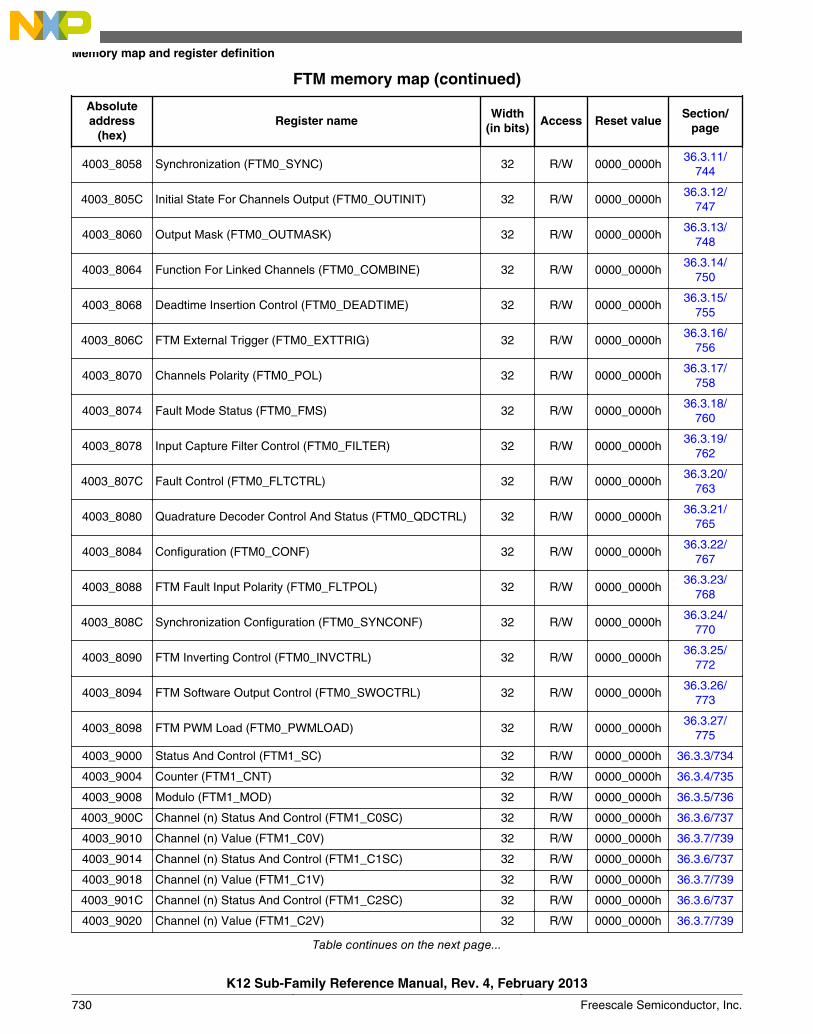
FTM memory map (continued)
Absoluteaddress
(hex)Register name
Width(in bits)
Access Reset valueSection/
page
4003_8058 Synchronization (FTM0_SYNC) 32 R/W 0000_0000h36.3.11/
744
4003_805C Initial State For Channels Output (FTM0_OUTINIT) 32 R/W 0000_0000h36.3.12/
747
4003_8060 Output Mask (FTM0_OUTMASK) 32 R/W 0000_0000h36.3.13/
748
4003_8064 Function For Linked Channels (FTM0_COMBINE) 32 R/W 0000_0000h36.3.14/
750
4003_8068 Deadtime Insertion Control (FTM0_DEADTIME) 32 R/W 0000_0000h36.3.15/
755
4003_806C FTM External Trigger (FTM0_EXTTRIG) 32 R/W 0000_0000h36.3.16/
756
4003_8070 Channels Polarity (FTM0_POL) 32 R/W 0000_0000h36.3.17/
758
4003_8074 Fault Mode Status (FTM0_FMS) 32 R/W 0000_0000h36.3.18/
760
4003_8078 Input Capture Filter Control (FTM0_FILTER) 32 R/W 0000_0000h36.3.19/
762
4003_807C Fault Control (FTM0_FLTCTRL) 32 R/W 0000_0000h36.3.20/
763
4003_8080 Quadrature Decoder Control And Status (FTM0_QDCTRL) 32 R/W 0000_0000h36.3.21/
765
4003_8084 Configuration (FTM0_CONF) 32 R/W 0000_0000h36.3.22/
767
4003_8088 FTM Fault Input Polarity (FTM0_FLTPOL) 32 R/W 0000_0000h36.3.23/
768
4003_808C Synchronization Configuration (FTM0_SYNCONF) 32 R/W 0000_0000h36.3.24/
770
4003_8090 FTM Inverting Control (FTM0_INVCTRL) 32 R/W 0000_0000h36.3.25/
772
4003_8094 FTM Software Output Control (FTM0_SWOCTRL) 32 R/W 0000_0000h36.3.26/
773
4003_8098 FTM PWM Load (FTM0_PWMLOAD) 32 R/W 0000_0000h36.3.27/
775
4003_9000 Status And Control (FTM1_SC) 32 R/W 0000_0000h 36.3.3/734
4003_9004 Counter (FTM1_CNT) 32 R/W 0000_0000h 36.3.4/735
4003_9008 Modulo (FTM1_MOD) 32 R/W 0000_0000h 36.3.5/736
4003_900C Channel (n) Status And Control (FTM1_C0SC) 32 R/W 0000_0000h 36.3.6/737
4003_9010 Channel (n) Value (FTM1_C0V) 32 R/W 0000_0000h 36.3.7/739
4003_9014 Channel (n) Status And Control (FTM1_C1SC) 32 R/W 0000_0000h 36.3.6/737
4003_9018 Channel (n) Value (FTM1_C1V) 32 R/W 0000_0000h 36.3.7/739
4003_901C Channel (n) Status And Control (FTM1_C2SC) 32 R/W 0000_0000h 36.3.6/737
4003_9020 Channel (n) Value (FTM1_C2V) 32 R/W 0000_0000h 36.3.7/739
Table continues on the next page...
Memory map and register definition
K12 Sub-Family Reference Manual, Rev. 4, February 2013
730 Freescale Semiconductor, Inc.
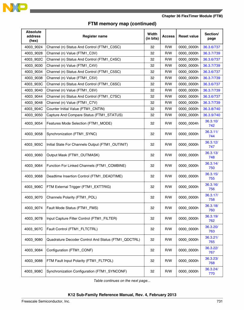
FTM memory map (continued)
Absoluteaddress
(hex)Register name
Width(in bits)
Access Reset valueSection/
page
4003_9024 Channel (n) Status And Control (FTM1_C3SC) 32 R/W 0000_0000h 36.3.6/737
4003_9028 Channel (n) Value (FTM1_C3V) 32 R/W 0000_0000h 36.3.7/739
4003_902C Channel (n) Status And Control (FTM1_C4SC) 32 R/W 0000_0000h 36.3.6/737
4003_9030 Channel (n) Value (FTM1_C4V) 32 R/W 0000_0000h 36.3.7/739
4003_9034 Channel (n) Status And Control (FTM1_C5SC) 32 R/W 0000_0000h 36.3.6/737
4003_9038 Channel (n) Value (FTM1_C5V) 32 R/W 0000_0000h 36.3.7/739
4003_903C Channel (n) Status And Control (FTM1_C6SC) 32 R/W 0000_0000h 36.3.6/737
4003_9040 Channel (n) Value (FTM1_C6V) 32 R/W 0000_0000h 36.3.7/739
4003_9044 Channel (n) Status And Control (FTM1_C7SC) 32 R/W 0000_0000h 36.3.6/737
4003_9048 Channel (n) Value (FTM1_C7V) 32 R/W 0000_0000h 36.3.7/739
4003_904C Counter Initial Value (FTM1_CNTIN) 32 R/W 0000_0000h 36.3.8/740
4003_9050 Capture And Compare Status (FTM1_STATUS) 32 R/W 0000_0000h 36.3.9/740
4003_9054 Features Mode Selection (FTM1_MODE) 32 R/W 0000_0004h36.3.10/
742
4003_9058 Synchronization (FTM1_SYNC) 32 R/W 0000_0000h36.3.11/
744
4003_905C Initial State For Channels Output (FTM1_OUTINIT) 32 R/W 0000_0000h36.3.12/
747
4003_9060 Output Mask (FTM1_OUTMASK) 32 R/W 0000_0000h36.3.13/
748
4003_9064 Function For Linked Channels (FTM1_COMBINE) 32 R/W 0000_0000h36.3.14/
750
4003_9068 Deadtime Insertion Control (FTM1_DEADTIME) 32 R/W 0000_0000h36.3.15/
755
4003_906C FTM External Trigger (FTM1_EXTTRIG) 32 R/W 0000_0000h36.3.16/
756
4003_9070 Channels Polarity (FTM1_POL) 32 R/W 0000_0000h36.3.17/
758
4003_9074 Fault Mode Status (FTM1_FMS) 32 R/W 0000_0000h36.3.18/
760
4003_9078 Input Capture Filter Control (FTM1_FILTER) 32 R/W 0000_0000h36.3.19/
762
4003_907C Fault Control (FTM1_FLTCTRL) 32 R/W 0000_0000h36.3.20/
763
4003_9080 Quadrature Decoder Control And Status (FTM1_QDCTRL) 32 R/W 0000_0000h36.3.21/
765
4003_9084 Configuration (FTM1_CONF) 32 R/W 0000_0000h36.3.22/
767
4003_9088 FTM Fault Input Polarity (FTM1_FLTPOL) 32 R/W 0000_0000h36.3.23/
768
4003_908C Synchronization Configuration (FTM1_SYNCONF) 32 R/W 0000_0000h36.3.24/
770
Table continues on the next page...
Chapter 36 FlexTimer Module (FTM)
K12 Sub-Family Reference Manual, Rev. 4, February 2013
Freescale Semiconductor, Inc. 731

FTM memory map (continued)
Absoluteaddress
(hex)Register name
Width(in bits)
Access Reset valueSection/
page
4003_9090 FTM Inverting Control (FTM1_INVCTRL) 32 R/W 0000_0000h36.3.25/
772
4003_9094 FTM Software Output Control (FTM1_SWOCTRL) 32 R/W 0000_0000h36.3.26/
773
4003_9098 FTM PWM Load (FTM1_PWMLOAD) 32 R/W 0000_0000h36.3.27/
775
4003_A000 Status And Control (FTM2_SC) 32 R/W 0000_0000h 36.3.3/734
4003_A004 Counter (FTM2_CNT) 32 R/W 0000_0000h 36.3.4/735
4003_A008 Modulo (FTM2_MOD) 32 R/W 0000_0000h 36.3.5/736
4003_A00C Channel (n) Status And Control (FTM2_C0SC) 32 R/W 0000_0000h 36.3.6/737
4003_A010 Channel (n) Value (FTM2_C0V) 32 R/W 0000_0000h 36.3.7/739
4003_A014 Channel (n) Status And Control (FTM2_C1SC) 32 R/W 0000_0000h 36.3.6/737
4003_A018 Channel (n) Value (FTM2_C1V) 32 R/W 0000_0000h 36.3.7/739
4003_A01C Channel (n) Status And Control (FTM2_C2SC) 32 R/W 0000_0000h 36.3.6/737
4003_A020 Channel (n) Value (FTM2_C2V) 32 R/W 0000_0000h 36.3.7/739
4003_A024 Channel (n) Status And Control (FTM2_C3SC) 32 R/W 0000_0000h 36.3.6/737
4003_A028 Channel (n) Value (FTM2_C3V) 32 R/W 0000_0000h 36.3.7/739
4003_A02C Channel (n) Status And Control (FTM2_C4SC) 32 R/W 0000_0000h 36.3.6/737
4003_A030 Channel (n) Value (FTM2_C4V) 32 R/W 0000_0000h 36.3.7/739
4003_A034 Channel (n) Status And Control (FTM2_C5SC) 32 R/W 0000_0000h 36.3.6/737
4003_A038 Channel (n) Value (FTM2_C5V) 32 R/W 0000_0000h 36.3.7/739
4003_A03C Channel (n) Status And Control (FTM2_C6SC) 32 R/W 0000_0000h 36.3.6/737
4003_A040 Channel (n) Value (FTM2_C6V) 32 R/W 0000_0000h 36.3.7/739
4003_A044 Channel (n) Status And Control (FTM2_C7SC) 32 R/W 0000_0000h 36.3.6/737
4003_A048 Channel (n) Value (FTM2_C7V) 32 R/W 0000_0000h 36.3.7/739
4003_A04C Counter Initial Value (FTM2_CNTIN) 32 R/W 0000_0000h 36.3.8/740
4003_A050 Capture And Compare Status (FTM2_STATUS) 32 R/W 0000_0000h 36.3.9/740
4003_A054 Features Mode Selection (FTM2_MODE) 32 R/W 0000_0004h36.3.10/
742
4003_A058 Synchronization (FTM2_SYNC) 32 R/W 0000_0000h36.3.11/
744
4003_A05C Initial State For Channels Output (FTM2_OUTINIT) 32 R/W 0000_0000h36.3.12/
747
4003_A060 Output Mask (FTM2_OUTMASK) 32 R/W 0000_0000h36.3.13/
748
4003_A064 Function For Linked Channels (FTM2_COMBINE) 32 R/W 0000_0000h36.3.14/
750
4003_A068 Deadtime Insertion Control (FTM2_DEADTIME) 32 R/W 0000_0000h36.3.15/
755
4003_A06C FTM External Trigger (FTM2_EXTTRIG) 32 R/W 0000_0000h36.3.16/
756
Table continues on the next page...
Memory map and register definition
K12 Sub-Family Reference Manual, Rev. 4, February 2013
732 Freescale Semiconductor, Inc.
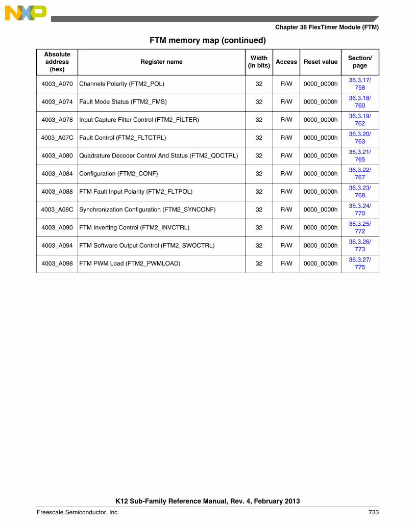
FTM memory map (continued)
Absoluteaddress
(hex)Register name
Width(in bits)
Access Reset valueSection/
page
4003_A070 Channels Polarity (FTM2_POL) 32 R/W 0000_0000h36.3.17/
758
4003_A074 Fault Mode Status (FTM2_FMS) 32 R/W 0000_0000h36.3.18/
760
4003_A078 Input Capture Filter Control (FTM2_FILTER) 32 R/W 0000_0000h36.3.19/
762
4003_A07C Fault Control (FTM2_FLTCTRL) 32 R/W 0000_0000h36.3.20/
763
4003_A080 Quadrature Decoder Control And Status (FTM2_QDCTRL) 32 R/W 0000_0000h36.3.21/
765
4003_A084 Configuration (FTM2_CONF) 32 R/W 0000_0000h36.3.22/
767
4003_A088 FTM Fault Input Polarity (FTM2_FLTPOL) 32 R/W 0000_0000h36.3.23/
768
4003_A08C Synchronization Configuration (FTM2_SYNCONF) 32 R/W 0000_0000h36.3.24/
770
4003_A090 FTM Inverting Control (FTM2_INVCTRL) 32 R/W 0000_0000h36.3.25/
772
4003_A094 FTM Software Output Control (FTM2_SWOCTRL) 32 R/W 0000_0000h36.3.26/
773
4003_A098 FTM PWM Load (FTM2_PWMLOAD) 32 R/W 0000_0000h36.3.27/
775
Chapter 36 FlexTimer Module (FTM)
K12 Sub-Family Reference Manual, Rev. 4, February 2013
Freescale Semiconductor, Inc. 733
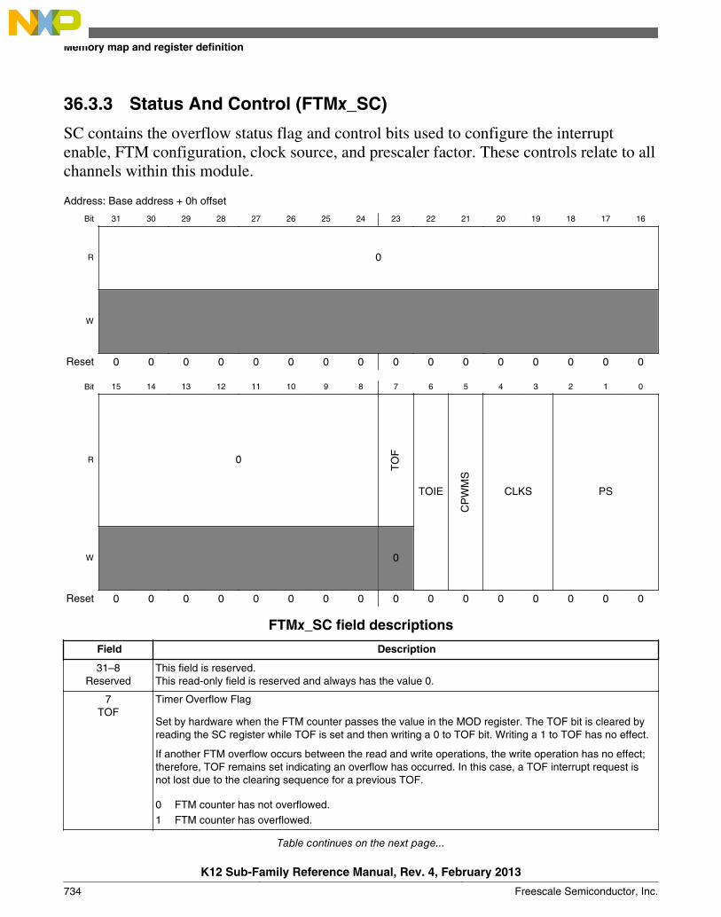
36.3.3 Status And Control (FTMx_SC)
SC contains the overflow status flag and control bits used to configure the interruptenable, FTM configuration, clock source, and prescaler factor. These controls relate to allchannels within this module.
Address: Base address + 0h offset
Bit 31 30 29 28 27 26 25 24 23 22 21 20 19 18 17 16
R 0
W
Reset 0 0 0 0 0 0 0 0 0 0 0 0 0 0 0 0
Bit 15 14 13 12 11 10 9 8 7 6 5 4 3 2 1 0
R 0
TO
F
TOIE
CP
WM
S
CLKS PS
W 0
Reset 0 0 0 0 0 0 0 0 0 0 0 0 0 0 0 0
FTMx_SC field descriptions
Field Description
31–8Reserved
This field is reserved.This read-only field is reserved and always has the value 0.
7TOF
Timer Overflow Flag
Set by hardware when the FTM counter passes the value in the MOD register. The TOF bit is cleared byreading the SC register while TOF is set and then writing a 0 to TOF bit. Writing a 1 to TOF has no effect.
If another FTM overflow occurs between the read and write operations, the write operation has no effect;therefore, TOF remains set indicating an overflow has occurred. In this case, a TOF interrupt request isnot lost due to the clearing sequence for a previous TOF.
0 FTM counter has not overflowed.1 FTM counter has overflowed.
Table continues on the next page...
Memory map and register definition
K12 Sub-Family Reference Manual, Rev. 4, February 2013
734 Freescale Semiconductor, Inc.
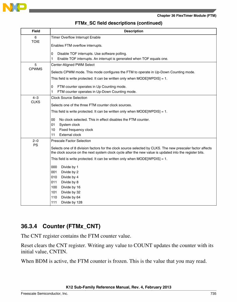
FTMx_SC field descriptions (continued)
Field Description
6TOIE
Timer Overflow Interrupt Enable
Enables FTM overflow interrupts.
0 Disable TOF interrupts. Use software polling.1 Enable TOF interrupts. An interrupt is generated when TOF equals one.
5CPWMS
Center-Aligned PWM Select
Selects CPWM mode. This mode configures the FTM to operate in Up-Down Counting mode.
This field is write protected. It can be written only when MODE[WPDIS] = 1.
0 FTM counter operates in Up Counting mode.1 FTM counter operates in Up-Down Counting mode.
4–3CLKS
Clock Source Selection
Selects one of the three FTM counter clock sources.
This field is write protected. It can be written only when MODE[WPDIS] = 1.
00 No clock selected. This in effect disables the FTM counter.01 System clock10 Fixed frequency clock11 External clock
2–0PS
Prescale Factor Selection
Selects one of 8 division factors for the clock source selected by CLKS. The new prescaler factor affectsthe clock source on the next system clock cycle after the new value is updated into the register bits.
This field is write protected. It can be written only when MODE[WPDIS] = 1.
000 Divide by 1001 Divide by 2010 Divide by 4011 Divide by 8100 Divide by 16101 Divide by 32110 Divide by 64111 Divide by 128
36.3.4 Counter (FTMx_CNT)
The CNT register contains the FTM counter value.
Reset clears the CNT register. Writing any value to COUNT updates the counter with itsinitial value, CNTIN.
When BDM is active, the FTM counter is frozen. This is the value that you may read.
Chapter 36 FlexTimer Module (FTM)
K12 Sub-Family Reference Manual, Rev. 4, February 2013
Freescale Semiconductor, Inc. 735

Address: Base address + 4h offset
Bit 31 30 29 28 27 26 25 24 23 22 21 20 19 18 17 16 15 14 13 12 11 10 9 8 7 6 5 4 3 2 1 0
R 0 COUNTW
Reset 0 0 0 0 0 0 0 0 0 0 0 0 0 0 0 0 0 0 0 0 0 0 0 0 0 0 0 0 0 0 0 0
FTMx_CNT field descriptions
Field Description
31–16Reserved
This field is reserved.This read-only field is reserved and always has the value 0.
15–0COUNT
Counter Value
36.3.5 Modulo (FTMx_MOD)
The Modulo register contains the modulo value for the FTM counter. After the FTMcounter reaches the modulo value, the overflow flag (TOF) becomes set at the next clock,and the next value of FTM counter depends on the selected counting method; seeCounter.
Writing to the MOD register latches the value into a buffer. The MOD register is updatedwith the value of its write buffer according to Registers updated from write buffers.
If FTMEN = 0, this write coherency mechanism may be manually reset by writing to theSC register whether BDM is active or not.
Initialize the FTM counter, by writing to CNT, before writing to the MOD register toavoid confusion about when the first counter overflow will occur.
Address: Base address + 8h offset
Bit 31 30 29 28 27 26 25 24 23 22 21 20 19 18 17 16 15 14 13 12 11 10 9 8 7 6 5 4 3 2 1 0
R Reserved MODW
Reset 0 0 0 0 0 0 0 0 0 0 0 0 0 0 0 0 0 0 0 0 0 0 0 0 0 0 0 0 0 0 0 0
FTMx_MOD field descriptions
Field Description
31–16Reserved
This field is reserved.
15–0MOD
Modulo Value
Memory map and register definition
K12 Sub-Family Reference Manual, Rev. 4, February 2013
736 Freescale Semiconductor, Inc.
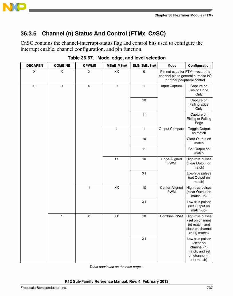
36.3.6 Channel (n) Status And Control (FTMx_CnSC)
CnSC contains the channel-interrupt-status flag and control bits used to configure theinterrupt enable, channel configuration, and pin function.
Table 36-67. Mode, edge, and level selection
DECAPEN COMBINE CPWMS MSnB:MSnA ELSnB:ELSnA Mode Configuration
X X X XX 0 Pin not used for FTM—revert thechannel pin to general purpose I/O
or other peripheral control
0 0 0 0 1 Input Capture Capture onRising Edge
Only
10 Capture onFalling Edge
Only
11 Capture onRising or Falling
Edge
1 1 Output Compare Toggle Outputon match
10 Clear Output onmatch
11 Set Output onmatch
1X 10 Edge-AlignedPWM
High-true pulses(clear Output on
match)
X1 Low-true pulses(set Output on
match)
1 XX 10 Center-AlignedPWM
High-true pulses(clear Output on
match-up)
X1 Low-true pulses(set Output on
match-up)
1 0 XX 10 Combine PWM High-true pulses(set on channel(n) match, and
clear on channel(n+1) match)
X1 Low-true pulses(clear on
channel (n)match, and seton channel (n
+1) match)
Table continues on the next page...
Chapter 36 FlexTimer Module (FTM)
K12 Sub-Family Reference Manual, Rev. 4, February 2013
Freescale Semiconductor, Inc. 737
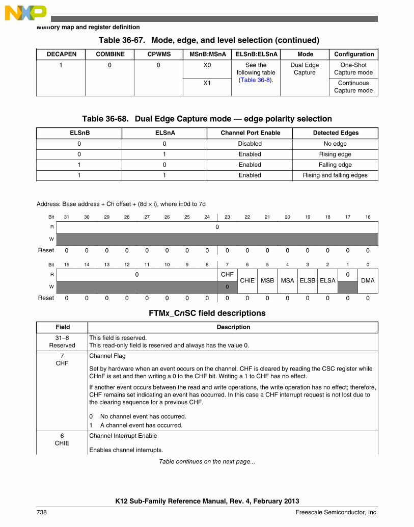
Table 36-67. Mode, edge, and level selection (continued)
DECAPEN COMBINE CPWMS MSnB:MSnA ELSnB:ELSnA Mode Configuration
1 0 0 X0 See thefollowing table(Table 36-8).
Dual EdgeCapture
One-ShotCapture mode
X1 ContinuousCapture mode
Table 36-68. Dual Edge Capture mode — edge polarity selection
ELSnB ELSnA Channel Port Enable Detected Edges
0 0 Disabled No edge
0 1 Enabled Rising edge
1 0 Enabled Falling edge
1 1 Enabled Rising and falling edges
Address: Base address + Ch offset + (8d × i), where i=0d to 7d
Bit 31 30 29 28 27 26 25 24 23 22 21 20 19 18 17 16
R 0
W
Reset 0 0 0 0 0 0 0 0 0 0 0 0 0 0 0 0
Bit 15 14 13 12 11 10 9 8 7 6 5 4 3 2 1 0
R 0 CHFCHIE MSB MSA ELSB ELSA
0DMA
W 0
Reset 0 0 0 0 0 0 0 0 0 0 0 0 0 0 0 0
FTMx_CnSC field descriptions
Field Description
31–8Reserved
This field is reserved.This read-only field is reserved and always has the value 0.
7CHF
Channel Flag
Set by hardware when an event occurs on the channel. CHF is cleared by reading the CSC register whileCHnF is set and then writing a 0 to the CHF bit. Writing a 1 to CHF has no effect.
If another event occurs between the read and write operations, the write operation has no effect; therefore,CHF remains set indicating an event has occurred. In this case a CHF interrupt request is not lost due tothe clearing sequence for a previous CHF.
0 No channel event has occurred.1 A channel event has occurred.
6CHIE
Channel Interrupt Enable
Enables channel interrupts.
Table continues on the next page...
Memory map and register definition
K12 Sub-Family Reference Manual, Rev. 4, February 2013
738 Freescale Semiconductor, Inc.
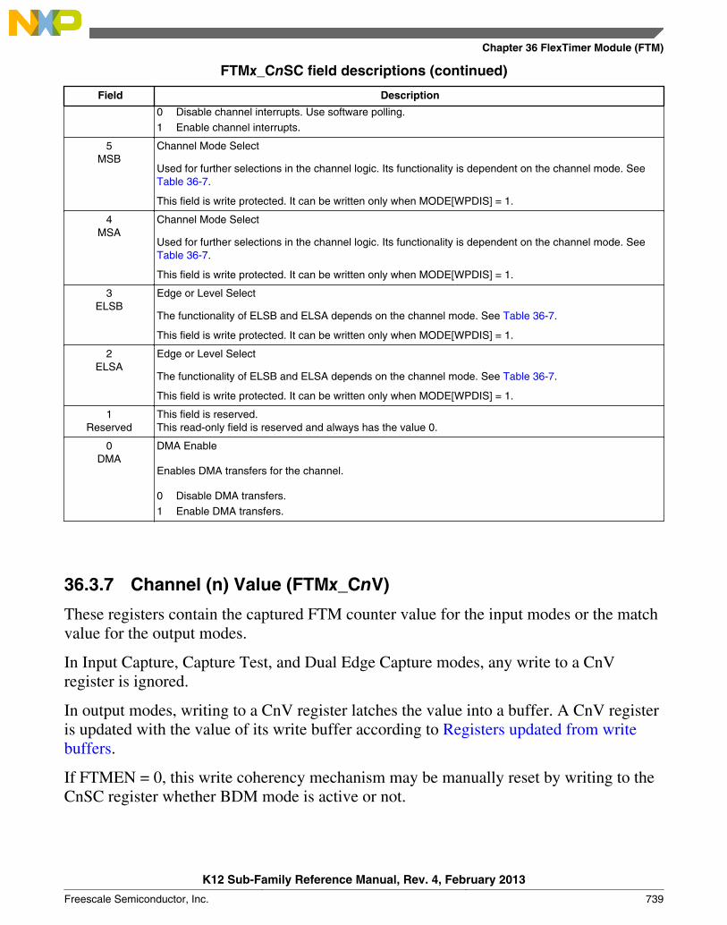
FTMx_CnSC field descriptions (continued)
Field Description
0 Disable channel interrupts. Use software polling.1 Enable channel interrupts.
5MSB
Channel Mode Select
Used for further selections in the channel logic. Its functionality is dependent on the channel mode. SeeTable 36-7.
This field is write protected. It can be written only when MODE[WPDIS] = 1.
4MSA
Channel Mode Select
Used for further selections in the channel logic. Its functionality is dependent on the channel mode. SeeTable 36-7.
This field is write protected. It can be written only when MODE[WPDIS] = 1.
3ELSB
Edge or Level Select
The functionality of ELSB and ELSA depends on the channel mode. See Table 36-7.
This field is write protected. It can be written only when MODE[WPDIS] = 1.
2ELSA
Edge or Level Select
The functionality of ELSB and ELSA depends on the channel mode. See Table 36-7.
This field is write protected. It can be written only when MODE[WPDIS] = 1.
1Reserved
This field is reserved.This read-only field is reserved and always has the value 0.
0DMA
DMA Enable
Enables DMA transfers for the channel.
0 Disable DMA transfers.1 Enable DMA transfers.
36.3.7 Channel (n) Value (FTMx_CnV)
These registers contain the captured FTM counter value for the input modes or the matchvalue for the output modes.
In Input Capture, Capture Test, and Dual Edge Capture modes, any write to a CnVregister is ignored.
In output modes, writing to a CnV register latches the value into a buffer. A CnV registeris updated with the value of its write buffer according to Registers updated from writebuffers.
If FTMEN = 0, this write coherency mechanism may be manually reset by writing to theCnSC register whether BDM mode is active or not.
Chapter 36 FlexTimer Module (FTM)
K12 Sub-Family Reference Manual, Rev. 4, February 2013
Freescale Semiconductor, Inc. 739

Address: Base address + 10h offset + (8d × i), where i=0d to 7d
Bit 31 30 29 28 27 26 25 24 23 22 21 20 19 18 17 16 15 14 13 12 11 10 9 8 7 6 5 4 3 2 1 0
R 0 VALW
Reset 0 0 0 0 0 0 0 0 0 0 0 0 0 0 0 0 0 0 0 0 0 0 0 0 0 0 0 0 0 0 0 0
FTMx_CnV field descriptions
Field Description
31–16Reserved
This field is reserved.This read-only field is reserved and always has the value 0.
15–0VAL
Channel Value
Captured FTM counter value of the input modes or the match value for the output modes
36.3.8 Counter Initial Value (FTMx_CNTIN)
The Counter Initial Value register contains the initial value for the FTM counter.
Writing to the CNTIN register latches the value into a buffer. The CNTIN register isupdated with the value of its write buffer according to Registers updated from writebuffers.
When the FTM clock is initially selected, by writing a non-zero value to the CLKS bits,the FTM counter starts with the value 0x0000. To avoid this behavior, before the firstwrite to select the FTM clock, write the new value to the the CNTIN register and theninitialize the FTM counter by writing any value to the CNT register.
Address: Base address + 4Ch offset
Bit 31 30 29 28 27 26 25 24 23 22 21 20 19 18 17 16 15 14 13 12 11 10 9 8 7 6 5 4 3 2 1 0
R Reserved INITW
Reset 0 0 0 0 0 0 0 0 0 0 0 0 0 0 0 0 0 0 0 0 0 0 0 0 0 0 0 0 0 0 0 0
FTMx_CNTIN field descriptions
Field Description
31–16Reserved
This field is reserved.
15–0INIT
Initial Value Of The FTM Counter
36.3.9 Capture And Compare Status (FTMx_STATUS)
The STATUS register contains a copy of the status flag CHnF bit in CnSC for each FTMchannel for software convenience.
Memory map and register definition
K12 Sub-Family Reference Manual, Rev. 4, February 2013
740 Freescale Semiconductor, Inc.
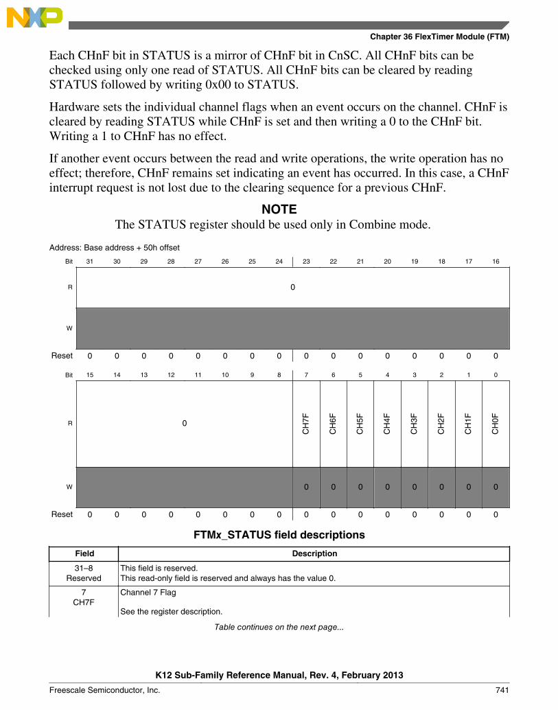
Each CHnF bit in STATUS is a mirror of CHnF bit in CnSC. All CHnF bits can bechecked using only one read of STATUS. All CHnF bits can be cleared by readingSTATUS followed by writing 0x00 to STATUS.
Hardware sets the individual channel flags when an event occurs on the channel. CHnF iscleared by reading STATUS while CHnF is set and then writing a 0 to the CHnF bit.Writing a 1 to CHnF has no effect.
If another event occurs between the read and write operations, the write operation has noeffect; therefore, CHnF remains set indicating an event has occurred. In this case, a CHnFinterrupt request is not lost due to the clearing sequence for a previous CHnF.
NOTEThe STATUS register should be used only in Combine mode.
Address: Base address + 50h offset
Bit 31 30 29 28 27 26 25 24 23 22 21 20 19 18 17 16
R 0
W
Reset 0 0 0 0 0 0 0 0 0 0 0 0 0 0 0 0
Bit 15 14 13 12 11 10 9 8 7 6 5 4 3 2 1 0
R 0
CH
7F
CH
6F
CH
5F
CH
4F
CH
3F
CH
2F
CH
1F
CH
0FW 0 0 0 0 0 0 0 0
Reset 0 0 0 0 0 0 0 0 0 0 0 0 0 0 0 0
FTMx_STATUS field descriptions
Field Description
31–8Reserved
This field is reserved.This read-only field is reserved and always has the value 0.
7CH7F
Channel 7 Flag
See the register description.
Table continues on the next page...
Chapter 36 FlexTimer Module (FTM)
K12 Sub-Family Reference Manual, Rev. 4, February 2013
Freescale Semiconductor, Inc. 741
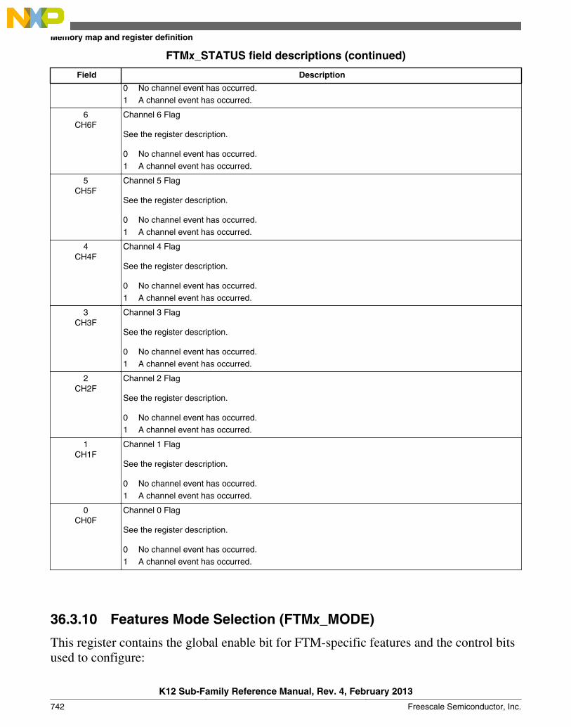
FTMx_STATUS field descriptions (continued)
Field Description
0 No channel event has occurred.1 A channel event has occurred.
6CH6F
Channel 6 Flag
See the register description.
0 No channel event has occurred.1 A channel event has occurred.
5CH5F
Channel 5 Flag
See the register description.
0 No channel event has occurred.1 A channel event has occurred.
4CH4F
Channel 4 Flag
See the register description.
0 No channel event has occurred.1 A channel event has occurred.
3CH3F
Channel 3 Flag
See the register description.
0 No channel event has occurred.1 A channel event has occurred.
2CH2F
Channel 2 Flag
See the register description.
0 No channel event has occurred.1 A channel event has occurred.
1CH1F
Channel 1 Flag
See the register description.
0 No channel event has occurred.1 A channel event has occurred.
0CH0F
Channel 0 Flag
See the register description.
0 No channel event has occurred.1 A channel event has occurred.
36.3.10 Features Mode Selection (FTMx_MODE)
This register contains the global enable bit for FTM-specific features and the control bitsused to configure:
Memory map and register definition
K12 Sub-Family Reference Manual, Rev. 4, February 2013
742 Freescale Semiconductor, Inc.
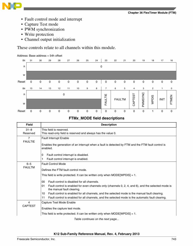
• Fault control mode and interrupt• Capture Test mode• PWM synchronization• Write protection• Channel output initialization
These controls relate to all channels within this module.
Address: Base address + 54h offset
Bit 31 30 29 28 27 26 25 24 23 22 21 20 19 18 17 16
R 0
W
Reset 0 0 0 0 0 0 0 0 0 0 0 0 0 0 0 0
Bit 15 14 13 12 11 10 9 8 7 6 5 4 3 2 1 0
R 0
FA
ULT
IE
FAULTM
CA
PT
ES
T
PW
MS
YN
C
WP
DIS
INIT
FT
ME
N
W
Reset 0 0 0 0 0 0 0 0 0 0 0 0 0 1 0 0
FTMx_MODE field descriptions
Field Description
31–8Reserved
This field is reserved.This read-only field is reserved and always has the value 0.
7FAULTIE
Fault Interrupt Enable
Enables the generation of an interrupt when a fault is detected by FTM and the FTM fault control isenabled.
0 Fault control interrupt is disabled.1 Fault control interrupt is enabled.
6–5FAULTM
Fault Control Mode
Defines the FTM fault control mode.
This field is write protected. It can be written only when MODE[WPDIS] = 1.
00 Fault control is disabled for all channels.01 Fault control is enabled for even channels only (channels 0, 2, 4, and 6), and the selected mode is
the manual fault clearing.10 Fault control is enabled for all channels, and the selected mode is the manual fault clearing.11 Fault control is enabled for all channels, and the selected mode is the automatic fault clearing.
4CAPTEST
Capture Test Mode Enable
Enables the capture test mode.
This field is write protected. It can be written only when MODE[WPDIS] = 1.
Table continues on the next page...
Chapter 36 FlexTimer Module (FTM)
K12 Sub-Family Reference Manual, Rev. 4, February 2013
Freescale Semiconductor, Inc. 743
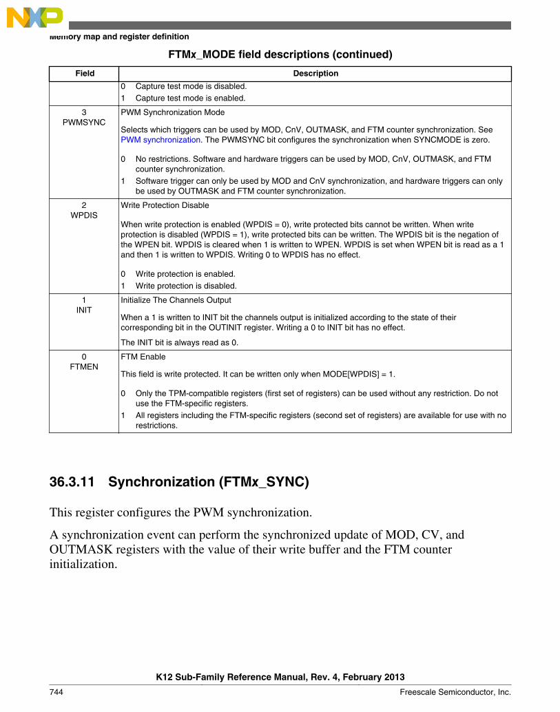
FTMx_MODE field descriptions (continued)
Field Description
0 Capture test mode is disabled.1 Capture test mode is enabled.
3PWMSYNC
PWM Synchronization Mode
Selects which triggers can be used by MOD, CnV, OUTMASK, and FTM counter synchronization. SeePWM synchronization. The PWMSYNC bit configures the synchronization when SYNCMODE is zero.
0 No restrictions. Software and hardware triggers can be used by MOD, CnV, OUTMASK, and FTMcounter synchronization.
1 Software trigger can only be used by MOD and CnV synchronization, and hardware triggers can onlybe used by OUTMASK and FTM counter synchronization.
2WPDIS
Write Protection Disable
When write protection is enabled (WPDIS = 0), write protected bits cannot be written. When writeprotection is disabled (WPDIS = 1), write protected bits can be written. The WPDIS bit is the negation ofthe WPEN bit. WPDIS is cleared when 1 is written to WPEN. WPDIS is set when WPEN bit is read as a 1and then 1 is written to WPDIS. Writing 0 to WPDIS has no effect.
0 Write protection is enabled.1 Write protection is disabled.
1INIT
Initialize The Channels Output
When a 1 is written to INIT bit the channels output is initialized according to the state of theircorresponding bit in the OUTINIT register. Writing a 0 to INIT bit has no effect.
The INIT bit is always read as 0.
0FTMEN
FTM Enable
This field is write protected. It can be written only when MODE[WPDIS] = 1.
0 Only the TPM-compatible registers (first set of registers) can be used without any restriction. Do notuse the FTM-specific registers.
1 All registers including the FTM-specific registers (second set of registers) are available for use with norestrictions.
36.3.11 Synchronization (FTMx_SYNC)
This register configures the PWM synchronization.
A synchronization event can perform the synchronized update of MOD, CV, andOUTMASK registers with the value of their write buffer and the FTM counterinitialization.
Memory map and register definition
K12 Sub-Family Reference Manual, Rev. 4, February 2013
744 Freescale Semiconductor, Inc.
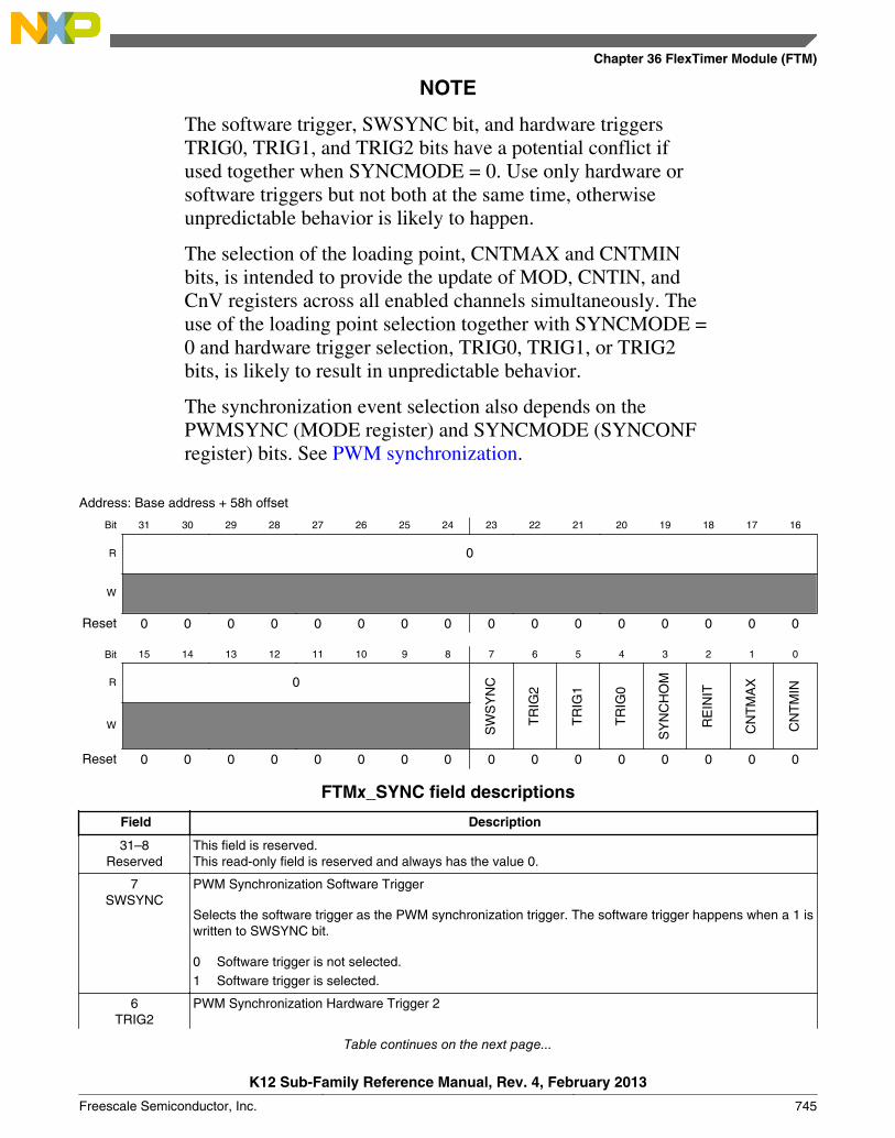
NOTE
The software trigger, SWSYNC bit, and hardware triggersTRIG0, TRIG1, and TRIG2 bits have a potential conflict ifused together when SYNCMODE = 0. Use only hardware orsoftware triggers but not both at the same time, otherwiseunpredictable behavior is likely to happen.
The selection of the loading point, CNTMAX and CNTMINbits, is intended to provide the update of MOD, CNTIN, andCnV registers across all enabled channels simultaneously. Theuse of the loading point selection together with SYNCMODE =0 and hardware trigger selection, TRIG0, TRIG1, or TRIG2bits, is likely to result in unpredictable behavior.
The synchronization event selection also depends on thePWMSYNC (MODE register) and SYNCMODE (SYNCONFregister) bits. See PWM synchronization.
Address: Base address + 58h offset
Bit 31 30 29 28 27 26 25 24 23 22 21 20 19 18 17 16
R 0
W
Reset 0 0 0 0 0 0 0 0 0 0 0 0 0 0 0 0
Bit 15 14 13 12 11 10 9 8 7 6 5 4 3 2 1 0
R 0
SW
SY
NC
TR
IG2
TR
IG1
TR
IG0
SY
NC
HO
M
RE
INIT
CN
TM
AX
CN
TM
IN
W
Reset 0 0 0 0 0 0 0 0 0 0 0 0 0 0 0 0
FTMx_SYNC field descriptions
Field Description
31–8Reserved
This field is reserved.This read-only field is reserved and always has the value 0.
7SWSYNC
PWM Synchronization Software Trigger
Selects the software trigger as the PWM synchronization trigger. The software trigger happens when a 1 iswritten to SWSYNC bit.
0 Software trigger is not selected.1 Software trigger is selected.
6TRIG2
PWM Synchronization Hardware Trigger 2
Table continues on the next page...
Chapter 36 FlexTimer Module (FTM)
K12 Sub-Family Reference Manual, Rev. 4, February 2013
Freescale Semiconductor, Inc. 745
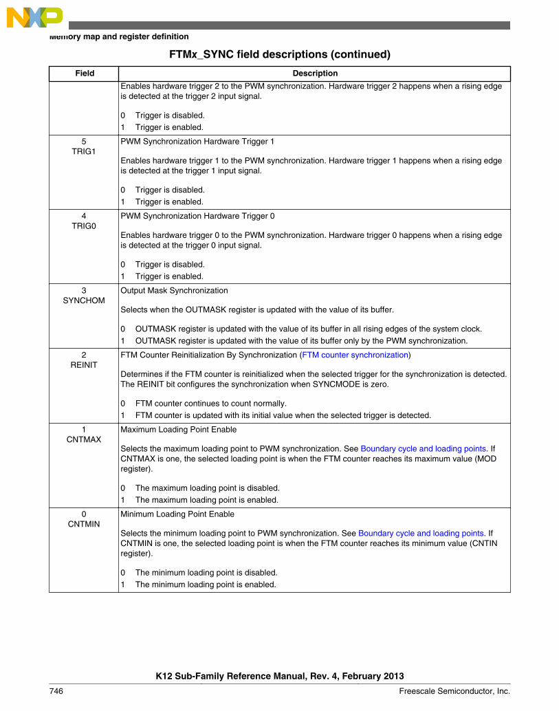
FTMx_SYNC field descriptions (continued)
Field Description
Enables hardware trigger 2 to the PWM synchronization. Hardware trigger 2 happens when a rising edgeis detected at the trigger 2 input signal.
0 Trigger is disabled.1 Trigger is enabled.
5TRIG1
PWM Synchronization Hardware Trigger 1
Enables hardware trigger 1 to the PWM synchronization. Hardware trigger 1 happens when a rising edgeis detected at the trigger 1 input signal.
0 Trigger is disabled.1 Trigger is enabled.
4TRIG0
PWM Synchronization Hardware Trigger 0
Enables hardware trigger 0 to the PWM synchronization. Hardware trigger 0 happens when a rising edgeis detected at the trigger 0 input signal.
0 Trigger is disabled.1 Trigger is enabled.
3SYNCHOM
Output Mask Synchronization
Selects when the OUTMASK register is updated with the value of its buffer.
0 OUTMASK register is updated with the value of its buffer in all rising edges of the system clock.1 OUTMASK register is updated with the value of its buffer only by the PWM synchronization.
2REINIT
FTM Counter Reinitialization By Synchronization (FTM counter synchronization)
Determines if the FTM counter is reinitialized when the selected trigger for the synchronization is detected.The REINIT bit configures the synchronization when SYNCMODE is zero.
0 FTM counter continues to count normally.1 FTM counter is updated with its initial value when the selected trigger is detected.
1CNTMAX
Maximum Loading Point Enable
Selects the maximum loading point to PWM synchronization. See Boundary cycle and loading points. IfCNTMAX is one, the selected loading point is when the FTM counter reaches its maximum value (MODregister).
0 The maximum loading point is disabled.1 The maximum loading point is enabled.
0CNTMIN
Minimum Loading Point Enable
Selects the minimum loading point to PWM synchronization. See Boundary cycle and loading points. IfCNTMIN is one, the selected loading point is when the FTM counter reaches its minimum value (CNTINregister).
0 The minimum loading point is disabled.1 The minimum loading point is enabled.
Memory map and register definition
K12 Sub-Family Reference Manual, Rev. 4, February 2013
746 Freescale Semiconductor, Inc.
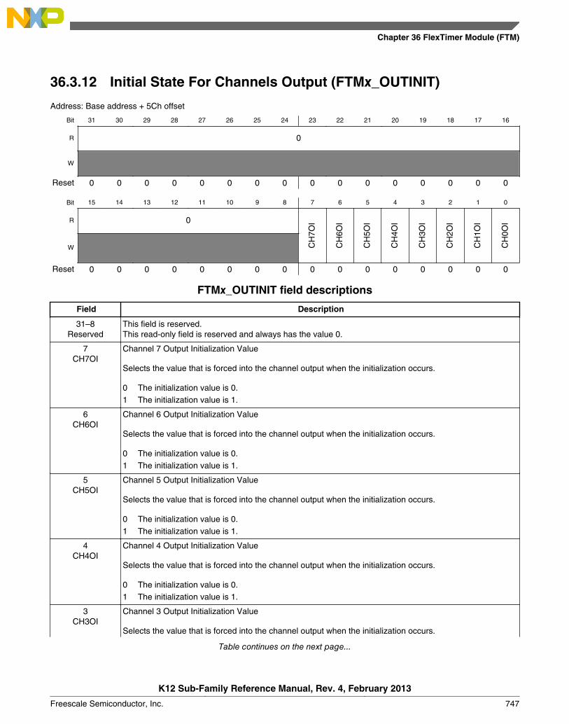
36.3.12 Initial State For Channels Output (FTMx_OUTINIT)
Address: Base address + 5Ch offset
Bit 31 30 29 28 27 26 25 24 23 22 21 20 19 18 17 16
R 0
W
Reset 0 0 0 0 0 0 0 0 0 0 0 0 0 0 0 0
Bit 15 14 13 12 11 10 9 8 7 6 5 4 3 2 1 0
R 0
CH
7OI
CH
6OI
CH
5OI
CH
4OI
CH
3OI
CH
2OI
CH
1OI
CH
0OI
W
Reset 0 0 0 0 0 0 0 0 0 0 0 0 0 0 0 0
FTMx_OUTINIT field descriptions
Field Description
31–8Reserved
This field is reserved.This read-only field is reserved and always has the value 0.
7CH7OI
Channel 7 Output Initialization Value
Selects the value that is forced into the channel output when the initialization occurs.
0 The initialization value is 0.1 The initialization value is 1.
6CH6OI
Channel 6 Output Initialization Value
Selects the value that is forced into the channel output when the initialization occurs.
0 The initialization value is 0.1 The initialization value is 1.
5CH5OI
Channel 5 Output Initialization Value
Selects the value that is forced into the channel output when the initialization occurs.
0 The initialization value is 0.1 The initialization value is 1.
4CH4OI
Channel 4 Output Initialization Value
Selects the value that is forced into the channel output when the initialization occurs.
0 The initialization value is 0.1 The initialization value is 1.
3CH3OI
Channel 3 Output Initialization Value
Selects the value that is forced into the channel output when the initialization occurs.
Table continues on the next page...
Chapter 36 FlexTimer Module (FTM)
K12 Sub-Family Reference Manual, Rev. 4, February 2013
Freescale Semiconductor, Inc. 747
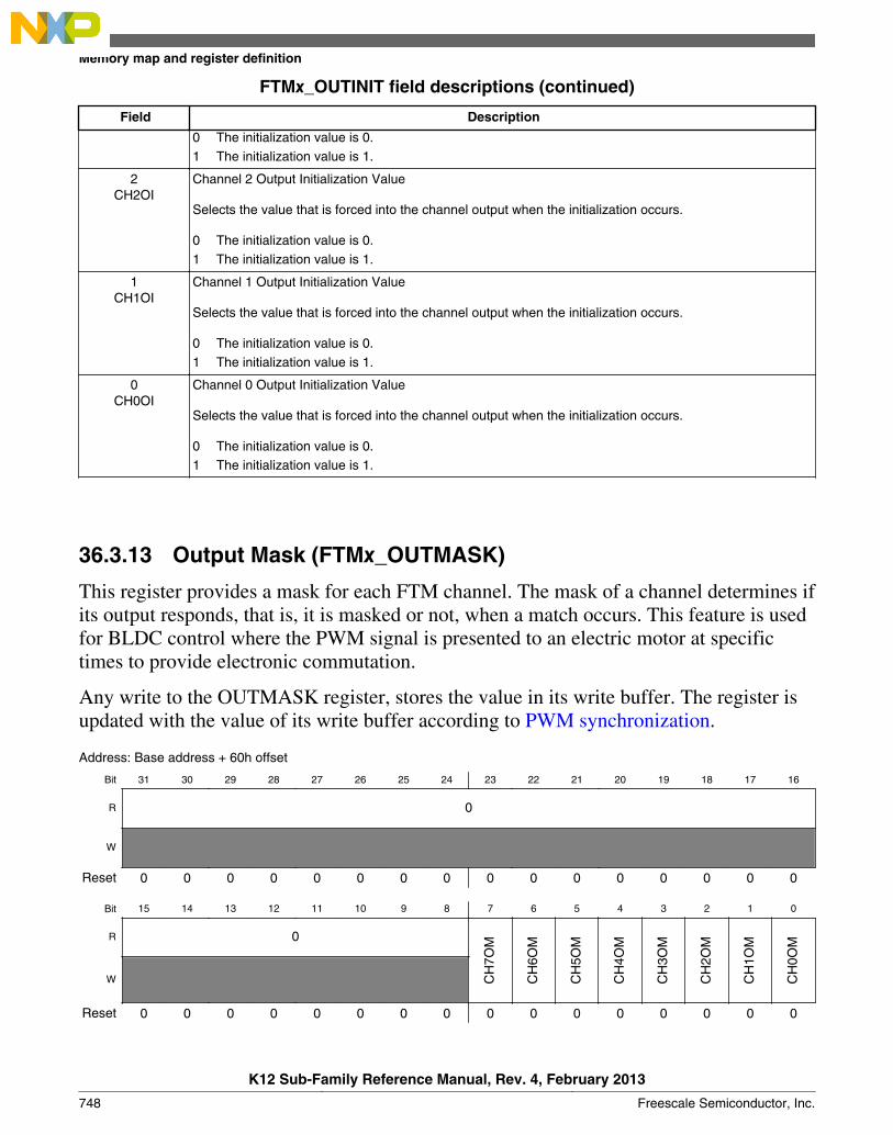
FTMx_OUTINIT field descriptions (continued)
Field Description
0 The initialization value is 0.1 The initialization value is 1.
2CH2OI
Channel 2 Output Initialization Value
Selects the value that is forced into the channel output when the initialization occurs.
0 The initialization value is 0.1 The initialization value is 1.
1CH1OI
Channel 1 Output Initialization Value
Selects the value that is forced into the channel output when the initialization occurs.
0 The initialization value is 0.1 The initialization value is 1.
0CH0OI
Channel 0 Output Initialization Value
Selects the value that is forced into the channel output when the initialization occurs.
0 The initialization value is 0.1 The initialization value is 1.
36.3.13 Output Mask (FTMx_OUTMASK)
This register provides a mask for each FTM channel. The mask of a channel determines ifits output responds, that is, it is masked or not, when a match occurs. This feature is usedfor BLDC control where the PWM signal is presented to an electric motor at specifictimes to provide electronic commutation.
Any write to the OUTMASK register, stores the value in its write buffer. The register isupdated with the value of its write buffer according to PWM synchronization.
Address: Base address + 60h offset
Bit 31 30 29 28 27 26 25 24 23 22 21 20 19 18 17 16
R 0
W
Reset 0 0 0 0 0 0 0 0 0 0 0 0 0 0 0 0
Bit 15 14 13 12 11 10 9 8 7 6 5 4 3 2 1 0
R 0
CH
7OM
CH
6OM
CH
5OM
CH
4OM
CH
3OM
CH
2OM
CH
1OM
CH
0OM
W
Reset 0 0 0 0 0 0 0 0 0 0 0 0 0 0 0 0
Memory map and register definition
K12 Sub-Family Reference Manual, Rev. 4, February 2013
748 Freescale Semiconductor, Inc.
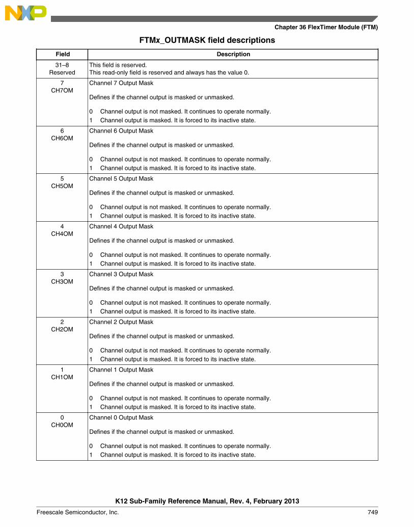
FTMx_OUTMASK field descriptions
Field Description
31–8Reserved
This field is reserved.This read-only field is reserved and always has the value 0.
7CH7OM
Channel 7 Output Mask
Defines if the channel output is masked or unmasked.
0 Channel output is not masked. It continues to operate normally.1 Channel output is masked. It is forced to its inactive state.
6CH6OM
Channel 6 Output Mask
Defines if the channel output is masked or unmasked.
0 Channel output is not masked. It continues to operate normally.1 Channel output is masked. It is forced to its inactive state.
5CH5OM
Channel 5 Output Mask
Defines if the channel output is masked or unmasked.
0 Channel output is not masked. It continues to operate normally.1 Channel output is masked. It is forced to its inactive state.
4CH4OM
Channel 4 Output Mask
Defines if the channel output is masked or unmasked.
0 Channel output is not masked. It continues to operate normally.1 Channel output is masked. It is forced to its inactive state.
3CH3OM
Channel 3 Output Mask
Defines if the channel output is masked or unmasked.
0 Channel output is not masked. It continues to operate normally.1 Channel output is masked. It is forced to its inactive state.
2CH2OM
Channel 2 Output Mask
Defines if the channel output is masked or unmasked.
0 Channel output is not masked. It continues to operate normally.1 Channel output is masked. It is forced to its inactive state.
1CH1OM
Channel 1 Output Mask
Defines if the channel output is masked or unmasked.
0 Channel output is not masked. It continues to operate normally.1 Channel output is masked. It is forced to its inactive state.
0CH0OM
Channel 0 Output Mask
Defines if the channel output is masked or unmasked.
0 Channel output is not masked. It continues to operate normally.1 Channel output is masked. It is forced to its inactive state.
Chapter 36 FlexTimer Module (FTM)
K12 Sub-Family Reference Manual, Rev. 4, February 2013
Freescale Semiconductor, Inc. 749
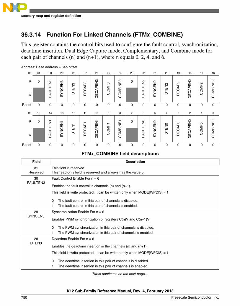
36.3.14 Function For Linked Channels (FTMx_COMBINE)
This register contains the control bits used to configure the fault control, synchronization,deadtime insertion, Dual Edge Capture mode, Complementary, and Combine mode foreach pair of channels (n) and (n+1), where n equals 0, 2, 4, and 6.
Address: Base address + 64h offset
Bit 31 30 29 28 27 26 25 24 23 22 21 20 19 18 17 16
R 0
FA
ULT
EN
3
SY
NC
EN
3
DT
EN
3
DE
CA
P3
DE
CA
PE
N3
CO
MP
3
CO
MB
INE
3 0
FA
ULT
EN
2
SY
NC
EN
2
DT
EN
2
DE
CA
P2
DE
CA
PE
N2
CO
MP
2
CO
MB
INE
2
W
Reset 0 0 0 0 0 0 0 0 0 0 0 0 0 0 0 0
Bit 15 14 13 12 11 10 9 8 7 6 5 4 3 2 1 0
R 0
FA
ULT
EN
1
SY
NC
EN
1
DT
EN
1
DE
CA
P1
DE
CA
PE
N1
CO
MP
1
CO
MB
INE
1 0
FA
ULT
EN
0
SY
NC
EN
0
DT
EN
0
DE
CA
P0
DE
CA
PE
N0
CO
MP
0
CO
MB
INE
0
W
Reset 0 0 0 0 0 0 0 0 0 0 0 0 0 0 0 0
FTMx_COMBINE field descriptions
Field Description
31Reserved
This field is reserved.This read-only field is reserved and always has the value 0.
30FAULTEN3
Fault Control Enable For n = 6
Enables the fault control in channels (n) and (n+1).
This field is write protected. It can be written only when MODE[WPDIS] = 1.
0 The fault control in this pair of channels is disabled.1 The fault control in this pair of channels is enabled.
29SYNCEN3
Synchronization Enable For n = 6
Enables PWM synchronization of registers C(n)V and C(n+1)V.
0 The PWM synchronization in this pair of channels is disabled.1 The PWM synchronization in this pair of channels is enabled.
28DTEN3
Deadtime Enable For n = 6
Enables the deadtime insertion in the channels (n) and (n+1).
This field is write protected. It can be written only when MODE[WPDIS] = 1.
0 The deadtime insertion in this pair of channels is disabled.1 The deadtime insertion in this pair of channels is enabled.
Table continues on the next page...
Memory map and register definition
K12 Sub-Family Reference Manual, Rev. 4, February 2013
750 Freescale Semiconductor, Inc.

FTMx_COMBINE field descriptions (continued)
Field Description
27DECAP3
Dual Edge Capture Mode Captures For n = 6
Enables the capture of the FTM counter value according to the channel (n) input event and theconfiguration of the dual edge capture bits.
This field applies only when FTMEN = 1 and DECAPEN = 1.
DECAP bit is cleared automatically by hardware if dual edge capture – one-shot mode is selected andwhen the capture of channel (n+1) event is made.
0 The dual edge captures are inactive.1 The dual edge captures are active.
26DECAPEN3
Dual Edge Capture Mode Enable For n = 6
Enables the Dual Edge Capture mode in the channels (n) and (n+1). This bit reconfigures the function ofMSnA, ELSnB:ELSnA and ELS(n+1)B:ELS(n+1)A bits in Dual Edge Capture mode according to Table36-7.
This field applies only when FTMEN = 1.
This field is write protected. It can be written only when MODE[WPDIS] = 1.
0 The Dual Edge Capture mode in this pair of channels is disabled.1 The Dual Edge Capture mode in this pair of channels is enabled.
25COMP3
Complement Of Channel (n) for n = 6
Enables Complementary mode for the combined channels. In Complementary mode the channel (n+1)output is the inverse of the channel (n) output.
This field is write protected. It can be written only when MODE[WPDIS] = 1.
0 The channel (n+1) output is the same as the channel (n) output.1 The channel (n+1) output is the complement of the channel (n) output.
24COMBINE3
Combine Channels For n = 6
Enables the combine feature for channels (n) and (n+1).
This field is write protected. It can be written only when MODE[WPDIS] = 1.
0 Channels (n) and (n+1) are independent.1 Channels (n) and (n+1) are combined.
23Reserved
This field is reserved.This read-only field is reserved and always has the value 0.
22FAULTEN2
Fault Control Enable For n = 4
Enables the fault control in channels (n) and (n+1).
This field is write protected. It can be written only when MODE[WPDIS] = 1.
0 The fault control in this pair of channels is disabled.1 The fault control in this pair of channels is enabled.
21SYNCEN2
Synchronization Enable For n = 4
Enables PWM synchronization of registers C(n)V and C(n+1)V.
0 The PWM synchronization in this pair of channels is disabled.1 The PWM synchronization in this pair of channels is enabled.
Table continues on the next page...
Chapter 36 FlexTimer Module (FTM)
K12 Sub-Family Reference Manual, Rev. 4, February 2013
Freescale Semiconductor, Inc. 751

FTMx_COMBINE field descriptions (continued)
Field Description
20DTEN2
Deadtime Enable For n = 4
Enables the deadtime insertion in the channels (n) and (n+1).
This field is write protected. It can be written only when MODE[WPDIS] = 1.
0 The deadtime insertion in this pair of channels is disabled.1 The deadtime insertion in this pair of channels is enabled.
19DECAP2
Dual Edge Capture Mode Captures For n = 4
Enables the capture of the FTM counter value according to the channel (n) input event and theconfiguration of the dual edge capture bits.
This field applies only when FTMEN = 1 and DECAPEN = 1.
DECAP bit is cleared automatically by hardware if dual edge capture – one-shot mode is selected andwhen the capture of channel (n+1) event is made.
0 The dual edge captures are inactive.1 The dual edge captures are active.
18DECAPEN2
Dual Edge Capture Mode Enable For n = 4
Enables the Dual Edge Capture mode in the channels (n) and (n+1). This bit reconfigures the function ofMSnA, ELSnB:ELSnA and ELS(n+1)B:ELS(n+1)A bits in Dual Edge Capture mode according to Table36-7.
This field applies only when FTMEN = 1.
This field is write protected. It can be written only when MODE[WPDIS] = 1.
0 The Dual Edge Capture mode in this pair of channels is disabled.1 The Dual Edge Capture mode in this pair of channels is enabled.
17COMP2
Complement Of Channel (n) For n = 4
Enables Complementary mode for the combined channels. In Complementary mode the channel (n+1)output is the inverse of the channel (n) output.
This field is write protected. It can be written only when MODE[WPDIS] = 1.
0 The channel (n+1) output is the same as the channel (n) output.1 The channel (n+1) output is the complement of the channel (n) output.
16COMBINE2
Combine Channels For n = 4
Enables the combine feature for channels (n) and (n+1).
This field is write protected. It can be written only when MODE[WPDIS] = 1.
0 Channels (n) and (n+1) are independent.1 Channels (n) and (n+1) are combined.
15Reserved
This field is reserved.This read-only field is reserved and always has the value 0.
14FAULTEN1
Fault Control Enable For n = 2
Enables the fault control in channels (n) and (n+1).
This field is write protected. It can be written only when MODE[WPDIS] = 1.
Table continues on the next page...
Memory map and register definition
K12 Sub-Family Reference Manual, Rev. 4, February 2013
752 Freescale Semiconductor, Inc.
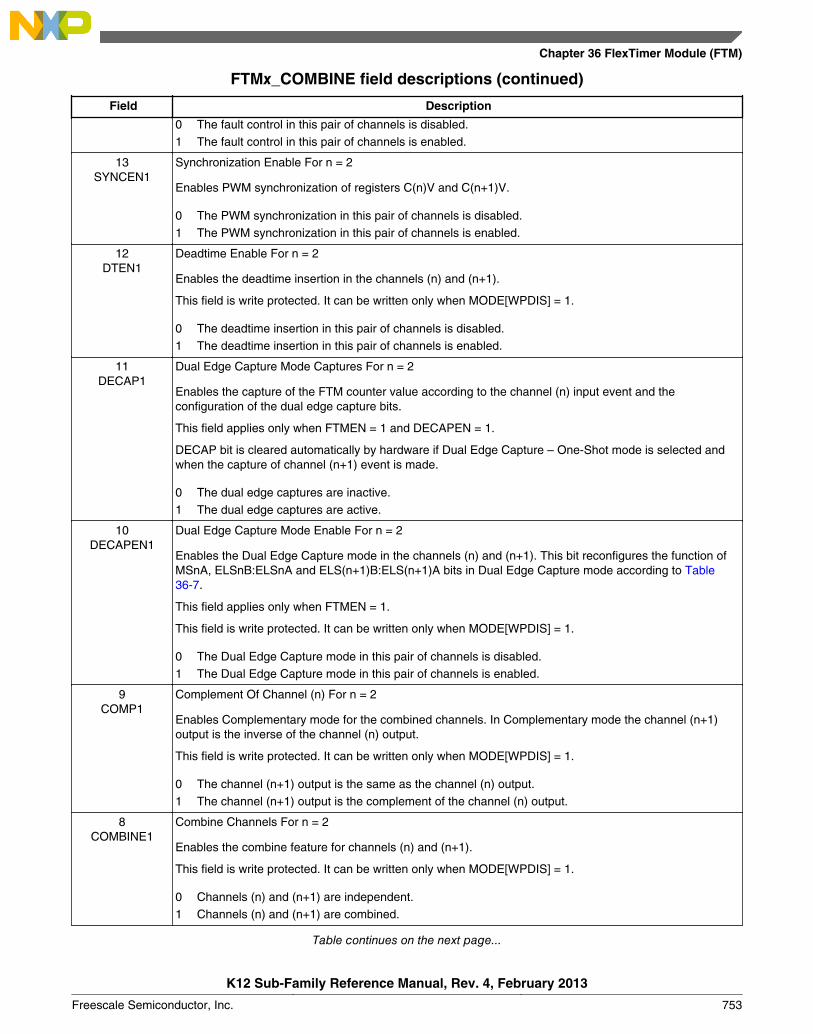
FTMx_COMBINE field descriptions (continued)
Field Description
0 The fault control in this pair of channels is disabled.1 The fault control in this pair of channels is enabled.
13SYNCEN1
Synchronization Enable For n = 2
Enables PWM synchronization of registers C(n)V and C(n+1)V.
0 The PWM synchronization in this pair of channels is disabled.1 The PWM synchronization in this pair of channels is enabled.
12DTEN1
Deadtime Enable For n = 2
Enables the deadtime insertion in the channels (n) and (n+1).
This field is write protected. It can be written only when MODE[WPDIS] = 1.
0 The deadtime insertion in this pair of channels is disabled.1 The deadtime insertion in this pair of channels is enabled.
11DECAP1
Dual Edge Capture Mode Captures For n = 2
Enables the capture of the FTM counter value according to the channel (n) input event and theconfiguration of the dual edge capture bits.
This field applies only when FTMEN = 1 and DECAPEN = 1.
DECAP bit is cleared automatically by hardware if Dual Edge Capture – One-Shot mode is selected andwhen the capture of channel (n+1) event is made.
0 The dual edge captures are inactive.1 The dual edge captures are active.
10DECAPEN1
Dual Edge Capture Mode Enable For n = 2
Enables the Dual Edge Capture mode in the channels (n) and (n+1). This bit reconfigures the function ofMSnA, ELSnB:ELSnA and ELS(n+1)B:ELS(n+1)A bits in Dual Edge Capture mode according to Table36-7.
This field applies only when FTMEN = 1.
This field is write protected. It can be written only when MODE[WPDIS] = 1.
0 The Dual Edge Capture mode in this pair of channels is disabled.1 The Dual Edge Capture mode in this pair of channels is enabled.
9COMP1
Complement Of Channel (n) For n = 2
Enables Complementary mode for the combined channels. In Complementary mode the channel (n+1)output is the inverse of the channel (n) output.
This field is write protected. It can be written only when MODE[WPDIS] = 1.
0 The channel (n+1) output is the same as the channel (n) output.1 The channel (n+1) output is the complement of the channel (n) output.
8COMBINE1
Combine Channels For n = 2
Enables the combine feature for channels (n) and (n+1).
This field is write protected. It can be written only when MODE[WPDIS] = 1.
0 Channels (n) and (n+1) are independent.1 Channels (n) and (n+1) are combined.
Table continues on the next page...
Chapter 36 FlexTimer Module (FTM)
K12 Sub-Family Reference Manual, Rev. 4, February 2013
Freescale Semiconductor, Inc. 753

FTMx_COMBINE field descriptions (continued)
Field Description
7Reserved
This field is reserved.This read-only field is reserved and always has the value 0.
6FAULTEN0
Fault Control Enable For n = 0
Enables the fault control in channels (n) and (n+1).
This field is write protected. It can be written only when MODE[WPDIS] = 1.
0 The fault control in this pair of channels is disabled.1 The fault control in this pair of channels is enabled.
5SYNCEN0
Synchronization Enable For n = 0
Enables PWM synchronization of registers C(n)V and C(n+1)V.
0 The PWM synchronization in this pair of channels is disabled.1 The PWM synchronization in this pair of channels is enabled.
4DTEN0
Deadtime Enable For n = 0
Enables the deadtime insertion in the channels (n) and (n+1).
This field is write protected. It can be written only when MODE[WPDIS] = 1.
0 The deadtime insertion in this pair of channels is disabled.1 The deadtime insertion in this pair of channels is enabled.
3DECAP0
Dual Edge Capture Mode Captures For n = 0
Enables the capture of the FTM counter value according to the channel (n) input event and theconfiguration of the dual edge capture bits.
This field applies only when FTMEN = 1 and DECAPEN = 1.
DECAP bit is cleared automatically by hardware if dual edge capture – one-shot mode is selected andwhen the capture of channel (n+1) event is made.
0 The dual edge captures are inactive.1 The dual edge captures are active.
2DECAPEN0
Dual Edge Capture Mode Enable For n = 0
Enables the Dual Edge Capture mode in the channels (n) and (n+1). This bit reconfigures the function ofMSnA, ELSnB:ELSnA and ELS(n+1)B:ELS(n+1)A bits in Dual Edge Capture mode according to Table36-7.
This field applies only when FTMEN = 1.
This field is write protected. It can be written only when MODE[WPDIS] = 1.
0 The Dual Edge Capture mode in this pair of channels is disabled.1 The Dual Edge Capture mode in this pair of channels is enabled.
1COMP0
Complement Of Channel (n) For n = 0
Enables Complementary mode for the combined channels. In Complementary mode the channel (n+1)output is the inverse of the channel (n) output.
This field is write protected. It can be written only when MODE[WPDIS] = 1.
0 The channel (n+1) output is the same as the channel (n) output.1 The channel (n+1) output is the complement of the channel (n) output.
Table continues on the next page...
Memory map and register definition
K12 Sub-Family Reference Manual, Rev. 4, February 2013
754 Freescale Semiconductor, Inc.
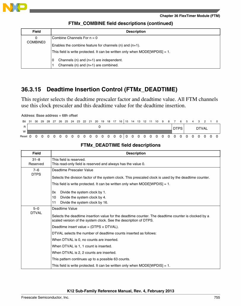
FTMx_COMBINE field descriptions (continued)
Field Description
0COMBINE0
Combine Channels For n = 0
Enables the combine feature for channels (n) and (n+1).
This field is write protected. It can be written only when MODE[WPDIS] = 1.
0 Channels (n) and (n+1) are independent.1 Channels (n) and (n+1) are combined.
36.3.15 Deadtime Insertion Control (FTMx_DEADTIME)
This register selects the deadtime prescaler factor and deadtime value. All FTM channelsuse this clock prescaler and this deadtime value for the deadtime insertion.
Address: Base address + 68h offset
Bit 31 30 29 28 27 26 25 24 23 22 21 20 19 18 17 16 15 14 13 12 11 10 9 8 7 6 5 4 3 2 1 0
R 0 DTPS DTVALW
Reset 0 0 0 0 0 0 0 0 0 0 0 0 0 0 0 0 0 0 0 0 0 0 0 0 0 0 0 0 0 0 0 0
FTMx_DEADTIME field descriptions
Field Description
31–8Reserved
This field is reserved.This read-only field is reserved and always has the value 0.
7–6DTPS
Deadtime Prescaler Value
Selects the division factor of the system clock. This prescaled clock is used by the deadtime counter.
This field is write protected. It can be written only when MODE[WPDIS] = 1.
0x Divide the system clock by 1.10 Divide the system clock by 4.11 Divide the system clock by 16.
5–0DTVAL
Deadtime Value
Selects the deadtime insertion value for the deadtime counter. The deadtime counter is clocked by ascaled version of the system clock. See the description of DTPS.
Deadtime insert value = (DTPS × DTVAL).
DTVAL selects the number of deadtime counts inserted as follows:
When DTVAL is 0, no counts are inserted.
When DTVAL is 1, 1 count is inserted.
When DTVAL is 2, 2 counts are inserted.
This pattern continues up to a possible 63 counts.
This field is write protected. It can be written only when MODE[WPDIS] = 1.
Chapter 36 FlexTimer Module (FTM)
K12 Sub-Family Reference Manual, Rev. 4, February 2013
Freescale Semiconductor, Inc. 755
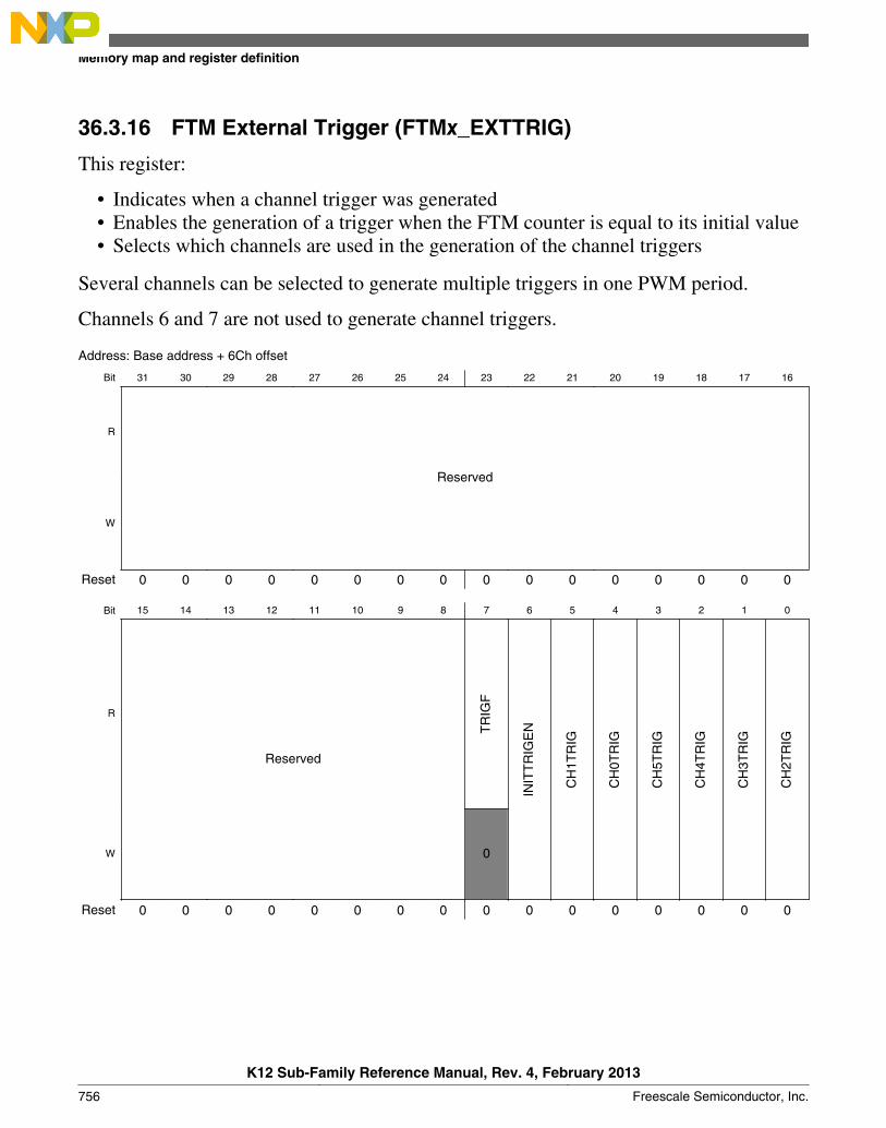
36.3.16 FTM External Trigger (FTMx_EXTTRIG)
This register:
• Indicates when a channel trigger was generated• Enables the generation of a trigger when the FTM counter is equal to its initial value• Selects which channels are used in the generation of the channel triggers
Several channels can be selected to generate multiple triggers in one PWM period.
Channels 6 and 7 are not used to generate channel triggers.
Address: Base address + 6Ch offset
Bit 31 30 29 28 27 26 25 24 23 22 21 20 19 18 17 16
R
Reserved
W
Reset 0 0 0 0 0 0 0 0 0 0 0 0 0 0 0 0
Bit 15 14 13 12 11 10 9 8 7 6 5 4 3 2 1 0
R
Reserved
TR
IGF
INIT
TR
IGE
N
CH
1TR
IG
CH
0TR
IG
CH
5TR
IG
CH
4TR
IG
CH
3TR
IG
CH
2TR
IG
W 0
Reset 0 0 0 0 0 0 0 0 0 0 0 0 0 0 0 0
Memory map and register definition
K12 Sub-Family Reference Manual, Rev. 4, February 2013
756 Freescale Semiconductor, Inc.
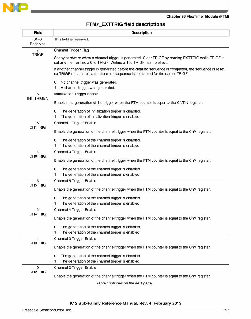
FTMx_EXTTRIG field descriptions
Field Description
31–8Reserved
This field is reserved.
7TRIGF
Channel Trigger Flag
Set by hardware when a channel trigger is generated. Clear TRIGF by reading EXTTRIG while TRIGF isset and then writing a 0 to TRIGF. Writing a 1 to TRIGF has no effect.
If another channel trigger is generated before the clearing sequence is completed, the sequence is resetso TRIGF remains set after the clear sequence is completed for the earlier TRIGF.
0 No channel trigger was generated.1 A channel trigger was generated.
6INITTRIGEN
Initialization Trigger Enable
Enables the generation of the trigger when the FTM counter is equal to the CNTIN register.
0 The generation of initialization trigger is disabled.1 The generation of initialization trigger is enabled.
5CH1TRIG
Channel 1 Trigger Enable
Enable the generation of the channel trigger when the FTM counter is equal to the CnV register.
0 The generation of the channel trigger is disabled.1 The generation of the channel trigger is enabled.
4CH0TRIG
Channel 0 Trigger Enable
Enable the generation of the channel trigger when the FTM counter is equal to the CnV register.
0 The generation of the channel trigger is disabled.1 The generation of the channel trigger is enabled.
3CH5TRIG
Channel 5 Trigger Enable
Enable the generation of the channel trigger when the FTM counter is equal to the CnV register.
0 The generation of the channel trigger is disabled.1 The generation of the channel trigger is enabled.
2CH4TRIG
Channel 4 Trigger Enable
Enable the generation of the channel trigger when the FTM counter is equal to the CnV register.
0 The generation of the channel trigger is disabled.1 The generation of the channel trigger is enabled.
1CH3TRIG
Channel 3 Trigger Enable
Enable the generation of the channel trigger when the FTM counter is equal to the CnV register.
0 The generation of the channel trigger is disabled.1 The generation of the channel trigger is enabled.
0CH2TRIG
Channel 2 Trigger Enable
Enable the generation of the channel trigger when the FTM counter is equal to the CnV register.
Table continues on the next page...
Chapter 36 FlexTimer Module (FTM)
K12 Sub-Family Reference Manual, Rev. 4, February 2013
Freescale Semiconductor, Inc. 757
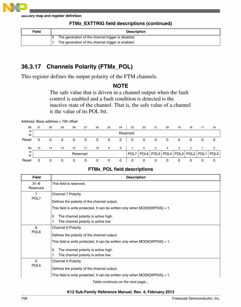
FTMx_EXTTRIG field descriptions (continued)
Field Description
0 The generation of the channel trigger is disabled.1 The generation of the channel trigger is enabled.
36.3.17 Channels Polarity (FTMx_POL)
This register defines the output polarity of the FTM channels.
NOTEThe safe value that is driven in a channel output when the faultcontrol is enabled and a fault condition is detected is theinactive state of the channel. That is, the safe value of a channelis the value of its POL bit.
Address: Base address + 70h offset
Bit 31 30 29 28 27 26 25 24 23 22 21 20 19 18 17 16
R ReservedW
Reset 0 0 0 0 0 0 0 0 0 0 0 0 0 0 0 0
Bit 15 14 13 12 11 10 9 8 7 6 5 4 3 2 1 0
R Reserved POL7 POL6 POL5 POL4 POL3 POL2 POL1 POL0W
Reset 0 0 0 0 0 0 0 0 0 0 0 0 0 0 0 0
FTMx_POL field descriptions
Field Description
31–8Reserved
This field is reserved.
7POL7
Channel 7 Polarity
Defines the polarity of the channel output.
This field is write protected. It can be written only when MODE[WPDIS] = 1.
0 The channel polarity is active high.1 The channel polarity is active low.
6POL6
Channel 6 Polarity
Defines the polarity of the channel output.
This field is write protected. It can be written only when MODE[WPDIS] = 1.
0 The channel polarity is active high.1 The channel polarity is active low.
5POL5
Channel 5 Polarity
Defines the polarity of the channel output.
This field is write protected. It can be written only when MODE[WPDIS] = 1.
Table continues on the next page...
Memory map and register definition
K12 Sub-Family Reference Manual, Rev. 4, February 2013
758 Freescale Semiconductor, Inc.
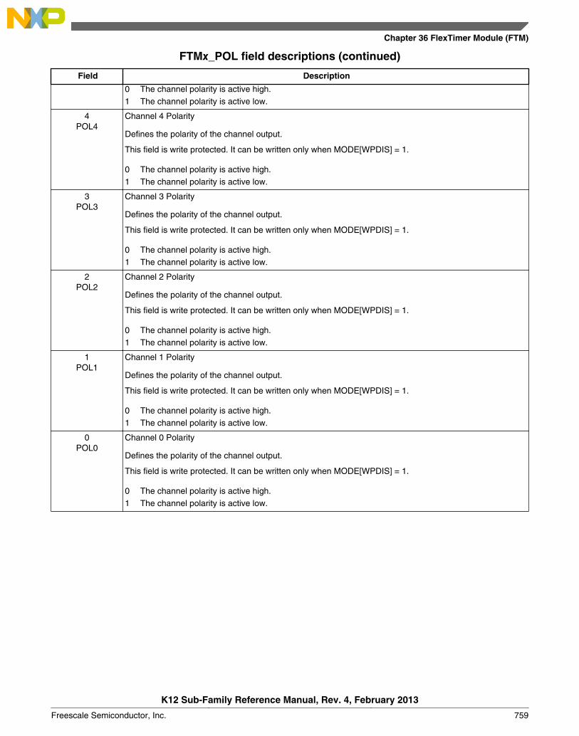
FTMx_POL field descriptions (continued)
Field Description
0 The channel polarity is active high.1 The channel polarity is active low.
4POL4
Channel 4 Polarity
Defines the polarity of the channel output.
This field is write protected. It can be written only when MODE[WPDIS] = 1.
0 The channel polarity is active high.1 The channel polarity is active low.
3POL3
Channel 3 Polarity
Defines the polarity of the channel output.
This field is write protected. It can be written only when MODE[WPDIS] = 1.
0 The channel polarity is active high.1 The channel polarity is active low.
2POL2
Channel 2 Polarity
Defines the polarity of the channel output.
This field is write protected. It can be written only when MODE[WPDIS] = 1.
0 The channel polarity is active high.1 The channel polarity is active low.
1POL1
Channel 1 Polarity
Defines the polarity of the channel output.
This field is write protected. It can be written only when MODE[WPDIS] = 1.
0 The channel polarity is active high.1 The channel polarity is active low.
0POL0
Channel 0 Polarity
Defines the polarity of the channel output.
This field is write protected. It can be written only when MODE[WPDIS] = 1.
0 The channel polarity is active high.1 The channel polarity is active low.
Chapter 36 FlexTimer Module (FTM)
K12 Sub-Family Reference Manual, Rev. 4, February 2013
Freescale Semiconductor, Inc. 759

36.3.18 Fault Mode Status (FTMx_FMS)
This register contains the fault detection flags, write protection enable bit, and the logicOR of the enabled fault inputs.
Address: Base address + 74h offset
Bit 31 30 29 28 27 26 25 24 23 22 21 20 19 18 17 16
R 0
W
Reset 0 0 0 0 0 0 0 0 0 0 0 0 0 0 0 0
Bit 15 14 13 12 11 10 9 8 7 6 5 4 3 2 1 0
R 0
FA
ULT
F
WP
EN F
AU
LTIN
0
FA
ULT
F3
FA
ULT
F2
FA
ULT
F1
FA
ULT
F0
W 0 0 0 0 0
Reset 0 0 0 0 0 0 0 0 0 0 0 0 0 0 0 0
FTMx_FMS field descriptions
Field Description
31–8Reserved
This field is reserved.This read-only field is reserved and always has the value 0.
7FAULTF
Fault Detection Flag
Represents the logic OR of the individual FAULTFj bits where j = 3, 2, 1, 0. Clear FAULTF by reading theFMS register while FAULTF is set and then writing a 0 to FAULTF while there is no existing fault conditionat the enabled fault inputs. Writing a 1 to FAULTF has no effect.
If another fault condition is detected in an enabled fault input before the clearing sequence is completed,the sequence is reset so FAULTF remains set after the clearing sequence is completed for the earlier faultcondition. FAULTF is also cleared when FAULTFj bits are cleared individually.
0 No fault condition was detected.1 A fault condition was detected.
Table continues on the next page...
Memory map and register definition
K12 Sub-Family Reference Manual, Rev. 4, February 2013
760 Freescale Semiconductor, Inc.

FTMx_FMS field descriptions (continued)
Field Description
6WPEN
Write Protection Enable
The WPEN bit is the negation of the WPDIS bit. WPEN is set when 1 is written to it. WPEN is clearedwhen WPEN bit is read as a 1 and then 1 is written to WPDIS. Writing 0 to WPEN has no effect.
0 Write protection is disabled. Write protected bits can be written.1 Write protection is enabled. Write protected bits cannot be written.
5FAULTIN
Fault Inputs
Represents the logic OR of the enabled fault inputs after their filter (if their filter is enabled) when faultcontrol is enabled.
0 The logic OR of the enabled fault inputs is 0.1 The logic OR of the enabled fault inputs is 1.
4Reserved
This field is reserved.This read-only field is reserved and always has the value 0.
3FAULTF3
Fault Detection Flag 3
Set by hardware when fault control is enabled, the corresponding fault input is enabled and a faultcondition is detected at the fault input.
Clear FAULTF3 by reading the FMS register while FAULTF3 is set and then writing a 0 to FAULTF3 whilethere is no existing fault condition at the corresponding fault input. Writing a 1 to FAULTF3 has no effect.FAULTF3 bit is also cleared when FAULTF bit is cleared.
If another fault condition is detected at the corresponding fault input before the clearing sequence iscompleted, the sequence is reset so FAULTF3 remains set after the clearing sequence is completed forthe earlier fault condition.
0 No fault condition was detected at the fault input.1 A fault condition was detected at the fault input.
2FAULTF2
Fault Detection Flag 2
Set by hardware when fault control is enabled, the corresponding fault input is enabled and a faultcondition is detected at the fault input.
Clear FAULTF2 by reading the FMS register while FAULTF2 is set and then writing a 0 to FAULTF2 whilethere is no existing fault condition at the corresponding fault input. Writing a 1 to FAULTF2 has no effect.FAULTF2 bit is also cleared when FAULTF bit is cleared.
If another fault condition is detected at the corresponding fault input before the clearing sequence iscompleted, the sequence is reset so FAULTF2 remains set after the clearing sequence is completed forthe earlier fault condition.
0 No fault condition was detected at the fault input.1 A fault condition was detected at the fault input.
1FAULTF1
Fault Detection Flag 1
Set by hardware when fault control is enabled, the corresponding fault input is enabled and a faultcondition is detected at the fault input.
Clear FAULTF1 by reading the FMS register while FAULTF1 is set and then writing a 0 to FAULTF1 whilethere is no existing fault condition at the corresponding fault input. Writing a 1 to FAULTF1 has no effect.FAULTF1 bit is also cleared when FAULTF bit is cleared.
Table continues on the next page...
Chapter 36 FlexTimer Module (FTM)
K12 Sub-Family Reference Manual, Rev. 4, February 2013
Freescale Semiconductor, Inc. 761
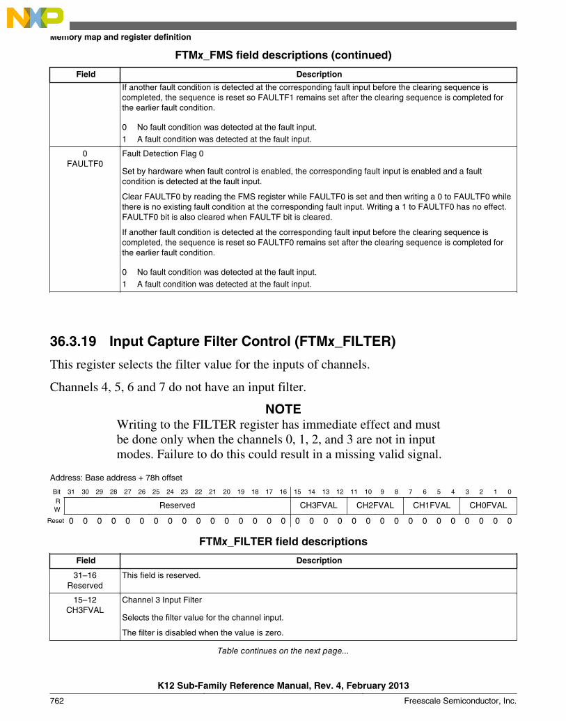
FTMx_FMS field descriptions (continued)
Field Description
If another fault condition is detected at the corresponding fault input before the clearing sequence iscompleted, the sequence is reset so FAULTF1 remains set after the clearing sequence is completed forthe earlier fault condition.
0 No fault condition was detected at the fault input.1 A fault condition was detected at the fault input.
0FAULTF0
Fault Detection Flag 0
Set by hardware when fault control is enabled, the corresponding fault input is enabled and a faultcondition is detected at the fault input.
Clear FAULTF0 by reading the FMS register while FAULTF0 is set and then writing a 0 to FAULTF0 whilethere is no existing fault condition at the corresponding fault input. Writing a 1 to FAULTF0 has no effect.FAULTF0 bit is also cleared when FAULTF bit is cleared.
If another fault condition is detected at the corresponding fault input before the clearing sequence iscompleted, the sequence is reset so FAULTF0 remains set after the clearing sequence is completed forthe earlier fault condition.
0 No fault condition was detected at the fault input.1 A fault condition was detected at the fault input.
36.3.19 Input Capture Filter Control (FTMx_FILTER)
This register selects the filter value for the inputs of channels.
Channels 4, 5, 6 and 7 do not have an input filter.
NOTEWriting to the FILTER register has immediate effect and mustbe done only when the channels 0, 1, 2, and 3 are not in inputmodes. Failure to do this could result in a missing valid signal.
Address: Base address + 78h offset
Bit 31 30 29 28 27 26 25 24 23 22 21 20 19 18 17 16 15 14 13 12 11 10 9 8 7 6 5 4 3 2 1 0
R Reserved CH3FVAL CH2FVAL CH1FVAL CH0FVALW
Reset 0 0 0 0 0 0 0 0 0 0 0 0 0 0 0 0 0 0 0 0 0 0 0 0 0 0 0 0 0 0 0 0
FTMx_FILTER field descriptions
Field Description
31–16Reserved
This field is reserved.
15–12CH3FVAL
Channel 3 Input Filter
Selects the filter value for the channel input.
The filter is disabled when the value is zero.
Table continues on the next page...
Memory map and register definition
K12 Sub-Family Reference Manual, Rev. 4, February 2013
762 Freescale Semiconductor, Inc.
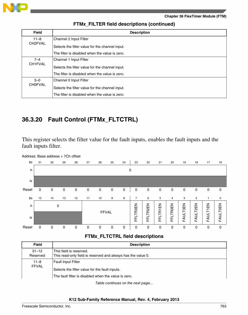
FTMx_FILTER field descriptions (continued)
Field Description
11–8CH2FVAL
Channel 2 Input Filter
Selects the filter value for the channel input.
The filter is disabled when the value is zero.
7–4CH1FVAL
Channel 1 Input Filter
Selects the filter value for the channel input.
The filter is disabled when the value is zero.
3–0CH0FVAL
Channel 0 Input Filter
Selects the filter value for the channel input.
The filter is disabled when the value is zero.
36.3.20 Fault Control (FTMx_FLTCTRL)
This register selects the filter value for the fault inputs, enables the fault inputs and thefault inputs filter.
Address: Base address + 7Ch offset
Bit 31 30 29 28 27 26 25 24 23 22 21 20 19 18 17 16
R 0
W
Reset 0 0 0 0 0 0 0 0 0 0 0 0 0 0 0 0
Bit 15 14 13 12 11 10 9 8 7 6 5 4 3 2 1 0
R 0
FFVAL
FF
LTR
3EN
FF
LTR
2EN
FF
LTR
1EN
FF
LTR
0EN
FA
ULT
3EN
FA
ULT
2EN
FA
ULT
1EN
FA
ULT
0EN
W
Reset 0 0 0 0 0 0 0 0 0 0 0 0 0 0 0 0
FTMx_FLTCTRL field descriptions
Field Description
31–12Reserved
This field is reserved.This read-only field is reserved and always has the value 0.
11–8FFVAL
Fault Input Filter
Selects the filter value for the fault inputs.
The fault filter is disabled when the value is zero.
Table continues on the next page...
Chapter 36 FlexTimer Module (FTM)
K12 Sub-Family Reference Manual, Rev. 4, February 2013
Freescale Semiconductor, Inc. 763

FTMx_FLTCTRL field descriptions (continued)
Field Description
NOTE: Writing to this field has immediate effect and must be done only when the fault control or all faultinputs are disabled. Failure to do this could result in a missing fault detection.
7FFLTR3EN
Fault Input 3 Filter Enable
Enables the filter for the fault input.
This field is write protected. It can be written only when MODE[WPDIS] = 1.
0 Fault input filter is disabled.1 Fault input filter is enabled.
6FFLTR2EN
Fault Input 2 Filter Enable
Enables the filter for the fault input.
This field is write protected. It can be written only when MODE[WPDIS] = 1.
0 Fault input filter is disabled.1 Fault input filter is enabled.
5FFLTR1EN
Fault Input 1 Filter Enable
Enables the filter for the fault input.
This field is write protected. It can be written only when MODE[WPDIS] = 1.
0 Fault input filter is disabled.1 Fault input filter is enabled.
4FFLTR0EN
Fault Input 0 Filter Enable
Enables the filter for the fault input.
This field is write protected. It can be written only when MODE[WPDIS] = 1.
0 Fault input filter is disabled.1 Fault input filter is enabled.
3FAULT3EN
Fault Input 3 Enable
Enables the fault input.
This field is write protected. It can be written only when MODE[WPDIS] = 1.
0 Fault input is disabled.1 Fault input is enabled.
2FAULT2EN
Fault Input 2 Enable
Enables the fault input.
This field is write protected. It can be written only when MODE[WPDIS] = 1.
0 Fault input is disabled.1 Fault input is enabled.
1FAULT1EN
Fault Input 1 Enable
Enables the fault input.
This field is write protected. It can be written only when MODE[WPDIS] = 1.
Table continues on the next page...
Memory map and register definition
K12 Sub-Family Reference Manual, Rev. 4, February 2013
764 Freescale Semiconductor, Inc.
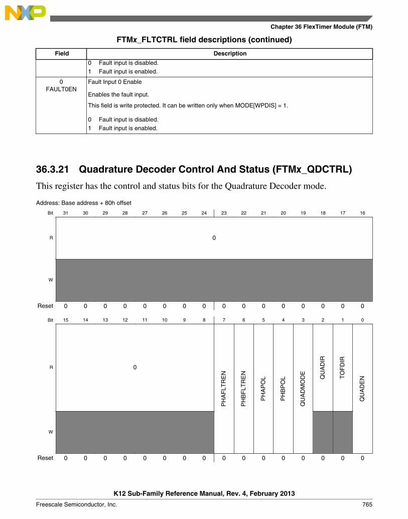
FTMx_FLTCTRL field descriptions (continued)
Field Description
0 Fault input is disabled.1 Fault input is enabled.
0FAULT0EN
Fault Input 0 Enable
Enables the fault input.
This field is write protected. It can be written only when MODE[WPDIS] = 1.
0 Fault input is disabled.1 Fault input is enabled.
36.3.21 Quadrature Decoder Control And Status (FTMx_QDCTRL)
This register has the control and status bits for the Quadrature Decoder mode.
Address: Base address + 80h offset
Bit 31 30 29 28 27 26 25 24 23 22 21 20 19 18 17 16
R 0
W
Reset 0 0 0 0 0 0 0 0 0 0 0 0 0 0 0 0
Bit 15 14 13 12 11 10 9 8 7 6 5 4 3 2 1 0
R 0
PH
AF
LTR
EN
PH
BF
LTR
EN
PH
AP
OL
PH
BP
OL
QU
AD
MO
DE
QU
AD
IR
TO
FD
IR
QU
AD
EN
W
Reset 0 0 0 0 0 0 0 0 0 0 0 0 0 0 0 0
Chapter 36 FlexTimer Module (FTM)
K12 Sub-Family Reference Manual, Rev. 4, February 2013
Freescale Semiconductor, Inc. 765
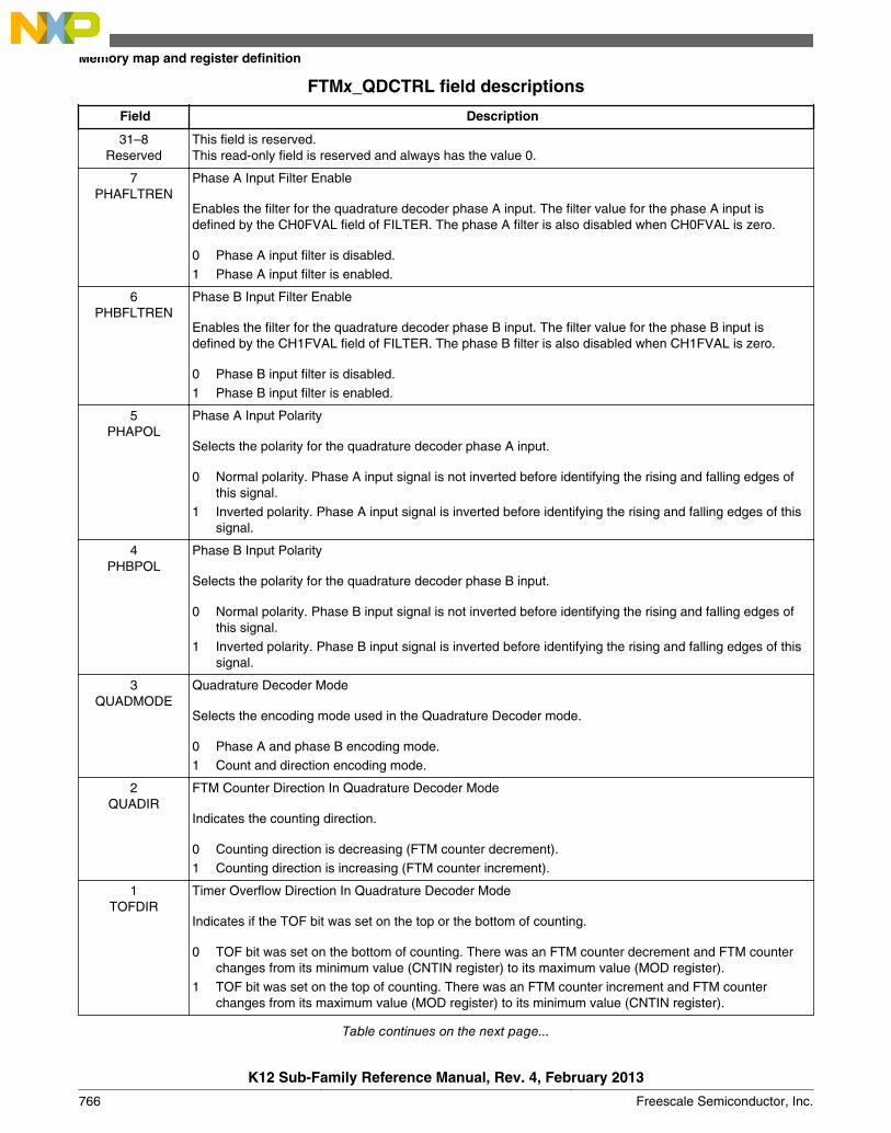
FTMx_QDCTRL field descriptions
Field Description
31–8Reserved
This field is reserved.This read-only field is reserved and always has the value 0.
7PHAFLTREN
Phase A Input Filter Enable
Enables the filter for the quadrature decoder phase A input. The filter value for the phase A input isdefined by the CH0FVAL field of FILTER. The phase A filter is also disabled when CH0FVAL is zero.
0 Phase A input filter is disabled.1 Phase A input filter is enabled.
6PHBFLTREN
Phase B Input Filter Enable
Enables the filter for the quadrature decoder phase B input. The filter value for the phase B input isdefined by the CH1FVAL field of FILTER. The phase B filter is also disabled when CH1FVAL is zero.
0 Phase B input filter is disabled.1 Phase B input filter is enabled.
5PHAPOL
Phase A Input Polarity
Selects the polarity for the quadrature decoder phase A input.
0 Normal polarity. Phase A input signal is not inverted before identifying the rising and falling edges ofthis signal.
1 Inverted polarity. Phase A input signal is inverted before identifying the rising and falling edges of thissignal.
4PHBPOL
Phase B Input Polarity
Selects the polarity for the quadrature decoder phase B input.
0 Normal polarity. Phase B input signal is not inverted before identifying the rising and falling edges ofthis signal.
1 Inverted polarity. Phase B input signal is inverted before identifying the rising and falling edges of thissignal.
3QUADMODE
Quadrature Decoder Mode
Selects the encoding mode used in the Quadrature Decoder mode.
0 Phase A and phase B encoding mode.1 Count and direction encoding mode.
2QUADIR
FTM Counter Direction In Quadrature Decoder Mode
Indicates the counting direction.
0 Counting direction is decreasing (FTM counter decrement).1 Counting direction is increasing (FTM counter increment).
1TOFDIR
Timer Overflow Direction In Quadrature Decoder Mode
Indicates if the TOF bit was set on the top or the bottom of counting.
0 TOF bit was set on the bottom of counting. There was an FTM counter decrement and FTM counterchanges from its minimum value (CNTIN register) to its maximum value (MOD register).
1 TOF bit was set on the top of counting. There was an FTM counter increment and FTM counterchanges from its maximum value (MOD register) to its minimum value (CNTIN register).
Table continues on the next page...
Memory map and register definition
K12 Sub-Family Reference Manual, Rev. 4, February 2013
766 Freescale Semiconductor, Inc.

FTMx_QDCTRL field descriptions (continued)
Field Description
0QUADEN
Quadrature Decoder Mode Enable
Enables the Quadrature Decoder mode. In this mode, the phase A and B input signals control the FTMcounter direction. The Quadrature Decoder mode has precedence over the other modes. See Table 36-7.
This field is write protected. It can be written only when MODE[WPDIS] = 1.
0 Quadrature Decoder mode is disabled.1 Quadrature Decoder mode is enabled.
36.3.22 Configuration (FTMx_CONF)
This register selects the number of times that the FTM counter overflow should occurbefore the TOF bit to be set, the FTM behavior in BDM modes, the use of an externalglobal time base, and the global time base signal generation.
Address: Base address + 84h offset
Bit 31 30 29 28 27 26 25 24 23 22 21 20 19 18 17 16
R 0
W
Reset 0 0 0 0 0 0 0 0 0 0 0 0 0 0 0 0
Bit 15 14 13 12 11 10 9 8 7 6 5 4 3 2 1 0
R 0
GT
BE
OU
T
GT
BE
EN 0
BDMMODE
0
NUMTOFW
Reset 0 0 0 0 0 0 0 0 0 0 0 0 0 0 0 0
FTMx_CONF field descriptions
Field Description
31–11Reserved
This field is reserved.This read-only field is reserved and always has the value 0.
10GTBEOUT
Global Time Base Output
Enables the global time base signal generation to other FTMs.
0 A global time base signal generation is disabled.1
A global time base signal generation is enabled.
9GTBEEN
Global Time Base Enable
Configures the FTM to use an external global time base signal that is generated by another FTM.
Table continues on the next page...
Chapter 36 FlexTimer Module (FTM)
K12 Sub-Family Reference Manual, Rev. 4, February 2013
Freescale Semiconductor, Inc. 767
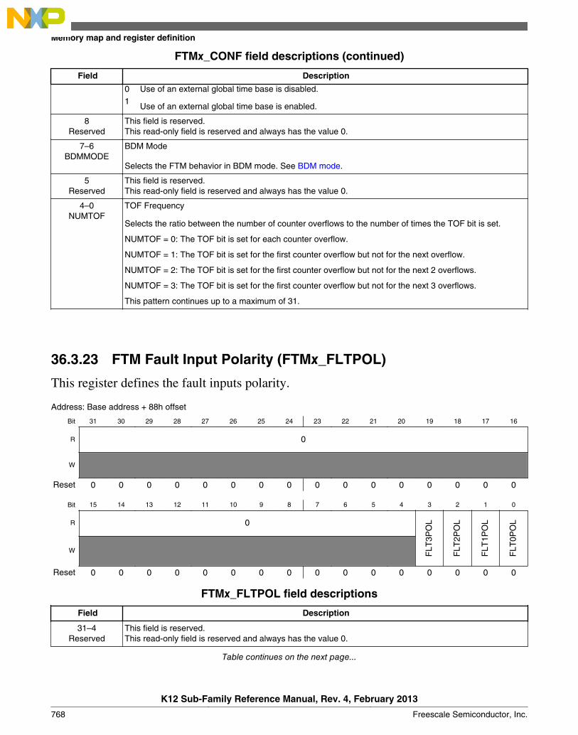
FTMx_CONF field descriptions (continued)
Field Description
0 Use of an external global time base is disabled.1
Use of an external global time base is enabled.
8Reserved
This field is reserved.This read-only field is reserved and always has the value 0.
7–6BDMMODE
BDM Mode
Selects the FTM behavior in BDM mode. See BDM mode.
5Reserved
This field is reserved.This read-only field is reserved and always has the value 0.
4–0NUMTOF
TOF Frequency
Selects the ratio between the number of counter overflows to the number of times the TOF bit is set.
NUMTOF = 0: The TOF bit is set for each counter overflow.
NUMTOF = 1: The TOF bit is set for the first counter overflow but not for the next overflow.
NUMTOF = 2: The TOF bit is set for the first counter overflow but not for the next 2 overflows.
NUMTOF = 3: The TOF bit is set for the first counter overflow but not for the next 3 overflows.
This pattern continues up to a maximum of 31.
36.3.23 FTM Fault Input Polarity (FTMx_FLTPOL)
This register defines the fault inputs polarity.
Address: Base address + 88h offset
Bit 31 30 29 28 27 26 25 24 23 22 21 20 19 18 17 16
R 0
W
Reset 0 0 0 0 0 0 0 0 0 0 0 0 0 0 0 0
Bit 15 14 13 12 11 10 9 8 7 6 5 4 3 2 1 0
R 0
FLT
3PO
L
FLT
2PO
L
FLT
1PO
L
FLT
0PO
L
W
Reset 0 0 0 0 0 0 0 0 0 0 0 0 0 0 0 0
FTMx_FLTPOL field descriptions
Field Description
31–4Reserved
This field is reserved.This read-only field is reserved and always has the value 0.
Table continues on the next page...
Memory map and register definition
K12 Sub-Family Reference Manual, Rev. 4, February 2013
768 Freescale Semiconductor, Inc.
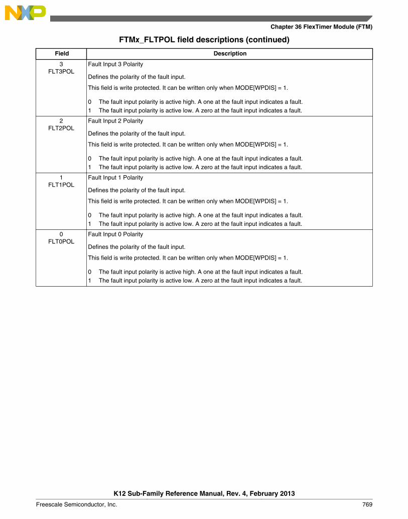
FTMx_FLTPOL field descriptions (continued)
Field Description
3FLT3POL
Fault Input 3 Polarity
Defines the polarity of the fault input.
This field is write protected. It can be written only when MODE[WPDIS] = 1.
0 The fault input polarity is active high. A one at the fault input indicates a fault.1 The fault input polarity is active low. A zero at the fault input indicates a fault.
2FLT2POL
Fault Input 2 Polarity
Defines the polarity of the fault input.
This field is write protected. It can be written only when MODE[WPDIS] = 1.
0 The fault input polarity is active high. A one at the fault input indicates a fault.1 The fault input polarity is active low. A zero at the fault input indicates a fault.
1FLT1POL
Fault Input 1 Polarity
Defines the polarity of the fault input.
This field is write protected. It can be written only when MODE[WPDIS] = 1.
0 The fault input polarity is active high. A one at the fault input indicates a fault.1 The fault input polarity is active low. A zero at the fault input indicates a fault.
0FLT0POL
Fault Input 0 Polarity
Defines the polarity of the fault input.
This field is write protected. It can be written only when MODE[WPDIS] = 1.
0 The fault input polarity is active high. A one at the fault input indicates a fault.1 The fault input polarity is active low. A zero at the fault input indicates a fault.
Chapter 36 FlexTimer Module (FTM)
K12 Sub-Family Reference Manual, Rev. 4, February 2013
Freescale Semiconductor, Inc. 769
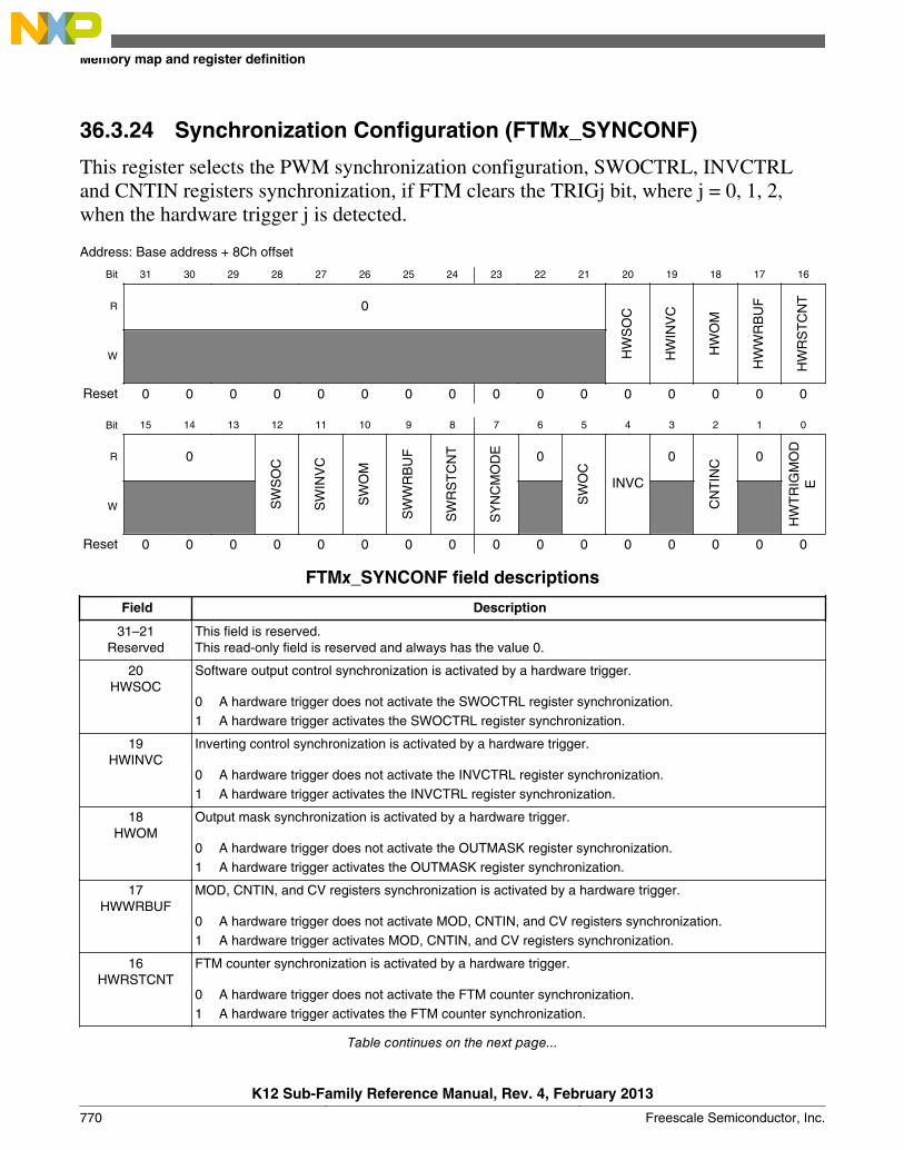
36.3.24 Synchronization Configuration (FTMx_SYNCONF)
This register selects the PWM synchronization configuration, SWOCTRL, INVCTRLand CNTIN registers synchronization, if FTM clears the TRIGj bit, where j = 0, 1, 2,when the hardware trigger j is detected.
Address: Base address + 8Ch offset
Bit 31 30 29 28 27 26 25 24 23 22 21 20 19 18 17 16
R 0
HW
SO
C
HW
INV
C
HW
OM
HW
WR
BU
F
HW
RS
TC
NT
W
Reset 0 0 0 0 0 0 0 0 0 0 0 0 0 0 0 0
Bit 15 14 13 12 11 10 9 8 7 6 5 4 3 2 1 0
R 0
SW
SO
C
SW
INV
C
SW
OM
SW
WR
BU
F
SW
RS
TC
NT
SY
NC
MO
DE 0
SW
OC
INVC
0
CN
TIN
C 0
HW
TR
IGM
OD
E
W
Reset 0 0 0 0 0 0 0 0 0 0 0 0 0 0 0 0
FTMx_SYNCONF field descriptions
Field Description
31–21Reserved
This field is reserved.This read-only field is reserved and always has the value 0.
20HWSOC
Software output control synchronization is activated by a hardware trigger.
0 A hardware trigger does not activate the SWOCTRL register synchronization.1 A hardware trigger activates the SWOCTRL register synchronization.
19HWINVC
Inverting control synchronization is activated by a hardware trigger.
0 A hardware trigger does not activate the INVCTRL register synchronization.1 A hardware trigger activates the INVCTRL register synchronization.
18HWOM
Output mask synchronization is activated by a hardware trigger.
0 A hardware trigger does not activate the OUTMASK register synchronization.1 A hardware trigger activates the OUTMASK register synchronization.
17HWWRBUF
MOD, CNTIN, and CV registers synchronization is activated by a hardware trigger.
0 A hardware trigger does not activate MOD, CNTIN, and CV registers synchronization.1 A hardware trigger activates MOD, CNTIN, and CV registers synchronization.
16HWRSTCNT
FTM counter synchronization is activated by a hardware trigger.
0 A hardware trigger does not activate the FTM counter synchronization.1 A hardware trigger activates the FTM counter synchronization.
Table continues on the next page...
Memory map and register definition
K12 Sub-Family Reference Manual, Rev. 4, February 2013
770 Freescale Semiconductor, Inc.

FTMx_SYNCONF field descriptions (continued)
Field Description
15–13Reserved
This field is reserved.This read-only field is reserved and always has the value 0.
12SWSOC
Software output control synchronization is activated by the software trigger.
0 The software trigger does not activate the SWOCTRL register synchronization.1 The software trigger activates the SWOCTRL register synchronization.
11SWINVC
Inverting control synchronization is activated by the software trigger.
0 The software trigger does not activate the INVCTRL register synchronization.1 The software trigger activates the INVCTRL register synchronization.
10SWOM
Output mask synchronization is activated by the software trigger.
0 The software trigger does not activate the OUTMASK register synchronization.1 The software trigger activates the OUTMASK register synchronization.
9SWWRBUF
MOD, CNTIN, and CV registers synchronization is activated by the software trigger.
0 The software trigger does not activate MOD, CNTIN, and CV registers synchronization.1 The software trigger activates MOD, CNTIN, and CV registers synchronization.
8SWRSTCNT
FTM counter synchronization is activated by the software trigger.
0 The software trigger does not activate the FTM counter synchronization.1 The software trigger activates the FTM counter synchronization.
7SYNCMODE
Synchronization Mode
Selects the PWM Synchronization mode.
0 Legacy PWM synchronization is selected.1 Enhanced PWM synchronization is selected.
6Reserved
This field is reserved.This read-only field is reserved and always has the value 0.
5SWOC
SWOCTRL Register Synchronization
0 SWOCTRL register is updated with its buffer value at all rising edges of system clock.1 SWOCTRL register is updated with its buffer value by the PWM synchronization.
4INVC
INVCTRL Register Synchronization
0 INVCTRL register is updated with its buffer value at all rising edges of system clock.1 INVCTRL register is updated with its buffer value by the PWM synchronization.
3Reserved
This field is reserved.This read-only field is reserved and always has the value 0.
2CNTINC
CNTIN Register Synchronization
0 CNTIN register is updated with its buffer value at all rising edges of system clock.1 CNTIN register is updated with its buffer value by the PWM synchronization.
1Reserved
This field is reserved.This read-only field is reserved and always has the value 0.
0HWTRIGMODE
Hardware Trigger Mode
Table continues on the next page...
Chapter 36 FlexTimer Module (FTM)
K12 Sub-Family Reference Manual, Rev. 4, February 2013
Freescale Semiconductor, Inc. 771

FTMx_SYNCONF field descriptions (continued)
Field Description
0 FTM clears the TRIGj bit when the hardware trigger j is detected, where j = 0, 1,2.1 FTM does not clear the TRIGj bit when the hardware trigger j is detected, where j = 0, 1,2.
36.3.25 FTM Inverting Control (FTMx_INVCTRL)
This register controls when the channel (n) output becomes the channel (n+1) output, andchannel (n+1) output becomes the channel (n) output. Each INVmEN bit enables theinverting operation for the corresponding pair channels m.
This register has a write buffer. The INVmEN bit is updated by the INVCTRL registersynchronization.
Address: Base address + 90h offset
Bit 31 30 29 28 27 26 25 24 23 22 21 20 19 18 17 16
R 0
W
Reset 0 0 0 0 0 0 0 0 0 0 0 0 0 0 0 0
Bit 15 14 13 12 11 10 9 8 7 6 5 4 3 2 1 0
R 0
INV
3EN
INV
2EN
INV
1EN
INV
0EN
W
Reset 0 0 0 0 0 0 0 0 0 0 0 0 0 0 0 0
FTMx_INVCTRL field descriptions
Field Description
31–4Reserved
This field is reserved.This read-only field is reserved and always has the value 0.
3INV3EN
Pair Channels 3 Inverting Enable
0 Inverting is disabled.1 Inverting is enabled.
2INV2EN
Pair Channels 2 Inverting Enable
0 Inverting is disabled.1 Inverting is enabled.
1INV1EN
Pair Channels 1 Inverting Enable
0 Inverting is disabled.1 Inverting is enabled.
Table continues on the next page...
Memory map and register definition
K12 Sub-Family Reference Manual, Rev. 4, February 2013
772 Freescale Semiconductor, Inc.

FTMx_INVCTRL field descriptions (continued)
Field Description
0INV0EN
Pair Channels 0 Inverting Enable
0 Inverting is disabled.1 Inverting is enabled.
36.3.26 FTM Software Output Control (FTMx_SWOCTRL)
This register enables software control of channel (n) output and defines the value forcedto the channel (n) output:
• The CHnOC bits enable the control of the corresponding channel (n) output bysoftware.
• The CHnOCV bits select the value that is forced at the corresponding channel (n)output.
This register has a write buffer. The fields are updated by the SWOCTRL registersynchronization.
Address: Base address + 94h offset
Bit 31 30 29 28 27 26 25 24 23 22 21 20 19 18 17 16
R 0
W
Reset 0 0 0 0 0 0 0 0 0 0 0 0 0 0 0 0
Bit 15 14 13 12 11 10 9 8 7 6 5 4 3 2 1 0
R
CH
7OC
V
CH
6OC
V
CH
5OC
V
CH
4OC
V
CH
3OC
V
CH
2OC
V
CH
1OC
V
CH
0OC
V
CH
7OC
CH
6OC
CH
5OC
CH
4OC
CH
3OC
CH
2OC
CH
1OC
CH
0OC
W
Reset 0 0 0 0 0 0 0 0 0 0 0 0 0 0 0 0
FTMx_SWOCTRL field descriptions
Field Description
31–16Reserved
This field is reserved.This read-only field is reserved and always has the value 0.
15CH7OCV
Channel 7 Software Output Control Value
0 The software output control forces 0 to the channel output.1 The software output control forces 1 to the channel output.
14CH6OCV
Channel 6 Software Output Control Value
Table continues on the next page...
Chapter 36 FlexTimer Module (FTM)
K12 Sub-Family Reference Manual, Rev. 4, February 2013
Freescale Semiconductor, Inc. 773
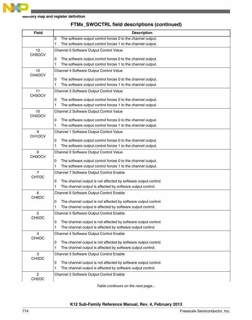
FTMx_SWOCTRL field descriptions (continued)
Field Description
0 The software output control forces 0 to the channel output.1 The software output control forces 1 to the channel output.
13CH5OCV
Channel 5 Software Output Control Value
0 The software output control forces 0 to the channel output.1 The software output control forces 1 to the channel output.
12CH4OCV
Channel 4 Software Output Control Value
0 The software output control forces 0 to the channel output.1 The software output control forces 1 to the channel output.
11CH3OCV
Channel 3 Software Output Control Value
0 The software output control forces 0 to the channel output.1 The software output control forces 1 to the channel output.
10CH2OCV
Channel 2 Software Output Control Value
0 The software output control forces 0 to the channel output.1 The software output control forces 1 to the channel output.
9CH1OCV
Channel 1 Software Output Control Value
0 The software output control forces 0 to the channel output.1 The software output control forces 1 to the channel output.
8CH0OCV
Channel 0 Software Output Control Value
0 The software output control forces 0 to the channel output.1 The software output control forces 1 to the channel output.
7CH7OC
Channel 7 Software Output Control Enable
0 The channel output is not affected by software output control.1 The channel output is affected by software output control.
6CH6OC
Channel 6 Software Output Control Enable
0 The channel output is not affected by software output control.1 The channel output is affected by software output control.
5CH5OC
Channel 5 Software Output Control Enable
0 The channel output is not affected by software output control.1 The channel output is affected by software output control.
4CH4OC
Channel 4 Software Output Control Enable
0 The channel output is not affected by software output control.1 The channel output is affected by software output control.
3CH3OC
Channel 3 Software Output Control Enable
0 The channel output is not affected by software output control.1 The channel output is affected by software output control.
2CH2OC
Channel 2 Software Output Control Enable
Table continues on the next page...
Memory map and register definition
K12 Sub-Family Reference Manual, Rev. 4, February 2013
774 Freescale Semiconductor, Inc.

FTMx_SWOCTRL field descriptions (continued)
Field Description
0 The channel output is not affected by software output control.1 The channel output is affected by software output control.
1CH1OC
Channel 1 Software Output Control Enable
0 The channel output is not affected by software output control.1 The channel output is affected by software output control.
0CH0OC
Channel 0 Software Output Control Enable
0 The channel output is not affected by software output control.1 The channel output is affected by software output control.
36.3.27 FTM PWM Load (FTMx_PWMLOAD)
Enables the loading of the MOD, CNTIN, C(n)V, and C(n+1)V registers with the valuesof their write buffers when the FTM counter changes from the MOD register value to itsnext value or when a channel (j) match occurs. A match occurs for the channel (j) whenFTM counter = C(j)V.
Address: Base address + 98h offset
Bit 31 30 29 28 27 26 25 24 23 22 21 20 19 18 17 16
R 0
W
Reset 0 0 0 0 0 0 0 0 0 0 0 0 0 0 0 0
Bit 15 14 13 12 11 10 9 8 7 6 5 4 3 2 1 0
R 0
LDO
K
0
CH
7SE
L
CH
6SE
L
CH
5SE
L
CH
4SE
L
CH
3SE
L
CH
2SE
L
CH
1SE
L
CH
0SE
L
W
Reset 0 0 0 0 0 0 0 0 0 0 0 0 0 0 0 0
FTMx_PWMLOAD field descriptions
Field Description
31–10Reserved
This field is reserved.This read-only field is reserved and always has the value 0.
9LDOK
Load Enable
Enables the loading of the MOD, CNTIN, and CV registers with the values of their write buffers.
0 Loading updated values is disabled.1 Loading updated values is enabled.
Table continues on the next page...
Chapter 36 FlexTimer Module (FTM)
K12 Sub-Family Reference Manual, Rev. 4, February 2013
Freescale Semiconductor, Inc. 775
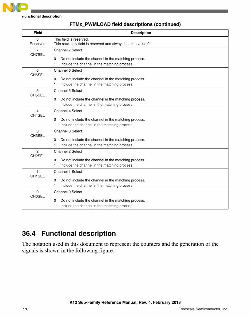
FTMx_PWMLOAD field descriptions (continued)
Field Description
8Reserved
This field is reserved.This read-only field is reserved and always has the value 0.
7CH7SEL
Channel 7 Select
0 Do not include the channel in the matching process.1 Include the channel in the matching process.
6CH6SEL
Channel 6 Select
0 Do not include the channel in the matching process.1 Include the channel in the matching process.
5CH5SEL
Channel 5 Select
0 Do not include the channel in the matching process.1 Include the channel in the matching process.
4CH4SEL
Channel 4 Select
0 Do not include the channel in the matching process.1 Include the channel in the matching process.
3CH3SEL
Channel 3 Select
0 Do not include the channel in the matching process.1 Include the channel in the matching process.
2CH2SEL
Channel 2 Select
0 Do not include the channel in the matching process.1 Include the channel in the matching process.
1CH1SEL
Channel 1 Select
0 Do not include the channel in the matching process.1 Include the channel in the matching process.
0CH0SEL
Channel 0 Select
0 Do not include the channel in the matching process.1 Include the channel in the matching process.
36.4 Functional descriptionThe notation used in this document to represent the counters and the generation of thesignals is shown in the following figure.
Functional description
K12 Sub-Family Reference Manual, Rev. 4, February 2013
776 Freescale Semiconductor, Inc.
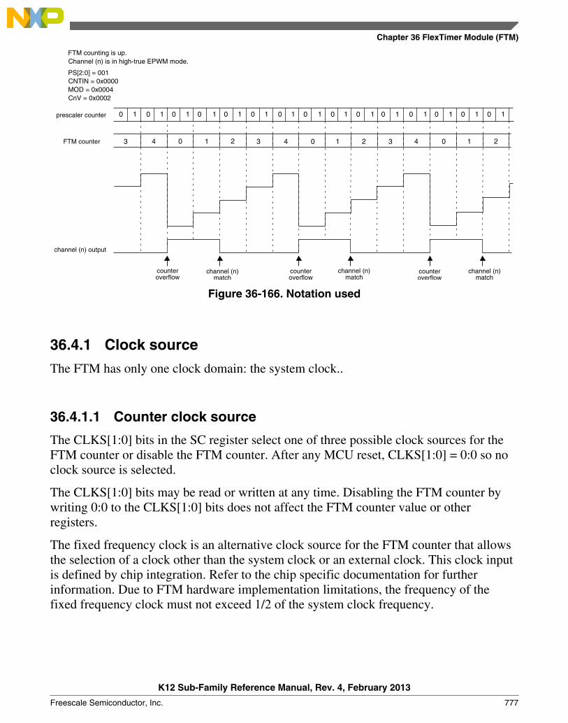
FTM counter
0
3 4 0 1 2 3 4 0 1 2 3 4 0 1 2
0 0 0 0 0 01 1 1 1 1 1 11 1 1 1 1 1 1 10 0 0 0 0 0 0 0prescaler counter
channel (n) output
counteroverflow
channel (n)match
counteroverflow
channel (n)match
channel (n)match
counteroverflow
FTM counting is up.Channel (n) is in high-true EPWM mode.
PS[2:0] = 001CNTIN = 0x0000MOD = 0x0004CnV = 0x0002
Figure 36-166. Notation used
36.4.1 Clock source
The FTM has only one clock domain: the system clock..
36.4.1.1 Counter clock source
The CLKS[1:0] bits in the SC register select one of three possible clock sources for theFTM counter or disable the FTM counter. After any MCU reset, CLKS[1:0] = 0:0 so noclock source is selected.
The CLKS[1:0] bits may be read or written at any time. Disabling the FTM counter bywriting 0:0 to the CLKS[1:0] bits does not affect the FTM counter value or otherregisters.
The fixed frequency clock is an alternative clock source for the FTM counter that allowsthe selection of a clock other than the system clock or an external clock. This clock inputis defined by chip integration. Refer to the chip specific documentation for furtherinformation. Due to FTM hardware implementation limitations, the frequency of thefixed frequency clock must not exceed 1/2 of the system clock frequency.
Chapter 36 FlexTimer Module (FTM)
K12 Sub-Family Reference Manual, Rev. 4, February 2013
Freescale Semiconductor, Inc. 777
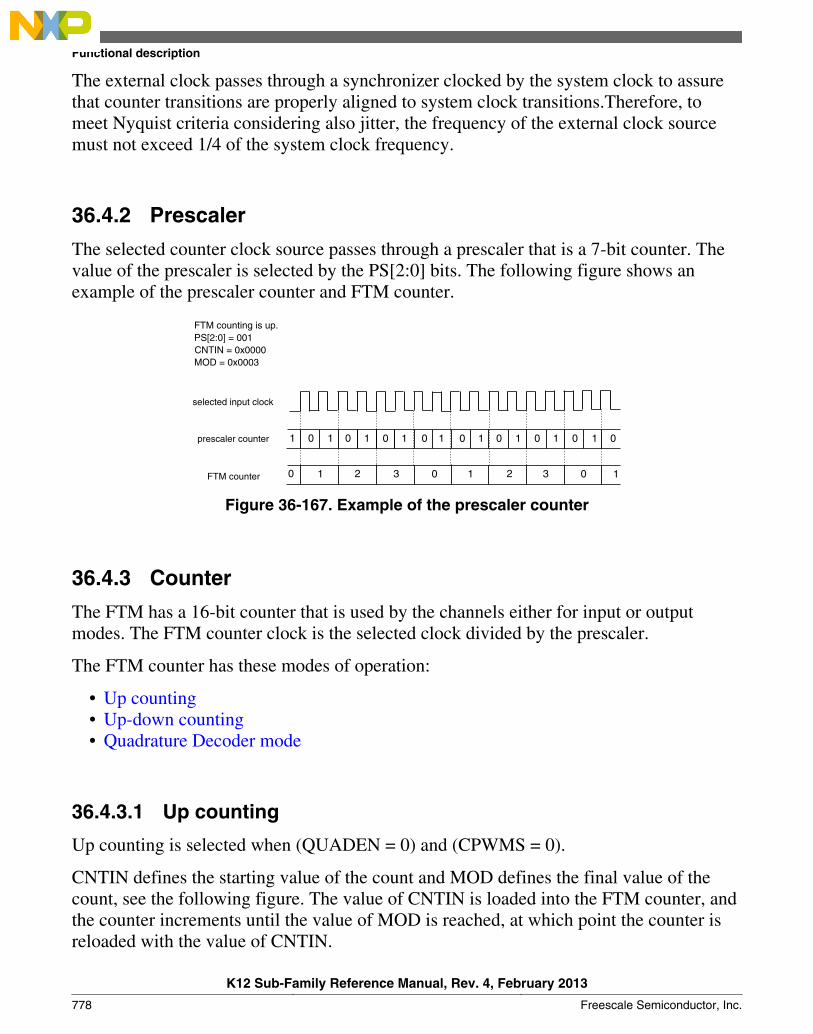
The external clock passes through a synchronizer clocked by the system clock to assurethat counter transitions are properly aligned to system clock transitions.Therefore, tomeet Nyquist criteria considering also jitter, the frequency of the external clock sourcemust not exceed 1/4 of the system clock frequency.
36.4.2 Prescaler
The selected counter clock source passes through a prescaler that is a 7-bit counter. Thevalue of the prescaler is selected by the PS[2:0] bits. The following figure shows anexample of the prescaler counter and FTM counter.
FTM counter
0
0
00 0
0 0
0 00 0 01
1 12 23 3
11 1 1 11 1 1
1
selected input clock
prescaler counter
FTM counting is up.PS[2:0] = 001CNTIN = 0x0000MOD = 0x0003
Figure 36-167. Example of the prescaler counter
36.4.3 Counter
The FTM has a 16-bit counter that is used by the channels either for input or outputmodes. The FTM counter clock is the selected clock divided by the prescaler.
The FTM counter has these modes of operation:
• Up counting• Up-down counting• Quadrature Decoder mode
36.4.3.1 Up counting
Up counting is selected when (QUADEN = 0) and (CPWMS = 0).
CNTIN defines the starting value of the count and MOD defines the final value of thecount, see the following figure. The value of CNTIN is loaded into the FTM counter, andthe counter increments until the value of MOD is reached, at which point the counter isreloaded with the value of CNTIN.
Functional description
K12 Sub-Family Reference Manual, Rev. 4, February 2013
778 Freescale Semiconductor, Inc.

The FTM period when using up counting is (MOD – CNTIN + 0x0001) × period of theFTM counter clock.
The TOF bit is set when the FTM counter changes from MOD to CNTIN.
FTM counting is up.
FTM counter (in decimal values)
period of FTM counter clock
MOD = 0x0004
TOF bit
set TOF bitset TOF bit set TOF bit
4 -4 -3 -2 -1 -4 -3 -2 -10 1 2 3 4 0 1 2 3 4 -4 -3
CNTIN = 0xFFFC (in two's complement is equal to -4)
period of counting = (MOD - CNTIN + 0x0001) x period of FTM counter clock
Figure 36-168. Example of FTM up and signed counting
Table 36-242. FTM counting based on CNTIN value
When Then
CNTIN = 0x0000 The FTM counting is equivalent to TPM up counting, that is,up and unsigned counting. See the following figure.
CNTIN[15] = 1 The initial value of the FTM counter is a negative number intwo's complement, so the FTM counting is up and signed.
CNTIN[15] = 0 and CNTIN ≠ 0x0000 The initial value of the FTM counter is a positive number, sothe FTM counting is up and unsigned.
Chapter 36 FlexTimer Module (FTM)
K12 Sub-Family Reference Manual, Rev. 4, February 2013
Freescale Semiconductor, Inc. 779
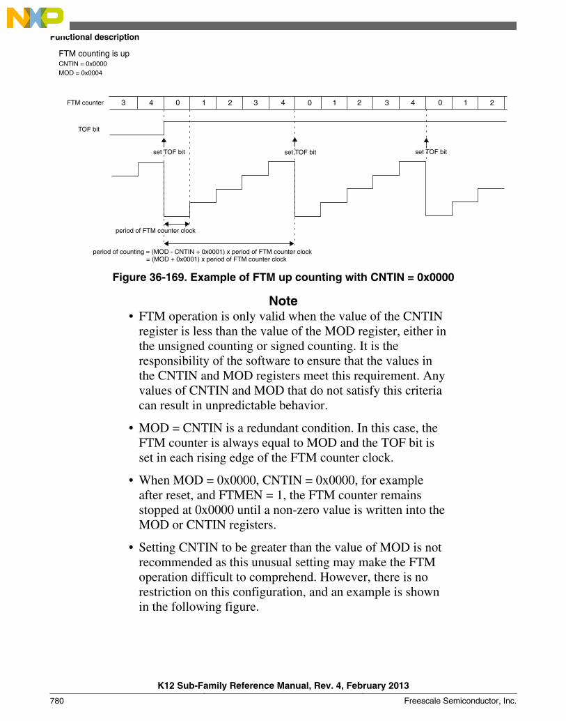
CNTIN = 0x0000MOD = 0x0004
FTM counting is up
TOF bit
3 4 0 01 12 23 34 4 0 1 2FTM counter
set TOF bit
period of FTM counter clock
period of counting = (MOD - CNTIN + 0x0001) x period of FTM counter clock
set TOF bit set TOF bit
= (MOD + 0x0001) x period of FTM counter clock
Figure 36-169. Example of FTM up counting with CNTIN = 0x0000
Note• FTM operation is only valid when the value of the CNTIN
register is less than the value of the MOD register, either inthe unsigned counting or signed counting. It is theresponsibility of the software to ensure that the values inthe CNTIN and MOD registers meet this requirement. Anyvalues of CNTIN and MOD that do not satisfy this criteriacan result in unpredictable behavior.
• MOD = CNTIN is a redundant condition. In this case, theFTM counter is always equal to MOD and the TOF bit isset in each rising edge of the FTM counter clock.
• When MOD = 0x0000, CNTIN = 0x0000, for exampleafter reset, and FTMEN = 1, the FTM counter remainsstopped at 0x0000 until a non-zero value is written into theMOD or CNTIN registers.
• Setting CNTIN to be greater than the value of MOD is notrecommended as this unusual setting may make the FTMoperation difficult to comprehend. However, there is norestriction on this configuration, and an example is shownin the following figure.
Functional description
K12 Sub-Family Reference Manual, Rev. 4, February 2013
780 Freescale Semiconductor, Inc.
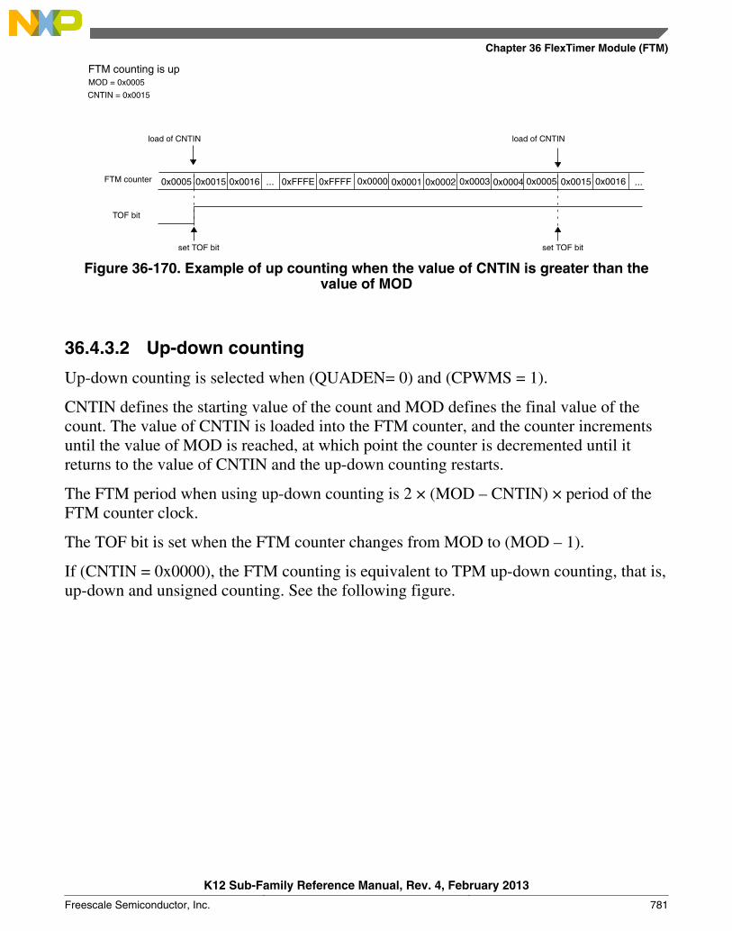
FTM counter ......
FTM counting is up
TOF bit
0x0005 0x0015 0x0016 0xFFFE 0xFFFF 0x0000 0x0001 0x0002 0x0003 0x0004 0x0005 0x0015 0x0016
MOD = 0x0005
CNTIN = 0x0015
set TOF bit set TOF bit
load of CNTIN load of CNTIN
Figure 36-170. Example of up counting when the value of CNTIN is greater than thevalue of MOD
36.4.3.2 Up-down counting
Up-down counting is selected when (QUADEN= 0) and (CPWMS = 1).
CNTIN defines the starting value of the count and MOD defines the final value of thecount. The value of CNTIN is loaded into the FTM counter, and the counter incrementsuntil the value of MOD is reached, at which point the counter is decremented until itreturns to the value of CNTIN and the up-down counting restarts.
The FTM period when using up-down counting is 2 × (MOD – CNTIN) × period of theFTM counter clock.
The TOF bit is set when the FTM counter changes from MOD to (MOD – 1).
If (CNTIN = 0x0000), the FTM counting is equivalent to TPM up-down counting, that is,up-down and unsigned counting. See the following figure.
Chapter 36 FlexTimer Module (FTM)
K12 Sub-Family Reference Manual, Rev. 4, February 2013
Freescale Semiconductor, Inc. 781
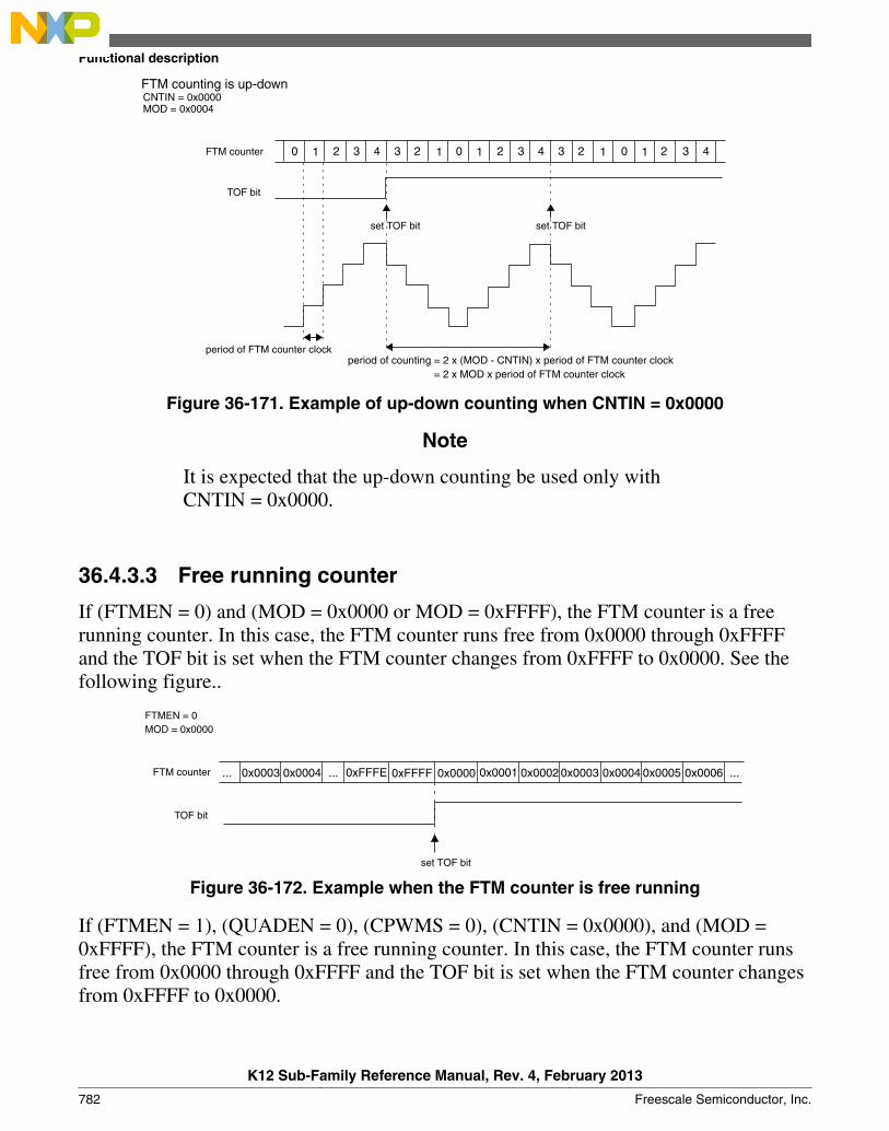
FTM counter 0 0 01 1 11 12 2 22 23 3 33 34 4 4
FTM counting is up-down
TOF bit
set TOF bit set TOF bit
period of FTM counter clockperiod of counting = 2 x (MOD - CNTIN) x period of FTM counter clock
= 2 x MOD x period of FTM counter clock
CNTIN = 0x0000MOD = 0x0004
Figure 36-171. Example of up-down counting when CNTIN = 0x0000
Note
It is expected that the up-down counting be used only withCNTIN = 0x0000.
36.4.3.3 Free running counter
If (FTMEN = 0) and (MOD = 0x0000 or MOD = 0xFFFF), the FTM counter is a freerunning counter. In this case, the FTM counter runs free from 0x0000 through 0xFFFFand the TOF bit is set when the FTM counter changes from 0xFFFF to 0x0000. See thefollowing figure..
FTM counter 0x00040x0004 0xFFFE 0xFFFF0x0003 0x0000 0x0001 0x0002 0x0003 0x0005 0x0006
TOF bit
... ... ...
FTMEN = 0
set TOF bit
MOD = 0x0000
Figure 36-172. Example when the FTM counter is free running
If (FTMEN = 1), (QUADEN = 0), (CPWMS = 0), (CNTIN = 0x0000), and (MOD =0xFFFF), the FTM counter is a free running counter. In this case, the FTM counter runsfree from 0x0000 through 0xFFFF and the TOF bit is set when the FTM counter changesfrom 0xFFFF to 0x0000.
Functional description
K12 Sub-Family Reference Manual, Rev. 4, February 2013
782 Freescale Semiconductor, Inc.

36.4.3.4 Counter reset
Any write to CNT resets the FTM counter to the value in the CNTIN register and thechannels output to its initial value, except for channels in Output Compare mode.
The FTM counter synchronization can also be used to force the value of CNTIN into theFTM counter and the channels output to its initial value, except for channels in OutputCompare mode.
36.4.3.5 When the TOF bit is set
The NUMTOF[4:0] bits define the number of times that the FTM counter overflowshould occur before the TOF bit to be set. If NUMTOF[4:0] = 0x00, then the TOF bit isset at each FTM counter overflow.
FTM counter
NUMTOF[4:0]
TOF counter
set TOF bit
0x01 0x02 0x00 0x01 0x02 0x00 0x01 0x02
0x02
Figure 36-173. Periodic TOF when NUMTOF = 0x02
FTM counter
NUMTOF[4:0]
TOF counter
set TOF bit
0x00
0x00
Figure 36-174. Periodic TOF when NUMTOF = 0x00
36.4.4 Input Capture mode
The Input Capture mode is selected when:
Chapter 36 FlexTimer Module (FTM)
K12 Sub-Family Reference Manual, Rev. 4, February 2013
Freescale Semiconductor, Inc. 783
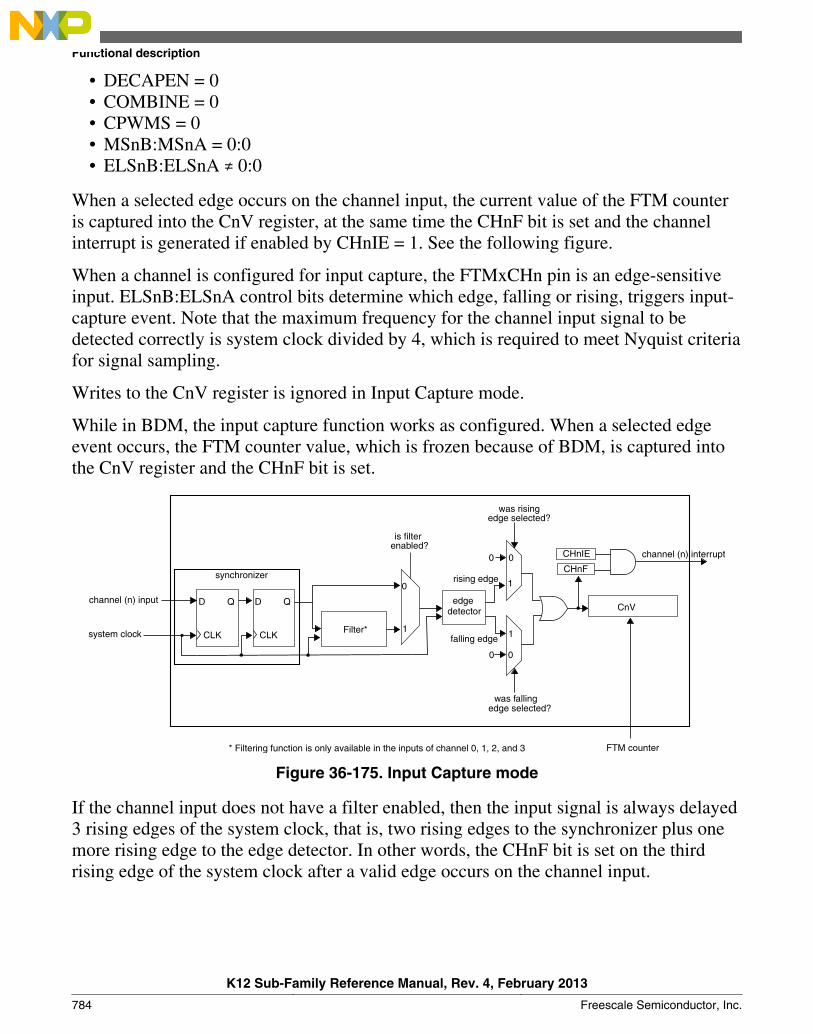
• DECAPEN = 0• COMBINE = 0• CPWMS = 0• MSnB:MSnA = 0:0• ELSnB:ELSnA ≠ 0:0
When a selected edge occurs on the channel input, the current value of the FTM counteris captured into the CnV register, at the same time the CHnF bit is set and the channelinterrupt is generated if enabled by CHnIE = 1. See the following figure.
When a channel is configured for input capture, the FTMxCHn pin is an edge-sensitiveinput. ELSnB:ELSnA control bits determine which edge, falling or rising, triggers input-capture event. Note that the maximum frequency for the channel input signal to bedetected correctly is system clock divided by 4, which is required to meet Nyquist criteriafor signal sampling.
Writes to the CnV register is ignored in Input Capture mode.
While in BDM, the input capture function works as configured. When a selected edgeevent occurs, the FTM counter value, which is frozen because of BDM, is captured intothe CnV register and the CHnF bit is set.
channel (n) input
synchronizer
1
is filter enabled?
edgedetector
was fallingedge selected?
was risingedge selected?
rising edge
falling edge
0
1
1
0
0 0
CnV
FTM counter
D Q
CLK
D Q
CLKsystem clock
channel (n) interruptCHnIE
CHnF
Filter*
0
* Filtering function is only available in the inputs of channel 0, 1, 2, and 3
Figure 36-175. Input Capture mode
If the channel input does not have a filter enabled, then the input signal is always delayed3 rising edges of the system clock, that is, two rising edges to the synchronizer plus onemore rising edge to the edge detector. In other words, the CHnF bit is set on the thirdrising edge of the system clock after a valid edge occurs on the channel input.
Functional description
K12 Sub-Family Reference Manual, Rev. 4, February 2013
784 Freescale Semiconductor, Inc.
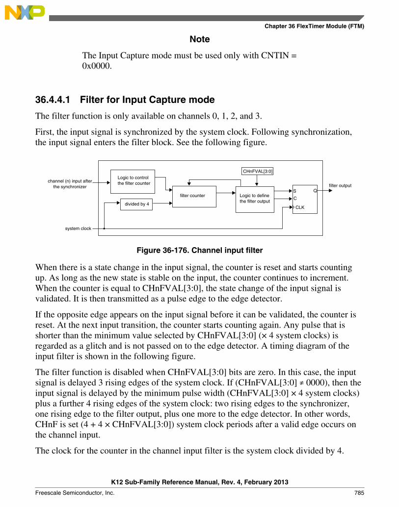
Note
The Input Capture mode must be used only with CNTIN =0x0000.
36.4.4.1 Filter for Input Capture mode
The filter function is only available on channels 0, 1, 2, and 3.
First, the input signal is synchronized by the system clock. Following synchronization,the input signal enters the filter block. See the following figure.
system clock
filter counter Logic to definethe filter output
filter output
divided by 4
channel (n) input afterthe synchronizer
Logic to controlthe filter counter
CHnFVAL[3:0]
C
S Q
CLK
Figure 36-176. Channel input filter
When there is a state change in the input signal, the counter is reset and starts countingup. As long as the new state is stable on the input, the counter continues to increment.When the counter is equal to CHnFVAL[3:0], the state change of the input signal isvalidated. It is then transmitted as a pulse edge to the edge detector.
If the opposite edge appears on the input signal before it can be validated, the counter isreset. At the next input transition, the counter starts counting again. Any pulse that isshorter than the minimum value selected by CHnFVAL[3:0] (× 4 system clocks) isregarded as a glitch and is not passed on to the edge detector. A timing diagram of theinput filter is shown in the following figure.
The filter function is disabled when CHnFVAL[3:0] bits are zero. In this case, the inputsignal is delayed 3 rising edges of the system clock. If (CHnFVAL[3:0] ≠ 0000), then theinput signal is delayed by the minimum pulse width (CHnFVAL[3:0] × 4 system clocks)plus a further 4 rising edges of the system clock: two rising edges to the synchronizer,one rising edge to the filter output, plus one more to the edge detector. In other words,CHnF is set (4 + 4 × CHnFVAL[3:0]) system clock periods after a valid edge occurs onthe channel input.
The clock for the counter in the channel input filter is the system clock divided by 4.
Chapter 36 FlexTimer Module (FTM)
K12 Sub-Family Reference Manual, Rev. 4, February 2013
Freescale Semiconductor, Inc. 785
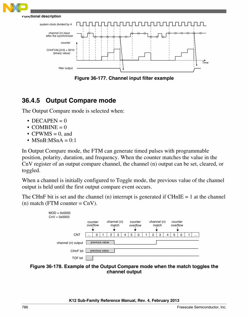
CHnFVAL[3:0] = 0010 (binary value)
channel (n) input after the synchronizer
counter
filter output
system clock divided by 4
Time
Figure 36-177. Channel input filter example
36.4.5 Output Compare mode
The Output Compare mode is selected when:
• DECAPEN = 0• COMBINE = 0• CPWMS = 0, and• MSnB:MSnA = 0:1
In Output Compare mode, the FTM can generate timed pulses with programmableposition, polarity, duration, and frequency. When the counter matches the value in theCnV register of an output compare channel, the channel (n) output can be set, cleared, ortoggled.
When a channel is initially configured to Toggle mode, the previous value of the channeloutput is held until the first output compare event occurs.
The CHnF bit is set and the channel (n) interrupt is generated if CHnIE = 1 at the channel(n) match (FTM counter = CnV).
TOF bit
...... 0 1 1 12 23 34 45 50 0
previous value
previous value
channel (n) output
counteroverflow
counteroverflow
counteroverflow
channel (n)match
channel (n)match
CNT
MOD = 0x0005CnV = 0x0003
CHnF bit
Figure 36-178. Example of the Output Compare mode when the match toggles thechannel output
Functional description
K12 Sub-Family Reference Manual, Rev. 4, February 2013
786 Freescale Semiconductor, Inc.
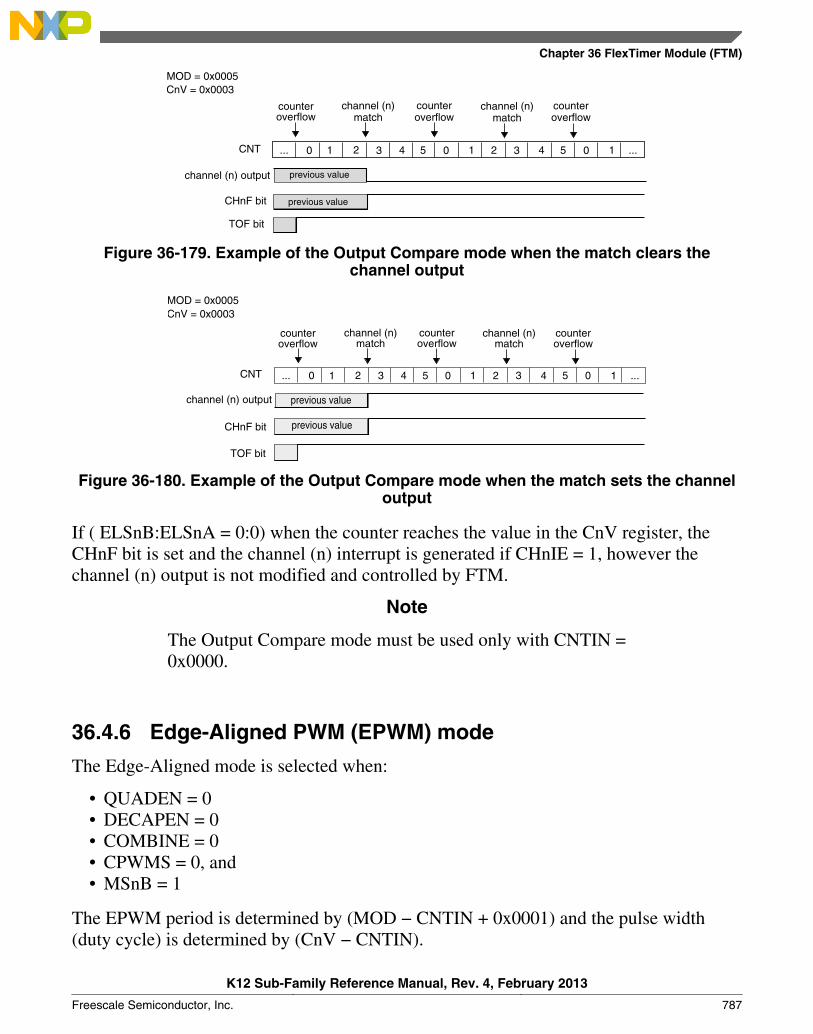
TOF bit
...... 0 1 1 12 23 34 45 50 0
previous value
previous value
channel (n) output
counteroverflow
counteroverflow
counteroverflow
channel (n)match
channel (n)match
CNT
MOD = 0x0005CnV = 0x0003
CHnF bit
Figure 36-179. Example of the Output Compare mode when the match clears thechannel output
channel (n) output
CHnF bit
TOF bit
CNT
MOD = 0x0005CnV = 0x0003
counteroverflow
channel (n)match
counteroverflow
channel (n)match
counteroverflow
... 0 1 2 3 4 5 0 1 2 3 4 5 0 1 ...
previous value
previous value
Figure 36-180. Example of the Output Compare mode when the match sets the channeloutput
If ( ELSnB:ELSnA = 0:0) when the counter reaches the value in the CnV register, theCHnF bit is set and the channel (n) interrupt is generated if CHnIE = 1, however thechannel (n) output is not modified and controlled by FTM.
Note
The Output Compare mode must be used only with CNTIN =0x0000.
36.4.6 Edge-Aligned PWM (EPWM) mode
The Edge-Aligned mode is selected when:
• QUADEN = 0• DECAPEN = 0• COMBINE = 0• CPWMS = 0, and• MSnB = 1
The EPWM period is determined by (MOD − CNTIN + 0x0001) and the pulse width(duty cycle) is determined by (CnV − CNTIN).
Chapter 36 FlexTimer Module (FTM)
K12 Sub-Family Reference Manual, Rev. 4, February 2013
Freescale Semiconductor, Inc. 787
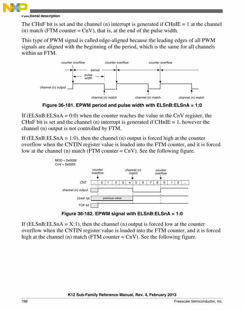
The CHnF bit is set and the channel (n) interrupt is generated if CHnIE = 1 at the channel(n) match (FTM counter = CnV), that is, at the end of the pulse width.
This type of PWM signal is called edge-aligned because the leading edges of all PWMsignals are aligned with the beginning of the period, which is the same for all channelswithin an FTM.
period
counter overflow counter overflow counter overflow
channel (n) output
channel (n) match channel (n) match channel (n) match
pulsewidth
Figure 36-181. EPWM period and pulse width with ELSnB:ELSnA = 1:0
If (ELSnB:ELSnA = 0:0) when the counter reaches the value in the CnV register, theCHnF bit is set and the channel (n) interrupt is generated if CHnIE = 1, however thechannel (n) output is not controlled by FTM.
If (ELSnB:ELSnA = 1:0), then the channel (n) output is forced high at the counteroverflow when the CNTIN register value is loaded into the FTM counter, and it is forcedlow at the channel (n) match (FTM counter = CnV). See the following figure.
TOF bit
CHnF bit
CNT
channel (n) output
MOD = 0x0008CnV = 0x0005
counteroverflow
channel (n)match
counteroverflow
... 0 1 2 3 4 5 6 7 8 0 1 2 ...
previous value
Figure 36-182. EPWM signal with ELSnB:ELSnA = 1:0
If (ELSnB:ELSnA = X:1), then the channel (n) output is forced low at the counteroverflow when the CNTIN register value is loaded into the FTM counter, and it is forcedhigh at the channel (n) match (FTM counter = CnV). See the following figure.
Functional description
K12 Sub-Family Reference Manual, Rev. 4, February 2013
788 Freescale Semiconductor, Inc.

TOF bit
CHnF bit
CNT
channel (n) output
MOD = 0x0008CnV = 0x0005
counteroverflow
channel (n)match
counteroverflow
... 0 1 2 3 4 5 6 7 8 0 1 2 ...
previous value
Figure 36-183. EPWM signal with ELSnB:ELSnA = X:1
If (CnV = 0x0000), then the channel (n) output is a 0% duty cycle EPWM signal andCHnF bit is not set even when there is the channel (n) match. If (CnV > MOD), then thechannel (n) output is a 100% duty cycle EPWM signal and CHnF bit is not set even whenthere is the channel (n) match. Therefore, MOD must be less than 0xFFFF in order to geta 100% duty cycle EPWM signal.
Note
The EPWM mode must be used only with CNTIN = 0x0000.
36.4.7 Center-Aligned PWM (CPWM) mode
The Center-Aligned mode is selected when:
• QUADEN = 0• DECAPEN = 0• COMBINE = 0, and• CPWMS = 1
The CPWM pulse width (duty cycle) is determined by 2 × (CnV − CNTIN) and theperiod is determined by 2 × (MOD − CNTIN). See the following figure. MOD must bekept in the range of 0x0001 to 0x7FFF because values outside this range can produceambiguous results.
In the CPWM mode, the FTM counter counts up until it reaches MOD and then countsdown until it reaches CNTIN.
The CHnF bit is set and channel (n) interrupt is generated (if CHnIE = 1) at the channel(n) match (FTM counter = CnV) when the FTM counting is down (at the begin of thepulse width) and when the FTM counting is up (at the end of the pulse width).
This type of PWM signal is called center-aligned because the pulse width centers for allchannels are aligned with the value of CNTIN.
Chapter 36 FlexTimer Module (FTM)
K12 Sub-Family Reference Manual, Rev. 4, February 2013
Freescale Semiconductor, Inc. 789
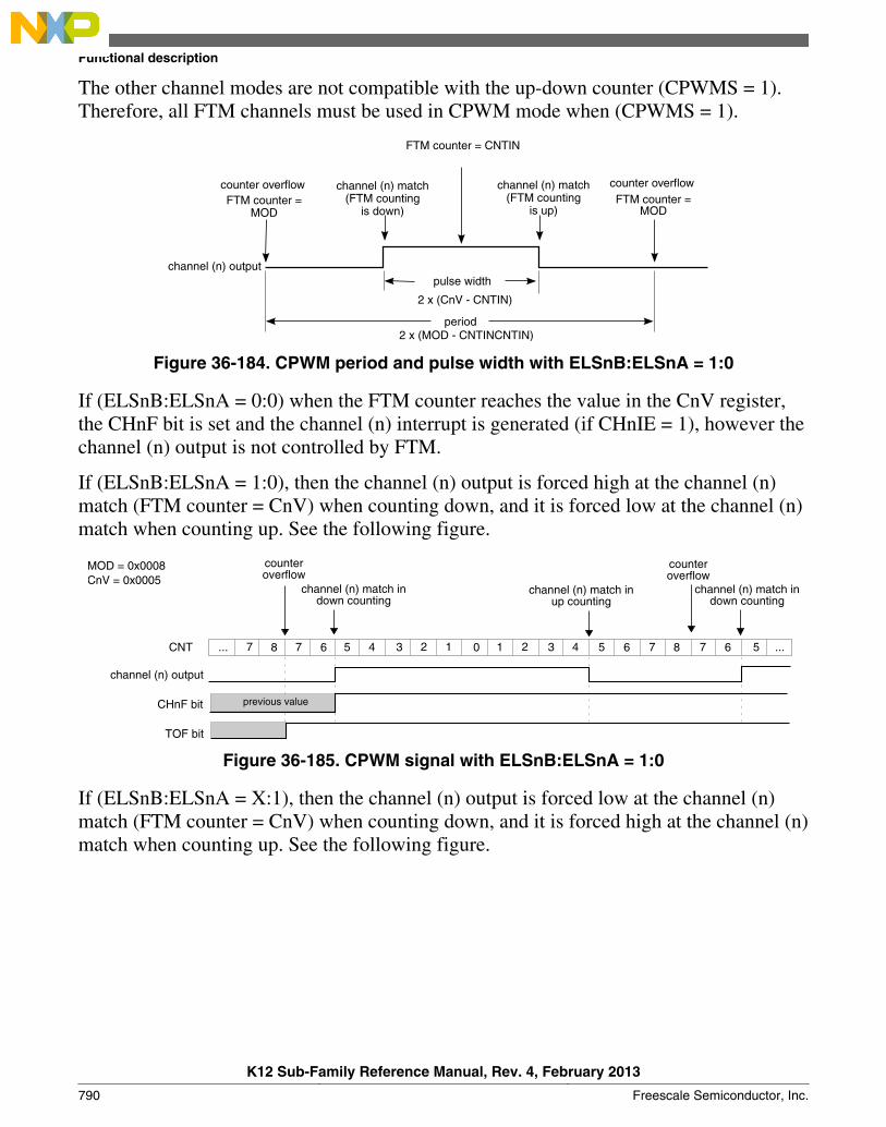
The other channel modes are not compatible with the up-down counter (CPWMS = 1).Therefore, all FTM channels must be used in CPWM mode when (CPWMS = 1).
pulse width
counter overflowFTM counter =
MOD
period
2 x (CnV - CNTIN)
2 x (MOD - CNTINCNTIN)
FTM counter = CNTIN
channel (n) match(FTM counting
is down)
channel (n) match(FTM counting
is up)
counter overflowFTM counter =
MOD
channel (n) output
Figure 36-184. CPWM period and pulse width with ELSnB:ELSnA = 1:0
If (ELSnB:ELSnA = 0:0) when the FTM counter reaches the value in the CnV register,the CHnF bit is set and the channel (n) interrupt is generated (if CHnIE = 1), however thechannel (n) output is not controlled by FTM.
If (ELSnB:ELSnA = 1:0), then the channel (n) output is forced high at the channel (n)match (FTM counter = CnV) when counting down, and it is forced low at the channel (n)match when counting up. See the following figure.
TOF bit
... 7 8 87 7 76 6 6 5 5 54 43 32 21 0 1 ...
previous value
CNT
channel (n) output
counteroverflow
channel (n) match indown counting
channel (n) match inup counting
channel (n) match indown counting
counteroverflow
CHnF bit
MOD = 0x0008CnV = 0x0005
Figure 36-185. CPWM signal with ELSnB:ELSnA = 1:0
If (ELSnB:ELSnA = X:1), then the channel (n) output is forced low at the channel (n)match (FTM counter = CnV) when counting down, and it is forced high at the channel (n)match when counting up. See the following figure.
Functional description
K12 Sub-Family Reference Manual, Rev. 4, February 2013
790 Freescale Semiconductor, Inc.
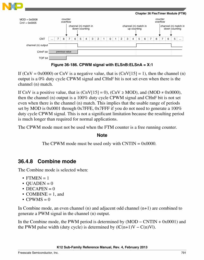
TOF bit
... 7 8 87 7 76 6 6 5 5 54 43 32 21 0 1 ...
previous value
CNT
channel (n) output
counteroverflow
channel (n) match indown counting
channel (n) match inup counting
channel (n) match indown counting
counteroverflow
CHnF bit
MOD = 0x0008CnV = 0x0005
Figure 36-186. CPWM signal with ELSnB:ELSnA = X:1
If (CnV = 0x0000) or CnV is a negative value, that is (CnV[15] = 1), then the channel (n)output is a 0% duty cycle CPWM signal and CHnF bit is not set even when there is thechannel (n) match.
If CnV is a positive value, that is (CnV[15] = 0), (CnV ≥ MOD), and (MOD ≠ 0x0000),then the channel (n) output is a 100% duty cycle CPWM signal and CHnF bit is not seteven when there is the channel (n) match. This implies that the usable range of periodsset by MOD is 0x0001 through 0x7FFE, 0x7FFF if you do not need to generate a 100%duty cycle CPWM signal. This is not a significant limitation because the resulting periodis much longer than required for normal applications.
The CPWM mode must not be used when the FTM counter is a free running counter.
Note
The CPWM mode must be used only with CNTIN = 0x0000.
36.4.8 Combine mode
The Combine mode is selected when:
• FTMEN = 1• QUADEN = 0• DECAPEN = 0• COMBINE = 1, and• CPWMS = 0
In Combine mode, an even channel (n) and adjacent odd channel (n+1) are combined togenerate a PWM signal in the channel (n) output.
In the Combine mode, the PWM period is determined by (MOD − CNTIN + 0x0001) andthe PWM pulse width (duty cycle) is determined by (|C(n+1)V − C(n)V|).
Chapter 36 FlexTimer Module (FTM)
K12 Sub-Family Reference Manual, Rev. 4, February 2013
Freescale Semiconductor, Inc. 791

The CHnF bit is set and the channel (n) interrupt is generated (if CHnIE = 1) at thechannel (n) match (FTM counter = C(n)V). The CH(n+1)F bit is set and the channel (n+1) interrupt is generated, if CH(n+1)IE = 1, at the channel (n+1) match (FTM counter =C(n+1)V).
If (ELSnB:ELSnA = 1:0), then the channel (n) output is forced low at the beginning ofthe period (FTM counter = CNTIN) and at the channel (n+1) match (FTM counter = C(n+1)V). It is forced high at the channel (n) match (FTM counter = C(n)V). See thefollowing figure.
If (ELSnB:ELSnA = X:1), then the channel (n) output is forced high at the beginning ofthe period (FTM counter = CNTIN) and at the channel (n+1) match (FTM counter = C(n+1)V). It is forced low at the channel (n) match (FTM counter = C(n)V). See thefollowing figure.
In Combine mode, the ELS(n+1)B and ELS(n+1)A bits are not used in the generation ofthe channels (n) and (n+1) output. However, if (ELSnB:ELSnA = 0:0) then the channel(n) output is not controlled by FTM, and if (ELS(n+1)B:ELS(n+1)A = 0:0) then thechannel (n+1) output is not controlled by FTM.
FTM counterchannel (n) match
channel (n+1) match
channel (n) output
with ELSnB:ELSnA = X:1
with ELSnB:ELSnA = 1:0
channel (n) output
Figure 36-187. Combine mode
The following figures illustrate the PWM signals generation using Combine mode.
Functional description
K12 Sub-Family Reference Manual, Rev. 4, February 2013
792 Freescale Semiconductor, Inc.
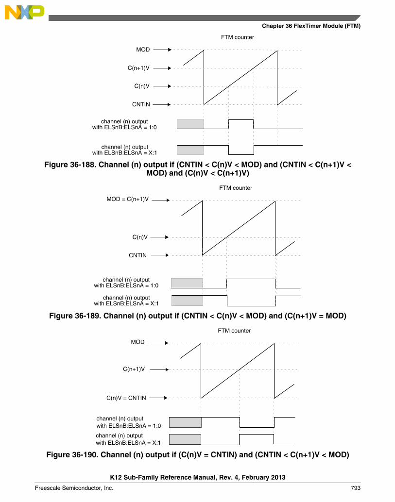
FTM counter
channel (n) outputwith ELSnB:ELSnA = 1:0
channel (n) outputwith ELSnB:ELSnA = X:1
MOD
C(n)V
CNTIN
C(n+1)V
Figure 36-188. Channel (n) output if (CNTIN < C(n)V < MOD) and (CNTIN < C(n+1)V <MOD) and (C(n)V < C(n+1)V)
FTM counter
channel (n) outputwith ELSnB:ELSnA = 1:0
channel (n) outputwith ELSnB:ELSnA = X:1
MOD = C(n+1)V
C(n)V
CNTIN
Figure 36-189. Channel (n) output if (CNTIN < C(n)V < MOD) and (C(n+1)V = MOD)
FTM counter
C(n+1)V
channel (n) outputwith ELSnB:ELSnA = 1:0
channel (n) outputwith ELSnB:ELSnA = X:1
MOD
C(n)V = CNTIN
Figure 36-190. Channel (n) output if (C(n)V = CNTIN) and (CNTIN < C(n+1)V < MOD)
Chapter 36 FlexTimer Module (FTM)
K12 Sub-Family Reference Manual, Rev. 4, February 2013
Freescale Semiconductor, Inc. 793

FTM counter
not fully 100% duty cyclechannel (n) output
with ELSnB:ELSnA = 1:0
not fully 0% duty cyclechannel (n) outputwith ELSnB:ELSnA = X:1
MOD = C(n+1)V
C(n)V
CNTIN
Figure 36-191. Channel (n) output if (CNTIN < C(n)V < MOD) and (C(n)V is Almost Equalto CNTIN) and (C(n+1)V = MOD)
FTM counter
not fully 100% duty cyclechannel (n) output
with ELSnB:ELSnA = 1:0
channel (n) outputwith ELSnB:ELSnA = X:1
not fully 0% duty cycle
MOD
C(n)V = CNTIN
C(n+1)V
Figure 36-192. Channel (n) output if (C(n)V = CNTIN) and (CNTIN < C(n+1)V < MOD) and(C(n+1)V is Almost Equal to MOD)
Functional description
K12 Sub-Family Reference Manual, Rev. 4, February 2013
794 Freescale Semiconductor, Inc.
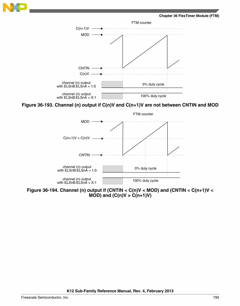
FTM counter
0% duty cyclechannel (n) outputwith ELSnB:ELSnA = 1:0
100% duty cyclechannel (n) outputwith ELSnB:ELSnA = X:1
C(n)V
MOD
CNTIN
C(n+1)V
Figure 36-193. Channel (n) output if C(n)V and C(n+1)V are not between CNTIN and MOD
FTM counter
0% duty cyclechannel (n) outputwith ELSnB:ELSnA = 1:0
channel (n) outputwith ELSnB:ELSnA = X:1 100% duty cycle
MOD
CNTIN
C(n+1)V = C(n)V
Figure 36-194. Channel (n) output if (CNTIN < C(n)V < MOD) and (CNTIN < C(n+1)V <MOD) and (C(n)V = C(n+1)V)
Chapter 36 FlexTimer Module (FTM)
K12 Sub-Family Reference Manual, Rev. 4, February 2013
Freescale Semiconductor, Inc. 795

FTM counter
C(n)V =C(n+1)V = CNTIN
channel (n) outputwith ELSnB:ELSnA = 1:0
channel (n) outputwith ELSnB:ELSnA = X:1 100% duty cycle
0% duty cycle
MOD
Figure 36-195. Channel (n) output if (C(n)V = C(n+1)V = CNTIN)
FTM counter
CNTIN
channel (n) outputwith ELSnB:ELSnA = 1:0
channel (n) outputwith ELSnB:ELSnA = X:1 100% duty cycle
0% duty cycle
MOD =C(n+1)V =
C(n)V
Figure 36-196. Channel (n) output if (C(n)V = C(n+1)V = MOD)
channel (n) matchis ignored
FTM counter
channel (n) outputwith ELSnB:ELSnA = 1:0
channel (n) outputwith ELSnB:ELSnA = X:1
100% duty cycle
0% duty cycle
MOD
C(n)V
CNTIN
C(n+1)V
Figure 36-197. Channel (n) output if (CNTIN < C(n)V < MOD) and (CNTIN < C(n+1)V <MOD) and (C(n)V > C(n+1)V)
Functional description
K12 Sub-Family Reference Manual, Rev. 4, February 2013
796 Freescale Semiconductor, Inc.

FTM counter
C(n)V
channel (n) outputwith ELSnB:ELSnA = 1:0
channel (n) outputwith ELSnB:ELSnA = X:1
0% duty cycle
100% duty cycle
MOD
C(n+1)V
CNTIN
Figure 36-198. Channel (n) output if (C(n)V < CNTIN) and (CNTIN < C(n+1)V < MOD)
C(n+1)V
channel (n) outputwith ELSnB:ELSnA = X:1
FTM counter
CNTIN
channel (n) outputwith ELSnB:ELSnA = 1:0
C(n)V
MOD
Figure 36-199. Channel (n) output if (C(n+1)V < CNTIN) and (CNTIN < C(n)V < MOD)
Chapter 36 FlexTimer Module (FTM)
K12 Sub-Family Reference Manual, Rev. 4, February 2013
Freescale Semiconductor, Inc. 797
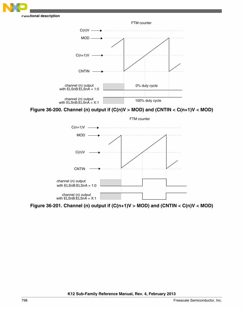
FTM counter
channel (n) outputwith ELSnB:ELSnA = 1:0
channel (n) outputwith ELSnB:ELSnA = X:1 100% duty cycle
0% duty cycle
MOD
C(n)V
C(n+1)V
CNTIN
Figure 36-200. Channel (n) output if (C(n)V > MOD) and (CNTIN < C(n+1)V < MOD)
C(n)V
CNTIN
channel (n) outputwith ELSnB:ELSnA = X:1
channel (n) outputwith ELSnB:ELSnA = 1:0
FTM counter
C(n+1)V
MOD
Figure 36-201. Channel (n) output if (C(n+1)V > MOD) and (CNTIN < C(n)V < MOD)
Functional description
K12 Sub-Family Reference Manual, Rev. 4, February 2013
798 Freescale Semiconductor, Inc.
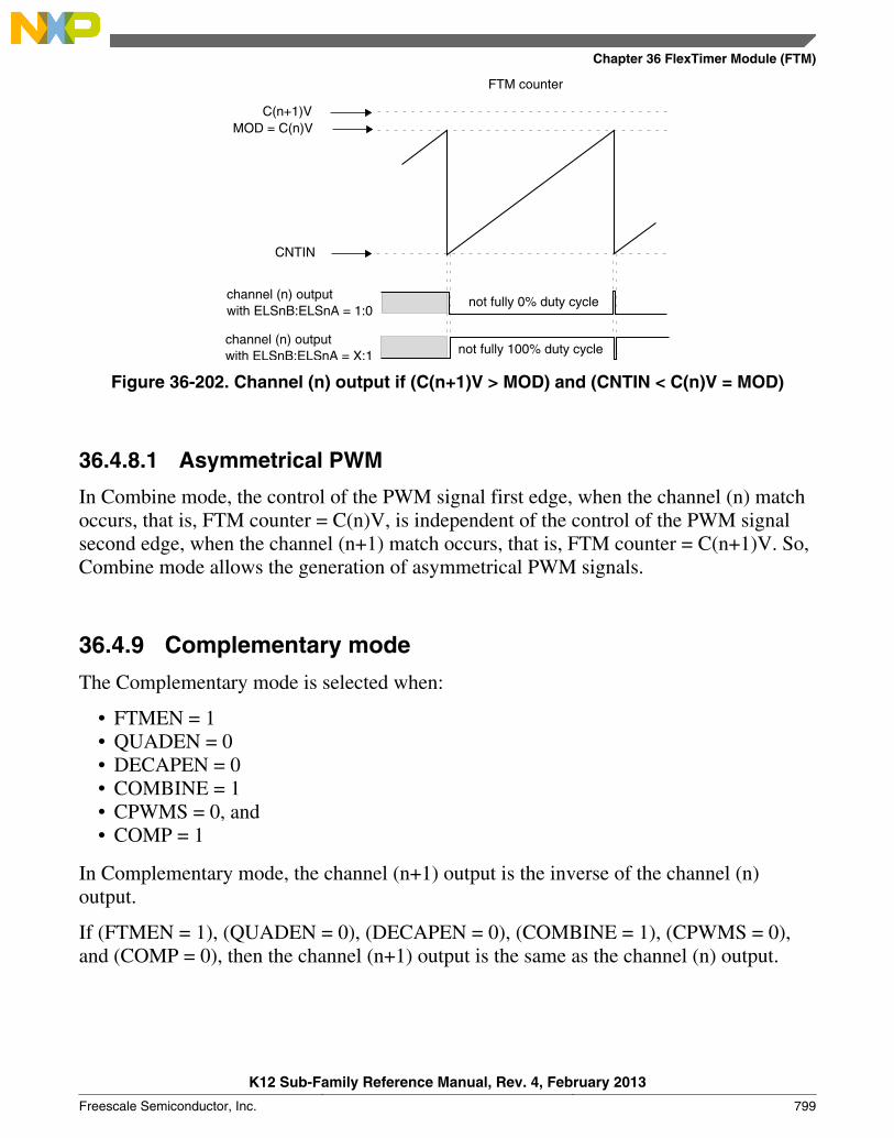
FTM counter
CNTIN
C(n+1)V
not fully 0% duty cyclechannel (n) outputwith ELSnB:ELSnA = 1:0
not fully 100% duty cyclechannel (n) outputwith ELSnB:ELSnA = X:1
MOD = C(n)V
Figure 36-202. Channel (n) output if (C(n+1)V > MOD) and (CNTIN < C(n)V = MOD)
36.4.8.1 Asymmetrical PWM
In Combine mode, the control of the PWM signal first edge, when the channel (n) matchoccurs, that is, FTM counter = C(n)V, is independent of the control of the PWM signalsecond edge, when the channel (n+1) match occurs, that is, FTM counter = C(n+1)V. So,Combine mode allows the generation of asymmetrical PWM signals.
36.4.9 Complementary mode
The Complementary mode is selected when:
• FTMEN = 1• QUADEN = 0• DECAPEN = 0• COMBINE = 1• CPWMS = 0, and• COMP = 1
In Complementary mode, the channel (n+1) output is the inverse of the channel (n)output.
If (FTMEN = 1), (QUADEN = 0), (DECAPEN = 0), (COMBINE = 1), (CPWMS = 0),and (COMP = 0), then the channel (n+1) output is the same as the channel (n) output.
Chapter 36 FlexTimer Module (FTM)
K12 Sub-Family Reference Manual, Rev. 4, February 2013
Freescale Semiconductor, Inc. 799

FTM counter
channel (n+1) match
channel (n+1) outputwith COMP = 1
channel (n+1) outputwith COMP = 0
channel (n) outputwith ELSnB:ELSnA = 1:0
channel (n) match
Figure 36-203. Channel (n+1) output in Complementary mode with (ELSnB:ELSnA = 1:0)
FTM counter
channel (n+1) match
channel (n+1) outputwith COMP = 1
channel (n+1) outputwith COMP = 0
channel (n) outputwith ELSnB:ELSnA = X:1
channel (n) match
Figure 36-204. Channel (n+1) output in Complementary mode with (ELSnB:ELSnA = X:1)
36.4.10 Registers updated from write buffers
36.4.10.1 CNTIN register update
The following table describes when CNTIN register is updated:
Table 36-243. CNTIN register update
When Then CNTIN register is updated
CLKS[1:0] = 0:0 When CNTIN register is written, independent of FTMEN bit.
• FTMEN = 0, or• CNTINC = 0
At the next system clock after CNTIN was written.
• FTMEN = 1,• SYNCMODE = 1, and• CNTINC = 1
By the CNTIN register synchronization.
Functional description
K12 Sub-Family Reference Manual, Rev. 4, February 2013
800 Freescale Semiconductor, Inc.
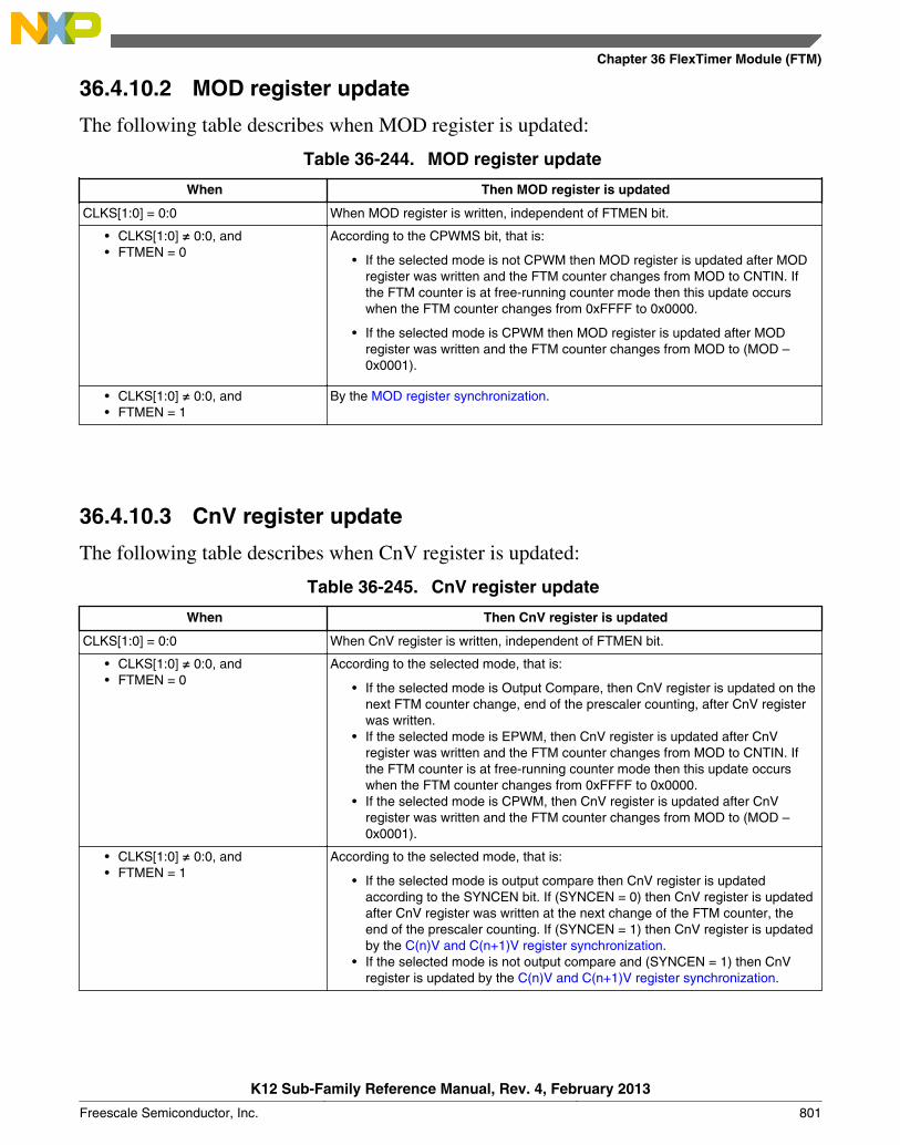
36.4.10.2 MOD register update
The following table describes when MOD register is updated:
Table 36-244. MOD register update
When Then MOD register is updated
CLKS[1:0] = 0:0 When MOD register is written, independent of FTMEN bit.
• CLKS[1:0] ≠ 0:0, and• FTMEN = 0
According to the CPWMS bit, that is:
• If the selected mode is not CPWM then MOD register is updated after MODregister was written and the FTM counter changes from MOD to CNTIN. Ifthe FTM counter is at free-running counter mode then this update occurswhen the FTM counter changes from 0xFFFF to 0x0000.
• If the selected mode is CPWM then MOD register is updated after MODregister was written and the FTM counter changes from MOD to (MOD –0x0001).
• CLKS[1:0] ≠ 0:0, and• FTMEN = 1
By the MOD register synchronization.
36.4.10.3 CnV register update
The following table describes when CnV register is updated:
Table 36-245. CnV register update
When Then CnV register is updated
CLKS[1:0] = 0:0 When CnV register is written, independent of FTMEN bit.
• CLKS[1:0] ≠ 0:0, and• FTMEN = 0
According to the selected mode, that is:
• If the selected mode is Output Compare, then CnV register is updated on thenext FTM counter change, end of the prescaler counting, after CnV registerwas written.
• If the selected mode is EPWM, then CnV register is updated after CnVregister was written and the FTM counter changes from MOD to CNTIN. Ifthe FTM counter is at free-running counter mode then this update occurswhen the FTM counter changes from 0xFFFF to 0x0000.
• If the selected mode is CPWM, then CnV register is updated after CnVregister was written and the FTM counter changes from MOD to (MOD –0x0001).
• CLKS[1:0] ≠ 0:0, and• FTMEN = 1
According to the selected mode, that is:
• If the selected mode is output compare then CnV register is updatedaccording to the SYNCEN bit. If (SYNCEN = 0) then CnV register is updatedafter CnV register was written at the next change of the FTM counter, theend of the prescaler counting. If (SYNCEN = 1) then CnV register is updatedby the C(n)V and C(n+1)V register synchronization.
• If the selected mode is not output compare and (SYNCEN = 1) then CnVregister is updated by the C(n)V and C(n+1)V register synchronization.
Chapter 36 FlexTimer Module (FTM)
K12 Sub-Family Reference Manual, Rev. 4, February 2013
Freescale Semiconductor, Inc. 801
36.4.11 PWM synchronization
The PWM synchronization provides an opportunity to update the MOD, CNTIN, CnV,OUTMASK, INVCTRL and SWOCTRL registers with their buffered value and force theFTM counter to the CNTIN register value.
Note• The PWM synchronization must be used only in Combine
mode.
• The legacy PWM synchronization (SYNCMODE = 0) is asubset of the enhanced PWM synchronization(SYNCMODE = 1). Thus, only the enhanced PWMsynchronization must be used.
36.4.11.1 Hardware trigger
Three hardware trigger signal inputs of the FTM module are enabled when TRIGn = 1,where n = 0, 1 or 2 corresponding to each one of the input signals, respectively. Thehardware trigger input n is synchronized by the system clock. The PWM synchronizationwith hardware trigger is initiated when a rising edge is detected at the enabled hardwaretrigger inputs.
If (HWTRIGMODE = 0) then the TRIGn bit is cleared when 0 is written to it or when thetrigger n event is detected.
In this case, if two or more hardware triggers are enabled (for example, TRIG0 andTRIG1 = 1) and only trigger 1 event occurs, then only TRIG1 bit is cleared. If a trigger nevent occurs together with a write setting TRIGn bit, then the synchronization is initiated,but TRIGn bit remains set due to the write operation.
Functional description
K12 Sub-Family Reference Manual, Rev. 4, February 2013
802 Freescale Semiconductor, Inc.

write 1 to TRIG0 bit
system clock
synchronized trigger_0
trigger 0 event
Note
TRIG0 bit
trigger_0 input
by system clock
All hardware trigger inputs have the same behavior.
Figure 36-205. Hardware trigger event with HWTRIGMODE = 0
If HWTRIGMODE = 1, then the TRIGn bit is only cleared when 0 is written to it.
NOTE
The HWTRIGMODE bit must be 1 only with enhanced PWMsynchronization (SYNCMODE = 1).
36.4.11.2 Software trigger
A software trigger event occurs when 1 is written to the SYNC[SWSYNC] bit. TheSWSYNC bit is cleared when 0 is written to it or when the PWM synchronization,initiated by the software event, is completed.
If another software trigger event occurs (by writing another 1 to the SWSYNC bit) at thesame time the PWM synchronization initiated by the previous software trigger event isending, a new PWM synchronization is started and the SWSYNC bit remains equal to 1.
If SYNCMODE = 0 then the SWSYNC bit is also cleared by FTM according toPWMSYNC and REINIT bits. In this case if (PWMSYNC = 1) or (PWMSYNC = 0 andREINIT = 0) then SWSYNC bit is cleared at the next selected loading point after that thesoftware trigger event occurred; see Boundary cycle and loading points and the followingfigure. If (PWMSYNC = 0) and (REINIT = 1) then SWSYNC bit is cleared when thesoftware trigger event occurs.
If SYNCMODE = 1 then the SWSYNC bit is also cleared by FTM according to theSWRSTCNT bit. If SWRSTCNT = 0 then SWSYNC bit is cleared at the next selectedloading point after that the software trigger event occurred; see the following figure. IfSWRSTCNT = 1 then SWSYNC bit is cleared when the software trigger event occurs.
Chapter 36 FlexTimer Module (FTM)
K12 Sub-Family Reference Manual, Rev. 4, February 2013
Freescale Semiconductor, Inc. 803
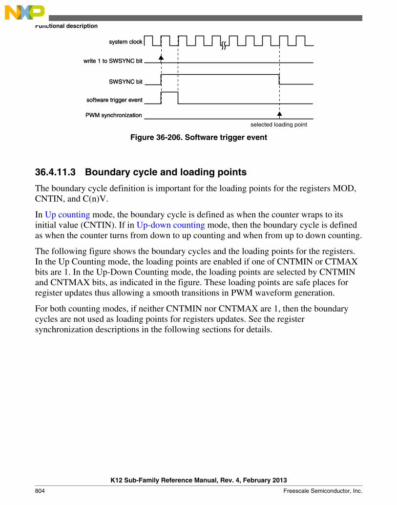
SWSYNC bit
system clock
software trigger event
write 1 to SWSYNC bit
selected loading point
PWM synchronization
SWSYNC bit
system clock
software trigger event
write 1 to SWSYNC bit
PWM synchronization
Figure 36-206. Software trigger event
36.4.11.3 Boundary cycle and loading points
The boundary cycle definition is important for the loading points for the registers MOD,CNTIN, and C(n)V.
In Up counting mode, the boundary cycle is defined as when the counter wraps to itsinitial value (CNTIN). If in Up-down counting mode, then the boundary cycle is definedas when the counter turns from down to up counting and when from up to down counting.
The following figure shows the boundary cycles and the loading points for the registers.In the Up Counting mode, the loading points are enabled if one of CNTMIN or CTMAXbits are 1. In the Up-Down Counting mode, the loading points are selected by CNTMINand CNTMAX bits, as indicated in the figure. These loading points are safe places forregister updates thus allowing a smooth transitions in PWM waveform generation.
For both counting modes, if neither CNTMIN nor CNTMAX are 1, then the boundarycycles are not used as loading points for registers updates. See the registersynchronization descriptions in the following sections for details.
Functional description
K12 Sub-Family Reference Manual, Rev. 4, February 2013
804 Freescale Semiconductor, Inc.
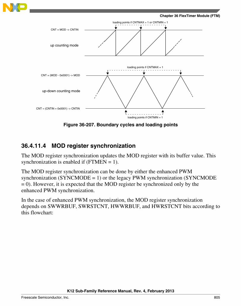
CNT = (MOD - 0x0001) -> MOD
CNT = (CNTIN + 0x0001) -> CNTIN
loading points if CNTMIN = 1
loading points if CNTMAX = 1
up-down counting mode
CNT = MOD -> CNTIN
loading points if CNTMAX = 1 or CNTMIN = 1
up counting mode
Figure 36-207. Boundary cycles and loading points
36.4.11.4 MOD register synchronization
The MOD register synchronization updates the MOD register with its buffer value. Thissynchronization is enabled if (FTMEN = 1).
The MOD register synchronization can be done by either the enhanced PWMsynchronization (SYNCMODE = 1) or the legacy PWM synchronization (SYNCMODE= 0). However, it is expected that the MOD register be synchronized only by theenhanced PWM synchronization.
In the case of enhanced PWM synchronization, the MOD register synchronizationdepends on SWWRBUF, SWRSTCNT, HWWRBUF, and HWRSTCNT bits according tothis flowchart:
Chapter 36 FlexTimer Module (FTM)
K12 Sub-Family Reference Manual, Rev. 4, February 2013
Freescale Semiconductor, Inc. 805
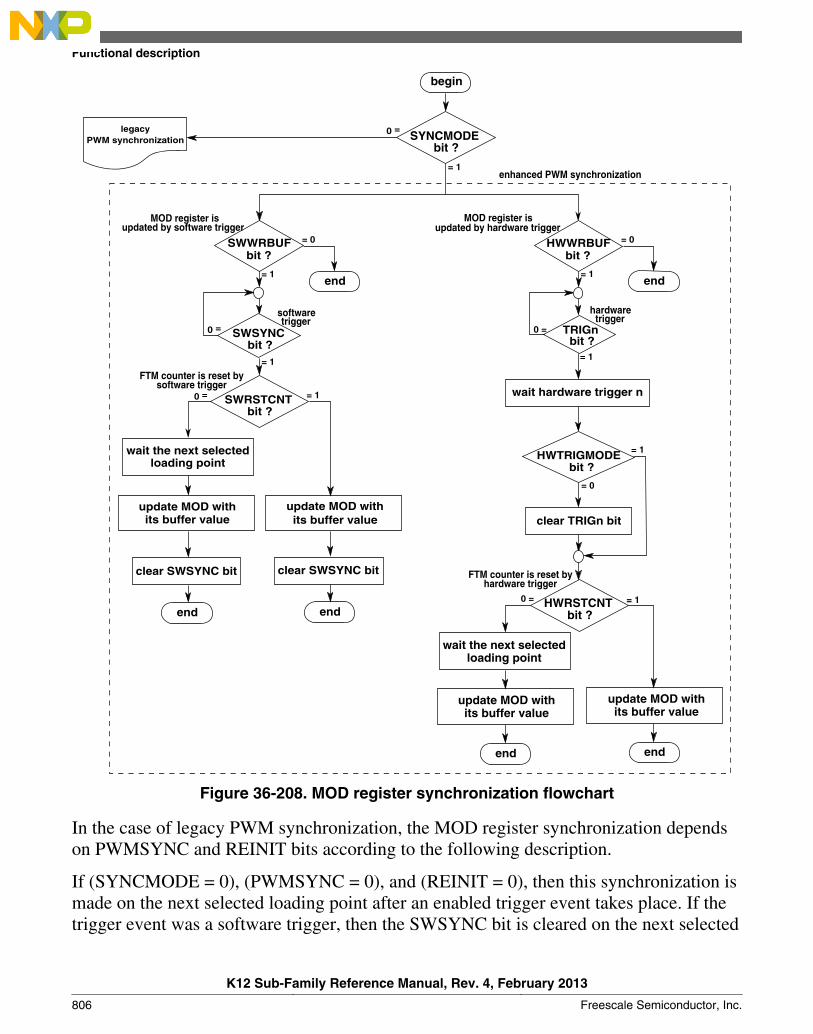
legacyPWM synchronization
end
= 0
enhanced PWM synchronization
begin
= 1
SYNCMODEbit ?
= 0
end
endend
end end
= 1
= 1
0 =
= 1
= 0
= 1 0 =
= 1
= 1
= 1
= 0
= 0
= 0
MOD register isupdated by software trigger
MOD register isupdated by hardware trigger
softwaretrigger
hardwaretrigger
FTM counter is reset bysoftware trigger
FTM counter is reset byhardware trigger
SWWRBUFbit ?
HWWRBUFbit ?
SWSYNCbit ?
SWRSTCNTbit ?
wait the next selectedloading point
update MOD withits buffer value
clear SWSYNC bit clear SWSYNC bit
update MOD withits buffer value
TRIGnbit ?
wait hardware trigger n
HWTRIGMODEbit ?
clear TRIGn bit
wait the next selectedloading point
update MOD withits buffer value
update MOD withits buffer value
HWRSTCNTbit ?
Figure 36-208. MOD register synchronization flowchart
In the case of legacy PWM synchronization, the MOD register synchronization dependson PWMSYNC and REINIT bits according to the following description.
If (SYNCMODE = 0), (PWMSYNC = 0), and (REINIT = 0), then this synchronization ismade on the next selected loading point after an enabled trigger event takes place. If thetrigger event was a software trigger, then the SWSYNC bit is cleared on the next selected
Functional description
K12 Sub-Family Reference Manual, Rev. 4, February 2013
806 Freescale Semiconductor, Inc.
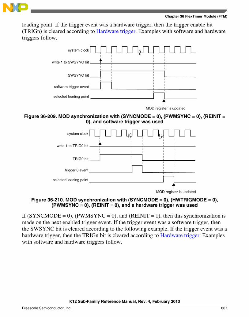
loading point. If the trigger event was a hardware trigger, then the trigger enable bit(TRIGn) is cleared according to Hardware trigger. Examples with software and hardwaretriggers follow.
system clock
selected loading point
MOD register is updated
write 1 to SWSYNC bit
SWSYNC bit
software trigger event
Figure 36-209. MOD synchronization with (SYNCMODE = 0), (PWMSYNC = 0), (REINIT =0), and software trigger was used
system clock
selected loading point
MOD register is updated
write 1 to TRIG0 bit
TRIG0 bit
trigger 0 event
Figure 36-210. MOD synchronization with (SYNCMODE = 0), (HWTRIGMODE = 0),(PWMSYNC = 0), (REINIT = 0), and a hardware trigger was used
If (SYNCMODE = 0), (PWMSYNC = 0), and (REINIT = 1), then this synchronization ismade on the next enabled trigger event. If the trigger event was a software trigger, thenthe SWSYNC bit is cleared according to the following example. If the trigger event was ahardware trigger, then the TRIGn bit is cleared according to Hardware trigger. Exampleswith software and hardware triggers follow.
Chapter 36 FlexTimer Module (FTM)
K12 Sub-Family Reference Manual, Rev. 4, February 2013
Freescale Semiconductor, Inc. 807

system clock
MOD register is updated
write 1 to SWSYNC bit
SWSYNC bit
software trigger event
Figure 36-211. MOD synchronization with (SYNCMODE = 0), (PWMSYNC = 0), (REINIT =1), and software trigger was used
system clock
MOD register is updated
write 1 to TRIG0 bit
TRIG0 bit
trigger 0 event
Figure 36-212. MOD synchronization with (SYNCMODE = 0), (HWTRIGMODE = 0),(PWMSYNC = 0), (REINIT = 1), and a hardware trigger was used
If (SYNCMODE = 0) and (PWMSYNC = 1), then this synchronization is made on thenext selected loading point after the software trigger event takes place. The SWSYNC bitis cleared on the next selected loading point:
system clock
selected loading point
MOD register is updated
write 1 to SWSYNC bit
SWSYNC bit
software trigger event
Figure 36-213. MOD synchronization with (SYNCMODE = 0) and (PWMSYNC = 1)
Functional description
K12 Sub-Family Reference Manual, Rev. 4, February 2013
808 Freescale Semiconductor, Inc.
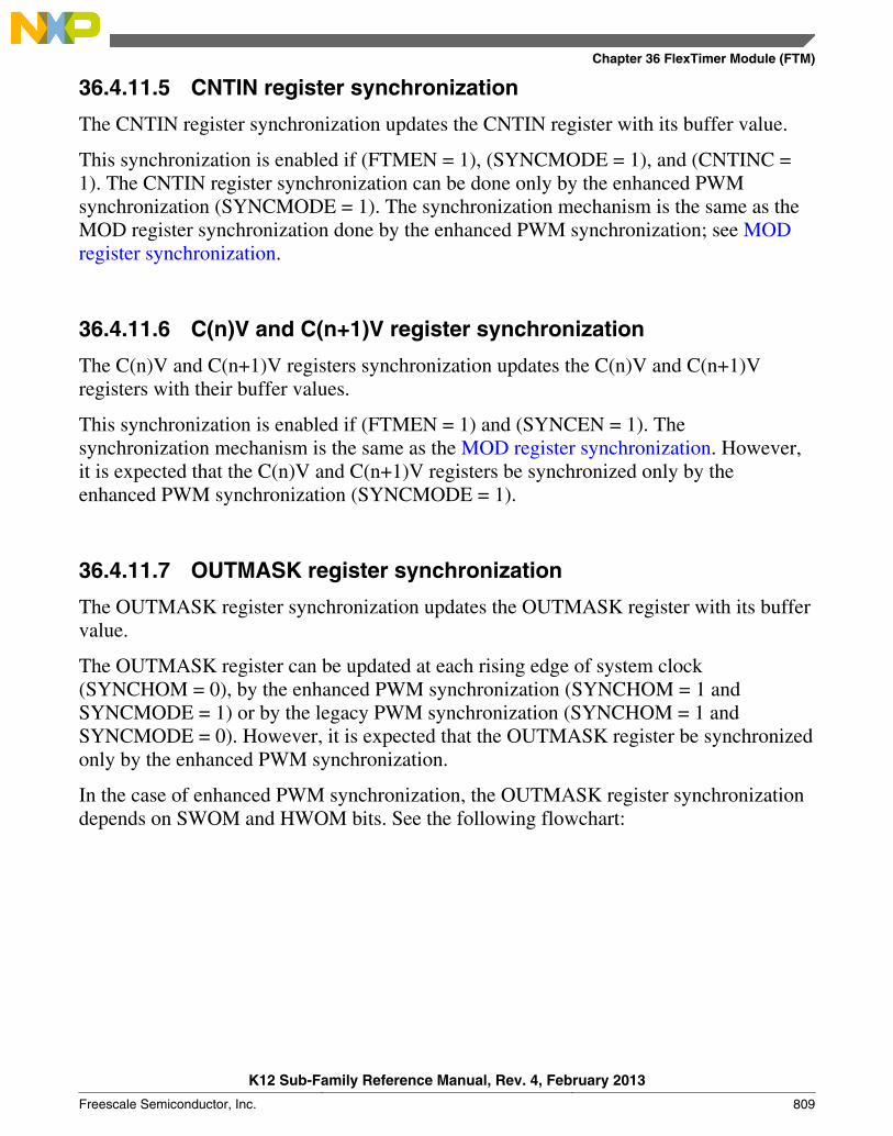
36.4.11.5 CNTIN register synchronization
The CNTIN register synchronization updates the CNTIN register with its buffer value.
This synchronization is enabled if (FTMEN = 1), (SYNCMODE = 1), and (CNTINC =1). The CNTIN register synchronization can be done only by the enhanced PWMsynchronization (SYNCMODE = 1). The synchronization mechanism is the same as theMOD register synchronization done by the enhanced PWM synchronization; see MODregister synchronization.
36.4.11.6 C(n)V and C(n+1)V register synchronization
The C(n)V and C(n+1)V registers synchronization updates the C(n)V and C(n+1)Vregisters with their buffer values.
This synchronization is enabled if (FTMEN = 1) and (SYNCEN = 1). Thesynchronization mechanism is the same as the MOD register synchronization. However,it is expected that the C(n)V and C(n+1)V registers be synchronized only by theenhanced PWM synchronization (SYNCMODE = 1).
36.4.11.7 OUTMASK register synchronization
The OUTMASK register synchronization updates the OUTMASK register with its buffervalue.
The OUTMASK register can be updated at each rising edge of system clock(SYNCHOM = 0), by the enhanced PWM synchronization (SYNCHOM = 1 andSYNCMODE = 1) or by the legacy PWM synchronization (SYNCHOM = 1 andSYNCMODE = 0). However, it is expected that the OUTMASK register be synchronizedonly by the enhanced PWM synchronization.
In the case of enhanced PWM synchronization, the OUTMASK register synchronizationdepends on SWOM and HWOM bits. See the following flowchart:
Chapter 36 FlexTimer Module (FTM)
K12 Sub-Family Reference Manual, Rev. 4, February 2013
Freescale Semiconductor, Inc. 809
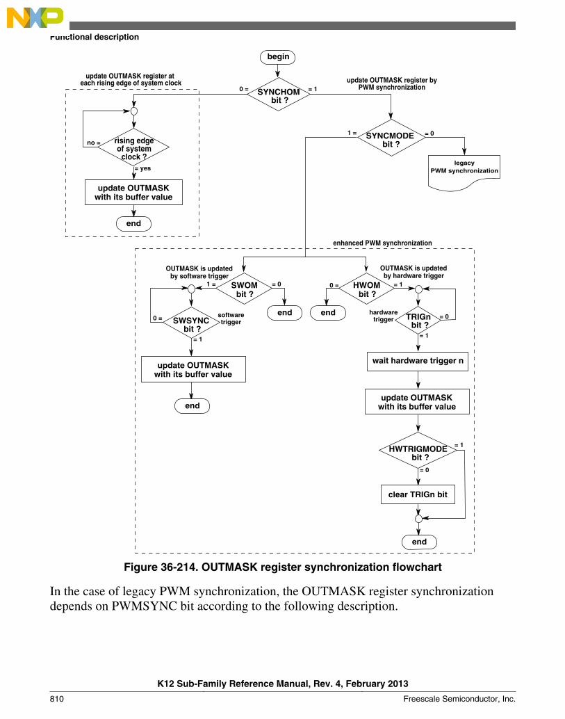
end
= 0
update OUTMASK register ateach rising edge of system clock
begin
softwaretrigger
endend
end
end
= 0
= 0
= 1
= 1
= 1
= 1
= 0
= 1
0 =
0 =
1 =
1 =
0 =
legacyPWM synchronization
SYNCHOMbit ?
update OUTMASK register byPWM synchronization
update OUTMASKwith its buffer value
SYNCMODEbit ?
clear TRIGn bit
HWTRIGMODEbit ?
update OUTMASKwith its buffer value
wait hardware trigger n
TRIGnbit ?
HWOMbit ?
SWOMbit ?
SWSYNCbit ?
rising edgeof system
clock ?
update OUTMASKwith its buffer value
hardwaretrigger
OUTMASK is updatedby software trigger
OUTMASK is updatedby hardware trigger
enhanced PWM synchronization
= yes
no =
Figure 36-214. OUTMASK register synchronization flowchart
In the case of legacy PWM synchronization, the OUTMASK register synchronizationdepends on PWMSYNC bit according to the following description.
Functional description
K12 Sub-Family Reference Manual, Rev. 4, February 2013
810 Freescale Semiconductor, Inc.
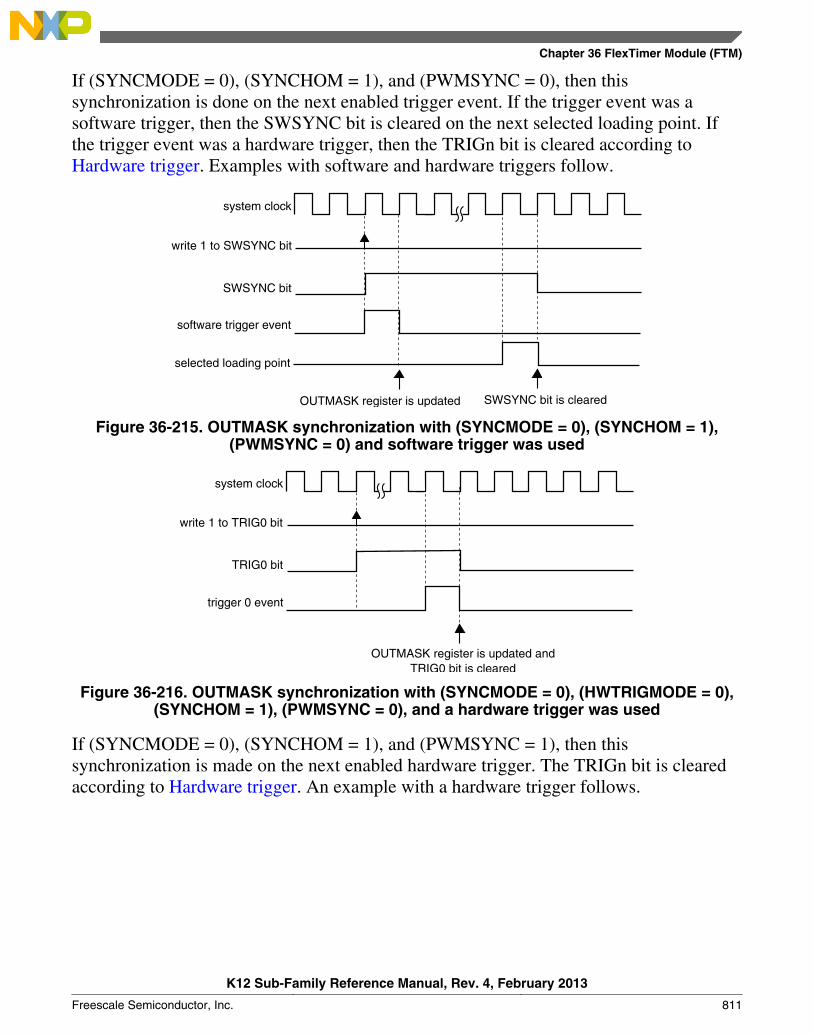
If (SYNCMODE = 0), (SYNCHOM = 1), and (PWMSYNC = 0), then thissynchronization is done on the next enabled trigger event. If the trigger event was asoftware trigger, then the SWSYNC bit is cleared on the next selected loading point. Ifthe trigger event was a hardware trigger, then the TRIGn bit is cleared according toHardware trigger. Examples with software and hardware triggers follow.
system clock
OUTMASK register is updated
selected loading point
SWSYNC bit is cleared
write 1 to SWSYNC bit
SWSYNC bit
software trigger event
Figure 36-215. OUTMASK synchronization with (SYNCMODE = 0), (SYNCHOM = 1),(PWMSYNC = 0) and software trigger was used
system clock
write 1 to TRIG0 bit
TRIG0 bit
trigger 0 event
OUTMASK register is updated and TRIG0 bit is cleared
Figure 36-216. OUTMASK synchronization with (SYNCMODE = 0), (HWTRIGMODE = 0),(SYNCHOM = 1), (PWMSYNC = 0), and a hardware trigger was used
If (SYNCMODE = 0), (SYNCHOM = 1), and (PWMSYNC = 1), then thissynchronization is made on the next enabled hardware trigger. The TRIGn bit is clearedaccording to Hardware trigger. An example with a hardware trigger follows.
Chapter 36 FlexTimer Module (FTM)
K12 Sub-Family Reference Manual, Rev. 4, February 2013
Freescale Semiconductor, Inc. 811
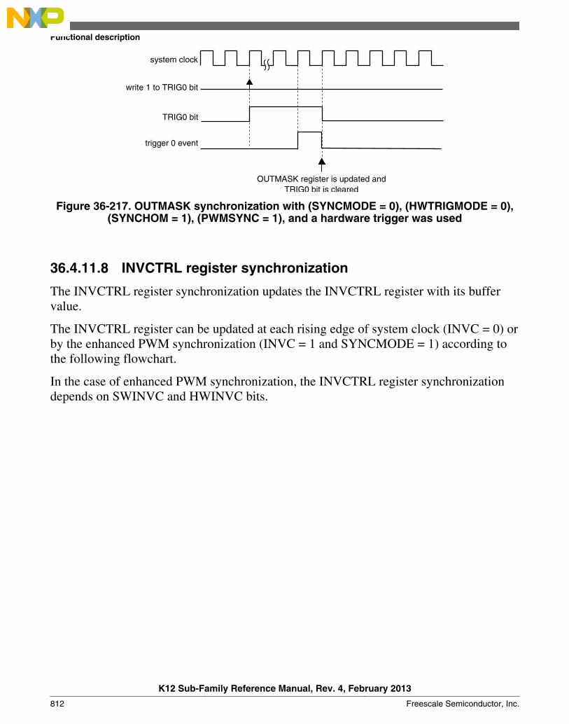
system clock
OUTMASK register is updated andTRIG0 bit is cleared
write 1 to TRIG0 bit
TRIG0 bit
trigger 0 event
Figure 36-217. OUTMASK synchronization with (SYNCMODE = 0), (HWTRIGMODE = 0),(SYNCHOM = 1), (PWMSYNC = 1), and a hardware trigger was used
36.4.11.8 INVCTRL register synchronization
The INVCTRL register synchronization updates the INVCTRL register with its buffervalue.
The INVCTRL register can be updated at each rising edge of system clock (INVC = 0) orby the enhanced PWM synchronization (INVC = 1 and SYNCMODE = 1) according tothe following flowchart.
In the case of enhanced PWM synchronization, the INVCTRL register synchronizationdepends on SWINVC and HWINVC bits.
Functional description
K12 Sub-Family Reference Manual, Rev. 4, February 2013
812 Freescale Semiconductor, Inc.
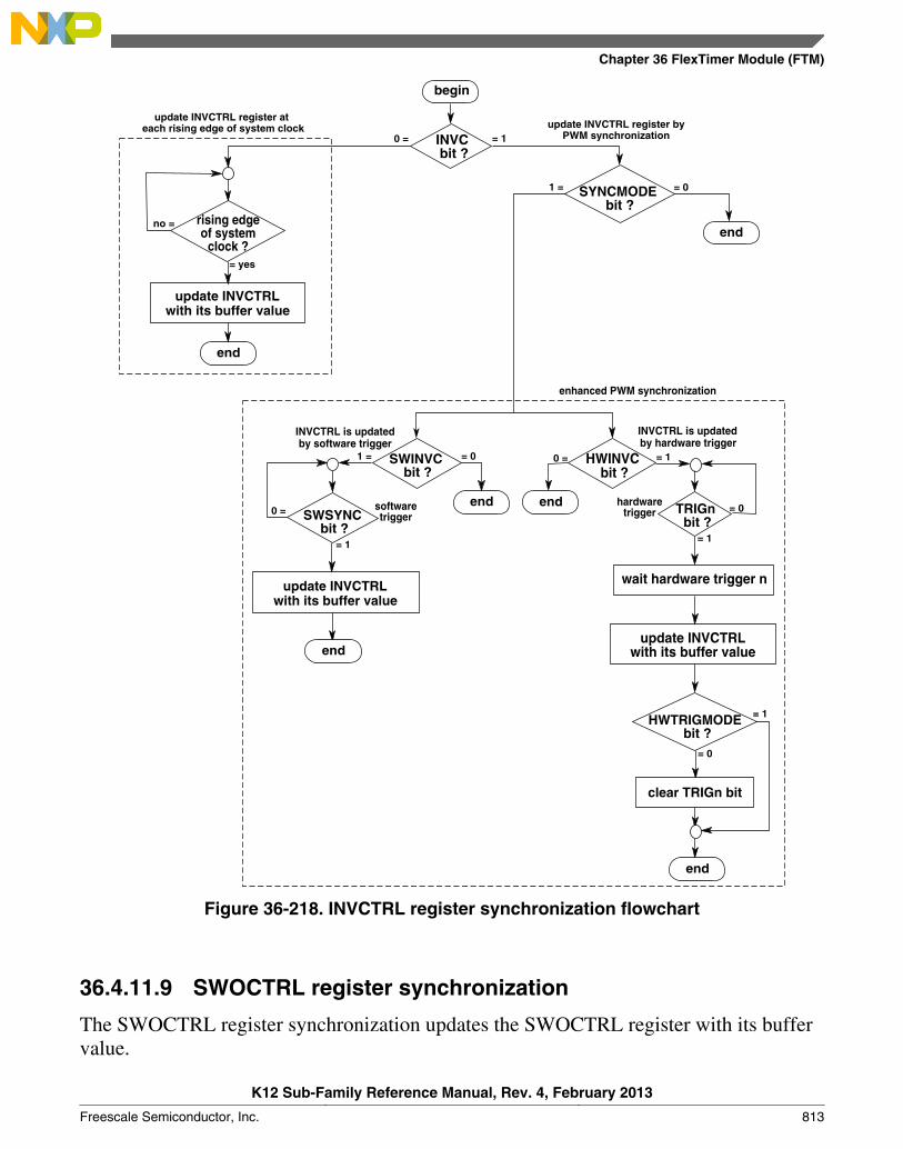
end
begin
= 1
= 0
end end
end
end
end
= 1
= 0
= 1= 1
= 0
= 0
= 1
INVCTRL is updatedby software trigger
softwaretrigger
hardwaretrigger
INVCTRL is updatedby hardware trigger
enhanced PWM synchronization
update INVCTRL register byPWM synchronization
update INVCTRL register ateach rising edge of system clock
= yes
0 =
1 = 0 =
0 =
no =
1 =
INVCbit ?
SYNCMODEbit ?
rising edgeof system
clock ?
update INVCTRLwith its buffer value
update INVCTRLwith its buffer value
HWINVCbit ?
TRIGnbit ?
wait hardware trigger n
update INVCTRLwith its buffer value
HWTRIGMODEbit ?
clear TRIGn bit
SWINVCbit ?
SWSYNCbit ?
Figure 36-218. INVCTRL register synchronization flowchart
36.4.11.9 SWOCTRL register synchronization
The SWOCTRL register synchronization updates the SWOCTRL register with its buffervalue.
Chapter 36 FlexTimer Module (FTM)
K12 Sub-Family Reference Manual, Rev. 4, February 2013
Freescale Semiconductor, Inc. 813
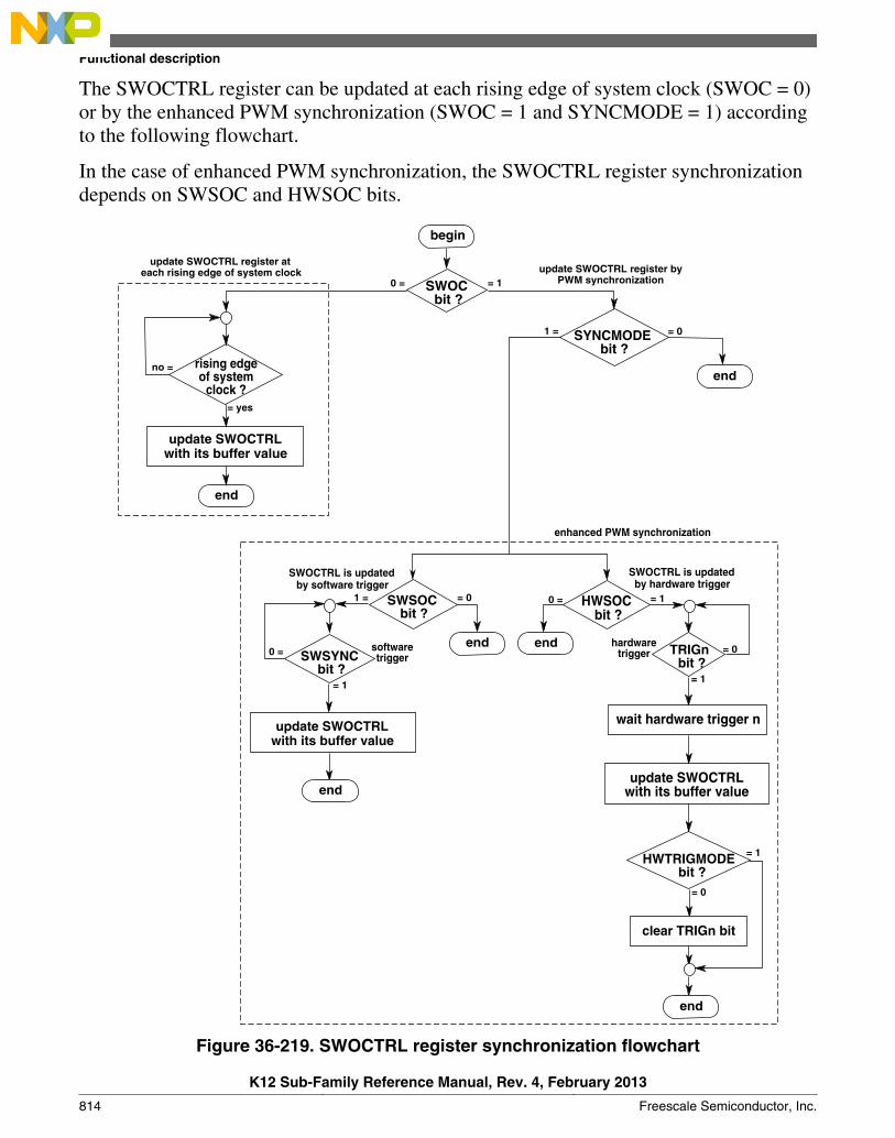
The SWOCTRL register can be updated at each rising edge of system clock (SWOC = 0)or by the enhanced PWM synchronization (SWOC = 1 and SYNCMODE = 1) accordingto the following flowchart.
In the case of enhanced PWM synchronization, the SWOCTRL register synchronizationdepends on SWSOC and HWSOC bits.
end
begin
= 1
= 0
end end
end
end
end
= 1
= 0
= 1= 1
= 0
= 0
= 1
SWOCTRL is updatedby software trigger
softwaretrigger
hardwaretrigger
SWOCTRL is updatedby hardware trigger
enhanced PWM synchronization
update SWOCTRL register byPWM synchronization
update SWOCTRL register ateach rising edge of system clock
= yes
0 =
1 = 0 =
0 =
no =
1 =
SWOCbit ?
SYNCMODEbit ?
rising edgeof system
clock ?
update SWOCTRLwith its buffer value
update SWOCTRLwith its buffer value
HWSOCbit ?
TRIGnbit ?
wait hardware trigger n
update SWOCTRLwith its buffer value
HWTRIGMODEbit ?
clear TRIGn bit
SWSOCbit ?
SWSYNCbit ?
Figure 36-219. SWOCTRL register synchronization flowchart
Functional description
K12 Sub-Family Reference Manual, Rev. 4, February 2013
814 Freescale Semiconductor, Inc.

36.4.11.10 FTM counter synchronization
The FTM counter synchronization is a mechanism that allows the FTM to restart thePWM generation at a certain point in the PWM period. The channels outputs are forcedto their initial value, except for channels in Output Compare mode, and the FTM counteris forced to its initial counting value defined by CNTIN register.
The following figure shows the FTM counter synchronization. Note that after thesynchronization event occurs, the channel (n) is set to its initial value and the channel (n+1) is not set to its initial value due to a specific timing of this figure in which thedeadtime insertion prevents this channel output from transitioning to 1. If no deadtimeinsertion is selected, then the channel (n+1) transitions to logical value 1 immediatelyafter the synchronization event occurs.
synchronization event
channel (n+1) match
FTM counterchannel (n) match
channel (n) output(after deadtime
insertion)
channel (n+1) output(after deadtime
insertion)
Figure 36-220. FTM counter synchronization
The FTM counter synchronization can be done by either the enhanced PWMsynchronization (SYNCMODE = 1) or the legacy PWM synchronization (SYNCMODE= 0). However, the FTM counter must be synchronized only by the enhanced PWMsynchronization.
In the case of enhanced PWM synchronization, the FTM counter synchronizationdepends on SWRSTCNT and HWRSTCNT bits according to the following flowchart.
Chapter 36 FlexTimer Module (FTM)
K12 Sub-Family Reference Manual, Rev. 4, February 2013
Freescale Semiconductor, Inc. 815

update FTM counter withCNTIN register value
update the channels outputswith their initial value
clear SWSYNC bit
end
FTM counter is reset bysoftware trigger
legacyPWM synchronization
end
clear TRIGn bit
HWTRIGMODEbit ?
= 1
= 0
update the channels outputswith their initial value
update FTM counter withCNTIN register value
wait hardware trigger n
enhanced PWM synchronization
FTM counter is reset byhardware trigger
begin
= 1
= 1
= 1
= 1
endend
HWRSTCNTbit ?
SWRSTCNTbit ?
SWSYNCbit ?
softwaretrigger
SYNCMODEbit ?
hardwaretrigger TRIGn
bit ?
= 0
= 0
= 0
= 0
= 0
1 =
Figure 36-221. FTM counter synchronization flowchart
In the case of legacy PWM synchronization, the FTM counter synchronization dependson REINIT and PWMSYNC bits according to the following description.
If (SYNCMODE = 0), (REINIT = 1), and (PWMSYNC = 0) then this synchronization ismade on the next enabled trigger event. If the trigger event was a software trigger thenthe SWSYNC bit is cleared according to the following example. If the trigger event was ahardware trigger then the TRIGn bit is cleared according to Hardware trigger. Exampleswith software and hardware triggers follow.
Functional description
K12 Sub-Family Reference Manual, Rev. 4, February 2013
816 Freescale Semiconductor, Inc.

system clock
FTM counter is updated with the CNTIN register valueand channel outputs are forced to their initial value
write 1 to SWSYNC bit
SWSYNC bit
software trigger event
Figure 36-222. FTM counter synchronization with (SYNCMODE = 0), (REINIT = 1),(PWMSYNC = 0), and software trigger was used
system clock
write 1 to TRIG0 bit
TRIG0 bit
trigger 0 event
FTM counter is updated with the CNTIN register valueand channel outputs are forced to their initial value
Figure 36-223. FTM counter synchronization with (SYNCMODE = 0), (HWTRIGMODE = 0),(REINIT = 1), (PWMSYNC = 0), and a hardware trigger was used
If (SYNCMODE = 0), (REINIT = 1), and (PWMSYNC = 1) then this synchronization ismade on the next enabled hardware trigger. The TRIGn bit is cleared according toHardware trigger.
system clock
write 1 to TRIG0 bit
TRIG0 bit
trigger 0 event
FTM counter is updated with the CNTIN register valueand channel outputs are forced to their initial value
Figure 36-224. FTM counter synchronization with (SYNCMODE = 0), (HWTRIGMODE = 0),(REINIT = 1), (PWMSYNC = 1), and a hardware trigger was used
Chapter 36 FlexTimer Module (FTM)
K12 Sub-Family Reference Manual, Rev. 4, February 2013
Freescale Semiconductor, Inc. 817

36.4.12 Inverting
The invert functionality swaps the signals between channel (n) and channel (n+1)outputs. The inverting operation is selected when (FTMEN = 1), (QUADEN = 0),(DECAPEN = 0), (COMBINE = 1), (COMP = 1), (CPWMS = 0), and (INVm = 1),where m represents a channel pair. The INVm bit in INVCTRL register is updated withits buffer value according to INVCTRL register synchronization
In High-True (ELSnB:ELSnA = 1:0) Combine mode, the channel (n) output is forced lowat the beginning of the period (FTM counter = CNTIN), forced high at the channel (n)match and forced low at the channel (n+1) match. If the inverting is selected, the channel(n) output behavior is changed to force high at the beginning of the PWM period, forcelow at the channel (n) match and force high at the channel (n+1) match. See the followingfigure.
NOTE
channel (n+1) match
FTM counterchannel (n) match
channel (n+1) outputbefore the inverting
write 1 to INV(m) bit
INV(m) bit buffer
INVCTRL registersynchronization
INV(m) bit
channel (n) outputafter the inverting
channel (n+1) outputafter the inverting
INV(m) bit selects the inverting to the pair channels (n) and (n+1).
channel (n) outputbefore the inverting
Figure 36-225. Channels (n) and (n+1) outputs after the inverting in High-True(ELSnB:ELSnA = 1:0) Combine mode
Note that the ELSnB:ELSnA bits value should be considered because they define theactive state of the channels outputs. In Low-True (ELSnB:ELSnA = X:1) Combine mode,the channel (n) output is forced high at the beginning of the period, forced low at thechannel (n) match and forced high at the channel (n+1) match. When inverting isselected, the channels (n) and (n+1) present waveforms as shown in the following figure.
Functional description
K12 Sub-Family Reference Manual, Rev. 4, February 2013
818 Freescale Semiconductor, Inc.
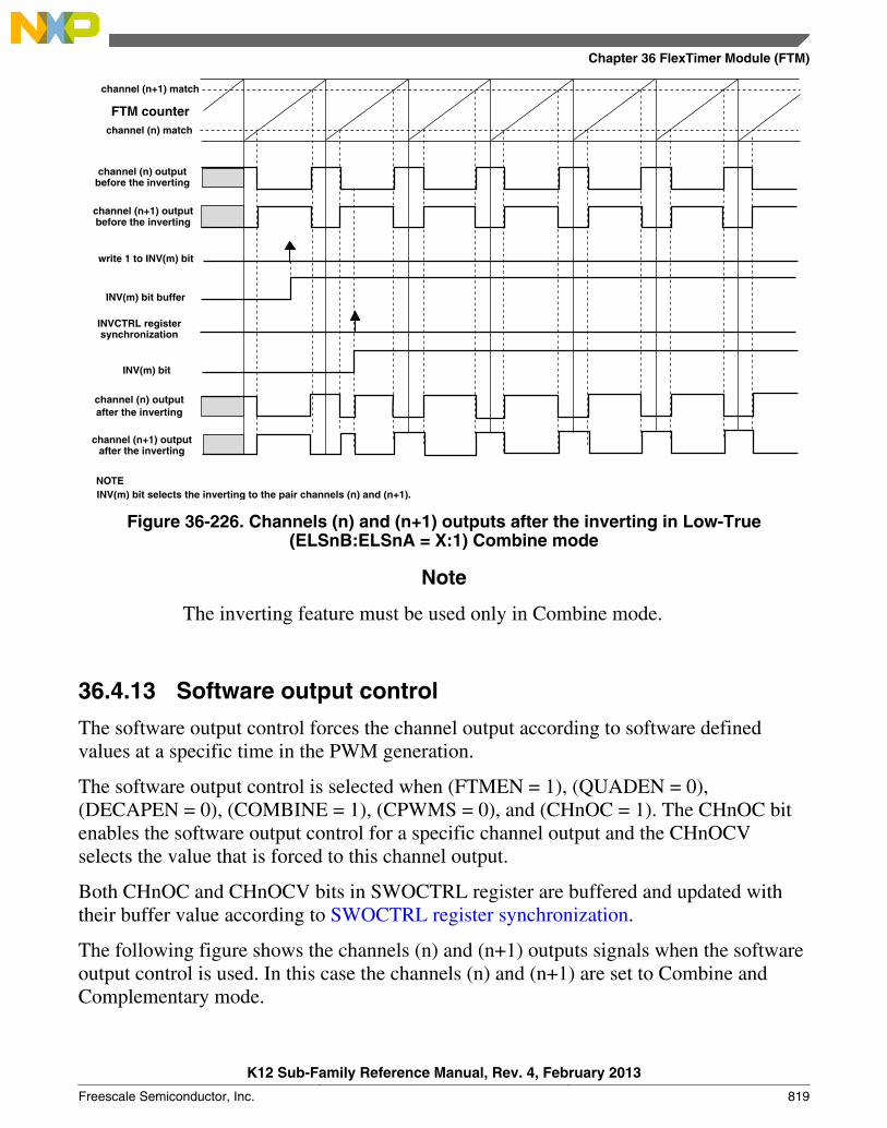
NOTE
channel (n+1) match
FTM counterchannel (n) match
channel (n+1) outputbefore the inverting
write 1 to INV(m) bit
INV(m) bit buffer
INVCTRL registersynchronization
INV(m) bit
channel (n) outputafter the inverting
channel (n+1) outputafter the inverting
INV(m) bit selects the inverting to the pair channels (n) and (n+1).
channel (n) outputbefore the inverting
Figure 36-226. Channels (n) and (n+1) outputs after the inverting in Low-True(ELSnB:ELSnA = X:1) Combine mode
Note
The inverting feature must be used only in Combine mode.
36.4.13 Software output control
The software output control forces the channel output according to software definedvalues at a specific time in the PWM generation.
The software output control is selected when (FTMEN = 1), (QUADEN = 0),(DECAPEN = 0), (COMBINE = 1), (CPWMS = 0), and (CHnOC = 1). The CHnOC bitenables the software output control for a specific channel output and the CHnOCVselects the value that is forced to this channel output.
Both CHnOC and CHnOCV bits in SWOCTRL register are buffered and updated withtheir buffer value according to SWOCTRL register synchronization.
The following figure shows the channels (n) and (n+1) outputs signals when the softwareoutput control is used. In this case the channels (n) and (n+1) are set to Combine andComplementary mode.
Chapter 36 FlexTimer Module (FTM)
K12 Sub-Family Reference Manual, Rev. 4, February 2013
Freescale Semiconductor, Inc. 819
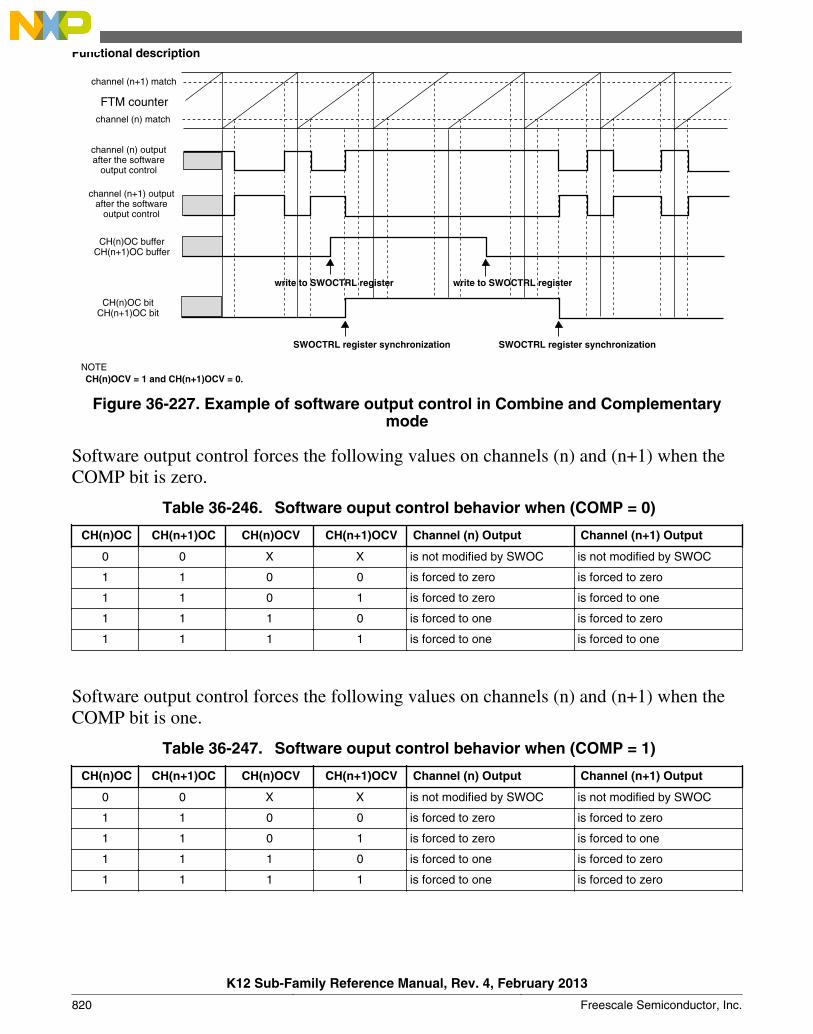
channel (n+1) match
FTM counterchannel (n) match
channel (n) outputafter the software
output control
channel (n+1) outputafter the software
output control
CH(n)OC bufferCH(n+1)OC buffer
CH(n)OC bitCH(n+1)OC bit
NOTECH(n)OCV = 1 and CH(n+1)OCV = 0.
SWOCTRL register synchronization SWOCTRL register synchronization
write to SWOCTRL register write to SWOCTRL register
Figure 36-227. Example of software output control in Combine and Complementarymode
Software output control forces the following values on channels (n) and (n+1) when theCOMP bit is zero.
Table 36-246. Software ouput control behavior when (COMP = 0)
CH(n)OC CH(n+1)OC CH(n)OCV CH(n+1)OCV Channel (n) Output Channel (n+1) Output
0 0 X X is not modified by SWOC is not modified by SWOC
1 1 0 0 is forced to zero is forced to zero
1 1 0 1 is forced to zero is forced to one
1 1 1 0 is forced to one is forced to zero
1 1 1 1 is forced to one is forced to one
Software output control forces the following values on channels (n) and (n+1) when theCOMP bit is one.
Table 36-247. Software ouput control behavior when (COMP = 1)
CH(n)OC CH(n+1)OC CH(n)OCV CH(n+1)OCV Channel (n) Output Channel (n+1) Output
0 0 X X is not modified by SWOC is not modified by SWOC
1 1 0 0 is forced to zero is forced to zero
1 1 0 1 is forced to zero is forced to one
1 1 1 0 is forced to one is forced to zero
1 1 1 1 is forced to one is forced to zero
Functional description
K12 Sub-Family Reference Manual, Rev. 4, February 2013
820 Freescale Semiconductor, Inc.

Note• The software output control feature must be used only in
Combine mode.
• The CH(n)OC and CH(n+1)OC bits should be equal.
• The COMP bit must not be modified when software outputcontrol is enabled, that is, CH(n)OC = 1 and/or CH(n+1)OC = 1.
• Software output control has the same behavior withdisabled or enabled FTM counter (see the CLKS fielddescription in the Status and Control register).
36.4.14 Deadtime insertion
The deadtime insertion is enabled when (DTEN = 1) and (DTVAL[5:0] is non- zero).
DEADTIME register defines the deadtime delay that can be used for all FTM channels.The DTPS[1:0] bits define the prescaler for the system clock and the DTVAL[5:0] bitsdefine the deadtime modulo, that is, the number of the deadtime prescaler clocks.
The deadtime delay insertion ensures that no two complementary signals (channels (n)and (n+1)) drive the active state at the same time.
If POL(n) = 0, POL(n+1) = 0, and the deadtime is enabled, then when the channel (n)match (FTM counter = C(n)V) occurs, the channel (n) output remains at the low valueuntil the end of the deadtime delay when the channel (n) output is set. Similarly, when thechannel (n+1) match (FTM counter = C(n+1)V) occurs, the channel (n+1) output remainsat the low value until the end of the deadtime delay when the channel (n+1) output is set.See the following figures.
If POL(n) = 1, POL(n+1) = 1, and the deadtime is enabled, then when the channel (n)match (FTM counter = C(n)V) occurs, the channel (n) output remains at the high valueuntil the end of the deadtime delay when the channel (n) output is cleared. Similarly,when the channel (n+1) match (FTM counter = C(n+1)V) occurs, the channel (n+1)output remains at the high value until the end of the deadtime delay when the channel (n+1) output is cleared.
Chapter 36 FlexTimer Module (FTM)
K12 Sub-Family Reference Manual, Rev. 4, February 2013
Freescale Semiconductor, Inc. 821
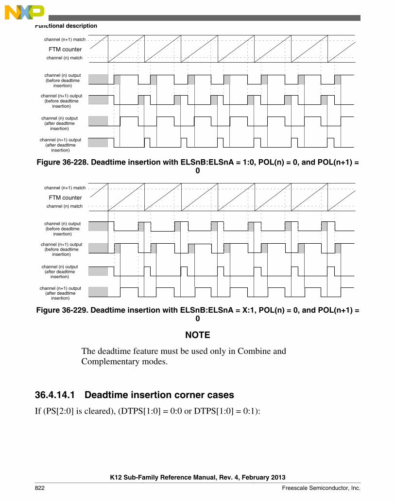
FTM counter
channel (n+1) match
channel (n) match
channel (n) output(before deadtime
insertion)
channel (n+1) output(before deadtime
insertion)
channel (n) output(after deadtime
insertion)
channel (n+1) output(after deadtime
insertion)
Figure 36-228. Deadtime insertion with ELSnB:ELSnA = 1:0, POL(n) = 0, and POL(n+1) =0
FTM counter
channel (n+1) match
channel (n) output(before deadtime
insertion)
channel (n+1) output(before deadtime
insertion)
channel (n) output(after deadtime
insertion)
channel (n+1) output(after deadtime
insertion)
channel (n) match
Figure 36-229. Deadtime insertion with ELSnB:ELSnA = X:1, POL(n) = 0, and POL(n+1) =0
NOTE
The deadtime feature must be used only in Combine andComplementary modes.
36.4.14.1 Deadtime insertion corner cases
If (PS[2:0] is cleared), (DTPS[1:0] = 0:0 or DTPS[1:0] = 0:1):
Functional description
K12 Sub-Family Reference Manual, Rev. 4, February 2013
822 Freescale Semiconductor, Inc.
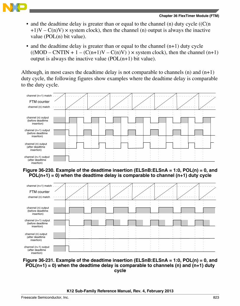
• and the deadtime delay is greater than or equal to the channel (n) duty cycle ((C(n+1)V – C(n)V) × system clock), then the channel (n) output is always the inactivevalue (POL(n) bit value).
• and the deadtime delay is greater than or equal to the channel (n+1) duty cycle((MOD – CNTIN + 1 – (C(n+1)V – C(n)V) ) × system clock), then the channel (n+1)output is always the inactive value (POL(n+1) bit value).
Although, in most cases the deadtime delay is not comparable to channels (n) and (n+1)duty cycle, the following figures show examples where the deadtime delay is comparableto the duty cycle.
FTM counter
channel (n+1) match
channel (n) match
channel (n) output(before deadtime
insertion)
channel (n) output(after deadtime
insertion)
channel (n+1) output(before deadtime
insertion)
channel (n+1) output(after deadtime
insertion)
Figure 36-230. Example of the deadtime insertion (ELSnB:ELSnA = 1:0, POL(n) = 0, andPOL(n+1) = 0) when the deadtime delay is comparable to channel (n+1) duty cycle
FTM counter
channel (n+1) match
channel (n) match
channel (n) output(before deadtime
insertion)
channel (n) output(after deadtime
insertion)
channel (n+1) output(before deadtime
insertion)
channel (n+1) output(after deadtime
insertion)
Figure 36-231. Example of the deadtime insertion (ELSnB:ELSnA = 1:0, POL(n) = 0, andPOL(n+1) = 0) when the deadtime delay is comparable to channels (n) and (n+1) duty
cycle
Chapter 36 FlexTimer Module (FTM)
K12 Sub-Family Reference Manual, Rev. 4, February 2013
Freescale Semiconductor, Inc. 823
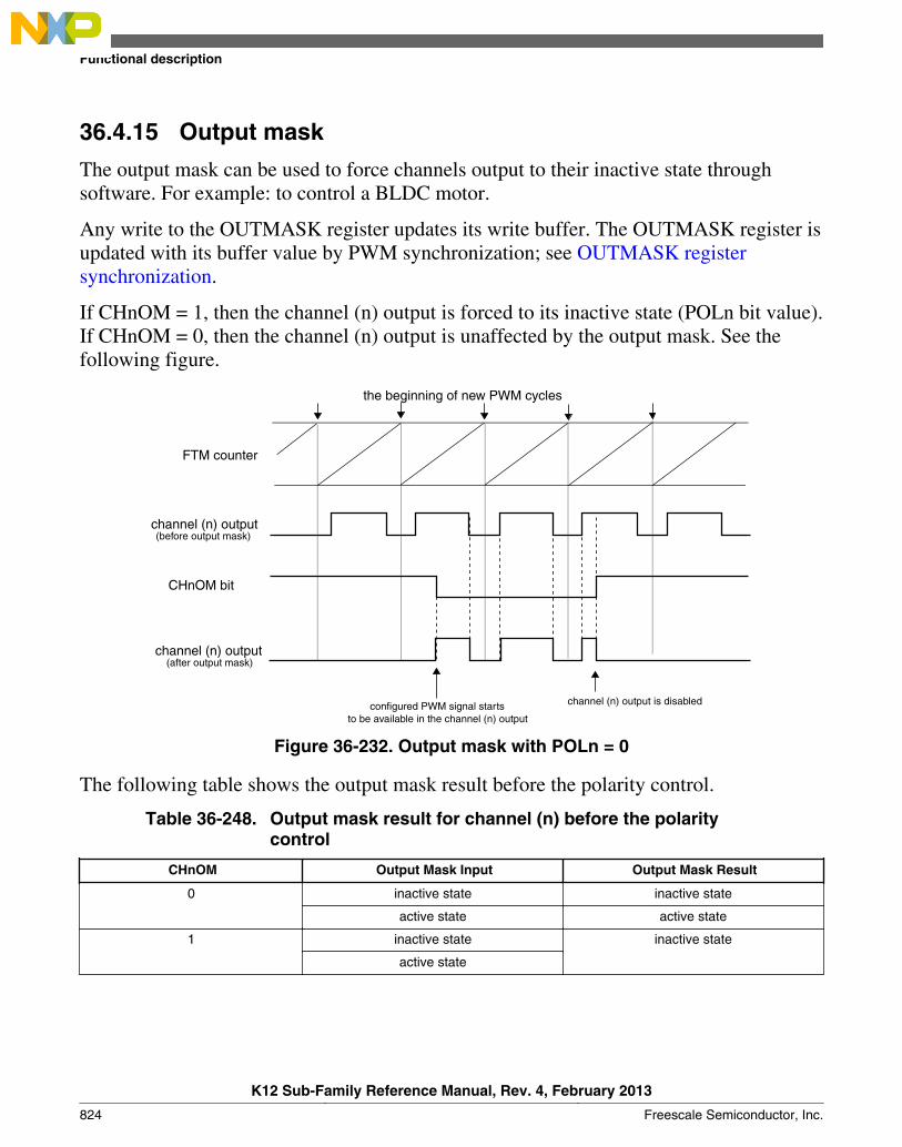
36.4.15 Output mask
The output mask can be used to force channels output to their inactive state throughsoftware. For example: to control a BLDC motor.
Any write to the OUTMASK register updates its write buffer. The OUTMASK register isupdated with its buffer value by PWM synchronization; see OUTMASK registersynchronization.
If CHnOM = 1, then the channel (n) output is forced to its inactive state (POLn bit value).If CHnOM = 0, then the channel (n) output is unaffected by the output mask. See thefollowing figure.
FTM counter
channel (n) output(before output mask)
CHnOM bit
channel (n) output(after output mask)
the beginning of new PWM cycles
configured PWM signal startsto be available in the channel (n) output
channel (n) output is disabled
Figure 36-232. Output mask with POLn = 0
The following table shows the output mask result before the polarity control.
Table 36-248. Output mask result for channel (n) before the polaritycontrol
CHnOM Output Mask Input Output Mask Result
0 inactive state inactive state
active state active state
1 inactive state inactive state
active state
Functional description
K12 Sub-Family Reference Manual, Rev. 4, February 2013
824 Freescale Semiconductor, Inc.
Note
The output mask feature must be used only in Combine mode.
36.4.16 Fault control
The fault control is enabled if (FTMEN = 1) and (FAULTM[1:0] ≠ 0:0).
FTM can have up to four fault inputs. FAULTnEN bit (where n = 0, 1, 2, 3) enables thefault input n and FFLTRnEN bit enables the fault input n filter. FFVAL[3:0] bits selectthe value of the enabled filter in each enabled fault input.
First, each fault input signal is synchronized by the system clock; see the synchronizerblock in the following figure. Following synchronization, the fault input n signal entersthe filter block. When there is a state change in the fault input n signal, the 5-bit counteris reset and starts counting up. As long as the new state is stable on the fault input n, thecounter continues to increment. If the 5-bit counter overflows, that is, the counter exceedsthe value of the FFVAL[3:0] bits, the new fault input n value is validated. It is thentransmitted as a pulse edge to the edge detector.
If the opposite edge appears on the fault input n signal before validation (counteroverflow), the counter is reset. At the next input transition, the counter starts countingagain. Any pulse that is shorter than the minimum value selected by FFVAL[3:0] bits (×system clock) is regarded as a glitch and is not passed on to the edge detector.
The fault input n filter is disabled when the FFVAL[3:0] bits are zero or whenFAULTnEN = 0. In this case, the fault input n signal is delayed 2 rising edges of thesystem clock and the FAULTFn bit is set on 3th rising edge of the system clock after arising edge occurs on the fault input n.
If FFVAL[3:0] ≠ 0000 and FAULTnEN = 1, then the fault input n signal is delayed (3 +FFVAL[3:0]) rising edges of the system clock, that is, the FAULTFn bit is set (4 +FFVAL[3:0]) rising edges of the system clock after a rising edge occurs on the fault inputn.
Chapter 36 FlexTimer Module (FTM)
K12 Sub-Family Reference Manual, Rev. 4, February 2013
Freescale Semiconductor, Inc. 825
fault input n*
system clock
* where n = 3, 2, 1, 0
synchronizer fault input n* value
FAULTFn*
0000) and (FFLTRnEN*)
0
1
rising edgedetector
fault inputpolaritycontrolFault filter
(5-bit counter)CLK CLK
D D QQ
FLTnPOL
(FFVAL[3:0]
Figure 36-233. Fault input n control block diagram
If the fault control and fault input n are enabled and a rising edge at the fault input nsignal is detected, a fault condition has occurred and the FAULTFn bit is set. TheFAULTF bit is the logic OR of FAULTFn[3:0] bits. See the following figure.
fault interruptFAULTIE
FAULTIN
fault input 0 valuefault input 1 valuefault input 2 valuefault input 3 value
FAULTF
FAULTF0
FAULTF1
FAULTF2
FAULTF3
Figure 36-234. FAULTF and FAULTIN bits and fault interrupt
If the fault control is enabled (FAULTM[1:0] ≠ 0:0), a fault condition has occurred and(FAULTEN = 1), then outputs are forced to their safe values:
• Channel (n) output takes the value of POL(n)• Channel (n+1) takes the value of POL(n+1)
The fault interrupt is generated when (FAULTF = 1) and (FAULTIE = 1). This interruptrequest remains set until:
• Software clears the FAULTF bit by reading FAULTF bit as 1 and writing 0 to it
• Software clears the FAULTIE bit
• A reset occurs
Note
The fault control must be used only in Combine mode.
Functional description
K12 Sub-Family Reference Manual, Rev. 4, February 2013
826 Freescale Semiconductor, Inc.
36.4.16.1 Automatic fault clearing
If the automatic fault clearing is selected (FAULTM[1:0] = 1:1), then the channels outputdisabled by fault control is again enabled when the fault input signal (FAULTIN) returnsto zero and a new PWM cycle begins. See the following figure.
FTM counter
channel (n) output(before fault control)
FAULTIN bit
channel (n) output
the beginning of new PWM cycles
FAULTF bit
FAULTF bit is cleared
The channel (n) output is after the fault control with automatic fault clearing and POLn = 0.NOTE
Figure 36-235. Fault control with automatic fault clearing
36.4.16.2 Manual fault clearing
If the manual fault clearing is selected (FAULTM[1:0] = 0:1 or 1:0), then the channelsoutput disabled by fault control is again enabled when the FAULTF bit is cleared and anew PWM cycle begins. See the following figure.
Chapter 36 FlexTimer Module (FTM)
K12 Sub-Family Reference Manual, Rev. 4, February 2013
Freescale Semiconductor, Inc. 827

FTM counter
channel (n) output(before fault control)
FAULTIN bit
channel (n) output
the beginning of new PWM cycles
FAULTF bit
FAULTF bit is cleared
The channel (n) output is after the fault control with manual fault clearing and POLn = 0.NOTE
Figure 36-236. Fault control with manual fault clearing
36.4.16.3 Fault inputs polarity control
The FLTjPOL bit selects the fault input j polarity, where j = 0, 1, 2, 3:
• If FLTjPOL = 0, the fault j input polarity is high, so the logical one at the fault input jindicates a fault.
• If FLTjPOL = 1, the fault j input polarity is low, so the logical zero at the fault input jindicates a fault.
36.4.17 Polarity control
The POLn bit selects the channel (n) output polarity:
• If POLn = 0, the channel (n) output polarity is high, so the logical one is the activestate and the logical zero is the inactive state.
• If POLn = 1, the channel (n) output polarity is low, so the logical zero is the activestate and the logical one is the inactive state.
Functional description
K12 Sub-Family Reference Manual, Rev. 4, February 2013
828 Freescale Semiconductor, Inc.

Note
The polarity control must be used only in Combine mode.
36.4.18 Initialization
The initialization forces the CHnOI bit value to the channel (n) output when a one iswritten to the INIT bit.
The initialization depends on COMP and DTEN bits. The following table shows thevalues that channels (n) and (n+1) are forced by initialization when the COMP andDTEN bits are zero.
Table 36-249. Initialization behavior when (COMP = 0 and DTEN = 0)
CH(n)OI CH(n+1)OI Channel (n) Output Channel (n+1) Output
0 0 is forced to zero is forced to zero
0 1 is forced to zero is forced to one
1 0 is forced to one is forced to zero
1 1 is forced to one is forced to one
The following table shows the values that channels (n) and (n+1) are forced byinitialization when (COMP = 1) or (DTEN = 1).
Table 36-250. Initialization behavior when (COMP = 1 or DTEN = 1)
CH(n)OI CH(n+1)OI Channel (n) Output Channel (n+1) Output
0 X is forced to zero is forced to one
1 X is forced to one is forced to zero
Note
The initialization feature must be used only in Combine modeand with disabled FTM counter. See the description of theCLKS field in the Status and Control register.
36.4.19 Features priority
The following figure shows the priority of the features used at the generation of channels(n) and (n+1) outputs signals.
Chapter 36 FlexTimer Module (FTM)
K12 Sub-Family Reference Manual, Rev. 4, February 2013
Freescale Semiconductor, Inc. 829
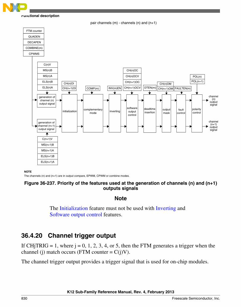
NOTE
The channels (n) and (n+1) are in output compare, EPWM, CPWM or combine modes.
pair channels (m) - channels (n) and (n+1)
initializationcomplementary
modeinverting
softwareoutputcontrol
deadtimeinsertion
outputmask
faultcontrol
polaritycontrol
FTM counter
QUADEN
DECAPEN
COMBINE(m)
CPWMS
C(n)V
MS(n)B
MS(n)A
ELS(n)B
ELS(n)A
generation ofchannel (n)
output signal
generation ofchannel (n+1)output signal
C(n+1)V
MS(n+1)B
MS(n+1)A
ELS(n+1)B
ELS(n+1)A
channel(n)
outputsignal
channel(n+1)outputsignal
CH(n)OI
CH(n+1)OI COMP(m) INV(m)EN
CH(n)OC
CH(n)OCV
CH(n+1)OC
CH(n+1)OCV DTEN(m)CH(n)OM
CH(n+1)OM FAULTEN(m)
POL(n)
POL(n+1)
Figure 36-237. Priority of the features used at the generation of channels (n) and (n+1)outputs signals
Note
The Initialization feature must not be used with Inverting andSoftware output control features.
36.4.20 Channel trigger output
If CHjTRIG = 1, where j = 0, 1, 2, 3, 4, or 5, then the FTM generates a trigger when thechannel (j) match occurs (FTM counter = C(j)V).
The channel trigger output provides a trigger signal that is used for on-chip modules.
Functional description
K12 Sub-Family Reference Manual, Rev. 4, February 2013
830 Freescale Semiconductor, Inc.

The FTM is able to generate multiple triggers in one PWM period. Because each triggeris generated for a specific channel, several channels are required to implement thisfunctionality. This behavior is described in the following figure.
NOTE(a) CH0TRIG = 0, CH1TRIG = 0, CH2TRIG = 0, CH3TRIG = 0, CH4TRIG = 0, CH5TRIG = 0
(b) CH0TRIG = 1, CH1TRIG = 0, CH2TRIG = 0, CH3TRIG = 0, CH4TRIG = 0, CH5TRIG = 0
(c) CH0TRIG = 0, CH1TRIG = 0, CH2TRIG = 0, CH3TRIG = 1, CH4TRIG = 1, CH5TRIG = 1
(d) CH0TRIG = 1, CH1TRIG = 1, CH2TRIG = 1, CH3TRIG = 1, CH4TRIG = 1, CH5TRIG = 1
the beginning of new PWM cycles
MOD
FTM counter = C5V
FTM counter = C4V
FTM counter = C3V
FTM counter = C2V
FTM counter = C1V
FTM counter = C0V
CNTIN
(a)
(b)
(c)
(d)
Figure 36-238. Channel match trigger
Note
The channel match trigger must be used only in Combine mode.
36.4.21 Initialization trigger
If INITTRIGEN = 1, then the FTM generates a trigger when the FTM counter is updatedwith the CNTIN register value in the following cases.
• The FTM counter is automatically updated with the CNTIN register value by theselected counting mode.
• When there is a write to CNT register
Chapter 36 FlexTimer Module (FTM)
K12 Sub-Family Reference Manual, Rev. 4, February 2013
Freescale Semiconductor, Inc. 831
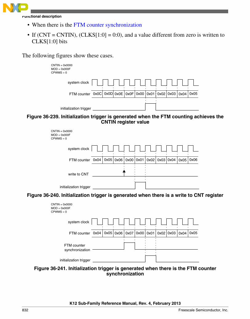
• When there is the FTM counter synchronization
• If (CNT = CNTIN), (CLKS[1:0] = 0:0), and a value different from zero is written toCLKS[1:0] bits
The following figures show these cases.
CPWMS = 0
0x0C 0x0D 0x0E 0x0F 0x00 0x01 0x02 0x03 0x04 0x05
initialization trigger
FTM counter
system clock
CNTIN = 0x0000MOD = 0x000F
Figure 36-239. Initialization trigger is generated when the FTM counting achieves theCNTIN register value
CPWMS = 0
0x04 0x05 0x06 0x00 0x01 0x02 0x03 0x04 0x05 0x06
initialization trigger
write to CNT
FTM counter
system clock
CNTIN = 0x0000MOD = 0x000F
Figure 36-240. Initialization trigger is generated when there is a write to CNT register
CPWMS = 0
0x04 0x05 0x06 0x07 0x00 0x01 0x02 0x03 0x04 0x05
initialization trigger
FTM countersynchronization
FTM counter
system clock
CNTIN = 0x0000MOD = 0x000F
Figure 36-241. Initialization trigger is generated when there is the FTM countersynchronization
Functional description
K12 Sub-Family Reference Manual, Rev. 4, February 2013
832 Freescale Semiconductor, Inc.

CPWMS = 0
0x00
00 01
0x01 0x02 0x03 0x04 0x05
initialization trigger
CLKS[1:0] bits
FTM counter
system clock
CNTIN = 0x0000MOD = 0x000F
Figure 36-242. Initialization trigger is generated if (CNT = CNTIN), (CLKS[1:0] = 0:0), anda value different from zero is written to CLKS[1:0] bits
The initialization trigger output provides a trigger signal that is used for on-chip modules.
Note
The initialization trigger must be used only in Combine mode.
36.4.22 Capture Test mode
The Capture Test mode allows to test the CnV registers, the FTM counter and theinterconnection logic between the FTM counter and CnV registers.
In this test mode, all channels must be configured for Input Capture mode and FTMcounter must be configured to the Up counting.
When the Capture Test mode is enabled (CAPTEST = 1), the FTM counter is frozen andany write to CNT register updates directly the FTM counter; see the following figure.After it was written, all CnV registers are updated with the written value to CNT registerand CHnF bits are set. Therefore, the FTM counter is updated with its next valueaccording to its configuration. Its next value depends on CNTIN, MOD, and the writtenvalue to FTM counter.
The next reads of CnV registers return the written value to the FTM counter and the nextreads of CNT register return FTM counter next value.
Chapter 36 FlexTimer Module (FTM)
K12 Sub-Family Reference Manual, Rev. 4, February 2013
Freescale Semiconductor, Inc. 833
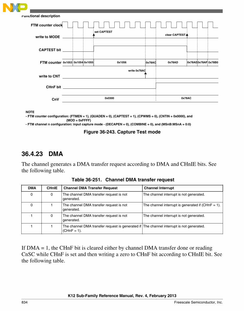
NOTE
FTM counter clock
write to MODE
CAPTEST bit
FTM counter
write to CNT
CHnF bit
CnV
- FTM counter configuration: (FTMEN = 1), (QUADEN = 0), (CAPTEST = 1), (CPWMS = 0), (CNTIN = 0x0000), and(MOD = 0xFFFF)
- FTM channel n configuration: input capture mode - (DECAPEN = 0), (COMBINE = 0), and (MSnB:MSnA = 0:0)
0x0300 0x78AC
set CAPTESTclear CAPTEST
write 0x78AC
0x10560x1053 0x10550x1054 0x78AC 0x78AD 0x78AE0x78AF 0x78B0
Figure 36-243. Capture Test mode
36.4.23 DMA
The channel generates a DMA transfer request according to DMA and CHnIE bits. Seethe following table.
Table 36-251. Channel DMA transfer request
DMA CHnIE Channel DMA Transfer Request Channel Interrupt
0 0 The channel DMA transfer request is notgenerated.
The channel interrupt is not generated.
0 1 The channel DMA transfer request is notgenerated.
The channel interrupt is generated if (CHnF = 1).
1 0 The channel DMA transfer request is notgenerated.
The channel interrupt is not generated.
1 1 The channel DMA transfer request is generated if(CHnF = 1).
The channel interrupt is not generated.
If DMA = 1, the CHnF bit is cleared either by channel DMA transfer done or readingCnSC while CHnF is set and then writing a zero to CHnF bit according to CHnIE bit. Seethe following table.
Functional description
K12 Sub-Family Reference Manual, Rev. 4, February 2013
834 Freescale Semiconductor, Inc.

Table 36-252. Clear CHnF bit when DMA = 1
CHnIE How CHnF Bit Can Be Cleared
0 CHnF bit is cleared either when the channel DMA transfer is done or by reading CnSC while CHnF is set andthen writing a 0 to CHnF bit.
1 CHnF bit is cleared when the channel DMA transfer is done.
36.4.24 Dual Edge Capture mode
The Dual Edge Capture mode is selected if FTMEN = 1 and DECAPEN = 1. This modeallows to measure a pulse width or period of the signal on the input of channel (n) of achannel pair. The channel (n) filter can be active in this mode when n is 0 or 2.
channel (n) input
system clock
synchronizer
Filter*
Dual edge capturemode logic
is filter enabled?
FTM counter* Filtering function for dual edge capture mode is only available in the channels 0 and 2
channel (n)interrupt
channel (n+1)interrupt
C(n+1)V[15:0]
C(n)V[15:0]
CH(n+1)IECH(n+1)F
CH(n)IE
CH(n)F
FTMENDECAPEN
DECAPMS(n)A
ELS(n)B:ELS(n)AELS(n+1)B:ELS(n+1)A
CLK CLK
D Q D Q
0
1
Figure 36-244. Dual Edge Capture mode block diagram
The MS(n)A bit defines if the Dual Edge Capture mode is one-shot or continuous.
The ELS(n)B:ELS(n)A bits select the edge that is captured by channel (n), and ELS(n+1)B:ELS(n+1)A bits select the edge that is captured by channel (n+1). If bothELS(n)B:ELS(n)A and ELS(n+1)B:ELS(n+1)A bits select the same edge, then it is theperiod measurement. If these bits select different edges, then it is a pulse widthmeasurement.
In the Dual Edge Capture mode, only channel (n) input is used and channel (n+1) input isignored.
If the selected edge by channel (n) bits is detected at channel (n) input, then CH(n)F bit isset and the channel (n) interrupt is generated (if CH(n)IE = 1). If the selected edge bychannel (n+1) bits is detected at channel (n) input and (CH(n)F = 1), then CH(n+1)F bit isset and the channel (n+1) interrupt is generated (if CH(n+1)IE = 1).
Chapter 36 FlexTimer Module (FTM)
K12 Sub-Family Reference Manual, Rev. 4, February 2013
Freescale Semiconductor, Inc. 835

The C(n)V register stores the value of FTM counter when the selected edge by channel(n) is detected at channel (n) input. The C(n+1)V register stores the value of FTMcounter when the selected edge by channel (n+1) is detected at channel (n) input.
In this mode, a coherency mechanism ensures coherent data when the C(n)V and C(n+1)V registers are read. The only requirement is that C(n)V must be read before C(n+1)V.
Note• The CH(n)F, CH(n)IE, MS(n)A, ELS(n)B, and ELS(n)A
bits are channel (n) bits.
• The CH(n+1)F, CH(n+1)IE, MS(n+1)A, ELS(n+1)B, andELS(n+1)A bits are channel (n+1) bits.
• The Dual Edge Capture mode must be used withELS(n)B:ELS(n)A = 0:1 or 1:0, ELS(n+1)B:ELS(n+1)A =0:1 or 1:0 and the FTM counter in Free running counter.
36.4.24.1 One-Shot Capture mode
The One-Shot Capture mode is selected when (FTMEN = 1), (DECAPEN = 1), and(MS(n)A = 0). In this capture mode, only one pair of edges at the channel (n) input iscaptured. The ELS(n)B:ELS(n)A bits select the first edge to be captured, and ELS(n+1)B:ELS(n+1)A bits select the second edge to be captured.
The edge captures are enabled while DECAP bit is set. For each new measurement inOne-Shot Capture mode, first the CH(n)F and CH(n+1) bits must be cleared, and then theDECAP bit must be set.
In this mode, the DECAP bit is automatically cleared by FTM when the edge selected bychannel (n+1) is captured. Therefore, while DECAP bit is set, the one-shot capture is inprocess. When this bit is cleared, both edges were captured and the captured values areready for reading in the C(n)V and C(n+1)V registers.
Similarly, when the CH(n+1)F bit is set, both edges were captured and the capturedvalues are ready for reading in the C(n)V and C(n+1)V registers.
Functional description
K12 Sub-Family Reference Manual, Rev. 4, February 2013
836 Freescale Semiconductor, Inc.
36.4.24.2 Continuous Capture mode
The Continuous Capture mode is selected when (FTMEN = 1), (DECAPEN = 1), and(MS(n)A = 1). In this capture mode, the edges at the channel (n) input are capturedcontinuously. The ELS(n)B:ELS(n)A bits select the initial edge to be captured, andELS(n+1)B:ELS(n+1)A bits select the final edge to be captured.
The edge captures are enabled while DECAP bit is set. For the initial use, first theCH(n)F and CH(n+1)F bits must be cleared, and then DECAP bit must be set to start thecontinuous measurements.
When the CH(n+1)F bit is set, both edges were captured and the captured values areready for reading in the C(n)V and C(n+1)V registers. The latest captured values arealways available in these registers even after the DECAP bit is cleared.
In this mode, it is possible to clear only the CH(n+1)F bit. Therefore, when the CH(n+1)Fbit is set again, the latest captured values are available in C(n)V and C(n+1)V registers.
For a new sequence of the measurements in the Dual Edge Capture – Continuous mode,clear the CH(n)F and CH(n+1)F bits to start new measurements.
36.4.24.3 Pulse width measurement
If the channel (n) is configured to capture rising edges (ELS(n)B:ELS(n)A = 0:1) and thechannel (n+1) to capture falling edges (ELS(n+1)B:ELS(n+1)A = 1:0), then the positivepolarity pulse width is measured. If the channel (n) is configured to capture falling edges(ELS(n)B:ELS(n)A = 1:0) and the channel (n+1) to capture rising edges (ELS(n+1)B:ELS(n+1)A = 0:1), then the negative polarity pulse width is measured.
The pulse width measurement can be made in One-Shot Capture mode or ContinuousCapture mode.
The following figure shows an example of the Dual Edge Capture – One-Shot mode usedto measure the positive polarity pulse width. The DECAPEN bit selects the Dual EdgeCapture mode, so it remains set. The DECAP bit is set to enable the measurement of nextpositive polarity pulse width. The CH(n)F bit is set when the first edge of this pulse isdetected, that is, the edge selected by ELS(n)B:ELS(n)A bits. The CH(n+1)F bit is setand DECAP bit is cleared when the second edge of this pulse is detected, that is, the edgeselected by ELS(n+1)B:ELS(n+1)A bits. Both DECAP and CH(n+1)F bits indicate whentwo edges of the pulse were captured and the C(n)V and C(n+1)V registers are ready forreading.
Chapter 36 FlexTimer Module (FTM)
K12 Sub-Family Reference Manual, Rev. 4, February 2013
Freescale Semiconductor, Inc. 837
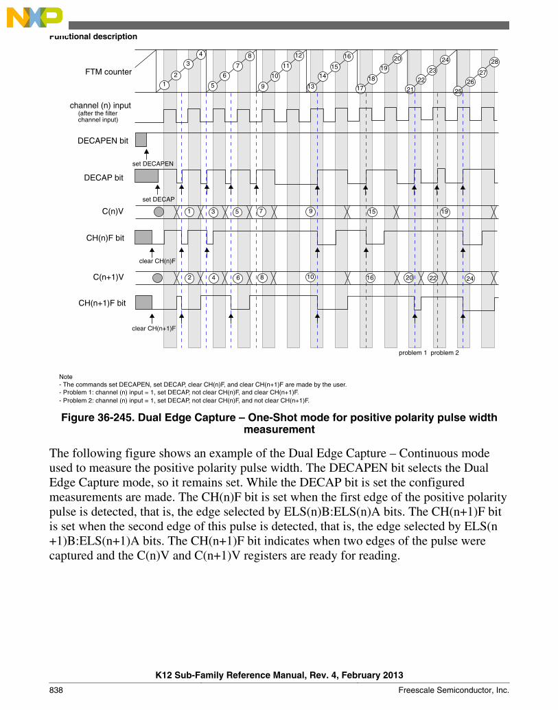
channel (n) input(after the filter
DECAPEN bit
C(n+1)V
FTM counter
clear CH(n+1)F
problem 1 problem 2
2
1
2
3
channel input)
DECAP bit
set DECAPEN
set DECAP
5
6
7
8
10
3
4 6
5
Note- The commands set DECAPEN, set DECAP, clear CH(n)F, and clear CH(n+1)F are made by the user.
4
9
11
12
13
14
9
10
7
8
15
16
17
18
19
20
21
22
23
24
25
2627
28
15
16
19
20 22 24
- Problem 1: channel (n) input = 1, set DECAP, not clear CH(n)F, and clear CH(n+1)F.- Problem 2: channel (n) input = 1, set DECAP, not clear CH(n)F, and not clear CH(n+1)F.
C(n)V
CH(n+1)F bit
CH(n)F bit
clear CH(n)F
1
Figure 36-245. Dual Edge Capture – One-Shot mode for positive polarity pulse widthmeasurement
The following figure shows an example of the Dual Edge Capture – Continuous modeused to measure the positive polarity pulse width. The DECAPEN bit selects the DualEdge Capture mode, so it remains set. While the DECAP bit is set the configuredmeasurements are made. The CH(n)F bit is set when the first edge of the positive polaritypulse is detected, that is, the edge selected by ELS(n)B:ELS(n)A bits. The CH(n+1)F bitis set when the second edge of this pulse is detected, that is, the edge selected by ELS(n+1)B:ELS(n+1)A bits. The CH(n+1)F bit indicates when two edges of the pulse werecaptured and the C(n)V and C(n+1)V registers are ready for reading.
Functional description
K12 Sub-Family Reference Manual, Rev. 4, February 2013
838 Freescale Semiconductor, Inc.
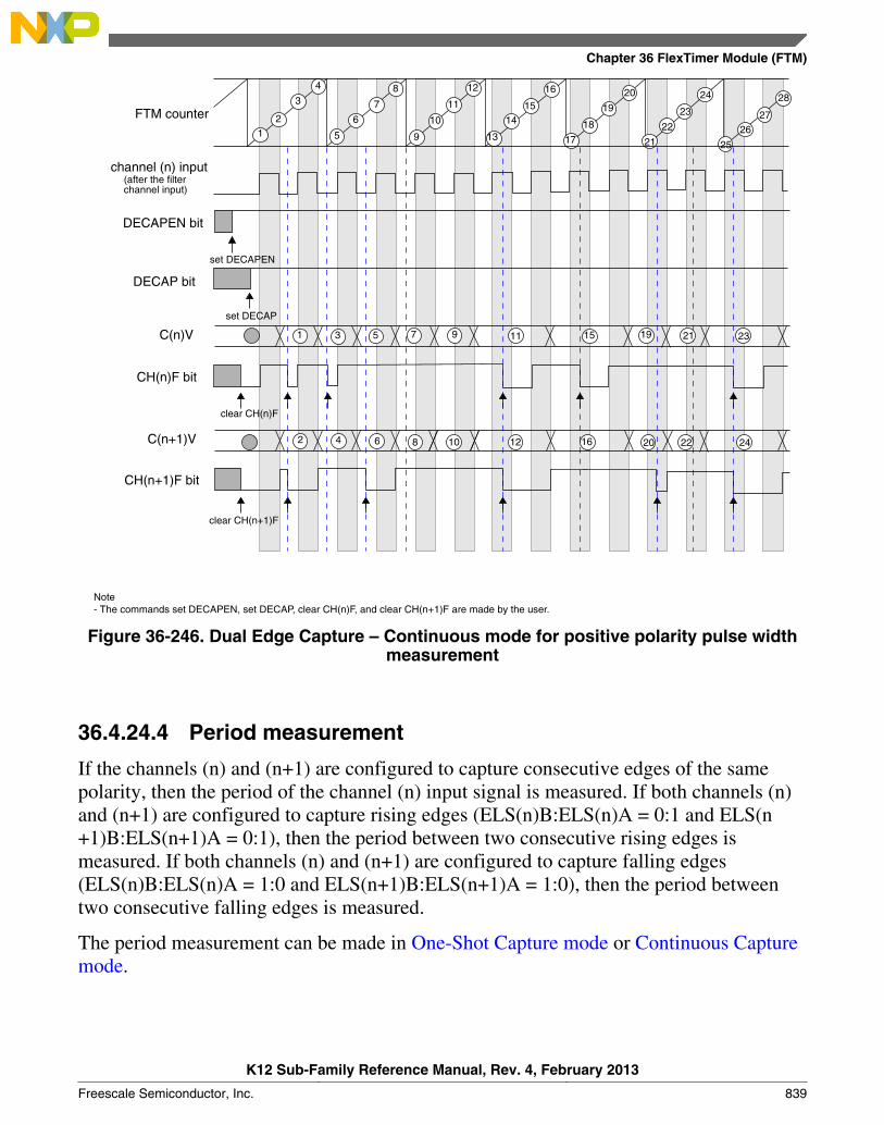
channel (n) input(after the filter
DECAPEN bit
C(n+1)V
FTM counter
clear CH(n+1)F
2
1
2
3
channel input)
DECAP bit
set DECAPEN
set DECAP
5
6
7
8
10
3
4 6
5
Note- The commands set DECAPEN, set DECAP, clear CH(n)F, and clear CH(n+1)F are made by the user.
4
9
11
12
13
14
9
10
7
15
16
17
18
19
20
21
22
23
24
25
2627
28
15
16 20
C(n)V
CH(n+1)F bit
CH(n)F bit
clear CH(n)F
1
8 12 22 24
11 19 21 23
Figure 36-246. Dual Edge Capture – Continuous mode for positive polarity pulse widthmeasurement
36.4.24.4 Period measurement
If the channels (n) and (n+1) are configured to capture consecutive edges of the samepolarity, then the period of the channel (n) input signal is measured. If both channels (n)and (n+1) are configured to capture rising edges (ELS(n)B:ELS(n)A = 0:1 and ELS(n+1)B:ELS(n+1)A = 0:1), then the period between two consecutive rising edges ismeasured. If both channels (n) and (n+1) are configured to capture falling edges(ELS(n)B:ELS(n)A = 1:0 and ELS(n+1)B:ELS(n+1)A = 1:0), then the period betweentwo consecutive falling edges is measured.
The period measurement can be made in One-Shot Capture mode or Continuous Capturemode.
Chapter 36 FlexTimer Module (FTM)
K12 Sub-Family Reference Manual, Rev. 4, February 2013
Freescale Semiconductor, Inc. 839

The following figure shows an example of the Dual Edge Capture – One-Shot mode usedto measure the period between two consecutive rising edges. The DECAPEN bit selectsthe Dual Edge Capture mode, so it remains set. The DECAP bit is set to enable themeasurement of next period. The CH(n)F bit is set when the first rising edge is detected,that is, the edge selected by ELS(n)B:ELS(n)A bits. The CH(n+1)F bit is set and DECAPbit is cleared when the second rising edge is detected, that is, the edge selected by ELS(n+1)B:ELS(n+1)A bits. Both DECAP and CH(n+1)F bits indicate when two selectededges were captured and the C(n)V and C(n+1)V registers are ready for reading.
channel (n) input(after the filter
DECAPEN bit
C(n+1)V
FTM counter
clear CH(n+1)F
problem 2
2
1
2
3
channel input)
DECAP bit
set DECAPEN
set DECAP
5
67
8
10
3
4 6
5
Note- The commands set DECAPEN, set DECAP, clear CH(n)F, and clear CH(n+1)F are made by the user.
4
9
1112
13
14
6
15
16
17
18
19
20
21
22
23
24
2526
27
28
17 20
15 20 23
C(n)V
CH(n+1)F bit
CH(n)F bit
clear CH(n)F
1
- Problem 1: channel (n) input = 0, set DECAP, not clear CH(n)F, and not clear CH(n+1)F.- Problem 2: channel (n) input = 1, set DECAP, not clear CH(n)F, and clear CH(n+1)F.- Problem 3: channel (n) input = 1, set DECAP, not clear CH(n)F, and not clear CH(n+1)F.
problem 3problem 1
7 9 18 26
1814 277
Figure 36-247. Dual Edge Capture – One-Shot mode to measure of the period betweentwo consecutive rising edges
The following figure shows an example of the Dual Edge Capture – Continuous modeused to measure the period between two consecutive rising edges. The DECAPEN bitselects the Dual Edge Capture mode, so it remains set. While the DECAP bit is set theconfigured measurements are made. The CH(n)F bit is set when the first rising edge isdetected, that is, the edge selected by ELS(n)B:ELS(n)A bits. The CH(n+1)F bit is set
Functional description
K12 Sub-Family Reference Manual, Rev. 4, February 2013
840 Freescale Semiconductor, Inc.
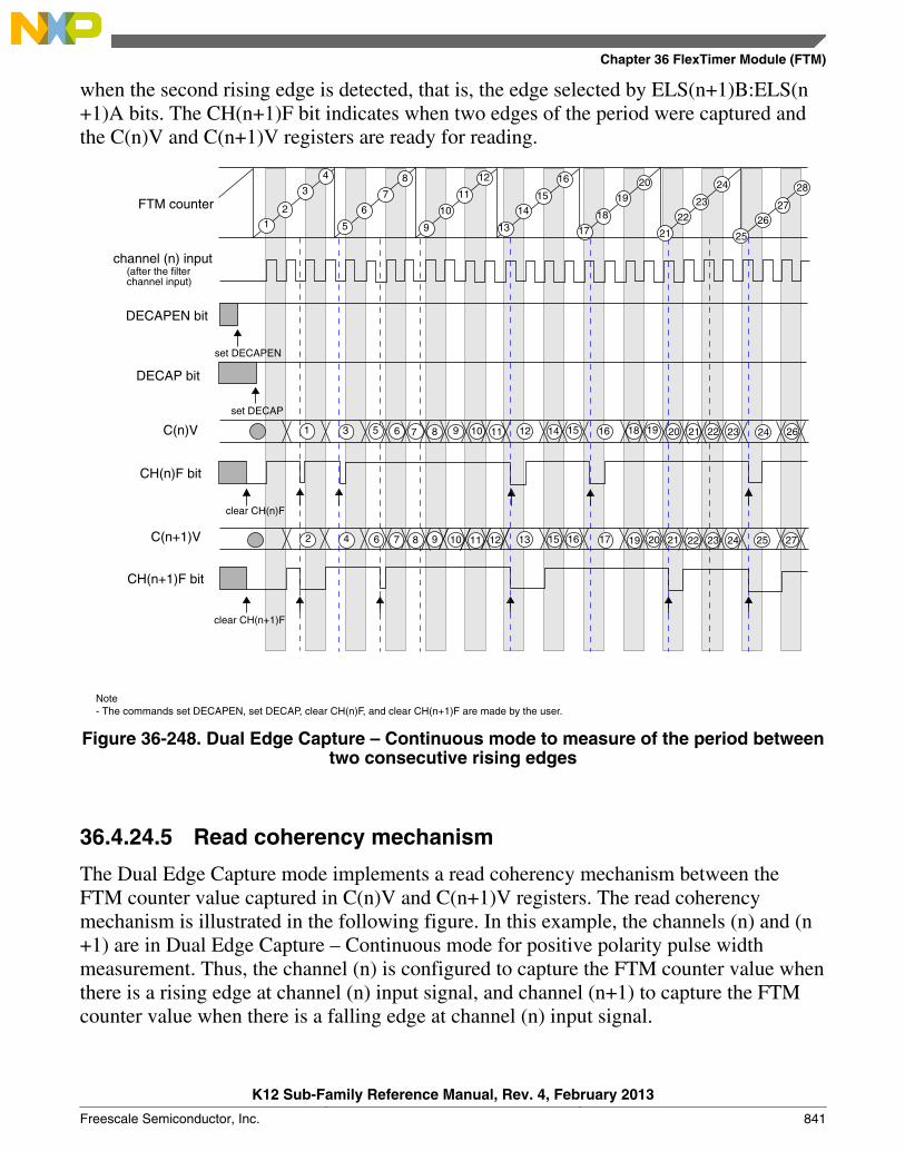
when the second rising edge is detected, that is, the edge selected by ELS(n+1)B:ELS(n+1)A bits. The CH(n+1)F bit indicates when two edges of the period were captured andthe C(n)V and C(n+1)V registers are ready for reading.
channel (n) input(after the filter
DECAPEN bit
C(n+1)V
FTM counter
clear CH(n+1)F
2
1
2
3
channel input)
DECAP bit
set DECAPEN
set DECAP
5
6
7
8
10
3
4 6
5
Note- The commands set DECAPEN, set DECAP, clear CH(n)F, and clear CH(n+1)F are made by the user.
4
9
11
12
13
14
9
10
7
15
16
17
18
19
20
22
23
24
2627
28
15
16 21
C(n)V
CH(n+1)F bit
CH(n)F bit
clear CH(n)F
1
8 12 22 24
11 19 21 23
25 27232019177 9 11 13 15
6 8 10 12 1614 24222018 26
2521
Figure 36-248. Dual Edge Capture – Continuous mode to measure of the period betweentwo consecutive rising edges
36.4.24.5 Read coherency mechanism
The Dual Edge Capture mode implements a read coherency mechanism between theFTM counter value captured in C(n)V and C(n+1)V registers. The read coherencymechanism is illustrated in the following figure. In this example, the channels (n) and (n+1) are in Dual Edge Capture – Continuous mode for positive polarity pulse widthmeasurement. Thus, the channel (n) is configured to capture the FTM counter value whenthere is a rising edge at channel (n) input signal, and channel (n+1) to capture the FTMcounter value when there is a falling edge at channel (n) input signal.
Chapter 36 FlexTimer Module (FTM)
K12 Sub-Family Reference Manual, Rev. 4, February 2013
Freescale Semiconductor, Inc. 841
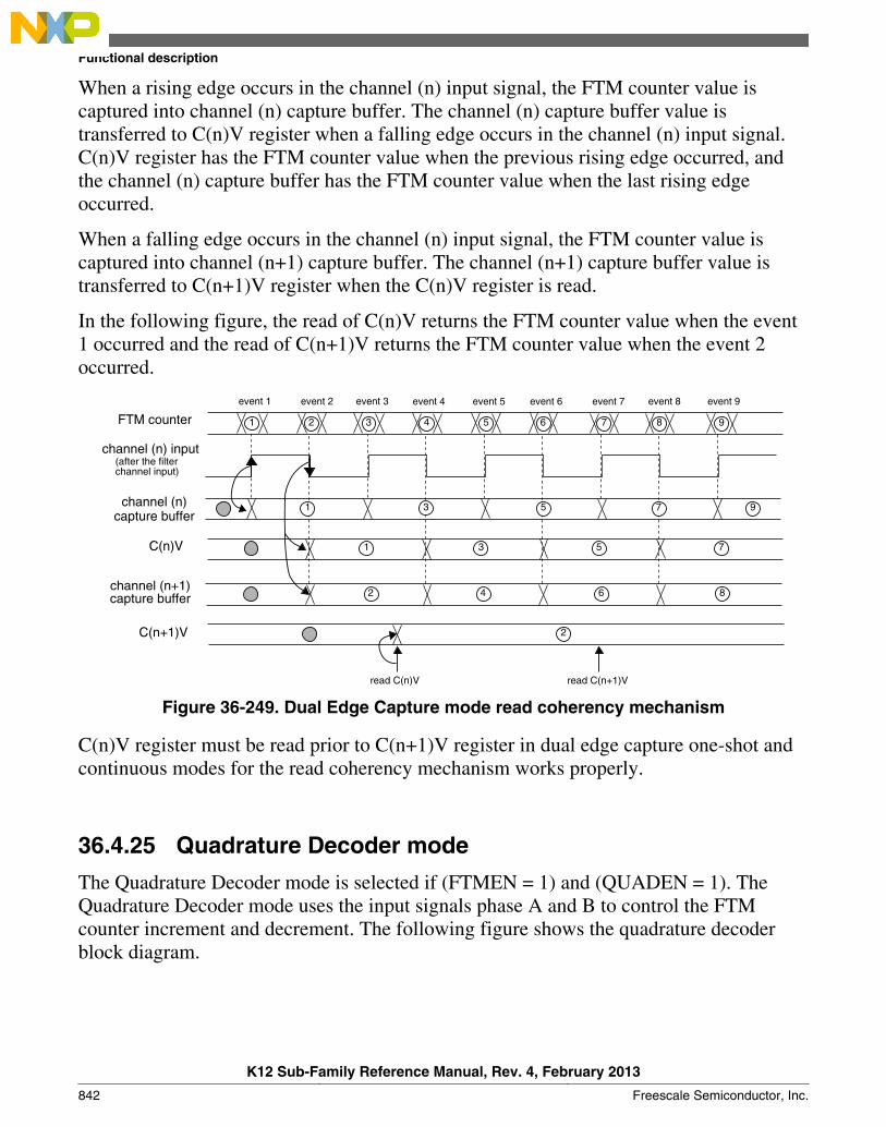
When a rising edge occurs in the channel (n) input signal, the FTM counter value iscaptured into channel (n) capture buffer. The channel (n) capture buffer value istransferred to C(n)V register when a falling edge occurs in the channel (n) input signal.C(n)V register has the FTM counter value when the previous rising edge occurred, andthe channel (n) capture buffer has the FTM counter value when the last rising edgeoccurred.
When a falling edge occurs in the channel (n) input signal, the FTM counter value iscaptured into channel (n+1) capture buffer. The channel (n+1) capture buffer value istransferred to C(n+1)V register when the C(n)V register is read.
In the following figure, the read of C(n)V returns the FTM counter value when the event1 occurred and the read of C(n+1)V returns the FTM counter value when the event 2occurred.
read C(n+1)V
FTM counter
channel (n) input(after the filterchannel input)
channel (n)capture buffer
C(n)V
C(n+1)V
channel (n+1)capture buffer
event 1 event 2 event 3 event 4 event 5 event 6 event 7 event 8 event 9
1 2 3 4 5 6 7 8 9
9
1 3 75
6 842
2
1 3 5 7
read C(n)V
Figure 36-249. Dual Edge Capture mode read coherency mechanism
C(n)V register must be read prior to C(n+1)V register in dual edge capture one-shot andcontinuous modes for the read coherency mechanism works properly.
36.4.25 Quadrature Decoder mode
The Quadrature Decoder mode is selected if (FTMEN = 1) and (QUADEN = 1). TheQuadrature Decoder mode uses the input signals phase A and B to control the FTMcounter increment and decrement. The following figure shows the quadrature decoderblock diagram.
Functional description
K12 Sub-Family Reference Manual, Rev. 4, February 2013
842 Freescale Semiconductor, Inc.
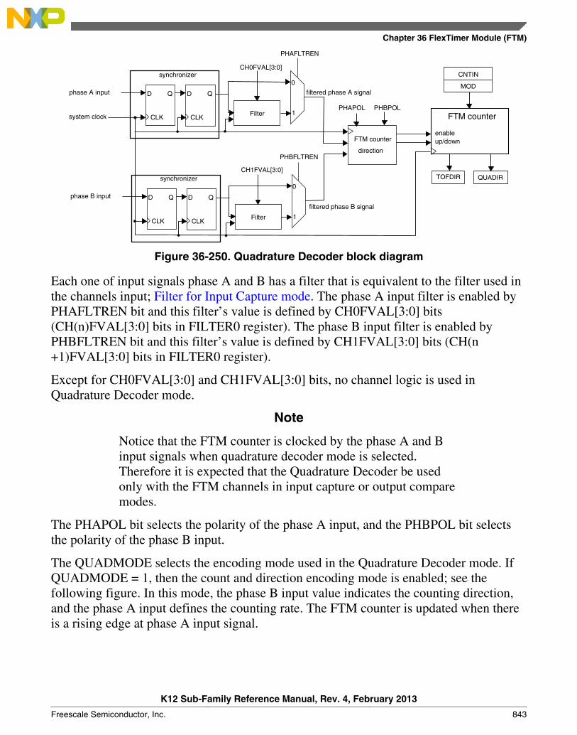
phase A input
system clock
phase B input
synchronizerCH0FVAL[3:0]
PHAFLTREN
filtered phase A signal
PHAPOL PHBPOL
filtered phase B signal
PHBFLTREN
CH1FVAL[3:0]synchronizer
Filter
CLK
D Q
CLK
D Q
CLK
D Q
CLK
D Q
Filter
Filter
FTM counter
direction
FTM counter
enableup/down
CNTIN
MOD
TOFDIR QUADIR
0
1
0
1
Figure 36-250. Quadrature Decoder block diagram
Each one of input signals phase A and B has a filter that is equivalent to the filter used inthe channels input; Filter for Input Capture mode. The phase A input filter is enabled byPHAFLTREN bit and this filter’s value is defined by CH0FVAL[3:0] bits(CH(n)FVAL[3:0] bits in FILTER0 register). The phase B input filter is enabled byPHBFLTREN bit and this filter’s value is defined by CH1FVAL[3:0] bits (CH(n+1)FVAL[3:0] bits in FILTER0 register).
Except for CH0FVAL[3:0] and CH1FVAL[3:0] bits, no channel logic is used inQuadrature Decoder mode.
Note
Notice that the FTM counter is clocked by the phase A and Binput signals when quadrature decoder mode is selected.Therefore it is expected that the Quadrature Decoder be usedonly with the FTM channels in input capture or output comparemodes.
The PHAPOL bit selects the polarity of the phase A input, and the PHBPOL bit selectsthe polarity of the phase B input.
The QUADMODE selects the encoding mode used in the Quadrature Decoder mode. IfQUADMODE = 1, then the count and direction encoding mode is enabled; see thefollowing figure. In this mode, the phase B input value indicates the counting direction,and the phase A input defines the counting rate. The FTM counter is updated when thereis a rising edge at phase A input signal.
Chapter 36 FlexTimer Module (FTM)
K12 Sub-Family Reference Manual, Rev. 4, February 2013
Freescale Semiconductor, Inc. 843
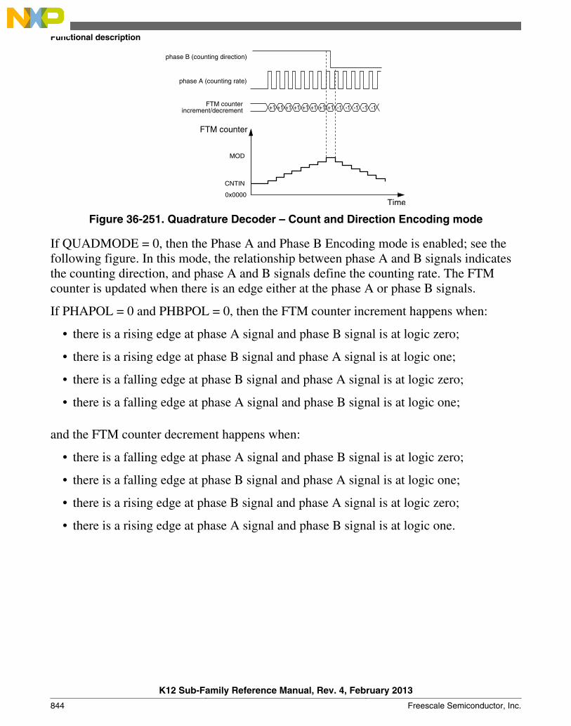
phase B (counting direction)
phase A (counting rate)
FTM counterincrement/decrement
FTM counter
MOD
CNTIN
0x0000Time
+1 +1 +1 +1 +1 +1 +1 +1 -1 -1 -1 -1 -1
Figure 36-251. Quadrature Decoder – Count and Direction Encoding mode
If QUADMODE = 0, then the Phase A and Phase B Encoding mode is enabled; see thefollowing figure. In this mode, the relationship between phase A and B signals indicatesthe counting direction, and phase A and B signals define the counting rate. The FTMcounter is updated when there is an edge either at the phase A or phase B signals.
If PHAPOL = 0 and PHBPOL = 0, then the FTM counter increment happens when:
• there is a rising edge at phase A signal and phase B signal is at logic zero;
• there is a rising edge at phase B signal and phase A signal is at logic one;
• there is a falling edge at phase B signal and phase A signal is at logic zero;
• there is a falling edge at phase A signal and phase B signal is at logic one;
and the FTM counter decrement happens when:
• there is a falling edge at phase A signal and phase B signal is at logic zero;
• there is a falling edge at phase B signal and phase A signal is at logic one;
• there is a rising edge at phase B signal and phase A signal is at logic zero;
• there is a rising edge at phase A signal and phase B signal is at logic one.
Functional description
K12 Sub-Family Reference Manual, Rev. 4, February 2013
844 Freescale Semiconductor, Inc.

phase A
phase B
FTM counterincrement/decrement
FTM counter
MOD
CNTIN
0x0000Time
+1 +1 +1 +1 +1 +1 +1 +1 -1 -1 -1 -1 -1-1 -1 +1 +1 +1 +1 +1 +1 +1 +1 +1 +1 +1 +1 +1 +1 +1-1 -1 -1 -1 -1-1 -1
Figure 36-252. Quadrature Decoder – Phase A and Phase B Encoding mode
The following figure shows the FTM counter overflow in up counting. In this case, whenthe FTM counter changes from MOD to CNTIN, TOF and TOFDIR bits are set. TOF bitindicates the FTM counter overflow occurred. TOFDIR indicates the counting was upwhen the FTM counter overflow occurred.
phase A
phase B
FTM counterincrement/decrement
FTM counter
MOD
CNTIN
0x0000Time
+1 +1 +1 +1 +1 +1 +1
set TOFset TOFDIR
set TOFset TOFDIR
+1 +1 +1 +1 +1 +1 +1 +1 +1 +1 +1 +1 +1 +1 +1 +1 +1
Figure 36-253. FTM Counter overflow in up counting for Quadrature Decoder mode
The following figure shows the FTM counter overflow in down counting. In this case,when the FTM counter changes from CNTIN to MOD, TOF bit is set and TOFDIR bit iscleared. TOF bit indicates the FTM counter overflow occurred. TOFDIR indicates thecounting was down when the FTM counter overflow occurred.
Chapter 36 FlexTimer Module (FTM)
K12 Sub-Family Reference Manual, Rev. 4, February 2013
Freescale Semiconductor, Inc. 845
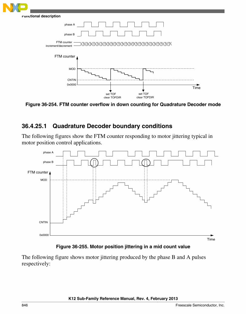
phase A
phase B
FTM counterincrement/decrement
FTM counter
MOD
CNTIN
0x0000Time
set TOFclear TOFDIR
-1
set TOFclear TOFDIR
-1-1-1-1-1-1-1-1-1-1-1-1-1-1-1-1-1-1-1-1-1-1-1-1
Figure 36-254. FTM counter overflow in down counting for Quadrature Decoder mode
36.4.25.1 Quadrature Decoder boundary conditions
The following figures show the FTM counter responding to motor jittering typical inmotor position control applications.
phase A
phase B
FTM counter
MOD
CNTIN
0x0000
Time
Figure 36-255. Motor position jittering in a mid count value
The following figure shows motor jittering produced by the phase B and A pulsesrespectively:
Functional description
K12 Sub-Family Reference Manual, Rev. 4, February 2013
846 Freescale Semiconductor, Inc.
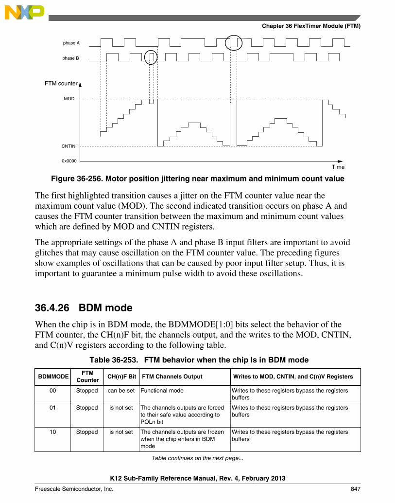
phase A
phase B
FTM counter
MOD
CNTIN
0x0000
Time
Figure 36-256. Motor position jittering near maximum and minimum count value
The first highlighted transition causes a jitter on the FTM counter value near themaximum count value (MOD). The second indicated transition occurs on phase A andcauses the FTM counter transition between the maximum and minimum count valueswhich are defined by MOD and CNTIN registers.
The appropriate settings of the phase A and phase B input filters are important to avoidglitches that may cause oscillation on the FTM counter value. The preceding figuresshow examples of oscillations that can be caused by poor input filter setup. Thus, it isimportant to guarantee a minimum pulse width to avoid these oscillations.
36.4.26 BDM mode
When the chip is in BDM mode, the BDMMODE[1:0] bits select the behavior of theFTM counter, the CH(n)F bit, the channels output, and the writes to the MOD, CNTIN,and C(n)V registers according to the following table.
Table 36-253. FTM behavior when the chip Is in BDM mode
BDMMODEFTM
CounterCH(n)F Bit FTM Channels Output Writes to MOD, CNTIN, and C(n)V Registers
00 Stopped can be set Functional mode Writes to these registers bypass the registersbuffers
01 Stopped is not set The channels outputs are forcedto their safe value according toPOLn bit
Writes to these registers bypass the registersbuffers
10 Stopped is not set The channels outputs are frozenwhen the chip enters in BDMmode
Writes to these registers bypass the registersbuffers
Table continues on the next page...
Chapter 36 FlexTimer Module (FTM)
K12 Sub-Family Reference Manual, Rev. 4, February 2013
Freescale Semiconductor, Inc. 847
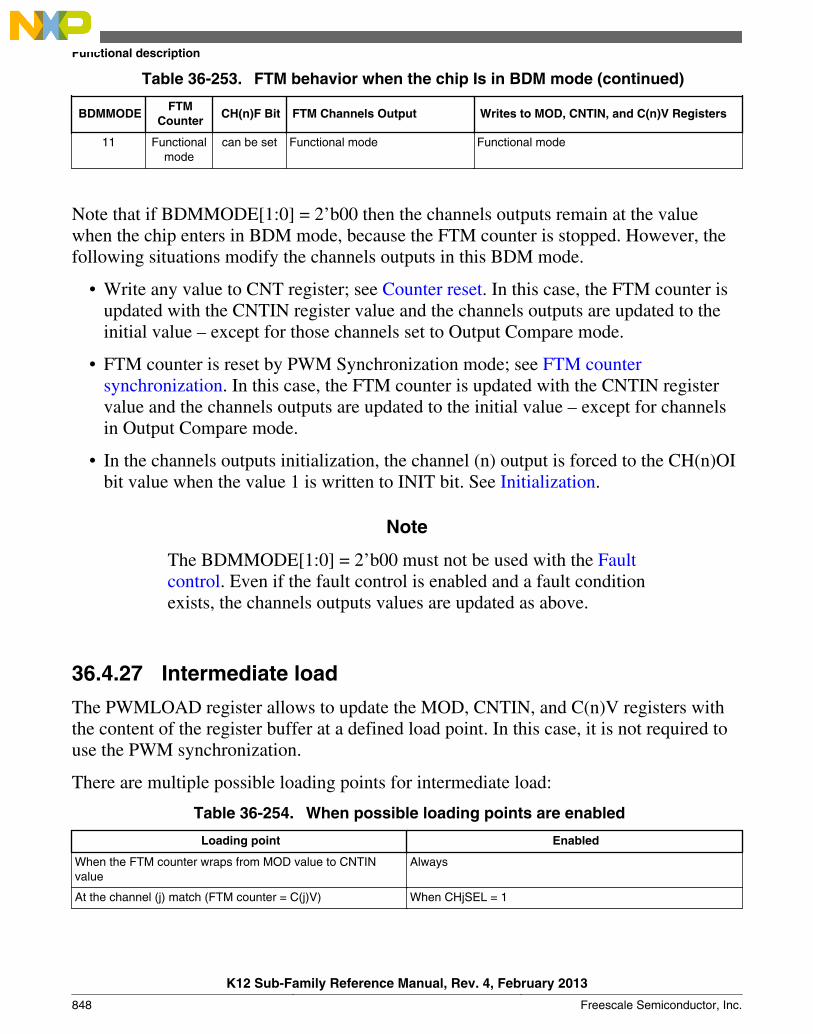
Table 36-253. FTM behavior when the chip Is in BDM mode (continued)
BDMMODEFTM
CounterCH(n)F Bit FTM Channels Output Writes to MOD, CNTIN, and C(n)V Registers
11 Functionalmode
can be set Functional mode Functional mode
Note that if BDMMODE[1:0] = 2’b00 then the channels outputs remain at the valuewhen the chip enters in BDM mode, because the FTM counter is stopped. However, thefollowing situations modify the channels outputs in this BDM mode.
• Write any value to CNT register; see Counter reset. In this case, the FTM counter isupdated with the CNTIN register value and the channels outputs are updated to theinitial value – except for those channels set to Output Compare mode.
• FTM counter is reset by PWM Synchronization mode; see FTM countersynchronization. In this case, the FTM counter is updated with the CNTIN registervalue and the channels outputs are updated to the initial value – except for channelsin Output Compare mode.
• In the channels outputs initialization, the channel (n) output is forced to the CH(n)OIbit value when the value 1 is written to INIT bit. See Initialization.
Note
The BDMMODE[1:0] = 2’b00 must not be used with the Faultcontrol. Even if the fault control is enabled and a fault conditionexists, the channels outputs values are updated as above.
36.4.27 Intermediate load
The PWMLOAD register allows to update the MOD, CNTIN, and C(n)V registers withthe content of the register buffer at a defined load point. In this case, it is not required touse the PWM synchronization.
There are multiple possible loading points for intermediate load:
Table 36-254. When possible loading points are enabled
Loading point Enabled
When the FTM counter wraps from MOD value to CNTINvalue
Always
At the channel (j) match (FTM counter = C(j)V) When CHjSEL = 1
Functional description
K12 Sub-Family Reference Manual, Rev. 4, February 2013
848 Freescale Semiconductor, Inc.
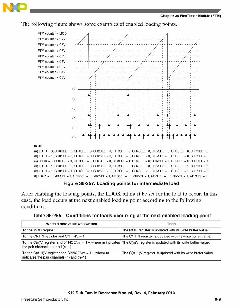
The following figure shows some examples of enabled loading points.
NOTE
(c)
(a) LDOK = 0, CH0SEL = 0, CH1SEL = 0, CH2SEL = 0, CH3SEL = 0, CH4SEL = 0, CH5SEL = 0, CH6SEL = 0, CH7SEL = 0
(b) LDOK = 1, CH0SEL = 0, CH1SEL = 0, CH2SEL = 0, CH3SEL = 0, CH4SEL = 0, CH5SEL = 0, CH6SEL = 0, CH7SEL = 0
(c) LDOK = 0, CH0SEL = 0, CH1SEL = 0, CH2SEL = 0, CH3SEL = 1, CH4SEL = 0, CH5SEL = 0, CH6SEL = 0, CH7SEL = 0
(d) LDOK = 1, CH0SEL = 0, CH1SEL = 0, CH2SEL = 0, CH3SEL = 0, CH4SEL = 0, CH5SEL = 0, CH6SEL = 1, CH7SEL = 0
(e) LDOK = 1, CH0SEL = 1, CH1SEL = 0, CH2SEL = 1, CH3SEL = 0, CH4SEL = 1, CH5SEL = 0, CH6SEL = 1, CH7SEL = 0
(f) LDOK = 1, CH0SEL = 1, CH1SEL = 1, CH2SEL = 1, CH3SEL = 1, CH4SEL = 1, CH5SEL = 1, CH6SEL = 1, CH7SEL = 1
(d)
(e)
(f)
(b)
(a)
FTM counter = MOD
FTM counter = C7V
FTM counter = C6V
FTM counter = C5V
FTM counter = C4V
FTM counter = C3V
FTM counter = C2V
FTM counter = C1V
FTM counter = C0V
Figure 36-257. Loading points for intermediate load
After enabling the loading points, the LDOK bit must be set for the load to occur. In thiscase, the load occurs at the next enabled loading point according to the followingconditions:
Table 36-255. Conditions for loads occurring at the next enabled loading point
When a new value was written Then
To the MOD register The MOD register is updated with its write buffer value.
To the CNTIN register and CNTINC = 1 The CNTIN register is updated with its write buffer value.
To the C(n)V register and SYNCENm = 1 – where m indicatesthe pair channels (n) and (n+1)
The C(n)V register is updated with its write buffer value.
To the C(n+1)V register and SYNCENm = 1 – where mindicates the pair channels (n) and (n+1)
The C(n+1)V register is updated with its write buffer value.
Chapter 36 FlexTimer Module (FTM)
K12 Sub-Family Reference Manual, Rev. 4, February 2013
Freescale Semiconductor, Inc. 849

NOTE• If ELSjB and ELSjA bits are different from zero, then the
channel (j) output signal is generated according to theconfigured output mode. If ELSjB and ELSjA bits are zero,then the generated signal is not available on channel (j)output.
• If CHjIE = 1, then the channel (j) interrupt is generatedwhen the channel (j) match occurs.
• At the intermediate load neither the channels outputs northe FTM counter are changed. Software must set theintermediate load at a safe point in time.
• The intermediate load feature must be used only inCombine mode.
36.4.28 Global time base (GTB)
The global time base (GTB) is a FTM function that allows the synchronization ofmultiple FTM modules on a chip. The following figure shows an example of the GTBfeature used to synchronize two FTM modules. In this case, the FTM A and B channelscan behave as if just one FTM module was used, that is, a global time base.
GTBEOUT bit
gtb_in
gtb_out
gtb_in
example glue logic
FTM module BFTM module A
GTBEEN bitFTM counterenable logic
FTM counter
enable
gtb_out
Figure 36-258. Global time base (GTB) block diagram
The GTB functionality is implemented by the GTBEEN and GTBEOUT bits in theCONF register, the input signal gtb_in, and the output signal gtb_out. The GTBEEN bitenables gtb_in to control the FTM counter enable signal:
• If GTBEEN = 0, each one of FTM modules works independently according to theirconfigured mode.
• If GTBEEN = 1, the FTM counter update is enabled only when gtb_in is 1.
Functional description
K12 Sub-Family Reference Manual, Rev. 4, February 2013
850 Freescale Semiconductor, Inc.
In the configuration described in the preceding figure, FTM modules A and B have theirFTM counters enabled if at least one of the gtb_out signals from one of the FTM modulesis 1. There are several possible configurations for the interconnection of the gtb_in andgtb_out signals, represented by the example glue logic shown in the figure. Note thatthese configurations are chip-dependent and implemented outside of the FTM modules.See the chip configuration details for the chip's specific implementation.
NOTE• In order to use the GTB signals to synchronize the FTM
counter of different FTM modules, the configuration ofeach FTM module should guarantee that its FTM counterstarts counting as soon as the gtb_in signal is 1.
• The GTB feature does not provide continuoussynchronization of FTM counters, meaning that the FTMcounters may lose synchronization during FTM operation.The GTB feature only allows the FTM counters to starttheir operation synchronously.
36.4.28.1 Enabling the global time base (GTB)
To enable the GTB feature, follow these steps for each participating FTM module:
1. Stop the FTM counter: Write 00b to SC[CLKS].2. Program the FTM to the intended configuration. The FTM counter mode needs to be
consistent across all participating modules.3. Write 1 to CONF[GTBEEN] and write 0 to CONF[GTBEOUT] at the same time.4. Select the intended FTM counter clock source in SC[CLKS]. The clock source needs
to be consistent across all participating modules.5. Reset the FTM counter: Write any value to the CNT register.
To initiate the GTB feature in the configuration described in the preceding figure, write 1to CONF[GTBEOUT] in the FTM module used as the time base.
36.5 Reset overviewThe FTM is reset whenever any chip reset occurs.
When the FTM exits from reset:
• the FTM counter and the prescaler counter are zero and are stopped (CLKS[1:0] =00b);
• the timer overflow interrupt is zero, see Timer Overflow Interrupt;
Chapter 36 FlexTimer Module (FTM)
K12 Sub-Family Reference Manual, Rev. 4, February 2013
Freescale Semiconductor, Inc. 851
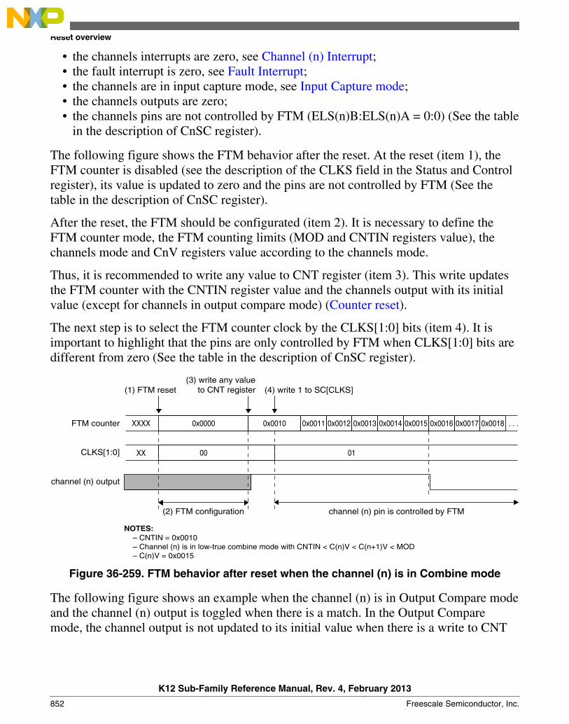
• the channels interrupts are zero, see Channel (n) Interrupt;• the fault interrupt is zero, see Fault Interrupt;• the channels are in input capture mode, see Input Capture mode;• the channels outputs are zero;• the channels pins are not controlled by FTM (ELS(n)B:ELS(n)A = 0:0) (See the table
in the description of CnSC register).
The following figure shows the FTM behavior after the reset. At the reset (item 1), theFTM counter is disabled (see the description of the CLKS field in the Status and Controlregister), its value is updated to zero and the pins are not controlled by FTM (See thetable in the description of CnSC register).
After the reset, the FTM should be configurated (item 2). It is necessary to define theFTM counter mode, the FTM counting limits (MOD and CNTIN registers value), thechannels mode and CnV registers value according to the channels mode.
Thus, it is recommended to write any value to CNT register (item 3). This write updatesthe FTM counter with the CNTIN register value and the channels output with its initialvalue (except for channels in output compare mode) (Counter reset).
The next step is to select the FTM counter clock by the CLKS[1:0] bits (item 4). It isimportant to highlight that the pins are only controlled by FTM when CLKS[1:0] bits aredifferent from zero (See the table in the description of CnSC register).
(1) FTM reset
0x00160x00150x00140x00130x0011 . . .0x0010 0x00180x0017XXXX 0x0000 0x0012FTM counter
CLKS[1:0]
channel (n) output
(4) write 1 to SC[CLKS](3) write any value
to CNT register
(2) FTM configuration channel (n) pin is controlled by FTM
NOTES: – CNTIN = 0x0010 – Channel (n) is in low-true combine mode with CNTIN < C(n)V < C(n+1)V < MOD – C(n)V = 0x0015
00XX 01
Figure 36-259. FTM behavior after reset when the channel (n) is in Combine mode
The following figure shows an example when the channel (n) is in Output Compare modeand the channel (n) output is toggled when there is a match. In the Output Comparemode, the channel output is not updated to its initial value when there is a write to CNT
Reset overview
K12 Sub-Family Reference Manual, Rev. 4, February 2013
852 Freescale Semiconductor, Inc.
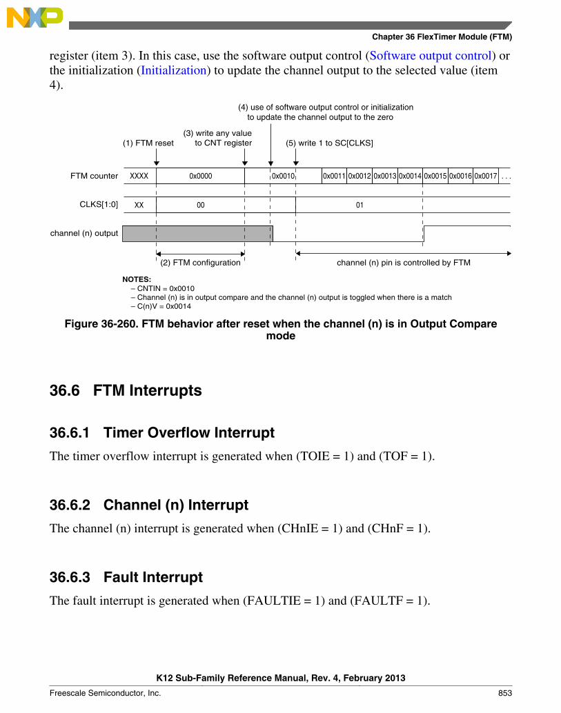
register (item 3). In this case, use the software output control (Software output control) orthe initialization (Initialization) to update the channel output to the selected value (item4).
(1) FTM reset
0x00150x00140x00130x0012 . . .0x0010 0x00170x0016XXXX 0x0000 0x0011FTM counter
CLKS[1:0]
channel (n) output
(5) write 1 to SC[CLKS](3) write any value
to CNT register
(2) FTM configuration channel (n) pin is controlled by FTM
NOTES: – CNTIN = 0x0010 – Channel (n) is in output compare and the channel (n) output is toggled when there is a match – C(n)V = 0x0014
00XX 01
(4) use of software output control or initialization to update the channel output to the zero
Figure 36-260. FTM behavior after reset when the channel (n) is in Output Comparemode
36.6 FTM Interrupts
36.6.1 Timer Overflow Interrupt
The timer overflow interrupt is generated when (TOIE = 1) and (TOF = 1).
36.6.2 Channel (n) Interrupt
The channel (n) interrupt is generated when (CHnIE = 1) and (CHnF = 1).
36.6.3 Fault Interrupt
The fault interrupt is generated when (FAULTIE = 1) and (FAULTF = 1).
Chapter 36 FlexTimer Module (FTM)
K12 Sub-Family Reference Manual, Rev. 4, February 2013
Freescale Semiconductor, Inc. 853

FTM Interrupts
K12 Sub-Family Reference Manual, Rev. 4, February 2013
854 Freescale Semiconductor, Inc.

Chapter 37Periodic Interrupt Timer (PIT-RTI)
37.1 IntroductionNOTE
For the chip-specific implementation details of this module'sinstances see the chip configuration information.
The PIT module is an array of timers that can be used to raise interrupts and trigger DMAchannels.
37.1.1 Block diagram
The following figure shows the block diagram of the PITmodule.
K12 Sub-Family Reference Manual, Rev. 4, February 2013
Freescale Semiconductor, Inc. 855

Timer n
Timer 1
PIT Peripheral
load_value
PIT
Triggers
bus clock
bus
Peripheral
Iinterrupts
registers
Figure 37-1. Block diagram of the PIT
NOTESee the chip configuration details for the number of PITchannels used in this MCU.
37.1.2 Features
The main features of this block are:
• Ability of timers to generate DMA trigger pulses
• Ability of timers to generate interrupts
• Maskable interrupts• Independent timeout periods for each timer
37.2 Modes of operationThis subsection describes briefly all operating modes supported by the PIT.
• Run Mode
Modes of operation
K12 Sub-Family Reference Manual, Rev. 4, February 2013
856 Freescale Semiconductor, Inc.
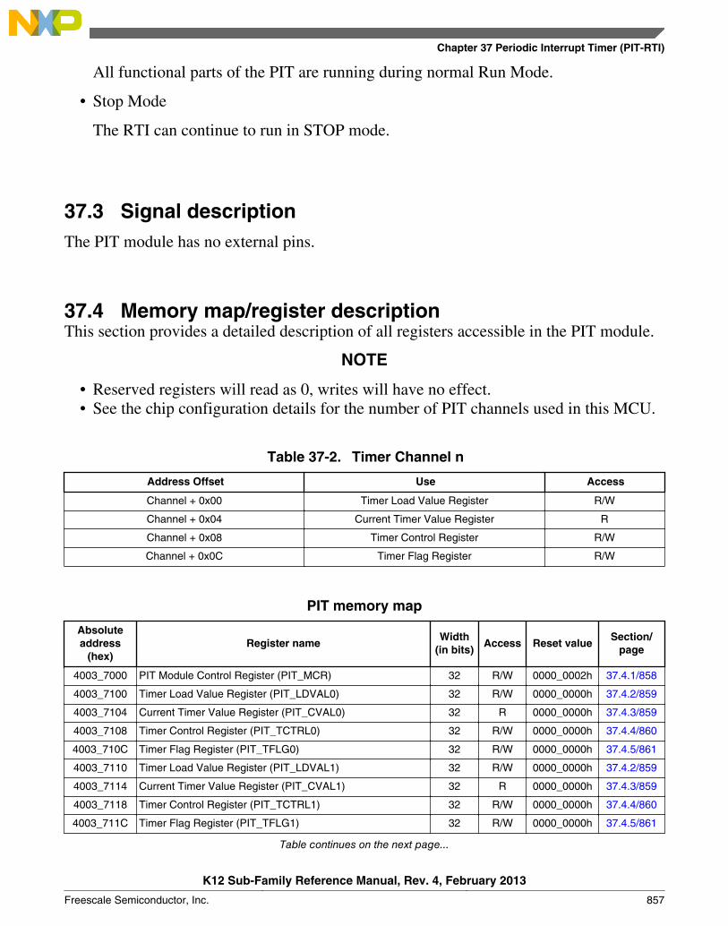
All functional parts of the PIT are running during normal Run Mode.
• Stop Mode
The RTI can continue to run in STOP mode.
37.3 Signal descriptionThe PIT module has no external pins.
37.4 Memory map/register descriptionThis section provides a detailed description of all registers accessible in the PIT module.
NOTE
• Reserved registers will read as 0, writes will have no effect.• See the chip configuration details for the number of PIT channels used in this MCU.
Table 37-2. Timer Channel n
Address Offset Use Access
Channel + 0x00 Timer Load Value Register R/W
Channel + 0x04 Current Timer Value Register R
Channel + 0x08 Timer Control Register R/W
Channel + 0x0C Timer Flag Register R/W
PIT memory map
Absoluteaddress
(hex)Register name
Width(in bits)
Access Reset valueSection/
page
4003_7000 PIT Module Control Register (PIT_MCR) 32 R/W 0000_0002h 37.4.1/858
4003_7100 Timer Load Value Register (PIT_LDVAL0) 32 R/W 0000_0000h 37.4.2/859
4003_7104 Current Timer Value Register (PIT_CVAL0) 32 R 0000_0000h 37.4.3/859
4003_7108 Timer Control Register (PIT_TCTRL0) 32 R/W 0000_0000h 37.4.4/860
4003_710C Timer Flag Register (PIT_TFLG0) 32 R/W 0000_0000h 37.4.5/861
4003_7110 Timer Load Value Register (PIT_LDVAL1) 32 R/W 0000_0000h 37.4.2/859
4003_7114 Current Timer Value Register (PIT_CVAL1) 32 R 0000_0000h 37.4.3/859
4003_7118 Timer Control Register (PIT_TCTRL1) 32 R/W 0000_0000h 37.4.4/860
4003_711C Timer Flag Register (PIT_TFLG1) 32 R/W 0000_0000h 37.4.5/861
Table continues on the next page...
Chapter 37 Periodic Interrupt Timer (PIT-RTI)
K12 Sub-Family Reference Manual, Rev. 4, February 2013
Freescale Semiconductor, Inc. 857

PIT memory map (continued)
Absoluteaddress
(hex)Register name
Width(in bits)
Access Reset valueSection/
page
4003_7120 Timer Load Value Register (PIT_LDVAL2) 32 R/W 0000_0000h 37.4.2/859
4003_7124 Current Timer Value Register (PIT_CVAL2) 32 R 0000_0000h 37.4.3/859
4003_7128 Timer Control Register (PIT_TCTRL2) 32 R/W 0000_0000h 37.4.4/860
4003_712C Timer Flag Register (PIT_TFLG2) 32 R/W 0000_0000h 37.4.5/861
4003_7130 Timer Load Value Register (PIT_LDVAL3) 32 R/W 0000_0000h 37.4.2/859
4003_7134 Current Timer Value Register (PIT_CVAL3) 32 R 0000_0000h 37.4.3/859
4003_7138 Timer Control Register (PIT_TCTRL3) 32 R/W 0000_0000h 37.4.4/860
4003_713C Timer Flag Register (PIT_TFLG3) 32 R/W 0000_0000h 37.4.5/861
37.4.1 PIT Module Control Register (PIT_MCR)
This register enables or disables the PIT timer clocks and controls the timers when thePIT enters the Debug mode.
Address: 4003_7000h base + 0h offset = 4003_7000h
Bit 31 30 29 28 27 26 25 24 23 22 21 20 19 18 17 16
R 0
W
Reset 0 0 0 0 0 0 0 0 0 0 0 0 0 0 0 0
Bit 15 14 13 12 11 10 9 8 7 6 5 4 3 2 1 0
R 0
Res
erve
d
MDIS FRZ
W
Reset 0 0 0 0 0 0 0 0 0 0 0 0 0 0 1 0
Memory map/register description
K12 Sub-Family Reference Manual, Rev. 4, February 2013
858 Freescale Semiconductor, Inc.

PIT_MCR field descriptions
Field Description
31–3Reserved
This field is reserved.This read-only field is reserved and always has the value 0.
2Reserved
This field is reserved.
1MDIS
Module Disable - (PIT section)
Disables the standard timers. This field must be enabled before any other setup is done.
0 Clock for standard PIT timers is enabled.1 Clock for standard PIT timers is disabled.
0FRZ
Freeze
Allows the timers to be stopped when the device enters the Debug mode.
0 Timers continue to run in Debug mode.1 Timers are stopped in Debug mode.
37.4.2 Timer Load Value Register (PIT_LDVALn)These registers select the timeout period for the timer interrupts.
Address: 4003_7000h base + 100h offset + (16d × i), where i=0d to 3d
Bit 31 30 29 28 27 26 25 24 23 22 21 20 19 18 17 16 15 14 13 12 11 10 9 8 7 6 5 4 3 2 1 0
R TSVW
Reset 0 0 0 0 0 0 0 0 0 0 0 0 0 0 0 0 0 0 0 0 0 0 0 0 0 0 0 0 0 0 0 0
PIT_LDVALn field descriptions
Field Description
31–0TSV
Timer Start Value
Sets the timer start value. The timer will count down until it reaches 0, then it will generate an interrupt andload this register value again. Writing a new value to this register will not restart the timer; instead thevalue will be loaded after the timer expires. To abort the current cycle and start a timer period with the newvalue, the timer must be disabled and enabled again.
37.4.3 Current Timer Value Register (PIT_CVALn)These registers indicate the current timer position.
Address: 4003_7000h base + 104h offset + (16d × i), where i=0d to 3d
Bit 31 30 29 28 27 26 25 24 23 22 21 20 19 18 17 16 15 14 13 12 11 10 9 8 7 6 5 4 3 2 1 0
R TVL
W
Reset 0 0 0 0 0 0 0 0 0 0 0 0 0 0 0 0 0 0 0 0 0 0 0 0 0 0 0 0 0 0 0 0
Chapter 37 Periodic Interrupt Timer (PIT-RTI)
K12 Sub-Family Reference Manual, Rev. 4, February 2013
Freescale Semiconductor, Inc. 859
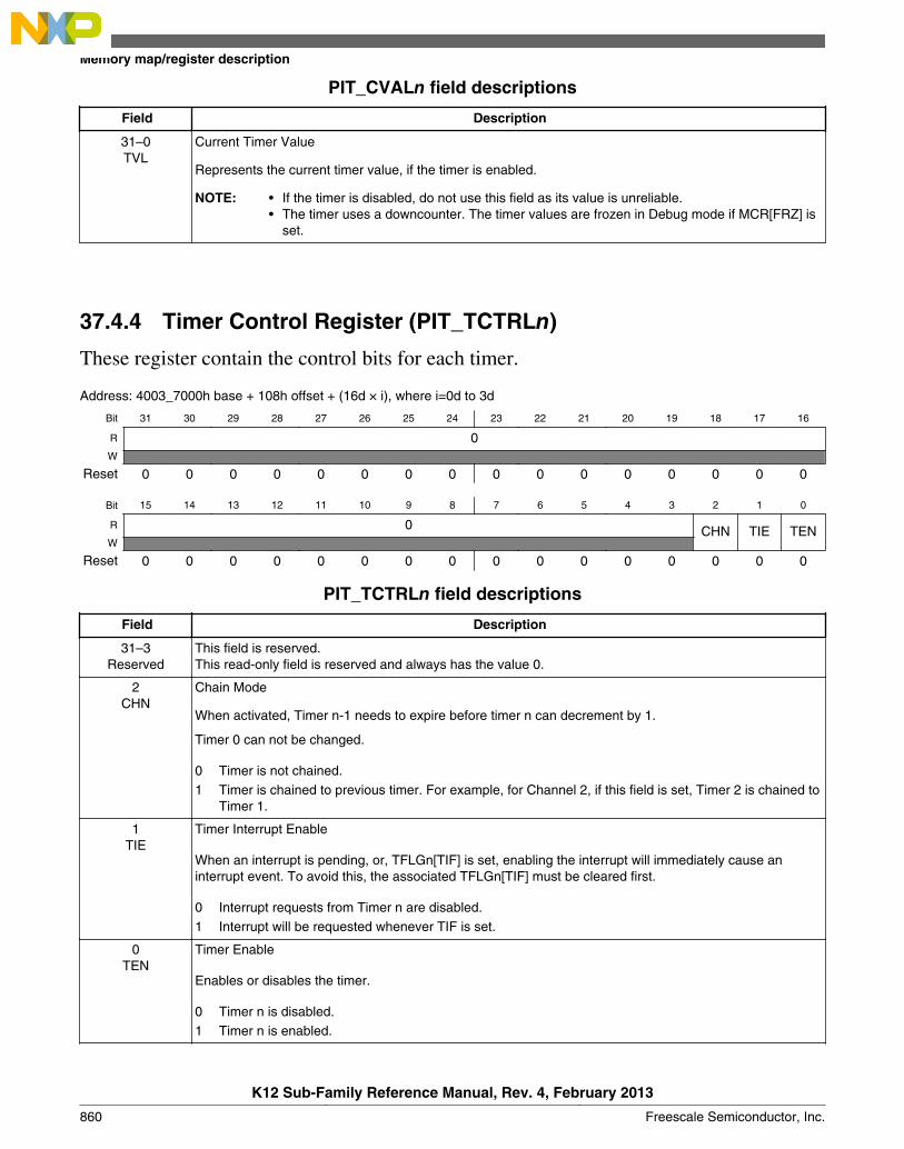
PIT_CVALn field descriptions
Field Description
31–0TVL
Current Timer Value
Represents the current timer value, if the timer is enabled.
NOTE: • If the timer is disabled, do not use this field as its value is unreliable.• The timer uses a downcounter. The timer values are frozen in Debug mode if MCR[FRZ] is
set.
37.4.4 Timer Control Register (PIT_TCTRLn)
These register contain the control bits for each timer.
Address: 4003_7000h base + 108h offset + (16d × i), where i=0d to 3d
Bit 31 30 29 28 27 26 25 24 23 22 21 20 19 18 17 16
R 0W
Reset 0 0 0 0 0 0 0 0 0 0 0 0 0 0 0 0
Bit 15 14 13 12 11 10 9 8 7 6 5 4 3 2 1 0
R 0 CHN TIE TENW
Reset 0 0 0 0 0 0 0 0 0 0 0 0 0 0 0 0
PIT_TCTRLn field descriptions
Field Description
31–3Reserved
This field is reserved.This read-only field is reserved and always has the value 0.
2CHN
Chain Mode
When activated, Timer n-1 needs to expire before timer n can decrement by 1.
Timer 0 can not be changed.
0 Timer is not chained.1 Timer is chained to previous timer. For example, for Channel 2, if this field is set, Timer 2 is chained to
Timer 1.
1TIE
Timer Interrupt Enable
When an interrupt is pending, or, TFLGn[TIF] is set, enabling the interrupt will immediately cause aninterrupt event. To avoid this, the associated TFLGn[TIF] must be cleared first.
0 Interrupt requests from Timer n are disabled.1 Interrupt will be requested whenever TIF is set.
0TEN
Timer Enable
Enables or disables the timer.
0 Timer n is disabled.1 Timer n is enabled.
Memory map/register description
K12 Sub-Family Reference Manual, Rev. 4, February 2013
860 Freescale Semiconductor, Inc.
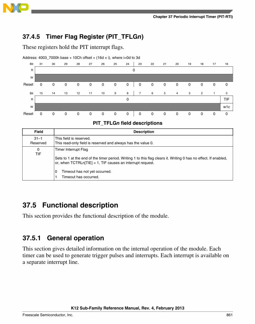
37.4.5 Timer Flag Register (PIT_TFLGn)
These registers hold the PIT interrupt flags.
Address: 4003_7000h base + 10Ch offset + (16d × i), where i=0d to 3d
Bit 31 30 29 28 27 26 25 24 23 22 21 20 19 18 17 16
R 0
W
Reset 0 0 0 0 0 0 0 0 0 0 0 0 0 0 0 0
Bit 15 14 13 12 11 10 9 8 7 6 5 4 3 2 1 0
R 0 TIF
W w1c
Reset 0 0 0 0 0 0 0 0 0 0 0 0 0 0 0 0
PIT_TFLGn field descriptions
Field Description
31–1Reserved
This field is reserved.This read-only field is reserved and always has the value 0.
0TIF
Timer Interrupt Flag
Sets to 1 at the end of the timer period. Writing 1 to this flag clears it. Writing 0 has no effect. If enabled,or, when TCTRLn[TIE] = 1, TIF causes an interrupt request.
0 Timeout has not yet occurred.1 Timeout has occurred.
37.5 Functional descriptionThis section provides the functional description of the module.
37.5.1 General operation
This section gives detailed information on the internal operation of the module. Eachtimer can be used to generate trigger pulses and interrupts. Each interrupt is available ona separate interrupt line.
Chapter 37 Periodic Interrupt Timer (PIT-RTI)
K12 Sub-Family Reference Manual, Rev. 4, February 2013
Freescale Semiconductor, Inc. 861
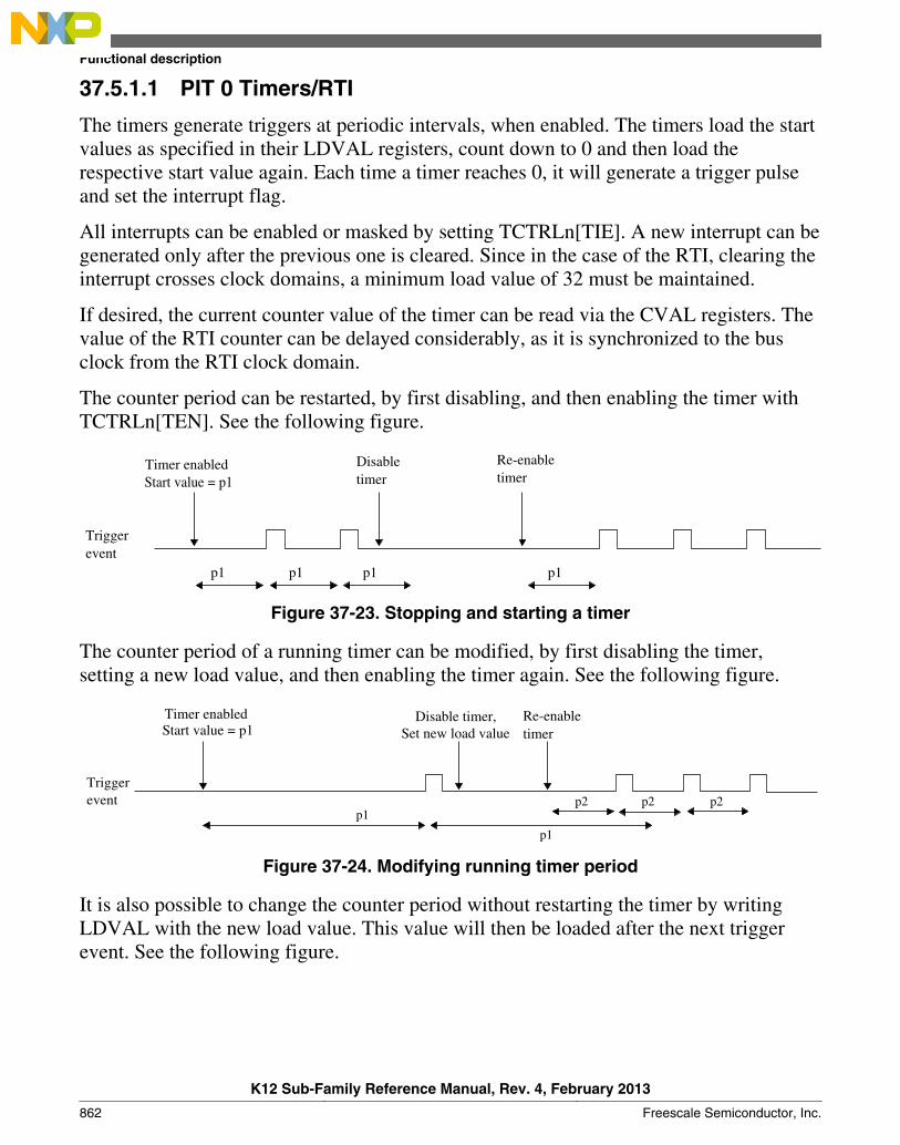
37.5.1.1 PIT 0 Timers/RTI
The timers generate triggers at periodic intervals, when enabled. The timers load the startvalues as specified in their LDVAL registers, count down to 0 and then load therespective start value again. Each time a timer reaches 0, it will generate a trigger pulseand set the interrupt flag.
All interrupts can be enabled or masked by setting TCTRLn[TIE]. A new interrupt can begenerated only after the previous one is cleared. Since in the case of the RTI, clearing theinterrupt crosses clock domains, a minimum load value of 32 must be maintained.
If desired, the current counter value of the timer can be read via the CVAL registers. Thevalue of the RTI counter can be delayed considerably, as it is synchronized to the busclock from the RTI clock domain.
The counter period can be restarted, by first disabling, and then enabling the timer withTCTRLn[TEN]. See the following figure.
p1
Timer enabled Disable timer
p1 p1
Start value = p1
Trigger event
p1
Re-enabletimer
Figure 37-23. Stopping and starting a timer
The counter period of a running timer can be modified, by first disabling the timer,setting a new load value, and then enabling the timer again. See the following figure.
Timer enabled Disable timer,
p1 p1
Re-enable timerStart value = p1
Trigger event
Set new load value
p2 p2 p2
Figure 37-24. Modifying running timer period
It is also possible to change the counter period without restarting the timer by writingLDVAL with the new load value. This value will then be loaded after the next triggerevent. See the following figure.
Functional description
K12 Sub-Family Reference Manual, Rev. 4, February 2013
862 Freescale Semiconductor, Inc.

Timer enabled
p1 p1
Start value = p1
Trigger event
p2 p2p1
New start Value p2 set
Figure 37-25. Dynamically setting a new load value
37.5.1.2 Debug mode
In Debug mode, the timers will be frozen based on MCR[FRZ]. This is intended to aidsoftware development, allowing the developer to halt the processor, investigate thecurrent state of the system, for example, the timer values, and then continue theoperation.
37.5.2 Interrupts
All the timers support interrupt generation.
Timer interrupts can be enabled by setting TCTRLn[TIE]. TFLGn[TIF] are set to 1 whena timeout occurs on the associated timer, and are cleared to 0 by writing a 1 to thecorresponding TFLGn[TIF].
37.5.3 Chained timers
When a timer has chain mode enabled, it will only count after the previous timer hasexpired. So if timer n-1 has counted down to 0, counter n will decrement the value byone. This allows to chain some of the timers together to form a longer timer. The firsttimer (timer 0) cannot be chained to any other timer.
37.6 Initialization and application informationIn the example configuration:
• The PIT clock has a frequency of 50 MHz.
Chapter 37 Periodic Interrupt Timer (PIT-RTI)
K12 Sub-Family Reference Manual, Rev. 4, February 2013
Freescale Semiconductor, Inc. 863

• Timer 1 creates an interrupt every 5.12 ms.
• Timer 3 creates a trigger event every 30 ms.
The PIT module must be activated by writing a 0 to MCR[MDIS].
The 50 MHz clock frequency equates to a clock period of 20 ns. Timer 1 needs to triggerevery 5.12 ms/20 ns = 256,000 cycles and Timer 3 every 30 ms/20 ns = 1,500,000 cycles.The value for the LDVAL register trigger is calculated as:
LDVAL trigger = (period / clock period) -1
This means LDVAL1 and LDVAL3 must be written with 0x0003E7FF and 0x0016E35Frespectively.
The interrupt for Timer 1 is enabled by setting TCTRL1[TIE]. The timer is started bywriting 1 to TCTRL1[TEN].
Timer 3 shall be used only for triggering. Therefore, Timer 3 is started by writing a 1 toTCTRL3[TEN]. TCTRL3[TIE] stays at 0.
The following example code matches the described setup:
// turn on PIT PIT_MCR = 0x00;
// Timer 1 PIT_LDVAL1 = 0x0003E7FF; // setup timer 1 for 256000 cycles PIT_TCTRL1 = TIE; // enable Timer 1 interrupts PIT_TCTRL1 |= TEN; // start Timer 1
// Timer 3 PIT_LDVAL3 = 0x0016E35F; // setup timer 3 for 1500000 cycles PIT_TCTRL3 |= TEN; // start Timer 3
37.7 Example configuration for chained timersIn the example configuration:
• The PIT clock has a frequency of 100 MHz.
• Timers 1 and 2 are available.
• An interrupt shall be raised every 1 hour.
The PIT module needs to be activated by writing a 0 to MCR[MDIS].
Example configuration for chained timers
K12 Sub-Family Reference Manual, Rev. 4, February 2013
864 Freescale Semiconductor, Inc.
The 100 MHz clock frequency equates to a clock period of 10 ns, so the PIT needs tocount for 6000 million cycles, which is more than a single timer can do. So, Timer 1 isset up to trigger every 6 s (600 million cycles). Timer 2 is chained to Timer 1 andprogrammed to trigger 10 times.
The value for the LDVAL register trigger is calculated as number of cycles-1, soLDVAL1 receives the value 0x23C345FF and LDVAL2 receives the value 0x00000009.
The interrupt for Timer 2 is enabled by setting TCTRL2[TIE], the Chain mode isactivated by setting TCTRL2[CHN], and the timer is started by writing a 1 toTCTRL2[TEN]. TCTRL1[TEN] needs to be set, and TCTRL1[CHN] and TCTRL1[TIE]are cleared.
The following example code matches the described setup:
// turn on PIT PIT_MCR = 0x00;
// Timer 2 PIT_LDVAL2 = 0x00000009; // setup Timer 2 for 10 counts PIT_TCTRL2 = TIE; // enable Timer 2 interrupt PIT_TCTRL2 |= CHN; // chain Timer 2 to Timer 1 PIT_TCTRL2 |= TEN; // start Timer 2
// Timer 1 PIT_LDVAL1 = 0x23C345FF; // setup Timer 1 for 600 000 000 cycles PIT_TCTRL1 = TEN; // start Timer 1
Chapter 37 Periodic Interrupt Timer (PIT-RTI)
K12 Sub-Family Reference Manual, Rev. 4, February 2013
Freescale Semiconductor, Inc. 865

Example configuration for chained timers
K12 Sub-Family Reference Manual, Rev. 4, February 2013
866 Freescale Semiconductor, Inc.
Chapter 38Low-Power Timer (LPTMR)
38.1 IntroductionNOTE
For the chip-specific implementation details of this module'sinstances see the chip configuration information.
The low-power timer (LPTMR) can be configured to operate as a time counter withoptional prescaler, or as a pulse counter with optional glitch filter, across all powermodes, including the low-leakage modes. It can also continue operating through mostsystem reset events, allowing it to be used as a time of day counter.
38.1.1 Features
The features of the LPTMR module include:
• 16-bit time counter or pulse counter with compare• Optional interrupt can generate asynchronous wakeup from any low-power mode• Hardware trigger output• Counter supports free-running mode or reset on compare
• Configurable clock source for prescaler/glitch filter• Configurable input source for pulse counter
• Rising-edge or falling-edge
38.1.2 Modes of operationThe following table describes the operation of the LPTMR module in various modes.
K12 Sub-Family Reference Manual, Rev. 4, February 2013
Freescale Semiconductor, Inc. 867
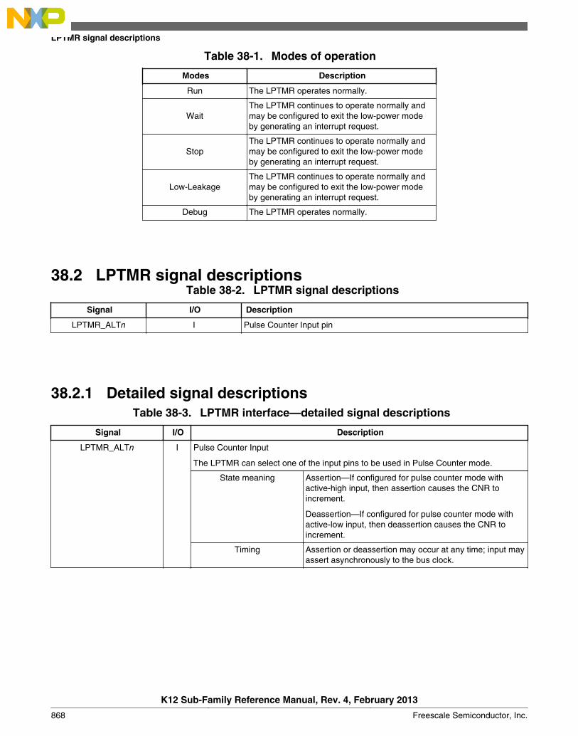
Table 38-1. Modes of operation
Modes Description
Run The LPTMR operates normally.
WaitThe LPTMR continues to operate normally andmay be configured to exit the low-power modeby generating an interrupt request.
StopThe LPTMR continues to operate normally andmay be configured to exit the low-power modeby generating an interrupt request.
Low-LeakageThe LPTMR continues to operate normally andmay be configured to exit the low-power modeby generating an interrupt request.
Debug The LPTMR operates normally.
38.2 LPTMR signal descriptionsTable 38-2. LPTMR signal descriptions
Signal I/O Description
LPTMR_ALTn I Pulse Counter Input pin
38.2.1 Detailed signal descriptionsTable 38-3. LPTMR interface—detailed signal descriptions
Signal I/O Description
LPTMR_ALTn I Pulse Counter Input
The LPTMR can select one of the input pins to be used in Pulse Counter mode.
State meaning Assertion—If configured for pulse counter mode withactive-high input, then assertion causes the CNR toincrement.
Deassertion—If configured for pulse counter mode withactive-low input, then deassertion causes the CNR toincrement.
Timing Assertion or deassertion may occur at any time; input mayassert asynchronously to the bus clock.
LPTMR signal descriptions
K12 Sub-Family Reference Manual, Rev. 4, February 2013
868 Freescale Semiconductor, Inc.

38.3 Memory map and register definitionNOTE
The LPTMR registers are reset only on a POR or LVD event.See LPTMR power and reset for more details.
LPTMR memory map
Absoluteaddress
(hex)Register name
Width(in bits)
Access Reset valueSection/
page
4004_0000 Low Power Timer Control Status Register (LPTMR0_CSR) 32 R/W 0000_0000h 38.3.1/869
4004_0004 Low Power Timer Prescale Register (LPTMR0_PSR) 32 R/W 0000_0000h 38.3.2/871
4004_0008 Low Power Timer Compare Register (LPTMR0_CMR) 32 R/W 0000_0000h 38.3.3/872
4004_000C Low Power Timer Counter Register (LPTMR0_CNR) 32 R 0000_0000h 38.3.4/873
38.3.1 Low Power Timer Control Status Register (LPTMRx_CSR)
Address: 4004_0000h base + 0h offset = 4004_0000h
Bit 31 30 29 28 27 26 25 24 23 22 21 20 19 18 17 16
R 0
W
Reset 0 0 0 0 0 0 0 0 0 0 0 0 0 0 0 0
Bit 15 14 13 12 11 10 9 8 7 6 5 4 3 2 1 0
R 0 TCFTIE TPS TPP TFC TMS TEN
W w1c
Reset 0 0 0 0 0 0 0 0 0 0 0 0 0 0 0 0
LPTMRx_CSR field descriptions
Field Description
31–8Reserved
This field is reserved.This read-only field is reserved and always has the value 0.
7TCF
Timer Compare Flag
TCF is set when the LPTMR is enabled and the CNR equals the CMR and increments. TCF is clearedwhen the LPTMR is disabled or a logic 1 is written to it.
0 The value of CNR is not equal to CMR and increments.1 The value of CNR is equal to CMR and increments.
6TIE
Timer Interrupt Enable
When TIE is set, the LPTMR Interrupt is generated whenever TCF is also set.
Table continues on the next page...
Chapter 38 Low-Power Timer (LPTMR)
K12 Sub-Family Reference Manual, Rev. 4, February 2013
Freescale Semiconductor, Inc. 869
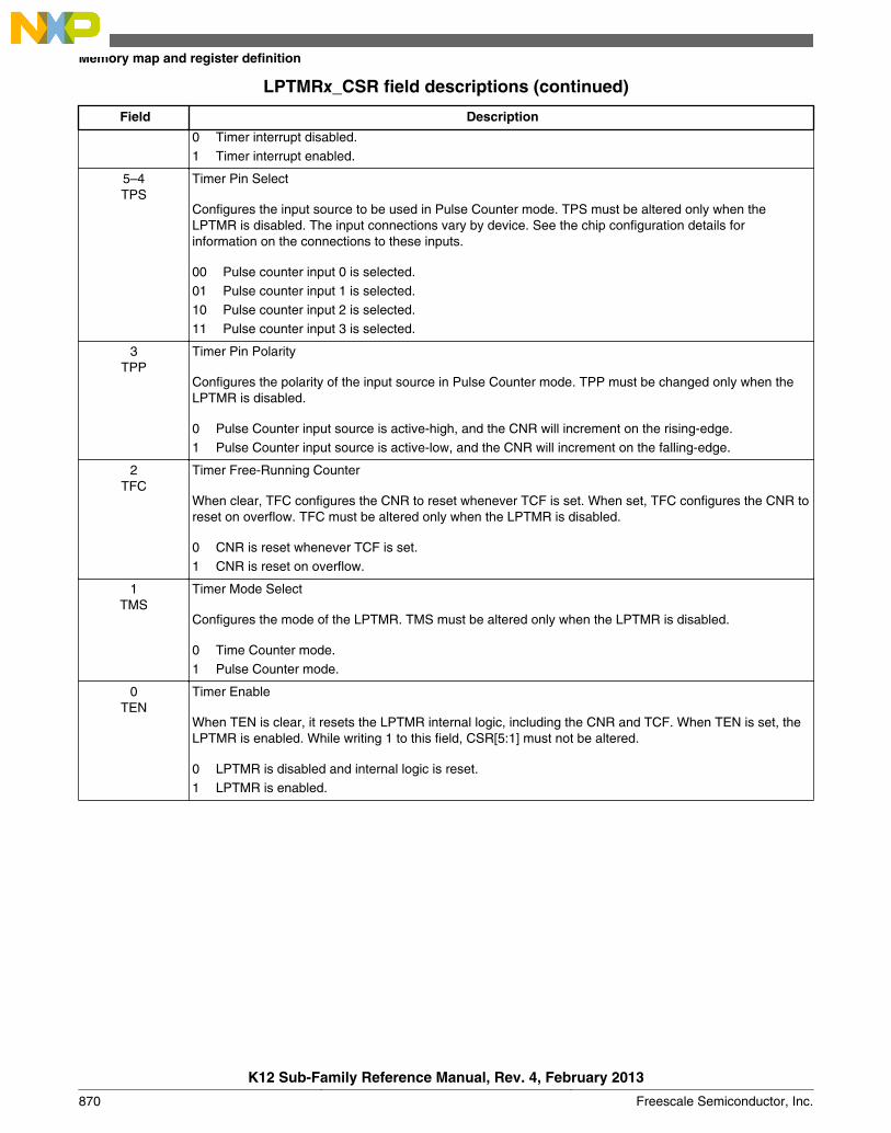
LPTMRx_CSR field descriptions (continued)
Field Description
0 Timer interrupt disabled.1 Timer interrupt enabled.
5–4TPS
Timer Pin Select
Configures the input source to be used in Pulse Counter mode. TPS must be altered only when theLPTMR is disabled. The input connections vary by device. See the chip configuration details forinformation on the connections to these inputs.
00 Pulse counter input 0 is selected.01 Pulse counter input 1 is selected.10 Pulse counter input 2 is selected.11 Pulse counter input 3 is selected.
3TPP
Timer Pin Polarity
Configures the polarity of the input source in Pulse Counter mode. TPP must be changed only when theLPTMR is disabled.
0 Pulse Counter input source is active-high, and the CNR will increment on the rising-edge.1 Pulse Counter input source is active-low, and the CNR will increment on the falling-edge.
2TFC
Timer Free-Running Counter
When clear, TFC configures the CNR to reset whenever TCF is set. When set, TFC configures the CNR toreset on overflow. TFC must be altered only when the LPTMR is disabled.
0 CNR is reset whenever TCF is set.1 CNR is reset on overflow.
1TMS
Timer Mode Select
Configures the mode of the LPTMR. TMS must be altered only when the LPTMR is disabled.
0 Time Counter mode.1 Pulse Counter mode.
0TEN
Timer Enable
When TEN is clear, it resets the LPTMR internal logic, including the CNR and TCF. When TEN is set, theLPTMR is enabled. While writing 1 to this field, CSR[5:1] must not be altered.
0 LPTMR is disabled and internal logic is reset.1 LPTMR is enabled.
Memory map and register definition
K12 Sub-Family Reference Manual, Rev. 4, February 2013
870 Freescale Semiconductor, Inc.
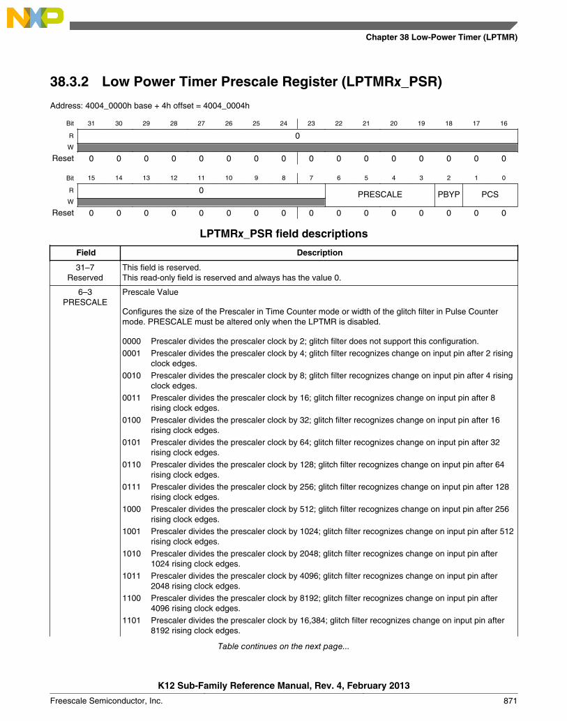
38.3.2 Low Power Timer Prescale Register (LPTMRx_PSR)
Address: 4004_0000h base + 4h offset = 4004_0004h
Bit 31 30 29 28 27 26 25 24 23 22 21 20 19 18 17 16
R 0W
Reset 0 0 0 0 0 0 0 0 0 0 0 0 0 0 0 0
Bit 15 14 13 12 11 10 9 8 7 6 5 4 3 2 1 0
R 0 PRESCALE PBYP PCSW
Reset 0 0 0 0 0 0 0 0 0 0 0 0 0 0 0 0
LPTMRx_PSR field descriptions
Field Description
31–7Reserved
This field is reserved.This read-only field is reserved and always has the value 0.
6–3PRESCALE
Prescale Value
Configures the size of the Prescaler in Time Counter mode or width of the glitch filter in Pulse Countermode. PRESCALE must be altered only when the LPTMR is disabled.
0000 Prescaler divides the prescaler clock by 2; glitch filter does not support this configuration.0001 Prescaler divides the prescaler clock by 4; glitch filter recognizes change on input pin after 2 rising
clock edges.0010 Prescaler divides the prescaler clock by 8; glitch filter recognizes change on input pin after 4 rising
clock edges.0011 Prescaler divides the prescaler clock by 16; glitch filter recognizes change on input pin after 8
rising clock edges.0100 Prescaler divides the prescaler clock by 32; glitch filter recognizes change on input pin after 16
rising clock edges.0101 Prescaler divides the prescaler clock by 64; glitch filter recognizes change on input pin after 32
rising clock edges.0110 Prescaler divides the prescaler clock by 128; glitch filter recognizes change on input pin after 64
rising clock edges.0111 Prescaler divides the prescaler clock by 256; glitch filter recognizes change on input pin after 128
rising clock edges.1000 Prescaler divides the prescaler clock by 512; glitch filter recognizes change on input pin after 256
rising clock edges.1001 Prescaler divides the prescaler clock by 1024; glitch filter recognizes change on input pin after 512
rising clock edges.1010 Prescaler divides the prescaler clock by 2048; glitch filter recognizes change on input pin after
1024 rising clock edges.1011 Prescaler divides the prescaler clock by 4096; glitch filter recognizes change on input pin after
2048 rising clock edges.1100 Prescaler divides the prescaler clock by 8192; glitch filter recognizes change on input pin after
4096 rising clock edges.1101 Prescaler divides the prescaler clock by 16,384; glitch filter recognizes change on input pin after
8192 rising clock edges.
Table continues on the next page...
Chapter 38 Low-Power Timer (LPTMR)
K12 Sub-Family Reference Manual, Rev. 4, February 2013
Freescale Semiconductor, Inc. 871
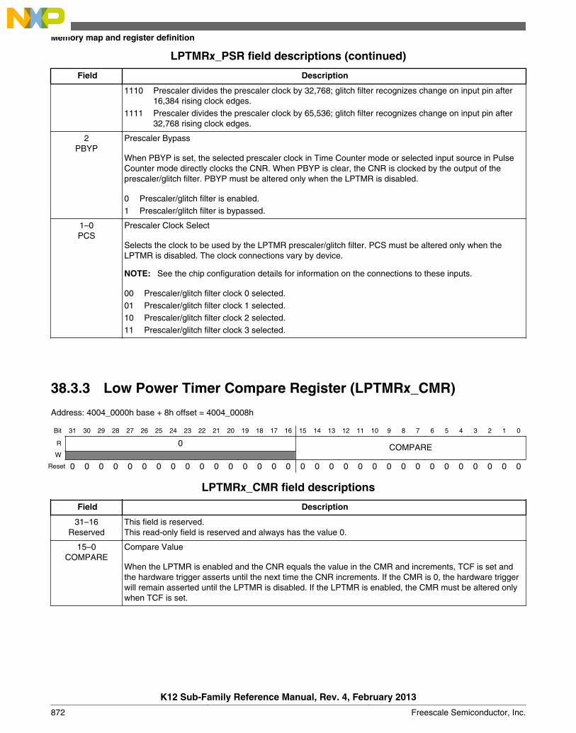
LPTMRx_PSR field descriptions (continued)
Field Description
1110 Prescaler divides the prescaler clock by 32,768; glitch filter recognizes change on input pin after16,384 rising clock edges.
1111 Prescaler divides the prescaler clock by 65,536; glitch filter recognizes change on input pin after32,768 rising clock edges.
2PBYP
Prescaler Bypass
When PBYP is set, the selected prescaler clock in Time Counter mode or selected input source in PulseCounter mode directly clocks the CNR. When PBYP is clear, the CNR is clocked by the output of theprescaler/glitch filter. PBYP must be altered only when the LPTMR is disabled.
0 Prescaler/glitch filter is enabled.1 Prescaler/glitch filter is bypassed.
1–0PCS
Prescaler Clock Select
Selects the clock to be used by the LPTMR prescaler/glitch filter. PCS must be altered only when theLPTMR is disabled. The clock connections vary by device.
NOTE: See the chip configuration details for information on the connections to these inputs.
00 Prescaler/glitch filter clock 0 selected.01 Prescaler/glitch filter clock 1 selected.10 Prescaler/glitch filter clock 2 selected.11 Prescaler/glitch filter clock 3 selected.
38.3.3 Low Power Timer Compare Register (LPTMRx_CMR)
Address: 4004_0000h base + 8h offset = 4004_0008h
Bit 31 30 29 28 27 26 25 24 23 22 21 20 19 18 17 16 15 14 13 12 11 10 9 8 7 6 5 4 3 2 1 0
R 0 COMPAREW
Reset 0 0 0 0 0 0 0 0 0 0 0 0 0 0 0 0 0 0 0 0 0 0 0 0 0 0 0 0 0 0 0 0
LPTMRx_CMR field descriptions
Field Description
31–16Reserved
This field is reserved.This read-only field is reserved and always has the value 0.
15–0COMPARE
Compare Value
When the LPTMR is enabled and the CNR equals the value in the CMR and increments, TCF is set andthe hardware trigger asserts until the next time the CNR increments. If the CMR is 0, the hardware triggerwill remain asserted until the LPTMR is disabled. If the LPTMR is enabled, the CMR must be altered onlywhen TCF is set.
Memory map and register definition
K12 Sub-Family Reference Manual, Rev. 4, February 2013
872 Freescale Semiconductor, Inc.
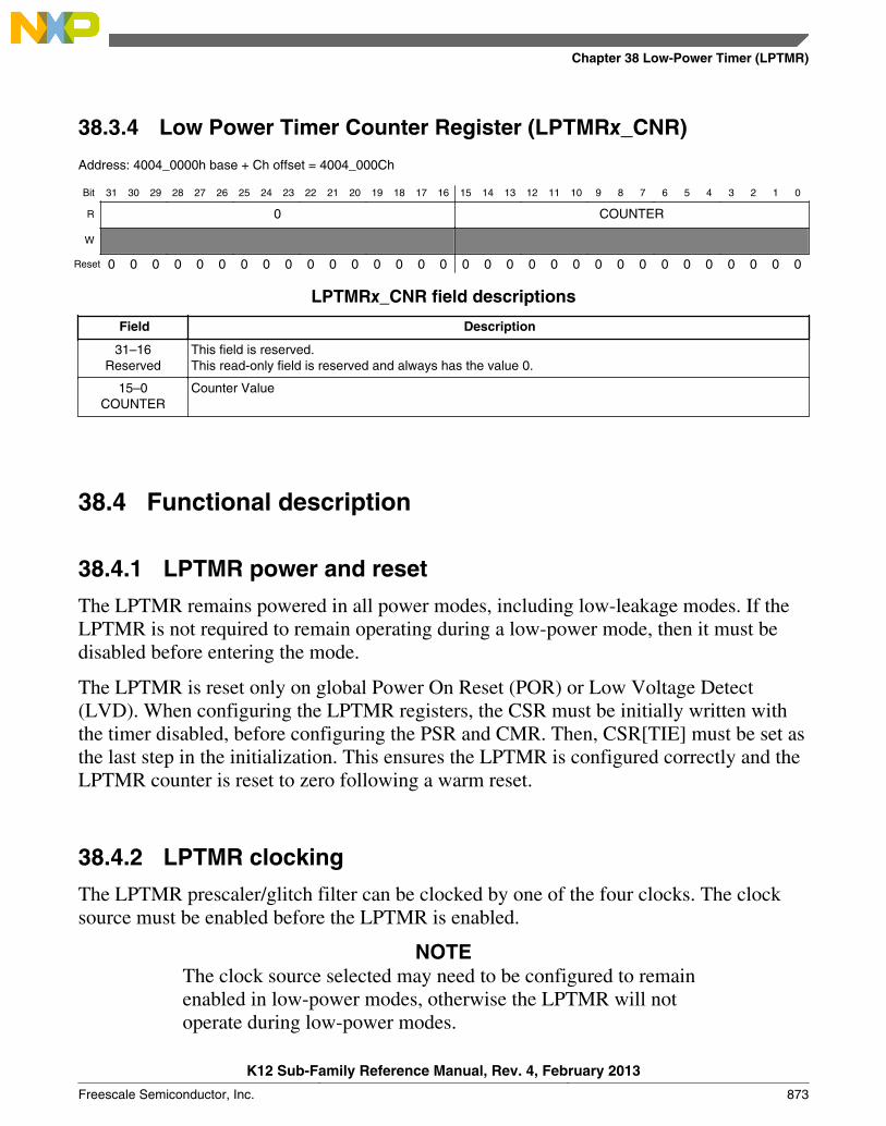
38.3.4 Low Power Timer Counter Register (LPTMRx_CNR)
Address: 4004_0000h base + Ch offset = 4004_000Ch
Bit 31 30 29 28 27 26 25 24 23 22 21 20 19 18 17 16 15 14 13 12 11 10 9 8 7 6 5 4 3 2 1 0
R 0 COUNTER
W
Reset 0 0 0 0 0 0 0 0 0 0 0 0 0 0 0 0 0 0 0 0 0 0 0 0 0 0 0 0 0 0 0 0
LPTMRx_CNR field descriptions
Field Description
31–16Reserved
This field is reserved.This read-only field is reserved and always has the value 0.
15–0COUNTER
Counter Value
38.4 Functional description
38.4.1 LPTMR power and reset
The LPTMR remains powered in all power modes, including low-leakage modes. If theLPTMR is not required to remain operating during a low-power mode, then it must bedisabled before entering the mode.
The LPTMR is reset only on global Power On Reset (POR) or Low Voltage Detect(LVD). When configuring the LPTMR registers, the CSR must be initially written withthe timer disabled, before configuring the PSR and CMR. Then, CSR[TIE] must be set asthe last step in the initialization. This ensures the LPTMR is configured correctly and theLPTMR counter is reset to zero following a warm reset.
38.4.2 LPTMR clocking
The LPTMR prescaler/glitch filter can be clocked by one of the four clocks. The clocksource must be enabled before the LPTMR is enabled.
NOTEThe clock source selected may need to be configured to remainenabled in low-power modes, otherwise the LPTMR will notoperate during low-power modes.
Chapter 38 Low-Power Timer (LPTMR)
K12 Sub-Family Reference Manual, Rev. 4, February 2013
Freescale Semiconductor, Inc. 873

In Pulse Counter mode with the prescaler/glitch filter bypassed, the selected input sourcedirectly clocks the CNR and no other clock source is required. To minimize power in thiscase, configure the prescaler clock source for a clock that is not toggling.
NOTEThe clock source or pulse input source selected for the LPTMRshould not exceed the frequency fLPTMR defined in the devicedatasheet.
38.4.3 LPTMR prescaler/glitch filter
The LPTMR prescaler and glitch filter share the same logic which operates as a prescalerin Time Counter mode and as a glitch filter in Pulse Counter mode.
NOTEThe prescaler/glitch filter configuration must not be alteredwhen the LPTMR is enabled.
38.4.3.1 Prescaler enabled
In Time Counter mode, when the prescaler is enabled, the output of the prescaler directlyclocks the CNR. When the LPTMR is enabled, the CNR will increment every 22 to 216
prescaler clock cycles. After the LPTMR is enabled, the first increment of the CNR willtake an additional one or two prescaler clock cycles due to synchronization logic.
38.4.3.2 Prescaler bypassed
In Time Counter mode, when the prescaler is bypassed, the selected prescaler clockincrements the CNR on every clock cycle. When the LPTMR is enabled, the firstincrement will take an additional one or two prescaler clock cycles due tosynchronization logic.
Functional description
K12 Sub-Family Reference Manual, Rev. 4, February 2013
874 Freescale Semiconductor, Inc.

38.4.3.3 Glitch filterIn Pulse Counter mode, when the glitch filter is enabled, the output of the glitch filterdirectly clocks the CNR. When the LPTMR is first enabled, the output of the glitch filteris asserted, that is, logic 1 for active-high and logic 0 for active-low. The following tableshows the change in glitch filter output with the selected input source.
If Then
The selected input source remains deasserted for at least 21
to 215 consecutive prescaler clock rising edgesThe glitch filter output will also deassert.
The selected input source remains asserted for at least 21 to215 consecutive prescaler clock rising-edges
The glitch filter output will also assert.
NOTEThe input is only sampled on the rising clock edge.
The CNR will increment each time the glitch filter output asserts. In Pulse Counter mode,the maximum rate at which the CNR can increment is once every 22 to 216 prescalerclock edges. When first enabled, the glitch filter will wait an additional one or twoprescaler clock edges due to synchronization logic.
38.4.3.4 Glitch filter bypassed
In Pulse Counter mode, when the glitch filter is bypassed, the selected input sourceincrements the CNR every time it asserts. Before the LPTMR is first enabled, the selectedinput source is forced to be asserted. This prevents the CNR from incrementing if theselected input source is already asserted when the LPTMR is first enabled.
38.4.4 LPTMR compare
When the CNR equals the value of the CMR and increments, the following events occur:
• CSR[TCF] is set.• LPTMR interrupt is generated if CSR[TIE] is also set.• LPTMR hardware trigger is generated.• CNR is reset if CSR[TFC] is clear.
When the LPTMR is enabled, the CMR can be altered only when CSR[TCF] is set. Whenupdating the CMR, the CMR must be written and CSR[TCF] must be cleared before theLPTMR counter has incremented past the new LPTMR compare value.
Chapter 38 Low-Power Timer (LPTMR)
K12 Sub-Family Reference Manual, Rev. 4, February 2013
Freescale Semiconductor, Inc. 875
38.4.5 LPTMR counter
The CNR increments by one on every:
• Prescaler clock in Time Counter mode with prescaler bypassed• Prescaler output in Time Counter mode with prescaler enabled• Input source assertion in Pulse Counter mode with glitch filter bypassed• Glitch filter output in Pulse Counter mode with glitch filter enabled
The CNR is reset when the LPTMR is disabled or if the counter register overflows. IfCSR[TFC] is cleared, then the CNR is also reset whenever CSR[TCF] is set.
The CNR continues incrementing when the core is halted in Debug mode.
The CNR cannot be initialized, but can be read at any time. On each read of the CNR,software must first write to the CNR with any value. This will synchronize and registerthe current value of the CNR into a temporary register. The contents of the temporaryregister are returned on each read of the CNR.
When reading the CNR, the bus clock must be at least two times faster than the rate atwhich the LPTMR counter is incrementing, otherwise incorrect data may be returned.
38.4.6 LPTMR hardware triggerThe LPTMR hardware trigger asserts at the same time the CSR[TCF] is set and can beused to trigger hardware events in other peripherals without software intervention. Thehardware trigger is always enabled.
When Then
The CMR is set to 0 with CSR[TFC] clear The LPTMR hardware trigger will assert on the first compareand does not deassert.
The CMR is set to a nonzero value, or, if CSR[TFC] is set The LPTMR hardware trigger will assert on each compareand deassert on the following increment of the CNR.
38.4.7 LPTMR interrupt
The LPTMR interrupt is generated whenever CSR[TIE] and CSR[TCF] are set.CSR[TCF] is cleared by disabling the LPTMR or by writing a logic 1 to it.
CSR[TIE] can be altered and CSR[TCF] can be cleared while the LPTMR is enabled.
Functional description
K12 Sub-Family Reference Manual, Rev. 4, February 2013
876 Freescale Semiconductor, Inc.

The LPTMR interrupt is generated asynchronously to the system clock and can be used togenerate a wakeup from any low-power mode, including the low-leakage modes,provided the LPTMR is enabled as a wakeup source.
Chapter 38 Low-Power Timer (LPTMR)
K12 Sub-Family Reference Manual, Rev. 4, February 2013
Freescale Semiconductor, Inc. 877

Functional description
K12 Sub-Family Reference Manual, Rev. 4, February 2013
878 Freescale Semiconductor, Inc.
Chapter 39Carrier Modulator Transmitter (CMT)
39.1 IntroductionNOTE
For the chip-specific implementation details of this module'sinstances see the chip configuration information.
The carrier modulator transmitter (CMT) module provides the means to generate theprotocol timing and carrier signals for a wide variety of encoding schemes. The CMTincorporates hardware to off-load the critical and/or lengthy timing requirementsassociated with signal generation from the CPU, releasing much of its bandwidth tohandle other tasks such as:
• Code data generation• Data decompression, or,• Keyboard scanning
. The CMT does not include dedicated hardware configurations for specific protocols, butis intended to be sufficiently programmable in its function to handle the timingrequirements of most protocols with minimal CPU intervention.
When the modulator is disabled, certain CMT registers can be used to change the state ofthe infrared output (IRO) signal directly. This feature allows for the generation of futureprotocol timing signals not readily producible by the current architecture.
39.2 FeaturesThe features of this module include:
• Four modes of operation:
• Time; with independent control of high and low times
K12 Sub-Family Reference Manual, Rev. 4, February 2013
Freescale Semiconductor, Inc. 879

• Baseband
• Frequency-shift key (FSK)
• Direct software control of the IRO signal
• Extended space operation in Time, Baseband, and FSK modes
• Selectable input clock divider
• Interrupt on end-of-cycle
• Ability to disable the IRO signal and use as timer interrupt
39.3 Block diagramThe following figure presents the block diagram of the CMT module.
Block diagram
K12 Sub-Family Reference Manual, Rev. 4, February 2013
880 Freescale Semiconductor, Inc.

Modulator CMT_IROCarrier generator
CMT registers
Clock divider
CMT Interrupts
Peripheral bus clock
Peripheral bus
CMT
divider_enable
Figure 39-1. CMT module block diagram
39.4 Modes of operationThe following table describes the operation of the CMT module operates in variousmodes.
Table 39-1. Modes of operation
Modes Description
TimeIn Time mode, the user independently defines the high andlow times of the carrier signal to determine both period andduty cycle
BasebandWhen MSC[BASE] is set, the carrier output (fcg) to themodulator is held high continuously to allow for thegeneration of baseband protocols.
Table continues on the next page...
Chapter 39 Carrier Modulator Transmitter (CMT)
K12 Sub-Family Reference Manual, Rev. 4, February 2013
Freescale Semiconductor, Inc. 881

Table 39-1. Modes of operation (continued)
Modes Description
Frequency-shift key
This mode allows the carrier generator to alternate betweentwo sets of high and low times. When operating in FSKmode, the generator will toggle between the two sets wheninstructed by the modulator, allowing the user todynamically switch between two carrier frequencies withoutCPU intervention.
The following table summarizes the modes of operation of the CMT module.
Table 39-2. CMT modes of operation
Mode MSC[MCGEN]1 MSC[BASE] MSC[FSK]2 MSC[EXSPC] Comment
Time 1 0 0 0
fcg controlled by primary high andlow registers.
fcg transmitted to the IRO signalwhen modulator gate is open.
Baseband 1 1 X 0fcg is always high. The IRO signal ishigh when the modulator gate isopen.
FSK 1 0 1 0
fcg control alternates betweenprimary high/low registers andsecondary high/low registers.
fcg transmitted to the IRO signalwhen modulator gate is open.
ExtendedSpace
1 X X 1
Setting MSC[EXSPC] causessubsequent modulator cycles to bespaces (modulator out not asserted)for the duration of the modulatorperiod (mark and space times).
IRO Latch 0 X X XOC[IROL] controls the state of theIRO signal.
1. To prevent spurious operation, initialize all data and control registers before beginning a transmission whenMSC[MCGEN]=1.
2. This field is not double-buffered and must not be changed during a transmission while MSC[MCGEN]=1.
NOTE
The assignment of module modes to core modes is chip-specific. For module-to-core mode assignments, see the chapterthat describes how modules are configured.
39.4.1 Wait mode operation
During Wait mode, the CMT if enabled, will continue to operate normally. However,there is no change in operating modes of CMT during Wait mode, because the CPU is notoperating.
Modes of operation
K12 Sub-Family Reference Manual, Rev. 4, February 2013
882 Freescale Semiconductor, Inc.
39.4.2 Stop mode operation
This section describes the CMT Stop mode operations.
39.4.2.1 Normal Stop mode operation
During Normal Stop mode, clocks to the CMT module are halted. No registers areaffected.
The CMT module will resume upon exit from Normal Stop mode because the clocks arehalted. Software must ensure that the Normal Stop mode is not entered while themodulator is still in operation so as to prevent the IRO signal from being asserted whilein Normal Stop mode. This may require a timeout period from the time thatMSC[MCGEN] is cleared to allow the last modulator cycle to complete.
39.4.2.2 Low-Power Stop mode operation
During Low-Power Stop mode, the CMT module is completely powered off internallyand the IRO signal state is latched and held at the time when the CMT enters this mode.To prevent the IRO signal from being asserted during Low-Power Stop mode, thesoftware must assure that the signal is not active when entering Low-Power Stop mode.Upon wakeup from Low-Power Stop mode, the CMT module will be in the reset state.
39.5 CMT external signal descriptionsThe following table shows the description of the external signal.
Table 39-3. CMT signal description
Signal Description I/O
CMT_IRO Infrared Output O
Chapter 39 Carrier Modulator Transmitter (CMT)
K12 Sub-Family Reference Manual, Rev. 4, February 2013
Freescale Semiconductor, Inc. 883
39.5.1 CMT_IRO — Infrared Output
This output signal is driven by the modulator output when MSC[MCGEN] andOC[IROPEN] are set. The IRO signal starts a valid transmission with a delay, afterMSC[MCGEN] bit be asserted to high, that can be calculated based on two register bits.Table 39-5 shows how to calculate this delay.
The following table describes conditions for the IRO signal to be active.
If Then
MSC[MCGEN] is cleared and OC[IROPEN] is set The signal is driven by OC[IROL] . This enables user softwareto directly control the state of the IRO signal by writing toOC[IROL] .
OC[IROPEN] is cleared The signal is disabled and is not driven by the CMT module.Therefore, CMT can be configured as a modulo timer forgenerating periodic interrupts without causing signal activity.
Table 39-5. CMT_IRO signal delay calculation
Condition Delay (bus clock cycles)
MSC[CMTDIV] = 0 PPS[PPSDIV] + 2
MSC[CMTDIV] > 0 (PPS[PPSDIV] *2) + 3
39.6 Memory map/register definitionThe following registers control and monitor the CMT operation.
The address of a register is the sum of a base address and an address offset. The baseaddress is defined at the chip level. The address offset is defined at the module level.
CMT memory map
Absoluteaddress
(hex)Register name
Width(in bits)
Access Reset valueSection/
page
4006_2000 CMT Carrier Generator High Data Register 1 (CMT_CGH1) 8 R/W Undefined 39.6.1/885
4006_2001 CMT Carrier Generator Low Data Register 1 (CMT_CGL1) 8 R/W Undefined 39.6.2/886
4006_2002 CMT Carrier Generator High Data Register 2 (CMT_CGH2) 8 R/W Undefined 39.6.3/886
4006_2003 CMT Carrier Generator Low Data Register 2 (CMT_CGL2) 8 R/W Undefined 39.6.4/887
4006_2004 CMT Output Control Register (CMT_OC) 8 R/W 00h 39.6.5/887
4006_2005 CMT Modulator Status and Control Register (CMT_MSC) 8 R/W 00h 39.6.6/888
4006_2006 CMT Modulator Data Register Mark High (CMT_CMD1) 8 R/W Undefined 39.6.7/890
Table continues on the next page...
Memory map/register definition
K12 Sub-Family Reference Manual, Rev. 4, February 2013
884 Freescale Semiconductor, Inc.

CMT memory map (continued)
Absoluteaddress
(hex)Register name
Width(in bits)
Access Reset valueSection/
page
4006_2007 CMT Modulator Data Register Mark Low (CMT_CMD2) 8 R/W Undefined 39.6.8/891
4006_2008 CMT Modulator Data Register Space High (CMT_CMD3) 8 R/W Undefined 39.6.9/891
4006_2009 CMT Modulator Data Register Space Low (CMT_CMD4) 8 R/W Undefined39.6.10/
892
4006_200A CMT Primary Prescaler Register (CMT_PPS) 8 R/W 00h39.6.11/
892
4006_200B CMT Direct Memory Access Register (CMT_DMA) 8 R/W 00h39.6.12/
893
39.6.1 CMT Carrier Generator High Data Register 1 (CMT_CGH1)
This data register contains the primary high value for generating the carrier output.
Address: 4006_2000h base + 0h offset = 4006_2000h
Bit 7 6 5 4 3 2 1 0
Read PHWriteReset x* x* x* x* x* x* x* x*
* Notes:x = Undefined at reset.•
CMT_CGH1 field descriptions
Field Description
7–0PH
Primary Carrier High Time Data Value
Contains the number of input clocks required to generate the carrier high time period. Whenoperating in Time mode, this register is always selected. When operating in FSK mode, thisregister and the secondary register pair are alternately selected under the control of themodulator. The primary carrier high time value is undefined out of reset. This register mustbe written to nonzero values before the carrier generator is enabled to avoid spuriousresults.
Chapter 39 Carrier Modulator Transmitter (CMT)
K12 Sub-Family Reference Manual, Rev. 4, February 2013
Freescale Semiconductor, Inc. 885

39.6.2 CMT Carrier Generator Low Data Register 1 (CMT_CGL1)
This data register contains the primary low value for generating the carrier output.
Address: 4006_2000h base + 1h offset = 4006_2001h
Bit 7 6 5 4 3 2 1 0
Read PLWriteReset x* x* x* x* x* x* x* x*
* Notes:x = Undefined at reset.•
CMT_CGL1 field descriptions
Field Description
7–0PL
Primary Carrier Low Time Data Value
Contains the number of input clocks required to generate the carrier low time period. Whenoperating in Time mode, this register is always selected. When operating in FSK mode, thisregister and the secondary register pair are alternately selected under the control of themodulator. The primary carrier low time value is undefined out of reset. This register must bewritten to nonzero values before the carrier generator is enabled to avoid spurious results.
39.6.3 CMT Carrier Generator High Data Register 2 (CMT_CGH2)
This data register contains the secondary high value for generating the carrier output.
Address: 4006_2000h base + 2h offset = 4006_2002h
Bit 7 6 5 4 3 2 1 0
Read SHWriteReset x* x* x* x* x* x* x* x*
* Notes:x = Undefined at reset.•
CMT_CGH2 field descriptions
Field Description
7–0SH
Secondary Carrier High Time Data Value
Contains the number of input clocks required to generate the carrier high time period. Whenoperating in Time mode, this register is never selected. When operating in FSK mode, thisregister and the primary register pair are alternately selected under control of the modulator.
Memory map/register definition
K12 Sub-Family Reference Manual, Rev. 4, February 2013
886 Freescale Semiconductor, Inc.
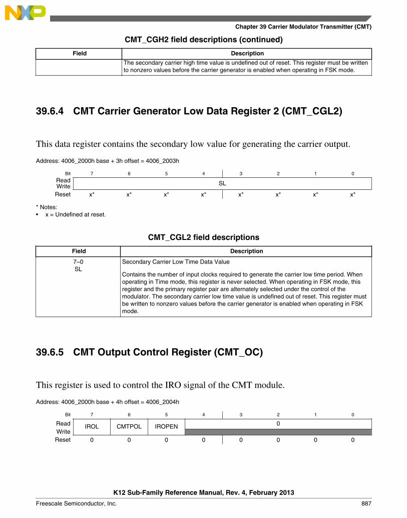
CMT_CGH2 field descriptions (continued)
Field Description
The secondary carrier high time value is undefined out of reset. This register must be writtento nonzero values before the carrier generator is enabled when operating in FSK mode.
39.6.4 CMT Carrier Generator Low Data Register 2 (CMT_CGL2)
This data register contains the secondary low value for generating the carrier output.
Address: 4006_2000h base + 3h offset = 4006_2003h
Bit 7 6 5 4 3 2 1 0
Read SLWriteReset x* x* x* x* x* x* x* x*
* Notes:x = Undefined at reset.•
CMT_CGL2 field descriptions
Field Description
7–0SL
Secondary Carrier Low Time Data Value
Contains the number of input clocks required to generate the carrier low time period. Whenoperating in Time mode, this register is never selected. When operating in FSK mode, thisregister and the primary register pair are alternately selected under the control of themodulator. The secondary carrier low time value is undefined out of reset. This register mustbe written to nonzero values before the carrier generator is enabled when operating in FSKmode.
39.6.5 CMT Output Control Register (CMT_OC)
This register is used to control the IRO signal of the CMT module.
Address: 4006_2000h base + 4h offset = 4006_2004h
Bit 7 6 5 4 3 2 1 0
Read IROL CMTPOL IROPEN 0WriteReset 0 0 0 0 0 0 0 0
Chapter 39 Carrier Modulator Transmitter (CMT)
K12 Sub-Family Reference Manual, Rev. 4, February 2013
Freescale Semiconductor, Inc. 887

CMT_OC field descriptions
Field Description
7IROL
IRO Latch Control
Reads the state of the IRO latch. Writing to IROL changes the state of the IRO signalwhen MSC[MCGEN] is cleared and IROPEN is set.
6CMTPOL
CMT Output Polarity
Controls the polarity of the IRO signal.
0 The IRO signal is active-low.1
The IRO signal is active-high.
5IROPEN
IRO Pin Enable
Enables and disables the IRO signal. When the IRO signal is enabled, it is an outputthat drives out either the CMT transmitter output or the state of IROL depending onwhether MSC[MCGEN] is set or not. Also, the state of output is either inverted or non-inverted, depending on the state of CMTPOL. When the IRO signal is disabled, it is ina high-impedance state and is unable to draw any current. This signal is disabledduring reset.
0 The IRO signal is disabled.1
The IRO signal is enabled as output.
4–0Reserved
This field is reserved.This read-only field is reserved and always has the value 0.
39.6.6 CMT Modulator Status and Control Register (CMT_MSC)
This register contains the modulator and carrier generator enable (MCGEN), end of cycleinterrupt enable (EOCIE), FSK mode select (FSK), baseband enable (BASE), extendedspace (EXSPC), prescaler (CMTDIV) bits, and the end of cycle (EOCF) status bit.
Address: 4006_2000h base + 5h offset = 4006_2005h
Bit 7 6 5 4 3 2 1 0
Read EOCFCMTDIV EXSPC BASE FSK EOCIE MCGEN
Write
Reset 0 0 0 0 0 0 0 0
CMT_MSC field descriptions
Field Description
7EOCF
End Of Cycle Status Flag
Sets when:
Table continues on the next page...
Memory map/register definition
K12 Sub-Family Reference Manual, Rev. 4, February 2013
888 Freescale Semiconductor, Inc.
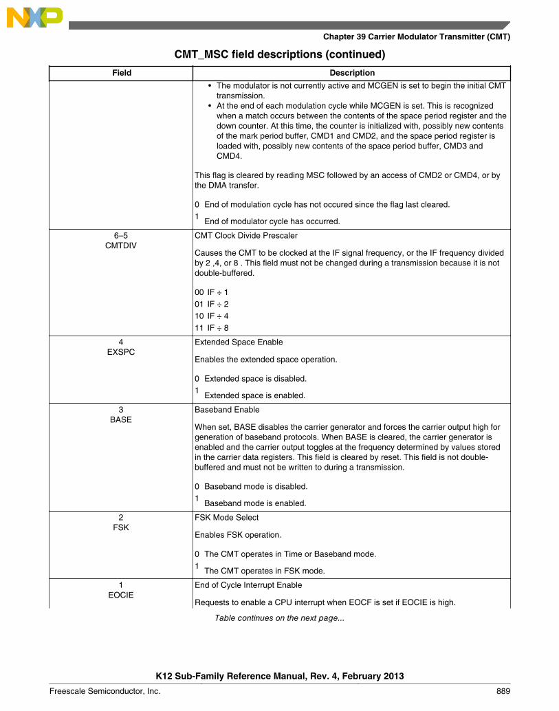
CMT_MSC field descriptions (continued)
Field Description
• The modulator is not currently active and MCGEN is set to begin the initial CMTtransmission.
• At the end of each modulation cycle while MCGEN is set. This is recognizedwhen a match occurs between the contents of the space period register and thedown counter. At this time, the counter is initialized with, possibly new contentsof the mark period buffer, CMD1 and CMD2, and the space period register isloaded with, possibly new contents of the space period buffer, CMD3 andCMD4.
This flag is cleared by reading MSC followed by an access of CMD2 or CMD4, or bythe DMA transfer.
0 End of modulation cycle has not occured since the flag last cleared.1
End of modulator cycle has occurred.
6–5CMTDIV
CMT Clock Divide Prescaler
Causes the CMT to be clocked at the IF signal frequency, or the IF frequency dividedby 2 ,4, or 8 . This field must not be changed during a transmission because it is notdouble-buffered.
00 IF ÷ 101 IF ÷ 210 IF ÷ 411 IF ÷ 8
4EXSPC
Extended Space Enable
Enables the extended space operation.
0 Extended space is disabled.1
Extended space is enabled.
3BASE
Baseband Enable
When set, BASE disables the carrier generator and forces the carrier output high forgeneration of baseband protocols. When BASE is cleared, the carrier generator isenabled and the carrier output toggles at the frequency determined by values storedin the carrier data registers. This field is cleared by reset. This field is not double-buffered and must not be written to during a transmission.
0 Baseband mode is disabled.1
Baseband mode is enabled.
2FSK
FSK Mode Select
Enables FSK operation.
0 The CMT operates in Time or Baseband mode.1
The CMT operates in FSK mode.
1EOCIE
End of Cycle Interrupt Enable
Requests to enable a CPU interrupt when EOCF is set if EOCIE is high.
Table continues on the next page...
Chapter 39 Carrier Modulator Transmitter (CMT)
K12 Sub-Family Reference Manual, Rev. 4, February 2013
Freescale Semiconductor, Inc. 889
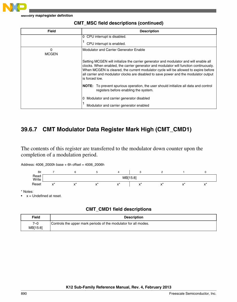
CMT_MSC field descriptions (continued)
Field Description
0 CPU interrupt is disabled.1
CPU interrupt is enabled.
0MCGEN
Modulator and Carrier Generator Enable
Setting MCGEN will initialize the carrier generator and modulator and will enable allclocks. When enabled, the carrier generator and modulator will function continuously.When MCGEN is cleared, the current modulator cycle will be allowed to expire beforeall carrier and modulator clocks are disabled to save power and the modulator outputis forced low.
NOTE: To prevent spurious operation, the user should initialize all data and controlregisters before enabling the system.
0 Modulator and carrier generator disabled1
Modulator and carrier generator enabled
39.6.7 CMT Modulator Data Register Mark High (CMT_CMD1)
The contents of this register are transferred to the modulator down counter upon thecompletion of a modulation period.
Address: 4006_2000h base + 6h offset = 4006_2006h
Bit 7 6 5 4 3 2 1 0
Read MB[15:8]WriteReset x* x* x* x* x* x* x* x*
* Notes:x = Undefined at reset.•
CMT_CMD1 field descriptions
Field Description
7–0MB[15:8]
Controls the upper mark periods of the modulator for all modes.
Memory map/register definition
K12 Sub-Family Reference Manual, Rev. 4, February 2013
890 Freescale Semiconductor, Inc.

39.6.8 CMT Modulator Data Register Mark Low (CMT_CMD2)
The contents of this register are transferred to the modulator down counter upon thecompletion of a modulation period.
Address: 4006_2000h base + 7h offset = 4006_2007h
Bit 7 6 5 4 3 2 1 0
Read MB[7:0]WriteReset x* x* x* x* x* x* x* x*
* Notes:x = Undefined at reset.•
CMT_CMD2 field descriptions
Field Description
7–0MB[7:0]
Controls the lower mark periods of the modulator for all modes.
39.6.9 CMT Modulator Data Register Space High (CMT_CMD3)
The contents of this register are transferred to the space period register upon thecompletion of a modulation period.
Address: 4006_2000h base + 8h offset = 4006_2008h
Bit 7 6 5 4 3 2 1 0
Read SB[15:8]WriteReset x* x* x* x* x* x* x* x*
* Notes:x = Undefined at reset.•
CMT_CMD3 field descriptions
Field Description
7–0SB[15:8]
Controls the upper space periods of the modulator for all modes.
Chapter 39 Carrier Modulator Transmitter (CMT)
K12 Sub-Family Reference Manual, Rev. 4, February 2013
Freescale Semiconductor, Inc. 891
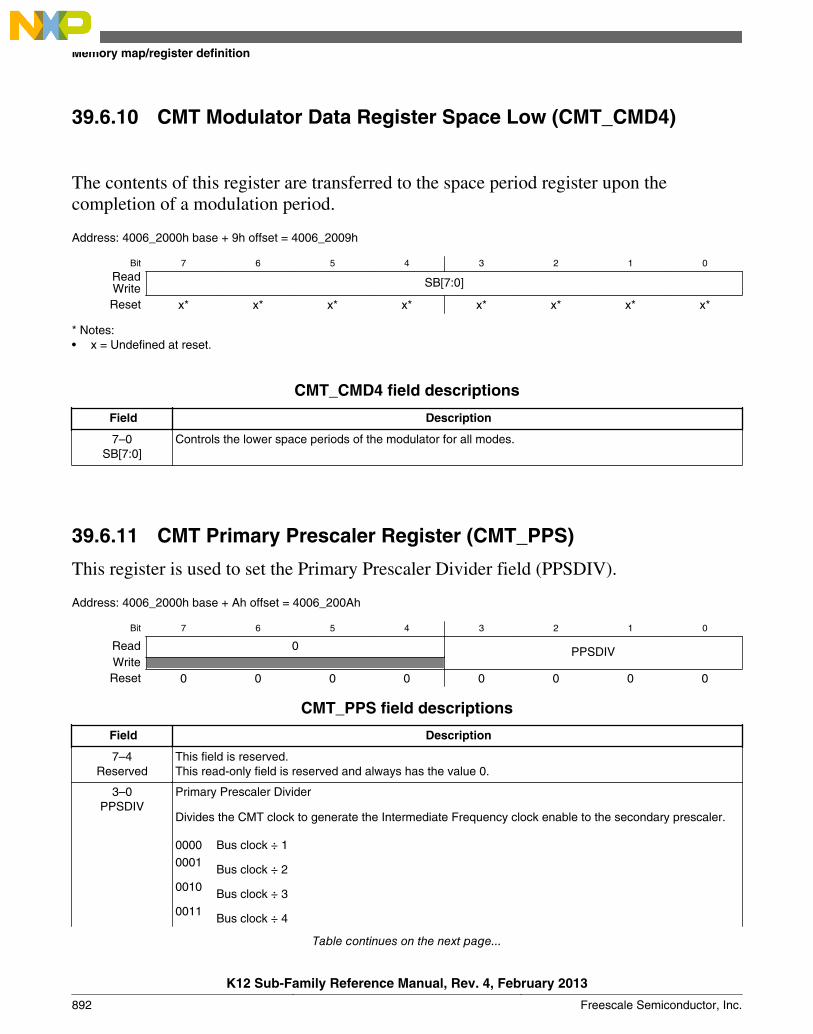
39.6.10 CMT Modulator Data Register Space Low (CMT_CMD4)
The contents of this register are transferred to the space period register upon thecompletion of a modulation period.
Address: 4006_2000h base + 9h offset = 4006_2009h
Bit 7 6 5 4 3 2 1 0
Read SB[7:0]WriteReset x* x* x* x* x* x* x* x*
* Notes:x = Undefined at reset.•
CMT_CMD4 field descriptions
Field Description
7–0SB[7:0]
Controls the lower space periods of the modulator for all modes.
39.6.11 CMT Primary Prescaler Register (CMT_PPS)
This register is used to set the Primary Prescaler Divider field (PPSDIV).
Address: 4006_2000h base + Ah offset = 4006_200Ah
Bit 7 6 5 4 3 2 1 0
Read 0 PPSDIVWriteReset 0 0 0 0 0 0 0 0
CMT_PPS field descriptions
Field Description
7–4Reserved
This field is reserved.This read-only field is reserved and always has the value 0.
3–0PPSDIV
Primary Prescaler Divider
Divides the CMT clock to generate the Intermediate Frequency clock enable to the secondary prescaler.
0000 Bus clock ÷ 10001
Bus clock ÷ 20010
Bus clock ÷ 30011
Bus clock ÷ 4
Table continues on the next page...
Memory map/register definition
K12 Sub-Family Reference Manual, Rev. 4, February 2013
892 Freescale Semiconductor, Inc.
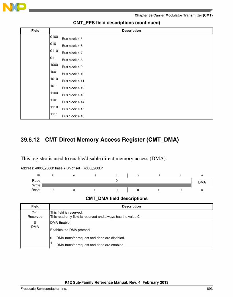
CMT_PPS field descriptions (continued)
Field Description
0100Bus clock ÷ 5
0101Bus clock ÷ 6
0110Bus clock ÷ 7
0111Bus clock ÷ 8
1000Bus clock ÷ 9
1001Bus clock ÷ 10
1010Bus clock ÷ 11
1011Bus clock ÷ 12
1100Bus clock ÷ 13
1101Bus clock ÷ 14
1110Bus clock ÷ 15
1111Bus clock ÷ 16
39.6.12 CMT Direct Memory Access Register (CMT_DMA)
This register is used to enable/disable direct memory access (DMA).
Address: 4006_2000h base + Bh offset = 4006_200Bh
Bit 7 6 5 4 3 2 1 0
Read 0 DMAWriteReset 0 0 0 0 0 0 0 0
CMT_DMA field descriptions
Field Description
7–1Reserved
This field is reserved.This read-only field is reserved and always has the value 0.
0DMA
DMA Enable
Enables the DMA protocol.
0 DMA transfer request and done are disabled.1
DMA transfer request and done are enabled.
Chapter 39 Carrier Modulator Transmitter (CMT)
K12 Sub-Family Reference Manual, Rev. 4, February 2013
Freescale Semiconductor, Inc. 893
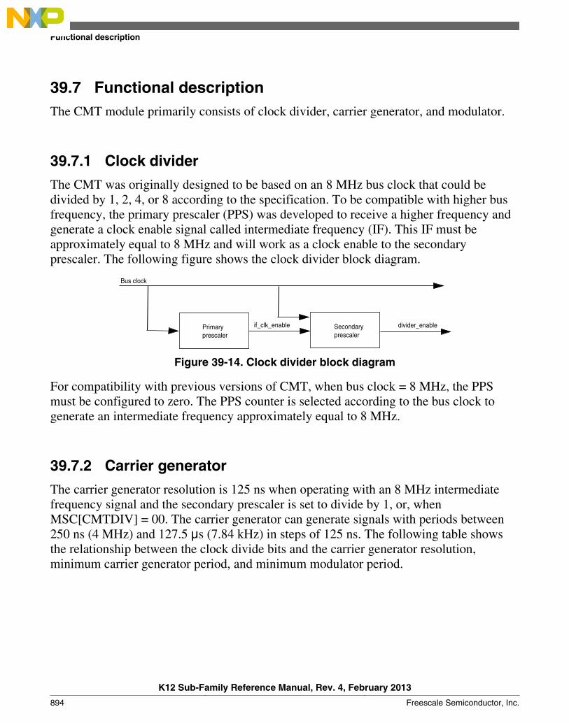
39.7 Functional descriptionThe CMT module primarily consists of clock divider, carrier generator, and modulator.
39.7.1 Clock divider
The CMT was originally designed to be based on an 8 MHz bus clock that could bedivided by 1, 2, 4, or 8 according to the specification. To be compatible with higher busfrequency, the primary prescaler (PPS) was developed to receive a higher frequency andgenerate a clock enable signal called intermediate frequency (IF). This IF must beapproximately equal to 8 MHz and will work as a clock enable to the secondaryprescaler. The following figure shows the clock divider block diagram.
Primaryprescaler
if_clk_enable divider_enable
Bus clock
Secondaryprescaler
Figure 39-14. Clock divider block diagram
For compatibility with previous versions of CMT, when bus clock = 8 MHz, the PPSmust be configured to zero. The PPS counter is selected according to the bus clock togenerate an intermediate frequency approximately equal to 8 MHz.
39.7.2 Carrier generator
The carrier generator resolution is 125 ns when operating with an 8 MHz intermediatefrequency signal and the secondary prescaler is set to divide by 1, or, whenMSC[CMTDIV] = 00. The carrier generator can generate signals with periods between250 ns (4 MHz) and 127.5 μs (7.84 kHz) in steps of 125 ns. The following table showsthe relationship between the clock divide bits and the carrier generator resolution,minimum carrier generator period, and minimum modulator period.
Functional description
K12 Sub-Family Reference Manual, Rev. 4, February 2013
894 Freescale Semiconductor, Inc.
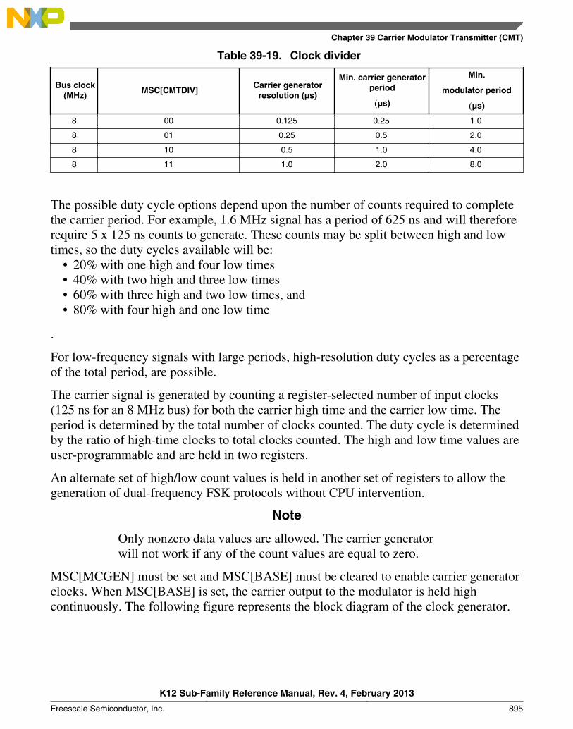
Table 39-19. Clock divider
Bus clock(MHz)
MSC[CMTDIV]Carrier generator
resolution (μs)
Min. carrier generatorperiod
(μs)
Min.
modulator period
(μs)
8 00 0.125 0.25 1.0
8 01 0.25 0.5 2.0
8 10 0.5 1.0 4.0
8 11 1.0 2.0 8.0
The possible duty cycle options depend upon the number of counts required to completethe carrier period. For example, 1.6 MHz signal has a period of 625 ns and will thereforerequire 5 x 125 ns counts to generate. These counts may be split between high and lowtimes, so the duty cycles available will be:
• 20% with one high and four low times• 40% with two high and three low times• 60% with three high and two low times, and• 80% with four high and one low time
.
For low-frequency signals with large periods, high-resolution duty cycles as a percentageof the total period, are possible.
The carrier signal is generated by counting a register-selected number of input clocks(125 ns for an 8 MHz bus) for both the carrier high time and the carrier low time. Theperiod is determined by the total number of clocks counted. The duty cycle is determinedby the ratio of high-time clocks to total clocks counted. The high and low time values areuser-programmable and are held in two registers.
An alternate set of high/low count values is held in another set of registers to allow thegeneration of dual-frequency FSK protocols without CPU intervention.
Note
Only nonzero data values are allowed. The carrier generatorwill not work if any of the count values are equal to zero.
MSC[MCGEN] must be set and MSC[BASE] must be cleared to enable carrier generatorclocks. When MSC[BASE] is set, the carrier output to the modulator is held highcontinuously. The following figure represents the block diagram of the clock generator.
Chapter 39 Carrier Modulator Transmitter (CMT)
K12 Sub-Family Reference Manual, Rev. 4, February 2013
Freescale Semiconductor, Inc. 895
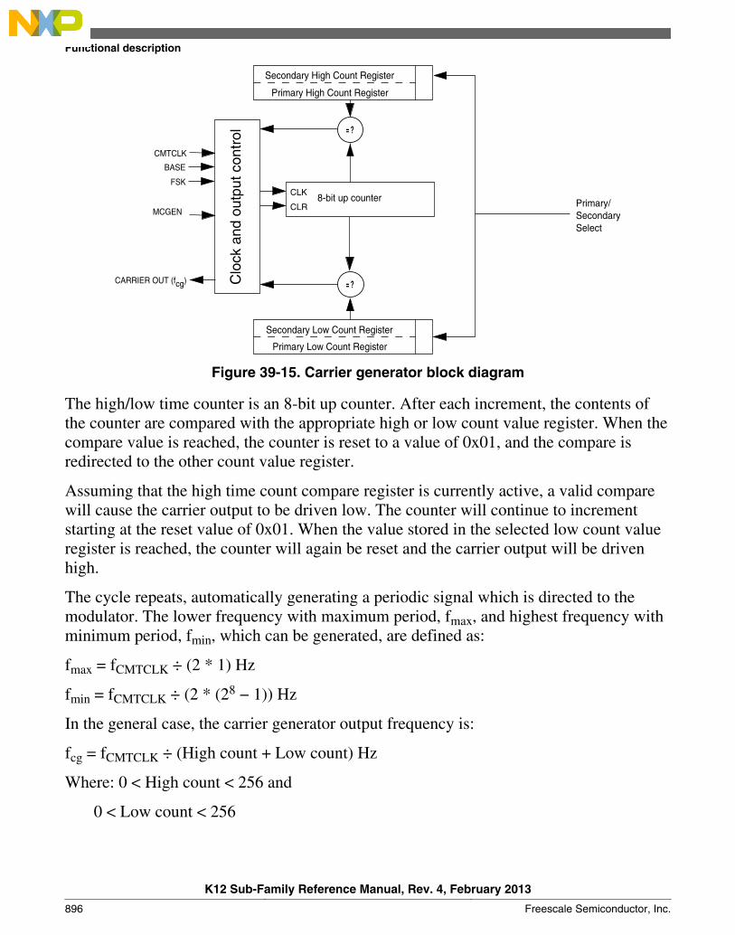
Clo
ck a
nd o
utpu
t con
trol
= ?
Secondary High Count Register
Primary High Count Register
8-bit up counterCLK
CLR
CMTCLK
BASE
FSK
MCGEN
CARRIER OUT (fcg)
Secondary Low Count Register
Primary Low Count Register
Primary/SecondarySelect
= ?
Figure 39-15. Carrier generator block diagram
The high/low time counter is an 8-bit up counter. After each increment, the contents ofthe counter are compared with the appropriate high or low count value register. When thecompare value is reached, the counter is reset to a value of 0x01, and the compare isredirected to the other count value register.
Assuming that the high time count compare register is currently active, a valid comparewill cause the carrier output to be driven low. The counter will continue to incrementstarting at the reset value of 0x01. When the value stored in the selected low count valueregister is reached, the counter will again be reset and the carrier output will be drivenhigh.
The cycle repeats, automatically generating a periodic signal which is directed to themodulator. The lower frequency with maximum period, fmax, and highest frequency withminimum period, fmin, which can be generated, are defined as:
fmax = fCMTCLK ÷ (2 * 1) Hz
fmin = fCMTCLK ÷ (2 * (28 − 1)) Hz
In the general case, the carrier generator output frequency is:
fcg = fCMTCLK ÷ (High count + Low count) Hz
Where: 0 < High count < 256 and
0 < Low count < 256
Functional description
K12 Sub-Family Reference Manual, Rev. 4, February 2013
896 Freescale Semiconductor, Inc.
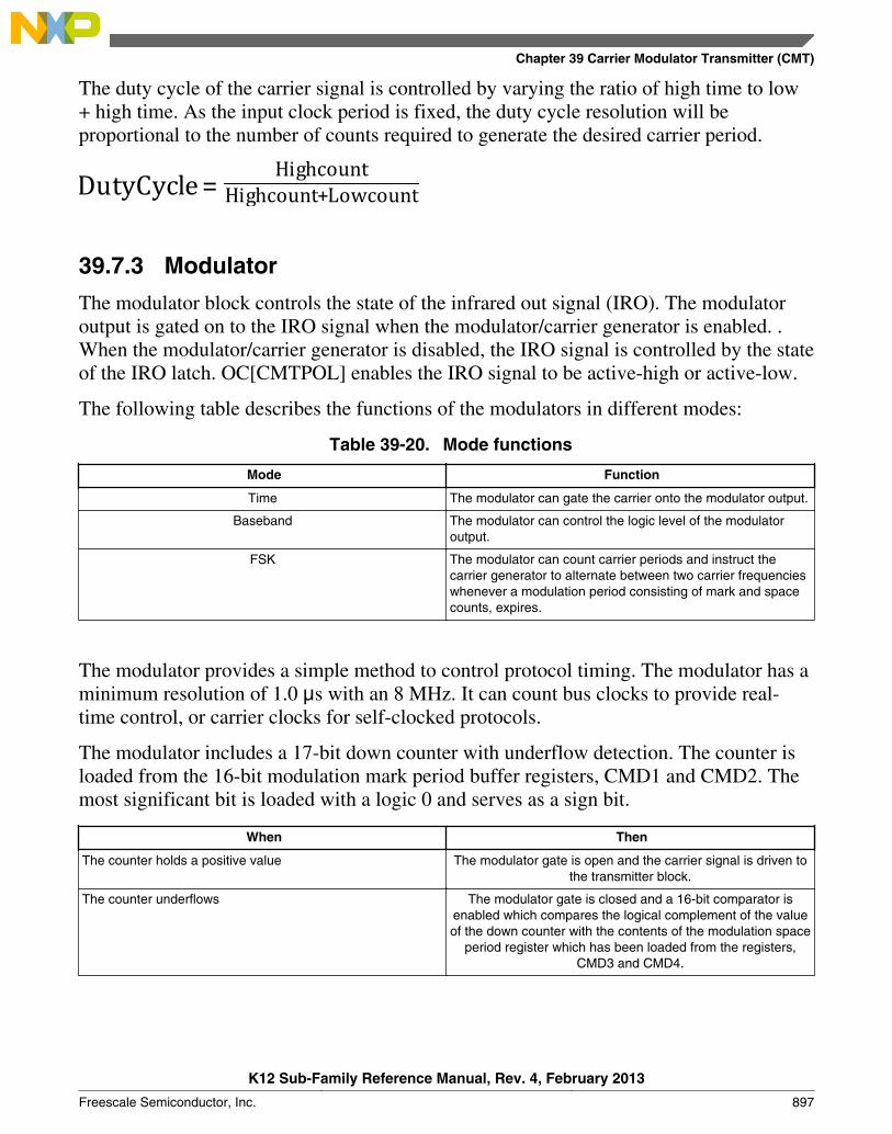
The duty cycle of the carrier signal is controlled by varying the ratio of high time to low+ high time. As the input clock period is fixed, the duty cycle resolution will beproportional to the number of counts required to generate the desired carrier period.
39.7.3 Modulator
The modulator block controls the state of the infrared out signal (IRO). The modulatoroutput is gated on to the IRO signal when the modulator/carrier generator is enabled. .When the modulator/carrier generator is disabled, the IRO signal is controlled by the stateof the IRO latch. OC[CMTPOL] enables the IRO signal to be active-high or active-low.
The following table describes the functions of the modulators in different modes:
Table 39-20. Mode functions
Mode Function
Time The modulator can gate the carrier onto the modulator output.
Baseband The modulator can control the logic level of the modulatoroutput.
FSK The modulator can count carrier periods and instruct thecarrier generator to alternate between two carrier frequencieswhenever a modulation period consisting of mark and spacecounts, expires.
The modulator provides a simple method to control protocol timing. The modulator has aminimum resolution of 1.0 μs with an 8 MHz. It can count bus clocks to provide real-time control, or carrier clocks for self-clocked protocols.
The modulator includes a 17-bit down counter with underflow detection. The counter isloaded from the 16-bit modulation mark period buffer registers, CMD1 and CMD2. Themost significant bit is loaded with a logic 0 and serves as a sign bit.
When Then
The counter holds a positive value The modulator gate is open and the carrier signal is driven tothe transmitter block.
The counter underflows The modulator gate is closed and a 16-bit comparator isenabled which compares the logical complement of the valueof the down counter with the contents of the modulation space
period register which has been loaded from the registers,CMD3 and CMD4.
Chapter 39 Carrier Modulator Transmitter (CMT)
K12 Sub-Family Reference Manual, Rev. 4, February 2013
Freescale Semiconductor, Inc. 897
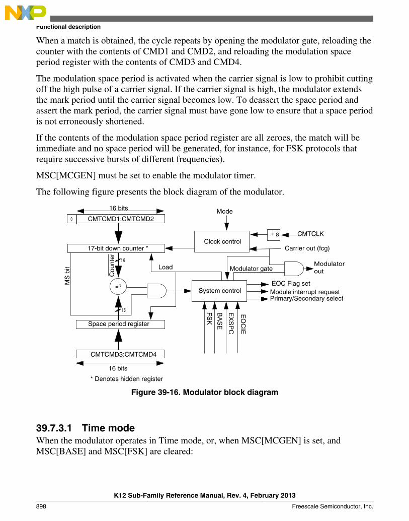
When a match is obtained, the cycle repeats by opening the modulator gate, reloading thecounter with the contents of CMD1 and CMD2, and reloading the modulation spaceperiod register with the contents of CMD3 and CMD4.
The modulation space period is activated when the carrier signal is low to prohibit cuttingoff the high pulse of a carrier signal. If the carrier signal is high, the modulator extendsthe mark period until the carrier signal becomes low. To deassert the space period andassert the mark period, the carrier signal must have gone low to ensure that a space periodis not erroneously shortened.
If the contents of the modulation space period register are all zeroes, the match will beimmediate and no space period will be generated, for instance, for FSK protocols thatrequire successive bursts of different frequencies).
MSC[MCGEN] must be set to enable the modulator timer.
The following figure presents the block diagram of the modulator.
MS
bit
16 bits Mode
Load
FS
K
BA
SE
EX
SP
C
EO
CIE
16 bits
1 6
=?
Cou
nter
Primary/Secondary select
0
1 6
17-bit down counter *
CMTCMD1:CMTCMD2
Clock controlCarrier out (fcg)
ModulatoroutModulator gate
EOC Flag setModule interrupt requestSystem control
CMTCLK
Space period register
CMTCMD3:CMTCMD4
* Denotes hidden register
8
Figure 39-16. Modulator block diagram
39.7.3.1 Time modeWhen the modulator operates in Time mode, or, when MSC[MCGEN] is set, andMSC[BASE] and MSC[FSK] are cleared:
Functional description
K12 Sub-Family Reference Manual, Rev. 4, February 2013
898 Freescale Semiconductor, Inc.
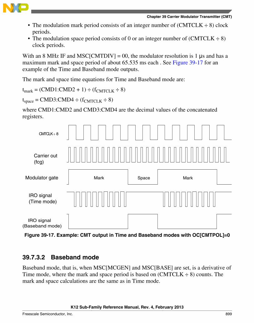
• The modulation mark period consists of an integer number of (CMTCLK ÷ 8) clockperiods.
• The modulation space period consists of 0 or an integer number of (CMTCLK ÷ 8)clock periods.
With an 8 MHz IF and MSC[CMTDIV] = 00, the modulator resolution is 1 μs and has amaximum mark and space period of about 65.535 ms each . See Figure 39-17 for anexample of the Time and Baseband mode outputs.
The mark and space time equations for Time and Baseband mode are:
tmark = (CMD1:CMD2 + 1) ÷ (fCMTCLK ÷ 8)
tspace = CMD3:CMD4 ÷ (fCMTCLK ÷ 8)
where CMD1:CMD2 and CMD3:CMD4 are the decimal values of the concatenatedregisters.
Carrier out(fcg)
Modulator gate
IRO signal(Time mode)
IRO signal(Baseband mode)
Mark Space Mark
CMTCLK 8
Figure 39-17. Example: CMT output in Time and Baseband modes with OC[CMTPOL]=0
39.7.3.2 Baseband mode
Baseband mode, that is, when MSC[MCGEN] and MSC[BASE] are set, is a derivative ofTime mode, where the mark and space period is based on (CMTCLK ÷ 8) counts. Themark and space calculations are the same as in Time mode.
Chapter 39 Carrier Modulator Transmitter (CMT)
K12 Sub-Family Reference Manual, Rev. 4, February 2013
Freescale Semiconductor, Inc. 899
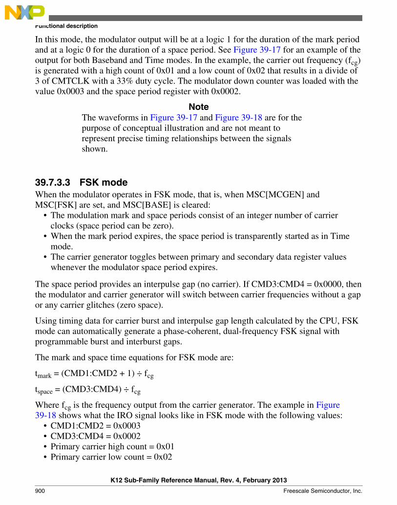
In this mode, the modulator output will be at a logic 1 for the duration of the mark periodand at a logic 0 for the duration of a space period. See Figure 39-17 for an example of theoutput for both Baseband and Time modes. In the example, the carrier out frequency (fcg)is generated with a high count of 0x01 and a low count of 0x02 that results in a divide of3 of CMTCLK with a 33% duty cycle. The modulator down counter was loaded with thevalue 0x0003 and the space period register with 0x0002.
NoteThe waveforms in Figure 39-17 and Figure 39-18 are for thepurpose of conceptual illustration and are not meant torepresent precise timing relationships between the signalsshown.
39.7.3.3 FSK modeWhen the modulator operates in FSK mode, that is, when MSC[MCGEN] andMSC[FSK] are set, and MSC[BASE] is cleared:
• The modulation mark and space periods consist of an integer number of carrierclocks (space period can be zero).
• When the mark period expires, the space period is transparently started as in Timemode.
• The carrier generator toggles between primary and secondary data register valueswhenever the modulator space period expires.
The space period provides an interpulse gap (no carrier). If CMD3:CMD4 = 0x0000, thenthe modulator and carrier generator will switch between carrier frequencies without a gapor any carrier glitches (zero space).
Using timing data for carrier burst and interpulse gap length calculated by the CPU, FSKmode can automatically generate a phase-coherent, dual-frequency FSK signal withprogrammable burst and interburst gaps.
The mark and space time equations for FSK mode are:
tmark = (CMD1:CMD2 + 1) ÷ fcg
tspace = (CMD3:CMD4) ÷ fcg
Where fcg is the frequency output from the carrier generator. The example in Figure39-18 shows what the IRO signal looks like in FSK mode with the following values:
• CMD1:CMD2 = 0x0003• CMD3:CMD4 = 0x0002• Primary carrier high count = 0x01• Primary carrier low count = 0x02
Functional description
K12 Sub-Family Reference Manual, Rev. 4, February 2013
900 Freescale Semiconductor, Inc.
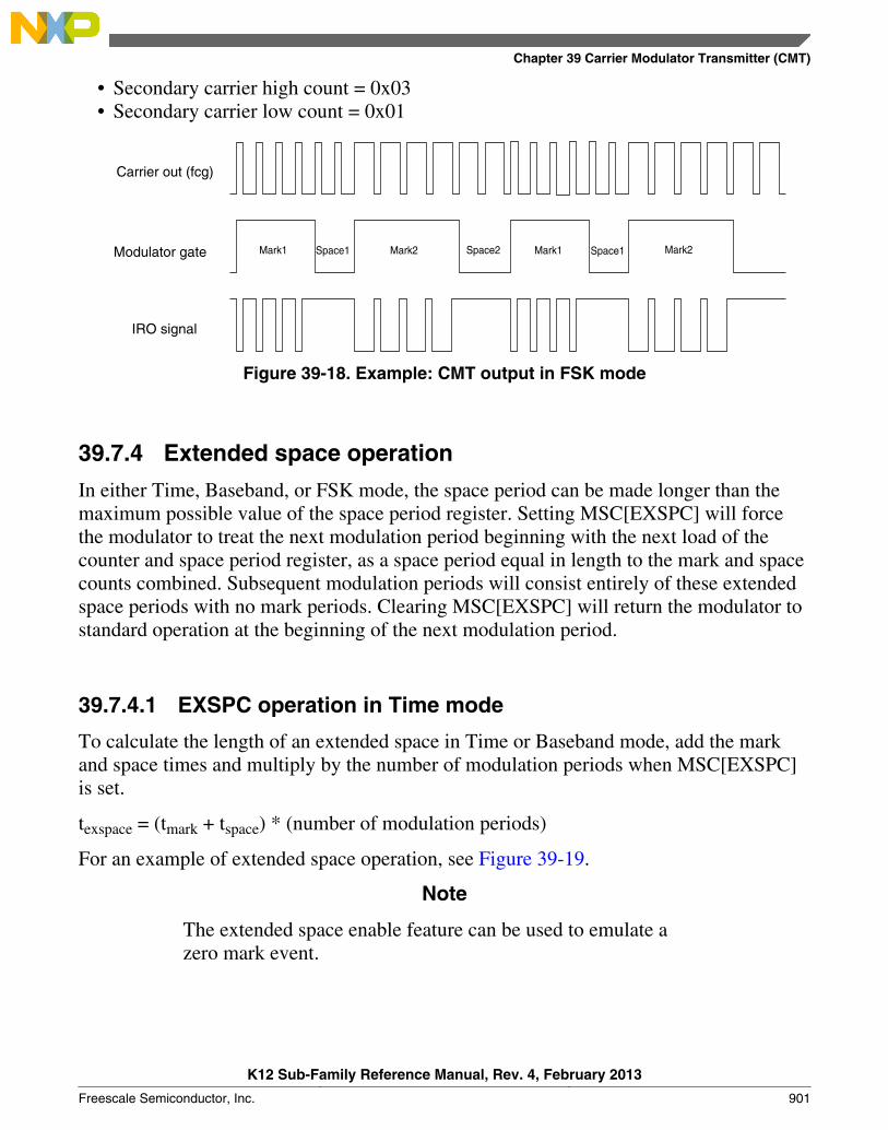
• Secondary carrier high count = 0x03• Secondary carrier low count = 0x01
IRO signal
Modulator gate
Carrier out (fcg)
Mark1 Space1 Mark2 Space2 Mark1 Mark2Space1
Figure 39-18. Example: CMT output in FSK mode
39.7.4 Extended space operation
In either Time, Baseband, or FSK mode, the space period can be made longer than themaximum possible value of the space period register. Setting MSC[EXSPC] will forcethe modulator to treat the next modulation period beginning with the next load of thecounter and space period register, as a space period equal in length to the mark and spacecounts combined. Subsequent modulation periods will consist entirely of these extendedspace periods with no mark periods. Clearing MSC[EXSPC] will return the modulator tostandard operation at the beginning of the next modulation period.
39.7.4.1 EXSPC operation in Time mode
To calculate the length of an extended space in Time or Baseband mode, add the markand space times and multiply by the number of modulation periods when MSC[EXSPC]is set.
texspace = (tmark + tspace) * (number of modulation periods)
For an example of extended space operation, see Figure 39-19.
Note
The extended space enable feature can be used to emulate azero mark event.
Chapter 39 Carrier Modulator Transmitter (CMT)
K12 Sub-Family Reference Manual, Rev. 4, February 2013
Freescale Semiconductor, Inc. 901
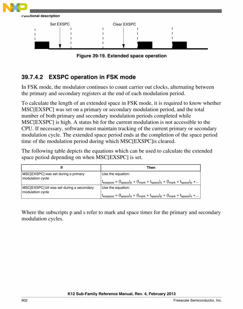
Set EXSPC Clear EXSPC
Figure 39-19. Extended space operation
39.7.4.2 EXSPC operation in FSK mode
In FSK mode, the modulator continues to count carrier out clocks, alternating betweenthe primary and secondary registers at the end of each modulation period.
To calculate the length of an extended space in FSK mode, it is required to know whetherMSC[EXSPC] was set on a primary or secondary modulation period, and the totalnumber of both primary and secondary modulation periods completed whileMSC[EXSPC] is high. A status bit for the current modulation is not accessible to theCPU. If necessary, software must maintain tracking of the current primary or secondarymodulation cycle. The extended space period ends at the completion of the space periodtime of the modulation period during which MSC[EXSPC]is cleared.
The following table depicts the equations which can be used to calculate the extendedspace period depending on when MSC[EXSPC] is set.
If Then
MSC[EXSPC] was set during a primarymodulation cycle
Use the equation:
texspace = (tspace)p + (tmark + tspace)s + (tmark + tspace)p +...
MSC[EXSPC] bit was set during a secondarymodulation cycle
Use the equation:
texspace = (tspace)s + (tmark + tspace)p + (tmark + tspace)s +...
Where the subscripts p and s refer to mark and space times for the primary and secondarymodulation cycles.
Functional description
K12 Sub-Family Reference Manual, Rev. 4, February 2013
902 Freescale Semiconductor, Inc.
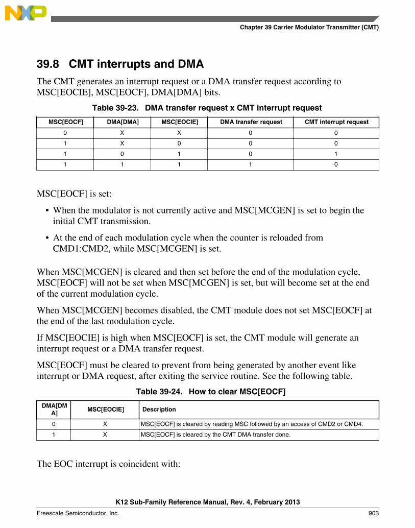
39.8 CMT interrupts and DMAThe CMT generates an interrupt request or a DMA transfer request according toMSC[EOCIE], MSC[EOCF], DMA[DMA] bits.
Table 39-23. DMA transfer request x CMT interrupt request
MSC[EOCF] DMA[DMA] MSC[EOCIE] DMA transfer request CMT interrupt request
0 X X 0 0
1 X 0 0 0
1 0 1 0 1
1 1 1 1 0
MSC[EOCF] is set:
• When the modulator is not currently active and MSC[MCGEN] is set to begin theinitial CMT transmission.
• At the end of each modulation cycle when the counter is reloaded fromCMD1:CMD2, while MSC[MCGEN] is set.
When MSC[MCGEN] is cleared and then set before the end of the modulation cycle,MSC[EOCF] will not be set when MSC[MCGEN] is set, but will become set at the endof the current modulation cycle.
When MSC[MCGEN] becomes disabled, the CMT module does not set MSC[EOCF] atthe end of the last modulation cycle.
If MSC[EOCIE] is high when MSC[EOCF] is set, the CMT module will generate aninterrupt request or a DMA transfer request.
MSC[EOCF] must be cleared to prevent from being generated by another event likeinterrupt or DMA request, after exiting the service routine. See the following table.
Table 39-24. How to clear MSC[EOCF]
DMA[DMA]
MSC[EOCIE] Description
0 X MSC[EOCF] is cleared by reading MSC followed by an access of CMD2 or CMD4.
1 X MSC[EOCF] is cleared by the CMT DMA transfer done.
The EOC interrupt is coincident with:
Chapter 39 Carrier Modulator Transmitter (CMT)
K12 Sub-Family Reference Manual, Rev. 4, February 2013
Freescale Semiconductor, Inc. 903
• Loading the down-counter with the contents of CMD1:CMD2• Loading the space period register with the contents of CMD3:CMD4
The EOC interrupt provides a means for the user to reload new mark/space values intothe modulator data registers. Modulator data register updates will take effect at the end ofthe current modulation cycle.
NOTEThe down-counter and space period register are updated at theend of every modulation cycle, irrespective of interrupthandling and the state of MSC[EOCF].
CMT interrupts and DMA
K12 Sub-Family Reference Manual, Rev. 4, February 2013
904 Freescale Semiconductor, Inc.
Chapter 40Real Time Clock (RTC)
40.1 IntroductionNOTE
For the chip-specific implementation details of this module'sinstances see the chip configuration information.
40.1.1 Features
The RTC module features include:
• 32-bit seconds counter with roll-over protection and 32-bit alarm
• 16-bit prescaler with compensation that can correct errors between 0.12 ppm and3906 ppm
• Register write protection• Lock register requires POR or software reset to enable write access• Access control registers require system reset to enable read and/or write access
• 1 Hz square wave output
• 64-bit monotonic counter with roll-over protection
• Tamper time seconds register that records when the time was invalidated
40.1.2 Modes of operation
The RTC remains functional in all low power modes and can generate an interrupt to exitany low power mode.
K12 Sub-Family Reference Manual, Rev. 4, February 2013
Freescale Semiconductor, Inc. 905
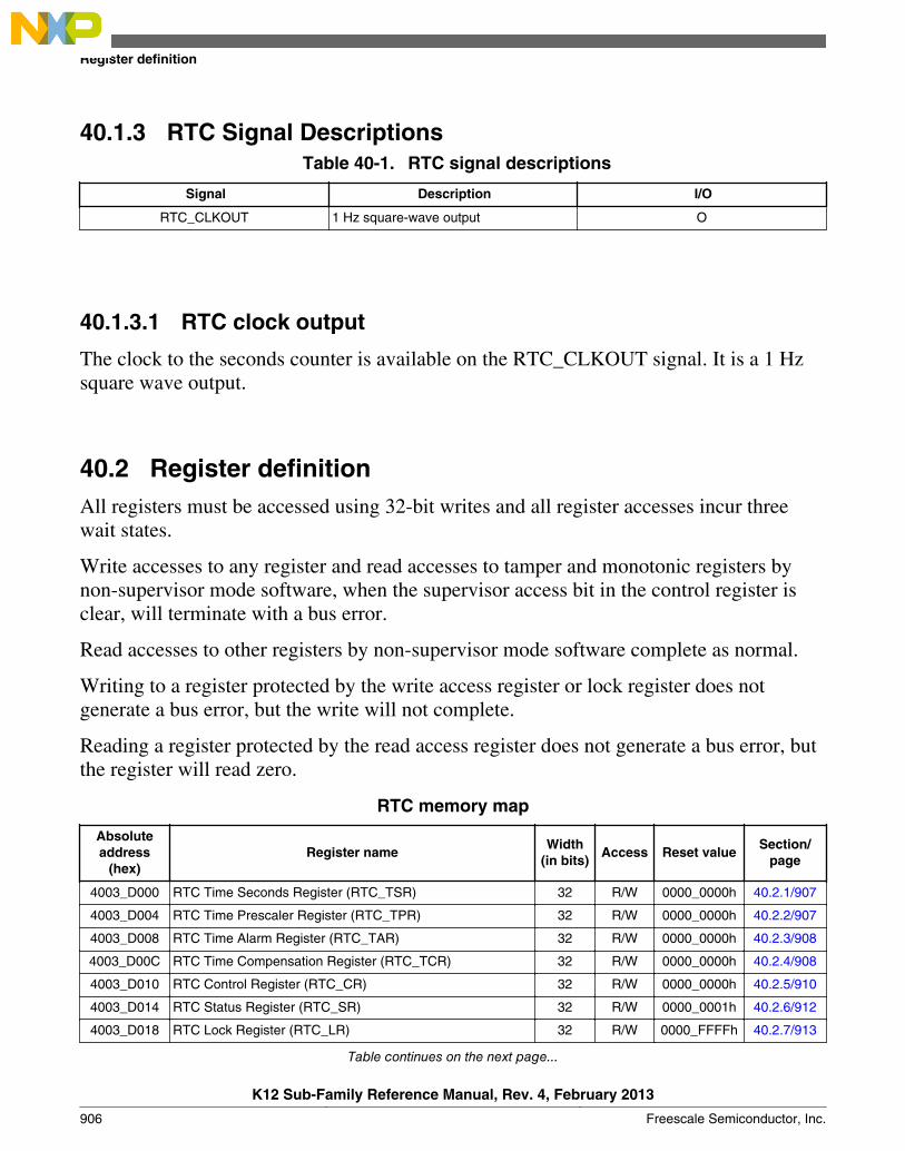
40.1.3 RTC Signal DescriptionsTable 40-1. RTC signal descriptions
Signal Description I/O
RTC_CLKOUT 1 Hz square-wave output O
40.1.3.1 RTC clock output
The clock to the seconds counter is available on the RTC_CLKOUT signal. It is a 1 Hzsquare wave output.
40.2 Register definitionAll registers must be accessed using 32-bit writes and all register accesses incur threewait states.
Write accesses to any register and read accesses to tamper and monotonic registers bynon-supervisor mode software, when the supervisor access bit in the control register isclear, will terminate with a bus error.
Read accesses to other registers by non-supervisor mode software complete as normal.
Writing to a register protected by the write access register or lock register does notgenerate a bus error, but the write will not complete.
Reading a register protected by the read access register does not generate a bus error, butthe register will read zero.
RTC memory map
Absoluteaddress
(hex)Register name
Width(in bits)
Access Reset valueSection/
page
4003_D000 RTC Time Seconds Register (RTC_TSR) 32 R/W 0000_0000h 40.2.1/907
4003_D004 RTC Time Prescaler Register (RTC_TPR) 32 R/W 0000_0000h 40.2.2/907
4003_D008 RTC Time Alarm Register (RTC_TAR) 32 R/W 0000_0000h 40.2.3/908
4003_D00C RTC Time Compensation Register (RTC_TCR) 32 R/W 0000_0000h 40.2.4/908
4003_D010 RTC Control Register (RTC_CR) 32 R/W 0000_0000h 40.2.5/910
4003_D014 RTC Status Register (RTC_SR) 32 R/W 0000_0001h 40.2.6/912
4003_D018 RTC Lock Register (RTC_LR) 32 R/W 0000_FFFFh 40.2.7/913
Table continues on the next page...
Register definition
K12 Sub-Family Reference Manual, Rev. 4, February 2013
906 Freescale Semiconductor, Inc.
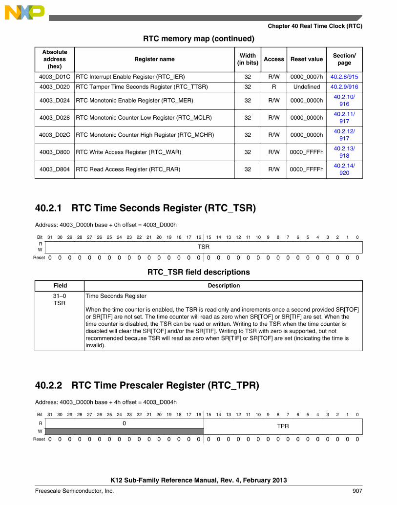
RTC memory map (continued)
Absoluteaddress
(hex)Register name
Width(in bits)
Access Reset valueSection/
page
4003_D01C RTC Interrupt Enable Register (RTC_IER) 32 R/W 0000_0007h 40.2.8/915
4003_D020 RTC Tamper Time Seconds Register (RTC_TTSR) 32 R Undefined 40.2.9/916
4003_D024 RTC Monotonic Enable Register (RTC_MER) 32 R/W 0000_0000h40.2.10/
916
4003_D028 RTC Monotonic Counter Low Register (RTC_MCLR) 32 R/W 0000_0000h40.2.11/
917
4003_D02C RTC Monotonic Counter High Register (RTC_MCHR) 32 R/W 0000_0000h40.2.12/
917
4003_D800 RTC Write Access Register (RTC_WAR) 32 R/W 0000_FFFFh40.2.13/
918
4003_D804 RTC Read Access Register (RTC_RAR) 32 R/W 0000_FFFFh40.2.14/
920
40.2.1 RTC Time Seconds Register (RTC_TSR)
Address: 4003_D000h base + 0h offset = 4003_D000h
Bit 31 30 29 28 27 26 25 24 23 22 21 20 19 18 17 16 15 14 13 12 11 10 9 8 7 6 5 4 3 2 1 0
R TSRW
Reset 0 0 0 0 0 0 0 0 0 0 0 0 0 0 0 0 0 0 0 0 0 0 0 0 0 0 0 0 0 0 0 0
RTC_TSR field descriptions
Field Description
31–0TSR
Time Seconds Register
When the time counter is enabled, the TSR is read only and increments once a second provided SR[TOF]or SR[TIF] are not set. The time counter will read as zero when SR[TOF] or SR[TIF] are set. When thetime counter is disabled, the TSR can be read or written. Writing to the TSR when the time counter isdisabled will clear the SR[TOF] and/or the SR[TIF]. Writing to TSR with zero is supported, but notrecommended because TSR will read as zero when SR[TIF] or SR[TOF] are set (indicating the time isinvalid).
40.2.2 RTC Time Prescaler Register (RTC_TPR)
Address: 4003_D000h base + 4h offset = 4003_D004h
Bit 31 30 29 28 27 26 25 24 23 22 21 20 19 18 17 16 15 14 13 12 11 10 9 8 7 6 5 4 3 2 1 0
R 0 TPRW
Reset 0 0 0 0 0 0 0 0 0 0 0 0 0 0 0 0 0 0 0 0 0 0 0 0 0 0 0 0 0 0 0 0
Chapter 40 Real Time Clock (RTC)
K12 Sub-Family Reference Manual, Rev. 4, February 2013
Freescale Semiconductor, Inc. 907
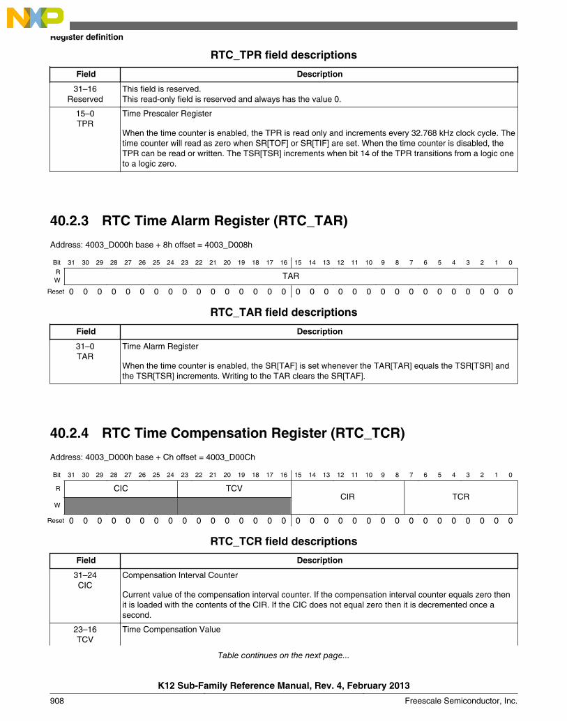
RTC_TPR field descriptions
Field Description
31–16Reserved
This field is reserved.This read-only field is reserved and always has the value 0.
15–0TPR
Time Prescaler Register
When the time counter is enabled, the TPR is read only and increments every 32.768 kHz clock cycle. Thetime counter will read as zero when SR[TOF] or SR[TIF] are set. When the time counter is disabled, theTPR can be read or written. The TSR[TSR] increments when bit 14 of the TPR transitions from a logic oneto a logic zero.
40.2.3 RTC Time Alarm Register (RTC_TAR)
Address: 4003_D000h base + 8h offset = 4003_D008h
Bit 31 30 29 28 27 26 25 24 23 22 21 20 19 18 17 16 15 14 13 12 11 10 9 8 7 6 5 4 3 2 1 0
R TARW
Reset 0 0 0 0 0 0 0 0 0 0 0 0 0 0 0 0 0 0 0 0 0 0 0 0 0 0 0 0 0 0 0 0
RTC_TAR field descriptions
Field Description
31–0TAR
Time Alarm Register
When the time counter is enabled, the SR[TAF] is set whenever the TAR[TAR] equals the TSR[TSR] andthe TSR[TSR] increments. Writing to the TAR clears the SR[TAF].
40.2.4 RTC Time Compensation Register (RTC_TCR)
Address: 4003_D000h base + Ch offset = 4003_D00Ch
Bit 31 30 29 28 27 26 25 24 23 22 21 20 19 18 17 16 15 14 13 12 11 10 9 8 7 6 5 4 3 2 1 0
R CIC TCVCIR TCR
W
Reset 0 0 0 0 0 0 0 0 0 0 0 0 0 0 0 0 0 0 0 0 0 0 0 0 0 0 0 0 0 0 0 0
RTC_TCR field descriptions
Field Description
31–24CIC
Compensation Interval Counter
Current value of the compensation interval counter. If the compensation interval counter equals zero thenit is loaded with the contents of the CIR. If the CIC does not equal zero then it is decremented once asecond.
23–16TCV
Time Compensation Value
Table continues on the next page...
Register definition
K12 Sub-Family Reference Manual, Rev. 4, February 2013
908 Freescale Semiconductor, Inc.

RTC_TCR field descriptions (continued)
Field Description
Current value used by the compensation logic for the present second interval. Updated once a second ifthe CIC equals 0 with the contents of the TCR field. If the CIC does not equal zero then it is loaded withzero (compensation is not enabled for that second increment).
15–8CIR
Compensation Interval Register
Configures the compensation interval in seconds from 1 to 256 to control how frequently the TCR shouldadjust the number of 32.768 kHz cycles in each second. The value written should be one less than thenumber of seconds. For example, write zero to configure for a compensation interval of one second. Thisregister is double buffered and writes do not take affect until the end of the current compensation interval.
7–0TCR
Time Compensation Register
Configures the number of 32.768 kHz clock cycles in each second. This register is double buffered andwrites do not take affect until the end of the current compensation interval.
80h Time Prescaler Register overflows every 32896 clock cycles.... ...FFh Time Prescaler Register overflows every 32769 clock cycles.00h Time Prescaler Register overflows every 32768 clock cycles.01h Time Prescaler Register overflows every 32767 clock cycles.... ...7Fh Time Prescaler Register overflows every 32641 clock cycles.
Chapter 40 Real Time Clock (RTC)
K12 Sub-Family Reference Manual, Rev. 4, February 2013
Freescale Semiconductor, Inc. 909
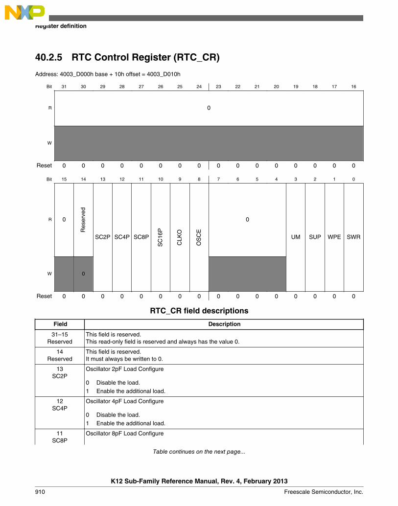
40.2.5 RTC Control Register (RTC_CR)
Address: 4003_D000h base + 10h offset = 4003_D010h
Bit 31 30 29 28 27 26 25 24 23 22 21 20 19 18 17 16
R 0
W
Reset 0 0 0 0 0 0 0 0 0 0 0 0 0 0 0 0
Bit 15 14 13 12 11 10 9 8 7 6 5 4 3 2 1 0
R 0
Res
erve
d
SC2P SC4P SC8P
SC
16P
CLK
O
OS
CE
0
UM SUP WPE SWR
W 0
Reset 0 0 0 0 0 0 0 0 0 0 0 0 0 0 0 0
RTC_CR field descriptions
Field Description
31–15Reserved
This field is reserved.This read-only field is reserved and always has the value 0.
14Reserved
This field is reserved.It must always be written to 0.
13SC2P
Oscillator 2pF Load Configure
0 Disable the load.1 Enable the additional load.
12SC4P
Oscillator 4pF Load Configure
0 Disable the load.1 Enable the additional load.
11SC8P
Oscillator 8pF Load Configure
Table continues on the next page...
Register definition
K12 Sub-Family Reference Manual, Rev. 4, February 2013
910 Freescale Semiconductor, Inc.
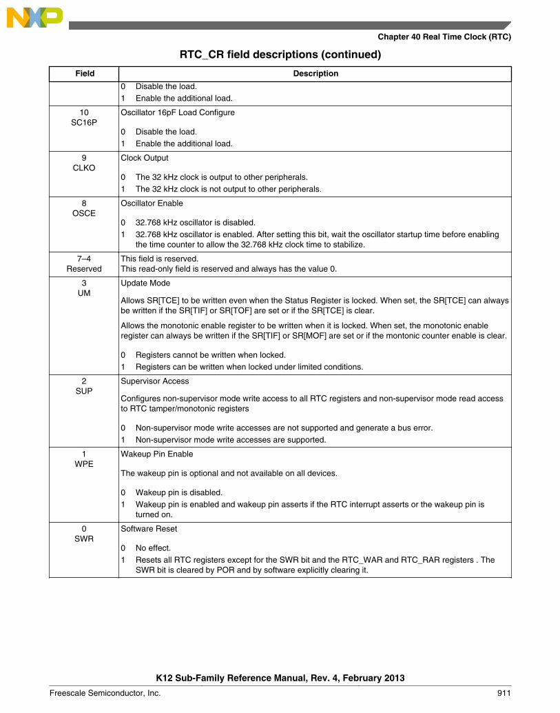
RTC_CR field descriptions (continued)
Field Description
0 Disable the load.1 Enable the additional load.
10SC16P
Oscillator 16pF Load Configure
0 Disable the load.1 Enable the additional load.
9CLKO
Clock Output
0 The 32 kHz clock is output to other peripherals.1 The 32 kHz clock is not output to other peripherals.
8OSCE
Oscillator Enable
0 32.768 kHz oscillator is disabled.1 32.768 kHz oscillator is enabled. After setting this bit, wait the oscillator startup time before enabling
the time counter to allow the 32.768 kHz clock time to stabilize.
7–4Reserved
This field is reserved.This read-only field is reserved and always has the value 0.
3UM
Update Mode
Allows SR[TCE] to be written even when the Status Register is locked. When set, the SR[TCE] can alwaysbe written if the SR[TIF] or SR[TOF] are set or if the SR[TCE] is clear.
Allows the monotonic enable register to be written when it is locked. When set, the monotonic enableregister can always be written if the SR[TIF] or SR[MOF] are set or if the montonic counter enable is clear.
0 Registers cannot be written when locked.1 Registers can be written when locked under limited conditions.
2SUP
Supervisor Access
Configures non-supervisor mode write access to all RTC registers and non-supervisor mode read accessto RTC tamper/monotonic registers
0 Non-supervisor mode write accesses are not supported and generate a bus error.1 Non-supervisor mode write accesses are supported.
1WPE
Wakeup Pin Enable
The wakeup pin is optional and not available on all devices.
0 Wakeup pin is disabled.1 Wakeup pin is enabled and wakeup pin asserts if the RTC interrupt asserts or the wakeup pin is
turned on.
0SWR
Software Reset
0 No effect.1 Resets all RTC registers except for the SWR bit and the RTC_WAR and RTC_RAR registers . The
SWR bit is cleared by POR and by software explicitly clearing it.
Chapter 40 Real Time Clock (RTC)
K12 Sub-Family Reference Manual, Rev. 4, February 2013
Freescale Semiconductor, Inc. 911
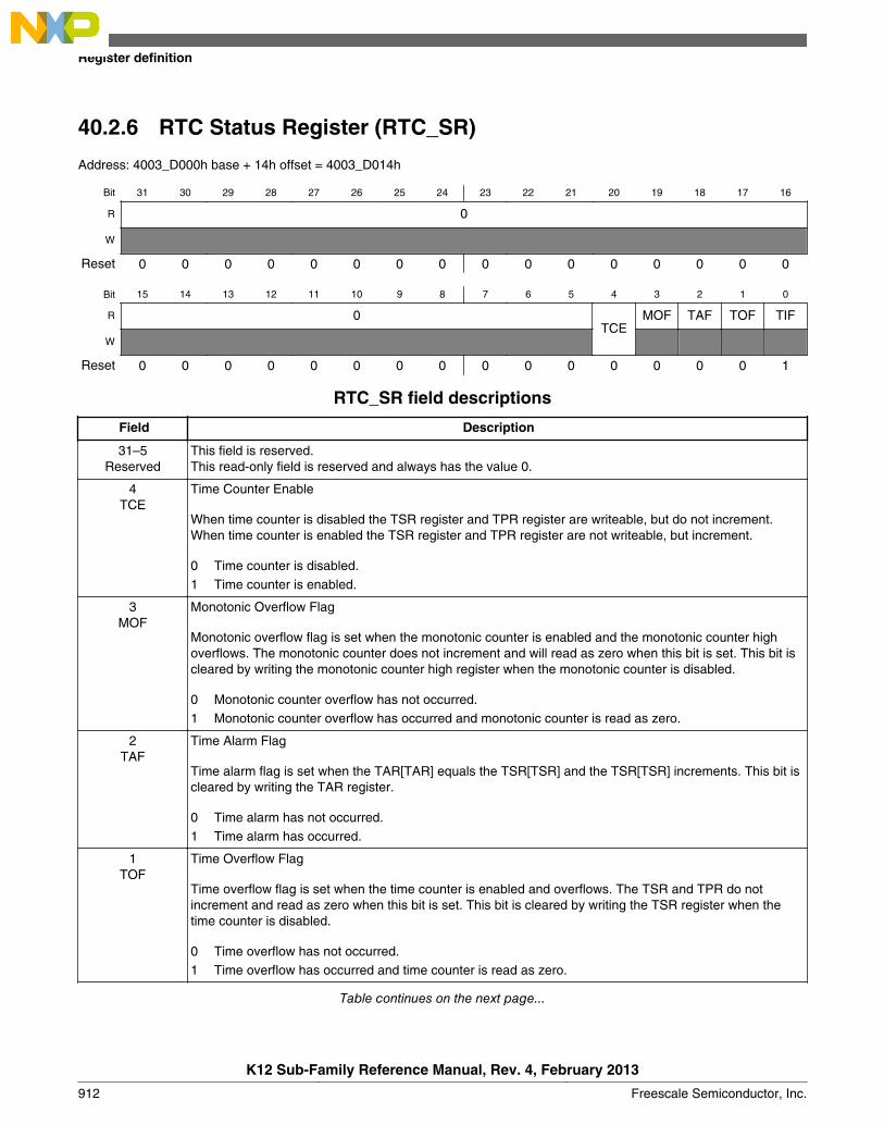
40.2.6 RTC Status Register (RTC_SR)
Address: 4003_D000h base + 14h offset = 4003_D014h
Bit 31 30 29 28 27 26 25 24 23 22 21 20 19 18 17 16
R 0
W
Reset 0 0 0 0 0 0 0 0 0 0 0 0 0 0 0 0
Bit 15 14 13 12 11 10 9 8 7 6 5 4 3 2 1 0
R 0TCE
MOF TAF TOF TIF
W
Reset 0 0 0 0 0 0 0 0 0 0 0 0 0 0 0 1
RTC_SR field descriptions
Field Description
31–5Reserved
This field is reserved.This read-only field is reserved and always has the value 0.
4TCE
Time Counter Enable
When time counter is disabled the TSR register and TPR register are writeable, but do not increment.When time counter is enabled the TSR register and TPR register are not writeable, but increment.
0 Time counter is disabled.1 Time counter is enabled.
3MOF
Monotonic Overflow Flag
Monotonic overflow flag is set when the monotonic counter is enabled and the monotonic counter highoverflows. The monotonic counter does not increment and will read as zero when this bit is set. This bit iscleared by writing the monotonic counter high register when the monotonic counter is disabled.
0 Monotonic counter overflow has not occurred.1 Monotonic counter overflow has occurred and monotonic counter is read as zero.
2TAF
Time Alarm Flag
Time alarm flag is set when the TAR[TAR] equals the TSR[TSR] and the TSR[TSR] increments. This bit iscleared by writing the TAR register.
0 Time alarm has not occurred.1 Time alarm has occurred.
1TOF
Time Overflow Flag
Time overflow flag is set when the time counter is enabled and overflows. The TSR and TPR do notincrement and read as zero when this bit is set. This bit is cleared by writing the TSR register when thetime counter is disabled.
0 Time overflow has not occurred.1 Time overflow has occurred and time counter is read as zero.
Table continues on the next page...
Register definition
K12 Sub-Family Reference Manual, Rev. 4, February 2013
912 Freescale Semiconductor, Inc.
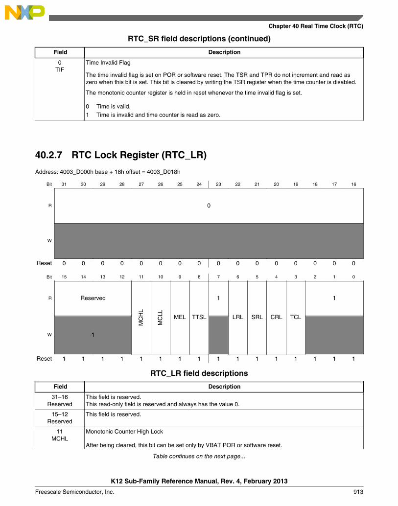
RTC_SR field descriptions (continued)
Field Description
0TIF
Time Invalid Flag
The time invalid flag is set on POR or software reset. The TSR and TPR do not increment and read aszero when this bit is set. This bit is cleared by writing the TSR register when the time counter is disabled.
The monotonic counter register is held in reset whenever the time invalid flag is set.
0 Time is valid.1 Time is invalid and time counter is read as zero.
40.2.7 RTC Lock Register (RTC_LR)
Address: 4003_D000h base + 18h offset = 4003_D018h
Bit 31 30 29 28 27 26 25 24 23 22 21 20 19 18 17 16
R 0
W
Reset 0 0 0 0 0 0 0 0 0 0 0 0 0 0 0 0
Bit 15 14 13 12 11 10 9 8 7 6 5 4 3 2 1 0
R Reserved
MC
HL
MC
LL MEL TTSL
1
LRL SRL CRL TCL
1
W 1
Reset 1 1 1 1 1 1 1 1 1 1 1 1 1 1 1 1
RTC_LR field descriptions
Field Description
31–16Reserved
This field is reserved.This read-only field is reserved and always has the value 0.
15–12Reserved
This field is reserved.
11MCHL
Monotonic Counter High Lock
After being cleared, this bit can be set only by VBAT POR or software reset.
Table continues on the next page...
Chapter 40 Real Time Clock (RTC)
K12 Sub-Family Reference Manual, Rev. 4, February 2013
Freescale Semiconductor, Inc. 913
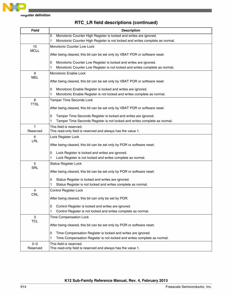
RTC_LR field descriptions (continued)
Field Description
0 Monotonic Counter High Register is locked and writes are ignored.1 Monotonic Counter High Register is not locked and writes complete as normal.
10MCLL
Monotonic Counter Low Lock
After being cleared, this bit can be set only by VBAT POR or software reset.
0 Monotonic Counter Low Register is locked and writes are ignored.1 Monotonic Counter Low Register is not locked and writes complete as normal.
9MEL
Monotonic Enable Lock
After being cleared, this bit can be set only by VBAT POR or software reset.
0 Monotonic Enable Register is locked and writes are ignored.1 Monotonic Enable Register is not locked and writes complete as normal.
8TTSL
Tamper Time Seconds Lock
After being cleared, this bit can be set only by VBAT POR or software reset.
0 Tamper Time Seconds Register is locked and writes are ignored.1 Tamper Time Seconds Register is not locked and writes complete as normal.
7Reserved
This field is reserved.This read-only field is reserved and always has the value 1.
6LRL
Lock Register Lock
After being cleared, this bit can be set only by POR or software reset.
0 Lock Register is locked and writes are ignored.1 Lock Register is not locked and writes complete as normal.
5SRL
Status Register Lock
After being cleared, this bit can be set only by POR or software reset.
0 Status Register is locked and writes are ignored.1 Status Register is not locked and writes complete as normal.
4CRL
Control Register Lock
After being cleared, this bit can only be set by POR.
0 Control Register is locked and writes are ignored.1 Control Register is not locked and writes complete as normal.
3TCL
Time Compensation Lock
After being cleared, this bit can be set only by POR or software reset.
0 Time Compensation Register is locked and writes are ignored.1 Time Compensation Register is not locked and writes complete as normal.
2–0Reserved
This field is reserved.This read-only field is reserved and always has the value 1.
Register definition
K12 Sub-Family Reference Manual, Rev. 4, February 2013
914 Freescale Semiconductor, Inc.
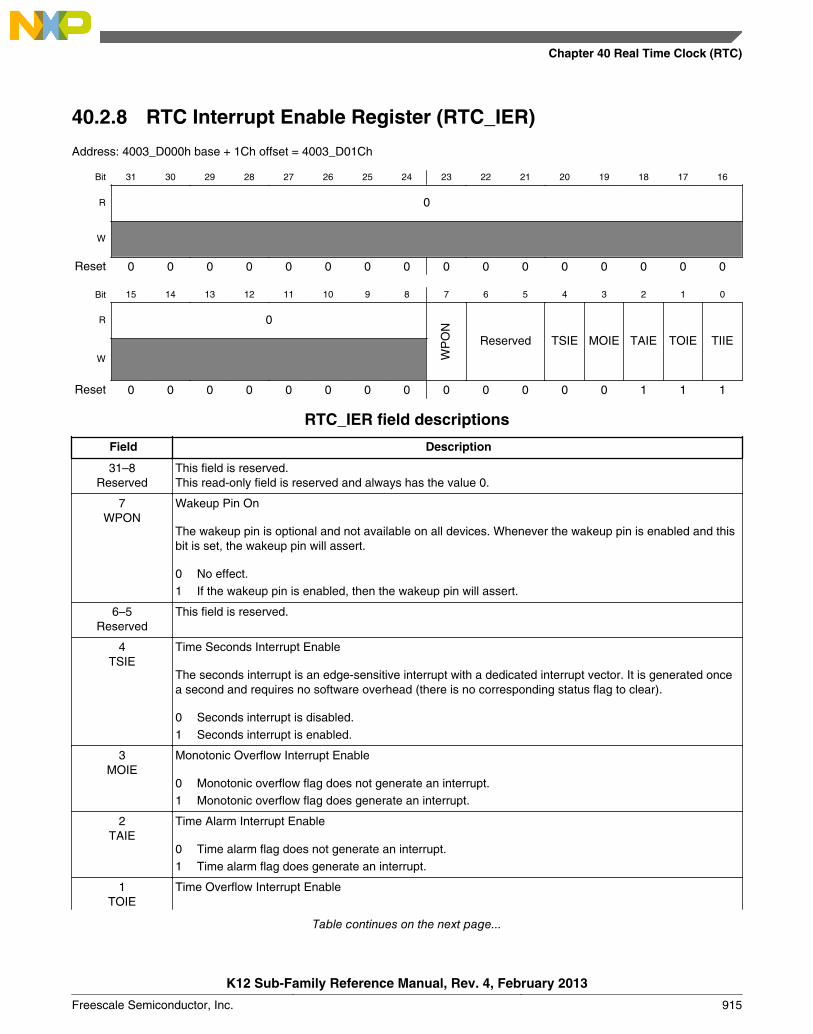
40.2.8 RTC Interrupt Enable Register (RTC_IER)
Address: 4003_D000h base + 1Ch offset = 4003_D01Ch
Bit 31 30 29 28 27 26 25 24 23 22 21 20 19 18 17 16
R 0
W
Reset 0 0 0 0 0 0 0 0 0 0 0 0 0 0 0 0
Bit 15 14 13 12 11 10 9 8 7 6 5 4 3 2 1 0
R 0
WP
ON
Reserved TSIE MOIE TAIE TOIE TIIEW
Reset 0 0 0 0 0 0 0 0 0 0 0 0 0 1 1 1
RTC_IER field descriptions
Field Description
31–8Reserved
This field is reserved.This read-only field is reserved and always has the value 0.
7WPON
Wakeup Pin On
The wakeup pin is optional and not available on all devices. Whenever the wakeup pin is enabled and thisbit is set, the wakeup pin will assert.
0 No effect.1 If the wakeup pin is enabled, then the wakeup pin will assert.
6–5Reserved
This field is reserved.
4TSIE
Time Seconds Interrupt Enable
The seconds interrupt is an edge-sensitive interrupt with a dedicated interrupt vector. It is generated oncea second and requires no software overhead (there is no corresponding status flag to clear).
0 Seconds interrupt is disabled.1 Seconds interrupt is enabled.
3MOIE
Monotonic Overflow Interrupt Enable
0 Monotonic overflow flag does not generate an interrupt.1 Monotonic overflow flag does generate an interrupt.
2TAIE
Time Alarm Interrupt Enable
0 Time alarm flag does not generate an interrupt.1 Time alarm flag does generate an interrupt.
1TOIE
Time Overflow Interrupt Enable
Table continues on the next page...
Chapter 40 Real Time Clock (RTC)
K12 Sub-Family Reference Manual, Rev. 4, February 2013
Freescale Semiconductor, Inc. 915
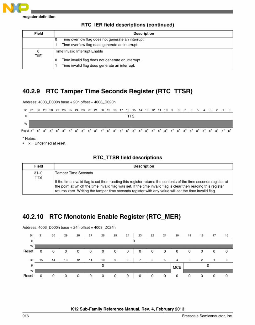
RTC_IER field descriptions (continued)
Field Description
0 Time overflow flag does not generate an interrupt.1 Time overflow flag does generate an interrupt.
0TIIE
Time Invalid Interrupt Enable
0 Time invalid flag does not generate an interrupt.1 Time invalid flag does generate an interrupt.
40.2.9 RTC Tamper Time Seconds Register (RTC_TTSR)
Address: 4003_D000h base + 20h offset = 4003_D020h
Bit 31 30 29 28 27 26 25 24 23 22 21 20 19 18 17 16 15 14 13 12 11 10 9 8 7 6 5 4 3 2 1 0
R TTS
W
Reset x* x* x* x* x* x* x* x* x* x* x* x* x* x* x* x* x* x* x* x* x* x* x* x* x* x* x* x* x* x* x* x*
* Notes:x = Undefined at reset.•
RTC_TTSR field descriptions
Field Description
31–0TTS
Tamper Time Seconds
If the time invalid flag is set then reading this register returns the contents of the time seconds register atthe point at which the time invalid flag was set. If the time invalid flag is clear then reading this registerreturns zero. Writing the tamper time seconds register with any value will set the time invalid flag.
40.2.10 RTC Monotonic Enable Register (RTC_MER)
Address: 4003_D000h base + 24h offset = 4003_D024h
Bit 31 30 29 28 27 26 25 24 23 22 21 20 19 18 17 16
R 0W
Reset 0 0 0 0 0 0 0 0 0 0 0 0 0 0 0 0
Bit 15 14 13 12 11 10 9 8 7 6 5 4 3 2 1 0
R 0 MCE 0W
Reset 0 0 0 0 0 0 0 0 0 0 0 0 0 0 0 0
Register definition
K12 Sub-Family Reference Manual, Rev. 4, February 2013
916 Freescale Semiconductor, Inc.
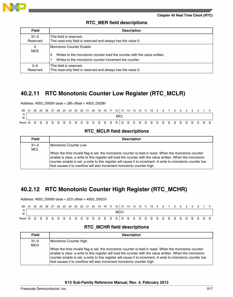
RTC_MER field descriptions
Field Description
31–5Reserved
This field is reserved.This read-only field is reserved and always has the value 0.
4MCE
Monotonic Counter Enable
0 Writes to the monotonic counter load the counter with the value written.1 Writes to the monotonic counter increment the counter.
3–0Reserved
This field is reserved.This read-only field is reserved and always has the value 0.
40.2.11 RTC Monotonic Counter Low Register (RTC_MCLR)
Address: 4003_D000h base + 28h offset = 4003_D028h
Bit 31 30 29 28 27 26 25 24 23 22 21 20 19 18 17 16 15 14 13 12 11 10 9 8 7 6 5 4 3 2 1 0
R MCLW
Reset 0 0 0 0 0 0 0 0 0 0 0 0 0 0 0 0 0 0 0 0 0 0 0 0 0 0 0 0 0 0 0 0
RTC_MCLR field descriptions
Field Description
31–0MCL
Monotonic Counter Low
When the time invalid flag is set, the monotonic counter is held in reset. When the monotonic counterenable is clear, a write to this register will load the counter with the value written. When the monotoniccounter enable is set, a write to this register will cause it to increment. A write to monotonic counter lowthat causes it to overflow will also increment monotonic counter high.
40.2.12 RTC Monotonic Counter High Register (RTC_MCHR)
Address: 4003_D000h base + 2Ch offset = 4003_D02Ch
Bit 31 30 29 28 27 26 25 24 23 22 21 20 19 18 17 16 15 14 13 12 11 10 9 8 7 6 5 4 3 2 1 0
R MCHW
Reset 0 0 0 0 0 0 0 0 0 0 0 0 0 0 0 0 0 0 0 0 0 0 0 0 0 0 0 0 0 0 0 0
RTC_MCHR field descriptions
Field Description
31–0MCH
Monotonic Counter High
When the time invalid flag is set, the monotonic counter is held in reset. When the monotonic counterenable is clear, a write to this register will load the counter with the value written. When the monotoniccounter enable is set, a write to this register will cause it to increment. A write to monotonic counter lowthat causes it to overflow will also increment monotonic counter high.
Chapter 40 Real Time Clock (RTC)
K12 Sub-Family Reference Manual, Rev. 4, February 2013
Freescale Semiconductor, Inc. 917
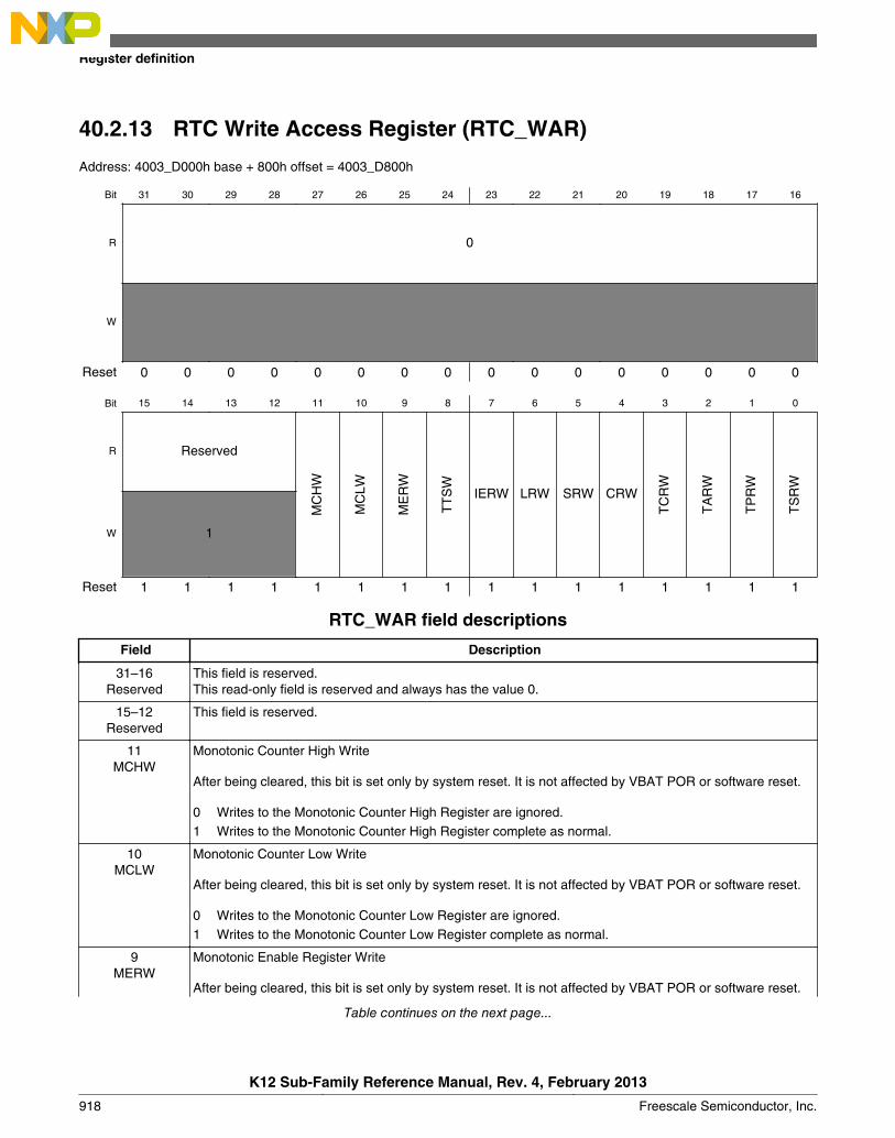
40.2.13 RTC Write Access Register (RTC_WAR)
Address: 4003_D000h base + 800h offset = 4003_D800h
Bit 31 30 29 28 27 26 25 24 23 22 21 20 19 18 17 16
R 0
W
Reset 0 0 0 0 0 0 0 0 0 0 0 0 0 0 0 0
Bit 15 14 13 12 11 10 9 8 7 6 5 4 3 2 1 0
R Reserved
MC
HW
MC
LW
ME
RW
TT
SW
IERW LRW SRW CRW
TC
RW
TA
RW
TP
RW
TS
RW
W 1
Reset 1 1 1 1 1 1 1 1 1 1 1 1 1 1 1 1
RTC_WAR field descriptions
Field Description
31–16Reserved
This field is reserved.This read-only field is reserved and always has the value 0.
15–12Reserved
This field is reserved.
11MCHW
Monotonic Counter High Write
After being cleared, this bit is set only by system reset. It is not affected by VBAT POR or software reset.
0 Writes to the Monotonic Counter High Register are ignored.1 Writes to the Monotonic Counter High Register complete as normal.
10MCLW
Monotonic Counter Low Write
After being cleared, this bit is set only by system reset. It is not affected by VBAT POR or software reset.
0 Writes to the Monotonic Counter Low Register are ignored.1 Writes to the Monotonic Counter Low Register complete as normal.
9MERW
Monotonic Enable Register Write
After being cleared, this bit is set only by system reset. It is not affected by VBAT POR or software reset.
Table continues on the next page...
Register definition
K12 Sub-Family Reference Manual, Rev. 4, February 2013
918 Freescale Semiconductor, Inc.

RTC_WAR field descriptions (continued)
Field Description
0 Writes to the Monotonic Enable Register are ignored.1 Writes to the Monotonic Enable Register complete as normal.
8TTSW
Tamper Time Seconds Write
After being cleared, this bit is set onlyby system reset. It is not affected by VBAT POR or software reset.
0 Writes to the Tamper Time Seconds Register are ignored.1 Writes to the Tamper Time Seconds Register complete as normal.
7IERW
Interrupt Enable Register Write
After being cleared, this bit is set only by system reset. It is not affected by software reset.
0 Writes to the Interupt Enable Register are ignored.1 Writes to the Interrupt Enable Register complete as normal.
6LRW
Lock Register Write
After being cleared, this bit is set only by system reset. It is not affected by software reset.
0 Writes to the Lock Register are ignored.1 Writes to the Lock Register complete as normal.
5SRW
Status Register Write
After being cleared, this bit is set only by system reset. It is not affected by software reset.
0 Writes to the Status Register are ignored.1 Writes to the Status Register complete as normal.
4CRW
Control Register Write
After being cleared, this bit is set only by system reset. It is not affected by software reset.
0 Writes to the Control Register are ignored.1 Writes to the Control Register complete as normal.
3TCRW
Time Compensation Register Write
After being cleared, this bit is set only by system reset. It is not affected by software reset.
0 Writes to the Time Compensation Register are ignored.1 Writes to the Time Compensation Register complete as normal.
2TARW
Time Alarm Register Write
After being cleared, this bit is set only by system reset. It is not affected by software reset.
0 Writes to the Time Alarm Register are ignored.1 Writes to the Time Alarm Register complete as normal.
1TPRW
Time Prescaler Register Write
After being cleared, this bit is set only by system reset. It is not affected by software reset.
0 Writes to the Time Prescaler Register are ignored.1 Writes to the Time Prescaler Register complete as normal.
Table continues on the next page...
Chapter 40 Real Time Clock (RTC)
K12 Sub-Family Reference Manual, Rev. 4, February 2013
Freescale Semiconductor, Inc. 919

RTC_WAR field descriptions (continued)
Field Description
0TSRW
Time Seconds Register Write
After being cleared, this bit is set only by system reset. It is not affected by software reset.
0 Writes to the Time Seconds Register are ignored.1 Writes to the Time Seconds Register complete as normal.
40.2.14 RTC Read Access Register (RTC_RAR)
Address: 4003_D000h base + 804h offset = 4003_D804h
Bit 31 30 29 28 27 26 25 24 23 22 21 20 19 18 17 16
R 0
W
Reset 0 0 0 0 0 0 0 0 0 0 0 0 0 0 0 0
Bit 15 14 13 12 11 10 9 8 7 6 5 4 3 2 1 0
R Reserved
MC
HR
MC
LR
ME
RR
TTSR IERR LRR SRR CRR TCRR TARR TPRR TSRR
W 1
Reset 1 1 1 1 1 1 1 1 1 1 1 1 1 1 1 1
RTC_RAR field descriptions
Field Description
31–16Reserved
This field is reserved.This read-only field is reserved and always has the value 0.
15–12Reserved
This field is reserved.
11MCHR
Monotonic Counter High Read
After being cleared, this bit is set only by system reset. It is not affected by VBAT POR or software reset.
0 Reads to the Monotonic Counter High Register are ignored.1 Reads to the Monotonic Counter High Register complete as normal.
Table continues on the next page...
Register definition
K12 Sub-Family Reference Manual, Rev. 4, February 2013
920 Freescale Semiconductor, Inc.
RTC_RAR field descriptions (continued)
Field Description
10MCLR
Monotonic Counter Low Read
After being cleared, this bit is set only by system reset. It is not affected by VBAT POR or software reset.
0 Reads to the Monotonic Counter Low Register are ignored.1 Reads to the Monotonic Counter Low Register complete as normal.
9MERR
Monotonic Enable Register Read
After being cleared, this bit is set only by system reset. It is not affected by VBAT POR or software reset.
0 Reads to the Monotonic Enable Register are ignored.1 Reads to the Monotonic Enable Register complete as normal.
8TTSR
Tamper Time Seconds Read
After being cleared, this bit is set only by system reset. It is not affected by VBAT POR or software reset.
0 Reads to the Tamper Time Seconds Register are ignored.1 Reads to the Tamper Time Seconds Register complete as normal.
7IERR
Interrupt Enable Register Read
After being cleared, this bit is set only by system reset. It is not affected by software reset.
0 Reads to the Interrupt Enable Register are ignored.1 Reads to the Interrupt Enable Register complete as normal.
6LRR
Lock Register Read
After being cleared, this bit is set only by system reset. It is not affected by software reset.
0 Reads to the Lock Register are ignored.1 Reads to the Lock Register complete as normal.
5SRR
Status Register Read
After being cleared, this bit is set only by system reset. It is not affected by software reset.
0 Reads to the Status Register are ignored.1 Reads to the Status Register complete as normal.
4CRR
Control Register Read
After being cleared, this bit is set only by system reset. It is not affected by software reset.
0 Reads to the Control Register are ignored.1 Reads to the Control Register complete as normal.
3TCRR
Time Compensation Register Read
After being cleared, this bit is set only by system reset. It is not affected by software reset.
0 Reads to the Time Compensation Register are ignored.1 Reads to the Time Compensation Register complete as normal.
2TARR
Time Alarm Register Read
After being cleared, this bit is set only by system reset. It is not affected by software reset.
Table continues on the next page...
Chapter 40 Real Time Clock (RTC)
K12 Sub-Family Reference Manual, Rev. 4, February 2013
Freescale Semiconductor, Inc. 921

RTC_RAR field descriptions (continued)
Field Description
0 Reads to the Time Alarm Register are ignored.1 Reads to the Time Alarm Register complete as normal.
1TPRR
Time Prescaler Register Read
After being cleared, this bit is set only by system reset. It is not affected by software reset.
0 Reads to the Time Pprescaler Register are ignored.1 Reads to the Time Prescaler Register complete as normal.
0TSRR
Time Seconds Register Read
After being cleared, this bit is set only by system reset. It is not affected by software reset.
0 Reads to the Time Seconds Register are ignored.1 Reads to the Time Seconds Register complete as normal.
40.3 Functional description
40.3.1 Power, clocking, and reset
The RTC is an always powered block that remains active in all low power modes.
The time counter within the RTC is clocked by a 32.768 kHz clock sourced from anexternal crystal using the oscillator.
The power-on-reset signal initializes all RTC registers to their default state. A softwarereset bit can also initialize all RTC registers.
40.3.1.1 Oscillator control
The 32.768 kHz crystal oscillator is disabled at POR and must be enabled by software.After enabling the cystal oscillator, wait the oscillator startup time before settingSR[TCE] or using the oscillator clock external to the RTC.
The crystal oscillator includes tunable capacitors that can be configured by software. Donot change the capacitance unless the oscillator is disabled.
Functional description
K12 Sub-Family Reference Manual, Rev. 4, February 2013
922 Freescale Semiconductor, Inc.

40.3.1.2 Software reset
Writing one to the CR[SWR] forces the equivalent of a POR to the rest of the RTCmodule. The CR[SWR] is not affected by the software reset and must be cleared bysoftware. The access control registers are not affected by either VBAT POR or thesoftware reset; they are reset by the chip reset.
40.3.1.3 Supervisor access
When the supervisor access control bit is clear, only supervisor mode software can writeto the RTC registers or read the RTC tamper and monotonic registers, non-supervisormode software will generate a bus error. Both supervisor and non-supervisor modesoftware can always read the other RTC registers.
40.3.2 Time counter
The time counter consists of a 32-bit seconds counter that increments once every secondand a 16-bit prescaler register that increments once every 32.768 kHz clock cycle.
The time seconds register and time prescaler register can be written only when SR[TCE]is clear. Always write to the prescaler register before writing to the seconds register,because the seconds register increments on the falling edge of bit 14 of the prescalerregister.
The time prescaler register increments provided SR[TCE] is set, SR[TIF] is clear,SR[TOF] is clear, and the 32.768 kHz clock source is present. After enabling theoscillator, wait the oscillator startup time before setting SR[TCE] to allow time for theoscillator clock output to stabilize.
If the time seconds register overflows then the SR[TOF] will set and the time prescalerregister will stop incrementing. Clear SR[TOF] by initializing the time seconds register.The time seconds register and time prescaler register read as zero whenever SR[TOF] isset.
SR[TIF] is set on VBAT POR and software reset and is cleared by initializing the timeseconds register. The time seconds register and time prescaler register read as zerowhenever SR[TIF] is set.
Chapter 40 Real Time Clock (RTC)
K12 Sub-Family Reference Manual, Rev. 4, February 2013
Freescale Semiconductor, Inc. 923
40.3.3 Compensation
The compensation logic provides an accurate and wide compensation range and cancorrect errors as high as 3906 ppm and as low as 0.12 ppm. The compensation factormust be calculated externally to the RTC and supplied by software to the compensationregister. The RTC itself does not calculate the amount of compensation that is required,although the 1 Hz clock is output to an external pin in support of external calibrationlogic.
Crystal compensation can be supported by using firmware and crystal characteristics todetermine the compensation amount. Temperature compensation can be supported byfirmware that periodically measures the external temperature via ADC and updates thecompensation register based on a look-up table that specifies the change in crystalfrequency over temperature.
The compensation logic alters the number of 32.768 kHz clock cycles it takes for theprescaler register to overflow and increment the time seconds counter. The timecompensation value is used to adjust the number of clock cycles between -127 and +128.Cycles are added or subtracted from the prescaler register when the prescaler registerequals 0x3FFF and then increments. The compensation interval is used to adjust thefrequency at which the time compensation value is used, that is, from once a second toonce every 256 seconds.
Updates to the time compensation register will not take effect until the next time the timeseconds register increments and provided the previous compensation interval has expired.When the compensation interval is set to other than once a second then the compensationis applied in the first second interval and the remaining second intervals receive nocompensation.
Compensation is disabled by configuring the time compensation register to zero.
40.3.4 Time alarm
The time alarm register, SR[TAF], and IER[TAIE] allow the RTC to generate aninterrupt at a predefined time. The 32-bit time alarm register is compared with the 32-bittime seconds register each time it increments. The SR[TAF] will set when the time alarmregister equals the time seconds register and the time seconds register increments.
The time alarm flag is cleared by writing the time alarm register. This will usually be thenext alarm value, although writing a value that is less than the time seconds register, suchas zero, will prevent the time alarm flag from setting again. The time alarm flag cannototherwise be disabled, although the interrupt it generates is enabled or disabled byIER[TAIE].
Functional description
K12 Sub-Family Reference Manual, Rev. 4, February 2013
924 Freescale Semiconductor, Inc.
40.3.5 Update mode
The Update Mode bit in the Control register (CR[UM]) configures software write accessto the Time Counter Enable (SR[TCE]) bit. When CR[UM] is clear, SR[TCE] can bewritten only when the LR[SRL] bit is set. When CR[UM] is set, the SR[TCE] can also bewritten when SR[TCE] is clear or when SR[TIF] or SR[TOF] are set. This allows thetime seconds and prescaler registers to be initialized whenever time is invalidated, whilepreventing the time seconds and prescaler registers from being changed on the fly. WhenLR[SRL] is set, CR[UM] has no effect on SR[TCE].
CR[UM] also configures software write access to the Monotonic Counter Enable(MER[MCE]) bit. When CR[UM] is clear, MER[MCE] can be written only whenLR[MEL] is set. When CR[UM] is set, MER[MCE] can also be written whenMER[MCE] is clear or when SR[TIF] or SR[MOF] are set. This allows the monotoniccounter register to be initialized whenever the monotonic counter is invalid, whilepreventing the monotonic counter from being changed on the fly. When LR[MEL] is set,CR[UM] has no effect on MCR[MCE].
40.3.6 Monotonic counter
The 64-bit Monotonic Counter is a counter that cannot be exhausted or return to anyprevious value, once it has been initialized. If the monotonic overflow flag is set, themonotonic counter returns zero and does not increment.
Depending on the value of the monotonic counter enable bit, writing to the monotoniccounter either initializes the register with the value written, or increments the register byone (and the value written is ignored).
When the monotonic counter is enabled, the monotonic counter high increments on eithera write to the monotonic counter high register or if the monotonic counter low registeroverflows (due to a write to the monotonic counter low register). The monotonicoverflow flag sets when the monotonic counter high register overflows and is cleared bywriting the monotonic counter high register when the monotonic counter is disabled.
The monotonic counter is held in reset whenever the time invalid flag is set. Always clearthe time invalid flag before initializing the monotonic counter.
Chapter 40 Real Time Clock (RTC)
K12 Sub-Family Reference Manual, Rev. 4, February 2013
Freescale Semiconductor, Inc. 925
40.3.7 Register lock
The lock register can be used to block write accesses to certain registers until the nextPOR or software reset. Locking the control register will disable the software reset.Locking the lock register will block future updates to the lock register.
Write accesses to a locked register are ignored and do not generate a bus error.
40.3.8 Access control
The read access and write access registers are implemented in the chip power domain andreset on the chip reset. They are not affected by the POR or the software reset. They areused to block read or write accesses to each register until the next chip system reset.
40.3.9 Interrupt
The RTC interrupt is asserted whenever a status flag and the corresponding interruptenable bit are both set. It is always asserted on POR, and software reset. The RTCinterrupt is enabled at the chip level by enabling the chip-specific RTC clock gate controlbit. The RTC interrupt can be used to wakeup the chip from any low-power mode.
The optional RTC seconds interrupt is an edge-sensitive interrupt with a dedicatedinterrupt vector that is generated once a second and requires no software overhead (thereis no corresponding status flag to clear). It is enabled in the RTC by the time secondsinterrupt enable bit and enabled at the chip level by setting the chip-specific RTC clockgate control bit. This interrupt is optional and may not be implemented on all devices.
Functional description
K12 Sub-Family Reference Manual, Rev. 4, February 2013
926 Freescale Semiconductor, Inc.
Chapter 41Serial Peripheral Interface (SPI)
41.1 IntroductionNOTE
For the chip-specific implementation details of this module'sinstances see the chip configuration information.
The serial peripheral interface (SPI) module provides a synchronous serial bus forcommunication between an MCU and an external peripheral device.
41.1.1 Block Diagram
The block diagram of this module is as follows:
K12 Sub-Family Reference Manual, Rev. 4, February 2013
Freescale Semiconductor, Inc. 927
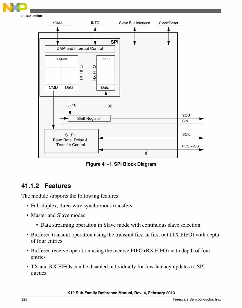
Baud Rate, Delay & Transfer Control
Shift Register
SPI
SCKS PI
16
Data Data
TX
FIF
O
Slave Bus Interface Clock/Reset
POPR
eDMA INTC
DMA and Interrupt Control
PUSHR
RX
FIF
O
CMD
32
8
PCS[x]/SS
SIN SOUT
Figure 41-1. SPI Block Diagram
41.1.2 Features
The module supports the following features:
• Full-duplex, three-wire synchronous transfers
• Master and Slave modes
• Data streaming operation in Slave mode with continuous slave selection
• Buffered transmit operation using the transmit first in first out (TX FIFO) with depthof four entries
• Buffered receive operation using the receive FIFO (RX FIFO) with depth of fourentries
• TX and RX FIFOs can be disabled individually for low-latency updates to SPIqueues
Introduction
K12 Sub-Family Reference Manual, Rev. 4, February 2013
928 Freescale Semiconductor, Inc.
• Visibility into TX and RX FIFOs for ease of debugging
• Programmable transfer attributes on a per-frame basis:
• two transfer attribute registers
• Serial clock (SCK) with programmable polarity and phase
• Various programmable delays
• Programmable serial frame size of 4–16 bits, expandable by software control
• SPI frames longer than 16 bits can be supported using the continuousselection format
• Continuously held chip select capability
• 5 peripheral chip selects (PCSs), expandable to 32 with external demultiplexer
• Deglitching support for up to 16 PCS with external demultiplexer
• DMA support for adding entries to TX FIFO and removing entries from RX FIFO:
• TX FIFO is not full (TFFF)
• RX FIFO is not empty (RFDF)
• Interrupt conditions:
• End of Queue reached (EOQF)
• TX FIFO is not full (TFFF)
• Transfer of current frame complete (TCF)
• Attempt to transmit with an empty Transmit FIFO (TFUF)
• RX FIFO is not empty (RFDF)
• Frame received while Receive FIFO is full (RFOF)
• Global interrupt request line
• Modified SPI transfer formats for communication with slower peripheral devices
• Power-saving architectural features:
• Support for Stop mode
• Support for Doze mode
Chapter 41 Serial Peripheral Interface (SPI)
K12 Sub-Family Reference Manual, Rev. 4, February 2013
Freescale Semiconductor, Inc. 929
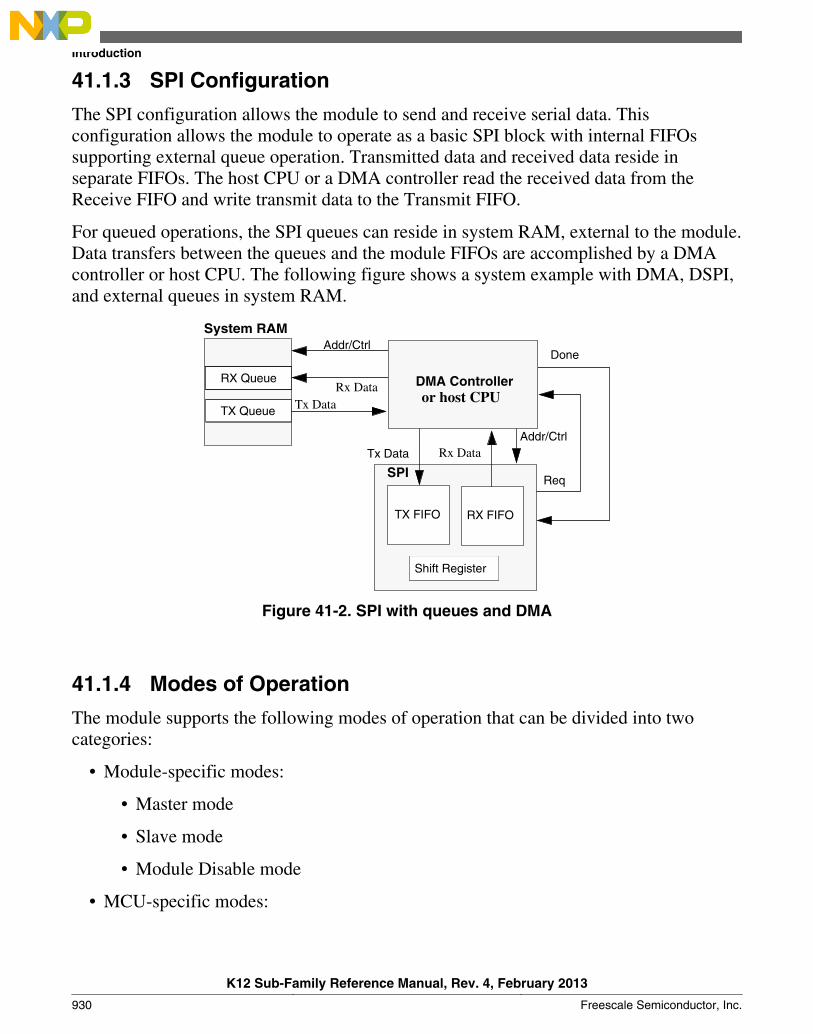
41.1.3 SPI Configuration
The SPI configuration allows the module to send and receive serial data. Thisconfiguration allows the module to operate as a basic SPI block with internal FIFOssupporting external queue operation. Transmitted data and received data reside inseparate FIFOs. The host CPU or a DMA controller read the received data from theReceive FIFO and write transmit data to the Transmit FIFO.
For queued operations, the SPI queues can reside in system RAM, external to the module.Data transfers between the queues and the module FIFOs are accomplished by a DMAcontroller or host CPU. The following figure shows a system example with DMA, DSPI,and external queues in system RAM.
System RAM
SPI
DMA Controller
TX Queue
RX FIFOTX FIFO
Shift Register
Addr/Ctrl
RX Queue
Addr/Ctrl
Req
Done
Tx Data
Rx Data
Rx Data
Tx Data or host CPU
Figure 41-2. SPI with queues and DMA
41.1.4 Modes of Operation
The module supports the following modes of operation that can be divided into twocategories:
• Module-specific modes:
• Master mode
• Slave mode
• Module Disable mode
• MCU-specific modes:
Introduction
K12 Sub-Family Reference Manual, Rev. 4, February 2013
930 Freescale Semiconductor, Inc.
• External Stop mode
• Debug mode
The module enters module-specific modes when the host writes a module register. TheMCU-specific modes are controlled by signals external to the module. The MCU-specificmodes are modes that an MCU may enter in parallel to the block-specific modes.
41.1.4.1 Master Mode
Master mode allows the module to initiate and control serial communication. In thismode, the SCK signal, SOUT signal, and the PCS[x] signals are controlled by the moduleand configured as outputs.
41.1.4.2 Slave Mode
Slave mode allows the module to communicate with SPI bus masters. In this mode, themodule responds to externally controlled serial transfers. The SCK signal and thePCS[0]/SS signals are configured as inputs and driven by an SPI bus master.
41.1.4.3 Module Disable Mode
The Module Disable mode can be used for MCU power management. The clock to thenon-memory mapped logic in the module can be stopped while in the Module Disablemode.
41.1.4.4 External Stop Mode
External Stop mode is used for MCU power management. The module supports thePeripheral Bus Stop mode mechanism. When a request is made to enter External Stopmode, it acknowledges the request and completes the transfer that is in progress. Whenthe module reaches the frame boundary, it signals that the system clock to the modulemay be shut off.
41.1.4.5 Debug ModeDebug mode is used for system development and debugging. The MCR[FRZ] bit controlsmodule behavior in the Debug mode:
Chapter 41 Serial Peripheral Interface (SPI)
K12 Sub-Family Reference Manual, Rev. 4, February 2013
Freescale Semiconductor, Inc. 931
• If the bit is set, the module stops all serial transfers, when the MCU is in debugmode.
• If the bit is cleared, the MCU debug mode has no effect on the module.
41.2 Module signal descriptionsThis section provides description of the module signals.
The following table lists the signals that may connect off chip depending on deviceimplementation.
Table 41-1. Module signal descriptions
Signal Master Mode Slave Mode Port Direction
PCS0/SS Peripheral Chip Select 0 output Slave Select input I/O
PCS[3:1] Peripheral Chip Select 1 – 3 Unused O
PCS4 Peripheral Chip Select 4 Unused O
SIN Serial Data In Serial Data In I
SOUT Serial Data Out Serial Data Out O
SCK Master mode: Serial Clock (output) Serial Clock (input) I/O
41.2.1 PCS0/SS — Peripheral Chip Select/Slave Select
In Master mode, the PCS0 signal is an output that selects which slave device the currenttransmission is intended for.
In Slave mode, the active low SS signal is an input signal that allows an SPI master toselect the module as the target for transmission.
41.2.2 PCS1 – PCS3 — Peripheral Chip Selects 1 – 3
PCS1 – PCS3 are output signals in Master mode.
In Slave mode, these signals are unused.
41.2.3 PCS4 — Peripheral Chip Select 4
In Master mode, PCS4 is an output signal.
Module signal descriptions
K12 Sub-Family Reference Manual, Rev. 4, February 2013
932 Freescale Semiconductor, Inc.

In Slave mode, this signal is unused.
41.2.4 SIN — Serial Input
SIN is a serial data input signal.
41.2.5 SOUT — Serial Output
SOUT is a serial data output signal.
41.2.6 SCK — Serial Clock
SCK is a serial communication clock signal.
In Master mode, the module generates the SCK.
In Slave mode, SCK is an input from an external bus master.
41.3 Memory Map/Register DefinitionRegister accesses to memory addresses that are reserved or undefined result in a transfererror. Write access to the POPR also results in a transfer error.
SPI memory map
Absoluteaddress
(hex)Register name
Width(in bits)
Access Reset valueSection/
page
4002_C000 Module Configuration Register (SPI0_MCR) 32 R/W 0000_4001h 41.3.1/936
4002_C008 Transfer Count Register (SPI0_TCR) 32 R/W 0000_0000h 41.3.2/939
4002_C00CClock and Transfer Attributes Register (In Master Mode)(SPI0_CTAR0)
32 R/W 7800_0000h 41.3.3/939
4002_C00CClock and Transfer Attributes Register (In Slave Mode)(SPI0_CTAR0_SLAVE)
32 R/W 7800_0000h 41.3.4/944
4002_C010Clock and Transfer Attributes Register (In Master Mode)(SPI0_CTAR1)
32 R/W 7800_0000h 41.3.3/939
4002_C02C DSPI Status Register (SPI0_SR) 32 R/W 0200_0000h 41.3.5/946
4002_C030DMA/Interrupt Request Select and Enable Register(SPI0_RSER)
32 R/W 0000_0000h 41.3.6/949
4002_C034 PUSH TX FIFO Register In Master Mode (SPI0_PUSHR) 32 R/W 0000_0000h 41.3.7/951
Table continues on the next page...
Chapter 41 Serial Peripheral Interface (SPI)
K12 Sub-Family Reference Manual, Rev. 4, February 2013
Freescale Semiconductor, Inc. 933

SPI memory map (continued)
Absoluteaddress
(hex)Register name
Width(in bits)
Access Reset valueSection/
page
4002_C034PUSH TX FIFO Register In Slave Mode(SPI0_PUSHR_SLAVE)
32 R/W 0000_0000h 41.3.8/953
4002_C038 POP RX FIFO Register (SPI0_POPR) 32 R 0000_0000h 41.3.9/953
4002_C03C DSPI Transmit FIFO Registers (SPI0_TXFR0) 32 R 0000_0000h41.3.10/
954
4002_C040 DSPI Transmit FIFO Registers (SPI0_TXFR1) 32 R 0000_0000h41.3.10/
954
4002_C044 DSPI Transmit FIFO Registers (SPI0_TXFR2) 32 R 0000_0000h41.3.10/
954
4002_C048 DSPI Transmit FIFO Registers (SPI0_TXFR3) 32 R 0000_0000h41.3.10/
954
4002_C07C DSPI Receive FIFO Registers (SPI0_RXFR0) 32 R 0000_0000h41.3.11/
954
4002_C080 DSPI Receive FIFO Registers (SPI0_RXFR1) 32 R 0000_0000h41.3.11/
954
4002_C084 DSPI Receive FIFO Registers (SPI0_RXFR2) 32 R 0000_0000h41.3.11/
954
4002_C088 DSPI Receive FIFO Registers (SPI0_RXFR3) 32 R 0000_0000h41.3.11/
954
4002_D000 Module Configuration Register (SPI1_MCR) 32 R/W 0000_4001h 41.3.1/936
4002_D008 Transfer Count Register (SPI1_TCR) 32 R/W 0000_0000h 41.3.2/939
4002_D00CClock and Transfer Attributes Register (In Master Mode)(SPI1_CTAR0)
32 R/W 7800_0000h 41.3.3/939
4002_D00CClock and Transfer Attributes Register (In Slave Mode)(SPI1_CTAR0_SLAVE)
32 R/W 7800_0000h 41.3.4/944
4002_D010Clock and Transfer Attributes Register (In Master Mode)(SPI1_CTAR1)
32 R/W 7800_0000h 41.3.3/939
4002_D02C DSPI Status Register (SPI1_SR) 32 R/W 0200_0000h 41.3.5/946
4002_D030DMA/Interrupt Request Select and Enable Register(SPI1_RSER)
32 R/W 0000_0000h 41.3.6/949
4002_D034 PUSH TX FIFO Register In Master Mode (SPI1_PUSHR) 32 R/W 0000_0000h 41.3.7/951
4002_D034PUSH TX FIFO Register In Slave Mode(SPI1_PUSHR_SLAVE)
32 R/W 0000_0000h 41.3.8/953
4002_D038 POP RX FIFO Register (SPI1_POPR) 32 R 0000_0000h 41.3.9/953
4002_D03C DSPI Transmit FIFO Registers (SPI1_TXFR0) 32 R 0000_0000h41.3.10/
954
4002_D040 DSPI Transmit FIFO Registers (SPI1_TXFR1) 32 R 0000_0000h41.3.10/
954
4002_D044 DSPI Transmit FIFO Registers (SPI1_TXFR2) 32 R 0000_0000h41.3.10/
954
4002_D048 DSPI Transmit FIFO Registers (SPI1_TXFR3) 32 R 0000_0000h41.3.10/
954
Table continues on the next page...
Memory Map/Register Definition
K12 Sub-Family Reference Manual, Rev. 4, February 2013
934 Freescale Semiconductor, Inc.
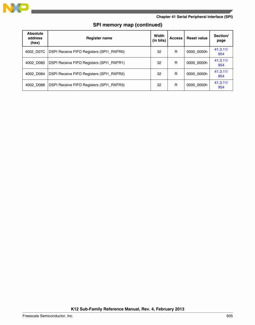
SPI memory map (continued)
Absoluteaddress
(hex)Register name
Width(in bits)
Access Reset valueSection/
page
4002_D07C DSPI Receive FIFO Registers (SPI1_RXFR0) 32 R 0000_0000h41.3.11/
954
4002_D080 DSPI Receive FIFO Registers (SPI1_RXFR1) 32 R 0000_0000h41.3.11/
954
4002_D084 DSPI Receive FIFO Registers (SPI1_RXFR2) 32 R 0000_0000h41.3.11/
954
4002_D088 DSPI Receive FIFO Registers (SPI1_RXFR3) 32 R 0000_0000h41.3.11/
954
Chapter 41 Serial Peripheral Interface (SPI)
K12 Sub-Family Reference Manual, Rev. 4, February 2013
Freescale Semiconductor, Inc. 935
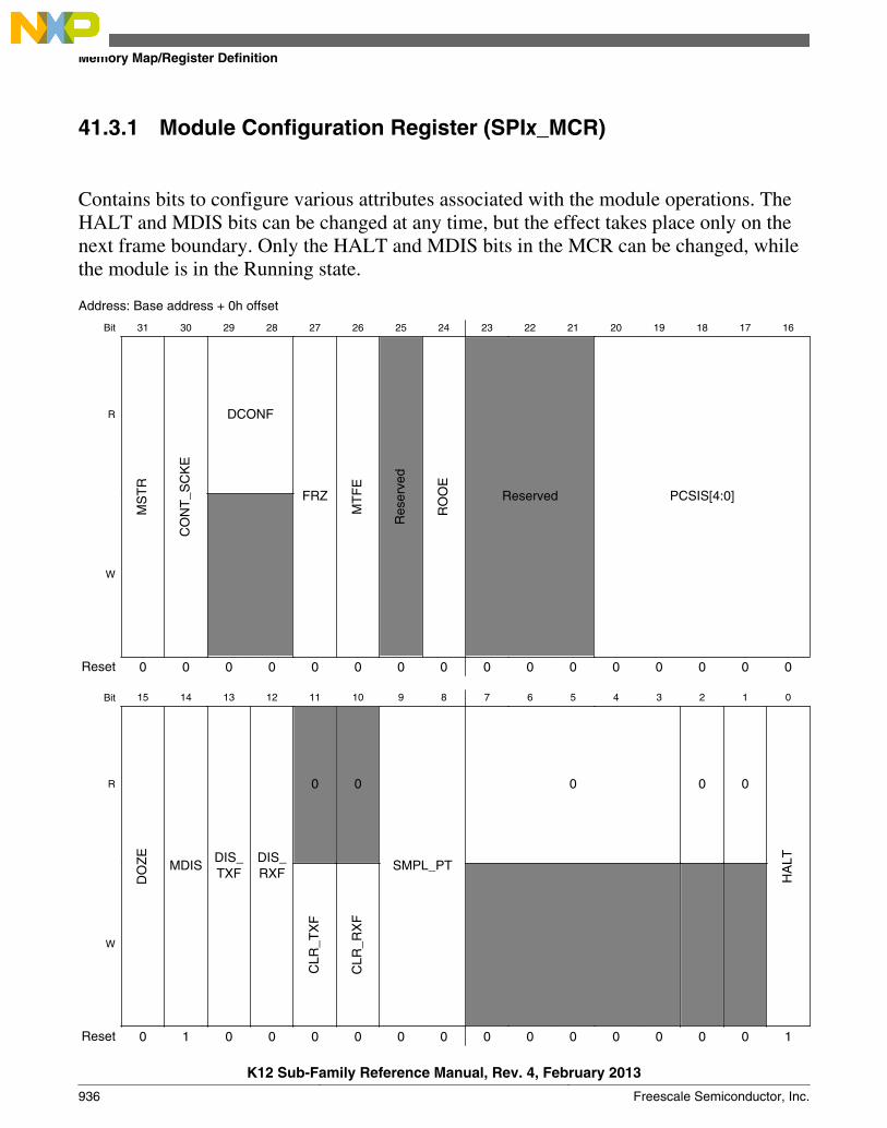
41.3.1 Module Configuration Register (SPIx_MCR)
Contains bits to configure various attributes associated with the module operations. TheHALT and MDIS bits can be changed at any time, but the effect takes place only on thenext frame boundary. Only the HALT and MDIS bits in the MCR can be changed, whilethe module is in the Running state.
Address: Base address + 0h offset
Bit 31 30 29 28 27 26 25 24 23 22 21 20 19 18 17 16
R
MS
TR
CO
NT
_SC
KE
DCONF
FRZ
MT
FE
Res
erve
d
RO
OE
Reserved PCSIS[4:0]
W
Reset 0 0 0 0 0 0 0 0 0 0 0 0 0 0 0 0
Bit 15 14 13 12 11 10 9 8 7 6 5 4 3 2 1 0
R
DO
ZE
MDISDIS_TXF
DIS_RXF
0 0
SMPL_PT
0 0 0H
ALT
W
CLR
_TX
F
CLR
_RX
F
Reset 0 1 0 0 0 0 0 0 0 0 0 0 0 0 0 1
Memory Map/Register Definition
K12 Sub-Family Reference Manual, Rev. 4, February 2013
936 Freescale Semiconductor, Inc.
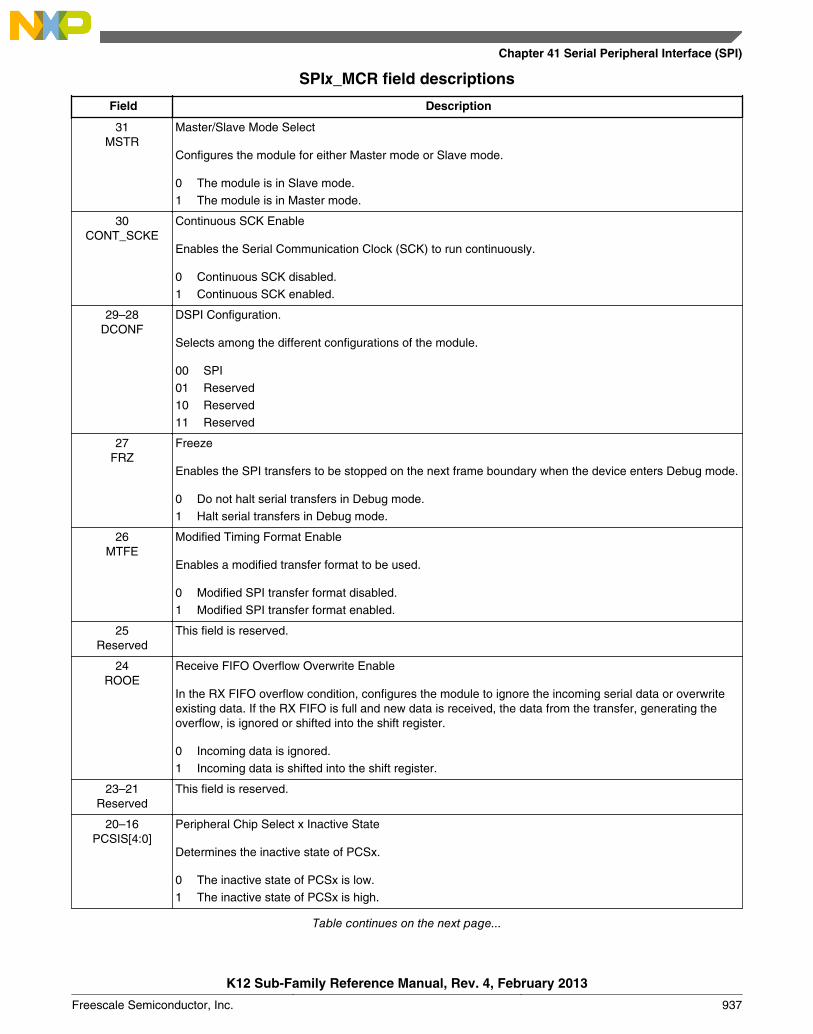
SPIx_MCR field descriptions
Field Description
31MSTR
Master/Slave Mode Select
Configures the module for either Master mode or Slave mode.
0 The module is in Slave mode.1 The module is in Master mode.
30CONT_SCKE
Continuous SCK Enable
Enables the Serial Communication Clock (SCK) to run continuously.
0 Continuous SCK disabled.1 Continuous SCK enabled.
29–28DCONF
DSPI Configuration.
Selects among the different configurations of the module.
00 SPI01 Reserved10 Reserved11 Reserved
27FRZ
Freeze
Enables the SPI transfers to be stopped on the next frame boundary when the device enters Debug mode.
0 Do not halt serial transfers in Debug mode.1 Halt serial transfers in Debug mode.
26MTFE
Modified Timing Format Enable
Enables a modified transfer format to be used.
0 Modified SPI transfer format disabled.1 Modified SPI transfer format enabled.
25Reserved
This field is reserved.
24ROOE
Receive FIFO Overflow Overwrite Enable
In the RX FIFO overflow condition, configures the module to ignore the incoming serial data or overwriteexisting data. If the RX FIFO is full and new data is received, the data from the transfer, generating theoverflow, is ignored or shifted into the shift register.
0 Incoming data is ignored.1 Incoming data is shifted into the shift register.
23–21Reserved
This field is reserved.
20–16PCSIS[4:0]
Peripheral Chip Select x Inactive State
Determines the inactive state of PCSx.
0 The inactive state of PCSx is low.1 The inactive state of PCSx is high.
Table continues on the next page...
Chapter 41 Serial Peripheral Interface (SPI)
K12 Sub-Family Reference Manual, Rev. 4, February 2013
Freescale Semiconductor, Inc. 937
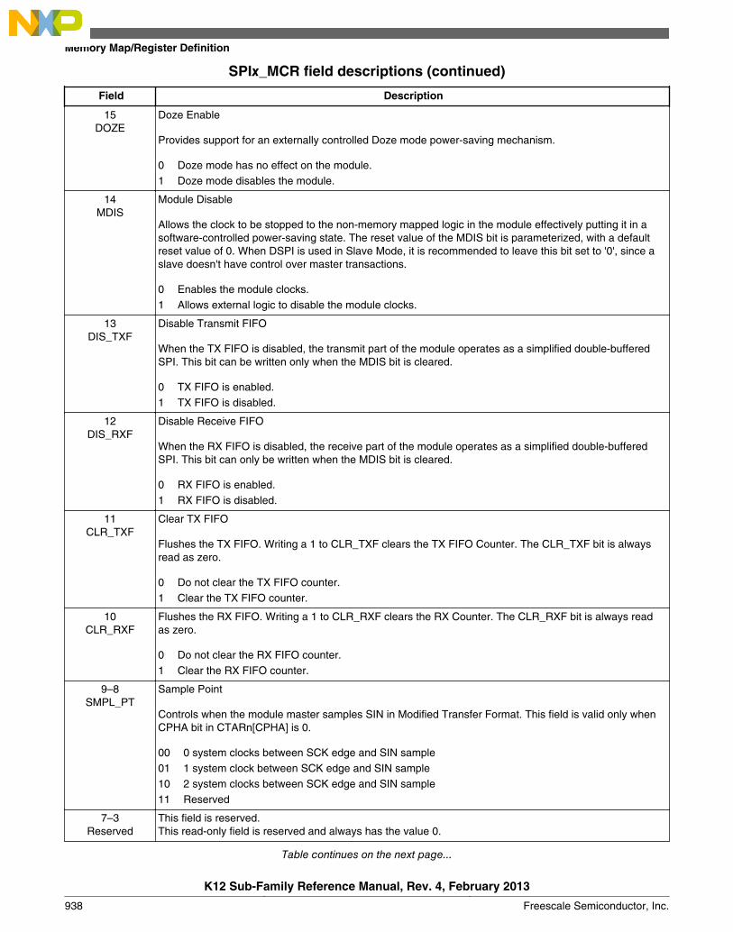
SPIx_MCR field descriptions (continued)
Field Description
15DOZE
Doze Enable
Provides support for an externally controlled Doze mode power-saving mechanism.
0 Doze mode has no effect on the module.1 Doze mode disables the module.
14MDIS
Module Disable
Allows the clock to be stopped to the non-memory mapped logic in the module effectively putting it in asoftware-controlled power-saving state. The reset value of the MDIS bit is parameterized, with a defaultreset value of 0. When DSPI is used in Slave Mode, it is recommended to leave this bit set to '0', since aslave doesn't have control over master transactions.
0 Enables the module clocks.1 Allows external logic to disable the module clocks.
13DIS_TXF
Disable Transmit FIFO
When the TX FIFO is disabled, the transmit part of the module operates as a simplified double-bufferedSPI. This bit can be written only when the MDIS bit is cleared.
0 TX FIFO is enabled.1 TX FIFO is disabled.
12DIS_RXF
Disable Receive FIFO
When the RX FIFO is disabled, the receive part of the module operates as a simplified double-bufferedSPI. This bit can only be written when the MDIS bit is cleared.
0 RX FIFO is enabled.1 RX FIFO is disabled.
11CLR_TXF
Clear TX FIFO
Flushes the TX FIFO. Writing a 1 to CLR_TXF clears the TX FIFO Counter. The CLR_TXF bit is alwaysread as zero.
0 Do not clear the TX FIFO counter.1 Clear the TX FIFO counter.
10CLR_RXF
Flushes the RX FIFO. Writing a 1 to CLR_RXF clears the RX Counter. The CLR_RXF bit is always readas zero.
0 Do not clear the RX FIFO counter.1 Clear the RX FIFO counter.
9–8SMPL_PT
Sample Point
Controls when the module master samples SIN in Modified Transfer Format. This field is valid only whenCPHA bit in CTARn[CPHA] is 0.
00 0 system clocks between SCK edge and SIN sample01 1 system clock between SCK edge and SIN sample10 2 system clocks between SCK edge and SIN sample11 Reserved
7–3Reserved
This field is reserved.This read-only field is reserved and always has the value 0.
Table continues on the next page...
Memory Map/Register Definition
K12 Sub-Family Reference Manual, Rev. 4, February 2013
938 Freescale Semiconductor, Inc.
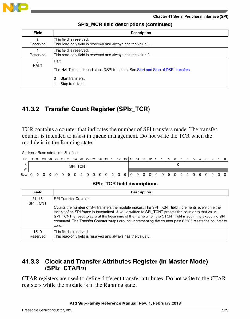
SPIx_MCR field descriptions (continued)
Field Description
2Reserved
This field is reserved.This read-only field is reserved and always has the value 0.
1Reserved
This field is reserved.This read-only field is reserved and always has the value 0.
0HALT
Halt
The HALT bit starts and stops DSPI transfers. See Start and Stop of DSPI transfers
0 Start transfers.1 Stop transfers.
41.3.2 Transfer Count Register (SPIx_TCR)
TCR contains a counter that indicates the number of SPI transfers made. The transfercounter is intended to assist in queue management. Do not write the TCR when themodule is in the Running state.
Address: Base address + 8h offset
Bit 31 30 29 28 27 26 25 24 23 22 21 20 19 18 17 16 15 14 13 12 11 10 9 8 7 6 5 4 3 2 1 0
R SPI_TCNT 0W
Reset 0 0 0 0 0 0 0 0 0 0 0 0 0 0 0 0 0 0 0 0 0 0 0 0 0 0 0 0 0 0 0 0
SPIx_TCR field descriptions
Field Description
31–16SPI_TCNT
SPI Transfer Counter
Counts the number of SPI transfers the module makes. The SPI_TCNT field increments every time thelast bit of an SPI frame is transmitted. A value written to SPI_TCNT presets the counter to that value.SPI_TCNT is reset to zero at the beginning of the frame when the CTCNT field is set in the executing SPIcommand. The Transfer Counter wraps around; incrementing the counter past 65535 resets the counter tozero.
15–0Reserved
This field is reserved.This read-only field is reserved and always has the value 0.
41.3.3 Clock and Transfer Attributes Register (In Master Mode)(SPIx_CTARn)
CTAR registers are used to define different transfer attributes. Do not write to the CTARregisters while the module is in the Running state.
Chapter 41 Serial Peripheral Interface (SPI)
K12 Sub-Family Reference Manual, Rev. 4, February 2013
Freescale Semiconductor, Inc. 939

In Master mode, the CTAR registers define combinations of transfer attributes such asframe size, clock phase and polarity, data bit ordering, baud rate, and various delays. Inslave mode, a subset of the bitfields in CTAR0 are used to set the slave transfer attributes.
When the module is configured as an SPI master, the CTAS field in the command portionof the TX FIFO entry selects which of the CTAR registers is used. When the module isconfigured as an SPI bus slave, the CTAR0 register is used.
Address: Base address + Ch offset + (4d × i), where i=0d to 1d
Bit 31 30 29 28 27 26 25 24 23 22 21 20 19 18 17 16
R
DBR FMSZ
CP
OL
CP
HA
LSB
FE
PCSSCK PASC PDT PBRW
Reset 0 1 1 1 1 0 0 0 0 0 0 0 0 0 0 0
Bit 15 14 13 12 11 10 9 8 7 6 5 4 3 2 1 0
R
CSSCK ASC DT BRW
Reset 0 0 0 0 0 0 0 0 0 0 0 0 0 0 0 0
SPIx_CTARn field descriptions
Field Description
31DBR
Double Baud Rate
Doubles the effective baud rate of the Serial Communications Clock (SCK). This field is used only inmaster mode. It effectively halves the Baud Rate division ratio, supporting faster frequencies, and odddivision ratios for the Serial Communications Clock (SCK). When the DBR bit is set, the duty cycle of theSerial Communications Clock (SCK) depends on the value in the Baud Rate Prescaler and the ClockPhase bit as listed in the following table. See the BR field description for details on how to compute thebaud rate.
Table 41-40. SPI SCK Duty Cycle
DBR CPHA PBR SCK Duty Cycle
0 any any 50/50
1 0 00 50/50
1 0 01 33/66
1 0 10 40/60
1 0 11 43/57
1 1 00 50/50
1 1 01 66/33
1 1 10 60/40
1 1 11 57/43
Table continues on the next page...
Memory Map/Register Definition
K12 Sub-Family Reference Manual, Rev. 4, February 2013
940 Freescale Semiconductor, Inc.
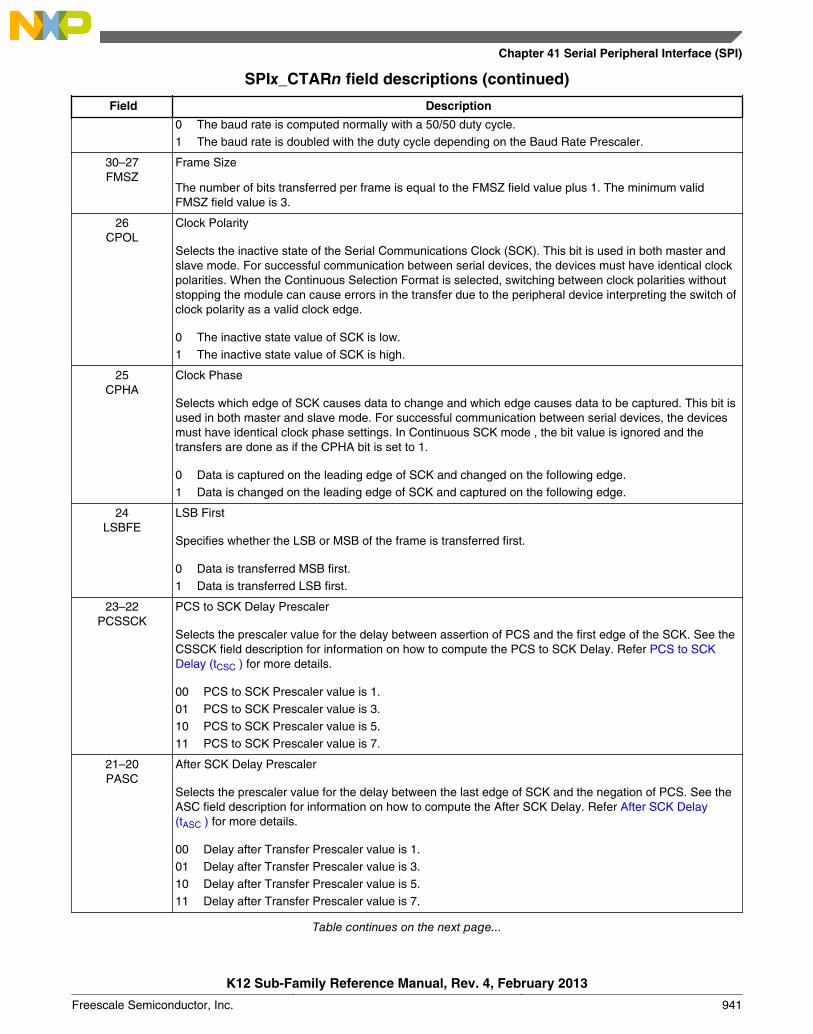
SPIx_CTARn field descriptions (continued)
Field Description
0 The baud rate is computed normally with a 50/50 duty cycle.1 The baud rate is doubled with the duty cycle depending on the Baud Rate Prescaler.
30–27FMSZ
Frame Size
The number of bits transferred per frame is equal to the FMSZ field value plus 1. The minimum validFMSZ field value is 3.
26CPOL
Clock Polarity
Selects the inactive state of the Serial Communications Clock (SCK). This bit is used in both master andslave mode. For successful communication between serial devices, the devices must have identical clockpolarities. When the Continuous Selection Format is selected, switching between clock polarities withoutstopping the module can cause errors in the transfer due to the peripheral device interpreting the switch ofclock polarity as a valid clock edge.
0 The inactive state value of SCK is low.1 The inactive state value of SCK is high.
25CPHA
Clock Phase
Selects which edge of SCK causes data to change and which edge causes data to be captured. This bit isused in both master and slave mode. For successful communication between serial devices, the devicesmust have identical clock phase settings. In Continuous SCK mode , the bit value is ignored and thetransfers are done as if the CPHA bit is set to 1.
0 Data is captured on the leading edge of SCK and changed on the following edge.1 Data is changed on the leading edge of SCK and captured on the following edge.
24LSBFE
LSB First
Specifies whether the LSB or MSB of the frame is transferred first.
0 Data is transferred MSB first.1 Data is transferred LSB first.
23–22PCSSCK
PCS to SCK Delay Prescaler
Selects the prescaler value for the delay between assertion of PCS and the first edge of the SCK. See theCSSCK field description for information on how to compute the PCS to SCK Delay. Refer PCS to SCKDelay (tCSC ) for more details.
00 PCS to SCK Prescaler value is 1.01 PCS to SCK Prescaler value is 3.10 PCS to SCK Prescaler value is 5.11 PCS to SCK Prescaler value is 7.
21–20PASC
After SCK Delay Prescaler
Selects the prescaler value for the delay between the last edge of SCK and the negation of PCS. See theASC field description for information on how to compute the After SCK Delay. Refer After SCK Delay(tASC ) for more details.
00 Delay after Transfer Prescaler value is 1.01 Delay after Transfer Prescaler value is 3.10 Delay after Transfer Prescaler value is 5.11 Delay after Transfer Prescaler value is 7.
Table continues on the next page...
Chapter 41 Serial Peripheral Interface (SPI)
K12 Sub-Family Reference Manual, Rev. 4, February 2013
Freescale Semiconductor, Inc. 941
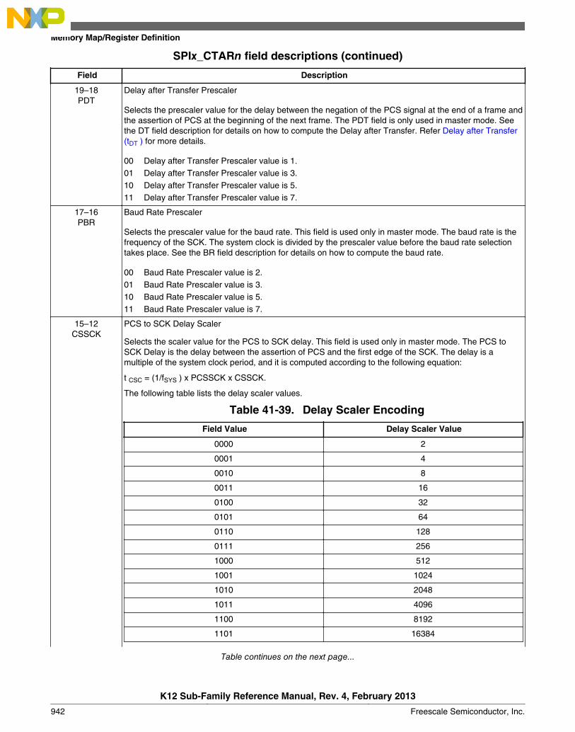
SPIx_CTARn field descriptions (continued)
Field Description
19–18PDT
Delay after Transfer Prescaler
Selects the prescaler value for the delay between the negation of the PCS signal at the end of a frame andthe assertion of PCS at the beginning of the next frame. The PDT field is only used in master mode. Seethe DT field description for details on how to compute the Delay after Transfer. Refer Delay after Transfer(tDT ) for more details.
00 Delay after Transfer Prescaler value is 1.01 Delay after Transfer Prescaler value is 3.10 Delay after Transfer Prescaler value is 5.11 Delay after Transfer Prescaler value is 7.
17–16PBR
Baud Rate Prescaler
Selects the prescaler value for the baud rate. This field is used only in master mode. The baud rate is thefrequency of the SCK. The system clock is divided by the prescaler value before the baud rate selectiontakes place. See the BR field description for details on how to compute the baud rate.
00 Baud Rate Prescaler value is 2.01 Baud Rate Prescaler value is 3.10 Baud Rate Prescaler value is 5.11 Baud Rate Prescaler value is 7.
15–12CSSCK
PCS to SCK Delay Scaler
Selects the scaler value for the PCS to SCK delay. This field is used only in master mode. The PCS toSCK Delay is the delay between the assertion of PCS and the first edge of the SCK. The delay is amultiple of the system clock period, and it is computed according to the following equation:
t CSC = (1/fSYS ) x PCSSCK x CSSCK.
The following table lists the delay scaler values.
Table 41-39. Delay Scaler Encoding
Field Value Delay Scaler Value
0000 2
0001 4
0010 8
0011 16
0100 32
0101 64
0110 128
0111 256
1000 512
1001 1024
1010 2048
1011 4096
1100 8192
1101 16384
Table continues on the next page...
Memory Map/Register Definition
K12 Sub-Family Reference Manual, Rev. 4, February 2013
942 Freescale Semiconductor, Inc.
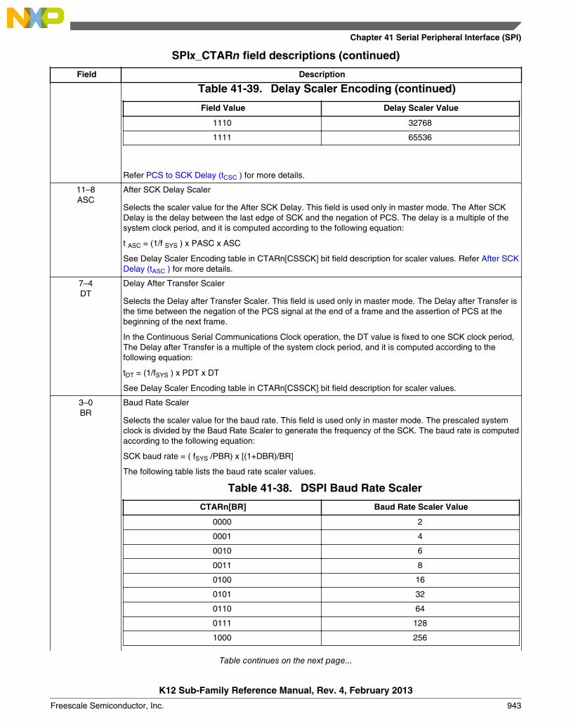
SPIx_CTARn field descriptions (continued)
Field Description
Table 41-39. Delay Scaler Encoding (continued)
Field Value Delay Scaler Value
1110 32768
1111 65536
Refer PCS to SCK Delay (tCSC ) for more details.
11–8ASC
After SCK Delay Scaler
Selects the scaler value for the After SCK Delay. This field is used only in master mode. The After SCKDelay is the delay between the last edge of SCK and the negation of PCS. The delay is a multiple of thesystem clock period, and it is computed according to the following equation:
t ASC = (1/f SYS ) x PASC x ASC
See Delay Scaler Encoding table in CTARn[CSSCK] bit field description for scaler values. Refer After SCKDelay (tASC ) for more details.
7–4DT
Delay After Transfer Scaler
Selects the Delay after Transfer Scaler. This field is used only in master mode. The Delay after Transfer isthe time between the negation of the PCS signal at the end of a frame and the assertion of PCS at thebeginning of the next frame.
In the Continuous Serial Communications Clock operation, the DT value is fixed to one SCK clock period,The Delay after Transfer is a multiple of the system clock period, and it is computed according to thefollowing equation:
tDT = (1/fSYS ) x PDT x DT
See Delay Scaler Encoding table in CTARn[CSSCK] bit field description for scaler values.
3–0BR
Baud Rate Scaler
Selects the scaler value for the baud rate. This field is used only in master mode. The prescaled systemclock is divided by the Baud Rate Scaler to generate the frequency of the SCK. The baud rate is computedaccording to the following equation:
SCK baud rate = ( fSYS /PBR) x [(1+DBR)/BR]
The following table lists the baud rate scaler values.
Table 41-38. DSPI Baud Rate Scaler
CTARn[BR] Baud Rate Scaler Value
0000 2
0001 4
0010 6
0011 8
0100 16
0101 32
0110 64
0111 128
1000 256
Table continues on the next page...
Chapter 41 Serial Peripheral Interface (SPI)
K12 Sub-Family Reference Manual, Rev. 4, February 2013
Freescale Semiconductor, Inc. 943
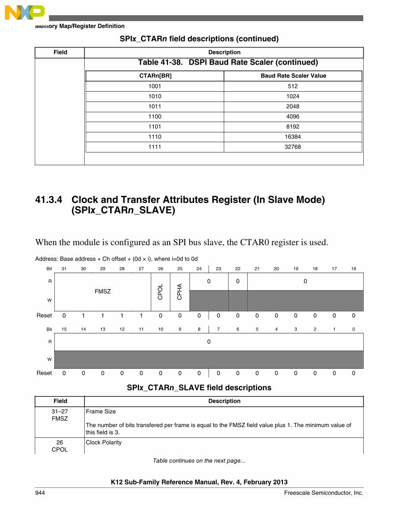
SPIx_CTARn field descriptions (continued)
Field Description
Table 41-38. DSPI Baud Rate Scaler (continued)
CTARn[BR] Baud Rate Scaler Value
1001 512
1010 1024
1011 2048
1100 4096
1101 8192
1110 16384
1111 32768
41.3.4 Clock and Transfer Attributes Register (In Slave Mode)(SPIx_CTARn_SLAVE)
When the module is configured as an SPI bus slave, the CTAR0 register is used.
Address: Base address + Ch offset + (0d × i), where i=0d to 0d
Bit 31 30 29 28 27 26 25 24 23 22 21 20 19 18 17 16
R
FMSZ
CP
OL
CP
HA
0 0 0
W
Reset 0 1 1 1 1 0 0 0 0 0 0 0 0 0 0 0
Bit 15 14 13 12 11 10 9 8 7 6 5 4 3 2 1 0
R 0
W
Reset 0 0 0 0 0 0 0 0 0 0 0 0 0 0 0 0
SPIx_CTARn_SLAVE field descriptions
Field Description
31–27FMSZ
Frame Size
The number of bits transfered per frame is equal to the FMSZ field value plus 1. The minimum value ofthis field is 3.
26CPOL
Clock Polarity
Table continues on the next page...
Memory Map/Register Definition
K12 Sub-Family Reference Manual, Rev. 4, February 2013
944 Freescale Semiconductor, Inc.
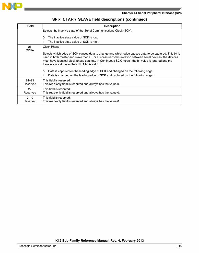
SPIx_CTARn_SLAVE field descriptions (continued)
Field Description
Selects the inactive state of the Serial Communications Clock (SCK).
0 The inactive state value of SCK is low.1 The inactive state value of SCK is high.
25CPHA
Clock Phase
Selects which edge of SCK causes data to change and which edge causes data to be captured. This bit isused in both master and slave mode. For successful communication between serial devices, the devicesmust have identical clock phase settings. In Continuous SCK mode , the bit value is ignored and thetransfers are done as the CPHA bit is set to 1.
0 Data is captured on the leading edge of SCK and changed on the following edge.1 Data is changed on the leading edge of SCK and captured on the following edge.
24–23Reserved
This field is reserved.This read-only field is reserved and always has the value 0.
22Reserved
This field is reserved.This read-only field is reserved and always has the value 0.
21–0Reserved
This field is reserved.This read-only field is reserved and always has the value 0.
Chapter 41 Serial Peripheral Interface (SPI)
K12 Sub-Family Reference Manual, Rev. 4, February 2013
Freescale Semiconductor, Inc. 945

41.3.5 DSPI Status Register (SPIx_SR)
SR contains status and flag bits. The bits reflect the status of the module and indicate theoccurrence of events that can generate interrupt or DMA requests. Software can clear flagbits in the SR by writing a 1 to them. Writing a 0 to a flag bit has no effect. This registermay not be writable in Module Disable mode due to the use of power savingmechanisms.
Address: Base address + 2Ch offset
Bit 31 30 29 28 27 26 25 24 23 22 21 20 19 18 17 16
R TCF
TX
RX
S
0
EO
QF
TF
UF
0T
FF
F0 0 0 0 0
RF
OF
0
RF
DF
0
W w1c w1c w1c w1c w1c w1c w1c
Reset 0 0 0 0 0 0 1 0 0 0 0 0 0 0 0 0
Bit 15 14 13 12 11 10 9 8 7 6 5 4 3 2 1 0
R TXCTR TXNXTPTR RXCTR POPNXTPTR
W
Reset 0 0 0 0 0 0 0 0 0 0 0 0 0 0 0 0
SPIx_SR field descriptions
Field Description
31TCF
Transfer Complete Flag
Indicates that all bits in a frame have been shifted out. TCF remains set until it is cleared by writing a 1 toit.
0 Transfer not complete.1 Transfer complete.
30TXRXS
TX and RX Status
Reflects the run status of the module.
0 Transmit and receive operations are disabled (The module is in Stopped state).1 Transmit and receive operations are enabled (The module is in Running state).
29Reserved
This field is reserved.This read-only field is reserved and always has the value 0.
Table continues on the next page...
Memory Map/Register Definition
K12 Sub-Family Reference Manual, Rev. 4, February 2013
946 Freescale Semiconductor, Inc.

SPIx_SR field descriptions (continued)
Field Description
28EOQF
End of Queue Flag
Indicates that the last entry in a queue has been transmitted when the module is in Master mode. TheEOQF bit is set when the TX FIFO entry has the EOQ bit set in the command halfword and the end of thetransfer is reached. The EOQF bit remains set until cleared by writing a 1 to it. When the EOQF bit is set,the TXRXS bit is automatically cleared.
0 EOQ is not set in the executing command.1 EOQ is set in the executing SPI command.
27TFUF
Transmit FIFO Underflow Flag
Indicates an underflow condition in the TX FIFO. The transmit underflow condition is detected only forDSPI blocks operating in Slave mode and SPI configuration. TFUF is set when the TX FIFO of the moduleoperating in SPI Slave mode is empty and an external SPI master initiates a transfer. The TFUF bitremains set until cleared by writing 1 to it.
0 No TX FIFO underflow.1 TX FIFO underflow has occurred.
26Reserved
This field is reserved.This read-only field is reserved and always has the value 0.
25TFFF
Transmit FIFO Fill Flag
Provides a method for the module to request more entries to be added to the TX FIFO. The TFFF bit is setwhile the TX FIFO is not full. The TFFF bit can be cleared by writing 1 to it or by acknowledgement fromthe DMA controller to the TX FIFO full request.
0 TX FIFO is full.1 TX FIFO is not full.
24Reserved
This field is reserved.This read-only field is reserved and always has the value 0.
23Reserved
This field is reserved.This read-only field is reserved and always has the value 0.
22Reserved
This field is reserved.This read-only field is reserved and always has the value 0.
21Reserved
This field is reserved.This read-only field is reserved and always has the value 0.
20Reserved
This field is reserved.This read-only field is reserved and always has the value 0.
19RFOF
Receive FIFO Overflow Flag
Indicates an overflow condition in the RX FIFO. The field is set when the RX FIFO and shift register arefull and a transfer is initiated. The bit remains set until it is cleared by writing a 1 to it.
0 No Rx FIFO overflow.1 Rx FIFO overflow has occurred.
18Reserved
This field is reserved.This read-only field is reserved and always has the value 0.
17RFDF
Receive FIFO Drain Flag
Table continues on the next page...
Chapter 41 Serial Peripheral Interface (SPI)
K12 Sub-Family Reference Manual, Rev. 4, February 2013
Freescale Semiconductor, Inc. 947
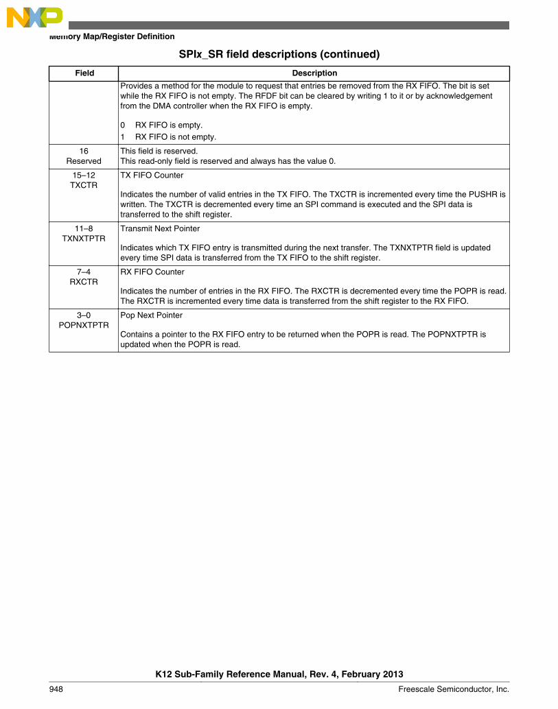
SPIx_SR field descriptions (continued)
Field Description
Provides a method for the module to request that entries be removed from the RX FIFO. The bit is setwhile the RX FIFO is not empty. The RFDF bit can be cleared by writing 1 to it or by acknowledgementfrom the DMA controller when the RX FIFO is empty.
0 RX FIFO is empty.1 RX FIFO is not empty.
16Reserved
This field is reserved.This read-only field is reserved and always has the value 0.
15–12TXCTR
TX FIFO Counter
Indicates the number of valid entries in the TX FIFO. The TXCTR is incremented every time the PUSHR iswritten. The TXCTR is decremented every time an SPI command is executed and the SPI data istransferred to the shift register.
11–8TXNXTPTR
Transmit Next Pointer
Indicates which TX FIFO entry is transmitted during the next transfer. The TXNXTPTR field is updatedevery time SPI data is transferred from the TX FIFO to the shift register.
7–4RXCTR
RX FIFO Counter
Indicates the number of entries in the RX FIFO. The RXCTR is decremented every time the POPR is read.The RXCTR is incremented every time data is transferred from the shift register to the RX FIFO.
3–0POPNXTPTR
Pop Next Pointer
Contains a pointer to the RX FIFO entry to be returned when the POPR is read. The POPNXTPTR isupdated when the POPR is read.
Memory Map/Register Definition
K12 Sub-Family Reference Manual, Rev. 4, February 2013
948 Freescale Semiconductor, Inc.
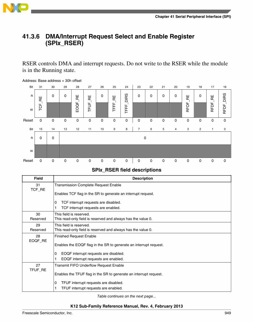
41.3.6 DMA/Interrupt Request Select and Enable Register(SPIx_RSER)
RSER controls DMA and interrupt requests. Do not write to the RSER while the moduleis in the Running state.
Address: Base address + 30h offset
Bit 31 30 29 28 27 26 25 24 23 22 21 20 19 18 17 16
R
TC
F_R
E 0 0
EO
QF
_RE
TF
UF
_RE 0
TF
FF
_RE
TF
FF
_DIR
S 0 0 0 0
RF
OF
_RE 0
RF
DF
_RE
RF
DF
_DIR
S
W
Reset 0 0 0 0 0 0 0 0 0 0 0 0 0 0 0 0
Bit 15 14 13 12 11 10 9 8 7 6 5 4 3 2 1 0
R 0 0 0
W
Reset 0 0 0 0 0 0 0 0 0 0 0 0 0 0 0 0
SPIx_RSER field descriptions
Field Description
31TCF_RE
Transmission Complete Request Enable
Enables TCF flag in the SR to generate an interrupt request.
0 TCF interrupt requests are disabled.1 TCF interrupt requests are enabled.
30Reserved
This field is reserved.This read-only field is reserved and always has the value 0.
29Reserved
This field is reserved.This read-only field is reserved and always has the value 0.
28EOQF_RE
Finished Request Enable
Enables the EOQF flag in the SR to generate an interrupt request.
0 EOQF interrupt requests are disabled.1 EOQF interrupt requests are enabled.
27TFUF_RE
Transmit FIFO Underflow Request Enable
Enables the TFUF flag in the SR to generate an interrupt request.
0 TFUF interrupt requests are disabled.1 TFUF interrupt requests are enabled.
Table continues on the next page...
Chapter 41 Serial Peripheral Interface (SPI)
K12 Sub-Family Reference Manual, Rev. 4, February 2013
Freescale Semiconductor, Inc. 949
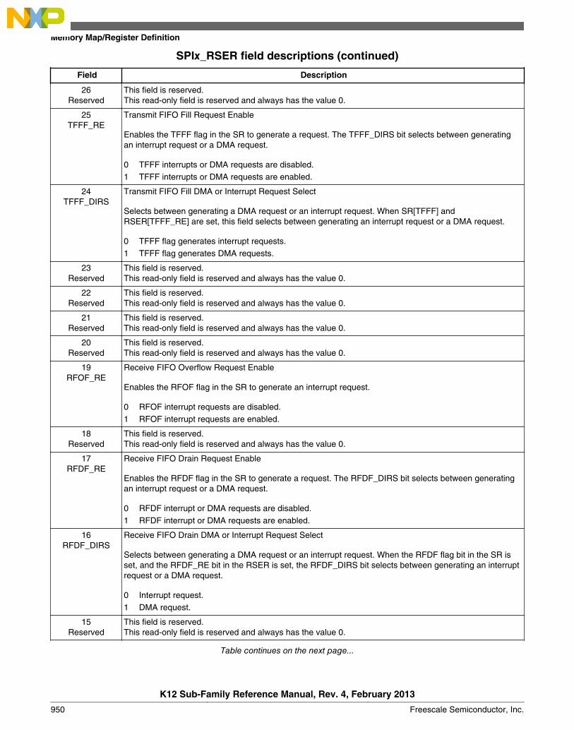
SPIx_RSER field descriptions (continued)
Field Description
26Reserved
This field is reserved.This read-only field is reserved and always has the value 0.
25TFFF_RE
Transmit FIFO Fill Request Enable
Enables the TFFF flag in the SR to generate a request. The TFFF_DIRS bit selects between generatingan interrupt request or a DMA request.
0 TFFF interrupts or DMA requests are disabled.1 TFFF interrupts or DMA requests are enabled.
24TFFF_DIRS
Transmit FIFO Fill DMA or Interrupt Request Select
Selects between generating a DMA request or an interrupt request. When SR[TFFF] andRSER[TFFF_RE] are set, this field selects between generating an interrupt request or a DMA request.
0 TFFF flag generates interrupt requests.1 TFFF flag generates DMA requests.
23Reserved
This field is reserved.This read-only field is reserved and always has the value 0.
22Reserved
This field is reserved.This read-only field is reserved and always has the value 0.
21Reserved
This field is reserved.This read-only field is reserved and always has the value 0.
20Reserved
This field is reserved.This read-only field is reserved and always has the value 0.
19RFOF_RE
Receive FIFO Overflow Request Enable
Enables the RFOF flag in the SR to generate an interrupt request.
0 RFOF interrupt requests are disabled.1 RFOF interrupt requests are enabled.
18Reserved
This field is reserved.This read-only field is reserved and always has the value 0.
17RFDF_RE
Receive FIFO Drain Request Enable
Enables the RFDF flag in the SR to generate a request. The RFDF_DIRS bit selects between generatingan interrupt request or a DMA request.
0 RFDF interrupt or DMA requests are disabled.1 RFDF interrupt or DMA requests are enabled.
16RFDF_DIRS
Receive FIFO Drain DMA or Interrupt Request Select
Selects between generating a DMA request or an interrupt request. When the RFDF flag bit in the SR isset, and the RFDF_RE bit in the RSER is set, the RFDF_DIRS bit selects between generating an interruptrequest or a DMA request.
0 Interrupt request.1 DMA request.
15Reserved
This field is reserved.This read-only field is reserved and always has the value 0.
Table continues on the next page...
Memory Map/Register Definition
K12 Sub-Family Reference Manual, Rev. 4, February 2013
950 Freescale Semiconductor, Inc.

SPIx_RSER field descriptions (continued)
Field Description
14Reserved
This field is reserved.This read-only field is reserved and always has the value 0.
13–0Reserved
This field is reserved.This read-only field is reserved and always has the value 0.
41.3.7 PUSH TX FIFO Register In Master Mode (SPIx_PUSHR)
PUSHR provides the means to write to the TX FIFO . Data written to this register istransferred to the TX FIFO 8- or 16-bit write accesses to the PUSHR transfer all 32register bits to the TXFIFO.The register structure is different in Master and Slave modes.In Master mode, the register provides 16-bit command and data to the TX FIFO. In Slavemode, all 32 register bits can be used as data, supporting upto 32-bit SPI Frameoperation.
A PUSHR Read Operation returns the topmost TX FIFO entry.
When the module is disabled, any writes to this register will not update the FIFO. Henceany reads performed during Module disable mode will return the last PUSHR writeperformed when Module was enabled.
Address: Base address + 34h offset
Bit 31 30 29 28 27 26 25 24 23 22 21 20 19 18 17 16
R
CO
NT
CTAS EOQ
CT
CN
T 0 0
PCS[5:0]W
Reset 0 0 0 0 0 0 0 0 0 0 0 0 0 0 0 0
Bit 15 14 13 12 11 10 9 8 7 6 5 4 3 2 1 0
R
TXDATAW
Reset 0 0 0 0 0 0 0 0 0 0 0 0 0 0 0 0
SPIx_PUSHR field descriptions
Field Description
31CONT
Continuous Peripheral Chip Select Enable
Selects a continuous selection format. The bit is used in SPI Master mode. The bit enables the selectedPCS signals to remain asserted between transfers.
Table continues on the next page...
Chapter 41 Serial Peripheral Interface (SPI)
K12 Sub-Family Reference Manual, Rev. 4, February 2013
Freescale Semiconductor, Inc. 951
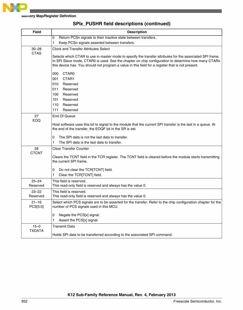
SPIx_PUSHR field descriptions (continued)
Field Description
0 Return PCSn signals to their inactive state between transfers.1 Keep PCSn signals asserted between transfers.
30–28CTAS
Clock and Transfer Attributes Select
Selects which CTAR to use in master mode to specify the transfer attributes for the associated SPI frame.In SPI Slave mode, CTAR0 is used. See the chapter on chip configuration to determine how many CTARsthis device has. You should not program a value in this field for a register that is not present.
000 CTAR0001 CTAR1010 Reserved011 Reserved100 Reserved101 Reserved110 Reserved111 Reserved
27EOQ
End Of Queue
Host software uses this bit to signal to the module that the current SPI transfer is the last in a queue. Atthe end of the transfer, the EOQF bit in the SR is set.
0 The SPI data is not the last data to transfer.1 The SPI data is the last data to transfer.
26CTCNT
Clear Transfer Counter
Clears the TCNT field in the TCR register. The TCNT field is cleared before the module starts transmittingthe current SPI frame.
0 Do not clear the TCR[TCNT] field.1 Clear the TCR[TCNT] field.
25–24Reserved
This field is reserved.This read-only field is reserved and always has the value 0.
23–22Reserved
This field is reserved.This read-only field is reserved and always has the value 0.
21–16PCS[5:0]
Select which PCS signals are to be asserted for the transfer. Refer to the chip configuration chapter for thenumber of PCS signals used in this MCU.
0 Negate the PCS[x] signal.1 Assert the PCS[x] signal.
15–0TXDATA
Transmit Data
Holds SPI data to be transferred according to the associated SPI command.
Memory Map/Register Definition
K12 Sub-Family Reference Manual, Rev. 4, February 2013
952 Freescale Semiconductor, Inc.
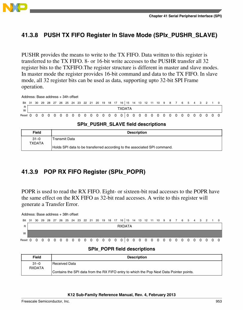
41.3.8 PUSH TX FIFO Register In Slave Mode (SPIx_PUSHR_SLAVE)
PUSHR provides the means to write to the TX FIFO. Data written to this register istransferred to the TX FIFO. 8- or 16-bit write accesses to the PUSHR transfer all 32register bits to the TXFIFO.The register structure is different in master and slave modes.In master mode the register provides 16-bit command and data to the TX FIFO. In slavemode, all 32 register bits can be used as data, supporting upto 32-bit SPI Frameoperation.
Address: Base address + 34h offset
Bit 31 30 29 28 27 26 25 24 23 22 21 20 19 18 17 16 15 14 13 12 11 10 9 8 7 6 5 4 3 2 1 0
R TXDATAW
Reset 0 0 0 0 0 0 0 0 0 0 0 0 0 0 0 0 0 0 0 0 0 0 0 0 0 0 0 0 0 0 0 0
SPIx_PUSHR_SLAVE field descriptions
Field Description
31–0TXDATA
Transmit Data
Holds SPI data to be transferred according to the associated SPI command.
41.3.9 POP RX FIFO Register (SPIx_POPR)
POPR is used to read the RX FIFO. Eight- or sixteen-bit read accesses to the POPR havethe same effect on the RX FIFO as 32-bit read accesses. A write to this register willgenerate a Transfer Error.
Address: Base address + 38h offset
Bit 31 30 29 28 27 26 25 24 23 22 21 20 19 18 17 16 15 14 13 12 11 10 9 8 7 6 5 4 3 2 1 0
R RXDATA
W
Reset 0 0 0 0 0 0 0 0 0 0 0 0 0 0 0 0 0 0 0 0 0 0 0 0 0 0 0 0 0 0 0 0
SPIx_POPR field descriptions
Field Description
31–0RXDATA
Received Data
Contains the SPI data from the RX FIFO entry to which the Pop Next Data Pointer points.
Chapter 41 Serial Peripheral Interface (SPI)
K12 Sub-Family Reference Manual, Rev. 4, February 2013
Freescale Semiconductor, Inc. 953
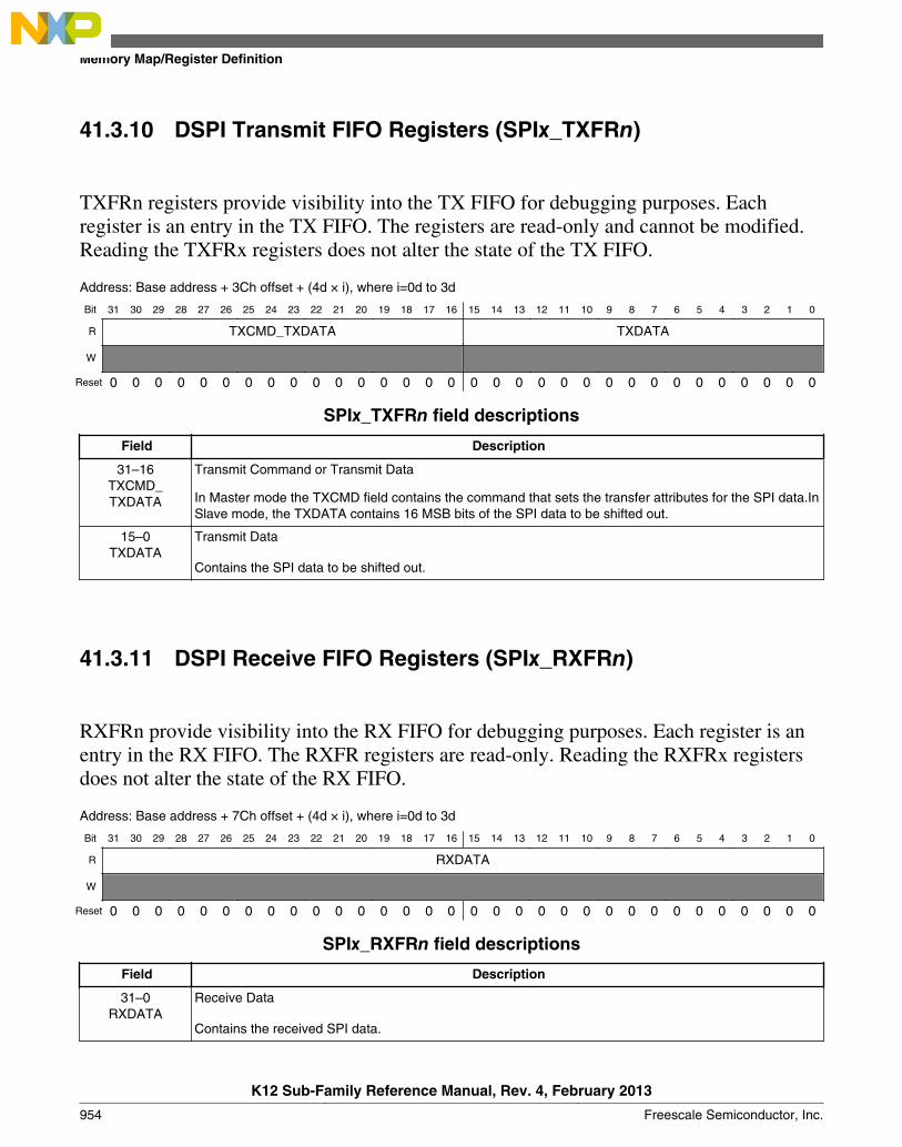
41.3.10 DSPI Transmit FIFO Registers (SPIx_TXFRn)
TXFRn registers provide visibility into the TX FIFO for debugging purposes. Eachregister is an entry in the TX FIFO. The registers are read-only and cannot be modified.Reading the TXFRx registers does not alter the state of the TX FIFO.
Address: Base address + 3Ch offset + (4d × i), where i=0d to 3d
Bit 31 30 29 28 27 26 25 24 23 22 21 20 19 18 17 16 15 14 13 12 11 10 9 8 7 6 5 4 3 2 1 0
R TXCMD_TXDATA TXDATA
W
Reset 0 0 0 0 0 0 0 0 0 0 0 0 0 0 0 0 0 0 0 0 0 0 0 0 0 0 0 0 0 0 0 0
SPIx_TXFRn field descriptions
Field Description
31–16TXCMD_TXDATA
Transmit Command or Transmit Data
In Master mode the TXCMD field contains the command that sets the transfer attributes for the SPI data.InSlave mode, the TXDATA contains 16 MSB bits of the SPI data to be shifted out.
15–0TXDATA
Transmit Data
Contains the SPI data to be shifted out.
41.3.11 DSPI Receive FIFO Registers (SPIx_RXFRn)
RXFRn provide visibility into the RX FIFO for debugging purposes. Each register is anentry in the RX FIFO. The RXFR registers are read-only. Reading the RXFRx registersdoes not alter the state of the RX FIFO.
Address: Base address + 7Ch offset + (4d × i), where i=0d to 3d
Bit 31 30 29 28 27 26 25 24 23 22 21 20 19 18 17 16 15 14 13 12 11 10 9 8 7 6 5 4 3 2 1 0
R RXDATA
W
Reset 0 0 0 0 0 0 0 0 0 0 0 0 0 0 0 0 0 0 0 0 0 0 0 0 0 0 0 0 0 0 0 0
SPIx_RXFRn field descriptions
Field Description
31–0RXDATA
Receive Data
Contains the received SPI data.
Memory Map/Register Definition
K12 Sub-Family Reference Manual, Rev. 4, February 2013
954 Freescale Semiconductor, Inc.
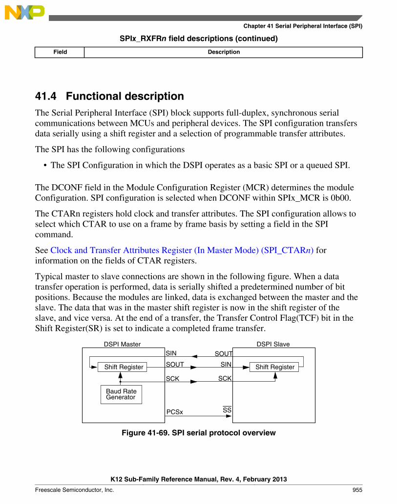
SPIx_RXFRn field descriptions (continued)
Field Description
41.4 Functional descriptionThe Serial Peripheral Interface (SPI) block supports full-duplex, synchronous serialcommunications between MCUs and peripheral devices. The SPI configuration transfersdata serially using a shift register and a selection of programmable transfer attributes.
The SPI has the following configurations
• The SPI Configuration in which the DSPI operates as a basic SPI or a queued SPI.
The DCONF field in the Module Configuration Register (MCR) determines the moduleConfiguration. SPI configuration is selected when DCONF within SPIx_MCR is 0b00.
The CTARn registers hold clock and transfer attributes. The SPI configuration allows toselect which CTAR to use on a frame by frame basis by setting a field in the SPIcommand.
See Clock and Transfer Attributes Register (In Master Mode) (SPI_CTARn) forinformation on the fields of CTAR registers.
Typical master to slave connections are shown in the following figure. When a datatransfer operation is performed, data is serially shifted a predetermined number of bitpositions. Because the modules are linked, data is exchanged between the master and theslave. The data that was in the master shift register is now in the shift register of theslave, and vice versa. At the end of a transfer, the Transfer Control Flag(TCF) bit in theShift Register(SR) is set to indicate a completed frame transfer.
Shift Register
Baud Rate Generator
Shift Register
SOUT
SCK
PCSx
DSPI SlaveDSPI Master
SINSOUT
SIN
SS
SCK
Figure 41-69. SPI serial protocol overview
Chapter 41 Serial Peripheral Interface (SPI)
K12 Sub-Family Reference Manual, Rev. 4, February 2013
Freescale Semiconductor, Inc. 955
Generally, more than one slave device can be connected to the module master. SixPeripheral Chip Select (PCS) signals of the module masters can be used to select whichof the slaves to communicate with. Refer to the chip configuration chapter for the numberof PCS signals used in this MCU.
The SPI configuration share transfer protocol and timing properties which are describedindependently of the configuration in Transfer formats . The transfer rate and delaysettings are described in Module baud rate and clock delay generation.
41.4.1 Start and Stop of module transfers
The module has two operating states: Stopped and Running. Both the states areindependent of it's configuration. The default state of the module is Stopped. In theStopped state, no serial transfers are initiated in Master mode and no transfers areresponded to in Slave mode. The Stopped state is also a safe state for writing the variousconfiguration registers of the module without causing undetermined results. In theRunning state serial transfers take place.
The TXRXS bit in the SR indicates the state of module. The bit is set if the module is inRunning state.
The module starts or transitions to Running when all of the following conditions are true:
• SR[EOQF] bit is clear
• MCU is not in the Debug mode or the MCR[FRZ] bit is clear
• MCR[HALT] bit is clear
The module stops or transitions from Running to Stopped after the current frame whenany one of the following conditions exist:
• SR[EOQF] bit is set
• MCU in the Debug mode and the MCR[FRZ] bit is set
• MCR[HALT] bit is set
State transitions from Running to Stopped occur on the next frame boundary if a transferis in progress, or immediately if no transfers are in progress.
Functional description
K12 Sub-Family Reference Manual, Rev. 4, February 2013
956 Freescale Semiconductor, Inc.
41.4.2 Serial Peripheral Interface (SPI) configuration
The SPI configuration transfers data serially using a shift register and a selection ofprogrammable transfer attributes. The module is in SPI configuration when the DCONFfield in the MCR is 0b00. The SPI frames can be 32 bits long. The host CPU or a DMAcontroller transfers the SPI data from the external to DSPI RAM queues to a TX FIFObuffer. The received data is stored in entries in the RX FIFO buffer. The host CPU or theDMA controller transfers the received data from the RX FIFO to memory external to themodule. The operation of FIFO buffers is described in Transmit First In First Out (TXFIFO) buffering mechanism, Transmit First In First Out (TX FIFO) buffering mechanismand Receive First In First Out (RX FIFO) buffering mechanism. The interrupt and DMArequest conditions are described in Interrupts/DMA requests.
The SPI configuration supports two block-specific modes—Master mode and Slavemode.In Master mode the module initiates and controls the transfer according to thefields of the executing SPI Command. In Slave mode, the module responds only totransfers initiated by a bus master external to it and the SPI command field space isreserved.
41.4.2.1 Master mode
In SPI Master, mode the module initiates the serial transfers by controlling the SCK andthe PCS signals. The executing SPI Command determines which CTARs will be used toset the transfer attributes and which PCS signals to assert . The command field alsocontains various bits that help with queue management and transfer protocol . See PUSHTX FIFO Register In Master Mode (SPI_PUSHR) for details on the SPI command fields.The data in the executing TX FIFO entry is loaded into the shift register and shifted outon the Serial Out (SOUT) pin. In SPI Master mode, each SPI frame to be transmitted hasa command associated with it, allowing for transfer attribute control on a frame by framebasis.
41.4.2.2 Slave mode
In SPI Slave mode the module responds to transfers initiated by an SPI bus master. Itdoes not initiate transfers. Certain transfer attributes such as clock polarity, clock phase,and frame size must be set for successful communication with an SPI master. The SPISlave mode transfer attributes are set in the CTAR0 . The data is shifted out with MSBfirst. Shifting out of LSB is not supported in this mode.
Chapter 41 Serial Peripheral Interface (SPI)
K12 Sub-Family Reference Manual, Rev. 4, February 2013
Freescale Semiconductor, Inc. 957
41.4.2.3 FIFO disable operation
The FIFO disable mechanisms allow SPI transfers without using the TX FIFO or RXFIFO. The module operates as a double-buffered simplified SPI when the FIFOs aredisabled. The Transmit and Receive side of the FIFOs are disabled separately; setting theMCR[DIS_TXF] bit disables the TX FIFO, and setting the MCR[DIS_RXF] bit disablesthe RX FIFO.
The FIFO disable mechanisms are transparent to the user and to host software. Transmitdata and commands are written to the PUSHR and received data is read from the POPR.
When the TX FIFO is disabled, the fields SR[TFFF], SR[TFUF] and SR[TXCTR] behaveas if there is a one-entry FIFO but the contents of TXFRs, SR[TXNXTPTR] areundefined. Similarly, when the RX FIFO is disabled, the RFDF, RFOF, and RXCTRfields in the SR behave as if there is a one-entry FIFO, but the contents of the RXFRregisters and POPNXTPTR are undefined.
41.4.2.4 Transmit First In First Out (TX FIFO) buffering mechanism
The TX FIFO functions as a buffer of SPI data for transmission. The TX FIFO holds fourwords, each consisting of SPI data. The number of entries in the TX FIFO is device-specific. SPI data is added to the TX FIFO by writing to the Data Field of module PUSHFIFO Register (PUSHR). TX FIFO entries can only be removed from the TX FIFO bybeing shifted out or by flushing the TX FIFO.
The TX FIFO Counter field (TXCTR) in the module Status Register (SR) indicates thenumber of valid entries in the TX FIFO. The TXCTR is updated every time a 8- or 16-bitwrite takes place to the Data Field of SPI_PUSHR or SPI data is transferred into the shiftregister from the TX FIFO.
The TXNXTPTR field indicates the TX FIFO Entry that will be transmitted during thenext transfer. The TXNXTPTR field is incremented every time SPI data is transferredfrom the TX FIFO to the shift register. The maximum value of the field is equal to themaximum implemented TXFR number and it rolls over after reaching the maximum.
41.4.2.4.1 Filling the TX FIFO
Host software or other intelligent blocks can add (push) entries to the TX FIFO bywriting to the PUSHR. When the TX FIFO is not full, the TX FIFO Fill Flag (TFFF) inthe SR is set. The TFFF bit is cleared when TX FIFO is full and the DMA controllerindicates that a write to PUSHR is complete. Writing a '1' to the TFFF bit also clears it.The TFFF can generate a DMA request or an interrupt request. See Transmit FIFO FillInterrupt or DMA Request for details.
Functional description
K12 Sub-Family Reference Manual, Rev. 4, February 2013
958 Freescale Semiconductor, Inc.

The module ignores attempts to push data to a full TX FIFO, and the state of the TXFIFO does not change and no error condition is indicated.
41.4.2.4.2 Draining the TX FIFO
The TX FIFO entries are removed (drained) by shifting SPI data out through the shiftregister. Entries are transferred from the TX FIFO to the shift register and shifted out aslong as there are valid entries in the TX FIFO. Every time an entry is transferred from theTX FIFO to the shift register, the TX FIFO Counter decrements by one. At the end of atransfer, the TCF bit in the SR is set to indicate the completion of a transfer. The TXFIFO is flushed by writing a '1' to the CLR_TXF bit in MCR.
If an external bus master initiates a transfer with a module slave while the slave's TXFIFO is empty, the Transmit FIFO Underflow Flag (TFUF) in the slave's SR is set. SeeTransmit FIFO Underflow Interrupt Request for details.
41.4.2.5 Receive First In First Out (RX FIFO) buffering mechanism
The RX FIFO functions as a buffer for data received on the SIN pin. The RX FIFO holdsfour received SPI data frames. The number of entries in the RX FIFO is device-specific.SPI data is added to the RX FIFO at the completion of a transfer when the received datain the shift register is transferred into the RX FIFO. SPI data are removed (popped) fromthe RX FIFO by reading the module POP RX FIFO Register (POPR). RX FIFO entriescan only be removed from the RX FIFO by reading the POPR or by flushing the RXFIFO.
The RX FIFO Counter field (RXCTR) in the module's Status Register (SR) indicates thenumber of valid entries in the RX FIFO. The RXCTR is updated every time the POPR isread or SPI data is copied from the shift register to the RX FIFO.
The POPNXTPTR field in the SR points to the RX FIFO entry that is returned when thePOPR is read. The POPNXTPTR contains the positive offset from RXFR0 in a numberof 32-bit registers. For example, POPNXTPTR equal to two means that the RXFR2contains the received SPI data that will be returned when the POPR is read. ThePOPNXTPTR field is incremented every time the POPR is read. The maximum value ofthe field is equal to the maximum implemented RXFR number and it rolls over afterreaching the maximum.
Chapter 41 Serial Peripheral Interface (SPI)
K12 Sub-Family Reference Manual, Rev. 4, February 2013
Freescale Semiconductor, Inc. 959
41.4.2.5.1 Filling the RX FIFO
The RX FIFO is filled with the received SPI data from the shift register. While the RXFIFO is not full, SPI frames from the shift register are transferred to the RX FIFO. Everytime an SPI frame is transferred to the RX FIFO, the RX FIFO Counter is incremented byone.
If the RX FIFO and shift register are full and a transfer is initiated, the RFOF bit in theSR is set indicating an overflow condition. Depending on the state of the ROOE bit in theMCR, the data from the transfer that generated the overflow is either ignored or shifted into the shift register. If the ROOE bit is set, the incoming data is shifted in to the shiftregister. If the ROOE bit is cleared, the incoming data is ignored.
41.4.2.5.2 Draining the RX FIFO
Host CPU or a DMA can remove (pop) entries from the RX FIFO by reading the modulePOP RX FIFO Register (POPR). A read of the POPR decrements the RX FIFO Counterby one. Attempts to pop data from an empty RX FIFO are ignored and the RX FIFOCounter remains unchanged. The data, read from the empty RX FIFO, is undetermined.
When the RX FIFO is not empty, the RX FIFO Drain Flag (RFDF) in the SR is set. TheRFDF bit is cleared when the RX_FIFO is empty and the DMA controller indicates that aread from POPR is complete or by writing a 1 to it.
41.4.3 Module baud rate and clock delay generation
The SCK frequency and the delay values for serial transfer are generated by dividing thesystem clock frequency by a prescaler and a scaler with the option for doubling the baudrate. The following figure shows conceptually how the SCK signal is generated.
System ClockPrescaler
1Scaler
1+DBR SCK
Figure 41-70. Communications clock prescalers and scalers
41.4.3.1 Baud rate generator
The baud rate is the frequency of the SCK. The system clock is divided by a prescaler(PBR) and scaler (BR) to produce SCK with the possibility of halving the scaler division.The DBR, PBR, and BR fields in the CTARs select the frequency of SCK by the formulain the BR field description. The following table shows an example of how to compute thebaud rate.
Functional description
K12 Sub-Family Reference Manual, Rev. 4, February 2013
960 Freescale Semiconductor, Inc.
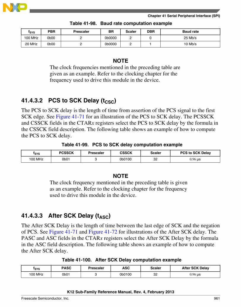
Table 41-98. Baud rate computation example
fSYS PBR Prescaler BR Scaler DBR Baud rate
100 MHz 0b00 2 0b0000 2 0 25 Mb/s
20 MHz 0b00 2 0b0000 2 1 10 Mb/s
NOTEThe clock frequencies mentioned in the preceding table aregiven as an example. Refer to the clocking chapter for thefrequency used to drive this module in the device.
41.4.3.2 PCS to SCK Delay (tCSC)
The PCS to SCK delay is the length of time from assertion of the PCS signal to the firstSCK edge. See Figure 41-71 for an illustration of the PCS to SCK delay. The PCSSCKand CSSCK fields in the CTARx registers select the PCS to SCK delay by the formula inthe CSSCK field description. The following table shows an example of how to computethe PCS to SCK delay.
Table 41-99. PCS to SCK delay computation example
fSYS PCSSCK Prescaler CSSCK Scaler PCS to SCK Delay
100 MHz 0b01 3 0b0100 32 0.96 μs
NOTEThe clock frequency mentioned in the preceding table is givenas an example. Refer to the clocking chapter for the frequencyused to drive this module in the device.
41.4.3.3 After SCK Delay (tASC)
The After SCK Delay is the length of time between the last edge of SCK and the negationof PCS. See Figure 41-71 and Figure 41-72 for illustrations of the After SCK delay. ThePASC and ASC fields in the CTARx registers select the After SCK Delay by the formulain the ASC field description. The following table shows an example of how to computethe After SCK delay.
Table 41-100. After SCK Delay computation example
fSYS PASC Prescaler ASC Scaler After SCK Delay
100 MHz 0b01 3 0b0100 32 0.96 μs
Chapter 41 Serial Peripheral Interface (SPI)
K12 Sub-Family Reference Manual, Rev. 4, February 2013
Freescale Semiconductor, Inc. 961
NOTEThe clock frequency mentioned in the preceding table is givenas an example. Refer to the clocking chapter for the frequencyused to drive this module in the device.
41.4.3.4 Delay after Transfer (tDT)
The Delay after Transfer is the minimum time between negation of the PCS signal for aframe and the assertion of the PCS signal for the next frame. See Figure 41-71 for anillustration of the Delay after Transfer. The PDT and DT fields in the CTARx registersselect the Delay after Transfer by the formula in the DT field description. The followingtable shows an example of how to compute the Delay after Transfer.
Table 41-101. Delay after Transfer computation example
fSYS PDT Prescaler DT Scaler Delay after Transfer
100 MHz 0b01 3 0b1110 32768 0.98 ms
NOTEThe clock frequency mentioned in the preceding table is givenas an example. Refer to the clocking chapter for the frequencyused to drive this module in the device.
When in Non-Continuous Clock mode the tDT delay is configured according to theequation specified in the CTAR[DT] field description. When in Continuous Clock mode,the delay is fixed at 1 SCK period.
41.4.4 Transfer formats
The SPI serial communication is controlled by the Serial Communications Clock (SCK)signal and the PCS signals. The SCK signal provided by the master device synchronizesshifting and sampling of the data on the SIN and SOUT pins. The PCS signals serve asenable signals for the slave devices.
In Master mode, the CPOL and CPHA bits in the Clock and Transfer Attributes Registers(CTARn) select the polarity and phase of the serial clock, SCK.
• CPOL - Selects the idle state polarity of the SCK
• CPHA - Selects if the data on SOUT is valid before or on the first SCK edge
Functional description
K12 Sub-Family Reference Manual, Rev. 4, February 2013
962 Freescale Semiconductor, Inc.
Even though the bus slave does not control the SCK signal, in Slave mode the values ofCPOL and CPHA must be identical to the master device settings to ensure propertransmission. In SPI Slave mode, only CTAR0 is used.
The module supports four different transfer formats:
• Classic SPI with CPHA=0
• Classic SPI with CPHA=1
• Modified Transfer Format with CPHA = 0
• Modified Transfer Format with CPHA = 1
A modified transfer format is supported to allow for high-speed communication withperipherals that require longer setup times. The module can sample the incoming datalater than halfway through the cycle to give the peripheral more setup time. The MTFEbit in the MCR selects between Classic SPI Format and Modified Transfer Format.
In the SPI configurations, the module provides the option of keeping the PCS signalsasserted between frames. See Continuous Selection Format for details.
41.4.4.1 Classic SPI Transfer Format (CPHA = 0)
The transfer format shown in following figure is used to communicate with peripheralSPI slave devices where the first data bit is available on the first clock edge. In thisformat, the master and slave sample their SIN pins on the odd-numbered SCK edges andchange the data on their SOUT pins on the even-numbered SCK edges.
Chapter 41 Serial Peripheral Interface (SPI)
K12 Sub-Family Reference Manual, Rev. 4, February 2013
Freescale Semiconductor, Inc. 963
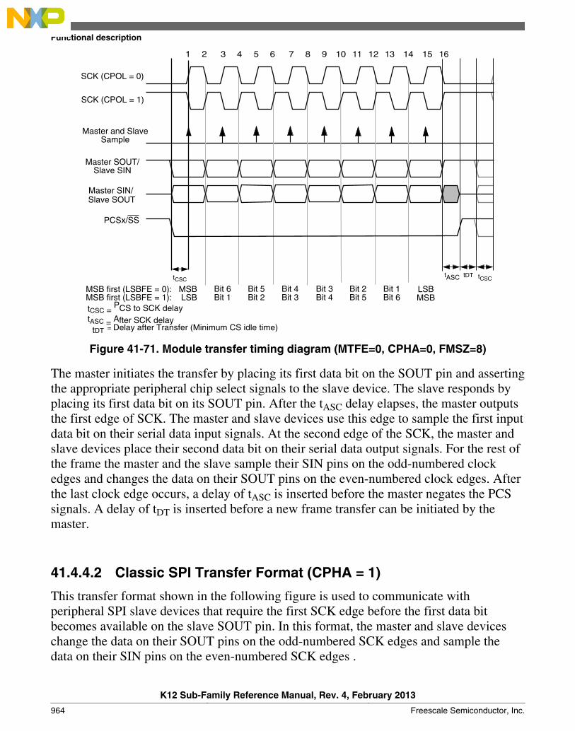
tASC = After SCK delaytCSC =
PCS to SCK delay
MSB first (LSBFE = 0): MSBMSB first (LSBFE = 1): LSB
tDT = Delay after Transfer (Minimum CS idle time)
tCSC
Bit 6Bit 1
Bit 5Bit 2
Bit 4Bit 3
Bit 3Bit 4
Bit 2Bit 5
Bit 1Bit 6
LSBMSB
tCSCtDTtASC
PCSx/SS
Slave SOUTMaster SIN/
Master SOUT/Slave SIN
Master and SlaveSample
SCK (CPOL = 1)
SCK (CPOL = 0)
1 2 3 4 5 6 7 8 9 10 11 12 13 14 15 16
Figure 41-71. Module transfer timing diagram (MTFE=0, CPHA=0, FMSZ=8)
The master initiates the transfer by placing its first data bit on the SOUT pin and assertingthe appropriate peripheral chip select signals to the slave device. The slave responds byplacing its first data bit on its SOUT pin. After the tASC delay elapses, the master outputsthe first edge of SCK. The master and slave devices use this edge to sample the first inputdata bit on their serial data input signals. At the second edge of the SCK, the master andslave devices place their second data bit on their serial data output signals. For the rest ofthe frame the master and the slave sample their SIN pins on the odd-numbered clockedges and changes the data on their SOUT pins on the even-numbered clock edges. Afterthe last clock edge occurs, a delay of tASC is inserted before the master negates the PCSsignals. A delay of tDT is inserted before a new frame transfer can be initiated by themaster.
41.4.4.2 Classic SPI Transfer Format (CPHA = 1)
This transfer format shown in the following figure is used to communicate withperipheral SPI slave devices that require the first SCK edge before the first data bitbecomes available on the slave SOUT pin. In this format, the master and slave deviceschange the data on their SOUT pins on the odd-numbered SCK edges and sample thedata on their SIN pins on the even-numbered SCK edges .
Functional description
K12 Sub-Family Reference Manual, Rev. 4, February 2013
964 Freescale Semiconductor, Inc.
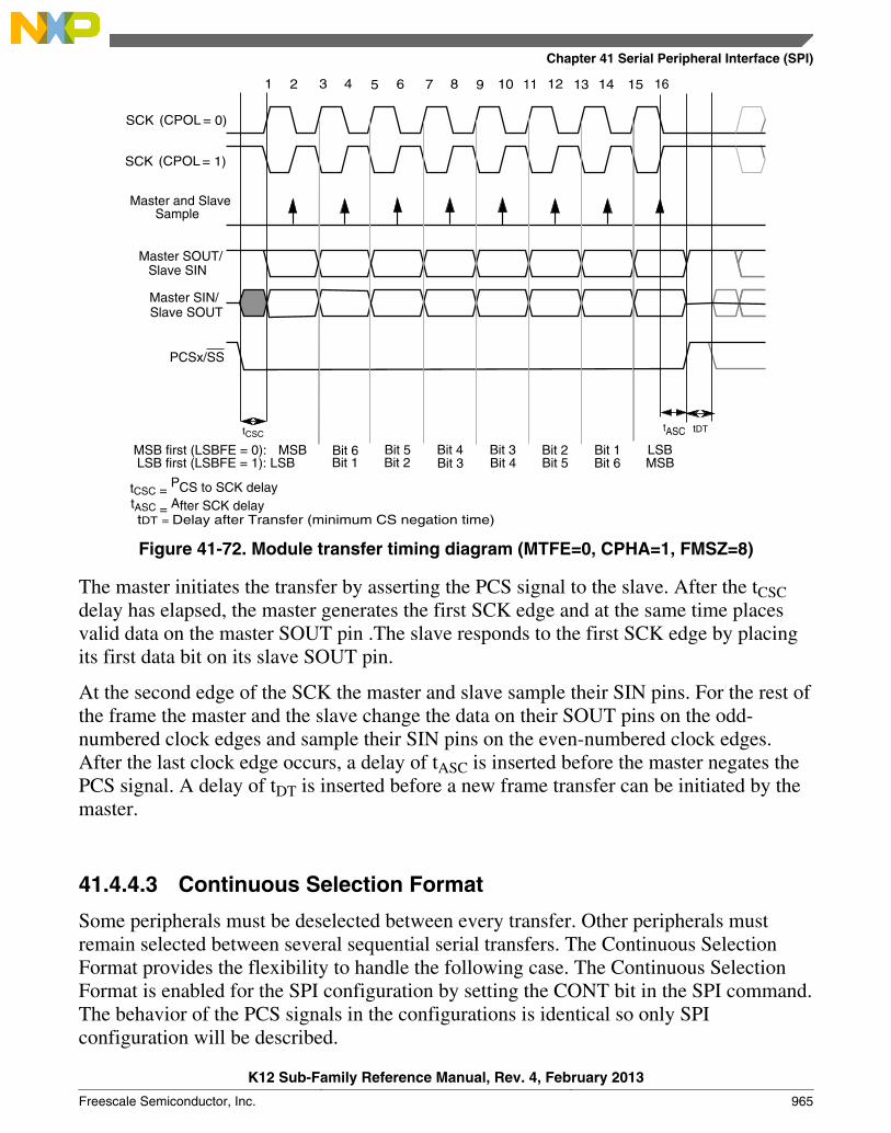
tASC = After SCK delaytCSC =
PCS to SCK delay
MSB first (LSBFE = 0): MSB tDT = Delay after Transfer (minimum CS negation time)
tCSC
Bit 1 MSB
tDT tASC
PCSx/SS
Slave SOUTMaster SIN/
Master SOUT/ Slave SIN
Master and Slave Sample
SCK (CPOL = 0)
1 2 3 4 5 6 7 8 9 10 11 12 13 14 15 16
SCK (CPOL = 1)
Bit 6Bit 2 Bit 3 Bit 4 Bit 5 Bit 6
LSBBit 5 Bit 4 Bit 3 Bit 2 Bit 1LSB first (LSBFE = 1): LSB
Figure 41-72. Module transfer timing diagram (MTFE=0, CPHA=1, FMSZ=8)
The master initiates the transfer by asserting the PCS signal to the slave. After the tCSCdelay has elapsed, the master generates the first SCK edge and at the same time placesvalid data on the master SOUT pin .The slave responds to the first SCK edge by placingits first data bit on its slave SOUT pin.
At the second edge of the SCK the master and slave sample their SIN pins. For the rest ofthe frame the master and the slave change the data on their SOUT pins on the odd-numbered clock edges and sample their SIN pins on the even-numbered clock edges.After the last clock edge occurs, a delay of tASC is inserted before the master negates thePCS signal. A delay of tDT is inserted before a new frame transfer can be initiated by themaster.
41.4.4.3 Continuous Selection Format
Some peripherals must be deselected between every transfer. Other peripherals mustremain selected between several sequential serial transfers. The Continuous SelectionFormat provides the flexibility to handle the following case. The Continuous SelectionFormat is enabled for the SPI configuration by setting the CONT bit in the SPI command.The behavior of the PCS signals in the configurations is identical so only SPIconfiguration will be described.
Chapter 41 Serial Peripheral Interface (SPI)
K12 Sub-Family Reference Manual, Rev. 4, February 2013
Freescale Semiconductor, Inc. 965

When the CONT bit = 0, the module drives the asserted Chip Select signals to their idlestates in between frames. The idle states of the Chip Select signals are selected by thePCSISn bits in the MCR. The following timing diagram is for two four-bit transfers withCPHA = 1 and CONT = 0.
PCSx
SCK
Master SIN
tCSC = PCS to SCK dela
t ASC = After SCK delay
SCK (CPOL = 0)
SCK (CPOL = 1)
Master SOUT
tDT = Delay after Transfer (minimum CS negation time)
tCSC t ASC tCSC tDT
Figure 41-73. Example of non-continuous format (CPHA=1, CONT=0)
When the CONT bit = 1, the PCS signal remains asserted for the duration of the twotransfers. The Delay between Transfers (tDT) is not inserted between the transfers. Thefollowing figure shows the timing diagram for two four-bit transfers with CPHA = 1 andCONT = 1.
PCS
Master SIN
tCSC = PCS to SCK del ay
t ASC = After SCK delay
SCK (CPOL = 0)
SCK (CPOL = 1)
Master SOUT
tCSC t ASC tCSC
Figure 41-74. Example of continuous transfer (CPHA=1, CONT=1)
When using the module with continuous selection follow these rules:
Functional description
K12 Sub-Family Reference Manual, Rev. 4, February 2013
966 Freescale Semiconductor, Inc.
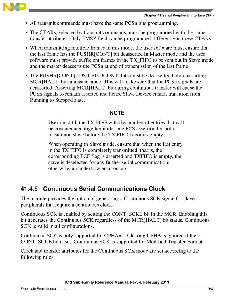
• All transmit commands must have the same PCSn bits programming.
• The CTARs, selected by transmit commands, must be programmed with the sametransfer attributes. Only FMSZ field can be programmed differently in these CTARs.
• When transmitting multiple frames in this mode, the user software must ensure thatthe last frame has the PUSHR[CONT] bit deasserted in Master mode and the usersoftware must provide sufficient frames in the TX_FIFO to be sent out in Slave modeand the master deasserts the PCSn at end of transmission of the last frame.
• The PUSHR[CONT] / DSICR0[DCONT] bits must be deasserted before assertingMCR[HALT] bit in master mode. This will make sure that the PCSn signals aredeasserted. Asserting MCR[HALT] bit during continuous transfer will cause thePCSn signals to remain asserted and hence Slave Device cannot transition fromRunning to Stopped state.
NOTE
User must fill the TX FIFO with the number of entries that willbe concatenated together under one PCS assertion for bothmaster and slave before the TX FIFO becomes empty.
When operating in Slave mode, ensure that when the last entryin the TX FIFO is completely transmitted, that is, thecorresponding TCF flag is asserted and TXFIFO is empty, theslave is deselected for any further serial communication;otherwise, an underflow error occurs.
41.4.5 Continuous Serial Communications Clock
The module provides the option of generating a Continuous SCK signal for slaveperipherals that require a continuous clock.
Continuous SCK is enabled by setting the CONT_SCKE bit in the MCR. Enabling thisbit generates the Continuous SCK regardless of the MCR[HALT] bit status. ContinuousSCK is valid in all configurations.
Continuous SCK is only supported for CPHA=1. Clearing CPHA is ignored if theCONT_SCKE bit is set. Continuous SCK is supported for Modified Transfer Format.
Clock and transfer attributes for the Continuous SCK mode are set according to thefollowing rules:
Chapter 41 Serial Peripheral Interface (SPI)
K12 Sub-Family Reference Manual, Rev. 4, February 2013
Freescale Semiconductor, Inc. 967
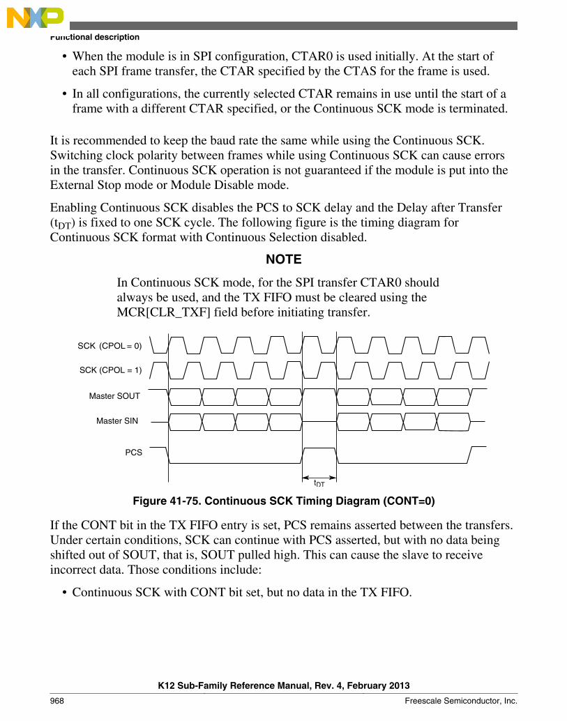
• When the module is in SPI configuration, CTAR0 is used initially. At the start ofeach SPI frame transfer, the CTAR specified by the CTAS for the frame is used.
• In all configurations, the currently selected CTAR remains in use until the start of aframe with a different CTAR specified, or the Continuous SCK mode is terminated.
It is recommended to keep the baud rate the same while using the Continuous SCK.Switching clock polarity between frames while using Continuous SCK can cause errorsin the transfer. Continuous SCK operation is not guaranteed if the module is put into theExternal Stop mode or Module Disable mode.
Enabling Continuous SCK disables the PCS to SCK delay and the Delay after Transfer(tDT) is fixed to one SCK cycle. The following figure is the timing diagram forContinuous SCK format with Continuous Selection disabled.
NOTE
In Continuous SCK mode, for the SPI transfer CTAR0 shouldalways be used, and the TX FIFO must be cleared using theMCR[CLR_TXF] field before initiating transfer.
PCS
Master SIN
SCK (CPOL = 0)
SCK (CPOL = 1)
Master SOUT
tDT
Figure 41-75. Continuous SCK Timing Diagram (CONT=0)
If the CONT bit in the TX FIFO entry is set, PCS remains asserted between the transfers.Under certain conditions, SCK can continue with PCS asserted, but with no data beingshifted out of SOUT, that is, SOUT pulled high. This can cause the slave to receiveincorrect data. Those conditions include:
• Continuous SCK with CONT bit set, but no data in the TX FIFO.
Functional description
K12 Sub-Family Reference Manual, Rev. 4, February 2013
968 Freescale Semiconductor, Inc.
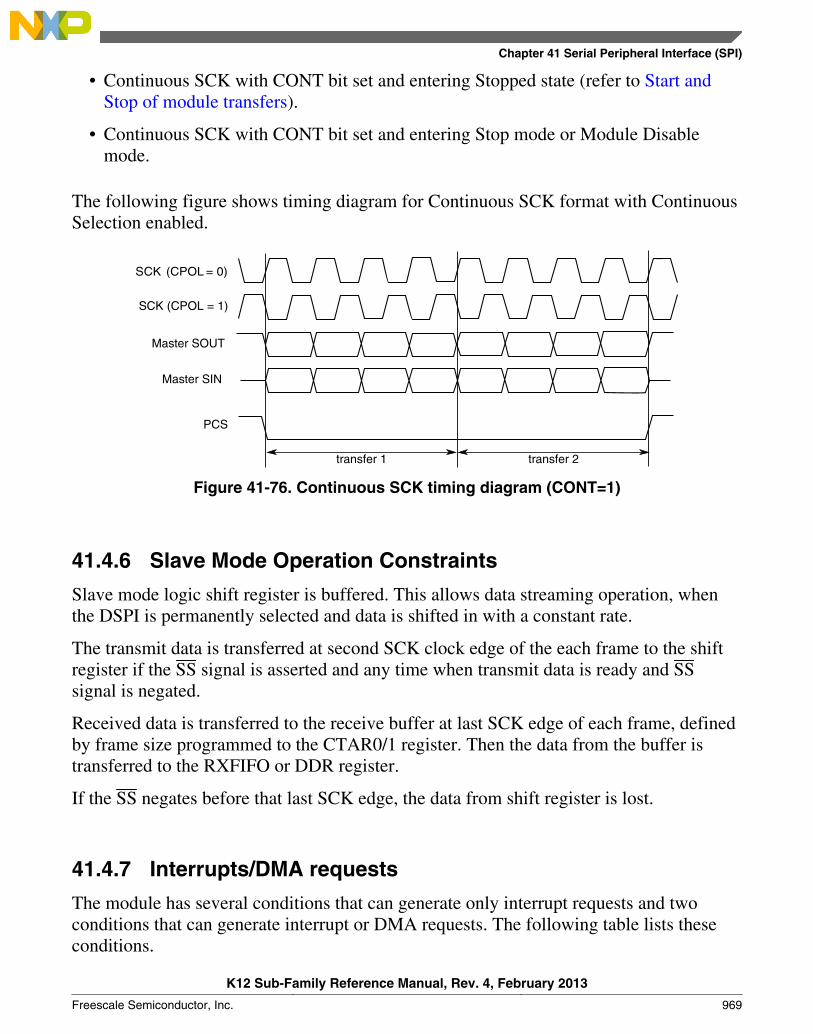
• Continuous SCK with CONT bit set and entering Stopped state (refer to Start andStop of module transfers).
• Continuous SCK with CONT bit set and entering Stop mode or Module Disablemode.
The following figure shows timing diagram for Continuous SCK format with ContinuousSelection enabled.
PCS
Master SIN
SCK (CPOL = 0)
SCK (CPOL = 1)
Master SOUT
transfer 1 transfer 2
Figure 41-76. Continuous SCK timing diagram (CONT=1)
41.4.6 Slave Mode Operation Constraints
Slave mode logic shift register is buffered. This allows data streaming operation, whenthe DSPI is permanently selected and data is shifted in with a constant rate.
The transmit data is transferred at second SCK clock edge of the each frame to the shiftregister if the SS signal is asserted and any time when transmit data is ready and SSsignal is negated.
Received data is transferred to the receive buffer at last SCK edge of each frame, definedby frame size programmed to the CTAR0/1 register. Then the data from the buffer istransferred to the RXFIFO or DDR register.
If the SS negates before that last SCK edge, the data from shift register is lost.
41.4.7 Interrupts/DMA requests
The module has several conditions that can generate only interrupt requests and twoconditions that can generate interrupt or DMA requests. The following table lists theseconditions.
Chapter 41 Serial Peripheral Interface (SPI)
K12 Sub-Family Reference Manual, Rev. 4, February 2013
Freescale Semiconductor, Inc. 969
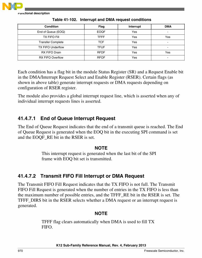
Table 41-102. Interrupt and DMA request conditions
Condition Flag Interrupt DMA
End of Queue (EOQ) EOQF Yes -
TX FIFO Fill TFFF Yes Yes
Transfer Complete TCF Yes -
TX FIFO Underflow TFUF Yes -
RX FIFO Drain RFDF Yes Yes
RX FIFO Overflow RFOF Yes -
Each condition has a flag bit in the module Status Register (SR) and a Request Enable bitin the DMA/Interrupt Request Select and Enable Register (RSER). Certain flags (asshown in above table) generate interrupt requests or DMA requests depending onconfiguration of RSER register.
The module also provides a global interrupt request line, which is asserted when any ofindividual interrupt requests lines is asserted.
41.4.7.1 End of Queue Interrupt Request
The End of Queue Request indicates that the end of a transmit queue is reached. The Endof Queue Request is generated when the EOQ bit in the executing SPI command is setand the EOQF_RE bit in the RSER is set.
NOTEThis interrupt request is generated when the last bit of the SPIframe with EOQ bit set is transmitted.
41.4.7.2 Transmit FIFO Fill Interrupt or DMA Request
The Transmit FIFO Fill Request indicates that the TX FIFO is not full. The TransmitFIFO Fill Request is generated when the number of entries in the TX FIFO is less thanthe maximum number of possible entries, and the TFFF_RE bit in the RSER is set. TheTFFF_DIRS bit in the RSER selects whether a DMA request or an interrupt request isgenerated.
NOTE
TFFF flag clears automatically when DMA is used to fill TXFIFO.
Functional description
K12 Sub-Family Reference Manual, Rev. 4, February 2013
970 Freescale Semiconductor, Inc.
To clear TFFF when not using DMA, follow these steps forevery PUSH performed using CPU to fill TX FIFO:
1. Wait until TFFF = 1.2. Write data to PUSHR using CPU.3. Clear TFFF by writing a 1 to its location. If TX FIFO is not
full, this flag will not clear.
41.4.7.3 Transfer Complete Interrupt Request
The Transfer Complete Request indicates the end of the transfer of a serial frame. TheTransfer Complete Request is generated at the end of each frame transfer when theTCF_RE bit is set in the RSER.
41.4.7.4 Transmit FIFO Underflow Interrupt Request
The Transmit FIFO Underflow Request indicates that an underflow condition in the TXFIFO has occurred. The transmit underflow condition is detected only for the moduleoperating in Slave mode and SPI configuration . The TFUF bit is set when the TX FIFOof a DSPI is empty, and a transfer is initiated from an external SPI master. If the TFUFbit is set while the TFUF_RE bit in the RSER is set, an interrupt request is generated.
41.4.7.5 Receive FIFO Drain Interrupt or DMA Request
The Receive FIFO Drain Request indicates that the RX FIFO is not empty. The ReceiveFIFO Drain Request is generated when the number of entries in the RX FIFO is not zero,and the RFDF_RE bit in the RSER is set. The RFDF_DIRS bit in the RSER selectswhether a DMA request or an interrupt request is generated.
41.4.7.6 Receive FIFO Overflow Interrupt Request
The Receive FIFO Overflow Request indicates that an overflow condition in the RXFIFO has occurred. A Receive FIFO Overflow request is generated when RX FIFO andshift register are full and a transfer is initiated. The RFOF_RE bit in the RSER must beset for the interrupt request to be generated.
Chapter 41 Serial Peripheral Interface (SPI)
K12 Sub-Family Reference Manual, Rev. 4, February 2013
Freescale Semiconductor, Inc. 971
Depending on the state of the ROOE bit in the MCR, the data from the transfer thatgenerated the overflow is either ignored or shifted in to the shift register. If the ROOE bitis set, the incoming data is shifted in to the shift register. If the ROOE bit is cleared, theincoming data is ignored.
41.4.8 Power saving features
The module supports following power-saving strategies:
• External Stop mode
• Module Disable mode – Clock gating of non-memory mapped logic
41.4.8.1 Stop mode (External Stop mode)
The DSPI supports the Stop mode protocol. When a request is made to enter ExternalStop mode, the DSPI block acknowledges the request . If a serial transfer is in progress,the DSPI waits until it reaches the frame boundary before it is ready to have its clocksshut off . While the clocks are shut off, the DSPI memory-mapped logic is not accessible.This also puts the DSPI in STOPPED state. The SR[TXRXS] bit is cleared to indicateSTOPPED state. The states of the interrupt and DMA request signals cannot be changedwhile in External Stop mode.
41.4.8.2 Module Disable mode
Module Disable mode is a block-specific mode that the module can enter to save power.Host CPU can initiate the Module Disable mode by setting the MDIS bit in the MCR.The Module Disable mode can also be initiated by hardware. A power management blockcan initiate the Module Disable mode by asserting the DOZE mode signal while theDOZE bit in the MCR is set.
When the MDIS bit is set or the DOZE mode signal is asserted while the DOZE bit is set,the module negates Clock Enable signal at the next frame boundary. Once the ClockEnable signal is negated, it is said to have entered Module Disable Mode. This also putsthe module in STOPPED state. The SR[TXRXS] bit is cleared to indicate STOPPEDstate.If implemented, the Clock Enable signal can stop the clock to the non-memorymapped logic. When Clock Enable is negated, the module is in a dormant state, but thememory mapped registers are still accessible. Certain read or write operations have adifferent effect when the module is in the Module Disable mode. Reading the RX FIFOPop Register does not change the state of the RX FIFO. Similarly, writing to the PUSHR
Functional description
K12 Sub-Family Reference Manual, Rev. 4, February 2013
972 Freescale Semiconductor, Inc.
Register does not change the state of the TX FIFO. Clearing either of the FIFOs has noeffect in the Module Disable mode. Changes to the DIS_TXF and DIS_RXF fields of theMCR have no effect in the Module Disable mode. In the Module Disable mode, all statusbits and register flags in the module return the correct values when read, but writing tothem has no effect. Writing to the TCR during Module Disable mode has no effect.Interrupt and DMA request signals cannot be cleared while in the Module Disable mode.
41.5 Initialization/application informationThis section describes how to initialize the module.
41.5.1 How to manage queues
The queues are not part of the module, but it includes features in support of queuemanagement. Queues are primarily supported in SPI configuration.
1. When module executes last command word from a queue, the EOQ bit in thecommand word is set to indicate it that this is the last entry in the queue.
2. At the end of the transfer, corresponding to the command word with EOQ set issampled, the EOQ flag (EOQF) in the SR is set.
3. The setting of the EOQF flag disables serial transmission and reception of data,putting the module in the Stopped state. The TXRXS bit is cleared to indicate theStopped state.
4. The DMA can continue to fill TX FIFO until it is full or step 5 occurs.
5. Disable DMA transfers by disabling the DMA enable request for the DMA channelassigned to TX FIFO and RX FIFO. This is done by clearing the correspondingDMA enable request bits in the DMA Controller.
6. Ensure all received data in RX FIFO has been transferred to memory receive queueby reading the RXCNT in SR or by checking RFDF in the SR after each readoperation of the POPR.
7. Modify DMA descriptor of TX and RX channels for new queues
8. Flush TX FIFO by writing a 1 to the CLR_TXF bit in the MCR. Flush RX FIFO bywriting a '1' to the CLR_RXF bit in the MCR.
9. Clear transfer count either by setting CTCNT bit in the command word of the firstentry in the new queue or via CPU writing directly to SPI_TCNT field in the TCR.
Chapter 41 Serial Peripheral Interface (SPI)
K12 Sub-Family Reference Manual, Rev. 4, February 2013
Freescale Semiconductor, Inc. 973

10. Enable DMA channel by enabling the DMA enable request for the DMA channelassigned to the module TX FIFO, and RX FIFO by setting the corresponding DMAset enable request bit.
11. Enable serial transmission and serial reception of data by clearing the EOQF bit.
41.5.2 Switching Master and Slave mode
When changing modes in the module, follow the steps below to guarantee properoperation.
1. Halt it by setting MCR[HALT].
2. Clear the transmit and receive FIFOs by writing a 1 to the CLR_TXF and CLR_RXFbits in MCR.
3. Set the appropriate mode in MCR[MSTR] and enable it by clearing MCR[HALT].
41.5.3 Initializing Module in Master/Slave Modes
Once the appropriate mode in MCR[MSTR] is configured, the module is enabled byclearing MCR[HALT]. It should be ensured that module Slave is enabled before enablingit's Master. This ensures the Slave is ready to be communicated with, before Masterinitializes communication.
41.5.4 Baud rate settings
The following table shows the baud rate that is generated based on the combination of thebaud rate prescaler PBR and the baud rate scaler BR in the CTARs. The values calculatedassume a 100 MHz system frequency and the double baud rate DBR bit is cleared.
NOTEThe clock frequency mentioned above is given as an example inthis chapter. See the clocking chapter for the frequency used todrive this module in the device.
Initialization/application information
K12 Sub-Family Reference Manual, Rev. 4, February 2013
974 Freescale Semiconductor, Inc.
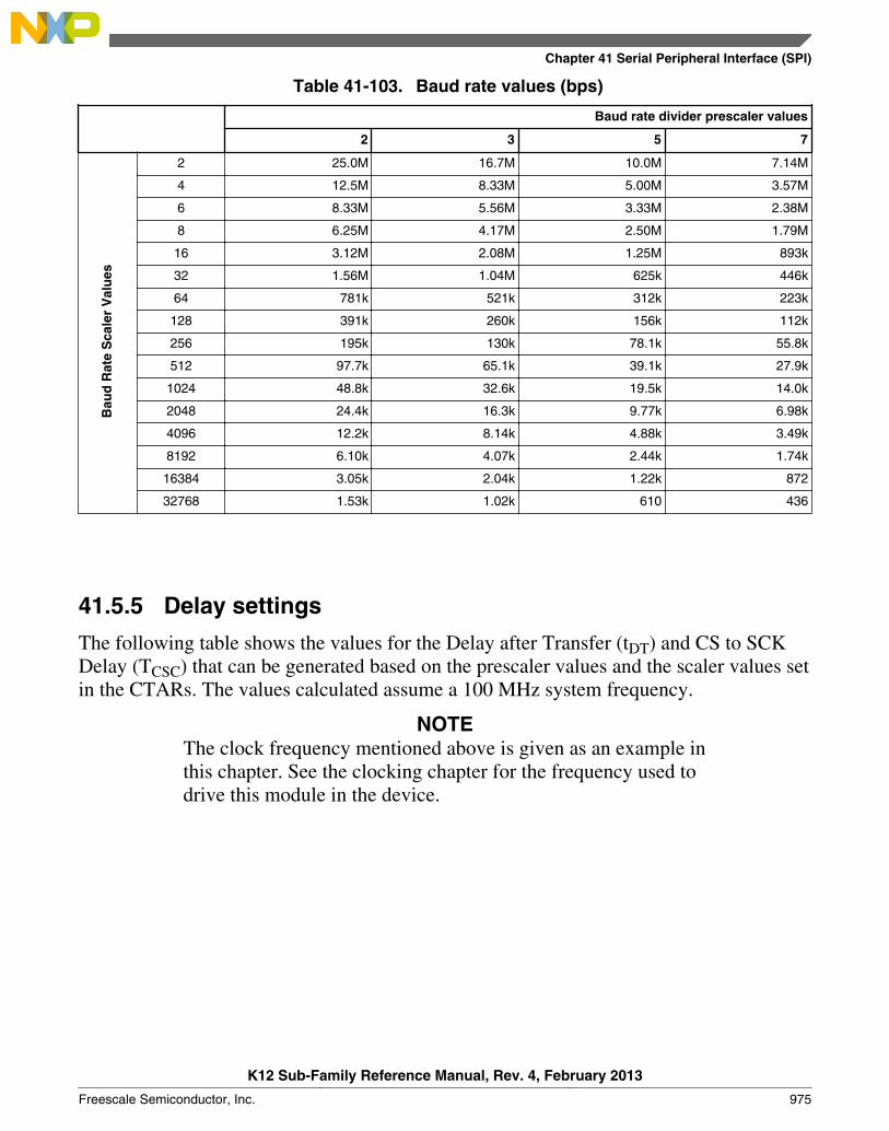
Table 41-103. Baud rate values (bps)
Baud rate divider prescaler values
2 3 5 7
Bau
d R
ate
Sca
ler
Val
ues
2 25.0M 16.7M 10.0M 7.14M
4 12.5M 8.33M 5.00M 3.57M
6 8.33M 5.56M 3.33M 2.38M
8 6.25M 4.17M 2.50M 1.79M
16 3.12M 2.08M 1.25M 893k
32 1.56M 1.04M 625k 446k
64 781k 521k 312k 223k
128 391k 260k 156k 112k
256 195k 130k 78.1k 55.8k
512 97.7k 65.1k 39.1k 27.9k
1024 48.8k 32.6k 19.5k 14.0k
2048 24.4k 16.3k 9.77k 6.98k
4096 12.2k 8.14k 4.88k 3.49k
8192 6.10k 4.07k 2.44k 1.74k
16384 3.05k 2.04k 1.22k 872
32768 1.53k 1.02k 610 436
41.5.5 Delay settings
The following table shows the values for the Delay after Transfer (tDT) and CS to SCKDelay (TCSC) that can be generated based on the prescaler values and the scaler values setin the CTARs. The values calculated assume a 100 MHz system frequency.
NOTEThe clock frequency mentioned above is given as an example inthis chapter. See the clocking chapter for the frequency used todrive this module in the device.
Chapter 41 Serial Peripheral Interface (SPI)
K12 Sub-Family Reference Manual, Rev. 4, February 2013
Freescale Semiconductor, Inc. 975
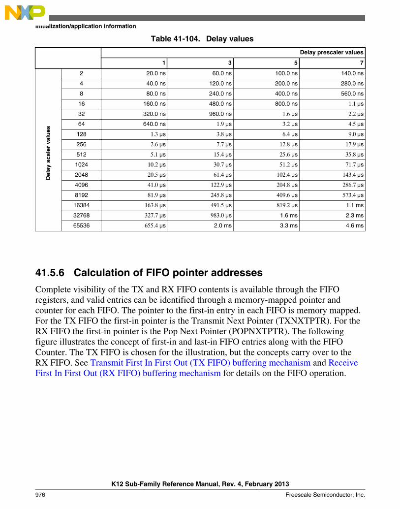
Table 41-104. Delay values
Delay prescaler values
1 3 5 7
Del
ay s
cale
r va
lues
2 20.0 ns 60.0 ns 100.0 ns 140.0 ns
4 40.0 ns 120.0 ns 200.0 ns 280.0 ns
8 80.0 ns 240.0 ns 400.0 ns 560.0 ns
16 160.0 ns 480.0 ns 800.0 ns 1.1 μs
32 320.0 ns 960.0 ns 1.6 μs 2.2 μs
64 640.0 ns 1.9 μs 3.2 μs 4.5 μs
128 1.3 μs 3.8 μs 6.4 μs 9.0 μs
256 2.6 μs 7.7 μs 12.8 μs 17.9 μs
512 5.1 μs 15.4 μs 25.6 μs 35.8 μs
1024 10.2 μs 30.7 μs 51.2 μs 71.7 μs
2048 20.5 μs 61.4 μs 102.4 μs 143.4 μs
4096 41.0 μs 122.9 μs 204.8 μs 286.7 μs
8192 81.9 μs 245.8 μs 409.6 μs 573.4 μs
16384 163.8 μs 491.5 μs 819.2 μs 1.1 ms
32768 327.7 μs 983.0 μs 1.6 ms 2.3 ms
65536 655.4 μs 2.0 ms 3.3 ms 4.6 ms
41.5.6 Calculation of FIFO pointer addresses
Complete visibility of the TX and RX FIFO contents is available through the FIFOregisters, and valid entries can be identified through a memory-mapped pointer andcounter for each FIFO. The pointer to the first-in entry in each FIFO is memory mapped.For the TX FIFO the first-in pointer is the Transmit Next Pointer (TXNXTPTR). For theRX FIFO the first-in pointer is the Pop Next Pointer (POPNXTPTR). The followingfigure illustrates the concept of first-in and last-in FIFO entries along with the FIFOCounter. The TX FIFO is chosen for the illustration, but the concepts carry over to theRX FIFO. See Transmit First In First Out (TX FIFO) buffering mechanism and ReceiveFirst In First Out (RX FIFO) buffering mechanism for details on the FIFO operation.
Initialization/application information
K12 Sub-Family Reference Manual, Rev. 4, February 2013
976 Freescale Semiconductor, Inc.

Push TX FIFO Register
Transmit Next Data Pointer
Shift Register SOUT
+1 -1TX FIFO Counter
TX FIFO Base -
Entry C
Entry A (first in)
Entry D (last in)
Entry B
-
- -
Figure 41-77. TX FIFO pointers and counter
41.5.6.1 Address Calculation for the First-in Entry and Last-in Entryin the TX FIFO
The memory address of the first-in entry in the TX FIFO is computed by the followingequation:
The memory address of the last-in entry in the TX FIFO is computed by the followingequation:
TX FIFO Base - Base address of TX FIFOTXCTR - TX FIFO CounterTXNXTPTR - Transmit Next PointerTX FIFO Depth - Transmit FIFO depth, implementation specific
41.5.6.2 Address Calculation for the First-in Entry and Last-in Entryin the RX FIFO
The memory address of the first-in entry in the RX FIFO is computed by the followingequation:
Chapter 41 Serial Peripheral Interface (SPI)
K12 Sub-Family Reference Manual, Rev. 4, February 2013
Freescale Semiconductor, Inc. 977

The memory address of the last-in entry in the RX FIFO is computed by the followingequation:
RX FIFO Base - Base address of RX FIFORXCTR - RX FIFO counterPOPNXTPTR - Pop Next PointerRX FIFO Depth - Receive FIFO depth, implementation specific
Initialization/application information
K12 Sub-Family Reference Manual, Rev. 4, February 2013
978 Freescale Semiconductor, Inc.

Chapter 42Inter-Integrated Circuit (I2C)
42.1 IntroductionNOTE
For the chip-specific implementation details of this module'sinstances see the chip configuration information.
The inter-integrated circuit (I2C, I2C, or IIC) module provides a method ofcommunication between a number of devices. The interface is designed to operate up to100 kbit/s with maximum bus loading and timing. The I2C device is capable of operatingat higher baud rates, up to a maximum of clock/20, with reduced bus loading. Themaximum communication length and the number of devices that can be connected arelimited by a maximum bus capacitance of 400 pF. The I2C module also complies withthe System Management Bus (SMBus) Specification, version 2.
42.1.1 Features
The I2C module has the following features:
• Compatible with The I2C-Bus Specification• Multimaster operation• Software programmable for one of 64 different serial clock frequencies• Software-selectable acknowledge bit• Interrupt-driven byte-by-byte data transfer• Arbitration-lost interrupt with automatic mode switching from master to slave• Calling address identification interrupt• START and STOP signal generation and detection• Repeated START signal generation and detection• Acknowledge bit generation and detection• Bus busy detection• General call recognition
K12 Sub-Family Reference Manual, Rev. 4, February 2013
Freescale Semiconductor, Inc. 979

• 10-bit address extension• Support for System Management Bus (SMBus) Specification, version 2• Programmable glitch input filter• Low power mode wakeup on slave address match• Range slave address support• DMA support
42.1.2 Modes of operation
The I2C module's operation in various low power modes is as follows:
• Run mode: This is the basic mode of operation. To conserve power in this mode,disable the module.
• Wait mode: The module continues to operate when the core is in Wait mode and canprovide a wakeup interrupt.
• Stop mode: The module is inactive in Stop mode for reduced power consumption,except that address matching is enabled in Stop mode. The STOP instruction doesnot affect the I2C module's register states.
42.1.3 Block diagram
The following figure is a functional block diagram of the I2C module.
Introduction
K12 Sub-Family Reference Manual, Rev. 4, February 2013
980 Freescale Semiconductor, Inc.
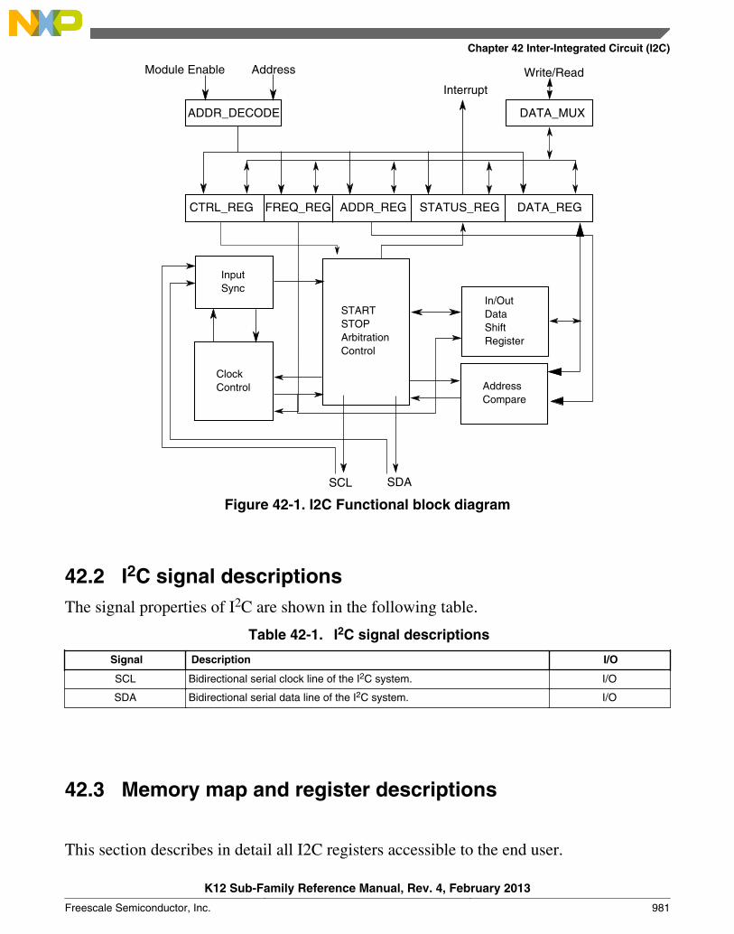
Interrupt
Write/Read Address
SCL SDA
Module Enable
CTRL_REG
DATA_MUXADDR_DECODE
DATA_REGSTATUS_REGADDR_REGFREQ_REG
Input Sync
Clock Control
START STOP Arbitration Control
In/Out Data Shift Register
Address Compare
Figure 42-1. I2C Functional block diagram
42.2 I2C signal descriptionsThe signal properties of I2C are shown in the following table.
Table 42-1. I2C signal descriptions
Signal Description I/O
SCL Bidirectional serial clock line of the I2C system. I/O
SDA Bidirectional serial data line of the I2C system. I/O
Memory map and register descriptions
This section describes in detail all I2C registers accessible to the end user.
42.3
Chapter 42 Inter-Integrated Circuit (I2C)
K12 Sub-Family Reference Manual, Rev. 4, February 2013
Freescale Semiconductor, Inc. 981
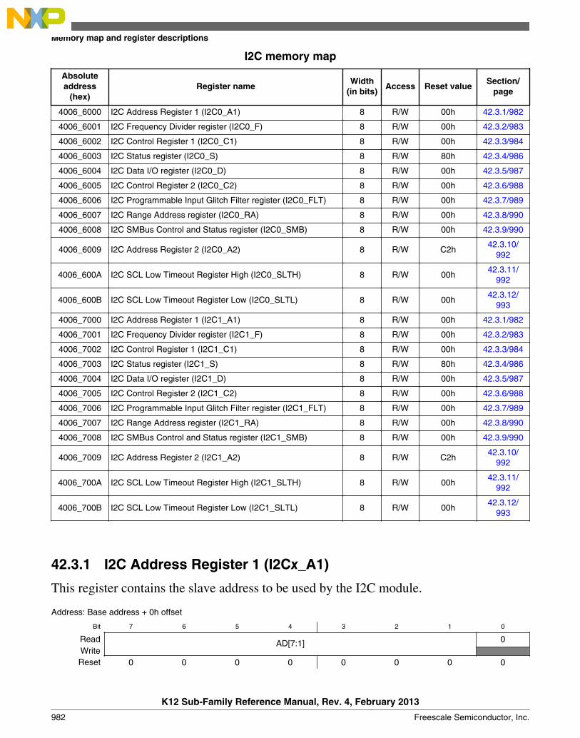
I2C memory map
Absoluteaddress
(hex)Register name
Width(in bits)
Access Reset valueSection/
page
4006_6000 I2C Address Register 1 (I2C0_A1) 8 R/W 00h 42.3.1/982
4006_6001 I2C Frequency Divider register (I2C0_F) 8 R/W 00h 42.3.2/983
4006_6002 I2C Control Register 1 (I2C0_C1) 8 R/W 00h 42.3.3/984
4006_6003 I2C Status register (I2C0_S) 8 R/W 80h 42.3.4/986
4006_6004 I2C Data I/O register (I2C0_D) 8 R/W 00h 42.3.5/987
4006_6005 I2C Control Register 2 (I2C0_C2) 8 R/W 00h 42.3.6/988
4006_6006 I2C Programmable Input Glitch Filter register (I2C0_FLT) 8 R/W 00h 42.3.7/989
4006_6007 I2C Range Address register (I2C0_RA) 8 R/W 00h 42.3.8/990
4006_6008 I2C SMBus Control and Status register (I2C0_SMB) 8 R/W 00h 42.3.9/990
4006_6009 I2C Address Register 2 (I2C0_A2) 8 R/W C2h42.3.10/
992
4006_600A I2C SCL Low Timeout Register High (I2C0_SLTH) 8 R/W 00h42.3.11/
992
4006_600B I2C SCL Low Timeout Register Low (I2C0_SLTL) 8 R/W 00h42.3.12/
993
4006_7000 I2C Address Register 1 (I2C1_A1) 8 R/W 00h 42.3.1/982
4006_7001 I2C Frequency Divider register (I2C1_F) 8 R/W 00h 42.3.2/983
4006_7002 I2C Control Register 1 (I2C1_C1) 8 R/W 00h 42.3.3/984
4006_7003 I2C Status register (I2C1_S) 8 R/W 80h 42.3.4/986
4006_7004 I2C Data I/O register (I2C1_D) 8 R/W 00h 42.3.5/987
4006_7005 I2C Control Register 2 (I2C1_C2) 8 R/W 00h 42.3.6/988
4006_7006 I2C Programmable Input Glitch Filter register (I2C1_FLT) 8 R/W 00h 42.3.7/989
4006_7007 I2C Range Address register (I2C1_RA) 8 R/W 00h 42.3.8/990
4006_7008 I2C SMBus Control and Status register (I2C1_SMB) 8 R/W 00h 42.3.9/990
4006_7009 I2C Address Register 2 (I2C1_A2) 8 R/W C2h42.3.10/
992
4006_700A I2C SCL Low Timeout Register High (I2C1_SLTH) 8 R/W 00h42.3.11/
992
4006_700B I2C SCL Low Timeout Register Low (I2C1_SLTL) 8 R/W 00h42.3.12/
993
42.3.1 I2C Address Register 1 (I2Cx_A1)
This register contains the slave address to be used by the I2C module.
Address: Base address + 0h offset
Bit 7 6 5 4 3 2 1 0
Read AD[7:1] 0WriteReset 0 0 0 0 0 0 0 0
Memory map and register descriptions
K12 Sub-Family Reference Manual, Rev. 4, February 2013
982 Freescale Semiconductor, Inc.
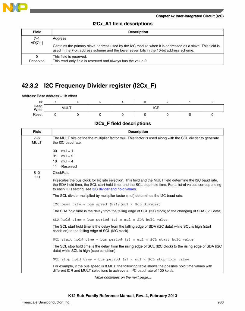
I2Cx_A1 field descriptions
Field Description
7–1AD[7:1]
Address
Contains the primary slave address used by the I2C module when it is addressed as a slave. This field isused in the 7-bit address scheme and the lower seven bits in the 10-bit address scheme.
0Reserved
This field is reserved.This read-only field is reserved and always has the value 0.
42.3.2 I2C Frequency Divider register (I2Cx_F)
Address: Base address + 1h offset
Bit 7 6 5 4 3 2 1 0
Read MULT ICRWriteReset 0 0 0 0 0 0 0 0
I2Cx_F field descriptions
Field Description
7–6MULT
The MULT bits define the multiplier factor mul. This factor is used along with the SCL divider to generatethe I2C baud rate.
00 mul = 101 mul = 210 mul = 411 Reserved
5–0ICR
ClockRate
Prescales the bus clock for bit rate selection. This field and the MULT field determine the I2C baud rate,the SDA hold time, the SCL start hold time, and the SCL stop hold time. For a list of values correspondingto each ICR setting, see I2C divider and hold values.
The SCL divider multiplied by multiplier factor (mul) determines the I2C baud rate.
I2C baud rate = bus speed (Hz)/(mul × SCL divider)
The SDA hold time is the delay from the falling edge of SCL (I2C clock) to the changing of SDA (I2C data).
SDA hold time = bus period (s) × mul × SDA hold value
The SCL start hold time is the delay from the falling edge of SDA (I2C data) while SCL is high (startcondition) to the falling edge of SCL (I2C clock).
SCL start hold time = bus period (s) × mul × SCL start hold value
The SCL stop hold time is the delay from the rising edge of SCL (I2C clock) to the rising edge of SDA (I2Cdata) while SCL is high (stop condition).
SCL stop hold time = bus period (s) × mul × SCL stop hold value
For example, if the bus speed is 8 MHz, the following table shows the possible hold time values withdifferent ICR and MULT selections to achieve an I2C baud rate of 100 kbit/s.
Table continues on the next page...
Chapter 42 Inter-Integrated Circuit (I2C)
K12 Sub-Family Reference Manual, Rev. 4, February 2013
Freescale Semiconductor, Inc. 983
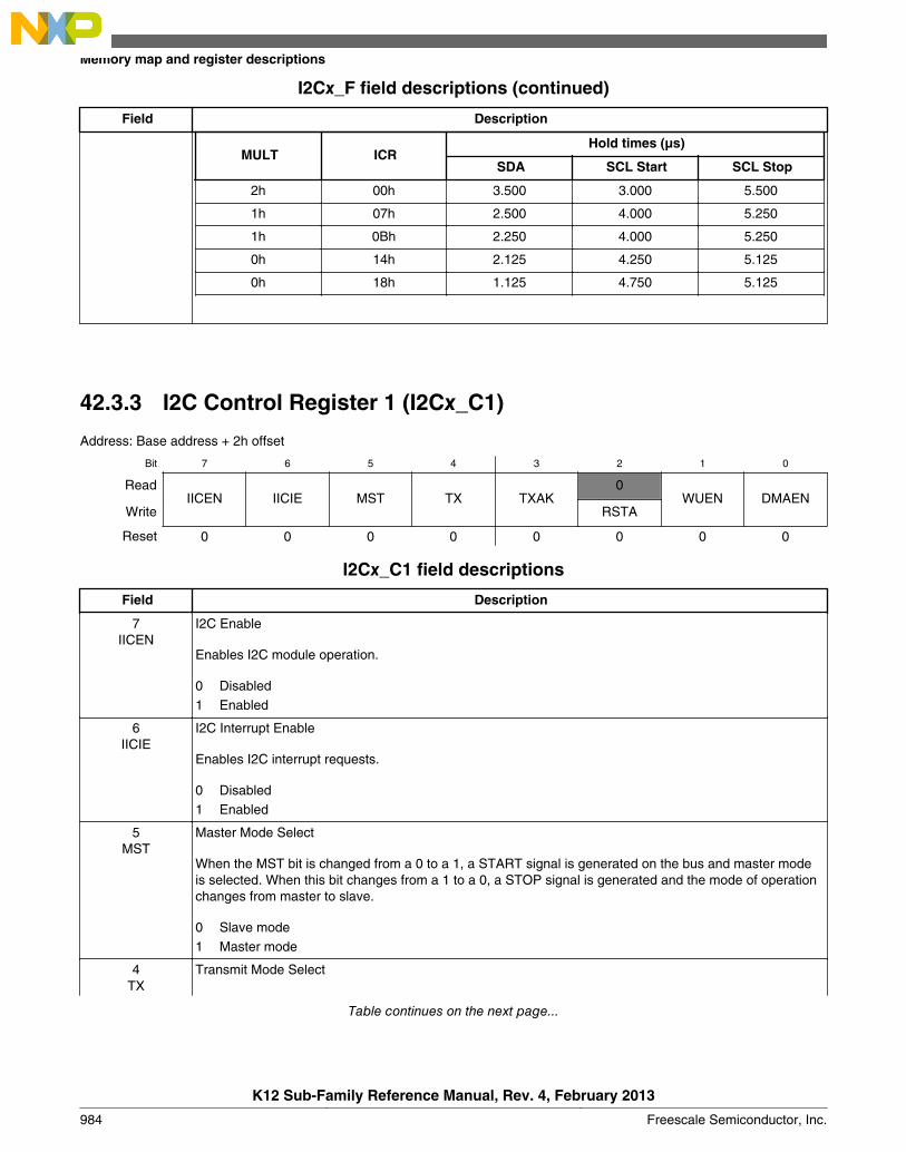
I2Cx_F field descriptions (continued)
Field Description
MULT ICRHold times (μs)
SDA SCL Start SCL Stop
2h 00h 3.500 3.000 5.500
1h 07h 2.500 4.000 5.250
1h 0Bh 2.250 4.000 5.250
0h 14h 2.125 4.250 5.125
0h 18h 1.125 4.750 5.125
42.3.3 I2C Control Register 1 (I2Cx_C1)
Address: Base address + 2h offset
Bit 7 6 5 4 3 2 1 0
ReadIICEN IICIE MST TX TXAK
0WUEN DMAEN
Write RSTA
Reset 0 0 0 0 0 0 0 0
I2Cx_C1 field descriptions
Field Description
7IICEN
I2C Enable
Enables I2C module operation.
0 Disabled1 Enabled
6IICIE
I2C Interrupt Enable
Enables I2C interrupt requests.
0 Disabled1 Enabled
5MST
Master Mode Select
When the MST bit is changed from a 0 to a 1, a START signal is generated on the bus and master modeis selected. When this bit changes from a 1 to a 0, a STOP signal is generated and the mode of operationchanges from master to slave.
0 Slave mode1 Master mode
4TX
Transmit Mode Select
Table continues on the next page...
Memory map and register descriptions
K12 Sub-Family Reference Manual, Rev. 4, February 2013
984 Freescale Semiconductor, Inc.
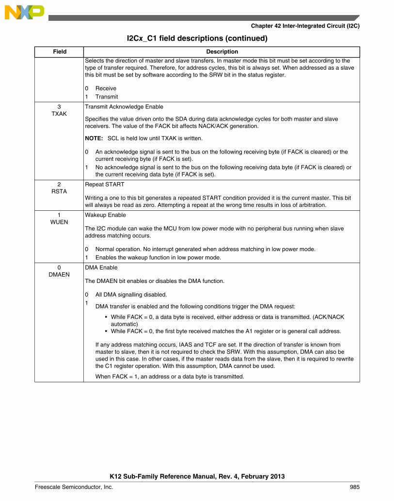
I2Cx_C1 field descriptions (continued)
Field Description
Selects the direction of master and slave transfers. In master mode this bit must be set according to thetype of transfer required. Therefore, for address cycles, this bit is always set. When addressed as a slavethis bit must be set by software according to the SRW bit in the status register.
0 Receive1 Transmit
3TXAK
Transmit Acknowledge Enable
Specifies the value driven onto the SDA during data acknowledge cycles for both master and slavereceivers. The value of the FACK bit affects NACK/ACK generation.
NOTE: SCL is held low until TXAK is written.
0 An acknowledge signal is sent to the bus on the following receiving byte (if FACK is cleared) or thecurrent receiving byte (if FACK is set).
1 No acknowledge signal is sent to the bus on the following receiving data byte (if FACK is cleared) orthe current receiving data byte (if FACK is set).
2RSTA
Repeat START
Writing a one to this bit generates a repeated START condition provided it is the current master. This bitwill always be read as zero. Attempting a repeat at the wrong time results in loss of arbitration.
1WUEN
Wakeup Enable
The I2C module can wake the MCU from low power mode with no peripheral bus running when slaveaddress matching occurs.
0 Normal operation. No interrupt generated when address matching in low power mode.1 Enables the wakeup function in low power mode.
0DMAEN
DMA Enable
The DMAEN bit enables or disables the DMA function.
0 All DMA signalling disabled.1
DMA transfer is enabled and the following conditions trigger the DMA request:
• While FACK = 0, a data byte is received, either address or data is transmitted. (ACK/NACKautomatic)
• While FACK = 0, the first byte received matches the A1 register or is general call address.
If any address matching occurs, IAAS and TCF are set. If the direction of transfer is known frommaster to slave, then it is not required to check the SRW. With this assumption, DMA can also beused in this case. In other cases, if the master reads data from the slave, then it is required to rewritethe C1 register operation. With this assumption, DMA cannot be used.
When FACK = 1, an address or a data byte is transmitted.
Chapter 42 Inter-Integrated Circuit (I2C)
K12 Sub-Family Reference Manual, Rev. 4, February 2013
Freescale Semiconductor, Inc. 985
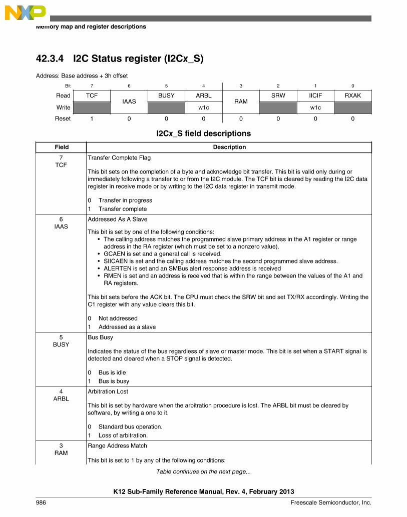
42.3.4 I2C Status register (I2Cx_S)
Address: Base address + 3h offset
Bit 7 6 5 4 3 2 1 0
Read TCFIAAS
BUSY ARBLRAM
SRW IICIF RXAK
Write w1c w1c
Reset 1 0 0 0 0 0 0 0
I2Cx_S field descriptions
Field Description
7TCF
Transfer Complete Flag
This bit sets on the completion of a byte and acknowledge bit transfer. This bit is valid only during orimmediately following a transfer to or from the I2C module. The TCF bit is cleared by reading the I2C dataregister in receive mode or by writing to the I2C data register in transmit mode.
0 Transfer in progress1 Transfer complete
6IAAS
Addressed As A Slave
This bit is set by one of the following conditions:• The calling address matches the programmed slave primary address in the A1 register or range
address in the RA register (which must be set to a nonzero value).• GCAEN is set and a general call is received.• SIICAEN is set and the calling address matches the second programmed slave address.• ALERTEN is set and an SMBus alert response address is received• RMEN is set and an address is received that is within the range between the values of the A1 and
RA registers.
This bit sets before the ACK bit. The CPU must check the SRW bit and set TX/RX accordingly. Writing theC1 register with any value clears this bit.
0 Not addressed1 Addressed as a slave
5BUSY
Bus Busy
Indicates the status of the bus regardless of slave or master mode. This bit is set when a START signal isdetected and cleared when a STOP signal is detected.
0 Bus is idle1 Bus is busy
4ARBL
Arbitration Lost
This bit is set by hardware when the arbitration procedure is lost. The ARBL bit must be cleared bysoftware, by writing a one to it.
0 Standard bus operation.1 Loss of arbitration.
3RAM
Range Address Match
This bit is set to 1 by any of the following conditions:
Table continues on the next page...
Memory map and register descriptions
K12 Sub-Family Reference Manual, Rev. 4, February 2013
986 Freescale Semiconductor, Inc.
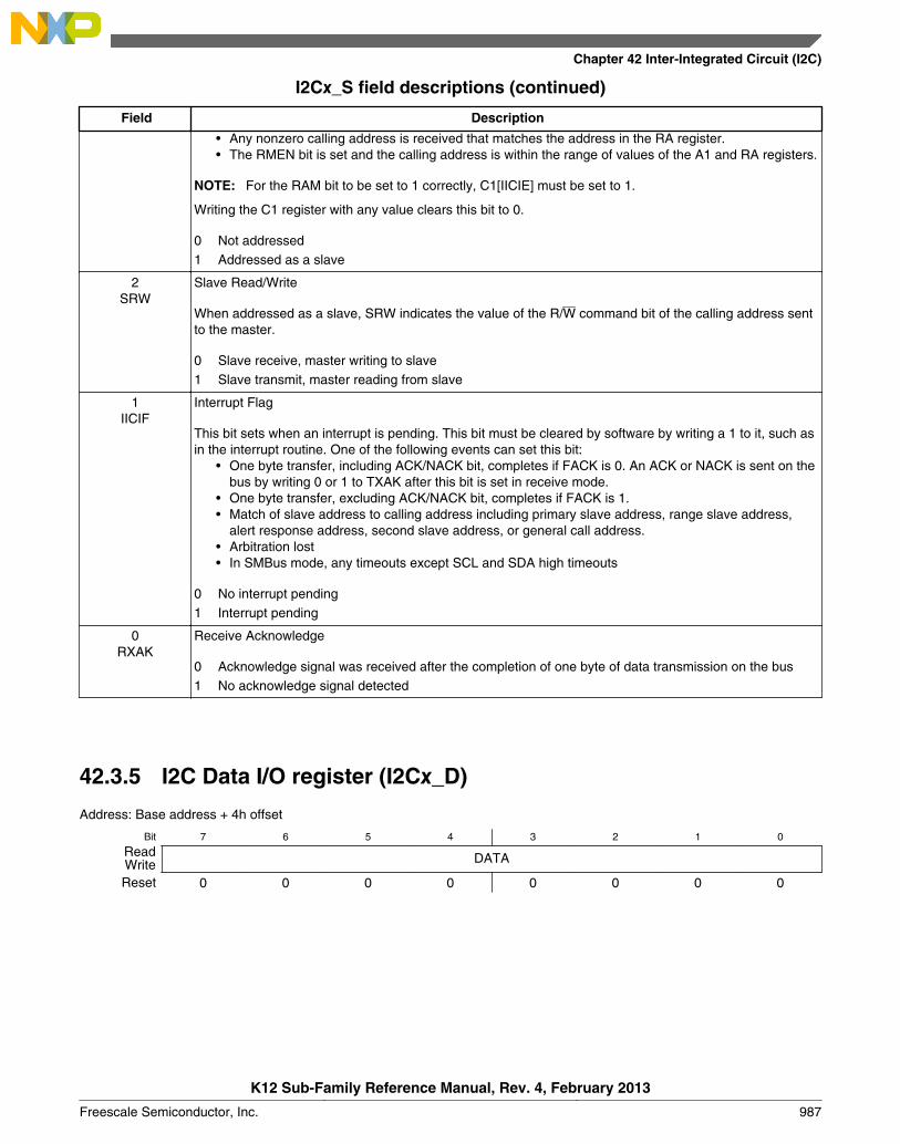
I2Cx_S field descriptions (continued)
Field Description
• Any nonzero calling address is received that matches the address in the RA register.• The RMEN bit is set and the calling address is within the range of values of the A1 and RA registers.
NOTE: For the RAM bit to be set to 1 correctly, C1[IICIE] must be set to 1.
Writing the C1 register with any value clears this bit to 0.
0 Not addressed1 Addressed as a slave
2SRW
Slave Read/Write
When addressed as a slave, SRW indicates the value of the R/W command bit of the calling address sentto the master.
0 Slave receive, master writing to slave1 Slave transmit, master reading from slave
1IICIF
Interrupt Flag
This bit sets when an interrupt is pending. This bit must be cleared by software by writing a 1 to it, such asin the interrupt routine. One of the following events can set this bit:
• One byte transfer, including ACK/NACK bit, completes if FACK is 0. An ACK or NACK is sent on thebus by writing 0 or 1 to TXAK after this bit is set in receive mode.
• One byte transfer, excluding ACK/NACK bit, completes if FACK is 1.• Match of slave address to calling address including primary slave address, range slave address,
alert response address, second slave address, or general call address.• Arbitration lost• In SMBus mode, any timeouts except SCL and SDA high timeouts
0 No interrupt pending1 Interrupt pending
0RXAK
Receive Acknowledge
0 Acknowledge signal was received after the completion of one byte of data transmission on the bus1 No acknowledge signal detected
42.3.5 I2C Data I/O register (I2Cx_D)
Address: Base address + 4h offset
Bit 7 6 5 4 3 2 1 0
Read DATAWriteReset 0 0 0 0 0 0 0 0
Chapter 42 Inter-Integrated Circuit (I2C)
K12 Sub-Family Reference Manual, Rev. 4, February 2013
Freescale Semiconductor, Inc. 987
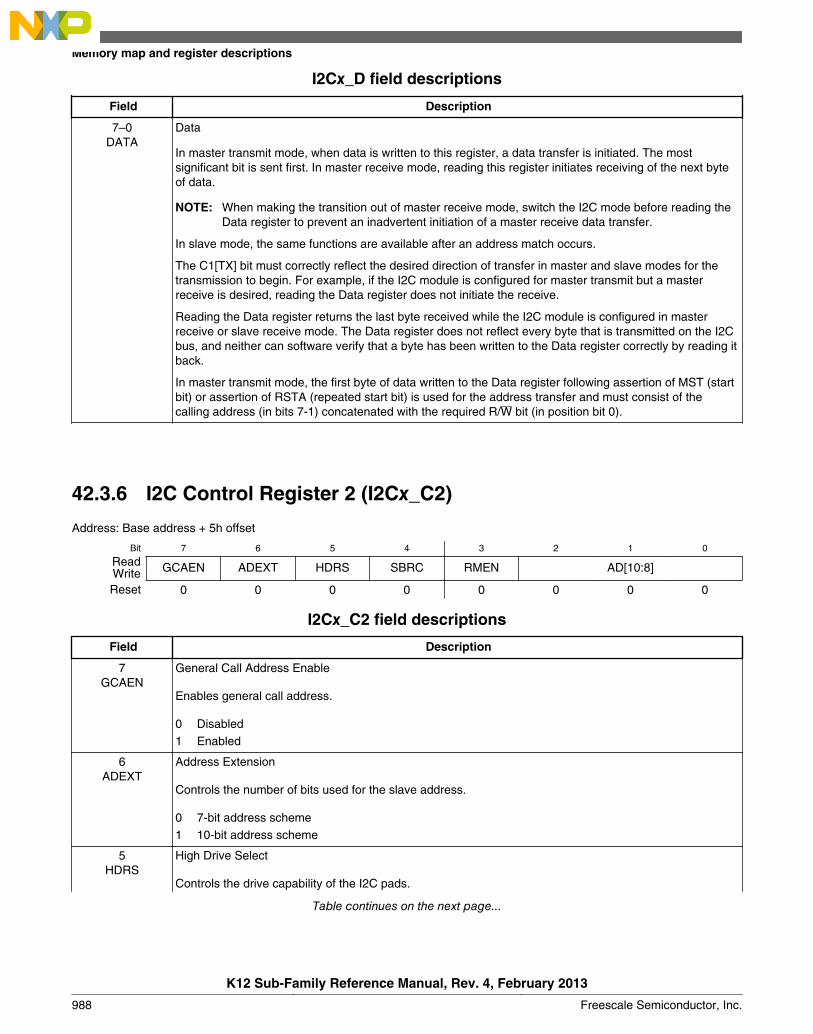
I2Cx_D field descriptions
Field Description
7–0DATA
Data
In master transmit mode, when data is written to this register, a data transfer is initiated. The mostsignificant bit is sent first. In master receive mode, reading this register initiates receiving of the next byteof data.
NOTE: When making the transition out of master receive mode, switch the I2C mode before reading theData register to prevent an inadvertent initiation of a master receive data transfer.
In slave mode, the same functions are available after an address match occurs.
The C1[TX] bit must correctly reflect the desired direction of transfer in master and slave modes for thetransmission to begin. For example, if the I2C module is configured for master transmit but a masterreceive is desired, reading the Data register does not initiate the receive.
Reading the Data register returns the last byte received while the I2C module is configured in masterreceive or slave receive mode. The Data register does not reflect every byte that is transmitted on the I2Cbus, and neither can software verify that a byte has been written to the Data register correctly by reading itback.
In master transmit mode, the first byte of data written to the Data register following assertion of MST (startbit) or assertion of RSTA (repeated start bit) is used for the address transfer and must consist of thecalling address (in bits 7-1) concatenated with the required R/W bit (in position bit 0).
42.3.6 I2C Control Register 2 (I2Cx_C2)
Address: Base address + 5h offset
Bit 7 6 5 4 3 2 1 0
Read GCAEN ADEXT HDRS SBRC RMEN AD[10:8]WriteReset 0 0 0 0 0 0 0 0
I2Cx_C2 field descriptions
Field Description
7GCAEN
General Call Address Enable
Enables general call address.
0 Disabled1 Enabled
6ADEXT
Address Extension
Controls the number of bits used for the slave address.
0 7-bit address scheme1 10-bit address scheme
5HDRS
High Drive Select
Controls the drive capability of the I2C pads.
Table continues on the next page...
Memory map and register descriptions
K12 Sub-Family Reference Manual, Rev. 4, February 2013
988 Freescale Semiconductor, Inc.
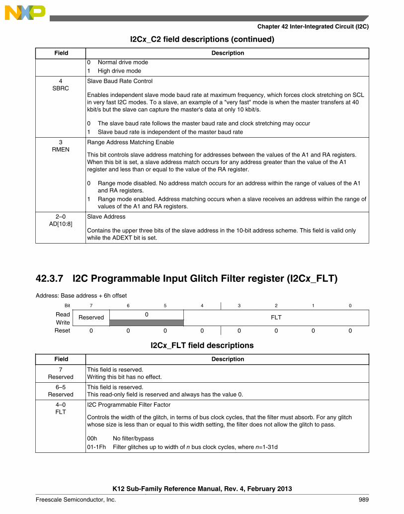
I2Cx_C2 field descriptions (continued)
Field Description
0 Normal drive mode1 High drive mode
4SBRC
Slave Baud Rate Control
Enables independent slave mode baud rate at maximum frequency, which forces clock stretching on SCLin very fast I2C modes. To a slave, an example of a "very fast" mode is when the master transfers at 40kbit/s but the slave can capture the master's data at only 10 kbit/s.
0 The slave baud rate follows the master baud rate and clock stretching may occur1 Slave baud rate is independent of the master baud rate
3RMEN
Range Address Matching Enable
This bit controls slave address matching for addresses between the values of the A1 and RA registers.When this bit is set, a slave address match occurs for any address greater than the value of the A1register and less than or equal to the value of the RA register.
0 Range mode disabled. No address match occurs for an address within the range of values of the A1and RA registers.
1 Range mode enabled. Address matching occurs when a slave receives an address within the range ofvalues of the A1 and RA registers.
2–0AD[10:8]
Slave Address
Contains the upper three bits of the slave address in the 10-bit address scheme. This field is valid onlywhile the ADEXT bit is set.
42.3.7 I2C Programmable Input Glitch Filter register (I2Cx_FLT)
Address: Base address + 6h offset
Bit 7 6 5 4 3 2 1 0
Read Reserved 0 FLTWriteReset 0 0 0 0 0 0 0 0
I2Cx_FLT field descriptions
Field Description
7Reserved
This field is reserved.Writing this bit has no effect.
6–5Reserved
This field is reserved.This read-only field is reserved and always has the value 0.
4–0FLT
I2C Programmable Filter Factor
Controls the width of the glitch, in terms of bus clock cycles, that the filter must absorb. For any glitchwhose size is less than or equal to this width setting, the filter does not allow the glitch to pass.
00h No filter/bypass01-1Fh Filter glitches up to width of n bus clock cycles, where n=1-31d
Chapter 42 Inter-Integrated Circuit (I2C)
K12 Sub-Family Reference Manual, Rev. 4, February 2013
Freescale Semiconductor, Inc. 989
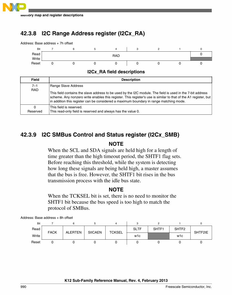
42.3.8 I2C Range Address register (I2Cx_RA)
Address: Base address + 7h offset
Bit 7 6 5 4 3 2 1 0
Read RAD 0WriteReset 0 0 0 0 0 0 0 0
I2Cx_RA field descriptions
Field Description
7–1RAD
Range Slave Address
This field contains the slave address to be used by the I2C module. The field is used in the 7-bit addressscheme. Any nonzero write enables this register. This register's use is similar to that of the A1 register, butin addition this register can be considered a maximum boundary in range matching mode.
0Reserved
This field is reserved.This read-only field is reserved and always has the value 0.
42.3.9 I2C SMBus Control and Status register (I2Cx_SMB)
NOTEWhen the SCL and SDA signals are held high for a length oftime greater than the high timeout period, the SHTF1 flag sets.Before reaching this threshold, while the system is detectinghow long these signals are being held high, a master assumesthat the bus is free. However, the SHTF1 bit rises in the bustransmission process with the idle bus state.
NOTEWhen the TCKSEL bit is set, there is no need to monitor theSHTF1 bit because the bus speed is too high to match theprotocol of SMBus.
Address: Base address + 8h offset
Bit 7 6 5 4 3 2 1 0
ReadFACK ALERTEN SIICAEN TCKSEL
SLTF SHTF1 SHTF2SHTF2IE
Write w1c w1c
Reset 0 0 0 0 0 0 0 0
Memory map and register descriptions
K12 Sub-Family Reference Manual, Rev. 4, February 2013
990 Freescale Semiconductor, Inc.
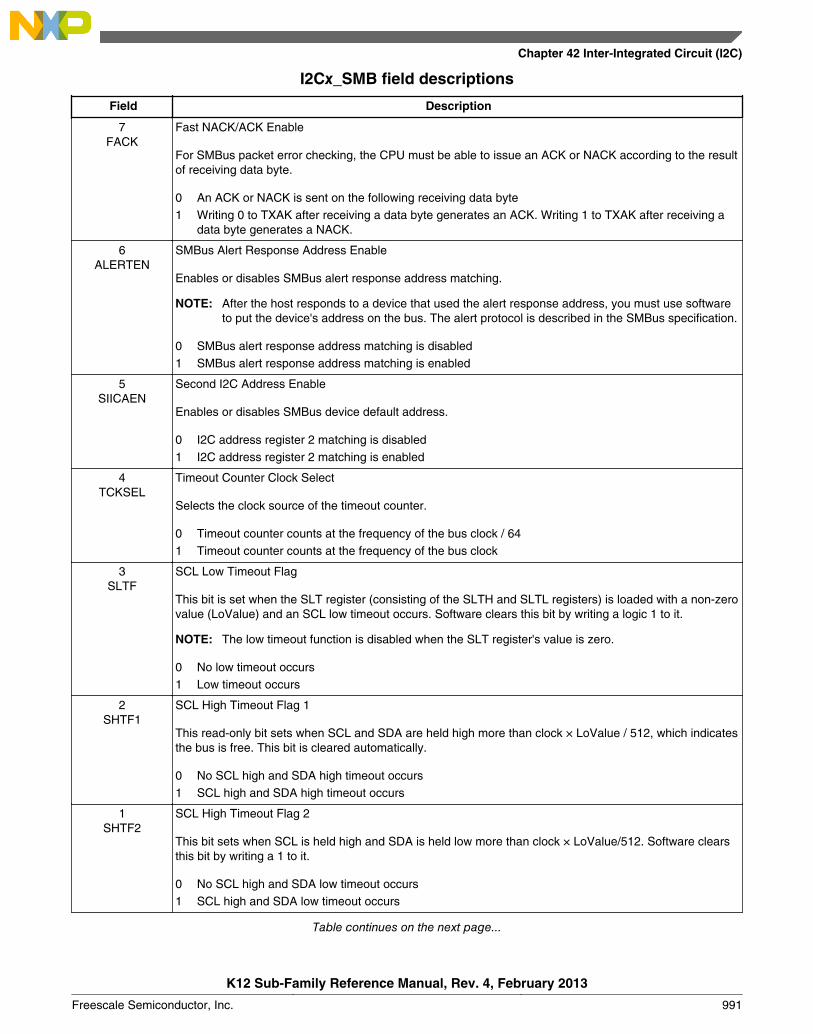
I2Cx_SMB field descriptions
Field Description
7FACK
Fast NACK/ACK Enable
For SMBus packet error checking, the CPU must be able to issue an ACK or NACK according to the resultof receiving data byte.
0 An ACK or NACK is sent on the following receiving data byte1 Writing 0 to TXAK after receiving a data byte generates an ACK. Writing 1 to TXAK after receiving a
data byte generates a NACK.
6ALERTEN
SMBus Alert Response Address Enable
Enables or disables SMBus alert response address matching.
NOTE: After the host responds to a device that used the alert response address, you must use softwareto put the device's address on the bus. The alert protocol is described in the SMBus specification.
0 SMBus alert response address matching is disabled1 SMBus alert response address matching is enabled
5SIICAEN
Second I2C Address Enable
Enables or disables SMBus device default address.
0 I2C address register 2 matching is disabled1 I2C address register 2 matching is enabled
4TCKSEL
Timeout Counter Clock Select
Selects the clock source of the timeout counter.
0 Timeout counter counts at the frequency of the bus clock / 641 Timeout counter counts at the frequency of the bus clock
3SLTF
SCL Low Timeout Flag
This bit is set when the SLT register (consisting of the SLTH and SLTL registers) is loaded with a non-zerovalue (LoValue) and an SCL low timeout occurs. Software clears this bit by writing a logic 1 to it.
NOTE: The low timeout function is disabled when the SLT register's value is zero.
0 No low timeout occurs1 Low timeout occurs
2SHTF1
SCL High Timeout Flag 1
This read-only bit sets when SCL and SDA are held high more than clock × LoValue / 512, which indicatesthe bus is free. This bit is cleared automatically.
0 No SCL high and SDA high timeout occurs1 SCL high and SDA high timeout occurs
1SHTF2
SCL High Timeout Flag 2
This bit sets when SCL is held high and SDA is held low more than clock × LoValue/512. Software clearsthis bit by writing a 1 to it.
0 No SCL high and SDA low timeout occurs1 SCL high and SDA low timeout occurs
Table continues on the next page...
Chapter 42 Inter-Integrated Circuit (I2C)
K12 Sub-Family Reference Manual, Rev. 4, February 2013
Freescale Semiconductor, Inc. 991
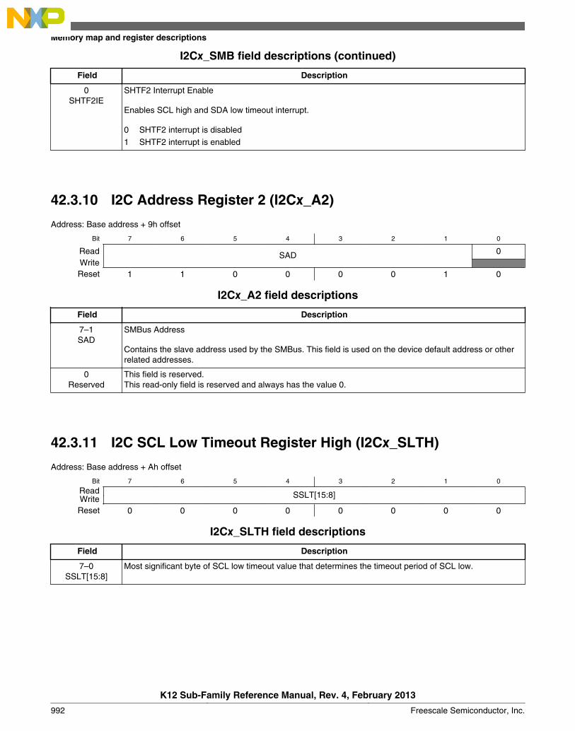
I2Cx_SMB field descriptions (continued)
Field Description
0SHTF2IE
SHTF2 Interrupt Enable
Enables SCL high and SDA low timeout interrupt.
0 SHTF2 interrupt is disabled1 SHTF2 interrupt is enabled
42.3.10 I2C Address Register 2 (I2Cx_A2)
Address: Base address + 9h offset
Bit 7 6 5 4 3 2 1 0
Read SAD 0WriteReset 1 1 0 0 0 0 1 0
I2Cx_A2 field descriptions
Field Description
7–1SAD
SMBus Address
Contains the slave address used by the SMBus. This field is used on the device default address or otherrelated addresses.
0Reserved
This field is reserved.This read-only field is reserved and always has the value 0.
42.3.11 I2C SCL Low Timeout Register High (I2Cx_SLTH)
Address: Base address + Ah offset
Bit 7 6 5 4 3 2 1 0
Read SSLT[15:8]WriteReset 0 0 0 0 0 0 0 0
I2Cx_SLTH field descriptions
Field Description
7–0SSLT[15:8]
Most significant byte of SCL low timeout value that determines the timeout period of SCL low.
Memory map and register descriptions
K12 Sub-Family Reference Manual, Rev. 4, February 2013
992 Freescale Semiconductor, Inc.
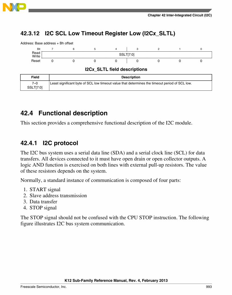
42.3.12 I2C SCL Low Timeout Register Low (I2Cx_SLTL)
Address: Base address + Bh offset
Bit 7 6 5 4 3 2 1 0
Read SSLT[7:0]WriteReset 0 0 0 0 0 0 0 0
I2Cx_SLTL field descriptions
Field Description
7–0SSLT[7:0]
Least significant byte of SCL low timeout value that determines the timeout period of SCL low.
42.4 Functional descriptionThis section provides a comprehensive functional description of the I2C module.
42.4.1 I2C protocol
The I2C bus system uses a serial data line (SDA) and a serial clock line (SCL) for datatransfers. All devices connected to it must have open drain or open collector outputs. Alogic AND function is exercised on both lines with external pull-up resistors. The valueof these resistors depends on the system.
Normally, a standard instance of communication is composed of four parts:
1. START signal2. Slave address transmission3. Data transfer4. STOP signal
The STOP signal should not be confused with the CPU STOP instruction. The followingfigure illustrates I2C bus system communication.
Chapter 42 Inter-Integrated Circuit (I2C)
K12 Sub-Family Reference Manual, Rev. 4, February 2013
Freescale Semiconductor, Inc. 993
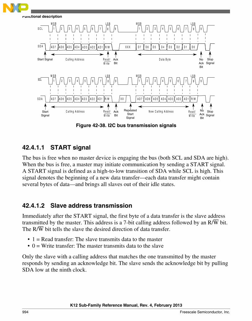
S C L
S D A
D 0
D a ta B y te
N e w C a ll in g A d d r e s s
X X
W r ite
C a l l in g A d d r e s sW r i te W r ite
S D A
C a l l in g A d d r e s s R e a d /
X X X D 7 D 6 D 5 D 4 D 3 D 2 D 1A D 6 A D 5A D 7 A D 4
L S BM S B
1 62 5 83 4 7 9 1 62 5 83 4 7 9
L S BM S B
1 62 5 83 4 7 9
L S BM S B
1 62 5 83 4 7 9
L S BM S B
A D 6 R /WA D 3 A D 2 A D 1A D 5A D 7 A D 4 A D 6 R /WA D 3 A D 2 A D 1A D 5A D 7 A D 4
R e a d / R e a d /
R /WA D 3 A D 2 A D 1
SCL
Start Signal Ack Bit
No Ack Bit
Stop Signal
Start Signal
Ack Bit
RepeatedStart
Signal
NoAck Bit
Stop Signal
Figure 42-38. I2C bus transmission signals
42.4.1.1 START signal
The bus is free when no master device is engaging the bus (both SCL and SDA are high).When the bus is free, a master may initiate communication by sending a START signal.A START signal is defined as a high-to-low transition of SDA while SCL is high. Thissignal denotes the beginning of a new data transfer—each data transfer might containseveral bytes of data—and brings all slaves out of their idle states.
42.4.1.2 Slave address transmission
Immediately after the START signal, the first byte of a data transfer is the slave addresstransmitted by the master. This address is a 7-bit calling address followed by an R/W bit.The R/W bit tells the slave the desired direction of data transfer.
• 1 = Read transfer: The slave transmits data to the master• 0 = Write transfer: The master transmits data to the slave
Only the slave with a calling address that matches the one transmitted by the masterresponds by sending an acknowledge bit. The slave sends the acknowledge bit by pullingSDA low at the ninth clock.
Functional description
K12 Sub-Family Reference Manual, Rev. 4, February 2013
994 Freescale Semiconductor, Inc.
No two slaves in the system can have the same address. If the I2C module is the master, itmust not transmit an address that is equal to its own slave address. The I2C modulecannot be master and slave at the same time. However, if arbitration is lost during anaddress cycle, the I2C module reverts to slave mode and operates correctly even if it isbeing addressed by another master.
42.4.1.3 Data transfers
When successful slave addressing is achieved, data transfer can proceed on a byte-by-byte basis in the direction specified by the R/W bit sent by the calling master.
All transfers that follow an address cycle are referred to as data transfers, even if theycarry subaddress information for the slave device.
Each data byte is 8 bits long. Data may be changed only while SCL is low. Data must beheld stable while SCL is high. There is one clock pulse on SCL for each data bit, and theMSB is transferred first. Each data byte is followed by a ninth (acknowledge) bit, whichis signaled from the receiving device by pulling SDA low at the ninth clock. In summary,one complete data transfer needs nine clock pulses.
If the slave receiver does not acknowledge the master in the ninth bit, the slave mustleave SDA high. The master interprets the failed acknowledgement as an unsuccessfuldata transfer.
If the master receiver does not acknowledge the slave transmitter after a data bytetransmission, the slave interprets it as an end to data transfer and releases the SDA line.
In the case of a failed acknowledgement by either the slave or master, the data transfer isaborted and the master does one of two things:
• Relinquishes the bus by generating a STOP signal.
• Commences a new call by generating a repeated START signal.
42.4.1.4 STOP signal
The master can terminate the communication by generating a STOP signal to free thebus. A STOP signal is defined as a low-to-high transition of SDA while SCL is asserted.
The master can generate a STOP signal even if the slave has generated anacknowledgement, at which point the slave must release the bus.
Chapter 42 Inter-Integrated Circuit (I2C)
K12 Sub-Family Reference Manual, Rev. 4, February 2013
Freescale Semiconductor, Inc. 995
42.4.1.5 Repeated START signal
The master may generate a START signal followed by a calling command withoutgenerating a STOP signal first. This action is called a repeated START. The master usesa repeated START to communicate with another slave or with the same slave in adifferent mode (transmit/receive mode) without releasing the bus.
42.4.1.6 Arbitration procedure
The I2C bus is a true multimaster bus that allows more than one master to be connectedon it.
If two or more masters try to control the bus at the same time, a clock synchronizationprocedure determines the bus clock. The bus clock's low period is equal to the longestclock low period, and the high period is equal to the shortest one among the masters.
The relative priority of the contending masters is determined by a data arbitrationprocedure. A bus master loses arbitration if it transmits logic level 1 while another mastertransmits logic level 0. The losing masters immediately switch to slave receive mode andstop driving SDA output. In this case, the transition from master to slave mode does notgenerate a STOP condition. Meanwhile, hardware sets a status bit to indicate the loss ofarbitration.
42.4.1.7 Clock synchronization
Because wire AND logic is performed on SCL, a high-to-low transition on SCL affectsall devices connected on the bus. The devices start counting their low period and, after adevice's clock has gone low, that device holds SCL low until the clock reaches its highstate. However, the change of low to high in this device clock might not change the stateof SCL if another device clock is still within its low period. Therefore, the synchronizedclock SCL is held low by the device with the longest low period. Devices with shorterlow periods enter a high wait state during this time; see the following diagram. When allapplicable devices have counted off their low period, the synchronized clock SCL isreleased and pulled high. Afterward there is no difference between the device clocks andthe state of SCL, and all devices start counting their high periods. The first device tocomplete its high period pulls SCL low again.
Functional description
K12 Sub-Family Reference Manual, Rev. 4, February 2013
996 Freescale Semiconductor, Inc.
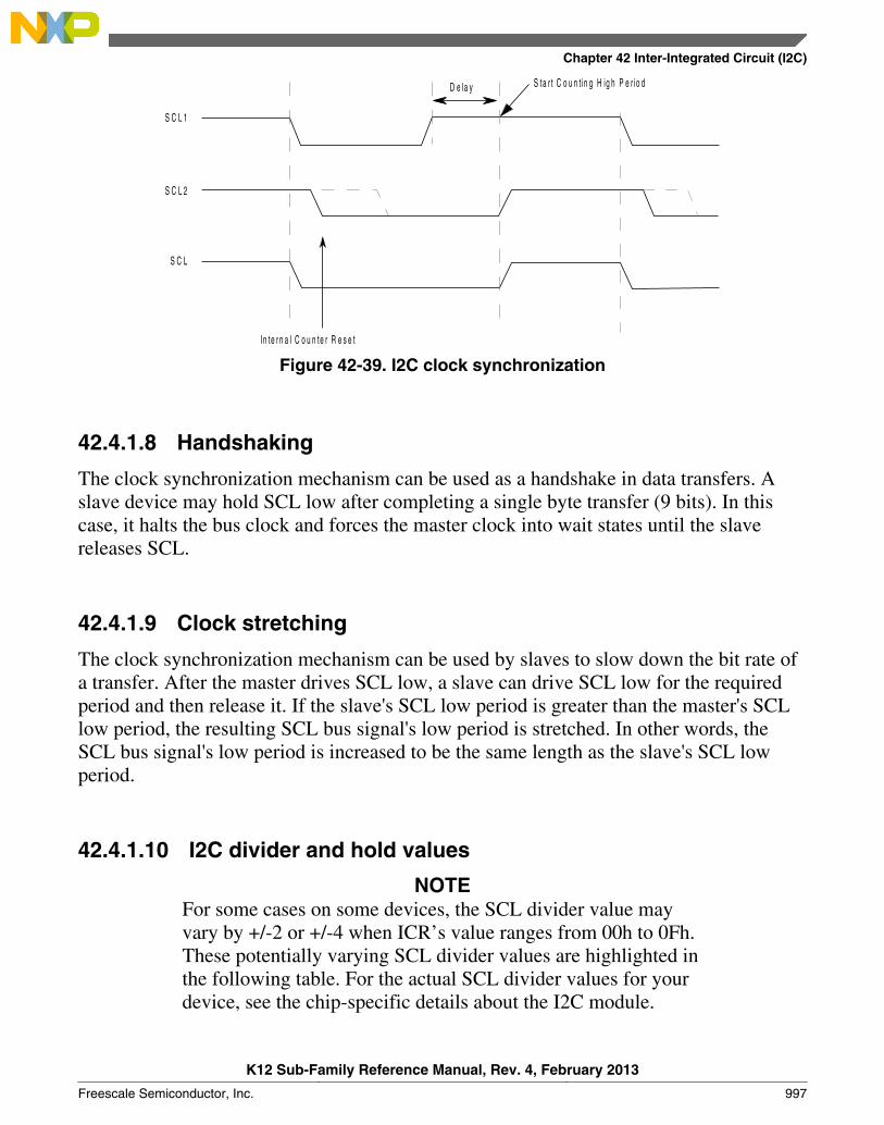
S C L 2
S ta r t C o u n t in g H ig h P e r io d
In te r n a l C o u n te r R e s e t
S C L 1
S C L
D e la y
Figure 42-39. I2C clock synchronization
42.4.1.8 Handshaking
The clock synchronization mechanism can be used as a handshake in data transfers. Aslave device may hold SCL low after completing a single byte transfer (9 bits). In thiscase, it halts the bus clock and forces the master clock into wait states until the slavereleases SCL.
42.4.1.9 Clock stretching
The clock synchronization mechanism can be used by slaves to slow down the bit rate ofa transfer. After the master drives SCL low, a slave can drive SCL low for the requiredperiod and then release it. If the slave's SCL low period is greater than the master's SCLlow period, the resulting SCL bus signal's low period is stretched. In other words, theSCL bus signal's low period is increased to be the same length as the slave's SCL lowperiod.
42.4.1.10 I2C divider and hold values
NOTEFor some cases on some devices, the SCL divider value mayvary by +/-2 or +/-4 when ICR’s value ranges from 00h to 0Fh.These potentially varying SCL divider values are highlighted inthe following table. For the actual SCL divider values for yourdevice, see the chip-specific details about the I2C module.
Chapter 42 Inter-Integrated Circuit (I2C)
K12 Sub-Family Reference Manual, Rev. 4, February 2013
Freescale Semiconductor, Inc. 997

Table 42-41. I2C divider and hold values
ICR
(hex)
SCLdivider
SDA holdvalue
SCL hold(start)value
SCL hold(stop)value
ICR
(hex)
SCLdivider(clocks)
SDA hold(clocks)
SCL hold(start)value
SCL hold(stop)value
00 20 7 6 11 20 160 17 78 81
01 22 7 7 12 21 192 17 94 97
02 24 8 8 13 22 224 33 110 113
03 26 8 9 14 23 256 33 126 129
04 28 9 10 15 24 288 49 142 145
05 30 9 11 16 25 320 49 158 161
06 34 10 13 18 26 384 65 190 193
07 40 10 16 21 27 480 65 238 241
08 28 7 10 15 28 320 33 158 161
09 32 7 12 17 29 384 33 190 193
0A 36 9 14 19 2A 448 65 222 225
0B 40 9 16 21 2B 512 65 254 257
0C 44 11 18 23 2C 576 97 286 289
0D 48 11 20 25 2D 640 97 318 321
0E 56 13 24 29 2E 768 129 382 385
0F 68 13 30 35 2F 960 129 478 481
10 48 9 18 25 30 640 65 318 321
11 56 9 22 29 31 768 65 382 385
12 64 13 26 33 32 896 129 446 449
13 72 13 30 37 33 1024 129 510 513
14 80 17 34 41 34 1152 193 574 577
15 88 17 38 45 35 1280 193 638 641
16 104 21 46 53 36 1536 257 766 769
17 128 21 58 65 37 1920 257 958 961
18 80 9 38 41 38 1280 129 638 641
19 96 9 46 49 39 1536 129 766 769
1A 112 17 54 57 3A 1792 257 894 897
1B 128 17 62 65 3B 2048 257 1022 1025
1C 144 25 70 73 3C 2304 385 1150 1153
1D 160 25 78 81 3D 2560 385 1278 1281
1E 192 33 94 97 3E 3072 513 1534 1537
1F 240 33 118 121 3F 3840 513 1918 1921
Functional description
K12 Sub-Family Reference Manual, Rev. 4, February 2013
998 Freescale Semiconductor, Inc.
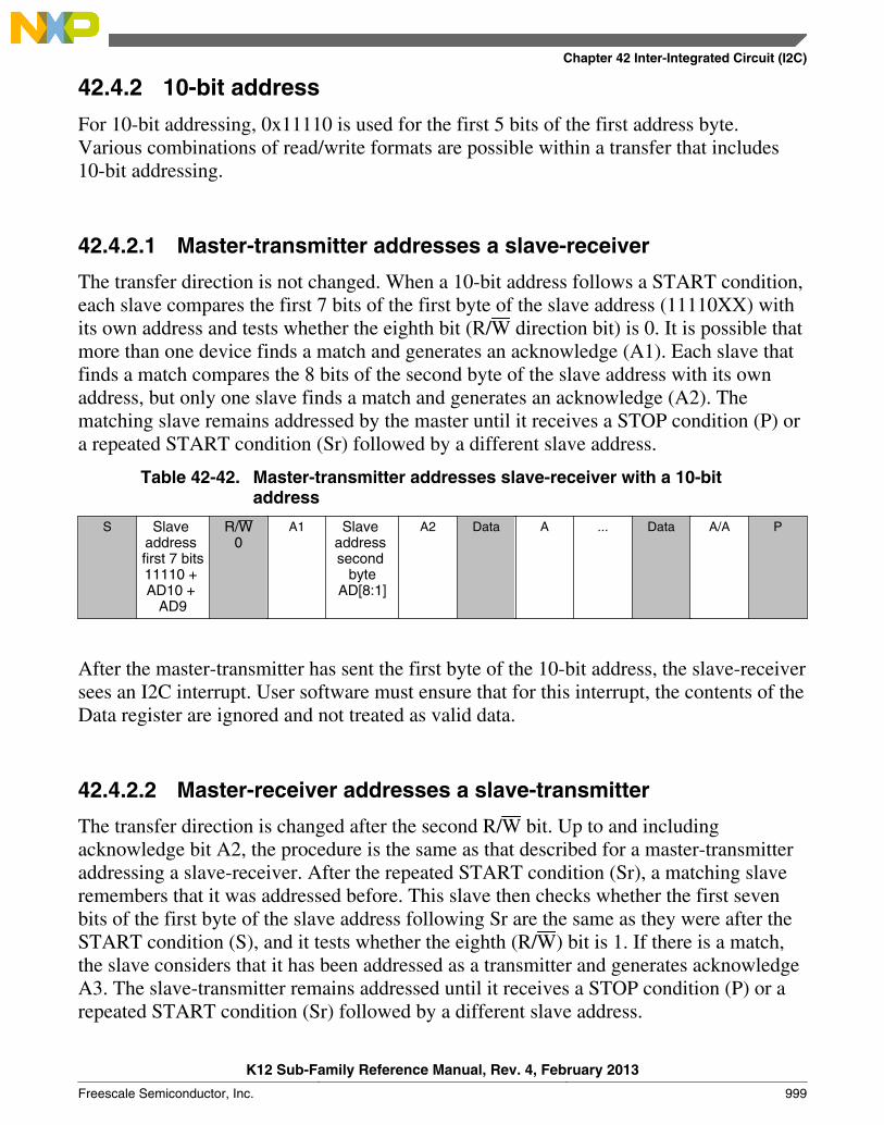
42.4.2 10-bit address
For 10-bit addressing, 0x11110 is used for the first 5 bits of the first address byte.Various combinations of read/write formats are possible within a transfer that includes10-bit addressing.
42.4.2.1 Master-transmitter addresses a slave-receiver
The transfer direction is not changed. When a 10-bit address follows a START condition,each slave compares the first 7 bits of the first byte of the slave address (11110XX) withits own address and tests whether the eighth bit (R/W direction bit) is 0. It is possible thatmore than one device finds a match and generates an acknowledge (A1). Each slave thatfinds a match compares the 8 bits of the second byte of the slave address with its ownaddress, but only one slave finds a match and generates an acknowledge (A2). Thematching slave remains addressed by the master until it receives a STOP condition (P) ora repeated START condition (Sr) followed by a different slave address.
Table 42-42. Master-transmitter addresses slave-receiver with a 10-bitaddress
S Slave address first 7 bits11110 + AD10 +
AD9
R/W0
A1 Slave address second
byteAD[8:1]
A2 Data A ... Data A/A P
After the master-transmitter has sent the first byte of the 10-bit address, the slave-receiversees an I2C interrupt. User software must ensure that for this interrupt, the contents of theData register are ignored and not treated as valid data.
42.4.2.2 Master-receiver addresses a slave-transmitter
The transfer direction is changed after the second R/W bit. Up to and includingacknowledge bit A2, the procedure is the same as that described for a master-transmitteraddressing a slave-receiver. After the repeated START condition (Sr), a matching slaveremembers that it was addressed before. This slave then checks whether the first sevenbits of the first byte of the slave address following Sr are the same as they were after theSTART condition (S), and it tests whether the eighth (R/W) bit is 1. If there is a match,the slave considers that it has been addressed as a transmitter and generates acknowledgeA3. The slave-transmitter remains addressed until it receives a STOP condition (P) or arepeated START condition (Sr) followed by a different slave address.
Chapter 42 Inter-Integrated Circuit (I2C)
K12 Sub-Family Reference Manual, Rev. 4, February 2013
Freescale Semiconductor, Inc. 999
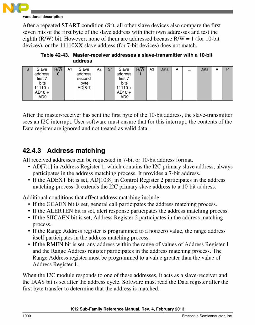
After a repeated START condition (Sr), all other slave devices also compare the firstseven bits of the first byte of the slave address with their own addresses and test theeighth (R/W) bit. However, none of them are addressed because R/W = 1 (for 10-bitdevices), or the 11110XX slave address (for 7-bit devices) does not match.
Table 42-43. Master-receiver addresses a slave-transmitter with a 10-bitaddress
S Slave address
first 7 bits
11110 + AD10 +
AD9
R/W0
A1 Slave address second
byteAD[8:1]
A2 Sr Slave address
first 7 bits
11110 + AD10 +
AD9
R/W1
A3 Data A ... Data A P
After the master-receiver has sent the first byte of the 10-bit address, the slave-transmittersees an I2C interrupt. User software must ensure that for this interrupt, the contents of theData register are ignored and not treated as valid data.
42.4.3 Address matchingAll received addresses can be requested in 7-bit or 10-bit address format.
• AD[7:1] in Address Register 1, which contains the I2C primary slave address, alwaysparticipates in the address matching process. It provides a 7-bit address.
• If the ADEXT bit is set, AD[10:8] in Control Register 2 participates in the addressmatching process. It extends the I2C primary slave address to a 10-bit address.
Additional conditions that affect address matching include:• If the GCAEN bit is set, general call participates the address matching process.• If the ALERTEN bit is set, alert response participates the address matching process.• If the SIICAEN bit is set, Address Register 2 participates in the address matching
process.• If the Range Address register is programmed to a nonzero value, the range address
itself participates in the address matching process.• If the RMEN bit is set, any address within the range of values of Address Register 1
and the Range Address register participates in the address matching process. TheRange Address register must be programmed to a value greater than the value ofAddress Register 1.
When the I2C module responds to one of these addresses, it acts as a slave-receiver andthe IAAS bit is set after the address cycle. Software must read the Data register after thefirst byte transfer to determine that the address is matched.
Functional description
K12 Sub-Family Reference Manual, Rev. 4, February 2013
1000 Freescale Semiconductor, Inc.
42.4.4 System management bus specification
SMBus provides a control bus for system and power management related tasks. A systemcan use SMBus to pass messages to and from devices instead of tripping individualcontrol lines. Removing the individual control lines reduces pin count. Acceptingmessages ensures future expandability. With the system management bus, a device canprovide manufacturer information, tell the system what its model/part number is, save itsstate for a suspend event, report different types of errors, accept control parameters, andreturn its status.
42.4.4.1 Timeouts
The TTIMEOUT,MIN parameter allows a master or slave to conclude that a defective deviceis holding the clock low indefinitely or a master is intentionally trying to drive devicesoff the bus. The slave device must release the bus (stop driving the bus and let SCL andSDA float high) when it detects any single clock held low longer than TTIMEOUT,MIN.Devices that have detected this condition must reset their communication and be able toreceive a new START condition within the timeframe of TTIMEOUT,MAX.
SMBus defines a clock low timeout, TTIMEOUT, of 35 ms, specifies TLOW:SEXT as thecumulative clock low extend time for a slave device, and specifies TLOW:MEXT as thecumulative clock low extend time for a master device.
42.4.4.1.1 SCL low timeout
If the SCL line is held low by a slave device on the bus, no further communication ispossible. Furthermore, the master cannot force the SCL line high to correct the errorcondition. To solve this problem, the SMBus protocol specifies that devices participatingin a transfer must detect any clock cycle held low longer than a timeout value condition.Devices that have detected the timeout condition must reset the communication. Whenthe I2C module is an active master, if it detects that SMBCLK low has exceeded thevalue of TTIMEOUT,MIN, it must generate a stop condition within or after the current databyte in the transfer process. When the I2C module is a slave, if it detects theTTIMEOUT,MIN condition, it resets its communication and is then able to receive a newSTART condition.
42.4.4.1.2 SCL high timeout
When the I2C module has determined that the SMBCLK and SMBDAT signals havebeen high for at least THIGH:MAX, it assumes that the bus is idle.
Chapter 42 Inter-Integrated Circuit (I2C)
K12 Sub-Family Reference Manual, Rev. 4, February 2013
Freescale Semiconductor, Inc. 1001
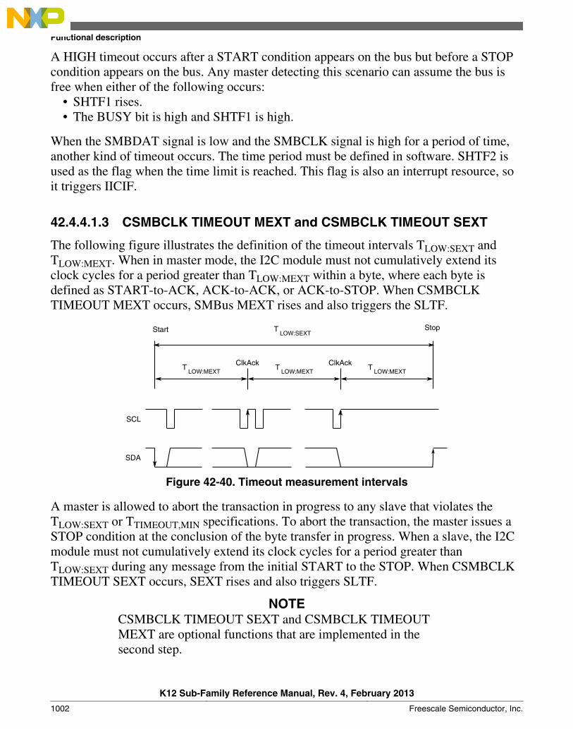
A HIGH timeout occurs after a START condition appears on the bus but before a STOPcondition appears on the bus. Any master detecting this scenario can assume the bus isfree when either of the following occurs:
• SHTF1 rises.• The BUSY bit is high and SHTF1 is high.
When the SMBDAT signal is low and the SMBCLK signal is high for a period of time,another kind of timeout occurs. The time period must be defined in software. SHTF2 isused as the flag when the time limit is reached. This flag is also an interrupt resource, soit triggers IICIF.
42.4.4.1.3 CSMBCLK TIMEOUT MEXT and CSMBCLK TIMEOUT SEXT
The following figure illustrates the definition of the timeout intervals TLOW:SEXT andTLOW:MEXT. When in master mode, the I2C module must not cumulatively extend itsclock cycles for a period greater than TLOW:MEXT within a byte, where each byte isdefined as START-to-ACK, ACK-to-ACK, or ACK-to-STOP. When CSMBCLKTIMEOUT MEXT occurs, SMBus MEXT rises and also triggers the SLTF.
Start LOW:SEXTT Stop
LOW:MEXTT
ClkAckLOW:MEXT
TClkAck
LOW:MEXTT
SCL
SDA
Figure 42-40. Timeout measurement intervals
A master is allowed to abort the transaction in progress to any slave that violates theTLOW:SEXT or TTIMEOUT,MIN specifications. To abort the transaction, the master issues aSTOP condition at the conclusion of the byte transfer in progress. When a slave, the I2Cmodule must not cumulatively extend its clock cycles for a period greater thanTLOW:SEXT during any message from the initial START to the STOP. When CSMBCLKTIMEOUT SEXT occurs, SEXT rises and also triggers SLTF.
NOTECSMBCLK TIMEOUT SEXT and CSMBCLK TIMEOUTMEXT are optional functions that are implemented in thesecond step.
Functional description
K12 Sub-Family Reference Manual, Rev. 4, February 2013
1002 Freescale Semiconductor, Inc.

42.4.4.2 FAST ACK and NACK
To improve reliability and communication robustness, implementation of packet errorchecking (PEC) by SMBus devices is optional for SMBus devices but required fordevices participating in and only during the address resolution protocol (ARP) process.The PEC is a CRC-8 error checking byte, calculated on all the message bytes. The PEC isappended to the message by the device that supplied the last data byte. If the PEC ispresent but not correct, a NACK is issued by the receiver. Otherwise an ACK is issued.To calculate the CRC-8 by software, this module can hold the SCL line low afterreceiving the eighth SCL (8th bit) if this byte is a data byte. So software can determinewhether an ACK or NACK should be sent to the bus by setting or clearing the TXAK bitif the FACK (fast ACK/NACK enable) bit is enabled.
SMBus requires a device always to acknowledge its own address, as a mechanism todetect the presence of a removable device (such as a battery or docking station) on thebus. In addition to indicating a slave device busy condition, SMBus uses the NACKmechanism to indicate the reception of an invalid command or invalid data. Because sucha condition may occur on the last byte of the transfer, SMBus devices are required tohave the ability to generate the not acknowledge after the transfer of each byte and beforethe completion of the transaction. This requirement is important because SMBus does notprovide any other resend signaling. This difference in the use of the NACK signaling hasimplications on the specific implementation of the SMBus port, especially in devices thathandle critical system data such as the SMBus host and the SBS components.
NOTEIn the last byte of master receive slave transmit mode, themaster must send a NACK to the bus, so FACK must beswitched off before the last byte transmits.
42.4.5 Resets
The I2C module is disabled after a reset. The I2C module cannot cause a core reset.
42.4.6 Interrupts
The I2C module generates an interrupt when any of the events in the following tableoccur, provided that the IICIE bit is set. The interrupt is driven by the IICIF bit (of theI2C Status Register) and masked with the IICIE bit (of the I2C Control Register 1). TheIICIF bit must be cleared (by software) by writing 1 to it in the interrupt routine. The
Chapter 42 Inter-Integrated Circuit (I2C)
K12 Sub-Family Reference Manual, Rev. 4, February 2013
Freescale Semiconductor, Inc. 1003
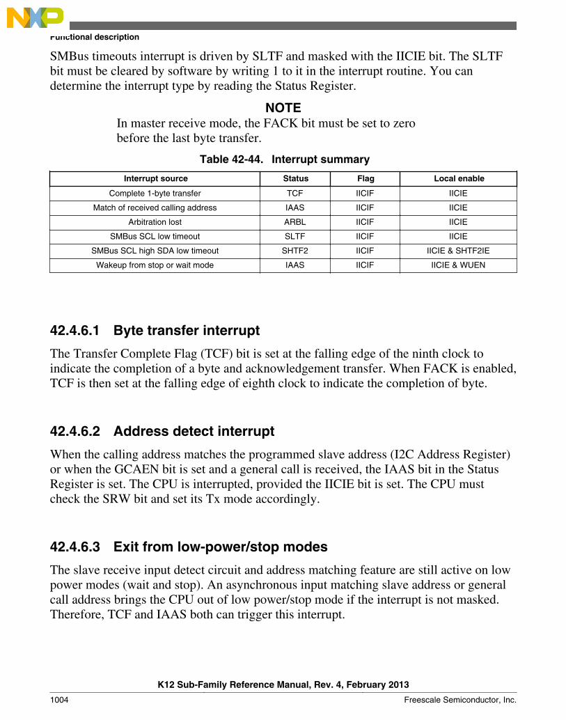
SMBus timeouts interrupt is driven by SLTF and masked with the IICIE bit. The SLTFbit must be cleared by software by writing 1 to it in the interrupt routine. You candetermine the interrupt type by reading the Status Register.
NOTEIn master receive mode, the FACK bit must be set to zerobefore the last byte transfer.
Table 42-44. Interrupt summary
Interrupt source Status Flag Local enable
Complete 1-byte transfer TCF IICIF IICIE
Match of received calling address IAAS IICIF IICIE
Arbitration lost ARBL IICIF IICIE
SMBus SCL low timeout SLTF IICIF IICIE
SMBus SCL high SDA low timeout SHTF2 IICIF IICIE & SHTF2IE
Wakeup from stop or wait mode IAAS IICIF IICIE & WUEN
42.4.6.1 Byte transfer interrupt
The Transfer Complete Flag (TCF) bit is set at the falling edge of the ninth clock toindicate the completion of a byte and acknowledgement transfer. When FACK is enabled,TCF is then set at the falling edge of eighth clock to indicate the completion of byte.
42.4.6.2 Address detect interrupt
When the calling address matches the programmed slave address (I2C Address Register)or when the GCAEN bit is set and a general call is received, the IAAS bit in the StatusRegister is set. The CPU is interrupted, provided the IICIE bit is set. The CPU mustcheck the SRW bit and set its Tx mode accordingly.
42.4.6.3 Exit from low-power/stop modes
The slave receive input detect circuit and address matching feature are still active on lowpower modes (wait and stop). An asynchronous input matching slave address or generalcall address brings the CPU out of low power/stop mode if the interrupt is not masked.Therefore, TCF and IAAS both can trigger this interrupt.
Functional description
K12 Sub-Family Reference Manual, Rev. 4, February 2013
1004 Freescale Semiconductor, Inc.
42.4.6.4 Arbitration lost interrupt
The I2C is a true multimaster bus that allows more than one master to be connected on it.If two or more masters try to control the bus at the same time, the relative priority of thecontending masters is determined by a data arbitration procedure. The I2C module assertsthe arbitration-lost interrupt when it loses the data arbitration process and the ARBL bitin the Status Register is set.
Arbitration is lost in the following circumstances:
1. SDA is sampled as low when the master drives high during an address or datatransmit cycle.
2. SDA is sampled as low when the master drives high during the acknowledge bit of adata receive cycle.
3. A START cycle is attempted when the bus is busy.
4. A repeated START cycle is requested in slave mode.
5. A STOP condition is detected when the master did not request it.
The ARBL bit must be cleared (by software) by writing 1 to it.
42.4.6.5 Timeout interrupt in SMBus
When the IICIE bit is set, the I2C module asserts a timeout interrupt (outputs SLTF andSHTF2) upon detection of any of the mentioned timeout conditions, with one exception.The SCL high and SDA high TIMEOUT mechanism must not be used to influence thetimeout interrupt output, because this timeout indicates an idle condition on the bus.SHTF1 rises when it matches the SCL high and SDA high TIMEOUT and fallsautomatically just to indicate the bus status. The SHTF2's timeout period is the same asthat of SHTF1, which is short compared to that of SLTF, so another control bit,SHTF2IE, is added to enable or disable it.
42.4.7 Programmable input glitch filter
An I2C glitch filter has been added outside legacy I2C modules but within the I2Cpackage. This filter can absorb glitches on the I2C clock and data lines for the I2Cmodule. The width of the glitch to absorb can be specified in terms of the number of(half) bus clock cycles. A single Programmable Input Glitch Filter control register isprovided. Effectively, any down-up-down or up-down-up transition on the data line that
Chapter 42 Inter-Integrated Circuit (I2C)
K12 Sub-Family Reference Manual, Rev. 4, February 2013
Freescale Semiconductor, Inc. 1005

occurs within the number of clock cycles programmed in this register is ignored by theI2C module. The programmer must specify the size of the glitch (in terms of bus clockcycles) for the filter to absorb and not pass.
SCL, SDAexternal signals
DFF
Noisesuppresscircuits
SCL, SDAinternal signals
DFF DFF DFF
Figure 42-41. Programmable input glitch filter diagram
42.4.8 Address matching wakeup
When a primary, range, or general call address match occurs when the I2C module is inslave receive mode, the MCU wakes from a low power mode with no peripheral busrunning. Data sent on the bus that is the same as a target device address might also wakethe target MCU.
After the address matching IAAS bit is set, an interrupt is sent at the end of addressmatching to wake the core. The IAAS bit must be cleared after the clock recovery.
NOTEAfter the system recovers and is in Run mode, restart the I2Cmodule if it is needed to transfer packets. The SCL line is notheld low until the I2C module resets after address matching.The main purpose of this feature is to wake the MCU from alow power mode where no peripheral bus is running. When theMCU is in such a mode: addressing as a slave, slave read/write,and sending an acknowledge bit are not fully supported. Toavoid I2C transfer problems resulting from this situation,firmware should prevent the MCU execution of a STOPinstruction when the I2C module is in the middle of a transfer.
42.4.9 DMA support
If the DMAEN bit is cleared and the IICIE bit is set, an interrupt condition generates aninterrupt request. If the DMAEN bit is set and the IICIE bit is set, an interrupt conditiongenerates a DMA request instead. DMA requests are generated by the transfer completeflag (TCF).
Functional description
K12 Sub-Family Reference Manual, Rev. 4, February 2013
1006 Freescale Semiconductor, Inc.
If the DMAEN bit is set, the only arbitration lost is to another I2C module (error), andSCL low timeouts (error) generate CPU interrupts. All other events initiate a DMAtransfer.
NOTEBefore the last byte of master receive mode, TXAK must be setto send a NACK after the last byte’s transfer. Therefore, theDMA must be disabled before the last byte’s transfer.
NOTEIn 10-bit address mode transmission, the addresses to sendoccupy 2-3 bytes. During this transfer period, the DMA must bedisabled because the C1 register is written to send a repeat startor to change the transfer direction.
42.5 Initialization/application information
Module Initialization (Slave)
1. Write: Control Register 2• to enable or disable general call• to select 10-bit or 7-bit addressing mode
2. Write: Address Register 1 to set the slave address3. Write: Control Register 1 to enable the I2C module and interrupts4. Initialize RAM variables (IICEN = 1 and IICIE = 1) for transmit data5. Initialize RAM variables used to achieve the routine shown in the following figure
Module Initialization (Master)
1. Write: Frequency Divider register to set the I2C baud rate (see example indescription of ICR)
2. Write: Control Register 1 to enable the I2C module and interrupts3. Initialize RAM variables (IICEN = 1 and IICIE = 1) for transmit data4. Initialize RAM variables used to achieve the routine shown in the following figure5. Write: Control Register 1 to enable TX6. Write: Control Register 1 to enable MST (master mode)7. Write: Data register with the address of the target slave (the LSB of this byte
determines whether the communication is master receive or transmit)
Chapter 42 Inter-Integrated Circuit (I2C)
K12 Sub-Family Reference Manual, Rev. 4, February 2013
Freescale Semiconductor, Inc. 1007

The routine shown in the following figure encompasses both master and slave I2Coperations. For slave operation, an incoming I2C message that contains the properaddress begins I2C communication. For master operation, communication must beinitiated by writing the Data register.
Initialization/application information
K12 Sub-Family Reference Manual, Rev. 4, February 2013
1008 Freescale Semiconductor, Inc.
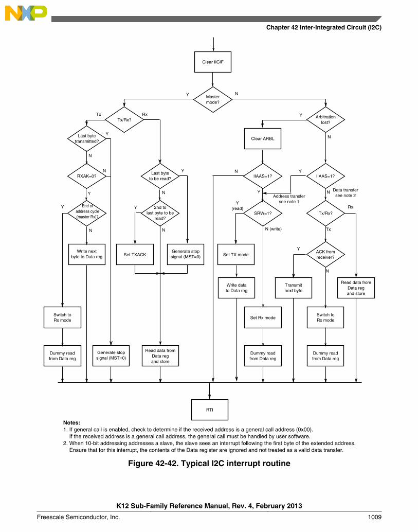
Clear IICIF
Mastermode?
Tx/Rx?Arbitration
lost?
IIAAS=1?
Tx/Rx?
ACK fromreceiver?
SRW=1?
IIAAS=1?
Clear ARBL
2nd tolast byte to be
read?
Last byteto be read?RXAK=0?
Last bytetransmitted?
End ofaddress cycle(master Rx)?
Write nextbyte to Data reg Set TXACK
Generate stopsignal (MST=0)
Write datato Data reg
Set TX mode
Transmitnext byte
Read data fromData reg and store
RTI
Switch toRx modeSet Rx mode
Switch toRx mode
Dummy readfrom Data reg
Generate stopsignal (MST=0)
Read data fromData reg and store
Dummy readfrom Data reg
Dummy readfrom Data reg
NY
N
N
N
N
N
N
Y
Y
Y Y
Y(read)
N (write)N
Y
RxTx
Rx
Tx
Y
N
Address transfersee note 1
Data transfersee note 2
N
Y
Y
Y
Notes:1. If general call is enabled, check to determine if the received address is a general call address (0x00). If the received address is a general call address, the general call must be handled by user software.2. When 10-bit addressing addresses a slave, the slave sees an interrupt following the first byte of the extended address. Ensure that for this interrupt, the contents of the Data register are ignored and not treated as a valid data transfer.
Figure 42-42. Typical I2C interrupt routine
Chapter 42 Inter-Integrated Circuit (I2C)
K12 Sub-Family Reference Manual, Rev. 4, February 2013
Freescale Semiconductor, Inc. 1009
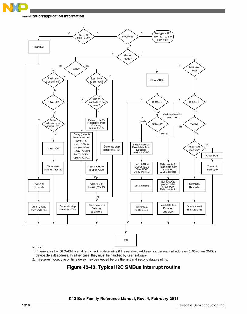
Mastermode?
Tx/Rx?Arbitration
lost?
IAAS=1?
Tx/Rx?
ACK fromreceiver?
SRW=1?
IAAS=1?
Clear ARBL
2nd tolast byte to be
read?
Last byteto be read?
RXAK=0?
Last bytetransmitted?
End ofaddress cycle(master Rx)?
Write nextbyte to Data reg
Generate stopsignal (MST=0)
Set TXAK toproper valueClear IICIF
Delay (note 2)
Delay (note 2)Read data from
Data reg and soft CRC
Transmitnext byte
RTI
Switch toRx mode
Switch toRx mode
Dummy readfrom Data reg
Generate stopsignal (MST=0)
Read data fromData reg and store
Read data fromData reg and store
Dummy readfrom Data reg
NY
N
N
N
N
N
N
Y
Y
Y
Y
Y(read)
N (write)N
Y
RxTx
Rx
Tx
Y
N
Address transfersee note 1
N
Y
Y
Y
SLTF orSHTF2=1?
NY
Clear IICIF
FACK=1?N
Y
See typical I2C interrupt routine
flow chart
Set TXAK toproper value
Clear IICIFDelay (note 2) Set Tx mode
Write datato Data reg
Clear IICIF
Notes:1. If general call or SIICAEN is enabled, check to determine if the received address is a general call address (0x00) or an SMBus device default address. In either case, they must be handled by user software.2. In receive mode, one bit time delay may be needed before the first and second data reading.
Clear IICIF
Delay (note 2)Read data from
Data reg and soft CRC
Set TXAK toproper valueClear IICIF
Delay (note 2)
Delay (note 2)Read data from
Data reg and soft CRC
Set TXACK=1Clear FACK=0
Delay (note 2)Read data and
Soft CRCSet TXAK toproper value
Delay (note 2)
Figure 42-43. Typical I2C SMBus interrupt routine
Initialization/application information
K12 Sub-Family Reference Manual, Rev. 4, February 2013
1010 Freescale Semiconductor, Inc.
Chapter 43Universal Asynchronous Receiver/Transmitter(UART)
43.1 IntroductionNOTE
For the chip-specific implementation details of this module'sinstances see the chip configuration information.
The UART allows asynchronous serial communication with peripheral devices andCPUs.
43.1.1 Features
The UART includes the following features:
• Full-duplex operation
• Standard mark/space non-return-to-zero (NRZ) format
• Selectable IrDA 1.4 return-to-zero-inverted (RZI) format with programmable pulsewidth
• 13-bit baud rate selection with /32 fractional divide, based on the module clockfrequency
• Programmable 8-bit or 9-bit data format
• Separately enabled transmitter and receiver
• Programmable transmitter output polarity
• Programmable receive input polarity
• 13-bit break character option
K12 Sub-Family Reference Manual, Rev. 4, February 2013
Freescale Semiconductor, Inc. 1011

• 11-bit break character detection option
• Independent FIFO structure for transmit and receive
• Two receiver wakeup methods:
• Idle line wakeup
• Address mark wakeup
• Address match feature in the receiver to reduce address mark wakeup ISR overhead
• Ability to select MSB or LSB to be first bit on wire
• Hardware flow control support for request to send (RTS) and clear to send (CTS)signals
• Support for ISO 7816 protocol to interface with SIM cards and smart cards
• Support for T=0 and T=1 protocols
• Automatic retransmission of NACK'd packets with programmable retrythreshold
• Support for 11 and 12 ETU transfers
• Detection of initial packet and automated transfer parameter programming
• Interrupt-driven operation with seven ISO-7816 specific interrupts:
• Wait time violated
• Character wait time violated
• Block wait time violated
• Initial frame detected
• Transmit error threshold exceeded
• Receive error threshold exceeded
• Guard time violated
• Interrupt-driven operation with 12 flags, not specific to ISO-7816 support
• Transmitter data buffer at or below watermark
• Transmission complete
• Receiver data buffer at or above watermark
• Idle receiver input
Introduction
K12 Sub-Family Reference Manual, Rev. 4, February 2013
1012 Freescale Semiconductor, Inc.

• Receiver data buffer overrun
• Receiver data buffer underflow
• Transmit data buffer overflow
• Noise error
• Framing error
• Parity error
• Active edge on receive pin
• LIN break detect
• Receiver framing error detection
• Hardware parity generation and checking
• 1/16 bit-time noise detection
• DMA interface
43.1.2 Modes of operation
The UART functions in the same way in all the normal modes.
It has the following low power modes:
• Wait mode• Stop mode
43.1.2.1 Run mode
This is the normal mode of operation.
43.1.2.2 Wait mode
UART operation in the Wait mode depends on the state of the C1[UARTSWAI] field.
Chapter 43 Universal Asynchronous Receiver/Transmitter (UART)
K12 Sub-Family Reference Manual, Rev. 4, February 2013
Freescale Semiconductor, Inc. 1013
• If C1[UARTSWAI] is cleared, and the CPU is in Wait mode, the UART operatesnormally.
• If C1[UARTSWAI] is set, and the CPU is in Wait mode, the UART clock generationceases and the UART module enters a power conservation state.
C1[UARTSWAI] does not initiate any power down or power up procedures for theISO-7816 smartcard interface.
Setting C1[UARTSWAI] does not affect the state of the C2[RE] or C2[TE].
If C1[UARTSWAI] is set, any ongoing transmission or reception stops at the Wait modeentry. The transmission or reception resumes when either an internal or external interruptbrings the CPU out of Wait mode. Bringing the CPU out of Wait mode by reset abortsany ongoing transmission or reception and resets the UART.
43.1.2.3 Stop mode
The UART is inactive during Stop mode for reduced power consumption. The STOPinstruction does not affect the UART register states, but the UART module clock isdisabled. The UART operation resumes after an external interrupt brings the CPU out ofStop mode. Bringing the CPU out of Stop mode by reset aborts any ongoing transmissionor reception and resets the UART. Entering or leaving Stop mode does not initiate anypower down or power up procedures for the ISO-7816 smartcard interface.
43.2 UART signal descriptionsThe UART signals are shown in the following table.
Table 43-1. UART signal descriptions
Signal Description I/O
CTS Clear to send I
RTS Request to send O
RXD Receive data I
TXD Transmit data O
43.2.1 Detailed signal descriptions
The detailed signal descriptions of the UART are shown in the following table.
UART signal descriptions
K12 Sub-Family Reference Manual, Rev. 4, February 2013
1014 Freescale Semiconductor, Inc.
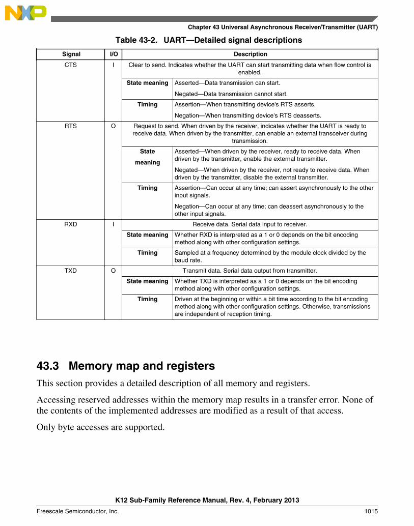
Table 43-2. UART—Detailed signal descriptions
Signal I/O Description
CTS I Clear to send. Indicates whether the UART can start transmitting data when flow control isenabled.
State meaning Asserted—Data transmission can start.
Negated—Data transmission cannot start.
Timing Assertion—When transmitting device's RTS asserts.
Negation—When transmitting device's RTS deasserts.
RTS O Request to send. When driven by the receiver, indicates whether the UART is ready toreceive data. When driven by the transmitter, can enable an external transceiver during
transmission.
State
meaning
Asserted—When driven by the receiver, ready to receive data. Whendriven by the transmitter, enable the external transmitter.
Negated—When driven by the receiver, not ready to receive data. Whendriven by the transmitter, disable the external transmitter.
Timing Assertion—Can occur at any time; can assert asynchronously to the otherinput signals.
Negation—Can occur at any time; can deassert asynchronously to theother input signals.
RXD I Receive data. Serial data input to receiver.
State meaning Whether RXD is interpreted as a 1 or 0 depends on the bit encodingmethod along with other configuration settings.
Timing Sampled at a frequency determined by the module clock divided by thebaud rate.
TXD O Transmit data. Serial data output from transmitter.
State meaning Whether TXD is interpreted as a 1 or 0 depends on the bit encodingmethod along with other configuration settings.
Timing Driven at the beginning or within a bit time according to the bit encodingmethod along with other configuration settings. Otherwise, transmissionsare independent of reception timing.
43.3 Memory map and registersThis section provides a detailed description of all memory and registers.
Accessing reserved addresses within the memory map results in a transfer error. None ofthe contents of the implemented addresses are modified as a result of that access.
Only byte accesses are supported.
Chapter 43 Universal Asynchronous Receiver/Transmitter (UART)
K12 Sub-Family Reference Manual, Rev. 4, February 2013
Freescale Semiconductor, Inc. 1015
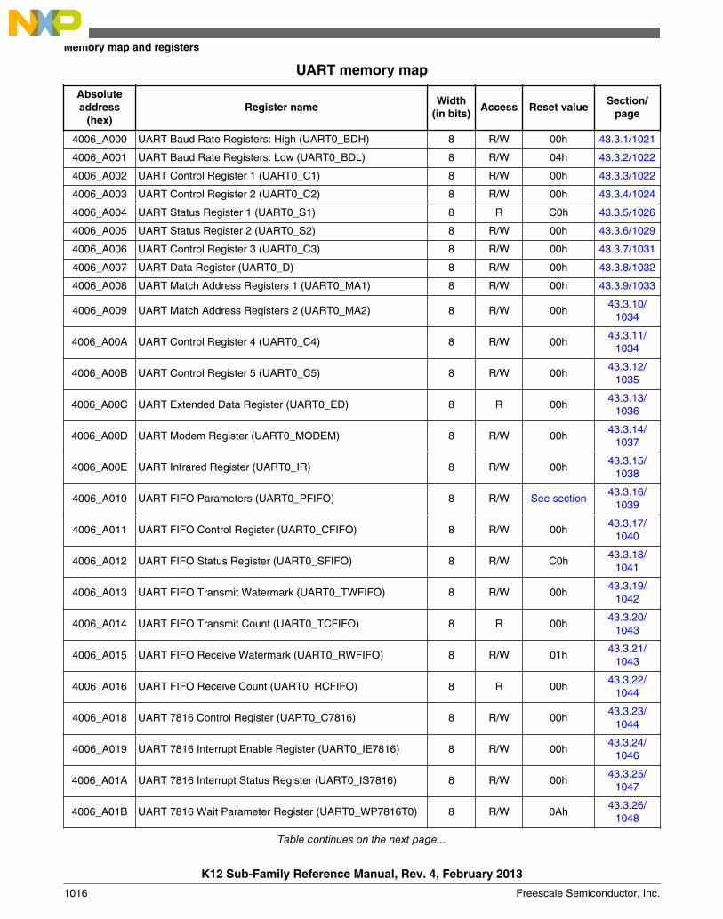
UART memory map
Absoluteaddress
(hex)Register name
Width(in bits)
Access Reset valueSection/
page
4006_A000 UART Baud Rate Registers: High (UART0_BDH) 8 R/W 00h 43.3.1/1021
4006_A001 UART Baud Rate Registers: Low (UART0_BDL) 8 R/W 04h 43.3.2/1022
4006_A002 UART Control Register 1 (UART0_C1) 8 R/W 00h 43.3.3/1022
4006_A003 UART Control Register 2 (UART0_C2) 8 R/W 00h 43.3.4/1024
4006_A004 UART Status Register 1 (UART0_S1) 8 R C0h 43.3.5/1026
4006_A005 UART Status Register 2 (UART0_S2) 8 R/W 00h 43.3.6/1029
4006_A006 UART Control Register 3 (UART0_C3) 8 R/W 00h 43.3.7/1031
4006_A007 UART Data Register (UART0_D) 8 R/W 00h 43.3.8/1032
4006_A008 UART Match Address Registers 1 (UART0_MA1) 8 R/W 00h 43.3.9/1033
4006_A009 UART Match Address Registers 2 (UART0_MA2) 8 R/W 00h43.3.10/
1034
4006_A00A UART Control Register 4 (UART0_C4) 8 R/W 00h43.3.11/
1034
4006_A00B UART Control Register 5 (UART0_C5) 8 R/W 00h43.3.12/
1035
4006_A00C UART Extended Data Register (UART0_ED) 8 R 00h43.3.13/
1036
4006_A00D UART Modem Register (UART0_MODEM) 8 R/W 00h43.3.14/
1037
4006_A00E UART Infrared Register (UART0_IR) 8 R/W 00h43.3.15/
1038
4006_A010 UART FIFO Parameters (UART0_PFIFO) 8 R/W See section43.3.16/
1039
4006_A011 UART FIFO Control Register (UART0_CFIFO) 8 R/W 00h43.3.17/
1040
4006_A012 UART FIFO Status Register (UART0_SFIFO) 8 R/W C0h43.3.18/
1041
4006_A013 UART FIFO Transmit Watermark (UART0_TWFIFO) 8 R/W 00h43.3.19/
1042
4006_A014 UART FIFO Transmit Count (UART0_TCFIFO) 8 R 00h43.3.20/
1043
4006_A015 UART FIFO Receive Watermark (UART0_RWFIFO) 8 R/W 01h43.3.21/
1043
4006_A016 UART FIFO Receive Count (UART0_RCFIFO) 8 R 00h43.3.22/
1044
4006_A018 UART 7816 Control Register (UART0_C7816) 8 R/W 00h43.3.23/
1044
4006_A019 UART 7816 Interrupt Enable Register (UART0_IE7816) 8 R/W 00h43.3.24/
1046
4006_A01A UART 7816 Interrupt Status Register (UART0_IS7816) 8 R/W 00h43.3.25/
1047
4006_A01B UART 7816 Wait Parameter Register (UART0_WP7816T0) 8 R/W 0Ah43.3.26/
1048
Table continues on the next page...
Memory map and registers
K12 Sub-Family Reference Manual, Rev. 4, February 2013
1016 Freescale Semiconductor, Inc.
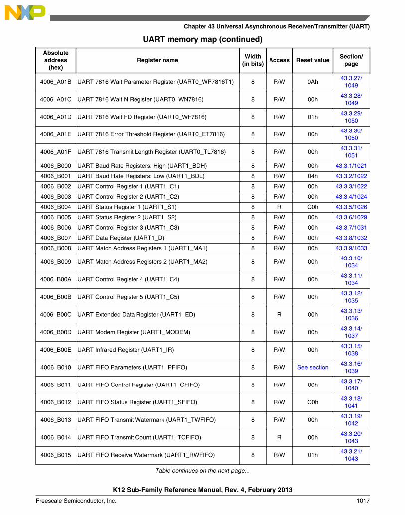
UART memory map (continued)
Absoluteaddress
(hex)Register name
Width(in bits)
Access Reset valueSection/
page
4006_A01B UART 7816 Wait Parameter Register (UART0_WP7816T1) 8 R/W 0Ah43.3.27/
1049
4006_A01C UART 7816 Wait N Register (UART0_WN7816) 8 R/W 00h43.3.28/
1049
4006_A01D UART 7816 Wait FD Register (UART0_WF7816) 8 R/W 01h43.3.29/
1050
4006_A01E UART 7816 Error Threshold Register (UART0_ET7816) 8 R/W 00h43.3.30/
1050
4006_A01F UART 7816 Transmit Length Register (UART0_TL7816) 8 R/W 00h43.3.31/
1051
4006_B000 UART Baud Rate Registers: High (UART1_BDH) 8 R/W 00h 43.3.1/1021
4006_B001 UART Baud Rate Registers: Low (UART1_BDL) 8 R/W 04h 43.3.2/1022
4006_B002 UART Control Register 1 (UART1_C1) 8 R/W 00h 43.3.3/1022
4006_B003 UART Control Register 2 (UART1_C2) 8 R/W 00h 43.3.4/1024
4006_B004 UART Status Register 1 (UART1_S1) 8 R C0h 43.3.5/1026
4006_B005 UART Status Register 2 (UART1_S2) 8 R/W 00h 43.3.6/1029
4006_B006 UART Control Register 3 (UART1_C3) 8 R/W 00h 43.3.7/1031
4006_B007 UART Data Register (UART1_D) 8 R/W 00h 43.3.8/1032
4006_B008 UART Match Address Registers 1 (UART1_MA1) 8 R/W 00h 43.3.9/1033
4006_B009 UART Match Address Registers 2 (UART1_MA2) 8 R/W 00h43.3.10/
1034
4006_B00A UART Control Register 4 (UART1_C4) 8 R/W 00h43.3.11/
1034
4006_B00B UART Control Register 5 (UART1_C5) 8 R/W 00h43.3.12/
1035
4006_B00C UART Extended Data Register (UART1_ED) 8 R 00h43.3.13/
1036
4006_B00D UART Modem Register (UART1_MODEM) 8 R/W 00h43.3.14/
1037
4006_B00E UART Infrared Register (UART1_IR) 8 R/W 00h43.3.15/
1038
4006_B010 UART FIFO Parameters (UART1_PFIFO) 8 R/W See section43.3.16/
1039
4006_B011 UART FIFO Control Register (UART1_CFIFO) 8 R/W 00h43.3.17/
1040
4006_B012 UART FIFO Status Register (UART1_SFIFO) 8 R/W C0h43.3.18/
1041
4006_B013 UART FIFO Transmit Watermark (UART1_TWFIFO) 8 R/W 00h43.3.19/
1042
4006_B014 UART FIFO Transmit Count (UART1_TCFIFO) 8 R 00h43.3.20/
1043
4006_B015 UART FIFO Receive Watermark (UART1_RWFIFO) 8 R/W 01h43.3.21/
1043
Table continues on the next page...
Chapter 43 Universal Asynchronous Receiver/Transmitter (UART)
K12 Sub-Family Reference Manual, Rev. 4, February 2013
Freescale Semiconductor, Inc. 1017

UART memory map (continued)
Absoluteaddress
(hex)Register name
Width(in bits)
Access Reset valueSection/
page
4006_B016 UART FIFO Receive Count (UART1_RCFIFO) 8 R 00h43.3.22/
1044
4006_B018 UART 7816 Control Register (UART1_C7816) 8 R/W 00h43.3.23/
1044
4006_B019 UART 7816 Interrupt Enable Register (UART1_IE7816) 8 R/W 00h43.3.24/
1046
4006_B01A UART 7816 Interrupt Status Register (UART1_IS7816) 8 R/W 00h43.3.25/
1047
4006_B01B UART 7816 Wait Parameter Register (UART1_WP7816T0) 8 R/W 0Ah43.3.26/
1048
4006_B01B UART 7816 Wait Parameter Register (UART1_WP7816T1) 8 R/W 0Ah43.3.27/
1049
4006_B01C UART 7816 Wait N Register (UART1_WN7816) 8 R/W 00h43.3.28/
1049
4006_B01D UART 7816 Wait FD Register (UART1_WF7816) 8 R/W 01h43.3.29/
1050
4006_B01E UART 7816 Error Threshold Register (UART1_ET7816) 8 R/W 00h43.3.30/
1050
4006_B01F UART 7816 Transmit Length Register (UART1_TL7816) 8 R/W 00h43.3.31/
1051
4006_C000 UART Baud Rate Registers: High (UART2_BDH) 8 R/W 00h 43.3.1/1021
4006_C001 UART Baud Rate Registers: Low (UART2_BDL) 8 R/W 04h 43.3.2/1022
4006_C002 UART Control Register 1 (UART2_C1) 8 R/W 00h 43.3.3/1022
4006_C003 UART Control Register 2 (UART2_C2) 8 R/W 00h 43.3.4/1024
4006_C004 UART Status Register 1 (UART2_S1) 8 R C0h 43.3.5/1026
4006_C005 UART Status Register 2 (UART2_S2) 8 R/W 00h 43.3.6/1029
4006_C006 UART Control Register 3 (UART2_C3) 8 R/W 00h 43.3.7/1031
4006_C007 UART Data Register (UART2_D) 8 R/W 00h 43.3.8/1032
4006_C008 UART Match Address Registers 1 (UART2_MA1) 8 R/W 00h 43.3.9/1033
4006_C009 UART Match Address Registers 2 (UART2_MA2) 8 R/W 00h43.3.10/
1034
4006_C00A UART Control Register 4 (UART2_C4) 8 R/W 00h43.3.11/
1034
4006_C00B UART Control Register 5 (UART2_C5) 8 R/W 00h43.3.12/
1035
4006_C00C UART Extended Data Register (UART2_ED) 8 R 00h43.3.13/
1036
4006_C00D UART Modem Register (UART2_MODEM) 8 R/W 00h43.3.14/
1037
4006_C00E UART Infrared Register (UART2_IR) 8 R/W 00h43.3.15/
1038
4006_C010 UART FIFO Parameters (UART2_PFIFO) 8 R/W See section43.3.16/
1039
Table continues on the next page...
Memory map and registers
K12 Sub-Family Reference Manual, Rev. 4, February 2013
1018 Freescale Semiconductor, Inc.
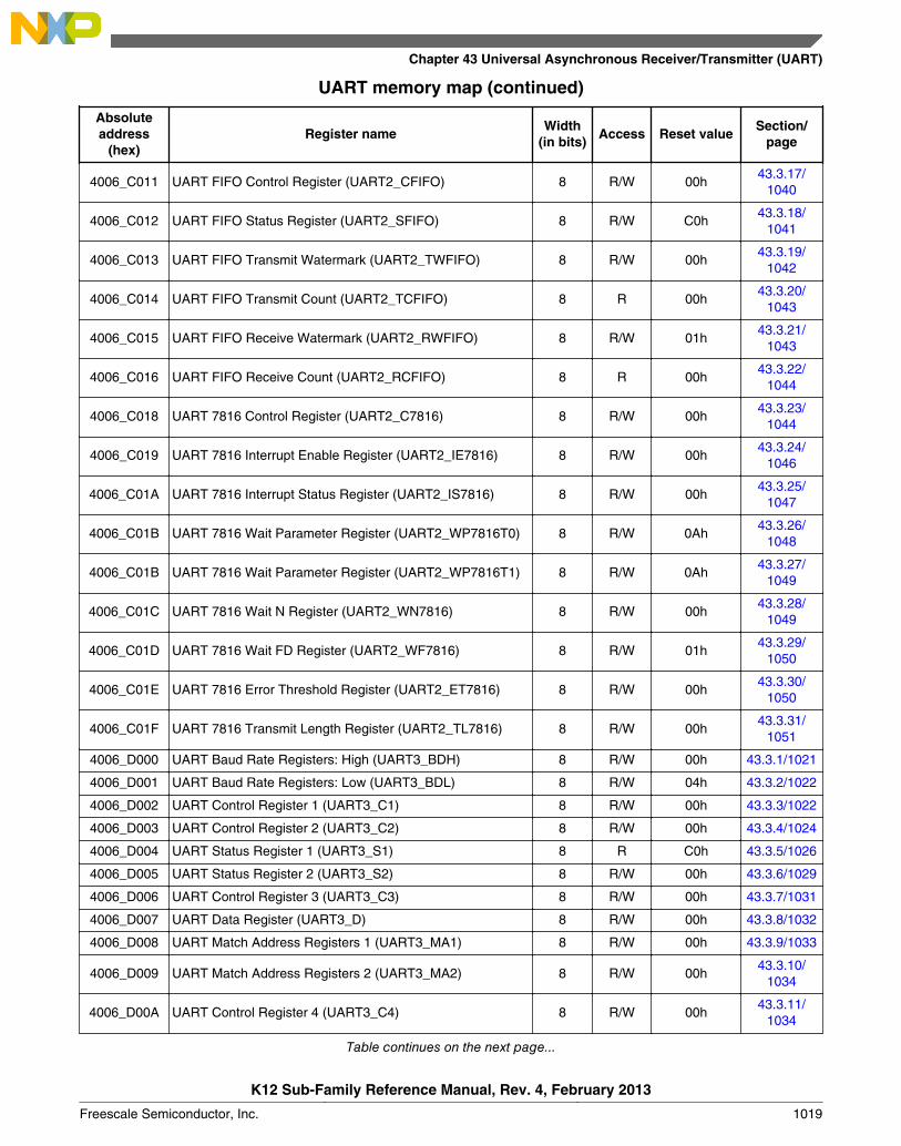
UART memory map (continued)
Absoluteaddress
(hex)Register name
Width(in bits)
Access Reset valueSection/
page
4006_C011 UART FIFO Control Register (UART2_CFIFO) 8 R/W 00h43.3.17/
1040
4006_C012 UART FIFO Status Register (UART2_SFIFO) 8 R/W C0h43.3.18/
1041
4006_C013 UART FIFO Transmit Watermark (UART2_TWFIFO) 8 R/W 00h43.3.19/
1042
4006_C014 UART FIFO Transmit Count (UART2_TCFIFO) 8 R 00h43.3.20/
1043
4006_C015 UART FIFO Receive Watermark (UART2_RWFIFO) 8 R/W 01h43.3.21/
1043
4006_C016 UART FIFO Receive Count (UART2_RCFIFO) 8 R 00h43.3.22/
1044
4006_C018 UART 7816 Control Register (UART2_C7816) 8 R/W 00h43.3.23/
1044
4006_C019 UART 7816 Interrupt Enable Register (UART2_IE7816) 8 R/W 00h43.3.24/
1046
4006_C01A UART 7816 Interrupt Status Register (UART2_IS7816) 8 R/W 00h43.3.25/
1047
4006_C01B UART 7816 Wait Parameter Register (UART2_WP7816T0) 8 R/W 0Ah43.3.26/
1048
4006_C01B UART 7816 Wait Parameter Register (UART2_WP7816T1) 8 R/W 0Ah43.3.27/
1049
4006_C01C UART 7816 Wait N Register (UART2_WN7816) 8 R/W 00h43.3.28/
1049
4006_C01D UART 7816 Wait FD Register (UART2_WF7816) 8 R/W 01h43.3.29/
1050
4006_C01E UART 7816 Error Threshold Register (UART2_ET7816) 8 R/W 00h43.3.30/
1050
4006_C01F UART 7816 Transmit Length Register (UART2_TL7816) 8 R/W 00h43.3.31/
1051
4006_D000 UART Baud Rate Registers: High (UART3_BDH) 8 R/W 00h 43.3.1/1021
4006_D001 UART Baud Rate Registers: Low (UART3_BDL) 8 R/W 04h 43.3.2/1022
4006_D002 UART Control Register 1 (UART3_C1) 8 R/W 00h 43.3.3/1022
4006_D003 UART Control Register 2 (UART3_C2) 8 R/W 00h 43.3.4/1024
4006_D004 UART Status Register 1 (UART3_S1) 8 R C0h 43.3.5/1026
4006_D005 UART Status Register 2 (UART3_S2) 8 R/W 00h 43.3.6/1029
4006_D006 UART Control Register 3 (UART3_C3) 8 R/W 00h 43.3.7/1031
4006_D007 UART Data Register (UART3_D) 8 R/W 00h 43.3.8/1032
4006_D008 UART Match Address Registers 1 (UART3_MA1) 8 R/W 00h 43.3.9/1033
4006_D009 UART Match Address Registers 2 (UART3_MA2) 8 R/W 00h43.3.10/
1034
4006_D00A UART Control Register 4 (UART3_C4) 8 R/W 00h43.3.11/
1034
Table continues on the next page...
Chapter 43 Universal Asynchronous Receiver/Transmitter (UART)
K12 Sub-Family Reference Manual, Rev. 4, February 2013
Freescale Semiconductor, Inc. 1019
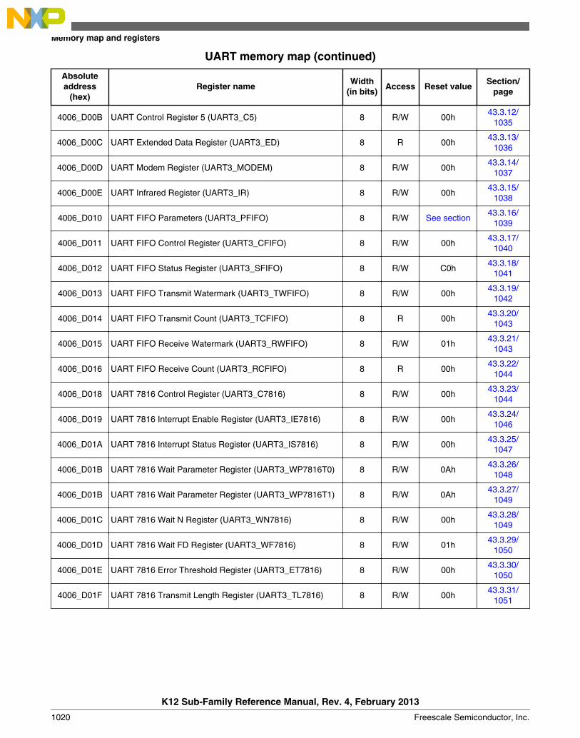
UART memory map (continued)
Absoluteaddress
(hex)Register name
Width(in bits)
Access Reset valueSection/
page
4006_D00B UART Control Register 5 (UART3_C5) 8 R/W 00h43.3.12/
1035
4006_D00C UART Extended Data Register (UART3_ED) 8 R 00h43.3.13/
1036
4006_D00D UART Modem Register (UART3_MODEM) 8 R/W 00h43.3.14/
1037
4006_D00E UART Infrared Register (UART3_IR) 8 R/W 00h43.3.15/
1038
4006_D010 UART FIFO Parameters (UART3_PFIFO) 8 R/W See section43.3.16/
1039
4006_D011 UART FIFO Control Register (UART3_CFIFO) 8 R/W 00h43.3.17/
1040
4006_D012 UART FIFO Status Register (UART3_SFIFO) 8 R/W C0h43.3.18/
1041
4006_D013 UART FIFO Transmit Watermark (UART3_TWFIFO) 8 R/W 00h43.3.19/
1042
4006_D014 UART FIFO Transmit Count (UART3_TCFIFO) 8 R 00h43.3.20/
1043
4006_D015 UART FIFO Receive Watermark (UART3_RWFIFO) 8 R/W 01h43.3.21/
1043
4006_D016 UART FIFO Receive Count (UART3_RCFIFO) 8 R 00h43.3.22/
1044
4006_D018 UART 7816 Control Register (UART3_C7816) 8 R/W 00h43.3.23/
1044
4006_D019 UART 7816 Interrupt Enable Register (UART3_IE7816) 8 R/W 00h43.3.24/
1046
4006_D01A UART 7816 Interrupt Status Register (UART3_IS7816) 8 R/W 00h43.3.25/
1047
4006_D01B UART 7816 Wait Parameter Register (UART3_WP7816T0) 8 R/W 0Ah43.3.26/
1048
4006_D01B UART 7816 Wait Parameter Register (UART3_WP7816T1) 8 R/W 0Ah43.3.27/
1049
4006_D01C UART 7816 Wait N Register (UART3_WN7816) 8 R/W 00h43.3.28/
1049
4006_D01D UART 7816 Wait FD Register (UART3_WF7816) 8 R/W 01h43.3.29/
1050
4006_D01E UART 7816 Error Threshold Register (UART3_ET7816) 8 R/W 00h43.3.30/
1050
4006_D01F UART 7816 Transmit Length Register (UART3_TL7816) 8 R/W 00h43.3.31/
1051
Memory map and registers
K12 Sub-Family Reference Manual, Rev. 4, February 2013
1020 Freescale Semiconductor, Inc.
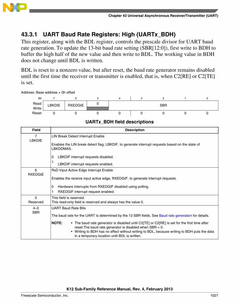
43.3.1 UART Baud Rate Registers: High (UARTx_BDH)This register, along with the BDL register, controls the prescale divisor for UART baudrate generation. To update the 13-bit baud rate setting (SBR[12:0]), first write to BDH tobuffer the high half of the new value and then write to BDL. The working value in BDHdoes not change until BDL is written.
BDL is reset to a nonzero value, but after reset, the baud rate generator remains disableduntil the first time the receiver or transmitter is enabled, that is, when C2[RE] or C2[TE]is set.
Address: Base address + 0h offset
Bit 7 6 5 4 3 2 1 0
Read LBKDIE RXEDGIE 0 SBRWriteReset 0 0 0 0 0 0 0 0
UARTx_BDH field descriptions
Field Description
7LBKDIE
LIN Break Detect Interrupt Enable
Enables the LIN break detect flag, LBKDIF, to generate interrupt requests based on the state ofLBKDDMAS.
0 LBKDIF interrupt requests disabled.1
LBKDIF interrupt requests enabled.
6RXEDGIE
RxD Input Active Edge Interrupt Enable
Enables the receive input active edge, RXEDGIF, to generate interrupt requests.
0 Hardware interrupts from RXEDGIF disabled using polling.1 RXEDGIF interrupt request enabled.
5Reserved
This field is reserved.This read-only field is reserved and always has the value 0.
4–0SBR
UART Baud Rate Bits
The baud rate for the UART is determined by the 13 SBR fields. See Baud rate generation for details.
NOTE: • The baud rate generator is disabled until C2[TE] or C2[RE] is set for the first time afterreset.The baud rate generator is disabled when SBR = 0.
• Writing to BDH has no effect without writing to BDL, because writing to BDH puts the datain a temporary location until BDL is written.
Chapter 43 Universal Asynchronous Receiver/Transmitter (UART)
K12 Sub-Family Reference Manual, Rev. 4, February 2013
Freescale Semiconductor, Inc. 1021
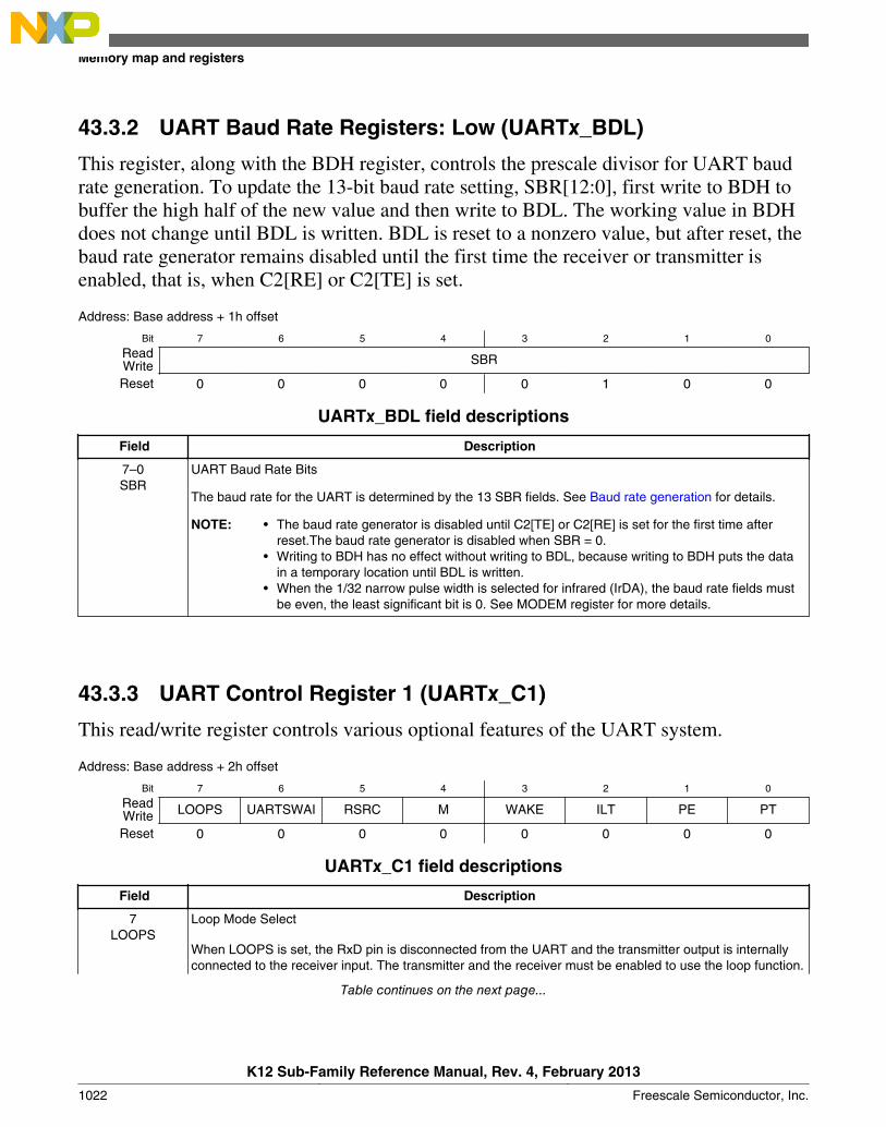
43.3.2 UART Baud Rate Registers: Low (UARTx_BDL)
This register, along with the BDH register, controls the prescale divisor for UART baudrate generation. To update the 13-bit baud rate setting, SBR[12:0], first write to BDH tobuffer the high half of the new value and then write to BDL. The working value in BDHdoes not change until BDL is written. BDL is reset to a nonzero value, but after reset, thebaud rate generator remains disabled until the first time the receiver or transmitter isenabled, that is, when C2[RE] or C2[TE] is set.
Address: Base address + 1h offset
Bit 7 6 5 4 3 2 1 0
Read SBRWriteReset 0 0 0 0 0 1 0 0
UARTx_BDL field descriptions
Field Description
7–0SBR
UART Baud Rate Bits
The baud rate for the UART is determined by the 13 SBR fields. See Baud rate generation for details.
NOTE: • The baud rate generator is disabled until C2[TE] or C2[RE] is set for the first time afterreset.The baud rate generator is disabled when SBR = 0.
• Writing to BDH has no effect without writing to BDL, because writing to BDH puts the datain a temporary location until BDL is written.
• When the 1/32 narrow pulse width is selected for infrared (IrDA), the baud rate fields mustbe even, the least significant bit is 0. See MODEM register for more details.
43.3.3 UART Control Register 1 (UARTx_C1)
This read/write register controls various optional features of the UART system.
Address: Base address + 2h offset
Bit 7 6 5 4 3 2 1 0
Read LOOPS UARTSWAI RSRC M WAKE ILT PE PTWriteReset 0 0 0 0 0 0 0 0
UARTx_C1 field descriptions
Field Description
7LOOPS
Loop Mode Select
When LOOPS is set, the RxD pin is disconnected from the UART and the transmitter output is internallyconnected to the receiver input. The transmitter and the receiver must be enabled to use the loop function.
Table continues on the next page...
Memory map and registers
K12 Sub-Family Reference Manual, Rev. 4, February 2013
1022 Freescale Semiconductor, Inc.
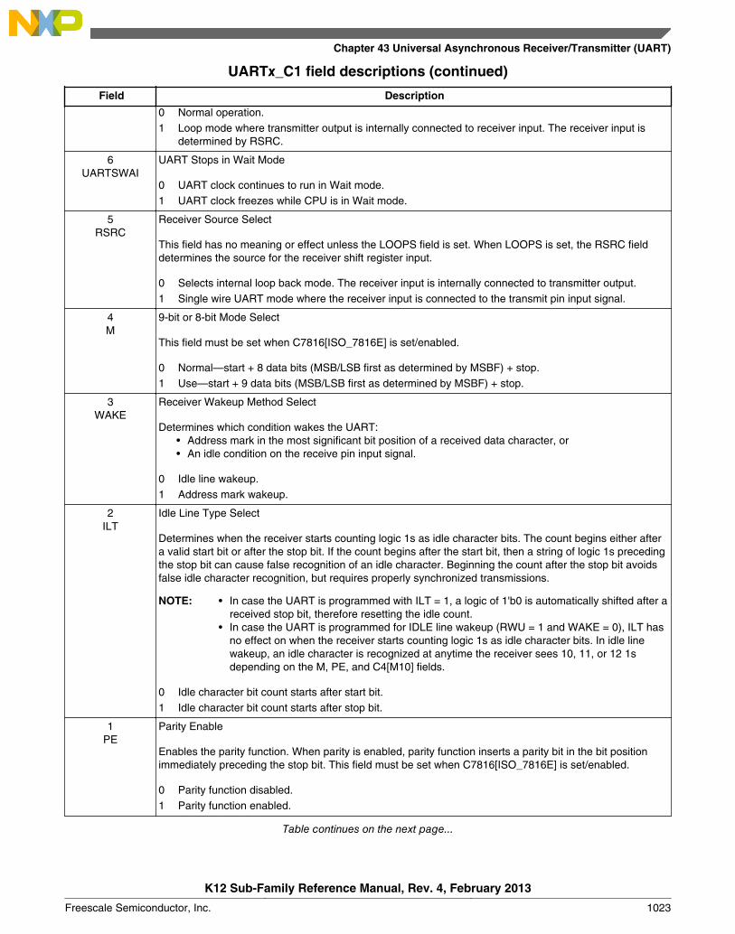
UARTx_C1 field descriptions (continued)
Field Description
0 Normal operation.1 Loop mode where transmitter output is internally connected to receiver input. The receiver input is
determined by RSRC.
6UARTSWAI
UART Stops in Wait Mode
0 UART clock continues to run in Wait mode.1 UART clock freezes while CPU is in Wait mode.
5RSRC
Receiver Source Select
This field has no meaning or effect unless the LOOPS field is set. When LOOPS is set, the RSRC fielddetermines the source for the receiver shift register input.
0 Selects internal loop back mode. The receiver input is internally connected to transmitter output.1 Single wire UART mode where the receiver input is connected to the transmit pin input signal.
4M
9-bit or 8-bit Mode Select
This field must be set when C7816[ISO_7816E] is set/enabled.
0 Normal—start + 8 data bits (MSB/LSB first as determined by MSBF) + stop.1 Use—start + 9 data bits (MSB/LSB first as determined by MSBF) + stop.
3WAKE
Receiver Wakeup Method Select
Determines which condition wakes the UART:• Address mark in the most significant bit position of a received data character, or• An idle condition on the receive pin input signal.
0 Idle line wakeup.1 Address mark wakeup.
2ILT
Idle Line Type Select
Determines when the receiver starts counting logic 1s as idle character bits. The count begins either aftera valid start bit or after the stop bit. If the count begins after the start bit, then a string of logic 1s precedingthe stop bit can cause false recognition of an idle character. Beginning the count after the stop bit avoidsfalse idle character recognition, but requires properly synchronized transmissions.
NOTE: • In case the UART is programmed with ILT = 1, a logic of 1'b0 is automatically shifted after areceived stop bit, therefore resetting the idle count.
• In case the UART is programmed for IDLE line wakeup (RWU = 1 and WAKE = 0), ILT hasno effect on when the receiver starts counting logic 1s as idle character bits. In idle linewakeup, an idle character is recognized at anytime the receiver sees 10, 11, or 12 1sdepending on the M, PE, and C4[M10] fields.
0 Idle character bit count starts after start bit.1 Idle character bit count starts after stop bit.
1PE
Parity Enable
Enables the parity function. When parity is enabled, parity function inserts a parity bit in the bit positionimmediately preceding the stop bit. This field must be set when C7816[ISO_7816E] is set/enabled.
0 Parity function disabled.1 Parity function enabled.
Table continues on the next page...
Chapter 43 Universal Asynchronous Receiver/Transmitter (UART)
K12 Sub-Family Reference Manual, Rev. 4, February 2013
Freescale Semiconductor, Inc. 1023
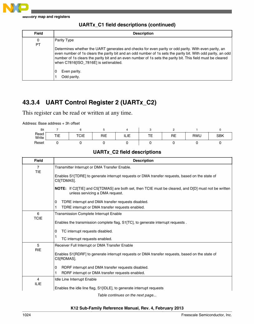
UARTx_C1 field descriptions (continued)
Field Description
0PT
Parity Type
Determines whether the UART generates and checks for even parity or odd parity. With even parity, aneven number of 1s clears the parity bit and an odd number of 1s sets the parity bit. With odd parity, an oddnumber of 1s clears the parity bit and an even number of 1s sets the parity bit. This field must be clearedwhen C7816[ISO_7816E] is set/enabled.
0 Even parity.1 Odd parity.
43.3.4 UART Control Register 2 (UARTx_C2)
This register can be read or written at any time.
Address: Base address + 3h offset
Bit 7 6 5 4 3 2 1 0
Read TIE TCIE RIE ILIE TE RE RWU SBKWriteReset 0 0 0 0 0 0 0 0
UARTx_C2 field descriptions
Field Description
7TIE
Transmitter Interrupt or DMA Transfer Enable.
Enables S1[TDRE] to generate interrupt requests or DMA transfer requests, based on the state ofC5[TDMAS].
NOTE: If C2[TIE] and C5[TDMAS] are both set, then TCIE must be cleared, and D[D] must not be writtenunless servicing a DMA request.
0 TDRE interrupt and DMA transfer requests disabled.1 TDRE interrupt or DMA transfer requests enabled.
6TCIE
Transmission Complete Interrupt Enable
Enables the transmission complete flag, S1[TC], to generate interrupt requests .
0 TC interrupt requests disabled.1
TC interrupt requests enabled.
5RIE
Receiver Full Interrupt or DMA Transfer Enable
Enables S1[RDRF] to generate interrupt requests or DMA transfer requests, based on the state ofC5[RDMAS].
0 RDRF interrupt and DMA transfer requests disabled.1 RDRF interrupt or DMA transfer requests enabled.
4ILIE
Idle Line Interrupt Enable
Enables the idle line flag, S1[IDLE], to generate interrupt requests
Table continues on the next page...
Memory map and registers
K12 Sub-Family Reference Manual, Rev. 4, February 2013
1024 Freescale Semiconductor, Inc.
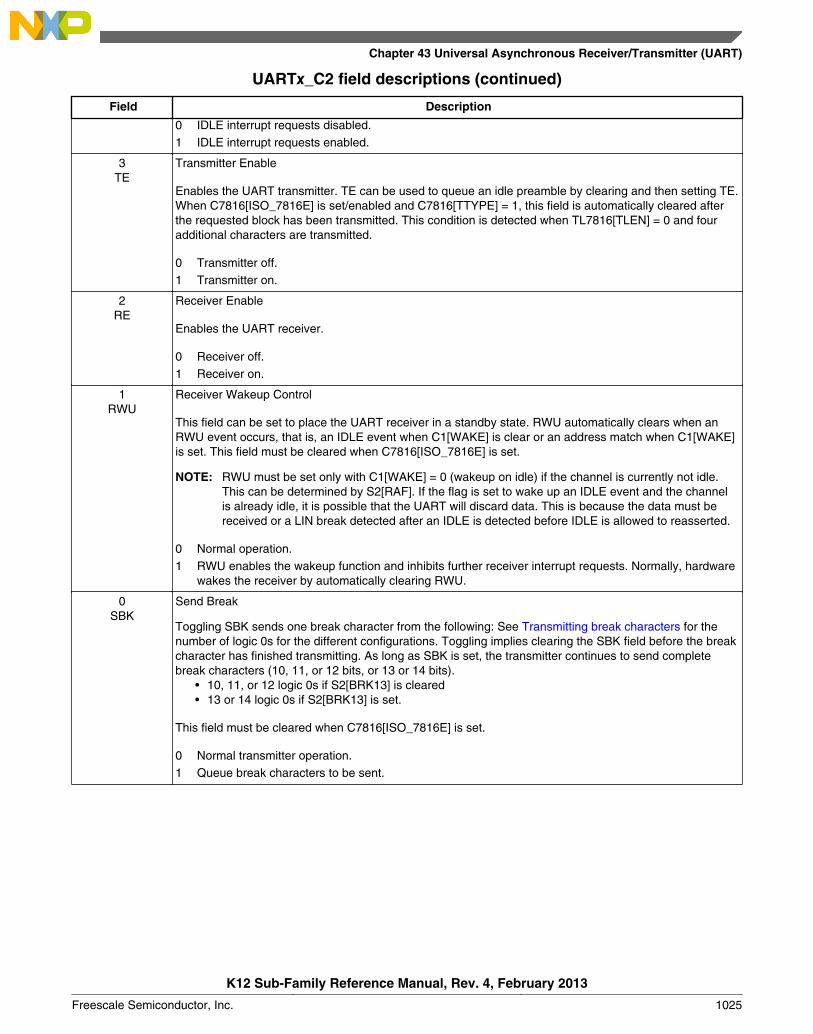
UARTx_C2 field descriptions (continued)
Field Description
0 IDLE interrupt requests disabled.1 IDLE interrupt requests enabled.
3TE
Transmitter Enable
Enables the UART transmitter. TE can be used to queue an idle preamble by clearing and then setting TE.When C7816[ISO_7816E] is set/enabled and C7816[TTYPE] = 1, this field is automatically cleared afterthe requested block has been transmitted. This condition is detected when TL7816[TLEN] = 0 and fouradditional characters are transmitted.
0 Transmitter off.1 Transmitter on.
2RE
Receiver Enable
Enables the UART receiver.
0 Receiver off.1 Receiver on.
1RWU
Receiver Wakeup Control
This field can be set to place the UART receiver in a standby state. RWU automatically clears when anRWU event occurs, that is, an IDLE event when C1[WAKE] is clear or an address match when C1[WAKE]is set. This field must be cleared when C7816[ISO_7816E] is set.
NOTE: RWU must be set only with C1[WAKE] = 0 (wakeup on idle) if the channel is currently not idle.This can be determined by S2[RAF]. If the flag is set to wake up an IDLE event and the channelis already idle, it is possible that the UART will discard data. This is because the data must bereceived or a LIN break detected after an IDLE is detected before IDLE is allowed to reasserted.
0 Normal operation.1 RWU enables the wakeup function and inhibits further receiver interrupt requests. Normally, hardware
wakes the receiver by automatically clearing RWU.
0SBK
Send Break
Toggling SBK sends one break character from the following: See Transmitting break characters for thenumber of logic 0s for the different configurations. Toggling implies clearing the SBK field before the breakcharacter has finished transmitting. As long as SBK is set, the transmitter continues to send completebreak characters (10, 11, or 12 bits, or 13 or 14 bits).
• 10, 11, or 12 logic 0s if S2[BRK13] is cleared• 13 or 14 logic 0s if S2[BRK13] is set.
This field must be cleared when C7816[ISO_7816E] is set.
0 Normal transmitter operation.1 Queue break characters to be sent.
Chapter 43 Universal Asynchronous Receiver/Transmitter (UART)
K12 Sub-Family Reference Manual, Rev. 4, February 2013
Freescale Semiconductor, Inc. 1025
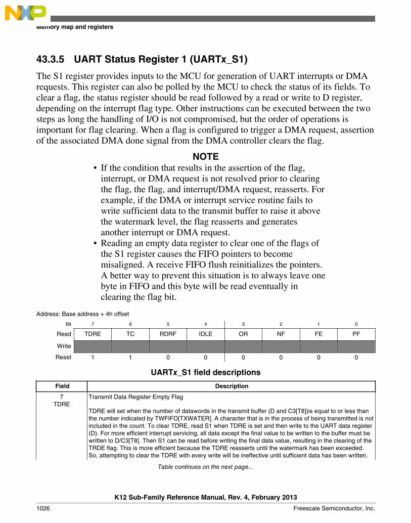
43.3.5 UART Status Register 1 (UARTx_S1)
The S1 register provides inputs to the MCU for generation of UART interrupts or DMArequests. This register can also be polled by the MCU to check the status of its fields. Toclear a flag, the status register should be read followed by a read or write to D register,depending on the interrupt flag type. Other instructions can be executed between the twosteps as long the handling of I/O is not compromised, but the order of operations isimportant for flag clearing. When a flag is configured to trigger a DMA request, assertionof the associated DMA done signal from the DMA controller clears the flag.
NOTE• If the condition that results in the assertion of the flag,
interrupt, or DMA request is not resolved prior to clearingthe flag, the flag, and interrupt/DMA request, reasserts. Forexample, if the DMA or interrupt service routine fails towrite sufficient data to the transmit buffer to raise it abovethe watermark level, the flag reasserts and generatesanother interrupt or DMA request.
• Reading an empty data register to clear one of the flags ofthe S1 register causes the FIFO pointers to becomemisaligned. A receive FIFO flush reinitializes the pointers.A better way to prevent this situation is to always leave onebyte in FIFO and this byte will be read eventually inclearing the flag bit.
Address: Base address + 4h offset
Bit 7 6 5 4 3 2 1 0
Read TDRE TC RDRF IDLE OR NF FE PF
Write
Reset 1 1 0 0 0 0 0 0
UARTx_S1 field descriptions
Field Description
7TDRE
Transmit Data Register Empty Flag
TDRE will set when the number of datawords in the transmit buffer (D and C3[T8])is equal to or less thanthe number indicated by TWFIFO[TXWATER]. A character that is in the process of being transmitted is notincluded in the count. To clear TDRE, read S1 when TDRE is set and then write to the UART data register(D). For more efficient interrupt servicing, all data except the final value to be written to the buffer must bewritten to D/C3[T8]. Then S1 can be read before writing the final data value, resulting in the clearing of theTRDE flag. This is more efficient because the TDRE reasserts until the watermark has been exceeded.So, attempting to clear the TDRE with every write will be ineffective until sufficient data has been written.
Table continues on the next page...
Memory map and registers
K12 Sub-Family Reference Manual, Rev. 4, February 2013
1026 Freescale Semiconductor, Inc.
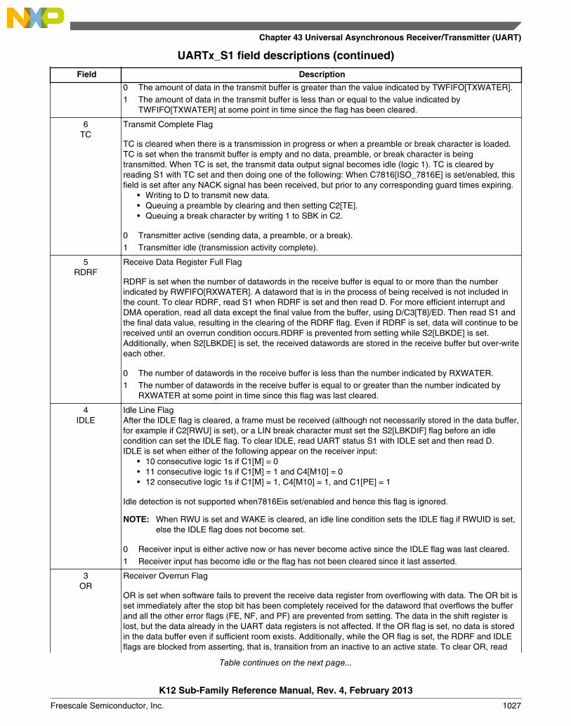
UARTx_S1 field descriptions (continued)
Field Description
0 The amount of data in the transmit buffer is greater than the value indicated by TWFIFO[TXWATER].1 The amount of data in the transmit buffer is less than or equal to the value indicated by
TWFIFO[TXWATER] at some point in time since the flag has been cleared.
6TC
Transmit Complete Flag
TC is cleared when there is a transmission in progress or when a preamble or break character is loaded.TC is set when the transmit buffer is empty and no data, preamble, or break character is beingtransmitted. When TC is set, the transmit data output signal becomes idle (logic 1). TC is cleared byreading S1 with TC set and then doing one of the following: When C7816[ISO_7816E] is set/enabled, thisfield is set after any NACK signal has been received, but prior to any corresponding guard times expiring.
• Writing to D to transmit new data.• Queuing a preamble by clearing and then setting C2[TE].• Queuing a break character by writing 1 to SBK in C2.
0 Transmitter active (sending data, a preamble, or a break).1 Transmitter idle (transmission activity complete).
5RDRF
Receive Data Register Full Flag
RDRF is set when the number of datawords in the receive buffer is equal to or more than the numberindicated by RWFIFO[RXWATER]. A dataword that is in the process of being received is not included inthe count. To clear RDRF, read S1 when RDRF is set and then read D. For more efficient interrupt andDMA operation, read all data except the final value from the buffer, using D/C3[T8]/ED. Then read S1 andthe final data value, resulting in the clearing of the RDRF flag. Even if RDRF is set, data will continue to bereceived until an overrun condition occurs.RDRF is prevented from setting while S2[LBKDE] is set.Additionally, when S2[LBKDE] is set, the received datawords are stored in the receive buffer but over-writeeach other.
0 The number of datawords in the receive buffer is less than the number indicated by RXWATER.1 The number of datawords in the receive buffer is equal to or greater than the number indicated by
RXWATER at some point in time since this flag was last cleared.
4IDLE
Idle Line FlagAfter the IDLE flag is cleared, a frame must be received (although not necessarily stored in the data buffer,for example if C2[RWU] is set), or a LIN break character must set the S2[LBKDIF] flag before an idlecondition can set the IDLE flag. To clear IDLE, read UART status S1 with IDLE set and then read D.IDLE is set when either of the following appear on the receiver input:
• 10 consecutive logic 1s if C1[M] = 0• 11 consecutive logic 1s if C1[M] = 1 and C4[M10] = 0• 12 consecutive logic 1s if C1[M] = 1, C4[M10] = 1, and C1[PE] = 1
Idle detection is not supported when7816Eis set/enabled and hence this flag is ignored.
NOTE: When RWU is set and WAKE is cleared, an idle line condition sets the IDLE flag if RWUID is set,else the IDLE flag does not become set.
0 Receiver input is either active now or has never become active since the IDLE flag was last cleared.1 Receiver input has become idle or the flag has not been cleared since it last asserted.
3OR
Receiver Overrun Flag
OR is set when software fails to prevent the receive data register from overflowing with data. The OR bit isset immediately after the stop bit has been completely received for the dataword that overflows the bufferand all the other error flags (FE, NF, and PF) are prevented from setting. The data in the shift register islost, but the data already in the UART data registers is not affected. If the OR flag is set, no data is storedin the data buffer even if sufficient room exists. Additionally, while the OR flag is set, the RDRF and IDLEflags are blocked from asserting, that is, transition from an inactive to an active state. To clear OR, read
Table continues on the next page...
Chapter 43 Universal Asynchronous Receiver/Transmitter (UART)
K12 Sub-Family Reference Manual, Rev. 4, February 2013
Freescale Semiconductor, Inc. 1027

UARTx_S1 field descriptions (continued)
Field Description
S1 when OR is set and then read D. See functional description for more details regarding the operation ofthe OR bit.If LBKDE is enabled and a LIN Break is detected, the OR field asserts if S2[LBKDIF] is notcleared before the next data character is received. In 7816 mode, it is possible to configure a NACK to bereturned by programing C7816[ONACK].
0 No overrun has occurred since the last time the flag was cleared.1 Overrun has occurred or the overrun flag has not been cleared since the last overrun occured.
2NF
Noise Flag
NF is set when the UART detects noise on the receiver input. NF does not become set in the case of anoverrun or while the LIN break detect feature is enabled (S2[LBKDE] = 1). When NF is set, it indicatesonly that a dataword has been received with noise since the last time it was cleared. There is noguarantee that the first dataword read from the receive buffer has noise or that there is only one datawordin the buffer that was received with noise unless the receive buffer has a depth of one. To clear NF, readS1 and then read D.
0 No noise detected since the last time this flag was cleared. If the receive buffer has a depth greaterthan 1 then there may be data in the receiver buffer that was received with noise.
1 At least one dataword was received with noise detected since the last time the flag was cleared.
1FE
Framing Error Flag
FE is set when a logic 0 is accepted as the stop bit. FE does not set in the case of an overrun or while theLIN break detect feature is enabled (S2[LBKDE] = 1). FE inhibits further data reception until it is cleared.To clear FE, read S1 with FE set and then read D. The last data in the receive buffer represents the datathat was received with the frame error enabled. Framing errors are not supported when 7816E is set/enabled. However, if this flag is set, data is still not received in 7816 mode.
0 No framing error detected.1 Framing error.
0PF
Parity Error Flag
PF is set when PE is set and the parity of the received data does not match its parity bit. The PF is not setin the case of an overrun condition. When PF is set, it indicates only that a dataword was received withparity error since the last time it was cleared. There is no guarantee that the first dataword read from thereceive buffer has a parity error or that there is only one dataword in the buffer that was received with aparity error, unless the receive buffer has a depth of one. To clear PF, read S1 and then read D.,S2[LBKDE] is disabled,Within the receive buffer structure the received dataword is tagged if it is receivedwith a parity error. This information is available by reading the ED register prior to reading the D register.
0 No parity error detected since the last time this flag was cleared. If the receive buffer has a depthgreater than 1, then there may be data in the receive buffer what was received with a parity error.
1 At least one dataword was received with a parity error since the last time this flag was cleared.
Memory map and registers
K12 Sub-Family Reference Manual, Rev. 4, February 2013
1028 Freescale Semiconductor, Inc.
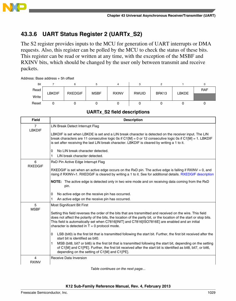
43.3.6 UART Status Register 2 (UARTx_S2)
The S2 register provides inputs to the MCU for generation of UART interrupts or DMArequests. Also, this register can be polled by the MCU to check the status of these bits.This register can be read or written at any time, with the exception of the MSBF andRXINV bits, which should be changed by the user only between transmit and receivepackets.
Address: Base address + 5h offset
Bit 7 6 5 4 3 2 1 0
ReadLBKDIF RXEDGIF MSBF RXINV RWUID BRK13 LBKDE
RAF
Write
Reset 0 0 0 0 0 0 0 0
UARTx_S2 field descriptions
Field Description
7LBKDIF
LIN Break Detect Interrupt Flag
LBKDIF is set when LBKDE is set and a LIN break character is detected on the receiver input. The LINbreak characters are 11 consecutive logic 0s if C1[M] = 0 or 12 consecutive logic 0s if C1[M] = 1. LBKDIFis set after receiving the last LIN break character. LBKDIF is cleared by writing a 1 to it.
0 No LIN break character detected.1 LIN break character detected.
6RXEDGIF
RxD Pin Active Edge Interrupt Flag
RXEDGIF is set when an active edge occurs on the RxD pin. The active edge is falling if RXINV = 0, andrising if RXINV=1. RXEDGIF is cleared by writing a 1 to it. See for additional details. RXEDGIF description
NOTE: The active edge is detected only in two wire mode and on receiving data coming from the RxDpin.
0 No active edge on the receive pin has occurred.1 An active edge on the receive pin has occurred.
5MSBF
Most Significant Bit First
Setting this field reverses the order of the bits that are transmitted and received on the wire. This fielddoes not affect the polarity of the bits, the location of the parity bit, or the location of the start or stop bits.This field is automatically set when C7816[INIT] and C7816[ISO7816E] are enabled and an initialcharacter is detected in T = 0 protocol mode.
0 LSB (bit0) is the first bit that is transmitted following the start bit. Further, the first bit received after thestart bit is identified as bit0.
1 MSB (bit8, bit7 or bit6) is the first bit that is transmitted following the start bit, depending on the settingof C1[M] and C1[PE]. Further, the first bit received after the start bit is identified as bit8, bit7, or bit6,depending on the setting of C1[M] and C1[PE].
4RXINV
Receive Data Inversion
Table continues on the next page...
Chapter 43 Universal Asynchronous Receiver/Transmitter (UART)
K12 Sub-Family Reference Manual, Rev. 4, February 2013
Freescale Semiconductor, Inc. 1029
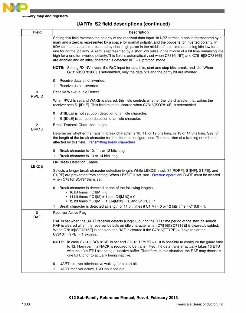
UARTx_S2 field descriptions (continued)
Field Description
Setting this field reverses the polarity of the received data input. In NRZ format, a one is represented by amark and a zero is represented by a space for normal polarity, and the opposite for inverted polarity. InIrDA format, a zero is represented by short high pulse in the middle of a bit time remaining idle low for aone for normal polarity. A zero is represented by a short low pulse in the middle of a bit time remaining idlehigh for a one for inverted polarity.This field is automatically set when C7816[INIT] and C7816[ISO7816E]are enabled and an initial character is detected in T = 0 protocol mode.
NOTE: Setting RXINV inverts the RxD input for data bits, start and stop bits, break, and idle. WhenC7816[ISO7816E] is set/enabled, only the data bits and the parity bit are inverted.
0 Receive data is not inverted.1 Receive data is inverted.
3RWUID
Receive Wakeup Idle Detect
When RWU is set and WAKE is cleared, this field controls whether the idle character that wakes thereceiver sets S1[IDLE]. This field must be cleared when C7816[ISO7816E] is set/enabled.
0 S1[IDLE] is not set upon detection of an idle character.1 S1[IDLE] is set upon detection of an idle character.
2BRK13
Break Transmit Character Length
Determines whether the transmit break character is 10, 11, or 12 bits long, or 13 or 14 bits long. See forthe length of the break character for the different configurations. The detection of a framing error is notaffected by this field. Transmitting break characters
0 Break character is 10, 11, or 12 bits long.1 Break character is 13 or 14 bits long.
1LBKDE
LIN Break Detection Enable
Selects a longer break character detection length. While LBKDE is set, S1[RDRF], S1[NF], S1[FE], andS1[PF] are prevented from setting. When LBKDE is set, see . Overrun operationLBKDE must be clearedwhen C7816[ISO7816E] is set.
0 Break character is detected at one of the following lengths:• 10 bit times if C1[M] = 0• 11 bit times if C1[M] = 1 and C4[M10] = 0• 12 bit times if C1[M] = 1, C4[M10] = 1, and S1[PE] = 1
1 Break character is detected at length of 11 bit times if C1[M] = 0 or 12 bits time if C1[M] = 1.
0RAF
Receiver Active Flag
RAF is set when the UART receiver detects a logic 0 during the RT1 time period of the start bit search.RAF is cleared when the receiver detects an idle character when C7816[ISO7816E] is cleared/disabled.When C7816[ISO7816E] is enabled, the RAF is cleared if the C7816[TTYPE] = 0 expires or theC7816[TTYPE] = 1 expires.
NOTE: In case C7816[ISO7816E] is set and C7816[TTYPE] = 0, it is possible to configure the guard timeto 12. However, if a NACK is required to be transmitted, the data transfer actually takes 13 ETUwith the 13th ETU slot being a inactive buffer. Therefore, in this situation, the RAF may deassertone ETU prior to actually being inactive.
0 UART receiver idle/inactive waiting for a start bit.1 UART receiver active, RxD input not idle.
Memory map and registers
K12 Sub-Family Reference Manual, Rev. 4, February 2013
1030 Freescale Semiconductor, Inc.
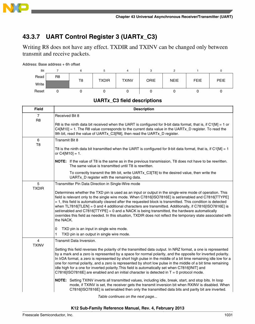
43.3.7 UART Control Register 3 (UARTx_C3)
Writing R8 does not have any effect. TXDIR and TXINV can be changed only betweentransmit and receive packets.
Address: Base address + 6h offset
Bit 7 6 5 4 3 2 1 0
Read R8T8 TXDIR TXINV ORIE NEIE FEIE PEIE
Write
Reset 0 0 0 0 0 0 0 0
UARTx_C3 field descriptions
Field Description
7R8
Received Bit 8
R8 is the ninth data bit received when the UART is configured for 9-bit data format, that is, if C1[M] = 1 orC4[M10] = 1. The R8 value corresponds to the current data value in the UARTx_D register. To read the9th bit, read the value of UARTx_C3[R8], then read the UARTx_D register.
6T8
Transmit Bit 8
T8 is the ninth data bit transmitted when the UART is configured for 9-bit data format, that is, if C1[M] = 1or C4[M10] = 1.
NOTE: If the value of T8 is the same as in the previous transmission, T8 does not have to be rewritten.The same value is transmitted until T8 is rewritten.
To correctly transmit the 9th bit, write UARTx_C3[T8] to the desired value, then write theUARTx_D register with the remaining data.
5TXDIR
Transmitter Pin Data Direction in Single-Wire mode
Determines whether the TXD pin is used as an input or output in the single-wire mode of operation. Thisfield is relevant only to the single wire mode. When C7816[ISO7816E] is set/enabled and C7816[TTYPE]= 1, this field is automatically cleared after the requested block is transmitted. This condition is detectedwhen TL7816[TLEN] = 0 and 4 additional characters are transmitted. Additionally, if C7816[ISO7816E] isset/enabled and C7816[TTYPE] = 0 and a NACK is being transmitted, the hardware automaticallyoverrides this field as needed. In this situation, TXDIR does not reflect the temporary state associated withthe NACK.
0 TXD pin is an input in single wire mode.1 TXD pin is an output in single wire mode.
4TXINV
Transmit Data Inversion.
Setting this field reverses the polarity of the transmitted data output. In NRZ format, a one is representedby a mark and a zero is represented by a space for normal polarity, and the opposite for inverted polarity.In IrDA format, a zero is represented by short high pulse in the middle of a bit time remaining idle low for aone for normal polarity, and a zero is represented by short low pulse in the middle of a bit time remainingidle high for a one for inverted polarity.This field is automatically set when C7816[INIT] andC7816[ISO7816E] are enabled and an initial character is detected in T = 0 protocol mode.
NOTE: Setting TXINV inverts all transmitted values, including idle, break, start, and stop bits. In loopmode, if TXINV is set, the receiver gets the transmit inversion bit when RXINV is disabled. WhenC7816[ISO7816E] is set/enabled then only the transmitted data bits and parity bit are inverted.
Table continues on the next page...
Chapter 43 Universal Asynchronous Receiver/Transmitter (UART)
K12 Sub-Family Reference Manual, Rev. 4, February 2013
Freescale Semiconductor, Inc. 1031

UARTx_C3 field descriptions (continued)
Field Description
0 Transmit data is not inverted.1 Transmit data is inverted.
3ORIE
Overrun Error Interrupt Enable
Enables the overrun error flag, S1[OR], to generate interrupt requests.
0 OR interrupts are disabled.1 OR interrupt requests are enabled.
2NEIE
Noise Error Interrupt Enable
Enables the noise flag, S1[NF], to generate interrupt requests.
0 NF interrupt requests are disabled.1 NF interrupt requests are enabled.
1FEIE
Framing Error Interrupt Enable
Enables the framing error flag, S1[FE], to generate interrupt requests.
0 FE interrupt requests are disabled.1 FE interrupt requests are enabled.
0PEIE
Parity Error Interrupt Enable
Enables the parity error flag, S1[PF], to generate interrupt requests.
0 PF interrupt requests are disabled.1 PF interrupt requests are enabled.
43.3.8 UART Data Register (UARTx_D)This register is actually two separate registers. Reads return the contents of the read-onlyreceive data register and writes go to the write-only transmit data register.
NOTE• In 8-bit or 9-bit data format, only UART data register (D)
needs to be accessed to clear the S1[RDRF] bit (assumingreceiver buffer level is less than RWFIFO[RXWATER]).The C3 register needs to be read, prior to the D register,only if the ninth bit of data needs to be captured. Similarly,the ED register needs to be read, prior to the D register,only if the additional flag data for the dataword needs to becaptured.
• In the normal 8-bit mode (M bit cleared) if the parity isenabled, you get seven data bits and one parity bit. Thatone parity bit is loaded into the D register. So, for the data
Memory map and registers
K12 Sub-Family Reference Manual, Rev. 4, February 2013
1032 Freescale Semiconductor, Inc.
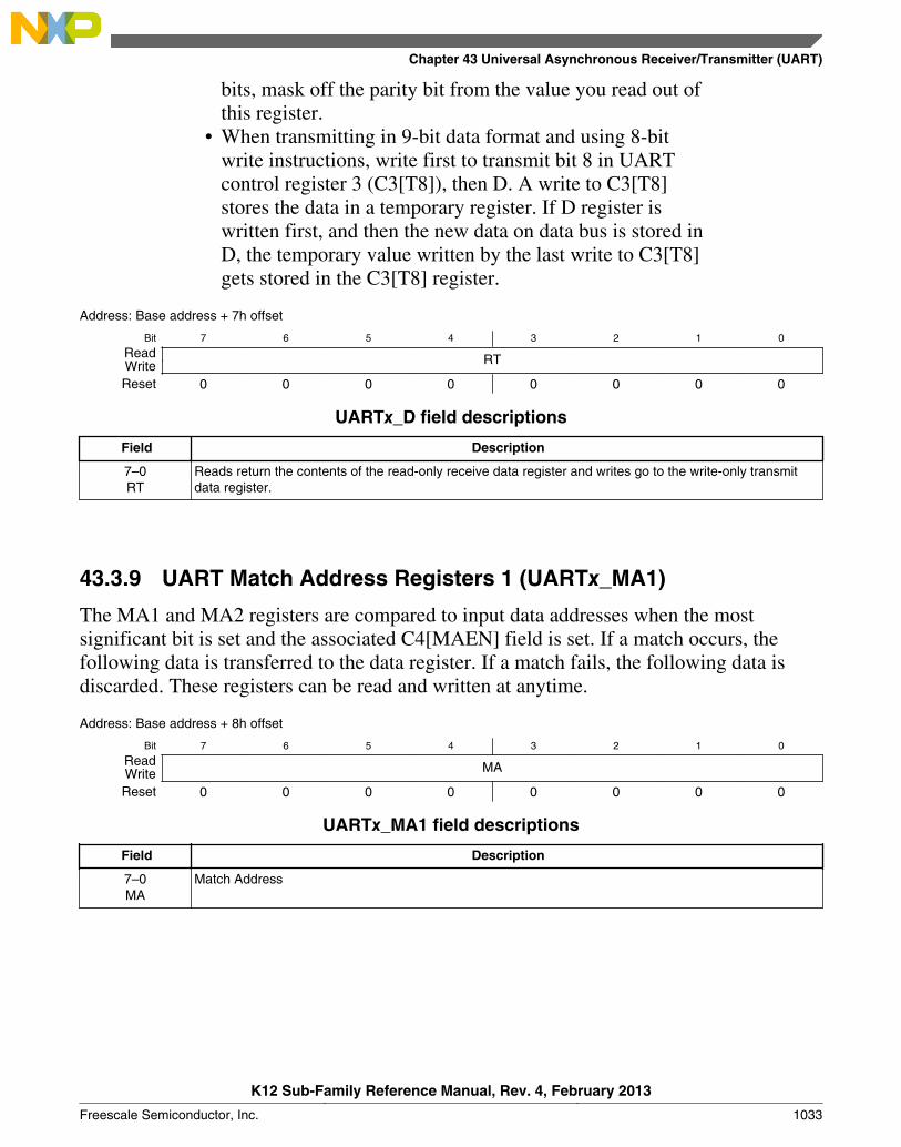
bits, mask off the parity bit from the value you read out ofthis register.
• When transmitting in 9-bit data format and using 8-bitwrite instructions, write first to transmit bit 8 in UARTcontrol register 3 (C3[T8]), then D. A write to C3[T8]stores the data in a temporary register. If D register iswritten first, and then the new data on data bus is stored inD, the temporary value written by the last write to C3[T8]gets stored in the C3[T8] register.
Address: Base address + 7h offset
Bit 7 6 5 4 3 2 1 0
Read RTWriteReset 0 0 0 0 0 0 0 0
UARTx_D field descriptions
Field Description
7–0RT
Reads return the contents of the read-only receive data register and writes go to the write-only transmitdata register.
43.3.9 UART Match Address Registers 1 (UARTx_MA1)
The MA1 and MA2 registers are compared to input data addresses when the mostsignificant bit is set and the associated C4[MAEN] field is set. If a match occurs, thefollowing data is transferred to the data register. If a match fails, the following data isdiscarded. These registers can be read and written at anytime.
Address: Base address + 8h offset
Bit 7 6 5 4 3 2 1 0
Read MAWriteReset 0 0 0 0 0 0 0 0
UARTx_MA1 field descriptions
Field Description
7–0MA
Match Address
Chapter 43 Universal Asynchronous Receiver/Transmitter (UART)
K12 Sub-Family Reference Manual, Rev. 4, February 2013
Freescale Semiconductor, Inc. 1033
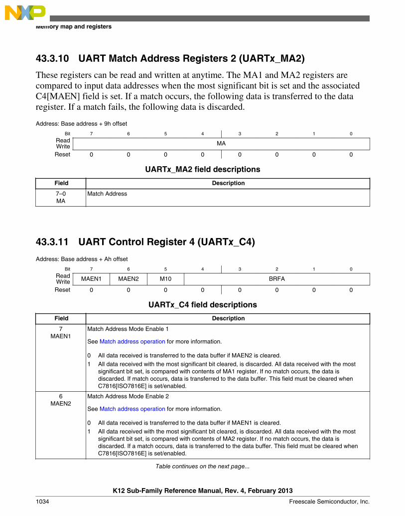
43.3.10 UART Match Address Registers 2 (UARTx_MA2)
These registers can be read and written at anytime. The MA1 and MA2 registers arecompared to input data addresses when the most significant bit is set and the associatedC4[MAEN] field is set. If a match occurs, the following data is transferred to the dataregister. If a match fails, the following data is discarded.
Address: Base address + 9h offset
Bit 7 6 5 4 3 2 1 0
Read MAWriteReset 0 0 0 0 0 0 0 0
UARTx_MA2 field descriptions
Field Description
7–0MA
Match Address
43.3.11 UART Control Register 4 (UARTx_C4)
Address: Base address + Ah offset
Bit 7 6 5 4 3 2 1 0
Read MAEN1 MAEN2 M10 BRFAWriteReset 0 0 0 0 0 0 0 0
UARTx_C4 field descriptions
Field Description
7MAEN1
Match Address Mode Enable 1
See Match address operation for more information.
0 All data received is transferred to the data buffer if MAEN2 is cleared.1 All data received with the most significant bit cleared, is discarded. All data received with the most
significant bit set, is compared with contents of MA1 register. If no match occurs, the data isdiscarded. If match occurs, data is transferred to the data buffer. This field must be cleared whenC7816[ISO7816E] is set/enabled.
6MAEN2
Match Address Mode Enable 2
See Match address operation for more information.
0 All data received is transferred to the data buffer if MAEN1 is cleared.1 All data received with the most significant bit cleared, is discarded. All data received with the most
significant bit set, is compared with contents of MA2 register. If no match occurs, the data isdiscarded. If a match occurs, data is transferred to the data buffer. This field must be cleared whenC7816[ISO7816E] is set/enabled.
Table continues on the next page...
Memory map and registers
K12 Sub-Family Reference Manual, Rev. 4, February 2013
1034 Freescale Semiconductor, Inc.

UARTx_C4 field descriptions (continued)
Field Description
5M10
10-bit Mode select
Causes a tenth, non-memory mapped bit to be part of the serial transmission. This tenth bit is generatedand interpreted as a parity bit. The M10 field does not affect the LIN send or detect break behavior. If M10is set, then both C1[M] and C1[PE] must also be set. This field must be cleared when C7816[ISO7816E] isset/enabled.
See Data format (non ISO-7816) for more information.
0 The parity bit is the ninth bit in the serial transmission.1 The parity bit is the tenth bit in the serial transmission.
4–0BRFA
Baud Rate Fine Adjust
This bit field is used to add more timing resolution to the average baud frequency, in increments of 1/32.See Baud rate generation for more information.
43.3.12 UART Control Register 5 (UARTx_C5)
Address: Base address + Bh offset
Bit 7 6 5 4 3 2 1 0
Read TDMAS 0 RDMAS 0WriteReset 0 0 0 0 0 0 0 0
UARTx_C5 field descriptions
Field Description
7TDMAS
Transmitter DMA Select
Configures the transmit data register empty flag, S1[TDRE], to generate interrupt or DMA requests ifC2[TIE] is set.
NOTE: • If C2[TIE] is cleared, TDRE DMA and TDRE interrupt request signals are not assertedwhen the TDRE flag is set, regardless of the state of TDMAS.
• If C2[TIE] and TDMAS are both set, then C2[TCIE] must be cleared, and D must not bewritten unless a DMA request is being serviced.
0 If C2[TIE] is set and the S1[TDRE] flag is set, the TDRE interrupt request signal is asserted to requestinterrupt service.
1 If C2[TIE] is set and the S1[TDRE] flag is set, the TDRE DMA request signal is asserted to request aDMA transfer.
6Reserved
This field is reserved.This read-only field is reserved and always has the value 0.
5RDMAS
Receiver Full DMA Select
Configures the receiver data register full flag, S1[RDRF], to generate interrupt or DMA requests if C2[RIE]is set.
NOTE: If C2[RIE] is cleared, and S1[RDRF] is set, the RDRF DMA and RDFR interrupt request signalsare not asserted, regardless of the state of RDMAS.
Table continues on the next page...
Chapter 43 Universal Asynchronous Receiver/Transmitter (UART)
K12 Sub-Family Reference Manual, Rev. 4, February 2013
Freescale Semiconductor, Inc. 1035
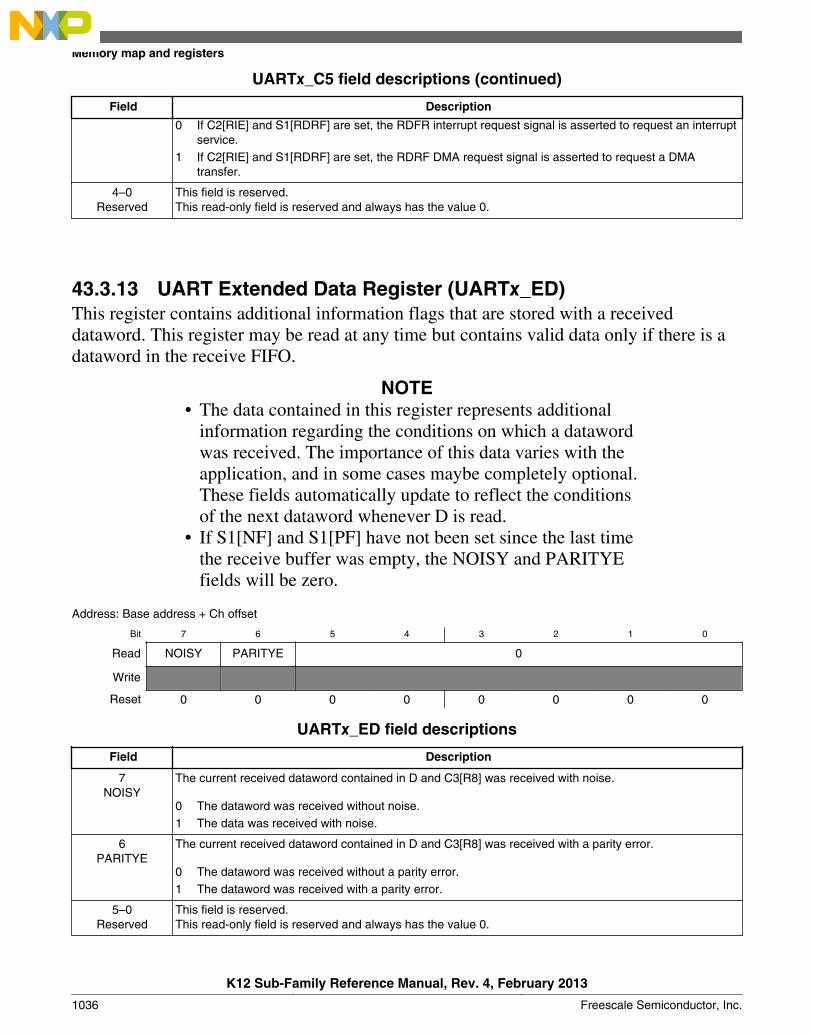
UARTx_C5 field descriptions (continued)
Field Description
0 If C2[RIE] and S1[RDRF] are set, the RDFR interrupt request signal is asserted to request an interruptservice.
1 If C2[RIE] and S1[RDRF] are set, the RDRF DMA request signal is asserted to request a DMAtransfer.
4–0Reserved
This field is reserved.This read-only field is reserved and always has the value 0.
43.3.13 UART Extended Data Register (UARTx_ED)This register contains additional information flags that are stored with a receiveddataword. This register may be read at any time but contains valid data only if there is adataword in the receive FIFO.
NOTE• The data contained in this register represents additional
information regarding the conditions on which a datawordwas received. The importance of this data varies with theapplication, and in some cases maybe completely optional.These fields automatically update to reflect the conditionsof the next dataword whenever D is read.
• If S1[NF] and S1[PF] have not been set since the last timethe receive buffer was empty, the NOISY and PARITYEfields will be zero.
Address: Base address + Ch offset
Bit 7 6 5 4 3 2 1 0
Read NOISY PARITYE 0
Write
Reset 0 0 0 0 0 0 0 0
UARTx_ED field descriptions
Field Description
7NOISY
The current received dataword contained in D and C3[R8] was received with noise.
0 The dataword was received without noise.1 The data was received with noise.
6PARITYE
The current received dataword contained in D and C3[R8] was received with a parity error.
0 The dataword was received without a parity error.1 The dataword was received with a parity error.
5–0Reserved
This field is reserved.This read-only field is reserved and always has the value 0.
Memory map and registers
K12 Sub-Family Reference Manual, Rev. 4, February 2013
1036 Freescale Semiconductor, Inc.
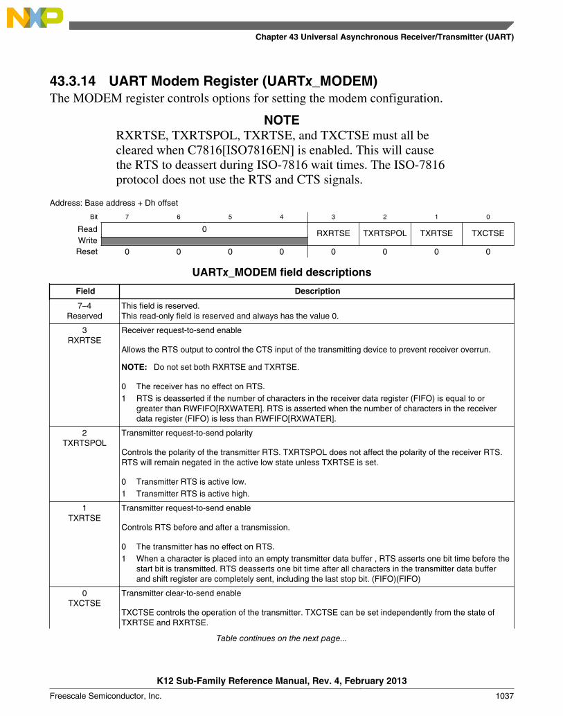
43.3.14 UART Modem Register (UARTx_MODEM)The MODEM register controls options for setting the modem configuration.
NOTERXRTSE, TXRTSPOL, TXRTSE, and TXCTSE must all becleared when C7816[ISO7816EN] is enabled. This will causethe RTS to deassert during ISO-7816 wait times. The ISO-7816protocol does not use the RTS and CTS signals.
Address: Base address + Dh offset
Bit 7 6 5 4 3 2 1 0
Read 0 RXRTSE TXRTSPOL TXRTSE TXCTSEWriteReset 0 0 0 0 0 0 0 0
UARTx_MODEM field descriptions
Field Description
7–4Reserved
This field is reserved.This read-only field is reserved and always has the value 0.
3RXRTSE
Receiver request-to-send enable
Allows the RTS output to control the CTS input of the transmitting device to prevent receiver overrun.
NOTE: Do not set both RXRTSE and TXRTSE.
0 The receiver has no effect on RTS.1 RTS is deasserted if the number of characters in the receiver data register (FIFO) is equal to or
greater than RWFIFO[RXWATER]. RTS is asserted when the number of characters in the receiverdata register (FIFO) is less than RWFIFO[RXWATER].
2TXRTSPOL
Transmitter request-to-send polarity
Controls the polarity of the transmitter RTS. TXRTSPOL does not affect the polarity of the receiver RTS.RTS will remain negated in the active low state unless TXRTSE is set.
0 Transmitter RTS is active low.1 Transmitter RTS is active high.
1TXRTSE
Transmitter request-to-send enable
Controls RTS before and after a transmission.
0 The transmitter has no effect on RTS.1 When a character is placed into an empty transmitter data buffer , RTS asserts one bit time before the
start bit is transmitted. RTS deasserts one bit time after all characters in the transmitter data bufferand shift register are completely sent, including the last stop bit. (FIFO)(FIFO)
0TXCTSE
Transmitter clear-to-send enable
TXCTSE controls the operation of the transmitter. TXCTSE can be set independently from the state ofTXRTSE and RXRTSE.
Table continues on the next page...
Chapter 43 Universal Asynchronous Receiver/Transmitter (UART)
K12 Sub-Family Reference Manual, Rev. 4, February 2013
Freescale Semiconductor, Inc. 1037
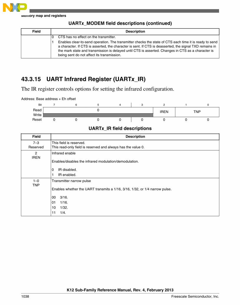
UARTx_MODEM field descriptions (continued)
Field Description
0 CTS has no effect on the transmitter.1 Enables clear-to-send operation. The transmitter checks the state of CTS each time it is ready to send
a character. If CTS is asserted, the character is sent. If CTS is deasserted, the signal TXD remains inthe mark state and transmission is delayed until CTS is asserted. Changes in CTS as a character isbeing sent do not affect its transmission.
43.3.15 UART Infrared Register (UARTx_IR)
The IR register controls options for setting the infrared configuration.
Address: Base address + Eh offset
Bit 7 6 5 4 3 2 1 0
Read 0 IREN TNPWriteReset 0 0 0 0 0 0 0 0
UARTx_IR field descriptions
Field Description
7–3Reserved
This field is reserved.This read-only field is reserved and always has the value 0.
2IREN
Infrared enable
Enables/disables the infrared modulation/demodulation.
0 IR disabled.1 IR enabled.
1–0TNP
Transmitter narrow pulse
Enables whether the UART transmits a 1/16, 3/16, 1/32, or 1/4 narrow pulse.
00 3/16.01 1/16.10 1/32.11 1/4.
Memory map and registers
K12 Sub-Family Reference Manual, Rev. 4, February 2013
1038 Freescale Semiconductor, Inc.
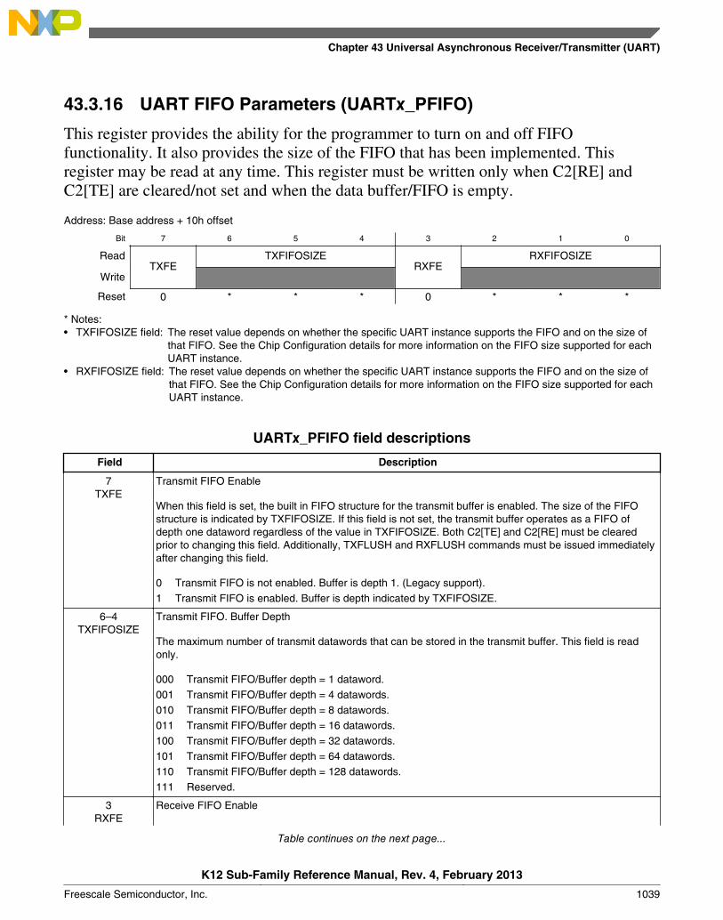
43.3.16 UART FIFO Parameters (UARTx_PFIFO)
This register provides the ability for the programmer to turn on and off FIFOfunctionality. It also provides the size of the FIFO that has been implemented. Thisregister may be read at any time. This register must be written only when C2[RE] andC2[TE] are cleared/not set and when the data buffer/FIFO is empty.
Address: Base address + 10h offset
Bit 7 6 5 4 3 2 1 0
ReadTXFE
TXFIFOSIZERXFE
RXFIFOSIZE
Write
Reset 0 * * * 0 * * *
* Notes:TXFIFOSIZE field: The reset value depends on whether the specific UART instance supports the FIFO and on the size of
that FIFO. See the Chip Configuration details for more information on the FIFO size supported for eachUART instance.
•
RXFIFOSIZE field: The reset value depends on whether the specific UART instance supports the FIFO and on the size ofthat FIFO. See the Chip Configuration details for more information on the FIFO size supported for eachUART instance.
•
UARTx_PFIFO field descriptions
Field Description
7TXFE
Transmit FIFO Enable
When this field is set, the built in FIFO structure for the transmit buffer is enabled. The size of the FIFOstructure is indicated by TXFIFOSIZE. If this field is not set, the transmit buffer operates as a FIFO ofdepth one dataword regardless of the value in TXFIFOSIZE. Both C2[TE] and C2[RE] must be clearedprior to changing this field. Additionally, TXFLUSH and RXFLUSH commands must be issued immediatelyafter changing this field.
0 Transmit FIFO is not enabled. Buffer is depth 1. (Legacy support).1 Transmit FIFO is enabled. Buffer is depth indicated by TXFIFOSIZE.
6–4TXFIFOSIZE
Transmit FIFO. Buffer Depth
The maximum number of transmit datawords that can be stored in the transmit buffer. This field is readonly.
000 Transmit FIFO/Buffer depth = 1 dataword.001 Transmit FIFO/Buffer depth = 4 datawords.010 Transmit FIFO/Buffer depth = 8 datawords.011 Transmit FIFO/Buffer depth = 16 datawords.100 Transmit FIFO/Buffer depth = 32 datawords.101 Transmit FIFO/Buffer depth = 64 datawords.110 Transmit FIFO/Buffer depth = 128 datawords.111 Reserved.
3RXFE
Receive FIFO Enable
Table continues on the next page...
Chapter 43 Universal Asynchronous Receiver/Transmitter (UART)
K12 Sub-Family Reference Manual, Rev. 4, February 2013
Freescale Semiconductor, Inc. 1039
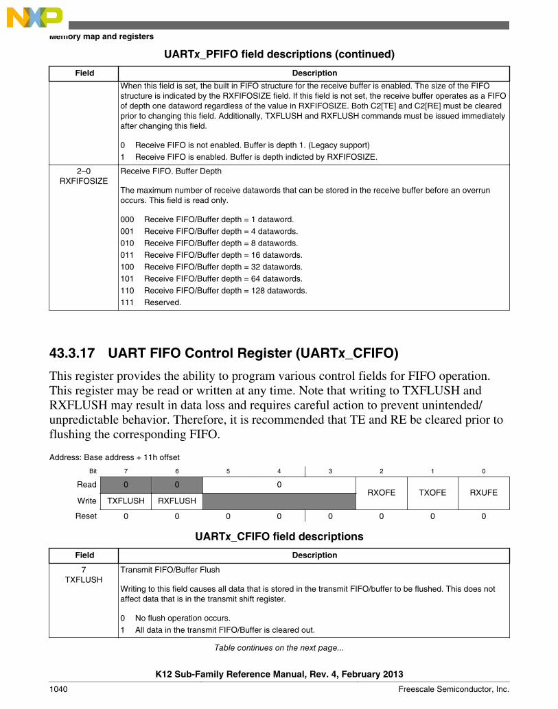
UARTx_PFIFO field descriptions (continued)
Field Description
When this field is set, the built in FIFO structure for the receive buffer is enabled. The size of the FIFOstructure is indicated by the RXFIFOSIZE field. If this field is not set, the receive buffer operates as a FIFOof depth one dataword regardless of the value in RXFIFOSIZE. Both C2[TE] and C2[RE] must be clearedprior to changing this field. Additionally, TXFLUSH and RXFLUSH commands must be issued immediatelyafter changing this field.
0 Receive FIFO is not enabled. Buffer is depth 1. (Legacy support)1 Receive FIFO is enabled. Buffer is depth indicted by RXFIFOSIZE.
2–0RXFIFOSIZE
Receive FIFO. Buffer Depth
The maximum number of receive datawords that can be stored in the receive buffer before an overrunoccurs. This field is read only.
000 Receive FIFO/Buffer depth = 1 dataword.001 Receive FIFO/Buffer depth = 4 datawords.010 Receive FIFO/Buffer depth = 8 datawords.011 Receive FIFO/Buffer depth = 16 datawords.100 Receive FIFO/Buffer depth = 32 datawords.101 Receive FIFO/Buffer depth = 64 datawords.110 Receive FIFO/Buffer depth = 128 datawords.111 Reserved.
43.3.17 UART FIFO Control Register (UARTx_CFIFO)
This register provides the ability to program various control fields for FIFO operation.This register may be read or written at any time. Note that writing to TXFLUSH andRXFLUSH may result in data loss and requires careful action to prevent unintended/unpredictable behavior. Therefore, it is recommended that TE and RE be cleared prior toflushing the corresponding FIFO.
Address: Base address + 11h offset
Bit 7 6 5 4 3 2 1 0
Read 0 0 0RXOFE TXOFE RXUFE
Write TXFLUSH RXFLUSH
Reset 0 0 0 0 0 0 0 0
UARTx_CFIFO field descriptions
Field Description
7TXFLUSH
Transmit FIFO/Buffer Flush
Writing to this field causes all data that is stored in the transmit FIFO/buffer to be flushed. This does notaffect data that is in the transmit shift register.
0 No flush operation occurs.1 All data in the transmit FIFO/Buffer is cleared out.
Table continues on the next page...
Memory map and registers
K12 Sub-Family Reference Manual, Rev. 4, February 2013
1040 Freescale Semiconductor, Inc.
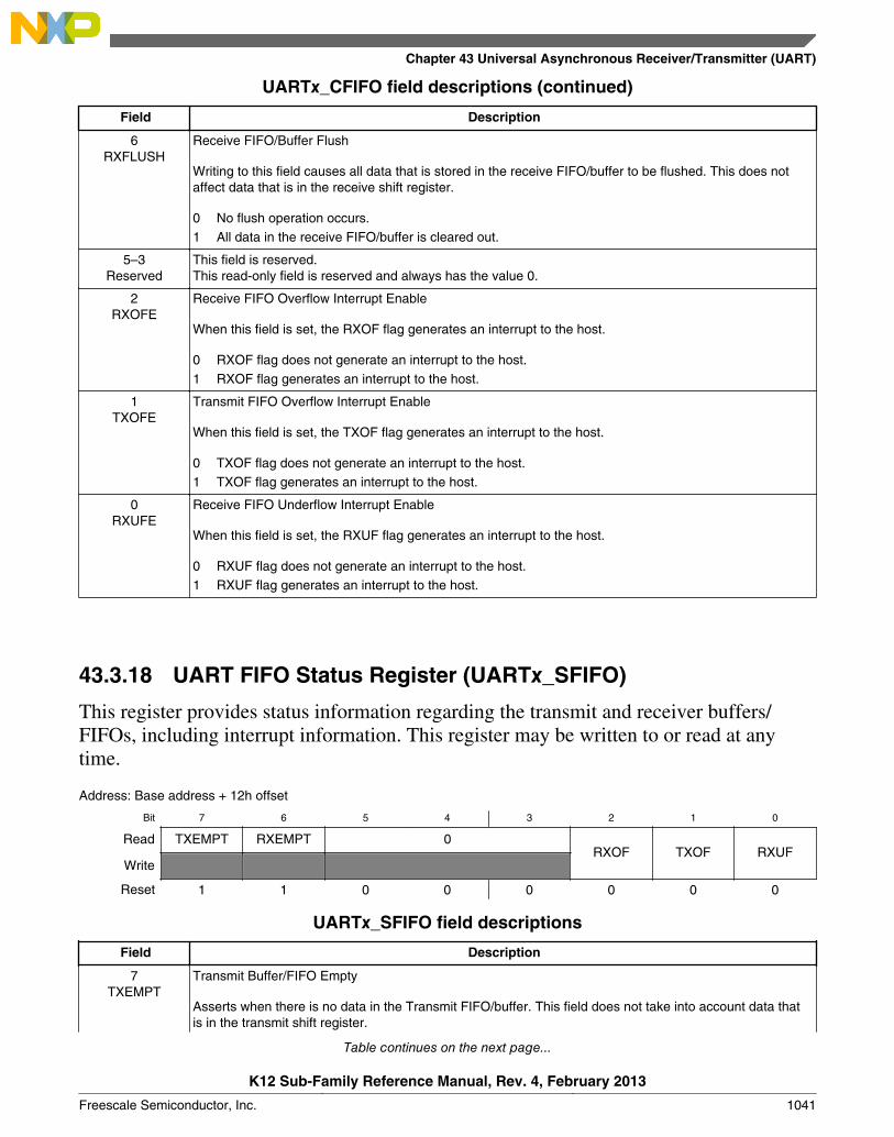
UARTx_CFIFO field descriptions (continued)
Field Description
6RXFLUSH
Receive FIFO/Buffer Flush
Writing to this field causes all data that is stored in the receive FIFO/buffer to be flushed. This does notaffect data that is in the receive shift register.
0 No flush operation occurs.1 All data in the receive FIFO/buffer is cleared out.
5–3Reserved
This field is reserved.This read-only field is reserved and always has the value 0.
2RXOFE
Receive FIFO Overflow Interrupt Enable
When this field is set, the RXOF flag generates an interrupt to the host.
0 RXOF flag does not generate an interrupt to the host.1 RXOF flag generates an interrupt to the host.
1TXOFE
Transmit FIFO Overflow Interrupt Enable
When this field is set, the TXOF flag generates an interrupt to the host.
0 TXOF flag does not generate an interrupt to the host.1 TXOF flag generates an interrupt to the host.
0RXUFE
Receive FIFO Underflow Interrupt Enable
When this field is set, the RXUF flag generates an interrupt to the host.
0 RXUF flag does not generate an interrupt to the host.1 RXUF flag generates an interrupt to the host.
43.3.18 UART FIFO Status Register (UARTx_SFIFO)
This register provides status information regarding the transmit and receiver buffers/FIFOs, including interrupt information. This register may be written to or read at anytime.
Address: Base address + 12h offset
Bit 7 6 5 4 3 2 1 0
Read TXEMPT RXEMPT 0RXOF TXOF RXUF
Write
Reset 1 1 0 0 0 0 0 0
UARTx_SFIFO field descriptions
Field Description
7TXEMPT
Transmit Buffer/FIFO Empty
Asserts when there is no data in the Transmit FIFO/buffer. This field does not take into account data thatis in the transmit shift register.
Table continues on the next page...
Chapter 43 Universal Asynchronous Receiver/Transmitter (UART)
K12 Sub-Family Reference Manual, Rev. 4, February 2013
Freescale Semiconductor, Inc. 1041
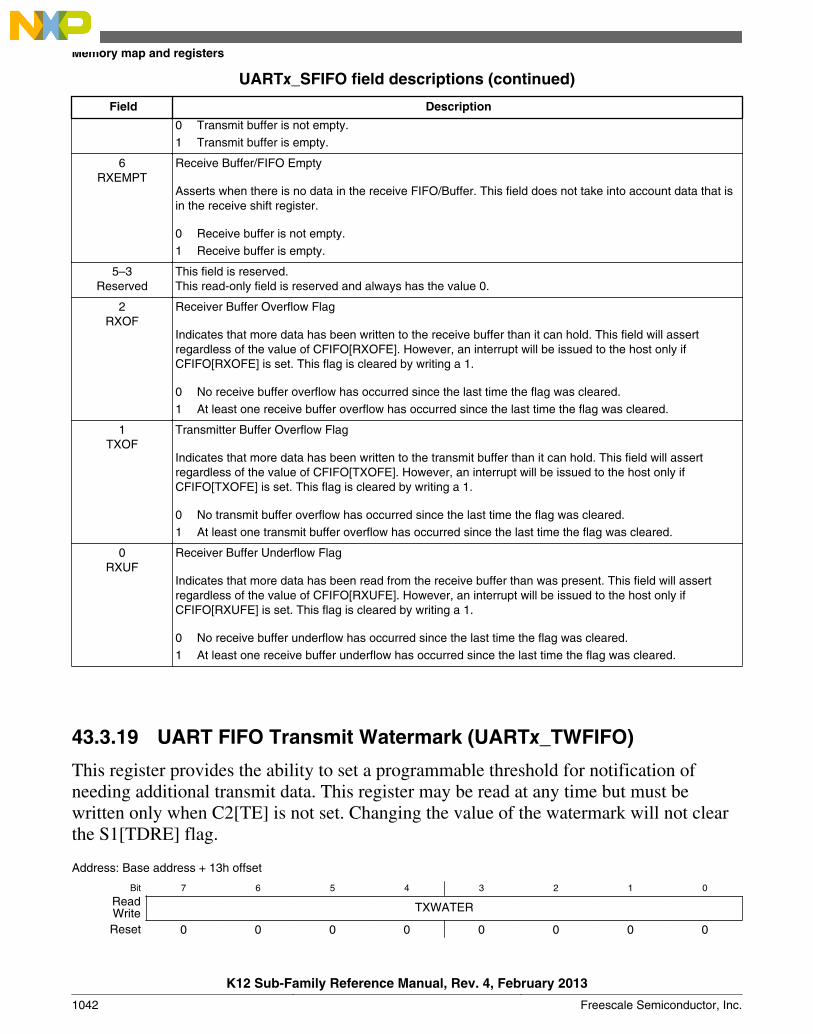
UARTx_SFIFO field descriptions (continued)
Field Description
0 Transmit buffer is not empty.1 Transmit buffer is empty.
6RXEMPT
Receive Buffer/FIFO Empty
Asserts when there is no data in the receive FIFO/Buffer. This field does not take into account data that isin the receive shift register.
0 Receive buffer is not empty.1 Receive buffer is empty.
5–3Reserved
This field is reserved.This read-only field is reserved and always has the value 0.
2RXOF
Receiver Buffer Overflow Flag
Indicates that more data has been written to the receive buffer than it can hold. This field will assertregardless of the value of CFIFO[RXOFE]. However, an interrupt will be issued to the host only ifCFIFO[RXOFE] is set. This flag is cleared by writing a 1.
0 No receive buffer overflow has occurred since the last time the flag was cleared.1 At least one receive buffer overflow has occurred since the last time the flag was cleared.
1TXOF
Transmitter Buffer Overflow Flag
Indicates that more data has been written to the transmit buffer than it can hold. This field will assertregardless of the value of CFIFO[TXOFE]. However, an interrupt will be issued to the host only ifCFIFO[TXOFE] is set. This flag is cleared by writing a 1.
0 No transmit buffer overflow has occurred since the last time the flag was cleared.1 At least one transmit buffer overflow has occurred since the last time the flag was cleared.
0RXUF
Receiver Buffer Underflow Flag
Indicates that more data has been read from the receive buffer than was present. This field will assertregardless of the value of CFIFO[RXUFE]. However, an interrupt will be issued to the host only ifCFIFO[RXUFE] is set. This flag is cleared by writing a 1.
0 No receive buffer underflow has occurred since the last time the flag was cleared.1 At least one receive buffer underflow has occurred since the last time the flag was cleared.
43.3.19 UART FIFO Transmit Watermark (UARTx_TWFIFO)
This register provides the ability to set a programmable threshold for notification ofneeding additional transmit data. This register may be read at any time but must bewritten only when C2[TE] is not set. Changing the value of the watermark will not clearthe S1[TDRE] flag.
Address: Base address + 13h offset
Bit 7 6 5 4 3 2 1 0
Read TXWATERWriteReset 0 0 0 0 0 0 0 0
Memory map and registers
K12 Sub-Family Reference Manual, Rev. 4, February 2013
1042 Freescale Semiconductor, Inc.
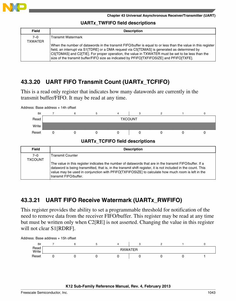
UARTx_TWFIFO field descriptions
Field Description
7–0TXWATER
Transmit Watermark
When the number of datawords in the transmit FIFO/buffer is equal to or less than the value in this registerfield, an interrupt via S1[TDRE] or a DMA request via C5[TDMAS] is generated as determined byC5[TDMAS] and C2[TIE]. For proper operation, the value in TXWATER must be set to be less than thesize of the transmit buffer/FIFO size as indicated by PFIFO[TXFIFOSIZE] and PFIFO[TXFE].
43.3.20 UART FIFO Transmit Count (UARTx_TCFIFO)
This is a read only register that indicates how many datawords are currently in thetransmit buffer/FIFO. It may be read at any time.
Address: Base address + 14h offset
Bit 7 6 5 4 3 2 1 0
Read TXCOUNT
Write
Reset 0 0 0 0 0 0 0 0
UARTx_TCFIFO field descriptions
Field Description
7–0TXCOUNT
Transmit Counter
The value in this register indicates the number of datawords that are in the transmit FIFO/buffer. If adataword is being transmitted, that is, in the transmit shift register, it is not included in the count. Thisvalue may be used in conjunction with PFIFO[TXFIFOSIZE] to calculate how much room is left in thetransmit FIFO/buffer.
43.3.21 UART FIFO Receive Watermark (UARTx_RWFIFO)
This register provides the ability to set a programmable threshold for notification of theneed to remove data from the receiver FIFO/buffer. This register may be read at any timebut must be written only when C2[RE] is not asserted. Changing the value in this registerwill not clear S1[RDRF].
Address: Base address + 15h offset
Bit 7 6 5 4 3 2 1 0
Read RXWATERWriteReset 0 0 0 0 0 0 0 1
Chapter 43 Universal Asynchronous Receiver/Transmitter (UART)
K12 Sub-Family Reference Manual, Rev. 4, February 2013
Freescale Semiconductor, Inc. 1043
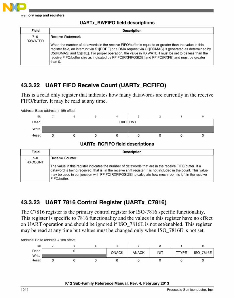
UARTx_RWFIFO field descriptions
Field Description
7–0RXWATER
Receive Watermark
When the number of datawords in the receive FIFO/buffer is equal to or greater than the value in thisregister field, an interrupt via S1[RDRF] or a DMA request via C5[RDMAS] is generated as determined byC5[RDMAS] and C2[RIE]. For proper operation, the value in RXWATER must be set to be less than thereceive FIFO/buffer size as indicated by PFIFO[RXFIFOSIZE] and PFIFO[RXFE] and must be greaterthan 0.
43.3.22 UART FIFO Receive Count (UARTx_RCFIFO)
This is a read only register that indicates how many datawords are currently in the receiveFIFO/buffer. It may be read at any time.
Address: Base address + 16h offset
Bit 7 6 5 4 3 2 1 0
Read RXCOUNT
Write
Reset 0 0 0 0 0 0 0 0
UARTx_RCFIFO field descriptions
Field Description
7–0RXCOUNT
Receive Counter
The value in this register indicates the number of datawords that are in the receive FIFO/buffer. If adataword is being received, that is, in the receive shift register, it is not included in the count. This valuemay be used in conjunction with PFIFO[RXFIFOSIZE] to calculate how much room is left in the receiveFIFO/buffer.
43.3.23 UART 7816 Control Register (UARTx_C7816)
The C7816 register is the primary control register for ISO-7816 specific functionality.This register is specific to 7816 functionality and the values in this register have no effecton UART operation and should be ignored if ISO_7816E is not set/enabled. This registermay be read at any time but values must be changed only when ISO_7816E is not set.
Address: Base address + 18h offset
Bit 7 6 5 4 3 2 1 0
Read 0 ONACK ANACK INIT TTYPE ISO_7816EWriteReset 0 0 0 0 0 0 0 0
Memory map and registers
K12 Sub-Family Reference Manual, Rev. 4, February 2013
1044 Freescale Semiconductor, Inc.

UARTx_C7816 field descriptions
Field Description
7–5Reserved
This field is reserved.This read-only field is reserved and always has the value 0.
4ONACK
Generate NACK on Overflow
When this field is set, the receiver automatically generates a NACK response if a receive buffer overrunoccurs, as indicated by S1[OR]. In many systems, this results in the transmitter resending the packet thatoverflowed until the retransmit threshold for that transmitter is reached. A NACK is generated only ifTTYPE=0. This field operates independently of ANACK. See . Overrun NACK considerations
0 The received data does not generate a NACK when the receipt of the data results in an overflowevent.
1 If the receiver buffer overflows, a NACK is automatically sent on a received character.
3ANACK
Generate NACK on Error
When this field is set, the receiver automatically generates a NACK response if a parity error occurs or ifINIT is set and an invalid initial character is detected. A NACK is generated only if TTYPE = 0. If ANACK isset, the UART attempts to retransmit the data indefinitely. To stop retransmission attempts, clear C2[TE]or ISO_7816E and do not set until S1[TC] sets C2[TE] again.
0 No NACK is automatically generated.1 A NACK is automatically generated if a parity error is detected or if an invalid initial character is
detected.
2INIT
Detect Initial Character
When this field is set, all received characters are searched for a valid initial character. If an invalid initialcharacter is identified, and ANACK is set, a NACK is sent. All received data is discarded and error flagsblocked (S1[NF], S1[OR], S1[FE], S1[PF], IS7816[WT], IS7816[CWT], IS7816[BWT], IS7816[GTV]) until avalid initial character is detected. Upon detecting a valid initial character, the configuration valuesS2[MSBF], C3[TXINV], and S2[RXINV] are automatically updated to reflect the initial character that wasreceived. The actual INIT data value is not stored in the receive buffer. Additionally, upon detection of avalid initial character, IS7816[INITD] is set and an interrupt issued as programmed by IE7816[INITDE].When a valid initial character is detected, INIT is automatically cleared. This Initial Character Detectfeature is supported only in T = 0 protocol mode.
0 Normal operating mode. Receiver does not seek to identify initial character.1 Receiver searches for initial character.
1TTYPE
Transfer Type
Indicates the transfer protocol being used.
See ISO-7816 / smartcard support for more details.
0 T = 0 per the ISO-7816 specification.1 T = 1 per the ISO-7816 specification.
0ISO_7816E
ISO-7816 Functionality Enabled
Indicates that the UART is operating according to the ISO-7816 protocol.
NOTE: This field must be modified only when no transmit or receive is occurring. If this field is changedduring a data transfer, the data being transmitted or received may be transferred incorrectly.
0 ISO-7816 functionality is turned off/not enabled.1 ISO-7816 functionality is turned on/enabled.
Chapter 43 Universal Asynchronous Receiver/Transmitter (UART)
K12 Sub-Family Reference Manual, Rev. 4, February 2013
Freescale Semiconductor, Inc. 1045
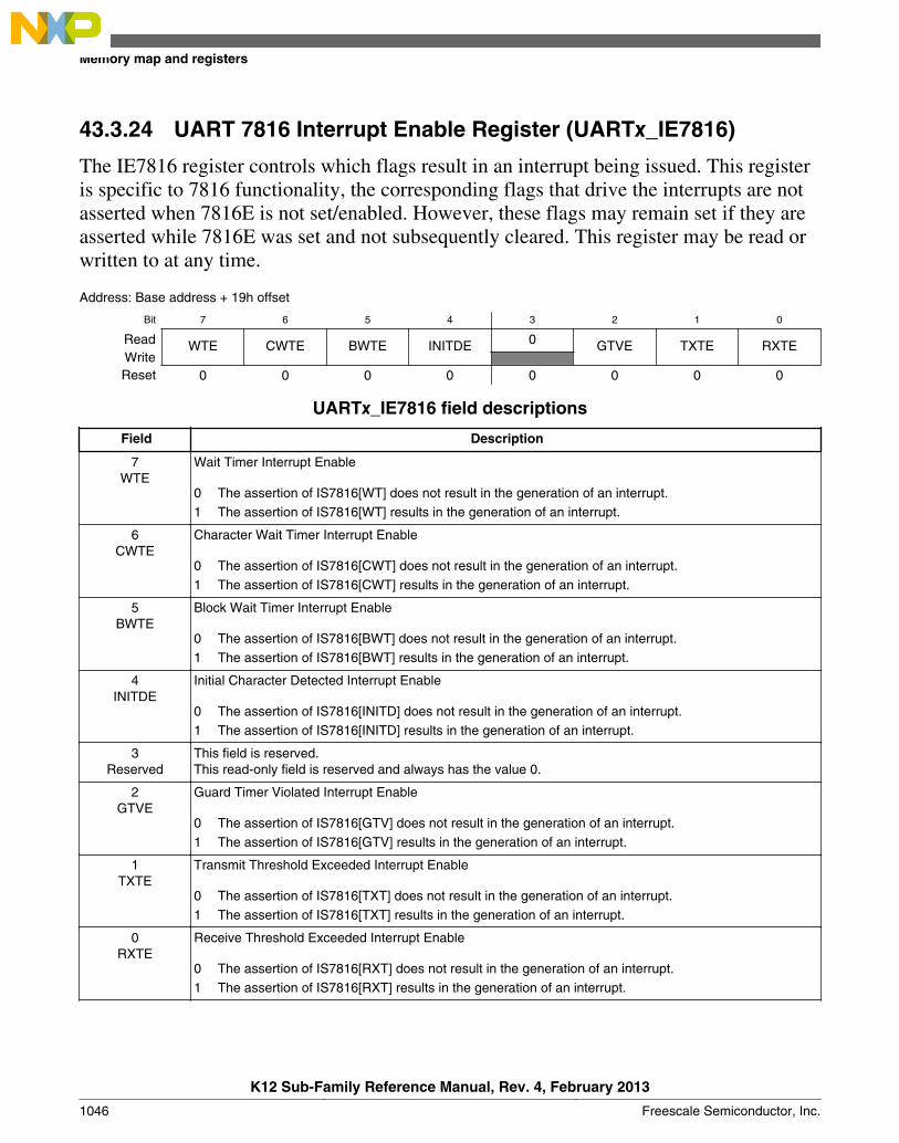
43.3.24 UART 7816 Interrupt Enable Register (UARTx_IE7816)
The IE7816 register controls which flags result in an interrupt being issued. This registeris specific to 7816 functionality, the corresponding flags that drive the interrupts are notasserted when 7816E is not set/enabled. However, these flags may remain set if they areasserted while 7816E was set and not subsequently cleared. This register may be read orwritten to at any time.
Address: Base address + 19h offset
Bit 7 6 5 4 3 2 1 0
Read WTE CWTE BWTE INITDE 0 GTVE TXTE RXTEWriteReset 0 0 0 0 0 0 0 0
UARTx_IE7816 field descriptions
Field Description
7WTE
Wait Timer Interrupt Enable
0 The assertion of IS7816[WT] does not result in the generation of an interrupt.1 The assertion of IS7816[WT] results in the generation of an interrupt.
6CWTE
Character Wait Timer Interrupt Enable
0 The assertion of IS7816[CWT] does not result in the generation of an interrupt.1 The assertion of IS7816[CWT] results in the generation of an interrupt.
5BWTE
Block Wait Timer Interrupt Enable
0 The assertion of IS7816[BWT] does not result in the generation of an interrupt.1 The assertion of IS7816[BWT] results in the generation of an interrupt.
4INITDE
Initial Character Detected Interrupt Enable
0 The assertion of IS7816[INITD] does not result in the generation of an interrupt.1 The assertion of IS7816[INITD] results in the generation of an interrupt.
3Reserved
This field is reserved.This read-only field is reserved and always has the value 0.
2GTVE
Guard Timer Violated Interrupt Enable
0 The assertion of IS7816[GTV] does not result in the generation of an interrupt.1 The assertion of IS7816[GTV] results in the generation of an interrupt.
1TXTE
Transmit Threshold Exceeded Interrupt Enable
0 The assertion of IS7816[TXT] does not result in the generation of an interrupt.1 The assertion of IS7816[TXT] results in the generation of an interrupt.
0RXTE
Receive Threshold Exceeded Interrupt Enable
0 The assertion of IS7816[RXT] does not result in the generation of an interrupt.1 The assertion of IS7816[RXT] results in the generation of an interrupt.
Memory map and registers
K12 Sub-Family Reference Manual, Rev. 4, February 2013
1046 Freescale Semiconductor, Inc.
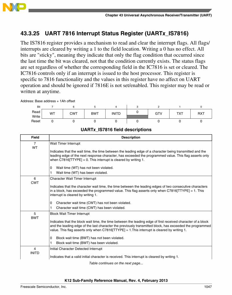
43.3.25 UART 7816 Interrupt Status Register (UARTx_IS7816)
The IS7816 register provides a mechanism to read and clear the interrupt flags. All flags/interrupts are cleared by writing a 1 to the field location. Writing a 0 has no effect. Allbits are "sticky", meaning they indicate that only the flag condition that occurred sincethe last time the bit was cleared, not that the condition currently exists. The status flagsare set regardless of whether the corresponding field in the IC7816 is set or cleared. TheIC7816 controls only if an interrupt is issued to the host processor. This register isspecific to 7816 functionality and the values in this register have no affect on UARToperation and should be ignored if 7816E is not set/enabled. This register may be read orwritten at anytime.
Address: Base address + 1Ah offset
Bit 7 6 5 4 3 2 1 0
Read WT CWT BWT INITD 0 GTV TXT RXTWriteReset 0 0 0 0 0 0 0 0
UARTx_IS7816 field descriptions
Field Description
7WT
Wait Timer Interrupt
Indicates that the wait time, the time between the leading edge of a character being transmitted and theleading edge of the next response character, has exceeded the programmed value. This flag asserts onlywhen C7816[TTYPE] = 0. This interrupt is cleared by writing 1.
0 Wait time (WT) has not been violated.1 Wait time (WT) has been violated.
6CWT
Character Wait Timer Interrupt
Indicates that the character wait time, the time between the leading edges of two consecutive charactersin a block, has exceeded the programmed value. This flag asserts only when C7816[TTYPE] = 1. Thisinterrupt is cleared by writing 1.
0 Character wait time (CWT) has not been violated.1 Character wait time (CWT) has been violated.
5BWT
Block Wait Timer Interrupt
Indicates that the block wait time, the time between the leading edge of first received character of a blockand the leading edge of the last character the previously transmitted block, has exceeded the programmedvalue. This flag asserts only when C7816[TTYPE] = 1.This interrupt is cleared by writing 1.
0 Block wait time (BWT) has not been violated.1 Block wait time (BWT) has been violated.
4INITD
Initial Character Detected Interrupt
Indicates that a valid initial character is received. This interrupt is cleared by writing 1.
Table continues on the next page...
Chapter 43 Universal Asynchronous Receiver/Transmitter (UART)
K12 Sub-Family Reference Manual, Rev. 4, February 2013
Freescale Semiconductor, Inc. 1047

UARTx_IS7816 field descriptions (continued)
Field Description
0 A valid initial character has not been received.1 A valid initial character has been received.
3Reserved
This field is reserved.This read-only field is reserved and always has the value 0.
2GTV
Guard Timer Violated Interrupt
Indicates that one or more of the character guard time, block guard time, or guard time are violated. Thisinterrupt is cleared by writing 1.
0 A guard time (GT, CGT, or BGT) has not been violated.1 A guard time (GT, CGT, or BGT) has been violated.
1TXT
Transmit Threshold Exceeded Interrupt
Indicates that the transmit NACK threshold has been exceeded as indicated by ET7816[TXTHRESHOLD].Regardless of whether this flag is set, the UART continues to retransmit indefinitely. This flag asserts onlywhen C7816[TTYPE] = 0. If 7816E is cleared/disabled, ANACK is cleared/disabled, C2[TE] is cleared/disabled, C7816[TTYPE] = 1, or packet is transferred without receiving a NACK, the internal NACKdetection counter is cleared and the count restarts from zero on the next received NACK. This interrupt iscleared by writing 1.
0 The number of retries and corresponding NACKS does not exceed the value inET7816[TXTHRESHOLD].
1 The number of retries and corresponding NACKS exceeds the value in ET7816[TXTHRESHOLD].
0RXT
Receive Threshold Exceeded Interrupt
Indicates that there are more than ET7816[RXTHRESHOLD] consecutive NACKS generated in responseto parity errors on received data. This flag requires ANACK to be set. Additionally, this flag asserts onlywhen C7816[TTYPE] = 0. Clearing this field also resets the counter keeping track of consecutive NACKS.The UART will continue to attempt to receive data regardless of whether this flag is set. If 7816E iscleared/disabled, RE is cleared/disabled, C7816[TTYPE] = 1, or packet is received without needing toissue a NACK, the internal NACK detection counter is cleared and the count restarts from zero on the nexttransmitted NACK. This interrupt is cleared by writing 1.
0 The number of consecutive NACKS generated as a result of parity errors and buffer overruns is lessthan or equal to the value in ET7816[RXTHRESHOLD].
1 The number of consecutive NACKS generated as a result of parity errors and buffer overruns isgreater than the value in ET7816[RXTHRESHOLD].
43.3.26 UART 7816 Wait Parameter Register (UARTx_WP7816T0)
The WP7816 register contains constants used in the generation of various wait timercounters. To save register space, this register is used differently when C7816[TTYPE] =0 and C7816[TTYPE] = 1. This register may be read at any time. This register must bewritten to only when C7816[ISO_7816E] is not set.
Address: Base address + 1Bh offset
Bit 7 6 5 4 3 2 1 0
Read WIWriteReset 0 0 0 0 1 0 1 0
Memory map and registers
K12 Sub-Family Reference Manual, Rev. 4, February 2013
1048 Freescale Semiconductor, Inc.
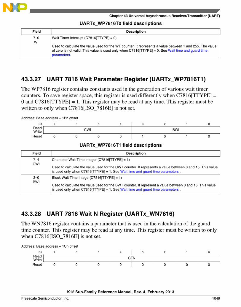
UARTx_WP7816T0 field descriptions
Field Description
7–0WI
Wait Timer Interrupt (C7816[TTYPE] = 0)
Used to calculate the value used for the WT counter. It represents a value between 1 and 255. The valueof zero is not valid. This value is used only when C7816[TTYPE] = 0. See Wait time and guard timeparameters.
43.3.27 UART 7816 Wait Parameter Register (UARTx_WP7816T1)
The WP7816 register contains constants used in the generation of various wait timercounters. To save register space, this register is used differently when C7816[TTYPE] =0 and C7816[TTYPE] = 1. This register may be read at any time. This register must bewritten to only when C7816[ISO_7816E] is not set.
Address: Base address + 1Bh offset
Bit 7 6 5 4 3 2 1 0
Read CWI BWIWriteReset 0 0 0 0 1 0 1 0
UARTx_WP7816T1 field descriptions
Field Description
7–4CWI
Character Wait Time Integer (C7816[TTYPE] = 1)
Used to calculate the value used for the CWT counter. It represents a value between 0 and 15. This valueis used only when C7816[TTYPE] = 1. See Wait time and guard time parameters .
3–0BWI
Block Wait Time Integer(C7816[TTYPE] = 1)
Used to calculate the value used for the BWT counter. It represent a value between 0 and 15. This valueis used only when C7816[TTYPE] = 1. See Wait time and guard time parameters .
43.3.28 UART 7816 Wait N Register (UARTx_WN7816)
The WN7816 register contains a parameter that is used in the calculation of the guardtime counter. This register may be read at any time. This register must be written to onlywhen C7816[ISO_7816E] is not set.
Address: Base address + 1Ch offset
Bit 7 6 5 4 3 2 1 0
Read GTNWriteReset 0 0 0 0 0 0 0 0
Chapter 43 Universal Asynchronous Receiver/Transmitter (UART)
K12 Sub-Family Reference Manual, Rev. 4, February 2013
Freescale Semiconductor, Inc. 1049

UARTx_WN7816 field descriptions
Field Description
7–0GTN
Guard Band N
Defines a parameter used in the calculation of GT, CGT, and BGT counters. The value represents aninteger number between 0 and 255. See Wait time and guard time parameters .
43.3.29 UART 7816 Wait FD Register (UARTx_WF7816)
The WF7816 contains parameters that are used in the generation of various countersincluding GT, CGT, BGT, WT, and BWT. This register may be read at any time. Thisregister must be written to only when C7816[ISO_7816E] is not set.
Address: Base address + 1Dh offset
Bit 7 6 5 4 3 2 1 0
Read GTFDWriteReset 0 0 0 0 0 0 0 1
UARTx_WF7816 field descriptions
Field Description
7–0GTFD
FD Multiplier
Used as another multiplier in the calculation of WT and BWT. This value represents a number between 1and 255. The value of 0 is invalid. This value is not used in baud rate generation. See Wait time and guardtime parameters and Baud rate generation .
43.3.30 UART 7816 Error Threshold Register (UARTx_ET7816)
The ET7816 register contains fields that determine the number of NACKs that must bereceived or transmitted before the host processor is notified. This register may be read atanytime. This register must be written to only when C7816[ISO_7816E] is not set.
Address: Base address + 1Eh offset
Bit 7 6 5 4 3 2 1 0
Read TXTHRESHOLD RXTHRESHOLDWriteReset 0 0 0 0 0 0 0 0
UARTx_ET7816 field descriptions
Field Description
7–4TXTHRESHOLD
Transmit NACK Threshold
The value written to this field indicates the maximum number of failed attempts (NACKs) a transmittedcharacter can have before the host processor is notified. This field is meaningful only when
Table continues on the next page...
Memory map and registers
K12 Sub-Family Reference Manual, Rev. 4, February 2013
1050 Freescale Semiconductor, Inc.
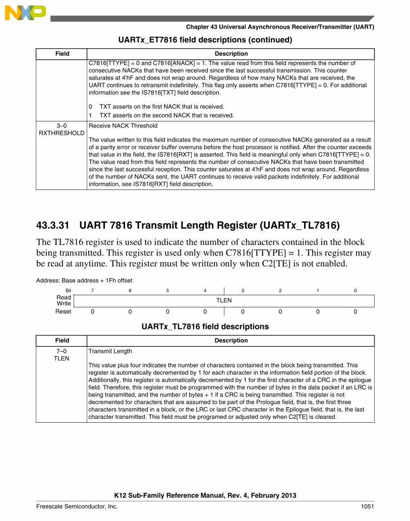
UARTx_ET7816 field descriptions (continued)
Field Description
C7816[TTYPE] = 0 and C7816[ANACK] = 1. The value read from this field represents the number ofconsecutive NACKs that have been received since the last successful transmission. This countersaturates at 4'hF and does not wrap around. Regardless of how many NACKs that are received, theUART continues to retransmit indefinitely. This flag only asserts when C7816[TTYPE] = 0. For additionalinformation see the IS7816[TXT] field description.
0 TXT asserts on the first NACK that is received.1 TXT asserts on the second NACK that is received.
3–0RXTHRESHOLD
Receive NACK Threshold
The value written to this field indicates the maximum number of consecutive NACKs generated as a resultof a parity error or receiver buffer overruns before the host processor is notified. After the counter exceedsthat value in the field, the IS7816[RXT] is asserted. This field is meaningful only when C7816[TTYPE] = 0.The value read from this field represents the number of consecutive NACKs that have been transmittedsince the last successful reception. This counter saturates at 4'hF and does not wrap around. Regardlessof the number of NACKs sent, the UART continues to receive valid packets indefinitely. For additionalinformation, see IS7816[RXT] field description.
43.3.31 UART 7816 Transmit Length Register (UARTx_TL7816)
The TL7816 register is used to indicate the number of characters contained in the blockbeing transmitted. This register is used only when C7816[TTYPE] = 1. This register maybe read at anytime. This register must be written only when C2[TE] is not enabled.
Address: Base address + 1Fh offset
Bit 7 6 5 4 3 2 1 0
Read TLENWriteReset 0 0 0 0 0 0 0 0
UARTx_TL7816 field descriptions
Field Description
7–0TLEN
Transmit Length
This value plus four indicates the number of characters contained in the block being transmitted. Thisregister is automatically decremented by 1 for each character in the information field portion of the block.Additionally, this register is automatically decremented by 1 for the first character of a CRC in the epiloguefield. Therefore, this register must be programmed with the number of bytes in the data packet if an LRC isbeing transmitted, and the number of bytes + 1 if a CRC is being transmitted. This register is notdecremented for characters that are assumed to be part of the Prologue field, that is, the first threecharacters transmitted in a block, or the LRC or last CRC character in the Epilogue field, that is, the lastcharacter transmitted. This field must be programed or adjusted only when C2[TE] is cleared.
Chapter 43 Universal Asynchronous Receiver/Transmitter (UART)
K12 Sub-Family Reference Manual, Rev. 4, February 2013
Freescale Semiconductor, Inc. 1051

43.4 Functional descriptionThis section provides a complete functional description of the UART block.
The UART allows full duplex, asynchronous, NRZ serial communication between theCPU and remote devices, including other CPUs. The UART transmitter and receiveroperate independently, although they use the same baud rate generator. The CPUmonitors the status of the UART, writes the data to be transmitted, and processesreceived data.
43.4.1 Transmitter
SHIFT DIRECTION
PARITY GENERATION
PE
PTTRANSMITTER CONTROL
M
MSBF
INTERNAL BUS
Tx port en
Tx input buffer en Tx output buffer en
ST
OP
TXINV
TxD Pin Control
ST
AR
T
BAUDRATE GENERATEMODULE
CLOCK
SBR12:0 BRFA4:0VARIABLE 12-BIT TRANSMIT SHIFT REGISTERM10
R485 CONTROL
RTS_B
CTS_B
TXDIR
SBK
TE
DMA Done
7816 LOGICTxD
IRQ / DMALOGIC
INFRARED LOGIC
DMA Requests
IRQ RequestsTxD
LOOPCONTROL
LOOPS
RSRC
UART DATA REGISTER (UART_D)
Figure 43-156. Transmitter Block Diagram
Functional description
K12 Sub-Family Reference Manual, Rev. 4, February 2013
1052 Freescale Semiconductor, Inc.
43.4.1.1 Transmitter character length
The UART transmitter can accommodate either 8, 9, or 10-bit data characters. The stateof the C1[M] and C1[PE] bits and the C4[M10] bit determine the length of datacharacters. When transmitting 9-bit data, bit C3[T8] is the ninth bit (bit 8).
43.4.1.2 Transmission bit order
When S2[MSBF] is set, the UART automatically transmits the MSB of the data word asthe first bit after the start bit. Similarly, the LSB of the data word is transmittedimmediately preceding the parity bit, or the stop bit if parity is not enabled. All necessarybit ordering is handled automatically by the module. Therefore, the format of the datawritten to D for transmission is completely independent of the S2[MSBF] setting.
43.4.1.3 Character transmission
To transmit data, the MCU writes the data bits to the UART transmit buffer using UARTdata registers C3[T8] and D. Data in the transmit buffer is then transferred to thetransmitter shift register as needed. The transmit shift register then shifts a frame outthrough the transmit data output signal after it has prefaced it with any required start andstop bits. The UART data registers, C3[T8] and D, provide access to the transmit bufferstructure.
The UART also sets a flag, the transmit data register empty flag S1[TDRE], andgenerates an interrupt or DMA request (C5[TDMAS]) whenever the number ofdatawords in the transmit buffer is equal to or less than the value indicated byTWFIFO[TXWATER]. The transmit driver routine may respond to this flag by writingadditional datawords to the transmit buffer using C3[T8]/D as space permits.
See Application information for specific programing sequences.
Setting C2[TE] automatically loads the transmit shift register with the followingpreamble:
• 10 logic 1s if C1[M] = 0• 11 logic 1s if C1[M] = 1 and C4[M10] = 0• 12 logic 1s if C1[M] = 1, C4[M10] = 1, C1[PE] = 1
After the preamble shifts out, control logic transfers the data from the D register into thetransmit shift register. The transmitter automatically transmits the correct start bit andstop bit before and after the dataword.
Chapter 43 Universal Asynchronous Receiver/Transmitter (UART)
K12 Sub-Family Reference Manual, Rev. 4, February 2013
Freescale Semiconductor, Inc. 1053
When C7816[ISO_7816E] = 1, setting C2[TE] does not result in a preamble beinggenerated. The transmitter starts transmitting as soon as the corresponding guard timeexpires. When C7816[TTYPE] = 0, the value in GT is used. When C7816[TTYPE] = 1,the value in BGT is used, because C2[TE] will remain asserted until the end of the blocktransfer. C2[TE] is automatically cleared when C7816[TTYPE] = 1 and the block beingtransmitted has completed. When C7816[TTYPE] = 0, the transmitter listens for a NACKindication. If no NACK is received, it is assumed that the character was correctlyreceived. If a NACK is received, the transmitter resends the data, assuming that thenumber of retries for that character, that is, the number of NACKs received, is less thanor equal to the value in ET7816[TXTHRESHOLD].
Hardware supports odd or even parity. When parity is enabled, the bit immediatelypreceding the stop bit is the parity bit.
When the transmit shift register is not transmitting a frame, the transmit data outputsignal goes to the idle condition, logic 1. If at any time software clears C2[TE], thetransmitter enable signal goes low and the transmit signal goes idle.
If the software clears C2[TE] while a transmission is in progress, the character in thetransmit shift register continues to shift out, provided S1[TC] was cleared during the datawrite sequence. To clear S1[TC], the S1 register must be read followed by a write to Dregister.
If S1[TC] is cleared during character transmission and C2[TE] is cleared, thetransmission enable signal is deasserted at the completion of the current frame. Followingthis, the transmit data out signal enters the idle state even if there is data pending in theUART transmit data buffer. To ensure that all the data written in the FIFO is transmittedon the link before clearing C2[TE], wait for S1[TC] to set. Alternatively, the same can beachieved by setting TWFIFO[TXWATER] to 0x0 and waiting for S1[TDRE] to set.
43.4.1.4 Transmitting break characters
Setting C2[SBK] loads the transmit shift register with a break character. A breakcharacter contains all logic 0s and has no start, stop, or parity bit. Break character lengthdepends on C1[M] and C1[PE], S2[BRK13], and C4[M10]. See the following table.
Table 43-163. Transmit break character length
S2[BRK13] C1[M] C4[M10] C1[PE] Bits transmitted
0 0 — — 10
0 1 0 — 11
0 1 1 0 11
0 1 1 1 12
Table continues on the next page...
Functional description
K12 Sub-Family Reference Manual, Rev. 4, February 2013
1054 Freescale Semiconductor, Inc.
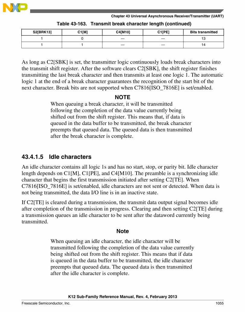
Table 43-163. Transmit break character length (continued)
S2[BRK13] C1[M] C4[M10] C1[PE] Bits transmitted
1 0 — — 13
1 1 — — 14
As long as C2[SBK] is set, the transmitter logic continuously loads break characters intothe transmit shift register. After the software clears C2[SBK], the shift register finishestransmitting the last break character and then transmits at least one logic 1. The automaticlogic 1 at the end of a break character guarantees the recognition of the start bit of thenext character. Break bits are not supported when C7816[ISO_7816E] is set/enabled.
NOTEWhen queuing a break character, it will be transmittedfollowing the completion of the data value currently beingshifted out from the shift register. This means that, if data isqueued in the data buffer to be transmitted, the break characterpreempts that queued data. The queued data is then transmittedafter the break character is complete.
43.4.1.5 Idle characters
An idle character contains all logic 1s and has no start, stop, or parity bit. Idle characterlength depends on C1[M], C1[PE], and C4[M10]. The preamble is a synchronizing idlecharacter that begins the first transmission initiated after setting C2[TE]. WhenC7816[ISO_7816E] is set/enabled, idle characters are not sent or detected. When data isnot being transmitted, the data I/O line is in an inactive state.
If C2[TE] is cleared during a transmission, the transmit data output signal becomes idleafter completion of the transmission in progress. Clearing and then setting C2[TE] duringa transmission queues an idle character to be sent after the dataword currently beingtransmitted.
Note
When queuing an idle character, the idle character will betransmitted following the completion of the data value currentlybeing shifted out from the shift register. This means that if datais queued in the data buffer to be transmitted, the idle characterpreempts that queued data. The queued data is then transmittedafter the idle character is complete.
Chapter 43 Universal Asynchronous Receiver/Transmitter (UART)
K12 Sub-Family Reference Manual, Rev. 4, February 2013
Freescale Semiconductor, Inc. 1055
If C2[TE] is cleared and the transmission is completed, theUART is not the master of the TXD pin.
43.4.1.6 Hardware flow control
The transmitter supports hardware flow control by gating the transmission with the valueof CTS. If the clear-to-send operation is enabled, the character is transmitted when CTSis asserted. If CTS is deasserted in the middle of a transmission with characters remainingin the receiver data buffer, the character in the shift register is sent and TXD remains inthe mark state until CTS is reasserted.
If the clear-to-send operation is disabled, the transmitter ignores the state of CTS. Also, ifthe transmitter is forced to send a continuous low condition because it is sending a breakcharacter, the transmitter ignores the state of CTS regardless of whether the clear-to-sendoperation is enabled.
The transmitter's CTS signal can also be enabled even if the same UART receiver's RTSsignal is disabled.
43.4.1.7 Transceiver driver enable
The transmitter can use RTS as an enable signal for the driver of an external transceiver.See Transceiver driver enable using RTS for details. If the request-to-send operation isenabled, when a character is placed into an empty transmitter data buffer, RTS assertsone bit time before the start bit is transmitted. RTS remains asserted for the whole timethat the transmitter data buffer has any characters. RTS deasserts one bit time after allcharacters in the transmitter data buffer and shift register are completely sent, includingthe last stop bit. Transmitting a break character also asserts RTS, with the same assertionand deassertion timing as having a character in the transmitter data buffer.
The transmitter's RTS signal asserts only when the transmitter is enabled. However, thetransmitter's RTS signal is unaffected by its CTS signal. RTS will remain asserted untilthe transfer is completed, even if the transmitter is disabled mid-way through a datatransfer.
The following figure shows the functional timing information for the transmitter. Alongwith the actual character itself, TXD shows the start bit. The stop bit is also indicated,with a dashed line if necessary.
Functional description
K12 Sub-Family Reference Manual, Rev. 4, February 2013
1056 Freescale Semiconductor, Inc.

C1 C2 C3 Break C4TXD C5
C1 C2 C3 C4 StartBreak
StopBreak
C5
databufferwrite
CTS_B
RTS_B
C1 in transmission
1
1. Cn = transmit characters
Figure 43-157. Transmitter RTS and CTS timing diagram
Chapter 43 Universal Asynchronous Receiver/Transmitter (UART)
K12 Sub-Family Reference Manual, Rev. 4, February 2013
Freescale Semiconductor, Inc. 1057

43.4.2 Receiver
M
PE
PT
RE
VARIABLE 12-BIT RECEIVE
ST
OP
ST
AR
T
RECEIVE
WAKEUP
DATA BUFFER
INTERNAL BUS
MODULE
SBR12:0
BAUDRATECLOCK
RAF
LOGIC
SHIFT DIRECTION
ACTIVE EDGEDETECT
LBKDE
BRFA4:0
MSBF
GENERATORSHIFT REGISTER M10
RXINV
IRQ / DMALOGIC
DMA Requests
IRQ Requests
PARITYLOGIC
CONTROL
RxD
RxD
LOOPS
RSRC
From Transmitter
RECEIVERSOURCECONTROL
7816 LOGICTo TxD
INFRARED LOGIC
Figure 43-158. UART receiver block diagram
43.4.2.1 Receiver character length
The UART receiver can accommodate 8-, 9-, or 10-bit data characters. The states ofC1[M], C1[PE], and C4[M10] determine the length of data characters. When receiving 9or 10-bit data, C3[R8] is the ninth bit (bit 8).
Functional description
K12 Sub-Family Reference Manual, Rev. 4, February 2013
1058 Freescale Semiconductor, Inc.

43.4.2.2 Receiver bit ordering
When S2[MSBF] is set, the receiver operates such that the first bit received after the startbit is the MSB of the dataword. Similarly, the bit received immediately preceding theparity bit, or the stop bit if parity is not enabled, is treated as the LSB for the dataword.All necessary bit ordering is handled automatically by the module. Therefore, the formatof the data read from receive data buffer is completely independent of S2[MSBF].
43.4.2.3 Character reception
During UART reception, the receive shift register shifts a frame in from theunsynchronized receiver input signal. After a complete frame shifts into the receive shiftregister, the data portion of the frame transfers to the UART receive buffer. Additionally,the noise and parity error flags that are calculated during the receive process are alsocaptured in the UART receive buffer. The receive data buffer is accessible via the D andC3[T8] registers. Additional received information flags regarding the receive datawordcan be read in ED register. S1[RDRF] is set if the number of resulting datawords in thereceive buffer is equal to or greater than the number indicated by RWFIFO[RXWATER].If the C2[RIE] is also set, RDRF generates an RDRF interrupt request. Alternatively, byprogramming C5[RDMAS], a DMA request can be generated.
When C7816[ISO_7816E] is set/enabled and C7816[TTYPE] = 0, character receptionoperates slightly differently. Upon receipt of the parity bit, the validity of the parity bit ischecked. If C7816[ANACK] is set and the parity check fails, or if INIT and the receivedcharacter is not a valid initial character, then a NACK is sent by the receiver. If thenumber of consecutive receive errors exceeds the threshold set byET7816[RXTHRESHOLD], then IS7816[RXT] is set and an interrupt generated ifIE7816[RXTE] is set. If an error is detected due to parity or an invalid initial character,the data is not transferred from the receive shift register to the receive buffer. Instead, thedata is overwritten by the next incoming data.
When the C7816[ISO_7816E] is set/enabled, C7816[ONACK] is set/enabled, and thereceived character results in the receive buffer overflowing, a NACK is issued by thereceiver. Additionally, S1[OR] is set and an interrupt is issued if required, and the data inthe shift register is discarded.
43.4.2.4 Data sampling
The receiver samples the unsynchronized receiver input signal at the RT clock rate. TheRT clock is an internal signal with a frequency 16 times the baud rate. To adjust for baudrate mismatch, the RT clock (see the following figure) is re-synchronized:
Chapter 43 Universal Asynchronous Receiver/Transmitter (UART)
K12 Sub-Family Reference Manual, Rev. 4, February 2013
Freescale Semiconductor, Inc. 1059
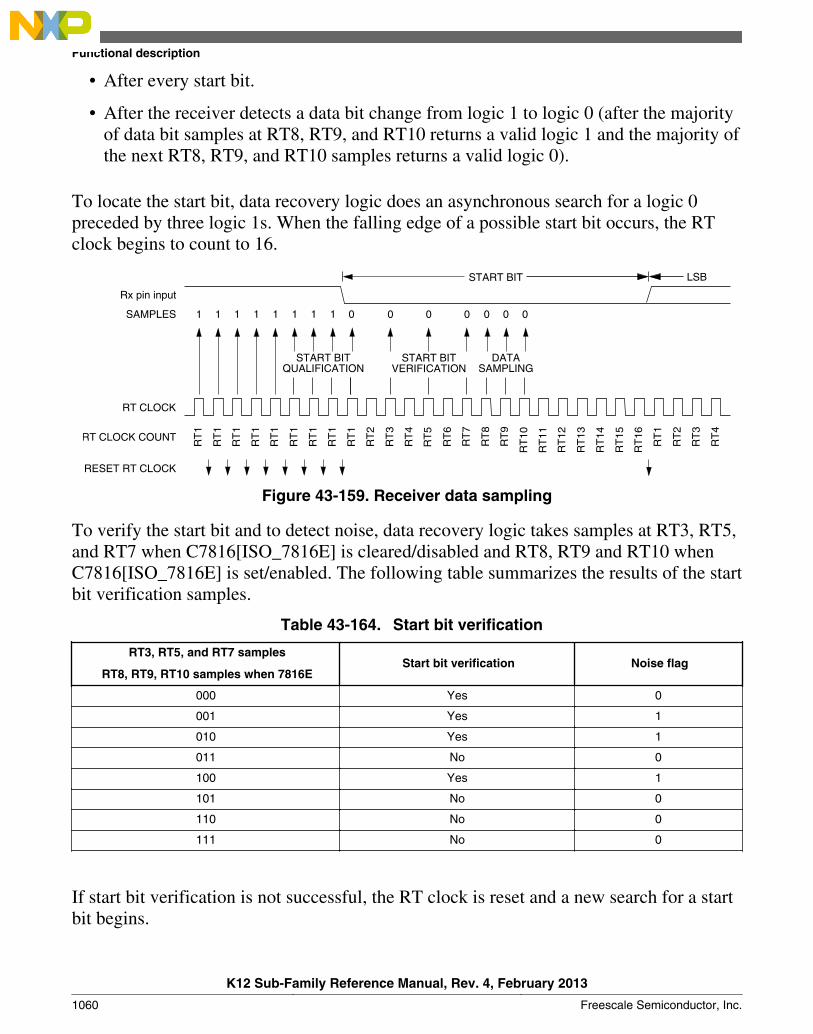
• After every start bit.
• After the receiver detects a data bit change from logic 1 to logic 0 (after the majorityof data bit samples at RT8, RT9, and RT10 returns a valid logic 1 and the majority ofthe next RT8, RT9, and RT10 samples returns a valid logic 0).
To locate the start bit, data recovery logic does an asynchronous search for a logic 0preceded by three logic 1s. When the falling edge of a possible start bit occurs, the RTclock begins to count to 16.
SAMPLES
Rx pin input
RT CLOCK
RT CLOCK COUNT
RESET RT CLOCK
1 1 1 1 0
START BIT LSB
RT
1
RT
1
RT
1
RT
1
RT
1
RT
1
RT
1
RT
1
RT
1
RT
2
RT
3
RT
4
RT
5
RT
6
RT
2
RT
3
RT
4
RT
7
RT
8
RT
9
RT
11
RT
13
RT
14
RT
15
RT
16
111 1 00 0 0 0 0
RT
10
RT
12
RT
1
START BITQUALIFICATION
DATASAMPLING
START BITVERIFICATION
Figure 43-159. Receiver data sampling
To verify the start bit and to detect noise, data recovery logic takes samples at RT3, RT5,and RT7 when C7816[ISO_7816E] is cleared/disabled and RT8, RT9 and RT10 whenC7816[ISO_7816E] is set/enabled. The following table summarizes the results of the startbit verification samples.
Table 43-164. Start bit verification
RT3, RT5, and RT7 samples
RT8, RT9, RT10 samples when 7816EStart bit verification Noise flag
000 Yes 0
001 Yes 1
010 Yes 1
011 No 0
100 Yes 1
101 No 0
110 No 0
111 No 0
If start bit verification is not successful, the RT clock is reset and a new search for a startbit begins.
Functional description
K12 Sub-Family Reference Manual, Rev. 4, February 2013
1060 Freescale Semiconductor, Inc.
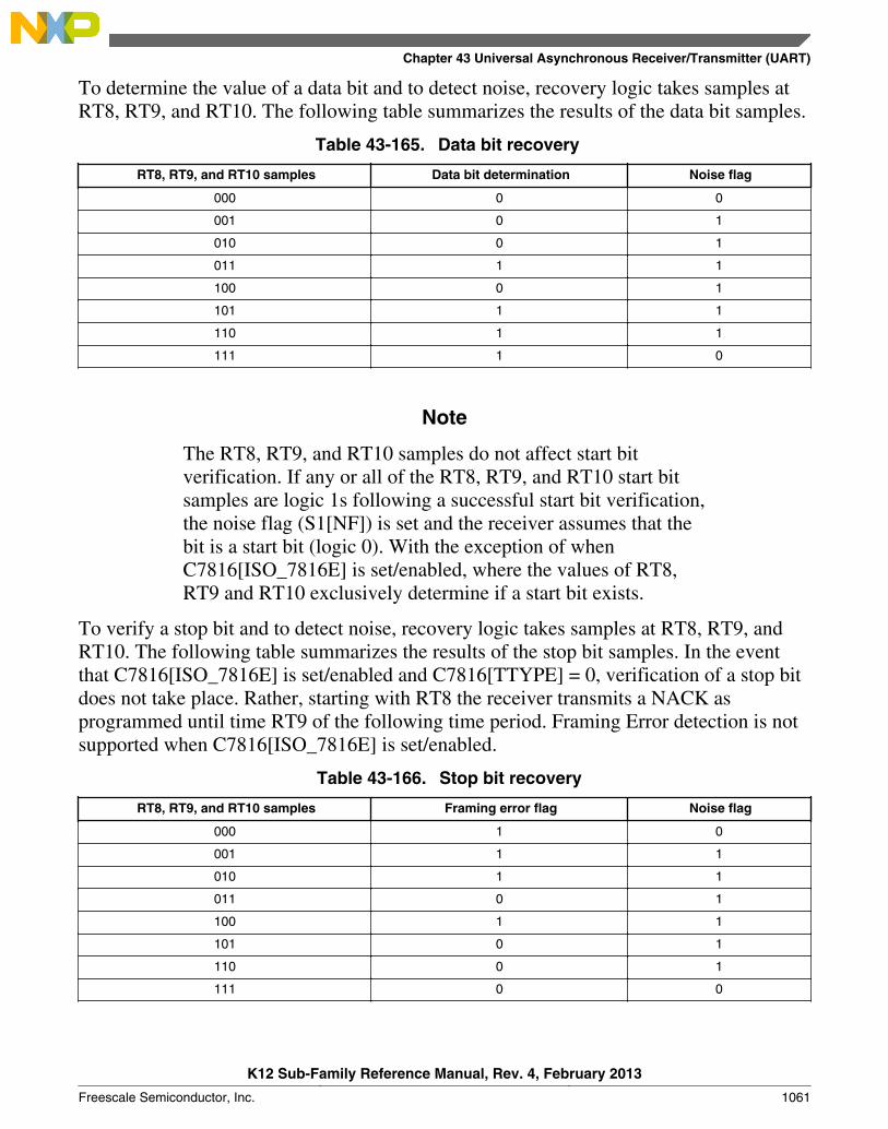
To determine the value of a data bit and to detect noise, recovery logic takes samples atRT8, RT9, and RT10. The following table summarizes the results of the data bit samples.
Table 43-165. Data bit recovery
RT8, RT9, and RT10 samples Data bit determination Noise flag
000 0 0
001 0 1
010 0 1
011 1 1
100 0 1
101 1 1
110 1 1
111 1 0
Note
The RT8, RT9, and RT10 samples do not affect start bitverification. If any or all of the RT8, RT9, and RT10 start bitsamples are logic 1s following a successful start bit verification,the noise flag (S1[NF]) is set and the receiver assumes that thebit is a start bit (logic 0). With the exception of whenC7816[ISO_7816E] is set/enabled, where the values of RT8,RT9 and RT10 exclusively determine if a start bit exists.
To verify a stop bit and to detect noise, recovery logic takes samples at RT8, RT9, andRT10. The following table summarizes the results of the stop bit samples. In the eventthat C7816[ISO_7816E] is set/enabled and C7816[TTYPE] = 0, verification of a stop bitdoes not take place. Rather, starting with RT8 the receiver transmits a NACK asprogrammed until time RT9 of the following time period. Framing Error detection is notsupported when C7816[ISO_7816E] is set/enabled.
Table 43-166. Stop bit recovery
RT8, RT9, and RT10 samples Framing error flag Noise flag
000 1 0
001 1 1
010 1 1
011 0 1
100 1 1
101 0 1
110 0 1
111 0 0
Chapter 43 Universal Asynchronous Receiver/Transmitter (UART)
K12 Sub-Family Reference Manual, Rev. 4, February 2013
Freescale Semiconductor, Inc. 1061
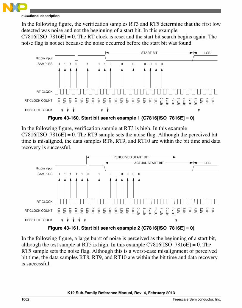
In the following figure, the verification samples RT3 and RT5 determine that the first lowdetected was noise and not the beginning of a start bit. In this exampleC7816[ISO_7816E] = 0. The RT clock is reset and the start bit search begins again. Thenoise flag is not set because the noise occurred before the start bit was found.
SAMPLES
Rx pin input
RT CLOCK
RT CLOCK COUNT
RESET RT CLOCK
1 1 1 0 1 0 0 0
START BIT LSB
RT
1
RT
1
RT
1
RT
1
RT
2
RT
4
RT
3
RT
5
RT
1
RT
1
RT
2
RT
3
RT
10
RT
1
RT
2
RT
3
1 1 0 0 0 0
RT
11
RT
12
RT
13
RT
14
RT
15
RT
16
RT
4
RT
5
RT
6
RT
7
RT
8
RT
9
Figure 43-160. Start bit search example 1 (C7816[ISO_7816E] = 0)
In the following figure, verification sample at RT3 is high. In this exampleC7816[ISO_7816E] = 0. The RT3 sample sets the noise flag. Although the perceived bittime is misaligned, the data samples RT8, RT9, and RT10 are within the bit time and datarecovery is successful.
SAMPLES
Rx pin input
RT CLOCK
RT CLOCK COUNT
RESET RT CLOCK
1 1 1 0 1 0 0 0
PERCEIVED START BIT
ACTUAL START BIT LSB
RT
1
RT
1
RT
1
RT
1
RT
1
RT
2
RT
1
RT
3
RT
4
RT
5
RT
6
RT
7
RT
13
RT
12
RT
11
RT
14
RT
1
RT
2
RT
3
RT
4
RT
5
RT
6
RT
7
1 1 0 0
RT
10
RT
8
RT
9
RT
15
RT
16
Figure 43-161. Start bit search example 2 (C7816[ISO_7816E] = 0)
In the following figure, a large burst of noise is perceived as the beginning of a start bit,although the test sample at RT5 is high. In this example C7816[ISO_7816E] = 0. TheRT5 sample sets the noise flag. Although this is a worst-case misalignment of perceivedbit time, the data samples RT8, RT9, and RT10 are within the bit time and data recoveryis successful.
Functional description
K12 Sub-Family Reference Manual, Rev. 4, February 2013
1062 Freescale Semiconductor, Inc.
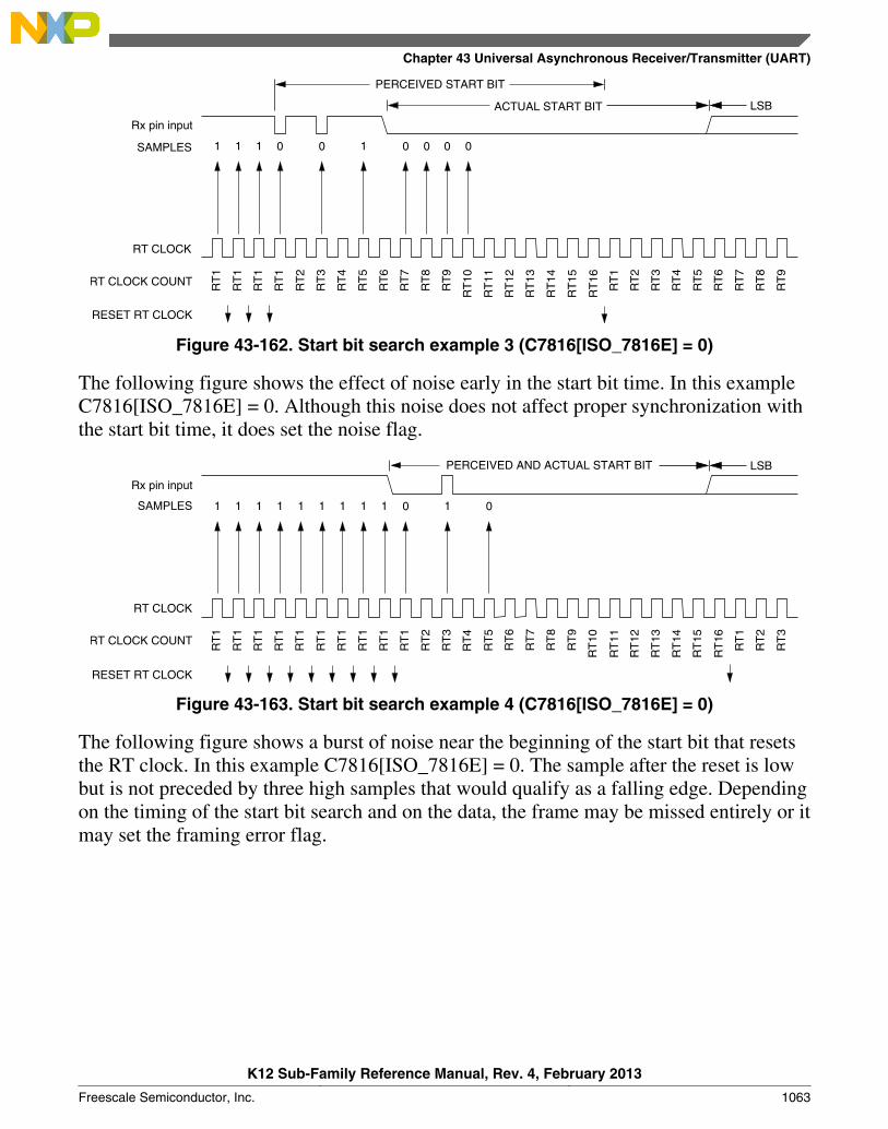
SAMPLES
Rx pin input
RT CLOCK
RT CLOCK COUNT
RESET RT CLOCK
1 1 1 0 0 1 0 0 0 0
PERCEIVED START BIT
ACTUAL START BIT LSB
RT
1
RT
1
RT
1
RT
1
RT
2
RT
4
RT
3
RT
5
RT
6
RT
7
RT
8
RT
9
RT
10
RT
11
RT
15
RT
14
RT
13
RT
12
RT
16
RT
1
RT
2
RT
3
RT
4
RT
5
RT
6
RT
7
RT
8
RT
9
Figure 43-162. Start bit search example 3 (C7816[ISO_7816E] = 0)
The following figure shows the effect of noise early in the start bit time. In this exampleC7816[ISO_7816E] = 0. Although this noise does not affect proper synchronization withthe start bit time, it does set the noise flag.
SAMPLES
Rx pin input
RT CLOCK
RT CLOCK COUNT
RESET RT CLOCK
1 1 1 1 0
PERCEIVED AND ACTUAL START BIT LSB
RT
1
RT
1
RT
1
RT
1
RT
1
RT
1
RT
1
RT
1
RT
1
RT
1
RT
2
RT
3
RT
4
RT
5
RT
1
RT
2
RT
3
RT
6
RT
7
RT
8
RT
9
RT
10
RT
11
RT
12
RT
13
RT
14
RT
15
RT
16
111 1 1 1 0
Figure 43-163. Start bit search example 4 (C7816[ISO_7816E] = 0)
The following figure shows a burst of noise near the beginning of the start bit that resetsthe RT clock. In this example C7816[ISO_7816E] = 0. The sample after the reset is lowbut is not preceded by three high samples that would qualify as a falling edge. Dependingon the timing of the start bit search and on the data, the frame may be missed entirely or itmay set the framing error flag.
Chapter 43 Universal Asynchronous Receiver/Transmitter (UART)
K12 Sub-Family Reference Manual, Rev. 4, February 2013
Freescale Semiconductor, Inc. 1063

SAMPLES
Rx pin input
RT CLOCK
RT CLOCK COUNT
RESET RT CLOCK
1 1 1 1 0 0
START BIT LSB
RT
1
RT
1
RT
1
RT
1
RT
1
RT
1
RT
1
RT
1
RT
1
RT
1
RT
2
RT
3
RT
1
RT
1
RT
1
RT
1
RT
1
RT
1
RT
1
RT
1
RT
1
NO START BIT FOUND
1 1 1 1 1 1 1 0 0 0 0 0 0 0 0
RT
4
RT
5
RT
6
RT
7
RT
1
RT
1
RT
1
Figure 43-164. Start bit search example 5 (C7816[ISO_7816E] = 0)
In the following figure, a noise burst makes the majority of data samples RT8, RT9, andRT10 high. In this example C7816[ISO_7816E] = 0. This sets the noise flag but does notreset the RT clock. In start bits only, the RT8, RT9, and RT10 data samples are ignored.In this example, if C7816[ISO_7816E] = 1 then a start bit would not have been detectedat all since at least two of the three samples (RT8, RT9, RT10) were high.
SAMPLES
Rx pin input
RT CLOCK
RT CLOCK COUNT
RESET RT CLOCK
1 1 1 1 0 0
START BIT LSB
RT
1
RT
1
RT
1
RT
1
RT
1
RT
1
RT
1
RT
1
RT
1
RT
1
RT
2
RT
3
RT
10
RT
1
RT
2
RT
3
1 1 1 1 1 0 0 1 0 1
RT
4
RT
5
RT
6
RT
7
RT
8
RT
9
RT
11
RT
12
RT
13
RT
14
RT
15
RT
16Figure 43-165. Start bit search example 6
43.4.2.5 Framing errors
If the data recovery logic does not detect a logic 1 where the stop bit should be in anincoming frame, it sets the framing error flag, S1[FE], if S2[LBKDE] is disabled. WhenS2[LBKDE] is disabled, a break character also sets the S1[FE] because a break characterhas no stop bit. S1[FE] is set at the same time that received data is placed in the receivedata buffer. Framing errors are not supported when C7816[ISO7816E] is set/enabled.However, if S1[FE] is set, data will not be received when C7816[ISO7816E] is set.
Functional description
K12 Sub-Family Reference Manual, Rev. 4, February 2013
1064 Freescale Semiconductor, Inc.
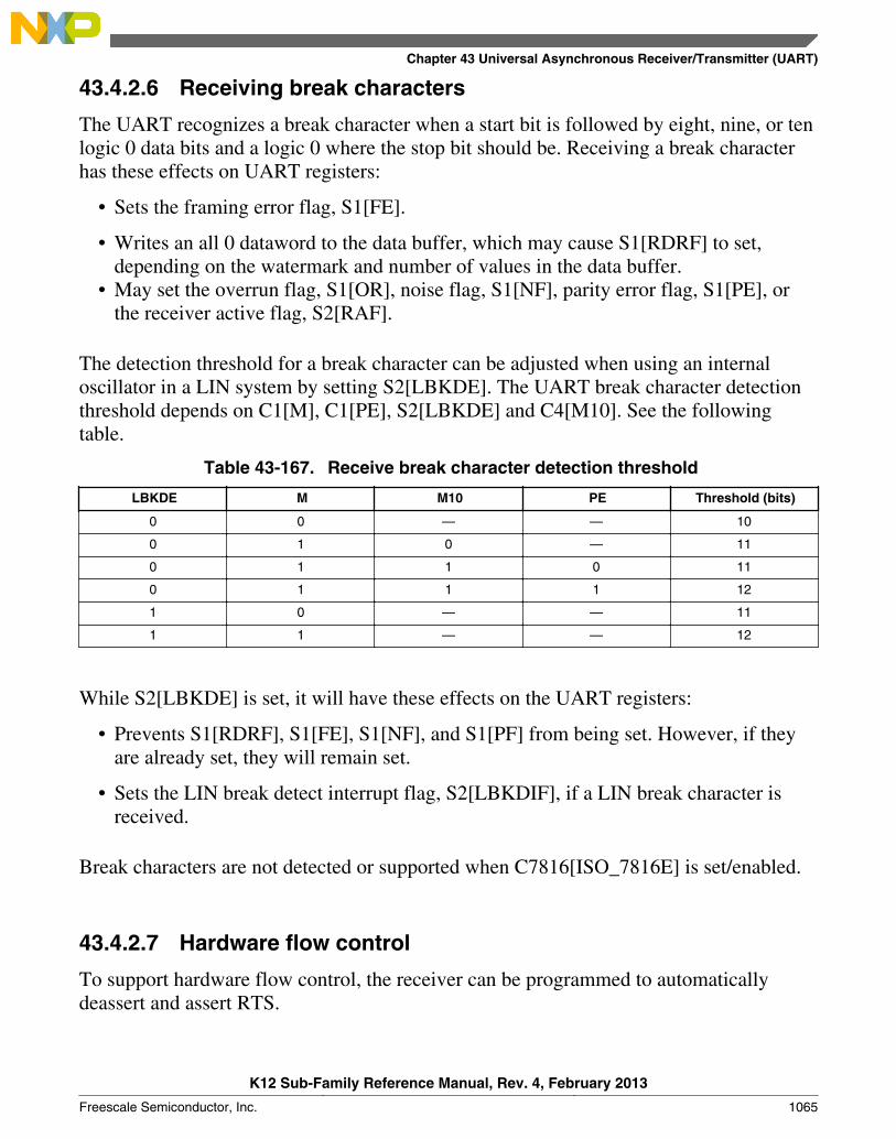
43.4.2.6 Receiving break characters
The UART recognizes a break character when a start bit is followed by eight, nine, or tenlogic 0 data bits and a logic 0 where the stop bit should be. Receiving a break characterhas these effects on UART registers:
• Sets the framing error flag, S1[FE].
• Writes an all 0 dataword to the data buffer, which may cause S1[RDRF] to set,depending on the watermark and number of values in the data buffer.
• May set the overrun flag, S1[OR], noise flag, S1[NF], parity error flag, S1[PE], orthe receiver active flag, S2[RAF].
The detection threshold for a break character can be adjusted when using an internaloscillator in a LIN system by setting S2[LBKDE]. The UART break character detectionthreshold depends on C1[M], C1[PE], S2[LBKDE] and C4[M10]. See the followingtable.
Table 43-167. Receive break character detection threshold
LBKDE M M10 PE Threshold (bits)
0 0 — — 10
0 1 0 — 11
0 1 1 0 11
0 1 1 1 12
1 0 — — 11
1 1 — — 12
While S2[LBKDE] is set, it will have these effects on the UART registers:
• Prevents S1[RDRF], S1[FE], S1[NF], and S1[PF] from being set. However, if theyare already set, they will remain set.
• Sets the LIN break detect interrupt flag, S2[LBKDIF], if a LIN break character isreceived.
Break characters are not detected or supported when C7816[ISO_7816E] is set/enabled.
43.4.2.7 Hardware flow control
To support hardware flow control, the receiver can be programmed to automaticallydeassert and assert RTS.
Chapter 43 Universal Asynchronous Receiver/Transmitter (UART)
K12 Sub-Family Reference Manual, Rev. 4, February 2013
Freescale Semiconductor, Inc. 1065
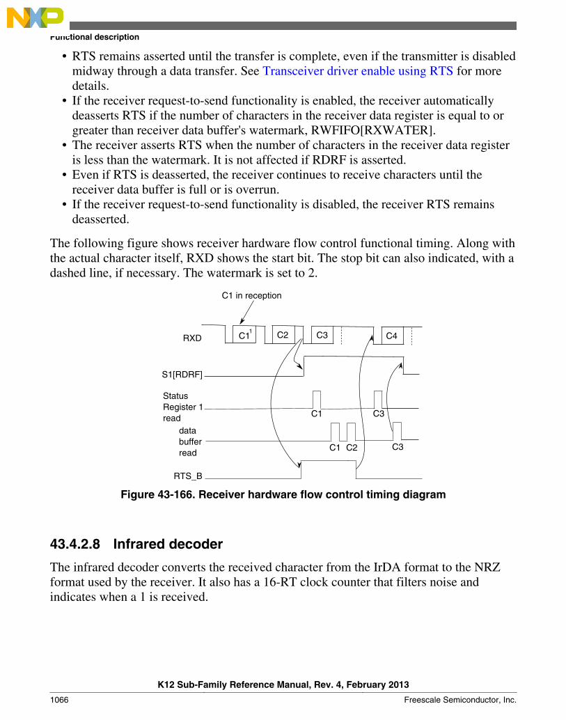
• RTS remains asserted until the transfer is complete, even if the transmitter is disabledmidway through a data transfer. See Transceiver driver enable using RTS for moredetails.
• If the receiver request-to-send functionality is enabled, the receiver automaticallydeasserts RTS if the number of characters in the receiver data register is equal to orgreater than receiver data buffer's watermark, RWFIFO[RXWATER].
• The receiver asserts RTS when the number of characters in the receiver data registeris less than the watermark. It is not affected if RDRF is asserted.
• Even if RTS is deasserted, the receiver continues to receive characters until thereceiver data buffer is full or is overrun.
• If the receiver request-to-send functionality is disabled, the receiver RTS remainsdeasserted.
The following figure shows receiver hardware flow control functional timing. Along withthe actual character itself, RXD shows the start bit. The stop bit can also indicated, with adashed line, if necessary. The watermark is set to 2.
C1 C2 C3 C4RXD
C3
databufferread
S1[RDRF]
RTS_B
C1 in reception
1
C1 C3
StatusRegister 1read
C1 C2
Figure 43-166. Receiver hardware flow control timing diagram
43.4.2.8 Infrared decoder
The infrared decoder converts the received character from the IrDA format to the NRZformat used by the receiver. It also has a 16-RT clock counter that filters noise andindicates when a 1 is received.
Functional description
K12 Sub-Family Reference Manual, Rev. 4, February 2013
1066 Freescale Semiconductor, Inc.

43.4.2.8.1 Start bit detection
When S2[RXINV] is cleared, the first rising edge of the received character correspondsto the start bit. The infrared decoder resets its counter. At this time, the receiver alsobegins its start bit detection process. After the start bit is detected, the receiversynchronizes its bit times to this start bit time. For the rest of the character reception, theinfrared decoder's counter and the receiver's bit time counter count independently fromeach other.
43.4.2.8.2 Noise filtering
Any further rising edges detected during the first half of the infrared decoder counter areignored by the decoder. Any pulses less than one RT clocks can be undetected by itregardless of whether it is seen in the first or second half of the count.
43.4.2.8.3 Low-bit detection
During the second half of the decoder count, a rising edge is decoded as a 0, which is sentto the receiver. The decoder counter is also reset.
43.4.2.8.4 High-bit detection
At 16-RT clocks after the previous rising edge, if a rising edge is not seen, then thedecoder sends a 1 to the receiver.
If the next bit is a 0, which arrives late, then a low-bit is detected according to Low-bitdetection. The value sent to the receiver is changed from 1 to a 0. Then, if a noise pulseoccurs outside the receiver's bit time sampling period, then the delay of a 0 is notrecorded as noise.
43.4.2.9 Baud rate tolerance
A transmitting device may be operating at a baud rate below or above the receiver baudrate. Accumulated bit time misalignment can cause one of the three stop bit data samples(RT8, RT9, and RT10) to fall outside the actual stop bit. A noise error will occur if theRT8, RT9, and RT10 samples are not all the same logical values. A framing error willoccur if the receiver clock is misaligned in such a way that the majority of the RT8, RT9,and RT10 stop bit samples are a logic 0.
As the receiver samples an incoming frame, it resynchronizes the RT clock on any validfalling edge within the frame. Resynchronization within frames corrects a misalignmentbetween transmitter bit times and receiver bit times.
Chapter 43 Universal Asynchronous Receiver/Transmitter (UART)
K12 Sub-Family Reference Manual, Rev. 4, February 2013
Freescale Semiconductor, Inc. 1067
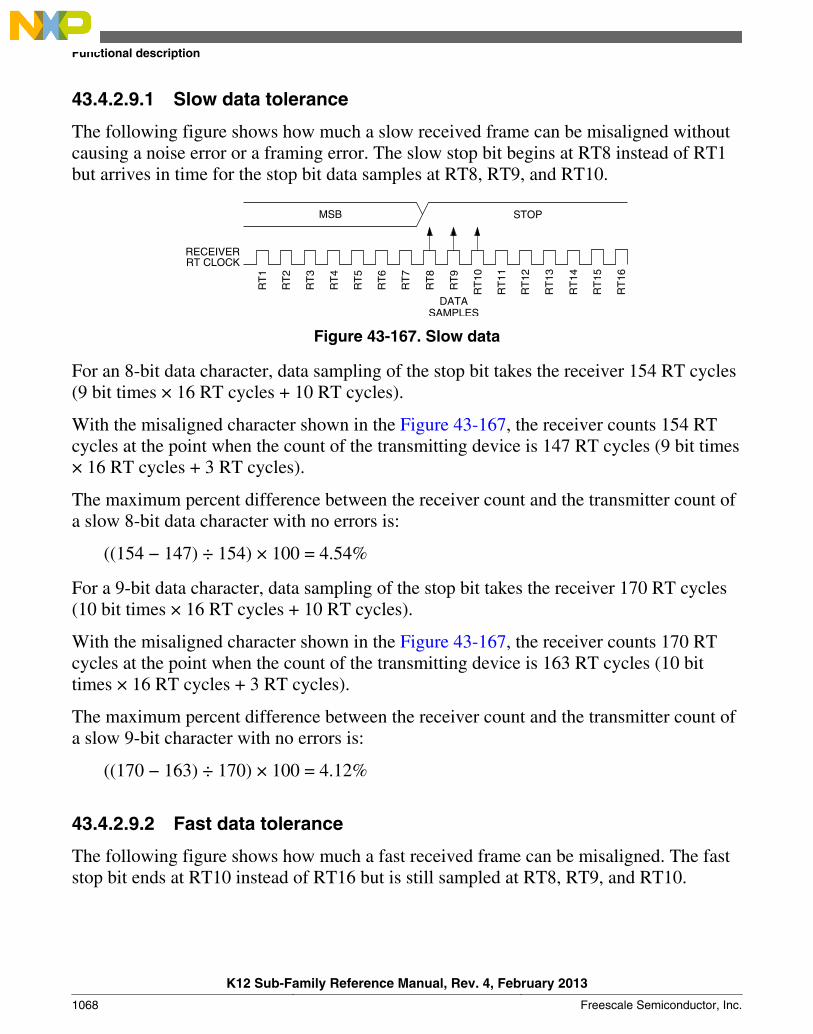
43.4.2.9.1 Slow data tolerance
The following figure shows how much a slow received frame can be misaligned withoutcausing a noise error or a framing error. The slow stop bit begins at RT8 instead of RT1but arrives in time for the stop bit data samples at RT8, RT9, and RT10.
RECEIVERRT CLOCK
MSB STOP
DATASAMPLES
RT
16
RT
15
RT
14
RT
13
RT
12
RT
11
RT
10
RT
9
RT
8
RT
7
RT
6
RT
5
RT
4
RT
3
RT
2
RT
1
Figure 43-167. Slow data
For an 8-bit data character, data sampling of the stop bit takes the receiver 154 RT cycles(9 bit times × 16 RT cycles + 10 RT cycles).
With the misaligned character shown in the Figure 43-167, the receiver counts 154 RTcycles at the point when the count of the transmitting device is 147 RT cycles (9 bit times× 16 RT cycles + 3 RT cycles).
The maximum percent difference between the receiver count and the transmitter count ofa slow 8-bit data character with no errors is:
((154 − 147) ÷ 154) × 100 = 4.54%
For a 9-bit data character, data sampling of the stop bit takes the receiver 170 RT cycles(10 bit times × 16 RT cycles + 10 RT cycles).
With the misaligned character shown in the Figure 43-167, the receiver counts 170 RTcycles at the point when the count of the transmitting device is 163 RT cycles (10 bittimes × 16 RT cycles + 3 RT cycles).
The maximum percent difference between the receiver count and the transmitter count ofa slow 9-bit character with no errors is:
((170 − 163) ÷ 170) × 100 = 4.12%
43.4.2.9.2 Fast data tolerance
The following figure shows how much a fast received frame can be misaligned. The faststop bit ends at RT10 instead of RT16 but is still sampled at RT8, RT9, and RT10.
Functional description
K12 Sub-Family Reference Manual, Rev. 4, February 2013
1068 Freescale Semiconductor, Inc.
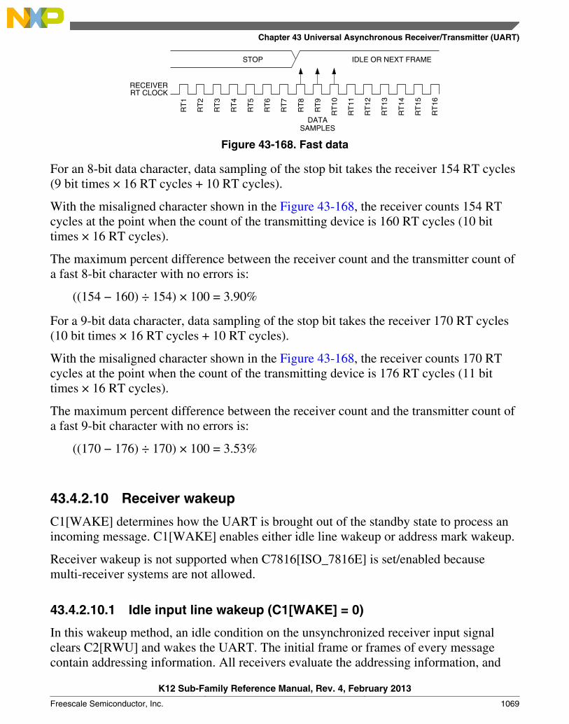
RECEIVERRT CLOCK
STOP IDLE OR NEXT FRAME
DATASAMPLES
RT
16
RT
15
RT
14
RT
13
RT
12
RT
11
RT
10
RT
9
RT
8
RT
7
RT
6
RT
5
RT
4
RT
3
RT
2
RT
1
Figure 43-168. Fast data
For an 8-bit data character, data sampling of the stop bit takes the receiver 154 RT cycles(9 bit times × 16 RT cycles + 10 RT cycles).
With the misaligned character shown in the Figure 43-168, the receiver counts 154 RTcycles at the point when the count of the transmitting device is 160 RT cycles (10 bittimes × 16 RT cycles).
The maximum percent difference between the receiver count and the transmitter count ofa fast 8-bit character with no errors is:
((154 − 160) ÷ 154) × 100 = 3.90%
For a 9-bit data character, data sampling of the stop bit takes the receiver 170 RT cycles(10 bit times × 16 RT cycles + 10 RT cycles).
With the misaligned character shown in the Figure 43-168, the receiver counts 170 RTcycles at the point when the count of the transmitting device is 176 RT cycles (11 bittimes × 16 RT cycles).
The maximum percent difference between the receiver count and the transmitter count ofa fast 9-bit character with no errors is:
((170 − 176) ÷ 170) × 100 = 3.53%
43.4.2.10 Receiver wakeup
C1[WAKE] determines how the UART is brought out of the standby state to process anincoming message. C1[WAKE] enables either idle line wakeup or address mark wakeup.
Receiver wakeup is not supported when C7816[ISO_7816E] is set/enabled becausemulti-receiver systems are not allowed.
43.4.2.10.1 Idle input line wakeup (C1[WAKE] = 0)
In this wakeup method, an idle condition on the unsynchronized receiver input signalclears C2[RWU] and wakes the UART. The initial frame or frames of every messagecontain addressing information. All receivers evaluate the addressing information, and
Chapter 43 Universal Asynchronous Receiver/Transmitter (UART)
K12 Sub-Family Reference Manual, Rev. 4, February 2013
Freescale Semiconductor, Inc. 1069

receivers for which the message is addressed process the frames that follow. Any receiverfor which a message is not addressed can set its C2[RWU] and return to the standby state.C2[RWU] remains set and the receiver remains in standby until another idle characterappears on the unsynchronized receiver input signal.
Idle line wakeup requires that messages be separated by at least one idle character andthat no message contains idle characters.
When C2[RWU] is 1 and S2[RWUID] is 0, the idle character that wakes the receiverdoes not set S1[IDLE] or the receive data register full flag, S1[RDRF]. The receiverwakes and waits for the first data character of the next message which is stored in thereceive data buffer. When S2[RWUID] and C2[RWU] are set and C1[WAKE] is cleared,any idle condition sets S1[IDLE] and generates an interrupt if enabled.
Idle input line wakeup is not supported when C7816[ISO_7816E] is set/enabled.
43.4.2.10.2 Address mark wakeup (C1[WAKE] = 1)
In this wakeup method, a logic 1 in the bit position immediately preceding the stop bit ofa frame clears C2[RWU] and wakes the UART. A logic 1 in the bit position immediatelypreceeding the stop bit marks a frame as an address frame that contains addressinginformation. All receivers evaluate the addressing information, and the receivers forwhich the message is addressed process the frames that follow. Any receiver for which amessage is not addressed can set its C2[RWU] and return to the standby state. C2[RWU]remains set and the receiver remains in standby until another address frame appears onthe unsynchronized receiver input signal.
A logic 1 in the bit position immediately preceding the stop bit clears the receiver'sC2[RWU] before the stop bit is received and places the received data into the receiverdata buffer.
Address mark wakeup allows messages to contain idle characters but requires that the bitposition immediately preceding the stop bit be reserved for use in address frames.
If module is in standby mode and nothing triggers to wake the UART, no error flag is seteven if an invalid error condition is detected on the receiving data line.
Address mark wakeup is not supported when C7816[ISO_7816E] is set/enabled.
43.4.2.10.3 Match address operation
Match address operation is enabled when C4[MAEN1] or C4[MAEN2] is set. In thisfunction, a frame received by the RX pin with a logic 1 in the bit position immediatelypreceding the stop bit is considered an address and is compared with the associated MA1or MA2 register. The frame is transferred to the receive buffer, and S1[RDRF] is set, only
Functional description
K12 Sub-Family Reference Manual, Rev. 4, February 2013
1070 Freescale Semiconductor, Inc.

if the comparison matches. All subsequent frames received with a logic 0 in the bitposition immediately preceding the stop bit are considered to be data associated with theaddress and are transferred to the receive data buffer. If no marked address match occurs,then no transfer is made to the receive data buffer, and all following frames with logic 0in the bit position immediately preceding the stop bit are also discarded. If bothC4[MAEN1] and C4[MAEN2] are negated, the receiver operates normally and all datareceived is transferred to the receive data buffer.
Match address operation functions in the same way for both MA1 and MA2 registers.
• If only one of C4[MAEN1] and C4[MAEN2] is asserted, a marked address iscompared only with the associated match register and data is transferred to thereceive data buffer only on a match.
• If C4[MAEN1] and C4[MAEN2] are asserted, a marked address is compared withboth match registers and data is transferred only on a match with either register.
Address match operation is not supported when C7816[ISO_7816E] is set/enabled.
43.4.3 Baud rate generation
A 13-bit modulus counter and a 5-bit fractional fine-adjust counter in the baud rategenerator derive the baud rate for both the receiver and the transmitter. The value from 1to 8191 written to SBR[12:0] determines the module clock divisor. The SBR bits are inthe UART baud rate registers, BDH and BDL. The baud rate clock is synchronized withthe module clock and drives the receiver. The fractional fine-adjust counter addsfractional delays to the baud rate clock to allow fine trimming of the baud rate to matchthe system baud rate. The transmitter is driven by the baud rate clock divided by 16. Thereceiver has an acquisition rate of 16 samples per bit time.
Baud rate generation is subject to two sources of error:
• Integer division of the module clock may not give the exact target frequency. Thiserror can be reduced with the fine-adjust counter.
• Synchronization with the module clock can cause phase shift.
The Table 43-168 lists the available baud divisor fine adjust values.
UART baud rate = UART module clock / (16 × (SBR[12:0] + BRFD))
The following table lists some examples of achieving target baud rates with a moduleclock frequency of 10.2 MHz, with and without fractional fine adjustment.
Chapter 43 Universal Asynchronous Receiver/Transmitter (UART)
K12 Sub-Family Reference Manual, Rev. 4, February 2013
Freescale Semiconductor, Inc. 1071

Table 43-168. Baud rates (example: module clock = 10.2 MHz)
Bits
SBR
(decimal)
Bits
BRFABRFD value
Receiver
clock (Hz)
Transmitter
clock (Hz)
Target Baudrate
Error
(%)
17 00000 0 600,000.0 37,500.0 38,400 2.3
16 10011 19/32=0.59375 614,689.3 38,418.08 38,400 0.047
33 00000 0 309,090.9 19,318.2 19,200 0.62
33 00110 6/32=0.1875 307,344.6 19,209.04 19,200 0.047
66 00000 0 154,545.5 9659.1 9600 0.62
133 00000 0 76,691.7 4793.2 4800 0.14
266 00000 0 38,345.9 2396.6 2400 0.14
531 00000 0 19,209.0 1200.6 1200 0.11
1062 00000 0 9604.5 600.3 600 0.05
2125 00000 0 4800.0 300.0 300 0.00
4250 00000 0 2400.0 150.0 150 0.00
5795 00000 0 1760.1 110.0 110 0.00
Table 43-169. Baud rate fine adjust
BRFA Baud Rate Fractional Divisor (BRFD)
0 0 0 0 0 0/32 = 0
0 0 0 0 1 1/32 = 0.03125
0 0 0 1 0 2/32 = 0.0625
0 0 0 1 1 3/32 = 0.09375
0 0 1 0 0 4/32 = 0.125
0 0 1 0 1 5/32 = 0.15625
0 0 1 1 0 6/32 = 0.1875
0 0 1 1 1 7/32 = 0.21875
0 1 0 0 0 8/32 = 0.25
0 1 0 0 1 9/32 = 0.28125
0 1 0 1 0 10/32 = 0.3125
0 1 0 1 1 11/32 = 0.34375
0 1 1 0 0 12/32 = 0.375
0 1 1 0 1 13/32 = 0.40625
0 1 1 1 0 14/32 = 0.4375
0 1 1 1 1 15/32 = 0.46875
1 0 0 0 0 16/32 = 0.5
1 0 0 0 1 17/32 = 0.53125
1 0 0 1 0 18/32 = 0.5625
1 0 0 1 1 19/32 = 0.59375
1 0 1 0 0 20/32 = 0.625
Table continues on the next page...
Functional description
K12 Sub-Family Reference Manual, Rev. 4, February 2013
1072 Freescale Semiconductor, Inc.
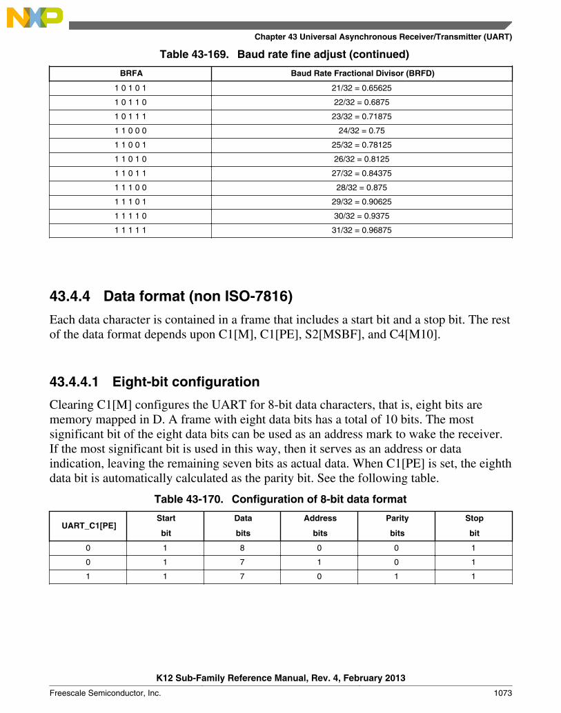
Table 43-169. Baud rate fine adjust (continued)
BRFA Baud Rate Fractional Divisor (BRFD)
1 0 1 0 1 21/32 = 0.65625
1 0 1 1 0 22/32 = 0.6875
1 0 1 1 1 23/32 = 0.71875
1 1 0 0 0 24/32 = 0.75
1 1 0 0 1 25/32 = 0.78125
1 1 0 1 0 26/32 = 0.8125
1 1 0 1 1 27/32 = 0.84375
1 1 1 0 0 28/32 = 0.875
1 1 1 0 1 29/32 = 0.90625
1 1 1 1 0 30/32 = 0.9375
1 1 1 1 1 31/32 = 0.96875
43.4.4 Data format (non ISO-7816)
Each data character is contained in a frame that includes a start bit and a stop bit. The restof the data format depends upon C1[M], C1[PE], S2[MSBF], and C4[M10].
43.4.4.1 Eight-bit configuration
Clearing C1[M] configures the UART for 8-bit data characters, that is, eight bits arememory mapped in D. A frame with eight data bits has a total of 10 bits. The mostsignificant bit of the eight data bits can be used as an address mark to wake the receiver.If the most significant bit is used in this way, then it serves as an address or dataindication, leaving the remaining seven bits as actual data. When C1[PE] is set, the eighthdata bit is automatically calculated as the parity bit. See the following table.
Table 43-170. Configuration of 8-bit data format
UART_C1[PE]Start
bit
Data
bits
Address
bits
Parity
bits
Stop
bit
0 1 8 0 0 1
0 1 7 1 0 1
1 1 7 0 1 1
Chapter 43 Universal Asynchronous Receiver/Transmitter (UART)
K12 Sub-Family Reference Manual, Rev. 4, February 2013
Freescale Semiconductor, Inc. 1073
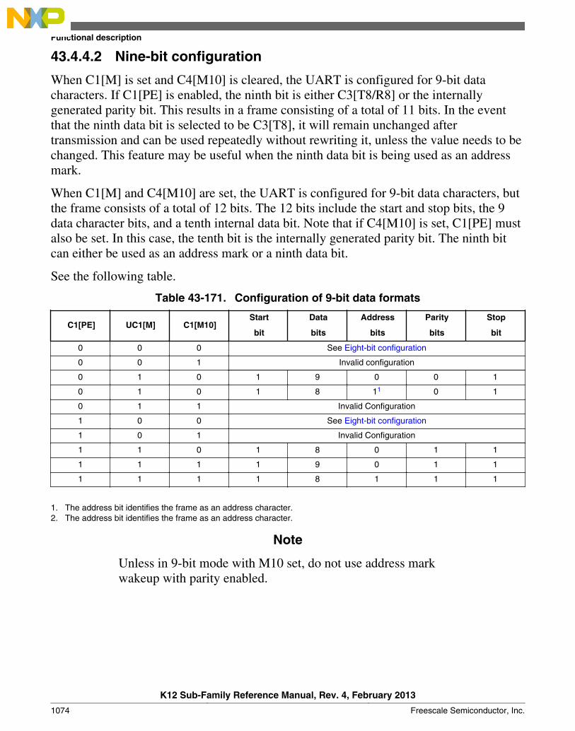
43.4.4.2 Nine-bit configuration
When C1[M] is set and C4[M10] is cleared, the UART is configured for 9-bit datacharacters. If C1[PE] is enabled, the ninth bit is either C3[T8/R8] or the internallygenerated parity bit. This results in a frame consisting of a total of 11 bits. In the eventthat the ninth data bit is selected to be C3[T8], it will remain unchanged aftertransmission and can be used repeatedly without rewriting it, unless the value needs to bechanged. This feature may be useful when the ninth data bit is being used as an addressmark.
When C1[M] and C4[M10] are set, the UART is configured for 9-bit data characters, butthe frame consists of a total of 12 bits. The 12 bits include the start and stop bits, the 9data character bits, and a tenth internal data bit. Note that if C4[M10] is set, C1[PE] mustalso be set. In this case, the tenth bit is the internally generated parity bit. The ninth bitcan either be used as an address mark or a ninth data bit.
See the following table.
Table 43-171. Configuration of 9-bit data formats
C1[PE] UC1[M] C1[M10]Start
bit
Data
bits
Address
bits
Parity
bits
Stop
bit
0 0 0 See Eight-bit configuration
0 0 1 Invalid configuration
0 1 0 1 9 0 0 1
0 1 0 1 8 11 0 1
0 1 1 Invalid Configuration
1 0 0 See Eight-bit configuration
1 0 1 Invalid Configuration
1 1 0 1 8 0 1 1
1 1 1 1 9 0 1 1
1 1 1 1 8 1 1 1
1. The address bit identifies the frame as an address character.2. The address bit identifies the frame as an address character.
Note
Unless in 9-bit mode with M10 set, do not use address markwakeup with parity enabled.
Functional description
K12 Sub-Family Reference Manual, Rev. 4, February 2013
1074 Freescale Semiconductor, Inc.
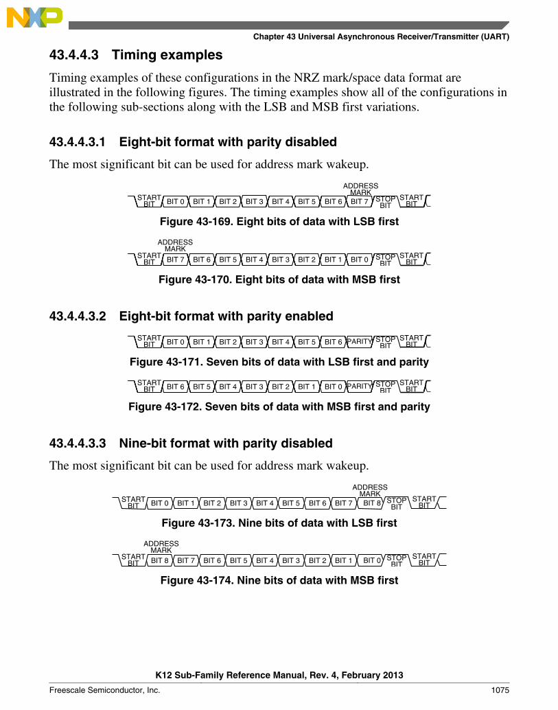
43.4.4.3 Timing examples
Timing examples of these configurations in the NRZ mark/space data format areillustrated in the following figures. The timing examples show all of the configurations inthe following sub-sections along with the LSB and MSB first variations.
43.4.4.3.1 Eight-bit format with parity disabled
The most significant bit can be used for address mark wakeup.
BIT 0 BIT 1 BIT 2 BIT 3 BIT 4 BIT 5 BIT 6 BIT 7 STOPBIT
ADDRESSMARK
STARTBIT
STARTBIT
Figure 43-169. Eight bits of data with LSB first
BIT 7 BIT 6 BIT 5 BIT 4 BIT 3 BIT 2 BIT 1 BIT 0 STOPBIT
ADDRESSMARK
STARTBIT
STARTBIT
Figure 43-170. Eight bits of data with MSB first
43.4.4.3.2 Eight-bit format with parity enabled
BIT 0 BIT 1 BIT 2 BIT 3 BIT 4 BIT 5 BIT 6 STOPBIT
STARTBIT
STARTBIT PARITY
Figure 43-171. Seven bits of data with LSB first and parity
BIT 6 BIT 5 BIT 4 BIT 3 BIT 2 BIT 1 BIT 0 STOPBIT
STARTBIT
STARTBIT PARITY
Figure 43-172. Seven bits of data with MSB first and parity
43.4.4.3.3 Nine-bit format with parity disabled
The most significant bit can be used for address mark wakeup.
BIT 0 BIT 1 BIT 2 BIT 3 BIT 4 BIT 5 BIT 6 BIT 7 BIT 8 STOPBIT
ADDRESSMARK
STARTBIT
STARTBIT
Figure 43-173. Nine bits of data with LSB first
BIT 8 BIT 7 BIT 6 BIT 5 BIT 4 BIT 3 BIT 2 BIT 1 BIT 0 STOPBIT
ADDRESSMARK
STARTBIT
STARTBIT
Figure 43-174. Nine bits of data with MSB first
Chapter 43 Universal Asynchronous Receiver/Transmitter (UART)
K12 Sub-Family Reference Manual, Rev. 4, February 2013
Freescale Semiconductor, Inc. 1075
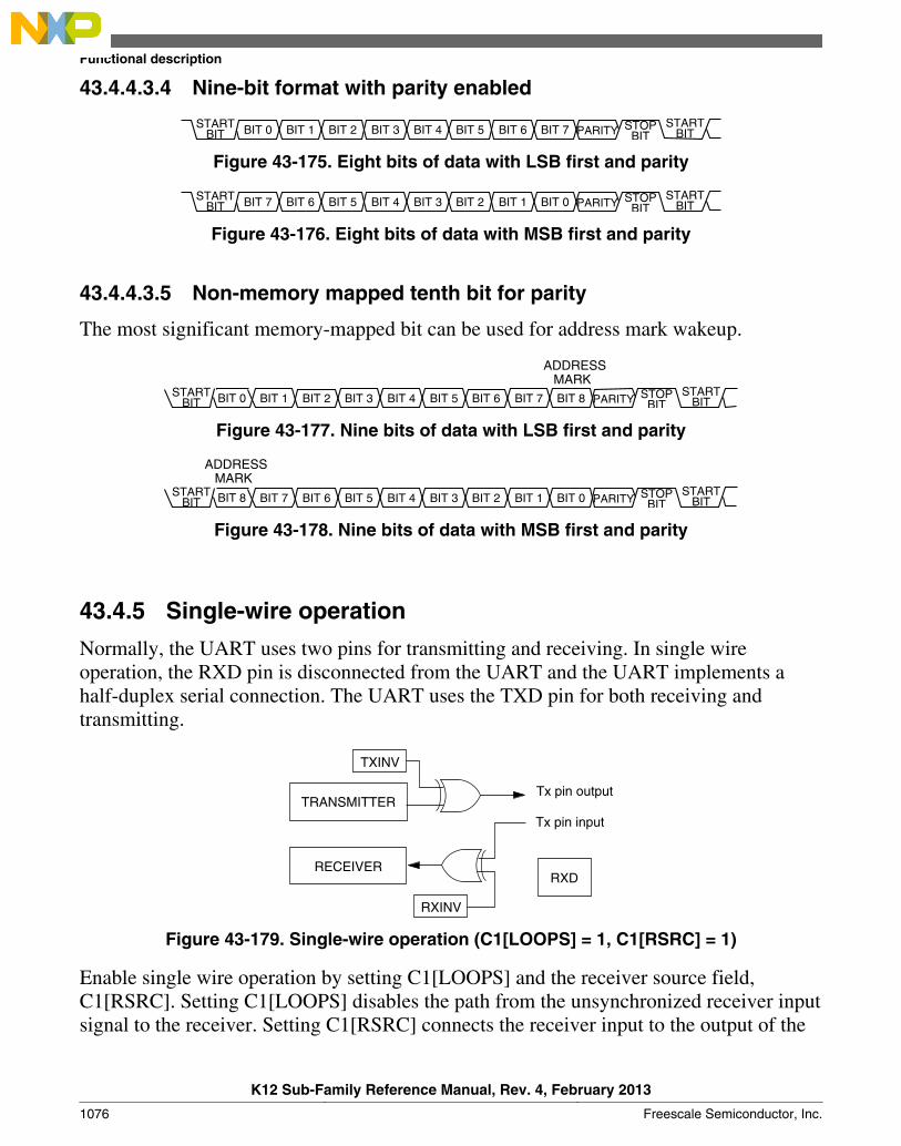
43.4.4.3.4 Nine-bit format with parity enabled
BIT 0 BIT 1 BIT 2 BIT 3 BIT 4 BIT 5 BIT 6 BIT 7 PARITY STOPBIT
STARTBIT
STARTBIT
Figure 43-175. Eight bits of data with LSB first and parity
BIT 7 BIT 6 BIT 5 BIT 4 BIT 3 BIT 2 BIT 1 BIT 0 PARITY STOPBIT
STARTBIT
STARTBIT
Figure 43-176. Eight bits of data with MSB first and parity
43.4.4.3.5 Non-memory mapped tenth bit for parity
The most significant memory-mapped bit can be used for address mark wakeup.
BIT 1 BIT 2 BIT 3 BIT 4 BIT 5 BIT 6 BIT 7 BIT 8 PARITY STOPBIT
STARTBIT
STARTBIT BIT 0
ADDRESSMARK
Figure 43-177. Nine bits of data with LSB first and parity
BIT 7 BIT 6 BIT 5 BIT 4 BIT 3 BIT 2 BIT 1 BIT 0 PARITY STOPBIT
STARTBIT
STARTBIT BIT 8
ADDRESSMARK
Figure 43-178. Nine bits of data with MSB first and parity
43.4.5 Single-wire operation
Normally, the UART uses two pins for transmitting and receiving. In single wireoperation, the RXD pin is disconnected from the UART and the UART implements ahalf-duplex serial connection. The UART uses the TXD pin for both receiving andtransmitting.
RXD
Tx pin input
Tx pin output
TXINV
TRANSMITTER
RECEIVER
RXINV
Figure 43-179. Single-wire operation (C1[LOOPS] = 1, C1[RSRC] = 1)
Enable single wire operation by setting C1[LOOPS] and the receiver source field,C1[RSRC]. Setting C1[LOOPS] disables the path from the unsynchronized receiver inputsignal to the receiver. Setting C1[RSRC] connects the receiver input to the output of the
Functional description
K12 Sub-Family Reference Manual, Rev. 4, February 2013
1076 Freescale Semiconductor, Inc.

TXD pin driver. Both the transmitter and receiver must be enabled (C2[TE] = 1 andC2[RE] = 1). When C7816[ISO_7816EN] is set, it is not required that both C2[TE] andC2[RE] are set.
43.4.6 Loop operation
In loop operation, the transmitter output goes to the receiver input. The unsynchronizedreceiver input signal is disconnected from the UART.
RXD
Tx pin output
RXINV
TXINV
TRANSMITTER
RECEIVER
Figure 43-180. Loop operation (C1[LOOPS] = 1, C1[RSRC] = 0)
Enable loop operation by setting C1[LOOPS] and clearing C1[RSRC]. SettingC1[LOOPS] disables the path from the unsynchronized receiver input signal to thereceiver. Clearing C1[RSRC] connects the transmitter output to the receiver input. Boththe transmitter and receiver must be enabled (C2[TE] = 1 and C2[RE] = 1). WhenC7816[ISO_7816EN] is set, it is not required that both C2[TE] and C2[RE] are set.
43.4.7 ISO-7816/smartcard support
The UART provides mechanisms to support the ISO-7816 protocol that is commonlyused to interface with smartcards. The ISO-7816 protocol is an NRZ, single wire, half-duplex interface. The TxD pin is used in open-drain mode because the data signal is usedfor both transmitting and receiving. There are multiple subprotocols within the ISO-7816standard. The UART supports both T = 0 and T = 1 protocols. The module also providesfor automated initial character detection and configuration, which allows for support ofboth direct convention and inverse convention data formats. A variety of interruptsspecific to 7816 are provided in addition to the general interrupts to assist software.Additionally, the module is able to provide automated NACK responses and hasprogrammed automated retransmission of failed packets. An assortment of programmabletimeouts and guard band times are also supported.
The term elemental time unit (ETU) is frequently used in the context of ISO-7816. Thisconcept is used to relate the frequency that the system (UART) is running at and thefrequency that data is being transmitted and received. One ETU represents the time it
Chapter 43 Universal Asynchronous Receiver/Transmitter (UART)
K12 Sub-Family Reference Manual, Rev. 4, February 2013
Freescale Semiconductor, Inc. 1077
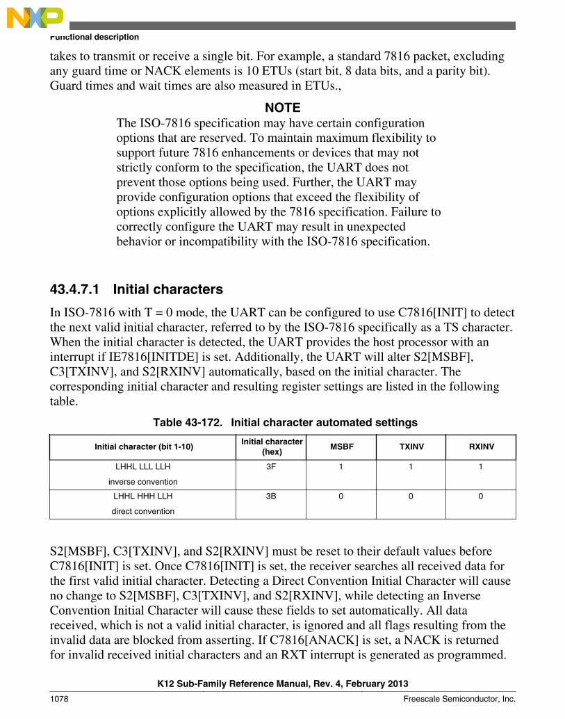
takes to transmit or receive a single bit. For example, a standard 7816 packet, excludingany guard time or NACK elements is 10 ETUs (start bit, 8 data bits, and a parity bit).Guard times and wait times are also measured in ETUs.,
NOTEThe ISO-7816 specification may have certain configurationoptions that are reserved. To maintain maximum flexibility tosupport future 7816 enhancements or devices that may notstrictly conform to the specification, the UART does notprevent those options being used. Further, the UART mayprovide configuration options that exceed the flexibility ofoptions explicitly allowed by the 7816 specification. Failure tocorrectly configure the UART may result in unexpectedbehavior or incompatibility with the ISO-7816 specification.
43.4.7.1 Initial characters
In ISO-7816 with T = 0 mode, the UART can be configured to use C7816[INIT] to detectthe next valid initial character, referred to by the ISO-7816 specifically as a TS character.When the initial character is detected, the UART provides the host processor with aninterrupt if IE7816[INITDE] is set. Additionally, the UART will alter S2[MSBF],C3[TXINV], and S2[RXINV] automatically, based on the initial character. Thecorresponding initial character and resulting register settings are listed in the followingtable.
Table 43-172. Initial character automated settings
Initial character (bit 1-10)Initial character
(hex)MSBF TXINV RXINV
LHHL LLL LLH
inverse convention
3F 1 1 1
LHHL HHH LLH
direct convention
3B 0 0 0
S2[MSBF], C3[TXINV], and S2[RXINV] must be reset to their default values beforeC7816[INIT] is set. Once C7816[INIT] is set, the receiver searches all received data forthe first valid initial character. Detecting a Direct Convention Initial Character will causeno change to S2[MSBF], C3[TXINV], and S2[RXINV], while detecting an InverseConvention Initial Character will cause these fields to set automatically. All datareceived, which is not a valid initial character, is ignored and all flags resulting from theinvalid data are blocked from asserting. If C7816[ANACK] is set, a NACK is returnedfor invalid received initial characters and an RXT interrupt is generated as programmed.
Functional description
K12 Sub-Family Reference Manual, Rev. 4, February 2013
1078 Freescale Semiconductor, Inc.
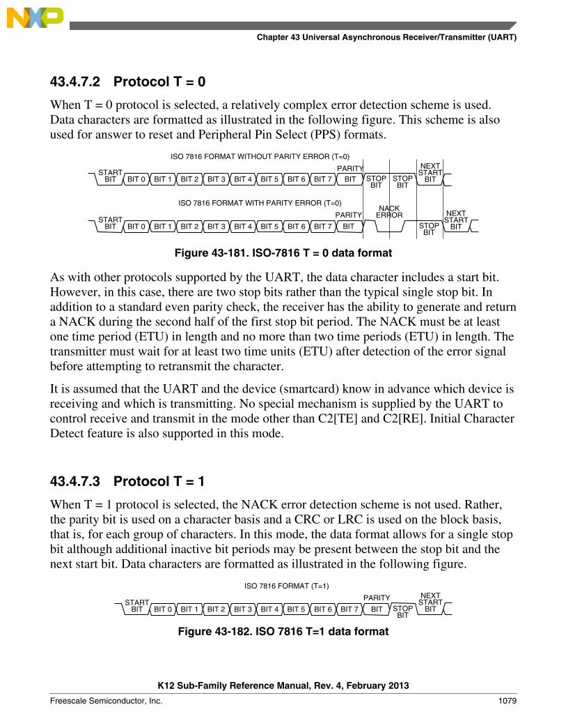
43.4.7.2 Protocol T = 0
When T = 0 protocol is selected, a relatively complex error detection scheme is used.Data characters are formatted as illustrated in the following figure. This scheme is alsoused for answer to reset and Peripheral Pin Select (PPS) formats.
BIT 0 BIT 1 BIT 2 BIT 3 BIT 4 BIT 5 BIT 6 BIT 7 BIT STOPBIT
PARITY NEXTSTART
BITSTART
BIT
ISO 7816 FORMAT WITHOUT PARITY ERROR (T=0)
STOPBIT
BIT 0 BIT 1 BIT 2 BIT 3 BIT 4 BIT 5 BIT 6 BIT 7 BIT STOPBIT
PARITY NEXTSTART
BITSTART
BIT
NACKERROR
ISO 7816 FORMAT WITH PARITY ERROR (T=0)
Figure 43-181. ISO-7816 T = 0 data format
As with other protocols supported by the UART, the data character includes a start bit.However, in this case, there are two stop bits rather than the typical single stop bit. Inaddition to a standard even parity check, the receiver has the ability to generate and returna NACK during the second half of the first stop bit period. The NACK must be at leastone time period (ETU) in length and no more than two time periods (ETU) in length. Thetransmitter must wait for at least two time units (ETU) after detection of the error signalbefore attempting to retransmit the character.
It is assumed that the UART and the device (smartcard) know in advance which device isreceiving and which is transmitting. No special mechanism is supplied by the UART tocontrol receive and transmit in the mode other than C2[TE] and C2[RE]. Initial CharacterDetect feature is also supported in this mode.
43.4.7.3 Protocol T = 1
When T = 1 protocol is selected, the NACK error detection scheme is not used. Rather,the parity bit is used on a character basis and a CRC or LRC is used on the block basis,that is, for each group of characters. In this mode, the data format allows for a single stopbit although additional inactive bit periods may be present between the stop bit and thenext start bit. Data characters are formatted as illustrated in the following figure.
BIT 0 BIT 1 BIT 2 BIT 3 BIT 4 BIT 5 BIT 6 BIT 7 BIT STOPBIT
PARITY NEXTSTART
BITSTART
BIT
ISO 7816 FORMAT (T=1)
Figure 43-182. ISO 7816 T=1 data format
Chapter 43 Universal Asynchronous Receiver/Transmitter (UART)
K12 Sub-Family Reference Manual, Rev. 4, February 2013
Freescale Semiconductor, Inc. 1079
The smallest data unit that is transferred is a block. A block is made up of several datacharacters and may vary in size depending on the block type. The UART does notprovide a mechanism to decode the block type. As part of the block, an LRC or CRC isincluded. The UART does not calculate the CRC or LRC for transmitted blocks, nor doesit verify the validity of the CRC or LRC for received blocks. The 7816 protocol requiresthat the initiator and the smartcard (device) takes alternate turns in transmitting andreceiving blocks. When the UART detects that the last character in a block has beentransmitted it will automatically clear C2[TE] and enter receive mode. Therefore, thesoftware must program the transmit buffer with the next data to be transmitted, and thenenable C2[TE], once the software has determined that the last character of the receivedblock has been received. The UART detects that the last character of the transmit blockhas been sent when TL7816[TLEN] = 0 and four additional characters have been sent.The four additional characters are made up of three prior to TL7816[TLEN]decrementing (prologue) and one after TL7816[TLEN] = 0, the final character of theepilogue.
43.4.7.4 Wait time and guard time parameters
The ISO-7816 specification defines several wait time and guard time parameters. TheUART allows for flexible configuration and violation detection of these settings. Onreset, the wait time (IS7816[WT]) defaults to 9600 ETUs and guard time (GT) to 12ETUs. These values are controlled by parameters in the WP7816, WN7816, and WF7816registers. Additionally, the value of C7816[TTYPE] also factors into the calculation. Theformulae used to calculate the number ETUs for each wait time and guard time value areshown in Table 43-173.
Wait time (WT) is defined as the maximum allowable time between the leading edge of acharacter transmitted by the smartcard device and the leading edge of the previouscharacter that was transmitted by the UART or the device. Similarly, character wait time(CWT) is defined as the maximum allowable time between the leading edge of twocharacters within the same block. Block wait time (BWT) is defined as the maximumtime between the leading edge character of the last block received by the smartcarddevice and the leading edge of the first character transmitted by the smartcard device.
Guard time (GT) is defined as the minimum allowable time between the leading edge oftwo consecutive characters. Character guard time (CGT) is the minimum allowable timebetween the leading edges of two consecutive characters in the same direction, that is,transmission or reception. Block guard time (BGT) is the minimum allowable timebetween the leading edges of two consecutive characters in opposite directions, that is,transmission then reception or reception then transmission.
Functional description
K12 Sub-Family Reference Manual, Rev. 4, February 2013
1080 Freescale Semiconductor, Inc.
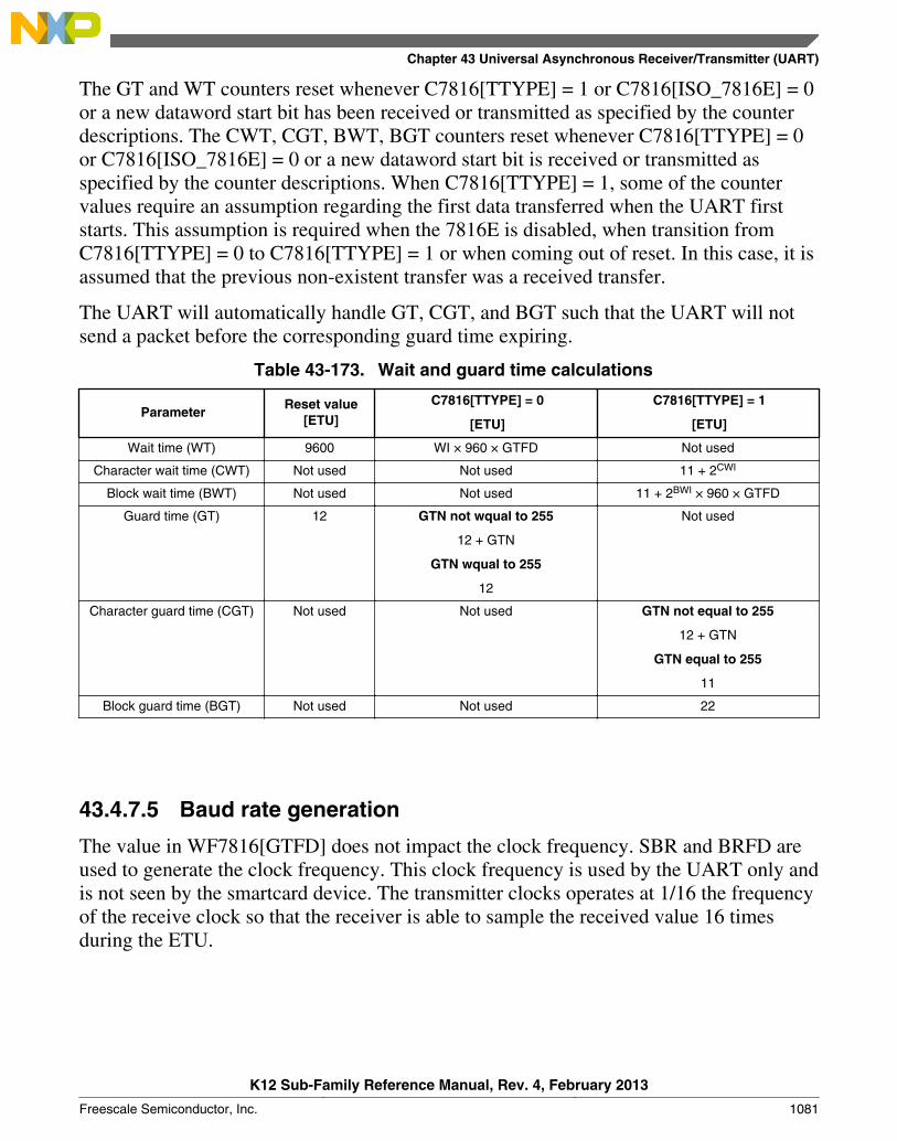
The GT and WT counters reset whenever C7816[TTYPE] = 1 or C7816[ISO_7816E] = 0or a new dataword start bit has been received or transmitted as specified by the counterdescriptions. The CWT, CGT, BWT, BGT counters reset whenever C7816[TTYPE] = 0or C7816[ISO_7816E] = 0 or a new dataword start bit is received or transmitted asspecified by the counter descriptions. When C7816[TTYPE] = 1, some of the countervalues require an assumption regarding the first data transferred when the UART firststarts. This assumption is required when the 7816E is disabled, when transition fromC7816[TTYPE] = 0 to C7816[TTYPE] = 1 or when coming out of reset. In this case, it isassumed that the previous non-existent transfer was a received transfer.
The UART will automatically handle GT, CGT, and BGT such that the UART will notsend a packet before the corresponding guard time expiring.
Table 43-173. Wait and guard time calculations
ParameterReset value
[ETU]
C7816[TTYPE] = 0
[ETU]
C7816[TTYPE] = 1
[ETU]
Wait time (WT) 9600 WI × 960 × GTFD Not used
Character wait time (CWT) Not used Not used 11 + 2CWI
Block wait time (BWT) Not used Not used 11 + 2BWI × 960 × GTFD
Guard time (GT) 12 GTN not wqual to 255
12 + GTN
GTN wqual to 255
12
Not used
Character guard time (CGT) Not used Not used GTN not equal to 255
12 + GTN
GTN equal to 255
11
Block guard time (BGT) Not used Not used 22
43.4.7.5 Baud rate generation
The value in WF7816[GTFD] does not impact the clock frequency. SBR and BRFD areused to generate the clock frequency. This clock frequency is used by the UART only andis not seen by the smartcard device. The transmitter clocks operates at 1/16 the frequencyof the receive clock so that the receiver is able to sample the received value 16 timesduring the ETU.
Chapter 43 Universal Asynchronous Receiver/Transmitter (UART)
K12 Sub-Family Reference Manual, Rev. 4, February 2013
Freescale Semiconductor, Inc. 1081
43.4.7.6 UART restrictions in ISO-7816 operation
Due to the flexibility of the UART module, there are several features and interrupts thatare not supported while running in ISO-7816 mode. These restrictions are documentedwithin the register field definitions.
43.4.8 Infrared interface
The UART provides the capability of transmitting narrow pulses to an IR LED andreceiving narrow pulses and transforming them to serial bits, which are sent to theUART. The IrDA physical layer specification defines a half-duplex infraredcommunication link for exchanging data. The full standard includes data rates up to 16Mbits/s. This design covers data rates only between 2.4 kbits/s and 115.2 kbits/s.
The UART has an infrared transmit encoder and receive decoder. The UART transmitsserial bits of data that are encoded by the infrared submodule to transmit a narrow pulsefor every zero bit. No pulse is transmitted for every one bit. When receiving data, the IRpulses are detected using an IR photo diode and transformed to CMOS levels by the IRreceive decoder, external from the MCU. The narrow pulses are then stretched by theinfrared receive decoder to get back to a serial bit stream to be received by the UART.The polarity of transmitted pulses and expected receive pulses can be inverted so that adirect connection can be made to external IrDA transceiver modules that use active lowpulses.
The infrared submodule receives its clock sources from the UART. One of these twoclocks are selected in the infrared submodule to generate either 3/16, 1/16, 1/32, or 1/4narrow pulses during transmission.
43.4.8.1 Infrared transmit encoder
The infrared transmit encoder converts serial bits of data from transmit shift register tothe TXD signal. A narrow pulse is transmitted for a zero bit and no pulse for a one bit.The narrow pulse is sent in the middle of the bit with a duration of 1/32, 1/16, 3/16, or 1/4of a bit time. A narrow high pulse is transmitted for a zero bit when C3[TXINV] iscleared, while a narrow low pulse is transmitted for a zero bit when C3[TXINV] is set.
Functional description
K12 Sub-Family Reference Manual, Rev. 4, February 2013
1082 Freescale Semiconductor, Inc.

43.4.8.2 Infrared receive decoder
The infrared receive block converts data from the RXD signal to the receive shift register.A narrow pulse is expected for each zero received and no pulse is expected for each onereceived. A narrow high pulse is expected for a zero bit when S2[RXINV] is cleared,while a narrow low pulse is expected for a zero bit when S2[RXINV] is set. This receivedecoder meets the edge jitter requirement as defined by the IrDA serial infrared physicallayer specification.
43.5 ResetAll registers reset to a particular value are indicated in Memory map and registers.
43.6 System level interrupt sourcesThere are several interrupt signals that are sent from the UART. The following table liststhe interrupt sources generated by the UART. The local enables for the UART interruptsources are described in this table. Details regarding the individual operation of eachinterrupt are contained under various sub-sections of Memory map and registers.However, RXEDGIF description also outlines additional details regarding the RXEDGIFinterrupt because of its complexity of operation. Any of the UART interrupt requestslisted in the table can be used to bring the CPU out of Wait mode.
Table 43-174. UART interrupt sources
Interrupt Source Flag Local enable DMA select
Transmitter TDRE TIE TDMAS = 0
Transmitter TC TCIE -
Receiver IDLE ILIE -
Receiver RDRF RIE RDMAS = 0
Receiver LBKDIF LBKDIE -
Receiver RXEDGIF RXEDGIE -
Receiver OR ORIE -
Receiver NF NEIE -
Receiver FE FEIE -
Receiver PF PEIE -
Receiver RXUF RXUFE -
Transmitter TXOF TXOFE -
Receiver WT WTWE -
Receiver CWT CWTE -
Table continues on the next page...
Chapter 43 Universal Asynchronous Receiver/Transmitter (UART)
K12 Sub-Family Reference Manual, Rev. 4, February 2013
Freescale Semiconductor, Inc. 1083
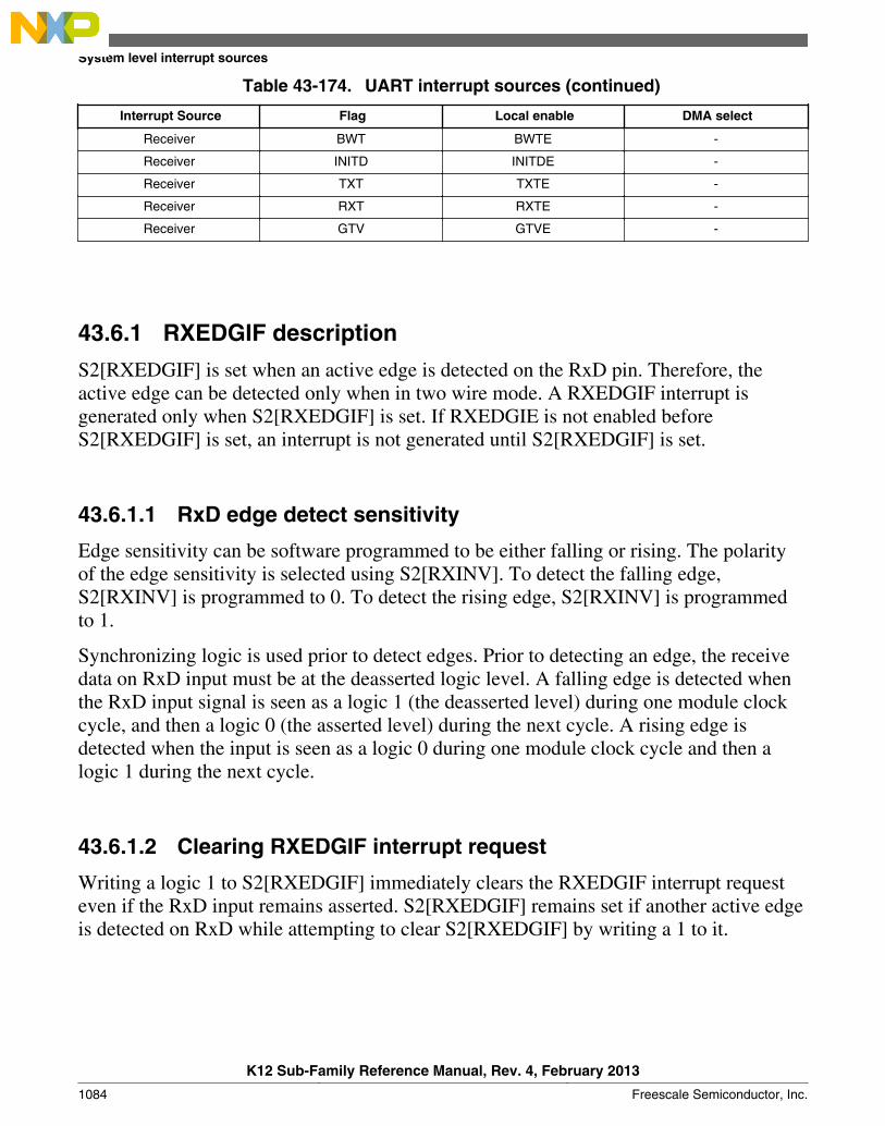
Table 43-174. UART interrupt sources (continued)
Interrupt Source Flag Local enable DMA select
Receiver BWT BWTE -
Receiver INITD INITDE -
Receiver TXT TXTE -
Receiver RXT RXTE -
Receiver GTV GTVE -
43.6.1 RXEDGIF description
S2[RXEDGIF] is set when an active edge is detected on the RxD pin. Therefore, theactive edge can be detected only when in two wire mode. A RXEDGIF interrupt isgenerated only when S2[RXEDGIF] is set. If RXEDGIE is not enabled beforeS2[RXEDGIF] is set, an interrupt is not generated until S2[RXEDGIF] is set.
43.6.1.1 RxD edge detect sensitivity
Edge sensitivity can be software programmed to be either falling or rising. The polarityof the edge sensitivity is selected using S2[RXINV]. To detect the falling edge,S2[RXINV] is programmed to 0. To detect the rising edge, S2[RXINV] is programmedto 1.
Synchronizing logic is used prior to detect edges. Prior to detecting an edge, the receivedata on RxD input must be at the deasserted logic level. A falling edge is detected whenthe RxD input signal is seen as a logic 1 (the deasserted level) during one module clockcycle, and then a logic 0 (the asserted level) during the next cycle. A rising edge isdetected when the input is seen as a logic 0 during one module clock cycle and then alogic 1 during the next cycle.
43.6.1.2 Clearing RXEDGIF interrupt request
Writing a logic 1 to S2[RXEDGIF] immediately clears the RXEDGIF interrupt requesteven if the RxD input remains asserted. S2[RXEDGIF] remains set if another active edgeis detected on RxD while attempting to clear S2[RXEDGIF] by writing a 1 to it.
System level interrupt sources
K12 Sub-Family Reference Manual, Rev. 4, February 2013
1084 Freescale Semiconductor, Inc.
43.6.1.3 Exit from low-power modes
The receive input active edge detect circuit is still active on low power modes (Wait andStop). An active edge on the receive input brings the CPU out of low power mode if theinterrupt is not masked (S2[RXEDGIF] = 1).
43.7 DMA operationIn the transmitter, S1[TDRE] can be configured to assert a DMA transfer request. In thereceiver, S1[RDRF], can be configured to assert a DMA transfer request. The followingtable shows the configuration field settings required to configure each flag for DMAoperation.
Table 43-175. DMA configuration
Flag Request enable bit DMA select bit
TDRE TIE = 1 TDMAS = 1
RDRF RIE = 1 RDMAS = 1
When a flag is configured for a DMA request, its associated DMA request is assertedwhen the flag is set. When S1[RDRF] is configured as a DMA request, the clearingmechanism of reading S1, followed by reading D, does not clear the associated flag. TheDMA request remains asserted until an indication is received that the DMA transactionsare done. When this indication is received, the flag bit and the associated DMA request iscleared. If the DMA operation failed to remove the situation that caused the DMArequest, another request is issued.
43.8 Application informationThis section describes the UART application information.
43.8.1 Transmit/receive data buffer operation
The UART has independent receive and transmit buffers. The size of these buffers mayvary depending on the implementation of the module. The implemented size of thebuffers is a fixed constant via PFIFO[TXFIFOSIZE] and PFIFO[RXFIFOSIZE].Additionally, legacy support is provided that allows for the FIFO structure to operate as a
Chapter 43 Universal Asynchronous Receiver/Transmitter (UART)
K12 Sub-Family Reference Manual, Rev. 4, February 2013
Freescale Semiconductor, Inc. 1085
depth of one. This is the default/reset behavior of the module and can be adjusted usingthe PFIFO[RXFE] and PFIFO[TXFE] bits. Individual watermark levels are also providedfor transmit and receive.
There are multiple ways to ensure that a data block, which is a set of characters, hascompleted transmission. These methods include:
1. Set TXFIFO[TXWATER] to 0. TDRE asserts when there is no further data in thetransmit buffer. Alternatively the S1[TC] flag can be used to indicate when thetransmit shift register is also empty.
2. Poll TCFIFO[TXCOUNT]. Assuming that only data for a data block has been putinto the data buffer, when TCFIFO[TXCOUNT] = 0, all data has been transmitted oris in the process of transmission.
3. S1[TC] can be monitored. When S1[TC] asserts, it indicates that all data has beentransmitted and there is no data currently being transmitted in the shift register.
43.8.2 ISO-7816 initialization sequence
This section outlines how to program the UART for ISO-7816 operation. Elements suchas procedures to power up or power down the smartcard, and when to take those actions,are beyond the scope of this description. To set up the UART for ISO-7816 operation:
1. Select a baud rate. Write this value to the UART baud registers (BDH/L) to begin thebaud rate generator. Remember that the baud rate generator is disabled when thebaud rate is zero. Writing to the BDH has no effect without also writing to BDL.According to the 7816 specification the initial (default) baud rating setting should beFi = 372 and Di = 1 and a maximum frequency of 5 MHz. In other words, the BDH,BDL, and C4 registers should be programmed such that the transmission frequencyprovided to the smartcard device must be 1/372th of the clock and must not exceed 5MHz.
2. Write to set BDH[LBKDIE] = 0.
3. Write to C1 to configure word length, parity, and other configuration fields (LOOPS,RSRC) and set C1[M] = 1, C1[PE] = 1, and C1[PT] = 0.
4. Write to set S2[RWUID] = 0 and S2[LBKDE] = 0.
5. Write to set MODEM[RXRTSE] = 0, MODEM[TXRTSPOL] = 0,MODEM[TXRTSE] = 0, and MODEM[TXCTSE] = 0.
Application information
K12 Sub-Family Reference Manual, Rev. 4, February 2013
1086 Freescale Semiconductor, Inc.
6. Write to set up interrupt enable fields desired (C3[ORIE], C3[NEIE], C3[PEIE], andC3[FEIE])
7. Write to set C4[MAEN1] = 0 and C4[MAEN2] = 0.
8. Write to C5 register and configure DMA control register fields as desired forapplication.
9. Write to set C7816[INIT] = 1,C7816[ TTYPE] = 0, and C7816[ISO_7816E] = 1.Program C7816[ONACK] and C7816[ANACK] as desired.
10. Write to IE7816 to set interrupt enable parameters as desired.
11. Write to ET7816 and set as desired.
12. Write to set C2[ILIE] = 0, C2[RE] = 1, C2[TE] = 1, C2[RWU] = 0, and C2[SBK] =0. Set up interrupt enables C2[TIE], C2[TCIE], and C2[RIE] as desired.
At this time, the UART will start listening for an initial character. After being identified,it will automatically adjust S2[MSBF], C3[TXINV], and S2[RXINV]. The software mustthen receive and process an answer to reset. Upon processing the answer to reset, thesoftware must write to set C2[RE] = 0 and C2[TE] = 0. The software should then adjust7816 specific and UART generic parameters to match and configure data that wasreceived during the answer on reset period. After the new settings have beenprogrammed, including the new baud rate and C7816[TTYPE], C2[RE] and C2[TE] canbe reenabled as required.
43.8.2.1 Transmission procedure for (C7816[TTYPE] = 0)
When the protocol selected is C7816[TTYPE] = 0, it is assumed that the software has aprior knowledge of who should be transmitting and receiving. Therefore, no mechanismis provided for automated transmission/receipt control. The software must monitorS1[TDRE], or configure for an interrupt, and provide additional data for transmission, asappropriate. Additionally, software should set C2[TE] = 1 and control TXDIR wheneverit is the UART's turn to transmit information. For ease of monitoring, it is suggested thatonly data be transmitted until the next receiver/transmit switchover is loaded into thetransmit FIFO/buffer.
Chapter 43 Universal Asynchronous Receiver/Transmitter (UART)
K12 Sub-Family Reference Manual, Rev. 4, February 2013
Freescale Semiconductor, Inc. 1087

43.8.2.2 Transmission procedure for (C7816[TTYPE] = 1)
When the protocol selected is C7816[TTYPE] = 1, data is transferred in blocks. Beforestarting a transmission, the software must write the size, in number of bytes, for theInformation Field portion of the block into TLEN. If a CRC is being transmitted for theblock, the value in TLEN must be one more than the size of the information field. Thesoftware must then set C2[TE] = 1 and C2[RE] = 1. The software must then monitorS1[TDRE]/interrupt and write the prologue, information, and epilogue field to thetransmit buffer. TLEN automatically decrements, except for prologue bytes and the finalepilogue byte. When the final epilogue byte has been transmitted, the UARTautomatically clears C2[TE] to 0, and the UART automatically starts capturing theresponse to the block that was transmitted. After the software has detected the receipt ofthe response, the transmission process must be repeated as needed with sufficient urgencyto ensure that the block wait time and character wait times are not violated.
43.8.3 Initialization sequence (non ISO-7816)
To initiate a UART transmission:
1. Configure the UART.
a. Select a baud rate. Write this value to the UART baud registers (BDH/L) tobegin the baud rate generator. Remember that the baud rate generator is disabledwhen the baud rate is zero. Writing to the BDH has no effect without alsowriting to BDL.
b. Write to C1 to configure word length, parity, and other configuration bits(LOOPS, RSRC, M, WAKE, ILT, PE, and PT). Write to C4, MA1, and MA2 toconfigure.
c. Enable the transmitter, interrupts, receiver, and wakeup as required, by writing toC2 (TIE, TCIE, RIE, ILIE, TE, RE, RWU, and SBK), S2 (MSBF and BRK13),and C3 (ORIE, NEIE, PEIE, and FEIE). A preamble or idle character is thenshifted out of the transmitter shift register.
2. Transmit procedure for each byte.
a. Monitor S1[TDRE] by reading S1 or responding to the TDRE interrupt. Theamount of free space in the transmit buffer directly using TCFIFO[TXCOUNT]can also be monitored.
b. If the TDRE flag is set, or there is space in the transmit buffer, write the data tobe transmitted to (C3[T8]/D). A new transmission will not result until data existsin the transmit buffer.
Application information
K12 Sub-Family Reference Manual, Rev. 4, February 2013
1088 Freescale Semiconductor, Inc.

3. Repeat step 2 for each subsequent transmission.
NoteDuring normal operation, S1[TDRE] is set when the shiftregister is loaded with the next data to be transmitted from thetransmit buffer and the number of datawords contained in thetransmit buffer is less than or equal to the value inTWFIFO[TXWATER]. This occurs 9/16ths of a bit time afterthe start of the stop bit of the previous frame.
To separate messages with preambles with minimum idle line time, use this sequencebetween messages.
1. Write the last dataword of the first message to C3[T8]/D.
2. Wait for S1[TDRE] to go high with TWFIFO[TXWATER] = 0, indicating thetransfer of the last frame to the transmit shift register.
3. Queue a preamble by clearing and then setting C2[TE].
4. Write the first and subsequent datawords of the second message to C3[T8]/D.
43.8.4 Overrun (OR) flag implications
To be flexible, the overrun flag (OR) operates slight differently depending on the modeof operation. There may be implications that need to be carefully considered. This sectionclarifies the behavior and the resulting implications. Regardless of mode, if a dataword isreceived while S1[OR] is set, S1[RDRF] and S1[IDLE] are blocked from asserting. IfS1[RDRF] or S1[IDLE] were previously asserted, they will remain asserted until cleared.
43.8.4.1 Overrun operation
The assertion of S1[OR] indicates that a significant event has occurred. The assertionindicates that received data has been lost because there was a lack of room to store it inthe data buffer. Therefore, while S1[OR] is set, no further data is stored in the data bufferuntil S1[OR] is cleared. This ensures that the application will be able to handle theoverrun condition.
In most applications, because the total amount of lost data is known, the application willattempt to return the system to a known state. Before S1[OR] is cleared, all received datawill be dropped. For this, the software does the following.
Chapter 43 Universal Asynchronous Receiver/Transmitter (UART)
K12 Sub-Family Reference Manual, Rev. 4, February 2013
Freescale Semiconductor, Inc. 1089
1. Remove data from the receive data buffer. This could be done by reading data fromthe data buffer and processing it if the data in the FIFO was still valuable when theoverrun event occurred, or using CFIFO[RXFLUSH] to clear the buffer.
2. Clear S1[OR]. Note that if data was cleared using CFIFO[RXFLUSH], then clearingS1[OR] will result in SFIFO[RXUF] asserting. This is because the only way to clearS1[OR] requires reading additional information from the FIFO. Care should be takento disable the SFIFO[RXUF] interrupt prior to clearing the OR flag and then clearingSFIFO[RXUF] after the OR flag has been cleared.
Note that, in some applications, if an overrun event is responded to fast enough, the lostdata can be recovered. For example, when C7816[ISO_7816E] is asserted,C7816[TTYPE]=1 and C7816[ONACK] = 1, the application may reasonably be able todetermine whether the lost data will be resent by the device. In this scenario, flushing thereceiver data buffer may not be required. Rather, if S1[OR] is cleared, the lost data maybe resent and therefore may be recoverable.
When LIN break detect (LBKDE) is asserted, S1[OR] has significantly different behaviorthan in other modes. S1[OR] will be set, regardless of how much space is actuallyavailable in the data buffer, if a LIN break character has been detected and thecorresponding flag, S2[LBKDIF], is not cleared before the first data character is receivedafter S2[LBKDIF] asserted. This behavior is intended to allow the software sufficienttime to read the LIN break character from the data buffer to ensure that a break characterwas actually detected. The checking of the break character was used on some olderimplementations and is therefore supported for legacy reasons. Applications that do notrequire this checking can simply clear S2[LBKDIF] without checking the stored value toensure it is a break character.
43.8.5 Overrun NACK considerations
When C7816[ISO_7816E] is enabled and C7816[TTYPE] = 0, the retransmission featureof the 7816 protocol can be used to help avoid lost data when the data buffer overflows.Using C7816[ONACK], the module can be programmed to issue a NACK on anoverflow event. Assuming that the smartcard device has implemented retransmission, thelost data will be retransmitted. While useful, there is a programming implication that mayrequire special consideration. The need to transmit a NACK must be determined andcommitted to prior to the dataword being fully received. While the NACK is beingreceived, it is possible that the application code will read the data buffer such thatsufficient room will be made to store the dataword that is being NACKed. Even if roomhas been made in the data buffer after the transmission of a NACK is completed, thereceived data will always be discarded as a result of an overflow and the
Application information
K12 Sub-Family Reference Manual, Rev. 4, February 2013
1090 Freescale Semiconductor, Inc.
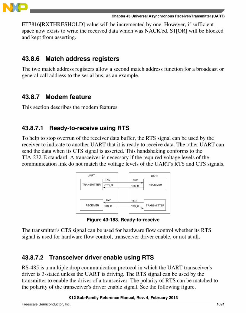
ET7816[RXTHRESHOLD] value will be incremented by one. However, if sufficientspace now exists to write the received data which was NACK'ed, S1[OR] will be blockedand kept from asserting.
43.8.6 Match address registers
The two match address registers allow a second match address function for a broadcast orgeneral call address to the serial bus, as an example.
43.8.7 Modem feature
This section describes the modem features.
43.8.7.1 Ready-to-receive using RTS
To help to stop overrun of the receiver data buffer, the RTS signal can be used by thereceiver to indicate to another UART that it is ready to receive data. The other UART cansend the data when its CTS signal is asserted. This handshaking conforms to theTIA-232-E standard. A transceiver is necessary if the required voltage levels of thecommunication link do not match the voltage levels of the UART's RTS and CTS signals.
TRANSMITTER
UART
RECEIVER TRANSMITTER
UART
RECEIVER
TXD
CTS_B
RXD
RTS_B
RXD
RTS_B
TXD
CTS_B
Figure 43-183. Ready-to-receive
The transmitter's CTS signal can be used for hardware flow control whether its RTSsignal is used for hardware flow control, transceiver driver enable, or not at all.
43.8.7.2 Transceiver driver enable using RTS
RS-485 is a multiple drop communication protocol in which the UART transceiver'sdriver is 3-stated unless the UART is driving. The RTS signal can be used by thetransmitter to enable the driver of a transceiver. The polarity of RTS can be matched tothe polarity of the transceiver's driver enable signal. See the following figure.
Chapter 43 Universal Asynchronous Receiver/Transmitter (UART)
K12 Sub-Family Reference Manual, Rev. 4, February 2013
Freescale Semiconductor, Inc. 1091

TRANSMITTER
UART
RECEIVER
DRIVER
RS-485 TRANSCEIVER
RECEIVER
TXD
RTS_B
RXD
DI
DE
RO
RE_B
Y
Z
A
B
Figure 43-184. Transceiver driver enable using RTS
In the figure, the receiver enable signal is asserted. Another option for this connection isto connect RTS_B to both DE and RE_B. The transceiver's receiver is disabled whiledriving. A pullup can pull RXD to a non-floating value during this time. This option canbe refined further by operating the UART in single wire mode, freeing the RXD pin forother uses.
43.8.8 IrDA minimum pulse width
The IrDA specifies a minimum pulse width of 1.6 µs. The UART hardware does notinclude a mechanism to restrict/force the pulse width to be greater than or equal to 1.6 µs.However, configuring the baud rate to 115.2 kbit/s and the narrow pulse width to 3/16 ofa bit time results in a pulse width of 1.6 µs.
43.8.9 Clearing 7816 wait timer (WT, BWT, CWT) interrupts
The 7816 wait timer interrupts associated with IS7816[WT], IS7816[BWT], andIS7816[CWT] will automatically reassert if they are cleared and the wait time is stillviolated. This behavior is similar to most of the other interrupts on the UART. In mostcases, if the condition that caused the interrupt to trigger still exists when the interrupt iscleared, then the interrupt will reassert. For example, consider the following scenario:
1. IS7816[WT] is programmed to assert after 9600 cycles of unresponsiveness.
2. The 9600 cycles pass without a response resulting in the WT interrupt asserting.3. The IS7816[WT] is cleared at cycle 9700 by the interrupt service routine.4. After the WT interrupt has been cleared, the smartcard remains unresponsive. At
cycle 9701 the WT interrupt will be reasserted.
Application information
K12 Sub-Family Reference Manual, Rev. 4, February 2013
1092 Freescale Semiconductor, Inc.
If the intent of clearing the interrupt is such that it does not reassert, the interrupt serviceroutine must remove or clear the condition that originally caused the interrupt to assertprior to clearing the interrupt. There are multiple ways that this can be accomplished,including ensuring that an event that results in the wait timer resetting occurs, such as, thetransmission of another packet.
43.8.10 Legacy and reverse compatibility considerations
Recent versions of the UART have added several new features. Whenever reasonablypossible, reverse compatibility was maintained. However, in some cases this was eithernot feasible or the behavior was deemed as not intended. This section describes severaldifferences to legacy operation that resulted from these recent enhancements. Ifapplication code from previous versions is used, it must be reviewed and modified to takethe following items into account. Depending on the application code, additional itemsthat are not listed here may also need to be considered.
1. Various reserved registers and register bits are used, such as, MSFB and M10.2. This module now generates an error when invalid address spaces are used.3. While documentation indicated otherwise, in some cases it was possible for
S1[IDLE] to assert even if S1[OR] was set.4. S1[OR] will be set only if the data buffer (FIFO) does not have sufficient room.
Previously, the data buffer was always a fixed size of one and the S1[OR] flag wouldset so long as S1[RDRF] was set even if there was room in the data buffer. While theclearing mechanism has remained the same for S1[RDRF], keeping the OR flagassertion tied to the RDRF event rather than the data buffer being full would havegreatly reduced the usefulness of the buffer when its size is larger than one.
5. Previously, when C2[RWU] was set (and WAKE = 0), the IDLE flag could reassertup to every bit period causing an interrupt and requiring the host processor to reassertC2[RWU]. This behavior has been modified. Now, when C2[RWU] is set (andWAKE = 0), at least one non-idle bit must be detected before an idle can be detected.
Chapter 43 Universal Asynchronous Receiver/Transmitter (UART)
K12 Sub-Family Reference Manual, Rev. 4, February 2013
Freescale Semiconductor, Inc. 1093

Application information
K12 Sub-Family Reference Manual, Rev. 4, February 2013
1094 Freescale Semiconductor, Inc.
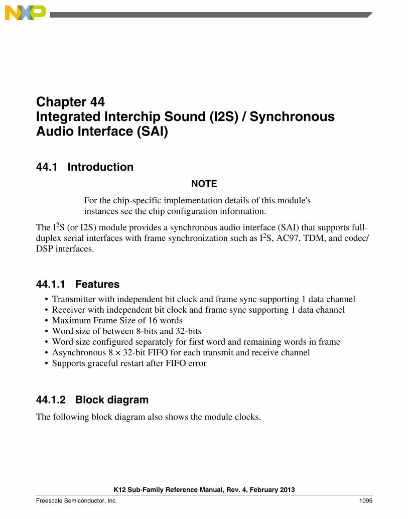
Chapter 44Integrated Interchip Sound (I2S) / SynchronousAudio Interface (SAI)
44.1 IntroductionNOTE
For the chip-specific implementation details of this module'sinstances see the chip configuration information.
The I2S (or I2S) module provides a synchronous audio interface (SAI) that supports full-duplex serial interfaces with frame synchronization such as I2S, AC97, TDM, and codec/DSP interfaces.
44.1.1 Features• Transmitter with independent bit clock and frame sync supporting 1 data channel• Receiver with independent bit clock and frame sync supporting 1 data channel• Maximum Frame Size of 16 words• Word size of between 8-bits and 32-bits• Word size configured separately for first word and remaining words in frame• Asynchronous 8 × 32-bit FIFO for each transmit and receive channel• Supports graceful restart after FIFO error
44.1.2 Block diagram
The following block diagram also shows the module clocks.
K12 Sub-Family Reference Manual, Rev. 4, February 2013
Freescale Semiconductor, Inc. 1095
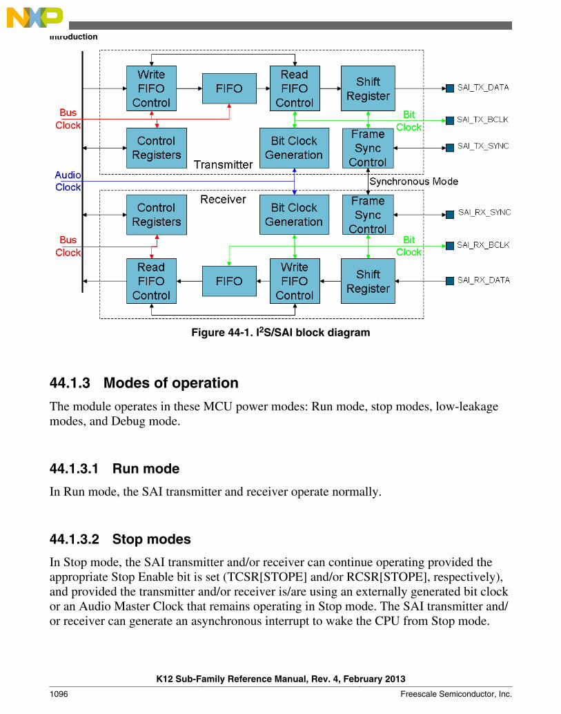
Figure 44-1. I2S/SAI block diagram
44.1.3 Modes of operation
The module operates in these MCU power modes: Run mode, stop modes, low-leakagemodes, and Debug mode.
44.1.3.1 Run mode
In Run mode, the SAI transmitter and receiver operate normally.
44.1.3.2 Stop modes
In Stop mode, the SAI transmitter and/or receiver can continue operating provided theappropriate Stop Enable bit is set (TCSR[STOPE] and/or RCSR[STOPE], respectively),and provided the transmitter and/or receiver is/are using an externally generated bit clockor an Audio Master Clock that remains operating in Stop mode. The SAI transmitter and/or receiver can generate an asynchronous interrupt to wake the CPU from Stop mode.
Introduction
K12 Sub-Family Reference Manual, Rev. 4, February 2013
1096 Freescale Semiconductor, Inc.
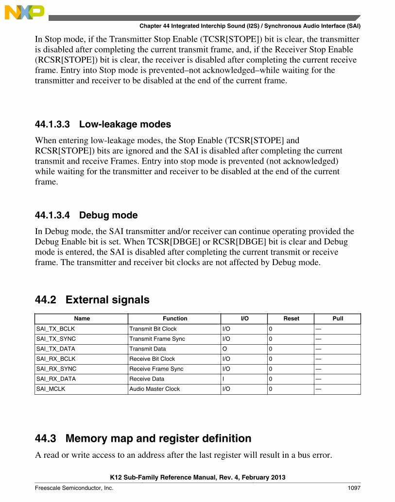
In Stop mode, if the Transmitter Stop Enable (TCSR[STOPE]) bit is clear, the transmitteris disabled after completing the current transmit frame, and, if the Receiver Stop Enable(RCSR[STOPE]) bit is clear, the receiver is disabled after completing the current receiveframe. Entry into Stop mode is prevented–not acknowledged–while waiting for thetransmitter and receiver to be disabled at the end of the current frame.
44.1.3.3 Low-leakage modes
When entering low-leakage modes, the Stop Enable (TCSR[STOPE] andRCSR[STOPE]) bits are ignored and the SAI is disabled after completing the currenttransmit and receive Frames. Entry into stop mode is prevented (not acknowledged)while waiting for the transmitter and receiver to be disabled at the end of the currentframe.
44.1.3.4 Debug mode
In Debug mode, the SAI transmitter and/or receiver can continue operating provided theDebug Enable bit is set. When TCSR[DBGE] or RCSR[DBGE] bit is clear and Debugmode is entered, the SAI is disabled after completing the current transmit or receiveframe. The transmitter and receiver bit clocks are not affected by Debug mode.
44.2 External signals
Name Function I/O Reset Pull
SAI_TX_BCLK Transmit Bit Clock I/O 0 —
SAI_TX_SYNC Transmit Frame Sync I/O 0 —
SAI_TX_DATA Transmit Data O 0 —
SAI_RX_BCLK Receive Bit Clock I/O 0 —
SAI_RX_SYNC Receive Frame Sync I/O 0 —
SAI_RX_DATA Receive Data I 0 —
SAI_MCLK Audio Master Clock I/O 0 —
44.3 Memory map and register definitionA read or write access to an address after the last register will result in a bus error.
Chapter 44 Integrated Interchip Sound (I2S) / Synchronous Audio Interface (SAI)
K12 Sub-Family Reference Manual, Rev. 4, February 2013
Freescale Semiconductor, Inc. 1097

I2S memory map
Absoluteaddress
(hex)Register name
Width(in bits)
Access Reset valueSection/
page
4002_F000 SAI Transmit Control Register (I2S0_TCSR) 32 R/W 0000_0000h 44.3.1/1099
4002_F004 SAI Transmit Configuration 1 Register (I2S0_TCR1) 32 R/W 0000_0000h 44.3.2/1102
4002_F008 SAI Transmit Configuration 2 Register (I2S0_TCR2) 32 R/W 0000_0000h 44.3.3/1102
4002_F00C SAI Transmit Configuration 3 Register (I2S0_TCR3) 32 R/W 0000_0000h 44.3.4/1104
4002_F010 SAI Transmit Configuration 4 Register (I2S0_TCR4) 32 R/W 0000_0000h 44.3.5/1105
4002_F014 SAI Transmit Configuration 5 Register (I2S0_TCR5) 32 R/W 0000_0000h 44.3.6/1106
4002_F020 SAI Transmit Data Register (I2S0_TDR0) 32W
(alwaysreads 0)
0000_0000h 44.3.7/1107
4002_F040 SAI Transmit FIFO Register (I2S0_TFR0) 32 R 0000_0000h 44.3.8/1108
4002_F060 SAI Transmit Mask Register (I2S0_TMR) 32 R/W 0000_0000h 44.3.9/1108
4002_F080 SAI Receive Control Register (I2S0_RCSR) 32 R/W 0000_0000h44.3.10/
1109
4002_F084 SAI Receive Configuration 1 Register (I2S0_RCR1) 32 R/W 0000_0000h44.3.11/
1112
4002_F088 SAI Receive Configuration 2 Register (I2S0_RCR2) 32 R/W 0000_0000h44.3.12/
1113
4002_F08C SAI Receive Configuration 3 Register (I2S0_RCR3) 32 R/W 0000_0000h44.3.13/
1114
4002_F090 SAI Receive Configuration 4 Register (I2S0_RCR4) 32 R/W 0000_0000h44.3.14/
1115
4002_F094 SAI Receive Configuration 5 Register (I2S0_RCR5) 32 R/W 0000_0000h44.3.15/
1117
4002_F0A0 SAI Receive Data Register (I2S0_RDR0) 32 R 0000_0000h44.3.16/
1117
4002_F0C0 SAI Receive FIFO Register (I2S0_RFR0) 32 R 0000_0000h44.3.17/
1118
4002_F0E0 SAI Receive Mask Register (I2S0_RMR) 32 R/W 0000_0000h44.3.18/
1118
4002_F100 SAI MCLK Control Register (I2S0_MCR) 32 R/W 0000_0000h44.3.19/
1119
4002_F104 SAI MCLK Divide Register (I2S0_MDR) 32 R/W 0000_0000h44.3.20/
1120
Memory map and register definition
K12 Sub-Family Reference Manual, Rev. 4, February 2013
1098 Freescale Semiconductor, Inc.
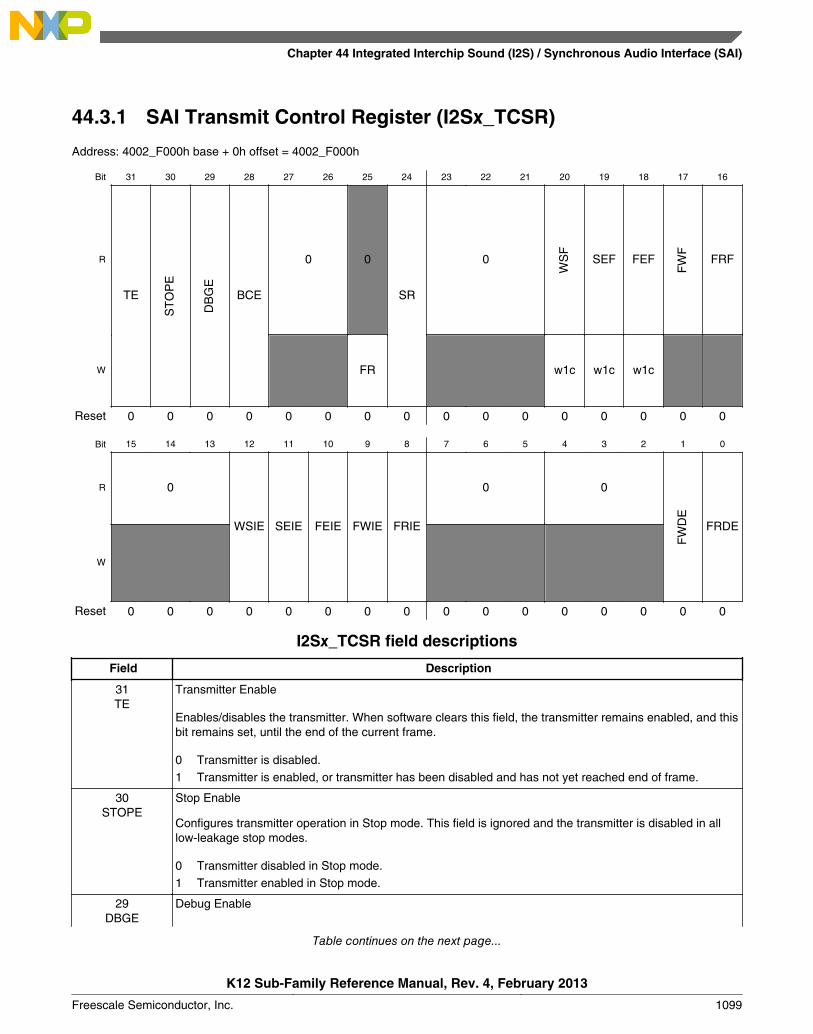
44.3.1 SAI Transmit Control Register (I2Sx_TCSR)
Address: 4002_F000h base + 0h offset = 4002_F000h
Bit 31 30 29 28 27 26 25 24 23 22 21 20 19 18 17 16
R
TE
ST
OP
E
DB
GE
BCE
0 0
SR
0
WS
F
SEF FEF
FW
F
FRF
W FR w1c w1c w1c
Reset 0 0 0 0 0 0 0 0 0 0 0 0 0 0 0 0
Bit 15 14 13 12 11 10 9 8 7 6 5 4 3 2 1 0
R 0
WSIE SEIE FEIE FWIE FRIE
0 0
FW
DE
FRDE
W
Reset 0 0 0 0 0 0 0 0 0 0 0 0 0 0 0 0
I2Sx_TCSR field descriptions
Field Description
31TE
Transmitter Enable
Enables/disables the transmitter. When software clears this field, the transmitter remains enabled, and thisbit remains set, until the end of the current frame.
0 Transmitter is disabled.1 Transmitter is enabled, or transmitter has been disabled and has not yet reached end of frame.
30STOPE
Stop Enable
Configures transmitter operation in Stop mode. This field is ignored and the transmitter is disabled in alllow-leakage stop modes.
0 Transmitter disabled in Stop mode.1 Transmitter enabled in Stop mode.
29DBGE
Debug Enable
Table continues on the next page...
Chapter 44 Integrated Interchip Sound (I2S) / Synchronous Audio Interface (SAI)
K12 Sub-Family Reference Manual, Rev. 4, February 2013
Freescale Semiconductor, Inc. 1099
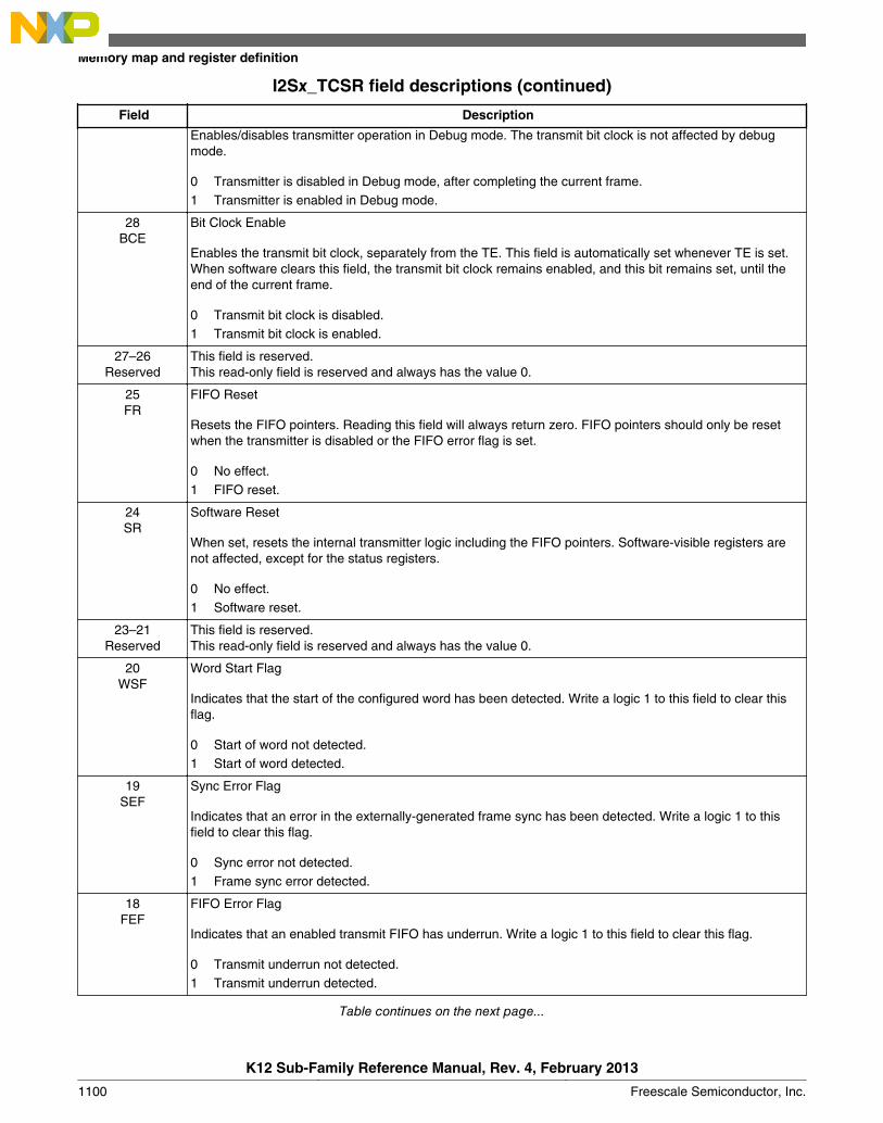
I2Sx_TCSR field descriptions (continued)
Field Description
Enables/disables transmitter operation in Debug mode. The transmit bit clock is not affected by debugmode.
0 Transmitter is disabled in Debug mode, after completing the current frame.1 Transmitter is enabled in Debug mode.
28BCE
Bit Clock Enable
Enables the transmit bit clock, separately from the TE. This field is automatically set whenever TE is set.When software clears this field, the transmit bit clock remains enabled, and this bit remains set, until theend of the current frame.
0 Transmit bit clock is disabled.1 Transmit bit clock is enabled.
27–26Reserved
This field is reserved.This read-only field is reserved and always has the value 0.
25FR
FIFO Reset
Resets the FIFO pointers. Reading this field will always return zero. FIFO pointers should only be resetwhen the transmitter is disabled or the FIFO error flag is set.
0 No effect.1 FIFO reset.
24SR
Software Reset
When set, resets the internal transmitter logic including the FIFO pointers. Software-visible registers arenot affected, except for the status registers.
0 No effect.1 Software reset.
23–21Reserved
This field is reserved.This read-only field is reserved and always has the value 0.
20WSF
Word Start Flag
Indicates that the start of the configured word has been detected. Write a logic 1 to this field to clear thisflag.
0 Start of word not detected.1 Start of word detected.
19SEF
Sync Error Flag
Indicates that an error in the externally-generated frame sync has been detected. Write a logic 1 to thisfield to clear this flag.
0 Sync error not detected.1 Frame sync error detected.
18FEF
FIFO Error Flag
Indicates that an enabled transmit FIFO has underrun. Write a logic 1 to this field to clear this flag.
0 Transmit underrun not detected.1 Transmit underrun detected.
Table continues on the next page...
Memory map and register definition
K12 Sub-Family Reference Manual, Rev. 4, February 2013
1100 Freescale Semiconductor, Inc.

I2Sx_TCSR field descriptions (continued)
Field Description
17FWF
FIFO Warning Flag
Indicates that an enabled transmit FIFO is empty.
0 No enabled transmit FIFO is empty.1 Enabled transmit FIFO is empty.
16FRF
FIFO Request Flag
Indicates that the number of words in an enabled transmit channel FIFO is less than or equal to thetransmit FIFO watermark.
0 Transmit FIFO watermark has not been reached.1 Transmit FIFO watermark has been reached.
15–13Reserved
This field is reserved.This read-only field is reserved and always has the value 0.
12WSIE
Word Start Interrupt Enable
Enables/disables word start interrupts.
0 Disables interrupt.1 Enables interrupt.
11SEIE
Sync Error Interrupt Enable
Enables/disables sync error interrupts.
0 Disables interrupt.1 Enables interrupt.
10FEIE
FIFO Error Interrupt Enable
Enables/disables FIFO error interrupts.
0 Disables the interrupt.1 Enables the interrupt.
9FWIE
FIFO Warning Interrupt Enable
Enables/disables FIFO warning interrupts.
0 Disables the interrupt.1 Enables the interrupt.
8FRIE
FIFO Request Interrupt Enable
Enables/disables FIFO request interrupts.
0 Disables the interrupt.1 Enables the interrupt.
7–5Reserved
This field is reserved.This read-only field is reserved and always has the value 0.
4–2Reserved
This field is reserved.This read-only field is reserved and always has the value 0.
1FWDE
FIFO Warning DMA Enable
Table continues on the next page...
Chapter 44 Integrated Interchip Sound (I2S) / Synchronous Audio Interface (SAI)
K12 Sub-Family Reference Manual, Rev. 4, February 2013
Freescale Semiconductor, Inc. 1101
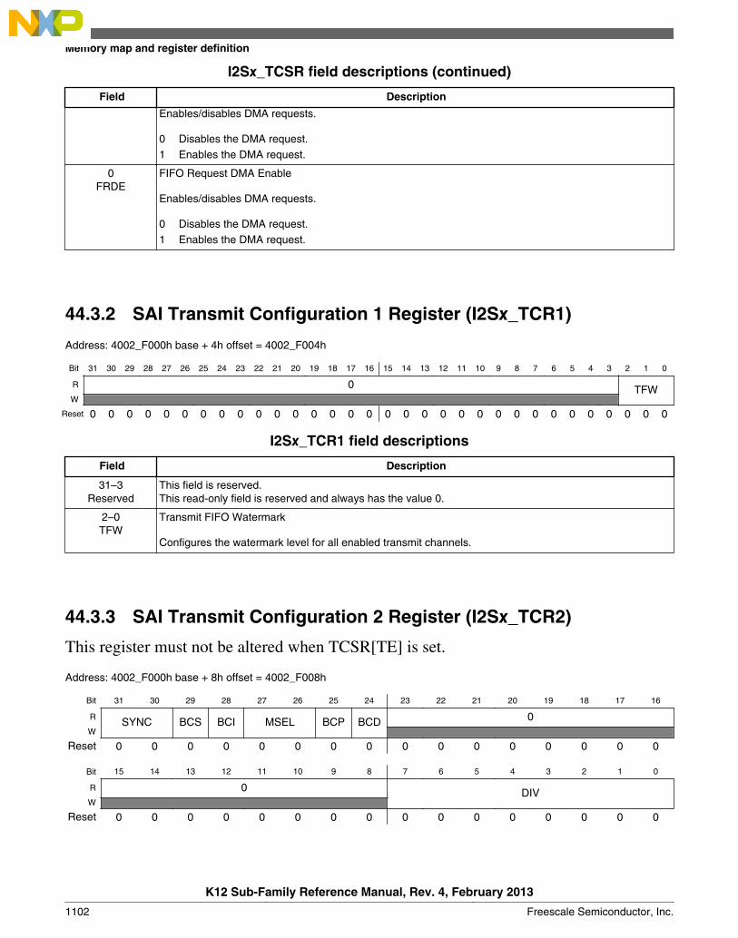
I2Sx_TCSR field descriptions (continued)
Field Description
Enables/disables DMA requests.
0 Disables the DMA request.1 Enables the DMA request.
0FRDE
FIFO Request DMA Enable
Enables/disables DMA requests.
0 Disables the DMA request.1 Enables the DMA request.
44.3.2 SAI Transmit Configuration 1 Register (I2Sx_TCR1)
Address: 4002_F000h base + 4h offset = 4002_F004h
Bit 31 30 29 28 27 26 25 24 23 22 21 20 19 18 17 16 15 14 13 12 11 10 9 8 7 6 5 4 3 2 1 0
R 0 TFWW
Reset 0 0 0 0 0 0 0 0 0 0 0 0 0 0 0 0 0 0 0 0 0 0 0 0 0 0 0 0 0 0 0 0
I2Sx_TCR1 field descriptions
Field Description
31–3Reserved
This field is reserved.This read-only field is reserved and always has the value 0.
2–0TFW
Transmit FIFO Watermark
Configures the watermark level for all enabled transmit channels.
44.3.3 SAI Transmit Configuration 2 Register (I2Sx_TCR2)
This register must not be altered when TCSR[TE] is set.
Address: 4002_F000h base + 8h offset = 4002_F008h
Bit 31 30 29 28 27 26 25 24 23 22 21 20 19 18 17 16
R SYNC BCS BCI MSEL BCP BCD 0W
Reset 0 0 0 0 0 0 0 0 0 0 0 0 0 0 0 0
Bit 15 14 13 12 11 10 9 8 7 6 5 4 3 2 1 0
R 0 DIVW
Reset 0 0 0 0 0 0 0 0 0 0 0 0 0 0 0 0
Memory map and register definition
K12 Sub-Family Reference Manual, Rev. 4, February 2013
1102 Freescale Semiconductor, Inc.
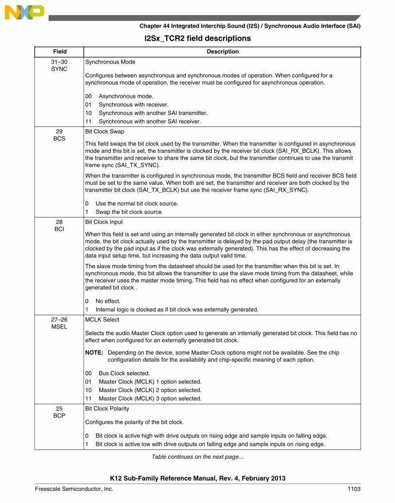
I2Sx_TCR2 field descriptions
Field Description
31–30SYNC
Synchronous Mode
Configures between asynchronous and synchronous modes of operation. When configured for asynchronous mode of operation, the receiver must be configured for asynchronous operation.
00 Asynchronous mode.01 Synchronous with receiver.10 Synchronous with another SAI transmitter.11 Synchronous with another SAI receiver.
29BCS
Bit Clock Swap
This field swaps the bit clock used by the transmitter. When the transmitter is configured in asynchronousmode and this bit is set, the transmitter is clocked by the receiver bit clock (SAI_RX_BCLK). This allowsthe transmitter and receiver to share the same bit clock, but the transmitter continues to use the transmitframe sync (SAI_TX_SYNC).
When the transmitter is configured in synchronous mode, the transmitter BCS field and receiver BCS fieldmust be set to the same value. When both are set, the transmitter and receiver are both clocked by thetransmitter bit clock (SAI_TX_BCLK) but use the receiver frame sync (SAI_RX_SYNC).
0 Use the normal bit clock source.1 Swap the bit clock source.
28BCI
Bit Clock Input
When this field is set and using an internally generated bit clock in either synchronous or asynchronousmode, the bit clock actually used by the transmitter is delayed by the pad output delay (the transmitter isclocked by the pad input as if the clock was externally generated). This has the effect of decreasing thedata input setup time, but increasing the data output valid time.
The slave mode timing from the datasheet should be used for the transmitter when this bit is set. Insynchronous mode, this bit allows the transmitter to use the slave mode timing from the datasheet, whilethe receiver uses the master mode timing. This field has no effect when configured for an externallygenerated bit clock .
0 No effect.1 Internal logic is clocked as if bit clock was externally generated.
27–26MSEL
MCLK Select
Selects the audio Master Clock option used to generate an internally generated bit clock. This field has noeffect when configured for an externally generated bit clock.
NOTE: Depending on the device, some Master Clock options might not be available. See the chipconfiguration details for the availability and chip-specific meaning of each option.
00 Bus Clock selected.01 Master Clock (MCLK) 1 option selected.10 Master Clock (MCLK) 2 option selected.11 Master Clock (MCLK) 3 option selected.
25BCP
Bit Clock Polarity
Configures the polarity of the bit clock.
0 Bit clock is active high with drive outputs on rising edge and sample inputs on falling edge.1 Bit clock is active low with drive outputs on falling edge and sample inputs on rising edge.
Table continues on the next page...
Chapter 44 Integrated Interchip Sound (I2S) / Synchronous Audio Interface (SAI)
K12 Sub-Family Reference Manual, Rev. 4, February 2013
Freescale Semiconductor, Inc. 1103
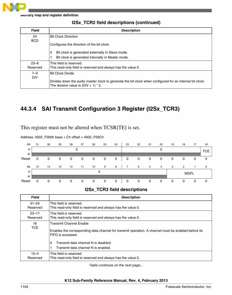
I2Sx_TCR2 field descriptions (continued)
Field Description
24BCD
Bit Clock Direction
Configures the direction of the bit clock.
0 Bit clock is generated externally in Slave mode.1 Bit clock is generated internally in Master mode.
23–8Reserved
This field is reserved.This read-only field is reserved and always has the value 0.
7–0DIV
Bit Clock Divide
Divides down the audio master clock to generate the bit clock when configured for an internal bit clock.The division value is (DIV + 1) * 2.
44.3.4 SAI Transmit Configuration 3 Register (I2Sx_TCR3)
This register must not be altered when TCSR[TE] is set.
Address: 4002_F000h base + Ch offset = 4002_F00Ch
Bit 31 30 29 28 27 26 25 24 23 22 21 20 19 18 17 16
R 0 0 TCEW
Reset 0 0 0 0 0 0 0 0 0 0 0 0 0 0 0 0
Bit 15 14 13 12 11 10 9 8 7 6 5 4 3 2 1 0
R 0 WDFLW
Reset 0 0 0 0 0 0 0 0 0 0 0 0 0 0 0 0
I2Sx_TCR3 field descriptions
Field Description
31–24Reserved
This field is reserved.This read-only field is reserved and always has the value 0.
23–17Reserved
This field is reserved.This read-only field is reserved and always has the value 0.
16TCE
Transmit Channel Enable
Enables the corresponding data channel for transmit operation. A channel must be enabled before itsFIFO is accessed.
0 Transmit data channel N is disabled.1 Transmit data channel N is enabled.
15–4Reserved
This field is reserved.This read-only field is reserved and always has the value 0.
Table continues on the next page...
Memory map and register definition
K12 Sub-Family Reference Manual, Rev. 4, February 2013
1104 Freescale Semiconductor, Inc.

I2Sx_TCR3 field descriptions (continued)
Field Description
3–0WDFL
Word Flag Configuration
Configures which word sets the start of word flag. The value written must be one less than the wordnumber. For example, writing 0 configures the first word in the frame. When configured to a value greaterthan TCR4[FRSZ], then the start of word flag is never set.
44.3.5 SAI Transmit Configuration 4 Register (I2Sx_TCR4)
This register must not be altered when TCSR[TE] is set.
Address: 4002_F000h base + 10h offset = 4002_F010h
Bit 31 30 29 28 27 26 25 24 23 22 21 20 19 18 17 16
R 0 0 0 0 0 FRSZW
Reset 0 0 0 0 0 0 0 0 0 0 0 0 0 0 0 0
Bit 15 14 13 12 11 10 9 8 7 6 5 4 3 2 1 0
R 0 SYWD 0 MF FSE 0 FSP FSDW
Reset 0 0 0 0 0 0 0 0 0 0 0 0 0 0 0 0
I2Sx_TCR4 field descriptions
Field Description
31–29Reserved
This field is reserved.This read-only field is reserved and always has the value 0.
28Reserved
This field is reserved.This read-only field is reserved and always has the value 0.
27–26Reserved
This field is reserved.This read-only field is reserved and always has the value 0.
25–24Reserved
This field is reserved.This read-only field is reserved and always has the value 0.
23–20Reserved
This field is reserved.This read-only field is reserved and always has the value 0.
19–16FRSZ
Frame size
Configures the number of words in each frame. The value written must be one less than the number ofwords in the frame. For example, write 0 for one word per frame. The maximum supported frame size is16 words.
15–13Reserved
This field is reserved.This read-only field is reserved and always has the value 0.
12–8SYWD
Sync Width
Configures the length of the frame sync in number of bit clocks. The value written must be one less thanthe number of bit clocks. For example, write 0 for the frame sync to assert for one bit clock only. The syncwidth cannot be configured longer than the first word of the frame.
Table continues on the next page...
Chapter 44 Integrated Interchip Sound (I2S) / Synchronous Audio Interface (SAI)
K12 Sub-Family Reference Manual, Rev. 4, February 2013
Freescale Semiconductor, Inc. 1105
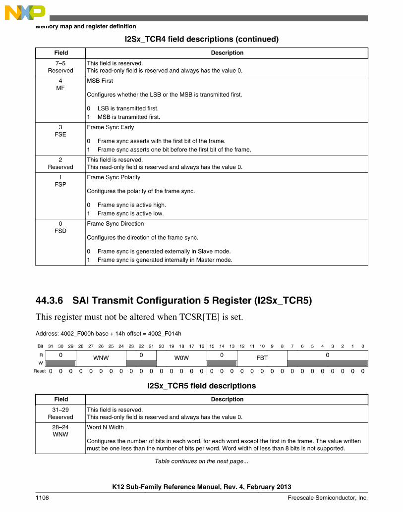
I2Sx_TCR4 field descriptions (continued)
Field Description
7–5Reserved
This field is reserved.This read-only field is reserved and always has the value 0.
4MF
MSB First
Configures whether the LSB or the MSB is transmitted first.
0 LSB is transmitted first.1 MSB is transmitted first.
3FSE
Frame Sync Early
0 Frame sync asserts with the first bit of the frame.1 Frame sync asserts one bit before the first bit of the frame.
2Reserved
This field is reserved.This read-only field is reserved and always has the value 0.
1FSP
Frame Sync Polarity
Configures the polarity of the frame sync.
0 Frame sync is active high.1 Frame sync is active low.
0FSD
Frame Sync Direction
Configures the direction of the frame sync.
0 Frame sync is generated externally in Slave mode.1 Frame sync is generated internally in Master mode.
44.3.6 SAI Transmit Configuration 5 Register (I2Sx_TCR5)
This register must not be altered when TCSR[TE] is set.
Address: 4002_F000h base + 14h offset = 4002_F014h
Bit 31 30 29 28 27 26 25 24 23 22 21 20 19 18 17 16 15 14 13 12 11 10 9 8 7 6 5 4 3 2 1 0
R 0 WNW 0 W0W 0 FBT 0W
Reset 0 0 0 0 0 0 0 0 0 0 0 0 0 0 0 0 0 0 0 0 0 0 0 0 0 0 0 0 0 0 0 0
I2Sx_TCR5 field descriptions
Field Description
31–29Reserved
This field is reserved.This read-only field is reserved and always has the value 0.
28–24WNW
Word N Width
Configures the number of bits in each word, for each word except the first in the frame. The value writtenmust be one less than the number of bits per word. Word width of less than 8 bits is not supported.
Table continues on the next page...
Memory map and register definition
K12 Sub-Family Reference Manual, Rev. 4, February 2013
1106 Freescale Semiconductor, Inc.
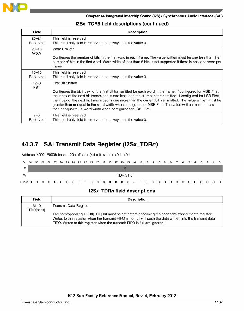
I2Sx_TCR5 field descriptions (continued)
Field Description
23–21Reserved
This field is reserved.This read-only field is reserved and always has the value 0.
20–16W0W
Word 0 Width
Configures the number of bits in the first word in each frame. The value written must be one less than thenumber of bits in the first word. Word width of less than 8 bits is not supported if there is only one word perframe.
15–13Reserved
This field is reserved.This read-only field is reserved and always has the value 0.
12–8FBT
First Bit Shifted
Configures the bit index for the first bit transmitted for each word in the frame. If configured for MSB First,the index of the next bit transmitted is one less than the current bit transmitted. If configured for LSB First,the index of the next bit transmitted is one more than the current bit transmitted. The value written must begreater than or equal to the word width when configured for MSB First. The value written must be lessthan or equal to 31-word width when configured for LSB First.
7–0Reserved
This field is reserved.This read-only field is reserved and always has the value 0.
44.3.7 SAI Transmit Data Register (I2Sx_TDRn)
Address: 4002_F000h base + 20h offset + (4d × i), where i=0d to 0d
Bit 31 30 29 28 27 26 25 24 23 22 21 20 19 18 17 16 15 14 13 12 11 10 9 8 7 6 5 4 3 2 1 0
R 0
W TDR[31:0]
Reset 0 0 0 0 0 0 0 0 0 0 0 0 0 0 0 0 0 0 0 0 0 0 0 0 0 0 0 0 0 0 0 0
I2Sx_TDRn field descriptions
Field Description
31–0TDR[31:0]
Transmit Data Register
The corresponding TCR3[TCE] bit must be set before accessing the channel's transmit data register.Writes to this register when the transmit FIFO is not full will push the data written into the transmit dataFIFO. Writes to this register when the transmit FIFO is full are ignored.
Chapter 44 Integrated Interchip Sound (I2S) / Synchronous Audio Interface (SAI)
K12 Sub-Family Reference Manual, Rev. 4, February 2013
Freescale Semiconductor, Inc. 1107

44.3.8 SAI Transmit FIFO Register (I2Sx_TFRn)
The MSB of the read and write pointers is used to distinguish between FIFO full andempty conditions. If the read and write pointers are identical, then the FIFO is empty. Ifthe read and write pointers are identical except for the MSB, then the FIFO is full.
Address: 4002_F000h base + 40h offset + (4d × i), where i=0d to 0d
Bit 31 30 29 28 27 26 25 24 23 22 21 20 19 18 17 16
R 0 0 WFP
W
Reset 0 0 0 0 0 0 0 0 0 0 0 0 0 0 0 0
Bit 15 14 13 12 11 10 9 8 7 6 5 4 3 2 1 0
R 0 RFP
W
Reset 0 0 0 0 0 0 0 0 0 0 0 0 0 0 0 0
I2Sx_TFRn field descriptions
Field Description
31Reserved
This field is reserved.This read-only field is reserved and always has the value 0.
30–20Reserved
This field is reserved.This read-only field is reserved and always has the value 0.
19–16WFP
Write FIFO Pointer
FIFO write pointer for transmit data channel.
15–4Reserved
This field is reserved.This read-only field is reserved and always has the value 0.
3–0RFP
Read FIFO Pointer
FIFO read pointer for transmit data channel.
44.3.9 SAI Transmit Mask Register (I2Sx_TMR)
This register is double-buffered and updates:
1. When TCSR[TE] is first set2. At the end of each frame.
This allows the masked words in each frame to change from frame to frame.
Memory map and register definition
K12 Sub-Family Reference Manual, Rev. 4, February 2013
1108 Freescale Semiconductor, Inc.
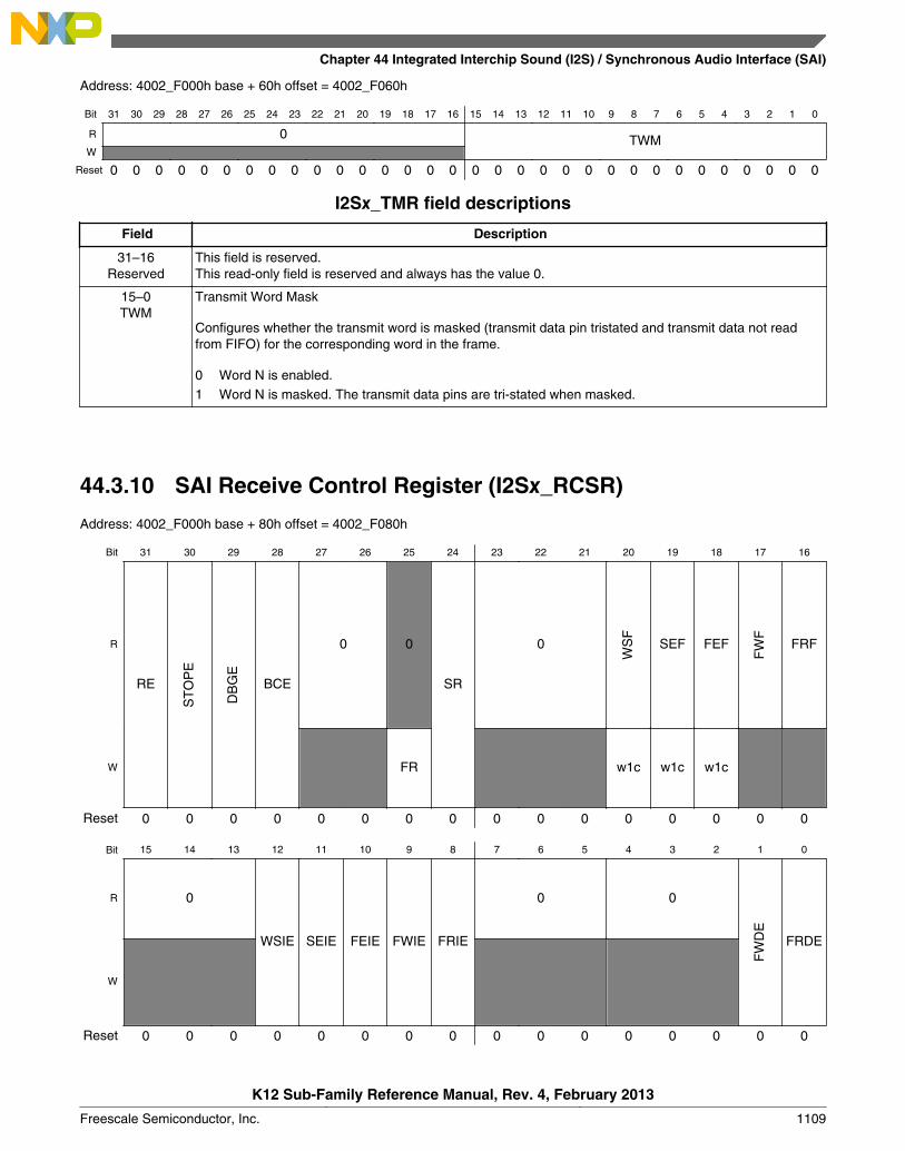
Address: 4002_F000h base + 60h offset = 4002_F060h
Bit 31 30 29 28 27 26 25 24 23 22 21 20 19 18 17 16 15 14 13 12 11 10 9 8 7 6 5 4 3 2 1 0
R 0 TWMW
Reset 0 0 0 0 0 0 0 0 0 0 0 0 0 0 0 0 0 0 0 0 0 0 0 0 0 0 0 0 0 0 0 0
I2Sx_TMR field descriptions
Field Description
31–16Reserved
This field is reserved.This read-only field is reserved and always has the value 0.
15–0TWM
Transmit Word Mask
Configures whether the transmit word is masked (transmit data pin tristated and transmit data not readfrom FIFO) for the corresponding word in the frame.
0 Word N is enabled.1 Word N is masked. The transmit data pins are tri-stated when masked.
44.3.10 SAI Receive Control Register (I2Sx_RCSR)
Address: 4002_F000h base + 80h offset = 4002_F080h
Bit 31 30 29 28 27 26 25 24 23 22 21 20 19 18 17 16
R
RE
ST
OP
E
DB
GE
BCE
0 0
SR
0W
SF
SEF FEF
FW
F
FRF
W FR w1c w1c w1c
Reset 0 0 0 0 0 0 0 0 0 0 0 0 0 0 0 0
Bit 15 14 13 12 11 10 9 8 7 6 5 4 3 2 1 0
R 0
WSIE SEIE FEIE FWIE FRIE
0 0
FW
DE
FRDE
W
Reset 0 0 0 0 0 0 0 0 0 0 0 0 0 0 0 0
Chapter 44 Integrated Interchip Sound (I2S) / Synchronous Audio Interface (SAI)
K12 Sub-Family Reference Manual, Rev. 4, February 2013
Freescale Semiconductor, Inc. 1109

I2Sx_RCSR field descriptions
Field Description
31RE
Receiver Enable
Enables/disables the receiver. When software clears this field, the receiver remains enabled, and this bitremains set, until the end of the current frame.
0 Receiver is disabled.1 Receiver is enabled, or receiver has been disabled and has not yet reached end of frame.
30STOPE
Stop Enable
Configures receiver operation in Stop mode. This bit is ignored and the receiver is disabled in all low-leakage stop modes.
0 Receiver disabled in Stop mode.1 Receiver enabled in Stop mode.
29DBGE
Debug Enable
Enables/disables receiver operation in Debug mode. The receive bit clock is not affected by Debug mode.
0 Receiver is disabled in Debug mode, after completing the current frame.1 Receiver is enabled in Debug mode.
28BCE
Bit Clock Enable
Enables the receive bit clock, separately from RE. This field is automatically set whenever RE is set.When software clears this field, the receive bit clock remains enabled, and this field remains set, until theend of the current frame.
0 Receive bit clock is disabled.1 Receive bit clock is enabled.
27–26Reserved
This field is reserved.This read-only field is reserved and always has the value 0.
25FR
FIFO Reset
Resets the FIFO pointers. Reading this field will always return zero. FIFO pointers should only be resetwhen the receiver is disabled or the FIFO error flag is set.
0 No effect.1 FIFO reset.
24SR
Software Reset
Resets the internal receiver logic including the FIFO pointers. Software-visible registers are not affected,except for the status registers.
0 No effect.1 Software reset.
23–21Reserved
This field is reserved.This read-only field is reserved and always has the value 0.
20WSF
Word Start Flag
Indicates that the start of the configured word has been detected. Write a logic 1 to this field to clear thisflag.
Table continues on the next page...
Memory map and register definition
K12 Sub-Family Reference Manual, Rev. 4, February 2013
1110 Freescale Semiconductor, Inc.

I2Sx_RCSR field descriptions (continued)
Field Description
0 Start of word not detected.1 Start of word detected.
19SEF
Sync Error Flag
Indicates that an error in the externally-generated frame sync has been detected. Write a logic 1 to thisfield to clear this flag.
0 Sync error not detected.1 Frame sync error detected.
18FEF
FIFO Error Flag
Indicates that an enabled receive FIFO has overflowed. Write a logic 1 to this field to clear this flag.
0 Receive overflow not detected.1 Receive overflow detected.
17FWF
FIFO Warning Flag
Indicates that an enabled receive FIFO is full.
0 No enabled receive FIFO is full.1 Enabled receive FIFO is full.
16FRF
FIFO Request Flag
Indicates that the number of words in an enabled receive channel FIFO is greater than the receive FIFOwatermark.
0 Receive FIFO watermark not reached.1 Receive FIFO watermark has been reached.
15–13Reserved
This field is reserved.This read-only field is reserved and always has the value 0.
12WSIE
Word Start Interrupt Enable
Enables/disables word start interrupts.
0 Disables interrupt.1 Enables interrupt.
11SEIE
Sync Error Interrupt Enable
Enables/disables sync error interrupts.
0 Disables interrupt.1 Enables interrupt.
10FEIE
FIFO Error Interrupt Enable
Enables/disables FIFO error interrupts.
0 Disables the interrupt.1 Enables the interrupt.
9FWIE
FIFO Warning Interrupt Enable
Enables/disables FIFO warning interrupts.
Table continues on the next page...
Chapter 44 Integrated Interchip Sound (I2S) / Synchronous Audio Interface (SAI)
K12 Sub-Family Reference Manual, Rev. 4, February 2013
Freescale Semiconductor, Inc. 1111
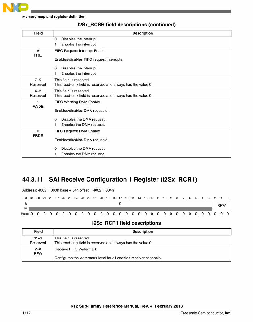
I2Sx_RCSR field descriptions (continued)
Field Description
0 Disables the interrupt.1 Enables the interrupt.
8FRIE
FIFO Request Interrupt Enable
Enables/disables FIFO request interrupts.
0 Disables the interrupt.1 Enables the interrupt.
7–5Reserved
This field is reserved.This read-only field is reserved and always has the value 0.
4–2Reserved
This field is reserved.This read-only field is reserved and always has the value 0.
1FWDE
FIFO Warning DMA Enable
Enables/disables DMA requests.
0 Disables the DMA request.1 Enables the DMA request.
0FRDE
FIFO Request DMA Enable
Enables/disables DMA requests.
0 Disables the DMA request.1 Enables the DMA request.
44.3.11 SAI Receive Configuration 1 Register (I2Sx_RCR1)
Address: 4002_F000h base + 84h offset = 4002_F084h
Bit 31 30 29 28 27 26 25 24 23 22 21 20 19 18 17 16 15 14 13 12 11 10 9 8 7 6 5 4 3 2 1 0
R 0 RFWW
Reset 0 0 0 0 0 0 0 0 0 0 0 0 0 0 0 0 0 0 0 0 0 0 0 0 0 0 0 0 0 0 0 0
I2Sx_RCR1 field descriptions
Field Description
31–3Reserved
This field is reserved.This read-only field is reserved and always has the value 0.
2–0RFW
Receive FIFO Watermark
Configures the watermark level for all enabled receiver channels.
Memory map and register definition
K12 Sub-Family Reference Manual, Rev. 4, February 2013
1112 Freescale Semiconductor, Inc.
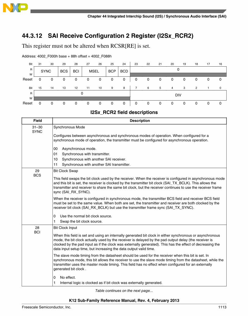
44.3.12 SAI Receive Configuration 2 Register (I2Sx_RCR2)
This register must not be altered when RCSR[RE] is set.
Address: 4002_F000h base + 88h offset = 4002_F088h
Bit 31 30 29 28 27 26 25 24 23 22 21 20 19 18 17 16
R SYNC BCS BCI MSEL BCP BCD 0W
Reset 0 0 0 0 0 0 0 0 0 0 0 0 0 0 0 0
Bit 15 14 13 12 11 10 9 8 7 6 5 4 3 2 1 0
R 0 DIVW
Reset 0 0 0 0 0 0 0 0 0 0 0 0 0 0 0 0
I2Sx_RCR2 field descriptions
Field Description
31–30SYNC
Synchronous Mode
Configures between asynchronous and synchronous modes of operation. When configured for asynchronous mode of operation, the transmitter must be configured for asynchronous operation.
00 Asynchronous mode.01 Synchronous with transmitter.10 Synchronous with another SAI receiver.11 Synchronous with another SAI transmitter.
29BCS
Bit Clock Swap
This field swaps the bit clock used by the receiver. When the receiver is configured in asynchronous modeand this bit is set, the receiver is clocked by the transmitter bit clock (SAI_TX_BCLK). This allows thetransmitter and receiver to share the same bit clock, but the receiver continues to use the receiver framesync (SAI_RX_SYNC).
When the receiver is configured in synchronous mode, the transmitter BCS field and receiver BCS fieldmust be set to the same value. When both are set, the transmitter and receiver are both clocked by thereceiver bit clock (SAI_RX_BCLK) but use the transmitter frame sync (SAI_TX_SYNC).
0 Use the normal bit clock source.1 Swap the bit clock source.
28BCI
Bit Clock Input
When this field is set and using an internally generated bit clock in either synchronous or asynchronousmode, the bit clock actually used by the receiver is delayed by the pad output delay (the receiver isclocked by the pad input as if the clock was externally generated). This has the effect of decreasing thedata input setup time, but increasing the data output valid time.
The slave mode timing from the datasheet should be used for the receiver when this bit is set. Insynchronous mode, this bit allows the receiver to use the slave mode timing from the datasheet, while thetransmitter uses the master mode timing. This field has no effect when configured for an externallygenerated bit clock .
0 No effect.1 Internal logic is clocked as if bit clock was externally generated.
Table continues on the next page...
Chapter 44 Integrated Interchip Sound (I2S) / Synchronous Audio Interface (SAI)
K12 Sub-Family Reference Manual, Rev. 4, February 2013
Freescale Semiconductor, Inc. 1113
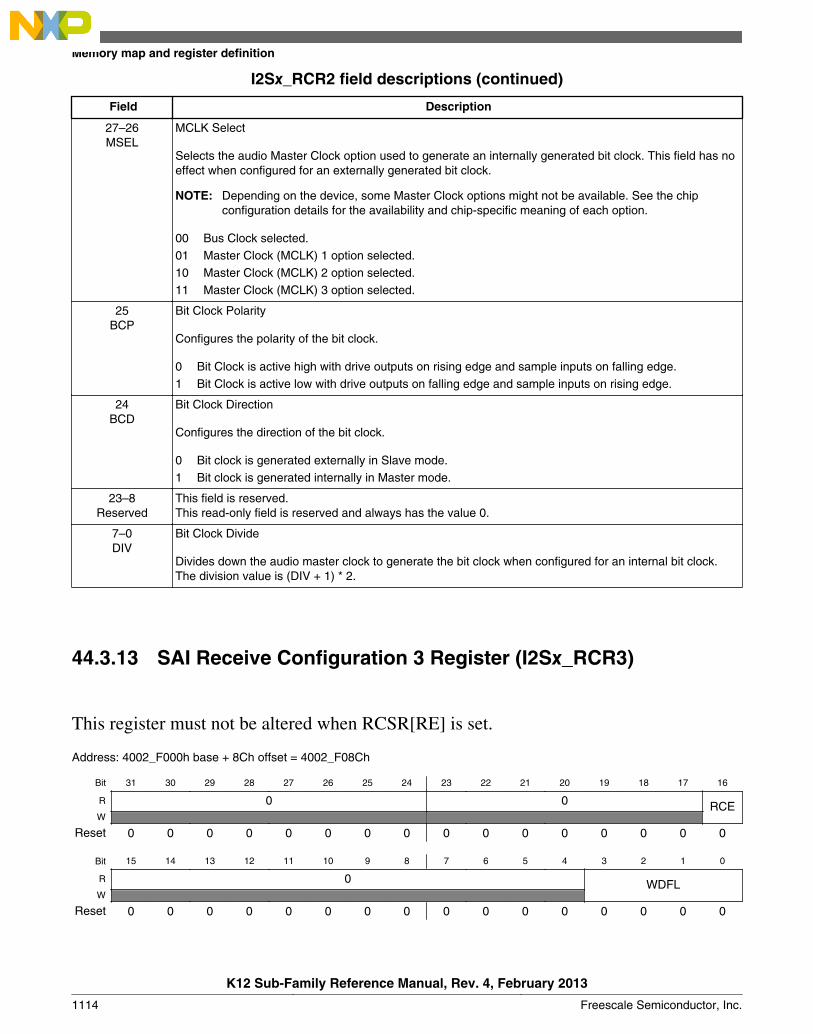
I2Sx_RCR2 field descriptions (continued)
Field Description
27–26MSEL
MCLK Select
Selects the audio Master Clock option used to generate an internally generated bit clock. This field has noeffect when configured for an externally generated bit clock.
NOTE: Depending on the device, some Master Clock options might not be available. See the chipconfiguration details for the availability and chip-specific meaning of each option.
00 Bus Clock selected.01 Master Clock (MCLK) 1 option selected.10 Master Clock (MCLK) 2 option selected.11 Master Clock (MCLK) 3 option selected.
25BCP
Bit Clock Polarity
Configures the polarity of the bit clock.
0 Bit Clock is active high with drive outputs on rising edge and sample inputs on falling edge.1 Bit Clock is active low with drive outputs on falling edge and sample inputs on rising edge.
24BCD
Bit Clock Direction
Configures the direction of the bit clock.
0 Bit clock is generated externally in Slave mode.1 Bit clock is generated internally in Master mode.
23–8Reserved
This field is reserved.This read-only field is reserved and always has the value 0.
7–0DIV
Bit Clock Divide
Divides down the audio master clock to generate the bit clock when configured for an internal bit clock.The division value is (DIV + 1) * 2.
44.3.13 SAI Receive Configuration 3 Register (I2Sx_RCR3)
This register must not be altered when RCSR[RE] is set.
Address: 4002_F000h base + 8Ch offset = 4002_F08Ch
Bit 31 30 29 28 27 26 25 24 23 22 21 20 19 18 17 16
R 0 0 RCEW
Reset 0 0 0 0 0 0 0 0 0 0 0 0 0 0 0 0
Bit 15 14 13 12 11 10 9 8 7 6 5 4 3 2 1 0
R 0 WDFLW
Reset 0 0 0 0 0 0 0 0 0 0 0 0 0 0 0 0
Memory map and register definition
K12 Sub-Family Reference Manual, Rev. 4, February 2013
1114 Freescale Semiconductor, Inc.

I2Sx_RCR3 field descriptions
Field Description
31–24Reserved
This field is reserved.This read-only field is reserved and always has the value 0.
23–17Reserved
This field is reserved.This read-only field is reserved and always has the value 0.
16RCE
Receive Channel Enable
Enables the corresponding data channel for receive operation. A channel must be enabled before its FIFOis accessed.
0 Receive data channel N is disabled.1 Receive data channel N is enabled.
15–4Reserved
This field is reserved.This read-only field is reserved and always has the value 0.
3–0WDFL
Word Flag Configuration
Configures which word the start of word flag is set. The value written should be one less than the wordnumber (for example, write zero to configure for the first word in the frame). When configured to a valuegreater than the Frame Size field, then the start of word flag is never set.
44.3.14 SAI Receive Configuration 4 Register (I2Sx_RCR4)
This register must not be altered when RCSR[RE] is set.
Address: 4002_F000h base + 90h offset = 4002_F090h
Bit 31 30 29 28 27 26 25 24 23 22 21 20 19 18 17 16
R 0 0 0 0 0 FRSZW
Reset 0 0 0 0 0 0 0 0 0 0 0 0 0 0 0 0
Bit 15 14 13 12 11 10 9 8 7 6 5 4 3 2 1 0
R 0 SYWD 0 MF FSE 0 FSP FSDW
Reset 0 0 0 0 0 0 0 0 0 0 0 0 0 0 0 0
I2Sx_RCR4 field descriptions
Field Description
31–29Reserved
This field is reserved.This read-only field is reserved and always has the value 0.
28Reserved
This field is reserved.This read-only field is reserved and always has the value 0.
27–26Reserved
This field is reserved.This read-only field is reserved and always has the value 0.
25–24Reserved
This field is reserved.This read-only field is reserved and always has the value 0.
Table continues on the next page...
Chapter 44 Integrated Interchip Sound (I2S) / Synchronous Audio Interface (SAI)
K12 Sub-Family Reference Manual, Rev. 4, February 2013
Freescale Semiconductor, Inc. 1115
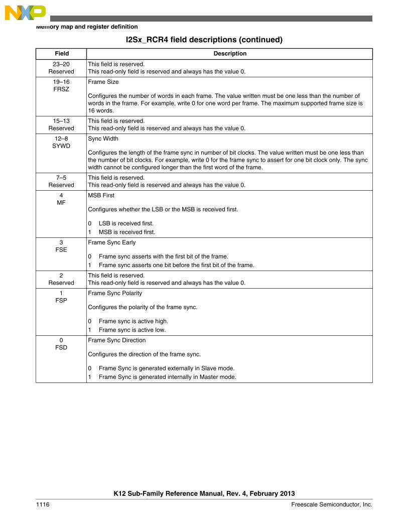
I2Sx_RCR4 field descriptions (continued)
Field Description
23–20Reserved
This field is reserved.This read-only field is reserved and always has the value 0.
19–16FRSZ
Frame Size
Configures the number of words in each frame. The value written must be one less than the number ofwords in the frame. For example, write 0 for one word per frame. The maximum supported frame size is16 words.
15–13Reserved
This field is reserved.This read-only field is reserved and always has the value 0.
12–8SYWD
Sync Width
Configures the length of the frame sync in number of bit clocks. The value written must be one less thanthe number of bit clocks. For example, write 0 for the frame sync to assert for one bit clock only. The syncwidth cannot be configured longer than the first word of the frame.
7–5Reserved
This field is reserved.This read-only field is reserved and always has the value 0.
4MF
MSB First
Configures whether the LSB or the MSB is received first.
0 LSB is received first.1 MSB is received first.
3FSE
Frame Sync Early
0 Frame sync asserts with the first bit of the frame.1 Frame sync asserts one bit before the first bit of the frame.
2Reserved
This field is reserved.This read-only field is reserved and always has the value 0.
1FSP
Frame Sync Polarity
Configures the polarity of the frame sync.
0 Frame sync is active high.1 Frame sync is active low.
0FSD
Frame Sync Direction
Configures the direction of the frame sync.
0 Frame Sync is generated externally in Slave mode.1 Frame Sync is generated internally in Master mode.
Memory map and register definition
K12 Sub-Family Reference Manual, Rev. 4, February 2013
1116 Freescale Semiconductor, Inc.
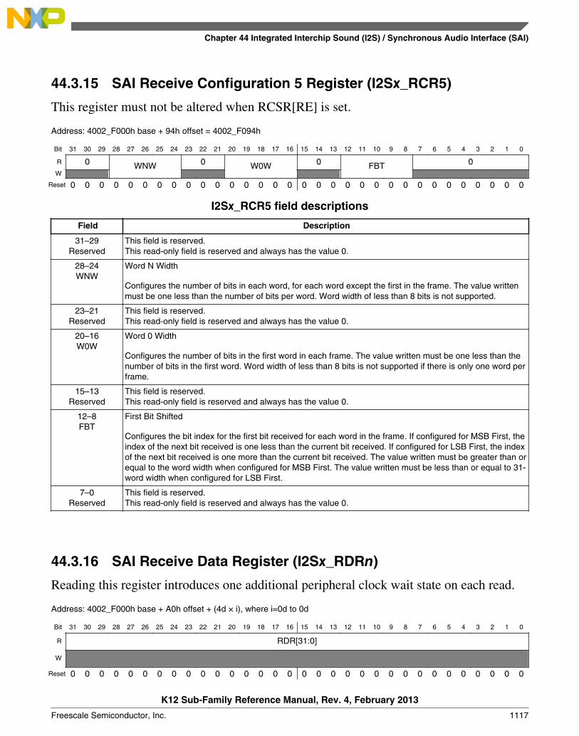
44.3.15 SAI Receive Configuration 5 Register (I2Sx_RCR5)
This register must not be altered when RCSR[RE] is set.
Address: 4002_F000h base + 94h offset = 4002_F094h
Bit 31 30 29 28 27 26 25 24 23 22 21 20 19 18 17 16 15 14 13 12 11 10 9 8 7 6 5 4 3 2 1 0
R 0 WNW 0 W0W 0 FBT 0W
Reset 0 0 0 0 0 0 0 0 0 0 0 0 0 0 0 0 0 0 0 0 0 0 0 0 0 0 0 0 0 0 0 0
I2Sx_RCR5 field descriptions
Field Description
31–29Reserved
This field is reserved.This read-only field is reserved and always has the value 0.
28–24WNW
Word N Width
Configures the number of bits in each word, for each word except the first in the frame. The value writtenmust be one less than the number of bits per word. Word width of less than 8 bits is not supported.
23–21Reserved
This field is reserved.This read-only field is reserved and always has the value 0.
20–16W0W
Word 0 Width
Configures the number of bits in the first word in each frame. The value written must be one less than thenumber of bits in the first word. Word width of less than 8 bits is not supported if there is only one word perframe.
15–13Reserved
This field is reserved.This read-only field is reserved and always has the value 0.
12–8FBT
First Bit Shifted
Configures the bit index for the first bit received for each word in the frame. If configured for MSB First, theindex of the next bit received is one less than the current bit received. If configured for LSB First, the indexof the next bit received is one more than the current bit received. The value written must be greater than orequal to the word width when configured for MSB First. The value written must be less than or equal to 31-word width when configured for LSB First.
7–0Reserved
This field is reserved.This read-only field is reserved and always has the value 0.
44.3.16 SAI Receive Data Register (I2Sx_RDRn)
Reading this register introduces one additional peripheral clock wait state on each read.
Address: 4002_F000h base + A0h offset + (4d × i), where i=0d to 0d
Bit 31 30 29 28 27 26 25 24 23 22 21 20 19 18 17 16 15 14 13 12 11 10 9 8 7 6 5 4 3 2 1 0
R RDR[31:0]
W
Reset 0 0 0 0 0 0 0 0 0 0 0 0 0 0 0 0 0 0 0 0 0 0 0 0 0 0 0 0 0 0 0 0
Chapter 44 Integrated Interchip Sound (I2S) / Synchronous Audio Interface (SAI)
K12 Sub-Family Reference Manual, Rev. 4, February 2013
Freescale Semiconductor, Inc. 1117
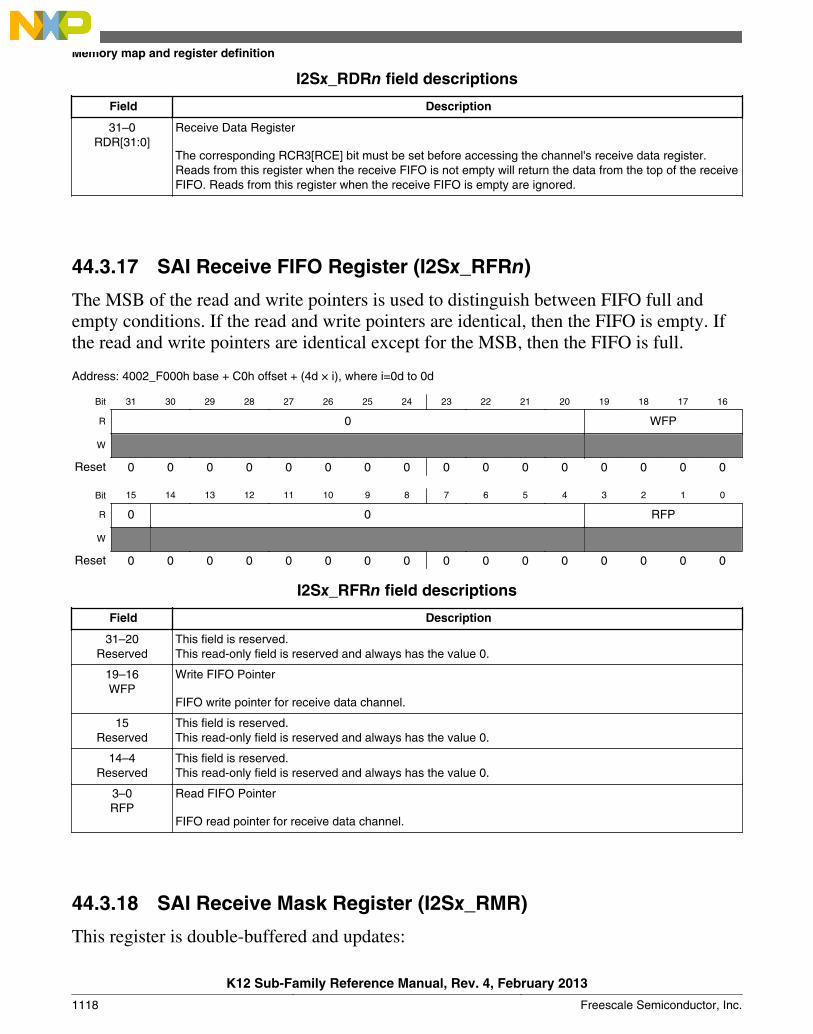
I2Sx_RDRn field descriptions
Field Description
31–0RDR[31:0]
Receive Data Register
The corresponding RCR3[RCE] bit must be set before accessing the channel's receive data register.Reads from this register when the receive FIFO is not empty will return the data from the top of the receiveFIFO. Reads from this register when the receive FIFO is empty are ignored.
44.3.17 SAI Receive FIFO Register (I2Sx_RFRn)
The MSB of the read and write pointers is used to distinguish between FIFO full andempty conditions. If the read and write pointers are identical, then the FIFO is empty. Ifthe read and write pointers are identical except for the MSB, then the FIFO is full.
Address: 4002_F000h base + C0h offset + (4d × i), where i=0d to 0d
Bit 31 30 29 28 27 26 25 24 23 22 21 20 19 18 17 16
R 0 WFP
W
Reset 0 0 0 0 0 0 0 0 0 0 0 0 0 0 0 0
Bit 15 14 13 12 11 10 9 8 7 6 5 4 3 2 1 0
R 0 0 RFP
W
Reset 0 0 0 0 0 0 0 0 0 0 0 0 0 0 0 0
I2Sx_RFRn field descriptions
Field Description
31–20Reserved
This field is reserved.This read-only field is reserved and always has the value 0.
19–16WFP
Write FIFO Pointer
FIFO write pointer for receive data channel.
15Reserved
This field is reserved.This read-only field is reserved and always has the value 0.
14–4Reserved
This field is reserved.This read-only field is reserved and always has the value 0.
3–0RFP
Read FIFO Pointer
FIFO read pointer for receive data channel.
44.3.18 SAI Receive Mask Register (I2Sx_RMR)
This register is double-buffered and updates:
Memory map and register definition
K12 Sub-Family Reference Manual, Rev. 4, February 2013
1118 Freescale Semiconductor, Inc.
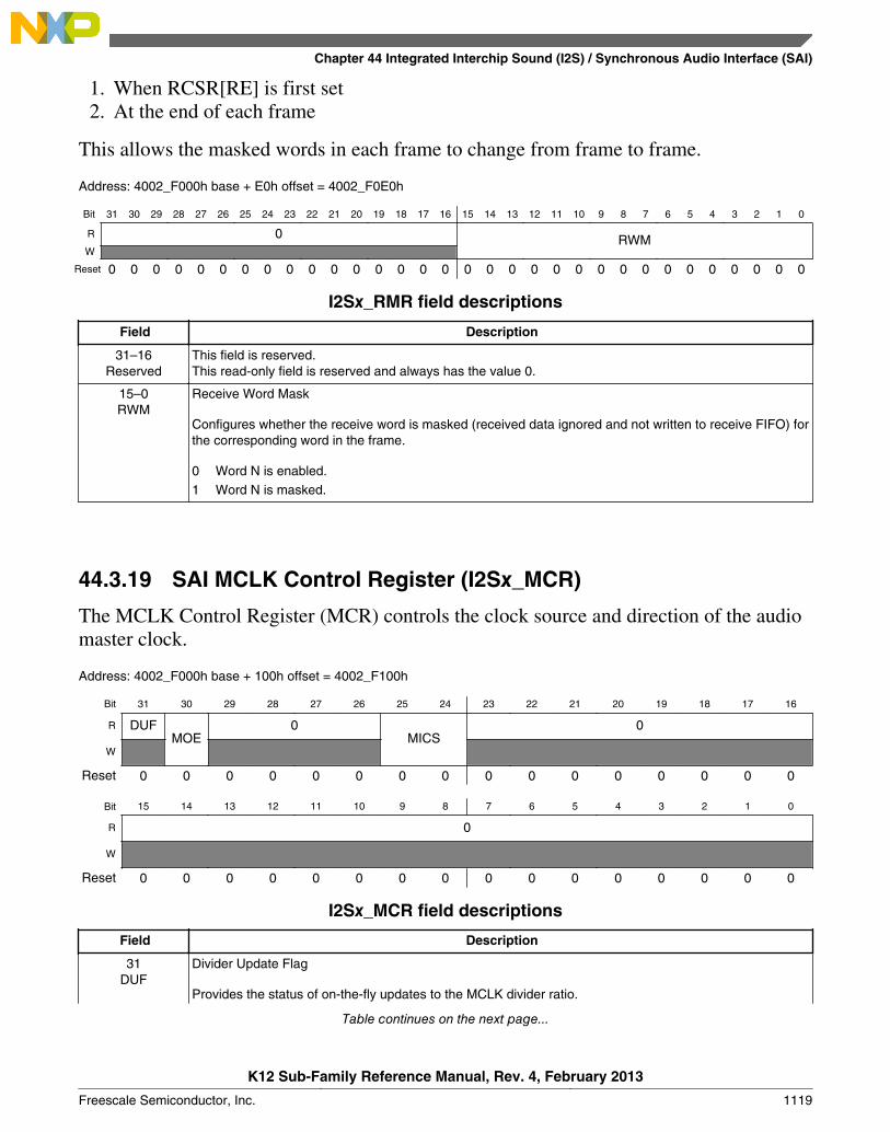
1. When RCSR[RE] is first set2. At the end of each frame
This allows the masked words in each frame to change from frame to frame.
Address: 4002_F000h base + E0h offset = 4002_F0E0h
Bit 31 30 29 28 27 26 25 24 23 22 21 20 19 18 17 16 15 14 13 12 11 10 9 8 7 6 5 4 3 2 1 0
R 0 RWMW
Reset 0 0 0 0 0 0 0 0 0 0 0 0 0 0 0 0 0 0 0 0 0 0 0 0 0 0 0 0 0 0 0 0
I2Sx_RMR field descriptions
Field Description
31–16Reserved
This field is reserved.This read-only field is reserved and always has the value 0.
15–0RWM
Receive Word Mask
Configures whether the receive word is masked (received data ignored and not written to receive FIFO) forthe corresponding word in the frame.
0 Word N is enabled.1 Word N is masked.
44.3.19 SAI MCLK Control Register (I2Sx_MCR)
The MCLK Control Register (MCR) controls the clock source and direction of the audiomaster clock.
Address: 4002_F000h base + 100h offset = 4002_F100h
Bit 31 30 29 28 27 26 25 24 23 22 21 20 19 18 17 16
R DUFMOE
0MICS
0
W
Reset 0 0 0 0 0 0 0 0 0 0 0 0 0 0 0 0
Bit 15 14 13 12 11 10 9 8 7 6 5 4 3 2 1 0
R 0
W
Reset 0 0 0 0 0 0 0 0 0 0 0 0 0 0 0 0
I2Sx_MCR field descriptions
Field Description
31DUF
Divider Update Flag
Provides the status of on-the-fly updates to the MCLK divider ratio.
Table continues on the next page...
Chapter 44 Integrated Interchip Sound (I2S) / Synchronous Audio Interface (SAI)
K12 Sub-Family Reference Manual, Rev. 4, February 2013
Freescale Semiconductor, Inc. 1119

I2Sx_MCR field descriptions (continued)
Field Description
0 MCLK divider ratio is not being updated currently.1 MCLK divider ratio is updating on-the-fly. Further updates to the MCLK divider ratio are blocked while
this flag remains set.
30MOE
MCLK Output Enable
Enables the MCLK divider and configures the MCLK signal pin as an output. When software clears thisfield, it remains set until the MCLK divider is fully disabled.
0 MCLK signal pin is configured as an input that bypasses the MCLK divider.1 MCLK signal pin is configured as an output from the MCLK divider and the MCLK divider is enabled.
29–26Reserved
This field is reserved.This read-only field is reserved and always has the value 0.
25–24MICS
MCLK Input Clock Select
Selects the clock input to the MCLK divider. This field cannot be changed while the MCLK divider isenabled. See the chip configuration details for information about the connections to these inputs.
00 MCLK divider input clock 0 selected.01 MCLK divider input clock 1 selected.10 MCLK divider input clock 2 selected.11 MCLK divider input clock 3 selected.
23–0Reserved
This field is reserved.This read-only field is reserved and always has the value 0.
44.3.20 SAI MCLK Divide Register (I2Sx_MDR)
The MCLK Divide Register (MDR) configures the MCLK divide ratio. Although theMDR can be changed when the MCLK divider clock is enabled, additional writes to theMDR are blocked while MCR[DUF] is set. Writes to the MDR when the MCLK dividedclock is disabled do not set MCR[DUF].
Address: 4002_F000h base + 104h offset = 4002_F104h
Bit 31 30 29 28 27 26 25 24 23 22 21 20 19 18 17 16 15 14 13 12 11 10 9 8 7 6 5 4 3 2 1 0
R 0 FRACT DIVIDEW
Reset 0 0 0 0 0 0 0 0 0 0 0 0 0 0 0 0 0 0 0 0 0 0 0 0 0 0 0 0 0 0 0 0
I2Sx_MDR field descriptions
Field Description
31–20Reserved
This field is reserved.This read-only field is reserved and always has the value 0.
19–12FRACT
MCLK Fraction
Sets the MCLK divide ratio such that: MCLK output = MCLK input * ( (FRACT + 1) / (DIVIDE + 1) ).FRACT must be set equal or less than the value in the DIVIDE field.
Table continues on the next page...
Memory map and register definition
K12 Sub-Family Reference Manual, Rev. 4, February 2013
1120 Freescale Semiconductor, Inc.
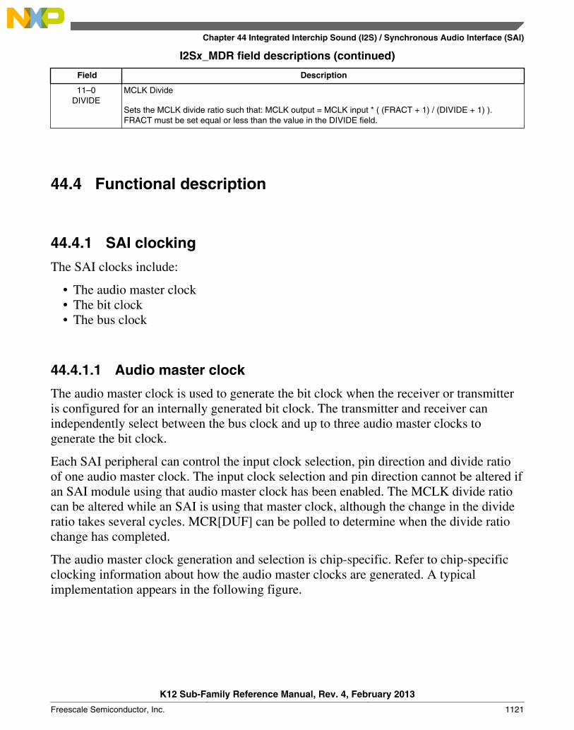
I2Sx_MDR field descriptions (continued)
Field Description
11–0DIVIDE
MCLK Divide
Sets the MCLK divide ratio such that: MCLK output = MCLK input * ( (FRACT + 1) / (DIVIDE + 1) ).FRACT must be set equal or less than the value in the DIVIDE field.
44.4 Functional description
44.4.1 SAI clocking
The SAI clocks include:
• The audio master clock• The bit clock• The bus clock
44.4.1.1 Audio master clock
The audio master clock is used to generate the bit clock when the receiver or transmitteris configured for an internally generated bit clock. The transmitter and receiver canindependently select between the bus clock and up to three audio master clocks togenerate the bit clock.
Each SAI peripheral can control the input clock selection, pin direction and divide ratioof one audio master clock. The input clock selection and pin direction cannot be altered ifan SAI module using that audio master clock has been enabled. The MCLK divide ratiocan be altered while an SAI is using that master clock, although the change in the divideratio takes several cycles. MCR[DUF] can be polled to determine when the divide ratiochange has completed.
The audio master clock generation and selection is chip-specific. Refer to chip-specificclocking information about how the audio master clocks are generated. A typicalimplementation appears in the following figure.
Chapter 44 Integrated Interchip Sound (I2S) / Synchronous Audio Interface (SAI)
K12 Sub-Family Reference Manual, Rev. 4, February 2013
Freescale Semiconductor, Inc. 1121
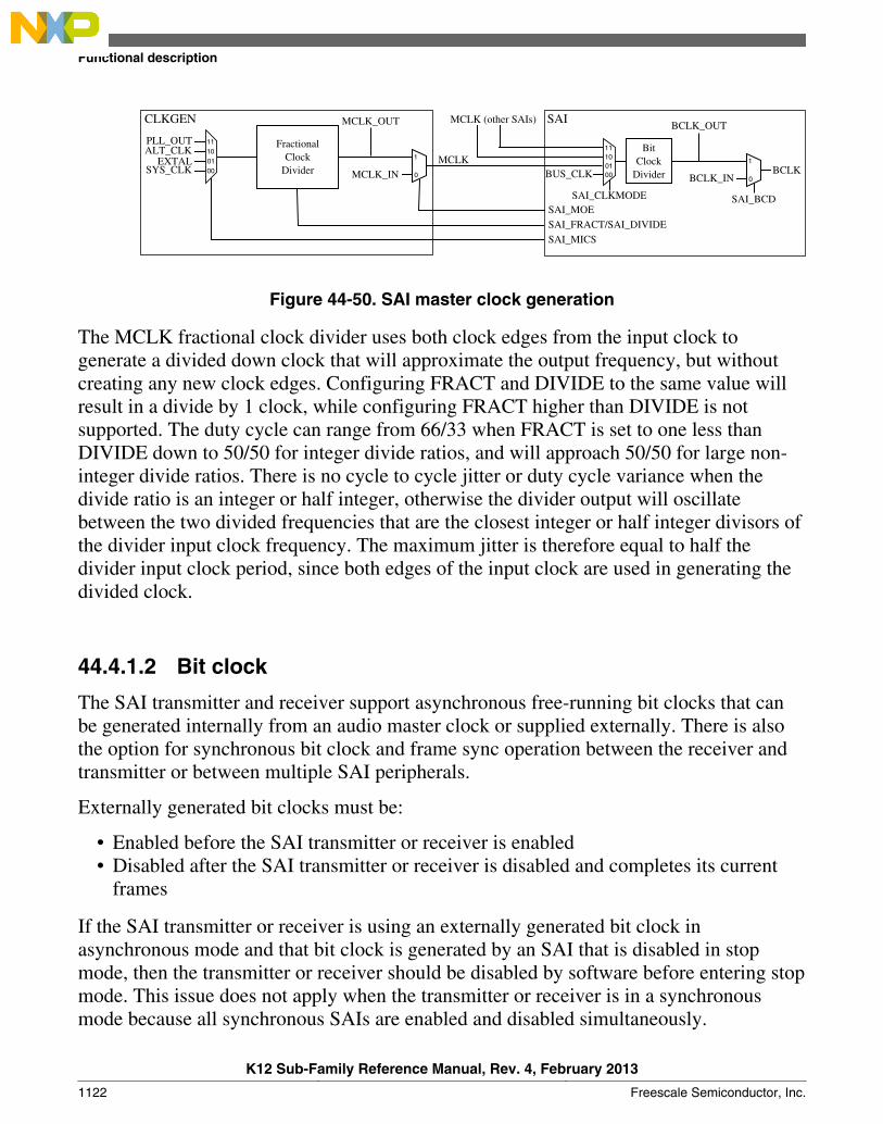
Fractional Clock
Divider1
0
11
0110
00EXTAL
PLL_OUTALT_CLK
SYS_CLK
SAI_MOE
MCLK
MCLK_OUT
MCLK_IN
11
0110
00BUS_CLK
SAI_CLKMODE
Bit Clock
Divider1
0BCLK_IN
SAIBCLK_OUT
SAI_BCD
BCLK
SAI_FRACT/SAI_DIVIDE
SAI_MICS
MCLK (other SAIs)CLKGEN
Figure 44-50. SAI master clock generation
The MCLK fractional clock divider uses both clock edges from the input clock togenerate a divided down clock that will approximate the output frequency, but withoutcreating any new clock edges. Configuring FRACT and DIVIDE to the same value willresult in a divide by 1 clock, while configuring FRACT higher than DIVIDE is notsupported. The duty cycle can range from 66/33 when FRACT is set to one less thanDIVIDE down to 50/50 for integer divide ratios, and will approach 50/50 for large non-integer divide ratios. There is no cycle to cycle jitter or duty cycle variance when thedivide ratio is an integer or half integer, otherwise the divider output will oscillatebetween the two divided frequencies that are the closest integer or half integer divisors ofthe divider input clock frequency. The maximum jitter is therefore equal to half thedivider input clock period, since both edges of the input clock are used in generating thedivided clock.
44.4.1.2 Bit clock
The SAI transmitter and receiver support asynchronous free-running bit clocks that canbe generated internally from an audio master clock or supplied externally. There is alsothe option for synchronous bit clock and frame sync operation between the receiver andtransmitter or between multiple SAI peripherals.
Externally generated bit clocks must be:
• Enabled before the SAI transmitter or receiver is enabled• Disabled after the SAI transmitter or receiver is disabled and completes its current
frames
If the SAI transmitter or receiver is using an externally generated bit clock inasynchronous mode and that bit clock is generated by an SAI that is disabled in stopmode, then the transmitter or receiver should be disabled by software before entering stopmode. This issue does not apply when the transmitter or receiver is in a synchronousmode because all synchronous SAIs are enabled and disabled simultaneously.
Functional description
K12 Sub-Family Reference Manual, Rev. 4, February 2013
1122 Freescale Semiconductor, Inc.
44.4.1.3 Bus clock
The bus clock is used by the control and configuration registers and to generatesynchronous interrupts and DMA requests.
44.4.2 SAI resets
The SAI is asynchronously reset on system reset. The SAI has a software reset and aFIFO reset.
44.4.2.1 Software reset
The SAI transmitter includes a software reset that resets all transmitter internal logic,including the bit clock generation, status flags, and FIFO pointers. It does not reset theconfiguration registers. The software reset remains asserted until cleared by software.
The SAI receiver includes a software reset that resets all receiver internal logic, includingthe bit clock generation, status flags and FIFO pointers. It does not reset the configurationregisters. The software reset remains asserted until cleared by software.
44.4.2.2 FIFO reset
The SAI transmitter includes a FIFO reset that synchronizes the FIFO write pointer to thesame value as the FIFO read pointer. This empties the FIFO contents and is to be usedafter TCSR[FEF] is set, and before the FIFO is re-initialized and TCSR[FEF] is cleared.The FIFO reset is asserted for one cycle only.
The SAI receiver includes a FIFO reset that synchronizes the FIFO read pointer to thesame value as the FIFO write pointer. This empties the FIFO contents and is to be usedafter the RCSR[FEF] is set and any remaining data has been read from the FIFO, andbefore the RCSR[FEF] is cleared. The FIFO reset is asserted for one cycle only.
44.4.3 Synchronous modes
The SAI transmitter and receiver can operate synchronously to each other.
Chapter 44 Integrated Interchip Sound (I2S) / Synchronous Audio Interface (SAI)
K12 Sub-Family Reference Manual, Rev. 4, February 2013
Freescale Semiconductor, Inc. 1123
44.4.3.1 Synchronous mode
The SAI transmitter and receiver can be configured to operate with synchronous bit clockand frame sync.
If the transmitter bit clock and frame sync are to be used by both the transmitter andreceiver:
• The transmitter must be configured for asynchronous operation and the receiver forsynchronous operation.
• In synchronous mode, the receiver is enabled only when both the transmitter andreceiver are enabled.
• It is recommended that the transmitter is the last enabled and the first disabled.
If the receiver bit clock and frame sync are to be used by both the transmitter andreceiver:
• The receiver must be configured for asynchronous operation and the transmitter forsynchronous operation.
• In synchronous mode, the transmitter is enabled only when both the receiver andtransmitter are both enabled.
• It is recommended that the receiver is the last enabled and the first disabled.
When operating in synchronous mode, only the bit clock, frame sync, and transmitter/receiver enable are shared. The transmitter and receiver otherwise operate independently,although configuration registers must be configured consistently across both thetransmitter and receiver.
44.4.4 Frame sync configuration
When enabled, the SAI continuously transmits and/or receives frames of data. Eachframe consists of a fixed number of words and each word consists of a fixed number ofbits. Within each frame, any given word can be masked causing the receiver to ignorethat word and the transmitter to tri-state for the duration of that word.
The frame sync signal is used to indicate the start of each frame. A valid frame syncrequires a rising edge (if active high) or falling edge (if active low) to be detected and thetransmitter or receiver cannot be busy with a previous frame. A valid frame sync is alsoignored (slave mode) or not generated (master mode) for the first four bit clock cyclesafter enabling the transmitter or receiver.
The transmitter and receiver frame sync can be configured independently with any of thefollowing options:
Functional description
K12 Sub-Family Reference Manual, Rev. 4, February 2013
1124 Freescale Semiconductor, Inc.
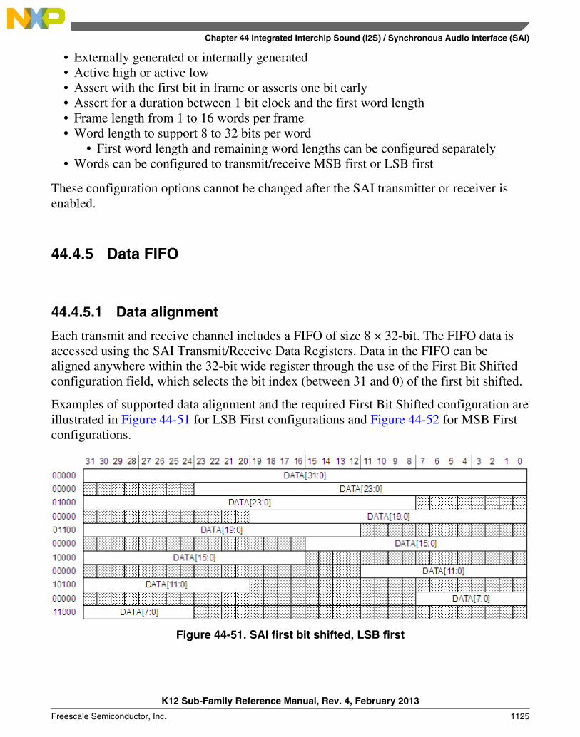
• Externally generated or internally generated• Active high or active low• Assert with the first bit in frame or asserts one bit early• Assert for a duration between 1 bit clock and the first word length• Frame length from 1 to 16 words per frame• Word length to support 8 to 32 bits per word
• First word length and remaining word lengths can be configured separately• Words can be configured to transmit/receive MSB first or LSB first
These configuration options cannot be changed after the SAI transmitter or receiver isenabled.
44.4.5 Data FIFO
44.4.5.1 Data alignment
Each transmit and receive channel includes a FIFO of size 8 × 32-bit. The FIFO data isaccessed using the SAI Transmit/Receive Data Registers. Data in the FIFO can bealigned anywhere within the 32-bit wide register through the use of the First Bit Shiftedconfiguration field, which selects the bit index (between 31 and 0) of the first bit shifted.
Examples of supported data alignment and the required First Bit Shifted configuration areillustrated in Figure 44-51 for LSB First configurations and Figure 44-52 for MSB Firstconfigurations.
Figure 44-51. SAI first bit shifted, LSB first
Chapter 44 Integrated Interchip Sound (I2S) / Synchronous Audio Interface (SAI)
K12 Sub-Family Reference Manual, Rev. 4, February 2013
Freescale Semiconductor, Inc. 1125

Figure 44-52. SAI first bit shifted, MSB first
44.4.5.2 FIFO pointers
When writing to a TDR, the WFP of the corresponding TFR increments after each validwrite. The SAI supports 8-bit, 16-bit and 32-bit writes to the TDR and the FIFO pointerwill increment after each individual write. Note that 8-bit writes should only be usedwhen transmitting up to 8-bit data and 16-bit writes should only be used whentransmitting up to 16-bit data.
Writes to a TDR are ignored if the corresponding bit of TCR3[TCE] is clear or if theFIFO is full. If the Transmit FIFO is empty, the TDR must be written at least three bitclocks before the start of the next unmasked word to avoid a FIFO underrun.
When reading an RDR, the RFP of the corresponding RFR increments after each validread. The SAI supports 8-bit, 16-bit and 32-bit reads from the RDR and the FIFO pointerwill increment after each individual read. Note that 8-bit reads should only be used whenreceiving up to 8-bit data and 16-bit reads should only be used when receiving up to 16-bit data.
Reads from an RDR are ignored if the corresponding bit of RCR3[RCE] is clear or if theFIFO is empty. If the Receive FIFO is full, the RDR must be read at least three bit clocksbefore the end of an unmasked word to avoid a FIFO overrun.
Functional description
K12 Sub-Family Reference Manual, Rev. 4, February 2013
1126 Freescale Semiconductor, Inc.
44.4.6 Word mask register
The SAI transmitter and receiver each contain a word mask register, namely TMR andRMR, that can be used to mask any word in the frame. Because the word mask register isdouble buffered, software can update it before the end of each frame to mask a particularword in the next frame.
The TMR causes the Transmit Data pin to be tri-stated for the length of each selectedword and the transmit FIFO is not read for masked words.
The RMR causes the received data for each selected word to be discarded and not writtento the receive FIFO.
44.4.7 Interrupts and DMA requests
The SAI transmitter and receiver generate separate interrupts and separate DMA requests,but support the same status flags. Asynchronous versions of the transmitter and receiverinterrupts are generated to wake up the CPU from stop mode.
44.4.7.1 FIFO request flag
The FIFO request flag is set based on the number of entries in the FIFO and the FIFOwatermark configuration.
The transmit FIFO request flag is set when the number of entries in any of the enabledtransmit FIFOs is less than or equal to the transmit FIFO watermark configuration and iscleared when the number of entries in each enabled transmit FIFO is greater than thetransmit FIFO watermark configuration.
The receive FIFO request flag is set when the number of entries in any of the enabledreceive FIFOs is greater than the receive FIFO watermark configuration and is clearedwhen the number of entries in each enabled receive FIFO is less than or equal to thereceive FIFO watermark configuration.
The FIFO request flag can generate an interrupt or a DMA request.
44.4.7.2 FIFO warning flag
The FIFO warning flag is set based on the number of entries in the FIFO.
Chapter 44 Integrated Interchip Sound (I2S) / Synchronous Audio Interface (SAI)
K12 Sub-Family Reference Manual, Rev. 4, February 2013
Freescale Semiconductor, Inc. 1127

The transmit warning flag is set when the number of entries in any of the enabledtransmit FIFOs is empty and is cleared when the number of entries in each enabledtransmit FIFO is not empty.
The receive warning flag is set when the number of entries in any of the enabled receiveFIFOs is full and is cleared when the number of entries in each enabled receive FIFO isnot full.
The FIFO warning flag can generate an Interrupt or a DMA request.
44.4.7.3 FIFO error flag
The transmit FIFO error flag is set when the any of the enabled transmit FIFOsunderflow. After it is set, all enabled transmit channels repeat the last valid word readfrom the transmit FIFO until TCSR[FEF] is cleared and the next transmit frame starts.All enabled transmit FIFOs must be reset and initialized with new data beforeTCSR[FEF] is cleared.
RCSR[FEF] is set when the any of the enabled receive FIFOs overflow. After it is set, allenabled receive channels discard received data until RCSR[FEF] is cleared and the nextnext receive frame starts. All enabled receive FIFOs should be emptied beforeRCSR[FEF] is cleared.
The FIFO error flag can generate only an interrupt.
44.4.7.4 Sync error flag
The sync error flag, TCSR[SEF] or RCSR[SEF], is set when configured for an externallygenerated frame sync and the external frame sync asserts when the transmitter or receiveris busy with the previous frame. The external frame sync assertion is ignored and thesync error flag is set. When the sync error flag is set, the transmitter or receiver continueschecking for frame sync assertion when idle or at the end of each frame.
The sync error flag can generate an interrupt only.
44.4.7.5 Word start flag
The word start flag is set at the start of the second bit clock for the selected word, asconfigured by the Word Flag register field.
The word start flag can generate an interrupt only.
Functional description
K12 Sub-Family Reference Manual, Rev. 4, February 2013
1128 Freescale Semiconductor, Inc.
Chapter 45General-Purpose Input/Output (GPIO)
45.1 IntroductionNOTE
For the chip-specific implementation details of this module'sinstances see the chip configuration information.
The general-purpose input and output (GPIO) module communicates to the processorcore via a zero wait state interface for maximum pin performance. The GPIO registerssupport 8-bit, 16-bit or 32-bit accesses.
The GPIO data direction and output data registers control the direction and output data ofeach pin when the pin is configured for the GPIO function. The GPIO input data registerdisplays the logic value on each pin when the pin is configured for any digital function,provided the corresponding Port Control and Interrupt module for that pin is enabled.
Efficient bit manipulation of the general-purpose outputs is supported through theaddition of set, clear, and toggle write-only registers for each port output data register.
45.1.1 Features• Features of the GPIO module include:
• Pin input data register visible in all digital pin-multiplexing modes• Pin output data register with corresponding set/clear/toggle registers• Pin data direction register• Zero wait state access to GPIO registers through IOPORT
NOTEGPIO module is clocked by system clock.
K12 Sub-Family Reference Manual, Rev. 4, February 2013
Freescale Semiconductor, Inc. 1129

45.1.2 Modes of operationThe following table depicts different modes of operation and the behavior of the GPIOmodule in these modes.
Table 45-1. Modes of operation
Modes of operation Description
Run The GPIO module operates normally.
Wait The GPIO module operates normally.
Stop The GPIO module is disabled.
Debug The GPIO module operates normally.
45.1.3 GPIO signal descriptionsTable 45-2. GPIO signal descriptions
GPIO signal descriptions Description I/O
PORTA31–PORTA0 General-purpose input/output I/O
PORTB31–PORTB0 General-purpose input/output I/O
PORTC31–PORTC0 General-purpose input/output I/O
PORTD31–PORTD0 General-purpose input/output I/O
PORTE31–PORTE0 General-purpose input/output I/O
NOTENot all pins within each port are implemented on each device.See the chapter on signal multiplexing for the number of GPIOports available in the device.
Introduction
K12 Sub-Family Reference Manual, Rev. 4, February 2013
1130 Freescale Semiconductor, Inc.
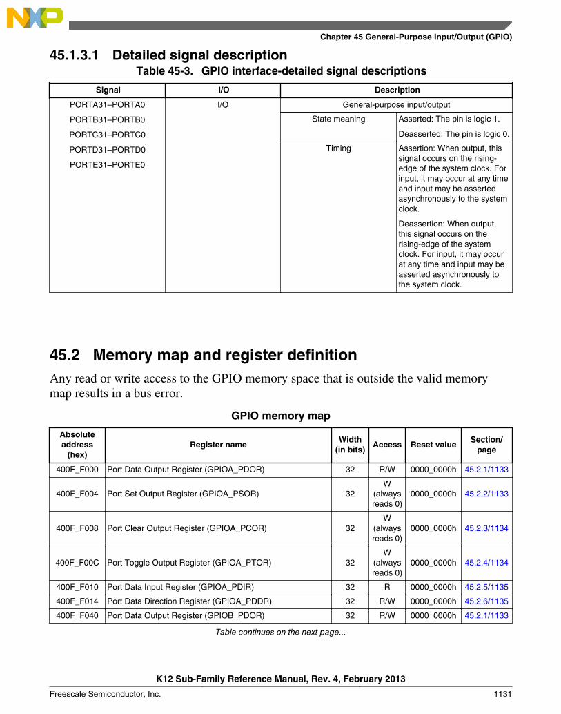
45.1.3.1 Detailed signal descriptionTable 45-3. GPIO interface-detailed signal descriptions
Signal I/O Description
PORTA31–PORTA0
PORTB31–PORTB0
PORTC31–PORTC0
PORTD31–PORTD0
PORTE31–PORTE0
I/O General-purpose input/output
State meaning Asserted: The pin is logic 1.
Deasserted: The pin is logic 0.
Timing Assertion: When output, thissignal occurs on the rising-edge of the system clock. Forinput, it may occur at any timeand input may be assertedasynchronously to the systemclock.
Deassertion: When output,this signal occurs on therising-edge of the systemclock. For input, it may occurat any time and input may beasserted asynchronously tothe system clock.
45.2 Memory map and register definitionAny read or write access to the GPIO memory space that is outside the valid memorymap results in a bus error.
GPIO memory map
Absoluteaddress
(hex)Register name
Width(in bits)
Access Reset valueSection/
page
400F_F000 Port Data Output Register (GPIOA_PDOR) 32 R/W 0000_0000h 45.2.1/1133
400F_F004 Port Set Output Register (GPIOA_PSOR) 32W
(alwaysreads 0)
0000_0000h 45.2.2/1133
400F_F008 Port Clear Output Register (GPIOA_PCOR) 32W
(alwaysreads 0)
0000_0000h 45.2.3/1134
400F_F00C Port Toggle Output Register (GPIOA_PTOR) 32W
(alwaysreads 0)
0000_0000h 45.2.4/1134
400F_F010 Port Data Input Register (GPIOA_PDIR) 32 R 0000_0000h 45.2.5/1135
400F_F014 Port Data Direction Register (GPIOA_PDDR) 32 R/W 0000_0000h 45.2.6/1135
400F_F040 Port Data Output Register (GPIOB_PDOR) 32 R/W 0000_0000h 45.2.1/1133
Table continues on the next page...
Chapter 45 General-Purpose Input/Output (GPIO)
K12 Sub-Family Reference Manual, Rev. 4, February 2013
Freescale Semiconductor, Inc. 1131
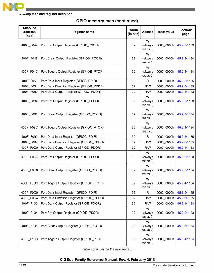
GPIO memory map (continued)
Absoluteaddress
(hex)Register name
Width(in bits)
Access Reset valueSection/
page
400F_F044 Port Set Output Register (GPIOB_PSOR) 32W
(alwaysreads 0)
0000_0000h 45.2.2/1133
400F_F048 Port Clear Output Register (GPIOB_PCOR) 32W
(alwaysreads 0)
0000_0000h 45.2.3/1134
400F_F04C Port Toggle Output Register (GPIOB_PTOR) 32W
(alwaysreads 0)
0000_0000h 45.2.4/1134
400F_F050 Port Data Input Register (GPIOB_PDIR) 32 R 0000_0000h 45.2.5/1135
400F_F054 Port Data Direction Register (GPIOB_PDDR) 32 R/W 0000_0000h 45.2.6/1135
400F_F080 Port Data Output Register (GPIOC_PDOR) 32 R/W 0000_0000h 45.2.1/1133
400F_F084 Port Set Output Register (GPIOC_PSOR) 32W
(alwaysreads 0)
0000_0000h 45.2.2/1133
400F_F088 Port Clear Output Register (GPIOC_PCOR) 32W
(alwaysreads 0)
0000_0000h 45.2.3/1134
400F_F08C Port Toggle Output Register (GPIOC_PTOR) 32W
(alwaysreads 0)
0000_0000h 45.2.4/1134
400F_F090 Port Data Input Register (GPIOC_PDIR) 32 R 0000_0000h 45.2.5/1135
400F_F094 Port Data Direction Register (GPIOC_PDDR) 32 R/W 0000_0000h 45.2.6/1135
400F_F0C0 Port Data Output Register (GPIOD_PDOR) 32 R/W 0000_0000h 45.2.1/1133
400F_F0C4 Port Set Output Register (GPIOD_PSOR) 32W
(alwaysreads 0)
0000_0000h 45.2.2/1133
400F_F0C8 Port Clear Output Register (GPIOD_PCOR) 32W
(alwaysreads 0)
0000_0000h 45.2.3/1134
400F_F0CC Port Toggle Output Register (GPIOD_PTOR) 32W
(alwaysreads 0)
0000_0000h 45.2.4/1134
400F_F0D0 Port Data Input Register (GPIOD_PDIR) 32 R 0000_0000h 45.2.5/1135
400F_F0D4 Port Data Direction Register (GPIOD_PDDR) 32 R/W 0000_0000h 45.2.6/1135
400F_F100 Port Data Output Register (GPIOE_PDOR) 32 R/W 0000_0000h 45.2.1/1133
400F_F104 Port Set Output Register (GPIOE_PSOR) 32W
(alwaysreads 0)
0000_0000h 45.2.2/1133
400F_F108 Port Clear Output Register (GPIOE_PCOR) 32W
(alwaysreads 0)
0000_0000h 45.2.3/1134
400F_F10C Port Toggle Output Register (GPIOE_PTOR) 32W
(alwaysreads 0)
0000_0000h 45.2.4/1134
Table continues on the next page...
Memory map and register definition
K12 Sub-Family Reference Manual, Rev. 4, February 2013
1132 Freescale Semiconductor, Inc.
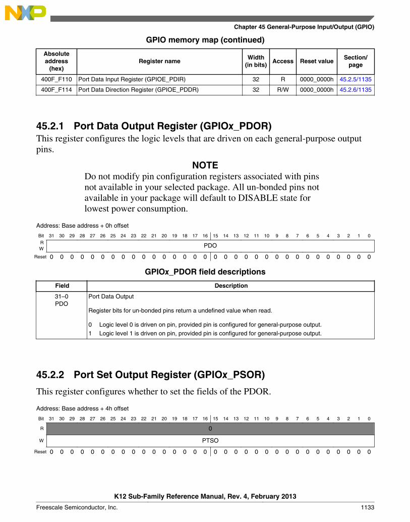
GPIO memory map (continued)
Absoluteaddress
(hex)Register name
Width(in bits)
Access Reset valueSection/
page
400F_F110 Port Data Input Register (GPIOE_PDIR) 32 R 0000_0000h 45.2.5/1135
400F_F114 Port Data Direction Register (GPIOE_PDDR) 32 R/W 0000_0000h 45.2.6/1135
45.2.1 Port Data Output Register (GPIOx_PDOR)This register configures the logic levels that are driven on each general-purpose outputpins.
NOTEDo not modify pin configuration registers associated with pinsnot available in your selected package. All un-bonded pins notavailable in your package will default to DISABLE state forlowest power consumption.
Address: Base address + 0h offset
Bit 31 30 29 28 27 26 25 24 23 22 21 20 19 18 17 16 15 14 13 12 11 10 9 8 7 6 5 4 3 2 1 0
R PDOW
Reset 0 0 0 0 0 0 0 0 0 0 0 0 0 0 0 0 0 0 0 0 0 0 0 0 0 0 0 0 0 0 0 0
GPIOx_PDOR field descriptions
Field Description
31–0PDO
Port Data Output
Register bits for un-bonded pins return a undefined value when read.
0 Logic level 0 is driven on pin, provided pin is configured for general-purpose output.1 Logic level 1 is driven on pin, provided pin is configured for general-purpose output.
45.2.2 Port Set Output Register (GPIOx_PSOR)
This register configures whether to set the fields of the PDOR.
Address: Base address + 4h offset
Bit 31 30 29 28 27 26 25 24 23 22 21 20 19 18 17 16 15 14 13 12 11 10 9 8 7 6 5 4 3 2 1 0
R 0
W PTSO
Reset 0 0 0 0 0 0 0 0 0 0 0 0 0 0 0 0 0 0 0 0 0 0 0 0 0 0 0 0 0 0 0 0
Chapter 45 General-Purpose Input/Output (GPIO)
K12 Sub-Family Reference Manual, Rev. 4, February 2013
Freescale Semiconductor, Inc. 1133

GPIOx_PSOR field descriptions
Field Description
31–0PTSO
Port Set Output
Writing to this register will update the contents of the corresponding bit in the PDOR as follows:
0 Corresponding bit in PDORn does not change.1 Corresponding bit in PDORn is set to logic 1.
45.2.3 Port Clear Output Register (GPIOx_PCOR)
This register configures whether to clear the fields of PDOR.
Address: Base address + 8h offset
Bit 31 30 29 28 27 26 25 24 23 22 21 20 19 18 17 16 15 14 13 12 11 10 9 8 7 6 5 4 3 2 1 0
R 0
W PTCO
Reset 0 0 0 0 0 0 0 0 0 0 0 0 0 0 0 0 0 0 0 0 0 0 0 0 0 0 0 0 0 0 0 0
GPIOx_PCOR field descriptions
Field Description
31–0PTCO
Port Clear Output
Writing to this register will update the contents of the corresponding bit in the Port Data Output Register(PDOR) as follows:
0 Corresponding bit in PDORn does not change.1 Corresponding bit in PDORn is cleared to logic 0.
45.2.4 Port Toggle Output Register (GPIOx_PTOR)
Address: Base address + Ch offset
Bit 31 30 29 28 27 26 25 24 23 22 21 20 19 18 17 16 15 14 13 12 11 10 9 8 7 6 5 4 3 2 1 0
R 0
W PTTO
Reset 0 0 0 0 0 0 0 0 0 0 0 0 0 0 0 0 0 0 0 0 0 0 0 0 0 0 0 0 0 0 0 0
GPIOx_PTOR field descriptions
Field Description
31–0PTTO
Port Toggle Output
Writing to this register will update the contents of the corresponding bit in the PDOR as follows:
Memory map and register definition
K12 Sub-Family Reference Manual, Rev. 4, February 2013
1134 Freescale Semiconductor, Inc.
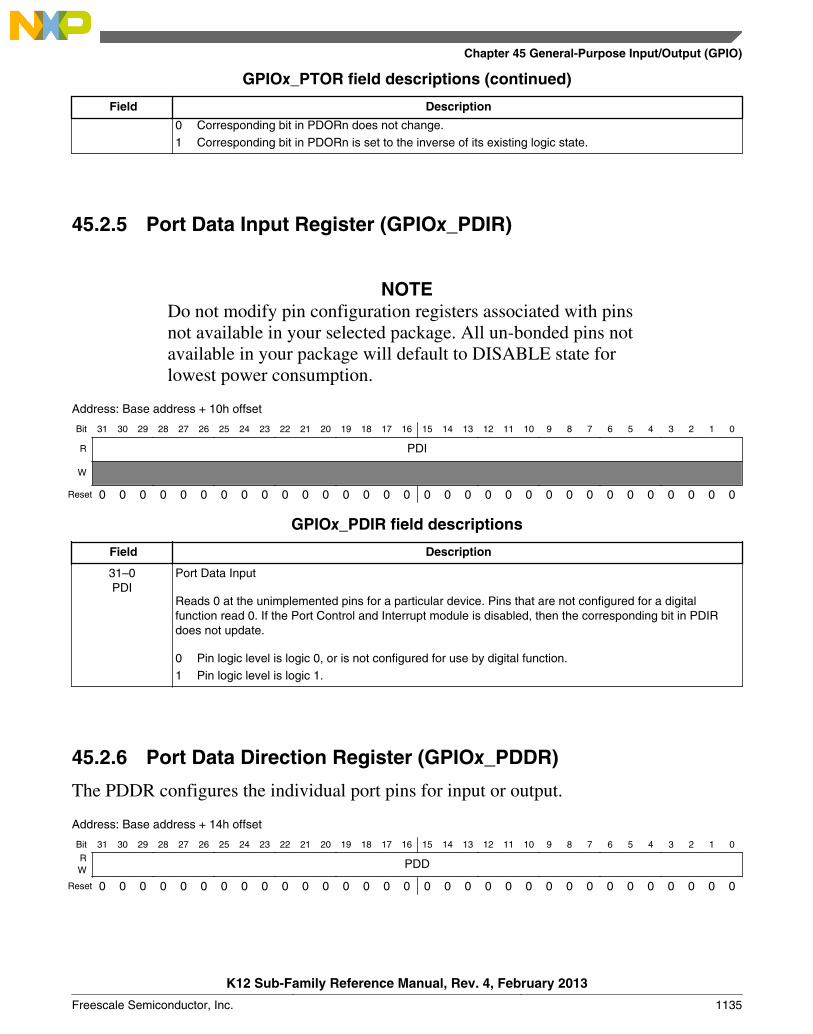
GPIOx_PTOR field descriptions (continued)
Field Description
0 Corresponding bit in PDORn does not change.1 Corresponding bit in PDORn is set to the inverse of its existing logic state.
45.2.5 Port Data Input Register (GPIOx_PDIR)
NOTEDo not modify pin configuration registers associated with pinsnot available in your selected package. All un-bonded pins notavailable in your package will default to DISABLE state forlowest power consumption.
Address: Base address + 10h offset
Bit 31 30 29 28 27 26 25 24 23 22 21 20 19 18 17 16 15 14 13 12 11 10 9 8 7 6 5 4 3 2 1 0
R PDI
W
Reset 0 0 0 0 0 0 0 0 0 0 0 0 0 0 0 0 0 0 0 0 0 0 0 0 0 0 0 0 0 0 0 0
GPIOx_PDIR field descriptions
Field Description
31–0PDI
Port Data Input
Reads 0 at the unimplemented pins for a particular device. Pins that are not configured for a digitalfunction read 0. If the Port Control and Interrupt module is disabled, then the corresponding bit in PDIRdoes not update.
0 Pin logic level is logic 0, or is not configured for use by digital function.1 Pin logic level is logic 1.
45.2.6 Port Data Direction Register (GPIOx_PDDR)
The PDDR configures the individual port pins for input or output.
Address: Base address + 14h offset
Bit 31 30 29 28 27 26 25 24 23 22 21 20 19 18 17 16 15 14 13 12 11 10 9 8 7 6 5 4 3 2 1 0
R PDDW
Reset 0 0 0 0 0 0 0 0 0 0 0 0 0 0 0 0 0 0 0 0 0 0 0 0 0 0 0 0 0 0 0 0
Chapter 45 General-Purpose Input/Output (GPIO)
K12 Sub-Family Reference Manual, Rev. 4, February 2013
Freescale Semiconductor, Inc. 1135
GPIOx_PDDR field descriptions
Field Description
31–0PDD
Port Data Direction
Configures individual port pins for input or output.
0 Pin is configured as general-purpose input, for the GPIO function.1 Pin is configured as general-purpose output, for the GPIO function.
45.3 Functional description
45.3.1 General-purpose input
The logic state of each pin is available via the Port Data Input registers, provided the pinis configured for a digital function and the corresponding Port Control and Interruptmodule is enabled.
The Port Data Input registers return the synchronized pin state after any enabled digitalfilter in the Port Control and Interrupt module. The input pin synchronizers are sharedwith the Port Control and Interrupt module, so that if the corresponding Port Control andInterrupt module is disabled, then synchronizers are also disabled. This reduces powerconsumption when a port is not required for general-purpose input functionality.
45.3.2 General-purpose outputThe logic state of each pin can be controlled via the port data output registers and portdata direction registers, provided the pin is configured for the GPIO function. Thefollowing table depicts the conditions for a pin to be configured as input/output.
If Then
A pin is configured for the GPIO function and thecorresponding port data direction register bit is clear.
The pin is configured as an input.
A pin is configured for the GPIO function and thecorresponding port data direction register bit is set.
The pin is configured as an output and and the logic state ofthe pin is equal to the corresponding port data output register.
To facilitate efficient bit manipulation on the general-purpose outputs, pin data set, pindata clear, and pin data toggle registers exist to allow one or more outputs within one portto be set, cleared, or toggled from a single register write.
Functional description
K12 Sub-Family Reference Manual, Rev. 4, February 2013
1136 Freescale Semiconductor, Inc.

The corresponding Port Control and Interrupt module does not need to be enabled toupdate the state of the port data direction registers and port data output registers includingthe set/clear/toggle registers.
Chapter 45 General-Purpose Input/Output (GPIO)
K12 Sub-Family Reference Manual, Rev. 4, February 2013
Freescale Semiconductor, Inc. 1137

Functional description
K12 Sub-Family Reference Manual, Rev. 4, February 2013
1138 Freescale Semiconductor, Inc.
Chapter 46JTAG Controller (JTAGC)
46.1 IntroductionNOTE
For the chip-specific implementation details of this module'sinstances see the chip configuration information.
The JTAGC block provides the means to test chip functionality and connectivity whileremaining transparent to system logic when not in test mode. Testing is performed via aboundary scan technique, as defined in the IEEE 1149.1-2001 standard. All data input toand output from the JTAGC block is communicated in serial format.
46.1.1 Block diagram
The following is a simplified block diagram of the JTAG Controller (JTAGC) block.Refer to the chip-specific configuration information as well as Register description formore information about the JTAGC registers.
K12 Sub-Family Reference Manual, Rev. 4, February 2013
Freescale Semiconductor, Inc. 1139

Power-on reset
TMS
TCK
TDI
1-bit Bypass Register
32-bit Device Identification Register
Boundary Scan Register
TAP Instruction Decoder
TAP Instruction Register
TDO
Test Access Port (TAP) Controller
Figure 46-1. JTAG (IEEE 1149.1) block diagram
46.1.2 Features
The JTAGC block is compliant with the IEEE 1149.1-2001 standard, and supports thefollowing features:
• IEEE 1149.1-2001 Test Access Port (TAP) interface
• 4 pins (TDI, TMS, TCK, and TDO)
• Instruction register that supports several IEEE 1149.1-2001 defined instructions aswell as several public and private device-specific instructions. Refer to Table 46-3for a list of supported instructions.
• Bypass register, boundary scan register, and device identification register.
• TAP controller state machine that controls the operation of the data registers,instruction register and associated circuitry.
46.1.3 Modes of operation
The JTAGC block uses a power-on reset indication as its primary reset signals. SeveralIEEE 1149.1-2001 defined test modes are supported, as well as a bypass mode.
Introduction
K12 Sub-Family Reference Manual, Rev. 4, February 2013
1140 Freescale Semiconductor, Inc.

46.1.3.1 Reset
The JTAGC block is placed in reset when either power-on reset is asserted, or the TMSinput is held high for enough consecutive rising edges of TCK to sequence the TAPcontroller state machine into the Test-Logic-Reset state. Holding TMS high for fiveconsecutive rising edges of TCK guarantees entry into the Test-Logic-Reset stateregardless of the current TAP controller state. Asserting power-on reset results inasynchronous entry into the reset state. While in reset, the following actions occur:
• The TAP controller is forced into the Test-Logic-Reset state, thereby disabling thetest logic and allowing normal operation of the on-chip system logic to continueunhindered
• The instruction register is loaded with the IDCODE instruction
46.1.3.2 IEEE 1149.1-2001 defined test modes
The JTAGC block supports several IEEE 1149.1-2001 defined test modes. A test mode isselected by loading the appropriate instruction into the instruction register while theJTAGC is enabled. Supported test instructions include EXTEST, HIGHZ, CLAMP,SAMPLE and SAMPLE/PRELOAD. Each instruction defines the set of data register(s)that may operate and interact with the on-chip system logic while the instruction iscurrent. Only one test data register path is enabled to shift data between TDI and TDO foreach instruction.
The boundary scan register is enabled for serial access between TDI and TDO when theEXTEST, SAMPLE or SAMPLE/PRELOAD instructions are active. The single-bitbypass register shift stage is enabled for serial access between TDI and TDO when theBYPASS, HIGHZ, CLAMP or reserved instructions are active. The functionality of eachtest mode is explained in more detail in JTAGC block instructions.
46.1.3.3 Bypass mode
When no test operation is required, the BYPASS instruction can be loaded to place theJTAGC block into bypass mode. While in bypass mode, the single-bit bypass shiftregister is used to provide a minimum-length serial path to shift data between TDI andTDO.
Chapter 46 JTAG Controller (JTAGC)
K12 Sub-Family Reference Manual, Rev. 4, February 2013
Freescale Semiconductor, Inc. 1141
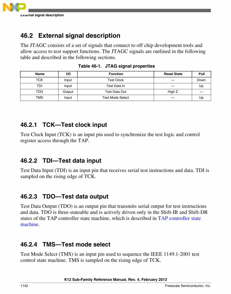
46.2 External signal descriptionThe JTAGC consists of a set of signals that connect to off chip development tools andallow access to test support functions. The JTAGC signals are outlined in the followingtable and described in the following sections.
Table 46-1. JTAG signal properties
Name I/O Function Reset State Pull
TCK Input Test Clock — Down
TDI Input Test Data In — Up
TDO Output Test Data Out High Z —
TMS Input Test Mode Select — Up
46.2.1 TCK—Test clock input
Test Clock Input (TCK) is an input pin used to synchronize the test logic and controlregister access through the TAP.
46.2.2 TDI—Test data input
Test Data Input (TDI) is an input pin that receives serial test instructions and data. TDI issampled on the rising edge of TCK.
46.2.3 TDO—Test data output
Test Data Output (TDO) is an output pin that transmits serial output for test instructionsand data. TDO is three-stateable and is actively driven only in the Shift-IR and Shift-DRstates of the TAP controller state machine, which is described in TAP controller statemachine.
46.2.4 TMS—Test mode select
Test Mode Select (TMS) is an input pin used to sequence the IEEE 1149.1-2001 testcontrol state machine. TMS is sampled on the rising edge of TCK.
External signal description
K12 Sub-Family Reference Manual, Rev. 4, February 2013
1142 Freescale Semiconductor, Inc.

46.3 Register descriptionThis section provides a detailed description of the JTAGC block registers accessiblethrough the TAP interface, including data registers and the instruction register. Individualbit-level descriptions and reset states of each register are included. These registers are notmemory-mapped and can only be accessed through the TAP.
46.3.1 Instruction register
The JTAGC block uses a 4-bit instruction register as shown in the following figure. Theinstruction register allows instructions to be loaded into the block to select the test to beperformed or the test data register to be accessed or both. Instructions are shifted inthrough TDI while the TAP controller is in the Shift-IR state, and latched on the fallingedge of TCK in the Update-IR state. The latched instruction value can only be changed inthe Update-IR and Test-Logic-Reset TAP controller states. Synchronous entry into theTest-Logic-Reset state results in the IDCODE instruction being loaded on the fallingedge of TCK. Asynchronous entry into the Test-Logic-Reset state results in asynchronousloading of the IDCODE instruction. During the Capture-IR TAP controller state, theinstruction shift register is loaded with the value 0001b , making this value the register'sread value when the TAP controller is sequenced into the Shift-IR state.
RW
Reset:Instruction Code
2 1 00 0 0 1
0 0 0 1
3
Figure 46-2. Instruction register
46.3.2 Bypass register
The bypass register is a single-bit shift register path selected for serial data transferbetween TDI and TDO when the BYPASS, CLAMP, HIGHZ or reserve instructions areactive. After entry into the Capture-DR state, the single-bit shift register is set to a logic0. Therefore, the first bit shifted out after selecting the bypass register is always a logic 0.
Chapter 46 JTAG Controller (JTAGC)
K12 Sub-Family Reference Manual, Rev. 4, February 2013
Freescale Semiconductor, Inc. 1143
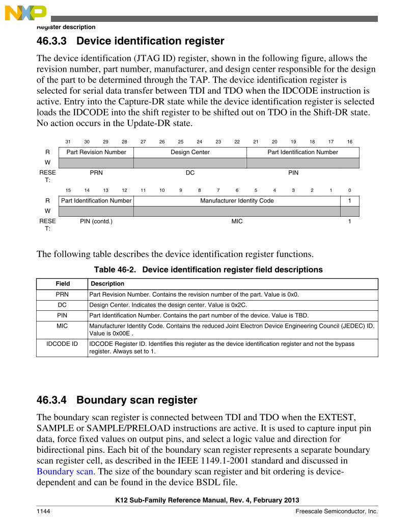
46.3.3 Device identification register
The device identification (JTAG ID) register, shown in the following figure, allows therevision number, part number, manufacturer, and design center responsible for the designof the part to be determined through the TAP. The device identification register isselected for serial data transfer between TDI and TDO when the IDCODE instruction isactive. Entry into the Capture-DR state while the device identification register is selectedloads the IDCODE into the shift register to be shifted out on TDO in the Shift-DR state.No action occurs in the Update-DR state.
31 30 29 28 27 26 25 24 23 22 21 20 19 18 17 16
R Part Revision Number Design Center Part Identification Number
W
RESET:
PRN DC PIN
15 14 13 12 11 10 9 8 7 6 5 4 3 2 1 0
R Part Identification Number Manufacturer Identity Code 1
W
RESET:
PIN (contd.) MIC 1
The following table describes the device identification register functions.
Table 46-2. Device identification register field descriptions
Field Description
PRN Part Revision Number. Contains the revision number of the part. Value is 0x0.
DC Design Center. Indicates the design center. Value is 0x2C.
PIN Part Identification Number. Contains the part number of the device. Value is TBD.
MIC Manufacturer Identity Code. Contains the reduced Joint Electron Device Engineering Council (JEDEC) ID.Value is 0x00E .
IDCODE ID IDCODE Register ID. Identifies this register as the device identification register and not the bypassregister. Always set to 1.
46.3.4 Boundary scan register
The boundary scan register is connected between TDI and TDO when the EXTEST,SAMPLE or SAMPLE/PRELOAD instructions are active. It is used to capture input pindata, force fixed values on output pins, and select a logic value and direction forbidirectional pins. Each bit of the boundary scan register represents a separate boundaryscan register cell, as described in the IEEE 1149.1-2001 standard and discussed inBoundary scan. The size of the boundary scan register and bit ordering is device-dependent and can be found in the device BSDL file.
Register description
K12 Sub-Family Reference Manual, Rev. 4, February 2013
1144 Freescale Semiconductor, Inc.
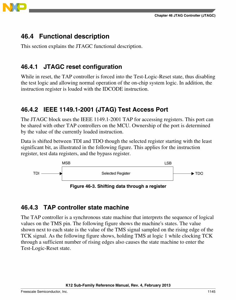
46.4 Functional descriptionThis section explains the JTAGC functional description.
46.4.1 JTAGC reset configuration
While in reset, the TAP controller is forced into the Test-Logic-Reset state, thus disablingthe test logic and allowing normal operation of the on-chip system logic. In addition, theinstruction register is loaded with the IDCODE instruction.
46.4.2 IEEE 1149.1-2001 (JTAG) Test Access Port
The JTAGC block uses the IEEE 1149.1-2001 TAP for accessing registers. This port canbe shared with other TAP controllers on the MCU. Ownership of the port is determinedby the value of the currently loaded instruction.
Data is shifted between TDI and TDO though the selected register starting with the leastsignificant bit, as illustrated in the following figure. This applies for the instructionregister, test data registers, and the bypass register.
Selected Register
LSBMSB
TDI TDO
Figure 46-3. Shifting data through a register
46.4.3 TAP controller state machine
The TAP controller is a synchronous state machine that interprets the sequence of logicalvalues on the TMS pin. The following figure shows the machine's states. The valueshown next to each state is the value of the TMS signal sampled on the rising edge of theTCK signal. As the following figure shows, holding TMS at logic 1 while clocking TCKthrough a sufficient number of rising edges also causes the state machine to enter theTest-Logic-Reset state.
Chapter 46 JTAG Controller (JTAGC)
K12 Sub-Family Reference Manual, Rev. 4, February 2013
Freescale Semiconductor, Inc. 1145
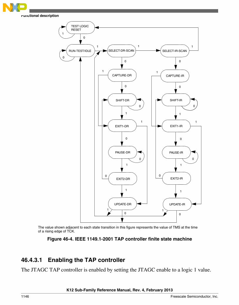
The value shown adjacent to each state transition in this figure represents the value of TMS at the time of a rising edge of TCK.
TEST LOGIC RESET
RUN-TEST/IDLE SELECT-DR-SCAN SELECT-IR-SCAN
CAPTURE-DR CAPTURE-IR
SHIFT-IRSHIFT-DR
EXIT1-DR EXIT1-IR
PAUSE-DR PAUSE-IR
EXIT2-IREXIT2-DR
UPDATE-DR UPDATE-IR
1
1
1
1
1
1
1 1
1
1
11
1 1
1 1
0
00 0
00
0 0
00
0 0
00
00
Figure 46-4. IEEE 1149.1-2001 TAP controller finite state machine
46.4.3.1 Enabling the TAP controller
The JTAGC TAP controller is enabled by setting the JTAGC enable to a logic 1 value.
Functional description
K12 Sub-Family Reference Manual, Rev. 4, February 2013
1146 Freescale Semiconductor, Inc.

46.4.3.2 Selecting an IEEE 1149.1-2001 register
Access to the JTAGC data registers is achieved by loading the instruction register withany of the JTAGC block instructions while the JTAGC is enabled. Instructions are shiftedin via the Select-IR-Scan path and loaded in the Update-IR state. At this point, all dataregister access is performed via the Select-DR-Scan path.
The Select-DR-Scan path is used to read or write the register data by shifting in the data(LSB first) during the Shift-DR state. When reading a register, the register value is loadedinto the IEEE 1149.1-2001 shifter during the Capture-DR state. When writing a register,the value is loaded from the IEEE 1149.1-2001 shifter to the register during the Update-DR state. When reading a register, there is no requirement to shift out the entire registercontents. Shifting may be terminated once the required number of bits have beenacquired.
46.4.4 JTAGC block instructions
The JTAGC block implements the IEEE 1149.1-2001 defined instructions listed in thefollowing table. This section gives an overview of each instruction; refer to the IEEE1149.1-2001 standard for more details. All undefined opcodes are reserved.
Table 46-3. 4-bit JTAG instructions
Instruction Code[3:0] Instruction summary
IDCODE 0000 Selects device identification register for shift
EZPORT 0001 Enables the EZPORT function for the SoC
SAMPLE/PRELOAD 0010 Selects boundary scan register for shifting, sampling, andpreloading without disturbing functional operation
SAMPLE 0011 Selects boundary scan register for shifting and samplingwithout disturbing functional operation
EXTEST 0100 Selects boundary scan register and applies preloaded valuesto output pins.
NOTE: Execution of this instruction asserts functional reset.
Factory debug reserved 0101 Intended for factory debug only
Factory debug reserved 0110 Intended for factory debug only
Factory debug reserved 0111 Intended for factory debug only
ARM JTAG-DP Reserved 1000 This instruction goes the ARM JTAG-DP controller. See theARM JTAG-DP documentation for more information.
HIGHZ 1001 Selects bypass register and three-states all output pins.
NOTE: Execution of this instruction asserts functional reset.
Table continues on the next page...
Chapter 46 JTAG Controller (JTAGC)
K12 Sub-Family Reference Manual, Rev. 4, February 2013
Freescale Semiconductor, Inc. 1147
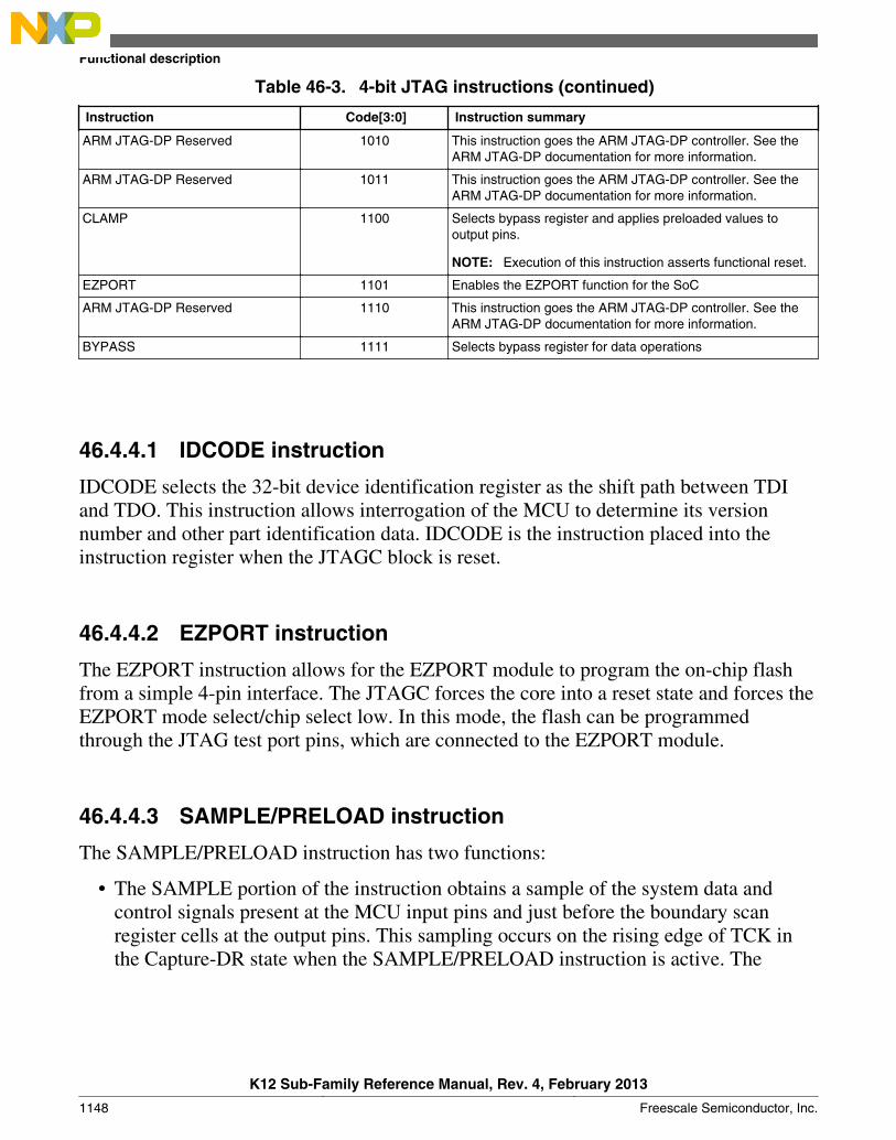
Table 46-3. 4-bit JTAG instructions (continued)
Instruction Code[3:0] Instruction summary
ARM JTAG-DP Reserved 1010 This instruction goes the ARM JTAG-DP controller. See theARM JTAG-DP documentation for more information.
ARM JTAG-DP Reserved 1011 This instruction goes the ARM JTAG-DP controller. See theARM JTAG-DP documentation for more information.
CLAMP 1100 Selects bypass register and applies preloaded values tooutput pins.
NOTE: Execution of this instruction asserts functional reset.
EZPORT 1101 Enables the EZPORT function for the SoC
ARM JTAG-DP Reserved 1110 This instruction goes the ARM JTAG-DP controller. See theARM JTAG-DP documentation for more information.
BYPASS 1111 Selects bypass register for data operations
46.4.4.1 IDCODE instruction
IDCODE selects the 32-bit device identification register as the shift path between TDIand TDO. This instruction allows interrogation of the MCU to determine its versionnumber and other part identification data. IDCODE is the instruction placed into theinstruction register when the JTAGC block is reset.
46.4.4.2 EZPORT instruction
The EZPORT instruction allows for the EZPORT module to program the on-chip flashfrom a simple 4-pin interface. The JTAGC forces the core into a reset state and forces theEZPORT mode select/chip select low. In this mode, the flash can be programmedthrough the JTAG test port pins, which are connected to the EZPORT module.
46.4.4.3 SAMPLE/PRELOAD instruction
The SAMPLE/PRELOAD instruction has two functions:
• The SAMPLE portion of the instruction obtains a sample of the system data andcontrol signals present at the MCU input pins and just before the boundary scanregister cells at the output pins. This sampling occurs on the rising edge of TCK inthe Capture-DR state when the SAMPLE/PRELOAD instruction is active. The
Functional description
K12 Sub-Family Reference Manual, Rev. 4, February 2013
1148 Freescale Semiconductor, Inc.
sampled data is viewed by shifting it through the boundary scan register to the TDOoutput during the Shift-DR state. Both the data capture and the shift operation aretransparent to system operation.
• The PRELOAD portion of the instruction initializes the boundary scan register cellsbefore selecting the EXTEST or CLAMP instructions to perform boundary scantests. This is achieved by shifting in initialization data to the boundary scan registerduring the Shift-DR state. The initialization data is transferred to the parallel outputsof the boundary scan register cells on the falling edge of TCK in the Update-DRstate. The data is applied to the external output pins by the EXTEST or CLAMPinstruction. System operation is not affected.
46.4.4.4 SAMPLE instruction
The SAMPLE instruction obtains a sample of the system data and control signals presentat the MCU input pins and just before the boundary scan register cells at the output pins.This sampling occurs on the rising edge of TCK in the Capture-DR state when theSAMPLE instruction is active. The sampled data is viewed by shifting it through theboundary scan register to the TDO output during the Shift-DR state. There is no definedaction in the Update-DR state. Both the data capture and the shift operation aretransparent to system operation.
46.4.4.5 EXTEST External test instruction
EXTEST selects the boundary scan register as the shift path between TDI and TDO. Itallows testing of off-chip circuitry and board-level interconnections by driving preloadeddata contained in the boundary scan register onto the system output pins. Typically, thepreloaded data is loaded into the boundary scan register using the SAMPLE/PRELOADinstruction before the selection of EXTEST. EXTEST asserts the internal system reset forthe MCU to force a predictable internal state while performing external boundary scanoperations.
46.4.4.6 HIGHZ instruction
HIGHZ selects the bypass register as the shift path between TDI and TDO. WhileHIGHZ is active all output drivers are placed in an inactive drive state (e.g., highimpedance). HIGHZ also asserts the internal system reset for the MCU to force apredictable internal state.
Chapter 46 JTAG Controller (JTAGC)
K12 Sub-Family Reference Manual, Rev. 4, February 2013
Freescale Semiconductor, Inc. 1149
46.4.4.7 CLAMP instruction
CLAMP allows the state of signals driven from MCU pins to be determined from theboundary scan register while the bypass register is selected as the serial path betweenTDI and TDO. CLAMP enhances test efficiency by reducing the overall shift path to asingle bit (the bypass register) while conducting an EXTEST type of instruction throughthe boundary scan register. CLAMP also asserts the internal system reset for the MCU toforce a predictable internal state.
46.4.4.8 BYPASS instruction
BYPASS selects the bypass register, creating a single-bit shift register path between TDIand TDO. BYPASS enhances test efficiency by reducing the overall shift path when notest operation of the MCU is required. This allows more rapid movement of test data toand from other components on a board that are required to perform test functions. Whilethe BYPASS instruction is active the system logic operates normally.
46.4.5 Boundary scan
The boundary scan technique allows signals at component boundaries to be controlledand observed through the shift-register stage associated with each pad. Each stage is partof a larger boundary scan register cell, and cells for each pad are interconnected seriallyto form a shift-register chain around the border of the design. The boundary scan registerconsists of this shift-register chain, and is connected between TDI and TDO when theEXTEST, SAMPLE, or SAMPLE/PRELOAD instructions are loaded. The shift-registerchain contains a serial input and serial output, as well as clock and control signals.
46.5 Initialization/Application informationThe test logic is a static logic design, and TCK can be stopped in either a high or lowstate without loss of data. However, the system clock is not synchronized to TCKinternally. Any mixed operation using both the test logic and the system functional logicrequires external synchronization.
To initialize the JTAGC block and enable access to registers, the following sequence isrequired:
Initialization/Application information
K12 Sub-Family Reference Manual, Rev. 4, February 2013
1150 Freescale Semiconductor, Inc.

1. Place the JTAGC in reset through TAP controller state machine transitions controlledby TMS
2. Load the appropriate instruction for the test or action to be performed
Chapter 46 JTAG Controller (JTAGC)
K12 Sub-Family Reference Manual, Rev. 4, February 2013
Freescale Semiconductor, Inc. 1151

Initialization/Application information
K12 Sub-Family Reference Manual, Rev. 4, February 2013
1152 Freescale Semiconductor, Inc.
Chapter 47Release Notes for Revision 4
47.1 General changes throughout document
• No substantial content changes
47.2 About This Document chapter changes
• No substantial content changes
47.3 Introduction chapter changes
• No substantial content changes
47.4 Chip Configuration chapter changes
• No substantial content changes
47.5 Memory Map chapter changes
• Added the new section "Read-after-write sequence and required serialization of memory operations"• For the table "System memory map", corrected the access and slave port information for the DRAM controller
K12 Sub-Family Reference Manual, Rev. 4, February 2013
Freescale Semiconductor, Inc. 1153
47.6 Clock Distribution chapter changes
• No substantial content changes
47.7 Reset and Boot chapter changes
• No substantial content changes
47.8 Power Management chapter changes
• No substantial content changes
47.9 Security chapter changes
• No substantial content changes
47.10 Debug chapter changes
• No substantial content changes
47.11 Signal Multiplexing and Signal Descriptions chapterchanges
• No substantial content changes
47.12 PORT changes
• No substantial content changes
Clock Distribution chapter changes
K12 Sub-Family Reference Manual, Rev. 4, February 2013
1154 Freescale Semiconductor, Inc.
47.13 SIM changes
• No substantial content changes
47.14 RCM changes
• No substantial content changes
47.15 SMC changes
• No substantial content changes
47.16 PMC changes
• No substantial content changes
47.17 LLWU changes
• No substantial content changes
47.18 MCM changes
• No substantial content changes
47.19 Crossbar switch module changes
• No substantial content changes
Chapter 47 Release Notes for Revision 4
K12 Sub-Family Reference Manual, Rev. 4, February 2013
Freescale Semiconductor, Inc. 1155
47.20 AIPS-Lite changes
• No substantial content changes
47.21 DMAMUX module changes
• No substantial content changes
47.22 DMA module changes
• Changed TCDn_CSR[Reserved], TCDn_BITER_ELINKYES[Reserved], and TCD_CITER_ELINKYES[Reserved] to beWOZ instead of ROZ.
• added image of TCD structure to the beginning of the Memory Map section.
• Changed CR reset value to 0000_0000h
47.23 EWM changes
• No substantial content changes
47.24 WDOG changes
• No substantial content changes
47.25 MCG changes
• No substantial content changes
47.26 OSC changes
• No substantial content changes
AIPS-Lite changes
K12 Sub-Family Reference Manual, Rev. 4, February 2013
1156 Freescale Semiconductor, Inc.
47.27 RTC Oscillator changes
• No substantial content changes
47.28 FMC changes
• No substantial content changes
47.29 FTFL changes
• Add footnote to error handling table for erase commands• Swap Indicator Address is stored in the IFR with bits [2:0] removed (Swap control command code 0x01)
47.30 EzPort changes
• No substantial content changes
47.31 CRC changes
No substantial content changes
47.32 RNGA chapter changes
• No substantial content changes
47.33 ADC changes
• No substantial content changes
Chapter 47 Release Notes for Revision 4
K12 Sub-Family Reference Manual, Rev. 4, February 2013
Freescale Semiconductor, Inc. 1157
47.34 CMP changes
• No substantial content changes
47.35 DAC changes
• Replace introduction topic content.
47.36 VREF changes
• No substantial content changes
47.37 PDB changes
• No substantial content changes
47.38 FTM changes
• For section "Filter for Input Capture mode", removed the phrase "5-bit" in references to the counter and clarified whenthe input signal is validated.
47.39 PIT module changes
• Added to registers header: "Timer Channel n / RTI Channel" table and all content.
47.40 LPTMR changes
• No substantial content changes
CMP changes
K12 Sub-Family Reference Manual, Rev. 4, February 2013
1158 Freescale Semiconductor, Inc.
47.41 CMT changes
• No substantial content changes
47.42 RTC changes
Swapped the TDTL and TDTH fields in the RTC_TTR register.
47.43 DSPI chapter changes
• No substantial content changes
47.44 I2C changes
• No substantial content changes
47.45 UART changes
• Updated S2[MSBF], S2[RXINV], C3[TXINV] and C7816[INIT] register bit field descriptions to mention that InitialCharacter Detect feature can only be used in TTYPE = 0 mode.
• Updated Initial Characters Section in 7816 Functional Description.• Updated Protocol T=0 Section in 7816 Functional Description.• Updated IE[ISDIE] register bit field description.
• Added bits CFIFO[RXOFE] and SFIFO[RXOF] which were missing. These are legacy register bits.
47.46 GPIO changes
• No substantial content changes
47.47 JTAGC module changes
Chapter 47 Release Notes for Revision 4
K12 Sub-Family Reference Manual, Rev. 4, February 2013
Freescale Semiconductor, Inc. 1159

• In the General JTAG instructions table, updated the Instruction summary cells to emphasize which instructions assertfunctional reset.
JTAGC module changes
K12 Sub-Family Reference Manual, Rev. 4, February 2013
1160 Freescale Semiconductor, Inc.
How to Reach Us:
Home Page:www.freescale.com
Web Support:http://www.freescale.com/support
USA/Europe or Locations Not Listed:Freescale SemiconductorTechnical Information Center, EL5162100 East Elliot RoadTempe, Arizona 85284+1-800-521-6274 or +1-480-768-2130www.freescale.com/support
Europe, Middle East, and Africa:Freescale Halbleiter Deutschland GmbHTechnical Information CenterSchatzbogen 781829 Muenchen, Germany+44 1296 380 456 (English)+46 8 52200080 (English)+49 89 92103 559 (German)+33 1 69 35 48 48 (French)www.freescale.com/support
Japan:Freescale Semiconductor Japan Ltd.HeadquartersARCO Tower 15F1-8-1, Shimo-Meguro, Meguro-ku,Tokyo 153-0064Japan0120 191014 or +81 3 5437 [email protected]
Asia/Pacific:Freescale Semiconductor China Ltd.Exchange Building 23FNo. 118 Jianguo RoadChaoyang DistrictBeijing 100022China+86 10 5879 [email protected]
Document Number: K12P121M50SF4RMRev. 4, February 2013
Information in this document is provided solely to enable system and softwareimplementers to use Freescale Semiconductors products. There are no express or impliedcopyright licenses granted hereunder to design or fabricate any integrated circuits orintegrated circuits based on the information in this document.
Freescale Semiconductor reserves the right to make changes without further notice to anyproducts herein. Freescale Semiconductor makes no warranty, representation, orguarantee regarding the suitability of its products for any particular purpose, nor doesFreescale Semiconductor assume any liability arising out of the application or use of anyproduct or circuit, and specifically disclaims any liability, including without limitationconsequential or incidental damages. "Typical" parameters that may be provided inFreescale Semiconductor data sheets and/or specifications can and do vary in differentapplications and actual performance may vary over time. All operating parameters,including "Typicals", must be validated for each customer application by customer'stechnical experts. Freescale Semiconductor does not convey any license under its patentrights nor the rights of others. Freescale Semiconductor products are not designed,intended, or authorized for use as components in systems intended for surgical implantinto the body, or other applications intended to support or sustain life, or for any otherapplication in which failure of the Freescale Semiconductor product could create asituation where personal injury or death may occur. Should Buyer purchase or useFreescale Semiconductor products for any such unintended or unauthorized application,Buyer shall indemnify Freescale Semiconductor and its officers, employees, subsidiaries,affiliates, and distributors harmless against all claims, costs, damages, and expenses, andreasonable attorney fees arising out of, directly or indirectly, any claim of personal injuryor death associated with such unintended or unauthorized use, even if such claims allegesthat Freescale Semiconductor was negligent regarding the design or manufacture ofthe part.
RoHS-compliant and/or Pb-free versions of Freescale products have the functionality andelectrical characteristics as their non-RoHS-complaint and/or non-Pb-free counterparts.For further information, see http://www.freescale.com or contact your Freescalesales representative.
For information on Freescale's Environmental Products program, go tohttp://www.freescale.com/epp.
Freescale™ and the Freescale logo are trademarks of Freescale Semiconductor, Inc.All other product or service names are the property of their respective owners.
© 2012–2013 Freescale Semiconductor, Inc.