Unilever\'s contribution to achieving sustainable development ...
Upload
khangminh22Category
view
1download
0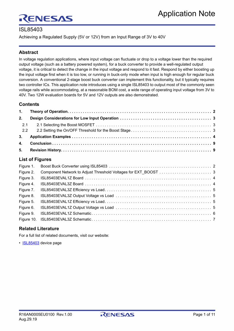
R16AN0005EU0100 Rev.1.00 Page 1 of 11Aug.29.19
ISL85403Achieving a Regulated Supply (5V or 12V) from an Input Range of 3V to 40V
Application Note
AbstractIn voltage regulation applications, where input voltage can fluctuate or drop to a voltage lower than the required output voltage (such as a battery powered system), for a buck converter to provide a well-regulated output voltage, it is critical to detect the change in the input voltage and respond to it fast. Respond by either boosting up the input voltage first when it is too low, or running in buck-only mode when input is high enough for regular buck conversion. A conventional 2-stage boost buck converter can implement this functionality, but it typically requires two controller ICs. This application note introduces using a single ISL85403 to output most of the commonly seen voltage rails while accommodating, at a reasonable BOM cost, a wide range of operating input voltage from 3V to 40V. Two 12W evaluation boards for 5V and 12V outputs are also demonstrated.
Contents
1. Theory of Operation. . . . . . . . . . . . . . . . . . . . . . . . . . . . . . . . . . . . . . . . . . . . . . . . . . . . . . . . . . . . . . . . . . 2
2. Design Considerations for Low Input Operation . . . . . . . . . . . . . . . . . . . . . . . . . . . . . . . . . . . . . . . . . . 3
2.1 2.1 Selecting the Boost MOSFET . . . . . . . . . . . . . . . . . . . . . . . . . . . . . . . . . . . . . . . . . . . . . . . . . . . . . 3
2.2 2.2 Setting the On/OFF Threshold for the Boost Stage . . . . . . . . . . . . . . . . . . . . . . . . . . . . . . . . . . . . . 3
3. Application Examples . . . . . . . . . . . . . . . . . . . . . . . . . . . . . . . . . . . . . . . . . . . . . . . . . . . . . . . . . . . . . . . . 4
4. Conclusion . . . . . . . . . . . . . . . . . . . . . . . . . . . . . . . . . . . . . . . . . . . . . . . . . . . . . . . . . . . . . . . . . . . . . . . . . 9
5. Revision History. . . . . . . . . . . . . . . . . . . . . . . . . . . . . . . . . . . . . . . . . . . . . . . . . . . . . . . . . . . . . . . . . . . . . 9
List of FiguresFigure 1. Boost Buck Converter using ISL85403 . . . . . . . . . . . . . . . . . . . . . . . . . . . . . . . . . . . . . . . . . . . . . . . 2
Figure 2. Component Network to Adjust Threshold Voltages for EXT_BOOST . . . . . . . . . . . . . . . . . . . . . . . . 3
Figure 3. ISL85403EVAL1Z Board . . . . . . . . . . . . . . . . . . . . . . . . . . . . . . . . . . . . . . . . . . . . . . . . . . . . . . . . . . 4
Figure 4. ISL85403EVAL3Z Board . . . . . . . . . . . . . . . . . . . . . . . . . . . . . . . . . . . . . . . . . . . . . . . . . . . . . . . . . . 4
Figure 7. ISL85403EVAL3Z Efficiency vs Load. . . . . . . . . . . . . . . . . . . . . . . . . . . . . . . . . . . . . . . . . . . . . . . . . 5
Figure 8. ISL85403EVAL3Z Output Voltage vs Load . . . . . . . . . . . . . . . . . . . . . . . . . . . . . . . . . . . . . . . . . . . . 5
Figure 5. ISL85403EVAL1Z Efficiency vs Load. . . . . . . . . . . . . . . . . . . . . . . . . . . . . . . . . . . . . . . . . . . . . . . . . 5
Figure 6. ISL85403EVAL1Z Output Voltage vs Load . . . . . . . . . . . . . . . . . . . . . . . . . . . . . . . . . . . . . . . . . . . . 5
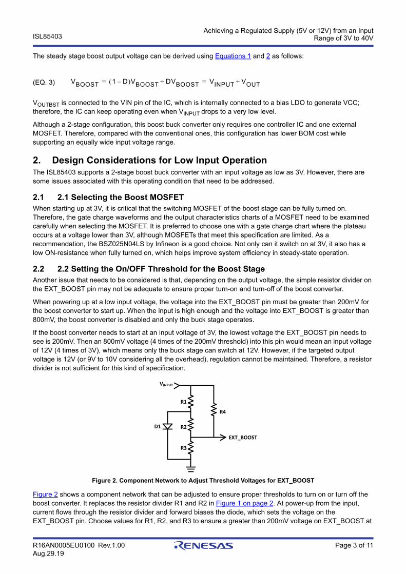
Figure 9. ISL85403EVAL1Z Schematic . . . . . . . . . . . . . . . . . . . . . . . . . . . . . . . . . . . . . . . . . . . . . . . . . . . . . . . 6
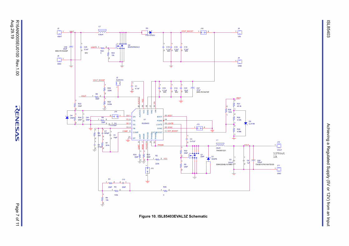
Figure 10. ISL85403EVAL3Z Schematic . . . . . . . . . . . . . . . . . . . . . . . . . . . . . . . . . . . . . . . . . . . . . . . . . . . . . . . 7
Related LiteratureFor a full list of related documents, visit our website:
• ISL85403 device page

ISL85403Achieving a Regulated Supply (5V or 12V) from an Input
Range of 3V to 40V
R16AN0005EU0100 Rev.1.00 Page 2 of 11Aug.29.19
1. Theory of OperationWhen the input voltage for a power supply varies or decreases significantly, it is necessary to boost it up whenever needed by turning on a boost converter, so that output regulation can be maintained. However, when the input voltage is adequate or resumes back to normal, the boost is not needed and therefore should be disabled. This can be achieved with a single control IC in the ISL85403. The ISL85403 is a synchronous buck controller integrated with a high-side MOSFET and both high-side and low-side drivers. However, it can be configured to control a boost buck converter as well. The low-side driver can drive a boost converter preceding a buck stage controlled by the same IC. This allows the IC to control a 2-stage boost buck converter. When the system input voltage drops to a level too low for the second stage buck converter to maintain regulation, the first stage boost converter can boost the input voltage up to keep the output voltage in regulation. This provides a reliable converter solution in applications that warrant support for a very wide input voltage range.
Figure 1 shows a typical application circuit of a 2-stage boost buck converter. The EXT_BOOST pin is connected to the system input (oftentimes a battery) through a resistor divider. The EXT_BOOST pin monitors the boost input voltage to turn on and off the boost stage. When the input is high enough for the buck stage to regulate the output voltage, either at startup, or after the input recovers to normal from a decline, the boost stage is disabled. Select the threshold voltage to turn on the boost PWM (from low-side gate drive LGATE) with enough margin to cover the voltage drop of the boost inductor and diode, and the buck’s maximum duty cycle and conduction drop, so that the buck converter is still in regulation before the boost kicks in and input voltage can be boosted up. The values of R1 and R2 set the boost turn-on threshold and hysteresis. The AUX VCC pin monitors the boost output voltage in a similar way. More detailed information can be found in the ISL85403 datasheet.
The steady stage DC transfer functions for the output voltage of the boost stage (VBOOST) and the output of the buck stage (VOUT) are:
where VINPUT is the system, or boost, input voltage.
Figure 1. Boost Buck Converter using ISL85403
VOUT
ISL85403VCC
SGND
MODE
BOOT
VIN
PHASE
PGNDFS
PGOOD
ENSS
FBCOMP
AUXVCCLGATE
ILIMIT
+
VINPUT
EXT_BOOST
SYNC
R1
R2
+R3
R4
Boost
Buck
VBOOST
VBOOST1
1 D–-------------VINPUT=(EQ. 1)
VOUT DVBOOSTD
1 D–-------------VINPUT= =(EQ. 2)
ISL85403Achieving a Regulated Supply (5V or 12V) from an Input
Range of 3V to 40V
R16AN0005EU0100 Rev.1.00 Page 3 of 11Aug.29.19
The steady stage boost output voltage can be derived using Equations 1 and 2 as follows:
VOUTBST is connected to the VIN pin of the IC, which is internally connected to a bias LDO to generate VCC; therefore, the IC can keep operating even when VINPUT drops to a very low level.
Although a 2-stage configuration, this boost buck converter only requires one controller IC and one external MOSFET. Therefore, compared with the conventional ones, this configuration has lower BOM cost while supporting an equally wide input voltage range.
2. Design Considerations for Low Input Operation The ISL85403 supports a 2-stage boost buck converter with an input voltage as low as 3V. However, there are some issues associated with this operating condition that need to be addressed.
2.1 2.1 Selecting the Boost MOSFETWhen starting up at 3V, it is critical that the switching MOSFET of the boost stage can be fully turned on. Therefore, the gate charge waveforms and the output characteristics charts of a MOSFET need to be examined carefully when selecting the MOSFET. It is preferred to choose one with a gate charge chart where the plateau occurs at a voltage lower than 3V, although MOSFETs that meet this specification are limited. As a recommendation, the BSZ025N04LS by Infineon is a good choice. Not only can it switch on at 3V, it also has a low ON-resistance when fully turned on, which helps improve system efficiency in steady-state operation.
2.2 2.2 Setting the On/OFF Threshold for the Boost StageAnother issue that needs to be considered is that, depending on the output voltage, the simple resistor divider on the EXT_BOOST pin may not be adequate to ensure proper turn-on and turn-off of the boost converter.
When powering up at a low input voltage, the voltage into the EXT_BOOST pin must be greater than 200mV for the boost converter to start up. When the input is high enough and the voltage into EXT_BOOST is greater than 800mV, the boost converter is disabled and only the buck stage operates.
If the boost converter needs to start at an input voltage of 3V, the lowest voltage the EXT_BOOST pin needs to see is 200mV. Then an 800mV voltage (4 times of the 200mV threshold) into this pin would mean an input voltage of 12V (4 times of 3V), which means only the buck stage can switch at 12V. However, if the targeted output voltage is 12V (or 9V to 10V considering all the overhead), regulation cannot be maintained. Therefore, a resistor divider is not sufficient for this kind of specification.
Figure 2 shows a component network that can be adjusted to ensure proper thresholds to turn on or turn off the boost converter. It replaces the resistor divider R1 and R2 in Figure 1 on page 2. At power-up from the input, current flows through the resistor divider and forward biases the diode, which sets the voltage on the EXT_BOOST pin. Choose values for R1, R2, and R3 to ensure a greater than 200mV voltage on EXT_BOOST at
Figure 2. Component Network to Adjust Threshold Voltages for EXT_BOOST
VBOOST 1 D– VBOOST DVBOOST+ VINPUT VOUT+= =(EQ. 3)
VINPUT
EXT_BOOST
R1
R2
R3
R4
D1

ISL85403Achieving a Regulated Supply (5V or 12V) from an Input
Range of 3V to 40V
R16AN0005EU0100 Rev.1.00 Page 4 of 11Aug.29.19
the low end of the input voltage range. R4 is a large value resistor that pulls minimum current when the input voltage is low. As input goes up, R4 pulls more current and voltage on EXT_BOOST increases. Therefore, R4 can be adjusted to set the input voltage where EXT_BOOST sees 800mV and the boost converter is disabled.
Note: The forward voltage of the diode changes across temperature; therefore, the resistor values need to yield proper threshold voltages over the entire operating temperature range specified for the application, based on the characteristics of the diode. Detailed instruction about how to design such a network can be seen in the R16ZZ0001 Tips for Using the ISL85403 in Boost-Buck Mode.
3. Application ExamplesAs examples, two evaluation boards using the ISL85403 in the 2-stage boost buck configuration are provided, one for a 5V output voltage (ISL85403EVAL1Z) and the other for a 12V output voltage (ISL85403EVAL3Z). Both examples support an input range from 3V to 40V and an output power up to12W.
Pictures for the two evaluation boards, ISL85403EVAL1Z and ISL85403EVAL3Z, can be seen in Figures 3 and 4. They are designed for the specifications listed below:
Specification ISL85403EVAL1Z ISL85403EVAL3Z
Input Voltage (VIN) 3V to 40V 3V to 40V
Output Voltage (VOUT) 5.0V 12.0V
Maximum Output Current (IOUT_MAX) 2.5A 1A
Figure 3. ISL85403EVAL1Z Board Figure 4. ISL85403EVAL3Z Board

ISL85403Achieving a Regulated Supply (5V or 12V) from an Input
Range of 3V to 40V
R16AN0005EU0100 Rev.1.00 Page 5 of 11Aug.29.19
Figures 5 and 6 show efficiency and regulation performance of the 5V converter on ISL85403EVAL1Z. Figures 7 and 8 show efficiency and regulation performance of the 12V converter on ISL85403EVAL3Z.
Figure 9 shows the schematic of the ISL85403EVAL1Z, and Figure 10 shows the schematic of ISL85403EVAL3Z.
In ISL85403EVAL1Z, it can be seen that a simple resistor divider sets the voltage on the EXT_BOOST pin. This is sufficient in this application where the output voltage is 5V and the minimum input voltage is 3V. At 3V input, EXT_BOOST sees 293mV, which is well above the required 200mV to start up the boost stage. When the voltage at EXT_BOOST is 800mV, the corresponding input voltage is 8.2V, where enough headroom is present to allow the converter to run in Buck mode only.
In the ISL85403EVAL3Z where the output voltage is 12V, the component network illustrated in Figure 2 on page 3 needs to be included in this application. The LL4148 by On Semiconductors is used as the diode in the network, and based on its characteristics, the resistor values are chosen as follows:
Figure 5. ISL85403EVAL1Z Efficiency vs Load Figure 6. ISL85403EVAL1Z Output Voltage vs Load
Figure 7. ISL85403EVAL3Z Efficiency vs Load Figure 8. ISL85403EVAL3Z Output Voltage vs Load
R1 R2 R3 R4
45.3k 4.02k 4.99k 120k
0102030405060708090
100
0.0 0.5 1.0 1.5 2.0 2.5
Effic
ienc
y (%
)
IOUT (A)
VIN = 5VVIN = 12VVIN = 24VVIN = 36V
4.954.964.974.984.995.005.015.025.035.045.05
0.0 0.5 1.0 1.5 2.0 2.5
V OU
T(V
)
Output Current (A)
VIN = 5VVIN = 12VVIN = 24VVIN = 36V
10
20
30
40
50
60
70
80
90
100
0.0 0.2 0.4 0.6 0.8 1.0
Effic
ienc
y (%
)
IOUT (A)
VIN = 5VVIN = 12VVIN = 24VVIN = 36V 11.90
11.9211.9411.9611.9812.0012.0212.0412.0612.0812.10
0.0 0.2 0.4 0.6 0.8 1.0
V OU
T(V
)
IOUT (A)
VIN = 5VVIN = 12VVin = 24VVIN = 36V
R16
AN
000
5E
U0
100
Re
v.1.0
0P
ag
e 6 of 11
Au
g.2
9.19
ISL8
540
3A
chievin
g a
Re
gula
ted S
upp
ly (5V or 1
2V) fro
m an
Inp
ut
Figure 9. ISL85403EVAL1Z Schematic
5Vout2.5A
C61DNP
1
2
C7820pF
1
2
R1
DNP
21
C60220uF
6TPE220MI
C252.2uF
50V
1
2
R5DNP
2
1
C141uF50V
1
2
R410k
2
1
C5922uF
EEE-FK1K220P
C8470pF
1
2
D4DNP
R6
DNP
21
R34DNP
2
1
C61uF
1
2
J5
VBAT
1
Q1DNP
C2210uF50V
1
2
C5722uFEEE-FK1K220P
R30
36.k
21
R8
DNP
21
R2
220k
21
J131 2
L1
10uHDR125-100-RR32
DNP2
1
C192.2uF50V
1
2
C40.015uF12
R299.09k
2
1
J6
GND
1
R24DNP
2
1
R7301k
2
1
R3
52.5k
21
R2310k
2
1
R26
0
21
R25DNP
2
1
J8
VIN
1
C5DNP
1
2
C14.7uF
1
2
R9750
2
1
R33DNP
2
1
L2
6.8uH
C30.47uF
1
2
C10
DNP
12
R31332k
2
1
J9
GND
1
Q2NTTFS5826NLTAG
J11
GND
1
C230.1uF50V
1
2
C910pF
1
2
J161 2
J14
12
J10
VOUT
1
D3
SS3P6
R220
21
J15
12
C182.2uF50V
1
2
R28332K
2
1
C150.1uF50V
1
2
U1
ISL85403
FB4
PHASE2
10VIN
16
PGOOD
8
SS3
PHASE
9
PGND14
BOOT15
COMP5
FS2
LGATE13
EN1
ILIMIT
6
MODE
7
EXT_BOOST11
SYNC12
VIN2
17SGND
18VCC
19AUXVCC
20
EP21
J2AUXVCC
1
D1SS3P6
AUXVCC
VCC
FS
SS
FB
COMPILIMIT
MODE
PGOOD
EXT_BOOST
SYNC
VIN
LGATE
PHASE
BOOT
VOUT
VOUT
VBAT
LGATE
VOUT_BOOST
EN
VOUT_BOOST
VCC
VBAT
R16
AN
000
5E
U0
100
Re
v.1.0
0P
ag
e 7 of 11
Au
g.2
9.19
ISL8
540
3A
chievin
g a
Re
gula
ted S
upp
ly (5V or 1
2V) fro
m an
Inp
ut
Figure 10. ISL85403EVAL3Z Schematic
12Vout1A
C141uF50V
1
2
R5DNP
2
1
C252.2uF
50V
1
2
C60100uF
T543D107K016ATE035
R1
DNP
21
C7820pF
1
2
C61DNP
1
2
R410k
2
1
C61uF
1
2
R34DNP
2
1
R6
DNP
21
D4DNP
C8470pF
1
2
C5922uF
EEE-FK1K220P
R36120k
2
1
Q1DNP
J5
VBAT
1
C2210uF50V
1
2
R304.02k
2
1
C5747uFEEE-FK1K470P
J131 2
R8
DNP
21
R2
220k
21
C192.2uF50V
1
2
R32DNP
2
1
L1
22uH7443551221
J6
GND
1
R299.09k
2
1
C40.015uF12
J8
VIN
1
R25DNP
2
1
R26
0
21
R2310k
2
1
R3
140k
21
R7301k
2
1
R24DNP
2
1
R33DNP
2
1
R9750
2
1
C14.7uF
1
2
C5100uF
EMK325ABJ107MM-T
1
2
R354.99k
2
1
R3145.3k
2
1
C10
DNP
12
C30.47uF
1
2
D5LL4148
L2
6.8uH
J9
GND
1
C910pF
1
2
C230.1uF50V
1
2
J11
GND
1
Q2BSZ025N04LS
J14
12
J161 2
C182.2uF50V
1
2
J15
12
R220
21
D3
FSV15100V
J10
VOUT
1
D1SS3P6
J2AUXVCC
1U1
ISL85403
FB4
PHASE2
10VIN
16
PGOOD
8
SS3
PHASE
9
PGND14
BOOT15
COMP5
FS2
LGATE13
EN1
ILIMIT
6
MODE
7
EXT_BOOST11
SYNC12
VIN2
17SGND
18VCC
19AUXVCC
20EP
21
C150.1uF50V
1
2
R28332K
2
1
AUXVCC
VCC
FS
SS
FB
COMP
ILIMIT
MODE
PGOOD
EXT_BOOST
SYNC
VIN
LGATE
PHASE
BOOT
VOUT
VOUT
VBAT
LGATE
VOUT_BOOST
EN
VOUT_BOOST
VCC
VBAT
ISL85403Achieving a Regulated Supply (5V or 12V) from an Input
Range of 3V to 40V
R16AN0005EU0100 Rev.1.00 Page 8 of 11Aug.29.19
As a result, the voltage thresholds to turn on and off the boost stage are set as the following:
Note: The input voltage at which the boost converter is disabled is set above 16V to account for the maximum duty cycle of the buck converter and to cover voltage drop from components such as the boost diode and inductor.
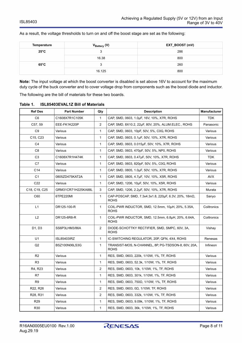
The following are the bill of materials for these two boards.
Temperature VBattery (V) EXT_BOOST (mV)
25°C 3 286
16.38 800
65°C 3 260
16.125 800
Table 1. ISL85403EVAL1Z Bill of Materials
Ref Des Part Number Qty Description Manufacturer
C6 C1608X7R1C105K 1 CAP, SMD, 0603, 1.0µF, 16V, 10%, X7R, ROHS TDK
C57, 59 EEE-FK1K220P 2 CAP, SMD, 8X10.2, 22µF, 80V, 20%, ALUM.ELEC., ROHS Panasonic
C9 Various 1 CAP, SMD, 0603, 10pF, 50V, 5%, C0G, ROHS Various
C15, C23 Various 1 CAP, SMD, 0603, 0.1µF, 50V, 10%, X7R, ROHS Various
C4 Various 1 CAP, SMD, 0603, 0.015µF, 50V, 10%, X7R, ROHS Various
C8 Various 1 CAP, SMD, 0603, 470pF, 50V, 5%, NP0, ROHS Various
C3 C1608X7R1H474K 1 CAP, SMD, 0603, 0.47µF, 50V, 10%, X7R, ROHS TDK
C7 Various 1 CAP, SMD, 0603, 820pF, 50V, 5%, C0G, ROHS Various
C14 Various 1 CAP, SMD, 0805, 1.0µF, 50V, 10%, X7R, ROHS Various
C1 0805ZD475KAT2A 1 CAP, SMD, 0805, 4.7µF, 10V, 10%, X5R, ROHS AVX
C22 Various 1 CAP, SMD, 1206, 10µF, 50V, 10%, X5R, ROHS Various
C18, C19, C25 GRM31CR71H225KA88L 3 CAP, SMD, 1206, 2.2µF, 50V, 10%, X7R, ROHS Murata
C60 6TPE220MI 1 CAP-POSCAP, SMD, 7.3x4.3x1.8, 220µF, 6.3V, 20%, 18mΩ, ROHS
Sanyo
L1 DR125-100-R 1 COIL-PWR INDUCTOR, SMD, 12.5mm, 10µH, 20%, 5.35A, ROHS
Coiltronics
L2 DR125-6R8-R 1 COIL-PWR INDUCTOR, SMD, 12.5mm, 6.8µH, 20%, 6.64A, ROHS
Coiltronics
D1, D3 SS6P3LHM3/86A 2 DIODE-SCHOTTKY RECTIFIER, SMD, SMPC, 60V, 3A, ROHS
Vishay
U1 ISL85403IRZ 1 IC-SWITCHING REGULATOR, 20P, QFN, 4X4, ROHS Renesas
Q2 BSZ100N06LS3G 1 TRANSIST-MOS, N-CHANNEL, 8P, PG-TSDSON-8, 60V, 20A, ROHS
Infineon
R2 Various 1 RES, SMD, 0603, 220k, 1/10W, 1%, TF, ROHS Various
R3 Various 1 RES, SMD, 0603, 52.3k, 1/10W, 1%, TF, ROHS Various
R4, R23 Various 2 RES, SMD, 0603, 10k, 1/10W, 1%, TF, ROHS Various
R7 Various 1 RES, SMD, 0603, 301k, 1/10W, 1%, TF, ROHS Various
R9 Various 1 RES, SMD, 0603, 750Ω, 1/10W, 1%, TF, ROHS Various
R22, R26 Various 2 RES, SMD, 0603, 0Ω, 1/10W, TF, ROHS Various
R28, R31 Various 2 RES, SMD, 0603, 332k, 1/10W, 1%, TF, ROHS Various
R29 Various 1 RES, SMD, 0603, 9.09k, 1/10W, 1%, TF, ROHS Various
R30 Various 1 RES, SMD, 0603, 36k, 1/10W, 1%, TF, ROHS Various
ISL85403Achieving a Regulated Supply (5V or 12V) from an Input
Range of 3V to 40V
R16AN0005EU0100 Rev.1.00 Page 9 of 11Aug.29.19
R1, R5, R6, R8, R24, R25, R32, R33, R34, C5, C10, C61, D4, Q1
N/A 0 Do not populate N/A
Table 2. ISL85403EVAL3Z Bill of Materials
Ref Des Part Number Qty Description Manufacturer
C5 EMK325ABJ107MM-T 1 CAP, SMD, 1210, 100µF, 16V, 20%, X5R, ROHS
C6 C1608X7R1C105K 1 CAP, SMD, 0603, 1.0µF, 16V, 10%, X7R, ROHS TDK
C57 EEE-FK1K470P 1 CAP, SMD, 10X10.2, 47µF, 80V, 20%, ALUM.ELEC., ROHS Panasonic
C59 EEE-FK1K220P 1 CAP, SMD, 8X10.2, 22µF, 80V, 20%, ALUM.ELEC., ROHS Panasonic
C9 Various 1 CAP, SMD, 0603, 10pF, 50V, 5%, C0G, ROHS Various
C15, C23 Various 1 CAP, SMD, 0603, 0.1µF, 50V, 10%, X7R, ROHS Various
C4 Various 1 CAP, SMD, 0603, 0.015µF, 50V, 10%, X7R, ROHS Various
C8 Various 1 CAP, SMD, 0603, 470pF, 50V, 5%, NP0, ROHS Various
C3 C1608X7R1H474K 1 CAP, SMD, 0603, 0.47µF, 50V, 10%, X7R, ROHS TDK
C7 Various 1 CAP, SMD, 0603, 820pF, 50V, 5%, C0G, ROHS Various
C14 Various 1 CAP, SMD, 0805, 1.0µF, 50V, 10%, X7R, ROHS Various
C1 0805ZD475KAT2A 1 CAP, SMD, 0805, 4.7µF, 10V, 10%, X5R, ROHS AVX
C22 Various 1 CAP, SMD, 1206, 10µF, 50V, 10%, X5R, ROHS Various
C18, C19, C25 GRM31CR71H225KA88L
3 CAP, SMD, 1206, 2.2µF, 50V, 10%, X7R, ROHS Murata
C60 T543D107K016ATE035 1 CAP-TANTALUM, SMD, 2917, 100µF, 16V, 10%, 35mΩ, ROHS
Kemet
L1 7443551221 1 22uH SHIELDED WIREWOUND INDUCTOR, 6A,24.7mOhm Wurth
L2 DR125-6R8-R 1 COIL-PWR INDUCTOR, SMD, 12.5mm, 6.8µH, 20%, 6.64A, ROHS
Coiltronics
D1 SS6P3LHM3/86A 1 DIODE-SCHOTTKY RECTIFIER, SMD, SMPC, 60V, 3A, ROHS
Vishay
D3 FSV15100V 1 DIODE-SCHOTTYKY, 100V, 15A, TO-277-3 ON Semi
D5 LL4148 1 DIODE, 100V, 200mA, SOD80 ON Semi
U1 ISL85403IRZ 1 IC-SWITCHING REGULATOR, 20P, QFN, 4X4, ROHS Renesas
Q2 BSZ100N06LS3G 1 TRANSIST-MOS, N-CHANNEL, 8P, PG-TSDSON-8, 60V, 20A, ROHS
Infineon
R2 Various 1 RES, SMD, 0603, 220k, 1/10W, 1%, TF, ROHS Various
R3 Various 1 RES, SMD, 0603, 140k, 1/10W, 1%, TF, ROHS Various
R4, R23 Various 2 RES, SMD, 0603, 10k, 1/10W, 1%, TF, ROHS Various
R7 Various 1 RES, SMD, 0603, 301k, 1/10W, 1%, TF, ROHS Various
R9 Various 1 RES, SMD, 0603, 750Ω, 1/10W, 1%, TF, ROHS Various
R22, R26 Various 2 RES, SMD, 0603, 0Ω, 1/10W, TF, ROHS Various
R28 Various 1 RES, SMD, 0603, 332k, 1/10W, 1%, TF, ROHS Various
R29 Various 1 RES, SMD, 0603, 9.09k, 1/10W, 1%, TF, ROHS Various
R30 Various 1 RES, SMD, 0603, 4.02k, 1/10W, 1%, TF, ROHS Various
R31 Various 1 RES, SMD, 0603, 45.3k, 1/10W, 1%, TF, ROHS Various
R35 Various 1 RES, SMD, 0603, 4.99k, 1/10W, 1%, TF, ROHS Various
Table 1. ISL85403EVAL1Z Bill of Materials (Continued)
Ref Des Part Number Qty Description Manufacturer
ISL85403Achieving a Regulated Supply (5V or 12V) from an Input
Range of 3V to 40V
R16AN0005EU0100 Rev.1.00 Page 10 of 11Aug.29.19
4. ConclusionThe ISL85403 by Renesas is a versatile regulator IC that can be used not only as a conventional buck controller, but also as a boost buck controller, which accommodates a wide range of input voltage while reliably maintaining output regulation. It also has comprehensive protections against various faults including overcurrent, overvoltage and over-temperature, which makes it a robust solution in a large variety of applications.
5. Revision History
R36 Various 1 RES, SMD, 0603, 120k, 1/10W, 1%, TF, ROHS Various
R1, R5, R6, R8, R24, R25, R32, R33, R34,
C10, C61, D4, Q1
N/A 0 Do not populate N/A
Rev. Date Description
1.00 Aug.29.19 Initial release
Table 2. ISL85403EVAL3Z Bill of Materials (Continued)
Ref Des Part Number Qty Description Manufacturer

Corporate HeadquartersTOYOSU FORESIA, 3-2-24 Toyosu,Koto-ku, Tokyo 135-0061, Japanwww.renesas.com
Contact InformationFor further information on a product, technology, the most up-to-date version of a document, or your nearest sales office, please visit:
www.renesas.com/contact/
TrademarksRenesas and the Renesas logo are trademarks of Renesas Electronics Corporation. All trademarks and registered trademarks are the property of their respective owners.
Copyright © 2022 FDOKUMEN