Inversion Domain Boundaries in Aluminum Nitride
14
J Am Cerom Soc 74 [61 1226-39 (1991) Inversion Domain Boundaries in Aluminum Nitride Alistair D. Westwood* and Michael R. Notis* Department of Materials Science and Engineering, Lehigh University, Bethlehem, Pennsylvania 1801 5 Inversion domain boundaries (IDBs) have been identified in undoped, hot-pressed AlN. The microstructure and micro- chemistry of the IDBs have been studied using conventional transmission electron microscopy, convergent-beam electron diffraction, and analytical electron microscopy. Two dis- tinct IDB morphologies are present: a planar variant which lies on the basal plane (OOOl), and a curved variant which does not possess a particular habit plane, but portions of the boundary are often seen lying on one of the (1011) planes. The boundaries exhibit d i k e fringe contrast, indicating that a translation exists across the boundary. The displace- ment vectors RF for the planar and curved boundaries have been investigated using both two-beam and multiple-beam techniques. Microchemical analysis has revealed oxygen segregation to the planar IDB; when present on the curved IDB, oxygen is at a lower concentration than in the planar case. Lattice fringe imaging and long-exposure selected area electron diffraction patterns have indicated the pres- ence of thin, platelike precipitates at the planar IDBs. Sin- tering and annealing studies indicate that oxygen is necessary for the formation of the planar IDBs and that oxy- gen is not uniformly distributed along the curved IDBs. [Key words: aluminum nitride, domains, microstructure, defects, oxygen.] I. Introduction URTZITE and sphalerite (zinc blende) are two common W noncentrosymmetric crystal structures which are of great technological importance. A large number of electronic materials possess the crystal structures of sphalerite (GaAs, a-ZnS, ZnSe, SIC) and wurtzite (BeO, ZnO, P-ZnS, AIN). The demand of the electronics industry for high-purity defect-free material has led to much research concerned with the characterization of defects in these crystal structures. The work in this paper concentrates primarily on AlN, however, discussion of the results and their applicability to other wurtzite and sphalerite structures are made where possible. (1) crystallography of AIN AIN possesses a slightly distorted noncentrosymmetric wurtzite crystal structure which belongs to the P63mc space group (#186), with lattice parameters of a = 0.311 and c = 0.498 nm.' The structure consists of two interpenetrating hexagonal close-packed (hcp) lattices of Al and N atoms, forming cation and anion sublattices. The two sublattices are displaced from each other by 0.385[0001]. The Al and N atoms are tetrahedrally coordinated with respect to one an- other. Within an N hcp sublattice there are 12 possible tetra- hedrally coordinated sites in which Al atoms can sit. These 12 sites can be separated into 6 upward- and 6 downward-point- T. E. Mitchell-contributing editor Manuscript No. 197189. Received October 30, 1990; approved January 23, Supported by Semiconductor Research Corporation (SRC), Triangle Park, *Member, American Ceramic Society. 1991. NC . ing sites. In Fig. 1, two upward- and two downward-pointing tetrahedral sites are present because the unit cell drawn is one-third of the hexagonal unit cell. To minimize electro- static repulsion, the A1 atoms fill only one type of tetrahedral site. Therefore, AIN can exist in two forms: one with all upward-pointing tetrahedra filled and one with all downward- pointing tetrahedra filled. The wurtzite crystal structure possesses the 6mm point group, which is 1 of the 10 polar noncentrosymmetric point groups (1, 2, 3, 4, 6, m, mm2, 3m, 4mm, 6mm).2 These point groups possess polar directions, defined as directions in a crystal in which [U F W] is not symmetrically related to {uvw]; i.e., [iiViGl z [uvw]. In the 6mm point group, the polar direc- tions are those not lycng perpendicular to_the sixfold rotation axis; therefore the (1100), (1120), and (2130) family of direc- tions are not polar. A polar axis will possess different proper- ties in the [uvw] when compared with the [UVW]. The effects of polar properties of a crystal are most easily observed in the different etching responses of their surfaces, as in the case of AIN, where the surface etching behavior is different in the [OOOl] and [OOOl].3 (2) Previous Deject Studies on AlN Recently, studies of AIN have revealed that two distinct defect morphologies are present4-" (see Fig. 2). The first is a planar fault which lies on the basal plane. The second is a fault which twists and curves through the grain, exhibiting no specific habit plane. These two morphologies can exist sepa- rately, or they can be joined to form complex defects in which the two crystallographic variants alternate between the planar and curved morphologies. At the intersection point a disloca- tion is present; dislocations are also sometimes observed lying in the basal plane of the planar defect. In most cases, when they exist either separately or in a more complex morphology, these defects are seen to emanate from and terminate at grain boundaries. Plang defects or planar segments of curved de- fects lying on (1011) are occasionally observed adjoined to a basal fault (see Fig. 2); the defect zigzags through the grain matrix. The curved defects often have portions (particularly those adjoining the inte_rsection point with a ptanar boundary) which lie on (1011). Another characteristic defect morphology present in AIN consists of a planar defect joined at both ends by the same curved defect, forming a D shape, and it is always contained within a grain (see Fig. 5(a)). In three dimensions the defects enclose a dome-shaped volume of material. Defects exhibiting the planar or curved mor- phologies have previously been seen in BeSiN2by Shaw,12 who identified them as enantiomorphs. l3 Enantiomorphs are structures which can possess left- handed and right-handed symmetry: an enantiomorphic boundary separates these two different structures. However, enantiomorphic boundaries exist only in lattices where the space group does not contain a "symmetry operation of the second sort," that is, an operation which does not involve an inversion or refle~tion.'~,'~ AIN possesses a mirror plane (reflection) and, therefore, cannot contain enantiomorphic boundaries. A number of authors have noted the a fringe contrast ex- hibited by the planar and curved defects when inclined to the foil surface. An a boundary image consists of dark and bright 1226
-
Upload
independent -
Category
Documents
-
view
0 -
download
0
Transcript of Inversion Domain Boundaries in Aluminum Nitride

J Am Cerom Soc 74 [61 1226-39 (1991)
Inversion Domain Boundaries in Aluminum Nitride
Alistair D. Westwood* and Michael R. Notis* Department of Materials Science and Engineering, Lehigh University, Bethlehem, Pennsylvania 1801 5
Inversion domain boundaries (IDBs) have been identified in undoped, hot-pressed AlN. The microstructure and micro- chemistry of the IDBs have been studied using conventional transmission electron microscopy, convergent-beam electron diffraction, and analytical electron microscopy. Two dis- tinct IDB morphologies are present: a planar variant which lies on the basal plane (OOOl), and a curved variant which does not possess a particular habit plane, but portions of the boundary are often seen lying on one of the (1011) planes. The boundaries exhibit d i k e fringe contrast, indicating that a translation exists across the boundary. The displace- ment vectors RF for the planar and curved boundaries have been investigated using both two-beam and multiple-beam techniques. Microchemical analysis has revealed oxygen segregation to the planar IDB; when present on the curved IDB, oxygen is at a lower concentration than in the planar case. Lattice fringe imaging and long-exposure selected area electron diffraction patterns have indicated the pres- ence of thin, platelike precipitates at the planar IDBs. Sin- tering and annealing studies indicate that oxygen is necessary for the formation of the planar IDBs and that oxy- gen is not uniformly distributed along the curved IDBs. [Key words: aluminum nitride, domains, microstructure, defects, oxygen.]
I. Introduction
URTZITE and sphalerite (zinc blende) are two common W noncentrosymmetric crystal structures which are of great technological importance. A large number of electronic materials possess the crystal structures of sphalerite (GaAs, a-ZnS, ZnSe, SIC) and wurtzite (BeO, ZnO, P-ZnS, AIN). The demand of the electronics industry for high-purity defect-free material has led to much research concerned with the characterization of defects in these crystal structures. The work in this paper concentrates primarily on AlN, however, discussion of the results and their applicability to other wurtzite and sphalerite structures are made where possible.
(1) crystallography of AIN AIN possesses a slightly distorted noncentrosymmetric
wurtzite crystal structure which belongs to the P63mc space group (#186), with lattice parameters of a = 0.311 and c = 0.498 nm.' The structure consists of two interpenetrating hexagonal close-packed (hcp) lattices of Al and N atoms, forming cation and anion sublattices. The two sublattices are displaced from each other by 0.385[0001]. The Al and N atoms are tetrahedrally coordinated with respect to one an- other. Within an N hcp sublattice there are 12 possible tetra- hedrally coordinated sites in which Al atoms can sit. These 12 sites can be separated into 6 upward- and 6 downward-point-
T. E. Mitchell-contributing editor
Manuscript No. 197189. Received October 30, 1990; approved January 23,
Supported by Semiconductor Research Corporation (SRC), Triangle Park,
*Member, American Ceramic Society.
1991.
NC .
ing sites. In Fig. 1, two upward- and two downward-pointing tetrahedral sites are present because the unit cell drawn is one-third of the hexagonal unit cell. To minimize electro- static repulsion, the A1 atoms fill only one type of tetrahedral site. Therefore, AIN can exist in two forms: one with all upward-pointing tetrahedra filled and one with all downward- pointing tetrahedra filled.
The wurtzite crystal structure possesses the 6mm point group, which is 1 of the 10 polar noncentrosymmetric point groups (1, 2, 3, 4, 6, m, mm2, 3m, 4mm, 6mm).2 These point groups possess polar directions, defined as directions in a crystal in which [U F W] is not symmetrically related to {uvw]; i.e., [iiViGl z [uvw]. In the 6mm point group, the polar direc- tions are those not lycng perpendicular to_the sixfold rotation axis; therefore the (1100), (1120), and (2130) family of direc- tions are not polar. A polar axis will possess different proper- ties in the [uvw] when compared with the [ U V W ] . The effects of polar properties of a crystal are most easily observed in the different etching responses of their surfaces, as in the case of AIN, where the surface etching behavior is different in the [OOOl] and [OOOl].3
(2) Previous Deject Studies on AlN Recently, studies of AIN have revealed that two distinct
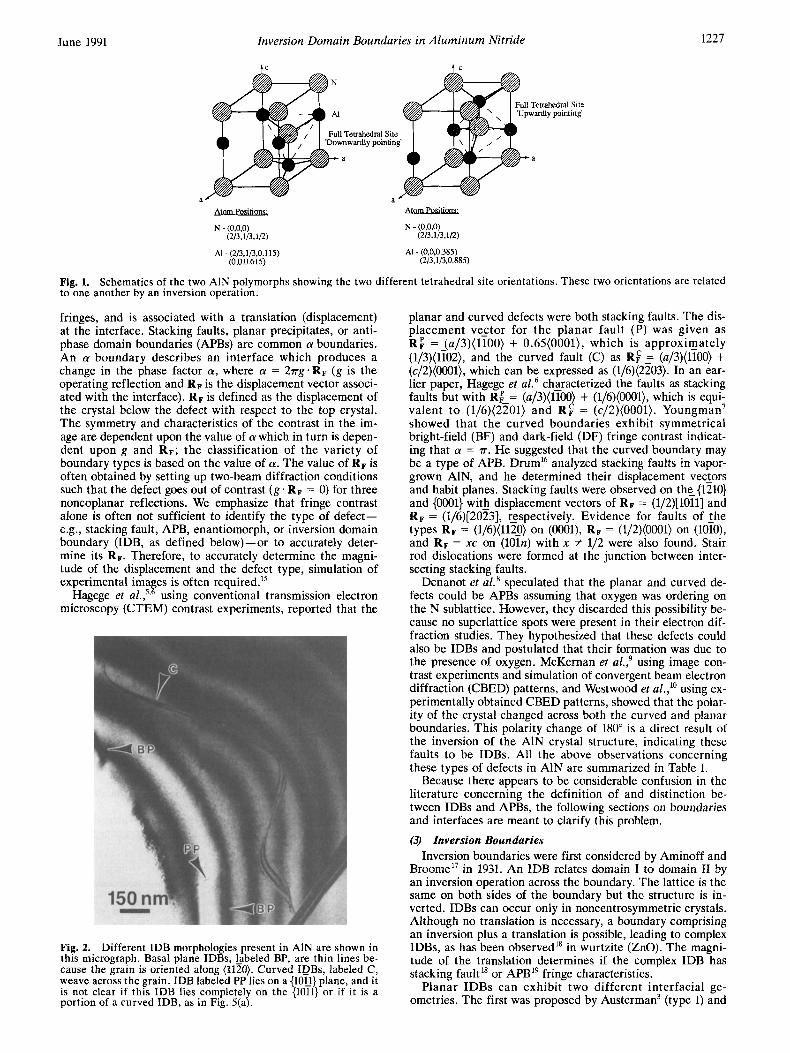
defect morphologies are present4-" (see Fig. 2). The first is a planar fault which lies on the basal plane. The second is a fault which twists and curves through the grain, exhibiting no specific habit plane. These two morphologies can exist sepa- rately, or they can be joined to form complex defects in which the two crystallographic variants alternate between the planar and curved morphologies. At the intersection point a disloca- tion is present; dislocations are also sometimes observed lying in the basal plane of the planar defect. In most cases, when they exist either separately or in a more complex morphology, these defects are seen to emanate from and terminate at grain boundaries. Plang defects or planar segments of curved de- fects lying on (1011) are occasionally observed adjoined to a basal fault (see Fig. 2); the defect zigzags through the grain matrix. The curved defects often have portions (particularly those adjoining the inte_rsection point with a ptanar boundary) which lie on (1011). Another characteristic defect morphology present in AIN consists of a planar defect joined at both ends by the same curved defect, forming a D shape, and it is always contained within a grain (see Fig. 5(a)). In three dimensions the defects enclose a dome-shaped volume of material. Defects exhibiting the planar or curved mor- phologies have previously been seen in BeSiN2 by Shaw,12 who identified them as enantiomorphs. l3
Enantiomorphs are structures which can possess left- handed and right-handed symmetry: an enantiomorphic boundary separates these two different structures. However, enantiomorphic boundaries exist only in lattices where the space group does not contain a "symmetry operation of the second sort," that is, an operation which does not involve an inversion or r e f l e~ t ion . '~ , ' ~ AIN possesses a mirror plane (reflection) and, therefore, cannot contain enantiomorphic boundaries.
A number of authors have noted the a fringe contrast ex- hibited by the planar and curved defects when inclined to the foil surface. An a boundary image consists of dark and bright
1226
June 1991 Inversion Domain Boundaries in Aluminum Nitride 1227
11 Tetrahedral Site
trahedral Site ardly pointing'
N - (0,O.O) (2/3,1/3.1/2)
Al - (2/3.1/3,0.115) (0.0.0.615)
Atom Positions:
N - (O,O,O) (2/3,1/3,1/2)
Al - (0,0,0,385) (213,113.0.885)
Fig. 1. to one another by an inversion operation.
Schematics of the two AIN polymorphs showing the two different tetrahedral site orientations. These two orientations are related
fringes, and is associated with a translation (displacement) at the interface. Stacking faults, planar precipitates, or anti- phase domain boundaries (APBs) are common a boundaries. An a boundary describes an interface which produces a change in the phase factor a, where a = 2 ~ g . R ~ (g is the operating reflection and RF is the displacement vector associ- ated with the interface). RF is defined as the displacement of the crystal below the defect with respect to the top crystal. The symmetry and characteristics of the contrast in the im- age are dependent upon the value of a which in turn is depen- dent upon g and RF; the classification of the variety of boundary types is based on the value of a. The value of RF is often obtained by setting up two-beam diffraction conditions such that the defect goes out of contrast (g.RF = 0) for three noncoplanar reflections. We emphasize that fringe contrast alone is often not sufficient to identify the type of defect- e.g., stacking fault, APB, enantiomorph, or inversion domain boundary (IDB, as defined below)-or to accurately deter- mine its Rp. Therefore, to accurately determine the magni- tude of the displacement and the defect type, simulation of experimental ima es is often req~ired. '~
Hagege et a1.,5f using conventional transmission electron microscopy (CTEM) contrast experiments, reported that the
Fig. 2. Different IDB morphologies present in A1N are shown in this micrograph. Basal plane IDBs, labeled BP, are thin lines be- cause the grain is oriented along (1120). Curved IQBs, labeled C , weave across the grain. IDB labeled PP lies on a (10l-l) plane, and it is not clear if this IDB lies completely on the (1011) or if it is a portion of a curved IDB, as in Fig. 5(a).
planar and curved defects were both stacking faults. The dis- placement vestor for the planar fault (P) was given as Rg = (a/3)(1100) + 0.65(0001), which is approximately (1/3)(1702), and the curved fault (C) as R$_= (a/3)(1100) + (c/2)(0001), which can be expressed as (1/6)(2203). In an ear- lier paper, Hagege et aL6 characterized the faults as stacking faults but with R:-= (a/3)(1109 + (1/6)(0001), which is equi- valent to (1/6)(2201) and RP = (c/2)(0001). Youngman7 showed that the curved boundaries exhibit symmetrical bright-field (BF) and dark-field (DF) fringe contrast indicat- ing that a = T . He suggested that the curved boundary may be a type of APB. Drum'6 analyzed stacking faults in vapor- grown AlN, and he determined their displacement vectors and habit planes. Stacking faults were observed on the_ (1210) and (0001) with displacement vectors of RF = (1/2)[1011] and RF = (1/6)[2023], Espectively. Evidence for faults of the types RF = (1/6)(1121) on (OOOl), RF = (1/2)(0001) on (lolo), and RF = xc on (101n) with x f 1/2 were also found. Stair rod dislocations were formed at the junction between inter- secting stacking faults.
Denanot et al.' speculated that the planar and curved de- fects could be APBs assuming that oxygen was ordering on the N sublattice. However, they discarded this possibility be- cause no superlattice spots were present in their electron dif- fraction studies. They hypothesized that these defects could also be IDBs and postulated that their formation was due to the presence of oxygen. McKernan et a1.: using image con- trast experiments and simulation of convergent beam electron diffraction (CBED) patterns, and Westwood et al.," using ex- perimentally obtained CBED patterns, showed that the polar- ity of the crystal changed across both the curved and planar boundaries. This polarity change of 180" is a direct result of the inversion of the AlN crystal structure, indicating these faults to be IDBs. All the above observations concerning these types of defects in AlN are summarized in Table I.
Because there appears to be considerable confusion in the literature concerning the definition of and distinction be- tween IDBs and APBs, the following sections on boundaries and interfaces are meant to clarify this problem.
(3) Inversion Boundaries Inversion boundaries were first considered by Aminoff and
BroomeI7 in 1931. An IDB relates domain I to domain I1 by an inversion operation across the boundary. The lattice is the same on both sides of the boundary but the structure is in- verted. IDBs can occur only in noncentrosymmetric crystals. Although no translation is necessary, a boundary comprising an inversion plus a translation is possible, leading to complex IDBs, as has been observed'' in wurtzite (ZnO). The magni- tude of the translation determines if the complex IDB has stacking fault" or APBI9 fringe characteristics.
Planar IDBs can exhibit two different interfacial ge- ometries. The first was proposed by Austerman3 (type I) and

1228 Vol. 74, No. 6 Journal of the American Ceramic Society - Westwood and Notis
Table I. Summary of Research on Planar and Curved Defects in A1N Comments Researchers Description of defect
Hagege et aL6 Stacking fault Determined displacement vectors for planar and curved interfaces:
Hagege et aL5
Youngman7
Denanot et al.’
McKernan et aL9 Westwood et al. I’
West wood et al.
Westwood et al. (present work)
~i (a/3) iioo) + (1/6)(0001) RF - (c/2){0001)
and curved interfaces: R P - a/3) 1100 + 0.65(0001) R i ((a/3){1100{ + (c/2)(0001)
Stacking fault Determined displacement vectors for planar
APB
Extended defects
APB/polarity reversal boundary APB
Based description on the nature of observed fringe contrast, a = T
Speculated defects to be IDBs with presence of oxygen at these defects; no experimental evidence
Simulated CBED patterns Fringe contrast from both planar and curved
boundaries was a = P; believed that they were APBs
CBED analysis indicated polarity reversal across the interface; only possibility is inversion operation; preliminary AEM results indicated oxygen on planar IDB
Confirmed defects as IDBs using a variety of techniques; ox gen present on planar IDBs;
IDB
IDB
R$ = .d0001? + E
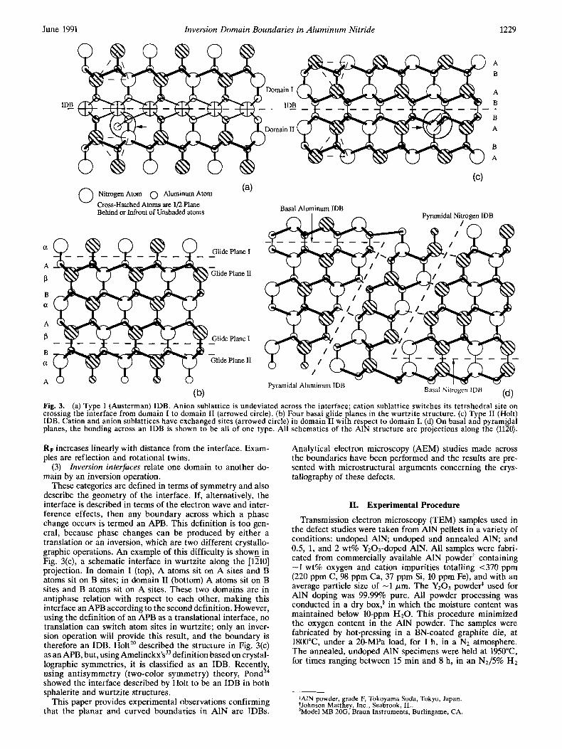
the second by Holt’” (type 11). A~s te rman ,~ reviewing the work of Knippenberg2’ in Sic and of Witzke‘* in AlN in con- junction with his own work in BeO, inferred that inversion boundaries are present in these materials, and he called them “inversion twins.” The model shown in Fig. 3(a), proposed by Austerman to describe the inversion twin configuration, as- sumes that the anion sublattice is undeviated across the boundary, with the cation sublattice switching its tetrahedral packing from one site to the other. In the case of a fault on the basal plane, the twin is of a reflection type, whereas faults on the prism or pyramidal plans are rotation twins. Recently, Kim1* expanded Austerman’s model, showing that eight dif- ferent basal inversion twin configurations are possible, de- pending upon the choice of basal plane on which the twin interface is found, i.e., I (aA or PB) or 11 (Ba or Aj3)23 (see Fig. 3(b)), and also if a translation is present at the interface. A ~ s t e r m a n ~ ~ later showed that the anion sublattice is slightly deviated across the twin interface, with RF = (1/16)[0001]. High-resolution electron microscopy (HREM) has verified this model on (111) in ZnSe (Ref. 25) and on (0001) in ZnO.” Although inversion twins have been observed on basal planes, no experimental observations of inversion twins have been observed on the prism or pyramidal planes. In these types of inversion boundaries, the bonding across the interface is con- sistent with the matrix, meaning that no A-A or B-B bond- ing occurs across the interface.
The second type of IDB (type 11) consists of A atoms on A sites and B atoms on B sites in domain I and A atoms on B sites and B atoms on A sites in domain I1 (see Fig. 3(c)). This type of IDB has been observed experimentally in GaAs using HREM.26 This type of boundary can be either stoichiometric (equal number of A-A and B-B bonds across the interface) or nonstoichiometric (unequal number of A-A and B-B bonds across the interface). In the case of boundaries on the basal and pyramidal planes, the bonds are all the same type (see Fig. 3(d)). The wrong bonding is expected to produce a con- traction or expansion at the interface; the interfacial energy of this IDB is expected to be high because of the wrong bond- ing,2’a and consequently the possibility of segregation to the boundary is increased. As in the case of the inversion twin model, a translation at the interface is theoretically possible and has been observed experimentally by Carter,27b Young- man:* and our~elves?~
Blank et aL3” first considered contrast effects from IDBs (calling them “antistructure” boundaries). A fuller expla-
nation of the contrast effects from IDBs was developed in conjunction with studies performed by Amelinckx and co- w o r k e r ~ . ~ ~ , ’ ~ These studies reveal symmetrical a fringe con- trast in BF and asymmetrical in D F such contrast effects arise because of the violation of Friedel’s law3’ when the boundaries are imaged under multibeam conditions. Friedel’s law states that the diffracted intensity in the direction k, + g for an incident beam k, equals the intensity diffracted in the direction -(ko + g) for an incident beam along -k.. Friedel’s law fails for noncentrosymmetric crystals; i.e., (k, + g) f -(ko + g), and the observed intensities of diffracted beams in different (opposite) directions are not equal. The failure of Friedel’s law can only be observed under specific diffracting conditions. Under multibeam diffracting conditions, i.e., on a zone axis, and imaging in DF using *(hkil) reflections which highlight the noncentrosymmetry of the crystal, a contrast re- versal across the boundary will be seen.
(4) It appears that confusion exists over the definition of and
distinction between IDBs and APBs: IDBs have frequently been called APBS?,~,~’,’~~~’ A major reason for this confusion is due to the different definitions used to describe an APB, which sometimes allows an IDB to be considered as a type of APB. If the characteristics of planar interfaces are derived from crystallographic (symmetry) considerations, then this leads to the definition of three categories of interface^.^^
(1) Translational interfaces separate two parts of a crystal that are related to one another by a constant displacement vector RF, independent of the distance from the interface. Examples are stacking faults and APBs.*
Twin inlerfaces separate orientational variants which possess a displacement field in which the displacement vector
IDB versus APB-The Same or Different?
(2)
*In general the term stacking fault is applied to crystals which can be constructed from stacked planes, and, therefore, they possess specific values for Re; an APB is a translation interface with a displacement vector Up equal to a vector connecting different atom species in the unit cell.)’ Stack- ing faults occur only on close-packed planes; APBs can, in principle, occur on any plane and need not be planar. APBs can also accommodate nonstoi- chiometry within the boundary region. APBs can form between ordered and disordered structures as well as between two ordered structures.)6 APBs are almost always thought of as having a = a symmetrical fringe contrast be- cause the pioneering work into the contrast effects of APBs was conducted on CuAu,’s an alloy in which the phase change associated with the APB is a = a. However, M a r c i n k ~ w s k i ~ ~ showed APBs with the values ?(1/3)~r, ?(1/2)a, &(2/3)a, and a for a.
June 1991 Inversion Domain Boundaries in Aluminum Nitride 1229
(4 Nitrogen Atom 0 Aluminum Atom Cross-Hatched Atoms are 1/2 Plane Behind or Infront of Unshaded atoms
Glide Plane I a
A - -
Glide Plane I1 P B a
A
Glide Plane I - P B - a
A
Glide Plane I1
Fig. 3. (a) Type I (Austerman) IDB. Anion sublattice is undeviated across the interface; cation sublattice switches its tetrahedral site on crossing the interface from domain I to domain I1 (arrowed circle). (b) Four basal glide planes in the wurtzite structure. (c) Ty e I1 (Holt) IDB. Cation and anion sublattices have exchanged sites (arrowed circle) in domain I1 with respect to domain I. (d) On basal anipyramdal planes, the bonding across an IDB is shown to be all of one type. All schematics of the AIN structure are projections along the (1120).
RF increases linearly with distance from the interface. Exam- ples are reflection and rotational twins.
(3) Inversion interfaces relate one domain to another do- main by an inversion operation.
These categories are defined in terms of symmetry and also describe the geometry of the interface. If, alternatively, the interface is described in terms of the electron wave and inter- ference effects, then any boundary across which a phase change occurs is termed an APB. This definition is too gen- eral, because phase changes can be produced by either a translation or an inversion, which are two different crystallo- graphic operations. An example of this difficulty is shown_ in Fig. 3(c), a schematic interface in wurtzite along the [1210] projection. In domain I (top), A atoms sit on A sites and B atoms sit on B sites; in domain I1 (bottom) A atoms sit on B sites and B atoms sit on A sites. These two domains are in antiphase relation with respect to each other, making this interface an APB according to the second definition. However, using the definition of an APB as a translational interface, no translation can switch atom sites in wurtzite; only an inver- sion operation will provide this result, and the boundary is therefore an IDB. HoltZ0 described the structure in Fig. 3(c) as an APB, but, using Amel in~kx ' s~~ definition based on crystal- lographic symmetries, it is classified as an IDB. Recently, using antisymmetry (two-color symmetry) theory, Pond34 showed the interface described by Holt to be an IDB in both sphalerite and wurtzite structures.
This paper provides experimental observations confirming that the planar and curved boundaries in AIN are IDBs.
Analytical electron microscopy (AEM) studies made across the boundaries have been performed and the results are pre- sented with microstructural arguments concerning the crys- tallography of these defects.
11. Experimental Procedure
Transmission electron microscopy (TEM) samples used in the defect studies were taken from AlN pellets in a variety of conditions: undoped AIN, undoped and annealed AIN, and 0.5, 1, and 2 wt% Yz03-doped A1N. All samples were fabri- cated from commercially available AIN powdert containing -1 wt% oxygen and cation impurities totalling <370 ppm (220 ppm C, 98 ppm Ca, 37 ppm Si, 10 ppm Fe), and with an average particle size of -1 pm. The Yzo3 powdert used for A1N doping was 99.99% pure. All powder processing was conducted in a dry box,$ in which the moisture content was maintained below 10-ppm HzO. This procedure minimized the oxygen content in the AIN powder. The samples were fabricated by hot-pressing in a BN-coated graphite die, at 1800"C, under a 20-MPa load, for 1 h, in a NZ atmosphere. The annealed, undoped AIN specimens were held at 1950"C, for times ranging between 15 min and 8 h, in an N2/5% H2
+AlN powder, rade F Tokoyama Soda, Tokyo, Japan. *Johnson Mattkey, Ind., Seabrook, IL. 'Model M B ZOG, Braun Instruments, Burlingame, CA.

1230 Journal of the American Ceramic Society - Westwood and Notis Vol. 74, No. 6
atmosphere and furnace cooled to room temperature. Samples containing CaO as a sintering additiven were also analyzed.
The TEM samples were prepared by cutting thin slices of AlN from the fabricated bulk samples using a diamond saw, followed by grinding on 600-grit S i c paper to -100 to 150 p,m. Further grinding using a dimpler** to obtain larger amounts of thin area was conducted to a final thickness of -10 to 15 pm. The sample was ion-beam thinned to perforation using 4-keV Ar' ions. CTEM and CBED were conducted on an electron microscopert operated at 120 keV. Lattice fringe images were observed on an electron microscope** operated at 250 keV. AEM was conducted on a dedicated scanning transmission electron microscope (STEM),@ fitted with a field emission gun (FEG) source operated at 100 keV. This system was equipped with a windowless enerfj dispersive spectrome- ter (EDS) and a computer system, which allowed light- element analysis at high spatial resolution to be performed.
111. Results
(1) Identification of ZDBs Identification of IDBs requires a multibeam diffraction
condition using reflections that belong to a zone which high- lights the noncentrosymmetry of the crystal. The (1210) zone axis in AIN readily shows the noncentrosymmetric nature of this crystal structure. CBED patterns can be used to confirm this, and Fig. 4 shows a zero-order Laue zone (ZOLZ) from a (1210) zone axis; notelhe asymmetry in the intensities in the 20002 disks and to l l1 family of disks. Figure 5(a) shows a BF image of a D-shaped boundary under strong diffracting conditions in a (1120) orientation. Figure 5(b) is a DF image using the g(ooo2) reflection and Fig. 5(c) is a DF image using g(oooTl. Friedel's law is violated under these diffraction condi- tions, and, therefore, according to Blank et al,30 a contrast difference should be seen in the DF images obtained from either side of the boundary. In the two DF images shown, the
'Hitachi Co., Mountain View, CA. **Model 656 Mk3, Gatan, Inc., Pleasanton, CA. "Model EM400T, Philips Electronics Instruments, Inc., Mahwah, NJ. **Model 430, Philips Electronics Instruments, Inc. PgModel HB-501, Vacuum Generator, East Grinstead, U.K. "Model 1000, Link Systems, High Wycombe, U.K.
Fig. 4. CBED pat tern of t h e zero-order layer f rom a (1130) zone axis. Note t h e mirror runn ing vertically in t h e image a n d t h e asyrn- metry in t h e 20002 disks ( top a n d bo t tom center); therefore, there is no rotational or reflection symmet ry across t h e basal plane.
thickness fringe contrast reverses upon crossing both the curved and planar boundaries, and the contrast is reversed between the images formed using g(w2) and g(oooz) reflections. This type of image contrast is also observed when using g{Ioil} reflections. The results indicate that the two domains sepa- rated by the boundary are related to each other by an inver- sion operation.
A consequence of the inversion operation in the wurtzite structure is a change in the polarity of the crystal. Using a two-beam condition in the ZOLZ with the presence of reflec- tions in the first-order Laue zone (FOLZ) at exact Bragg dif- fraction conditions, Taft0 et al.38 developed a CBED technique for determining the polarity of a crystal. Figure 6 shows the two-beam CBED analysis performed on a D- shaped fault in A1N. In the (0001) reflection in Fig. 6(a), higher-order Laue zone (HOLZ) lines form a bright cross, and in the (0001) reflection (not shown) the cross is dark. On crossing the boundary, the contrast of the crosses changes; the HOLZ lines in the (0001) reflection are dark (see Fig. 6(b)); i.e., a contrast reversal with respect to the top pattern has occurred. This indicates that the polarity of the crystal has reversed direction across the boundary. This polarity change is possible only by an inversion operation, and this result con- firms the previous multiple-beam contrast experiments; the planar and curved portions of the D defect have been unam- biguously identified as IDBs. Similar analyses have been per- formed on separate planar and curved defects with the same result.
The change in polarity can also be observed on close-in- spection of a CBED zone axis pattern from the (1120). Figure 7(a) shows the ZOLZ of the (1210) zone axis from the region inside the domain in Fig. 5(a), and Fig. 7(b) is the ZOLZ from the same orientation but outside of the domain. The intensity in the g(m2) and g(ooo3) disks is reversed on cross- ing the boundary; this is also observed in the g(I(nl)-type reflections.
(2) Displacement Vector (R F) Determination Fringe contrast for the curved and planar IDBs using two-
beam diffraction conditions is symmetrical in both BF and DF, with the contrast being reversed (see Fig. 8). This con- trast is characteristic of a = n-, which is a 180" phase change and is associated with a displacement equal to a vector con- necting the A1 and N sites in the wurtzite structure. The sym- metrical fringe contrast in both BF and DF images has not previously been seen for IDBs; other analyses of IDBs have shown asymmetrical fringe ~ontrast.~'
Determination of RF using g * RF = n ( n = 0,1,2, . . .) for three noncoplanar reflections was tried on both planar and curved IDBs. Four different families of reflections were found for which the curved IDBs were invisible: g(lTlo), g(iioo,, g(2130), and g(31a) (see Fig. 9). These are all consistent with a displacement along the (Owl), in accordance with the zone law, hu + kv + it + lw = 0. For all planar IDBs analyzed, only one family of reflections was found for which the boundaries lost contrast: g(lzlo). For two planar boundaries, a second reflection was found: for one IDB, no contrast was observed forg(iol-j) (see Fig. 10). For another boundary no con- trast was observed for g(ioi5). In all cases, when the IDBs were out of contrast, a very small amount of residual contrast remained indicating that the displacement vector RF also con- tained a small additional displacement E ; i.e., the displace- ment vector of the IDBs was RF + E. HREM and CBED studie? to be reported elsewhere indicated that RF = (1/3)(1100) + E. Displacement vectors of this type are associ- ated with a relaxation at the IDB.39
An IDB relates domain I to domain I1 by an inversion opera- tion, but a translation can also be present. In the particular case of an IDB with translation, the vector RF depends upon the choice of origin of the inversion point, because it is pos- sible to chose an origin for which RF = 0. An inversion through the origin followed by a displacement of RF gives the

June 1991 Inversion Domain Boundaries in Aluminum Nifride 1231
(c) Fig. 5. (a) B-F image of a strongly diffracting grain along a (1120) zone axis, containing a D-shaped IDB center and the planar IDB far left. Note the {loll} portion of the curved section of the D-shaped IDB at the intersection with the basal IDB. (b) DF imsge using a 0002 reflection. Note the contrast reversal in the thickness fringes across the curved and planar IDBs. (c) DF image using 0002 reflection. Note the reversal in contrast between (b) and (c).
(a) ( b) Fig. 6. Two-beam CBED patterns using the 0001 disk and transmitted disk: (a) CBED pattern from inside the D in Fig. 5 and (b) CBED pattern from outside of the D. Change in contrast of the dynamic intensity and the HOLZ lines occur in both the transmitted and 0001 disks on crossing the IDB. This contrast reversal is indicative of a polarity change of the crystal structure.

1232 Journal of the American Ceramic Society - Westwood and Notis Vol. 74, No. 6
Fig. 7. CBED zero-order layer pattern from a (1150) zone axis. Polarity change can be observed in the multibeam condition by the reversal in the intensities between the two patterns (a) from inside the D and (b) from outside the D. The 20002 disks have switched position indicating a reversal in polarity.
same result as an inversion at a position RF/2; therefore, if we had chosen our origin at this position, then RF = 0. Serneels et al.,31 has indicated that a two-beam approach may be am- biguous for determination of RF and proposed that the origin be chosen as a symmetry axis in domain I at position T ( * , ~ , ~ ) .
An equivalent point in domain I1 is at - T ( ~ , ~ , ~ ) + RF. It fol- lows that RF links the equivalent symmetry axis in domain I with that in domain 11. This method requires that the sample be oriented along a zone axis and that only the RF component perpendicular to the symmetry axis is involved in producing fringe contrast. Under these conditions, if RF = O,l, 2, . . . , n, then the symmetry axis in the adjacent domain coincides and no fringe contrast would be observed in DF. However, when the symmetry axis in an adjacent domain does not coincide, RF f 0,1,2, ..., n , and the IDB is imaged such that it ap- pears as (Y fringes.
Frige contrast is observed_ for the cuped boundaries when viewed along the (1100), (1120), and (2130) zone axes, indicat- ing a displacement in the caxis. Figure 5 shows a D-shaped IDB viewed along the (1120). The fringe contrast is clearly present in the curved portion in both BF and DF g(%0,~,2) im- ages. The nature of the c-axis displacement is supported by both two-beam g*RF = n analysis and HREM, which indi- cates the displacement to be -(1/4)(0001);"9 however, whether the two-beam condition is a valid analysis technique or not for IDBs is not clear. The planar IDBs cannot be clearly im- aged under the above zone axis viewing conditions because they are parallel to the incident electron beam; therefore, fringe contrast cannot be observed.
When the sample was oriented along the (0001) zone axis, the curved boundary did not show strong fringe contrast (see Fig. 11). Only very weak residual contrast was observed, indi-
Fig. 8. BF/DF pair of D-shaped IDBs showing the symmetrical (Y fringe contrast. Contrast reverses between the BF and DF images. Note the contrast from the end-on view of the dislocation core at the intersection of the curved and planar portions of the IDB.

June 1991 Inversion Domain Boundaries in Aluminum Nitride 1233
Fig. 9. Series of DF two-beam conditions using (a) g(,l?o), (b) g(loi01, and (c) g(2170). Curved IDB, is out of contrast.for all these reflections. In (a) the planar portion of the D IDB was also out of contrast. Planar portion of the IDB in (c) IS very close to being parallel to the beam but some contrast can be seen. Note the residual contrast in the images.
cating the presence of either a very small displacement vector E
for the curved IDB in the basal plane or a lattice relaxation due to segregation at the IDB interface. Moirt fringe contrast was associated with the planar IDBs due to a misorientation between the two domains across the interface. Associated with the misorientation was a displacement vector RF in the basal plane (see Fig. 11).
(3) Selected Area Electron Diffraction (SAED) Studies SAED patterns were obtained from the IDBs by placing
the 50-pm objective aperture over the boundary of interest and then spreading the illumination on the screen and focus- ing the diffraction pattern. Under these conditions any fine structure that might be present in the diffraction pattern could be observed. Exposures of 180 s were used to allow the faint fine structure to be recorded.
SAED patterns from the curved IDBs showed satellite spots lying close to the fundamental spots. The direction of the satellite spots with respect to the fundamental spots was
always perpendicular to the inversion domain interface, such that the direction of the satellite spots changed as the SAED aperture was moved along the curved interface (see Fig. 12). The satellite spots moved progressively farther away from the fundamental spots with increasing distance from the trans- mitted spot. Gevers et ~ 1 . ~ ' ~ ~ ~ provided both a theoretical and experimental study of fine-structure satellite spots resulting from stacking faults, APBs, and domain boundaries (6 boundaries in Ni,Mo). The present work is the first report of fine-structure spots associated with IDBs.
Streaking was present in a large number of SAED patterns taken from planar IDBs oriented parallel to the beam. How- ever, not all planar IDBs showed streaking. The streakhg for IDBs on the basal plane was along (OOOl), and along (1011) for planar boundaries on the pyramidal planes (see Fig. 13). The planar IDBs appeared as faint broad lines when imaged using the streaks; however, sharp recorded images were difficult to obtain because of specimen drift. Satellite spots could not be observed because the boundary was not inclined to the beam.

1234 Journal of the American Ceramic Society - Westwood and Notis Vol. 74, No. 6
Fig. 10. Series of DF images showing the presence of a planar IDB with a different displacement across the interface: (a)gcozro,, showing the invisibility of the curved section and the contrast of the two basal plane IDBs; (b) g(llza), showing all IDBs to lose contrast as expected from Fig. 9; and (c) g~,,l~,, showing the bottom planar IDB to lose contrast while the top planar IDB remains in contrast.
SAED patterns from two curved IDBs showed faint streaking parallel to (0001) (see Fig. 12); streaking was seen only from portions of the curved boundary which were parallel to the beam, similar to the planar IDBs. Further evidence for a thin planar precipitate was obtained from lattice fringe imaging. A random selection of planar IDBs were imaged, and all were found to have a -1-nm-wide region across which the regular fringe spacing was lost; this work will be reported elsewhere.
(4) Dislocation Analysis Dislocations have been observed at the intersection points
of curved and planar IDBs and on the basal plane of the planar IDBs. The analysis of dislocations, their type, and Burgers vector b can provide information on the defect dis- placement and possible formation mechanisms; for example, Frank dislocations are produced by either coalescence and collapse of vacancies or segregation of interstitials. The con- trast seen at a dislocation is due to the strain field surround- ing it, which causes a displacement in the local lattice planes
related to b. Determination of b is similar to that for the dis- placement of a planar defect, requiring three noncoplanar re- flections for which the dislocation loses contrast. b can be calculated using g * b = 0, g . be = 0, and g . b A u = 0, where g is the operating reflection, b is the Burgers vector, be is the edge component of b, and u is the vector along the dislocation line. These expressions are valid only for displacement fields produced by pure edge and pure screw dislocations in isotropic materials. Often, dislocations have both edge and screw character, and, therefore, they will not go out of con- trast; also, very few materials are isotropic.
Dislocations have been studied in thin, vapor-grown platelets of AlN and ZnS by Blank et dZ3 Dislocationsin the basal I glide plane (aA or PB) have either b = (1/3)(1210) for a perfect dislocation or b = (1/3)(1100) for a Shockley partial. If the glide plane is type I1 (Ba or A@), then only the perfect dislocation is present. If the dislocation is a sessile Frank, and it lies on a (1~10) plane, then b _ = (1/2)(0001), or if its on the basal plane, then b = (1/6)(2023). Shchentanov et aL4' com-

June 1991 Inversion Domain Boundaries in Aluminum Nitride 1235
piled a table for all these values of b and for a number of different reflections. None of the dislocations present in our samples were of the types listed above. A further complica- tion was that the dislocations were clearly visible only when fringe contrast was not present and that was only forg{,2,0); for all other reflections, dislocation contrast and fringe contrast were superimposed, making interpretation difficult. These dislocations were difficult, but not impossible to analyze, but, because of the nature of the defect, we were unable to deter- mine the b value for these dislocations. This area of the work warrants more research. (5) Microchemical Analysis (AEM)
Hagege et aL6 and Denanot et al.’ speculated that oxygen was present at defect boundaries. AEM analysis using a win- dowless X-ray detector, allowing light-element analysis, was conducted on the IDBs to ascertain if segregation of oxygen to these boundaries had occurred. Michael et al.43 showed that, when segregation analysis is performed, a small inclina- tion of a boundary with respect to the beam has dramatic effects on the X-ray detection limits of a segregant species. Therefore, in the present case, all analyses were taken with the boundaries parallel to the beam.
Oxygen was found on all planar defects analyzed, confirm-
high oxygen concentration on the defect (solid line), and also a spectrum obtained -15 nm away from the IDB (dashed
Fig. 11. DF image of a lanar and curved IDB using g(oEo, with the grain oriented along t i e (0001). Moire fringes are shown defin- ing a triangular plate which is the basal portion of the IDB. Very faint residual contrast is shown indicating the presence of the curved section of the IDB (arrowed). Dislocation is shown at the interface between the basal IDB and the matrix.
ing that oxygen segregation was occurring at the planar 1 ~ ~ s . Figure l4 shows the ‘pectrum from a planar boundary with a
Fig. 12. (a) BF image of a curved IDB in a grain oriented on the (1120) zone axis, from which 180-s exposure SAED patterns were obtained from the sections labeled A, B, and C. (b) SAED pattern from region A. Large number of satellite spots are observed oriented perpendicular to the inclined IDB interface. (c) SAED pattern from region B. Faint streaking in the (0001) direction. Some faint satellite spots in two ori- entations because of the change in orientation of the analyzed interface. (d) SAED pattern from region C. Faint streaking in the (0001) direc- tion, and satellite spots normal to the interface.

1236 Journal of the American Ceramic Society - Westwood and Notis Vol. 74, No. 6
Fig. 13. the (0001) and (b) streaking in the (1011) from planar IDB lying on the {loll}.
Streaking from planar IDBs-attributed to oxygen-rich platelike pecipitates: (a) streaking from basal plane IDB with streaking in
line), showing a negligible amount of oxygen to be present in the matrix. Figure 15 shows a profile obtained across a planar IDB and into an enclosed domain; the oxygen concentration on either side of the boundary is constant. The use of a ratio plot of 0 : A l and N:Al intensities eliminates problems re- lated to thickness and absorption factors and allows a com- parison to be made between the 0 and N concentrations. Figure 16 shows the results from a similar analysis performed on a curved IDB. The analysis was taken at a point along the boundary such that the boundary plane was parallel to the beam. Only a small difference in oxygen concentration be- tween the defect and the matrix was observed. A number of other analyses also obtained from curved defects showed no detectable oxygen to be present. A small amount of Ca was detected at the dislocation between intersecting curved and planar IDBs.
(6) Effects of Sintering Additives and Annealing Studies on IDBs
Samples of AlN doped with 0.5, 1, and 2 wt% Y203 were found to be comprised of an A1N matrix with a yttrium alu-
16 d
10
8 $ i l o
2 4 6 8 10 12 14 16 18 20 MmECT R a w (x10- 'keW1
Fig. 14. EDS spectrum comparing spectra obtained from a planar IDB (solid line), and from a region of matrix 15 nm from the IDB (dashed line). Large difference in oxygen peak intensity is appar- ent between the spectra obtained from on and off the IDB.
(FFCE=Ecl - - - _ _ __ -
minate second phase of either 3Yz03.5A1203 for the 0.5 wt% YzO3 sample or a mixture of both Y203.A1203 and 2Y203. A1203 second phases found locally in different regions for the 1 and 2 wt% Y203-doped samples. In all three doped samples very few IDBs were found, and those present were curved defects. In samples that we examined that were doped with CaO, very few IDBs were observed. H ~ r v a t h ~ ~ observed IDBs in great numbers for AlN doped with Mg3N2.
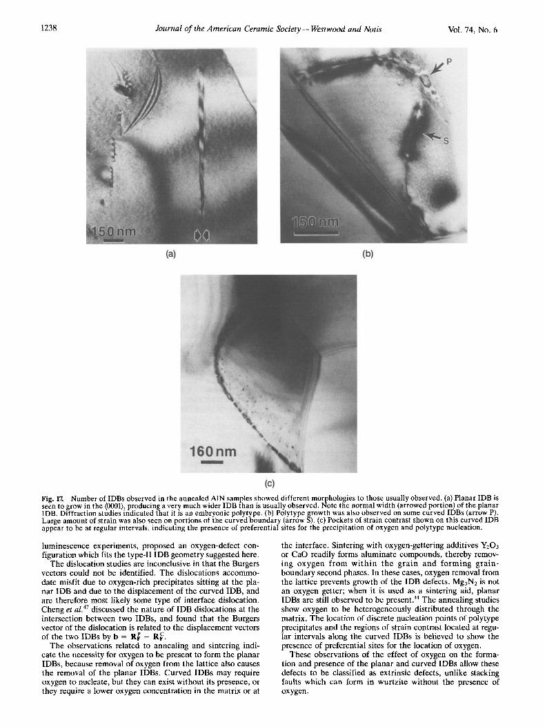
New defect morphologies were encountered in annealed samples of undoped AlN. Figure 17(a) shows broadening of an originally thin planar IDB. Diffraction studies on the widened portion indicate that this region is an embryonic AlON polytype. The diffraction pattern shows streaking be- tween the fundamental spots; closer scrutiny reveals these streaks to be separate spots indicative of a polytypoid struc- ture. Not all planar IDBs show this polytypoid growth, possi- bly because of heterogeneous oxygen distribution. Polytype growth is also seen on some curved boundaries (see Fig. 17(b)). Large strains appear to be associated with this process; Fig. 17(c) shows regions of local strain at regular in- tervals along the curved interface. Precipitation of polytype on the planar and curved IDBs was not commonly seen in annealed AIN. In the annealed samples, polytype precipitates were found associated with IDBs and also at grain boundaries. With increased annealing times ( > 2 h), IDBs were annealed out, leaving the polytype precipitates.
IK Discussion
The planar and curved defects observed in undoped AlN are identified as IDBs. The planar IDBs lie most commonly on the basal plane and less frequently on the pyramidal planes. An interesting property of these two families of planes are that they are both polar?' The structure in these directions is comprised of alternating layers of Al and N atoms. Using the zone axis fringe contrast technique sug- gested by Serneels et aL3' or the two-beam technique, all curved IDBs are found to have RF = ~(0001) + E, where x is a noninteger and E is a small additional displacement vector due to relaxation at the IDB interface, resulting from either a small translation in the basal plane or oxygen segregation. This displacement vector does not agree with those proposed by Ishida4 and Hagege? The question of the validity of the two-beam technique for the determination of the displace- ment at IDBs was posed by Serneels et however, in our work, the two-beam technique provides the same answer as the zone axis technique.
The planar IDBs were always found to lose contrast for g(ll~ol under two-beam conditions. Only two planar IDBs lost contrast for any other reflections, these being gFolT) and g(loi5),
June 1991
0.14
0.12
y" 0.10 0 P) a ;? 0.08 \ 0 % 0.06
0 .- u
0.04
0.02
0.00
Inversion Domain Boundaries in Aluminum Nitride
I I I I I I I I 1 0.14
-------- I a
0 %
2. Z
0.06 - TI m D
0.04 2
> t 10.02
I I I I I I I I I 0.00 1 )O 0 500 1000 1500 2000
1237
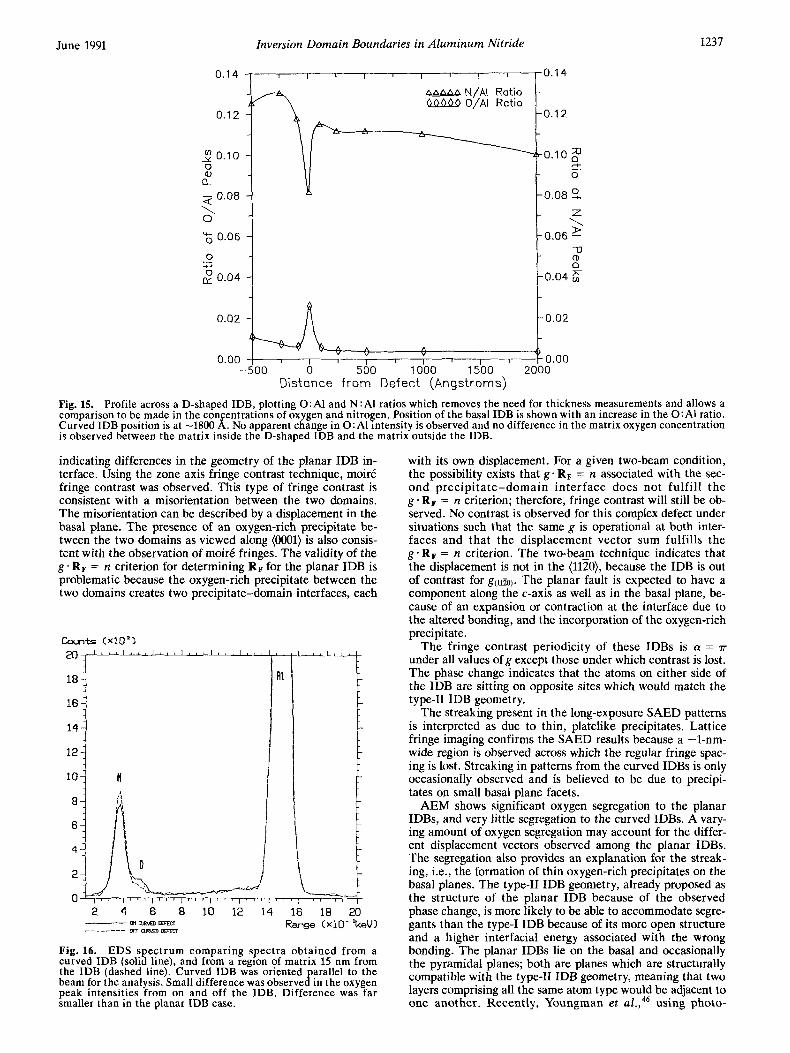
Distance from Defect (Angstroms) Fig. 15. Profile across a D-shaped IDB, plotting 0 : A l and N:Al ratios which removes the need for thickness measurements and allows a comparison to be made in the con entrations of oxygen and nitrogen. Position of the basal IDB is shown with an increase in the 0:Al ratio. Curved IDB position is at -1800 k. No apparent change in 0:Al intensity is observed and no difference in the matrix oxygen concentration is observed between the matrix inside the D-shaped IDB and the matrix outside the IDB.
indicating differences in the geometry of the planar IDB in- terface. Using the zone axis fringe contrast technique, moir6 fringe contrast was observed. This type of fringe contrast is consistent with a misorientation between the two domains. The misorientation can be described by a displacement in the basal plane. The presence of an oxygen-rich precipitate be- tween the two domains as viewed along (0001) is also consis- tent with the observation of moir6 fringes. The validity of the g . RF = n criterion for determining RF for the planar IDB is problematic because the oxygen-rich precipitate between the two domains creates two precipitate-domain interfaces, each
2 4 6 8 10 12 14 16 18 20 -------rnw= Range ( ~ 1 0 - 'keU)
(IFoRmCFEcl _-___---
Fig. 16. EDS spectrum comparing spectra obtained from a curved IDB (solid line), and from a region of matrix 15 nm from the IDB (dashed line). Curved IDB was oriented arallel to the beam for the analysis. Small difference was observefin the oxygen peak intensities from on and off the IDB. Difference was far smaller than in the planar IDB case.
with its own displacement. For a given two-beam condition, the possibility exists that g . RF = n associated with the sec- ond precipitate-domain interface does not fulfill the g . RF = n criterion; therefore, fringe contrast will still be ob- served. No contrast is observed for this complex defect under situations such that the same g is operational at both inter- faces and that the displacement vector sum fulfills the g - R F = n criterion. The two-becm technique indicates that the displacement is not in the (1120), because the IDB is out of contrast for g(llzo). The planar fault is expected to have a component along the c-axis as well as in the basal plane, be- cause of an expansion or contraction at the interface due to the altered bonding, and the incorporation of the oxygen-rich precipitate.
The fringe contrast periodicity of these IDBs is a = 7 under all values ofg except those under which contrast is lost. The phase change indicates that the atoms on either side of the IDB are sitting on opposite sites which would match the type-I1 IDB geometry.
The streaking present in the long-exposure SAED patterns is interpreted as due to thin, platelike precipitates. Lattice fringe imaging confirms the SAED results because a -1-nm- wide region is observed across which the regular fringe spac- ing is lost. Streaking in patterns from the curved IDBs is only occasionally observed and is believed to be due to precipi- tates on small basal plane facets.
AEM shows significant oxygen segregation to the planar IDBs, and very little segregation to the curved IDBs. A vary- ing amount of oxygen segregation may account for the differ- ent displacement vectors observed among the planar IDBs. The segregation also provides an explanation for the streak- ing, i.e., the formation of thin oxygen-rich precipitates on the basal planes. The type-I1 IDB geometry, already proposed as the structure of the planar IDB because of the observed phase change, is more likely to be able to accommodate segre- gants than the type-I IDB because of its more open structure and a higher interfacial energy associated with the wrong bonding. The planar IDBs lie on the basal and occasionally the pyramidal planes; both are planes which are structurally compatible with the type-I1 IDB geometry, meaning that two layers comprising all the same atom type would be adjacent to one another. Recently, Youngman et al.,46 using photo-
1238 Journal of the American Ceramic Society - Westwood and Notis Vol. 74, No. 6
Fig. 17. Number of IDBs observed in the annealed A1N samples showed different morphologies to those usually observed. (a) Planar IDB is seen to grow in the (OOOl), producing a very much wider IDB than is usually observed. Note the normal width (arrowed portion) of the planar IDB. Diffraction studies indicated that it is an embryonic polytype. (b) Polytype growth was also observed on some curved IDBs (arrow P). Large amount of strain was also seen on portions of the curved boundary (arrow S). (c) Pockets of strain contrast shown on this curved IDB appear to be at regular intervals, indicating the presence of preferential sites for the precipitation of oxygen and polytype nucleation.
luminescence experiments, proposed an oxygen-defect con- figuration which fits the type-I1 IDB geometry suggested here.
The dislocation studies are inconclusive in that the Burgers vectors could not be identified. The dislocations accommo- date misfit due to oxygen-rich precipitates sitting at the pla- nar IDB and due to the displacement of the curved IDB, and are therefore most likely some type of interface dislocation. Cheng et al.47 discussed the nature of IDB dislocations at the intersection between two IDBs, and found that the Burgers vector of the dislocation is related to the displacement vectors of the two IDBs by b = Ri - R;.
The observations related to annealing and sintering indi- cate the necessity for oxygen to be present to form the planar IDBs, because removal of oxygen from the lattice also causes the removal of the planar IDBs. Curved IDBs may require oxygen to nucleate, but they can exist without its presence, or they require a lower oxygen concentration in the matrix or at
the interface. Sintering with oxygen-gettering additives Y203 or CaO readily forms aluminate compounds, thereby remov- ing oxygen from within the grain and forming grain- boundary second phases. In these cases, oxygen removal from the lattice prevents growth of the IDB defects. Mg3N2 is not an oxygen getter; when it is used as a sintering aid, planar IDBs are still observed to be present.44 The annealing studies show oxygen to be heterogeneously distributed through the matrix. The location of discrete nucleation points of polytype precipitates and the regions of strain contrast located at regu- lar intervals along the curved IDBs is believed to show the presence of preferential sites for the location of oxygen.
These observations of the effect of oxygen on the forma- tion and presence of the planar and curved IDBs allow these defects to be classified as extrinsic defects, unlike stacking faults which can form in wurtzite without the presence of oxygen.

June 1991 Inversion Domain Boundaries in Aluminum Nitride 1239
V. Conclusions
(1) Curved and planar defects in AIN have been identi- fied as inversion domain boundaries (IDBs). The curved IDB possesses a displacement vector RF = ~(0001) + E, and the planar IDB has a displacement vector with components along the c-axis and contained within the basal plane.
(2) The planar IDBs observed in AlN are not inversion twins (type I) but rather the type-I1 IDB configuration dis- cussed in the text.
(3) Oxygen segregation occurs to the planar IDB, which requires oxygen for its nucleation and stabilization. The pla- nar IDBs contain thin, platelike oxygen-rich precipitates. Oxygen concentration differences may account for the differ- ent displacements observed for the planar IDBs. Oxygen seg- regation to the curved IDB appears to occur to specific locations along the boundary. (4) In a more general context, definition of defect inter-
face type should be based on crystallographic symmetry of the interface, and not on changes in phase factor (a) across the interface. The definition based on symmetry indicates a clear difference between IDBs and APBs and provides the understanding necessary to use analytical methods capable of identifying each of the defect types.
Acknowledgments: The authors thank Bethlehem Steel Co., especially Dr. J. R. Michael for the use of AEM, Dr. S. Witek for supplying the un- doped hot-pressed AIN sample, and Mr. Vinayak P. Dravid for his insightful discussion.
References ‘H. Scholz and K. H. Thiemann, “Crystal Structure Refinement in AIN
and GaN,” Solid State Commun., 23, 815-19 (1977). 2F. D. Bloss, Crystallography and Crystal Chemistry; pp. 407-408. Holt,
Rinehart, and Winston, New York, 1971. 3S. B. Austerman and W. G. Gehman, “The Inversion Twin Prototype in
Beryllium Oxide , ” l Mater. Sci., 1, 249-60 (1966). 4Y. Ishida, “Frontiers of Interfacial and Atomic Structure Studies,”
1 Phys., 51 [l] C1-13-C1-22 (1990). %. Hagege, Y. Ishida, and S. Tanaka, “Structural Analysis of Planar De-
fects in Wurtzite-type Aluminum Nitride,” J. Ceram. Soc. Jpn. Int. Ed., 96 [12] 1093-99 (1988).
%. Hagege, Y. Ishida, and S. Tanaka, “HREM and HVEM of Interfaces in Aluminum Nitride Ceramics,” J. Phys., 45, C5-189 (1988).
7R. A. Youngman, ‘Xntiphase Domain Boundaries in Liquid-Phase Sin- tered Aluminum Nitride”; pp. 576-77 in Proceedings of the 46th EMSA Meeting (Milwaukee, WI). Edited by G.W. Bailey. San Francisco Press, San Francisco, CA, 1988.
“. F. Denanot and J. Rabier, “Extended Defects in AIN,” J. Mater. Sci., 24, 1594-98 (1989).
9S. McKernan and C. B. Carter, “On the Structure of Planar Defects in AlN,” Muter. Res. Soc. Symp. Proc., 167, 289-94 (1989).
1°A. D. Westwood and M. R. Notis, “Planar and Curved Defects in Alu- minum Nitride: Their Microstructure and Microchemistry,” Mater. Res. Soc. Symp. Proc., 167, 295-300 (1989).
“A. D. Westwood and M. R. Notis, “Analytical Electron Microscopy Study of AIN Substrates and Metallization Interfaces”; pp. 171-87 in Ad- vances in Ceramics, Vol. 26, Ceramic Substrates for Packages. Edited by M. F. Yan, H. M. OBryan, Jr., K. Niwa, and W. S. Young. American Ceramic So- ciety, Westerville, OH, 1989.
lZT. M. Shaw, “EM Study of Crystallography and Phase Relationships in the Be3Nz-BeSiN2 System”; M.S. Thesis. University of California, Berkeley, CA, 1974.
1 3 0 . Van der Biest and G . Thomas, “Identification of Enantiomorphism in Crystals by Electron Microscopy,” Acta Crystallogr., Sect. A: Cryst. Phys., Diffr., Theor. Gen. Crystallogr., A31, 70-76 (1975).
I4P. Goodman and T.W. Secomh, “Identification of Enantiomorphously Related Space Groups by Electron Diffraction,” Acta Crystallogr., Sect. A: Cryst. Phys., Diffr., Theor. Gen. Crystallogr., A33, 126-33 (1977).
15D. R. Rasmussen, N. Cho, D.W. Susnitzky, and C. B. Carter, “Determi- nation of the Lattice Translation Across Antiphase Boundaries,” Ultrami- croscopy, 30, 27-32 (1989).
I6C. M. Drum, “Intersecting Faults on Basal and Prismatic Planes in Alu-
minum Nitride,” Philos. Mag., 11, 313-34 (1965). l’G. Aminoff and G. Broome, “Strukturtheoretische Studien iiber Zwill-
inge. I.,” 2. Kristullogr., 80, 355-76 (1931). C. Kim and E. Goo, “Inversion Twin Boundaries in Zinc Oxide,”
J. A m . Ceram. Soc., 73 [4] 877-84 (1990). I9M. Snykers, R. Serneels, P. Delavignette, R. Gevers, and S . Amelinckx,
“Inversion Domains in the ,y-Phase Alloy Fe36Crz2-,TiX with 8 i x < 10,” Cryst. Lattice Defects, 3, 99-101 (1972).
*OD. B. Holt, ‘Antiphase Boundaries in Semiconducting Compounds,” J. Phys. Chem. Solids, 30, 1297-308 (1969).
21W. F. Knippenbtxg, Philips Res. Rep., 18, 161-274 (1963). 22H. D. Witzke, “Uber Wachstum Von AIN-Einkristallen aus der Dampf-
phase,” Phys. Status Solidi, 2, 1109-14 (1962). 23H. Blank, P. Delavignette, and S. Amelinckx, “Dislocations and Wide
Stacking Faults in Wurtzite-Type Crystals: Zinc Sulfide and Aluminum Ni- tride,” Phys. Status Solidi, 2, 1660-69 (1962).
“J. Chikawa and S. B. Austerman. “X-ray Diffraction Contrast of Inver- sion Twin Boundaries in B e 0 Crystal,”J. Appl. Crystallogr., 1, 165-71 (1968).
=M. Shiojiri, C. Kaito, S. Sekimoto, and N. Nakamura, “Polarity and In - version Twins in ZnSe Crystals Observed by High-Resolution Electron Mi- croscopy,” Philos. Mag. A, 46 [3] 495-505 (1982).
z6Z. Liliental-Weber, M. A. OKeefe, and J. Washburn, “lnversion Do- mains in GaAs Grown on Si,” Ultramicroscopy, 30, 20-26 (1989).
”(a) J. A. Van Vechten, “Simple Theoretical Estimates of the Enthalapy of Antistructure Pair Formation and Virtual-Enthalpies of Isolated Antisite Defects in Zinc-Blende and Wurtzite Type Semiconductors,” J. Electrochem. Soc., 122,423-29 (1975). (h) S. McKernan, M. G. Norton, and C. B. Carter, “High-Resolution Electron Microscopy of Planar Defects in AIN,” Mater. Res. Soc. Symp. Proc., 183, 267-72 (1990).
28R. A. Youngman; private communication. ”A. D. Westwood and M. R. Notis; unpublished work. ,OH. Blank, P. Delavignette, R. Gevers, and S. Amelinckx, “Fault Struc-
tures in Wurtzite,” Phys. Status Solidi, 7, 747-64 (1964). 31R. Serneels, M. Snykers, P. Delavignette, R. Gevers, and S. Amelinckx,
“Friedel’s Law in Electron Diffraction as Applied to the Study of Domain Structures in Non-centrosymmetric Crystals,” Phys. Status Solidi B, 58, 277- 92 (1973).
32M. Snykers, R. Serneels, P. Delavignette, R. Gevers, J. Van Landuyt, and S. Amelinckx, “Diffraction Contrast between Inversion Domains and at Inversion Domain Boundaries,” Phys. Sfatus Solidi A, 41, 51-63 (1977).
33S. Amelinckx and J. Van Landuyt, Diffraction and Imaging Techniques in Material Science, Vol. I: Electron Microscopy; pp. 107-51. North-Holland, Am- sterdam, Netherlands, 1979.
34R. C. Pond and D. B. Holt, “Antisymmetry of Surfaces and Interfaces in Polar Materials,” l Phys. (Paris), 43 [lo] C1-57-C1-62 (1982).
3sP. Hirsch, A. Howie, R. B. Nicholson, D.W. Pashley, and M. J. Whelan, Electron Microscopy of Thin Crystals; pp. 380-84. Robert E. Krieger Publish- ing Co., New York, 1977.
30A. H . Heuer and G. L. Nord, Jr., Electron Microscopy in Mineralogy; pp. 275-303. Springer-Verlag, Berlin, FRG, 1976.
37M. J . Marcinkowski, Electron Microscopy and Strength of Crystals; pp. 333-440. Edited by G. Thomas and J. Washburn. Interscience Publish- ers, New York, 1963.
38J. Tafto and J. C. H. Spence, ‘X Simple Method for Determination of Structure-Factor Phase Relationships and Crystal Polarity Using Electron Diffraction,” J. Appl. Crystallogr., 15, 60-64 (1982).
39G. Van Tendeloo and S. Amelinckx, “Lattice Relaxation at Glide Anti- phase Boundaries and Stacking Faults in Ni3Mo and in Ni4Mo,”Phys. Status and Solidi A, 21, 93-98 (1975).
“R. Gevers, J. Van Landuyt, and S. Amelinckx, “The Fine Structure of Spots in Electron Diffraction Resulting from the Presence of Planar Inter- faces and Dislocations-Part 1,” Phys. Status Solidi, 18, 342-61 (1966).
41R. Gevers, J. Van Landuyt, and S. Amelinckx, “The Fine Structure of Spots in Electron Diffraction Resulting from the Presence of Planar Inter- faces and Dislocations-Part 111,” Phys. Status Solidi, 26, 577-90 (1968).
42B.V. Shchetanov, Yu. A. Skakov, and V. N. Gribkov, ’Axial Stacking Faults in Aluminum Nitride and its Role in the Crystallization Process,” Sov Phys. Crystallogr. (Engl. Transl.), 19, 641-43 (1975).
43J. R. Michael, G . Cliff, and D. B. Williams, ‘X Microcomputer-Based Monte Carlo Simulation and Its Application to Grain-Boundary Segregation Studies in the AEM,” Scanning Electron Microsc., 4, 1697-705 (1984).
%. F. Horvath, “Effect of Carbon Additions on the Sintering Behavior and Thermal Conductivity of Oxygen-Contaminated Aluminum Nitride”; Ph.D. Dissertation. Lehigh University, Bethlehem, PA, 1989.
45D. B. Holt, “Surface Polarity and Symmetry in Semiconducting Com- pounds,”l Mater. Sci’., 23, 1131-36 (1988).
46J. H. Harris, R. A. Youngman, and R. G . Teller, “On the Nature of the Oxygen-Related Defects in Aluminum Nitride,” J. Muter. Res., 5 [8] 1763-73 (1990).
47T.T. Cheng, P. Pirouz, and F. Ernst, “Inversion Domain Boundary Dis- locations in Heteroepitaxial Films,” Muter. Res. Soc. Symp. Proc., in press. 0