Inventor, Innovator, Entrepreneur and Corporate President
181
Inventor, Innovator, Entrepreneur and Corporate President ---- Industrialization of the FeRAM ---- Larry D. McMillan A dissertation submitted to Kochi University of Technology in partial fulfillment of the requirements for the degree of Doctor of Philosophy Department of Engineering Graduate School of Engineering Kochi University of Technology Kochi, Japan September 2005
-
Upload
khangminh22 -
Category
Documents
-
view
1 -
download
0
Transcript of Inventor, Innovator, Entrepreneur and Corporate President

Inventor, Innovator, Entrepreneur
and
Corporate President
---- Industrialization of the FeRAM ----
Larry D. McMillan
A dissertation submitted to Kochi University of Technology
in partial fulfillment of the requirements for the degree of
Doctor of Philosophy
Department of Engineering Graduate School of Engineering Kochi University of Technology
Kochi, Japan
September 2005

Dedicated To
Ira Duncan McMillan
And
Lilly Bell (Reed) McMillan

i
Synopsis
The world economy is becoming increasingly global and more
knowledge-based [27], [56]. Getting new ideas (not just new technology)
into the world market-place quickly and efficiently has become a significant
concern for nearly every business on the planet. While the legal, political,
language and cultural differences around the world tend to inhibit the rapid
distribution of knowledge, the internet (with its satellite network) is now
providing a vehicle for nearly instantaneous communication between all
members of all societies. With continuous improvement in shipping and
transportation technologies, even the distribution of goods and services is
beginning to take on new meaning. (Note, for instance, that global
positioning (GPS) technology, RFID tags and biometric identification
systems are all having a significant affect on air, sea and ground
transportation services [63].) As supply and demand adjusts to changing
global markets, business practices and organizational structures obviously
must change accordingly in order to stay effective and globally competitive.
With this in mind, it appears that even the meaning of such words as
inventor, innovator, entrepreneur and president should now be re-examined,
and perhaps re-defined to accommodate 21st century business and economic
conditions. Part of this thesis provides insight into some of these terms and
proposes some new models for business operations and, perhaps, business
survival, in the 21st century.
A few inventions, with their subsequent technological advancements,
move society either forward or backward in every century, depending on the
ii
applications of such technology. (It would be hard, of course, to argue that
society moves forward, rather than backward, with the invention of weapons
and/or instruments of mass destruction.) For instance, the invention of the
automobile, the airplane, the transistor and the integrated circuit, all had
profound, and generally positive, effects on 20th century society. In this
thesis we will investigate the origin and evolution of another technology, the
non-volatile ferroelectric memory, that is quite certain to have a significant,
and positive, effect on the new ubiquitous society of the 21st century.1
Background Much of this thesis is based on the business and technology
experiences of the author, Larry McMillan. McMillan is an entrepreneur
from the United States. At the time of this writing (2005) he has forty years
experience encompassing the disciplines of inventor, innovator, entrepreneur
and corporate executive, hence the title of this thesis.2 In this thesis
McMillan’s invention of the integrated, non-volatile, ferroelectric memory
and his persistent efforts to bring it, along with a number of his other
1 In the 20th century, most actively addressed (read/write) computer memories (such as DRAM's) required a source of power to maintain data storage. Without a power supply such memories are volatile and cannot store data for long periods for time. Non-volatile memories do not require a power supply to store data.
2 McMillan began working as an engineer and manager in the semiconductor industry in
1965, before either Bipolar or MOS integrated circuits had entered production (at Motorola). He has worked in nearly every segment of the integrated circuit industry, ranging from Research and Development to Production Engineering to Corporate Management to Consulting for a number of international corporations. Note the brief listing of his U. S. corporate experience (in Appendix D), the listing of his publications and presentations (in Appendix C) and the listing of his patents (in Appendix B).

iii
inventions, to commercialization, should provide some insight into the
actual meaning of many of the terms associated with entrepreneurial
engineering.3
Purpose of research The research of this thesis defines and elucidates some of the practical
and theoretical aspects of entrepreneurial engineering. Concurrently,
research into the origins of ferroelectricity and the ferroelectric random
access memory (FeRAM) will provide support for the idea that most
inventions actually originate from existing knowledge that has accumulated
over hundreds of years. All of this should also help disperse some common
misconceptions concerning the origin, authenticity, ownership and status of
this technology as well as its importance for 21st century ubiquitous society.
We will also try to achieve some understanding of the globalization that had
to occur for ferroelectric memories to play into an industry as complex as the
semiconductor industry. Throughout this thesis, this experience will be
registered against the academic foundation achieved at Kochi University of
Technology.
3 McMillan received B.S and M.S. degrees in Physics, Math and Electrical Engineering
in the U.S. but most of the academic background reflected in this thesis was achieved through graduate studies in Entrepreneurial Engineering (with Professor Gota Kano), Business Theory (with Professor Keizo Baba) and Technology Management (with Professor Osamu Tomisawa) at Kochi University of Technology. (Reference the thesis bibliography.)

iv
Significance of research The significance of this research becomes evident with an
understanding of the historical significance and economic potential of
ferroelectric memory technology. (Of course, the real significance of this
entrepreneurial engineering exercise must ultimately be measured by the
resulting benefits to society.) The author's invention of the integrated
ferroelectric random access memory and his continuous efforts to bring this
technology to commercialization has resulted in much of the revolutionary
product and knowledge base now driving the nonvolatile technology growth
predicted by S. M. Sze in his book ULSI Devices, (published in 2000,
reference [19]). This thesis will show that the author was not only a
primary inventor of this technology but also that, over a period of three
decades, he played a crucial and leading role in its development and
commercialization (reference Figure 1.1 in Chapter one).
With reference to economic potential of the technology, we note that
millions of ferroelectric memory (FeRAM) integrated circuits are now being
manufactured and sold, especially in Japan and other parts of Asia.
Microcontrollers, RFID chips and many other integrated systems are now
being embedded with ferroelectric random access memories (FeRAM’s),
and the US government is now incorporating radiation-hardened
ferroelectric memory devices into their satellite and space probe systems.

v
Summary of contents Following a brief introduction in Chapter 1, we define some of the
differences between the inventor, the innovator and the entrepreneur in
Chapter 2. We also discuss the evolution from inventor to entrepreneur and
explore the environment that cultivates their respective activities.
In Chapter 3, we address the evolution and history of ferroelectric
technology from its earliest roots to the invention (by the author) of the
integrated ferroelectric memory and ultimately to the introduction of viable
non-volatile memory products to the world market place. This process
occurred over many years and several generations of scientists and engineers.
This chapter also introduces Symetrix Corporation, a company co-founded
and co-owned by McMillan and shows the strategic foundation upon which
its core competency was developed.
Chapter 4 addresses some of the management styles, cultural
differences and corporate structures that will mold global business
relationships in the 21st Century. Chapter 5 outlines some ideas on
sustainability and business growth and Chapter 6 discusses protection of
intellectual property and cost minimization through global business
relationships.
Chapter 7 explores the evolution of the new corporation in a changing
business and philosophical environment. Conclusions are presented in
Chapter 8.

vi
Contents
Synopsis i
Content listing vi
Table and figure listing ix
1. Introduction 1
1.1 The status of non-volatile memory 1
1.2 Innovation generators 4
1.3 Ferroelectric memories 5
2. From inventor to entrepreneur; definitions and evolving
characteristics 12
2.1 Invention 12
2.2 Innovation 17
2.3 McMillan's stagnation wall 18
2.4 Entrepreneur 21
2.5 McMillan's hierarchy of mentality model 25
3. Ferroelectric memory: from invention to industrialization 28
3.1 The early history 28
3.2 The single crystal ferroelectric memory 35
vii
3.3 The first polycrystalline thin film ferroelectric
memory 37
3.4 McMillan's cubic integration 38
3.5 Ferroelectric capacitor C-V plots 40
3.6 Integrated ferroelectric memory 43
3.7 The founding of Ramtron Corporation 46
3.8 Symetrix Corporation 49
3.9 The new management approach 51
3.10 Material synthesis 56
3.11 LSMCD 65
3.12 The serendipidous discovery of Y-1 71
4. Cultural differences that mold international business
relationships 76
4.1 Communication and business between world cultures 76
4.2 Classification of cultural characteristics 77
4.3 Business culture: Japan, Korea and the United States 81
5. Strategies for sustainability and business growth 85
5.1 The single technology model 85
5.2 The multi-modal model 87
5.3 A self-correcting neural network model 88
6. Protecting intellectual property through business
relationships and managing the cost of patent protection 91
6.1 The patent assessment 91

viii
6.2 The JDP patent protection model 93
7. Evolution of the new corporation 97
7.1 The changing business environment 97
7.2 Evolving business philosophy and strategy 99
7.3 Value building, exit strategies and longer life spans 103
8. Conclusions 107
Acknowledgments 113
Bibliography 114
Appendices A. The First Ferroelectric Memory Integrated Circuit.
McMillan Disclosure to Motorola, February 7, 1976 121
B. McMillan’s Patents 130
C. McMillan’s Publications and Presentations 142
D. McMillan’s Corporate Experience 157
E. McMillan’s 1972 C-V Publication 158
F. McMillan’s 1994 LSMCD BST Publication 164

ix
Tables and figures
Table
3-1. Ferromagnetic – Ferroelectric Analogy 32
Figure
1-1. Growth curves for different technology drivers 3
1-2. Significant inventions of the 20th century 6
1-3. Innovation generators of the 20th century 7
1-4. FeRAM integrated circuit 8
1-5. A few applications for FeRAM’s 9
1-6. A brief history 10
2-1. Patents per million population 15
2-2. The transition from invention to innovation 20
2-3. Right and wrong entrepreneurs 24
2-4. McMillan’s hierarchy of mentality model 26
3-1. A simple illustration of a ferroelectric material 29
3-2. Rochelle salt hysteresis loop 30
3-3. Basic perovskite structure 34
3-4. Typical electrode arrangement for single crystal memory 35
3-5. George Rohrer’s thin film KNO3 memory 37
3-6. Ferroelectric versus magnetic core memory 39
3-7. Capacitance/Dielectric constant versus voltage for
a ferroelectric capacitor 40
3-8. The relationship between (a) P vs. E, (b) C vs. V and
(c) I vs. V for a ferroelectric capacitor 42
3-9. First integrated ferroelectric memory device patent 44
3-10. The initial intellectual property assets of Ramtron Corp. 48

x
3-11. Symetrix business strategy 49
3-12. Symetrix research strategy 55
3-13. Sol-gel polymerization 56
3-14. Sol-gel copolymerization of multicomponent glass
Networks 57
3-15. Typical precursors 58
3-16. Process flow for Sol-gel Y-1 59
3-17. Process flow for modified Sol-gel + MOD SBT process 60
3-18. Process flow for Barium Strontium Titanate Precursors 61
3-19. Gelation of multiple component solutions 62
3-20. EMOD precursor system 63
3-21. EMOD chemistry process development 64
3-22. EMOD chemistry 66
3-23. LSMCD R&D strategy 67
3-24. LSMCD experimental apparatus 68
3-25. Liquid source chemical vapor deposition technology 69
3-26. Advanced LSCD block schematic for production machine 70
3-27. Production model LSMCD machine 71
3-28. The serendipitous discovery of SBT (Y-1) 73
3-29. ABi2B2O9 lattice structure 74
5-1. Common single technology business model 86
5-2. Multi-modal IP based business model 87
5-3. McMillan’s neural network sustainability model 89
6-1. Joint development program with IP/patent
protection 93
8-1. Panasonic integrated ferroelectric contactless cards 108
8-2. The rapidly expanding market for ferroelectric devices 109

1
Chapter 1
Introduction
1.1 The Status of Non-Volatile Memory
Since the invention of the computer, non-volatile (or pseudo-non-
volatile) memories such as ROM's, EEPROM's, FLASH, etc., have been
used to store data and program code. However, with the exception of ferrite
core memories of the early sixties, most of these semiconductor non-volatile
memories wear out after less than one million erase/write commands,
consume considerable power, and write at microsecond or millisecond
speeds. Ferroelectric non-volatile memories (FeRAM's), however, have
tenth of nanosecond, symmetric, read/write speeds (at the molecular level)
and show very little degradation even after more than 100 billion erase/write
operations.
FeRAM's are currently being used in stand-alone memories, smart
cards, RFID tags and in many other consumer products. Commercially,
more than 100 million FeRAMs have been introduced to the market and now,
due to continuous upgrades, they are becoming key candidates for system-
on-chip applications.

2
S. M. Sze predicted in his book ULSI Devices, (published in 2000)
that non-volatile memory would become a significant technology driver
exceeding the market size of transistors, DRAM’s and CPU’s by about 2010
[19]. Sze placed the accelerating part of his proposed growth curve for non-
volatile memories, very accurately, twenty years after the market
introduction of DRAM’s and CPU’s. It seems unlikely that Sze was aware
of the progress being made with ferroelectric devices, or that he was
referring to ferroelectrics in any way, when he published his growth curve
for nonvolatile memory.7 It, therefore, becomes quite interesting to note that
his growth versus time curve (Figure 1-1) coincides exactly with the S-curve
associated with the invention, development and industrialization of the
FeRAM. Figure 1-1 shows the superposition of the two curves with
McMillan's colored S-curve representing FeRAM's.
7 There are several other "non-volatile" technologies, such as MRAM, Ovonic, etc., that are presently in research; however, FeRAM technology is already mature, in production and exhibits real certainty for future applications..

3
Figure 1-1. Sze's Growth curves for different
technology drivers. The superimposed colored
line represents McMillan's S-curve for
FeRAM's. (After Sze, ULSI Devices, pg. 13, [19])

4
1.2 Innovation Generators
According to Christensen, the semiconductor industry is based on a
disruptive technology, namely the transistor, which displaced the vacuum
tube in the 1950's [25]. Looking back over the last century it becomes
apparent that the invention of the transistor was not only disruptive but also
one of several related inventions that may now be called innovation
generators. 8 The invention of the transistor by Shockley, Brattain and
Bardeen at Bell Labs in 1947, inspired Jack Kilby to invent the integrated
circuit in 1958.9, 10 The integrated circuit would never have been invented
without the prior invention of the transistor. In 1968 George Rohrer used
water soluble KNO3 to build a capacitor like thin film ferroelectric memory
on a glass slide. Indirectly, this was related to the transistor and the
integrated circuit. Rohrer, however, was not particularly interested in the
processing of transistors and integrated circuits, but was inspired by the
work of Schubring, Anderson,Von Hippel and several others who were
trying to find a replacement for magnetic core memories. It is interesting to
note that the transistor, the integrated circuit and the ferroelectric memory all
originated from extremely simple appearing, and yet very technologically
complicated, initial prototypes (Figure 1-2).
8 "Innovation Generator" is a term devised by the author to describe inventions and/or
innovations that cause many people to generate more inventions and innovations.
9 It should be noted that Julius Edgar Lilienfeld proposed the basic principle behind the MOS field-effect transistor in 1925. Reference Lilienfeld U.S patents 1,745,175 (1930) and 1,900,018 (1933) [67] 10 Nobel laureate Jack Kilby, died of cancer at age 81, June 22, 2005.

5
The invention of the integrated ferroelectric memory by McMillan in
1975 was inspired by the previous invention of the transistor, the bipolar
integrated circuit, the MOS integrated circuit, Rohrer’s ferroelectric memory
and many others. (A brief history of ferroelectric memories will be given in
Chapter 3.) As with the transistor and the integrated circuit, the integrated
ferroelectric memory has also become an "innovation generator" (Figure 1-
3) causing the formation of thousands of new companies and the production
of millions of new products as well as inspiring new research and
development interest in almost every country on the planet.
1.3 Ferroelectric Memories
From simple beginnings, ferroelectric memories have now progressed
to the point where they are not only competing with other integrated circuits,
they now display some characteristics that other IC's cannot match. With
their low power consumption, radiation hardness, fast read-write cycle times
and nearly infinite endurance, ferroelectric non-volatile memories
(FeRAM’s) are now widely recognized as superior to other commercially
available nonvolatile devices such as electrically erasable programmable
read-only memories EEPROM's and FLASH (Figure 1-4). It is also
apparent that FeRAM's may soon be replacing many devices in existing
products and appearing in a broad spectrum of new, and/or not yet designed,
products that will have a significant effect on 21st Century society (Figure 1-
5).

6
Figure 1-2. Some significant invention/innovations of the
20th Century [53] (Note the apparent simplicity of the prototypes.)

7
Figure 1-3. Innovation generators of the 20th Century

8
Figure 1-4. FeRAM integrated circuit. (Photo courtesy of
Panasonic Corporation.)

9
RFID Cards Televisions Helicopter: control, navigation, communication VCRs Medicine administering systems Automatic doors Smart hospital bed with sensors and communication
Electric wheelchairs
Patient monitoring system Smart briefcase with fingerprint enabled lock Surgical displays Ambulance medical and communication
equipment Digital thermometers Automatic irrigation systems Portable data entry systems Jet aircraft: control, navigation, communicaton,
autopilot, collision-avoidance, in-flight enterntainment, passenger telephones, etc.
Pacemakers Laptop computer (contains embedded systems) Portable stereos Automatic lighting Satellite receiver systems Pump monitoring system Credit/debit card readers Lottery ticket dispenser Barcode scanners Traffic light controllers Cash registers Police vehicle (data lookup, communication,
sirens, radar detector, etc.) ATM machines Handheld communicator (walkie-talkie) Automobile (engine control, cruise control, temperature control, music system, anti-lock brakes, active suspension, navigaton, toll transponder, etc.)
Fire-control onboard computer
Cordless phones Microwave oven Coffee makers Smart refrigerator Rice cookers In-home computer network switch Portable radios TV-based Web access box Programmable ranges House temperature control Portable MP3 player Home alarm system Digital camera Point-of-sale system Electronic books Video game console Hearing aids TV remote control Dishwashers Electronic keyboards/synthesizer Electronic clock Fax machine Streaming video cameras Scanners Electronic wristwatches Wireless networking Pagers Telephone modem Cell phone Cable modems CD players Printers DVD players Portable video games Smart speakers Personal digital assistant Stereo receivers Portable digital picture viewer TV set-top boxes
Figure 1-5. A few applications for FeRAM's

10
To the general public, all of this may appear to have happened very
recently (Figure 1-1). That, of course, is not the case. This "new"
ferroelectric random access memory (FeRAM) technology is really the result
of a difficult journey that started many years ago encompassing the
resources and lives of hundreds of people. The author, alone, has dedicated
over 35 years of his life to bring this technology to commercial reality
(Figure 1-6).
Figure 1-6. A brief history.

11
Throughout the author’s career, especially during the years of his
involvement in ferroelectric technology, he experienced the roles of inventor,
innovator, entrepreneur, etc., without really being cognizant of what those
terms meant. In like manner, he was unaware that some of his efforts might
possibly result in breakthroughs that would have significant and positive
effects on global society. In many respects, this thesis represents part of the
author’s awakening to those possibilities and his struggle to achieve that
understanding.

12
Chapter 2
From inventor to entrepreneur:
definitions and evolving
characteristics
2.1 Invention No one really knows exactly when, why, or how our ancestors
achieved the ability to visualize ideas in their minds and then bring those
ideas into existance. From the fossil record it appears that sometime
between 50,000 and 100,000 years ago primative man evolved millions of
new brain cells that, somehow, established the ability to create images and
then express those images through the generation (invention) of new tools
and various aesthetically pleasing artifacts. 11
It appears that mankind alone has this imaginative capability. It
could be argued that this ability to create and/or invent is the single most
significant factor differentiating modern human beings from all other
organisms found on earth. It could, likewise, be argued that every person,
by the very fact that they are human, has the potential to discover, express
ideas and build objects that were previously non-existant.
11 The word “invention” comes from the Latin verb meaning “to come upon” [10].

13
Having the potential to invent and actually being inclined to exercise
that ability, however, are very disparate concepts. Innumerable
psychological, financial, environmental and socialogical factors effect the
thought processes of potential inventors such that relatively few (compared
to the total world population) ever attempt to invent anything. Everyone
interprets the world around them differently than everyone else. The same
insights that drive some people to despair can drive other people to think of
solutions, new products or new methodologies. No one knows, of course,
but the inventor of glass manufacturing may have been someone who
observed glassy materials in the embers of a beach fire sometime in the far
distant past. Perhaps George de Mestral became upset by cocklebur seeds
sticking to his jacket, which inspired him to invent Velcro. Frustration with
the many errors found in mathematical tables may have led the
mathematician Charles Babbage to think of the invention of the computer.
No one, of course, will ever know what really happened in the inventor's, or
anyone else’s, mind at any point in time.
Much has been written about the inspirational origin of various
inventions. Common thought channels range from simple frustration, to
analysis of data, to serendipitous encounters (Figure 3-28) [21].12 It may not
be intuitively obvious, but to the author at least, it appears that most
inventions actually originate from knowledge of something that already
exists. It could be calculus, bicycles or railroads, but every invention
appears to draw, in some way, on the accumulation of know-how that has
built up over thousands of years. To support this idea, the origins of
12 Serendipitous – finding something valuable or unexpected by accident or chance.

14
technological know-how predicating the discovery of ferroelectricity and
subsequently the invention of the FeRAM are detailed later in this thesis.
With the rapid accumulation of know-how and the world population
increasing at a phenomenal rate, one could easily assume that the invention
generation rate should be increasing accordingly.13 Indeed, this may be true
in some parts of the world, but certainly not in those areas that are
economically or politically stressed. We have no way to measure the
number of inventions that are not documented or never reach the patent
stage. We can note, however, that the large majority of issued patents fall
generally in those regions of the world that incourage freedom of expression
and have well developed economies (Figure 2-1). This would seem to
support the idea that the propensity to invent is a strong function of the
inventor’s political and economic environment.
For most of recorded history it appears that no one really believed that
anyone should receive special consideration for their creations. Until the
late 1400’s it appears that inventions were, somehow, considered community
property.14 (Remnants of this mentality are still present in those parts of the
world still adhering to communist doctrine.) Even with the thousands of
international treaties, laws and regulations presently in force to protect
inventors and their intellectual property, there is still little protection for the 13 It took until 1950 for the world population to reach 2.5 billion. Since then, it has More than doubled, reaching 6.1 billion in 2000. In the 50 years between 1950 and 2000, the world grew in population by an amount equal to all previous growth in all of human history. [55]

15
individual inventor from practitoners of unscrupulous legal and business
activities.
Figure 2-1. Patents per million population
(After Carnel, Ref. [3])
For instance, according to James White, (page 2, reference [5]):
“It is estimated that every year 25 to 30,000 would-be inventors
in the U.S. alone are talked out of $500 to $25,000 by people
14 The first systematic attempt to protect inventors by a form of patent granting
exclusive rights to an individual occurred in Venice, Italy in 1474.

16
with no interest whatsoever in the inventor’s invention, only
their money.”
White also estimates that this probably amounts to around $300
million per year and that inventor support, such as patent attorneys, patent
agents, prototype makers, machine shops, manufacturers, etc., (in the United
States, alone) collect about $1.5 billion per year [5]. Is it any wonder that
most inventors become extremely protective of their intellectual property?
At a fundamental level, discriptions of inventor characteristics are
probably as complicated as the discriptions of divergent world cultures. It
may be easy to simply follow Webster’s dictionary and define an inventor
as “someone who creates or produces something for the first time” and an
invention as “a creation of the imagination”, but these definitions really do
little to illuminate the complicated mental and socialogical mechanisms that
ultimately lead to most of the worlds known inventions.15 We can, however,
gain some insight into these mechanisms by adding the concept of
innovation to the basic definitions of inventor and invention.
15 Webster’s New Dictionary of the English Language, Merriam-Webster, Incorporated,
Popular Publishing, New York, 2003.

17
2.2 Innovation
The concept of innovation probably entered the language of sociology
through Gabrial Tarde (1843-1904) according to Fontan [22]. Tarde
proposed that the accumulation of inventions – “innovations” – makes
societies evolve and gradually alter human behavior [22]. Tarde apparently
did not persue this concept and it was not until Joseph Schumpeter (1883 –
1950) that a better definition of innovation emerged. Schumpeter believed
that innovation lies in the process that leads to social change through use of
inventions [22], [23]. From this we can see that the terms “innovation” and
“invention” might be interchanged and easily confused. It appears that
innovation could be defined as “the process that transforms new ideas or
concepts into commercial value,” or “the turning of a new concept into
widespread use”.16 In a broad sense, we might say that an invention is the
product of a person’s mind and that it (the invention) is capable of self
existence. In that sense, an inventor is really the creator of intellectual
property and an invention perhaps becomes an innovation only when it is
enhanced with existing knowledge and enters the commercial mainstream.
If future developments are influenced by this combination the author
maintains that the innovation becomes an innovation generator. (See the
definition of innovation generator in footnote 5.) With these concepts, the
innovator is actually a change maker and innovation becomes an economic
and social, rather than a technological term (note the quote from Peter
Drucker in Section 2.4.).
16 Webster's New World College Dictionary defines innovation as "..something newly introduced…change in the way of doing things…."

18
2.3 McMillan's Stagnation Wall
Figure 2-2 separates some characteristics of inventors and innovators
and illustrates the transition from invention to innovation. This illustration
also proposes that a primary stagnation wall often differentiates or separates
the inventor from the innovator.17 This stagnation wall is generally brought
about by inventor protectionism and subjective distractions from value
building. Often this wall appears because inventors tend to inflate the value
of their inventions (as perceived by potential investors) or because they fear
losing their intellectual property to unscrupulous financial and/or business
practioners. An example of the latter, experienced by the author, is
presented later in section 3.6.
Inventors, in general, cannot become innovators unless they overcome the
stagnation wall.18 By most simple definitions, we imply that inventors are
creators (producing something with their individual minds that never before
existed) and that innovators effect economic change by somehow
implementing what the inventor has already brought into existence. It is
often this sense of individual creation, and the personal need to protect that
creation, that drives the inventor's thinking as they face the stagnation wall.
This sense of protectionism may be similar to the feeling that a parent has
for their children. In like manner, inventors often cannot put a monetary
17 The term, "stagnation wall" was invented by the author. 18 No one knows for sure; however, it appears that no more than 2 to 7% of the patents issued ever return a profit to the inventor [69].

19
value on their inventions any more than parents can put a particular value on
their children.
As evidenced by the low percentage of inventions that reach maturity or
provide profit, most inventors have considerable difficulty overcoming the
stagnation wall. In some respects it seems that the primary mediator of the
inventor's protectionism may simply be the allure of wealth and recognition
provided by innovation.19 This, however, is an obvious over-simplification
that may apply to some, but not all, inventors. The author considers himself
far outside the group driven by wealth and recognition.
In the following chapters, the author provides a few examples of
patent-sharing, joint development and other procedures that may solve
many, but not all, problems related to the stagnation wall. 20 It seems more
likely that successful inventors must ultimately look beyond their individual
greed and ego inclinations to embrace the enhancement of society if they are
to really overcome their individual stagnations walls.
19 “But in science the credit goes to the man who convinces the world, not to the man to whom the idea was born,” Francis Darwin, [17]. 20 It should be noted that most of the author's patents are shared with other individuals. This practice of adding "several inventor's" names to patents, evolved from political, financial and bureaucratic considerations and may confuse or violate the fundamental concept of individual creativity. It does, however, provide a simple route over the stagnation wall problem.

20
Figure 2-2. The transition from invention to
Innovation: an illustration of McMillan's
"Stagnation Wall"

21
2.4 Entrepreneur
If the innovator is the creator of change, then the entrepreneur must
be the risk taker and merchant of change. The word entrepreneur originates
from the French word, entreprendre, which means “to undertake.” The
Merriam-Webster Dictionary defines the entrepreneur as one who organizes,
manages, and assumes the risks of a business or enterprise. In reality the
concept of entrepreneurship has a wide range of meanings. On the one
extreme an entrepreneur is a person of very high aptitude who pioneers
change, possessing characteristics found in only a very small fraction of the
population. On the other extreme of definitions, any one who wants to work
for himself or herself could be considered an entrepreneur.21
Schumpeter maintained that entrepreneurs sometimes put themselves
at risk while introducing new products, production innovations and new
organizations [23]. In almost all definitions of entrepreneurship (and there
are now many), there appears to be agreement that entrepreneurs (1) take
initiative, (2) organize social and economic resources to practical account,
and (3) accept risks and failures [24].
It is interesting to note what Peter Drucker has said along these lines.
The following is a direct quote from, Drucker, Managing in the Next Society,
page 95, reference [56]:
21 People with vision usually have some control over their own lives. People with no vision are generally controlled by others (unknown source).
22
“In this country (USA) we, by and large, still believe that
entrepreneurship is having a great idea and that innovation is
largely R&D, which is technical. Of course, we know that
entrepreneurship is a discipline, a fairly rigorous one, and that
innovation is an economic not a technical term, and
entrepreneurship creates new business....”
How can anyone beat Drucker in simple prose?
The popular press (various sources) attributes many rather confusing
characteristics to entrepreneurs that the author feels compelled to comment
on. A few examples follow:
• They are willing to work long hours, with patience and perseverence.
The author's opinion: Not necessarily so. A good entrepreneur
usually trys to work his/her way out of a job, therefore minimizing
work hours because he/she is tenacious and impatient .
• They love challenges and show tolerance for ambiguous, unstructured
situations.
The author's opinion: Somehow this sounds more like the
characteristics of an inventor. Most of the entrepreneurs known to the
author are somewhat intolerant to ambiguous and unstructured
situations.
• They possess a desire for change and constant improvement.
The author's opinion: Agree. Good entrepreneurs should monitor

23
social trends and try to adopt new technologies to those trends.
• They listen and communicate well.
The author's opinion: Not necessarily so. The author knows some self
proclaimed entrepreneurs that seem to listen only to themselves.
• They are independent, extroverted and often driven by incredible ego.
The author's opinion: Sometimes, but not always, true. Sometimes
self confidence and determination are manifested as egocentric
behavior. It is also possible to be introverted and still act in an
extroverted way under certain circumstances.22
• They learn quickly, enjoy feedback, and are able to learn from their
mistakes
The author's opinion: You don't need to be a scholar to be an
entrepreneur.
• They are self-confident and determined to succeed.
The author's opinion: In general this seems to be true.
• They generally want to make all, or most of, the decisions.
The author's opinion: Not always true. Really good entrepreneur's
should be team players. Dictator-like decision tactics are not very
well received by anybody, especially in the new global society.
22 The author appears to be extroverted but is actually quite introverted.

24
• They love to take calculated risks.
The author's opinion: Schumpeter was right. Good entrepreneurs
should not be afraid to take risks.
• They are able to exert influence and inspiration on others without a
need to impose status or power.
The author's opinion: This appears to be generally true. However,
unfortunately, some entrepreneurs will impose status and power to
convince or influence others, especially if there is a lot of money
involved in the deal. Note closely Figure 2.3 below.
Figure 2-3. “Right” and “Wrong” Entrepreneurs
(After Oxford University Survey, 2003, reference [57].)

25
It is generally believed that these characteristics, along with know-
how, personal contacts, and business expertise, somehow separate successful
from unsuccessful entrepreneurs. If this is true then it seems obvious that
there must be a minimal set of individuals in the world satisfying the
requirements of successful entrepreneurs.
2.5 McMillan's Heirarchy Of Mentality
Model
It appears to the author that it is difficult, or impossible, to list a firm
set of characteristics that apply to all successful people at all times. The
author believes however, that there may be a loosly connected hierarchy of
mentality separating leaders, managers, entrepreneurs, innovators, and
inventors from visionaries and dreamers. In reality, of course we can easily
imagine visionaries as dreamers, and dreamers as visionaries, with a subtle
difference in the respect given to visionaries. (Note the simple model shown
below in Figure 2-4.) Referencing this model, we see that visionaries do
not have to be leaders, leaders do not have to be entrepreneurs, entrepreneurs
do not have to be managers, innovators do not have to be inventors and
inventors do not have to be dreamers. In like manner, dreamers are not
necessarily inventors, inventors are not necessarily innovators, innovators
are not necessarily managers, managers are not necessarily entrepreneurs,
entrepreneurs are not necessarily leaders and leaders are not necessarily
visionaries. After saying all of this, it should still be obvious that some

26
individuals might exhibit the characteristics associated with all of these titles
at some point in time.
Figure 2-4. McMillan’s
Heirarchy Of Mentality Model

27
Again, directly quoting Drucker, The Essential Drucker, page 323, reference
[59]:
“What we need is an entrepreneurial society in which
innovation and entrepreneurship are normal, steady, and
continual. Just as management has become the specific organ
of all contemporary institutions, and the integrating organ of
our society of organizations, so innovation and
entrepreneurship have to become an integral life-sustaining
activity in our organizations, our economy, our society. This
requires of executives in all institutions that they make
innovation and entrepreneurship a normal, ongoing, everyday
activity, a practice in their own work and in that of their
organization.”
Again, Drucker sums it up rather nicely, and the author fully agrees with
Drucker.

28
Chapter 3
Ferroelectric memory:
From invention to industrialization
3.1. The early history
The discovery of ferroelectricity did not occur in a vacuum. It
probably resulted from a long history of observation that, under certain
conditions, some materials could become "charged", generate sparks and
attract small pieces of paper, wood, etc.23 It appears that this phenomenon
was not investigated scientifically, however, until about 1824, when Sir
David Brewster, a Scottish scientist, first used the term pyro (fire) electricity
to describe materials that change polarization amplitude when heated [ 65].24
In the early 1880’s Pierre and Jacques Curie discovered that some
naturally occurring crystalline materials, such as quartz, could change shape
when subjected to an electric field. This property, which they named
piezoelectricity, was later also found in some artificially produced crystals
such as ammonium dihydrogen phosphate, lithium sulphate and sodium 23 Theophrast noted in 314 BC that tourmaline becomes charged when heated [65]. 24 It is questionable how Brewster did his measurements. The author could find no reference documents.

29
potassium tartrate tetrahydrate.25 One of these materials, sodium potassium
tartrate tetrahydrate, (NaKC4H406.4H20 – also known as Rochelle Salt)
appeared to exhibit a higher piezoelectric effect than most other materials,
and later became known as the first discovered ferroelectric material.26
Figure 3-1. A simple illustration of a ferroelectric material
(figure courtesy of Symetrix Corporation).
25 When an electric potential is applied to a piezoceramic material, its dimensions change. This may be referred to as “motor effect”. Conversely, if an electric charge is produced when mechanical stress is applied, this may be called “generator effect.” 26 Relatively little work was done with this material, however, until Joseph Valasek
began investigating some of its dielectric properties in the early 1920’s [1], [58]. (The paper, History of Ferroelectrics, by Eric Cross, reference [58] is an excellent reference for the early history of ferroelectrics.)

30
In 1920 Valasek presented a paper at the Meeting of the American
Physical Society in which he showed a D (displacement current) versus E
(electric field) hysteresis plot for Rochelle Salt (Figure 3-1, Figure 3-2). He
also noted that P (polarization) versus E (electric field) was analogous to B
(magnetic flux density) versus H (magnetic field intensity). He found that
he could produce a reorientable spontaneous polarization (Ps) in Rochelle
Salt when it was cooled below a certain transition temperature (Tc: Curie
Point). By applying an alternating electric field across a sample of this
cooled material and tracking the output current, he produced a hysteretic
charge loop. [See Figure 3-2]
Figure 3-2. Rochelle Salt hysteresis loop
(After Valasek, page 479, reference [4] )
(By todays standards, this hysteresis loop was plotted backwards.)

31
He concluded that polarization is a natural state for Rochelle Salt [2], [4].
This analogy with ferromagnetic properties led easily to the misnomer
“ferro”- electric to describe this new class of materials.27,28 [See Table 3-1]
By definition, today, a material is considered ferroelectric if it has a
spontaneous polarization, Ps, which can be reoriented with an electric field
across the sample that is larger than the coercive field for that particular
material. (By definition, the coercive field is that field where the
polarization is reversed and E = V/d, where E=field, V=volts and d is the
thickness of the capacitor structure.) This reversal is also known as
switching.29
27 Joseph Valasek was born of Czech parents in the United States. He died at the age of
96 in 1993. His PhD thesis, "Piezoelectric activity of Rochelle Salt under various conditions" is dated 1922. [58]
28 The early designations Seignette-electric and Rochelleelectric, to describe ferroelectric materials, were dropped by 1935. 29 It should be noted that all ferroelectric materials appear to be piezoelectric, and that all
piezoelectric materials appear to be pyroelectric. This would imply that all ferroelectrics are piezoelectric and pyroelectric. The difference, of course, is that ferroelectrics additionally possess a reversible, potentially non-volatile macroscopic spontaneous electric dipole moment in the absence of an external electric field.

32
FERROMAGNETIC
FERROELECTRIC
Ferromagnetic materials show a
spontaneous magnetic polarization
due to an alignment of magnetic
dipoles
Ferroelectric materials show a
spontaneous electric polarization due
to an alignment of ionic dipoles
Magnetic Domain
Alignment
Easy Axis
Hard Axis
Electric Domain
Alignment
Easy Axis
Hard Axis
Magnetic Hysteresis
B Versus H Loop
Electric Hysteresis
P Versus E Loop
Table 3-1. Ferromagnetic – Ferroelectric Analogy
(Table courtesy of George Rohrer)
The resulting states for each orientation are generally symetrical at zero
voltage, and may be enantiomorphous.30
A second ferroelectric material, potassium dihydrogen phosphate
(KH2PO4 – “KDP”), was discovered by G. Busch and P. Scherrer in 1935.
This, in turn, was followed by some of its isomorphs (ammonium
dihydrogen phosphate and potassium dihydrogen arsenate) [6].31
30 Enantiomorphous: The resulting states are mirror images of each other. 31 Isomorphs are materials with close similarity in crystalline form but with different compositional elements.

33
The third major ferroelectric substance, barium titanate, BaTiO3, was
discovered sometime after 1940 (probably by A. Von Hipple at MIT). We
know that many independent researchers in Russia, England, Holland, Japan
and Switzerland worked on this material between 1940 and 1945.
Unfortunately, all publications concerning this material were security
classified in the United States during this time period. An excellent
accounting of this research, however, is given by A. Von Hippel in a paper
published in Modern Physics in 1950 [8]. It is interesting to note that von
Hippel does not claim credit for discovering the ferroelectric properties of
barium titanate, at least in this paper, but that others imply that he should be
given that credit [58].
Barium titanate was the first ceramic material that exhibited
ferroelectric behavior. This proved that ferroelectricity could exist in simple
oxide materials, and that it was not always associated with hydrogen
bonding (such as found in such water soluble compounds as Rochelle Salt,
potassium dihydrogen phosphate, ammonium dihydrogen phosphate, etc.).
Barium titanate is a member of the perovskite family. This crystal family
designation is based on the atomic configuration of the mineral perovskite,
CaTiO3 (Figure 3-3). Following the barium titanate discovery, this same
crystal family has since yielded over 250 pure materials and many more
mixed systems that are also ferroelectric.32
32 It is estimated that there are now approximately 2000 known ferroelectric materials. It is interesting to note that even ice exhibits ferroelectric properties [7].

34
Figure 3-3. Basic perovskite structure of BaTiO3 with the Ba ion in the
center of the cell and Ti ions inside the oxygen octahedra. (After Randall, reference [54])

35
3.2. The single crystal ferroelectric
memory
In 1952, J. R. Anderson proposed construction of the first non-volatile
memory device using ferroelectric barium titanate [11], [12]. This device
consisted of a 100 micron slice of single-crystal barium titanate with an x-y
addressing electrode matrix. An electric field was used to switch, or “write”,
each ferroelectric cell into either a positive or negative polarisation state.
His proposed device was built, with sevaral design variations, by AT&T,
Ford, IBM and Westinghouse during the 1950’s (Figure 3-4).
Figure 3-4. Typical electrode arrangement for a 100 micron thick
barium titanate crystal memory, circa. 1955
(After Daglish, Pg. 23, Reference [11])

36
The basic principle of a ferroelectric (matrix) memory was
demonstrated, but none of these devices proved to be commercially practical
for a number of reasons. Preparation and selection of the uniformly thin
pure crystal slices was very expensive. Regardless of how the conductors
were configured, excessive cross-talk between adjacent address lines could
not be eliminated, and single crystal slices could never be thinned to the
point where reasonably small write voltages could be achieved [13].
In 1962, James Nolta and Norman Schubring of General Motors
Research Laboratories in Warren, Michigan, reported that, based on the
earlier work of Sawada, Nomura, Fujii and Yoshida with sodium nitrate,
they (Nolta and Shubring) had discovered ferroelectricity in room
temperature potassium nitrate [9], [14]. In their experiments, Nolta and
Schubring melted reagent grade potassium nitrate on a copper substrate
which became the bottom electrode of a capacitor-like structure. For top
electrodes they tried mercury, metallic foils and silver paint which they
applied while the potassium nitrate was still molten. Some of their KNO3
sandwich structures were as thin as 2 x 10⁻³ cm. They achieved extremely
symetrical hysteresis loops with their devices but noted that all ferroelectric
properties quickly diminished in the presence of moisture.. (They, of course,
realized that, like many of the earliest known ferroelectric materials,
potassium nitrate was water soluble.)

37
3.3. The first polycrystalline thin film
ferroelectric memory
In 1968, George Rohrer, who was then a graduate student at Michigan
Technological University in Houghton, Michigan, succeeded in building a
large number of very thin (750 Angstrom thick) potassium nitrate capacitors
in a vacuum chamber. Utilizing a modified metal evaporation system, he
evaporated KNO3, onto gold electroded glass substrates and then evaporated
gold top electrodes and silicon monoxide passivation glass (through shadow
masks) onto the KNO3 while the devices were held under vacuum (Figure 3-
5). This process essentially eliminated the moisture problem and resulted in
thin film capacitors with excellent ferroelectric memory properties [15], [16].
Figure 3-5. George Rohrer’s Thin Film KNO3 Ferroelectric Memory
built on a glass slide with a shadow mask vacuum deposition process, circa. 1968 (Photo, courtesy of George Rohrer)
Rohrer quickly patented his invention(s) and organized a small company in
Sault Ste. Marie, Michigan with the objectives of manufacturing and selling
“raw” thin film ferroelectric memories.33
33 Rohrer’s company was named Technovation Corporation and was financed by private investors out of Detroit, Michigan.

38
3.4. McMillan’s cubic integration
McMillan, the author of this thesis, met George Rohrer in 1973. After
visiting Rohrer’s laboratory in Sault. Ste. Marie, McMillan soon realized
that polycrystalline and randomly oriented films could replace the highly
structured crystalline materials previously considered for memories. He also
came to the conclusion that Rohrer’s raw ferroelectric memory array (with
its external decoding arrangement) could possibly become the key
component for a non-volatile, random access memory device with all the
required power supplies, decoding circuitry and I/O capabilities built into a
“cubically integrated” structure. It seemed obvious to McMillan that it
would be less costly and technologically more feasible to build integrated
circuits as three dimenensional arrays with active and passive components
deposited in layers above a substrate, rather than following Moores law and
continuously crowding more and more electrical components into smaller
and smaller planar structures [20], [66].34
34 Gordon Moore predicted in 1965 that the transistor count per chip would double about every two years. He apparently based his prediction on the fact that the number of transistors per chip in 1961 was about four and by 1965 the number per chip was about 200. The actual growth rate, after nearly forty years of data, now appears to double about every eighteen months.

39
Figure 3-6. Ferroelectric versus magnetic core memory
After reference [68]
McMillan became so enamored with Rohrer’s ferroelectric memory that he
took a leave of absence from Motorola, his employer at that time, and moved
to Sault. Ste. Marie to work with Rohrer on his “new” technology.

40
3.5. Ferroelectric capacitor C-V plots
Based on his earlier research on capacitance versus voltage (C-V)
testing of metal-oxide-silicon (MOS) devices and his seminal paper on C-V
modeling (MOS C-V Techniques for IC Process Control, Appendix E),
McMillan developed a C-V test for switching metal-ferroelectric-metal
capacitors. A typical C-V plot of a potassium nitrate (low dielectric
constant) ferroelectric capacitor during switching is shown in Figure 3-7.
Figure 3-7. Capacitance/Dielectric constant versus
voltage for a ferroelectric capacitor

41
In figure 3-7 it is quite apparent that the dielectric pulse amplitude is
proportional to the voltage ramp rate and that the (measured) capacitance
value changes dramatically as the switching ferroelectric induces varying
charge pulses on the capacitor electrodes.
We note the following for any parallel plate capacitor:
CV=Q (C = capacitance, V = voltage, Q = charge.)
If the dielectric medium between the electrodes is linear then:
CdV = dQ = i cap dt dt However, if the dielectric medium is also ferroelectric and switches from one state to the other during a voltage pulse then we have:
CdV + VdC = dQ = i total dt dt dt where CdV = i cap dt and VdC = i switch (due to switching ferroelectric) dt
Figure 3-8 shows the relationship between (a) P vs. E, (b) C vs. V and
(c) I vs. V for a ferroelectric capacitor. It is generally believed that McMillan
was the first person to develop such a method for plotting the changing
dielectric constant of a ferroelectric capacitor during ferroelectric switching.
This test not only became standardized at Symetrix Coporation many years

42
later, but also provided the unique and critical data needed to understand and
solve the fatigue and retention problems associated with the FeRAM.
Figure 3-8. The relationship between (a) P vs. E, (b) C vs. V and
(c) I vs. V for a ferroelectric capacitor.
P
E
C
V
I
V
(b) Capacitance vs. voltage
(a) Polarization vs. Electric Field
(c) Current vs. voltage

43
3.6. Integrated ferroelectric memory
The first integrated ferroelectric memory device (with active
components – ferroelectric switches - that were not dependent on single
crystal silicon) was finally disclosed by McMillan to Motorola in 1976
(Appendix A).35 Figure 3-9 shows the abstract and primary drawing from
the patent that was ultimately filed several years later.
Motorola sent several technical and legal people to Technovation to
investigate Rohrer and McMillan’s integrated memory. They concluded that
the technology was valid and quite interesting, but not commercially viable
at that time. Motorola declined to invest in any way, which led McMillan to
depart from Motorola soon thereafter (in 1976).
Unable to obtain additional funding, Rohrer was forced to close
operations in Sault. Ste. Marie, and seek other employment in southern
California. McMillan moved to Silicon Valley where he became employed
by American Micro Systems. Rohrer and McMillan continued close
communications with each other and both continued to seek, unsuccessfully,
reliable and ethical investors for their integrated ferroelectric memory.
35 This should dispel questions concerning the identity of the inventor of the integrated ferroelectric memory.

44
Figure 3-9. Drawing and abstract from McMillan's patent
for first integrated ferroelectric memory device

45
In 1977, a former employee of American Micro Systems (who shall remain
un-named), unethically copied McMillan’s 1976 Motorola memo (Appendix
A) and used it to file for, and obtain, two patents without referencing
McMillan.36, 37 Following extended litigation and the expenditure of
thousands of dollars in legal fees, (paid by McMillan, Rohrer and Ramtron
Corporation) new patents were issued and ultimately assigned to Ramtron
Corporation. (See listing of patents at end of thesis).
36 It is interesting to note that McMillan's name, initials (on each page) and disclosure dates were all plainly visible on the documents sent by the perpetrator to the U.S. Patent office. The Patent Office, however, ignored the evidence (and proof ) of McMillan's invention(s) and issued the patents to the perpetrator. The attorneys on all sides of the ensuing legal proceedings were extremely well compensated, the perpetrator was never prosecuted and the inventor, McMillan, lost thousands of dollars in the process. 37 Reference McMillan's Stagnation Wall in section 2.3.

46
3.7. The Founding of Ramtron
Corporation
In 1983, an investment group out of Australia contacted Rohrer and
offered to buy out Technovation and start a new company. Rohrer asked
McMillan, who was then a manager at Honeywell, to assist him (Rohrer)
with the Australian venture group negotiations. These discussions finally
led to McMillan’s resignation from Honeywell, and McMillan’s friend, Dr.
Carlos Paz de Araujo, a professor at UCCS in Colorado Springs, joining the
effort to form Ramtron Corporation. (Note that the name Ramtron is derived
from the names Rohrer, Araujo and McMillan.) Following several
discussions and agreements between UCCS, the Australian investors and the
founders, Ramtron Corporation was incorporated in 1984 and began
operations in a UCCS laboratory in May of that same year (note Figure 3-
10).
The Australian investors hired a new management team who had
previous experience in the IC industry but very little knowledge or
experience with ferroelectric materials or devices. Ramtron’s new managers
decided to change the ferroelectric material from potassium nitrate to lead
zirconate titanate (PZT) and the founders were assigned to technical
supporting roles.38 It was impossible to convince George Rohrer that he
should work on anything other than the potassium nitrate that he had
38 Ramtron announced at the ISSCC the development of a 256-bit PZT memory with 4 micron design rules in 1988 [64].

47
pursued for over sixteen years. Obviously, Rohrer had reached his
stagnation wall!
It soon became obvious that the investors, the new managers and the
founder scientists were on very different paths. Ramtron purchased
Technovation’s intellectual property and George Rohrer retired to the upper
peninsula of Michigan, where he later died.39 McMillan and Araujo left
Ramtron Corporation in 1986.
39 George Rohrer died of cancer, at age 61, in Sault Ste. Marie, Michigan, March 9, 1997. Rohrer's contributions to the technology of thin film ferroelectric memories were very significant. Among other things, he proved that viable memory devices could be built with polycrystalline materials. He also proved conclusively that such devices exhibited excellent electrical characteristics down to 75 nm in thickness.

48
Figure 3-10. The initial intellectual property assets of Ramtron
Corporation.

49
3.8. Symetrix Corporation
Symetrix Corporation was co-founded by McMillan and Araujo in
1986. With no capital, other then their personal savings, their startup
business strategy was quite simple and centered around several areas of
concern that were obviously related to their Ramtron experiences. Although
never written into any kind of formal business plan, the corporate founders
were highly motivated and actually driven emotionally by the strategic
elements shown below in Figure 3-11.
(1) Minimize the number of outside investors.
(2) Maximize the founders’ ownership.
(3) Remain a “Privately Held Corporation” as long as possible.
(4) Stay away from outside “Entrepreneurs” and venture capitalists.
(5) Provide initial funding with SBIR (U.S. Government) contracts.
(6) Seek working relationships with large companies – rather than
competing with them.
(7) Remain an intellectual property based company, selling licenses to
other companies and collecting royalties for their patents.
Figure 3-11. Symetrix Business Strategy
By most standards, this was not the way to start a company. Most
experts in the field teach that writing a comprehensive business plan is
essential to initiating any corporate activity. For instance, Michael Baird, in
his book Engineering Your Start-Up, states quite unequivocally:

50
"Other than your last will and testament, the most important
document you will ever write is your business plan. A business
plan gives birth to your start-up. It enables you and your team
to envision and plan how the business will be run and to raise
funds." (Baird, page 108, reference [60].)
Obviously, McMillan and Araujo were being driven by factors that
surpassed common sense. Their "business strategy", however, became
effective immediately. They applied for and won several SBIR contracts
with the U.S. Government.40 The proceeds from these contracts were
sufficient to finance Symetrix for several years until they were able to
negotiate research contracts with a number of large corporations.
Their research strategy for the new company was not quite as simple
as their business strategy. It had now become obvious that devices built
with either potassium nitrate or PZT could not meet commercially viable
fatigue and retention criteria. A thin film ferroelectric material needed to be
developed that could withstand the rigors of continuous switching over long
periods of time while still exhibiting solid data retention, fast speed and low
leakage. The search for a better (fatigue free) material quickly became the
critical element of the research plan.
For any ferroelectric product or device to become commercially
viable, the ferroelectric material and related structures must also be
manufacturable. The problem was that most of the hundreds of possible

51
ferroelectric material candidates had very complex stoichiometries that
could neither be easily synthesized, nor deposited as thin films with existing
equipment. Device models and testing methods for ferroelectric thin film
devices were essentially non-existant. Extensive device theory was
obviously needed to move the technology forward. Figure 3-12 shows a
simplified flowchart of the research strategy that eventually drove the
company forward, resulting in the portfolio of McMillan authored and co-
authored patents shown in Appendix B.
3.9. The New Management Approach
Program and project management proceedures were implemented as
soon as the first SBIR contract was received and the same basic proceedures
continued to be used throughout the many years of Symetrix Corporate
operations.
From the initial formation of their management strategy, McMillan
and Araujo were very concerned with the recruitment and development of a
small, efficient and dedicated heavyweight team that could assume
responsibility for simultaneously running multiple projects.
It is interesting to note that, while defining such a heavyweight team,
Clayton Christensen, in his book, The Innovator's Dilemma, states:
40 SBIR: Small Business Innovative Research.

52
"...They define a heavyweight team as one in which team
members typically are dedicated and colocated. The charge of
each team member is not to represent their functional group on
the team, but to act as a general manager - to assume
responsibility for the success of the entire project, and to be
actively involved in the decisions and work of members who
come from each functional area. As they work together to
complete their project, they will work out new ways of
interacting, coordinating, and decision-making that will come
to comprise the new processes, or new capabilities, that will be
needed to succeed in the new enterprise on an ongoing
basis....."
(Christensen, The Innovator's Dilemma, page 209,
reference [25].)
Christensen seemed to know exactly what we wanted!
Rather than recruiting experienced, industry-savvy, engineers (who
would probably have many preconceived ideas from their previous work
experience), we knew that we really were looking for people who would
become associates, not regular employess driven by traditions and old ideas,
but rather driven by knowledge. As Drucker stated in his book Management
Challenges for the 21st Century (page 18, reference [27]):
"….Even if employed full-time by the organization, fewer and
fewer people are "subordinates"- even in fairly low-level jobs.
Increasingly they are "knowledge workers." And knowledge workers
are not subordinates; they are "associates." For, once beyond the

53
apprentice stage, knowledge workers must know more about their
job than their boss does-or else they are no good at all. In fact,
that they know more about their job than anybody else in the
organization is part of the definition of knowledge workers."
We were looking for "knowledge workers"! Eventually we hired
several top notch Ph.D.'s, fresh out of school, who were extremely willing to
learn and ready to cooperate with each other. None of these people
considered themselves inventors and none of them had patents listed in their
work experience. Every Symetrix employee was required to enter into an
agreement that assigned to Symetrix Corporation all inventions and patents
derived during their term of employment. This, of course, implied that most
new inventions should result from teamwork and that such inventions would
necessarily be patented with co-authors rather than single authors. In a rather
subtle way, this strategy tended to minimize the inventor stagnation wall
problem before it could became a consideration of the individual inventors.
The management approach adopted by Symetrix was quite simple and
followed, to a considerable extent, the Plan, Do, Check, and Act (P-D-C-A)
decision-making process outlined by R. Ray Genani in his book,
Management of Technology and Operations (pages 325 - 326, reference
[44]).
The Symetrix team, however, changed slightly Genani's basic P-D-
C-A process and introduced a general philosophy that every project was to
'begin with the end in mind' and work backwards from the end
objectives. With the end goal(s) clearly defined and understood, project
flow charts and schedules were implemented using various software tools

54
such as Microsoft Project, Project Management Pro and various other Gantt
Chart and Pert Chart management programs. By defining individual tasks
from the perspective of desired results and working backwards, activities
not directly contributing to the end goal(s) were eliminated.
Following closely the Nominal Group Technique (NGT)
outlined by Geheni (pages 352 -355, Management of Technology and
Operations [44]), all team members contributed to the development of
project flows, patents applications, risk assessments, critical path
determinations and personnel assignments. As each project/program
advanced, all Gantt charts, program assessments, process data, etc.,
were reviewed, corrected and updated on a weekly basis.41 All
engineers and scientists were required to produce written weekly, bi-
weekly and monthly progress reports on all of their activities. These
reports were used for project status visibility and identification of issues.
Very detailed quarterly technical reports were prepared for all customers
giving insight into achievements. These reports also identified past and
current technical and management problems and offered strategies to
overcome difficulties.
41 Gantt charts were developed by Henry L. Gantt early in the twentieth century [40].

55
Figure 3-12. Symetrix Research Strategy

56
3.10. Material synthesis
To address the material synthesis problems, McMillan resorted to his
prior experience with sol-gel (solution-gelation) chemistry. Sol-gel, which
probably originated in Russia during the 1940’s, is based on the various
reactant species of hydrolyzed metal alkoxides and alcohol.
Figure 3-13. Sol-gel polymerization reactions.

57
Such chemistries produce preciptant gels that may be applied to
smooth surfaces and dried to form glass-like layers (see figures 3-13, 3-14,
3-15 and 3-16). Such processes had been used in the semiconductor industry
for several years to form passivation layers on silicon substrates.
Figure 3-14. Sol-gel copolymerization of multicomponent glass
networks.

58
Figure 3-15. Typical precursors.
Figures 3-16 and 3-17 outline process flows for various modified sol-
gel and metal-organic-decomposition (MOD) chemistries that are referenced
later in this thesis.

59
3-16. Process flow for sol-gel Y-1.
This enabled the synthesis of a rather large number of complex
ferroelectric materials with multiple stoichiometries in various solvents.
These liquid solutions were easily applied to silicon wafer substrates
via spin coating using a standard IC photoresist spinner. The films

60
hydrolized, forming M-O-M (metal-oxide-metal) bonds, resulting in
stoichiometrically controlled ferroelectric materials
Figure 3-17. Process flow for modified sol-gel + MOD SBT process

61
Figure 3-18. Process flow for Barium Strontium Titanate precursors.

62
By coating wafers patterned with bottom electrodes, annealing
(crystallizing) the films and then depositing (and patterning) top electrode
metal, thousands of ferroelectric capacitors, with different materials, were
built and tested during the initial phases of Symetrix research.
Liquid sol-gel, however, is very moisture sensitive, so gelation and
precipitation occur during storage. Gelation rates (kBa, kSr, kTi, etc.) vary
with the complexity of the metal hydroxide bonds, ambient temperature and
light exposure. Different metal compounds therefore precipitate at different
rates resulting in non-stoichiometric solutions and uncontrollable film
properties Figure 3-19.
Figure 3-19. Gelation of multiple component solutions Nonuniform
microaggregates result in uncontrollable stoichiometries.

63
McMillan became aware of another chemical synthesis technique
being developed under U.S. government contract at the University of Illinois.
The scientists there were using a neodeconoic acid/solvent decomposition
process that prevented hydrolization of metal ions in solution. Using a
solvent exchange technique, McMillan and the Symetrix team were able to
merge the two chemistries such that the moisture/hydroxide problem was
eliminated and a new enhanced metal organic decomposition (EMOD)
chemistry was invented (Figure 3-20). Millan's solvent exchange process
was then used by the Symetrix team to encorporate over fifty elements into a
common solvent system. This, in turn, allowed the mixing of any of these
elements with all other elements in the same solvent system (Figure 3-21).
Figure 3-20. EMOD precursor system. All elemental precursors are
miscible with all other precursors in the same solvent system.
The new chemical process became the basis for all future material
synthesis work at Symetrix. Over a period of several months, The chemical

64
processes were then patented and licensed to several manufacturing
companies (Figure 3-22).
Figure 3-21. EMOD chemical synthesis process development
65
3.11. LSMCD
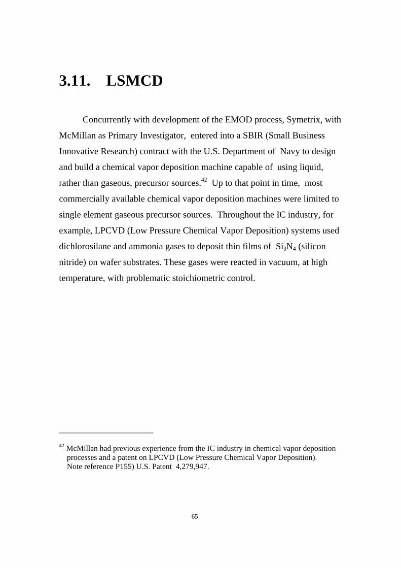
Concurrently with development of the EMOD process, Symetrix, with
McMillan as Primary Investigator, entered into a SBIR (Small Business
Innovative Research) contract with the U.S. Department of Navy to design
and build a chemical vapor deposition machine capable of using liquid,
rather than gaseous, precursor sources.42 Up to that point in time, most
commercially available chemical vapor deposition machines were limited to
single element gaseous precursor sources. Throughout the IC industry, for
example, LPCVD (Low Pressure Chemical Vapor Deposition) systems used
dichlorosilane and ammonia gases to deposit thin films of Si3N4 (silicon
nitride) on wafer substrates. These gases were reacted in vacuum, at high
temperature, with problematic stoichiometric control.
42 McMillan had previous experience from the IC industry in chemical vapor deposition processes and a patent on LPCVD (Low Pressure Chemical Vapor Deposition). Note reference P155) U.S. Patent 4,279,947.

66
Figure 3-22. EMOD chemistry was licensed to several companies
With separate precursor gases required for each element, this process
was limited to deposition of single, or at most three element, compound
films. Stoichiometric control of multi-element compounds was nearly
impossible.
An experimental vacuum deposition apparatus was designed and built
based on the premise that it might be possible to utilize complex compound
EMOD liquid sources as CVD precursors. If the EMOD solutions could be
processed into small droplets by ultrasonic or other means, then this mist
could become the complex compound source for the apparatus. Figure 3-23
shows the R& D strategy and Figure 3-24 shows a basic outline of the
operating apparatus used to build several different deposition machines.

67
The first deposition system built utilized a PZT (lead zirconate
titanate) piezoelectric crystal ultrasonic apparatus to generate a mist of
various sized
Figure 3-23. LSMCD R&D strategy
particles. These particles were injectred into a vacuum chamber at room
temperature and radiated with 240 nm. wavelength ultraviolet light (to
resonate hydroxyl ions). The particles “settled” onto the substrates via
gravity. Device worthy PZT, BST (barium strontium titanate) and SBT
(strontium bismuth tantalate) films were deposited, with fairly good
uniformity and excellent stoichiometric control over four inch diameter

68
silicon wafers. McMillan's 1994 LSMCD BST publication in Appendix F
discloses initial results.
This technology was licenced to Samco Corporation for the
manufacturing of small volume Liquid Source CVD machines to be sold
primarily to universities for R & D and materials research (Figure 3-25).
Figure 3-24. LSMCD Experimental Apparatus
The Samco built machine worked quite well for thin film research and
development with large feature size (1 or 2 micron) IC structures. For
smaller feature sizes, however, the atomizer had to be modified to generate

69
liquid droplets that were very small and uniform in size. It soon became
evident that such small droplets would not settle onto the substrates with just
the force of gravity. A new prototype machine was built that charged the
small particles such that they could be driven to the substrate surface by an
electric field. (The charging field plate, the charging screen and ground
connections are shown in Figure 3-24.)
Figure 3-25. Liquid Source Chemical Vapor Deposition
technology licensed by Symetrix Corporation to Samco
Corporation

70
Liquid Source Misted Chemical Deposition (LSMCD), the advanced
fine particle size technology, was licensed to Primaxx Corporation for
manufacturing and sales. Figure 3-26 shows the block schematic for their
machine and Figure 3-27 shows the Primaxx production model LSMCD
machine being sold (especially in Japan).
Figure 3-26. Advanced LSMCD block schematic for
production machine

71
3.12. The serendipidous discovery of Y-1
A primary objective of the research was accomplished in 1991 when a
number of capacitor structures containing layers of strontium, tantalum and
bismuth was accidently over-annealed (Figure 3-28). Normally, such an
experiment would have been scrapped, but one of the Symetrix researchers
decided, perhaps on a whim, to test the capacitor structures and discovered,
to everyone's surprise, that they exhibited superior fatigue-free and retention
properties, even when switched to over 1013 cycles at 85o C!
Figure 3-27. Production model LSMCD machine licenced by Symetrix
Corporation to Primaxx Corp. and manufactured by Primaxx Corp.

72
This over-annealing mistake had caused the strontium, bismuth and
tantalum layers to mix together, resulting in the formation of a layered
superlattice material (Figure 3-29). Symetrix was obligated by their US
government contract to disclose that a serendipitous discovery had been
made; however, they were not required to disclose (to the public) the
composition of the new material until it was fully protected by patents. The
new material was therefore named Y-1 (not SBT or strontium bismuth
tantalate) after the number of the particular process flow outlined in the
experimental matrix. (This, of course, was done to prevent infringement of
the intellectual property prior to patent filing.)
This serendipitous discovery literally put Symetrix Corporation ahead
of all ferroelecctric competition and put them on the map as a world class
research group. Y-1, along with the development of extensive device
models and new testing methods, opened the way to a number of very
significant patents and ultimately to the sale of several new technology
licenses.

73
Figure 3-28. The serendipitous discovery of SBT (Y-1). We had found
the “Right” Ferroelectric Material!

74
Figure 3-29. a.) The lattice structure of ABi2B209 (where A is a divalent metal
such as Sr, Ba, Pb; B is a metal of valence +5, usually Ta or
Nb); b.) The lattice structure of ABi2B4015 (where A is a
divalent metal such as Sr, Ba, Pb; B is a metal of valence +4,
usually Ti). (After, Nature, Vol. 374, page 628, April 1995.
Paper co-authored by McMillan.)

75
The initial strategy had worked. Everything that had been strategized
many years earlier had now been accomplished. Millions of reliable
ferroelectric products are now being sold every year. Following the buyout
of two major stockholders, the original partner/founders now own over 70%
of the company. The company escaped the venture capital dilution trap and
is completely free of debt. R & D contracts continue to be a viable source of
revenue and the revenue from royalties is increasing every year.

76
Chapter 4
Cultural differences that mold
international business relationships
4.1. Communication and business
between world cultures
The mechanisms enabling global communication are nearly all
pervasive. It can be easily assumed that, through the internet and via
satellites, communication with people on the other side of the world is as
easy as speaking with one’s next door neighbors. Such spoken and written
communication between people of various cultures must, however, be
understood as only the opening dialog for successful commercial exchange.
Assuming minimal language barriers and/or the availability of competent
translators, there must also be some mutual understanding of, and respect for,
the various cultural, social and traditional values separating the parties
before effective business transactions can be accomplished. To do otherwise,
could lead, at a minimum, to misunderstanding and embarrassment to
everyone involved.

77
Recent statistics indicate that between fifteen and forty percent of US
managers sent overseas, fail with their foreign operations and return to the
United States much earlier than originally planned [46]. It is the author’s
opinion, based on some amount of personal experience with companies
foreign to the U.S., that many of these failures probably occurred because of
insufficient understanding of the cultural, traditional and social differences
separating the people trying to do business with each other.
There is a considerable amount of written information available on
such differences (reference, for instance, [37], [38], [46], [47], [48], [49],
[50], [51]); however, it appears (again, the author’s opinion) that completely
successful global interactions can only be accomplished between parties
actually willing to participate in each others cultures. It is far beyond the
scope of this thesis to elaborate on the multitude of elements that affect
international business relationships; however, the following seems
appropriate.
4.2. Classification of cultural
characteristics
On a very broad basis, following mostly the works of Hofstede
(reference [18], [37], [38], [51]), Ting-Toomey (reference [46]), Anbari
(reference [50] and Tung (reference [48], there appears to be a few cultural

78
characteristics that can be categorized and reflected in management style
comparisons and business relationships all over the world. Among many
other factors, such comparisons generally include: individualism versus
collectivism, masculinity versus femininity, long-term versus short-term
orientation, power distance and uncertainty avoidance. Certainly these
terms are neither all-pervasive nor all-inclusive, but they do provide some
basis for discussion and a means to generally differentiate certain
characteristics between different countries. The following definitions and
differentiating tendencies did not originate with the author. (In fact, the
author has considerable difficulty trying to differentiate between people of
different races and cultures.) These definitions and classifications are
generally provided, however with some variations, throughout the above
references.
Individualism refers to the tendency in a culture for individuals to look after
themselves, and put their own needs and goals as a priority ahead of the
collective majority. Individualistic countries are reported to include the
United States, France, Germany, South Africa and Canada with the U.S.
being generally assumed as the highest individualistic country.
Collectivism refers to the tendency in a culture for individuals to work in
harmony with other people and other groups, putting harmony and group
needs ahead of their individual needs and desires.43 Collectivist cultures are
reported to include Japan, Mexico, Korea and Greece.
43 It is interesting to note that boisterous, self-centered, ego driven business people and entrepreneurs from the United States are often misunderstood, isolated or ignored in Japan.

79
Masculinity versus femininity refers to the distribution of emotional roles
between genders in a society. In “masculine” societies, people tend to be
assertive, tough, and focused on material success. Some masculine societies
are reported to include the United States, Japan, Mexico, Hong Kong, Italy
and Great Britain.
In “feminine” societies, reported to be present in such countries as Sweden,
France, Israel and Denmark, gender roles tend to overlap. In these countries
feminine values are said to be prevalent. Both men and women are
supposed to be modest, tender, and concerned with the quality of life.
Power distance generally refers to a culture’s expectations regarding how
power in an organization is distributed. Different cultures seem to have
different expectations regarding power distribution and equality; this leads to
how subordinates tend to respond to power and authority. In the high power
distance cultures reported to be located in Latin America, France, Spain and
most Asian countries, subordinates may tend to show more respect and fear
for authority. Authoritative management styles appear to be common in
these cultures. In low power distance countries, such as the United States,
Britain and much of Europe, subordinates expect to be treated as equals by
their bosses. In these cultures, consultative management styles appear to be
more effective.
Uncertainty avoidance refers to the level of comfort members of a culture
feel in unstructured or unknown situations. Employment stability, rule
orientation, and stress over uncontrollable situations are common concerns

80
in such cultures. Uncertainty avoidance is reported to be high in countries
such as South Korea, Japan and Latin America. Where uncertainty
avoidance is weaker, in countries such as the United States, the Netherlands,
Singapore, Great Britain and Hong Kong, people may feel less threatened by
unknown situations.
Long-term versus short-term orientation refers to how a culture teaches or
programs its members to accept delayed satisfaction or gratification of their
emotional, social and material needs. Long-term oriented societies appear to
be characterized by persistence and perseverance. People in long-term
oriented cultures, such as found in Asia, tend to accept that it may take
considerable time to reach their goals and receive gratification. People from
countries such as the United States, Canada, Germany Australia and Latin
America may tend to be more focused on security and protection of their
individual reputations, and hence may expect more immediate results.
Reflecting on all of this, it becomes understandable why business
practice, organizational structure, management style and contract
understanding varies significantly from country to country and why each
country must be studied separately to fully appreciate the interplay between
culture and international business issues. It should also be apparent that
there cannot possibly be agreement between all people that all, or any, of
these cultural classifications are either accurate or relevant. Certainly the
universal aspect of such a study is far beyond the scope of this thesis and our
attention should logically be narrowed to those areas of the world where the
author has some personal experience. McMillan has rather extensive
business experience in Japan and Korea and his academic experience at

81
Kochi University of Technology (especially with the guidance of Professor
Keizo Baba) has focused primarily on these areas.
4.3. Business culture: Japan, Korea and
the United States
In most world cultures, religion and a long history of family
development appear to mold the foundation of its beliefs, traditions and
social values. Korean and Japanese corporate cultures, for instance, are
influenced to considerable extent by Confucian and Buddhist traditions.
Such traditions place emphasis on loyalty to superiors, respect for authority
and faithfulness to friends. This results in such practices as lifetime, or long-
term, employment, promotions based on seniority, working in collective
harmony and family based management systems in these countries. Even
with such similarities, however, each country has its own unique
management styles and corporate structures.
Japanese and Korean corporate structures are generally based on
family-like units. Korean corporations tend to be structured around actual
blood (genetic) relatives, whereas Japanese corporations are often built
around family-like units consisting of relatives, neighbors, friends, etc.. In
both cases, personal connections tie business, family and friends into the
same unit. Such connections are not compromised by short-term or bottom-
line problems and often last for a lifetime. In both Japan and Korea, it is
common for workers to preserve group harmony by sacrificing their

82
individual interests, In Japan, especially, work is considered a meaningful
vehicle to prepare employees for participation in social groups and the
company is considered to have a legitimate social mission. All of this, of
course, is in sharp contrast to the United States and most European countries
where law and social norms take precedence over friendship, and employees
work only to live while many self-gratifying employers show little interest
in social causes or their employee's welfare.44
Early in the author’s experience with Japanese companies, he learned
that Japan may be quite unique in being a nation where individual identity,
to a large extent, is a function of group and corporate membership. Within
each Japanese corporation, individuals appeared to have a very strong
allegiance to the corporation’s structure, expressing individual submission
from below and management benevolence from above.
Such relationships are generally not easily understood and/or accepted
by the independent and competitive mentality pervasive in the U.S. and
Europe. McMillan soon realized, however, that understanding (and
accepting) the philosophy behind such relationships could provide a better
understanding of the "inventor's stagnation wall" that he had encountered
earlier in the United States. It was really quite simple. If inventors could
somehow feel that they were not alone, that they were personally obligated
to work for the common good of society, and that they were happy to share
44 To Americans, the company is a convenient tool to serve the interests of owners, managers and employees. Americans recognize the company as an organization to generate wealth. They tend to view work as a means to economic end. Employees of the corporation willingly perform work in return for promised compensation.

83
their wealth, then the stagnation wall might crumble and inventions could
then flow into innovations with little resistance. A great solution, but not
one that could be implemented easily or immediately!
Early in the history of Symetrix Corporation, contract negotiations
with Japanese companies proved to be considerably more complicated than
negotiations with American or European companies. Japanese companies
tended to emphasize building a mutually trusting relationship prior to
entering into any kind of written contract.45 This, of course, is in stark
contrast to the United States, where business deals tend to be structured
around suspicion and distrust and where lawyers and legal documents set the
tone for the relationship. In Japan, contract terms and subsequent revisions
are ultimately effected by committee (almost family-like) action with,
usually final and silent, senior management approval.46, 47
In the United States, most contracts are negotiated by a few
participants exchanging extensive documents laden with “boiler plate” legal
language designed to protect and isolate the participating parties.48 Final
45 Without such "trust building" prior to contract negotiations, Symetrix Corporation would never have been able to enter into the JDP contracts that finally broke down some of the stagnation wall referenced earlier. 46 Collective decision-making in Japan generally involves extensive consultation between all concerned parties until a consensus is achieved. 47 From personal experience, the author observes that decision making in Korean companies seems to be centered more in top level management than it is in Japan. It appears that the Korean approach to top-down decision making excludes lower level managers. 48 American workers are not accustomed to being involved in organizational decision- making processes.

84
signed contracts are usually exchanged (rather impersonally) by mail in the
United States, whereas in Japan friendly, and often elaborate, ceremonies
initiate new relations with the delivery of the contract documents.
From opening dialog to successful execution of international projects
to global commercial enterprises, management on all sides, and at all levels,
must recognize and appreciate the significance and pervasiveness of cultural
diversity. The world has moved far beyond the point where isolationism can
play a role in business strategy. Any new business model must anticipate
multi-cultural communication at all organizational levels and must promote
flexible leadership capable of inspiring cooperation, creativity and
innovation across international boundaries.

85
Chapter 5
Strategies for sustainability and
business growth
5.1. The single technology model
Most business startups begin with the presentation of a business plan
to groups of potential investors, bankers, venture capital groups or other
wealthy individuals. Such investors, whether ethical or not, will access the
investmen risk factors and structure their interest, service and expected ROI
(return on investment) rates accordingly.49 This means, of course, that most
companies start off with a significant debt load and the risk of losing
everything (to the investors) if sufficient revenue (investor ROI) is not
achieved in a short period of time.
Assuming success, at some point in time (usually after several years)
there must be a break-even point where the company shows a profit and a
growth (“S”) curve can be generated.50 As discussed below in Chapter 7,
49 It must be noted that the author has had several unpleasant experiences with venture capital firms attempting to control intellectual assets and corporate management positions in exchange for minimal investments. 50 The author is grateful for the considerable insight into S curves provided by Professor Osamu Tomisawa of Kochi University of Technology.

86
both investors and corporate founders must also, at some time, exercise exit
strategies that maximize return on investments.
A simple financial model for such a classic single technology business
is shown in Figure 5-1. It is obvious that exit point determination
(especially for the founders) is not a simple process with this model. In most
cases, outside investors will structure their agreements in such a way that
they insure maximum financial success far ahead of the founders. It is quite
common, at least in the United States, for investors, especially venture
capitalists, to take over early management of the fledgling company and
terminate the founders within a year or so of startup. Failure rates are quite
high for startups following this single technology model and it appears that
some of the business practices associated with it are quite detrimental to
technical progress and economic growth.
Figure 5-1. Common Single Technology Business Model

87
5.2. The multi-modal model
Following the line of reasoning developed by Christensen, Foster and
others, the multi-modal IP model shown in Figure 5-2 alleviates many of the
risk factors associated with the classic model [42], [43]. Symetrix started
with this multi-modal business model and has successfully used it for nearly
twenty years.
Figure 5-2. Multi-modal IP based business model

88
As described in Chapter 6 above, the founders of Symetrix
Corporation (Araujo and McMillan) did not seek initial funding from any
lending or investment source. The startup was funded through proceeds
from SBIR contracts, hence no initial debt was incurred. Rather than
focusing on a single technology path, several projects (chemicals, machines,
devices, models, etc.) were run in parallel, with their individual maturing S-
curves sequentially overlapping. Rather than trying to exit any single
technology at some prescribed time, each technology was licensed at
maturity to other companies with resulting license fees and royalty streams
returning to Symetrix. As these royalties and license fees were added to
corporate reserves these funds were also used to develop and leverage new
technology (in a cost effective manner), thereby establishing sustainability
and corporate growth.
5.3. A self-correcting neural network
model
Looking back at our experiences over the last twenty years, it appears
that, somehow, all of this could be modeled with a Self-Correcting Neural
Network. Figure 5-3 shows the author's initial attempt at such a model.
In this configuration, the inputs x1, x 2 , x 3,.... etc.... represent income
(with respect to time) from JDP's, royalties, etc., and x4 represents expenses
or negative income. These quantities, times their weight factors w1, w2, w3...,

89
are summed with the minimum of such total (over any particular time
period) adjusted by the desired profit and reserves, d(t), such that e(t) equals
y(t) the output. If the output is running profit then nothing is done to effect
the weights, w1, w2, w3,... etc., and the system runs freely. If, however, the
profit is unsatisfactory, then the function f(t) is less than some set amount
and a switch is closed causing the weights (adjustment factors) to be
regulated. The network should then recycle and readjust the various
parameters until the desired output is achieved.
Figure 5-3. McMillan's initial attempt at using a neural network to model sustainability
In principle, this model should work quite well. With the ongoing advances
being made in global computer networks and communication systems, and

90
with the availability of massive amounts of non volatile, fast, FeRAM
memory, this model could become reality in the very near future.

91
Chapter 6
Protecting intellectual property
through business relationships and
managing the cost of patent protection
6.1. The patent assessment
Like most living organisms, a company begins to die as soon as it
stops growing. (This becomes evident with consideration of the single
technology S curve associated with the model in Figure 5-2.) Symetrix
Corporation continues to grow after nearly twenty years because it has
leveraged its intellectual capital in a rather ingenious way. Through
alliances with a few large corporations, Symetrix has been able to minimize
its own bureaucratic structure by reducing the number of employees, along
with the associated burden and overhead rates, while continuing to generate
new patents and avoid the difficulties and obligations associated with
outside investment.
As discussed earlier in Chapter 2, the path from invention to commercial
realization can be perilous and very expensive. With any invention, the
inventor must determine the initial disclosure path early in the process. In
some cases the invention might best be kept secret. This is especially true if

92
the invention involves processes, ingredients or techniques that cannot be
reverse-engineered. (Coca-cola and Smith’s cough-drops are examples of
such inventions.)
In most cases, however, inventors should try to get patents on their
achievements prior to any kind of business negotiations.51 Without a patent,
the inventor has little recourse to infringement or intellectual property theft.
Inventions that are not patented generally bring very little financial gain to
the inventor.
Patent costs can be staggering. It is not unusual for the inventor, or the
inventor’s financial backers, to spend many thousands of dollars trying to
get viable patent coverage. Even after patents are issued, there are
significant costs associated with maintenence and other fees in every country
where the patent has recognition. (In the case of Symetrix Corporation, with
over 150 issued patents, this also amounts to many thousands of dollars
every year.)
51 It should be noted that there are several vehicles for conferring intellectual property rights, such as material transfer agreements, licenses, technology transfer agreements, research agreements, joint development agreements, etc.[52].

93
Figure 6-1. Joint development program with IP/Patent
protection.
6.2. The JDP patent protection model
Early in the development of Symetrix Corporation it became evident
that the multi-modal model (shown in Figure 5-2), with its technology
licensing features, could only work if Symetrix entered into joint
development programs (JDP’s) with other companies. This resulted in the
model shown in Figure 6-1 and ultimately in the sale of technology licenses
to a number of companies including Panasonic, Mitsubishi, Raytheon,
Primaxx, Kojundo and many others.

94
The model is quite simple. Company X enters into a JDP with
company Y such that company X pays company Y to manage and originate
the joint R & D activities. The results of their joint efforts are patented
with both parties sharing the patent costs and both parties receiving patent
assignment. A non-exclusive license to patent use is granted to both parties
with royalties being paid by either product producing party to the other party.
Company X and company Y can both license (non-exclusively) to other
companies with the approval of their joint development partner. The model
works extremely well. Patent filing and maintenence costs are shared
equally by the JDP partners, effectively cutting the cost in half for each of
them.
Patent costs, of course, are only part of the problem. Once a patent is
issued there are no guarantees that someone, somewhere, will not commit
patent infringement, fraud or otherwise try to steal the intellectual property.
With globalization of the economy, policing and protecting intellectual
property has now moved from being a local concern to becoming a
complicated international legal involvement.52 Laws affecting intellectual
property not only vary from country to country, but the level of IP
protection varies considerably from country to country as well. In many
cases, it is unclear which courts have, or will have, jurisdiction over disputes
relating to intellectual property infringement violations.53 In general,
however, such problems must ultimately be resolved in the country of 52 International laws and legal jurisdiction concerns are likewise applicable to trade secrets, copyrights, brands, designs and trademarks. 53 Some countries/cultures restrict or question private property versus public common good and copying is still considered flattery in some areas of the world [52].

95
infringement. For an (international) intellectual property lawsuit to succeed,
the defendant generally must reside in the country in which the lawsuit is
filed Clearly, prejudice and judgement enforcement issues are often
insurrmountable [52].
Our model doesn't necessarily solve such international IP conflicts; it
does, however, simplify patent enforcement problems by placing the
defendents and complainants in the same country under the same judicial
system. This is obvious by the fact that the international partners in the JDP
are not only owners but strong patent defenders in their own countries as
well.
There can be little doubt that globalization is out-pacing our capability
to manage and protect intellectual property. New markets are opening up in
countries that, until recently, had little regard for intellectual or private
property rights. In such countries, international trade and intellectual
property treaties are slow to take effect, yet the international exchange of
goods and services (especially via the internet) continues to accelerate.54, 55
There are obviously no quick or easy answers to the problems
associated with intellectual property generation and protection, especially on
a global scale. The model presented in this chapter, however, may alleviate
54 Product life cycles in many industries are shortening. The length of time and the amount of investment required to obtain intellectual property rights (especially patents) can be disproportionate to the life of the products [52]. 55 It is interesting to note that some governments view WTO (World Trade Organization) rules as a starting point for negotiations rather than a set of binding regulations [52].

96
some of the more difficult problems facing start-ups, small businesses and
even large corporations as they attempt to deal across international borders.
It seems obvious that the recognition and rewards associated with ownership
of inventions and creative works should stimulate further inventive and
creative activities which, in turn, should stimulate economic growth for all
parties involved. Anything short of that must be considered unsatisfactory.

97
Chapter 7
Evolution of the new corporation
7.1. The changing business environment
The Symetrix business model referenced above has been proven
successful. After nearly twenty years of operation, the company is debt free
and probably has sufficient reserves to continue pursuing new technology
and expanding its influence in the global marketplace. The problem,
however, is that no one can predict exactly what the future will bring, and
the rapidly changing global business environment could force our model into
obsolescence.56, 57
Peter Drucker stated in his book, Managing In The Next Society
(Drucker, page 3, reference [56]):
“It is something that practically no one foresaw or, indeed, even
talked about ten or fifteen years ago: e-commerce – that is, the
explosive emergence of the Internet as a major, perhaps eventually 56 It is commonly believed (U.S. folk-lore) that Yogi Berra once said, “The future ain’t what it used to be!” 57 Global business is defined by Griffin as, “A business that transcends national boundaries and is not committed to a single home country.” (Ricky Griffin, Management, page 133, reference [61].)

98
the major, worldwide distribution channel for goods, for services, and,
surprisingly, for managerial and professional jobs.”
From a business perspective, the mechanisms for inexpensive global
communication are already in place. Competition has now moved from
local influence to, in some cases, global jeopardy. Because of the computer,
the internet and extensive satellite communication systems, every business,
large or small, must now compete in the global market. As Moore states in
Crossing The Chasm (page 182, reference [45]:
"....As a future channel of distribution, the Internet
represents the most significant change in computing to
date, and maybe ever. It promises to reingineer all other
forms of commerce, not eliminating them, nor even
disintermediating them, but simply reconstructing them
to incorporate its phenomenal reach and service
capabilities...."
With continually improving air and surface transportaton systems,
larger cargotainer shipping facilities and global propagation of a few
common languages, new labor and material sources are becoming available
to nearly every business on the planet. In other words, the supply chain for
most businesses has changed, and is continuing to change on a regular
basis.58 Many high cost local operations can now be shifted to specialized
58 Armstrong and Kotler, in Marketing, An Introduction, differentiate marketing channels

99
facilities (and experts) around the world. For instance, a specialized central
IC fab located in a low labor cost region of the world, can now service
several competing fabless semiconductor companies (located in other parts
of the world) such that everyone along the supply/value chain recognizes
profit.59
7.2. Evolving business philosophy and
strategy
It seems obvious that traditional business philosophy will require
some modifications. Where traditionally, companies were inward-looking
for self optimization they now must become globally cognizant of supply
and value chain optimization. Corporate organization structures must change
from common independent stand-alone configurations, such as matrix,
horizontal, mixed or vertical, to interdependent entities cooperating closely
on a global scale. As Drucker stated in Management Challenges for the 21st
Century (page 61, reference [27]):
All institutions have to make global competitiveness a strategic
goal. No institution, whether a business, a university or a
from supply chain as “Marketing channels consist of distributors, retailers, and others who connect the company to its buyers. The supply chain describes a longer channel, stretching from raw materials to components to final products that are carried to final buyers.” (Armstron and Kottler, page 22, reference [41].) 59 Variously defined, a value chain is a string of suppliers, companies or workers that cooperate (work closely together) to satisfy market demands for a particular product.

100
hospital, can hope to survive, let alone to succeed, unless it
measures up to the standards set by the leaders in its field,
anyplace in the world."
Where traditional stand-alone companies shared minimal information
with other companies, they may now be forced to share extensive
information with all other parties on their supply and value chains.
Independent companies oriented toward specific commodities or
devices may now be forced to direct their efforts towards differentiated
products or systems that incorporate original devices into larger systems
more closely aligned with direct consumers. It seems obvious that single
component producers, especially if they are a relatively small company,
cannot survive if they do not integrate their work products with system
integrators. (Note the example of Symetrix Corporation working closely
with Panasonic Corporation to incorporate the ferroelectric memory into
smart card, identification, communication, and other systems.)
On the marketing front, the focus must shift from cost and price to
value and quality. (Remember that anyone in the world can now use the
internet to educate themselves and search for the best price and best quality
any where else in the world.) It is the author’s opinion that, in this new
global market, value and quality will ultimately win against cost and price
every time! In like manner, we easily see that suppliers will no longer be
able to simply push onto (force sale to) their customers whatever they have
available. Instead, the seller-buyer power relationship must now shift more

101
closely to satisfy exactly what the customer needs or wants. As Moore said
in Crossing The Chasm (page 189, reference [45]):
"…..All organizations are market-driven, whether they
acknowledge it or not. The chasm phenomenon-the
rapid acceleration in market development followed
by a dramatic lull, occurring whenever a
discontinuous innovation is introduced drives all
emerging high-tech enterprises to a point of crisis
where they must leave the relative safety of their
established early market and go out in search of a
new home in the mainstream. These forces are
inexorable-they will drive the company. The key
question is whether the management can become
aware of the changes in time to leverage the
opportunities such awareness confers.
How all this affects business strategy seems quite obvious. The new
corporation must compete in new and evolving markets around the world.
Local markets may easily be over-run with foreign goods. Inernational laws
and treaties will continue to offer ineffective and insufficient defense
against global piracy and counterfeiting. Many companies will continue to
decentralize their operations, with production, marketing and R & D moving
to lower cost areas of the world. The internet will be utilized to satisfy most
communication needs and local operations will minimize labor, burden and

102
overhead costs by reducing the number of employees and utilizing
specialized, experienced consultants and part-time workers.
In view of all this, the growth and evolution of the new world-
spanning corporation is obviously going to be dependent on many of the
factors above outlined. No longer can any company, including Symetrix,
continue to operate in the new globally competitive business environment,
with a philosophy that worked twenty, or even ten, years ago.

103
7.3. Value building, exit strategies and
longer life spans
With a few variations caused by cultural or other biases, retirement
plans are becoming world pervasive, yet apparently increasingly ineffective.
Even in countries where families still take care of their elderly, such as in
Japan, Korea and China, increased life span considerations are driving every
worker to re-evaluate his/her own long term financial security. In the United
States, where social security has become a political issue, thousands of
young workers are being told that, even if they pay into the government
sponsored social security program for most of their lives, there will still be
insufficient funds available for them to retire with dignity. Is it possible that
there is really something wrong with the whole philosophy behind long term
security, value building and retirement?
It is commonly believed that, prior to entering into any kind of
business relationship, the inventor, innovator or entrepreneur should try to
plan ahead to maximize their own (personal) return on investiment (ROI). It
seems that the whole idea behind writing a business plan is to maximize the
corporate founders personal ROI as well as the investors. Unfortunately, it
seems that during the writing of a business plan, most people fail to address
the long term issues, such as corporate continuity and exit strategies.

104
There are many ways that exit strategis have been, and might be,
defined. Logically, part of any definition, however, should probably start
with the simple premise that at some point in time, every business owner
leaves his/her business, voluntarily or otherwise. Some people, of course,
may be very reluctant to think about such things, but even those people want
to maximize their income to accomplish personal, financial, income, estate
planning and other objectives. Unfortunately, many business owners, even
those who are not afraid to die, become so busy worrying about, and
running, their business that they fail to take into account that one day they
will exit.
Every situation is as unique as the personality of each person, so each
situation must be addressed in a way that is taylored to the individual. The
result of such consideration, however, must arrive at the fact that everyone
becomes incapabale of, or disinterested in, working at some point in time. In
the end, every business, large or small, will probably change hands.
Ownership, and certainly management, will change either by IPO (Initial
Public Offering), sale, transfer to a family member or by merging with
another company.60
It appears that the most common exit strategy today may be the
acquisition of the start-up by a larger corporation. Michael Baird, in
Engineering your start-up (page 139, reference [60]) states:
".....More and more entrepreneurs are including a section in their
business plan that recommends a preferred exit strategy: for example,
60 It should be noted that relatively few start-up companies ever make it to an IPO.

105
acquisition by a large company that is also a strategic partner. This is
a change from a few years earlier when few gave thought to whether
(and if so, how) the business would be sold. The reason for this new
awareness is probably that more start-up entrepreneurs see starting a
business as a means to an end, not an end in its own right…."
In his book, Managing In The Next Society, (page 249, reference [56]),
Drucker says:
"……In the past, employing organizations have outlived em-
ployees. In (the) future, employees, and especially knowledge
workers, will increasingly outlive even successful organizations.
Few businesses, or even government agencies or programs,
last for more than thirty years. Historically, the working life
span of most employees has been less than thirty years because
most manual workers simply wore out. But knowledge workers
who enter the labor force in their twenties are likely to be still in
good physical and mental shape fifty years later.
So it appears that, regardless of what is planned for exit strategy or
retirement, future knowledge workers, and that might include nearly every
person on the planet, will probably outlive their company and,
consequently, their retirement savings. The question then becomes, "why
should anyone bother with such plans in the first place?"
Drucker goes on to say (pages 249-250, reference [56]):

106
"…Increasingly, employees take early retirement as soon as
their pension and social security rights are guaranteed for the
time when they reach traditional retirement age; but they
do not stop working. Instead, their "second career" often takes
an unconventional form. They may work freelance (and often
forget to tell the taxman about their work, thus boosting
their net income) or part-time or as "temporaries" or for
an outsourcing contractor or as contractors themselves.
Such "early retirement to keep on working" is particularly
common among knowledge workers, who are still a minority
among people now reaching fifty or fifty-five, but will become the
largest single group of older people in America from about
2030."
Who knows better about this than Peter Drucker. At the time of this
writing he is nearly 100 years old and still working every day. From the
author's perspective, value building and exit strategizing may become
obsolete philosophical discussions in the near future.61 Both concepts
appear to be contingent on short life spans, health problems and fear of
senility with old age. Perhaps future generations of knowledge workers will
consider work as essential, enjoyable and an integral part of their lives.
Then, perhaps people around the world and will stop thinking about
continuous saving, value building and retirement plans all together and
begin living every day as if it were their last.
61 It might be noted that the author is 69 years old as of this writing, and fully intends to continue working until he expires.

107
Chapter 8
Conclusions
Using the evolving FeRAM as a case study, we have explored some
fundamental aspects of inventors, innovators, entrepreneurs, dreamers, etc.,
especially as they relate to the author. This study has also shown how a
company can be started with minimal physical assets and yet sustain
operations for nearly twenty years without the infusion of borrowed money
or venture capital. It is interesting to note that, even with the circumstances
of this particular case, including minimal funding, public disbelief,
antagonism of competitors, and many other problems, the technology still
evolved on a time scale exactly corresponding to that predicted by Simon
Sze [19].
Symetrix Corporation, the primary focus of this study, is still prosperous
after nearly twenty years of operation. The company has borrowed no
money, it escaped the venture capital dilution trap (a major concern of the
founders), and it remains completely free of debt. Following a recent buyout
of two major stockholders, the original partner/founders now own over 80%
of the company. R & D contracts continue to be a viable source of revenue
and the revenue from royalties is increasing every year.
The maturing rate for layered perovskite SBT FeRAM devices during the
last few years has been astonishing. Symetrix’ main licensee, Panasonic,

108
began shipping FeRAM based contactless identification (ID) cards in 1998.
In that year they shipped 12 million cards and in 2001 their sales grew to
150 million pieces (Figure 8-1). Panasonic has also been shipping mixed
signal FeRAM ASICS, at the 0.8/0.6 micron double level metal technology
level , at a rate of 2-3 million units per month for the last few years. Now it
is shipping 3 and 4 level metal 0.18 micron ferroelectric embedded mixed
signal microcontrollers at several million units per year. In May of 2005,
Matsushita/Panasonic announced that they had sold, to that date, 100 million
FeRAM chips!
Figure 8-1. Panasonic integrated ferroelectric contactless cards
(figure courtesy of Matsushita Corporation)
In the non-switching (non-memory) area, Panasonic has shipped over 600
million units of BST (high dielectric constant) GaAs MMICS since 1993.
This technology, which enabled the miniaturization of mobile phones in

109
Japan, was co-developed by Symetrix Corporation and Matsushita during
the early 1990s. (For McMillan’s contribution to this effort, refer to his
1994 paper, Deposition of barium strontium titanate and strontium titanate
via liquid source chemical vapor deposition, in Appendix F.)
No one, of course, can really predict the future; however, it appears
that Matsushita's world FeRAM market forcast from a few years ago may be
accurate to a variance of less than three years (Figure 8-2). If this is, indeed
the case, then the FeRAM story could possibly go down in history as an
achievement in league with transistors and integrated circuits.
Figure 8-2. The rapidly expanding market for ferroelectric devices
(figure courtesy of Matsushita Corporation)

110
Reflecting back to McMillan’s dream of “cubic integration” in the early
1970s, it appears that his ideas are as valid today as they were thirty years
ago. The semiconductor industry is still chasing ever smaller feature sizes
and still trying to pack more and more components into smaller and smaller
spaces. Moore’s Law aside, it seems more relevant and logical today than
ever before, that the exceptional ideas of Edmond Abbott, who lived in the
1800s, long before integrated circuits were even thought of, should be
examined closely. It is easy to imagine Abbott's "Flatland" as the two
dimensional geometry of planar circuits and McMillan’s "cubic integration"
as the coming into awareness of three dimensional integrated device
structures [20].
In Chapter 1, the author stated that: "…He was unaware that some of his
efforts might possibly result in breakthroughs that would have significant
and positive effects on global society.".....and, that "This thesis represents
part of the author’s awakening to those possibilities and his struggle to
achieve that understanding...."
After thirty years of searching, the author now realizes that, in many
respects, this experience, this awakening, has become not only an education,
but something philosophical, perhaps even something spiritual, as well. In
the book, "The Mind of Management," by Masaharu Matsushita, Konosuke
Matsushita is quoted as saying (pages 20 -21, reference [ 62 ]):
"Even after returning home, I could not get the thought of
religion on the one hand and management on the other off
my mind. I stayed awake for a long time thinking about it.

111
Religion was a holy pursuit aimed at guiding people out of
suffering and toward happiness and peace of mind. Our
business, too, is sacred, 1 thought, in the sense that
industry provides necessities that sustain and improve man's
existence. Indeed, the ultimate aim of production is to wipe
out poverty and create prosperity. There is an old saying in
Japanese that poverty is harder to bear than a thousand
illnesses. Eliminating poverty is a sacred task, the loftiest
purpose in life. To achieve it we must work hard and produce
a great abundance of goods; this is our mission and our
enterprise. Production aimed at enriching the life of every
person on earth is the sacred mission of a manufacturer. Not
only spiritual peace but material abundance is necessary if the
quality of human life is to be better and people are to be
happier. You may be spiritually enlightened, but if you are
deprived of certain material comforts you will find it hard to
survive. And of course, the greatest abundance of material
wealth is worthless unless you enjoy fulfillment and a
purpose in living. Spiritual peace and material abundance
are as inseparable as the two wheels of a cart. So, I realized,
management of a religious organization and of a business
concern are equally sacred and necessary pursuits."
To the mind of the author, Konosuke had put into words, what McMillan
had believed all along, but had been unable to express.

112
It appears now that we have looked into the future and concluded that the
adventure is just beginning.

113
Acknowledgements
I am very grateful to my advisors: Professor Gota Kano, Professor Keizo
Baba, Professor Osamu Tomisawa, Professor Chihiro Hamaguchi and
Professor Shunji Kusayanagi. Without their patient and generous instruction
and counselling this thesis would not have been possible.
I am deeply indebted to Dr. Gota Kano for his friendship, guidance,
supervision and encouragement throughout the many years of this difficult
entrepreneurial exercise.
I wish to thank Professor Carlos A. Paz de Araujo (University of Colorado at
Colorado Springs) for his continuous friendship, support and unwavering
confidence over the last twenty years.
I also wish to thank Dr. Ana Maria Guerreiro for her guidance and council in
Neural Networks and Systems Engineering.
I am indebted to Mrs. Kerry Baugh for her assistance with the typing and
arrangement of this thesis, and to the many kind people at Symetrix
Corporation who supplied their generosity, patience and encouragement.
Finally, I am deeply indebted to my wife, Victoria, and to my nine children
for their continuous support, encouragement and patience throughout this
endeavor.

114
Bibliography
Reference Chapter
[1] Valasek, J., Piezo-Electric activity of Rochelle salt under various
conditions, Selected Early Work (1921-1961), located in Gonzalo,
J.A., Ferroelectricity, Wiley Verlag, 2005.
3
[2] Cross, Erik. A Tribute To Professor Joseph Valasek,
Ferroelectricity Newsletter, Summer, 1996. Available:
http://www.sp.nps.navy.mil/projects/ferro/vol4no3.pdf
3
[3] Carnell, Brian. Patents Per Million Population, Available:
http://www.Overpopulation.com/faq/health/education/patents
2
[4] Valasek, J., Piezo-Electric Activity Of Rochelle Salt Under Various
Conditions, Phys. Rev. 19, 478-491, (1922).
3
[5] White, James, Honest Inventor Help. Available: http://www.
expertclick.com/7117.html.
2
[6] Busch, G. and Scherrer, G., A New Seignette-electric Substance,
Naturwiss 23, 737 (1935).
3
[7] Nelson, J. and Baker, M., Charging Of Ice-Vapor Interfaces,
Atmos. Chem. Phys.Discuss., 3, 41-73, 2003, Available:
http://www.atmos-chem-phys.org /acpd/3/41.
3
[8] Von Hippel, A., Ferroelectricity, Domain Structure, and Phase
Transitions Barium Titanate, Reviews of Modern Physics, Vol. 22,
No. 3, July, 1950.
3
[9] Nolta, James P. and Schubring, Norman W., Ferroelectricity in
Potassium N itrate at Room Temperature, Physical review
Letters, Vol. 9, No. 7, October 1962.
3

115
[10] Dyson, James and Uhlig, Robert, Great Inventions, Barnes and
Noble Publishing Inc., Printed in India, 2004.
2
[11] Daglish, M. and Kemmitt, T., Ferroelectric Thin Films –Research,
Development and Commercialization, The Institution of
Professional Engineers New Zealand (IPENZ) Transactons, Vol.
27, No. 1, 2000.
3
[12] Anderson, J. R. 1952. Electrical Engineering, 71, 916. 3
[13] Rymer, T. B., Summarized Proceedings Of A Conference On Solid
State Memory and Switching Devices – London, September, 1958,
British Journal Of Applied Physics, Vol. 10, April, 1959.
3
[14] Sawada, Nomura, Fujii and Yoshida, Ferroelectricity in NaNO3 ,
Physical Review Letters, Vol. 1, No. 9, November 1, 1958.
3
[15] Rohrer, George, Ferroelectric Device and Process Of
Manufacturing Same, U.S. Patent 3,728,694.
3
[16] Rohrer, George, Process For Stable Phase III Potassium Nitrate
And Articles Prepared Therefrom, U.S. Patent 3,939,292.
3
[17] Kochhar, Rajesh, Science, Technology and Innovation Viewpoint,
2005. Available:
http://www.cid.harvard.edu/cidbiotech/comments150.htm
2
[18] Hofstede, Geert, Culture’s Consequences: Comparing Values,
Behaviors and Organizations Across Nations, 2000.
4
[19] Sze, S. M. and Chang, C. Y., ULSI Devices, John Wiley
Publishers, New York, 2000.
Syn. iv,
1, 8
[20] Abbott, Edwin A., Flatland, A Romance of Many Dimensions,
(originally written in 1884), Dover Publications, New York, 1952.
3, 8
[21] Roberts, Royston M., Serendipity: Accidental Discoveries In 2

116
Science, John Wiley & Sons, Inc., New York, 1989.
[22] Fontan, Jean-Marc, Innovation and Society: Broadening the
analysis of the Territorial Effects of Innovation, 2004, Available:
http://www.utoronto.ca/isrn/documents/note.doc.
2
[23] Langlois, Richard, N. Schumpeter and the Obsolescence of the
Entrepreneur, 1987, Available: http://www.ucc.uconn.edu/-
langlois/schumpet.html.
2
[24] Hisrich, Robert D., Peters, Michael P., and Shepherd, Dean A.,
Entrepreneurship, 6 ed. New York: McGraw-Hill Irwin, 2005.
2
[25] Christensen, Clayton.M., The Innovator’s Delemma, Harvard
Business School Press: Boston, MA., 1997
1, 3
[26] Christensen, C.M. and M.E. Raynor, The Innovator’s Solution,
Harvard Business School Press: Boston, MA, 2003.
[27] Drucker, P.F., Management Challenges for the 21st Century,
Harper Collins Publishers: New York, NY, 1999.
3, 7
Syn. i
[28] Edvinson, L. and M. Malone, Intellectual Capital, HarperCollins
Publishers: New York, NY, 1997.
[29] Kyrand, F.M., and E.C. Prescot, Real Business Cycle Theory
[30] Botkin, J., Smart Business: How Knowledge Communities Can
Revolutionize Your Company, The Free Press: New York, NY,
1999.
[31] Boyett, J. and J. Boyett, The Guru Guide; The Best Ideas of the Top
Management Thinkers Stephen Covey, Peter Drucker, Warren
Bennis, and Others,” John Wiley & Sons: New York, NY, 1998.
[32] Chandler, A. D., Jr., Chapters in the History of the American
Industrial Enterprise, Beard Books: Washington, D.C., 1962,
117
reprinted 2003.
[33] Drucker, P. F., Management: Tasks, Responsibilities, Practices,
HarperCollins Publishers: New York, NY, 1973.
[34] Drucker, P. F., Innovation and Entrepreneurship, Harper Collins
Publishers: New York, NY, 1985.
[35] Friedman, D.D., Price Theory, South-Western Publishing
Company: Cincinatti, OH, 1986.
[36] Galbraith, J. K., Economics in Perspective: A Critical History,
Houghton Mifflin Company, Boston, 1987.
[37] Hofstede, G. J., Pederson, P. B. and G. Hofstede, Exploring
Culture: Exercises, Stories and Synthetic Cultures, Intercultural
Press, Inc.: Yarmouth, Maine, 2002.
4
[38] Hofstede, G., Cultures and Organizations: Software of the Mind:
Intercultural Cooperation and its Importance for Survival,
McGraw Hill: New York, NY, 1991
4
[39] Martin, L.W., Stiglitz Principles of Micro-Economics, W.W.
Norton & Company: New York, NY 1993.
[40] Weihrich, H. and H. Koontz, Management: A Global Perspective,
10th Edition, McGraw Hill: New York, NY, 1993.
3
[41] Armstrong, G., and P. Kotler, Marketing: An Introduction,
Pearson Prentice Hall: Upper Saddle River, NJ, 2005.
[42] Christensen, C.M., The Innovator’s Delimma, Harvard Business
School Press: Boston, MA, 1997.
5
[43] Foster, R., Innovation: The Attacker’s Advantage, McKinsey &
Co., Inc., New York, NY, 1986.
5
[44] Gehani, R. R., Management of Technology and Operations, John 3

118
Wiley & Sons, Inc.: New York, NY, 1998.
[45] Moore, G. A., Crossing The Chasm: Marketing and Selling
Disruptive Products to Mainstream Customers, HarperCollins
Publishers: New York, NY, 2002.
7
[46] Ting-Toomey, Cross-Cultural Face-Negotiation: An Analytical
Overview, Pacific Region Forum, April 15, 1992, Available:
http://www.cic.sfu.ca/forum/ting-too.html
4
[47] Robert Paterson’s Radio Weblog, Geert Hofstede’s Model, April
20, 2005, Avail:
http://radio.weblogs.com/0107127/stories/cultureGeertHofstedesM
odel.html
4
[48] Tung, Rosalie, Business Negotiations with the Koreans: a Cross-
Cultural Perspective, October 26, 1990, Pacific Region Forum,
Available: http://www.cic.sfu.ca/forum/tung.html
4
[49] Steers, Richard, Culture and Communication Patterns in Korean
Firms, April 20, 2005, Available:
http://www.cic.sfu.ca/forum/steers.html
4
[50] Anbari, F. T., Cross cultural differences and their implications for
managing international projects, March 30, 2005,
Available:http://www.gwu.edu/-
umpleby/recent-papers/managing.differences/html
4
[51] Enclyclopedia: Geert Hofstede, May 29, 2005, Available:
http://www.nationmaster.com/encyclopedia/Geert-Hofstede
4
[52] McMillan, Larry, D., Intellectual Property Issues for International
Business, Lecture/Presentation at Kochi University of Technology,
September 11, 2004.
6

119
[53] McMillan, Larry, Innovation Management: A Case Study on
FeRAM Commercialization, Presentation, The Institute of Image
Information and Television Engineers, Tokyo, Japan, June 14,
2004.
1
[54] Randall, C. A., Newnham, and L. E. Cross, History of the first
ferroelectric oxide, BaTiO3, Materials Research Institute, The
Pennsylvania State University, University Park, PA. (Unpublished
manuscript).
3
[55] United Nations, World Population Prospects, The 1998 Revision
(New York: NY, 1998); and estimates by the Population Reference
Bureau.
Available: http://www.prb.org/Content/NavigationMenu/PRB/
Educators/Human_Population/Population.htm
2
[56] Drucker, Peter F., Managing in the Next Society, Truman Talley
Books, St. Martin’s Griffin, New York, 2002.
2, 7, 8
Syn. i
[57] Oxford University Survey, 2003. Available: 100ventures.com 2
[58] Cross, L.E., and Newnham R.D., History of Ferroelectrics,
Available: http://www.ieee-
uffc.org/ferroelectrics/review/articles/e003/e0030289.pdf.
3
[59] Drucker, Peter F., The Essential Drucker, Harper Collins
Publishers, New York, 2001.
2
[60] Baird, Michael L., Engineering your start-up, Professional
Publications, Belmont, CA., 1997.
3, 8
[61] Griffin, Ricky W., Management, Houghton Mifflin Company,
Boston, 2002.
7
[62] Matsushita, Masaharu, The Mind of Management – Fifty Years with 8

120
Konosuke Matsushita, Tosho Printing Co., Ltd., Tokyo, 1996.
[63] Gershman, Anatole, Ubiquitous Commerce - Always On, Always
Aware, Always Pro-active, Paper presented at the 2002
International Symposium on Applications and the Internet (SAINT
2002), Nara, Japan, January 30, 2002.
8,
Syn. i
[64] Eaton, Butler, Parris, Wilson, McNeillie, First Ferroelectric
nonvolatile memory, ISSCC, 1988
3
[65] Pyroelectricity, Globalspec, available:
http://www.absoluteastronomy.com/encyclopedia
/p/py/pyroelectricity.htm.
3
[66] Moore, Gordon E., Cramming more components onto integrated
circuits, Electronics, Volume 38, Number 8, April 19, 1965
3
[67] Lilienfeld, Julius Edgar, available: http://chem.ch.huji.ac.il/-
eugeniik/history/lilienfeld.htm.
1
[68] FeRAM Tutorial. Available: http://www.eecg.toronto.edu/-
ali/ferro/tutorial.html
3
[69] Ironman Inventing. Available:
http://www.tenonline.org/art/imi/9910.html
2

121
APPENDICES
A. The First Ferroelectric Memory IC
McMillan Disclosure to Motorola, February 7, 1976

122

123

124

125

126

127

128

129

130
B. McMillan’s Patents
Primary Author Patents
P1) 6,404,003, USA, Thin Film Capacitors On Silicon Germanium Substrate, 6/11/2002
P2) NI 149 411, Taiwan ROC, Thin Film Capacitors On Silicon Germanium Substrate And Process For Making The Same, 5/17/2002
P3) 327 839, South Korea, Method and Apparatus for Fabricating Silicon Dioxide and Silicon Glass Layers in Integrated Circuits, 2/26/2002
P4) 327,612, South Korea, Method and Apparatus for Misted Liquid Source Deposition of Thin Films with Increased Yield, 2/23/2002
P5) 6,203,619, USA, Multiple Station Apparatus for Liquid Source Fabrication of Thin Films, 3/20/2001
P6) 56717, Singapore, Method and Apparatus for Fabricating Silicon Dioxide and Silicon Glass Layers in Integrated Circuits, 5/23/2000
P7) 5,943,111, USA, Layered Superlattice Ferroelectric Liquid Crystal Display, 8/24/1999
P8) NI 102 545, Taiwan ROC, Method and Apparatus for Fabricating Silicon Dioxide and Silicon Glass Layers in Integrated Circuits, 8/19/1999
P9) 5,932,295, USA, Method and Apparatus for Misted Liquid Source Deposition of Thin Films with Increased Yield, 8/3/1999
P10) 5,888,583, USA, Misted Deposition Method of Fabricating Integrated Circuits, 3/30/1999
P11) 5,759,923, USA, Method and Apparatus for Fabricating Silicon Dioxide and Silicon Glass Layers in Integrated Circuits, 6/2/1998

131
P12) 5,688,565, USA, Misted Deposition Method Of Fabricating Layered Superlattice Materials, 11/18/1997
P13) 5,614,252, USA, Method of Fabricating Barium Strontium Titanate, 3/25/1997
P14) 5,559,733, USA, Memory with Ferroelectric Capacitor Connectable to Transistor Gate, 9/24/1996
P15) 5,540,772, USA, Misted Deposition Apparatus For Fabricating an Integrated Circuit, 7/30/1996
P16) 5,523,964, USA, Ferroelectric Non-Volatile Memory Unit, 6/4/1996
P17) 5,463,244, USA, Anti-Fuse Programmable Element Using Ferroelectric Material, 10/31/1995
P18) 5,444,290, USA, Method And Apparatus For Programming Anti-Fuse Elements Using Combined AC And DC Electric Fields, 8/22/1995
P19) 5,316,579, USA, Apparatus for Forming a Thin Film with Mist Forming Means, 5/31/1994
P20) 5,119,760, USA, Methods and Apparatus for Material Deposition, 6/9/1992
P21) 4,713,157, USA, Combined Integrated Circuit/Ferroelectric Memory Device, and Ion Beam Methods of Constructing Same, 12/15/1987
P22) 3,986,897, USA, Aluminum Treatment to Prevent Hillocking, 10/19/1976
Co-Author Patents P23) 0 665 981, France, Process for Fabricating Layered Superlattice
Materials and Making Electronic Devices Including Same

132
P24) 6,864,146, USA, Metal Oxide Integrated Circuit On Silicon Germanium Substrate, 3/8/2005
P25) 6,830,623, USA, Method Of Liquid Deposition By Selection Of Liquid Viscosity And Other Precursor Properties, 12/14/2004
P26) 6,831,313, USA, Ferroelectric Composite Material, Method Of Making Same, And Memory Utilizing Same, 12/14/2004
P27) 6,815,223, USA, Low Thermal Budget Fabrication of Ferroelectric Memory Using RTP, 11/9/2004
P28) 100 98 82, Hong Kong, Integrated Circuits Having Mixed Layered Superlattice Materials and Precursor Solutions For Use In A Process of Making The Same, 8/27/2004
P29) 6,781,184, USA, Barrier Layers for Protecting Metal Oxides From Hydrogen Degradation, 8/24/2004
P30) 696 29 361, Germany, Integrated Circuits Having Mixed Layered Superlattice Materials and Precursor Solutions For Use In A Process of Making The Same, 6/24/2004
P31) 6,743,643, USA, Stacked Memory klLCell Having Diffusion Barriers, 6/1/2004
P32) NI 194 382, Taiwan ROC, Ferroelectric Composite Material, Method Of Making Same, And Memory Utilizing Same, 5/5/2004
P33) 6,686,489, USA, Metal Organic Precursors For Transparent Metal Oxide Thin Films And Method Of Making Same, 2/3/2004
P34) 96 192 642.2, China, Integrated Circuits Having Mixed Layered Superlattice Materials and Precursor Solutions For Use In A Process Of Making The Same, 11/12/2003
P35) 6,639,262, USA, Metal Oxide Integrated Circuit On Silicon Germanium Substrate, 10/28/2003
P36) 462 852, Japan, Low Temperatrue Method And Apparatus For Fabrication Of Integrated Circuit Thin Films By Chemical Vapor Deposition, 8/15/2003

133
P37) EP 0 815 586, Europe, Integrated Circuits Having Mixed Layered Superlattice Materials And Precursor Solutions For Use In A Process Of Making The Same, 8/6/2003
P38) 0 815 586, Germany, Integrated Circuits Having Mixed Layered Superlattice Materials And Precursor Solutions For Use In A Process Of Making The Same, 8/6/2003
P39) 0 815 586, France, Integrated Circuits Having Mixed Layered Superlattice Materials And Precursor Solutions For Use In A Process Of Making The Same, 8/6/2003
P40) 392 213, South Korea, Layered Superlattice Materials For Ferroelectric High Dieletric Constant & Integrated Circuit Applications, 7/8/2003
P41) 6,582,972, USA, Low Temperature Oxidizing Method Of Making A Layered Superlattice Material, 6/24/2003
P42) 3 439 222, Japan, Low Imprint Ferroelectric Material for Long Retention Memory and Method of Making the Same, 6/13/2003
P43) 6,559,469, USA, Ferroelectric And High Dielectric Constant Transistors, 5/6/2003
P44) EP 0 894 155, European, Composition and Process For Fabricating Metal Oxide Films, 4/16/2003
P45) 6,537,830, USA, Method Of Making Ferroelectric FET With Polycyrstalline Crystallographically Oriented Ferroelectric Material, 3/25/2003
P46) 6,511,718, USA, Method And Apparatus For Fabrication Of Thin Films by Chemical Vapor Depositon, 1/28/2003
P47) 6,448,190, USA, Method And Pparatus For Fabrication Of Integrated Circuit By Selective Deposition Of Precursor Liquid, 9/10/2002
P48) 6,441,414, USA, Ferroelectric Field Effect Transistor, Memory Utilizing Same, And Memory Of Operating Same, 8/27/2002

134
P49) 6,437,380, USA, Ferroelectric Device with Bismuth Tantalate Capping Layer And Method Of Making Same, 8/20/2002
P50) NI 154 419, Taiwan ROC, Apparatus For Fabricating An Integrated Circuit (1), 8/16/2002
P51) 693 31 743.4-08, Germany, Process for Fabricating Layered Superlattice Materials and Making Electronic Devices Including Same, 8/8/2002
P52) 345 892, South Korea, Non-Volatile Memory, 7/11/2002
P53) 6,413,883, USA, Methof Of Liquid Depositioin By Selection Of Liquid Viscosity And Other Precursor Properties, 7/2/2002
P54) 6,383,555 B1, USA, Misted Precursor Deposition Apparaatus And Method With Improved Mist And Mist Flow, 5/7/2002
P55) 692 31 889, Germany, Process For Fabricating Layered Superlattice Materials, 4/25/2002
P56) 6,376,691, USA, Metal Organic Precursors For Transparent Metal Oxide Thin Films And Method Of Making Same, 4/23/2002
P57) 6,373,743, USA, Ferroelectric Memeory And Method Of Operating Same, 4/16/2002
P58) 6,370,056, USA, Ferroelectric Memory And Method Of Operating Same, 4/9/2002
P59) 6,365,927, USA, Ferroelectric IntegratedCircuit Having Hydrogen Garrier Layer, 4/2/2002
P60) EP 0 665 981, European, Process for Fabricating Layered Superlattice Materials and Making Electronic Devices Including Same, 3/20/2002
P61) 0 665 981, France, Process for Fabricating Layered Superlattice Materials and Making Electronic Devices Including Same, 3/20/2002
P62) 67226, Singapore, Strontium Bismuth Niobate Tantalate Ferroelectric Thin Film, 3/5/2002

135
P63) NI 143 368, Taiwan ROC, Ferroelectric Memory With Ferroelectric Thin Film Having Thickness of 90 Nanometers or Less, and Method of Making Same, 2/25/2002
P64) 327 615, South Korea, Misted Precusor Deposition Apparatus And Method With Improved Mist And Mist Flow, 2/23/2002
P65) 326,498, South Korea, Method And Apparatus For Material Deposition Using Primer, 2/18/2002
P66) 6,339,238, USA, Ferroelectric Field Effect Transistor, Memory Utilizing Same, And Memory Of Operating Same, 1/15/2002
P67) 320,282, South Korea, Method of Forming Magnesium Oxide Films on Glass Substrate for Use in Plasma Display Panels, 12/27/2001
P68) NI 137 589, Taiwan ROC, Mehtod And Apparatus For Fabrication Of Integrated Circuit by Selective Deposition Of Precursor Liquid, 11/21/2001
P69) EP 0 975 556, European, Method of Forming Magnesium Oxide Films on Glass Substrate for Use in Plasma Display Panels, 11/7/2001
P70) NI 134 402, Taiwan ROC, Apparatus For Fabricating An Integrated Circuit (2), 10/12/2001
P71) 3 238 663, Japan, Methods And Apparatus For Material Deposition, 10/5/2001
P72) 692 31 865, Germany, Layered Superlattice Material Applications, 9/20/2001
P73) 9369-BE/2001, Italy, Process For Fabricating Layered Superlattice Materials, 9/19/2001
P74) NI 132 591, Taiwan ROC, Method Of Liquid Deposition By Selection Of Liquid Viscosity And Other Precursor Properties, 9/13/2001
P75) NI 130 298, Taiwan ROC, Ferroelectric Flat Panel Displays, 8/9/2001

136
P76) 201 938, Austria, Layered Superlattice Material Applications, 7/25/2001
P77) 6,258,733, USA, Method and Apparatus for Misted Liquid Source Deposition of Thin Film with Reduced Mist Particle Size, 7/10/2001
P78) EP 0 616 726 B1, Europe, Layered Superlattice Material Applications, 7/3/2001
P79) EP 0 616 723, Europe, Process For Fabricating Layered Superlattice Materials, 6/20/2001
P80) 0 616 726, France, Layered Superlattice Material Applications, 6/6/2001
P81) NI 126 993, Taiwan ROC, Misted Precursor Deposition Apparatus and Method with Improved Mist And Mist Flow, 6/4/2001
P82) 295,698, South Korea , Integrated Circuits Having Mixed Layered Superlattice Materials and Precusor Solutions For Use In A Process of Making The Same, 5/2/2001
P83) NI 123 550, Taiwan ROC, Method And Apparatus For Material Deposition Using Primer, 4/16/2001
P84) 6,198,225, USA, Ferroelectric Flat Panel Displays, 3/6/2001
P85) 3 162 718, Japan, Layered Superlattice Material Applications, 2/23/2001
P86) 3 162 717, Japan, Process For Fabricating Layered Superlattice Materials, 2/23/2001
P87) 6,174,213, USA , Fluorescent Lamp and Method of Manufacturing Same, 1/16/2001
P88) NI 116 293, Taiwan ROC, Low Imprint Ferroelectric Material for Long Retention Memory and Method of Making the Same, 1/10/2001
P89) 6,143,063, USA, Misted Precursor Deposition Apparatus and Method with Improved Mist Flow, 11/7/2000

137
P90) 6,133,050, USA, UV Radiation Process for Making Electronic Devices Having Low-Leakage-Current and Low-Polarization Fatigue, 10/17/2000
P91) 3 113 281, Japan, Precursors and Processes for Making Metal Oxides, 9/22/2000
P92) 6,116,184, USA, Method and Apparatus for Misted Liquid Source Deposition of Thin Film with Reduced Mist Particle Size, 9/12/2000
P93) 6,110,531, USA, Method and Apparatus for Preparing Integrated Circuit Thin Films by Chemical Vapor Deposition, 8/29/2000
P94) 6,104,049, USA, Ferroelectric Memory With Ferroelectric Thin Film Having Thickness of 90 Nanometers or Less, and Method of Making Same, 8/15/2000
P95) 269,025, South Korea, Process For Fabricating Layered Superlattice Materials, 7/18/2000
P96) 6,080,592, USA, Method of Making Layered Superlattice Materials for Ferroelectric, High Dielectric Constant, Integrated Circuit Applications, 6/27/2000
P97) 6,072,207, USA, Process for Fabricating Layered Superlattice Materials and Making Electronic Devices Including Same, 6/6/2000
P98) 6,056,994, USA, Liquid Deposition Methods of Fabricating Layered Superlattice, 5/2/2000
P99) 6,051,858, USA, Ferroelectric/High Dielectric Constant Integrated Circuit and Method of Fabricating Same., 4/18/2000
P100) 6,022,669, USA, Method of Fabricating an Integrated Circuit Using Self-Patterned Thin Films, 2/8/2000
P101) 6,017,579, USA, Method of Forming Magnesium Oxide Films on Glass Substrate for Use in Plasma Display Panels, 1/25/2000
P102) NI 106 205, Taiwan ROC, Liquid Source Formation of Thin films Using Hexamethyl-Disilazane, 12/30/1999

138
P103) 5,997,642, USA, Method and Appratus For Misted Deposition of Integrated Circuit Quality Thin Films, 12/7/1999
P104) 56664, Singapore, Misted Precursor Deposition Apparatus and Method with Improved Mist Flow, 11/16/1999
P105) 5,972,428, USA, Methods and Apparatus for Material Deposition Using Primer, 10/26/1999
P106) 5,965,219, USA, Misted Deposition Method with Applied UV Radiation, 10/12/1999
P107) 5,966,318, USA, Nondestructive Readout Memory Utilizing Ferroelectric Capacitors Isolated From Bitlines by Buffer Amplifiers, 10/12/1999
P108) 5,962,085, USA, Misted Precursors Deposition Apparatus and Method with Improved Mist and Mist Flow, 10/5/1999
P109) 5,955,754, USA, Integrated Circuits Having Mixed Layered Superlattice Materials and Precusor Solutions for Use in a Process of Making Same, 9/21/1999
P110) 53405, Singapore, Methods and Apparatus for Material Deposition Using Primer, 9/21/1999
P111) 234,621, South Korea, Precursors and Processes for Making Metal Oxides, 9/17/1999
P112) 5,942,376, USA, Shelf-Stable Liquid Metal Aryketone Alcoholate Solutions and Use Thereof in Photo Initiated Patterning of Thin Films, 8/24/1999
P113) 5,909,042, USA, Electrical Component Having Low-Leakage Current and Low Polarization Fatigue Made by UV Radiation Process, 6/1/1999
P114) 45985, Singapore, Integrated Circuits Having Mixed Layered Superlattice Materials and Precursor Solutions For Use In A Process of Making The Same, 3/30/1999
P115) 202,532, South Korea, Methods of Apparatus for Materials Deposition, 3/29/1999

139
P116) 5,883,828, USA, Low Imprint Ferroelectric Material for Long Retention Memory and Method of Making the Same, 3/16/1999
P117) 5,871,853, USA, UV Radiation Process for Making Electronic Devices Having Low-Leakage-Current and Low-Polarization Fatigue, 2/16/1999
P118) 5,849,071, USA, Liquid Source Formation of Thin films Using Hexamethyl-Disilazane, 12/15/1998
P119) 2 860 505, Japan, Apparatus for Depositing Materials, 12/11/1998
P120) 5,846,597, USA, Liquid Source Formation of Thin films Using Hexamethyl-Disilazane, 12/8/1998
P121) 5,843,516, USA, Liquid Source Formation of Thin films Using Hexamethyl-Disilazane, 12/1/1998
P122) 5,840,110, USA, Integrated Circuits having Mixed Layered Superlattice Materials and Precursor Solutions for Use in a Process of Making Same, 11/24/1998
P123) 5,825,057, USA, Process for Fabricating Layered Superlattice Materials and Making Electronic Devices Including Same, 10/20/1998
P124) 5,811,847, USA, PSZT for Integrated Circuit Applications, 9/22/1998
P125) 5,803,961, USA, Integrated Circuits having Mixed Layered Superlattice Materials and Precursor Solutions for Use in a Process of Making the Same, 9/8/1998
P126) 5,792,592, USA, Photosensitive Liquid Precusor Solutions and Use Thereof in Making Thin Films, 8/11/1998
P127) 5,788,757, USA, Composition and Process Using Ester Solvents for Fabricating Metal Oxide Films and Electronic Devices Including the Same, 8/4/1998
P128) 5,784,310, USA, Low Inprint Ferroelectric Material for Long Retention Memory and Method of Making the Same, 7/21/1998

140
P129) 98909128.5-2111, Method of Forming Magnesium Oxide Films on Glass Substrate for Use in Plasma Display Panels, 3/12/1998
P130) 5,723,171, USA, Integrated Circuit Electrode Structure and Process for Fabricating Same, 3/3/1998
P131) 5,719,416, USA, Integrated Circuit with Layered Superlattice Material Compound, 2/17/1998
P132) 5,699,035, USA, ZNO thin Film Varistors And Method Of Making The Same, 12/16/1997
P133) 5,654,456, USA, Precursors and Processes for Making Metal Oxides, 8/5/1997
P134) 5,612,082, USA, Process For Making Metal Oxides, 3/18/1997
P135) EP 0 665 814, Europe, Precursors and Processes for Making Metal Oxides, 1/15/1997
P136) 5,561,307, USA, Ferroelectric Integrated Circuit, 10/1/1996
P137) 5,559,260, USA, Precursors and Processes for Making Metal Oxides, 9/24/1996
P138) 5,541,870, USA, Ferroelectric Memory and Non-Volatile Memory Cell for Same, 7/30/1996
P139) 5,519,234, USA, Ferroelectric Dielectric Memory Cell Can Switch at Least Giga Cycles and has Low Fatigue - Has High Dielectric Constant and Low Leakage Current, 5/21/1996
P140) 5,514,822, USA, Precursors and Processes for Making Metal Oxides, 5/7/1996
P141) 5,508,954, USA, Method and Apparatus for Reduced Fatigue in Ferroelectric Memory, 4/16/1996
P142) 5,487,032, USA, Method and Apparatus for Reduced Fatigue in Ferroelectric Memory Elements, 1/23/1996

141
P143) 5,468,679, USA, Process for Fabricating Materials for Ferroelectric High Dielectric Constant and Integrated Circuit Applications, 11/21/1995
P144) 5,468,684, USA, Integrated Circuit with Layered Superlattice Material and Method of Fabricating Same, 11/21/1995
P145) 5,466,629, USA, Process for Fabricating Ferroelectric Integrated Circuit, 11/14/1995
P146) 5,456,945, USA, Method and Apparatus for Materials Deposition, 10/10/1995
P147) 5,439,845, USA, Process for Fabricating Layered Superlattice Materials and Making Electronic Devices Including Same, 8/8/1995
P148) 5,434,102, USA, Process for Fabricating Layered Superlattice Materials and Making Electronic Devices Including Same, 7/18/1995
P149) 5,423,285, USA, Process for Fabricating Materials for Ferroelectric High Dielectric Constant and Integrated Circuit Applications, 6/13/1995
P150) 5,406,510, USA, Non-Volatile Memory, 4/11/1995
P151) 5,214,300, USA, Monolithic Semiconductor Integrated Circuit Ferroelectric Memory Device., 5/25/1993
P152) 5,138,520, USA, Methods and Apparatus for Material Deposition, 8/11/1992
P153) 5,024,964, USA, Method of Making Ferroelectric Memory Devices, 6/18/1991
P154) 4,707,897, USA, Monolithic Semiconductor Integrated Circuit Ferroelectric Memory Device, And Methods of Fabricating And Utilizing Same., 11/24/1987
P155) 4,279,947, USA, Deposition of Silicon Nitride, 7/21/1981

142
C. McMillan’s Publications and Presentations
Primary Author—Journal PP1) L. D. McMillan, “Deposition Of Barium Strontium Titanate and
Strontium Titanate via Liquid Source Chemical Vapor Deposition”, Integrated Ferroelectrics, Volume 5, pp. 97-102, 1994.
PP2) L. D. McMillan, M. Huffman, T. Roberts, M. Scott, and C. A. Paz
de Araujo, “Deposition of Ba1-xSrxTiO3 and SrTiO3 via Liquid Source CVD (LSCVD) for ULSI DRAMS”, Integrated Ferroelectrics, Volume 4, pp. 319-324, 1994.
PP3) L. D. McMillan, C. A. Paz de Araujo, J. F. Scott, J. Gregory, T.
Roberts, and D-Y Chen, “Process Development and Integration of Non-Destructive Readout (NDRO) Ferroelectric Memory”, Defense Nuclear Agency Technical Report, DNA-TR-93-11, September 1993.
PP4) L. D. McMillan, C. A. Paz de Araujo, T. Roberts, J. D. Cuchiaro,
M.C. Scott, and J. F. Scott, “Liquid Source CVD”, Integrated Ferroelectrics, Volume 2, pp. 351-359, 1992.
PP5) L. D. McMillan, “MOS C-V Techniques For IC Process Control”,
Solid State Technology, pp. 605-610, September 1972.
Co-Author Journal PP6) C. A. Paz de Araujo, J. D. Cuchiaro, L. D. McMillan, M. C. Scott,
and J. F. Scott, “Fatigue-Free Ferroelectric Capacitors With Platinum Electrodes”, Nature, Volume 374, pp. 627-629, April 1995.
PP7) Y. Shimada, U. Kato, T. Yamada, T. Otsuki, Z. Chen, M. Lim, V.
Joshi, L. D. McMillan, and C. A. Paz de Araujo, “High Density

143
and Long Retention Non-Destructive Readout FeRAMs Using A Linked Cell Architecture”, Integrated Ferroelectrics, p. 208, 2001.
PP8) J. Karasawa, Y. Hamada, K. Ohashi, E. Natori, K. Oguchi, T.
Shimoda, V. Joshi, L. D. McMillan, and C. A. Paz de Araujo, “Improvement In Microstructure Of SBT Thin Films”, Integrated Ferroelectrics, Volume 39, pp. 199-214, 2001.
PP9) K. Uchiyama, K. Tanaka, Y. Shimada, M. Azuma, T. Otsuki, S.
Narayan, V. Joshi, C. A. Paz de Araujo, and L. D. McMillan, “Low Temperature Crystallization Of MOCVD Deposited SBT Films”, Integrated Ferroelectrics, Volume 36, pp.119-126, 2001.
PP10) H. M. Duiker, P. D. Beale, J. F. Scott, C. A. Paz de Araujo, B. M.
Melnick, J. D. Cuchiaro, and L. D. McMillan, “Fatigue and Switching in Ferroelectric Memories: Theory and Experiment”, Journal of Applied Physics, Volume 68, Number 11, pp. 5783-5791, December 1990.
PP11) J. F. Scott, C. A. Paz de Araujo, B. M. Melnick, L. D. McMillan,
and R. Zuleeg, “Quantitative Measurement of Space-Charge Effects in lead Zirconate-Titanate Memories”, Journal of Applied Physics, Volume 70, Number 1, pp. 382-388, July 1, 1991.
PP12) J. F. Scott, C. A. Paz de Araujo, B. M. Melnick, L. D. McMillan,
and R. Zuleeg, “Quantitative Measurement of Space-Charge Effects in Lead Zirconate-Titanate Memories”, Journal of Applied Physics, Volume 69, Number 11, June 1991.
PP13) J. F. Scott, C. A. Paz de Araujo, H. B. Meadows, L. D. McMillan,
and A. Shawabkeh, “Radiation Effects on Ferroelectric Thin Film Memories: Retention Failure Mechanisms”, Journal of Applied Physics, Volume 66, Number 3, pp. 1444-1453, August 1989.
PP14) G. Rohrer, L. D. McMillan, and A. K. Kulkarni, “A New
Technique For Characterization Of Thin Film Ferroelectric Memory Devices”, Journal of Vacuum Science Technology, A 6(3), May/June 1988.

144
PP15) F. Scott, M. Zhang, R. B. Godfrey, C. A. Paz de Araujo, and L. D. McMillan, “Raman Spectroscopy of Sub-Micron KNO3 Films”, Physical Review B-Condensed Matter, The American Physical Society, Volume 35, Number 8, pp. 4044-4051, March 1987.
PP16) C. A. Paz de Araujo, J. F. Scott, R. B. Godfrey, and L. D.
McMillan, “Analysis of Switching Transients in KNO3 Ferroelectric Memories”, Applied Physics Letter, Volume 48, Number 21, May 1986.
Co-Author –Book PP17) J. F. Scott, C. A. Paz de Araujo, and L. D. McMillan,
“Ferroelectric Thin Films and Thin Film Devices”, Ferroelectric Ceramics, Springer-Verlag (London) 1992.
PP18) J. F. Scott, C. A. Paz de Araujo, and L. D. McMillan,
“Ferroelectric Thin Films and Thin Film Devices”, Ferroelectric Ceramics, book chapter, pp. 185-211, 1993.
Primary Author—International Conferences PP19) L. D. McMillan, and C. A. Paz de Araujo, “Effects of Process
Condition On Microstructure of Thin SBT-Based Films”, abstract presented at The Proceedings for the 13th International Symposium on International Ferroelectrics, Colorado Springs, CO, p. 79, March 2001
PP20) .L. D. McMillan, C. A. Paz de Araujo, S. Narayan, V. Joshi, “The
Limits of Thickness Scaling In PZT and SBT and Its Effect on Reliability”, abstract presented at The Proceedings of the13th International Symposium on Integrated Ferroelectrics, Colorado Springs, CO, p. 60, March 2001.

145
PP21) L. D. McMillan, J. F. Scott, and C. A. Paz de Araujo, “Liquid Source CVD of Ferroelectric Thin Film Memories”, invited paper, 39th National Symposium, American Vacuum Society, November 1992.
Co-Author International Conferences PP22) N. Solayappan, V. Joshi, A. DeVilbiss, J. W. Bacon, J. D.
Cuchiaro, L. D. McMillan, and C. A. Paz de Araujo, “Chemical Solution Deposition (CSD) and Characterization of Ferroelectric and Dielectric Thin Films”, Integrated Ferroelectrics, Volume 22, pp. 521-531, 1998.
PP23) C. A. Paz de Araujo, T. Otsuki, J. D. Cuchiaro, and L. D. McMillan,
“Microcontrollers With Ferroelectric Embedded Memory”, presented at IEEE 1998 International Non-Volatile Memory Technology Conference, Albuquerque, NM, June 22-24, 1998.
PP24) C. A. Paz de Araujo, L.D. McMillan, V. Joshi, N. Solayappan, M.
Lim, K. Arita, N. Moriwaki, H. Hirano, T. Baba, Y. Shimada, T. Sumi, E. Fujii, and T. Otsuki, “The Future of Ferroelectric Memories”, presented at IEEE International Solid-State Circuits Conference, San Francisco, CA, February 2000.
PP25) S. Narayan, V. Joshi, M. Lim, J. Celinska, C. A. Paz de Araujo, L.
D. McMillan, K. Uchiyama, Y. Shimada, S. Miedl, P. Lehnen, F. Schienle, M. Schumacher, and H. Juergensen, “Development of 500 A Thick MOCVD SBT Films For High Density FeRAM Process”, IFFF 2002 and 14th International Symposium on Integrated Ferroelectrics, Nara, Japan.
PP26) Y. Shimada, U. Kato, T. Yamada, T. Otsuki, Z. Chen, M. Lim, V.
Joshi, L. D. McMillan, and C. A. Paz de Araujo, “High Density and Long Retention Non-Destructive Readout FeRAM Using A Linked Cell Architecture”, abstract presented at The Proceedings of the 13th International Symposium on Integrated Ferroelectrics, Colorado Springs, CO, Volume 40, pp. 41-54, March 2001.

146
PP27) Z. Chen, M. Lim, V. Joshi, C. A. Paz de Araujo, and L. D. McMillan, “Advanced Simulation Tool For FeRAM Design”, abstract presented at The Proceedings of the 13th International Symposium on Integrated Ferroelectrics, Colorado Springs, CO, p. 269, March 2001.
PP28) C. A. Paz de Araujo, L. D. McMillan, Z. Chen, Y. Shimada, Y.
Kato, and T. Otsuki, “Ferroelectric Linked Cell Device Physics”, abstract presented at The Proceedings of the 13th International Symposium on Integrated Ferroelectrics, Colorado Springs, CO, p.268, March 2001.
PP29) M. Lim, Z. Chen, V. Joshi, L. D. McMillan, and C. A. Paz de
Araujo, “Random Accessibility Of Ferroelectric FET As A Non-Destructive Readout (NDRO) Memory”, abstract presented at The Proceedings of the 13th International Symposium on Integrated Ferroelectrics, Colorado Springs, CO, p. 366, March 2001.
PP30) J. Celinska, V. Joshi, N. Solayappan, M. Lim, L. D. McMillan, and
C. A. Paz de Araujo, “Low Crystallization Temperature Regime of Strontuim Bismuth Tantalate Ultra-Thin Films For High Density FeRAM Applications”, abstract presented at The Proceedings of the 13th International Symposium on Integrated Ferroelectrics, Colorado Springs, CO, March 2001.
PP31) Z. Chen, N. Solayappan, V. Joshi, K R. Laetz, C. A. Paz de Araujo,
and L. D. McMillan, “1K FeRAM-Based Smart Card Application For Handspring Visor”, abstract presented at The Proceedings of the 13th International Symposium on Integrated Ferroelectrics, Colorado Springs, CO, p.189, March 2001.
PP32) J. Celinska, V. Joshi, S. Narayan, L. D. McMillan, and C. A. Paz
de Araujo, “Low Temperature Process For Strontium Bismuth Tantalate Thin Films”, abstract presented at The Proceedings of the 12th International Symposium on Integrated Ferroelectrics, Aachen, Germany, Volume 30, pp. 1-8, March 2000.
PP33) V. Joshi, N. Solayappan, J. Celinska, L. D. McMillan, and C. A.
Paz de Araujo, “A 650o C Process For Strontium Bismuth Tantalate Thin Films”, abstract presented at The Proceedings of the

147
12th International Symposium on Integrated Ferroelectrics, Aachen, Germany, March 2000.
PP34) C. A. Paz de Araujo, L.D. McMillan, V. Joshi, N. Solayappan, M.
Lim, K. Arita, N. Moriwaki, H. Hirano, T. Baba, Y. Shimada, T. Sumi, E. Fujii, and T. Otsuki, “The Future of Ferroelectric Memories”, presented at IEEE International Solid-State Circuits Conference, San Francisco, CA, February 2000.
PP35) C. A. Paz de Araujo, L.D. McMillan, V. Joshi, N. Solayappan, M.
Lim, K. Arita, N. Moriwaki, H. Hirano, T. Baba, Y. Shimada, T. Sumi, E. Fujii, and T. Otsuki, “The Future of Ferroelectric Memories”, ISSCC 2000 Paper Submission.
PP36) S.Narayan, V. Joshi, L. D. McMillan, and C. A. Paz de Araujo,
“Sub-100 nm SBT Films For Low Voltage and High Density FeRAM Applications”, Proceedings of the 11th International Symposium on Integrated Ferroelectrics, Volume 25, Colorado Springs, CO, pp.509-517, March 1999.
PP37) N. Solayappan, V. Joshi, A. DeVilbiss, J. W. Bacon, J. D.
Cuchiaro, L. D. McMillan, and C. A. Paz de Araujo, “Chemical Solution Deposition (CSD) and Characterization of Ferroelectric and Dielectric Thin Films”, Integrated Ferroelectrics, Volume 22, pp. 521-531, 1998.
PP38) C. A. Paz de Araujo, T. Otsuki, J. D. Cuchiaro, and L. D.
McMillan, “Microcontrollers With Ferroelectric Embedded Memory”, presented at IEEE 1998 International Non-Volatile Memory Technology Conference, Albuquerque, NM, June 22-24, 1998.
PP39) E. Fujii, T. Otsuki, Y. Judai, Y. Shimada, M. Azuma, Y. Uemoto,
Y. Nagano, T. Nasu, Y. Izutsu, A. Matsuda, K. Nakao, K. Tanaka, K. Hirano, T. Ito, T. Mikawa, T. Kutsunai, L. D. McMillan, and C. A. Paz de Araujo, “Highly Reliable Ferroelectric Memory Technology with Bismuth-Layer Structured Thin Films (Y-1 Family)”, IEDM, IEEE, PP. 597-600, July 1997.

148
PP40) C. A. Paz de Araujo, J. D. Cuchiaro, V. Joshi, A. DeVilbiss, L. D. McMillan, and M. Azuma, “Characterization and Optimization Of Am-1Bi2(Ta1-xNbx)mO3m+3 Layered Perovskites Using Rayleight’s Analysis”, abstract presented at The Proceedings of the 9th International Symposium On Integrated Ferroelectrics, Tempe, AZ, March 1997
PP41) J. D. Cuchiaro, V. Joshi, C. A. Paz de Araujo, and L. D. McMillan,
“On The Voltage Linearity And Scalability Of Thin Film High Capacitance Density Using [X(Ban1Srn2(Nb, Ta)10O30 + (1-x) SrTiO3} Solid Solutions”, presented at The 9th International Symposium On Integrated Ferroelectrics, Santa Fe, NM, March 1997, to be published in 1998.
PP42) J. D. Cuchiaro, N. Solayappan, C. A. Paz de Araujo, and L. D.
McMillan, “Optimization Of Low Imprint Characteristics Of Layered Perovskites”, Proceedings of the 9th International Symposium On Integrated Ferroelectrics, Santa Fe, NM, March 1997, to be published in 1998.
PP43) E. Fujii, T. Otsuki, Y. Shimada, M. Azuma, Y. Uemoto, Y Oishi, S.
Hayashi, T. Sumi, Y. Judai, N. Moriwaki, J. Nakane, C. A. Paz de Araujo, G. Derbenwick, and L. D. McMillan, “Integration Technology of Ferroelectric Thin Films And Its Application To Si Devices”, abstract presented at The Proceedings of the 9th International Symposium On Integrated Ferroelectrics, Tempe, AZ, March 1997.
PP44) M. Azuma, T. Nasu, M. Kibe, Y. Uemoto, A. Inoue, Y. Shimada,
E. Fujii, T. Otsuki, G. Kano, M. Scott, L. D. McMillan, and C. A. Paz de Araujo, “Optimized C-axis Oriented Strontium Bismuth Tantalate Grown From Metal Organic Deposition (MOD) Solutions”, abstract presented at The Proceedings of the 9th International Symposium On Integrated Ferroelectrics, Tempe, AZ, March 1997.
PP45) S. Hayashi, Y. Oishi, Y. Shimada, T. Mikawa, T. Otsuki, L. D.
McMillan, G. Derbenwick, and C. A. Paz de Araujo, “Characterization Of SrBi2Ta2O9 Thin Film Capacitors On Pt/TiOx Electrodes By Misted Deposition Technique”, abstract presented at

149
The Proceedings of the 9th International Symposium on Integrated Ferroelectrics, Tempe, AZ, March 1997.
PP46) K. Arita, Y. Shimada, Y. Uemoto, S. Hayashi, M. Azuma, Y. Judai,
T. Sumi, E. Fujii, T. Otsuki, L. D. McMillan, and C. A. Paz de Araujo, “Ferroelectric Non-Volatile Memory Technology With Bismuth Layer-Structured Ferroelectric Materials”, Proceedings of the 10th IEEE International Symposium on Applications of Ferroelectrics, Volume 1, August 1996.
PP47) N. Soyama, H. Uchida, K. Kageyama, K. Ogi, M. C. Scott, J. D.
Cuchiaro, G. Derbenwick, L. D. McMillan, and C. A. Paz de Araujo, “Preparation of Self-Patterned SrBi2Ta2O9 Thin Films From PhotoSensitive Solutions”, Materials Research Society symposium Proceedings, San Francisco, CA, Volume 433, pp. 91-96, April 1996.
PP48) T. Ito, S. Hiraide, H. Yoshimori, H. Watanabe, T. Mihara, C. A.
Paz de Araujo, M. C. Scott, and L. D. McMillan, “Characteristics of Low Temperature Annealed SrBi2Ta2O9”, abstract presented at The Proceedings of the 8th International Symposium on Integrated Ferroelectrics, Colorado Springs, CO, March 1996.
PP49) V. Joshi, J. D. Cuchiaro, L. D. McMillan, and C. A. Paz de Araujo,
“Stoichiometry Control of Spin-on SrBi2Ta2O9 Ferroelectric Thin Films”, abstract presented at The Proceedings of the 8th International Symposium on Integrated Ferroelectrics, Colorado Springs, CO, March 1996.
PP50) S. Hayashi, M. Azuma, Y Oishi, T. Otsuki, M. Huffman, L. D.
McMillan, and C. A. Paz de Araujo, “Preparation and Characterization of Y-1 Capacitors by Misted Deposition Technique”, abstract presented at The Proceedings of the 8th International Symposium on Integrated Ferroelectrics, Colorado Springs, CO, March 1996.
PP51) T. Mihara, H. Yoshimori, H. Watanabe, T. Itoh, C. A. Paz de
Araujo, and L. D. McMillan, “Superior Electrical Characteristics of Bi-layered Perovskite Thin Film and Comparison With PZT”, abstract presented at The Proceedings of the 8th International

150
Symposium on Integrated Ferroelectrics, Colorado Springs, CO, March 1996.
PP52) Y. Oishi, M. Azuma, S. Hayashi, L. D. McMillan, and C. A. Paz
de Araujo, “Electrical Characteristics of Mn Doped Thin Film BST”, abstract presented at The Proceedings of the 8th International Symposium on Integrated Ferroelectrics, Colorado Springs, CO, March 1996.
PP53) T. Ito, S. Hiraide, H. Yoshimori, H. Watanabe, T. Mihara, C. A.
Paz de Araujo, M. C. Scott, and L. D. McMillan, “Characteristics of Low Temperature Annealed SrBi2Ta2O9”, abstract presented at The Proceedings of the 7th International Symposium on Integrated Ferroelectrics, Colorado Springs, CO, March 1995.
PP54) V. Joshi, J. D. Cuchiaro, L. D. McMillan, and C. A. Paz de Araujo,
“Stoichiometry Control of Spin-on SrBi2Ta2O9 Ferroelectric Thin Films”, abstract presented at The Proceedings of the 7th International Symposium on Integrated Ferroelectrics, Colorado Springs, CO, March 1995.
PP55) T. Mihara, H. Yoshimori, H. Watanabe, T. Itoh, C. A. Paz de
Araujo, and L. D. McMillan, “Superior Electrical Characteristics of Bi-Layered Perovskite Thin Film and Comparison With PZT”, abstract presented at The Proceedings of the 7th International Symposium on Integrated Ferroelectrics, Colorado Springs, CO, March 1995.
PP56) Y. Oishi, M. Azuma, S. Hayashi, L. D. McMillan, and C. A. Paz
de Araujo, “Electrical Characteristics of Mn Doped Thin Film BST”, abstract presented at The Proceedings of the 7th International Symposium on Integrated Ferroelectrics, Colorado Springs, CO, March 1995.
PP57) M. Huffman, C. A. Paz de Araujo, L. D. McMillan, J. D. Cuchiaro,
M. C. Scott, and C. Echer, “Layered Perovskites and Their Applications in Ferroelectric Memories: Microstructural Compositional and electrical Characterization of Y1-type Ferroelectric Films”, presented at The 1994 Fall Meeting of Materials Research Society, Boston, MA, November 1994.

151
PP58) S. Hayashi, M. Azuma, Y. Yumoto, Y. Shimada, T. Otsuki, M.
Huffman, M. C. Scott, L. D. McMillan, and C. A. Paz de Araujo, “Preparation and Characterization of Ferroelectric Thin Films by LSMCVD”, presented at The 1994 Fall Meeting of Materials Research Society, Boston, MA, November 1994.
PP59) D. Chen, M. Azuma, L. D. McMillan, and C. A. Paz de Araujo, “A
Simple Unified Analytic Model For Ferroelectric Thin Film Capacitor and Its Application For Non-Volatile Memory Operation”, presented at The Ninth International Symposium on the Applications of Ferroelectrics, University Park, PA, August 1994.
PP60) M. Huffman, L. D. McMillan, M. C. Scott, and C. A. Paz de
Araujo, “Novel Liquid Source CVD Technique For Ferroelectric, High Dielectric Constant and Complex Oxide Thin Films”, presented at The 9th International Symposium on the Applications of Ferroelectrics, University Park, PA, August 1994.
PP61) S. Hayashi, M. Huffman, M. Azuma, Y. Shimada, T. Otsuki, G.
Kano, L. D. McMillan, and C. A. Paz de Araujo, “Gigabit-Scale DRAM Capacitor Technology With High Dielectric Constant Thin Films by a Novel Conformal Deposition Technique”, Symposium on VLSI Technology, Honolulu, Hawaii, June 1994.
PP62) B. M. Melnick, M. C. Scott, L. D. McMillan, and C. A. Paz de
Araujo, “Characterization of a Spin-On 70/30 BST Process”, abstract presented at The 6th International Symposium on Integrated Ferroelectrics, Monterey, CA, March 1994.
PP63) T. Ito, S. Hiraide, H. Yoshimori, H. Watanabe, T. Mihara, C. A.
Paz de Araujo, M. C. Scott, and L. D. McMillan, “Characteristics of Ultra Thin Y-1 For A 1V Non-Volatile Memory”, abstract presented at The 6th International Symposium on Integrated Ferroelectrics, Monterey, CA, March 1994.
PP64) J. D. Cuchiaro, C. A. Paz de Araujo, B. M. Melnick, and L. D.
McMillan, “The Effects of Bi-Polar Pulsed Fatiguing on the CV Characteristics of PZT and Y-1 Discrete Capacitors”, abstract

152
presented at The 6th International Symposium on Integrated Ferroelectrics, Monterey, CA, March 1994.
PP65) J. W. Gregory, C. A. Paz de Araujo, and L. D. McMillan, “The Effect
of Thin Scaling on the Capacitance Versus Voltage Characteristic of a Ferroelectric Memory Cell”, abstract presented at The 6th International Symposium on Integrated Ferroelectrics, Monterey, CA, March 1994.
PP66) M. Azuma, M. Huffman, S. Hayashi, M. C. Scott, L. D. McMillan,
and C. A. Paz de Araujo, “Device Characteristics of Fatigue Free Y-1 Deposited by LSCVD”, presented at The 6th International Symposium on Integrated Ferroelectrics, Monterey, CA, March 1994.
PP67) K. Arita, E. Fujii, Y. Shimada, Y. Uemoto, M. Azuma, S. Hayashi,
T. Nasu, A. Inoue, A. Matsuda, Y. Nagano, S. Ktasu, T. Otsuki, G. Kano, L. D. McMillan, and C. A. Paz de Araujo, “Application of Ferroelectric Thin Films to Si Devices”, The Institute of Electronics, Information and Communication Engineers, E77-C, Number 3, March 1994.
PP68) M. Huffman, L. D. McMillan, and C. A. Paz de Araujo,
“Ferroelectric Integration: Progress and Challenges”, The 6th International Symposium on Integrated Ferroelectrics, Monterey, CA, March 1994.
PP69) S. Hayashi, M. Huffman, M. Azuma, L. D. McMillan, C. A. Paz
de Araujo, Y. Shimada, and T. Otsuki, “Growth and Electrical Properties of Ba0.7Sro.3TiO3 Thin Films By LSCVD On 6 Inch Wafers”, The 6th International Symposium on Integrated Ferroelectrics, Monterey, CA, March 1994.
PP70) S. Hayashi, M. Huffman, M. Azuma, L. D. McMillan, C. A. Paz
de Araujo, Y. Shimada, and T. Otsuki, “Growth and Electrical Properties of Ba0.7Sr0.3TiO3 Thin Films by LSCVD on 6 Inch Wafers”, abstract presented at The 6th International Symposium on Integrated Ferroelectrics, Monterey, CA, March 1994.

153
PP71) M. Azuma, M. Huffman, S. Hayashi, M. Scott, L. D. McMillan, and C. A. Paz de Araujo, “Characteristics of Fatigue Free “Y1” Deposited by LSCVD”, The 6th International Symposium on Integrated Ferroelectrics, Monterey, CA, March 1994.
PP72) T. Sumi, N. Moriwaki, G. Nakane, T. Nakakuma, Y. Judai, Y.
Uemoto, Y. Nagano, S. Hayashi, M. Azuma, T. Otsuki, G. Kano, J. D. Cuchiaro, M. C. Scott, L. D. McMillan, and C. A. Paz de Araujo, “256Kb Ferroelectric Non-Volatile Memory Technology For 1t/1C Cell With 100ns Read/Write Time At 3V”, abstract presented at The 6th International Symposium on Integrated Ferroelectrics, Monterey, CA, March 1994.
PP73) J. F. Scott, D. Galt, J. C. Price, J. A. Beall, R. H. Ono, C. A. Paz de
Araujo, and L. D. McMillan, “A Model Of Voltage-Dependent Dielectric Losses For Ferroelectric MMIC Devices”, abstract presented at The 6th International Symposium on Integrated Ferroelectrics, Monterey, CA, March 1994.
PP74) H. Yoshimori, T. Mihara, H. Watanabe, H. Nakano, T. Takahashi,
C. A. Paz de Araujo, and L. D. McMillan, “A Feasibility Study For Non-Destructive Read Out Ferroelectric Memory Device”, abstract presented at The 6th International Symposium on Integrated Ferroelectrics, Monterey, CA, March 1994.
PP75) J. F. Scott, B. M. Melnick, L. D. McMillan, and C. A. Paz de
Araujo, “Dielectric Breakdown In High-E Films For ULSI DRAMs”, Integrated Ferroelectric, pp. 225-243, 1993.
PP76) J. F. Scott, M. Azuma, C. A. Paz de Araujo, L. D. McMillan, M. C.
Scott, and T. Roberts, “Dielectric Breakdown In High-E Films For ULSI DRAMs: II Barium-Strontium Titanate Ceramics”, International Symposium on Integrated Ferroelectrics, Monterey, Ca, 1993.
PP77) T. Mihara, H. Yoshimori, S. Hiraide, H. Watanabe, Y. Kuroda, T.
Takahashi, H. Nankano, C. A. Paz de Araujo, L. D. McMillan, and Y. Ishibashi, “Studies of Integrated Ferroelectric Thin Film Capacitors For Non-Volatile Memory Application”, presented at The 5th International Symposium on Integrated Ferroelectrics,

154
Colorado Springs, CO, April 1993. Also, peer reviewed and published in The Journal of Integrated Ferroelectrics.
PP78) T. Mihara, H. Watanabe, H. Nakano, S. Hiraide, C. A. Paz de
Araujo, and L. D. McMillan, “Process Integration For Y-1 Capacitors With CMOS Devices”, presented at The 5th International Symposium on Integrated Ferroelectrics, Colorado Springs, CO, April 1993. Also, peer reviewed and published in The Journal of Integrated Ferroelectrics.
PP79) M. Azuma, E. Fuji, Y. Uemoto, S. Hayashi, T. Hasu, Y. Shimada,
A. Matsuda, M. Kibe, T. Otsuki, G. Kano, M. C. Scott, L. D. McMillan, and C. A. Paz de Araujo, “ULSI DRAM Technology With High Dielectric Constant Materials”, presented at The 5th International Symposium on Integrated Ferroelectrics, Colorado Springs, CO, April 1993. Also, peer reviewed and published in The Journal of Integrated Ferroelectrics.
PP80) J. F. Scott, C. A. Paz de Araujo, and L. D. McMillan, “Anomalous
Switching Kinetics in Ferroelectric Thin (<200nm) Films”, presented at International Conference on Domains, Nantes, France, 1992. (Ferroelectrics, Volume 140, pp. 219-223, 1993).
PP81) E. Fujii, Y. Uemoto, S. Hayashi, T. Nasu, Y. Shimada, S. Matsude,
M. Kibe, M. Azuma, T. Otsuki, G. Kano, M. C. Scott, L. D. McMillan, and C. A. Paz de Araujo, “ULSI DRAM Technology With Ba0-7Sr0-3TiO3 Film of 1.3nm Equivalent SiO2 Thickness and 10-9 A/cm2 Leakage Current”, presented at IEEE International Electron Devices Meeting, San Francisco, CA, December 1992.
PP82) J. F. Scott, L. D. McMillan, and C. A. Paz de Araujo, “High-E
Films as SiO2 Replacements in ULSI Devices”, abstract for invited paper at IEEE Specialists Conference on Semiconductor Interfaces, San Diego, CA, December 12, 1992.
PP83) J. F. Scott, C. A. Paz de Araujo, L. D. McMillan, H. Yoshimori, H.
Watanabe, T. Mihara, M. Azuma, T. Ueda, D. Ueda, and G. Kano, “Ferroelectric Thin Films in Integrated Microelectronics Devices”, presented at The 25th International Conference On Polar Dielectrics,

155
London, April 1992. (Ferroelectrics, Volume 133, pp. 47-60, 1992).
PP84) J. D. Scott, C. A. Paz de Araujo, and L. D. McMillan, “Integrated
Ferroelectrics”, presented at TMS Electronic and Photonic Device Materials Conference, San Diego, CA, March 1992.
PP85) B.M. Melnick, M. C. Scott, C.A. Paz de Araujo, and L.D.
McMillan, “Anomalous Fatigue Behavior in Zn Doped PZT”, The Proceedings of the Fourth International Conference on Integrated Ferroelectrics, Monterey, CA, p. 221, March 1992.
PP86) H. Yoshimori, H. Nakano, T. Mihara, H. Watanabe, C. A. Paz de
Araujo, and L. D. McMillan, “A Low Density Ferroelectric RAM”, The Proceedings of the 4th International Conference on Integrated Ferroelectrics, Monterey, CA, p. 275, March 1992.
PP87) T. Mihara, H. Watanabe, C. A. Paz de Araujo, J. D. Cuchiaro, M.C.
Scott, and L. D. McMillan, “Feasibility For Memory Devices and Electrical Characterization of Newly Developed Fatigue Free Capacitors”, The Proceedings of the 4th International Conference on Integrated Ferroelectrics, Monterey, Ca, p 137-157, March 1992.
PP88) J. D. Cuchiaro, M. C. Scott, C. A. Paz de Araujo, T. Mihara, and L.
D. McMillan, “Switching Kinetics of Ferroelectric Fatigue Free Material”, presented at The 4th International Conference on Integrated Ferroelectrics, Monterey, CA, March 1992.
PP89) T. Mihara, H. Watanabe, H. Yoshimori, C. A. Paz de Araujo, B. M.
Melnick, L. D. McMillan, “Process Dependent Electrical Characteristics and Equivalent Circuit Model of Sol-Gel Based PZT Capacitors”, abstract from the 3rd International Symposium on Integrated Ferroelectrics, Colorado Springs, CO, pp. 116-138, April
PP90) J. F. Scott, C. A. Paz de Araujo, and L. D. McMillan,
“Ferroelectric Memory Applications”, invited paper, presented at The IEEE 1989 Ultrasonic Symposium & Short Courses, Montreal, Canada, pp. 299-308, October 1989.

156
PP91) J. F. Scott, C. A. Paz de Araujo, and L. D. McMillan, “Ferroelectrics and MSW”, 1989 IEEE Ultrasonic Symposium, Montreal, Quebec, Canada, October 3-6, 1989.

157
D. McMillan’s Corporate Experience
1955-1965 Associated Truck Lines: Claim Investigator,
Dispatcher, Terminal Manager 1965-1975 Motorola, Inc.: Bipolar IC Process, Engineer,
Manager: Bipolar IC R&D Pilot Line, Manager: Linear IC, Production Engr. Staff Scientist (APRDL)
1975-1976 Motorola, Inc.: Manager: NMOS IC, Production
Engineering 1976-1977 American Microsystems: Manager: CMOS IC Process
Engineering 1977-1979 National Cash Register (NCR): Corporate Director of
Engineering 1979-1980 Storage Technology Corp.: Vice Pres. & General Mgr:
Microtech Operations 1980-1982 Stephenson Western Corp.: Vice Pres.: Semiconductor
Industry Consulting 1982-1984 Honeywell Corp.: Manager: MOS IC Operations 1984-1986 Ramtron Corp.: Co-Founder, Vice President R&D 1986-Present Symetrix Corp.: Co-Founder, President & CEO 2004-Present Nexcard Systems Japan: Co-Founder, Board Member

158
E. McMillan’s 1972 C-V Publication

159

160

161
162

163

164
F. McMillan’s 1994 LSMCD BST Publication

165

166

167

168

169