P a g e SUSTAINABLE INNOVATION IN THE DUTCH CONSTRUCTION INDUSTRY. ENTREPRENEURS AS AGENTS OF CHANGE
Upload
khangminh22Category
view
2download
0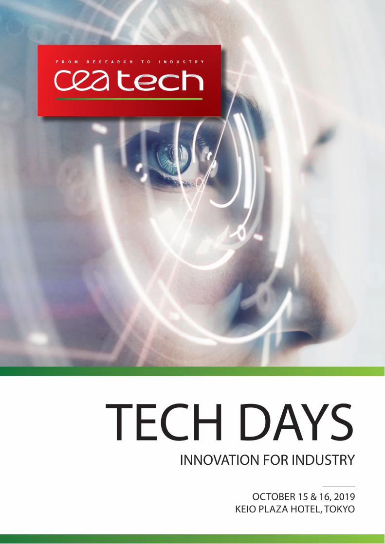
TECH DAYSINNOVATION FOR INDUSTRY
OCTOBER 15 & 16, 2019KEIO PLAZA HOTEL, TOKYO
OCTOBER 15, 2019KEIO PLAZA HOTEL, TOKYO
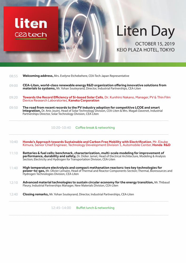
Liten Day
Welcoming address, Mrs. Evelyne Etchebehere, CEA-Tech Japan Representative08:55
09:00 CEA-Liten, world-class renewable energy R&D organization offering innovative solutions from materials to systems, Mr. Yohan Souteyrand, Director, Industrial Partnerships, CEA-Liten
09:20 Towards the Record Efficiency of Si-based Solar Cells, Dr. Kunihiro Nakano, Manager, PV & Thin Film Device Research Laboratories, Kaneka Corporation
09:50 The road from recent records to the PV industry adoption for competitive LCOE and smart integration, Dr. Anis Jouini, Head of Solar Technology Division, CEA-Liten & Mrs. Magali Davenet, Industrial Partnerships Director, Solar Technology Division, CEA-Liten
Coffee break & networking
10:40 Honda’s Approach towards Sustainable and Carbon Free Mobility with Electrification, Mr. Eisuke Kimura, Senior Chief Engineer, Technology Development Division 1, Automobile Center, Honda R&D
11:10 Batteries & fuel cells: benchmark, characterization, multi-scale modeling for improvement of performance, durability and safety, Dr. Didier Jamet, Head of Electrical Architecture, Modeling & Analysis Section; Electricity and Hydrogen for Transportation Division, CEA-Liten
11:40 High temperature electrolysis and compact methanation reactors: two key technologies for power-to-gas, Mr. Olivier Lemaire, Head of Thermal and Reactor Components Section; Thermal, Bioresources and Hydrogen Technologies Division, CEA-Liten
12:10 Advanced material technologies to sustain circular economy for the energy transition, Mr. Thibaud Fleury, Industrial Partnerships Manager, New Materials Division, CEA-Liten
12:40 Closing remarks, Mr. Yohan Souteyrand, Director, Industrial Partnerships, CEA-Liten
Buffet lunch & networking12:45-14:00
10:20-10:40
OCTOBER 15, 2019KEIO PLAZA HOTEL, TOKYO
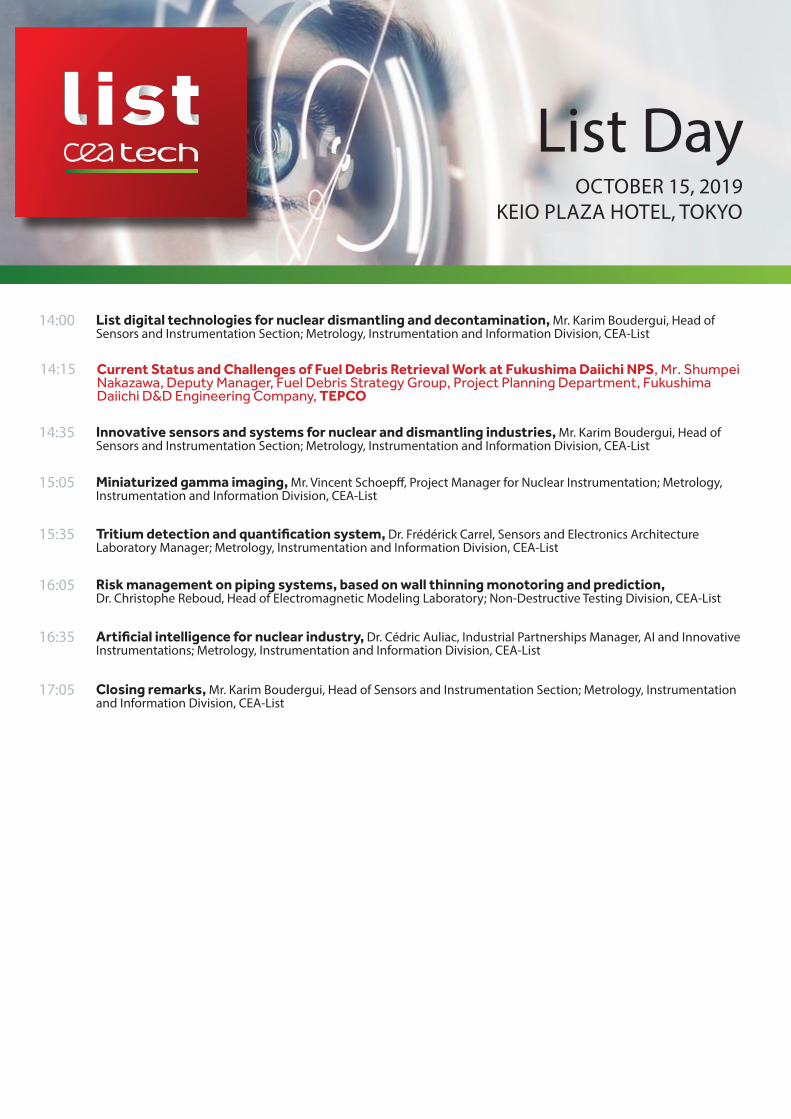
List Day
List digital technologies for nuclear dismantling and decontamination, Mr. Karim Boudergui, Head of Sensors and Instrumentation Section; Metrology, Instrumentation and Information Division, CEA-List
14:00
14:15 Current Status and Challenges of Fuel Debris Retrieval Work at Fukushima Daiichi NPS, Mr. Shumpei Nakazawa, Deputy Manager, Fuel Debris Strategy Group, Project Planning Department, Fukushima Daiichi D&D Engineering Company, TEPCO
Innovative sensors and systems for nuclear and dismantling industries, Mr. Karim Boudergui, Head of Sensors and Instrumentation Section; Metrology, Instrumentation and Information Division, CEA-List
14:35
Miniaturized gamma imaging, Mr. Vincent Schoepff, Project Manager for Nuclear Instrumentation; Metrology, Instrumentation and Information Division, CEA-List
15:05
Tritium detection and quantification system, Dr. Frédérick Carrel, Sensors and Electronics Architecture Laboratory Manager; Metrology, Instrumentation and Information Division, CEA-List
15:35
Risk management on piping systems, based on wall thinning monotoring and prediction, Dr. Christophe Reboud, Head of Electromagnetic Modeling Laboratory; Non-Destructive Testing Division, CEA-List
16:05
Artificial intelligence for nuclear industry, Dr. Cédric Auliac, Industrial Partnerships Manager, AI and Innovative Instrumentations; Metrology, Instrumentation and Information Division, CEA-List
16:35
Closing remarks, Mr. Karim Boudergui, Head of Sensors and Instrumentation Section; Metrology, Instrumentation and Information Division, CEA-List
17:05

OCTOBER 16, 2019KEIO PLAZA HOTEL, TOKYO
Leti Day
INTRODUCTION SESSION
Introduction to CEA-Leti, Dr. Emmanuel Sabonnadière, CEO, CEA-Leti 09:00
09:20
Overview of Leti platforms, Dr. Laurent Clavelier, Head of Technology Platform Division, CEA-Leti09:45
Highlights of Leti technologies, Dr. Jean-René Lequèpeys, CTO and Deputy Director, CEA-Leti10:10
Coffee break & networking10:35-11:05
QUANTUM COMPUTING SESSION
Quantum-Inspired Computing Digital Annealer, Dr. Toshiyuki Miyazawa, Manager of Digital Annealer Technology Development Project, Fujitsu Limited
11:05
Leti program on Quantum Computing, Dr. Maud Vinet, Quantum Computing Program Director, CEA-Leti 11:30
Leti initiative for Startups, Mr. Philippe Ruffin, Startup Program Manager, CEA-Leti12:00
EMBEDDED AI SESSION
Leti program on Embedded AI, Dr. Frédéric Heitzmann, Embedded AI Program Director, CEA-Leti13:55
LIDAR SESSION
Leti program on LIDAR, Dr. François Simoens, LIDAR Program Director, CEA-Leti14:25
5G SESSION
5G Integration of Services and Technologies, Dr. Yuichi Nakamura, VP Central Research Labs, NEC Corporation
15:25
Leti program on 5G, Mr. Eric Mercier, 5G Program Manager, CEA-Leti15:50
Opportunities of collaboration with Leti through European programs, Dr. Laurent Hérault, VP, Director of the Europe Division, CEA-Leti
16:20
Closing remarks, Dr. Emmanuel Sabonnadière, CEO, CEA-Leti16:45
Buffet lunch & networking12:25-13:55
Coffee break & networking14:55-15:25
SEMI Market Outlook — Fab investment, Equipment and Materials Market, Mr. Jim Hamajima, President, SEMI Japan
SPEAKERS BIOS
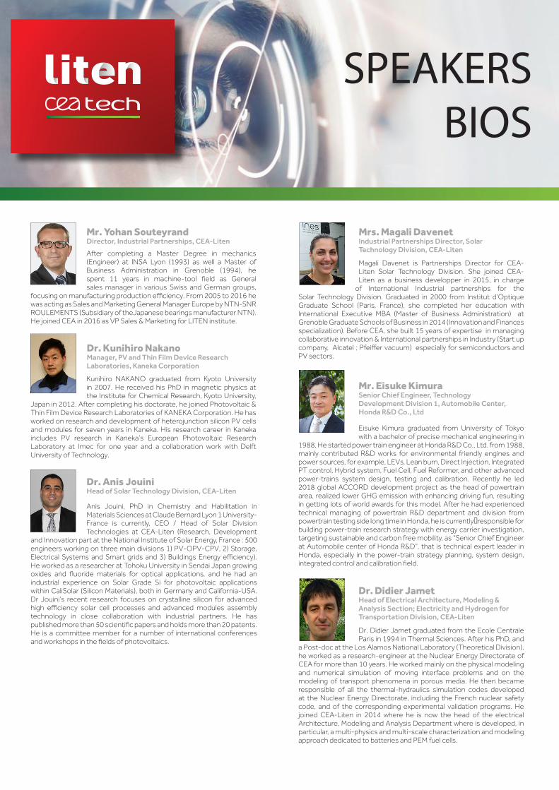
Mr. Yohan SouteyrandDirector, Industrial Partnerships, CEA-Liten
Dr. Anis JouiniHead of Solar Technology Division, CEA-Liten
After completing a Master Degree in mechanics (Engineer) at INSA Lyon (1993) as well a Master of Business Administration in Grenoble (1994), he spent 11 years in machine-tool field as General sales manager in various Swiss and German groups,
focusing on manufacturing production efficiency. From 2005 to 2016 he was acting as Sales and Marketing General Manager Europe by NTN-SNR ROULEMENTS (Subsidiary of theJapanese bearings manufacturer NTN). He joined CEA in 2016 as VP Sales & Marketing for LITEN institute.
Dr. Kunihiro NakanoManager, PV and Thin Film Device Research Laboratories, Kaneka Corporation
Dr. Didier JametHead of Electrical Architecture, Modeling & Analysis Section; Electricity and Hydrogen for Transportation Division, CEA-Liten
Dr. Didier Jamet graduated from the Ecole Centrale Paris in 1994 in Thermal Sciences. After his PhD, and
a Post-doc at the Los Alamos National Laboratory (Theoretical Division), he worked as a research-engineer at the Nuclear Energy Directorate of CEA for more than 10 years. He worked mainly on the physical modeling and numerical simulation of moving interface problems and on the modeling of transport phenomena in porous media. He then became responsible of all the thermal-hydraulics simulation codes developed at the Nuclear Energy Directorate, including the French nuclear safety code, and of the corresponding experimental validation programs. He joined CEA-Liten in 2014 where he is now the head of the electrical Architecture, Modeling and Analysis Department where is developed, in particular, a multi-physics and multi-scale characterization and modeling approach dedicated to batteries and PEM fuel cells.
Anis Jouini, PhD in Chemistry and Habilitation in Materials Sciences at Claude Bernard Lyon 1 University-France is currently, CEO / Head of Solar Division Technologies at CEA-Liten (Research, Development
and Innovation part at the National Institute of Solar Energy, France : 500 engineers working on three main divisions 1) PV-OPV-CPV, 2) Storage, Electrical Systems and Smart grids and 3) Buildings Energy efficiency). He worked as a researcher at Tohoku University in Sendai Japan growing oxides and fluoride materials for optical applications, and he had an industrial experience on Solar Grade Si for photovoltaic applications within CaliSolar (Silicon Materials), both in Germany and California-USA. Dr Jouini’s recent research focuses on crystalline silicon for advanced high efficiency solar cell processes and advanced modules assembly technology in close collaboration with industrial partners. He has published more than 50 scientific papers and holds more than 20 patents. He is a committee member for a number of international conferences and workshops in the fields of photovoltaics.
Kunihiro NAKANO graduated from Kyoto University in 2007. He received his PhD in magnetic physics at the Institute for Chemical Research, Kyoto University,
Japan in 2012. After completing his doctorate, he joined Photovoltaic & Thin Film Device Research Laboratories of KANEKA Corporation. He has worked on research and development of heterojunction silicon PV cells and modules for seven years in Kaneka. His research career in Kaneka includes PV research in Kaneka’s European Photovoltaic Research Laboratory at Imec for one year and a collaboration work with Delft University of Technology.
Mrs. Magali DavenetIndustrial Partnerships Director, Solar Technology Division, CEA-Liten
Magali Davenet is Partnerships Director for CEA-Liten Solar Technology Division. She joined CEA-Liten as a business developper in 2015, in charge
of International Industrial partnerships for the Solar Technology Division. Graduated in 2000 from Institut d’Optique Graduate School (Paris, France), she completed her education with International Executive MBA (Master of Business Administration) at Grenoble Graduate Schools of Business in 2014 (Innovation and Finances specialization). Before CEA, she built 15 years of expertise in managing collaborative innovation & International partnerships in Industry (Start up company, Alcatel ; Pfeiffer vacuum) especially for semiconductors and PV sectors.
Mr. Eisuke KimuraSenior Chief Engineer, Technology Development Division 1, Automobile Center, Honda R&D Co., Ltd
Eisuke Kimura graduated from University of Tokyo with a bachelor of precise mechanical engineering in
1988. He started power train engineer at Honda R&D Co., Ltd. from 1988, mainly contributed R&D works for environmental friendly engines and power sources, for example, LEVs, Lean burn, Direct Injection, Integrated PT control, Hybrid system, Fuel Cell, Fuel Reformer, and other advanced power-trains system design, testing and calibration. Recently he led 2018 global ACCORD development project as the head of powertrain area, realized lower GHG emission with enhancing driving fun, resulting in getting lots of world awards for this model. After he had experienced technical managing of powertrain R&D department and division from powertrain testing side long time in Honda, he is currently responsible for building power-train research strategy with energy carrier investigation, targeting sustainable and carbon free mobility, as “Senior Chief Engineer at Automobile center of Honda R&D”, that is technical expert leader in Honda, especially in the power-train strategy planning, system design, integrated control and calibration field.

SPEAKERS BIOS
Dr. Olivier LemaireHead of Thermal Components and Reactors Section; Thermal, Biomass and Hydrogen Division, CEA-Liten
Mr. Thibaud FleuryIndustrial Partnership Manager, New Materials Division, CEA-Liten
Olivier Lemaire is graduated from the University of Science and Technology of Lille, France. After his PhD in 2001, and a post-doc in the field of water radiolysis at
the Nuclear Energy Directorate of CEA, he worked in a private company for the development of gas analysis technologies. Then, he joined CEA-Liten as a research-engineer in the field of hydrogen with proton exchange membrane fuel cells, and managed the laboratory (50 people) from 2010 to 2013 with experimental, nano-characterisation and modeling activities. Since 2014, he is the head of the Thermal Components and Reactors Department with three labs: Heat Exchangers and Reactors lab, Thermal Storage lab and Conception/Assembling Technologies lab.
Thibaud Fleury graduated in 2004 from the French engineering school Supélec and completed a Master of Science degree from the Georgia Institute of Technology in Atlanta USA. He started his career in the
R&D labs of Sagem Communication in Paris, for which he developed and deployed new digital products for key accounts. After this 1st experience of 3 years, Thibaud held for 11 years various position in Sales & Tendering, Strategic Marketing, Market & Competitive Intelligence for international companies in the field of electrical grid and power generation: Areva T&D, Alstom, General Electric. With a strong focus on Power markets, Renewable and emerging technologies, he developed his expertise in Smart Grids, Solar PV, Wind On & Offshore, stationary battery storage and electrical vehicles. Thibaud joined CEA-Liten in 2018 for developing industrial partnerships for DTNM organization, specialized in new materials, printed electronics and advanced manufacturing processes such as 3D printing.

SPEAKERS BIOS
Mr. Karim Boudergui Head of Sensors and Instrumentation Section; Metrology, Instrumentation and Information Division, CEA-List
Mr. Shumpei Nakazawa Deputy Manager, Fuel Debris Strategy Group, Project Planning Department, Fukushima Daiichi D&D Engineering Company (FDEC), TEPCO
M. Karim Boudergui is a research engineer in CEA-List, head of SCI (Sensor and Instrumentation
Service, ~60 people) since the beginning of 2019. He began his career with AREVA as a software engineer and project manager in the field of nuclear measurement systems. He holds a post-graduate diploma in Instrumentation optical signals and optoelectronics (1995), a MS degree in Electronic, Electrotechnic and Automatic (1994). He took part in the design, development, qualification and demonstration tests of the Tagged Neutron Inspection System (TNIS) within UNCOSS EU project. He was also strongly involved in several European Security projects, enabling to develop advanced Radiation Portal Monitors (RPM) or specific systems for contamination monitoring in water.
As a Deputy Manager, Shumpei Nakazawa has responsibilities in the Fuel Debris Strategy Group,
Project Planning Department, which is focusing on fuel debris retrieval and PCV internal investigation project at Unit 1-3 at Fukushima Daiichi NPS. He joined Tokyo Electric Power Company Holdings (TEPCO) in 2005 after master graduation from Keio University in mechanical engineering. This allowed him to grasp multiple experiences especially in turbine maintenance, nuclear asset management, nuclear power and plant siting and finally project planning since 2017.
Dr. Frédérick Carrel Sensors and Electronics Architecture Laboratory Manager; Metrology, Instrumentation and Information Division, CEA-List
M. Frédérick CARREL graduated from the ENSICAEN engineer school in 2004. His PhD (2007) was dedicated to the characterization of nuclear waste packages using photon or neutron active interrogation and delayed gamma-ray spectrometry. He worked for AREVA CANBERRA in 2008 and has been hired by CEA-List the same year. His research topic is related to nuclear measurements (passive and active neutron measurements, gamma-ray spectrometry using various detectors, use of plastic scintillators, gamma imaging) and associated Monte Carlo simulation (MCNP code). He is part of the development team of the GAMPIX gamma camera. He is CEA senior expert in nuclear measurements from 2017. He is the Head of Sensors and Electronic Architectures Laboratory (LCAE, ~30 people in 2019) from the beginning of 2019.
Dr. Christophe ReboudHead of Electromagnetic Modeling Laboratory; Non-Destructive Testing Division, CEA-List
M. Christophe Reboud received his Engineering and Master degrees at Ecole Centrale de Nantes in 2003 and defended in 2006 a PhD at University
Paris Sud XI. He then joined CEA-List as a permanent researcher in charge of electromagnetic modelling for Non Destructive Testing (NDT) applications. He specialized in semi-analytical methods for efficient simulation of eddy current testing problems, as well as meta-modelling and statistical studies for reliability assessment. Since 2012, he is responsible for the Electromagnetic modelling laboratory inside the NDT department (Département Imagerie Simulation pour le Contrôle) of CEA LIST. This laboratory is in charge of developments related to quasi-static Electromagnetics, X-ray modelling, computed tomography, statistical studies, meta-modelling and model-based inversion for NDT applications. Developed tools are integrated into the multi-physics CIVA software, which is a leading product in the field of NDT. Christophe Reboud is a senior expert of CEA in the fields of NDT techniques, Electromagnetics and modelling. He is currently chairing the Intenational Scientific Committee of the International Workshop on Electromagnetic Nondestructive Evaluation (ENDE).
Mr. Vincent Schoepff Project Manager for Nuclear Instrumentation; Metrology, Instrumentation and Information Division, CEA-List
M. Vincent SCHOEPFF is part of the Sensors and Electronic Architectures Laboratory, part of CEA-List
Institute. He graduated from the ENSICAEN engineer school in 2009. He is responsible of developments carried out on radiation imaging systems in his laboratory for several years and is part of the GAMPIX development team (industrial name iPIX commercialized by MIRION Technologies). He is now project officer of the Common Innovation Laboratory signed with MIRION Technologies (CANBERRA), mainly working on improvement of the iPIX commercial system and future generations of radiation imagers. Since 2015, he worked on the miniaturization of the GAMPIX gamma imager (Nanopix technology) in collaboration with ORANO team. He is responsible from 2019 of the nuclear measurement section in LCAE.
SPEAKERS BIOS
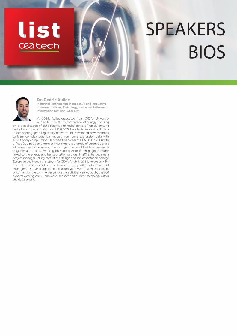
Dr. Cédric Auliac Industrial Partnerships Manager, AI and Innovative Instrumentations; Metrology, Instrumentation and Information Division, CEA-List
M. Cédric Auliac graduated from ORSAY University with an MSc (2003) in computational biology, focusing
on the application of data sciences to make sense of rapidly growing biological datasets. During his PhD (2007), in order to support biologists in deciphering gene regulatory networks, he developed new methods to learn complex graphical models from gene expression data with evolutionary computation. He started his career at CEA LIST in 2008 with a Post Doc position aiming at improving the analysis of seismic signals with deep neural networks. The next year, he was hired has a research engineer and started working on various AI research projects mainly linked to the energy and transportation sectors. In 2012, he became a project manager, taking care of the design and implementation of large European and industrial projects for CEA’s AI lab. In 2018, he got an MBA from HEC Business School. He took over the position of commercial manager of the DM2I department the next year. He is now the main point of contact for the commercial & industrial activities carried out by the 200 experts working on AI, innovative sensors and nuclear metrology within the department.

SPEAKERS BIOS
Dr. Emmanuel SabonnadiereCEO, CEA-Leti
Dr. Laurent Pain, Head of Partnerships, Technology Division Platform, CEA-Leti
Since November 20th, 2017, Emmanuel Sabonnadiere has been CEO of Leti, institute of CEA Tech. Before, he was in charge of the industrial partnerships of CEA Tech. Previously, he was CEO of the Business
Group Professional of Philips Lighting based in Amsterdam (NL). From 2008 till 2014, he was CEO & Chairman of General Cable Europe based in Barcelona (Spain). From 2005 till 2008, he was CEO of NKM Noell at Wurzburg (Germany). He has been vice-president of the Distribution Transformers division of Alstom T&D for 5 years. He began his career in 1992 with Schneider Electric holding various positions including that of Managing Director of development for equipment units. He has a strong technological background combined with a successful business track record over decades. With 25+ years of executive leadership of large operations, he produced successful operating results and great team building. He has gained a sound experience of change management in large multi-cultural matrix organizations in order to adapt to the new markets conditions and a strong knowledge of European and international environments. He designed and set-up strategic plans including innovation process. He believes in operational excellence, technology innovation, talent management and enthusiasm in leadership. He obtained a PhD in physics (France), and an engineering degree in Information Technology (France). He holds an MBA (France). He is a member of the Advisory Board of IAC.
Laurent Pain is graduated from the Ecole Nationale Supérieure de Physique de Grenoble in 1992. After receiving a PhD in 1996, he joined the Optronic Division of CEA-LETI. In 2000, he moved to STMicroelectronics Crolles site to participate to the start of the first 193nm
litho cell. From 2001 to 2008, he leaded the E-Beam direct write litho cell in the ST Crolles manufacturing site. The objective of this activity was first to show the integration capabilities of the EBDW lithography in industrial environment. From 2008 to 2014, Laurent Pain leaded the Lithography Laboratory of the Silicon Technology Division of CEA-LETI back at Grenoble pushing the insertion of innovative lithography techniques : multibeam, DSA and imprint. During this period, he also managed the industrial consortium IMAGINE dedicated to the development of MAPPER multibeam technology.Since July 2014, still within the LETI Silicon Technologies Division, he is now Head of Partnerships at the Technology Division Platform, and ensures the developments of all the associated business development.
Mr. Jim Hamajima President, SEMI Japan
As President of SEMI Japan, Masahiko (Jim) Hamajima has full responsibility for SEMI operations and oversees development of the association’s programs, committees, products, and services in the region.
He is responsible for relationships with SEMI members as well as with representatives of industry, government, academia, and other local constituencies. He is additionally charged with supporting SEMI members worldwide who have interests in SEMICON Japan, the region’s premier microelectronics event.Hamajima brings more than 30 years of experience in the semiconductor equipment industry in Japan and the U.S. and a comprehensive understanding of the global industry. Starting at Tokyo Electron Ltd. (TEL) in diffusion, Hamajima later held vice president positions overseeing multiple product lines at Tokyo Electron America and later for Cleaning Systems in Japan. Hamajima’s experience includes leading complex integrations as senior vice president at Timbre Technologies and as vice president and general manager at TEL-FSI. Prior to joining SEMI, Hamajima served as vice president and general manager of Corporate Strategy at TEL. Hamajima holds a Bachelor of Science degree in Metallurgy from the Nagoya Institute of Technology.
Dr. Jean-René Lequèpeys CTO and Deputy Director, CEA-Leti
Jean-René Lequèpeys received his engineering degree in 1983 from Supélec and taught physics for 2 years in Ouarzazate, Morocco. He joined CEA in October 1985, in Saclay, within the Central Security
Office, in the laboratory for the evaluation of means of detection and intrusion; in 1987, he hold the head of the laboratory. In 1993, he was recruited by DSYS, at LETI in Grenoble, as an R & D engineer, in the field of image processing. He then lead projects in the field of «Telecom» at LETI before getting the head of «Telecom, Communicating Objects and Smart Card» programs in 1999, within the team of Jean-Frédéric Clerc. In 2000, Jean-René Lèquepeys received the famous award from SEE «Grand Prix de l’électronique Général Ferrié» for his work in the telecommunications field. He is the author of about fifteen patents in this field. In 2005, he took in charge the Circuits Design Department at LETI / DSYS, and then created, in partenership with the Ecole des Mines de Saint-Etienne, a laboratory dedicated to electronic components safety analysis located in Gardanne (Paca). In 2010, from the common initiative of both LETI and LIST Directors, he launched DACLE division, relying on original bi-site and bi-institute model, and focusing on Electronic Architectures, Integrated Circuit Design and Embedded Software. He participated to the creation of the Division DCOS (Division of Silicon Components) in 2011, and then lead the division until the end of 2017, when he got back to the head of DACLE division in 2018. Since 2019 he is Deputy Director & CTO at CEA-Leti.
SPEAKERS BIOS
Dr. François SimoensLIDAR Program Director, CEA-Leti
Dr François Simoens carried out seven years of research in the accelerator field at CEA Saclay, before joining CEA-Leti in Grenoble in 2003 with the position of program manager and expert in infrared and THz sensors. From 2015 to 2018, he has been
the Marketing and Strategy Manager for the imaging technologies and systems developed at Leti from X-ray to Far-Infrared. Since 2019 he acts as the Director of the LETI strategic program named ‘miniaturized LIDAR – CPS’.
Dr. Toshiyuki Miyazawa, Manager of Digital Annealer Technology Development Project, Fujitsu Limited
Dr. Toshiyuki Miyazawa is currently the Manager of Digital Annealer Technology Development Project at Fujitsu Laboratories Ltd. He has been leading
hardware architecture of Digital Annealer, which was inspired by quantum phenomena, for solving large scale combinatorial optimization problems.He joined Fujitsu Laboratories Ltd. in 2001, where he has been engaged in research and development of single photon generator and quantum bits using semiconductor nanostructure. He contributed quantum dots project in Institute for Nano Quantum Information Electronics, University of Tokyo from 2003 to 2015.He received his B.S. degree in Physics from Yokohama National University in 1997, and his MS and PhD degrees in Electrical Engineering from University of Tokyo in 1999 and 2011 respectively. He is a member of The Japan Society of Applied Physics and The Physical Society of Japan.
Dr. Maud Vinet Quantum Computing Program Director, CEA-Leti
Maud Vinet (CEA-Leti, University Grenoble Alpes, France) is currently leading the quantum computing program in Leti. Her team is in charge of developing a silicon based quantum computer and on the other
hand, she fosters innovation in quantum technologies through creation of a public-private collaboration ecosystem. Since she joined in Leti, her research activities have been focused on advanced CMOS integration and they are evolving towards new computing paradigms. She defended her PhD in Physics from University of Grenoble Alps in 2001 and then was hired Leti in 2001 as a CMOS integration and device engineer. From 2009 to 2013, she spent 4 years in Albany, NY as a Leti assignee with IBM Alliance. She took part to the development of Fully Depleted Silicon-on-Insulator technology. In 2015, she joined Globalfoundries for 6 months as an assignee to launch 22FDX technology in Malta, NY, USA. From 2013 to 2018, she managed the Advanced CMOS integration team activities in Leti (~50 people). In 2019, she was appointed project leader for the quantum computing program in Leti. In 2011-12 she took Management of Innovation classes at the MIT Sloan School of Management, Boston, USA. In 2018, she followed the IHEST (French Institute of High Studies for Science and Technology) one-year training cycle, which aims at strengthening the relationship between science and society. She is part of the board of Quantum Engineering Grenoble. She has served in many technical committees; she is currently part of VLSI Symposium TPC. Maud Vinet authored or co-authored about 150 papers, she owns more than 65 patents related to nanotechnology and her Google h-index is 41.
Mr. Philippe RuffinStartup Program Manager, CEA-Leti
Philippe joins CEA-LETI in 2013 to set up a new program for aspiring entrepreneurs, Leti Startup Program. This program is dedicated to supporting and accelerating deep-tech startups through technology evaluation and Proof of Concept development, IP portfolio
enhancement, business design, access to partners and VCs. Philippe previously served as startup advisor at Grenoble’s public accelerator ‘Grain’, specializing in technology transfer to high tech companies in the fields of bio-technology, energy, microelectronics and ICT. Prior to that he held several marketing positions in the semiconductor and smart card industries, in both startups and large corporations. Philippe holds a Master of Science degree in Information Technology (systems integration) from Napier University, Edinburgh (Scotland).
Dr. Frédéric Heitzmann Embedded AI Program Director, CEA-Leti
Frederic Heitzmann was born in 1977. He received a master degree from the Ecole Polytechnique (France) in 2000, and a master degree from Telecom Paritech 2002. He started his career in a software development company, with a focus on multimedia contents,
database, and rich user interfaces. In 2004, he came to the Mobile Phone Division of Sagem (Safran group), in the OS-driver team. He contributed to the development of several platform (2G, 2.5G, 3G) integrated in dozens of commercial products, then took the lead of the low-level software team in 2005. In 2007, he moved to CEA-Leti, the French leading RTO in semiconductors, micro/nano devices, design and systems. He was part of the digital design research group, and contributed to reduce the gap between software and hardware developments. Notable realizations include: prototype of a programming environment for heterogeneous dataflow multicore SoC, joint algorithm/hardware design of a 60GHz demodulator, leading the development of a full Rx Telecom platform (software model and FPGA IPs), and a common framework for digital simulation/emulation. In 2012, he joined the Embedded Software Research group at CEA-Leti. He developed a compiler backend for asynchronous processor, and was part of the “sensor fusion” team, contributed to several patents and demonstrators. From 2018, he moves to his current position, head of the strategic program “EdgeAI” for CEA-Leti, whose purpose is to design, build, and demonstrate System breakthroughs for Artificial Intelligence at the edge.

SPEAKERS BIOS
Dr. Yuichi Nakamura VP Central Research Labs, NEC Corporation
Yuichi Nakamura received his B.E. degree in information engineering and M.E. degree in electrical engineering from the Tokyo Institute of Technology in 1986 and 1988, respectively. He received his PhD. from the
Graduate School of Information, Production and Systems, Waseda University, in 2007. He joined NEC Corp. in 1988 and he is currently he is currently vice president at Central Research Labs. NEC Corp. He is also a guest professor of National Institute of Informatics. He has more than 25 years of professional experience in electronic design automation, signal processing, optical communication and quantum computing.
Mr. Eric Mercier 5G Program Director, CEA-Leti
Eric MERCIER is at the CEA-Leti in Grenoble since 2006, now in charge of the LETI Technology Line - Connectivity coordination, including 5G and IoT topics. Graduated from the ENSEEIH of Toulouse,
France, 1991, and holding a DEA in Microwaves focused on Near-field/Far-field antenna diagram conversion done at Thales-Alenia Space (formerly Alcatel Space), he had held positions in the Optical Test Equipment with Schlumberger/Wavetek, for physical fiber optical link tests, as Analog & Signal Processing engineer, and had pursued his work in the semiconductor domain, back to RF topics in companies like ST and Atmel as R&D Application & Characterization engineer, as well as Marketing engineer, in the field of low-power RF dedicated to IoT. At CEA-Leti, he has led projects in the scope of ULP RF, with a specific focus on low-power RF transceiver design & implementation, and on embedded resources dedicated to low-power IoT solutions. Amongst these researches, the FOXY solution has been awarded ‘’’Electron D’Or – Golden Electron 2018’’ for ‘’Connected Objects’’ in France. He had been the Head Manager of the Laboratory for Architectures & Integrated RF design (LAIR) in the Architecture, IC Design and Embedded Software department (DACLE) for 4 years, the Lab. being in charge of designing RF solutions for ULP, UWB, UNB, mmW, High-Data Rate, RFID, PA & FEM systems, with a common target of addressing the lowest possible power consumption and make use of the most advanced CMOS technologies. He has co-authored some conference papers and participated to a book chapter on Wireless Sensor Network topic.
Dr. Laurent HéraultVP, Director of the Europe Division, CEA-Leti
Dr. Laurent Hérault was born in Tours, France, in 1964. He received the BS degree in electrical engineering and the MS degree in control engineering from the Institute National Polytechnique de Grenoble, (INPG) in 1987 and a Ph.D. degree in computer science from INPG
in 1991. He won the Best Junior Researcher Award from the University of Grenoble, France, in 1990. Since 2004 he is ‘International Expert’ at CEA. From 2009 to 2011, he has led the Wireless Communications and Security labs. Since 2011 he is Vice President, Director of the Europe division of CEA-Leti.

Liten Day Presentations
TECH DAYSINNOVATION FOR INDUSTRY
LITEN DAYOCTOBER 15, 2019
KEIO PLAZA HOTEL, TOKYO
CEA Tech Days 2019 | Yohan Souteyrand | 15/10/2019
CEA-LITEN, WORLD-CLASS RENEWABLE ENERGY R&D
ORGANIZATION OFFERING INNOVATIVE SOLUTIONS FROM
MATERIALS TO SYSTEMS
| 2
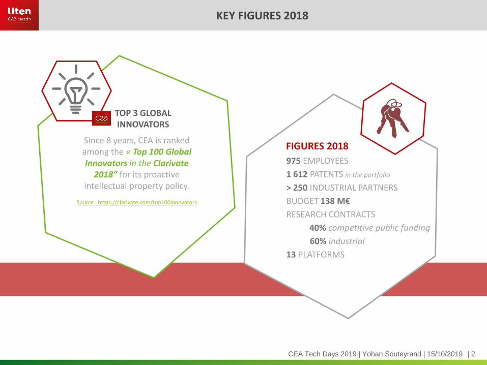
TOP 3 GLOBAL INNOVATORS
Since 8 years, CEA is ranked among the « Top 100 Global Innovators in the Clarivate
2018” for its proactive intellectual property policy.
Source : https://clarivate.com/top100innovators
975 EMPLOYEES
1 612 PATENTS in the portfolio
> 250 INDUSTRIAL PARTNERS
BUDGET 138 M€
RESEARCH CONTRACTS
40% competitive public funding
60% industrial
13 PLATFORMS
FIGURES 2018
KEY FIGURES 2018
CEA Tech Days 2019 | Yohan Souteyrand | 15/10/2019
| 3
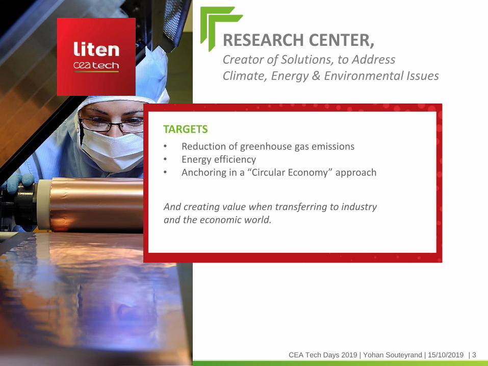
RESEARCH CENTER, Creator of Solutions, to AddressClimate, Energy & Environmental Issues
TARGETS
• Reduction of greenhouse gas emissions• Energy efficiency• Anchoring in a “Circular Economy” approach
And creating value when transferring to industry and the economic world.
CEA Tech Days 2019 | Yohan Souteyrand | 15/10/2019
| 4
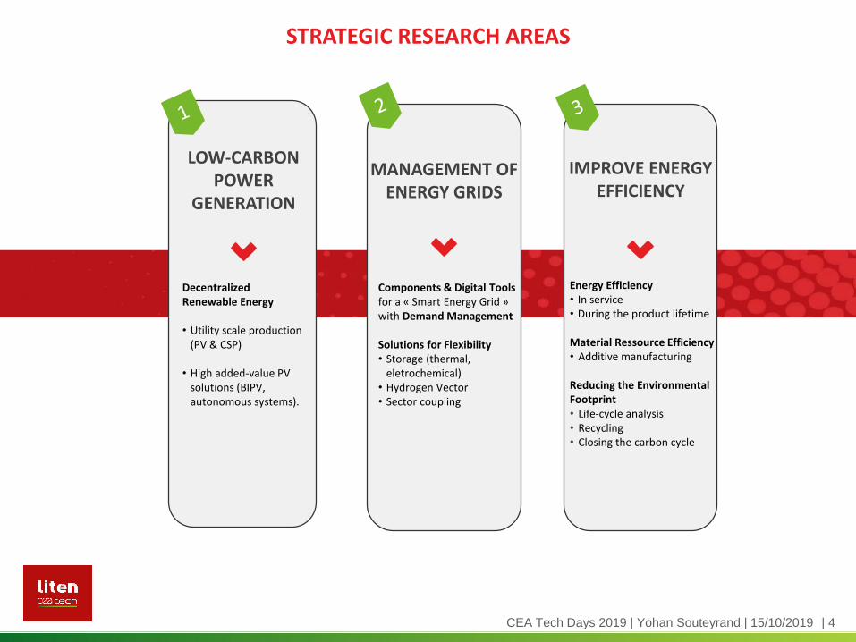
LOW-CARBON POWER
GENERATION
DecentralizedRenewable Energy
• Utility scale production (PV & CSP)
• High added-value PV solutions (BIPV, autonomous systems).
MANAGEMENT OF ENERGY GRIDS
Components & Digital Tools for a « Smart Energy Grid » with Demand Management
Solutions for Flexibility• Storage (thermal,
eletrochemical)• Hydrogen Vector• Sector coupling
IMPROVE ENERGY EFFICIENCY
STRATEGIC RESEARCH AREAS
Energy Efficiency• In service• During the product lifetime
Material Ressource Efficiency• Additive manufacturing
Reducing the EnvironmentalFootprint• Life-cycle analysis• Recycling• Closing the carbon cycle
CEA Tech Days 2019 | Yohan Souteyrand | 15/10/2019

| 5
LOW-CARBON POWER
GENERATION
DecentralizedRenewable Energy
• Utility scale production (PV & CSP)
• High added-value PV solutions (BIPV, autonomous systems).
MANAGEMENT OF ENERGY GRIDS
Components & Digital Tools for a « Smart Energy Grid » with Demand Management
Solutions for Flexibility• Storage (thermal,
eletrochemical)• Hydrogen Vector• Sector coupling
IMPROVE ENERGY EFFICIENCY
Energy Efficiency• In service• During the product lifetime
Material Ressource Efficiency• Additive manufacturing
Reducing the EnvironmentalFootprint• Life-cycle analysis• Recycling• Closing the carbon cycle
CEA Tech Days 2019 | Yohan Souteyrand | 15/10/2019

| 6
PV EverywhereLarge Solar Power Plants
• Homojunction• Heterojunction• Tandem Cells
• Custom Integration
• High-level RequirementsSolutions
• PV Inverters
• Architecture and Downstream Module Components
Develop PV Technologies with High Efficiency and Controlled Cost
Optimize the Overall Efficiency of Solar Systems
LOW-CARBON POWER GENERATION
CEA Tech Days 2019 | Yohan Souteyrand | 15/10/2019

| 7
LOW-CARBON POWER
GENERATION
Stratobus project : Development of a flexible and ultra-light PV module to power stratospheric aircrafts
Heterojunction : 23,9% of efficiency over the entire surface area. 348 Watts record: power for a nominal module using 120 half-cells with heterojunction
http://www.cea.fr/presse/Pages/actualites-communiques/energies/cellules-solaires-meyer-burger.aspx
CEA Tech Days 2019 | Yohan Souteyrand | 15/10/2019

| 8
LOW-CARBON POWER
GENERATION
DecentralizedRenewable Energy
• Utility scale production (PV & CSP)
• High added-value PV solutions (BIPV, autonomous systems).
MANAGEMENT OF ENERGY GRIDS
Components & Digital Tools for a « Smart Energy Grid » with Demand Management
Solutions for Flexibility• Storage (thermal,
eletrochemical)• Hydrogen Vector• Sector coupling
IMPROVE ENERGY EFFICIENCY
Energy Efficiency• In service• During the product lifetime
Material Ressource Efficiency• Additive manufacturing
Reducing the EnvironmentalFootprint• Life-cycle analysis• Recycling• Closing the carbon cycle
CEA Tech Days 2019 | Yohan Souteyrand | 15/10/2019
| 9
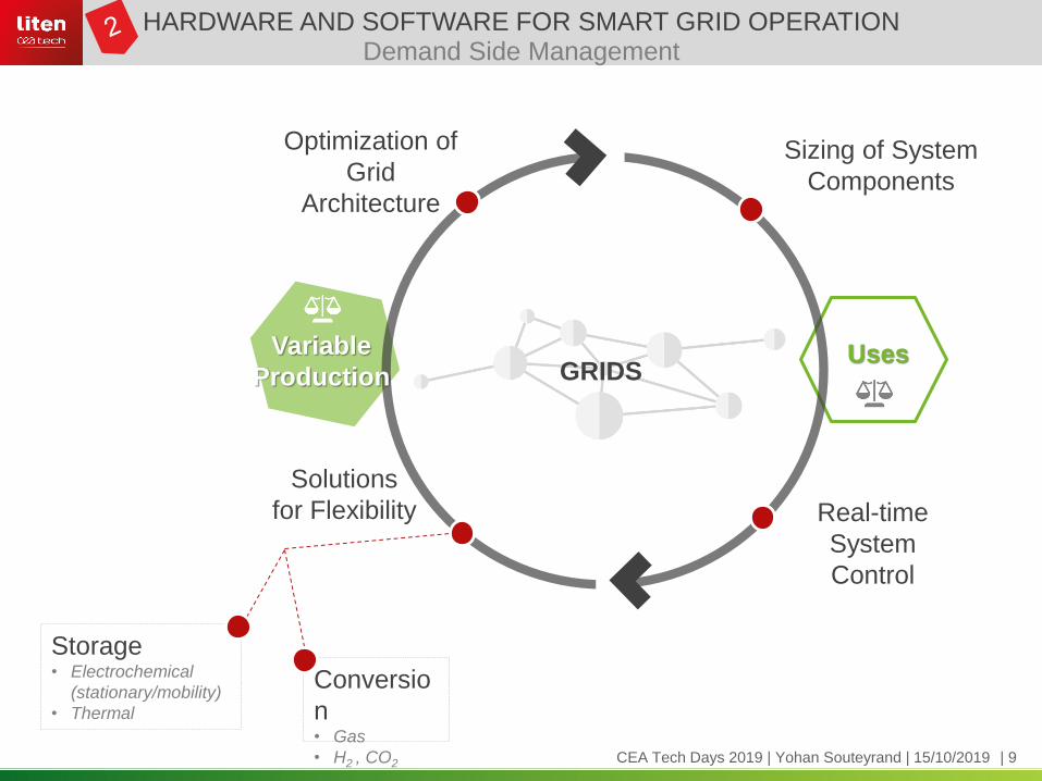
HARDWARE AND SOFTWARE FOR SMART GRID OPERATIONDemand Side Management
Optimization of
Grid
Architecture
Real-time
System
Control
Sizing of System
Components
Variable
Production Uses
Storage• Electrochemical
(stationary/mobility)
• Thermal
Conversio
n• Gas
• H2 , CO2
Solutions
for Flexibility
GRIDS
CEA Tech Days 2019 | Yohan Souteyrand | 15/10/2019

| 10
MANAGEMENT OF ENERGY GRIDS
SOEC Hydrogen ProductionProven system level performance: 87% PCIDemonstrator 300 kW in 2022
Marie Galante, Caribbean island, is moving towards 100% renewable
Liten has dimensioned the PV and battery storage installations with the grid operator
CEA Tech Days 2019 | Yohan Souteyrand | 15/10/2019
| 11
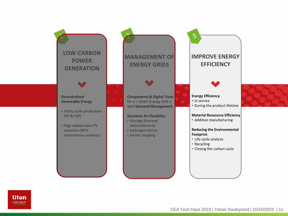
LOW-CARBON POWER
GENERATION
DecentralizedRenewable Energy
• Utility scale production (PV & CSP)
• High added-value PV solutions (BIPV, autonomous systems).
MANAGEMENT OF ENERGY GRIDS
Components & Digital Tools for a « Smart Energy Grid » with Demand Management
Solutions for Flexibility• Storage (thermal,
eletrochemical)• Hydrogen Vector• Sector coupling
IMPROVE ENERGY EFFICIENCY
Energy Efficiency• In service• During the product lifetime
Material Ressource Efficiency• Additive manufacturing
Reducing the EnvironmentalFootprint• Life-cycle analysis• Recycling• Closing the carbon cycle
CEA Tech Days 2019 | Yohan Souteyrand | 15/10/2019
| 12
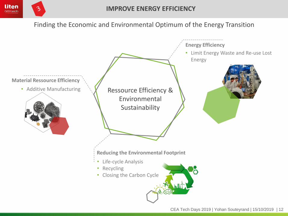
Finding the Economic and Environmental Optimum of the Energy Transition
Material Ressource Efficiency
• Limit Energy Waste and Re-use Lost Energy
Energy Efficiency
Reducing the Environmental Footprint
• Life-cycle Analysis• Recycling• Closing the Carbon Cycle
• Additive Manufacturing
IMPROVE ENERGY EFFICIENCY
Ressource Efficiency & EnvironmentalSustainability
CEA Tech Days 2019 | Yohan Souteyrand | 15/10/2019

| 13
IMPROVE ENERGY EFFICIENCY
Development of the hydrometallurgical process for the extraction of precious metals (Ni, Co, Mn, Li)Pilot scale (5L) validation of a single-step process for the selective extraction of precious metals.
Additive Manufacturing : Extend the fields of application with the manufacture of magnetic parts by laser fusion on a powder bed.
CEA Tech Days 2019 | Yohan Souteyrand | 15/10/2019

| 14
IMPROVE ENERGY EFFICIENCY
• Contribute to Carbon Neutrality• Limiting Dependence on Fossil Fuels
HYDROTHERMAL CONVERSIONOF MICROALGAE
Microalgae culture pool "fed" with factory smoke
Continuous hydrothermal
liquefaction pilot of CEA Grenoble
Valorization of CO2 emitted by manufacturers with the testing of a new biomass production solution based on biological recycling of CO2
1ST DEMONSTRATOR FOR THE PRODUCTION OF OPERATIONAL SYNTHETIC GAS
Demonstrator on a scale of 1 with 4 reactors (in Poland)
Compact reactor technology with a millistructured plate tested by CEA
Carbon conversion rate > 97% Carbon-rich oil 75%
CEA Tech Days 2019 | Yohan Souteyrand | 15/10/2019
| 15
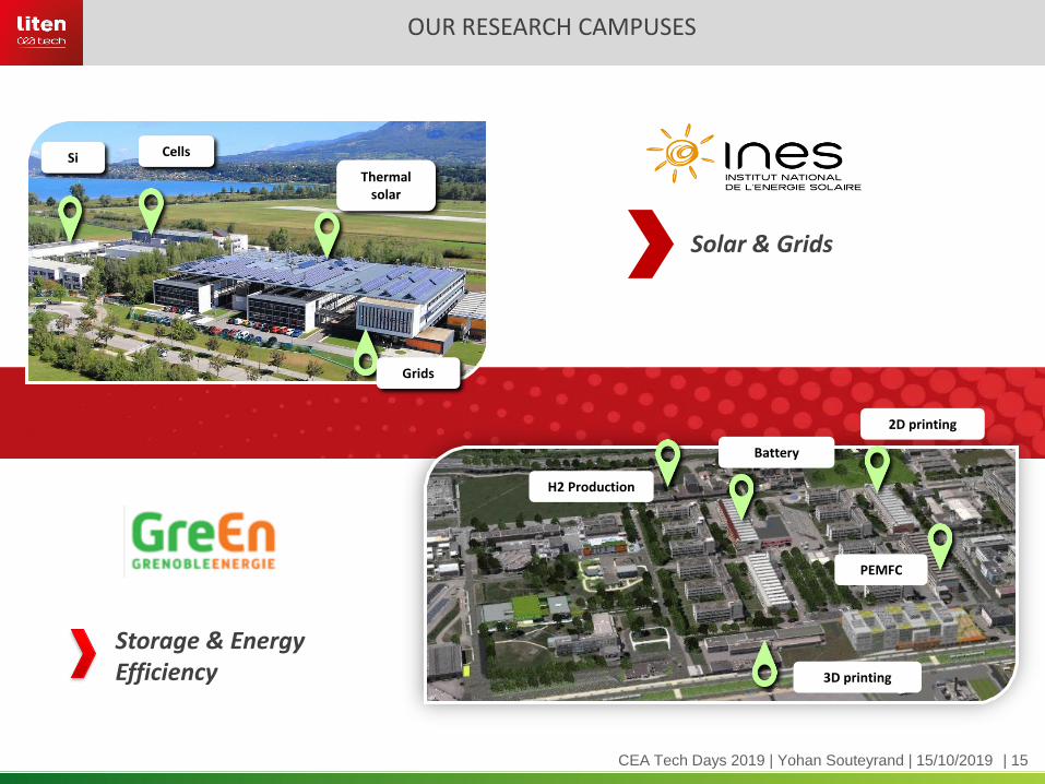
H2 Production
Battery
2D printing
PEMFC
3D printing
Si
Thermal solar
Cells
Grids
Solar & Grids
Storage & EnergyEfficiency
OUR RESEARCH CAMPUSES
CEA Tech Days 2019 | Yohan Souteyrand | 15/10/2019

| 16
300 m2 - 100 pers. - 2 M€
OUR TECHNOLOGICAL AND DIGITAL PLATFORMS
SOLAR PHOTOVOLTAIC15 000 m2 - staff 200- 100 M€
BATTERY3 000 m2 - staff 100 - 40 M€
SMART GRID300 m2 - staff 100 - 2 M€
BIO RESSOURCES800 m2 - staff 40 - 7 M€
NANO-CHARACTERIZATION3 000 m2 - staff 80 - 30 M€
BUILDING & ENERGYstaff 40 - 1,5 M€
PRINTING LARGE SURFACE600 m2 - staff 50 - 9 M€
NETWORK & THERMAL STORAGE1 500 m2 - staff 75 - 15 M€
ELECTRICAL MOBILITY1 500 m2 - staff 20 - 4 M€
NANO SECURITY5 000 m2 - staff 150 - 17 M€
FUEL CELLS500 m2 - staff 40 - 6 M€
PRODUCTION & STORAGE H2
820 m2 - staff 40 - 6 M€
POUDR’INNOV 2.01 400 m2 - staff 50 - 12 M€
CEA Tech Days 2019 | Yohan Souteyrand | 15/10/2019
| 17
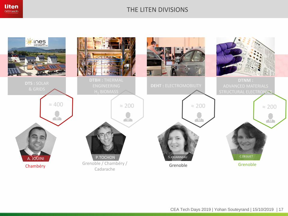
THE LITEN DIVISIONS
DTS : SOLAR & GRIDS
≈ 400
DTBH : THERMAL ENGINEERINGH2 BIOMASS
≈ 200
DEHT : ELECTROMOBILITY
≈ 200
DTNM : ADVANCED MATERIALS
STRUCTURAL ELECTRONICS
≈ 200
Chambéry
A. JOUINIGrenoble / Chambéry /
Cadarache
P.TOCHON
Grenoble
S.JOUANNEAU
Grenoble
C.DEGUET
CEA Tech Days 2019 | Yohan Souteyrand | 15/10/2019
| 18
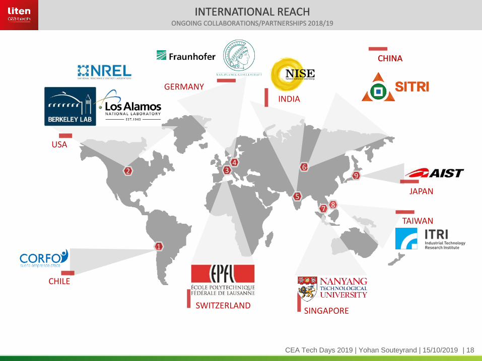
INTERNATIONAL REACH ONGOING COLLABORATIONS/PARTNERSHIPS 2018/19
1
2 3 6
7
USA
CHILE
SWITZERLANDSINGAPORE
CHINA
9
JAPAN5
INDIA
8
TAIWAN
4
INTERNATIONAL REACH ONGOING COLLABORATIONS/PARTNERSHIPS 2018/19
CHINA
GERMANY
CEA Tech Days 2019 | Yohan Souteyrand | 15/10/2019

| 19
MULTI-SECTORIAL
From low-end to high-end technologies
CUSTUMER ORIENTED
• Customized support to facilitate technology integration
• Personalized collaboration (contract, industrial transfer, high quality account management)
INNOVATIVE & COMPETITIVE
• Key enabling technologies as a driver for innovation
• Internationally renowned for our scientists’ expertise
UNRIVALED
Technology Platforms and a real I.P. « heritage »
FULLYCONFIDENTIAL
Strict protocols governing data and
client interest
CEA TECH SERVICE OFFERING
CEA Tech Days 2019 | Yohan Souteyrand | 15/10/2019
| 20
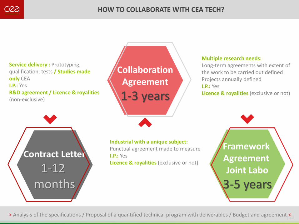
CollaborationAgreement
1-3 years
Contract Letter
1-12 months
Framework Agreement Joint Labo
3-5 years
Multiple research needs:Long-term agreements with extent of the work to be carried out definedProjects annually definedI.P.: Yes Licence & royalities (exclusive or not)
Industrial with a unique subject:Punctual agreement made to measureI.P.: Yes Licence & royalities (exclusive or not)
Service delivery : Prototyping, qualification, tests / Studies made only CEAI.P.: Yes R&D agreement / Licence & royalities(non-exclusive)
> Analysis of the specifications / Proposal of a quantified technical program with deliverables / Budget and agreement <
HOW TO COLLABORATE WITH CEA TECH?

Commissariat à l’énergie atomique et aux énergies alternatives
17 rue des Martyrs | 38054 Grenoble Cedex
www-liten.cea.fr
Établissement public à caractère industriel et commercial | RCS Paris B 775 685 019
Contact:
Yohan Souteyrand
Email: [email protected]
THANK YOU
ご清聴ありがとうございました
COME TO VISIT US IN FRANCE !
Kunihiro NAKANO
KANEKA Corporation
Towards the Record Efficiency of
Si-Based Solar Cells
Liten Day
Oct 15, 2019

2
• Overview of solar photovoltaics;
Current status and perspectives
• High efficiency crystalline Si solar cells using Si heterojunction
technology
• Multi-junction solar cell (HJ & perovskite solar cells)
• Summary
Outline
3
• Overview of solar photovoltaics;
Current status and perspectives
• High efficiency crystalline Si solar cells using Si heterojunction
technology
• Multi-junction solar cell (HJ & perovskite solar cells)
• Summary
Outline
4
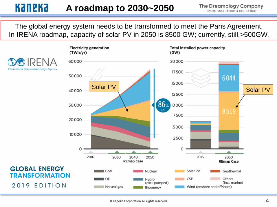
The global energy system needs to be transformed to meet the Paris Agreement.
In IRENA roadmap, capacity of solar PV in 2050 is 8500 GW; currently, still,>500GW.
A roadmap to 2030~2050
Solar PVSolar PV

5
Learning curve on PV module*
During 38 years :1980-2018
• Module price: 1/150
Recently, learning rate
become larger.
• Module power:double
• Developments of cell and
module technologies made them
possible besides the scale-up.
* ITRPV 2019
6
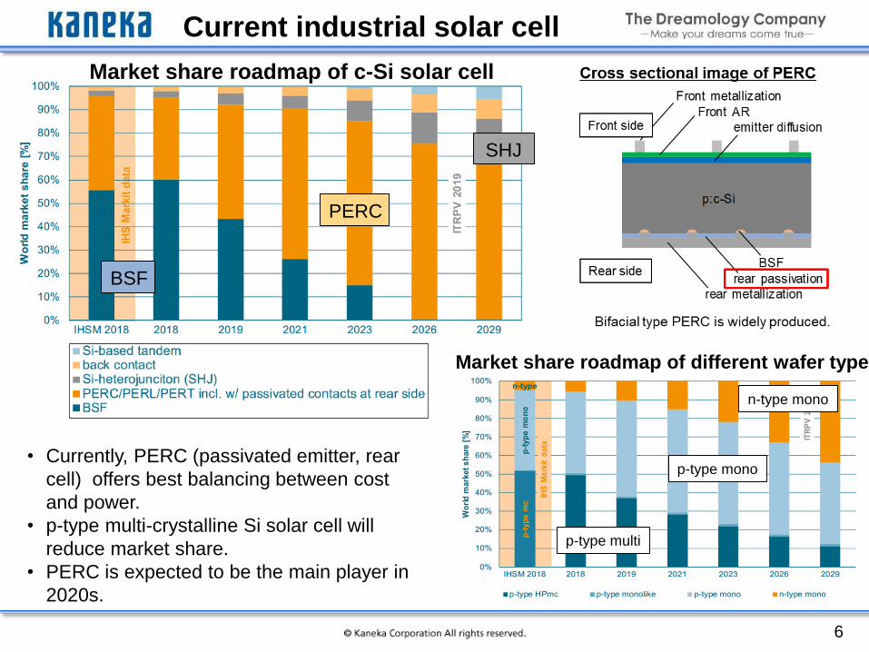
Current industrial solar cell
PERC
BSF
SHJ
• Currently, PERC (passivated emitter, rear
cell) offers best balancing between cost
and power.
• p-type multi-crystalline Si solar cell will
reduce market share.
• PERC is expected to be the main player in
2020s.
Market share roadmap of c-Si solar cell
Market share roadmap of different wafer type
p-type multi
p-type mono
n-type mono
7
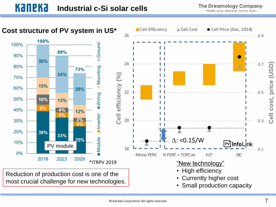
Industrial c-Si solar cells
Cost structure of PV system in US*
Cell c
ost,
pri
ce (
US
D)
*ITRPV 2019
PV module
Reduction of production cost is one of the
most crucial challenge for new technologies.
“New technology”
• High efficiency
• Currently higher cost
• Small production capacity
Ce
ll e
ffic
ien
cy (
%)
D: <0.1$/W

8
Industrial c-Si solar cells
C. Gerardi et al., presented in 1st International
Workshop on Silicon Heterojunction Solar Cells
Ratio of module cost in PV system cost is
expected to be smaller and smaller;
Higher efficiency is a key to realize the further
reduction of system cost.
Cost structure of PV system in US*
*ITRPV 2019
PV module
Reduction of production cost is one of the
most crucial challenge for new technologies.
9
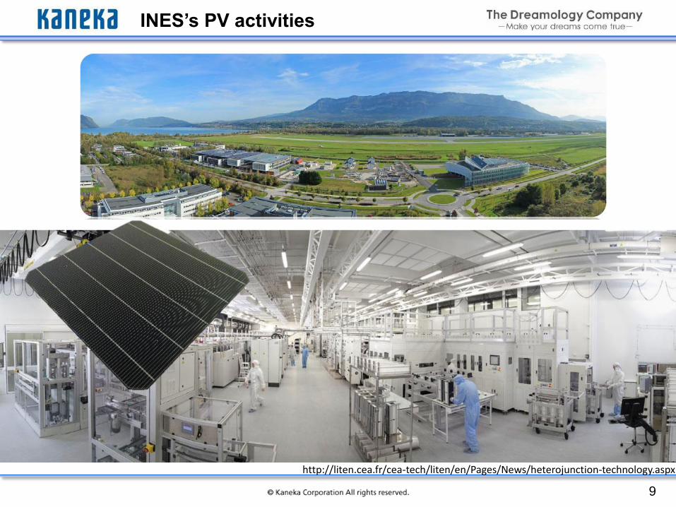
INES’s PV activities
http://liten.cea.fr/cea-tech/liten/en/Pages/News/heterojunction-technology.aspx

10
• Overview of solar photovoltaics
Current status and perspectives
• High efficiency crystalline Si solar cells using Si
heterojunction technology
• Multi-junction solar cell (HJ & perovskite solar cells)
• Summary
Outline
11
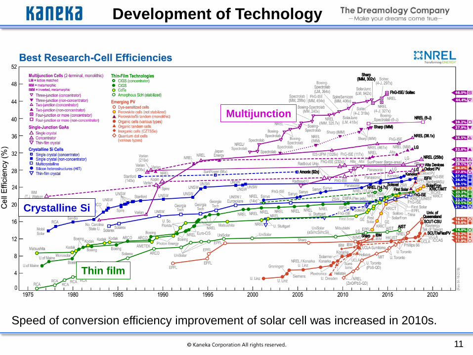
Development of Technology
Multijunction
Crystalline Si
Thin film
Speed of conversion efficiency improvement of solar cell was increased in 2010s.

12
Trend of High efficiency Si PV
26.7% back-contact Si heterojunction
(KANEKA, 2017) 1)
25.7% Tunnel oxide passivated contact
(Fraunhofer ISE, 2017) 4)
25.2% Back-contact
(SunPower, 2015) 3)
25.1% top/rear-
contacted a-Si/c-Si
heterojunction
(KANEKA, 2015)2)
1) K. Yamamoto et al, Jpn. J. Appl. Phys. 57 08RB20 (2018) 2) K. Yamamoto et al, Proc. of 31st EUPVSEC (2015), 1003.3)“SunPower 2015 Analyst Day” (2015), 4)A. Richter et al. Sol. Energy Mater. Sol. Cells 173 (2017), 96.

13
Trend of High efficiency Si PV
26.7% back-contact Si heterojunction
(KANEKA, 2017)
25.7% Tunnel oxide passivated contact
(Fraunhofer ISE, 2017) 4)
25.2% Back-contact
(SunPower, 2015) 3)
25.1% top/rear-
contacted a-Si/c-Si
heterojunction
(KANEKA, 2015)2)
1) K. Yamamoto et al, Jpn. J. Appl. Phys. 57 08RB20 (2018) 2) K. Yamamoto et al, Proc. of 31st EUPVSEC (2015), 1003.3)“SunPower 2015 Analyst Day” (2015), 4)A. Richter et al. Sol. Energy Mater. Sol. Cells 173 (2017), 96.
a-Si/c-Si HJ : High Voc and FF with smaller temperature coefficient of power
by excellent a-Si/c-Si interface
Production process :First process, Low thermal budget (T<200ºC)
Si wafer-based: Reasonable production cost
Advantages of a-Si/c-Si heterojunction (HJ) Si solar cell
14
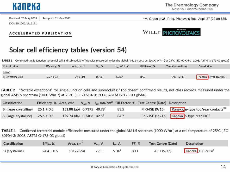
*M. Green et al., Prog. Photovolt: Res. Appl. 27 (2019) 565.
15
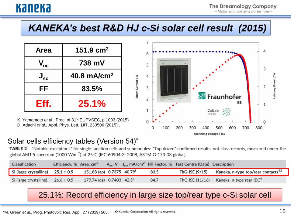
KANEKA’s best R&D HJ c-Si solar cell result (2015)
Area 151.9 cm2
Voc 738 mV
Jsc 40.8 mA/cm2
FF 83.5%
Eff. 25.1%
K. Yamamoto et al., Proc. of 31st EUPVSEC, p.1003 (2015)
D. Adachi et al., Appl. Phys. Lett. 107, 233506 (2015) .
Solar cells efficiency tables (Version 54)*
25.1%: Record efficiency in large size top/rear type c-Si solar cell
*M. Green et al., Prog. Photovolt: Res. Appl. 27 (2019) 565.
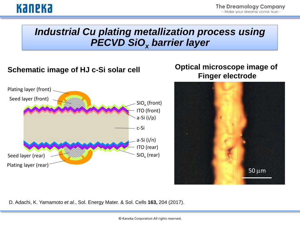
50 mm
Schematic image of HJ c-Si solar cell Optical microscope image of
Finger electrode
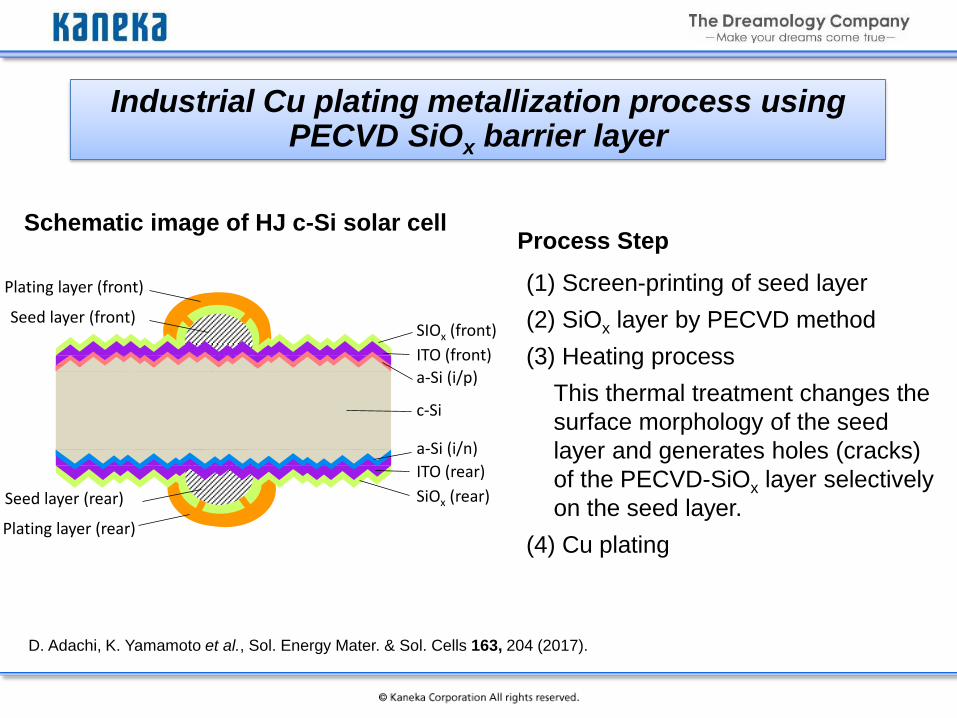
Industrial Cu plating metallization process using PECVD SiOx barrier layer
D. Adachi, K. Yamamoto et al., Sol. Energy Mater. & Sol. Cells 163, 204 (2017).
Seed layer (front)
Plating layer (front)
Seed layer (rear)
Plating layer (rear)
c-Si
a-Si (i/p)
a-Si (i/n)
ITO (rear)
ITO (front)
SIOx (front)
SiOx (rear)
Seed layer (front)
Plating layer (front)
Seed layer (rear)
Plating layer (rear)
c-Si
a-Si (i/p)
a-Si (i/n)
ITO (rear)
ITO (front)
SIOx (front)
SiOx (rear)
Industrial Cu plating metallization process using PECVD SiOx barrier layer
Schematic image of HJ c-Si solar cell
(1) Screen-printing of seed layer
(2) SiOx layer by PECVD method
(3) Heating process
This thermal treatment changes the
surface morphology of the seed
layer and generates holes (cracks)
of the PECVD-SiOx layer selectively
on the seed layer.
(4) Cu plating
Process Step
D. Adachi, K. Yamamoto et al., Sol. Energy Mater. & Sol. Cells 163, 204 (2017).
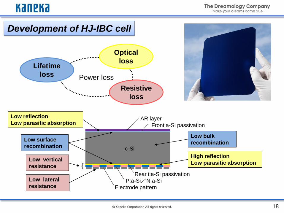
18
Power loss
Rear i:a-Si passivation
P:a-Si/N:a-Si
Electrode pattern
AR layer
Front a-Si passivation
c-Si
Low reflection
Low parasitic absorption
Low surface
recombination
Low vertical
resistance
High reflection
Low parasitic absorption
Low bulk
recombination
Low lateral
resistance
Lifetime
loss
Resistive
loss
Optical
loss
Development of HJ-IBC cell

19
Achievement of 26.3% by HJ-IBC (2016)
Silicon heterojunction solar cell with interdigitated back contacts for a
photoconversion efficiency over 26% (*)
Area 180.43±0.18 cm2
VOC 743.8 ±2.5 mV
JSC 42.25 ±0.80 mA/cm2
FF 83.78 ±0.54%
Eff 26.33 ±0.53%
(*) K. Yoshikawa et al., Nat. Energy 2, 17032 (2017).
20
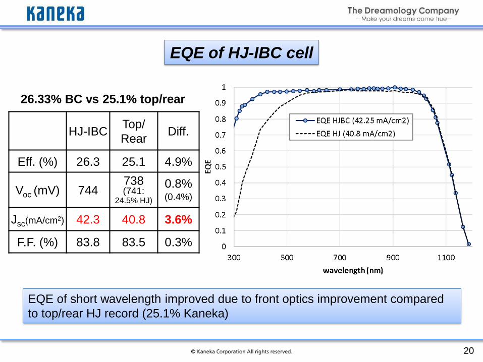
EQE of HJ-IBC cell
EQE of short wavelength improved due to front optics improvement compared
to top/rear HJ record (25.1% Kaneka)
HJ-IBCTop/
RearDiff.
Eff. (%) 26.3 25.1 4.9%
Voc (mV) 744 738(741:
24.5% HJ)
0.8%(0.4%)
Jsc(mA/cm2) 42.3 40.8 3.6%
F.F. (%) 83.8 83.5 0.3%
26.33% BC vs 25.1% top/rear
21
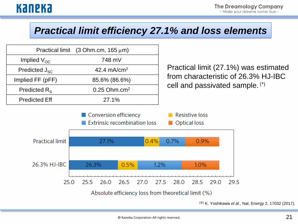
Practical limit efficiency 27.1% and loss elements
Practical limit (3 Ohm.cm, 165 mm)
Implied VOC 748 mV
Predicted JSC 42.4 mA/cm2
Implied FF (pFF) 85.6% (86.6%)
Predicted RS 0.25 Ohm.cm2
Predicted Eff 27.1%
Practical limit (27.1%) was estimated
from characteristic of 26.3% HJ-IBC
cell and passivated sample. (*)
(※) K. Yoshikawa et al., Nat. Energy 2, 17032 (2017).
22
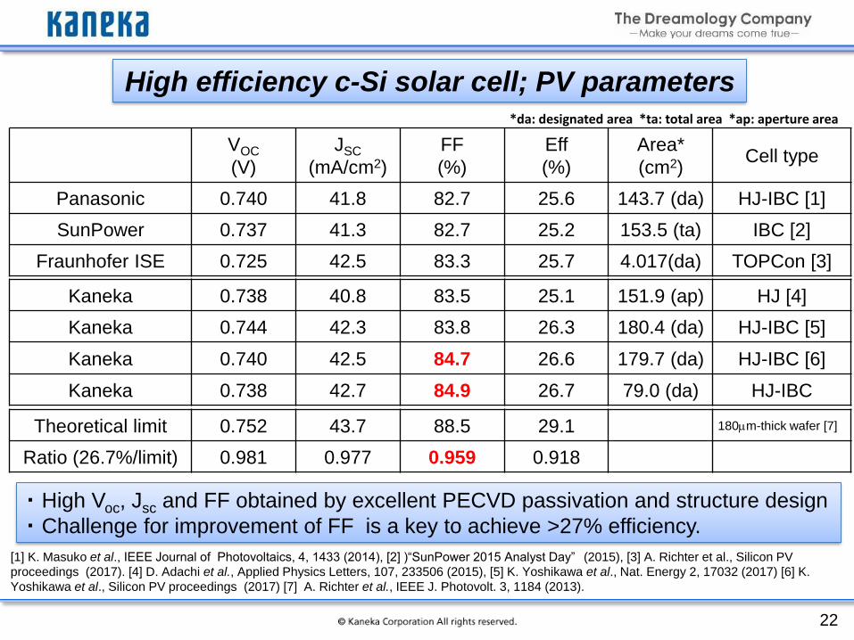
*da: designated area *ta: total area *ap: aperture area
・ High Voc, Jsc and FF obtained by excellent PECVD passivation and structure design
・ Challenge for improvement of FF is a key to achieve >27% efficiency.
VOC
(V)
JSC
(mA/cm2)
FF
(%)
Eff
(%)
Area*
(cm2)Cell type
Panasonic 0.740 41.8 82.7 25.6 143.7 (da) HJ-IBC [1]
SunPower 0.737 41.3 82.7 25.2 153.5 (ta) IBC [2]
Fraunhofer ISE 0.725 42.5 83.3 25.7 4.017(da) TOPCon [3]
High efficiency c-Si solar cell; PV parameters
[1] K. Masuko et al., IEEE Journal of Photovoltaics, 4, 1433 (2014), [2] )“SunPower 2015 Analyst Day” (2015), [3] A. Richter et al., Silicon PV
proceedings (2017). [4] D. Adachi et al., Applied Physics Letters, 107, 233506 (2015), [5] K. Yoshikawa et al., Nat. Energy 2, 17032 (2017) [6] K.
Yoshikawa et al., Silicon PV proceedings (2017) [7] A. Richter et al., IEEE J. Photovolt. 3, 1184 (2013).
Kaneka 0.738 40.8 83.5 25.1 151.9 (ap) HJ [4]
Kaneka 0.744 42.3 83.8 26.3 180.4 (da) HJ-IBC [5]
Kaneka 0.740 42.5 84.7 26.6 179.7 (da) HJ-IBC [6]
Kaneka 0.738 42.7 84.9 26.7 79.0 (da) HJ-IBC
Theoretical limit 0.752 43.7 88.5 29.1 180mm-thick wafer [7]
Ratio (26.7%/limit) 0.981 0.977 0.959 0.918

23
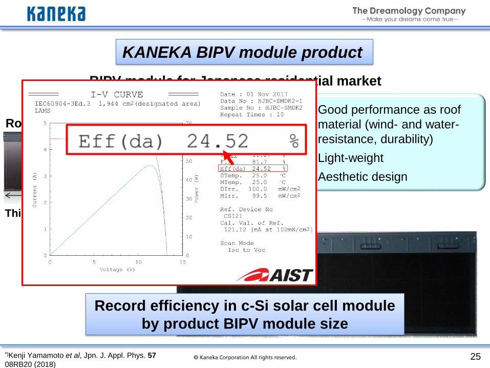
HJ-IBC module
Record efficiency for c-Si solar cell module, 24.37%
Area: 1.32 m2
*M. Green et al., Prog. Photovolt: Res. Appl. 27 (2019) 565.

24
VISOLATM type
HJ-IBC
(Prototype)
VISOLATM
KANEKA BIPV module product
1000 mm
BIPV module for Japanese residential market
Roof tile type• Good performance as roof
material (wind- and water-
resistance, durability)
• Light-weight
• Aesthetic design
Thin-film Si
25
VISOLATM type
HJ-IBC
(Prototype)
VISOLATM
KANEKA BIPV module product
1000 mm
BIPV module for Japanese residential market
Roof tile type• Good performance as roof
material (wind- and water-
resistance, durability)
• Light-weight
• Aesthetic design
Thin-film Si
Record efficiency in c-Si solar cell module
by product BIPV module size
*)Kenji Yamamoto et al, Jpn. J. Appl. Phys. 57
08RB20 (2018)
26
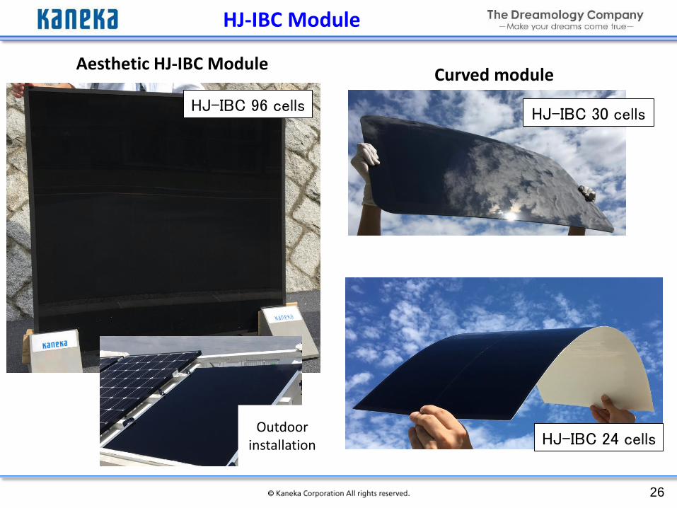
HJ-IBC Module
Aesthetic HJ-IBC ModuleCurved module
HJ-IBC 24 cells
HJ-IBC 96 cells
Outdoor installation
HJ-IBC 30 cells

27
• Overview of solar photovoltaics: current status and
perspectives
• High efficiency crystalline Si solar cells using Si heterojunction
technology
• Multi-junction solar cell (HJ & perovskite solar cells)
• Summary
Outline
28
0
0.2
0.4
0.6
0.8
1
1.2
1.4
1.6
1.8
300 800 1300 1800
Spec
tral
Irra
dia
tio
n (
W/m
2 /n
m)
Wavelength (nm)
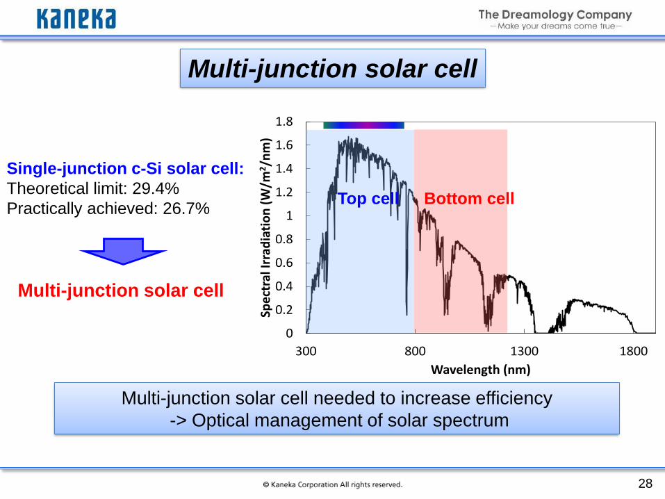
Top cell Bottom cell
Single-junction c-Si solar cell:
Theoretical limit: 29.4%
Practically achieved: 26.7%
Multi-junction solar cell
Multi-junction solar cell
Multi-junction solar cell needed to increase efficiency
-> Optical management of solar spectrum

29
c-Si heterojunction perovskite Tandem
Demonstrated: η >26%
Perovskite sola cell
on c-Si solar cell
Demonstrated: η = 28%
(Potentially η > 30%)Demonstrated: η >24%
Monolithic perovskite/c-Si tandem
30
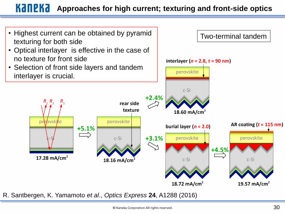
R. Santbergen, K. Yamamoto et al., Optics Express 24, A1288 (2016)
• Highest current can be obtained by pyramid
texturing for both side
• Optical interlayer is effective in the case of
no texture for front side
• Selection of front side layers and tandem
interlayer is crucial.
Approaches for high current; texturing and front-side optics
Two-terminal tandem

31
Back-contact/Perovskite 3-terminal tandem solar cell
Equivalent circuit
Optical simulation
Electrical circuit simulation
Cross-sectional image
R. Santbergen, K. Yamamoto et al., IEEE J. Photovoltaics 9, 446 (2019).

32
24.2(mA/cm2) 16.8(mA/cm2)
42.7(mA/cm2)
Possibility of over 35% efficiency
This plot is courtesy of the National Renewable Energy Laboratory, Golden, CO.
1) M. A. Green et al., “Solar cell efficiency tables (version 54),” Prog. Photovolt., Res. Appl., vol. 27, pp. 565–575, 2019.2) M. A. Green et al., “Solar cell efficiency tables (version 50),” Prog. Photovolt., Res. Appl., vol. 25, pp. 668–676, 2017.
3)
Voc(V) Jsc(mA/cm2) FF(%)
Perovskite(Krict) 1.195 24.16 84.0
HJBC(Kaneka) 0.738 42.65 84.9
2TT(概算) Top/Bottom 1.800 21.00 78.1
Top 1.195 24.16 84.0 24.2
Bottom 0.716 16.78 83.4 10.0
cell
Single cell
3TT(概算) 34.2
Eff(%)
24.2
26.7
29.5
Simulation result under some assumptions is shown below.
The over 35% efficiency can be achievable with the 3TT cell which consists of highest efficiency
perovskite cell and HJ-IBC cell.

33
Current record efficiency of Perovskite/Si tandem
*C.Case, Heterojunction and thin film solar cell forum (2019)

34
• PV market is growing rapidly in this 10 years. Further growth is expected.
Currently, dominant solar cell structure is PERC cell with ~22%-efficiency.
• Efficiency of 25.1% reached for top/bottom contacted HJ solar cell
• World record efficiency for c-Si solar cell of 26.7% and module of 24.5%
using back contact HJ solar cell
• Perovskite-HJ tandem structure is expected towards conversion efficiency > 30%.
Cell structure candidate: 2-terminal, 3-terminal, 4-terminal
• Technology improvement for high-efficiency is a key to reduce the electricity cost of
PV.
ACKNOWLEDGEMENT
This work was supported in part by the New Energy and Industrial Technology
Development Organization (NEDO) under the Ministry of Economy, Trade and Industry
of Japan.
SUMMARY

TECH DAYSINNOVATION FOR INDUSTRY
LITEN DAYOCTOBER 15, 2019
KEIO PLAZA HOTEL, TOKYO
CEA Tech Days | Anis JOUINI | CEO INES | 15/10/2019
| Head of Solar Technologies Department – CEA/LITEN
TTHE ROAD FROM RECENT RECORDS TO THE PV INDUSTRY
ADOPTION FOR COMPETITIVE LCOE & SMART INTEGRATION
| 2
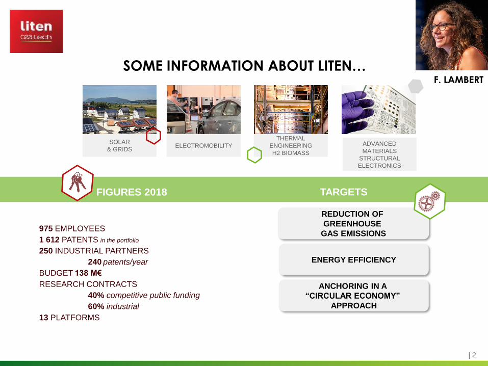
SOME INFORMATION ABOUT LITEN…
ELECTROMOBILITYSOLAR
& GRIDS
THERMAL
ENGINEERING
H2 BIOMASS
ADVANCED
MATERIALS
STRUCTURAL
ELECTRONICS
975 EMPLOYEES
1 612 PATENTS in the portfolio
250 INDUSTRIAL PARTNERS
240 patents/year
BUDGET 138 M€
RESEARCH CONTRACTS
40% competitive public funding
60% industrial
13 PLATFORMS
FIGURES 2018
ENERGY EFFICIENCY
REDUCTION OF
GREENHOUSE
GAS EMISSIONS
ANCHORING IN A
“CIRCULAR ECONOMY”
APPROACH
TARGETS
F. LAMBERT
| 3
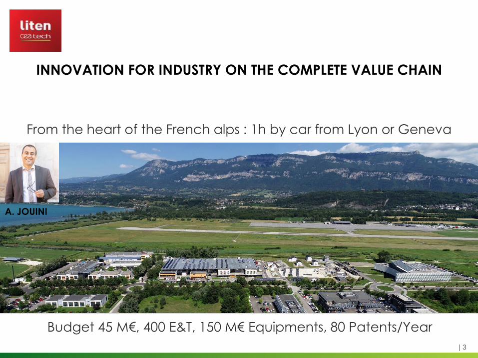
INNOVATION FOR INDUSTRY ON THE COMPLETE VALUE CHAIN
From the heart of the French alps : 1h by car from Lyon or Geneva
Budget 45 M€, 400 E&T, 150 M€ Equipments, 80 Patents/Year
A. JOUINI
| 4
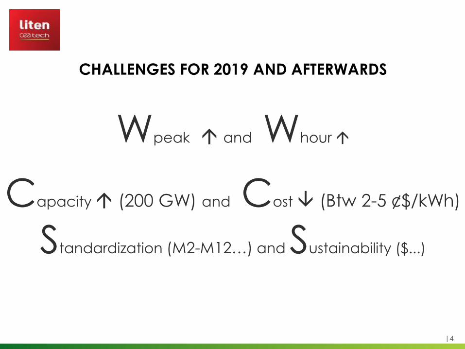
Wpeak and Whour
Capacity (200 GW) and Cost (Btw 2-5 ¢$/kWh)
Standardization (M2-M12…) and Sustainability ($...)
CHALLENGES FOR 2019 AND AFTERWARDS
| 5
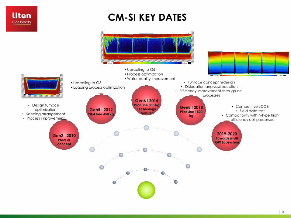
CM-SI KEY DATES
Gen2 I 2010Proof of concept
Gen5 I 2012Pilot Line 450 kg
Gen6 I 2014Pilot Line 800 kg
Technology
Transfer
Gen8 I 2018Pilot Line 1500
kg
2019-2020Towards multi GW Ecosystem
• Design furnace
optimization
• Seeding arrangement
• Process improvement
• Upscaling to G5
• Loading process optimization
• Upscaling to G6
• Process optimization
• Wafer quality improvement• Furnace concept redesign
• Dislocation analysis/reduction
• Efficiency improvement through cell
processes
• Competitive LCOE
• Field data test
• Compatibility with n-type high
efficiency cell processes
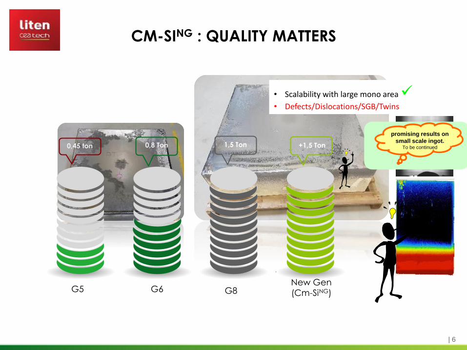
| 6
G5 G6
0,45 ton 0,8 Ton +1,5 Ton1,5 Ton
G8New Gen (Cm-SiNG)
• Scalability with large mono area
• Defects/Dislocations/SGB/Twins
promising results on
small scale ingot. To be continued
CM-SING : QUALITY MATTERS

| 7
G5
25
bricks
G6
36
bricks
G8
64
bricks
Technology upgrade from G6 to G8 ingot size
D.G
uill
audin
-CE
A
1300 kg G8 CrystalMax
ingot
WAFER DEVELOPMENT = CAST MONO (MONOLIKE)

| 888
EvolutionPERC/PERC+ +22%
Towards
Passivated contacts +23%
BreakthroughSHJ 25%
Near FutureTandem 30%
1 2 3
• +24% proven as a record
certified cell (EGP/MB)
• +24% using industrial high
throughput production line• IBC SHJ simplified process
for +25%
• +25% Perovskite on SHJ
end of 2019• Perovskite on perovskite
• +30% III/V with poly Si
deposition : Cost
compatibility with PV
• Codoping using Plasma
immersion (IBS)
• iVoc @ 740 mV using LPCVD
(SEMCO Technologies)
• Simplified n-type HT
processes for +23%• ALD
module Pk +20,3%
11 cm2
| 9
• DESCRIPTION
• Passivated contact technology using polycrystalline
silicon layers deposited on ultra-thin oxide films
• In the roadmap evolution of existing PERC manufacturer
PASSIVATED CONTACT BIFACIAL
• KEY FIGURES
• Record Efficiency 22.8% with
industrial processes
• Efficiency potential of 26%
• Compatible with all kinds of silicon
wafers (n&p, Cz, cast mono, …)
• Compatible with multi-junction devices
(30% efficiency already obtained)
• WHAT’S NEXT?
• Integration into multi-junction devices
for efficiencies above 30%.
| 10
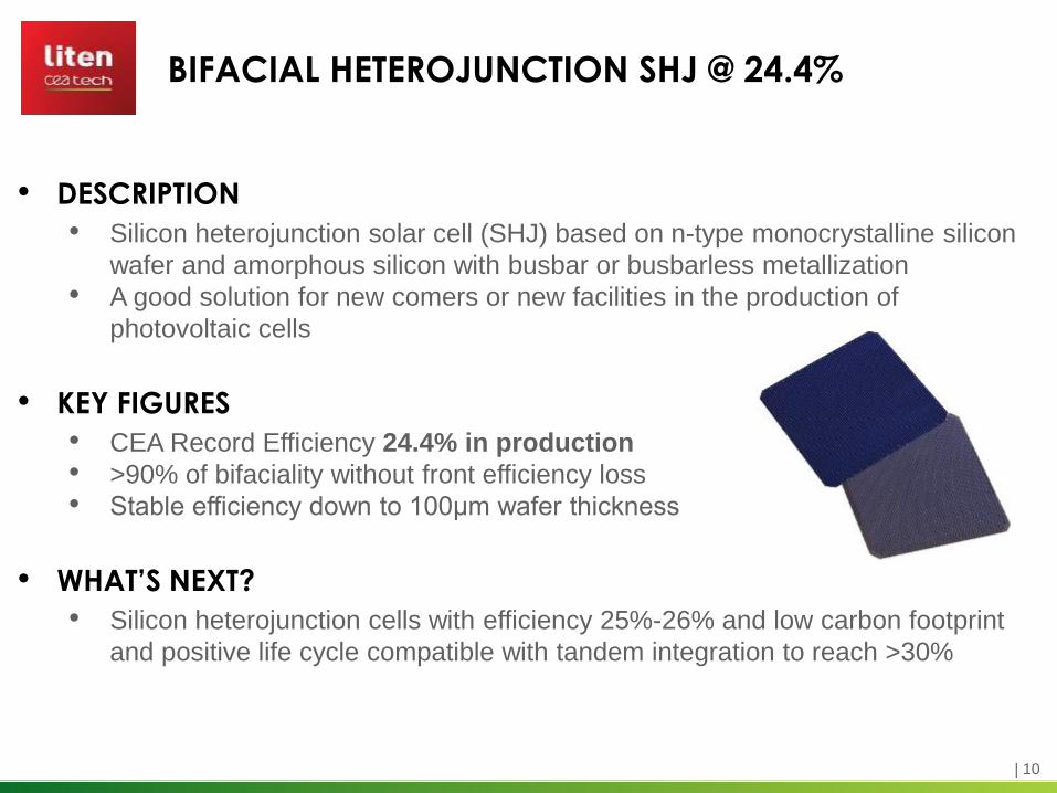
• DESCRIPTION
• Silicon heterojunction solar cell (SHJ) based on n-type monocrystalline silicon
wafer and amorphous silicon with busbar or busbarless metallization
• A good solution for new comers or new facilities in the production of
photovoltaic cells
• KEY FIGURES
• CEA Record Efficiency 24.4% in production
• >90% of bifaciality without front efficiency loss
• Stable efficiency down to 100μm wafer thickness
• WHAT’S NEXT?
• Silicon heterojunction cells with efficiency 25%-26% and low carbon footprint
and positive life cycle compatible with tandem integration to reach >30%
BIFACIAL HETEROJUNCTION SHJ @ 24.4%
| 11
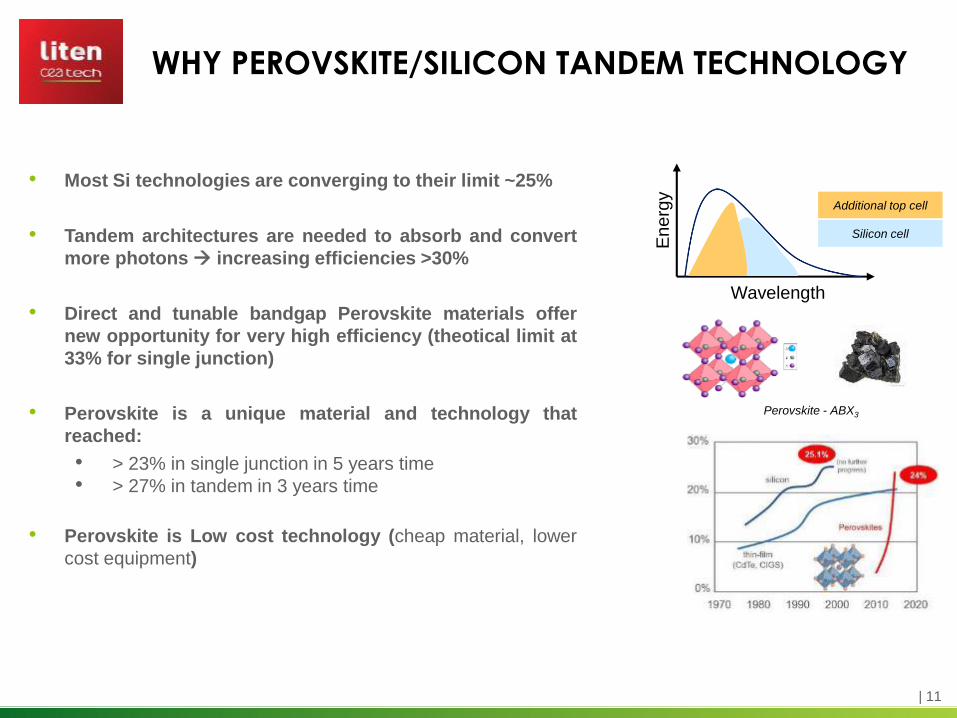
WHY PEROVSKITE/SILICON TANDEM TECHNOLOGY
• Most Si technologies are converging to their limit ~25%
• Tandem architectures are needed to absorb and convert
more photons increasing efficiencies >30%
• Direct and tunable bandgap Perovskite materials offer
new opportunity for very high efficiency (theotical limit at
33% for single junction)
• Perovskite is a unique material and technology that
reached:
• > 23% in single junction in 5 years time
• > 27% in tandem in 3 years time
• Perovskite is Low cost technology (cheap material, lower
cost equipment)
Perovskite - ABX3
En
erg
y
Wavelength
Silicon cell
Additional top cell
| 12
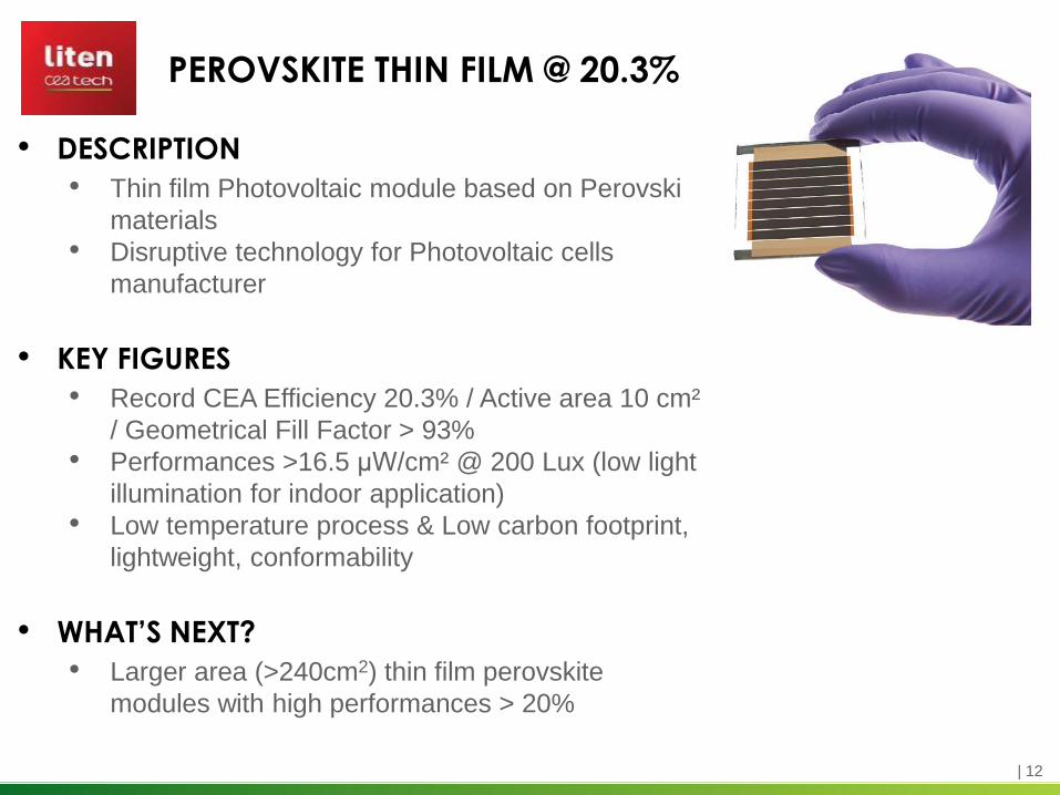
• DESCRIPTION
• Thin film Photovoltaic module based on Perovskite
materials
• Disruptive technology for Photovoltaic cells
manufacturer
• KEY FIGURES
• Record CEA Efficiency 20.3% / Active area 10 cm²
/ Geometrical Fill Factor > 93%
• Performances >16.5 μW/cm² @ 200 Lux (low light
illumination for indoor application)
• Low temperature process & Low carbon footprint,
lightweight, conformability
• WHAT’S NEXT?
• Larger area (>240cm2) thin film perovskite
modules with high performances > 20%
PEROVSKITE THIN FILM @ 20.3%
| 13
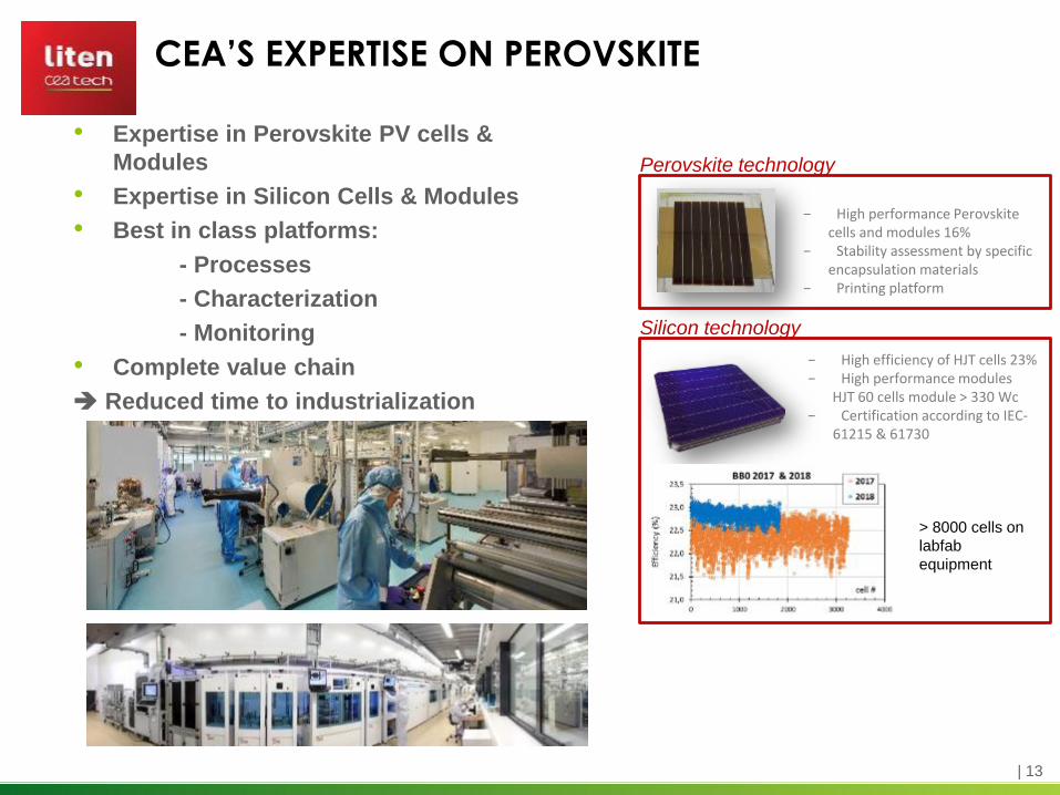
• Expertise in Perovskite PV cells &
Modules
• Expertise in Silicon Cells & Modules
• Best in class platforms:
- Processes
- Characterization
- Monitoring
• Complete value chain
Reduced time to industrialization
CEA’S EXPERTISE ON PEROVSKITE
On Industrial Pilot
Line
> 8000 cells on
labfab
equipment
− High efficiency of HJT cells 23%− High performance modules
HJT 60 cells module > 330 Wc− Certification according to IEC-
61215 & 61730
− High performance Perovskite cells and modules 16%
− Stability assessment by specific encapsulation materials
− Printing platform
Perovskite technology
Silicon technology
| 14
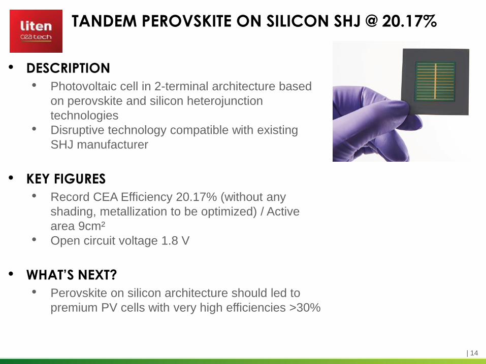
• DESCRIPTION
• Photovoltaic cell in 2-terminal architecture based
on perovskite and silicon heterojunction
technologies
• Disruptive technology compatible with existing
SHJ manufacturer
• KEY FIGURES
• Record CEA Efficiency 20.17% (without any
shading, metallization to be optimized) / Active
area 9cm²
• Open circuit voltage 1.8 V
• WHAT’S NEXT?
• Perovskite on silicon architecture should led to
premium PV cells with very high efficiencies >30%
TANDEM PEROVSKITE ON SILICON SHJ @ 20.17%

| 15
CEA’S ROADMAP TOWARDS TANDEM
15
Perovskite :
18%, 12 mm²
16% 10cm², 1000h 1SUN
Tandem Si/PK :
Cells > 30%, 243 cm²
Modules: P > 500W – 72 cells
Qualification = 3xIECTandem Si/PK :
> 27%, 243 cm²
Modules IEC qualification
2018 20242020
Silicon technologies :
HMJ 21%
HJT 23%
Tandem Si/PK :
> 25%, 25 cm²
Module BOM development

| 16
• 22.8%
• with industrial
processes
PV CELLS RECORD RESULTS !
• 24.4%
• in production
• 20.3%
• Active area
10 cm² /
Geometrical
Fill Factor >
93%
• 20.17%
• without any
shading,
metallization to be
optimized / Active
area 9cm²
Re
co
rd E
ffic
ien
cy
| 17
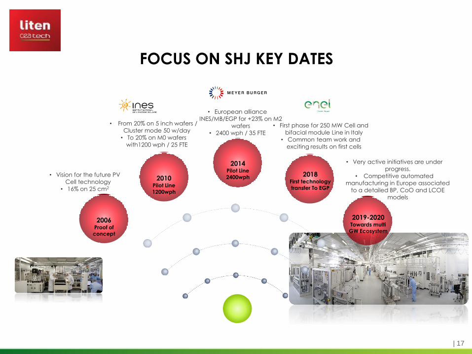
FOCUS ON SHJ KEY DATES
2006Proof of concept
2010Pilot Line 1200wph
2014Pilot Line 2400wph 2018
First technology transfer To EGP
2019-2020Towards multi GW Ecosystem
• Vision for the future PV
Cell technology
• 16% on 25 cm2
• From 20% on 5 inch wafers /
Cluster mode 50 w/day
• To 20% on M0 wafers
with1200 wph / 25 FTE
• First phase for 250 MW Cell and
bifacial module Line in Italy
• Common team work and
exciting results on first cells
• Very active initiatives are under
progress.
• Competitive automated
manufacturing in Europe associated
to a detailed BP, CoO and LCOE
models
• European alliance
INES/MB/EGP for +23% on M2
wafers
• 2400 wph / 35 FTE

| 18
CEA/LITEN-INES
The European R&D center of reference for PV SHJ
and Tandem development : Lets join forces

| 1919
PV MODULES CHANGING THE GAME
GBS (BB/BBL)1• Transparent BS
• Efficiency or power (wafer
size M2, M4, M6, M12…)
• HC cells
• Shingling
• Glass coatings / Soiling
SHJ Moduling : for simple integration
GG (BB/BBL)2• CTM improvements
• Certified module BOM (ECA,
glass, JB)
• Specific equipments
• Reliability• Specific characterization
ECA
SWCT
| 20
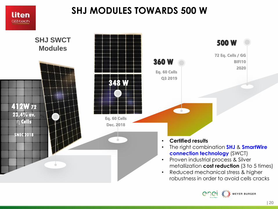
SHJ MODULES TOWARDS 500 W
%
412W 72
23,4% av.
ɳ Cells
SNEC 2018
348 W
Eq. 60 Cells
Q3 2019
360 W72 Eq. Cells / GG
BIFI10
2020
500 W
Eq. 60 Cells
Dec. 2018
• Certified results• The right combination SHJ & SmartWire
connection technology (SWCT)• Proven industrial process & Silver
metallization cost reduction (3 to 5 times)• Reduced mechanical stress & higher
robustness in order to avoid cells cracks
SHJ SWCT
Modules
| 2121
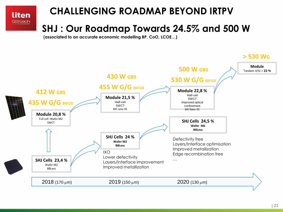
CHALLENGING ROADMAP BEYOND IRTPV
SHJ : Our Roadmap Towards 24.5% and 500 W(associated to an accurate economic modelling BP, CoO, LCOE…)
412 W GBS
435 W G/G BiFi10
> 530 Wc
Module 20,8 %Full cell -Wafer M2
SWCT
Module 21,5 %Half-cell
SWCTBifi ratio 95
ModuleTandem X/Si > 23 %
SHJ Cells 23,4 %Wafer M2
BBLess
SHJ Cells 24 %Wafer M2
BBLess
IXOLower defectivityLayers/Interface improvementImproved metallization
SHJ Cells 24,5 %Wafer M6
BBLess
Defectivity freeLayers/Interface optimisationImproved metallizationEdge recombination free…
Module 22,8 %Half-cell
SWCT
Improved optical
confinement Bifi Ratio 95
430 W GBS
455 W G/G BiFi10
500 W GBS
530 W G/G BiFi10
2018 (170 mm) 2019 (150 mm) 2020 (130 mm)

| 2222
PV SOLAR CELLS INNOVATIVE TECHNOLOGIES
A NICE BRIDGE FOR LOWER LCOE PV INSTALLATIONS
HJT technology combines several key benefits for a new European eco-system
1. Power potential well above announced public roadmaps
2. Improved energy yield due to T coefficient and bifaciality
3. Adapted to thin wafer leading to cost reduction and LCA benefit
ENEL GREEN POWER-3SUN
PANASONIC-GS SOLAR
PANASONIC-TESLA
HEVEL SOLAR
ECOSOLIFER
JINERGY
REC
CIE
…
Industrialization of HJT technology at GW scale associated to a development Roadmap towards Tandem for 30%
and Collecting additional data regarding SHJ production yield benefits at the MW scale including new features like
tracking, cleaning…
For a multiple GWAnnual MarketA reliable high
efficiency bifacial
module is ready
| 23
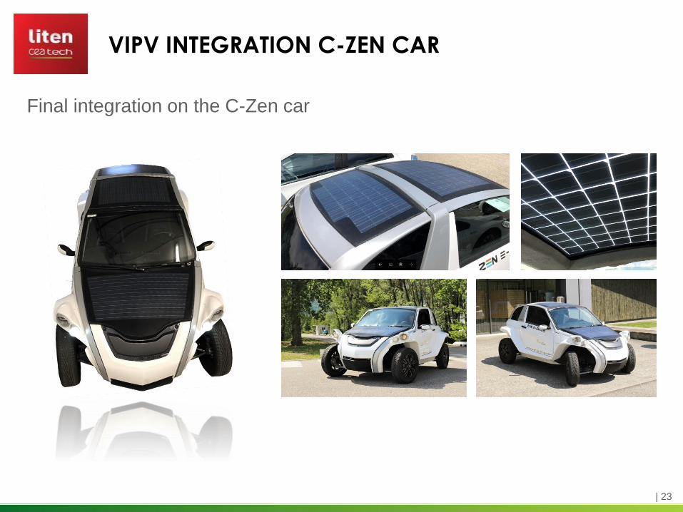
Final integration on the C-Zen car
VIPV INTEGRATION C-ZEN CAR

| 24
Electrical and imaging characterization
• Total peak power: > 210 Wp STC.
• Active area: 1,3 m²
Global efficiency: 16 %
Estimated PV gain: > 1 600 km / year in Chambéry1
Back Roof Front Roof Hood
Electroluminescence
Power STC 54 W 85 W 73 W
1Static estimation based on PVGIS 5 simulation tool, including all losses
VIPV INTEGRATION C-ZEN CAR
| 25
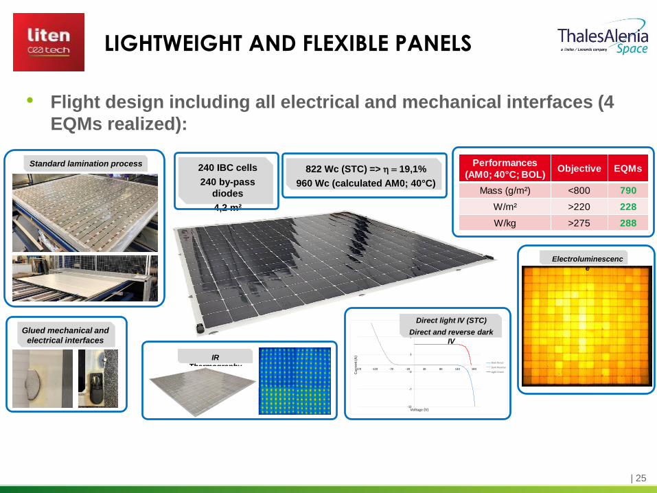
LIGHTWEIGHT AND FLEXIBLE PANELS
• Flight design including all electrical and mechanical interfaces (4
EQMs realized):
Standard lamination process
Glued mechanical and
electrical interfaces
-12
-7
-2
3
8
-170 -120 -70 -20 30 80 130 180
Cu
rre
nt
(A)
Voltage (V)
Dark Direct
Dark Reverse
Light Direct
240 IBC cells
240 by-pass
diodes
4,2 m²
822 Wc (STC) => = 19,1%
960 Wc (calculated AM0; 40°C)
Electroluminescenc
e
Direct light IV (STC)
Direct and reverse dark
IV
IR
Thermography
Performances
(AM0; 40°C; BOL)Objective EQMs
Mass (g/m²) <800 790
W/m² >220 228
W/kg >275 288

| 26
STRATOBUS : NEXT STEPS
•Successful development of a specific module designed for the
StratobusTM airship:
•Lightweight <800 gm/m²
•High efficiency >220 W/m² (AM0; 40°C)
•Large scale >4m² with 1 by-pass diode per cell.
• Integrated electrical and mechanical interfaces.
•Terrestrial and low cost fabrication processes.
•Resistance to stratospheric conditions: temperature, UV, Ozone, wind….
• PVA EQMs flight tests scheduled in 2020 on a small scale airship.
• Further developments will focus on the PVA/envelop interface.
• Integration of this technology on the StratobusTM PFM for its first
flight in 2022/2023.
| 27
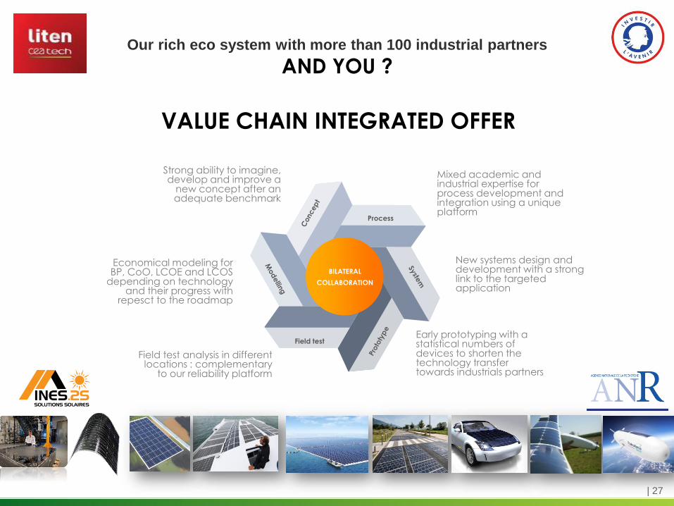
Our rich eco system with more than 100 industrial partners
AND YOU ?
Process
Field test
Strong ability to imagine, develop and improve a
new concept after an adequate benchmark
VALUE CHAIN INTEGRATED OFFER
BILATERAL
COLLABORATION
Economical modeling for BP, CoO, LCOE and LCOS
depending on technology and their progress with
repesct to the roadmap
Field test analysis in different locations : complementary
to our reliability platform
Mixed academic and industrial expertise for process development and integration using a unique platform
New systems design and development with a strong link to the targeted application
Early prototyping with a statistical numbers of devices to shorten the technology transfer towards industrials partners
| 2828
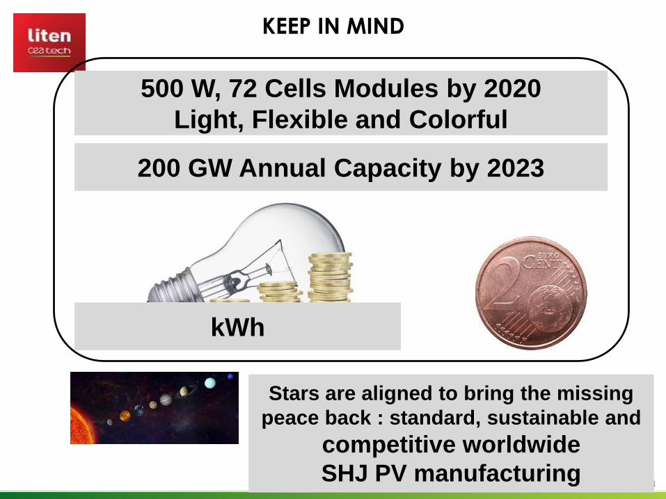
kWh
200 GW Annual Capacity by 2023
500 W, 72 Cells Modules by 2020
Light, Flexible and Colorful
Stars are aligned to bring the missing
peace back : standard, sustainable and
competitive worldwide
SHJ PV manufacturing
KEEP IN MIND
| 29
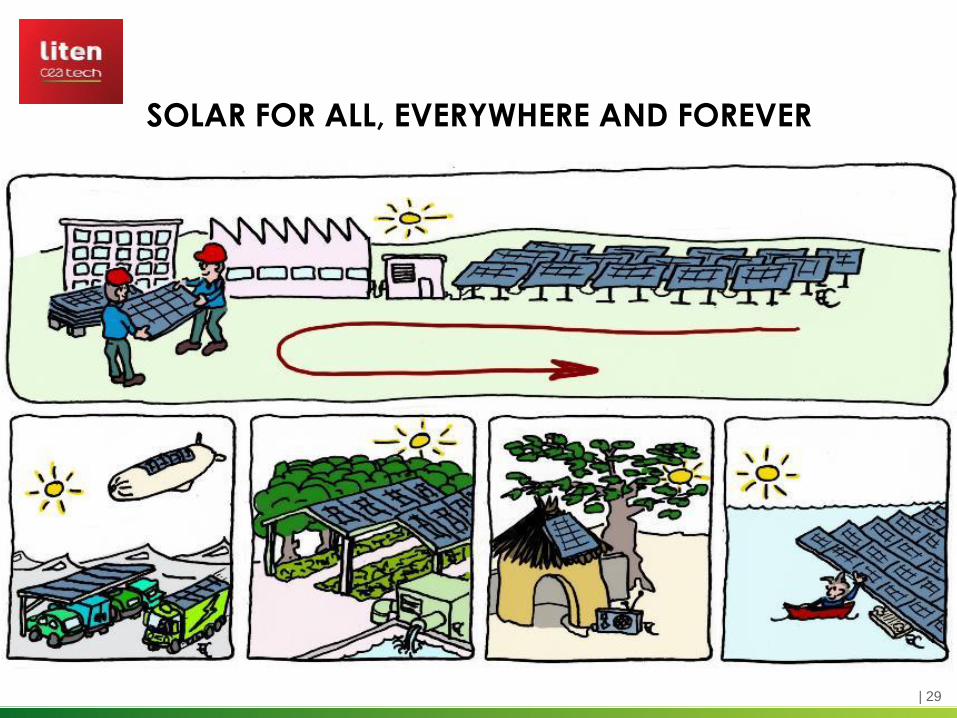
SOLAR FOR ALL, EVERYWHERE AND FOREVER
Honda R&D Co., Ltd. All Rights Reserved
Honda R&D Co., Ltd. Automobile Center
15th October, 2019
Eisuke Kimura
Honda R&D Co., Ltd. All Rights Reserved
Global warming
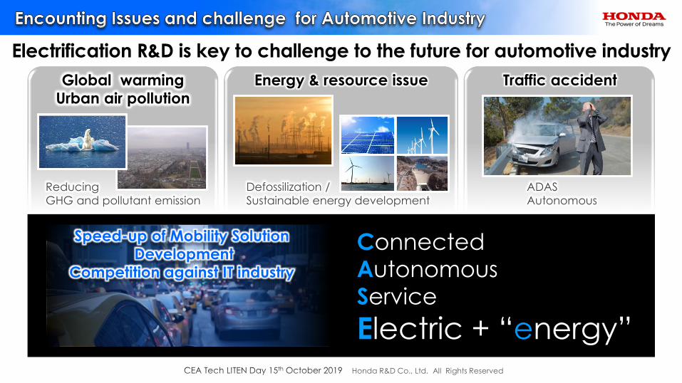
Urban air pollution
Traffic accidentEnergy & resource issue
Defossilization /
Sustainable energy development
Electrification R&D is key to challenge to the future for automotive industry
Reducing
GHG and pollutant emission
ADAS
Autonomous
Connected
Autonomous
Service
Electric + “energy”
Speed-up of Mobility Solution
Development
Competition against IT industry
Honda R&D Co., Ltd. All Rights Reserved
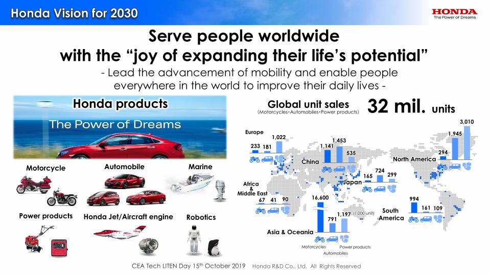
32 mil. units
233 181
1,022
67 41 90
1,1411,453
535
7911,197
16,600
165724
299
994
161 109
294
1,945
3,010
Honda Jet/Aircraft engine(1,000 unit)
Motorcycle
Power products
Marine
Robotics
Automobile
Honda products Global unit sales (Motorcycles・Automobiles・Power products)
China North America
South
America
Africa &
Middle East
Japan
Asia & Oceania
Europe
Automobiles
Motorcycles Power products
Serve people worldwide
with the “joy of expanding their life’s potential”- Lead the advancement of mobility and enable people
everywhere in the world to improve their daily lives -

Honda R&D Co., Ltd. All Rights Reserved
IPCC CO2 reduction target2DS Scenario
Go shifting to WB2DS*Source: IPCC AR5 WG3 SPM Fig. SPM.4
*Trend line of 1.5DS is drawn from IPCC SR1.5 information
1960 1980 2000 2020 2040 2060 2080 21000.00
0.25
0.50
0.75
1.00
1.25
1.50
1.75
2.00
Wa
rmin
g r
ela
tive
to
1850
-1900(℃
)
Current warming rate
Human-induced
warming
Climate response
Uncertainty for
1.5℃-consistentpathway
Observedwarming
RCP8.5
RCP6.0
RCP4.5
〉1000 ppm CO2eqA
nn
ua
l G
HG
Em
issi
on
s(G
tCO
2e
q/y
r)90th Percentile
Median
10th Percentile
GHG Emission Pathways 2000-2100 All AR5 Scenarios
-20
0
20
40
60
80
100
120
140
2000 2020 2040 2060 2080 2100 2100
2DS (450ppm)1.5DS
2050y -100%
WB2DS2DS
RCP2.6
720-1000 ppm CO2eq
580-720 ppm CO2eq
530-580 ppm CO2eq
480-530 ppm CO2eq
430-480 ppm CO2eq
Full AR5 Database Range
Ba
selin
e
※WB2DS=Well Below 2 Degree Scenario
(Scenario to hold increase in global temperature to well below 2°C)
Honda R&D Co., Ltd. All Rights Reserved
BEV/PHEV-based environmental
requirements scenario<IEA : WB2DS>
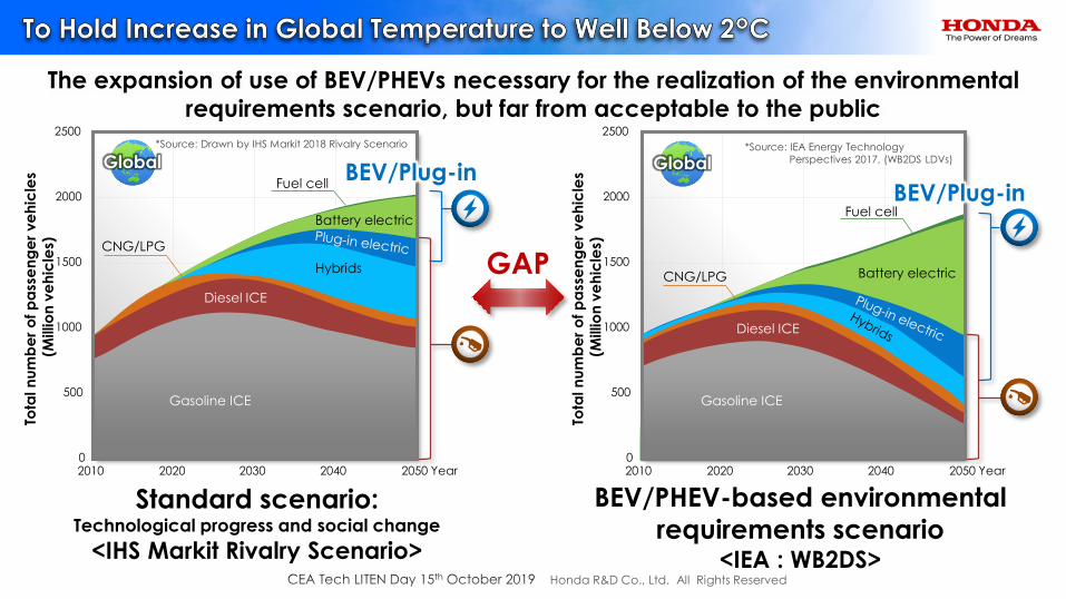
The expansion of use of BEV/PHEVs necessary for the realization of the environmental
requirements scenario, but far from acceptable to the public
Standard scenario: Technological progress and social change
<IHS Markit Rivalry Scenario>
GAP
Gasoline ICE
Diesel ICE
Battery electric
Tota
l n
um
be
r o
f p
ass
en
ge
r ve
hic
les
(Millio
n v
eh
icle
s)
Gasoline ICE
Diesel ICE
Hybrids
Battery electric
2010 2020 2030 2040 2050 Year
2000
1500
1000
500
02010 2020 2030 2040 2050 Year
2500
*Source: IEA Energy Technology
Perspectives 2017, (WB2DS LDVs)
*Source: Drawn by IHS Markit 2018 Rivalry Scenario
Gasoline ICE
Diesel ICE
Battery electric
Fuel cell
CNG/LPG
CNG/LPG
Fuel cell
Tota
l n
um
be
r o
f p
ass
en
ge
r ve
hic
les
(Millio
n v
eh
icle
s)
2000
1500
1000
500
0
2500
BEV/Plug-inBEV/Plug-in
Global Global

Honda R&D Co., Ltd. All Rights Reserved
Necessary reduction in CO2 emissions for achievement of WB2DS in BEV/PHEV-based
environmental requirement scenario
Necessary ratio of renewable fuels for achievement of WB2DS in standard scenario
The realization of WB2DS is a high hurdle no matter the scenarioR
ate
of a
pp
lic
atio
n o
f
ren
ew
ab
le f
ue
ls (
%)
発電時
CO
2排出量
[g-C
O2
/MJ]
Status quo
WB2DS
60
30
-30
0
90
120
150
60
40
02020 2030 20502040
20
80
100
Status quo
Ratio of renewable fuels80% or more
WB2DS
Ca
rbo
n e
mis
sio
ns
du
rin
g g
en
era
tio
n
[g-C
O2/M
J]
Zero emissions of CO2
during generation
Challenge for
society as a wholeChallenge for
society as a whole
2060 Year 2020 2030 20502040 2060 Year
*Source: This analysis is based on the Mobility model developed by the International Energy Agency, ©OECA/IEA2017,
but the resulting analysis has been prepared by Honda and does not necessarily reflect the views of the International Energy Agency
Global Global
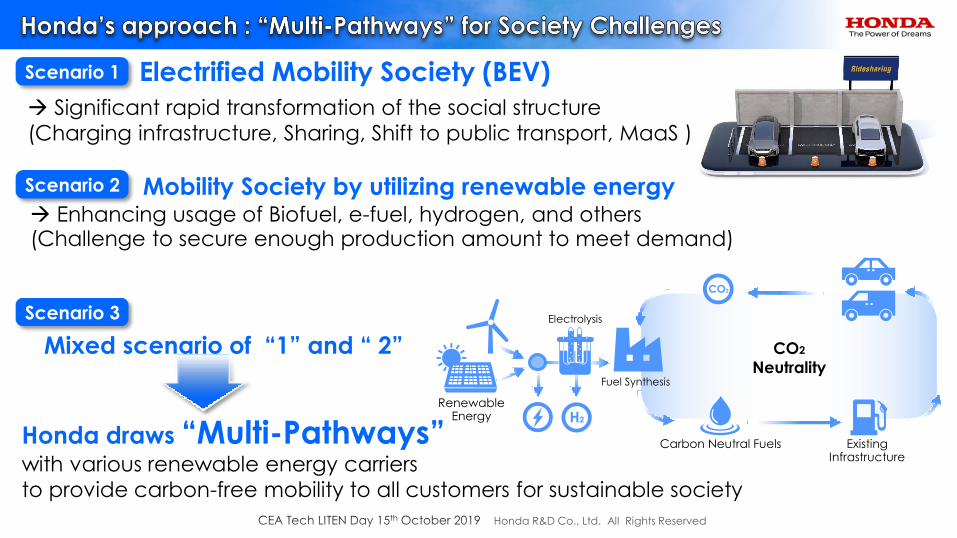
Honda R&D Co., Ltd. All Rights Reserved
Significant rapid transformation of the social structure
(Charging infrastructure, Sharing, Shift to public transport, MaaS )
Enhancing usage of Biofuel, e-fuel, hydrogen, and others
Honda draws “Multi-Pathways” with various renewable energy carriers
to provide carbon-free mobility to all customers for sustainable society
H2
CO2
Neutrality
ExistingInfrastructure
Carbon Neutral Fuels
RenewableEnergy
Fuel Synthesis
CO2
Electrolysis
Scenario 1
Scenario 2
Scenario 3
Electrified Mobility Society (BEV)
Mobility Society by utilizing renewable energy
(Challenge to secure enough production amount to meet demand)
Mixed scenario of “1” and “ 2”

Honda R&D Co., Ltd. All Rights Reserved
“Connect electrified powertrain product with renewable energy carriers”
FCV PHEVBEV
Electrolysis
Synthetic fuel
(e-fuel)
+
Biofuel
CO2CO2
captureH2
Renewable energies
BiomassRenewable
electric power
Electric
power
HydrogenH2
HEV ICE
JET
Energy
carrier
Right product (power unit) in the Right place for the Right application by providing the Right energy carrier
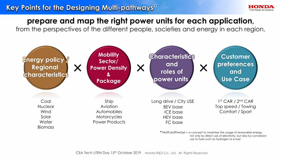
Honda R&D Co., Ltd. All Rights Reserved
*
* Multi-pathways = a concept to maximize the usage of renewable energy
not only by direct use of electricity, but also by conversion
use to fuels such as hydrogen or e-fuel
CoalNuclear
WindSolar
WaterBiomass
ShipAviation
AutomobilesMotorcycles
Power Products
Long drive / City USE
× × ×
1st CAR / 2nd CARTop speed / Towing
Comfort / Sport
Energy policy /
Regional
characteristics
MobilitySector/
Power Density&
Package
Characteristics
and
roles of
power units
Customer
preferences
and
Use Case
BEV baseICE base
HEV baseFC base
prepare and map the right power units for each application,from the perspectives of the different people, societies and energy in each region.
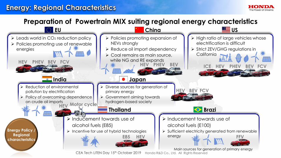
Honda R&D Co., Ltd. All Rights Reserved
HEV FCV
Motor cycle
ICE HEV PHEV BEV FCVHEV PHEV BEVHEV PHEV BEV FCV
HEV
BEV
Japan
USChina
Brazi
EU
India
Thailand
Preparation of Powertrain MIX suiting regional energy characteristics
Energy Policy /
Regional
characteristics
Leads world in CO2 reduction policy
Policies promoting use of renewable energies
Policies promoting expansion of NEVs strongly
Reduce oil import dependency
Coal remains as main source, while NG and RE expands
High ratio of large vehicles whose electrification is difficult
Strict ZEV/GHG regulations in California
Diverse sources for generation of
primary energy
Government aiming towards
hydrogen-based society
Inducement towards use of
alcohol fuels (E85)
Incentive for use of hybrid technologies
Inducement towards use of
alcohol fuels (E100)
Sufficient electricity generated from renewable
energy
Reduction of environmental
pollution by electrification
Policy of overcoming dependence
on crude oil imports
FFVE85 HEV
Main sources for generation of primary energy
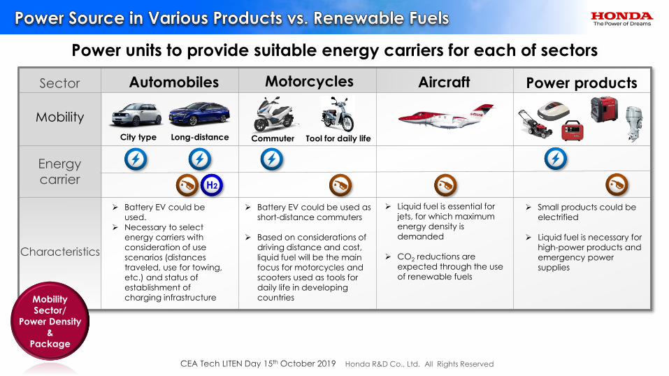
Honda R&D Co., Ltd. All Rights Reserved
H2
Power units to provide suitable energy carriers for each of sectors
Motorcycles
Tool for daily life
Automobiles
City type Long-distance
Aircraft Power productsSector
Energy carrier
Characteristics
Commuter
Battery EV could be
used.
Necessary to select
energy carriers with
consideration of use
scenarios (distances
traveled, use for towing,
etc.) and status of
establishment of
charging infrastructure
Battery EV could be used as
short-distance commuters
Based on considerations of
driving distance and cost,
liquid fuel will be the main
focus for motorcycles and
scooters used as tools for
daily life in developing
countries
Liquid fuel is essential for
jets, for which maximum
energy density is
demanded
CO2 reductions are
expected through the use
of renewable fuels
Small products could be
electrified
Liquid fuel is necessary for
high-power products and
emergency power
supplies
Mobility
Mobility
Sector/
Power Density
&
Package
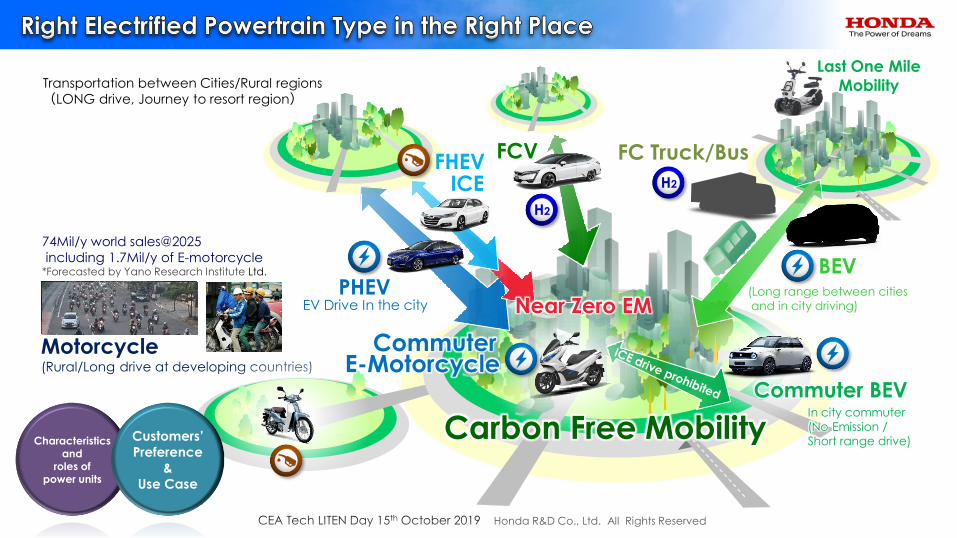
Honda R&D Co., Ltd. All Rights Reserved
FC Truck/Bus
Motorcycle(Rural/Long drive at developing countries)
74Mil/y world sales@2025
including 1.7Mil/y of E-motorcycle*Forecasted by Yano Research Institute Ltd.
Transportation between Cities/Rural regions
(LONG drive, Journey to resort region)
(Long range between cities
and in city driving)
BEV
Commuter BEVIn city commuter
(No Emission /
Short range drive)
FCV
Carbon Free Mobility
CommuterE-Motorcycle
Characteristicsand
roles ofpower units
Customers’
Preference
&
Use Case
EV Drive In the cityPHEV
Near Zero EM
ICEFHEV
Last One Mile
Mobility
H2
H2
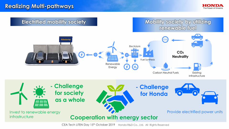
Honda R&D Co., Ltd. All Rights Reserved
Electrified mobility society Mobility society by utilizing
renewable fuel
- Challenge
for society
as a whole
- Challenge
for Honda
H2
CO2
Neutrality
Existing
Infrastructure
Carbon Neutral Fuels
Renewable
Energy
Fuel Synthesis
CO2
Electrolysis
Cooperation with energy sectorProvide electrified power unitsInvest to renewable energy
infrastructure
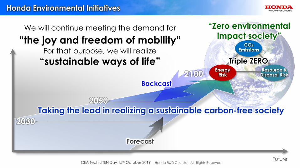
Honda R&D Co., Ltd. All Rights ReservedFuture
2100
2030
CO2
Emissions
Resource &Disposal Risk
EnergyRisk
Triple ZERO
2050
We will continue meeting the demand for
“the joy and freedom of mobility”For that purpose, we will realize
“sustainable ways of life”
“Zero environmental
impact society”
Backcast
Forecast
Taking the lead in realizing a sustainable carbon-free society

Honda R&D Co., Ltd. All Rights Reserved
Focus our efforts on further enhancing HEV performance
as well as on PHEV and zero emission vehicles
2020 20302010
ICE
PHEV
ZEV
2019
CO
2(g
/km)
0
Thermal efficiencyenhancement technology
ZERO emission
technology
FIT EV CLARITY EVFCX CLARITY Honda eCLARITY FCV
ACCORD PHEV
CLARITY PHEV
CVT series
Electric motor drive efficiencyenhancement technology
HEVACCORD HEV
INSIGHT HEV
CR-V HEV
STEP WGN HEV
ODESSY HEV
Year
Global
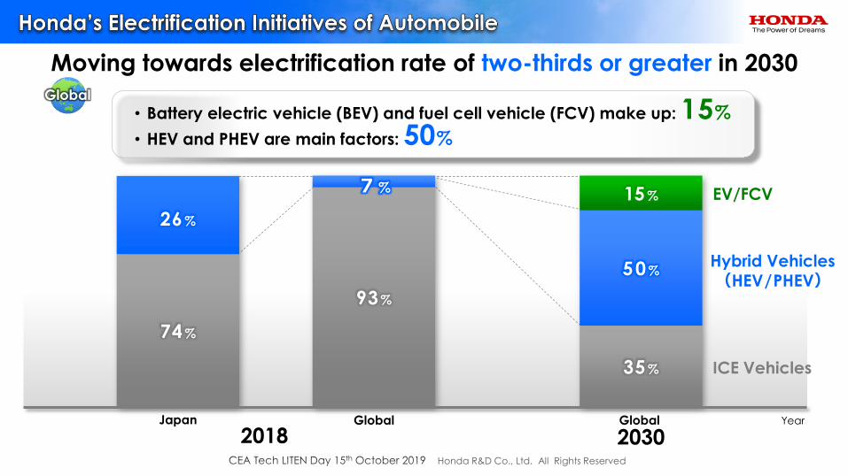
Honda R&D Co., Ltd. All Rights Reserved
• Battery electric vehicle (BEV) and fuel cell vehicle (FCV) make up: 15%
• HEV and PHEV are main factors: 50%
Moving towards electrification rate of two-thirds or greater in 2030
50 %
35 %
15 %
Hybrid Vehicles(HEV/PHEV)
EV/FCV
ICE Vehicles
74 %
26 %
93 %
7%
2018 2030Japan Global Global Year
Global

Honda R&D Co., Ltd. All Rights Reserved
Sophisticated and light driving feel with motor drive
Light acceleration and response by high power motor
Enjoy the DriveTime
Powerful & Smooth
Ac
ce
lera
tio
nG
NON HYBRID
Parallel HybridSeries Hybrid
DRIVE DRIVE DRIVE
Operates as an EV when driving inurban areas
Realizes strong acceleration by drivingthe generator motor using engine power
During high-speed cruising, the engine directly drives the tires
ClutchTireEngine
Battery
Tractionmotor
Generatormotor
ClutchTireEngine
Battery
Tractionmotor
Generatormotor
ClutchTireEngine
Battery
Tractionmotor
Generatormotor
Honda
Specific
Clutchengaged
Enginestopped
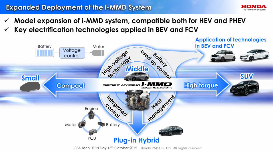
Honda R&D Co., Ltd. All Rights Reserved
Model expansion of i-MMD system, compatible both for HEV and PHEV
Key electrification technologies applied in BEV and FCV
Small SUV
Motor Battery
PCU
Engine
Battery MotorVoltage
control
Application of technologiesin BEV and FCV
Plug-in Hybrid
Compact High torque
Middle
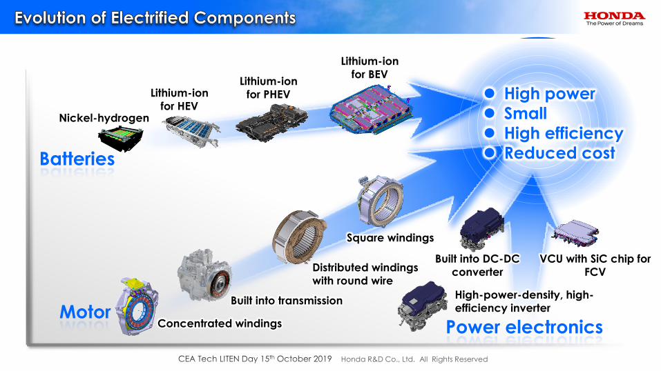
Honda R&D Co., Ltd. All Rights Reserved
Distributed windings
with round wire
Batteries
MotorConcentrated windings
Square windings
Built into transmission
Nickel-hydrogen
Lithium-ion
for HEV
Lithium-ion
for PHEV
Lithium-ion
for BEV
VCU with SiC chip for
FCV
Built into DC-DC
converter
Power electronics
High-power-density, high-
efficiency inverter
High power
Small
High efficiency
Reduced cost

Honda R&D Co., Ltd. All Rights Reserved
Effective BEV launch by sharing same platform with 3 types of electrified power-train
Honda eRealization of electrification value with dedicated platformStart of EV-centered business
Initial phase
Introduction phase
Expansion phase
Offering values for wider range of customers by EV architecture
BEV-dedicated
car
BEV-derived model
理念 VE-1X-NV concept
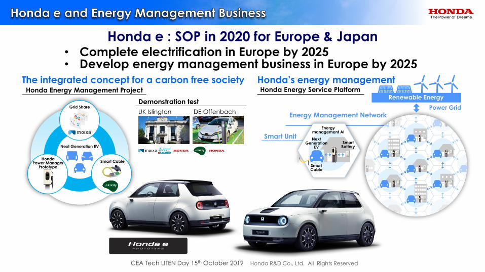
Honda R&D Co., Ltd. All Rights Reserved
Honda Energy Management Project Honda Energy Service Platform
Honda’s energy managementThe integrated concept for a carbon free society
Energy Management NetworkPower Grid
Demonstration test
UK Islington DE Offenbach
Renewable Energy
Smart Unit
HondaPower Manager
Prototype
Grid Share
Smart Cable
Next Generation EV
Honda e : SOP in 2020 for Europe & Japan• Complete electrification in Europe by 2025• Develop energy management business in Europe by 2025
SmartCable
Energymanagement AI
SmartBattery
NextGeneration
EV
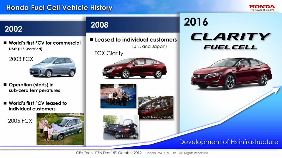
Honda R&D Co., Ltd. All Rights Reserved
2003 FCX
World’s first FCV for commercial
use (U.S.-certified)
Operation (starts) in
sub-zero temperatures
World’s first FCV leased to
individual customers
2002
2005 FCX
Leased to individual customers
FCX Clarity
2008
(U.S. and Japan)
Scott Niedermayer
Jamie Lee Curtis
2016
Development of H2 infrastructure
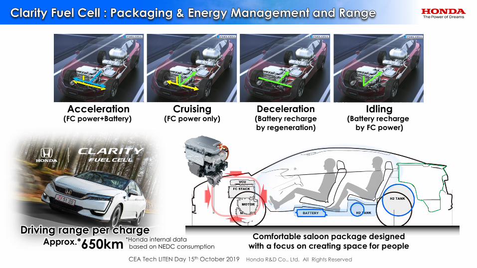
Honda R&D Co., Ltd. All Rights Reserved
Driving range per chargeApprox.*650km
*Honda internal data
based on NEDC consumption
Comfortable saloon package designed
with a focus on creating space for people
Acceleration(FC power+Battery)
Cruising(FC power only)
Deceleration(Battery recharge
by regeneration)
Idling(Battery recharge
by FC power)
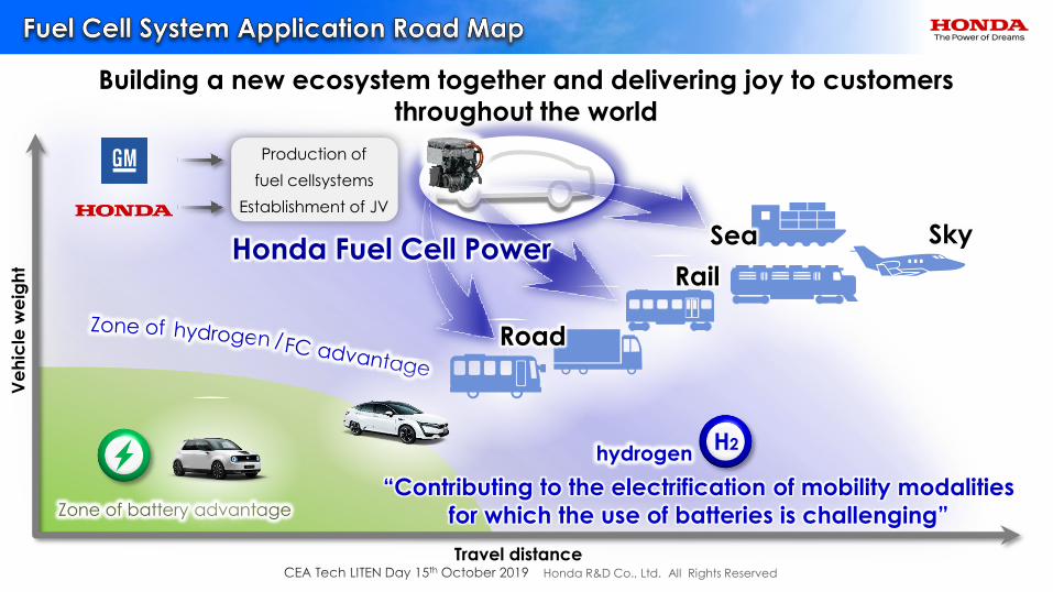
Honda R&D Co., Ltd. All Rights Reserved
Ve
hic
le w
eig
ht
Travel distance
Building a new ecosystem together and delivering joy to customers
throughout the world
hydrogen
Zone of battery advantage
H2
Production of
fuel cellsystems
Establishment of JV
Honda Fuel Cell Power
Road
Sea Sky
Rail
“Contributing to the electrification of mobility modalities
for which the use of batteries is challenging”

Honda R&D Co., Ltd. All Rights Reserved
Use the standardized battery pack as an exchangeable power source to resolve charging issues
Generateelectricity using natural energy
Useelectricity for compact mobility,
household appliances, and so on
Mobile Power Pack with electric-powered mobility
= Travel by clean energy
You can exchange it right away, without waiting,
when you need it and where you need it
Honda Mobile Power Pack
You can use electricity when you need it and where you need it,
without having to worry about power outages
Honda Mobile Power Pack Charge & Supply Concept
"Local Production for Local Consumption" makes
use of energy that can be harvested at that
location
Renewable Energy
Mobile Power Pack
Exchanger Concept
Mobile Power Pack Charge
and Supply
Expandable Concept
Get Connectedwith electricity anytime, anywhereHonda Mobile Power Pack Exchanger Concept
Field test at Miyakojima @ Japan
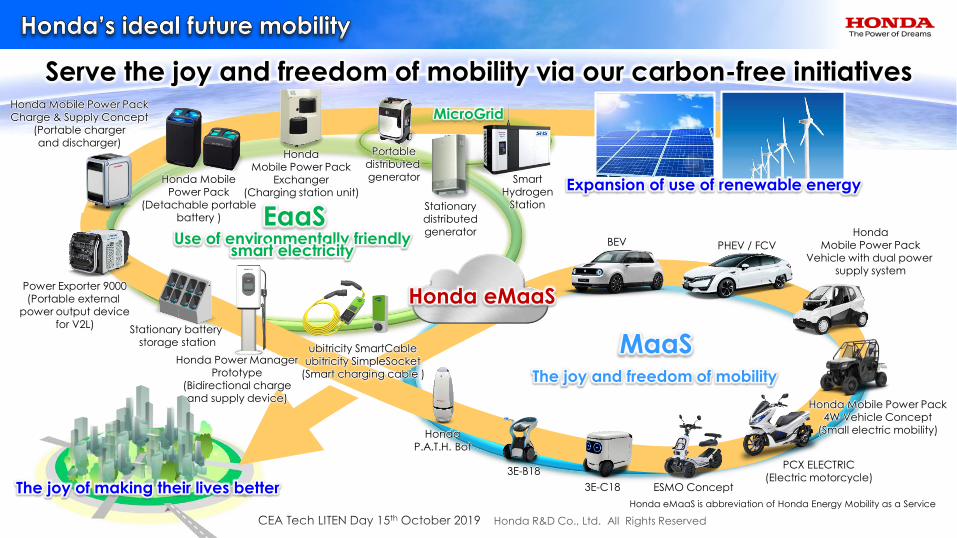
Honda R&D Co., Ltd. All Rights Reserved
Serve the joy and freedom of mobility via our carbon-free initiatives
3E-B18
HondaP.A.T.H. Bot
MicroGrid
EaaSBEV
ESMO Concept3E-C18
MaaS
PHEV / FCV
Honda eMaaS
Stationarydistributedgenerator
Honda Mobile Power Pack
(Detachable portable battery )
HondaMobile Power Pack
Exchanger(Charging station unit)
SmartHydrogen
Station
Honda Mobile Power PackCharge & Supply Concept
(Portable charger
and discharger)Portable
distributed
generator
Use of environmentally friendly smart electricity
Stationary battery storage station
Honda Power ManagerPrototype
(Bidirectional charge and supply device)
The joy of making their lives better
Power Exporter 9000(Portable external
power output devicefor V2L)
ubitricity SmartCableubitricity SimpleSocket
(Smart charging cable )
Expansion of use of renewable energy
PCX ELECTRIC(Electric motorcycle)
Honda Mobile Power Pack4W-Vehicle Concept
(Small electric mobility)
The joy and freedom of mobility
HondaMobile Power Pack
Vehicle with dual power supply system
Honda eMaaS is abbreviation of Honda Energy Mobility as a Service

Honda R&D Co., Ltd. All Rights Reserved
Pursuit customers’ smiles everywhere in the world“Right power units” with “right energy carriers”
to “Right sector”, “right place” & “right use case”
With Honda electrified technologies
For Carbon Free Society

Honda R&D Co., Ltd. All Rights Reserved
TECH DAYSINNOVATION FOR INDUSTRY
LITEN DAYOCTOBER 15, 2019
KEIO PLAZA HOTEL, TOKYO
CEA Tech Days | Didier Jamet | 15/10/2019
BATTERIES & FUEL CELLS: BENCHMARK, CHARACTERIZATION,
MULTI-SCALE MODELING FOR IMPROVEMENT OF
PERFORMANCE, DURABILITY AND SAFETY
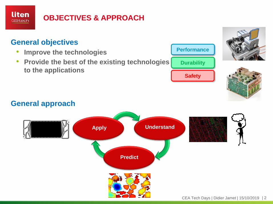
| 2CEA Tech Days | Didier Jamet | 15/10/2019
General objectives
• Improve the technologies
• Provide the best of the existing technologies
to the applications
OBJECTIVES & APPROACH
Performance
Durability
Safety
General approach
UnderstandApply
Predict
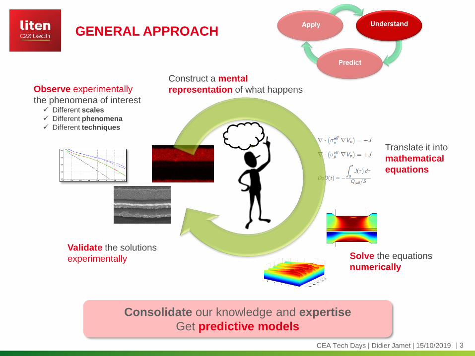
| 3CEA Tech Days | Didier Jamet | 15/10/2019
GENERAL APPROACH
Consolidate our knowledge and expertise
Get predictive models
Observe experimentally
the phenomena of interest Different scales
Different phenomena
Different techniques
Construct a mental
representation of what happens
Translate it into
mathematical
equations
Solve the equations
numerically
Validate the solutions
experimentally

| 4CEA Tech Days | Didier Jamet | 15/10/2019
GENERAL APPROACH
Get the response of a system in unknown conditions
Accelerate the developments
Known conditions Unknown conditions of interest
Predictive model
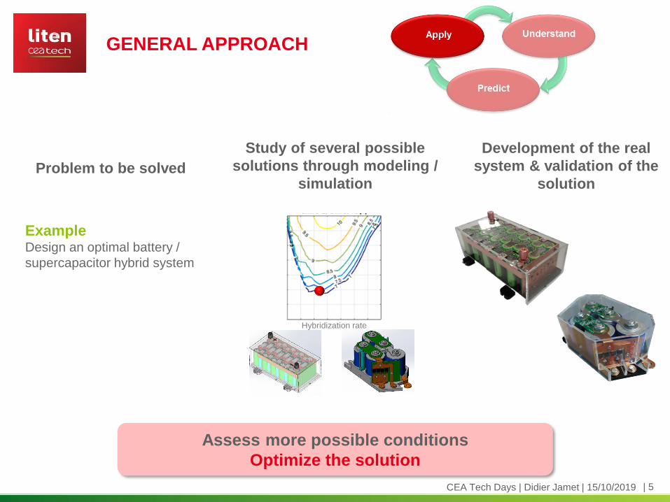
| 5CEA Tech Days | Didier Jamet | 15/10/2019
GENERAL APPROACH
Assess more possible conditions
Optimize the solution
Problem to be solved
Study of several possible
solutions through modeling /
simulation
Development of the real
system & validation of the
solution
ExampleDesign an optimal battery /
supercapacitor hybrid system
Hybridization rate
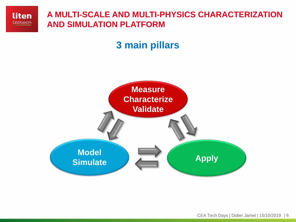
| 6CEA Tech Days | Didier Jamet | 15/10/2019
A MULTI-SCALE AND MULTI-PHYSICS CHARACTERIZATION
AND SIMULATION PLATFORM
Measure
Characterize
Validate
ApplyModel
Simulate
3 main pillars

| 7CEA Tech Days | Didier Jamet | 15/10/2019
EXPERIMENTAL CHARACTERIZATION
Of all the electro-chemical storage technologies
With client-specific experimental protocols
With standardized experimental protocols for inter-
comparison purposes
Put into perspective into a CEA-LITEN data base
Added value thanks to advanced analyses and modeling
Performance evaluation
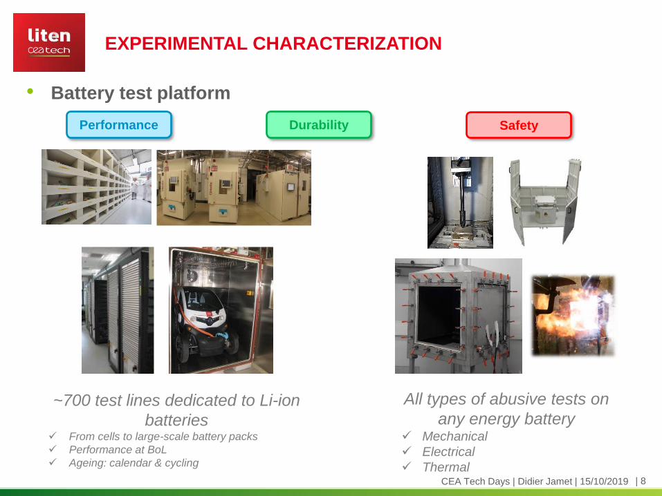
| 8CEA Tech Days | Didier Jamet | 15/10/2019
EXPERIMENTAL CHARACTERIZATION
• Battery test platform
~700 test lines dedicated to Li-ion
batteries From cells to large-scale battery packs
Performance at BoL
Ageing: calendar & cycling
All types of abusive tests on
any energy battery Mechanical
Electrical
Thermal
Performance Durability Safety

| 9CEA Tech Days | Didier Jamet | 15/10/2019
EXPERIMENTAL CHARACTERIZATION
• Battery data base
Performance Durability Safety
Ex.: energy density Ex.: cycling ageing
Ex.: calendar ageing
Ex.: thermal stability

| 10CEA Tech Days | Didier Jamet | 15/10/2019
EXPERIMENTAL CHARACTERIZATION
• Battery advanced analyses
Gassing
Leakage
Defects on collector
Dissolution of electrode
in electrolyte
Li plating
Delamination
of electrodes
Inhomogeneous SoC
Internal
structure &
geometry
Before cycling
After cycling
POE bonds
NMC crystal structure
ICP elemental analysisGCMS on volatile electrolyte products
SEM & IR on
membrane
In-situ XRD in overcharge test
Cell autopsy
Physico-chemical and electrochemical analyses of internal components
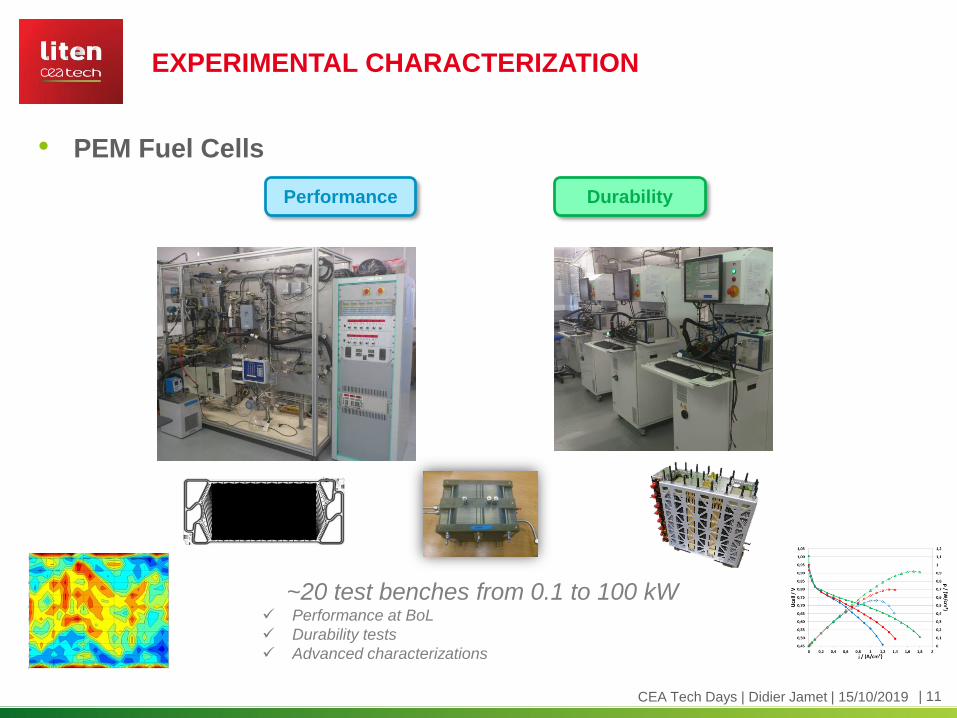
| 11CEA Tech Days | Didier Jamet | 15/10/2019
EXPERIMENTAL CHARACTERIZATION
• PEM Fuel Cells
Performance Durability
~20 test benches from 0.1 to 100 kW Performance at BoL
Durability tests
Advanced characterizations

| 12CEA Tech Days | Didier Jamet | 15/10/2019
EXPERIMENTAL CHARACTERIZATION
• PEM Fuel Cells
0
50
100
150
200
250
300
350
21/09/2011 21/09/2012 21/09/2013 21/09/2014 21/09/2015 21/09/2016 21/09/2017
Stac
k re
fere
nce
nu
mb
er
& n
um
be
r o
f ce
lls
History of stacks tested at CEA (2011 - 2018)
Number of cells Stack reference n°
328

| 13CEA Tech Days | Didier Jamet | 15/10/2019
EXPERIMENTAL CHARACTERIZATION
• Nano-characterization platform: cutting-edge capabilities
TEM / SEM
NMR / SQUID
XPS
Neutron diffraction
X ray Synchrotron
Contact Angle
Gas Permeation
Profilometer / AFM
GC/MS
HPLC / SEC
FTIR / UV
X-Ray diffraction
DSC / TGA-DTA
Look into the heart of technologies
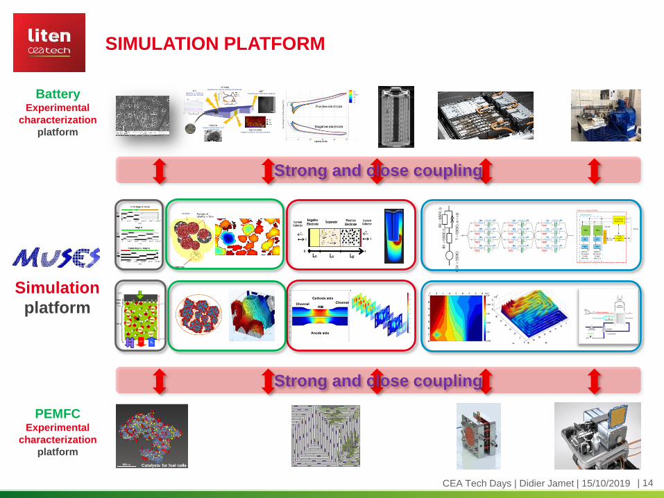
| 14CEA Tech Days | Didier Jamet | 15/10/2019
SIMULATION PLATFORM
Strong and close coupling
Strong and close coupling
BatteryExperimental
characterization
platform
Simulation
platform
PEMFCExperimental
characterization
platform
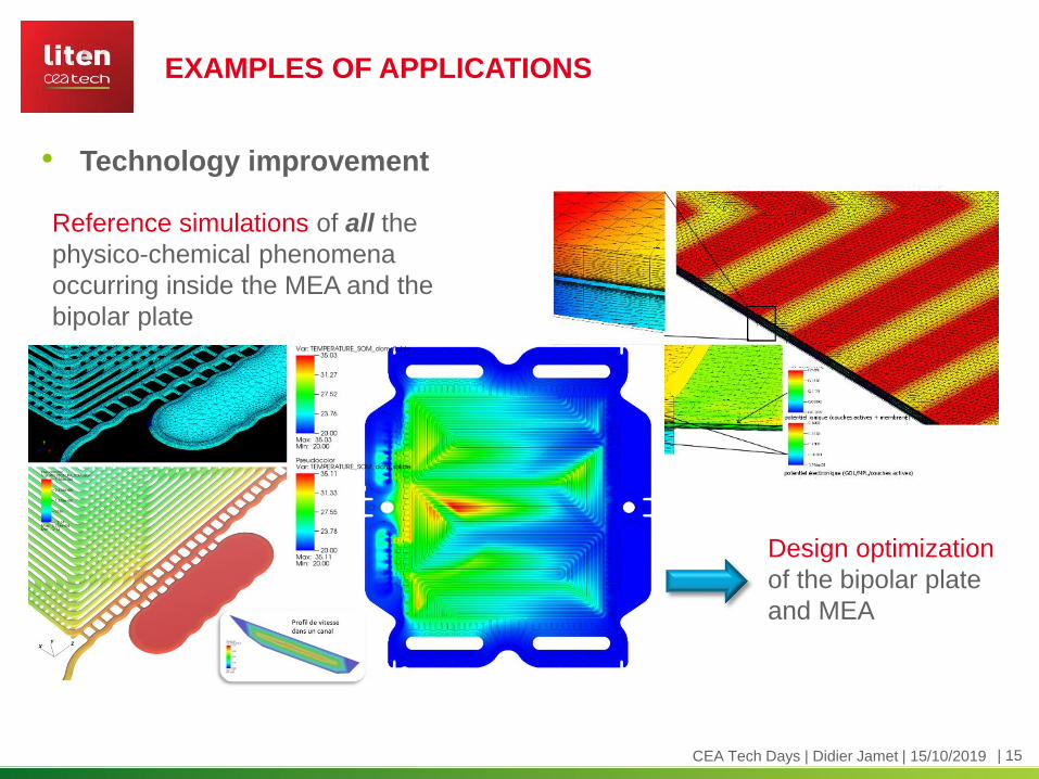
| 15CEA Tech Days | Didier Jamet | 15/10/2019
• Technology improvement
EXAMPLES OF APPLICATIONS
Reference simulations of all the
physico-chemical phenomena
occurring inside the MEA and the
bipolar plate
Design optimization
of the bipolar plate
and MEA
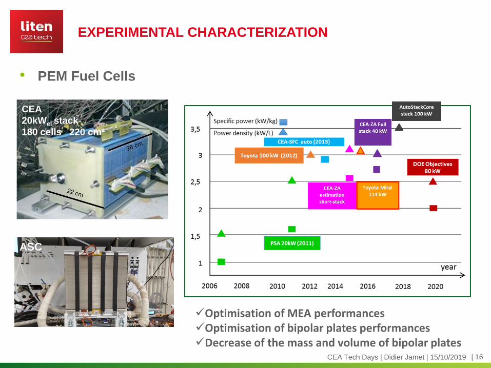
| 16CEA Tech Days | Didier Jamet | 15/10/2019
EXPERIMENTAL CHARACTERIZATION
• PEM Fuel Cells
CEA
20kWel stack
180 cells_ 220 cm²
Optimisation of MEA performances Optimisation of bipolar plates performances Decrease of the mass and volume of bipolar plates
ASC
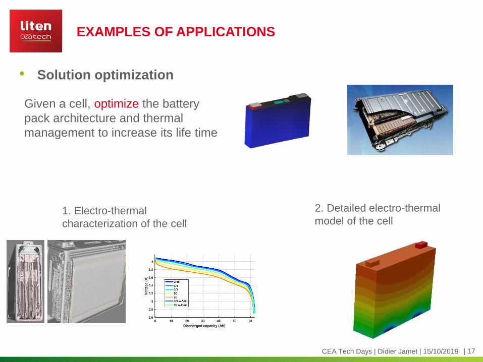
| 17CEA Tech Days | Didier Jamet | 15/10/2019
• Solution optimization
EXAMPLES OF APPLICATIONS
Given a cell, optimize the battery
pack architecture and thermal
management to increase its life time
1. Electro-thermal
characterization of the cell
2. Detailed electro-thermal
model of the cell

| 18CEA Tech Days | Didier Jamet | 15/10/2019
• Solution optimization
EXAMPLES OF APPLICATIONS
Given a cell, optimize the battery
pack architecture and thermal
management to increase its life time
3. Ageing characterization of
the cell
4. Simulation of different
thermal architectures
and managements
5. Increase the battery life time
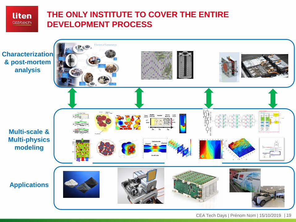
| 19CEA Tech Days | Prénom Nom | 15/10/2019
THE ONLY INSTITUTE TO COVER THE ENTIRE
DEVELOPMENT PROCESS
C
Multi-scale &
Multi-physics
modeling
Characterization
& post-mortem
analysis
Applications

Commissariat à l’énergie atomique et aux énergies alternatives
17 rue des Martyrs | 38054 Grenoble Cedex
www-liten.cea.fr
Établissement public à caractère industriel et commercial | RCS Paris B 775 685 019
Contact:
Didier Jamet
Email: [email protected]
Tel: +33.4.38.78.10.97
Cell: +33.6.37.72.20.54
THANK YOU
COME TO VISIT US IN FRANCE !
TECH DAYSINNOVATION FOR INDUSTRY
LITEN DAYOCTOBER 15, 2019
KEIO PLAZA HOTEL, TOKYO
CEA Tech Days | Dr. Olivier Lemaire | 15/10/2019
HIGH TEMPERATURE ELECTROLYSIS AND COMPACT
METHANATION REACTORS:
TWO KEY TECHNOLOGIES FOR POWER-TO-GAS
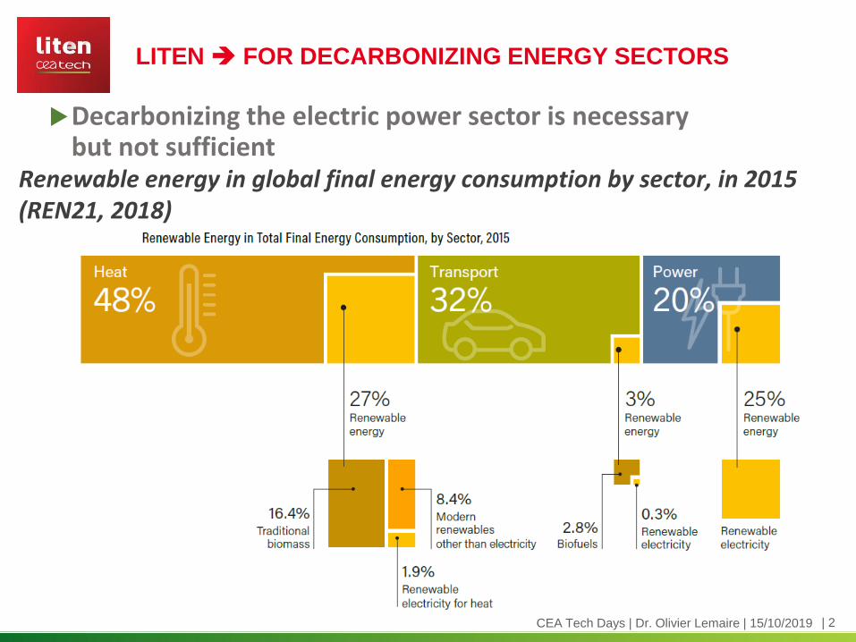
| 2CEA Tech Days | Dr. Olivier Lemaire | 15/10/2019
LITEN FOR DECARBONIZING ENERGY SECTORS
Renewable energy in global final energy consumption by sector, in 2015(REN21, 2018)
Decarbonizing the electric power sector is necessary but not sufficient
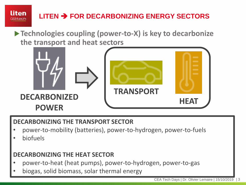
| 3CEA Tech Days | Dr. Olivier Lemaire | 15/10/2019
LITEN FOR DECARBONIZING ENERGY SECTORS
Technologies coupling (power-to-X) is key to decarbonize the transport and heat sectors
DECARBONIZING THE TRANSPORT SECTOR• power-to-mobility (batteries), power-to-hydrogen, power-to-fuels• biofuels
DECARBONIZING THE HEAT SECTOR• power-to-heat (heat pumps), power-to-hydrogen, power-to-gas• biogas, solid biomass, solar thermal energy
DECARBONIZEDPOWER
TRANSPORTHEAT

| 4CEA Tech Days | Dr. Olivier Lemaire | 15/10/2019
LITEN FOR ENERGY STORAGE
Evolution of the energy mix: growth of renewable energies and local productions
Need of electricity storage solutions
Technologies coupling is key to store energy in different sectors (heat, transport and power)
H2 and methanation can play a role

| 5CEA Tech Days | Dr. Olivier Lemaire | 15/10/2019
LITEN FOR DECARBONIZING ENERGY SECTORS &
ENERGY STORAGE
Expertise on Energy
Conversion
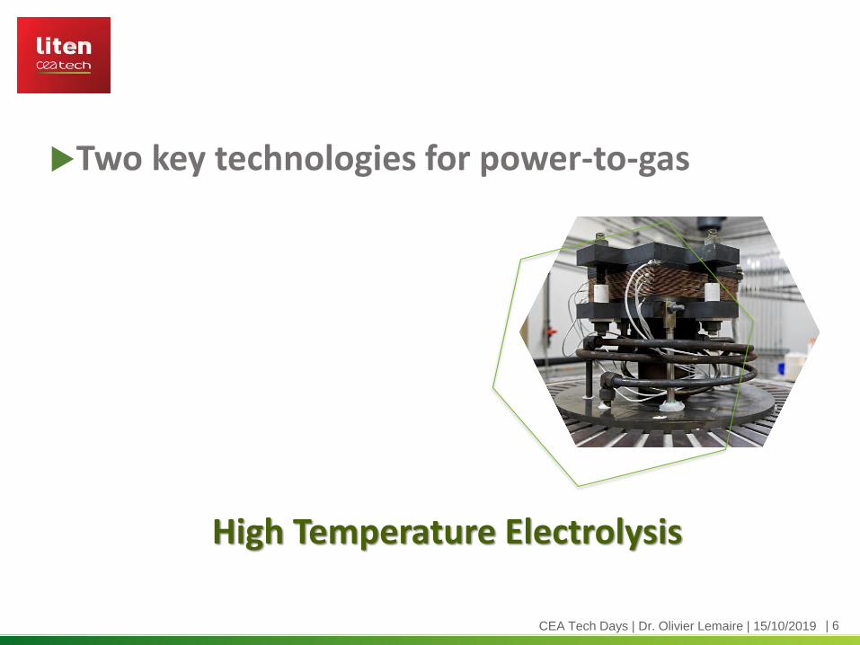
| 6CEA Tech Days | Dr. Olivier Lemaire | 15/10/2019
High Temperature Electrolysis
Two key technologies for power-to-gas
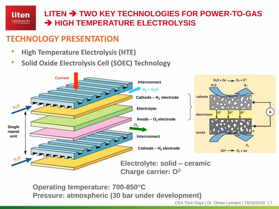
| 7CEA Tech Days | Dr. Olivier Lemaire | 15/10/2019
LITEN TWO KEY TECHNOLOGIES FOR POWER-TO-GAS
HIGH TEMPERATURE ELECTROLYSIS
• High Temperature Electrolysis (HTE)
• Solid Oxide Electrolysis Cell (SOEC) Technology
Single
repeat
unit
Cathode – H2 electrode
Anode – O2 electrode
Electrolyte
Interconnect
Interconnect
Cathode – H2 electrode
Current
H2 + H2O
Single
repeat
unit
Cathode – H2 electrode
Anode – O2 electrode
Electrolyte
Interconnect
Interconnect
Cathode – H2 electrode
Current
H2 + H2O
O2
Electrolyte: solid – ceramic
Charge carrier: O2-
Operating temperature: 700-850°C
Pressure: atmospheric (30 bar under development)
TECHNOLOGY PRESENTATION

| 8CEA Tech Days | Dr. Olivier Lemaire | 15/10/2019
LITEN TWO KEY TECHNOLOGIES FOR POWER-TO-GAS
HIGH TEMPERATURE ELECTROLYSIS
TECHNOLOGY PRESENTATIONCell Stack SystemModule
Modular technology:
- A stack can contain a variable number of cells depending on the target power
- Cells can have different sizes depending on the targeted power
- To increase the power, the stack size can be adjusted
- Possibility to have several stacks in a module and several modules in a system: flexibility
• Electrolysis cell
• Core of the electrochemical
reaction
• Electrolyte + 2 electrodes
• Complete electrolyzer / factory
• Composed of several modules
• Contains shared 2nd level
auxiliaries
• Integration of several stacks
• Includes 1st level auxiliaries
(fluidic, electric, thermal)
• Cells stacking to
increase power
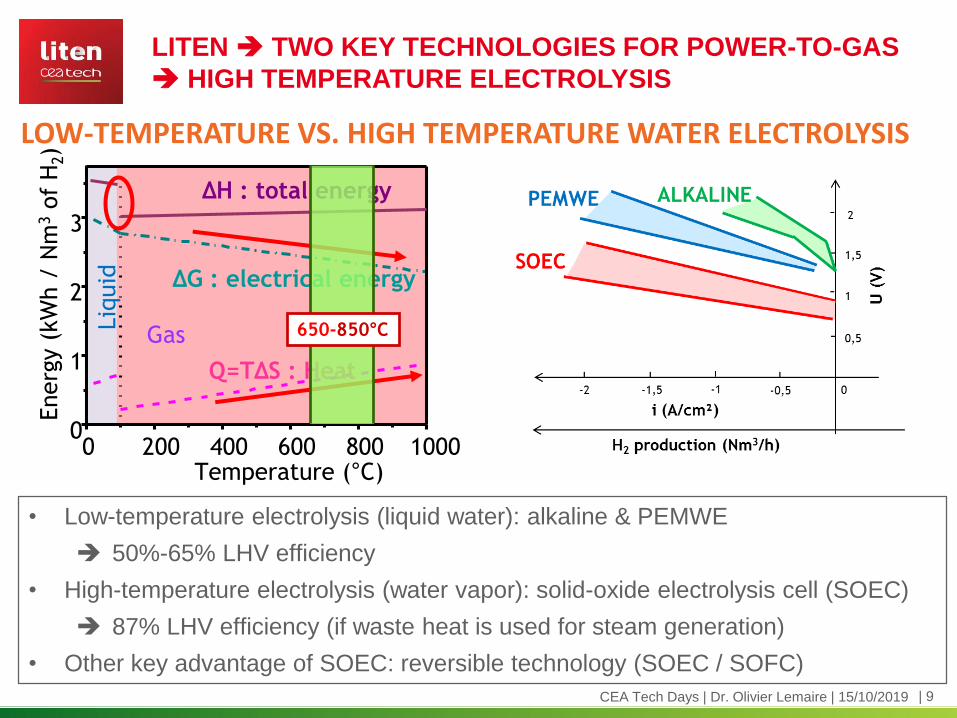
| 9CEA Tech Days | Dr. Olivier Lemaire | 15/10/2019
LITEN TWO KEY TECHNOLOGIES FOR POWER-TO-GAS
HIGH TEMPERATURE ELECTROLYSIS
LOW-TEMPERATURE VS. HIGH TEMPERATURE WATER ELECTROLYSIS
0 200 400 600 800 10000
1
2
3
Energ
y (
kW
h /
Nm
3of
H2)
Temperature (°C)
Liq
uid ΔG : electrical energy
Q=TΔS : Heat
Gas
ΔH : total energy
650-850°C
• Low-temperature electrolysis (liquid water): alkaline & PEMWE
50%-65% LHV efficiency
• High-temperature electrolysis (water vapor): solid-oxide electrolysis cell (SOEC)
87% LHV efficiency (if waste heat is used for steam generation)
• Other key advantage of SOEC: reversible technology (SOEC / SOFC)
| 10CEA Tech Days | Dr. Olivier Lemaire | 15/10/2019
LITEN TWO KEY TECHNOLOGIES FOR POWER-TO-GAS
HIGH TEMPERATURE ELECTROLYSIS
SOME RESULTS: PERFORMANCES. Stack and system levels
0
0.2
0.4
0.6
0.8
1
1.2
1.4
1.6
-3.00 -2.50 -2.00 -1.50 -1.00 -0.50 0.00
Vo
ltag
e (
V)
i (A/cm²)
9NmL/min/cm²12NmL/min/cm²16NmL/min/cm²24NmL/min/cm²simulation 9NmL/min/cm²simulation 12 NmL/min/cm²simulation 16NmL/min/cm²simulation 24NmL/min/cm²
Electric power for heating (W)
Stack temp. (°C)
H2 production (l/h)
Good performance at stack level:
• May exceed -2 A/cm² at 1.3V
• 100% recovery rate of produced H2
• Ability to operate with high conversion
rates of water vapor (~80%)
• 1.7 Nm3/h of H2 produced for a 25-
cells stack
Good performance at system
level:
• 1.2 Nm3/h H2 produced at 700°C
with a 25-cells stack
• Good efficiency of heat
exchangers for preheating input
gases
• A 87% LHV electrolysis
efficiency is measured at the
system level

| 11CEA Tech Days | Dr. Olivier Lemaire | 15/10/2019
LITEN TWO KEY TECHNOLOGIES FOR POWER-TO-GAS
HIGH TEMPERATURE ELECTROLYSIS
SOME RESULTS: PERFORMANCES. Operating strategy
• Ability to follow very fast current transients
• No degradation related to these transients
Coupling to intermittent renewable
energies is possible
800°C, 90%H2O/10%H2 on the H2 side, air on the O2 side
J. Mougin et al., Energy Procedia 29 (2012) 445 – 454
Possibility to operate under pressure
at 10-30 bar
Double gain:
• At system level: avoiding a
compression stage
• At stack level: limiting current shifted =
possibility to operate at higher currents
and steam conversion
| 12CEA Tech Days | Dr. Olivier Lemaire | 15/10/2019
LITEN TWO KEY TECHNOLOGIES FOR POWER-TO-GAS
HIGH TEMPERATURE ELECTROLYSIS
SOME SPECIFICITIES: REVERSIBLE OPERATION SOEC/SOFC rSOC
System testing
Stack testing
Source: J. Aicartet al., Fuel Cells
(2019)
• Better CAPEX: only one system
• Better return on investment: system running 100% of the time
• Similar operation in both modes
• Cycling between SOEC and SOFC
possible, no further degradation
• Relatively fast transitions (<10 min)
| 13CEA Tech Days | Dr. Olivier Lemaire | 15/10/2019
LITEN TWO KEY TECHNOLOGIES FOR POWER-TO-GAS
HIGH TEMPERATURE ELECTROLYSIS
COST ANALYSIS: LEVELIZED COST OF HYDROGEN (LCOH)
123
High-temperature water electrolysis:LCOH 8€/kg @ 100 kg/day ( elec. price 123 €/MWh)LCOH 2 €/kg @ 3,000 kg/day ( elec. price 40 €/MWh)
LCO
H (
€/k
g)
Electricity price (€/MWh)Replacement frequency: 3 years for SOEC, 10 years for alkaline, 6 years for PEMWE
Source: M. Reytier, et al., IJHE 40 (2015) 11370
| 14CEA Tech Days | Dr. Olivier Lemaire | 15/10/2019
LITEN TWO KEY TECHNOLOGIES FOR POWER-TO-GAS
HIGH TEMPERATURE ELECTROLYSIS
DEVELOPMENT STATUS
Examples of realization
- 2014: 1st SOEC system set up by CEA
1 stack – 1 Nm3/h H2 produced at 700°C Energy efficiency 99%HHV
- 2017: Grinhy system set up by Sunfire
steelmaking site in Germany
150 kW - 40 Nm3/h of H2 produced
- 2019: start of Grinhy 2.0 project:
720 kW
Production of 100t of H2 by the end of 2022
- 2019: call EU FCH-JU
SOEC of >2 MW
French roadmap
- 2022: 300 kW
- 2024: 2 MW
- 2027 and beyond: ~100 MW

| 15CEA Tech Days | Dr. Olivier Lemaire | 15/10/2019
Compact methanation reactors
Two key technologies for power-to-gas
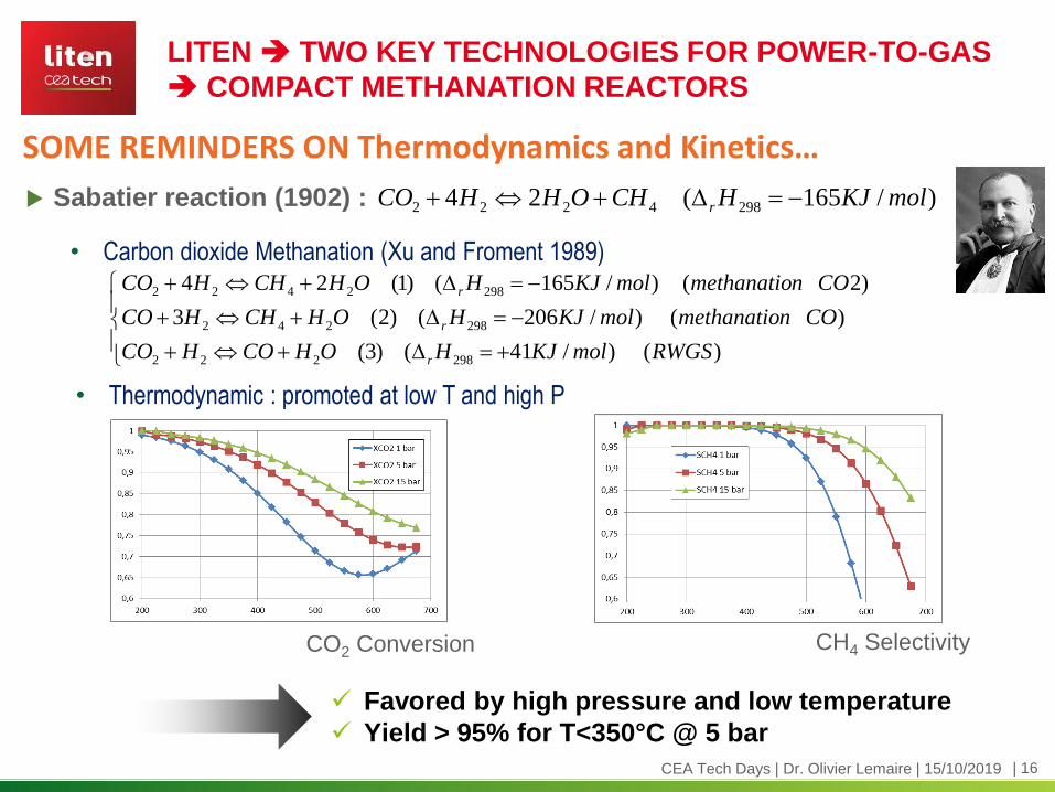
| 16CEA Tech Days | Dr. Olivier Lemaire | 15/10/2019
LITEN TWO KEY TECHNOLOGIES FOR POWER-TO-GAS
COMPACT METHANATION REACTORS
SOME REMINDERS ON Thermodynamics and Kinetics…
)/165(24 2984222 molKJHCHOHHCO r
Favored by high pressure and low temperature
Yield > 95% for T<350°C @ 5 bar
• Carbon dioxide Methanation (Xu and Froment 1989)
)()/41()3(
)()/206()2(3
)2()/165()1(24
298222
298242
2982422
RWGSmolKJHOHCOHCO
COnmethanatiomolKJHOHCHHCO
COnmethanatiomolKJHOHCHHCO
r
r
r
• Thermodynamic : promoted at low T and high P
CO2 Conversion CH4 Selectivity
Sabatier reaction (1902) :
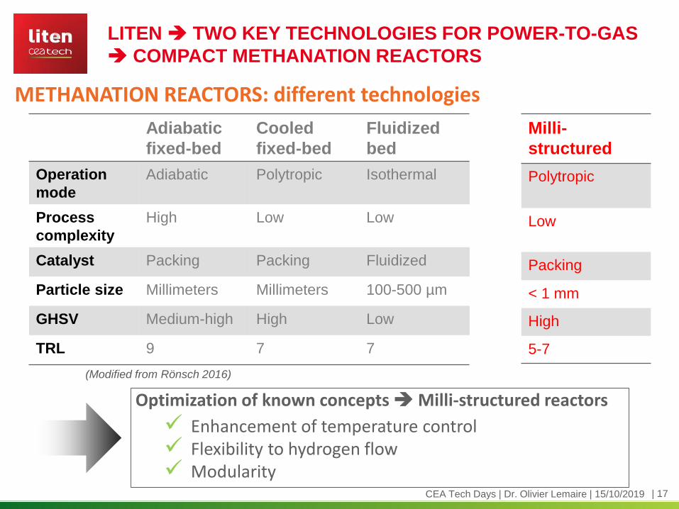
| 17CEA Tech Days | Dr. Olivier Lemaire | 15/10/2019
LITEN TWO KEY TECHNOLOGIES FOR POWER-TO-GAS
COMPACT METHANATION REACTORS
METHANATION REACTORS: different technologies
Optimization of known concepts Milli-structured reactors
Enhancement of temperature control Flexibility to hydrogen flow Modularity
(Modified from Rönsch 2016)
Adiabatic
fixed-bed
Cooled
fixed-bed
Fluidized
bed
Operation
mode
Adiabatic Polytropic Isothermal
Process
complexity
High Low Low
Catalyst Packing Packing Fluidized
Particle size Millimeters Millimeters 100-500 µm
GHSV Medium-high High Low
TRL 9 7 7
Milli-
structured
Polytropic
Low
Packing
< 1 mm
High
5-7

| 18CEA Tech Days | Dr. Olivier Lemaire | 15/10/2019
LITEN TWO KEY TECHNOLOGIES FOR POWER-TO-GAS
COMPACT METHANATION REACTORS
MILLI-STRUCTURED REACTOR DEVELOPMENT Prototype milli-structured reactor
- Keep small scale channels for intensification of heat and mass transfer
- Use of millimeter-scale catalyst particles (high catalyst density and easy loading)
- Scale-up by numbering-up reactive channels and coolant channels
Manufacturing by HIP (CEA nuclear background)- Machining of metallic plates (reactive and coolant channels)
- Stacking of machined and non-machined plates
- Bonding by Hot Isostatic Pressure (high temperature, high pressure)
- High quality bonding
Qualification- High methane yield for high GHSV (>95% @4000 h-1)
- Flexibility : Adaptation to flowrates 20%-100%
- Ageing : >90% CO2 conversion sustained for 700 h (& more)
Plates

| 19CEA Tech Days | Dr. Olivier Lemaire | 15/10/2019
LITEN TWO KEY TECHNOLOGIES FOR POWER-TO-GAS
COMPACT METHANATION REACTORS
SOME RESULTS: PERFORMANCES
2,5 bar and cooling fluid at 290°C(Conversion rate at the equilibrium 96.9%)
CO2 conversion, P = 2.5 bar, T = 290°C, flowrates from 20% to 100%
Inlet flowrates, P = 2.5 bar, T = 290°C, flowrates from 20% to 100%
Flowrate flexibility
CO2 Conversion rate vs GHSV
Good performance:
Technology validated
Upscaling of module and integration into a methanation unit
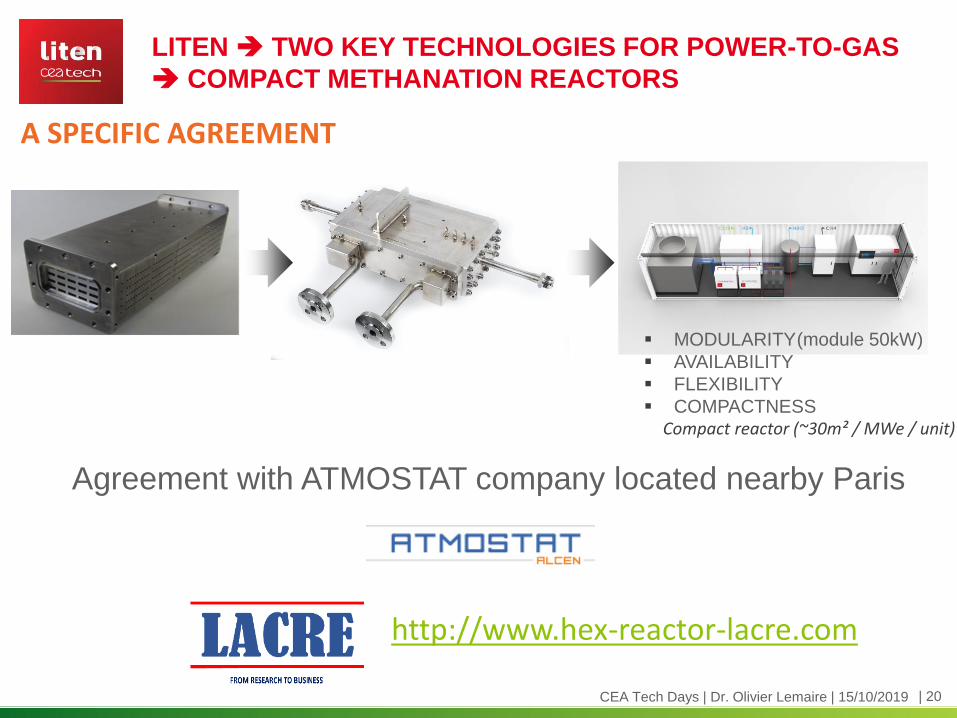
| 20CEA Tech Days | Dr. Olivier Lemaire | 15/10/2019
LITEN TWO KEY TECHNOLOGIES FOR POWER-TO-GAS
COMPACT METHANATION REACTORS
A SPECIFIC AGREEMENT
MODULARITY(module 50kW)
AVAILABILITY
FLEXIBILITY
COMPACTNESSCompact reactor (~30m² / MWe / unit)
Agreement with ATMOSTAT company located nearby Paris
http://www.hex-reactor-lacre.com

| 21CEA Tech Days | Dr. Olivier Lemaire | 15/10/2019
LITEN TWO KEY TECHNOLOGIES FOR POWER-TO-GAS
COMPACT METHANATION REACTORS
DEVELOPMENT STATUS. Projects in France JUPITER 1000: 1 MWel plant led by GRTgaz company
Upscaling of one
reference module of
reactor and tested at
CEA.
Manufacturing of the
methanation unit in
progress
Schedule:
Start of the H2 chain: August 2019
Start of the SNG chain: Early 2020
www.jupiter1000.com
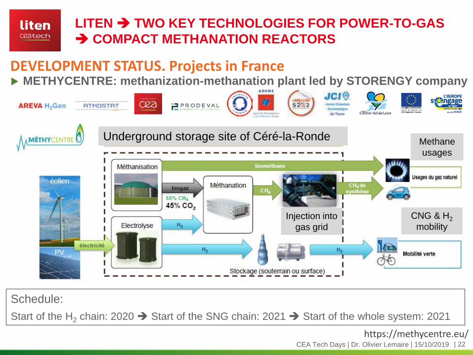
| 22CEA Tech Days | Dr. Olivier Lemaire | 15/10/2019
LITEN TWO KEY TECHNOLOGIES FOR POWER-TO-GAS
COMPACT METHANATION REACTORS
DEVELOPMENT STATUS. Projects in France METHYCENTRE: methanization-methanation plant led by STORENGY company
Schedule:
Start of the H2 chain: 2020 Start of the SNG chain: 2021 Start of the whole system: 2021
https://methycentre.eu/
Underground storage site of Céré-la-Ronde
Injection into
gas grid
CNG & H2
mobility
Methane
usages

| 23CEA Tech Days | Dr. Olivier Lemaire | 15/10/2019
LITEN TWO KEY TECHNOLOGIES FOR POWER-TO-GAS
COMPACT METHANATION REACTORS
DEVELOPMENT STATUS. Projects in Europe
H2020 project including 3 demo P2G plants
Power to gas demo plant in Troia• Capturing of CO2 from
ambient air
• Modular millistructured-
reactor based methanation
concept
• A “small-scale” liquefaction
to supply LNG to a
dedicated cryogenic tank
CO2-SNG: Upscaling of module and tests at CEA.
SNG with a good quality and high conversion rate (for mobility)
A KIC Inno Energy project located in Poland
• SNG quality: the plant can produce
SNG with the quality required, the
conversion rate of CO2 has reached
98,5%.
• Control of methanation temperature:
as expected with the innovative
technology of the methanation
reactors, the control of the reaction
temperature is efficient.
• Flexibility: the plant can produce SNG
from 20% to 100% in a few minutes.
• Long run with stable parameters in
progress, to confirm stabilization of catalyst.

| 24CEA Tech Days | Dr. Olivier Lemaire | 15/10/2019
LITEN TWO KEY TECHNOLOGIES FOR POWER-TO-GAS
CONCLUSIONS and PERSPECTIVES
Development of two promising power-to-gas technologies for
DECARBONIZING and STORAGE ENERGY
Advanced development of the two technologies (high temperature
electrolysis and compact reactors for methanation)
Good performances at laboratory level and also at system level
Starting of industrialization with partners
High temperature electrolysis
Continue/speed up demonstration projects
Upscaling
Diversification with co-electrolysis for producing syngas or other molecules
Compact methanation reactors
Demonstration projects on-going to gather Return of Experience
(JUPITER1000, CO2-SNG, STORE&GO, METHYCENTRE)
Durability and upscaling
Diversification to other reactions (in progress): methanol, FT, other
molecules
Commissariat à l’énergie atomique et aux énergies alternatives
17 rue des Martyrs | 38054 Grenoble Cedex
www-liten.cea.fr
Établissement public à caractère industriel et commercial | RCS Paris B 775 685 019
Contact:
Dr. Olivier Lemaire
Email: [email protected]
Tel: +33.4.38.78.11.45
Cell: +33.6.80.53.71.27
THANK YOU
ご清聴ありがとうございました
COME TO VISIT US IN FRANCE !
TECH DAYSINNOVATION FOR INDUSTRY
LITEN DAYOCTOBER 15, 2019
KEIO PLAZA HOTEL, TOKYO
Thibaud FLEURY, Industrial Partnership Manager, New Materials Division DTNM, CEA-Liten
ADVANCED MATERIAL TECHNOLOGIES TO SUSTAIN THE ENERGY
TRANSITION WITH CIRCULAR ECONOMY FOCUS

| 2
CURRENT ENVIRONMENTAL ISSUES
INNOVATION OPPORTUNITIES FOR MATERIALS &
PROCESSES WITH CIRCULAR ECONOMY FOCUS
Raw materials
limitation
Impact of environmental
degradation on health
Environmental
regulations
Collective awareness Climate change
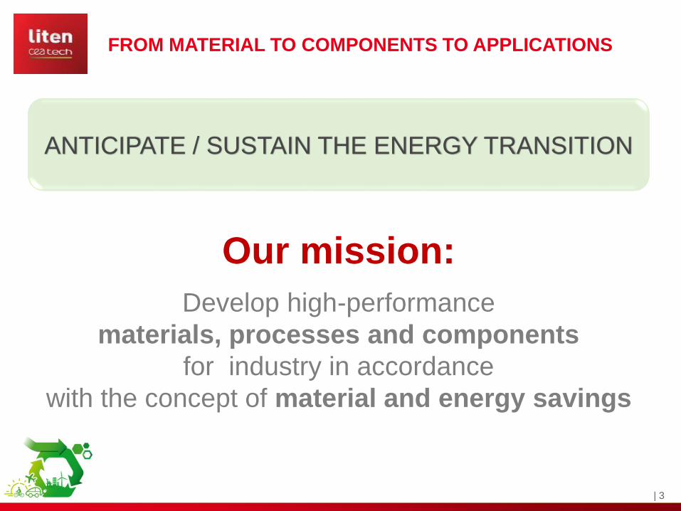
| 3
FROM MATERIAL TO COMPONENTS TO APPLICATIONS
Our mission:
Develop high-performance
materials, processes and components
for industry in accordance
with the concept of material and energy savings
ANTICIPATE / SUSTAIN THE ENERGY TRANSITION

| 4
CIRCULAR ECONOMY: « 3 R » STRATEGY
Reduce
Replace
Reuse
Use less materials
Decrease the environmental
footprint of materials
Integrate recycled materials
Material: Rare-earth permanent & Temporary magnets
Process: Additive Manufacturing
Application: Structural Electronics
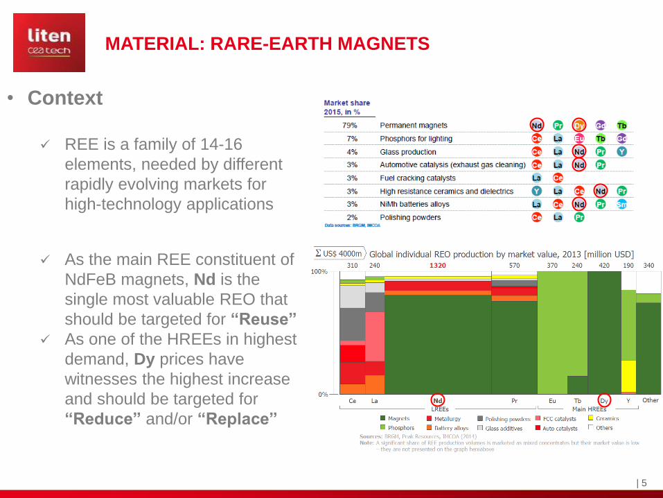
| 5
MATERIAL: RARE-EARTH MAGNETS
• Context
REE is a family of 14-16
elements, needed by different
rapidly evolving markets for
high-technology applications
As the main REE constituent of
NdFeB magnets, Nd is the
single most valuable REO that
should be targeted for “Reuse”
As one of the HREEs in highest
demand, Dy prices have
witnesses the highest increase
and should be targeted for
“Reduce” and/or “Replace”

| 6
MATERIAL: RARE-EARTH MAGNETS
REUSE
• Magnets recycling (by chemical treatment, powder, fusion)
• The recycled powder alone does not densify (cause: 9000 ppm 02 contamination)
• When mixing with standard NdFeB powder, 30% blend achieved
• When mixing with Co-enriched powder, 50% blend achieved
REDUCE
• Control of microstructure, phases's nature and stability
• Dy location in grain boundaries
• Less material thanks to additive manufacturing
REPLACE
• Use new phases to reduce/replace REE (Ce instead of Dy)
• “3 R” strategy: how do we optimize REE in permanent magnets?
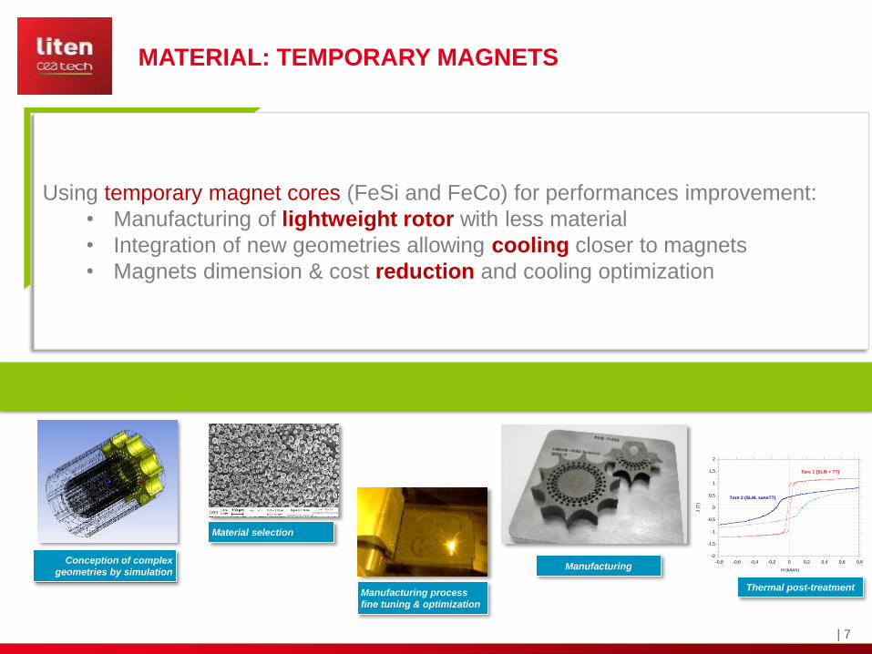
| 7
MATERIAL: TEMPORARY MAGNETS
Using temporary magnet cores (FeSi and FeCo) for performances improvement:
• Manufacturing of lightweight rotor with less material
• Integration of new geometries allowing cooling closer to magnets
• Magnets dimension & cost reduction and cooling optimization
Conception of complex
geometries by simulation
Manufacturing process
fine tuning & optimization
-2
-1,5
-1
-0,5
0
0,5
1
1,5
2
-0,8 -0,6 -0,4 -0,2 0 0,2 0,4 0,6 0,8
J (
T)
H (kA/m)
Tore 1 (SLM + TT)
Tore 2 (SLM, sansTT)
Material selection
Manufacturing
Thermal post-treatment

| 8
PROCESS: ADDITIVE MANUFACTURING
Advanced processes
Injection Molding and Additive
Manufacturing
PIM, LBM, DLP, FDM, MJF
Applications
Energy, Transportation, Defense, Electronic,
Industry, Medical, Luxury
MaterialsMetals,
Ceramics, Polymers, & Composites
Additive manufacturing: Advanced processes at the heart of our circular
economy approach
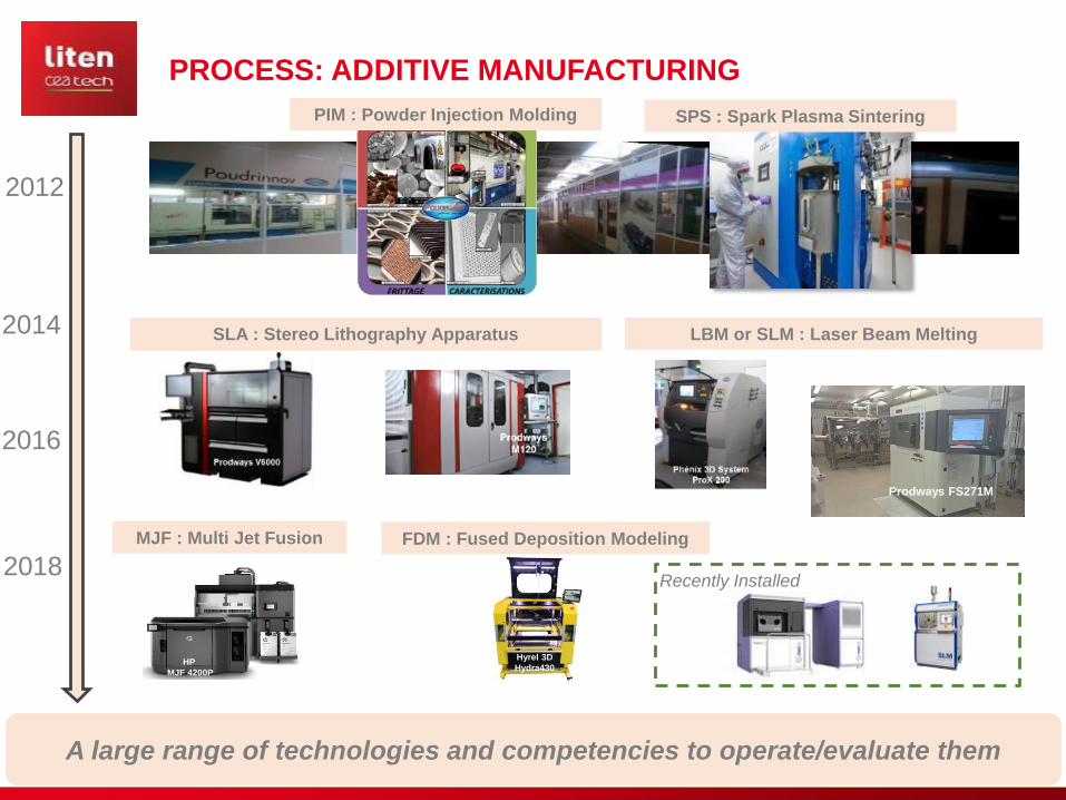
| 9
PROCESS: ADDITIVE MANUFACTURING
A large range of technologies and competencies to operate/evaluate them
2012
2014
2018
HP
MJF 4200P
Prodways FS271M
Hyrel 3D
Hydra430
2016
Recently Installed
SLA : Stereo Lithography Apparatus LBM or SLM : Laser Beam Melting
MJF : Multi Jet Fusion FDM : Fused Deposition Modeling
PIM : Powder Injection Molding SPS : Spark Plasma Sintering
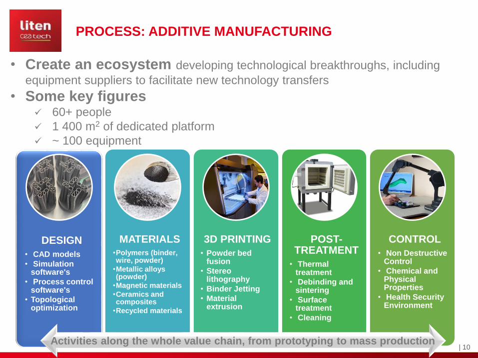
| 10
PROCESS: ADDITIVE MANUFACTURING
• Create an ecosystem developing technological breakthroughs, including
equipment suppliers to facilitate new technology transfers
• Some key figures 60+ people
1 400 m2 of dedicated platform
~ 100 equipment
DESIGN
• CAD models
• Simulation software's
• Process control software's
• Topological optimization
MATERIALS
•Polymers (binder, wire, powder)
•Metallic alloys (powder)
•Magnetic materials
•Ceramics and composites
•Recycled materials
3D PRINTING
• Powder bed fusion
• Stereo lithography
• Binder Jetting
• Material extrusion
POST-TREATMENT
• Thermal treatment
• Debinding and sintering
• Surface treatment
• Cleaning
CONTROL
• Non Destructive Control
• Chemical and Physical Properties
• Health Security Environment
Activities along the whole value chain, from prototyping to mass production

| 11
PROCESS: ADDITIVE MANUFACTURING
H2 phase separator
for PEM technology
(AlSi)
Polymer heat exchanger
(PA, ABS)
Net shape magnets
(NdFeB)
Magnetic rotor (FeSi)
Helicoidal heat exchanger
(AlSi, 316L)
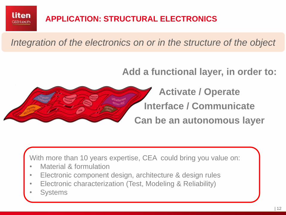
| 12
APPLICATION: STRUCTURAL ELECTRONICS
Add a functional layer, in order to:
Activate / Operate
Interface / Communicate
Can be an autonomous layer
With more than 10 years expertise, CEA could bring you value on:
• Material & formulation
• Electronic component design, architecture & design rules
• Electronic characterization (Test, Modeling & Reliability)
• Systems
Integration of the electronics on or in the structure of the object
| 13
APPLICATION: STRUCTURAL ELECTRONICS
Organic Electronics
Flexible/Stretchable Electronics
Plastronics
3D PrintingStructural Electronics
R&D roadmap
• Materials & Formulation
• Devices fabrication
• Electronic component design, architecture & design rules
• Electronic characterization (Test, Modeling & Reliability)
• Systems
Key drivers: weight / cost / congestion reduction, customization, design, usages
Integration of the electronics on or in the structure of the object
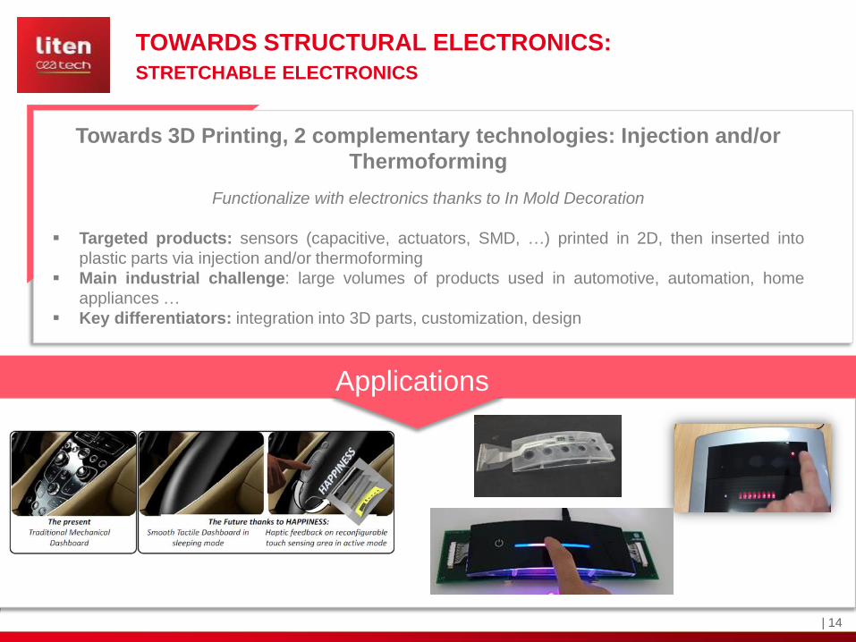
| 14
TOWARDS STRUCTURAL ELECTRONICS:
STRETCHABLE ELECTRONICS
Produit visé : capteur (capacitifs, LED SMD, …) imprimés en 2D, et intégrés sur pièces plastique, parthermoformage et/ou injection
Enjeu majeur en terme d’industrialisation : produit dans le domaine de l’automobile, domotique,home appliances pour la Strat Up Symbiose
Applications
Towards 3D Printing, 2 complementary technologies: Injection and/or
Thermoforming
Functionalize with electronics thanks to In Mold Decoration
Targeted products: sensors (capacitive, actuators, SMD, …) printed in 2D, then inserted into
plastic parts via injection and/or thermoforming
Main industrial challenge: large volumes of products used in automotive, automation, home
appliances …
Key differentiators: integration into 3D parts, customization, design

| 15
TOWARDS STRUCTURAL ELECTRONICS:
PLASTRONICS
Produit visé : capteur (capacitifs, LED SMD, …) imprimés en 2D, et intégrés sur pièces plastique, parthermoformage et/ou injection
Enjeu majeur en terme d’industrialisation : produit dans le domaine de l’automobile, domotique,home appliances pour la Strat Up Symbiose
Applications
Towards 3D Printing, 2 complementary technologies: Injection and/or
Thermoforming
Development of strain sensors, generic and relevant for a wide range of applications such as
batteries monitoring, robotics, wearable devices, etc…
Main challenges: sensors, multiplexer, energy generation/harvesting
Key differentiators: integration on stretchable substrates, low consumption, compatible with traditional electronics (SMD, ASICS, etc…) to create hybrid devices
Piezo-E & piezo-R printed sensors – Low consumption pressure measurement
Dérivateur
Piézoélectrique
Comparateur
µContrôleur
interruption
PiézorésistifAlimentation
Lecture ADC
Lecture ADC
Détection du maximum de
tension piézoélectrique
Commissariat à l’énergie atomique et aux énergies alternatives
17 rue des Martyrs | 38054 Grenoble Cedex
www-liten.cea.fr
Établissement public à caractère industriel et commercial | RCS Paris B 775 685 019
Contact:
Thibaud FLEURY
Email: [email protected]
Tel: +33.4.38.78.25.66
Cell: +33.6.34.17.40.93
THANK YOU
COME AND VISIT US IN FRANCE !

Evelyne EtchebehereRepresentative
CEA-Tech Japan [email protected]
Louis PriauxDeputy Representative
CEA-Tech Japan [email protected]
Arthur Del PiccoloIndustrial PartnershipsCEA-Tech Japan Office
CEA Tech is the CEA’s technology research unit. CEA Tech’s three labs—Leti, Liten, and List—develop a broad portfolio of technologies for ICTs, energy, and healthcare.
CEA Tech leverages a unique innovation-driven culture and unrivalled expertise to develop and disseminate new technologies for industry, effectively bridging the gap between the worlds of research and business.
CEA-Tech17 rue des Martyrs
FR-38054 Grenoble Cedex 9http://www.cea-tech.fr
Copyright © 2022 FDOKUMEN