Influences of dopant concentration in sol–gel derived AZO layer on the performance of P3HT:PCBM...
8
Influences of dopant concentration in sol–gel derived AZO layer on the performance of P3HT:PCBM based inverted solar cell Annisa Aprilia a,b,n , Priastuti Wulandari a , Veinardi Suendo c , Herman a , Rahmat Hidayat a,nn , Akihiko Fujii d , Masanori Ozaki d a Physics of Magnetism and Photonics Research Division, Faculty of Mathematics and Natural Sciences, Bandung Institute of Technology, Jl. Ganesha 10, Bandung 40132, West Java, Indonesia b Materials Physics Research Division, Faculty of Mathematics and Natural Sciences, Universitas Padjadjaran, Jl. Raya Jatinangor Km. 21, Sumedang 45363, West Java, Indonesia c Inorganic and Physical Chemistry Research Division, Faculty of Mathematics and Natural Sciences, Bandung Institute of Technology, Jl. Ganesha 10, Bandung 40132, West Java, Indonesia d Department of Electrical, Electronics, and Information Engineering, Faculty of Engineering, Osaka University, Yamada-Oka 2-1, Suita, Osaka 565-0871, Japan article info Article history: Received 7 June 2012 Received in revised form 7 December 2012 Accepted 14 December 2012 Available online 5 February 2013 Keywords: Organic solar cell Inverted solar cell Al doped ZnO (AZO) Small AC impedance abstract Organic solar cells based on P3HT:PCBM bulk heterojunction with an inverted structure have been fabricated using aluminum doped ZnO (AZO) as their electron transport layer, which was prepared by sol-gel route with 2-methoxyethanol as the solvent. The influences of Al concentration on the surface morphology and electrical properties of AZO layer were investigated by atomic force microscopy, X-ray diffraction and Hall effect measurements. The experimental results indicate that Al concentration has major influence on the grain size and only minor influence on crystallite size, leading to different surface morphology for different doping concentrations. Doping at high concentration produces higher charge carrier density, but not for charge carrier mobility and its electrical conductivity, which may be also influenced by the surface morphology. The effects of Al concentration in AZO layer were also observed in the J–V (current density–voltage) and small AC impedance characteristics of the fabricated solar cells. The resistance increases with Al concentration, but the capacitance decreases. The solar cell using AZO layer with doping concentration of 0.5 wt% shows the smallest impedance and the best J–V characteristics with the highest conversion efficiency. These characteristics seem to be correlated with the properties of AZO layer and its interface with the active layer. & 2012 Elsevier B.V. All rights reserved. 1. Introduction In some recent years, there is a deep interest to apply metal oxides such as ZnO and TiO 2 as electron transport layer (ETL) or electron extraction layer (EEL) in hybrid solar cells with inverted structure [1–7]. The use of metal oxide layer may give an advantage in preventing the active layer from the unwanted oxidation due to UV light radiations of the sunlight and humidity exposure [5,6]. The use of ZnO layer in solar cell with inverted structure, such as in ITO/ZnO/C 60 /P3HT/Au structure configura- tion, improves charge carrier extraction as a result of the lowering of Fermi energy level at the cathode [8]. Moreover, Beek et al. has also reported the observation of charge transfer between poly(3- hexylthiophene) (P3HT) and ZnO, indicating the role of ZnO as an electron acceptor layer [9]. After this report, many studies con- cern on the role of ZnO and its nano-structured layer on exciton dissociation and charge carrier extraction [10,11]. While some reports shows clearly the improvement of the solar cell perfor- mance by addition of ZnO layer, but other reports cannot show such improvement. It seems that the role of ZnO as electron acceptors is affected by some factors which are still not well understood at the moment. It should be also noted that, in the past two decades, ZnO has been intensively studied as transparent conducting oxide (TCO) thin film [12,13]. ZnO is one type of non-stoichiometric metal oxides with native defect such as zinc interstitial and oxygen vacancies, which intrinsically forms the n-type amorphous semi- conductor [14]. The conductivity of ZnO thin film can be improved by addition of a small amount of metal ions, such as Al, Ge, etc. [15]. Aluminum doped ZnO (AZO) is one of the most studied ZnO film for TCO applications, which is considerable prospective material as a substitute of Sn-doped In 2 O 3 (ITO), the Contents lists available at SciVerse ScienceDirect journal homepage: www.elsevier.com/locate/solmat Solar Energy Materials & Solar Cells 0927-0248/$ - see front matter & 2012 Elsevier B.V. All rights reserved. http://dx.doi.org/10.1016/j.solmat.2012.12.033 n Corresponding author at: Physics of Magnetism and Photonics Research Division, Faculty of Mathematics and Natural Sciences, Bandung Institute of Technology, Jl. Ganesha 10, Bandung 40132, West Java, Indonesia. Tel.: þ62 22 250 0834; fax: þ62 22 250 6452. nn Corresponding author. Tel.: þ62 22 250 0834; fax: þ62 22 250 6452. E-mail addresses: [email protected], [email protected] (A. Aprilia), rahmat@fi.itb.ac.id (R. Hidayat). Solar Energy Materials & Solar Cells 111 (2013) 181–188
-
Upload
independent -
Category
Documents
-
view
3 -
download
0
Transcript of Influences of dopant concentration in sol–gel derived AZO layer on the performance of P3HT:PCBM...
Solar Energy Materials & Solar Cells 111 (2013) 181–188
Contents lists available at SciVerse ScienceDirect
Solar Energy Materials & Solar Cells
0927-02
http://d
n Corr
Division
Technol
Tel.: þ6nn Cor
E-m
a.aprilia
journal homepage: www.elsevier.com/locate/solmat
Influences of dopant concentration in sol–gel derived AZO layeron the performance of P3HT:PCBM based inverted solar cell
Annisa Aprilia a,b,n, Priastuti Wulandari a, Veinardi Suendo c, Herman a,Rahmat Hidayat a,nn, Akihiko Fujii d, Masanori Ozaki d
a Physics of Magnetism and Photonics Research Division, Faculty of Mathematics and Natural Sciences, Bandung Institute of Technology, Jl. Ganesha 10,
Bandung 40132, West Java, Indonesiab Materials Physics Research Division, Faculty of Mathematics and Natural Sciences, Universitas Padjadjaran, Jl. Raya Jatinangor Km. 21, Sumedang 45363, West Java, Indonesiac Inorganic and Physical Chemistry Research Division, Faculty of Mathematics and Natural Sciences, Bandung Institute of Technology, Jl. Ganesha 10,
Bandung 40132, West Java, Indonesiad Department of Electrical, Electronics, and Information Engineering, Faculty of Engineering, Osaka University, Yamada-Oka 2-1, Suita, Osaka 565-0871, Japan
a r t i c l e i n f o
Article history:
Received 7 June 2012
Received in revised form
7 December 2012
Accepted 14 December 2012Available online 5 February 2013
Keywords:
Organic solar cell
Inverted solar cell
Al doped ZnO (AZO)
Small AC impedance
48/$ - see front matter & 2012 Elsevier B.V. A
x.doi.org/10.1016/j.solmat.2012.12.033
esponding author at: Physics of Magnetis
, Faculty of Mathematics and Natural Sci
ogy, Jl. Ganesha 10, Bandung 40132, West Ja
2 22 250 0834; fax: þ62 22 250 6452.
responding author. Tel.: þ62 22 250 0834; fa
ail addresses: [email protected],
@students.itb.ac.id (A. Aprilia), [email protected]
a b s t r a c t
Organic solar cells based on P3HT:PCBM bulk heterojunction with an inverted structure have been
fabricated using aluminum doped ZnO (AZO) as their electron transport layer, which was prepared by
sol-gel route with 2-methoxyethanol as the solvent. The influences of Al concentration on the surface
morphology and electrical properties of AZO layer were investigated by atomic force microscopy, X-ray
diffraction and Hall effect measurements. The experimental results indicate that Al concentration has
major influence on the grain size and only minor influence on crystallite size, leading to different
surface morphology for different doping concentrations. Doping at high concentration produces higher
charge carrier density, but not for charge carrier mobility and its electrical conductivity, which may be
also influenced by the surface morphology. The effects of Al concentration in AZO layer were also
observed in the J–V (current density–voltage) and small AC impedance characteristics of the fabricated
solar cells. The resistance increases with Al concentration, but the capacitance decreases. The solar cell
using AZO layer with doping concentration of 0.5 wt% shows the smallest impedance and the best J–V
characteristics with the highest conversion efficiency. These characteristics seem to be correlated with
the properties of AZO layer and its interface with the active layer.
& 2012 Elsevier B.V. All rights reserved.
1. Introduction
In some recent years, there is a deep interest to apply metaloxides such as ZnO and TiO2 as electron transport layer (ETL) orelectron extraction layer (EEL) in hybrid solar cells with invertedstructure [1–7]. The use of metal oxide layer may give anadvantage in preventing the active layer from the unwantedoxidation due to UV light radiations of the sunlight and humidityexposure [5,6]. The use of ZnO layer in solar cell with invertedstructure, such as in ITO/ZnO/C60/P3HT/Au structure configura-tion, improves charge carrier extraction as a result of the loweringof Fermi energy level at the cathode [8]. Moreover, Beek et al. has
ll rights reserved.
m and Photonics Research
ences, Bandung Institute of
va, Indonesia.
x: þ62 22 250 6452.
.ac.id (R. Hidayat).
also reported the observation of charge transfer between poly(3-hexylthiophene) (P3HT) and ZnO, indicating the role of ZnO as anelectron acceptor layer [9]. After this report, many studies con-cern on the role of ZnO and its nano-structured layer on excitondissociation and charge carrier extraction [10,11]. While somereports shows clearly the improvement of the solar cell perfor-mance by addition of ZnO layer, but other reports cannot showsuch improvement. It seems that the role of ZnO as electronacceptors is affected by some factors which are still not wellunderstood at the moment.
It should be also noted that, in the past two decades, ZnO hasbeen intensively studied as transparent conducting oxide (TCO)thin film [12,13]. ZnO is one type of non-stoichiometric metaloxides with native defect such as zinc interstitial and oxygenvacancies, which intrinsically forms the n-type amorphous semi-conductor [14]. The conductivity of ZnO thin film can beimproved by addition of a small amount of metal ions, such asAl, Ge, etc. [15]. Aluminum doped ZnO (AZO) is one of the moststudied ZnO film for TCO applications, which is considerableprospective material as a substitute of Sn-doped In2O3 (ITO), the
A. Aprilia et al. / Solar Energy Materials & Solar Cells 111 (2013) 181–188182
most widely used TCO nowadays. Similar as the undoped ZnO,AZO can be prepared by various methods such as direct current(DC) magnetron sputtering, solvothermal, self assembly mono-layer and sol–gel process [14]. The preparation method by sol–gelprocess is attractive because it is possible for fabrication of largearea TCO with more simple and inexpensive equipments incomparison to other methods. For the preparation of AZO bysol–gel process, aluminum chloride (AlCl3) and aluminum nitrateAl(NO3) are commonly used as the precursor of Al dopant ion[16]. The preparation of AZO from aluminum acetate Al(OAc)2
through aqueous solution processing at relatively low tempera-ture of around 140 1C has been also reported [18,19]. At thattemperature regime, AZO layer then can be prepared on the top ofplastic substrate (PET) by roll-to-roll (R2R) technique, which is anemerging technique for flexible electronics manufacturing tech-nology. The fabrication of large area plastic solar cell with AZOlayer as its transport layer by R2R has been demonstratedrecently [5].
The presence of Al dopant may increase the density of states(DOS) near Fermi energy level and thus increases charge carrierdensity, leading to the increase in electrical conductivity [15,16].By using AZO thin film instead of the undoped ZnO layer, one maythus expect the reduction of the solar cell impedance and thus theimprovement in solar cell performance. Moreover, because AZOhas relatively larger charger carrier concentration and chargercarrier mobility in comparison to the organic transport layer, thesolar cell performance is also almost unaffected by the layerthickness variation [17]. However, the effect of using doped ZnOlayer on the performance of organic solar cell has not beeninvestigated in detail. Therefore, in this paper, we present theeffect of doping concentration of AZO layer on the characteristicsof organic solar cells with bulk hetero-junction of P3HT:PCBM astheir active layer. The characteristics of those solar cells wereinvestigated by the current density–voltage (J–V) and small AC-impedance measurements. The present experimental resultshows the relationship between the Al dopant concentration onthe J–V characteristics and small AC impedance, which will bediscussed in the following sections.
Ag
PEDOT: PSS
P3HT: PCBM
Al doped ZnO (AZO)
ITO
e-
h+
glass
light
Fig. 1. Schematic structure of inverted type of organic solar cells based on
P3HT:PCBM with AZO as its electron transport layer.
2. Experimental details
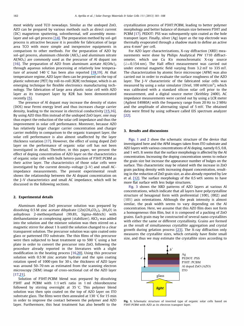
Aluminum doped ZnO precursor solution was prepared bydissolving 0.5 M zinc acetate dihydrate ((Zn(CH3CO2)2 �2H2O) inanhydrous 2-methoxyethanol (99.8%, Sigma–Aldrich) withdiethanolamine as complexing agent (stabilizer). AlCl3 was addedinto the solution and the mixture solution was then stirred on amagnetic stirrer for about 1 h until the solution changed to a cleartransparent solution. The precursor solution was spin coated ontoglass or patterned ITO substrate. The thin films of this precursorwere then subjected to heat treatment up to 500 1C using a hotplate in order to convert the precursor into ZnO, following theprocedure already reported in the literatures with a slightmodification in the heating process [16,20]. Using this precursorsolution with 0.5 M zinc acetate hydrate and the spin coatingrotation speed of 1000 rpm for 30 s, the thickness of AZO layerwas around 50–70 nm as estimated from the scanning electronmicroscopy (SEM) image of cross-sectional cut of the AZO layer[17,21].
Solution of P3HT:PCBM blend was prepared by dissolvingP3HT and PCBM with 1:1 wt% ratio in 1 ml chlorobenzenefollowed by stirring overnight at 35 1C. This polymer blendsolution was then spin coated on the top of AZO layer on ITOsubstrate glass. The films were then annealed at 130 1C for 15 minin order to improve the contact between the polymer and AZOlayer. Furthermore, this heat treatment has also benefit to the
crystallization process of P3HT:PCBM, leading to better polymermorphology and better balance of domain size between P3HT andPCBM [17]. PEDOT: PSS was subsequently spin coated as the holetransport layer. Finally, silver (Ag) layer as the top electrode wasthermally evaporated through a shadow mask to define an activearea 4 mm2 per cell.
For AZO layer characterizations, X-ray diffraction (XRD) mea-surements were done by Philips Analytical PW 1710 diffract-ometer, which use Cu Ka monochromatic X-ray source(l¼0.154 nm). The Hall effect measurement was carried outunder external magnetic field varying from 3.2 mT to 335 mT.The characterization by atomic force microscope (AFM) was alsocarried out in order to evaluate the surface roughness of the AZOlayer. The J–V characteristic of the fabricated solar cells wasmeasured by using a solar simulator (Oriel, 100 mW/cm2), whichwas calibrated with a standard silicon solar cell prior to themeasurement, and a digital source meter (Keithley 2400). ACimpedance measurements were carried out by using a LCR meter(Agilent E4980A) with the frequency range from 20 Hz to 2 MHzand the amplitude of alternating signal of 5 mV. The obtaineddata were fitted by using software called EIS spectrum analyzer[22].
3. Results and discussions
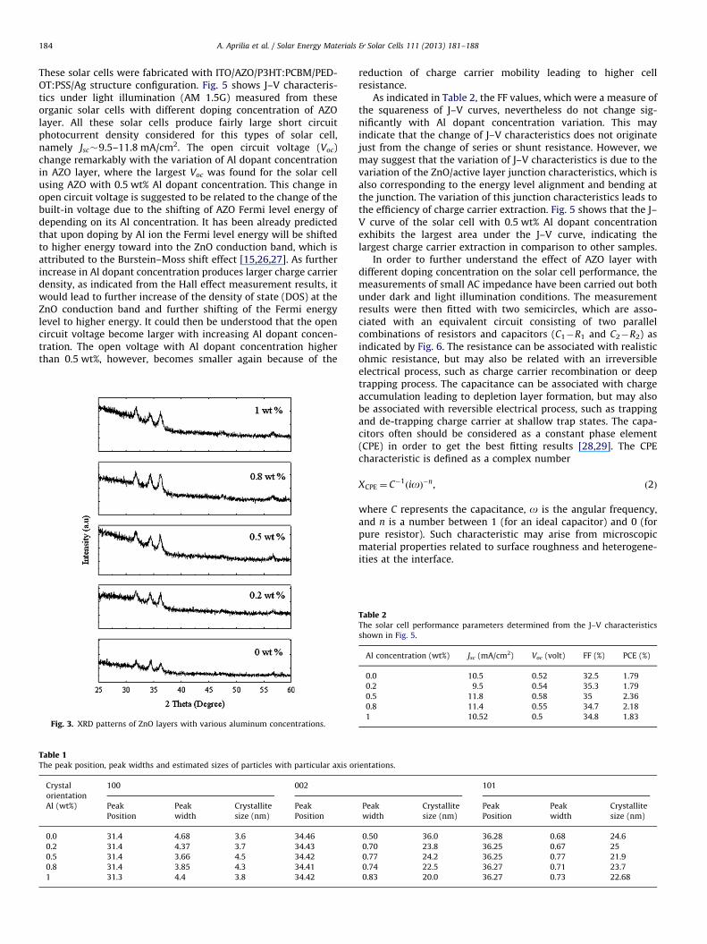
Figs. 1 and 2 show the schematic structure of the device thatinvestigated here and the AFM images taken from ITO substrate andAZO layers with various concentrations of Al doping, namely 0.5, 0.8,and 1 wt%. It seems that the surface morphology is affected by the Alconcentration. Increasing the doping concentration seems to reducethe grain size but increase the appearance number of bulges on thesurface. This characteristic may be related with the increase in ZnOgrain packing density with increasing dopant concentration, result-ing in the reduction of ZnO grain size, as also already reported by Leeet al. [12]. The surface morphology of the 0.5 wt% seems to havemore flat surface with less bulge structures.
Fig. 3 shows the XRD patterns of AZO layers at various Alconcentrations, which indicate that all layers have polycrystallinestructure of hexagonal form with preferential (100), (002) and(101) axis orientations. Although the peak intensity is almostsimilar, the peak width seems to vary depending on the Alconcentration. Here, we assume that this AZO film does not forma homogeneous thin film, but it is composed of a packing of ZnOgrains. Each grain may be constructed of several nano-crystalliteswith either the same or different crystallinity. Grains are formedas the result of simultaneous crystallite aggregation and crystalgrowth during gelation process [23]. The X-ray diffraction onlymeasures the crystallite sizes, which certainly have finite smallsize, and thus we may estimate the crystallite sizes according to
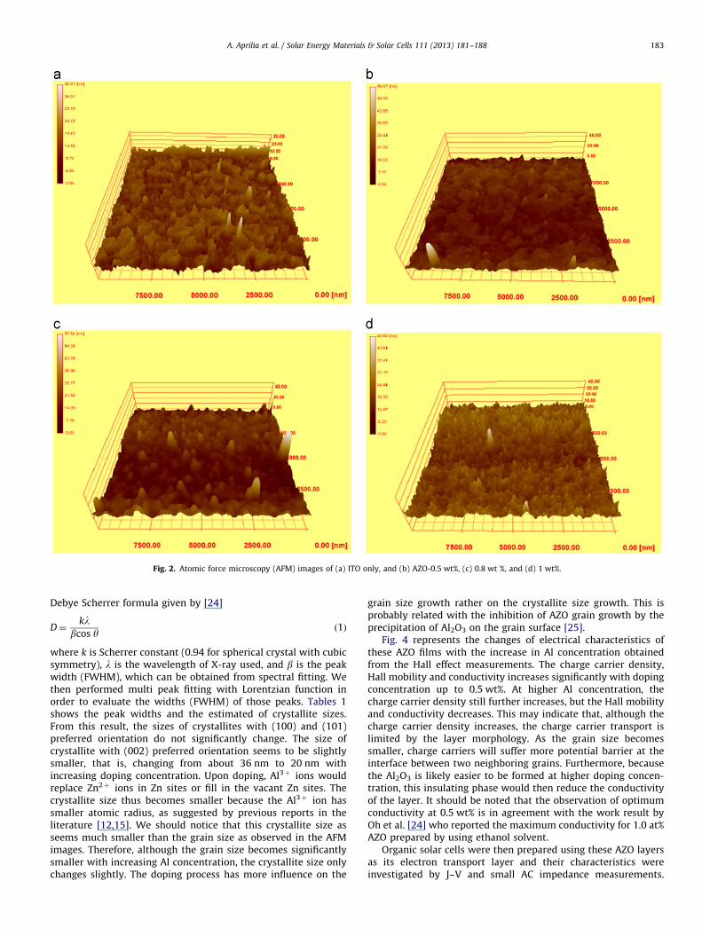
Fig. 2. Atomic force microscopy (AFM) images of (a) ITO only, and (b) AZO-0.5 wt%, (c) 0.8 wt %, and (d) 1 wt%.
A. Aprilia et al. / Solar Energy Materials & Solar Cells 111 (2013) 181–188 183
Debye Scherrer formula given by [24]
D¼kl
bcos yð1Þ
where k is Scherrer constant (0.94 for spherical crystal with cubicsymmetry), l is the wavelength of X-ray used, and b is the peakwidth (FWHM), which can be obtained from spectral fitting. Wethen performed multi peak fitting with Lorentzian function inorder to evaluate the widths (FWHM) of those peaks. Tables 1shows the peak widths and the estimated of crystallite sizes.From this result, the sizes of crystallites with (100) and (101)preferred orientation do not significantly change. The size ofcrystallite with (002) preferred orientation seems to be slightlysmaller, that is, changing from about 36 nm to 20 nm withincreasing doping concentration. Upon doping, Al3þ ions wouldreplace Zn2þ ions in Zn sites or fill in the vacant Zn sites. Thecrystallite size thus becomes smaller because the Al3þ ion hassmaller atomic radius, as suggested by previous reports in theliterature [12,15]. We should notice that this crystallite size asseems much smaller than the grain size as observed in the AFMimages. Therefore, although the grain size becomes significantlysmaller with increasing Al concentration, the crystallite size onlychanges slightly. The doping process has more influence on the
grain size growth rather on the crystallite size growth. This isprobably related with the inhibition of AZO grain growth by theprecipitation of Al2O3 on the grain surface [25].
Fig. 4 represents the changes of electrical characteristics ofthese AZO films with the increase in Al concentration obtainedfrom the Hall effect measurements. The charge carrier density,Hall mobility and conductivity increases significantly with dopingconcentration up to 0.5 wt%. At higher Al concentration, thecharge carrier density still further increases, but the Hall mobilityand conductivity decreases. This may indicate that, although thecharge carrier density increases, the charge carrier transport islimited by the layer morphology. As the grain size becomessmaller, charge carriers will suffer more potential barrier at theinterface between two neighboring grains. Furthermore, becausethe Al2O3 is likely easier to be formed at higher doping concen-tration, this insulating phase would then reduce the conductivityof the layer. It should be noted that the observation of optimumconductivity at 0.5 wt% is in agreement with the work result byOh et al. [24] who reported the maximum conductivity for 1.0 at%AZO prepared by using ethanol solvent.
Organic solar cells were then prepared using these AZO layersas its electron transport layer and their characteristics wereinvestigated by J–V and small AC impedance measurements.
A. Aprilia et al. / Solar Energy Materials & Solar Cells 111 (2013) 181–188184
These solar cells were fabricated with ITO/AZO/P3HT:PCBM/PED-OT:PSS/Ag structure configuration. Fig. 5 shows J–V characteris-tics under light illumination (AM 1.5G) measured from theseorganic solar cells with different doping concentration of AZOlayer. All these solar cells produce fairly large short circuitphotocurrent density considered for this types of solar cell,namely Jsc�9.5–11.8 mA/cm2. The open circuit voltage (Voc)change remarkably with the variation of Al dopant concentrationin AZO layer, where the largest Voc was found for the solar cellusing AZO with 0.5 wt% Al dopant concentration. This change inopen circuit voltage is suggested to be related to the change of thebuilt-in voltage due to the shifting of AZO Fermi level energy ofdepending on its Al concentration. It has been already predictedthat upon doping by Al ion the Fermi level energy will be shiftedto higher energy toward into the ZnO conduction band, which isattributed to the Burstein–Moss shift effect [15,26,27]. As furtherincrease in Al dopant concentration produces larger charge carrierdensity, as indicated from the Hall effect measurement results, itwould lead to further increase of the density of state (DOS) at theZnO conduction band and further shifting of the Fermi energylevel to higher energy. It could then be understood that the opencircuit voltage become larger with increasing Al dopant concen-tration. The open voltage with Al dopant concentration higherthan 0.5 wt%, however, becomes smaller again because of the
Fig. 3. XRD patterns of ZnO layers with various aluminum concentrations.
Table 1The peak position, peak widths and estimated sizes of particles with particular axis or
Crystal
orientation
100 002
Al (wt%) Peak
Position
Peak
width
Crystallite
size (nm)
Peak
Position
0.0 31.4 4.68 3.6 34.46
0.2 31.4 4.37 3.7 34.43
0.5 31.4 3.66 4.5 34.42
0.8 31.4 3.85 4.3 34.41
1 31.3 4.4 3.8 34.42
reduction of charge carrier mobility leading to higher cellresistance.
As indicated in Table 2, the FF values, which were a measure ofthe squareness of J–V curves, nevertheless do not change sig-nificantly with Al dopant concentration variation. This mayindicate that the change of J–V characteristics does not originatejust from the change of series or shunt resistance. However, wemay suggest that the variation of J–V characteristics is due to thevariation of the ZnO/active layer junction characteristics, which isalso corresponding to the energy level alignment and bending atthe junction. The variation of this junction characteristics leads tothe efficiency of charge carrier extraction. Fig. 5 shows that the J–V curve of the solar cell with 0.5 wt% Al dopant concentrationexhibits the largest area under the J–V curve, indicating thelargest charge carrier extraction in comparison to other samples.
In order to further understand the effect of AZO layer withdifferent doping concentration on the solar cell performance, themeasurements of small AC impedance have been carried out bothunder dark and light illumination conditions. The measurementresults were then fitted with two semicircles, which are asso-ciated with an equivalent circuit consisting of two parallelcombinations of resistors and capacitors (C1�R1 and C2�R2) asindicated by Fig. 6. The resistance can be associated with realisticohmic resistance, but may also be related with an irreversibleelectrical process, such as charge carrier recombination or deeptrapping process. The capacitance can be associated with chargeaccumulation leading to depletion layer formation, but may alsobe associated with reversible electrical process, such as trappingand de-trapping charge carrier at shallow trap states. The capa-citors often should be considered as a constant phase element(CPE) in order to get the best fitting results [28,29]. The CPEcharacteristic is defined as a complex number
XCPE ¼ C�1ðioÞ�n, ð2Þ
where C represents the capacitance, o is the angular frequency,and n is a number between 1 (for an ideal capacitor) and 0 (forpure resistor). Such characteristic may arise from microscopicmaterial properties related to surface roughness and heterogene-ities at the interface.
ientations.
101
Peak
width
Crystallite
size (nm)
Peak
Position
Peak
width
Crystallite
size (nm)
0.50 36.0 36.28 0.68 24.6
0.70 23.8 36.25 0.67 25
0.77 24.2 36.25 0.77 21.9
0.74 22.5 36.27 0.71 23.7
0.83 20.0 36.27 0.73 22.68
Table 2The solar cell performance parameters determined from the J–V characteristics
shown in Fig. 5.
Al concentration (wt%) Jsc (mA/cm2) Voc (volt) FF (%) PCE (%)
0.0 10.5 0.52 32.5 1.79
0.2 9.5 0.54 35.3 1.79
0.5 11.8 0.58 35 2.36
0.8 11.4 0.55 34.7 2.18
1 10.52 0.5 34.8 1.83
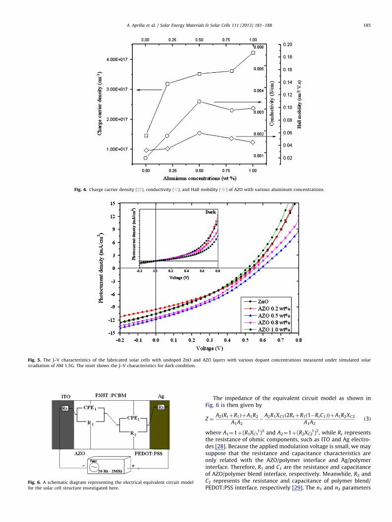
Fig. 4. Charge carrier density (&), conductivity (J), and Hall mobility (B) of AZO with various aluminum concentrations.
Fig. 5. The J–V characteristics of the fabricated solar cells with undoped ZnO and AZO layers with various dopant concentrations measured under simulated solar
irradiation of AM 1.5G. The inset shows the J–V characteristics for dark condition.
Fig. 6. A schematic diagram representing the electrical equivalent circuit model
for the solar cell structure investigated here.
A. Aprilia et al. / Solar Energy Materials & Solar Cells 111 (2013) 181–188 185
The impedance of the equivalent circuit model as shown inFig. 6 is then given by
Z ¼A2 RsþR1ð ÞþA1R2
A1A2�
A2R1XC1ð2RsþR1 1�RsC1ð ÞÞþA1R2XC2
A1A2ð3Þ
where A1¼1þ(R1XC1�1)2 and A2¼1þ(R2XC2
�1)2, while Rs representsthe resistance of ohmic components, such as ITO and Ag electro-des [28]. Because the applied modulation voltage is small, we maysuppose that the resistance and capacitance characteristics areonly related with the AZO/polymer interface and Ag/polymerinterface. Therefore, R1 and C1 are the resistance and capacitanceof AZO/polymer blend interface, respectively. Meanwhile, R2 andC2 represents the resistance and capacitance of polymer blend/PEDOT:PSS interface, respectively [29]. The n1 and n2 parameters
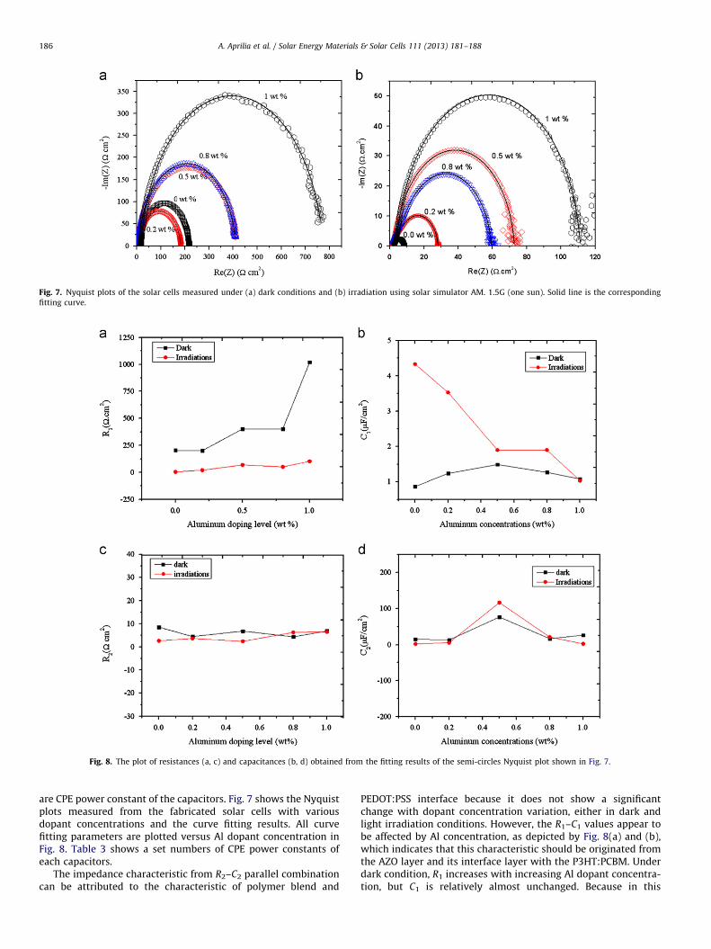
Fig. 7. Nyquist plots of the solar cells measured under (a) dark conditions and (b) irradiation using solar simulator AM. 1.5G (one sun). Solid line is the corresponding
fitting curve.
Fig. 8. The plot of resistances (a, c) and capacitances (b, d) obtained from the fitting results of the semi-circles Nyquist plot shown in Fig. 7.
A. Aprilia et al. / Solar Energy Materials & Solar Cells 111 (2013) 181–188186
are CPE power constant of the capacitors. Fig. 7 shows the Nyquistplots measured from the fabricated solar cells with variousdopant concentrations and the curve fitting results. All curvefitting parameters are plotted versus Al dopant concentration inFig. 8. Table 3 shows a set numbers of CPE power constants ofeach capacitors.
The impedance characteristic from R2–C2 parallel combinationcan be attributed to the characteristic of polymer blend and
PEDOT:PSS interface because it does not show a significantchange with dopant concentration variation, either in dark andlight irradiation conditions. However, the R1–C1 values appear tobe affected by Al concentration, as depicted by Fig. 8(a) and (b),which indicates that this characteristic should be originated fromthe AZO layer and its interface layer with the P3HT:PCBM. Underdark condition, R1 increases with increasing Al dopant concentra-tion, but C1 is relatively almost unchanged. Because in this
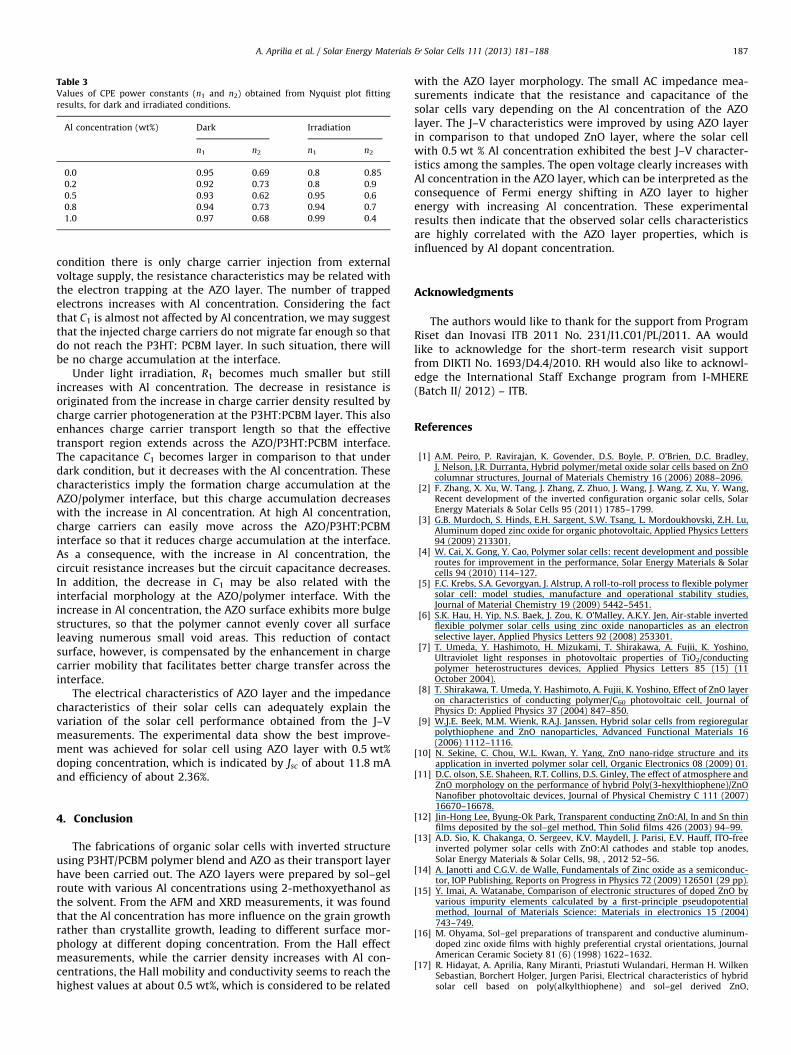
Table 3Values of CPE power constants (n1 and n2) obtained from Nyquist plot fitting
results, for dark and irradiated conditions.
Al concentration (wt%) Dark Irradiation
n1 n2 n1 n2
0.0 0.95 0.69 0.8 0.85
0.2 0.92 0.73 0.8 0.9
0.5 0.93 0.62 0.95 0.6
0.8 0.94 0.73 0.94 0.7
1.0 0.97 0.68 0.99 0.4
A. Aprilia et al. / Solar Energy Materials & Solar Cells 111 (2013) 181–188 187
condition there is only charge carrier injection from externalvoltage supply, the resistance characteristics may be related withthe electron trapping at the AZO layer. The number of trappedelectrons increases with Al concentration. Considering the factthat C1 is almost not affected by Al concentration, we may suggestthat the injected charge carriers do not migrate far enough so thatdo not reach the P3HT: PCBM layer. In such situation, there willbe no charge accumulation at the interface.
Under light irradiation, R1 becomes much smaller but stillincreases with Al concentration. The decrease in resistance isoriginated from the increase in charge carrier density resulted bycharge carrier photogeneration at the P3HT:PCBM layer. This alsoenhances charge carrier transport length so that the effectivetransport region extends across the AZO/P3HT:PCBM interface.The capacitance C1 becomes larger in comparison to that underdark condition, but it decreases with the Al concentration. Thesecharacteristics imply the formation charge accumulation at theAZO/polymer interface, but this charge accumulation decreaseswith the increase in Al concentration. At high Al concentration,charge carriers can easily move across the AZO/P3HT:PCBMinterface so that it reduces charge accumulation at the interface.As a consequence, with the increase in Al concentration, thecircuit resistance increases but the circuit capacitance decreases.In addition, the decrease in C1 may be also related with theinterfacial morphology at the AZO/polymer interface. With theincrease in Al concentration, the AZO surface exhibits more bulgestructures, so that the polymer cannot evenly cover all surfaceleaving numerous small void areas. This reduction of contactsurface, however, is compensated by the enhancement in chargecarrier mobility that facilitates better charge transfer across theinterface.
The electrical characteristics of AZO layer and the impedancecharacteristics of their solar cells can adequately explain thevariation of the solar cell performance obtained from the J–Vmeasurements. The experimental data show the best improve-ment was achieved for solar cell using AZO layer with 0.5 wt%doping concentration, which is indicated by Jsc of about 11.8 mAand efficiency of about 2.36%.
4. Conclusion
The fabrications of organic solar cells with inverted structureusing P3HT/PCBM polymer blend and AZO as their transport layerhave been carried out. The AZO layers were prepared by sol–gelroute with various Al concentrations using 2-methoxyethanol asthe solvent. From the AFM and XRD measurements, it was foundthat the Al concentration has more influence on the grain growthrather than crystallite growth, leading to different surface mor-phology at different doping concentration. From the Hall effectmeasurements, while the carrier density increases with Al con-centrations, the Hall mobility and conductivity seems to reach thehighest values at about 0.5 wt%, which is considered to be related
with the AZO layer morphology. The small AC impedance mea-surements indicate that the resistance and capacitance of thesolar cells vary depending on the Al concentration of the AZOlayer. The J–V characteristics were improved by using AZO layerin comparison to that undoped ZnO layer, where the solar cellwith 0.5 wt % Al concentration exhibited the best J–V character-istics among the samples. The open voltage clearly increases withAl concentration in the AZO layer, which can be interpreted as theconsequence of Fermi energy shifting in AZO layer to higherenergy with increasing Al concentration. These experimentalresults then indicate that the observed solar cells characteristicsare highly correlated with the AZO layer properties, which isinfluenced by Al dopant concentration.
Acknowledgments
The authors would like to thank for the support from ProgramRiset dan Inovasi ITB 2011 No. 231/I1.C01/PL/2011. AA wouldlike to acknowledge for the short-term research visit supportfrom DIKTI No. 1693/D4.4/2010. RH would also like to acknowl-edge the International Staff Exchange program from I-MHERE(Batch II/ 2012) – ITB.
References
[1] A.M. Peiro, P. Ravirajan, K. Govender, D.S. Boyle, P. O’Brien, D.C. Bradley,J. Nelson, J.R. Durranta, Hybrid polymer/metal oxide solar cells based on ZnOcolumnar structures, Journal of Materials Chemistry 16 (2006) 2088–2096.
[2] F. Zhang, X. Xu, W. Tang, J. Zhang, Z. Zhuo, J. Wang, J. Wang, Z. Xu, Y. Wang,Recent development of the inverted configuration organic solar cells, SolarEnergy Materials & Solar Cells 95 (2011) 1785–1799.
[3] G.B. Murdoch, S. Hinds, E.H. Sargent, S.W. Tsang, L. Mordoukhovski, Z.H. Lu,Aluminum doped zinc oxide for organic photovoltaic, Applied Physics Letters94 (2009) 213301.
[4] W. Cai, X. Gong, Y. Cao, Polymer solar cells: recent development and possibleroutes for improvement in the performance, Solar Energy Materials & Solarcells 94 (2010) 114–127.
[5] F.C. Krebs, S.A. Gevorgyan, J. Alstrup, A roll-to-roll process to flexible polymersolar cell: model studies, manufacture and operational stability studies,Journal of Material Chemistry 19 (2009) 5442–5451.
[6] S.K. Hau, H. Yip, N.S. Baek, J. Zou, K. O’Malley, A.K.Y. Jen, Air-stable invertedflexible polymer solar cells using zinc oxide nanoparticles as an electronselective layer, Applied Physics Letters 92 (2008) 253301.
[7] T. Umeda, Y. Hashimoto, H. Mizukami, T. Shirakawa, A. Fujii, K. Yoshino,Ultraviolet light responses in photovoltaic properties of TiO2/conductingpolymer heterostructures devices, Applied Physics Letters 85 (15) (11October 2004).
[8] T. Shirakawa, T. Umeda, Y. Hashimoto, A. Fujii, K. Yoshino, Effect of ZnO layeron characteristics of conducting polymer/C60 photovoltaic cell, Journal ofPhysics D: Applied Physics 37 (2004) 847–850.
[9] W.J.E. Beek, M.M. Wienk, R.A.J. Janssen, Hybrid solar cells from regioregularpolythiophene and ZnO nanoparticles, Advanced Functional Materials 16(2006) 1112–1116.
[10] N. Sekine, C. Chou, W.L. Kwan, Y. Yang, ZnO nano-ridge structure and itsapplication in inverted polymer solar cell, Organic Electronics 08 (2009) 01.
[11] D.C. olson, S.E. Shaheen, R.T. Collins, D.S. Ginley, The effect of atmosphere andZnO morphology on the performance of hybrid Poly(3-hexylthiophene)/ZnONanofiber photovoltaic devices, Journal of Physical Chemistry C 111 (2007)16670–16678.
[12] Jin-Hong Lee, Byung-Ok Park, Transparent conducting ZnO:Al, In and Sn thinfilms deposited by the sol–gel method, Thin Solid films 426 (2003) 94–99.
[13] A.D. Sio, K. Chakanga, O. Sergeev, K.V. Maydell, J. Parisi, E.V. Hauff, ITO-freeinverted polymer solar cells with ZnO:Al cathodes and stable top anodes,Solar Energy Materials & Solar Cells, 98, , 2012 52–56.
[14] A. Janotti and C.G.V. de Walle, Fundamentals of Zinc oxide as a semiconduc-tor, IOP Publishing, Reports on Progress in Physics 72 (2009) 126501 (29 pp).
[15] Y. Imai, A. Watanabe, Comparison of electronic structures of doped ZnO byvarious impurity elements calculated by a first-principle pseudopotentialmethod, Journal of Materials Science: Materials in electronics 15 (2004)743–749.
[16] M. Ohyama, Sol–gel preparations of transparent and conductive aluminum-doped zinc oxide films with highly preferential crystal orientations, JournalAmerican Ceramic Society 81 (6) (1998) 1622–1632.
[17] R. Hidayat, A. Aprilia, Rany Miranti, Priastuti Wulandari, Herman H. WilkenSebastian, Borchert Holger, Jurgen Parisi, Electrical characteristics of hybridsolar cell based on poly(alkylthiophene) and sol–gel derived ZnO,
A. Aprilia et al. / Solar Energy Materials & Solar Cells 111 (2013) 181–188188
International Symposium on Functional Materials Science, Bali, April 27th–28th, 2011.
[18] R. Sondergaard, M. Helgesen, M. Jorgensen, F.C. Krebs, Fabrication of polymersolar cells using aqueous processing for all layers including the metal backelectrode, Advance Energy Materials (2011) 68–71.
[19] J. Alstrup, M. Jorgensen, A.J. Medford, F.C. Krebs, Ultrafast and parsimoniousmaterials screening for polymer solar cells using differentially pumped slot-die coating, ACS Applied Materials & Interfaces 2 (10) (2010) 2819–2827.
[20] G. Srinivasan, J. Kumar, Optical and structural characterization of zinc oxidethin films prepared by sol–gel process, Crystal Research and Technology 41(9) (2006) 893–896.
[21] T. Stubhan, H. Oh, L. Pinna, J. Krantz, I. Litzov, C.J. Brabec, Inverted organicsolar cells using a solution processed aluminum-doped zinc oxide bufferlayer, Organic Electronics 12 (2011) 1539–1543.
[22] /http://www.abc.chemistry.bsu.by/vi/analyser/S.[23] L. Spanhel, M.A. Anderson, Semiconductor clusters in the sol–gel process:
quantized aggregation, gelation, and crystal growth in concentrated ZnOcolloids, Journal of the American Chemical Society 113 (1991) 2826–2833.
[24] H. Oh, J. Krantz, I. Litzov, T. Stubhan, L. Pinna, C.J. Brabec, Comparison ofVarious sol–gel derived metal oxide layers for inverted organic solar cells,Solar Energy Materials & Solar Cells 95 (2011) 2194–2199.
[25] D. Shimono, S. Tanaka, T. Torikai, T. Watari, M. Murano, Preparation oftransparent and conductive ZnO films using a chemical solution depositionprocess, Journal of Ceramic Processing Research 2 (4) (2001) 184–188.
[26] V. Bhoslea, J.T. Prater, D. Fan Yang, S.R. Burk, Forrest, J. Narayan, Gallium-dopedzinc oxide films as transparent electrodes for organic solar cell applications,
Journal of Applied Physics 102 (2007) 023501.[27] J.P. Kar, S. Kim, B. Shin, K.I. Park, K.J. Ahn, W. Lee, J.H. Cho, J.M. Myoung,
Influence of sputtering pressure on morphological, mechanical and electricalproperties of Al-doped ZnO films, Solid-State Electronics 54 (2010)1447–1450.
[28] E. Barsoukov, J.R. Macdonald, Impedance Spectroscopy Theory, Experiment,and Applications, Second edition, Published by John Wiley & Sons, Inc,
Hoboken, New Jersey, ISBN 0-471-64749-7, 2005.[29] B. Conings, L. Baeten, H. Boyen, D. Spoltore, J. D’Haen, L. Grieten, P. Wagner,
M.K. Van bael, J.V. Manca, Influences of interface Morphology onto thephotovoltaic properties of nanopatterned ZnO/Poly(3-hexylthiophene)hybrid solar cells, An Impedance spectroscopy study, The Journal of Physical
Chemistry C 115 (2011) 16695–16700.