Influence of Poly(ethylene oxide) on the Process of Copper Electrodeposition onto p-Si(100
10
Influence of Poly(ethylene oxide) on the Process of Copper Electrodeposition onto p-Si(100) Eduardo C. Mun ˜ oz, ²,‡ Ricardo S. Schrebler,* ,² Ricardo A. Co ´ rdova, ² Ricardo E. Marotti, § and Enrique A. Dalchiele § Instituto de Quı ´mica, Facultad de Ciencias, Pontificia UniVersidad Cato ´ lica de Valparaı ´so, Casilla 4059, Valparaı ´so, Chile, Departamento de Ciencias Ba ´ sicas, Escuela de Educacio ´ n, UniVersidad de Vin ˜ a del Mar, Agua Santa 7255, Vin ˜ a del Mar, Chile, and Instituto de Fı ´sica, Facultad de Ingenierı ´a, UniVersidad de La Repu ´ blica, Herrera y Reissig 565, C.C. 30, 11000 MonteVideo, Uruguay ReceiVed: June 20, 2007; In Final Form: August 10, 2007 In this study we examined the influence of the illumination intensity and the presence of poly(ethylene oxide) (PEO) as an additive for the process of copper electrodeposition onto p-Si(100). The study was carried out by means of cyclic voltammetry (CV) and the potential step method from which the corresponding nucleation and growth mechanism (NGM) were determined. Both methods were performed under illumination for the electron’s photogeneration. Likewise, a morphologic analysis of the deposits obtained at different potential values by means of atomic force microscopy (AFM) was carried out. In the first stage, Mott-Schottky measurements were taken to characterize the energetic of the semiconductor/electrolyte interface. The CV results indicated that the presence of PEO inhibits the electrochemical reaction of oxide formation on the surface of the semiconductor. This allows a decrease in the overpotential associated with the electrodeposition process. The analysis of the j/t transients shows that in the absence of additive the NGM corresponds to progressive 3D diffusional controlled (PN3D DIFF ), while in the presence of PEO the NGM corresponds to instantaneous 3D diffusional controlled (IN3D DIFF ). In both cases analysis by the AFM technique was performed and confirmed these mechanisms. The morphologic analysis by this technique led us to the conclusion that the deposits made in the presence of additive are more homogeneous. 1. Introduction The deposition of metallic films on semiconductors is usually performed in a vacuum from the vapor phase by evaporation or sputter deposition. Electrochemical deposition represents an alternative approach for the deposition of these films on semiconductor surfaces. The formation of these metallic phases requires a study of the nucleation and growth mechanisms and the influence of parameters such as potential and chemical composition of the solution. Considering silicon, there have been studies of electrochemi- cal film growth. The deposition of metals on silicon generally follows a 3D islands growth mode due to the fact that the metal-metal interaction is stronger than the substrate-metal interaction. 1-19 The copper nucleation and growth process onto silicon has been confirmed by means different techniques, such as scanning electronic microscopy (SEM), atomic force mi- croscopy (AFM), and scanning tunneling microscopy (STM). 1,7,12,13 The microstructure and morphology of electrodeposited thin films are controlled by addition of additives to the plating solution. These additives are widely used to control long length scale roughness (levelers) and to produce a textured, small grain size film (brighteners). In this sense, it has been shown that for the copper electrodeposition on Si, the use of additives, such as poly(ethylene glycol) (PEG), PEO, and bis(3-sulfopropyl) bisulfide, improve the homogeneity and texture of the depos- its. 1,11 However, when using polymeric additives, the under- standing of the influence on the deposition process is still empirical. In a previous work we demonstrated that the presence of poly(ethylene oxide) (PEO) in the copper electrodeposition process on n-Si(100) increased the copper nucleus density due to the adsorption of this molecule at the active sites inhibiting the oxide formation and this way allowing a more homogeneous deposit. 1 In this paper we report the influence of the additive PEO on the nucleation and growth mechanism of copper onto p-Si(100), in a sulfuric acid media. This process must be carried out under illumination for the photogeneration of electrons which in this case is necessary for observing the reduction of copper ions. The study was performed by cyclic voltammetry (CV) and the potential step method (PS). In addition, the morphology of the copper deposits was followed by atomic force microscopy (AFM). Also, a discussion about the nucleus density obtained by both methods was achieved. 2. Experimental Section Electrodeposition was performed on monocrystalline p-Si (100) with a resistivity between 0.1 and 0.3 Ω cm (N A = 5 × 10 15 cm -3 ) and B-doped and polished/etched surfaces (Int. Wafer Service, CA). The silicon wafer was cut into squares (1.0 × 1.0 cm 2 ) that were first degreased in boiling acetone for 10 min. Then they were sequentially cleaned ultrasonically for 10 min in acetone, ethanol, and finally water. The water was distilled and deionized (Millipore) and had a resistivity of 18 MΩ cm. Then the electrodes were treated for 10 min with a 1:1 H 2 SO 4 -H 2 O 2 mixture heated up to 80 °C to remove any trace of heavy metals and organic species. Afterward, the oxide * Corresponding author. Tel./fax: +56-32-273422. E-mail: rschrebl@ ucv.cl. ² Pontificia Universidad Cato ´lica de Valparaı ´so. ‡ Universidad de Vin ˜a del Mar. § Universidad de La Repu ´blica. 16506 J. Phys. Chem. C 2007, 111, 16506-16515 10.1021/jp074813m CCC: $37.00 © 2007 American Chemical Society Published on Web 10/11/2007
-
Upload
independent -
Category
Documents
-
view
2 -
download
0
Transcript of Influence of Poly(ethylene oxide) on the Process of Copper Electrodeposition onto p-Si(100

Influence of Poly(ethylene oxide) on the Process of Copper Electrodeposition onto p-Si(100)
Eduardo C. Munoz,†,‡ Ricardo S. Schrebler,*,† Ricardo A. Cordova,† Ricardo E. Marotti, § andEnrique A. Dalchiele§
Instituto de Quı´mica, Facultad de Ciencias, Pontificia UniVersidad Cato´ lica de Valparaı´so,Casilla 4059, Valparaı´so, Chile, Departamento de Ciencias Ba´sicas, Escuela de Educacio´n, UniVersidad deVina del Mar, Agua Santa 7255, Vin˜a del Mar, Chile, and Instituto de Fı´sica, Facultad de Ingenierı´a,UniVersidad de La Repu´blica, Herrera y Reissig 565, C.C. 30, 11000 MonteVideo, Uruguay
ReceiVed: June 20, 2007; In Final Form: August 10, 2007
In this study we examined the influence of the illumination intensity and the presence of poly(ethylene oxide)(PEO) as an additive for the process of copper electrodeposition onto p-Si(100). The study was carried outby means of cyclic voltammetry (CV) and the potential step method from which the corresponding nucleationand growth mechanism (NGM) were determined. Both methods were performed under illumination for theelectron’s photogeneration. Likewise, a morphologic analysis of the deposits obtained at different potentialvalues by means of atomic force microscopy (AFM) was carried out. In the first stage, Mott-Schottkymeasurements were taken to characterize the energetic of the semiconductor/electrolyte interface. The CVresults indicated that the presence of PEO inhibits the electrochemical reaction of oxide formation on thesurface of the semiconductor. This allows a decrease in the overpotential associated with the electrodepositionprocess. The analysis of thej/t transients shows that in the absence of additive the NGM corresponds toprogressive 3D diffusional controlled (PN3DDIFF), while in the presence of PEO the NGM corresponds toinstantaneous 3D diffusional controlled (IN3DDIFF). In both cases analysis by the AFM technique was performedand confirmed these mechanisms. The morphologic analysis by this technique led us to the conclusion thatthe deposits made in the presence of additive are more homogeneous.
1. Introduction
The deposition of metallic films on semiconductors is usuallyperformed in a vacuum from the vapor phase by evaporationor sputter deposition. Electrochemical deposition represents analternative approach for the deposition of these films onsemiconductor surfaces. The formation of these metallic phasesrequires a study of the nucleation and growth mechanisms andthe influence of parameters such as potential and chemicalcomposition of the solution.
Considering silicon, there have been studies of electrochemi-cal film growth. The deposition of metals on silicon generallyfollows a 3D islands growth mode due to the fact that themetal-metal interaction is stronger than the substrate-metalinteraction.1-19 The copper nucleation and growth process ontosilicon has been confirmed by means different techniques, suchas scanning electronic microscopy (SEM), atomic force mi-croscopy (AFM), and scanning tunneling microscopy(STM).1,7,12,13
The microstructure and morphology of electrodeposited thinfilms are controlled by addition of additives to the platingsolution. These additives are widely used to control long lengthscale roughness (levelers) and to produce a textured, small grainsize film (brighteners). In this sense, it has been shown that forthe copper electrodeposition on Si, the use of additives, suchas poly(ethylene glycol) (PEG), PEO, and bis(3-sulfopropyl)bisulfide, improve the homogeneity and texture of the depos-
its.1,11 However, when using polymeric additives, the under-standing of the influence on the deposition process is stillempirical. In a previous work we demonstrated that the presenceof poly(ethylene oxide) (PEO) in the copper electrodepositionprocess on n-Si(100) increased the copper nucleus density dueto the adsorption of this molecule at the active sites inhibitingthe oxide formation and this way allowing a more homogeneousdeposit.1
In this paper we report the influence of the additive PEO onthe nucleation and growth mechanism of copper onto p-Si(100),in a sulfuric acid media. This process must be carried out underillumination for the photogeneration of electrons which in thiscase is necessary for observing the reduction of copper ions.The study was performed by cyclic voltammetry (CV) and thepotential step method (PS). In addition, the morphology of thecopper deposits was followed by atomic force microscopy(AFM). Also, a discussion about the nucleus density obtainedby both methods was achieved.
2. Experimental Section
Electrodeposition was performed on monocrystalline p-Si(100) with a resistivity between 0.1 and 0.3Ω cm (NA = 5 ×1015 cm-3) and B-doped and polished/etched surfaces (Int.Wafer Service, CA). The silicon wafer was cut into squares(1.0× 1.0 cm2) that were first degreased in boiling acetone for10 min. Then they were sequentially cleaned ultrasonically for10 min in acetone, ethanol, and finally water. The water wasdistilled and deionized (Millipore) and had a resistivity of 18MΩ cm. Then the electrodes were treated for 10 min with a1:1 H2SO4-H2O2 mixture heated up to 80°C to remove anytrace of heavy metals and organic species. Afterward, the oxide
* Corresponding author. Tel./fax:+56-32-273422. E-mail: [email protected].
† Pontificia Universidad Cato´lica de Valparaı´so.‡ Universidad de Vin˜a del Mar.§ Universidad de La Repu´blica.
16506 J. Phys. Chem. C2007,111,16506-16515
10.1021/jp074813m CCC: $37.00 © 2007 American Chemical SocietyPublished on Web 10/11/2007
film was removed by etching with 2 M HF solution for 2 minand thoroughly rinsed with ultrapure water. The ohmic contactwas made with InGa eutectic on the etched face of the samples,and the electrodes were mounted onto a Teflon holder. Thesilicon area exposed to the solution was 0.16 cm2. Before theelectrochemical experiments, the electrode surface was againetched for 2 min in a 2 M HFsolution. After this procedure, anatomically smooth and hydrogen-terminated surface has beenobtained. For each measurement, a new electrode of p-Si(100)was used, due to the fact that it is well-known that copper candiffuse toward the inside of the silicon.9-20
A platinum wire was used as a counter electrode, and amercury/mercury sulfate electrode (MSE) (Hg/Hg2SO4, K2SO4
(saturated), 0.640 V vs NHE) was used as a reference electrode.It was positioned close to the silicon samples using a Luggincapillary. All the potentials reported in this study refer to thisreference electrode.
The electrolytic solutions were prepared from analytical gradereagents with the following compositions: 5 mM CuSO4‚5H2O+ 0.1 M H2SO4 + x mg/L [PEO] (0e × e 100 mg/L). Themolecular weight of the additive was 1 000 000.
Cyclic voltammetry experiments were carried out at roomtemperature and at a scan rate of 0.010 V s-1, according to theperturbation programs indicated in the corresponding figures.For the chronoamperometric measurements, the followingE/t program was applied to the electrode: the potential wasfirst held for 5 s at a potential value where the copperelectrodeposition is not observed and then stepped to theelectrodeposition potentialEd. The Ed values varied between-0.350 and-0.650 V. All the measurements were carried outin darkness and illumination conditions. In this last case, a xenonlamp of 75 W (Oriel Instruments 6263) mounted in a lampholder (Oriel 66902) was connected to the cell through a waterfilter (Oriel 61945) and a 1 mlength optical fiber (Oriel 77578).A power supply of 40-200 W (Oriel 68907) was used togenerate the arc in the lamp. The illumination power wasquantified inside of the cell with an energy radiant meter (Oriel70260). The samples were illuminated with different intensitiesthat were of 2 and 3.5 mW cm-2. A pure argon stream waspassed through the solution for 30 min before measurementsand over the solution when the experiments were under way.
The electrochemical measurements (cyclic voltammetry andchronoaperometry) were done using Princeton Applied Research(PAR) model 273 A equipment. The electrochemical impedancespectroscopy (EIS) measurements were done using Zahnermodel IM6e equipment. All samples used for ex situ AFM wereprepared in the electrochemical cell. The AFM images wereobtained with a Digital Instrument Nanoscope IIIa Seriesemployed in tapping mode at a scan rate of 0.02µm/s.
3. Results and Discussion
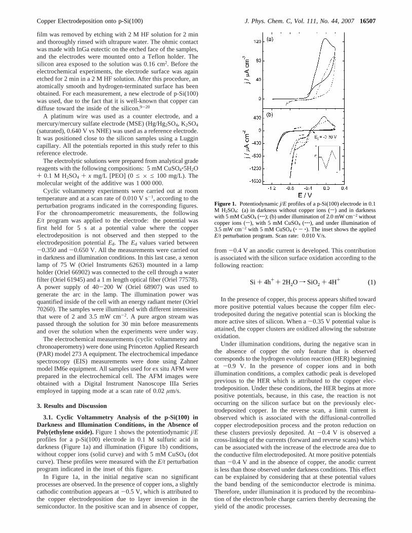
3.1. Cyclic Voltammetry Analysis of the p-Si(100) inDarkness and Illumination Conditions, in the Absence ofPoly(ethylene oxide).Figure 1 shows the potentiodynamicj/Eprofiles for a p-Si(100) electrode in 0.1 M sulfuric acid indarkness (Figure 1a) and illumination (Figure 1b) conditions,without copper ions (solid curve) and with 5 mM CuSO4 (dotcurve). These profiles were measured with theE/t perturbationprogram indicated in the inset of this figure.
In Figure 1a, in the initial negative scan no significantprocesses are observed. In the presence of copper ions, a slightlycathodic contribution appears at-0.5 V, which is attributed tothe copper electrodeposition due to layer inversion in thesemiconductor. In the positive scan and in absence of copper,
from -0.4 V an anodic current is developed. This contributionis associated with the silicon surface oxidation according to thefollowing reaction:
In the presence of copper, this process appears shifted towardmore positive potential values because the copper film elec-trodeposited during the negative potential scan is blocking themore active sites of silicon. When a-0.35 V potential value isattained, the copper clusters are oxidized allowing the substrateoxidation.
Under illumination conditions, during the negative scan inthe absence of copper the only feature that is observedcorresponds to the hydrogen evolution reaction (HER) beginningat -0.9 V. In the presence of copper ions and in bothillumination conditions, a complex cathodic peak is developedprevious to the HER which is attributed to the copper elec-trodeposition. Under these conditions, the HER begins at morepositive potentials, because, in this case, the reaction is notoccurring on the silicon surface but on the previously elec-trodeposited copper. In the reverse scan, a limit current isobserved which is associated with the diffusional-controlledcopper electrodeposition process and the proton reduction onthese clusters previosly deposited. At-0.4 V is observed across-linking of the currents (forward and reverse scans) whichcan be associated with the increase of the electrode area due tothe conductive film electrodeposited. At more positive potentialsthan-0.4 V and in the absence of copper, the anodic currentis less than those observed under darkness conditions. This effectcan be explained by considering that at these potential valuesthe band bending of the semiconductor electrode is minima.Therefore, under illumination it is produced by the recombina-tion of the electron/hole charge carriers thereby decreasing theyield of the anodic processes.
Figure 1. Potentiodynamicj/E profiles of a p-Si(100) electrode in 0.1M H2SO4: (a) in darkness without copper ions (s) and in darknesswith 5 mM CuSO4 (‚‚‚); (b) under illumination of 2.0 mW cm-2 withoutcopper ions (s), with 5 mM CuSO4 (‚‚‚), and under illumination of3.5 mW cm-2 with 5 mM CuSO4 (‚ - ‚). The inset shows the appliedE/t perturbation program. Scan rate: 0.010 V/s.
Si + 4h+ + 2H2O f SiO2 + 4H+ (1)
Copper Electrodeposition onto p-Si(100) J. Phys. Chem. C, Vol. 111, No. 44, 200716507
The presence of complex peaks as much in the cathodic andanodic hemicycles is in agreement with those observed usingn-Si(100).1 However, the processes associated with the copperelectrodeposition on p-Si(100) appear at potential values nearthe reversible potential (∼0.34 V vs MSE).
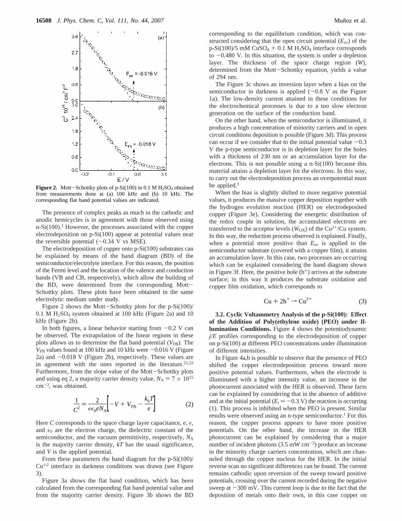
The electrodeposition of copper onto p-Si(100) substrates canbe explained by means of the band diagram (BD) of thesemiconductor/electrolyte interface. For this reason, the positionof the Fermi level and the location of the valence and conductionbands (VB and CB, respectively), which allow the building ofthe BD, were determined from the corresponding Mott-Schottky plots. These plots have been obtained in the sameelectrolytic medium under study.
Figure 2 shows the Mott-Schottky plots for the p-Si(100)/0.1 M H2SO4 system obtained at 100 kHz (Figure 2a) and 10kHz (Figure 2b).
In both figures, a linear behavior starting from-0.2 V canbe observed. The extrapolation of the linear regions in theseplots allows us to determine the flat band potential (VFB). TheVFB values found at 100 kHz and 10 kHz were-0.016 V (Figure2a) and-0.018 V (Figure 2b), respectively. These values arein agreement with the ones reported in the literature.21,22
Furthermore, from the slope value of the Mott-Schottky plotsand using eq 2, a majority carrier density value,NA ) 7 × 10¹⁵
cm-3, was obtained.
HereC corresponds to the space charge layer capacitance,e, ε,and ε0 are the electron charge, the dielectric constant of thesemiconductor, and the vacuum permittivity, respectively,NA
is the majority carrier density,kT has the usual significance,andV is the applied potential.
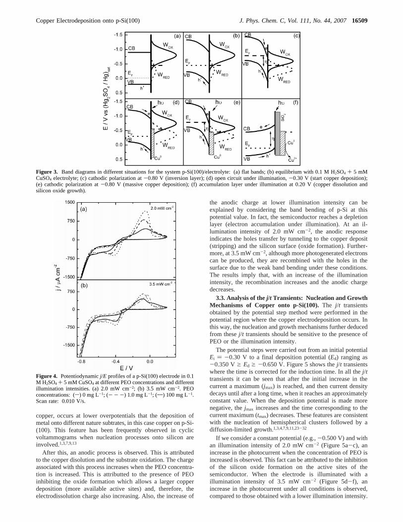
From these parameters the band diagram for the p-Si(100)/Cu+2 interface in darkness conditions was drawn (see Figure3).
Figure 3a shows the flat band condition, which has beencalculated from the corresponding flat band potential value andfrom the majority carrier density. Figure 3b shows the BD
corresponding to the equilibrium condition, which was con-structed considering that the open circuit potential (Eoc) of thep-Si(100)/5 mM CuSO4 + 0.1 M H2SO4 interface correspondsto -0.480 V. In this situation, the system is under a depletionlayer. The thickness of the space charge region (W),determined from the Mott-Schottky equation, yields a valueof 294 nm.
The Figure 3c shows an inversion layer when a bias on thesemiconductor in darkness is applied (-0.8 V as the Figure1a). The low-density current attained in these conditions forthe electrochemical processes is due to a too slow electrongeneration on the surface of the conduction band.
On the other hand, when the semiconductor is illuminated, itproduces a high concentration of minority carriers and in opencircuit conditions deposition is possible (Figure 3d). This processcan occur if we consider that to the initial potential value-0.3V the p-type semiconductor is in depletion layer for the holeswith a thickness of 230 nm or an accumulation layer for theelectrons. This is not possible using a n-Si(100) because thismaterial attains a depletion layer for the electrons. In this way,to carry out the electrodeposition process an overpotential mustbe applied.1
When the bias is slightly shifted to more negative potentialvalues, it produces the massive copper deposition together withthe hydrogen evolution reaction (HER) on electrodepositedcopper (Figure 3e). Considering the energetic distribution ofthe redox couple in solution, the accumulated electrons aretransferred to the acceptor levels (WOX) of the Cu2+/Cu system.In this way, the reduction process observed is explained. Finally,when a potential more positive thanEoc is applied to thesemiconductor substrate (covered with a copper film), it attainsan accumulation layer. In this case, two processes are occurringwhich can be explained considering the band diagram shownin Figure 3f. Here, the positive hole (h+) arrives at the substratesurface; in this way it produces the substrate oxidation andcopper film oxidation, which corresponds to
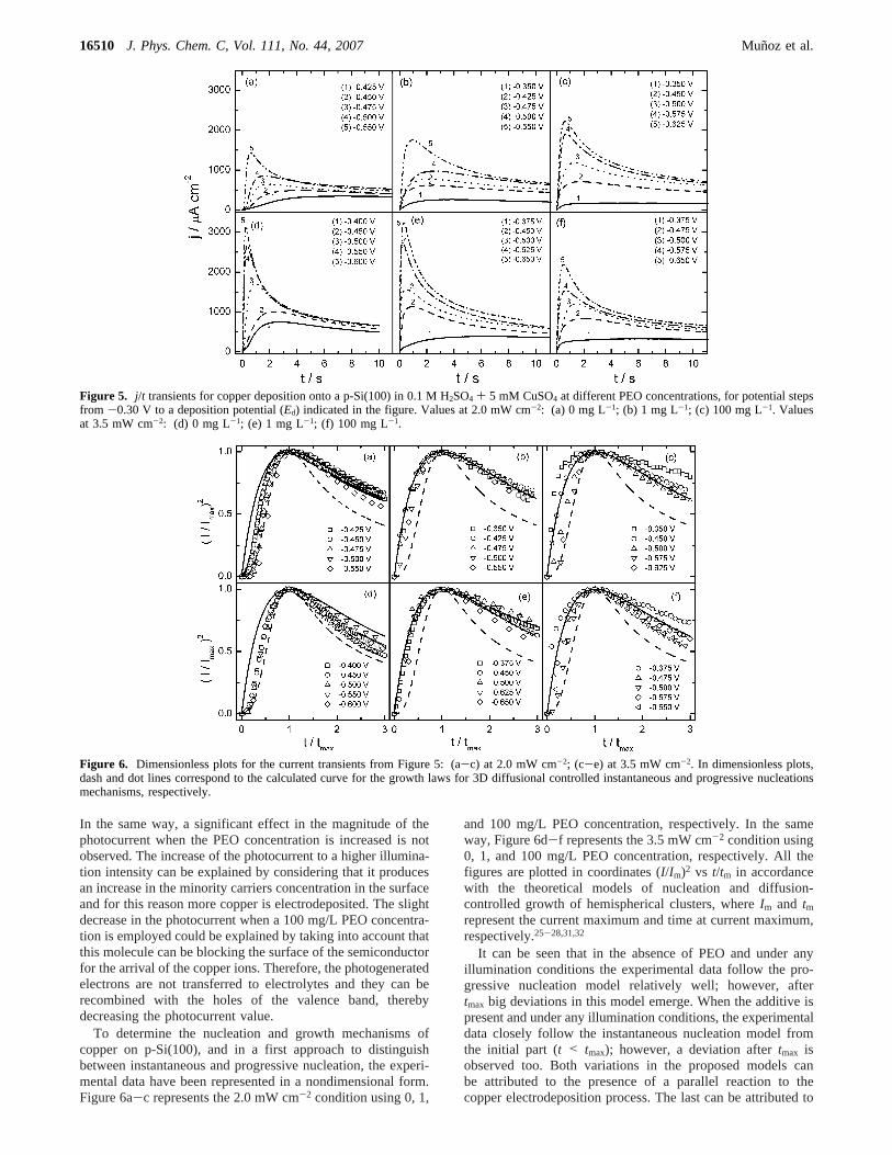
3.2. Cyclic Voltammetry Analysis of the p-Si(100): Effectof the Addition of Poly(ethylene oxide) (PEO) under Il-lumination Conditions. Figure 4 shows the potentiodynamicj/E profiles corresponding to the electrodeposition of copperon p-Si(100) at different PEO concentrations under illuminationof different intensities.
In Figure 4a,b is possible to observe that the presence of PEOshifted the copper electrodeposition process toward morepositive potential values. Furthermore, when the electrode isilluminated with a higher intensity value, an increase in thephotocurrent associated with the HER is observed. These factscan be explained by considering that in the absence of additiveand at the initial potential (Ei ) -0.3 V) the reaction is occurring(1). This process is inhibited when the PEO is present. Similarresults were observed using an n-type semiconductor.1 For thisreason, the copper process appears to have more positivepotentials. On the other hand, the increase in the HERphotocurrent can be explained by considering that a majornumber of incident photons (3.5 mW cm-2) produce an increasein the minority charge carriers concentration, which are chan-neled through the copper nucleus for the HER. In the initialreverse scan no significant differences can be found. The currentremains cathodic upon reversion of the sweep toward positivepotentials, crossing over the current recorded during the negativesweep at-300 mV. This current loop is due to the fact that thedeposition of metals onto their own, in this case copper on
Figure 2. Mott-Schottky plots of p-Si(100) in 0.1 M H2SO4 obtainedfrom measurements done at (a) 100 kHz and (b) 10 kHz. Thecorresponding flat band potential values are indicated.
1
C2) 2
εε0eNA[-V + VFB -
kbT
e ] (2)
Cu + 2h+ f Cu2+ (3)
16508 J. Phys. Chem. C, Vol. 111, No. 44, 2007 Munoz et al.
copper, occurs at lower overpotentials that the deposition ofmetal onto different nature subtrates, in this case copper on p-Si-(100). This feature has been frequently observed in cyclicvoltammograms when nucleation processes onto silicon areinvolved.1,3,7,9,13
After this, an anodic process is observed. This is attributedto the copper disolution and the substrate oxidation. The chargeassociated with this process increases when the PEO concentra-tion is increased. This is attributted to the presence of PEOinhibiting the oxide formation which allows a larger copperdeposition (more available active sites) and, therefore, theelectrodissolution charge also increasing. Also, the increase of
the anodic charge at lower illumination intensity can beexplained by considering the band bending of p-Si at thispotential value. In fact, the semiconductor reaches a depletionlayer (electron accumulation under illumination). At an il-lumination intensity of 2.0 mW cm-2, the anodic responseindicates the holes transfer by tunneling to the copper deposit(stripping) and the silicon surface (oxide formation). Further-more, at 3.5 mW cm-2, although more photogenerated electronscan be produced, they are recombined with the holes in thesurface due to the weak band bending under these conditions.The results imply that, with an increase of the illuminationintensity, the recombination increases and the anodic chargedecreases.
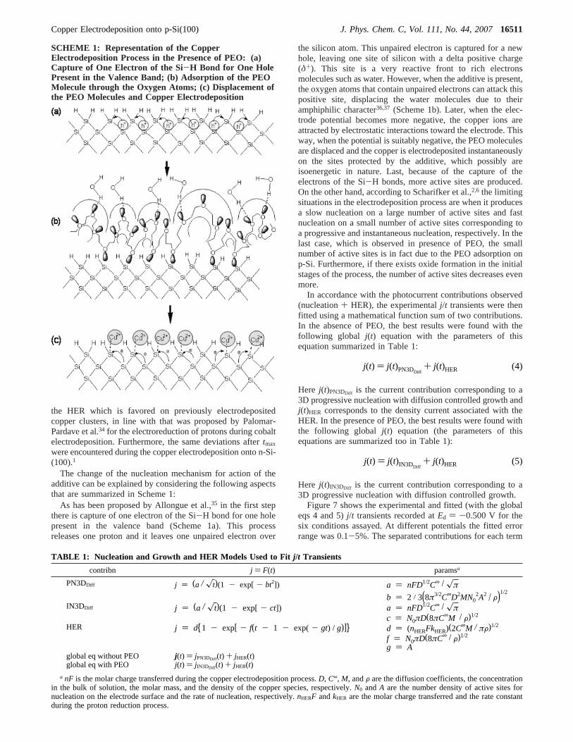
3.3. Analysis of thej/t Transients: Nucleation and GrowthMechanisms of Copper onto p-Si(100).The j/t transientsobtained by the potential step method were performed in thepotential region where the copper electrodeposition occurs. Inthis way, the nucleation and growth mechanisms further deducedfrom thesej/t transients should be sensitive to the presence ofPEO or the illumination intensity.
The potential steps were carried out from an initial potentialEi ) -0.30 V to a final deposition potential (Ed) ranging as-0.350 Vg Ed g -0.650 V. Figure 5 shows thej/t transientswhere the time is corrected for the induction time. In all thej/ttransients it can be seen that after the initial increase in thecurrent a maximum (jmax) is reached, and then current densitydecays until after a long time, when it reaches an approximatelyconstant value. When the deposition potential is made morenegative, thejmax increases and the time corresponding to thecurrent maximum (tmax) decreases. These features are consistentwith the nucleation of hemispherical clusters followed by adiffusion-limited growth.1,3,4,7,9,11,23-32
If we consider a constant potential (e.g.,-0.500 V) and withan illumination intensity of 2.0 mW cm-2 (Figure 5a-c), anincrease in the photocurrent when the concentration of PEO isincreased is observed. This fact can be attributed to the inhibitionof the silicon oxide formation on the active sites of thesemiconductor. When the electrode is illuminated with aillumination intensity of 3.5 mW cm-2 (Figure 5d-f), anincrease in the photocurrent under all conditions is observed,compared to those obtained with a lower illumination intensity.
Figure 3. Band diagrams in different situations for the system p-Si(100)/electrolyte: (a) flat bands; (b) equilibrium with 0.1 M H2SO4 + 5 mMCuSO4 electrolyte; (c) cathodic polarization at-0.80 V (inversion layer); (d) open circuit under illumination,-0.30 V (start copper deposition);(e) cathodic polarization at-0.80 V (massive copper deposition); (f) accumulation layer under illumination at 0.20 V (copper dissolution andsilicon oxide growth).
Figure 4. Potentiodynamicj/E profiles of a p-Si(100) electrode in 0.1M H2SO4 + 5 mM CuSO4 at different PEO concentrations and differentillumination intensities. (a) 2.0 mW cm-2; (b) 3.5 mW cm-2. PEOconcentrations: (s) 0 mg L-1; (- - -) 1.0 mg L-1; (‚‚‚) 100 mg L-1.Scan rate: 0.010 V/s.
Copper Electrodeposition onto p-Si(100) J. Phys. Chem. C, Vol. 111, No. 44, 200716509
In the same way, a significant effect in the magnitude of thephotocurrent when the PEO concentration is increased is notobserved. The increase of the photocurrent to a higher illumina-tion intensity can be explained by considering that it producesan increase in the minority carriers concentration in the surfaceand for this reason more copper is electrodeposited. The slightdecrease in the photocurrent when a 100 mg/L PEO concentra-tion is employed could be explained by taking into account thatthis molecule can be blocking the surface of the semiconductorfor the arrival of the copper ions. Therefore, the photogeneratedelectrons are not transferred to electrolytes and they can berecombined with the holes of the valence band, therebydecreasing the photocurrent value.
To determine the nucleation and growth mechanisms ofcopper on p-Si(100), and in a first approach to distinguishbetween instantaneous and progressive nucleation, the experi-mental data have been represented in a nondimensional form.Figure 6a-c represents the 2.0 mW cm-2 condition using 0, 1,
and 100 mg/L PEO concentration, respectively. In the sameway, Figure 6d-f represents the 3.5 mW cm-2 condition using0, 1, and 100 mg/L PEO concentration, respectively. All thefigures are plotted in coordinates (I/Im)2 vs t/tm in accordancewith the theoretical models of nucleation and diffusion-controlled growth of hemispherical clusters, whereIm and tmrepresent the current maximum and time at current maximum,respectively.25-28,31,32
It can be seen that in the absence of PEO and under anyillumination conditions the experimental data follow the pro-gressive nucleation model relatively well; however, aftertmax big deviations in this model emerge. When the additive ispresent and under any illumination conditions, the experimentaldata closely follow the instantaneous nucleation model fromthe initial part (t < tmax); however, a deviation aftertmax isobserved too. Both variations in the proposed models canbe attributed to the presence of a parallel reaction to thecopper electrodeposition process. The last can be attributed to
Figure 5. j/t transients for copper deposition onto a p-Si(100) in 0.1 M H2SO4 + 5 mM CuSO4 at different PEO concentrations, for potential stepsfrom -0.30 V to a deposition potential (Ed) indicated in the figure. Values at 2.0 mW cm-2: (a) 0 mg L-1; (b) 1 mg L-1; (c) 100 mg L-1. Valuesat 3.5 mW cm-2: (d) 0 mg L-1; (e) 1 mg L-1; (f) 100 mg L-1.
Figure 6. Dimensionless plots for the current transients from Figure 5: (a-c) at 2.0 mW cm-2; (c-e) at 3.5 mW cm-2. In dimensionless plots,dash and dot lines correspond to the calculated curve for the growth laws for 3D diffusional controlled instantaneous and progressive nucleationsmechanisms, respectively.
16510 J. Phys. Chem. C, Vol. 111, No. 44, 2007 Munoz et al.
the HER which is favored on previously electrodepositedcopper clusters, in line with that was proposed by Palomar-Pardave et al.34 for the electroreduction of protons during cobaltelectrodeposition. Furthermore, the same deviations aftertmax
were encountered during the copper electrodeposition onto n-Si-(100).1
The change of the nucleation mechanism for action of theadditive can be explained by considering the following aspectsthat are summarized in Scheme 1:
As has been proposed by Allongue et al.,35 in the first stepthere is capture of one electron of the Si-H bond for one holepresent in the valence band (Scheme 1a). This processreleases one proton and it leaves one unpaired electron over
the silicon atom. This unpaired electron is captured for a newhole, leaving one site of silicon with a delta positive charge(δ+). This site is a very reactive front to rich electronsmolecules such as water. However, when the additive is present,the oxygen atoms that contain unpaired electrons can attack thispositive site, displacing the water molecules due to theiramphiphilic character36,37 (Scheme 1b). Later, when the elec-trode potential becomes more negative, the copper ions areattracted by electrostatic interactions toward the electrode. Thisway, when the potential is suitably negative, the PEO moleculesare displaced and the copper is electrodeposited instantaneouslyon the sites protected by the additive, which possibly areisoenergetic in nature. Last, because of the capture of theelectrons of the Si-H bonds, more active sites are produced.On the other hand, according to Scharifker et al.,2,6 the limitingsituations in the electrodeposition process are when it producesa slow nucleation on a large number of active sites and fastnucleation on a small number of active sites corresponding toa progressive and instantaneous nucleation, respectively. In thelast case, which is observed in presence of PEO, the smallnumber of active sites is in fact due to the PEO adsorption onp-Si. Furthermore, if there exists oxide formation in the initialstages of the process, the number of active sites decreases evenmore.
In accordance with the photocurrent contributions observed(nucleation+ HER), the experimentalj/t transients were thenfitted using a mathematical function sum of two contributions.In the absence of PEO, the best results were found with thefollowing global j(t) equation with the parameters of thisequation summarized in Table 1:
Here j(t)PN3DDiff is the current contribution corresponding to a3D progressive nucleation with diffusion controlled growth andj(t)HER corresponds to the density current associated with theHER. In the presence of PEO, the best results were found withthe following global j(t) equation (the parameters of thisequations are summarized too in Table 1):
Here j(t)IN3DDiff is the current contribution corresponding to a3D progressive nucleation with diffusion controlled growth.
Figure 7 shows the experimental and fitted (with the globaleqs 4 and 5)j/t transients recorded atEd ) -0.500 V for thesix conditions assayed. At different potentials the fitted errorrange was 0.1-5%. The separated contributions for each term
SCHEME 1: Representation of the CopperElectrodeposition Process in the Presence of PEO: (a)Capture of One Electron of the Si-H Bond for One HolePresent in the Valence Band; (b) Adsorption of the PEOMolecule through the Oxygen Atoms; (c) Displacement ofthe PEO Molecules and Copper Electrodeposition
TABLE 1: Nucleation and Growth and HER Models Used to Fit j/t Transients
contribn j ) F(t) paramsa
PN3DDiff j ) (a / xt)(1 - exp[ - bt2]) a ) nFD1/2C∞ / xπb ) 2 / 3(8π3/2C∞D2MN0
2A2 / F)1/2
IN3DDiff j ) (a / xt)(1 - exp[ - ct]) a ) nFD1/2C∞ / xπc ) N0πD(8πC∞M / F)1/2
HER j ) d1 - exp[ - f(t - 1 - exp( - gt) / g)] d ) (nHERFkHER)(2C∞M / πF)1/2
f ) N0πD(8πC∞ / F)1/2
g ) Aglobal eq without PEO j(t) ) jPN3DDiff (t) + jHER(t)global eq with PEO j(t) ) j IN3DDiff (t) + jHER(t)
a nF is the molar charge transferred during the copper electrodeposition process.D, C∞, M, andF are the diffusion coefficients, the concentrationin the bulk of solution, the molar mass, and the density of the copper species, respectively.N0 andA are the number density of active sites fornucleation on the electrode surface and the rate of nucleation, respectively.nHERF andkHER are the molar charge transferred and the rate constantduring the proton reduction process.
j(t) ) j(t)PN3DDiff+ j(t)HER (4)
j(t) ) j(t)IN3DDiff+ j(t)HER (5)
Copper Electrodeposition onto p-Si(100) J. Phys. Chem. C, Vol. 111, No. 44, 200716511

are also shown in Figure 7. The electric charge associated witheach contribution expressed as percentages of the transient totalcharge are summarized in Table 2.
On the basis of the results shown in Figure 7 and the valuespresented in Table 2, it can be concluded that the principalcontribution in the copper electrodeposition process is NP3DDIFF
and NI3DDIFF in the absence and in the presence of PEO,respectively. In cases where the HER appears, this is developedat t > tmax, which indicates that this reaction is revealed afterthe coalescence of the diffusion zones. The last is due to thatthe adsorption of hydrogen in the nucleation process productof the diffusion zones growth around of the metallic nucleus isnot possible. When the 1D diffusion is attained, the adsorptionis possible and this occur aftertmax.
25,31,34
For a quantitative analysis of the NGM, the nucleation ratein the absence of additive was evaluated using the followingequation:26,31-33
Herekn is the nucleation rate constant,N0 is the final nucleusdensity,Vm is the molar volume, and the other symbols havetheir usual meanings. Figure 8a shows log(knN0) vs potentialfor the systems in the absence of PEO at different illuminationintensities, and it indicates that the nucleation rate increasesexponentially with the applied potential.
In the kinetic approach, the nucleation rate is given by32,33
whereNcrit is the number of atoms required to form a criticalnucleus,η is the overpotential,k is the Boltzmann constant,and A3D is a preexponential factor. The preexponential factorandNcrit are independent of the potential, whereasâ dependson the mechanism of attachment. Thisâ parameter can takevalues ranging from 0 to 1 depending on this attachmentmechanism. The potential dependence of the nucleationrate is in a potential range whereNcrit is a constant and is givenby33
The (â + NCrit)C values found from the slope values of theplots shown in Figure 8a were also<1, which indicates thatNCrit < 1. Values ofNcrit < 1 can be deduced, which suggeststhat an adsorbed copper atom can be considered as a stablecluster in this range of potentials. Also, theNcrit < 1 result is
Figure 7. Experimental (O) and fitted (s) j/t transients obtained atEd ) -0.500 V. Dashed lines 1 (in a and d) correspond to PN3DDIFF. Dashedlines 1 (in b, c, e, and f) correspond to IN3DDIFF. Dotted lines 2 correspond to the HER contributions. Values at 2.0 mW cm-2: (a) 0 mg L-1 PEO;(b) 1 mg L-1 PEO; (c) 100 mg L-1 PEO. Values at 3.5 mW cm-2: (d) 0 mg L-1 PEO; (e) 1 mg L-1 PEO; (f) 100 mg L-1 PEO.
TABLE 2: Electric Charge and Percentage of the TotalCharge Associated with the Contributions PN3DDIFF andIN3DDIFF (N3DDiff ) and HER Obtained from the j/tTransients Fitted from Figure 7
conditionexptl tot.
charge/mC cm-2calcd tot.
charge/mC cm-2N3DDIFFcharge/%
HERcharge/%
2.0 mW cm-2
without PEO 6.47 6.47 4.76 1.741 mg L-1 PEO 7.94 8.00 7.99 0.01100 mg L-1 PEO 8.42 8.48 7.12 1.36
3.5 mW cm-2
without PEO 9.62 9.62 8.97 0.651 mg L-1 PEO 10.1 10.0 9.26 0.79100 mg L-1 PEO 8.08 8.46 8.46 0.00
Figure 8. Semilogarithmic plot of the nucleation rate (a) calculatedfrom eq 6 as a function of the potential in absence of PEO: (O) 2.0mW cm-2; (0) 3.5 mW cm-2. (b) Nucleus density calculated from eq9 as a function of the potential in the presence of PEO: values at 2.0mW cm-2 (0, O), 1.0 and 100 mg L-1 PEO concentrations, respectively;values at 3.5 mW cm-2 (4, 3), 1.0 and 100 mg L-1 PEO concentrations,respectively.
JNucl ) knN0 ) A3D exp((â + NCrit)e|η|kT ) (7)
d(logJNucl)
d|η| ) e2.303kT
(â + NCrit) (8)
Jnucl ) knN0 ) 0.2898(8πc0Vm)-1/2(zFc0)
2
imax2tmax
3(6)
16512 J. Phys. Chem. C, Vol. 111, No. 44, 2007 Munoz et al.
not a rare event when electrochemical nucleation takes placeon a foreign substrate. According to Milchev et al.,33 the valueof 0 e Ncrit < 1 was obtained when silver was deposited on thecubic face of the platinum single-crystal cathode, and takinginto account the atomistic model, this result has a clear physicalmeaning. A critical nucleus consisting of zero atoms can beobtained when the nucleation proceeds on active centers. Then,at sufficiently high supersaturation, the combination “activecenter-adsorbed atom” is a stable configuration and, therefore,the active center itself plays the role of a critical nucleus.
Furtheremore, according to Gunawardena et al.,32 the signifi-cance of small values ofNcrit is hard to evaluate and they maysimply be the result of the application of the high overpotential,as was observed in the silver electrodeposition on vitreouscarbon.
On the other hand, when PEO is present, the nucleus densityat each deposition potential can be also be determinated fromthe current transients. According to the model for instantaneusnucleation followed by three-dimensional diffusion-limitedgrowth, tmax and imax are give by9,25,31
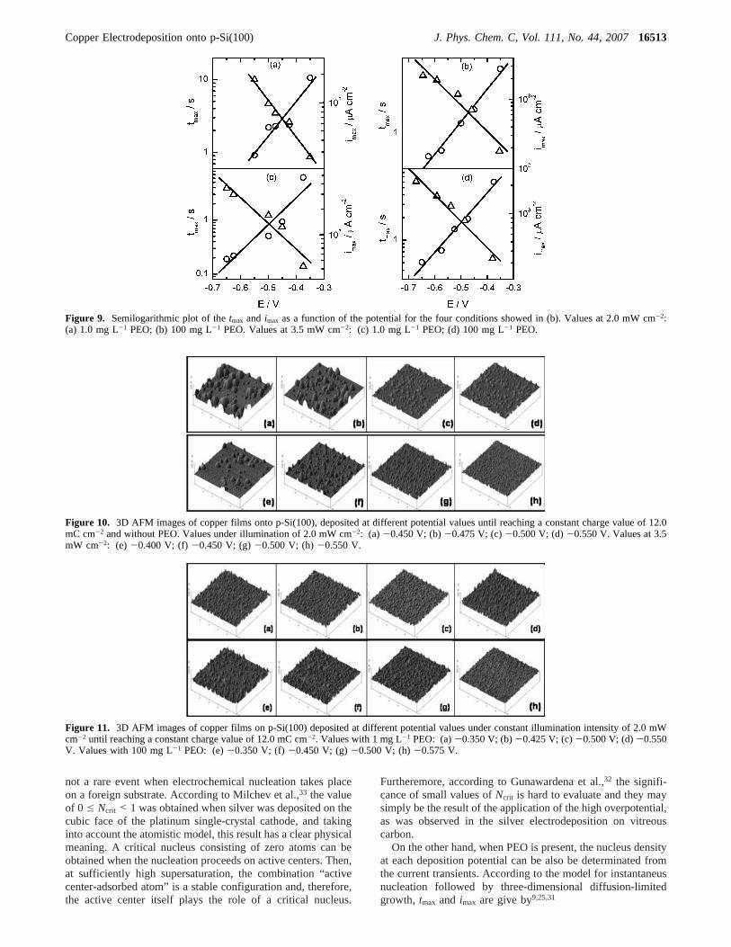
Figure 9. Semilogarithmic plot of thetmax and imax as a function of the potential for the four conditions showed in (b). Values at 2.0 mW cm-2:(a) 1.0 mg L-1 PEO; (b) 100 mg L-1 PEO. Values at 3.5 mW cm-2: (c) 1.0 mg L-1 PEO; (d) 100 mg L-1 PEO.
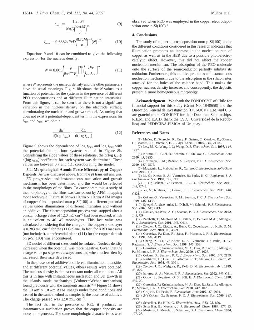
Figure 10. 3D AFM images of copper films onto p-Si(100), deposited at different potential values until reaching a constant charge value of 12.0mC cm-2 and without PEO. Values under illumination of 2.0 mW cm-2: (a) -0.450 V; (b)-0.475 V; (c)-0.500 V; (d)-0.550 V. Values at 3.5mW cm-2: (e) -0.400 V; (f) -0.450 V; (g)-0.500 V; (h)-0.550 V.
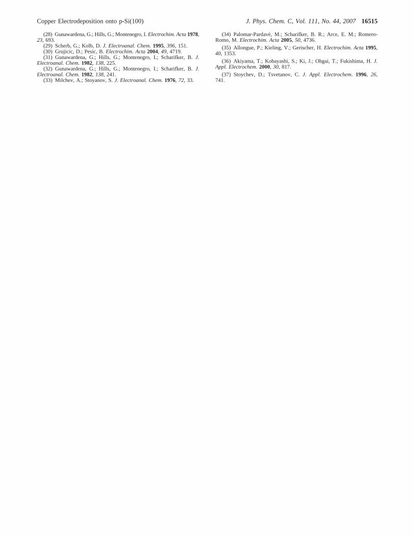
Figure 11. 3D AFM images of copper films on p-Si(100) deposited at different potential values under constant illumination intensity of 2.0 mWcm-2 until reaching a constant charge value of 12.0 mC cm-2. Values with 1 mg L-1 PEO: (a)-0.350 V; (b)-0.425 V; (c)-0.500 V; (d)-0.550V. Values with 100 mg L-1 PEO: (e)-0.350 V; (f) -0.450 V; (g)-0.500 V; (h)-0.575 V.
Copper Electrodeposition onto p-Si(100) J. Phys. Chem. C, Vol. 111, No. 44, 200716513
Equations 9 and 10 can be combined to give the followingexpression for the nucleus density:
whereN represents the nucleus density and the other parametershave the usual meanings. Figure 8b shows theN values as afunction of potential for the systems in the presence of differentPEO concentrations and at different illumination intensities.From this figure, it can be seen that there is not a significantvariation in the nucleus density on the electrode surface,corroborating the nucleation and growth model. Assuming thatdoes not exist a potential-dependent term in the expressions forimax and tmax, we obtain
Figure 9 shows the dependence of logtmax and log imax withthe potential for the four systems studied in Figure 8b.Considering the slope values of these relations, the d(logtmax)/d(log imax) coefficient for each system was determined. Thesevalues are between 0.7 and 1.1, corroborating the model.
3.4. Morphological Atomic Force Microscopy of CopperDeposits.As was discussed above, from thej/t transient analysis,a 3D progressive and instantaneous nucleation and growthmechanism has been determined, and this would be reflectedin the morphology of the films. To corroborate this, a study ofthe morphology of the films was carried out by AFM in tappingmode technique. Figure 10 shows 10µm × 10µm AFM imagesof copper films deposited onto p-Si(100) at different potentialvalues under illumination of different intensities and withoutan additive. The electrodeposition process was stopped after aconstant charge value of 12.0 mC cm-2 had been reached, whichis equivalent to 40-45 monolayers. This last value wascalculated considering that the charge of the copper monolayeris 0.283 mC cm-2 for the (111) plane. In fact, for XRD measures(not included), a preferential plane (111) for the copper depositon p-Si(100) was encountered.
3D nuclei of different sizes could be isolated. Nucleus densityincreased when the potential was more negative. Given that thecharge value passage was always constant, when nucleus densityincreased, their size decreased.
In the presence of additive at different illumination intensitiesand at different potential values, others results were obtained.The nucleus density is almost constant under all conditions. Allthis is in line with instantaneous nucleation and 3D growth inthe islands mode mechanism (Volmer-Weber mechanism)found previously with the transients analysis.9,19Figure 11 showsthe 10µm × 10 µm AFM images under these conditions andtreated in the same method as samples in the absence of additive.The charge passed was 12.0 mC cm-2.
The fact that in the presence of PEO it produces aninstantaneous nucleation proves that the copper deposits aremore homogeneous. The same morphologic characteristics were
observed when PEO was employed in the copper electrodepo-sition onto n-Si(100).1
4. Conclusions
The study of copper electrodeposition onto p-Si(100) underthe different conditions considered in this research indicates thatillumination promotes an increase in the nucleation rate ofcopper as well as in the HER due to a possible photoelectro-catalytic effect. However, this did not affect the coppernucleation mechanism. The adsorption of the PEO moleculeonto the surface of the semiconductor partially inhibits itsoxidation. Furthermore, this additive promotes an instantaneousnucleation mechanism due to the adsorption in the silicon sitesattacked for the holes of the valence band. This makes thecopper nucleus density increase, and consequently, the depositspresent a more homogeneous morpholgy.
Acknowledgment. We thank the FONDECYT of Chile forfinancial support for this study (Grant No. 1040658) and theDireccion General de Investigacio´n (DGI-UCV). E.M. and C.S.are grateful to the CONICYT for their Doctorate Scholarships.R.E.M. and E.A.D. thank the CSIC (Universidad de la Repu´b-lica) and PEDECIBA-FISICA of Uruguay.
References and Notes
(1) Munoz, E.; Schrebler, R.; Cury, P.; Sua´rez, C.; Co´rdova, R.; Go´mez,H.; Marotti, R.; Dalchiele, E.J. Phys. Chem. B2006, 110, 21109.
(2) Lee, M. K.; Wang, J. J.; Wang, D.J. Electrochem. Soc.1997, 144,1777.
(3) Krumm, R.; Guel, B.; Schmitz, C.; Staikov, G.Electrochim. Acta2000, 45, 3255.
(4) Hoffmann, P. M.; Radisic, A.; Searson, P. C.J. Electrochem. Soc.2000, 147, 2576.
(5) Magagnin, L.; Maboudian, R.; Carraro, C.Electrochem. Solid-StateLett. 2001, 4, C5.
(6) Li, G.; Kneer, E. A.; Vermeire, B.; Parks, H. G.; Raghavan, S.J.Electrochem. Soc. 1998, 145, 241.
(7) Ji, C.; Oskam, G.; Searson, P. C.J. Electrochem. Soc.2001,148, C746.
(8) Ye, S.; Ichihara, T.; Uosaki, K.J. Electrochem. Soc. 2001, 148,C421.
(9) Oskam, G.; Vereecken, P. M.; Searson, P. C.J. Electrochem. Soc.1999, 146, 1436.
(10) Spiegel, A.; Staemmier, L.; Do¨beli, M.; Schmuki, P.J. Electrochem.Soc.2002, 149, C432.
(11) Radisic, A.; West, A. C.; Searson, P. C.J. Electrochem. Soc.2002,149, C94.
(12) Zambelli, T.; Munford, M. L.; Pillier, F.; Bernard, M.-C.; Allongue,P. J. Electrochem. Soc. 2001, 148, C614.
(13) Ziegler, J. C.; Rietzle, A.; Bunk, O.; Zegenhagen, J.; Kolb, D. M.Electrochim. Acta2000, 45, 4599.
(14) Gorostiza, P.; Dı´az, R.; Sanz, F.; Morante, J. R.J. Electrochem.Soc. 1997, 144, 4119.
(15) Cheng, X.; Li, G.; Kneer, E. A.; Vermeire, B.; Parks, H. G.;Raghavan, S.J. Electrochem. Soc.1998, 145, 352.
(16) Gorostiza, P.; Kulandannathan, M. A.; Dı´az, R.; Sanz, F.; Allongue,P.; Morante, J. R.J. Electrochem. Soc.2000, 147, 1026.
(17) Oskam, G.; Searson, P. C.J. Electrochem. Soc. 2000, 147, 2199.(18) Rashkova, B.; Guel, B.; Po¨tzchke, R. T.; Staikov, G.; Lorenz, W.
Electrochim. Acta1998, 43, 3021.(19) Ziegler, J. C.; Wielgosz, R.; Kolb, D. M.Electrochim. Acta1999,
45, 827.(20) Istratov, A. A.; Weber, E. R.J. Electrochem. Soc.2002, 149, G21.(21) Ottow, S.; Popkirov, G. S.; Fo¨ll, H. J. Electroanal. Chem. 1998,
455, 29.(22) Gorostiza, P.; Kulandannathan, M. A.; Dı´az, R.; Sanz, F.; Allongue,
P.; Morante, J. R.J. Electrochem. Soc.2000, 147, 1026.(23) Grujicic, D.; Pesic, B.Electrochim. Acta2002, 47, 2901.(24) 24) Oskam, G.; Searson, P. C.J. Electrochem. Soc. 2000, 147,
2199.(25) Scharfker, B.; Hills, G.Electrochim. Acta1983, 28, 879.(26) Scharfker, B.; Mostany, J.J. Electroanal. Chem.1984, 177, 13.(27) Mostany, J.; Mozota, J.; Scharfker, B.J. Electroanal. Chem.1984,
177, 25.
tmax ) 1.2564
NπD(8πcMF )1/2
(9)
imax ) 0.6382zFcD(8πcMF )1/4
(N)1/2 (10)
N ) 0.065( F8πC∞Vm
)1/2( zFcimaxtmax)2
(11)
dEd(log imax)
) dEd(log tmax)
(12)
16514 J. Phys. Chem. C, Vol. 111, No. 44, 2007 Munoz et al.
(28) Gunawardena, G.; Hills, G.; Montenegro, I.Electrochim. Acta1978,23, 693.
(29) Scherb, G.; Kolb, D.J. Electroanal. Chem.1995, 396, 151.(30) Grujicic, D.; Pesic, B.Electrochim. Acta2004, 49, 4719.(31) Gunawardena, G.; Hills, G.; Montenegro, I.; Scharifker, B.J.
Electroanal. Chem.1982, 138, 225.(32) Gunawardena, G.; Hills, G.; Montenegro, I.; Scharifker, B.J.
Electroanal. Chem.1982, 138, 241.(33) Milchev, A.; Stoyanov, S.J. Electroanal. Chem.1976, 72, 33.
(34) Palomar-Pardave´, M.; Scharifker, B. R.; Arce, E. M.; Romero-Romo, M.Electrochim. Acta2005, 50, 4736.
(35) Allongue, P.; Kieling, V.; Gerischer, H.Electrochim. Acta1995,40, 1353.
(36) Akiyama, T.; Kobayashi, S.; Ki, J.; Ohgai, T.; Fukishima, H.J.Appl. Electrochem. 2000, 30, 817.
(37) Stoychev, D.; Tsvetanov, C.J. Appl. Electrochem. 1996, 26,741.
Copper Electrodeposition onto p-Si(100) J. Phys. Chem. C, Vol. 111, No. 44, 200716515