Weiss & Kislev JAS 2004 Plant indication economy Ashkelon.pdf
Upload
independentCategory
view
1download
0
Ip
MD
a
ARRAA
KPSCSH
1
hrgpi[nttts[w
of
U
0d
Synthetic Metals 161 (2011) 1390– 1399
Contents lists available at ScienceDirect
Synthetic Metals
j o ur nal homep ag e: www.elsev ier .com/ locate /synmet
ndication of formation of charge density waves in silver nanoparticles dispersedoly(methyl methacrylate) thin films
anisree Majumder, Aloke Kumar Chakraborty1, Bipul Biswas, Avijit Chowdhury, Biswanath Mallik ∗
epartment of Spectroscopy, Indian Association for the Cultivation of Science, 2A & 2B, Raja S. C. Mullick Road, Jadavpur, Kolkata 700 032, India
r t i c l e i n f o
rticle history:eceived 8 March 2011eceived in revised form 4 May 2011ccepted 7 May 2011vailable online 2 June 2011
eywords:olymerilver nanoparticleharge density wave
a b s t r a c t
Silver nanoparticles of various sizes have been prepared through the chemical synthesis and dispersedinto poly(methyl methacrylate) (PMMA) matrix resulting in solution cast nanocomposite thin films. Forcharacterization of the films, UV–vis absorption spectroscopy and FESEM were used. Observed blue shiftof the surface plasmon absorption band position of the nanocomposite films is an indication of graduallysmaller size of the silver nanoparticles that have been dispersed into the PMMA matrix. Dark current(Id) vs. time profiles and the fluctuations in current–voltage characteristics for the PMMA films with dis-persed silver nanoparticles were found to depend on the position of surface plasmon absorption band.Results of electrical studies have been found to be temperature- and voltage-dependent manifestingnonlinear nature of the Id which may be an indication of formation of charge density waves in the sil-
urface plasmon absorption bandysteresis in current
ver nanoparticles–PMMA nanocomposite films. The increase in the standard deviation in Id (calculatedfrom the Id vs. time profiles) for the silver nanoparticles–PMMA nanocomposite films may be due to theincrease in the plasmon oscillations. Thermal hysteresis has been observed in the PMMA films and in thesilver nanoparticles–PMMA nanocomposite films. Results on the observed electrical properties have beendiscussed in the light of interaction of silver nanoparticles with PMMA matrix, structural reorientationof PMMA, role of electric field in the manipulation of silver nanoparticles in the polymer matrix etc.
. Introduction
The huge development of nanoscience till the present timesas influenced enormously whole scientific understanding andesearch arena [1]. The combination of organic polymers and inor-anic nanoparticles can lead to nanocomposites having more usefulroperties than either of the individual components [2,3]. Stud-
es on polymer nanocomposites are an important area of research1–7]. Proper formulation of polymer nanocomposites, in whichanosized particles are dispersed in a polymer network is believedo modulate the properties of the polymeric materials, especiallyhe optical and electrical properties to a great extent [2–7]. Poten-ial applications of nanodimensional materials have also shownignificant impacts in various advanced fields like nanophotonics8], nanosensors [9], biosensing and nanoelectronics [10], solar cellsith higher efficiency [11], etc.
Earlier, in our laboratory, photoinduced charge-transfer wasbserved between metallocenes (electron donors) and chloro-orm molecules (electron acceptors) present in the poly(methyl
∗ Corresponding author. Tel.: +91 33 2473 4971; fax: +91 33 2473 2805.E-mail address: [email protected] (B. Mallik).
1 Present address: Department of Computer Science and Engineering, BGC Trustniversity, Chandanaish, Chittagong, Bangladesh.
379-6779/$ – see front matter © 2011 Elsevier B.V. All rights reserved.oi:10.1016/j.synthmet.2011.05.007
© 2011 Elsevier B.V. All rights reserved.
methacrylate) (PMMA) matrix leading to enhanced photoconduc-tivity of the system [12]. Also, in another programme in ourlaboratory, for observing various effects of metal nanoparticles-dispersed PMMA films, studies on optical and electrical properties,photoluminescence of PMMA films dispersed with silver nanopar-ticles (synthesized in a novel way) were performed [2,3]. The metalsilver invites its studies on its various aspects due to its surfacestability, good thermal and electrical conductivity and catalyticproperties [13].
The versatile polymer PMMA has been observed to manifestcharge density waves (CDWs) [14]. A charge density wave is aspatially modulated condensate of conduction electrons accom-panied with a slight lattice distortion which stabilizes at a finitetemperature in metallic crystals with a quasi-one-dimensionalFermi surface [15]. The studies on CDWs have been carried outby various research groups and such studies have resulted in theobservation of many interesting and often surprising physical phe-nomena [16–22]. On the basis of the previous report [14] thatPMMA can manifest CDW and considering the possible applicationof PMMA in various fields, it was thought worthwhile to study theelectrical properties of PMMA having dispersed silver nanoparti-
cles of different sizes. In fact the manifestation of CDW in PMMAand the presence of silver nanoparticles in it were expected toinfluence significantly the time dependence of the electrical cur-rent/conductivity. Therefore the temperature dependence of the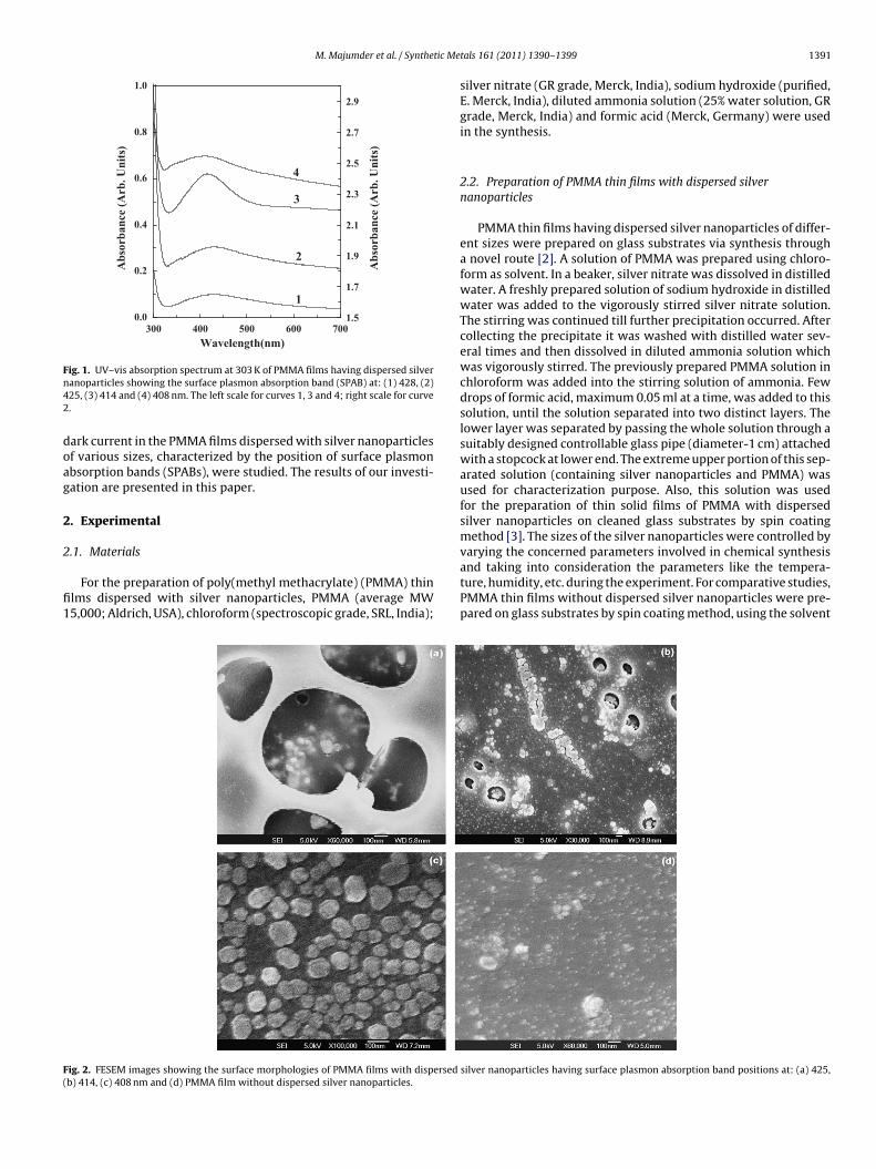
M. Majumder et al. / Synthetic Me
300 400 500 600 7000.0
0.2
0.4
0.6
0.8
1.0
4
3
2
Abs
orba
nce
(Arb
. Uni
ts)
Abs
orba
nce
(Arb
. Uni
ts)
Wavelength(nm)
11.5
1.7
1.9
2.1
2.3
2.5
2.7
2.9
Fig. 1. UV–vis absorption spectrum at 303 K of PMMA films having dispersed silvern42
doag
2
2
fi1
F(
anoparticles showing the surface plasmon absorption band (SPAB) at: (1) 428, (2)25, (3) 414 and (4) 408 nm. The left scale for curves 1, 3 and 4; right scale for curve.
ark current in the PMMA films dispersed with silver nanoparticlesf various sizes, characterized by the position of surface plasmonbsorption bands (SPABs), were studied. The results of our investi-ation are presented in this paper.
. Experimental
.1. Materials
For the preparation of poly(methyl methacrylate) (PMMA) thinlms dispersed with silver nanoparticles, PMMA (average MW5,000; Aldrich, USA), chloroform (spectroscopic grade, SRL, India);
ig. 2. FESEM images showing the surface morphologies of PMMA films with dispersed
b) 414, (c) 408 nm and (d) PMMA film without dispersed silver nanoparticles.
tals 161 (2011) 1390– 1399 1391
silver nitrate (GR grade, Merck, India), sodium hydroxide (purified,E. Merck, India), diluted ammonia solution (25% water solution, GRgrade, Merck, India) and formic acid (Merck, Germany) were usedin the synthesis.
2.2. Preparation of PMMA thin films with dispersed silvernanoparticles
PMMA thin films having dispersed silver nanoparticles of differ-ent sizes were prepared on glass substrates via synthesis througha novel route [2]. A solution of PMMA was prepared using chloro-form as solvent. In a beaker, silver nitrate was dissolved in distilledwater. A freshly prepared solution of sodium hydroxide in distilledwater was added to the vigorously stirred silver nitrate solution.The stirring was continued till further precipitation occurred. Aftercollecting the precipitate it was washed with distilled water sev-eral times and then dissolved in diluted ammonia solution whichwas vigorously stirred. The previously prepared PMMA solution inchloroform was added into the stirring solution of ammonia. Fewdrops of formic acid, maximum 0.05 ml at a time, was added to thissolution, until the solution separated into two distinct layers. Thelower layer was separated by passing the whole solution through asuitably designed controllable glass pipe (diameter-1 cm) attachedwith a stopcock at lower end. The extreme upper portion of this sep-arated solution (containing silver nanoparticles and PMMA) wasused for characterization purpose. Also, this solution was usedfor the preparation of thin solid films of PMMA with dispersedsilver nanoparticles on cleaned glass substrates by spin coatingmethod [3]. The sizes of the silver nanoparticles were controlled byvarying the concerned parameters involved in chemical synthesis
and taking into consideration the parameters like the tempera-ture, humidity, etc. during the experiment. For comparative studies,PMMA thin films without dispersed silver nanoparticles were pre-pared on glass substrates by spin coating method, using the solventsilver nanoparticles having surface plasmon absorption band positions at: (a) 425,
1 tic Metals 161 (2011) 1390– 1399
cn
2
c
2
N
A
H
aasttf
2n
tttsUstatEwtTdct
3
3
eUsrrsbaSpficofpe
0 100 200 300 400 50010
15
20
25
30
35a
b
SPAB at 425 nm
Time (sec)
0 100 200 300 400 50014.0
14.5
15.0
15.5
16.0
16.5
17.0
SPAB at 414 nm
I d(p
A)
I d(n
A)
Time (sec)
392 M. Majumder et al. / Synthe
hloroform. It could be mentioned here that the synthesized silveranoparticles–PMMA nanocomposites are very stable.
.3. Reaction mechanism
The reaction mechanism for the formation of silver nanoparti-les is shown below:
NaOH + 2AgNO3 → Ag2O + 2NaNO3 + H2O
H3 + H2O → NH4OH
g2O + 4NH4OH → 2[Ag(NH3)2]OH (transparent solution) + 3H2O
COOH + [Ag(NH3)2]OH → 2Ag + CO2 + H2O
It could be mentioned here that polymer PMMA does not acts the capping/stabilizing agent in the present case but it acts as
matrix. The silver nanoparticles of different sizes were synthe-ized by varying the reaction parameters and were dispersed inhe PMMA matrix during synthesis. The annealing of the PMMAhin films with dispersed silver nanoparticles was not consideredor varying the sizes of the silver nanoparticles.
.4. Characterization of PMMA thin films with dispersed silveranoparticles
The spectroscopic studies of the films at room temperature inhe range of 200–800 nm were performed by an UV–vis spectropho-ometer, Model UV-2401 PC (Shimadzu, Japan). Dark current ofhe films (following heating and cooling treatments) were mea-ured (electrometer, Model 6517 A, Keithley Inst., Cleveland, OH,SA) with silver paste contacts using surface type cell placed in a
pecially designed conductivity chamber [3]. The mentioned elec-rometer was also used for the supply of 5 V and 27 V bias voltagesnd voltage for the studies of I–V characteristics. Temperature ofhe sample cell was controlled by a temperature controller (Model:urotherm 2404, UK). FESEM (Model: JSM – 6700F, JEOL, Japan)as used to record the scanning electron micrograph images of
he PMMA films with and without dispersed silver nanoparticles.he electrometer was interfaced with a computer for recording theata. All electrical studies were performed in vacuum and hence thehance of any interaction of oxygen or other gases and vapors withhe sample, affecting the electrical property, could be excluded.
. Results and discussion
.1. Absorption spectra and surface morphology
PMMA thin films dispersed with silver nanoparticles of differ-nt sizes were prepared. These films were characterized by theirV–vis absorption spectra and their surface morphologies were
tudied by FESEM images. The UV–vis absorption spectra of fewepresentative silver nanoparticles (NPs)-dispersed PMMA films atoom temperature (303 K) represented by curves 1–4 in Fig. 1 havehown the positions of the surface plasmon resonance absorptionands, referred to as surface plasmon absorption bands (SPABs)round 428, 425, 414 and 408 nm, respectively. The positions ofPABs are the indications of size of the silver nanoparticles dis-ersed in PMMA matrix. The gradual blue shift of the SPABs of thelms indicated that comparatively smaller sized silver nanoparti-les have been dispersed in PMMA films. The well-defined spectra
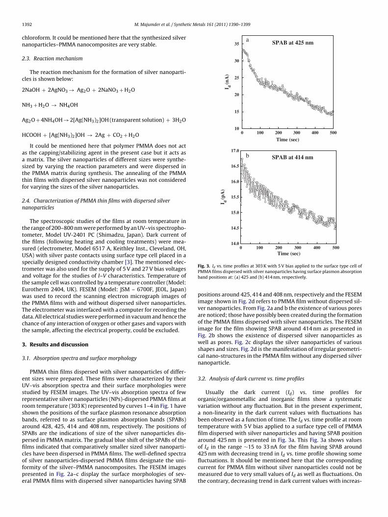
f silver nanoparticles-dispersed PMMA films designate the uni-ormity of the silver–PMMA nanocomposites. The FESEM imagesresented in Fig. 2a–c display the surface morphologies of sev-ral PMMA films with dispersed silver nanoparticles having SPABFig. 3. Id vs. time profiles at 303 K with 5 V bias applied to the surface type cell ofPMMA films dispersed with silver nanoparticles having surface plasmon absorptionband positions at: (a) 425 and (b) 414 nm, respectively.
positions around 425, 414 and 408 nm, respectively and the FESEMimage shown in Fig. 2d refers to PMMA film without dispersed sil-ver nanoparticles. From Fig. 2a and b the existence of various poresare noticed; those have possibly been created during the formationof the PMMA films dispersed with silver nanoparticles. The FESEMimage for the film showing SPAB around 414 nm as presented inFig. 2b shows the existence of dispersed silver nanoparticles aswell as pores. Fig. 2c displays the silver nanoparticles of variousshapes and sizes. Fig. 2d is the manifestation of irregular geometri-cal nano-structures in the PMMA film without any dispersed silvernanoparticle.
3.2. Analysis of dark current vs. time profiles
Usually the dark current (Id) vs. time profiles fororganic/organometallic and inorganic films show a systematicvariation without any fluctuation. But in the present experiment,a non-linearity in the dark current values with fluctuations hasbeen observed as a function of time. The Id vs. time profile at roomtemperature with 5 V bias applied to a surface type cell of PMMAfilm dispersed with silver nanoparticles and having SPAB positionaround 425 nm is presented in Fig. 3a. This Fig. 3a shows valuesof Id in the range ∼15 to 33 nA for the film having SPAB around425 nm with decreasing trend in Id vs. time profile showing some
fluctuations. It should be mentioned here that the correspondingcurrent for PMMA film without silver nanoparticles could not bemeasured due to very small values of Id as well as fluctuations. Onthe contrary, decreasing trend in dark current values with increas-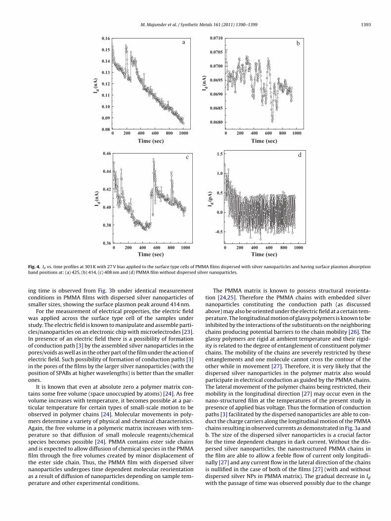
M. Majumder et al. / Synthetic Metals 161 (2011) 1390– 1399 1393
0 200 400 600 800 10000.08
0.09
0.10
0.11
0.12
0.13
0.14
0.15
0.16 a b
dc
I d(n
A)
0 200 400 600 800 10000.36
0.38
0.40
0.42
0.44
0.46
I d(n
A)
Time (sec) Time (sec)
Time (sec) Time (sec)0 200 400 600 800 1000
0.0680
0.0685
0.0690
0.0695
0.0700
0.0705
0.0710
I d(n
A)
0 200 400 600 800 1000
-0.5
0.0
0.5
1.0
1.5
I d(p
A)
F PMMb d silve
ics
wscIopeipo
tvtomApsafitnap
ig. 4. Id vs. time profiles at 303 K with 27 V bias applied to the surface type cells ofand positions at: (a) 425, (b) 414, (c) 408 nm and (d) PMMA film without disperse
ng time is observed from Fig. 3b under identical measurementonditions in PMMA films with dispersed silver nanoparticles ofmaller sizes, showing the surface plasmon peak around 414 nm.
For the measurement of electrical properties, the electric fieldas applied across the surface type cell of the samples under
tudy. The electric field is known to manipulate and assemble parti-les/nanoparticles on an electronic chip with microelectrodes [23].n presence of an electric field there is a possibility of formationf conduction path [3] by the assembled silver nanoparticles in theores/voids as well as in the other part of the film under the action oflectric field. Such possibility of formation of conduction paths [3]n the pores of the films by the larger silver nanoparticles (with theosition of SPABs at higher wavelengths) is better than the smallernes.
It is known that even at absolute zero a polymer matrix con-ains some free volume (space unoccupied by atoms) [24]. As freeolume increases with temperature, it becomes possible at a par-icular temperature for certain types of small-scale motion to bebserved in polymer chains [24]. Molecular movements in poly-ers determine a variety of physical and chemical characteristics.gain, the free volume in a polymeric matrix increases with tem-erature so that diffusion of small molecule reagents/chemicalpecies becomes possible [24]. PMMA contains ester side chainsnd is expected to allow diffusion of chemical species in the PMMAlm through the free volumes created by minor displacement of
he ester side chain. Thus, the PMMA film with dispersed silveranoparticles undergoes time dependent molecular reorientations a result of diffusion of nanoparticles depending on sample tem-erature and other experimental conditions.A films dispersed with silver nanoparticles and having surface plasmon absorptionr nanoparticles.
The PMMA matrix is known to possess structural reorienta-tion [24,25]. Therefore the PMMA chains with embedded silvernanoparticles constituting the conduction path (as discussedabove) may also be oriented under the electric field at a certain tem-perature. The longitudinal motion of glassy polymers is known to beinhibited by the interactions of the substituents on the neighboringchains producing potential barriers to the chain mobility [26]. Theglassy polymers are rigid at ambient temperature and their rigid-ity is related to the degree of entanglement of constituent polymerchains. The mobility of the chains are severely restricted by theseentanglements and one molecule cannot cross the contour of theother while in movement [27]. Therefore, it is very likely that thedispersed silver nanoparticles in the polymer matrix also wouldparticipate in electrical conduction as guided by the PMMA chains.The lateral movement of the polymer chains being restricted, theirmobility in the longitudinal direction [27] may occur even in thenano-structured film at the temperatures of the present study inpresence of applied bias voltage. Thus the formation of conductionpaths [3] facilitated by the dispersed nanoparticles are able to con-duct the charge carriers along the longitudinal motion of the PMMAchains resulting in observed currents as demonstrated in Fig. 3a andb. The size of the dispersed silver nanoparticles is a crucial factorfor the time dependent changes in dark current. Without the dis-persed silver nanoparticles, the nanostructured PMMA chains inthe film are able to allow a feeble flow of current only longitudi-
nally [27] and any current flow in the lateral direction of the chainsis nullified in the case of both of the films [27] (with and withoutdispersed silver NPs in PMMA matrix). The gradual decrease in Idwith the passage of time was observed possibly due to the change
1394 M. Majumder et al. / Synthetic Me
0 100 200 300 400 500 600 700 800
1.5
1.6
1.7
1.8
1.9
2.0a
b
I d(n
A)
Time (sec)
0 100 200 300 400 500 600 700 800155
165
175
185
195
205
215
225
I d(p
A)
Time (sec)
Fig. 5. Id vs. time profiles at 368 K (heating cycle) for (a) PMMA film dispersedwith silver nanoparticles having surface plasmon absorption band at 414 nm and(
iTrocw
vnadaistthtsvwFtvts
b) PMMA film without dispersed silver nanoparticles.
n resistance [28] in course of creation of weaker conduction paths.he PMMA is known as polar polymer and it needs long time toeach a steady state current [14]. Therefore, the initial trend eitherf increasing or decreasing nature in the Id vs. time profile of a filmontaining PMMA can continue throughout the time of observationhich is the inherent property of the polymer [14].
Fig. 4a–c shows the effect of comparatively higher value of biasoltage of 27 V on the Id vs. time profiles at 303 K for the silveranoparticles-dispersed PMMA films with SPABs around 425, 414nd 408 nm, respectively. In general, the curves in Fig. 4a–c showecreasing trend with larger amount of fluctuations/oscillations as
function of increasing time. Comparing Figs. 3 and 4a and b, its reasonable to note that PMMA film dispersed with a particularize of the silver nanoparticles is susceptible to heavy fluctua-ions/oscillations at a higher voltage at room temperature. Also,he PMMA film showing SPAB position around 408 nm showseavy fluctuations/oscillations under 27 V bias (Fig. 4c) similaro the other films. Under the identical measurement condition,ignificantly higher/severe fluctuations were observed in the Ids. time profile with bias voltage 27 V at 303 K for PMMA filmithout dispersed silver-nanoparticles as presented in Fig. 4d.
ig. 4a–d shows that the nature of fluctuations with increasing
ime and value of the Id depend on the size of the dispersed sil-er nanoparticles in the PMMA matrix. The current profile forhe PMMA film without dispersed silver nanoparticles althoughhow initially decreasing trend with increasing time, ultimatelytals 161 (2011) 1390– 1399
values of current show some sort of saturation accompanied byfrequent/severe fluctuations (Fig. 4d), but no irregular peak wasnoticed as was observed in the case of other films having dis-persed silver nanoparticles showing SPABs at various positions(Fig. 4a–c). From Figs. 3 and 4a–c, it is observed that the measuredId vs. time profiles show nonlinearity in the silver nanoparticles-dispersed film with bias voltages of 5 V and 27 V, respectivelyat a room temperature of 303 K. The observation of nonlinear Id(also conductivity) leads to the phenomenon of charge densitywaves (CDWs) [21,29] in the case of silver nanoparticles-dispersedPMMA films. Similarly, non-linearity in current shown in Fig. 4din the case of PMMA film without dispersed silver nanoparti-cles could be the indication of the formation of CDWs in thisfilm.
It should be mentioned here that the Id vs. time profiles dependon the sample temperature for PMMA films with dispersed sil-ver nanoparticles as well as PMMA films without dispersed silvernanoparticles. Fig. 5a shows the Id vs. time profile at 368 K (heatingcycle) and applied voltage of 27 V for a PMMA film dispersed withsilver nanoparticles showing surface plasmon absorption bandposition around 414 nm and in Fig. 5b, the Id vs. time profile underidentical experimental conditions for a PMMA film without dis-persed silver nanoparticles is shown. Thus, Fig. 5 demonstrates thesignificant modification in the Id vs. time profiles at higher temper-ature.
3.3. Analysis of dark current vs. voltage characteristics
Linear plots of the dark current vs. dc voltage (Id–V) character-istics in the range 0–100 V at 303 K for the PMMA films showingSPABs around 422, 414 and 408 nm are shown in Fig. 6a–c, respec-tively. The slopes of the linear portions calculated from the log Idvs. log V plots (not shown) are found to be 1.101, 1.107 and 1.114for the mentioned films. The values of the slopes indicate that theId–V characteristics at 303 K are almost ohmic in nature and lin-ear. From Fig. 6a–c it is seen that for each film sudden fluctuationsoccur in Id values in different voltage regions and the fluctuationscontinue through different span/range of voltage showing somesort of regular behavior. It is interesting to note that the voltagespan of fluctuations increases with the decreasing size of the silvernanoparticles (indicated by the position of the SPAB) dispersed inthe PMMA films.
The PMMA being a polymer, its free volume increases with tem-perature and at a particular temperature as 303 K, certain types ofsmall-scale motion are observed in their chains [24,30] and withincreasing free volume, the diffusion of small molecules of chemicalspecies like silver nanoparticles becomes possible [24] as men-tioned earlier. The PMMA surface is dominated by the ester methylgroups with some orientation orderings [31] and the backbone ofPMMA chain is of insulating nature [7]. The ester side groups ofPMMA possess high electron density [26]. The rotations of the func-tional groups/atoms [30], exchange of void spaces (free spaces)with some groups [30], diffusion of silver nanoparticles in the poly-mer matrix and electric field induced manipulation in conductionpaths [23] take place during the application of slowly increasing dcvoltage. The experimental results indicate that at a certain voltagefavorable conduction paths are created showing a fluctuation/jumpin Id to a higher value (i.e. switching to a higher conducting state).Such higher values of current are observed for a span/region ofvoltage. However, at a certain higher voltage the system returnsto its previous conducting state. The span/region of voltage show-ing higher values in current depends on the size of the silver
nanoparticles dispersed in PMMA matrix. The jumps/fluctuationsin Id do not appear at other voltages. The charge distribution in thenanocomposite film [32,33] is likely to be influenced by the appliedvoltage/electric field and can lead to the formation of CDWs. The
M. Majumder et al. / Synthetic Metals 161 (2011) 1390– 1399 1395
0 20 40 60 80 1000.0
0.1
0.2
0.3
0.4
0.5
0.6
0.7 a
b
c
I d(n
A)
Voltage (V)
SPAB at 422 nm
0 20 40 60 80 100
0.0
0.1
0.2
0.3
0.4
0.5
I d(n
A)
Voltage (V)
SPAB at 414 nm
0 20 40 60 80 1000.0
0.2
0.4
0.6
0.8
1.0
1.2
1.4
1.6
1.8
I d(n
A)
Voltage (V)
SPAB at 408 nm
Fig. 6. Linear plots of Id vs. voltage at 303 K in the PMMA films dispersed with silvernanoparticles having surface plasmon absorption band positions at: (a) 422, (b) 414a
nn3Cr0iF1(v
-5 -4 -3 -2 -1 0 1 2 3 4 5
-0.012
-0.008
-0.004
0.000
0.004
0.008
0.012 a
b
I d(n
A)
Voltage (V)
-5 -4 -3 -2 -1 0 1 2 3 4 5
-0.04
-0.02
0.00
0.02
0.04
I d(n
A)
Voltage (V)
nd (c) 408 nm, respectively.
onlinear nature in Id vs. time profiles shown in Fig. 4a–c and theonlinearities of Id vs. V characteristics in some regions of voltage at03 K (Fig. 6a–c) can be attributed due to the possible formation ofDWs [22] in the silver nanoparticles-dispersed PMMA films. Theesult of application of the forward and reverse bias (0 to +5 V and
to −5 V) at room temperature of 303 K to the PMMA films hav-ng SPABs around 414 and 408 nm are presented in linear plots inig. 7a and b, respectively. The values of their slopes are 1.12 and
.04, have been calculated from the positive side of log Id vs. log Vnot shown) indicate almost ohmic nature of the Id in the region ofoltage studied.Fig. 7. Plots of Id vs. voltage for forward and reverse bias at 303 K in the case ofPMMA films dispersed with silver nanoparticles having surface plasmon absorptionband positions at: (a) 414, (b) 408 nm, respectively.
3.4. Thermal hysteresis of dark current
To check whether the Id values measured in a silvernanoparticles-dispersed PMMA film show any hysteresis with tem-perature, a representative PMMA film having dispersed silvernanoparticles showing SPAB around 414 nm was subjected to heat-ing and cooling cycles in the temperature range of ∼303 to 363 Kwith the application of constant dc bias of 27 V. The sample cellwas subjected to heating–cooling cycles by heating the film from303 K to 323 K under vacuum without applying any bias voltagebefore applying the heating and cooling cycle for the study of hys-teresis. The value of Id at each temperature was recorded as afunction of time for about 700 s during the heating as well as cool-ing cycles. Fig. 8 represents the plots of Id as a function of timeduring the heating and cooling cycles in the case of PMMA thinfilms with dispersed silver nanoparticles showing SPAB positionat 414 nm. From Fig. 8 wavy nature/fluctuation in Id vs. time pro-files is noticed. The Id vs. time profile depends drastically on thesample cell temperature both during heating and cooling (Fig. 8).During the heating cycles current shows decreasing tendency withincreasing time and during cooling cycle current shows increas-ing tendency with increasing time. It is interesting to note that atsome temperatures (e.g. 323, 363 K) the Id vs. time profile during
cooling is almost the mirror image of the corresponding profile dur-ing heating cycle. Wavy nature/fluctuations in Id vs. time profilesduring the heating and cooling cycles in a PMMA thin film with dis-persed silver nanoparticles indicate the possibility of formation of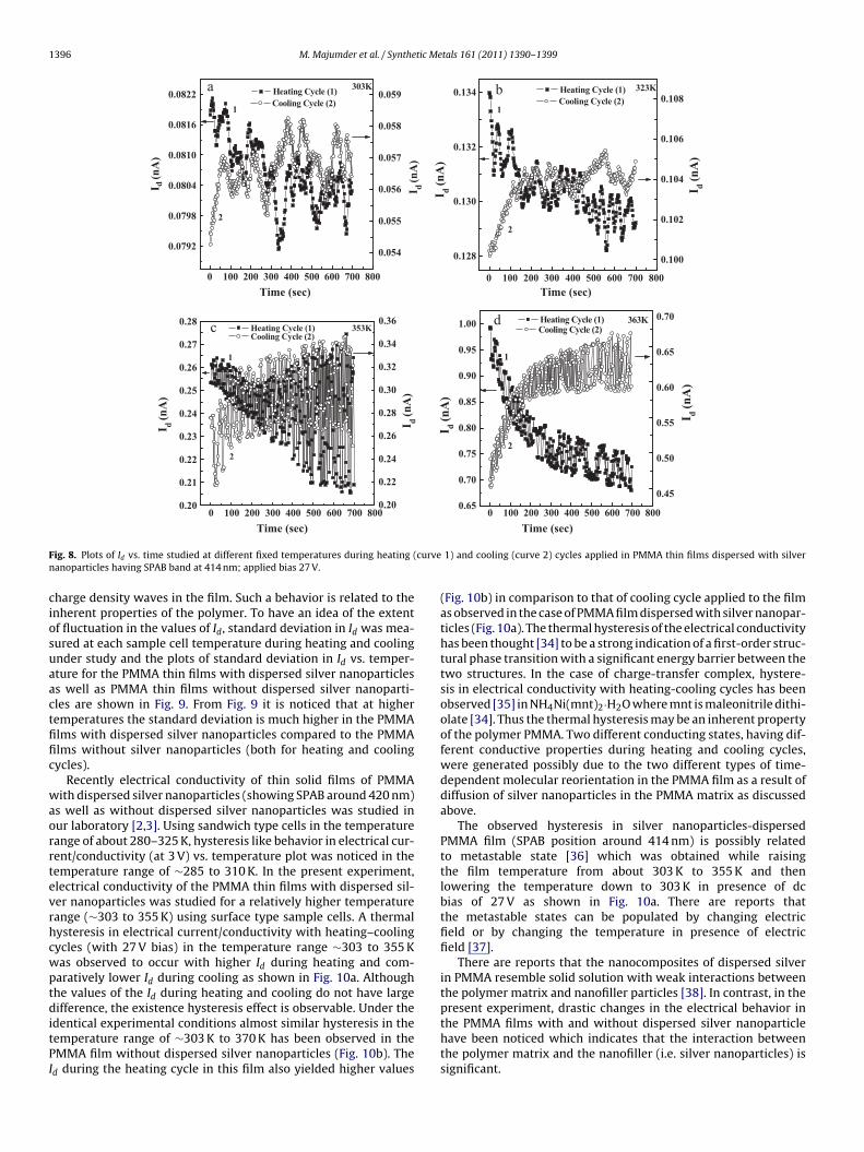
1396 M. Majumder et al. / Synthetic Metals 161 (2011) 1390– 1399
0 100 200 300 400 500 600 700 800
0.0792
0.0798
0.0804
0.0810
0.0816
0.0822a b
c d
Heating Cycle (1)
I d(n
A)
Time (sec)
0.054
0.055
0.056
0.057
0.058
0.059Cooling Cycle (2)
2
1
I d(n
A)
303K
0 100 200 300 400 500 600 700 800
0.128
0.130
0.132
0.134
2
I d(n
A)
Heating Cycle (1)
1
I d(n
A)
Time (sec)
0.100
0.102
0.104
0.106
0.108Cooling Cycle (2)323K
0 100 200 300 400 500 600 700 8000.20
0.21
0.22
0.23
0.24
0.25
0.26
0.27
0.28Heating Cycle (1) 353K
I d(n
A)
I d(n
A)
Time (sec)
0.20
0.22
0.24
0.26
0.28
0.30
0.32
0.34
0.36
2
1
Cooling Cycle (2)
0 100 200 300 400 500 600 700 8000.65
0.70
0.75
0.80
0.85
0.90
0.95
1.00 Heating Cycle (1) 363K
I d(n
A)
I d(n
A)
Time (sec)
0.45
0.50
0.55
0.60
0.65
0.70Cooling Cycle (2)
2
1
F curven
ciosuaactfific
waorrtevrhcwptditPI
ig. 8. Plots of Id vs. time studied at different fixed temperatures during heating (anoparticles having SPAB band at 414 nm; applied bias 27 V.
harge density waves in the film. Such a behavior is related to thenherent properties of the polymer. To have an idea of the extentf fluctuation in the values of Id, standard deviation in Id was mea-ured at each sample cell temperature during heating and coolingnder study and the plots of standard deviation in Id vs. temper-ture for the PMMA thin films with dispersed silver nanoparticless well as PMMA thin films without dispersed silver nanoparti-les are shown in Fig. 9. From Fig. 9 it is noticed that at higheremperatures the standard deviation is much higher in the PMMAlms with dispersed silver nanoparticles compared to the PMMAlms without silver nanoparticles (both for heating and coolingycles).
Recently electrical conductivity of thin solid films of PMMAith dispersed silver nanoparticles (showing SPAB around 420 nm)
s well as without dispersed silver nanoparticles was studied inur laboratory [2,3]. Using sandwich type cells in the temperatureange of about 280–325 K, hysteresis like behavior in electrical cur-ent/conductivity (at 3 V) vs. temperature plot was noticed in theemperature range of ∼285 to 310 K. In the present experiment,lectrical conductivity of the PMMA thin films with dispersed sil-er nanoparticles was studied for a relatively higher temperatureange (∼303 to 355 K) using surface type sample cells. A thermalysteresis in electrical current/conductivity with heating–coolingycles (with 27 V bias) in the temperature range ∼303 to 355 Kas observed to occur with higher Id during heating and com-aratively lower Id during cooling as shown in Fig. 10a. Althoughhe values of the Id during heating and cooling do not have largeifference, the existence hysteresis effect is observable. Under the
dentical experimental conditions almost similar hysteresis in theemperature range of ∼303 K to 370 K has been observed in theMMA film without dispersed silver nanoparticles (Fig. 10b). The
d during the heating cycle in this film also yielded higher values
1) and cooling (curve 2) cycles applied in PMMA thin films dispersed with silver
(Fig. 10b) in comparison to that of cooling cycle applied to the filmas observed in the case of PMMA film dispersed with silver nanopar-ticles (Fig. 10a). The thermal hysteresis of the electrical conductivityhas been thought [34] to be a strong indication of a first-order struc-tural phase transition with a significant energy barrier between thetwo structures. In the case of charge-transfer complex, hystere-sis in electrical conductivity with heating-cooling cycles has beenobserved [35] in NH4Ni(mnt)2·H2O where mnt is maleonitrile dithi-olate [34]. Thus the thermal hysteresis may be an inherent propertyof the polymer PMMA. Two different conducting states, having dif-ferent conductive properties during heating and cooling cycles,were generated possibly due to the two different types of time-dependent molecular reorientation in the PMMA film as a result ofdiffusion of silver nanoparticles in the PMMA matrix as discussedabove.
The observed hysteresis in silver nanoparticles-dispersedPMMA film (SPAB position around 414 nm) is possibly relatedto metastable state [36] which was obtained while raisingthe film temperature from about 303 K to 355 K and thenlowering the temperature down to 303 K in presence of dcbias of 27 V as shown in Fig. 10a. There are reports thatthe metastable states can be populated by changing electricfield or by changing the temperature in presence of electricfield [37].
There are reports that the nanocomposites of dispersed silverin PMMA resemble solid solution with weak interactions betweenthe polymer matrix and nanofiller particles [38]. In contrast, in thepresent experiment, drastic changes in the electrical behavior in
the PMMA films with and without dispersed silver nanoparticlehave been noticed which indicates that the interaction betweenthe polymer matrix and the nanofiller (i.e. silver nanoparticles) issignificant.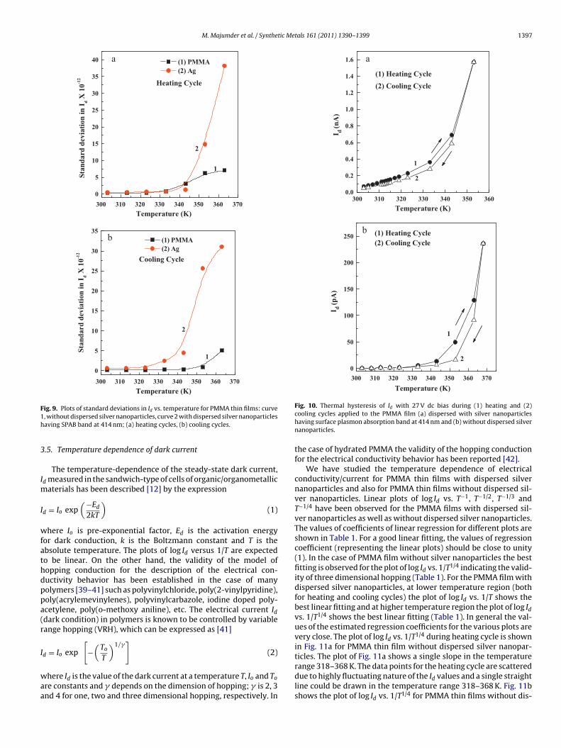
M. Majumder et al. / Synthetic Metals 161 (2011) 1390– 1399 1397
300 310 320 330 340 350 360 3700
5
10
15
20
25
30
35
40 a
b
2
Heating CycleSt
anda
rdde
viat
ion
inI d
X10
-12
Temperature (K)
(1) PMMA(2) Ag
1
300 310 320 330 340 350 360 3700
5
10
15
20
25
30
35
2
Cooling Cycle
Stan
dard
devi
a tio
nin
I dX
10-1
2
Temperature (K)
(1) PMMA(2) Ag
1
F1h
3
Im
I
wfathdppa(r
I
waa
300 310 320 330 340 350 3600.0
0.2
0.4
0.6
0.8
1.0
1.2
1.4
1.6 a
b
(2) Cooling Cycle(1) Heating Cycle
2
1
I d(n
A)
Temperature (K)
300 310 320 330 340 350 360 3700
50
100
150
200
250 (1) Heating Cycle(2) Cooling Cycle
2
1I d
(pA
)
Temperature (K)
Fig. 10. Thermal hysteresis of Id with 27 V dc bias during (1) heating and (2)
ig. 9. Plots of standard deviations in Id vs. temperature for PMMA thin films: curve, without dispersed silver nanoparticles, curve 2 with dispersed silver nanoparticlesaving SPAB band at 414 nm; (a) heating cycles, (b) cooling cycles..5. Temperature dependence of dark current
The temperature-dependence of the steady-state dark current,d measured in the sandwich-type of cells of organic/organometallic
aterials has been described [12] by the expression
d = Io exp(−Ed
2kT
)(1)
here Io is pre-exponential factor, Ed is the activation energyor dark conduction, k is the Boltzmann constant and T is thebsolute temperature. The plots of log Id versus 1/T are expectedo be linear. On the other hand, the validity of the model ofopping conduction for the description of the electrical con-uctivity behavior has been established in the case of manyolymers [39–41] such as polyvinylchloride, poly(2-vinylpyridine),oly(acrylemevinylenes), polyvinylcarbazole, iodine doped poly-cetylene, poly(o-methoxy aniline), etc. The electrical current Iddark condition) in polymers is known to be controlled by variableange hopping (VRH), which can be expressed as [41]
d = Io exp
[−(
To
T
)1/�]
(2)
here Id is the value of the dark current at a temperature T, Io and To
re constants and � depends on the dimension of hopping; � is 2, 3nd 4 for one, two and three dimensional hopping, respectively. In
cooling cycles applied to the PMMA film (a) dispersed with silver nanoparticleshaving surface plasmon absorption band at 414 nm and (b) without dispersed silvernanoparticles.
the case of hydrated PMMA the validity of the hopping conductionfor the electrical conductivity behavior has been reported [42].
We have studied the temperature dependence of electricalconductivity/current for PMMA thin films with dispersed silvernanoparticles and also for PMMA thin films without dispersed sil-ver nanoparticles. Linear plots of log Id vs. T−1, T−1/2, T−1/3 andT−1/4 have been observed for the PMMA films with dispersed sil-ver nanoparticles as well as without dispersed silver nanoparticles.The values of coefficients of linear regression for different plots areshown in Table 1. For a good linear fitting, the values of regressioncoefficient (representing the linear plots) should be close to unity(1). In the case of PMMA film without silver nanoparticles the bestfitting is observed for the plot of log Id vs. 1/T1/4 indicating the valid-ity of three dimensional hopping (Table 1). For the PMMA film withdispersed silver nanoparticles, at lower temperature region (bothfor heating and cooling cycles) the plot of log Id vs. 1/T shows thebest linear fitting and at higher temperature region the plot of log Idvs. 1/T1/4 shows the best linear fitting (Table 1). In general the val-ues of the estimated regression coefficients for the various plots arevery close. The plot of log Id vs. 1/T1/4 during heating cycle is shownin Fig. 11a for PMMA thin film without dispersed silver nanopar-ticles. The plot of Fig. 11a shows a single slope in the temperature
range 318–368 K. The data points for the heating cycle are scattereddue to highly fluctuating nature of the Id values and a single straightline could be drawn in the temperature range 318–368 K. Fig. 11bshows the plot of log Id vs. 1/T1/4 for PMMA thin films without dis-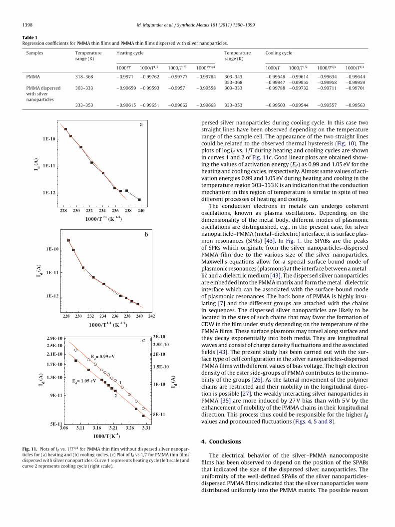
1398 M. Majumder et al. / Synthetic Metals 161 (2011) 1390– 1399
Table 1Regression coefficients for PMMA thin films and PMMA thin films dispersed with silver nanoparticles.
Samples Temperaturerange (K)
Heating cycle Temperaturerange (K)
Cooling cycle
1000/T 1000/T1/2 1000/T1/3 1000/T1/4 1000/T 1000/T1/2 1000/T1/3 1000/T1/4
PMMA 318–368 −0.9971 −0.99762 −0.99777 −0.99784 303–343 −0.99548 −0.99614 −0.99634 −0.99644353–368 −0.99947 −0.99955 −0.99958 −0.99959
PMMA dispersedwith silvernanoparticles
303–333 −0.99659 −0.99593 −0.9957 −0.99558 303–333 −0.99788 −0.99732 −0.99711 −0.99701
333–353 −0.99615 −0.99651 −0.99662 −0
3.06 3.11 3.16 3.21 3.26 3.315E-11
9E-11
1.3E-10
1.7E-10
2.1E-10
2.5E-10
2.9E-10
I d(A
)
Ed= 1.05 eV
Ed= 0.99 eV
2
1I d(A
)
1000/T(K-1)
5E-11
1E-10
1.5E-10
2E-10
2.5E-10
3E-10
228 230 232 234 236 238 240
1E-12
1E-11
1E
a
b
c
-10
I d(A
)
1000/T1/4 (K-1/4)
228 230 232 234 236 238 240 242
1E-12
1E-11
1E-10
I d(A
)
1000/T1/4 (K -1/4)
Fig. 11. Plots of Id vs. 1/T1/4 for PMMA thin film without dispersed silver nanopar-ticles for (a) heating and (b) cooling cycles. (c) Plot of Id vs.1/T for PMMA thin filmsdispersed with silver nanoparticles. Curve 1 represents heating cycle (left scale) andcurve 2 represents cooling cycle (right scale).
.99668 333–353 −0.99503 −0.99544 −0.99557 −0.99563
persed silver nanoparticles during cooling cycle. In this case twostraight lines have been observed depending on the temperaturerange of the sample cell. The appearance of the two straight linescould be related to the observed thermal hysteresis (Fig. 10). Theplots of log Id vs. 1/T during heating and cooling cycles are shownin curves 1 and 2 of Fig. 11c. Good linear plots are obtained show-ing the values of activation energy (Ed) as 0.99 and 1.05 eV for theheating and cooling cycles, respectively. Almost same values of acti-vation energies 0.99 and 1.05 eV during heating and cooling in thetemperature region 303–333 K is an indication that the conductionmechanism in this region of temperature is similar in spite of twodifferent processes of heating and cooling.
The conduction electrons in metals can undergo coherentoscillations, known as plasma oscillations. Depending on thedimensionality of the metal body, different modes of plasmonicoscillations are distinguished, e.g., in the present case, for silvernanoparticle–PMMA (metal–dielectric) interface, it is surface plas-mon resonances (SPRs) [43]. In Fig. 1, the SPABs are the peaksof SPRs which originate from the silver nanoparticles-dispersedPMMA film due to the various size of the silver nanoparticles.Maxwell’s equations allow for a special surface-bound mode ofplasmonic resonances (plasmons) at the interface between a metal-lic and a dielectric medium [43]. The dispersed silver nanoparticlesare embedded into the PMMA matrix and form the metal–dielectricinterface which can be associated with the surface-bound modeof plasmonic resonances. The back bone of PMMA is highly insu-lating [7] and the different groups are attached with the chainsin sequences. The dispersed silver nanoparticles are likely to belocated in the sites of such chains that may favor the formation ofCDW in the film under study depending on the temperature of thePMMA films. These surface plasmons may travel along surface andthey decay exponentially into both media. They are longitudinalwaves and consist of charge density fluctuations and the associatedfields [43]. The present study has been carried out with the sur-face type of cell configuration in the silver nanoparticles-dispersedPMMA films with different values of bias voltage. The high electrondensity of the ester side-groups of PMMA contributes to the immo-bility of the groups [26]. As the lateral movement of the polymerchains are restricted and their mobility in the longitudinal direc-tion is possible [27], the weakly interacting silver nanoparticles inPMMA [35] are more induced by 27 V bias than with 5 V by theenhancement of mobility of the PMMA chains in their longitudinaldirection. This process thus could be responsible for the higher Idvalues and pronounced fluctuations (Figs. 4, 5 and 8).
4. Conclusions
The electrical behavior of the silver–PMMA nanocompositefilms has been observed to depend on the position of the SPABs
that indicated the size of the dispersed silver nanoparticles. Theuniformity of the well-defined SPABs of the silver nanoparticles-dispersed PMMA films indicated that the silver nanoparticles weredistributed uniformly into the PMMA matrix. The possible reason
tic Me
fddnmlifivctwmptftmdilfipthtsestt
A
ttNcr
R
[[[[
[
[[[
[[
[[[
[[
[[[[
[[[[[[
[
[[[
[
[
M. Majumder et al. / Synthe
or the decreasing trends in the Id vs. time profiles could be assignedue to the change in resistance in course of creation of weaker con-uction paths owing to the accumulation of comparatively smalleranoparticles. This process was aided by the longitudinal move-ents of the nano-structured PMMA chains under the action of
ow electric field at a fixed temperature. The systematic fluctuationsn the Id–V characteristics of silver nanoparticles-dispersed PMMAlms having SPABs at different positions have been explained iniew of the creation of favorable conduction paths during the appli-ation of slowly increasing dc voltage as a result of the rotations ofhe functional groups/atoms, exchange of void spaces (free spaces)ith some groups, diffusion of silver nanoparticles in the poly-er matrix and electric field induced manipulation in conduction
aths. The charge distribution in the nanocomposite film is likelyo be influenced by the voltage/electric field and can lead to theormation of CDWs. The changing temperature in presence of elec-ric fields yielded hysteresis when the system was perturbed and
etastable state was induced in both of the films with and withoutispersed silver nanoparticles. An enhancement in the nonlinearity
n Id has been observed with increasing bias voltage. The non-inearity in Id vs. time profiles were explained in terms of theormation of charge density waves (CDWs) in the nanocompos-te films of dispersed silver nanoparticles into PMMA films. In theresent experiment, drastic changes in the electrical behavior inhe PMMA films with and without dispersed silver nanoparticlesave been noticed which indicates that the interaction betweenhe polymer matrix and the nanofiller (i.e. silver nanoparticles) isignificant. Other controlling factors for the observed changes inlectrical properties have been attributed to the manipulation ofilver nanoparticles in the PMMA matrix by the electric field, struc-ural reorientation of the PMMA matrix and surface morphology ofhe PMMA films (i.e. presence of pores/voids).
cknowledgements
One of the authors, Bipul Biswas thanks the Council of Scien-ific and Industrial Research (CSIR), New Delhi, India, for providinghe financial assistances in the form of NET CSIR fellowship (Fileo.: 09/080(0628)/2008/EMR-I). A.K.C. is thankful to the con-erned authorities for the approval of leave and permission ofesearch.
eferences
[1] M. Reith, W. Schommers, Handbook of Theoretical and Computational Nano-technology; Functional Nanomaterials, Nanoparticles and Polymer Design, vol.8, American Scientific Publishers (ASP), 2006, Chapter 3, p. 104.
[2] D. Basak, S. Karan, B. Mallik, Chem. Phys. Lett. 420 (2006) 115–119.[3] D. Basak, S. Karan, B. Mallik, Solid State Commun. 141 (2007) 483–487.
[[[
tals 161 (2011) 1390– 1399 1399
[4] F. Yakuphanoglua, I.S. Yahiab, G. Barim, B.F. Senkal, Synth. Met. 160 (2010)1718–1726.
[5] K.S. Kim, S.J. Park, Synth. Met. 160 (2010) 123–126.[6] M.S. Mehata, M. Majumder, B. Mallik, N. Ohta, J. Phys. Chem. C 114 (2010)
15594–15601.[7] C. McClory, T. McNally, M. Baxendale, P. Pötschke, W. Blau, M. Ruether, Euro.
Polym. J. 46 (2010) 854–868.[8] W. Bogaerts, R. Baets, P. Dumon, V. Wiaux, S. Beckx, D. Taillaert, B. Luyssaert,
J.V. Campenhout, P. Bienstman, D.V. Thourhout, J. Lightwave Technol. 23 (2005)401–412.
[9] Y. Cui, Q. Wei, H. Park, C.M. Lieber, Science 293 (2001) 1289–1292.10] S.D. Wettig, C. Li, Y. Long, H. Kraatz, J.S. Lee, Anal. Sci. 19 (2003) 23–26.11] A. Corma, P. Atienzar, H. Garcia, J.Y. Chane-Ching, Nat. Mater. 3 (2004) 394–397.12] D. Basak, B. Mallik, Synth. Met. 146 (2004) 151–158.13] D. Miranda, V. Sencadas, A. Sánchez- Iglesias, I. Pastoriza-Santos, L.M. Liz-
Marzán, J.L. Gómez Ribelles, S. Lanceros-Mendez, J. Nanosci. Nanotechnol. 9(2009) 2910–2916.
14] A. Hacinliyan, Y. Skarlatos, H.A. Yildirim, G. Sahin, Phys. Rev. B 73 (2006)134302,1–134302,5.
15] H. Frölich, Proc. R. Soc. Lond. Ser. A 223 (1954) 296–305.16] Y.I. Latyshev, B. Pannetier, P. Monceau, Eur. Phys. J. B 3 (1998) 421–426.17] C. Deisl, K. Swamy, S. Penner, E. Bertel, Phys. Chem. Chem. Phys. 3 (2001)
1213–1217.18] L. Pietronero, S. Strässler, Phys. Rev. B 28 (1983) 5863–5865.19] K. Tsutsumi, T. Takagaki, M. Yamamato, Y. Shiozaki, M. Ido, T. Sambongi, K.
Yamaya, Y. Abe, Phys. Rev. Lett. 39 (1977) 1675–1676.20] R.M. Fleming, D.E. Moncton, D.B. McWhan, Phys. Rev. B 18 (1978) 5560–5563.21] P.A. Lee, T.M. Rice, Phys. Rev. B 19 (1979) 3970–3980.22] L. Yongjun, C. Kyongsik, K. Hwi, K. Seyoon, H. Seunghoon, L. Byoungho, Proceed-
ings of SPIE, the International Society for Optical Engineering, ISSN 0277-786XCODEN PSISDG, edited by Society of Photo-Optical Instrumentation Engineers,vol. 6136, Bellingham, WA, ETATS-UNIS, 1981, p. 61360L (8 p).
23] O.D. Velev, K.H. Bhatt, Soft Matter 2 (2006) 738–750.24] J. Guillet, Polymer Photophysics and Photochemistry, Cambridge University
Press, Cambridge, New York, 1987.25] C. Chen, J.K. Maranas, V.G. Sakai, Macromolecules 39 (2006) 9630–9640.26] P. Prentice, J. Mater. Sci. 20 (1985) 1445–1454.27] J. Klein, B.J. Briscoe, Proc. Roy. Soc. A 365 (1979) 53–73.28] M. Pattabi, M.S.M. Sastry, V. Sivsramkrishnan, Phys. Rev. B 39 (1989)
9959–9962.29] P. Monceau, J. Richard, M. Renard, Phys. Rev. B 25 (1982) 931–947.30] L.A. Pfister, Z.H. Stachurski, Polymer 43 (2002) 7419–7427.31] J. Wang, C. Chen, S.M. Buck, Z. Chen, J. Phys. Chem. B 105 (2001) 12118–12125.32] M. Mierzejewski, M.M. Maska, Phys. Rev. B 73 (2006) 205103,1–205103,7.33] T. Kostyrko, B.R. Bułka, Phys. Rev. B 67 (2003) 205331,1–205331,10.34] M.L. Allan, J.H.F. Martens, A.T. Coomber, R.H. Friend, I. Marsden, E.A. Marseglia,
A.E. Underhill, A. Charlton, Mol. Cryst. Liq. Cryst. 229 (1993) 147–152.35] M. Taniguchi, Y. Misaki, T. Yamabe, K. Murata, T. Mori, Solid State Commun.
111 (1999) 559–564.36] R.M. Fleming, L.F. Schneemeyer, Phys. Rev. B 28 (1983) 6996–6999.37] R.M. Fleming, L.F. Schneemeyer, Phys. Rev. B 33 (1986) 2930–2932.38] V.V. Vodnik, J.V. Vukovic, J.M. Nedeljkovic, Colloid Polym. Sci. 287 (2009)
847–851.39] F. Gutmann, H. Keyzer, L.E. Lyons, Organic Semiconductors, Robert E. Krieger.
Publ Co. Inc., Malabar, Florida, 1983, p. 130.40] R.R. Chance, D.S. Boudreaux, J.L. Bredas, R. Silbey, in: T.A. Skothem (Ed.), Hand-
book of Conducting Polymers, vol. 2, Marcel Dekker, Inc., New York, Basel, 1986,
p. 825.41] A. Paul, T.N. Misra, D. Talukdar, Solid State Commun. 99 (1996) 633–636.42] A. Thander, R.N. Bera, B. Mallik, Phys. Stat. Solidi A 189 (2002) 233–241.43] V. M. Shalaev, S. Kawata (Eds.), Nanophotonics with Surface Plasmons, Elsevier,
The Netherlands, 2007, p. 222, 223, 225.
Copyright © 2022 FDOKUMEN