Increasing organic solar cell efficiency with polymer interlayers
7
ISSN 1463-9076 Physical Chemistry Chemical Physics www.rsc.org/pccp Volume 15 | Number 3 | 21 January 2013 | Pages 705–1036 1463-9076(2013)15:3;1-J PAPER MacKenzie et al. Increasing organic solar cell efficiency with polymer interlayers
-
Upload
independent -
Category
Documents
-
view
0 -
download
0
Transcript of Increasing organic solar cell efficiency with polymer interlayers
ISSN 1463-9076
Physical Chemistry Chemical Physics
www.rsc.org/pccp Volume 15 | Number 3 | 21 January 2013 | Pages 705–1036
1463-9076(2013)15:3;1-J
PAPERMacKenzie et al.Increasing organic solar cell effi ciency with polymer interlayers
764 Phys. Chem. Chem. Phys., 2013, 15, 764--769 This journal is c the Owner Societies 2013
Cite this: Phys. Chem.Chem.Phys.,2013,15, 764
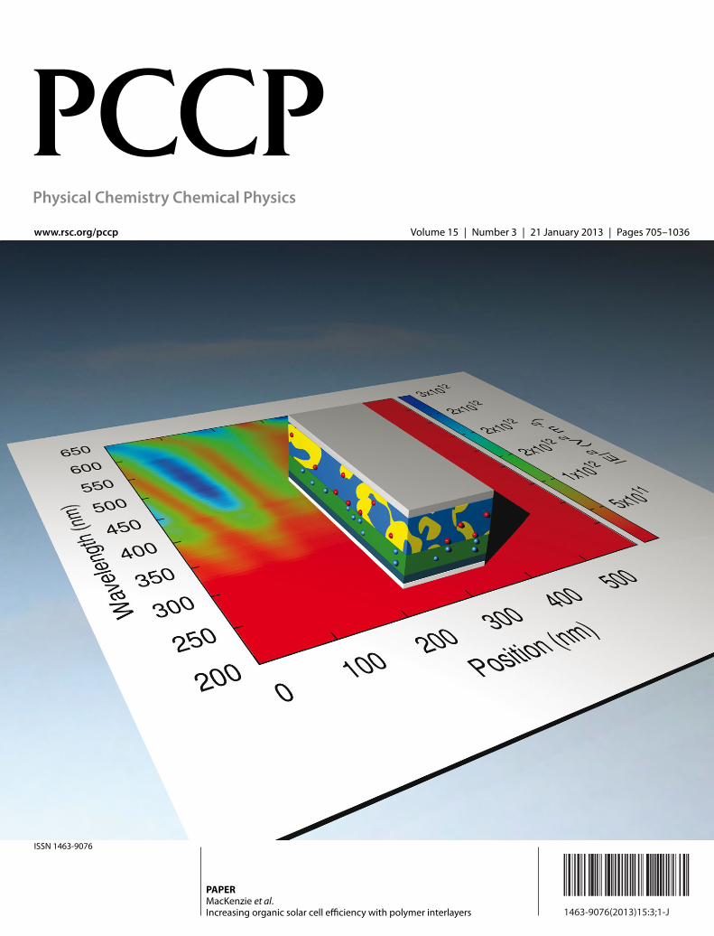
Increasing organic solar cell efficiency with polymerinterlayers†
Felix Deschler,a Daniel Riedel,a Bernhard Ecker,b Elizabeth von Hauff,bc
Enrico Da Comoad and Roderick C. I. MacKenzie*ef
We demonstrate how organic solar cell efficiency can be increased by introducing a pure polymer interlayer
between the PEDOT:PSS layer and the polymer:fullerene blend. We observe an increase in device efficiency
with three different material systems over a number of devices. Using both electrical characterization and
numerical modeling we show that the increase in efficiency is caused by optical absorption in the pure
polymer layer and hence efficient charge separation at the polymer bulkheterojunction interface.
1 Introduction
Organic solar cells have recently shown great promises as a lowcost source of low carbon electricity, their efficiencies haverapidly improved from 3% in 20071 to over 10% today.2 Therehas been much work done on optimizing all aspects of organicphotovoltaic devices (OPVs) including; development of narrowbandgap polymers to improve light absorption;3 developingbetter contacts4,5 to replace expensive Indium Tin Oxide;6,7
and development of faster production technologies to reducethe fabrication cost.8–10 However the cost per Watt of energyproduced with an organic solar cell is still not competitive tosilicon2,11 and for OPV devices to become commercially viable,improvements still need to be made in both efficiency and cost.
In the following pages we demonstrate how a significantimprovement in device efficiency can be achieved by replacing a30 nm layer of the bulk heterojunction material next to thePEDOT:PSS layer with a pure polymer layer (see Fig. 1). It isfound that by introducing this layer of conjugate polymer theenergy conversing efficiency can be reliably increased for cellsmade from three different material systems. Furthermore, asthis polymer layer replaces a section of the bulkheterojunctionlayer containing expensive fullerene, the total fabrication costof the new solar cell can be reduced.
The paper is divided into three sections; first we describe thefabrication process of the bi-layer structures as depicted in Fig. 1,next we characterize the devices using Impedance Spectroscopy (IS),steady state electrical measurements and transient optoelectronictechniques. We then extend our electro-optical device model12 tosimulate carrier transport over heterojunctions13–15 and opticalpropagation/carrier generation in multilayered structures. Finallyusing a combination of characterization and modeling we show thatthe increased efficiency is due to optical generation of excitonswithin the polymer layer and subsequent charge separation at thepolymer:fullerene interface. Hereafter, the solar cell structure withthe polymer layer will be referred to as the bi-layer structure and thenormal structure will be referred to as the mono-layer structure.
2 Experimental
Three polymer:fullerene material systems were investigated; poly(3-hexylthiophene):phenyl-C61-butyric acid methyl ester (P3HT:PCBM);poly[(4,40-bis(2-ethylhexyl)dithiene[3,2-b:20,30-d]silole)-2,6-diyl-alt-(4,7-bis(2-thienyl)-2,1,3-benzothiadiazole)-5,50-diyl] (Si-PCPDTBT:
Fig. 1 A diagram of the more efficient bi-layer structure. A polymer layer is usedto replace a 30 nm section of the BHJ. This reduces the amount of fullerene usedand increases solar cell efficiency. The blue spheres represent holes and the redspheres represent electrons.
a Department of Physics and CeNS, Ludwig-Maximilians-Universtitat Munchen,
Amalienstr. 54, D-80799 Munchen, Germanyb Institute of Physics, Hermann-Herder-Str. 3a, Freiburg, D-79104, Germanyc Fraunhofer Institute for Solar Energy Systems (ISE), Heidenhofstr. 2, Freiburg,
D-79110, Germanyd Department of Physics, University of Bath, Somerset, BA2 7AY, UKe FRIAS, School of Soft Matter Research, University of Freiburg, Albertstraße 19,
Freiburg, 79104, Germanyf Faculty of Engineering, University of Nottingham, Nottingham, Nottinghamshire
NG7 2RD, UK. E-mail: [email protected]
† Electronic supplementary information (ESI) available. See DOI: 10.1039/c2cp43876c
Received 1st November 2012,Accepted 6th November 2012
DOI: 10.1039/c2cp43876c
www.rsc.org/pccp
PCCP
PAPER
Dow
nloa
ded
by U
nive
rsita
tsbi
blio
thek
Old
enbu
rg o
n 26
Jan
uary
201
3Pu
blis
hed
on 0
7 N
ovem
ber
2012
on
http
://pu
bs.r
sc.o
rg |
doi:1
0.10
39/C
2CP4
3876
C
View Article OnlineView Journal | View Issue
This journal is c the Owner Societies 2013 Phys. Chem. Chem. Phys., 2013, 15, 764--769 765
PCBM); and Poly[[4,8-bis[(2-ethylhexyl)oxy]benzo[1,2-b:4,5-b0]dithio-phene-2,6-diyl][3-fluoro-2-[(2-ethylhexyl)carbonyl]thieno[3,4-b]thio-phenediyl]] (PTB7:PCBM). Mono-layer devices and bi-layer deviceswere fabricated from each material system, in the bi-layer devicesthe polymer layer was made from the same polymer as was usedin the bulk-heterojunction. A picture of a bi-layer device is shownin Fig. 1. The detailed fabrication of the devices is described in theESI.† For characterization, the solar cells were mounted in asealed box providing inert atmosphere to prevent degradationand masking of the active area, defining three solar cells, eachwith pixel sizes of 0.125 cm2. The light and dark JV-characteristicswere measured using a source-measure unit (Keithley 2400),illumination was provided through a solar simulator (LOT-Oriel)equipped with filters maintaining an AM 1.5G spectrum. Theintensity was set to 100 mW cm�2 using a calibrated siliconreference diode. The transient photovoltage measurements werecarried out using a Xenon high pressure lamp with differentillumination intensities for background illumination. A diodepumped passively Q-switched laser (FTSS 355-50, CryLas GmbH)with a pulse length around 1 ns and a wavelength of 532 nm wasused to perturbate the solar cell held at open circuit with theinternal 1 M O impedance of an oscilloscope.
The resulting transients were recorded using a digital oscillo-scope (DPO 7254, Tektronix). For impedance spectroscopy16 apotentiostat system (Autolab PGSTAT302N, Metrohm) equipped
with an impedance module, controlled via NOVA software, wasused. The complex resistance was recorded from 1 MHz down to10 Hz at an applied AC voltage of 30 mV (RMS). The solar cellswere either kept in dark or illuminated by high brightness LEDswith varying illumination intensities together with an super-imposed DC voltage equal to the respective Voc.
3 Results3.1 Statistical JV curve measurement
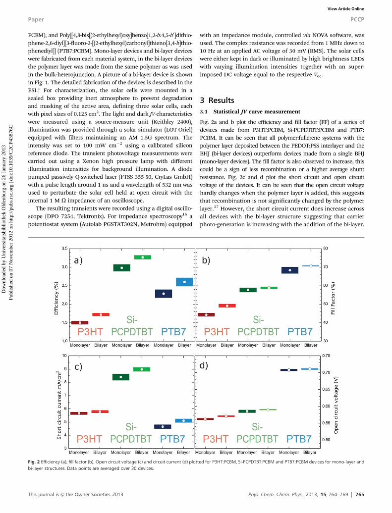
Fig. 2a and b plot the efficiency and fill factor (FF) of a series ofdevices made from P3HT:PCBM, Si-PCPDTBT:PCBM and PTB7:PCBM. It can be seen that all polymer:fullerene systems with thepolymer layer deposited between the PEDOT:PSS interlayer and theBHJ (bi-layer devices) outperform devices made from a single BHJ(mono-layer devices). The fill factor is also observed to increase, thiscould be a sign of less recombination or a higher average shuntresistance. Fig. 2c and d plot the short circuit and open circuitvoltage of the devices. It can be seen that the open circuit voltagehardly changes when the polymer layer is added, this suggeststhat recombination is not significantly changed by the polymerlayer.17 However, the short circuit current does increase acrossall devices with the bi-layer structure suggesting that carrierphoto-generation is increasing with the addition of the bi-layer.
Fig. 2 Efficiency (a), fill factor (b), Open circuit voltage (c) and circuit current (d) plotted for P3HT:PCBM, Si-PCPDTBT:PCBM and PTB7:PCBM devices for mono-layer andbi-layer structures. Data points are averaged over 30 devices.
Paper PCCP
Dow
nloa
ded
by U
nive
rsita
tsbi
blio
thek
Old
enbu
rg o
n 26
Jan
uary
201
3Pu
blis
hed
on 0
7 N
ovem
ber
2012
on
http
://pu
bs.r
sc.o
rg |
doi:1
0.10
39/C
2CP4
3876
CView Article Online
766 Phys. Chem. Chem. Phys., 2013, 15, 764--769 This journal is c the Owner Societies 2013
3.2 Analysis of dark JV curves and recombination data
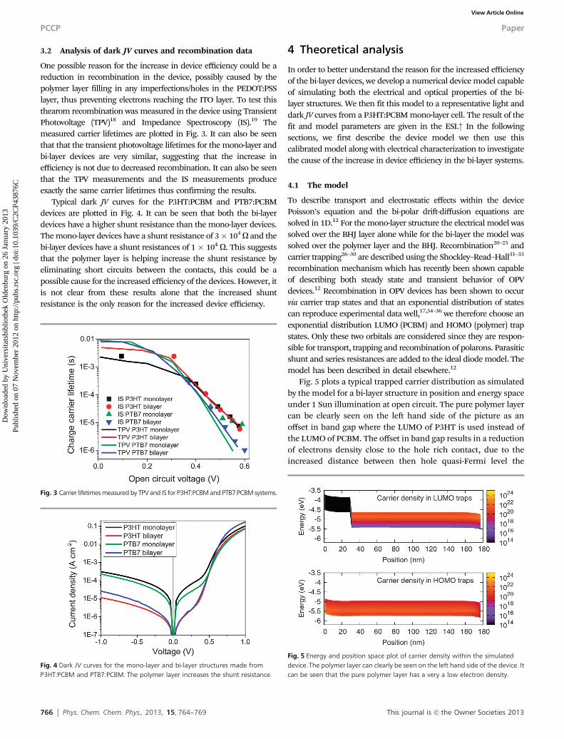
One possible reason for the increase in device efficiency could be areduction in recombination in the device, possibly caused by thepolymer layer filling in any imperfections/holes in the PEDOT:PSSlayer, thus preventing electrons reaching the ITO layer. To test thisthearom recombination was measured in the device using TransientPhotovoltage (TPV)18 and Impedance Spectroscopy (IS).19 Themeasured carrier lifetimes are plotted in Fig. 3. It can also be seenthat that the transient photovoltage lifetimes for the mono-layer andbi-layer devices are very similar, suggesting that the increase inefficiency is not due to decreased recombination. It can also be seenthat the TPV measurements and the IS measurements produceexactly the same carrier lifetimes thus confirming the results.
Typical dark JV curves for the P3HT:PCBM and PTB7:PCBMdevices are plotted in Fig. 4. It can be seen that both the bi-layerdevices have a higher shunt resistance than the mono-layer devices.The mono-layer devices have a shunt resistance of 3� 104 O and thebi-layer devices have a shunt resistances of 1 � 104 O. This suggeststhat the polymer layer is helping increase the shunt resistance byeliminating short circuits between the contacts, this could be apossible cause for the increased efficiency of the devices. However, itis not clear from these results alone that the increased shuntresistance is the only reason for the increased device efficiency.
4 Theoretical analysis
In order to better understand the reason for the increased efficiencyof the bi-layer devices, we develop a numerical device model capableof simulating both the electrical and optical properties of the bi-layer structures. We then fit this model to a representative light anddark JV curves from a P3HT:PCBM mono-layer cell. The result of thefit and model parameters are given in the ESI.† In the followingsections, we first describe the device model we then use thiscalibrated model along with electrical characterization to investigatethe cause of the increase in device efficiency in the bi-layer systems.
4.1 The model
To describe transport and electrostatic effects within the devicePoisson’s equation and the bi-polar drift-diffusion equations aresolved in 1D.12 For the mono-layer structure the electrical model wassolved over the BHJ layer alone while for the bi-layer the model wassolved over the polymer layer and the BHJ. Recombination20–25 andcarrier trapping26–30 are described using the Shockley–Read–Hall31–33
recombination mechanism which has recently been shown capableof describing both steady state and transient behavior of OPVdevices.12 Recombination in OPV devices has been shown to occurvia carrier trap states and that an exponential distribution of statescan reproduce experimental data well,17,34–36 we therefore choose anexponential distribution LUMO (PCBM) and HOMO (polymer) trapstates. Only these two orbitals are considered since they are respon-sible for transport, trapping and recombination of polarons. Parasiticshunt and series resistances are added to the ideal diode model. Themodel has been described in detail elsewhere.12
Fig. 5 plots a typical trapped carrier distribution as simulatedby the model for a bi-layer structure in position and energy spaceunder 1 Sun illumination at open circuit. The pure polymer layercan be clearly seen on the left hand side of the picture as anoffset in band gap where the LUMO of P3HT is used instead ofthe LUMO of PCBM. The offset in band gap results in a reductionof electrons density close to the hole rich contact, due to theincreased distance between then hole quasi-Fermi level the
Fig. 3 Carrier lifetimes measured by TPV and IS for P3HT:PCBM and PTB7:PCBM systems.
Fig. 4 Dark JV curves for the mono-layer and bi-layer structures made fromP3HT:PCBM and PTB7:PCBM. The polymer layer increases the shunt resistance.
Fig. 5 Energy and position space plot of carrier density within the simulateddevice. The polymer layer can clearly be seen on the left hand side of the device. Itcan be seen that the pure polymer layer has a very a low electron density.
PCCP Paper
Dow
nloa
ded
by U
nive
rsita
tsbi
blio
thek
Old
enbu
rg o
n 26
Jan
uary
201
3Pu
blis
hed
on 0
7 N
ovem
ber
2012
on
http
://pu
bs.r
sc.o
rg |
doi:1
0.10
39/C
2CP4
3876
CView Article Online
This journal is c the Owner Societies 2013 Phys. Chem. Chem. Phys., 2013, 15, 764--769 767
electron band edge. This reduction in electron population can beseen as an un-populated area in the graph which is coloredblack. This low electron density in the pure polymer layer resultsin a very low carrier recombination rate is low within this layer.
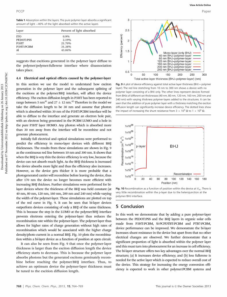
The optical field profile within the device was calculated byassuming the incident radiation on the cell is transversely polarizedto the interfaces. Then the forward and backward propagating fieldsacross the all material interfaces were forced to be continuous. Phaseshifts and absorption are taken into account assuming an exponentialdependence of field on propagation distance in the complex plane.The optical model is solved over all material layers within the device,the differences in refractive index and absorption were taken toaccount using the following previously published data (ITO37/PED-OT:37PSS/P3HT37,38/P3HT:PCBM38/LiF/Al39). The influence of theglass substrate was neglected and a 1.5 AM optical spectrum wasused as the light source. This method is identical to the transfer matrixmethod40 however all equations are solved on a finite difference gridwithin one matrix to minimize the computational effort (see ESI†). Atypical field profile calculated as a function of position and wavelengthis shown in Fig. 6, it can be seen that in this example there is a highphoton density in the pure P3HT polymer layer.
4.2 Analysis of increased shunt resistance caused by thepolymer layer
To investigate if the change in shunt resistance could explain theincrease in device efficiency, a series of JV curves were simulatedwith the calibrated model using different shunt resistances and theresulting device efficiency plotted. The results can be seen in Fig. 7.It can be seen that for shunt resistances under 1 � 106 O the shuntresistance has an influence on device efficiency. However thedifference in efficiency between a device with a shunt resistance of3� 104 O and 1� 106 O is only 0.1%. This is not enough to explainthe observed 0.25% increase in efficiency shown in Fig. 2. Further-more, we were unable to explain the increase in short circuit currentwith an increase in shunt resistance alone.
4.3 Optical effects caused by the polymer-layer
In the previous sections we demonstrated that the increase indevice efficiency can not be explained by electrical effects withinthe device alone. This leaves optical effects left to be investigated.
When PCBM is mixed with P3HT to form a blend the resulting filmis optically less dense over the solar spectrum than a film of pureP3HT because the absorption of PCBM is weak below 400 nm anddoes not coincide with the maxima in the solar spectra.38 Thus onewould expect the pure polymer layer of P3HT in the bi-layerstructure to absorb a significant amount of solar radiation. Thisis confirmed by the optical simulation plotted in Fig. 8. It can beseen that very little light is absorbed in the ITO/PEDOT:PSS layers,however a significant amount of light is absorbed in the 30 nmthick P3HT layer. Indeed the peak photon absorption in thepolymer layer is higher than in the peak photon absorption inthe BHJ of the mono-layer or bi-layer device. Table 1 plots thepercentage of light absorbed in each layer of the bi-layer deviceshown in Fig. 8. It can be seen that the P3HT layer absorbs 21.70%of the total light and accounts for 40% of the light absorbed in theelectrically active layer. From Fig. 8, it can also be seen that theaddition of the polymer-layer significantly reduces the lightabsorbed within the BHJ. Thus the light absorbed in the poly-mer-layer must contribute to the photocurrent or the cell efficiencywould decrease with the addition of the polymer layer. This in turn
Fig. 6 The photon distribution within the devices as a function position andwavelength. Fig. 7 Device efficiency plotted against shunt resistance. The mono-layer devices
have a low shunt resistance, this was boosted with the introduction of the bi-layer.
Fig. 8 The photon absorption within the device as a function of position summed overthe spectrum. It can be seen that a significant amount of light is absorbed in the purepolymer layer, therefore, for the bi-layer devices to have an increased efficiency theexcitons generated within this layer must be split and reach the contacts as current.
Paper PCCP
Dow
nloa
ded
by U
nive
rsita
tsbi
blio
thek
Old
enbu
rg o
n 26
Jan
uary
201
3Pu
blis
hed
on 0
7 N
ovem
ber
2012
on
http
://pu
bs.r
sc.o
rg |
doi:1
0.10
39/C
2CP4
3876
CView Article Online
768 Phys. Chem. Chem. Phys., 2013, 15, 764--769 This journal is c the Owner Societies 2013
suggests that excitions generated in the polymer layer diffuse tothe polymer/polymer:fullerene interface where disassociationtakes place.
4.4 Electrical and optical effects caused by the polymer-layer
In this section we use the model to understand how excitongeneration in the polymer layer and the subsequent splitting ofthe excitions at the polymer/BHJ interface, will affect the deviceefficiency. The exciton diffusion length in P3HT has been reported torange between 5 nm41 and 27� 12 nm.42 Therefore in the model wetake the diffusion length to be 30 nm and assume that photonwhich is absorbed within 30 nm of the P3HT:PCBM interface will beable to diffuse to the interface and generate an electron hole pair,with an electron being generated in the PCBM LUMO and a hole inthe pure P3HT layer HOMO. Any photon which is absorbed morethan 30 nm away from the interface will be recombine and notgenerate photocurrent.
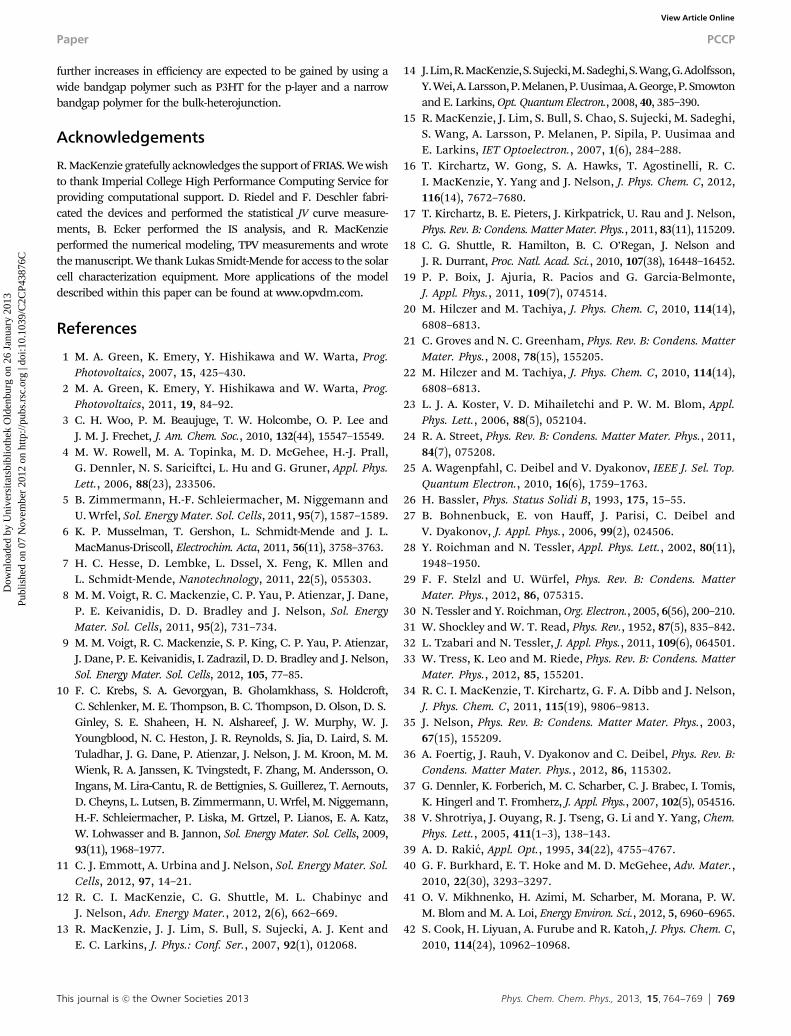
Initially full electrical and optical simulations were performed topredict the efficiency in mono-layer devices with different BHJthicknesses. The results from these simulations are shown in Fig. 9as the continuous red line between 10 nm and 300 nm. It shows thatwhen the BHJ is very thin the device efficiency is very low, because thedevice can not absorb much light. As the BHJ thickness is increasedthe device absorbs more light and thus the efficiency also increases.However, as the device gets thicker it is more probable that aphotogenerated carrier will recombine before leaving the device, thusafter 170 nm the device no longer becomes more efficient withincreasing BHJ thicknes. Further simulations were performed for bi-layer devices where the thickness of the BHJ was held constant (at40 nm, 80 nm, 120 nm, 160 nm, 200 nm and 240 nm) while varyingthe width of the polymer-layer. These simulations are plotted on topof the red curve in Fig. 9. It can be seen that bi-layer devicesoutperform devices consisting of only a BHJ of the same thickness.This is because the step in the LUMO at the polymer/BHJ interfaceprevents electrons entering the polymer-layer thus reduces therecombination rate within the polymer-layer. The polymer-layer thusallows for higher rates of charge generation without high rates ofrecombination which would be associated with the higher chargedensity/photo current in a normal BHJ. Fig. 10 plots the recombina-tion within a bi-layer device as a function of position at open circuit.
It can also be seen from Fig. 9 that once the polymer-layerthickness is larger than the exciton diffusion length the deviceefficiency starts to decrease. This is because the polymer layerabsorbs photons but the generated excitons geminately recom-bine before reaching the polymer/BHJ interface. Thus, toachieve an optimum device the polymer-layer thickness mustbe tuned to the excition diffusion length.
5 Conclusion
In this work we demonstrate that by adding a pure polymer-layerbetween the PEDOT:PSS and the BHJ layers in organic solar cellsmade from P3HT:PCBM, Si-PCPDTBT:PCBM and PTB7:PCBM,device performance can be improved. We demonstrate the bi-layerincreases shunt resistance in the device but apart from that no otherelectrical changes are observed. We further demonstrate that asignificant proportion of light is absorbed within the polymer layerand this must turn into photocurrent for an increase in cell efficiency.The bi-layer structure offers two key advantages over the normal BHJstructure; (a) It increases device efficiency; and (b) less fullerene isneeded for the active layer which is expected to reduce overall cost ofthe device. This strategy for increasing the energy conversion effi-ciency is expected to work in other polymer:PCBM systems and
Table 1 Absorption within the layers. The pure polymer layer absorbs a significantamount of light �40% of the light absorbed within the active layers
Layer Percent of light absorbed
ITO 0.9%PEDOT:PSS 2.19%P3HT 21.70%P3HT:PCBM 31.38%Al 43.84%
Fig. 9 A plot of device efficiency against total active layer thickness (BHJ + polymerlayer). The red line stretching from 10 nm to 300 nm shows a device with nopolymer layer consisting of a BHJ only. The other lines represent devices formedfrom BHJs of different set thicknesses (40 nm, 80 nm, 120 nm, 160 nm, 200 nm and240 nm) with varying thickness polymer-layers added to the structures. It can beseen that the addition of pure polymer layer with a thickness matching the excitondiffusion length can significantly increase device efficiency. The dotted lines showthe impact of increasing the shunt resistance from 3 � 104 O to 1 � 106 O.
Fig. 10 Recombination as a function of position within the device at Voc. There isvery little recombination within the p-layer due to the heterojunction at thepolymer/BHJ interface.
PCCP Paper
Dow
nloa
ded
by U
nive
rsita
tsbi
blio
thek
Old
enbu
rg o
n 26
Jan
uary
201
3Pu
blis
hed
on 0
7 N
ovem
ber
2012
on
http
://pu
bs.r
sc.o
rg |
doi:1
0.10
39/C
2CP4
3876
CView Article Online
This journal is c the Owner Societies 2013 Phys. Chem. Chem. Phys., 2013, 15, 764--769 769
further increases in efficiency are expected to be gained by using awide bandgap polymer such as P3HT for the p-layer and a narrowbandgap polymer for the bulk-heterojunction.
Acknowledgements
R. MacKenzie gratefully acknowledges the support of FRIAS. We wishto thank Imperial College High Performance Computing Service forproviding computational support. D. Riedel and F. Deschler fabri-cated the devices and performed the statistical JV curve measure-ments, B. Ecker performed the IS analysis, and R. MacKenzieperformed the numerical modeling, TPV measurements and wrotethe manuscript. We thank Lukas Smidt-Mende for access to the solarcell characterization equipment. More applications of the modeldescribed within this paper can be found at www.opvdm.com.
References
1 M. A. Green, K. Emery, Y. Hishikawa and W. Warta, Prog.Photovoltaics, 2007, 15, 425–430.
2 M. A. Green, K. Emery, Y. Hishikawa and W. Warta, Prog.Photovoltaics, 2011, 19, 84–92.
3 C. H. Woo, P. M. Beaujuge, T. W. Holcombe, O. P. Lee andJ. M. J. Frechet, J. Am. Chem. Soc., 2010, 132(44), 15547–15549.
4 M. W. Rowell, M. A. Topinka, M. D. McGehee, H.-J. Prall,G. Dennler, N. S. Sariciftci, L. Hu and G. Gruner, Appl. Phys.Lett., 2006, 88(23), 233506.
5 B. Zimmermann, H.-F. Schleiermacher, M. Niggemann andU. Wrfel, Sol. Energy Mater. Sol. Cells, 2011, 95(7), 1587–1589.
6 K. P. Musselman, T. Gershon, L. Schmidt-Mende and J. L.MacManus-Driscoll, Electrochim. Acta, 2011, 56(11), 3758–3763.
7 H. C. Hesse, D. Lembke, L. Dssel, X. Feng, K. Mllen andL. Schmidt-Mende, Nanotechnology, 2011, 22(5), 055303.
8 M. M. Voigt, R. C. Mackenzie, C. P. Yau, P. Atienzar, J. Dane,P. E. Keivanidis, D. D. Bradley and J. Nelson, Sol. EnergyMater. Sol. Cells, 2011, 95(2), 731–734.
9 M. M. Voigt, R. C. Mackenzie, S. P. King, C. P. Yau, P. Atienzar,J. Dane, P. E. Keivanidis, I. Zadrazil, D. D. Bradley and J. Nelson,Sol. Energy Mater. Sol. Cells, 2012, 105, 77–85.
10 F. C. Krebs, S. A. Gevorgyan, B. Gholamkhass, S. Holdcroft,C. Schlenker, M. E. Thompson, B. C. Thompson, D. Olson, D. S.Ginley, S. E. Shaheen, H. N. Alshareef, J. W. Murphy, W. J.Youngblood, N. C. Heston, J. R. Reynolds, S. Jia, D. Laird, S. M.Tuladhar, J. G. Dane, P. Atienzar, J. Nelson, J. M. Kroon, M. M.Wienk, R. A. Janssen, K. Tvingstedt, F. Zhang, M. Andersson, O.Ingans, M. Lira-Cantu, R. de Bettignies, S. Guillerez, T. Aernouts,D. Cheyns, L. Lutsen, B. Zimmermann, U. Wrfel, M. Niggemann,H.-F. Schleiermacher, P. Liska, M. Grtzel, P. Lianos, E. A. Katz,W. Lohwasser and B. Jannon, Sol. Energy Mater. Sol. Cells, 2009,93(11), 1968–1977.
11 C. J. Emmott, A. Urbina and J. Nelson, Sol. Energy Mater. Sol.Cells, 2012, 97, 14–21.
12 R. C. I. MacKenzie, C. G. Shuttle, M. L. Chabinyc andJ. Nelson, Adv. Energy Mater., 2012, 2(6), 662–669.
13 R. MacKenzie, J. J. Lim, S. Bull, S. Sujecki, A. J. Kent andE. C. Larkins, J. Phys.: Conf. Ser., 2007, 92(1), 012068.
14 J.Lim,R.MacKenzie,S.Sujecki,M.Sadeghi,S.Wang,G.Adolfsson,Y. Wei, A. Larsson, P. Melanen, P. Uusimaa, A. George, P. Smowtonand E. Larkins, Opt. Quantum Electron., 2008, 40, 385–390.
15 R. MacKenzie, J. Lim, S. Bull, S. Chao, S. Sujecki, M. Sadeghi,S. Wang, A. Larsson, P. Melanen, P. Sipila, P. Uusimaa andE. Larkins, IET Optoelectron., 2007, 1(6), 284–288.
16 T. Kirchartz, W. Gong, S. A. Hawks, T. Agostinelli, R. C.I. MacKenzie, Y. Yang and J. Nelson, J. Phys. Chem. C, 2012,116(14), 7672–7680.
17 T. Kirchartz, B. E. Pieters, J. Kirkpatrick, U. Rau and J. Nelson,Phys. Rev. B: Condens. Matter Mater. Phys., 2011, 83(11), 115209.
18 C. G. Shuttle, R. Hamilton, B. C. O’Regan, J. Nelson andJ. R. Durrant, Proc. Natl. Acad. Sci., 2010, 107(38), 16448–16452.
19 P. P. Boix, J. Ajuria, R. Pacios and G. Garcia-Belmonte,J. Appl. Phys., 2011, 109(7), 074514.
20 M. Hilczer and M. Tachiya, J. Phys. Chem. C, 2010, 114(14),6808–6813.
21 C. Groves and N. C. Greenham, Phys. Rev. B: Condens. MatterMater. Phys., 2008, 78(15), 155205.
22 M. Hilczer and M. Tachiya, J. Phys. Chem. C, 2010, 114(14),6808–6813.
23 L. J. A. Koster, V. D. Mihailetchi and P. W. M. Blom, Appl.Phys. Lett., 2006, 88(5), 052104.
24 R. A. Street, Phys. Rev. B: Condens. Matter Mater. Phys., 2011,84(7), 075208.
25 A. Wagenpfahl, C. Deibel and V. Dyakonov, IEEE J. Sel. Top.Quantum Electron., 2010, 16(6), 1759–1763.
26 H. Bassler, Phys. Status Solidi B, 1993, 175, 15–55.27 B. Bohnenbuck, E. von Hauff, J. Parisi, C. Deibel and
V. Dyakonov, J. Appl. Phys., 2006, 99(2), 024506.28 Y. Roichman and N. Tessler, Appl. Phys. Lett., 2002, 80(11),
1948–1950.29 F. F. Stelzl and U. Wurfel, Phys. Rev. B: Condens. Matter
Mater. Phys., 2012, 86, 075315.30 N. Tessler and Y. Roichman, Org. Electron., 2005, 6(56), 200–210.31 W. Shockley and W. T. Read, Phys. Rev., 1952, 87(5), 835–842.32 L. Tzabari and N. Tessler, J. Appl. Phys., 2011, 109(6), 064501.33 W. Tress, K. Leo and M. Riede, Phys. Rev. B: Condens. Matter
Mater. Phys., 2012, 85, 155201.34 R. C. I. MacKenzie, T. Kirchartz, G. F. A. Dibb and J. Nelson,
J. Phys. Chem. C, 2011, 115(19), 9806–9813.35 J. Nelson, Phys. Rev. B: Condens. Matter Mater. Phys., 2003,
67(15), 155209.36 A. Foertig, J. Rauh, V. Dyakonov and C. Deibel, Phys. Rev. B:
Condens. Matter Mater. Phys., 2012, 86, 115302.37 G. Dennler, K. Forberich, M. C. Scharber, C. J. Brabec, I. Tomis,
K. Hingerl and T. Fromherz, J. Appl. Phys., 2007, 102(5), 054516.38 V. Shrotriya, J. Ouyang, R. J. Tseng, G. Li and Y. Yang, Chem.
Phys. Lett., 2005, 411(1–3), 138–143.39 A. D. Rakic, Appl. Opt., 1995, 34(22), 4755–4767.40 G. F. Burkhard, E. T. Hoke and M. D. McGehee, Adv. Mater.,
2010, 22(30), 3293–3297.41 O. V. Mikhnenko, H. Azimi, M. Scharber, M. Morana, P. W.
M. Blom and M. A. Loi, Energy Environ. Sci., 2012, 5, 6960–6965.42 S. Cook, H. Liyuan, A. Furube and R. Katoh, J. Phys. Chem. C,
2010, 114(24), 10962–10968.
Paper PCCP
Dow
nloa
ded
by U
nive
rsita
tsbi
blio
thek
Old
enbu
rg o
n 26
Jan
uary
201
3Pu
blis
hed
on 0
7 N
ovem
ber
2012
on
http
://pu
bs.r
sc.o
rg |
doi:1
0.10
39/C
2CP4
3876
CView Article Online