
Implementing and communicating with SHILS - University of ...
86
Implementing and communicating with SHILS Master’s Thesis by Remco Blumink Committee: ir. P.T. Wolkotte dr. ir. A.B.J. Kokkeler ir. P.K.F. Hölzenspies University of Twente, Enschede, The Netherlands August 25, 2008
-
Upload
khangminh22 -
Category
Documents
-
view
3 -
download
0
Transcript of Implementing and communicating with SHILS - University of ...

Implementing and communicating with SHILS
Master’s Thesisby
Remco Blumink
Committee:ir. P.T. Wolkotte
dr. ir. A.B.J. Kokkelerir. P.K.F. Hölzenspies
University of Twente, Enschede, The NetherlandsAugust 25, 2008


Abstract
Simulation can be used to check whether a design complies to its specifications.Digital hardware designsmust be simulated cycle-true, bit accurate to verify timing.Performing such simulations takes prohibitively long for large hardware designs, i.e.a 6x6 NoC design requires 29 hours for simulation.
Simulation on an FPGA platform can be used to shorten the simulation time.However, a large hardware design can not be simulated in a single FPGA as a whole.To be able to simulate a large system using a single FPGA, the system is divided insections (entities) that are simulated sequentially. The entities in homogeneous sys-tems are identical, the required logic for an entity can be reused for all entities whenthe state of the entities can be extracted. For extraction, a tool is provided. The re-sulting simulator performs simulations on a Design Under Test (DUT) sequentially.
To simulate a system in an FPGA, it must be supplied with stimuli and control.This thesis integrates the simulator in an FPGA design, referred to as SHILS. SHILSprovides stimuli and control buffers, and a MMIO interface. SHILS is controlled bysoftware in an embedded processor, it is a co-simulation system.
In order to extend the capabilities of SHILS, a design is proposed to link MAT-LAB to SHILS. The design is based on Xilinx System Generator, which arranges thecommunication between the MATLAB model and SHILS over Ethernet.
i


Contents
Contents iii
List of Acronyms vii
1 Introduction 11.1 Motivation . . . . . . . . . . . . . . . . . . . . . . . . . . . . . . . . 1
1.1.1 Hardware-based simulation: emulation . . . . . . . . . . . . 21.1.2 Sequential Simulation . . . . . . . . . . . . . . . . . . . . . 3
1.2 Assignment . . . . . . . . . . . . . . . . . . . . . . . . . . . . . . . . 51.3 Thesis Outline . . . . . . . . . . . . . . . . . . . . . . . . . . . . . . 6
2 Background 72.1 System design process . . . . . . . . . . . . . . . . . . . . . . . . . . 7
2.1.1 Digital System Design . . . . . . . . . . . . . . . . . . . . . . 82.1.2 Tool chain . . . . . . . . . . . . . . . . . . . . . . . . . . . . 8
2.2 Co-simulation . . . . . . . . . . . . . . . . . . . . . . . . . . . . . . 92.3 Sequential Simulator . . . . . . . . . . . . . . . . . . . . . . . . . . 9
2.3.1 Simulator design . . . . . . . . . . . . . . . . . . . . . . . . 102.3.2 Using SHILS . . . . . . . . . . . . . . . . . . . . . . . . . . . 11
2.4 Related work . . . . . . . . . . . . . . . . . . . . . . . . . . . . . . . 142.4.1 Hardware emulation systems . . . . . . . . . . . . . . . . . . 142.4.2 Sequential Simulation . . . . . . . . . . . . . . . . . . . . . 142.4.3 Co-simulation . . . . . . . . . . . . . . . . . . . . . . . . . . 15
3 Basic SHILS design 173.1 System structure . . . . . . . . . . . . . . . . . . . . . . . . . . . . . 173.2 Design . . . . . . . . . . . . . . . . . . . . . . . . . . . . . . . . . . . 18
3.2.1 Stimuli . . . . . . . . . . . . . . . . . . . . . . . . . . . . . . 183.2.2 Stimuli Buffer design . . . . . . . . . . . . . . . . . . . . . . 203.2.3 Output buffer design . . . . . . . . . . . . . . . . . . . . . . 223.2.4 Interface bridge design . . . . . . . . . . . . . . . . . . . . . 23
4 Implementation 254.1 Platform . . . . . . . . . . . . . . . . . . . . . . . . . . . . . . . . . 254.2 Hardware implementation . . . . . . . . . . . . . . . . . . . . . . . 26
4.2.1 System Controller . . . . . . . . . . . . . . . . . . . . . . . . 274.2.2 Memory-Mapped I/O interface . . . . . . . . . . . . . . . . . 284.2.3 Simulator . . . . . . . . . . . . . . . . . . . . . . . . . . . . 294.2.4 Stimuli buffer . . . . . . . . . . . . . . . . . . . . . . . . . . 29
iii

iv CONTENTS
4.2.5 Timecode checker . . . . . . . . . . . . . . . . . . . . . . . . 304.2.6 Output buffer . . . . . . . . . . . . . . . . . . . . . . . . . . 31
4.3 Software implementation . . . . . . . . . . . . . . . . . . . . . . . . 314.3.1 Configure connection . . . . . . . . . . . . . . . . . . . . . . 324.3.2 Test connection . . . . . . . . . . . . . . . . . . . . . . . . . 334.3.3 Configure simulation . . . . . . . . . . . . . . . . . . . . . . 334.3.4 Run simulation . . . . . . . . . . . . . . . . . . . . . . . . . 33
5 Tool evaluation 355.1 Requirements . . . . . . . . . . . . . . . . . . . . . . . . . . . . . . 365.2 Criteria . . . . . . . . . . . . . . . . . . . . . . . . . . . . . . . . . . 365.3 Selected tools . . . . . . . . . . . . . . . . . . . . . . . . . . . . . . . 385.4 MATLAB . . . . . . . . . . . . . . . . . . . . . . . . . . . . . . . . . 38
5.4.1 MATLAB EDA link MQ . . . . . . . . . . . . . . . . . . . . . . 395.5 Xilinx System Generator . . . . . . . . . . . . . . . . . . . . . . . . . 405.6 Altera DSP Builder . . . . . . . . . . . . . . . . . . . . . . . . . . . . 405.7 CosiMate . . . . . . . . . . . . . . . . . . . . . . . . . . . . . . . . . 405.8 Ptolemy . . . . . . . . . . . . . . . . . . . . . . . . . . . . . . . . . . 425.9 Simics . . . . . . . . . . . . . . . . . . . . . . . . . . . . . . . . . . . 425.10 Manual solution . . . . . . . . . . . . . . . . . . . . . . . . . . . . . 435.11 Comparison . . . . . . . . . . . . . . . . . . . . . . . . . . . . . . . . 435.12 Conclusion . . . . . . . . . . . . . . . . . . . . . . . . . . . . . . . . 46
6 Co-simulation system design 476.1 Requirements . . . . . . . . . . . . . . . . . . . . . . . . . . . . . . 486.2 Global system structure . . . . . . . . . . . . . . . . . . . . . . . . . 486.3 Data transfer method . . . . . . . . . . . . . . . . . . . . . . . . . . 49
6.3.1 Reuse MMIO interface in FPGA . . . . . . . . . . . . . . . . . 496.3.2 Add address generation to Field Programmable Gate Array
(FPGA) . . . . . . . . . . . . . . . . . . . . . . . . . . . . . . 496.3.3 Interconnection medium . . . . . . . . . . . . . . . . . . . . 50
6.4 Xilinx-based design . . . . . . . . . . . . . . . . . . . . . . . . . . . 526.4.1 Performance . . . . . . . . . . . . . . . . . . . . . . . . . . . 536.4.2 Deployment effort . . . . . . . . . . . . . . . . . . . . . . . . 536.4.3 Resources . . . . . . . . . . . . . . . . . . . . . . . . . . . . 53
6.5 Conclusion . . . . . . . . . . . . . . . . . . . . . . . . . . . . . . . . 53
7 Results 557.1 Simulator Scalability . . . . . . . . . . . . . . . . . . . . . . . . . . . 567.2 Scalability of stimuli buffer . . . . . . . . . . . . . . . . . . . . . . . 56
7.2.1 Storage scaling . . . . . . . . . . . . . . . . . . . . . . . . . 577.2.2 Control scaling . . . . . . . . . . . . . . . . . . . . . . . . . 57
7.3 Control buffer scalability . . . . . . . . . . . . . . . . . . . . . . . . 57
8 Conclusion 598.1 Recommendations and Future work . . . . . . . . . . . . . . . . . . 60
8.1.1 Improve conversion to simulator . . . . . . . . . . . . . . . 608.1.2 Better simulation control in FPGA . . . . . . . . . . . . . . . 608.1.3 Data compression of stimuli and output data . . . . . . . . . 608.1.4 Replace QuestaSim with SHILS . . . . . . . . . . . . . . . . . 60

CONTENTS v
A Memory Map 61
B Test case: IIR filter 65B.1 IIR filter . . . . . . . . . . . . . . . . . . . . . . . . . . . . . . . . . . 65B.2 Homogeneous structure . . . . . . . . . . . . . . . . . . . . . . . . . 67B.3 Challenges . . . . . . . . . . . . . . . . . . . . . . . . . . . . . . . . 68B.4 Results . . . . . . . . . . . . . . . . . . . . . . . . . . . . . . . . . . 70
C C code listings 71
Bibliography 73


List of Acronyms
AHB Advanced High-Speed Bus
ASIC Application Specific Integrated Circuit
BCVP Basic Concept Verification Platform
CAES Computer Architecture for Embedded Systems
DSP Digital Signal Processing
DMA Direct Memory Access
DUT Design Under Test
EBI External Bus Interface
EDA Electronic Design Automation
EDIF Electronic Data Interchange Format
FIFO First In-First Out
FSB Front Side Bus
FPGA Field Programmable Gate Array
GPP General Purpose Processor
GUI Graphical User Interface
HDL Hardware Description Language
HIL Hardware-in-the-loop
IC Integrated Circuit
IIR Infinite Impulse Response
ISE Integrated Synthesis Environment
LUT Look Up Table
MMIO Memory Mapped In-/Output
NoC Network on Chip
OSI Open Systems Interconnection reference model
vii

viii LIST OF ACRONYMS
SoC System on Chip
SHILS Sequential Hardware-In-the-Loop Simulator
RAMP Research Accelerator for Multiple Processors
RTL Register Transfer Level
VHDL Very High Speed Integrated Circuit Hardware Description Language
CHAPTER1Introduction
1.1 Motivation
When a system is designed, it is important to know whether the design is correct.Knowledge on this matter is evenly important for digital systems and digitalhardware designs. Technology for digital systems has evolved greatly because ofadvances in Integrated Circuit (IC) technology. More flexible chips have becomeavailable, like Field Programmable Gate Arrays (FPGAs) and nowadays a completesystem is constructed on a single chip (a System on Chip (SoC)) instead of severalchips mounted on a Printed Circuit Board(PCB). Also, there is a tendency to designmulticore processors, possibly connected to each other via a Network on Chip (NoC).
Development of a SoC is a very complex task, but can be structured by the sep-aration of communication and computation. This can be implemented by means ofa NoC [2]. Still, errors and mistakes are introduced in system design. SoCs can berealized in an Application Specific Integrated Circuit (ASIC). Production of an ASICis extremely costly. Therefore, design errors need to be eliminated. Besides designverification, the facility to optimise the network’s parameters is desirable to achievethe best possible results.
Before continuing, several terms should be defined to avoid confusion.
Definition 1 (Verification): Based on a complete specification (using pre- and post-conditions), give a solid proof that the postcondition holds given the truth of the precondition.Thus, if the precondition does not hold, the postcondition needs to fail too. This also holds forthe system’s specification and its implementation.
In verification, an important assumption is that a system is accurately specifiedbymeans of pre- and postconditions. That is to say, if the precondition is true beforean execution of the system starts, then the postcondition must be true after execu-tion. If a system is specified using pre- and postconditions, than its correctness canbe formally verified (proved): just assume that the precondition holds for all inputof the system, and prove that the output satisfies the postcondition. However, inpractice this technique is only possible for fairly small components of a system, thesystem as a whole is often too complex to be proven correctly in a formal way. Inreal life, the best way to check whether a system is correct, is by simulation:
1
2 CHAPTER 1. INTRODUCTION
Definition 2 (Simulation): To represent the behaviour of a design by using anothersystem, for example by a computer program designed for this purpose. Characteristic is thatsimulation should imitate the internal processes and not necessarily deliver the results of thedesign that is simulated for the purpose of detailed analysis andprediction. Also, the executiontime of the simulated entity does not necessarily match the real time.
The term verification by simulation is used when applying simulation to checkthe correctness of a system. This is not formal verification as only can be proventhat in certain conditions a system will fail or pass. Nevertheless, verification bysimulation is often used in system design to replace formal verification.
Using simulation, the behaviour of a design can thus be examined. Simulation ofa synchronous digital system is possible at multiple abstraction levels, but is mainlyperformed at two levels: abstract (behavioural) and cycle-accurate (precise). Be-havioural simulation focuses on theway a design behaves, the exact number of clockcycles anoperation requires arenot taken into account. An advantage of thismethodis that behavioural simulation is reasonably fast to compute on a normal PC. Simu-lation is completed in an acceptable amount of time.
Another, often used, method is cycle-accurate or cycle-true simulation. Themain difference with behavioural simulation is that timing is included in simula-tion. Each operation takes exactly as many clock cycles as a real ASIC. Calculatingall states in each time step creates a greater computational complexity, which even-tually leads to prohibitively long simulation timeswhen designs are large. For exam-ple, a 6x6 NoC described in the SystemC language requires 29 hours to complete [39].
When simulating a complete system, only system-wide details are required bythe user. Internal details are required for precise timing and are thus calculatedevery simulation step although system-wide data is examined.
1.1.1 Hardware-based simulation: emulation
Due to the problems which arose with the time needed to complete a cycle-accuratesimulation, and the availability of parallel hardware, several initiatives started to in-vestigate the possibilities of using FPGAs for simulation. By creating the hardware inthe FPGA, the simulated design can be operated fully in parallel instead of sequen-tially in software on an ordinary PC. This will reduce the total simulation time byseveral factors.
Performing simulation in physical hardware is sometimes also referred as emu-lation. For the sake of completeness, emulation is defined in definition 3.
Definition 3 (Emulation): A system which is behaving exactly as a real system, but ismapped to a different system. The main difference with simulation is that to the system’senvironment, the system acts fully identically compared to the system it replaces. It is possi-ble to replace a real design with an emulator in a system without notice of the other systemparts. For developers/debugging, an emulator often provides for several facilities to monitorvariables inside the emulator.
Several research initiatives started exploring the use of emulation for verifica-tion of designs, which are discussed in more detail in section 2.4.
At the University of Twente, several platforms for streaming data applicationsare developed and researched.

1.1. MOTIVATION 3
..
Streaming data is a model which is used when large quantities of dataarrive continuously. Characteristic is that storage of this data is not neededfor a long period, as it is either impractical, or just unnecessary. There areseveral applications which naturally generate vast amounts of data whicharrive continuously, instead of simple sets of data arriving accidental, forexample multimedia applications (IPTV etc.), financial markets and newsorganizations [28].Focus of the University is mainly at multimedia applications.
.Intermezzo: Streaming data
These streaming applications are mapped on homo- and heterogeneous tiledarchitectures which often incorporate parallelism and have a more or less regularstructure, composed out of a lot of identical components. An example of this is a SoCbuild of 9 elements interconnected via a NoC as shown in figure 1.1. The processingelements (PE) in this figure are displayed smaller than the router for ease of drawing.This is not necessarily the case in reality.
.
.
.Router
.PE
.Router
.PE
.Router
.PE
.Router
.PE
.Router
.PE
.Router
.PE
.Router
.PE
.Router
.PE
.Router
.PE
Figure 1.1: System on Chip Example
Systems that are just slightly larger than this example (like a NoC of 6x6 ele-ments), are virtually impossible to simulate in software [38]. Therefore, researcheffort has been put into the development of a dedicated simulation system.
1.1.2 Sequential Simulation
Systems like the example of figure 1.1 require too many resources to be realized ina single FPGA to be used as emulator. For example, the RAMP project [3] uses a lotof very expensive FPGAs to map a multiprocessor on. To reduce size and cost allo-cations, several initiatives create a system which operates in a single FPGA by using

4 CHAPTER 1. INTRODUCTION
time-multiplexing [12, 39]. System-level simulations are then performed sequen-tially in parallel hardware instead of parallel on a sequential system.
A digital system is represented by its state and logic. When logic and state be-come too large, it is not possible to update the entire state at a single moment dueto resource constraints in an FPGA.
It is possible to partially update the state of a system. This is achieved by divid-ing the state is into several sections, which are then sequentially updated. Thesesections are referred to as entities. The number of logic needed to update an indi-vidual section of the system state is significantly less than the required logic for theentire system. Common functionality of entities can be shared by all state updates ofindividual sections. The logic can be reused, therefore fewer resources are required.This enables the use of a single FPGA for simulation of the entire system (when theentity requires nomore resources than available in a single FPGA). The example sys-tem shown in figure 1.1 can be simulated in sections based upon the reuse of logicfrom single router and processing element. The modification of the figure is shownin figure 1.2.
.. .Router
.PE
.Router
.PE
.Router
.PE
.Router
.PE
.Router
.PE
.
.time
Figure 1.2: Sequential System on Chip Example
The state of digital synchronous systems can alter both on the rising edge and thefalling edge of the system clock. Therefore, the entire system should be evaluatedfor both parts of a clock period. An entity can be simulated during each simulationcycle. A single instance simulation cycle is addressed as delta cycle for readability.An example system consisting of four identical parts requires eight simulator clockcycles to complete simulation of one system clock cycle, which is shown in the ex-ample schedule in figure 1.3.
.
.Simulation clock
..t=0 .t=1 .t=2 .t=3 .t=4 .t=5 .t=6 .t=7 .t=8
.System clock
.Simulated entity
.One full system simulation cycle
.Single instance evaluation.#1 .#2 .#3 .#4 .#1 .#2 .#3 .#4
Figure 1.3: Global simulator time line
To simulate an entity with the sequential simulator, the state of the other en-tities should be stored elsewhere. After all, the logic is reused in simulation. The

1.2. ASSIGNMENT 5
registers and other memory elements are replaced by custom components that linkto an external storage location for their values. Thus instead of an entity with somememory elements shown in figure 1.4a, the memory elements are replaced with acomponent that fetches and updates the corresponding element of external state asshown in figure 1.4b. By storing the entire state of a system in an external memory,more efficient storage is provided compared to flip-flops as the density of RAM inFPGAs is much higher compared to that of registers.
In this way, at any moment in time, only a small section (a single entity) of theentire system is used in the simulator. Therefore, the number of required resourcesare much lower than for the complete system. In homogeneous systems the logicfor most entities is identical, which lowers the required resources further.
...Mem
.Mem
.Mem
.
.Inpu
t(s)
.
.Output(s)
(a) Original design
...?
.?
.?
.
.Inpu
t(s)
.
.Output(s)
.state
(b) Design with extracted memory elements
Figure 1.4: State extraction example
Of course, emulating a system sequentially requires more time than a fully par-allel system, but this is several orders of magnitude faster compared to simulationin software. To control the simulator, hardware is added to the FPGA.
Efforts from Rutgers [33] at the University of Twente delivered a tool which:
1. Automatically extracts memory elements out of a design.
2. Provides a wrapper around the transformed entity, which provides memoryfor the extracted state of the simulated entity and the links between entities.
Rutgers has also provided in the simulator, to which is referred as “the simulator”in this thesis.
The simulator requires external control and the simulator should be providedwith stimuli. The simulator is designed to operate in a system consisting of an FPGAthat houses the simulator and a processor to provide it with stimuli, according to theHardware-in-the-loop (HIL) principle. However, the external interface of the sim-ulator is not directly linked to any physical interface like a Direct Memory Access(DMA) interface. The simulator is also not equipped with buffering capabilities forboth stimuli and the output data of simulated entities. Therefore, the simulator de-livered by Rutgers is not yet able to perform simulations.
1.2 Assignment
This thesis project started to provide the simulator with external control and stim-uli. It is centred around communication between the simulator and processor. This

6 CHAPTER 1. INTRODUCTION
section discusses the problems dealt with in this thesis.The main focus of this thesis is:
What measures are needed to connect a stimuli generator and an anal-ysis program operating on a PC to the sequential simulator operating inan FPGA?
This question is based upon two pillars, which explain why this problem is discussedin this thesis.
First, the simulator delivered by Rutgers was not ready for usage in the FPGA. Amajor concern is that the simulator andprocessor operate at different clock frequen-cies. Also, the frequency of producing and consuming differs. Therefore, bufferingis required. The first part of this thesis is thus focused at:
How to implement the simulator in an actual FPGA, how to connect it toa processor and how to make them communicate?
Second, as noted in [38, 39], there is a significant effort required of a small pro-cessor for stimuli generation. Since a PC is equipped with a much greater amount ofprocessing power, it is very interesting to replace this processor with a PC to savemore processing power for analysis and control tasks. Also, software is available fordata generation and analysis. The second question is formulated as follows:
How to connect a PC with the sequential simulator on the FPGA, how tomake them communicate and process data?
The PC-based simulation systemmust have better performance than the system us-ing an embedded processor. Also, tool chain integration is important for more easygeneration of stimuli and analysis.
For readability, SHILS is used to refer to the complete sequential simulation sys-tem hardware. Statements on the simulator exclusively apply to the simulator de-livered by Rutgers.
1.3 Thesis Outline
This thesis begins with background information on sequential simulation and re-lated work. To introduce sequential simulation, chapter 2 starts with a discussion ofa basic FPGA design flow, and indicates the required adjustments for sequential sim-ulation. Chapter 3 discusses the design of the initial version of the simulator whichhas been tested on a hardware platform, using an example design. The implemen-tation of this design is discussed in chapter 4. Implementation specific issues forthe example are discussed in appendix B. Chapter 5 discusses PC-based tools, whichcould provide in a method to connect the simulator with a PC, formulates selectioncriteria and selects the best suitable product. Chapter 6 discusses the design of a co-simulation system based upon the selected tool. The results of the implementationare discussed in chapter 7.

CHAPTER2Background
This chapter introduces a number of topics, which are important for the SHILS dis-cussion, they create the context for it.
Before describing the sequential simulator in detail, its role in the system designprocess should be pointed out. Therefore, the normal system design process is dis-cussed first. The sequential simulator is designed to aid in the verification processof a design. Using the sequential simulator in an existing design does not requiremany additional steps, but requires attention throughout the entire process.
SHILS is a co-simulation system. Co-simulation is discussed in general in sec-tion 2.2.
The discussion of sequential simulation also introduces the sequential simulatordesign of Rutgers [33] in more detail, focused towards usage of the simulator.
2.1 System design process
The design process is based upon the Waterfall model, which is briefly discussednext.
TheWaterfallmodel (shown in figure 2.1) is a verywell knownmodel, introducedin 1970 by Royce [32]. In this iterative model, each successive step adds more detailto a design. Themain benefit of this approach is that the number of changes is man-ageable, and it is possible to return to an earlier phase if unforeseen problems occur.This process is referred to as feedback.
.
..Feedback
.Requirement analysis.Specifications
.Design.Implementation
.Test
Figure 2.1: Waterfall model
7

8 CHAPTER 2. BACKGROUND
2.1.1 Digital System DesignThe methodology of both ASIC and FPGA design are identical, the main difference isthe tooling which is used. Therefore, a design that shall be produced in an ASIC, istestable in an FPGA.
A design can be specified at several levels, but most digital systems are designedusing a Hardware Description Language (HDL), specified at Register Transfer Level(RTL). The sequential simulator also is designed at RTL. This discussion of digitalsystem design is therefore focused at RTL level.
Globally, the design process can be divided into three steps, as shown in fig-ure 2.2. The Waterfall model is applicable to these steps, and to the internals ofthe design phase. Verification of a design, the goal of SHILS, takes place prior to theproduction.
.
.
.Design
.Synthesis
.Placement and routing
.Production
Figure 2.2: Global design process
The synthesis phase translates the RTL design into technology dependent cellsthat perform a certain function, like flip flops and multiplexers and deals with in-terconnection of those cells. This is performed in two tasks:
1. Assemble all system parts to create a single integrated system
2. Translate the logic cells in the design to technology dependant cells
Subsequently, the placement and routing phase then performs two tasks:
1. Map the assembly of logic cells to a grid of available resources. In FPGAs theLookUpTables (LUTs) aremapped into a suitable physical position on the chip.
2. Connect the logic cells which are used in the grid of an FPGA.
In the end, the production phase generates a programming file for an FPGA.The designer is mostly involved in the first phase. Tooling can solve the other
phases. In special cases, the designer influences the solutions of the tooling. Still,designing remains an iterative process with feedback from previous phases, evenautomated tasks generate feedback that should be used in preceding phases.
2.1.2 Tool chainSeveral tools are used to ease the developers’ life in system development. This sec-tion discusses the tools used for this project. For simulation, QuestaSim from Men-tor Graphics is used. This tool, the successor of asModelSim, is capable of simulatingRTL descriptions with a normal PC, which gives maximum flexibility at a reasonable

2.2. CO-SIMULATION 9
speed for behavioural descriptions. Bit-accurate, cycle-accurate simulations con-sume quite a lot of time.
PrecisionSynthesis is used for synthesis. This tool, also from Mentor, is used totranslate a RTL description to industry standard Electronic Data Interchange Format(EDIF). This describes the logic cells which will be used to physically realise the RTLdescription.
Finally, the placement and routing phase is performed by Xilinx Integrated Syn-thesis Environment (ISE). This tool accesses several tools internally:
1. ngdbuild, which combines all subparts into a single file combined with con-straints.
2. map, which maps the logic cells to the actual cells.
3. par, which places the cells at positions on the FPGA and interconnects them
4. bitgen, which generates the programming file
The tool flow can be highly automated. This saves the designer time and in-creases the ease of use, and a single command can be used to perform both synthesis,and placement and routing.
2.2 Co-simulation
Verification of a design using SHILS is closely related to co-simulation. Therefore,co-simulation basics are briefly introduced.
Embedded systems are often multidisciplinary, spanning between between puresoftware design, pure hardware design and mechanics. These disciplines require acombined methodology to create a system. Co-simulation is a powerful techniquein virtual prototyping to provide a solution for this [16].
Co-simulation is a simulation which spans across multiple disciplines, and canbe performed within a single simulation package capable of performing multidisci-plinary simulations, or by connecting several simulators specific for each discipline.For example 20-sim [6] andPtolemy [4] canbeused formultidisciplinary simulations.
A number of simulators specific to a discipline can be linked with a separate in-frastructure that deals with interconnection of these simulators [10] or by linkingthe simulators directly together [26].
Several co-simulation environments already incorporate a form of distributedsimulation. By distributing the simulation across multiple PCs, it is possible to in-crease the overall simulation speed as the available processing power is increased.A similar approach could be used to connect the sequential simulator in the co-simulation environment althoughmost co-simulation approaches use only softwarefor simulation.
2.3 Sequential simulator introduction
This sectiondescribes sequential simulation inmoredetail, using the SHILS approach.Also, this section describes the sequential simulator design of Rutgers [33] in moredetail. The discussion is focused towards usage of the simulator, the detailed inter-nals are not discussed. SHILS requires a revised approach to system design.

10 CHAPTER 2. BACKGROUND
The process of extracting memory elements from a design is extensively dis-cussed by Rutgers [33, chapters 2 and 3]. Usage of the transformation tool is dis-cussed in section 2.3.2.
2.3.1 Simulator designThe simulator framework designed by Rutgers is globally divided into four mainblocks. These are depicted in figure 2.3.
..
..
.SimulatedEntity
.Entity wrapper
.Scheduler
.Addressmap
.Controlunit
. State
.Control
.Stimuli
. Output
Figure 2.3: Global simulator design
As shown, the simulator is wrapped around a simulated entity. The entity is notan integral part of the simulator, it is purely for simulation of a specific DesignUnderTest (DUT). To match the entity to the standard interfaces used by the simulator, aseparate wrapper is provided by the transformation tool. This wrapper also holdsthe storage for theDUT’s state and dealswith linking the entities of theDUT togetherin simulation; the wrapper is discussed in more detail by Rutgers [33]. The wrapperis controlled by the control unit and signals when the system can advance to a nextdelta cycle when the DUT has stabilised after data of a next entity has been offered.
Input ports of DUT entities that are not connected internally must be suppliedwith data. The stimuli input of the simulator provides this data. The simulator is notequipped with any logic to check input data correctness at any moment, it requiresdata to be ready at the moment it needs the stimuli. The output of entity instancescan be examined via the output port. The simulator control state is accessible via anoutput port.
The simulator is controlled using a set of commands, i.e. “RUN CYCLE”, definedby Rutgers. Another command is used to initialize connections between entities ina DUT. For each connection, the arguments of this command specify:
• Which input port reads from what entity instance?
• Which input ports are connected to the stimuli input(if any)?
• Which output port writes to what entity instance?
The information is used by the address map to fetch data from the correct memoryaddresses of the DUT’s state storage in the entitywrapper. The scheduler is provided

2.3. SEQUENTIAL SIMULATOR 11
with a vector of entities that are dependant of the entity instance that is currentlysimulated by the address map.
The scheduler determines which entity instance is simulated next. The imple-mentation of Rutgers uses a fairly basic Round Robin scheduling mechanism.
Thedependencyvector is important for the scheduler as an entity instancemightchange the input of a previously simulated entity instance, thatmust be re-scheduledfor simulation. Information on changed outputs is gained from the entity wrapper.Re-scheduling is depicted in figure 2.4.
.
.Simulation clock
..t=0 .t=1 .t=2 .t=3 .t=4 .t=5 .t=6 .t=7 .t=8
.System clock
.Simulated entity .#1 .#2 .#3 .#1 .#1 .#2 .#3 .#2
Figure 2.4: Re-scheduling example
To improve performance, the simulator is pipelined. Several stepsmust be takenbefore an entity instance can be simulated, which can be performed simultaneouslyfor several instances. Pipelining boosts performance of the simulator, it is capable ofprocessing an entity instance each clock cycle. These simulation cycles are referredto as delta cycles. To complete a system cycle, the simulatormust process simulationof all entities for both the “high” period as well as the “low” period of the systemclock. This is also depicted in figure 2.4
2.3.2 Using SHILSTo start using SHILS, several steps should be followed. The entire system is too largeto simulate in an FPGA. Therefore, the top level description is not usable for simu-lation, but it is the starting point in the design flow. The system design flow dividesinto two separate flows, which is depicted in figure 2.5 and discussed next.
The flow of information indicated in figure 2.5with “manual”must be performedmanually for now, as information that is described in the top-level description can-not be extracted automatically yet [33]. The developer should extract the followinginformation manually:
1. How many entities are simulated?
2. How are entities interconnected?
3. What are the global clock and reset signals?
These questions are used in the translation process, and in the actual simulationruns.
After design of the entity, thememory elements can be extracted from it and theentity is transformed using the information gatheredmanually. That information isalso used to integrate the simulator in SHILS, which is implementation specific.

12 CHAPTER 2. BACKGROUND
.
.
.Design Top-level
.Design Entity
.Transform Entity
.Integrate simulator
.Synthesis
.Placement and Route
.Manual
.Partially automated
Figure 2.5: Sequential simulator design process
Transform entity
Memory elements in an entity are automatically extracted by a transformation tooldelivered by Rutgers [33]. Besides the entity, the tool requires a number of basicarguments:
• The set of possible links between the ports of an entity
• How to order ports internally
• Specification of which signal to use for clock and reset
To specify these arguments, the information gathered in themanual sub flow(section 2.3.2)is used. Rutgers defined additional arguments for several purposes [33, chapter 4].
This tool operates on EDIF files only. Therefore, the design specified inVeryHighSpeed Integrated Circuit Hardware Description Language (VHDL) should be synthe-sized prior to transformation. The transformation tool requires a number of optionsto be set in synthesis:
• Do not generate I/O pads
• Preserve hierarchy
This is required for correct integration in SHILS after transformation. Precision-Synthesis, which is used at the CAES chair, uses the following commands to set therequired options:setup_design -addio=falseset_attribute -design rtl -name HIERARCHY -value preserve NAMEOFENTITYupdate_constraint_file
Listing 2.1: Additional synthesis commands for entity transformation

2.3. SEQUENTIAL SIMULATOR 13
The transformation tool is run using a Makefile, which automatically executesseveral steps to deliver several items:
• Transformed entity in EDIF and Xilinx-proprietary NGO format1 as well asVHDL format that can be used for simulation.
• Entity wrapper in VHDL format
• VHDL package with correct bit widths, port specifications etc.
Integrate entity in simulator
After transformation, the entity is integrated in the simulator. Some data widths arenot adjusted automatically and should be modified. The simulator integrated in therest of hardware design, described in chapter 3.
SHILS is then integrated and synthesised using the tool flow described in sec-tion 2.1.2. The synthesis tool integrates the transformed entity into the simulatorduring synthesis of SHILS.
Simulator usage
The synthesis tool generates a programming file which can be inserted in the FPGA.Before simulation, several configuration variables must be set. The transformationtool does not extract these variables automatically, the information gathered in themanual sub flow (section 2.3.2) is therefore used. Configuration is done at run-time,and can be changed if desired (reset is required). These configuration variables are:
Number of simulated entities The simulator is capable of simulating a certain maxi-mum number of entities. This number is set manually in the simulator VHDL code.Per simulation it is selectable how many entities are used for simulation.
Initialize connections between instances Inside the simulator, link memories are usedto store data for input of other entities. Per entity, three configuration variablesmust be set. These are:
• Which input port reads from which entity
• Which output port writes to which entity
• Which input port is connected to external stimuli (if any)
The simulator internally uses different memories to store the read and write actionson entity ports. Therefore, these must be specified separately.
With these configuration steps, the simulation can be run. Of course, for inputports of simulated entities that should be suppliedwith stimuli, data should be ready.
1Basically, the transformation tool could transform any FPGA technology. The current implementa-tion can only translate Xilinx-based designs

14 CHAPTER 2. BACKGROUND
2.4 Related work
As introduced in chapter 1, research for simulation of large embedded multipro-cessing designs has been extendedwith (at least partial) hardware-based simulation.Several approaches exist, which are discussed in this section.
The software industry tends towardsmultiprocessor systemsbecause of the “brickwall” [21]. Compared to research in NoC and SoC verification, there are similaritieswith ordinary software research inmultiprocessing. FPGAs have attracted the atten-tion of software researchers, too due to their flexibility and scalability. Accordingto Chung et al. [12] a slowdown of about 100x in an FPGA compared to a real multi-processor is acceptable for software research. This figure is supported by figures ofOlukotun et al. [29]. Ideas used in this research field are also applicable in simulationand verification of SoC and NoC designs.
2.4.1 Hardware emulation systemsThere are several initiatives to port a basic multiprocessor system to an FPGA-basedplatform and to realise a basic infrastructure for simulating a large number of pro-cessors. For example theResearchAccelerator forMultiple Processors (RAMP)project[3], can simulate up to 1024MicroBlaze processors. This project is heavily sponsoredby Xilinx and Intel, and has already delivered a few versions of a prototyping board,like BEE2 [9]. This approach is costly, as a single board costs about 20.000 USD and acomplete simulation system is constructed out of several of these boards.
2.4.2 Sequential SimulationAnother — cheaper — approach is started by Chung et al. [11, 12] in the ProtoFlexproject. The ProtoFlex project is carried out in conjunction with the RAMP project.They present a system which uses time-multiplexing to save FPGA resources and aclever hybrid mechanism to keep implementation complexity low, running at theBEE2 board [9]. The time-multiplexing mechanism used by ProtoFlex is very similarto that of SHILS, an interleaved pipeline is used to sequentially simulate all CPUswhich are simulated. The idea behind the ProtoFlex approach is that computation-intensive and often used tasks are performed directly on the FPGA, whereas less usedtasks are performed in software. The tasks that are executed by software are eitherexecuted in a soft-core processor residing in an FPGA or in an external PC, connectedvia Ethernet [12] to the FPGA board. A speedup of 39x compared to common usedmultiprocessor simulation software is obtained [12].
Parashar and Chandrachoodan also present a sequential simulation framework[31]. They present an algorithm intended to simulate synchronous systems of log-ical processes, using events and a simulator to test their algorithm. The algorithmis for simulation using very basic processing elements, and it eliminates the needto sort the events of single queue event based simulation algorithms. Those pro-cessing elements only support simulation of the straightforward Boolean functionsAND, NAND, OR, NOR, XOR, XNOR, and NOT, and simulation of an edge-triggered D-flipflop. Nothing is stated aboutmore complex operations. The cycle-true simulatoris transaction-based in which scheduling of processing elements occurs at compiletime.
The system is implemented using the Verilog Programming Level Interface (PLI)to handle reading and writing of all events. A maximum of 64 processing elements

2.4. RELATED WORK 15
fits in a medium sized FPGA(Xilinx Spartan XC3S1200E) after synthesis. The pro-posed algorithm is only tested in the ModelSim simulation software, not in physicalhardware.
2.4.3 Co-simulationSeveral systems create a co-simulation system, a simulation system assembled ofboth hardware and software. A considerable number of resources is required to im-plement a complete simulator in hardware. Therefore, several initiatives proposeto use the versatility and power of an ordinary General Purpose Processor (GPP) forstimuli generation and analysis combined with the parallel simulation capabilitiesof FPGAs for the actual simulator.
The aforementioned ProtoFlex project [11,12] applies this form of co-simulation,primarily to save time and resources from implementing rarely used functionalityin hardware. The key concepts behind this approach have been discussed in sec-tion 2.4.2.
Another example of co-simulation is proposed byOu and Prasanna [30]. They useco-simulation in an entirely different manner; the novel aspect in their approach isthe usage of high-level cycle-accurate abstractions of a low-level implementation tospeed up the simulation process. MATLAB is used for the high-level abstractions.The origin of their approach is in the increased usage of soft core processors onFPGAs, and those processors aremore customisable than normal processors. Certainparts can easily be performed in hardware, whereas other parts are executed withinthe soft core. By replacing the FPGA hardware with MATLAB connected to the softcore, complicated calculations can be performed at high speeds with hardware en-suring cycle-accuracy. Simulation of programs executing in a soft core processor isdifficult within low-level simulation software like QuestaSim, therefore executionon a target platform is required to benefit fully from the speed-up.
Genko et al. [19] present another approach primarily intended for NoC featureexploration. Their approach uses a Xilinx Virtex 2 Pro (v20) FPGA as hardware plat-form to emulate NoCs. The system offers designers a platform to quickly character-ize performance figures of a NoC, without loosing cycle-accuracy. A speed up of fourorders of magnitude compared to cycle-accurate HDL simulation is reached accord-ing to the presented results. Different from other approaches is that this platformis suited purely for NoC emulation. Within the FPGA, several NoC topologies canbe simulated without re-synthesis by software configuration. Primary results arelatency statistics.
The presented results are based on relative small networks; presented figures arefor a 2x2meshnetwork. Scalability of this approachwithin a single FPGA is thereforepoor.
Other examples of co-simulation are introduced in [16] and [35].The communication between multiple platforms is often limiting the perfor-
mance of co-simulation. The improved performance gained by running simulationsin hardware can be eliminated by communication overhead easily [13]. Chung andKyung present an algorithm to reduce the communication overhead between theindividual simulators in co-simulation [13]. Their algorithm allows the simulatorsto run asynchronous if there are no transactions between the simulation models. Inorder to predict the duration of the interval in which no communication is guar-anteed, two methods are introduced by Chung and Kyung. One method focuses atbackward tracing of HDL models, whereas the other focuses at software code anal-

16 CHAPTER 2. BACKGROUND
ysis. Their approach reduces the amount of communication by a factor of 15 to 67,which results in an overall speed-up factor of 4-40 compared to existing lock-stepsimulation.
Co-simulation systems distribute functionality. One can argue that challengesare similar to those of distributed computing systems; therefore the problems andsolutions discussed by Tanenbaum and Van Steen [34] for distributed systems, suchas data consistency and data distribution, are also applicable to the co-simulationfield.
Co-simulation can be performed by several co-simulation tools. A number ofthese tools are discussed in chapter 5.
CHAPTER3Basic SHILS design
Earlier, it was not yet possible to test the simulator of Rutgers [33] in real hardware,due to the lack of a physical interface with a controller (i.e. a GPP).
To connect the simulator shown in figure 2.3 with the physical world, a unifiedinterface should be used to offer a sturdy connection with simulator control andanalysis software.
3.1 System structure
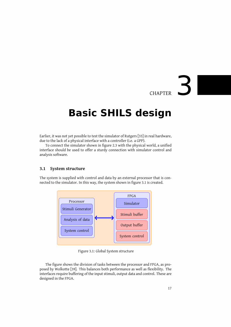
The system is supplied with control and data by an external processor that is con-nected to the simulator. In this way, the system shown in figure 3.1 is created.
.
.. .
.Stimuli Generator
.Analysis of data
.System control
.Simulator
.Stimuli buffer
.Output buffer
.System control
.Processor.FPGA
Figure 3.1: Global System structure
The figure shows the division of tasks between the processor and FPGA, as pro-posed by Wolkotte [39]. This balances both performance as well as flexibility. Theinterfaces require buffering of the input stimuli, output data and control. These aredesigned in the FPGA.
17
18 CHAPTER 3. BASIC SHILS DESIGN
Hardware design is related to the targeted technology. The simulator designof Rutgers is not technology dependant, but the transformation tool is currentlytailored to Xilinx technology dependant EDIF files.
3.2 Design
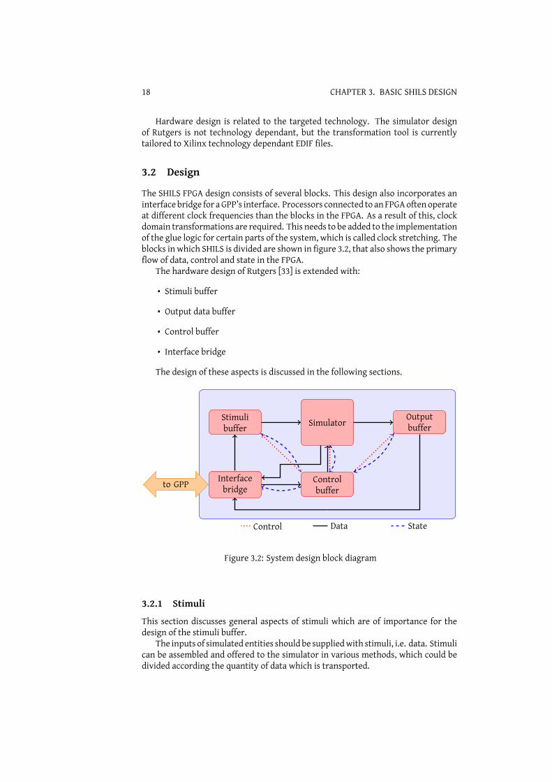
The SHILS FPGA design consists of several blocks. This design also incorporates aninterface bridge for aGPP’s interface. Processors connected to an FPGAoften operateat different clock frequencies than the blocks in the FPGA. As a result of this, clockdomain transformations are required. This needs to be added to the implementationof the glue logic for certain parts of the system, which is called clock stretching. Theblocks in which SHILS is divided are shown in figure 3.2, that also shows the primaryflow of data, control and state in the FPGA.
The hardware design of Rutgers [33] is extended with:
• Stimuli buffer
• Output data buffer
• Control buffer
• Interface bridge
The design of these aspects is discussed in the following sections.
.
.
.Simulator
.Stimulibuffer
. Outputbuffer
.Controlbuffer
.Interfacebridge
. to GPP
.Data.Control .State
Figure 3.2: System design block diagram
3.2.1 StimuliThis section discusses general aspects of stimuli which are of importance for thedesign of the stimuli buffer.
The inputs of simulated entities should be suppliedwith stimuli, i.e. data. Stimulican be assembled and offered to the simulator in various methods, which could bedivided according the quantity of data which is transported.

3.2. DESIGN 19
The least efficient method of offering stimuli to a system is by sending new dataprecisely at the moment it is required to change. It is very impractical; as the tightcoupling requires that theproducer and consumer of stimuli operate fully synchronousor use a tight handshakemechanism. Amore flexible link is required that decouplesproduction and consumption rates and times.
Stimuli are generated in a GPP as shown in figure 3.1. The operating frequen-cies of the GPP and FPGA differ; clock domain transition signals that are fully syn-chronous are hardly possible therefore. Because the amount of communication thatis required to keep the system synchronized is very high.
To reduce the communication overhead, several measures are possible:
• Compress stimuli in time
• Produce stimuli in the FPGA
• Compress stimuli in space
Compress stimuli in time
Stimuli will not change every clock cycle, therefore not every clock cycle a sampleshould be transmitted. To be able to offer data efficiently in this case, a sample is ap-pended with a time stamp. This time code directs the earliest moment at which thestimuli buffer is required to offer the data to the simulator. Compression of stimuliin time is also used by Wolkotte [39].
Adding a time code to stimuli requires additional storage and communication.If stimuli is changing each clock cycle, this is not the best solution to reduce thequantity of date that is transmitted. To reduce the number of bits needed for thetime code, relative timing could be used — the time code then signals the number ofclock cycles between two samples.
Produce stimuli in FPGA
To completely eliminate the clock domain transformation, the stimuli generatorcould also be moved to the FPGA. This can greatly enhance the system’s perfor-mance, but significantly limits the flexibility for the designer. This lowers the gen-erator speed, as most FPGAs operate at much lower clock frequencies than GPPs.A less restrictive solution is to generate a time code in the FPGA for stimuli that isgenerated in software. Time compression is applied in this manner without the ad-ditional communication overhead.
Compress stimuli in space
Data compression is a method which is often used to reduce the number of bits re-quired to transmit data. Previously, no data compression methods have been ap-plied to SHILS. As limited experience with data compression is available, this is leftas future work.
There is an important aspect on using data compression: the compression anddecompression processes require time, which could harm the performance of thesystem. However, if a compression method is used that is efficiently to compressand decompress, the amount of communication is cut down. This results in lesscommunication overhead and possibly higher SHILS performance.

20 CHAPTER 3. BASIC SHILS DESIGN
SHILS approach
As the addition of a timestamp has already been successfully used by Wolkotte [39],it has been chosen to design the system using this approach. Time compression alsooffers a lot of flexibility and configurability for the stimuli generation mechanism.
3.2.2 Stimuli Buffer design
Figure 3.1 shows that stimuli are generated in a GPP. The link between GPP andSHILS requires the translation of the clock domain. The frequency at which stimuliis generated and consumed differs. The producer and consumer of stimuli must bedecoupled for this reason too. Buffering is required to convert clock domains and todecouple producing and consuming frequencies. By decoupling the operating fre-quency of the simulator and stimuli generator, several issues are introduced, focusedtowards efficient transport of the data through the buffer.
The buffer has tomaintain data consistency— the order in which data enters thebuffer should be preserved. This avoids nondeterministic behaviour in simulationand analysis. Inmany cases generates the stimuli generator blocks of samples, whichmust be inserted in the buffer rapidly. For optimal data consistency, a useful featureis an interrupt mechanism. When the buffer is almost empty, the processor has tofill it fast. Another option is to temporary pause the simulator in the FPGA, but thishas a significant performance penalty.
The simulator has no facilities to control the input stimuli. It just expects data tobe available at themoment. Therefore, the buffer also has to be capable of extractingthe oldest element out of the buffer and offer it at the right moment in time to thesimulator.
Simulated entities canhavemultiple inputs, for examplemultiple ports of a routerin a NoC. SHILS should be able to supply data for all these inputs. When mutual ex-clusion is ensured, a single buffer could be shared by multiple ports to reduce re-source usage. The simulator knows which port accepts a sample at what moment,therefore the same element can be offered to both ports simultaneously. Still, forinput ports which are accessed by the same entity at the same moment, separatebuffers or data outputs should be used. This also partially holds for multiple portswithin the same clock cycle, an identifier could be used to signal which entity needswhich data. The most straightforward method to create a buffer for all inputs is toprovide a unique stimuli buffer for each input port. This allows data to be consumedby multiple input ports in parallel. Of course, this approach requires the most re-sources.
A buffer, using the First In-First Out (FIFO) principle, is chosen for the stimulibuffer. It preserves data ordering and — implementation dependently — offers thebuffer to be filled with blocks of data rapidly. This leads to the design shown infigure 3.3. Future choices could lead to stimuli generation in the FPGA. The designalready includes facilities for the stimuli generation mechanism and stimuli sourceselector, these are also shown in figure 3.3. The stimuli buffer is controlled by acontroller which manages data consistency and prevents data of being overwrittenor incorrectly read. The buffer is provided with separate read and write ports tofully decouple producer and consumer.

3.2. DESIGN 21
.
.
.Processor clock .Simulator clock
.Selectstimulisource
.Stimuli
generator
.FIFO buffer
.Timecodechecker
.Buffer
controller .Stimuli buffer
.Data in .Data out.Control
Figure 3.3: Stimuli buffer block diagram
Stimuli buffer output timing
As noted, the simulator cannot control its stimuli input, it expects data to be avail-able. A separate component is introduced to offer stimuli at the designatedmomentto the simulator: the time checker. This component compares the current time withthe timestamp of the stimuli element that is the oldest in the FIFO buffer.
..Wait until rising_edge(clk)
.Bufferempty?
.Timecode<= time?
. Data inregister?
.Move data
.Done
.Buffer empty
. Currentstimuli valid
. Data isalready copied
.No
.Yes
.No
.Yes
.No
.Yes
Figure 3.4: Time checker flowchart

22 CHAPTER 3. BASIC SHILS DESIGN
It monitors the top register of the FIFO buffer, and copies its value to the outputof the stimuli buffer at the intendedmoment. Theprocess of checking the timestampis depicted graphically in figure 3.4. To decouple the stimuli buffer and simulator,the checker does not offer stimuli directly to the simulator, it only extracts the cor-rect sample from the buffer. The precise moment at which it is offered is arrangedby the interface bridge. Data is ready within one delta cycle.
Timing is important in this stage. Based on [33, figure 5.2], timing of the sim-ulator regarding stimuli is shown in figure 3.5. To clarify the steps, a single flowthrough the pipeline is shown. In reality, each delta step a new address is generatedand thus a sample should be available.
..Simulation clock.t=0 .t=1 .t=2 .t=3 .t=4 .t=5
.Step signal of simulator controller
.Generate next address .X .addr .
.Fetch input .XXX .val .XXX
.Input data and state registered .XXX .val .XXX
.Simulation
.Output of the entity .XXX . . .XXX.
.Read address . . .XXX
.Stimuli ready
.Stimuli related
Figure 3.5: Timing diagram based on Rutgers [33]
After the controller of the simulator has given the “step” signal, the address ofthe instance that is simulated next is generated. It is available at the next rising edgeof the clock. If the instance corresponding to the generated address requires stimuli,data is copied from the output register of the stimuli buffer to the stimuli input at t=1.This is determined by the developer. At t=2, is the stimulus ready for the simulatorand copied to an internal register. At t=3, all data is ready for simulation, thus theactual simulation is performed at this moment in time. At t=4, the simulation of thisdelta cycle is done.
The simulator is pipelined. This indicates that stimulus must be buffered for 2clock cycles in the pipeline.
3.2.3 Output buffer designThe design of the output buffer is similar to the input buffer design, except for thecontrol logic. The simulator is not equipped to control the write cycle, the buffercontroller provides this feature therefore. Themechanism is straightforward; it willstore the data with the current simulator time in the buffer on data changes.

3.2. DESIGN 23
All data in the buffer should be accessible. Therefore, the entire buffer contentsmust be readable by the processor, which makes it similar to the producer side ofthe input buffer.
3.2.4 Interface bridge designTo connect all hardware parts with a GPP, an interconnection block is required. Thisprovides glue logic to translate the data signals, which are used in the hardware, to aunified interface that connects to the GPP.. Also, clock domain translations are per-formed by the buffers of the interconnection logic. Clock domain transformationsfor the system’s control are performed by the control buffer. This buffer retains thesame value for a minimal of one SHILS simulator clock cycle, which implies that thisis the maximum frequency at which new commands can be issued by a GPP. In thisway it is ensured that the command is received correctly.
The interface bridge connects the external interface to:
• Stimuli buffer
• Output buffer
• Simulator control via clock stretch buffer
• Simulator state
Also, the connector manages the overall system and provides internal connec-tions between certain parts. Therefore, it is referred to as system controller in theimplementation.
SHILS incorporates several buffers that are externally addressed using MemoryMapped In-/Output (MMIO). To connect a GPP easily to the internalMMIO interface,the external interface for SHILS is also a MMIO interface. This provides in a directlink between the GPP and the internal buffers. Glue logic provides for integrationof the internal MMIO interfaces. It is a common practice to use MMIO in systemsconsisting of both a processor and dedicated hardware for communication betweenthem. MMIO has proved itself thoroughly in the past in numerous applications.
MMIO interfaces come in several sorts. To provide the simulatorwith a universalaccess method for multiple platforms, an additional glue logic block is added thatholds the interface for a specific platform.


CHAPTER4SHILS Implementation
To gain more feeling with the basic FPGA/ASIC design tool flow and to have a goodexample of the challenges for the tool developer, an example is used for the imple-mentation of the basic simulator design discussed in chapter 3. An Infinite ImpulseResponse (IIR) filter is used for this purpose. A filter type often used in digital sig-nal processing. More detail about the filter and its implementation is discussed inappendix B. For a more straightforward implementation of the IIR filter in the sim-ulator, tweaks are used in the system implementation.
For future scaling possibilities, the design is made suitable for a large variety ofplatforms. This implementation, however, is created for a specific platform, whichis discussed next.
4.1 Platform
The simulator is tested on a platform that consists of both hardware and software, toprovide both flexibility and performance to the developer. The implementation istailored for a verification platform referred as Basic Concept Verification Platform(BCVP), shown in figure 4.1.
The platform is constructed with a Xilinx Virtex 2 FPGA (3000 series) and twoARM9 processors (an ARM920 and an ARM946 processor). A single processor is usedfor this first application, as the test simulations are very basic and do not requiremany resources. The processors and FPGA operate at a frequency of 86 MHz.
The FPGA and processor are connected via the Advanced High-Speed Bus (AHB)bus and External Bus Interface (EBI), providing the processor with a direct memoryinterface to communicate with the FPGA. This is referred to as MMIO.
Besides the connection to the processor(s), the FPGA also offers a test/debuginterface which is connected to LEDs.
For more information on the BCVP platform, see [5].
25

26 CHAPTER 4. IMPLEMENTATION
Figure 4.1: BCVP platform
4.2 Hardware implementation
The features of the BCVP platform, which are used by the hardware, are:
• EBI interface
• Test interface
• Clock divider
This leads to a system structure shown in figure 4.2 combinedwith the simulatordesign discussed in chapter 3. The simulator functions at a lower frequency than theARM processor on the BCVP platform. To be more precise, the simulator operatesat a frequency 13 times slower than that of the ARM and MMIO interface. The clockdivision is provided by a clock divider block in the FPGA and used therefore.
As discussed in section 3.2.4, a universal interface is required for easy adaptingto a newhardware platform. The BCVP platform specific parts can be replaced easilywith a specific interface for any other platform. The topmost level in the implemen-tation is the BCVP specific interfaces. These interfaces are defined in figure 4.3.

4.2. HARDWARE IMPLEMENTATION 27
.
..
.Controlbuffer
.Simulator
.Stimulibuffer
. Outputbuffer
. MemoryMap
.System controller
.Glue logic
.BCVP platform FPGA
.Clock
transform
.Test logic
.Universal data/address bus
.Clock
.Test
. EBIinterface
Figure 4.2: FPGA System implementation block diagram
. .BCVP platform interface.clk..reset..not output enable.
.not write enable.
.not chip select.
.not byte select 0.
.not byte select 1.
.not byte select 2.
.not byte select 3.
.Address..18..
.Data . .32..
.Test ..17.
..IRQ .
Figure 4.3: BCVP port spec
4.2.1 System ControllerThe required universal interface is provided by the system controller, which is con-nected to the top level entity using the ports specified in figure 4.4.
The EBI interface of the BCVP platformmaps easily to this interface by logic thatconverts the EBI-specific signals to the universal interface. For example, the writeenable signal is formed by a logic ’AND’ operation of the inverted EBI signals writeenable and chip select.
For ease of implementation, the read and write data is divided into two signalsinstead of a bidirectional bus. It is not possible to simultaneously read and writefrom the bus, as the data bus of the EBI interface is bidirectional.
This part of SHILS structure is named system controller, as it provides the con-trol of all system parts and interconnects of these parts. Besides interfacing withthe hardware platform, the system controller provides interconnection of the othersystem parts listed on the next page.

28 CHAPTER 4. IMPLEMENTATION
. .System Controller.ARM clock.
.simulator clock.
.reset.
.write address..18..
.write data..32..
.write valid.
.read address..18..
.read data . .32..
.read valid .
Figure 4.4: System controller port specification
• Simulator
• Stimuli buffer
• Output buffer
The VHDL implementation instantiates these parts from within the system con-troller as components, which is depicted in figure 4.2.
SHILS is externally is controlled by a GPP over a MMIO interface. The MMIOinterface has been chosen as it provides for a direct connection between the GPPand the stimuli and output buffer. Thememory interface is used to control memory,which is efficiently and fast in the test platform. This interface is discussed in thenext section.
The BCVP platform is equippedwith an interrupt connection to the ARMproces-sor. The system controller does not use this interface; this is left as future work.
4.2.2 Memory-Mapped I/O interfaceMemory-Mapped I/O provides a robust interface for the processor to connect to thehardware. A dedicated section of the processor’s addressing range is assigned toexternal hardware for this purpose. In the BCVP platform this address range is from0x30000000 up to 0x301FFFFF. The sequential hardware-in-the-loop simulator requiresonly a small number of the available addresses. The addressing space is divided into16 blocks, of which 4 are used, like shown in figure 4.5. For now, this provides forsufficient addressing space. This division is made by using 4 bits in the upper regionof the address vector.
The physical platform used for the tests has a defect in its EBI interface. Bit 13of the address bus is defect and replaced by shifting bits 18 downto 14 a position tothe right. The primary address division is made using bits 16 downto 13 instead of15 downto 12. By the shift introduced by the physical defect, no awkward transfor-mations should be made in addressing; only a conversion to byte addressing is stillrequired.
For easy programming, read and write of the same data is put on the same ad-dress but distinct values are separated. This is shown in appendix A; tables A.1and A.2.

4.2. HARDWARE IMPLEMENTATION 29
.
.Data
tostim
ulib
uffer
.Data
from
output
buffe
r
.Echo
register
.System
statea
ndcontrol
.0x000
0
.0x100
0
.0x400
0
.0x500
0
.0x800
0
.0x800
1
.0xF00
0
.0xFFF
F
.32bits
Figure 4.5: Global address space division
4.2.3 SimulatorThe simulator connects with the system controller through an interface specified byRutgers [33], shown in figure 4.6.
. .Simulator.clok..reset.
.Stimuli....
.Stimuli bus . ...
.Entity output . ...
.Simulator control....
.Simulator state . ...
Figure 4.6: Simulator port specification
For more information on port naming and specification, see [33]. Several of theports are design specific and therefore are not specified in detail. The reset mech-anism of the simulator is active-low, whereas the rest of the system uses active-highreset. Active-high reset is used as this is considered more intuitive.
4.2.4 Stimuli bufferThe FIFO principle is used by stimuli buffer to store stimuli, as noted in section 3.2.2.Circular addressing is used to reduce the amount of required addresses in the buffer.Circular addressingmoves the pointer of the buffer to the start addresswhen the endof the buffer has been reached.
Writing newdata is performed at the clock frequency of theGPP connected to theFPGA, whereas retrieval of data is at the clock frequency of the simulator. The fre-quency at which data is produced and consumed also differs. Therefore, the bufferprovides for separate read and write ports. Pointers are used to indicate which el-ements have been written and which elements are read. The buffer controller pre-vents that the read pointer can pass by the write pointer. To provide the producer(the GPP) with unlimited access to the buffer’s memory, the input side of the bufferis fully addressable by the GPP. Several elements can be written to the buffer beforethe pointer has to be updated. This allows for large quantities of data to be written

30 CHAPTER 4. IMPLEMENTATION
at once. The GPP must prevent the write pointer from passing the read pointer; thisis not done by the controller.
For initial testing of SHILS at theBCVPplatform, stimuli generation in the FPGA isnot required. Therefore, the implementation does not support selecting the sourcefor stimuli. Also, the interrupt is not implemented, as no interrupt handler is avail-able.
To control the state of the stimuli buffer, two record types are introduced in thisimplementation, specified in listings 4.1 and 4.2. All elements are data words, 32 bitswide. Using these types, the ports of the stimuli buffer are specified as shown infigure 4.7.
The stimuli buffer instantiates the timecode checker internally. Therefore, it isnot depicted in figure 4.2.
type fifo_status_t is recordsize : word; -- Total capacityfull : word; -- Number of filled positionsempty : word; -- Number of available positionsptr : word; -- Current address position
end record;
Listing 4.1: Status type specification
type fifo_status_upd_t is recordptr : word; -- New pointer positionvalid : std_logic; -- Write enable
end record;
Listing 4.2: Control type specification
. .Stimuli buffer.reset.
.simulator clock.
.simulator state....
.data to simulator . ...
.memory map clock.
.buffer state . .4*32..
.buffer control..32+1..
.address from ARM..12..
.data from ARM..32..
.Write enable.
.IRQ .
Figure 4.7: Stimuli buffer port specification
4.2.5 Timecode checkerThe timecode checker compares the timecode of the topmost sample in the stimulibuffer with the current timecode of the simulator. The timecode is checked usinga combinatorial path. The sample is copied to the output of the timecode checkerimmediately to avoid delay if the timecode matches the current time. The sample is

4.3. SOFTWARE IMPLEMENTATION 31
also copied to a register that is used in the following delta cycles if the sample is stillvalid. This avoids incorrect consumption of data. The ports of the timecode checkerare specified as shown in figure 4.8.
. .Timecode Checker.clock..reset.
.simulator time..11..
.data out ...
.
.stimuli in....
.read acknowledge ..buffer empty .
.buffer state..4*32..
Figure 4.8: Timecode checker port specification
As noted in section 3.2.2, the timecode checker delivers data to the system con-troller, which determines the precise moment at which the data is offered to thesimulator. Thismoment is determinedusing two signals in the state port of the simu-lator, named prefetch_stimuli and prefetch_stimuli_valid. The first signal identifiesthe instance that will be simulated after three clock cycles. When the signal is valid(prefetch_stimuli_valid becomes high), the stimuli element for the correspondingidentifier should be offered to the stimuli port of the simulator.
If A DUThasmultiple external inputs, a shift registermust be used to offer data atthe correct moment to the simulator. The IIR filter only has a single external input.Therefore, the identifier check and shift register are not implemented.
4.2.6 Output bufferFor analysis of the simulation afterwards, the output of the simulated entities isstored in a FIFO buffer also. The implementation of the output buffer is based onthe implementation of the input buffer. The controller extracts the current timefrom the state of the simulator. It is coupled to the output of the current entity andstored in the buffer. For fast consumption, the entire address space of the buffer isaccessible by a GPP, but for data validity, only addresses which have been writtenmay be read. The GPP must prevent this by verifying that the read pointer does notpass thewrite pointer. The controller of the output buffer prevents that data is writ-ten before being read. The controller can set the interrupt flag at a certain capacitylevel, to prevent buffer overflow, but this is not implemented.
The output buffer interface is specified as shown in figure 4.9, using the typedefinitions of listings 4.1 and 4.2.
4.3 Software implementation
The software is intentionally kept basic, as the test case is very basic. This meansthat several steps, which could be eased with procedures and functions, are left forfuture implementation and have to be performed manually for now. An exceptionis made for the initialisation procedure of the bridge with the FPGA, as this will beused often.
To access thememory portion reserved for the simulator in the FPGA, a structureis used. This is specified in listing C.1.

32 CHAPTER 4. IMPLEMENTATION
. .Output buffer.memory map clock.
.simulator clock.
.reset.
.read address..12..
.data to ARM . ...
.buffer state . .4*32..
.buffer control..32+1..
.IRQ .
.data from simulator....
.simulator state....
.acknowledge .
Figure 4.9: Output buffer port specification
The structure is initialized in a precompiler directive, which places the memorymap at the correct start address. For readability, several portions are divided in anown structure. For example the simulator state and control are specified as shownin listings C.2 and C.3. For more information on the definition of these variablessee [33].
In contrast with the hardware implementation, the variables like read_from arenot yet assembled of record structures. C is byte-oriented, not bit oriented likeVHDL.
To verify the behaviour of thememorymap in all regions of the addressing space,thehardware implementation returns debuggingdata at several positions. Themem-ory position of the test registers is specified in listing C.1.
4.3.1 Configure connectionBefore the ARM processor can use the connection with the FPGA, the connectionmust be configured correctly. The function bridge_init configures the interface in 5steps:
1. Configure (Parallel I/O)PIO clock
2. Enable PIO clock
3. Configure PIO Reset
4. Reset PIO
5. Configure memory controller
a) Configure Setup time
b) Configure pulse time
c) Configure total cycle duration
d) Configure read/write mode
For a detailed description on these configuration variables, see [24].

4.3. SOFTWARE IMPLEMENTATION 33
4.3.2 Test connectionTo verify whether the connection has been configured correctly, the test registersthat exist in the memory map listing C.1 are examined and compared with the ex-pected value. This is included in the function bridge_init().
4.3.3 Configure simulationAfter initialization of the connection with the FPGA, the simulator is stopped to con-figure the simulation. The number of entities which are used for this simulation areset by issuing the command ENABLE on the address 0x300F0300 and writing a value tomemory address 0x300F0304. After enabling a number of entities, links between en-tities are created. A function is created for this purpose which is listed in listing C.4.This function issues several commands according to section 2.3.2:
1. Command CREATE_LINKS at address 0x300F0300
2. Instance address at address 0x300F0304
3. Instance reads from at address 0x300F0308
4. Instance stimuli mask at address 0x300F030C
5. Instance writes to at address 0x300F0310
4.3.4 Run simulationWith all settings created, stimuli should be inserted in the stimuli buffer beforeperforming the actual simulation. Stimuli is copied to the an address in the range0x30000000 up to 0x30010000, and the write pointer is updated afterwards by writingthe new pointer value to address 0x300F000C.
Further description of the C code for the IIR filter can be found in appendix B asthis is design specific.


CHAPTER5Tool evaluation forHardware/Software
co-simulation
The design and implementation discussed in chapters 3 and 4 is actually the designof a co-simulation system. Basic ideas of co-simulation are discussed in section 2.2.
Previous work has shown that stimuli generation significantly increases the loadon a processor [39]. A PC is equipped with a greater amount of processing power;the amount of processing power available for other tasks is far greater than in theembedded processor. A PC will be used to replace the embedded processor as shownin figure 5.1. Also enhanced stimuli generation is possible. Using a PC also opens up
.
.. .
.Stimuli Generation
.Data Analysis
.System control
.Stimuli buffer
.Simulation
.Output buffer
.Computer(MATLAB) .FPGA
Figure 5.1: Co-simulation system structure
extended capabilities to perform data analysis in various tools. Several tools can beused for the connection of a PC to SHILS, which are compared in this chapter.
MATLAB is sometimes already used in initial design stages for algorithm explo-ration and other tests. To be able to reuse previously made test benches (in MAT-LAB), MATLAB is used to generate the stimuli and analyse the output data. Some-what equivalent to the computing capabilities of MATLAB is GNU Octave [18], but
35

36 CHAPTER 5. EVALUATING CO-SIMULATION TOOLS
that application is not directly equipped with co-simulation facilities and thereforenot discussed in the context of this thesis.
5.1 Requirements
An important aspect is the operating method of SHILS. Implementations so far usea data pushing method to keep the simulator supplied with sufficient stimuli (chap-ter 3, [39]). Thismethod is used tomaximize data throughput. The simulator expectsdata to be ready for it all the time; therefore the synchronization mechanism is im-portant. To reduce communication overhead, it is desirable to send a large quantityof data at the same time to the simulator input buffer. MATLAB is generally usedsequentially, but can function perfectly asynchronous.
The current implementation of the SHILS external interface is a MMIO interface(chapter 3). This enables transmission of data via a unified interface. Minimizedeffort in migration of the interface in both hardware as software towards the newco-simulation system is an advantage.
The tool discussion assumes that MATLAB is used for stimuli generation, andthe tool is used to arrange the connection. However, MATLAB can also arrange theconnection. It is discussed as an option for this reason.
5.2 Criteria
The tools to connect SHILS with MATLAB are evaluated according to multiple cri-teria. These criteria are based on the aforementioned requirements. In the toolcomparison is the interface that will be used to connect SHILS not decided.
Damstra has defined key factors which define a good co-simulation system [16].These key factors are purely focused on software-based simulation. The key factorsof Damstra have been used to formulate the tool evaluation criteria, they are modi-fied to apply to hardware connectivity, effort to use and performance. The criteriahave influence on each other and partially overlap.
The criteria are evaluated individually. Themajority of the criteria are evaluatedusing an ideal solution that is best for each specific criterion, resulting in ++, +, o, -,-- or --- to indicate how a specific product relates to the ideal. The ideal for eachcriterion is discussed below. Criterion 3 and 7 cannot be judged in this manner, theyare judged upon available features.
1. Hardware connectivity possible This criterion expresses whether the tool can con-nectwith hardware by default. It is desirable that connectivitywith hardware can beenabled without great effort. The best case is that connectivity can be automaticallyarranged/generated.
2. Interactionwithmultiple simulation tools/platforms (e.g. QuestaSimandhardware) Thiscriterion concerns the possibility of the evaluated tool to interconnectmultiple sim-ulation tools or hardware platforms. An example application is the use of QuestaSimfor functional and short simulations and SHILS for bit accurate cycle-true long sim-ulations. This feature is an advantage as one could replace QuestaSim with SHILStransparently to the end user. In the best case, the tool arranges the interconnec-tion and replacement without great effort.

5.2. CRITERIA 37
3. Supported I/O protocols This criterion concerns the differentmethodswhich couldbe used to connect the tool with hardware. This is closely related with the physicalinterface used by SHILS, as is must connect with software over this interface too.The evaluation of this criterion only lists the possible protocols, as the comparisonof tools is performed independently of the platform used and thus the physical in-terface used.
4. FPGA integration This criterion concerns the required effort to embed the con-nection with the tool in the SHILS hardware design. In contrast with criterion 1, thiscriterion judges whether the SHILS hardware design integrates well with the con-nection in the FPGA. Integration without a great deal of effort is best, preferablyautomatically generated.
5. Performance This criterion concerns the performance of the system. Appraisal ofthis criterion is based on the other criteria.
The performance of the entire system is dependant on the performance of thecommunication between PC and FPGA and can bemeasured by data throughput andoverall simulation time.
6. Communication overhead This criterion concerns the communication overhead.Some tools introduce significant communication overhead, whereas others handlethis efficiently. This criterion is assessed relative to the other tools. Of course, littleor no overhead is best.
7. Synchronisation mechanisms This criterion concerns the methods which could beused to provide synchronization between tool and hardware. Synchronization ismainly performed either by time synchronization (tightly coupled) or by using adata-push approach. This criterion lists the options offered by the tools.
8. Initial SHILS deployment effort This criterion concerns the effort that is requiredto set up the co-simulation system using the tool and SHILS for the first time. Loweffort is better.
9. Deployment effort of a new simulation model as DUT for SHILS This criterion dealswith the effort that is required to perform simulations using SHILS on a new DUT.Also for this criterion applies that low effort is better.
10. Parameter adjustment effort This criterion deals with the effort that is requiredto adjust parameters, for example the coefficients of an IIR filter or the topology of aNoC. It is desirable that this can be achieved without synthesis. This is highly imple-mentation dependant, though. Stimuli generation is not considered in this criterionas the interconnection tool does not influence the stimuli generation process.
11. Embedding of co-simulation into the normal design flow This criterion deals with theeffort that is required to embed the usage of SHILS simulation in the normal systemdesign flow described in section 2.1.1. Easy embedding is desired, also regardingusage of tools in earlier design phases and reusing testbenches.

38 CHAPTER 5. EVALUATING CO-SIMULATION TOOLS
12. Cost Although not a primary criterion, this criterion concerns the cost involvedin deployment of one of the tools. Both initial purchase cost and recurring costs areconsidered.
5.3 Selected tools
The tools discussed originate from several disciplines. All tools have possibilities forco-simulation. The discussed tools are:
• The Mathworks: MATLAB & Simulink
• Xilinx: System Generator for DSP
• Altera: DSP Builder
• Chiastek: CosiMate
• UC Berkely: Ptolemy II
• Virtutech: Simics
• Manual solution
The tools provided by Xilinx and Altera are MATLAB toolboxes, which requireMATLAB to function properly. Sometimes is constructing a solution manually thebest solution. This option is considered too. The manual solution deals with theproblems encountered in the discussion of the other tools.
5.4 MATLAB
MATLAB [27], created by The Mathworks, is commonly used in both industry andresearch for its computing capabilities in several application areas. Its computingcapabilities are extended by various toolboxes to connect MATLAB with externaltool and hardware, and perform tasks specific for an application area (e.g. FinancialModelling). The collection of toolboxes is quite large. A small selection with self-explanatory names consists of: “Instrument Control Toolbox,” “Image ProcessingToolbox,” “Signal Processing Toolbox” and “Control System Toolbox”. WithinMAT-LAB, Simulink offers an environment to applymodel-driven design in arithmetic andanalysis. Models in Simulink are created in an interactive graphical environment in-stead of using the scripting language of MATLAB. Simulink comes with a customiz-able set of block libraries for various application areas. Complicated operations andtransformations can be used to graphically create a model, which can be used forcalculations.
MATLAB is often used to explore and test the behaviour of systems at high levelsof abstraction, where calculations needs to be performed without timing and/or bitaccuracy like algorithm testing, signal processing and analysis and much more. Atthe University of Twente, MATLAB is used for various projects and purposes, in-detail knowledge on MATLAB is therefore available.
The collectionofMATLAB toolboxes extends in the field ofDigital Signal Processing(DSP) design, and also FPGA design for co-simulation with reconfigurable hardwareandhardware oriented simulators. There is a couplingpossiblewith several Electronic

5.4. MATLAB 39
Design Automation (EDA) tools, like QuestaSim (successor ofModelSim)which is dis-cussed in section 5.4.1.
Besides the toolboxes that are sold by The Mathworks, MATLAB is also extendedby several FPGA hardware vendors like Xilinx and Altera. These products are dis-cussed in sections 5.5 and 5.6. Both Xilinx and Altera, with respectively System Gen-erator and DSP builder, sell toolboxes which bring FPGA functionality and tools toMATLAB. Both vendor specific tools are primarily targeted at DSP applications, butare also provided with various blocks for HIL simulation.
5.4.1 MATLAB EDA link MQ
EDA linkMQ [26], also fromTheMathWorks, enables a designer to use the simulationcapabilities of QuestaSim for hardware designs combined with the computationalpower of MATLAB for control, signal processing and data analysis. The inputs andoutputs of a DUT are connected to structures in the MATLAB workspace, providingthe end user with a transparent interface, and a callback routine to control the DUTin QuestaSim from MATLAB.
The features of EDA link MQ enable the creation of test benches (figure 5.2a)for QuestaSim in MATLAB. Furthermore, EDA link MQ enables embedding MATLABfunctions in simulations in QuestaSim (figure 5.2b). Wrappers are provided for bothoptions.
... . .HDL entity
.HDL Simulator.Outputarguments
.InputArguments
.MATLAB
.stimuli .response
(a) MATLAB testbench wrapper
..
. MATLABcomponentfunction
.HDL
(b) QuestaSim wrapper
Figure 5.2: MATLAB QuestaSim toolbox diagram
The toolbox can be used in two methods, a universal method based on TCP/IPand a dedicated one using shared memory. QuestaSim operates as client for MAT-LAB. The direct memory connection provides the best performance, but the TCP/IPversion offers distribution of the simulation across multiple PCs. MATLAB can oper-ate at one PC as server, serving multiple QuestaSim clients. In theory, it should bepossible to replace the client (QuestaSim) by a hardware simulator when connect-ing using TCP. However, there is no specification of the protocol used, which makesengineering an interface for this protocol quite difficult.
A number of disadvantages and pitfalls of this product are discussed by Gestnerand Anderson [20]. Creation of test scripts is quite difficult, as users are requiredto monitor the progress of the simulation by communicating through test vectors,which is not very intuitive. Furthermore, the need to signal QuestaSim every clockcycle introduces a lot of communicationoverhead. Bothof these problems are solvedby the open source solution of Gestner and Anderson [20]. As their solution is in-

40 CHAPTER 5. EVALUATING CO-SIMULATION TOOLS
tended solely for software-only simulation, their connection is using amemory con-nection, it is not considered further.
5.5 Xilinx System Generator
Xilinx offers several tools to help a developer. One of these is System Generator,which is a MATLAB based DSP design tool, which can generate hardware configu-rations for a design [42]. In this manner, the model-driven design can be used todevelop a (sub)system by drag-n-drop methods in Simulink.
Amodel in Simulink can be constructed out of ordinary DSP building blocks suchas adders, multipliers and hardware, but also using more complex blocks or customhardware [43]. Custom hardware can be added as a black box, so that it is includedin synthesis. The Simulink model can communicate using MATLAB connectors withthe custom design. The sequential simulator can be viewed as such a black box, acomponent in the design.
System generator can either generate a HDL file to be included in a HDL design,generate a synthesised netlist (the Simulink model is then the top-level entity) orgenerate components that apply HIL co-simulation directly. The latter option inter-nally generates HDL code, synthesizes it and provides the FPGA programming file.With System generator, it is possible to realize both the hardware (FPGA/VHDL) andconnection to MATLAB at once [17].
The features offered by System Generator can be used to easily create hardware-in-the-loop simulation for various Xilinx-based target platforms. For this task, a GUIis provided (figure 5.3) .
Xilinx SystemGenerator can be used to generate hardware only for Xilinx FPGAs.This is a big disadvantage for flexibility and versatility, but not a very big problemwithin the CAES chair as primarily Xilinx FPGAs are used. Also, the transformationtool of Rutgers [33] is currently only equipped for Xilinx FPGAs.
5.6 Altera DSP Builder
Altera offers DSP capabilities for FPGA developers with the DSP Builder product.Similar to System Generator, a model can be created in Simulink which can be in-serted in an FPGA after synthesis, and used for co-simulation. Of course, usage ofthis tool requires that Altera FPGAs are used. The features offered by Altera’s prod-ucts [1] are similar to those of Xilinx System Generator, no differences have beenfound in the specifications of both.
5.7 CosiMate
Chiastek offers CosiMate, a product capable of connecting multiple tools togetherfor a co-simulation system using a unified backplane. A GUI is provided to connectthe products that are used for a simulation.
By default, CosiMate provides a connection to its backplane for several simula-tion packages [10], originating from various disciplines:
• The MathWorks: Matlab/Simulink
• Telelogic: Tau G2 (Model-driven software design)

5.7. COSIMATE 41
Figure 5.3: Xilinx System Generator targets
• Telelogic/I-Logix: Statemate Magnum (Graphical embedded system design)
• Synopsys: Saber Designer (Dynamic systems simulator)
• MSC Software: Easy5 (Dynamic systems construction)
• Imagine: AMESim (Mechanics simulation)
• Mentor Graphics: QuestaSim (Digital Hardware design simulation)
• Cadence: NCSim (Digital Hardware design simulation)
CosiMate offers interfaces for several languages:
• C, C++
• Hardware Description Languages: VHDL, Verilog
• SystemC
CosiMate is the master in the system and handles synchronisation issues for theend user, the backplane synchronizes with each simulator individually to allow foreach tool to operate at its own frequency. If desired, CosiMate also has the option tooperate all tools fully synchronous by tight coupling.
Connections between simulators can bemade using TCP, UDP or RCP. Networkedsimulation is therefore possible, making it possible to open a connection with thesequential simulator over TCP/IP or similar. Backplane connections with other,not supported, simulators can be created using the CosiMate Interface DevelopmentTool. SHILS can be connected either using the Interface Development Tool. Reverseengineering the communication protocol that CosiMate uses is not needed. Still,hardware needs to be developed to connect to the CosiMate interface.

42 CHAPTER 5. EVALUATING CO-SIMULATION TOOLS
CosiMate should allow for both functional and synchronised co-simulation, butthis is not yet possible in current tool releases according to Damstra [16].
Future development is an asynchronous mode to connect sequential and eventdriven simulators.
5.8 Ptolemy
Ptolemy is a long lasting project of UC Berkely, it can be used without cost for aca-demic and commercial purpose. Ptolemy can be described as “An extremely exten-sible, heterogeneous simulation and prototyping systemwith a sophisticated graph-ical interface” [22]. This description is far from complete, but important to noticeis that the objective of Ptolemy II is “to support the construction and interoperabil-ity of executable models that are built under a wide variety of models of computa-tion” [4].
Its primary feature is the support for multiple computational models, which caneven be used within one system model. This is made possible by the actor-orientedstructure of Ptolemy. Examples of actor-oriented languages include hardware de-scription languages, like VHDL and Verilog, and this makes Ptolemy well-suited forembedded system design.
Also, parallel hardware designs can be synthesised directly from SynchronousDataflow Graph Specifications [37]. Ptolemy can thus generate VHDL code, as FPGAvendor tools are able to generate VHDL code.
For distributed simulation, an architecture is provided that deals with mappingof the simulation processes, and arranges communication and synchronization in amanner that is transparent for the end user constructed on top of the SynchronousDataFlow (SDF) domain called Automated Distributed Simulation (ADS) [15]. This ispossible due to the structure of Ptolemy — using the actor formalism. It is imple-mented using the JINI platform, based on Java just like Ptolemy itself.
To use SHILS for hardware simulation, a client for the distributed simulation willneed to be developed according to available specifications. A MATLAB connector isavailable from commercial vendors that are constructed out of Ptolemy.
For sequential orienteddesigns, pipelining techniques are offered to benefit fromdistributed simulation.
5.9 Simics
Virtutech, a spin-off of the Swedish Institute of Computer Science (SICS), has createdSimics, a tool that aims at simulation and debugging software operating on mul-ticore and multiprocessor machines [36]. It can simulate networks of processors.Simulations in Simics can be distributed across multiple computers. It is used by theProtoFlex project in conjunction with an FPGA to increase the overall simulationspeed.
Problematic is that the Simics only supports simulation of multiprocessors thatare currently on themarket, no customdesigns are supported. To be able to simulatea new design in Simics requires significant effort as a new processor model must becreated for each new hardware design. Also, these extensions can be implementedonly by Virtutech, not directly by an end user.
Another disadvantage of Simics is that there is no previous experience with us-age of Simics at the CAES chair.

5.10. MANUAL SOLUTION 43
5.10 Manual solution
Each of the tools discussed above has disadvantages. The desired result of the man-ual solution is a tool that perfectly matches the requirements of SHILS, stimuli gen-erator/analyser and end user. This solution matches all the criteria of section 5.2perfectly from the performance point of view. However, the manual solution is theworst solution for effort and resources.
Themajor concern of the discussion of the tools is the communication overhead.There are communication media available for even faster communication betweenSHILS and MATLAB, like PCI-X, PCI-E [40] and a direct Front Side Bus (FSB) connec-tion [7]. In thismanner, a connection capable of transmitting several Gbps is offered.In the FPGA an interface to the SHILS design has to be created, similar to the alreadyexisting interface (chapter 3). Besides an interface for the FPGA, MATLAB connec-tors need to be created. In order to replace QuestaSim transparently with SHILS inMATLAB, additional effort is required.
5.11 Comparison
A decision should bemade in favour of one of the discussed solutions based upon thecriteria listed in table 5.1. Per tool, a score is added to the criteria. Criterion 3 and 7are not evaluated according to scores but according to features.
Statements on Xilinx System Generator also apply to Altera DSP Builder and arereferred to as FPGA vendor tools in this section.
Hardware connectivity is possible for almost every tool. The FPGA vendor toolsconnect directly to FPGAs, whereas CosiMate, Simics andPtolemyprovide for aTCP/IPinterface for distributed simulation in the software. The FPGA connectormust be de-veloped for all tools, except for the FPGA vendor tools. TCP/IP hardware blocks areavailable, but co-simulation logic still must be created manually. The FPGA vendortools generate the specialized co-simulation blocks too.
Most tools only support connectivity with a single other tool, except CosiMatewhich has been designed specifically to interconnect multiple tools, and Ptolemywith its computational domains. Transparent replacement of QuestaSim by SHILSwithout changes is only possible with CosiMate, as only CosiMate configuration ischanged.
Each tool supports communication over the TCP/IP protocol. Most implementa-tions work local at a single machine, but the co-simulation can be distributed acrossmultiple machines. MATLAB is equipped with a large number of connection proto-cols including USB and serial connection that are sold separately. Therefore, MAT-LAB is very versatile regarding connections. The FPGA vendor tools can access theseconnectionmedia too when available, but require changes to the connectors in boththe Simulink model and FPGA design.
The FPGA vendor tools generate hardware, and provide several options to inte-grate this hardware in a design. For this reason the integration with the FPGA de-sign is best for these tools. Code generation of designed cores is possible for Ptolemy,CosiMate andMATLAB,which indicates that integration is possible, but less versatilethan the vendor tools.
Literature states performance problems with MATLAB due to significant com-munication overhead [20]. Communication overhead is caused by a lot of effort re-quired to keep the entire system synchronized. Future versions of CosiMate are

44 CHAPTER 5. EVALUATING CO-SIMULATION TOOLS
said to be capable of performing functional (asynchronous) simulation, a solutionwith less communication could be developed for the FPGA vendor tools. Ptolemy isequipped with ADS that arranges distribution across multiple clients [15]. This im-proves performance if computation requires more computational power than com-municating by pipelined parallel execution. Simulation in Simics is performed func-tionally, therefore the performance is acceptable but not suitable for cycle-accurateverification.
Data-pushing synchronisation can be applied by System Generator or CosiMatenatively. Ptolemy offers an automated mechanism to distribute actors in simula-tion(ADS). The other tools use time synchronisation which can involve a lot of com-munication overhead. Simics allows the simulationhosts to be out of sync slightly, toreduce this overhead. Therefore, tools offering data-pushing synchronisation havean advantage over the rest.
The required effort to create an initial system is large for CosiMate, Ptolemy andSimics, due to the lack of previous experience within the CAES chair with these toolsin general and especially for use in co-simulation. System creation is graphical inCosiMate, which indicates that the effort required to create the system is not Ex-perience with MATLAB is available, initial deployment effort is therefore less forMATLAB and the FPGA vendor tools, which use Simulink for modelling. As the FPGAhardware can be generated by the FPGA vendor tools, total effort is lower for initialdeployment than for MATLAB.
The easiest approach to deploy a new DUT for simulation is to connect the newmodel to already existing infrastructure. Therefore, CosiMate has an advantage overthe rest. As insertion of a block is pretty straightforward in Simulink, this is consid-ered easy too. In the FPGA, no changes should be requiredwhen the implementationhas grown to its full potential.
The possibility to easily implement small changes to a design during simulationis highly appreciated. The manner in which this is dealt with is highly implemen-tation dependant. For example, at run-time, SHILS can change the connections be-tween entities and the number of simulated entities. CosiMate only operates at theinterconnection level. It therefore does not directly provide facilities for this. Thetools, which only generate code for FPGAs (CosiMate, Ptolemy and MATLAB), arenot suited well, as a rerun of the synthesis process is not desired. This is of courseheavily dependant on the specific implementation which is made.
MATLAB is alreadyusedwithin thenormal design flow. Therefore, usage ofMAT-LAB requires the least changes to the design flow. Tools which do not operate withinMATLAB (e.g. CosiMate), require minor changes to the design flow.
Most of the discussed tools require a license that must be purchased, exceptPtolemy, which is available free of charge. Fortunately, academic research licensesare available for several of the other tools. A research licence for MATLAB mustbe purchased. However, the communication interfaces are provided by a toolboxwhich is not available at the CAES chair due to licensing specifications1. Using theInstrument Control Toolbox require additional funds.
System requirements are comparable for each tool; a faster CPU will result infaster generation of stimuli etc.
1The Research license of MATLAB does not include these toolboxes by default, whereas the educa-tional licence does.
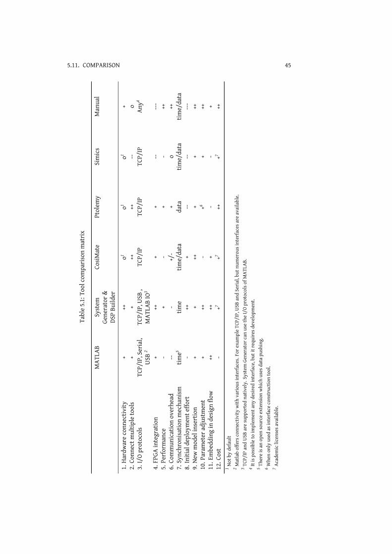
5.11. COMPARISON 45
Table5
.1:To
olco
mpa
rison
matrix
MAT
LAB
System
Gene
rator&
DSPBu
ilder
CosiM
ate
Ptolem
ySimics
Man
ual
1.Ha
rdwa
reco
nnec
tivity
+++
o1o1
o1+
2.Co
nnec
tmultip
letools
++
++++
--o
3.I/Opr
otoc
ols
TCP/
IP,S
erial,
USB
2TC
P/IP,U
SB,
MAT
LABIO
3TC
P/IP
TCP/
IPTC
P/IP
Any4
4.FP
GAintegr
ation
+++
++
-----
5.Pe
rfor
man
ce-
+-
+-
++6.
Commun
icationov
erhe
ad--
-+/
-+
o++
7.Sy
nchr
onisa
tionmec
hanism
time5
time
time/
data
data
time/
data
time/
data
8.Initi
alde
ploy
men
teffo
rt-
+++
----
---9.
New
mod
elinsertion
++
+++
+++
10.P
aram
eter
adjustmen
t+
++-
+6+
++11
.Embe
ddingin
desig
nflo
w++
+++
--
+12
.Cos
t-
+7+7
+++7
++1No
tbyde
fault
2Matlaboffers
conn
ectiv
itywi
thva
rious
interfac
es.F
orex
ampleT
CP/IP,
USBan
dSe
rial,bu
tnum
erou
sint
erface
sare
available.
3TC
P/IP
andUS
Bares
uppo
rted
nativ
ely.
System
Gene
ratorc
anus
ethe
I/Opr
otoc
olso
fMAT
LAB.
4Itispo
ssible
toim
plem
enta
nyde
sired
interfac
e,bu
titr
equiresd
evelop
men
t.5Th
erei
sanop
enso
urce
extens
ionwh
ichus
esda
tapu
shing.
6Whe
non
lyus
edas
interfac
econ
stru
ctiontool.
7Ac
adem
iclic
ensesa
vaila
ble.

46 CHAPTER 5. EVALUATING CO-SIMULATION TOOLS
5.12 Conclusion
Based on all arguments in the previous section (summarized in table 5.1), the bestsolution is to implement the SHILS interface using Xilinx System Generator, andslightly alter the MMIO interface in the FPGA accordingly. It offers all desired func-tionality at a reasonable effort and performance. Whenmore performance is desiredthan Xilinx System Generator can offer, the next step is to create a custom system,which requires a far greater effort to implement. When the custom solution is cho-sen, CosiMate could provide easily for an interface for the interconnection medium.
Ptolemy scores quitewell in table 5.1. It is not selected as best as it is not equippedwith FPGA connectivity features out-of-the-box. Furthermore, little experience ofPtolemy is available at the CAES chair. Significant effort is thus required to gainknowledge on how to use Ptolemy for co-simulation.

CHAPTER6SHILS co-simulation
system design
SHILS is intended as an aid in the verification(by simulation) process of large SoC/NoCdesigns. Verification is performed by doing extensive simulations of a DUT. Previ-ously, a relatively small embedded processor was used to generate stimuli for thesesimulations [38, 39]. Besides the computational load of stimuli generation on theprocessor, also the effort to deploy the test bench is considerable.
Software is already used inNoC design for several research tasks, such as analysisand simulationof communication anddata processing applications. MATLAB/Simulinkis often used for design exploration, but can also be used to perform behaviouralanalysis of the implementation of such systems combinedwithQuestaSimand there-fore to create advanced test benches. These test benches could be reused in theverification process, but when verification is performed on a different platform, sig-nificant effort is still required to port the test benches towards the other platform.For flexibility in the stimuli generation procedure and re-usage of previously de-veloped components, it is desirable that stimuli are generated by software, not byhardware. By replacing the small processor with a standard PC, the performanceof stimuli generation can be improved with enhanced features. Software like MAT-LAB offers advanced data analysis tooling for the analysis of simulation results. Byconnecting SHILS to a PC, a “new” co-simulation system is created.
The system tasks are distributed across the PC and FPGA to fully benefit from thecapabilities of both FPGAs and PCs like shown in figure 6.1. Chapter 5 focuses on theconnection of PC and FPGA, whereas this chapter focuses on the entire system usingthat connection.
The PC runs MATLAB for stimuli generation and analysis afterwards, and theFPGA is charged with performing the simulation to accelerate the verification pro-cess. The link between PC and FPGA can be tightly coupled, which can lead to a thePC waiting on the FPGA or the opposite. This will lead to less performance than allparts operating at full speed. To enable the simulator andMATLAB to operate at dif-ferent operating speeds, buffering is required in the FPGA for stimuli elements andoutput data, also used in the first design, see chapter 3.
47

48 CHAPTER 6. SHILS CO-SIMULATION SYSTEM DESIGN
.
.. .
.Stimuli Generation
.Data Analysis
.System control
.Stimuli buffer
.Simulation
.Output buffer
.System control
.Computer(MATLAB).FPGA
Figure 6.1: Global System structure
The connectionbetweenprocessor andFPGA in earlier implementations of SHILShas been a DMA connection. For connectivity between PC and FPGA, several othermedia are possible (discussed in section 6.3.3). Using these media, the connectioncan be made using several tools (discussed in chapter 5), or manually.
The rest of this chapter discusses the high-level communication first. After-wards, low-level communication using Xilinx System Generator is discussed, whichcame up best out of the tool comparison.
6.1 Requirements
Criteria for co-simulation tools are defined in section 5.2, which are also applicablefor the created co-simulation system. The design should profit from general knowl-edge of the target platform, based upon platforms available in the CAES chair. Also,the system has to deal with requirements described in chapter 3 on reuse of previ-ously developed parts.
Another important requirement is that the new design is more efficient thanprevious implementations, especially in the field of communication overhead as thisis quite often a major bottleneck. The precise elements that are communicated andthe number of transmitted elements should be considered with great care for thisreason.
Earlier implementations show that, with significant effort in a processor (about25% of the time purely to generate new elements), it is possible to keep up with thesimulator [38, 39]. The link between PC and FPGA must be loose without causingproblems with buffers or the rest of the system’s integrity. Stopping the simulatorto wait for data to be transmitted is not a good option for maximal performance.
6.2 Global system structure
The global system structure is depicted in figure 6.1. This shows the division of func-tionality between the PC and FPGA. The global structure of this design is similar tothe design discussed in chapter 3.
Within the system, the PC is the master, the FPGA slave. To loosen up the linkbetween PC and FPGA, buffering is used for stimuli and output data. Previously,

6.3. DATA TRANSFER METHOD 49
a MMIO interface was used to control this. The MMIO interface was also used forsystem control. Usage of a MMIO interface is a bit different than the data transfermethod used by MATLAB.
6.3 Data transfer method
Usage of the MMIO interface in the new system is evaluated for the data intensivestimuli and output flows. The linear buffer (FIFO), implemented using circular ad-dressing is not discussed at this point. Only themethods to transfer data to and fromthe buffer are treated.
Within the system, options are available for placing data in the FIFO buffers,these are discussed below.
6.3.1 Reuse MMIO interface in FPGAThe option that is easy to deploy in the FPGA is to keep the existing interface tothe FIFO buffers. MATLAB will then need to generate addresses where to store theelements . This requires that MATLAB maintains an up-to-date administration ofthe state of the buffer, involving a significant quantity of communication.
6.3.2 Add address generation to FPGAStimuli are generated as a sequence of elements most of the time. Therefore, noadvanced address generationmechanism is required, and this could easily be imple-mented in hardware. Generally, it is better to execute such tasks in hardware to gainbetter performance. Also, moving the task of address generation from MATLAB, re-duces the communication overhead. The FPGA design is extended with an addressgeneration mechanism to reduce communication overhead, increasing overall per-formance and reducing interface complexity in MATLAB.
Synchronized operation is required, even with loose coupling of PC and FPGA.When buffers are full, no more elements may be transmitted to avoid buffer over-flow problems, and empty places in the buffer must be filled as soon as possible tokeep the simulation from stalling. Stalling the simulator, of course, leads to a lossof performance, but provides a safety net when the unlikely event might occur thata buffer is empty. The FPGA design should be extended with logic that temporarilyhalts the simulator when stimuli buffers are empty.
The moment until which the simulation in the FPGA can run undisturbed is eas-ily determined at the moment that time codes are generated. The PC can use thisperiod of time to generate new stimuli. Knowledge about the time it takes to gen-erate elements must be available. The FPGA control can be extended by a “Run forn cycles” command using this principle. A parameter of the command is “n”, thenumber of cycles that the simulator will run. This is a more sophisticated methodof pausing the simulator after a predetermined number of cycles, instead of usingthe emergency break when a buffer is empty. Some administration is used in the PCthat sets the “Run for n cycles” counterwhennewdata has arrived in the FPGA. Withthese measures taken, the control data is significantly reduced. Instead of sending acommand each system cycle, the number of transmitted commands is divided by n.
Performance degrades slightly, but simulatingwith incorrect data leads to a sim-ulation run that is completely useless.

50 CHAPTER 6. SHILS CO-SIMULATION SYSTEM DESIGN
The amount of data, which arrives in the FPGA differs with the medium usedfor connection. A single stimulus sample could arrive in one frame or several thou-sands of elements in one frame. The communication interface buffers these ele-ments shortly as it is not possible to copy multiple elements instantaneously to thestimuli buffers, and of course, the buffers are large enough to accommodate thisnumber of elements in the buffer. Large buffers allow a more loosely coupling ofPC and FPGA, simply due to the larger time both parts can operate independently.Also, communication overhead is naturally loweredwhen transmittingmore data inthe same package, according to Chan et al. [8]. This is not possible for all interfacemedia, like serial communication. Considering these aspects, a good balance has tobe found between buffer size, packet size and stimuli generation frequency.
The amount of data generated for stimuli is far greater than the amount of con-trol data. Although the MMIO interface is well-proven, there is a lot of additionaldata communicated for addressing. Reducing the number of addressing bits reducesthis overhead. Instead of using 26 bits for addressing(BCVP platform), this could bereduced to only a few (2-4) bits to select between stimuli and control, which is easierto implement in MATLAB and requires less resources in the FPGA.
However, when implementing the new SHILS using a DMA interface, argumenta-tion above is invalid, as the connection is already equippedwith theMMIO interface.Thus, this is largely dependant on the used interconnection medium.
MATLAB is not equipped best for generating data/address bus like structures.The mapping to physical addresses needs to be made in the background, by pro-gramming MATLAB to write to certain predetermined addresses.
6.3.3 Interconnection mediumA number of features are available for some connection media only. These need tobe discussed. Based upon available platforms at the CAES chair, possible interfacesare:
• Serial
• USB
• TCP/IP (Ethernet)
• Direct memory, i.e. PCI-X
Several other interfaces exist, possibly offering better throughput/performance.PCI-Express is an example. Even a direct Front Side Bus link is available [7]. Focusof this thesis is on available platforms, therefore, these kind of interfaces are notconsidered.
To implement the connection between PC and FPGA, several tools are available,which are discussed in chapter 5. As noted in chapter 3, the implementation isequipped with a MMIO interface for connection to the BCVP platform. This maybe changed upon requirements of the connecting interface.
Serial interface
The serial interface is an often applied interface for connection of embedded sys-tems, due to its simplicity and ease of implementation. However, SHILS will gen-erate a lot of data at high frequencies. For most serial interface implementations,
6.3. DATA TRANSFER METHOD 51
this is not practical. Therefore is it not considered as an option for data communica-tion. For high-priority, low latency, communication it can be a good option, i.e. IRQsignals.
Serial interfaces operate at low layers in the Open Systems Interconnection ref-erence model (OSI) model, for example the RS232 defines only the physical layer(layer 1).
USB interface
For several applications, USB has superseded the serial interface, primarily due tothe higher bandwidth. In contrast with basic serial interfaces (i.e. RS232), severalprotocol layers are offered on top of the physical layer. There are four types of trans-fer defined [14]:
• Control Transfers
• Interrupt Transfers
• Asynchronous Transfers
• Bulk Transfers
These types allow a better match to the requirements of the client software. In-teresting for SHILS are Interrupt transfers, which offer bounded-latency communi-cation at low frequencies and Bulk transfers for transferring a large quantities ofdata at once.
TCP/IP over Ethernet interface
Several low level implementations of the TCP/IP protocol are available dealing withlevels 1 to 4 of the OSI model. IP is the Network layer. TCP is the Transport layer,both operate on top of several physical media. Ethernet is most often used for thispurpose. The upper levels are left to the developer, and application-specific imple-mentations. The required implementation effort is lowerwhen standard connectorsare available for higher level communication.
The best solution formaximal throughput is Ethernet according to Xilinx SystemGenerator. System Generator can both operate in a normal TCP/IP network as wellas a point-to-point connection over Ethernet. This point-to-point connection onlyimplements the Physical and Data link layer for maximal throughput.
Direct memory
Theoretically, Direct Memory Access (DMA) for the processor offers maximum per-formance, which is used in the first implementation of SHILS, see chapter 3. Anotherdirect connection is using a PCI interface, or its successors. Available for usage arethe EBI connection for the BCVP platform. A different platform provides a PCI-Xinterface which offers a maximum throughput of 4.3 GB/s.
A hazard when using DMA is that a major part needs to be developed especiallyfor a specific target platform with its specific interconnection, which requires sig-nificant effort.

52 CHAPTER 6. SHILS CO-SIMULATION SYSTEM DESIGN
6.4 Xilinx-based design
This section discusses a co-simulation system design based on Xilinx System Gen-erator. System Generator can generate all required elements to use an FPGA in co-simulation over Ethernet. The created system is depicted graphically in figure 6.2.
.
.
.
.
.
.Simulator
.Ethernet
Co-simulationprocessor
.Tri-modeEthernetMAC
.EthernetPHY
interface
.Generated by System Generator
. PCEthernetPHY
interface
. MATLAB
. SystemGeneratorGateway
.SimulationMATLABmodel
.FPGA
.PC
. . .
. . .
Figure 6.2: System design using Xilinx System Generator
Inside the FPGA are several cores generated by System Generator. The Ethernetco-simulation processor takes care of the communication process with the PC. Forthe Ethernet communication, an Ethernet MAC core is generated and a PHY inter-face. The co-simulation processor offers a number of ports to the simulator in theFPGA. These ports are defined in MATLAB using “Gateway” blocks which convertMATLAB data types to System Generator fixed point data types (when applicable)and takes care of the instantiation of the corresponding ports in the FPGA design.
The ports in the FPGA connects to registers for control and state or FIFO bufferports for the stimuli and output data. The output gateways of MATLAB write to theinput registers and stimuli buffers, the input gateways read from state registers andoutput buffers. Of course, the amount of data that is transported to the FIFO buffersis much larger than the amount of data for control and state.
The Ethernet connection delivers large packets of data at one moment for lowcommunication overhead. Therefore, the buffer capacity has to be large enough toaccommodate for the number of elements that are delivered. There are IO buffersprovided by System Generator, allowing delay to clock in the data.

6.5. CONCLUSION 53
6.4.1 PerformanceAccording to Xilinx, connecting System Generator over point-to-point Ethernet of-fers the best performance and throughput, as it can operate at speeds up to 1Gbpsand use jumbo Ethernet frames (up to 8MB per frame) [8]. The communication over-head, as the system of course requires management of the co-simulation processor,is minimized when transmitting large quantities of data at a time. In creating largeframes of data, large buffers are required. By using System Generator to arrange thecommunication, throughput is not considered a bottleneck, which is also substanti-ated with figures on throughput [25].
In the unexpected event that communication throughput becomes a problem,the system could be redefined to use either PCI-X, which offers amaximal bandwidthof more than 4 GB/s, or create a system directly coupled to the FSB of a processorlike [7]. As consequence, Xilinx System Generator cannot be used to arrange thecommunication for those platforms; it can be used to regulate the gateway struc-tures.
If time it takes to generate new stimuli and perform analysis on the results be-comes a problem, can this be solved by using computationally cheaper algorithms,or by distributing stimuli generation across multiple PCs.
6.4.2 Deployment effortIf system parts could be generated, it requires less effort to implement. This hasbeen one of the primary reasons to choose Xilinx System Generator. Deployment inthe FPGAwill be fairly easy, although caution should be taken to correctly design thecontrol and state interfaces which are structures that require multiple 32-bit words.These interfaces are highly design specific.
6.4.3 ResourcesThe design has been based on hardware platforms that are already available at theCAES chair. Therefore, the major cost is MATLAB, including the connectivity tool-boxes and Xilinx System Generator. To examine the features of System Generator,a limited demo version has been used. Academic licensing is available for SystemGenerator. The toolboxes for MATLAB need to be purchased for research purposes.
System Generator runs fine in MATLAB on a up to date PC (Intel Core 2 duo pro-cessor at 3 GHz, 2GB RAM).
6.5 Conclusion
This chapter discussed the redesign of SHILS using Xilinx System Generator. It ispossible to design a loosely coupled system over Ethernet, with enough bandwidthavailable for large amounts of data. In case that the interface does not offer enoughthroughput, alternatives are proposed which will require larger deployment effort,as System Generator could not be used for that purpose. An available platform hasa PCI-X interface. This interface is generally not supported in a normal PC. To gainmore throughput, significantly more resources are required to purchase dedicatedhardware.


CHAPTER7Results
To provide more insight in scalability of SHILS, the resource requirements are ex-amined. These results are obtained from synthesis using Xilinx Integrated SynthesisEnvironment (ISE).
The implementation of SHILS uses stimuli buffer that is 2048 elements deep and32 bits wide. The output buffer is implemented identical. The IIR filter entity is usedas DUT.
SHILS is synthesized for a Xilinx Virtex-II series FPGA, type 3000, this FPGA hasresources shown in table 7.1 [41].
To be able to compare the number of required resources across multiple tech-nologies, 4 figures are used:
• the number of 4-input Look-Up Tables (LUTs)
• the number of synchronous memory (distributed RAM)
• the number of Flip flops
• the number of Block RAMs
Table 7.2 shows that 2.3% of the available 4-input LUTs are used, 3.5% of the num-ber of available Flip Flops and 15.6% of the available Block RAMs are in use in theVirtex-II FPGA. A distributed RAM 2 LUTs in a Virtex-II FPGA [41]. The number ofLUTs used for distributedRAM is not added to thenumber of 4 input LUTs in table 7.2.
Table 7.1: Xilinx Virtex-II available resources
4 input LUTs Flip Flops Block RAMsVirtex-II 3000ff1152 28672 28672 96
55
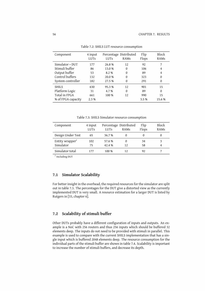
56 CHAPTER 7. RESULTS
Table 7.2: SHILS LUT resource consumption
Component 4 inputLUTs
PercentageLUTs
DistributedRAMs
FlipFlops
BlockRAMs
Simulator + DUT 177 26.8 % 12 92 7Stimuli buffer 86 13.0 % 0 106 4Output buffer 53 8.2 % 0 89 4Control buffers 132 20.0 % 0 323 0System controller 182 27.5 % 0 291 0SHILS 630 95.3 % 12 901 15Platform Logic 31 4.7 % 0 89 0Total in FPGA 661 100 % 12 990 15% of FPGA capacity 2.3 % 3.5 % 15.6 %
Table 7.3: SHILS Simulator resource consumption
Component 4 inputLUTs
PercentageLUTs
DistributedRAMs
FlipFlops
BlockRAMs
Design Under Test 65 36.7 % 0 0 0Entity wrapper1 102 57.6 % 0 34 3Simulator 75 42.4 % 12 58 4Simulator total 177 100 % 12 92 71 Including DUT
7.1 Simulator Scalability
For better insight in the overhead, the required resources for the simulator are splitout in table 7.3. The percentages for the DUT give a distorted view as the currentlyimplemented DUT is very small. A resource estimation for a larger DUT is listed byRutgers in [33, chapter 6].
7.2 Scalability of stimuli buffer
Other DUTs probably have a different configuration of inputs and outputs. An ex-ample is a NoC with 256 routers and thus 256 inputs which should be buffered 32elements deep. The inputs do not need to be provided with stimuli in parallel. Thisexample is used to compare with the current SHILS implementation that has a sin-gle input which is buffered 2048 elements deep. The resource consumption for theindividual parts of the stimuli buffer are shown in table 7.4. Scalability is importantto increase the number of stimuli buffers, and decrease its depth.

7.3. CONTROL BUFFER SCALABILITY 57
Table 7.4: Stimuli buffer specified resource consumption
Component 4 inputLUTs
PercentageLUTs
DistributedRAMs
FlipFlops
BlockRAMs
Controller 61 70.9 % 0 89 0Buffer 0 0 0 0 4Timecode checker 25 29.1 % 0 17 0Total 86 100 % 0 106 4
7.2.1 Storage scalingThe current implementation of both the stimuli buffer and the output buffer store2048 samples of 32 bits. These require 4 block RAMs each, as one block RAMcan storeup to 512 elements of 36 bits wide. The alternative example stores 32 elements of 32bits wide for 256 buffers, a total of 8192 elements, which can be stored easily in 16block RAMs. The resources required to store the larger number of elements scaleslinearly.
The data can be either stored in one large memory, or in 256 smaller memories.Control of a largememory is important. The best solution is to divide the addressingspace into blocks for each input to avoid searching for stimuli for input X. Due to thelarger address width of a large memory, more LUTs are required and other inter-connection logic for implementation are required, especially when the memory isdivided into blocks, although data density in the block RAMS is higher when using alarge memory.
7.2.2 Control scalingWhen the entire stimuli buffer is instantiated multiple times for multiple inputs,the number of resources required scales linearly. For selection of the correct buffer,additional logic is necessary of course.
A controller for multiple buffers could be created, but would increase the com-plexity and would thus increase the combinatorial path. Therefore, it is best to use aseparate controller for each stimuli input, of which the data is either stored in a sin-gle large memory or individual memories. As noted above, a division of addressingspace in blocks eases access to the contents in an FIFO oriented fashion. Using mul-tiple controllers is possible, as a controller requires little resources(0.3% resourceconsumtion in Virtex-II 3000 FPGA).
7.3 Control buffer scalability
The control buffers are implemented as 32 bits wide buffers. Therefore, they con-sume the same amount of logic when used in larger systems (with larger bit widths).Also, the amount of resources required for all control buffers is marginal comparedto the available resources.

CHAPTER8Conclusion
The research for this final project has focused on two main issues as stated in theintroduction:
How to implement the simulator in an actual FPGA, how to connect it toa processor and how to make them communicate?
and
How to connect a PC with the sequential simulator, how to make themcommunicate and process?
For the implementation of the simulator in an FPGA, several components aredesigned to provide the simulator with a sturdy external interface and buffers forclock domain conversion. The external interface provides the simulator with a con-nection to a processor, so that the processor and simulator can communicate usingDirect Memory Access over an MMIO interface. This interface theoretically offersmaximum throughput as the processor can access the FPGA directly. The design ismade suitable for a large variety of platforms. The implementation is created for theBCVP platform. Resources for the stimuli buffer scale proportionally, the resourcesconsumed by the control buffers are constant. The stimuli buffers should be scaledwith care, implementation using fully parallel buffers is easiest.
The initial design and implementation for the BCVP platform were created withlimited features to provide a solid base for further research. Creating this imple-mentation consumed much more time than was anticipated. Therefore, the focusremained on the main topic of this final project — communicating with the simula-tor.
To provide for a more versatile test platform, the ARM processor is replaced bya PC. The PC can take care of the set-up of link memories in the simulator beforesimulation. This is done manually up till now.
The combination of an FPGA and a PC create a new co-simulation system. Theinterconnection is often a major performance bottleneck in co-simulation systems.To create the interconnection between PC and FPGA without much effort, severaltools can be used. Xilinx System Generator is evaluated as the best tool for SHILS,in particular as it generates facilities the for synchronization and communication.
59

60 CHAPTER 8. CONCLUSION
The required effort to deploy SHILS using System Generator is lower than for otheroptions, and communication overhead is not significant. Ethernet is used as com-municationmediumoverwhich SystemGenerator can transmit rawEthernet framesin a point-to-point connection to obtain the best possible throughput. Transmissionspeeds of 1Gbps are theoretically possible according to Xilinx.
8.1 Recommendations and Future work
SHILS is work in progress, several issues arose in the design and implementationphases. Besides optimizations for SHILS and its tooling, also new ideas are men-tioned.
8.1.1 Improve conversion to simulatorWhen a design is made, the designer will need to manually define the entity whichwill be simulated sequentially. These manual changes imply a serious risk of in-troducing additional errors in the process of linking the entities together. This isundesired in the test and verification of a design.
8.1.2 Better simulation control in FPGAControl of the simulation in the FPGA is easy, but should be donewith care. Registerskeep the same value when set once. It often is easier to allow a fixed number of sys-temcycles before issuing another command. Tight coupling of FPGAandprocessor isnot desired, the processor cannotmonitor exactly at whatmoment the simulation isdone. Therefore, the simulator control should be extended such that the commandregister in the FPGA is reset each time a command is accepted. This ensures that thesimulator stops after a full system cycle, instead of running to completion.
8.1.3 Data compression of stimuli and output dataFor now, all data is transmitted and stored without any form of compression. Withlimited bandwidths and storage capacity, using compression poses an opportunityto enhance throughput and storage capability. As compression and decompressionrequires resources and time, this requires more thorough examination.
8.1.4 Replace QuestaSim with SHILSThe new design can be constructed in such a method that one can choose whetherto simulate using QuestaSim, or using SHILS with the same set of test data.
Behavioural simulations can be done easily in QuestaSim, and SHILS can be usedfor cycle-true bit-accurate simulations that in QuestaSim last prohibitively long.

APPENDIXAMemory Map
Figure A.1 shows the address space which is available for SHILS as designed in theFPGA. The addresses which are mentioned indicate the range which is reserved fora certain block. The figure shows the word address. In the connection to the proces-sor is the most significant byte one position shifted left. This is caused by physicaldefects on the test platform (section 4.1) The processor uses byte addressing. Forthese reasons, an address translation table is created, depicted in tables A.1 and A.2.
.
.Data
tostim
ulib
uffer
.Data
from
output
buffe
r
.Echo
register
.System
statea
ndcontrol
.0x000
0
.0x100
0
.0x400
0
.0x500
0
.0x800
0
.0x800
1
.0xF00
0
.0xFFF
F
.32bits
Figure A.1: Global address space division
The system state and control address space is expanded in figureA.2. The addressspace for simulator control and state is in the range of 0xF0C0 up to 0xF0FF, which isexpanded in figure A.3. Figure A.3 uses naming in accordance with Rutgers [33]. Allthese figures show the address space as designed in the FPGA, which is a sort of wordaddressing.
61

62 APPENDIX A. MEMORY MAP
.
.Stim
ulib
uffers
ize
.Stim
ulib
ufferfull
.Stim
ulib
uffere
mpty
.Stim
ulib
ufferw
ritep
ointer
.Output
buffe
rsize
.Output
buffe
rfull
.Output
buffe
rempty
.Output
buffe
rreadpo
inter
.Simulator
control
.Simulator
state
.0xF00
0
.0xF00
4
.0xF04
0
.0xF04
4
.0xF0C
0
.0xF0E
0
.0xF0F
F
.32bits
Figure A.2: System control address space
.
.Comman
d.Ad
dress
.Read
from
.Stim
ulim
ask
.Writ
eto
.Enable
.Runn
ing
.Curren
tadd
ress
.Curren
tadd
ressvalid
.Prefetch
stim
uli
.Prefetch
stim
ulivalid
.Prefetch
mask
.Clockcoun
ter
.
.0xF0C
0
.0xF0C
6
.0xF0E
0
.0xF0E
7
.32bits
Figure A.3: Simulator state and control address space
Table A.1: Write memory map
GPP FPGA addressing DescriptionByte address bits 16-13 bits 7-4 bits 3-0
0x00000 0x0 X1 X1 Write data to FIFO0x80000 0x8 X X Write data to echo register
Buffer control0xF000C 0xF 0x0 0x3 Update FIFO input write pointer0xF000C 0xF 0x4 0x3 Update FIFO output read pointer
bits 4-02 Simulator control0xF0300 0xF 0xC 0x0 Command0xF0304 0xF 0xC 0x1 Address0xF0308 0xF 0xC 0x2 Read from0xF030C 0xF 0xC 0x3 Stimuli mask0xF0310 0xF 0xC 0x4 Write to0xF0314 0xF 0xC 0x5 Enable
1 Actually, these bits determine the address at which the data is stored in the FIFO buffer.2 To reserve a larger addressing space for simulator control, 5 bits are used.

63
Table A.2: Read memory map
GPP FPGA addressing DescriptionByte address bits 16-13 bits 7-4 bits 3-0
0x00000 0x0 X X Return 0xDEADBEEF0x10000 0x1 X X Return 0xBEEFDEAD0x40000 0x4 X1 X1 Return FIFO output data0x80000 0x8 X X Read data from echo register
Buffer State0xF0000 0xF 0x0 0x0 Return input size0xF0004 0xF 0x0 0x1 Return input full0xF0008 0xF 0x0 0x2 Return input empty0xF000C 0xF 0x0 0x3 Return input write pointer0xF0100 0xF 0x4 0x0 Return output size0xF0104 0xF 0x4 0x1 Return output full0xF0108 0xF 0x4 0x2 Return output empty0xF010C 0xF 0x4 0x3 Return output read pointer
bits 4-02 Simulator state0xF0380 0xF 0xE 0x0 Running0xF0384 0xF 0xE 0x1 Current_address0xF0388 0xF 0xE 0x2 Current_addr_valid0xF038C 0xF 0xE 0x3 Prefetch_stimuli0xF0390 0xF 0xE 0x4 Prefetch_addr_valid0xF0394 0xF 0xE 0x5 Prefetch_mask0xF0398 0xF 0xE 0x6 Clk_cnt
1 Actually, these bits determine the address at which the data is read from the FIFO buffer.2 To reserve a larger addressing space for simulator state, 5 bits are used.

APPENDIXBTest case: IIR filter
A test case is used to verify whether there are difficulties with the test flow, and totest the challenges for a system designer.
The test case is very basic, but nevertheless involves these aspects:
1. Homogeneous structure1
2. Easily adaptable number of taps, thus increasing the number of entities andthe complexity.
3. Contains both forwards and backwards loops.
B.1 IIR filter
The example is an Infinite Impulse Response (IIR) filter. The equation for an IIR filter is:
yn =n∑
i=0
bixn−i −n∑
i=0
aixn−i (B.1)
This equation expands to:
yn = b0xn + b1xn−1 + b2xn−2 − a1yn−1 − a2yn−2 · · ·with n = 0, 1, 2, · · · (B.2)
The equation above clearly shows several recognisable items of a regular struc-ture. Graphically, this is evenmore clear (see figureB.1). An IIR filter canbedesignedin several structures [23]. Figure B.1 shows the direct-form structure of an IIR filterthat is used for tests.
The regular structure of an IIR filter is easily recognisable in the forwards path,but somewhat less straightforward in the backwards part. The single entity whichshould be processed by the tool of Rutgers is shown in figure B.2, which is a verysmall piece of hardware.
1A number of changes to the structure are necessary to create an entirely homogeneous structure,however.
65

66 APPENDIX B. TEST CASE: IIR FILTER
.
.
.
.
.
. .
.x(t) . ..... ... .b0
.. ... .y(t). ...
.Z−1 .Z−1
.. ... .b1 .-a1.. ...
.Z−1 .Z−1
Figure B.1: Basic IIR filter
.
.
.x(t) . ..... ... .x
.sum_out. ...
.Z−1 .sum_in . ...
.d_out. ...
.coefficient. ...
Figure B.2: IIR entity design
A first order IIR filter design has been made to test the outcome of the trans-formed design. The design for the IIR entity shown in figure B.2 is specified in list-ing B.2. The entity is equipped with several ports, specified in listing B.1.
The implementation of the asynchronous and synchronous part are explicitlyseparated for clarity. The IIR entity is used by the IIR filter top-level entity. Thetop-level entity uses the generate statement of VHDL for automated instantiation ofa multi-taps IIR filter.

B.2. HOMOGENEOUS STRUCTURE 67
entity iir isport (reset : in std_logic;clk : in std_logic;x : in std_logic_vector (15 downto 0);coefficient : in std_logic_vector (15 downto 0);sum_in : in std_logic_vector (15 downto 0);d_out : out std_logic_vector (15 downto 0);sum_out : out std_logic_vector (15 downto 0));
end iir;
Listing B.1: IIR entity definition
-- ========= asynchronous ========process(x,sum_in, coefficient)
variable mult_out : signed(31 downto 0);variable sum_int : signed(15 downto 0);
begin--calculate productmult_out := signed(x) * signed(coefficient);
--calculate sumsum_int := mult_out(30 downto 15) + signed(sum_in);sum_out <= std_logic_vector(sum_int);
end process;
-- ========= synchronous ========--delay input sample with one clock cycle and provide reset circuitryprocess (clk,reset)begin
if reset =’1’ then -- ATTN: Active high reset!delay <= x”0000”;
elsif rising_edge(clk) then --force fdc flip-flop by if statement.delay <= x;
end if;end process;
Listing B.2: IIR entity behaviour VHDL code
B.2 Homogeneous structure
Figure B.1 shows that an IIR filter is not entirely homogeneous by the componentsfilled light. To generate the IIR filter, a number of different conditions are used. Thecode to generate an IIR filter is added in listing B.3.
The transformation tool of Rutgers [33] is not able to process systems that arenot fully homogeneous. The structure of the IIR filter must be changed for this rea-

68 APPENDIX B. TEST CASE: IIR FILTER
son. Two additional instantiations of the basic IIR entity were added to replace theirregular components.
Mathematically, the multipliers can be “bypassed” using coefficient 1. The IIRfilter is constructed in a fixed-width system, which can not represent 1. A solution,which is correct, is tomultiply two times by−1, as−12 is exactly 1. This requires theaddition of more entities, which results in a total of seven entities for a first orderIIR filter. To scale the filter to a second order only two entities need to be added and4 to create a third order filter.
In the end, the design is built out of 7 blocks, which are tied together by a numberof wires as shown in figure B.3. For readability, the coefficient input is not named,though the values for it are depicted.
.
.
.IIR #0
.x .s_out
.d_out .s_in
.
.IIR #1
.x .s_out
.d_out .s_in
.
.IIR #2
.x .s_out
.d_out .s_in
.
.IIR #3
.x .s_out
.d_out .s_in
.
.IIR #5
.x .s_out
.d_out .s_in
.
.IIR #4
.s_out .x
.s_in .d_out
.
.IIR #6
.x .s_out
.d_out .s_in
.
.0
.0
.0
.0 .0
.a0
.a1
.-1 .-1
.-b1
.-1 .-1
Figure B.3: IIR filter as block, homogeneous
B.3 Challenges
Usage of the transformation tool has posed challenges, which are discussed in thissection. A common mistake on signal naming is discussed.
As specified by Rutgers [33, section 5.5.3], the tool can connect only one outputto a single input. However, the IIR filter requires that both the output of the adderand the delay output can be connected to the ‘x’ input of an IIR entity, as shownin figure B.3. The hatched components are connected via different ports than theother components. In simulation, multiple link memory outputs try to write to thesame signal simultaneously. This pitfall causes conflicts in the signal, which becomesinvalid. Therefore, a manual change has been made to the wrapper entity; an addi-tional multiplexer was added. This is suggested by Rutgers too. The transformationtool is not adjusted to support this feature.
A common practice in system design is to name a signal ‘reset’ when the resetcondition is active when the signal is ‘high’, instead of ‘low’. However, the trans-formation tool uses the name ’reset’ for its active-low reset condition, which is mis-leading. Listing B.2 uses active-high reset for this reason.

B.3. CHALLENGES 69
--Instantiate FIR partsfir:for tap in 0 to LENGTH_IIR generatefir_in : if (tap=0) generate -- Irregular: upmost blockfir_part_1: entity work.iir port map( x,
fir_delay(0),fir_sum_out(0),fir_sum_out(1),fir_coeff(0),clk, reset);
end generate;fir_others : if (tap>0) generate -- Regular structure (tap 1 to end)fir_part : entity work.iir port map(fir_delay(tap-1),
fir_delay(tap),fir_sum_out(tap),fir_sum_out(tap+1),fir_coeff(tap),clk,reset);
end generate;end generate;-- Regular partiir: for tap in 0 to LENGTH_IIR+1 generateiir_irr : if (tap=0) generatetotal_part: entity work.iir port map(fir_sum_out(0),
iir_delay(0),iir_sum_out(0),iir_sum_out(2),iir_coeff(0),clk,reset);
iir_part_1: entity work.iir port map(iir_sum_out(0),iir_delay(1),iir_sum_out(1),zero,iir_coeff(0),clk, reset);
end generate;iir_reg : if (tap>1) generateiir_part: entity work.iir port map( iir_delay(tap-1),
iir_delay(tap),iir_sum_out(tap),iir_sum_out(tap+1),iir_coeff(tap-1),clk, reset);
end generate;end generate;
Listing B.3: IIR filter generation code

70 APPENDIX B. TEST CASE: IIR FILTER
Table B.1: IIR filter entity resource consumption
Precision SynthesisResource Used Available UtilizationFunction Generators 16 28672 0.06%CLB Slices 8 14336 0.06%Dffs or Latches 16 30832 0.05%Block RAMs 0 96 0.00%Block Multipliers 0 96 0.00%
B.4 Results
Synthesis results are listed in table B.1.

APPENDIXCC code listings
This appendix contains the definitions of the structures that are used to describethe memory map for the processor in the BCVP platform. Similar to appendix A,the simulator control and state are expanded in individual structures (listings C.2and C.3)struct Hw_bridge{/* 0x00000000 */ volatile long data2fifo[IN_FIFO_SIZE];/* 0x00000040 */ fill(reserved, sizeof(data2fifo),0x10000); //Initial test size/* 0x00010000 */ volatile long test1;/* 0x00010003 */ fill(reserved0,0x10004,0x40000);/* 0x00040000 */ volatile long data2arm[OUT_FIFO_SIZE];/* 0x00040040 */ fill(reserved1,0x40000+sizeof(data2arm),0x80000); //Initial test size/* 0x00080000 */ volatile long echo;/* 0x00080004 */ fill(reserved2,0x80004,0xF0000);/* 0x000F0000 */ Fifo_state in_fifo;/* 0x000F0010 */ fill(reserved3,0xF0010,0xF0100);/* 0x000F0100 */ Fifo_state out_fifo;/* 0x000F0110 */ fill(reserved4,0xF0110,0xF02C0);/* 0x000F02C0 */ volatile long test2;/* 0x000F02C4 */ fill(reserved5,0xF02C4,0xF0300);/* 0x000F0300 */ Sim_ctrl control;/* 0x000F0318 */ fill(reserved6,0xF0318,0xF0380);/* 0x000F0380 */ Sim_state state;/* 0x000F0398 */ // End address
};
Listing C.1: Structure describing memory map in processor
struct Sim_ctrl{/* 0x0000 */ volatile long cmd;/* 0x0004 */ volatile long addr;/* 0x0008 */ volatile long read_from;/* 0x000C */ volatile long stimuli_mask;/* 0x0010 */ volatile long write_to;/* 0x0014 */ volatile long enable;
};
Listing C.2: Simulator control struct
71
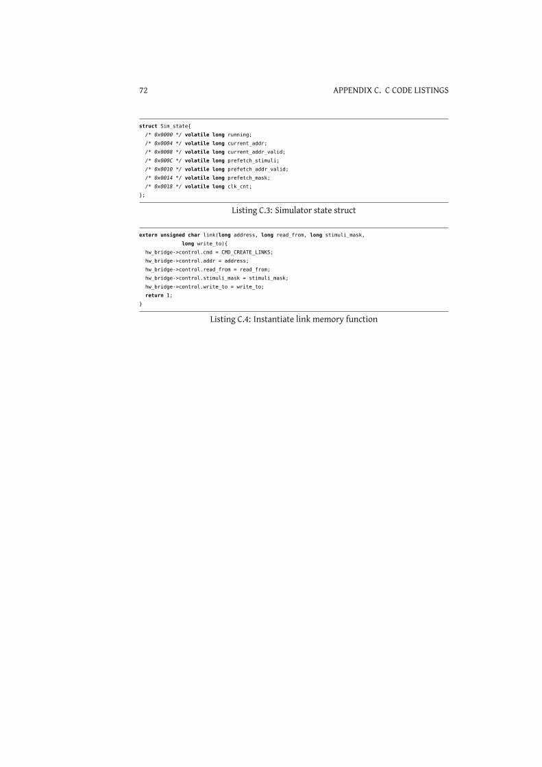
72 APPENDIX C. C CODE LISTINGS
struct Sim_state{/* 0x0000 */ volatile long running;/* 0x0004 */ volatile long current_addr;/* 0x0008 */ volatile long current_addr_valid;/* 0x000C */ volatile long prefetch_stimuli;/* 0x0010 */ volatile long prefetch_addr_valid;/* 0x0014 */ volatile long prefetch_mask;/* 0x0018 */ volatile long clk_cnt;
};
Listing C.3: Simulator state struct
extern unsigned char link(long address, long read_from, long stimuli_mask,long write_to){
hw_bridge->control.cmd = CMD_CREATE_LINKS;hw_bridge->control.addr = address;hw_bridge->control.read_from = read_from;hw_bridge->control.stimuli_mask = stimuli_mask;hw_bridge->control.write_to = write_to;return 1;
}
Listing C.4: Instantiate link memory function

Bibliography
[1] Altera. DSP Builder User Guide, 8.0 edition, May 2008.
[2] L. Benini and G. De Micheli. Networks on chips: a new soc paradigm. Computer,35(1):70–78, 2002.
[3] UC Berkeley. Research Accelerator for Multiple Processors (RAMP) project.http://ramp.eecs.berkeley.edu/. Last checked August 15, 2008.
[4] Christopher Brooks, Edward A. Lee, Xiaojun Liu, Stephen Neuendorffer, YangZhao, and Haiyang Zheng. Heterogeneous Concurrent Modeling and Design inJava (Volume 1: Introduction to Ptolemy II). Technical Report UCB/EECS-2008-28, EECS Department, University of California, Berkeley, April 2008.
[5] W. Brugger, M. Hofinger, and 4S partners. 4S BCVP specification. Atmel Germany,April 2004.
[6] Controllab Products B.V. 20-sim. www.20-sim.com. Last checked August 15, 2008.
[7] Allan Cantle and Robin Bruce(Nallatech). An introduction to the NallatechSlipstream FSB-FPGA Accelerator Module for Intel Platforms & the NallatechHigh-Level Toolset. White paper NT 405-0342, September 2007. NT 405-0342http://www.nallatech.com/mediaLibrary/images/english/6615.pdf.
[8] Ben Chan, Nabeel Shirazi, and Jonathan Ballagh. Achieving high-bandwidthDSP simulations using Ethernet Hardware-in-the-Loop. DSP Magazine, 2:42–44,May 2006. Xilinx.
[9] C. Chang, C. Chang, J. Wawrzynek, and R.W. Brodersen. BEE2: a high-end re-configurable computing system. IEEE Design & Test of Computers, 22(2):114–125,2005.
[10] ChiasTek. Cosimate: Heterogeneous co-simulation in distributed environ-ments. http://www.chiastek.com/products/cosimate.html, 2008. Last checked Au-gust 15, 2008.
[11] Eric S. Chung, Eriko Nurvitadhi, James C. Hoe, Babak Falsafi, and Ken Mai. Vir-tualized Full-System Emulation of Multiprocessors using FPGAs. In Workshopon Architectural Research Prototyping (during ISCA2007), volume 2, New York, NY,USA, June 2007. ACM.
[12] Eric S. Chung, Eriko Nurvitadhi, James C. Hoe, Babak Falsafi, and Ken Mai.A complexity-effective architecture for accelerating full-system multiproces-sor simulations using FPGAs. In FPGA ’08: Proceedings of the 16th international
73

74 BIBLIOGRAPHY
ACM/SIGDA symposium on Field programmable gate arrays, pages 77–86, New York,NY, USA, February 2008. ACM.
[13] Moo-Kyoung Chung andChong-MinKyung. Enhancing performance of HW/SWcosimulation and coemulation by reducing communication overhead. IEEETransactions on Computers, 55(2):125–136, February 2006.
[14] Hewlett-Packard Company, Intel Corporation, Lucent Technologies Inc, Mi-crosoft Corporation, NEC Corporation, and Koninklijke Philips Electronics N.V.Universal serial bus specification revision 2.0, 2000. downloaded from www.usb.org.
[15] Daniel Lázaro Cuadrado, Anders P. Ravn, and Peter Koch. Automated Dis-tributed Simulation in Ptolemy II. In Proceedings on the 25th IASTED InternationalMulti-Conference Parallel and Distributed Computing and Networks (PCDN’07), pages139–144, Anaheim, CA, USA, February 2007. ACTA Press.
[16] A.S. Damstra. Virtual prototyping through co-simulation in hardware/softwareand mechatronics co-design. Master’s thesis, Control Laboraty, University ofTwente, April 2008.
[17] Daniel Denning(Nallatech). Accelerate and verify algorithms with theXtremeDSP development kit-II. Xcell Journal Online, (49), Summer 2004.
[18] John W. Eaton and Community. GNU Octave. http://www.gnu.org/software/octave/, 2008. Last checked August 15, 2008.
[19] Nicolas Genko, David Atienza, and Giovanni De Micheli. NoC Emulation onFPGA: HW/SW Synergy for NoC Features Exploration. In Proceedings of the Inter-national Conference on Parallel Computing (ParCo2005), volume 33, pages 753–760,Jülich, Germany, September 2005. John von Neumann Institute for Computing(NIC).
[20] B. Gestner and D.V. Anderson. Automatic generation of ModelSim-Matlab in-terface for RTL debugging and verification. In Proceedings of the 50th MidwestSymposium on Circuits and Systems MWSCAS 2007, pages 1497–1500, Los Alamitos,CA, USA, August 2007. IEEE.
[21] John L. Hennessy and David A. Patterson. Computer Architecture: A QuantitativeApproach. Morgan Kaufmann, Third edition, May 2003. ISBN 1-55860-596-7.
[22] K. J. Hines. Pia: A framework for embedded system co-simulationwith dynamiccommunication support. Technical Report TR-96-11-04, University ofWashing-ton, October 1996.
[23] Douglas L. Jones. IIR Filter Structures. Connexions http://cnx.org/content/m11919/latest/, December 2004. Last checked August 15, 2008.
[24] A. Lafage. HSMC3 functional specifications. Atmel Coorporation, April 2003.
[25] V. S. Lin and D. E. Pansatiankul. Hardware-accelerated simulation tool for end-to-end communication systems. In Proceedings of the IEEE Global Telecommunica-tions Conference GLOBECOM ’06, pages 1–5, Los Alamitos, CA, USA, November 2006.IEEE.

BIBLIOGRAPHY 75
[26] The Mathworks. EDA Simulator Link™MQ. http://www.mathworks.com/products/modelsim/, March 2008. (version 2.4) Last checked August 15, 2008.
[27] The Mathworks. MATLAB®- the language of technical computing. http://www.mathworks.com/products/matlab/, March 2008. (version 7.6) Last checked: August15, 2008.
[28] L. O’Callaghan, N. Mishra, A. Meyerson, S. Guha, and R. Motwani. Streaming-data algorithms for high-quality clustering. In Proceedings of the 18th Inter-national Conference on Data Engineering, pages 685–694, Los Alamitos, CA, USA,February 2002. IEEE Computer Society.
[29] K. Olukotun, M. Heinrich, and D. Ofelt. Digital system simulation: methodolo-gies and examples. In Proc. Design Automation Conference, pages 658–663, LosAlamitos, CA, USA, June 1998. IEEE Computer Society.
[30] Jingzhao Ou and V.K. Prasanna. MATLAB/Simulink Based Hardware/Soft-ware Co-Simulation for Designing Using FPGA Configured Soft Processors. InProc. 19th IEEE International Parallel and Distributed Processing Symposium, pages148b–148b, Los Alamitos, CA, USA, April 2005. IEEE.
[31] K.N. Parashar and N. Chandrachoodan. A novel event based simulation algo-rithm for sequential digital circuit simulation. In Proc. International Conferenceon Field Programmable Logic and Applications FPL 2007, pages 792–795, Los Alami-tos, CA, USA, August 2007. IEEE.
[32] W. W. Royce. Managing the development of large software systems: conceptsand techniques. In ICSE ’87: Proceedings of the 9th international conference on Soft-ware Engineering, pages 328–338, Los Alamitos, CA, USA, March 1987. IEEE Com-puter Society Press.
[33] J. H. Rutgers. Automated sequential hardware-in-the-loop simulator genera-tion. Technical report, University of Twente, November 2007.
[34] A.S. Tanenbaum and M. van Steen. Distributed Systems: Principles and Paradigms.Prentice Hall, 2002. ISBN 0-13-121786-0.
[35] C. A. Verhaar. An integrated embedded control softwaredesign case study us-ing Ptolemy II. Master’s thesis, Control Laboratory, University of Twente, May2008.
[36] Virtutech. Simics for multicore software. White paper, June 2007. www.virtutech.com.
[37] Michael C. Williamson. Synthesis of Parallel Hardware Implementations from Syn-chronous Dataflow Graph Specifications. PhD thesis, EECS Department, Universityof California, Berkeley, 1998.
[38] P. T.Wolkotte, P. K. F. Hölzenspies, and G. J. M. Smit. Fast, Accurate and DetailedNoC Simulations. In Proceedings of the 1st ACM/IEEE International Symposium onNetworks-on-Chip, Princeton, NJ, USA, pages 323–332, Los Alamitos, May 2007. IEEEComputer Society Press.

76 BIBLIOGRAPHY
[39] P. T. Wolkotte, P. K. F. Hölzenspies, and G. J. M. Smit. Using an FPGA for FastBit Accurate SoC Simulation. In Proceedings of the 21th IEEE International Paralleland Distributed Processing Symposium (IPDPS’07) - 14th Reconfigurable ArchitectureWorkshop (RAW2007), Long Beach, CA, USA, page 167, Piscataway,March 2007. IEEEComputer Society Press.
[40] Xilinx. Technology solutions - connectivity. http://www.xilinx.com/products/design_resources/conn_central/index.htm. Last checked August 15, 2008.
[41] Xilinx. Virtex-II platform FPGAs: Complete data sheet, November 2007. DS031,version 3.5.
[42] Xilinx. System Generator for DSP User Manual, 10.1.1 edition, April 2008.
[43] Xilinx, Justin Delva, Adrian Chirila-Rus, Ben Chan, and Shay Seng. Using systemgenerator for systematic HDL design, verification and validation. White Paper,January 2008.