Implementation and Optimization of the Advanced Encryption ...
149
Air Force Institute of Technology Air Force Institute of Technology AFIT Scholar AFIT Scholar Theses and Dissertations Student Graduate Works 3-6-2007 Implementation and Optimization of the Advanced Encryption Implementation and Optimization of the Advanced Encryption Standard Algorithm on an 8-Bit Field Programmable Gate Array Standard Algorithm on an 8-Bit Field Programmable Gate Array Hardware Platform Hardware Platform Ryan J. Silva Follow this and additional works at: https://scholar.afit.edu/etd Part of the Computer Engineering Commons, and the Information Security Commons Recommended Citation Recommended Citation Silva, Ryan J., "Implementation and Optimization of the Advanced Encryption Standard Algorithm on an 8-Bit Field Programmable Gate Array Hardware Platform" (2007). Theses and Dissertations. 3142. https://scholar.afit.edu/etd/3142 This Thesis is brought to you for free and open access by the Student Graduate Works at AFIT Scholar. It has been accepted for inclusion in Theses and Dissertations by an authorized administrator of AFIT Scholar. For more information, please contact richard.mansfield@afit.edu.
-
Upload
khangminh22 -
Category
Documents
-
view
3 -
download
0
Transcript of Implementation and Optimization of the Advanced Encryption ...
Air Force Institute of Technology Air Force Institute of Technology
AFIT Scholar AFIT Scholar
Theses and Dissertations Student Graduate Works
3-6-2007
Implementation and Optimization of the Advanced Encryption Implementation and Optimization of the Advanced Encryption
Standard Algorithm on an 8-Bit Field Programmable Gate Array Standard Algorithm on an 8-Bit Field Programmable Gate Array
Hardware Platform Hardware Platform
Ryan J. Silva
Follow this and additional works at: https://scholar.afit.edu/etd
Part of the Computer Engineering Commons, and the Information Security Commons
Recommended Citation Recommended Citation Silva, Ryan J., "Implementation and Optimization of the Advanced Encryption Standard Algorithm on an 8-Bit Field Programmable Gate Array Hardware Platform" (2007). Theses and Dissertations. 3142. https://scholar.afit.edu/etd/3142
This Thesis is brought to you for free and open access by the Student Graduate Works at AFIT Scholar. It has been accepted for inclusion in Theses and Dissertations by an authorized administrator of AFIT Scholar. For more information, please contact [email protected].

xz
IMPLEMENTATION AND OPTIMIZATION OF THE ADVANCED ENCRYPTION STANDARD ALGORITHM ON AN 8-BIT FIELD PROGRAMMABLE GATE ARRAY HARDWARE PLATFORM
THESIS
Ryan J. Silva, 2nd Lieutenant, USAF
AFIT/GE/ENG/07-21
DEPARTMENT OF THE AIR FORCE AIR UNIVERSITY
AIR FORCE INSTITUTE OF TECHNOLOGY
Wright-Patterson Air Force Base, Ohio
APPROVED FOR PUBLIC RELEASE; DISTRIBUTION UNLIMITED

The views expressed in this thesis are those of the author and do not reflect the official
policy or position of the United States Air Force, Department of Defense, or the U.S.
Government.

AFIT/GE/ENG/07-21
IMPLEMENTATION AND OPTIMIZATION OF THE ADVANCED ENCRYPTION STANDARD ALGORITHM ON AN 8-BIT FIELD PROGRAMMABLE GATE ARRAY HARDWARE PLATFORM
THESIS
Presented to the Faculty
Department of Electrical and Computer Engineering
Graduate School of Engineering and Management
Air Force Institute of Technology
Air University
Air Education and Training Command
In Partial Fulfillment of the Requirements for the
Degree of Master of Science in Electrical Engineering
Ryan J. Silva, BSEE
2nd Lieutenant, USAF
March 2007
APPROVED FOR PUBLIC RELEASE; DISTRIBUTION UNLIMITED


AFIT/GE/ENG/07-21
Abstract
The contribution of this research is three-fold. The first is a method of converting
the area occupied by a circuit implemented on a Field Programmable Gate Array (FPGA)
to an equivalent (memory included) as a measure of total gate count. This allows direct
comparison between two FPGA implementations independent of the manufacturer or
chip family. The second contribution improves the performance of the Advanced
Encryption Standard (AES) on an 8-bit computing platform. This research develops an
AES design that occupies less than three quarters of the area reported by the smallest
design in current literature as well as significantly increases area efficiency. The third
contribution of this research is an examination of how various designs for the critical
AES SubBytes and MixColumns transformations interact and affect the overall
performance of AES. The transformations responsible for the largest variance in
performance are identified and the effect is measured in terms of throughput, area
efficiency, and area occupied.
iv

AFIT/GE/ENG/07-21
Shout out to Jesus
v
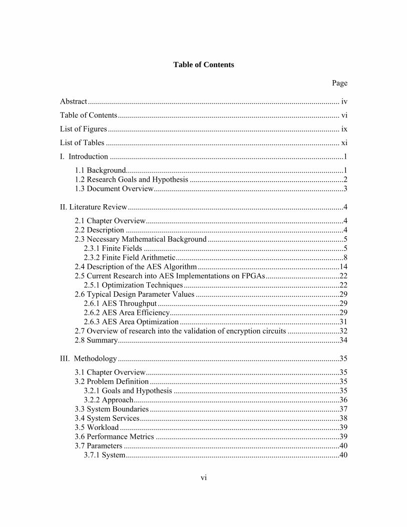
Table of Contents
Page
Abstract .............................................................................................................................. iv
Table of Contents............................................................................................................... vi
List of Figures .................................................................................................................... ix
List of Tables ..................................................................................................................... xi
I. Introduction .....................................................................................................................1
1.1 Background.............................................................................................................1 1.2 Research Goals and Hypothesis .............................................................................2 1.3 Document Overview...............................................................................................3
II. Literature Review............................................................................................................4
2.1 Chapter Overview...................................................................................................4 2.2 Description .............................................................................................................4 2.3 Necessary Mathematical Background ....................................................................5
2.3.1 Finite Fields ....................................................................................................5 2.3.2 Finite Field Arithmetic....................................................................................8
2.4 Description of the AES Algorithm.......................................................................14 2.5 Current Research into AES Implementations on FPGAs.....................................22
2.5.1 Optimization Techniques ..............................................................................22 2.6 Typical Design Parameter Values ........................................................................29
2.6.1 AES Throughput ...........................................................................................29 2.6.2 AES Area Efficiency.....................................................................................29 2.6.3 AES Area Optimization ................................................................................31
2.7 Overview of research into the validation of encryption circuits ..........................32 2.8 Summary...............................................................................................................34
III. Methodology ...............................................................................................................35
3.1 Chapter Overview.................................................................................................35 3.2 Problem Definition ...............................................................................................35
3.2.1 Goals and Hypothesis ...................................................................................35 3.2.2 Approach.......................................................................................................36
3.3 System Boundaries ...............................................................................................37 3.4 System Services....................................................................................................38 3.5 Workload ..............................................................................................................39 3.6 Performance Metrics ............................................................................................39 3.7 Parameters ............................................................................................................40
3.7.1 System...........................................................................................................40
vi
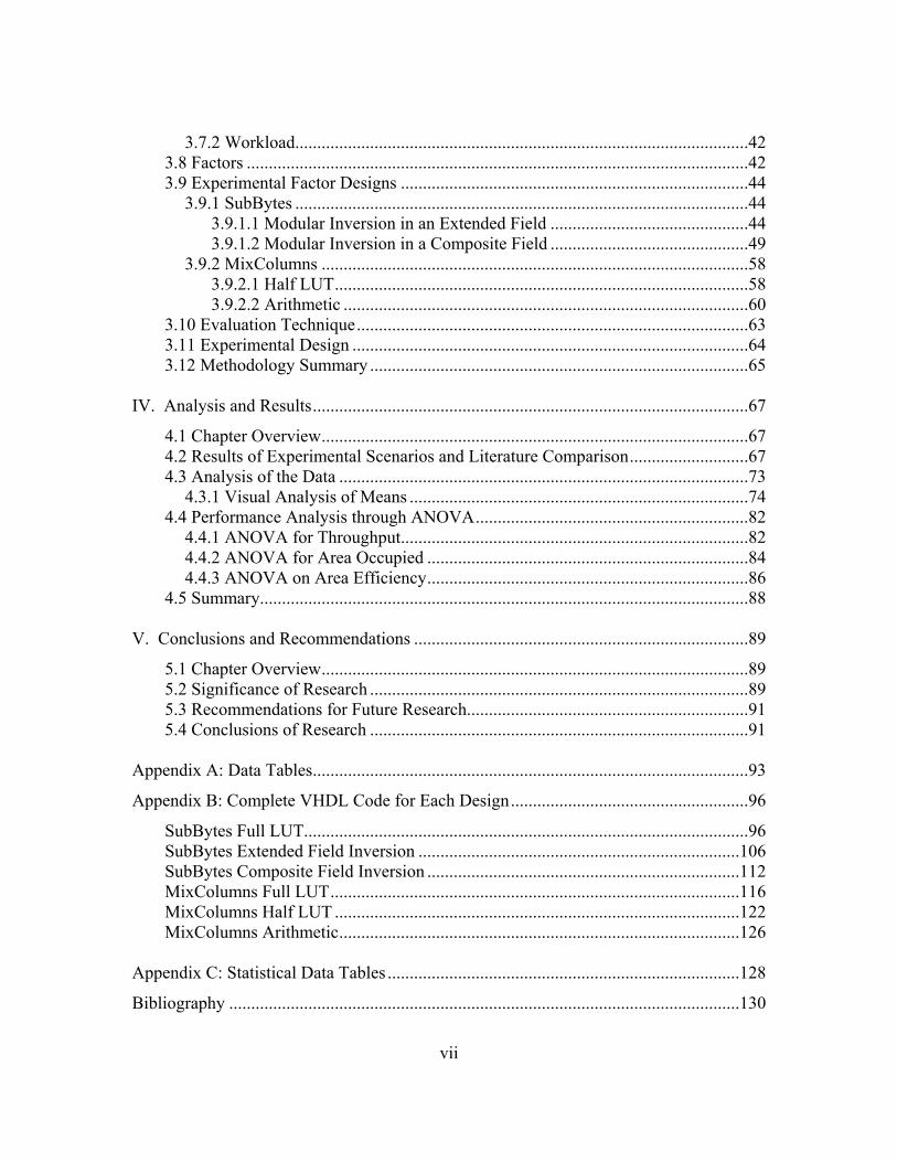
3.7.2 Workload.......................................................................................................42 3.8 Factors ..................................................................................................................42 3.9 Experimental Factor Designs ...............................................................................44
3.9.1 SubBytes .......................................................................................................44 3.9.1.1 Modular Inversion in an Extended Field .............................................44 3.9.1.2 Modular Inversion in a Composite Field .............................................49
3.9.2 MixColumns .................................................................................................58 3.9.2.1 Half LUT..............................................................................................58 3.9.2.2 Arithmetic ............................................................................................60
3.10 Evaluation Technique.........................................................................................63 3.11 Experimental Design ..........................................................................................64 3.12 Methodology Summary ......................................................................................65
IV. Analysis and Results...................................................................................................67
4.1 Chapter Overview.................................................................................................67 4.2 Results of Experimental Scenarios and Literature Comparison...........................67 4.3 Analysis of the Data .............................................................................................73
4.3.1 Visual Analysis of Means .............................................................................74 4.4 Performance Analysis through ANOVA..............................................................82
4.4.1 ANOVA for Throughput...............................................................................82 4.4.2 ANOVA for Area Occupied .........................................................................84 4.4.3 ANOVA on Area Efficiency.........................................................................86
4.5 Summary...............................................................................................................88
V. Conclusions and Recommendations ............................................................................89
5.1 Chapter Overview.................................................................................................89 5.2 Significance of Research ......................................................................................89 5.3 Recommendations for Future Research................................................................91 5.4 Conclusions of Research ......................................................................................91
Appendix A: Data Tables...................................................................................................93
Appendix B: Complete VHDL Code for Each Design......................................................96
SubBytes Full LUT.....................................................................................................96 SubBytes Extended Field Inversion .........................................................................106 SubBytes Composite Field Inversion .......................................................................112 MixColumns Full LUT.............................................................................................116 MixColumns Half LUT ............................................................................................122 MixColumns Arithmetic...........................................................................................126
Appendix C: Statistical Data Tables ................................................................................128
Bibliography ....................................................................................................................130
vii

Vita...................................................................................................................................133
viii

List of Figures
Figure Page
1. Basic Operation of a Symmetric Key Cipher ............................................................... 15
2. High Level Encryption Procedure for AES Algorithm [DaR98].................................. 16
3. AddRoundKey [Wik07a] .............................................................................................. 17
4. ShiftRows [Wik07a]...................................................................................................... 18
5. MixColumns [Wik07a] ................................................................................................. 19
6. FPGA Design Methodology [ZCN04].......................................................................... 23
7. Loop Unrolling an AES Architecture [QIS05] ............................................................. 26
8. Parallelization of MixColumns [CaA03] ...................................................................... 27
9. System Under Test........................................................................................................ 37
10. VHDL Code Implementing the Affine Transform ..................................................... 46
11. VHDL Code Implementing the Inverse Affine Transform......................................... 47
12. SubBytes design flow for Modular Inversion in an Extended Field........................... 48
13. Inverse SubBytes design flow for Modular Inversion in an Extended Field.............. 48
14. SubBytes Design Flow for Composite Field Inversion .............................................. 49
15. Inverse SubBytes Design Flow for Composite Field Inversion.................................. 49
16. Schematic of Modular Inversion in a Composite Field .............................................. 50
17. VHDL Code Implementing the Transform Matrix..................................................... 53
18. VHDL Code Implementing the Inverse Transform Matrix ........................................ 54
19. VHDL Implementation of Multiplication in GF(24)................................................... 56
20. VHDL Implementation of Squaring in GF(24) ........................................................... 57
ix

21. VHDL Implementation of the Highlighted Portion of Table 10................................. 60
22. VHDL Implementation of xtime in Combinational Logic ......................................... 62
23. VHDL Implementation of the Column Transform Routine ....................................... 63
24. Block Diagram of Testing Environment..................................................................... 65
25. Individual Values Plot for Throughput ....................................................................... 70
27. Individual Values Plot for Area Efficiency ................................................................ 72
28. Main Effects Plot for SubBytes on Area Occupied .................................................... 74
29. Main Effects Plot for SubBytes on Throughput ......................................................... 75
30. Main Effects Plot for SubBytes on Area Efficiency................................................... 76
31. Main Effects Plot for MixColumns on Area Occupied .............................................. 77
32. Main Effects Plot for MixColumns on Throughput.................................................... 78
33. Main Effects Plot for MixColumns on Area Efficiency ............................................. 79
34. Main Effects Plot for Synthesis Goal on Throughput................................................. 80
35. Main Effects Plot for Synthesis Goal on Area Occupied ........................................... 81
36. Main Effects Plot for Synthesis Goal on Area Efficiency .......................................... 81
x

List of Tables
Table Page
1. Truth Table for Addition in GF(2).................................................................................. 6
2. Truth Table for Multiplication in GF(2) ......................................................................... 6
3. Examples of Representing Polynomials in GF(2)| 8 ....................................................... 8
4. Throughput Comparison of Previous AES Designs ..................................................... 29
5. Area Efficiency Comparison of Previous AES Designs............................................... 31
6. Performance Comparison: Area, Area Efficiency, and Throughput............................. 32
7. Variable Key Known Answer Test Values for Keysize = 128 ..................................... 34
8. AES FPGA Performance in Current Literature ............................................................ 35
9. Factor Levels................................................................................................................. 43
10. Xtime Table: Elements Not Requiring Modulus Reduction Highlighted................... 59
11. Summary of Experimental Data.................................................................................. 68
12. Analysis of Variance Table for Throughput ............................................................... 83
13. Quantification of Effects for Throughput ................................................................... 83
14. Percentage of Variance Explained for Throughput .................................................... 84
15. Order of Importance for Throughput’s Factors and Interactions................................ 84
16. Percentage of Variance Explained for Area Occupied ............................................... 85
17. Order of Importance for Area Occupied’s Factors and Interactions........................... 86
18. Percentage of Variance Explained for Area Efficiency.............................................. 87
19. Order of Importance for Area Efficiency’s Factors and Interactions ......................... 88
20. Modular Inverses in the Rijndael Field [Odr01]......................................................... 93
xi
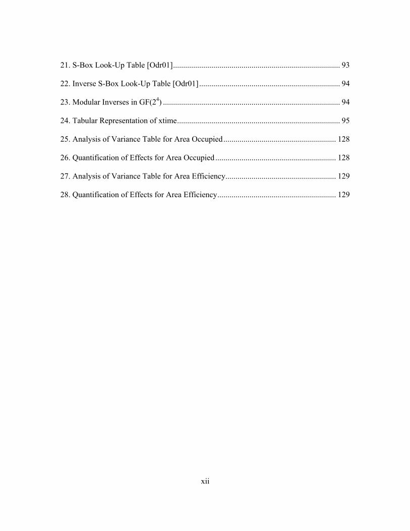
21. S-Box Look-Up Table [Odr01]................................................................................... 93
22. Inverse S-Box Look-Up Table [Odr01]...................................................................... 94
23. Modular Inverses in GF(24) ........................................................................................ 94
24. Tabular Representation of xtime................................................................................. 95
25. Analysis of Variance Table for Area Occupied........................................................ 128
26. Quantification of Effects for Area Occupied ............................................................ 128
27. Analysis of Variance Table for Area Efficiency....................................................... 129
28. Quantification of Effects for Area Efficiency........................................................... 129
xii
IMPLEMENTATION AND OPTIMIZATION OF THE ADVANCED ENCRYPTION STANDARD ALGORITHM ON AN 8-BIT FIELD PROGRAMMABLE GATE ARRAY HARDWARE PLATFORM
I. Introduction
1.1 Background
This research implements the US National Institute of Standards and Technology
(NIST) Advanced Encryption Standard (AES) algorithm on an FPGA device and
develops three designs for each of the AES transformations SubBytes and MixColumns.
The results of this research can be used in areas such as onboard encryption of satellite
communication. Most satellites being launched into orbit today are equipped with
FPGAs. This allows controllers on the ground to change the configuration of electronic
hardware on the satellite without having physical contact with the satellite. The amount
of hardware a satellite can carry is limited but the need for high throughput remains the
same. Achieving high area efficiency balances the amount of hardware the satellite must
carry, while maintaining a reasonably high throughput.
Nine AES designs account for the various combinations of SubBytes and
MixColumns designs. These designs use the Daemen and Rijmen’s Rijndael algorithm
targeting an 8-bit platform as a baseline [DaR98]. Each change to the baseline is an
attempt to increase the throughput of the AES algorithm while decreasing the total area
occupied, which results in increased area efficiency.
1
1.2 Research Goals and Hypothesis
This research has two primary goals. The first is to improve the speed of the AES
algorithm on an 8-bit platform while reducing the chip area of the implementation. This
goal is met when a design is produced that has a better performance than the baseline
implementation. The second goal of this research is to determine the effect of factor
interaction on the speed and space required to implement AES. This goal directly
supports the hypothesis to be tested. By using modular inversion in an extended field and
composite modular inversion in a subfield during the transformation of SubBytes in lieu
of a full look up table; and by utilizing a bitwise shift and combinational logic in the
transformation of MixColumns, the performance of AES and can be improved to a level
that surpasses AES performance relative to a baseline level.
The approach used to satisfy the two goals uses various SubBytes and
MixColumns designs to analyze the performance based on the three metrics and
compares the results to the baseline algorithm as well as other optimized designs
including Caltagirone’s fully pipelined architecture and Good’s compact Xilinx Spartan
implementation [CaA03][GoB05].
The performance of AES on 8-bit processing platforms is an important issue in
the AES design because most smart cards have such processors and many cryptographic
applications run on smart cards [DaR98]. Tailoring a compact AES design specifically
for an 8-bit platform would increase the overall usefulness of the algorithm. This compact
AES design could then be used more efficiently on smart cards and for other processor-
limited applications.
2

1.3 Document Overview
Chapter II presents an overview of the mathematical foundation of AES and
introduces the original design of the algorithm targeted to an 8-bit processing platform.
This chapter also reviews current research into AES implementations on FPGAs. Chapter
III defines the experiment conducted in this research. Chapter IV presents and interprets
the data collected from the experiment. The goal of Chapter IV is to answer the
investigative research questions posed in Chapter III: (1) how do experimental factors
interact and affect the overall performance metrics, and (2) how does each SubBytes and
MixColumns design affect performance? Chapter V summarizes the conclusions drawn
from the analysis of experimental data in Chapter IV. This chapter also highlights the
significance of this work and its impact on current research methods involving the
implementation of AES on FPGAs. Recommendations for future research are also
included.
3

II. Literature Review
2.1 Chapter Overview
This chapter provides an overview of the mathematics behind AES and presents
the design specified by the creators of the algorithm targeted to an 8-bit processing
platform. This chapter also provides a review of current research into AES
implementations on FPGAs.
2.2 Description
Implementing encryption algorithms on an FPGA brings many advantages such as
flexibility of re-design, run-time reconfiguration, and a vast amount of logic on a single
chip. The major drawback of an FPGA implementation is reduced throughput compared
to an equivalent AISC implementation. Through the use of a Xilinx Virtex II Pro FPGA
and Xilinx ISE software, nine different designs of the AES algorithm are created with the
ultimate goal of reducing the total equivalent gate count while increasing area efficiency.
On 2 October, 2000, the National Institute of Standards and Technology
announced that the Rijndael algorithm would be adopted as the Advanced Encryption
Standard [ZCN04]. Rijndael is a block cipher with a variable block and key length. The
block length and key length can be independently specified to be any integer multiple of
32 bits, with a minimum of 128 bits and a maximum of 256 bits. The AES algorithm
adopted by NIST is the unmodified Rijndael cipher except that AES has a fixed block
length of 128 bits and only supports key lengths of 128, 192 or 256 bits [DaR98]. This
research considers AES designs with a key length of 128 bits.
4
2.3 Necessary Mathematical Background
A grasp of the mathematics behind the Advanced Encryption Standard is
necessary to understand the algorithm’s design [DaR98]. AES utilizes the nonlinear
properties of abstract algebra to encrypt input data; consequently, a condensed discussion
in finite fields and how they are represented is presented before discussing design options
that optimize the AES algorithm.
2.3.1 Finite Fields
In abstract algebra, a field is an algebraic structure where the operations of
addition, subtraction, multiplication and division (except by zero) may be defined, and
the same rules from the arithmetic of ordinary numbers hold [Wik07b]. A finite field, or
Galois field, is a field that contains a finite number of elements. The number of elements
in a set defined as a finite field is termed the order of that field. A field with order m
exists iff m is a prime power. A prime power is any integer m for which m=pn for some
integer n and some prime integer p. The characteristic of a finite field is defined as p. All
finite fields used in AES have a characteristic of 2 [DaR98]. Finite fields with the same
order are isomorphic. Since only prime powers are considered for the AES algorithm, for
each prime power there is only one finite field denoted by GF(pn). Rijmen and Daemen
provide intuitive examples of finite fields of prime order p. The elements of a prime order
finite field GF(p) can be represented by the integers 0, 1, …, p-1. The two operations of
the field are integer addition modulo p and integer multiplication modulo p [DaR98].
Example 1 illustrates these properties.
5

Example 1. In the field GF(2) The elements of the field are 0 and 1; therefore the
two operations of the field are defined as integer addition modulo 2 and integer
multiplication modulo 2. The following truth tables define the operations of
addition and multiplication in the field GF(2)
Table 1. Truth Table for Addition in GF(2)
A B A + B 0 0 0 0 1 1 1 0 1 1 1 0
Table 2. Truth Table for Multiplication in GF(2)
A B A · B 0 0 0 0 1 0 1 0 0 1 1 1
Finite fields with an order that is not prime excludes the premise that addition and
multiplication can occur by simple addition and multiplication of integers modulo a
number [DaR98]. This results in a more complex representation of elements. AES chose
to represent finite fields GF(pn), with n > 1, by means of polynomials over GF(p) because
it provides an easy method of converting complex polynomials into binary strings, which
make implementations of the algorithm much more manageable.
The transformation of a polynomial residing in a finite field F into a binary string
begins with the following expression for a polynomial of the form
b(x)=bn-1 xn-1+bn-2 xn-2+…+b2 x2+b1 x+b0 (1)
6
where x is the indeterminate of the polynomial and bi in the field F are the coefficients
[DaR98]. Since all finite fields used in AES have a characteristic of 2, the coefficients, bi,
can only be represented by 2 numbers; in the case of AES those numbers are 0 and 1.
It is helpful to work out definitions of important terms and symbols the designers
of AES use throughout the algorithm. First, the degree of a polynomial equals l if bj = 0,
j > l, and l is the smallest number with that property [DaR98]. In other words, the
degree of a polynomial is equal to the largest power of x. The set of polynomials over a
field F is denoted by F[x]. Finally, The set of polynomials over a field F, which have a
degree below l, is denoted by F[x]|
∀
l [DaR98].
It is important to note that these polynomials are abstract entities in that they are
never evaluated. The elements of a finite field are represented as polynomials to simplify
storing the coefficients in computer memory as well as to increase the mathematical
complexity of the algorithm (it is much more difficult to find the modulus of a
polynomial than it is to find the modulus of an integer). For the purposes of AES, the
coefficients of the polynomials are stored in computer memory as a string. Examples 2
and 3 demonstrate how polynomials are converted to strings of bits and vice versa.
Example 2 Let the field F be GF(2), and let l = 8. The polynomials can be stored as 8-bit values, or bytes [DaR98]
b(x) → b7b6b5b4b3b2b1b0. (2)
The reverse holds true as well. A byte can be considered as a polynomial with
coefficients in GF(2)
b7b6b5b4b3b2b1b0 → b(x), or (3)
7
b(x) → b7 x7 + b6 x6 + b5 x5+ b4 x4 + b3 x3 + b2 x2 + b1 x + b0. (4)
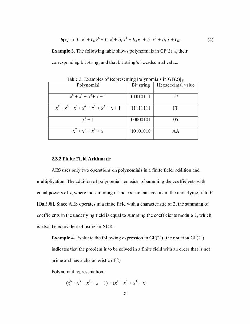
Example 3. The following table shows polynomials in GF(2)| 8, their corresponding bit string, and that bit string’s hexadecimal value.
Table 3. Examples of Representing Polynomials in GF(2)| 8Polynomial Bit string Hexadecimal value
x6 + x4 + x2+ x + 1 01010111 57
x7 + x6 + x5+ x4 + x3 + x2 + x + 1 11111111 FF
x2 + 1 00000101 05
x7 + x5 + x3 + x 10101010 AA
2.3.2 Finite Field Arithmetic
AES uses only two operations on polynomials in a finite field: addition and
multiplication. The addition of polynomials consists of summing the coefficients with
equal powers of x, where the summing of the coefficients occurs in the underlying field F
[DaR98]. Since AES operates in a finite field with a characteristic of 2, the summing of
coefficients in the underlying field is equal to summing the coefficients modulo 2, which
is also the equivalent of using an XOR.
Example 4. Evaluate the following expression in GF(2n) (the notation GF(2n)
indicates that the problem is to be solved in a finite field with an order that is not
prime and has a characteristic of 2)
Polynomial representation:
(x6 + x5 + x2 + x + 1) + (x7 + x5 + x3 + x)
8
Binary representation:
{01100111} + {10101010}
Hexadecimal representation:
{67} + {AA}
Solution
According to the definition of the addition of polynomials in a finite field above,
the solution can be found by simply applying an XOR (denoted as ) to the
coefficients with equal powers of x:
⊕
Polynomial:
x7 + x6 + (1 ⊕ 1) x5 + x3 + x2 + (1 ⊕ 1) x + 1
= x7 + x6 + x3 + x2 + 1
Binary:
01100111
⊕10101010
11001101
Hexadecimal:
{67} + {AA} = {CD}
The operation of addition in a finite field with a characteristic of 2 can be
implemented using an XOR operator; multiplication in a finite field will prove much
more complex. Multiplication of polynomials in a finite field has much of the same
properties of ordinary polynomial multiplication. These properties are the associative,
9

commutative, and distributive property with respect to addition of polynomials [DaR98].
Since the underlying property of a finite field is that it is a closed set (finite number of
elements), the multiplication of two elements in a finite field must yield another element
of that field. This property is not intuitive because usually the magnitude of the product
of two numbers is not less than the magnitude of the two numbers originally multiplied
(i.e., 6 x 7 = 1 ?!). To make the multiplication closed over F[x]| l a polynomial of degree l
called the reduction polynomial [DaR98]. The reduction polynomial for all byte
multiplications will be designated throughout this document as m(x). The designers of
AES selected the following polynomial as the reduction polynomial for all 8-bit
multiplications throughout AES [DaR98].
m(x) = x8+ x4 + x3+ x + 1 (5)
This polynomial’s corresponding bit string is 100011011. Therefore all multiplications in
the Rijndael field are defined as
c(x) = a(x) · b(x) ↔ c(x) ≡ (a(x) x b(x) ) mod m(x) [DaR98]. (6)
This reducing polynomial is not an arbitrary choice for it displays a characteristic known
as irreducibility. According the Daemen and Rijmen, a polynomial d(x) is considered
irreducible over the field GF(p) iff there are no two polynomials a(x) and b(x) with
coefficients in GF(p) such that d(x) = a(x) · b(x). Since the reduction polynomial is itself
irreducible, it effectively constructs a representation for the field GF(28), which is known
as the Rijndael field. In AES, all bytes are considered elements of GF(28). All subsequent
operations on bytes are defined as operations in GF(28) [DaR98]. The following example
10

illustrates how the reduction polynomial is used during polynomial multiplication in a
finite field.
Example 5. Evaluate the following expression for byte multiplication in the Rijndael finite field:
{11110011} · {00110100}
or in hexadecimal, {F9} · {34}
Solution
The bytes above correspond to the following polynomials in Rijndael’s finite field {x7 + x6 + x5+ x4+ x + 1} · {x5+ x4+ x2}.
Ordinary polynomial multiplication (FOIL method) yields the following product:
x12 +x11+x11+ x10+x10+ x9+x9+x9+ x8+ x8+x7+x6+ x6+ x5+ x5+x4+ x3+ x2
The addition of polynomials utilizes the XOR operation resulting in the removal of all pairs of x with equal degree (shown in bold). This yields x12 + x9+ x7+ x4+ x3+ x2.
The final procedure takes the modulus of the above result with the reducing polynomial m(x): x12 + x9+ x7+ x4+ x3+ x2 modulo x8+ x4 + x3+ x + 1
or in binary {1001010011100} modulo {100011011}
This operation can be performed using the “long division” method below (note XOR is used in lieu of subtraction in ordinary long division). The result of the modulo operation is highlighted.
11
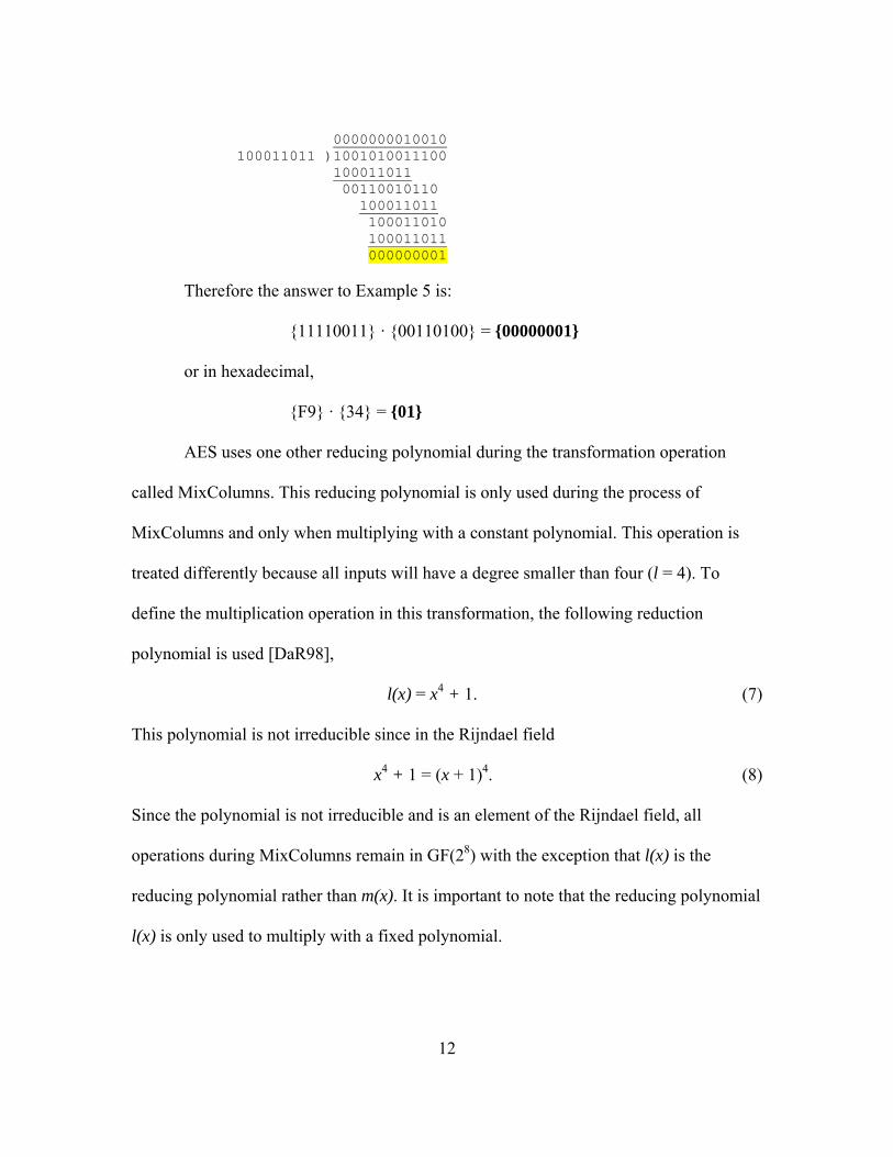
0000000010010 100011011 )1001010011100 100011011 00110010110 100011011 100011010 100011011 000000001
Therefore the answer to Example 5 is:
{11110011} · {00110100} = {00000001}
or in hexadecimal,
{F9} · {34} = {01}
AES uses one other reducing polynomial during the transformation operation
called MixColumns. This reducing polynomial is only used during the process of
MixColumns and only when multiplying with a constant polynomial. This operation is
treated differently because all inputs will have a degree smaller than four (l = 4). To
define the multiplication operation in this transformation, the following reduction
polynomial is used [DaR98],
l(x) = x4 + 1. (7)
This polynomial is not irreducible since in the Rijndael field
x4 + 1 = (x + 1)4. (8)
Since the polynomial is not irreducible and is an element of the Rijndael field, all
operations during MixColumns remain in GF(28) with the exception that l(x) is the
reducing polynomial rather than m(x). It is important to note that the reducing polynomial
l(x) is only used to multiply with a fixed polynomial.
12

Daemen and Rijmen outline a matrix method for multiplying with a fixed
polynomial using l(x) as the reduction polynomial [DaR98]. A summary of this method is
outlined below.
Let c(x) be the fixed polynomial with degree three or
c(x) = c3 x3 + c2 x2 + c1 x + c0. (9)
Further, let a(x) and b(x) be two variable polynomials with coefficients ai and bi
respectively with i being less than 4 such that b(x) = c(x) · a(x). The matrix representation
of the transformation takes the coefficients of polynomial a as input and produces as
output the coefficients of the polynomial b or
b(x) = c(x) · a(x)
≡ (c3 x3 + c2 x2 + c1 x + c0 ) · (a3 x3 + a2 x2 + a1 x + a0) (11)
≡ (b3 x3 + b2 x2 + b1 x + b0 ) mod (x4 + 1) (12)
After working out the product through ordinary polynomial multiplication, separating the
conditions for different powers of x, and accounting for the modulus operation, Daemen
and Rijmen give the following matrix representation of (12) [DaR98]
0 0 3 2 1
1 1 0 3 2 1
2 2 1 0 3
3 3 2 1 0
b c c c c ab c c c c ab c c c c ab c c c c a
0
2
3
⎡ ⎤ ⎡ ⎤ ⎡ ⎤⎢ ⎥ ⎢ ⎥ ⎢ ⎥⎢ ⎥ ⎢ ⎥ ⎢ ⎥= ×⎢ ⎥ ⎢ ⎥ ⎢ ⎥⎢ ⎥ ⎢ ⎥ ⎢ ⎥⎣ ⎦ ⎣ ⎦ ⎣ ⎦
. (13)
This representation is only used for multiplication with a fixed polynomial during the
MixColumns transformation.
One significant property of a finite field is that each element of a finite field F has
an inverse under multiplication. This property is used throughout the algorithm because it
13
allows a number to refer back to itself through a complex operation (i.e., multiplication).
This characteristic is what allows ciphertext to be decrypted back into the original
message. The method for determining the inverse element for a multiplication operation
in a finite field is via the extended Euclidean Algorithm. The Euclidean Algorithm takes
an element of the finite field, a(x), and finds the inverse element, b(x), while satisfying
the following identity,
a(x) x b(x) = 1 mod m(x) (14)
where m(x) is the reducing polynomial. If the above equation holds, then b(x) is the
inverse element of a(x) in a finite field F under multiplication ‘·’ [DaR98]. Recall the
solution to Example 5 was {F9} · {34} = {01} in the Rijndael finite field. According to
the above property then F9 is the multiplicative inverse of 34 and vice versa. The
extended Euclidean algorithm is applied to each element of the Rijndael finite field and
the multiplicative inverses of all elements are recorded in Table 20 in Appendix A.
A key element of the algorithm is the Rijndael finite field. From F in the field
GF(2), a suitable reduction polynomial m(x) is found. This defines multiplication and
addition over a set of polynomials less than degree = 8, or F[x]| 8 as a field with 28
elements denoted GF(28), and otherwise known as the Rijndael finite field.
2.4 Description of the AES Algorithm
The Data Encryption Standard expired in 1998 and the US National Institute of
Standards and Technology (NIST) announced an open international competition for
cipher designs to replace DES as the federal information processing standard [ZCN04].
Rijndael won the competition based on security, simplicity, and suitability for both
14
hardware and software implementations, and was designated the Advanced Encryption
Standard. AES, like DES, is a symmetric key block cipher encryption algorithm. The
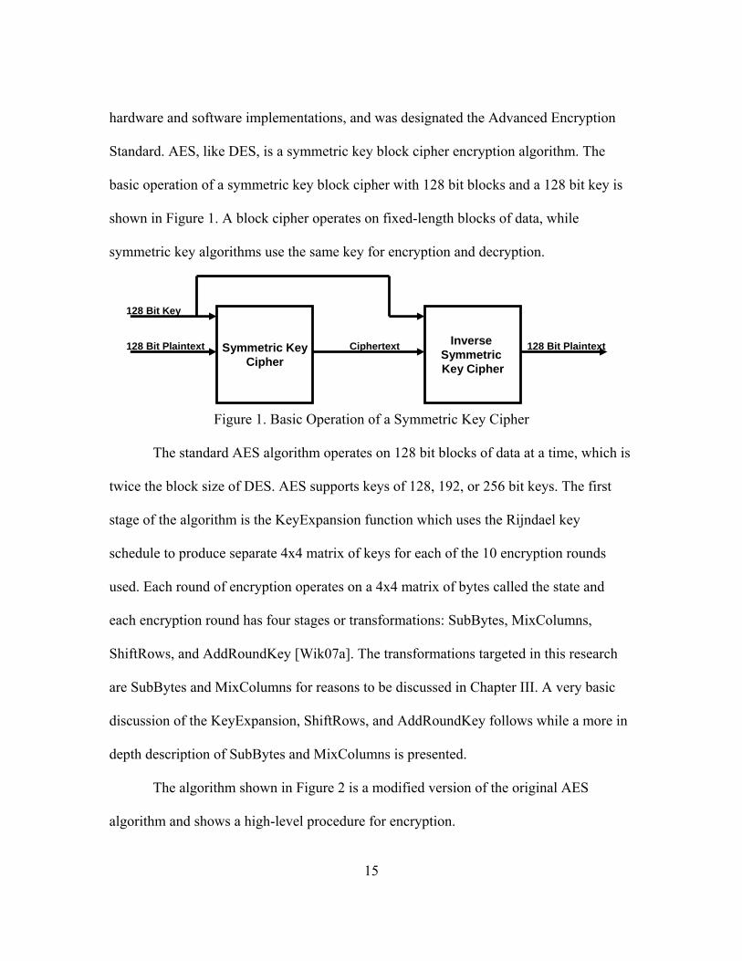
basic operation of a symmetric key block cipher with 128 bit blocks and a 128 bit key is
shown in Figure 1. A block cipher operates on fixed-length blocks of data, while
symmetric key algorithms use the same key for encryption and decryption.
Symmetric KeyCipher
128 Bit Plaintext Inverse Symmetric Key Cipher
128 Bit Key
Ciphertext 128 Bit Plaintext
Figure 1. Basic Operation of a Symmetric Key Cipher
The standard AES algorithm operates on 128 bit blocks of data at a time, which is
twice the block size of DES. AES supports keys of 128, 192, or 256 bit keys. The first
stage of the algorithm is the KeyExpansion function which uses the Rijndael key
schedule to produce separate 4x4 matrix of keys for each of the 10 encryption rounds
used. Each round of encryption operates on a 4x4 matrix of bytes called the state and
each encryption round has four stages or transformations: SubBytes, MixColumns,
ShiftRows, and AddRoundKey [Wik07a]. The transformations targeted in this research
are SubBytes and MixColumns for reasons to be discussed in Chapter III. A very basic
discussion of the KeyExpansion, ShiftRows, and AddRoundKey follows while a more in
depth description of SubBytes and MixColumns is presented.
The algorithm shown in Figure 2 is a modified version of the original AES
algorithm and shows a high-level procedure for encryption.
15
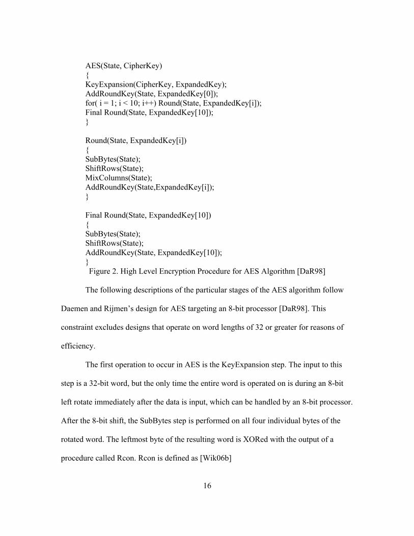
AES(State, CipherKey) { KeyExpansion(CipherKey, ExpandedKey); AddRoundKey(State, ExpandedKey[0]); for( i = 1; i < 10; i++) Round(State, ExpandedKey[i]); Final Round(State, ExpandedKey[10]); } Round(State, ExpandedKey[i]) { SubBytes(State); ShiftRows(State); MixColumns(State); AddRoundKey(State,ExpandedKey[i]); } Final Round(State, ExpandedKey[10]) { SubBytes(State); ShiftRows(State); AddRoundKey(State, ExpandedKey[10]); } Figure 2. High Level Encryption Procedure for AES Algorithm [DaR98]
The following descriptions of the particular stages of the AES algorithm follow
Daemen and Rijmen’s design for AES targeting an 8-bit processor [DaR98]. This
constraint excludes designs that operate on word lengths of 32 or greater for reasons of
efficiency.
The first operation to occur in AES is the KeyExpansion step. The input to this
step is a 32-bit word, but the only time the entire word is operated on is during an 8-bit
left rotate immediately after the data is input, which can be handled by an 8-bit processor.
After the 8-bit shift, the SubBytes step is performed on all four individual bytes of the
rotated word. The leftmost byte of the resulting word is XORed with the output of a
procedure called Rcon. Rcon is defined as [Wik06b]
16
Rcon(i) = x(254+i) mod m(x) (15)
where, i is the iteration number. The most important aspect of the KeyExpansion step, as
far as this research is concerned, is that KeyExpansion uses the SubBytes operation; thus
the performance of KeyExpansion is directly related to that of SubBytes.
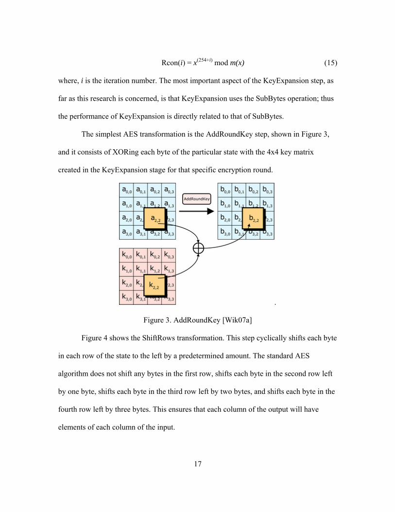
The simplest AES transformation is the AddRoundKey step, shown in Figure 3,
and it consists of XORing each byte of the particular state with the 4x4 key matrix
created in the KeyExpansion stage for that specific encryption round.
.
Figure 3. AddRoundKey [Wik07a]
Figure 4 shows the ShiftRows transformation. This step cyclically shifts each byte
in each row of the state to the left by a predetermined amount. The standard AES
algorithm does not shift any bytes in the first row, shifts each byte in the second row left
by one byte, shifts each byte in the third row left by two bytes, and shifts each byte in the
fourth row left by three bytes. This ensures that each column of the output will have
elements of each column of the input.
17

Figure 4. ShiftRows [Wik07a]
Outside of the Rcon operation during KeyExpansion, the transformations
presented thus far have not reached beyond the computational complexity of bitwise
XORing two bytes of data or shifting bytes left by a predetermined amount. The
computational complexity of the KeyExpansion step directly relates to the computation
complexity of SubBytes. The SubBytes and MixColumns transformations are the most
complicated and hardware intensive steps in the AES process, therefore they are the
transformations most attractive for optimization. What follows is a description of the
specific designs for the AES transformations MixColumns and SubBytes for an 8-bit
processor from The Design of Rijndael [DaR98].
In SubBytes, each byte in the state is replaced with its specific entry, S, in a fixed
256 byte look-up table (LUT), which can be found in Table 21 in Appendix A. This look-
up table, known as an S-box, is generated using inverse functions of a finite field and
provides an element of non-linearity to the system. During decryption, a separate 256
byte look-up table containing the values of the inverse SubBytes transformation is used.
This look-up table can be found in Table 22 in Appendix A. More detail in the generation
of these tables is provided in the SubBytes designs outlined in Chapter III. This SubBytes
implementation is the standard design for the SubBytes transformation for use on an 8-
Bit processor [DaR98]. This design is called a LUT design for obvious reasons.
18

The MixColumns step combines all four bytes of each of the four columns of the
state using an invertible linear transformation polynomial. The four bytes of each column
are inputs and each input affects all four bytes of the output. Since the dimensions of the
columns consist of 4 bytes, this is optimal for 32-bit architectures using look-up table
implementations [DaR98]. This fact makes the implementation of MixColumns in an 8-
bit architecture without using LUTs an extremely difficult and hardware intensive
process. Daemen and Rijmen point out that good MixColumn performance on 8-bit
processors is not trivial to obtain because its design is best suited for a 32-bit processor.
The MixColumns transformation takes the columns of the state in polynomial form over
the Rijndael finite field and multiplies them modulo l(x) (cf. (7) ) with a fixed polynomial
c(x). Figure 5 shows how each column is multiplied by a fixed polynomial c(x).
Figure 5. MixColumns [Wik07a]
The polynomial c(x) is
c(x) = 03 · x3 + 01 · x2 + 01 · x + 02. (16)
This polynomial is coprime to l(x) and is therefore invertible [DaR98]. The inverse of
c(x) is d(x) and is used for the inverse MixColumns routine during the process of
decryption. The polynomial d(x) is
19

d(x) = 0B · x3 + 0D · x2 + 09 · x + 0E. (17)
By substituting c(x) into (13), the matrix representation for multiplication in the Rijndael
specified MixColumns stage of AES is obtained below (i.e., b(x) = c(x) · a(x) mod l(x)) or
0 0
1
2 2
3 3
02 03 01 0101 02 03 0101 01 02 0303 01 01 02
b ab ab ab a
⎡ ⎤ ⎡ ⎤⎡ ⎤⎢ ⎥ ⎢ ⎥⎢ ⎥⎢ ⎥ ⎢ ⎥⎢=⎢ ⎥ ⎢ ⎥⎢⎢ ⎥ ⎢ ⎥⎢ ⎥
⎣ ⎦⎣ ⎦ ⎣ ⎦
1⎥×⎥
. (18)
Recall that the input to MixColumns is a 32 bit string representing the four
columns in the state. Thus, each coefficient of a is comprised of four bits in F[x]| 4. To
implement this on an 8-bit processor, (18) must be executed in hardware. Multiplication
with the coefficient 01 requires no processing power because the input equals the output.
Daemen and Rijmen outline a process for multiplication with 02 and 03 on an 8-bit
platform. This process takes advantage of the fact that all elements of the Rijndael finite
field can be written as a sum of powers of 02 since the characteristic of the Rijndael finite
field is 2. This fact coupled with the idea that the value 02 is associated with the
polynomial x makes it possible to construct a 256 byte table of all possible 8-bit input
values and their subsequent values after being multiplied by 02 in the Rijndael field. The
multiplication by 02 is denoted xtime(y) where y is the value to be multiplied. Example 6
illustrates how xtime is used to multiply an input b by the constant value 05.
Example 6. Use xtime to multiply the input value b by the constant value 05.
Solution
b · 05 = b · (01 04) = b · (01 ⊕ ⊕022) Now, xtime is used to multiply a value by 02. To multiply a value by 022, xtime is
20

used twice or = b ⊕xtime(xtime(b)).
The look-up table for the xtime process can be found in Table 24 in Appendix A.
This table is used to determine the product of any two 8-bit input values. The most
complex multiplication during MixColumns is a multiplication by 03, as shown in (13).
Since the coefficients of d(x) (c.f., (17) ) are much higher than c(x) (c.f., (16) ), the
Rijndael design for an 8-bit platform uses a simple property of matrix multiplication to
develop a preprocessing step used during the inverse MixColumns routine. The following
relationship holds between the MixColumns polynomial c(x) and the inverse
MixColumns polynomial d(x) [DaR98]
d(x) = (04 x2 + 05) c(x) mod l(x). (19)
This follows from the matrix notation
0 0 0 09 02 03 01 01 05 00 04 0009 0 0 0 01 02 03 01 00 05 00 040 09 0 0 01 01 02 03 04 00 05 000 0 09 0 03 01 01 02 00 04 00 05
E B DE B D
D E BB D E
⎡ ⎤ ⎡ ⎤ ⎡⎢ ⎥ ⎢ ⎥ ⎢⎢ ⎥ ⎢ ⎥ ⎢= ×⎢ ⎥ ⎢ ⎥ ⎢⎢ ⎥ ⎢ ⎥ ⎢⎣ ⎦ ⎣ ⎦ ⎣
⎤⎥⎥⎥⎥⎦
(20)
which is the inverse MixColumns matrix as defined in (17) and (13) obtained by
multiplying the original MixColumns matrix in (18) by a preprocessing matrix [DaR98].
This preprocessing step reduces the number of 256 byte look-up tables needed to one and
can be used for both MixColumns and inverse Mixcolumns as opposed to SubBytes,
which requires two tables (one for SubBytes and one for inverse SubBytes). This design
for MixColumns is designated the Full LUT design.
21
The specification of the above designs for MixColumns and SubBytes effectively
outlines the baseline AES design used during the experiment outlined in Chapter III.
2.5 Current Research into AES Implementations on FPGAs
2.5.1 Optimization Techniques
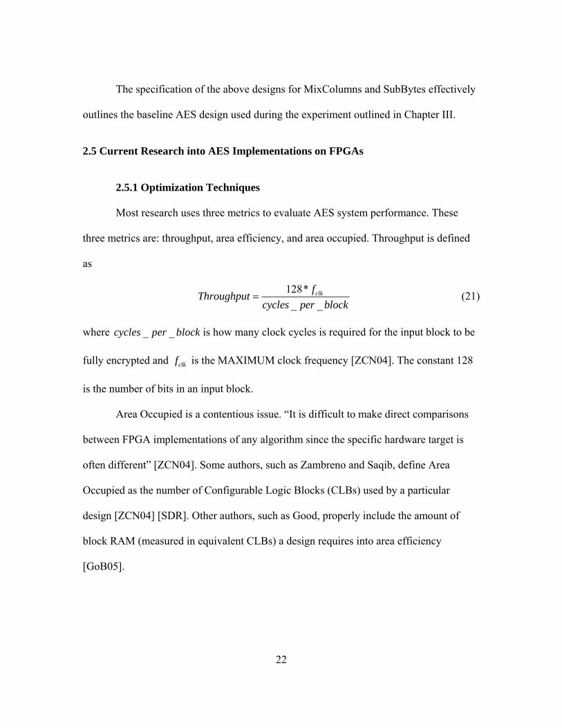
Most research uses three metrics to evaluate AES system performance. These
three metrics are: throughput, area efficiency, and area occupied. Throughput is defined
as
128*_ _
clkfThroughputcycles per block
= (21)
where is how many clock cycles is required for the input block to be
fully encrypted and
_ _cycles per block
clkf is the MAXIMUM clock frequency [ZCN04]. The constant 128
is the number of bits in an input block.
Area Occupied is a contentious issue. “It is difficult to make direct comparisons
between FPGA implementations of any algorithm since the specific hardware target is
often different” [ZCN04]. Some authors, such as Zambreno and Saqib, define Area
Occupied as the number of Configurable Logic Blocks (CLBs) used by a particular
design [ZCN04] [SDR]. Other authors, such as Good, properly include the amount of
block RAM (measured in equivalent CLBs) a design requires into area efficiency
[GoB05].
22
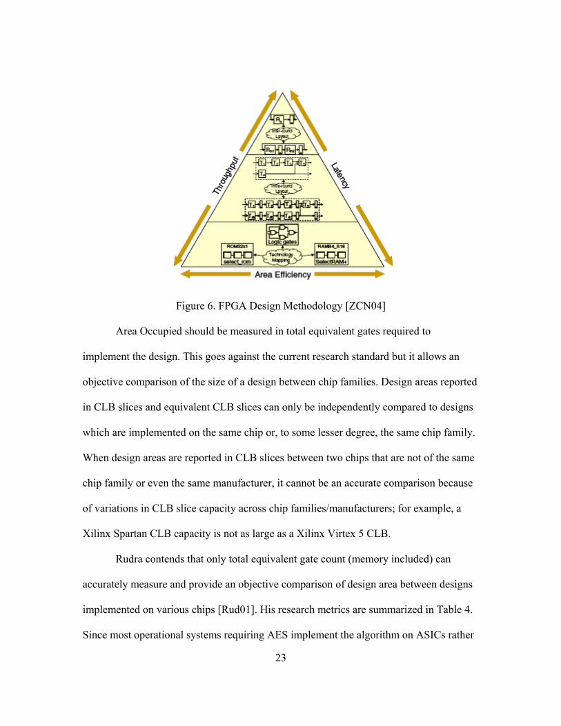
Figure 6. FPGA Design Methodology [ZCN04]
Area Occupied should be measured in total equivalent gates required to
implement the design. This goes against the current research standard but it allows an
objective comparison of the size of a design between chip families. Design areas reported
in CLB slices and equivalent CLB slices can only be independently compared to designs
which are implemented on the same chip or, to some lesser degree, the same chip family.
When design areas are reported in CLB slices between two chips that are not of the same
chip family or even the same manufacturer, it cannot be an accurate comparison because
of variations in CLB slice capacity across chip families/manufacturers; for example, a
Xilinx Spartan CLB capacity is not as large as a Xilinx Virtex 5 CLB.
Rudra contends that only total equivalent gate count (memory included) can
accurately measure and provide an objective comparison of design area between designs
implemented on various chips [Rud01]. His research metrics are summarized in Table 4.
Since most operational systems requiring AES implement the algorithm on ASICs rather
23

than FPGAs, it makes sense to report area occupied as a measure of gates, which can be
compared to both ASIC and FPGA designs, rather than CLBs, which can only be
accurately compared to designs implemented on the same FPGA chip. Research that
presents designs measured in some estimate of theoretical gate counts are considered
unreliable. Therefore gate counts only obtained by HDL synthesizers or by ASIC design
fabrication methods are used herein. Theoretical gate counts are unreliable since they
cannot be directly implemented in hardware nor do they account for buffers required to
achieve correct timing as well as other factors which may increase the gate count at the
place and route stage of synthesis.
Since most of the current literature reviewed reports area occupied in CLBs or
slices, a method for estimating gate counts must be devised. For each FPGA chip it
manufactures, Xilinx provides a maximum gate capability (logic and RAM) as well as a
total number of CLBs. From these two measures it is possible to devise a conversion
factor which translates an area in CLBs to an estimate of area given in total equivalent
gate count as shown below. This conversion factor is unique for each Xilinx chip model
used and is
_ __
gates maximum gate capabilityCLB total CLBs
= (22)
where the conversion factor is gatesCLB
. maximum_gate_capability is the maximum
number of gates an FPGA has the potential of implementing and total_CLBs is the total
number of CLBs the FPGA contains. Both maximum_gate_capability and total_CLBs are
reported by the chip manufacturer.
24

Much research has focused on increasing the performance of the various stages of
AES (MixColumns, SubBytes, KeyExpansion, AddRoundKey, and ShiftRows) but this
same research does not account for how the different transformations interact with each
other to affect the design of AES as a whole. The only recent research on AES designs
targeting an 8-bit processor found that “a good FPGA based 8-bit datapath for
comparison could not be found”[GoB05].
Zambreno attempts to balance throughput, latency, and area efficiency by
searching for an optimal point in the pyramid in Figure 6. As the figure illustrates, simple
methods of increasing throughput have a negative effect on area efficiency. One such
method is loop unrolling. A loop will normally execute an operation in the same area of
hardware numerous times. When loop unrolling is used, that area of hardware is
replicated as many times as the loop needs to execute so the loop can execute in parallel.
It is easy to see how this method has a dramatically negative effect on area efficiency.
Loop unrolling is a common method of optimizing encryption algorithms since
encryption performs multiple operations on blocks of input data numerous times.
Figure 7a shows the Rijndael algorithm without modification. The algorithm runs
a loop using rotating inputs from the key expansion block and the 128-bit state register to
hold all plaintext input states. As shown in Figure 7b, This function can be optimized by
unrolling this loop and executing each encryption round using its own dedicated
hardware circuit for each of 10 rounds and storing the results of each round in 10
different 128 bit registers [QIS05]. The pyramid in Figure 6 would show a significant
25

increase in throughput, although since the hardware already used large area, increasing
throughput in this fashion will result in a dramatic decrease in area efficiency.
Figure 7. Loop Unrolling an AES Architecture [QIS05]
Another method of increasing throughput is pipelining. Pipelining maximizes
hardware utilization by executing multiple instructions simultaneously with each
instruction being in a different stage of execution at any one moment. Pipelining does not
require the addition of any new functional hardware, in fact pipelining is a simple method
of making the most of the hardware already available. For this reason, except for the
overhead associated with starting a pipeline, it is possible to increase throughput and
decrease latency with a small effect on area efficiency.
26

Another technique increases the throughput of AES by parallelizing stages of
Rijndael’s algorithm [CaA03]. Figure 8 reduces the entire MixColumns stage of AES
into simple combinational logic.
Figure 8. Parallelization of MixColumns [CaA03]
Although it may be the dominant catalyst for optimization, throughput is not the
only important measure of an implementation. Area efficiency is a design consideration
when implementing AES since an increase in area efficiency means an AES chip can
operate using less hardware as well as requiring less power. Many portable electronic
devices such as cell phones or mobile WLAN terminals could benefit from AES, but
since they require batteries, power consumption is an issue. For these hardware
platforms, an efficient design should deliver an acceptable throughput while maintaining
high area efficiency to reduce power consumption. A quick analysis of Figure 6 shows
how difficult this is to reach. In fact, most methods designed to increase area efficiency
have a detrimental impact on the system’s overall throughput.
27

There are minor variations in the definition of area efficiency; for example,
Zambreno and Saqib define area efficiency as
Area Efficiency = ( )_ (
Throughput kbpsArea Occupied CLBs)
(23)
which measures the throughput per CLB or slice [ZCN04][SDR]. Therefore, a high Area
Efficiency implies a more efficient design. In contrast Pionteck defines area efficiency as
the inverse of (23) or
Area Efficiency = _ (( )
Area Occupied CLBsThroughput kbps
) (24)
which measures the area in CLBs needed per one kbps [Pio04]. Therefore, a low number
signifies a more efficient design. This research reports area in terms of total equivalent
gates rather than CLBs or slices,
Area Efficiency = ( )_ (
Throughput kbpsArea Occupied gates)
. (25)
Recently the AES algorithm was selected for the upcoming WLAN standard
IEEE 802.11i [Pio04]. This means portable electronic devices using this new WLAN
standard such as network cards for laptops and mobile WLAN terminals will benefit from
a design with optimized power consumption through a highly efficient area design.
Area efficiency is a significant design goal when dealing with devices that require
a small amount of hardware as well as relatively high throughput. Some designs have
modest throughput requirements but require the hardware to be as small as possible. For
these systems, reducing hardware area will come at a dramatic cost in throughput.
28

2.6 Typical Design Parameter Values
2.6.1 AES Throughput
The fastest FPGA implementation of the AES algorithm transmits at 23.65 Gbps
[GoB05]. Since this implementation had maximizing throughput as the primary objective,
area occupied and area efficiency suffer. It is because of this trade-off that this design is
the largest of those reported in Table 4. The data for gates per slice is from the
documentation for the Xilinx Virtex-II family of FPGAs [Xil07]. Similar results were
produced by Zambreno although the maximum optimized throughput was only 23.57
Gbps [ZCN04]. Another high-speed implementation of the AES algorithm achieved a
throughput of 16.5 Gbps [JST03].
Table 4. Throughput Comparison of Previous AES Designs Design FPGA Area
(Slices) Gates Slice
Area (Gates)
Freq. MHz
Throughput (Gbps)
Zambreno [ZCN04]
Virtex-II XC2V4000
16938 173 2,930,274 184.1 23.57
Järvinen [JST03]
Virtex- E XCV1000c-8
11719 195 2,285,205 129.2 16.50
Good [GoB05]
Virtex-E XCV2000E-8
16693 186 3,104,898 184.8 23.65
Rudra [Rud01]
ASIC - - 256,000 32.0 7.50
2.6.2 AES Area Efficiency
AES operates on 128 bit blocks of data for each encryption round. Current
literature has numerous examples of partitioning the blocks of 128 bits into smaller sub-
blocks called datapaths to maximize area efficiency [GoB05]. However, by breaking one
128 bit block of data into smaller, more manageable sub-blocks, a number of additional
cycles are required to complete each encryption round. As the 128 bit block of data is
29

divided into datapaths, the number of cycles required to complete an encryption round
increases and consequently has a detrimental effect on throughput. The most common
datapath size is 32 bits and can only be implemented on a platform with 32-bit processing
capability [GoB05]. The Good design achieves a balance between area efficiency and
throughput is achieved at this datapath size.
When calculating total area occupied by a particular design, the size of a
particular FPGA’s block memory should be included [GoB05]. Different FPGAs have
different sizes of block memories. For example, the block memory size on a Xilinx
Spartan-II is only 4 kbits whereas the block memory sizes on a Xilinx Spartan-III or
Vertex-II are 18 kbits [GoB05]. Translating this into the equivalent number of slices
those bits will occupy gives a common basis for comparison [GoB05]. Another method
of determining area is in the number of Configurable Logic Block (CLB) slices used by
the design [SDR]. Many studies do not include the block RAM used by a design, but only
report the number of CLBs or slices and thereby underestimate the actual hardware
required.
As shown in Table 5, the highest area efficiency, as calculated by (25) while
ignoring block RAM was 15.72 [Rou04]. However, when block RAM is included, this
number drops to 1.89. Chodowiec and Gaj have the most area efficient AES design
including block RAM with 2.30; when block RAM is not considered efficiency rises to
5.42 [ChG01]. Table 5 summarizes area efficiency results of other designs.
30
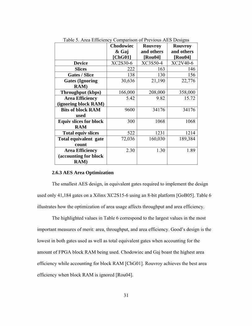
Table 5. Area Efficiency Comparison of Previous AES Designs Chodowiec
& Gaj [ChG01]
Rouvroy and others
[Rou04]
Rouvroy and others
[Rou04] Device XC2S30-6 XC3S50-4 XC2V40-6 Slices 222 163 146
Gates / Slice 138 130 156 Gates (Ignoring
RAM) 30,636 21,190 22,776
Throughput (kbps) 166,000 208,000 358,000 Area Efficiency
(ignoring block RAM)5.42 9.82 15.72
Bits of block RAM used
9600 34176 34176
Equiv slices for block RAM
300 1068 1068
Total equiv slices 522 1231 1214 Total equivalent gate
count 72,036 160,030 189,384
Area Efficiency (accounting for block
RAM)
2.30 1.30 1.89
2.6.3 AES Area Optimization
The smallest AES design, in equivalent gates required to implement the design
used only 41,184 gates on a Xilinx XC2S15-6 using an 8-bit platform [GoB05]. Table 6
illustrates how the optimization of area usage affects throughput and area efficiency.
The highlighted values in Table 6 correspond to the largest values in the most
important measures of merit: area, throughput, and area efficiency. Good’s design is the
lowest in both gates used as well as total equivalent gates when accounting for the
amount of FPGA block RAM being used. Chodowiec and Gaj boast the highest area
efficiency while accounting for block RAM [ChG01]. Rouvroy achieves the best area
efficiency when block RAM is ignored [Rou04].
31
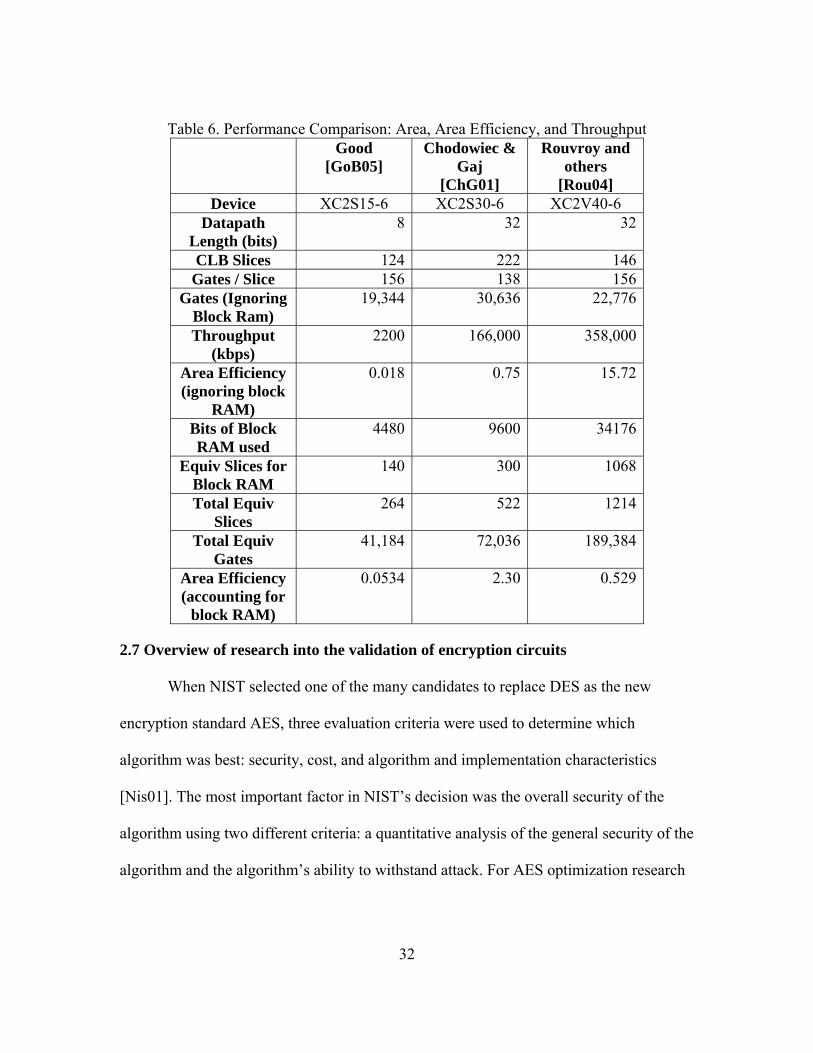
Table 6. Performance Comparison: Area, Area Efficiency, and Throughput Good
[GoB05] Chodowiec &
Gaj [ChG01]
Rouvroy and others
[Rou04] Device XC2S15-6 XC2S30-6 XC2V40-6
Datapath Length (bits)
8 32 32
CLB Slices 124 222 146 Gates / Slice 156 138 156
Gates (Ignoring Block Ram)
19,344 30,636 22,776
Throughput (kbps)
2200 166,000 358,000
Area Efficiency (ignoring block
RAM)
0.018 0.75 15.72
Bits of Block RAM used
4480 9600 34176
Equiv Slices for Block RAM
140 300 1068
Total Equiv Slices
264 522 1214
Total Equiv Gates
41,184 72,036 189,384
Area Efficiency (accounting for
block RAM)
0.0534 2.30 0.529
2.7 Overview of research into the validation of encryption circuits
When NIST selected one of the many candidates to replace DES as the new
encryption standard AES, three evaluation criteria were used to determine which
algorithm was best: security, cost, and algorithm and implementation characteristics
[Nis01]. The most important factor in NIST’s decision was the overall security of the
algorithm using two different criteria: a quantitative analysis of the general security of the
algorithm and the algorithm’s ability to withstand attack. For AES optimization research
32

however, the most important characteristic is the correctness of the implementation (i.e.,
whether or not the implemented algorithm EXACTLY matches the specification of AES).
NIST released the Advanced Encryption Standard Algorithm Validation Suite
(AESAVS) in November 2002. The suite provides three different tests which validate the
functionality of the AES algorithm: the Monte Carlo algorithm test, the Multi-Block
Message test, and the Known Answer Test. AES is a substitution cipher. That is, if the
same block of data is run through the algorithm multiple times with the same key, the
output ciphertext will be exactly the same each time. The Known Answer Tests take
advantage of this and are an easy method of determining the functionality of a particular
AES implementation through the use of look up tables containing the expected answers.
There are four different types of known answer tests: GFSbox, KeySbox, Variable Key,
and Variable Text. GFSbox and KeySbox each test the functionality of the Substitution
Box (S-Box) elements of the AES and DES ciphers.
Variable Key and Variable Text Known Answer Tests are the most easily
realizable methods of testing the functionality of an AES implementation. The Variable
Key test simply keeps the plain text input block constant at all zeros and varies the value
of the key. The AES validation suite provides look up tables containing the known
ciphertext output for zeroed out plain text and different key values. Table 7 is an example
of a Variable Key Known Answer Test value look up table. The Variable Text works the
same way as the Variable Key test but Variable Text operates on a zeroed out key and
varies the value of the plaintext.
33

Table 7. Variable Key Known Answer Test Values for Keysize = 128
2.8 Summary
This chapter describes the baseline AES design. The design is specified by the
creators of AES and is composed of a full LUT design for both the SubBytes and
MixColumns transformations. This chapter also presents current research topics on the
implementation of AES on FPGAs and provides tables of common values associated with
each performance metric to be tested. The designs that perform best for each metric are
highlighted. These designs allow a comparison to be made between the performance of
AES designs in current literature and the new AES designs specified in Chapter III.
34

III. Methodology
3.1 Chapter Overview
The purpose of this chapter is to define the experiment conducted in this research.
3.2 Problem Definition
3.2.1 Goals and Hypothesis
This research has two primary goals. The first is to improve the performance of
the baseline design of AES targeting an 8-bit platform based on throughput, area
occupied, and area efficiency. This goal is met when a design is produced has a better
performance than the baseline design. Designs developed herein are compared to designs
from literature that specifically target each metric. Table 8 lists the best values for each
AES metric as reported in current literature. These designs target each specific metric
individually (i.e., throughput, area efficiency, and area occupied) and use hardware
optimization techniques not considered in this effort for reasons of area efficiency.
Table 8. AES FPGA Performance in Current Literature Metric Design FPGA Value Throughput Good
[GoB05] Virtex-II XC2V2000E-8
23.65 Gbps
Area Efficiency (ignoring block RAM)
Rouvroy [Rou04]
XC2V40-6 15.72
Area Efficiency (accounting for block RAM)
Chodowiec & Gaj [ChG01]
XC2S30-6 2.30
Area Occupied Good [GoB05]
XC2S15-6 41,184 Total Equivalent Gates
35

The second goal of this research is to answer the following question: how does
each factor interact and affect each metric and do the changes to the baseline design
increase performance? This goal directly supports the hypothesis to be tested. By using
modular inversion in an extended field and composite modular inversion in a subfield
during the transformation of SubBytes in lieu of a full look up table as defined in the
baseline design; and by utilizing a bitwise shift and combinational logic in the
transformation of MixColumns, it is expected that the performance of AES can be
improved to a level that surpasses the baseline AES performance.
3.2.2 Approach
The approach to achieving the first goal uses four techniques to reduce hardware
requirements in the transformations for MixColumns and SubBytes. The amount of
hardware needed can be reduced by computing values rather than using LUTs. SubBytes
requires a table of 256 bytes to store the SubBytes step and another table of 256 bytes to
perform the inverse of SubBytes. MixColumns uses one 256 byte table and together with
SubBytes these two transformations use a total of 768 bytes of memory (these values are
the uncompressed storage requirement). Table 8 illustrates the significant impact memory
usage has on area efficiency. When total memory usage is not accounted for, the best area
efficiency attained by current research is 15.72, but when memory is taken into account
the area efficiency drops to 2.30. MixColumns and SubBytes are targeted because they
are the only transformations to use any operations outside of combinational logic and use
LUTs as their primary means of execution. The second goal is realized by evaluating
each technique’s impact on performance separately. The experiment compares these
36

results with the results obtained from each possible combination of optimization
techniques.
3.3 System Boundaries
The system under test is called the Data Encryption System. The Data Encryption
System consists of four components illustrated in Figure 9. The first component of the
Data Encryption System is the hardware description language used to create the
component under test, the AES algorithm.
SUT
(Data Encryption System)
Hardware Description Language
AES Algorithm Hardware
NIST Algorithm Validation Suite
System Parameters
Area Efficiency
Area Occupied
Throughput
Optimization Techniques
Clock S
peed
FPG
A Typ
e
HD
L Synth
esis Tool
Full Factorial
Design
Syn
thesis D
irection
Su
bB
ytesD
esign
MixC
olumns
Design
Speed of Inpu
t D
ata Stream
Key Len
gth
Figure 9. System Under Test
The AES algorithm component always contains the verified inverse cipher
(decryption). It is assumed that the design used for encrypting data will also be used for
decrypting data (i.e., a MixColumns Full LUT design for encryption will not be
37

combined with a MixColumns combinational logic design for decryption). While
combining different designs for encryption and decryption will still properly encrypt and
decrypt data, this method is avoided in order to maintain symmetry in the experiment.
The third component is the FPGA being used as well as the development board. This
device is the Xilinx Virtex-II PRO XC2VP30. The final component is the various design
techniques used to improve the algorithm’s performance. The scope of this study is
limited to controlling the three factors and observing the three metrics. The input
(workload) to the system under test is the NIST Algorithm Validation Suite.
3.4 System Services
The Data Encryption System encrypts the input data stream using the AES
algorithm. The first, and most desirable, outcome is for the Data Encryption System to
correctly encrypt the input data stream. The verification of proper encryption is done
using the NIST Algorithm Validation Suite. The second possible outcome of the system
is for the Data Encryption System to improperly encrypt the input data stream. The result
of this outcome is that the system will be unable to recover the entire, correct input data
stream. The third possible outcome of the data encryption system is that no encryption
occurs. The result of this outcome is that the input data stream is exactly the same as the
output of the system. The final possibility is that nothing occurs. The result of this
outcome is that no signal is observed at the output. This indicates a complete malfunction
of the system.
38
3.5 Workload
The workload for the Data Encryption System is the NIST Algorithm Validation
Suite. When applied to an implementation, the suite verifies the correctness of the
implementation. This is a suitable workload for the Data Encryption System because it is
provided by the institute responsible for the creation of the Advanced Encryption
Standard. Another added benefit of using the NIST Algorithm Validation Suite is that it
not only provides a suitable input data stream for the system, but also verifies that the
system is providing the correct service (i.e., properly encrypting the input data stream).
3.6 Performance Metrics
Three performance metrics are used to evaluate system performance: throughput,
area efficiency, and area occupied. Throughput is defined as
128*( )_ _
clkfThroughput kbpscycles per block
= (25)
where is the number of clock cycles required for the input block to
be fully encrypted and
_ _cycles per block
clkf is the MAXIMUM clock frequency as identified by the
hardware description language (HDL) synthesizer. The HDL synthesizer is the Xilinx
XST synthesizer, which identifies a design’s critical path and subsequently determines
the theoretical maximum combinational delay measured in seconds. This measurement is
the minimum clock period and since frequency is the inverse of period, the maximum
clock frequency can easily be determined. The constant 128 is the number of bits in an
input block. Maximum clock frequency does not solely determine throughput as
39
throughput is also inversely related to the number of clock cycles required to operate on a
block of data.
Area efficiency is defined as
Area Efficiency = (( )
Throughput kbpsArea gates
) (26)
where throughput is from (25) and Area is measured in gates. The total equivalent gate
count is measured by the HDL synthesizer.
3.7 Parameters
3.7.1 System
• FPGA Type – Different FPGA’s have inherent differences in performance; for
example, a Xilinx Spartan CLB slice is different from a Xilinx Virtex CLB
slice.
• HDL Synthesis Tool – It is unlikely that two different synthesis tools will
implement the same HDL code the same way. The synthesis tool used in this
experiment is the Xilinx XST tool packaged with the full version of the Xilinx
ISE 8.2i software.
• Synthesis Goal – The Xilinx XST synthesis tool requires a user defined input
as to the desired overall goal of the design synthesis. The two options are
synthesize to reduce area or synthesize to increase speed. The option to
increase speed does so by reducing the number of logic levels required by the
design. This means that synthesizing for speed does not necessarily indicate
40

an increase in area occupied nor is it certain that synthesizing for area will
result in a decrease in speed.
• ShiftRows Design – There are many designs that properly implement the
ShiftRows transformation. The ShiftRows design used in this research is
defined by The Design of Rijndael for an 8-bit platform as described in
Chapter II [DaR98].
• AddRoundKey Design – The AddRoundKey design used in this research is
implemented as a bitwise XOR of the round key and the state as defined by
The Design of Rijndael for an 8-bit platform as described in Chapter II.
• KeyExpansion Design – The KeyExpansion step requires using the SubBytes
transformation. SubBytes is considered an experimental factor yet
KeyExpansion is not. This is possible by using a function call for SubBytes
within the KeyExpansion HDL design. This allows for hardware executing the
KeyExpansion transformation to remain the same but permits the hardware
implementing SubBytes to change. Thus the SubBytes design can be
considered an experimental factor while the KeyExpansion design remains a
constant system parameter.
• MixColumns Design – The baseline design for MixColumns is explained in
detail in Chapter II. The MixColumns transformation is the most difficult to
achieve good performance on an 8-bit processor due to 4 byte column blocks
of data [DaR98].
41

• SubBytes Design – The baseline specification for the SubBytes transformation
on an 8-bit platform consumes the most memory in AES. The baseline design
uses two independent 256 byte LUTs; one for the encryption cipher
(SubBytes) and one for the decryption cipher (inverse SubBytes).
3.7.2 Workload
• Validation Suite – The NIST Algorithm Verification Suite validates the AES
algorithm through a number of tests. One such test is the Known Answer Test.
This test takes advantage of the fact that AES is a substitution cipher and if
the same input is used with the same key, the cipher text will always be the
same. The entire battery of Known Answer Tests is run on each design of
AES to ensure correctness, but only one Known Answer Test is used as the
workload in this experiment. This test is the rotating plaintext test, which
maintains an all zero key and varies the input plaintext.
• Key Length –AES has the option of using a 128, 192, or 256 bit key.
Increasing key length increases the amount of computation required to encrypt
and therefore decreases throughput. For this experiment, the key length is set
at 128 bits.
3.8 Factors
The factors for this experiment are: MixColumns design, SubBytes design, and
Synthesis Goal. The specific levels of the transformation factors (MixColumns and
SubBytes) are determined by which design is utilized during an experiment. The levels
42

for the factor of synthesis goal are area or speed. These factors and their levels are
summarized in Table 9. SubBytes was chosen as an experimental factor because it
consumes the most memory in AES. There are a number of alternative designs for
implementing a more compact version of the AES S-box, but most of these designs use
multiplication or access memory in a way that cannot be easily supplied by an 8-bit
processor. The three designs chosen for SubBytes in this experiment can be executed on
an 8-bit platform. The first of these designs is the LUT design outlined in Chapter II (cf.
Description of the AES Algorithm) and is the Rijndael specified baseline design for AES
on an 8-bit platform. The other two designs focus on modular inversion in a finite field.
These designs are called Modular Inversion in an Extended Field and Modular Inversion
in a Composite Field.
Table 9. Factor Levels
Factor Level SubBytes Design Full LUT,
Modular Inversion in an Extended Field, Modular Inversion in a Composite Field
MixColumns Design Full LUT, Half LUT, Combinational Logic
Synthesis Direction Area, Speed
The size of the input and output blocks for the MixColumns routine makes the
transform ideal for implementation on a 32-bit platform. For this reason, the task of
implementing the MixColumns stage of AES on an 8-bit platform with good performance
(i.e., low area and high throughput) is not a trivial task [DaR98]. MixColumns is chosen
as a factor for this reason. Past research on MixColumns has introduced a number of
alternative designs. These designs encompass a range of implementation options for
43

MixColumns. The first is the Rijndael specified Full LUT design, as described in Chapter
II. The second design was developed during this research and is the baseline design
modified such that it requires half of the original LUT to operate. This design is titled the
Half LUT design. The final design was developed by Satyanarayana and follows an
algorithm created by Trenholme, which implements MixColumns using combinational
logic alone [Sat04]. These three design levels were chosen because they represent the
entire spectrum of MixColumns designs from a full look up table design to an entirely
combinational logic design. These designs are described in detail in the following section
labeled “Experimental Factor Designs”.
3.9 Experimental Factor Designs
3.9.1 SubBytes
3.9.1.1 Modular Inversion in an Extended Field
There are two fundamental steps performed in the SubBytes transformation. The
first step is the most mathematically complex and the most difficult to implement in
hardware: the modular inversion of a polynomial in the Rijndael finite field. The second
step is an invertible operation known as an affine transformation. A critical aspect of this
design is the fact that the inverse SubBytes transform is simply the two steps reversed.
Thus, during decryption the inverse SubBytes step executes the inverse affine transform
and then determines the modular inverse, as shown in Figure 13. This is important
because it allows the entire SubBytes operation (both encryption and decryption) to use
one 256 byte look-up table containing all modular inverses in a Rijndael Field. The
44
generation of this table is explained in the Chapter II and the table itself can be found in
Table 20 in Appendix A.
Both the affine transform and its inverse are specified in The Design of Rijndael.
The affine transform used during SubBytes is
7 7
6 6
5 5
4
3 3
2 2
1 1
0 0
1 1 1 1 1 0 0 0 00 1 1 1 1 1 0 0 10 0 1 1 1 1 1 0 10 0 0 1 1 1 1 1 01 0 0 0 1 1 1 1 01 1 0 0 0 1 1 1 01 1 1 0 0 0 1 1 11 1 1 1 0 0 0 1 1
b ab ab ab ab ab ab ab a
⎡ ⎤ ⎡ ⎤⎡ ⎤⎢ ⎥ ⎢ ⎥⎢ ⎥⎢ ⎥ ⎢ ⎥⎢ ⎥⎢ ⎥ ⎢ ⎥⎢ ⎥⎢ ⎥ ⎢ ⎥⎢ ⎥⎢ ⎥ ⎢ ⎥⎢ ⎥=⎢ ⎥ ⎢ ⎥⎢ ⎥⎢ ⎥ ⎢ ⎥⎢ ⎥⎢ ⎥ ⎢ ⎥⎢ ⎥⎢ ⎥ ⎢ ⎥⎢ ⎥⎢ ⎥ ⎢ ⎥⎢ ⎥
⎢ ⎥⎢ ⎥ ⎢ ⎥⎣ ⎦⎣ ⎦ ⎣ ⎦
4
⎡ ⎤⎢⎢⎢⎢⎢× ⊕ ⎢⎢⎢⎢⎢⎢⎣ ⎦
⎥⎥⎥⎥⎥⎥⎥⎥⎥⎥⎥
(27)
where b is the affine transform of a [DaR98]. The coefficients of the polynomial to be
transformed in (27), a, is multiplied with a binary matrix; the result of which is XORed
with a constant bit pattern {01100011}. Implementing (27) in VHDL using only 8-bit
operations would be a complex operation if the elements of the matrix were anything but
binary. Since, however, the matrix is binary, the product of the matrix multiplication will
only yield either the identity of coefficient ai (multiply by 1) or 0 (multiply by 0). If each
coefficient of b is treated as a separate entity rather than as elements of a column vector,
it is possible to map a unique equation for each coefficient of b. This can be achieved via
ordinary matrix multiplication on the 8x8 binary matrix and the vector of a coefficients.
This result is XORed with the corresponding bit from the constant bit pattern, which
results in the following equations for each coefficient of b
45
7 7 6 5 4 3
6 6 5 4 3 2
5 5 4 3 2 1
4 4 3 2 1 0
3 7 3 2 1 0
2 7 6 2 1 0
1 7 6 5 1 0
0 7 6 5 4 0
0,1,1,0,0,0,1,1.
b a a a a ab a a a a ab a a a a ab a a a a ab a a a a ab a a a a ab a a a a ab a a a a a
= ⊕ ⊕ ⊕ ⊕ ⊕
= ⊕ ⊕ ⊕ ⊕ ⊕
= ⊕ ⊕ ⊕ ⊕ ⊕
= ⊕ ⊕ ⊕ ⊕ ⊕
= ⊕ ⊕ ⊕ ⊕ ⊕= ⊕ ⊕ ⊕ ⊕ ⊕
= ⊕ ⊕ ⊕ ⊕ ⊕
= ⊕ ⊕ ⊕ ⊕ ⊕
(28)
The equations in (28) are equivalent to (27) except that (28) replaces matrix arithmetic,
which is difficult to implement in hardware, with simple combinational logic using only
XOR gates. (28) can be implemented on an 8-bit platform using the VHDL code in
Figure 10. Notice that as the number of ‘1’s in the binary matrix increases, so too does
the number of XOR gates required to implement the necessary matrix multiplication.
variable a: std_logic_vector(7 downto 0); variable b: std_logic_vector(7 downto 0);
b(7) := a(7) xor a(6) xor a(5) xor a(4) xor a(3) xor '0'; b(6) := a(6) xor a(5) xor a(4) xor a(3) xor a(2) xor '1'; b(5) := a(5) xor a(4) xor a(3) xor a(2) xor a(1) xor '1'; b(4) := a(4) xor a(3) xor a(2) xor a(1) xor a(0) xor '0'; b(3) := a(7) xor a(3) xor a(2) xor a(1) xor a(0) xor '0'; b(2) := a(7) xor a(6) xor a(2) xor a(1) xor a(0) xor '0'; b(1) := a(7) xor a(6) xor a(5) xor a(1) xor a(0) xor '1'; b(0) := a(7) xor a(6) xor a(5) xor a(4) xor a(0) xor '1';
Figure 10. VHDL Code Implementing the Affine Transform
The inverse affine transform used during decryption precedes the modular
inversion step. Daemen and Rijmen determine that the inverse operation of (27) is
46

7 7
6 6
5 5
4
3 3
2 2
1 1
0 0
0 1 0 1 0 0 1 0 00 0 1 0 1 0 0 1 01 0 0 1 0 1 0 0 00 1 0 0 1 0 1 0 00 0 1 0 0 1 0 1 01 0 0 1 0 0 1 0 10 1 0 0 1 0 0 1 01 0 1 0 0 1 0 0 1
a ba ba ba ba ba ba ba b
⎡ ⎤ ⎡ ⎤⎡ ⎤⎢ ⎥ ⎢ ⎥⎢ ⎥⎢ ⎥ ⎢ ⎥⎢ ⎥⎢ ⎥ ⎢ ⎥⎢ ⎥⎢ ⎥ ⎢ ⎥⎢ ⎥⎢ ⎥ ⎢ ⎥⎢ ⎥=⎢ ⎥ ⎢ ⎥⎢ ⎥⎢ ⎥ ⎢ ⎥⎢ ⎥⎢ ⎥ ⎢ ⎥⎢ ⎥⎢ ⎥ ⎢ ⎥⎢ ⎥⎢ ⎥ ⎢ ⎥⎢ ⎥
⎢ ⎥⎢ ⎥ ⎢ ⎥⎣ ⎦⎣ ⎦ ⎣ ⎦
4
⎡ ⎤⎢⎢⎢⎢⎢× ⊕ ⎢⎢⎢⎢⎢⎢⎣ ⎦
⎥⎥⎥⎥⎥⎥⎥⎥⎥⎥⎥
(29)
where b is the input polynomial [DaR98]. Applying the same technique used above to
derive (28) from (27), (29) is reduced into individual equations for each coefficient of b.
This yields
7 6 4 1
6 5 3 0
5 7 4 2
4 6 3 1
3 5 2 0
2 7 4 1
1 6 3 0
0 7 5 2
0,0,0,0,0,1,0,1.
a b b ba b b ba b b ba b b ba b b ba b b ba b b ba b b b
= ⊕ ⊕ ⊕
= ⊕ ⊕ ⊕
= ⊕ ⊕ ⊕
= ⊕ ⊕ ⊕
= ⊕ ⊕ ⊕= ⊕ ⊕ ⊕
= ⊕ ⊕ ⊕
= ⊕ ⊕ ⊕
(30)
which can be implemented on an 8-bit platform using the VHDL code in Figure 11.
variable a: std_logic_vector(7 downto 0); variable b: std_logic_vector(7 downto 0);
a(7) := b(6) xor b(4) xor b(1) xor '0'; a(6) := b(5) xor b(3) xor b(0) xor '0'; a(5) := b(7) xor b(4) xor b(2) xor '0'; a(4) := b(6) xor b(3) xor b(1) xor '0'; a(3) := b(5) xor b(2) xor b(0) xor '0'; a(2) := b(7) xor b(4) xor b(1) xor '1'; a(1) := b(6) xor b(3) xor b(0) xor '0'; a(0) := b(7) xor b(5) xor b(2) xor '1';
Figure 11. VHDL Code Implementing the Inverse Affine Transform
47

The design Modular Inversion in an Extended Field consists of the three parts
outlined above: 256 byte modular inversion LUT, affine transform, and inverse affine
transform. The affine transform is only used during encryption and is executed after
modular inversion. The inverse affine transform is only used during decryption and is
executed before modular inversion. The entire VHDL code used for implementing the
SubBytes design Modular Inversion in an Extended Field can be found in Appendix B.
The objective of this design is to reduce the memory required to perform SubBytes by
replacing the two 256 byte LUTs (one for encryption and one for decryption) with one
256 byte LUT that can be used for both encryption and decryption. The cost of this
replacement is an increase in combinational logic used to perform the affine transforms.
Figure 12 illustrates a block diagram of this design during encryption and Figure 13
illustrates the design for decryption. In both figures y represents the input to the
transformation while z is the output.
Affine TransformModular Inversionin GF(28)
y y-1 z
Figure 12. SubBytes design flow for Modular Inversion in an Extended Field
Affine Transform Modular Inversionin GF(28)
y z
Figure 13. Inverse SubBytes design flow for Modular Inversion in an Extended Field
48

3.9.1.2 Modular Inversion in a Composite Field
The most mathematically complex operation of the AES cipher is modular
inversion in a finite field. A more compact implementation of the cipher’s S-box can be
obtained by performing modular inversion in the field GF(24)2 rather than in GF(28)
[Rij94]. The field over GF(28) called an extended field while the more compact
representation GF(24)2 is called a composite field. The field GF(24) is referred to as a
subfield. To perform modular inversion in the extended field requires a 256 byte LUT.
An equivalent representation of the extended Rijndael field into a more compressed
subfield over GF(24)2 reduces the size of the LUT to just 8 bytes. Figure 14 illustrates the
design flow of SubBytes for Rijmen’s efficient S-box implementation for encryption and
Figure 15 shows the process for decryption.
Modular Inversionin GF(24)2 Affine TransformMapping to
GF(24)2Inverse Mapping
to GF(28)
b
c
p
q
y y-1 z
Figure 14. SubBytes Design Flow for Composite Field Inversion
Modular Inversionin GF(24)2Affine Transform Mapping to
GF(24)2Inverse Mapping
to GF(28)
b
c
p
q
y z
Figure 15. Inverse SubBytes Design Flow for Composite Field Inversion
Every element of GF(28) can be written as a polynomial of the first degree with
coefficients from GF(24). This polynomial has the form bx + c, where b and c are
coefficients from GF(24) [Rij94]. The reducing polynomial for multiplication in this field
49

is an irreducible second degree polynomial of the form x2 + Ax + B where the A and B
coefficients are constants from GF(24) [Rij94]. The values for the A and B coefficients
are unspecified. However, the inverse of an element of GF(28) represented in GF(24)2 as
bx + c is [Rij94]
(bx + c)-1 = b(b2 B + bcA + c2)-1 x + (c + bA) (b2 B + bcA + c2)-1. (31)
b
c
x2
q
p
x-1
B
A
x2
⊗⊕⊗
⊗
⊕
⊗
⊗
⊗
Figure 16. Schematic of Modular Inversion in a Composite Field
Figure 16 illustrates a schematic representation of (31) where p represents the b(b2 B +
bcA + c2)-1 term and q represents the (c + bA) (b2 B + bcA + c2)-1 term. The schematic
shown in Figure 16 corresponds to the “Modular Inversion in GF(24)2” blocks in Figures
4 and 5. Before Figure 16 can be implemented, an invertible method for mapping
elements of GF(28) into polynomials with coefficients in GF(24) must be defined.
50
Paar and Rosner map a finite field over GF(28) into an equivalent representation
over GF(24)2 using a transformation matrix. However, this method is only valid for fields
that use primitive reducing polynomials [PaR97]. The Rijndael field reducing polynomial
m(x) is irreducible but not primitive [Rud01]. Therefore, the Paar and Rosner method
cannot be used directly. However, Rudra used the Paar and Rosner method to develop an
algorithm for determining transformation matrices specifically for the Rijndael field. This
algorithm is composed of three steps that ensure the matrix has the required mathematical
properties [Rud01]. These steps are iterated until a matrix has all of the properties
specified in the algorithm. Rudra uses his algorithm to determine a transformation matrix
which correctly splits a polynomial in GF(28) into a first degree polynomial with
coefficients in GF(24). The mapping equation with Rudra’s transformation matrix is
3 7
2 6
1 5
0 4
3 3
2 2
1 1
0 0
1 0 1 0 0 0 0 01 0 1 0 1 1 0 01 1 0 1 0 0 1 00 1 1 1 0 0 0 01 1 0 0 0 1 1 00 1 0 1 0 0 1 00 0 0 0 1 0 1 01 1 0 1 1 1 0 1
b yb yb yb yc yc yc yc y
⎡ ⎤ ⎡ ⎤⎡ ⎤⎢ ⎥ ⎢ ⎥⎢ ⎥⎢ ⎥ ⎢ ⎥⎢ ⎥⎢ ⎥ ⎢ ⎥⎢ ⎥⎢ ⎥ ⎢ ⎥⎢ ⎥⎢ ⎥ ⎢ ⎥⎢=⎢ ⎥ ⎢ ⎥⎢⎢ ⎥ ⎢ ⎥⎢ ⎥⎢ ⎥ ⎢ ⎥⎢ ⎥⎢ ⎥ ⎢ ⎥⎢ ⎥⎢ ⎥ ⎢ ⎥⎢ ⎥
⎢ ⎥⎢ ⎥ ⎢ ⎥⎣ ⎦⎣ ⎦ ⎣ ⎦
⎥×⎥ (32)
where b and c are the coefficients of the polynomial bx + c and y is a polynomial in
GF(28) [Rud01]. The matrix which maps from GF(24)2 back to GF(28) is the
mathematical inverse of the original transformation matrix shown in (32). Therefore, the
inverse mapping equation is [Rud01]
51

7 3
6 2
5 1
4 0
3 3
2 2
1 1
0 0
0 0 1 0 0 1 0 01 1 1 0 1 1 1 01 0 1 0 0 1 0 00 1 0 1 1 0 1 01 0 1 1 0 0 1 00 1 1 1 0 0 1 01 0 1 1 0 0 0 00 1 0 1 0 0 0 1
y by by by by cy cy cy c
⎡ ⎤ ⎡ ⎤⎡ ⎤⎢ ⎥ ⎢ ⎥⎢ ⎥⎢ ⎥ ⎢ ⎥⎢ ⎥⎢ ⎥ ⎢ ⎥⎢ ⎥⎢ ⎥ ⎢ ⎥⎢ ⎥⎢ ⎥ ⎢ ⎥⎢=⎢ ⎥ ⎢ ⎥⎢⎢ ⎥ ⎢ ⎥⎢ ⎥⎢ ⎥ ⎢ ⎥⎢ ⎥⎢ ⎥ ⎢ ⎥⎢ ⎥⎢ ⎥ ⎢ ⎥⎢ ⎥
⎢ ⎥⎢ ⎥ ⎢ ⎥⎣ ⎦⎣ ⎦ ⎣ ⎦
⎥×⎥
⎥×⎥
. (33)
As the number of ‘1’s a matrix contains increases, so does the number of XOR
operations required to perform the matrix multiplication. The transformation matrix in
(32) contains 28 ‘1’s and its inverse in (33) contains 29 ‘1’s for a total of 57 ‘1’s in both
matrices. O’Driscoll’s research uses the Paar algorithm determining a transform matrix to
find a more efficient (i.e., less ‘1’s) version of the transform matrix. He was able to find a
transform matrix containing 27 ‘1’s and whose corresponding inverse matrix contains 24
‘1’s for a total of 51 ‘1’s between the two matrices. Therefore the mapping equations in
this research will use O’Driscoll’s more efficient transform matrix. The mapping
equation used herein is [Odr01]
3 7
2 6
1 5
0 4
3 3
2 2
1 1
0 0
1 0 1 0 0 0 1 00 0 0 0 1 1 0 01 1 0 1 0 0 1 01 0 1 0 0 0 0 01 1 0 1 1 0 0 10 1 0 0 0 1 0 01 0 1 0 0 1 1 01 0 1 1 0 1 1 0
b yb yb yb yc yc yc yc y
⎡ ⎤ ⎡ ⎤⎡ ⎤⎢ ⎥ ⎢ ⎥⎢ ⎥⎢ ⎥ ⎢ ⎥⎢ ⎥⎢ ⎥ ⎢ ⎥⎢ ⎥⎢ ⎥ ⎢ ⎥⎢ ⎥⎢ ⎥ ⎢ ⎥⎢=⎢ ⎥ ⎢ ⎥⎢⎢ ⎥ ⎢ ⎥⎢ ⎥⎢ ⎥ ⎢ ⎥⎢ ⎥⎢ ⎥ ⎢ ⎥⎢ ⎥⎢ ⎥ ⎢ ⎥⎢ ⎥
⎢ ⎥⎢ ⎥ ⎢ ⎥⎣ ⎦⎣ ⎦ ⎣ ⎦
. (34)
The inverse mapping equation is [Odr01]
52

7 3
6 2
5 1
4 0
3 3
2 2
1 1
0 0
0 0 1 1 0 1 0 11 0 0 0 0 1 1 00 0 1 0 0 1 0 10 0 0 0 0 0 1 11 1 0 0 0 0 1 01 0 0 0 0 0 1 01 0 0 1 0 0 0 00 1 1 1 1 0 1 0
y by by by by cy cy cy c
⎡ ⎤ ⎡ ⎤⎡ ⎤⎢ ⎥ ⎢ ⎥⎢ ⎥⎢ ⎥ ⎢ ⎥⎢ ⎥⎢ ⎥ ⎢ ⎥⎢ ⎥⎢ ⎥ ⎢ ⎥⎢ ⎥⎢ ⎥ ⎢ ⎥⎢=⎢ ⎥ ⎢ ⎥⎢⎢ ⎥ ⎢ ⎥⎢ ⎥⎢ ⎥ ⎢ ⎥⎢ ⎥⎢ ⎥ ⎢ ⎥⎢ ⎥⎢ ⎥ ⎢ ⎥⎢ ⎥
⎢ ⎥⎢ ⎥ ⎢ ⎥⎣ ⎦⎣ ⎦ ⎣ ⎦
⎥×⎥ . (35)
O’Driscoll uses the European standard “little-endian” ordering of bit strings;
therefore the bits are switched and the inverse of the transform matrix is recalculated to
match the “big-endian” convention used in this research. The mapping equation in (34) is
implemented in hardware using the VHDL code in Figure 17.
variable y: std_logic_vector(7 downto 0); variable b: std_logic_vector(3 downto 0); variable c: std_logic_vector(3 downto 0);
b(3) := y(7) xor y(5) xor y(1); b(2) := y(3) xor y(2); b(1) := y(7) xor y(6) xor y(4) xor y(1); b(0) := y(7) xor y(5); c(3) := y(7) xor y(6) xor y(4) xor y(3) xor y(0); c(2) := y(6) xor y(2); c(1) := y(7) xor y(5) xor y(2) xor y(1); c(0) := y(7) xor y(5) xor y(4) xor y(2) xor y(1); Figure 17. VHDL Code Implementing the Transform Matrix
The inverse mapping equation in (35) is implemented using the the VHDL code in Figure
18.
Using the mapping blocks in Figures 14 and 15 as defined in VHDL in Figures 17
and 18, the complicated process of modular inversion in GF(24)2 must be implemented.
Modular inversion is accomplished using VHDL circuits for each block shown in
Rijmen’s schematic as illustrated in Figure 16.
53

variable y: std_logic_vector(7 downto 0); variable b: std_logic_vector(3 downto 0); variable c: std_logic_vector(3 downto 0);
y(7) := b(1) xor b(0) xor c(2) xor c(0); y(6) := b(3) xor c(2) xor c(1); y(5) := b(1) xor c(2) xor c(0); y(4) := c(1) xor c(0); y(3) := b(3) xor b(2) xor c(1); y(2) := b(3) xor c(1); y(1) := b(3) xor b(0); y(0) := b(2) xor b(1) xor b(0) xor c(3) xor c(1);
Figure 18. VHDL Code Implementing the Inverse Transform Matrix
Figure 16 shows four primary operations: addition, multiplication, squaring, and
inversion. All of these operations are performed in the subfield GF(24). Since the subfield
still has a characteristic of 2, addition will remain the same (addition modulo 2). The
remaining operations require a new reducing polynomial to account for the shift in finite
fields. Rijmen does not specify a reducing polynomial for the subfield, nor does he
specify the values of the constants A and B in (31). The reducing polynomial for the
subfield is denoted as q(x) and the reducing polynomial for the extended field is p(x)
[Odr01]. Choosing the suitable value for the subfield reducing polynomial was
investigated extensively by O’Driscoll. Through a method which computes all possible
cyclotomic cosets over 2 of degree 4 in GF(28) he concluded that there were only three
choices for a reducing polynomial in the subfield GF(24) [Odr01]. Further, he calculates
the number of XOR and AND operations required by multiplication in the subfield using
each of the three possible polynomials and determined the most efficient choice for the
reducing polynomial q(x) is
q(x) = x4 + x + 1. (36)
54

Now that the subfield reducing polynomial has been established, the extended
field irreducible, p(x), of the form x2 + Ax + B can be determined. However, p(x) is
specified only when values for the constants A and B have been chosen. These constants
represent polynomials in the subfield GF(24). An exhaustive search of the 120 possible
p(x) polynomials determined that the least number of XOR and AND operations to
perform multiplication is
p(x) = x2 + x + β14 (37)
where β14 is an element of the subfield and is defined by the polynomial x4 + 1 [Odr01].
This constant polynomial’s corresponding bit string is {1001}. Therefore the value
chosen for the constant A in (31) is 1 and the bit string representing the constant B is
{1001}[Odr01].
Given p(x) and q(x), Figure 16 can be implemented in hardware. The
multiplication operation in the subfield, designated by the⊗operator, can be
implemented using (36) to perform a multiplication operation of the form c = (a · b) mod
q(x) where a, b, and c are polynomials. Paar uses this technique to create a so-called Z
matrix [PaR97]. Multiplication in a subfield using the Z matrix method takes two
polynomials in GF(24) and applies the Z matrix to either input (the result of the
multiplication is the same when the Z matrix is applied to either). This multiplication in
matrix form is
3 3 0 1 2
2 2 3 0 1 0 2 1
1 1 2 3 0 1 0
0 0 1 2 3 0
c a a a a bc a a a a a a a bc a a a a a a bc a a a a a b
⎡ ⎤ ⎡ ⎤ ⎡ ⎤⎢ ⎥ ⎢ ⎥ ⎢ ⎥+ + +⎢ ⎥ ⎢ ⎥ ⎢ ⎥= ×⎢ ⎥ ⎢ ⎥ ⎢ ⎥+ +⎢ ⎥ ⎢ ⎥ ⎢ ⎥+⎣ ⎦ ⎣ ⎦ ⎣ ⎦
3
2
1
0
(38)
55
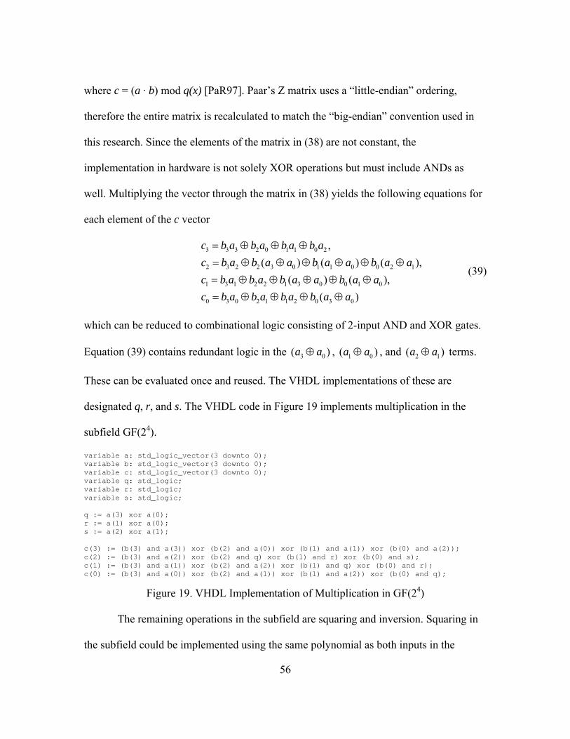
where c = (a · b) mod q(x) [PaR97]. Paar’s Z matrix uses a “little-endian” ordering,
therefore the entire matrix is recalculated to match the “big-endian” convention used in
this research. Since the elements of the matrix in (38) are not constant, the
implementation in hardware is not solely XOR operations but must include ANDs as
well. Multiplying the vector through the matrix in (38) yields the following equations for
each element of the c vector
3 3 3 2 0 1 1 0 2
2 3 2 2 3 0 1 1 0 0 2 1
1 3 1 2 2 1 3 0 0 1 0
0 3 0 2 1 1 2 0 3 0
,( ) ( ) (
( ) ( ),( )
c b a b a b a b ac b a b a a b a a b a ac b a b a b a a b a ac b a b a b a b a a
= ⊕ ⊕ ⊕= ⊕ ⊕ ⊕ ⊕ ⊕ ⊕= ⊕ ⊕ ⊕ ⊕ ⊕= ⊕ ⊕ ⊕ ⊕
), (39)
which can be reduced to combinational logic consisting of 2-input AND and XOR gates.
Equation (39) contains redundant logic in the 3 0( )a a⊕ , 1 0( )a a⊕ , and terms.
These can be evaluated once and reused. The VHDL implementations of these are
designated q, r, and s. The VHDL code in Figure 19 implements multiplication in the
subfield GF(2
2 1(a a⊕ )
4).
variable a: std_logic_vector(3 downto 0); variable b: std_logic_vector(3 downto 0); variable c: std_logic_vector(3 downto 0); variable q: std_logic; variable r: std_logic; variable s: std_logic; q := a(3) xor a(0); r := a(1) xor a(0); s := a(2) xor a(1); c(3) := (b(3) and a(3)) xor (b(2) and a(0)) xor (b(1) and a(1)) xor (b(0) and a(2)); c(2) := (b(3) and a(2)) xor (b(2) and q) xor (b(1) and r) xor (b(0) and s); c(1) := (b(3) and a(1)) xor (b(2) and a(2)) xor (b(1) and q) xor (b(0) and r); c(0) := (b(3) and a(0)) xor (b(2) and a(1)) xor (b(1) and a(2)) xor (b(0) and q);
Figure 19. VHDL Implementation of Multiplication in GF(24)
The remaining operations in the subfield are squaring and inversion. Squaring in
the subfield could be implemented using the same polynomial as both inputs in the
56

multiplication function shown above. However, O’Driscoll develops a much more
computationally efficient method of squaring a polynomial in the subfield. O’Driscoll
found a constant binary matrix that will, when multiplied with a polynomial’s bit string,
produce the square of that polynomial in the subfield. This operation is
3 3
2
1 1
0 0
1 0 1 00 0 1 00 1 0 10 0 0 1
b ab ab ab a
2
⎡ ⎤ ⎡⎡ ⎤ ⎤⎢ ⎥ ⎢⎢ ⎥ ⎥⎢ ⎥ ⎢ ⎥= ⎢ ⎥×⎢ ⎥ ⎢ ⎥ ⎢ ⎥⎢ ⎥ ⎢⎢ ⎥
⎣ ⎦⎥
⎣ ⎦ ⎣ ⎦
(40)
where b = a2 [Odr01]. Multiplying the a vector with the constant bit matrix yields the
following set of equations for the elements of b
3 3 1
2 1
1 2 0
0 0
,,
,.
b a ab ab a ab a
= ⊕== ⊕=
(41)
Thus, squaring a polynomial in the subfield can be implemented using only two XOR
gates. The VHDL code implementing squaring in a subfield is in Figure 20.
variable b: std_logic_vector(3 downto 0); variable b: std_logic_vector(3 downto 0);
b(3) := a(3) xor a(1); b(2) := a(1); b(1) := a(2) xor a(0); b(0) := a(0);
Figure 20. VHDL Implementation of Squaring in GF(24)
The final operation in the schematic in Figure 16 is modular inversion. The
Extended Euclidean algorithm method for modular inversion used to generate the table of
57

inverses in GF(28) in Appendix A is the same process as that of determining a table of
inverses in GF(24), but uses q(x) as the reducing polynomial. If
a(x) x b(x) = 1 mod q(x) (42)
holds, then a(x) is the inverse of b(x) in GF(24) and vice versa. The extended Euclidean
Algorithm is used to find polynomials that satisfy (42). The subsequent polynomials and
their inverses are recorded in an 8 byte look up table that can be found in Table 23 in
Appendix A.
With all blocks of the schematic in Figure 16 implemented a VHDL circuit that
performs the operation of SubBytes in a composite field can be realized. The design
flows of Figures 14 and 15 summarize the circuit. The complete VHDL code for the
implementation of SubBytes and inverse SubBytes in a composite field is in Appendix B.
3.9.2 MixColumns
3.9.2.1 Half LUT
Chapter II outlines the baseline MixColumns design Daemen and Rijmen
specified for an 8-bit platform. The design described below for the MixColumns
transformation uses a 256 byte look up table containing the values of the xtime operation.
Xtime takes an 8-bit polynomial and produces the product multiplied by 02 in the
Rijndael field using l(x) as the reducing polynomial. This table has a property which can
be exploited to halve the amount of memory required to perform MixColumns. The xtime
table’s purpose was to avoid performing complex polynomial multiplication modulo the
58

reducing polynomial l(x). Consider, however, an important property of modular
arithmetic
x modulo y = x, 0 < x < y. (43)
This means when every element of GF(28) is multiplied by 02, half of the elements would
create a product less than the modulus and (43) could be applied. Careful examination of
the xtime table shows that half of the table consists of simple multiplication by 02 with
no modulus operation as indicated by the highlighted portion of Table 10.
Table 10. Xtime Table: Elements Not Requiring Modulus Reduction Highlighted 0 1 2 3 4 5 6 7 8 9 A B C D E F
0 00 02 04 06 08 0A 0C 0E 10 12 14 16 18 1A 1C 1E1 02 22 24 26 28 2A 2C 2E 30 32 34 36 38 3A 3C 3E2 40 42 44 46 48 4A 4C 4E 50 52 54 56 58 5A 5C 5E3 60 62 64 66 68 6A 6C 6E 70 72 74 76 78 7A 7C 7E4 80 82 84 86 88 8A 8C 8E 90 92 94 96 98 9A 9C 9E5 A0 A2 A4 A6 A8 AA AC AE B0 B2 B4 B6 B8 BA BC BE6 C0 C2 C4 C6 C8 CA CC CE D0 D2 D4 D6 D8 DA DC DE7 E0 E2 E4 E6 E8 EA EC EE F0 F2 F4 F6 F8 FA FC FE8 1B 19 1F 1D 13 11 17 15 0B 09 0F 0D 03 01 07 059 3B 39 3F 3D 33 31 37 35 2B 29 2F 2D 23 21 27 25A 5B 59 5F 5D 53 51 57 55 4B 49 4F 4D 43 41 47 45B 7B 79 7F 7D 73 71 77 75 6B 69 6F 6D 63 61 67 65C 9B 99 9F 9D 93 91 97 95 8B 89 8F 8D 83 81 87 85D BB B9 BF BD B3 B1 B7 B5 AB A9 AF AD A3 A1 A7 A5E DB D9 DF DD D3 D1 D7 D5 CB C9 CF CD C3 C1 C7 C5F FB F9 FF FD F3 F1 F7 F5 EB E9 EF ED E3 E1 E7 E5
x
y
Another important property of multiplication by 02 in the Rijndael field is its
equivalence to multiplying a polynomial by x. This is because the hexadecimal number
02 is equal to the bit string {00000010} which represents the polynomial x. Any
polynomial multiplied by x will result in increasing the power of each indeterminate by
one. The corresponding bit string of the product of any polynomial multiplied by x would
be the original bit string shifted left by one. Example 7 illustrates this property.
Example 7. Evaluate the following expression:
(x6 + x4 + x2+ x + 1) • x
59

Solution
Polynomial Representation Bit String Representation (x6 + x4 + x2+ x + 1) • x 01010111 • 00000010 = x7 + x5 + x3+ x2 + x = 10101110
=Bitwise shift to the left!
A bitwise shift to the left is implemented in VHDL below in Figure 21 and simply
changing the wiring utilizes no hardware resources.
variable input: std_logic_vector(7 downto 0); variable output: std_logic_vector(7 downto 0);
if input < X"80" then
output := (input(6 downto 0) & '0'); end if
Figure 21. VHDL Implementation of the Highlighted Portion of Table 10
The above VHDL circuit effectively implements all highlighted elements of Table
10, thereby eliminating the need to store these values in memory. This results in a 128
byte decrease in memory at absolutely no cost (assuming the HDL synthesizer chooses
not to register the 8 bit value of output). The complete VHDL circuit for this
MixColumns labeled “Half LUT” can be found in Appendix B.
3.9.2.2 Arithmetic
The final design is due to Satyanarayana following an algorithm created by
Trenholme [Sat04][Wik06a]. Satyanarayana’s implementation is open source VHDL
code. This design implements MixColumns using no look up tables by implementing the
xtime function in combinational logic rather than through a LUT. Recall that xtime
60
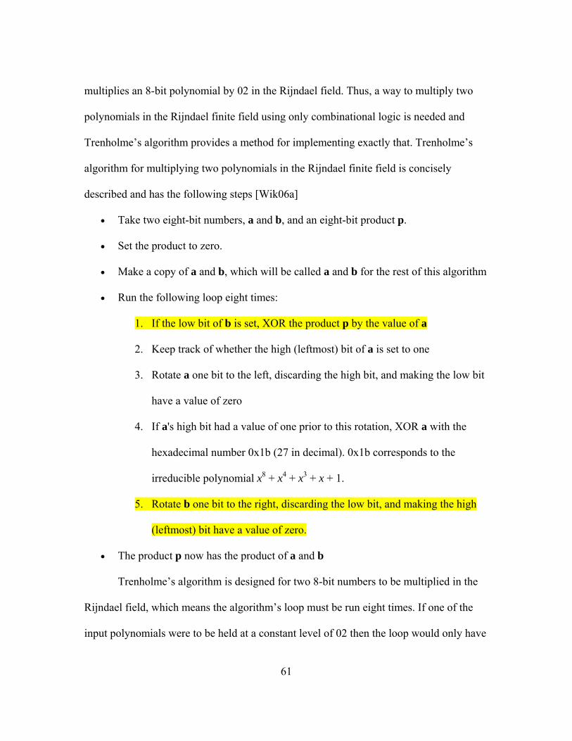
multiplies an 8-bit polynomial by 02 in the Rijndael field. Thus, a way to multiply two
polynomials in the Rijndael finite field using only combinational logic is needed and
Trenholme’s algorithm provides a method for implementing exactly that. Trenholme’s
algorithm for multiplying two polynomials in the Rijndael finite field is concisely
described and has the following steps [Wik06a]
• Take two eight-bit numbers, a and b, and an eight-bit product p.
• Set the product to zero.
• Make a copy of a and b, which will be called a and b for the rest of this algorithm
• Run the following loop eight times:
1. If the low bit of b is set, XOR the product p by the value of a
2. Keep track of whether the high (leftmost) bit of a is set to one
3. Rotate a one bit to the left, discarding the high bit, and making the low bit
have a value of zero
4. If a's high bit had a value of one prior to this rotation, XOR a with the
hexadecimal number 0x1b (27 in decimal). 0x1b corresponds to the
irreducible polynomial x8 + x4 + x3 + x + 1.
5. Rotate b one bit to the right, discarding the low bit, and making the high
(leftmost) bit have a value of zero.
• The product p now has the product of a and b
Trenholme’s algorithm is designed for two 8-bit numbers to be multiplied in the
Rijndael field, which means the algorithm’s loop must be run eight times. If one of the
input polynomials were to be held at a constant level of 02 then the loop would only have
61
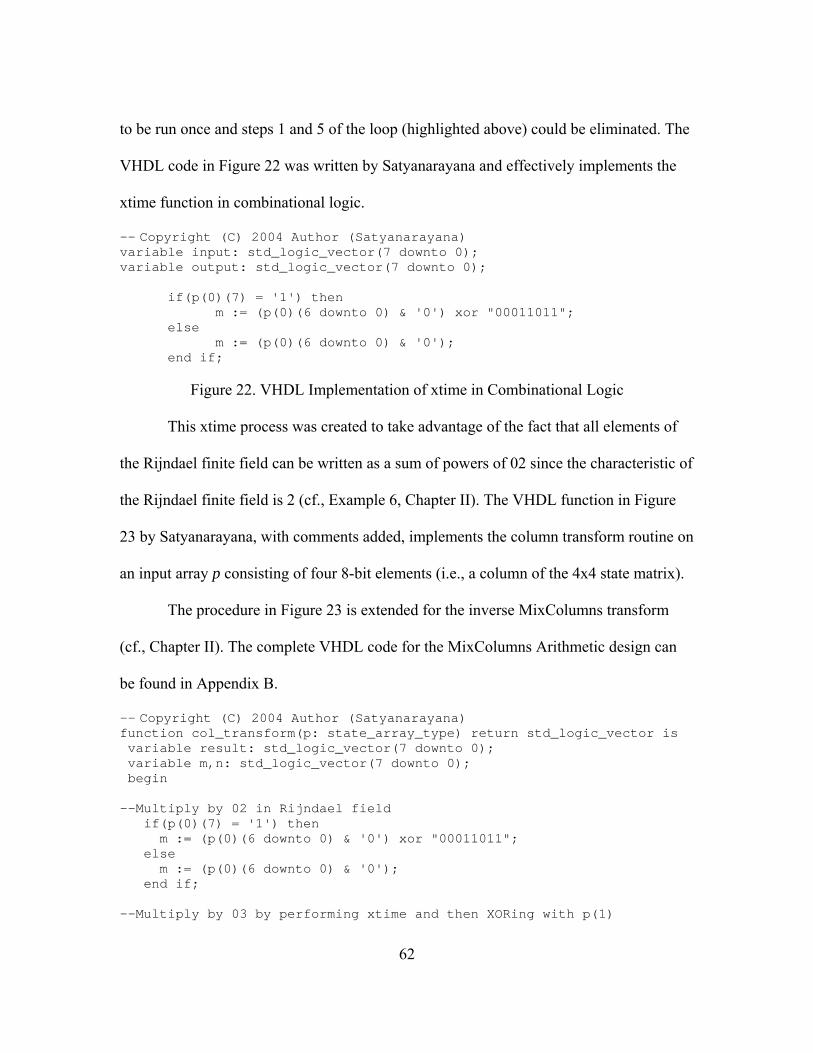
to be run once and steps 1 and 5 of the loop (highlighted above) could be eliminated. The
VHDL code in Figure 22 was written by Satyanarayana and effectively implements the
xtime function in combinational logic.
-- Copyright (C) 2004 Author (Satyanarayana) variable input: std_logic_vector(7 downto 0); variable output: std_logic_vector(7 downto 0); if(p(0)(7) = '1') then m := (p(0)(6 downto 0) & '0') xor "00011011"; else m := (p(0)(6 downto 0) & '0'); end if;
Figure 22. VHDL Implementation of xtime in Combinational Logic
This xtime process was created to take advantage of the fact that all elements of
the Rijndael finite field can be written as a sum of powers of 02 since the characteristic of
the Rijndael finite field is 2 (cf., Example 6, Chapter II). The VHDL function in Figure
23 by Satyanarayana, with comments added, implements the column transform routine on
an input array p consisting of four 8-bit elements (i.e., a column of the 4x4 state matrix).
The procedure in Figure 23 is extended for the inverse MixColumns transform
(cf., Chapter II). The complete VHDL code for the MixColumns Arithmetic design can
be found in Appendix B.
-- Copyright (C) 2004 Author (Satyanarayana) function col_transform(p: state_array_type) return std_logic_vector is variable result: std_logic_vector(7 downto 0); variable m,n: std_logic_vector(7 downto 0); begin --Multiply by 02 in Rijndael field if(p(0)(7) = '1') then m := (p(0)(6 downto 0) & '0') xor "00011011"; else m := (p(0)(6 downto 0) & '0'); end if; --Multiply by 03 by performing xtime and then XORing with p(1)
62

if(p(1)(7) = '1') then n := (p(1)(6 downto 0) & '0') xor "00011011" xor p(1); else n := (p(1)(6 downto 0) & '0') xor p(1); end if; --Bytes p(2) and p(3) require no processing since they are multiplied -- by 01 as specified in Chapter II equation (18) result := m xor n xor p(2) xor p(3); return result; end function col_transform;
Figure 23. VHDL Implementation of the Column Transform Routine
3.10 Evaluation Technique
The NIST Algorithm Validation Suite is the result of the findings of an analytical
evaluation of AES by NIST. The evaluation of a candidate implementation is verified
using the NIST Algorithm Validation Suite’s Known Answer Test. AES is a substitution
cipher; so, if the same block of data is run through the algorithm multiple times with the
same key, the output ciphertext will be exactly the same each time. The Known Answer
Test takes advantage of this and provides an easy method of determining the functionality
of a particular AES implementation. This method uses look up tables containing known
answer values given an input key and plaintext (i.e., validation against analytic analysis).
The experiment testing environment consists of an HDL module which contains
the NIST Algorithm Validation Suite. This module provides the workload and key entry
for the data encryption system. The internal signals of the data encryption system is
monitored using the Xilinx software package ChipScope. A separate HDL module
implements the actual data encryption system which is monitored via ChipScope. Most of
the testing environment is localized to the FPGA chip. The FPGA sends the input/output
data to two separate pins on the Xilinx board such that they can be viewed on a computer
63

running the ChipScope software. ChipScope verifies the maximum clock frequency
dictated by the critical path found by the HDL synthesizer using an iterative process by
which the frequency of the system clock is increased by 0.01 MHZ until the output of the
data encryption system does not pass the known answer test as defined by the validation
suite. Area Occupied is measured by the Xilinx XST HDL synthesis software. After the
software finishes synthesizing the VHDL code and routes all logic blocks, the total
number of gates (including memory) required to implement the design is given in the
synthesis report. Figure 24 is a block diagram outlining the testing environment.
3.11 Experimental Design
There are three factors in each experiment (SubBytes design, MixColumns
Design, and Synthesis goal). The two transformation factors (SubBytes and MixColumns
design) each have three different levels (cf., Table 9). The Synthesis goal factor has two
levels (area and speed). The total number of factors and their levels require 32 • 21 or 18
different experiments for each algorithm in order to account for every possible
combination of factors and levels. After each experiment is run, values for all three
metrics are recorded. For example, the first experiment implements the baseline AES
design on the FPGA and runs the NIST Algorithm Validation Suite. Values for all
metrics (throughput, area efficiency, area occupied) are recorded after the suite has been
completed. Each subsequent experiment is a permutation of experimental factor levels.
The expected variance of the data is minimal, meaning it is assumed that the performance
of the system given the same design, workload, and HDL compilation will have similar
results. Data is analyzed using ANOVA and other statistical tests as appropriate.
64

Figure 24. Block Diagram of Testing Environment
3.12 Methodology Summary
This research has two primary goals; to optimize the AES algorithm’s
performance based on the chosen metrics and to answer the following questions: How
does each factor of optimization interact and affect the overall values of each
optimization metric, and how does each SubBytes and MixColumns design affect
performance with respect to the full factorial design? The metrics are throughput, area
efficiency, and area occupied. These questions are investigated by controlling the level of
the following three factors: SubBytes design, MixColumns design, and Synthesis Goal.
The approach used to satisfy the two goals of the research uses a variety of SubBytes and
MixColumns designs to analyze the performance based on the three metrics with respect
to the baseline AES design for an 8-bit processor.
65

The system under test is called the data encryption system and consists of HDL
modules, the AES algorithm, and an FPGA board. A functional implementation of this
system provides a properly encrypted data stream of a defined workload, which in this
experiment is the NIST Algorithm Validation Suite. This system is evaluated by
performing multiple experiments on multiple system designs and measuring values for
the performance metrics. These measurements are validated by comparing them to the
findings of the analysis provided by the validation suite.
66

IV. Analysis and Results
4.1 Chapter Overview
This chapter presents and interprets the data collected from executing the
experiment outlined in Chapter III. The goal of this chapter is to answer the investigative
research questions posed in Chapter III: (1) how do experimental factors interact and
affect the overall performance metrics, and (2) how does each SubBytes and
MixColumns design affect performance? A tabular summary and graphs are used to give
a quick overview of the raw data. The data is then examined through an analysis of
means. Finally the percentage of variation explained by each factor and their interactions
is determined through an analysis of variance (ANOVA). This analysis allows the effects
to be sorted and the most important effects and interactions identified.
4.2 Results of Experimental Scenarios and Literature Comparison
Total equivalent gate count and maximum clock frequency data from all
experimental scenarios are summarized in Table 11. This data is represented graphically
in Figures 25, 26 and 27. The theoretical maximum clock frequency matched the
measured clock frequency to 1 kHz. Using this data, throughput, area occupied, and
subsequently area efficiency are calculated. The number of clock cycles required to
encrypt a block of data for all designs is 12. The highlighted values are the maximum
(minimum) values obtained by this research. Table 11 reflects only one replication of
each experiment. Pilot studies using two different methods were used to generate
multiple replications of the experiment and neither method resulted in any significant
67
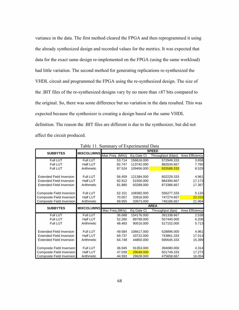
variance in the data. The first method cleared the FPGA and then reprogrammed it using
the already synthesized design and recorded values for the metrics. It was expected that
data for the exact same design re-implemented on the FPGA (using the same workload)
had little variation. The second method for generating replications re-synthesized the
VHDL circuit and programmed the FPGA using the re-synthesized design. The size of
the .BIT files of the re-synthesized designs vary by no more than ±87 bits compared to
the original. So, there was some difference but no variation in the data resulted. This was
expected because the synthesizer is creating a design based on the same VHDL
definition. The reason the .BIT files are different is due to the synthesizer, but did not
affect the circuit produced.
Table 11. Summary of Experimental Data
Max Freq (MHz) Eq Gate Ct Throughput (kbps) Area EfficiencyFull LUT Full LUT 53.714 156616.000 572949.333 3.658Full LUT Half LUT 82.747 113742.000 882634.667 7.760Full LUT Arithmetic 87.524 109456.000 933589.333 8.529
Extended Field Inversion Full LUT 56.459 121384.000 602229.333 4.961Extended Field Inversion Half LUT 82.912 51500.000 884394.667 17.173Extended Field Inversion Arithmetic 81.880 50289.000 873386.667 17.367
Composite Field Inversion Full LUT 52.151 108382.000 556277.333 5.133Composite Field Inversion Half LUT 70.057 33916.000 747274.667 22.033Composite Field Inversion Arithmetic 69.955 33973.000 746186.667 21.964
Max Freq (MHz) Eq Gate Ct Throughput (bps) Area EfficiencyFull LUT Full LUT 36.688 154176.000 391338.667 2.538Full LUT Half LUT 52.260 89799.000 557440.000 6.208Full LUT Arithmetic 48.483 90516.000 517152.000 5.713
Extended Field Inversion Full LUT 49.584 106617.000 528896.000 4.961Extended Field Inversion Half LUT 69.737 43722.000 743861.333 17.013Extended Field Inversion Arithmetic 64.748 44850.000 690645.333 15.399
Composite Field Inversion Full LUT 36.945 91353.000 394080.000 4.314Composite Field Inversion Half LUT 47.039 29049.000 501749.333 17.273Composite Field Inversion Arithmetic 44.593 29628.000 475658.667 16.054
SPEED
AREASUBBYTES MIXCOLUMNS
SUBBYTES MIXCOLUMNS
68

The smallest area occupied uses 29,049 total equivalent gates using the
Composite Field Inversion SubBytes design, Half LUT MixColumns design, and a
Synthesis Goal of area. Since the Composite Field Inversion design for SubBytes is the
design that uses the least amount of memory, the fact that the overall AES design
achieves the smallest area occupied is expected. The Half LUT MixColumns design uses
128 bytes of memory, whereas the Arithmetic design uses no look-up table. The reason
the Half LUT MixColumns design results in the AES design achieving the lowest total
area occupied is because the sheer amount of combinational logic required to perform the
complex finite field arithmetic for the MixColumns transform. The logic required for the
combinational logic design outweighs the memory required for the Half LUT design. It is
also expected that the smallest design would be achieved by synthesizing for area. The
smallest area found in current research occupies an estimated 41,184 total equivalent
gates [GoB05]. Thus, the design developed in this research occupies 29.5% less space.
The largest area efficiency (including memory) achieved by this research is
22.033 for the Composite Field Inversion SubBytes design, Half LUT MixColumns
design, and Synthesis Goal of speed. Since the area efficiency metric is obtained by
dividing throughput by area, a sound strategy is to keep the area occupied figure low. It is
no surprise that the SubBytes and MixColumns designs used to generate the lowest total
area occupied for the overall AES algorithm (Composite Field Inversion and Half LUT)
are responsible for achieving the lowest area efficiency. The only difference in the factor
levels used to produce the lowest total area and the highest area efficiency is that the
HDL synthesizer’s goal for high area efficiency is speed rather than area. This is a vast
69

improvement over the 2.30 obtained by Chodowiec & Gaj. These results are estimates
because the total area occupied as reported in current research is specified in CLBs or
slices. Converting CLBs or slices to total equivalent gate count used the conversion factor
described in Chapter II (22). This transformation is based on logic capabilities published
by the manufacturer of the device and does not account for the specific design or
implementation considerations such as routing. Furthermore, this estimate also assumes
that all slices or CLBs are completely occupied by relevant logic, which may or may not
be the case for some designs.
Thro
ughp
ut (
kbps
)
SubBytes Design
MixColumns Design
Synthesis Goal
LUT
EFI
CFI
LUT
Half L
UTAr
ithLUT
Half L
UTAr
ithLUT
Half L
UTAr
ithSp
eed
Area
Spee
dAr
eaSp
eed
Area
Spee
dAr
eaSp
eed
Area
Spee
dAr
eaSp
eed
Area
Spee
dAr
eaSp
eed
Area
1000000
900000
800000
700000
600000
500000
400000
Individual Values for Throughput
Figure 25. Individual Values Plot for Throughput
The maximum throughput achieved is about 934 Mbps for the Full LUT SubBytes
design, Arithmetic MixColumns design, and Speed Synthesis Goal. The Full LUT
SubBytes design results in highest throughput since in the Full LUT design the entire
SubBytes transform is reduced to a single table look-up. Arithmetic MixColumns design
70

is faster than the LUT table MixColumns design is because the LUT design, unlike the
SubBytes Full LUT design, requires combinational logic as well as a table look-up. The
gate delay involved with performing the MixColumns transformation entirely through
combinational logic (i.e., Arithmetic design) is not as large as the latency required to
access memory for a table look-up on top of a combinational logic delay (i.e., LUT
design).
Tota
l Equ
ival
ent
Gate
Cou
nt
SubBytes Design
MixColumns Design
Synthesis Goal
LUT
EFI
CFI
LUT
Half L
UTAr
ithLUT
Half L
UTAr
ithLUT
Half L
UTAr
ithSp
eed
Area
Spee
dAr
eaSp
eed
Area
Spee
dAr
eaSp
eed
Area
Spee
dAr
eaSp
eed
Area
Spee
dAr
eaSp
eed
Area
160000
140000
120000
100000
80000
60000
40000
20000
Individual Values for Area Occupied
Figure 26. Individual Values Plot for Area Occupied
Although the maximum throughput achieved by this research is not close to the
maximum throughput obtained by Good of 23.5 Gbps, the objective of this research was
to maximize area efficiency, not speed. Thus, this research used methods that reduced the
memory required to complete the transformations. This limits design goals solely to the
correct operation of AES and not to the hardware responsible for implementing it. For
example, pipelining was not used even though the fastest current implementation is
71

pipelined because pipelining has no impact on the correct functioning of AES. Another
powerful method for increasing throughput at the hardware level is loop unrolling. Loop
unrolling was not implemented for the same reason.
Are
a Ef
ficie
ncy
SubBytes Design
MixColumns Design
Synthesis Goal
LUT
EFI
CFI
LUT
Half L
UTAr
ithLUT
Half L
UTAr
ithLUT
Half L
UTAr
ithSp
eed
Area
Spee
dAr
eaSp
eed
Area
Spee
dAr
eaSp
eed
Area
Spee
dAr
eaSp
eed
Area
Spee
dAr
eaSp
eed
Area
20
15
10
5
0
Individual Values for Area Efficiency
Figure 27. Individual Values Plot for Area Efficiency
The individual values plots shown in Figures 25, 26 and 27 show the highest and
lowest values obtained for each metric. Figure 25 shows that the design with the slowest
throughput is the baseline AES design for an 8-bit processor (Full LUT designs for both
SubBytes and MixColumns) synthesized for area. Since the HDL synthesizer has a goal
of area, it does not route the design to reduce the latency required for a table look-up. The
baseline AES design uses table look-ups as its primary means of operation, and this
coupled with the high latency attributed to LUT designs synthesized for area explains the
slow throughput value for this particular design.
72

Figure 26 shows the largest (highest area occupied) overall AES design is the
baseline AES design for an 8-bit platform synthesized for speed. One of the goals of this
research is to improve the performance of the baseline AES design. This goal was
achieved by reducing the design’s dependence on look-up tables and memory. The
design’s large area can be attributed to its three 256 byte look-up tables coupled with
synthesizing for speed.
4.3 Analysis of the Data
The individual values plots shown in Figures 25, 26 and 27 illustrate the
performance of individual AES designs, but they do not reveal how individual
experimental factors and their associated levels affect the performance metrics. Through
the analysis of the baseline experimental design outlined in Chapter III it is possible to
associate individual factor levels and assess their impact on performance. A visual
analysis of the data is accomplished using main effects plots. This provides insight into
the first research goal that is to determine how each factor level affects the performance
of the design as a whole. It does not, however, address the second goal, which is to
quantify the interactions of the factors and explain how these interactions affect the
system as a whole. An analysis of an ANOVA table will aid in quantifying the main
effects of each factor and, more importantly, their interactions. The interactions are
quantified as percentages of variation explained by each factor. The final product of this
analysis is an enumeration the significance of each factor and interaction.
73

4.3.1 Visual Analysis of Means
The first step in evaluating the data is to visually determine how each factor level
impacts the performance of the system using the chosen metrics. The first factor to be
analyzed is SubBytes design. The main effects plot in Figure 28 shows the Full LUT
design drastically increases the total area occupied. The graph in Figure 28 shows the
mean of the gate count attributed to the Extended Field Inversion design is roughly half
of the gates required to implement the Full LUT design. This makes intuitive sense
because Extended Field Inversion is intended to halve the amount of memory required by
the Full LUT design by reducing the required amount of look-up tables from two 256
byte LUTs to one 256 byte LUT.
SubBytes Design
Mea
n of
Tot
al E
quiv
alen
t Ga
te C
ount
Full LUTExtended Field InversionComposite Field Inversion
120000
110000
100000
90000
80000
70000
60000
50000
Main Effects Plot for SubBytes' Impact on Area Occupied
Figure 28. Main Effects Plot for SubBytes on Area Occupied
74

Figure 29 indicates that the Composite Field Inversion design has the lowest mean
throughput of the three designs tested. This is because of the complexity of the
combinational logic required to implement the entire SubBytes transform using a single
64 bit LUT. What is surprising is that the mean throughput of Extended Field Inversion is
higher than simply using the Full LUT design. This is linked to the percentage of
variation explained by each design. This will become clearer once the ANOVA results
are presented. Figure 29 also shows that the Extended Field Inversion design, which
blends combinational logic and one 256 byte LUT, has a higher mean throughput than the
designs at either end of the combinational logic / LUT spectrum.
SubBytes Design
Mea
n of
Thr
ough
put
(kbp
s)
Full LUTExtended Field InversionComposite Field Inversion
725000
700000
675000
650000
625000
600000
575000
550000
Main Effects Plot for SubBytes' Impact on Throughput
Figure 29. Main Effects Plot for SubBytes on Throughput
The mean area efficiency of the Full LUT design for SubBytes is by far the lowest
shown in Figure 30. Thus, the additional throughput value of a Full LUT SubBytes
75
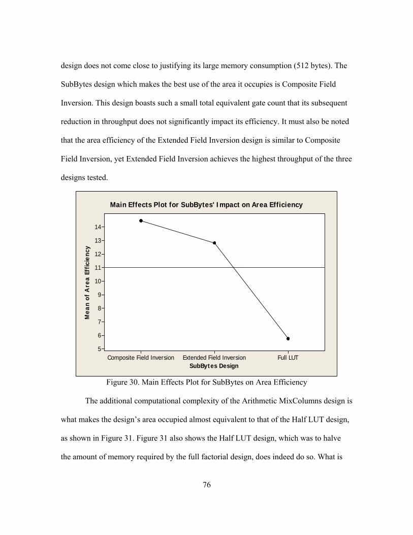
design does not come close to justifying its large memory consumption (512 bytes). The
SubBytes design which makes the best use of the area it occupies is Composite Field
Inversion. This design boasts such a small total equivalent gate count that its subsequent
reduction in throughput does not significantly impact its efficiency. It must also be noted
that the area efficiency of the Extended Field Inversion design is similar to Composite
Field Inversion, yet Extended Field Inversion achieves the highest throughput of the three
designs tested.
SubBytes Design
Mea
n of
Are
a Ef
ficie
ncy
Full LUTExtended Field InversionComposite Field Inversion
14
13
12
11
10
9
8
7
6
5
Main Effects Plot for SubBytes' Impact on Area Efficiency
Figure 30. Main Effects Plot for SubBytes on Area Efficiency
The additional computational complexity of the Arithmetic MixColumns design is
what makes the design’s area occupied almost equivalent to that of the Half LUT design,
as shown in Figure 31. Figure 31 also shows the Half LUT design, which was to halve
the amount of memory required by the full factorial design, does indeed do so. What is
76

interesting is that, on average, the Half LUT and the Arithmetic designs require about the
same amount of equivalent gates even though the Arithmetic design uses only
combinational logic while the Half LUT design uses one 128 byte LUT as well as
combinational logic. This is because the hardware required to implement the LUT
entirely in combinational logic, as is the intention of the Arithmetic design, approaches
the resources required to simply use the table look-up.
MixColumns Design
Mea
n of
Tot
al E
quiv
alen
t Ga
te C
ount
LUTHalf LUTArithmetic
130000
120000
110000
100000
90000
80000
70000
60000
Main Effects Plot for MixColumns Design's Impact on Area Occupied
Figure 31. Main Effects Plot for MixColumns on Area Occupied
The results obtained in Figure 32 for the MixColumns design’s impact on
throughput are similar to those observed for SubBytes’ effect on throughput in Figure 29.
The average throughput for the MixColumns LUT design is the lowest of the three, while
the Half LUT design obtained the highest throughput with the Arithmetic design
achieving a throughput comparable to the Half LUT design. Just as with the SubBytes
77

designs, the designs tested for MixColumns encompass the entire spectrum of design
options ranging from a full LUT design to an entirely combinational logic design.
MixColumns Design
Mea
n of
Thr
ough
put
(kbp
s)
LUTHalf LUTArithmetic
750000
700000
650000
600000
550000
500000
Main Effects Plot for MixColumn Design's Impact on Throughput
Figure 32. Main Effects Plot for MixColumns on Throughput
Memory latency again proves to be a weakness of the LUT design. The Half LUT
design requires a table look-up on half of the values operated on. This halves the amount
of memory latency associated with table look-ups and thus increases the overall average
throughput of the design. The throughput obtained by the Arithmetic design is
comparable to the Half LUT because the combinational logic delay associated with the
complex mathematical operations the Arithmetic design must execute is similar to the
memory latency associated with a table look-up on half of the values operated on.
The average effects of MixColumns design on area efficiency are summarized in
Figure 33. This figure shows how inefficient the full factorial MixColumns LUT design
78

is compared to the other two options. The average area efficiency performance of both
the Arithmetic and Half LUT designs are above 14, whereas the baseline design specified
by Daemen and Rijmen for an 8-bit processor is below one third of that. The full factorial
LUT design for MixColumns occupies the most area and achieves the slowest
throughput, and therefore it has an extremely low average area efficiency.
MixColumns Design
Mea
n of
Are
a Ef
ficie
ncy
LUTHalf LUTArithmetic
15.0
12.5
10.0
7.5
5.0
Main Effects Plot for MixColumns Design's Impact on Area Efficiency
Figure 33. Main Effects Plot for MixColumns on Area Efficiency
The best average area efficiency is obtained through the Half LUT design. This
design is successful because it allows half of the full factorial LUT to be reduced to a
simple bitwise shift. This shift is accomplished through the changes in wiring and halves
the memory required from the full factorial design at the cost of a mere 8-bit register.
The main effects plot in Figure 34 illustrates the positive impact synthesizing a
VHDL design for speed has on throughput. This is expected. It is assumed that
79

synthesizing for speed comes at a cost, namely an increase in area. This raises an
interesting question as to whether the increase in throughput as a result of synthesizing
for speed justifies an increase in area.
Synthesis Goal
Mea
n of
Thr
ough
put
(kbp
s)
SpeedArea
750000
700000
650000
600000
550000
Main Effects Plot for Synthesis Goal's Impact on Throughput
Figure 34. Main Effects Plot for Synthesis Goal on Throughput
Figure 35 shows that synthesizing for speed does, in fact, increase the average
area occupied by a design, thus proving the above supposition. But the answer to the
question as to whether the increase in throughput as a result of synthesis for speed is
worth the cost of an increase in average area occupied is given in Figure 36. Figure 36
shows that synthesis for speed increases the average area efficiency, which means that the
synthesis goal of speed will, on average, increase a design’s ability to efficiently use its
available hardware resources. Thus, the increase in throughput resulting from synthesis
for speed justifies the cost of a subsequent increase in area occupied.
80
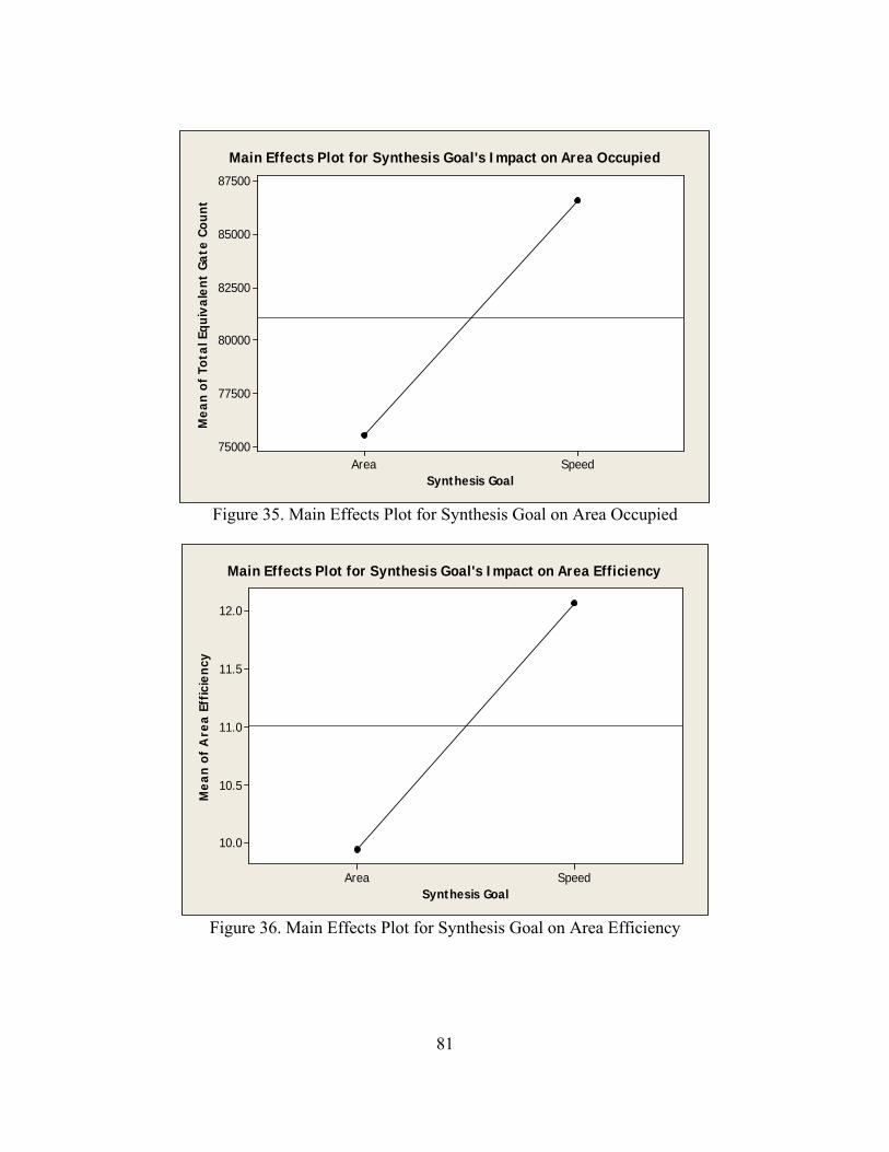
Synthesis Goal
Mea
n of
Tot
al E
quiv
alen
t Ga
te C
ount
SpeedArea
87500
85000
82500
80000
77500
75000
Main Effects Plot for Synthesis Goal's Impact on Area Occupied
Figure 35. Main Effects Plot for Synthesis Goal on Area Occupied
Synthesis Goal
Mea
n of
Are
a Ef
ficie
ncy
SpeedArea
12.0
11.5
11.0
10.5
10.0
Main Effects Plot for Synthesis Goal's Impact on Area Efficiency
Figure 36. Main Effects Plot for Synthesis Goal on Area Efficiency
81
4.4 Performance Analysis through ANOVA
The analysis of the data in Table 11 through visual analysis of means, as
presented above, indicates how each factor individually affects the average performance
of the entire AES system, but it does not reveal how the factors interact to affect the
performance metrics. Through an ANOVA it is possible to determine which factor is
responsible for the most variance in each performance metric and consequently which
factor level is most suitable when optimizing AES for a particular performance metric.
4.4.1 ANOVA for Throughput
The data in Table 11 is analyzed by MINITAB’s Analyze Factorial Design feature
for a three factor General Factorial Design. MINITAB’s output for the Balanced
ANOVA for throughput is reproduced in Table 12.
Table 12. Analysis of Variance Table for Throughput Source DF Seq SS Adj SS Adj MS SubBytes Design 2 67861330654 67861330654 33930665327 MixColumns Design 2 1.68976E+11 1.68976E+11 84487864855 Synthesis Goal 1 2.21800E+11 2.21800E+11 2.21800E+11 SubBytes Design*MixColumns Design 4 8597865719 8597865719 2149466430 SubBytes Design*Synthesis Goal 2 23149318959 23149318959 11574659480 MixColumns Design*Synthesis Goal 2 17579150621 17579150621 8789575310 SubBytes Design*MixColumns Design* 4 2696989634 2696989634 674247408 Synthesis Goal Error 0 * * * Total 17 5.10661E+11
Table 12 displays the Sum of Squares values, the Adjusted Sum of Squares, and
the Mean Square Values. Most notably the values of Error for all three columns is zero
since the experiment has only one replication, therefore no error can be calculated. The
output of MINITAB’s Factorial Design Analysis also includes a quantification of the
main effects as shown in Table 13. Note the difference in terminology, what this research
calls an effect, MINITAB calls a coefficient (Coef).
82
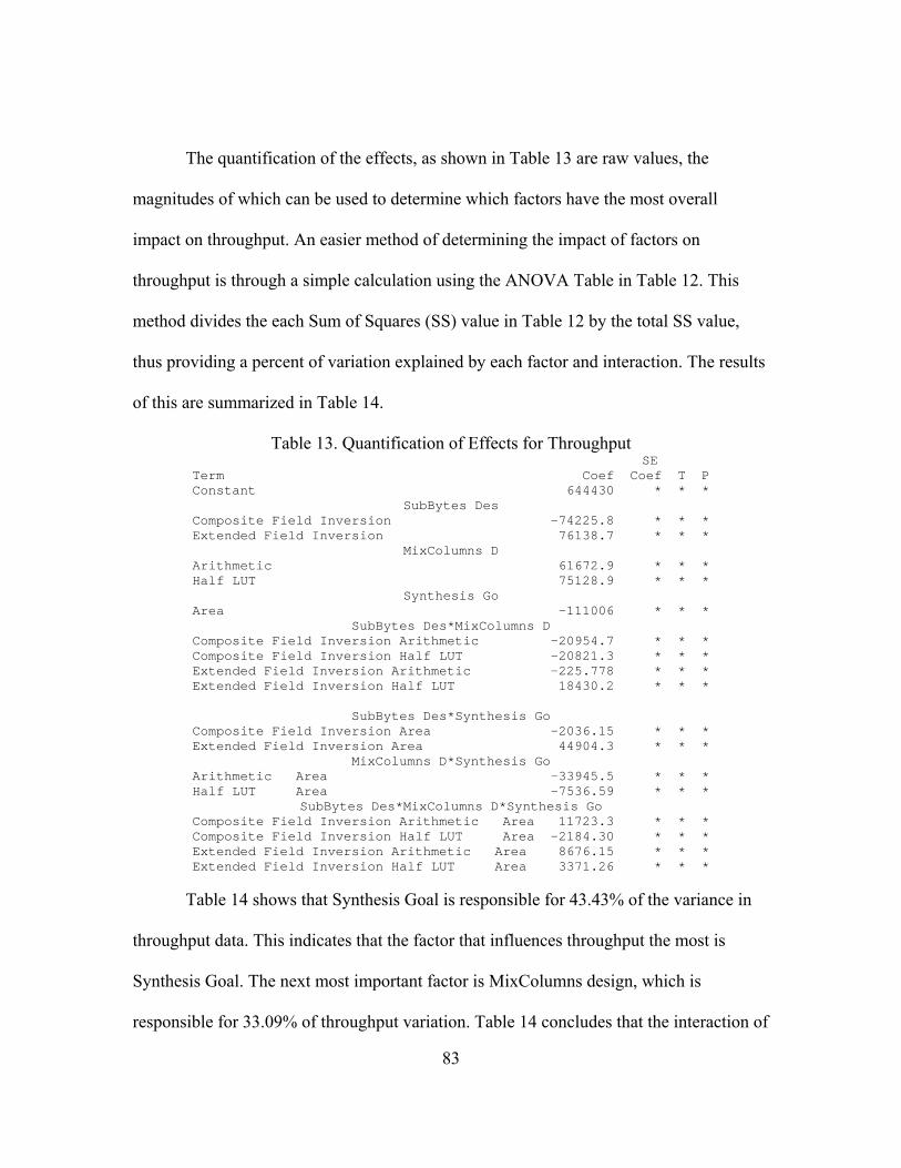
The quantification of the effects, as shown in Table 13 are raw values, the
magnitudes of which can be used to determine which factors have the most overall
impact on throughput. An easier method of determining the impact of factors on
throughput is through a simple calculation using the ANOVA Table in Table 12. This
method divides the each Sum of Squares (SS) value in Table 12 by the total SS value,
thus providing a percent of variation explained by each factor and interaction. The results
of this are summarized in Table 14.
Table 13. Quantification of Effects for Throughput SE
Term Coef Coef T P Constant 644430 * * *
SubBytes Des Composite Field Inversion -74225.8 * * * Extended Field Inversion 76138.7 * * *
MixColumns D Arithmetic 61672.9 * * * Half LUT 75128.9 * * *
Synthesis Go Area -111006 * * *
SubBytes Des*MixColumns D Composite Field Inversion Arithmetic -20954.7 * * * Composite Field Inversion Half LUT -20821.3 * * * Extended Field Inversion Arithmetic -225.778 * * * Extended Field Inversion Half LUT 18430.2 * * *
SubBytes Des*Synthesis Go
Composite Field Inversion Area -2036.15 * * * Extended Field Inversion Area 44904.3 * * *
MixColumns D*Synthesis Go Arithmetic Area -33945.5 * * * Half LUT Area -7536.59 * * *
SubBytes Des*MixColumns D*Synthesis Go Composite Field Inversion Arithmetic Area 11723.3 * * * Composite Field Inversion Half LUT Area -2184.30 * * * Extended Field Inversion Arithmetic Area 8676.15 * * * Extended Field Inversion Half LUT Area 3371.26 * * *
Table 14 shows that Synthesis Goal is responsible for 43.43% of the variance in
throughput data. This indicates that the factor that influences throughput the most is
Synthesis Goal. The next most important factor is MixColumns design, which is
responsible for 33.09% of throughput variation. Table 14 concludes that the interaction of
83

factors does not account for as much percentage of variance for throughput as the
individual factors themselves, for the highest interaction percentage is 4.53% (interaction
of SubBytes Design and Synthesis Goal) and the lowest individual factor percentage is
13.29% (SubBytes Design).
Table 14. Percentage of Variance Explained for Throughput
Sum of Squares % Variance Explained
SubBytes Design 67861330654 13.29MixColumns Design 1.68976E+11 33.09Synthesis Goal 2.218E+11 43.43SubBytes * MixColumns 8597865719 1.68SubBytes * Synthesis Goal 23149318959 4.53MixColumns * Synthesis Goal 17579150621 3.44SubBytes * MixColumns * Synthesis Goal 2696989634 0.53
Total 5.10661E+11 Table 15 ranks each factor and interaction in descending order of importance as
defined by percentage of variation explained.
Table 15. Order of Importance for Throughput’s Factors and Interactions Importance Factor
1 Synthesis Goal 2 MixColumns Design 3 SubBytes Design 4 SubBytes * Synthesis Goal 5 MixColumns * Synthesis Goal 6 SubBytes * MixColumns 7 SubBytes * MixColumns * Synthesis Goal
4.4.2 ANOVA for Area Occupied
Doing a similar analysis on area occupied yields Table 16. The MINITAB output
for the balanced ANOVA for area occupied is reproduced in Table 25 in Appendix C and
the quantification of the main effects table is summarized in Table 26 in Appendix C.
84

Table 16 summarizes the percentages of variance explained by each factor and interaction
for area occupied.
Table 16. Percentage of Variance Explained for Area Occupied
Sum of Squares % Variance Explained
SubBytes Design 13700255055 44.86MixColumns Design 15902640562 52.07Synthesis Goal 550544684 1.80SubBytes * MixColumns 150371320 0.49SubBytes * Synthesis Goal 37100094 0.12MixColumns * Synthesis Goal 5430919 0.02SubBytes * MixColumns * Synthesis Goal 196245452 0.64
Total 30542588085 Table 16 shows that MixColumns Design is responsible for 52.07% of the
variance in total equivalent gate count. This indicates that the factor which influences
area occupied the most is MixColumns Design. The next most important factor is
SubBytes Design and is responsible for 44.86% of total equivalent gate count variation.
The full ordering of each factor and interaction is shown in Table 17. It is surprising that
MixColumns Design is responsible for more variation in area occupied than SubBytes
since alternative SubBytes designs eliminated the need for more memory than alternative
MixColumns Designs.
The full factorial SubBytes design requires 512 bytes of memory while the least
memory consuming SubBytes design requires 64 bits of memory, thus reducing the
original design’s memory usage by 508 bytes. The full factorial MixColumns requires
256 bytes of memory while the Arithmetic design requires no memory to execute, thus
saving a total of 256 bytes of memory. The reason MixColumns still accounts for more
variance in total equivalent gate count is because the combinational logic needed for
85

reducing the memory requirements of the baseline SubBytes design is much more
complicated than reducing the full factorial MixColumns design. This large requirement
for logic across all designs of SubBytes is why the variance in area for MixColumns due
to this factor is so small. Table 16 reveals that the interaction of factors accounts for little
variance in total equivalent gate count, for the highest interaction percentage is only 0.64
(interaction of SubBytes, MixColumns, and Synthesis Goal).
Table 17. Order of Importance for Area Occupied’s Factors and Interactions Importance Factor
1 MixColumns Design 2 SubBytes Design 3 Synthesis Goal 4 SubBytes * MixColumns * Synthesis Goal 5 SubBytes * MixColumns 6 SubBytes * Synthesis Goal 7 MixColumns * Synthesis Goal
4.4.3 ANOVA on Area Efficiency
Performing a similar analysis on area efficiency yields Table 18. The MINITAB
output for the Balanced ANOVA for area occupied is reproduced in Table 27 in
Appendix C and the quantification of the main effects table is summarized in Table 28 in
Appendix C. Table 18 summarizes the percentages of variance explained by each factor
and interaction for area efficiency.
The hypothesis that MixColumns will produce a large percentage of variation
explained due to the large magnitudes of MixColumns effects is confirmed by Table 18.
The percentage of variation explained by the factor MixColumns Design is 52.11% and is
larger than any other factor or interaction. This makes intuitive sense because
MixColumns Design is responsible for the most variation in area occupied and the second
86
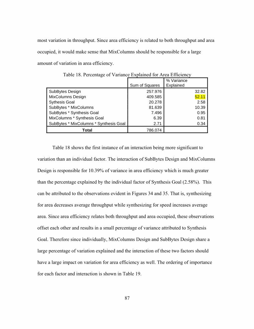
most variation in throughput. Since area efficiency is related to both throughput and area
occupied, it would make sense that MixColumns should be responsible for a large
amount of variation in area efficiency.
Table 18. Percentage of Variance Explained for Area Efficiency
Sum of Squares % Variance Explained
SubBytes Design 257.976 32.82MixColumns Design 409.585 52.11Sythesis Goal 20.278 2.58SubBytes * MixColumns 81.639 10.39SubBytes * Synthesis Goal 7.496 0.95MixColumns * Synthesis Goal 6.39 0.81SubBytes * MixColumns * Synthesis Goal 2.71 0.34
Total 786.074
Table 18 shows the first instance of an interaction being more significant to
variation than an individual factor. The interaction of SubBytes Design and MixColumns
Design is responsible for 10.39% of variance in area efficiency which is much greater
than the percentage explained by the individual factor of Synthesis Goal (2.58%). This
can be attributed to the observations evident in Figures 34 and 35. That is, synthesizing
for area decreases average throughput while synthesizing for speed increases average
area. Since area efficiency relates both throughput and area occupied, these observations
offset each other and results in a small percentage of variance attributed to Synthesis
Goal. Therefore since individually, MixColumns Design and SubBytes Design share a
large percentage of variation explained and the interaction of these two factors should
have a large impact on variation for area efficiency as well. The ordering of importance
for each factor and interaction is shown in Table 19.
87

Table 19. Order of Importance for Area Efficiency’s Factors and Interactions Importance Factor
1 MixColumns Design 2 SubBytes Design 3 SubBytes * MixColumns 4 Sythesis Goal 5 SubBytes * Synthesis Goal 6 MixColumns * Synthesis Goal 7 SubBytes * MixColumns * Synthesis Goal
4.5 Summary
This chapter shows that the baseline SubBytes and MixColumns designs (i.e., Full
LUT designs) always perform poorly in area efficiency and area occupied. The only
design to produce a lower performance than the baseline Full LUT design for any metric
is the SubBytes design Composite Field Inversion, which produced a lower throughput
than the baseline design. Composite Field Inversion has the highest area efficiency of the
three SubBytes design, thus justifying the reduction in throughput for more efficient area
usage. MixColumns Design and Synthesis Goal are responsible for the largest variance in
performance of the AES algorithm in terms of throughput, area efficiency, and area
occupied.
88
V. Conclusions and Recommendations
5.1 Chapter Overview
This chapter presents the conclusions drawn from the analysis of experimental
data. This chapter also highlights the significance of this work and its impact on current
research methods involving the implementation of AES on FPGAs, as well as provides
recommendations for future research in this area.
5.2 Significance of Research
The significance of this research is three-fold. This research establishes a method
of comparing AES FPGA implementations across FPGAs independent of chip family or
manufacturer by normalizing measures of area. This research also provides an in depth
analysis of design considerations for AES implementations on 8-bit processing platforms.
Finally, this research compares the performance of each AES transformation design
implementation as a part of the AES system as a whole, rather than as its own separate
entity.
The trend in current research for specific AES transformations (i.e., designs for
SubBytes, MixColumns, KeyExpansion, AddRoundKey, or ShiftRows) is to implement a
design independent of the AES algorithm and compare the result to some baseline
transformation. This method, essentially, takes an incremental step in a process and treats
the individual transformation as its own system. The problem with this approach is that it
ignores the impact the new design may have on the algorithm as a whole. This research
addresses this issue by assessing the impact of each new transformation as a part of the
89

overall AES system, which allows a more comprehensive perspective on how the new
transformation affects the algorithm as a whole.
The state of current research to minimize area occupied is summed up best by
Zambreno: “It is difficult to make direct comparisons between FPGA implementations of
any algorithm since the specific hardware target is often different” [ZCN04]. This
research addresses this concern by proposing a way to estimate the area occupied by an
implementation independent of manufacturer or chip family using a conversion factor
(cf., Chapter II (22) ). Area occupied is measured in terms of total equivalent gate count
rather than CLBs or slices. Comparing gate count rather than CLB or slice count
eliminates the specific hardware target’s architecture from consideration because the
number of gates required to implement a design on any hardware platform is measured
using the same units, whereas the number of CLB or slices required to implement a
design is a function of the specific hardware target.
Research that has examined throughput, area, or efficiency of AES
implementations often does so with no consideration to the usefulness of the design in
practice, especially if they assume the availability of a 32-bit processor. Most
implementations of AES requiring a small area also have a correspondingly small
processing capability (e.g., smart card). This research realistically assumes an 8-bit
processing capability. The importance of this constraint is so significant that the
designers of AES incorporated into their specification of the algorithm a separate design
intended to perform well on an 8-bit platform. This research succeeds in its goal of
90

increasing the performance of this constrained AES design based on the metrics of
throughput, area occupied, and area efficiency.
5.3 Recommendations for Future Research
Future AES transformation designs are possible. Some examples include a
SubBytes design that uses no table look-ups, which can be accomplished by reducing the
64 bit LUT associated with Composite Field Inversion to combinational logic by
reducing the composite field GF(24)2 to the field GF((22)2)2 . Since this experiment
concentrated on design considerations at the algorithmic level, future research could also
carry out a similar performance analysis on designs targeting the hardware level using
optimization techniques such as loop unrolling, pipelining, and speculation.
The process of mapping GF(28) to the composite field GF(24)2 could be expanded
to research work being done in GF(216). Through further research, operations in GF(216)
could be reduced to the composite field GF(28)2, which could be reduced again to the
composite field GF((24)2)2.
5.4 Conclusions of Research
This research has two primary goals, the first of which is to improve the
performance of the baseline design of AES targeting an 8-bit platform based on the
chosen metrics. The second goal of this research is to quantify how each factor interacts
and affects the overall values of each metric and to identify which factors are responsible
for the largest variance in performance of the AES algorithm measured in throughput,
area efficiency, and area occupied.
91

92
The first goal is accomplished through the visual analysis of means plots shown in
Chapter IV (cf., Figures 28-36). These plots show that the baseline SubBytes and
MixColumns designs (i.e., Full LUT designs) are always the poorest performers in area
efficiency and area occupied. The only design to produce a lower performance than the
baseline Full LUT design for any metric is the SubBytes design Composite Field
Inversion, which produced a lower throughput than the baseline design. Figure 30 shows
Composite Field Inversion has the highest area efficiency of the three SubBytes design,
thus justifying the reduction in throughput for more efficient area usage. Thus, the first
goal of improving the performance of the baseline design of AES targeting an 8-bit
platform is achieved.
The second research goal is to determine how each factor interacts and affects the
overall values of each metric. This is accomplished through the identification of which
factors are responsible for the largest variance in performance of the AES algorithm
measured in throughput, area efficiency, and area occupied by quantifying the percentage
of variance attributed to each factor. Table 15 identifies the factor most responsible for
affecting throughput is Synthesis Goal. Tables 17 and 19 identify that the factor most
responsible for variance in both area efficiency and area occupied is MixColumns design.
This research also contributes a method of estimating area as a measure of total
equivalent gate count. This method allows a direct comparison to be made between two
FPGA implementations independent of manufacturer or chip family. Thus, this research
meets both research goals and answers both investigative questions posed through a
quantitative and qualitative analysis of the data collected through experimentation.

Appendix A: Data Tables
Table 20. Modular Inverses in the Rijndael Field [Odr01]
Table 21. S-Box Look-Up Table [Odr01]
93
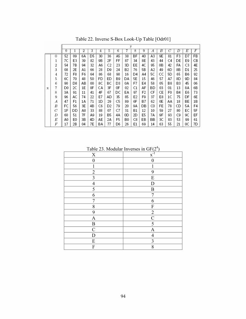
Table 22. Inverse S-Box Look-Up Table [Odr01]
Table 23. Modular Inverses in GF(24) X x-1
0 0 1 1 2 9 3 E 4 D 5 B 6 7 7 6 8 F 9 2 A C B 5 C A D 4 E 3 F 8
94

Table 24. Tabular Representation of xtime 0 1 2 3 4 5 6 7 8 9 A B C D E F
0 00 02 04 06 08 0A 0C 0E 10 12 14 16 18 1A 1C 1E1 02 22 24 26 28 2A 2C 2E 30 32 34 36 38 3A 3C 3E2 40 42 44 46 48 4A 4C 4E 50 52 54 56 58 5A 5C 5E3 60 62 64 66 68 6A 6C 6E 70 72 74 76 78 7A 7C 7E4 80 82 84 86 88 8A 8C 8E 90 92 94 96 98 9A 9C 9E5 A0 A2 A4 A6 A8 AA AC AE B0 B2 B4 B6 B8 BA BC BE6 C0 C2 C4 C6 C8 CA CC CE D0 D2 D4 D6 D8 DA DC DE7 E0 E2 E4 E6 E8 EA EC EE F0 F2 F4 F6 F8 FA FC FE8 1B 19 1F 1D 13 11 17 15 0B 09 0F 0D 03 01 07 059 3B 39 3F 3D 33 31 37 35 2B 29 2F 2D 23 21 27 25A 5B 59 5F 5D 53 51 57 55 4B 49 4F 4D 43 41 47 45B 7B 79 7F 7D 73 71 77 75 6B 69 6F 6D 63 61 67 65C 9B 99 9F 9D 93 91 97 95 8B 89 8F 8D 83 81 87 85D BB B9 BF BD B3 B1 B7 B5 AB A9 AF AD A3 A1 A7 A5E DB D9 DF DD D3 D1 D7 D5 CB C9 CF CD C3 C1 C7 C5F FB F9 FF FD F3 F1 F7 F5 EB E9 EF ED E3 E1 E7 E5
x
y
95

Appendix B: Complete VHDL Code for Each Design
SubBytes Full LUT
--Copyright (C) 2004 Hemanth Satyanarayana --This function implements the S-Box LUT function sbox_val(address: std_logic_vector(7 downto 0)) return std_logic_vector is variable data: bit_vector(7 downto 0); variable data_stdlogic: std_logic_vector(7 downto 0); begin case address is when "00000000" => data := X"63"; when "00000001" => data := X"7C"; when "00000010" => data := X"77"; when "00000011" => data := X"7B"; when "00000100" => data := X"F2"; when "00000101" => data := X"6B"; when "00000110" => data := X"6F"; when "00000111" => data := X"C5"; when "00001000" => data := X"30"; when "00001001" => data := X"01"; when "00001010" => data := X"67"; when "00001011" => data := X"2B"; when "00001100" => data := X"FE"; when "00001101" => data := X"D7"; when "00001110" => data := X"AB"; when "00001111" => data := X"76"; when "00010000" => data := X"CA"; when "00010001" => data := X"82"; when "00010010" => data := X"C9"; when "00010011" => data := X"7D"; when "00010100" => data := X"FA"; when "00010101" => data := X"59"; when "00010110" => data := X"47"; when "00010111" => data := X"F0"; when "00011000" => data := X"AD"; when "00011001" => data := X"D4"; when "00011010" => data := X"A2"; when "00011011" => data := X"AF"; when "00011100" => data := X"9C"; when "00011101" => data := X"A4"; when "00011110" => data := X"72"; when "00011111" => data := X"C0"; when "00100000" => data := X"B7"; when "00100001" => data := X"FD"; when "00100010" => data := X"93"; when "00100011" => data := X"26"; when "00100100" => data := X"36"; when "00100101" => data := X"3F"; when "00100110" => data := X"F7";
96

when "00100111" => data := X"CC"; when "00101000" => data := X"34"; when "00101001" => data := X"A5"; when "00101010" => data := X"E5"; when "00101011" => data := X"F1"; when "00101100" => data := X"71"; when "00101101" => data := X"D8"; when "00101110" => data := X"31"; when "00101111" => data := X"15"; when "00110000" => data := X"04"; when "00110001" => data := X"C7"; when "00110010" => data := X"23"; when "00110011" => data := X"C3"; when "00110100" => data := X"18"; when "00110101" => data := X"96"; when "00110110" => data := X"05"; when "00110111" => data := X"9A"; when "00111000" => data := X"07"; when "00111001" => data := X"12"; when "00111010" => data := X"80"; when "00111011" => data := X"E2"; when "00111100" => data := X"EB"; when "00111101" => data := X"27"; when "00111110" => data := X"B2"; when "00111111" => data := X"75"; when "01000000" => data := X"09"; when "01000001" => data := X"83"; when "01000010" => data := X"2C"; when "01000011" => data := X"1A"; when "01000100" => data := X"1B"; when "01000101" => data := X"6E"; when "01000110" => data := X"5A"; when "01000111" => data := X"A0"; when "01001000" => data := X"52"; when "01001001" => data := X"3B"; when "01001010" => data := X"D6"; when "01001011" => data := X"B3"; when "01001100" => data := X"29"; when "01001101" => data := X"E3"; when "01001110" => data := X"2F"; when "01001111" => data := X"84"; when "01010000" => data := X"53"; when "01010001" => data := X"D1"; when "01010010" => data := X"00"; when "01010011" => data := X"ED"; when "01010100" => data := X"20"; when "01010101" => data := X"FC"; when "01010110" => data := X"B1"; when "01010111" => data := X"5B"; when "01011000" => data := X"6A"; when "01011001" => data := X"CB"; when "01011010" => data := X"BE"; when "01011011" => data := X"39"; when "01011100" => data := X"4A"; when "01011101" => data := X"4C";
97
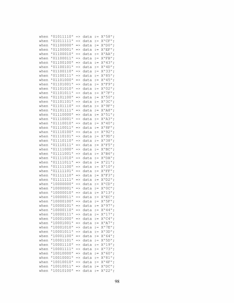
when "01011110" => data := X"58"; when "01011111" => data := X"CF"; when "01100000" => data := X"D0"; when "01100001" => data := X"EF"; when "01100010" => data := X"AA"; when "01100011" => data := X"FB"; when "01100100" => data := X"43"; when "01100101" => data := X"4D"; when "01100110" => data := X"33"; when "01100111" => data := X"85"; when "01101000" => data := X"45"; when "01101001" => data := X"F9"; when "01101010" => data := X"02"; when "01101011" => data := X"7F"; when "01101100" => data := X"50"; when "01101101" => data := X"3C"; when "01101110" => data := X"9F"; when "01101111" => data := X"A8"; when "01110000" => data := X"51"; when "01110001" => data := X"A3"; when "01110010" => data := X"40"; when "01110011" => data := X"8F"; when "01110100" => data := X"92"; when "01110101" => data := X"9D"; when "01110110" => data := X"38"; when "01110111" => data := X"F5"; when "01111000" => data := X"BC"; when "01111001" => data := X"B6"; when "01111010" => data := X"DA"; when "01111011" => data := X"21"; when "01111100" => data := X"10"; when "01111101" => data := X"FF"; when "01111110" => data := X"F3"; when "01111111" => data := X"D2"; when "10000000" => data := X"CD"; when "10000001" => data := X"0C"; when "10000010" => data := X"13"; when "10000011" => data := X"EC"; when "10000100" => data := X"5F"; when "10000101" => data := X"97"; when "10000110" => data := X"44"; when "10000111" => data := X"17"; when "10001000" => data := X"C4"; when "10001001" => data := X"A7"; when "10001010" => data := X"7E"; when "10001011" => data := X"3D"; when "10001100" => data := X"64"; when "10001101" => data := X"5D"; when "10001110" => data := X"19"; when "10001111" => data := X"73"; when "10010000" => data := X"60"; when "10010001" => data := X"81"; when "10010010" => data := X"4F"; when "10010011" => data := X"DC"; when "10010100" => data := X"22";
98

when "10010101" => data := X"2A"; when "10010110" => data := X"90"; when "10010111" => data := X"88"; when "10011000" => data := X"46"; when "10011001" => data := X"EE"; when "10011010" => data := X"B8"; when "10011011" => data := X"14"; when "10011100" => data := X"DE"; when "10011101" => data := X"5E"; when "10011110" => data := X"0B"; when "10011111" => data := X"DB"; when "10100000" => data := X"E0"; when "10100001" => data := X"32"; when "10100010" => data := X"3A"; when "10100011" => data := X"0A"; when "10100100" => data := X"49"; when "10100101" => data := X"06"; when "10100110" => data := X"24"; when "10100111" => data := X"5C"; when "10101000" => data := X"C2"; when "10101001" => data := X"D3"; when "10101010" => data := X"AC"; when "10101011" => data := X"62"; when "10101100" => data := X"91"; when "10101101" => data := X"95"; when "10101110" => data := X"E4"; when "10101111" => data := X"79"; when "10110000" => data := X"E7"; when "10110001" => data := X"C8"; when "10110010" => data := X"37"; when "10110011" => data := X"6D"; when "10110100" => data := X"8D"; when "10110101" => data := X"D5"; when "10110110" => data := X"4E"; when "10110111" => data := X"A9"; when "10111000" => data := X"6C"; when "10111001" => data := X"56"; when "10111010" => data := X"F4"; when "10111011" => data := X"EA"; when "10111100" => data := X"65"; when "10111101" => data := X"7A"; when "10111110" => data := X"AE"; when "10111111" => data := X"08"; when "11000000" => data := X"BA"; when "11000001" => data := X"78"; when "11000010" => data := X"25"; when "11000011" => data := X"2E"; when "11000100" => data := X"1C"; when "11000101" => data := X"A6"; when "11000110" => data := X"B4"; when "11000111" => data := X"C6"; when "11001000" => data := X"E8"; when "11001001" => data := X"DD"; when "11001010" => data := X"74"; when "11001011" => data := X"1F";
99

when "11001100" => data := X"4B"; when "11001101" => data := X"BD"; when "11001110" => data := X"8B"; when "11001111" => data := X"8A"; when "11010000" => data := X"70"; when "11010001" => data := X"3E"; when "11010010" => data := X"B5"; when "11010011" => data := X"66"; when "11010100" => data := X"48"; when "11010101" => data := X"03"; when "11010110" => data := X"F6"; when "11010111" => data := X"0E"; when "11011000" => data := X"61"; when "11011001" => data := X"35"; when "11011010" => data := X"57"; when "11011011" => data := X"B9"; when "11011100" => data := X"86"; when "11011101" => data := X"C1"; when "11011110" => data := X"1D"; when "11011111" => data := X"9E"; when "11100000" => data := X"E1"; when "11100001" => data := X"F8"; when "11100010" => data := X"98"; when "11100011" => data := X"11"; when "11100100" => data := X"69"; when "11100101" => data := X"D9"; when "11100110" => data := X"8E"; when "11100111" => data := X"94"; when "11101000" => data := X"9B"; when "11101001" => data := X"1E"; when "11101010" => data := X"87"; when "11101011" => data := X"E9"; when "11101100" => data := X"CE"; when "11101101" => data := X"55"; when "11101110" => data := X"28"; when "11101111" => data := X"DF"; when "11110000" => data := X"8C"; when "11110001" => data := X"A1"; when "11110010" => data := X"89"; when "11110011" => data := X"0D"; when "11110100" => data := X"BF"; when "11110101" => data := X"E6"; when "11110110" => data := X"42"; when "11110111" => data := X"68"; when "11111000" => data := X"41"; when "11111001" => data := X"99"; when "11111010" => data := X"2D"; when "11111011" => data := X"0F"; when "11111100" => data := X"B0"; when "11111101" => data := X"54"; when "11111110" => data := X"BB"; when "11111111" => data := X"16"; when others => null; end case; data_stdlogic := to_StdLogicVector(data);
100

return data_stdlogic; end function sbox_val; --This function implements the inverse S-Box LUT function inv_sbox_val(address: std_logic_vector(7 downto 0)) return std_logic_vector is variable inv_data: bit_vector(7 downto 0); variable inv_data_stdlogic: std_logic_vector(7 downto 0); begin case address is when "00000000" => inv_data := X"52"; when "00000001" => inv_data := X"09"; when "00000010" => inv_data := X"6a"; when "00000011" => inv_data := X"d5"; when "00000100" => inv_data := X"30"; when "00000101" => inv_data := X"36"; when "00000110" => inv_data := X"a5"; when "00000111" => inv_data := X"38"; when "00001000" => inv_data := X"bf"; when "00001001" => inv_data := X"40"; when "00001010" => inv_data := X"a3"; when "00001011" => inv_data := X"9e"; when "00001100" => inv_data := X"81"; when "00001101" => inv_data := X"f3"; when "00001110" => inv_data := X"d7"; when "00001111" => inv_data := X"fb"; when "00010000" => inv_data := X"7c"; when "00010001" => inv_data := X"e3"; when "00010010" => inv_data := X"39"; when "00010011" => inv_data := X"82"; when "00010100" => inv_data := X"9b"; when "00010101" => inv_data := X"2f"; when "00010110" => inv_data := X"ff"; when "00010111" => inv_data := X"87"; when "00011000" => inv_data := X"34"; when "00011001" => inv_data := X"8e"; when "00011010" => inv_data := X"43"; when "00011011" => inv_data := X"44"; when "00011100" => inv_data := X"c4"; when "00011101" => inv_data := X"de"; when "00011110" => inv_data := X"e9"; when "00011111" => inv_data := X"cb"; when "00100000" => inv_data := X"54"; when "00100001" => inv_data := X"7b"; when "00100010" => inv_data := X"94"; when "00100011" => inv_data := X"32"; when "00100100" => inv_data := X"a6"; when "00100101" => inv_data := X"c2"; when "00100110" => inv_data := X"23"; when "00100111" => inv_data := X"3d"; when "00101000" => inv_data := X"ee"; when "00101001" => inv_data := X"4c"; when "00101010" => inv_data := X"95"; when "00101011" => inv_data := X"0b";
101
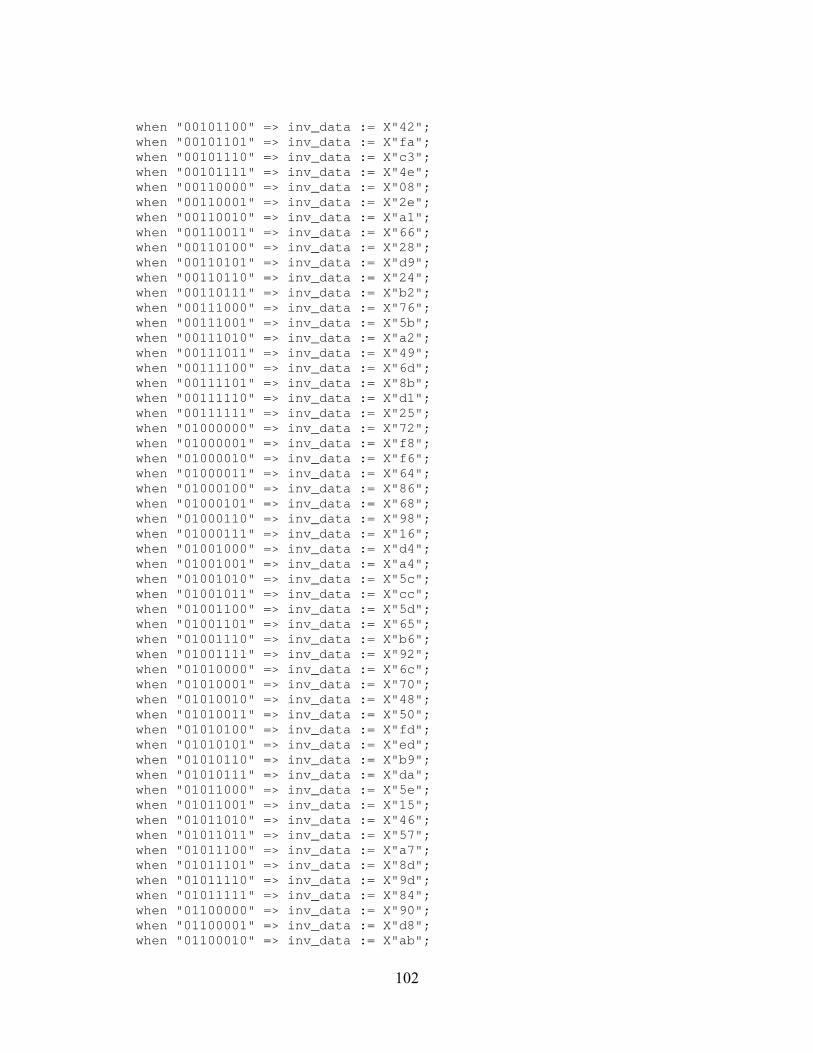
when "00101100" => inv_data := X"42"; when "00101101" => inv_data := X"fa"; when "00101110" => inv_data := X"c3"; when "00101111" => inv_data := X"4e"; when "00110000" => inv_data := X"08"; when "00110001" => inv_data := X"2e"; when "00110010" => inv_data := X"a1"; when "00110011" => inv_data := X"66"; when "00110100" => inv_data := X"28"; when "00110101" => inv_data := X"d9"; when "00110110" => inv_data := X"24"; when "00110111" => inv_data := X"b2"; when "00111000" => inv_data := X"76"; when "00111001" => inv_data := X"5b"; when "00111010" => inv_data := X"a2"; when "00111011" => inv_data := X"49"; when "00111100" => inv_data := X"6d"; when "00111101" => inv_data := X"8b"; when "00111110" => inv_data := X"d1"; when "00111111" => inv_data := X"25"; when "01000000" => inv_data := X"72"; when "01000001" => inv_data := X"f8"; when "01000010" => inv_data := X"f6"; when "01000011" => inv_data := X"64"; when "01000100" => inv_data := X"86"; when "01000101" => inv_data := X"68"; when "01000110" => inv_data := X"98"; when "01000111" => inv_data := X"16"; when "01001000" => inv_data := X"d4"; when "01001001" => inv_data := X"a4"; when "01001010" => inv_data := X"5c"; when "01001011" => inv_data := X"cc"; when "01001100" => inv_data := X"5d"; when "01001101" => inv_data := X"65"; when "01001110" => inv_data := X"b6"; when "01001111" => inv_data := X"92"; when "01010000" => inv_data := X"6c"; when "01010001" => inv_data := X"70"; when "01010010" => inv_data := X"48"; when "01010011" => inv_data := X"50"; when "01010100" => inv_data := X"fd"; when "01010101" => inv_data := X"ed"; when "01010110" => inv_data := X"b9"; when "01010111" => inv_data := X"da"; when "01011000" => inv_data := X"5e"; when "01011001" => inv_data := X"15"; when "01011010" => inv_data := X"46"; when "01011011" => inv_data := X"57"; when "01011100" => inv_data := X"a7"; when "01011101" => inv_data := X"8d"; when "01011110" => inv_data := X"9d"; when "01011111" => inv_data := X"84"; when "01100000" => inv_data := X"90"; when "01100001" => inv_data := X"d8"; when "01100010" => inv_data := X"ab";
102
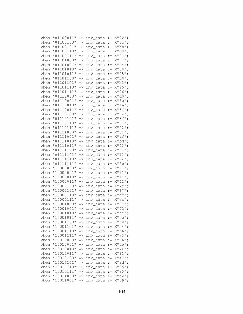
when "01100011" => inv_data := X"00"; when "01100100" => inv_data := X"8c"; when "01100101" => inv_data := X"bc"; when "01100110" => inv_data := X"d3"; when "01100111" => inv_data := X"0a"; when "01101000" => inv_data := X"f7"; when "01101001" => inv_data := X"e4"; when "01101010" => inv_data := X"58"; when "01101011" => inv_data := X"05"; when "01101100" => inv_data := X"b8"; when "01101101" => inv_data := X"b3"; when "01101110" => inv_data := X"45"; when "01101111" => inv_data := X"06"; when "01110000" => inv_data := X"d0"; when "01110001" => inv_data := X"2c"; when "01110010" => inv_data := X"1e"; when "01110011" => inv_data := X"8f"; when "01110100" => inv_data := X"ca"; when "01110101" => inv_data := X"3f"; when "01110110" => inv_data := X"0f"; when "01110111" => inv_data := X"02"; when "01111000" => inv_data := X"c1"; when "01111001" => inv_data := X"af"; when "01111010" => inv_data := X"bd"; when "01111011" => inv_data := X"03"; when "01111100" => inv_data := X"01"; when "01111101" => inv_data := X"13"; when "01111110" => inv_data := X"8a"; when "01111111" => inv_data := X"6b"; when "10000000" => inv_data := X"3a"; when "10000001" => inv_data := X"91"; when "10000010" => inv_data := X"11"; when "10000011" => inv_data := X"41"; when "10000100" => inv_data := X"4f"; when "10000101" => inv_data := X"67"; when "10000110" => inv_data := X"dc"; when "10000111" => inv_data := X"ea"; when "10001000" => inv_data := X"97"; when "10001001" => inv_data := X"f2"; when "10001010" => inv_data := X"cf"; when "10001011" => inv_data := X"ce"; when "10001100" => inv_data := X"f0"; when "10001101" => inv_data := X"b4"; when "10001110" => inv_data := X"e6"; when "10001111" => inv_data := X"73"; when "10010000" => inv_data := X"96"; when "10010001" => inv_data := X"ac"; when "10010010" => inv_data := X"74"; when "10010011" => inv_data := X"22"; when "10010100" => inv_data := X"e7"; when "10010101" => inv_data := X"ad"; when "10010110" => inv_data := X"35"; when "10010111" => inv_data := X"85"; when "10011000" => inv_data := X"e2"; when "10011001" => inv_data := X"f9";
103

when "10011010" => inv_data := X"37"; when "10011011" => inv_data := X"e8"; when "10011100" => inv_data := X"1c"; when "10011101" => inv_data := X"75"; when "10011110" => inv_data := X"df"; when "10011111" => inv_data := X"6e"; when "10100000" => inv_data := X"47"; when "10100001" => inv_data := X"f1"; when "10100010" => inv_data := X"1a"; when "10100011" => inv_data := X"71"; when "10100100" => inv_data := X"1d"; when "10100101" => inv_data := X"29"; when "10100110" => inv_data := X"c5"; when "10100111" => inv_data := X"89"; when "10101000" => inv_data := X"6f"; when "10101001" => inv_data := X"b7"; when "10101010" => inv_data := X"62"; when "10101011" => inv_data := X"0e"; when "10101100" => inv_data := X"aa"; when "10101101" => inv_data := X"18"; when "10101110" => inv_data := X"be"; when "10101111" => inv_data := X"1b"; when "10110000" => inv_data := X"fc"; when "10110001" => inv_data := X"56"; when "10110010" => inv_data := X"3e"; when "10110011" => inv_data := X"4b"; when "10110100" => inv_data := X"c6"; when "10110101" => inv_data := X"d2"; when "10110110" => inv_data := X"79"; when "10110111" => inv_data := X"20"; when "10111000" => inv_data := X"9a"; when "10111001" => inv_data := X"db"; when "10111010" => inv_data := X"c0"; when "10111011" => inv_data := X"fe"; when "10111100" => inv_data := X"78"; when "10111101" => inv_data := X"cd"; when "10111110" => inv_data := X"5a"; when "10111111" => inv_data := X"f4"; when "11000000" => inv_data := X"1f"; when "11000001" => inv_data := X"dd"; when "11000010" => inv_data := X"a8"; when "11000011" => inv_data := X"33"; when "11000100" => inv_data := X"88"; when "11000101" => inv_data := X"07"; when "11000110" => inv_data := X"c7"; when "11000111" => inv_data := X"31"; when "11001000" => inv_data := X"b1"; when "11001001" => inv_data := X"12"; when "11001010" => inv_data := X"10"; when "11001011" => inv_data := X"59"; when "11001100" => inv_data := X"27"; when "11001101" => inv_data := X"80"; when "11001110" => inv_data := X"ec"; when "11001111" => inv_data := X"5f"; when "11010000" => inv_data := X"60";
104
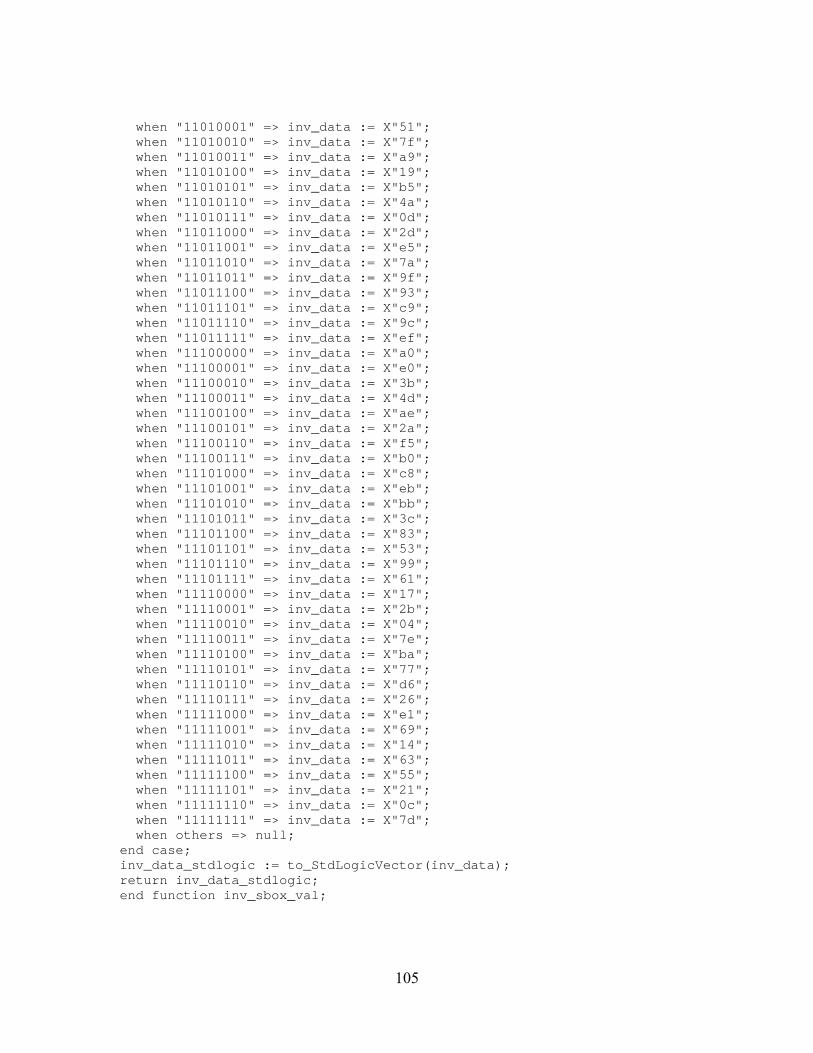
when "11010001" => inv_data := X"51"; when "11010010" => inv_data := X"7f"; when "11010011" => inv_data := X"a9"; when "11010100" => inv_data := X"19"; when "11010101" => inv_data := X"b5"; when "11010110" => inv_data := X"4a"; when "11010111" => inv_data := X"0d"; when "11011000" => inv_data := X"2d"; when "11011001" => inv_data := X"e5"; when "11011010" => inv_data := X"7a"; when "11011011" => inv_data := X"9f"; when "11011100" => inv_data := X"93"; when "11011101" => inv_data := X"c9"; when "11011110" => inv_data := X"9c"; when "11011111" => inv_data := X"ef"; when "11100000" => inv_data := X"a0"; when "11100001" => inv_data := X"e0"; when "11100010" => inv_data := X"3b"; when "11100011" => inv_data := X"4d"; when "11100100" => inv_data := X"ae"; when "11100101" => inv_data := X"2a"; when "11100110" => inv_data := X"f5"; when "11100111" => inv_data := X"b0"; when "11101000" => inv_data := X"c8"; when "11101001" => inv_data := X"eb"; when "11101010" => inv_data := X"bb"; when "11101011" => inv_data := X"3c"; when "11101100" => inv_data := X"83"; when "11101101" => inv_data := X"53"; when "11101110" => inv_data := X"99"; when "11101111" => inv_data := X"61"; when "11110000" => inv_data := X"17"; when "11110001" => inv_data := X"2b"; when "11110010" => inv_data := X"04"; when "11110011" => inv_data := X"7e"; when "11110100" => inv_data := X"ba"; when "11110101" => inv_data := X"77"; when "11110110" => inv_data := X"d6"; when "11110111" => inv_data := X"26"; when "11111000" => inv_data := X"e1"; when "11111001" => inv_data := X"69"; when "11111010" => inv_data := X"14"; when "11111011" => inv_data := X"63"; when "11111100" => inv_data := X"55"; when "11111101" => inv_data := X"21"; when "11111110" => inv_data := X"0c"; when "11111111" => inv_data := X"7d"; when others => null; end case; inv_data_stdlogic := to_StdLogicVector(inv_data); return inv_data_stdlogic; end function inv_sbox_val;
105

SubBytes Extended Field Inversion
function sbox_val(inp: std_logic_vector(7 downto 0); mode: std_logic) return std_logic_vector is variable address: std_logic_vector(7 downto 0); variable data: bit_vector(7 downto 0); variable data_stdlogic: std_logic_vector(7 downto 0); variable outdata: std_logic_vector(7 downto 0); begin --Performs affine transform first if in Decrypt mode if mode='0' then address(7) := inp(6) xor inp(4) xor inp(1) xor '0'; address(6) := inp(5) xor inp(3) xor inp(0) xor '0'; address(5) := inp(7) xor inp(4) xor inp(2) xor '0'; address(4) := inp(6) xor inp(3) xor inp(1) xor '0'; address(3) := inp(5) xor inp(2) xor inp(0) xor '0'; address(2) := inp(7) xor inp(4) xor inp(1) xor '1'; address(1) := inp(6) xor inp(3) xor inp(0) xor '0'; address(0) := inp(7) xor inp(5) xor inp(2) xor '1'; else address := inp; end if; --Modular inversion in the extended field LUT case address is when "00000000" => data := "00000000"; when "00000001" => data := "00000001"; when "00000010" => data := "10001101"; when "00000011" => data := "11110110"; when "00000100" => data := "11001011"; when "00000101" => data := "01010010"; when "00000110" => data := "01111011"; when "00000111" => data := "11010001"; when "00001000" => data := "11101000"; when "00001001" => data := "01001111"; when "00001010" => data := "00101001"; when "00001011" => data := "11000000"; when "00001100" => data := "10110000"; when "00001101" => data := "11100001"; when "00001110" => data := "11100101"; when "00001111" => data := "11000111"; when "00010000" => data := "01110100"; when "00010001" => data := "10110100"; when "00010010" => data := "10101010"; when "00010011" => data := "01001011"; when "00010100" => data := "10011001"; when "00010101" => data := "00101011"; when "00010110" => data := "01100000"; when "00010111" => data := "01011111"; when "00011000" => data := "01011000"; when "00011001" => data := "00111111"; when "00011010" => data := "11111101"; when "00011011" => data := "11001100";
106
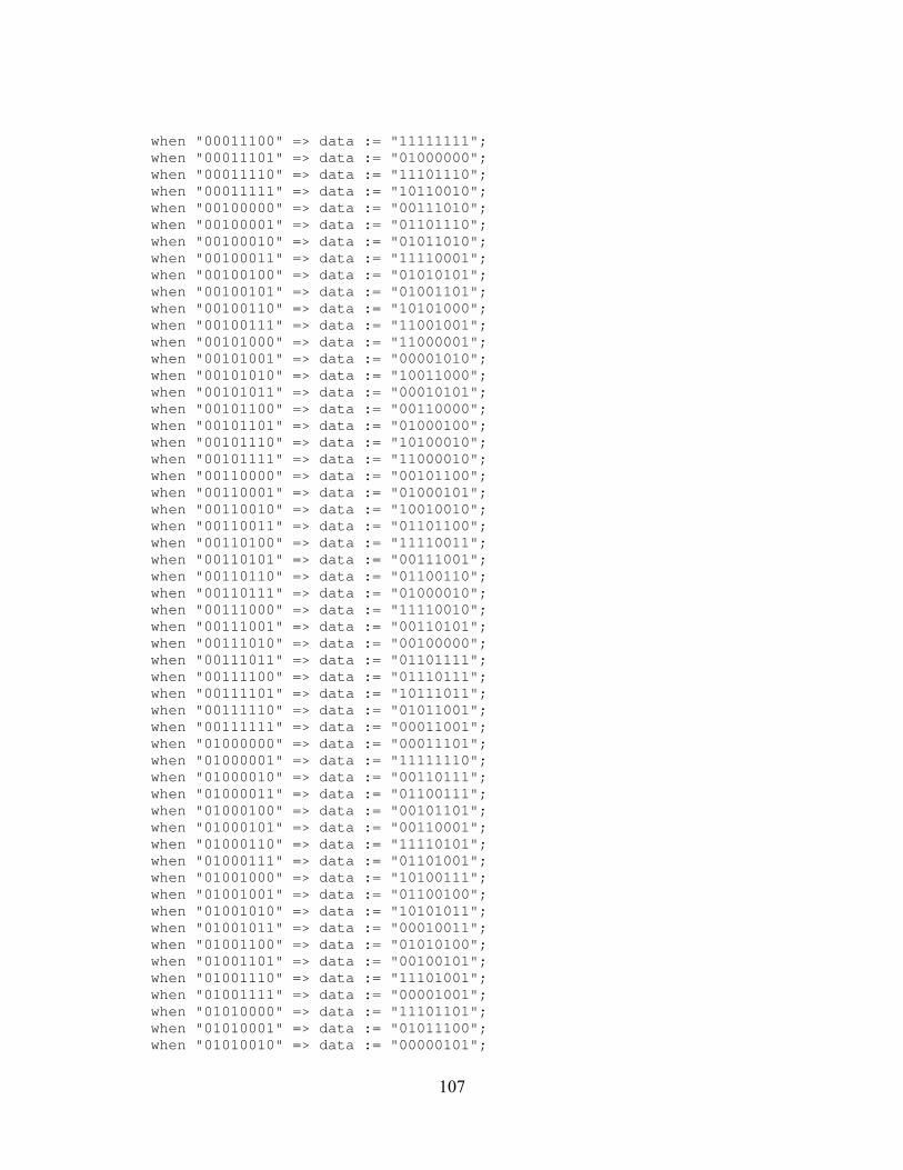
when "00011100" => data := "11111111"; when "00011101" => data := "01000000"; when "00011110" => data := "11101110"; when "00011111" => data := "10110010"; when "00100000" => data := "00111010"; when "00100001" => data := "01101110"; when "00100010" => data := "01011010"; when "00100011" => data := "11110001"; when "00100100" => data := "01010101"; when "00100101" => data := "01001101"; when "00100110" => data := "10101000"; when "00100111" => data := "11001001"; when "00101000" => data := "11000001"; when "00101001" => data := "00001010"; when "00101010" => data := "10011000"; when "00101011" => data := "00010101"; when "00101100" => data := "00110000"; when "00101101" => data := "01000100"; when "00101110" => data := "10100010"; when "00101111" => data := "11000010"; when "00110000" => data := "00101100"; when "00110001" => data := "01000101"; when "00110010" => data := "10010010"; when "00110011" => data := "01101100"; when "00110100" => data := "11110011"; when "00110101" => data := "00111001"; when "00110110" => data := "01100110"; when "00110111" => data := "01000010"; when "00111000" => data := "11110010"; when "00111001" => data := "00110101"; when "00111010" => data := "00100000"; when "00111011" => data := "01101111"; when "00111100" => data := "01110111"; when "00111101" => data := "10111011"; when "00111110" => data := "01011001"; when "00111111" => data := "00011001"; when "01000000" => data := "00011101"; when "01000001" => data := "11111110"; when "01000010" => data := "00110111"; when "01000011" => data := "01100111"; when "01000100" => data := "00101101"; when "01000101" => data := "00110001"; when "01000110" => data := "11110101"; when "01000111" => data := "01101001"; when "01001000" => data := "10100111"; when "01001001" => data := "01100100"; when "01001010" => data := "10101011"; when "01001011" => data := "00010011"; when "01001100" => data := "01010100"; when "01001101" => data := "00100101"; when "01001110" => data := "11101001"; when "01001111" => data := "00001001"; when "01010000" => data := "11101101"; when "01010001" => data := "01011100"; when "01010010" => data := "00000101";
107

when "01010011" => data := "11001010"; when "01010100" => data := "01001100"; when "01010101" => data := "00100100"; when "01010110" => data := "10000111"; when "01010111" => data := "10111111"; when "01011000" => data := "00011000"; when "01011001" => data := "00111110"; when "01011010" => data := "00100010"; when "01011011" => data := "11110000"; when "01011100" => data := "01010001"; when "01011101" => data := "11101100"; when "01011110" => data := "01100001"; when "01011111" => data := "00010111"; when "01100000" => data := "00010110"; when "01100001" => data := "01011110"; when "01100010" => data := "10101111"; when "01100011" => data := "11010011"; when "01100100" => data := "01001001"; when "01100101" => data := "10100110"; when "01100110" => data := "00110110"; when "01100111" => data := "01000011"; when "01101000" => data := "11110100"; when "01101001" => data := "01000111"; when "01101010" => data := "10010001"; when "01101011" => data := "11011111"; when "01101100" => data := "00110011"; when "01101101" => data := "10010011"; when "01101110" => data := "00100001"; when "01101111" => data := "00111011"; when "01110000" => data := "01111001"; when "01110001" => data := "10110111"; when "01110010" => data := "10010111"; when "01110011" => data := "10000101"; when "01110100" => data := "00010000"; when "01110101" => data := "10110101"; when "01110110" => data := "10111010"; when "01110111" => data := "00111100"; when "01111000" => data := "10110110"; when "01111001" => data := "01110000"; when "01111010" => data := "11010000"; when "01111011" => data := "00000110"; when "01111100" => data := "10100001"; when "01111101" => data := "11111010"; when "01111110" => data := "10000001"; when "01111111" => data := "10000010"; when "10000000" => data := "10000011"; when "10000001" => data := "01111110"; when "10000010" => data := "01111111"; when "10000011" => data := "10000000"; when "10000100" => data := "10010110"; when "10000101" => data := "01110011"; when "10000110" => data := "10111110"; when "10000111" => data := "01010110"; when "10001000" => data := "10011011"; when "10001001" => data := "10011110";
108

when "10001010" => data := "10010101"; when "10001011" => data := "11011001"; when "10001100" => data := "11110111"; when "10001101" => data := "00000010"; when "10001110" => data := "10111001"; when "10001111" => data := "10100100"; when "10010000" => data := "11011110"; when "10010001" => data := "01101010"; when "10010010" => data := "00110010"; when "10010011" => data := "01101101"; when "10010100" => data := "11011000"; when "10010101" => data := "10001010"; when "10010110" => data := "10000100"; when "10010111" => data := "01110010"; when "10011000" => data := "00101010"; when "10011001" => data := "00010100"; when "10011010" => data := "10011111"; when "10011011" => data := "10001000"; when "10011100" => data := "11111001"; when "10011101" => data := "11011100"; when "10011110" => data := "10001001"; when "10011111" => data := "10011010"; when "10100000" => data := "11111011"; when "10100001" => data := "01111100"; when "10100010" => data := "00101110"; when "10100011" => data := "11000011"; when "10100100" => data := "10001111"; when "10100101" => data := "10111000"; when "10100110" => data := "01100101"; when "10100111" => data := "01001000"; when "10101000" => data := "00100110"; when "10101001" => data := "11001000"; when "10101010" => data := "00010010"; when "10101011" => data := "01001010"; when "10101100" => data := "11001110"; when "10101101" => data := "11100111"; when "10101110" => data := "11010010"; when "10101111" => data := "01100010"; when "10110000" => data := "00001100"; when "10110001" => data := "11100000"; when "10110010" => data := "00011111"; when "10110011" => data := "11101111"; when "10110100" => data := "00010001"; when "10110101" => data := "01110101"; when "10110110" => data := "01111000"; when "10110111" => data := "01110001"; when "10111000" => data := "10100101"; when "10111001" => data := "10001110"; when "10111010" => data := "01110110"; when "10111011" => data := "00111101"; when "10111100" => data := "10111101"; when "10111101" => data := "10111100"; when "10111110" => data := "10000110"; when "10111111" => data := "01010111"; when "11000000" => data := "00001011";
109

when "11000001" => data := "00101000"; when "11000010" => data := "00101111"; when "11000011" => data := "10100011"; when "11000100" => data := "11011010"; when "11000101" => data := "11010100"; when "11000110" => data := "11100100"; when "11000111" => data := "00001111"; when "11001000" => data := "10101001"; when "11001001" => data := "00100111"; when "11001010" => data := "01010011"; when "11001011" => data := "00000100"; when "11001100" => data := "00011011"; when "11001101" => data := "11111100"; when "11001110" => data := "10101100"; when "11001111" => data := "11100110"; when "11010000" => data := "01111010"; when "11010001" => data := "00000111"; when "11010010" => data := "10101110"; when "11010011" => data := "01100011"; when "11010100" => data := "11000101"; when "11010101" => data := "11011011"; when "11010110" => data := "11100010"; when "11010111" => data := "11101010"; when "11011000" => data := "10010100"; when "11011001" => data := "10001011"; when "11011010" => data := "11000100"; when "11011011" => data := "11010101"; when "11011100" => data := "10011101"; when "11011101" => data := "11111000"; when "11011110" => data := "10010000"; when "11011111" => data := "01101011"; when "11100000" => data := "10110001"; when "11100001" => data := "00001101"; when "11100010" => data := "11010110"; when "11100011" => data := "11101011"; when "11100100" => data := "11000110"; when "11100101" => data := "00001110"; when "11100110" => data := "11001111"; when "11100111" => data := "10101101"; when "11101000" => data := "00001000"; when "11101001" => data := "01001110"; when "11101010" => data := "11010111"; when "11101011" => data := "11100011"; when "11101100" => data := "01011101"; when "11101101" => data := "01010000"; when "11101110" => data := "00011110"; when "11101111" => data := "10110011"; when "11110000" => data := "01011011"; when "11110001" => data := "00100011"; when "11110010" => data := "00111000"; when "11110011" => data := "00110100"; when "11110100" => data := "01101000"; when "11110101" => data := "01000110"; when "11110110" => data := "00000011"; when "11110111" => data := "10001100";
110
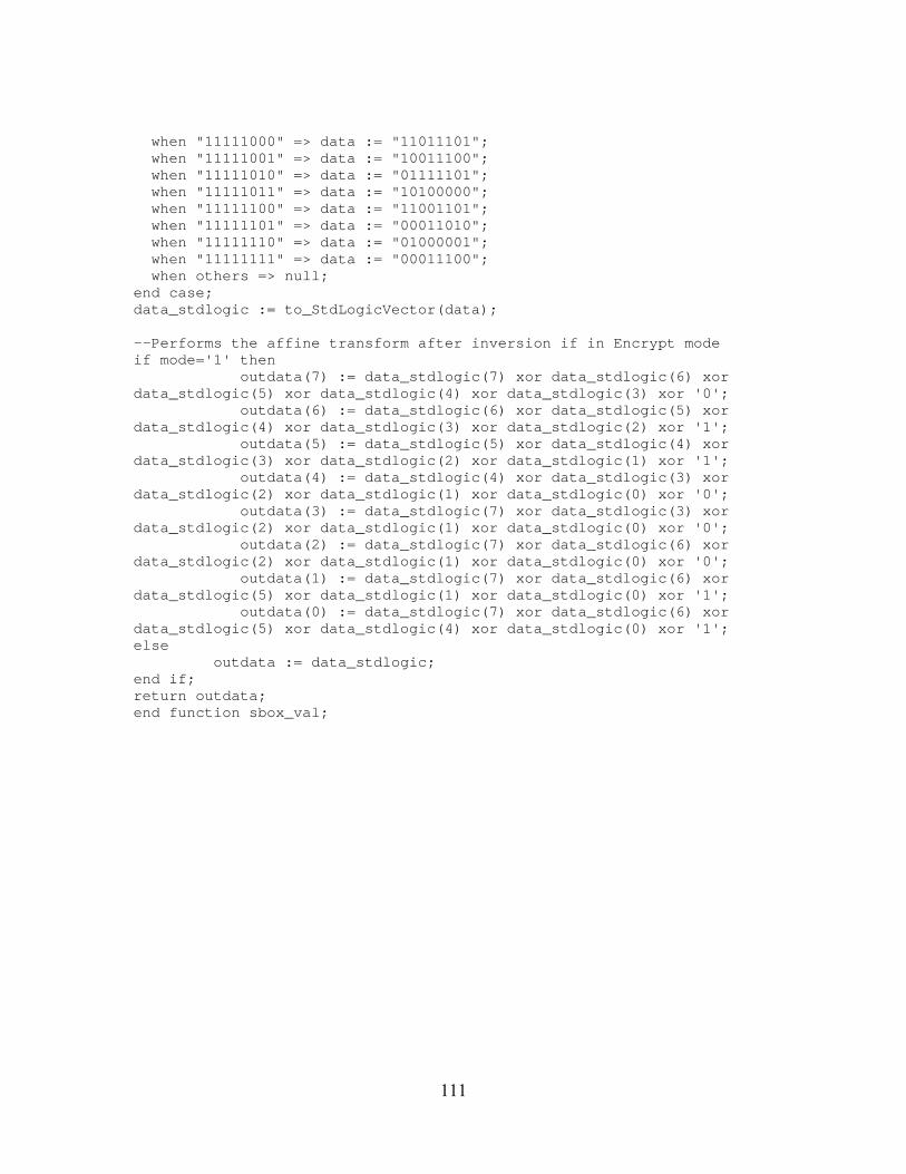
when "11111000" => data := "11011101"; when "11111001" => data := "10011100"; when "11111010" => data := "01111101"; when "11111011" => data := "10100000"; when "11111100" => data := "11001101"; when "11111101" => data := "00011010"; when "11111110" => data := "01000001"; when "11111111" => data := "00011100"; when others => null; end case; data_stdlogic := to_StdLogicVector(data); --Performs the affine transform after inversion if in Encrypt mode if mode='1' then outdata(7) := data_stdlogic(7) xor data_stdlogic(6) xor data_stdlogic(5) xor data_stdlogic(4) xor data_stdlogic(3) xor '0'; outdata(6) := data_stdlogic(6) xor data_stdlogic(5) xor data_stdlogic(4) xor data_stdlogic(3) xor data_stdlogic(2) xor '1'; outdata(5) := data_stdlogic(5) xor data_stdlogic(4) xor data_stdlogic(3) xor data_stdlogic(2) xor data_stdlogic(1) xor '1'; outdata(4) := data_stdlogic(4) xor data_stdlogic(3) xor data_stdlogic(2) xor data_stdlogic(1) xor data_stdlogic(0) xor '0'; outdata(3) := data_stdlogic(7) xor data_stdlogic(3) xor data_stdlogic(2) xor data_stdlogic(1) xor data_stdlogic(0) xor '0'; outdata(2) := data_stdlogic(7) xor data_stdlogic(6) xor data_stdlogic(2) xor data_stdlogic(1) xor data_stdlogic(0) xor '0'; outdata(1) := data_stdlogic(7) xor data_stdlogic(6) xor data_stdlogic(5) xor data_stdlogic(1) xor data_stdlogic(0) xor '1'; outdata(0) := data_stdlogic(7) xor data_stdlogic(6) xor data_stdlogic(5) xor data_stdlogic(4) xor data_stdlogic(0) xor '1'; else outdata := data_stdlogic; end if; return outdata; end function sbox_val;
111

SubBytes Composite Field Inversion
--Function performs multiplication in the subfield function mult( inmult1: std_logic_vector(3 downto 0); inmult2: std_logic_vector(3 downto 0) ) return std_logic_vector is variable outmult: std_logic_vector(3 downto 0); variable a: std_logic; variable b: std_logic; variable c: std_logic; begin a := inmult1(3) xor inmult1(0); b := inmult1(1) xor inmult1(0); c := inmult1(2) xor inmult1(1); outmult(3) := (inmult2(3) and inmult1(3)) xor (inmult2(2) and inmult1(0)) xor (inmult2(1) and inmult1(1)) xor (inmult2(0) and inmult1(2)); outmult(2) := (inmult2(3) and inmult1(2)) xor (inmult2(2) and a) xor (inmult2(1) and b) xor (inmult2(0) and c); outmult(1) := (inmult2(3) and inmult1(1)) xor (inmult2(2) and inmult1(2)) xor (inmult2(1) and a) xor (inmult2(0) and b); outmult(0) := (inmult2(3) and inmult1(0)) xor (inmult2(2) and inmult1(1)) xor (inmult2(1) and inmult1(2)) xor (inmult2(0) and a); return outmult; end function mult; --Function squares in the subfield function squarer(in_sq: std_logic_vector(3 downto 0)) return std_logic_vector is variable out_sq: std_logic_vector(3 downto 0); begin out_sq(3) := in_sq(3) xor in_sq(1); out_sq(2) := in_sq(1); out_sq(1) := in_sq(2) xor in_sq(0); out_sq(0) := in_sq(0); return out_sq; end function squarer; --Function inverts polynomials in the subfield function inv_val(input: std_logic_vector(7 downto 0)) return std_logic_vector is variable z1: std_logic_vector(3 downto 0); variable input2: std_logic_vector(7 downto 0); variable z0: std_logic_vector(3 downto 0); variable z1_squared: std_logic_vector(3 downto 0); variable z0_squared: std_logic_vector(3 downto 0);
112

variable z1z0: std_logic_vector(3 downto 0); variable bz1 : std_logic_vector(3 downto 0); variable F: std_logic_vector(3 downto 0); variable Finv: bit_vector(3 downto 0); variable Finv_stdlogic: std_logic_vector(3 downto 0); variable D1: std_logic_vector(3 downto 0); variable D0: std_logic_vector(3 downto 0); variable z1xorz0: std_logic_vector(3 downto 0); variable final : std_logic_vector(7 downto 0); constant b14: std_logic_vector := "1001"; begin --Converts to “big endian” notation input2(7) := input(0); input2(6) := input(1); input2(5) := input(2); input2(4) := input(3); input2(3) := input(4); input2(2) := input(5); input2(1) := input(6); input2(0) := input(7); --Computes Z values z1(3) := input2(6) xor input2(2) xor input2(0); z1(2) := input2(5) xor input2(4); z1(1) := input2(6) xor input2(3) xor input2(1) xor input2(0); z1(0) := input2(2) xor input2(0); z0(3) := input2(7) xor input2(4) xor input2(3) xor input2(1) xor input2(0); z0(2) := input2(5) xor input2(1); z0(1) := input2(6) xor input2(5) xor input2(2) xor input2(0); z0(0) := input2(6) xor input2(5) xor input2(3) xor input2(2) xor input2(0); z1_squared := squarer(z1); z0_squared := squarer(z0); z1z0 := mult(z1,z0); bz1 := mult(b14,z1_squared); F(3) := z0_squared(3) xor z1z0(3) xor bz1(3); F(2) := z0_squared(2) xor z1z0(2) xor bz1(2); F(1) := z0_squared(1) xor z1z0(1) xor bz1(1); F(0) := z0_squared(0) xor z1z0(0) xor bz1(0); --Composite field inversion LUT case F is when "0000" => Finv := "0000"; when "0001" => Finv := "1111"; when "0010" => Finv := "1011"; when "0011" => Finv := "0101"; when "0100" => Finv := "1001"; when "0101" => Finv := "0011";
113

when "0110" => Finv := "1110"; when "0111" => Finv := "1100"; when "1000" => Finv := "1000"; when "1001" => Finv := "0100"; when "1010" => Finv := "1101"; when "1011" => Finv := "0010"; when "1100" => Finv := "0111"; when "1101" => Finv := "1010"; when "1110" => Finv := "0110"; when "1111" => Finv := "0001"; when others => null; end case; Finv_stdlogic := to_StdLogicVector(Finv); D1 := mult(z1, Finv_stdlogic); z1xorz0(3) := z1(3) xor z0(3); z1xorz0(2) := z1(2) xor z0(2); z1xorz0(1) := z1(1) xor z0(1); z1xorz0(0) := z1(0) xor z0(0); D0 := mult(z1xorz0, Finv_stdlogic); --[D1(3) D1(2) D1(1) D1(0) D0(3) D0(2) D0(1) D0(0) final(0) := D1(2) xor D1(1) xor D1(0) xor D0(3) xor D0(1); final(1) := D1(3) xor D1(0); final(2) := D1(3) xor D0(1); final(3) := D1(3) xor D1(2) xor D0(1); final(4) := D0(1) xor D0(0); final(5) := D1(1) xor D0(2) xor D0(0); final(6) := D1(3) xor D0(2) xor D0(1); final(7) := D1(1) xor D1(0) xor D0(2) xor D0(0); return final; end function inv_val; --Function performs affine transforms depending on Encrypt/Decrypt mode function sbox_val(inp: std_logic_vector(7 downto 0); mode: std_logic) return std_logic_vector is variable address: std_logic_vector(7 downto 0); variable data_stdlogic: std_logic_vector(7 downto 0); variable outdata: std_logic_vector(7 downto 0); begin if mode='0' then address(7) := inp(6) xor inp(4) xor inp(1) xor '0'; address(6) := inp(5) xor inp(3) xor inp(0) xor '0'; address(5) := inp(7) xor inp(4) xor inp(2) xor '0'; address(4) := inp(6) xor inp(3) xor inp(1) xor '0'; address(3) := inp(5) xor inp(2) xor inp(0) xor '0'; address(2) := inp(7) xor inp(4) xor inp(1) xor '1'; address(1) := inp(6) xor inp(3) xor inp(0) xor '0'; address(0) := inp(7) xor inp(5) xor inp(2) xor '1'; else
114
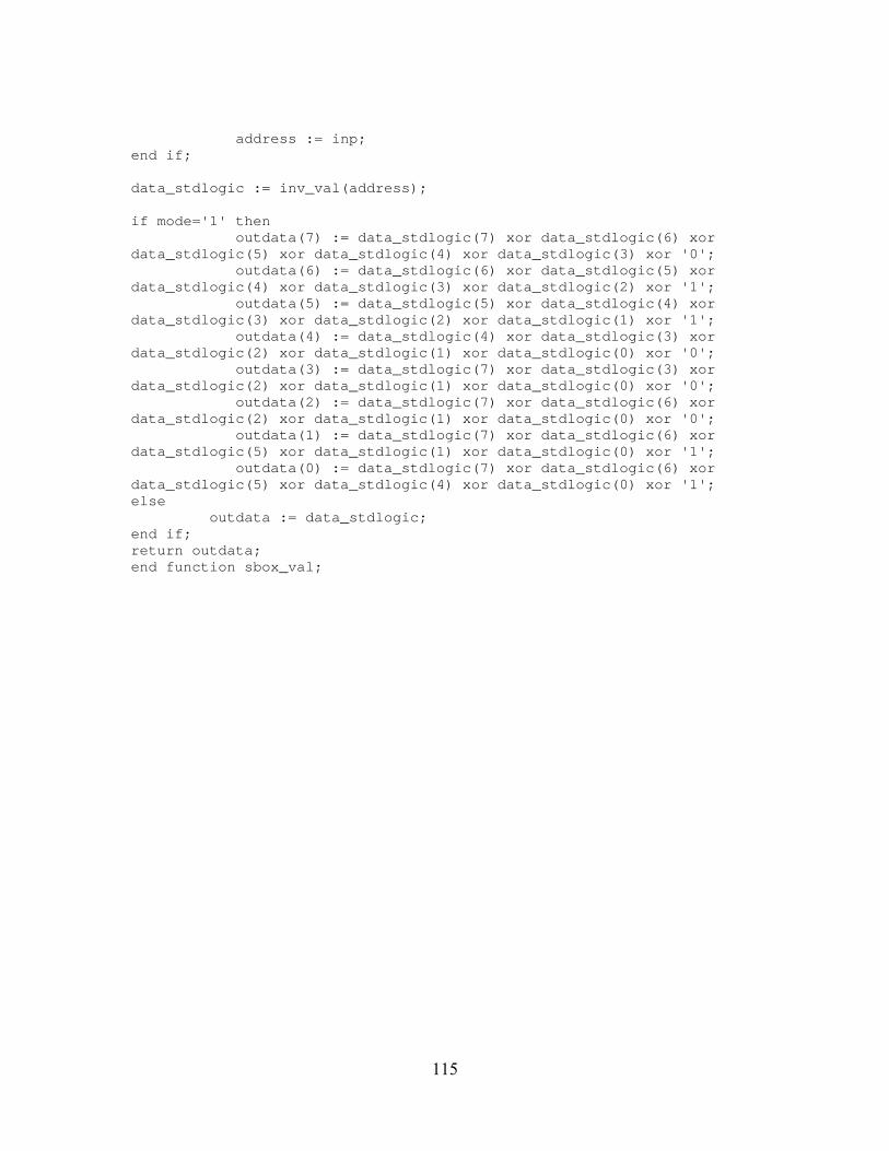
address := inp; end if; data_stdlogic := inv_val(address); if mode='1' then outdata(7) := data_stdlogic(7) xor data_stdlogic(6) xor data_stdlogic(5) xor data_stdlogic(4) xor data_stdlogic(3) xor '0'; outdata(6) := data_stdlogic(6) xor data_stdlogic(5) xor data_stdlogic(4) xor data_stdlogic(3) xor data_stdlogic(2) xor '1'; outdata(5) := data_stdlogic(5) xor data_stdlogic(4) xor data_stdlogic(3) xor data_stdlogic(2) xor data_stdlogic(1) xor '1'; outdata(4) := data_stdlogic(4) xor data_stdlogic(3) xor data_stdlogic(2) xor data_stdlogic(1) xor data_stdlogic(0) xor '0'; outdata(3) := data_stdlogic(7) xor data_stdlogic(3) xor data_stdlogic(2) xor data_stdlogic(1) xor data_stdlogic(0) xor '0'; outdata(2) := data_stdlogic(7) xor data_stdlogic(6) xor data_stdlogic(2) xor data_stdlogic(1) xor data_stdlogic(0) xor '0'; outdata(1) := data_stdlogic(7) xor data_stdlogic(6) xor data_stdlogic(5) xor data_stdlogic(1) xor data_stdlogic(0) xor '1'; outdata(0) := data_stdlogic(7) xor data_stdlogic(6) xor data_stdlogic(5) xor data_stdlogic(4) xor data_stdlogic(0) xor '1'; else outdata := data_stdlogic; end if; return outdata; end function sbox_val;
115

MixColumns Full LUT
--xtime LUT function xtimes(inp: std_logic_vector(7 downto 0)) return std_logic_vector is variable table: bit_vector(7 downto 0); variable table_stdlogic: std_logic_vector(7 downto 0); begin case inp is when X"00" => table := X"00"; when X"01" => table := X"02"; when X"02" => table := X"04"; when X"03" => table := X"06"; when X"04" => table := X"08"; when X"05" => table := X"0a"; when X"06" => table := X"0c"; when X"07" => table := X"0e"; when X"08" => table := X"10"; when X"09" => table := X"12"; when X"0a" => table := X"14"; when X"0b" => table := X"16"; when X"0c" => table := X"18"; when X"0d" => table := X"1a"; when X"0e" => table := X"1c"; when X"0f" => table := X"1e"; when X"10" => table := X"20"; when X"11" => table := X"22"; when X"12" => table := X"24"; when X"13" => table := X"26"; when X"14" => table := X"28"; when X"15" => table := X"2a"; when X"16" => table := X"2c"; when X"17" => table := X"2e"; when X"18" => table := X"30"; when X"19" => table := X"32"; when X"1a" => table := X"34"; when X"1b" => table := X"36"; when X"1c" => table := X"38"; when X"1d" => table := X"3a"; when X"1e" => table := X"3c"; when X"1f" => table := X"3e"; when X"20" => table := X"40"; when X"21" => table := X"42"; when X"22" => table := X"44"; when X"23" => table := X"46"; when X"24" => table := X"48"; when X"25" => table := X"4a"; when X"26" => table := X"4c"; when X"27" => table := X"4e"; when X"28" => table := X"50"; when X"29" => table := X"52"; when X"2a" => table := X"54"; when X"2b" => table := X"56"; when X"2c" => table := X"58";
116
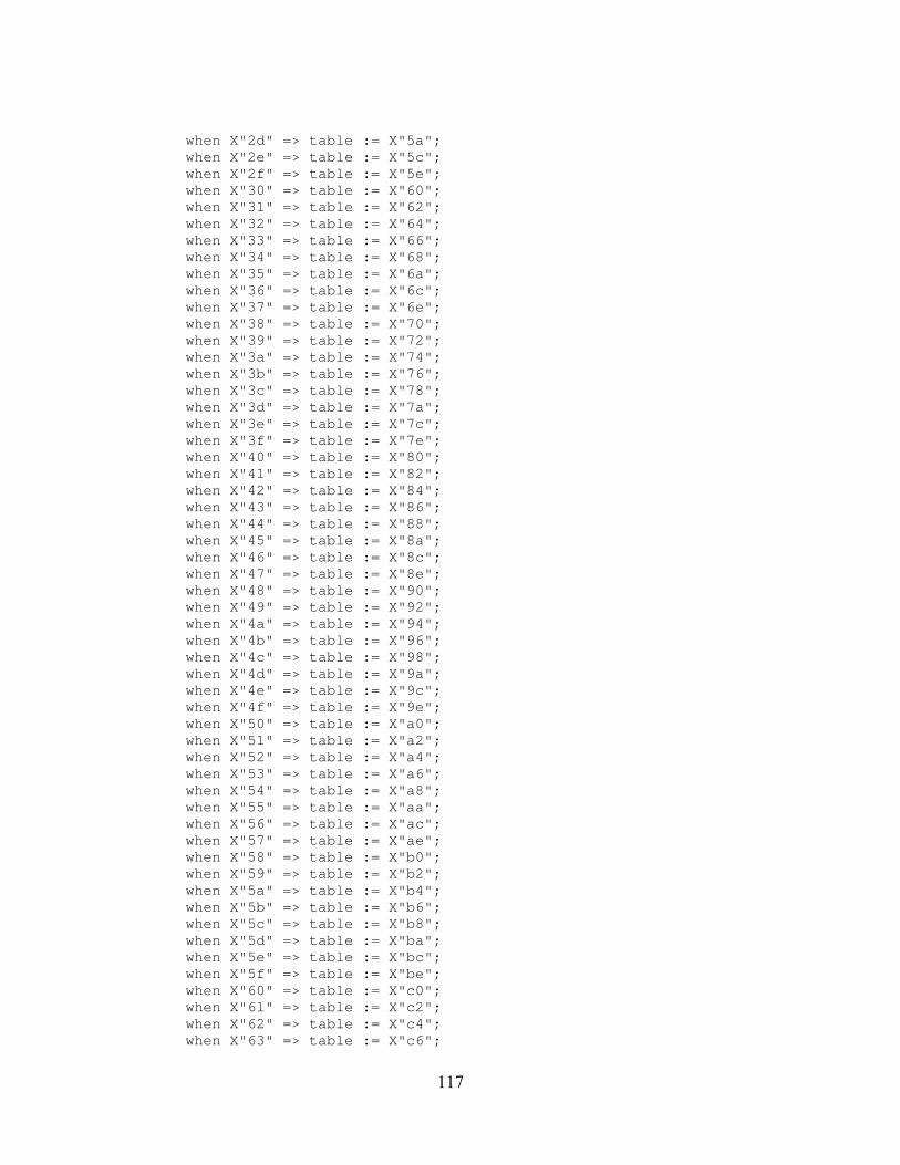
when X"2d" => table := X"5a"; when X"2e" => table := X"5c"; when X"2f" => table := X"5e"; when X"30" => table := X"60"; when X"31" => table := X"62"; when X"32" => table := X"64"; when X"33" => table := X"66"; when X"34" => table := X"68"; when X"35" => table := X"6a"; when X"36" => table := X"6c"; when X"37" => table := X"6e"; when X"38" => table := X"70"; when X"39" => table := X"72"; when X"3a" => table := X"74"; when X"3b" => table := X"76"; when X"3c" => table := X"78"; when X"3d" => table := X"7a"; when X"3e" => table := X"7c"; when X"3f" => table := X"7e"; when X"40" => table := X"80"; when X"41" => table := X"82"; when X"42" => table := X"84"; when X"43" => table := X"86"; when X"44" => table := X"88"; when X"45" => table := X"8a"; when X"46" => table := X"8c"; when X"47" => table := X"8e"; when X"48" => table := X"90"; when X"49" => table := X"92"; when X"4a" => table := X"94"; when X"4b" => table := X"96"; when X"4c" => table := X"98"; when X"4d" => table := X"9a"; when X"4e" => table := X"9c"; when X"4f" => table := X"9e"; when X"50" => table := X"a0"; when X"51" => table := X"a2"; when X"52" => table := X"a4"; when X"53" => table := X"a6"; when X"54" => table := X"a8"; when X"55" => table := X"aa"; when X"56" => table := X"ac"; when X"57" => table := X"ae"; when X"58" => table := X"b0"; when X"59" => table := X"b2"; when X"5a" => table := X"b4"; when X"5b" => table := X"b6"; when X"5c" => table := X"b8"; when X"5d" => table := X"ba"; when X"5e" => table := X"bc"; when X"5f" => table := X"be"; when X"60" => table := X"c0"; when X"61" => table := X"c2"; when X"62" => table := X"c4"; when X"63" => table := X"c6";
117

when X"64" => table := X"c8"; when X"65" => table := X"ca"; when X"66" => table := X"cc"; when X"67" => table := X"ce"; when X"68" => table := X"d0"; when X"69" => table := X"d2"; when X"6a" => table := X"d4"; when X"6b" => table := X"d6"; when X"6c" => table := X"d8"; when X"6d" => table := X"da"; when X"6e" => table := X"dc"; when X"6f" => table := X"de"; when X"70" => table := X"e0"; when X"71" => table := X"e2"; when X"72" => table := X"e4"; when X"73" => table := X"e6"; when X"74" => table := X"e8"; when X"75" => table := X"ea"; when X"76" => table := X"ec"; when X"77" => table := X"ee"; when X"78" => table := X"f0"; when X"79" => table := X"f2"; when X"7a" => table := X"f4"; when X"7b" => table := X"f6"; when X"7c" => table := X"f8"; when X"7d" => table := X"fa"; when X"7e" => table := X"fc"; when X"7f" => table := X"fe"; when X"80" => table := X"1b"; when X"81" => table := X"19"; when X"82" => table := X"1f"; when X"83" => table := X"1d"; when X"84" => table := X"13"; when X"85" => table := X"11"; when X"86" => table := X"17"; when X"87" => table := X"15"; when X"88" => table := X"0b"; when X"89" => table := X"09"; when X"8a" => table := X"0f"; when X"8b" => table := X"0d"; when X"8c" => table := X"03"; when X"8d" => table := X"01"; when X"8e" => table := X"07"; when X"8f" => table := X"05"; when X"90" => table := X"3b"; when X"91" => table := X"39"; when X"92" => table := X"3f"; when X"93" => table := X"3d"; when X"94" => table := X"33"; when X"95" => table := X"31"; when X"96" => table := X"37"; when X"97" => table := X"35"; when X"98" => table := X"2b"; when X"99" => table := X"29"; when X"9a" => table := X"2f";
118

when X"9b" => table := X"2d"; when X"9c" => table := X"23"; when X"9d" => table := X"21"; when X"9e" => table := X"27"; when X"9f" => table := X"25"; when X"a0" => table := X"5b"; when X"a1" => table := X"59"; when X"a2" => table := X"5f"; when X"a3" => table := X"5d"; when X"a4" => table := X"53"; when X"a5" => table := X"51"; when X"a6" => table := X"57"; when X"a7" => table := X"55"; when X"a8" => table := X"4b"; when X"a9" => table := X"49"; when X"aa" => table := X"4f"; when X"ab" => table := X"4d"; when X"ac" => table := X"43"; when X"ad" => table := X"41"; when X"ae" => table := X"47"; when X"af" => table := X"45"; when X"b0" => table := X"7b"; when X"b1" => table := X"79"; when X"b2" => table := X"7f"; when X"b3" => table := X"7d"; when X"b4" => table := X"73"; when X"b5" => table := X"71"; when X"b6" => table := X"77"; when X"b7" => table := X"75"; when X"b8" => table := X"6b"; when X"b9" => table := X"69"; when X"ba" => table := X"6f"; when X"bb" => table := X"6d"; when X"bc" => table := X"63"; when X"bd" => table := X"61"; when X"be" => table := X"67"; when X"bf" => table := X"65"; when X"c0" => table := X"9b"; when X"c1" => table := X"99"; when X"c2" => table := X"9f"; when X"c3" => table := X"9d"; when X"c4" => table := X"93"; when X"c5" => table := X"91"; when X"c6" => table := X"97"; when X"c7" => table := X"95"; when X"c8" => table := X"8b"; when X"c9" => table := X"89"; when X"ca" => table := X"8f"; when X"cb" => table := X"8d"; when X"cc" => table := X"83"; when X"cd" => table := X"81"; when X"ce" => table := X"87"; when X"cf" => table := X"85"; when X"d0" => table := X"bb"; when X"d1" => table := X"b9";
119
when X"d2" => table := X"bf"; when X"d3" => table := X"bd"; when X"d4" => table := X"b3"; when X"d5" => table := X"b1"; when X"d6" => table := X"b7"; when X"d7" => table := X"b5"; when X"d8" => table := X"ab"; when X"d9" => table := X"a9"; when X"da" => table := X"af"; when X"db" => table := X"ad"; when X"dc" => table := X"a3"; when X"dd" => table := X"a1"; when X"de" => table := X"a7"; when X"df" => table := X"a5"; when X"e0" => table := X"db"; when X"e1" => table := X"d9"; when X"e2" => table := X"df"; when X"e3" => table := X"dd"; when X"e4" => table := X"d3"; when X"e5" => table := X"d1"; when X"e6" => table := X"d7"; when X"e7" => table := X"d5"; when X"e8" => table := X"cb"; when X"e9" => table := X"c9"; when X"ea" => table := X"cf"; when X"eb" => table := X"cd"; when X"ec" => table := X"c3"; when X"ed" => table := X"c1"; when X"ee" => table := X"c7"; when X"ef" => table := X"c5"; when X"f0" => table := X"fb"; when X"f1" => table := X"f9"; when X"f2" => table := X"ff"; when X"f3" => table := X"fd"; when X"f4" => table := X"f3"; when X"f5" => table := X"f1"; when X"f6" => table := X"f7"; when X"f7" => table := X"f5"; when X"f8" => table := X"eb"; when X"f9" => table := X"e9"; when X"fa" => table := X"ef"; when X"fb" => table := X"ed"; when X"fc" => table := X"e3"; when X"fd" => table := X"e1"; when X"fe" => table := X"e7"; when X"ff" => table := X"e5"; when others => null; end case; table_stdlogic := to_StdLogicVector(table); return table_stdlogic; end function xtimes; --Processing step for encryption function col_transform(p: state_array_type) return std_logic_vector is variable result: std_logic_vector(7 downto 0);
120
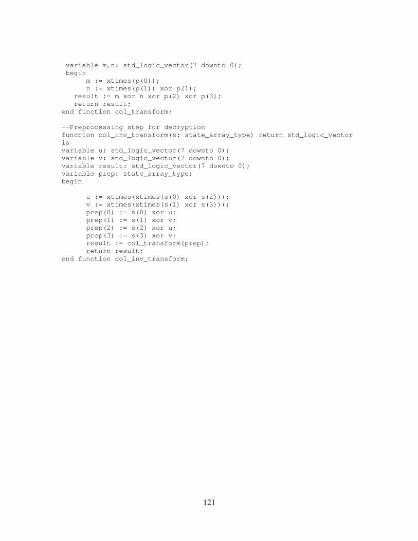
variable m,n: std_logic_vector(7 downto 0); begin m := xtimes(p(0)); n := xtimes(p(1)) xor p(1); result := m xor n xor p(2) xor p(3); return result; end function col_transform; --Preprocessing step for decryption function col_inv_transform(s: state_array_type) return std_logic_vector is variable u: std_logic_vector(7 downto 0); variable v: std_logic_vector(7 downto 0); variable result: std_logic_vector(7 downto 0); variable prep: state_array_type; begin u := xtimes(xtimes(s(0) xor s(2))); v := xtimes(xtimes(s(1) xor s(3))); prep(0) := s(0) xor u; prep(1) := s(1) xor v; prep(2) := s(2) xor u; prep(3) := s(3) xor v; result := col_transform(prep); return result; end function col_inv_transform;
121

MixColumns Half LUT
function xtimes(inp: std_logic_vector(7 downto 0)) return std_logic_vector is variable table: bit_vector(7 downto 0); variable table_stdlogic: std_logic_vector(7 downto 0); begin --replaces half of xtime LUT with a bitwise shift if inp < X"80" then table_stdlogic := (inp(6 downto 0) & '0'); else --the other half of the LUT case inp is when X"80" => table := X"1b"; when X"81" => table := X"19"; when X"82" => table := X"1f"; when X"83" => table := X"1d"; when X"84" => table := X"13"; when X"85" => table := X"11"; when X"86" => table := X"17"; when X"87" => table := X"15"; when X"88" => table := X"0b"; when X"89" => table := X"09"; when X"8a" => table := X"0f"; when X"8b" => table := X"0d"; when X"8c" => table := X"03"; when X"8d" => table := X"01"; when X"8e" => table := X"07"; when X"8f" => table := X"05"; when X"90" => table := X"3b"; when X"91" => table := X"39"; when X"92" => table := X"3f"; when X"93" => table := X"3d"; when X"94" => table := X"33"; when X"95" => table := X"31"; when X"96" => table := X"37"; when X"97" => table := X"35"; when X"98" => table := X"2b"; when X"99" => table := X"29"; when X"9a" => table := X"2f"; when X"9b" => table := X"2d"; when X"9c" => table := X"23"; when X"9d" => table := X"21"; when X"9e" => table := X"27"; when X"9f" => table := X"25"; when X"a0" => table := X"5b"; when X"a1" => table := X"59"; when X"a2" => table := X"5f"; when X"a3" => table := X"5d"; when X"a4" => table := X"53"; when X"a5" => table := X"51"; when X"a6" => table := X"57"; when X"a7" => table := X"55";
122

when X"a8" => table := X"4b"; when X"a9" => table := X"49"; when X"aa" => table := X"4f"; when X"ab" => table := X"4d"; when X"ac" => table := X"43"; when X"ad" => table := X"41"; when X"ae" => table := X"47"; when X"af" => table := X"45"; when X"b0" => table := X"7b"; when X"b1" => table := X"79"; when X"b2" => table := X"7f"; when X"b3" => table := X"7d"; when X"b4" => table := X"73"; when X"b5" => table := X"71"; when X"b6" => table := X"77"; when X"b7" => table := X"75"; when X"b8" => table := X"6b"; when X"b9" => table := X"69"; when X"ba" => table := X"6f"; when X"bb" => table := X"6d"; when X"bc" => table := X"63"; when X"bd" => table := X"61"; when X"be" => table := X"67"; when X"bf" => table := X"65"; when X"c0" => table := X"9b"; when X"c1" => table := X"99"; when X"c2" => table := X"9f"; when X"c3" => table := X"9d"; when X"c4" => table := X"93"; when X"c5" => table := X"91"; when X"c6" => table := X"97"; when X"c7" => table := X"95"; when X"c8" => table := X"8b"; when X"c9" => table := X"89"; when X"ca" => table := X"8f"; when X"cb" => table := X"8d"; when X"cc" => table := X"83"; when X"cd" => table := X"81"; when X"ce" => table := X"87"; when X"cf" => table := X"85"; when X"d0" => table := X"bb"; when X"d1" => table := X"b9"; when X"d2" => table := X"bf"; when X"d3" => table := X"bd"; when X"d4" => table := X"b3"; when X"d5" => table := X"b1"; when X"d6" => table := X"b7"; when X"d7" => table := X"b5"; when X"d8" => table := X"ab"; when X"d9" => table := X"a9"; when X"da" => table := X"af"; when X"db" => table := X"ad"; when X"dc" => table := X"a3"; when X"dd" => table := X"a1"; when X"de" => table := X"a7";
123

when X"df" => table := X"a5"; when X"e0" => table := X"db"; when X"e1" => table := X"d9"; when X"e2" => table := X"df"; when X"e3" => table := X"dd"; when X"e4" => table := X"d3"; when X"e5" => table := X"d1"; when X"e6" => table := X"d7"; when X"e7" => table := X"d5"; when X"e8" => table := X"cb"; when X"e9" => table := X"c9"; when X"ea" => table := X"cf"; when X"eb" => table := X"cd"; when X"ec" => table := X"c3"; when X"ed" => table := X"c1"; when X"ee" => table := X"c7"; when X"ef" => table := X"c5"; when X"f0" => table := X"fb"; when X"f1" => table := X"f9"; when X"f2" => table := X"ff"; when X"f3" => table := X"fd"; when X"f4" => table := X"f3"; when X"f5" => table := X"f1"; when X"f6" => table := X"f7"; when X"f7" => table := X"f5"; when X"f8" => table := X"eb"; when X"f9" => table := X"e9"; when X"fa" => table := X"ef"; when X"fb" => table := X"ed"; when X"fc" => table := X"e3"; when X"fd" => table := X"e1"; when X"fe" => table := X"e7"; when X"ff" => table := X"e5"; when others => null; end case; table_stdlogic := to_StdLogicVector(table); end if; return table_stdlogic; end function xtimes; --Processing step for encryption function col_transform(p: state_array_type) return std_logic_vector is variable result: std_logic_vector(7 downto 0); variable m,n: std_logic_vector(7 downto 0); begin m := xtimes(p(0)); n := xtimes(p(1)) xor p(1); result := m xor n xor p(2) xor p(3); return result; end function col_transform; --Preprocessing step for decryption function col_inv_transform(s: state_array_type) return std_logic_vector is variable u: std_logic_vector(7 downto 0);
124
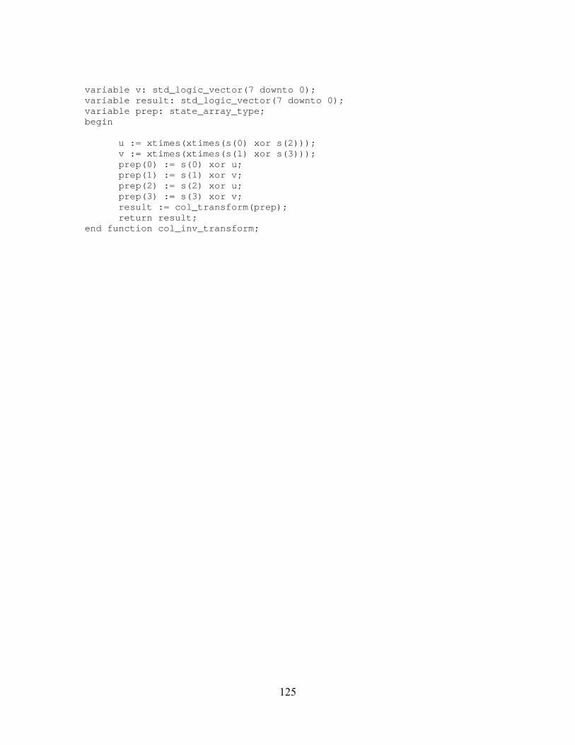
variable v: std_logic_vector(7 downto 0); variable result: std_logic_vector(7 downto 0); variable prep: state_array_type; begin u := xtimes(xtimes(s(0) xor s(2))); v := xtimes(xtimes(s(1) xor s(3))); prep(0) := s(0) xor u; prep(1) := s(1) xor v; prep(2) := s(2) xor u; prep(3) := s(3) xor v; result := col_transform(prep); return result; end function col_inv_transform;
125
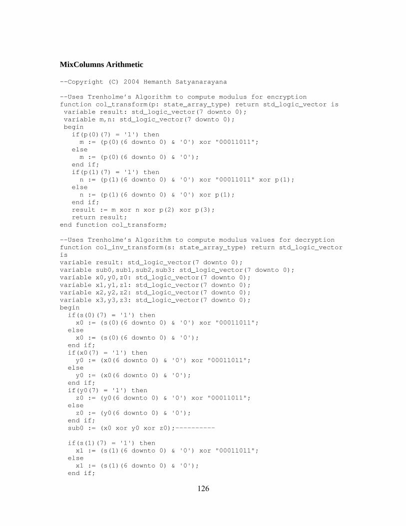
MixColumns Arithmetic
--Copyright (C) 2004 Hemanth Satyanarayana --Uses Trenholme’s Algorithm to compute modulus for encryption function col_transform(p: state_array_type) return std_logic_vector is variable result: std_logic_vector(7 downto 0); variable m,n: std_logic_vector(7 downto 0); begin if(p(0)(7) = '1') then m := (p(0)(6 downto 0) & '0') xor "00011011"; else m := (p(0)(6 downto 0) & '0'); end if; if(p(1)(7) = '1') then n := (p(1)(6 downto 0) & '0') xor "00011011" xor p(1); else n := (p(1)(6 downto 0) & '0') xor p(1); end if; result := m xor n xor p(2) xor p(3); return result; end function col_transform; --Uses Trenholme’s Algorithm to compute modulus values for decryption function col_inv_transform(s: state_array_type) return std_logic_vector is variable result: std_logic_vector(7 downto 0); variable sub0,sub1,sub2,sub3: std_logic_vector(7 downto 0); variable x0,y0,z0: std_logic_vector(7 downto 0); variable x1,y1,z1: std_logic_vector(7 downto 0); variable x2,y2,z2: std_logic_vector(7 downto 0); variable x3,y3,z3: std_logic_vector(7 downto 0); begin if(s(0)(7) = '1') then x0 := (s(0)(6 downto 0) & '0') xor "00011011"; else x0 := (s(0)(6 downto 0) & '0'); end if; if(x0(7) = '1') then y0 := (x0(6 downto 0) & '0') xor "00011011"; else y0 := (x0(6 downto 0) & '0'); end if; if(y0(7) = '1') then z0 := (y0(6 downto 0) & '0') xor "00011011"; else z0 := (y0(6 downto 0) & '0'); end if; sub0 := (x0 xor y0 xor z0);---------- if(s(1)(7) = '1') then x1 := (s(1)(6 downto 0) & '0') xor "00011011"; else x1 := (s(1)(6 downto 0) & '0'); end if;
126

if(x1(7) = '1') then y1 := (x1(6 downto 0) & '0') xor "00011011"; else y1 := (x1(6 downto 0) & '0'); end if; if(y1(7) = '1') then z1 := (y1(6 downto 0) & '0') xor "00011011"; else z1 := (y1(6 downto 0) & '0'); end if; sub1 := (x1 xor z1 xor s(1));---------- if(s(2)(7) = '1') then x2 := (s(2)(6 downto 0) & '0') xor "00011011"; else x2 := (s(2)(6 downto 0) & '0'); end if; if(x2(7) = '1') then y2 := (x2(6 downto 0) & '0') xor "00011011"; else y2 := (x2(6 downto 0) & '0'); end if; if(y2(7) = '1') then z2 := (y2(6 downto 0) & '0') xor "00011011"; else z2 := (y2(6 downto 0) & '0'); end if; sub2 := (y2 xor z2 xor s(2));---------- if(s(3)(7) = '1') then x3 := (s(3)(6 downto 0) & '0') xor "00011011"; else x3 := (s(3)(6 downto 0) & '0'); end if; if(x3(7) = '1') then y3 := (x3(6 downto 0) & '0') xor "00011011"; else y3 := (x3(6 downto 0) & '0'); end if; if(y3(7) = '1') then z3 := (y3(6 downto 0) & '0') xor "00011011"; else z3 := (y3(6 downto 0) & '0'); end if; sub3 := (z3 xor s(3));---------- result := sub0 xor sub1 xor sub2 xor sub3; return result; end function col_inv_transform;
127

128
Appendix C: Statistical Data Tables
Table 25. Analysis of Variance Table for Area Occupied Source DF Seq SS Adj SS Adj MS SubBytes Design 2 13700255055 13700255055 6850127527 MixColumns Design 2 15902640562 15902640562 7951320281 Synthesis Goal 1 550544684 550544684 550544684 SubBytes Design*MixColumns Design 4 150371320 150371320 37592830 SubBytes Design*Synthesis Goal 2 37100094 37100094 18550047 MixColumns Design*Synthesis Goal 2 5430919 5430919 2715460 SubBytes Design*MixColumns Design* 4 196245452 196245452 49061363 Synthesis Goal Error 0 * * * Total 17 30542588085 S = *
Table 26. Quantification of Effects for Area Occupied SE
Term Coef Coef T P Constant 81053.8 * * *
SubBytes Des Composite Field Inversion -26670.3 * * * Extended Field Inversion -11326.8 * * *
MixColumns D Arithmetic -21268.4 * * * Half LUT -20765.8 * * *
Synthesis Go Area -5530.44 * * *
SubBytes Des*MixColumns D Composite Field Inversion Arithmetic -1314.56 * * * Composite Field Inversion Half LUT -2135.22 * * * Extended Field Inversion Arithmetic -889.056 * * * Extended Field Inversion Half LUT -1350.22 * * *
SubBytes Des*Synthesis Go Composite Field Inversion Area 1156.94 * * * Extended Field Inversion Area 866.444 * * *
MixColumns D*Synthesis Go Arithmetic Area 743.111 * * * Half LUT Area -567.556 * * *
SubBytes Des*MixColumns D*Synthesis Go Composite Field Inversion Arithmetic Area 1457.89 * * * Composite Field Inversion Half LUT Area 2507.56 * * * Extended Field Inversion Arithmetic Area 1201.39 * * * Extended Field Inversion Half LUT Area 1342.56 * * *

129
Table 27. Analysis of Variance Table for Area Efficiency Source DF Seq SS Adj SS Adj MS F P SubBytes Design 2 257.976 257.976 128.988 ** MixColumns Design 2 409.585 409.585 204.792 ** Synthesis Goal 1 20.278 20.278 20.278 ** SubBytes Design*MixColumns Design 4 81.639 81.639 20.410 ** SubBytes Design*Synthesis Goal 2 7.496 7.496 3.748 ** MixColumns Design*Synthesis Goal 2 6.390 6.390 3.195 ** SubBytes Design*MixColumns Design* 4 2.710 2.710 0.677 ** Synthesis Goal Error 0 * * * Total 17 786.074 S = *
Table 28. Quantification of Effects for Area Efficiency
SE SE Term Coef Coef T P Constant 11.0028 * * *
SubBytes Des Composite Field Inversion 3.45900 * * * Extended Field Inversion 1.80950 * * *
MixColumns D Arithmetic 3.16817 * * * Half LUT 3.57383 * * *
Synthesis Go Area -1.06139 * * *
SubBytes Des*MixColumns D Composite Field Inversion Arithmetic 1.37900 * * * Composite Field Inversion Half LUT 1.61733 * * * Extended Field Inversion Arithmetic 0.402500 * * * Extended Field Inversion Half LUT 0.706833 * * *
SubBytes Des*Synthesis Go Composite Field Inversion Area -0.853444 * * * Extended Field Inversion Area 0.706722 * * *
MixColumns D*Synthesis Go Arithmetic Area -0.720944 * * * Half LUT Area -0.017278 * * *
SubBytes Des*MixColumns D*Synthesis Go Composite Field Inversion Arithmetic Area -0.319222 * * * Composite Field Inversion Half LUT Area -0.447889 * * * Extended Field Inversion Arithmetic Area 0.091611 * * * Extended Field Inversion Half LUT Area 0.291944 * * *

130
Bibliography
[CaA03] C. Caltagirone and K. Anantha. High Throughput, Parallelized 128-bit AES Encryption in a Resource-Limited FPGA. In Proceedings of the Fifteenth Annual ACM Symposium on Parallel Algorithms and Architectures, pages 240-241, San Diego, CA, 2003.
[ChG01] P. Chodowiec and K. Gaj. Comparison of the Hardware Performance of
the AES Candidates using Reconfigurable Hardware. George Mason University, Fairfax, VA, 2001.
[DaR98] J. Daemen and V. Rijmen. The Design of Rijndael. AES—The Advanced
Encryption Standard. Heidelberg: Springer-Verlag, 1998. [GoB05] T. Good and M. Benaissa. AES on FPGA from the Fastest to the Smallest.
In Proceedings of the Cryptographic Hardware and Embedded Systems Conference, Lecture Notes in Computer Science vol 3659, pages 427-440, 29 August 2005.
[JST03] K. Järvinen, J.O. Skyttä, and M.T. Tommiska. A Fully Pipelined
Memoryless 17.8 Gbps AES-128 Encryptor. In Proceedings of the 2003 ACM/SIGDA Elenventh International Symposium on FPGAs, pages 207-215, Monterey, CA, 2003.
[Nis01] National Institute of Standards and Technology. Announcing the Advanced
Encryption Standard (AES). Federal Information Standards Publication, 2001.
[Odr01] C. O’Driscoll. Hardware Implementation Aspects of the Rijndael Block
Cipher. Masters thesis. National University of Ireland, Cork, Ireland 2001. [PaR97] C. Paar and M. Rosner. Comparison of arithmetic architectures for Reed-
Solomon decoders in reconfigurable hardware. In Proceedings of the Fifth IEEE Symposium on FPGA-Based Custom Compting Machines, pages 219-225, 1997.
[Pio04] T. Pionteck, T. Staake, T. Stiefmeier, L.D. Kabulepa, and M. Glesner.
Design of a reconfigurable AES encryption/decryption engine for mobile terminals. In Proceedings of the 2004 International Symposium on Circuits and Systems vol 2, pages 545-548, May 2004.
[QIS05] H. Qin, Y. Iguchi, and T. Sasao. An FPGA design of AES encryption
circuit with 128-bit keys. In Proceedings of the 15th ACM Great Lakes Symposium on VLSI, pages 147-151, 2005.
131
[Rij94] V. Rijmen. Efficient Implementation of the Rijndael S-Box. Katholieke Universiteit Leuven, Heverlee, Belgium, 1994.
[Rou04] G. Rouvroy, F.X. Standaert, J.J. Quisquater, and J.D. Legat. Compact and
Efficient Encryption/Decryption Module for FPGA Implementation of the AES Rijndael Very Well Suited for Small Embedded Applications. In Proceedings of the International Converence on Information Technology: Coding and Computing vol 2, page 583, 2004.
[Rud01] A. Rudra, P.K. Dubey, C.S. Jutla, V. Kumar, J.R. Rao, and P. Rohatgi.
Efficient Implementation of Rijndael Encryption with Composite Field Arithmetic. In Proceedings of the Cryptographic Hardware and Embedded Systems Conference, Lecture Notes in Computer Science vol 2162, pages 171-185, Paris, France, May 2001.
[Sat04] H. Satyanarayana. aes_crypto_core. open source VHDL http://www.opencores.org/projects.cgi/web/aes_crypto_core/overview 28 December 2004. [SDR] N.A. Saqib, A. Díaz-Pérez, and F. Rodríguez-Henriquez. A Compact and
Efficient FPGA Implementation of the DES Algorithm. Computer Science Section, Electrical Engineering Department, Centro de Investigaci´on y de Estudios Avanzados del IPN (Not Dated).
[Sti06] D.R. Stinson. Cryptography Theory and Practice (3rd Edition). Boca
Raton: Chapman & Hall/CRC, 2006. [Wik06a] Wikipedia Contributors. “Finite Field Arithmetic”, Wikipedia, The Free
Encyclopedia. n. pag. http://en.wikipedia.org/w/index.php?title=Finite_field_arithmetic&oldid=95285693, 19 December 2006.
[Wik06b] Wikipedia Contributors. “Rijndael key schedule”, Wikipedia, The Free
Encyclopedia. n. pag. http://en.wikipedia.org/w/index.php?title=Rijndael_key_schedule&oldid=95563942, 20 December 2006.
[Wik07a] Wikipedia Contributors. “Advanced Encryption Standard”, Wikipedia, The
Free Encyclopedia. n. pag. http://en.wikipedia.org/w/index.php?title=Advanced_Encryption_Standard&oldid=102110762, 21 January 2007.
132
[Wik07b] Wikipedia Contributors. “Finite Field”, Wikipedia, The Free Encyclopedia. n. pag. http://en.wikipedia.org/w/index.php?title=Finite_field&oldid=99871161, 10 January 2007.
[Xil07] Xilinx. Xilinx Virtex-II Series FPGAs. page 2, 2007.
http://www.xilinx.com/publications/matrix/virtexmatrix.pdf. [ZCN04] J. Zambreno, A. Choudhary, and D. Nguyen. Exploring Area/Delay
Tradeoffs in an AES FPGA Implementation. In Proceedings of the International Conference on Field-Programmable Logic and its Applications, pages 575-585, August 2004.
133
Vita
Second Lieutenant Ryan Jay Silva graduated from Regis Jesuit High School in
Aurora, Colorado. He entered undergraduate studies at the United States Air Force
Academy in Colorado Springs, Colorado where he graduated with a Bachelor of Science
degree in Electrical Engineering in June 2005. His first assignment was to complete this
thesis at the Air Force Institute of Technology. Upon graduation he will be assigned to
the 84 Radar Evaluation Squadron at Hill, AFB in Ogden, Utah. He looks forward to
leaving the dreary Midwestern landscape for the sunny mountains of Utah.

Form Approved REPORT DOCUMENTATION PAGE OMB No. 074-0188
The public reporting burden for this collection of information is estimated to average 1 hour per response, including the time for reviewing instructions, searching existing data sources, gathering and maintaining the data needed, and completing and reviewing the collection of information. Send comments regarding this burden estimate or any other aspect of the collection of information, including suggestions for reducing this burden to Department of Defense, Washington Headquarters Services, Directorate for Information Operations and Reports (0704-0188), 1215 Jefferson Davis Highway, Suite 1204, Arlington, VA 22202-4302. Respondents should be aware that notwithstanding any other provision of law, no person shall be subject to an penalty for failing to comply with a collection of information if it does not display a currently valid OMB control number. PLEASE DO NOT RETURN YOUR FORM TO THE ABOVE ADDRESS. 1. REPORT DATE (DD-MM-YYYY) 2. REPORT TYPE 3. DATES COVERED (From – To)
22-03-2007 Master’s Thesis August 2005 – March 2007 5a. CONTRACT NUMBER
5b. GRANT NUMBER
134
4. TITLE AND SUBTITLE
Implementation and Optimization of the Advanced Encryption Standard Algorithm on an 8-Bit Field Programmable Gate Array
Hardware Platform 5c. PROGRAM ELEMENT NUMBER
5d. PROJECT NUMBER
6. AUTHOR(S)
5e. TASK NUMBER
Silva, Ryan J., 2LT, USAF 5f. WORK UNIT NUMBER
8. PERFORMING ORGANIZATION 7. PERFORMING ORGANIZATION NAMES(S) AND ADDRESS(S) Air Force Institute of Technology Graduate School of Engineering and Management (AFIT/EN) 2950 Hobson Way, Building 640
REPORT NUMBER AFIT/GE/ENG/07-21
WPAFB OH 45433-8865 10. SPONSOR/MONITOR’S ACRONYM(S)
9. SPONSORING/MONITORING AGENCY NAME(S) AND ADDRESS(ES) Christopher E Reuter, Civ, AFRL/SNTA (937) 320-9068 x163, [email protected] 2241 Avionics Circle WPAFB, OH 4433-7320
11. SPONSOR/MONITOR’S REPORT NUMBER(S)
12. DISTRIBUTION/AVAILABILITY STATEMENT APPROVED FOR PUBLIC RELEASE; DISTRIBUTION UNLIMITED.
13. SUPPLEMENTARY NOTES 14. ABSTRACT The contribution of this research is three-fold. The first is a method of converting the area occupied by a circuit implemented on a Field Programmable Gate Array (FPGA) to an equivalent as a measure of total gate count. This allows direct comparison between two FPGA implementations independent of the manufacturer or chip family. The second contribution improves the performance of the Advanced Encryption Standard (AES) on an 8-bit computing platform. This research develops an AES design that occupies less than three quarters of the area reported by the smallest design in current literature as well as significantly increases area efficiency. The third contribution of this research is an examination of how various designs for the critical AES SubBytes and MixColumns transformations interact and affect the overall performance of AES. The transformations responsible for the largest variance in performance are identified and the effect is measured in terms of throughput, area efficiency, and area occupied. 15. SUBJECT TERMS Advanced Encryption Standard, Cryptology, Field Programmable Gate Array, Number Theory
16. SECURITY CLASSIFICATION OF:
19a. NAME OF RESPONSIBLE PERSON Dr. Rusty O. Baldwin
17. LIMITATION OF
18. NUMBER
ABSTRACT OF 19b. TELEPHONE NUMBER (Include area code) a. REPORT
U
b. ABSTRACT
U
c. THIS PAGE
PAGES 937-785-6565
[email protected] 133 UU U Standard Form 298 (Rev. 8-98)
Prescribed by ANSI Std. Z39-18

135