IJRMHM 24 418 2006
9
Magnesium interlayered diamond coating on silicon M.A. Dar a , S.G. Ansari b , Z.A. Ansari b , Hironobu Umemoto b , Young-Soon Kim a , Hyung-Kee Seo a , Gil-Sung Kim a , Eun-Kyung Suh c , Hyung-Shik Shin a, * a Thin Film Technology Laboratory, School of Chemical Engineering, Chonbuk National University, Chonju 561-756, South Korea b School of Materials Science, Japan Advanced Institute of Science and Technology, 1-1 Asahidai, Nomi, Ishikawa 923-1292, Japan c Department of Semiconductor Science and Technology, Chonbuk National University, Chonju 561-756, South Korea Received 8 March 2005; accepted 30 June 2005 Abstract Diamond thin films have been deposited using hot filament chemical vapour deposition technique on manually scratched p- Si(1 0 0) substrate, with and without magnesium interlayer. In spite of magnesium melting point being lower (T m = 649 °C) than the growth temperature of the substrate (T s 750 °C) used in these experiments, it was found that high quality diamond films could be grown on Mg covered substrate. A liquid substrate is probably generated during the diamond film growth. Raman spectroscopy analysis exhibited only the triply degenerate, zone centre optical phonon peak at 1333 cm 1 indicating that nearly stress free crys- tallites were present. Broadening of the Raman peak (11.76 cm 1 ) indicates that some small crystallites also are present. Scanning electron and atomic force microscopy accompanied by X-ray diffraction analysis where used to compare the details of diamond film growth directly on scratched Si(1 0 0) and Mg interlayered scratched Si(1 0 0) substrates. Ó 2005 Elsevier Ltd. All rights reserved. Keywords: HFCVD; Diamond film; Buffer layer; Bias growth 1. Introduction Diamond thin films have been deposited on a variety of substrates in order to exploit the excellent mechani- cal, thermal, optical or electronic properties of diamond for a wide variety of applications. Properties and appli- cations of diamond thin films have been discussed in some excellent reviews published earlier, e.g. Refs. [1– 3]. Due to their high wear resistance; diamond thin films coated tools are often used in industry. Protective, smooth coatings of diamond are deposited on magnetic disks. Chemical inertness and mechanical strength accompanied by their scratch resistance and large trans- mission coefficient in visible and infrared regions make them suitable as a window material for IR and other detectors. They are also investigated for their field emis- sion properties and array of diamond coated metal tips are expected to be used in flat panel displays. Electronics industry finds diamond thin films also useful for high- speed devices, especially when they are to be deployed at high temperature. Their large thermal conductivity and large electrical resistance makes them suitable as heat sinks. When used in electronics, deposition of diamond film on silicon substrate becomes important in order to inte- grate it with current microelectronics technology. How- ever, its nucleation density on polished silicon substrates is very low [4], in the range of 10 3 –10 5 cm 2 . Therefore, several methods [4–7] have been used to increase the nucleation density and growth rate of diamond films on silicon. Success of Mitsuda et al. [8] to enhance the nucleation density of diamond film by scratching the 0263-4368/$ - see front matter Ó 2005 Elsevier Ltd. All rights reserved. doi:10.1016/j.ijrmhm.2005.06.009 * Corresponding author. Tel.: +82 63 270 2438; fax: +82 63 270 2306. E-mail address: [email protected] (H.-S. Shin). International Journal of Refractory Metals & Hard Materials 24 (2006) 418–426 www.elsevier.com/locate/ijrmhm
Transcript of IJRMHM 24 418 2006

International Journal of Refractory Metals & Hard Materials 24 (2006) 418–426
www.elsevier.com/locate/ijrmhm
Magnesium interlayered diamond coating on silicon
M.A. Dar a, S.G. Ansari b, Z.A. Ansari b, Hironobu Umemoto b, Young-Soon Kim a,Hyung-Kee Seo a, Gil-Sung Kim a, Eun-Kyung Suh c, Hyung-Shik Shin a,*
a Thin Film Technology Laboratory, School of Chemical Engineering, Chonbuk National University, Chonju 561-756, South Koreab School of Materials Science, Japan Advanced Institute of Science and Technology, 1-1 Asahidai, Nomi, Ishikawa 923-1292, Japan
c Department of Semiconductor Science and Technology, Chonbuk National University, Chonju 561-756, South Korea
Received 8 March 2005; accepted 30 June 2005
Abstract
Diamond thin films have been deposited using hot filament chemical vapour deposition technique on manually scratched p-Si(100) substrate, with and without magnesium interlayer. In spite of magnesium melting point being lower (Tm = 649 �C) thanthe growth temperature of the substrate (Ts � 750 �C) used in these experiments, it was found that high quality diamond films couldbe grown on Mg covered substrate. A liquid substrate is probably generated during the diamond film growth. Raman spectroscopyanalysis exhibited only the triply degenerate, zone centre optical phonon peak at 1333 cm�1 indicating that nearly stress free crys-tallites were present. Broadening of the Raman peak (�11.76 cm�1) indicates that some small crystallites also are present. Scanningelectron and atomic force microscopy accompanied by X-ray diffraction analysis where used to compare the details of diamond filmgrowth directly on scratched Si(100) and Mg interlayered scratched Si(100) substrates.� 2005 Elsevier Ltd. All rights reserved.
Keywords: HFCVD; Diamond film; Buffer layer; Bias growth
1. Introduction
Diamond thin films have been deposited on a varietyof substrates in order to exploit the excellent mechani-cal, thermal, optical or electronic properties of diamondfor a wide variety of applications. Properties and appli-cations of diamond thin films have been discussed insome excellent reviews published earlier, e.g. Refs. [1–3]. Due to their high wear resistance; diamond thin filmscoated tools are often used in industry. Protective,smooth coatings of diamond are deposited on magneticdisks. Chemical inertness and mechanical strengthaccompanied by their scratch resistance and large trans-mission coefficient in visible and infrared regions make
0263-4368/$ - see front matter � 2005 Elsevier Ltd. All rights reserved.doi:10.1016/j.ijrmhm.2005.06.009
* Corresponding author. Tel.: +82 63 270 2438; fax: +82 63 2702306.
E-mail address: [email protected] (H.-S. Shin).
them suitable as a window material for IR and otherdetectors. They are also investigated for their field emis-sion properties and array of diamond coated metal tipsare expected to be used in flat panel displays. Electronicsindustry finds diamond thin films also useful for high-speed devices, especially when they are to be deployedat high temperature. Their large thermal conductivityand large electrical resistance makes them suitable asheat sinks.
When used in electronics, deposition of diamond filmon silicon substrate becomes important in order to inte-grate it with current microelectronics technology. How-ever, its nucleation density on polished silicon substratesis very low [4], in the range of 103–105 cm�2. Therefore,several methods [4–7] have been used to increase thenucleation density and growth rate of diamond filmson silicon. Success of Mitsuda et al. [8] to enhance thenucleation density of diamond film by scratching the

M.A. Dar et al. / International Journal of Refractory Metals & Hard Materials 24 (2006) 418–426 419
substrate with diamond grit has lead many groups to usethis procedure as a common practice. The substrateshave also been scratched using c-BN [9], Cu [10], siliconcarbide [11], etc. Manual as well as ultrasonic scratchinghas been employed to increase the nucleation density bynearly five orders of magnitude. Scratching creates de-fects, steps or dislocations, which can act as nucleationcentres. Sometimes the residual particles of scratchingmaterial left behind also initiate the growth. However,it is rather difficult to reproduce or control the surfaceuniformity by scratching. Nonetheless systematic effortswere made by Ali et al. [12] to investigate the effect ofparticle size of the scratching material and scratchingtime on diamond film growth on the substrate. Theyshowed that better results could be obtained when usingparticle size less than �3 lm and scratching time�10 min or above produced similar results. It has alsobeen shown in the past that seeding or coating [13,14]enhances the nucleation centres on the substrate. A re-cent work using SnO2 overlayers [15] scratching alsowas essential to enhance the diamond thin film growth.
Yugo et al. [16] and many others later (e.g. [17])adopted a different approach to achieve as high as1010 cm�2 nucleation density without scratching orusing any other surface pre-treatment. They simplybiased the substrate to enhance the nucleation density.Combination of bias enhanced nucleation (BEN) meth-od with diamond grit scratched silicon surface producesgood quality diamond thin films as demonstrated in ourlaboratory [18] and some others.
Another approach bearing similarity to the tradi-tional growth technique of high temperature high-pres-sure growth of diamonds is to use some catalyst.Carbide forming catalysts like Ti, W, Fe, Co, B, etc.and non-carbidic catalysts like Au, Ag, Cu, etc. also ap-pear to have been widely used [4]. In certain cases, met-als, metal oxides, metal carbides as catalysts or theiroverlayers [4,7,15,19–21] have been utilized in order tounderstand the growth rates of diamond films on thesesubstrates. In general the growth of diamond thin filmson carbidic surfaces is better.
Besides the substrate materials and their pre-treat-ment, the methods of deposition and conditions are verycrucial in the growth of diamond films [2,4]. In mostof the depositions, growth of diamond films is observedat relatively high substrate temperatures, viz. above600 �C. At such temperatures surface diffusion wouldalso be quite important in determining the growth ofdiamond film on any surface. In this context it is inter-esting to note that diamonds have been grown [22] withCu, Zn and Ge at high temperature and pressure muchabove their melting point. Magnesium melting tempera-ture is 649 �C, lower than that used in hot filamentchemical vapour deposition (HFCVD). It was thereforefound interesting to use magnesium interlayer to growdiamond thin film on silicon substrate, using HFCVD
technique. To the best of our knowledge, so far thereare no reports about diamond film growth either onMg or its thin film. Besides, there are certain advantagesof using Mg as an interlayer. Magnesium is also a lightelement, useful as a structural material. However it caneasily get oxidized and scratched. Therefore protectivecoating like diamond thin film on Mg is desired.
Amongst the various chemical vapour deposition(CVD) techniques like DC, RF, microwave, electroncyclotron resonance (ECR) or laser ablation, hot fila-ment chemical vapour deposition HFCVD has beenone of the most attractive methods due to its relativelysimple instrumentation and high deposition ratecapability.
In this communication, we show that high qualitydiamond thin films comparable or even better thanthose on scratched silicon substrate can be grown onMg interlayered scratched Si(1 00) using HFCVDmethod.
2. Experimental
2.1. Substrate preparation
In these experiments p-Si(100) substrates (borondoped) cut from a single wafer to 15 · 7 mm2 size wereemployed. Wafers of �650-lm thickness were obtained,purchased from Siltron Inc. (LG) Korea. Substrateswere degreased in boiling acetone for 20 min and thenwashed ultrasonically in de-ionized water. Many groupshave adopted this cleaning procedure for diamond filmdeposition by HFCVD. Substrates were scratchedmanually using 1 lm diamond paste (mono-crystallinediamond, commercially available for grinding and poli-shing). This was followed by cleaning in acetone andultrasonic bath as before.
2.2. Thin films depositions
Deposition of magnesium overlayers on scratchedSi(1 00) substrates was carried out in a physical vapourdeposition system pumped to a base vacuum �10�6 Torr.Ten samples were deposited simultaneously by evapo-rating high purity Mg(99.9%) from Aldrich, held in atungsten filament. Post deposition analysis of thin filmsusing stylus technique showed that �0.05 ± 0.002 lmthick films were deposited.
Deposition of diamond thin films on scratchedSi(1 00) and Mg covered scratched Si(1 00) substratewas carried out in an HFCVD reported elsewhere [18].Briefly, the HFCVD reactor is an ultra high vacuumstainless steel chamber equipped with a filament andsubstrate manipulators, gas inlets and view ports. Thefilament temperature is monitored using an opticalpyrometer (Minolta TR-630, Japan) and substrate

420 M.A. Dar et al. / International Journal of Refractory Metals & Hard Materials 24 (2006) 418–426
temperature is recorded using K-type thermocouple.For diamond deposition the substrate and filament dis-tance was kept as �5 mm. The tungsten filament (coilshaped, 0.5 mm diameters, 150 mm length) was resis-tively heated to 2150 ± 50 �C temperature resulting intothe substrate temperature equal to 750 ± 50 �C. The sub-strate surface temperature must be higher than this tem-perature, as it was measured by touching thermocoupleat the backside of the substrate. In the present setup, itwas not possible to measure the surface temperature.
A mixture of high purity H2(99.999%) and CH4(99.5%)was introduced from the bottom of the reaction cham-ber. The gas flow rates were controlled using mass flowcontrollers in such a way that volume % of CH4:H2
was 1:100. The total flow rate was 100 sccm and thetotal pressure inside the chamber was maintained at30 ± 2 Torr during the deposition. The substrates werenegatively biased to �280 V for first 30 min and furtherdeposition was carried out for 90 min. The entire sample(scratched Si and Mg coated Si) was deposited undersimilar conditions. As the only difference between thetwo substrates is the Mg overlayer, which coversthe scratches on Si(10 0) we expect any change in thediamond film growth to be due to the presence of Mglayers exclusively. In case of substrates coated withMg, the bias current was slightly less (�5–7 mA) thanthe Si without Mg overlayer.
2.3. Analysis of samples
Surface topography/morphology of the samples wasobserved using atomic force microscope (ATM) andscanning electron microscope (SEM). The AFM Nano-scope R IV from Digital Instruments Metrology Groupwas employed in tapping mode. A silicon probe with10 nm diameters was used in the analysis. SEM analysiswas performed using an ISM-6400, JEOL, Japanmicroscope.
Structure analysis of the samples was carried outusing X-ray diffraction technique (XRD). For this pur-pose, a Rigaku III/A, Japan, powder diffractometer withcopper target (Cu Ka-1.54 A) and nickel filter was used.Raman spectra were recorded using a Micro Raman(Reinshaw) with He–Ne laser source (k-6328 A). Spec-tral resolution �2 cm�1 could be achieved with thisinstrument. The X-ray photoelectron spectroscopicstudy was carried out using S-Probe ESCA model2803 (Fision Instrument, 10 kV, 20 mA) with Al Ka asthe source of X-rays.
3. Results and discussion
Nucleation and growth on transition metals, metaloxides and carbides have been widely studied and alsoreviewed [4]. In most of the cases they are used as cata-
lysts. As well as the structural defects like terraces, steps,and pores along with chemical impurities, seeds andoverlayers greatly affect the quality and crystallinity ofthe diamond film. Therefore growth directly on de-fected/over layers deposited on Si has been a subjectof research and is being investigated. Here we discussthe effect of a Mg layer (�0.05 lm), deposited onscratched Si(1 00), on the nucleation and growth of dia-mond film, in comparison with that of diamond filmgrown on scratched Si(1 00) substrate, an often usedsubstrate. Magnesium has a hexagonal close pack(hcp) structure with a = 3.21 A and c = 5.21 A as latticeparameters. Therefore the lattice mismatch of diamondwith magnesium can be 6.6% or 33.6% depending uponthe growth. However as mentioned earlier, magnesiumhas a melting point of 649 �C, which is substantiallylower than the substrate heating performed in thisexperiment (750 ± 50 �C). It should be mentioned herethat magnesium thin films were deposited in a relativelypoor vacuum �10�6 Torr and were transported in labo-ratory environment from one system to another forHFCVD growth, therefore inclusion of some carbonand oxygen is inevitable. However as discussed in somereviews earlier [1,4], small amounts of oxygen and inclu-sion may not adversely affect the nucleation and growthbut even assist in some cases. During the electrical bias-ing, it was noticed that the bias current, with Mg layerwas slight less (�5–7 mA) than Si substrate. This mightbe due the inclusion of oxygen while sample transfer.
SEM images of diamond film on scratched Si(1 00)and that with Mg interlayer on scratched Si(1 00) areillustrated in Fig. 1(a) and (b), respectively. Here theimmediate impression is that the particles grown onscratched Si(1 00) are larger than those with Mg inter-layer. A careful examination of Fig. 1(a) shows thatthere are many triangular platelets on top of bigger crys-tallites. These triangles are (111) oriented crystallitesand have �0.5–1.5 lm sides. Fig. 1(b) too has similarsized triangular platelets but they are not grown onlarger crystallites, and they appear to be smaller, denserand uniform. A rough estimate, from SEM image, ofthe surface nucleation density is of the order of 0.3 ·1010 cm�2, 0.8 · 1010 cm�2 whereas growth rate is0.2 · 1010 cm�2 h�1, 0.5 · 1010 cm�2 h�1, for the scratchedand Mg coated substrate.
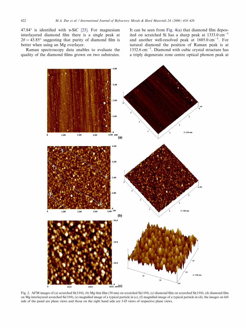
As AFM is an extremely surface sensitive techniquewith zoom-in capability, more insight about the differ-ences between the two films was possible from the fol-lowing analysis. Fig. 2 illustrate the AFM (planar and3D) images of (a) scratched Si(10 0) surface, (b) Mg thinfilm grown on scratched Si(1 00) surface (before dia-mond deposition), (c) diamond thin film grown onSi(1 00) surface and (d) that grown on Mg coveredSi(1 00) surface. In Fig. 2(a) random but nearly parallel�50 nm width lines, broken at various points are ob-served. There are also few other bigger particles, proba-

Fig. 1. SEM images of (a) diamond film grown on scratched Si(100)surface, (b) diamond film grown on Mg interlayered scratched Si(100)surface.
M.A. Dar et al. / International Journal of Refractory Metals & Hard Materials 24 (2006) 418–426 421
bly from the diamond grit, randomly distributed on thesurface. Small particles usually are active centres for fur-ther growth due to their large surface area and danglingbonds in case of semiconductors. As high is the densityof such particles as better it is for the film growth. Aver-age root mean square (RMS) roughness of scratchedSi(1 00) surface as estimated from AFM is �2.6 nm.The roughened surface of the substrate is consideredto be responsible for the enhanced growth and adhesionof thin film. Thus growth of Mg thin film, as seen inFig. 2(b), also would be favoured by a silicon-roughenedsurface. As can be seen from Fig. 2(b), Mg film hasnearly spherical particles �0.05–0.1 lm size, randomlydistributed over the surface. However they are quitedense. Film RMS roughness is 10 nm as obtained byAFM. In this film Si scratches are no more observed, ex-cept few regions, which appear like reminiscences ofscratching. Such regions are marked with arrows anddotted lines in Fig. 2(b). In bulk XRD very weak signal
(not showed here) due to Mg could be detected at2h = 34.4� and 36.6� corresponding to hcp Mg(002)and (101) planes. The signal is very weak because Mgoverlayer thickness (�0.05 lm) is small and bulk XRDis employed here. However, the effect of Mg over layeron diamond film deposition could be observed. InFig. 2(c) and (d) morphology of diamond thin film onsilicon scratched and that on Mg covered scratched sili-con surface can be seen. These images grabbed by AFMare shown on a much wider scale (30 · 30 lm2) in eachcase compared to Fig. 2(a) and (b) because the size ofthe diamond particles are �0.5–1.5 lm (as in SEM) inboth the cases. Images in Fig. 2(c) and (d) appear tobe similar, except that the particle density is higherand height shorter in Fig. 2(d) as compared to that inFig. 2(c). Thus by observing Fig. 2(c) and (d), one getsan impression that morphology and perhaps the qualityof films grown on scratched Si(1 00) and Mg coveredscratched Si(100) are nearly the same. However furtheranalysis of the films reveals some marked differences.Fig. 2(e) and (f), respectively show the magnified topview of the smaller regions on typical particles for dia-mond film on scratched Si and that with Mg overlayer.Interestingly, these images of single particles indeedshow morphological differences. In Fig. 2(e), for dia-mond film on scratched Si, two faceted particles withbase of about 400 nm are visible. Whereas on Mg cov-ered scratched Si substrate there are numerous ratherflat but triangular particles with varied sizes. Most ofthese particles have sides smaller than 100 nm. On thesesmaller particles there can be even smaller particles,however they could not be observed with the AFM usedin these experiments. In any case, the surface of Mginterlayered diamond film has much smaller and denserparticles (surface nucleation density 0.8 · 1010 cm�2) ascompared to film grown on scratched Si(0.3 ·1010 cm�2). Also in Fig. 2(e) and (f) the RMS roughnessare �17 and �6 nm, respectively. Thus, much smotherfilms are formed on Mg interlayered surface. Thereforedenser diamond film is expected to grow on Mg interlay-ered substrate.
Further differences in the qualities of diamond filmson scratched Si(10 0) and Mg covered scratchedSi(1 00) are discerned by X-ray diffraction analysis. Onscratched Si(10 0) diffraction peak at 2h = 69.04� wasobserved due to Si(400). However in Fig. 3 only a lim-ited range has been shown as the intensity of Si peak istoo high compared to that due to (111) peaks of dia-mond for the same reasons discussed earlier for Mg film,viz. XRD instrument is for bulk analysis and the dia-mond films are thin. Fig. 3(a)–(d) shows the XRD forall the four samples under consideration. There are nopeaks (curve a and b) on scratched Si or Mg coveredSi scratched substrates in 2h = 38–54� range. InFig. 3(c) the peak at 43.89� is due to the diamond(111) plane [Ref. JCPDS-06-0675] and broad peak at
422 M.A. Dar et al. / International Journal of Refractory Metals & Hard Materials 24 (2006) 418–426
47.84� is identified with a-SiC [23]. For magnesiuminterlayered diamond film there is a single peak at2h = 43.85� suggesting that purity of diamond film isbetter when using an Mg overlayer.
Raman spectroscopy data enables to evaluate thequality of the diamond films grown on two substrates.
Fig. 2. AFM images of (a) scratched Si(100), (b) Mg thin film (50 nm) on scraon Mg interlayered scratched Si(100), (e) magnified image of a typical particleside of the panel are plane views and those on the right hand side are 3-D v
It can be seen from Fig. 4(a) that diamond film depos-ited on scratched Si has a sharp peak at 1333.0 cm�1
and another well-resolved peak at 1605.0 cm�1. Fornatural diamond the position of Raman peak is at1332.6 cm�1. Diamond with cubic crystal structure hasa triply degenerate zone centre optical phonon peak at
tched Si(100), (c) diamond film on scratched Si(100), (d) diamond filmin (c), (f) magnified image of a typical particle in (d), the images on left
iews of respective plane views.
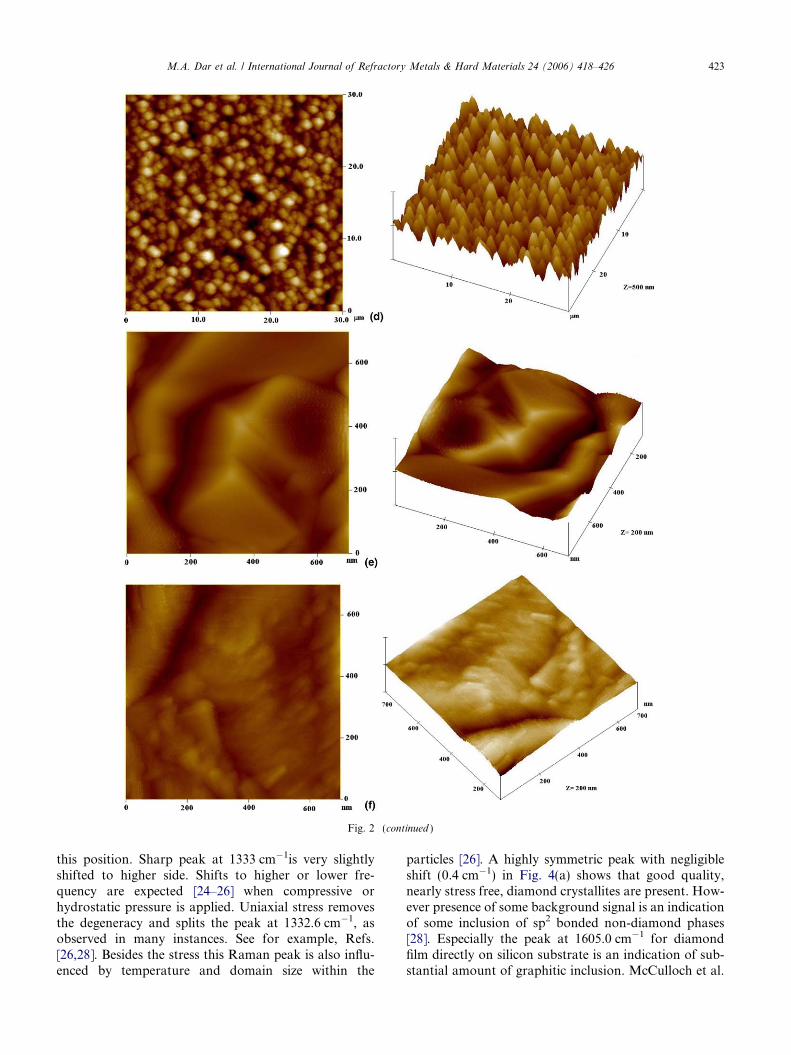
Fig. 2 (continued )
M.A. Dar et al. / International Journal of Refractory Metals & Hard Materials 24 (2006) 418–426 423
this position. Sharp peak at 1333 cm�1is very slightlyshifted to higher side. Shifts to higher or lower fre-quency are expected [24–26] when compressive orhydrostatic pressure is applied. Uniaxial stress removesthe degeneracy and splits the peak at 1332.6 cm�1, asobserved in many instances. See for example, Refs.[26,28]. Besides the stress this Raman peak is also influ-enced by temperature and domain size within the
particles [26]. A highly symmetric peak with negligibleshift (0.4 cm�1) in Fig. 4(a) shows that good quality,nearly stress free, diamond crystallites are present. How-ever presence of some background signal is an indicationof some inclusion of sp2 bonded non-diamond phases[28]. Especially the peak at 1605.0 cm�1 for diamondfilm directly on silicon substrate is an indication of sub-stantial amount of graphitic inclusion. McCulloch et al.

38 40 42 44 46 48 50 52 54
Inte
nsity
(arb
. uni
ts)
a
Bragg angle (2θ, degrees)
bSi
C
cD
(111
)
d
Fig. 3. X-ray diffraction of (a) scratched Si(100), (b) Mg coveredscratched Si(100), (c) diamond film on scratched Si(100) and (d)diamond film on Mg covered scratched Si(100), Cu Ka (k = 1.54 A) isused for XRD.
1100 1200 1300 1400 1500 1600 1700
1333
b
1605 a
Wave number (cm-1)
Nor
mal
ize
Inte
nsity
Fig. 4. Raman spectra of (a) diamond film on scratched Si(100), (b)diamond film on Mg interlayered scratched Si(100). Spectra arenormalized w.r.t. height of the Raman peak at 1333 cm�1. Spectra arerecorded using He–Ne laser (k = 6328 A).
424 M.A. Dar et al. / International Journal of Refractory Metals & Hard Materials 24 (2006) 418–426
[29] showed that due to small graphitic crystallites, aRaman peak (D 0) arises at 1615 cm�1 along with peaks(G and D) at 1580 cm�1 and 1355 cm�1, respectively. Asa result of increase in disorder D 0 and G peaks convo-lute to form a single peak whose position is somewherebetween their original position and shifting to lowerfrequency with increasing disorder. Thus peak in curveFig. 4(a) at 1605 cm�1 can be explained. Besides, smallvariations in substrate conditions, specially uncontrolledmanual scratching of the substrates may be responsiblefor this change. Mg covered scratched Si (Fig. 4(b))shows only a single, symmetric peak at 1333.0 cm�1.There could be small component of amorphous dia-mond (relating to sp2 carbon) as indicated by increasein background from 1400 to 1600 cm�1. However thereis no specific peak and background is less compared tothat in curve of Fig. 4(a). Thus the diamond film onMg overlayer is better as far as inclusions of non-dia-mond film in agreement with XRD results.
The FWHM of Raman peaks observed at 1333.0 cm�1
for diamond film grown on scratched Si and Mg coatedSi is 13.16 cm�1 and 11.76 cm�1, respectively. The stan-dard FWHM for pure diamond is 2.5 cm�1. The addi-tional width can arise due to domain size effect. In fact,the smaller domains lead to the break down in the wavevector (k) conservation rule and thus, states with non-zero k can also contribute in the Raman scattering pro-cess, which leads to peak broadening [26,27]. Thereforeother non-k zero states also may contribute and increasethe Raman peak width. It is thus possible that smallergrains as observed from AFM may be contributing tothe observed Raman peak width in this case. Quantitative
estimation of these contributions is rather difficult tomake at this stage in presence of small particles on largeparticles. Further insight may be obtained in future,using AFM and with Raman spectroscopy.
The most important question however is, what is themechanism for the observed growth of diamond film onthe Mg film with melting point lower than the substratetemperature? The concept of �liquid substrate� forgrowth of diamond films has been proposed by Royet al. [30] and proved in a few cases. Recently Kaoet al. [31] have shown the diamond formation in caseof gold thin film deposited on amorphous silicon layers.They showed that Au–Si alloying takes place and dia-mond formation occurs at a temperature much abovethe melting point of Au–Si, suggesting the diamondgrowth on a �liquid� substrate.
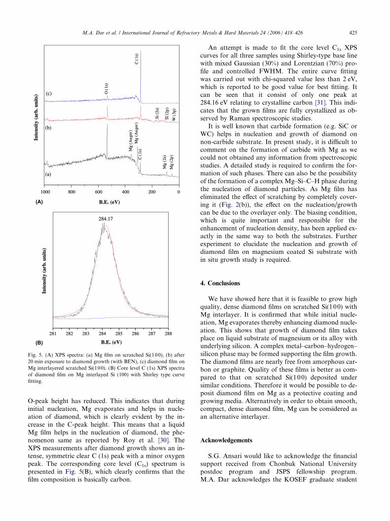
As mentioned before, the substrate temperature ishigher than the melting temperature of Mg; therefore,it can be possible that Mg can evaporate. An attemptis made to understand what happens with Mg whilethe early nucleation of diamond by studying the sampleswith X-ray photoelectron spectroscopic technique. Forthis study, three types of samples are used, viz. (a) Mgdeposited on Si, (b) after 20 min exposure to diamondgrowth (with BEN) and (c) diamond grown on Mginterlayer Si. The corresponding wide scan spectra areshown in Fig. 5(A). In case of sample type (a), peaksrelated to Mg, C and O are seen. The C-contaminationis due to the ambient exposure. It is worth noticing thatSi-substrate is fully coated with Mg. When the samplewas exposed just for 20 min to the initial diamondgrowth (with BEN), the Mg peaks disappeared fromthe XPS spectra, instead Si peaks with a minor W (5p)peaks, can be seen. The C-peak height has increased and
1000 800 600 400 200 0
W (
5p)
Si (
2s)
Si (
2p)
(c)
(b)
C (
1s)
O (
1s)
Mg
(Au
ger)
Mg
(Au
ger)
C (
1s)
Mg
(2s
)
B.E. (eV)
Mg
(2p
)(a)
Inte
nsit
y (a
rb. u
nits
)
281 282 283 284 285 286 287 288
B.E. (eV)
Inte
nsit
y (a
rb. u
nits
)
284.17
(A)
(B)
Fig. 5. (A) XPS spectra: (a) Mg film on scratched Si(100), (b) after20 min exposure to diamond growth (with BEN), (c) diamond film onMg interlayered scratched Si(100). (B) Core level C (1s) XPS spectraof diamond film on Mg interlayed Si (100) with Shirley type curvefitting.
M.A. Dar et al. / International Journal of Refractory Metals & Hard Materials 24 (2006) 418–426 425
O-peak height has reduced. This indicates that duringinitial nucleation, Mg evaporates and helps in nucle-ation of diamond, which is clearly evident by the in-crease in the C-peak height. This means that a liquidMg film helps in the nucleation of diamond, the phe-nomenon same as reported by Roy et al. [30]. TheXPS measurements after diamond growth shows an in-tense, symmetric clear C (1s) peak with a minor oxygenpeak. The corresponding core level (C1s) spectrum ispresented in Fig. 5(B), which clearly confirms that thefilm composition is basically carbon.
An attempt is made to fit the core level C1s XPScurves for all three samples using Shirley-type base linewith mixed Gaussian (30%) and Lorentzian (70%) pro-file and controlled FWHM. The entire curve fittingwas carried out with chi-squared value less than 2 eV,which is reported to be good value for best fitting. Itcan be seen that it consist of only one peak at284.16 eV relating to crystalline carbon [31]. This indi-cates that the grown films are fully crystallized as ob-served by Raman spectroscopic studies.
It is well known that carbide formation (e.g. SiC orWC) helps in nucleation and growth of diamond onnon-carbide substrate. In present study, it is difficult tocomment on the formation of carbide with Mg as wecould not obtained any information from spectroscopicstudies. A detailed study is required to confirm the for-mation of such phases. There can also be the possibilityof the formation of a complex Mg–Si–C–H phase duringthe nucleation of diamond particles. As Mg film haseliminated the effect of scratching by completely cover-ing it (Fig. 2(b)), the effect on the nucleation/growthcan be due to the overlayer only. The biasing condition,which is quite important and responsible for theenhancement of nucleation density, has been applied ex-actly in the same way to both the substrates. Furtherexperiment to elucidate the nucleation and growth ofdiamond film on magnesium coated Si substrate within situ growth study is required.
4. Conclusions
We have showed here that it is feasible to grow highquality, dense diamond films on scratched Si(1 00) withMg interlayer. It is confirmed that while initial nucle-ation, Mg evaporates thereby enhancing diamond nucle-ation. This shows that growth of diamond film takesplace on liquid substrate of magnesium or its alloy withunderlying silicon. A complex metal–carbon–hydrogen–silicon phase may be formed supporting the film growth.The diamond films are nearly free from amorphous car-bon or graphite. Quality of these films is better as com-pared to that on scratched Si(1 00) deposited undersimilar conditions. Therefore it would be possible to de-posit diamond film on Mg as a protective coating andgrowing media. Alternatively in order to obtain smooth,compact, dense diamond film, Mg can be considered asan alternative interlayer.
Acknowledgements
S.G. Ansari would like to acknowledge the financialsupport received from Chonbuk National Universitypostdoc program and JSPS fellowship program.M.A. Dar acknowledges the KOSEF graduate student
426 M.A. Dar et al. / International Journal of Refractory Metals & Hard Materials 24 (2006) 418–426
fellowship program. KMOST (2004-01352) and KOSEF(R01-2004-000-10792-0) supported this work. Theauthors gratefully acknowledge J.P. Jeong for his assis-tance in Raman analysis.
References
[1] Tong LS, Lin Z, Jiang X. CVD diamond films: nucleation andgrowth. Mater Sci Eng 1999;25:123–54.
[2] Pan LS, Kania DR. Diamond: electronic properties and applica-tions. Norwell: Massachusetts; 1995.
[3] Spear KE, Dismuka JP. Synthetic diamond: emerging. Penning-ton, New Jersey: CVD Science & Technology; 1994.
[4] Liu H, Dandy DS. Studies on nucleation process in diamondCVD: an overview of recent developments. Diamond Relat Mater1995;4:1173–88.
[5] Stoner BR, Ma G-HM, Wolter SD, Glass JT. Characterization ofbias-enhanced nucleation of diamond on silicon by in vacuosurface analysis and transmission electron microscopy. Phys RevB 1992;45:11067–84.
[6] Hayashi Y, Drawl W, Meisser R. Temperature dependence ofnucleation density of chemical vapor deposition diamond. Jpn JAppl Phys Part 2 1992;31:L193–6.
[7] Schmidt I, Benndorf C. Low temperature CVD diamond depo-sition using halogenated precursors-deposition low melting mate-rials: Al, Zn and glass. Diamond Relat Mater 2000;10:347–51.
[8] Mitsuda K, Kojima Y, Yoshida T, Akashi K. The growth ofdiamond in microwave plasma under low pressure. J Mater Sci1987;22:1557–62.
[9] Suzuki K, Swabe A, Yasuda H, Inuzuka T. Growth of diamondthin films by dc plasma chemical vapor deposition. Appl PhysLett 1987;50:728–9.
[10] Chang CP, Flamm DL, Ibbotson DE, Mucha JA. Diamondcrystal growth by plasma chemical vapor deposition. J Appl Phys1988;63:1744–8.
[11] Sawabe A, Inuzuka T. Growth of diamond thin films by electron-assisted chemical vapor deposition and their characterization.Thin Solid Films 1986;137:89–99.
[12] Ali N, Fan QH, Ahmed W, Hassan IU, Rego CA, O�Hare IP.Role of surface pre-treatment in the CVD of diamond films oncopper. Thin Solid Films 1999;162:355–6.
[13] Ihara M, Komiyama H, Okubo T. Correlation between nucle-ation site density and residual diamond dust density in diamondfilm deposition. Appl Phys Lett 1994;65:1192–4.
[14] Feng Z, Komvopoulos K, Brown IG, Bogy DB. Effect ofgraphitic carbon films on diamond nucleation by microwave-plasma-enhanced chemical vapor deposition. J Appl Phys1993;74:2841–9.
[15] Mahajan JR, More MA, Patil PP, Sainkar SR. Influence of SnO2
overlayer on nucleation and growth of diamond films on siliconsubstrates. Mater Sci Eng 2003;B97:117–22.
[16] Yugo S, Kanai T, Kimura T, Muto T. Generation of diamondnuclei by electric field in plasma chemical vapor deposition. ApplPhys Lett 1991;58:1036–8.
[17] Stoner BR, Ma G-HM, Walter SD, Glass JT. Characterization ofbias-enhanced nucleation of diamond on silicon by in vacuosurface analysis and transmission electron microscopy. Phys Rev1992;B45:11067–84.
[18] Chiem CV, Kim JH, Shin HS, Seo JM. Diamond nucleationenhancement on reconstructed Si(100). J Vac Sci Technol2002;A20:202.
[19] Kalss W, Haubner R, Lux B. Diamond deposition on Nobelmetals. Diamond Relat Mater 1997;6:240–6.
[20] Wu Y, Qi J, Lee CH, Hung LS, Zhang WJ, Bello I, et al.Diamond growth on IR/CaF2/Si substrates. Diamond RelatMater 2003;12:1675–80.
[21] Fujisaki T, Tachiki M, Taniyama N, Kudo M, Kawarada H.Initial growth of heteroepitaxial diamond on Ir(001)/MgO(001)substrates using antenna-edge-type microwave plasma assistedchemical vapor deposition. Diamond Relat Mater 2003;12:246–50.
[22] Kanda H, Akaishi M, Yamaoka SO. New catalysts for diamondgrowth under high pressure and high temperature. Appl Phys Lett1994;65:784–6.
[23] Culity BD. Elements of X-ray diffraction. Addison-Wesley Pub.Co. Inc.; 1978.
[24] Grimsditch MH, Anastassakis E, Cardona M. Effect of uniaxialstress on the zone-center optical phonon of diamond. Phys Rev B1978;18:901–4.
[25] Chen KH, Lai YL, Lin JC, Song KJ, Chen LC, Huang CY.Micro-Raman for diamond film stress analysis. Diamond RelatMater 1995;4:460–3.
[26] Windischmann H, Gray KJ. Stress measurement of CVDdiamond films. Diamond Relat Mater 1995;4:837–42.
[27] Pandey M, D�Cunha R, Tyagi AK. Defects in CVDdiamond: Raman and XRD studies. J Alloys Compd 2002;333:260–5.
[28] Kaenel Y, Steigler J, Blank E. Evolution of the density ofgraphite-like defects during CVD diamond growth. DiamondRelat Mater 1995;4:972–6.
[29] McCulloch DG, Prawer S, Hoffman A. Structural investigation ofXenon-ion-beam-irradiated glassy carbon. Phys Rev 1994;B50:5905–17.
[30] Roy R, Cherian KA, Cheng JP, Badzian A, Langlade C, DewanH, et al. Precipitation of diamond from MexCyHz solutions at 1ATM. Mater Res Innov 1997;1:117–29.
[31] Kao CK, Yan JK, Chang L, Cho SY, Chen HG. Diamonddeposition on Au/amorphous Si thin films. Diamond Relat Mater2004;13:585–9.


![arXiv:math/0608429v5 [math.GR] 24 Dec 2006 - CiteSeerX](https://static.fdokumen.com/doc/165x107/631f749313819e2fbb0fbd2f/arxivmath0608429v5-mathgr-24-dec-2006-citeseerx.jpg)