High Performance Dense Linear Algebra on a Spatially ...
10
High Performance Dense Linear Algebra on a Spatially Distributed Processor Jeff Diamond * Behnam Robatmili * Stephen W. Keckler Robert van de Geijn Kazushige Goto Doug Burger Department of Computer Science Texas Advanced Computing Center The University of Texas at Austin {jdiamond,beroy,skeckler,rvdg}@cs.utexas.edu [email protected], [email protected] Abstract As technology trends have limited the performance scaling of con- ventional processors, industry and academic research has turned to parallel architectures on a single chip, including distributed unipro- cessors and multicore chips. This paper examines how to extend the archtypical operation of dense linear algebra, matrix multiply, to an emerging class of uniprocessor architectures characterized by a large number of independent functional units, register banks, and cache banks connected by a 2-D on-chip network. We extend the well known algorithm for matrix multiplication by Goto to this spatially distributed class of uniprocessor and describe the opti- mizations of the innermost kernel, a systolic-like algorithm running on a general purpose uniprocessor. The resulting implementation yields the first demonstration of high-performance in an applica- tion executing on the TRIPS processor hardware, a next-generation distributed processor core. We show that such processors are in- deed capable of substantial improvements in single threaded per- formance provided their spatial topography is taken into account. Categories and Subject Descriptors C.1.1 [Computer Systems Organization]: Single Data Stream Architectures; C.4 [Computer Systems Organization]: Performance of Systems; C.1.3 [Com- puter Systems Organization]: Other Architecture Styles; C.5.3 [Computer Systems Organization]: Microcomputers; D.1.3 [Con- current Programming]: Parallel Programming General Terms Algorithms, Design, Performance Keywords Instruction Level Parallelism, dense linear algebra, matrix multiply, hybrid dataflow, on-chip networks, tile based ar- chitecture, grid processors, GotoBLAS 1. Introduction Previous techniques of increasing single thread performance through ever deepening pipelines have finally run up against power limits * First authors Robatmili and Diamond have made equal contributions to this work and are listed alphabetically. Permission to make digital or hard copies of all or part of this work for personal or classroom use is granted without fee provided that copies are not made or distributed for profit or commercial advantage and that copies bear this notice and the full citation on the first page. To copy otherwise, to republish, to post on servers or to redistribute to lists, requires prior specific permission and/or a fee. PPoPP’08, February 20–23, 2008, Salt Lake City, Utah, USA. Copyright c 2008 ACM 978-1-59593-960-9/08/0002. . . $5.00 and diminishing returns. This has led to changes in computer ar- chitecture, including emerging massively multicore processors [8], so dramatic that entire programming paradigms must shift to take advantage of them. Existing software will no longer see perfor- mance increases, so many applications will need to be rewritten. That conventional processors will no longer be able to accelerate legacy code ironically frees architects to pursue novel architec- tures. Processors like Raw [5, 10], WaveScalar [4], and TRIPS [7] tend to depart from the classic scalar/Von Neumann architecture of program execution and begin to resemble two-dimensional dis- tributed programming models. In our experience, the characteristic of spatially distributed processors most relevant to the design of optimized code is the communication substrate, especially when the topology is exposed to the programmer. To determine how conventional algorithms might need to be modified and what performance gains might be possible for these new architectures, we chose to evaluate the implementation of ma- trix multiply on such a system. A heavily optimized matrix-matrix multiply is at the core of high performance dense linear algebra libraries like the BLAS [17, 18], while at the same time repre- senting a simple, regular operation that is easy to reason about. In this paper, we demonstrate that for our target application, obtain- ing extremely high performance on such architectures is possible. We further show that this performance can be achieved by applying well known existing parallel algorithms in novel contexts, but that careful attention to detail is required to prevent the interconnecting network from becoming a bottleneck. The result is a systolic-like algorthm running on a general purpose processor. The part of our algorithm most important to achieving high per- formance is the design of our innermost kernel. We focus on the optimizations that are broadly applicable to spatially distributed processors, omitting many details specific only to our chosen im- plementation platform. Section 2 discusses the basic mathematical underpinnings of general high performance matrix multiply, reviews the basic ap- proach of [1, 3], and presents an overview of distributed architec- tures such as the TRIPS processor, which we use for our evaluation. Section 3 discusses extensions to the conventional algorithm for spatially distributed processors and how to apply these principles to the TRIPS prototype hardware. Section 4 presents an empirical study of matrix multiply on the TRIPS processor. Section 5 dis- cusses optimization principles we discovered when mapping matrix multiply to TRIPS and Section 6 concludes the paper.
-
Upload
khangminh22 -
Category
Documents
-
view
2 -
download
0
Transcript of High Performance Dense Linear Algebra on a Spatially ...

High Performance Dense Linear Algebra on a SpatiallyDistributed Processor
Jeff Diamond∗ Behnam Robatmili∗Stephen W. Keckler Robert van de Geijn Kazushige Goto Doug Burger
Department of Computer ScienceTexas Advanced Computing CenterThe University of Texas at Austin
{jdiamond,beroy,skeckler,rvdg}@[email protected], [email protected]
AbstractAs technology trends have limited the performance scaling of con-ventional processors, industry and academic research has turned toparallel architectures on a single chip, including distributed unipro-cessors and multicore chips. This paper examines how to extendthe archtypical operation of dense linear algebra, matrix multiply,to an emerging class of uniprocessor architectures characterized bya large number of independent functional units, register banks, andcache banks connected by a 2-D on-chip network. We extend thewell known algorithm for matrix multiplication by Goto to thisspatially distributed class of uniprocessor and describe the opti-mizations of the innermost kernel, a systolic-like algorithm runningon a general purpose uniprocessor. The resulting implementationyields the first demonstration of high-performance in an applica-tion executing on the TRIPS processor hardware, a next-generationdistributed processor core. We show that such processors are in-deed capable of substantial improvements in single threaded per-formance provided their spatial topography is taken into account.
Categories and Subject Descriptors C.1.1 [Computer SystemsOrganization]: Single Data Stream Architectures; C.4 [ComputerSystems Organization]: Performance of Systems; C.1.3 [Com-puter Systems Organization]: Other Architecture Styles; C.5.3[Computer Systems Organization]: Microcomputers; D.1.3 [Con-current Programming]: Parallel Programming
General Terms Algorithms, Design, Performance
Keywords Instruction Level Parallelism, dense linear algebra,matrix multiply, hybrid dataflow, on-chip networks, tile based ar-chitecture, grid processors, GotoBLAS
1. IntroductionPrevious techniques of increasing single thread performance throughever deepening pipelines have finally run up against power limits
∗ First authors Robatmili and Diamond have made equal contributions tothis work and are listed alphabetically.
Permission to make digital or hard copies of all or part of this work for personal orclassroom use is granted without fee provided that copies are not made or distributedfor profit or commercial advantage and that copies bear this notice and the full citationon the first page. To copy otherwise, to republish, to post on servers or to redistributeto lists, requires prior specific permission and/or a fee.PPoPP’08, February 20–23, 2008, Salt Lake City, Utah, USA.Copyright c© 2008 ACM 978-1-59593-960-9/08/0002. . . $5.00
and diminishing returns. This has led to changes in computer ar-chitecture, including emerging massively multicore processors [8],so dramatic that entire programming paradigms must shift to takeadvantage of them. Existing software will no longer see perfor-mance increases, so many applications will need to be rewritten.That conventional processors will no longer be able to acceleratelegacy code ironically frees architects to pursue novel architec-tures. Processors like Raw [5, 10], WaveScalar [4], and TRIPS [7]tend to depart from the classic scalar/Von Neumann architectureof program execution and begin to resemble two-dimensional dis-tributed programming models. In our experience, the characteristicof spatially distributed processors most relevant to the design ofoptimized code is the communication substrate, especially whenthe topology is exposed to the programmer.
To determine how conventional algorithms might need to bemodified and what performance gains might be possible for thesenew architectures, we chose to evaluate the implementation of ma-trix multiply on such a system. A heavily optimized matrix-matrixmultiply is at the core of high performance dense linear algebralibraries like the BLAS [17, 18], while at the same time repre-senting a simple, regular operation that is easy to reason about. Inthis paper, we demonstrate that for our target application, obtain-ing extremely high performance on such architectures is possible.We further show that this performance can be achieved by applyingwell known existing parallel algorithms in novel contexts, but thatcareful attention to detail is required to prevent the interconnectingnetwork from becoming a bottleneck. The result is a systolic-likealgorthm running on a general purpose processor.
The part of our algorithm most important to achieving high per-formance is the design of our innermost kernel. We focus on theoptimizations that are broadly applicable to spatially distributedprocessors, omitting many details specific only to our chosen im-plementation platform.
Section 2 discusses the basic mathematical underpinnings ofgeneral high performance matrix multiply, reviews the basic ap-proach of [1, 3], and presents an overview of distributed architec-tures such as the TRIPS processor, which we use for our evaluation.Section 3 discusses extensions to the conventional algorithm forspatially distributed processors and how to apply these principlesto the TRIPS prototype hardware. Section 4 presents an empiricalstudy of matrix multiply on the TRIPS processor. Section 5 dis-cusses optimization principles we discovered when mapping matrixmultiply to TRIPS and Section 6 concludes the paper.

Algorithm: C := DGEPP(A, B, C)
C0
C1...
+:=
A0
A1...
B
Pack B into Bfor i = 0, . . . , M − 1
Pack Ai into A
Ci := AB + Ci
endfor
Figure 1. Outline of optimized implementation of DGEPP.
2. BackgroundThis section summarizes a state-of-the-art algorithm for high per-formance matrix multiply on conventional uniprocessors. It thenhighlights some emerging trends in uniprocessor design which haveled to modern spatially distributed architectures.
2.1 Conventional DGEMM AlgorithmGoto’s streaming matrix multiply algorithms are commonly foundat the core of state of the art linear algebra libraries in conventionalprocessors [1]. There have been other high profile approaches tomatrix multiply algorithms in the past, e.g. Atlas [19, 20], butGoto’s algorithms have demonstrated the highest performance [1,13]. Consider the computation C := AB + C, where C, A, and Bare m × n, m × k, and k × n matrices, respectively. Assume forsimplicity that m = bmM , n = bnN , and k = bkK, where M ,N , K, bm, bn, and bk are all integers. Partition original matrices asfollows:
A → `A0 A1 · · · AK−1
´and B →
0BBB@
B0
B1
...BK−1
1CCCA ,
where Ap and Bp contain bk columns and rows, respectively andthe symbolˇ is used to indicate a partitioning by rows. Then
C := A0B0 + A1B1 + · · ·+ AK−1BK−1 + C.
A typical high-performance implementation of DGEMM (Doubleprecision General Matrix Multiply) will focus on making each up-date C := ApBp + C (a panel-panel multiplication, DGEPP) asfast as possible. The overall performance of DGEMM is driven bythat of each individual DGEPP (Double precision General PanelPanel multiply) with panel width equal to an optimal size bk.
Figure 1 gives a high-performance algorithm for the DGEPPoperation, C := AB + C, where the “k” dimension is bk. Thealgorithm requires three highly optimized components:• Pack B: A routine for packing B into a contiguous buffer. On
some architectures this routine may also reorganize the data forspecialized instructions used by the DGEBP (Double GeneralBlock Panel multiply) kernel routine described below.
• Pack and transpose Ai: A routine for packing Ai into a con-tiguous buffer (A). Often this routine also transposes the matrixto improve the order in which it is accessed by the DGEBP ker-nel routine. In general, the purpose of packing the Ai and Bpanels, where the symbol ∼ indicates a packed block, is to re-arrange the data in a way that the lower level kernel can accessit more coherently.
• DGEBP kernel routine: This routine computes Ci := AB+Ci
using the packed buffers.
Algorithm: C := DGEBP(A, B, C)
for j = 0, n− 1for i = 0, mb − 1
for p = 0, kb − 1γij+ = αipβpj
endforendfor
9>>>=>>>;
cj := Abj + cj
endfor
Figure 2. The DGEBP algorithm for conventional processors
On current conventional architectures, the size of Ai is chosento fill about half of the L2 cache (or the memory addressable by theTLB), as explained in [1]. Considerable effort is required to tuneeach of these components, especially the DGEBP kernel routine.
We now give a high level description of how DGEBP itselfis (naively) implemented. Assume that C = AB + C is to becomputed, where A is mb × kb and C and B have n columns.The key is to orchestrate the computation so that A stays in the L2cache and B and C are streamed from memory. To accomplish this,the jth column of C, denoted by cj , is computed as cj := Abj + cj ,where bj equals the jth column of B. Thus as a first approximation,the implementation of DGEBP boils down to the implementation ofa matrix-vector multiplication, where the matrix is in the L2 cacheand the vectors are assumed to be in memory.
A specific entry of C, γij , can be computed as the inner prod-uct of the ith row of A and bj . Thus, we should orchestrate thecomputation so that bj remains in the L1 cache (since it is reusedmany times), and to load elements of cij into registers from mainmemory before they are updated by the inner product, after whichthey are stored back to main memory. In practice, a number of el-ements of cij at a time are kept in registers and updated, allowingthe cost of loading an element of bj from the L1 cache to regis-ters to be amortized over more computation. Furthermore, in orderto amortize the cost of bringing elements of A into registers, com-putation with several columns cij and bj may be occurring. Withcareful prefetching, the cost of loading elements of A from the L2cache into registers can be hidden by the computation with a pre-vious element of that matrix, allowing DGEBP to achieve close topeak performance. Figure 2 shows the resulting algorithm that im-plements this simple DGEBP.
2.2 Linear Algebra Algorithms for Distributed Memory andMultithreaded Architectures
Many studies have been focused on parallel dense linear algebra al-gorithms for distributed memory and SMP/multicore architectures.The most practical distributed memory matrix multiplication algo-rithms are summarized in [15] while a recent algorithm that targetsSMP-like architectures is discussed in [14] . Further references canbe found in those papers. On those architectures, the primary chal-lenge lies with the partitioning of the matrices and course-grainedcomputation among processors. Extending the conventional algo-rithm to Chip Multi Processors (CMPs) is largely an extension ofthis paradigm in which each core is in essence a uniprocessor, al-though the nature of the higher level algorithm must be altered toaccommodate shared on chip caches and off chip bandwidth [16].
Future chips are clearly going to allow for more concurrency,but it is not yet clear what architectures will be the best. The coreof a spatially partitioned uniprocessor represents the finest granu-larity of parallelism, and the purpose of this paper is to examinehow current approaches for matrix multiply can be adapted in this

context. Light weight CMPs such as Cyclops, Niagara 2, or modernGPUs represent a different point in the spectrum [22]. Our resultsand other published data [1] show that our algorithm is generallyapplicable to a wide range of architectures, and so we expect itwould do well on a varety of CMPs. In particular, our observationsabout network contention and load balancing will likely play animportant role across this spectrum, while specific optimizations ofthe innermost kernel will likely be different on each platform.
2.3 Characteristics of an Emerging Class of UniprocessorArchitectures
The low level kernel of a matrix multiply algorithm is highly de-pendent on the structure of the uniprocessor. Distributed unipro-cessor architectures are now emerging to allow higher frequencyoperation at lower power, while exposing greater concurrency anddata bandwidth. For example, the Raw processor [9, 10] integratesa low latency on-chip network into the pipelines of the processorsin a single-chip multiprocessor and allows a programmer to pro-gram the network routers for static routing. This feature allows aprogrammer to treat the Raw tiles as elements of a distributed se-rial processor. A 2-D spatially distributed uniprocessor may super-ficially look like a CMP, but the key differences are in the gran-ularity of computation, with only a few computations done and afew data values transferred per operation, and the granularity ofsynchronization, with the ability to efficiently synchronize at a finegrain such as a single datum. Often computation is triggered by thearrival of data at each element. Computational elements are oftenlittle more than a simple FPU with little local storage, and are typ-ically referred to as Data Processing Units (DPUs).
The most important programming characteristic of a spatiallydistributed architecture is that the actual topology of instructionplacement is exposed in the ISA (instruction set architecture), andperformance is greatly dependent on the exact placement of instruc-tions and the methods of routing data between them. For matrixmultiply algorithms, 2-D spatial arrays are a natural match for 2-Dmatrix blocks.
Systolic arrays were specifically designed for regular, compu-tationally intensive tasks like matrix multiply [11, 12]. A typicalsystolic array for matrix multiply has a 2-D array of DPUs, eachwith a certain number of local registers for accumulating C values.Values are passed among DPUs through nearest neighbor networkconnections.
In a systolic algorithm for matrix multiplication, a panel of Avalues is streamed through one side of the array, while a panel of Bvalues is streamed through the orthogonal network. On each cycleof operation, each DPU adds the product of A and B to a local Cregister, then passes A and B on to their nearest neighbor.
While it would be possible to implement a systolic algorithmon TRIPS, it would not truly be “systolic”, since TRIPS has nolocal storage at DPUs for accumulating values, and both A and Bvectors would both need to be streamed from memory, removingthe benefits of orthogonal datapaths.
Spatially distributed uniprocessors are designed for generalpurpose computation, not matrix multiply, and thus differ from asystolic array in ways that require some changes to the algorithm.TRIPS [7] is a prototypical example of a spatially distributed pro-cessor, having DPUs, register banks, and L1 cache banks connectedvia a tightly coupled on-chip network coordinated by the program.TRIPS uses a hybrid dataflow model that places small groups of in-structions on the 2-D grid of DPUs and executes them in dataflowfashion using systolic-like communication between the DPUs. Un-like a pure dataflow design, each dataflow group reads and writesto register banks, allowing more conventional algorithms to beused. Wavescalar is another tiled architecture that also employs adataflow execution model but incorporates greater degree of spec-
ulation [4]. Exploiting locality in Wavescalar is challenging as thelack of register storage prevents easy accumulation of C in matrixmultiply.
2.4 Overview of the TRIPS ProcessorBecause TRIPS is a good example of a distributed uniprocessor de-sign and has existing hardware that is readily accessible, we chosethis as the basis for our matrix multiply implementation. Substan-tial detail on the TRIPS architecture and its silicon implementationcan be found in [6, 7].
Figure 3 shows a diagram of a TRIPS processor core composedof a 2-D grid of 16 execution tiles (ETs), 4 distributed register filetiles (RTs), 4 distributed data tiles (DTs) as L1 cache, 5 instructioncache tiles, and a global control tile. Each ET has an integer unit,a floating-point unit, and reservation stations for instructions. EachRT includes 32 registers resulting in a total register file capacityof 128 registers. The TRIPS tiles communicate using a lightweightoperand network which dynamically routes operands and load/storetraffic through intermediate tiles in Y-X order as necessary.
A TRIPS program consists of a series of instruction blocks thatare individually mapped onto the array of execution tiles and ex-ecuted atomically. Instruction block inputs are read from registersand delivered into the ET array. Operands produced and consumedwithin the array are delivered directly to the target instruction witheach instruction encoding its targets. Operand arrival triggers in-struction execution, thus implementing a dataflow execution model.A TRIPS block may hold up to 128 computation instructions withup to 8 mapped to any given ET. Up to 8 blocks may execute simul-taneously (1 non-speculative block and up to 7 speculative blocks)resulting in a maximum of a 1,024 instruction window. Becauseeach of the tiles operates independently, the processor can executeup to 16 instructions and perform up to 4 L1 cache accesses percycle.
3. A New Kernel Algorithm for SpatiallyDistributed Processors
Goto’s algorithm has two primary components: a higher level con-cerned with data packing and large block movement, and an in-nermost kernel routine that performs the block panel matrix multi-ply [1]. Our contribution lies primarily with the innermost kernel.We describe a data placement motivated by spatial characteristicsand derive a sub-blocking scheme to accommodate this placement.We also discuss the mapping of operations in the inner kernel to the2-D topology of a partitioned uniprocessor and resulting alterationsto the higher level algorithm.
3.1 Extending DGEBP Blocking Hierarchy for SpatialProcessors
We extend the high level DGEBP algorithm with another level ofsub-blocking to exploit a partitioned processor’s large number ofpartitioned registers. We then show how the topology of a spatialuniprocessor motivates general block placement.
The two characteristics of spatially distributed processors thatmost affect data placement in the inner kernel are a large numberof registers and a 2-D network connecting the DPUs, L1 cachebanks and register banks. The traditional method of block panelmultiply stores small blocks of C in registers and performs outerproducts on these register blocks. Distributed register banks allowsuch architectures to have a large number of registers, which inturn permits larger register blocks and leverages the property thatthe ratio of computation to bandwidth increases linearly with blocksize.
We can take full advantage of bandwidth in two dimensions andavoid loading both elements of A and B from L1 cache banks by
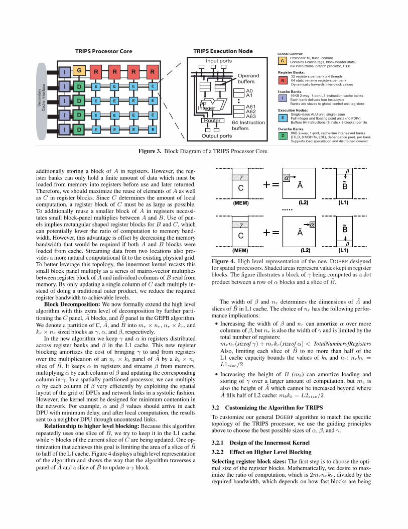
G
E
R
Global Control:
Protocols: fill, flush, commit
Contains I-cache tags, block header state,
r/w instructions, branch predictor, ITLB
Register Banks:
32 registers per bank x 4 threads
64 static rename registers per bank
Dynamically forwards inter-block values
Execution Nodes:
Single-issue ALU unit, single-issue
Full integer and floating point units (no FDIV)
Buffers 64 instructions (8 insts x 8 blocks) per tile
D-cache Banks
8KB 2-way, 1-port, cache-line interleaved banks
DTLB, 8 MSHRs, LSQ, dependence pred. per bank
Supports load speculation and distributed commit
D
I-cache Banks
16KB 2-way, 1-port L1 instruction cache banks
Each bank delivers four insts/cycle
Banks are slaves to global control unit tag store
I
G RR R R
Router
Input ports
Output ports
Operand
buffers
IntegerFP
64 Instruction
buffers
A61A62A63
A0A1
TRIPS Execution Node TRIPS Processor Core
I
I
I
I
I
D
D
D
D
S
econdary
Cache In
terf
ace
I
E
E
E
E
E
E
E
E
E
E
E
E
E
E
E
E
Figure 3. Block Diagram of a TRIPS Processor Core.
additionally storing a block of A in registers. However, the reg-ister banks can only hold a finite amount of data which must beloaded from memory into registers before use and later returned.Therefore, we should maximize the reuse of elements of A as wellas C in register blocks. Since C determines the amount of localcomputation, a register block of C must be as large as possible.To additionally reuse a smaller block of A in registers necessi-tates small block-panel multiplies between A and B. Use of pan-els implies rectangular shaped register blocks for B and C, whichcan potentially lower the ratio of computation to memory band-width. However, this advantage is offset by decreasing the memorybandwidth that would be required if both A and B blocks wereloaded from cache. Streaming data from two locations also pro-vides a more natural computational fit to the existing physical grid.To better leverage this topology, the innermost kernel recasts thissmall block panel multiply as a series of matrix-vector multipliesbetween register block of A and individual columns of B read frommemory. By only updating a single column of C each multiply in-stead of doing a traditional outer product, we reduce the requiredregister bandwidth to achievable levels.
Block Decomposition: We now formally extend the high levelalgorithm with this extra level of decomposition by further parti-tioning the C panel, A blocks, and B panel in the GEPB algorithm.We denote a partition of C, A, and B into mr × nr , nr × kr , andkr × nr sized blocks as γ, α, and β, respectively.
In the new algorithm we keep γ and α in registers distributedacross register banks and β in the L1 cache. This new registerblocking amortizes the cost of bringing γ to and from registersover the multiplication of an nr × kb panel of A by a kb × nr
slice of B. It keeps α in registers and streams β from memory,multiplying α by each column of β and updating the correspondingcolumn in γ. In a spatially partitioned processor, we can multiplyα by each column of β very efficiently by exploiting the spatiallayout of the grid of DPUs and network links in a systolic fashion.However, the kernel must be designed for minimum contention inthe network. For example, α and β values should arrive in eachDPU with minimum delay, and after local computation, the resultssent to a neighbor DPU through uncontested links.
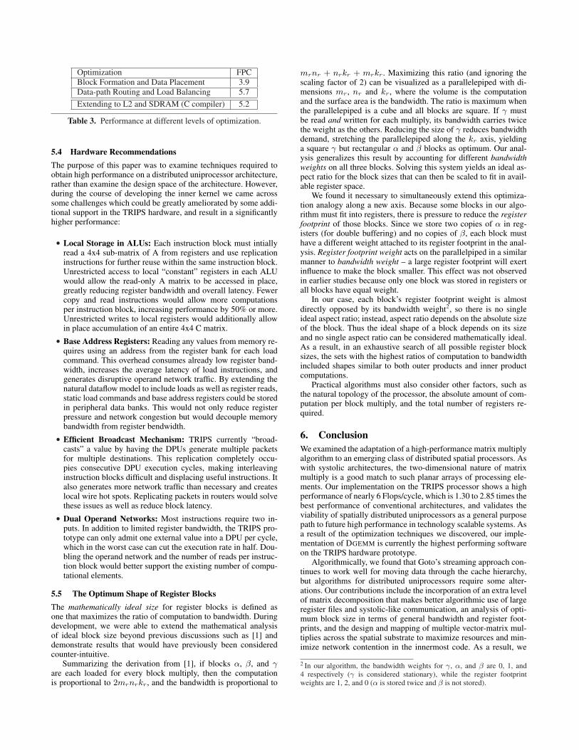
Relationship to higher level blocking: Because this algorithmrepeatedly uses one slice of B, we try to keep it in the L1 cachewhile γ blocks of the current slice of C are being updated. One op-timization that achieves this goal is limiting the area of a slice of Bto half of the L1 cache. Figure 4 displays a high level representationof the algorithm and shows the way that the algorithm traverses apanel of A and a slice of B to update a γ block.
Figure 4. High level representation of the new DGEBP designedfor spatial processors. Shaded areas represent values kept in registerblocks. The figure illustrates a block of γ being computed as a dotproduct between a row of α blocks and a slice of B.
The width of β and nr determines the dimensions of A andslices of B in L1 cache. The choice of nr has the following perfor-mance implications:• Increasing the width of β and nr can amortize α over more
columns of β, but nr is also the width of γ and is limited by thetotal number of registers:mrnr(sizeof γ) + mrkr(sizeof α) < TotalNumberofRegistersAlso, limiting each slice of B to no more than half of theL1 cache capacity bounds the values of kb and nr: nrkb =L1size/2
• Increasing the height of B (mb) can amortize loading andstoring of γ over a larger amount of computation, but mb isalso the height of A which cannot be increased beyond whereA fills half of L2 cache: mbkb = L2size/2
3.2 Customizing the Algorithm for TRIPSTo customize our general DGEBP algorithm to match the specifictopology of the TRIPS processor, we use the guiding principlesabove to choose the best possible sizes of α, β, and γ.
3.2.1 Design of the Innermost Kernel3.2.2 Effect on Higher Level BlockingSelecting register block sizes: The first step is to choose the opti-mal size of the register blocks. Mathematically, we desire to max-imize the ratio of computation, which is 2mrnrkr , divided by therequired bandwidth, which depends on how fast blocks are being

L1 cachebanksz }| {
γ(0)+ =α(0,0)β(0) α(1,0)β(0) α(2,0)β(0) α(3,0)β(0)
α(0,1)β(1) γ(1)+ =α(1,1)β(1) α(2,1)β(1) α(3,1)β(1)
α(0,2)β(2) α(1,2)β(2) γ(2)+ =α(2,2)β(2) α(3,2)β(2)
α(0,3)β(3) α(1,3)β(3) α(2,3)β(3) γ(3)+ =α(3,3)β(3)
+
+
+
+
+
+
+
+
+
+
+
+
β(0) →
β(1) →
β(2) →
β(3) →
γ(0)
l
γ(1)
l
γ(2)
l
γ(3)
l
Figure 5. Mapping of operations into the TRIPS FPUs for updat-ing a column of γ by multiplying a column of β with a block of αin registers, where superscripts denote elements.
loaded, constrained such that we can fit needed blocks in registers.For example, if γ, α, and β must be loaded every time (ignoringwrites), then the bandwidth is mrnr + mrkr + krnr , and the ra-tio is maximum when mr = nr = kr , that is, square blocks areoptimum. However, if only one block is reloaded, then rectangulardimensions which minimize the size of that block create a morefavorable ratio. In our algorithm, we stream β the fastest and αat a lower rate, while γ can be viewed as stationary, leading to abandwidth cost of mrkr + krnr and an optimal area for α that issignificantly smaller than β . However, Section 5.5 describes in de-tail that this optimization depends not only on relative bandwidthbut also on relative register usage (register foot print). Maximizingall these ratios while constraining size to available register storageyields a mathematically ideal size of 7× 14 for γ.
However, we learned quickly that the cost of not mapping to thenatural 4×4 topology of TRIPS more than offsets any performancegains, so the next closest match was a size of 4 × 16 for γ, whichimplied a size of 4x4 for a block of α, and a width of 16 for eachpanel of β. Note that this has the optimum computation/bandwidthratio of any possible multiple-of-four sizes, and its ratio is stillalmost 70% that of the mathematically ideal size, while using only2/3 of the registers.
Mapping to the grid: In the case of TRIPS, the data banks andregister banks are connected orthogonally to the computation gridas shown Figure 3, providing a data flow of A and B elementssimilar to systolic arrays. Arranging the data for systolic computa-tion is obvious: each register bank is assigned one successive col-umn of the transpose of α and γ. Similarly, each column of β isstored on successive TRIPS L1 cache banks. As we send values ofα from registers to corresponding DPUs, we load each column of βfrom the data banks, broadcasting elements of it across each row ofDPUs. Next, we multiply β by α at each DPU, and add the resultsup each column, updating each column’s γ.
Figure 5 shows the mathematical notation of this method andidentifies which values of α and β participate in computing avalue of γ in each column. In this figure the four boxes on thetop are register banks holding the values of γ. The 4 × 4 grid in
Figure 6. Typical blocking sizes for the TRIPS processor
the middle represents DPUs. For each DPU, the figure shows thecorresponding α value, read from the register bank in that column,and β value, loaded from L1 data bank in the same row. This patternmakes excellent usage of the network links because fetching valuesof α and β into DPUs uses south bound and east bound links whilesending load addresses for β and reducing sums of γ uses only westbound and north bound links. Sixteen of the remaining registersare used for double buffering α, loading the next α block whilemultiplying the current α by β.
On a partitioned core communicating over a network, the properrouting of values to minimize network contention and latency isthe most important aspect of optimized kernel design – a factorthat is completely absent from conventional kernels, but which willlikely be increasingly important to kernel design in future on chiparchitectures. In our case, we relied heavily on the concept of datapath routing. This approach first lays out uncontested data pathsbetween registers and data banks. Then, all the computation thatwould operate on this data stream are attached to the path. Finally,TRIPS has eight instruction blocks in flight and competing forthe shared resources such as registers, L1 caches, DPUs and theoperand network. To minimize inter-block contention, we have allinstructions in one data path operate on the data like an assemblyline.
The design of the innermost kernel and register block sizesaffects both the sizes of the higher level blocks in DGEBP and theway data must be packed into those blocks in DGEMM.
High level block size: Having determined the optimum size ofregister blocks α and panels of γ and β, we can determine the sizeof the buffers in Goto’s high level algorithm [1], namely the blockof A stored in the L2 cache and the slice of B stored in the L1cache. As described in Section 3.1, filling half of the L1 cache witha slice of B and half of the L2 cache with A produces the bestreuse. Figure 4 shows that for the innermost kernel to reuse theregister panel, γ, it must use all of the panels of β in a verticalcolumn. Given the TRIPS L1 cache size of 32KB and the width βbeing 16 values (each eight bytes), the height B is set to 128 values,which must also be the width of A. Since the TRIPS L2 cache sizeis 1MB and we want to fill half of it with A, the height of the Aand the height of C is 512. Figure 6 summarizes different blocksizes calculated for the improved DGEBP algorithm optimized forTRIPS processor.
Effect on packing: As mentioned before, Goto’s algorithm [1]requires packing for A blocks and B panels. Simultaneously lever-aging all cache banks in our innermost kernel can quadruple mem-ory bandwidth, reduce operand network contention, and help loadbalance the entire computation grid. The price is a slightly morecomplicated packing algorithm and the need to pack C in additionto A and B. Figure 7 illustrates a sample cache interleave packingof two consecutive α blocks and β columns. The γ columns arepacked similarly to β.

Figure 7. Data packing model for α and β blocks using in DGEBPalgorithm customized for TRIPS.
4. Experimental ResultsTo evaluate the algorithmic modifications for distributed proces-sor cores, we used actual TRIPS hardware with basic character-istics shown in Table 1 [7]. The TRIPS prototype processor chipis a custom 170 million transistor ASIC implemented in a 130nmtechnology. We collected cycle counts from the hardware perfor-mance counters using customized libraries and a runtime environ-ment developed by the TRIPS team. The algorithm is implementedin C and assembly language and compiled using the TRIPS customcompiler [21]. Section 4.1 includes a standard performance anal-ysis and Section 4.2 compares our results to implementations ofGoto’s algorithm on other processors. All the results in the sectionare shown in FLOPS per cycles (FPC).
Table 1. TRIPS Chip Parameters.L1 cache L2 cache SDRAM Processor
size size size speed32KB 1MB 2GB 366MHz
4.1 Performance Results and AnalysisPerformance vs Matrix Size: Figure 8 shows how performance(measured in FPC) varies in response to changes in the size of A,B and C matrices, for three different kernel implementations:• DGEMM: The full matrix multiply application including pack-
ing, a DGEBP layer, and our inner kernel customized for TRIPSbased on the algorithm described in previous sections.
• C Kernel: Identical to above DGEMM implementation, includ-ing packing and a DGEBP layer, but with the innermost kernelimplemented in C with no explicit spatial positioning of instruc-tions.
• Simple: A classic triple loop implementation of the matrix mul-tiply.The performance of Simple grows gradually and drops at the
point where matrix sizes outgrow the L2 cache near 512×512 ma-trix size. However, C Kernel does not drop for any matrix sizes be-yond that point due to the explicit data management of the DGEBP.DGEMM starts ramping up soon and performs at peak at almost thesame point where the Simple code drops. The fluctuations seen by
Figure 8. Different implementations of the Matrix Multiply withor without GEBP layer, inner kernel and the packing code
the complete DGEMM timings are due to the unoptimized natureof the packing code. Another interesting observation is that while CKernel and DGEMM share identical code except for the innermostkernel, the 10X performance difference demonstrates the impact ofdata placement and spatial layout of instructions on performance.
Packing Overhead: Figure 9 illustrates the performance lostdue to the packing overhead by showing timings for:
• No-Packing: DGEMM code without re-arranging the data dur-ing packing, i.e., we pre-arrange the data so that no packing isrequired.
• DGEMM : The full matrix multiply application.• Remainder: The packing overhead computed by taking the dif-
ference between No-Packing and DGEMM.
The small variation in the No-Packing performance is due tofringe overhead where matrix sizes not evenly divisible by thebuffer size decompose into small remainder blocks. Packing over-head is roughly 5% once the size reaches 1024 × 1024, falling toless than 1% at 4096×4096 matrix sizes. As previously mentioned,our high packing overhead at smaller matrix sizes is due to our un-optimized implementation of packing which cannot take advantageof all four available data banks. Additionally, packing is more com-plex for distributed caches than for single-banked caches due to theinterleaving of cache lines across the four banks.
The Effect of the Shape of A: To examine our choice for thedimensions of the A buffer (512 × 128, which is narrow and tall),we varied the aspect ratio of A while keeping its size at half of theL2 cache. As shown in Figure 10, both square and wide A buffershave lower performance, with the wide buffer performing the worst.Our observations confirm Goto’s assertion that a tall and narrow Atypically offers better performance.
Performance on the Thin Matrices: Dense linear algebra li-braries like LAPACK [2] can cast algorithms most typically interms of DGEMM where the k dimension is relatively small (alsoknown as a rank-k update). Figure 11 shows the performance fordifferent values of k when m and n are held constant at 4,096. Per-formance ramps up with k as low as 100, which is important sincethis allows algorithms that cast computation in terms of rank-k up-dates to achieve high performance for smaller problem sizes.

Table 2. Comparing our performance with select performance numbers taken from [1], Figure 12Processor Kernel FPC DGEMM FPC1 # of Reg2 γ dim A dim L2 cache3
Opteron-EM64T 1.88 1.79 16x2 4x4 384x256 1024P4-Prescott-EM64T 1.92 1.87 16x2 4x4 696x192 2048Core2 Duo 3.68 3.58 16x2 4x4 512x256 4096POWER5 3.84 3.78 32 4x4 256x256 1920Itanium2 3.96 3.92 128 8x8 128x1924 256TRIPS 5.80 5.10 128 4x16 128x512 10241Flops Per Cycle measured at m=n=k=2000, 2”x2” denotes 2-way SIMD register storage, 3L2 cache size in kilobytes
Figure 9. The packing overhead and the performance ideal kernelwith no packing overhead.
Figure 10. The effect of different A buffer dimensions.
4.2 Comparative AnalysisIn this section, we compare the performance characteristics of ouralgorithm for spatial processors to that of Goto’s algorithm onconventional processors [1].
The simplest metric for evaluating the performance of DGEMMis absolute performance in gigaflops/second during computation ofa large matrix multiply. However, DGEMM is also used to im-plement the Basic Linear Algebra Subroutines, and these routinesbreak up matrices into smaller blocks of different shapes. For this
Figure 11. Varying k while keeping m and n are constant.
reason, other metrics are important in evaluating DGEMM perfor-mance:• ramp-up speed: how large must a matrix be to reach peak
performance.• aspect ratio: how thin can a vertical panel become before caus-
ing a performance penalty.• smoothness: how much does performance vary for incremental
changes in matrix size.However, this paper focuses on the implementation of the high
speed inner kernel on spatially distributed uniprocessors. As seenin Figure 9, when removing the influence of unoptimized packingcode, our kernel exhibits sufficient ramp-up speed and smoothness.
An important metric that accompanies any matrix multiply pa-per is the theoretical peak floating point performance of the pro-cessor, but TRIPS does not have a clear peak Flops Per Cycle(FPC) because unlike conventional processors, a DPU must explic-itly trade off floating point computations with data replication andmovement across the network as well as loads, stores, prefetchingand integer operations.
Table 2 compares the performance of our full DGEMM imple-mentation to other implementations of Goto’s algorithm on con-ventional processors. Because the TRIPS prototype is an ASIC im-plemented on 130nm, we compare FPC instead of absolute per-formance in gigaflops/second 1. We measure “peak FPC” at a ma-trix size of 2000 to compare directly with [1]. Results indicate thatTRIPS performance ranges from 1.30x to 2.85x times the peak FPC
1 On the current prototype, our sustained performance is 1.9 gigaflops.However, spatially partitioned processors are specifically designed for ex-tremely high megahertz/low power performance. For a conservative full-custom 90nm VLSI implementation at 4 GHz with 8 cores, our algorithmwould sustain over 20 gigaflops per core.

of the five most significant conventional processors in the study.This improvement is even more significant considering that it wasaccomplished solely with general purpose instructions, whereasmost other implementations leverage specialized SIMD units inaddition to general purpose resources. Also note that the chosenoptimal register blocking was generally different, reflecting majordifferences between the architectures.
5. DiscussionDuring the course of our development, we made several interestingobservations on the algorithms and architectures that are worthy ofextra discussion.
5.1 Register Resources on Distributed UniprocessorsOn conventional processors, register bandwidth is essentially infi-nite (being twice the instruction bandwidth) and so is consideredfree. But on a distributed processor of the topology we have de-scribed, a 2-D grid of DPUs borders a 1-D array of register banks,and so all the DPUs in a column of the grid must share serial ac-cess to a single register bank. The result is an imbalance of register-file to computation bandwidth which increases with the size of thegrid, although partially mitigated via local communication betweenDPUs. For this reason, highly parallel algorithms like matrix mul-tiply must be designed to conserve register bandwidth as well ascache bandwidth.
5.2 Designing an Optimized Algorithm for a Grid TopologySection 3.2.1 discussed a set of optimization principles for design-ing an grid-topology aware algorithm that can be summarized as:• Minimize network contention: excess contention for even a
single link could cut code performance in half.• Balance use of grid resources: A single resource bottleneck
can easily dominate performance, and on a spatially distributeduniprocessor, the opportunity cost is high – when one resourceis used more than the rest, every network link and DPU execu-tion slot in the 2-D grid goes idle.
• Utilize all register banks and L1 cache banks: use appropriatelystrided data access to simultaneously access all cache banks.Mirror common register values across all register banks.Because any violation of these principles can adversely affect
performance, there is a degree of fragility to optimizations akin towhat parallel programmers experience. We did find, however, thatcreating optimized code for a distributed processor is surprisinglysimple. Straightforward instruction layout techniques like datapathrouting simultaneously satisfy all of the optimization requirements.
5.3 Implementation DetailsDuring the implementation of the kernel, we used the optimizationprinciples introduced in the previous subsection to overcome archi-tectural bottlenecks.
Instruction Block Formation: As mentioned before, a TRIPSprogram is a series of instruction blocks which are executed atomi-cally. A TRIPS processor can execute up to eight instruction blockssimultaneously. In this pipeline, the maximum instruction blockcompletion rate (BCR) is clamped to one instruction block per 8cycles. Therefore, each instruction block should contain as as muchactual computation as possible. Instruction block formation (decid-ing what assembly instructions to place in an execution block) is thesingle most important optimization step, responsible for up to 75%of the performance of the kernel. The goals of instruction blockformation are mapping the algorithm described in Section 3 to theTRIPS topology, minimizing instruction overhead (code quality),facilitating interleaving of instruction blocks within the pipeline.
At this stage in the optimization, only conventional style assem-bly was used, relying on a high performance scheduler to positionall of the instructions along the 2-D grid automatically. Getting fur-ther performance requires manual 2-D placement of the instruc-tions.
Avoiding Network Contention: The next fundamental stepafter instruction block formation is to avoid network contentionbetween ALUs. A simple method we use to layout a 2-D schedulethat both minimizes network contention and facilitates instructionblock interleaving is called data path routing. In this optimization,we think of an instruction block’s operations as parallel data pathsin each column of the grid. Each data path performs the dot-productof one of the B vectors and a column of the A sub-matrix and addsthe results back to the corresponding C element in that registerbank. Each of these parallel data paths works as an assembly lineoperating on the data stream. This pattern requires the B vectorsread from L1 banks to be broadcast to all four columns of the DPUgrid. Because TRIPS has no general broadcast mechanism, movetrees are used to duplicate values. By utilizing a mov4 instructionthat replicates its source to four restricted targets, we reduce movefanout and achieve 12% improvement. Remaining fanout can beeliminated by a technique called register mirroring, in which thesame value is put in multiple registers across all banks. As anexample, the address values for loading elements of C are fetchedfrom registers. If all loads fetch their addresses from the sameregister, it causes fanout and network contention. This optimizationincreased performance by 30%.
Load Balancing and Block Latency: The optimization meth-ods explained so far aim to improve useful instructions per blockand end-to-end block execution. However, another important factoraffecting the performance is the maximum use of a single physi-cal resource per block. Since TRIPS maximum block completionrate (BCR) is one block every 8 cycles and 8 blocks can be inflight, exceeding 64 cycles block latency (about half being blockoverhead) reduces BCR rate by (64/average latency). Another ma-jor factor affecting BCR relates to load balancing between the 8blocks in flight. If a block (on average) uses any single physicalresource (network link or execution slot) more than 8 active cyclesthen the BCR is reduced by a factor of 8/(the max number of uses ina block). Once the basic data path was laid out, load balancing andminimizing block latency to the extent possible was trivial. Con-sidering this rule, we realized that our schedule utilized the southbound links under the register tiles 12 active cycles instead of 8.For each of those links, 4 of these cycles are spent on reading theB vector addresses and C vectors’ elements and the remaining 8cycles are needed to read a row of A sub-matrix twice, once foreach of the two data path mapped to the DPU column below thatregister file. We had to read each A element twice because there isno local storage (register or memory) in the DPUs. Because of thisimbalance in the use of Southbound links, the code ran at exactly2/3rds the expected speed. We fixed this problem by replacing theextra 4 register reads with one local replication in each DPU, whichled to a 30% boost in performance. Table 3 shows different levelsof optimization and the performance associated with them.
Although these optimizations used in the inner kernel are im-plemented in assembly language, and the current TRIPS compilerdoes not store arrays in registers, such transformations are withinthe realm of standard blocking/tiling compilers, and could be easilyadded to the compiler. Data path routing can be automated in thecompiler by detecting parallel paths with minimal communicationbetween them in instruction blocks and mapping each path ontoa section of the grid. Finally, achieving a low contention scheduleby the compiler is simple by allocating separate data paths in theInstruction Block, interleaving (overlapping) data movement andcomputation (mov instructions).
Optimization FPCBlock Formation and Data Placement 3.9Data-path Routing and Load Balancing 5.7Extending to L2 and SDRAM (C compiler) 5.2
Table 3. Performance at different levels of optimization.
5.4 Hardware RecommendationsThe purpose of this paper was to examine techniques required toobtain high performance on a distributed uniprocessor architecture,rather than examine the design space of the architecture. However,during the course of developing the inner kernel we came acrosssome challenges which could be greatly ameliorated by some addi-tional support in the TRIPS hardware, and result in a significantlyhigher performance:
• Local Storage in ALUs: Each instruction block must intiallyread a 4x4 sub-matrix of A from registers and use replicationinstructions for further reuse within the same instruction block.Unrestricted access to local “constant” registers in each ALUwould allow the read-only A matrix to be accessed in place,greatly reducing register bandwidth and overall latency. Fewercopy and read instructions would allow more computationsper instruction block, increasing performance by 50% or more.Unrestricted writes to local registers would additionally allowin place accumulation of an entire 4x4 C matrix.
• Base Address Registers: Reading any values from memory re-quires using an address from the register bank for each loadcommand. This overhead consumes already low register band-width, increases the average latency of load instructions, andgenerates disruptive operand network traffic. By extending thenatural dataflow model to include loads as well as register reads,static load commands and base address registers could be storedin peripheral data banks. This would not only reduce registerpressure and network congestion but would decouple memorybandwidth from register bendwidth.
• Efficient Broadcast Mechanism: TRIPS currently “broad-casts” a value by having the DPUs generate multiple packetsfor multiple destinations. This replication completely occu-pies consecutive DPU execution cycles, making interleavinginstruction blocks difficult and displacing useful instructions. Italso generates more network traffic than necessary and createslocal wire hot spots. Replicating packets in routers would solvethese issues as well as reduce block latency.
• Dual Operand Networks: Most instructions require two in-puts. In addition to limited register bandwidth, the TRIPS pro-totype can only admit one external value into a DPU per cycle,which in the worst case can cut the execution rate in half. Dou-bling the operand network and the number of reads per instruc-tion block would better support the existing number of compu-tational elements.
5.5 The Optimum Shape of Register BlocksThe mathematically ideal size for register blocks is defined asone that maximizes the ratio of computation to bandwidth. Duringdevelopment, we were able to extend the mathematical analysisof ideal block size beyond previous discussions such as [1] anddemonstrate results that would have previously been consideredcounter-intuitive.
Summarizing the derivation from [1], if blocks α, β, and γare each loaded for every block multiply, then the computationis proportional to 2mrnrkr , and the bandwidth is proportional to
mrnr + nrkr + mrkr . Maximizing this ratio (and ignoring thescaling factor of 2) can be visualized as a parallelepiped with di-mensions mr , nr and kr , where the volume is the computationand the surface area is the bandwidth. The ratio is maximum whenthe parallelepiped is a cube and all blocks are square. If γ mustbe read and written for each multiply, its bandwidth carries twicethe weight as the others. Reducing the size of γ reduces bandwidthdemand, stretching the parallelepiped along the kr axis, yieldinga square γ but rectangular α and β blocks as optimum. Our anal-ysis generalizes this result by accounting for different bandwidthweights on all three blocks. Solving this system yields an ideal as-pect ratio for the block sizes that can then be scaled to fit in avail-able register space.
We found it necessary to simultaneously extend this optimiza-tion analogy along a new axis. Because some blocks in our algo-rithm must fit into registers, there is pressure to reduce the registerfootprint of those blocks. Since we store two copies of α in reg-isters (for double buffering) and no copies of β, each block musthave a different weight attached to its register footprint in the anal-ysis. Register footprint weight acts on the parallelpiped in a similarmanner to bandwidth weight – a large register footprint will exertinfluence to make the block smaller. This effect was not observedin earlier studies because only one block was stored in registers orall blocks have equal weight.
In our case, each block’s register footprint weight is almostdirectly opposed by its bandwidth weight2, so there is no singleideal aspect ratio; instead, aspect ratio depends on the absolute sizeof the block. Thus the ideal shape of a block depends on its sizeand no single aspect ratio can be considered mathematically ideal.As a result, in an exhaustive search of all possible register blocksizes, the sets with the highest ratios of computation to bandwidthincluded shapes similar to both outer products and inner productcomputations.
Practical algorithms must also consider other factors, such asthe natural topology of the processor, the absolute amount of com-putation per block multiply, and the total number of registers re-quired.
6. ConclusionWe examined the adaptation of a high-performance matrix multiplyalgorithm to an emerging class of distributed spatial processors. Aswith systolic architectures, the two-dimensional nature of matrixmultiply is a good match to such planar arrays of processing ele-ments. Our implementation on the TRIPS processor shows a highperformance of nearly 6 Flops/cycle, which is 1.30 to 2.85 times thebest performance of conventional architectures, and validates theviability of spatially distributed uniprocessors as a general purposepath to future high performance in technology scalable systems. Asa result of the optimization techniques we discovered, our imple-mentation of DGEMM is currently the highest performing softwareon the TRIPS hardware prototype.
Algorithmically, we found that Goto’s streaming approach con-tinues to work well for moving data through the cache hierarchy,but algorithms for distributed uniprocessors require some alter-ations. Our contributions include the incorporation of an extra levelof matrix decomposition that makes better algorithmic use of largeregister files and systolic-like communication, an analysis of opti-mum block size in terms of general bandwidth and register foot-prints, and the design and mapping of multiple vector-matrix mul-tiplies across the spatial substrate to maximize resources and min-imize network contention in the innermost code. As a result, we
2 In our algorithm, the bandwidth weights for γ, α, and β are 0, 1, and4 respectively (γ is considered stationary), while the register footprintweights are 1, 2, and 0 (α is stored twice and β is not stored).

have succesfully implemented a systolic-like algorithm on a gen-eral purpose processor.
We found that the costs of network communication versus lo-cal computation in on-chip networks makes performance sensi-tive to small changes in network and execution unit contention.Nonetheless, achieving high performance was relatively straight-forward once we determined the relevant resource and algorith-mic constraints. Our experience indicates that well-engineered al-gorithms will continue be relevant to emerging architectures thatwe anticipate seeing in the future.
AcknowledgmentsWe would like to thank all the people who gave us valuable feed-back including the anonymous reviewers.
This research is supported by the Defense Advanced ResearchProjects Agency under contract F33615-01-C-4106 and NSF grantCCF-0540926. Any opinions, findings and conclusions or recom-mendations expressed in this material are those of the author(s)and do not necessarily reflect the views of the National ScienceFoundation (NSF).
References[1] K. Goto and R. A. van de Geijn, Anatomy of High-Performance
Matrix Multiplication, ACM Transactions on Mathematical Software,2008.
[2] E. Anderson and Z. Bai, C. Bischof, J. Demmel, J. Dongarra, J. DuCroz, A. Greenbaum, S. Hammarling, A. McKenney, S. Ostrouchov,D. Sorensen, LAPACK’s user’s guide, Society for Industrial andApplied Mathematics, 1995.
[3] K. Goto and R. van de Geijn, On Reducing TLB Misses in MatrixMultiplication, FLAME Working Note #9, The University of Texasat Austin, Department of Computer Sciences. Technical Report TR-2002-55, November 2002.
[4] S. Swanson, K. Michelson, A. Schwerin and M. Oskin, WaveScalar,International Symposium on Microarchitecture, 36:291, December2003.
[5] E. Waingold, M. Taylor, D. Srikrishna, V. Sarkar, W. Lee, V. Lee andJ. Kim, M. Frank, P. Finch, R. Barua, J. Babb, S. Amarasinghe and A.Agarwal, Baring It All to Software: RAW Machines, IEEE Computer,volume 30(9):86-93, September 1997.
[6] D. Burger, S. W. Keckler, K. S. McKinley, M. Dahlin, L. K. John,C. Lin, C. R. Moore, J. Burrill, R. G. McDonald, W. Yoder and theTRIPS Team, Scaling to the End of Silicon with EDGE Architectures,IEEE Computer, 37(7):44-55, July 2004.
[7] K. Sankaralingam, R. Nagarajan, P. Gratz, R. Desikan, D. Gulati,H. Hanson, C. Kim, H. Liu, N. Ranganathan, S. Sethumadhavan,S. Sharif, P. Shivakumar, W. Yoder, R. McDonald, S.W. Kecklerand D.C. Burger, The Distributed Microarchitectural Protocolsof the TRIPS Prototype Processor, International Symposium onMicroarchitecture, 39:480-491, November 2006.
[8] S. Vangal, J. Howard, G. Ruhl, S. Dighe, H. Wilson, J. Tschanz,D. Finan, P. Iyer, A. Singh, T. Jacob, S. Jain, S. Venkataraman, Y.Hoskote and N. Borkar, An 80-Tile 1.28 TFLOPS Network-on-Chipin 65nm CMOS, IEEE International Solid-State Circuits Conference,February 2007.
[9] M. B. Taylor and A. Agarwal, Evaluation of the Raw Microprocessor:An Exposed-Wire-Delay Architecture for ILP and Streams, ACMSIGARCH Computer Architecture News, 32(2):2, March 2004.
[10] M. B. Taylor and A. Agarwal, The Raw Microprocessor: AComputational Fabric for Software Circuits and General PurposePrograms, IEEE Micro, 22(2), March 2002.
[11] H. T. Kung and C. E. Leiserson, Algorithms for VLSI processorarrays, Introduction to VLSI Systems; Addison-Wesley, 1979.
[12] M. Kunde, H.W. Lang and H. Schmeck and H. Schrder, TheInstruction Systolic Array and its Relation to Other Models of ParallelComputers, Parallel Computing, 7:25-39, April 1988.
[13] John A. Gunnels, Greg M. Henry and Robert A. van de Geijn, AFamily of High-Performance Matrix Algorithms, ComputationalScience Part I, Lecture Notes in Computer Science, 2073:51-60,2001.
[14] B. Marker, F. Van Zee, K. Goto, G. Quintana-Orti and Robertvan de Geijn, Toward Scalable Matrix Multiply on MultithreadedArchitectures, Euroropean Conference on Parallel Processing,13:748-757, August 2007.
[15] J. Gunnels, C. Lin, G. Morrow and R. van de Geijn, A FlexibleClass of Parallel Matrix Multiplication Algorithms, First MergedInternational Parallel Processing Symposium and Symposium onParallel and Distributed Processing, 12:110-116, March 1998.
[16] S. Chen, P. B Gibbons, M.l Kozuch, V. Liaskovitis, A. Ailamaki,G. E. Blelloch, B. Falsafi, L. Fix, N. Hardavellas, T. C. Mowry andC. Wilkerson, Scheduling Threads for Constructive Cache Sharingon CMPs, ACM Symposium on Parallelism in Algorithms andArchitecture, 19:105-115, June 2007.
[17] J. J. Dongarra, J. Du Croz, S. Hammarling and I. Duff, A set oflevel 3 basic linear algebra subprograms, ACM Transactions OnMathematical Software, volume 16(1):1-17, March 1990.
[18] K. Goto and R. van de Geijn, High-performance implementationof the level-3 BLAS, FLAME Working Note #20 TR-2006-23, TheUniversity of Texas at Austin, Department of Computer Sciences,2006.
[19] R. C. Whaley and J. J. Dongarra, Automatically tuned linear algebrasoftware, ACM/IEEE conference on Supercomputing, pp 1-27,November 1998 .
[20] R. C. Whaley, A. Petitet and J. J. Dongarra, Automated empiricaloptimization of software and the ATLAS project, Parallel Computing27(1-2):3-35, 2001.
[21] A. Smith, J. Gibson, B. Maher, D. Burger, K. S. McKinleyand J. Burrill, Compiling for EDGE Architectures, InternationalSymposium on Code Generation and Optimization, pp 185-195,March 2006.
[22] J. Laudon and L. Spracklen, The Coming Wave of MultithreadedChip Multiprocessors, International Journal of Parallel Programming,volume 35(3):299-330, June 2007.