Formation of Sulfur Atomic Layers on Gold from Aqueous Solutions of Sulfide and Thiosulfate: Studies...
12
Formation of Sulfur Atomic Layers on Gold from Aqueous Solutions of Sulfide and Thiosulfate: Studies Using EC-STM, UHV-EC, and TLEC Marcus D. Lay, Kris Varazo, and John L. Stickney* Department of Chemistry, University of Georgia, Athens, Georgia 30602 Received March 18, 2003. In Final Form: June 20, 2003 The formation of S atomic layers on Au from alkaline solutions of sulfide and thiosulfate is described. These studies are relevant to the formation of self-assembled monolayers (SAMs), as sulfide can be thought of as the simplest thiol and, thus, S atomic layers as the shortest chain SAM. S atomic layers are also of interest as precursors for the electrochemical formation of compound semiconductor thin films such as ZnS, CdS, and PbS. The deposition of S was investigated using electrochemical scanning tunneling microscopy (EC-STM), thin layer electrochemistry (TLEC), and ultrahigh vacuum electrochemical techniques (UHV- EC). UHV-EC studies included analysis with Auger electron spectroscopy (AES), low energy electron diffraction (LEED), and X-ray photoelectron spectroscopy (XPS). EC-STM and LEED revealed a 1 /3 coverage (x3 ×x3)R30°-S structure, previously observed by a number of workers, formed from both sulfide and thiosulfate solutions. From sulfide solutions, EC-STM showed that the (x3 ×x3)R30°-S structure converted to a more complex (3x3 × 3x3)R30°-S structure at higher potentials, with an accompanying surface roughening transition. LEED indicated the formation of a structure with a (2 × 2) unit cell near bulk deposition potentials in sulfide and thiosulfate solutions. EC-STM studies in thiosulfate solutions evinced this (2 × 2) structure, apparently composed of S dimers. Initial immersion into the thiosulfate solution resulted in a structure with a c(4 × 2x3) unit cell, believed to contain adsorbed thiosulfate species. The c(4 × 2x3) structure was replaced by the (x3 ×x3)R30°-S structure via reduction, as thiosulfate can be reductively decomposed to produce sulfide. In general, sulfide can be oxidized at fairly low potentials to form an adsorbed sulfur atomic layer, initially the (x3 ×x3)R30°-S structure on Au(111), a process referred to as oxidative underpotential deposition (upd). Bulk deposits of sulfur and possibly polysulfides are formed at more positive potentials. Introduction The power of scanning tunneling microscopy (STM) for resolving surface structures with atomic resolution is presently unmatched. Atomic resolution STM studies have been successfully carried out in a vacuum, 1,2 under ambient conditions, 3 and in solution. 4 A major constraint is the need for a conducting substrate. However, this is not a problem in electrochemical studies, as electrodes are generally highly conductive. Therefore, electrochemical scanning tunneling microscopy (EC-STM) has proven to be an invaluable tool for the in-situ investigation of atomic scale processes at the solid/liquid interface; it provides a real space image, elucidating the repeating unit of the lattice (unit cell), the arrangement of atoms within (basis), and morphology changes, up to the micron scale. Elemental, structural, and oxidation state information can be obtained using ultrahigh vacuum electrochemical techniques (UHV-EC) 5 such as Auger electron spectros- copy (AES), low energy electron diffraction (LEED), and X-ray photoelectron spectroscopy (XPS), respectively. UHV-EC involve the emersion (withdrawal) and transfer of the electrode from solution to a surface analysis chamber, while minimizing exposure to ambient condi- tions. The electrochemistry and electrode transfer are performed in an ultrahigh purity (UHP) inert gas and in a vacuum, respectively. However, even UHP inert gas has a significant amount of oxygen. Additionally, changes in surface structure and composition may occur when potential control is lost during the emersion process. This often becomes an issue when using potentials below that for hydrogen evolution and/or with highly reversible systems. 6 However, the chalcogenides have proven to work well in UHV-EC studies, partly as a result of the irreversibility of their deposition. 7 The studies here are concerned with electrochemically forming and describing atomic monolayers of S on Au(111) surfaces. There are a number of important compounds which contain S, such as PbS, CdS, ZnS, CuInS 2 , and HgS, thus making the formation of an atomic layer of S a central issue for our work. The formation of sulfur atomic layers on metallic single crystal surfaces has been widely studied: Au, 8-16 Pt, 17-24 Ni, 25-28 Rh, 29-31 Pd, 32-36 and Ru. 37-41 Sulfur atomic layers play an important role in * To whom correspondence should be addressed. E-mail: [email protected]. (1) Barth, J. V.; Brune, H.; Ertl, G.; Behm, R. J. Phys. Rev. B 1990, 42, 9307-9318. (2) Woll, C.; Chiang, S.; Wilson, R. J.; Lippel, P. H. Phys. Rev. B 1989, 39, 7988-7991. (3) Mizutani, W.; Ohi, A.; Motomatsu, M.; Tokumoto, H. Appl. Surf. Sci. 1995, 87-8, 398-404. (4) Tao, N. J.; Lindsay, S. M. J. Appl. Phys. 1991, 70, 5141-5143. (5) Soriaga, M. P.; Stickney, J. L. In Modern Techniques in Electro- analytical Chemistry; Vanysek, P., Ed.; Wiley & Sons: New York, 1996; p 1. (6) Lay, M. D.; Varazo, K.; Srisook, N.; Stickney, J. L. J. Electroanal. Chem., in press. (7) Ocko, B. M.; Magnussen, O. M.; Adzic, R. R.; Wang, J. X.; Shi, Z.; Lipkowski, J. J. Electroanal. Chem. 1994, 376, 35-39. (8) Kostelitz, M.; Oudar, J. C. R. Acad. Sci., Ser. C 1970, 271, 1205. (9) Kostelitz, M.; Oudar, J. Surf. Sci. 1971, 27, 176. (10) Kostelitz, M.; Domange, J. L.; Oudar, J. Surf. Sci. 1973, 34, 431-449. (11) Gao, X. P.; Zhang, Y.; Weaver, M. J. J. Phys. Chem. 1992, 96, 4156-4159. (12) Demir, U.; Shannon, C. Langmuir 1994, 10, 2794-2799. (13) Bondzie, V.; Dixon-Warren, S.; Yu, Y. J. Chem. Phys. 1999, 111, 10670-10680. (14) Andreasen, G.; Vericat, C.; Vela, M. E.; Salvarezza, R. C. J. Chem. Phys. 1999, 111, 9457-9460. 8416 Langmuir 2003, 19, 8416-8427 10.1021/la034474y CCC: $25.00 © 2003 American Chemical Society Published on Web 08/13/2003
Transcript of Formation of Sulfur Atomic Layers on Gold from Aqueous Solutions of Sulfide and Thiosulfate: Studies...
Formation of Sulfur Atomic Layers on Gold from AqueousSolutions of Sulfide and Thiosulfate: Studies Using
EC-STM, UHV-EC, and TLEC
Marcus D. Lay, Kris Varazo, and John L. Stickney*
Department of Chemistry, University of Georgia, Athens, Georgia 30602
Received March 18, 2003. In Final Form: June 20, 2003
The formation of S atomic layers on Au from alkaline solutions of sulfide and thiosulfate is described.These studies are relevant to the formation of self-assembled monolayers (SAMs), as sulfide can be thoughtof as the simplest thiol and, thus, S atomic layers as the shortest chain SAM. S atomic layers are also ofinterest as precursors for the electrochemical formation of compound semiconductor thin films such asZnS, CdS,andPbS.The depositionofSwas investigatedusingelectrochemical scanning tunnelingmicroscopy(EC-STM), thin layer electrochemistry (TLEC), and ultrahigh vacuum electrochemical techniques (UHV-EC). UHV-EC studies included analysis with Auger electron spectroscopy (AES), low energy electrondiffraction (LEED), and X-ray photoelectron spectroscopy (XPS). EC-STM and LEED revealed a 1/3 coverage(x3 × x3)R30°-S structure, previously observed by a number of workers, formed from both sulfide andthiosulfate solutions. From sulfide solutions, EC-STM showed that the (x3×x3)R30°-S structure convertedto a more complex (3x3 × 3x3)R30°-S structure at higher potentials, with an accompanying surfaceroughening transition. LEED indicated the formation of a structure with a (2 × 2) unit cell near bulkdeposition potentials in sulfide and thiosulfate solutions. EC-STM studies in thiosulfate solutions evincedthis (2 × 2) structure, apparently composed of S dimers. Initial immersion into the thiosulfate solutionresulted in a structure with a c(4 × 2x3) unit cell, believed to contain adsorbed thiosulfate species. Thec(4 × 2x3) structure was replaced by the (x3 × x3)R30°-S structure via reduction, as thiosulfate can bereductively decomposed to produce sulfide. In general, sulfide can be oxidized at fairly low potentials toform an adsorbed sulfur atomic layer, initially the (x3 × x3)R30°-S structure on Au(111), a processreferred to as oxidative underpotential deposition (upd). Bulk deposits of sulfur and possibly polysulfidesare formed at more positive potentials.
Introduction
The power of scanning tunneling microscopy (STM) forresolving surface structures with atomic resolution ispresently unmatched. Atomic resolution STM studies havebeensuccessfully carriedout inavacuum,1,2 underambientconditions,3 and in solution.4 A major constraint is theneed for a conducting substrate. However, this is not aproblem in electrochemical studies, as electrodes aregenerally highly conductive. Therefore, electrochemicalscanning tunneling microscopy (EC-STM) has proven tobe an invaluable tool for the in-situ investigation of atomicscale processes at the solid/liquid interface; it provides areal space image, elucidating the repeating unit of thelattice (unit cell), the arrangement of atoms within (basis),and morphology changes, up to the micron scale.
Elemental, structural, and oxidation state informationcan be obtained using ultrahigh vacuum electrochemicaltechniques (UHV-EC)5 such as Auger electron spectros-copy (AES), low energy electron diffraction (LEED), andX-ray photoelectron spectroscopy (XPS), respectively.UHV-EC involve the emersion (withdrawal) and transferof the electrode from solution to a surface analysis
chamber, while minimizing exposure to ambient condi-tions. The electrochemistry and electrode transfer areperformed in an ultrahigh purity (UHP) inert gas and ina vacuum, respectively. However, even UHP inert gashas a significant amount of oxygen. Additionally, changesin surface structure and composition may occur whenpotential control is lost during the emersion process. Thisoften becomes an issue when using potentials below thatfor hydrogen evolution and/or with highly reversiblesystems.6 However, the chalcogenides have proven to workwell in UHV-EC studies, partly as a result of theirreversibility of their deposition.7
The studies here are concerned with electrochemicallyforming and describing atomic monolayers of S on Au(111)surfaces. There are a number of important compoundswhich contain S, such as PbS, CdS, ZnS, CuInS2, and HgS,thus making the formation of an atomic layer of S a centralissue for our work. The formation of sulfur atomic layerson metallic single crystal surfaces has been widelystudied: Au,8-16 Pt,17-24 Ni,25-28 Rh,29-31 Pd,32-36 andRu.37-41 Sulfur atomic layers play an important role in
* To whom correspondence should be addressed. E-mail:[email protected].
(1) Barth, J. V.; Brune, H.; Ertl, G.; Behm, R. J. Phys. Rev. B 1990,42, 9307-9318.
(2) Woll, C.; Chiang, S.; Wilson, R. J.; Lippel, P. H. Phys. Rev. B1989, 39, 7988-7991.
(3) Mizutani, W.; Ohi, A.; Motomatsu, M.; Tokumoto, H. Appl. Surf.Sci. 1995, 87-8, 398-404.
(4) Tao, N. J.; Lindsay, S. M. J. Appl. Phys. 1991, 70, 5141-5143.(5) Soriaga, M. P.; Stickney, J. L. In Modern Techniques in Electro-
analytical Chemistry; Vanysek, P., Ed.; Wiley & Sons: New York, 1996;p 1.
(6) Lay, M. D.; Varazo, K.; Srisook, N.; Stickney, J. L. J. Electroanal.Chem., in press.
(7) Ocko, B. M.; Magnussen, O. M.; Adzic, R. R.; Wang, J. X.; Shi, Z.;Lipkowski, J. J. Electroanal. Chem. 1994, 376, 35-39.
(8) Kostelitz, M.; Oudar, J. C. R. Acad. Sci., Ser. C 1970, 271, 1205.(9) Kostelitz, M.; Oudar, J. Surf. Sci. 1971, 27, 176.(10) Kostelitz, M.; Domange, J. L.; Oudar, J. Surf. Sci. 1973, 34,
431-449.(11) Gao, X. P.; Zhang, Y.; Weaver, M. J. J. Phys. Chem. 1992, 96,
4156-4159.(12) Demir, U.; Shannon, C. Langmuir 1994, 10, 2794-2799.(13) Bondzie, V.; Dixon-Warren, S.; Yu, Y. J. Chem. Phys. 1999, 111,
10670-10680.(14) Andreasen, G.; Vericat, C.; Vela, M. E.; Salvarezza, R. C. J.
Chem. Phys. 1999, 111, 9457-9460.
8416 Langmuir 2003, 19, 8416-8427
10.1021/la034474y CCC: $25.00 © 2003 American Chemical SocietyPublished on Web 08/13/2003
corrosion processes,42,43 in poisoning catalysis,44-47 and inthe electrochemical formation of sulfur containing com-pound semiconductor thin films.12,48-56 Additionally, inthe area of self-assembly, or self-assembled monolayers(SAMs), thiols are a main protagonist. Sulfide can bethought of as the smallest thiol, and a sulfide layer canbe thought of as the shortest chain SAM.
The compound electrodeposition method used in thisgroup is referred to as electrochemical atomic layer epitaxy(EC-ALE). EC-ALE is a method for electrodepositing
compound semiconductors one monolayer at a time.57-59
It is the electrochemical analogue of atomic layer epitaxy(ALE).60-63 ALE is based on the use of surface-limitedreactions to promote two-dimensional growth and formmaterials layer-by-layer, with the number of cyclesdetermining the thickness of the deposit. In electro-deposition, surface-limited reactions are generally referredto as underpotential deposition (upd);57,64-67 this processinvolves an atomic layer of a species depositing on anotherat a potential prior to that required for the species todeposit on itself. In EC-ALE, thin films are formed by thesequential upd of each element from a separate solution.Several groups have prepared thin films of CdS and ZnScompound semiconductors using EC-ALE.12,48-56,68 CdTe,CdSe, and ZnSe have also been prepared.69-78 There arerecent reports of the EC-ALE formation of the III-Vcompounds InSb and InAs and IV-VI compounds such asPbSe and PbTe, as well as superlattices of these com-pounds.79,80 The first cycle of compound deposition turnsout to be the most difficult to control and the mostimportant. Thus, knowledge of the structure and com-position of the first atomic layer of S becomes critical tocontrol of the deposit structure.
EC-STM has been extensively applied to the charac-terization of sulfur atomic layers on Au(111). Sulfideoxidation on Au(111) electrodes was studied by Weaveret al. using EC-STM.11 In acidic solutions containing 1mM Na2S, a 1/3 ML (x3 × x3)R30° unit cell was observedbetween -0.4 and -0.1 V vs SCE, with sulfur atoms in
(15) Vericat, C.; Andreasen, G.; Vela, M. E.; Salvarezza, R. C. J.Phys. Chem. B 2000, 104, 302-307.
(16) Martin, H.; Vericat, C.; Andreasen, G.; Creus, A. H.; Vela, M.E.; Salvarezza, R. C. Langmuir 2001, 17, 2334-2339.
(17) Berthier, Y.; Perdereau, M.; Oudar, J. Surf. Sci. 1973, 36, 225-241.
(18) Heegemann, W.; Bechtold, E.; Hayek, K. Jpn. J. Appl. Phys.1974, 185-187.
(19) Heegemann, W.; Meister, K. H.; Bechtold, E.; Hayek, K. Surf.Sci. 1975, 49, 161-180.
(20) Fischer, T. E.; Kelemen, S. R. Surf. Sci. 1977, 69, 1-22.(21) Hayek, K.; Glassl, H.; Gutmann, A.; Leonhard, H.; Prutton, M.;
Tear, S. P.; Weltoncook, M. R. Surf. Sci. 1985, 152, 419-425.(22) Hayek, K.; Glassl, H.; Gutmann, A.; Leonhard, H.; Prutton, M.;
Tear, S. P.; Weltoncook, M. R. Surf. Sci. 1986, 175, 535-550.(23) Sung, Y. E.; Chrzanowski, W.; Zolfaghari, A.; Jerkiewicz, G.;
Wieckowski, A. J. Am. Chem. Soc. 1997, 119, 194-200.(24) Sung, Y. E.; Chrzanowski, T.; Wieckowski, A.; Zolfaghari, A.;
Blais, S.; Jerkiewicz, G. Electrochim. Acta 1998, 44, 1019-1030.(25) Perdereau, M.; Oudar, J. Surf. Sci. 1970, 20, 80-98.(26) Demuth, J. E.; Jepsen, D. W.; Marcus, P. M. Phys. Rev. Lett.
1974, 32, 1182-1185.(27) Ruan, L.; Stensgaard, I.; Besenbacher, F.; Laegsgaard, E. J.
Vac. Sci. Technol., B 1994, 12, 1772-1775.(28) Li, L. F.; Totir, D.; Chottiner, G. S.; Scherson, D. A. J. Phys.
Chem. B 1998, 102, 8013-8016.(29) Foord, J. S.; Reynolds, A. E. Surf. Sci. 1985, 164, 640-648.(30) Wong, K. C.; Liu, W.; Saidy, M.; Mitchell, K. A. R. Surf. Sci.
1996, 345, 101-109.(31) Yoon, H. A.; Salmeron, M.; Somorjai, G. A. Surf. Sci. 1998, 395,
268-279.(32) Maca, F.; Scheffler, M.; Berndt, W. Surf. Sci. 1985, 160, 467-
474.(33) Patterson, C. H.; Lambert, R. M. Surf. Sci. 1987, 187, 339-358.(34) Forbes, J. G.; Gellman, A. J.; Dunphy, J. C.; Salmeron, M. Surf.
Sci. 1992, 279, 68-78.(35) Dhanak, V. R.; Shard, A. G.; Cowie, B. C. C.; Santoni, A. Surf.
Sci. 1998, 410, 321-329.(36) Speller, S.; Rauch, T.; Bomermann, J.; Borrmann, P.; Heiland,
W. Surf. Sci. 1999, 441, 107-116.(37) Kelemen, S. R.; Fischer, T. E. Surf. Sci. 1979, 87, 53-68.(38) Dennert, R.; Sokolowski, M.; Pfnur, H. Surf. Sci. 1992, 271,
1-20.(39) Heuer, D.; Muller, T.; Pfnur, H.; Kohler, U. Surf. Sci. 1993, 297,
L61-L67.(40) Jurgens, D.; Held, G.; Pfnur, H. Surf. Sci. 1994, 303, 77-88.(41) Muller, T.; Heuer, D.; Pfnur, H.; Kohler, U. Surf. Sci. 1996, 347,
80-96.(42) Touzov, I.; Gorman, C. B. Langmuir 1997, 13, 4850-4854.(43) Cabibil, H.; Lin, J. S.; Kelber, J. A. Surf. Sci. 1997, 382, L645-
L651.(44) Somorjai, G. A. J. Catal. 1972, 27, 453.(45) Barbouth, N.; Salame, M. J. Catal. 1987, 104, 240-245.(46) Owens, W. T.; Rodriguez, N. M.; Baker, R. T. K. Catal. Today
1994, 21, 3-22.(47) Aguinaga, A.; Montes, M.; Malet, P.; Capitan, M. J.; Carrizona,
I.; Odriozola, J. A. Appl. Catal., A 1994, 110, 197-205.(48) Foresti, M. L.; Pezzatini, G.; Cavallini, M.; Aloisi, G.; Innocenti,
M.; Guidelli, R. J. Phys. Chem. B 1998, 102, 7413-7420.(49) Innocenti, M.; Pezzatini, G.; Forni, F.; Foresti, M. L. J.
Electrochem. Soc. 2001, 148, C357-C362.(50) Cecconi, T.; Atrei, A.; Bardi, U.; Forni, F.; Innocenti, M.; Loglio,
F.; Foresti, M. L.; Rovida, G. J. Electron Spectrosc. Relat. Phenom. 2001,114, 563-568.
(51) Demir, U.; Shannon, C. Langmuir 1996, 12, 6091-6097.(52) Gichuhi, A.; Boone, B. E.; Demir, U.; Shannon, C. J. Phys. Chem.
B 1998, 102, 6499-6506.(53) Gichuhi, A.; Shannon, C.; Perry, S. S. Langmuir 1999, 15, 5654-
5661.(54) Torimoto, T.; Obayashi, A.; Kuwabata, S.; Yasuda, H.; Mori, H.;
Yoneyama, H. Langmuir 2000, 16, 5820-5824.(55) Torimoto, T.; Nagakubo, S.; Nishizawa, M.; Yoneyama, H.
Langmuir 1998, 14, 7077-7081.(56) Torimoto, T.; Obayashi, A.; Kuwabata, S.; Yoneyama, H.
Electrochem. Commun. 2000, 2, 359-362.
(57) Gregory, B. W.; Stickney, J. L. J. Electroanal. Chem. 1991, 300,543-561.
(58) Stickney, J. L. In Electroanalytical Chemistry A Series ofAdvances; Bard, A. J., Rubinstein, I., Eds.; Marcel Dekker: New York,1999; Vol. 21, p 75.
(59) Stickney, J. L. In Advances in Electrochemical Science andEngineering; Kolb, D. M., Alkire, R., Eds.; Wiley-VCH: Weinheim, 2002;Vol. 7, pp 1-107.
(60) Goodman, C. H. L.; Pessa, M. V. J. Appl. Phys. 1986, 60, R65-R81.
(61) Kuech, T. F.; Dapkus, P. D.; Aoyagi, Y. Atomic Layer Growthand Processing; Materials Research Society: Pittsburgh, PA, 1991; Vol.222.
(62) Tischler, M. A.; Bedair, S. M. J. Cryst. Growth 1986, 77, 89-94.(63) Niinisto, L.; Leskela, M. Thin Solid Films 1993, 225, 130.(64) Kolb, D. M. In Advances in Electrochemistry and Electrochemical
Engineering; Gerischer, H., Tobias, C. W., Eds.; Wiley & Sons: NewYork, 1978; Vol. 11, p 125.
(65) Juttner, K.; Lorenz, W. J. Z. Phys. Chem. (Wiesbaden) 1980,122, 163-185.
(66) Adzic, R. R. In Advances in Electrochemistry and ElectrochemicalEngineering; Gerischer, H., Tobias, C. W., Eds.; 1984; Vol. 13, pp 159-260.
(67) Niece, B. K.; Gewirth, A. A. Langmuir 1997, 13, 6302-6309.(68) Zou, S. Z.; Weaver, M. J. J. Phys. Chem. B 1999, 103, 2323-
2326.(69) Colletti, L. P.; Flowers, B. H.; Stickney, J. L. J. Electrochem.
Soc. 1998, 145, 1442-1449.(70) Colletti, L. P.; Stickney, J. L. J. Electrochem. Soc. 1998, 145,
3594-3602.(71) Huang, B. M.; Colletti, L. P.; Gregory, B. W.; Anderson, J. L.;
Stickney, J. L. J. Electrochem. Soc. 1995, 142, 3007-3016.(72) Lister, T. E.; Colletti, L. P.; Stickney, J. L. Isr. J. Chem. 1997,
37, 287-295.(73) Forni, F.; Innocenti, M.; Pezzatini, G.; Foresti, M. L. Electrochim.
Acta 2000, 45, 3225-3231.(74) Pezzatini, G.; Caporali, S.; Innocenti, M.; Foresti, M. L. J.
Electroanal. Chem. 1999, 475, 164-170.(75) Murase, K.; Watanabe, H.; Mori, S.; Hirato, T.; Awakura, Y. J.
Electrochem. Soc. 1999, 146, 4477-4484.(76) Murase, K.; Uchida, H.; Hirato, T.; Awakura, Y. J. Electrochem.
Soc. 1999, 146, 531-536.(77) Murase, K.; Honda, T.; Yamamoto, M.; Hirato, T.; Awakura, Y.
J. Electrochem. Soc. 2001, 148, C203-C210.(78) Murase, E.; Watanabe, H.; Uchida, H.; Hirato, T.; Awakura, Y.
Electrochemistry 1999, 67, 331-335.(79) Stickney, J. L.; Wade, T. L.; Flowers, B. H. Abstr. Pap.sAm.
Chem. Soc. 1999, 217, 147-ANYL.(80) Wade, T. L.; Ward, L. C.; Maddox, C. B.; Happek, U.; Stickney,
J. L. Electrochem. Solid State Lett. 1999, 2, 616-618.
Formation of Sulfur Atomic Layers on Gold Langmuir, Vol. 19, No. 20, 2003 8417
threefold hollow binding sites. At more negative potentialsthe Au(111) lattice was imaged, indicating desorption ofsulfur atoms from the surface. At potentials positive of-0.1 V, a structure composed of rectangular eight-membersulfur rings was observed. Using surface-enhanced Ramanspectroscopy (SERS), further evidence for the existenceof S8 rings and other polysulfides was obtained at theonset of bulk sulfur layer formation.81 Demir and Shannonhave also observed the (x3 × x3)R30° unit cell onAu(111),12 as have Salvarezza and co-workers.14-16
Sulfur layer deposition on Ag(111) from aqueous Na2Shas been studied by Foresti and co-workers.82 Prior tobulk deposition of sulfur, two ordered structures wereobserved using EC-STM: a 1/3 ML (x3 × x3)R30°structure and a 3/7 ML (x7 ×x7)R19° structure. Hatchettand White also investigated sulfur electrodeposition onAg(111) with EQCM and STM.83,84 The reversible adsorp-tion of HS- was observed prior to the formation of a Ag2Sadlayer.
Somorjai et al. performed AES, LEED, and STM studiesof sulfur layers on the Rh(111) surface.31 Ordered sulfurstructures were obtained by gas-phase deposition at roomtemperature followed by substrate heating. Sharp LEEDpatterns were observed, indicating a number of unit cellswith varying coverages, from 1/3 to 3/4 ML, including (x3× x3)R30°, c(x3 × 7)rect, c(4 × 2), (4 × 4), and (7 × 7).Somorjai and co-workers also examined sulfur structureson Pt(111) by LEED and STM,85 where 1/4 ML (2 × 2), 1/3ML (x3 × x3)R30°, and 3/7 ML c(7 × x3)rec structureswere observed.
The formation of S layers has also been studied viaUHV-EC, beginning with the adsorption of S on Pt(111)from a sulfide solution86 and continuing with studies byWieckowski et al.23,24 Exposing the Pt crystal to a 1 mMNa2S solution at open circuit produced sulfur layers thatwere slowly stripped in sulfuric acid, yielding a numberof ordered structures depending on the amount of sulfuroxidized to sulfate. Using LEED and AES, a full coverage(1×1)wasobservedprior to strippinganydepositedsulfur.After one cycle in sulfuric acid a 1/2 ML c(2 × 2) structurewas observed, and after two cycles a 1/3 ML (x3 ×x3)R30°structure was observed.
This report describes EC-STM,87 UHV-EC,88 and thinlayer electrochemistry (TLEC)89,90 studies of S atomiclayers formed from sulfide (K2S) and thiosulfate (Na2S2O3)precursors, with the intent of exploring conditions for theelectrochemical formation of sulfur based compoundsemiconductors.
Experimental SectionThe experimental arrangements used for EC-STM,91 UHV-
EC,92 and TLEC93 experiments have been described elsewhere.For EC-STM experiments, solutions were composed of 0.2 mM
K2S (Atomergic Chemicals) + 1 mM Na2SO4 (Baker Analyzed)and 1.0 mM Na2S2O3 (Baker Analyzed) + 1.0 mM KOH (BakerAnalyzed). UHV-EC solutions contained 0.2 mM K2S withoutelectrolyte, to avoid an emersion layer and 1 mM Na2S2O3adjusted to pH 9.7 with KOH. TLEC solutions contained 1 mMNa2S‚9H2O + 0.1 M KOH + 0.1 M K2SO4, and 6 mM Na2S2O3+ 0.1 M KOH + 0.1 M K2SO4 (Baker Analyzed). Higher electrolytelevels were used in TLEC studies to offset the greater solutionresistance due to the cell geometry. All solutions were preparedfresh daily with water from a Nanopure filtration system (>18MΩ) and purged with N2 prior to adding the S precursor.Polycrystalline Au wire was used for auxiliary electrodes, andall potentials were referenced to a 3 M Ag/AgCl reference electrode(BAS).
The TLEC consisted of a polished and annealed polycrystallineAu rod (1.17 × 0.0312 cm2) fitted into a vacuum shrunk Pyrexglass cavity, shaped to hold the Au rod 0.005 cm from the glasswall of the TLEC.90,94 The electrode surface area was 8.26 cm2,with a solution volume of 3.0 µL, producing a very large surfacearea-to-volume ratio. Two holes at the bottom of the TLEC cavityprovided a path for solution to enter and exit the cell and alsoprovided electrical conductivity. Solution entered the cavity viacapillary action and was expelled by pressurizing with high purityN2 gas. Solution reservoirs for TLEC experiments were PyrexH-cells with standard ground glass joints. The TLEC was fittedusing a Teflon thermometer adapter. The reference and auxiliaryelectrodes were housed in a separate compartment, connectedvia a fine glass frit. Separate H-cells were used for each solution.The potentiostat was built in house and was based on aconventional op-amp design. The Au working electrode wascleaned electrochemically in 1 M H2SO4 prior to each experiment.The cleaning cycle consisted of alternating the electrode potentialbetween -0.5 and 1.4 V and rinsing the TLEC compartment 10times at each potential. This protocol was repeated three times.The cleanliness of the Au electrode was then assessed with acyclic voltammogram.
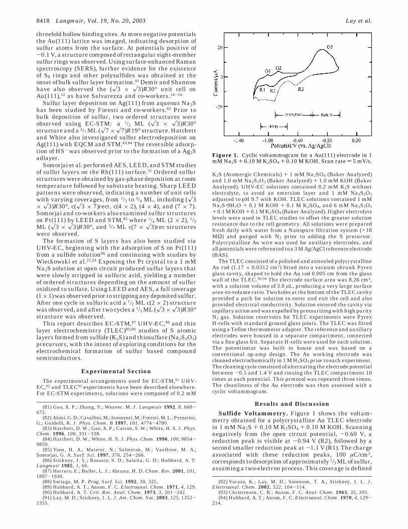
Results and DiscussionSulfide Voltammetry. Figure 1 shows the voltam-
metry obtained for a polycrystalline Au TLEC electrodein 1 mM Na2S + 0.10 M K2SO4 + 0.10 M KOH. Scanningnegatively from the open circuit potential, -0.60 V, areduction peak is visible at -0.94 V (R2), followed by asecond smaller reduction peak at -1.1 V (R1). The chargeassociated with these reduction peaks, 100 µC/cm2,corresponds todesorptionofapproximately 1/3 MLof sulfur,assuming a two-electron process. This coverage is defined
(81) Gao, X. P.; Zhang, Y.; Weaver, M. J. Langmuir 1992, 8, 668-672.
(82) Aloisi,G.D.;Cavallini,M.; Innocenti,M.;Foresti,M.L.;Pezzatini,G.; Guidelli, R. J. Phys. Chem. B 1997, 101, 4774-4780.
(83) Hatchett, D. W.; Gao, X. P.; Catron, S. W.; White, H. S. J. Phys.Chem. 1996, 100, 331-338.
(84) Hatchett, D. W.; White, H. S. J. Phys. Chem. 1996, 100, 9854-9859.
(85) Yoon, H. A.; Materer, N.; Salmeron, M.; VanHove, M. A.;Somorjai, G. A. Surf. Sci. 1997, 376, 254-266.
(86) Stickney, J. L.; Rosasco, S. D.; Salaita, G. D.; Hubbard, A. T.Langmuir 1985, 1, 66.
(87) Herrero, E.; Buller, L. J.; Abruna, H. D. Chem. Rev. 2001, 101,1897-1930.
(88) Soriaga, M. P. Prog. Surf. Sci. 1992, 39, 325.(89) Hubbard, A. T.; Anson, F. C. Electroanal. Chem. 1971, 4, 129.(90) Hubbard, A. T. Crit. Rev. Anal. Chem. 1973, 3, 201-242.(91) Lay, M. D.; Stickney, J. L. J. Am. Chem. Soc. 2003, 125, 1352-
1355.
(92) Varazo, K.; Lay, M. D.; Sorenson, T. A.; Stickney, J. L. J.Electroanal. Chem. 2002, 522, 104-114.
(93) Christensen, C. R.; Anson, F. C. Anal. Chem. 1963, 35, 205.(94) Hubbard, A. T.; Anson, F. C. Electroanal. Chem. 1970, 4, 129-
214.
Figure 1. Cyclic voltammogram for a Au(111) electrode in 1mM Na2S + 0.10 M K2SO4 + 0.10 M KOH. Scan rate ) 5 mV/s.
8418 Langmuir, Vol. 19, No. 20, 2003 Lay et al.
relative to the number of Au substrate surface atoms.Negative of -1.2 V, there is an increase in reductivecurrent corresponding to solvent decomposition.95 Uponreversing the scan direction, two small oxidation peaksare visible, with the first at -1.0 V (O1) and the secondat -0.86 V (O2). The oxidation and reduction peaks appearto be related, with O1 and O2 being the oxidative upd ofS, and R1 and R2 being the reductive stripping of Supd.81,95-100 Scanning further positive, there is a largeroxidation process (O3), due to the oxidation of sulfide tobulk sulfur and polysulfides,81,95,97,100 beginning at -0.60V and continuing until 0.0 V.
Reversing the scan direction at 0 V produces a newreduction feature (R3), not present in the initial scan, at-0.60 V (Figure 1). This is the reduction of sulfur speciesproduced during the large oxidation process at O3. It isinteresting that R3 is significantly smaller than O3,suggesting that only some of the product of O3 is reducedin R3. The rest of the product formed in O3 appears to bereduced commensurate with the original R2 and R1 peaks,showing less reversibility. In studies of sulfur depositionusing a gold rotating ring disk electrode (RRDE), Buckleyand Woods found that some soluble polysulfide interme-diates formed during the oxidation of sulfide to sulfur andduring the reductive dissolution of sulfur.95 TLEC studiesin this group showed that the product of O3 was stronglyadsorbed, as rinsing the TLEC cell with blank electrolytepositive of O3 still resulted in the extra reductive currentbetween -0.4 and -1.0 V, during the subsequent negativegoing scan.
EC-STM and UHV-EC Studies of Sulfide. Two seriesof sulfide electrodeposition experiments, using EC-STMand UHV-EC, on Au(111) were performed. Electrolyteconcentrations in UHV-EC studies were kept very low inorder to avoid precipitation of an electrolyte layer thatcould interfere with analysis upon emersion of theelectrode.101 Additionally, K2S was used as a source forsulfide, as K has a much higher Auger yield than Na,making it easier to quantify.
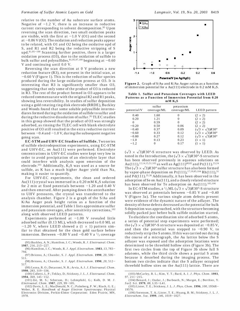
For UHV-EC experiments, the clean and orderedAu(111) crystal was immersed in a 0.20 mM K2S solutionfor 2 min at fixed potentials between -1.20 and 0.40 Vand then emersed. After pumping down the antechamberto UHV pressures, the crystal was transferred to theanalysis chamber. Figure 2 is a graph of the S/Au andK/Au Auger peak height ratios as a function of theimmersion potential, and Table 1 lists approximate sulfurand potassium coverages, after sensitivity corrections,102
along with observed LEED patterns.Experiments performed at -1.00 V revealed little
adsorbed sulfur (0.13 ML), which decreased to 0.0 ML at-1.20 V, where LEED showed a (1 × 1) pattern sim-ilar to that obtained for the clean gold surface beforeimmersion. Between -0.80 V and -0.40 V a 1/3 coverage
(x3 × x3)R30°-S structure was observed by LEED. Asnoted in the Introduction, the (x3 × x3)R30°-S structurehas been observed previously in aqueous solutions onAu(111),12,14,15,51,103 as well as Ag(111)48,82 and Pt(111).23,24
The (x3 × x3)R30° sulfur structure has also been formedby vapor-phase deposition on Pt(111),17,19,85,104 Rh(111),31
and Pd(111).35,36 Additionally, it has been observed in theadsorption of Se on Au(111), and a closely related structurehas been observed for Te adsorption on Au(111).105,106
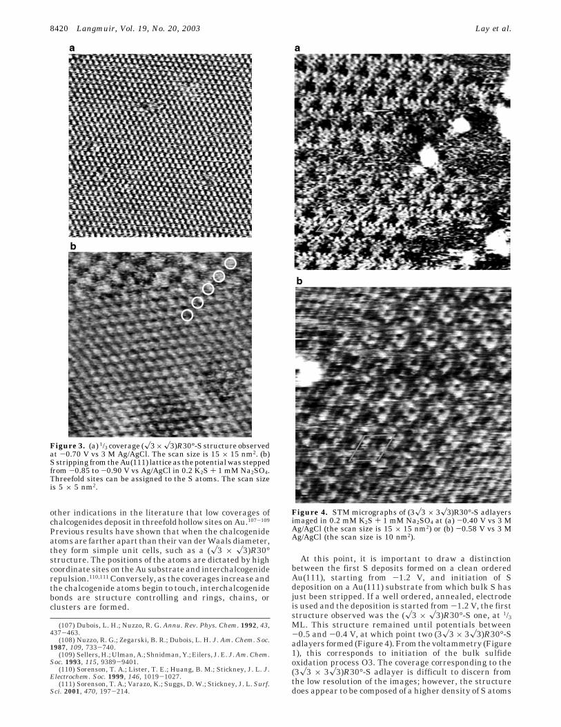
In EC-STM studies, a 1/3 ML (x3 ×x3)R30°-S structurewas observed at potentials between -0.85 V and -0.40V (Figure 3a). The various single atom defects presentwere evidence of the dynamic nature of the adlayer. Thedensity of these defects decreased as the potential for bulkS deposition was approached, with the structure becomingsolidly packed just before bulk sulfide oxidation started.
To elucidate the coordination site of adsorbed S atoms,a series of potential step experiments were performed;the (x3 × x3)R30°-S structure was deposited at -0.85 V,and then the potential was stepped to -0.90 V, toreductively strip the S atoms. If this was carried out duringthe course of a micrograph, the Au lattice below the Sadlayer was exposed and the adsorption locations weredetermined to be threefold hollow sites (Figure 3b). Thefirst two circles from the top of Figure 3b show full Sadatoms, while the third circle shows a partial S atombecause it desorbed during the imaging process. Thebottom two circles indicate that the S adlayer occupiedthreefold hollow sites on the Au(111) lattice. There are
(95) Buckley, A. N.; Hamilton, I. C.; Woods, R. J. Electroanal. Chem.1987, 216, 213-227.
(96) Hamilton, I. C.; Woods, R. J. Appl. Electrochem. 1983, 13, 783-794.
(97) Briceno, A.; Chander, S. J. Appl. Electrochem. 1990, 20, 506-511.
(98) Briceno, A.; Chander, S. J. Appl. Electrochem. 1990, 20, 512-517.
(99) Lezna, R. O.; Detacconi, N. R.; Arvia, A. J. J. Electroanal. Chem.1990, 283, 319-336.
(100) Colletti, L. P.; Teklay, D.; Stickney, J. L. J. Electroanal. Chem.1994, 369, 145-152.
(101) Zei, M. S.; Scherson, D.; Lehmpfuhl, G.; Kolb, D. M. J.Electroanal. Chem. 1987, 229, 99-105.
(102) Davis, L. E.; MacDonald, N. C.; Palmberg, P. W.; Riach, G. E.;Weber, R. E. Handbook of Auger Electron Spectroscopy; PhysicalElectronics Division, Perkin-Elmer Corporation: Eden Prairie, MN,1978.
(103) McCarley, R. L.; Kim, Y. T.; Bard, A. J. J. Phys. Chem. 1993,97, 211-215.
(104) Benard, J.; Oudar, J.; Barbouth, N.; Margot, E.; Berthier, Y.Surf. Sci. 1979, 88, L35-L41.
(105) Lister, T. E.; Stickney, J. L. J. Phys. Chem. 1996, 100, 19568-19576.
(106) Sorenson, T. A.; Lister, T. E.; Huang, B. M.; Stickney, J. L. J.Electrochem. Soc. 1999, 146, 1019-1027.
Figure 2. Graph of S/Au and K/Au Auger ratios as a functionof immersion potential for a Au(111) electrode in 0.2 mM K2S.
Table 1. Sulfur and Potassium Coverages with LEEDPatterns as a Function of Immersion Potential from 0.20
mM K2S
potential/Vsulfur
coverage/MLpotassium
coverage/ML LEED pattern
0.40 1.60 0 (2 × 2)0.20 1.21 0 (2 × 2)0 0.59 0 (2 × 2)
-0.20 0.50 0.06 (2 × 2)-0.40 0.37 0.09 (x3 × x3)R30°-0.60 0.33 0.12 (x3 × x3)R30°-0.80 0.27 0.12 (x3 × x3)R30°-1.0 0.13 0.23 (1 × 1)-1.2 0 0.17 (1 × 1)
Formation of Sulfur Atomic Layers on Gold Langmuir, Vol. 19, No. 20, 2003 8419
other indications in the literature that low coverages ofchalcogenides deposit in threefold hollow sites on Au.107-109
Previous results have shown that when the chalcogenideatoms are farther apart than their van der Waals diameter,they form simple unit cells, such as a (x3 × x3)R30°structure. The positions of the atoms are dictated by highcoordinate sites on the Au substrate and interchalcogeniderepulsion.110,111 Conversely, as the coverages increase andthe chalcogenide atoms begin to touch, interchalcogenidebonds are structure controlling and rings, chains, orclusters are formed.
At this point, it is important to draw a distinctionbetween the first S deposits formed on a clean orderedAu(111), starting from -1.2 V, and initiation of Sdeposition on a Au(111) substrate from which bulk S hasjust been stripped. If a well ordered, annealed, electrodeis used and the deposition is started from -1.2 V, the firststructure observed was the (x3 × x3)R30°-S one, at 1/3ML. This structure remained until potentials between-0.5 and -0.4 V, at which point two (3x3 × 3x3)R30°-Sadlayers formed (Figure 4). From the voltammetry (Figure1), this corresponds to initiation of the bulk sulfideoxidation process O3. The coverage corresponding to the(3x3 × 3x3)R30°-S adlayer is difficult to discern fromthe low resolution of the images; however, the structuredoes appear to be composed of a higher density of S atoms
(107) Dubois, L. H.; Nuzzo, R. G. Annu. Rev. Phys. Chem. 1992, 43,437-463.
(108) Nuzzo, R. G.; Zegarski, B. R.; Dubois, L. H. J. Am. Chem. Soc.1987, 109, 733-740.
(109) Sellers, H.; Ulman, A.; Shnidman, Y.; Eilers, J. E. J. Am. Chem.Soc. 1993, 115, 9389-9401.
(110) Sorenson, T. A.; Lister, T. E.; Huang, B. M.; Stickney, J. L. J.Electrochem. Soc. 1999, 146, 1019-1027.
(111) Sorenson, T. A.; Varazo, K.; Suggs, D. W.; Stickney, J. L. Surf.Sci. 2001, 470, 197-214.
Figure 3. (a) 1/3 coverage (x3 ×x3)R30°-S structure observedat -0.70 V vs 3 M Ag/AgCl. The scan size is 15 × 15 nm2. (b)S stripping from the Au(111) lattice as the potential was steppedfrom -0.85 to -0.90 V vs Ag/AgCl in 0.2 K2S + 1 mM Na2SO4.Threefold sites can be assigned to the S atoms. The scan sizeis 5 × 5 nm2.
Figure 4. STM micrographs of (3x3 × 3x3)R30°-S adlayersimaged in 0.2 mM K2S + 1 mM Na2SO4 at (a) -0.40 V vs 3 MAg/AgCl (the scan size is 15 × 15 nm2) or (b) -0.58 V vs 3 MAg/AgCl (the scan size is 10 nm2).
8420 Langmuir, Vol. 19, No. 20, 2003 Lay et al.
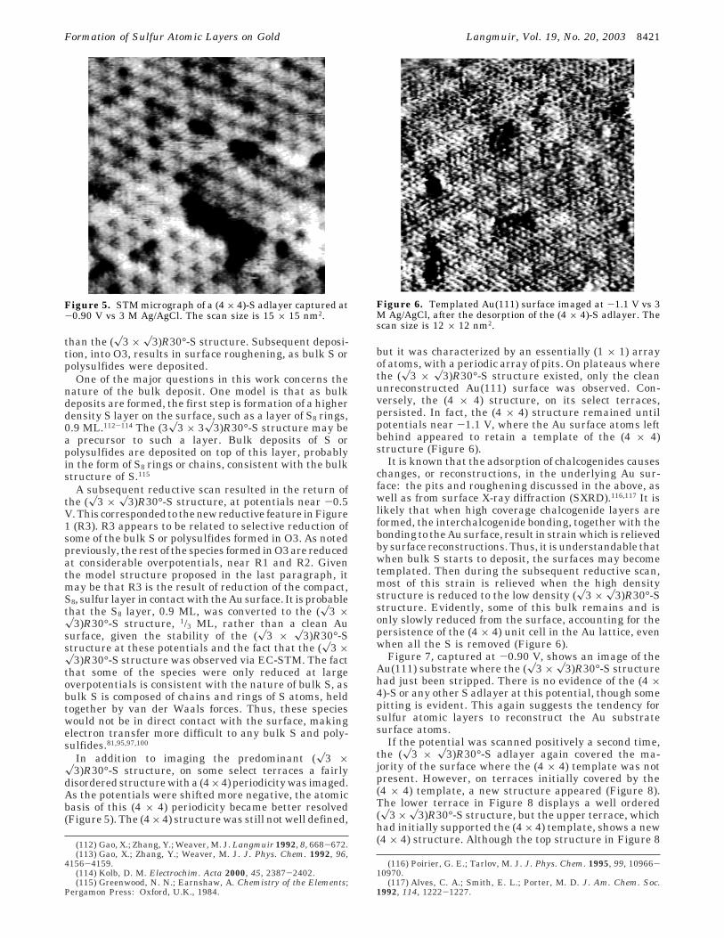
than the (x3 × x3)R30°-S structure. Subsequent deposi-tion, into O3, results in surface roughening, as bulk S orpolysulfides were deposited.
One of the major questions in this work concerns thenature of the bulk deposit. One model is that as bulkdeposits are formed, the first step is formation of a higherdensity S layer on the surface, such as a layer of S8 rings,0.9 ML.112-114 The (3x3 × 3x3)R30°-S structure may bea precursor to such a layer. Bulk deposits of S orpolysulfides are deposited on top of this layer, probablyin the form of S8 rings or chains, consistent with the bulkstructure of S.115
A subsequent reductive scan resulted in the return ofthe (x3 × x3)R30°-S structure, at potentials near -0.5V.This correspondedto thenew reductive feature inFigure1 (R3). R3 appears to be related to selective reduction ofsome of the bulk S or polysulfides formed in O3. As notedpreviously, the rest of the species formed in O3 are reducedat considerable overpotentials, near R1 and R2. Giventhe model structure proposed in the last paragraph, itmay be that R3 is the result of reduction of the compact,S8, sulfur layer in contact with the Au surface. It is probablethat the S8 layer, 0.9 ML, was converted to the (x3 ×x3)R30°-S structure, 1/3 ML, rather than a clean Ausurface, given the stability of the (x3 × x3)R30°-Sstructure at these potentials and the fact that the (x3 ×x3)R30°-S structure was observed via EC-STM. The factthat some of the species were only reduced at largeoverpotentials is consistent with the nature of bulk S, asbulk S is composed of chains and rings of S atoms, heldtogether by van der Waals forces. Thus, these specieswould not be in direct contact with the surface, makingelectron transfer more difficult to any bulk S and poly-sulfides.81,95,97,100
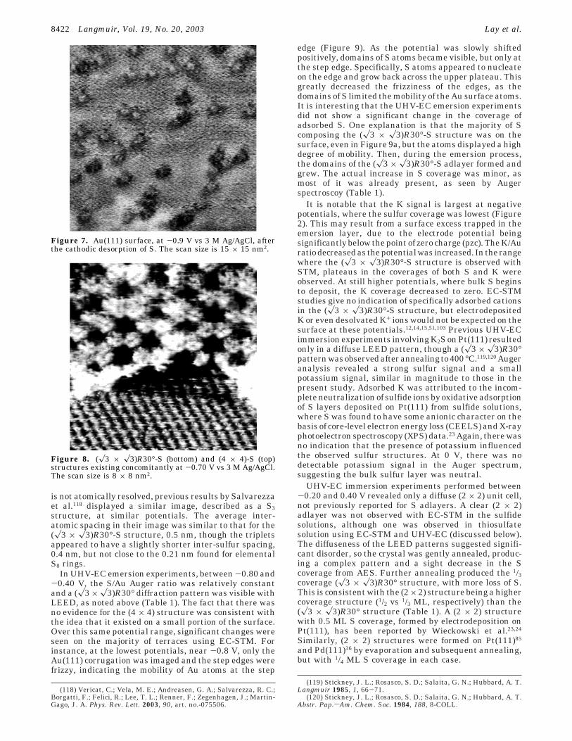
In addition to imaging the predominant (x3 ×x3)R30°-S structure, on some select terraces a fairlydisordered structure with a (4×4) periodicity was imaged.As the potentials were shifted more negative, the atomicbasis of this (4 × 4) periodicity became better resolved(Figure 5). The (4 × 4) structure was still not well defined,
but it was characterized by an essentially (1 × 1) arrayof atoms, with a periodic array of pits. On plateaus wherethe (x3 × x3)R30°-S structure existed, only the cleanunreconstructed Au(111) surface was observed. Con-versely, the (4 × 4) structure, on its select terraces,persisted. In fact, the (4 × 4) structure remained untilpotentials near -1.1 V, where the Au surface atoms leftbehind appeared to retain a template of the (4 × 4)structure (Figure 6).
It is known that the adsorption of chalcogenides causeschanges, or reconstructions, in the underlying Au sur-face: the pits and roughening discussed in the above, aswell as from surface X-ray diffraction (SXRD).116,117 It islikely that when high coverage chalcogenide layers areformed, the interchalcogenide bonding, together with thebonding to the Au surface, result in strain which is relievedby surface reconstructions. Thus, it is understandable thatwhen bulk S starts to deposit, the surfaces may becometemplated. Then during the subsequent reductive scan,most of this strain is relieved when the high densitystructure is reduced to the low density (x3 × x3)R30°-Sstructure. Evidently, some of this bulk remains and isonly slowly reduced from the surface, accounting for thepersistence of the (4 × 4) unit cell in the Au lattice, evenwhen all the S is removed (Figure 6).
Figure 7, captured at -0.90 V, shows an image of theAu(111) substrate where the (x3 × x3)R30°-S structurehad just been stripped. There is no evidence of the (4 ×4)-S or any other S adlayer at this potential, though somepitting is evident. This again suggests the tendency forsulfur atomic layers to reconstruct the Au substratesurface atoms.
If the potential was scanned positively a second time,the (x3 × x3)R30°-S adlayer again covered the ma-jority of the surface where the (4 × 4) template was notpresent. However, on terraces initially covered by the(4 × 4) template, a new structure appeared (Figure 8).The lower terrace in Figure 8 displays a well ordered(x3 × x3)R30°-S structure, but the upper terrace, whichhad initially supported the (4 × 4) template, shows a new(4 × 4) structure. Although the top structure in Figure 8(112) Gao, X.; Zhang, Y.; Weaver, M. J. Langmuir 1992, 8, 668-672.
(113) Gao, X.; Zhang, Y.; Weaver, M. J. J. Phys. Chem. 1992, 96,4156-4159.
(114) Kolb, D. M. Electrochim. Acta 2000, 45, 2387-2402.(115) Greenwood, N. N.; Earnshaw, A. Chemistry of the Elements;
Pergamon Press: Oxford, U.K., 1984.
(116) Poirier, G. E.; Tarlov, M. J. J. Phys. Chem. 1995, 99, 10966-10970.
(117) Alves, C. A.; Smith, E. L.; Porter, M. D. J. Am. Chem. Soc.1992, 114, 1222-1227.
Figure 5. STM micrograph of a (4 × 4)-S adlayer captured at-0.90 V vs 3 M Ag/AgCl. The scan size is 15 × 15 nm2.
Figure 6. Templated Au(111) surface imaged at -1.1 V vs 3M Ag/AgCl, after the desorption of the (4 × 4)-S adlayer. Thescan size is 12 × 12 nm2.
Formation of Sulfur Atomic Layers on Gold Langmuir, Vol. 19, No. 20, 2003 8421
is not atomically resolved, previous results by Salvarezzaet al.118 displayed a similar image, described as a S3structure, at similar potentials. The average inter-atomic spacing in their image was similar to that for the(x3 × x3)R30°-S structure, 0.5 nm, though the tripletsappeared to have a slightly shorter inter-sulfur spacing,0.4 nm, but not close to the 0.21 nm found for elementalS8 rings.
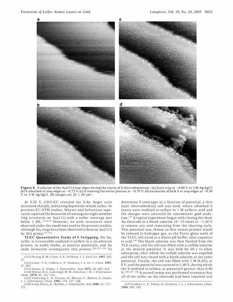
In UHV-EC emersion experiments, between -0.80 and-0.40 V, the S/Au Auger ratio was relatively constantand a (x3 × x3)R30° diffraction pattern was visible withLEED, as noted above (Table 1). The fact that there wasno evidence for the (4 × 4) structure was consistent withthe idea that it existed on a small portion of the surface.Over this same potential range, significant changes wereseen on the majority of terraces using EC-STM. Forinstance, at the lowest potentials, near -0.8 V, only theAu(111) corrugation was imaged and the step edges werefrizzy, indicating the mobility of Au atoms at the step
edge (Figure 9). As the potential was slowly shiftedpositively, domains of S atoms became visible, but only atthe step edge. Specifically, S atoms appeared to nucleateon the edge and grow back across the upper plateau. Thisgreatly decreased the frizziness of the edges, as thedomains of S limited the mobility of the Au surface atoms.It is interesting that the UHV-EC emersion experimentsdid not show a significant change in the coverage ofadsorbed S. One explanation is that the majority of Scomposing the (x3 × x3)R30°-S structure was on thesurface, even in Figure 9a, but the atoms displayed a highdegree of mobility. Then, during the emersion process,the domains of the (x3 × x3)R30°-S adlayer formed andgrew. The actual increase in S coverage was minor, asmost of it was already present, as seen by Augerspectroscoy (Table 1).
It is notable that the K signal is largest at negativepotentials, where the sulfur coverage was lowest (Figure2). This may result from a surface excess trapped in theemersion layer, due to the electrode potential beingsignificantly below the point of zero charge (pzc). The K/Auratio decreased as the potential was increased. In the rangewhere the (x3 × x3)R30°-S structure is observed withSTM, plateaus in the coverages of both S and K wereobserved. At still higher potentials, where bulk S beginsto deposit, the K coverage decreased to zero. EC-STMstudies give no indication of specifically adsorbed cationsin the (x3 × x3)R30°-S structure, but electrodepositedK or even desolvated K+ ions would not be expected on thesurface at these potentials.12,14,15,51,103 Previous UHV-ECimmersion experiments involving K2S on Pt(111) resultedonly in a diffuse LEED pattern, though a (x3 × x3)R30°pattern was observed after annealing to 400 °C.119,120 Augeranalysis revealed a strong sulfur signal and a smallpotassium signal, similar in magnitude to those in thepresent study. Adsorbed K was attributed to the incom-plete neutralization of sulfide ions by oxidative adsorptionof S layers deposited on Pt(111) from sulfide solutions,where S was found to have some anionic character on thebasis of core-level electron energy loss (CEELS) and X-rayphotoelectron spectroscopy (XPS) data.23 Again, there wasno indication that the presence of potassium influencedthe observed sulfur structures. At 0 V, there was nodetectable potassium signal in the Auger spectrum,suggesting the bulk sulfur layer was neutral.
UHV-EC immersion experiments performed between-0.20 and 0.40 V revealed only a diffuse (2 × 2) unit cell,not previously reported for S adlayers. A clear (2 × 2)adlayer was not observed with EC-STM in the sulfidesolutions, although one was observed in thiosulfatesolution using EC-STM and UHV-EC (discussed below).The diffuseness of the LEED patterns suggested signifi-cant disorder, so the crystal was gently annealed, produc-ing a complex pattern and a sight decrease in the Scoverage from AES. Further annealing produced the 1/3coverage (x3 × x3)R30° structure, with more loss of S.This is consistent with the (2 × 2) structure being a highercoverage structure (1/2 vs 1/3 ML, respectively) than the(x3 × x3)R30° structure (Table 1). A (2 × 2) structurewith 0.5 ML S coverage, formed by electrodeposition onPt(111), has been reported by Wieckowski et al.23,24
Similarly, (2 × 2) structures were formed on Pt(111)85
and Pd(111)36 by evaporation and subsequent annealing,but with 1/4 ML S coverage in each case.
(118) Vericat, C.; Vela, M. E.; Andreasen, G. A.; Salvarezza, R. C.;Borgatti, F.; Felici, R.; Lee, T. L.; Renner, F.; Zegenhagen, J.; Martin-Gago, J. A. Phys. Rev. Lett. 2003, 90, art. no.-075506.
(119) Stickney, J. L.; Rosasco, S. D.; Salaita, G. N.; Hubbard, A. T.Langmuir 1985, 1, 66-71.
(120) Stickney, J. L.; Rosasco, S. D.; Salaita, G. N.; Hubbard, A. T.Abstr. Pap.sAm. Chem. Soc. 1984, 188, 8-COLL.
Figure 7. Au(111) surface, at -0.9 V vs 3 M Ag/AgCl, afterthe cathodic desorption of S. The scan size is 15 × 15 nm2.
Figure 8. (x3 × x3)R30°-S (bottom) and (4 × 4)-S (top)structures existing concomitantly at -0.70 V vs 3 M Ag/AgCl.The scan size is 8 × 8 nm2.
8422 Langmuir, Vol. 19, No. 20, 2003 Lay et al.
At 0.20 V, UHV-EC revealed the S/Au Auger ratioincreased sharply, indicating deposition of bulk sulfur. Inprevious EC-STM studies, Weaver and Salvarezza sepa-rately reported the formation of rectangular eight-memberring structures on Au(111) with a sulfur coverage justbelow 1 ML.11,14,15 However, no such structures wereobserved under the conditions used in the present studies,although Se8 rings have been observed to form on Au(111)by this group.121,122
TLEC Quantitative Study of S Stripping. On Au,sulfur is irreversibly oxidized to sulfate in a six-electronprocess, in acidic media, at positive potentials, and Auoxide formation accompanies this process.100,123-126 To
determine S coverages as a function of potential, a thinlayer electrochemical cell was used, where adsorbed Slayers were oxidized to sulfate in 1 M sulfuric acid andthe charges were corrected for concomitant gold oxida-tion.127 A typical experiment began with rinsing the cleanAu electrode in a blank solution 10-15 times at -1.30 Vto remove any acid remaining from the cleaning cycle.This potential was chosen so that excess protons wouldbe reduced to hydrogen gas, as the Pyrex glass walls ofthe TLEC cell acted as a dilute pH buffer, after exposureto acid.100 The blank solution was then flushed from theTLE cavity, and the cell was filled with a sulfide solutionat the desired potential. It was held for 60 s to allowadsorption, after which the sulfide solution was expelledand the cell was rinsed with a blank solution at the samepotential. Finally, the cell was filled with 1 M H2SO4 at0 V, and the potential was scanned to 1.40 V, during whichthe S oxidized to sulfate, at potentials greater than 0.80V.100,123-126 A second sweep was performed to ensure thatall of the sulfur on the electrode had been removed and
(121) Huang, B. M.; Lister, T. E.; Stickney, J. L. Surf. Sci. 1997, 392,27.
(122) Lister, T. E.; Colletti, L. P.; Stickney, J. L. Isr. J. Chem. 1997,37, 287.
(123) Samec, Z.; Weber, J. Electrochim. Acta 1975, 20, 403-412.(124) Wierse, D. G.; Lohrengel, M. M.; Schultze, J. W. J. Electroanal.
Chem. 1978, 92, 121-131.(125) Vanhuong, C. N.; Parsons, R.; Marcus, P.; Montes, S.; Oudar,
J. J. Electroanal. Chem. 1981, 119, 137-148.(126) Lamy-Pitara, E.; Barbier, J. Electrochim. Acta 1986, 31, 717-
721.(127) Colletti, L. P.; Teklay, D.; Stickney, J. L. J. Electroanal. Chem.
1994, 369, 145.
Figure 9. Evolution of the Au(111) step edges during the course of S electrodeposition: (a) fuzzy step at -0.80 V vs 3 M Ag/AgCl;(b) S adsorbed at step edges at -0.73 V; (c) S covering the entire plateau at -0.70 V; (d) nucleation of bulk S at step edges at -0.50V vs 3 M Ag/AgCl. All images are 20 × 20 nm2.
Formation of Sulfur Atomic Layers on Gold Langmuir, Vol. 19, No. 20, 2003 8423
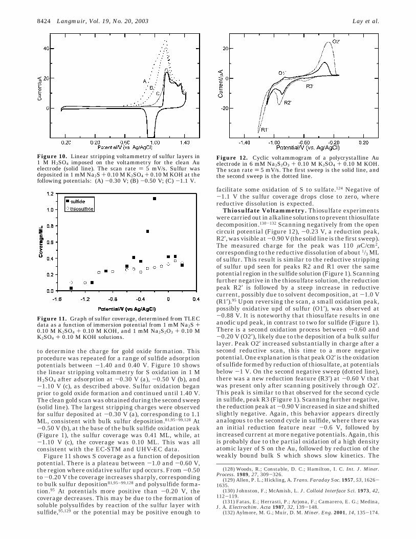
to determine the charge for gold oxide formation. Thisprocedure was repeated for a range of sulfide adsorptionpotentials between -1.40 and 0.40 V. Figure 10 showsthe linear stripping voltammetry for S oxidation in 1 MH2SO4 after adsorption at -0.30 V (a), -0.50 V (b), and-1.10 V (c), as described above. Sulfur oxidation beganprior to gold oxide formation and continued until 1.40 V.The clean gold scan was obtained during the second sweep(solid line). The largest stripping charges were observedfor sulfur deposited at -0.30 V (a), corresponding to 1.1ML, consistent with bulk sulfur deposition.81,95-99,128 At-0.50 V (b), at the base of the bulk sulfide oxidation peak(Figure 1), the sulfur coverage was 0.41 ML, while, at-1.10 V (c), the coverage was 0.10 ML. This was allconsistent with the EC-STM and UHV-EC data.
Figure 11 shows S coverage as a function of depositionpotential. There is a plateau between -1.0 and -0.60 V,the region where oxidative sulfur upd occurs. From -0.50to -0.20 V the coverage increases sharply, correspondingto bulk sulfur deposition81,95-99,128 and polysulfide forma-tion.95 At potentials more positive than -0.20 V, thecoverage decreases. This may be due to the formation ofsoluble polysulfides by reaction of the sulfur layer withsulfide,95,129 or the potential may be positive enough to
facilitate some oxidation of S to sulfate.124 Negative of-1.1 V the sulfur coverage drops close to zero, wherereductive dissolution is expected.
Thiosulfate Voltammetry. Thiosulfate experimentswere carried out in alkaline solutions to prevent thiosulfatedecomposition.130-132 Scanning negatively from the opencircuit potential (Figure 12), -0.23 V, a reduction peak,R2′, was visible at -0.90 V (the solid line is the first sweep).The measured charge for the peak was 110 µC/cm2,corresponding to the reductive dissolution of about 1/3 MLof sulfur. This result is similar to the reductive strippingof sulfur upd seen for peaks R2 and R1 over the samepotential region in the sulfide solution (Figure 1). Scanningfurther negative in the thiosulfate solution, the reductionpeak R2′ is followed by a steep increase in reductivecurrent, possibly due to solvent decomposition, at -1.0 V(R1′).95 Upon reversing the scan, a small oxidation peak,possibly oxidative upd of sulfur (O1′), was observed at-0.88 V. It is noteworthy that thiosulfate results in oneanodic upd peak, in contrast to two for sulfide (Figure 1).There is a second oxidation process between -0.60 and-0.20 V (O2′), likely due to the deposition of a bulk sulfurlayer. Peak O2′ increased substantially in charge after asecond reductive scan, this time to a more negativepotential. One explanation is that peak O2′ is the oxidationof sulfide formed by reduction of thiosulfate, at potentialsbelow -1 V. On the second negative sweep (dotted line),there was a new reduction feature (R3′) at -0.60 V thatwas present only after scanning positively through O2′.This peak is similar to that observed for the second cyclein sulfide, peak R3 (Figure 1). Scanning further negative,the reduction peak at -0.90 V increased in size and shiftedslightly negative. Again, this behavior appears directlyanalogous to the second cycle in sulfide, where there wasan initial reduction feature near -0.6 V, followed byincreased current at more negative potentials. Again, thisis probably due to the partial oxidation of a high densityatomic layer of S on the Au, followed by reduction of theweakly bound bulk S which shows slow kinetics. The
(128) Woods, R.; Constable, D. C.; Hamilton, I. C. Int. J. Miner.Process. 1989, 27, 309-326.
(129) Allen, P. L.; Hickling, A. Trans. Faraday Soc. 1957, 53, 1626-1635.
(130) Johnston, F.; McAmish, L. J. Colloid Interface Sci. 1973, 42,112-119.
(131) Fatas, E.; Herrasti, P.; Arjona, F.; Camarero, E. G.; Medina,J. A. Electrochim. Acta 1987, 32, 139-148.
(132) Aylmore, M. G.; Muir, D. M. Miner. Eng. 2001, 14, 135-174.
Figure 10. Linear stripping voltammetry of sulfur layers in1 M H2SO4 imposed on the voltammetry for the clean Auelectrode (solid line). The scan rate ) 5 mV/s. Sulfur wasdeposited in 1 mM Na2S + 0.10 M K2SO4 + 0.10 M KOH at thefollowing potentials: (A) -0.30 V; (B) -0.50 V; (C) -1.1 V.
Figure 11. Graph of sulfur coverage, determined from TLECdata as a function of immersion potential from 1 mM Na2S +0.10 M K2SO4 + 0.10 M KOH, and 1 mM Na2S2O3 + 0.10 MK2SO4 + 0.10 M KOH solutions.
Figure 12. Cyclic voltammogram of a polycrystalline Auelectrode in 6 mM Na2S2O3 + 0.10 M K2SO4 + 0.10 M KOH.The scan rate ) 5 mV/s. The first sweep is the solid line, andthe second sweep is the dotted line.
8424 Langmuir, Vol. 19, No. 20, 2003 Lay et al.
charge was 210 µC/cm2 for bulk oxidation (O2′) and 200µC/cm2 for the corresponding reductions, suggesting aquantitative process.
In the second cycle (dotted line in Figure 12), theelectrode was scanned further negative than was the casein the first dotted scan. In the subsequent positive scan,the upd feature O1′ was essentially the same, while thebulk oxidation feature O2′ more than doubled. In the caseof sulfide, the size of the bulk peak appeared to be self-limiting. Self-poisoning in the bulk chalcogenide layer haspreviously been observed in Se deposition.133 In the presentcase, it appears that the bulk peak (O2′) is limited by theextent of the previous reduction process. Explicitly, itappears that the reduction process R1′ includes thiosulfatereduction to sulfide, in addition to solvent decomposition,with the product sulfide being subsequently oxidativelydeposited in O2′.
As noted previously, TLEC was used to show that thelarge oxidation peak at -0.30 V (O3 in Figure 1) in sulfidewas due to the deposition of an insoluble elemental sulfurspecies on the electrode.100 Similar TLEC experimentswere performed with thiosulfate, which showed that thespecies formed in O2′, probably bulk S or polysulfides,was not soluble and stayed on the surface despite rinsingin the blank solution.
A related experiment was performed to identify thesulfur species undergoing oxidation at -0.30 V. Afterextensive reduction to -1.2 V and scanning positivelythrough sulfur upd, the solution was again exchanged forthe blank, 0.10 M K2SO4 + 0.10 M KOH, at -0.65 V, andthe scan was then continued in the positive direction to0 V. Peak O2′ was absent, demonstrating that the speciesoxidized at -0.30 V (O2′) was a soluble species, likelysulfide, and was rinsed out of the TLEC cavity, precludingbulk sulfur deposition.
The average oxidation state for the sulfur atoms in athiosulfate molecule is +2, though one may think of themolecule as having sulfur atoms with oxidation states of0 and +4. Either way, it is known that sulfide can beproduced by the reduction of thiosulfate.115 As mentionedabove, the reduction process occurring at -1.0 V is believedto include thiosulfate reduction to sulfide, as O2′ is notvisible unless the electrode potential is first scanned below-0.90 V. The open circuit potential in the thiosulfatesolution was more positive than that in the correspondingsulfide solution, -0.2 and -0.6 V, respectively. For thesulfide solution, the rest potential was held negative ofthe potential for bulk sulfide oxidation, while, for thio-sulfate, the rest potential was in the range where bulksulfide oxidation is expected. This suggests that at opencircuit in the thiosulfate solution there was no sulfidepresent to oxidize and thus no redox species in solutionto shift the potential more negative, as observed in sulfidesolutions. This point is borne out by the EC-STM databelow.
The S coverage from thiosulfate follows that from sulfide(Figure 11), until potentials corresponding to the initiationof bulk sulfur formation. At this point, the S coverage inthe thiosulfate solution does not dramatically increase,as was the case in the sulfide solutions. This is consistentwith the above discussions, as there should be no sulfidein solution, and any elemental sulfur on the surface isprobably the result of a surface-limited decomposition ofthiosulfate.
EC-STM and UHV-EC Studies of Thiosulfate.At the open circuit potential, -0.2 V, EC-STM revealed
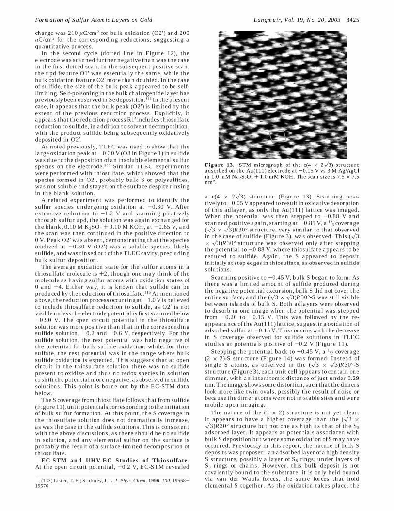
a c(4 × 2x3) structure (Figure 13). Scanning posi-tively to -0.05 V appeared to result in oxidative desorptionof this adlayer, as only the Au(111) lattice was imaged.When the potential was then stepped to -0.88 V andscanned positive again, starting at -0.85 V, a 1/3 coverage(x3 × x3)R30° structure, very similar to that observedin the case of sulfide (Figure 3), was observed. This (x3× x3)R30° structure was observed only after steppingthe potential to -0.88 V, where thiosulfate appears to bereduced to sulfide. Again, the S appeared to depositinitially at step edges in thiosulfate, as observed in sulfidesolutions.
Scanning positive to -0.45 V, bulk S began to form. Asthere was a limited amount of sulfide produced duringthe negative potential excursion, bulk S did not cover theentire surface, and the (x3 × x3)R30°-S was still visiblebetween islands of bulk S. Both adlayers were observedto desorb in one image when the potential was steppedfrom -0.20 to -0.15 V. This was followed by the re-appearance of the Au(111) lattice, suggesting oxidation ofadsorbed sulfur at -0.15 V. This concurs with the decreasein S coverage observed for sulfide solutions in TLECstudies at potentials positive of -0.2 V (Figure 11).
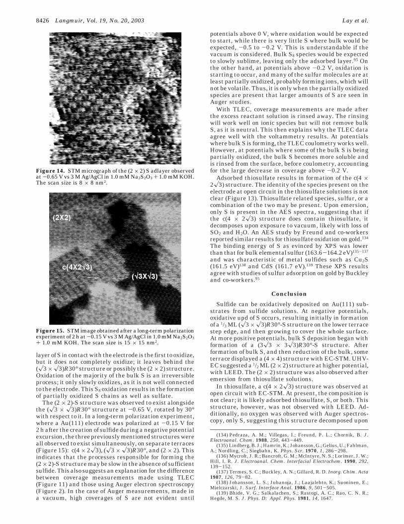
Stepping the potential back to -0.45 V, a 1/2 coverage(2 × 2)-S structure (Figure 14) was formed. Instead ofsingle S atoms, as observed in the (x3 × x3)R30°-Sstructure (Figure 3), each unit cell appears to contain onedimmer, with an interatomic distance of just under 0.29nm. The image shows some distortion, such that the dimerslook more like twin ovals, possibly the result of noise orbecause the dimer atoms were not in stable sites and weremobile upon imaging.
The nature of the (2 × 2) structure is not yet clear.It appears to have a higher coverage than the (x3 ×x3)R30° structure but not one as high as that of the S8adsorbed layer. It appears at potentials associated withbulk S deposition but where some oxidation of S may haveoccurred. Previously in this report, the nature of bulk Sdeposits was proposed: an adsorbed layer of a high densityS structure, possibly a layer of S8 rings, under layers ofS8 rings or chains. However, this bulk deposit is notcovalently bound to the substrate; it is only held boundvia van der Waals forces, the same forces that holdelemental S together. As the oxidation takes place, the
(133) Lister, T. E.; Stickney, J. L. J. Phys. Chem. 1996, 100, 19568-19576.
Figure 13. STM micrograph of the c(4 × 2x3) structureadsorbed on the Au(111) electrode at -0.15 V vs 3 M Ag/AgClin 1.0 mM Na2S2O3 + 1.0 mM KOH. The scan size is 7.5 × 7.5nm2.
Formation of Sulfur Atomic Layers on Gold Langmuir, Vol. 19, No. 20, 2003 8425
layer of S in contact with the electrode is the first to oxidize,but it does not completely oxidize; it leaves behind the(x3 × x3)R30° structure or possibly the (2 × 2) structure.Oxidation of the majority of the bulk S is an irreversibleprocess; it only slowly oxidizes, as it is not well connectedto the electrode. This S8 oxidation results in the formationof partially oxidized S chains as well as sulfate.
The (2 × 2)-S structure was observed to exist alongsidethe (x3 × x3)R30° structure at -0.65 V, rotated by 30°with respect to it. In a long-term polarization experiment,where a Au(111) electrode was polarized at -0.15 V for2 h after the creation of sulfide during a negative potentialexcursion, the three previously mentioned structures wereall observed to exist simultaneously, on separate terraces(Figure 15): c(4 × 2x3), (x3 × x3)R30°, and (2 × 2). Thisindicates that the processes responsible for forming the(2 × 2)-S structure may be slow in the absence of sufficientsulfide. This also suggests an explanation for the differencebetween coverage measurements made using TLEC(Figure 11) and those using Auger electron spectroscopy(Figure 2). In the case of Auger measurements, made ina vacuum, high coverages of S are not evident until
potentials above 0 V, where oxidation would be expectedto start, while there is very little S where bulk would beexpected, -0.5 to -0.2 V. This is understandable if thevacuum is considered. Bulk S8 species would be expectedto slowly sublime, leaving only the adsorbed layer.95 Onthe other hand, at potentials above -0.2 V, oxidation isstarting to occur, and many of the sulfur molecules are atleast partially oxidized, probably forming ions, which willnot be volatile. Thus, it is only when the partially oxidizedspecies are present that larger amounts of S are seen inAuger studies.
With TLEC, coverage measurements are made afterthe excess reactant solution is rinsed away. The rinsingwill work well on ionic species but will not remove bulkS, as it is neutral. This then explains why the TLEC dataagree well with the voltammetry results. At potentialswhere bulk S is forming, the TLEC coulometry works well.However, at potentials where some of the bulk S is beingpartially oxidized, the bulk S becomes more soluble andis rinsed from the surface, before coulometry, accountingfor the large decrease in coverage above -0.2 V.
Adsorbed thiosulfate results in formation of the c(4 ×2x3) structure. The identity of the species present on theelectrode at open circuit in the thiosulfate solutions is notclear (Figure 13). Thiosulfate related species, sulfur, or acombination of the two may be present. Upon emersion,only S is present in the AES spectra, suggesting that ifthe c(4 × 2x3) structure does contain thiosulfate, itdecomposes upon exposure to vacuum, likely with loss ofSO2 and H2O. An AES study by Freund and co-workersreported similar results for thiosulfate oxidation on gold.134
The binding energy of S as evinced by XPS was lowerthan that for bulk elemental sulfur (163.6-164.2 eV)135-137
and was characteristic of metal sulfides such as Cu2S(161.5 eV)138 and CdS (161.7 eV).139 These XPS resultsagree with studies of sulfur adsorption on gold by Buckleyand co-workers.95
Conclusion
Sulfide can be oxidatively deposited on Au(111) sub-strates from sulfide solutions. At negative potentials,oxidative upd of S occurs, resulting initially in formationof a 1/3 ML (x3 ×x3)R30°-S structure on the lower terracestep edge, and then growing to cover the whole surface.At more positive potentials, bulk S deposition began withformation of a (3x3 × 3x3)R30°-S structure. Afterformation of bulk S, and then reduction of the bulk, someterrace displayed a (4 × 4) structure with EC-STM. UHV-EC suggested a 1/2 ML (2×2) structure at higher potential,with LEED. The (2 × 2) structure was also observed afteremersion from thiosulfate solutions.
In thiosulfate, a c(4 × 2x3) structure was observed atopen circuit with EC-STM. At present, the composition isnot clear; it is likely adsorbed thiosulfate, S, or both. Thisstructure, however, was not observed with LEED. Ad-ditionally, no oxygen was observed with Auger spectros-copy, only S, suggesting this structure decomposed upon
(134) Pedraza, A. M.; Villegas, I.; Freund, P. L.; Chornik, B. J.Electroanal. Chem. 1988, 250, 443-449.
(135) Lindberg, B. J.; Hamrin, K.; Johansson, G.; Gelius, U.; Fahlman,A.; Nordling, C.; Siegbahn, K. Phys. Scr. 1970, 1, 286-298.
(136) Mycroft, J. R.; Bancroft, G. M.; McIntyre, N. S.; Lorimer, J. W.;Hill, I. R. J. Electroanal. Chem. Interfacial Electrochem. 1990, 292,139-152.
(137) Termes, S. C.; Buckley, A. N.; Gillard, R. D. Inorg. Chim. Acta1987, 126, 79-82.
(138) Johansson, L. S.; Juhanoja, J.; Laajalehto, K.; Suoninen, E.;Mielczarski, J. Surf. Interface Anal. 1986, 9, 501-505.
(139) Bhide, V. G.; Salkalachen, S.; Rastogi, A. C.; Rao, C. N. R.;Hegde, M. S. J. Phys. D: Appl. Phys. 1981, 14, 1647.
Figure 14. STM micrograph of the (2 × 2) S adlayer observedat -0.65 V vs 3 M Ag/AgCl in 1.0 mM Na2S2O3 + 1.0 mM KOH.The scan size is 8 × 8 nm2.
Figure 15. STM image obtained after a long-term polarizationexperiment of 2 h at -0.15 V vs 3 M Ag/AgCl in 1.0 mM Na2S2O3+ 1.0 mM KOH. The scan size is 15 × 15 nm2.
8426 Langmuir, Vol. 19, No. 20, 2003 Lay et al.
exposure to vacuum. Over time, or with excursions to lowerpotentials, a 1/3 coverage (x3 × x3)R30° structure, verylike that formed in sulfide, was observed. At higherpotentials, a (2 × 2) structure, that appeared to becomposed of S dimers, was observed with EC-STM andLEED. Exposure of the electrode to potentials below -0.9V resulted in decomposition of thiosulfate, with sulfideformation. Subsequent positive going scans resulted inoxidation of the sulfide to sulfur and formation of a bulksulfur layer on the electrode at potentials above -0.6 V.
It is interesting that coverage measurements with Augerand thin layer electrochemistry do not agree. However,there are logical reasons for them not to agree, and overall,combining the two methods led to a better understandingof the surface chemistry involved in the present study. In
thin layer coulometric studies, partially ionized S8 chainswere rinsed away and not accounted for. In Auger studies,bulk S8 species sublimed, leaving only the adsorbed layer,unless the chains were partially oxidized and thus notvolatile.
Sulfide or thiosulfate may be used to form atomic layersof S. However, a broader range of potentials, over whichan atomic layer of S exists, can be obtained usingthiosulfate. Thus, it may be more practical to use thio-sulfate than sulfide when using EC-ALE to grow sulfurbased compounds, as formation of bulk S, and thepossibility of three-dimensional growth that would ac-company it, would be avoided.
LA034474Y
Formation of Sulfur Atomic Layers on Gold Langmuir, Vol. 19, No. 20, 2003 8427