Electronic Assistant for the Sight Impaired - Department of ...
155
Electronic Assistant for the Sight Impaired Department of Electrical Engineering and Computer Science University of Central Florida 4915 Senior Design II Dr. Lei Wei Project Documentation Group 35 Heath Cissell Computer Engineer [email protected] Stephen Miles Electrical Engineer [email protected] Patrick Shiver Electrical Engineer [email protected] Hung Tran Computer Engineer [email protected]
-
Upload
khangminh22 -
Category
Documents
-
view
0 -
download
0
Transcript of Electronic Assistant for the Sight Impaired - Department of ...

Electronic Assistant for the Sight Impaired
Department of Electrical Engineering and Computer Science
University of Central Florida
4915 Senior Design II
Dr. Lei Wei
Project Documentation
Group 35
Heath Cissell Computer Engineer [email protected]
Stephen Miles Electrical Engineer [email protected]
Patrick Shiver Electrical Engineer [email protected]
Hung Tran Computer Engineer [email protected]

University of Central Florida Page i EEL 4914
Electrical Engineering Department
Table of Contents 1. Executive Summary .................................................................................................................... 1 2. Project Description...................................................................................................................... 2
2.1 Project Motivation and Goals ................................................................................................ 2 2.2 Objectives .............................................................................................................................. 3
2.3 Requirements Specifications ................................................................................................. 4 2.4 House of Quality ................................................................................................................... 5
3. Research Related to Project EASI .............................................................................................. 7 3.1 Existing Similar Projects and Products ................................................................................. 7
3.1.1 Guide Dog....................................................................................................................... 7
3.1.2 Walking Stick (White Cane)........................................................................................... 8 3.1.3 Sensewalk ....................................................................................................................... 8
3.2 Strategic Components ........................................................................................................... 9
3.2.1 Distance Sensing Subsystem .......................................................................................... 9 3.2.1.1 Proximity Sensors ................................................................................................... 9 3.2.1.2 Motion Detectors .................................................................................................. 12 3.2.1.3 Image sensor ......................................................................................................... 12
3.2.1.4 Sensor Selection Summary ................................................................................... 13 3.2.2 Power Systems .............................................................................................................. 14
3.2.2.1 Battery Technologies ............................................................................................ 14
3.2.2.2 Battery Selection Summary .................................................................................. 16
3.2.3 Smartphone Subsystem................................................................................................. 17 3.2.3.1 Bluetooth Communication .................................................................................... 17
3.2.3.2 Mobile Applications.............................................................................................. 19 3.2.4 Tactile Feedback Subsystem ........................................................................................ 22
3.2.4.1 Linear Actuators.................................................................................................... 23
3.2.4.2 Vibration Motors ................................................................................................... 25 3.2.5 Microcontroller Subsystem........................................................................................... 27
3.2.5.1 Microcontroller ..................................................................................................... 27 3.3 Part Selections ..................................................................................................................... 31
3.3.1 Distance Sensing Subsystem ........................................................................................ 31
3.3.1.1 Sensors .................................................................................................................. 31 3.3.1.2 Servos .................................................................................................................... 33
3.3.2 Power Subsystem .......................................................................................................... 35 3.3.2.1 Battery ................................................................................................................... 35 Power System Components .............................................................................................. 36
3.3.2.3 General Circuit Components................................................................................. 37 3.3.3 Smartphone System ...................................................................................................... 37
3.3.3.1 Bluetooth System .................................................................................................. 38 3.3.3.2 Navigation System ................................................................................................ 40 3.3.3.3 Mobile Application ............................................................................................... 44
3.3.4 Tactile Feedback Subsystem ........................................................................................ 45 3.3.4.1 Solenoid Actuators ................................................................................................ 45
3.3.4.2 ERMs .................................................................................................................... 46 3.3.4.3 Vibration Motor Driver IC .................................................................................... 48
3.3.5 Microcontroller Subsystem........................................................................................... 49

University of Central Florida Page ii EEL 4915
Electrical Engineering Department
3.4 Part Selection Summary ...................................................................................................... 49 4. Related Standards and Realistic Design Constraints ................................................................ 52
4.1 Standards ............................................................................................................................. 52
4.1.1 Distance Sensing Subsystem Related Standards .......................................................... 52 4.1.2 Power Subsystem Related Standards ............................................................................ 52 4.1.3 Smartphone Subsystem Related Standards................................................................... 54 4.1.4 Tactile Feedback Subsystem Related Standards .......................................................... 54 4.1.5 Microcontroller Subsystem Related Standards............................................................. 55
4.1.6 General Project Related Standards ............................................................................... 55 4.2 Realistic Design Constraints ............................................................................................... 56
4.2.1 Economic and Time constraints ................................................................................... 56
4.2.2 Environmental, Social constraints ................................................................................ 57 4.2.3 Functional and Aesthetic constraints ............................................................................ 58 4.2.4 Quality and Safety constraints ...................................................................................... 58 4.2.5 Manufacturability and Sustainability constraints ......................................................... 59
5. Project Hardware and Software Design Details........................................................................ 61 5.1 Hardware Architecture ........................................................................................................ 61
5.2 Initial Design Architectures and Related Diagrams ............................................................ 62 5.2.1 Distance Sensing Subsystem ........................................................................................ 62
5.2.1.1 Linear Sensor System ........................................................................................... 62 5.2.1.2 Radar Sensor System ............................................................................................ 63
5.2.2 Power Subsystem .......................................................................................................... 64 Initial Design ..................................................................................................................... 64
Related Diagrams .............................................................................................................. 65 5.2.3 Smartphone Subsystem................................................................................................. 66
5.2.3.1 Mobile Application ............................................................................................... 66
5.2.4 Tactile Feedback Subsystem ........................................................................................ 67 5.2.4.1 Solenoid Control System ...................................................................................... 68
5.2.4.2 Vibration Motor Control System .......................................................................... 70 5.2.5 Microcontroller Subsystem........................................................................................... 72
Initial Design ..................................................................................................................... 72
Related Diagrams .............................................................................................................. 73 5.3 Device Subsystem Details ................................................................................................... 75
5.3.1 Distance Sensing Subsystem ........................................................................................ 75 5.3.1.1 Linear Sensor System ........................................................................................... 75
5.3.1.2 Directional Sensor System .................................................................................... 79 5.3.2 Power Subsystem .......................................................................................................... 80
5.3.2.1 General Theory of Operation ................................................................................ 80 5.3.2.2 System Related Design Details ............................................................................. 84
5.3.3 Smartphone Subsystem................................................................................................. 85
5.3.3.1 Mobile Application ............................................................................................... 85 5.3.4 Tactile Feedback Subsystem ........................................................................................ 86
5.3.4.1 General Theory of Operation ................................................................................ 86 5.3.4.2 System Related Design Details ............................................................................. 87
5.3.5 Microcontroller Subsystem........................................................................................... 89 5.3.5.1 General Theory of Operation ................................................................................ 89

University of Central Florida Page iii EEL 4915
Electrical Engineering Department
5.3.5.2 System Related Design Details ............................................................................. 90 5.4 Software Architecture ......................................................................................................... 90
5.4.1 Mobile Application Architecture .................................................................................. 90
5.4.2 Microcontroller Software Architecture ........................................................................ 91 5.5 Software Design .................................................................................................................. 91
5.5.1 Smartphone Software Design ....................................................................................... 91 5.5.1.1 Modes .................................................................................................................... 92 5.5.1.2 Navigation Mode (Top Button) ............................................................................ 92
5.5.1.3 Audio Ping Mode (Bottom Left Button) ............................................................... 92 5.5.1.4 Audio Voice Mode (Bottom Right Button) .......................................................... 93
5.5.2 Microcontroller Software Design ................................................................................. 93
5.5.2.1 Distance Sensing Input to Microcontroller ........................................................... 93 5.5.2.2 Bluetooth Input to Microcontroller ....................................................................... 94 5.5.2.3 Bluetooth Output from Microcontroller................................................................ 95 5.5.2.4 Direction Sensing Input to Microcontroller .......................................................... 95
6. Project Prototype Construction and Coding ............................................................................. 96 6.1 Integrated Schematics ......................................................................................................... 96
6.1.1 Power System Schematics ............................................................................................ 96 6.1.2 Tactile Feedback System Schematics ........................................................................... 97
6.1.2.1 Vibration Subsystem Schematics .......................................................................... 97 6.1.2.2 Actuator Subsystem Schematics ........................................................................... 99
6.1.3 Microcontroller Schematics ........................................................................................ 102 6.1.4 Complete Schematic Design ....................................................................................... 105
6.2 PCB Vendor and Assembly............................................................................................... 105 6.2.1 Structure...................................................................................................................... 106 6.2.2 Design Plan ................................................................................................................. 106
6.2.3 Power/MCU/Bluetooth PCB ...................................................................................... 108 6.2.3.1 Revision 1 ........................................................................................................... 108
6.2.3.2 Revision 2 ........................................................................................................... 109 6.2.3.3 Revision 3 ........................................................................................................... 110
6.2.4 Tactile Feedback System PCB ................................................................................... 112
6.3 Final Coding Plan .............................................................................................................. 114 6.3.1 Final Coding Plan Smartphone ................................................................................... 114 6.3.2 Final Coding Plan Microcontroller ............................................................................. 116
7. Project Prototype Testing Plan................................................................................................ 118
7.1 Hardware Test Environment ............................................................................................. 118 7.2 Hardware Testing .............................................................................................................. 118
7.2.1 Sensor Testing ............................................................................................................ 118 7.2.2 Power Testing ............................................................................................................. 119 7.2.3 Tactile System Testing ............................................................................................... 119
7.3 Software Test Environment ............................................................................................... 120 7.3.1 Mobile application testing environment ..................................................................... 121
7.3.2 Microcontroller testing environment .......................................................................... 121 7.4 Software Specific Testing ................................................................................................. 121
7.4.1 Smartphone ................................................................................................................. 122 7.4.2 Microcontroller ........................................................................................................... 126

University of Central Florida Page iv EEL 4915
Electrical Engineering Department
7.4.3 Software Specific Testing Summary .......................................................................... 130 7.4.3.1 Software Final Conclusion .................................................................................. 131
8. Administrative Content ........................................................................................................... 132
8.1 Milestone Discussion ........................................................................................................ 132 8.2 Budget and Finance Discussion ........................................................................................ 133
8.2.1 Initial Budget Estimation ............................................................................................ 133 8.2.2 Final Part Selections Budget....................................................................................... 135
8.2.2.1 Final Budget Conclusion..................................................................................... 136
9. Conclusion .............................................................................................................................. 137 Appendices .................................................................................................................................. 138
Appendix A - Copyright Permissions ..................................................................................... 138
Appendix B References .............................................................................................................. 147 Appendix C - Datasheets ......................................................................................................... 149

University of Central Florida Page 1 EEL 4914
Electrical Engineering Department
1. Executive Summary
The visually impaired across the globe face many difficulties that sadly most of us take for granted.
As of 2013 an estimated 7.3 million people worldwide are reported to have a visual disability. [1]
Each of them has to struggle with their independence within this world often having to rely on
others to simply get from point A to point B. Existing technologies have not changed much from
their invention. The two most common forms of assistance available are Seeing Eye dogs,
commonly called guide dogs, and a walking cane commonly called a “white cane”. Both of these
systems are effective in keeping the user from walking into things and getting around by using
these tools to sense their environment; But each has their own advantages and limitations. In the
past people have tried to improve upon these systems by placing sensors or systems onto the
existing cane or service animal. Our proposed project is to design a handheld device that can be
either held or worn discreetly using distance finding technology to replace the need for a walking
cane and help to restore a small bit of independence.
The biggest complaints many of the visually impaired have in regards to guide dogs and walking
canes are that they are not discreet and they are often cumbersome to have at all times. In the
modern world. Most people do not have to worry about walking down the street with the fear of
being instantly regarded or judged as disabled. It is like constantly showing the world something
very private and personal about them; simply because they wish for more independence in their
lives. This is why discretion is very important. There are some places that guide dogs have
difficulty going and a cane, though light weight, have to be folded and stored out of the way; often
leading to bulky items constantly needed to be carried around. The proposed design addresses
these concerns in regards to size and portability.
EASI, the electronic assistant for the seeing impaired will be lightweight, portable, and small
enough to be discreet and stored away when not in use. EASI will have a power source capable of
lasting all day with normal use and able to charge overnight. EASI will focus on tactile feedback
to relay sensory and navigation information to its user with the option of audio outputs. Audio is
not the focus of our design as noisy environments may hinder the device at critical moments and
negatively impacting hearing can hinder the visual impaired of their situational awareness. Users
will be able to select these settings based on their preference and environment.
The biggest challenges of this project will be size and user feedback. With our budget and
resources, designing a small electrical device may pose a significant challenge while maintaining
our high level of functionality as this device is meant to be relied on for safety. We cannot hinder
quality for size. User feedback will be a challenge as this device needs to be a natural system as it
must relay as much information to the user as possible while still being natural to the user. Ideally
we wish for this device to be easy to use, though this system may require a learning curve; that is
fine if the human interaction with this device is intuitive enough that during both high stress and
normal activity information can still be relayed naturally.

University of Central Florida Page 2 EEL 4915
Electrical Engineering Department
2. Project Description
The section below provides an overview of our project in regards to our motivation, objective and
the design requirements. Figure 2-a shows a high level block diagram.
Figure 2-a High Level Block Diagram
2.1 Project Motivation and Goals
The motivation for this project came from our desire to challenge ourselves to grow as engineers
while giving back to the community. Engineering came into existence from scientists wishing to
apply their technical knowledge for the benefit of society. As we take our first steps as engineers
we want to embody this core belief by designing a product that can be used to help others. The
market for the seeing impaired, though affecting millions, is quite small when people think of the
global impact. As engineering students, we can be less concerned about profit and market share so
we decided to design a product for a sect of society that does not always receive constant
developmental support. Many of the existing technologies that the visual impaired now utilize
have not been enhanced with many of the technologies the world currently has available to it. For
our group this was our starting point.
This group was formed out of 4 complete strangers, who came together due to 3 common core
beliefs: Integrity, Family and Hard work. Though none of these values directly affect our project
motivation, they are important to note as core beliefs are what drive our passions and the number
one reason why groups fall apart. We have all been in groups who have taken advantage of our
hard work; by allying ourselves with other hard workers, we are able to increase our output and
efficiency for the betterment of our grades and society. Integrity and family are the values that
pushed us to want to stand up proud and tall and use our skills and knowledge to help people.
Without our inner integrity and our families mentoring us to succeed we would not be here as
engineers today.
As stated above, we wished to help others who may not be in a position to help themselves or due
to numerous reasons may have fallen unnoticed in society. The many individuals who are visually
impaired are sadly clear examples of this. Personal independence is something our country is built
on. Our country has fought for it and many have died for this ideal and many take it for granted.
Power System
ControllerSystem
Navigation
Tactile SubSystem

University of Central Florida Page 3 EEL 4915
Electrical Engineering Department
Some have become disabled themselves trying to grant others their own independence. It is integral
to our identity; our group wishes to try to improve their quality of life. By creating a device that
increases both function and discretion of the user, we are giving people the tools and options to
live a better, more independent life. Modern technology improves everyday it is our motivation to
simply utilize these technologies to improve their lives and as a result we can improve our
knowledge to assist even more people in the future.
2.2 Objectives
The objective of this Project is to create a discreet smart cane to replace the existing guide cane
for the visually impaired. This smart cane will sense distance and provide smart feedback through
tactile and audio systems. The Mid-Level Block diagram of our design as well as the person who
spearheaded the effort. The detailed specifications for our device is shown below. Our device will
include a battery charging system which will power the device for daily operation and can be
charged completely overnight. The device will include a Bluetooth receiver/transmitter to receive
Navigation data from a smart phone. The smart phone will be able to receive voice commands to
aid our visually impaired user with inputting navigation data. The eyes of our device will be an
array of proximity sensors that will provide distance data. The system controller will process all
of the inputs into these systems and utilize either an Audio System or Tactile Feedback System to
provide intelligent outputs to the user.
In the below block diagram (Figure 2-2-a), the subsystem each of us are primarily responsible for
can be seen. Grouping responsibilities more broadly, Patrick and Stephen will collaborate on each
of the four electrical subsystems, and Heath and Hung will do the same for the software
subsystems. We will all have to collaborate collectively on coordinating I/O through the controller,
however Heath will be primarily responsible for the embedded programming aspect, whereas
Hung will be primarily responsible for the app development and navigation integration. Figure
2.2-a shows the overall system block diagram and group responsibilities

University of Central Florida Page 4 EEL 4915
Electrical Engineering Department
Figure 2.2-a-Mid Level Block Diagram
2.3 Requirements Specifications
• Housing – Device enclosure must be small enough to fit comfortably in the hand and light
enough to carry throughout the day. Ideally small enough to fit in a typical pants pocket.
1. Weight: ≤ 2.2 𝑘𝑔
2. Dimensions: ≅ 6.5 𝑐𝑚 ×6.5 𝑐𝑚 ×25 𝑐𝑚
• Power System – Rechargeable power system which must be able to power the device for
an entire day and charge fully overnight.
3. Lasts ≥ 12 hours without charge
4. Fully recharges in ≤ 6 hours
• Microcontroller – Runs all necessary software to coordinate I/O between all subsystems
5. Is fast enough microprocessor to process all I/O concurrently and in real time
6. Enough memory to store and run all software locally
7. Sufficient I/O ports and pins to accommodate all peripherals
8. Small enough size & power requirement to meet housing constraints
Heath
Stephen
Patrick
Hung
Packaging
Group 35
Battery
Charging System
Battery
Distance
SensorSystems
System
Controller
Bluetooth
Audio
System
NavigationAndroid App
Tactile
System

University of Central Florida Page 5 EEL 4915
Electrical Engineering Department
• GPS system – Device must communicate with a GPS system and generate walking
directions
9. Can be disabled to conserve power
10. Tie in with the Here Maps API and provide directions to the audio and tactile output
11. Can accept routing instructions via voice recognition
• Sensor Array – Collection of sensors which relays information about any variety of nearby
obstacles to the microcontroller
12. Maximum Range: ≥ 2 meters
13. FOV: between 1o and 90o
14. Must be sensitive to information about position as well as distance
• Tactile Feedback System – Provide the user feedback about nearby obstacles via touch
15. Can relay information about both position and distance of obstacles within the sensor
array’s FOV
16. Must provide detailed enough feedback to be used with audio feedback disabled
• Audio Feedback System – Output to an audio device to supplement tactile feedback,
provide instructions and GPS directions
17. Will use common I/O standard, either Bluetooth or 3.5mm phone connector
• User Interface – Complete device configuration and functionality must be able to be
exploited via a combination of touch and voice controls
18. Buttons must be easily distinguishable from one another by touch
19. Voice recognition system, primarily for entering an address for GPS navigation
2.4 House of Quality
The house of quality shown in below demonstrates all of our market and engineering requirements,
and how they correlate with one another. In addition, it shows any correlations between individual
engineering requirements, indicating potential technical tradeoffs that may need to be made. Figure
2.4.a shows the full house of quality below. Figure 2.4.b shows the legend that corresponds with
the house of quality figure.

University of Central Florida Page 6 EEL 4915
Electrical Engineering Department
Figure 2.4-a-House of Quality
Figure 2.4-b-House of Quality Legend
Signal Range Signal FOV Cost Weight DimensionsPower
Required
+ + - - - -
Detection
Accuracy+ ↑↑ ↑↑ ↓↓ ↓ ↓ ↓
Discreetness + ↑ ↑ ↓ ↑↑ ↑↑
Portability + ↓ ↓ ↓ ↑↑ ↑↑
Battery Life + ↓ ↓ ↓ ↓↓ ↓↓ ↑↑
Performance + ↑↑ ↑↑ ↓↓ ↓ ↓
Price - ↓↓ ↓↓ ↑↑ ↑ ↑ ↑
Usability + ↑ ↑ ↓ ↓ ↓
Lasts >12 hours
without charge
Fully recharges
in < 6 hours
Mar
keti
ng
Re
qu
ire
me
nts
Targets for
Engineering
Requirements
< $1000 ≤ 2.2 kg≈ 2.5in X
2.5in X 10in
Engineering Requirements
at least 2m
between 1
and 90
degree
Signal Range Signal FOV Cost Weight DimensionsPower
Required
+ + - - - -
Signal Range + ↓↓ ↓↓
Signal FOV + ↓ ↓↓
Cost - ↑ ↑
Weight - ↑↑ ↑↑
Dimensions -
Power Required -
Engineering Tradeoffs
↑↑ = Strong positive correlation
Legend
↑ = Positive correlation
- = Undesirable
+ = Desirable
↓↓ = Strong negative correlation
↓ = Negative correlation

University of Central Florida Page 7 EEL 4915
Electrical Engineering Department
3. Research Related to Project EASI
The section below describes the research into the technologies and part selection for our project.
The first section of research will dive into existing products or similar projects of the past; we must
first know what has been done to drive our research going forward. Following this section will be
our research divided into key subsystems that will focus on choosing the best technology type for
our design. Concluding with a selection of parts and a parts summary. As choosing a technology
is only part of the problem, many different types of sensors fall under the ultrasonic category for
instance; The true goal is choosing the best ultrasonic sensor that meets our specifications.
3.1 Existing Similar Projects and Products
As described above this section focuses on what comes before. The traditional form of walking
aids for the visually impaired come in two main variations, the Guide Dog and the walking stick.
Our project was actually inspired by a former senior design project called Sensewalk, the details
and differences between our two projects will be described below.
3.1.1 Guide Dog
This history of guide dogs is a rich one. The first interaction with wolves date back nearly 400,000
years with their domestication being over 150,000 years ago. The true origin of guide dogs are lost
in the mist of this long period but the first systematic attempt to train dogs to aid blind people came
around 1780 at ‘Les Quinze-Vingts’ hospital in Paris, France. [1] In 1788 the first great success
story came from Josef Riesinger of Vienna who trained a Spitz so well that people often questioned
whether he was even blind. [1] Since then there have been ups and downs due to the differences
of training in organization and dog quality however guide dogs have remained a popular and
effective asset to aid the visually impaired in day to day activities. In modern times the
organizations have firmer regulations and have learned from centuries of training, improving the
quality of dogs and dog training and making methods far more consistent.
A guide dog has many advantages and capabilities. As a sentient and intelligent animal a guide
dog can think for itself, learning places and judging dangerous situations. The common ways a
guide dog assists the visual impaired are helping their users travel around independently and safely.
They can make navigating streets much less stressful by assisting with finding locations, avoiding
obstacles, and stopping at curbs. [2] They can be trained to make the use of public transportation
easier, as they can help in finding doors, empty seats and crossing buttons. The lesser known
function of a guide dog is the improvement of social inclusion for they provide companionship
and a way to make friends as they are great conversation starters and a way to meet new people.
As with every technology or product each has advantages and disadvantages, though I do not want
to belittle our project understanding its disadvantages is pushing towards improvement. A guide
dog is still an animal so though often intelligent and reliable there are times when a guide dog can
be uncooperative. Animals as do all living things must also be constantly maintained and cared
for. The biggest disadvantage and one we hope to improve on, is size. A guide dog is often quite
big and there are sometimes limits to places they are allowed to go.

University of Central Florida Page 8 EEL 4915
Electrical Engineering Department
3.1.2 Walking Stick (White Cane)
The walking stick for the visually impaired (commonly called the white cane) has been dated back
to Biblical times when a shepherd’s staff was used as a tool for solitary travel. For countless years
the cane was used merely for travel and it was not until the turn of the twentieth century that the
cane took on new meaning and development to be a symbol to alert others that an individual is
blind. Thus became a primary tool to aid in helping the visual impaired get around. The new role
for the white cane came about in 1921 when James Biggs of Bristol claimed to have invented the
white cane. [3] After an accident claimed his sight the artist had to readjust to his environment,
using a standard walking stick he made it white to increase his visibility to motor vehicle traffic.
This trend would be fully introduced to society over a decade later when a movement was proposed
in 1931 to nationally recognize the white cane as a symbol to distinguish the blind or the visual
impaired for their safety. [3] The movement was a success and by October 15, 1964 was designated
white cane safety day by President Johnson. [3]
As you can see, the shear support of the community and national recognition of this tool, the white
cane is not just an effective device but a symbol for the growing spirit of independence and the
increased determination for the visual impaired to be self-reliant and dignified. As with every tool
as stated above each comes with their advantages and disadvantages. The white can much like the
guide dog can help one transverse their environment by helping one determine the location of
obstacles in their path such curbs, steps or uneven pavement. The white cane offers a recognized
symbol that the user is blind so you should be careful and courteous around them. Lesser known
advantage is the ability to create a personal barrier to prevent people or objects from getting too
close.
The white cane offers many great advantages and a few major disadvantages. In truth the core of
our project is to simulate the same advantages of the white cane but we wish to improve on the
few disadvantages of the white cane, such as its limited range and size. The cane obviously is
limited to the size of the stick which is often roughly 3-5 feet. The white cane as a common feature
can be stowed away in a smaller form by breaking it down into a bundle. This size is quite bulky
and we hope to minimize its size utilizing sensors instead of a physical stick. But our design will
not be able to create the physical barrier or be known as a national symbol for the blind. Though
it is a goal of all engineers to minimize the disadvantages the reality is there is no such thing as a
perfect tool for every situation.
3.1.3 Sensewalk
Our project was inspired by another senior design project called Sensewalk developed in the fall
of 2012. Though our project takes a drastically different design approach the ambition to improve
the lives of the visually impaired is the same. The purpose of the Sensewalk project is to combat
the limitations of the white cane by creating a sensing walking stick that integrates voice-guided
GPS navigation and proximity detection of its surroundings. [4] In a nut shell, the projects focus
is to add sensors and a microcontroller to a white cane to improve its functionality. Sensewalk
features sonar detection of objects in the area, alerting the user as they come closer to objects by
an automated-voice message. [4] The individual can choose to connect it to a headset or utilize a

University of Central Florida Page 9 EEL 4915
Electrical Engineering Department
native speaker for audio outputs. The user may also input a specific stored route within walking
distance into the microcontroller. [4] The smart cane will calculate the route and help guide the
user to their destination. The entire sensor array and computer is attached to the cane by strapping
the console to the handle and cane. [4]
As you have read the spirit of our projects is the same. We are both trying to improve the current
technology available by adding sensors and microcontrollers to improve current technologies.
Where our projects differ is the approach. While their approach was to improve the cane, our group
wishes to remove the need for the cane itself with an increased focus on tactile function over audio.
Audio is effective in communicating information but it also removes or distracts the visual
impaired from utilizing their greatest sense their hearing. Hearing allows the visually impaired to
sense their environment. We wish to enhance their sense of the environment, diminishing any
sense is counterproductive to our purpose. Another improvement is the utilization of the
smartphone for navigation and audio this cuts down on the size and weight of the device. We are
hoping to make the device small enough to fit into a purse. As you can see the differences are
pretty clear in summary, though our device features are mostly the same. Their device is attached
to a cane and is all in one while our device utilizes the smart phone and is smaller removing the
need for the cane. Our project also focuses on tactile input over audio though we are including
audio as an alternative based on user preference.
3.2 Strategic Components
The sections below involve the research, analysis and methodology in selecting the technology of
each subsystem. Each section includes a brief description and the advantages and disadvantages
of each technology. At the end of each subsystem section the final choice of technology is
summarized
3.2.1 Distance Sensing Subsystem
One of the primary systems of our project includes the sensing elements. The sensing element
system provides all the inputs to the microcontroller. This system is vital to our project for it
provides the eyes for our device and for the user. The system is set up into an array of sensors for
both redundancy checking and to serve 2 purposes, to sense the distance in front of the device and
detecting objects in the immediate field of view. The sections below include our initial research of
different sensing types, their advantages and disadvantages of each in terms of our design. At the
end will discuss why each element was chosen and how it meets our design requirements. Distance
Sensing sensors can be classified into 3 main types; proximity, motion and Image. Each technology
has its own advantages and disadvantages as will be discussed in more detail below.
3.2.1.1 Proximity Sensors
Proximity sensors utilize several different technologies to sense the presence of objects or
obstacles without having to make any physical contact. The technologies utilized include
ultrasonic sensors, capacitive, photoelectric inductive or magnetic.
Photoelectric Sensor

University of Central Florida Page 10 EEL 4915
Electrical Engineering Department
Photoelectric sensors detect distance of an object by using a light transmitter and a receiver.
Common forms of this technology are infrared and laser. A laser light is very useful for tracking
and detect a target located at a long distance. The distance between sensor and target is measured
by calculating the speed of light and the time since light is emitted and until it is returned to the
receiver. A laser sensor is very precise in measurement and in the same time is very expensive.
Advantages and Disadvantages of Photoelectric Sensor (Laser)
• Advantages
o Accurate; can resolve measurements up to one micron at the fraction of the cost
of similar technologies
o Long measurement range
o The increased range allows for the sensor to avoid damage from contacting
moving targets.
• Disadvantages
o Due to the need of both a transmitter and a receiver size is greater than some
other sensors
o Increased cost to minimize size and for their increased component cost and
innate increased accuracy
o Minimum Range due to the speed of light. Time of flight is too short for most
processing
o Must be kept clean as a dirty lenses can degrade performance
o Limitation on operating temperatures
Ultrasonic sensor (Sonar)
These sensors are designed to generate high frequency sound waves and receive the echo reflected
by the target. These sensors are used in a wide range of applications and are very useful when it is
not important the detection of colors, surface texture, or transparency.
The sonar sensor can be used primarily in navigation for object detection, even for small objects,
and generally are used in projects with a big budget because this type of sensor is very expensive.
This sensor has high performances on the ground and in water where it can be used for submersed
robotics projects.
Advantages and Disadvantages of Ultrasonic sensors
• Advantages
o The output value is linear with the distance between the sensor and the target;
o Sensor response is not dependent on the colors, transparency of objects, optical
reflection properties, or by the surface texture of the object;
o Sensors are designed for contact free detection
o Accurate detection even of small objects
o Can work in critical conditions such as dirt and dust
o Available in a few forms for easier design

University of Central Florida Page 11 EEL 4915
Electrical Engineering Department
• Disadvantages
o Must view a high density surface for good results. Soft surface like foam or
cloth absorb soundwaves
o Could have false positives from loud noises such as air hoses
o Response time slightly greater compared to other sensors
o Has a minimum sensing distance
o Changes in the environment can affect the response of the sensor (temp,
humidity, pressure, etc.)
Capacitive Sensors
Capacitive sensors can be divided into two categories based upon their performance and intended
use. High resolution sensors are typically used in displacement and position monitoring
applications where high accuracy, stability and low temperature drift are required. Quite frequently
these sensors are used in process monitoring and closed-loop feedback control systems. Proximity
type capacitive sensors are much less expensive and are typically used to detect the presence of a
part or used in counting applications. Due to their max range this sensor will not be effective in
our design.
• Advantages
o Very small Minimum range up to (<25nm)
o Passive by design so able to use in extreme environments with reliable stability
o Easily customized
o Cheap
o Immune to target composition and will work well on all conductive targets
o Immune to ultrasonic noise, light humidity and temperature for normal
conditions
• Disadvantages
o Low range rarely greater then 15mm
o Must be kept clean as dirt or foreign debris can offset measurements
Inductive sensors and Magnetic Sensors
Due to their max range this sensor will not be effective in our design.
• Advantages
o Maintenance free
o Can operate as both pnp or npn configurations
o 360 degree of sensing for easy operation and maintenance
o Inexpensive
o Electrical protections against short circuits, overload, noise, false pules and
reverse polarity in DC application
• Disadvantages
o Cannot be repaired

University of Central Florida Page 12 EEL 4915
Electrical Engineering Department
o Must be kept clean as dirt or foreign debris can offset measurements
o Max range
3.2.1.2 Motion Detectors
Motion Detectors utilize infrared light, ultrasonic sensors and radar technology to sense moving
objects most typically people. By detecting the constant motion and comparing the differences in
their position you can sense their location.
Infrared Sensor
An infrared (IR) sensor measures the IR light that is transmitted in the environment to find objects
by an IR LED. This type of sensor is very popular in navigation for object avoidance, distance
measured or line following applications. This sensor is very sensitive to IR lights and sunlight, and
this is the main reason that an IR sensor is used with great precision in spaces with low light.
• Advantages
o Can detect objects over a larger area
o Can operate in real-time
o Uses non visible light for detection
o Inexpensive
• Disadvantages
o Sensitive to IR lights and sunlight
o Weakness to darker colors such as black
3.2.1.3 Image sensor
Image sensors capture an image of the surroundings and by analyzing the image and comparing
several frames a great deal of data can be acquired. However, this method in particular involves a
great deal of processing power compared to the other types of systems. This combination may be
the best in detection and tracking applications, but it is necessary to have advanced programming
skills and a mini computer like a Raspberry Pi. The camera is the best example of an image sensor.
The advantages and disadvantages of the camera are shown below.
• Advantages
o Can detect objects over a larger Area
o Can operate in real-time
o Simulates the function of the human eye
o Versatile
• Disadvantages
o Requires software to decode each frame to extract relevant information
o Requires increased processing power to decode images in real-time
o Increasing the power requirements and potentially increases the size of our
mobile device

University of Central Florida Page 13 EEL 4915
Electrical Engineering Department
o More expensive overall than other sensors factoring in the increased
requirements.
3.2.1.4 Sensor Selection Summary
We researched a broad range of sensors each with their own advantages and disadvantages. Our
top considerations included the laser sensor, ultrasonic sensor, infrared sensor and the camera.
Initially we were hoping to use a combination of 2 technologies to offset the varying weaknesses
of each sensor, but due to size and cost we went with a more traditional approach. The needs our
design as stated above is to have a sensor with a focused linear beam to tell the distance in front
of the user and a sensor that can detect objects in a cone shape in front of the user much like radar.
Lasers were our initial top choice but upon further research, we found that optic sensors are either
too big or too expensive for our design application. Though cost for our design is not a factor we
are trying to keep things within a budget that most people can afford. Also the users of this device
will be visually impaired, so there is only so much information we can convey to the user of this
device. For this reason we do not need to focus on accuracy which is a laser sensor’s biggest
strength. We did find a sensor that would suit all our above needs for radar sensor such as a
scanning laser sensor but the lowest price of such a sensor was over 1200 dollars for just the base
unit. A price that is prohibitively expensive for most consumers.
Infrared Sensors were less expensive option for it allows us to detect the presence of an object at
the range we are looking for. The issue with this sensor was finding the correct beam width that
would allow for the sensor to sweep and area much like radar. The most common sensors have a
beam width of 120degrees or greater which would simple tell us if there is an object in front of the
user or not, and if there are multiple objects and so on.
Camera sensors were also considered for this project as this device is supposed to act as the eyes
for our user. However, given our limited resources and the time available we found this sensor to
be to unfeasible for our application; a camera requires increased processing power and software to
decode the relevant information from each frame in real-time. This is ultimately the path our
project should take as this technology is getting more and more powerful such as in the realm of
automatic cars but it is simply too ambitious for us to try and reinvent the wheel with cutting-edge
applications. Furthermore, this would lock us into a design path as it dictates a more powerful
microcontroller and increased power requirements leaving us very little design flexibility.
Ultimately, we decided that 3 ultrasonic sensors would be the most feasible as it is considered to
be the most traditional option for most proximity applications. The sensor beam can be narrow or
wide based on the sensor design giving flexibility and is traditionally smaller than most proximity
sensors. The disadvantage of these sensors are that compared to other sensors they are not as quick
to refresh and less accurate. However, as stated above accuracy is our lowest concern as there is
only so much we can convey to the user. At an inch of resolution, ultrasonic sensors are still more
accurate than our design requires. The cost and size for these sensors compared to the other options
were the biggest advantages for our design application, along with having lower power options.
As the beam of an ultrasonic sensor can be configured differently we chose to utilize 3 ultrasonic
sensors. One is used to tell the linear distance and two attached at 45 degree angles detecting
objects to the left and right collecting data about the environment. Further testing will determine

University of Central Florida Page 14 EEL 4915
Electrical Engineering Department
if our choice was correct for a big disadvantage of ultrasonic sensors is the absorption of
soundwaves by soft objects such as clothing. However, due to our project requiring less precision
this may not be an issue and can be swapped with a more expensive model or technology with
little change in the development of our design.
3.2.2 Power Systems
Project EASI per our design specifications must be lightweight and portable thus requiring a power
source that can efficiently store energy and power our device. The most efficient approach to this
is the utilization of a rechargeable battery. There are several battery technologies out there. Our
research on the advantages and disadvantages of each technology will be stated below along with
a brief description of each technology. Finally, there will be a battery selection summary.
Project EASI will have several subsystems, such as the sensors, tactile feedback and the
microcontroller each requiring different energy sources. Due to our limited size having a power
source for each subsystem is not feasible for our design. Due to this issue our device like many
others requires the use of power regulation to harness and control the power from our battery
source to provide the needs of the various subsystems.
3.2.2.1 Battery Technologies
Project EASI as stated above will need to be powered by a rechargeable battery to allow for our
device to be light weight and portable. Below is a breakdown of the current battery technologies
with their advantages and disadvantages. The battery will need to meet our devices power needs,
be able to be recharged in a night’s time. The battery needs to not have high heat during recharge
and be able to relay its current charge state to the microcontroller to relay battery information to
the user.
Lithium Ion (Li-Ion)
The lithium ion battery is currently the one most popular batteries, found in most cell-phones and
electronics. The core of a battery is often based on around the type of material used. Lithium is the
lightest of all metals and provides the largest energy density for its weight due to having the
greatest electrochemical potential. The major drawback of this battery are due to safety issues. The
inherent instability of lithium metal, especially during charging can result in damaging the battery,
burning the user or possibly exploding. These problems slowed the development of this battery in
favor of other designs despite lower energy density. The energy density of lithium-ion is typically
twice that of the standard nickel-cadmium and offers low maintenance compared to other batteries.
Advantages and Disadvantages Lithium Ion (Li-Ion)
• Advantages
o Long life cycles
o Low Maintenance – No battery memory
o High Energy to Size Ratio – twice the performance of the standard NiCd
o Versatile- Many options for size, capacity and with specialty cells can provide
other variables such as high current applications.

University of Central Florida Page 15 EEL 4915
Electrical Engineering Department
• Disadvantages
o Requires circuit protection to prevent overcharging
o Transportation restrictions if this device goes into mass production.
o Expensive
o Aging – Capacity diminishes over time even when not in use.
o Technology continues to change and evolve an issue in mass production
Nickel-Cadmium (NiCd)
Invented in 1899 the nickel-cadmium battery became the standard battery for portable electronics
for most of the 1900’s. Offering several advantages over its predecessor the lead acid battery, the
NiCd offered higher capacity and cycle count but was slow to develop due to expensive materials
at the time. Today the NiCd remains the most rugged and forgiving battery and is still the favorite
of the airline industry due to its stability and long shelf life. The biggest drawbacks of NiCd is the
effect of battery memory and loss of performance due to improper maintenance.
Advantages and Disadvantages NiCd
• Advantages
o Rugged and stable – forgiving in load performance and transportation
o High performance with proper maintenance
o Long shelf life
o Only battery that can be charged quickly with little stress or safety concerns
o Economical – the lowest cost per cycle
o Versatile- Due to its history available in many sizes and performance options
• Disadvantages
o Lower Energy compared to newer battery systems
o Memory Effect - needs periodic full discharges and charge to maintain
performance
o Requires priming after long term storage
o Cadmium is a toxic metal that must be disposed properly
Nickel-metal-hydride (NiMH)
The most readily available rechargeable battery for consumer use, this battery is an attempted
upgrade to the standard NiCd battery. NiMH offers several improvements to the NiCd but is not
without drawbacks. The biggest drawback is the complicated charging requirements of this battery,
it is far more delicate then the rugged NiCd. NiMH main advantage come from its higher capacity,
less memory issues and removes the high toxicity of NiCd batteries.
Advantages and Disadvantages NiMH
• Advantages
o Higher Capacity than standard NiCd – generally 30-40 percent

University of Central Florida Page 16 EEL 4915
Electrical Engineering Department
o Less prone to memory then NiCd
o Stable - simple storage and transportation
o Environmentally friendly – contains only mild toxins
o Wide temperature ranges
• Disadvantages
o Limited life cycle
o Charging - sensitive to overcharging, complex charging issues, high
temperature during fast charging or high-load discharge
o Minimum Range due to the speed of light. Time of flight is too short for most
processing
o High self-discharge
o Efficiency – only about 65% compared to 99% with Li-ion
Lithium Polymer (Li-Po)
The successor to the lithium ion battery is the lithium polymer battery. This type of battery is a
derivative of the lithium ion design. This battery is more stable and generally safer than its
predecessor at the cost of battery capacity and sometimes the cost to the manufacturer. The
advantages and disadvantages for this battery are stated below. This battery type was found as we
were searching for the ideal battery to fit our needs and for our design; this technology outweighed
its disadvantages compared to the Li-ion.
• Advantages
o Long life cycles
o Low Maintenance – No battery memory
o High Energy to Size Ratio – twice the performance of the standard NiCd
o Versatile- Many options for size, capacity and with specialty cells can provide
other variables such as high current applications
o Very low profile compared to Li-ion
o Flexible Form Factor and Lighter weight
o Improved stability and safety from Li-Ion
• Disadvantages
o Requires circuit protection to prevent overcharging
o Transportation restrictions if this device goes into mass production.
o Expensive
o Aging – Capacity diminishes over time even when not in use.
o Technology continues to change and evolve an issue in mass production
o Lower Energy Density as compared to Li-Ion
o Generally Higher cost-to-energy ratio then Li-Ion
3.2.2.2 Battery Selection Summary
The battery selection for our design was quite straightforward. Though we considered a few
possible technologies, latest technology lithium polymer (Li-Po) has become standard for most

University of Central Florida Page 17 EEL 4915
Electrical Engineering Department
mobile devices and for good reason. Li-Po has one of the highest capacity to size ratio and the
most versatile charging options available without the drawback of battery memory. The only major
drawback to this technology for our design project is the increased need for charging protection
circuits as Li-ion batteries are potentially unstable and can prove to be hazardous under certain
charging or overvoltage conditions. Though this is an issue with all batteries other technologies
are more rugged and stable. The other drawbacks for this technology are only an issue if we took
our design into production as Li-Po batteries face regulations for transport which increase
production costs. The Li-Po as stated above is basically the popular Li-Ion battery which was our
original first choice but the increase in stability which improves safety during development and
the smaller foam size outweighed the small increase in cost and loss of battery capacity.
3.2.3 Smartphone Subsystem
The smartphone subsystem of the project allows the user to interact with the device through the
use of their smartphone. This interaction will be done wirelessly through the use of the technology
of Bluetooth and an app developed for a mobile platform. In order to make informed decisions
about what specific part/software to select, the developers need to know what specifications to
look for when selecting a product so that it will satisfy the objectives of the project.
3.2.3.1 Bluetooth Communication
Bluetooth is a widely-used method of connecting electronic devices to each other wirelessly. It
uses radio waves at 2.4GHz frequency to communicate wirelessly between Bluetooth connected
devices. Bluetooth is used in headsets, speakers, activity trackers, smartwatches, and video game
controllers, just to name a few. It has applications that span all different types of industries.
Bluetooth Master/Slave Relationship
Bluetooth uses a master/slave relationship to operate. One Bluetooth device in a network acts as
the master, which controls communication among devices connected to the Bluetooth network. Up
to seven slave devices can connect to a single master at any one time. Slaves can only communicate
with the master in the Bluetooth network that they are connected to. Slaves in a Bluetooth network
cannot communicate with other slaves in their same Bluetooth network. [5] Since the EASI device
will only need to communicate with a single smartphone at a time, it can be a slave device in the
Bluetooth network formed between it and the paired smartphone.
Bluetooth Power Classes
The range of communication of a Bluetooth module is determined by its transmission power.
Transmission power is broken up into three classes. Class 1 has a maximum output power of
20dBm which results in a maximum range of 100m. Class 2 has a maximum output power of
4dBm which results in a maximum range of 10m. Class 3 has a maximum output power of 0dBm
which results in a maximum range of 10cm. [5] Since the EASI device should be held in the user’s
hand while in use, a Class 1 Bluetooth module is not needed. However, a Class 3 Bluetooth module
would have too short of a range for the needs of the EASI device. If the user is holding the EASI
device in one hand and their smartphone is in the pocket on the opposite side of their body, the

University of Central Florida Page 18 EEL 4915
Electrical Engineering Department
distance between the device and their smartphone could be greater than 10cm. Therefore, the least
powerful Bluetooth module that still meets the requirements of the project would be a Class 2
Bluetooth module that has a range of 10m.
Bluetooth Profiles
Bluetooth has a number of established profiles that allow Bluetooth devices to have specialized
applications. Profiles allows for the definition of what kind of data a device can send or receive.
In order for two devices to be able to communicate with each other, they must support the same
profiles.
Since Bluetooth would be used in the EASI project to transmit turn-by-turn navigation data from
a smartphone to the EASI device, a Bluetooth profile that allows for the transfer of bursts of data
between devices would be required. The existing Bluetooth profile that most closely matches this
requirement would be the Serial Port Profile (SPP). SPP is intended to serve as a wireless
replacement for serial communication. [6] If two connected devices are implementing SPP, the
paired devices are able to both send and receive data between each other wirelessly.
Bluetooth Versions
Since Bluetooth v4.0 is backwards compatible with previous Bluetooth versions, meaning a
Bluetooth module using v4.0 can pair with a Bluetooth device using any previous Bluetooth
version, and also offers increased data transmission speed, reduced power consumption, and
additional data transmission security, there is really no reason to use a version of Bluetooth less
than v4.0. However, within Bluetooth v4.0 there are three categories. Basic Rate/Enhanced Data
Rate(BR/EDR) with offer backward compatibility with previous Bluetooth versions and Bluetooth
Low Energy(BLE). [6] Since the EASI device will only occasionally be sending turn-by-turn
navigation data, EDR would offer greater transmission speeds than are required resulting in
unnecessary power consumption.
Bluetooth BR offers backwards compatibility with previous Bluetooth versions, additional data
throughput (0.7-2.1 Mbps), and potentially greater range (100m) if a class 1 power class is used at
the cost of higher power consumption over Bluetooth BLE. In comparison, Bluetooth BLE offers
a much lower typical data throughput of 0.27 Mbps at greatly reduced power consumption with a
range of 50m. Bluetooth BLE also lacks the profile support of SPP. [5] Since the data transmission
throughput needs of the project are quite small, the decision left to the design team to make is
whether to place a higher value on the backward compatibility feature of Bluetooth v4.0 BR or the
greatly reduced power consumption of Bluetooth v4.0 BLE but added complexity of not having a
preexisting SPP profile to allow for easier implementation of serial communication when deciding
what kind of Bluetooth module to select for the EASI device.
Bluetooth Summary
The technology of Bluetooth allows the microcontroller of the EASI device to communicate with
the smartphone of a user wirelessly. Due to its essential role in the project, Bluetooth had to be
extensively researched so that the developers could make informed decisions about what features

University of Central Florida Page 19 EEL 4915
Electrical Engineering Department
to look for when selecting a Bluetooth module. This research lead to the conclusion that the final
Bluetooth module selection should be a slave module since it will only need to connect to one
other Bluetooth device at a time. Ideally, the Bluetooth module will be power class 2, although a
power class 1 module will work, but will use additional power. A Bluetooth module implementing
the spp profile will facilitate the easiest implementation of serial communication between the EASI
device and a paired smartphone. Either a Bluetooth module with Bluetooth 4.0 or BLE would be
the best fit for the project. It would most likely be easier to implement serial communication on a
Bluetooth 4.0 module because it allows the use of the spp profile. However, a BLE module would
use considerably less power. The decision of which version to use will most likely be decided
based on the what other sought after features the module offers.
3.2.3.2 Mobile Applications
For the mobile application, there are three main popular operating platforms that are widely used
on most of smart phones on the market at the time: Android, IOS, and Windows. The mobile
application will help the users to communicate with the device through any smart phones. The app
design will be as simple as it can be so that users can use it without having much learning curve.
Android
Android is a mobile operating system created by Google and based on Linux kernel. Android was
designed and widely used by many touch screen devices like phones, tablet, TV and vehicles with
Android enable user interface.
Advantages and Disadvantages Android
• Advantages
o Open sources: since this is Linux based, Android applications can be developed
by anyone with any computer operating systems.
o Multitasking: Android can have many applications running at the same time so
users can enjoy listening to music while browsing the internet or while playing
games.
o Ease of app market access: users can easily get access to a very large Android
app market to download many applications for free.
o Modified ROM: ROM are usually updated by the mobile device companies to
give updates, new features, and fix bugs. Unofficial ROM can also be found
that were modified by software techs to give different looks, features and
functions than the one officially given out. Android allows users to have custom
ROM installed at their own risks, but many ROM released are very stable.
o Diverse phone options: many phone manufactures use Android like Samsung,
LG, Motorola, HTC and so on. That give buyers and users the freedom to
choose the phone brand of their liking and not tied to one specific brand only.
o Widget: widgets help users to access to many settings and applications of their
choice from home screen quick and easy.
o Formats: support different types of audio and video formats so there is no need
to convert one format to another.

University of Central Florida Page 20 EEL 4915
Electrical Engineering Department
• Disadvantages
o Internet connection required: almost every application that users need daily
required to have internet connection to operate.
o Advertising: because many applications can be obtained for free and easy, ads
will be display and take up viewing space.
o Short battery life: Android allow to have multitasking to have many
applications to be open at a time resulting in using more processing power and
RAM causing using more battery.
o Viruses: applications can contain viruses, and might destroy the user’s phone
software.
o Heat: multitasking can also create heat problems due to the device processing
many apps at a time.
IOS
IOS is a mobile operating system OS X and UNIX based created by Apple. IOS is only used on
only Apple devices like phones, tablets and computers. It is one of the two most popular platforms
using today on mobile devices.
Advantages and Disadvantages IOS
• Advantages
o Security: IOS is less prone to virus because it is not open source and required a
certain software to create applications.
o Reliability: with less virus encounter, software tends not to corrupt.
o User friendly: the user interface is designed to give users ease of navigate and
use the applications.
o Quality applications: not being an open source platforms, IOS does not have to
worry about uniformity between phone brands, screen sizes, specifications. IOS
applications would be easier to create with better quality.
o Apple service: with many apple store locations in many cities, if users have any
problems with software or hardware, just bring the device into an Apple store
and technical support will handle it.
o Device integration: contents on any Apple devices can be sync and access at
any time using iCloud without having to download third party applications like
other platforms.
• Disadvantages
o No customizations: most of the applications cannot freely customize like on
Android, upgrades cannot be mixed and matched like on Windows.
o Expensive: IOS only used by Apple products hence the premium price for the
brand.
o Not open source: programmers are strictly using IOS software to create apps.
o No widget: apps shortcut not available.
o High repair cost: since the cost of devices are high, repairing cost also get
affected.

University of Central Florida Page 21 EEL 4915
Electrical Engineering Department
o Formats: IOS only support certain formats to use for audio and video files.
Windows
Windows is created by Microsoft initially for computer systems and now moving to mobile devices
and gaming devices. Windows is transitioning into cross devices, applications and programs can
be access on mobile devices, PC or gaming systems.
Advantages and Disadvantages Windows
• Advantages
o Support Multi-Core Processors: this will help devices process applications
faster.
o PC compatible: windows phone applications can be sync directly with programs
on PC make it convenience for users to access it.
o Gaming system compatible: apps and programs starting to sync between mobile
devices and PC to gaming systems.
o Hardware: largest windows phone brand is Nokia, and Nokia phones has been
known to very good quality.
• Disadvantages
o Limited user base: windows phones are not popular hence small users base.
o Limited applications: because of its popularity, not much apps created for the
platform.
o Formats: limited audio and video playing formats.
o Security: no anti-virus to protect the system.
o Expensive: prices are almost same as Android with less features to offer.
Mobile Technology Summary
Windows mobile platform is changing over time and it is getting better in terms of design and
applications. On the newest Windows 10 Mobile upgrade, it has a new and eye catchy user
interface. The UI is trying to be smooth, simple and easy to understand to the users. The UI
represent the apps in tiles style, each application will be a tile and a screen page is consisting of
many tiles for many apps. Users can modify the tile faces to show app’s information to their liking,
but many users are not used to tiles representations. And with these changes, Windows try to get
users attentions but not enough. Windows mobile is still new, and they trying new features that
different to Android and IOS but not simple to understand to all users. And for that, user base for
Windows Mobile phones is still very limited.
IOS on the other hand has been around longer than Windows Mobile, and with their attractive
device appeal, is more popular to the users. IOS is designed to give users ease of access and
operate, their UI is simple but appealing. IOS is not open source, which improve on security,
applications must be created on Apple computers only and platforms are not easy to be modify.
Better security leads to better virus protection from malicious websites and third party apps. Less
virus will lead to more reliable software and apps. Since applications do not have to be on various

University of Central Florida Page 22 EEL 4915
Electrical Engineering Department
screen sizes and phone specifications, developers can focus on building a more quality application
for user’s experience.
Android is the most popular platform and has been around as long as IOS. Because of Android’s
open source applications, many phone manufactures can easily put the platform into their phones,
give a diverse phone brand options for the users to choose phones to their liking. And with that,
developers can be easily created Android applications on any computers of their choice and not
have to tie to Apple computers only. Android ROM is easier to modified by developers to give
users experience differ than what stock ROM give.
Android IOS Windows
Advantages
• Open Source
• Multitasking
• App market size
• Modifiable ROM
• Diverse phones
• Formats
• Security
• Reliability
• User friendly
• Quality
applications
• Apple service
• Device
integration
• PC compatible
• Gaming system
compatible
• Quality
hardware
Disadvantages
• Shorter battery life
• Viruses
• Heat
• Premium price
• No
customizations
• Not open source
• Formats
• Limited user
base
• Limited
applications
• Formats
• Security
• Price
Table 3.2.3.2-a Mobile Technology Table Summary
3.2.4 Tactile Feedback Subsystem
This subsystem will be responsible for relaying all communicable information to the end user via
touch. We have three major goals in this design: first, it must be able to relay complete navigation
and obstacle-avoidance information, independent of any audio or visual cues. Obviously, visual
cues are useless to a blind or visually impaired user. Making any audio cues optional is nearly as
important though, as having to wear headphones to listen for cues would limit usability for those
who rely on their hearing to compensate for their disability.
Our second primary design goal is to create a system of comparable granularity to our sensor
system. Any resources we invest in improving the robustness of our sensors will be wasted if the
feedback system is not capable of communicating those improvements to the user. Similarly, a
feedback system capable of relaying high-resolution information about the user’s surroundings
will only be useful if the sensors are able to capture that information in the first place.

University of Central Florida Page 23 EEL 4915
Electrical Engineering Department
Finally, this system must be able to quickly and dynamically respond to a changing environment.
The device is intended to assist the end user in walking to their destination, which means obstacles
will constantly be in motion with respect to the device, and feedback about obstacles must be
provided quickly enough for the user to react to them.
The most obvious way to provide tactile feedback is thorough the use of vibrating motors, as these
are commonly used for that purpose in many consumer devices, such as cell phones. Vibration
motors alone would not be able to provide the granularity we are hoping for though, so in addition
this system will use several linear actuator motors, which will be positioned such that the user will
be able to feel them rise and fall. There are several varieties of both components, and many
different technologies upon which those varieties are based, and choosing the right one will be
vital to creating a good design.
In designing this system, we will first consider which technologies we can use based on our
engineering constraints and performance requirements. From there, we will conceive of a top-level
implementation specification, which will include the quantity and arrangement of these
components, as well as a specific list of the functions they will perform. Finally, we will select the
specific components that will be used in this implementation, based on their electrical and
mechanical characteristics, and lab testing.
3.2.4.1 Linear Actuators
There are two main technologies to consider when choosing a linear actuator. The first is called a
Voice Coil actuator. The name “voice coil” originates with its’ common use as a driver for
loudspeakers. They involve a current-carrying coil in a permanent magnetic field, which generates
a Lorentz Force perpendicular to the direction and proportional to the magnitude of the current.
The other is known as a Solenoid actuator. This is a much simpler technology, only consisting of
a current carrying coil which generates a near uniform magnetic field which applies a force to a
ferromagnetic shaft in its’ center. Solenoids are often used in applications where a valve must be
electrically opened and closed. Each of these technologies has definitive strengths and weaknesses,
which will be discussed below.
Voice Coil Actuators
• Advantages
o Reversibility. The direction of force and hence the direction of motion of the
stroke is always perpendicular to the direction of current, so the shaft can be
retracted simply by reversing the direction of current into the device.
o Force Linearity. Voice Coil actuators have near constant push and pull force
throughout their entire stroke length, save for some tapering off at the two
extremes
o Position Control. The Voice Coil’s force linearity and current proportionality
property allows its position and force to be precisely controlled and tracked,
without the need of any external position tracking or feedback control.
o Documentation. These devices are only typically purchasable directly from the
manufacturer. This comes with the benefit that technical specifications and

University of Central Florida Page 24 EEL 4915
Electrical Engineering Department
datasheets are always uniform, complete, and readily available. There is also a
lot in the way of tutorials, support resources, and complimentary hardware
direct from the manufacturers.
o Reliability. Actuators of this nature are typically designed to bear high loads in
industrial applications. In particular, the non-commutated (brushless) models
have very few moving mechanical parts, and thus are very resilient to failure.
• Disadvantages
o Unit Cost. VCA’s are substantially more expensive than solenoids. Though the
technology is used in many products, its application as a linear actuator is
relatively niche. Thus, the low manufacturing volume and high performance
standards drive cost up substantially. The least expensive models can be found
for roughly $70, with more specialized devices increasing into hundreds of
dollars.
o Implementation Cost. Taking advantage of the full capabilities of these
actuators requires more sophisticated control circuitry, which will take more
design time and introduce more potential for unforeseen design complications
o Size. There are only a select few models of VCA which would be small enough
to fit our device. This would limit the selection of components available to
choose from and hence less freedom to choose a product based on mechanical
or electrical characteristics.
Solenoid Actuators
• Advantages
o Unit Cost. Solenoids are quite inexpensive, costing on average between $5 and $15.
Not only would this have significant impact on the end-unit cost; it will also allow
us to buy extra in case of malfunctions, and to try out several different models
before setting on one.
o Size. Solenoids are much smaller than VCA’s on average, and many size variations
will fall well within our design constraints. They can be found as small as roughly
0.7𝑐𝑚 𝑥 0.7𝑐𝑚 𝑥 2𝑐𝑚 o Variety. There is a large selection of solenoids available which fit our size
constraints, giving us the freedom to choose between rated voltages, current draw,
form factors, and duty cycles.
• Disadvantages
o Heat. As primarily inductive devices, solenoids heat up very quickly while
energized. Particularly since our design will consist of many solenoids close
together, a not insignificant amount of design consideration must go into mitigating
this heat generation, both to prevent component damage and unnecessary
consumption of our limited power resources.
o Control. Solenoids are definitively on-off devices. They have no capacity for
position or acceleration feedback control, and thus are limited in the kind and depth
of information they can convey.

University of Central Florida Page 25 EEL 4915
Electrical Engineering Department
Linear Actuators Summary
VCA’s offer many benefits which are particularly appealing for haptic applications. Specifically,
their capability for precise position tracking and control has a lot of potential for relaying a variety
of tactile signals to the user. This is especially true for the visually impaired, as they can be
expected to me much more sensitive to minimal changes in position or force, particularly if they
have been trained to read braille.
Despite this, we feel that the drawbacks are simply too significant for us to realistically consider
using VCA’s in our final design. Even with position control, our design will require several of
these actuators, which would be tremendously expensive. On top of that, any functionality we
would gain from position control would be hampered by the small size – there’s only so much
information that can be communicated in ~2 cm of stroke length variations. Ultimately, simple on-
off control should be sufficient for what we have in mind for our design.
3.2.4.2 Vibration Motors
As with solenoids, there are two primary technologies to consider when selecting a vibration
motor. The first and most common is called an Eccentric Rotating Mass, or ERM, motor. As the
name implies, these are small DC rotary motors, with a mass offset from center attached to the
rotor. These are traditionally brushed motors, however more recently brushless variants have been
developed, which primarily boast a substantially improved mean time to failure and reduced noise.
This technology has been the basis for vibration motors since the days of pagers.
The other, more recent variety, is called a Linear Resonant Actuator, or LRA. These actuators use
the same voice coil technology as VCA’s. A voice coil driven by an AC power signal and vibrates
a permanently magnetic mass fixed to a spring along a single axis. Since the voice coil’s position
in space is directly proportional to the magnitude of the input voltage, an AC signal input will
cause the system to vibrate. The mass-spring system is used to magnify the force of vibration by
tuning the AC signal at its mechanical resonant frequency. In recent years, LRA’s have been
becoming more and more prevalent in personal electronic devices for their unique suitability for
precision haptic feedback applications and device longevity.
ERMs
• Advantages
o Simplicity. Like solenoids, ERMs are DC powered, primarily on-off devices.
Neither their equivalent circuit model nor their standard control circuitry is
particularly complicated, and in fact they are controlled in a very similar method to
solenoids. Though a DC motor driver IC can be used to control them, it is not
necessary.
o Variety. The simplicity of this technology lends itself to a wide variety of sizes,
form factors, and rated operating voltages. There are models designed to be
mounted directly on a PCB or to the device housing, using anything from adhesive
to rubberized padding.

University of Central Florida Page 26 EEL 4915
Electrical Engineering Department
o Cost. Though the cost discrepancy is not as large as it is between actuator
technologies, there is still a not insignificant difference in cost between these two
vibration motor technologies. This advantage is compounded by their reduced
implementation cost, due to their relative simplicity.
• Disadvantages
o Longevity. Particularly for the much more common brushed variant, ERMs are
rated for a much shorted MTTF than their counterparts. If the application requires
consistent use over an extended period of time, ERMs may not be an adequate
solution.
o Control. Though there can be some control of vibration intensity by varying the DC
input voltage around its rated values, ERMs are primarily on-off devices, and any
signaling schemes will need to be done through pulse width modulation signaling.
It is worth noting that ERM motors can be controlled by dedicated driver ICs, which
can offload generation of more complex signal patterns from the system controller
and can bring their capabilities more in line with an LRA.
LRAs
• Advantages
o Longevity. The only moving parts in an LRA are a simple mass-spring system. The
voice coil itself, which produces the oscillating magnetic force that moves this
mass, does not actually have any moving parts of its own. Thus, LRAs have
virtually no components which will fail due to mechanical wear and tear. They are
therefore typically rated for many more vibration cycles than ERMs.
o Control. As the vibration frequency of an LRA depends on the mechanical
characteristics of its spring system, its vibration frequency is more or less fixed.
The frequency can vary somewhat at the cost of power efficiency and performance
(see the Figure 3.2.4.2-a below). Different signals are created by varying the
amplitude of vibration, by amplitude modulating the input signal. This allows for
precision control of the vibration intensity at any given instant, which opens a wide
Figure 3.2.4.2-a Example of an LRA’s Frequency Response

University of Central Florida Page 27 EEL 4915
Electrical Engineering Department
variety of signal schemes we could use to convey high information resolution to
users, particularly those who we can assume will be more sensitive to touch.
o Start Time. LRAs are generally able to transition from rest to full speed roughly an
order of magnitude (~milliseconds versus tens of milliseconds) which allows them
to respond to input changes quickly and form more complex haptic signals. It is
worth noting that on its own, an LRA takes a very long time to stop vibrating, due
to the spring-mass system’s inertia, however LRA controllers employ active
braking, which just phase shifts the input AC power signal by 180 degrees to oppose
the system’s motion.
• Disadvantages
o Complexity. Controlling an LRA all but requires using a dedicated driver IC.
Building a circuit which would be able to generate and modulate an AC signal to
fit the motor’s specifications on an embedded device would be impractical at best.
The requirement for a dedicated controller will in turn necessitate an increase in the
complexity of our design, whereas with an ERM we would have the option of
whether to use one, and hence we would have more flexibility in our final
implementation.
o Cost. Slightly higher individual unit cost, addition of a dedicated driver IC, and an
increase in total circuit elements needed to implement a controller for an LRA all
will contribute to a non-negligible increase in our final design’s price.
Vibration Motor Summary
As it turns out, once a driver IC becomes involved, these two technologies become fairly
interchangeable. Many of these chips are designed to work for both kinds of motor, with a jumper
or configuration bit set to select which of the two is being used. Given our current design progress,
and conceptualization of the required minimum capabilities of the vibration motors we choose, we
feel that it makes the most sense to start with a direct driven ERM. It is not obvious at this point
that we will require more than simple on-off signaling, and until that is no longer the case it doesn’t
seem reasonable to introduce the extra complexity associated with implementing a driver chip.
3.2.5 Microcontroller Subsystem
In any smart devices that have an embedded system, all have microcontroller to run the
components. Microcontroller, or MCU, stand for microcontroller unit, also known as the “brain”
or the heart of the device.
3.2.5.1 Microcontroller
Microcontroller is a small computer containing processing core, memory and programmable input
output ports. A device will consist of few to many components that provide functionalities of the
device. But each component will only have one simple specifics function, and only send out and
receive a specifics signal information for the function. So, a device with many components will
need to have something to process all the information that sent out by the components and signal
back to them. Microcontrollers then used for the components to communicate with each other.

University of Central Florida Page 28 EEL 4915
Electrical Engineering Department
Once signal has been sent out from the component, it will get send and processed at the
microcontroller. Programmers program the microcontrollers to handle the information that
received from the signals and report back to the users depend on different devices. There are many
types of microcontrollers but most are categorized into clock speed, bits, flash memory size,
voltage and numbers of input/output pins. Different projects will need different specifications
depend on the needs and functionalities of that project, but decisions can be made after researching
on microcontrollers that fit all the standards. Clock speed will determine how fast the
microcontroller can process the information, this also depend on the coding size and coding
algorithm, more efficient algorithm will lead to faster processing speed. Flash memory size will
show how much programming code can store and rerun after the device restart, the larger size, the
larger amount of code a programmer can store. Input/output pins are to transfer signal information
in and out of the microcontroller to the components. Each I/O pin can be put as input or output
state with the software; as input state, the pin can read data from other components like sensors;
as output state, signal can be send out from the microcontroller to drive components like LED
lights, LED displays and motors. To choose a suitable microcontroller for any projects,
programmers must know the numbers of clock speeds, bits, flash size and numbers of I/O pins
needed.
The microcontroller lines that had most attention to were the Arduino, Teensy and Texas
Instruments. The Arduino line uses mostly Atmel (ARM based) microcontrollers, the Teensy line
consists ARM microcontrollers, and the Texas Instrument line have their own microcontrollers.
The Arduino is well known for its user friendly and great for beginners with a slow learning curve.
The Texas Instrument was widely used on many projects and application because of its popularities
and successes, but it has a very steep learning curve so it would be difficult to any beginners that
was introduced to embedded system programming. ARM has a very large range of different variety
microcontrollers, from small to big projects, because of its powerful clock speed and flash
memory.
Arduino Zero (ATSAMD21G18)
The Arduino Zero development board has microcontroller design by Atmel, [7] the
ATSAMD21G18. The ATSAMD21G18 is a 32-bit with the clock frequency of 48 MHz, 256KB
of flash memory which will be enough for the software, and 38 general I/O pins which will be
more than what the device components need.
Advantages and Disadvantages Arduino Zero
• Advantages
o With a 48MHz clock frequency, there will be plenty of power to process the
information signals in a fast time to give better user’s feedback.
o With 256KB of flash memory available, a large amount of software can be store.
o With a 32-bits, the microcontroller would be more than sufficient.
o 38 general input/output pins would leave a lot of room for more components if
needed.
o Low active power consumption, great for devices that use battery as power source.

University of Central Florida Page 29 EEL 4915
Electrical Engineering Department
o User friendly programming tutorial for learning helps beginners to have better
success.
• Disadvantages
o Arduino using their own language that is very like C language so programming is
a little different at some level and not all libraries can be compatible.
Teensy 3.6 (MK66FX1M0VMD18)
The Teensy 3.6 development board uses ARM Cortex microcontroller MK66FX1M0VMD18.
[8]The MK66FX1M0VMD18 has a clock frequency of 180 MHz, which is much more powerful
than the Arduino and much more than what this project need, with flash memory of 1000KB, there
will be plenty of space for software. Up to 100 general purpose I/O pins which will be far more
than what the device need for all the components.
Advantages and Disadvantages Teensy 3.6
• Advantages
o With a 180MHz clock frequency, there will be much more power to process the
information signals in a very fast time to give best user’s feedback.
o With 1000KB of flash memory available, a very large amount of software can be
store.
o With a 32-bits, the microcontroller would be more than sufficient.
o 100 general input/output pins would leave a lot of room for more components if
needed.
o Compatible with most Arduino’s user friendly IDE and libraries.
• Disadvantages
o Power consumption is very high.
o Consume more battery power.
o Less run time.
o Unused I/O pins.
o Not compatible with some of Arduino’s libraries.
MSP430 (MSP430F6766)
[9]MSP430 is one of many microcontroller lines from Texas Instrument, TI has many lines of
microcontroller with many sub-microcontrollers with many different specifications, clock speeds,
flash memory size, I/O pin numbers that fit any kind of embedded system projects anyone can use
for. For this project, a powerful processing microcontroller with many I/O pins for the components
is required so no need to choose from low-level MSP430s that has lower clock speeds, less flash
memory size, and less I/O pins, one was chosen for this project because it has most of the
specifications close to what needed, the MSP430F6766. The MSP430F6766 microcontroller is an
ARM base for TI. The clock frequency is set to 25MHz; flash memory size is 256KB with 90
general I/O pins.

University of Central Florida Page 30 EEL 4915
Electrical Engineering Department
Advantages and Disadvantages MSP430
• Advantages
o With a 25MHz clock frequency, it would be right where the device need to have to
give user’s feedback at the required time.
o With 256KB of flash memory available, a large amount of software can be store.
o With a 32-bits, the microcontroller would be more than sufficient.
o 90 general input/output pins would leave a lot of room for more components if
needed.
o Ultra-low active power consumption, best for devices that use battery as power
source that will get longest function period.
o User friendly programming tutorial for learning helps beginners to have better
success.
o Popular microcontroller that is in many projects, hence the stability.
• Disadvantages
o With Texas Instrument microcontrollers, $500+ full version of Code Composer
Studios is needed to program.
Microcontroller Summary
For this project, the microcontroller will need to have more than fifteen I/O pins as to connect with
many components like sensor, Bluetooth, vibration motors and actuators. Clock speed must be
more than enough to handle the processing power for the system to function at a fast speed. Flash
memory size must be more than the system needed to store the large amount of software so that
the device can continue to function normally after restarting. Active power draw needs to be as
low as possible depend on the clock speed because this project is a handheld device and all the
components need to consume as little battery power as possible so that users can use the device
for a long time. All the specifications of the microcontrollers will be compare in table 3.2.5.1-a.
[7]The ATSAMD21G18 microcontroller in the Arduino Zero board has a fairly high clock speed
of 48MHz resulting a good amount of processing power for this project. With 256KB flash
memory, programming can be easier, larger amount of codes can be done. 38 I/O pins will be more
than sufficient for all the components to connect to the microcontroller. Low active power
consumption of around 10.3mA, the microcontroller will save power when in use resulting longer
battery life. Programming IDE is very users friendly, it will help beginners create better projects.
[8]The MK66FXM0VMD18 microcontroller in the Teensy 3.6 board has a very high clock speed
of 180MHz, will give his project a lot of overhead in processing power. 1000KB of flash memory
is much more than what this project needs. The amount of 100 I/O pins would also be much more
extra than all the components need to communicate with the microcontroller. Very high active
power consumption of 116mA will consume much more battery life resulting shorter battery life
for the users.
[9]The MSP430F6766 microcontroller in the MSP430 board has a lower clock speed of 25MHz
comparing to the other two microcontrollers above. 256KB flash memory is the same amount with

University of Central Florida Page 31 EEL 4915
Electrical Engineering Department
the Arduino board, but it has a higher 90 I/O pins comparing to the Arduino so it will give more
pins overhead than the Arduino. The ultra-low active power consumption of 0.346mA is best for
this project than the Arduino and Teensy, this will give the user maximum battery life. MSP IDE
is friendly and easy to use but free version only gives programmers to code 16KB of flash memory,
this is not enough for this project. Full MSP IDE version cost starting from $500 that does not
limit the amount of flash memory.
Arduino Zero MSP430 Teensy 3.6
Clock Frequency (MHz) 48 25 180
Voltage (V) 3.3 3.3 3.3
Flash (KB) 256 256 1000
SRAM (B) 32 16 256
Bits 32 32 32
GIOP 38 90 100
Active Power Consumption 10.3mA 346uA 116mA
Timer Counter 3 Yes Yes
Real-Time Counter Yes Yes Yes Table 3.2.5.1-a-Microcontroller Table Summary
3.3 Part Selections
This section involves the analysis and methodology in selecting the parts of each subsystem. Each
section includes a brief description and a table for the choices for each part including the final part
selection. This is done as a flowing table, as during development and testing advantages and
disadvantages become more apparent so new parts with different specifications must be selected
for the improvement of the design
3.3.1 Distance Sensing Subsystem
The sections below describe the parts selected for the distance sensor subsystem. Both sensors are
ultrasonic, with one focusing on linear proximity detection and the other connected with a servo
which detects left and right much like a radar. Thus, three parts will be needed as described below.
3.3.1.1 Sensors
As stated above we are utilizing ultrasonic sensors for our design. Based on the strategic
component selection, our group chose to go with the an ultrasonic sensor. Our design calls for two
sensors one for linear and one for radar to detect left and right. Parts are changed for several
possible reasons, but usually a part that might meet our needs on paper but does not fully work out
in reality. Below is a discussion of parts describing why we selected it and why it did or did not
work out. At the end of this section, there will be a summary. The summary will compare parts
specifications and the final choice

University of Central Florida Page 32 EEL 4915
Electrical Engineering Department
HC-SR04
The HC-SR04 is a very popular and very cost effective ultrasonic sensor. With a range of 2cm-4m
it falls well within our specifications and even provides a 3mm resolution that more than exceeds
our ability to relay such precision to our visually impaired user. The module includes an ultrasonic
transmitter, receiver and a control circuit. With only 4 pins: VCC(Power), Trig(Trigger),
Echo(Receive) and GND(Ground) this sensor is actually very easy to set up and use which is a
bonus for our project implementation. Also with its popularity comes a great deal of documentation
on its use. Due to this factor popularity and low cost we considered using this for both the radar
and linear sensor type.
The disadvantage of this sensor is mainly its size and lack of versatility. The sensor was replaced
by the models described below due their smaller size and we opted to choose a model with different
beam widths and resolutions based on our needs or possible future needs.
Ultrasonic Range Finder - LV-MaxSonar-EZ1
Another popular ultrasonic sensor has several advantages to the HC-SR04 at the disadvantage of
a higher cost. This sensor offers several possible ways to communicate with the microcontroller
unlike the HC-SR04 such as RS232, Analog Voltage, Pulse Width and TTL serial. These robust
options will give us different implementation options should the need arise. The main advantage
of this sensor besides the increased features is the size. At half the size of the HC-SR04 this sensor
was well worth the cost. This sensor also used less power than its larger predecessor.
The LV line of MaxSonar sensors feature a 1-inch resolution which decrease the cost and falls
well within our specifications. As stated above there is a limit to how much information we can
provide our user using only a tactile system. However, this sensor gives us the option to buy a
higher resolution line with resolutions of 1cm and 1mm. These options of improving the resolution
or changing the beam width allows us to develop and implement without worry if we need to
change these parameters down the line. This sensor will be used for the radar type.
The disadvantage of this sensor is mainly its cost, but unless things change during testing or
implementation this sensor meets our current needs for the radar sensor and thus is our final choice.
Ultrasonic Range Finder - LV-MaxSonar-EZ4
This ultrasonic sensor is the same as above with the only difference being that the beam width is
¼ the size of the radar sensor. This sensor will be used for our linear application. The disadvantage
of this sensor is mainly its cost, but unless things change during testing or implementation this
sensor meets our current needs for the linear sensor and thus is our final choice.
Sensor Summary
In conclusion, we will discuss our final parts selection. Table 3.3.1.1-a shows a comparison of key
technical data of the final parts we considered. The table also shows how they compare to our
project requirements or desired specifications. For the distance sensing system, the specifications

University of Central Florida Page 33 EEL 4915
Electrical Engineering Department
were quite simpler than our desired needs. Per our specifications, the only requirement is that the
sensor has to detect an object at a distance greater than 2 meters. All the sensors below meet this
requirement thus we focused on parameters that we desired or gave us more options to improve
our design should time allow.
Specification HC-SR04 MaxSonar-EZ1 MaxSonar-EZ4 Project Req.(R) and
Desires(D)
Working Voltage 5V DC 2.5-5.5V DC 2.5-5.5V DC ≤7.4V (D)
Working Current 15mA 2mA 2mA Lower is better (D)
Max range 4m 6.45m 6.45m >2m (R)
Min Range 2cm 1mm 1mm ≥1inch (D)
Min 100% read
range
12in. 6in./15.2cm 6in./15.2cm ≤1foot (D)
Beam Width 15 degrees 4feet 4feet Lower is better (D)
Resolution 2mm 1in. 1in. Lower is better (D)
Measurement Cycle Not Given 50ms 50ms Lower is better (D)
Operating
Temperature
Not Given -15ºC to +65ºC -15ºC to +65ºC Not a major Factor
Dimension
(HxWxD)
45*20*15mm 19.9*22.1*15.5mm 19.9*22.1*15.5mm Lower is better (D)
Cost 3.49 29.99 29.99 Lower is better (D) Table 3.3.1.1-a – Data Sheet Comparison (Permission Pending see Appendix A)
As you can see from the above aside from cost the MaxSonar sensors offer greater documentation
and most importantly a smaller size. The smaller form factor is what ultimately put the sensor
ahead though the MaxSonar sensor has a lot more options when it comes to collecting the sensor
data with varying advantages and programming options that will be considered during field testing.
There are currently very few disadvantages to this model, unless things change during testing or
implementation this sensor meets our current needs for the linear sensor and thus is our final
choice. Table 3.3.1.2-b shows the first parts we considered, the final selection and the cost per unit
of each.
# Type Description Cost/Unit
1 Both Ultrasonic Sensor HC-SR04x2 3.49
Final Linear Ultrasonic Range Finder - LV-MaxSonar-EZ1 29.99 Table 3.3.1.2-b – Part Selection for Sensors
3.3.1.2 Servos
As stated above our design calls for a servo to allow a sensor to sweep left and right. The main
criterion for this servo is position feedback. We require a servo that can not only move and function
but tell us within a small error its current position. Below are two smart servos that we are
considering in our design

University of Central Florida Page 34 EEL 4915
Electrical Engineering Department
SMART ROBOT SERVO - REV 41-1097
The Smart Robot Servo from REV Robotics is a configurable metal-geared servo that can be
programmed to align and adjust the servo based mechanisms. This gives us more control over left
and right angular limits. We chose a smart servo over a traditional servo for the additional feedback
and precision as well as the increased power savings.
DRS-0101 Herkulex Smart Servo
The DRS-0101 Herkulex Smart Servo is much like the REV Robotics servo however it has far
more programing options. The documentation from Herkulex is also far more detailed and though
REV Robotics offers documentation it is quite vague on how to program and implement the
features it claims it has. Due to these reasons, we decided for our project it was best to move away
from the REV 41-1097 to this new smart servo.
Servo Summary
In conclusion, we will discuss our final parts selection for servos. Much like the above sensor
section Table 3.3.1.2-c below shows a comparison of key technical data of the final parts we
considered and how they compare. For the distance sensing system, the specifications were quite
simpler than our desired needs. Per our specifications, the only requirement is that the servos has
to have a field of view of less than 90 degrees and detect objects to the left and right of the user.
All the sensors below meet this requirement thus we focused on parameters that we desired or gave
us more options to improve our design should time allow.
We chose to go with the Herkulex smart servo over the REV Robotics servo mainly due to
documentation and capability. The Herkulex costs a bit more though it had far more documentation
though on how to program and set up the feedback options for the servo. The Herkulex also had
many more features and options to explore. Table 3.3.1.2-d shows the first parts we considered the
final selection, and the cost per unit of each. There are currently very few disadvantages to this
model, unless things change during testing or implementation this sensor meets our current needs
for the linear sensor and thus is our final choice.
Upon further testing we decided that the servo moving a sensor back and forth caused to much
crosstalk or interference of two sensors. We decided to go with a simpler method of mounting a
sensor on the left and right of the device. The disadvantage of this was the limited capability of
detecting multiple objects.

University of Central Florida Page 35 EEL 4915
Electrical Engineering Department
Specification REV 41-1097 Herkulex Project Req.(R) and Desires(D)
Working Voltage 6V DC 7.4V DC ≤7.4V (D)
Stall current 2A 2A Lower is better (D)
Stall torque at 6V 13.5 kg-cm 12 kg-cm Greater is better (D)
Rated Current 300mA @6V 450mA @7.4V Lower is better (D)
Speed .13s/60º .166s/60º ≤1foot (D)
Max angular range 180º 320º At least 90 º (R)
Resolution .425 º .325 º Lower is better (D)
Gear material Metal Plastic Not a major Factor
Trigger Input Signal 10µS TTL pulse Serial More Options are Better (D)
Weight 2.05 oz. 45g Lower is better (D)
Dimension 40.2*20*38mm 45*24*31mm Lower is better (D)
Cost 29.99 39.99 Lower is better (D) Table 3.3.1.2-c – Data Sheet Comparison (Permission Pending see Appendix A)
# Description Cost/Unit
1 SMART ROBOT SERVO - Rev 41-1097 29.99
Final DRS-0101 Herkulex Smart Servo 29.99 Table 3.3.1.2-d – Part Selection for Servos
3.3.2 Power Subsystem
The sections below describe the parts selected for the Power subsystem. The parts included in the
section below include the main power source, the battery, the power controller, and general power
system components.
3.3.2.1 Battery
Based on the strategic component selection, our group chose to go with the modern lithium
polymer battery. The battery will ultimately be the final choice in our design profile once we are
gathering data on our breadboard test. In not wanting to waste time we initially chose a higher
capacity battery at 7.4 volts taking in the size as the biggest concern.
All battery choices will be rechargeable and include native circuit protection in the form of a
protective circuit board (PCB). Having native circuit protection makes it smaller and safer for our
circuit and consumer. Our final design will include considerations for further safety features.
The Tenergy 18650 7.4V Battery pack is a Li-Ion battery that meets our estimated needs. The
voltage, capacity and the overall physical size of this battery may need to be adjusted.
3.3.2.2 Battery Summary
In conclusion, we will discuss our final parts selection for batteries. Much like the above sensor
section Table 3.3.1.2-a shows a comparison of key technical data of the final parts we considered
and how they compare. For the power subsystem, the specifications were quite simpler than our

University of Central Florida Page 36 EEL 4915
Electrical Engineering Department
desired needs. Per our specifications, the only requirement is that the battery lasts greater than 12
hours without charging and fully recharges in less the 6 hours. All the batteries below meet this
requirement thus we focused on parameters that we desired or gave us more options to improve
our design should time allow.
Specification Tenergy 18650 Tenergy LiPo 7.4V Project Req.(R) and Desires(D)
Nominal Voltage 7.4V DC 7.4V DC ≥7.4V (D)
Capacity 6600 mAh 6000 mAh Greater is better (D)
Max Cont. Discharge Curr. 5A 5A Greater is better (D)
Battery Charge Curr. Standard 1.3A
Rapid 3A
Standard 1.3A
Rapid 3A
Lower is better (D)
Average Temp 0-60ºC 0-60ºC Not a major Factor
PCB Protection 6V<Protect>8.4V 4.8V<Protect>8.7V YES (D)
Over Current 8±2A 11±3A Not a major Factor
Weight 311g 150g Lower is better (D)
Dimension 66*54*36mm 110*59*22mm Lower is better (D)
Fast Charge Capable YES YES Not a major Factor
Battery Chemistry Li-Ion Li-Po Li-Po (D)
Cost 59.99 47.99 Lower is better (D) Table 3.3.2.2-a – Data Sheet Comparison
All battery choices will be rechargeable and include native circuit protection in the form of a
protective circuit board (PCB). Having native circuit protection makes it smaller and safer for our
circuit and consumer. Our final design will include considerations for further safety features. We
chose the LiPo battery pack because we preferred the more stable battery chemistry. Table 3.3.2.2-
b below details the choices starting with our first choice and ending with our final choice. This is
our current choice based on estimated design needs. The voltage, capacity and the overall physical
size of this battery may need to be adjusted
# Description Cost/Unit
1 AT: Tenergy 18650 7.4V 6600mAh Battery Pack 59.99
Final AT: Tenergy LiPo 7.4V 6000mAh Battery Pack 47.99 Table 3.3.2.2-b – Part Selection for Batteries
Power System Components
When we first started our project, we intended to charge our battery with a USB battery controller.
The Adafruit Industries usb controller is a usb charging interface that met our initial design criteria,
however the max charging voltage was 5V. In order to charge a 7.4V battery an 8.4 charging
voltage is needed. We looked at options to boost the 5V voltage but such options were complex
and inefficient. The MCP73213 battery management controller met our specifications. Built to
deliver an 8.4V charging voltage this controller is small, inexpensive, simple to use and does not
require many outside components which further cuts down on size. This controller allows for the
adjustment of the charging speed, which we can further tweak to meet our design specifications.
The controller is further explained in section 5.3.2.

University of Central Florida Page 37 EEL 4915
Electrical Engineering Department
Our power system design calls for the use of two buck or step-down switching regulators for our
design. The function and reasons why we chose to go with switching regulators is described in
detail in section 5.3.2. A 3.3V and a 5V buck regulator is needed.
The charging circuit controller allows us to configure the charging circuit with minimum effort
and space. The regulators provide our 2 main 3.3V and 5V power busses for our design. Table
3.3.2.2-c below details the choices starting with our first choice and ending with our final choice.
This is our current choice based on estimated design needs. The voltage, capacity and the overall
physical size of these components may need to be adjusted
Battery Controller and Regulator Summary
Table 3.3.2.2-c below gives a summary of the parts described above. The table is separated into
sections and gives the per unit cost.
# Description Cost/Unit
Battery Controller
Final MCP73213- Battery Management Controller 1.79
Buck Regulators
Final Mini DC/DC Step-Down Converter 3.3V 14.95
Final Mini DC/DC Step-Down Converter 5V 14.95 Table 3.3.2.2-c Part Selection for Power System Components
3.3.2.3 General Circuit Components
The parts in this section will include any general circuit components such as resistors and capacitors. Table 3.3.2.3-a will include these parts and their quantity and cost.
Component Quantity Cost/Unit
Resistor 10kΩ 1 .05
Resistor 1kΩ 3 .05
Resistor 150Ω 1 .05
Capacitor 4.7µF 2 .05
Capacitor 1µF 1 .05 Table 3.3.2.3-a Part Selection for General Circuit Components
3.3.3 Smartphone System
After doing some background research on Bluetooth and different mobile platforms, specific parts
that meet the requirements of the system can be compared and contrasted to determine which part
or software will be the best fit for the project. In addition, different map navigation software must
have researched and compared to determine which one will be used to provide turn-by-turn
navigation instructions for the project.

University of Central Florida Page 38 EEL 4915
Electrical Engineering Department
3.3.3.1 Bluetooth System
Bluetooth is an important part of this project. It is needed in order to transfer data between the
EASI device and a smartphone with the EASI app. The data transfer capability allows the EASI
device to receive turn-by-turn navigation instructions from the user’s smartphone which will be
communicated to the user through EASI’s tactile feedback system.
Potential Bluetooth devices were selected based on the developers’ knowledge of Bluetooth and
what Bluetooth module would best serve the needs of the EASI project.
HM-13
The HM-13 is a Bluetooth 4.0 BLE dual mode module. This means that it can be used as either an
enhanced data rate(EDR) Bluetooth 4.0 device or a Bluetooth BLE device allowing the module to
support both older Bluetooth versions through the backwards compatibility feature of Bluetooth
4.0 and the newer, more energy efficient BLE. Using both Bluetooth 4.0 and BLE would allow the
EASI device to be able to communicate with virtually every smartphone regardless of what version
Bluetooth the smartphone supports.
The HM-13 implements the Serial Port Profile(SPP) to offer a data transmission size of up to 90
bytes per packet using Bluetooth 4.0. The HM-13 is also able to receive data transmissions of up
to 20 bytes per packet using BLE. For the requirements of the project, 20 bytes per packet of data
throughput should be more than enough. The major difference between using the Bluetooth 4.0
mode over the BLE mode on the HM-13 module is that in Bluetooth 4.0 mode the power
consumption is 13.5mA, but while in BLE mode the power consumption is only 9.5mA, as shown
below in Figure 3.3.3.1 -a. However, because SPP is specifically designed to facilitate easy
implementation of serial communication, in the end, it may be more beneficial to use Bluetooth
4.0 over BLE.
The flexibility to use either Bluetooth 4.0 or BLE is definitely one of the major benefits of using
the HM-13 Bluetooth module. It gives the designers the freedom to choose whether they want to
use the Bluetooth 4.0 mode for the ease of implementation and backwards compatibility, the BLE
mode for the power consumption savings, or both to utilize the best that both modes have to offer.

University of Central Florida Page 39 EEL 4915
Electrical Engineering Department
Figure 3.3.3.1-a HM-13 Features (Permission Pending see Appendix A)
Adafruit Bluefruit LE UART Friend – BLE
The Adafruit Bluefruit LE UART Friend – BLE is strictly a BLE Bluetooth module. It was
specifically designed by Adafruit to easily connect to Arduino and other microcontrollers, but can
also add BLE connectivity to anything with a hardware or software serial port. The Bluefruit comes
with a standard Nordic UART RX/TX connection profile which allows it to serve as a data pipe
between the device it is installed on and any BLE capable IOS or Android device. The technical
details of the device are shown in Figure 3.3.3.1-b.
One of the major benefits of using the Adafruit Bluefruit LE UART Friend – BLE is that it is well
documented and has numerous tutorials available to help facilitate its rapid implementation into
the project. Also, Adafruit offers excellent product support for the Bluefruit. If there were ever a
problem with the Bluefruit firmware, Adafruit states they would be able to rapidly push a fix out
for the problem. UART connection capabilities comes standard with the Bluefruit. As soon as the
Bluefruit has been properly connected to a hardware or software serial port it is able to begin
communicating with any BLE capable IOS or Android device that has the nRF UART application
installed on it. This would give the developers a good starting point to test the capabilities of the
Bluefruit device and would allow them to eventually fine tune the EASI app to implement similar
capabilities.
The ease of implementation and readily available datasheet and tutorials are one of the major
advantages to choosing the Adafruit Bluefruit LE UART Friend – BLE. These resources would
make it easier for the developers to integrate the Bluefruit into the EASI device and develop the
EASI app’s ability to communicate with the EASI device via Bluetooth. The Bluefruit might also
offer a decreased implementation time for the Bluetooth aspect of the project since it comes with
a profile that allows serial communication to occur between the Bluetooth module and a paired
device.

University of Central Florida Page 40 EEL 4915
Electrical Engineering Department
Figure 3.3.3.1-b Adafruit Bluefruit LE UART Friend (Permission Pending see Appendix A)
Final Bluetooth Part Selection
Both the HM-13 and Adafruit Bluefruit LE UART Friend – BLE Bluetooth modules would satisfy
the requirements for the Bluetooth system for the project. Both modules allow the equivalent of
serial communication over wireless Bluetooth transmission. Both modules are also able to utilize
the newest, most power efficient version of Bluetooth, BLE.
# Description Cost/Unit
Final Adafruit Bluefruit LE UART Friend – BLE $17.50 Table 3.3.3.1-c Part Selection for Bluetooth Module
However, for this project, the Adafruit Bluefruit LE UART Friend – BLE was selected as first
Bluetooth module as shown in Table 3.3.3.1.c. Adafruit provides a software library that makes
integrating the Bluefruit into projects extremely simple. There are numerous examples programs
available from Adafruit that demonstrate the functionality of the Bluefruit Bluetooth module and
give programmers a starting point to integrating the module into their projects. One such example
program was modified to implement Bluetooth into our own project. The ease of implementation
was ultimately the reason why the Adafruit Bluefruit LE UART Friend was chosen as the
Bluetooth module for the EASI project.
3.3.3.2 Navigation System
Initially, our group was planning on implementing the navigational aspect of our project design on
board the device. What is meant by this is that turn-by-turn navigational directions would be able
to be obtained by the EASI device independent of any other system. After our group had a meeting
with our advising professor, we decided to implement navigation by pairing our device to a
smartphone using Bluetooth.
On-Board Navigation
In order to accomplish this, we wanted to download the map files for the entire United States to an
SD card which could be accessed at any time by our device. The EASI device would have to have
some way to get updates for the downloaded maps so that they don’t become outdated. One way

University of Central Florida Page 41 EEL 4915
Electrical Engineering Department
to do this would be to have the device automatically search for map updates as soon as it is plugged
into a computer to charge. The implementation of the automatic map updating feature would add
additional complexity to the project.
Google Maps
At first, we thought that the best existing map API to use would be Google Maps API, but after
further research, we discovered that the size of the map you can download for offline use is limited
to 120,000 square kilometers. This might sound like a large area, but considering more than half
of the states in the United States are larger than 120,000 square kilometers, it would not satisfy our
objectives.
In addition to the limited offline map area issue, it is also against Google Maps API’s privacy
policy to use their API to implement a turn-by-turn navigation function. From Google Maps API
privacy policy: “No navigation. You will not use the Service or Content for or in connection with
(a) real-time navigation or route guidance; or (b) automatic or autonomous vehicle control.” Seeing
as our primary use of a map API would be for real-time navigation, we are not allowed to use
Google Maps API for the purposes of our project.
HERE Maps
Another option for navigational API is HERE Maps API. It also is fairly popular in the world of
map/navigation software. However, unlike Google Maps, it allows users to download the map
information for as many states/regions as they can fit on their device. Here Maps also provides
excellent documentation, which would help to reduce the implementation time of the navigation
system.
Smartphone Navigation
The user would pair the EASI device to their smartphone and then open up the EASI app. Inside
the app, the user will be able to input the destination. Implementing turn-by-turn navigation
directions in this way would have a number of benefits. One benefit is the task of navigational
routing could be offloaded onto the processing power of a smartphone allowing a microcontroller
with a less powerful processor to be chosen, making our device more power efficient. Additionally,
the EASI device would not need to have an on-board GPS module since the GPS navigation would
be done on the paired smartphone. This would save some space on the device, but ultimately,
instead of a GPS module, a Bluetooth module would still be needed.
In order for the EASI app to get turn-by-turn navigation directions from another smartphone app,
it would need to make a startActivityForResult() call. This call would open the app that provides
turn-by-turn navigation directions and allow the user to use the app as they normally would. Once
the app gets the turn-by-turn navigation directions to the destination specified by the user, the app
would return that result to the EASI app so that it could be relayed to the EASI device.
Another option would be for the EASI app to use a maps API to make the request for turn-by-turn
navigation directions directly from the EASI app. This method of implementing navigation would

University of Central Florida Page 42 EEL 4915
Electrical Engineering Department
add additional complexity to the project. This method would only be used if it is discovered that
making a call to a navigation app does not satisfy all our navigation objectives, since making a call
to a navigation app would probably be easier to implement,
Google Maps
Google Maps is one of the most, if not the most, widely used smartphone navigation apps in the
world. As such, it would seem like a logical choice to provide turn-by-turn navigation directions
to the EASI device since it is highly likely that the user would already have this app installed on
their smartphone. Unfortunately, Google Maps does not support the startActivityForResult() call,
so the EASI app would be unable to get any turn-by-turn navigation data back from the Google
Maps app.
As mentioned previously, using Google Maps API to make a request for turn-by-turn navigation
directions is expressly against Google Maps API’s privacy policy. This effectively eliminates any
possibility for our project to use Google Maps for any part of our project since the only objective
of our navigation system is for it to provide turn-by-turn navigation directions to the user.
HERE Maps
HERE maps API is very well documented. They provide numerous example programs and
tutorials on their website which would be invaluable in the implementation of the EASI project’s
navigation system. There are also detailed explanations of how to implement various features into
your application. For example, Figure 3.3.3.2-a below shows an example of calculating a walking
route which would be important to know how to do for the navigation system requirements of the
project.
Figure 3.3.3.2-a Walking Route Request Example (Permission Pending see Appendix A)
It is developer friendly in the sense that it doesn’t restrict the developers from doing certain things
with it. This is beneficial for the EASI project because our application requires the use of
pedestrian turn-by-turn navigation which a number of other map APIs prohibit the implementation

University of Central Florida Page 43 EEL 4915
Electrical Engineering Department
of. HERE maps offers accurate maps and provides excellent map coverage of many countries and
regions.
HERE maps API offer a number of plans for the use of their API. These plans range from $0 a
month for the Basic, $59 a month for the Starter, $149 a month for the Standard, and $399 a month
for the advanced plan. These plans differ in the amount of transactions, or requests, they allow you
to make per month as well in the number of features available for you to use. The Basic plan offers
Car & Pedestrian Routing as well as a few other features which satisfy the requirements for our
project. It also limits the number of transactions per month to less than 50,000, which should be
more than enough for our testing and demonstration purposes.
Skobbler SDK
Skobbler offers a SDK instead of an API like HERE map and Google Maps offer. A SDK, or
software development kit, is a set of software development tools that are used to develop a software
application for a specific platform. On the other hand, an API, or application programming
interface, an interface that allows software to interact with other software. A SDK might be more
challenging to implement in the project than an API, but it also offers more design freedom and
the possibility to add more features.
Skobbler SDK meets most of the mandatory requirements of the project’s navigation system. It is
developer friendly. On their website, they offer a quick start guide as well as numerous how to
guides to implement specific features into your application. Also, very importantly, Skobbler SDK
offers turn-by-turn navigation directions which is the primary objective of the project’s navigation
system.
Skobbler SDK also offers some additional features that would be nice to have, but are not
necessarily requirements of the EASI project. Skobbler SDK makes it possible to implement
offline turn-by-turn navigation which would come in handy for users who have a limited or no
data plan on the smartphone or if the user was operating their EASI device in a region without
reliable cell phone network coverage. Skobbler also verifies navigation condition updates from
users so that their routing function can take into account new navigation conditions such as road
blockages, road closures, or the opening of a new road. In addition, Skobbler SDK is free to use
up to a certain amount of usage. For the purposes of the EASI project, the significant restriction is
that the first one million map sessions are free. One map session is defined as unlimited usage of
a map by one user for up to 10 minutes, which includes up to 10 calls to the routing/search servers.
One million map sessions should be more than enough for the purposes of testing and
demonstration of the project.
Final Navigation Map Suite Selection
The first decision that had to be made about the navigation system is where the software will reside.
It could be implemented on the EASI device which would allow the device to function In
conclusion, the comparison of the simulated results agrees with each variation thus verifying the
experiment. In doing this, we gained a further basic understanding of the theory of Single Op-Amp

University of Central Florida Page 44 EEL 4915
Electrical Engineering Department
Band Pass Filters. independently of any other devices. It could also be implemented on the user’s
smartphone through the development of a smartphone app for the EASI project.
Ultimately, the developers chose to move the navigation software off the physical EASI device
and on to the user’s smartphone in the form of the EASI app. This moves the processing burden
of calculating a route from the microcontroller to the user’s smartphone. As a result, the power
draw of the microcontroller should be reduced, consequently increasing the battery life of the EASI
device. Realizing the navigation system through a smartphone app would also decrease the
implementation complexity of the system. Interfacing navigation software with a smartphone app
has much better documentation than interfacing navigation software with other devices.
After immediately ruling out arguably the most popular smartphone navigation software, Google
Maps, due to its privacy policy, the choice of navigation system software falls between HERE
Maps and Skobbler. Both options offer turn-by-turn navigation, developer friendly guides, and are
effectively free to use for the requirements of our project. Also, both HERE Maps and Skobbler
could satisfy the requirements of the navigation system in our project.
# Description Cost/Unit
Final HERE Maps 0.00 Table 3.3.3.2-b Part Selection for Bluetooth Module
However, for the project, HERE maps was selected as the first map navigation software to be used
as shown in Table 3.3.3.2-b. What separates HERE Maps and Skobbler is the ease of
implementation of each of them. Since Skobbler offers a SDK, there would be more parts for the
developers to get working in order to satisfy the requirements of the navigation system. The
increase in implementation time might not be significant, but since more things would have to be
implemented it would open up more opportunities for problems to arise. On the other hand, HERE
Maps offers an API which would require less work from the developers to implement.
3.3.3.3 Mobile Application
Windows Mobile user base is very limited so app developers tend not to create apps for Windows
first, they develop for Android and IOS then will develop for Windows if time and budget allow
them to. IOS and Android are both very equally in terms of quality, user base, popularities. But
there are a few things that separate them like the price of the devices, IOS devices have more
premium price than Android devices. IOS is not compatible with many audio and video formats
like Android, make it difficult for many users to convert from one format to another. Last thing is
the open sources of Android; Android is much easier and more convenience to create apps than
IOS, apps creating software can be obtaining for free. IOS for not being open source force
developers to develop apps on Apple devices only. And for this device, all the engineers in the
group do not have Apple computers hence having no experience in IOS systems, and more
comfortable programming in non-Apple computers. With the limited time to complete the device,
none of the engineer will have time to get familiar with IOS development so it is decided to use
Android platforms (Table 3.3.3.3-a below) for the mobile application of the device.

University of Central Florida Page 45 EEL 4915
Electrical Engineering Department
# Description Reason Cost
Final Android
• Open source
• Multitasking
• App market size
• Diverse phones
• Formats
0.00
Table 3.3.3.3-a Part Selection for Mobile Application
3.3.4 Tactile Feedback Subsystem
The process by which I compared and selected the relevant peripheral devices and ICs for the
Tactile Feedback System is shown below. The three main components I had to select were a
solenoid actuator, an ERM vibration motor, and a haptic driver IC. It is worth noting that our initial
designs will not incorporate the haptic driver, however we felt it prudent to select and order one
so that it would be on hand in case it became clear we would need one.
3.3.4.1 Solenoid Actuators
There are many parameters which we can use to narrow down our component choice. The first and
most obvious requirement is that we select a “push-type” solenoid. Solenoids can be either push
type or pull type, which corresponds to how the plunger moves when energized. A pull type
solenoid’s plunger is initially extended and retracts when energized, while a push type is initially
retracted and extends when energized. Clearly, our application calls for a push-type, as it would
be impractical and power inefficient to have all of the retracted actuators consuming power.
The other absolute requirements are size and rated voltage. To fit several of these in a handheld
device, we will need to choose from the smallest varieties available. Similarly, since the system
will be powered by a USB rechargeable battery, the main supplied voltage will be on the order of
~5V, so we should choose a solenoid which actuates at a similar voltage to minimize how much it
needs to be stepped up. It would be completely out of bounds of our requirements to choose
solenoids that are larger in size, and would be more expensive and power inefficient to select a
device rated at too high a voltage.
As it turns out, filtering by these criteria alone was sufficient to filter out all but one or two potential
candidates. It turns out there are very few 5 to 6 volt solenoids that are not pull-type. Searching
many vendors, I could find two: a delta electronics DSMS-0730-05 open frame 5V device sold by
DigiKey, and the ZH0-0420S-05A4.5, also 5V open frame, sold by SparkFun. Both are rated for
a pulsed duty cycle for heat dissipation, so unfortunately there simply is not the option to choose
a continuous duty cycle solenoid. If I wanted a broader selection of push type solenoids,
particularly any rated for a continuous duty cycle, I would need to go up to 12 volts input, and start
seriously pushing the envelope on our size constraints. Therefore, I must select from these two.
Below is a table of the relevant parameters of these two devices:

University of Central Florida Page 46 EEL 4915
Electrical Engineering Department
ZH0-0420S-05A4.5 DSMS-0730-05
Rated Voltage (V) 5 5
Rated Current (A) 1.1 5.9
DC Resistance (Ω) 4.5 0.85
Duty Cycle 25% (1 sec on) 2% (45 ms on)
DC Power (W) 5.5 30
Average Power (W) 1.375 0.6
Dimensions (mm) 11 x 12 x 29.1 14 x 16 x 43.9
Cost/Unit 4.95 20.16 Table 3.3.4.1-a Spec Comparison for Solenoid Actuators
The DC power refers to the power consumption listed on the respective datasheets and is simply
the 𝐼2 ∗ 𝑅 power consumed if the actuator is left energized continuously. The average power, on
the other hand, is calculated by multiplying the duty cycle by the DC power, and refers to the
power which is consumed while the solenoids are left actuated while operating at the
recommended duty cycle. The actual total power the actuators will consume in our device will be
even less than this, as they will obviously not all be actuated all the time. For the sake of comparing
the two devices however, this average power gives a much better idea of how much power one
will consume relative to the other.
The DSMS-0730-05 shows much more promise with respect to average power consumption,
however it is a fair bit larger and quite a lot more expensive than the ZH0-0420S-05A4.5.
Additionally, during the time that it is energized, it would draw much more current, which will put
more demand on components upstream. Overall, we believe the ZH0-0420S-05A4.5 to be the safer
choice, particularly due to its cost. We may need to explore additional methods of power/heat
dissipation to offset the difference in its power consumption.
# Description Cost/Unit
1 5V Solenoid - DSMS-0730-05 20.16
Final 5V Solenoid - ZH0-0420S-05A4.5 4.95 Table 3.3.4.1-b Part Selection for Solenoid Actuators
3.3.4.2 ERMs
Unlike with solenoids, there is a vast array of ERM vibration motors from which to choose. Their
operating voltages all generally range from 2V to 5V, with a maximum current draw on the order
of ~100mA. In addition, they all vibrate in a range of about 7000rpm to 15000rpm. There is also
not a large range of price variation, and since we will only require 2 in our design these variations
mean even less. As far as form factors go, there are cylindrical, rectangular, and coin, for
rectangular and cylindrical you can choose between an exposed mass and a fully enclosed system.
Finally, we much choose whether we wish to PCB mount the motor. Below are some examples of
the varieties of ERM:

University of Central Florida Page 47 EEL 4915
Electrical Engineering Department
Figure 3.3.4.2-a – Example ERM form factors. Left: Seed Tech. coin motor; Middle: Jinlong Inc. PCB
mounted exposed mass cylindrical motor; Right: Parallax Inc. fully enclosed cylindrical motor
After reviewing these options, we narrowed our selection down to the following. First, we decided
that we would not be choosing a PCB mounted motor. The device will have two motors and their
actuation must be distinguishable from one another, so we will need them separated by as much
space as possible and likely mounted directly to the case. We also chose to go with a fully enclosed
model to avoid complications or malfunctions caused by exposed moving parts. Finally, we
decided to choose a coin form factor to allow for as much flexibility as possible in mounting the
unit. In the end, we narrowed it down to three units, whose specifications are compared below:
KOTL-
S07161
B1034.FL45-00-
015
Adafruit Vibrating Mini Motor
Disc, ID: 1201
Rated Voltage (V) 3 ± 0.3 3 ± 0.6 2-5
Rated Current (mA) 80 60 40-100
Speed (RPM) 9000 13000±3000 11000 Max
DC Power (W) 0.24 0.18 0.08 – 0.5
Dimensions (mm) 10 x 3.4 10 x 3.4 10 x 2.7
Cost/Unit 3.32 4.95 1.95 Table 3.3.4.1-a Spec Comparison for Vibration Motors
Each of these units had very similar specifications. In the end, we decided to go with the Sparkfun
B1034.FL45-00-015 because of its good power performance relative to its speed, and because this
both it and the solenoids would be shipped from the same vendor, saving on shipping expenses.
For this same reason, we also ordered some of the Adafruit motors as a backup, since they are so
inexpensive and since we already had an order from that vendor.
After receiving the Sparkfun Vibration motor, it became immediately apparent that it would not
be a powerful enough motor to meet our needs, since it both needed to be large enough to feel
through the walls of our case, and since we are interested in more signal variety than simple on-
off. So, rather than relying on datasheets, we decided to order several varieties of motor so that we
could handle them and decide by touch which would be the lowest power solution that would meet
our needs. Additionally, since more powerful motors are not available from standard vendors like
Sparkfun, Adafruit, and Digikey, we ordered this second set from the specialized UK-based retailer
Precision Microdrives. Below is a table comparing the different motor models we purchased from
them.
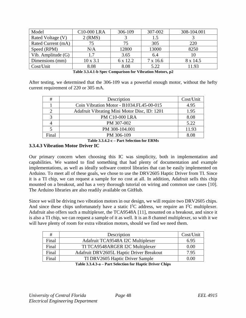
University of Central Florida Page 48 EEL 4915
Electrical Engineering Department
Model C10-000 LRA 306-109 307-002 308-104.001
Rated Voltage (V) 2 (RMS) 3 1.5 3
Rated Current (mA) 75 75 305 220
Speed (RPM) N/A 12800 13000 8250
Vib. Amplitude (G) 1.7 3.65 6.4 10
Dimensions (mm) 10 x 3.1 6 x 12.2 7 x 16.6 8 x 14.5
Cost/Unit 8.08 8.08 5.22 11.93 Table 3.3.4.1-b Spec Comparison for Vibration Motors, p2
After testing, we determined that the 306-109 was a powerful enough motor, without the hefty
current requirement of 220 or 305 mA.
# Description Cost/Unit
1 Coin Vibration Motor - B1034.FL45-00-015 4.95
2 Adafruit Vibrating Mini Motor Disc, ID: 1201 1.95
3 PM C10-000 LRA 8.08
4 PM 307-002 5.22
5 PM 308-104.001 11.93
Final PM 306-109 8.08 Table 3.3.4.2-c – Part Selection for ERMs
3.3.4.3 Vibration Motor Driver IC
Our primary concern when choosing this IC was simplicity, both in implementation and
capabilities. We wanted to find something that had plenty of documentation and example
implementations, as well as ideally software control libraries that can be easily implemented on
Arduino. To meet all of these goals, we chose to use the DRV2605 Haptic Driver from TI. Since
it is a TI chip, we can request a sample for no cost at all. In addition, Adafruit sells this chip
mounted on a breakout, and has a very thorough tutorial on wiring and common use cases [10].
The Arduino libraries are also readily available on GitHub.
Since we will be driving two vibration motors in our design, we will require two DRV2605 chips.
And since these chips unfortunately have a static I2C address, we require an I2C multiplexer.
Adafruit also offers such a multiplexer, the TCA9548A [11], mounted on a breakout, and since it
is also a TI chip, we can request a sample of it as well. It is an 8 channel multiplexer, so with it we
will have plenty of room for extra vibration motors, should we find we need them.
# Description Cost/Unit
Final Adafruit TCA9548A I2C Multiplexer 6.95
Final TI TCA9548ARGER I2C Multiplexer 0.00
Final Adafruit DRV2605L Haptic Driver Breakout 7.95
Final TI DRV2605 Haptic Driver Sample 0.00 Table 3.3.4.3-a – Part Selection for Haptic Driver Chips

University of Central Florida Page 49 EEL 4915
Electrical Engineering Department
3.3.5 Microcontroller Subsystem
For the microcontroller’s final part selection, the Arduino Zero has been selected. [7] See Table
3.3.5-a below for a part specification and cost. The Zero has a clock of 48MHz which will be
enough processing power to run and process the big amount of software to communicate between
many components at a high speed to give users fast feedback on the functionalities. The 256KB
amount of flash memory the Zero can hold would be plenty for the software size that the device
need to have, however, efficient algorithm will be utilizing and optimizing to make the calculations
faster. The 38 general I/O pins would be more than enough to connect all the components to the
microcontroller, there would be extra pins that will not be used, but they can be serve as extra for
future if any new components need to be add to give the device new features. One of the feature
of this microcontroller that will be best for this project device is the low active power of 10.3mA.
Because this device is going to be handheld and will be used for hours, low consumption
components are a must, they will give the device maximum operation time. If low power
consumption components were not considered, the device will not have a long operating time and
the users will not be able to use it. Another advantage from using the Zero is that the Arduino IDE
is very user friendly and the tutorial is clear to understand so it would be the best for beginner
programmers like all the members in the group. Also, Arduino is very popular to a lot of people
so there are a lot of projects and forum based on Arduino product, so there will be a lot of
information and help to help beginner programmers on their projects.
# Description Specifications Project Requirements Cost
Final
Arduino
Zero
Clock Frequency (MHz) 48 >20
54.99
Voltage (V) 3.3 >3.3
Flash (KB) 256 >256
SRAM (B) 32 >16
Bits 32 >16
GIOP 38 >20
Active Power
Consumption
10.3mA <30mA
Timer Counter 3 YES
Real-Time Counter Yes YES
Table 3.3.5-a Part Selection for Microcontroller (Permission Pending see Appendix A)
3.4 Part Selection Summary
Table 3.4-a of Part Selection Summary below basically showing all the final parts selected for the
device. There are final parts selected in each of the part selection section above, but to make it
easier to look at the table below to quickly see how many and what parts are used in the device
instead of reading through all the pages and write down the parts selected. Any details about each
of the part will be in sections above with datasheet summaries and other initial part researches.

University of Central Florida Page 50 EEL 4915
Electrical Engineering Department
# Description Cost/Unit
Distance Sensors
1 Ultrasonic Range Finder - LV-MaxSonar-EZ1 29.99
2 Ultrasonic Range Finder - LV-MaxSonar-EZ4 29.99
Servos
3 DRS-0101 Herkulex Smart Servo 30
Battery
4 AT: Tenergy LiPo 7.4V 6000mAh Battery Pack 47.99
Battery Controller
5 MCP73213 – Battery Management Controller 1.79
Buck Regulators
6 Mini DC/DC Step-Down Converter 3.3V 14.95
7 Mini DC/DC Step-Down Converter 5V 14.95
Bluetooth
8 Adafruit Bluefruit LE UART Friend – BLE 17.50
Navigation Systems
9 HERE Maps 0.00
Mobile Applications
10 Android 0.00
Solenoid
11 5V Solenoid - ZH0-0420S-05A4.5 4.95
Vibration Motor
12 PM 306-109 8.08
Vibration Motor Driver ICs
13 Adafruit DRV2605L Haptic Driver 7.95
14 Adafruit TCA9548A I2C Multiplexer 6.95
Microcontrollers
15 Arduino Zero 49.99 Table 3.4-a– Part Selections Summary
Figure 3.4-b below is a picture of all the parts included in the Table 3.4-a and details in the section
3 above, the parts in the picture are labeled according to the Table 3.4-a for easy referencing

University of Central Florida Page 51 EEL 4915
Electrical Engineering Department
Figure 3.4-b Part Selections Summary

University of Central Florida Page 52 EEL 4915
Electrical Engineering Department
4. Related Standards and Realistic Design Constraints
Discussing related standards and the realistic design constraints of the project allow the designers
to be aware of the ways in which the project are affected by outside sources. By adhering to related
standards, the project designers ensure compatibility with other products and services. Also,
discussing the realistic design constraints allows the designers to be aware of the potential
problems and setbacks that could arise and by doing so they can prepare in case one occurs. The
below sections detail the standards related to the project and the realistic design constraints that
are placed on the project.
4.1 Standards
Standards are critical in the development of a product because they ensure that it will be compatible
with other products and operates in a safe and efficient way. The sections below involve the related
standards for each subsystem. Each section includes how the relevant standards impact the design
and development of the product and a table containing the name of each relevant standard and a
brief description of it.
4.1.1 Distance Sensing Subsystem Related Standards
The standards that directly relate to project EASI’s distance sensing subsystem are listed in the
table below (Table 4.1.1-a) along with a brief description of each.
ANSI Z80.9-2010 (R2015) specifies test methods for optical and electro-optical devices for use
by visually impaired persons. Since EASI is designed to be used by visually impaired people, test
methods specified by the standard will be taken into account when creating tests and actually
testing the effectiveness of the distance sensing subsystem.
Standard Description
ANSI Z80.9-2010 (R2015) Applies to optical and electro-optical devices specified by
the manufacturer for use by visually impaired persons as
low-vision devices. Specifies optical and mechanical
requirements and test methods. Includes devices with optical
and/or electrical and/or electronic components used for
image capture or display. Table 4.1.1-a Distance Sensing Subsystem Related Standards (Permission Pending see Appendix A)
4.1.2 Power Subsystem Related Standards
The standards that directly relate to project EASI’s power subsystem are listed in the table below
(Table 4.1.2-a) along with a brief description of each.
IEC 62281 will affect the acquisition of lithium cell batteries for our project. Due to these
standard’s safety requirements for the transport of lithium cell batteries, any lithium batteries that

University of Central Florida Page 53 EEL 4915
Electrical Engineering Department
are ordered for the project may take additional shipping time. As a result, the designers will have
to order any lithium cell batteries that are needed earlier so that the additional shipping time
required will not delay the project. Also, IEC 62281 will affect how the finished EASI product is
transported to the consumer.
Although, not immediately pertinent to our project, IEC 62281 compliance when shipping finished
EASI devices is something that will have to be taken into account if commercial sales of the device
are pursued. IEC 62133 will impact how the lithium batteries are used in the design and ensure the
safety of users under intended use of EASI as well as reasonably foreseeable misuse.
IEC 62680-1-1, IEC 62680-2-1, and IEC 62680-2-2 will all need to be considered if the developers
decide to move forward with plans to use USB to charge the device. IEC 62680-1-1 would
specifically impact the way in which USB 2.0 is used to charge the device. IEC 62680-2-1 would
require the developers to check to see if any USB connectors that are purchased to install on the
device are compliant with this standard. Doing this will ensure that the USB connectors on the
device would be compatible with other USB compliant connectors. IEC 62680-2-2 would require
the developers to check to see if any Micro-USB connectors that are purchased to install on the
device are compliant with this standard. Doing this will ensure that the Micro-USB connectors on
the device would be compatible with other Micro-USB compliant connectors.
Standard Description
IEC 62281 Ed. 2.0 b:2012 States requirements for primary and secondary
(rechargeable) lithium cells and batters to ensure their safety
during transport other than for recycling or disposal.
IEC 62133 Ed. 2.0 b:2012 States requirements and tests for the safe operation of
portable sealed secondary cells and batteries (other than
button) containing alkaline or other non-acid electrolyte,
under intended use and reasonably foreseeable misuse.
IEC 62680-1-1 Ed. 1.0 en:2015
States requirements that define limits as well as detection,
control and reporting mechanisms to permit devices to draw
current in excess of the USB 2.0 specification for charging
and/or powering up from dedicated chargers, hosts, hubs and
charging downstream ports.
IEC 62680-2-1 Ed. 1.0 en:2015 Defines an industry-standard USB. The specification
describes the bus attributes, the protocol definition, types of
transactions, bus management, and the programming
interface required to design and build systems and
peripherals that are compliant with this standard.
IEC 62680-2-2 Ed. 1.0 en:2015 States requirements and features of a Micro-USB connector
that will meet the current and future needs of the Cell Phone
and Portable Devices markets, while conforming to the USB
2.0 specification for performance, physical size and shape of
the Micro-USB interconnect. Table 4.1.2-a Power Subsystem Related Standards (Permission Pending see Appendix A)
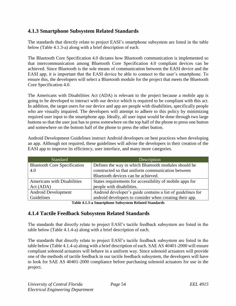
University of Central Florida Page 54 EEL 4915
Electrical Engineering Department
4.1.3 Smartphone Subsystem Related Standards
The standards that directly relate to project EASI’s smartphone subsystem are listed in the table
below (Table 4.1.3-a) along with a brief description of each.
The Bluetooth Core Specification 4.0 dictates how Bluetooth communication is implemented so
that intercommunication among Bluetooth Core Specification 4.0 compliant devices can be
achieved. Since Bluetooth is the sole means of communication between the EASI device and the
EASI app, it is important that the EASI device be able to connect to the user’s smartphone. To
ensure this, the developers will select a Bluetooth module for the project that meets the Bluetooth
Core Specification 4.0.
The Americans with Disabilities Act (ADA) is relevant to the project because a mobile app is
going to be developed to interact with our device which is required to be compliant with this act.
In addition, the target users for our device and app are people with disabilities, specifically people
who are visually impaired. The developers will attempt to adhere to this policy by minimizing
required user input to the smartphone app. Ideally, all user input would be done through two large
buttons so that the user just has to press somewhere on the top half of the phone to press one button
and somewhere on the bottom half of the phone to press the other button.
Android Development Guidelines instruct Android developers on best practices when developing
an app. Although not required, these guidelines will advise the developers in their creation of the
EASI app to improve its efficiency, user interface, and many more categories.
Standard Description
Bluetooth Core Specification
4.0
Defines the way in which Bluetooth modules should be
constructed so that uniform communication between
Bluetooth devices can be achieved.
Americans with Disabilities
Act (ADA)
States requirements for accessibility of mobile apps for
people with disabilities.
Android Development
Guidelines
Android developer’s guide contains a list of guidelines for
android developers to consider when creating their app. Table 4.1.3-a Smartphone Subsystem Related Standards
4.1.4 Tactile Feedback Subsystem Related Standards
The standards that directly relate to project EASI’s tactile feedback subsystem are listed in the
table below (Table 4.1.4-a) along with a brief description of each.
The standards that directly relate to project EASI’s tactile feedback subsystem are listed in the
table below (Table 4.1.4-a) along with a brief description of each. SAE AS 40401-2000 will ensure
compliant solenoid actuators will behave in a uniform way. Since solenoid actuators will provide
one of the methods of tactile feedback in our tactile feedback subsystem, the developers will have
to look for SAE AS 40401-2000 compliance before purchasing solenoid actuators for use in the
project.

University of Central Florida Page 55 EEL 4915
Electrical Engineering Department
Standard Description
SAE AS 40401-2000 This specification covers the general requirements for
electrical solenoids used to actuate various devices through
the conversion of electrical signals into mechanical motion.
These solenoids are of the axial stroke type and the rotary
stroke type. Table 4.1.4-a Tactile Feedback Subsystem Related Standards (Permission Pending see Appendix A)
4.1.5 Microcontroller Subsystem Related Standards
To facilitate communication between a microcontroller and IC, I2C (Inter-Integrated Circuit) is a
standard clocked bus developed in the 1980’s by Philips “to allow easy communication between
components which reside on the same circuit board” [12]. It is an invaluable tool to use when
developing embedded devices, as it facilitates multiple master and multiple slave devices all
connected on the same clock (SCL) and data line (SDA). Every device on the bus is either a master
device or a slave device.
The standard includes arbitration logic to and busy bus detection to coordinate and avoid collisions
between multiple master devices, and 7 address bits to allow for roughly 128 unique slave devices
sharing the same bus. Each I2C compatible IC has either a single or a user-configurable range of
addresses set by the manufacturer, and no two slave devices on the I2C bus may share the same
address. If two ICs do have the same address, an I2C multiplexer must be used.
Standard Description
UM10204 - I2C-bus
specification
This specification catalogues the electrical characteristics, as
well as arbitration, data transfer, and handshake protocols of
the I2C bus. It also specifies the various operating modes,
which select between various data transfer speeds (up to
3.4Mbps bidirectional or 5Mbps unidirectional), and how to
configure multiple-master and single-master systems.
Finally, it describes how the serial data is synchronized and
how bytes are packaged in the transmission.
4.1.6 General Project Related Standards
The standards that do not directly relate to any specific subsystem of project EASI, but will be
useful for the project in general are listed in the table below (Table 4.1.6-a) along with a brief
description of each.
The coding standards chosen to be used on the project are: descriptive variable names, comments
above functions, and the Allman bracket style. The chosen coding standards will make any
software that is written for the project look more uniform and be easier for other people to
understand. These standards will ultimately have little impact on the project because, for the most
part, they are common practice when writing computer software.

University of Central Florida Page 56 EEL 4915
Electrical Engineering Department
Standard Description
Descriptive Variable Names Requires variables used to have names which help describe
what the role of the variable is in the code.
Comments Above Functions Requires that all in-code comments be written above each
function declaration so that they will be easier find and
understand.
Allman Bracket Style Requires that opening braces go underneath the opening
block statement. Table 4.1.6-a General Project Related Standards
4.2 Realistic Design Constraints
In a project, constraint is a restriction that limit a project goals, specifications, and requirements.
Economic constraint is about the budget that funds the project. Time constraint is about the limited
time period that the project needs to be finished. Environmental constraint is to comparing to any
other project that are already on the market. Social constraint showing how the people and users
react to the functionalities of the device in real life use.
The constraints are to be mutually exclusive, changing or modifying one constraint might affect
others. Sometimes, it is hard to resolved all the constraints, like quality, inexpensive and fast
delivered, a project can be deliver fast and inexpensive but the quality will decrease.
4.2.1 Economic and Time constraints
The economic constraint of the project is the limited budget. Due to this budget, the final product
might not achieve the best goal and quality. Some of the components for the device can be purchase
at different prices depend on the quality and functionality of it. Distance sensors can range from
ten dollars to two hundred fifty dollars based on their detecting distance, field of range, signal
travel time and the quality, and can be ultrasonic or laser type. This can be address by starting to
get the ten dollars’ range sensors early in the process and test them so see if the data can match
with the device specifications, if not, then there will be time to pick and choose another sensor that
can be better fit and might be more expensive. Microcontroller prices rely on the clock speed, add-
ons like Bluetooth and Wi-Fi module included, and the number of I/O ports available. All the other
parts must be chosen before getting the right microcontroller, so specifications for the
microcontroller can comfortably handle the power and I/O ports needed for the parts. Another
economic constraint is to make the final product affordable to many people that need it. To achieve
this, the device must have components that are quality and low cost. Many tests and trials on the
components to find out which parts can be obtaining at the lowest cost without compromising the
specification requirements. Buying the components in large quantities to mass produce the device
will also lower the total cost of the device to the customers. One optional approach to low cost is
to introduce the device to the insurance companies as a must device to help the special needs users.
With the help with insurance companies, the cost of the device would reduce to little or to no-cost
for the buyers. One down side if going with the insurance company is that the cost of the device
will get reduce by a big margin amount to the company, because to be able for insurance company
to give equipment at a great discount to the users, they have to also get a great discount from the
manufacture company. This will decrease company’s margin and might not make as much money
University of Central Florida Page 57 EEL 4915
Electrical Engineering Department
back as it supposed to. Introducing to other tech companies might help to introduce the device to
more customers but this will cost money to the company as well. Also, getting the parts in large
quantity will reduce the cost of each component resulting lower the cost of the final products.
Prices of any current similar products on market will also impact on the economics of the project.
Price of the final product must be similar or lower than the competition products or else it won’t
sell. With the price set in, each unit cost and profit must be carefully calculated to support the
company, components and assembly cost have to be optimal to both low cost and quality. Quality
components will lead to quality final products and lead to low maintenance cost to the users that
use the device every day. Quality components would help low the cost in the long run by reusing
old used parts from different devices. A lot of times when some devices that are out of service or
been updated with newer version, companies try to sell those devices in very large quantity for
parts that can be reuse or even just selling the reusable parts in bulk to recoup some of the money
invested. Buying those reusable parts would save a lot of money in the long term, those parts will
be check and test very carefully to maintain the specifications and quality. As the new version of
the project device will be available in the future, old and used devices will be taken back and reuse
most of the components to make new updated version devices, and of course every part would get
tested before going to the new systems.
The time constraint is the total amount of time to finish the device. Start from the beginning to the
end are only about forty weeks for researching, choosing parts, testing, implementing, put all
together and final product testing. If there are any problems troubleshooting, testing the parts and
turn out that the part is not working or not compatible with other parts, new part must be purchase;
more money and time to add because of shipping period, testing and implementing the parts again.
Milestone is enforced to give deadline to all the progresses. Up to a certain date, certain progress
must be finish like parts must be chosen and ordered, parts testing must be done, certain number
of the user manual has to be written and so forth… Without the milestone, work will not get divided
equally throughout forty weeks and might have too much to do toward the end of the period and
final product will not be finish on time. With the limited time, the project planning, design
detailing, design tests and prototypes tests, all must be done in a very short period of time for each
stage resulting not the best quality for final device. And at any of the stages, if major problems
happen and must be delay, all the stages after that would also be delay costing more time and
money, might even costing the whole project not finish on time or not finish at all. With the safety
requirements on transporting the lithium battery mention above on standard section, the shipping
time for the battery will be extended, and this will affect the total time to finish the project
4.2.2 Environmental, Social constraints
Environmental constraint includes many important factors. We must watch the actions of
competitors if have any, device cannot use similar technologies to any of the device in the market
that are meant to solve the same problem, to prevent any lawsuits. This device might be able to
solve the same problem with any other companies with the same device technology, but this device
project has to be able to solve the same problem but in a different way, ways that can improve on
the solutions and still have different design specifications with other devices. Coming up with
ideas to solve existing problem but in a new way will not be easy, a lot of times, engineers have
good ideas but because of the limitations of current technology, the ideas cannot become reality.
Legal requirements involving to have good protections for the device components and
University of Central Florida Page 58 EEL 4915
Electrical Engineering Department
functionalities against anyone try to copy the design. So, patents need to have on the design to
protect it for a long period while the device is in the market. There will be moving parts in the
device, so one of the constraints is the noise and vibration that might happen and cost
uncomfortable to the users and surrounding people. To address this problem, more expensive parts
need to be bought to obtain and give minimal amount of noise and vibrations, this will also lead to
high budget. Product casing with noise deduction layers could be implemented to decrease noise,
but this results in higher cost of productions, higher risk of overheating due to less air flow, and
more weight to the device would cause inconvenience to users if used for too long. Environmental
constraints on the manufacturing side would be about waste collection and processing. Any wastes
created while manufacturing the components need to be properly collect and processing according
to the local laws and standards to minimize and eliminate the uncontrolled disposed waste material
into the environment causing ecological and biological harm. Social constraint affects the buying
patterns and the taste. The discreet looks of the device will help the users to freely use the device
without exposing the fact that they are using it. The small device design will help users holding in
their hand and using it without any bulky looks, the tactile functions can let users detect objects
by their feelings on the hands, and directions can be alert to the users through the help of Bluetooth
headsets. Small and discreet device will lead to small components inside and lead to higher cost
due to the size and will become the project’s economic constraint. Buyers will always try to look
for newer technology with more advance
4.2.3 Functional and Aesthetic constraints
Functional constraint is the overall functions of the device. The overall geometry of the device like
size and width must be carefully study and measure. All the space inside the device should be
utilized fully, the components need to be arranged to minimize the size of the device. But the space
must provide enough space between components for any heat disbursement and for any short to
the electrical that might happen during use. The size of the device has to fit into the user hands, so
that they can comfortably using it for a long period of time. The constraint of this is the sizes of
the components, for a handheld device, the components not only have to utilize space using, they
have to be in small sizes to be able to have all the parts with different functionalities the device
required. Another constraint is the casing material to be use for the device, to have best protection
against elements, accidental drops and bumps, user’s error, the casing should be made from steel
alloy or even carbon fiber. But steel alloy would be very heavy for the users to hold the device on
their hands for hours, and carbon fiber is light weight and durable and would be very expensive to
produce. The casing then must be made from plastics for the lightweight and inexpensive,
however, would be more prone to accidental drops and hitting other objects. Follow the safety
requirement for transporting the lithium battery in the standards section 4.1.2, the casing interior
has to be design and tested the functional of the battery while the user is holding and use the device
while transporting on the street. Designing the casing for this purpose will create more time for all
the testing to ensure the safety is meet.
4.2.4 Quality and Safety constraints
The main factors to the quality constraint are the limited time and budget set for this device project.
The limited time give the project completion schedule not much time to fully test for components
quality. Components were bought depend on the budget, many were compared and lower quality

University of Central Florida Page 59 EEL 4915
Electrical Engineering Department
parts were chosen based on the maximum that can be spend on that specifics part. Would there
have been more time and budget on the project, more quality components would be chosen,
maximum testing time could be done. With better quality parts and more testing time, the reliability
of the device would increase. The device life would be much longer, have less failures and more
worry-free to users. Quality constraint also include the quality assurance. Regulations and codes
cannot be follow much because there is only enough time to design and develop the device follow
the standards and requirements. Although, some regulations and codes will be follow like power
and battery charging to make it safe for the users to operate the device daily. Standards like energy
star, Bluetooth, battery, USB and audio will be meet to make sure all the functionalities meet with
the requirements that were set for the device.
Safety constraint included direct and indirect operational to the users. Indirect would be due to the
limit of testing time on the device, the limited budget, the components quality is decrease might
result in malfunctioning. Malfunctioning like short circuits, heat can happen at any time during
use or charging, and can indirectly cause troubles or even injure users. Overuse the faulty battery
pack in the device can cause it to overheat and causing other components to overheat and might
even ignite fire, burn the device and can cause injure to the users. Direct will be the malfunctioning
of the sensors systems or the tactile systems that fail to communicate with the users and will cause
users to run into objects in the front mean fail to operate the core functionalities that was set that
the device have to do which is to guide disable users to avoid objects in walking path. Safety of
people around the users also need to worry about, the device needs to work like it supposed to, and
without any error to avoid users bump into others in the walk way. Another problem is that the
Bluetooth signal from the device to the user’s Bluetooth headset might get distort and lose
connections or breaking up the connections making it hard for the users to navigate with the
navigation prompt, or the users might not be able to listen to the device objects in the front due to
broken communications and will cause accidents from running into objects in the front of them.
Due to the safety requirements for transporting lithium in the standard section 4.1.2 above, battery
placement inside the device will have to be carefully study and testing to meet the safety standard
for the users to carry the device.
4.2.5 Manufacturability and Sustainability constraints
Manufacturability constraint would fall into the ability to manufacture the components.
Manufacturing companies have to be research and compare to figure out if any with limitations to
produce the components correct and exact to specifications and requirements the device need. The
means of production from companies to be able to produce parts fast and good quality. What kind
of waste would be produce and how to safely disposed? For the components that can be purchase,
quality control need to be check regularly for the reliability on a large number of parts being
purchase. Also there will be assembly factories to assemble all the parts gotten from manufacture
companies to a complete final device, quality control need to be check on final products as well.
Then final product will be boxed and transport to the buyers, transporting container material and
proper padding would help to ensure the buyers to receive the device with full functionalities and
no damage from shipping. In the designing and prototyping process, parts and components are
being bought pre-made with manufacture’s specifications, errors will be more prone to happen. At
least until the device is complete and fully functioning, then components can be manufacture
according to device’s specifications.

University of Central Florida Page 60 EEL 4915
Electrical Engineering Department
Sustainability constraint would focus on the manufacture companies able to sustain the number of
products being produce and the same quality throughout. Also there has to be enough principle to
cover the manufacturing cost to sustain producing the product. The life span of the device would
have to be reasonable of at least one to two years of under normal operation conditions, this will
be the warranty period. Under extreme environmental factors like extreme temperature, corrosive
fluid, abrasive air, how much of that can the device handle? With the limited designing time, there
would not be enough to test the device under all these conditions. All devices produced must have
similar life span to give durability and quality that users can trust and use every day.

University of Central Florida Page 61 EEL 4915
Electrical Engineering Department
5. Project Hardware and Software Design Details
This section describes in detail the scope and function of each subsystem. The focus of this section
includes the theory of operation of each system, as in how the technology and components work
in the real-world and in our design. In this section as things get more detailed the programming
aspect of our design has been separated into their own sections as programming and user feedback
will be central to the function of our design.
5.1 Hardware Architecture
Our design is composed of several different hardware systems, Sections 5.2 and 5.3 focus heavily
on the hardware design and system functionality. Shown below is a high-level block diagram
outlining the hardware and the connections within our design. Below there will also be a legend
designating which subsystem each hardware falls under. The details of each of these sections will
be described in the sections below.
Figure 5.1-a High Level Hardware Block Diagram
Sensor

University of Central Florida Page 62 EEL 4915
Electrical Engineering Department
5.2 Initial Design Architectures and Related Diagrams
As stated above the purpose of this section is to describe in detail the purpose and function of each
subsystem. This section will include all related diagram and overview of each subsystem. As the
following section will describe in detail its operation and function calling upon these diagrams and
structure.
5.2.1 Distance Sensing Subsystem
The section below consists of our initial design thoughts and diagrams related to the general
overview of our design. These diagrams will be at times called on to explain our design concepts
below.
5.2.1.1 Linear Sensor System
The Linear Sensor System is responsible for detecting in a straight line from the end of a device
much like a laser tape measure or a stick would sense the proximity of an object. Below are the
initial design thoughts and any related diagrams for this system.
Initial Design
Our initial design thoughts for the linear sensor were vastly different than the current design. We
initially wanted to utilize an accurate laser to measure the linear distance to an object directly in
front of the user but this proved not feasible. Due to the speed of light that a laser travels it is
capable of extremely fast and accurate proximity sensing but for this reason there is usually a
significant dead zone range near the sensor. These dead zones were commonly a meter in length
for most products. Due to the nature of our device we need to relay if a wall or person is directly
in front of the user so minimizing the dead zone is important. Our current design has a dead zone
of 15cm or about 6 inches.
Another factor in the changing of our initial thoughts was the cost and accuracy. Lasers are very
accurate but they are costly to our design team and the user. Though often quite inexpensive for
the amount of precision that a laser offers as we designed our tactile feedback system, we realized
that we could never convey that much detail. Our current sensors have a 1inch resolution which is
quite large compared to the .001mm resolution some lasers offer but even with this resolution we
still may not be able to convey such accurate measuring detail.
Related Diagrams
Figure 5.2.1.1-a below shows the pins and profile of the LV-MaxSonar ultrasonic sensor. The two
sensors are identical in pin configuration and size. The only difference is the beam width and range.
This diagram will be explained more in section 5.3.1.

University of Central Florida Page 63 EEL 4915
Electrical Engineering Department
Figure 5.2.1.1-a Ultrasonic Sensor Diagram (Permission Pending see Appendix A)
5.2.1.2 Radar Sensor System
The Radar Sensor System is responsible for detecting the proximity of the objects in the area. This
radar system is mostly focused on to the left and right of the user but will sense all values. Below
are the initial design thoughts and any related diagrams for this system.
Initial Design
Originally we first thought of sensing the proximity of objects using one sensor and like magic it
would work. Upon further research we found that a sensor can only detect distance off of one
object at a time. We then thought to utilize a camera that takes constant images and then by
processing these images we can detect objects much like an eye. Though as stated in greater detail
above such technology requires a lot of processing power and is proprietary for our budget and
size constraints.
The second option was to utilize a scanning laser sensor which is an all in one sensor that sweeps
a signal back and forth creating a map of the objects in front of the user much like a radar. However,
the drawback to this design is the extraordinary cost associated with it. At over a minimum of 1000
dollars for the sensor alone we thought that this was too extreme for a college project budget. In
response to this we decided to utilize a less expensive ultrasonic sensor in conjunction with a smart
servo that can provide feedback on position to create a radar of our own. This radar however is
crude and we fear that the noise of the servo will be quite annoying to the user but given our cost
constraints this seems to be the most logical implementable solution.

University of Central Florida Page 64 EEL 4915
Electrical Engineering Department
Related Diagrams
Figure 5.2.1.2-a below shows the pins and profile of the DRS-0101 Herkulex smart servo. This
diagram will be explained more in section 5.3.1.2. Upon further testing this was not used due to
sensor interference.
Figure 5.2.1.2-a Smart Servo Diagram (Permission Pending see Appendix A)
5.2.2 Power Subsystem
The Section below consists of our initial design thoughts and diagrams related to the general
overview of our design. These diagrams will be at times called on to explain our design concepts
below.
Initial Design
The initial design for our power system was a bit idealistic. We originally planned for simply using
a small standard smartphone type battery that could be charged via a USB. The initial voltages and
current requirements were all guesses based on the requirements of a traditional smartphone. The
ideal design which given enough time and resources is still the ultimate goal of this design; to
make something small enough and portable enough to be handheld and easily stowed away in a
purse or in a pocket. Given our resources however we do not foresee us realizing this ultimate
ideal as our research into the parts required and the actual voltage requirements are currently far
greater than a traditional smartphone. For comparison a traditional smartphone such as the iPhone
6 uses roughly 12 Watts per hour with a battery voltage of approximately 3.82 volts. [13] Our
design looks to require nearly 3 times that in terms of Watts per hour with everything functioning.
This level of requirement is mainly due to the need of actuators and servos which require
mechanical operation and though they are less power hungry options they currently exceed our
capability as college students to develop within our time constraints. Our initial design also did

University of Central Florida Page 65 EEL 4915
Electrical Engineering Department
not take into account the need for voltage regulation or load sharing when charging. The need for
a battery management controller was also not considered especially due to the vast differences of
battery chemistries
Based on our current knowledge of the design it’s looking like the charging circuit will be far more
sophisticated with the use of a battery controller IC to help manage our use of a lithium polymer
based battery chemistry. The circuit will now have load sharing capabilities and utilize DC-DC
conversion and regulators to add 3 different levels of a power bus for use within our design.
Initially we thought that each of the circuits the battery circuit and the power regulation circuit
would be the different. For simplicity and reduction of components we combined the circuit to
both charge and supply regulated power all in one. A more detailed explanation on the general
theory of how this will work and then relate to our design can be found in section 5.3.2 below.
Related Diagrams
This section will include any power system related diagrams that will be used in section 5.3.2.2.
The diagram below shown in Figure 5.2.2.2-a is the typical application for the MCP73213 Battery
management controller. It is from this typical circuit that will be the start of our battery charging
design.
Figure 5.2.2.2-a MCP73213 Typical Application Schematic (Permission Pending see Appendix A)
The diagram below shown in Figure 5.3.2.2-b is an example of how the load sharing circuit will
function. Though the MCP battery management chip is different from our design this is from the
same manufacturer so makes it simpler to convey the load sharing circuit.

University of Central Florida Page 66 EEL 4915
Electrical Engineering Department
Figure 5.2.2.2-b Typical Load Sharing Schematic (Permission Pending see Appendix A)
5.2.3 Smartphone Subsystem
The Section below consists of our initial design thoughts and diagrams related to the general
overview of our design. These diagrams will be at times called on to explain our design concepts
below.
5.2.3.1 Mobile Application
Below are the initial design thoughts and any related diagrams for the mobile application system.
Initial Design
Since this project device is for sight impair users, the mobile application has to be as simple as
possible but still have all the functions needed for the users to communicate and control the device
without seeing the applications. The initially button design is to have button for each of the modes
and to turn modes on and off, users just have to press on the mode button selection. But having
button for each of the modes will result in too many buttons and each one would be a lot smaller
and will cause problem for users trying to tap the right mode to turn it on and off. Then next initial
design for the mobile application would have two buttons of equal sizes that take up the whole
space of the mobile device screen. The button on top would function as to turn modes on and off,
once users choose which modes they want to change, on and off can be switch with the button on
the top. To change the modes, there will be another button on the bottom that the main function
would be cycling through all the modes when pressed. Once get to the mode users want to switch
on and off, top button can be press.
Initially, there were more modes in the design for the application, but as more research and testing
progress, the application is going to have important modes. Important modes were decided by the
easiness, most convenient to the users. With many modes, the users will spend much more time
try to cycle between the modes to get to where they want to make the selections. With less modes,
users can make their selection much faster and with only a fewer modes, users will not get confused
on which modes is which and what it does.

University of Central Florida Page 67 EEL 4915
Electrical Engineering Department
The graphical user interface for the application will be created for Android mobile devices by
Android Studio software. The software will help create and modified how the application would
look, and how it will communicate with the device through software developments.
Related Diagrams
Figure 5.2.3.1-a below showing how the initial design of the graphical user interface is going to
function. One function will be the top button to turn the modes on and off when pressed. The other
button on the bottom will be to cycle the modes around when pressed. And at the mode that users
want to select, modes can be switch on/off with the top button.
Figure 5.2.3.1-a Mobile Application Graphical User Interface Chart
5.2.4 Tactile Feedback Subsystem
This section will detail the process we underwent, from initial conceptions to concrete
implementations, of the tactile feedback system. This system will take as input control signals
from the system microcontroller, in order to use the vibration motors and actuators selected in
section 3 to communicate navigation instructions and meaningful information about the
surroundings to a visually impaired end-user.
Initial Design
In conceiving of this design, we began by listing ways in which tactile information and signals can
be generated. The most obvious of these was the vibration motor, as these are found in countless
consumer and handheld devices. Typically, these signals are either used for only relatively simple
binary signaling, or in conjunction with other sensory cues to communicate more complex
information. We therefore felt that a secondary tactile system would be needed to meet our
requirements for information granularity.
The idea to use actuators stemmed from some initial ideas about this secondary system. We were
inspired primarily by refreshable braille displays [14], a technology developed in the 1990’s which
uses screen-reading software to map text on a computer display to a series of pins which raised
and lowered to spell out braille which the user could read. Our idea was to create a grid of pins
similar to these displays which, rather than displaying braille, would create a two-dimensional
projection of the device’s field of view, and generate something like a topographical map of the
obstacles detected in that area which updates in real time. Unfortunately, the displays themselves
are prohibitively expensive (thousands of dollars per unit), and the technology they and similar

University of Central Florida Page 68 EEL 4915
Electrical Engineering Department
devices use requires precision manufacturing. So, we took this concept, and scaled it down so that
we could develop it with inexpensive and readily available components at a level of complexity
compatible with the scope of this project.
Related Diagrams
Below is a system level diagram of the tactile subsystems, and how they will interface with the
microcontroller.
Figure 5.2.4-a Tactile Feedback System Interface Diagram
The actuators will require 7 digital outputs from the microcontroller, one pin for each of the
solenoids. The vibration motors would require two more digital pins if the microcontroller directly
controlled them, however the haptic IC that will control them uses an I2C bus to communicate with
the microcontroller. Since microcontrollers have dedicated I2C pins, this will have the added
benefit of reducing the total number of digital pins the tactile system will need.
5.2.4.1 Solenoid Control System
The following section details the two design iterations considered for the solenoid actuator
subsystem and an in depth description of how each individual solenoid will be controlled.
Initial Design
The first iteration of this system was going to be a 3x3 grid of actuators, as shown in Figure
5.2.4.1-a below.
Figure 5.2.4.1-a Initial Solenoid Configuration
Haptic IC
& motor
Haptic IC
& motor 7-bit Digital
I2C
Solenoid Actuators
& Control
Microcontroller
1 2 3
8
5
9
6
7
4

University of Central Florida Page 69 EEL 4915
Electrical Engineering Department
Each one of these actuators would map to a region within the sensor system’s field of view. For
example, say the sensors could detect obstacles in a three-square meter area in front of the device.
If an obstacle was detected between two and three meters in front of and two and three meters to
the right of the device, solenoid #3 would actuate. Similarly, if an obstacle was detected between
zero and one meters in front of and two and three meters to the left of the device, solenoid #7
would actuate.
Unfortunately, this design would have put a serious strain on the device’s available power. Seeing
as this configuration would require 11 total actuators (2 more for navigation), we could use the
solenoid specs to estimate the system’s total worst case power consumption. Using the power
consumption shown in Table 3.3.4.1-a, and assuming all 11 actuators stay energized continuously,
the total power they would consume is shown below:
1.375 𝑊 ∗ 11 = 15.125 𝑊
From Table 3.3.2.2-a, we can calculate the total watt-hours of our system’s battery:
6𝐴ℎ ∗ 7.4𝑉 = 44.4 𝑊ℎ
Finally, the number of hours the battery would be able to supply this much power is found as
follows: 44.4 𝑊ℎ
15.125 𝑊≅ 3 ℎ𝑜𝑢𝑟𝑠
Even though this is worst case, and in no practical scenario would all 11 solenoids be active at
once for that long, that level of power consumption was too concerning to keep, particularly since
there are several other systems which also require power. This implementation would also require
11 digital pins from the microcontroller, when it only has ~18 in total.
Thus, we adjusted our design to accommodate these restrictions. The refactored arrangement can
be seen in Figure 5.2.5.2-a. Solenoids 6 and 7 will be used exclusively for navigation instructions.
The center column of solenoids will behave the same as in the initial arrangement, raising and
lowering based on detected obstacles within a relatively narrow field directly in front of the device,
however now solenoids 4 and 5 will actuate if an obstacle is detected anywhere in the left or right
portions of the field of view. The implication of this is that for the user to get an accurate read on
how far away an obstacle to the left or right is, they must point the device in the direction indicated
by these two actuators.
Now, in the absolute worst case, using the same method of calculation shown above, the battery
would be able to power this system for 5 hours instead of 3. In addition, the nature of this
arrangement should guarantee that only 4 solenoids are raised at once (solenoids 6 or 7 will never
both be raised, and only 1 of solenoids 1, 2, or 3 will ever be raised at a given time), so a more
realistic calculation of worst case power consumption would yield 8 hours of power. Even though
this is still a significant amount of power consumption, it is much more likely to fall in line with
our engineering requirements.

University of Central Florida Page 70 EEL 4915
Electrical Engineering Department
Related Diagrams
A digital PWM signal from the microcontroller will directly control each individual solenoid in
the circuit. This signal will open a transistor, which will allow current to flow through the actuator.
The diagram below shows an example of one of these control circuits.
Figure 5.2.4.1-b Example Solenoid Control Circuit [15] (Permission Pending see Appendix A)
Since a solenoid is an inductive load, with a conductor moving within a magnetic field, the act of
stopping and starting the solenoid produces spikes of back-EMF which can damage a transistor or
microcontroller connected to it. The flywheel diode in this circuit is in place to protect the transistor
from that negative voltage.
5.2.4.2 Vibration Motor Control System
The section below details the initial conceptions and final implementations of the vibration motor
control system.
Initial Design
Our initial inclination was to control the vibration motors directly, in a similar manner to how the
actuators are controlled. As ERMs are DC powered inductive devices, the control circuit would
look nearly identical to the one used for the solenoids. All that would need to change would be the
supply voltage, resistor values and potentially the model of transistor used. As performance metrics
were fleshed out, it became clear that having the capability to generate more complex vibration
patterns would likely be very useful. This method of control makes such signaling very
challenging, as it would require the embedded programmers to generate complex waveforms on
the microcontroller for each desired signal.
Fortunately, due to the abundance of vibration motors in haptic applications, many ICs have been
developed specifically to drive this kind of device and streamline complex signal generation. The
IC we chose in section 3.3.4.3 can access a library of over 100 different haptic signal patterns, all
accessible via function call in the embedded software.

University of Central Florida Page 71 EEL 4915
Electrical Engineering Department
Each IC controls a single vibration motor; hence two are be required. I2C supports multiple slaves
sharing the same SCL and SDA lines, given that each slave has a unique hardware address (See
section 4.1.5 for more detail on this standard). Unfortunately, the address of the DRV2605 haptic
driver is static and unconfigurable, so two of these chips cannot share the I2C bus without
multiplexing. Fortunately, I2C multiplexing chips are also commonplace. The TCA9548A chip
from TI is an 8-channel multiplexer, which would allow us to connect up to eight I2C devices with
the same address.
Related Diagrams
Below is a reference design for how a direct PWM controlled vibration motor circuit would be
constructed:
Figure 5.2.4.2-a Example Vibration Motor Control Circuit [16] (Permission Pending see Appendix A)
Identical to the solenoid control circuit, this too requires a diode across the motor terminals to
block back-EMF from an inductive load from damaging the transistor. In addition to that though,
a capacitor is also required. This is because unlike a solenoid, a vibration motor oscillates at a high
frequency, it will in turn generate high frequency electromagnetic noise in the circuit. This
capacitor is therefore used as a filter against that noise.
Interfacing the I2C controllers and multiplexer requires a different approach from the above. The
two DRV2605 chips’ SDA and SCL lines must each be connected to one of the MUX outputs, the
main I2C bus connected to the microcontroller must connect to the MUX inputs. The MUX has a
base address of 0x700, and the lines A0-A2 allow the user to vary that address up to 0x707 (in the
case that another device on the I2C bus is already using address 0x700). A device is selected by
calling a function tcaselect(n) in software, where n is the MUX output the device is connected to
(in the case below it would either be 3 or 7). Below is a mockup of how each component would be
connected. Images are of the chips mounted on breakouts, and can be found at Adafruit.com [10]
[11]).

University of Central Florida Page 72 EEL 4915
Electrical Engineering Department
Figure 5.2.4.2-b Haptic IC - controlled vibration motor diagram
5.2.5 Microcontroller Subsystem
The Microcontroller Subsystem is responsible for gathering data from the sensors and Bluetooth,
interpreting that data into something meaningful to the user, and then controlling the devices that
provide feedback to the user. Below are the initial design thoughts and any related diagrams for
this system.
Initial Design
At first we were debating whether to use a microcontroller or a single-board computer such as a
raspberry pi for our data processing and input/output controlling needs. After doing some research,
we learned that if the raspberry pi is improperly powered down, data on it could be corrupted.
Since our device is running on battery power, it is entirely possible for it to power down without
warning once the battery runs out of charge. It would be possible to overcome this obstacle, but
we chose to forgo the additional complexity of solving this problem and instead pursue the use of
a microcontroller which did not have the same problem.
Our initial design for the microcontroller subsystem assumed the input to the microcontroller from
the sensors was going to be a number which represented the distance in millimeters to the detected
object. After finding out that this was not the case, our microcontroller subsystem design had to
be altered to include a conversion to millimeters. This could be accomplished in one of two ways.
Either using a time calculated from the start and end time of a pulse received from the sensor
multiplied by a value provided in the sensor documentation to get the distance in inches which
could then be converted to whatever unit of distance that the project required. Another option is to
get a voltage input from the sensor, the value of which could also be multiplied by a value provided
in the sensor documentation to again get the distance in inches.
VDD
M
M
I2C Bus

University of Central Florida Page 73 EEL 4915
Electrical Engineering Department
Related Diagrams
The below figure (Figure 5.2.5.2-a) displays the relative placement of solenoids to other solenoids,
the names assigned to each solenoid, and the very brief description of the function of each solenoid.
The assigned names are not necessarily the way the solenoids will be referenced in the code
programmed on the microcontroller, they are merely assigned so that individual solenoids can be
referenced in the 5.5.2 Microcontroller Software Design section.
Figure 5.2.5.2-a Solenoid Configuration
The below figure (Figure 5.2.5.2-b) displays the flowchart for the distance sensing input to the
microcontroller. The solenoid labels are based off the configuration and naming scheme shown in
Figure 5.2.5.2-a.
Figure 5.2.5.2-b Distance Sensing Input to the Microcontroller Flowchart
Sole4
Left
Detect
Sole1
Dist
Detect
Sole5
Right
Detect
Sole6
Left
Nav Sole3
Dist
Detect
Sole7
Right
Nav
Sole2
Dist
Detect

University of Central Florida Page 74 EEL 4915
Electrical Engineering Department
The below figure (Figure 5.2.5.2-c) displays the flowchart for the Bluetooth input to the
microcontroller. The solenoid labels are based off the configuration and naming scheme shown in
Figure 5.2.5.2-a.
Figure 5.2.5.2-c Bluetooth Input to Microcontroller Flowchart
The below figure (Figure 5.2.5.2-d) displays the flowchart for the Bluetooth input to the
microcontroller. The start point comes from the “Calculate distance to object” processing block
from the flowchart of the distance sensing input to the microcontroller shown in Figure 5.2.5.2-b.
Figure 5.2.5.2-d Bluetooth Output from Microcontroller Flowchart

University of Central Florida Page 75 EEL 4915
Electrical Engineering Department
The below figure (Figure 5.2.5.2-e) displays the flowchart for the direction sensing input to the
microcontroller. The solenoid labels are based off the configuration and naming scheme shown in
Figure 5.2.5.2-a.
Figure 5.2.5.2-e Direction Sensing Input to Microcontroller Flowchart
5.3 Device Subsystem Details
The Section below discusses the system details of each subsystem. Each section will start with the
general theory of operation followed by our design specific details.
5.3.1 Distance Sensing Subsystem
The Section below consists of our details the general operation of sensors and servos and how they
will relate to our design. This section will refer at times to section 5.1.1 for related diagrams.
5.3.1.1 Linear Sensor System
The Linear Sensor System is responsible for detecting in a straight line from the end of a device
much like a laser tape measure or a stick would sense the proximity of an object. Described below
is the general theory of how a linear Sensing system works and then the design specific details
General Theory of Operation
The ultrasonic sensor dates back to 1790 when Lazzaro Spallanzani first discovered bats
maneuvered in flight using their hearing rather than sight. [17] Bats are amazing creatures who
can precisely distinguish even small objects in full flight, a vision that far surpasses that of a human
all while being blind. Bats utilize a technique known as echolocation or ultrasonic ranging. The

University of Central Florida Page 76 EEL 4915
Electrical Engineering Department
ultrasonic sensor is our way of simulating this technique. The use of these techniques is commonly
referred to as Sonar or sound navigation and ranging. Historically used mainly in water, Sonar was
developed in 1912 to detect icebergs which was prompted by the Titanic disaster of 1912. [17] A
few years later during World War I sonar was reconfigured to detect submarines. This technology
continued to improve over the course of World War 2. Today there are many uses of sonar from
detecting people to small objects. The sensors being used in our design use active sonar to function.
Active sonar uses a sound transmitter and a receiver. When the two are fixed in the same place, as
in our design it is considered monostatic operation which is the most common type of sonar. Active
sonar creates a pulse of sound and then listens for the sounds reflections or echoes. [18] This sound
signal is electronically generated using a signal generator, amplifier and electro-acoustic
transducer. The sound is concentrated to a certain beam width and then transmitted. [18] The
measurements of object distances are done by measuring the time from transmission of the pulse
to its reception. Using the known speed of sound this time is converted into a range. The concept
of converting time and known speeds into range is often referred to as Time of Flight. [18] In order
to avoid false positives, the sound pulse created by the receiver is often a constant frequency much
higher than ordinary objects will produce. [18] The factors effecting the performance of ultrasonic
sensors will be discussed below. Figure 5.3.1.1-a gives a visual interpretation of how active sonar
works. The red wave pattern is the originating sound wave, while the green wave pattern is the
reflected sound wave. The range distance r is calculated by using the known speed of sound (v)
which is approximately 343m/s multiplied by the time of flight (t) of the pulse signal divided by
two as the range distance is doubled. [18] This of course assumes no loss of signal or interference
which is unlikely unless in a vacuum. This equation is shown below: [18]
𝑅𝑎𝑛𝑔𝑒 =𝑣 ∗ t
2
Figure 5.3.1.1-a Sonar Principle Diagram [18]
Performance factors
There are several factors that can affect the accuracy of an ultrasonic sensor and though accuracy
is not a major concern for our design it is important to understand that they are present. By
understanding they are present it can allow us to be able to consider these issues later during

University of Central Florida Page 77 EEL 4915
Electrical Engineering Department
breadboard and more importantly field testing when outside factors are more apparent. The major
factors that contribute to performance are reflection angle, reflection surface, crosstalk and field
conditions such as temperature and air density.
The first factor is reflection angle which relates to the reflection surface. This angle is the angle of
the surface that reflects back the transmitted pulse back to the source. The ideal angle for a
reflective surface is a flat surface perpendicular to the ultrasonic beam; this will reflect most of the
transmitted pulse back to its source. But this ideal is rarely seen in the field. Most of the time even
if we are considering the ground surface which is mostly flat it is rarely completely even. Cracks,
dirt, debris as well as the surface type will also diminish the reflected signal which can alter its
accuracy. The combination of an angled surface that absorbs sounds waves can cause significant
degradation of our sensors accuracy. This factor will be monitored quite closely as we will
predominately be dealing with humans who have an irregular shape so the reflection angle will not
be ideal and clothes that are a softer material will dampen our sound signal. [18]
Crosstalk is an issue that occurs when multiple ultrasonic sensors or close proximity of objects can
degrade the signal accuracy by inducing extra noise into the system. In the case of an object within
the minimum distance of the sensor, the transmitted pulse and the reflected signal back interfere
with each other for they are so close. The sensor can only transmit, read and process so fast. Now
this is normally done in microseconds the speed of sound is actually quite fast and the time from
transmission to reception can exceed the read time at certain minimum distances. Thus the
reflecting beams are not fully processed. Combining this with the fact that a sound beam does not
diminish completely on one cycle of reflection there can be multiple reflected sound pulses within
this minimum zone. With each beam influencing the other this cause a great deal of noise that can
degrade the accuracy or cause no output or completely erroneous readings. These factors are also
found when 2 or more sensors are transmitted in the same area. The combination of two sensors
talking can create added noise as the receiver is picking up on possibly two transmitted pulse
signals. [18]
The final factor which can degrade the performance of our sensor system is the fields conditions.
The sensors will provide a time signal based on the time of flight from transmission to reception.
Ideally the calculation for range will simply be Time times Velocity divided by 2. However, a
sound wave will be slower or faster in certain mediums or environments. Temperature, air density,
humidity and more will all affect the speed of sound. The ideal equation above will only be possible
in a vacuum where no outside forces can interfere with the speed of light. Though accuracy is not
a huge issue for us, these factors or variables are normally factored into the range equation using
additional sensors. These sensors could include a temperature sensor, a pressure sensor and a
humidity sensor. [19]
System Related Design Details
The system related details described below, give relevant information from the datasheets and how
they relate to our designs. Most of the relevant functional details were discussed in the above
general section. Below we will discuss the pin details and the related sensor specifications of the
hardware. How these pins will be utilized will be discussed in the microcontroller software section.

University of Central Florida Page 78 EEL 4915
Electrical Engineering Department
How each of these specifications will be tested or related to our demo will be discussed in the
testing section below.
Pin details
There are a total of 7 pins related to the LV-MaxSonar sensors we are utilizing these pins are going
to be outlined in Table 5.3.1.1-b below.
Pin Name Description
Pin 1- BW Works in conjunction with the TX pin when this pin is held high Pin 5 will send
a pulse output instead of a serial output which is suitable for low noise situations
Pin 2- PW This pin outputs a Pulse Width representation of the range. The distance can be
calculated using a set scaling factor of 147µS per inch
Pin 3- AN Outputs an analog voltage with a scaling factor of Vcc/512 per inch. This is the
standard used for the datasheet collection.
Pin 4- RX This pin is internally held high, which will allow for continuous ranging. If this
pin is triggered to be low, then the sensor will stop sensing the range.
Pin 5- TX Works in conjunction with pin BW. This outputs a serial RS232 format signal
when BW is low
Pin 6- +5V Operating voltage 2.5-5VDC, Recommended 3mA for 5V and 2mA for 3V
Pin 7- GND Return for the DC power supply. Must be noise free for best operation. Table 5.3.1.1-b Pins for LV-MaxSonar Sensors (Permission Pending see Appendix A)
As you can see above this sensor provides several options for operations. The only pins that are
required are Pin 6 and Pin 7 which is are Vin and Ground. The other pins will be determined by
our design and will be selected based on the software and hardware testing. The timing diagram
below, Figure 5.3.1.1-c, will be referred to in the software section to determine how the range will
be selected per our specifications.
Figure 5.3.1.1-c Ultrasonic Sensor Timing Diagram (Permission Pending see Appendix A)
The sensors minimum distance is 6 inches or 15 cm, below this range the sensor cannot guarantee
100 percent accuracy. This minimum distance is fine for at this min range we will want our user
to be making sure they are not too close to a wall or object. A range that does have us concerned

University of Central Florida Page 79 EEL 4915
Electrical Engineering Department
is the sensor operation from 6inches to 20inches. As cited in the performance factors above within
this range crosstalk is more prevalent increasing inaccuracies of up to 2 inches. This effect becomes
less and less prevalent at larger distances.
5.3.1.2 Directional Sensor System
The Radar Sensor System is responsible for detecting the proximity of the objects in the area. This
radar system is mostly focused on the left and right of the user but will sense all values. Described
below is the general theory of how a linear Sensing system works and then the design specific
details.
General Theory of Operation
The general theory of operation for this sensor is very similar to the above linear sensor system.
The only difference is the addition of a servo which rotates the sensor in a circular motion. As
shown in the figure below. The radar system will operate by sending out linear pulse signals and
based on the time for the signal to return to the source, calculate a range based on the
microcontroller. This range is then calculated and stored. The servo will then move the sensor
along a predetermined arc either left or right repeating this process. Over time this collected stream
of data will paint a picture of the surrounding area allowing us to interrupt the data and determine
if there is an object of significance either left or right of the user. Due to the limitation of our tactile
feedback system we can only determine if a user is left or right of the object and if the user wants
more information he or she can point the device in that direction.
Upon further testing we removed the servo and used a simpler design that used two sensors that
are the same as the linear sensors that will detect an object within 5 feet. This system only has an
issue of detecting multiple objects.
System Related Design Details
The system related details described below just like in the above section gives relevant information
from the datasheets and how they relate to our designs. Below we will discuss the pin details and
the related sensor specifications of the hardware. How these pins will be utilized will be discussed
in the microcontroller software section. How each of these specifications will be tested or related
to our demo will be discussed in the testing section below.
Pin details
There are a total of 7 pins related to the Smart servo. These pins send packets of data to be used in
communication and programming of the servo. The programming and utilization of these
communication protocols will be outlined in the micro controller software section below. Figure
5.3.1.2-a below outlines the range of function for our servo that can be programmed based on our
specifications. The green shows the recommended range which is within our specifications.
Upon further testing this was not used but kept as it was apart of our initial concept and is an ideal
scenario upon further development.

University of Central Florida Page 80 EEL 4915
Electrical Engineering Department
Figure 5.3.1.2 - a Servo Angular Range Diagram (Permission Pending see Appendix A)
5.3.2 Power Subsystem
The Section below consists of the details for the general operation the power subsystem and how
they will relate to our design. This section will refer at times to section 5.2.2 for related diagrams.
5.3.2.1 General Theory of Operation
The history of power systems dates back to the history of electricity itself and though people have
known about the existence of electricity since ancient times, the ability to harness this electricity
was not established until the seventeen and eighteen hundreds. [20] In 1752, Benjamin Franklin
famous kite experiment showed us how little we knew about electricity and it wasn’t until 1831
that we as a people had our first major breakthrough with Michael Faraday. [20] He discovered
the basic principles of power generation building on past experiments such as Franklin and others.
As the saying goes, everything begins with power and ends with power. Electricity is an important
concept for our design and without it our design would be nothing more than a paper weight. The
theory of operation will be broken up into several sections including battery charging,
Battery Charging System
The charging and discharging of the battery has tremendous impact on a design for it depicts
whether a battery needs to be replaced or how long you can go between having to hook your device
to a power source such as a wall outlet. There is a lot that goes into the design of a battery charging
system beginning with the battery itself. Certain battery chemistries are greatly affected by the
charging and discharging cycles. The lithium polymer type batteries that we are using can be
charged or discharged with very little effect on the lifestyle of the battery. However, this advantage
comes at the cost of requiring far more precautions when recharging this type of battery.
Overcharging a lithium polymer battery can result in destroying the battery, causing a fire or even
causing an explosion. For this reason, a charging protection circuit is necessary. Sometimes this
circuit is referred to as a protective circuit board or PCB for short.

University of Central Florida Page 81 EEL 4915
Electrical Engineering Department
Figure 5.3.2.1-a below shows the four stages of charging a li-ion battery. In the first stage, the
battery begins to charge and the voltage increases while the current stays the same. In the second
stage, the voltage has peaked and stays constant while the current decreases till it is less than 3
percent of the rated current. At this point, the current drops off while the voltage starts to decrease;
this is the third stage. And in the fourth and final stage, a topping charge is applied to make sure
the battery stays at a full charge. [21]
Figure 5.3.2.1-a Four Stages of Li-Ion Charging (Permission Approved see Appendix A)
A lithium ion battery as stated above does not need to be fully charged to fully function as this
battery does not have the so called “battery memory”. For this type of battery chemistry, it is
actually ideal to not fully charge this battery as fully charging this battery can put extra stress on
the battery and cause safety issues as stated above. Overcharging and under discharging the battery
can result in reduced battery life cycle. [21]
Lithium ion batteries have the ability to fast charge by using higher current levels sometimes
achieving a full charge in a quarter of the time. However, this type of charging comes at a cost of
lower battery saturation. Using fast charging will only allow the use of 85 percent of the full
capacity of the battery. [21] While normal charging will allow for full use of the battery’s capacity.
The chart below shows the different charging thresholds. As you can see different charging
voltages result in different battery saturations and different charging times. The full use of a lithium
ion battery capacity requires both a constant voltage and a constant current. Often due to the need
for steady current and voltage requirements a battery management IC is necessary. Our current
and voltage levels will be discussed below in the design details section. [21]

University of Central Florida Page 82 EEL 4915
Electrical Engineering Department
Figure 5.3.2.1-b Four Stages of Li-Ion Charging (Permission Approved see Appendix A)
Often in the charging of a battery knowing the current capacity level is important as it can alert the
user how much of the battery is left and approximately when the battery should be charged. There
are 3 types of circuits that can be used to measure this capacity: Closed Circuit Voltage (CCV),
Open Circuit Voltage (OCV) and Coulomb Counting. Closed circuit voltage is simply the potential
difference of the battery while under a load. Coulomb Counting is used by most laptops and other
portable devices by measuring the current into the battery and the current out of the battery. [21]
Open circuit voltage is the same thing without a load. OCV is the most accurate of the methods
but is not practical for it often requires waiting 4 to 24 hours without using the device to get a
proper reading. CCV is the simplest to use but can be inaccurate due to various variables such as
temperature and load conditions. Coulumb counting is actually quite accurate working on the
concept of conservation of energy and the batteries characteristics however it requires a much
more sophisticated circuit and is not always accurate towards the end of a charge cycle. [21]
Power Regulation
As stated above every circuit design requires a supply of power. The design of a power supply to
regulate the power within a circuit is a complicated field branching off into two main types, AC-
DC and DC-DC. DC- AC does exist as a method of power supply design but is far less common
in practice. AC or alternating current is the type of electricity most power plants generate and
transmit to residential and commercial areas. In layman’s terms it is the type of electricity found
in most wall outlets across the world. Many portable devices including our own requires the use
of DC power or direct current. This power most commonly associated with batteries provides a
steady level of voltage potential while AC fluctuates from a positive potential level to a negative
potential level. AC-DC converts AC voltage to a DC voltage. Though it is possible for AC-DC to
change voltage or current characteristics of the output the main purpose is to convert the different
types of power. DC-DC keeps the same type of power but changes the voltage or current
parameters. The conversion and regulation of electrical power is often simply referred to as power
regulation.
There are many different types of power regulation circuits that can be implemented in a power
supply design. There are two main types of voltage regulators, the current popular choice the
switching regulator and the older but still useful linear regulator. Both regulators provide the same
function but differ in terms of the overall design and performance.
Linear regulators operate by using a voltage controlled current source to force a fixed voltage to
appear at the regulator output terminal. As shown in Figure 5.3.2.1-c the control circuitry must

University of Central Florida Page 83 EEL 4915
Electrical Engineering Department
sense the output voltage and then by adjusting the current the output voltage can be regulated as
required by the circuit parameters. As you can see this type of circuit forms a simple feedback
loop. The control circuitry must have a built in compensator to assure for loop stability. Linear
regulators were the first type of regulators introduced and are still available due to their low cost
and simple function. The main disadvantage of the linear regulator is that they must always divide
or lower the voltage coming in to reliably regulate the output voltage and are generally less
efficient than their successor the switching regulator.
Figure 5.3.2.1-c Linear Regulator Functional Diagram
Switching regulators are the successors of the linear regulators. They provide several advantages
over linear regulators such as increased efficiency and accuracy, lower standby current draw, and
do not require external components such as capacitors. The main disadvantage of switching
regulators is their increased size and cost. Switching regulators work by taking small chunks of
energy from the input voltage source and moving them to the output. They are designed and
calibrated to a certain voltage or current parameter and will often keep that parameter within an
accuracy of 2 percent. The regulation or moving of energy bit by bit is accomplished by an
electrical switch and a controller hence the name switching regulator. Because the energy is moved
bit by bit the energy losses are relatively small thus far more efficient than linear regulators. [22]
The most commonly used switching regulators in DC-DC are the Step-Down (Buck) regulator and
the Step-Up (Boost) regulator. Unlike the linear regulators due to the movement of energy its
possible to increase or boost the voltage by a certain degree. This type of regulation or conversion
is simply called a boost regulator. We initially thought to boost the voltage of our battery so we
could use a standard USB charger but to boost the voltage in a circuit is far more inefficient. The
Buck regulator or converter described in more detail below reduces the voltage. [23]
DC-DC Buck
As stated above buck regulators or converters as they are sometimes called are step-down DC-DC
voltage convertors. As this is the type of switching regulator we are using in our system, we will
explain the function of a buck converter in more detail. Figure 5.3.2.1-d below shows the basic
schematic of the Buck regulator.

University of Central Florida Page 84 EEL 4915
Electrical Engineering Department
Figure 5.3.2.1-d Buck Regulator Schematic
The Buck regulator uses a mosfet electrical switch that feeds into an inductor and a capacitor. The
inductor and capacitor form a Low pass filter that provides a steady voltage. As the inductor resists
sudden changes in current and the capacitor resists sudden changes in voltage. The diode stabilizes
the circuit as without the diode in real life your circuit would most likely catch fire as the switch
will continue to cycle adding more and more negative voltage as the current and voltage cannot
immediately change due to the nature of the capacitor and inductor. The diode allows for current
to flow more naturally when the switch is open preventing an unstable loop
5.3.2.2 System Related Design Details
The general theory for how the power system will work was just described in the above section.
This section focuses on the system specific design details. Starting from the beginning as stated
above most power is generated from power plants in the form of AC voltage and delivered to both
residential and commercial areas usually in the form of a wall socket. Due to the nature of our
design we decided that though it is possible to design an AC-DC power supply it was far more
practical to use a store bought power plug that will convert this voltage for us as it will not be
native to our design. Our design calls for 9V DC power to eventually give us the 8.4V regulated
voltage to safely charge our battery pack. We chose 9V as its one of the more common voltages.
This DC power will then be inputted into the MCP73213 battery management controller. This
controller is set to a specific voltage from the manufacturer to deliver a constant 8.4V to a battery
as shown in Figure 5.2.2.2-a above. The PROG pin of this controller set by certain resistances
controls the level of current that the controller outputs this allows you to set possible charging
levels including fast charging. For our application, we are using standard charging of 1A per our
battery’s specifications.
From there the battery controller outputs to the Lithium-polymer battery and if this circuit only
called for charging the battery it would be complete. However, ultimately the battery will supply
voltage to our design thus we require a circuit that will sense when the battery is being charged to
safely charge and discharge the battery. An example of this type of load sharing is shown in Figure
5.2.2.2-b above. The circuit basically demonstrates the working of an electrical switch. When
power is connected to the battery controller the mosfet will sense this voltage and open or close
the load from the battery. This will allow the battery to charge safely without it being under a load.
Though we do not see a normal reason why you would want to use this device when its charging
due to the simplicity of implementation we allowed for the circuit to use the 9V DC power while
the battery is charging.

University of Central Florida Page 85 EEL 4915
Electrical Engineering Department
Either from the battery when the device is unplugged from the wall or when the device is plugged
in our device will be powered by 3 power busses. Due to the fact that the output voltage is different
for either scenario with 7.4V and 9V respectively these busses will be generated through the use
of DC-DC buck switching regulators. We will be utilizing 2 regulators one at 5V and one at 3.3V.
These regulators are quite accurate and efficient and will supply power to most of our design.
However, the smart servo is designed for 7.4V though can work with lower voltages. Ideally the
servo will work straight off the battery or the 9V from the wall which the servo is also rated for.
However, we are also looking into using the servo off the 5V bus though this will limit its speed
and torque while providing safer more reliable power. After the creation of these 3 busses, the
power system has met its purpose of charging the battery from a wall outlet and supplying power
to our design.
5.3.3 Smartphone Subsystem
In this section, the smartphone subsystem will be explaining in more details on how each function
of the application will work and how to application interface will look like.
5.3.3.1 Mobile Application
There will be three buttons to turn on and off three modes: navigations, audio (ping), and audio
(voice). Users can select any modes to turn on/off by their positions, there will be voice prompts
as the buttons are clicked to let the users know that the mode is turning on or off. The application
will be using the directions pulling from HERE Maps API and send the data to the
microcontroller’s Bluetooth module to be send to the tactile system, the directions will then be
given to the users via actuators. The sensor system will send data to the microcontroller and will
be send to the application via Bluetooth, the data will include the distance to the objects. The
application will then send the distance data to the Bluetooth headset telling users the distance with
audio voice and audio ping.
Figure 5.3.3.1-a below is the project initial graphical user interface. As mention above, the
application will be as simple as possible, the top button will be to turn the navigation mode on and
off, the bottom left button will be to turn the voice sound on and off. The bottom right button will
be to turn the ping sound on and off. When the user tap on the application icon on the mobile
device, the application will be open and this screen would appear next and waiting for user’s
selections.

University of Central Florida Page 86 EEL 4915
Electrical Engineering Department
Figure 5.3.3.1-a Mobile Application Graphical User Interface
Mobile Application Summary
The device will be having most of the functionalities that it was designed for the users, the
application will be for helping the users to get more functionalities and to gain access control to
some of them. The three functions on the application can be turn on and off depend on user’s
selections, those functions are navigation mode, audio ping mode, and audio voice mode. The
navigation mode is to get directions and navigate users around with tactile system on the device,
but users will not use this mode all the time so it can be turn off and turn on only when needed.
The next mode is the audio ping, the application will get scanned object’s distance from the sensor
system and alert users in ping pulses for them to know how far the object is in the front, this also
can be turn on and off because the users already get alert from the tactile system on the device.
The last mode will be the audio voice, the application get data from the sensor system on the
positions of the object in the front, to determine if the object is on the left or on the right, and then
send to the Bluetooth headset for voice prompts on the object’s location. Again, this mode can be
turn on and off because the object’s location is already being alerted on the device via actuators.
5.3.4 Tactile Feedback Subsystem
Below is a brief overview of the basic operation of the tactile feedback system, as well as a
description of the techniques and theory used in its implementation and design.
5.3.4.1 General Theory of Operation
Implementing the haptic vibration motors and drivers is fairly straightforward execution of an I2C
interface. For a more detailed description of the I2C standard, refer to section 4.1.4. Given that our
concept only calls for a single master, three slave interface, the implementation considerations are
simple. We need only ensure that a) all I/O pins for each IC are configured as specified by their

University of Central Florida Page 87 EEL 4915
Electrical Engineering Department
datasheets, b) all SDA and SCL nets have a pullup resistor within the acceptable range, and c) the
total I2C bus capacitance does not exceed 400nF.
As discussed in section 5.2.4, the linear actuator subsystem will sink a majority of our device’s
power. Though the fundamental design is based on the model shown in that section (Figure 5.2.4.1-
b), the primary design challenges here were to add to and modify it in order to minimize the power
consumed by these actuators as much as possible. To do this, we took advantage of a few key
principles, the first of which is that it takes much more current to initially actuate a solenoid than
it does to keep it actuated. Therefore, we only need draw high current for the fractions of a second
it takes to move the solenoid plunger. Additionally, though the solenoids are rated to operate at
1.1A (5V, 4.7Ω ESR), they will still actuate with much less current than that, just with less force.
Since our application only calls for signaling and not actually performing work or moving a
physical load, this reduced force is irrelevant. As long as the user can feel the actuator press against
their finger/hand, and as long as it is not too easy to accidentally force the plunger back down, they
have served their purpose.
5.3.4.2 System Related Design Details
As far as implementing these chips, most circuit design involves simply connecting the chips’ I/O pins as specified in their datasheets, and determining the range of acceptable pullup resistance values for our I2C bus. This process is detailed in the I2C standard [12]. The minimum resistance is as follows, where VOL and IOL are the minimum logic low voltage and current levels:
𝑅𝑚𝑖𝑛 = (𝑉𝐶𝐶 − 𝑉𝑂𝐿)/𝐼𝑂𝐿 VOL and typical IOL can be found in the I2C specification, in Table 9. Using these values, we find that 𝑅𝑚𝑖𝑛 = 725Ω ≅ 1𝑘Ω. Our goal is ultimately to maximize the pullup resistance without increasing the signal rise time past what is allowed by the I2C bus speed, to minimize overall current consumption. The maximum pullup value relies on an estimation of our I2C bus capacitance, which is based on the total trace length and the capacitance of each chip in series along the bus:
𝑅𝑚𝑎𝑥 = 𝑡𝑟/(0.8473 ∗ 𝐶𝑏) Where tr is the maximum allowed rise time. Referring to the datasheets for the two I2C slave devices shows a bus capacitance of roughly 20nF per device. Given that two chips will be active at any given time, and a 𝑡𝑟 = 1000𝑛𝑠 for standard mode [12], 𝑅𝑚𝑎𝑥 ≅ 30𝑘Ω. Thus, we chose pullup values of 20𝑘Ω to allow for any excess parasitic capacitance in the traces. With these observations, it is also clear that the total bus capacitance will not exceed the maximum of 400nF, as given the size that the PCB will need to be, there is no way the I2C trace length will come anywhere close to the ~1 meter needed to contribute this much capacitance. To implement the first principle practically, we first tested to determine exactly what the minimum necessary DC voltage was that would A) move the plunger to its actuated position, and B) keep it in position given that it is already actuated. The table below shows the results of this test:

University of Central Florida Page 88 EEL 4915
Electrical Engineering Department
Voltage (V)
Current (mA)
A) Actuation
2.3 489
B) Holding 0.9 191 Fig. 4. Measured actuator characteristics
This observation is what informed our decision to include two 5V regulators: each one is rated for 1A, and our actuator configuration will worst case have four solenoids actuated at a given moment. This means that worst case current draw will be 1.96A, though only for fractions of a second at a time. We attempted two methods for reducing the actuation current from 1.1A. The first and simplest is to simply add a series resistance in line with the solenoid load, which will drop the DC voltage across the solenoid down to the measured 2.3V. The downside to this approach is that a fairly substantial amount of power will inevitably be dissipated through this resistor as heat. Due to its simplicity, we implemented this solution as a backup. The second method avoids this waste by taking advantage of the actuators’ inherent inductance. By pulsing the input voltage at a high enough frequency, the current draw won’t have time to catch up to the change in voltage. As frequency increases, the instantaneous current draw will approach DC, and its magnitude will decrease as the current has less time to rise during the positive voltage cycle. By experimentation, we found a 20kHz, 60% duty cycle pulse adequate for supplying enough current to actuate a solenoid. To generate this waveform, we used an ICM7555 Timer IC configured in astable mode. The reference design we relied on [15] shown below indicates the output frequency and duty cycle of the output signal can be configured as follows:
Fig. 5. 555 Timer Reference Design [15]
𝑓 = 1.44/(𝐶 ∗ (𝑅1 + 2𝑅2)) 𝐷 = (𝑅1 + 𝑅2)/(𝑅1 + 2𝑅2)
The output of this IC drives a power MOSFET, which gates the power signal driving the actuators. To drop current down to the holding level, we use an additional series resistance between the source and ground of the MOSFET connecting the MCU and solenoid. In parallel with this resistor is an additional MOSFET, which when opened will effectively short across that resistor due to the low drain-source resistance (on the order of 10’s of milliohms) and increase the current through the solenoid to the actuation level. To gate this MOSFET, we use an additional 555 timer, this time
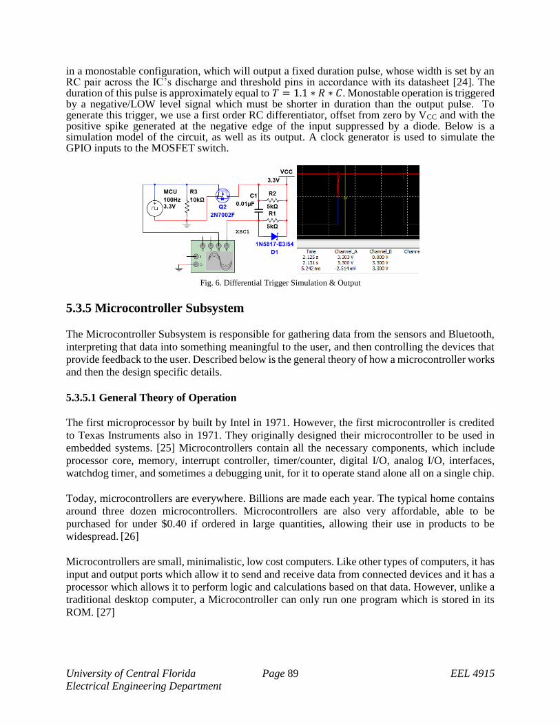
University of Central Florida Page 89 EEL 4915
Electrical Engineering Department
in a monostable configuration, which will output a fixed duration pulse, whose width is set by an RC pair across the IC’s discharge and threshold pins in accordance with its datasheet [24]. The duration of this pulse is approximately equal to 𝑇 = 1.1 ∗ 𝑅 ∗ 𝐶. Monostable operation is triggered by a negative/LOW level signal which must be shorter in duration than the output pulse. To generate this trigger, we use a first order RC differentiator, offset from zero by VCC and with the positive spike generated at the negative edge of the input suppressed by a diode. Below is a simulation model of the circuit, as well as its output. A clock generator is used to simulate the GPIO inputs to the MOSFET switch.
Fig. 6. Differential Trigger Simulation & Output
5.3.5 Microcontroller Subsystem
The Microcontroller Subsystem is responsible for gathering data from the sensors and Bluetooth,
interpreting that data into something meaningful to the user, and then controlling the devices that
provide feedback to the user. Described below is the general theory of how a microcontroller works
and then the design specific details.
5.3.5.1 General Theory of Operation
The first microprocessor by built by Intel in 1971. However, the first microcontroller is credited
to Texas Instruments also in 1971. They originally designed their microcontroller to be used in
embedded systems. [25] Microcontrollers contain all the necessary components, which include
processor core, memory, interrupt controller, timer/counter, digital I/O, analog I/O, interfaces,
watchdog timer, and sometimes a debugging unit, for it to operate stand alone all on a single chip.
Today, microcontrollers are everywhere. Billions are made each year. The typical home contains
around three dozen microcontrollers. Microcontrollers are also very affordable, able to be
purchased for under $0.40 if ordered in large quantities, allowing their use in products to be
widespread. [26]
Microcontrollers are small, minimalistic, low cost computers. Like other types of computers, it has
input and output ports which allow it to send and receive data from connected devices and it has a
processor which allows it to perform logic and calculations based on that data. However, unlike a
traditional desktop computer, a Microcontroller can only run one program which is stored in its
ROM. [27]

University of Central Florida Page 90 EEL 4915
Electrical Engineering Department
5.3.5.2 System Related Design Details
The general theory for how the microcontroller will work was just described in the above section.
This section focuses on the system specific design details. How each of these specifications will
be tested or related to our demo will be discussed in the testing section later on.
The program code will be loaded into the ROM of the microcontroller. An endless loop will allow
the microcontroller to continually run the code until it is powered off. The required components of
the project will be connected to the microcontroller’s I/O pins so that they can communicate with
each other. The program code will allow the microcontroller to process input from sensors on the
device and from the Bluetooth module and to communicate relevant feedback to the user.
5.4 Software Architecture
Our design is composed of several different software systems, section 5.5 focuses heavily on the
software design and system functionality. Shown below are high-level block diagrams outlining
the software and the connections within our design. Below there will also be a legend designated
which subsystem each software falls under. The details of each of these sections will be described
in the sections below.
5.4.1 Mobile Application Architecture
5.4.1-a Mobile Application Architecture Diagram

University of Central Florida Page 91 EEL 4915
Electrical Engineering Department
In the diagram 5.4.1-a above showing how the software for mobile application of the project
communicate with each other. The users will have the option to have navigation connected to the
device to help them navigate from their location to the destination. The directions will be received
from the HERE Maps API and then communicate with the microcontroller via Bluetooth,
directions then get to the tactile system of the device to give the users directions. The
microcontroller would get the information from the sensor system, the data will then send out to
the application via Bluetooth. The application will then send the information data to the Bluetooth
headset to let the users know the navigation part with audio voice or audio ping.
5.4.2 Microcontroller Software Architecture
In Figure 5.4.2-a below, the block diagram for the microcontroller software architecture is given.
The direction of the arrows connecting the blocks indicates whether data is being input or output
between blocks. The microcontroller receives input from the direction sensor, servo, and the
distance sensor. It then processes this input and outputs the relevant information the solenoids,
vibrators, and Bluetooth module. The Bluetooth module then sends this data to the smartphone.
The smartphone also sends data to the Bluetooth module which sends it to the microcontroller.
5.4.2-a Microcontroller Software Architecture Block Diagram
5.5 Software Design
In this section, the design of the smartphone software and the microcontroller software will be
presented in more details.
5.5.1 Smartphone Software Design
As stated in section 5.3.3.1 above, the mobile application for this project will include three buttons
for some of the device functions that users can have the settings change, one button will be on top,

University of Central Florida Page 92 EEL 4915
Electrical Engineering Department
and other two will be on the bottom. The functions that users can change will be call modes on the
application, the top button will be for turning the navigation mode on and off once the mode
position is at where users want to change. On the left bottom button, will be for turning the voice
sound mode on and off once the mode position is at where users want to change. On the right
bottom button, will be for turning the ping sound mode on and off once the mode position is at
where users want to change .There will be three modes total that users can change the functions of
the device, the navigation mode, the audio ping mode, and the audio voice mode. Those three
functions can be turn on and off follow the user’s selections, other functions of the device cannot
be turn on or off individually by the users, once the device is on, most of the functions will start to
work right away.
5.5.1.1 Modes
The device will have a lot of components that make up many functions to help the users to navigate,
but most of the functions will not be able to turn on and off individually by the users. The main
functions that make the device work will turn on when the device is on and off when the device is
off. There will be three device functions that the users can turn on and off if they choose to do so,
the navigation, the audio ping, and the audio voice. When the buttons is pressed to turn modes on
or off, the software will then communicate with the device through Bluetooth system to have that
mode turn on or off.
5.5.1.2 Navigation Mode (Top Button)
On the navigation mode of the mobile application, users tap on the top button (refer to Figure
5.3.3.1-a) to turn the mode on or off depend of user’s selections. Using HERE Maps, the
application can navigate the users to their destinations by letting the users know through the tactile
system on the device. HERE Maps API will be providing the directions in data type which the
application only need is left, right directions, and how far to the turn that need to be make. The
application will get the data provided by HERE Maps and push it to the device via Bluetooth
signal. Once the device gets the navigation data from the application, the microcontroller will
process those data and communicate with the actuators in the tactile system to let users know which
direction to take and how far to the turns. In the tactile system, there will be two of the actuators
to be use for left turn and right turn directions. When the microcontroller gets the left turn direction
signal, the left actuator will raise up and let users know to turn left, and same thing works for the
right turn actuator. The distance data will include the distance in feet to every turn, when the users
is at within one feet to the turn, the application will signal the actuators so that users can turn at
the right moment. One optional function that could be implemented is navigation distance get
transfer to the vibration motor on the device, the motor will vibrate depend on the distance to the
turns that users need to make. And with the optional function, the application will not only send
direction data to the device, it will also send the data to the headset via Bluetooth, the voice prompt
will tell users how many more feet to the turns, and when to turn immediately at the turns.
5.5.1.3 Audio Ping Mode (Bottom Left Button)
On the audio ping mode of the mobile application, users tap on the bottom left button (refer to
Figure 5.3.3.1-a) to turn the mode on or off depend of user’s selections. On the device, the sensor

University of Central Florida Page 93 EEL 4915
Electrical Engineering Department
system will sense if there is an object in the front and will send a data signal to the microcontroller
to process, the signal will include the distance in feet to the object in the front. Like mentioned in
section 5.5.2.1, the vibration motor will vibrate at different speed depend on the distance of the
users to the objects. Audio ping mode is the mode that will send to the Bluetooth headset the ping
sound indicating the distance to the objects. The ping sound will be pulsing at the same levels as
the vibration motors on the device. If the distance to the object is between 9ft and 6ft, the ping
pulsing will be at low speed, if the distance to the object is between 6ft and 3ft, the ping pulsing
will be at medium speed, and if the distance to the object is between 3ft and 0ft, the ping pulsing
will be at fast speed. The ping pulsing speed levels will be the same for the whole interval. With
this, the users can also listen to the distance from them to the objects through ping pulses and not
just relying on the actuators on the device. But if at any time, users do not want to have the ping
function to their Bluetooth headset, they can always turn it off with the mobile application.
5.5.1.4 Audio Voice Mode (Bottom Right Button)
On the audio voice mode of the mobile application, users tap on the bottom right button (refer to
Figure 5.3.3.1-a) to turn the mode on or off depend of user’s selections. On the device, the sensor
system will sense if there is an object in the front and will send a data signal to the microcontroller
to process, the signal will include the distance to the objects, and include the position of the objects,
to the left or to the right or straight in the front of the users. The application will use that
information and send it to the Bluetooth headset. There will be voice prompts to alert the users,
the prompt will include “Left”, “Right”, and the distance to that object, “8ft”, “7ft”, “6ft”, “5ft”,
“4ft”, “3ft”, and under 3ft will be prompt "Danger!". Extra optional function that can be included
in the future development of the device is to have the voice prompt for the navigation function.
Users will be alert to “Turn left”, “Turn right”, “X meter to the turn” so that it would be easier and
faster to listen to the voice prompts from the Bluetooth headset. But if at any time, users do not
want to have the ping function to their Bluetooth headset, they can always turn it off with the
mobile application.
5.5.2 Microcontroller Software Design
The microcontroller software design explains what needs to be implemented in the microcontroller
software in order for the project to meet its requirements. This section does not specifically discuss
how to implement different parts of the microcontroller software, but focuses more on what needs
to be implemented.
5.5.2.1 Distance Sensing Input to Microcontroller
The expected input to the microcontroller from the sensor whose task is to detect directly in front
of the EASI device is a digital wave. The shorter the length of time that each wave pulse is high,
the closer the object is to the sensor. Conversely, the longer the length of time that each wave pulse
is high, the further the object is from the sensor. From the inputted digital wave, the microcontroller
will determine the start and end time of each pulse in which the wave is high. The end time will
then be subtracted from the start time of the pulse to get the total time that the pulse was high. In
order to convert this time measurement into a meaningful measure of the distance to the detected
object, the total time of each high pulse must be multiplied by the speed of sound, since that is the

University of Central Florida Page 94 EEL 4915
Electrical Engineering Department
speed at which the sonar pulses travel. After this multiplication, the microcontroller will have the
distance to the detected object in inches.
Once the distance to the detected object has been calculated, the microcontroller needs to convey
this information to the user. That is where the tactile subsystem of the project comes into play. If
the distance to the object is between six and nine feet, Sole1 is raised while Sole2 and Sole3 are
lowered (please refer to Figure 5.2.5.2-a for solenoid configuration, naming convention, and brief
description of function). Also, if the distance is between eight and nine feet, one of the vibrators
will pulse at a slow speed. If the distance is between seven and eight feet, one of the vibrators will
pulse at a medium speed. If the distance is between six and seven feet, one of the vibrators will
pulse at a fast speed.
If the distance to the object is between three and six feet, Sole2 is raised while Sole1 and Sole3 are
lowered. Also, if the distance is between five and six feet, one of the vibrators will pulse at a slow
speed. If the distance is between four and five feet, one of the vibrators will pulse at a medium
speed. If the distance is between three and four, one of the vibrators will pulse at a fast speed.
If the distance to the object is less than three feet, Sole3 while Sole1 and Sole2 are lowered. Also,
if the distance is between two and three feet, one of the vibrators will pulse at a slow speed. If the
distance is between one and two feet, one of the vibrators will pulse at a medium speed. If the
distance is between zero and one feet, one of the vibrators will pulse at a fast speed. Else, if none
of these cases are met, Sole1, Sole2, and Sole3 are all lowered to indicate that no object is detected
within the sensors effective range. For each case, the appropriate solenoid will remain raised until
new data from the distance sensor is processed and the distance no longer falls within the
corresponding distance category. As a visual aid to help understand the flow of logic for this
section, please refer to this section’s corresponding flowchart (Figure 5.2.5.2-b).
Another functionality of the distance sensing input that we considered implementing is an
automatic stand-by mode. This mode would active if the distance sensing input to the
microcontroller does not change for a certain amount of time, say 30 seconds. In stand-by mode,
the device would power down all non-essential components. It would then test the distance sensor
every 30 seconds to see if the distance started to change again. Once the distance again starts
changing, the device is restored to its normal operating state. Ultimately, due to the time constraints
of the project, this functionality was not implemented.
5.5.2.2 Bluetooth Input to Microcontroller
The Bluetooth module of the microcontroller will receive input from the paired smartphone when
turn-by-turn navigation directions are requested. The Bluetooth module is capable of transmitting
and receiving up to 20 bytes of data using BLE. The data that the microcontroller’s Bluetooth
module will receive from the paired smartphone will be two bytes long. The microcontroller will
parse the input to separate the important information in the input.
The first byte will indicate if the next navigation action that the user must perform is a left or right
turn. If the user needs to take a left turn, Sole6 will be raised and Sole7 will be lowered (refer to
Figure 5.2.5.2-a). If the user needs to take a right turn, Sole7 will be raised and Sole6 will be

University of Central Florida Page 95 EEL 4915
Electrical Engineering Department
lowered. The second byte will indicate the distance to the point that the navigation action must be
performed. If the distance to upcoming turn is 250ft, one of the vibrators on the device will pulse
four times. If the distance to the upcoming turn is 100ft, one of the vibrators on the device will
pulse three times. If the distance to the upcoming turn is 50ft, one of the vibrators on the device
will pulse twice. If the user has reached the point at which they need to perform a turn, one of the
vibrators will perform one pulse of a longer duration than the turn distance warning pulses. As a
visual aid to help understand the flow of logic for this section, please refer to this section’s
corresponding flowchart (Figure 5.2.5.2-c).
5.5.2.3 Bluetooth Output from Microcontroller
The microcontroller will also be used to output data to the EASI smartphone app on the paired
smartphone through a connected Bluetooth module. The distance to the detected object calculated
earlier (in section 5.4.2.1) will be sent to the paired smartphone using one byte of data. Only one
byte of data is needed because the calculated distance will be between zero and nine feet which
can be represented in a single character. The microcontroller will send the character corresponding
to the number of feet to the detected object between two and nine feet. Between zero and two feet,
the character ‘0’ will be sent. This will allow the smartphone app to send a single warning for
distances falling within this range. As a visual aid to help understand the flow of logic for this
section, please refer to this section’s corresponding flowchart (Figure 5.2.5.2-d).
5.5.2.4 Direction Sensing Input to Microcontroller
In order to sense approaching objects that are not directly in front of the user, two additional
sensors mounted on top of a servo will be used to detect if there is an object in front of and to the
left of the user or if there is an object in front of and to the right of the user.
If the left direction sensor detects an object to the left of the user within five feet, sole4 will be
raised (refer to Figure 5.2.5.2-a). Otherwise, if an object is detected greater than five feet away
from the user, sole4 will be lowered. If the right direction sensor detects an object to the right of
the user closer than five feet, sole5 will be raised. Otherwise, if an object is detected greater than
five feet away from the user, sole5 will be lowered. For each case, the appropriate solenoid will
remain raised until additional sensor data is received. As a visual aid to help understand the flow
of logic for this section, please refer to this section’s corresponding flowchart (Figure 5.2.5.2-e).
We considered the potential problem of crosstalk between our different sensing systems. Upon
testing, it was determined that there was definitely a problem with crosstalk between the direction
sensing sensors and the distance sensing sensor. To solve this problem, each sensor was only
powered on when it they were needed to get new sensor data. Each sensor took turns being powered
on so that crosstalk between the sensors would be eliminated.

University of Central Florida Page 96 EEL 4915
Electrical Engineering Department
6. Project Prototype Construction and Coding
The project prototype and construction section includes the details of how the electrical schematics
and the final plan for the final PCB construction and assembly. The schematics will include a
visual of the schematic itself and the breadboard assembly. The PCB section will describe the
possible venders and plan for assembly and construction. Included in this section is the final coding
plan which will outline the final planned programming features involved in our design.
6.1 Integrated Schematics
This section includes the various electrical schematics. It is from these schematics that we will
derive the PCB layout. It is also from the schematics that we will test and possibly perform circuit
analysis to determine if there is a better and more efficient way to design the flow of electricity
within our design. These equations will be presented along with the data in the testing section if
they become needed. As with any design the schematics below were first pulled from the
datasheets and then altered to suit our design needs. We will start off with the power system
schematic and with the complete schematic design
6.1.1 Power System Schematics
The power systems schematic is the heart and soul of our design. The initial design for our power
system separated the schematic into two: one being a battery charging schematic and one being a
power regulation schematic. However, as we first designed the battery charging schematic we
realized that only two buck DC-DC converters were necessary to provide the circuit with the
regulated power the circuit required. Due to the limited components and the advantages of
simplifying our design and possibly making a smaller PCB we decided to combine the two
schematics.
Below is the power systems schematic shown in Figure 6.1.1-a and the breadboard construction
shown in Figure 6.1.1-b.
Figure 6.1.1-a Power Systems Schematic
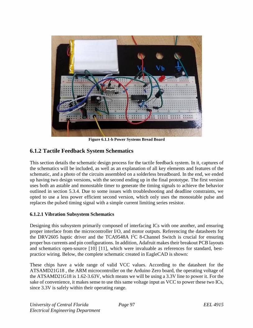
University of Central Florida Page 97 EEL 4915
Electrical Engineering Department
Figure 6.1.1-b Power Systems Bread Board
6.1.2 Tactile Feedback System Schematics
This section details the schematic design process for the tactile feedback system. In it, captures of
the schematics will be included, as well as an explanation of all key elements and features of the
schematic, and a photo of the circuits assembled on a solderless breadboard. In the end, we ended
up having two design versions, with the second ending up in the final prototype. The first version
uses both an astable and monostable timer to generate the timing signals to achieve the behavior
outlined in section 5.3.4. Due to some issues with troubleshooting and deadline constraints, we
opted to use a less power efficient second version, which only uses the monostable pulse and
replaces the pulsed timing signal with a simple current limiting series resistor.
6.1.2.1 Vibration Subsystem Schematics
Designing this subsystem primarily composed of interfacing ICs with one another, and ensuring
proper interface from the microcontroller I/O, and motor outputs. Referencing the datasheets for
the DRV2605 haptic driver and the TCA9548A I2C 8-Channel Switch is crucial for ensuring
proper bus currents and pin configurations. In addition, Adafruit makes their breakout PCB layouts
and schematics open-source [10] [11], which were invaluable as references for standard, best-
practice wiring. Below, the complete schematic created in EagleCAD is shown:
These chips have a wide range of valid VCC values. According to the datasheet for the
ATSAMD21G18 , the ARM microcontroller on the Arduino Zero board, the operating voltage of
the ATSAMD21G18 is 1.62-3.63V, which means we will be using a 3.3V line to power it. For the
sake of convenience, it makes sense to use this same voltage input as VCC to power these two ICs,
since 3.3V is safely within their operating range.

University of Central Florida Page 98 EEL 4915
Electrical Engineering Department
Figure 6.1.2.1-a Vibration Subsystem Schematic
The basic I/O configurations can be inferred from the datasheet sections “Pin Functions”. For the
DRV2605, the on-chip voltage regulator output VREG must be connected to a 1uF capacitor, and
if unused can be tied to ground. The IN/TRIG pin is a multimodal (PWM, edge triggered, or
analog) input, configured via I2C. Since we will be doing all control via I2C, this pin is not used
and therefore must be grounded. EN is an active high device enable signal, so currently since there
is no need to disable these controllers, it can be left high. If we were to implement a device-scale
low-power mode, the microcontroller may instead set this pin to disable these chips in a low-power
state. OUT+ and OUT- are simply the PWM outputs which will power and control the vibration
motor.
For the TCA9548A, the pins A0-A2 are I2C address configuration pins. They allow the designer
to vary the address of the IC between 0x700 and 0x707. This allows up to eight of these
multiplexers on the same bus, and allows avoiding collisions with other slave devices with
addresses in this range. Since we only have one of these on the bus, and since there is no need to
adjust the device address, so according to the datasheet we may connect the pins directly to ground
to leave the address at 0x700. The unused SDA and SCL outputs can be left floating, since they
are output pins. The SCLPU and SDAPU devices shown are solder jumpers, which are pads on
the PCB that can be opened/closed with solder, for the purpose of more rapid prototyping and
circuit modifications after the PCB has been printed. They are present on the Adafruit breakout,
and are likely there in case the microcontroller the board is connected to has internal pullups

University of Central Florida Page 99 EEL 4915
Electrical Engineering Department
enabled. They have been left in the design above, however they may be removed in layout design
if they are found to be not needed.
The capacitors between the VCC and ground pins of the ICs are decoupling capacitors, to isolate
the power bus from ground noise. The datasheets indicate 0.1uF capacitors should be sufficient,
however the values in the design above were the ones used in the Adafruit breakouts. In general,
logic level ICs typically use values between 0.1 and 10uF, so the values used should be sufficient.
Further analysis would be required if high frequency noise was expected in the circuit.
Finally, as shown by the I2C bus specification [12] and the IC’s datasheet, an I2C bus should be
tied to VCC via pullup resistors. Without pullups, the I2C signals’ rise time will be too long, and
thus they will not be able to reach HIGH before the next bit is sent. The Adafruit breakout
schematics use 10kOhm resistors for this purpose, however just to confirm that these values are
within acceptable range, we can again refer to the I2C bus standard for the standard method of
calculating the pullup range. To find the minimum value for Rp, we must know the maximum
output-LOW voltage and current VOL and IOL, as well as the reference voltage VCC. For both the
microcontroller bus and the multiplexer bus, these values are listed in the datasheets as VOL = 0.4V
and IOL = 3mA. Therefore, the minimum pullup resistance RP(min) = 1kOhm. The maximum value
can be calculated from the I2C bus capacitance and Cb and the maximum rise time tr. Both the TI
reference document, and the TCA9548A datasheet, list the maximum bus capacitance (Cb) in
normal mode as 400pF, and the maximum rise time as 1000ns. According to the pullup resistor
calculation, in order to 10kOhm to fall under the maximum, the total bus capacitance of this circuit
must be under 118pF. I could not find the I2C output capacitance in the microcontroller datasheet,
however the TCA9548A and DRV2605 do list theirs, and as they are on the order of 1 to 10 pF,
and since the traces will likely be very short, it is very unlikely that the bus capacitance will exceed
118pF and hence 10kOhm is very likely an acceptable value. Scoping the I2C bus on breadboard
tests to demonstrate an acceptable rise time, or directly measuring the capacitance of the final bus
on breadboard would verify these values are acceptable. Such breadboard tests would in fact
overstate the end bus capacitance, as the wire capacitance on breadboard jumpers is likely much
higher than that of PCB traces.
6.1.2.2 Actuator Subsystem Schematics
The actuator subsystem schematic shown below uses dummy components, however given that we
know the electrical characteristics of both the solenoid and the microcontroller PWM signal, we
can list the parameters by which we will select real components to replace them. In order to do this
selection, we must first determine how to custom components in EagleCAD and what the footprint
of each component must look like. The circuit’s overall structure is based on the model discussed
in section 5.2.4. Additionally, the circuit used for the final PCB layout will contain one of the
shown circuits for each solenoid (seven in total), all connected to the same 5V line.

University of Central Florida Page 100 EEL 4915
Electrical Engineering Department
Figure 6.1.2.2-a Actuator Subsystem & I/O Header Schematic (Rev 2)
The solenoid leads will connect to the +SOL and -SOL solder pads, and the input controlling PWM
signal from the microcontroller will connect to the DIG_IN net. The first two components which
must be selected are the N-Channel MOSFETs, and the flyback diode. In choosing a diode, there
are two primary parameters we need be concerned with: it’s breakdown voltage, and its maximum
forward current. The breakdown voltage simply must exceed the 5V supply voltage by a safe
margin, as in normal operating conditions it will be reverse biased at that voltage. Similarly, the
diode must be able to conduct at least as much forward current as the solenoid’s rated current draw
(for our solenoid, that is 1.1A). Whenever the solenoid actuates, it can produce strong spikes of
negative voltage that would normally damage the MOSFET. The flyback diode will become
forward biased by this negative voltage, giving the current a safe path to loop through it and the
solenoid until it dissipates through the solenoid’s internal resistance.
In choosing a MOSFET, there are a few more parameters to keep in mind. The first and simplest
is its maximum IDS. This is the current that will pass from drain to source when the switch is open.
Since this current will be equal to the current passing through the solenoid, it must be at least as
large as the solenoid’s rated current, 1.1A. Related to this is the maximum drain to source voltage,
VDS. This will be equal to the voltage across the output minus the voltage drop across R3, which
can still be approximated to 5V, as R3 will be small. The final main characteristic we must consider
is the MOSFET’s threshold voltage, VGS(th). This is the voltage at or above which the switch will
open and allow current to flow through the solenoid. It is therefore dependent on the output logic
levels of our microcontroller, the ATSAMD21G18. According to its datasheet, the maximum
output voltage at logic LOW is 0.2 ∗ 𝑉𝐷𝐷 = 0.2 ∗ 3.3 = 0.66𝑉, and the minimum output voltage
at logic HIGH is 0.8 ∗ 𝑉𝐷𝐷 = 0.8 ∗ 3.3 = 2.64𝑉. We must therefore choose a MOSFET which has

University of Central Florida Page 101 EEL 4915
Electrical Engineering Department
a VGS(th) between these two values, rated for the estimated logic LOW leakage current. Finally, we
must consider RDS, which is the resistance across the drain-source terminals when the gate is open.
This will determine how much power the MOSFET will dissipate, so we should keep this value as
small as possible.
Each GPIO input has a small series 150Ω resistor to protect the MCU outputs from current
overdraw in the event of accidental shorts. In addition, there is a 10kΩ pulldown resistor for each
input, to give the FET gate a path to discharge and pull the logic level low. In the first design
version, the 4.7Ω resistor R1 is replaced with a direct connection to the pulsed power signal
generated using the astable 555 timer. The second version, which is the version shown in Figure
6.1.2.2-a, uses a series resistor in place of the pulsed power signal to reduce current at the cost of
increased power consumption.
Figure 6.1.2.2-b Timer Schematic Diagram. Rev. 1

University of Central Florida Page 102 EEL 4915
Electrical Engineering Department
Figure 6.1.2.2-b above shows the first revision of the solenoid control timer circuit. It implements
all of the techniques discussed in section 5.3.4, along with an OR gate ensure the monostable timer
is triggered any time any one of the solenoids is actuated. A MOSFET switch is used at the power
input of the astable timer to disable it when no solenoids are actuated. Upon implementing this
design, we found what appeared to be switching parasitics in the astable output signal, and
unfortunately due to time constraints we were unable to determine a solution using this design.
Therefore, the second revision, shown below, is what we ultimately used in the final prototype.
Figure 6.1.2.2-c Timer Schematic Diagram, Rev. 2
6.1.3 Microcontroller Schematics
The Microcontroller schematic is at its core simple. For the most part the schematic simply has
connections from the various outputs and inputs of our circuit and connecting them to the
microcontroller. Each component is powered separately from the Power System schematic above
as that power system schematic provides a 3.3V, and 5V bus to power our various components
and the microcontroller itself. Below is the are the schematics for the microcontroller: Figure 6.1.3-
a shows MCU 1, Figure 6.1.3-b shows MCU 2, Figure 6.1.3-c shows the Bluetooth portion and
the breadboard construction shown in Figure 6.1.3-d.

University of Central Florida Page 103 EEL 4915
Electrical Engineering Department
Figure 6.1.3-a Microcontroller MCU 1 Schematic
Figure 6.1.3-b Microcontroller MCU 2 Schematic

University of Central Florida Page 104 EEL 4915
Electrical Engineering Department
Figure 6.1.3-c Microcontroller Bluetooth Schematic
Figure 6.1.3-d Microcontroller Bread Board

University of Central Florida Page 105 EEL 4915
Electrical Engineering Department
6.1.4 Complete Schematic Design
This section is the compilation of the 3 above chips for potentially making one fully functional
PCB. As stated above we plan to create 3 individual PCB’s to ensure the working functionality of
each. However, the ultimate goal is to combine them into one design. The advantages of this are
the reduction in size and the ease of assembly of our design. The disadvantage of this is the
possibility of component or PCB failure. An all in one design is ideally the best but requires a lot
more development time to ensure all the circuits work well and fit within the confines of your
PCB. The other issue is the pressure of the deadline to ensure that this prototype works. If a
complete PCB fails, you suffer a complete failure but if you have several working smaller PCB’s
you can make it work on the fly by swapping out damaged sections.
Due to the size of the tactile breadboard we found it easier to simply utilize the working pcb. Below
is the completed construction of the entire circuit.
Figure 6.1.4-a Microcontroller Bread Board
6.2 PCB Vendor and Assembly
We have researched the general process for designing and printing them, what design tools we will
use, what manufacturer service we will use, and what the general structure will look like. We ended
up with three design revisions for our power system PCB, and two for the tactile system PCB.

University of Central Florida Page 106 EEL 4915
Electrical Engineering Department
6.2.1 Structure
The current plan is to have two PCBs in the final product: one which houses the power regulation
and USB charging circuits, and one which houses the tactile feedback system control circuitry. We
are planning on leaving the ATSAMD21G18 mounted on the Arduino Zero development board.
Dedicating design resources to laying out a dedicated PCB for the microcontroller and Bluetooth
module, or expanding the tactile control PCB to house them, would be ideal for power
consumption optimization and substantially reducing the size of the system, however currently we
simply do not feel we have the time or resources to accomplish this. If we are overestimating the
difficulty of this task and end up with design resources to spare, or if we find that our initial plans
would simply be too large and heavy to meet our engineering requirements, then we will adopt
these changes. Especially since it is a handheld device, and it is meant to be discreet, space is an
absolute premium and any size reductions will greatly improve the product’s appeal and
marketability.
Figure 6.2.1-a PCB Physical Interface Diagram
The interface diagram above clearly defines the concrete I/O between each discrete component in
the final product, including the planned I/O through the PCBs. The current plan would have the
Arduino Zero as a drop in for the microcontroller block, however given sufficient design resources
we could also design a custom PCB to fill that role.
6.2.2 Design Plan

University of Central Florida Page 107 EEL 4915
Electrical Engineering Department
To design the PCB, we will be using the EagleCAD PCB design software. We currently have some
of our designs created in the Eagle Schematic editor, and some built in National Instruments
Multisim. Below, all of the specific steps we will need to take to produce final PCBs for test. This
process will be applied to both the power system PCB and the Tactile feedback PCB first, then if
we have design resources to spare we will also apply it to a microcontroller PCB we design. Given
the relative simplicity of our circuits, our current plan is to design for a two-layer PCB.
Additionally, we plan on using Advanced Circuits to print the PCB, as they have very fast turnover
along with good student pricing.
1. We must first complete any breadboard verification tests of these schematic designs
necessary to independently demonstrate individual subsystem circuit functionality.
2. We then will need to do interface testing between any of these circuits that will exist on
the same PCB, so that intra-PCB functionality is verified to the point that any issues
encountered post fabrication can be attributed to layout bugs and not design/schematic
issues
3. We must port all schematics not currently in EagleCAD into its schematic design tool, and
integrate any schematics which will share a PCB into one project.
4. Any dummy/ideal circuit components used in initial designs must be substituted for real
circuit components
5. Once a PCB’s schematic has been unified, we can use Eagle’s Generate/Switch to Board
tool to port all nets and schematic component footprints into Eagle’s board layout editor.
All pin connections between components will be represented by thin, translucent gold lines
known as airwires.
6. From here, the component footprints can be moved into the arrangement they will be in on
the PCB. Below are some heuristics for creating a good component layout:
a. The end goal should be creating a PCB with the smallest possible surface area.
Minimizing overall size is a massive priority for this project, and in general a PCB
is more expensive the larger it is.
b. Minimize intersections between airwires. Since, in the final routing stages, no
traces on the same layer can cross, so the fewer of these intersections there are, the
simpler routing will be. Too tangled a ratsnest can make routing impossible given
a limited number of layers to work with. The Ratsnest tool can be used to force a
recalculation of airwires
c. Leave adequate space between components and pins. Overlapping pins will cause
shorts, and placement too close to exposed copper pads can also lead to shorts.
Additionally, be mindful of any special case placement considerations, such as
keeping decoupling capacitors as close to their IC as possible.
7. Adjust the board dimensions to fit around all of the board components, while minimizing
excess space and being sure to not cut off components at the edge
8. Select either the top or bottom layer, and use the Route tool to begin replacing airwires
with traces, such that they do not cross over any vias or other traces. Vias pass copper
through the substrate to connect traces between layers. Use a trace width calculator to
determine how wide each trace should be given how much current it is expected to have to
pass.

University of Central Florida Page 108 EEL 4915
Electrical Engineering Department
9. If ever unable to find a valid trace path, the Autoroute tool can be used to attempt
algorithmically finding a solution. This will not always work, and may take some time to
complete.
10. Use the Ratsnest tool to verify all required traces have been drawn.
11. The design must now be checked for any broken design rules. Each PCB manufacturer has
their own set of design rules (minimum component spacing, trace widths, hole sizes, etc.)
which must be followed. Eagle has its own design rule check tool, in which the designer
may manually enter rules or read them in from a .DRC file. If no such file is provided, the
manufacturer will often provide their own tool for doing so.
12. Once DRC is passed, all that is left to do is add silkscreen labels to pins, ports, I/O, and
devices.
13. Finally, use Eagle’s CAM processor to generate the required gerber files for
manufacturing. Each vendor will have different specifications for packaging and
formatting the repository. Be sure to comply with them before submitting a design.
6.2.3 Power/MCU/Bluetooth PCB
The power/MCU/Bluetooth PCB was initially all considered separate however due to the issues of
having so many wires in a small space it made sense to try and combine everything. Through the
course of our device development we had 3 revisions of our PCB with the third revision having 2
versions. Each revision will be described in detail below and the issues we had with it.
6.2.3.1 Revision 1
The revision 1 took a very barebones approach. We were initially worried about processing power
so a 2nd MCU was added to help save time in case it was needed. This 2nd MCU was used for the
Bluetooth with lines sent directly to the MCU from the Bluetooth module. This pcb design tried
to remove all components necessary to save on cost and space. Below is the layout and PCB
shown in Figure 6.2.3.1-a and Figure 6.2.3.1-b respectfully

University of Central Florida Page 109 EEL 4915
Electrical Engineering Department
Figure 6.2.3.1-a Revision 1 Layout
Figure 6.2.3.1-b Revision 1 PCB
6.2.3.2 Revision 2
The revision 2 was made after initially trying to program revision 1. We found that though the
power circuit worked perfectly we could not program the MCU. The cause of this problem was
that the MCU did not have a boot loader. Because we took a barebones approach we did not
include the debug pins for the MCU’s. This made it impossible to program. The revision 2
addressed these issues by making it so every pin of each MCU was accessible. This allowed for a
lot more flexibility and would allow us to solder wires on to program it. Below is the layout and
PCB shown in Figure 6.2.3.2-a and Figure 6.2.3.2-b respectfully
Figure 6.2.3.2-a Revision 2 Layout

University of Central Florida Page 110 EEL 4915
Electrical Engineering Department
Figure 6.2.3.2-b Revision 2 PCB
6.2.3.3 Revision 3
Revision 3 was the combination of trying everything we could to produce working PCB’s. Version
2 as we found could be programmed successfully however not matter how we tried to program the
PCB we could not output the program to the pins. We never determined if it was hardware or
software but due to time constraints as group leader I decided to sacrifice my work for the sake of
improving other areas of the project allowing for a more finished product by the deadline. Version
A however focused on trying to tweak the crystal circuit and make less sharp corners for the digital
pins. It also made the programing pins more accessible while removing things like usb and
Bluetooth. We removed Bluetooth as it was easier to upgrade the firmware as a standalone. By
removing these things we also cut the cost of the PCB board significantly. Only a single MCU
was used as through software optimization we found we only needed one MCU for our design’s
function. Version B is a pcb with only power in mind. The power circuit worked on all versions
of the PCB and was needed to power the tactile actuators. This Version was the one used in our
final design as despite efforts and a lack of time we could never program the MCU to output to the
pins. Below is the layout and PCB of version A shown in Figure 6.2.3.3-a and Figure 6.2.3.3-b
respectfully. Figure 6.2.3.3-c and Figure 6.2.3.3-d show the layout and PCB of version B
Figure 6.2.3.3-a Revision 3a Layout

University of Central Florida Page 111 EEL 4915
Electrical Engineering Department
Figure 6.2.3.3-b Revision 3a PCB
Figure 6.2.3.3-c Revision 3b Layout
Figure 6.2.3.3-d Revision 3b PCB

University of Central Florida Page 112 EEL 4915
Electrical Engineering Department
6.2.4 Tactile Feedback System PCB
As discussed in section 6.1.2, we went through two revisions of tactile feedback system design.
The PCB layout and assembled board for the first revision can be seen below:
Figure 6.2.4-a Revision 1 Layout and PCB

University of Central Florida Page 113 EEL 4915
Electrical Engineering Department
This 2.59 x 2.5-inch board has two layers and uses all surface mounted components. The second
board, shown below, was 2.6 x 2.35-inches, and additionally had some of its components mounted
on the bottom layer to make routing easier. As previously stated, this board is the one in the final
prototype.
Figure 6.2.4-b Revision 2 Layout and PCB

University of Central Florida Page 114 EEL 4915
Electrical Engineering Department
6.3 Final Coding Plan
Sections below are final combine flowcharts for mobile application and microcontroller software
including detail explanations of each flowchart.
6.3.1 Final Coding Plan Smartphone
The final coding plan for the mobile application software combine all the functions described in
section 5.5.1. These functions are: navigation mode, audio ping mode and audio voice mode. Since
the program code for the mobile application software must be a single program stored in the mobile
device, each of these functions must be combined in a way that allows the code to be continuously
run. How this combination will be achieved is discussed below and is illustrated in the figure
further below (Figure 6.3.1-a).
The software program will first check to see if there is and data received from the microcontroller.
If there is any data, next block of the diagram will check to see if it is object’s left position data, if
the left position is received, the program will then check to see if the audio voice mode of the
application is on or off. The data will then process into voice prompt and get to send over to the
Bluetooth headset to alert the users. If the data from the microcontroller is not the object’s left
position, then it will check to see if it is object’s right position. Voice mode on/off will then get
check and if the mode is on, the data will then process into voice prompt and get to send over to
the Bluetooth headset to alert the users. If the microcontroller data is not the left or right position
of the objects and then would be the distance to that object. Then the program will check if the
audio ping mode of the application is in on or off position, if the mode is on, the program will
check for the distance data. The distance data will be check in three groups, distance between two
meters and three meters, between two meters and one meter, and less than one meter. At each
group of distance, program will then check for another sublevel of distance groups; for the two
meters to three meters’ group example, if it is between 2.666 meters and 3 meters, the pulse ping
in the Bluetooth headset will be at slow speed; if it is between 2.333 meters and 2.666 meters, the
pulse ping will be at medium speed; if it is between 2 meters and 2.333 meters, the pulse ping will
be at high speed. The program will check for the same thing in one to two meters’ group, and less
than one meter and pulse the same ping level according to the distance level like in other groups
to the users Bluetooth headset. If it is not the object’s distance data sent to the application or the
audio ping mode is not on, the software will continue to wait for data and process the data from
the beginning.
If there are no data received from the microcontroller, the program will then check to see if any
data received from the HERE Maps API. The HERE Maps API will consist of the direction
navigations to the destination that the users selected, the program will only process the left turns,
right turns, and distances to each of the turn. Those data will then get send to the tactile system of
the device to guild users to their destinations. If there are no data received from the HERE Maps
API, the program will continue to cycle back and wait for data and process them from the
beginning.

University of Central Florida Page 115 EEL 4915
Electrical Engineering Department
Figure 6.3.1-a Mobile Application Flowchart

University of Central Florida Page 116 EEL 4915
Electrical Engineering Department
6.3.2 Final Coding Plan Microcontroller
The final coding plan for the microcontroller subsystem combines all the functions described in
section 5.5.2. These functions are: distance sensing input to microcontroller, Bluetooth input to
microcontroller, Bluetooth output from microcontroller, and direction sensing input to
microcontroller. Since the program code for the microcontroller must be a single program stored
in the microcontroller’s ROM, each of these functions must be combined in a way that allows the
code to be continuously run until the device is powered off. How this combination will be achieved
is discussed below and a rough coding flowchart is illustrated in the figure further below (Figure
6.3.2-a).
The program first gets new data from the left direction sensor. If the calculated distance to the
object detected is less than five feet, the left direction solenoid is raised and Bluetooth module is
instructed to transmit a symbol indicating an object is to the left to the paired smartphone.
Otherwise, the left direction solenoid is lowered. Once the left direction sensor input to the
microcontroller code block has been completed, execution of the next code block begins.
Next, the program gets new data from the right direction sensor. If the calculated distance to the
object detected is less than five feet, the right direction solenoid is raised and Bluetooth module is
instructed to transmit a symbol indicating an object is to the right to the paired smartphone.
Otherwise, the right direction solenoid is lowered. Once the right direction sensor input to the
microcontroller code block has been completed, execution of the next code block begins.
After that, the program gets new data from the distance sensor. The program then calculates the
distance to the object and instructs the Bluetooth module to transmit that distance in feet to the
paired smartphone. Next, the distance is used to determine which of the three distance sensing
solenoids or if any should be raised and how fast to pulse one of the vibrators. The process for
determining this is described in greater detail in section 5.5.2.1. Once the combined distance
sensing input to the microcontroller and Bluetooth output from the microcontroller code block has
been completed, execution of the next code block begins.
The final code block of the program begins by determining if new data has been received from the
Bluetooth module. If no new data was received, this block of code is skipped and the program
immediately begins execution of another loop of the code. If new data was received, the program
then parses that data to get the next navigation action and distance until that action needs to be
performed. The two navigation solenoids are raised or lowered depending on if the next navigation
action is a left or right turn. Also, one of the vibrators is pulsed according to the distance until the
action needs to be performed. The process for determining which solenoids are raised and lowered
and how many times the vibrator is pulsed is described in greater detail in section 5.5.2.2. Once
the Bluetooth input to the microcontroller code black has completed, execution then loops back to
the beginning of the program so that the program can run continuously on the microcontroller until
it is powered off.

University of Central Florida Page 117 EEL 4915
Electrical Engineering Department
Figure 6.3.2-a Microcontroller Combined Flowchart

University of Central Florida Page 118 EEL 4915
Electrical Engineering Department
7. Project Prototype Testing Plan
Section 7 will be about many different testing plans, testing environments and testing cases for
hardware and software components of the projects.
7.1 Hardware Test Environment
The approach we will be taking in verifying basic system functionality and validating specification
compliance will be a bottom-up approach. In general, we will strive to isolate the smallest possible
system units which can be independently breadboarded and stimulated, use lab equipment to
simulate expected interface inputs to that unit, then monitor output signals and behavior to verify
that they behave as expected.
7.2 Hardware Testing
The section below consists of the systematic tests of hardware. Though each component
was tested on their own, the PCB’s designed by us were each tested in similar fashion. Though
this process was important it was done in a basic way, ensuring that there are no shorts and that
each circuit board line is correct. This testing was done with a multimeter first testing resistance
and then with DC voltage to ensure both was correct before connecting it to our components.
7.2.1 Sensor Testing
The sensor testing was done to compare each type of sensor and how it would effect our
design. Each sensor regardless of beam had a range that far exceeded what our project needed.
However, upon testing we found that the narrow beam sensor could not sense people beyond 5
feet. The wider beam sensor detected people between 7-9 feet, this data was supported by
recommended applications for each sensor found in the data sheet. In Figure 7.2.1-a, our results
for testing each sensor at varying distance
Figure 7.2.1-a Sensor Testing Data
Cork Board 132 132 132
Cork Board 108 108 108
Cork Board 84 84 84
Cork Board 60 60 60
Cork Board 48 48 48
Cork Board 36 36 36
Cork Board 24 24 24
Cork Board 12 12 12
2x2 Vertical 132 134 132 36
2x2 Vertical 108 107 12 107 36
2x2 Vertical 84 83 12 83 48
2x2 Vertical 60 60 12 59 36
2x2 Vertical 48 48 8 48 36
2x2 Vertical 36 36 12 35 24
2x2 Vertical 24 23 12 23 24
2x2 Vertical 12 12 6 11 10
Object
MaxSonar EZ4 MaxSonar EZ1
Actual
Distance
Detected
Distance
Detection
Spread
Detected
Distance
Detection
Spread

University of Central Florida Page 119 EEL 4915
Electrical Engineering Department
7.2.2 Power Testing
The battery was tested using a cycling program that turned each actuator on and off in succession.
This was done over a period of 12hrs measuring the voltage of the battery every 30min. The results
of this was just shy of 12 hours but this was with heavy usage. On the charging side, it was easier
we waited for the battery to fully die and then we charged it. Due to our battery manager, we could
simply monitor the charging status light. Once the light went out the battery was fully charged.
After several attempts the average charge time was 6-6.5 hours.
Figure 7.2.1-a Battery Testing Data
7.2.3 Tactile System Testing
Most testing for this system took place on breadboard. The first stage, as mentioned in section
5.3.4, was to connect the actuators to a DC power supply and experimentally determine their
actuation and holding current. After conceiving the design, we built the circuit on a breadboard
(shown below) to ensure it functioned as expected, and to tweak timer configurations for optimal
power consumption. Below is a picture of the final breadboard setup used to test a single actuator:
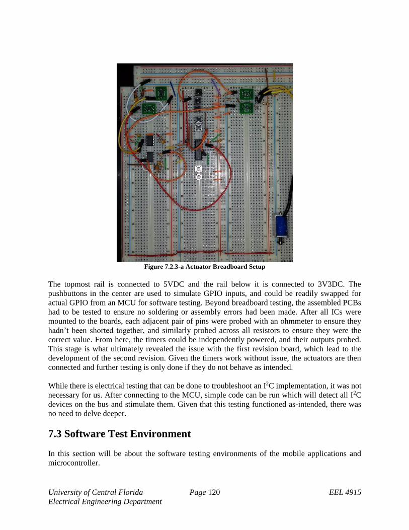
University of Central Florida Page 120 EEL 4915
Electrical Engineering Department
Figure 7.2.3-a Actuator Breadboard Setup
The topmost rail is connected to 5VDC and the rail below it is connected to 3V3DC. The
pushbuttons in the center are used to simulate GPIO inputs, and could be readily swapped for
actual GPIO from an MCU for software testing. Beyond breadboard testing, the assembled PCBs
had to be tested to ensure no soldering or assembly errors had been made. After all ICs were
mounted to the boards, each adjacent pair of pins were probed with an ohmmeter to ensure they
hadn’t been shorted together, and similarly probed across all resistors to ensure they were the
correct value. From here, the timers could be independently powered, and their outputs probed.
This stage is what ultimately revealed the issue with the first revision board, which lead to the
development of the second revision. Given the timers work without issue, the actuators are then
connected and further testing is only done if they do not behave as intended.
While there is electrical testing that can be done to troubleshoot an I2C implementation, it was not
necessary for us. After connecting to the MCU, simple code can be run which will detect all I2C
devices on the bus and stimulate them. Given that this testing functioned as-intended, there was
no need to delve deeper.
7.3 Software Test Environment
In this section will be about the software testing environments of the mobile applications and
microcontroller.

University of Central Florida Page 121 EEL 4915
Electrical Engineering Department
7.3.1 Mobile application testing environment
In the testing environment, many devices with different age and different versions of Android are
included, to give the testing more accurate on how the application would perform. Testing the
application on different phone’s age and Android versions would give the developers more insights
on how the application would runs and performs with the impact of the technology limitations
from older devices or older software versions. Different device manufacturers are also a key factor
in testing environment, manufactures use different hardware designs and component quality in
their phones and that can have the application react differently. Testing for different kinds of inputs
and outputs will also be done, inputs and outputs communications between the application to the
device and back to the application to make sure that all the data is transmitted and received. Each
testing cases will be focus on how each of the function of one specifics component, on how
information is send and receive when the software is running. The inputs and outputs information
has to be received in full or nearly complete for the applications and the device to function
correctly.
The main testers that will be using are mainly the developers first, there are different phone
manufactures, and Android versions among the developers to create enough test cases. Once
further testing is required between the different types of hardware and software, alpha and beta
testers from group of friends and family, and even more bigger testing group of random selections
of people from different cities or even countries with a bigger variety of phone manufactures and
Android version will be chosen to further test the software functionalities. Going for large scale
test groups will required a lot of budgets and it will available and doable until the device is more
known and need to scale bigger to cover more users across countries and continents. Different
people in different backgrounds are using their phones different ways, testing on different groups
of people will give better feedback on how the application is being use and will be study to develop
better version of the application. The software will be tested within the same testing environment
in which the it is being developed and operated on, then it will be expected to branch out and test
on mobile hardware that might or might not be in the same testing environment.
7.3.2 Microcontroller testing environment
The tests for the microcontroller will be tested once inside a building in a large open room and
again outside in an open area. The tests will be conducted in this two different environments to
simulate potential usage of the device and to ensure that everything runs as expected despite
differing lighting conditions. Also, the tests will be conducted one at a time so that each test
independent of each other to ensure that the results are accurate.
7.4 Software Specific Testing
Every project, hardware or software only or both, will have a testing phase in the developing
process, the software testing is design to sort out problems found in the software that can cause the
system to stop working potentially. Verifying and validating through the testing cases will help to

University of Central Florida Page 122 EEL 4915
Electrical Engineering Department
ensure that the software works as planned and meet all the software requirements. Software testing
is to confirm the software functionality performances with little to no errors.
7.4.1 Smartphone
The software testing is done when the software has reached a certain stage of mature development,
means that the software is testable. Most of the features of the software application has been
created and with under certain environments and conditions to test for functionalities. When
software testing, it is important to document steps and re-production rate of the bug, so developers
can recreate the bugs for more testing and debugging. This will include all possible detail of why
a bug happen, and to recreate the steps that caused the bug and following steps to fix it, with
following the document of all bugs found, bugs can be fixed easily by the developers beside a fatal
bug is found. If a fatal bug is found, it will be put on high priority than other bugs and will get
fixing immediately or else further testing will not be done.
The testing procedure will have document type reporting system where tickets will have priority,
steps to recreate the bugs, pictures, and tips on how the bug can be fix. When critical bugs are
found, testing will be stopped to get the bugs fix so more testing can be done on other areas. Once
a feature has been created in the software, testing will be done and will get documented if the bug
is found. It is important to set up timelines and testing criteria before the software is delivered, this
will include testing time to fix the found bugs. This type of testing allow the developers to keep
working on the software and having the option to fix the bugs by looking at the document whenever
possible. If no bugs are found during testing does not mean that the software is completely free of
errors. It is impossible for software to be bug free with the amounts of software and hardware
available today. Software needs to work as planned for the different amount of hardware in the
market, to do this, about ten test cases running on different systems will decide if the software is
good for the current market. It is important that the software is working and performing as planned
before delivering it to the users.
Description of Individual Test Cases
1) Android OS software test (Physical Environment)
• Test Objective: The software should run on Android operating systems without
any error. This test will see if Android is working with different types of
hardware.
• Test Description: This test will determine if the software is able to run in the
Android operating system. Users will be able to open the application and control
the functions to communicate with the device. For testing the software, each
operation must be check, like pressing any button is able to run without crashing
the application. A data file is not needed because the test will rely on the
function of each feature in the software.
• Test Conditions: The Android software is being tested using different kinds of
hardware, old phones with older hardware might not be able to operate to
application. Newer phones should be able to run the software without any error.

University of Central Florida Page 123 EEL 4915
Electrical Engineering Department
• Expected Results: The software is running properly. This test case is to see if
the hardware running Android operating system have any problems with the
software. The result of this test is whether the application is able to open and
run all the functionalities normally.
2) Main screen user interface test (User and Human Factors)
• Test Objective: This test is to determine that the main screen interface is
appearing without any error, simple and easy to use.
• Test Description: The users will be interacting with the software interface, so
it has to be working at all times, for example, the buttons should work properly
when pressed and communicate with the device to change the options. The data
to test the interface will rely on whether the buttons work and the correct
information is show on the screen, and voice prompt will let users know what
position the button is on through the Bluetooth headset. The test will rely on
physically testing the software and see if each button works properly.
• Test Conditions: Every time the users press on any of the buttons, the correct
options will be displayed, and voice prompt will alert users.
• Expected Results: For the main screen interface, it is required that when users
press on any of the buttons, the correct information of the button position is
display and voice prompt will happen to let users know. It is all about whether
the right options are displayed based on the user inputs. If nothing shows up
and changes, there is a problem that need to be address and fix, if a button is
pressed, something should happen.
3) Navigation mode button test (Functionality)
• Test Objective: This test is to determine if the navigation mode is being turn
on or off when pressed.
• Test Description: The users will be interacting with the navigation on/off
button of the software. When users press the button, navigation mode will be
turn on and off and voice prompt will alert the users that the modes have been
turn on or off depend on user’s intentions. Data will be check to see if being
sent successfully to communicate with the device to turn the functions on and
off. Voice prompt will also be check to see if users are being alert every time
the button is pressed.
• Test Conditions: Every time the users press the button, the mode will get turn
on and off, and voice prompt will alert.
• Expected Results: For the on/off button, navigation mode will get to turn on
and off whenever the users press the button. The functions of that specific mode
will get to turn on and off and voice prompt will alert the users that the modes
is on or off. When the button is pressed, something will happen and if nothing
happens, then the button is not working properly.
4) Audio Voice mode button test (Functionality)
• Test Objective: This test is to determine if the audio voice mode button is
pressed.

University of Central Florida Page 124 EEL 4915
Electrical Engineering Department
• Test Description: The users will be interacting with the audio voice on/off
button of the software. When users press the button, audio voice mode will be
turn on and off and voice prompt will alert the users that the modes have been
turn on or off depend on user’s intentions. Data will be check to see if being
sent successfully to communicate with the device to turn the functions on and
off. Voice prompt will also be check to see if users are being alert every time
the button is pressed.
• Test Conditions: Every time the users press the button, the mode will get turn
on and off, voice prompt will alert.
• Expected Results: For the on/off button, audio voice mode will get to turn on
and off whenever the users press the button. The functions of that specific mode
will get to turn on and off and voice prompt will alert the users that the modes
is on or off. When the button is pressed, something will happen and if nothing
happens, then the button is not working properly.
5) Audio Ping mode button test (Functionality) • Test Objective: This test is to determine if the audio ping mode button is
pressed.
• Test Description: The users will be interacting with the audio ping on/off
button of the software. When users press the button, audio ping mode will be
turn on and off and voice prompt will alert the users that the modes have been
turn on or off depend on user’s intentions. Data will be check to see if being
sent successfully to communicate with the device to turn the functions on and
off. Voice prompt will also be check to see if users are being alert every time
the button is pressed.
• Test Conditions: Every time the users press the button, the mode will get turn
on and off, voice prompt will alert.
• Expected Results: For the on/off button, audio ping mode will get to turn on
and off whenever the users press the button. The functions of that specific mode
will get to turn on and off and voice prompt will alert the users that the modes
is on or off. When the button is pressed, something will happen and if nothing
happens, then the button is not working properly.
6) Navigation mode test (Functionality)
• Test Objective: This test is to check whether the navigation modes get to turn
on and off when top button is pressed.
• Test Description: If the users wish to, they have the option to turn the
navigation function of the device on and off. In this test, when the users want
to turn this mode on or off, they must press the top button to get the mode and
voice prompt alert users that the audio ping mode is ready to be turn on or off
depend on the user’s selection. Voice prompt will alert the users that the audio
ping mode has turned on or off.
• Test Conditions: After navigation mode button is pressed, the mode selection
will get to turn on or off.
• Expected Results: Based on the user’s selection, the navigation mode will get
turn on or off after button is being press, voice prompt will alert users that the
audio ping mode is on or off, and the audio ping function on the headphone is

University of Central Florida Page 125 EEL 4915
Electrical Engineering Department
on or off. When the buttons are pressed, the navigation will get to turn on or
off, if nothing happen then the software need to be recheck. 7) Audio ping mode test (Functionality)
• Test Objective: This test is to check whether the audio ping modes get to turn
on and off when top button is pressed.
• Test Description: If the users wish to, they have the option to turn the audio
ping function of the device on and off. In this test, when the users want to turn
this mode on or off, they must press the bottom right button to get the mode and
voice prompt alert users that the audio ping mode is ready to be turn on or off
depend on the user’s selection. Voice prompt will alert the users that the audio
ping mode has turned on or off.
• Test Conditions: After audio ping mode button is pressed, the mode selection
will get to turn on or off.
Expected Results: Based on the user’s selection, the audio ping mode will get
turn on or off after button is being press, voice prompt will alert users that the
audio ping mode is on or off, and the audio ping function on the headphone is
on or off. When the buttons are pressed, the audio ping will get to turn on or
off, if nothing happen then the software need to be recheck.
8) Audio voice mode test (Functionality)
• Test Objective: This test is to check whether the audio voice modes get to turn
on and off when top button is pressed.
• Test Description: If the users wish to, they have the option to turn the audio
voice function of the device on and off. In this test, when the users want to turn
this mode on or off, they must press the bottom left button to get the mode and
voice prompt alert users that the audio voice mode is ready to be turn on or off
depend on the user’s selection. Voice prompt will alert the users that the audio
ping mode has turned on or off.
• Test Conditions: After audio voice mode button is pressed, the mode selection
will get to turn on or off.
Expected Results: Based on the user’s selection, the audio voice mode will get
turn on or off after button is being press, voice prompt will alert users that the
audio ping mode is on or off, and the audio voice function on the headphone is
on or off. When the buttons are pressed, the audio voice will get to turn on or
off, if nothing happen then the software need to be recheck.
9) Application Bluetooth connection status (Quality Assurance)
• Test Objective: This test is to determine if the Bluetooth connection is good
between the software application and the device.
• Test Description: When the application is turned on, it will automatically
connect with the device wirelessly via Bluetooth connection. A voice prompt
will alert the users after they open the applications that Bluetooth connection
has been established. If the connection having trouble and cannot get connected,
then an error voice prompt will alert the users and keep trying to establish the
connection.

University of Central Florida Page 126 EEL 4915
Electrical Engineering Department
• Test Conditions: The application will connect automatically with the device
once turned on.
• Expected Results: The application will connect to the device after turning on,
and voice prompt will alert the users that connection is successful. If connection
is unsuccessful, voice prompt will alert users and keep trying to connect. If
Bluetooth connection cannot be established after many tries, or the applications
failed to alert the users, then the software need to be recheck.
10) Application upkeep (Quality Assurance)
• Test Objective: This test will determine if the application is functioning the
way it supposed to be, and to see if it needs any improvement.
• Test Description: Application upkeep will make sure that it is running and
functioning the way it was design to do. Many tests will be applied like pressing
buttons, cycling modes, turning modes on and off, checking for voice prompts,
and Bluetooth connection status to see if any error appear, or to see if there are
any improvements can be made to make the application work better and look
better.
• Test Conditions: All buttons need to work the way they supposed to work with
no errors occur.
• Expected Results: All the buttons work, modes can be cycle and turn on and
off following the inputs with no errors, Bluetooth connections is established
every time the application is open. If any functions are not working the way it
is supposed to, then software need to be recheck. Any improvement suggestions
can be made on the application need to be documented and review to make the
adjustments.
7.4.2 Microcontroller
The tests specified below will attempt to test all of the functionalities of the microcontroller
discussed in detail in section 5.5.2. The tests will be thorough and will be repeated until consistent
conclusive results are obtained.
Description of Individual Test Cases
1) Bluetooth transmission test (Functionality)
• Test Objective: This test is to determine if the microcontroller can successfully
instruct the connected Bluetooth module to send data to the paired smartphone.
• Test Description: A specific software program will be written with the sole
purpose of testing the Bluetooth transmission functionality. The Bluetooth
module will be instructed to send specific packets of data to the connected
smartphone.
• Test Conditions: Data is able to be transmitted from the Bluetooth module
connected to the microcontroller to the paired smartphone.
• Expected Results: After the data is sent from the Bluetooth module connected
to the microcontroller, the tester should be able to consult the paired smartphone
and ensure that the original data sent matches the data received.

University of Central Florida Page 127 EEL 4915
Electrical Engineering Department
2) Bluetooth receiving test (Functionality)
• Test Objective: This test is to determine if the microcontroller can successfully
receive data from the connected Bluetooth module that was transmitted to it
from a paired smartphone.
• Test Description: A specific software program will be written with the sole
purpose of testing the Bluetooth receiving functionality. The paired smartphone
will send specific packets of data to the Bluetooth module connected to the
microcontroller. The microcontroller will then receive the packets and parse the
data to obtain the expected input.
• Test Conditions: Data is able to be received from the Bluetooth module
connected to the microcontroller from the paired smartphone.
• Expected Results: After the data is sent from the smartphone paired to the
Bluetooth module connected to the microcontroller, the microcontroller will
process the received data and will raise a specified solenoid to indicate that the
test was successful.
3) Bluetooth receiving left turn action test (Functionality)
• Test Objective: This test is to determine if the microcontroller can successfully
receive a parse a left turn action from the connected Bluetooth module that was
transmitted to it from a paired smartphone.
• Test Description: Data that indicates a left turn action needs to be taken will
be sent from the paired smartphone to the Bluetooth module connected to the
microcontroller. The microcontroller will then receive the data and parse the
data to determine that and left turn action needs to be taken. The feedback
provided to the user will be recorded.
• Test Conditions: The appropriate solenoids should be raised and lowered.
• Expected Results: After the data is sent from the smartphone paired to the
Bluetooth module connected to the microcontroller, the microcontroller will
process the received data and will determine that a left turn action needs to be
taken. The microcontroller will then indicate this to the user by raising sole6
and lowering sole7.
4) Bluetooth receiving right turn action test (Functionality)
• Test Objective: This test is to determine if the microcontroller can successfully
receive and parse a right turn action from the connected Bluetooth module that
was transmitted to it from a paired smartphone.
• Test Description: Data that indicates a right turn action needs to be taken will
be sent from the paired smartphone to the Bluetooth module connected to the
microcontroller. The microcontroller will then receive the data and parse the
data to determine that a right turn action needs to be taken. The feedback
provided to the user will be recorded.
• Test Conditions: The appropriate solenoids should be raised and lowered.
• Expected Results: After the data is sent from the smartphone paired to the
Bluetooth module connected to the microcontroller, the microcontroller will
process the received data and will determine that a right turn action needs to be
taken. The microcontroller will then indicate this to the user by raising sole7
and lowering sole6.
5) Bluetooth receiving distance to action test (Functionality)

University of Central Florida Page 128 EEL 4915
Electrical Engineering Department
• Test Objective: This test is to determine if the microcontroller can successfully
receive and parse a left turn action and the distance to the action from the
connected Bluetooth module that was transmitted to it from a paired
smartphone.
• Test Description: Data that indicates a left turn action needs to be taken in
100ft will be sent from the paired smartphone to the Bluetooth module
connected to the microcontroller. The microcontroller will then receive the data
and parse the data to determine that a left turn action needs to be taken in 100ft.
The feedback provided to the user will be recorded.
• Test Conditions: The appropriate solenoids should be raised and lowered and
one of the vibrators should pulse the correct number of times.
• Expected Results: After the data is sent from the smartphone paired to the
Bluetooth module connected to the microcontroller, the microcontroller will
process the received data and will determine that a left turn action needs to be
taken in 100ft. The microcontroller will then indicate this to the user by raising
sole6 and lowering sole7 and pulsing the vibrator three times.
6) Distance sensing test 6 to 9 feet range test (Functionality)
• Test Objective: This test is to ensure that an object is detected when straight in
front of the distance sensor at a distance between 6 and 9 feet. It will also test
whether the correct solenoids are raised and lowered and the vibrators pulse
with the correct speed.
• Test Description: Objects will be placed and tested one at a time at measured
distances of 8.5, 7.5, and 6.5 feet. This will test all possible solenoid
state/vibration speed combinations for the 6 to 9 feet distance range. The
distance sensor will be pointed at the object, and the feedback provided to the
user will be recorded.
• Test Conditions: The appropriate solenoids should be raised and lowered and
the vibrator should pulse at the correct speed.
• Expected Results: When each of the three distances is tested, sole1 should be
raised, while sole2 and sole3 should be lowered. With the object at 8.5 feet, the
vibrator should pulse at a slow speed. With the object at 7.5 feet, the vibrator
should pulse at a medium speed. With the object at 6.5 feet, the vibrator should
pulse at a fast speed. Also, the user should be able to easily differentiate
between the different speeds of the vibrator.
7) Distance sensing test 3 to 6 feet range test (Functionality)
• Test Objective: This test is to ensure that an object is detected when straight in
front of the distance sensor at a distance between 3 and 6 feet. It will also test
whether the correct solenoids are raised and lowered and the vibrators pulse
with the correct speed.
• Test Description: Objects will be placed and tested one at a time at measured
distances of 5.5, 4.5, and 3.5 feet. This will test all possible solenoid
state/vibration speed combinations for the 3 to 6 feet distance range. The
distance sensor will be pointed at the object, and the feedback provided to the
user will be recorded.
• Test Conditions: The appropriate solenoids should be raised and lowered and
the vibrator should pulse at the correct speed.

University of Central Florida Page 129 EEL 4915
Electrical Engineering Department
• Expected Results: When each of the three distances is tested, sole2 should be
raised, while sole1 and sole3 should be lowered. With the object at 5.5 feet, the
vibrator should pulse at a slow speed. With the object at 4.5 feet, the vibrator
should pulse at a medium speed. With the object at 3.5 feet, the vibrator should
pulse at a fast speed. Also, the user should be able to easily differentiate
between the different speeds of the vibrator.
8) Distance sensing test 0 to 3 feet range test (Functionality)
• Test Objective: This test is to ensure that an object is detected when straight in
front of the distance sensor at a distance between 0 and 3 feet. It will also test
whether the correct solenoids are raised and lowered and the vibrators pulse
with the correct speed.
• Test Description: Objects will be placed and tested one at a time at measured
distances of 2.5 feet, 1.5 feet, and 0.5 feet. This will test all possible solenoid
state/vibration speed combinations for the 0 to 3 feet distance range. The
distance sensor will be pointed at the object, and the feedback provided to the
user will be recorded.
• Test Conditions: The appropriate solenoids should be raised and lowered and
the vibrator should pulse at the correct speed.
• Expected Results: When each of the three distances is tested, sole3 should be
raised, while sole1 and sole2 should be lowered. With the object at 2.5 feet, the
vibrator should pulse at a slow speed. With the object at 1.5 feet, the vibrator
should pulse at a medium speed. With the object at 0.5 feet, the vibrator should
pulse at a fast speed. Also, the user should be able to easily differentiate
between the different speeds of the vibrator.
9) Distance sensing when no object detected (Functionality)
• Test Objective: This test is to ensure that no object can be detected and an
object outside the feedback range, but still within the sensor’s range can be
detected. It will also test whether the correct tactile feedback is provided to the
user.
• Test Description: An object will be placed and tested at a measured distance
of 9.5 feet. This distance is outside the sensor’s effective range in the project.
The distance sensor will be pointed at the object, and the feedback provided to
the user will be recorded. Also, the device will be pointed straight up into the
air so that the distance sensor has no way of detecting an object and the feedback
provided to the user will be recorded.
• Test Conditions: No distance solenoids should be raised and no vibration
pulses should be made.
• Expected Results: When each of the two cases is tested sole1, sole2, and sole3
should all be lowered. When the object is at 9.5 feet and also when the device
is pointed up at the sky so that no object can be detected no vibration pulses
should be felt by the user.
10) Direction sensing object to user’s left test (Functionality)
• Test Objective: This test is to ensure that an object is detected when placed
within the left direction sensor’s distance range and within the direction range
that indicates it is to the left of the user. It will also test whether the correct
solenoids are raised and lowered.

University of Central Florida Page 130 EEL 4915
Electrical Engineering Department
• Test Description: An object will be placed at a 45-degree angle to the left of
where the EASI device is pointing at 1 meter1. The left direction sensor will be
pointed at the object. The sensor will detect the object and send data to the
microcontroller. The microcontroller will then determine if the object is within
five feet of the user and raise and lower the appropriate solenoids.
• Test Conditions: The appropriate solenoids should be raised and lowered.
• Expected Results: When the test is conducted, sole4 should be raised after the
microcontroller receives the data from the direction sensor indication an object
is to the user’s left.
11) Direction sensing object to user’s right test (Functionality)
• Test Objective: This test is to ensure that an object is detected when placed
within the right direction sensor’s distance range and within the direction range
that indicates it is to the right of the user. It will also test whether the correct
solenoids are raised and lowered.
• Test Description: An object will be placed at a 45-degree angle to the right of
where the EASI device is pointing at 1 meter1. The right direction sensor will
be pointed at the object. The sensor will detect the object and send data to the
microcontroller. The microcontroller will then determine if the object is within
five feetof the user and raise and lower the appropriate solenoids.
• Test Conditions: The appropriate solenoids should be raised and lowered.
• Expected Results: When the test is conducted, sole5 should be raised after the
microcontroller receives the data from the direction sensor indication an object
is to the user’s right.
7.4.3 Software Specific Testing Summary
Verifying and validating are important factors in software testing, when testing a software,
different inputs need to be try to get the correct, intended outputs. Many test cases needed to test
the application functions to perform correctly as intended. The application need to be turn on when
the users press the icon on mobile device, main screen of the application then displayed. Users will
have the selections to cycle through the modes (navigation, audio ping, and audio voice modes)
with the bottom button and turn modes on and off with the top button. There will be voice prompt
alerting users the positions of the modes, modes have been turn on and off, and when the Bluetooth
connection is successful. When the navigation mode is turn off, the application will stop
connecting to the HERE Maps, voice prompt direction will stop, and directions from the device’s
tactile system will stop also. Audio ping mode will turn off the ping sound that represent the
distance from the objects to the device that is being alerted through headsets. Audio voice mode
will turn off all voice prompt function being sent to the headsets. Many test cases also needed to
test the microcontroller software functions to perform correctly as intended. When the device is
turn on, the microcontroller software need to send signal to all the components connected to it and
make them run as they were supposed to in the software coding design for each of them. The
sensors should send back data to the microcontroller if there is object in the scanning zone and the
distance to it. Then the microcontroller needs to send data signal to the tactile system on the device
and the headset via Bluetooth to alert the users of objects in the front and the distance to the users.
The actuators need to be moving up and down according to the object position, and the vibration
motors need to vibrate to determine if the object is getting closer to the users or not to show that
the microcontroller is working properly on getting signal from the sensor system, process it, and
University of Central Florida Page 131 EEL 4915
Electrical Engineering Department
transfer it to the tactile system. The connection between the application and the microcontroller
via Bluetooth will also need to be test, navigation mode on the application can be turn on and off
many times to see if the actuators for navigation on the device working or not. The actuators will
move up and down for left and right turns and many different testing times, and if they all function
the way they are supposed to, then the Bluetooth connection is good. The criteria for when to stop
the software testing to deliver it includes, but not limited to, time constraints, budget constraints,
faulty in critical modules, and bugs. Budget constraints in necessary because the project is under
a very specific and limited budget, time constraints will be depending on the due date of the final
device which is by the end of second semester. It is important to the number of bugs found in the
software and whether the main functions of the application software can perform without any
errors. If there are bugs found in the software, developers need to determine if the bug is related
to the critical part of the software and making the software not working as planned, then need to
spend more time for further development. Otherwise, the software would pass the testing and get
delivered to the users. But this does not mean that the software will be totally bug free, it should
work as intended with few minor bugs.
7.4.3.1 Software Final Conclusion
After testing the mobile application extensively with many test cases, all the functionalities and
buttons work, except for the navigation function of the device. For the purpose of this device,
navigation need to be added to help the seeing impaired users to navigate their way around and to
their destination. The navigations need to be accurate for pedestrians as the users of this device
will be walking around most of the time. Through many testing of the HERE Maps API, the GPS
location is not accurate enough for users to navigate around, the destination coordinates are most
of the times were off by forty to fifty feet, means that the users were around that far off of the test
coordinates. With this results, HERE Maps API will not be used in the final prototype.
One solution to this is to add a GPS module to the device to generate its own location, and adding
local map to the mobile application to communicate with the GPS module to create turn by turn
navigations. This solution is also adding another possible problem to the device. The GPS module
will be adding higher power consumption to the device, hence, lower the total usage time
throughout the day for the users.

University of Central Florida Page 132 EEL 4915
Electrical Engineering Department
8. Administrative Content
The following sections discuss the administrative content of the project which includes milestones
and budget and finance. These discussions are important in the creation of a project because they
ensure that all group members are on the same page as far as when certain aspects of the project
need to be completed and also how much can be money can be afforded to spend on specific parts.
8.1 Milestone Discussion
Figure 8.1-a Milestones
In Figure 8.1-a, we have listed all goals and deadlines we will attempt to meet for both semesters.
It includes both official course deliverables and deadlines we set for ourselves to keep things on
# Task Start End Status Primary Secondary
1 Ideas Completed Group 35
2 Project Selection Completed Group 35
3 Initial Document 8/29/2016 9/9/2016 Completed Group 35
4 Table of Contents 10/28/2016 11/4/2016 Completed Group 35
5 First Draft 11/4/2016 11/11/2016 Completed Group 35
6 Final Document 11/20/2016 12/6/2016 Completed Group 35
7 Initial Layout 9/9/2016 9/16/2016 Completed Group 35
8 Schematics 9/16/2016 9/23/2016 Completed Group 35
9 Microcontroller 9/16/2016 9/30/2016 Completed Heath Hung
10 Power Supply 9/16/2016 10/14/2016 Completed Stephen Patrick
11 Packaging 9/16/2016 10/21/2016 Designing Group 35
12 Distance Systems 9/16/2016 10/28/2016 Completed Patrick Stephen
13 Tactile Systems 9/16/2016 12/2/2016 Designing Stephen Patrick
14 Project ID Meeting 9/21/2016 Completed Group 35
15 PCB Layout/Schematics 9/30/2016 10/7/2016 Researching Stephen Patrick
16 Audio System 10/7/2016 11/11/2016 Completed Hung Heath
17 Programming Suite 10/7/2016 11/11/2016 Completed Hung Group 35
18 Navigation System 10/7/2016 11/11/2016 Completed Heath Hung
19 Voice Sensing System 10/7/2016 11/11/2016 Completed Hung Heath
20 Order & Test Parts 11/11/2016 12/2/2016 Completed Group 35
21 Draft Discussion Meeting 11/16/2016 Completed Group 35
22 Build Prototype 12/12/2016 12/31/2016 Group 35
23 Testing & Redesign TBA TBA Group 35
24 Finalize Prototype TBA TBA Group 35
25 Peer Presentation TBA TBA Group 35
26 Final Report TBA TBA Group 35
27 Final Presentation TBA TBA Group 35
Research, Documentation & Design
Initial Project Milestones
Senior Design 2 (16Weeks)
Project Report
Senior Design 1

University of Central Florida Page 133 EEL 4915
Electrical Engineering Department
track. This table will be updated internally as we progress through the course. Additionally, we
will add dates to the second semester deadlines as they become more clearly defined.
The only tasks in the Senior Design 1 section that have not yet been completed are packaging,
tactile systems, and PCB layout/schematics. The tactile system design will be completed by the
start of Senior Design 2, so its delay will have minimal impact on the completion of the project.
Besides those three categories, all Senior Design 1 tasks were completed.
We decided to hold off on designing the packaging for our device until during the break in between
Senior Design 1 and Senior Design 2. Our reasoning behind this decision was two-fold. First, our
primary focus thus far has been to complete the design for all of the subsystems of the project. We
felt like having completed designs would be more beneficial to the project than having partially
completed designs and a completed design for the device’s packaging. Second, until a prototype
is constructed, it is very difficult to know what dimensions to make the packaging and where ports
should be located. Since we had not scheduled to complete the first prototype of the device until
the start of Senior Design 2, it didn’t make sense for us to start designing the device’s packaging.
We were instructed by our advising professor that the PCB layout/schematics would be completed
in the first couple of weeks of Senior Design 2. We hope to complete these a week or two ahead
of schedule so that we can send for them to be made at the start of Senior Design 2 and receive
back the PCBs by the second week of class.
Not all of the completed tasks listed in Figure 8.1-a were completed by the time scheduled.
However, it was more important for our team that they were eventually completed despite not
having them completed by when we wanted. This allows us to begin Senior Design 2 next semester
on schedule.
Members of our team were in constant contact with each other over the messaging service Slack.
It allowed us to check up on each other’s progress and to ask/answer questions when they arose.
We also met as a group at least once a week on Thursday from 7:15pm until 9:15pm. Also, after
our the required class times for our Senior Design 1 course were completed, some, if not all of us
also met on Tuesday and Thursday from 1:30pm until 2:45pm. This meetings allowed us to discuss
what direction we wanted to take certain aspects of the project and to further check in on the
progress that each team member was making.
8.2 Budget and Finance Discussion
In this section, the initial budget on how the initial estimations of the components is going to cost,
and the final component selections with the part numbers and more precise on how much each part
is going to cost with the final total cost for the project device.
8.2.1 Initial Budget Estimation

University of Central Florida Page 134 EEL 4915
Electrical Engineering Department
Table 8.2.1-a– Initial Budget Estimation
The items on the list in table 8.2.1-a above are estimates cost of all the parts needed for this
project. As we are still very early in development, these numbers are only rough estimates due to
broad range of part variety, and to uncertainty in choice of specific parts/technologies. As a low-
cost solution is not very high in our design priorities, we have left considerable flexibility in
component costs. Research need to be done to determine more precise the specifications for each
of the components that will be in the device, and follow those specification requirements, choosing
components for those specifications can be made. Then when choosing components after
researching, the cost of each component will be varied depend on the quality of the parts and the
extra functionalities. Higher quality components will result in higher cost of them, decisions then
need to be made to see how high of the quality that the device prototype will need and depend on
the allowed budget. Device prototype will not need very high quality components as the project is
still in the development process, components might need to be change to fit to the specification
process better, so if high quality components with higher price been purchase at the beginning of
the process and get replace later in the process, the budget of the project can be easily exceeded.
Also, components with extra functionalities can add more cost to the project, some might need
those extra functionalities, some might not. Costs of all the parts will be divide evenly among team
members as we do not have any sponsorships. Total max budget allowed for this project will be
$1000.
#Part
NumberDescription Vendor Price/Unit ($) Quantity
1 Microcontroller 15-35 1
2 Distance Senor 15-40 1
3 Battery 15-30 4
4 Bluetooth 8-30 1
5 PCB 40 1
6 Package 50 1
7 Battery Charger 10 1
8 Headphones 20 1
9 Motors 10 10
10 Misc. 200
11 Current total 518 - 645

University of Central Florida Page 135 EEL 4915
Electrical Engineering Department
8.2.2 Final Part Selections Budget
# Description Cost/Unit Quantity Total
Distance Sensors
1 Ultrasonic Range Finder - LV-MaxSonar-EZ4 29.99 3 89.97
Battery
2 AT: Tenergy LiPo 7.4V 600mAh Battery Pack 48 1 48
Battery Controller
3 MCP73213 – Battery Management Controller 1.79 1 1.79
Buck Regulators
4 Mini DC/DC Step-Down Converter 3.3V 15 2 30
5 Mini DC/DC Step-Down Converter 5V 15 1 15
Bluetooth
6 HM-13 8.00 1 8
Navigation Systems
7 HERE Maps 0.00 1 0.00
Mobile Applications
8 Android 0.00 1 0.00
Solenoid
9 5V Solenoid – ZH0-0420S-05A4.5 4.95 7 35
Vibration Motors
10 Precision Microdrives 306-109 8.08 2 16.16
Vibration Motor Driver ICs
11 Adafruit DRV2605L Haptic Driver Driver 7.95 1 8
12 TI DRV2605 Haptic Driver Sample 0.00 3 0.00
Microcontrollers
13 Arduino Zero 55 1 55
14 Miscellaneous 170
15 PCB 2 91.50
16 3D Housing 60 1 60
Total 28 623
Table 8.2.2-b– Final Part Selections Budget Summary
Table 8.2-b is about the final selections of the components for the device. After researching for
many components on different requirements and specifications for the device, most of the parts

University of Central Florida Page 136 EEL 4915
Electrical Engineering Department
have been selected and ordered. The final part selection chart budget is much more detail and have
more components than the budget chart (table 8.2-a), prices are exactly corresponding to the
components, include their names and model. Due to the new technology advancing every year,
new parts with new specifications being produced, and manufactures stop making old design and
it will be very hard to find replacements if any of the part failed, most of the components have
been ordered more than one, so there will be extra of the same components in case one of them
fail from manufacture’s production errors or from over testing. One set of components will be used
for breadboard testing for functionalities and the communication with each other’s, one more set
will be used to build the prototype device and final product testing, and at least one set to set as
reserve to be ready to replace any parts that might fail during development and testing period.
Some of the components are more expensive to buy because of their better specifications and
quality. For examples, the ultrasonic sensor and range finder are bought more expensive than the
regular ones that only cost a few dollars, because of they can sense objects at a further distance
with a bigger field of view and more sensitive, also they have less I/O pins needed to connect to
the microcontroller. The smart servo was bought instead of the cheaper ones because of its smart
function, it can calculate the angles which combine with the sensors will let users know the object
is on the left or right of the device. The expensive battery pack is chosen due to its higher voltage
supply needed to run the components and higher capacity which will give users more operating
time. The microcontroller price is based on its clock speed, low power consumption, and high
number of I/O ports available. Lower prices can be available for the microcontroller but the trade
of can be lower clock speed which might results in slower processing speed and slower respond
time to the users, higher power consumption can lead to lower battery life and less operating time,
and low number of I/O ports will make it very hard to connect all the components to the
microcontroller for communications. It is very important in the researching process to research
carefully for the components for their requirements and specifications so that many components
can be purchase at the same time to save on the shipping cost overall. If every part is ordered
separately, shipping cost alone can be as much as the cost of one components. It is also important
to keep quality in mind when researching for components, better quality parts generally more
expensive to buy than others, if the budget is limited, different part categories need to be prioritize
to see which parts need to be bought with better quality to avoid major setback from critical part
fail making the device not working properly. So, it is good to get better quality components for the
durability and a piece of mind when building and developing a new device. With the current
components ordered, the total spent is still under the budget of one thousand dollars, any more
miscellaneous will be added as appear.
8.2.2.1 Final Budget Conclusion
After completing the project E.A.S.I. prototype, the total budget for the whole team came to be
around $2400. This high budget due to the hardware plan changed, and we no longer needed the
servo and using more sensors. Also, through creating custom PCB boards for testing, new
problems showed and the team needed to fix the problem and ordering new PCB. The team went
through three versions of MCU PCB and two versions of tactile PCB, these version each adding a
lot of cost to the final budget overall, each new version of PCB need to have new parts like
resistors, capacitors.... to be complete. But in the end, the prototype is working and we had enough
parts for a full device and a breadboard version of the device.

University of Central Florida Page 137 EEL 4915
Electrical Engineering Department
9. Conclusion
The proposed project will seek to achieve a meaningful improvement to society. A noble goal
many people who join engineering wish to achieve. For this device can improve the quality of life
of the legally blind, using modern technology to help update or improve technology systems that
are long outdated. EASI will be lightweight and handheld, will use distance sensing elements to
provide tactile and audio feedback to the user. Replacing the current walking cane, this device will
be more discreet and easily portable making it at times far more convenient than current
technologies. The sense of sight is our most vital sense. Without it everything we do though not
impossible becomes extremely difficult and we all have the possibility of losing it. For the millions
currently struggling with this disability every day and for the millions more that could be affected
in the future we strive to improve their quality of life.

University of Central Florida Page 138 EEL 4915
Electrical Engineering Department
Appendices
Appendix A - Copyright Permissions

University of Central Florida Page 139 EEL 4915
Electrical Engineering Department

University of Central Florida Page 140 EEL 4915
Electrical Engineering Department

University of Central Florida Page 141 EEL 4915
Electrical Engineering Department

University of Central Florida Page 142 EEL 4915
Electrical Engineering Department

University of Central Florida Page 143 EEL 4915
Electrical Engineering Department

University of Central Florida Page 144 EEL 4915
Electrical Engineering Department

University of Central Florida Page 145 EEL 4915
Electrical Engineering Department

University of Central Florida Page 146 EEL 4915
Electrical Engineering Department

University of Central Florida Page 147 EEL 4915
Electrical Engineering Department
Appendix B References
[1] I. G. D. Federation, "History of Guide Dogs," [Online]. Available:
https://www.igdf.org.uk/about-us/facts-and-figures/history-of-guide-dogs/. [Accessed 5
November 2016].
[2] I. G. D. Federation, "Would a guide dog help me?," [Online]. Available:
https://www.igdf.org.uk/about-us/would-a-guide-dog-help-me/. [Accessed 5 November
2016].
[3] P. Strong, "the history of the white cane," [Online]. Available:
http://www.acb.org/tennessee/white_cane_history.html. [Accessed 5 November 2016].
[4] M. Appelgate, S. Belichki, M. Czarniak and N. Heintze. [Online]. Available:
http://www.eecs.ucf.edu/seniordesign/fa2012sp2013/g27/Files/SD2/SD2.pdf. [Accessed 8
November 2016].
[5] Jimb0, "Bluetooth Basics," SparkFun Electronics, [Online]. Available:
https://learn.sparkfun.com/tutorials/bluetooth-basics. [Accessed 23 September 2016].
[6] Bluetooth SIG, Inc., "Bluetooth," Bluetooth SIG, Inc, 2016. [Online]. Available:
https://www.bluetooth.com/. [Accessed 27 September 2016].
[7] "Arduino Board Zero," Arduino, [Online]. Available:
https://www.arduino.cc/en/Main/ArduinoBoardZero. [Accessed 9 10 2016].
[8] "Sparkfun Tennsy 3.6," [Online]. Available: https://www.sparkfun.com/products/14057.
[Accessed 9 10 2016].
[9] "TI MSP430F6766," Texas Instrument, [Online]. Available:
http://www.ti.com/product/MSP430F6766. [Accessed 9 10 2016].
[10] Adafruit Industries, "Adafruit DRV2605 Haptic Controller Breakout," 04 05 2015. [Online].
Available: https://learn.adafruit.com/adafruit-drv2605-haptic-controller-breakout/overview.
[11] Adafruit Industries, "Adafruit TCA9548A 1-to-8 I2C Multiplexer Breakout," 11 09 2015.
[Online].
[12] NXP Semiconductors, "I2C Bus Specification," 04 04 2014. [Online]. Available:
http://cache.nxp.com/documents/user_manual/UM10204.pdf. [Accessed 07 04 2017].
[13] [Online]. Available: https://www.ifixit.com/Store/iPhone/iPhone-6-Plus-Replacement-
Battery/IF269-002-2. [Accessed 1 Decemember 2016].
[14] American Foundation for the Blind, "Refreshable Braille Displays," [Online]. Available:
http://www.afb.org/prodBrowseCatResults.aspx?CatID=43. [Accessed 12 11 2016].
[15] ElectronicsTutorials, "555 Oscillator Tutorial," 06 12 2016. [Online]. Available:
http://www.electronics-tutorials.ws/waveforms/555_oscillator.html. [Accessed 07 04 2017].
[16] Precision Microdrives, "Linear Resonant Acutators - LRAs," 2016. [Online]. Available:
https://www.precisionmicrodrives.com/vibration-motors/linear-resonant-actuators-lras.
[Accessed September 2016].
[17] A. Thakur. [Online]. Available: http://www.engineersgarage.com/articles/ultrasonic-
sensors. [Accessed 27 November 2016].
[18] [Online]. Available: https://en.wikipedia.org/wiki/Sonar. [Accessed 18 November 2016].

University of Central Florida Page 148 EEL 4915
Electrical Engineering Department
[19] A. M.-F. J. L. A. C. L. B.-R. A. R.-L. Juan Luis Gamarra-Diezma. [Online]. Available:
https://www.ncbi.nlm.nih.gov/pmc/articles/PMC4367340/. [Accessed 28 November 2016].
[20] "History of Electricity," 29 August 2014. [Online]. Available:
http://instituteforenergyresearch.org/history-electricity/. [Accessed 30 November 2016].
[21] [Online]. Available:
http://batteryuniversity.com/learn/article/charging_lithium_ion_batteries. [Accessed 30
November 2016].
[22] [Online]. Available: http://www.ti.com/lit/an/snva558/snva558.pdf.
[23] [Online]. Available: https://www.dimensionengineering.com/info/switching-regulators.
[24] Maxim Integrated, "ICM7555/556 General Purpose Timers," 11 1992. [Online]. Available:
http://datasheets.maximintegrated.com/en/ds/ICM7555-ICM7556.pdf. [Accessed 07 04
2017].
[25] G. Gridling and B. Weiss, "Introduction to Microcontrollers," 26 February 2007. [Online].
Available: https://ti.tuwien.ac.at/ecs/teaching/courses/mclu/theory-
material/Microcontroller.pdf. [Accessed 27 November 2016].
[26] Wikipedia, "Microcontroller," Wikipedia, 25 November 2016. [Online]. Available:
https://en.wikipedia.org/wiki/Microcontroller. [Accessed 27 November 2016].
[27] M. Brain, "How Microcontrollers Work," HowStuffWorks.com, 1 April 2000. [Online].
Available: http://electronics.howstuffworks.com/microcontroller1.htm. [Accessed 28
November 2016].
[28] G. P. Gogue, "Voice-coil actuators," [Online]. Available: http://www.consult-
g2.com/papers/paper8/paper.html. [Accessed September 2016].
[29] Precision Microdrives, "AB-001 : Discrete Driver Circuits for Vibration Motors," [Online].
Available: https://www.precisionmicrodrives.com/application-notes/ab-001-discrete-driver-
circuits-for-vibration-motors. [Accessed 24 10 2016].

University of Central Florida Page 149 EEL 4915
Electrical Engineering Department
Pricing References:
Sensors 1. https://www.adafruit.com/categories/57
2. https://www.sparkfun.com/categories/84
3. http://www.digikey.com/product-search/en/sensors-transducers/optical-sensors-distance-
measuring/1967026
Microcontroller 4. https://www.google.com/#q=atmega2560%20microcontroller&safe=off&tbm=shop&rct=
j
5. https://www.adafruit.com/categories/261
Battery 6. http://www.all-battery.com/37vli-polymerandli-ionbatterypacks.aspx
PCB 7. http://www.4pcb.com/
8. http://www.sunstone.com/pcb-products
Bluetooth Module 9. https://www.intorobotics.com/pick-right-bluetooth-module-diy-arduino-project/
GPS Module 10. https://www.sparkfun.com/pages/GPS_Guide
Vibration Motor 11. https://www.precisionmicrodrives.com/product-catalogue/vibration-motor
Appendix C - Datasheets
Adafruit https://cdn-shop.adafruit.com/product-files/2267/MDBT40-P256R.pdf
Arduino Zero ATSAMD21G18 Datasheet: http://www.atmel.com/Images/Atmel-42181-SAM-
D21_Datasheet.pdf
Delta DSMS-0730 Solenoid -
http://www.deltaww.com/filecenter/Products/download/04/0409/DSMS-0730.pdf
HM-13 Datasheet: https://www.itead.cc/wiki/File:Bluetoothdual_en.zip
Herkulex DRS – 0101 http://www.robotshop.com/media/files/pdf/manual-drs-0201.pdf

University of Central Florida Page 150 EEL 4915
Electrical Engineering Department
MCP73213 - http://ww1.microchip.com/downloads/en/DeviceDoc/20002190C.pdf LV-MaxSonar-EZ - http://maxbotix.com/documents/LV-MaxSonar-EZ_Datasheet.pdf
Sparkfun ZH0-0420S-05A4.5 Solenoid –
https://cdn.sparkfun.com/datasheets/Robotics/ZHO-0420S-05A4.5%20SPECIFICATION.pdf
TI DRV2605 Haptic Motor Driver - http://www.ti.com/lit/ds/symlink/drv2605.pdf
TI TCA9548A 8-Channel I2C Switch - http://www.ti.com/lit/ds/symlink/tca9548a.pdf