
EEE223 | ASSIGNMENT 1
16
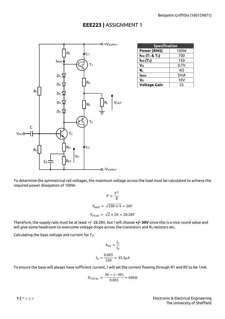
Benjamin Griffiths (160159871) 1 | Page Electronic & Electrical Engineering The University of Sheffield EEE223 | ASSIGNMENT 1 To determine the symmetrical rail voltages, the maximum voltage across the load must be calculated to achieve the required power dissipation of 100W. = 2 = √100 × 4 = 20 = √2 × 20 = 28.28 Therefore, the supply rails must be at least +/- 28.28V, but I will choose +/- 30V since this is a nice round value and will give some headroom to overcome voltage drops across the transistors and RS resistors etc. Calculating the base voltage and current for T3: ℎ = = 0.005 150 = 33.3 To ensure the base will always have sufficient current, I will set the current flowing through R1 and R2 to be 1mA. = 30 − (−30) 0.001 = 60Ω Specification Power (RMS) 100W hFE (T1 & T2) 700 hFE (T3) 150 Vd 0.7V RL 4Ω IBIAS 5mA VE 10V Voltage Gain 25 R1 R2 RS RS RL RE1 RE2 CE VIN VOUT T1 T2 T3 RC +VSUPPLY D1 D2 D3 D4 D5 -VSUPPLY VE IBIAS IC1 IC2 C
-
Upload
khangminh22 -
Category
Documents
-
view
0 -
download
0
Transcript of EEE223 | ASSIGNMENT 1
Benjamin Griffiths (160159871)
1 | P a g e Electronic & Electrical Engineering
The University of Sheffield
EEE223 | ASSIGNMENT 1
To determine the symmetrical rail voltages, the maximum voltage across the load must be calculated to achieve the
required power dissipation of 100W.
𝑃 = 𝑉2
𝑅
𝑉𝑅𝑀𝑆 = √100 × 4 = 20𝑉
𝑉𝑃𝐸𝐴𝐾 = √2 × 20 = 28.28𝑉
Therefore, the supply rails must be at least +/- 28.28V, but I will choose +/- 30V since this is a nice round value and
will give some headroom to overcome voltage drops across the transistors and RS resistors etc.
Calculating the base voltage and current for T3:
ℎ𝐹𝐸 =𝐼𝐶
𝐼𝐵
𝐼𝐵 =0.005
150= 33.3𝜇𝐴
To ensure the base will always have sufficient current, I will set the current flowing through R1 and R2 to be 1mA.
𝑅𝑇𝑂𝑇𝐴𝐿 = 30 − (−30)
0.001= 60𝑘Ω
Specification
Power (RMS) 100W
hFE (T1 & T2) 700
hFE (T3) 150
Vd 0.7V
RL 4Ω
IBIAS 5mA
VE 10V
Voltage Gain 25
R1
R2
RS
RS RL
RE1
RE2 CE
VIN
VOUT
T1
T2
T3
RC
+VSUPPLY
D1
D2
D3
D4
D5
-VSUPPLY
VE
IBIAS
IC1
IC2
C
Benjamin Griffiths (160159871)
2 | P a g e Electronic & Electrical Engineering
The University of Sheffield
From the specification, VE is 10V, hence the voltage at the base of T3 will be:
𝑉𝐵 = −30 + 10 + 0.7 = −19.3𝑉
Hence:
1𝑚𝐴 × 𝑅2 = 10.7𝑉
1𝑚𝐴 × 𝑅1 = 49.3𝑉
𝑅1 + 𝑅2 = 60𝑘Ω
Solving:
𝑅1 + (10.7
1𝑚𝐴) = 60𝑘Ω
(49.3
1𝑚𝐴) + 𝑅2 = 60𝑘Ω
𝑹𝟏 = 𝟒𝟗. 𝟑𝒌Ω
𝑹𝟐 = 𝟏𝟎. 𝟕𝒌Ω
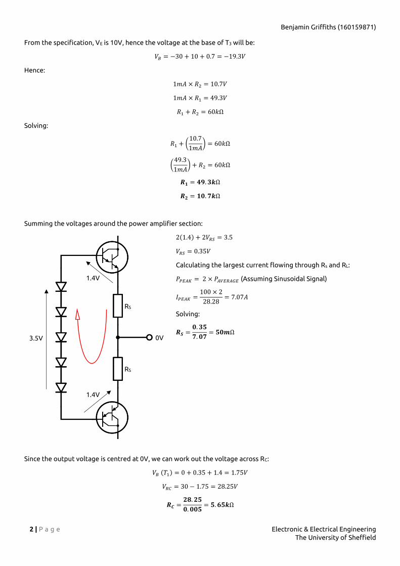
Summing the voltages around the power amplifier section:
2(1.4) + 2𝑉𝑅𝑆 = 3.5
𝑉𝑅𝑆 = 0.35𝑉
Calculating the largest current flowing through Rs and RL:
𝑃𝑃𝐸𝐴𝐾 = 2 × 𝑃𝐴𝑉𝐸𝑅𝐴𝐺𝐸 (Assuming Sinusoidal Signal)
𝐼𝑃𝐸𝐴𝐾 =100 × 2
28.28= 7.07𝐴
Solving:
𝑹𝑺 =𝟎. 𝟑𝟓
𝟕. 𝟎𝟕= 𝟓𝟎𝒎Ω
Since the output voltage is centred at 0V, we can work out the voltage across RC:
𝑉𝐵 (𝑇1) = 0 + 0.35 + 1.4 = 1.75𝑉
𝑉𝑅𝐶 = 30 − 1.75 = 28.25𝑉
𝑹𝑪 =𝟐𝟖. 𝟐𝟓
𝟎. 𝟎𝟎𝟓= 𝟓. 𝟔𝟓𝒌Ω
0V
1.4V
1.4V
RS
RS
3.5V
Benjamin Griffiths (160159871)
3 | P a g e Electronic & Electrical Engineering
The University of Sheffield
We know the current flowing through RE1 and RE2 is 5mA, and that there is a voltage of 10V across them.
10 = 0.005(𝑅𝐸1 + 𝑅𝐸2)
(𝑅𝐸1 + 𝑅𝐸2) = 2𝑘Ω
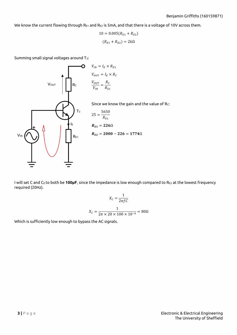
Summing small signal voltages around T3:
𝑉𝐼𝑁 = 𝐼𝐸 × 𝑅𝐸1
𝑉𝑂𝑈𝑇 = 𝐼𝐸 × 𝑅𝐶
𝑉𝑂𝑈𝑇
𝑉𝐼𝑁
=𝑅𝐶
𝑅𝐸1
Since we know the gain and the value of RC:
25 =5650
𝑅𝐸1
𝑹𝑬𝟏 = 𝟐𝟐𝟔Ω
𝑹𝑬𝟐 = 𝟐𝟎𝟎𝟎 − 𝟐𝟐𝟔 = 𝟏𝟕𝟕𝟒Ω
I will set C and CE to both be 100μF, since the impedance is low enough compared to RE2 at the lowest frequency
required (20Hz).
𝑋𝐶 =1
2𝜋𝑓𝐶
𝑋𝐶 =1
2𝜋 × 20 × 100 × 10−6= 80Ω
Which is sufficiently low enough to bypass the AC signals.
VIN RE1
RC
T3
IE
VOUT

Benjamin Griffiths (160159871)
4 | P a g e Electronic & Electrical Engineering
The University of Sheffield
Power dissipation in each component:
𝑃𝑇1 = 3.5 × (30 − 0.35) = 104𝑊
𝑃𝑇2 = 3.5 × (−30 − (−0.35)) = 104𝑊
𝑃𝑇3 = 0.005(1.75 − 3.5 − (−20)) = 0.09𝑊
𝑃𝐷 = 0.005 × 0.7 = 3.5𝑚𝑊
𝑃𝑅𝑆 = 7.07 × 0.35 = 2.5𝑊
𝑃𝑅𝐸1 = (0.005)2 × 226 = 5.65𝑚𝑊
𝑃𝑅𝐸2 = (0.005)2 × 1774 = 44.35𝑚𝑊
𝑃𝑅𝐶 = (0.005)2 × 5650 = 141.25𝑚𝑊
𝑃𝑅1 = (0.001)2 × 49.3𝑘 = 49.3𝑚𝑊
𝑃𝑅2 = (0.001)2 × 10.7𝑘 = 10.7𝑚𝑊
To calculate the thermal properties of the Darlington transistors, I have decided to use the TIP142 and TIP 147
from ON Semiconductor for the NPN and PNP Darlington transistors respectively. [1]
Both these transistors are capable of a constant Collector current (IC) of 10A, hence they are more than adequate
for the 7A needed to achieve the needed power in the load.
Furthermore, the total power dissipation is up to 125W, which gives some headroom above the average 104W
dissipation previously calculated.
From the specification, the Darlington transistors should not exceed a junction temperature of 100°C, and the
external heatsink should be limited to 50°C.
From the data sheet, the junction-to-case thermal resistance is 1.0°C/W, and we will assume a thermal washer of
RC-h = 0.35°C/W.
Using the equation shown below, we can calculate the maximum thermal resistance of the heatsink necessary to
achieve the 104W power dissipation:
𝑃𝐷 =𝑇𝑗(max)−𝑇𝑎
𝑅𝑗−𝑐 + 𝑅𝑐−ℎ + 𝑅ℎ−𝑎
Where Tj(max) is the max junction temperature, Ta is the ambient temperature, Rj-c is the junction-case thermal
resistance, Rc-h is the case-heatsink thermal resistance and Rh-a is the heatsink-air thermal resistance.
Re-arranging to find the maximum value of Rh-a:
104 =100 − 30
1 + 0.35 + 𝑅ℎ−𝑎
𝑹𝒉−𝒂 = −𝟎. 𝟔𝟕𝟕
The value obtained is impossible, hence it would not be appropriate to dissipate 104W through 1 transistor. The
solutions would be to run several Darlington transistors in parallel, say 5 for example, with a power dissipation of
20W each to share the load. For example, if using 5 of the TIP142/TIP147 transistors instead of 1:
20 =100 − 30
1 + 0.35 + 𝑅ℎ−𝑎
𝑹𝒉−𝒂 = 𝟐. 𝟏𝟓
Hence, for each transistor, a heatsink with a thermal resistance less than 2.15 will be sufficient. Realistically
however, the 5 transistors would all share a common large heatsink.
Average current
through transistor.
Benjamin Griffiths (160159871)
5 | P a g e Electronic & Electrical Engineering
The University of Sheffield
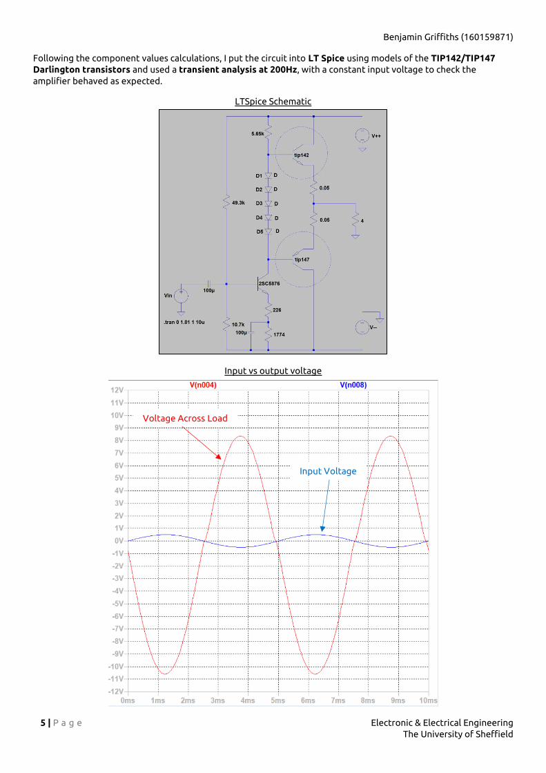
Following the component values calculations, I put the circuit into LT Spice using models of the TIP142/TIP147
Darlington transistors and used a transient analysis at 200Hz, with a constant input voltage to check the
amplifier behaved as expected.
Voltage Across Load
Input Voltage
LTSpice Schematic
Input vs output voltage

Benjamin Griffiths (160159871)
6 | P a g e Electronic & Electrical Engineering
The University of Sheffield
The current through each power section transistor can be seen in the graph below, where the current switches
from one transistor to the other at the 0A crossover point, but never actually reaches 0A. This mean the push-pull
power amplifier is successfully operating in Class A mode since the transistors are always or slightly on.
NPN Collector Current
PNP Collector Current
Current through each Darlington Transistor
Benjamin Griffiths (160159871)
7 | P a g e Electronic & Electrical Engineering
The University of Sheffield
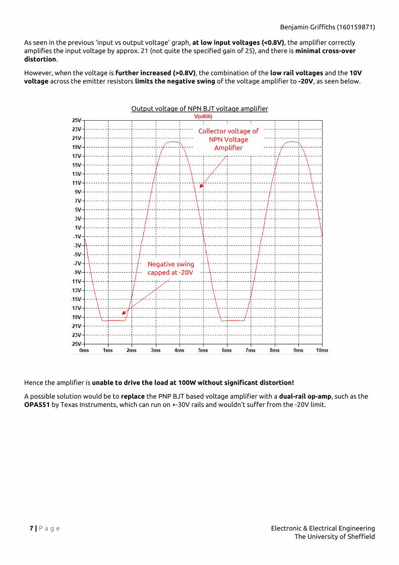
As seen in the previous ‘input vs output voltage’ graph, at low input voltages (<0.8V), the amplifier correctly
amplifies the input voltage by approx. 21 (not quite the specified gain of 25), and there is minimal cross-over
distortion.
However, when the voltage is further increased (>0.8V), the combination of the low rail voltages and the 10V
voltage across the emitter resistors limits the negative swing of the voltage amplifier to -20V, as seen below.
Hence the amplifier is unable to drive the load at 100W without significant distortion!
A possible solution would be to replace the PNP BJT based voltage amplifier with a dual-rail op-amp, such as the
OPA551 by Texas Instruments, which can run on +-30V rails and wouldn’t suffer from the -20V limit.
Negative swing
capped at -20V
Collector voltage of
NPN Voltage
Amplifier
Output voltage of NPN BJT voltage amplifier

Benjamin Griffiths (160159871)
8 | P a g e Electronic & Electrical Engineering
The University of Sheffield
Below is the new schematic for the circuit with a OPA551 op-amp as the voltage amplifier. The two 5.65kΩ
resistors provide the 5mA of quiescent current while making the base voltages of the NPN and PNP Darlington
transistors +1.75V and -1.75V respectively.
The two 100µF capacitors act to pass the input signal onto the bias of the transistors inputs (coupling
capacitors) so that each transistor can receive the signal at the necessary DC bias.
The result of these changes enables the output of the amplifier to reach the desired +-28V at 7A through the loud,
as shown in the figure below named ‘Input vs output voltage of op-amp’.
The downside is that high voltage op-amps are not the cheapest around.
New customised circuit schematic

Benjamin Griffiths (160159871)
9 | P a g e Electronic & Electrical Engineering
The University of Sheffield
NPN Collector Current
PNP Collector Current
Op-amp Output
Voltage
Input Voltage
Input vs output voltage of op-amp
Current through each Darlington Transistor

Benjamin Griffiths (160159871)
10 | P a g e Electronic & Electrical Engineering
The University of Sheffield
However, upon closer inspection, as shown in the diagram below, the current actually does reach 0A when the
Darlington transistors are not in use – hence not being a Class A amplifier.
To rectify this, I put an extra diode between the two Darlington transistors to bump up the voltage difference
between their bases, the result is shown below, where around 5-10mA of conduction is maintained, hence
operating in Class A.
Original crossover current
Crossover current with added diode
Never reaches 0A!
Benjamin Griffiths (160159871)
11 | P a g e Electronic & Electrical Engineering
The University of Sheffield
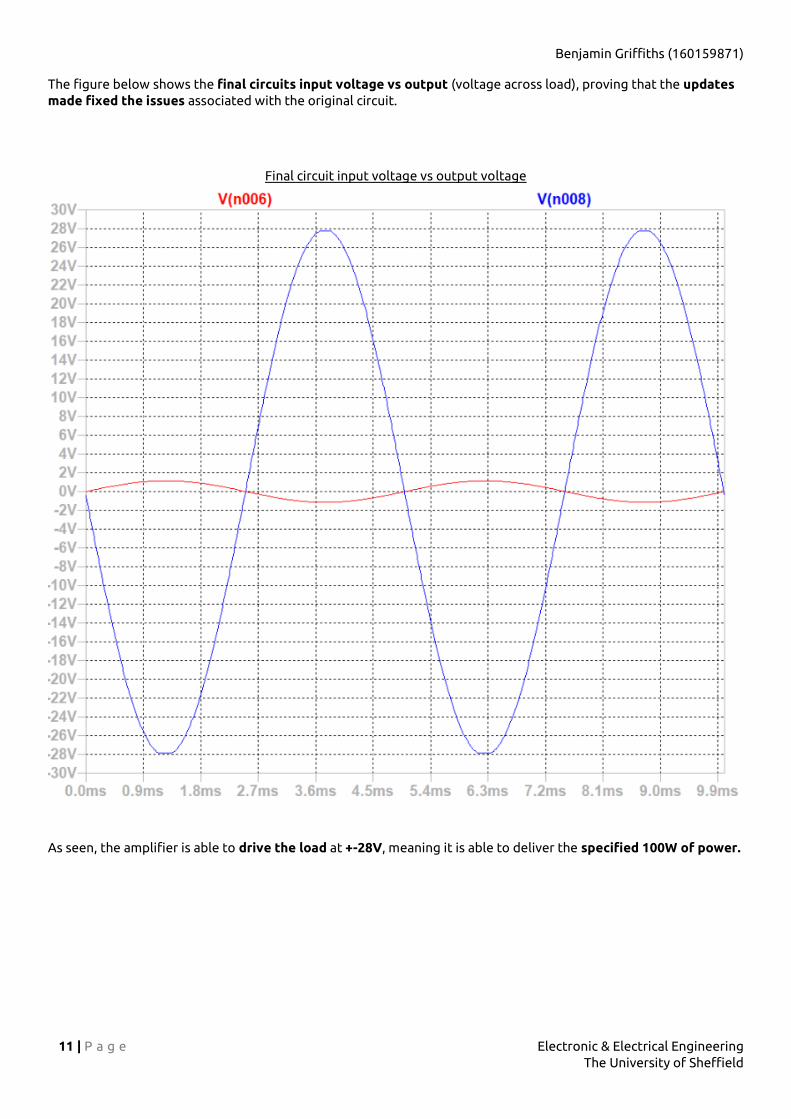
The figure below shows the final circuits input voltage vs output (voltage across load), proving that the updates
made fixed the issues associated with the original circuit.
As seen, the amplifier is able to drive the load at +-28V, meaning it is able to deliver the specified 100W of power.
Final circuit input voltage vs output voltage
Benjamin Griffiths (160159871)
12 | P a g e Electronic & Electrical Engineering
The University of Sheffield
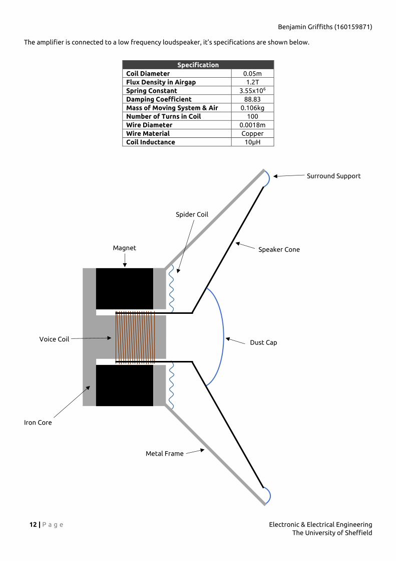
The amplifier is connected to a low frequency loudspeaker, it’s specifications are shown below.
Specification
Coil Diameter 0.05m
Flux Density in Airgap 1.2T
Spring Constant 3.55x10⁶
Damping Coefficient 88.83
Mass of Moving System & Air 0.106kg
Number of Turns in Coil 100
Wire Diameter 0.0018m
Wire Material Copper
Coil Inductance 10μH
Magnet Speaker Cone
Dust Cap
Surround Support
Spider Coil
Voice Coil
Metal Frame
Iron Core

Benjamin Griffiths (160159871)
13 | P a g e Electronic & Electrical Engineering
The University of Sheffield
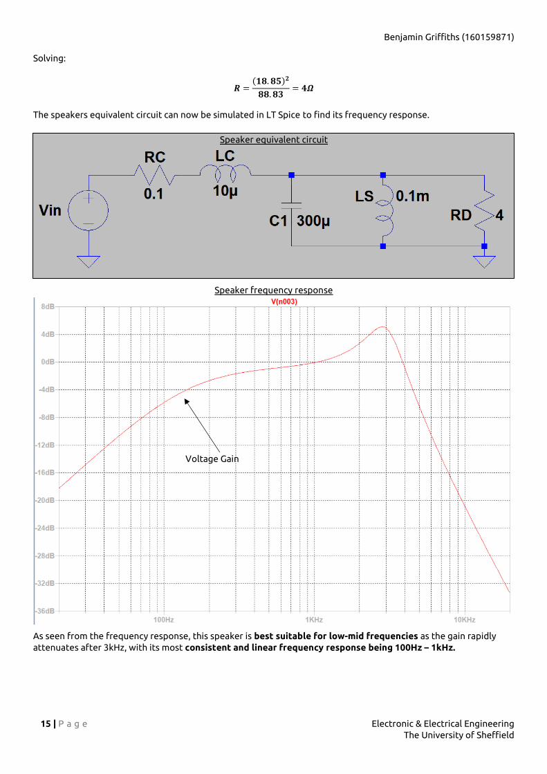
The equivalent circuit for the loudspeaker is shown below:
To calculate the coil resistance (RC), the physical resistance of the voice coil must be calculated:
𝑅 = 𝜌𝑙
𝐴
𝜌𝑐𝑜𝑝𝑝𝑒𝑟 ≈ 1.68 × 10⁻⁸Ω𝑚
𝑙 = 𝜋 × (0.05 + (0.0018
2)) × 100 = 15.99𝑚
𝐴 = 𝜋(0.0009)2 = 2.54 × 10⁻⁶𝑚2
𝑹𝑪 = 𝟏. 𝟔𝟖 × 𝟏𝟎−𝟖 × 𝟏𝟓. 𝟗𝟗
𝟏. 𝟗𝟔 × 𝟏𝟎−𝟑= 𝟎. 𝟏𝟎𝟓𝟔Ω
The coil inductance (LC), is given in the specification:
𝑳𝑪 = 𝟏𝟎𝝁𝑯
Next, the capacitance that represents the air mass (CA) can be calculated using the electrical equivalent of:
𝐼 =𝑀
𝐾𝑒2
∆𝐸
∆𝑡
Which is:
𝐼 = 𝐶∆𝑉
∆𝑡
Hence:
𝐶 =𝑀
𝐾𝑒2
Where the electromagnetic constant is given by:
𝐾𝑒 = 𝐵𝑁𝜋𝐷
𝐾𝑒 = 1.2 × 100 × 𝜋(0.05) = 18.85
Coil Resistance
RC
Coil Inductance
LC
Air Mass represented
by capacitor
CA
Spring compliance
represented by
inductor
LS
Mechanical loss
& damping
represented by
resistor
RD
Taking into account
the wires diameter

Benjamin Griffiths (160159871)
14 | P a g e Electronic & Electrical Engineering
The University of Sheffield
Solving:
𝑪 = 𝟎. 𝟏𝟎𝟔
𝟏𝟖. 𝟖𝟓𝟐= 𝟐𝟗𝟖. 𝟑𝝁𝑭
The spring compliance, represented by the inductor (LS) is given by:
𝐹 = 𝜎𝑠𝑥
Which can be manipulated to give:
𝐸 =𝐾𝑒
2
𝜎𝑠
∆𝐼
∆𝑡
Where an electrical equivalent can be given by:
𝑉 = 𝐿∆𝐼
∆𝑡
Hence:
𝐿 =𝐾𝑒
2
𝜎𝑠
Where the spring compliance is given in the specification:
𝜎𝑠 = 3.55 × 10⁻⁶
Solving:
𝑳𝑺 =(𝟏𝟖. 𝟖𝟓)𝟐
𝟑. 𝟓𝟓 × 𝟏𝟎𝟔= 𝟎. 𝟏𝒎𝑯
Lastly the mechanical loss and dampening, represented by the resistor (RD), is given by:
𝐹 = 𝐾𝑑𝑣
Which can be manipulated to give:
𝐸 = 𝐼𝐾𝑒
2
𝐾𝑑
Where an electrical equivalent can be given by:
𝑉 = 𝐼𝑅
Hence:
𝑅 =𝐾𝑒
2
𝐾𝑑
Where the damping coefficient is given in the specification:
𝐾𝑑 = 88.83
Benjamin Griffiths (160159871)
15 | P a g e Electronic & Electrical Engineering
The University of Sheffield
Solving:
𝑹 =(𝟏𝟖. 𝟖𝟓)𝟐
𝟖𝟖. 𝟖𝟑= 𝟒𝜴
The speakers equivalent circuit can now be simulated in LT Spice to find its frequency response.
As seen from the frequency response, this speaker is best suitable for low-mid frequencies as the gain rapidly
attenuates after 3kHz, with its most consistent and linear frequency response being 100Hz – 1kHz.
Voltage Gain
Speaker equivalent circuit
Speaker frequency response

Benjamin Griffiths (160159871)
16 | P a g e Electronic & Electrical Engineering
The University of Sheffield
References
[1] TIP142 & TIP147 Data sheet: [Online]. Available: https://www.onsemi.com/pub/Collateral/TIP140-D.PDF
[2] OPA551 Data sheet: [Online]. Available: http://www.ti.com/lit/ds/symlink/opa551.pdf