DVD Home Theater Sound System - Planetatecnico
107
lGENERAL Power Supply: AC 110 to 240 V, 50/60 Hz Power Consumption: Main unit 105 W Power Consumption in Standby Mode: approx. 1 W Dimensions (W×H×D): 430×60×342 mm Mass: Main unit 3 kg Operating Temperature Range: +5°C to +35°C Operating Humidity Range: 5% to 90% RH (no condensation) lAMPLIFIER SECTION RMS Output Power: Dolby Digital Mode lTotal RMS Dolby Digital mode power: 330 W At 1 kHz and total harmonic of 10% lFront Ch: 55 W / Channel (5 Ω) lCenter Ch: 55 W / Channel (5 Ω) lSurround Ch: 55 W / Channel (5 Ω) At 100 Hz and total harmonic of 10% lSubwoofer Ch: 55 W / Channel (5 Ω) PMPO Output Power: 2800 W DIN Output Power: Dolby Digital Mode: lTotal DIN Dolby Digital mode power: 150 W At 1 kHz and total harmonic of 1% © 2007 Matsushita Electric Industrial Co., Ltd. All rights reserved. Unauthorized copying and distribution is a violation of law. SA-PT150GC SA-PT150GCP SA-PT150GCS SA-PT150GCT SA-PT150GS Colour (S).......................Silver Type lFront Ch: 25 W / Channel (5 Ω) lCenter Ch: 25 W / Channel (5 Ω) lSurround Ch: 25 W / Channel (5 Ω) At 100 Hz and total harmonic of 1% lSubwoofer Ch: 25 W / Channel (5 Ω) lFM TUNER, TERMINALS SECTION Preset Memory: FM 30 stations Frequency Modulation (FM) Frequency range: 87.50-108.00 MHz (50-kHz step) Sensitivity: 1.8 μV (IHF) S/N 26 dB: 1.4 μV Antenna terminals: 75 Ω (unbalanced) Mic Jack: Sensitivity: 0.7 mV (1.2 kΩ) Terminal: Mono, 6.3 mm jack (1 system) lUSB SECTION USB Port: USB standard: USB 2.0 full speed Media file format support: MP3 (*.mp3) WMA (*.wma) JPEG (*.Jpg, *.JPEG) MPEG4 (*.asf) DVD Home Theater Sound System Specifications ORDER NO. MD0705010CE
-
Upload
khangminh22 -
Category
Documents
-
view
5 -
download
0
Transcript of DVD Home Theater Sound System - Planetatecnico

lGENERALPower Supply: AC 110 to 240 V, 50/60 Hz
Power Consumption: Main unit 105 W
Power Consumption in Standby Mode:approx. 1 W
Dimensions (W×H×D): 430×60×342 mm
Mass: Main unit 3 kg
Operating Temperature Range: +5°C to +35°C
Operating Humidity Range: 5% to 90% RH (nocondensation)
lAMPLIFIER SECTIONRMS Output Power: Dolby Digital Mode
lTotal RMS Dolby Digital mode power:330 W
At 1 kHz and total harmonic of 10%lFront Ch: 55 W / Channel (5 Ω)
lCenter Ch: 55 W / Channel (5 Ω)
lSurround Ch: 55 W / Channel (5 Ω)
At 100 Hz and total harmonic of 10%lSubwoofer Ch: 55 W / Channel (5 Ω)
PMPO Output Power: 2800 W
DIN Output Power: Dolby Digital Mode:lTotal DIN Dolby Digital mode power:
150 W
At 1 kHz and total harmonic of 1%
© 2007 Matsushita Electric Industrial Co., Ltd. Allrights reserved. Unauthorized copying anddistribution is a violation of law.
SA-PT150GCSA-PT150GCPSA-PT150GCSSA-PT150GCTSA-PT150GSColour(S).......................Silver Type
lFront Ch: 25 W / Channel (5 Ω)
lCenter Ch: 25 W / Channel (5 Ω)
lSurround Ch: 25 W / Channel (5 Ω)
At 100 Hz and total harmonic of 1%lSubwoofer Ch: 25 W / Channel (5 Ω)
lFM TUNER, TERMINALS SECTIONPreset Memory: FM 30 stations
Frequency Modulation (FM)Frequency range: 87.50-108.00 MHz
(50-kHz step)
Sensitivity: 1.8 µV (IHF)
S/N 26 dB: 1.4 µV
Antenna terminals: 75 Ω (unbalanced)
Mic Jack:Sensitivity: 0.7 mV (1.2 kΩ)
Terminal: Mono, 6.3 mm jack (1 system)
lUSB SECTIONUSB Port:
USB standard: USB 2.0 full speed
Media file format support: MP3 (*.mp3)
WMA (*.wma)
JPEG (*.Jpg, *.JPEG)
MPEG4 (*.asf)
DVD Home Theater Sound System
Specifications
ORDER NO. MD0705010CE

USB device file system: FAT12FAT16FAT32
USB Port power: 500 mA (Max)
lDISC SECTIONDiscs played (8 cm or 12 cm):
(1) DVD [DVD-Video, DivX (*1, *2)]
(2) DVD-RAM [DVD-VR, MP3 (*2, *6), JPEG (*2, *3), MPEG4(*2, *4), DivX (*1, *2)]
(3) DVD-R [DVD-Video, DVD-VR, MP3 (*2, *6), JPEG (*2, *3),MPEG4 (*2, *4), DivX (*1, *2)]
(4) DVD-R DL [DVD-Video, DVD-VR]
(5) DVD-RW [DVD-Video, DVD-VR, MP3 (*2, *6), JPEG (*2, *3),MPEG4 (*2, *4), DivX (*1, *2)]
(6) +R/+RW [Video]
(7) +R DL [Video]
(8) CD, CD-R/RW [CD-DA, Video CD, SVCD (*5), MP3 (*2, *6),WMA (*2, *7), JPEG (*2, *3), MPEG4 (*2, *4), DivX (*1, *2)]
*1 Plays all versions of DivX® video (including DivX®6) withstandard playback of DivX® media files. Certified to the DivXHome Theater Profile.
*2 The total combined maximum number of recognizable audio,picture and video contents and groups: 4000 audio, pictureand video contents and 400 groups.
*3 Exif Ver 2.1 JPEG Baseline files
lPicture resolution: between 160 x 120 and 6144 x 4096pixels (Sub sampling is 4:0:0, 4:2:0, 4:2:2, or 4:4:4).Extremely long and narrow pictures may not be displayed.
*4 MPEG4 data recorded with the Panasonic SD multi camerasor DVD video recorders.
lConforming to SD VIDEO specifications (ASF standard)/MPEG4 (Simple Profile) video system/G.726 audio system.
*5 Conforming to IEC62107
*6 MPEG-1 Layer 3, MPEG-2 Layer 3
*7 Windows Media Audio Ver.9.0 L3
lNot compatible with Multiple Bit Rate (MBR)
Pick Up:Wavelength:
lCD: 785 nm
lDVD: 662 nm
Laser power:lCD: CLASS 1M
lDVD: CLASS 1
Audio Output (Disc):Number of channels: 5.1 ch (FL, FR, C, SL, SR,
SW)
lVIDEO SECTIONVideo system:(GC/GCS/GCT/GS)
PAL 625/50, PAL 525/60,NTSC
Video system: (GCP) NTSC
Composite Video Output:lOutput level: 1 Vp-p (75 Ω)
lTerminal: Pin jack (1 system)
Component video output: [NTSC: 480p/480i, PAL:576p/576i]lY output level: 1 Vp-p (75 Ω)
lPB output level: 0.7 Vp-p (75 Ω)
lPR output level: 0.7 Vp-p (75 Ω)
lTerminal: Pin jack (Y: green, PB: blue,PR: red) (1 system)
Note:1. Specifications are subject to change without notice.
Mass and dimensions are approximate.
2. Total harmonic distortion is measured by the digital spectrumanalyzer.
Solder:This model uses lead free solder (PbF).
Mechanism:This model uses DL2S (Single tray) mechanism.
Power Supply:This unit uses Switching Mode Power Supply (SMPS).
Refer to their respective original service manuals for *1, *2,*3, *4.
2
SA-PT150GC / SA-PT150GCP / SA-PT150GCS / SA-PT150GCT / SA-PT150GS
1 Safety Precautions 5 1.1. GENERAL GUIDELINES 5
1.2. Before Repair and Adjustment (Using SMPS Module
P.C.B.) 5
1.3. Protection Circuitry 5
CONTENTS Page Page
3
SA-PT150GC / SA-PT150GCP / SA-PT150GCS / SA-PT150GCT / SA-PT150GS

1.4. Safety Parts Information 6
1.5. Caution for AC Cord 7
2 Prevention of Electro Static Discharge (ESD) toElectrostatically Sensitive (ES) Devices 8
3 Precaution of Laser Diode 9 4 About Lead Free Solder (PbF) 10
4.1. Service caution based on legal restrictions 10
5 Handling Precautions for Traverse Unit 11 5.1. Cautions to Be Taken in Handling the Optical Pickup Unit
11
5.2. Grounding for electrostatic breakdown prevention 11
6 Accessories 13 7 Operation Procedures 14
7.1. Remote Control Key Buttons Operations 14
7.2. Main Unit Key Buttons Operations 15
7.3. About DivX VOD Content 16
7.4. USB Connection and Operation 17
7.5. Audio and Video Connections 18
7.6. Disc Information 20
8 Self-Diagnosis and Special Mode Setting 22 8.1. Service Mode Summary Table 22
8.2. Service Mode Table 22
8.3. DVD Self Diagnostic Function-Error Code 30
8.4. Sales Demonstration Lock Function 33
8.5. Service Precautions 34
9 Assembling and Disassembling 35 9.1. Disassembly Flow Chart 36
9.2. Main Components and P.C.B. Locations 37
9.3. Disassembly of Top Cabinet 38
9.4. Disassembly of the DVD Lid (When taking out disc
manually) 38
9.5. Disassembly of Front Panel 39
9.6. Disassembly of Volume P.C.B. 39
9.7. Disassembly of Panel P.C.B. 40
9.8. Disassembly of Mic P.C.B. 40
9.9. Disassembly of USB P.C.B. 40
9.10. Disassembly of Rear panel 41
9.11. Disassembly of DVD Mechanism Unit 41
9.12. Disassembly of DVD Module P.C.B. 41
9.13. Disassembly of USB Relay P.C.B. 42
9.14. Disassembly of Main P.C.B. & Tuner Extent P.C.B. 42
9.15. Replacement of Digital Amp IC (IC5100) 43
9.16. Replacement of Regulator IC (IC2903) 43
9.17. Disassembly of SMPS Module P.C.B. 44
10 Assembly and Disassembly of DVD Mechanism Unit 45 10.1. Disassembly Procedure 45
11 Service Position 50 11.1. Checking & Repairing Panel P.C.B. 50
11.2. Checking & Repairing Mic P.C.B. 50
11.3. Checking & Repairing Main P.C.B. 50
11.4. Checking & Repairing SMPS Module P.C.B. 51
11.5. Checking & Repairing DVD Module P.C.B. 51
12 Measurements and Adjustments 52 12.1. Service Tools and Equipment 52
12.2. Important points in adjustment 52
12.3. Storing and handling of test discs 52
12.4. Optical adjustment 53
13 Abbreviations 54 14 Voltage and Waveform Chart 56
14.1. DVD Module P.C.B. 56
14.2. Main P.C.B. 58
14.3. Panel P.C.B. 59
14.4. Tray Loading & SMPS Module P.C.B. 59
14.5. Waveform Chart 60
15 Illustration of IC's, Transistors and Diodes 62 16 Wiring Connection Diagram 63 17 Block Diagram 65
17.1. System Control 65
17.2. DVD (Servo) 66
17.3. DVD (Audio) 67
17.4. DVD (Video) 68
17.5. Audio 69
17.6. Amp & Power 70
18 Schematic Diagram Notes 71 19 Schematic Diagram 73
19.1. DVD Module Circuit 73
19.2. Main Circuit 77
19.3. Tuner Extent, Panel & Volume Circuit 81
19.4. Mic, USB Relay, USB, Tray Loading & Optical Pickup Unit
Circuit 82
20 Printed Circuit Board 85 20.1. DVD Module P.C.B. 85
20.2. Main P.C.B. 86
20.3. Panel, Volume & Tuner Extent P.C.B. 87
20.4. Mic, USB, USB Relay & Tray Loading P.C.B. 88
21 Basic Troubleshooting Guide 89 21.1. Basic Troubleshooting Guide for Traverse Unit (DVD
Module P.C.B) 89
21.2. Basic Troubleshooting Guide for SMPS/MAIN/PANEL 90
22 Overall Block Diagram for PT150 91 22.1. SC-PT150 Simplified Block 91
23 Terminal Function of ICs 92 23.1. IC2018 (C2CBYY000438): System Control IC 92
24 Exploded Views 93 24.1. Cabinet Parts Location 95
24.2. Packaging 97
25 Replacement Parts List 98 25.1. Component Parts List 99
4
SA-PT150GC / SA-PT150GCP / SA-PT150GCS / SA-PT150GCT / SA-PT150GS
1 Safety Precautions1.1. GENERAL GUIDELINES 1. When servicing, observe the original lead dress. If a short circuit is found, replace all parts which have been overheated or
damaged by the short circuit. 2. After servicing, see to it that all the protective devices such as insulation barriers, insulation papers shields are properly
installed. 3. After servicing, carry out the following leakage current checks to prevent the customer from being exposed to shock hazards.
1.1.1. LEAKAGE CURRENT COLD CHECK 1. Unplug the AC cord and connect a jumper between the two prongs on the plug. 2. Measure the resistance value, with an ohmmeter, between the jumpered AC plug and each exposed metallic cabinet part on
the equipment such as screwheads, connectors, control shafts, etc. When the exposed metallic part has a return path to thechassis, the reading should be between 1MΩ and 5.2MΩ.When the exposed metal does not have a return path to the chassis, the reading must be
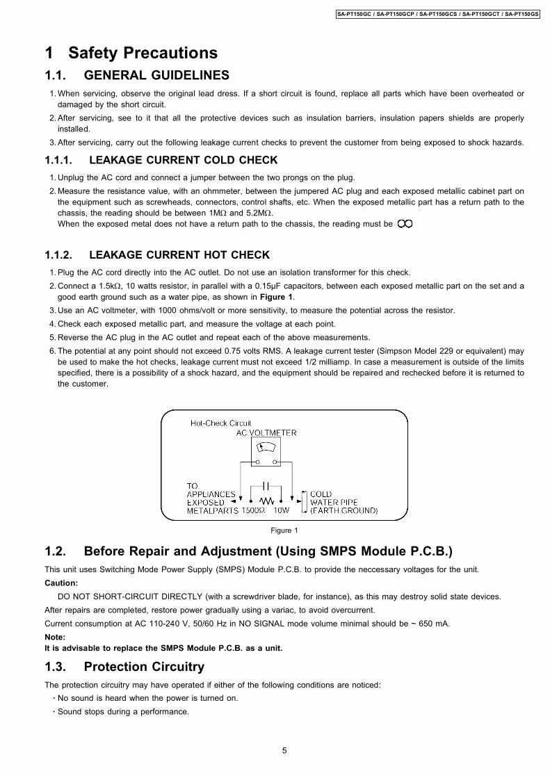
1.1.2. LEAKAGE CURRENT HOT CHECK 1. Plug the AC cord directly into the AC outlet. Do not use an isolation transformer for this check. 2. Connect a 1.5kΩ, 10 watts resistor, in parallel with a 0.15µF capacitors, between each exposed metallic part on the set and a
good earth ground such as a water pipe, as shown in Figure 1. 3. Use an AC voltmeter, with 1000 ohms/volt or more sensitivity, to measure the potential across the resistor. 4. Check each exposed metallic part, and measure the voltage at each point. 5. Reverse the AC plug in the AC outlet and repeat each of the above measurements. 6. The potential at any point should not exceed 0.75 volts RMS. A leakage current tester (Simpson Model 229 or equivalent) may
be used to make the hot checks, leakage current must not exceed 1/2 milliamp. In case a measurement is outside of the limitsspecified, there is a possibility of a shock hazard, and the equipment should be repaired and rechecked before it is returned tothe customer.
Figure 1
1.2. Before Repair and Adjustment (Using SMPS Module P.C.B.)This unit uses Switching Mode Power Supply (SMPS) Module P.C.B. to provide the neccessary voltages for the unit.Caution:
DO NOT SHORT-CIRCUIT DIRECTLY (with a screwdriver blade, for instance), as this may destroy solid state devices.After repairs are completed, restore power gradually using a variac, to avoid overcurrent.Current consumption at AC 110-240 V, 50/60 Hz in NO SIGNAL mode volume minimal should be ~ 650 mA.Note:It is advisable to replace the SMPS Module P.C.B. as a unit.
1.3. Protection CircuitryThe protection circuitry may have operated if either of the following conditions are noticed: · No sound is heard when the power is turned on. · Sound stops during a performance.
5
SA-PT150GC / SA-PT150GCP / SA-PT150GCS / SA-PT150GCT / SA-PT150GS
The function of this circuitry is to prevent circuitry damage if, for example, the positive and negative speaker connection wires are“shorted”, or if speaker systems with an impedance less than the indicated rated impedance of the amplifier are used.If this occurs, follow the procedure outlines below: 1. Turn off the power. 2. Determine the cause of the problem and correct it. 3. Turn on the power once again after one minute.Note:When the protection circuitry functions, the unit will not operate unless the power is first turned off and then on again.
1.4. Safety Parts InformationSafety Parts List:
There are special components used in this equipment which are important for safety.These parts are marked by in the Schematic Diagrams & Replacement Parts List. It is essential that these critical partsshould be replaced with manufacturer’s specified parts to prevent shock, fire or other hazards. Do not modify the original designwithout permission of manufacturer.
Table 1Reference No. Part No. Part Name & Description Remarks
340 RAE2023Z-S TRAVERSE UNIT [M]A2 K2CQ2CA00002 AC CORD [M] GCTA2 K2CQ2CA00007 AC CORD [M] GC/GCP/GCSA2 K2CT3CA00004 AC CORD [M] GS
· SMPS Module P.C.B.:Table 2
Reference No. Part No. Part Name & Description Remarks40 N0AZ6GE00006 SMPS MODULE [M] (RTL)F1 K5D502BNA005 FUSE [M]
6
SA-PT150GC / SA-PT150GCP / SA-PT150GCS / SA-PT150GCT / SA-PT150GS
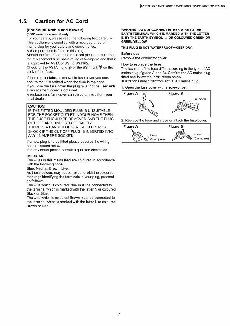
1.5. Caution for AC Cord(For Saudi Arabia and Kuwait)("GS" area code model only)For your safety, please read the following text carefully.This appliance is supplied with a moulded three pin mains plug for your safety and convenience.A 5-ampere fuse is fitted in this plug.Should the fuse need to be replaced please ensure that the replacement fuse has a rating of 5-ampere and that it is approved by ASTA or BSI to BS1362.Check for the ASTA mark or the BSI mark on the body of the fuse.
If the plug contains a removable fuse cover you must ensure that it is refitted when the fuse is replaced.If you lose the fuse cover the plug must not be used until a replacement cover is obtained.A replacement fuse cover can be purchased from your local dealer.
If a new plug is to be fitted please observe the wiring code as stated below.If in any doubt please consult a qualified electrician.
IMPORTANTThe wires in this mains lead are coloured in accordance with the following code:Blue: Neutral, Brown: Live.As these colours may not correspond with the coloured markings identifying the terminals in your plug, proceed as follows:The wire which is coloured Blue must be connected to the terminal which is marked with the letter N or coloured Black or Blue.The wire which is coloured Brown must be connected to the terminal which is marked with the letter L or coloured Brown or Red.
Before useRemove the connector cover.
How to replace the fuseThe location of the fuse differ according to the type of AC mains plug (figures A and B). Confirm the AC mains plug fitted and follow the instructions below.Illustrations may differ from actual AC mains plug.
1. Open the fuse cover with a screwdriver.
2. Replace the fuse and close or attach the fuse cover.
CAUTION!IF THE FITTED MOULDED PLUG IS UNSUITABLE FOR THE SOCKET OUTLET IN YOUR HOME THEN THE FUSE SHOULD BE REMOVED AND THE PLUG CUT OFF AND DISPOSED OF SAFELY.THERE IS A DANGER OF SEVERE ELECTRICAL SHOCK IF THE CUT OFF PLUG IS INSERTED INTO ANY 13-AMPERE SOCKET.
Figure A Figure B
Fuse cover
Figure A Figure B
Fuse(5 ampere)
Fuse(5 ampere)
WARNING: DO NOT CONNECT EITHER WIRE TO THE EARTH TERMINAL WHICH IS MARKED WITH THE LETTER E, BY THE EARTH SYMBOL OR COLOURED GREEN OR GREEN/YELLOW.
THIS PLUG IS NOT WATERPROOF KEEP DRY.
A A
7
SA-PT150GC / SA-PT150GCP / SA-PT150GCS / SA-PT150GCT / SA-PT150GS

2 Prevention of Electro Static Discharge (ESD) toElectrostatically Sensitive (ES) Devices
Some semiconductor (solid state) devices can be damaged easily by static electricity. Such components commonly are calledElectrostatically Sensitive (ES) Devices. Examples of typical ES devices are integrated circuits and some field-effect transistors andsemiconductor "chip" components. The following techniques should be used to help reduce the incidence of component damagecaused by electro static discharge (ESD). 1. Immediately before handling any semiconductor component or semiconductor-equipped assembly, drain off any ESD on your
body by touching a known earth ground. Alternatively, obtain and wear a commercially available discharging ESD wrist strap,which should be removed for potential shock reasons prior to applying power to the unit under test.
2. After removing an electrical assembly equipped with ES devices, place the assembly on a conductive surface such asaluminum foil, to prevent electrostatic charge buildup or exposure of the assembly.
3. Use only a grounded-tip soldering iron to solder or unsolder ES devices. 4. Use only an anti-static solder removal device. Some solder removal devices not classified as "anti-static (ESD protected)" can
generate electrical charge sufficient to damage ES devices. 5. Do not use freon-propelled chemicals. These can generate electrical charges sufficient to damage ES devices. 6. Do not remove a replacement ES device from its protective package until immediately before you are ready to install it. (Most
replacement ES devices are packaged with leads electrically shorted together by conductive foam, aluminum foil or comparableconductive material).
7. Immediately before removing the protective material from the leads of a replacement ES device, touch the protective materialto the chassis or circuit assembly into which the device will be installed.Caution:
Be sure no power is applied to the chassis or circuit, and observe all other safety precautions. 8. Minimize bodily motions when handling unpackaged replacement ES devices. (Otherwise harmless motion such as the
brushing together of your clothes fabric or the lifting of your foot from a carpeted floor can generate static electricity (ESD)sufficient to damage an ES device).
8
SA-PT150GC / SA-PT150GCP / SA-PT150GCS / SA-PT150GCT / SA-PT150GS

3 Precaution of Laser Diode
CAUTION :This product utilizes a laser diode with the unit turned on, invisible laser radiation is emitted from the pickup lens.Wavelength : 662nm/785nmMaximum output radiation power from pickup : 100µW/VDELaser radiation from pickup unit is safety level, but be sure the followings: 1. Do not disassemble the pickup unit, since radiation from exposed laser diode is dangerous. 2. Do not adjust the variable resistor on the pickup unit. It was already adjusted. 3. Do not look at the focus lens using optical instruments. 4. Recommend not to look at pickup lens for a long time.
9
SA-PT150GC / SA-PT150GCP / SA-PT150GCS / SA-PT150GCT / SA-PT150GS

4 About Lead Free Solder (PbF)4.1. Service caution based on legal restrictions4.1.1. General description about Lead Free Solder (PbF)The lead free solder has been used in the mounting process of all electrical components on the printed circuit boards used for thisequipment in considering the globally environmental conservation.
The normal solder is the alloy of tin (Sn) and lead (Pb). On the other hand, the lead free solder is the alloy mainly consists of tin(Sn), silver (Ag) and Copper (Cu), and the melting point of the lead free solder is higher approx.30 degrees C (86°F) more than thatof the normal solder.
Definition of PCB Lead Free Solder being usedThe letter of “PbF” is printed either foil side or components side on the PCB using the lead free solder.(See right figure)
Service caution for repair work using Lead Free Solder (PbF) · The lead free solder has to be used when repairing the equipment for which the lead free solder is used.
(Definition: The letter of “PbF” is printed on the PCB using the lead free solder.) · To put lead free solder, it should be well molten and mixed with the original lead free solder. · Remove the remaining lead free solder on the PCB cleanly for soldering of the new IC. · Since the melting point of the lead free solder is higher than that of the normal lead solder, it takes the longer time to melt
the lead free solder. · Use the soldering iron (more than 70W) equipped with the temperature control after setting the temperature at 350±30
degrees C (662±86°F).Recommended Lead Free Solder (Service Parts Route.)
· The following 3 types of lead free solder are available through the service parts route.
RFKZ03D01K-----------(0.3mm 100g Reel)RFKZ06D01K-----------(0.6mm 100g Reel)RFKZ10D01K-----------(1.0mm 100g Reel)
Note* Ingredient: tin (Sn), 96.5%, silver (Ag) 3.0%, Copper (Cu) 0.5%, Cobalt (Co) / Germanium (Ge) 0.1 to 0.3%
10
SA-PT150GC / SA-PT150GCP / SA-PT150GCS / SA-PT150GCT / SA-PT150GS

5 Handling Precautions for Traverse UnitThe laser diode in the optical pickup unit may break down due to static electricity of clothes or human body. Special care must betaken avoid caution to electrostatic breakdown when servicing and handling the laser diode.
5.1. Cautions to Be Taken in Handling the Optical Pickup UnitThe laser diode in the optical pickup unit may be damaged due to electrostatic discharge generating from clothes or human body.Special care must be taken avoid caution to electrostatic discharge damage when servicing the laser diode. 1. Do not give a considerable shock to the optical pickup unit as it has an extremely high-precise structure. 2. To prevent the laser diode from the electrostatic discharge damage, the flexible cable of the optical pickup unit removed should
be short-circuited with a short pin or a clip. 3. The flexible cable may be cut off if an excessive force is applied to it. Use caution when handling the flexible cable. 4. The antistatic FPC is connected to the new optical pickup unit. After replacing the optical pickup unit and connecting the flexible
cable, cut off the antistatic FPC.
5.2. Grounding for electrostatic breakdown preventionSome devices such as the DVD player use the optical pickup (laser diode) and the optical pickup will be damaged by staticelectricity in the working environment. Proceed servicing works under the working environment where grounding works iscompleted.
5.2.1. Worktable grounding 1. Put a conductive material (sheet) or iron sheet on the area where the optical pickup is placed, and ground the sheet.
5.2.2. Human body grounding 1. Use the anti-static wrist strap to discharge the static electricity form your body.
11
SA-PT150GC / SA-PT150GCP / SA-PT150GCS / SA-PT150GCT / SA-PT150GS

12
SA-PT150GC / SA-PT150GCP / SA-PT150GCS / SA-PT150GCT / SA-PT150GS
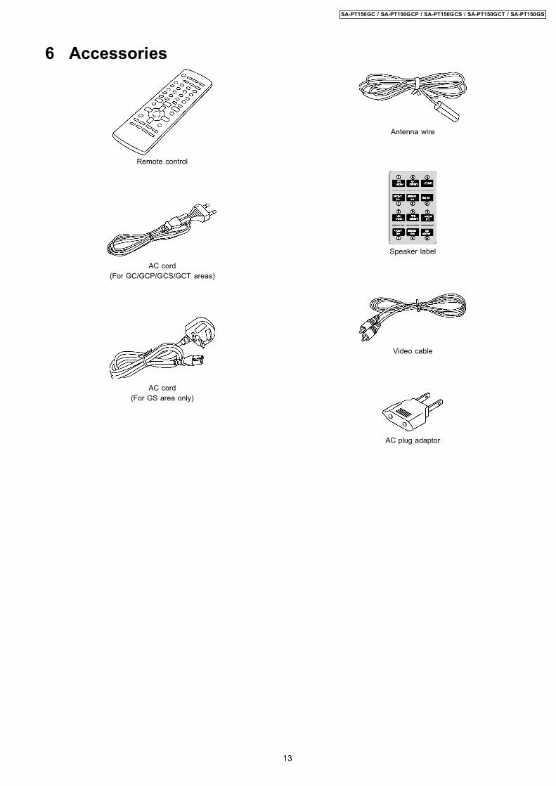
Remote control
AC cord(For GC/GCP/GCS/GCT areas)
AC cord(For GS area only)
Antenna wire
Speaker label
Video cable
AC plug adaptor
6 Accessories
13
SA-PT150GC / SA-PT150GCP / SA-PT150GCS / SA-PT150GCT / SA-PT150GS

7 Operation Procedures7.1. Remote Control Key Buttons Operations
Adjust the television volume
Select the sourceDVD: DVD/CD FM EXT-IN: AUX, USB
Show the current disc’s playback condition
Adjust the volume of the main unit
Basic operations for play
Show a disc menu or play list
Select or confirm menu items on the television screen, Frame-by-frame
Return to previous screen,Show the Setup menu
To mute the soundTo cancel
Press [MUTING] again or adjust the volume.Muting is cancelled when you switch the unit to standby.
Television operations
Switch the main unit on or off
Change the television’s videoinput mode
Select disc’s title numbers and etc., Enter numbers
Select preset radio stations
Show a disc top menuor program list
Show on-screen menu
Show the display on themain unit
Set the sleep timerThis function enables you to turn
off the unit automatically after theset time.
SLEEP 30 SLEEP 60OFF SLEEP 120 SLEEP 90
To cancel the timerPress and hold [ SLEEP] to select
"OFF".
To confirm the remaining timePress and hold [ SLEEP] again.
Karaoke
14
SA-PT150GC / SA-PT150GCP / SA-PT150GCS / SA-PT150GCT / SA-PT150GS
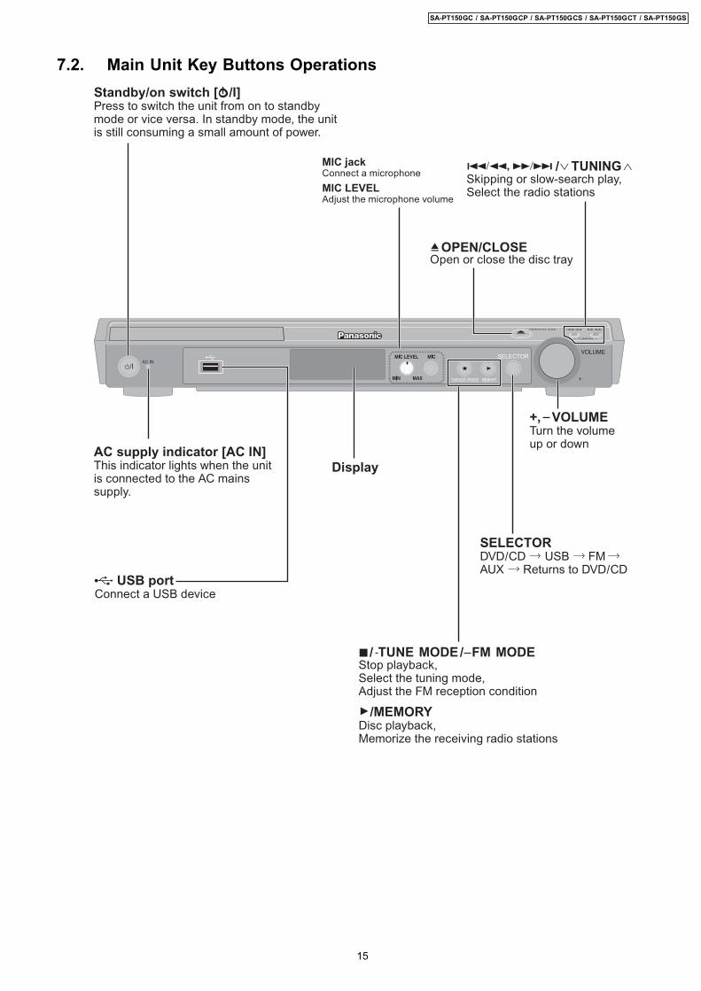
7.2. Main Unit Key Buttons Operations
AC supply indicator [AC IN]This indicator lights when the unit is connected to the AC mains supply.
Open or close the disc tray
Display
Stop playback, Select the tuning mode,Adjust the FM reception condition
Disc playback,Memorize the receiving radio stations
Turn the volume up or down
Skipping or slow-search play, Select the radio stations
Press to switch the unit from on to standby mode or vice versa. In standby mode, the unit is still consuming a small amount of power.
SELECTORDVD/CD USB FM AUX Returns to DVD/CD
USB portConnect a USB device
Standby/on switch [ /I]
OPEN/CLOSE
/ TUNING
+, VOLUME
/ TUNE MODE / FM MODE
/MEMORY
MIC jackConnect a microphone
MIC LEVELAdjust the microphone volume
15
SA-PT150GC / SA-PT150GCP / SA-PT150GCS / SA-PT150GCT / SA-PT150GS
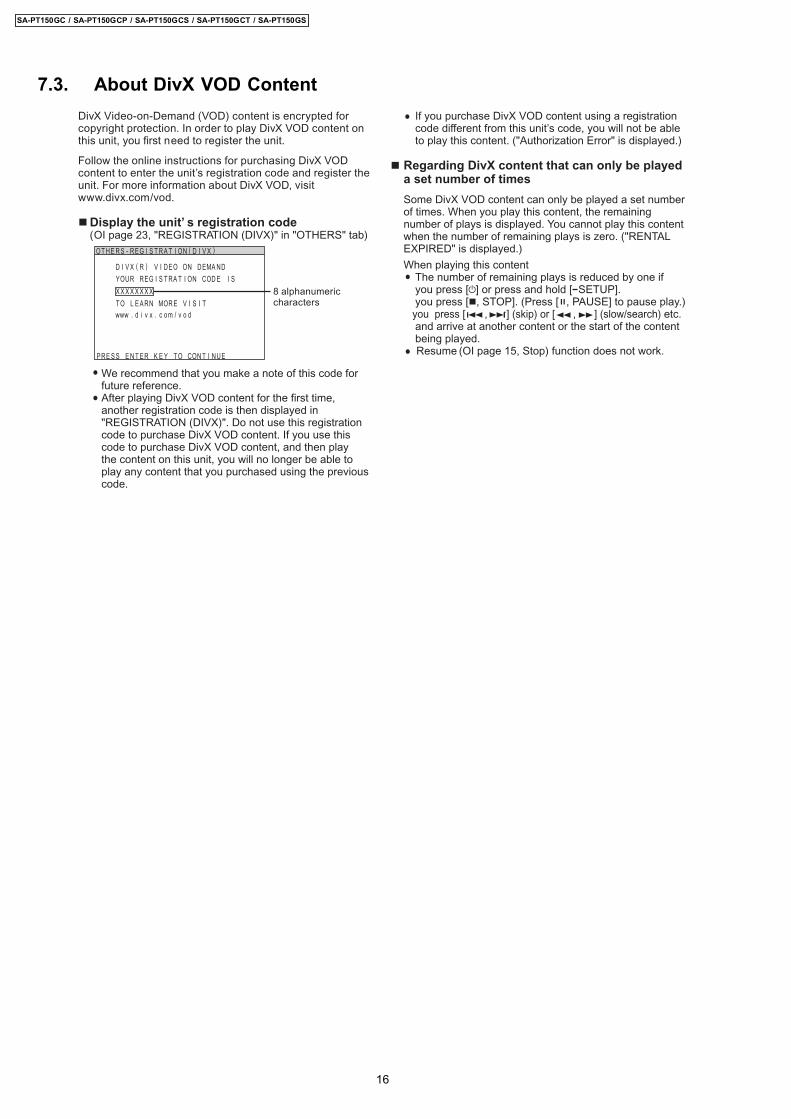
7.3. About DivX VOD ContentDivX Video-on-Demand (VOD) content is encrypted for copyright protection. In order to play DivX VOD content on this unit, you first n eed to register the unit.
Follow the online instructions for purchasing DivX VOD content to enter the unit’s registration code and register the unit. For more information about DivX VOD, visit www.divx.com/vod.
Display the unit’ s registration code(OI page 23, "REGISTRATION (DIVX)" in "OTHERS" tab)
If you purchase DivX VOD content using a registration code different from this unit’s code, you will not be able to play this content. ("Authorization Error" is displayed.)
Regarding DivX content that can only be played a set number of times
Some DivX VOD content can only be played a set number of times. When you play this content, the remaining number of plays is displayed. You cannot play this content when the number of remaining plays is zero. ("RENTAL EXPIRED" is displayed.)
When playing this contentThe number of remaining plays is reduced by one if
you press [ ] or press and hold [ SETUP]. you press [ , STOP]. (Press [ , PAUSE] to pause play.) you press [ , ] (skip) or [ , ] (slow/search) etc.
and arrive at another content or the start of the content being played.Resume (OI page 15, Stop) function does not work.
We recommend that you make a note of this code for future reference.After playing DivX VOD content for the first time, another registration code is then displayed in "REGISTRATION (DIVX)". Do not use this registration code to purchase DivX VOD content. If you use this code to purchase DivX VOD content, and then play the content on this unit, you will no longer be able to play any content that you purchased using the previous code.
16
SA-PT150GC / SA-PT150GCP / SA-PT150GCS / SA-PT150GCT / SA-PT150GS
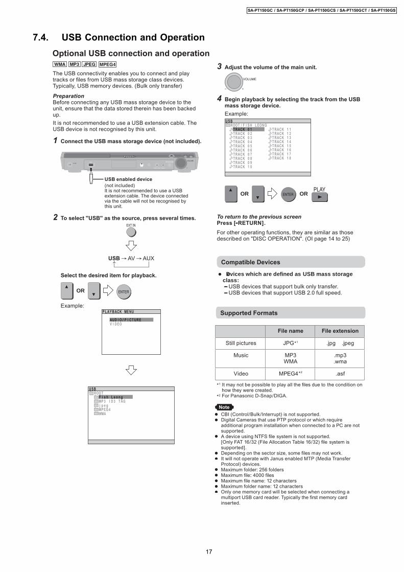
7.4. USB Connection and OperationOptional USB connection and operationOptional USB connection and operation
The USB connectivity enables you to connect and play tracks or files f rom USB mass storage class devices.Typically, USB memory devices. (Bulk only transfer)
PreparationBefore connecting any USB mass storage device to the unit, ensure that the data stored therein has been backed up.
It is not recommended to use a USB extension cable. The USB device is not recognised by this unit.
1 Connect the USB mass storage device (not included).
USB enabled device(not included)It is not recommended to use a USB extension cable. The device connected via the cable will not be recognised by this unit.
2 To select "USB" as the source, press several times.
USB AV AUX
Select the desired item for playback.
OR
Example:
3 Adjust the volume of the main unit.
4 Begin playback by selecting the track from the USB mass storage device.Example:
OR
OR
To return to the previous screenPress [ RETURN].
For other operating functions, they are similar as those described on "DISC OPERATION". (OI page 14 to 25)
Compatible Devices
Devices which are defined as USB mass storage class:
USB devices that support bulk only transfer.USB devices that support USB 2.0 full speed.
File name File extension
Still pictures JPG 1*
2*
2*
1*
.jpg .jpeg
Music MP3WMA
.mp3
.wma
Video MPEG4 .asf
It may not be possible to play all the files due to the condition on how they were created.For Panasonic D-Snap/DIGA.
NoteCBI (Control/Bulk/Interrupt) is not supported.Digital Cameras that use PTP protocol or which require additional program installation when connected to a PC are not supported.A device using NTFS file system is not supported.[Only FAT 16/32 (File Allocation Table 16/32) file system is supported].Depending on the sector size, some files m ay not work.It will not operate with Janus enabled MTP (Media Transfer Protocol) devices.Maximum folder: 256 foldersMaximum file: : 4000 files Maximum file name: 12 charactersMaximum folder name: 12 charactersOnly one memory card will be selected when connecting a multiport USB card reader. Typically the first memory cardinserted.
Supported Formats
17
SA-PT150GC / SA-PT150GCP / SA-PT150GCS / SA-PT150GCT / SA-PT150GS

7.5. Audio and Video Connections7.5.1. Television with Video In Terminal
7.5.2. Television with Component Video In Terminals
7.5.3. Audio Connection for Video Cassette Recorder or Television
18
SA-PT150GC / SA-PT150GCP / SA-PT150GCS / SA-PT150GCT / SA-PT150GS
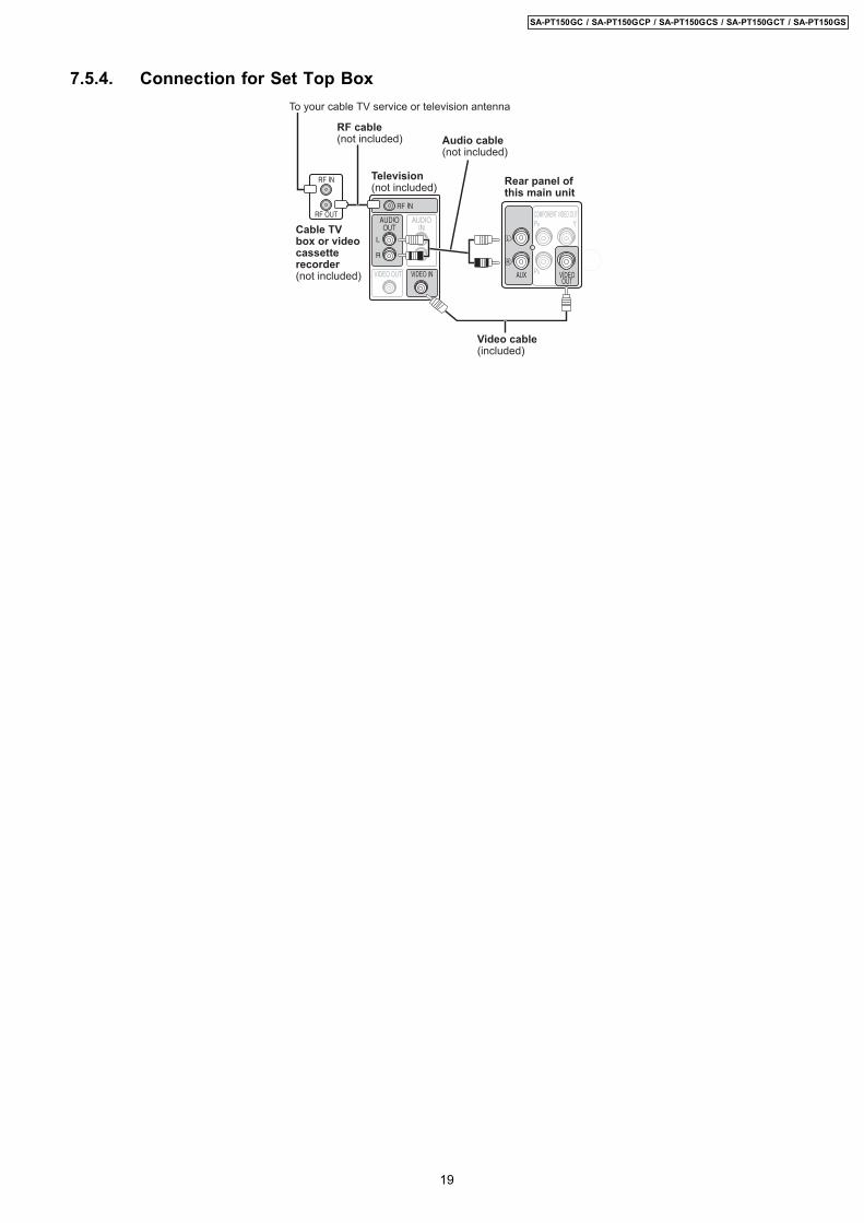
7.5.4. Connection for Set Top Box
19
SA-PT150GC / SA-PT150GCP / SA-PT150GCS / SA-PT150GCT / SA-PT150GS

7.6. Disc Information7.6.1. Disc Playability (Media)
This unit can play CD-R/RW recorded with CD-DA or Video CD format.
MPEG4 data recorded with the Panasonic SD multi cameras or DVD video recorders [conforming to SD VIDEO specifications (ASF standard)/MPEG4 (Simple Profi le) video system/G.726 audio system]. Functions added with DivX ultra are not supported.
Discs that can be playedDiscs that can be played
Disc LogoIndicated in
theseinstructions by
Remarks
DVD-Video High quality movie and music discs.
Video CD
Music discs with video.
Including SVCD (Conforming to IEC62107).
CD Music discs.
Disc Logo
Recorded on a DVD video recorder, etc. Recorded on a personal computer, etc.
Finalizing
DVD-RAM Not necessary
DVD-R/RW Necessary
DVD-R DL Necessary
+R/+RW Necessary
+R DL Necessary
CD-R/RW Necessary
Recorded discs ( : Playable, : Not playable)
Note about using a DualDiscThe digital audio content side of a DualDisc does not meet the technical specifi cations of the Compact Disc Digital Audio (CD-DA) format so playback may not be possible.
Discs that cannot be playedDVD-RW version 1.0, DVD-Audio, DVD-ROM, CD-ROM,CDV, CD-G, SACD, Photo CD, DVD-RAM that cannot be removed from their cartridge, 2.6-GB and 5.2-GB DVD- RAM, and "Chaoji VCD" available on the market including CVD, DVCD and SVCD that do not conform to IEC62107.
Video systemsThis unit can play PAL and NTSC, but your television must match the system used on the disc.PAL discs cannot be correctly viewed on an NTSC television.This unit can convert NTSC signals to PAL 60 for viewing on a PAL television. (OI page 22, "NTSC DISC
1
6
9
8
2
3
5
1
Discs recorded on DVD video recorders or DVD video cameras, etc. using Version 1.1 of the Video Recording Format (a uni ed video recording standard).
fi2
Discs recorded on DVD video recorders or DVD video cameras using Version 1.2 o f the Video Recording Format (a uni efi d video recording standard).
3
Discs recorded on DVD video recorders or DVD video cameras using DVD-Video Format.4
Recorded using a format different from DVD-Video Format, therefore, some functions cannot be used.5
A process that allows play on compatible equipment. To play a disc that is displa yed as "Necessary" on this unit, the disc must rfi st be nfi alized on the device it was recorded on.
6
Closing the session will also work.7
8
9
5
4
7
( )
( )
It may not be possible to play all the above-mentioned discs in some cases due to the type of disc, the condition of the recording, the recording method, or how the files were created [ Item 7.6.2 File Extension Type Support (WMA/MP3/JPEG/
MPEG4/DivX]
OUT" in "VIDEO" tab.)
20
SA-PT150GC / SA-PT150GCP / SA-PT150GCS / SA-PT150GCT / SA-PT150GS
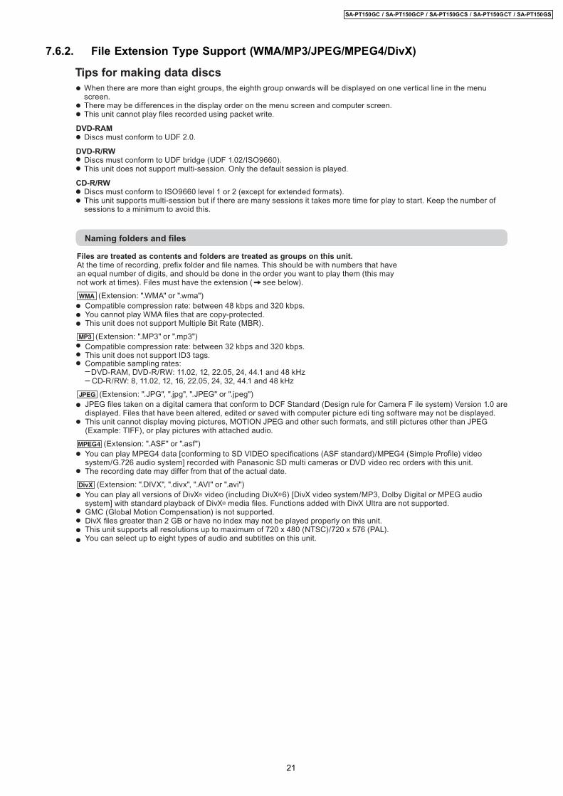
7.6.2. File Extension Type Support (WMA/MP3/JPEG/MPEG4/DivX)
Tips for making data discsTips for making data discsWhen there are more than eight groups, the eighth group onwards will be displayed on one vertical line in the menu screen.There may be differences in the display order on the menu screen and computer screen.This unit cannot play lfi es recorded using packet write.
DVD-RAMDiscs must conform to UDF 2.0.
DVD-R/RWDiscs must conform to UDF bridge (UDF 1.02/ISO9660).This unit does not support multi-session. Only the default session is played.
CD-R/RWDiscs must conform to ISO9660 level 1 or 2 (except for extended formats).This unit supports multi-session but if there are many sessions it takes more time for play to start. Keep the number of sessions to a minimum to avoid this.
Naming folders and files
Files are treated as contents and folders are treated as groups on this unit.At the time of recording, prefi fix folder and le names. This should be with numbers that have an equal number of digits, and should be done in the order you want to play them (this may not work at times). Files must have the extension ( see below).
(Extension: ".WMA" or ".wma")Compatible compression rate: between 48 kbps and 320 kbps.You cannot play WMA files that are copy-protected.This unit does not support Multiple Bit Rate (MBR).
(Extension: ".MP3" or ".mp3")Compatible compression rate: between 32 kbps and 320 kbps.This unit does not support ID3 tags.Compatible sampling rates: DVD-RAM, DVD-R/RW: 11.02, 12, 22.05, 24, 44.1 and 48 kHz
CD-R/RW: 8, 11.02, 12, 16, 22.05, 24, 32, 44.1 and 48 kHz
(Extension: ".JPG", ".jpg", ".JPEG" or ".jpeg")
(Extension: ".ASF" or ".asf")
(Extension: ".DIVX", ".divx", ".AVI" or ".avi")
JPEG lfi es taken on a digital camera that conform to DCF Standard (Design rule for Camera F ile system) Version 1.0 are displayed. Files that have been altered, edited or saved with computer picture edi ting software may not be displayed.
You can play MPEG4 data [conforming to SD VIDEO speci cfi ations (ASF standard)/MPEG4 (Simple Pro le) video system/G.726 audio system] recorded with Panasonic SD multi cameras or DVD video rec orders with this unit.The recording date may differ from that of the actual date.
This unit cannot display moving pictures, MOTION JPEG and other such formats, and still pictures other than JPEG (Example: TIFF), or play pictures with attached audio.
You can play all versions of DivX video (including DivX 6) [DivX video system/MP3, Dolby Digital or MPEG audio system] with standard playback of DivX media lfi es. Functions added with DivX Ultra are not supported.GMC (Global Motion Compensation) is not supported.
This unit supports all resolutions up to maximum of 720 x 480 (NTSC)/720 x 576 (PAL).You can select up to eight types of audio and subtitles on this unit.
fi
DivX les greater than 2 GB or have no index may not be played properly on this unit.fi
21
SA-PT150GC / SA-PT150GCP / SA-PT150GCS / SA-PT150GCT / SA-PT150GS

8 Self-Diagnosis and Special Mode Setting8.1. Service Mode Summary TableThe service modes can be activated by pressing various button combination on the main unit and remote control unit.Below is the summary for the various modes for checking:
Player buttons Remote control unit buttons Application Note[STOP] [0] Error code check. (Refer to the section
“8.2.1. Service ModeTable 1” for moreinformation.)
[5] Jitter checking.[PAUSE] Initial setting of laser drive current.
[FUNCTIONS] DVD laser drive current check. (Refer to the section“8.2.2. Service ModeTable 2” for moreinformation.)
[1] ADSC internal RAM data check.[3] CD laser drive current check.
[6] Region display and mode. (Refer to the section“8.2.3. Service ModeTable 3“ for moreinformation.)
[7] Micro-processor firmware version check.[ ] Initialization of the player (factory setting is restored).
Used after replacement of Micro-processor (DV5 LSI) IC, FLASHROM IC (IC8651), EEPROM IC (IC8611) and DVD ModuleP.C.B.
[8] DVD Module P.C.B. firmware version check. (Refer to the section“8.2.4. Service ModeTable 4“ for moreinformation.)
[EQ] CPPM/CRM keys check.[ENTER] DVD Module P.C.B. reset.
[ ] Timer 1 check. (Refer to the section“8.2.5. Service ModeTable 5“ for moreinformation.)
[ ] Timer 1 reset.[ ] Timer 2 check.[ ] Timer 2 reset.
Note:An error code will be canceled if a power supply is turned OFF.*1: CPPM is the copy guard function beforehand written in the disk for protection of copyrights.*2: CEC is the consumer electronic control used for high-level user control of HDMI-connected devices.*3: HDCP is the specification developed to control digital audio & video contents transmission for DVI or HDMI connections.
8.2. Service Mode TableBy pressing various button combinations on the main unit and remote control unit, you can activate the various service modes forchecking.Special Note:
· Due to the limitations of the no. characters that can be shown on the FL Display, the “FL Display” button on the remotecontrol unit can be used to show the two display pages. (Display 1 / Display 2).
· Refer to Section 7.1 for the section on “Remote Control Key Buttons Operations”.
22
SA-PT150GC / SA-PT150GCP / SA-PT150GCS / SA-PT150GCT / SA-PT150GS

8.2.1. Service Mode Table 1
FL DisplayKey Operation
Front Key
Item
Jitter check
DescriptionMode Name
Initial setting of laser drive
current
Error code check
Cancelled automatically 5 seconds later.To exit, press [POWER]button on main unit or remote control.
Press [FL Display] on remote control unit for nextpage (FL Display) on valuesof laser drive current.
Cancelled automatically 5 seconds later.
Press [POWER] button to exit.
In STOP (no disc) mode, press [STOP] button on the main unit, and [5] button on the remote control unit.
Jitter check.Jitter rate is measured and displayed. Measurement is repeatedly done in the cycle of one second. Read error counter starts from zero upon mode setting. When target block data failed to be read out, the counter advances by one increment. When the failure is caused by minor error, it may be corrected when retried to enable successful reading. In this case, the counter advances by one. When the error persists even after retry, the counter may jump by two or more.
FL Display sequence:Display 1 2.
Jitter rate is shown in decimal notation to one place of decimal.Focus drive value is shown in hexadecimal notation.
(Display 1)
(Display 1)
(Display 2)
(Display 2)
In STOP (no disc) mode, press [STOP] button on the main unit, and [0] button on the remote control unit. * With pointing of cursor up and down on display.
Error code checkThe latest error code stored in the EEPROM IC is displayed.
Note: Refer to "Section 8.3 DVD SelfDiagnostic Function-Error Code" for more detailed information on the error codes.
In STOP (no disc) mode, press [STOP] button on the main unit, and [PAUSE] button on the remote control unit.
Initial setting of laser drive current. Initial current value for the DVD laser and CD laser is separately saved in the EEPROM IC.
FL Display sequence:Display 1 2.
Press [FL Display] on remote control unit for nextpage (FL Display).
Jitter rate
LeadErrorCounter
Focus Drive Value
Jitter checkmode
U / H / F
Laser currentmeasurement mode
CDLaser
DVD Laser
Error code (play_err) is expressed in the following convention.Error code = 0 x DAXX is expressed: DVDnn U12Error code = 0 x DBXX is expressed: DVDnn H12Error code = 0 x DXXX is expressed: DVDnn F123Error code = 0 x 0000 is expressed: DVDnn F---* "xx" denotes the error code
The value denotes the current in decimal notation.
The above example shows the initial current is XXXmA and YYYmA for CD laser and DVD laser respectively when the laser is switched on.
23
SA-PT150GC / SA-PT150GCP / SA-PT150GCS / SA-PT150GCT / SA-PT150GS

8.2.2. Service Mode Table 2
FL DisplayKey Operation
Front Key
Item
DescriptionMode Name
Press [FL Display] on remote control unit for nextpage. (FL Display)
Cancelled automatically 5 seconds later.
CD laser drive current
measurement
In STOP (no disc) mode, press [STOP] button on the main unit, and [3] button on the remote control unit.
CD laser drive current measurement.CD laser drive current is measured and the result is displayed together with the initial value stored in the EEPROM IC.After the measurement, CD laser emission is kept on. It is turned off when POWER key is switched off.
FL Display sequence:Display 1 2.
CD laser current measurement mode
CDlaser initialvalue
CD laservalue
The value denotes the current in decimal notation.
The above example shows the initial current is 0XXmA and the measured value is 0YYmA.
To exit, press [POWER] button.
ADSC internal RAM data
check
In STOP (no disc) mode, press [STOP] button on the main unit, and [1] button on the remote
ADSC internal RAM data check. ADSC internal RAM data is read out and displayed.
The value is shown in hexadecimal notation. The above example shows the data in ADSC address FBOh is XXXXh.
Address RAM datafor specifiedaddress
DVD laser drive current measurement
Press [FL Display] on remote control unit for nextpage (FL Display) on valuesof dvd drive current.
Cancelled automatically 5 seconds later.
(Display 1)
(Display 2)
(Display 1)
(Display 2)
In STOP (no disc) mode, press [STOP] button on the main unit, and [FUNCTIONS] button on the remote control unit.
DVD laser drive current measurement. DVD laser drive current is measured and the result is displayed together with the initial value stored in the EEPROM IC.After the measurement, DVD laser emission is kept on. It is turned off when POWER key is switched off.
FL Display sequence:Display 1 2.
DVD laser current measurement mode
DVD Laser Initial Value
DVD Laser Value
The value denotes the current in decimal notation.
The above example shows the initial current is XXXmA and the measured value is YYYmA.
24
SA-PT150GC / SA-PT150GCP / SA-PT150GCS / SA-PT150GCT / SA-PT150GS

8.2.3. Service Mode Table 3
FL DisplayKey Operation
Front Key
Item
DescriptionMode Name
Initialization
Cancelled automatically 5 seconds later.
Initialization.User settings are cancelled and player is initialized to factory setting.It is necessary when after replacementof Micro-processor (DV5 LSI) IC, FLASH ROM IC (IC8651), EEPROM IC (IC8611) & DVD Module P.C.B.
Cancelled automatically 5 seconds later.
Region code display, TV broadcastingsystem & the model no. information.
Note: Refer to Figure 2 for "VideoDesign Information".
Region display In STOP (no disc) mode, press [STOP] button on the main unit, and [6] button on the remote control unit.
Region No.: 0-8
N: no PAL / P: PALN: NTSC / 6: PAL60
ModelNo.Information
In STOP (no disc) mode, press [STOP] button on the main unit, and [ 10] button on the remote control unit.
If the EEPROM version matches, checksum[YYYY] is displayed.
If the version of the EEPROM does not match,[NG] is displayed.
(a) If there is NO EEPROM header stringOR (b) If there is no EEPROM (no data is receivedby Micro-processor), [NO] is displayed.
EEPROMChecksum(If applicable, refer below.)(Condition1)
OpeconVersion
(Display 1)
(Display 2)
(Display 3)
(Condition 2)
(Condition 3)
Micro-processorfirmware version
display & EEPROM checksum
display. Cancelled automatically 5 seconds later.
In STOP (no disc) mode, press [STOP] button on the main unit, and [7] button on the remote control unit.
Press [FL Display] button on remote control unit for nextpage. (FL Display)
Micro-processor firmware versiondisplay & EEPROM checksum display. EEPROM checksum is only availabledue to existence of EEPROM IC.
Note: Condition 1/2/3 shows the state of EEPROM IC.
FL Display sequence:Display 1 2 3.
25
SA-PT150GC / SA-PT150GCP / SA-PT150GCS / SA-PT150GCT / SA-PT150GS
TV Broadcasting Signal System Region DisplayCode System (Default) (Default)English, Spanish, Canadian
French
(S) Japan 2 NTSC NTSC (*A) 2PN Japanese, English
English, French, German,
Spanish, Polish, Russian,
Czech, Hungarian
English, French, German,
Italian, Spanish, Polish,
Swedish, Dutch
English, French, German,
Spanish, Polish, Russian,
Czech, Hungarian
GCS, GD, South East Asia, PAL English, Traditional Chinese
GT, GCT Korea, Taiwan NTSC
New Zealand, English, French, German,
AustraliaItalian, Spanish, Polish,
Swedish, Dutch
Central/South/NTSC (*D) 4PN
English, Spanish, French,
Latin America Brazilian Portuguese
English, French, German,
Spanish, Polish, Russian,
Czech, Hungarian
GK China 6 PAL NTSC (*B) 6PN English, Simplified Chinese
5P6PAL (*C)SECAM5
NTSC4
4GN
EE CIS
PL, GCP, LB
3PN
4P6PAL (*C)PAL
2P6PAL (*C)PAL2
2P6PAL (*C)PAL2
1PNNTSC1
E Europe 2 PAL PAL (*C) 2P6
P, PC, PX USA, Canada, PX NTSC (*A)
Europe
GC, GS
EB, EG
Middle East
3 NTSC (*B)
Product
OSD Menu LanguageModel Series Country Region
Region
Explanation of Display
Individual Model Code
can play PAL disc
Region code
N: If NTSC disc is played, NTSC output.6: If NTSC disc is played, PAL60 output.
NTSC (*A) NTSC (*B)
Source Output Source Output
Screen Saver NTSC Screen Saver NTSC
NTSC disc NTSCNTSC disc
NTSC (default)
PAL discPAL (DVD-V) PAL60
NTSC (DVD-A/VCD) PAL disc PAL60
PAL (*C) NTSC (*D)
Source Output Source Output
Screen Saver PAL Screen Saver NTSC
NTSC discPAL60 (default) NTSC disc NTSC
NTSC PAL disc NTSC
PAL disc PAL
Figure 2
26
SA-PT150GC / SA-PT150GCP / SA-PT150GCS / SA-PT150GCT / SA-PT150GS

8.2.4. Service Mode Table 4
Cancelled automatically 5 seconds later.
CPPM/CRMKeys Check
In STOP (no disc) mode, press [STOP] button on the main unit, and [EQ] button on the remote control unit.
0: NG1: OK
0: NG1: OK
DVDModule P.C.B.
firmwareversion display
Cancelled automatically 5 seconds later.
In STOP (no disc) mode, press [STOP] button on the main unit, and [8] button on the remote control unit.
System controller generation
Destination
System controller version
Region No.: 0-8
DVD Module P.C.B. firmware version is displayed on the FL Display.The firmware version can be updatedusing recovery disc.
Note: It is necessary to check for firmware version before carrying out the version up using the disc.
CPPM/CRM refers to the Content Protection for Recordable Media and Pre-Recorded Media. It displays the existence of the keys as "1" or "0".OK: Existing of keys.NG: Non existing of keys.
FL DisplayKey Operation
Front Key
Item
DescriptionMode Name
DVDModule P.C.B.
Reset
To reset DVD Module P.C.B.This process is used when the DVDModule P.C.B. or FLASH ROMIC is replaced with a new one.
Cancelled automatically 5 seconds later.
While in initialization mode, press & hold [STOP] button on the main unit, follow by [ENTER] button on the remote control unit.
27
SA-PT150GC / SA-PT150GCP / SA-PT150GCS / SA-PT150GCT / SA-PT150GS

8.2.5. Service Mode Table 5
Timer 1 check
Cancelled automatically5 seconds later.DVD laser usage time
(Display 1)
(Display 2)
CD laser usage time
Cancelled automatically 5 seconds later
Cancelled automatically 5 seconds later.
Cancelled automatically 5 seconds later.
Timer 1 reset
Timer 2 check
Timer 2 reset
In STOP (no disc) mode, press [STOP] button on the main unit, and [ ] button on the remote control unit.
While displaying Timer 1 data, press [STOP] button on the main unit, and [ ] button on the remote control unit.
In STOP (no disc) mode, press [STOP] button on the main unit, and [ ] button on the remote control unit.
While displaying Timer 2 data, press [STOP] button on the main unit, and [ ] button on the remote control unit.
Timer 1 checkLaser operation timer is measured separately for DVD laser and CD laser.
FL Display sequence:Display 1 2.
Press [FL Display] button fornext page of FL Display.
Timer 1 resetLaser operation timer of both DVD laser and CD laser is reset all at once.
Timer 2 checkSpindle motor operation timer
Timer 2 resetSpindle motor operation timer
Time is shown in 5 digits of decimal notation in a unit of 1 hour."00000" will follow "99999".
Shown to the above is DVD laser usage time, and to the below is CD laser usage time.Time is shown in 4 digits of decimal notation in a unit of 10 hours."0000" will follow "9999". (DVD laser)
Time is shown in 4 digits of decimal notation in a unit of 10 hours."0000" will follow "9999". (CD laser)
Time is shown in 4 digits of decimal notation in a unit of 10 hours.It will clear to "0000" upon reset.
Time is shown in 5 digits of decimal notation in a unit of 1 hour.It will be cleared to "00000" upon activating this.
FL DisplayKey Operation
Front Key
Item
DescriptionMode Name
28
SA-PT150GC / SA-PT150GCP / SA-PT150GCS / SA-PT150GCT / SA-PT150GS

8.2.6. Optical Pick-up Self-DiagnosisThe optical pickup self-diagnosis function and tilt adjustment check function have been included in this unit. When repairing, usethe following procedure for effective self-diagnosis and tilt adjustment. Be sure to use the self-diagnosis function before replacingthe optical pickup when "NO DISC" is displayed. As a guideline, you should replace the optical pickup when the value of the laserdrive current is more than 55.Note:
Press the power button to turn on the power, and check the value within three minutes before the unit warms up. (Otherwise,the result will be incorrect.)
"NO DISC" is displayed, unit does not play smoothly, etc.
Check the laser drive current.
Replace the optical pickup. (Refer to the section "OPTICAL PICKUP REPLACEMENT PROCEDURE" in this Guide.)
Do the optical pickup tilt adjustment. (Refer to the section "TILT ADJUSTMENT" in this Guide.)
Initialize the main unit.
Check the laser drive current after replacement. Write the present value into the unit if it is 23 (DVD), 34 (CD) or less.
Value is 23 (DVD), 34 (CD) or less.
Value is more than 23 (DVD), 34 (CD).
Use the tilt adjustment check function.
Note: Press "FL DISPLAY" button on remote Note: Press "FL DISPLAY" button on remote control unit for next page display.control unit for next page display.
Replace with a new optical pickup if the present value is more than 23 (DVD), 34 (CD).Cause: Damage due to static electricity
during replacement.
Method: With no disc in the main unit:· Press the "FUNCTIONS" button on the remote control unit while pressing the "STOP" button on the main unit. (DVD)
· Press the "3" button on the remote control unit while pressing the "STOP" button on the main unit. (CD)
Use the optical pickup self-diagnosis function.
Method: With no disc in the main unit:· Press the "FUNCTIONS" button on the remote control unit while pressing the "STOP" button on the main unit. (DVD)
· Press the "3" button on the remote control unit while pressing the "STOP" button on the main unit. (CD)
Display content (display1/display2)LDD (DVD)
LDC (CD)
Factory setting Present value
Factory setting Present value
/
/
Writing method:· Press the "PAUSE" button on the remote control unit while pressing the "STOP" button on the main unit.
29
SA-PT150GC / SA-PT150GCP / SA-PT150GCS / SA-PT150GCT / SA-PT150GS

8.3. DVD Self Diagnostic Function-Error Code8.3.1. Mechanism Error Code Table
Error CodeH01 Tray loading error The tray opening and closing is Press [ STOP] on
abnormal. CLOSE and OPEN of the main unit for next error.tray cannot be carried out properly. (OPEN time: OPENLoading motor error, DV5 LSI IC CLOSE OPEN (IC8001) error. H01 at CLOSE: CLOSE
OPEN CLOSE H01)
H02 Spindle servo error The spindle servo/motor is abnormal. Press [ STOP] on The FG pulse is abnormal. CLV servo main unit for next error.error.
H03 Traverse servo error The traverse is abnormal. (Traverse Press [ STOP] on servo, DV5 LSI IC (IC8001), TRV main unit for next error.motor error.)
H04 Tracking servo error Tracking coil NG (OPU unit Press [ STOP] on abnormal), DV5 LSI IC (IC8001) main unit for next error.error.
H05 Seek time out error It is not possible to access the disc. Press [ STOP] on TOC cannot read. Abnormal disc etc. main unit for next error.Pickup abnormal or disk is dirty.(TRV motor error, DV5 LSI IC (IC8001) error.)
H07 Driver IC thermal The spindle motor is abnormal. (short Press [ STOP] on shut down between brushes) main unit for next error.
H15 Disc tray open The disc tray cannot be opened & it Press [ STOP] on detection switch closes spontaneously. main unit for next error.failure
H16 Disc tray close The disc tray cannot be closed & it Press [ STOP] on detection switch opens spontaneously. main unit for next error.failure
U11 Focus servo error Focus coil, FE signal error. Press [ STOP] on main unit for next error.(Unfinalized DVD-R
U15 Unfinalized DVD-R is likely to beocme U11.)
F500 DSC error DV5 LSI IC (IC8001) stops in the Press [ STOP] on occurance of servo error (startup, main unit for next error.focus error, etc)
F506 Invalid media Disc is flipped over, TOC unreadable, Press [ STOP] on incompatible disc. main unit for next error.
F620 OPU unit Laser protection at high temperature. Press [ STOP] on abnormality main unit for next error.temperature
F621 OPU unit Laser protection at circuit failure. Press [ STOP] on circuitry main unit for next error.temperature
Diagnosis Contents Description of error Automatic FL Display Remarks
30
SA-PT150GC / SA-PT150GCP / SA-PT150GCS / SA-PT150GCT / SA-PT150GS

8.3.2. DVD Module Error Code Table
Error CodeU702 DVD/DVI I2C The communication error of I2C Press [ STOP] on
communication error when connecting it with DVD/ main unit for next error.DVI. For instance, when EDID information to which information on theTV set side has been described cannot be read, it is generated.
U703 DVD/DVI attestation When attestation (HDCP) with the TV Press [ STOP] on error side fails when connecting it with main unit for next error.
DVD/DVI, it is generated.
U704 DVD/DVI SRM It is generated at the equipment to Press [ STOP] on Riborcerar which the TV set is Riborced when main unit for next error.
connecting it with DVD/DVI.
U705 DVD/DVI SRM disk It is generated at the time of it is time Press [ STOP] on falsification check when illegal the SRM data of the main unit for next error.error reproducing disk (verify error), when
connecting it with DVD/DVI.
F740 DVD device key I2C error when writing DVD Key Press [ STOP] on device into transmitter. main unit for next error.
F893 FLASH ROM IC data Firmware error, DV5.0 LSI IC (IC8651) Press [ STOP] on falsification error error. main unit for next error.
F894 EEPROM IC When failing in the access to Press [ STOP] on abnormality error EEPROM IC located in the DVD main unit for next error.
Module P.C.B. (IC8611)
F895 Language area Firmware version agreement check for Press [ STOP] on abnormal factory preset setting failure main unit for next error.
prevention.
F896 No existence model Firmware version agreement check for Press [ STOP] on factory preset setting failure main unit for next error.prevention.
F897 Initialization Incomplete initialization after writing of Press [ STOP] on error new firmware (Factory preset setting main unit for next error.
failure prevention)
F898 Disagreement of Unsuitable combination of AV Decoder, Press [ STOP] on hardware and SDRAM & FLASH ROM IC (firmware). main unit for next error.software
F899 The communication Unsuitable combination of number of Press [ STOP] on specification system com and panel com used. main unit for next error.disagreement (Frimware)between micro-processor
Diagnosis Contents Description of error Automatic FL Display Remarks
31
SA-PT150GC / SA-PT150GCP / SA-PT150GCS / SA-PT150GCT / SA-PT150GS

8.3.3. Power Supply Error Code Table
Error CodeF61 The abnormalities In normal operation, when DCDET2 Press [ STOP] on
in an output or power goes to "L" (Low) (Not during POWER main unit for next error.supply circuit of OFF condition), F61 appears on FL POWER AMP Display and PCONT goes to "L" (Low).
This is due to speaker output has DCvoltage or fan is not working.
F76 Abnormality in the In normal operation when DCDET1 is Press [ STOP] on output voltage of detected "L" (Low) for two consecutive main unit for next error.stabilized power times, F76 is displayed on FL for 2supply seconds and after that PCONT will be
turned to "L" (Low). This is due to any ofthe DC voltages (+9V, +7V, -7V, +5V, +5.3V etc.) not available.
Diagnosis Contents Description of error Automatic FL Display Remarks
8.3.4. ECC Error Code Table
Error CodeF600 Administrative It becomes impossible NaviPack etc. Press [ STOP] on
information cannot were done, and not to be able to main unit for next error.be acquired by the acquire necessary information in the recovery error. navigation’s changing due to wound
etc. of DISC, and to have done the reproduction transition.
F601 Irregular sector ID It tried to access the position that did Press [ STOP] on was demanded. not exist on DISC by the recording main unit for next error.
error etc. of authoring.
F603 KEYDET cannot be The data for decoding copyright Press [ STOP] on acquired by the protection (CSS) cannot be acquired main unit for next error.recovery error. due to wound etc. of DISC, and it is not
possible to reproduce.
Diagnosis Contents Description of error Automatic FL Display Remarks
32
SA-PT150GC / SA-PT150GCP / SA-PT150GCS / SA-PT150GCT / SA-PT150GS

8.3.5. USB Error Code Table
Error CodeF650 USB device: Devices Devices other than the mass storage Press [ STOP] on
other than mass class are connected. main unit for next error.storage
F651 USB device: Non- The device that the transfer rate did not Press [ STOP] on Full Speed Device correspond to Full Speed was main unit for next error.
connected.
F652 USB device: The device in the interface (subclass) Press [ STOP] on Interface NG outside correspondence was main unit for next error.
connected. (correspondence interface)001b: Reduced Block Commands (RBC)010b: SFF-8020i. MMC-2 (ATAPI)110b: SCSI transparent command set.
F655 USB device: The overcurrent of 500mA or more was Press [ STOP] on Overcurrent detected in VDD USB, and the USB main unit for next error.detection device driver function was intercepted.
(To intercept the current.)
Diagnosis Contents Description of error Automatic FL Display Remarks
8.4. Sales Demonstration Lock FunctionThis function prevents discs from being lost when the unit is used for sales demonstrations by disabling the disc eject function."LOCKED" is displayed on the unit, and ordinary operation is disabled.
8.4.1. Setting · Prohibiting removal of disc
1. Select the DVD/CD function. 2. At POWER ON condition, press and hold down the button and the power button on the player for at least three seconds.
(The message, “___LOCKED_” appears when the function is activated.)Note:
OPEN/CLOSE is invalid and the player displays “___LOCKED_” while the lock function mode is entered.
· Prohibiting operation of selector and disc 1. Select the DVD/CD function. 2. At POWER ON condition, press and hold down the button and the power button on the player for at least three seconds.
(The message, “___LOCKED_” appears when the function is activated.)Note:
The following buttons are invalid and the player displays “___LOCKED_” while the lock function mode is entered.
Player , , SELECTOR, / , , /Remote
controller unitNUMERIC KEYS 0~9, , , , , , , , FUNCTIONS/KARAOKE, TOPMENU/DIRECT NAVIGATOR, RETURN/SETUP, FL DISPLAY/SLEEP, MUTING, MENU/PLAY LIST, TEST, EXT-IN,FM, UP, DOWN, LEFT & RIGHT
8.4.2. CancellationThe lock can be cancelled by the same procedure as used in setting. ("UNLOCKED" is displayed on cancellation. Disconnectingthe power cable from power outlet does not cancel the lock.)
33
SA-PT150GC / SA-PT150GCP / SA-PT150GCS / SA-PT150GCT / SA-PT150GS

8.5. Service Precautions8.5.1. Recovery after the DVD player is repaired · When the FLASH ROM IC or DVD Module P.C.B. is replaced, carry out the recovery processing to optimize the drive.
Playback the recovery disk to process the recovery automatically. · Recovery disc (Product number: RFKZD03R005) [SPG] · Performing recovery process
1. Load the recovery disc RFKZD03R005 on to the player and run it. 2. Recovery is performed automatically. When it is finished, a message appears on the screen. 3. Remove the recovery disc. 4. Turn off the power. 5. Initialize the player.
8.5.2. Firmware version-up of the DVD player · The firmware of the DVD player may be renewed to improve the quality including operability and playability to the substandard
discs.processing to optimize the drive.The recovery disc has also firmware version-up.
· After version-up, recovery processing is executed automatically. · Part number of the recovery disc for version-up will be noticed when it is supplied. · Updating firmware
1. Load the recovery disc on to the player and run it. 2. Firmware version of the player is automatically checked. Appropriate message appears whenever necessary. 3. Using remote controller´s cursor key, select whether version updating is to be done or not. (Selection of Yes/No) 4. a. If Yes is selected, version updating is performed.
b. If No is selected, only recovery is performed. 5. a. When updating is finished, remove the disc according to the message appearing on the screen.
b. Remove the disc according to the message appearing on the screen. 6. Turn off the power.
Note:If the AC power supply is shut out during version-up due to a power failure, the version-up is improperly carried out.In such a case, replace the FLASH ROM IC and carry out the version-up again.
8.5.3. DVD Module P.C.B. Reset · When after replacing FLASH ROM IC or DVD Module P.C.B., FL displays error code “ DVD F897”. This means the unit is not
initialized properly and the following process needs to be carry out. · Procedures:
1. Press on remote control while pressing “STOP” button on main unit. (To enter into initialization) 2. FL display show “INIT” 3. While still pressing “STOP” button on main unit, press “ENTER” on remote control. (To reset the unit) 4. FL will display “RESET” before FL display will change to TOC reading again. 5. Power off unit. Unplug the AC cord. 6. Power on the unit. It should be no problem. If problem persist check on the DVD Module P.C.B. or FLASH ROM IC.
34
SA-PT150GC / SA-PT150GCP / SA-PT150GCS / SA-PT150GCT / SA-PT150GS
Be careful when disassembling and servicing.Some chassis components may have sharp edges.
Special Note:
9 Assembling and Disassembling“ATTENTION SERVICER”
1. This section describes the disassembly procedures for all the major printed circuit boards and main components. 2. Before the disassembly process was carried out, do take special note that all safety precautions are to be carried out.
(Ensure that no AC power supply is connected during disassembling.) 3. For assembly after operation checks or replacement, reverse the respective procedures.
Special reassembly procedures are described only when required. 4. The Digital Amp IC may have high temperature after prolonged use. 5. Use caution when removing the top cabinet and avoid touching heat sinks located in the unit
6. This unit uses Switching Mode Power Supply (SMPS) Module P.C.B. for providing the voltage supply. It is advisable toreplace as a unit. Do not attempt to replace any individual components on board.
7. Select items from the following index when checks or replacement are required. · Disassembly of Top Cabinet · Disassembly of DVD Lid (When taking out disc manually) · Disassembly of Front Panel · Disassembly of Volume P.C.B. · Disassembly of Panel P.C.B. · Disassembly of Mic P.C.B. · Disassembly of USB P.C.B. · Disassembly of Rear Panel · Disassembly of DVD Mechanism Unit · Disassembly of DVD Module P.C.B. · Disassembly of USB Relay P.C.B. · Disassembly of Main P.C.B. & Tuner Extent P.C.B. · Replacement of Digital Amp IC (IC5100) · Replacement of Regulator IC (IC2903) · Disassembly of SMPS Module P.C.B.
35
SA-PT150GC / SA-PT150GCP / SA-PT150GCS / SA-PT150GCT / SA-PT150GS

· SMPS Module P.C.B. Replacement: 1. This model uses SMPS Module P.C.B. to provide the necessary supply voltages for the unit. 2. It is advisable to replace the SMPS Module P.C.B. once upon detecting of non-working conditions. Do not attempt to
repair or replace it by components. 3. Non-working conditions include:
lWith AC supply but no supply voltages after checking at CN2 and/or CN3 respectively.lBroken fuse. (Substitute compatible part for fuse: K5D502BNA005)lWire connection problem.lNon-working parts in SMPS Module P.C.B. (Check components)
9.1. Disassembly Flow Chart
9.4. DVD Lid 9.9. Rear Panel
9.3. Top Cabinet
9.17. SMPS ModuleP.C.B.
9.9. USB P.C.B. 9.8. Mic P.C.B.
9.7. Panel P.C.B.
9.6. Volume P.C.B.
9.5. Front Panel
9.12. DVD Module P.C.B.
9.16. Regulator IC (IC2903)
9.14. Main P.C.B. &Tuner Extent P.C.B.
9.13. USB Relay P.C.B.
9.11. DVD Mechanism Unit
9.15. Digital Amp IC (IC5100)
36
SA-PT150GC / SA-PT150GCP / SA-PT150GCS / SA-PT150GCT / SA-PT150GS

9.2. Main Components and P.C.B. Locations
37
SA-PT150GC / SA-PT150GCP / SA-PT150GCS / SA-PT150GCT / SA-PT150GS
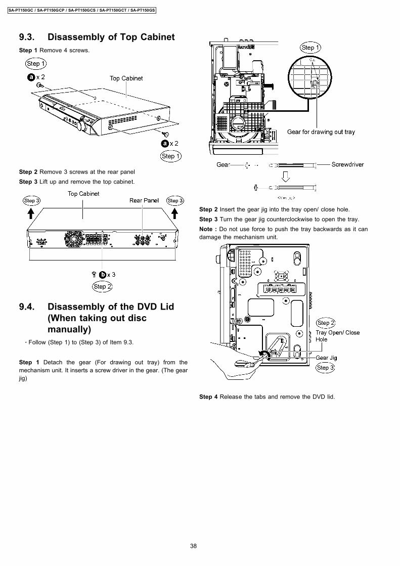
9.3. Disassembly of Top CabinetStep 1 Remove 4 screws.
Step 2 Remove 3 screws at the rear panelStep 3 Lift up and remove the top cabinet.
9.4. Disassembly of the DVD Lid(When taking out discmanually)
· Follow (Step 1) to (Step 3) of Item 9.3.
Step 1 Detach the gear (For drawing out tray) from themechanism unit. It inserts a screw driver in the gear. (The gearjig)
Step 2 Insert the gear jig into the tray open/ close hole.Step 3 Turn the gear jig counterclockwise to open the tray.Note : Do not use force to push the tray backwards as it candamage the mechanism unit.
Step 4 Release the tabs and remove the DVD lid.
38
SA-PT150GC / SA-PT150GCP / SA-PT150GCS / SA-PT150GCT / SA-PT150GS
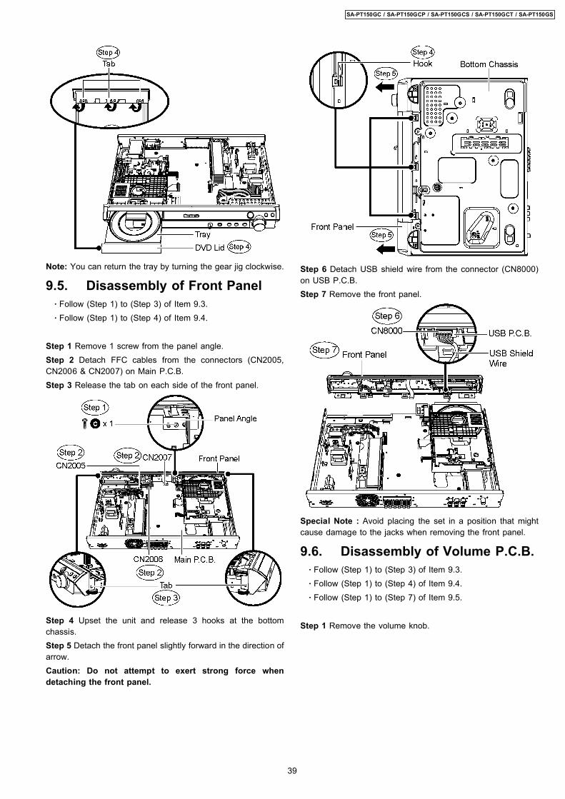
Note: You can return the tray by turning the gear jig clockwise.
9.5. Disassembly of Front Panel · Follow (Step 1) to (Step 3) of Item 9.3. · Follow (Step 1) to (Step 4) of Item 9.4.
Step 1 Remove 1 screw from the panel angle.Step 2 Detach FFC cables from the connectors (CN2005,CN2006 & CN2007) on Main P.C.B.Step 3 Release the tab on each side of the front panel.
Step 4 Upset the unit and release 3 hooks at the bottomchassis.Step 5 Detach the front panel slightly forward in the direction ofarrow.Caution: Do not attempt to exert strong force whendetaching the front panel.
Step 6 Detach USB shield wire from the connector (CN8000)on USB P.C.B.Step 7 Remove the front panel.
Special Note : Avoid placing the set in a position that mightcause damage to the jacks when removing the front panel.
9.6. Disassembly of Volume P.C.B. · Follow (Step 1) to (Step 3) of Item 9.3. · Follow (Step 1) to (Step 4) of Item 9.4. · Follow (Step 1) to (Step 7) of Item 9.5.
Step 1 Remove the volume knob.
39
SA-PT150GC / SA-PT150GCP / SA-PT150GCS / SA-PT150GCT / SA-PT150GS

Step 2 Remove 4 screws from Volume P.C.B..Step 3 Remove Volume P.C.B.
9.7. Disassembly of Panel P.C.B. · Follow (Step 1) to (Step 3) of Item 9.3. · Follow (Step 1) to (Step 4) of Item 9.4. · Follow (Step 1) to (Step 7) of Item 9.5.
· Disassembly of Mecha Holder.
Step 1 Remove 2 screws.Step 2 Remove the mecha holder.
· Disassembly of Panel P.C.B.
Step 3 Release 2 hooks.Step 4 Remove Panel P.C.B.
9.8. Disassembly of Mic P.C.B. · Follow (Step 1) to (Step 3) of Item 9.3. · Follow (Step 1) to (Step 4) of Item 9.4. · Follow (Step 1) to (Step 7) of Item 9.5. · Follow (Step 1) to (Step 3) of Item 9.6. · Follow (Step 1) to (Step 4) of Item 9.7.
Step 1 Remove the mic knob.
Step 2 Remove Mic P.C.B.
9.9. Disassembly of USB P.C.B. · Follow (Step 1) to (Step 3) of Item 9.3. · Follow (Step 1) to (Step 4) of Item 9.4. · Follow (Step 1) to (Step 7) of Item 9.5. · Follow (Step 1) to (Step 4) of Item 9.7.
Step 1 Remove USB P.C.B.
40
SA-PT150GC / SA-PT150GCP / SA-PT150GCS / SA-PT150GCT / SA-PT150GS

9.10. Disassembly of Rear panel · Follow (Step 1) to (Step 3) of Item 9.3.
Step 1 Remove 7 screws from the rear panel.
Step 2 Remove the fan wire clamper to detach the fan unitconnector (CN5704) on Main P.C.B.Step 3 Release the tab on each side of the rear panel in thedirection of arrows.Step 4 Remove the rear panel.
9.11. Disassembly of DVDMechanism Unit
· Follow (Step 1) to (Step 3) of Item 9.3. · Follow (Step 1) to (Step 4) of Item 9.4.
Step 1 Remove 2 screws from the DVD mechanism unit.Step 2 Detach FFC cable from the connectors (CN2001) onMain P.C.B. and (CS901) on Tray Loading P.C.B.
Step 3 Lift up the DVD mechanism unit and detach FFC cablefrom the connector (CN8003) on USB Relay P.C.B..Step 4 Remove DVD mechanism unit.
9.12. Disassembly of DVD ModuleP.C.B.
· Follow (Step 1) to (Step 3) of Item 9.3. · Follow (Step 1) to (Step 4) of Item 9.4. · Follow (Step 1) to (Step 4) of Item 9.11.
Step 1 Remove 4 screws from DVD Module P.C.B.
41
SA-PT150GC / SA-PT150GCP / SA-PT150GCS / SA-PT150GCT / SA-PT150GS

Step 2 Lift up DVD Module P.C.B. and detach FFC cable fromthe connector (FP8251).
Step 3 Turn over DVD Module P.C.B. and detach FFC cablefrom the connector (FP8531).Step 4 Remove DVD Module P.C.B.
Caution : Do not use strong or excessive force to avoiddamage to FFC cables.
9.13. Disassembly of USB RelayP.C.B.
· Follow (Step 1) to (Step 3) of Item 9.3. · Follow (Step 1) to (Step 4) of Item 9.4. · Follow (Step 1) to (Step 4) of Item 9.11.
Step 1 Remove 1 screw.Step 2 Detach FFC cable from the connector (CN8002).Step 3 Lift up and remove USB Relay P.C.B.
9.14. Disassembly of Main P.C.B. &Tuner Extent P.C.B.
· Follow (Step 1) to (Step 3) of Item 9.3. · Follow (Step 1) to (Step 4) of Item 9.10.
· Disassembly of Bracket.
Step 1 Remove 1 screw from the bracket.Step 2 Remove the bracket.
· Disassembly of Main P.C.B. & Tuner Extent P.C.B.
Step 3 Remove 4 screws on Main P.C.B.
42
SA-PT150GC / SA-PT150GCP / SA-PT150GCS / SA-PT150GCT / SA-PT150GS

Step 4 Detach FFC cable from the connectors (CN2 & CN3) onSMPS Module P.C.B., (CN2001,CN2005, CN2006 & CN2007)on Main P.C.B. and (CS901) on Tray Loading P.C.B.Step 5 Remove Main P.C.B. & Tuner Extent P.C.B.
9.15. Replacement of Digital Amp IC(IC5100)
· Follow (Step 1) to (Step 3) of Item 9.3. · Follow (Step 1) to (Step 4) of Item 9.9. · Follow (Step 1) to (Step 5) of Item 9.14.
Step 1 Desolder pins of the digital amp IC (IC5100) on the backside of Main P.C.B.
Step 2 Remove 2 screws from the digital amp IC (IC5100).Step 3 Remove the digital amp IC (IC5100) from the heatsinkunit.Caution : Handle the heatsink unit with caution due to its hightemperature after prolonged use. Touching it may lead toinjuries.
Note : For replacement of IC5200 & IC5300, repeat the (Step1) to (Step 3). Refer to the diagrams of Main P.C.B. (Item 9.14)for the location of the parts.
9.16. Replacement of Regulator IC(IC2903)
· Follow (Step 1) to (Step 3) of Item 9.3. · Follow (Step 1) to (Step 4) of Item 9.9. · Follow (Step 1) to (Step 5) of Item 9.14.
Step 1 Desolder pins of the regulator IC (IC2903) on the backside of Main P.C.B.
43
SA-PT150GC / SA-PT150GCP / SA-PT150GCS / SA-PT150GCT / SA-PT150GS

Step 2 Remove 1 screw from the regulator IC (IC2903).Step 3 Remove the regulator IC (IC2903) from the heatsinkextrusion.Caution : Handle the heatsink extrusion with caution due to itshigh prolonged use. Touching it may lead to injuries.
Note : Refer to the diagrams of Main P.C.B. (Item 9.14.) for thelocation of the part.
9.17. Disassembly of SMPS ModuleP.C.B.
· Follow (Step 1) to (Step 3) of Item 9.3.
Caution Note: The SMPS Module P.C.B. is advisable to bereplaced as a unit. Do not attempt to replace any individualcomponents on board.
Step 1 Remove 4 screws from SMPS Module P.C.B.
Step 2 Detach FFC cable from the connectors (CN2 & CN3) onSMPS Module P.C.B.Step 3 Remove 1 screw from the rear panel.Step 4 Release tab of the rear panel in the direction of arrow.Step 5 Remove SMPS Module P.C.B.
44
SA-PT150GC / SA-PT150GCP / SA-PT150GCS / SA-PT150GCT / SA-PT150GS
10 Assembly andDisassembly of DVDMechanism Unit
10.1. Disassembly Procedure
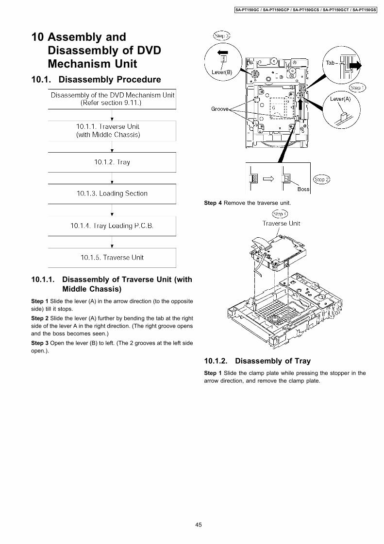
10.1.1. Disassembly of Traverse Unit (withMiddle Chassis)
Step 1 Slide the lever (A) in the arrow direction (to the oppositeside) till it stops.Step 2 Slide the lever (A) further by bending the tab at the rightside of the lever A in the right direction. (The right groove opensand the boss becomes seen.)Step 3 Open the lever (B) to left. (The 2 grooves at the left sideopen.).
Step 4 Remove the traverse unit.
10.1.2. Disassembly of TrayStep 1 Slide the clamp plate while pressing the stopper in thearrow direction, and remove the clamp plate.
45
SA-PT150GC / SA-PT150GCP / SA-PT150GCS / SA-PT150GCT / SA-PT150GS
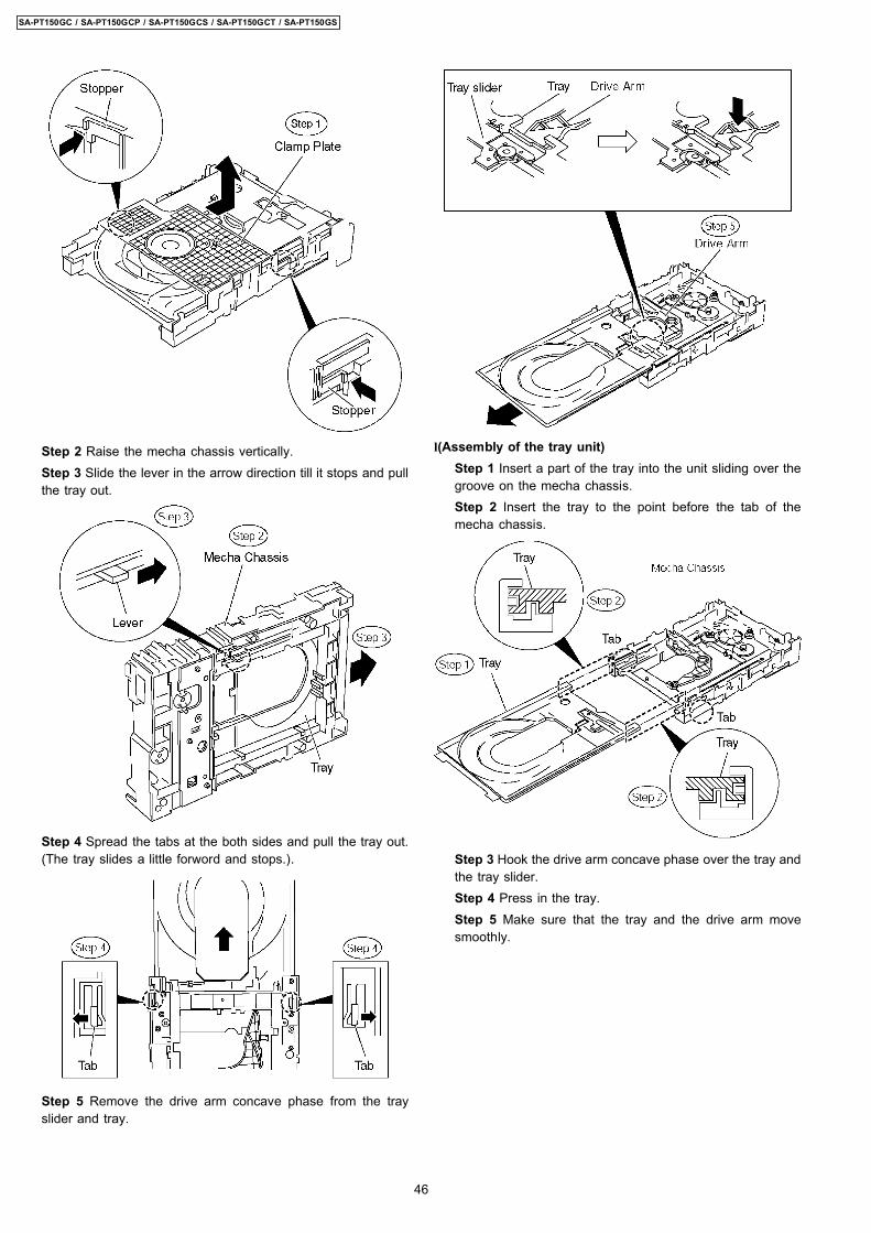
Step 2 Raise the mecha chassis vertically.Step 3 Slide the lever in the arrow direction till it stops and pullthe tray out.
Step 4 Spread the tabs at the both sides and pull the tray out.(The tray slides a little forword and stops.).
Step 5 Remove the drive arm concave phase from the trayslider and tray.
l(Assembly of the tray unit)Step 1 Insert a part of the tray into the unit sliding over thegroove on the mecha chassis.Step 2 Insert the tray to the point before the tab of themecha chassis.
Step 3 Hook the drive arm concave phase over the tray andthe tray slider.Step 4 Press in the tray.Step 5 Make sure that the tray and the drive arm movesmoothly.
46
SA-PT150GC / SA-PT150GCP / SA-PT150GCS / SA-PT150GCT / SA-PT150GS
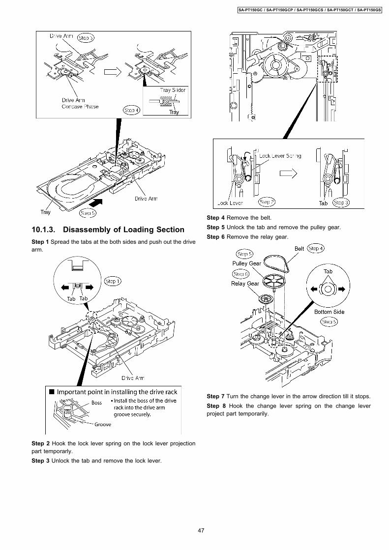
10.1.3. Disassembly of Loading SectionStep 1 Spread the tabs at the both sides and push out the drivearm.
Step 2 Hook the lock lever spring on the lock lever projectionpart temporarly.Step 3 Unlock the tab and remove the lock lever.
Step 4 Remove the belt.Step 5 Unlock the tab and remove the pulley gear.Step 6 Remove the relay gear.
Step 7 Turn the change lever in the arrow direction till it stops.Step 8 Hook the change lever spring on the change leverproject part temporarily.
47
SA-PT150GC / SA-PT150GCP / SA-PT150GCS / SA-PT150GCT / SA-PT150GS

Step 9 Pull the lever (B) at the bottom side in the direction ofarrow and remove the change lever.
Step 10 Remove the drive rack, the sub rack and the drive gearin the direction of arrow.
10.1.4. Disassembly of Tray LoadingP.C.B.
Step 1 Remove 3 screwsStep 2 Remove Tray Loading P.C.B.
10.1.5. Disassembly of Traverse UnitStep 1 Spread the tabs to push in the pin in the direction ofarrows.
Step 2 Remove 4 fixed pins.
48
SA-PT150GC / SA-PT150GCP / SA-PT150GCS / SA-PT150GCT / SA-PT150GS

Step 3 Remove the middle chassis.Step 4 Remove the traverse unit.
49
SA-PT150GC / SA-PT150GCP / SA-PT150GCS / SA-PT150GCT / SA-PT150GS
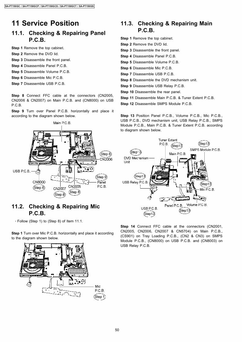
11 Service Position11.1. Checking & Repairing Panel
P.C.B.Step 1 Remove the top cabinet.Step 2 Remove the DVD lid.Step 3 Disassemble the front panel.Step 4 Disassemble Panel P.C.B.Step 5 Disassemble Volume P.C.B.Step 6 Disassemble Mic P.C.B.Step 7 Disassemble USB P.C.B.
Step 8 Connect FFC cable at the connectors (CN2005,CN2006 & CN2007) on Main P.C.B. and (CN8000) on USBP.C.B.Step 9 Turn over Panel P.C.B. horizontally and place itaccording to the diagram shown below.
11.2. Checking & Repairing MicP.C.B.
· Follow (Step 1) to (Step 8) of Item 11.1.
Step 1 Turn over Mic P.C.B. horizontally and place it accordingto the diagram shown below.
11.3. Checking & Repairing MainP.C.B.
Step 1 Remove the top cabinet.Step 2 Remove the DVD lid.Step 3 Disassemble the front panel.Step 4 Disassemble Panel P.C.B.Step 5 Disassemble Volume P.C.B.Step 6 Disassemble Mic P.C.B.Step 7 Disassemble USB P.C.B.Step 8 Disassemble the DVD mechanism unit.Step 9 Disassemble USB Relay P.C.B.Step 10 Disassemble the rear panel.Step 11 Disassemble Main P.C.B. & Tuner Extent P.C.B.Step 12 Disassemble SMPS Module P.C.B.
Step 13 Position Panel P.C.B., Volume P.C.B., Mic P.C.B.,USB P.C.B., DVD mechanism unit, USB Relay P.C.B., SMPSModule P.C.B., Main P.C.B. & Tuner Extent P.C.B. accordingto diagram shown below.
Step 14 Connect FFC cable at the connectors (CN2001,CN2005, CN2006, CN2007 & CN5704) on Main P.C.B.,(CS901) on Tray Loading P.C.B., (CN2 & CN3) on SMPSModule P.C.B., (CN8000) on USB P.C.B. and (CN8003) onUSB Relay P.C.B.
50
SA-PT150GC / SA-PT150GCP / SA-PT150GCS / SA-PT150GCT / SA-PT150GS
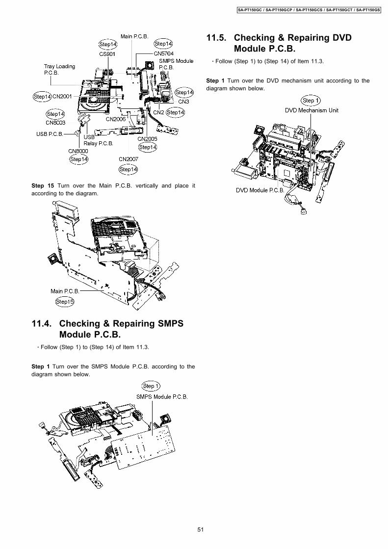
Step 15 Turn over the Main P.C.B. vertically and place itaccording to the diagram.
11.4. Checking & Repairing SMPSModule P.C.B.
· Follow (Step 1) to (Step 14) of Item 11.3.
Step 1 Turn over the SMPS Module P.C.B. according to thediagram shown below.
11.5. Checking & Repairing DVDModule P.C.B.
· Follow (Step 1) to (Step 14) of Item 11.3.
Step 1 Turn over the DVD mechanism unit according to thediagram shown below.
51
SA-PT150GC / SA-PT150GCP / SA-PT150GCS / SA-PT150GCT / SA-PT150GS
12 Measurements and Adjustments12.1. Service Tools and Equipment
Application Name NumberTilt adjustment DVD test disc DVDT-S20 [SPG]
TORX screw driver (T6) Available on sales route. (T6) orRFKZ0185 [SPG]
Others Grease RFKXPG641 [SPG]Confirmation CD test disc PVCD-K06 or any other commercially
available discVCD test disc PVCD-K06 or any other commercially
available discRecovery disc RFKZD03R005 [SPG]
12.2. Important points in adjustment12.2.1. Important points in optical adjustment · Before starting optical adjustment, be sure to take anti-static measures. · Optical pickup tilt adjustment is needed after replacement of the following components.
1. Optical pickup unit 2. Spindle motor unit 3. Optical pickup peripheral partsNotes
Adjustment is generally unnecessary after replacing other parts of the traverse unit. However, make adjustment if there is anoticeable degradation in picture quality. Optical adjustments cannot be made inside the optical pickup. Adjustment is generallyunnecessary after replacing the traverse unit.
12.2.2. Important points in electrical adjustment · Follow the adjustment procedures described in this manual.
12.3. Storing and handling of test discs · Surface precision is vital for DVD test discs. Be sure to store and handle them carefully.
1. Do not place discs directly onto the workbench, etc., after use. 2. Handle discs carefully in order to maintain their flatness. Place them into their case after use and store them vertically. Store
discs in a cool place where they are not exposed to direct sunlight or air from air conditioners. 3. Accurate adjustment will not be possible if the disc is warped when placed on a surface made of glass, etc. If this happens, use
a new test disc to make optical adjustments. 4. If adjustment is done using a warped disc, the adjustment will be incorrect and some discs will not be playable.
52
SA-PT150GC / SA-PT150GCP / SA-PT150GCS / SA-PT150GCT / SA-PT150GS
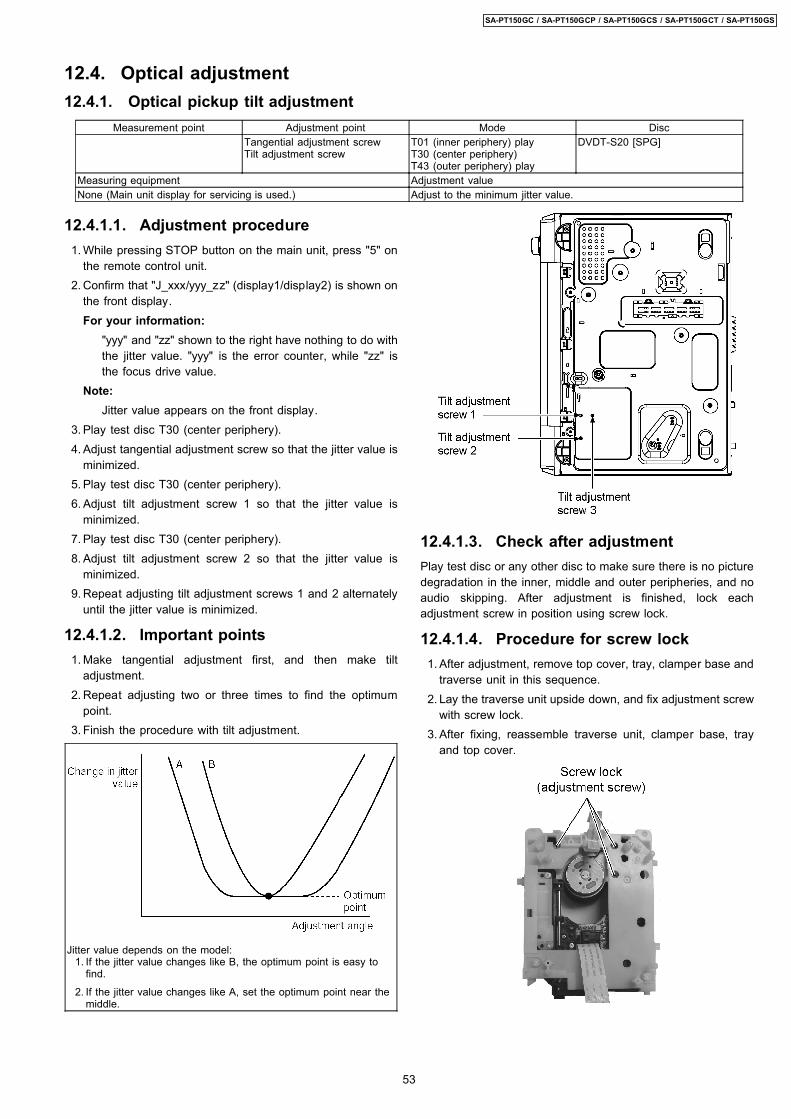
12.4.1.1. Adjustment procedure 1. While pressing STOP button on the main unit, press "5" on
the remote control unit. 2. Confirm that "J_xxx/yyy_zz" (display1/display2) is shown on
the front display.For your information:
"yyy" and "zz" shown to the right have nothing to do withthe jitter value. "yyy" is the error counter, while "zz" isthe focus drive value.
Note:Jitter value appears on the front display.
3. Play test disc T30 (center periphery). 4. Adjust tangential adjustment screw so that the jitter value is
minimized. 5. Play test disc T30 (center periphery). 6. Adjust tilt adjustment screw 1 so that the jitter value is
minimized. 7. Play test disc T30 (center periphery). 8. Adjust tilt adjustment screw 2 so that the jitter value is
minimized. 9. Repeat adjusting tilt adjustment screws 1 and 2 alternately
until the jitter value is minimized.
12.4.1.2. Important points 1. Make tangential adjustment first, and then make tilt
adjustment. 2. Repeat adjusting two or three times to find the optimum
point. 3. Finish the procedure with tilt adjustment.
Jitter value depends on the model: 1. If the jitter value changes like B, the optimum point is easy to
find.
2. If the jitter value changes like A, set the optimum point near themiddle.
12.4.1.3. Check after adjustmentPlay test disc or any other disc to make sure there is no picturedegradation in the inner, middle and outer peripheries, and noaudio skipping. After adjustment is finished, lock eachadjustment screw in position using screw lock.
12.4.1.4. Procedure for screw lock 1. After adjustment, remove top cover, tray, clamper base and
traverse unit in this sequence. 2. Lay the traverse unit upside down, and fix adjustment screw
with screw lock. 3. After fixing, reassemble traverse unit, clamper base, tray
and top cover.
12.4. Optical adjustment12.4.1. Optical pickup tilt adjustment
Measurement point Adjustment point Mode DiscTangential adjustment screwTilt adjustment screw
T01 (inner periphery) playT30 (center periphery)T43 (outer periphery) play
DVDT-S20 [SPG]
Measuring equipment Adjustment valueNone (Main unit display for servicing is used.) Adjust to the minimum jitter value.
53
SA-PT150GC / SA-PT150GCP / SA-PT150GCS / SA-PT150GCT / SA-PT150GS

13 AbbreviationsINITIAL/LOGO ABBREVIATIONS
A A0~UPACLKAD0~UPADATAALEAMUTEAREQARFASIASOASYNC
ADDRESSAUDIO CLOCKADDRESS BUSAUDIO PES PACKET DATAADDRESS LATCH ENABLEAUDIO MUTEAUDIO PES PACKET REQUESTAUDIO RFSERVO AMP INVERTED INPUTSERVO AMP OUTPUTAUDIO WORD DISTINCTION SYNC
B BCKBCKINBDOBLKCKBOTTOMBYPBYTCK
BIT CLOCK (PCM)BIT CLOCK INPUTBLACK DROP OUTSUB CODE BLOCK CLOCKCAP. FOR BOTTOM HOLDBYPATHBYTE CLOCK
C CAVCBDOCDCDSCKCDSRDATACDRFCDVCHNDATACKSLCLVCOFTRCPACPCSCPDTCPUADRCPUADTCPUIRQCPRDCPWRCSCSYNCINCSYNCOUT
CONSTANT ANGULAR VELOCITYCAP. BLACK DROP OUTCOMPACT DISCCD SERIAL DATA CLOCKCD SERIAL DATACD RF (EFM) SIGNALCOMPACT DISC-VIDEOCHANNEL DATASYSTEM CLOCK SELECTCONSTANT LINEAR VELOCITYCAP. OFF TRACKCPU ADDRESSCPU CHIP SELECTCPU DATACPU ADDRESS LATCHCPU ADDRESS DATA BUSCPU INTERRUPT REQUESTCPU READ ENABLECPU WRITE ENABLECHIP SELECTCOMPOSITE SYNC INCOMPOSITE SYNC OUT
D DACCKDEEMPDEMPHDIG0~UPDINDMSRCKDMUTEDODOUT0~UPDRFDRPOUTDREQDRESPDSCDSLFDVD
D/A CONVERTER CLOCKDEEMPHASIS BIT ON/OFFDEEMPHASIS SWITCHINGFL DIGIT OUTPUTDATA INPUTDM SERIAL DATA READ CLOCKDIGITAL MUTE CONTROLDROP OUTDATA OUTPUTDATA SLICE RF (BIAS)DROP OUT SIGNALDATA REQUESTDATA RESPONSEDIGITAL SERVO CONTROLLERDATA SLICE LOOP FILTERDIGITAL VIDEO DISC
INITIAL/LOGO ABBREVIATIONSE EC
ECR
ENCSELETMCLKETSCLK
ERROR TORQUE CONTROLERROR TORQUE CONTROLREFERENCEENCODER SELECTEXTERNAL M CLOCK (81MHz/40.5MHz)EXTERNAL S CLOCK (54MHz)
F FBALFCLKFEFFIFEOFGFSCFSCK
FOCUS BALANCEFRAME CLOCKFOCUS ERRORFOCUS ERROR AMP INVERTED INPUTFOCUS ERROR AMP OUTPUTFREQUENCY GENERATORFREQUENCY SUB CARRIERFS (384 OVER SAMPLING) CLOCK
G GND COMMON GROUNDING (EARTH)H HA0~UP
HD0~UPHINTHRXW
HOST ADDRESSHOST DATAHOST INTERRUPTHOST READ/WRITE
I IECOUTIPFRAGIREFISEL
IEC958 FORMAT DATA OUTPUTINTERPOLATION FLAGI (CURRENT) REFERENCEINTERFACE MODE SELECT
L LDONLPCLRCK
LASER DIODE CONTROLLASER POWER CONTROLL CH/R CH DISTINCTION CLOCK
M MA0~UPMCKMCKIMCLKMDATAMDQ0~UPMDQMMLDMPEG
MEMORY ADDRESSMEMORY CLOCKMEMORY CLOCK INPUTMEMORY SERIAL COMMAND CLOCKMEMORY SERIAL COMMAND DATAMEMORY DATA INPUT/OUTPUTMEMORY DATA I/O MASKMEMORY SERIAL COMMAND LOADMOVING PICTURE EXPERTS GROUP
O ODCOFTROSCIOSCOOSD
OPTICAL DISC CONTROLLEROFF TRACKINGOSCILLATOR INPUTOSCILLATOR OUTPUTON SCREEN DISPLAY
P P1~UPPCDPCKPDVDPEAKPLLCLKPLLOKPWMCTLPWMDAPWMOA, B
PORTCD TRACKING PHASE DIFFERENCEPLL CLOCKDVD TRACKING PHASE DIFFERENCECAP. FOR PEAK HOLDCHANNEL PLL CLOCKPLL LOCKPWM OUTPUT CONTROLPULSE WAVE MOTOR DRIVE APULSE WAVE MOTOR OUT A, B
54
SA-PT150GC / SA-PT150GCP / SA-PT150GCS / SA-PT150GCT / SA-PT150GS

INITIAL/LOGO ABBREVIATIONSR RE
RFENVRFORSRSELRSTRSV
READ ENABLERF ENVELOPERF PHASE DIFFERENCE OUTPUT(CD-ROM) REGISTER SELECTRF POLARITY SELECTRESETRESERVE
S SBI0, 1SBO0SBT0, 1SCKSCKRSCLSCLKSDASEG0~UPSELCLKSENSIN1, 2SOUT1, 2SPDISPDOSPENSPRCLKSPWCLKSQCKSQCXSRDATASRMADRSRMDT0~7SSSTATSTCLKSTD0~UPSTENABLESTSELSTVALIDSUBCSBCKSUBQSYSCLK
SERIAL DATA INPUTSERIAL DATA OUTPUTSERIAL CLOCKSERIAL DATA CLOCKAUDIO SERIAL CLOCK RECEIVERSERIAL CLOCKSERIAL CLOCKSERIAL DATAFL SEGMENT OUTPUTSELECT CLOCKSERIAL PORT ENABLESERIAL DATA INSERIAL DATA OUTSERIAL PORT DATA INPUTSERIAL PORT DATA OUTPUTSERIAL PORT R/W ENABLESERIAL PORT READ CLOCKSERIAL PORT WRITE CLOCKSUB CODE Q CLOCKSUB CODE Q DATA READ CLOCKSERIAL DATASRAM ADDRESS BUSSRAM DATA BUS 0~7START/STOPSTATUSSTREAM DATA CLOCKSTREAM DATASTREAM DATA INPUT ENABLESTREAM DATA POLARITY SELECTSTREAM DATA VALIDITYSUB CODE SERIALSUB CODE CLOCKSUB CODE Q DATASYSTEM CLOCK
T TETIBALTIDTINTIPTISTPSNTPSOTPSPTRCRSTRONTRSON
TRACKING ERRORBALANCE CONTROLBALANCE OUTPUT 1BALANCE INPUTBALANCE INPUTBALANCE OUTPUT 2OP AMP INPUTOP AMP OUTPUTOP AMP INVERTED INPUTTRACK CROSS SIGNALTRACKING ONTRAVERSE SERVO ON
INITIAL/LOGO ABBREVIATIONSV VBLANK
VCC
VCDCONT
VDDVFBVREFVSS
V BLANKINGCOLLECTOR POWER SUPPLYVOLTAGEVIDEO CD CONTROL (TRACKINGBALANCE)DRAIN POWER SUPPLY VOLTAGEVIDEO FEED BACKVOLTAGE REFERENCESOURCE POWER SUPPLY VOLTAGE
W WAITWDCKWEHWSR
BUS CYCLE WAITWORD CLOCKWRITE ENABLE HIGHWORD SELECT RECEIVER
X XXALEXAREQXCDROMXCSXCSYNCXDSXHSYNCOXHINTXIXINTXMWXOXREXSRMCEXSRMOEXSRMWEXVCSXVDSXVSYNCO
X´ TALX ADDRESS LATCH ENABLEX AUDIO DATA REQUESTX CD ROM CHIP SELECTX CHIP SELECTX COMPOSITE SYNCX DATA STROBEX HORIZONTAL SYNC OUTPUTXH INTERRUPT REQUESTX´ TAL OSCILLATOR INPUTX INTERRUPTX MEMORY WRITE ENABLEX´ TAL OSCILLATOR OUTPUTX READ ENABLEX SRAM CHIP ENABLEX SRAM OUTPUT ENABLEX SRAM WRITE ENABLEX V-DEC CHIP SELECTX V-DEC CONTROL BUS STROBEX VERTICAL SYNC OUTPUT
55
SA-PT150GC / SA-PT150GCP / SA-PT150GCS / SA-PT150GCT / SA-PT150GS

14 Voltage and Waveform Chart14.1. DVD Module P.C.B.
Ref No.MODE 1 2 3 4 5 6 7 8 9 10 11 12 13 14 15 16 17 18 19 20
CD PLAY 1.2 1.4 1.5 0 0 3.4 1.8 1.3 1.4 1.2 1.3 0 1.1 1 0 3.4 1.3 1.1 1.9 0.7Ref No.MODE 21 22 23 24 25 26 27 28 29 30 31 32 33 34 35 36 37 38 39 40
CD PLAY 0.6 0.4 2.3 0.5 1.4 2.6 2 0.8 1.8 0.7 3.4 0 3.4 0.7 1.1 1.5 1.6 1.8 1.4 2Ref No.MODE 41 42 43 44 45 46 47 48 49 50 51 52 53 54 55 56 57 58 59 60
CD PLAY 1.8 0 0 1.3 0 3.4 3.4 3.4 3.4 1.7 0 3.4 2.8 2.8 3 3.4 3.2 3.2 0 3.2Ref No.MODE 61 62 63 64 65 66 67 68 69 70 71 72 73 74 75 76 77 78 79 80
CD PLAY 0.1 0 0 0.8 0.1 1.9 1.6 0 3.2 3.2 0 3.2 3.2 0 0.1 0 0 0 0 0Ref No.MODE 81 82 83 84 85 86 87 88 89 90 91 92 93 94 95 96 97 98 99 100
CD PLAY 0 0 1.2 3.2 0.8 2.3 0 1.8 0 0.5 1.8 3.3 2.2 2.2 1.8 1.8 1.7 1.7 1.7 1.7Ref No.MODE 101 102 103 104 105 106 107 108 109 110 111 112 113 114 115 116 117 118 119 120
CD PLAY 0 0 0.4 0.1 0.2 1.9 3.3 0 2.2 1.7 2.6 2.6 2.6 2.6 2.7 2.7 2.4 2.5 2.5 2.5Ref No.MODE 121 122 123 124 125 126 127 128 129 130 131 132 133 134 135 136 137 138 139 140
CD PLAY 1.8 2.0 2 1.7 0 1.7 1.7 3.4 0.9 0.9 0.4 3.3 2.4 1 1 2.4 0 0.4 0.9 0Ref No.MODE 141 142 143 144 145 146 147 148 149 150 151 152 153 154 155 156 157 158 159 160
CD PLAY 3.4 3.4 0 0 0 0 3.4 1.5 1.7 1.7 0.9 1.7 0 3.4 1.5 1.6 0 1.3 3 3.1Ref No.MODE 161 162 163 164 165 166 167 168 169 170 171 172 173 174 175 176 177 178 179 180
CD PLAY 2.9 3.2 2.9 3.1 0 3.4 3.2 3.1 3 3 3.1 3 0 3.4 3.2 3 3.1 2.9 2.9 2.9Ref No.MODE 181 182 183 184 185 186 187 188 189 190 191 192 193 194 195 196 197 198 199 200
CD PLAY 3.3 0 1.6 3.4 1.6 0 1.3 3.3 3.3 3.2 3.1 0.1 2.1 0 0 3 1.5 0 0 1.6Ref No.MODE 201 202 203 204 205 206 207 208 209 210 211 212 213 214 215 216
CD PLAY 3.4 0.1 2.2 0.1 0 3.4 0.3 1.6 1.6 0 1.2 1.8 2.7 2.5 1.4 1Ref No.MODE 1 2 3 4 5 6 7 8 9 10 11 12 13 14 15 16 17 18 19 20
CD PLAY 3.3 3.1 3.4 3.2 3.1 0 3.1 3.3 3.4 3 3 0 2.9 3.4 2.9 3.3 3.3 3.3 3.2 2.2Ref No.MODE 21 22 23 24 25 26 27 28 29 30 31 32 33 34 35 36 37 38 39 40
CD PLAY 1.6 0 0.1 0.4 0.4 1.6 3.4 0 1.6 1.8 1.7 1.7 0.1 0.1 0.1 0 3.4 1.5 2.9 0Ref No.MODE 41 42 43 44 45 46 47 48 49 50 51 52 53 54
CD PLAY 0 3.1 3.4 3.2 3.1 0 3 3.2 3.4 2.9 2.9 0 3 0Ref No.MODE 1 2 3 4 5 6 7 8
CD PLAY 3.4 - 0.1 - 4.4 - - 4.7Ref No.MODE 1 2 3 4 5
CD PLAY 2.5 2.5 0 1.3 0.8Ref No.MODE 1 2 3 4 5 6 7 8 9 10 11 12 13 14 15 16 17 18 19 20
CD PLAY 1.7 1.7 1.7 2.2 2.2 1.8 0 5.1 3.3 0 2.4 2.8 2.6 2.6 4.1 4.3 4.8 3.7 0 3.3Ref No.MODE 21 22 23 24 25 26 27 28 29 30
CD PLAY 8.9 8.8 1.7 1.7 1.7 1.7 3.3 5.1 0 0Ref No.MODE 1 2 3 4 5 6 7 8 9 10 11 12 13 14 15 16 17 18 19 20
CD PLAY 0 3.3 2.9 3.3 1.6 0.9 1.7 1.7 5.2 0 0.9 0.1 0.1 0 2.5 2.5 5.2 0 2.5 2.5Ref No.MODE 21 22 23 24 25 26 27 28
CD PLAY 2.5 2.5 5.2 0 2.6 2.5 2.6 5.1Ref No.MODE 1 2 3 4 1 2 3 4 5 1 2 3 4 5 6 7 8
CD PLAY 1.2 3.3 0 0 3.3 3.3 0 0 - 0 0 0 0 3.2 3.3 0 3.3Ref No.MODE 1 2 3 4 5 6 7 8 9 10 11 12 13 14 15 16 17 18 19 20
CD PLAY 1.1 1.0 1.8 1.0 1.7 2.3 1.3 1.8 1.2 0.1 3.3 3.3 3.3 3.3 1.6 1.6 0.6 1.2 1.5 1.7Ref No.MODE 21 22 23 24 25 26 27 28 29 30 31 32 33 34 35 36 37 38 39 40
CD PLAY 1.8 1.8 2 1.9 0 2 0 2.5 1.7 1.1 0.8 1.6 1.0 1.6 2.3 1.4 3.3 1.7 1.1 1.4Ref No.MODE 41 42 43 44 45 46 47 48
CD PLAY 1.6 1.7 1.7 2 1.9 0 3.3 0.8
IC8421
IC8651
IC8651
IC8651
IC8251
IC8421
IC8051
IC8051
IC8111
IC8151
IC8251
IC8001
IC8051
IC8001
IC8001
IC8001
IC8001
IC8001
IC8001
IC8001
IC8001
IC8001
IC8001
IC8611IC8606IC8601
56
SA-PT150GC / SA-PT150GCP / SA-PT150GCS / SA-PT150GCT / SA-PT150GS

Ref No.MODE 1 2 3 4 5 1 2 3 4 5 1 2 3 4 5 6
CD PLAY 3 3 0 4.6 5.1 2.7 2.7 0 4.2 5.1 1.6 0.1 1.6 1.7 3.3 1.6Ref No.MODE 1 2 3 4 5 6 7 8
CD PLAY 0.1 5.1 5.1 3.3 2.2 3.3 0.1 3.4Ref No.MODE E C B E C B E C B E C B E C B
CD PLAY 1.1 0 0.4 1.5 0 0.9 1.1 0 0.4 1.6 0 0.9 1.5 0 0.9Ref No.MODE E C B E C B E C B E C B
CD PLAY 0.1 4.6 0.1 0.1 4.6 4.6 1.9 3.5 1.3 3.5 4.1 4.1Ref No.MODE 1 2 3 4 5 6 E C B E C B
CD PLAY 0.1 0.1 1.4 0.1 0.1 4.4 0 0.1 4.0 3.4 3.3 0.1
IC9005
IC9003IC8695IC8691
Q8341Q8335
Q8551
SA-PT150GC/GS/GCS/GCT/GCP DVD MODULE P.C.B.
QR8111 QR8420 QR8571
Q8552 Q8561 Q8562
Q8321 Q8325 Q8331
57
SA-PT150GC / SA-PT150GCP / SA-PT150GCS / SA-PT150GCT / SA-PT150GS

14.2. Main P.C.B.Ref No.MODE 1 2 3 4 5 6 7 8
CD PLAY - 5.2 0 0 0 0 0 -STANDBY - 5.2 0 0 0 0 0 -
Ref No.MODE 1 2 3 4 5 6 7 8 9 10 11 12 13 14 15 16 17 18 19 20
CD PLAY 0 2.2 4 3.6 0 2.8 0 0 0 0 0 4.2 2.4 0 2.5 5.1 5.1 5.1 3.2 0STANDBY 0 5 5.1 5.2 0 5 0 0 0 0 0 5.1 2.5 0 2.5 5.1 5.1 5.1 3.2 0
Ref No.MODE 21 22 23 24 25 26 27 28 29 30 31 32 33 34 35 36 37 38 39 40
CD PLAY 5.2 0 0 0 0 0 0 4.4 4.1 2.7 0 0 0 0 5.2 5.2 5.1 5.2 0 5.1STANDBY 5.2 0 0 0 0 0 0 4.5 4.1 2.8 0 0 0 0 5.2 5.2 5.1 5.2 0 5
Ref No.MODE 41 42 43 44 45 46 47 48 49 50 51 52 53 54 55 56 57 58 59 60
CD PLAY 0 0 0 0 0 0 0 0 0 0 0 0 0 0 0 0 0 0 0 0STANDBY 0 0 0 0 0 0 0 0 0 0 0 0 0 0 0 0 0 0 0 0
Ref No.MODE 61 62 63 64 65 66 67 68 69 70 71 72 73 74 75 76 77 78 79 80
CD PLAY 0 5.1 0 0 5.1 0 5.1 5.1 0 5.2 5.1 0 0 0 0 0 0 0 0 5.1STANDBY 0 5.1 0 0 5.1 0 5.1 5 5 5.2 5.1 0 0 0 0 0 0 0 4.6 5
Ref No.MODE 81 82 83 84 85 86 87 88 89 90 91 92 93 94 95 96 97 98 99 100
CD PLAY 0 0 5.1 0 4.1 2.5 1.9 5.2 2.6 0.4 5.2 1.7 3.1 4.8 2.1 0 5.2 5.2 5.1 5.1STANDBY 0 0 5.1 0 0 2.3 2 5.2 2.6 0.4 5.2 1.7 3.1 4.8 2.1 0 5.2 5.2 5.1 5.1
Ref No.MODE 1 2 3 4 5 6 7 8 9 10 11 12 13 14 15 16 17 18 19 20
CD PLAY 0 0 0 0 0 0 0 0 0 0 0 0 0 0 0 0 0 0 0 0STANDBY 0 0 0 0 0 0 0 0 0 0 0 0 0 0 0 0 0 0 0 0
Ref No.MODE 21 22 23 24 25 26 27 28 29 30 31 32 33 34 35 36 37 38 39 40
CD PLAY 0 0 0 0 0 0 0 0 0 0 0 0.1 0 0 0 0 0 0 0 0.1STANDBY 0 0 0 0 0 0 0 0 0 0 0 0.1 0 0 0 0 0 0 0 0.1
Ref No.MODE 41 42 43 44 45 46 47 48 49 50 51 52 53 54 55 56 57 58 59 60
CD PLAY 0 0 0 0 0 0 0 0 0 1.3 0 0 0 0.1 0 0 0 0 0 0STANDBY 0 0 0 0 0 0 0 0 1.4 0 0 0 0.1 0 0 0 0 0 0
Ref No.MODE 61 62 63 64 65 66 67 68 69 70 71 72 73 74 75 76 77 78 79 80
CD PLAY 0 -0.1 0 0 4.8 0 5.6 0 0 0 0 0 0 0 0 0 0 0 0 0STANDBY 0 -0.1 0 0 4.8 0 5.6 0.1 0 0 0 0 0 0 0 0 0 0 0 0
Ref No.MODE 81 82 83 84 85 86 87 88 89 90 91 92 93 94 95 96 97 98 99 100
CD PLAY 0 0 0 0 -6.2 6.3 0 0 0 0 0 0 0 0 0 0 0 0 0 0STANDBY 0 0 0 0 -6.4 6.5 0 0 0 0 0 0 0 0 0 0 0 0 0 0
Ref No.MODE 1 2 3 4 5 6 7 8 9 10 11 12 13 14 15 16 17 18 19 20
CD PLAY 4.9 0 2.1 4.8 1.6 0 1.6 2.1 0 0 0 2.1 4.8 2.1 4.9 2.2 2.2 0 2.2 2.2STANDBY 4.9 0 2.1 4.8 1.5 0 1.5 2.1 0 1.5 0 2.1 4.8 2.1 4.9 2.2 2.2 0 2.2 2.2
Ref No.MODE 21 22 23 24 25 26 27 28 29 30 31 1 2 3 4 5 6
CD PLAY 0 1.3 1.3 0 1.3 1.3 0 1.4 1.6 0 2.2 0 2.5 4.9 2.5 0 2.5STANDBY 0 1.3 1.3 0 1.3 1.3 0 1.4 1.6 0 2.2 0 2.5 4.9 2.5 0 2.5
Ref No.MODE 1 2 3 4 5 6
CD PLAY 1.6 0 1.7 1.7 3.4 1.7STANDBY 1.6 0 1.7 1.7 3.4 1.7
Ref No.MODE 1 2 3 4 5 6 7 8 9 10 11 12
CD PLAY 25.9 12.7 0 12.6 4.7 0 0 0 0 12.7 0 12.7STANDBY 26.0 12.8 0 12.7 4.7 0 0 0 3.0 12.8 0 12.8
Ref No.MODE 1 2 3 4 5 6 7 8 9 10 11 12
CD PLAY 25.9 12.7 0 12.7 4.7 0 0 0 3.0 12.7 0 12.7STANDBY 26.0 12.7 0 12.7 4.7 0 0 0 3.0 12.8 0 12.7
Ref No.MODE 1 2 3 4 5 6 7 8 9 10 11 12
CD PLAY 25.9 12.7 0 13.0 4.7 0 0 0 0 12.7 0 12.8STANDBY 25.6 12.7 0 12.7 4.6 0 0 0 3.0 12.7 0 12.8
Ref No.MODE 1 2 3 4 5 6 7 8 9 10 11 12 13 14 15 16
CD PLAY - 2.6 2.6 2.6 2.6 0.6 0.6 0 2.6 2.6 2.6 2.6 2.6 0.9 5.2 -STANDBY - 2.6 2.6 2.6 2.6 0.6 0.6 0 2.6 2.6 2.6 2.6 2.6 0.9 5.2 -
Ref No.MODE 1 2 3 4 5 6 7 8
CD PLAY 0 0 0 -7 0 0 6.7 7STANDBY 0 0 0 -7 0 0 6.7 7
Ref No.MODE E C B E C B E C B E C B E C B
CD PLAY 0 2.2 0 0 0 4.5 1.1 0 0.5 0 0 4.7 0 4.8 0STANDBY 0 0.1 0 0 0 0 0 0 0 0 0 4.6 0 4.6 2
Ref No.MODE E C B E C B E C B E C B E C B
CD PLAY 0 5.2 0 -7.5 -23.3 -7.0 -6.3 -21.0 -6.8 12.9 21.2 13.5 3.2 3.5 3.7STANDBY 0 5.2 0 -7.5 -23.3 -7.0 -6.9 -21.0 -6.4 12.9 21.2 13.5 3.2 3.2 3.8
Ref No.MODE E C B E C B E C B E C B E C B
CD PLAY -21.8 -25.4 -22.4 1.6 1.6 0 0 0 0.6 0 0.2 0.2 8.9 17.1 9.5STANDBY -21.7 -25.3 -22.3 1.6 1.6 0 0 0 0.6 0 0.1 0 8.9 17.1 9.5
Ref No.MODE E C B E C B 1 2 3 1 2 3 4 E C B
CD PLAY 0 4.9 0 0 0.1 0.7 0 4.6 0.1 5.6 4.4 0 0.4 0 0.1 4.8STANDBY 0 4.9 0 0 0.1 0.7 0 4.6 0.1 5.6 4.4 0 0.4 0 0.1 4.8
Ref No.MODE E C B E C B E C B
CD PLAY 0 0 0 0 0 5 0 0 0STANDBY 0 0 0 0 0 5 0 0 0
IC7101
Q7100 Q7101 Q7102
Q5742
Q3003 Q3008
Q2905
Q2801Q2004
IC2004
IC2801
IC2801 IC2802
IC2102
Q2003
IC2018
IC2018
IC2018
IC2018
IC2102
IC2102
IC2102
IC2102
IC5200
IC2903
IC7100
IC5300
IC2018
Q5744 Q5745 Q5746
Q2914
Q2974
IC5100
Q5741
Q2030
Q2910
Q2006
Q2907Q2906
SA-PT150GC/GS/GCS/GCT/GCP MAIN P.C.B.
Q5740Q3009
58
SA-PT150GC / SA-PT150GCP / SA-PT150GCS / SA-PT150GCT / SA-PT150GS
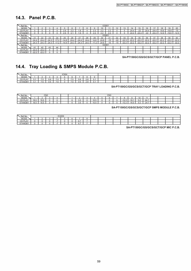
14.3. Panel P.C.B.Ref No.MODE 1 2 3 4 5 6 7 8 9 10 11 12 13 14 15 16 17 18 19 20
CD PLAY 0 0 0 0 2.9 2.2 1.8 4 2.3 2.2 2.2 0 5 -24.4 -22 -24.4 -24.4 -19.6 -19.8 -15STANDBY 0 0 0 0 2.9 2.1 1.9 4 2.2 2.2 2.2 0 5 -24.4 -24.4 -22 -24.4 -14.9 -19.6 -12.5
Ref No.MODE 21 22 23 24 25 26 27 28 29 30 31 32 33 34 35 36 37 38 39 40
CD PLAY -24.4 -24.4 -24.3 -17.2 -14.8 -24.4 -24.4 -24.4 14.8 -24.8 -15 -22 -22.3 -22.2 -22.2 -22.2 -22.2 -22.2 -22.2 -22.2STANDBY -24.3 -24.3 -24.3 -17.2 -14.9 -24.3 -24.3 -24.3 -17.2 -24.8 -15 -15 -22.2 -22.2 -22.2 -22.2 -22.2 -22.2 -22.2 -22.2
Ref No.MODE 41 42 43 44
CD PLAY -22.2 -22.2 5 0STANDBY -22.2 -22.2 5 0
SA-PT150GC/GS/GCS/GCT/GCP PANEL P.C.B.
IC6901
IC6901
IC6901
14.4. Tray Loading & SMPS Module P.C.B.Ref No.MODE 1 2 3 4 5 6 7 8 9
CD PLAY 5.1 7.5 0.6 7.5 0 7.5 0.6 2.8 5.1STANDBY 5.1 7.6 0.6 7.6 0 7.6 0.6 2.8 5.1
Ref No.MODE 1 2 3 4 1 2 3 4 5 6 7 8 9 10 11
CD PLAY 18.5 18.5 0 0 6 3.5 0 10.5 0 0 5 -12.3 -16.1 5.2 24.7STANDBY 18.5 18.5 0 0 6 3.5 0 10.5 0 0 5 -12.2 -16.0 5.2 -24.7
Ref No.MODE 1 2 3 4 5 6 7 8
CD PLAY 0 0 0 -7 0 0 6.7 7STANDBY 0 0 0 -7 0 0 6.7 7
SA-PT150GC/GS/GCS/GCT/GCP MIC P.C.B.
SA-PT150GC/GS/GCS/GCT/GCP SMPS MODULE P.C.B.
IC2204
CN2 CN3
SA-PT150GC/GS/GCS/GCT/GCP TRAY LOADING P.C.B.
IC904
59
SA-PT150GC / SA-PT150GCP / SA-PT150GCS / SA-PT150GCT / SA-PT150GS

14.5. Waveform Chart14.5.1. Waveform 1
WF No. IC2018-13 (PLAY)
200Vp-p(5msec/div)
WF No. IC2018-15 (PLAY)
3.4Vp-p(50nsec/div)
WF No. IC2102-79,80,81,82 83,84 (PLAY)
1.4Vp-p(200usec/div)
WF No. IC2102-95,99 (PLAY)
2Vp-p(200usec/div)
WF No. IC2102-96 (PLAY)
0.3Vp-p(200sec/div)
WF No. IC2102-100 (PLAY)
0.7Vp-p(200usec/div)
WF No. IC5100- 2,12(PLAY)
0.6Vp-p(200usec/div) 2.1Vp-p(200usec/div)
WF No. IC5100-6,8 (PLAY) WF No. IC5200- 2,12(PLAY)
0.6Vp-p(200usec/div)
2.1Vp-p(200usec/div)
WF No. IC5200-6,8 (PLAY) WF No. IC5300- 2,12(PLAY)
0.6Vp-p(200usec/div) 2.1Vp-p(200usec/div)
WF No. IC5300-6,8 (PLAY)
WF No. IC8001-64,67 (PLAY)
0.4Vp-p(200usec/div)
WF No. IC6901-5 (PLAY)
2.1Vp-p(5usec/div)
WF No. IC8001-95,96 (PLAY) WF No. IC8001-122,126 (PLAY)
3.4Vp-p(200usec/div) 4Vp-p(200usec/div)
WF No. IC2801-6 (PLAY)
1.2Vp-p(20usec/div)
WF No. IC2801-8,11 (PLAY)
1.3Vp-p(100nsec/div)
WF No. IC2801-4 (PLAY)
0.7Vp-p(20usec/div)
WF No. IC2801-13,15 (PLAY)
3.4Vp-p(2usec/div)
WF No. IC2801-18,21 (PLAY)
0.25Vp-p(20usec/div)
WF No. IC2801-24 (PLAY)
3.4Vp-p(20usec/div)
WF No. IC2801-30 (PLAY)
3.4Vp-p(20usec/div)
WF No. IC8001-146 (PLAY)
6.4Vp-p(2usec/div)
60
SA-PT150GC / SA-PT150GCP / SA-PT150GCS / SA-PT150GCT / SA-PT150GS
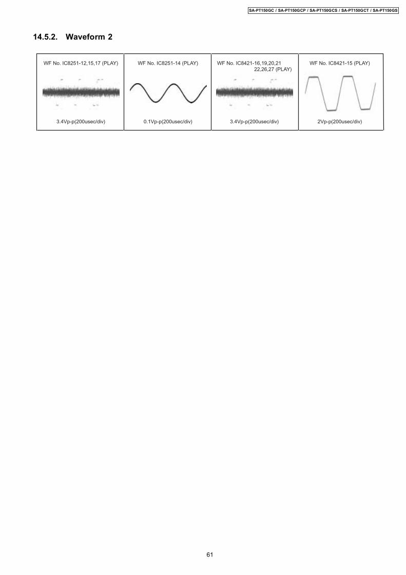
14.5.2. Waveform 2
WF No. IC8251-14 (PLAY)
0.1Vp-p(200usec/div)
WF No. IC8251-12,15,17 (PLAY) WF No. IC8421-15 (PLAY)WF No. IC8421-16,19,20,21 22,26,27 (PLAY)
3.4Vp-p(200usec/div)3.4Vp-p(200usec/div) 2Vp-p(200usec/div)
61
SA-PT150GC / SA-PT150GCP / SA-PT150GCS / SA-PT150GCT / SA-PT150GS
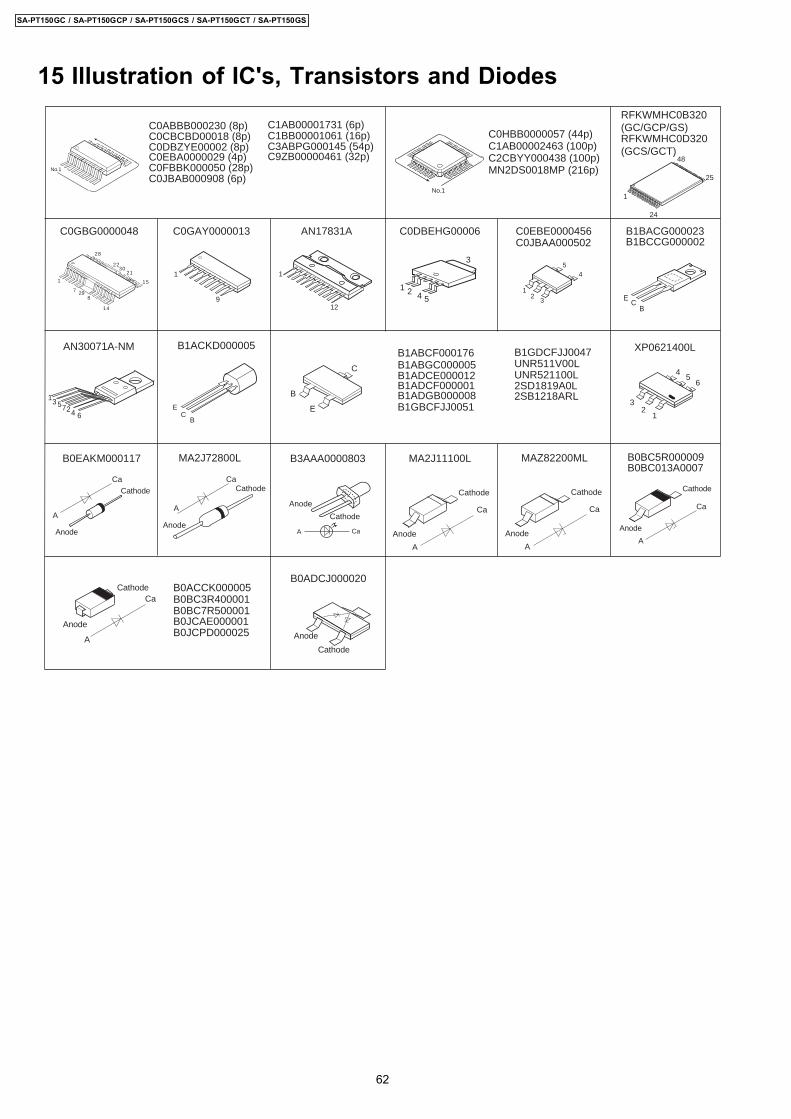
15 Illustration of IC's, Transistors and Diodes
No.1
No.1
B0EAKM000117
A
Ca
Cathode
Anode
C3ABPG000145 (54p)C1BB00001061 (16p)
C9ZB00000461 (32p)
XP0621400L
C0EBA0000029 (4p)C0FBBK000050 (28p)
C0DBZYE00002 (8p)C0CBCBD00018 (8p)C0ABBB000230 (8p)
C0JBAB000908 (6p)
C1AB00001731 (6p)C0HBB0000057 (44p)C1AB00002463 (100p)C2CBYY000438 (100p)MN2DS0018MP (216p)
RFKWMHC0B320(GC/GCP/GS)RFKWMHC0D320(GCS/GCT)
1
24
25
48
A
CaCathode
Anode
B0ACCK000005
B0JCPD000025
B0BC3R400001B0BC7R500001B0JCAE000001
A
Ca
Cathode
Anode
B0BC013A0007B0BC5R000009
Cathode
A
Ca
Anode
MA2J11100L
Cathode
A
Ca
Anode
MAZ82200ML
A
CaCathode
Anode
MA2J72800L
AN30071A-NM
2SD1819A0L2SB1218ARL
UNR511V00LUNR521100L
B1ABCF000176
B1GBCFJJ0051
B1GDCFJJ0047
B1ADGB000008
B1ABGC000005B1ADCE000012B1ADCF000001
C0GBG0000048
1
28
15
14
7
2130
22
829
B1ACKD000005
142
5
3
C0DBEHG00006
CE
B
B1BACG000023B1BCCG000002
EC
B
C0EBE0000456C0JBAA000502
1
45
23
B0ADCJ000020
Anode
Cathode
E
C
B
C0GAY0000013
1
9
B3AAA0000803
Anode
Cathode
CaA
AN17831A
1
12
2
134 6
571
23
45
6
62
SA-PT150GC / SA-PT150GCP / SA-PT150GCS / SA-PT150GCT / SA-PT150GS
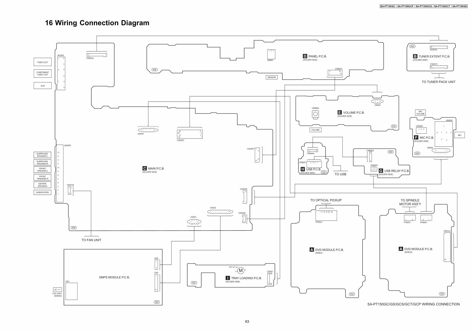
16 Wiring Connection Diagram
SA-PT150GC/GS/GCS/GCT/GCP WIRING CONNECTION
1
11
1
4
CN2
CN1
110V-240V 50/60HZ
AC
CN3
TO USB
A DVD MODULE P.C.B. (SIDE:B)
A DVD MODULE P.C.B. (SIDEA)
TO OPTICAL PICKUP
TO FAN UNIT
FP8531 FP9001FP8251
FP8101
50
1
1 5 10 15 20 26
151 6
AUX
SUBWOOFER
CENTER SPEAKER
FRONT SPEAKER R
FRONT SPEAKER L
SURROUND SPEAKER R
SURROUND SPEAKER L
JK2002
JK5000
CN2007
CN2001
H2004
CN5704
CN2002
H2002
H2001
CN2005
110
7 9
8
12
6
11
5
10
4
9
3
8
2
7
1
1
3
1 7
1
48
4749
5032
4
1 4
1 11
1
4
12
1213
CN6001
1
2 12
13
VR6800
H6004
1 4
CP2010
CN2010110
110
CN8000
CN8001
51
4 3 2 1
CN8003
CN8002
5 3 1
1
5
24
REF NO 316
+-
M CS9017
1
B TUNER EXTENT P.C.B. (SOLDER SIDE)
C MAIN P.C.B.
SMPS MODULE P.C.B.
(SOLDER SIDE)
I TRAY LOADING P.C.B. (SOLDER SIDE)
D PANEL P.C.B. (SOLDER SIDE)
E VOLUME P.C.B. (SOLDER SIDE)
G USB RELAY P.C.B. (SOLDER SIDE)
F MIC P.C.B. (SOLDER SIDE)
H USB P.C.B. (SOLDER SIDE)
VOLUME
SENSOR
1 32
Z6900
PbF
PbF
PbF
PbF
PbF
PbF
PbF
PbF
PbF
PbFPbF
TO SPINDLEMOTOR ASS’Y
TO TUNER PACK UNIT
3
4 6
5
1
2
COMPONENTVIDEO OUT
VIDEO OUT
VR6081
H6903
JK6802
MIC
MICVOLUME
32
54
1
78
17
1 2 3
1
7
CN2006
SA-PT150GC / SA-PT150GCP / SA-PT150GCS / SA-PT150GCT / SA-PT150GS
63

SA-PT150GC / SA-PT150GCP / SA-PT150GCS / SA-PT150GCT / SA-PT150GS
64
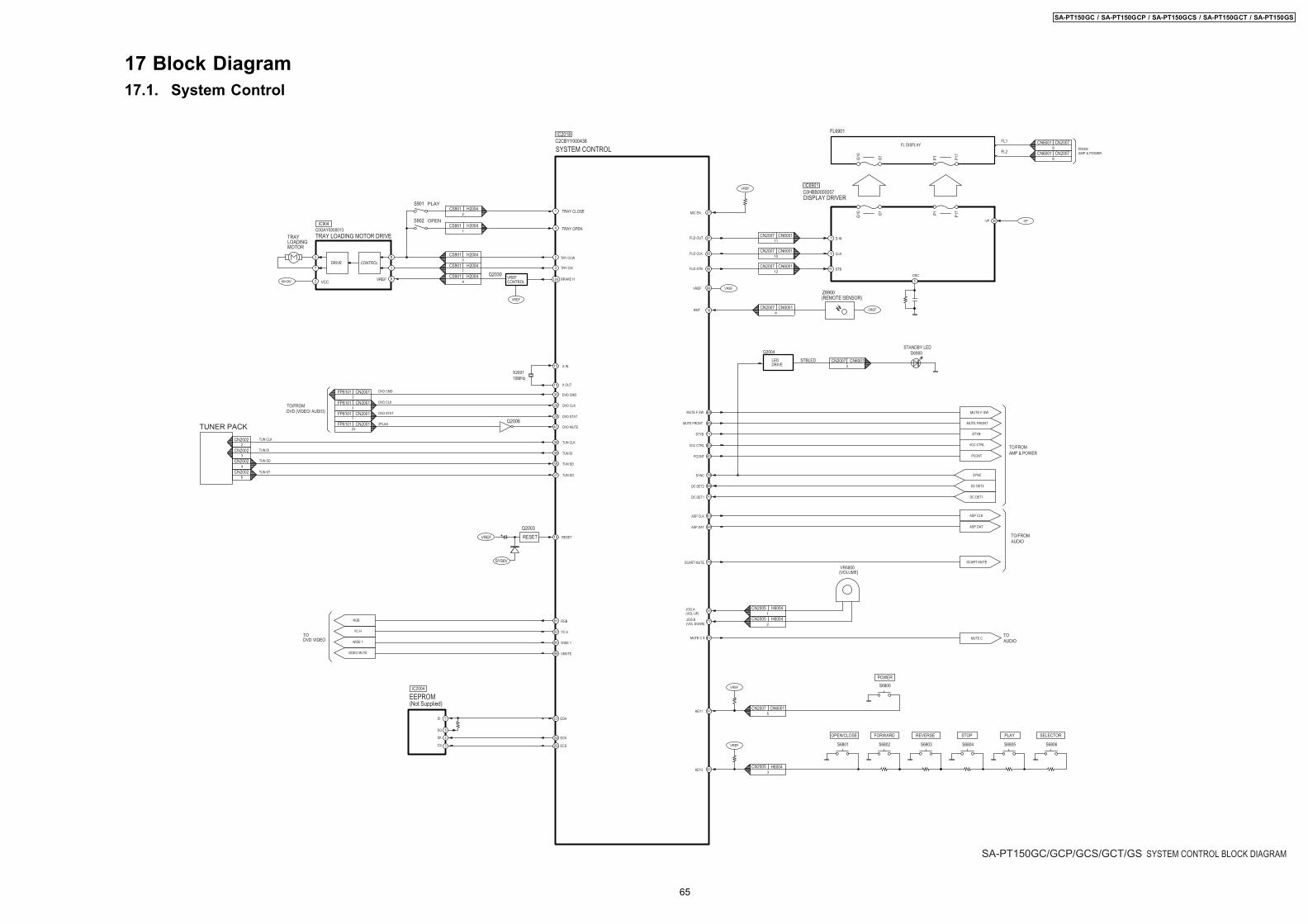
17 Block Diagram17.1. System Control
(VOLUME)VR6800
100
Q2006
S902
SYSTEM CONTROL
IC2018C2CBYY000438
SA-PT150GC/GCP/GCS/GCT/GS SYSTEM CONTROL BLOCK DIAGRAM
Q2030CONTROLVREF BRAKE H
VCCVREF
TRY CW
TRY CCW
MOTOR
TRAYLOADING
C0GAY0000013TRAY LOADING MOTOR DRIVE
IC904
CONTROLDRIVE7
3
28
1
9 2
12
3
13
15
30
4
TRAY CLOSE
DVD CMD
TUN CLK36
TUN DI38
DVD CLK28
DVD STAT29
DVD MUTE42
TUN SD35
TUN DO37
ECS25
ASP CLK 83
ASP DAT 84
MIC EN 21
ECK24
EDA23
SYNC 19
DC DET2 88
DC DET1 70
JOG A(VOL UP)
76
JOG B(VOL DOWN) 77
STYB
MUTE FRONT
68
PCONT 40
MUTE F SW
69
71
MUTE C S MUTE C67
VCC CTRL 65
KEY2 91
KEY1 97
DC DET1
MUTE F SW
MUTE FRONT
STYB
Q2004 D6900
DRIVELED
IC2004
EEPROM(Not Supplied)
CS
DO
SK
DI
FL DISPLAY
G1
P17
G10 P
1
G1
P17
G10
P1
FL6901
DISPLAY DRIVER
IC6901C0HBB0000057
FLD CLK
D IN
FL2
3
4
6
5
ASP CLK
ASP DAT
SCART MUTE 79 SCART MUTE
TO/FROM AUDIO
TOAUDIO
RGBRGB 81
YC HYC H 82
WIDE 1WIDE 1 80
VMUTEVIDEO MUTE 46
TO DVD VIDEO
87
STB
18
CLK85
7
8
9
FLD OUT
RMT
OSC
5
(REMOTE SENSOR)Z6900
98
86FLD STB
FL1
M+9V
OPEN
RESET
X IN
X OUT
X200110MHz
Q2003
RESETVREF
SYS6V
TUN CLK
TUN DI
TUN SD
TUN ST
TUNER PACK
SYNC
DC DET2
PCONT
VCC CTRL
ZFLAG
1
3
7
4
S9011
TRAY OPEN
PLAY
2
H2004CS901
CS901
DVD CLK
DVD STAT
DVD CMDFP81012
CN2001
FP8101 CN2001
FP8101 CN2001
CN20022
CN2002
CN2002
CN2002
3
4
6
1
FP8101 CN200123
3
VREF
S6801 S6802 S6803 S6804 S6805
FORWARD REVERSE PLAYSTOP
S6800
5CN6001
H6004
CN2007
CN20053
H6004
H6004
CN20051
CN20052
POWER
S6806
SELECTOROPEN/CLOSE
CN60012
CN2007
CN600111
CN2007
CN60014
CN2007
CN600110
CN2007
CN600112
CN2007
VREF
VREFVREF
VREF
VREF
AMP & POWERTO/FROM
DVD (VIDEO/ AUDIO)TO/FROM
H2004
CS901 H2004
CS901 H2004
CS901 H2004
STANDBY LED
VREF
FROMAMP & POWER
8CN2007CN6001
6CN2007CN6001
30 -VP-VP
STBLED
SA-PT150GC / SA-PT150GCP / SA-PT150GCS / SA-PT150GCT / SA-PT150GS
65

17.2. DVD (Servo)
1
-FP8251
2
-FP8251
MOTORSPINDLEM
3
-FP8251
4
-FP8251
CH3
CH3
VCC2-Vf2
2VCC2-Vf
CH4
CH4
-
+
2VCC1
CH2
CH2
CH1
CH1
OPIN+
OPIN-
4
5
+
-
MOTORTRAVERSM
BIAS2
+-
LDIN24
25
1
VO3-18
+
-
VO3+17
+
-
SHIFTLEVEL
VO4-16
+
-
VO4+15
-
+
-
+
-
+
SHIFTLEVEL
+
-BIAS1
SHIFTLEVEL
SHIFTLEVEL
-
+
-
+
-
+
-
+VO2-
VO2+
VO1-
VO1+
OPOUT
VIN3
VIN1
VIN2
TRIN
OPTICAL PICK UP UNIT
PHOTO DETECTOR
A3A4
B3B4
A2A1
B2B1
24FP8531 F-
22FP8531 HFM
25
COILFOCUS
FP8531 F+
ACTUATOR
COILTRACKING
23FP8531 T-
T+26
FP8531
(CD)DIODELASER
(DVD)DIODELASER
AMPHEAD
11
12
13
14
AD1 6122
66 23DRV1
PWM1 2126
127 3PWM0
DRV0 2667
VHALF 110
MOTOR DRIVE
48 27MUTECH3P3
P4 MUTECH1,2949
LPC2
P14
LPCO2
LPC1
LPCO1
RFINP
RFINN
VIN10
VIN9
VIN8
VIN7
VIN6
VIN5
VIN4
VIN3
VIN2
VIN1
105PIN(CD)FP8531
3
FP8531 PIN(DVD)103
12
LD DRIVE11
106LD+(CD)FP8531
Q8561,Q8562
SUPPLY CONTROLSWITCH
QR8571
LD DRIVE
Q8551,Q8552FP8531 LD+(DVD)
1049
1496
RFPFP8531
FP8531 RFN95
13
111
112
17116
FE2(DVD/CD)FP8531
FP8531 FE1(DVD/CD)115
16
5114
SUB2FP8531
4
FP8531 SUB1113
118TD(DVD)FP8531
19
TC(DVD)117
18
FP8531
20
FP8531 TB(DVD)119
TA(DVD)
21
FP8531
DV5.0 LSI
120
20MUTECH4
61HFMON
D+3.3V
IC8001 IC8251MN2DS0018MP C0GBG0000048
SA-PT150GC/GCP/GCS/GCT/GS DVD (SERVO) BLOCK DIAGRAM
TRVFT MUTE
SP MUTE
: DVD HEAD SIGNAL LINE
: DVD RF SIGNAL LINE
: MOTOR DRIVE SIGNAL LINE
: CD HEAD SIGNAL LINE : TRACKING ERROR SIGNAL LINE
: FOCUS ERROR SIGNAL LINE
SA-PT150GC / SA-PT150GCP / SA-PT150GCS / SA-PT150GCT / SA-PT150GS
66

17.3. DVD (Audio)
IC8651
32M FLASH MEMORY
ADDRESS
DATA
OPTICAL PIC-UP UNIT
ADDRESSMEMORY
DATAMEMORY
IC8051
64M SDRAM
ADDRESSMEMORY
DATAMEMORY
CLKNWENCASNRASNCS
A11A10A9A8A7A6A5A4A3A2A1A0
DQ15DQ14DQ13DQ12DQ11DQ10DQ9DQ8DQ7DQ6DQ5DQ4DQ3DQ2DQ1DQ0
3816171819
352234333231302926252423
535150484745444213111087542
MCKNWE
NCASNRASNCSM
MA11(DQM3)
MA10MA9MA8MA7MA6MA5MA4MA3MA2MA1MA0
MDQ15MDQ14MDQ13MDQ12MDQ11MDQ10
MDQ9MDQ8MDQ7MDQ6MDQ5MDQ4MDQ3MDQ2MDQ1MDQ0
IC8001
DV5.0 LSI
ADDRESS
RFINP
VN1RF
VN2RF
VN3RF
VN4RF
RFINN
P6
P7
P8
53
55
INTERFACETO/FROM DVD
CPU CLOCK
CPU STATUS
CPU CMDFP81012
CN2001
1
3FP8101CN2001
NRSTNEXOENEXCENEXWE
EXADR20EXADR19EXADR18EXADR17EXADR16
EXADT15EXADT14EXADT13EXADT12EXADT11EXADT10EXADT9EXADT8EXADT7EXADT6EXADT5EXADT4EXADT3EXADT2EXADT1EXADT0
XRST 1228XOE
XCE 2611XWE
A20 109A19
A18 1617A17
A16 48
1A15A14 2
3A13A12 4
5A11A10 6
7A9A8 8
18A7A6 19
20A5A4 21
22A3A2 23
24A1A0 25
45DQ15DQ14 43
41DQ13DQ12 39
36DQ11DQ10 34
32DQ9DQ8 30DQ7 44DQ6 42DQ5 40
38DQ4DQ3 35
33DQ231DQ1
DQ0 29
100
212
14
FP8531
RFP
RFN13
FP8531
4241403938
37362928272625242322
DATA
EDT15EDT14EDT13EDT12EDT11EDT10EDT9EDT8EDT7EDT6EDT5EDT4EDT3EDT2EDT1EDT0215
137911
1317
216248
10121418
2135343045
3121321470
160162164168170172176178177175171169
201203207209208206202200198
199192
190189188
194
181185
167163161159
TD(DVD)
19
TC(DVD)
18
20
TB(DVD)
TA(DVD)
21
95
96
97
98
99
1
24
54FP8101CN2001
62
151
63
64
150
149
58
215
148
57
71
FP8101 CN200139
FP8101 CN200137
FP8101 CN200135
FP8101 CN200133
FP8101 CN200131
FP8101 CN200129
FP8101 CN200127
FP8101 CN200125
23FP8101 CN2001
A MUTE
QR8420
MUTING
OUTPUT AMP AND
LOW-PASS FILTER
OUTPUT AMP AND
AND GATE
AND GATE
IC8695C0JBAA000502
IC8691C0JBAA000502
6
13
12
11
7
8
SRCK
LRCK
DRV3
DRV4
DRV5
ADOUTDATA1
DATA4
DATA3
DATA2
LRCK
BCK
4
3
2
DACCK
P11
STB DAC
P10MD
5
FG
SCK
MC
MS
27
28
15
16
19
20
21
22
26
DVD MIX L
DVD MIX R
DVD FL
DVD FR
DVD SL
DVD SR
DVD CNT
SUBW
ZFLAG
MN2DS0018MP
IC8421
AUDIO DACC0FBBK000050
I/FINPUTSERIAL
CONTROLLERFUNCTIONWITHDIGITAL FILTEROVERSAMPLING4X/8X
MODULATORDELTA-SIGMAMULTI-LEVELENHANCED
LOW-PASS FILTEROUTPUT AMP ANDDAC
LOW-PASS FILTEROUTPUT AMP ANDDAC
LOW-PASS FILTEROUTPUT AMP ANDDAC
LOW-PASS FILTEROUTPUT AMP ANDDAC
LOW-PASS FILTEROUTPUT AMP ANDDAC
V OUT5
V OUT4
V OUT3
V OUT2
V OUT1
LOW-PASS FILTERDAC
OUTPUT AMP ANDDAC
LOW-PASS FILTERDAC
ZERO2
V OUT8
V OUT7
V OUT6
MANAGERCLOCKSYSTEM
ZERO DETECT
CLOCKSYSTEM
I/FCONTROLFUNCTION
TO AUDIO
TOSYSTEM CONTROL
C3ABPG000145
FP8531
FP8531
FP8531
FP8531
1
24
FP8101 CN2001
SA-PT150GC/GCP/GCS/GCT/GSDVD (AUDIO) BLOCK DIAGRAM
P550
IC9003
X9004
INVERTER GATEC0JBAB000908
60
65
823
4
5
7
6
RFKWMHC0B320...GC/GCP/GS RFKWMHC0D320...GCS/GCT
4
6
3
1
USBRECEPTACLE
D +
D -
3CN8001
1CN8001VBUS OUT
2CN8001
3FP9001
1FP9001
2FP9001
3CN8003
5CN8003
4CN8003
3CN8002
5CN8002
4CN8002
3
5CN8000
4CN8000
CN8000
IC9005
5
4
32
OC
EN
ININ
OUTOUT
67
OUT 8
C0DBZYE00002
USB VBUS
USB OVER
D+5V
146ROUT
144LOUT
60
65
P13
DRV2
REGULATOR
: DVD : MAIN SIGNAL LINEAUDIO SIGNAL LINE : USB SIGNAL LINE: DVD RF SIGNAL LINE
SA-PT150GC / SA-PT150GCP / SA-PT150GCS / SA-PT150GCT / SA-PT150GS
67

17.4. DVD (Video)
X8621
OSCO
OSCI
NRST
P1
P2
IC8001
DV5.0 LSIMN2DS0018MP
156
155
70
5
6
1
1
46
47
OUT1
OUT
RESETC0EBA0000029
( Not Supplied)
SDASDA
SCLSCL
RESETC0EBE0000456IC8606
16M EEPROMIC8611
CR/PR/R
CB/PB/B
Y/PY/G131
130
C
Y
129
138
DAC1 OUT
DAC2 OUT
DAC3 OUT
DAC4 OUT
DAC5 OUT 139
IC8601
RGB
FROMSYSTEM CONTROL
VIDEO MUTE
BUFFER
Q8331
BUFFER
Q8335
BUFFER
Q8341
BUFFERQ8321
BUFFERQ8325
49CN2001FP8101
47CN2001FP8101
45CN2001FP8101
43CN2001FP8101
41CN2001FP8101
SA-PT150GC/GCP/GCS/GCT/GS DVD VIDEO BLOCK DIAGRAM
: DVD VIDEO SIGNAL LINE : MAIN SIGNAL LINE
6
4
1
Y(RED)JK2001
VIDEO BUFFER
IC2802C1AB00001731
IN1
IN2
SW
OUT2
4C IN
8
5
14
Y IN
MUTE 1
MUTE 2
CR IN15
13CB IN
CY IN11
C OUT32
IC2801
VIDEO BUFFERC9ZB00000461
10
VIDEO OUTJK2001
PR(BLUE)JK2001
PB(GREEN)JK2001
BIAS 6dB LPF6 MHz
CLAMP 6dB LPF6 MHz
LPF6 MHz
BIAS 6dB LPF12 MHz
BIAS 6dB LPF12 MHz
6dB LPF12 MHz
CLAMP
+
CY OUT
CY SAG23
2475
CR OUT
CR SAG17
1875
Y OUT
Y SAG26
2775
V OUT
V SAG29
3075
CB OUT
CB SAG20
2175
75
BIAS
6CV IN CLAMP 6dB
L
H
SEL
7SEL
L
H
MUTING
Q2801
MUTING
SA-PT150GC / SA-PT150GCP / SA-PT150GCS / SA-PT150GCT / SA-PT150GS
68

17.5. Audio
XM AOUT R
XM AOUT L
1H6903CN2006
+_ +
_
MIC AMP
IC2204C0ABBB000230
VR6081
5
67
2
31
JK6802
7
6
1
2
3
4
5
MIC
MIC SW
MIC SW7
H6903CN2006
+_
ECHO MUTE
ECHO LV2
FROM/TOSYSTEM CONTROL
9
IC7100
DIGITAL DELAY WITH ECHO VOLUMEC1BB00001061
LPF1LPF2 2A/DD/A MAINCONTROL
OSC AUTORESET
20KBIT SRAM
IC7101C0ABBB000230
MIC AMP
SWITCH
SWITCH
ECHO LV1
Q7100
MUTING
Q7102
Q7101
LPF2OUT LPF1IN ASP MICIN
SUB IN
MIC IN
C IN
OP IN 1
OP IN 2 OP OUT 2
FLVOL OUT
FRVOL OUT
SL OUT
SR OUT
FL OUT
FR OUT
C OUT
FRONT L
FRONT R
CENTER
SUBWOOFER
SURROUND L
SURROUND R
SUBOUT
OP OUT 1
46
C1AB00002463
AUDIO SIGNAL PROCESSOR
FL IN
SL IN
SR IN
INL4
INR4
INL2
INR3
INR2
INL3
RECOUTR
RECOUTL
AUX LJK2002
FLSEL OUT
FRSEL OUT
FLVOL IN
FRVOL IN
SLVOL IN
SRVOL IN
CVOL IN
SUBVOL IN
SLSEL OUT
SRSEL OUT
CSEL OUT
SUBSEL OUT
IC2102
AUX RJK2002
AMP
AMP
AMP
AMP
AMP
AMP
AMP
AGC
AMP
AMP
AMP
AMP
H BASS
ASS
TONE
INL1
INR1
AMP
100
TV RCH
TV LCH
MIX R
MIX L
TUN R-CH
TUN L-CH
AUX R-CH
AUX L-CH
FR IN
99
92
91
94
93
89
95
84
83
81
80
82
79
97
64
65
13
22
36
35
23
53
21
37
24
52
34
14
20
28
15
19
16
30
17
44
SRVOL OUT
SLVOL OUT
CVOL OUT
39
26
32SRF IN
CF IN
SLF IN
40
27
31
48
47
4546
MCU I/F
DVD FR
DVD FL
DVD SR
DVD SL
DVD CNT
DVD SUBW
LINEOUT R
LINEOUT L
96
90
18
41
MUTE C
ASP CLK
ASP DAT
FROMSYSTEM CONTROL
FROMDVD(AUDIO/VIDEO)
SA-PT150GC/GCP/GCS/GCT/GS AUDIO BLOCK DIAGRAM
TUNER PACKINR5
INL588
87
TOAMP &POWER
25CN2001FP8101
27CN2001FP8101
31CN2001FP8101
29CN2001FP8101
35CN2001FP8101
33CN2001FP8101
39CN2001FP8101
37CN2001FP8101
5
7
CN2002
CN2002
CP2010
CP2010
CN2010
CN2010
CLOCK
DATA
Q3008
MUTING
Q3009
MUTING
BUFFER
Q3003FROMSYSTEM CONTROL
JK1001
3
1
6
2
21PIN JACK
2
3
:FM SIGNAL LINE:MAIN SIGNAL LINE :AUX, MIC SIGNAL LINE
1
SA-PT150GC / SA-PT150GCP / SA-PT150GCS / SA-PT150GCT / SA-PT150GS
69

17.6. Amp & Power
FRONT +LOUT
FRONT +ROUT
SURROUND -LOUT
SURROUND +LOUT
SUBWOOFER-
SUBWOOFER+
SURROUND -ROUT
SURROUND +ROUT
CENTER-
CENTER+
FRONT -LOUT
FRNOT -ROUT
MUTE F SW
MUTE FRONT
STYB
FR0NT +L
FRONT L
FRONT R
FRONT -L
FRONT +R
FRONT -R
CH2 INPUT
CH1 INPUT
MUTE
STANDBY
IC5100AN17831APOWER
+_
+
_
_
+
MUTE
REF
STANDBY CIRCUIT
+_
+
_
_
+
VCC
CH2 + OUTPUT
CH2 - OUTPUT
CH1 + OUTPUT
CH1 - OUTPUT
GND7
12
10
SURROUND +L
SURROUND L
SURROUND R
SURROUND -L
SURROUND +R
SURROUND -R
CENTER +
CENTER
SUBWOOFER
CENTER -
SUBWOOFER +
SUBWOOFER -
AN30071A-NM
DC-DC CONVERTER
VCCLX(OUT)
Q2905
DC DETECT
Q2910
DC DETECT
Q2906,Q2907
-7VREGULATOR
Q2974, D2974
-VPREGULATOR
Q2914, D2944
DVD 2.7V REGULATOR
IC2903
POWER SUPPLY
H2001
+26V (VCC)
+26V (VCC)
FL2 (FL-)
FL1 (FL+)
-VP (-21V)
SYS6V
+9.1V
H2002
VREF+
D2918
TOSMPSMODULEP.C.B.
8
1
6
9
5
2
4
CH2 INPUT
CH1 INPUT
MUTE
STANDBY
IC5200AN17831APOWER
+_
+
_
_
+
MUTE
REF
STANDBY CIRCUIT
+_
+
_
_
+
VCC
CH2 + OUTPUT
CH2 - OUTPUT
CH1 + OUTPUT
CH1 - OUTPUT
GND7
12
10
8
1
6
9
5
2
4
CH2 INPUT
CH1 INPUT
MUTE
STANDBY
IC5300AN17831APOWER
+_
+
_
_
+
MUTE
REF
STANDBY CIRCUIT
+_
+
_
_
+
VCC
CH2 + OUTPUT
CH2 - OUTPUT
CH1 + OUTPUT
CH1 - OUTPUT
GND7
12
10
8
1
6
9
5
2
4
A+5V
D+5V
+1.2V
SW5V
M+9V
+9.1V
DC DET1
DVD 2.7V
-7V
-VP
SYS6V
+26V
+1.2V REGULATORC0DBEHG00006
IC8151
Q5740,Q5742,Q5744
FAN MOTORDRIVE M
Q5741
FAN LOCK DETECT
FAN LOCK
FAN DC OUT
FAN GND
FAN
1CN5704
3CN5704
2CN5704
FAN DCSUPPLY
INVERTER
FROM/TO SYSTEM CONTROL
8 8CN2007CN6001
6 6CN2007CN6001
Q5745
Q5746
D2007
23
FL2 (FL-)
FL1 (FL+)
TO SYSTEM CONTROL
2
1
9
8
11
1
VCC CTRL10
PCONT7
SYNC2
4
SA-PT150GC/GCP/GCS/GCT/GS AMP & POWER BLOCK DIAGRAM
C0CBCBD00018
POWER CONTROL
QR8111
+3.3V DC-DC CONVERTER
CONT
VINV0
IC8111
OUT VCC
+
-
SUBWOOFER
1JK5000
7JK5000
+
-
+
-
SURROUND L
SURROUND R
6JK5000
12JK5000
5JK5000
11JK5000
+
-
+
-
+
-
CENTER
FRONT L
FRONT R
SPEAKERS
2JK5000
4JK5000
10JK5000
3JK5000
9JK5000
8JK5000
+3.3V
4 2
1
5
8+26V
+26V
+26V
TOSYSTEM CONTROL
DC DET2
FROM AUDIO
FROM AUDIO
FROM SYSTEM CONTROL
SYNC
PCONT
VCC CTRL
FROM SYSTEM CONTROL
:MAIN SIGNAL LINE
SA-PT150GC / SA-PT150GCP / SA-PT150GCS / SA-PT150GCT / SA-PT150GS
70

18 Schematic Diagram Notes · This schematic diagram may be modified at any time
with the development of new technology.Notes:
S901: Play switch.S902: Open switch.S6800: Power switch ( AC IN).S6801: Open / close switch ( Open /
Close).S6802: Forward switch ( / /
TUNING ).S6803: Reverse switch ( / /
TUNING ).S6804: Stop switch ( / -TUNE MODE / —
FM MODE).S6805: Play switch ( / Memory).S6806: Selector switch.VR6081: Mic Volume.VR6800: Volume jog.
· Indicated voltage values are the standard values for the unitmeasured by the DC electronic circuit tester (high-impedance) with the chassis taken as standard. Therefore,there may exist some errors in the voltage values,depending on the internal impedance of the DC circuittester.
· Important safety notice:
Components identified by mark have specialcharacteristics important for safety.Furthermore, special parts which have purposes of fire-retardant (resistors), high-quality sound (capacitors), low-noise (resistors), etc. are used.When replacing any of components, be sure to use onlymanufacturer´s specified parts shown in the parts list.
· ResistorUnit of resistance is OHM [Ω] (K=1,000, M=1,000,000).
· CapacitorUnit of capacitance is µF, unless otherwise noted. F=Farad,pF=Pico-Farad
· CoilUnit of inductance is H, unless otherwise noted.
· Voltage and signal line
: +B signal line
: -B signal line
: USB signal line
: DVD RF signal line
: Motor Drive signal line
: DVD Audio signal line
: DVD Video signal line
: CD Head signal line
: DVD Head signal line
: Main signal line
: Tracking Error signal line
: Focus Error signal line
: FM signal line
: AUX/MIC signal line
71
SA-PT150GC / SA-PT150GCP / SA-PT150GCS / SA-PT150GCT / SA-PT150GS

72
SA-PT150GC / SA-PT150GCP / SA-PT150GCS / SA-PT150GCT / SA-PT150GS

19 Schematic Diagram19.1. DVD Module Circuit
TOUSB RELAY CIRCUIT (CN8003)IN SCHEMATICDIAGRAM - 10
G
: USB SIGNAL LINE: FOCUS ERROR SIGNAL LINE
: TRACKING ERROR SIGNAL LINE
A
B
C
D
E
F
G
H
1 2 3 4 5 6 7 8 9 10 11 12 13 14
TO DVD MODULESECTION (2/4)
TO DVD MODULESECTION (3/4)
: DVD
: DVD VIDEO SIGNAL LINE: +B SIGNAL LINE : DVD HEAD SIGNAL LINE
: DVD RF SIGNAL LINE
: MOTOR DRIVE SIGNAL LINE
: CD HEAD SIGNAL LINE AUDIO SIGNAL LINE
FODRV
TRDRV
R8225
C8226820P
C82
2210
00P
R82218.2K
8.2K
C83016.3V220
C83026.3V33
1000PC8221
1000
PC
8225
J0JHC0000045LB8001
LB8011J0JHC0000045
1200PC8211 R8211
10K
EXDT9
EXDT1 EXADR_7
0.1C8020
EXADR_12
EXADR_13
EXDT15
EXADR_11EXDT7
EXADR_14
EXADR_15
EXADR_17
EXADR_18
EXADR_20
XWE
EXADR_9
EXADR_10
EXADR_8
EXDT6
EXDT13
C86
520.
1
EXDT14
EXDT12
EXDT11
EXDT10
EXDT2
EXDT3
EXDT4
EXDT5
C86
510.
1
C80220.1
C8007 0.1
CPU-CMDCPU-STAT
SP_MUTE
0.1C8021EXADR_18
EXADR_17
EXADR_7EXADR_6EXADR_5
EXADR_4
EXADR_3EXADR_2
EXADR_1
XWE
EXADR_20
10KR8002
R908010K
R9040 10K
0.1C8006
EXADR_16
EXADR_15EXADR_14
EXADR_16
EXADR_13
EXADR_12
EXADR_11
EXADR_10EXADR_9
EXADR_8
0.1C8018
C90070.1
EXDT3
EXDT11
EXDT4
EXDT12
EXDT5
EXDT13EXDT6EXDT14
EXDT7
EXDT15
EXADR_3
EXADR_2
EXADR_1
EXADR_6
EXADR_5EXDT0
EXDT8
EXADR_4
22
23
21
14
15
13
18
17
20
19
16
3
5
4
6
1
2
12
10
8
7
9
11
26
28
30
32
39
40
36
37
34
35
38
47
45
46
48
41
43
44
42
33
31
29
27
2425
32M FLASH MEMORY
RFKWMHC0B320...GC/GCP/GS RFKWMHC0D320...GCS/GCT
IC8651
VH
ALF
MD
Q_5
DQ
M1
RX
8019
D1H
4220
2000
1DQ
M0
NC
AS
NR
AS
NC
SM
RX
8018
D1H
4220
2000
1
22R8011
NW
ER
8012
22
C80
030.
1
C80
130.
1
MD
Q_6
MD
Q_9
C80
140.
1
MD
Q_7
RX
8014
D1H
8820
4A02
4
MD
Q_8
MD
Q_1
2
MD
Q_1
MD
Q_0
MD
Q_1
4
MD
Q_2
MD
Q_1
3
MD
Q_1
1
MD
Q_1
0M
DQ
_4D
1H88
204A
024
RX
8013
MD
Q_3
D1H
8820
4A02
4R
X80
12
C80
150.
1
MA
_4
MA
_3
EXADR_0
C80
040.
1
R90
4210
K
C80
160.
1
C80
120.
1
215 213 211 209 207 173174 166165167 163164171170172 168169187188 184183186185191 189190 178177181182 179180194193203204 200202201206205 196195199 197198 192 175176208210212214
10698969492908886848280787674727068666462605856 57 59 61 63 65 67 69 71 73 75 77 79 81 83 85 87 89 91 93 95 97 99 103100 102101 105104 108107
161
159
109
115
113
114
118
117
121
120
125
124
129
130
127
128
135
133
134
139
151
152
149
150
154
156
158
157
155
153
141
143
142
140
147
148
144
146
145
137
136
138
131
132
126
122
123
119
116
110
112
111
160
162
2
4
3
1
8
9
5
7
6
11
10
17
16
1918
13
1514
26
27
22
23
20
21
25
24
12
216
53
50
51
46
48
47
42
43
38
39
34
35
30
31
28
29
3332
3736
4140
45
44
49
52
54
55
DV5.0 LSIMN2DS0018MP
IC8001
MA
_6
MA
_0
MA
_1
BA
1
22R
8013
BA
0
D1H
4220
2000
1R
X80
20
D1H
8820
4A02
4R
X80
16
D1H
8820
4A02
4R
X80
15M
A_9
MA
_10
MA
_8
MA
_11
MA
_7
MA
_5
D1H
8820
4A02
4R
X80
17M
A_2
MA2J11100LD8211
15PC8401
ADAC-CLK
C8203 0.1
C8305 0.1
C8304 0.1
421
3
RX8401D1H410120001
J0JBC0000042LB8401
LRCK
SRCK
R8541 15K
C8202 0.1
4700PC8541
R8314 15K
C8303 0.1
C8306 0.10.1C8005
C8026 0.1
C80
014V
330
C80
116.
3V10
0
C8312
1
1
C8313
15KR8313
R8401 100
VIN6
VR
EF
H
VIN5
1
2
3
4
5
6
7
8
1
2
3
4
5
6
7
8
1
2
3
4
5
6
7
8
1
2
3
4
1
2
3
4
1
2
3
4
1
2
3
4
5
6
7
8
1
2
3
4
5
6
7
8
1
2
3
4
5
6
7
8
1
2
3
4
5
6
7
8
D1H
8820
4A02
4R
X80
11
C84290.1
MD
Q_1
5
VIN7
VIN2
VIN4
VIN1
VIN8
VIN3
3R3_L8420
DMIXOUT
EXDT2EXDT2
EXDT1
MA
9
BA
1
MA
6M
A0
MA
5
VS
S
MA
4
VS
SM
A3
MA
2
MA
1
MA
8
MA
7
VS
S
MA
10
MD
Q4
MD
Q3
NW
E
MC
K
BA
0
CLK
CK
E
VS
S
VS
S
VS
S
MD
Q9
MD
Q7
DQ
M1
NC
AS
NC
SM
DQ
M3
DQ
M2
NR
AS
MC
KI
DQ
M0
MD
Q6
MD
Q8
MD
Q5
EXDT9EXDT9EXDT1
A0 A1 VD
D33
EX
AD
T0
NE
XO
E
NE
XC
E
VD
D12
VD
D33
VD
D33
MD
Q10
VD
D33
VD
D12
VD
D33
MD
Q12
MD
Q11
MDQ0
MDQ1
VS
S
MDQ14
A3VSSVDD33
XWE
A20
XRESETXRESET
A9
A12
A13
A10
A11
A15
A14
A8
A19
DQ4
DQ12
VDD
VSS
A16
DQ6
DQ5
DQ7
XBYTE
DQ15/A-1
DQ13
DQ14
A18
A6
A4
A5
A7
A17
NC
WP/ACC
RDY/XBSY
DQ2
DQ10
DQ1
DQ0
XOE
DQ8
DQ9
DQ3
DQ11
EXDT5
VSS
EXDT7
VSS
P3
P1
P2
P5
P7
P6
P4
P0
VSS
VSS
VSS
NEXWE
VDD12
VDD33
VDD33
VDD12
VDD33
EXDT6
EXDT3
EXDT4
VSSXCE A2
EXDT11
VDD33
OSCO
OSCI
AN
AM
ON
I1
VIN
4RF
VR
EF
H5
LPC
2
VREFH
LPC
O2
LPC
1
LPC
O1
VHALF
VR
EF
L5
VIN
3RF
RF
INP
RF
INN
VIN
2RF
VIN
1RF
[107]AVDDB
VIN4VIN3
VIN2
VIN6
VIN8
VIN7
AD4
PWM1
VREF
SRCK
LRCK
ROUT
LOUT
PWM0
AD0
VIN1
AD2AD1
AVDDH
COMP2
AVSSI
ADOUT
AVDDI
AVSSF
AVDDE
AVSSG
DACCK
AVDDG
AVSSE
COMP1
AVDDF
IREF1
DAC4OUT
DAC5OUT
DAC3OUT
DAC1OUTDAC2OUT
AVSSH
[108]AVSSB
VIN10
VIN5
VIN9
AN
AM
ON
I2
EXDT13
EX
TR
G0
VD
D12
AV
SS
D
CC
AP
A
AV
DD
C
CD
AT
A
AV
SS
C
AV
DD
D
VS
S
TR
CS
T
PLF
IL1
VR
EF
L7
VR
EF
H7
EX
TR
G1
TR
CC
LK
TR
CD
AT
A3
TR
CD
AT
A2
TR
CD
AT
A1
TR
CD
AT
A0
EXDT15
DR
V1
DR
V2
VS
S
FG
NR
ST
DR
V0
SC
LOC
K
SD
AT
A
VD
D33
EXADT14
P13
P14
DR
V3
DR
V5
DR
V4
EXADT11
EXADT12
EXADT8
EXADT3
EXADT1
EXADT2
EXADT6EXADT7
EXADT4
EXADT5
EXADT9P
11
P10
P12
[55]P8
[56]P9
EXADR19
EXADR17
EXADR18
EXADT10
EXADT13
EXADR16
EXADT15
EXDT14
VSS
IECOUT
EXDT12
VDD12[164]MDQ2MDQ15[163]MDQ13
VSS
[215]EXDT0EXDT10EXDT10
[216]EXDT8
EXDT8EXDT0
TR
V_I
NN
ER
_SW
A2
A3
A4
A5
A6
A7
A8
A9
A10
A11
A12
A13
A14
A15
A16
A17
A18
A19
A20
A21
A22
A23
A24
A25
A26
A28
A34
A35
A36
A37
A38
A39
A40
A41
A42
A43
A44
A45
A46
A47
A48
A49
A50
A51
A52
A53
A54
A55
A56
A57
A58 A59
A60
A64
A61
A62
A63
A75
A76
A77
A78
A79
A80
A81
A82
A83
A84
A88
A89
A90
A91
A92
A93
A94
A95
A96
A97
A1
DVD MODULE CIRCUIT
SCHEMATIC DIAGRAM - 1
1/4 2/4
3/4 4/4
DVD MODULE CIRCUITSA-PT150GC/GCP/GCS/GCT/GS
VBUS_OUT
D+
D-2
3
1
15
5
4
FP9001
D+D-
DGND
DGND
VBUS
A27
A86
A87
R90091K
3 2
14
1MR9008
C90057P
7PC9004
1
25
6
34
C0JBAB000908INVERTER GATE
IC9003
2Y 2A
1A1Y
VC GND
J0JCC0000119LB9001
X90
04H
1A48
05B
0027
A85
SA-PT150GC / SA-PT150GCP / SA-PT150GCS / SA-PT150GCT / SA-PT150GS
73

: USB SIGNAL LINE
C
15 16 17 18 19 20 21 22 23 24 25 26 27 28
A
B
D
E
F
H
G
C
TO DVD MODULESECTION (1/4)
TO DVD MODULESECTION (4/4)
: DVD : DVD VIDEO SIGNAL LINE : MAIN SIGNAL LINE: +B SIGNAL LINE AUDIO SIGNAL LINE
R83121K
R8311 2.4K
L8302
R8424 0
R90
3415
K
R90
3515
K
R90
3224
R90
3324
G1C100K00019
L8301 G1C100K000193R3_L8301
3R3_L8302
C83110.1
C862112P
H0J270500085X8621
J0JHC0000045LB8430
C84306.3V47
C862212P
R86
211M
R8622680
ERJ2GE0R00XLB8428
ERJ2GE0R00XLB8427
ERJ2GE0R00XLB8429
ERJ2GE0R00XLB8421
ERJ2GE0R00XLB8426
ERJ2GE0R00XLB8422
ERJ2GE0R00XLB8425
CB_PB_B
CR_PR_R
Y_PY_G
C
Y
J0JBC0000042LB8304
J0JBC0000042LB8303
J0JBC0000042LB8301
J0JBC0000042LB8302
J0JBC0000042LB8305
ERJ2GE0R00XLB8431
ERJ2GEJ101XLB8693CPU-CMD
ERJ2GEJ101XLB8691
ERJ2GEJ101XLB8692
FL8101F1H0J1050018
FL8104F1J1E1040022
ERJ2GE0R00XLB8424
ERJ2GE0R00XLB8423
ERJ2GE0R00XLB8491
F1H0J1050018FL8103
FL8102F1H0J1050018
67
5
9
47
44
39
40
35
31
27
24
21
20
22
1615
18
17
11
13
12
10
14
19
23
26
25
30
2829
34
32
33
38
36
37
43
41
42
46
45
49
48
8
1
3
4
2
50
FP8101
C84236.3V33
C84240.1
6.3V100C8421
C84220.1
1KR8154
R8153620
421 3 5
+1.2V REGULATOR
IC8151C0DBEHG00006
4.7C8151
UNR521100LQR8420
2.2KR8420
C84270.1
78
654
14
12
109
11
13
3
2
1 28
2726
2524
2322
2120
1918
1716
15
AUDIO DAC ICC0FBBK000050
IC8421
C81521
C8330
L8330
G1C100K00019
0R8421
RX8403D1H410120001
C8426 0.1A
5V_L
8330
CPU-CLK
CPU-STAT
0.1C8695
3
1
2
4
5
0.1C8320
0.1C8340
C86
91
0.1
3
1
2
4
5
AND GATE C0JBAA000502
IC8691
AND GATE C0JBAA000502
J0JBC0000044LB8690
R8323 33
R83
220
200
R83
21
R83
260
R83
2520
0
0R
8332
200
R83
31
33R8336
Q83352SB1218ARL
33R8333
R8327 33
0.1C8428
15PC8402
CYY_P
Y_G
Q83212SB1218ARL
C83250.1
R83
28
BUFFER
BUFFER
BUFFER
BUFFER
BUFFER
1K
Q83252SB1218ARL
ADAC-CLK
AOUT1
AOUT2_1
SBT3SBO3
DMIXOUT
AOUT0
LRCK
SRCK
R83241K
C83210.1
AMUTE
AMUTE
MUTING
R83341K
C83310.1
R83371K
CB
_PB
_B
Q83312SB1218ARL
C83350.1
R83
3520
0R
8341
200
33R8342
C83410.1
R83431K
Q83412SB1218ARL
CR
_PR
_R
10K
R90
36
10K
R90
37
1C
9008
USB_OVER
C90060.1
VCC_LB8001
USB_VBUS
STBDAC
C
Y
SL
FL
FR
SW
SR
CNT
ADGND
MIX-R
ADGND
ADGND
ADGND
ADGND
VGND
ADGND
MIX-L
ADAC5V
ADAC5V
M+9V
MGND
MGND
M+9V
DGND2R7V
2R7V
A+5V
AGND
DGNDA+5V
DGND
D+5V
D+5V
D+5V
D+5V
AGND
DGND
A-REF
VGND
VGND
CR/PR/R
VGND
Y/PY/G
CB/PB/B
VGND
MC
MD
MS
SCK
VDD
BCK
DGND
LRCK
MSELDATA4
DATA2
DATA3
DATA1
ZERO1
GND
VCC
ADJ
VCC
GND
GND
OUT
DGND
AGND
A+5V
2R7V
D+5V
VCOM
AGND2
VOUT1
VOUT2
VOUT4
CTL
VCC1
VCC
VOUT7
AGND1
VOUT8
VOUT5VOUT6
VCC2
VOUT3
ZERO2
ZFLAG&AMUTE
AUDIODIGTAL
DOP_CPU-CLKDOP_CPU-CMD
DOP_CPU-STAT
TOMAIN CIRCUIT(CN2001)IN SCHEMATICDIAGRAM - 6
A67A65
A66
A68
A69
A70
A71
A72
A73
A74
A88
A89
A90
A91
A92
A93
A94
A95
A96
A97
A84
A76
A77
A80
A81
A82
A83
A78
A79
A75
DVD MODULE CIRCUIT
SCHEMATIC DIAGRAM - 2
1/4 2/4
3/4 4/4 DVD MODULE CIRCUITSA-PT150GC/GCP/GCS/GCT/GS
6.3V47
421
3
D+
D-
A86
A87
A85
K8421 0
IC8695
VBUS_OUT
REGULATOR
67 5
2 43
8
1
C0DBZYE00002IC9005 F
LG
OU
T
OU
T
OU
TING
ND
IN EN
0R
9043
C9018
0.1
R90
450
R90
440
SA-PT150GC / SA-PT150GCP / SA-PT150GCS / SA-PT150GCT / SA-PT150GS
74
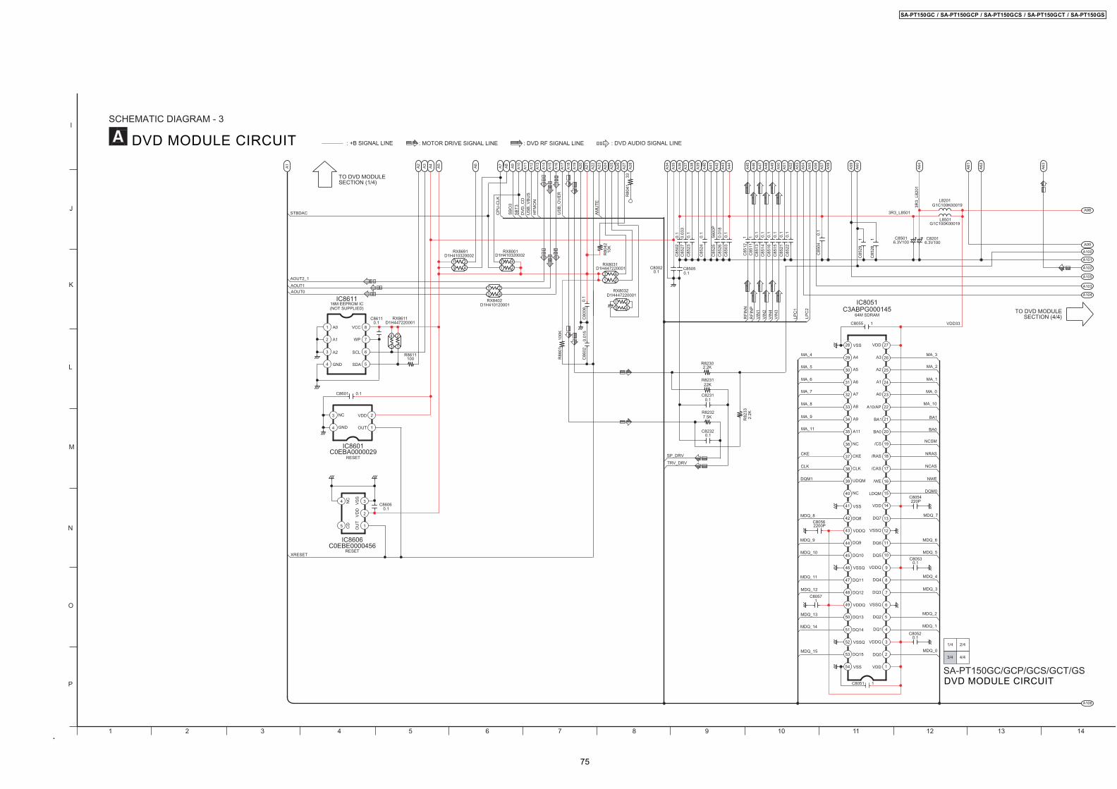
1 2 3 4 5 6 7 8 9 10 11 12 13 14
I
J
L
M
N
P
O
K
TO DVD MODULESECTION (4/4)
TO DVD MODULE SECTION (1/4)
: +B SIGNAL LINE
AOUT2_1
STBDAC
0.01
5C
8602
C85
111
C85
121
VIN
3V
IN4
AOUT1
C80
080.
1
0.1C8505
R86
0110
0K
AOUT0
C80020.1
R80
4210
K
421
3
RX8031D1H447220001
421
3
421
3421
3
RX8402D1H410120001
VIN
2
VIN
1
33R
8041
AM
UT
E
SB
T3
DV
D_C
D
SB
O3
US
B_V
BU
S
HF
MO
N
US
B_O
VE
R
MDQ_10
DQM1
MDQ_8
MDQ_9
2200PC8056
MDQ_6
MDQ_5
220PC8054
NWE
NRAS
NCAS
MDQ_7
DQM0
MDQ_13
MDQ_15
MDQ_14
MDQ_12
MDQ_11
1C8057
0.1C8052
MDQ_3
MDQ_0
MDQ_2
MDQ_1
0.1C8053
MDQ_4
MA_3
MA_0
MA_1
MA_10
BA0
NCSM
BA1
MA_2
1C8055
MA_6
MA_5
MA_9
MA_11
MA_7
MA_8
MA_4
RX8001D1H410320002
RX8691D1H410320002
CP
U-C
LK
C85
030.
1
C85
260.
018
C85
130.
1
C85
230.
1
C85
240.
1
C85
020.
10.
033
C85
27
C85
2556
00P
C85
150.
1
C85
140.
1
C85
160.
1
C85
040.
1
C85
220.
1C
8521
0.1
L8501G1C100K00019
G1C100K00019L8201
3R3_L8501
3R3_
L820
1
6.3V100C8501 C8201
6.3V100
C8051 1
C85
281
C85
291
29
28
30
31
27
26
24
25
20
21
19
16
12
14
15
13
18
17
9
10
8
7
6
11
2
3
1
4
5
34
36
39
41
42
40
38
49
52
51
54
53
50
44
43
45
47
48
46
37
35
23
22
32
33
64M SDRAMC3ABPG000145
IC8051
SP_DRV
7.5KR8232
C82320.1
C8601 0.1
100R8611
421
3
RX8032D1H447220001
1
1
2
3
4
8
7
6
5
4
23
C0EBA0000029IC8601
RESET
C86060.1
3
1
2
4
5
RESETC0EBE0000456
IC8606
TRV_DRV
C86110.1
2.2KR8230
4 2
13
RX8611D1H447220001
(NOT SUPPLIED)16M EEPROM IC
IC8611
C82310.1
22KR8231
RF
INP
RF
INN
LPC
1
LPC
2
A11 BA0
A9 BA1
A1A6
A2A5
VSS VDD
A3A4
A8 A10/AP
A7 A0
DQ11 DQ4
VDDQ
DQ12
VSSQ
DQ3
DQ8 DQ7
NC LDQM
/CS
/CAS
/RAS
NC
CLKCLK
CKECKE
/WEUDQM
VDDVSS
DQ9 DQ6
DQ5DQ10
VSSQ VDDQ
VSSQVDDQ
VDD33
DQ15
VSS
DQ14
VSSQ
DQ0
VDD
DQ1
VDDQ
DQ13 DQ2
XRESET
NC
CD
OU
TV
DD
OUT
VDD
VS
SSCL
WP
VCC
SDA
A2
A0
A1
GND
NC
GND
A1
A2
A3
A4
A5
A6
A7
A8
A9
A10
A11
A12
A13
A14
A15
A16
A17
A18
A19
A20
A21
A22
A23
A24
A25
A26
A28
A34
A35
A36
A37
A38
A39
A40
A41
A42
A43
A44
A45
A46
A47
A48
A49
A50
A51
A52
A53
A54
A55
A56
A57
A58
A59
A60
A64
A61
A62
A63
A98
A99
A100
A101
A102
A105
A106
A103
A104
DVD MODULE CIRCUIT
SCHEMATIC DIAGRAM - 3
1/4 2/4
3/4 4/4
DVD MODULE CIRCUITSA-PT150GC/GCP/GCS/GCT/GS
A27
R82
332.
2K
: DVD AUDIO SIGNAL LINE : DVD RF SIGNAL LINE: MOTOR DRIVE SIGNAL LINE
SA-PT150GC / SA-PT150GCP / SA-PT150GCS / SA-PT150GCT / SA-PT150GS
75
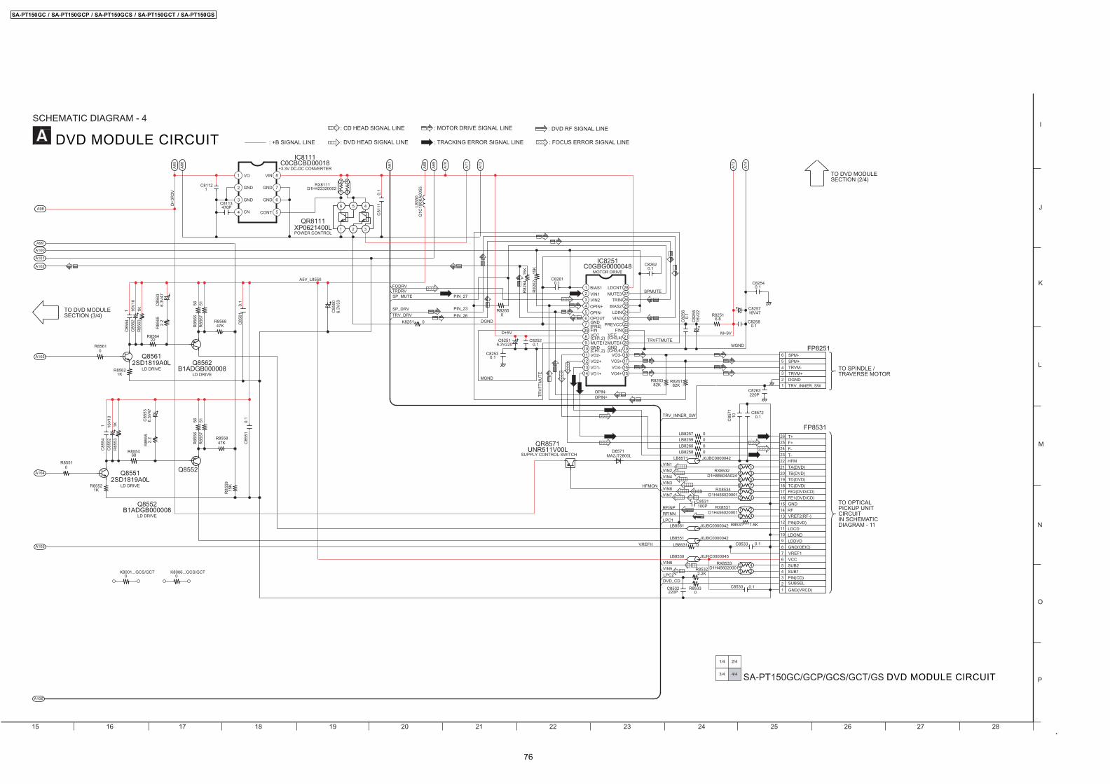
: DVD RF SIGNAL LINE
15 16 17 18 19 20 21 22 23 24 25 26 27 28
I
J
L
M
N
P
O
K
6
7
5
2
4
3
81 TO DVD MODULESECTION (2/4)
TO DVD MODULESECTION (3/4)
: +B SIGNAL LINE
22R8564
47KR8568
0.1
C85
61
R85
631K
R85
6751
R85
6656
2.2
R85
65C
8563
6.3V
47
R826182K82K
R8263
C82580.1
16V47C8257
R82516.8C
8255
16V
22
C82
560.
1
0.1C8262
2
43
1
65
FP8251
K8251 0
R82
6215
K
R82
6415
K
0.1C8261
TRDRVFODRV
TRVFTMUTEC82516.3V220 0.1
C8252
0.1C8253
12
34
5
67
89
29 30
10
11
14
12
13
192021
2223
24
2526
2728
18
15
17
16
MOTOR DRIVEC0GBG0000048
IC8251
2 31
5 46
POWER CONTROLXP0621400L
QR8111
SP_MUTESPMUTE
TRV_DRVSP_DRV
42
1 3D1H422320002
RX8111C81121
D+3
R3V
C8113470P L8
550
G1C
100K
A00
55
6.3V
33C
8550
A5V_L8550
C81
110.
1
68R8554R
8553
1K
R85322.2K
R85330
C8532220P
VIN5
VIN6
C8530 0.1DVD_CD
C8533 0.1LB8551 J0JBC0000042
0LB8531
D1H456020001RX8531
C8531100P
LB8561 J0JBC0000042 1.5KR8531
LB8530 J0JHC0000045
RX8533D1H456020001
UNR511V00LQR8571
421
3
421
21
3
43
D1H456020001RX8534
VIN3
VIN7
VIN8
VIN2
VIN4
VIN1
LB8259 0LB8257 0
LB8571 J0JBC0000042
57
1
3
68
2
4D1H85604A024RX8532
0LB8258
LB8260 0D8571
MA2J72800LSUPPLY CONTROL SWITCH
HFMON
47KR8558
15K
R85
59
C85720.1
C85
7110
TR
VF
TM
UT
E
7
8
5
6
9
24
14
16
15
11
12
10
13
22
23
19
20
1718
21
2
1
4
3
26
25
FP8531
0.1
C85
51
2.2
R85
556.
3V47
C85
53
Q8552
LD DRIVE
Q8552B1ADGB000008
LD DRIVE
Q8562B1ADGB000008
R85
5751
R85
5656
R85621K
R85521K
C85
541
C85
5216
V10
0R8551
C85
6216
V10
C85
641
LD DRIVE2SD1819A0L
Q8551
LD DRIVE2SD1819A0L
Q85610
R8561
RFINPRFINN
LPC1
LPC2
T+
F-
RF
VCC
GND
T-
TA(DVD)
SUB2SUB1
LDCD
LDDVD
VREF1
SUBSEL
LDGND
TB(DVD)
TC(DVD)
PIN(CD)
PIN(DVD)
GND(VRCD)
GND(OEIC)
FE2(DVD/CD)
VREF2(RF-)
FE1(DVD/CD)
TD(DVD)
HFM
F+
MUTE4
FIN
LDINVIN3
VCC[CH3,4]
M+9V
VO4-
VO4+
VO3+
VO3-
GND[CH3,4]
PREVCC
LDCNT
TRINMUTE3
BIAS2
SPM+
SPM-
TRVM-
DGNDTRVM+
MGND
TRV_INNER_SW
OPIN-
OPIN+
VO2-
VO1+
VO2+
VO1-
FIN
OPOUT
GND[CH1,2]
MUTE12
VCC[CH1,2]
D+5V
BIAS1
VIN2VIN1
OPIN-OPIN+
GND[PRE]
PIN_23
PIN_26
PIN_27
MGND
DGND
VO VIN
CN CONT
TRV_INNER_SW
GND
GND
GND
GND
IC8111
+3.3V DC-DC CONVERTERC0CBCBD00018
TO OPTICALPICKUP UNITCIRCUIT IN SCHEMATICDIAGRAM - 11
TO SPINDLE / TRAVERSE MOTOR
VREFH
A65
A66
A67
A68
A69
A70
A71
A72
A106
A99
A100
A101
A102
A103
A104
A105
A98
A73
A74
DVD MODULE CIRCUIT
SCHEMATIC DIAGRAM - 4
1/4 2/4
3/4 4/4 SA-PT150GC/GCP/GCS/GCT/GS DVD MODULE CIRCUIT
0.1C8254
C8263220P
R82650
K8001...GCS/GCT0
K8006...GCS/GCT0
: DVD HEAD SIGNAL LINE
: MOTOR DRIVE SIGNAL LINE
: TRACKING ERROR SIGNAL LINE : FOCUS ERROR SIGNAL LINE
: CD HEAD SIGNAL LINE
SA-PT150GC / SA-PT150GCP / SA-PT150GCS / SA-PT150GCT / SA-PT150GS
76

19.2. Main Circuit
TO MAINSECTION (2/4)
TO MAINSECTION (3/4)
1/4 2/4
3/4 4/4 SA-PT150GC/GCP/GCS/GCT/GS MAIN CIRCUIT
C5
C3
CSCHEMATIC DIAGRAM - 5
MAIN CIRCUIT
TO SPEAKERS
:+B SIGNAL LINE
:-B SIGNAL LINE
:MAIN SIGNAL LINE :AUX / MIC SIGNAL LINE
A
B
C
D
E
F
G
H
1 2 3 4 5 6 7 8 9 10 11 12 13 14
1
22K
R30
05
B1GDCFJJ0047Q3003
R30
061K
R25
1256
K
C2506 1
50V10C2619
0W4042
C2312 1
C2283 1
C2412 1
C2183 1
R26
2610
0K
R2412 10K
R2617 22K
R2510 15K
R2285 10K
R2312 10K
R30038.2K
C2624 6800P
C2724 1800P
10KR2185
C2324 2200P
C2524 6800P
SW-
SL+
C-
FR-
SL-
FL-
SR-
FR+
C+
FL+
SW+
SR+
7
9
10
8
4
5
1
3
2
6
12
11
JK5000
50V
10C
3007
R30091K
D3001
BUFFER
MUTING
MUTING
B0ACCK000005
R30
0727
K
Q3009B1ABCF000176
FR_IN
C3005 1
C3006 50V10
C24242200P
SL_IN
SR_IN
56K
R23
39
27K
R22
940
W40
07
0W
4026
W4043 0
56K
R24
39
R21
9427
K
FL_IN
Q3008B1ABGC000005
R300810K
R30
1556
K
R30
1456
K
50V
10C
3009
C_IN
FLOUT
SL_OUT
SUBW
CENTER
SR_OUT
FROUT
MUTE_C
+7V
12K
R26
20
AS
P_D
A
AS
P_C
K
16V
100
C24
10
220PC2023
C2024220P
R26
2139
K
10KR2606
1.8K
R2307
R24110
5.6KR2406R2405
5.6KR24071.8K
C24
0716
V10
0.02
2C
240816
V10
C24
04
C24
0533
00P
C23
0533
00P
C23
090.
082
16V
10C
2304
C23
0716
V10
C23
080.
022
R29528.2
W40480
C260816V10
DVD-SL
C20
19
16V
47
C20
200.
01
D2002
D2001 - D2002B0EAKM000117
D2001
-7V
DVD-CNT
C25
0747
0P
12K
R25
11
C26
1522
00P
20K
R26
19
47K
R26
01
C26
0750
V22
16V
10C
2606
C26
010.
022
12K
R23
04
12K
R24
04
10V
1C
2306
C24
0610
V1
AGND
10KR2607
R24
3612
K
C20
18
16V
47
0.01
C20
17
12K
R23
36
C23
2310
0P10
0PC
2423
DVD-SR
DVD-SUBW
C22
180.
22
R2303 10K1C
2119
1C
2501 6.8K
R25
01
0.04
7
C21
21
0.04
7
C22
21
C21
180.
22
C22
170.
047
1C
2219
C21
1647
00P
C21
140.
022
C21
150.
015
C22
140.
022
C22
1647
00P
C22
150.
015
C21
170.
047
CE
NT
ER
4.7K
R22
144.
7K
R22
18
FLO
UT
0.03
9C
2120
4.7K
R21
13
4.7K
R21
14
0.03
9C
2220
C2502
0.0470.047C2503
6.8KR2503
FR
OU
T
10KR2502
10K
R22
15
SL_
OU
T
R21
1510
K
AUX_LCH
AUX_RCH
TUN-RCH
MIXL
MIXRTUN-LCH
DVD-FR
R22
653.
3K
6.8K
R22
91
12K
R21
12
R21
653.
3K
1000
PC
2265
C21
6510
00P
100P
C21
72
R21
916.
8K
100P
C22
72
C21
9511
C22
95C
2112
470P
R22
1212
K
C22
1247
0P
3 42 5
98
95
92
91
93
97
96
1
100
99
80 78 767779
87
86
88
89
82
84
83
81
85
90
1614 15 1711 1312
69 67 65 64666870 51
49
45
47
46
41
44
42
43
48
50
30
39
37
35
32
31
34
33
36
38
40
22 2320 21 26 282724 2518 19
53555762 60 596163 58 56 54
29
5275 73 717274
976 8 10
IC2102C1AB00002463
94
6.8R2960
10KR2164
R2264 10K
DVD-FL
R26091.5K
10K
R23
02
R2612 56K
0.047
C2403
C26050.047
C2609 0.22
10KR2403
C2401 1
C2612 3300P
C2301 1
R2301 1.8K
C23
020.
033
C23
030.
047
R261056K
R260856K
0.012C2611
C26170.15R2611 1.2K
R2627 68K
C2402
0.033
C26100.47
SUBW
R2401 1.8K
10K
R24
02
SR_OUT
SW
+5V
C+_OUTFR+_OUT
SW+_OUT
SR+_OUT
C-_OUT
FR-_OUT
SW-_OUT
SR-_OUTSL-_OUT
FL-_OUT
SL+_OUT
FL+_OUT
-7V
AGND
ASP_GND
ASP_GND
AGND
AG
ND
_D
+9.1
V
DG
ND
AGND
SRFIN
SRNFIN
AG
C2
AGND
SU
BV
OLI
N
OPIN2
OPOUT2
SROUT
OPOUT1
OPIN1
SLO
UT
AG
ND
SLNFINSLVOLIN
SRVOLIN[TUNER LCH][TUNER RCH]
[AUX RCH]
[TV LCH][TV RCH]
[AUX LCH]
[MIX RCH][99]RECOUTR
AUDIO SIGNAL PROCESSOR
INR4
INL4
INR5
INL5
INL2INR2
INR1
INR3INL3
EX
TO
UT
R RF
RIN SF
LCIN
DV
DD
DG
ND
DA
TA
CLO
CK
RS
IN
LSINLF
RC
IN
HB
AS
S1
LIN
FRIN
SU
BIN
TUN+9V
SR
IN
AGND
AG
ND
EX
TO
UT
L
AVCC
FLIN
AVEE [82]CIN[81]SLIN
SRSELOUT
HB
AS
S9
SU
BS
ELO
UT
SRVOLOUT
[49]SUBC
HB
AS
S6
HB
AS
S7
HB
AS
S5
[50]AGC1
HB
AS
S8
HB
AS
S2
HB
AS
S3
HB
AS
S4
[48]SUBOUT
CV
OLO
UT
CO
UT
CF
IN
CN
FIN
FLF
IN
FLO
UT
AGND
FR
FIN
FR
OU
T
CS
ELO
UT
FR
VO
LIN
TT
R
TT
L
TM
R1
TB
R1
TB
R2
TM
R2
FLS
ELO
UT
TB
L2
TM
L1
AG
ND
CLP
F
TB
L1
TM
L2
CV
OLI
N
FLV
OLI
N
FR
VO
LOU
T
FR
SE
LOU
T
FLV
OLO
UT
[31]SLFIN[32]SLVOLOUT
MICIN
INL1 [MIX LCH][100]RECOUTL
SLSELOUT
SW_IN
SW+5V
0
0
W40
50
W40
47
W40
490
W40280
0W
4096
0W
4034
0W
7002
0W7001
0W7000
ASP_MICIN
1C6920
100R6920
2.2K
R69
21
220P
C69
21
+7VASP_MICIN
C71
160.
139
KR
7116
C71
1447
PC
7115
ECHO_LV1ECHO_LV2ECHO_MUTE
MIC_AGND
-7V
ASP_MICIN_1
R71094.7K
C711350V1
W2202...GC/GS 0
15K
R71
01C710150V1
15KR7100
15KR7102
1500PC7103
R712015K
B1GBCFJJ0051Q7100
1.5K
R71
10
Q7102B1GBCFJJ0051
R71
122.
7K Q7101B1GBCFJJ0051
0.22C7106
C71
0268
00P
C71
040.
068
0.015C7120
C71050.22
6800
PC
7107
5.6K
R71
14
C711950V2.2
10K
R71
13C
7118
0.1
6
7
5
2
4
3
81
C0ABBB000230IC7101
220P
7
5
6
1
2
4
3
10
12
14
15
16
13
11
8 9
LPF1OUT
LPF1IN
NC
MIC_ECHO_OUT
MIC AMP
MUTING
SWITCH
SWITCH
CC2
GND
OP1IN
OP1OUT
CC1
REF
CLOCK
NC
VCC
OP2IN
OP2OUT
LPF2IN
LPF2OUT
V-
V+
R7106120K
C711116V47
C711016V47
R710315K
15KR7105
0.06
8C
7109
R710415K
C71081500P
D71
00B
0BC
5R00
0009
C71120.1
R7107
DIGITAL DELAYWITH ECHO VOLUME
68
IC7100C1BB00001061
1
SA-PT150GC / SA-PT150GCP / SA-PT150GCS / SA-PT150GCT / SA-PT150GS
77
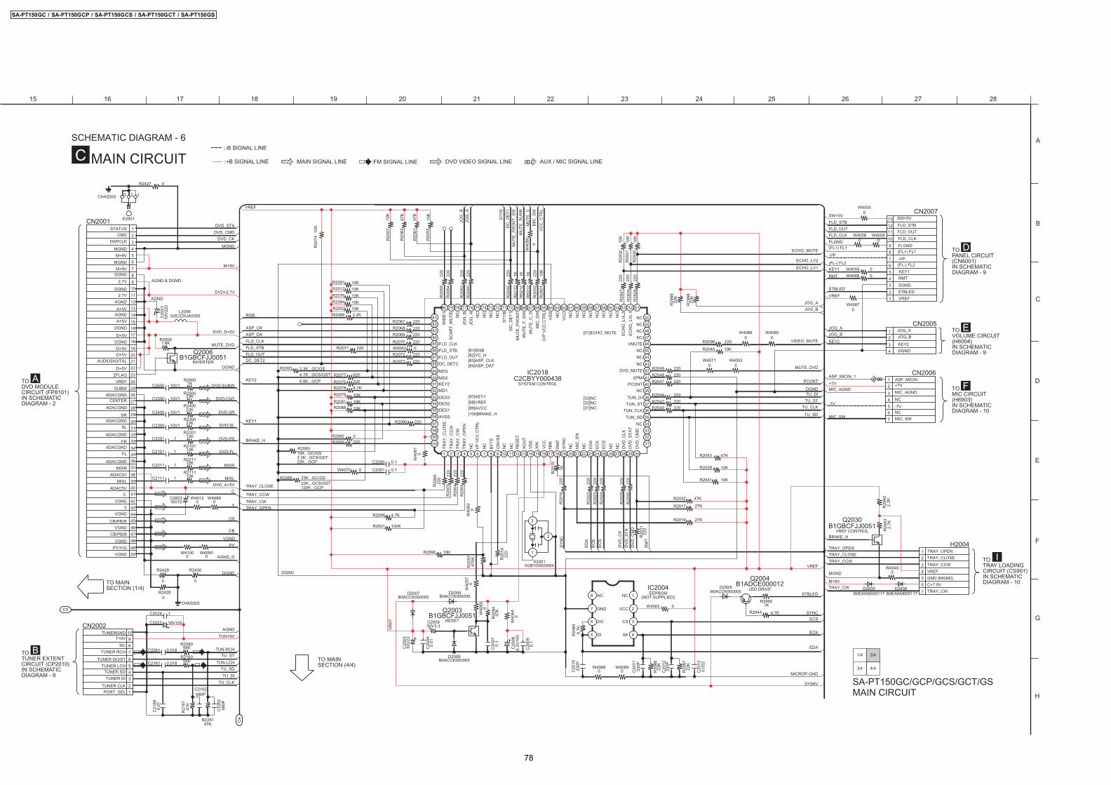
TO MAINSECTION (4/4)
TO MAINSECTION (1/4)
1/4 2/4
3/4 4/4
MAIN CIRCUITSA-PT150GC/GCP/GCS/GCT/GS
C4
C3
CSCHEMATIC DIAGRAM - 6
MAIN CIRCUIT
TODVD MODULECIRCUIT (FP8101)IN SCHEMATICDIAGRAM - 2
A
TOTUNER EXTENTCIRCUIT (CP2010)IN SCHEMATICDIAGRAM - 9
B
TOPANEL CIRCUIT (CN6001)IN SCHEMATICDIAGRAM - 9
D
TOVOLUME CIRCUIT (H6004)IN SCHEMATICDIAGRAM - 9
E
TOTRAY LOADINGCIRCUIT (CS901)IN SCHEMATICDIAGRAM - 10
I
:+B SIGNAL LINE
:-B SIGNAL LINE
:MAIN SIGNAL LINE :FM SIGNAL LINE :DVD VIDEO SIGNAL LINE
TOMIC CIRCUIT (H6903)IN SCHEMATICDIAGRAM - 10
F
:AUX / MIC SIGNAL LINE
15 16 17 18 19 20 21 22 23 24 25 26 27 28
A
B
D
E
F
H
G
C
220
R29
27
220R2098
220R2047
R2044 220
R2049 220
R2048 220
TU_DI
TU_ST
R29
3210
K
220
220
R29
29
R29
28
R29
31
R29
30
10K
10K
VIDEO_MUTE
MUTE_DVD
R2045 10K
PCONT
R20
8622
K
R2032 47K
10KR2039
R2041 10K
R2043 47K
27K
R2019
R2017
27K
[32]NC[31]NC
[33]NC
[51]ECHO_MUTE
330P
C20
12
22K
R20
87
C20
130.
022
ECK
ECS
TU_SD
TU_CLKR2042 220
R2040 220
22K
R29
99
1KR2950
SYNC
D2929B0ACCK000005
R2944 4.7K
Q2004B1ADCE000012
JOG_A
JOG_B
KEY2
JOG_A
2
1
4
3
CN2005
JOG_B
22K
R29
98
FLD_OUT
FLD_CLK
STBLED
FLD_STB
RMT
STBLED
7
9
11
10
12
8
2
3
1
5
6
4
13
CN2007
KEY1
EC
K
DV
D_C
K
R20
3122
0
DV
D_C
MD
C20
1133
0P
DV
D_S
TA
220
R20
29
220
R20
30
220
R20
24
220
R20
23E
CS
ED
A
SY
NC
MU
TE
_C
MU
TE
_SU
RR
MU
TE
_FR
ON
T_S
W
4
5
1
3
2
7
6
H2004
6
8
9
7
2
1
4
5
3
10
CN2002
6
7
5
9
47
44
39
40
35
31
27
24
21
20
22
16
15
18
17
11
13
12
10
14
19
23
26
25
30
28
29
34
32
33
38
36
37
43
41
42
46
45
49
48
8
1
3
4
2
50
CN2001
R2081 10KR2088 10K
R2079 10K
KEY2
B0ACCK000005D2005
10KR2096
0.01
C20
04
50V3.3C2006 RESET
EEPROMLED DRIVE
VREF CONTROL
(NOT SUPPLIED)
D2008B0ACCK000005
JOG
_B
R20
6147
K
R20
6222
0
10K
R20
53
220
R20
64
R20
6522
022
0R
2000
R20
0422
0
220
R20
05
220
R20
03
220
R20
10
0.1
C20
09
C20
086.
3V10
0
470K
R20
97
R20
8447
K
B1GBCFJJ0051Q2003
C20
070.
1
DC
_DE
T1
R51
121K
R20
4622
0
ST
YB
JOG
_AR
2060
220
R2075 220
820
4.7K
R2093 3.3K...GC/GS
6.8K...GCP
4.7K...GCS/GST
R2072 220
R2077
R2078
R2068 220
220R2067
R2066 2.2K
R2071 220
R2069 220
R2070 220
R2092 2200
R2089
R2082
R2090 220
R20
6347
K
B0ACCK000005D2007
50V
22C
2003
4.7KR2095
TRAY_OPEN
VR
EF
R208010K...GC/GS
22K...GCP3.3K...GCS/GST
33K...GC/GS22K...GCS/GST120K...GCP
BRAKE_H
0.1C2000
0.1C2001W4070
W40
61
0
0
220R2073
FLD_OUT
ASP_DA
R20
0710
K
RGB
ASP_CK
FLD_CLK
FLD_STB
KEY1
R20
7410
K
DC_DET2
R2002 10K
R2094 10K
R2076 10K
R2012 10K
R2091 10K
TRAY_CLOSE
TRAY_CCW
TRAY_CW
100KR2001
R226147K
R21
6147
K
TUN-RCH
R29
422.
2K2.
7KR
2943
BRAKE_H
TUN-LCH
680P
C22
62
680PC2162
16V100C2022
D2935B0EAKM000117
B1GBCFJJ0051Q2030
56KR2160
TU_SD
R226056K
DVD_D+5V
10V
220
C20
21
R2427 0
TUN+9V
DVD-SUBW
DVD-CNT
DVD-FL
MIXR
DVD-SL
DVD-SR
DVD-FR
B1GBCFJJ0051Q2006
R240022K
12KR2101
22KR2300
R220112K
1KR2600
R250022K
R2430
0
12KR2211
MIXL12KR2111
C283316V10
W40120
W40890
MUTE_DVD
G0C220JA0055
INVERTER
L2009
1.8KR2006
DVD_CMD
DVD_CK
DVD_STA
E2901
3 2 1
MGND
M+9V
C2261 0.018
C2161 0.018
0.01
C21
69
D2936B0EAKM000117
1C2026
AGND
TRAY_CLOSE
TRAY_CCW
TRAY_OPEN
TRAY_CW
TU_ST
TU_CLK
TU_DI
0R2428
R2429
0
Y
C2300 10V1
C2101 1
C2201 1
C2211 1
C2111 1
C
PY
AGND_D
CR
CB
C2400 10V1
C2600 10V1
C2500 10V1
VC
C_C
TR
L
W40
80
0R
2052
220
1KR
5312
R29
0110
K
R52
121K
3
1
2
X2001H2B100500004
220
R20
22
6
7
5
2
4
3
8 1
IC2004
EDA
4.7K
R20
85
1K
R20
15
R20
1622
0
C20
1033
0P
DVD_A+5V
RM
T
3 42 5
98
94
95
92
91
93
97
96
1
100
99
80 78 767779
87
86
88
89
82
84
83
81
85
90
1614 15 1711 1312
69 67 65 64666870 51
49
45
47
46
41
44
42
43
48
50
30
39
37
35
32
31
34
33
36
38
40
22 2320 21 26 282724 2518 19
53555762 60 596163 58 56 54
29
5275 73 717274
976 8 10
IC2018C2CBYY000438
VGND
PY/Y/G
VGND
CR/PR/R
MIXL
SL
SR
FR
FL
DGND
DGND
AGNDA+5V
A+5V
D+5VD+5V
D+5V
DGND
DGND
AGND
CMD
M+9V
MGND
MGND
M+9V
MIXR
VREF
D+5V
SUBW
C
VGND
ADACGND
ADACGND
2.7V
2.7V
ZFLAG
DSPCLK
CENTER
C+7.5V
TRAY_CW
TRAY_CCW
STATUS
GND (MGND)
VREF
ADACGND
ADACGND
TRAY_OPEN
AUDIODIGITAL
TUNER RCH
TUNER LCH
ADACGND
ADACGND
ADAC5V
ADAC5V
VGND
NC
T+9V
Y
TUNER SD
TUNERGND
TRAY_CLOSE
PORT_SEL
VGND
CB/PB/BVGND
DGND
CHASSIS
CN
VS
SN
C
NC
BY
TE
XO
UT
MU
TE
_F_S
W
DC
_DE
T1
MU
TE
_FR
ON
T
TUN_DI
NC
PCONT
TUN_SD
NC
EC
K
ED
A
NC
NC
NC
NC
EC
S
TUN_ST
TUN_CLK
VS
S
VC
C
XIN
RM
T
NM
I
NC
NC
NC
NC
NC
NC
NC
NC
EC
HO
_LV
L1
EC
HO
_LV
L2
NC
EPM
NC
NC
DVD_MUTE
NC
VMUTE
NC
NC
MIC
_SW NC
NC
VS
S
VC
C
MU
TE
_C_S
O/P
VC
C C
TR
L
SY
NC
NC
RE
SE
T
SYS6V
DV
D_C
MD
GND
NCNC
VCC
SKDI
CSDO
DV
D_S
TA
T
MIC
_EN
DV
D_C
LK
NC
ST
YB
DGND
DGND
[82]YC_H
VREF
TUNER DI
TUNER CLK
TUNER DO/ST
CHASSIS
MGND
M+9V
AGND
AGND & DGND
NC
NC
I/P V
CC
CT
RL
TR
AY
_CLO
SE
WID
E1
TR
AY
_CW
TR
AY
_OP
EN
NC
NC
TR
AY
_CC
W
JOG
_B
JOG
_ANC
SC
AR
T_M
UT
E
[83]ASP_CLK
[81]RGBFLD_STB
DC_DET2
FLD_OUT
FLD_CLK
[84]ASP_DAT
[99]AVCC[100]BRAKE_H
[98]VREF[97]KEY1
AVSS
MD3
MD1
MD2
DES2DES3
DES1
KEY2
RMT
-VP-VP
KEY1
FLGNDFLGND
DGND
VREFVREF
STBLED
FLD_OUT
JOG_B
DGND
DGND
KEY2
JOG_A
FLD_CLK
(FL-) FL2(FL-) FL2
(FL+) FL1(FL+) FL1
SW+5VSW+5V
FLD_STB
MICROP-GND
VREF
DVD+2.7V
SYSTEM CONTROL
W41000
W40900
W4062 0
W4055
W4058
W4059
W4056
0
W40670
W40860
W40850
W40710
W40530
0
0
W4068 0
0
0W
4060
0W
4057
0W
4064
0W
4065
0
0
W40660
W4069
W4063
W40450
MIC
_SW
ECHO_MUTE
ECHO_LV2
ECHO_LV1
4
5
1
3
2
7
6
CN2006
NC
NC
+7V
-7V
MIC_SW
MIC_AGND
ASP_MICIN+7V
-7V
MIC_AGND
ASP_MICIN_1
MIC_SW
SA-PT150GC / SA-PT150GCP / SA-PT150GCS / SA-PT150GCT / SA-PT150GS
78

TO MAINSECTION (4/4)
1/4 2/4
3/4 4/4
TO MAINSECTION (1/4)
MAIN CIRCUITSA-PT150GC/GCP/GCS/GCT/GS
C1
C2
C5
CSCHEMATIC DIAGRAM - 7
MAIN CIRCUIT
TO FAN
:+B SIGNAL LINE
:-B SIGNAL LINE
:MAIN SIGNAL LINE :FM SIGNAL LINE :AUX / MIC SIGNAL LINE :DVD VIDEO SIGNAL LINE
AUX COMPONENTVIDEO OUT
VIDEOOUT
1 2 3 4 5 6 7 8 9 10 11 12 13 14
I
J
L
M
N
P
O
K
W2201...GC/GS0
W40
030
W40010
W40
020
W40040
W40
160
W40180
W40
110
W40
130
W40
060
W40
140
10K
R57
65
Q5741B1ABCF000176
DC_DET2
C57
9850
V10
0
C57
990.
1
R57
362.
2KC57
9010
00P
B1BACG000023Q5740
3.3M
R57
58
C57
9416
V33
10K
R57
57
B0ACCK000005D5700
C57
950.
1
B0B
C01
3A00
07D
5745
16V
100
C57
91
10K
R57
55
10KR5756
56K
R57
54
6.3V
220
C57
92
C57
9650
V2.
2
10KR5760
Q5744B1ABCF000176
Q5745B1ACKD000005 10
0KR
5759
B1ABCF000176Q5742
2.7KR5763
3.9KR5764
1
3
2
CN5704
150K
R57
62
PCONT
2.2M
R57
61
D5744
B0ACCK000005
50V1C5797
10K
R57
66
Q5746B1GBCFJJ0051
D5743
B0ACCK000005
DVD_A+5V
C2164220P
C2264220P
AU
X_R
CH
C2853
100P
AU
X_L
CH
+26V
AG
ND
VG
ND
DG
ND
FLGND
SPEAKER CHASSIS GND HEATSINK GND
+13V GND
+26_VCC
FANLOCK
FAN DC SUPPLY
FAN LOCK DETECT
FAN MOTOR DRIVE
FAN MOTOR DRIVE
FAN MOTOR DRIVE
INVERTER
DC_DET2
FANDCOUT(+)
GND
L2801G0C220JA0055
W40
170
5 3 12479 8 6
[R-C
H]
[L-C
H]
[PB
]
[PR
]
[Y]
JK20
02
L280
3J0
JBC
0000
015
L280
2J0
JBC
0000
015
R28
0975 75
R28
12
C2823100P
100PC2825
CB
OU
T
CR
OU
T
L280
4J0
JBC
0000
015
L280
5J0
JBC
0000
015
R28
1375
C2826100P
YO
UT
VIDEO BUFFER
VIDEO BUFFER
1C
2804
C28
001
6.3V
330
IC2801C9ZB00000461
SE
L
YIN
BIA
S
GN
D
VC
C2
CB
IN
CY
IN
MU
TE
2
CR
IN S2
CIN
SE
L
S1
CV
IN
MU
TE
1
GN
D2
GN
D2
GN
D2
CB
SA
G
CY
SA
G
CY
OU
T
CB
OU
T
CR
SA
G
CR
OU
T
GN
D2
VS
AG
VO
UT
YS
AG
YO
UT
SD
CO
UT
VC
C1
CO
UT
6.3V
1000
C28
411 2
56
3
4
C1AB00001731IC2802
C28
066.
3V33
0
C28
05
OUT VCC
IN2GNDIN1
SWY
OU
T
CB
OU
T
CR
OU
T
2625 27 2817 18 20 22 24232119
8 7 5616 15 10 91314 1112 3 12
30 3231
4
29
RG
B Y CCB
PY
CR
VID
EO
_MU
TE
C28
120.
1
C28
100.
01
C280810V220
C28070.011K
R2803
MUTINGB1GBCFJJ0051
Q2801
10V
220
C28
09
C28
110.
11C
2817Q2801
1C
2818
R28041KD2810
B0JCAE000001
C28
026.
3V10
00
VO
UT
75R
2816
VO
UT
GNDVIDEO
100PC2827
W40840
W40050
W40910
K4030...GC/GS0
K4031...GCS/GCT0
K4032...GCP0
SA-PT150GC / SA-PT150GCP / SA-PT150GCS / SA-PT150GCT / SA-PT150GS
79
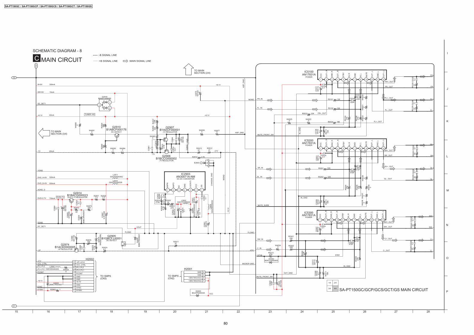
1/4 2/4
3/4 4/4
TO MAINSECTION (3/4)
TO MAINSECTION (2/4)
SA-PT150GC/GCP/GCS/GCT/GS MAIN CIRCUIT
C2
C4
C1
CSCHEMATIC DIAGRAM - 8
MAIN CIRCUIT
TO SMPS(CN3)
TO SMPS(CN2)
:+B SIGNAL LINE
:-B SIGNAL LINE
:MAIN SIGNAL LINE
15 16 17 18 19 20 21 22 23 24 25 26 27 28
I
J
L
M
N
P
O
K
C29
2082
00P
C29
520.
1
R5202 22K
R5201 22K SL+
22R
5209
C52
060.
1
SL-
R2914 2.7K
IN_GND
STYB
R530133K
22K
D5302B0ACCK000005
R531347K
W40240
R5302
5.6K
R53
04
C53
1350
V10
MUTE_SURR
R29770
C29
641
C29
1316
V10
0
16V
22C
5208
R52
1110
K
50V
10C
5301
C53240.1
R291347
R291247
0.01
C29
03
C-
22R
5309
27K
R53
08
C+
0.1
C53
06C5304470P
SW+
27K
R52
08
SW-
C53
020.
1R
5305
22
R52
0427
K
1141 2 3 8 95 6 7 10 12
AN17831AIC5300
STBY
C5305470P
C29
100.
01
Q2906B1BCCG000002
B1ADCF000001Q2907
1
68K
R29
24
R29
0822
0
B1ABCF000176Q2910
3
1
2
D2918B0ADCJ000020
DC DETECT
DC DETECT
DVD 2.7V REGULATOR
-VP REGULATOR
-7V REGULATOR
-7V REGULATOR
POWER
POWER
POWER
R29
073.
9K
C29
61139
KR
2940 C
2914
10V
33
R29
152.
7K
SR+
R51
0922
0.1
C51
06
FL-
FL+
27K
R51
08
0W
4020
0W
4021
0W
4023
C5105
220PC5104
220P
27K
R51
04
FR+
R51
0522
FR-
0.1
C51
02
C5204470P
C5205470P
SR-
22R
5205
0.1
C52
02
MUTE_FRONT_SW
C51240.1
R5533 22K
R5534 18K
R5101 12K
R5102 12K
16V
22C
5108
R51
1110
K
50V
10C
5101
1141 2 3 85 6 7 9 10 12
AN17831AIC5100
C52240.1
50V
10C
5201
IN_G
ND
IN_GND16
V10
0C
2975
DC_DET1
1141 2 3 8 95 6 7 10 12
AN17831AIC5200
C55
0335
V10
00
L2910G0A220GA0026
6 34 1257
IC2903AN30071A-NM
MUTE_FRONT_SW
470P
C55
05
E2900
32
1
R53
1110
K
16V
22C
5308
L2911G0A200D00002
D29
44
B0B
C3R
4000
01
C29
676.
3V10
00
R29
204.
7K
1KR2925
R292127K
C29
2216
V47
0
C29
700.
1
R2973220
16V
100
C29
83
C29
840.
1
6.3V
220
C29
25
C29
240.
1
22
R2972
C29
0116
V47
0
L290
9G
0A20
0D00
002
C29
690.
1L2902
G0A101G00022
D29
04B
0JC
PD
0000
25C
2921
16V
470
R29711.5
R29261.5
R2919270K C2
919
10P
Q2914B1BACG000023
D2000B0JCPD000025
2
1
4
3
H2001
B0BC7R500001D2900
R2900 1
PCONT
VCC_CTRL
L2800G0C220JA0055
R29
754.
7K
Q2974B1ACKD000005
6
8
9
7
2
1
45
3
10
11
H2002
-21V
-21V
SYS6V
+9.1
V
+9.1V
D29
74M
AZ
8220
0ML
B0B
C7R
5000
01D
2905
C29
8650
V10
0
DC_DET1
150R2976
B1GBCFJJ0051Q2905
R291147
0.01
C29
85
4.7R2974
DVD_A+5V
SW+5V
VCC
FL-_OUT
FL+_OUT
GN
D_L
GN
D_L
OU
T+_
L
OU
T-_
LO
UT
-_L
SW+_OUT
SL-_OUT
SR-_OUT
SR+_OUT
SL+_OUT
OU
T+_
L
OU
T-_
RO
UT
-_R
GN
D
IN_L
ST
BY
GN
D
IN_L
MU
TE
MU
TE
ST
BY
IN_R
IN_R
FR+_OUT
IN_R
ST
BY
OU
T-_
R
MU
TE
IN_L
GN
D
OU
T+_
L
OU
T-_
L
GN
D_L
FR-_OUT
SW-_OUT
C+_OUT
C-_OUT
+9.1V TUNER +9V
DVD+2.7V
60mA
AGND_D
OU
T+_
R
+9.1V
15mA
300mAM+9V
VC
C
FL+_OUT
FR_IN
FL_IN
FR+_OUT
OU
T+_
R
MICROP-GND
FLGND
VC
C
GN
D_R
GN
D_R
C_IN
SW_IN
OUT_GND
500mA
500mA
DVD_D+5V
-21V
-7V
SL_IN
SR_IN
MGND
+9.1V
60mA-7V
ASP_GND
AS
P_G
ND
VC
C
GN
D_R
OU
T+_
R
DVD2.7V
NC SS
MG
ND
VC
C
DC-DC CONVERTER
GN
D
AM
PO
AM
PN
LX(O
UT
)
-VP
GND
+26V/18V(VCC)
+26V/18V(VCC)GND
GND
GND
GND
SYNCSYNC
+9.1V
(FL-) FL2(FL-) FL2
PCONT
VCC_CTRL
-VP (-21V)
(FL+) FL1(FL+) FL1
SYS6V
FLGND
VOUT
DGND
VGND
700mA
CH
AS
SIS
_GN
D
0W
4082
0W4081
0W4093
0W4094
0W4095
0W4083
0W4054
W40
380
W40
370
W40
400
W40
390
W40220
W40250
SA-PT150GC / SA-PT150GCP / SA-PT150GCS / SA-PT150GCT / SA-PT150GS
80

19.3. Tuner Extent, Panel & Volume Circuit
BSCHEMATIC DIAGRAM - 9
SA-PT150GC/GCP/GCS/GCT/GS TUNER EXTENT / PANEL / VOLUME CIRCUIT
TUNER EXTENT CIRCUIT D PANEL CIRCUIT
E VOLUME CIRCUIT
TOMAIN CIRCUIT(CN2002)IN SCHEMATICDIAGRAM - 6
TO TUNER PACK(J3CBBB000001)
C
TOMAIN CIRCUIT(CN2007)IN SCHEMATICDIAGRAM - 6
C
:+B SIGNAL LINE :-B SIGNAL LINE
:+B SIGNAL LINE
:FM SIGNAL LINE
TOMAIN CIRCUIT(CN2005)IN SCHEMATICDIAGRAM - 6
C
A
B
C
D
E
F
G
H
1 2 3 4 5 6 7 8 9 10 11 12 13 14
1 2 3 4 5 6 7 8 9 10 11 12 13 14
A
B
D
E
F
H
G
C
G4
R6905 1.5KD6900
B3AAA0000803
W65090
W65110
FLD_STB1
FLD_CLK1
FLD_OUT1
S6800
FLGND
7
9
11
10
12
8
2
3
1
5
6
4
13CN6001
3 2 1
Z6900B3RAB0000025
C691810V47
C69
0410
00P
C6906100P
R691482K
C69
110.
01
C69
106.
3V10
0
C69
1610
0P
FLD_STB1
C69
1710
0P
68R6919
FLD_CLK1
FLD_OUT1
R69171K
68R6916
50V
3.3
C69
13
FLGND
P9
P8
P14
P12
P10
P11
P13
P17
P15
P16C69
090.
01
P2
P1
P3
P7
P5
P4
P6
47R6934
G1
D69
10B
0BC
3R40
0001
R69
1822
K
J0JBC0000041L6903
21
5
6
3
1
2
4
19
9
7
8
16 17
11
10
12 151413 18 20
35374244 43 39 3841 40 36
33
22
31
29
27
24
23
26
25
28
30
32
34
C0HBB0000057IC6901
-VP
F1
232114 15 1917 201810 117 8 22 4441403736 383332 3429 3025 2624 2827 31 35 39 43 45
FL6901A2BD00000170
4216131291 2 3 4 5 6
R69
3610
50V
22C
6903
G9
G7
G5
G3
G2
G4
G6
G8
G10
50V
22C
6905
G8
P16
P15 G2
P17P11
P12P8
P9
P6
P7
P10 G3
P13
P14 G9
G10
G5
G6 G1
G6
G7
0R6939
F2
P3
0R6940
P1
P2
P5
P4
6
8
9
7
2
1
45
3
10
CN2010
6
8
9
7
21
45
3
10
CP2010
F2
F2
TUNER DI
PORT_SELTUNER CLK
PORT_SEL
TUNER DI
TUNER CLK
T+9V
TUNER RCH
RDS DETECT
TUNER SDTUNER LCH
TUNER DO/ST
TUNERGND
TUNER SDTUNER LCH
TUNERGNDT+9V
TUNER RCH
TUNER DO/ST
RDS DETECT
G4
RMT
KEY1
POWER
VREF
STBLED
REMOTE CONTROL SENSORFLGND
FLD_CLK
(FL+) FL1
RMT
-VP
STBLED
VREF
DGND
KEY1
(FL-) FL2
SW+5V
FL2
FL1
F1
NP
P3
P1
P2
NX
(G9)
NX
(G10
)
NX
(G10
)
P4
F1
P1
G1
P3
P4
OSC
P2
-VP
G7
NX
(G1)
G2
G10
G9
P17
G3
P8
P6
P5
P7
P9
P15
P13
P11
P10
P12
P14
P16
NX
(G1)
NX
(G4)
NX
(G6)
NX
(G7)
NX
(G8)
NX
(G6)
NX
(G5)
NX
(G4)
G8
G1
G6
G5
G7
G6
G9
G8
VC
C
G10
GN
D
G4
G3
G5
-VP
FLD_STB
SW+5V
FLD_OUT
SW+5V
P17
P18
P15
P16
STB
DIN
CLK
GN
D
VC
C
P7
P9
P11
P13
P14
P12
P8
P5
P6
NP
DISPLAY DRIVER
FL DISPLAY
3 2 1
1.8KR6804 R6805
2.2K
S68
06
S68
05
S68
03
1KR6802
S68
04
1.2KR6803
1KR6801
S68
02
S68
01
100P
C68
05
100P
C68
06
EVEKE2F2524MVR6800
2
1
4
3
H6004
SE
LEC
TO
R
ST
OP
DGND
JOG_A
JOG_BJOG_A
JOG_B
KEY2
PLA
Y
RE
VE
RS
E
FO
RW
AR
D
OP
EN
/CLO
SE
VOLUME JOG
DGND
0W
6545
0W6101...GC/GCS
0W
6102
...G
C/G
S
W65130
W65
040
W65020
W65
120
SA-PT150GC / SA-PT150GCP / SA-PT150GCS / SA-PT150GCT / SA-PT150GS
81

19.4. Mic, USB Relay, USB, Tray Loading & Optical Pickup Unit Circuit
FSCHEMATIC DIAGRAM - 10
SA-PT150GC/GCP/GCS/GCT/GS MIC / USB RELAY / USB / TRAY LOADING CIRCUIT
MIC CIRCUIT
H USB CIRCUIT
G USB RELAY CIRCUIT
I TRAY LOADING CIRCUIT
TOMAIN CIRCUIT(CN2006)IN SCHEMATICDIAGRAM - 6
C
TO USB
TOUSB RELAYCIRCUIT (CN8002)IN SCHEMATICDIAGRAM - 10
G
TODVD MODULECIRCUIT (FP9001)IN SCHEMATICDIAGRAM - 1
ATOUSB CIRCUIT(CN8000)IN SCHEMATICDIAGRAM - 10
H
TOMAIN CIRCUIT(H2004)IN SCHEMATICDIAGRAM - 6
C
:+B SIGNAL LINE :MIC SIGNAL LINE
:-B SIGNAL LINE
:+B SIGNAL LINE
:USB SIGNAL LINE
:USB SIGNAL LINE
A
B
C
D
E
F
G
H
1 2 3 4 5 6 7 8 9 10 11 12 13 14
1 2 3 4 5 6 7 8 9 10 11 12 13 14
A
B
D
E
F
H
G
C
V-
V+
M
7
2
1
4
3
CN8001
VA
8001
EZ
JZ1V
171A
A
VA
8002
EZ
JZ1V
171A
A
L8003ERJ6GEY0R00V
L8002ERJ6GEY0R00V
K8005J0JHC0000096
K8004J0JHC0000096
K80030
K80020
2
3
1
15
5
4
CN8003
2
3
1
5
4
CN8002
2
3
1
5
4
CN8000
J0JBC0000019L6083
1
2
3
6
7
4
5
JK6802
R67
051K
47P
C67
03
C6709 0.1
R67
0368
0
W65
500
W65
140
W65
170
W65160
10K
R67
07
R6706 0
C6711 1
R6709
MIC AMP
0
R671010K
0R6701
1C6701
47P
C67
07
18K
R67
08
15K
R67
02
C6706
0.1
47P
C67
08
1000
PC
6702
6
7
5
2
4
3
81
C0ABBB000230IC2204
4
5
1
3
2
7
6
H6903
J0JBC0000030L6082C6093
0.047R6081
0
VR6081EVUE27FK3B53
D-
VBUS
D+
DGND
MIC
MIC VOLUME
D+
DGND
D+
DGND
DGNDDGND
D- D-+7V
ASP_MICIN
-7V
NC
MIC_SW
NC
MIC_AGND
D+
VBUSVBUS
D-
D-
D+
DGND
VBUS
DGND
VCC
OU
T2
NC
GN
D
VSOU
T1
VREF
IC904C0GAY0000013
TRAY LOADING MOTOR DRIVE
PLAYS901
S902C98425V10
OPEN
TRAY
CW
TRY
OPE
N
LOADING MOTOR(REF NO.316)
123456789CS901
TRAY CWM+9VGND1
VREF+TRAY CCW
TRY CLOSETRY OPEN
1234
7
56
3 2 1
L60810
SA-PT150GC / SA-PT150GCP / SA-PT150GCS / SA-PT150GCT / SA-PT150GS
82
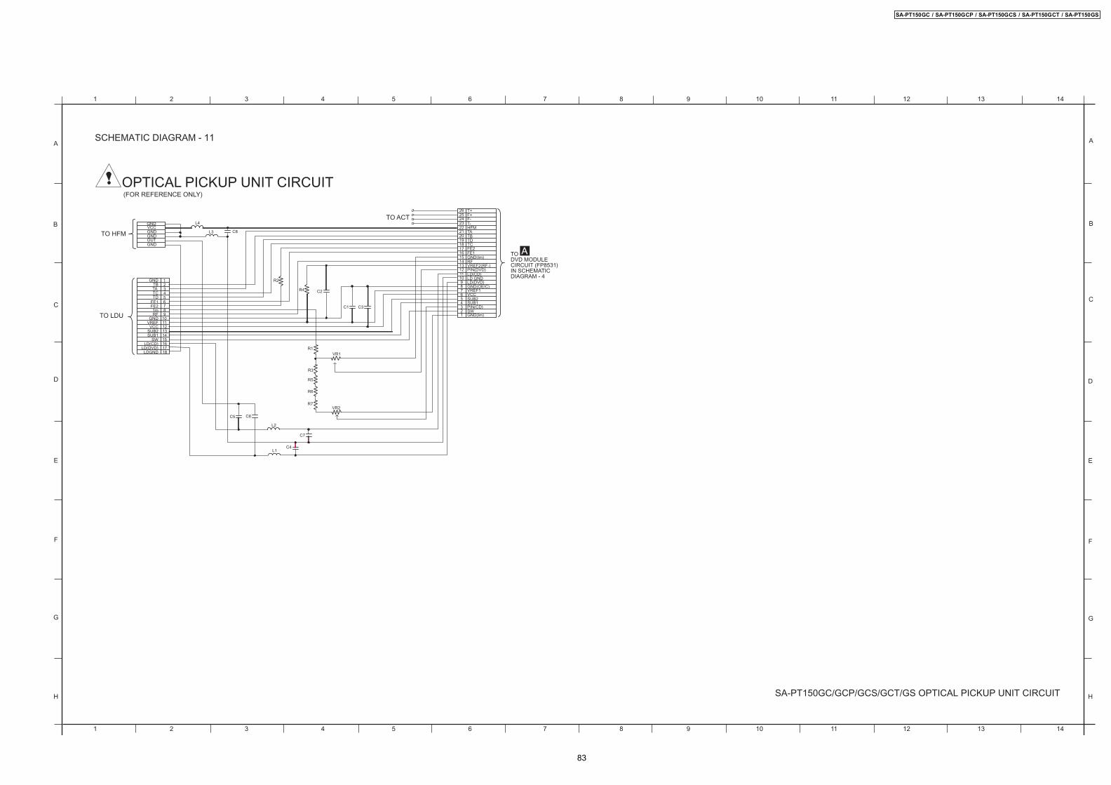
SCHEMATIC DIAGRAM - 11
SA-PT150GC/GCP/GCS/GCT/GS OPTICAL PICKUP UNIT CIRCUIT
TO HFM
TO LDU
(FOR REFERENCE ONLY)
OPTICAL PICKUP UNIT CIRCUIT
TO ACT
TODVD MODULECIRCUIT (FP8531)IN SCHEMATICDIAGRAM - 4
A
A
B
C
D
E
F
G
H
1 2 3 4 5 6 7 8 9 10 11 12 13 14
1 2 3 4 5 6 7 8 9 10 11 12 13 14
A
B
D
E
F
H
G
C
GND
GNDGNDOUTGND
GNDTBTATC
FE1FE21mRF
TD
GNDVREFVCC
SUB2SUB1
SWLD(CD)
LD(DVD)LDGND
VCC
123456789
101112131415161718
R2
R4
R1
R3
VR1
VR2
R5
R6
R7
C2
C5 C6
C1 C3
L2
L1C4
C7
L3
L4
C8
T+F+F-T-
TATBTDTCFE2FE1
VREF2(RF-)PIN(DVD)LD(CD)
LD(DVD)LD GND
RFGND(Im)
GND(Im)SWPIN(CD)SUB1SUB2VCCVREF1GND(OEIC)
HFM
1
32
456
87
910111213141516
181920212223242526
17
SA-PT150GC / SA-PT150GCP / SA-PT150GCS / SA-PT150GCT / SA-PT150GS
83

SA-PT150GC / SA-PT150GCP / SA-PT150GCS / SA-PT150GCT / SA-PT150GS
84

20 Printed Circuit Board20.1. DVD Module P.C.B.
1 2 3 4 5 6 7 8 9
A
B
C
D
E
F
G
H
10 11 12 13
A DVD MODULE P.C.B (REPX0562A...GC/GS/GCP) (REPX0562B...GCS/GCT)
(SIDE A) (SIDE B)SA-PT150GC/GS/GCS/GCT/GCP
DVD MODULE P.C.B.
0518A0518A 0518A0518A
BC
EB
C
E
BC
E
1 7 29 8 14
1521302228
BC
E
B
C
E
B
C
E
BC
E
BC
E
BC
E
BC
E
BC
E
PbF PbF
C9008
R90
43
C86
11
R80
02
GCS/GCT
(NOT SUPPLIED)IC8611
IC8651
(TO OPTICAL PICKUP UNIT)FP8531
R82
51
C8258 C8256
C82
55
C8257
C8251
C8254
C82
52
R85
67R
8568
R8565R8564
R8563
C8564
R85
57
R85
56
R8558R85
55
R8554
R8553
C8554
R8559
C8551
R85
66
Q8562
Q8552
R8263
R8261
C8262
C82
53
C8550
C8561
L8550
L8330
C83
30
C8501
L850
1
L8201
L8302
C8111
RX8111
QR8111LB8421
LB8422
C8113
C8112
C8320
K8421
IC8111
C85
63
C85
62
C85
53
C8201
C8301
C83
02
C8516
C8515
C8514
C8513
C82
02
R83
11R
8312
C8303
C8311
C8306
C8621
R86
21
X86
21
R86
22C
8622
R8154
LB8001
LB80
11
C80
01
C8011
C84
23
R8420
QR8420
C8421
IC8151
R81
53
C81
52
LB84
91LB
8423
LB84
24
LB84
31
LB84
29
LB84
28
LB84
27
LB84
25LB
8426
LB8690
C8151
C8026
C8430
L830
1
C82
03
C85
52
R8013C8054
C80
56 C8057
C8053C8052 C8051
R9035
R90
33
R90
32R
9034
RX8020
IC8051
C8652
C80
55
C8651
IC8251
C8261 R8262 R8264
Q8561
Q8551
QR8571
K82
51
LB8257
R8562
R85
61
R8211
C8211C8226C8340C8341
R8343C8335R8337C8331
R8336R8342
R8324 C8321
R8334
R8333
R8331
R83
35
R83
41
LB83
03
LB83
04
LB83
05
LB8301R8322
R8321R8323R8328
C8325
R8326
R83
14
R83
13
C83
04 C83
05C
8429
LB84
30
C8401LB8401
RX8401
RX8403
R84
01
C90
18
C80
05
C8015 C8014 C8013 C8003C8012
R9042C8016 C8004
R8011R80
12
RX8012
RX8011
RX8013
RX8014
RX8019
C8263
RX8018
RX8015
RX8016
RX8017
R8424
C8695
C9006
RX8032
FP9001FP8251(TO SPINDLE / TRAVERSE MOTOR)
IC8691
IC8695
IC9005
C86
91
FL8103FL8102
FL8101
FL8
104
LB8693
LB8692
LB8691
C8422
C8424
C8426
R84
21
C84
02
IC8421
C8427
C8428
FP8101
R8327
C83
13 C83
12
50
45
40
35
30
LB83
02
R83
32Q8331
Q83
35
Q8321
Q8325
Q83
41
C8225
R8225
C8222
C8221R8221
D82
11
C85
41
R85
51
R8552
LB85
71
D85
71
C8530 LB8530
R8531
C8531
C85
33
C85
32C
8232
C86
01
C86
06
R86
01R
8611
RX8611
RX8691RX8001
RX8402
C80
22C
8007
IC8001
R90
80R
9040
C80
21C
8006
C80
20C
8018
IC9003
X9004
GCS/GCT
LB90
01
R90
08
R90
09
C90
05
C90
04
C90
07
R8232
R9036
C8602
C8008
R9037
R82
33
R82
30
C8231R8231
C85
27C
8505
R8041
C8002C8502C8503C8504
C85
28
C85
29 RX8031
C85
23
C85
24
C85
25
C85
26
C85
12
C85
11
C8521
C8522
R85
32
R8533
IC8601
IC8606
LB85
31 RX8533
LB85
61
LB85
51C8572
RX8532
RX8534
RX8531C85
71
LB82
58LB
8260
LB82
59
R85
41
25
20
15
10
5
1
R80
42
R8325
R9044
R9045
R82
65
K80
06
K80
01
1 5 10 15 20 26
1
124
25 48
4 5
8
1510152027
28 35 40 45 50 54
14
5
54
6123
8
12345
12
1
2
34
5
43
4 3
21
16
4 3
123
5
58
1 4
4
123
54
1 14
1528
1 2 3 4 5 123456
1
216
54
55108
109
162
163
5101520
30 35 40 45
5 10
2025
5
10
15
20
25
30
35
40
45
50
6065707580859095100105
114
119
124
129
134
139
144
149
154
168 173 178 183 188 193 198 203 208
SA-PT150GC / SA-PT150GCP / SA-PT150GCS / SA-PT150GCT / SA-PT150GS
85

20.2. Main P.C.B.
11 2 3 4 5 6 7 8 9
A
B
C
D
E
F
G
H
10 1 12 13
C MAIN P.C.B. (REPX0581D...GCS/GCT, REPX0581E...GC/GS, REPX0581F...GCP)
SA-PT150GC/GS/GCS/GCT/GCP MAIN P.C.B.
AUX
SUBWOOFER
CENTER SPEAKER
FRONT SPEAKER R
FRONT SPEAKER L
SURROUND SPEAKER R
SURROUND SPEAKER L
COMPONENTVIDEO OUT
VIDEO OUT
W2282
W4017
W40
18
C22
62R
2261
R22
60C
2261
C21
61
C2162
C2169
R2160
R2161
C2026
C2264
W4084W4085
W4090 W4089
W4086
W40
06
W4007
W4011
W4013
C2164
W2033
JK2002
JK5000
W22
81
W4100
W2283
W2017
W2019
W2020
W2021
W2022
W20
18
W2023W40
12
W2024W2025
W2026
W4099
W4014
W2028
W20
11
W20
09
W20
29
W20
66
W20
68
W20
67
W20
65
W2075
C2018
C20
17C
2020
C21
72C
2272
C2323
R2619C2615C2423
R2436
C2211
R2300R2600
R2500C2600
C2500
C2400
R2405
R2404
C2408
C2024
C2023 C23
08
R24
07W
4083
R2400
R2101 C2101
C2507R2511 R2336
W4028
R21
91R
2291
C2111
R21
11
R2211
C2019
W22
75
W2076
C21
65
R2165C2265
R2265
IC2102
W4034C2195
R2113
C2114R2218
C2217C2218
R22
15C
2221
C22
83C
2183
C2424C2324
R2285
R2194C2506
C2624
W4026
R2294
C22
20C
2219
C25
01R
2501
C2215
C2216
C2121
R2115
R2185
C21
19
C2120R2214R2114C2214
C2117 C21
15
C2116C2118
C2295
W20
57
W2058
W20
77W
2071
W20
69
W20
70 W20
63
W20
73
W20
80W
2062
D2936
D2935W20
78
W20
79
W20
74
C2404
C2407
C2304
R2406
C2405C2305
W4049
R2411
C2307
R2304
C2306
C24
06
R23
07W
4050
W40
47
C23
09
W40
48
C2606R2620
R2607R2608
R26
12
R2611R2627
C2611
C26
17
R29
40W4042
R26
17R
3007
C26
05
C26
09C
2610
R2610
C2612
C24
02C
2403
R24
03
R24
02
C23
03
R23
01
C24
01
R2401
R2303
C24
12R
2512
W40
43R
2412
R2302
C2301R2312
C2524
R3003
R3014
Q3009
Q2910
Q2907
Q30
03
R2626
C2312
C2302R2609
R2621
C24
10
C26
01R
2601
R26
06D
2001
D20
02C
2914
C29
13
W70
01
C2922
D2904
C2921
IC2903
L2909
C5503
C5505R2900 W4054
D2900D2000
W2130
W2286
K29
13
W70
17
W21
49
W21
87
W21
80W
2178
W21
82
W21
81
W2179
W21
83
W21
77
W2176
W2175
W2174
W4057R2005
R2004
W40
61
R2096
W4058
R20
91R
2097
R20
88
R20
80R
2081
R2003R2000R2078
R2001R2092
R2090R20
12
R20
89
R20
79
R2076R2002
R2071
R20
75
R20
94
R2082
W4059
W40
60
X2001
IC2018
W2173
W2138
CN2007W2131
W2196
W2193
L2800
W21
84
W22
77
W70
14
W2185
W2186
C29
01R2976
R29
75 C2985C2986
R20
63
R20
52R
2053
R52
12
R2046
R2932
R2931
R29
30R
2901
R20
61
R2064
R2060R2062
R20
66
R2998
R2067
R20
69R
2073
R20
77
R20
93R
2074
R2068W4062R2070
R20
72R2065
R29
27
R2928
R2929
R5312
R29
99 D2974
Q2974W2170
W2171
R2911
R29
74
W70
11
R2913
HEATSINK
R2912
W21
28
W22
85
L2902
C29
25
Q2905 R29
71
R29
26 L291
0
L291
1
C2967
C2983
C2984
Q2914
K29
18
W23
00
W20
96
W40
95W
4081
R2908 D29
05
W40
82
R29
24R
2907
R2960
R2952
C2924
R2973
R2972
D29
44
D2918
W21
13W
2112
W21
10
W21
63 W21
64
W21
66
W40
53
W40
98
K29
05
K29
02
K29
03
K29
01
W21
67
W22
79
W2278
W2198
W7015
W2190
E2901
W21
92
C2975
C20
03
C20
04
C20
07
K2912 C20
08
C2006
R2950
R2944
W4067
R2022
R2031
R2023R2017
W4070R2024
R2029
R2030
R2010
W40
66
W40
69
R2041
R2043
R2045R2044
R2047
W4071
R2048R2049 R2098
R20
42
R2040R2039
R2032R2019
R2016R2015
C20
00
C2001
R2095
W4068
R2007
W40
56
W40
55
D2929
W4064
W4065
Q2003
Q2004W2189
W2191
W2129
W2195
W2197
W21
94
K2915
W2143
W2144
W7010
W2146
W2147
W2162
W2148
W7013
W2150
K2910
W2152
L200
9
R2006Q2006
C20
21
C2607 R2977
C2608
C26
19
C30
06 D30
01R
3009
C30
09
C5208
C3007R3005
C29
64
R3006
R30
15
C2961R2915
K2907W2099C2903
W4094W4093
W2083W2084
W2086
W4037
W2046
W20
98
W22
80
W2200 W21
15
W21
06
W21
17
W21
16
W21
26
W21
21
W21
22
W21
23
W21
24
W21
18
W21
25
W70
18
W21
20
W21
27
W21
04
W2105
CN2001
W21
69
W21
68
W21
45
W21
08
K29
14
W23
01
W23
02
W21
53
C2833
R2429R2430
R2428
R2427
R2085
C2011
W4063(NOT SUPPLIED)
R2084
C2009
C20
13 D20
05
D20
07
D20
08
C20
10
IC2004
R2086
C2012
R2087
W2154
W2157
W2158
W2159
W2160
W2161
W2064
R2943R2942 W
4045
Q2030
W2072
W2107
C2300
W2109
W2111
R2201
C2201
H2004
W20
12
W20
15
W2030W2008
W2013
W2014
W20
27
W20
10
W40
05
C52
06
C2853
R5754
C57
99
R57
63
R57
36
R5766 C5790
D57
45
W4001(GC/GS)
R5755
R5761
R5762
C5324
R5759
R5760
W4004
D57
44
D53
02
R53
13
C5124
R5533
D57
43
R57
64C
5795
R57
58
C5304R5304
R5308
R53
01
R53
02
C5305
R5311
W4002
W40
03
W22
01D
5700
C53
02C
5306
C52
02
C51
06
C51
02
R5205
R5209
R5105
R5309
R5305
L5101
L5303
W2007C5798
C53
13
C53
08
W2000
C51
01
C51
08
C52
01
W2045
C5104
R5104
R51
01
R5108W4020 C5224
R5204
C5204C5205R5208
R52
11
C2910
C2969
R29
20
C29
20
R2925 R2921
C2919
R51
12
R2919
C29
52W
7002
W7000C2970
R2914
W4038
W40
80
W40
39
W40
40
R52
01
R52
02
W40
21W
4024
W40
23
W40
22
W4025
R55
34
R5111R5102
C5105
W2044
W20
60
R25
02C
2502
R23
39R
2439
C25
03R
2503
W20
59
W20
48
W21
00
R30
08
C3005R2510C2724
Q30
08
W20
97W20
61
L5202
L520
4
W2047
C57
91
R57
65
C53
01 W2001
W2002
IC5300 IC5100 IC5200
Q2906
C57
97
C57
96
C57
94C57
92
R57
57R
5756
Q5741Q5742
Q5744
Q5740Q5746
Q5745
CN5704(TO FAN)
L5302
L530
1
L5102
L5103
L510
4
L520
1L5
203
L530
4
R5109
W4091
R2164
R2264
W4096
C22
12R
2212
R21
12C
2112
W20
42
W20
43
W20
35
W20
36
W20
37
W20
38
W20
39
W20
40
W20
41
W20
82
W20
81
C20
22
W2258
W2032
W2268
W2267
L2801
CN2002
W20
03
W20
06
W20
05
W20
04
W20
52
W20
53
W20
49
W20
51
W20
56
W20
54
W20
93
W20
92
W22
76
W20
94 W21
34
W20
91
W22
84
W21
33
W2136W7016
(TO SMPS CN2)
(TO SMPS CN3)
H2001
W21
40 W70
12
W2137 E2900
H2002
W2135 CN2005
W2172
W2139
0534A0534A
C28
17C
2811
C28
12W
4016
C2809
B
C
E
Q2801
R28
04
D28
10
C28
18
116
17 32
R2803
C28
08
13
4 6
IC2802
C28
41
R28
13L2
804
C2826
C2810C2807
L2802
C2823C2825
C2804C2806
R2812
L2803
R28
09
C2800C2805
R69
20C
6920
R6921
C6921
C7104R7102 C
7105
C71
06
C7113
C7107C7108
R7107
C71
12
R71
03
D71
00R71
05C7109
R7104
C7101
R7100
R71
20C
7120C71
10
R7106(GC/GS)
B
C
EB
C
E
B
C
E
Q71
00
Q7101
R71
14
C71
02
R7109
Q7102C7118
R7110
C71
15
C7114C7116
R71
16
5
41
8
IC7101
C71
11
W2202
1 8
16 9
IC7100
R71
12
R71
01C
7103
C71
19R
7113
1
2
3
4
5
6
7
CN2006
IC2801
L280
5L2
805
R28
16C2827C2802
K4030
K4031(GCS/GCT)
(GC/GS)
(GCP)K4032
B
C
E
B
C
E
B C E
B C E BCE
B
C
E
B
C
EB
C
E
B
C
E
B
C
E
A
C
CA
BC
E
B
C
E
B
C
E
B
C
E
B
C
E
B
C
E
B
C
E
B
C
E
B
C
E
PbF
12345678910
1 3
2
12
6
11
5
10
4
9
3
8
2
7
1
1
2
3
1 12 1 1 1212
1 2 3 4 5 6 7
159
10
11
12
13
14
15
16
17
18
19
20
22
21
23
2428
26
27
2529
32
31
3034
36
35
3741
43
42
4448
46
47
49
50
45
39
38
40
33
7
8
6
3
2
4
1 2 3
1
2 6
7
4
1 2 3 4 5 6 7 8 9 10
1
2
3
11
12
3
4
123
303135
40
45
50
5155
64
70
75
80 8185
90
95
100
1
5
10
15
20
25
1
2
3
12
34
56
78
910
1112
13
15
10
15
20
25
100
8185
90
95
80
5155
60
65
70
75
50
3135
40
45
30
14
5 8
3
4 6
5
1
2
SA-PT150GC / SA-PT150GCP / SA-PT150GCS / SA-PT150GCT / SA-PT150GS
86
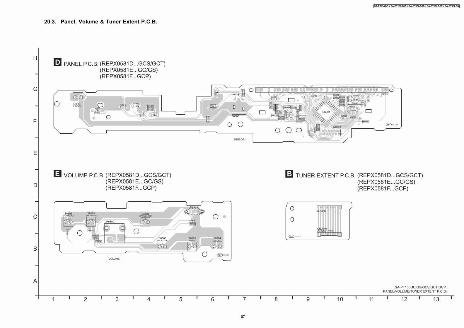
20.3. Panel, Volume & Tuner Extent P.C.B.
11 2 3 4 5 6 7 8 9
A
B
C
D
E
F
G
H
10 1 12 13
D PANEL P.C.B.
E VOLUME P.C.B.
SA-PT150GC/GS/GCS/GCT/GCP PANEL/VOLUME/TUNER EXTENT P.C.B.
(REPX0581D...GCS/GCT)(REPX0581E...GC/GS)(REPX0581F...GCP)
(REPX0581D...GCS/GCT)(REPX0581E...GC/GS)(REPX0581F...GCP)
B TUNER EXTENT P.C.B. (REPX0581D...GCS/GCT)(REPX0581E...GC/GS)(REPX0581F...GCP)
0534A0534A
0534A0534A
0534A0534A
PbF
PbF
PbF
S6800(POWER) W6010
D6900
C6905
C69
03
C69
11
R69
18
C6913
W61
04
C69
10
C6918
Z6900
SENSOR
VOLUME
W6513 W65
45
W6011
R6939 L6903
W6102
(GC/GS)
R6905
W6509
W6511
W65
12
C69
04
W65
04
W61
01
W60
08
W61
03
W61
00 R69
36 D69
10
FL6901W6012
IC6901
W6002
W6001
W6004
W6003
W6006
W6005C6909
R6940
C6906
R6914
C6916
R6916C6917R6919
R69
17
W65
02
CN6001
S6802(FORWARD) (REVERSE) (OPEN/CLOSE)
(SELECTOR) (PLAY) (STOP)
R68
01
S6803
R6802
R6804
R6803
R6805
S6801
S6806 S6805 S6804
VR6800
H6004
C6805
C6806
3 2 1
CP2010
CN2010(TO TUNER PACK)
R69
34
1 2 3
1 2 7 8 10 11 13 145 16 17 20 21 23 25 27 28 29 30 31 32 33 35 36 38 39 40 41 42 44 45
23
22
33 34
44
1
1
2
3
4
5
6
7
8
9
10
11
12
13
1112
1 2 3 4
12345678910
12345678910
SA-PT150GC / SA-PT150GCP / SA-PT150GCS / SA-PT150GCT / SA-PT150GS
87

20.4. Mic, USB, USB Relay & Tray Loading P.C.B.
11 2 3 4 5 6 7 8 9
A
B
C
D
E
F
G
H
10 1 12 13
G USB RELAY P.C.B. I TRAY LOADING P.C.B. (REP4238A)
H USB P.C.B.
SA-PT150GC/GS/GCS/GCT/GCP MIC/USB RELAY/USB/TRAY LOADING P.C.B.
(REPX0581D...GCS/GCT)(REPX0581E...GC/GS)(REPX0581F...GCP)
(REPX0581D...GCS/GCT)(REPX0581E...GC/GS)(REPX0581F...GCP)
F MIC P.C.B. (REPX0581D...GCS/GCT)(REPX0581E...GC/GS)(REPX0581F...GCP)
PbF 2462A-12462A-1
0534A0534A
0534A0534A
0534A0534A
+
-
M
PbF
PbF
PbF
S902(OPEN SW)
S901(PLAY SW)
REF NO.316
C98
4
IC904
CS901
K8001
CN8003
CN8002
K80
04
K80
05
5 3 1
1
2
3
4
5
24
CN8000
CN8001VA8001 (TO USB)
VA8002 K80
03
K80
02
L800
3
L800
2
VR6081
C6703
R6705
R6701
R6081
C6701
C6711
W6550
C6093
R6707R6708
C6707
C67
08
IC2204
W65
16
C67
09
W65
17
L608
2
L608
3
R67
03W
6514
R67
06R
6702
C67
02
C67
06
H6903 R6709 R6710
JK6802
MIC
MICVOLUME
32
54
1
76
L6081
1
2
3
4
5
6
7
8
9
7
6
5
4
3
2
1
54321
4 3 2 1
5
8 1
4
1234567
1 2 3
SA-PT150GC / SA-PT150GCP / SA-PT150GCS / SA-PT150GCT / SA-PT150GS
88

21 Basic Troubleshooting Guide21.1. Basic Troubleshooting Guide for Traverse Unit (DVD Module P.C.B)
Problems Checking Points Checking Components a) Check SDRAM address, data bus, CLK and other control signals waveform
IC8051
b) Check video signals LB8301, R8321, R8322, LB8302, R8325, R8326
1) Distorted picture or abnormal sound is head during the initialization
c) Check audio DAC circuitry
* Compare the above with OK condition DVD module P.C.B.
IC8421 *Check for solder short and/or component missing/damaged
a) Check motor driver circuitry (+5V)
IC8251 Pin 8, 21
b) Check laser drive circuitry (Voltages & current)
Q8551, Q8552, Q8561, Q8562
2) No TOC / Long TOC
c) Check LSI IC connection to motor drive circuitry *Compare the above with OK condition DVD Module P.C.B.
IC8001 Pin 66, 67* Check for solder short and/or component missing/damaged
a) Check connection from DVD Module to Traverse unit
FP8251 3) Disc not spinning 4) Traverse not moving 5) Traverse and spindle abnormal movement b) Check motor driver
circuitry on the voltages and control signals *Compare the above with OK condition DVD Module P.C.B
IC8251 *Check for solder short and/or component damaged
6) Cannot read the disc but spindle motor is spinning - Cannot read CD/DVD
a) Check laser drive circuitry (voltages and current)- Check CD Laser
Drive- Check DVD Laser
Drive * Check voltages and LD current and compare with OK condition DVDModule P.C.B.
Q8551, Q8552, LB8531 (For DVD Laser Drive current) Q8561, Q8562, LB8561 (For CD Laser Drive current)
7) Block Noise during play a) Check SDRAM address and data bus signal
IC8051
8) Jitter out of specification
9) Cannot read data from USB
a) Check LD currentb) Check OPU
a) Check USB connector & FFCb) Check LSI O/Pc) Check IC supply (+5V)
(Change to other unit and confirmed operating condition)
OPU Unit (Traverse unit), FPC connection
FP9001IC8001 Pin 144, 146IC9005 Pin 2, 3
89
SA-PT150GC / SA-PT150GCP / SA-PT150GCS / SA-PT150GCT / SA-PT150GS
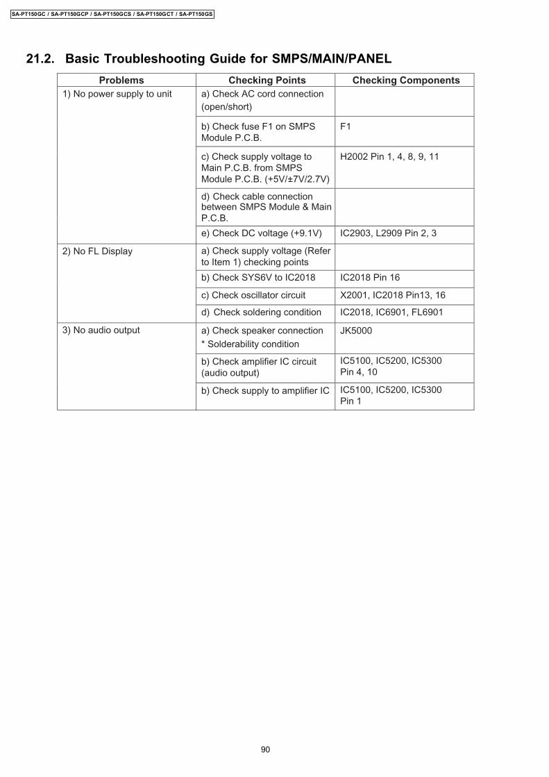
21.2. Basic Troubleshooting Guide for SMPS/MAIN/PANELProblems Checking Points Checking Components
a) Check AC cord connection(open/short)
b) Check fuse F1 on SMPSModule P.C.B.
F1
1) No power supply to unit
c) Check supply voltage to Main P.C.B. from SMPSModule P.C.B. (+5V/+7V/2.7V)
H2002 Pin 1, 4, 8, 9, 11
between SMPS Module & MainP.C.B.
d) Check cable connection
e) Check DC voltage (+9.1V)
IC2903, L2909 Pin 2, 3
a) Check supply voltage (Referto Item 1) checking points
a) Check speaker connection
b) Check amplifier IC circuit(audio output)
b) Check SYS6V to IC2018 IC2018 Pin 16
3) No audio output
2) No FL Display
c) Check oscillator circuit X2001, IC2018 Pin13, 16
d) Check soldering condition
* Solderability condition
IC2018, IC6901, FL6901
JK5000
IC5100, IC5200, IC5300 Pin 4, 10
b) Check supply to amplifier IC IC5100, IC5200, IC5300 Pin 1
90
SA-PT150GC / SA-PT150GCP / SA-PT150GCS / SA-PT150GCT / SA-PT150GS

22 Overall Block Diagram for PT15022.1. SC-PT150 Simplified Block
DV
5
SC
-PT
150
SIM
PL
IFIE
D B
LO
CK
(C/Y
/CR
/CB
/PY
)
A+5
V
IC28
01V
IDE
O IC
LD
CD
ET
1D
+5A
+5
DV
D 2
.7V
SW
+5V
+7V
-7V
-VP
FL1
/FL2
+9.1
V
+26V
DC
DE
T1
Reg
ulat
or
Reg
ulat
or
IC29
03D
C-D
CC
ON
VE
RT
ER
Reg
ulat
or-
-+
+
TO
DV
5
TO
AS
P
TO
PA
NE
LB
LOC
KT
OT
UN
ER
TO
FAN
PO
WE
R S
UP
PLY
BLO
CK
SM
PS
BLO
CK
B
DC
DE
T1
VC
C_C
TR
L
SY
S6V
1P
CO
NT
-VP
PA
NE
L B
LOC
K
IC69
01F
L D
river
IC
C
FLD_OUT1
FLD_CLK1
FLD_STB1
A
+7V
+26V
IC71
00IC
7100
EC
HO
IC FAN
CIR
CU
ITB
LOC
K
EC
HO
_MU
TE
EC
HO
_LV
1
EC
HO
_LV
2P
CO
NT
DC
DE
T1
F L D I S P L A Y
FL1
/FL2
FL6
901
IC22
04M
IC A
MP
+7V
/-7V
MIC
JK68
02
JK50
00
To S
peak
erU
nits
AM
P S
ectio
nIC
5100
(FL+
/-
FR
+/-)
IC52
00(S
L+/L
-
SR
+/R
-)
IC53
00(C
+/C
- &
S
W+/
SW
-)
SW
+5V
AS
P_M
ICIN
MU
TE
_FR
_SW
MU
TE
_SU
RR
S
TY
B
IC21
02A
SP
IC
IC20
18M
ICR
O-P
IC
AS
P_D
A/A
SP
_CLK
IC20
04E
EP
RO
M
2W
IDE A
B
C
RG
B
IC28
02S
witc
hIC
(PY
/Y)
(WID
E_O
UT
)
ICIC
1102
Sw
itch
Mut
ing
(VID
EO
_MU
TE
)
(SC
AR
T_M
UT
E)
(C/Y
/CR
/CB
/PY
)
+26V
IC11
01S
CA
RT
IC
JK20
01
(AU
X/C
B/C
R/Y
/CO
MP
OS
ITE
)
JK10
01
(SC
AR
TT
ER
MIN
AL)
AU
DIO
L/R
(VO
UT
/R
_OU
T
/G_O
UT
/B
_OU
T)
DL2
SU
LOA
DIN
G
AU
X
TU
NE
R
(TU
_DI/T
U_S
T/T
U_C
LK/T
U_S
D)
(DV
D_M
UT
E/
DV
D_S
TA/
DV
D_C
MD
/ D
VD
_CK
)
(TR
AY
_OP
EN
/
TR
AY
_CLO
SE
/T
RA
Y_C
CW
/ T
RA
Y_C
W)
SA-PT150GC / SA-PT150GCP / SA-PT150GCS / SA-PT150GCT / SA-PT150GS
91
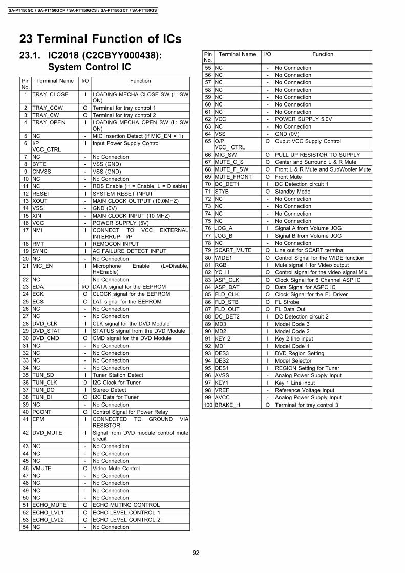
23.1. IC2018 (C2CBYY000438):System Control IC
PinNo.
Terminal Name I/O Function
1 TRAY_CLOSE I LOADING MECHA CLOSE SW (L: SWON)
2 TRAY_CCW O Terminal for tray control 13 TRAY_CW O Terminal for tray control 24 TRAY_OPEN I LOADING MECHA OPEN SW (L: SW
ON)5 NC - MIC Insertion Detect (if MIC_EN = 1)6 I/P
VCC_CTRLI Input Power Supply Control
7 NC - No Connection8 BYTE - VSS (GND)9 CNVSS - VSS (GND)10 NC - No Connection11 NC - RDS Enable (H = Enable, L = Disable)12 RESET I SYSTEM RESET INPUT13 XOUT - MAIN CLOCK OUTPUT (10.0MHZ)14 VSS - GND (0V)15 XIN - MAIN CLOCK INPUT (10 MHZ)16 VCC - POWER SUPPLY (5V)17 NMI I CONNECT TO VCC EXTERNAL
INTERRUPT I/P18 RMT I REMOCON INPUT19 SYNC I AC FAILURE DETECT INPUT20 NC - No Connection21 MIC_EN I Microphone Enable (L=Disable,
H=Enable)22 NC - No Connection23 EDA I/O DATA signal for the EEPROM24 ECK O CLOCK signal for the EEPROM25 ECS O LAT signal for the EEPROM26 NC - No Connection27 NC - No Connection28 DVD_CLK I CLK signal for the DVD Module29 DVD_STAT I STATUS signal from the DVD Module30 DVD_CMD O CMD signal for the DVD Module31 NC - No Connection32 NC - No Connection33 NC - No Connection34 NC - No Connection35 TUN_SD I Tuner Station Detect36 TUN_CLK 0 I2C Clock for Tuner37 TUN_DO I Stereo Detect38 TUN_DI O I2C Data for Tuner39 NC - No Connection40 PCONT O Control Signal for Power Relay41 EPM I CONNECTED TO GROUND VIA
RESISTOR42 DVD_MUTE I Signal from DVD module control mute
circuit43 NC - No Connection44 NC - No Connection45 NC - No Connection46 VMUTE O Video Mute Control47 NC - No Connection48 NC - No Connection49 NC - No Connection50 NC - No Connection51 ECHO_MUTE O ECHO MUTING CONTROL52 ECHO_LVL1 O ECHO LEVEL CONTROL 153 ECHO_LVL2 O ECHO LEVEL CONTROL 254 NC - No Connection
PinNo.
Terminal Name I/O Function
55 NC - No Connection56 NC - No Connection57 NC - No Connection58 NC - No Connection59 NC - No Connection60 NC - No Connection61 NC - No Connection62 VCC - POWER SUPPLY 5.0V63 NC - No Connection64 VSS - GND (0V)65 O/P
VCC_ CTRLO Ouput VCC Supply Control
66 MIC_SW O PULL UP RESISTOR TO SUPPLY67 MUTE_C_S O Center and Surround L & R Mute68 MUTE_F_SW O Front L & R Mute and SubWoofer Mute69 MUTE_FRONT O Front Mute70 DC_DET1 I DC Detection circuit 171 STYB O Standby Mode72 NC - No Connection73 NC - No Connection74 NC - No Connection75 NC - No Connection76 JOG_A I Signal A from Volume JOG77 JOG_B I Signal B from Volume JOG78 NC - No Connection79 SCART_MUTE O Line out for SCART terminal80 WIDE1 O Control Signal for the WIDE function81 RGB I Mute signal 1 for Video output82 YC_H O Control signal for the video signal Mix83 ASP_CLK O Clock Signal for 6 Channel ASP IC84 ASP_DAT O Data Signal for ASPC IC85 FLD_CLK O Clock Signal for the FL Driver86 FLD_STB O FL Strobe87 FLD_OUT O FL Data Out88 DC_DET2 I DC Detection circuit 289 MD3 I Model Code 390 MD2 I Model Code 291 KEY 2 I Key 2 line input92 MD1 I Model Code 193 DES3 I DVD Region Setting94 DES2 I Model Selector95 DES1 I REGION Setting for Tuner96 AVSS - Analog Power Supply Input97 KEY1 I Key 1 Line input98 VREF - Reference Voltage Input99 AVCC - Analog Power Supply Input100 BRAKE_H O Terminal for tray control 3
23 Terminal Function of ICs
92
SA-PT150GC / SA-PT150GCP / SA-PT150GCS / SA-PT150GCT / SA-PT150GS

24 Exploded Views
93
SA-PT150GC / SA-PT150GCP / SA-PT150GCS / SA-PT150GCT / SA-PT150GS

94
SA-PT150GC / SA-PT150GCP / SA-PT150GCS / SA-PT150GCT / SA-PT150GS
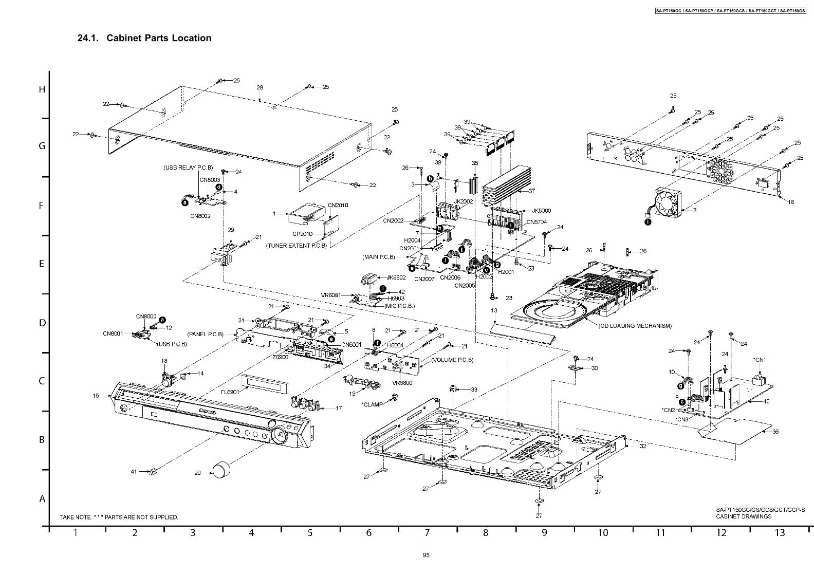
24.1. Cabinet Parts Location
SA-PT150GC / SA-PT150GCP / SA-PT150GCS / SA-PT150GCT / SA-PT150GS
95
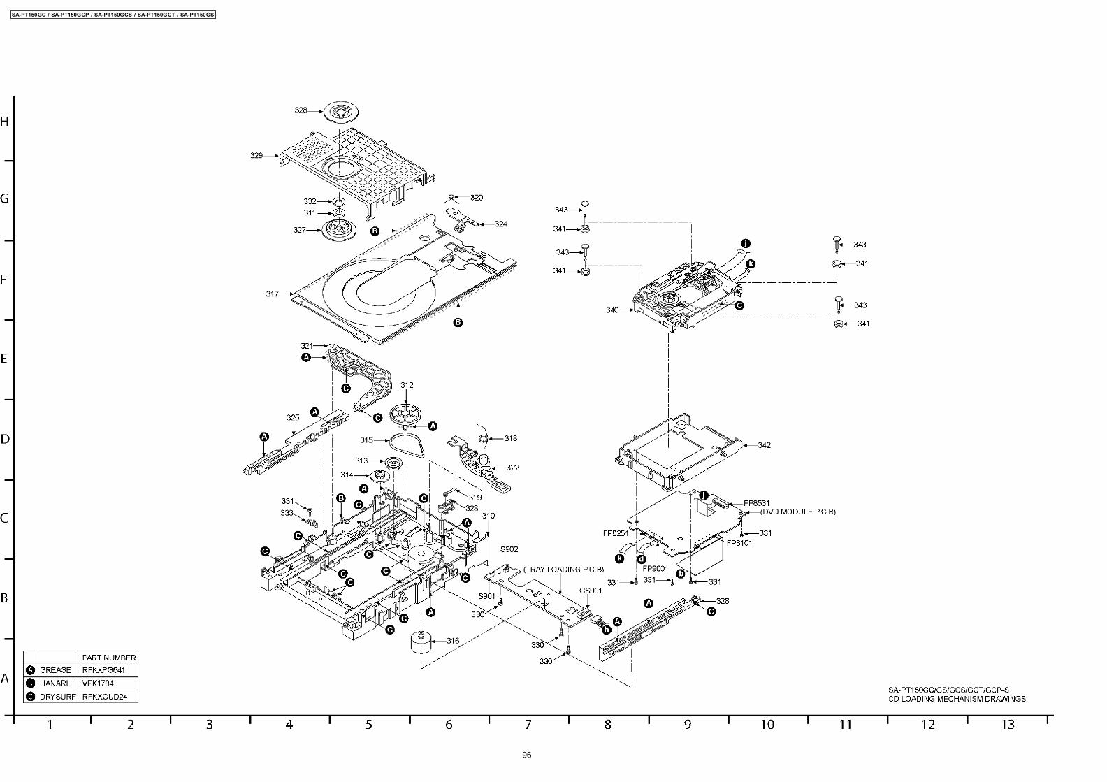
SA-PT150GC / SA-PT150GCP / SA-PT150GCS / SA-PT150GCT / SA-PT150GS
96

24.2. Packaging
SA-PT150GC / SA-PT150GCP / SA-PT150GCS / SA-PT150GCT / SA-PT150GS
97

Notes:
25 Replacement Parts List
· Important safety notice:
Components identified by mark have special characteristics important for safety purpose.Furthermore, special parts which have purposes of fire-retardant (resistors), high-quality sound (capacitors), low-noise(resistors), etc. are used.When replacing any of components, be sure to use only manufacture’s specified parts shown in the parts list.
· Warning: This product uses a laser diode. Refer to caution statements. · Capacity values are in microfarads (µF) unless specified otherwise, P=Pico-farads (pF), F=Farads (F). · Resistance values are in ohms, unless specified otherwise, 1K=1,000 (OHM), 1M=1,000K (OHM). · The parenthesized indications in the Remarks columns specify the model names and areas. (Refer to the cover page) · The marking (RTL) indicates the retention time is limited for this item. After the discontinuation of this assembly in production,
it will no longer be available. · Parts mentioned [M] are supplied from PAVCSG. · Parts mentioned [SPG] are supplied from PAVC. · Reference for O/I book languages are as follows:
Ar: Arablic Du: Dutch It: Italian Sp: SpanishCf: Canadian French En: English Ko: Korean Sw: SwedishCz: Czech Fr: French Po: Polish Co: Traditional ChineseDa: Danish Ge: German Ru: Russian Cn Simplified ChinesePe: Persian Ur: Ukrainian Pr: Portuguese
·
98
SA-PT150GC / SA-PT150GCP / SA-PT150GCS / SA-PT150GCT / SA-PT150GS
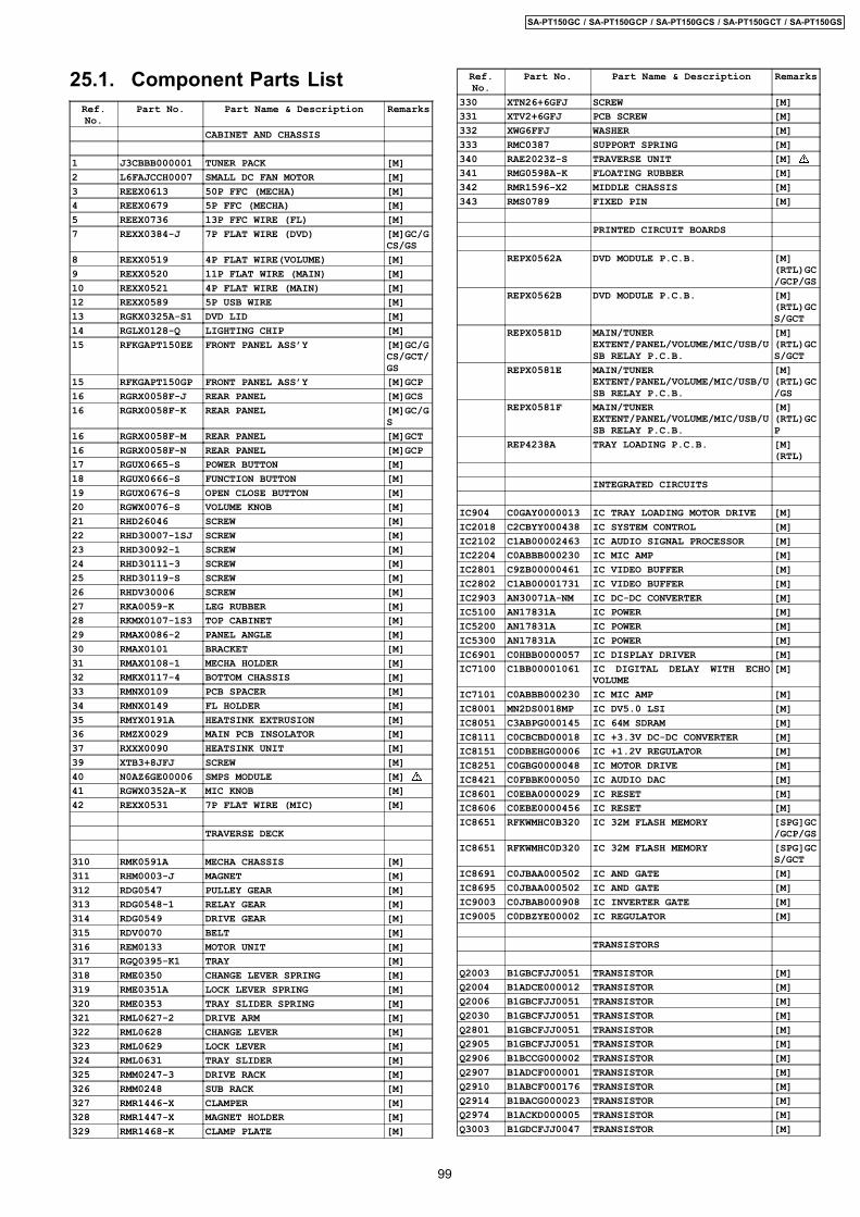
25.1. Component Parts ListRef.No.
Part No. Part Name & Description Remarks
CABINET AND CHASSIS
1 J3CBBB000001 TUNER PACK [M]2 L6FAJCCH0007 SMALL DC FAN MOTOR [M]3 REEX0613 50P FFC (MECHA) [M]4 REEX0679 5P FFC (MECHA) [M]5 REEX0736 13P FFC WIRE (FL) [M]7 REXX0384-J 7P FLAT WIRE (DVD) [M]GC/G
CS/GS8 REXX0519 4P FLAT WIRE(VOLUME) [M]9 REXX0520 11P FLAT WIRE (MAIN) [M]10 REXX0521 4P FLAT WIRE (MAIN) [M]12 REXX0589 5P USB WIRE [M]13 RGKX0325A-S1 DVD LID [M]14 RGLX0128-Q LIGHTING CHIP [M]15 RFKGAPT150EE FRONT PANEL ASS’Y [M]GC/G
CS/GCT/GS
15 RFKGAPT150GP FRONT PANEL ASS’Y [M]GCP16 RGRX0058F-J REAR PANEL [M]GCS16 RGRX0058F-K REAR PANEL [M]GC/G
S16 RGRX0058F-M REAR PANEL [M]GCT16 RGRX0058F-N REAR PANEL [M]GCP17 RGUX0665-S POWER BUTTON [M]18 RGUX0666-S FUNCTION BUTTON [M]19 RGUX0676-S OPEN CLOSE BUTTON [M]20 RGWX0076-S VOLUME KNOB [M]21 RHD26046 SCREW [M]22 RHD30007-1SJ SCREW [M]23 RHD30092-1 SCREW [M]24 RHD30111-3 SCREW [M]25 RHD30119-S SCREW [M]26 RHDV30006 SCREW [M]27 RKA0059-K LEG RUBBER [M]28 RKMX0107-1S3 TOP CABINET [M]29 RMAX0086-2 PANEL ANGLE [M]30 RMAX0101 BRACKET [M]31 RMAX0108-1 MECHA HOLDER [M]32 RMKX0117-4 BOTTOM CHASSIS [M]33 RMNX0109 PCB SPACER [M]34 RMNX0149 FL HOLDER [M]35 RMYX0191A HEATSINK EXTRUSION [M]36 RMZX0029 MAIN PCB INSOLATOR [M]37 RXXX0090 HEATSINK UNIT [M]39 XTB3+8JFJ SCREW [M]40 N0AZ6GE00006 SMPS MODULE [M]41 RGWX0352A-K MIC KNOB [M]42 REXX0531 7P FLAT WIRE (MIC) [M]
TRAVERSE DECK
310 RMK0591A MECHA CHASSIS [M]311 RHM0003-J MAGNET [M]312 RDG0547 PULLEY GEAR [M]313 RDG0548-1 RELAY GEAR [M]314 RDG0549 DRIVE GEAR [M]315 RDV0070 BELT [M]316 REM0133 MOTOR UNIT [M]317 RGQ0395-K1 TRAY [M]318 RME0350 CHANGE LEVER SPRING [M]319 RME0351A LOCK LEVER SPRING [M]320 RME0353 TRAY SLIDER SPRING [M]321 RML0627-2 DRIVE ARM [M]322 RML0628 CHANGE LEVER [M]323 RML0629 LOCK LEVER [M]324 RML0631 TRAY SLIDER [M]325 RMM0247-3 DRIVE RACK [M]326 RMM0248 SUB RACK [M]327 RMR1446-X CLAMPER [M]328 RMR1447-X MAGNET HOLDER [M]329 RMR1468-K CLAMP PLATE [M]
Ref.No.
Part No. Part Name & Description Remarks
330 XTN26+6GFJ SCREW [M]331 XTV2+6GFJ PCB SCREW [M]332 XWG6FFJ WASHER [M]333 RMC0387 SUPPORT SPRING [M]340 RAE2023Z-S TRAVERSE UNIT [M]341 RMG0598A-K FLOATING RUBBER [M]342 RMR1596-X2 MIDDLE CHASSIS [M]343 RMS0789 FIXED PIN [M]
PRINTED CIRCUIT BOARDS
REPX0562A DVD MODULE P.C.B. [M](RTL)GC/GCP/GS
REPX0562B DVD MODULE P.C.B. [M](RTL)GCS/GCT
REPX0581D MAIN/TUNEREXTENT/PANEL/VOLUME/MIC/USB/USB RELAY P.C.B.
[M](RTL)GCS/GCT
REPX0581E MAIN/TUNEREXTENT/PANEL/VOLUME/MIC/USB/USB RELAY P.C.B.
[M](RTL)GC/GS
REPX0581F MAIN/TUNEREXTENT/PANEL/VOLUME/MIC/USB/USB RELAY P.C.B.
[M](RTL)GCP
REP4238A TRAY LOADING P.C.B. [M](RTL)
INTEGRATED CIRCUITS
IC904 C0GAY0000013 IC TRAY LOADING MOTOR DRIVE [M]IC2018 C2CBYY000438 IC SYSTEM CONTROL [M]IC2102 C1AB00002463 IC AUDIO SIGNAL PROCESSOR [M]IC2204 C0ABBB000230 IC MIC AMP [M]IC2801 C9ZB00000461 IC VIDEO BUFFER [M]IC2802 C1AB00001731 IC VIDEO BUFFER [M]IC2903 AN30071A-NM IC DC-DC CONVERTER [M]IC5100 AN17831A IC POWER [M]IC5200 AN17831A IC POWER [M]IC5300 AN17831A IC POWER [M]IC6901 C0HBB0000057 IC DISPLAY DRIVER [M]IC7100 C1BB00001061 IC DIGITAL DELAY WITH ECHO
VOLUME[M]
IC7101 C0ABBB000230 IC MIC AMP [M]IC8001 MN2DS0018MP IC DV5.0 LSI [M]IC8051 C3ABPG000145 IC 64M SDRAM [M]IC8111 C0CBCBD00018 IC +3.3V DC-DC CONVERTER [M]IC8151 C0DBEHG00006 IC +1.2V REGULATOR [M]IC8251 C0GBG0000048 IC MOTOR DRIVE [M]IC8421 C0FBBK000050 IC AUDIO DAC [M]IC8601 C0EBA0000029 IC RESET [M]IC8606 C0EBE0000456 IC RESET [M]IC8651 RFKWMHC0B320 IC 32M FLASH MEMORY [SPG]GC
/GCP/GSIC8651 RFKWMHC0D320 IC 32M FLASH MEMORY [SPG]GC
S/GCTIC8691 C0JBAA000502 IC AND GATE [M]IC8695 C0JBAA000502 IC AND GATE [M]IC9003 C0JBAB000908 IC INVERTER GATE [M]IC9005 C0DBZYE00002 IC REGULATOR [M]
TRANSISTORS
Q2003 B1GBCFJJ0051 TRANSISTOR [M]Q2004 B1ADCE000012 TRANSISTOR [M]Q2006 B1GBCFJJ0051 TRANSISTOR [M]Q2030 B1GBCFJJ0051 TRANSISTOR [M]Q2801 B1GBCFJJ0051 TRANSISTOR [M]Q2905 B1GBCFJJ0051 TRANSISTOR [M]Q2906 B1BCCG000002 TRANSISTOR [M]Q2907 B1ADCF000001 TRANSISTOR [M]Q2910 B1ABCF000176 TRANSISTOR [M]Q2914 B1BACG000023 TRANSISTOR [M]Q2974 B1ACKD000005 TRANSISTOR [M]Q3003 B1GDCFJJ0047 TRANSISTOR [M]
99
SA-PT150GC / SA-PT150GCP / SA-PT150GCS / SA-PT150GCT / SA-PT150GS

Ref.No.
Part No. Part Name & Description Remarks
Q3008 B1ABGC000005 TRANSISTOR [M]Q3009 B1ABCF000176 TRANSISTOR [M]Q5740 B1BACG000023 TRANSISTOR [M]Q5741 B1ABCF000176 TRANSISTOR [M]Q5742 B1ABCF000176 TRANSISTOR [M]Q5744 B1ABCF000176 TRANSISTOR [M]Q5745 B1ACKD000005 TRANSISTOR [M]Q5746 B1GBCFJJ0051 TRANSISTOR [M]Q7100 B1GBCFJJ0051 TRANSISTOR [M]Q7101 B1GBCFJJ0051 TRANSISTOR [M]Q7102 B1GBCFJJ0051 TRANSISTOR [M]Q8321 2SB1218ARL TRANSISTOR [M]Q8325 2SB1218ARL TRANSISTOR [M]Q8331 2SB1218ARL TRANSISTOR [M]Q8335 2SB1218ARL TRANSISTOR [M]Q8341 2SB1218ARL TRANSISTOR [M]Q8551 2SD1819A0L TRANSISTOR [M]Q8552 B1ADGB000008 TRANSISTOR [M]Q8561 2SD1819A0L TRANSISTOR [M]Q8562 B1ADGB000008 TRANSISTOR [M]
QR8111 XP0621400L CHIP TRANSISTOR [M]QR8420 UNR521100L CHIP TRANSISTOR [M]QR8571 UNR511V00L CHIP TRANSISTOR [M]
DIODES
D2000 B0JCPD000025 DIODE [M]D2001 B0EAKM000117 DIODE [M]D2002 B0EAKM000117 DIODE [M]D2005 B0ACCK000005 DIODE [M]D2007 B0ACCK000005 DIODE [M]D2008 B0ACCK000005 DIODE [M]D2810 B0JCAE000001 DIODE [M]D2900 B0BC7R500001 DIODE [M]D2904 B0JCPD000025 DIODE [M]D2905 B0BC7R500001 DIODE [M]D2918 B0ADCJ000020 DIODE [M]D2929 B0ACCK000005 DIODE [M]D2935 B0EAKM000117 DIODE [M]D2936 B0EAKM000117 DIODE [M]D2944 B0BC3R400001 DIODE [M]D2974 MAZ82200ML DIODE [M]D3001 B0ACCK000005 DIODE [M]D5302 B0ACCK000005 DIODE [M]D5700 B0ACCK000005 DIODE [M]D5743 B0ACCK000005 DIODE [M]D5744 B0ACCK000005 DIODE [M]D5745 B0BC013A0007 DIODE [M]D6900 B3AAA0000803 DIODE [M]D6910 B0BC3R400001 DIODE [M]D7100 B0BC5R000009 DIODE [M]D8211 MA2J11100L DIODE [M]D8571 MA2J72800L DIODE [M]
VARIABLE RESISTORS
VR6081 EVUE27FK3B53 VR MIC LEVEL [M]VR6800 EVEKE2F2524M VR VOLUME JOG [M]
VA8001 EZJZ1V171AA CHIP VARISTOR [M]VA8002 EZJZ1V171AA CHIP VARISTOR [M]
SWITCHES
S901 RSH1A044-1A SW PLAY [M]S902 RSH1A044-1A SW OPEN [M]S6800 EVQ21405R SW POWER [M]S6801 EVQ21405R SW OPEN/CLOSE [M]S6802 EVQ21405R SW FORWARD [M]S6803 EVQ21405R SW REVERSE [M]S6804 EVQ21405R SW STOP [M]S6805 EVQ21405R SW PLAY [M]
Ref.No.
Part No. Part Name & Description Remarks
S6806 EVQ21405R SW SELECTOR [M]
CONNECTORS
CN2001 K1MY50AA0029 50P CONNECTOR [M]CN2002 K1KA10AA0031 10P CONNECTOR [M]CN2005 K1KA04AA0193 4P CONNECTOR [M]CN2006 K1KA07AA0193 7P CONNECTOR [M]CN2007 K1MN13AA0003 13P CONNECTOR [M]CN2010 K1KA10AA0031 10P CONNECTOR [M]CN5704 K1KA03AA0301 3P CONNECTOR [M]CN6001 K1MN13BA0004 13P CONNECTOR [M]CN8000 K1KA05BA0061 5P CONNECTOR [M]CN8001 K1FY104B0011 4P CONNECTOR [M]CN8002 K1KA05BA0061 5P CONNECTOR [M]CN8003 K1MY05BA0130 5P CONNECTOR [M]
CP2010 K1KB10B00042 10P CONNECTOR [M]
CS901 K1KA07BA0061 7P CONNECTOR [M]
FP8101 K1MN50BA0173 50P CONNECTOR [M]FP8251 K1MN06BA0148 6P CONNECTOR [M]FP8531 K1MY26BA0025 26P CONNECTOR [M]FP9001 K1MN05BA0148 5P CONNECTOR [M]
COILS & TRANSFORMERS
L2009 G0C220JA0055 COIL [M]L2800 G0C220JA0055 COIL [M]L2801 G0C220JA0055 COIL [M]L2802 J0JBC0000015 CHIP INDUCTOR [M]L2803 J0JBC0000015 CHIP INDUCTOR [M]L2804 J0JBC0000015 CHIP INDUCTOR [M]L2805 J0JBC0000015 CHIP INDUCTOR [M]L2902 G0A101G00022 COIL [M]L2909 G0A200D00002 COIL [M]L2910 G0A220GA0026 INDUCTOR [M]L2911 G0A200D00002 COIL [M]L6081 ERJ3GEY0R00V CHIP JUMPER [M]L6082 J0JBC0000030 CHIP BEEZ [M]L6083 J0JBC0000019 CHIP INDUCTOR [M]L6903 J0JBC0000041 CHIP INDUCTOR [M]L8002 ERJ6GEY0R00V CHIP RESISTOR [M]L8003 ERJ6GEY0R00V CHIP RESISTOR [M]L8201 G1C100K00019 CHIP COIL [M]L8301 G1C100K00019 CHIP COIL [M]L8302 G1C100K00019 CHIP COIL [M]L8330 G1C100K00019 CHIP COIL [M]L8501 G1C100K00019 CHIP COIL [M]L8550 G1C100KA0055 CHIP INDUCTOR [M]
CHIP INDUCTORS
LB8001 J0JHC0000045 CHIP INDUCTOR [M]LB8011 J0JHC0000045 CHIP INDUCTOR [M]LB8257 ERJ3GEY0R00V CHIP RESISTOR [M]LB8258 ERJ3GEY0R00V CHIP RESISTOR [M]LB8259 ERJ3GEY0R00V CHIP RESISTOR [M]LB8260 ERJ3GEY0R00V CHIP RESISTOR [M]LB8301 J0JBC0000042 CHIP BEAD [M]LB8302 J0JBC0000042 CHIP BEAD [M]LB8303 J0JBC0000042 CHIP BEAD [M]LB8304 J0JBC0000042 CHIP BEAD [M]LB8305 J0JBC0000042 CHIP BEAD [M]LB8401 J0JBC0000042 CHIP BEAD [M]LB8421 ERJ2GE0R00X CHIP RESISTOR [M]LB8422 ERJ2GE0R00X CHIP RESISTOR [M]LB8423 ERJ2GE0R00X CHIP RESISTOR [M]LB8424 ERJ2GE0R00X CHIP RESISTOR [M]LB8425 ERJ2GE0R00X CHIP RESISTOR [M]LB8426 ERJ2GE0R00X CHIP RESISTOR [M]LB8427 ERJ2GE0R00X CHIP RESISTOR [M]
100
SA-PT150GC / SA-PT150GCP / SA-PT150GCS / SA-PT150GCT / SA-PT150GS

Ref.No.
Part No. Part Name & Description Remarks
LB8428 ERJ2GE0R00X CHIP RESISTOR [M]LB8429 ERJ2GE0R00X CHIP RESISTOR [M]LB8430 J0JHC0000045 CHIP INDUCTOR [M]LB8431 ERJ2GE0R00X CHIP RESISTOR [M]LB8491 ERJ2GE0R00X CHIP RESISTOR [M]LB8530 J0JHC0000045 CHIP INDUCTOR [M]LB8531 ERJ2GE0R00X CHIP RESISTOR [M]LB8551 J0JBC0000042 CHIP BEAD [M]LB8561 J0JBC0000042 CHIP BEAD [M]LB8571 J0JBC0000042 CHIP BEAD [M]LB8690 J0JBC0000044 HIGH LOSS INDUCTOR [M]LB8691 ERJ2GEJ101X CHIP RESISTOR [M]LB8692 ERJ2GEJ101X CHIP RESISTOR [M]LB8693 ERJ2GEJ101X CHIP RESISTOR [M]LB9001 J0JCC0000119 CHIP INDUCTOR [M]
COMPONENT COMBINATION
Z6900 B3RAB0000025 REMOTE SENSOR [M]
OSCILLATORS
X2001 H2B100500004 CERAMIC RESONATOR [M]X8621 H0J270500085 CRYSTAL OSCILLATOR [M]X9004 H1A4805B0027 CRYSTAL OSCILLATOR [M]
DISPLAY TUBE
FL6901 A2BD00000170 FL DISPLAY [M]FL8101 F1H0J1050018 INDUCTOR [M]FL8102 F1H0J1050018 INDUCTOR [M]FL8103 F1H0J1050018 INDUCTOR [M]FL8104 F1J1E1040022 INDUCTOR [M]
FUSE
F1 K5D502BNA005 FUSE [M]
HOLDERS
H2001 K1YF04000001 4P CABLE HOLDER [M]H2002 K1YZ11000002 11P CABLE HOLDER [M]H2004 K1YZ07000001 7P WIRE HOLDER [M]H6004 K1YZ04000002 4P CABLE HOLDER [M]H6903 K1YZ07000001 7P WIRE HOLDER [M]
JACKS
JK2002 K2HA306B0070 JACK COMPONENT VIDEO OUT [M]JK5000 K4AC12B00003 JK SPEAKER [M]JK6802 K2HB102J0038 JACK MIC [M]
EARTH TERMINALS
E2900 K4CZ01000027 TERMINAL [M]E2901 K4CZ01000027 TERMINAL [M]
PACKING MATERIALS
P1 RPGX1727 PACKING CASE [M]GCP1 RPGX1728 PACKING CASE [M]GSP1 RPGX1729 PACKING CASE [M]GCSP1 RPGX1730 PACKING CASE [M]GCTP1 RPGX1731 PACKING CASE [M]GCPP2 RPNX0369-1 POLYFOAM [M]P3 RPFX0058-1J MIRAMAT [M]P4 RPNX0446 POLYFOAM [M]GC/G
CS/GS
ACCESSORIES
A1 N2QAYB000092 REMOTE CONTROL [M]A1-1 RKK-HTR0051K R/C BATTERY COVER [M]
Ref.No.
Part No. Part Name & Description Remarks
A2 K2CQ2CA00002 AC CORD [M]GCT
A2 K2CQ2CA00007 AC CORD [M]GC/GCS/GCP
A2 K2CT3CA00004 AC CORD [M]GS
A3 RQTX0028-2B O/I BOOK (EN) [M]GC/GCS/GCT/GS
A3 RQTX0031-G OI BOOK (AR/PE) [M]GC/GS
A3 RQTX0032-K OI BOOK (CN) [M]GCS/GCT
A3 RQTX0033-M O/I BOOK (SP) [M]GCPA4 RSA0007-M ANTENNA WIRE [M]A5 K2KA2BA00001 VIDEO CABLE [M]A6 K2DA42E00001 AC PLUG ADAPTOR [M]GCPA7 RQCA0968 SPEAKER LABEL [M]GCP/
GCT
RESISTORS
R2000 ERJ3GEYJ221V 220 1/16W [M]R2001 ERJ3GEYJ104V 100K 1/16W [M]R2002 ERJ3GEYJ103V 10K 1/16W [M]R2003 ERJ3GEYJ221V 220 1/16W [M]R2004 ERJ3GEYJ221V 220 1/16W [M]R2005 ERJ3GEYJ221V 220 1/16W [M]R2006 ERJ3GEYJ182V 1.8K 1/16W [M]R2007 ERJ3GEYJ103V 10K 1/16W [M]R2010 ERJ3GEYJ221V 220 1/16W [M]R2012 ERJ3GEYJ103V 10K 1/16W [M]R2015 ERJ3GEYJ102V 1K 1/16W [M]R2016 ERJ3GEYJ221V 220 1/16W [M]R2017 ERJ3GEYJ273V 27K 1/16W [M]R2019 ERJ3GEYJ273V 27K 1/16W [M]R2022 ERJ3GEYJ221V 220 1/16W [M]R2023 ERJ3GEYJ221V 220 1/16W [M]R2024 ERJ3GEYJ221V 220 1/16W [M]R2029 ERJ3GEYJ221V 220 1/16W [M]R2030 ERJ3GEYJ221V 220 1/16W [M]R2031 ERJ3GEYJ221V 220 1/16W [M]R2032 ERJ3GEYJ473V 47K 1/16W [M]R2039 ERJ3GEYJ103V 10K 1/16W [M]R2040 ERJ3GEYJ221V 220 1/16W [M]R2041 ERJ3GEYJ103V 10K 1/16W [M]R2042 ERJ3GEYJ221V 220 1/16W [M]R2043 ERJ3GEYJ473V 47K 1/16W [M]R2044 ERJ3GEYJ221V 220 1/16W [M]R2045 ERJ3GEYJ103V 10K 1/16W [M]R2046 ERJ3GEYJ221V 220 1/16W [M]R2047 ERJ3GEYJ221V 220 1/16W [M]R2048 ERJ3GEYJ221V 220 1/16W [M]R2049 ERJ3GEYJ221V 220 1/16W [M]R2052 ERJ3GEYJ221V 220 1/16W [M]R2053 ERJ3GEYJ103V 10K 1/16W [M]R2060 ERJ3GEYJ221V 220 1/16W [M]R2061 ERJ3GEYJ473V 47K 1/16W [M]R2062 ERJ3GEYJ221V 220 1/16W [M]R2063 ERJ3GEYJ473V 47K 1/16W [M]R2064 ERJ3GEYJ221V 220 1/16W [M]R2065 ERJ3GEYJ221V 220 1/16W [M]R2066 ERJ3GEYJ222V 2.2K 1/16W [M]R2067 ERJ3GEYJ221V 220 1/16W [M]R2068 ERJ3GEYJ221V 220 1/16W [M]R2069 ERJ3GEYJ221V 220 1/16W [M]R2070 ERJ3GEYJ221V 220 1/16W [M]R2071 ERJ3GEYJ221V 220 1/16W [M]R2072 ERJ3GEYJ221V 220 1/16W [M]R2073 ERJ3GEYJ221V 220 1/16W [M]R2074 ERJ3GEYJ103V 10K 1/16W [M]R2075 ERJ3GEYJ221V 220 1/16W [M]R2076 ERJ3GEYJ103V 10K 1/16W [M]R2077 ERJ3GEYJ821V 820 1/16W [M]
101
SA-PT150GC / SA-PT150GCP / SA-PT150GCS / SA-PT150GCT / SA-PT150GS

Ref.No.
Part No. Part Name & Description Remarks
R2078 ERJ3GEYJ472V 4.7K 1/16W [M]R2079 ERJ3GEYJ103V 10K 1/16W [M]R2080 ERJ3GEYJ103V 10K 1/16W [M]GC/G
SR2080 ERJ3GEYJ332V 3.3K 1/16W [M]GCS/
GCTR2080 ERJ3GEYJ223V 22K 1/16W [M]GCPR2081 ERJ3GEYJ103V 10K 1/16W [M]R2082 ERJ3GEY0R00V 0 1/16W [M]R2084 ERJ3GEYJ473V 47K 1/16W [M]R2085 ERJ3GEYJ472V 4.7K 1/16W [M]R2086 ERJ3GEYJ223V 22K 1/16W [M]R2087 ERJ3GEYJ223V 22K 1/16W [M]R2088 ERJ3GEYJ103V 10K 1/16W [M]R2089 ERJ3GEYJ223V 22K 1/16W [M]GCS/
GCTR2089 ERJ3GEYJ333V 33K 1/16W [M]GC/G
SR2089 ERJ3GEYJ124V 120K 1/16W [M]GCPR2090 ERJ3GEYJ221V 220 1/16W [M]R2091 ERJ3GEYJ103V 10K 1/16W [M]R2092 ERJ3GEYJ221V 220 1/16W [M]R2093 ERJ3GEYJ332V 3.3K 1/16W [M]GC/G
SR2093 ERJ3GEYJ472V 4.7K 1/16W [M]GCS/
GCTR2093 ERJ3GEYJ682V 6.8K 1/16W [M]GCPR2094 ERJ3GEYJ103V 10K 1/16W [M]R2095 ERJ3GEYJ472V 4.7K 1/16W [M]R2096 ERJ3GEYJ103V 10K 1/16W [M]R2097 ERJ3GEYJ474V 470K 1/16W [M]R2098 ERJ3GEYJ221V 220 1/16W [M]R2101 ERJ3GEYJ123V 12K 1/16W [M]R2111 ERJ3GEYJ123V 12K 1/16W [M]R2112 ERJ3GEYJ123V 12K 1/16W [M]R2113 ERJ3GEYJ472V 4.7K 1/16W [M]R2114 ERJ3GEYJ472V 4.7K 1/16W [M]R2115 ERJ3GEYJ103V 10K 1/16W [M]R2160 ERJ3GEYJ563V 56K 1/16W [M]R2161 ERJ3GEYJ473V 47K 1/16W [M]R2164 ERJ3GEYJ103V 10K 1/16W [M]R2165 ERJ3GEYJ332V 3.3K 1/16W [M]R2185 ERJ3GEYJ103V 10K 1/16W [M]R2191 ERJ3GEYJ682V 6.8K 1/16W [M]R2194 ERJ3GEYJ273V 27K 1/16W [M]R2201 ERJ3GEYJ123V 12K 1/16W [M]R2211 ERJ3GEYJ123V 12K 1/16W [M]R2212 ERJ3GEYJ123V 12K 1/16W [M]R2214 ERJ3GEYJ472V 4.7K 1/16W [M]R2215 ERJ3GEYJ103V 10K 1/16W [M]R2218 ERJ3GEYJ472V 4.7K 1/16W [M]R2260 ERJ3GEYJ563V 56K 1/16W [M]R2261 ERJ3GEYJ473V 47K 1/16W [M]R2264 ERJ3GEYJ103V 10K 1/16W [M]R2265 ERJ3GEYJ332V 3.3K 1/16W [M]R2285 ERJ3GEYJ103V 10K 1/16W [M]R2291 ERJ3GEYJ682V 6.8K 1/16W [M]R2294 ERJ3GEYJ273V 27K 1/16W [M]R2300 ERJ3GEYJ223V 22K 1/16W [M]R2301 ERJ3GEYJ182V 1.8K 1/16W [M]R2302 ERJ3GEYJ103V 10K 1/16W [M]R2303 ERJ3GEYJ103V 10K 1/16W [M]R2304 ERJ3GEYJ123V 12K 1/16W [M]R2307 ERJ3GEYJ182V 1.8K 1/16W [M]R2312 ERJ3GEYJ103V 10K 1/16W [M]R2336 ERJ3GEYJ123V 12K 1/16W [M]R2339 ERJ3GEYJ563V 56K 1/16W [M]R2400 ERJ3GEYJ223V 22K 1/16W [M]R2401 ERJ3GEYJ182V 1.8K 1/16W [M]R2402 ERJ3GEYJ103V 10K 1/16W [M]R2403 ERJ3GEYJ103V 10K 1/16W [M]R2404 ERJ3GEYJ123V 12K 1/16W [M]R2405 ERJ3GEYJ562V 5.6K 1/16W [M]R2406 ERJ3GEYJ562V 5.6K 1/16W [M]
Ref.No.
Part No. Part Name & Description Remarks
R2407 ERJ3GEYJ182V 1.8K 1/16W [M]R2411 ERJ3GEY0R00V 0 1/16W [M]R2412 ERJ3GEYJ103V 10K 1/16W [M]R2427 ERJ3GEY0R00V 0 1/16W [M]R2428 ERJ3GEY0R00V 0 1/16W [M]R2429 ERJ3GEY0R00V 0 1/16W [M]R2430 ERJ3GEY0R00V 0 1/16W [M]R2436 ERJ3GEYJ123V 12K 1/16W [M]R2439 ERJ3GEYJ563V 56K 1/16W [M]R2500 ERJ3GEYJ223V 22K 1/16W [M]R2501 ERJ3GEYJ682V 6.8K 1/16W [M]R2502 ERJ3GEYJ103V 10K 1/16W [M]R2503 ERJ3GEYJ682V 6.8K 1/16W [M]R2510 ERJ3GEYJ153V 15K 1/16W [M]R2511 ERJ3GEYJ123V 12K 1/16W [M]R2512 ERJ3GEYJ563V 56K 1/16W [M]R2600 ERJ3GEYJ102V 1K 1/16W [M]R2601 ERJ3GEYJ473V 47K 1/16W [M]R2606 ERJ3GEYJ103V 10K 1/16W [M]R2607 ERJ3GEYJ103V 10K 1/16W [M]R2608 ERJ3GEYJ563V 56K 1/16W [M]R2609 ERJ3GEYJ152V 1.5K 1/16W [M]R2610 ERJ3GEYJ563V 56K 1/16W [M]R2611 ERJ3GEYJ122V 1.2K 1/16W [M]R2612 ERJ3GEYJ563V 56K 1/16W [M]R2617 ERJ3GEYJ223V 22K 1/16W [M]R2619 ERJ3GEYJ203V 20K 1/16W [M]R2620 ERJ3GEYJ123V 12K 1/16W [M]R2621 ERJ3GEYJ393V 39K 1/16W [M]R2626 ERJ3GEYJ104V 100K 1/16W [M]R2627 ERJ3GEYJ683V 68K 1/16W [M]R2803 ERJ3GEYJ102V 1K 1/16W [M]R2804 ERJ3GEYJ102V 1K 1/16W [M]R2809 ERJ3GEYF750V 75 1/16W [M]R2812 ERJ3GEYF750V 75 1/16W [M]R2813 ERJ3GEYF750V 75 1/16W [M]R2816 ERJ3GEYF750V 75 1/16W [M]R2900 ERJ3GEYJ1R0V 1 1/16W [M]R2901 ERJ3GEYJ103V 10K 1/16W [M]R2907 ERJ3GEYJ392V 3.9K 1/16W [M]R2908 ERJ3GEYJ221V 220 1/16W [M]R2911 ERG2SJ470E 47 1/32W [M]R2912 ERG2SJ470E 47 1/32W [M]R2913 ERG2SJ470E 47 1/32W [M]R2914 ERJ3GEYJ272V 2.7K 1/16W [M]R2915 ERJ3GEYJ272V 2.7K 1/16W [M]R2919 ERJ3GEYJ274V 270K 1/16W [M]R2920 ERJ3GEYF472V 4.7K 1/16W [M]R2921 ERJ3GEYF273V 27K 1/16W [M]R2924 ERJ3GEYJ683V 68K 1/16W [M]R2925 ERJ3GEYF102V 1K 1/16W [M]R2926 ERX2SJ1R5E 1.5 1/32W [M]R2927 ERJ3GEYJ221V 220 1/16W [M]R2928 ERJ3GEYJ221V 220 1/16W [M]R2929 ERJ3GEYJ221V 220 1/16W [M]R2930 ERJ3GEYJ103V 10K 1/16W [M]R2931 ERJ3GEYJ103V 10K 1/16W [M]R2932 ERJ3GEYJ103V 10K 1/16W [M]R2940 ERJ3GEYJ393V 39K 1/16W [M]R2942 ERJ3GEYJ222V 2.2K 1/16W [M]R2943 ERJ3GEYJ272V 2.7K 1/16W [M]R2944 ERJ3GEYJ472V 4.7K 1/16W [M]R2950 ERJ3GEYJ102V 1K 1/16W [M]R2952 ERJ3GEYJ8R2V 8.2 1/16W [M]R2960 ERJ6GEYJ6R8V 6.8 1/10W [M]R2971 ERX2SJ1R5E 1.5 1/32W [M]R2972 ERJ3GEYJ220V 22 1/16W [M]R2973 ERJ3GEYJ221V 220 1/16W [M]R2974 ERD2FCVJ4R7T 4.7 1/4W [M]R2975 ERJ3GEYJ472V 4.7K 1/16W [M]R2976 ERJ3GEYJ151V 150 1/16W [M]R2977 ERJ3GEY0R00V 0 1/16W [M]R2998 ERJ3GEYJ223V 22K 1/16W [M]
102
SA-PT150GC / SA-PT150GCP / SA-PT150GCS / SA-PT150GCT / SA-PT150GS

Ref.No.
Part No. Part Name & Description Remarks
R2999 ERJ3GEYJ223V 22K 1/16W [M]R3003 ERJ3GEYJ822V 8.2K 1/16W [M]R3005 ERJ3GEYJ223V 22K 1/16W [M]R3006 ERJ3GEYJ102V 1K 1/16W [M]R3007 ERJ3GEYJ273V 27K 1/16W [M]R3008 ERJ3GEYJ103V 10K 1/16W [M]R3009 ERJ3GEYJ102V 1K 1/16W [M]R3014 ERJ3GEYJ563V 56K 1/16W [M]R3015 ERJ3GEYJ563V 56K 1/16W [M]R5101 ERJ3GEYJ123V 12K 1/16W [M]R5102 ERJ3GEYJ123V 12K 1/16W [M]R5104 ERJ3GEYJ273V 27K 1/16W [M]R5105 ERG2SJ220E 22 1/32W [M]R5108 ERJ3GEYJ273V 27K 1/16W [M]R5109 ERG2SJ220E 22 1/32W [M]R5111 ERJ3GEYJ103V 10K 1/16W [M]R5112 ERJ3GEYJ102V 1K 1/16W [M]R5201 ERJ3GEYJ223V 22K 1/16W [M]R5202 ERJ3GEYJ223V 22K 1/16W [M]R5204 ERJ3GEYJ273V 27K 1/16W [M]R5205 ERG2SJ220E 22 1/32W [M]R5208 ERJ3GEYJ273V 27K 1/16W [M]R5209 ERG2SJ220E 22 1/32W [M]R5211 ERJ3GEYJ103V 10K 1/16W [M]R5212 ERJ3GEYJ102V 1K 1/16W [M]R5301 ERJ3GEYJ333V 33K 1/16W [M]R5302 ERJ3GEYJ223V 22K 1/16W [M]R5304 ERJ3GEYJ562V 5.6K 1/16W [M]R5305 ERG2SJ220E 22 1/32W [M]R5308 ERJ3GEYJ273V 27K 1/16W [M]R5309 ERG2SJ220E 22 1/32W [M]R5311 ERJ3GEYJ103V 10K 1/16W [M]R5312 ERJ3GEYJ102V 1K 1/16W [M]R5313 ERJ3GEYJ473V 47K 1/16W [M]R5533 ERJ3GEYJ223V 22K 1/16W [M]R5534 ERJ3GEYJ183V 18K 1/16W [M]R5736 ERJ3GEYJ222V 2.2K 1/16W [M]R5754 ERJ3GEYJ563V 56K 1/16W [M]R5755 ERJ3GEYJ103V 10K 1/16W [M]R5756 ERJ3GEYJ103V 10K 1/16W [M]R5757 ERJ3GEYJ103V 10K 1/16W [M]R5758 ERJ3GEYJ335V 3.3M 1/16W [M]R5759 ERJ3GEYJ104V 100K 1/16W [M]R5760 ERJ3GEYJ103V 10K 1/16W [M]R5761 ERJ3GEYJ225V 2.2M 1/16W [M]R5762 ERJ3GEYJ154V 150K 1/16W [M]R5763 ERJ3GEYJ272V 2.7K 1/16W [M]R5764 ERJ3GEYJ392V 3.9K 1/16W [M]R5765 ERJ3GEYJ103V 10K 1/16W [M]R5766 ERJ3GEYJ103V 10K 1/16W [M]R6081 ERJ3GEY0R00V 0 1/16W [M]R6701 ERJ3GEY0R00V 0 1/16W [M]R6702 ERJ3GEYJ153V 15K 1/16W [M]R6703 ERJ3GEYJ681V 680 1/16W [M]R6705 ERJ3GEYJ102V 1K 1/16W [M]R6706 ERJ3GEY0R00V 0 1/16W [M]R6707 ERJ3GEYJ103V 10K 1/16W [M]R6708 ERJ3GEYJ183V 18K 1/16W [M]R6709 ERJ3GEY0R00V 0 1/16W [M]R6710 ERJ3GEYJ103V 10K 1/16W [M]R6801 ERJ3GEYJ102V 1K 1/16W [M]R6802 ERJ3GEYJ102V 1K 1/16W [M]R6803 ERJ3GEYJ122V 1.2K 1/16W [M]R6804 ERJ3GEYJ182V 1.8K 1/16W [M]R6805 ERJ3GEYJ222V 2.2K 1/16W [M]R6905 ERJ3GEYJ152V 1.5K 1/16W [M]R6914 ERJ3GEYJ823V 82K 1/16W [M]R6916 ERJ3GEYJ680V 68 1/16W [M]R6917 ERJ3GEYJ102V 1K 1/16W [M]R6918 ERJ3GEYJ223V 22K 1/16W [M]R6919 ERJ3GEYJ680V 68 1/16W [M]R6920 ERJ3GEYJ101V 100 1/16W [M]R6921 ERJ3GEYJ222V 2.2K 1/16W [M]
Ref.No.
Part No. Part Name & Description Remarks
R6934 ERJ3GEYJ470V 47 1/16W [M]R6936 ERJ3GEYJ100V 10 1/16W [M]R6939 ERJ3GEY0R00V 0 1/16W [M]R6940 ERJ3GEY0R00V 0 1/16W [M]R7100 ERJ3GEYJ153V 15K 1/16W [M]R7101 ERJ3GEYJ153V 15K 1/16W [M]R7102 ERJ3GEYJ153V 15K 1/16W [M]R7103 ERJ3GEYJ153V 15K 1/16W [M]R7104 ERJ3GEYJ153V 15K 1/16W [M]R7105 ERJ3GEYJ153V 15K 1/16W [M]R7106 ERJ3GEYJ124V 120K 1/16W [M]R7107 ERJ3GEYJ680V 68 1/16W [M]R7109 ERJ3GEYJ472V 4.7K 1/16W [M]R7110 ERJ3GEYJ152V 1.5K 1/16W [M]R7112 ERJ3GEYJ272V 2.7K 1/16W [M]R7113 ERJ3GEYJ103V 10K 1/16W [M]R7114 ERJ3GEYJ562V 5.6K 1/16W [M]R7116 ERJ3GEYJ393V 39K 1/16W [M]R7120 ERJ3GEYJ153V 15K 1/16W [M]R8002 ERJ2GEJ103X 10K 1/32W [M]R8011 ERJ2GEJ220X 22 1/32W [M]R8012 ERJ2GEJ220X 22 1/32W [M]R8013 ERJ2GEJ220X 22 1/32W [M]R8041 ERJ2GEJ330X 33 1/32W [M]R8042 ERJ2GEJ103X 10K 1/32W [M]R8153 ERJ2RHD621X 620 1/32W [M]R8154 ERJ2RHD102X 1K 1/32W [M]R8211 ERJ2GEJ103X 10K 1/32W [M]R8221 ERJ2GEJ822X 8.2K 1/32W [M]R8225 ERJ2GEJ822X 8.2K 1/32W [M]R8230 ERJ2GEJ222X 2.2K 1/32W [M]R8231 ERJ2GEJ223X 22K 1/32W [M]R8232 ERJ2GEJ752X 7.5K 1/32W [M]R8233 ERJ2GEJ222X 2.2K 1/32W [M]R8251 ERJ6GEYJ6R8V 6.8 1/10W [M]R8261 ERJ2GEJ823X 82K 1/32W [M]R8262 ERJ2GEJ153X 15K 1/32W [M]R8263 ERJ2GEJ823X 82K 1/32W [M]R8264 ERJ2GEJ153X 15K 1/32W [M]R8265 ERJ2GE0R00X 0 1/32W [M]R8311 ERJ2RHD242X 2.4K 1/32W [M]R8312 ERJ2RHD102X 1K 1/32W [M]R8313 ERJ2RHD153X 15K 1/32W [M]R8314 ERJ2RHD153X 15K 1/32W [M]R8321 ERJ3RBD201V 200 1/16W [M]R8322 ERJ3GEY0R00V 0 1/16W [M]R8323 ERJ2GEJ330X 33 1/32W [M]R8324 ERJ2RHD102X 1K 1/32W [M]R8325 ERJ3RBD201V 200 1/16W [M]R8326 ERJ3GEY0R00V 0 1/16W [M]R8327 ERJ2GEJ330X 33 1/32W [M]R8328 ERJ2RHD102X 1K 1/32W [M]R8331 ERJ3RBD201V 200 1/16W [M]R8332 ERJ3GEY0R00V 0 1/16W [M]R8333 ERJ2GEJ330X 33 1/32W [M]R8334 ERJ2RHD102X 1K 1/32W [M]R8335 ERJ3RBD201V 200 1/16W [M]R8336 ERJ2GEJ330X 33 1/32W [M]R8337 ERJ2RHD102X 1K 1/32W [M]R8341 ERJ3RBD201V 200 1/16W [M]R8342 ERJ2GEJ330X 33 1/32W [M]R8343 ERJ2RHD102X 1K 1/32W [M]R8401 ERJ2GEJ101X 100 1/32W [M]R8420 ERJ2GEJ222X 2.2K 1/32W [M]R8421 ERJ2GE0R00X 0 1/32W [M]R8424 ERJ2GE0R00X 0 1/32W [M]R8531 ERJ2GEJ152X 1.5K 1/32W [M]R8532 ERJ2GEJ222X 2.2K 1/32W [M]R8533 ERJ2GE0R00X 0 1/32W [M]R8541 ERJ2GEJ153X 15K 1/32W [M]R8551 ERJ2GE0R00X 0 1/32W [M]R8552 ERJ2GEJ102X 1K 1/32W [M]R8553 ERJ2GEJ102X 1K 1/32W [M]
103
SA-PT150GC / SA-PT150GCP / SA-PT150GCS / SA-PT150GCT / SA-PT150GS

Ref.No.
Part No. Part Name & Description Remarks
R8554 ERJ2GEJ680X 68 1/32W [M]R8555 ERJ2GEJ2R2X 2.2 1/32W [M]R8556 ERJ3GEYJ560V 56 1/16W [M]R8557 ERJ3GEYJ510V 51 1/16W [M]R8558 ERJ2GEJ473X 47K 1/32W [M]R8559 ERJ2GEJ153X 15K 1/32W [M]R8561 ERJ2GE0R00X 0 1/32W [M]R8562 ERJ2GEJ102X 1K 1/32W [M]R8563 ERJ2GEJ102X 1K 1/32W [M]R8564 ERJ2GEJ220X 22 1/32W [M]R8565 ERJ2GEJ2R2X 2.2 1/32W [M]R8566 ERJ3GEYJ560V 56 1/16W [M]R8567 ERJ3GEYJ510V 51 1/16W [M]R8568 ERJ2GEJ473X 47K 1/32W [M]R8601 ERJ2GEJ104X 100K 1/32W [M]R8611 ERJ2GEJ101X 100 1/32W [M]R8621 ERJ2GEJ105X 1M 1/32W [M]R8622 ERJ2RHD681X 680 1/32W [M]R9008 ERJ2GEJ105X 1M 1/32W [M]R9009 ERJ2RHD102X 1K 1/32W [M]R9032 ERJ2RKD240X 24 1/32W [M]R9033 ERJ2RKD240X 24 1/32W [M]R9034 ERJ2GEJ153X 15K 1/32W [M]R9035 ERJ2GEJ153X 15K 1/32W [M]R9036 ERJ2GEJ103X 10K 1/32W [M]R9037 ERJ2GEJ103X 10K 1/32W [M]R9040 ERJ2GEJ103X 10K 1/32W [M]R9042 ERJ2GEJ103X 10K 1/32W [M]R9043 ERJ2GE0R00X 0 1/32W [M]R9044 ERJ2GE0R00X 0 1/32W [M]R9045 ERJ2GE0R00X 0 1/32W [M]R9080 ERJ2GEJ103X 10K 1/32W [M]
RX8001 D1H410320002 CHIP RESISTOR [M]RX8011 D1H88204A024 CHIP RESISTOR [M]RX8012 D1H88204A024 CHIP RESISTOR [M]RX8013 D1H88204A024 CHIP RESISTOR [M]RX8014 D1H88204A024 CHIP RESISTOR [M]RX8015 D1H88204A024 CHIP RESISTOR [M]RX8016 D1H88204A024 CHIP RESISTOR [M]RX8017 D1H88204A024 CHIP RESISTOR [M]RX8018 D1H422020001 CHIP RESISTOR [M]RX8019 D1H422020001 CHIP RESISTOR [M]RX8020 D1H422020001 CHIP RESISTOR [M]RX8031 D1H447220001 CHIP RESISTOR [M]RX8032 D1H447220001 CHIP RESISTOR [M]RX8111 D1H422320002 CHIP RESISTOR [M]RX8401 D1H410120001 CHIP RESISTOR [M]RX8402 D1H410120001 CHIP RESISTOR [M]RX8403 D1H410120001 CHIP RESISTOR [M]RX8531 D1H456020001 CHIP RESISTOR [M]RX8532 D1H85604A024 CHIP RESISTOR [M]RX8533 D1H456020001 CHIP RESISTOR [M]RX8534 D1H456020001 CHIP RESISTOR [M]RX8611 D1H447220001 CHIP RESISTOR [M]RX8691 D1H410320002 CHIP RESISTOR [M]
K4030 ERJ3GEY0R00V CHIP JUMPER [M]GC/GS
K4031 ERJ3GEY0R00V CHIP JUMPER [M]GCS/GCT
K4032 ERJ3GEY0R00V CHIP JUMPER [M]GCPK8001 ERJ2GE0R00X CHIP JUMPER [M]GCS/
GCTK8002 ERJ3GEY0R00V CHIP JUMPER [M]K8003 ERJ3GEY0R00V CHIP JUMPER [M]K8004 J0JHC0000034 CHIP FERRITE BEAD [M]K8005 J0JHC0000034 CHIP FERRITE BEAD [M]K8006 ERJ2GE0R00X CHIP JUMPER [M]GCS/
GCTK8251 ERJ3GEY0R00V CHIP JUMPER [M]K8421 ERJ3GEY0R00V CHIP JUMPER [M]
Ref.No.
Part No. Part Name & Description Remarks
W2201 ERJ6GEY0R00V CHIP RESISTOR [M]GC/GS
W2202 ERJ3GEY0R00V CHIP JUMPER [M]GC/GS
W4001 ERJ6GEY0R00V CHIP RESISTOR [M]W4002 ERJ6GEY0R00V CHIP RESISTOR [M]W4003 ERJ3GEY0R00V CHIP JUMPER [M]W4004 ERJ3GEY0R00V CHIP JUMPER [M]W4005 ERJ3GEY0R00V CHIP JUMPER [M]W4006 ERJ6GEY0R00V CHIP RESISTOR [M]W4007 ERJ3GEY0R00V CHIP JUMPER [M]W4011 ERJ6GEY0R00V CHIP RESISTOR [M]W4012 ERJ3GEY0R00V CHIP JUMPER [M]W4013 ERJ6GEY0R00V CHIP RESISTOR [M]W4014 ERJ6GEY0R00V CHIP RESISTOR [M]W4016 ERJ3GEY0R00V CHIP JUMPER [M]W4017 ERJ6GEY0R00V CHIP RESISTOR [M]W4018 ERJ3GEY0R00V CHIP JUMPER [M]W4020 ERJ3GEY0R00V CHIP JUMPER [M]W4021 ERJ6GEY0R00V CHIP RESISTOR [M]W4022 ERJ6GEY0R00V CHIP RESISTOR [M]W4023 ERJ6GEY0R00V CHIP RESISTOR [M]W4024 ERJ3GEY0R00V CHIP JUMPER [M]W4025 ERJ6GEY0R00V CHIP RESISTOR [M]W4026 ERJ3GEY0R00V CHIP JUMPER [M]W4028 ERJ3GEY0R00V CHIP JUMPER [M]W4034 ERJ6GEY0R00V CHIP RESISTOR [M]W4037 ERJ6GEY0R00V CHIP RESISTOR [M]W4038 ERJ3GEY0R00V CHIP JUMPER [M]W4039 ERJ6GEY0R00V CHIP RESISTOR [M]W4040 ERJ3GEY0R00V CHIP JUMPER [M]W4042 ERJ3GEY0R00V CHIP JUMPER [M]W4043 ERJ3GEY0R00V CHIP JUMPER [M]W4045 ERJ6GEY0R00V CHIP RESISTOR [M]W4047 ERJ6GEY0R00V CHIP RESISTOR [M]W4048 ERJ6GEY0R00V CHIP RESISTOR [M]W4049 ERJ3GEY0R00V CHIP JUMPER [M]W4050 ERJ6GEY0R00V CHIP RESISTOR [M]W4053 ERJ6GEY0R00V CHIP RESISTOR [M]W4054 ERJ3GEY0R00V CHIP JUMPER [M]W4055 ERJ3GEY0R00V CHIP JUMPER [M]W4056 ERJ3GEY0R00V CHIP JUMPER [M]W4057 ERJ3GEY0R00V CHIP JUMPER [M]W4058 ERJ3GEY0R00V CHIP JUMPER [M]W4059 ERJ6GEY0R00V CHIP RESISTOR [M]W4060 ERJ3GEY0R00V CHIP JUMPER [M]W4061 ERJ3GEY0R00V CHIP JUMPER [M]W4062 ERJ3GEY0R00V CHIP JUMPER [M]W4063 ERJ6GEY0R00V CHIP RESISTOR [M]W4064 ERJ6GEY0R00V CHIP RESISTOR [M]W4065 ERJ6GEY0R00V CHIP RESISTOR [M]W4066 ERJ6GEY0R00V CHIP RESISTOR [M]W4067 ERJ3GEY0R00V CHIP JUMPER [M]W4068 ERJ6GEY0R00V CHIP RESISTOR [M]W4069 ERJ6GEY0R00V CHIP RESISTOR [M]W4070 ERJ6GEY0R00V CHIP RESISTOR [M]W4071 ERJ6GEY0R00V CHIP RESISTOR [M]W4080 ERJ6GEY0R00V CHIP RESISTOR [M]W4081 ERJ3GEY0R00V CHIP JUMPER [M]W4082 ERJ3GEY0R00V CHIP JUMPER [M]W4083 ERJ3GEY0R00V CHIP JUMPER [M]W4084 ERJ3GEY0R00V CHIP JUMPER [M]W4085 ERJ3GEY0R00V CHIP JUMPER [M]W4086 ERJ6GEY0R00V CHIP RESISTOR [M]W4089 ERJ3GEY0R00V CHIP JUMPER [M]W4090 ERJ3GEY0R00V CHIP JUMPER [M]W4091 ERJ3GEY0R00V CHIP JUMPER [M]W4093 ERJ3GEY0R00V CHIP JUMPER [M]W4094 ERJ6GEY0R00V CHIP RESISTOR [M]W4095 ERJ3GEY0R00V CHIP JUMPER [M]W4096 ERJ6GEY0R00V CHIP RESISTOR [M]W4100 ERJ6GEY0R00V CHIP RESISTOR [M]W6101 ERJ6GEY0R00V CHIP RESISTOR [M]GC/G
S
104
SA-PT150GC / SA-PT150GCP / SA-PT150GCS / SA-PT150GCT / SA-PT150GS
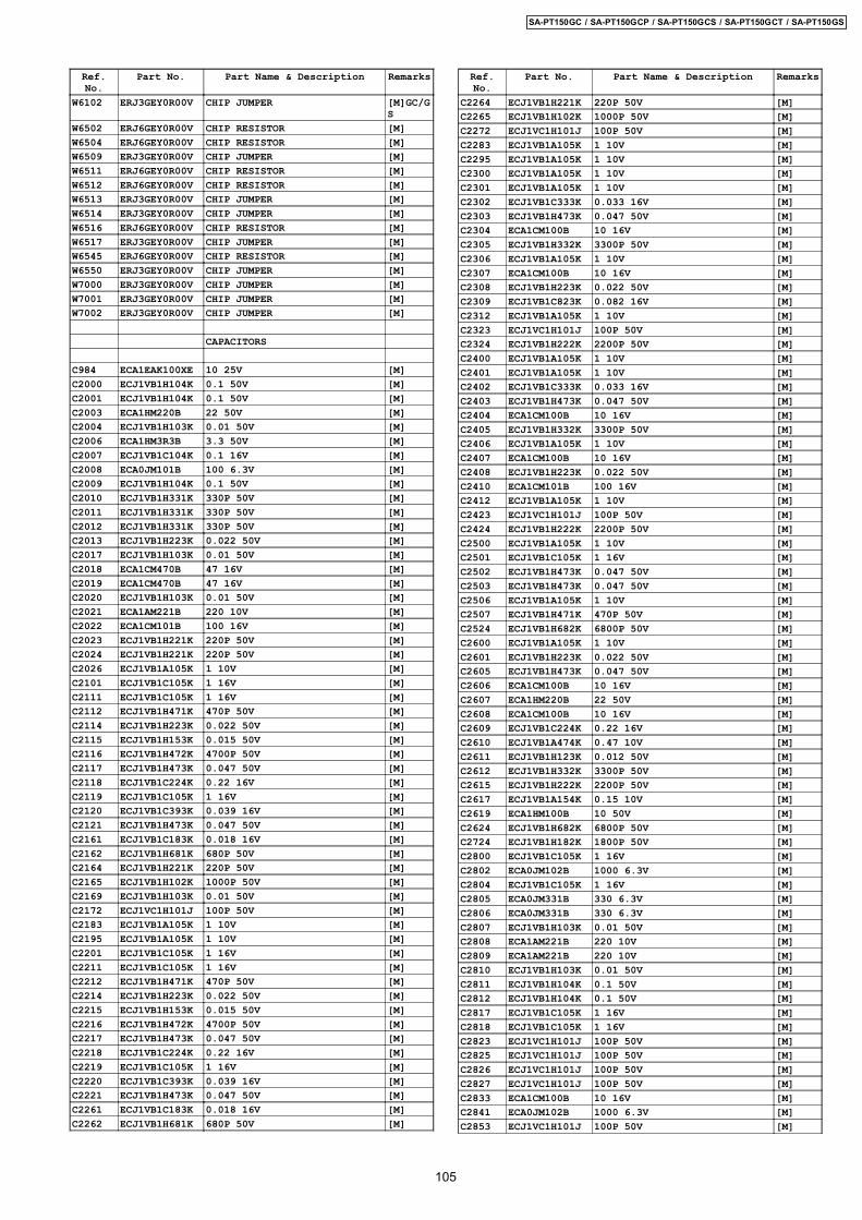
Ref.No.
Part No. Part Name & Description Remarks
W6102 ERJ3GEY0R00V CHIP JUMPER [M]GC/GS
W6502 ERJ6GEY0R00V CHIP RESISTOR [M]W6504 ERJ6GEY0R00V CHIP RESISTOR [M]W6509 ERJ3GEY0R00V CHIP JUMPER [M]W6511 ERJ6GEY0R00V CHIP RESISTOR [M]W6512 ERJ6GEY0R00V CHIP RESISTOR [M]W6513 ERJ3GEY0R00V CHIP JUMPER [M]W6514 ERJ3GEY0R00V CHIP JUMPER [M]W6516 ERJ6GEY0R00V CHIP RESISTOR [M]W6517 ERJ3GEY0R00V CHIP JUMPER [M]W6545 ERJ6GEY0R00V CHIP RESISTOR [M]W6550 ERJ3GEY0R00V CHIP JUMPER [M]W7000 ERJ3GEY0R00V CHIP JUMPER [M]W7001 ERJ3GEY0R00V CHIP JUMPER [M]W7002 ERJ3GEY0R00V CHIP JUMPER [M]
CAPACITORS
C984 ECA1EAK100XE 10 25V [M]C2000 ECJ1VB1H104K 0.1 50V [M]C2001 ECJ1VB1H104K 0.1 50V [M]C2003 ECA1HM220B 22 50V [M]C2004 ECJ1VB1H103K 0.01 50V [M]C2006 ECA1HM3R3B 3.3 50V [M]C2007 ECJ1VB1C104K 0.1 16V [M]C2008 ECA0JM101B 100 6.3V [M]C2009 ECJ1VB1H104K 0.1 50V [M]C2010 ECJ1VB1H331K 330P 50V [M]C2011 ECJ1VB1H331K 330P 50V [M]C2012 ECJ1VB1H331K 330P 50V [M]C2013 ECJ1VB1H223K 0.022 50V [M]C2017 ECJ1VB1H103K 0.01 50V [M]C2018 ECA1CM470B 47 16V [M]C2019 ECA1CM470B 47 16V [M]C2020 ECJ1VB1H103K 0.01 50V [M]C2021 ECA1AM221B 220 10V [M]C2022 ECA1CM101B 100 16V [M]C2023 ECJ1VB1H221K 220P 50V [M]C2024 ECJ1VB1H221K 220P 50V [M]C2026 ECJ1VB1A105K 1 10V [M]C2101 ECJ1VB1C105K 1 16V [M]C2111 ECJ1VB1C105K 1 16V [M]C2112 ECJ1VB1H471K 470P 50V [M]C2114 ECJ1VB1H223K 0.022 50V [M]C2115 ECJ1VB1H153K 0.015 50V [M]C2116 ECJ1VB1H472K 4700P 50V [M]C2117 ECJ1VB1H473K 0.047 50V [M]C2118 ECJ1VB1C224K 0.22 16V [M]C2119 ECJ1VB1C105K 1 16V [M]C2120 ECJ1VB1C393K 0.039 16V [M]C2121 ECJ1VB1H473K 0.047 50V [M]C2161 ECJ1VB1C183K 0.018 16V [M]C2162 ECJ1VB1H681K 680P 50V [M]C2164 ECJ1VB1H221K 220P 50V [M]C2165 ECJ1VB1H102K 1000P 50V [M]C2169 ECJ1VB1H103K 0.01 50V [M]C2172 ECJ1VC1H101J 100P 50V [M]C2183 ECJ1VB1A105K 1 10V [M]C2195 ECJ1VB1A105K 1 10V [M]C2201 ECJ1VB1C105K 1 16V [M]C2211 ECJ1VB1C105K 1 16V [M]C2212 ECJ1VB1H471K 470P 50V [M]C2214 ECJ1VB1H223K 0.022 50V [M]C2215 ECJ1VB1H153K 0.015 50V [M]C2216 ECJ1VB1H472K 4700P 50V [M]C2217 ECJ1VB1H473K 0.047 50V [M]C2218 ECJ1VB1C224K 0.22 16V [M]C2219 ECJ1VB1C105K 1 16V [M]C2220 ECJ1VB1C393K 0.039 16V [M]C2221 ECJ1VB1H473K 0.047 50V [M]C2261 ECJ1VB1C183K 0.018 16V [M]C2262 ECJ1VB1H681K 680P 50V [M]
Ref.No.
Part No. Part Name & Description Remarks
C2264 ECJ1VB1H221K 220P 50V [M]C2265 ECJ1VB1H102K 1000P 50V [M]C2272 ECJ1VC1H101J 100P 50V [M]C2283 ECJ1VB1A105K 1 10V [M]C2295 ECJ1VB1A105K 1 10V [M]C2300 ECJ1VB1A105K 1 10V [M]C2301 ECJ1VB1A105K 1 10V [M]C2302 ECJ1VB1C333K 0.033 16V [M]C2303 ECJ1VB1H473K 0.047 50V [M]C2304 ECA1CM100B 10 16V [M]C2305 ECJ1VB1H332K 3300P 50V [M]C2306 ECJ1VB1A105K 1 10V [M]C2307 ECA1CM100B 10 16V [M]C2308 ECJ1VB1H223K 0.022 50V [M]C2309 ECJ1VB1C823K 0.082 16V [M]C2312 ECJ1VB1A105K 1 10V [M]C2323 ECJ1VC1H101J 100P 50V [M]C2324 ECJ1VB1H222K 2200P 50V [M]C2400 ECJ1VB1A105K 1 10V [M]C2401 ECJ1VB1A105K 1 10V [M]C2402 ECJ1VB1C333K 0.033 16V [M]C2403 ECJ1VB1H473K 0.047 50V [M]C2404 ECA1CM100B 10 16V [M]C2405 ECJ1VB1H332K 3300P 50V [M]C2406 ECJ1VB1A105K 1 10V [M]C2407 ECA1CM100B 10 16V [M]C2408 ECJ1VB1H223K 0.022 50V [M]C2410 ECA1CM101B 100 16V [M]C2412 ECJ1VB1A105K 1 10V [M]C2423 ECJ1VC1H101J 100P 50V [M]C2424 ECJ1VB1H222K 2200P 50V [M]C2500 ECJ1VB1A105K 1 10V [M]C2501 ECJ1VB1C105K 1 16V [M]C2502 ECJ1VB1H473K 0.047 50V [M]C2503 ECJ1VB1H473K 0.047 50V [M]C2506 ECJ1VB1A105K 1 10V [M]C2507 ECJ1VB1H471K 470P 50V [M]C2524 ECJ1VB1H682K 6800P 50V [M]C2600 ECJ1VB1A105K 1 10V [M]C2601 ECJ1VB1H223K 0.022 50V [M]C2605 ECJ1VB1H473K 0.047 50V [M]C2606 ECA1CM100B 10 16V [M]C2607 ECA1HM220B 22 50V [M]C2608 ECA1CM100B 10 16V [M]C2609 ECJ1VB1C224K 0.22 16V [M]C2610 ECJ1VB1A474K 0.47 10V [M]C2611 ECJ1VB1H123K 0.012 50V [M]C2612 ECJ1VB1H332K 3300P 50V [M]C2615 ECJ1VB1H222K 2200P 50V [M]C2617 ECJ1VB1A154K 0.15 10V [M]C2619 ECA1HM100B 10 50V [M]C2624 ECJ1VB1H682K 6800P 50V [M]C2724 ECJ1VB1H182K 1800P 50V [M]C2800 ECJ1VB1C105K 1 16V [M]C2802 ECA0JM102B 1000 6.3V [M]C2804 ECJ1VB1C105K 1 16V [M]C2805 ECA0JM331B 330 6.3V [M]C2806 ECA0JM331B 330 6.3V [M]C2807 ECJ1VB1H103K 0.01 50V [M]C2808 ECA1AM221B 220 10V [M]C2809 ECA1AM221B 220 10V [M]C2810 ECJ1VB1H103K 0.01 50V [M]C2811 ECJ1VB1H104K 0.1 50V [M]C2812 ECJ1VB1H104K 0.1 50V [M]C2817 ECJ1VB1C105K 1 16V [M]C2818 ECJ1VB1C105K 1 16V [M]C2823 ECJ1VC1H101J 100P 50V [M]C2825 ECJ1VC1H101J 100P 50V [M]C2826 ECJ1VC1H101J 100P 50V [M]C2827 ECJ1VC1H101J 100P 50V [M]C2833 ECA1CM100B 10 16V [M]C2841 ECA0JM102B 1000 6.3V [M]C2853 ECJ1VC1H101J 100P 50V [M]
105
SA-PT150GC / SA-PT150GCP / SA-PT150GCS / SA-PT150GCT / SA-PT150GS

Ref.No.
Part No. Part Name & Description Remarks
C2901 ECA1CM471B 470 16V [M]C2903 ECJ1VB1H103K 0.01 50V [M]C2910 ECJ1VB1H103K 0.01 50V [M]C2913 ECA1CM101B 100 16V [M]C2914 ECA1AM330B 33 10V [M]C2919 ECJ1VC1H100D 10P 50V [M]C2920 ECJ1VB1H822K 8200P 50V [M]C2921 ECA1CM471B 470 16V [M]C2922 EEUFC1C471B 470 16V [M]C2924 ECJ1VB1H104K 0.1 50V [M]C2925 ECA0JM221B 220 6.3V [M]C2952 ECJ1VB1H104K 0.1 50V [M]C2961 ECJ1VB1A105K 1 10V [M]C2964 ECJ1VB1A105K 1 10V [M]C2967 ECA0JM102B 1000 6.3V [M]C2969 ECJ1VB1H104K 0.1 50V [M]C2970 ECJ1VB1H104K 0.1 50V [M]C2975 ECA1CM101B 100 16V [M]C2983 ECA1CM101B 100 16V [M]C2984 ECJ1VB1H104K 0.1 50V [M]C2985 ECJ1VB1H103K 0.01 50V [M]C2986 ECA1HM101B 100 50V [M]C3005 ECJ1VB1A105K 1 10V [M]C3006 ECA1HM100B 10 50V [M]C3007 ECA1HM100B 10 50V [M]C3009 ECA1HM100B 10 50V [M]C5101 ECA1HM100B 10 50V [M]C5102 ECJ1VB1C104K 0.1 16V [M]C5104 ECJ1VB1H221K 220P 50V [M]C5105 ECJ1VB1H221K 220P 50V [M]C5106 ECJ1VB1C104K 0.1 16V [M]C5108 ECA1CM220B 22 16V [M]C5124 ECJ1VB1H104K 0.1 50V [M]C5201 ECA1HM100B 10 50V [M]C5202 ECJ1VB1C104K 0.1 16V [M]C5204 ECJ1VB1H471K 470P 50V [M]C5205 ECJ1VB1H471K 470P 50V [M]C5206 ECJ1VB1C104K 0.1 16V [M]C5208 ECA1CM220B 22 16V [M]C5224 ECJ1VB1H104K 0.1 50V [M]C5301 ECA1HM100B 10 50V [M]C5302 ECJ1VB1C104K 0.1 16V [M]C5304 ECJ1VB1H471K 470P 50V [M]C5305 ECJ1VB1H471K 470P 50V [M]C5306 ECJ1VB1C104K 0.1 16V [M]C5308 ECA1CM220B 22 16V [M]C5313 ECA1HM100B 10 50V [M]C5324 ECJ1VB1H104K 0.1 50V [M]C5503 ECA1VM102B 1000 35V [M]C5505 ECJ1VB1H471K 470P 50V [M]C5790 ECJ1VB1H102K 1000P 50V [M]C5791 ECA1CM101B 100 16V [M]C5792 ECA0JM221B 220 6.3V [M]C5794 ECA1CM330B 33 16V [M]C5795 ECJ1VB1H104K 0.1 50V [M]C5796 ECA1HM2R2B 2.2 50V [M]C5797 ECEA1HKA010B 1 50V [M]C5798 ECA1HM101B 100 50V [M]C5799 ECJ1VB1H104K 0.1 50V [M]C6093 ECJ1VB1H473K 0.047 50V [M]C6701 ECJ1VB1C105K 1 16V [M]C6702 ECJ1VB1H102K 1000P 50V [M]C6703 ECJ1VC1H470J 47P 50V [M]C6706 ECJ1VB1H104K 0.1 50V [M]C6707 ECJ1VC1H470J 47P 50V [M]C6708 ECJ1VC1H470J 47P 50V [M]C6709 ECJ1VB1H104K 0.1 50V [M]C6711 ECJ1VB1C105K 1 16V [M]C6805 ECJ1VC1H101K 100P 50V [M]C6806 ECJ1VC1H101K 100P 50V [M]C6903 ECA1HM220B 22 50V [M]C6904 ECJ1VB1H102K 1000P 50V [M]C6905 ECA1HM220B 22 50V [M]
Ref.No.
Part No. Part Name & Description Remarks
C6906 ECJ1VC1H101K 100P 50V [M]C6909 ECJ1VB1H103K 0.01 50V [M]C6910 ECA0JM101B 100 6.3V [M]C6911 ECJ1VB1H103K 0.01 50V [M]C6913 ECA1HM3R3B 3.3 50V [M]C6916 ECJ1VC1H101K 100P 50V [M]C6917 ECJ1VC1H101K 100P 50V [M]C6918 ECA1AM470B 47 10V [M]C6920 ECJ1VB1C105K 1 16V [M]C6921 ECJ1VB1H221K 220P 50V [M]C7101 ECEA1HKA010B 1 50V [M]C7102 ECJ1VB1H682K 6800P 50V [M]C7103 ECJ1VB1H152K 1500P 50V [M]C7104 ECJ1VB1C683K 0.068 16V [M]C7105 ECJ1VB1C224K 0.22 16V [M]C7106 ECJ1VB1C224K 0.22 16V [M]C7107 ECJ1VB1H682K 6800P 50V [M]C7108 ECJ1VB1H152K 1500P 50V [M]C7109 ECJ1VB1C683K 0.068 16V [M]C7110 ECA1CM470B 47 16V [M]C7111 ECA1CM470B 47 16V [M]C7112 ECJ1VB1H104K 0.1 50V [M]C7113 ECEA1HKA010B 1 50V [M]C7114 ECJ1VC1H470J 47P 50V [M]C7115 ECJ1VB1H221K 220P 50V [M]C7116 ECJ1VB1H104K 0.1 50V [M]C7118 ECJ1VB1H104K 0.1 50V [M]C7119 ECA1HM2R2B 2.2 50V [M]C7120 ECJ1VB1H153K 0.015 50V [M]C8001 EEE0GA331WP 330 4V [M]C8002 ECJ0EF1C104Z 0.1 16V [M]C8003 ECJ0EF1C104Z 0.1 16V [M]C8004 ECJ0EF1C104Z 0.1 16V [M]C8005 ECJ0EF1C104Z 0.1 16V [M]C8006 ECJ0EF1C104Z 0.1 16V [M]C8007 ECJ0EF1C104Z 0.1 16V [M]C8008 ECJ0EF1C104Z 0.1 16V [M]C8011 F2G0J101A066 100 6.3V [M]C8012 ECJ0EF1C104Z 0.1 16V [M]C8013 ECJ0EF1C104Z 0.1 16V [M]C8014 ECJ0EF1C104Z 0.1 16V [M]C8015 ECJ0EF1C104Z 0.1 16V [M]C8016 ECJ0EF1C104Z 0.1 16V [M]C8018 ECJ0EF1C104Z 0.1 16V [M]C8020 ECJ0EF1C104Z 0.1 16V [M]C8021 ECJ0EF1C104Z 0.1 16V [M]C8022 ECJ0EF1C104Z 0.1 16V [M]C8026 ECJ0EF1C104Z 0.1 16V [M]C8051 ECJ1VB0J105K 1 6.3V [M]C8052 ECJ0EB1A104K 0.1 10V [M]C8053 ECJ0EF1C104Z 0.1 16V [M]C8054 ECJ0EC1H221J 220P 50V [M]C8055 ECJ1VB0J105K 1 6.3V [M]C8056 ECJ0EB1E222K 2200P 25V [M]C8057 ECJ1VB0J105K 1 6.3V [M]C8111 ECJ0EB1A104K 0.1 10V [M]C8112 ECJ1VB0J105K 1 6.3V [M]C8113 ECJ0EB1E471K 470P 25V [M]C8151 ECJ1VB0J475K 4.7 6.3V [M]C8152 ECJ1VB1C105K 1 16V [M]C8201 F2G0J101A066 100 6.3V [M]C8202 ECJ0EB1A104K 0.1 10V [M]C8203 ECJ0EB1A104K 0.1 10V [M]C8211 ECJ0EB1E122K 1200P 25V [M]C8221 ECJ0EB1E102K 1000P 25V [M]C8222 ECJ0EB1E102K 1000P 25V [M]C8225 ECJ0EB1E102K 1000P 25V [M]C8226 ECJ0EB1E821K 820P 25V [M]C8231 ECJ0EB1A104K 0.1 10V [M]C8232 ECJ0EB1A104K 0.1 10V [M]C8251 F2G0J221A065 220 6.3V [M]C8252 ECJ0EF1C104Z 0.1 16V [M]C8253 ECJ0EF1C104Z 0.1 16V [M]
106
SA-PT150GC / SA-PT150GCP / SA-PT150GCS / SA-PT150GCT / SA-PT150GS
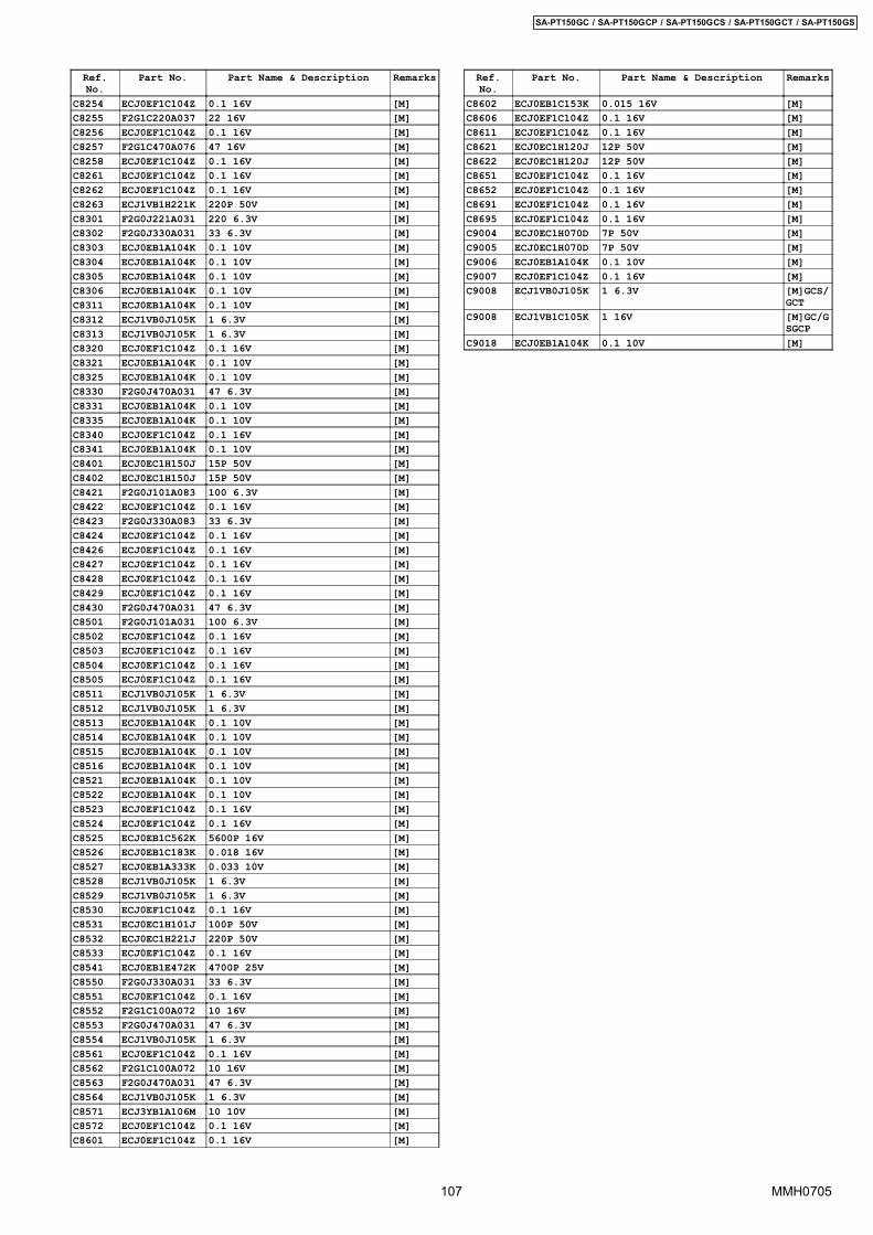
Ref.No.
Part No. Part Name & Description Remarks
C8254 ECJ0EF1C104Z 0.1 16V [M]C8255 F2G1C220A037 22 16V [M]C8256 ECJ0EF1C104Z 0.1 16V [M]C8257 F2G1C470A076 47 16V [M]C8258 ECJ0EF1C104Z 0.1 16V [M]C8261 ECJ0EF1C104Z 0.1 16V [M]C8262 ECJ0EF1C104Z 0.1 16V [M]C8263 ECJ1VB1H221K 220P 50V [M]C8301 F2G0J221A031 220 6.3V [M]C8302 F2G0J330A031 33 6.3V [M]C8303 ECJ0EB1A104K 0.1 10V [M]C8304 ECJ0EB1A104K 0.1 10V [M]C8305 ECJ0EB1A104K 0.1 10V [M]C8306 ECJ0EB1A104K 0.1 10V [M]C8311 ECJ0EB1A104K 0.1 10V [M]C8312 ECJ1VB0J105K 1 6.3V [M]C8313 ECJ1VB0J105K 1 6.3V [M]C8320 ECJ0EF1C104Z 0.1 16V [M]C8321 ECJ0EB1A104K 0.1 10V [M]C8325 ECJ0EB1A104K 0.1 10V [M]C8330 F2G0J470A031 47 6.3V [M]C8331 ECJ0EB1A104K 0.1 10V [M]C8335 ECJ0EB1A104K 0.1 10V [M]C8340 ECJ0EF1C104Z 0.1 16V [M]C8341 ECJ0EB1A104K 0.1 10V [M]C8401 ECJ0EC1H150J 15P 50V [M]C8402 ECJ0EC1H150J 15P 50V [M]C8421 F2G0J101A083 100 6.3V [M]C8422 ECJ0EF1C104Z 0.1 16V [M]C8423 F2G0J330A083 33 6.3V [M]C8424 ECJ0EF1C104Z 0.1 16V [M]C8426 ECJ0EF1C104Z 0.1 16V [M]C8427 ECJ0EF1C104Z 0.1 16V [M]C8428 ECJ0EF1C104Z 0.1 16V [M]C8429 ECJ0EF1C104Z 0.1 16V [M]C8430 F2G0J470A031 47 6.3V [M]C8501 F2G0J101A031 100 6.3V [M]C8502 ECJ0EF1C104Z 0.1 16V [M]C8503 ECJ0EF1C104Z 0.1 16V [M]C8504 ECJ0EF1C104Z 0.1 16V [M]C8505 ECJ0EF1C104Z 0.1 16V [M]C8511 ECJ1VB0J105K 1 6.3V [M]C8512 ECJ1VB0J105K 1 6.3V [M]C8513 ECJ0EB1A104K 0.1 10V [M]C8514 ECJ0EB1A104K 0.1 10V [M]C8515 ECJ0EB1A104K 0.1 10V [M]C8516 ECJ0EB1A104K 0.1 10V [M]C8521 ECJ0EB1A104K 0.1 10V [M]C8522 ECJ0EB1A104K 0.1 10V [M]C8523 ECJ0EF1C104Z 0.1 16V [M]C8524 ECJ0EF1C104Z 0.1 16V [M]C8525 ECJ0EB1C562K 5600P 16V [M]C8526 ECJ0EB1C183K 0.018 16V [M]C8527 ECJ0EB1A333K 0.033 10V [M]C8528 ECJ1VB0J105K 1 6.3V [M]C8529 ECJ1VB0J105K 1 6.3V [M]C8530 ECJ0EF1C104Z 0.1 16V [M]C8531 ECJ0EC1H101J 100P 50V [M]C8532 ECJ0EC1H221J 220P 50V [M]C8533 ECJ0EF1C104Z 0.1 16V [M]C8541 ECJ0EB1E472K 4700P 25V [M]C8550 F2G0J330A031 33 6.3V [M]C8551 ECJ0EF1C104Z 0.1 16V [M]C8552 F2G1C100A072 10 16V [M]C8553 F2G0J470A031 47 6.3V [M]C8554 ECJ1VB0J105K 1 6.3V [M]C8561 ECJ0EF1C104Z 0.1 16V [M]C8562 F2G1C100A072 10 16V [M]C8563 F2G0J470A031 47 6.3V [M]C8564 ECJ1VB0J105K 1 6.3V [M]C8571 ECJ3YB1A106M 10 10V [M]C8572 ECJ0EF1C104Z 0.1 16V [M]C8601 ECJ0EF1C104Z 0.1 16V [M]
Ref.No.
Part No. Part Name & Description Remarks
C8602 ECJ0EB1C153K 0.015 16V [M]C8606 ECJ0EF1C104Z 0.1 16V [M]C8611 ECJ0EF1C104Z 0.1 16V [M]C8621 ECJ0EC1H120J 12P 50V [M]C8622 ECJ0EC1H120J 12P 50V [M]C8651 ECJ0EF1C104Z 0.1 16V [M]C8652 ECJ0EF1C104Z 0.1 16V [M]C8691 ECJ0EF1C104Z 0.1 16V [M]C8695 ECJ0EF1C104Z 0.1 16V [M]C9004 ECJ0EC1H070D 7P 50V [M]C9005 ECJ0EC1H070D 7P 50V [M]C9006 ECJ0EB1A104K 0.1 10V [M]C9007 ECJ0EF1C104Z 0.1 16V [M]C9008 ECJ1VB0J105K 1 6.3V [M]GCS/
GCTC9008 ECJ1VB1C105K 1 16V [M]GC/G
SGCPC9018 ECJ0EB1A104K 0.1 10V [M]
107
SA-PT150GC / SA-PT150GCP / SA-PT150GCS / SA-PT150GCT / SA-PT150GS
MMH0705