DIGITAL ELECTRONICS LABoratory - MIT – Mysore
60
DIGITAL ELECTRONICS LABORATORY 17ECL38 MIT MYSORE | DEPT. OF ELECTRONICS & COMMUNICATION ENGG. 1 Circuit that takes the logical decision and processes are called logic gates. Each gate has one or more inputs and only one output. NOT, AND & OR are basic gates. NAND and NOR are known as universal gates. XOR and XNOR gates are known as special function gates. Universal gates the gates using which all the other gates can be realized. NOT Gate (Inverter): The inverter performs a basic logic function called “Inversion” or “Complementation”. The output is HIGH when the input is LOW and the output is LOW when the input is HIGH. AND Gate: The AND gate performs a logical multiplication commonly known as AND function. The operation of the AND gate is such that the output is HIGH only when all the inputs are HIGH; the output will be LOW, when any of the inputs are LOW. OR Gate: The OR gate performs a logical addition commonly known as OR function. The output is HIGH when any of the inputs are HIGH. The output is LOW only when all the inputs are LOW. NAND Gate: The NAND gate is a contraction of NOT-AND and implies an AND function with a complemented output. The NAND gate is a universal gate as it can be used to construct an AND gate, an OR gate, an inverter or any combination of these functions. The output is HIGH when any of the inputs is LOW; and is LOW only when all the inputs are HIGH. NOR Gate: The NOR gate is a contraction of NOT-OR. NOR gate is also a universal gate. The output is HIGH only when all the inputs are LOW; and is LOW when any of the inputs is HIGH. EX-OR Gate: The EX-OR gate is an abbreviation for Exclusive-OR gate. It recognizes only the words that have odd number of one’s i.e. output is HIGH for odd number of one’s; otherwise output is LOW. EX-OR Gate: The EX-OR gate is a contraction of NOT-EX-OR. It recognizes only the words that have even number of one’s i.e. output is HIGH for even number of one’s; otherwise output is LOW. BASICS
-
Upload
khangminh22 -
Category
Documents
-
view
0 -
download
0
Transcript of DIGITAL ELECTRONICS LABoratory - MIT – Mysore

D I G I T A L E L E C T R O N I C S L A B O R A T O R Y 1 7 E C L 3 8
M I T M Y S O R E | D E P T . O F E L E C T R O N I C S & C O M M U N I C A T I O N E N G G . 1
Circuit that takes the logical decision and
processes are called logic gates. Each gate has one or more inputs and only one output.
NOT, AND & OR are basic gates. NAND and NOR are
known as universal gates. XOR and XNOR gates are
known as special function gates.
Universal gates the gates using which all the other gates can be realized.
NOT Gate (Inverter):
The inverter performs a basic logic function called “Inversion” or “Complementation”.
The output is HIGH when the input is LOW and the output is LOW when the input is
HIGH.
AND Gate:
The AND gate performs a logical multiplication commonly known as AND function. The
operation of the AND gate is such that the output is HIGH only when all the inputs are
HIGH; the output will be LOW, when any of the inputs are LOW.
OR Gate: The OR gate performs a logical addition commonly known as OR function. The output is
HIGH when any of the inputs are HIGH. The output is LOW only when all the inputs are LOW.
NAND Gate:
The NAND gate is a contraction of NOT-AND and implies an AND function with a
complemented output. The NAND gate is a universal gate as it can be used to construct
an AND gate, an OR gate, an inverter or any combination of these functions. The
output is HIGH when any of the inputs is LOW; and is LOW only when all the inputs
are HIGH.
NOR Gate:
The NOR gate is a contraction of NOT-OR. NOR gate is also a universal gate. The
output is HIGH only when all the inputs are LOW; and is LOW when any of the inputs
is HIGH.
EX-OR Gate:
The EX-OR gate is an abbreviation for Exclusive-OR gate. It recognizes only the words
that have odd number of one’s i.e. output is HIGH for odd number of one’s; otherwise
output is LOW.
EX-OR Gate: The EX-OR gate is a contraction of NOT-EX-OR. It recognizes only the words that have even number of one’s i.e. output is HIGH for even number of one’s; otherwise output is
LOW.
BASICS

1 7 E C L 3 8 D I G I T A L E L E C T R O N I C S L A B O R A T O R Y
2 D E P T . O F E L E C T R O N I C S & C O M M U N I C A T I O N E N G G . | M I T M Y S O R E
I. Basic Gates:
1. NOT Gate
TRUTH TABLE SYMBOL IC7404
2. OR Gate
TRUTH TABLE SYMBOL IC7432
3. AND Gate
TRUTH TABLE SYMBOL IC7408
II. Universal Gates:
1. NAND Gate
TRUTH TABLE SYMBOL IC7400
D I G I T A L E L E C T R O N I C S L A B O R A T O R Y 1 7 E C L 3 8
M I T M Y S O R E | D E P T . O F E L E C T R O N I C S & C O M M U N I C A T I O N E N G G . 3
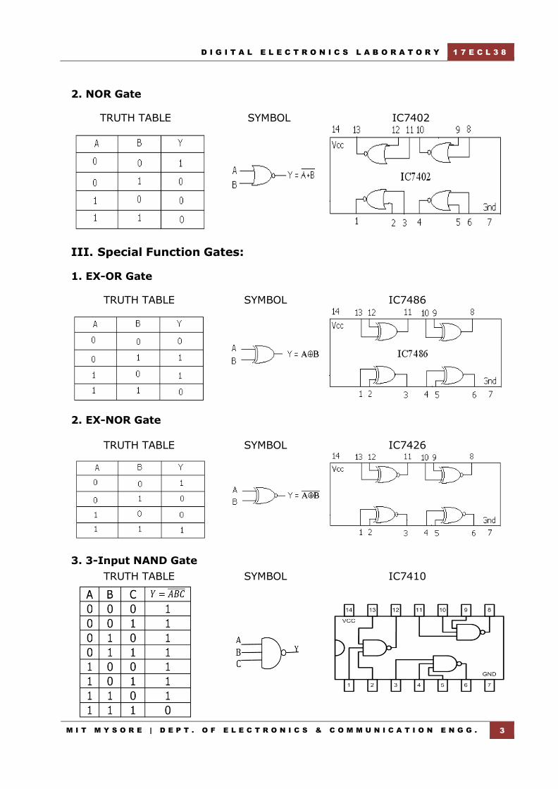
2. NOR Gate
TRUTH TABLE SYMBOL IC7402
III. Special Function Gates:
1. EX-OR Gate
TRUTH TABLE SYMBOL IC7486
2. EX-NOR Gate
TRUTH TABLE SYMBOL IC7426
3. 3-Input NAND Gate
TRUTH TABLE SYMBOL IC7410

1 7 E C L 3 8 D I G I T A L E L E C T R O N I C S L A B O R A T O R Y
4 D E P T . O F E L E C T R O N I C S & C O M M U N I C A T I O N E N G G . | M I T M Y S O R E
4. 4-Input NAND Gate
TRUTH TABLE SYMBOL IC7420

D I G I T A L E L E C T R O N I C S L A B O R A T O R Y 1 7 E C L 3 8
M I T M Y S O R E | D E P T . O F E L E C T R O N I C S & C O M M U N I C A T I O N E N G G . 5
Symbol NAND Implementation NOR Implementation

1 7 E C L 3 8 D I G I T A L E L E C T R O N I C S L A B O R A T O R Y
6 D E P T . O F E L E C T R O N I C S & C O M M U N I C A T I O N E N G G . | M I T M Y S O R E
a) Demorgan’s Theorem for 2 variables
b) The sum-of product and product-of-sum expressions using universal gates
SUM OF PRODUCT (SOP): F(A,B,C,D) = ∑(5,7,9,11,13,15)
Simplification- SOP form Implementation using basic gates
Using NAND gates using NOR gates
D I G I T A L E L E C T R O N I C S L A B O R A T O R Y 1 7 E C L 3 8
M I T M Y S O R E | D E P T . O F E L E C T R O N I C S & C O M M U N I C A T I O N E N G G . 7
To verify
a) Demorgan’s Theorem for 2 variables
b) The sum-of product and product-of-sum
expressions using universal gates.
Components Required:
Sl. No COMPONENT SPECIFICATION
1
2
3
4
5
6
7
8
AND gate
OR gate
Not gate
XOR gate
NAND gate
NOR gate
Patch chords
Trainer Kit
7408
7432
7404
7486
7400
7402
a) Demorgan’s Theorem for 2 variables
1. The complement of the sum of two or more variables is equal to the product of
the complements of the variables.
2. The complement of the product of two or more logical variables is equal to the sum of the complements of the variables.
b) The sum-of product and product-of-sum expressions using universal
gates
1. Sum of Product Form (SoP)
A sum of products (SoP) is a group of product terms ORed together. Each product term consists of one or more literals appearing in either complemented or true form. The sum of product form is known as disjunctive normal form or disjunctive
normal formula. Examples:
1. ABC+AB
2. PQ+QR+PQR
3. �̅��̅�𝐶̅𝐷 + 𝐴�̅�𝐶̅𝐷 + 𝐵𝐷 + 𝐵𝐶�̅�
2. Product of Sum Form (PoS)
A product of sums (PoS) is a group of sum terms ANDed together. Each sum term consists of one or more literals appearing in either complemented or true form.
The product of sum form is known as conjunctive normal form or conjunctive normal formula.
Examples:
1. (A+B) (B+C)
2. (A+B+C) (B+C+D)
E X P E R I M E N T
1

1 7 E C L 3 8 D I G I T A L E L E C T R O N I C S L A B O R A T O R Y
8 D E P T . O F E L E C T R O N I C S & C O M M U N I C A T I O N E N G G . | M I T M Y S O R E
PRODUCT OF SUM : F(A,B,C,D) = ∏(0,1,2,3,4,6,8,10,12,14) Simplification- POS form Using basic gates
Using NAND gates Using NOR gates
Truth Table
A B C D Y=(A+B)D
0 0 0 0 0
0 0 0 1 0
0 0 1 0 0
0 0 1 1 0
0 1 0 0 0
0 1 0 1 1
0 1 1 0 0
0 1 1 1 1
1 0 0 0 0
1 0 0 1 1
1 0 1 0 0
1 0 1 1 1
1 1 0 0 0
1 1 0 1 1
1 1 1 0 0
1 1 1 1 1

D I G I T A L E L E C T R O N I C S L A B O R A T O R Y 1 7 E C L 3 8
M I T M Y S O R E | D E P T . O F E L E C T R O N I C S & C O M M U N I C A T I O N E N G G . 9
Procedure:
1. Place the IC in the socket of the trainer kit.
2. Make the connections as shown in the circuit diagram.
3. Apply different combinations of i/ps according to the truth table. Verify the o/p.
4. Repeat the above procedure for all the circuit diagrams. *NOTE: The Truth Table is common for Both SOP and POS form.
Result:
Viva Questions: 1. What is a logic gate?
2. State Demorgan’s theorem. 3. What is the primary motivation for using Boolean algebra for simplifying logic
equations? 4. Why NAND & NOR gates are called universal gates? 5. Realize the EX – OR gates using minimum number of NAND gates.
6. Give the truth table for EX-NOR and realize using NAND gates? 7. What are the logic low and High levels of TTL IC’s and CMOS IC’s?
8. Compare TTL logic family with CMOS family? 9. Which logic family is fastest and which has low power dissipation? 10.What is a combinational circuit?
11.What is a sequential circuit? 12.What are the various methods of simplifying the logic functions?
13.What are the different methods to obtain minimal expression? 14.What is a Min term and Max term 15.State the difference between SOP and POS.
16.What is meant by canonical representation? 17.What is K-map? Why is it used?
18.What are universal gates?
1 7 E C L 3 8 D I G I T A L E L E C T R O N I C S L A B O R A T O R Y
1 0 D E P T . O F E L E C T R O N I C S & C O M M U N I C A T I O N E N G G . | M I T M Y S O R E
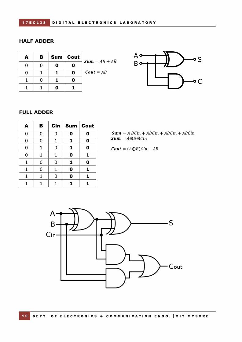
HALF ADDER
A B Sum Cout
𝑺𝒖𝒎 = �̅�𝐵 + 𝐴�̅�
𝑪𝒐𝒖𝒕 = 𝐴𝐵
0 0 0 0
0 1 1 0
1 0 1 0
1 1 0 1
FULL ADDER
A B Cin Sum Cout
0 0 0 0 0 𝑺𝒖𝒎 = 𝐴 ̅�̅�𝐶𝑖𝑛 + �̅�𝐵𝐶𝑖𝑛̅̅ ̅̅̅ + 𝐴�̅�𝐶𝑖𝑛̅̅ ̅̅̅ + 𝐴𝐵𝐶𝑖𝑛 𝑺𝒖𝒎 = 𝐴⨁𝐵⨁𝐶𝑖𝑛 𝑪𝒐𝒖𝒕 = (𝐴⨁𝐵)𝐶𝑖𝑛 + 𝐴𝐵
0 0 1 1 0
0 1 0 1 0
0 1 1 0 1
1 0 0 1 0
1 0 1 0 1
1 1 0 0 1
1 1 1 1 1

D I G I T A L E L E C T R O N I C S L A B O R A T O R Y 1 7 E C L 3 8
M I T M Y S O R E | D E P T . O F E L E C T R O N I C S & C O M M U N I C A T I O N E N G G . 1 1
To design and implement
a) Full Adder using logic gates and NAND gates
b) Full Subtractor using logic gates and NAND gates
Components required:
Sl. No COMPONENT SPECIFICATION
1
2
3
4
5
6
7
8
AND gate
OR gate
Not gate
XOR gate
NAND gate
NOR gate
Patch chords
Trainer Kit
7408
7432
7404
7486
7400
7402
BINARY ADDER: Digital computer performs various arithmetic operations. This
simple adder consists of four possible elementary operations, namely
0+0 = 0
0+1 = 1
1+0 = 1
1+1 = 102
The first three operations produce a sum whose length is one bit, but when the last
operation is performed, sum will be two bits. The higher significant bit of this result is
called a carry, and lower significant bit is called sum. The logic circuit that performs
this operation is called a half-adder. The circuit which performs addition of three bits
is a full-adder.
HALF ADDER: Half adder is a combinational logic circuit which performs the addition
of two bits and generates sum and carry. This circuit follows binary addition rule.
FULL ADDER: Full adder is a combinational logic circuit which performs addition of
three bits and generates sum and carry.
Procedure: 1. Place the IC in the socket of the trainer kit.
2. Make the connections as shown in the circuit diagram. 3. Apply different combinations of I/Ps according to the truth table. Verify the
o/p.
E X P E R I M E N T
2
1 7 E C L 3 8 D I G I T A L E L E C T R O N I C S L A B O R A T O R Y
1 2 D E P T . O F E L E C T R O N I C S & C O M M U N I C A T I O N E N G G . | M I T M Y S O R E
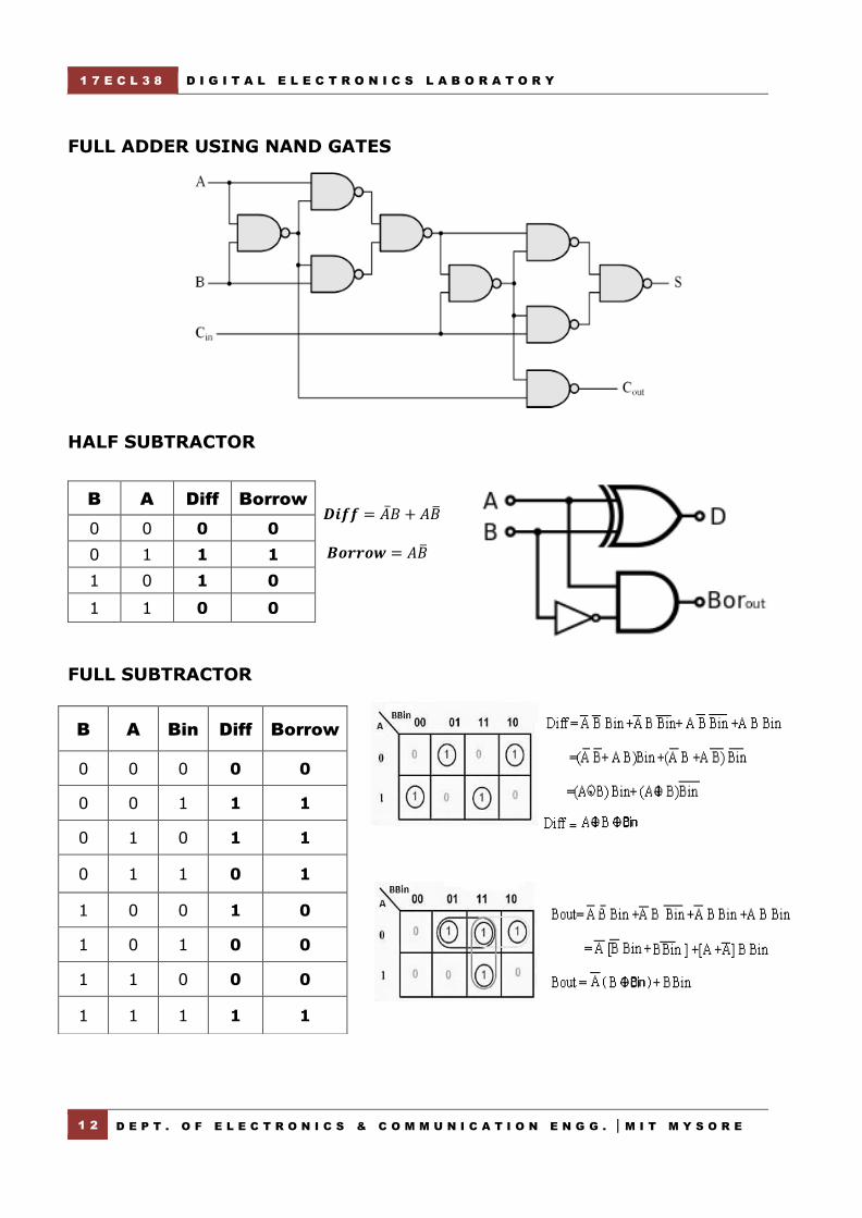
FULL ADDER USING NAND GATES
HALF SUBTRACTOR
B A Diff Borrow
𝑫𝒊𝒇𝒇 = �̅�𝐵 + 𝐴�̅�
𝑩𝒐𝒓𝒓𝒐𝒘 = 𝐴�̅�
0 0 0 0
0 1 1 1
1 0 1 0
1 1 0 0
FULL SUBTRACTOR
B A Bin Diff Borrow
0 0 0 0 0
0 0 1 1 1
0 1 0 1 1
0 1 1 0 1
1 0 0 1 0
1 0 1 0 0
1 1 0 0 0
1 1 1 1 1

D I G I T A L E L E C T R O N I C S L A B O R A T O R Y 1 7 E C L 3 8
M I T M Y S O R E | D E P T . O F E L E C T R O N I C S & C O M M U N I C A T I O N E N G G . 1 3
FULL SUBTRACTOR USING NAND GATES:
Procedure:
1. Place the IC in the socket of the trainer kit.
2. Make the connections as shown in the circuit diagram.
3. Apply different combinations of i/p according to the truth table. Verify the
o/p. Repeat the above procedure for all the circuit diagrams.
Result: Viva Questions:
1. What is a half adder? 2. What is a full adder?
3. What are the applications of adders? 4. What is a half Subtractor?
5. What is a full Subtractor? 6. What are the applications of subtractors? 7. Obtain the minimal expression for above circuits.
8. Realize a full adder using two half adders
9. Realize a full subtractors using two half subtractors

1 7 E C L 3 8 D I G I T A L E L E C T R O N I C S L A B O R A T O R Y
1 4 D E P T . O F E L E C T R O N I C S & C O M M U N I C A T I O N E N G G . | M I T M Y S O R E
Realization of Parallel adder/Subtractor using 7483 chip:
Logic Diagram
Readings: Addition & Subtraction
Cin A4 A3 A2 A1 B4 B3 B2 B1 Cout S4 S3 S2 S1
0 1 0 0 1 1 0 0 1 1 0 0 1 0
0 0 1 1 1 0 0 0 1 0 1 0 0 0
0 0 1 1 0 0 1 0 0 0 1 0 1 0
0 0 1 1 1 0 1 0 0 0 1 0 1 1
1 1 0 0 1 1 0 0 0 1 0 0 0 1
1 0 0 0 1 0 0 1 1 0 1 1 1 0
1 1 0 0 1 0 1 0 0 1 0 1 0 1
1 1 0 1 1 0 1 0 1 1 0 1 1 0

D I G I T A L E L E C T R O N I C S L A B O R A T O R Y 1 7 E C L 3 8
M I T M Y S O R E | D E P T . O F E L E C T R O N I C S & C O M M U N I C A T I O N E N G G . 1 5
To design and implement 4-bit Parallel
Adder/ Subtractor using IC 7483.
Components Required:
PARALLEL ADDER: Parallel adder is a combinational logic circuit, which performs
addition of two n-bit numbers. N-bit parallel adder is constructed with n-number of
full adders connected in cascaded, i.e. the carry output of each adder is connected to
the carry input of the next higher order adder.
PARALLEL SUBTRACTOR: Parallel adder is a combination logic circuit, which
performs subtraction of two n-bit numbers. The subtraction of binary numbers can be
done most conveniently by means of complements. The subtraction A-B can be done
by taking the 2’s complement of B and adding it to A. The 2’s complement can be
obtained by taking the 1’s complement and adding one to the least significant pair of
bits.
IC 7483: It is a high speed four bit binary full adder with internal carry look ahead
accepts two 4-bit binary inputs (A0 – A3, B0 – B3) and a carry input C0. They generate
binary sum outputs (S0 – S3) and the carry output C4, from the MSB. They operate
with high or active low operands.
Fig: Block Diagram of 4 bit parallel adder
Sl.
No. COMPONENT SPECIFICATION
1
2
3
4
EXOR gate
4 bit parallel adder
Patch chords
Trainer Kit
7486
7483
E X P E R I M E N T
3

1 7 E C L 3 8 D I G I T A L E L E C T R O N I C S L A B O R A T O R Y
1 6 D E P T . O F E L E C T R O N I C S & C O M M U N I C A T I O N E N G G . | M I T M Y S O R E
Pin Diagram IC 7483:
Procedure:
1. Make the connections as shown.
2. For addition ,make Cin=0 and apply the 4 bits as i/p for A and apply another set
of A bits to B. Observe the o/p at S3, S2 S1 S0 and carry generated at Cout. Repeat
the above steps for different inputs and tabulate the result.
3 . For subtraction Cin is made equal to 1 and A-B format is used.
A First no
B- Second no.
By Xor –ing the i/p bits of ‘B’ by 1 , is complement of ‘B’ is obtained. Further
Cin, wh ich is 1 is added to the LSB of the Xor –ed bits. This generates 2’s
complement of B.
4. Verify the difference and polarity of differences at S0, S1, S2, and S3.and Cout. If
Cout is 0, diff is –ve and diff is 2’s complement form. If Cout is 1, diff is +ve.
5. Repeat the above steps for different inputs. And tabulate the result.
Result:

D I G I T A L E L E C T R O N I C S L A B O R A T O R Y 1 7 E C L 3 8
M I T M Y S O R E | D E P T . O F E L E C T R O N I C S & C O M M U N I C A T I O N E N G G . 1 7
Viva Questions: 1. What is the internal structure of 7483 IC? 2. What do you mean by code conversion? 3. What are the applications of code conversion?
4. How do you realize a Subtractor using full adder?
5. What is a ripple Adder? What are its disadvantages?

1 7 E C L 3 8 D I G I T A L E L E C T R O N I C S L A B O R A T O R Y
1 8 D E P T . O F E L E C T R O N I C S & C O M M U N I C A T I O N E N G G . | M I T M Y S O R E
1- Bit Comparator
Truth Table
A0 B0 A>B A=B A<B
0 0 0 1 0
0 1 0 0 1
1 0 1 0 0
1 1 0 1 0
Logic Diagram Using Basic Gates
IC 7485 Pin Details

D I G I T A L E L E C T R O N I C S L A B O R A T O R Y 1 7 E C L 3 8
M I T M Y S O R E | D E P T . O F E L E C T R O N I C S & C O M M U N I C A T I O N E N G G . 1 9
Design and Implementation of 4-bit Magnitude
Comparator using IC 7485.
Components required:
Sl.
No. COMPONENT SPECIFICATION
1
2
3
4
5
6
7
AND gate
OR gate
Not gate
EXOR gate
Magnitude
comparator
Patch chords
Trainer Kit
7408
7432
7404
7486
7485
Comparator:
A comparator is a combinational circuit designed primarily to compare the relative
magnitude of two binary numbers. Consider an n-bit comparator. It receives two n-
bit numbers A and B as inputs and outputs are A>B, A=B, A<B. depending upon the
relative magnitudes of the two number, one of the outputs will be high.
IC 7485(4-bit Comparator)
IC 7485 is a 4-bit comparator. It can be used to compare two 4-bit binary words.
These ICs can be cascaded to compare words of almost any length. Its 4-bit inputs
are weighted (A0 –A3) and (B0 – B3) are the most significant bits.
Procedure:
1) Rig up the circuit for one bit comparator as shown in the figure using logic gates
and 4 bit comparator using IC 7485 magnitude comparator.
2) Verify the Table of values. The output obtained should indicate the required
result.
E X P E R I M E N T
4

1 7 E C L 3 8 D I G I T A L E L E C T R O N I C S L A B O R A T O R Y
2 0 D E P T . O F E L E C T R O N I C S & C O M M U N I C A T I O N E N G G . | M I T M Y S O R E
4 – Bit Comparator
A3 A2 A1 A0 B3 B2 B1 B0 A>B A=B A<B
0 0 1 0 1 1 0 1 0 0 1
1 1 1 1 1 1 1 0 1 0 0
1 0 0 1 1 0 0 1 0 1 0
0 1 0 1 0 0 0 0 1 0 0

D I G I T A L E L E C T R O N I C S L A B O R A T O R Y 1 7 E C L 3 8
M I T M Y S O R E | D E P T . O F E L E C T R O N I C S & C O M M U N I C A T I O N E N G G . 2 1
8–Bit Comparator
A4 A3 A2 A1 A0 B4 B3 B2 B1 B0 A>B A=B A<B
0 0 0 1 0 0 1 1 0 1 0 0 1
0 1 1 1 1 0 1 1 1 0 1 0 0
0 1 0 0 1 0 1 0 0 1 0 1 0
0 0 1 0 1 0 0 0 0 0 1 0 0
1 7 E C L 3 8 D I G I T A L E L E C T R O N I C S L A B O R A T O R Y
2 2 D E P T . O F E L E C T R O N I C S & C O M M U N I C A T I O N E N G G . | M I T M Y S O R E
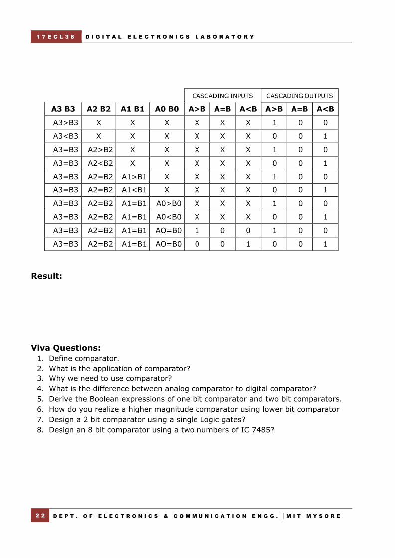
CASCADING INPUTS CASCADING OUTPUTS
A3 B3 A2 B2 A1 B1 A0 B0 A>B A=B A<B A>B A=B A<B
A3>B3 X X X X X X 1 0 0
A3<B3 X X X X X X 0 0 1
A3=B3 A2>B2 X X X X X 1 0 0
A3=B3 A2<B2 X X X X X 0 0 1
A3=B3 A2=B2 A1>B1 X X X X 1 0 0
A3=B3 A2=B2 A1<B1 X X X X 0 0 1
A3=B3 A2=B2 A1=B1 A0>B0 X X X 1 0 0
A3=B3 A2=B2 A1=B1 A0<B0 X X X 0 0 1
A3=B3 A2=B2 A1=B1 AO=B0 1 0 0 1 0 0
A3=B3 A2=B2 A1=B1 AO=B0 0 0 1 0 0 1
Result:
Viva Questions:
1. Define comparator.
2. What is the application of comparator?
3. Why we need to use comparator?
4. What is the difference between analog comparator to digital comparator?
5. Derive the Boolean expressions of one bit comparator and two bit comparators.
6. How do you realize a higher magnitude comparator using lower bit comparator
7. Design a 2 bit comparator using a single Logic gates?
8. Design an 8 bit comparator using a two numbers of IC 7485?

D I G I T A L E L E C T R O N I C S L A B O R A T O R Y 1 7 E C L 3 8
M I T M Y S O R E | D E P T . O F E L E C T R O N I C S & C O M M U N I C A T I O N E N G G . 2 3

1 7 E C L 3 8 D I G I T A L E L E C T R O N I C S L A B O R A T O R Y
2 4 D E P T . O F E L E C T R O N I C S & C O M M U N I C A T I O N E N G G . | M I T M Y S O R E
4:1 MUX
S1 S0 I0 I1 I2 I3 Y
0 0 I0 X X X I0
0 1 X I1 X X I1
1 0 X X I2 X I2
1 1 X X X I3 I3
Pin Details Of 74153

D I G I T A L E L E C T R O N I C S L A B O R A T O R Y 1 7 E C L 3 8
M I T M Y S O R E | D E P T . O F E L E C T R O N I C S & C O M M U N I C A T I O N E N G G . 2 5
To realize
a) 4:1 Multiplexer using gates
b) Adder & Subtractor using IC 74153.
c) 3-variable function using IC 74151(8:1MUX).
Components required:
Sl.
No. COMPONENT SPECIFICATION
1
2
3
4
5
6
7
8
NAND gate(2 I/P)
NAND gate(3 I/P)
NAND gate(4 I/P)
MUX
DE-MUX
NOT gate
Patch chords
Trainer Kit
7400
7410
7420
74153
74138
7404
Multiplexer: Multiplexer is a combinational circuit that is one of the most widely used in digital design.
The multiplexer is a data selector which gates one out of several inputs to a single o/p.
It has n data inputs & one o/p line & m select lines where 2m= n. Depending upon the
digital code applied at the select inputs one out of n data input is selected & transmitted
to a single o/p channel. Normally strobe (G) input is incorporated which is generally
active low which enables the multiplexer when it is LOW. Strobe i/p helps in cascading.
E X P E R I M E N T
5

1 7 E C L 3 8 D I G I T A L E L E C T R O N I C S L A B O R A T O R Y
2 6 D E P T . O F E L E C T R O N I C S & C O M M U N I C A T I O N E N G G . | M I T M Y S O R E
IC 74153:
The IC 74153 is a dual 4-i/p MUX that can select 2 bits of data from up to eight sources
under the control of the common select inputs (S0, S1). The two 4- i/p MUX circuits
have individual active low enables (E1, E2) which can be used to strobe the outputs
independently outputs (Y1, Y2) are forced low when the corresponding enables (E1,
E2) are high.
E S1 S0 Y1 Y2
1 X X 0 0
0 0 0 A0 B0
0 0 1 A1 B1
0 1 0 A2 B2
0 1 1 A3 B3
Realization of Half Adder Using IC 74153
Truth Table Circuit Diagram
Realization of Full Adder Using IC 74153
TRUTH TABLE CIRCUIT DIAGRAM
A B SUM Y1 COUT Y2
0 0 0 B
0 0
0 1 1 0
1 0 1 �̅�
0 B
1 1 0 1
A B Cin SUM Y1 COUT Y2
0 0 0 0 Cin
0 0
0 0 1 1 0
0 1 0 1 Cin
0 C
in
0 1 1 0 1
1 0 0 1 Cin
0 C
in
1 0 1 0 1
1 1 0 0 Cin
1 1
1 1 1 1 1

D I G I T A L E L E C T R O N I C S L A B O R A T O R Y 1 7 E C L 3 8
M I T M Y S O R E | D E P T . O F E L E C T R O N I C S & C O M M U N I C A T I O N E N G G . 2 7
Realization of Half Subtractor Using IC 74153
TRUTH TABLE CIRCUIT DIAGRAM
Realization of Full Subtractor Using IC 74153
TRUTH TABLE CIRCUIT DIAGRAM
A B Diff Y1 BOUT Y2
0 0 0 B
0 B
0 1 1 0
1 0 1 �̅�
0 0
1 1 0 1
A B Bin Diff Y1 Bout Y2
0 0 0 0 Bin
0
Bin 0 0 1 1 1
0 1 0 1 1
1 0 1 1 0 1
1 0 0 1 0
0 1 0 1 0 0
1 1 0 0
Bin
0
Bin 1 1 1 1 1
1 7 E C L 3 8 D I G I T A L E L E C T R O N I C S L A B O R A T O R Y
2 8 D E P T . O F E L E C T R O N I C S & C O M M U N I C A T I O N E N G G . | M I T M Y S O R E
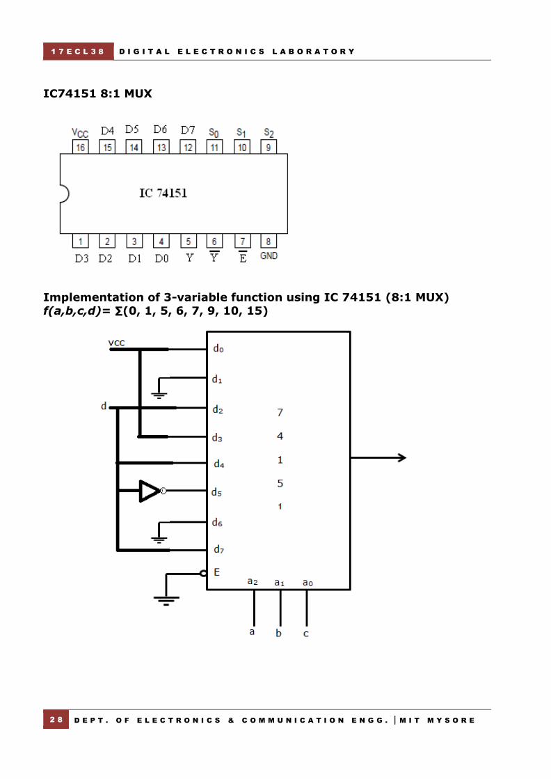
IC74151 8:1 MUX
Implementation of 3-variable function using IC 74151 (8:1 MUX) f(a,b,c,d)= ∑(0, 1, 5, 6, 7, 9, 10, 15)

D I G I T A L E L E C T R O N I C S L A B O R A T O R Y 1 7 E C L 3 8
M I T M Y S O R E | D E P T . O F E L E C T R O N I C S & C O M M U N I C A T I O N E N G G . 2 9
IC 74151: IC74151 is an 8 to 1 multiplexer which has 3 select lines, 8 data lines, 2 output lines (one true form, one complementary form) and enable lines.
Procedure: 1) Set up the circuit as shown in figure 2) Apply any arbitrary input at each of the input line of the multiplexer.
3) Set the index of the desired i/p channel which has to be linked to o/p. 4) Record the o/p for each combination of the select line and verify that with functional
table of respective multiplexer.
Result:
Viva questions: 1. Define MUX with example.
2. What are the differences between MUX and DE-MUX?
3. What is a multiplexer?
4. What are the applications of multiplexer and de-multiplexer?
5. Derive the Boolean expression for multiplexer.
6. How do you realize a given function using multiplexer
7. In 2n to 1 multiplexer how many selection lines are there?
8. How to get higher order multiplexers?
9. Implement an 8:1 mux using 4:1 MUX’s?
10. Why mux is called as a data selector?
A B C D Y
0 0 0 0 1
0 0 0 1 1
0 0 1 0 0
0 0 1 1 0
0 1 0 0 0
0 1 0 1 1
0 1 1 0 1
0 1 1 1 1
1 0 0 0 0
1 0 0 1 1
1 0 1 0 1
1 0 1 1 0
1 1 0 0 0
1 1 0 1 0
1 1 1 0 0
1 1 1 1 1
1 7 E C L 3 8 D I G I T A L E L E C T R O N I C S L A B O R A T O R Y
3 0 D E P T . O F E L E C T R O N I C S & C O M M U N I C A T I O N E N G G . | M I T M Y S O R E
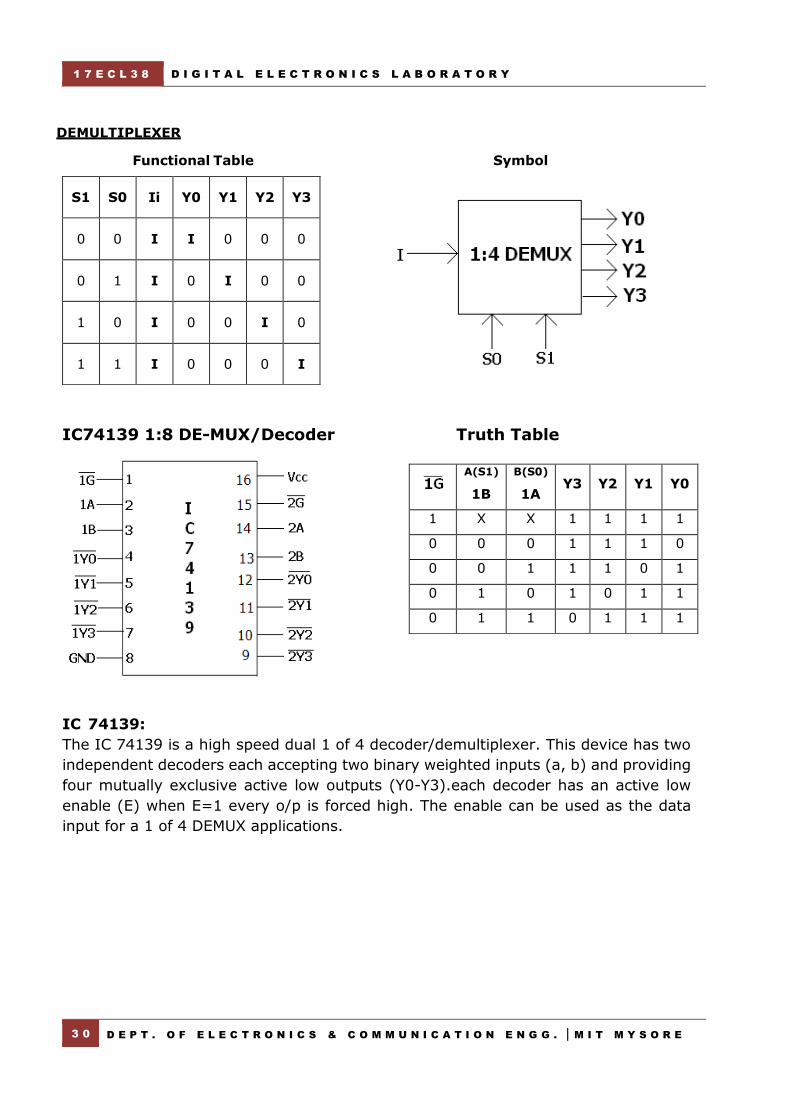
DEMULTIPLEXER
Functional Table Symbol
IC74139 1:8 DE-MUX/Decoder Truth Table
IC 74139:
The IC 74139 is a high speed dual 1 of 4 decoder/demultiplexer. This device has two
independent decoders each accepting two binary weighted inputs (a, b) and providing
four mutually exclusive active low outputs (Y0-Y3).each decoder has an active low
enable (E) when E=1 every o/p is forced high. The enable can be used as the data
input for a 1 of 4 DEMUX applications.
S1 S0 Ii Y0 Y1 Y2 Y3
0 0 I I 0 0 0
0 1 I 0 I 0 0
1 0 I 0 0 I 0
1 1 I 0 0 0 I
A(S1)
1B
B(S0)
1A Y3 Y2 Y1 Y0
1 X X 1 1 1 1
0 0 0 1 1 1 0
0 0 1 1 1 0 1
0 1 0 1 0 1 1
0 1 1 0 1 1 1

D I G I T A L E L E C T R O N I C S L A B O R A T O R Y 1 7 E C L 3 8
M I T M Y S O R E | D E P T . O F E L E C T R O N I C S & C O M M U N I C A T I O N E N G G . 3 1
Realize a Boolean expression using decoder IC74139.
Components required:
Sl.
No. COMPONENT SPECIFICATION
1
2
3
4
5
6
7
8
NAND gate(2 I/P)
NAND gate(3 I/P)
NAND gate(4 I/P)
MUX
DE-MUX
NOT gate
Patch chords
Trainer Kit
7400
7410
7420
74151
74139
7404
De-Multiplexer:
The data distributor, known more commonly as a Demultiplexer or “Demux” for short,
is the exact opposite of the Multiplexer. The demultiplexer takes one single input data
line and then switches it to any one of a number of individual output lines one at a time.
The demultiplexer converts a serial data signal at the input to a parallel data at its output
lines as shown below.
The function of the Demultiplexer is to switch one common data input line to any one of
the ‘n’ output data lines
74139 as a Full Adder f1(a, b, c)=∑(1,2,3,7); f2(a, b, c)=∑(3,5,6,7)
E X P E R I M E N T
6

1 7 E C L 3 8 D I G I T A L E L E C T R O N I C S L A B O R A T O R Y
3 2 D E P T . O F E L E C T R O N I C S & C O M M U N I C A T I O N E N G G . | M I T M Y S O R E
Truth Table Logic Diagram
A B Cin SUM Cout
0 0 0 0 0
0 0 1 1 0
0 1 0 1 0
0 1 1 0 1
1 0 0 1 0
1 0 1 0 1
1 1 0 0 1
1 1 1 1 1
Sum =∑1, 2, 4, 7
Carry =∑3, 5, 6, 7
Binary to Gray (Truth Table) Circuit Diagram
G2 = ∑ 4,5,6,7
G1 = ∑ 2,3,4,5
G0 = ∑ 1,2,5,6
Procedure:
Binary code Gray code
B2 B1 B0 G2 G1 G0
0 0 0 0 0 0
0 0 1 0 0 1
0 1 0 0 1 1
0 1 1 0 1 0
1 0 0 1 1 0
1 0 1 1 1 1
1 1 0 1 0 1
1 1 1 1 0 0
D I G I T A L E L E C T R O N I C S L A B O R A T O R Y 1 7 E C L 3 8
M I T M Y S O R E | D E P T . O F E L E C T R O N I C S & C O M M U N I C A T I O N E N G G . 3 3
1) Set up the circuit as shown in figure
2) Apply any arbitrary input at each of the input line of the multiplexer. 3) Set the index of the desired i/p channel which has to be linked to o/p.
4) Record the o/p for each combination of the select line and verify that with functional table of respective de-multiplexer.
Result:
Viva questions:
1. Define DE-MUX with example.
2. What are the differences between MUX and DE-MUX?
3. Application of DE-MUX.
4. What is a de-multiplexer?
5. Derive the Boolean expression for de-multiplexer.
6. Why a demultiplexer is called data distributer?

1 7 E C L 3 8 D I G I T A L E L E C T R O N I C S L A B O R A T O R Y
3 4 D E P T . O F E L E C T R O N I C S & C O M M U N I C A T I O N E N G G . | M I T M Y S O R E
Master Slave JK Flip-Flop
T Flip-flop using MS JK Flip-Flop

D I G I T A L E L E C T R O N I C S L A B O R A T O R Y 1 7 E C L 3 8
M I T M Y S O R E | D E P T . O F E L E C T R O N I C S & C O M M U N I C A T I O N E N G G . 3 5
To realize Master-Slave JK, D & T Flip-Flops using
NAND Gates
Components required:
Sl.
No. COMPONENT SPECIFICATION
1
2
3
4
NAND gate(2 I/P)
NAND gate(3 I/P)
Patch chords
Trainer Kit
7400
7410
Flip-Flop:
Flip Flops are bi-stable elements. These are the basic building blocks of most
sequential circuits. A Flip – Flop is a sequential logic circuit which is used to store one
bit of binary information’s. The term flip-flop is more appropriately associated with
devices that change state only on a Clock edge or pulse. Four types of flip-flops are
commonly considered: JK, SR, D and T. each stores binary data but has a unique set
of input variables. Each flip-flop type can be described in terms of its input and output
characteristics by writing a special truth table, called an excitation table. A
characteristic equation can be generated from the excitation tables.
JK MS Flip-Flop:
Master slave flip-flops are constructed by connecting two flip-flops in a cascade,
operating from a common clock input. The purpose of master slave flip-flops is to
protect a flip-flop’s output from inadvertent changes caused by glitches on the input.
A master flip-flop passes its output to the slave flip-flop. The basic core is a RS latch,
one for the master and another for the slave.
Procedure:
1. Rig up the circuit as shown in the diagram.
2. Apply I/Ps to the flip flops as per the truth table and observe the o/p to
verify with the truth table.
E X P E R I M E N T
7

1 7 E C L 3 8 D I G I T A L E L E C T R O N I C S L A B O R A T O R Y
3 6 D E P T . O F E L E C T R O N I C S & C O M M U N I C A T I O N E N G G . | M I T M Y S O R E
D Flip-flop using MS JK Flip-Flop
Result:

D I G I T A L E L E C T R O N I C S L A B O R A T O R Y 1 7 E C L 3 8
M I T M Y S O R E | D E P T . O F E L E C T R O N I C S & C O M M U N I C A T I O N E N G G . 3 7
Viva questions:
1. What is a flip-flop?
2. What is a latch?
3. Differentiate between Flip-Flop & latch?
4. Differentiate between combinational and sequential circuits?
5. Define the characteristic equation of a flip flop?
6. Give examples for synchronous & asynchronous inputs?
7. What are the applications of different Flip-Flops?
8. What is the advantage of Edge triggering over level triggering?
9. What is the relation between propagation delay & clock frequency of flip-flop?
10. What is race around in flip-flop & how to overcome it?
1 7 E C L 3 8 D I G I T A L E L E C T R O N I C S L A B O R A T O R Y
3 8 D E P T . O F E L E C T R O N I C S & C O M M U N I C A T I O N E N G G . | M I T M Y S O R E
Pin Diagram
M=1 for parallel operation
M=0 for serial operation
Serial-In Serial–Out Shift Register (SISO)-shift right
Serial-In Parallel–Out Shift Register (SIPO)
TIME Serial
i/p Qa Qb Qc Qd
T0 1 1
T1 0 0 1
T2 1 1 0 1
T3 1 1 1 0 1
T4 x 1 1 0
T5 x x 1 1
T6 x x x 1
Time Serial data
Qa Qb Qc Qd
T0 1 1
T1 0 0 1
T2 1 1 0 1
T3 1 1 1 0 1

D I G I T A L E L E C T R O N I C S L A B O R A T O R Y 1 7 E C L 3 8
M I T M Y S O R E | D E P T . O F E L E C T R O N I C S & C O M M U N I C A T I O N E N G G . 3 9
Realize the following shift registers using IC7474/IC 7495
(a) SISO (b) SIPO (c) PISO (d) PIPO (e) Ring and
(f) Johnson counter.
Components required:
Sl.
No. COMPONENT SPECIFICATION
1
2
3
D F l ip- f lop
Patch chords
Trainer Kit
7474
Shift Registers:
A collection of flip-flops in cascade is called a register. Registers are used to
store in a digital system. A cascade of 4 flip-flops configured as a register can store
one nibble of data. A 4-bit register can store binary bits from 0000 to 1111. These are
called contents or states of a register. Thus a 4-bit register has 16 possible states.
Shift registers are capable of moving or shifting the data stored in their flip-flops in
either direction i.e. right shift or left shift. Shift registers which can shift data in both
directions are called bi-directional while those which can shift the data in only one
direction are called unidirectional. Thus shift-registers are classified by their shift
direction capabilities. They are also classified based on whether data is input or output
in-serial or in-parallel. We have serial in-serial out, serial in-parallel out, parallel in-
serial out and parallel in-parallel out registers.
A register capable of shifting its binary information either to the left or to the
right is called a shift register. The logical configuration of a shift register consists of a
chain of flip flops connected in cascade with the output of one flip flop connected to
the input of the next flip flop. All the flip flops receive a common clock pulse which
causes the shift from one stage to the next.
The Q output of a D flip flop is connected to the D input of the flip flop to the left. Each
clock pulse shifts the contents of the register one bit position to the right. The serial
input determines, what goes into the right most flip flop during the shift. The serial
output is taken from the output of the left most flip flop prior to the application of a
pulse. Although this register shifts its contents to its left, if we turn the page upside
down we find that the register shifts its contents to the right. Thus a unidirectional
shift register can function either as a shift right or a shift left register.
E X P E R I M E N T
8
1 7 E C L 3 8 D I G I T A L E L E C T R O N I C S L A B O R A T O R Y
4 0 D E P T . O F E L E C T R O N I C S & C O M M U N I C A T I O N E N G G . | M I T M Y S O R E
Parallel-In Serial–Out Shift Register (PISO)
Parallel-In Parallel–Out Shift Register (PIPO)
Clk TIME Qa Qb Qc Qd
Clks
T0 1 1 0 1
T1 x 1 1 0
T2 x x 1 1
T3 x x x 1
Qa Qb Qc Qd
T0 1 1 0 1
T1 X 1 1 0
T2 X X 1 1
T3 X X X 1

D I G I T A L E L E C T R O N I C S L A B O R A T O R Y 1 7 E C L 3 8
M I T M Y S O R E | D E P T . O F E L E C T R O N I C S & C O M M U N I C A T I O N E N G G . 4 1
Procedure:
Serial in Serial out (SISO) shift right
1. Make the connections as per logic diagram.
2. Load the shift register with 4 bits of data one by one serially.
3. At the end of 4th clock pulse (clock 1) the first data ‘d0’ appears at QD.
4. Apply another clock pulse; the second data ‘d1’ appears at QD.
5. Apply another clock pulse; the third data appears at QD.
6. Application of next clock pulse will enable the 4th data ‘d3’ to appear at
QD. Thus the data applied serially at the input comes out serially at QD
Serial in Parallel Out (SIPO):-
1. Make the connections as per logic diagram.
2. Apply the data at serial i/p
3. Apply one clock pulse at clock 1 (Right Shift) observe this data at QA.
4. Apply the next data at serial i/p.
5. Apply one clock pulse at clock 1, observe that the data on QA will shift to
QB and the new data applied will appear at QA.
6. Repeat steps 2 and 3 till all the 4 bits data are entered one by one into the
shift register.
Parallel In Parallel Out (PIPO):-
1. Make the connections as per logic diagram.
2. Apply the 4 bit data at A, B, C and D.
3. Apply one clock pulse at Clock 2 and Mode control M=1.
4. The 4 bit data at A, B, C and D appears at QA, QB, QC and QD respectively.
Parallel In Serial Out (PISO):-
1. Make the connections as per logic diagram.
2. Apply the desired 4 bit data at A, B, C and D.
3. Keeping the mode control M=1 apply one clock pulse (clock 2). The data
applied at A, B, C and D will appear at QA, QB, QC and QD respectively.
4. Now mode control M=0. Apply clock pulses (clock 1) one by one and observe
the data coming out serially at QD.

1 7 E C L 3 8 D I G I T A L E L E C T R O N I C S L A B O R A T O R Y
4 2 D E P T . O F E L E C T R O N I C S & C O M M U N I C A T I O N E N G G . | M I T M Y S O R E
Ring Counter
Johnson Counter
CP QA QB QC QD
t0 1 0 0 0
t1 1 1 0 0
t2 1 1 1 0
t3 1 1 1 1
t4 0 1 1 1
t5 0 0 1 1
t6 0 0 1 1
t7 0 0 0 1
t8 1 0 0 0
CP QA QB QC QD
t0 1 0 0 0
t1 0 1 0 0
t2 0 0 1 0
t3 0 0 0 1
t4 1 0 0 0

D I G I T A L E L E C T R O N I C S L A B O R A T O R Y 1 7 E C L 3 8
M I T M Y S O R E | D E P T . O F E L E C T R O N I C S & C O M M U N I C A T I O N E N G G . 4 3
JOHNSON COUNTER (synchronous)
A type of counter that can be constructed directly from connecting the output
of one flip-flop to the input of another is the Johnson counter. A Johnson counter is
also called as switch-tail counter or twisted ring counter. The Johnson counter can
produce a series of outputs from each flip-flop that is offset by a clock pulse from
preceding flip-flop output.
RING COUNTER (synchronous): The ring counter is a counter where the output of one flip-flop connects directly into the
input of another to produce a particular output pattern. The ring counter produces
a continuous pattern of pulses from the flip-flop outputs. It is also a circular shift
register initialized such that only one of its flip-flops is at 1 state.
PROCEDURE:
Connect the circuit as in the figure to circulate logic ‘1’ mode control pin no 6 =
0, apply data ‘1’ at the serial input pin no 1 and apply clk pulses at clk 1 pin no
9,and observe the outputs. Apply a clk pulse of 1 kHz at the clk 1 input observe
the outputs Qa Qb Qc Qd on a dual trace CRO with ref to the clk input.
Result:
Viva questions:
1. What is a register? 2. What is the need of a register?
3. What is the necessity for sequence generation? 4. What are PISO, SIPO, and SISO with respect to shift register?
5. Differentiate between serial data & parallel data 6. List different types of shifting technique.
7. What are the applications of this shifting technique?
1 7 E C L 3 8 D I G I T A L E L E C T R O N I C S L A B O R A T O R Y
4 4 D E P T . O F E L E C T R O N I C S & C O M M U N I C A T I O N E N G G . | M I T M Y S O R E
Pin Diagram
INTERNAL DIAGRAM
Conditional Table
R1 R2 S1 S2 Qa Qb Qc Qd
H H L X L L L L
H H X L L L L L
X L H H 1 1 1 1
L X L X MOD-2 COUNTER
X L X L MOD-5 COUNTER

D I G I T A L E L E C T R O N I C S L A B O R A T O R Y 1 7 E C L 3 8
M I T M Y S O R E | D E P T . O F E L E C T R O N I C S & C O M M U N I C A T I O N E N G G . 4 5
Realize
(i) Mod-N Asynchronous Counter using IC7490
(ii) Mod-N Synchronous counter using IC74193
Components required:
Sl.
No. COMPONENT SPECIFICATION
1
2
3
4
Mod – N Counter IC
AND gate
Patch chords
Trainer Kit
7490
7410
COUNTERS: A counter is also a cascade of flip-flops configured to output a specific sequence
on application of a clock. Each output of the sequence is dependent on the contents of the flip-flops and is called a state of the counter. The modulus of a counter is the total
no of states of the counter. A counter which counts from 0000 to 1001(0 to 9 in decimal) and resets is called a modulus 10 counter. A counter which counts from 000 to101 and
resets is a modulus 6 counter. Thus a counter with m states is called a modulus m or mod-m counter. There are two types of counters i.e. synchronous and asynchronous counter.
(a)ASYNCRONOUS COUNTERS: A binary ripple (Asynchronous) counter consists of
series connections of T- flip-flops without any logic gates. Each FF is triggered by the output of its preceding FF goes from 1 to 0.
(b)SYNCHRONOUS COUNTERS: In Synchronous counters all FF are triggered simultaneously by the count pulse. The FF is complemented only if its T input is equal to
1 the advantage of synchronous counter is its speed, it takes only one propagation delay time for the correct binary count to appear the clock edge bits.
IC 7490: BCD Counter IC: The 7490 BCD counter IC functions very much as the discrete component BCD
counter. This monolithic counter contains four master–slave flip flops and additional
gates to provide a divide-by-two counter and a three –stage binary counter for which the
count cycles divide-by-three. Set up a symmetrical divide- by-ten (BCD) counter by
connecting the Q0 output to the (not CPI) input and applying the input count to the (not
CP0) input. This configuration provides a divide- by-ten square wave at the output Q3.
E X P E R I M E N T
9

1 7 E C L 3 8 D I G I T A L E L E C T R O N I C S L A B O R A T O R Y
4 6 D E P T . O F E L E C T R O N I C S & C O M M U N I C A T I O N E N G G . | M I T M Y S O R E
7490 AS MOD-2 COUNTER
7490 AS MOD-5 COUNTER
7490 AS MOD-6 COUNTER

D I G I T A L E L E C T R O N I C S L A B O R A T O R Y 1 7 E C L 3 8
M I T M Y S O R E | D E P T . O F E L E C T R O N I C S & C O M M U N I C A T I O N E N G G . 4 7
7490 AS MOD-8 COUNTER
7490 AS MOD-10 COUNTER
Procedure:
1. Rig up the circuit as shown in the diagram.
2. Apply c l o c k p u l s e s to the flip flops as per the truth table and observe
the o/p to verify with the truth table.
1 7 E C L 3 8 D I G I T A L E L E C T R O N I C S L A B O R A T O R Y
4 8 D E P T . O F E L E C T R O N I C S & C O M M U N I C A T I O N E N G G . | M I T M Y S O R E
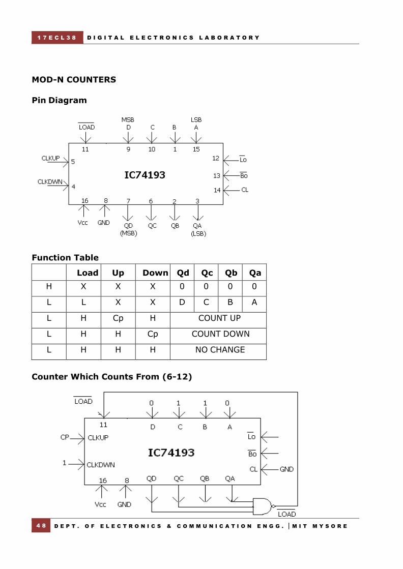
MOD-N COUNTERS
Pin Diagram
Function Table
Load Up Down Qd Qc Qb Qa
H X X X 0 0 0 0
L L X X D C B A
L H Cp H COUNT UP
L H H Cp COUNT DOWN
L H H H NO CHANGE
Counter Which Counts From (6-12)

D I G I T A L E L E C T R O N I C S L A B O R A T O R Y 1 7 E C L 3 8
M I T M Y S O R E | D E P T . O F E L E C T R O N I C S & C O M M U N I C A T I O N E N G G . 4 9
Invalid state 1101
Counter Which Counts From (15-6)
Invalid state---0101
Note:-Lo and Bo are used basically for cascading the counters
Result:
Viva Questions:
1. What is Mod-2 counter?
2. What is Mod-5 Counter?
3. What is Mod-N counter?
4. How many counters are there in IC 7490?
5. Differentiate between synchronous and asynchronous counters.

1 7 E C L 3 8 D I G I T A L E L E C T R O N I C S L A B O R A T O R Y
5 0 D E P T . O F E L E C T R O N I C S & C O M M U N I C A T I O N E N G G . | M I T M Y S O R E
Sequence: 100010011010111
TRUTH TABLE CIRCUIT DIAGRAM
Clk QA QB QC QD f
1 1 1 1 1 0
2 0 1 1 1 0
3 0 0 1 1 0
4 0 0 0 1 1
5 1 0 0 0 0
6 0 1 0 0 0
7 0 0 1 0 1
8 1 0 0 1 1
9 1 1 0 0 0
10 0 1 1 0 1
11 1 0 1 1 0
12 0 1 0 1 1
13 1 0 1 0 1
14 1 1 0 1 1
15 1 1 1 0 1

D I G I T A L E L E C T R O N I C S L A B O R A T O R Y 1 7 E C L 3 8
M I T M Y S O R E | D E P T . O F E L E C T R O N I C S & C O M M U N I C A T I O N E N G G . 5 1
Design Pseudo Random Sequence generator using
7495.
Components required:
Sl.
No. COMPONENT SPECIFICATION
1
2
3
4
5
Counter IC
AND gate
XOR gate
Patch chords
Trainer Kit
7495
7410
7486
COUNTERS:
Sequence generator is a synchronous counter to generate a given sequence.
Procedure:
1. Set up the circuit as shown in figure
2. Load the initial state by keeping mode control pin in HIGH state.
3. Set mode control = ‘0’ and apply clock pulses and record all observations.
Sequence: 1101011
Clk QA QB QC QD f
1 1 1 1 0 1
2 1 1 1 1 0
3 0 1 1 1 1
4 1 0 1 1 0
5 0 1 0 1 1
6 1 0 1 0 1
7 1 1 0 1 1
E X P E R I M E N T
10

1 7 E C L 3 8 D I G I T A L E L E C T R O N I C S L A B O R A T O R Y
5 2 D E P T . O F E L E C T R O N I C S & C O M M U N I C A T I O N E N G G . | M I T M Y S O R E
Result:
Viva Questions:
1. Define sequence generator.
2. What is the application of sequence generator?

D I G I T A L E L E C T R O N I C S L A B O R A T O R Y 1 7 E C L 3 8
M I T M Y S O R E | D E P T . O F E L E C T R O N I C S & C O M M U N I C A T I O N E N G G . 5 3
ELECTRONIC WORKBENCH:
Electronic WorkBench (EWB) is a simulation package for electronic circuits. It allows you
to design and analyze circuits without using breadboards, real components or actual instruments. EWB's click-and drag operations make editing a circuit fast and easy.
The user interface of EWB consists of the following:
The circuit window is where you create your schematics. The components and
instruments that you need to construct a circuit are grouped into parts bins. Each
parts bin has a corresponding button on the Parts Bin toolbar. Clicking one of
these buttons displays another toolbar containing buttons representing the
components and instruments contained in that parts bin. To place a component
or instrument on the circuit window, click the desired part button and drag the
component or instrument to the circuit widow. Instruments toolbar includes a
digital meter, a word generator, a logic analyzer, and a logic converter. These
instruments may be dragged onto the circuit window and used to test the circuit
that you build just as you would use test instruments in a lab. The final item on
the menu bar is a power switch. You need to click on the power switch when you
are ready to activate your circuit.

1 7 E C L 3 8 D I G I T A L E L E C T R O N I C S L A B O R A T O R Y
5 4 D E P T . O F E L E C T R O N I C S & C O M M U N I C A T I O N E N G G . | M I T M Y S O R E
Consider an example of AND GATE: STEP 1: Step 1: Find the following items from Parts Bin toolbars and place them in the circuit window as indicated below. Note that VCC represents +5 Volt.
Step 2: Label and rotate the components as indicated below:
To wire components together, press and hold the left mouse button, and drag it so that
a wire appears. Drag the wire to a terminal on another component or to an instrument connection. When the terminal on the second component or the instrument highlights, release the mouse button. The wire is routed at right angle, without overlapping other
components or instrument icons. If you drag a wire from a component’s terminal to another wire, a connector is automatically created when you release the mouse button.
A connector button also appears in the Basic toolbar. This let you insert connectors into an existing circuit, then drag another wire to one of its free terminals. Alternatively, you can place the connector on the circuit window where you plan to make a connection and
drag wires to its terminals. You can join up to 4 wires with one connector.

D I G I T A L E L E C T R O N I C S L A B O R A T O R Y 1 7 E C L 3 8
M I T M Y S O R E | D E P T . O F E L E C T R O N I C S & C O M M U N I C A T I O N E N G G . 5 5
Step 3: Wire components as indicated below:
Step 4: Using the mouse, click on the power switch to turn it on. Next, press combination of keys A and B to verify the truth table for the indicated AND gate.

1 7 E C L 3 8 D I G I T A L E L E C T R O N I C S L A B O R A T O R Y
5 6 D E P T . O F E L E C T R O N I C S & C O M M U N I C A T I O N E N G G . | M I T M Y S O R E
Simulation of Full- Adder
Circuit diagram:
Truth table:
Results:
A B Cin Sum Cout
0 0 0 0 0 𝑺𝒖𝒎 = 𝐴 ̅�̅�𝐶𝑖𝑛 + �̅�𝐵𝐶𝑖𝑛̅̅ ̅̅̅ + 𝐴�̅�𝐶𝑖𝑛̅̅ ̅̅̅ + 𝐴𝐵𝐶𝑖𝑛 𝑺𝒖𝒎 = 𝐴⨁𝐵⨁𝐶𝑖𝑛 𝑪𝒐𝒖𝒕 = (𝐴⨁𝐵)𝐶𝑖𝑛 + 𝐴𝐵
0 0 1 1 0
0 1 0 1 0
0 1 1 0 1
1 0 0 1 0
1 0 1 0 1
1 1 0 0 1
1 1 1 1 1
E X P E R I M E N T
11

D I G I T A L E L E C T R O N I C S L A B O R A T O R Y 1 7 E C L 3 8
M I T M Y S O R E | D E P T . O F E L E C T R O N I C S & C O M M U N I C A T I O N E N G G . 5 7
Simulation of Mod-8 Synchronous UP/DOWN Counter
Circuit diagram:
Truth table:
Up counter Down counter
Q2 Q1 Q0 Q2 Q1 Q0
0 0 0 1 1 1
0 0 1 1 1 0
0 1 0 1 0 1
0 1 1 1 0 0
1 0 0 0 1 1
1 0 1 0 1 0
1 1 0 0 0 1
1 1 1 0 0 0
RESULT:
E X P E R I M E N T
12

1 7 E C L 3 8 D I G I T A L E L E C T R O N I C S L A B O R A T O R Y
5 8 D E P T . O F E L E C T R O N I C S & C O M M U N I C A T I O N E N G G . | M I T M Y S O R E
Probable Viva Questions
1. Define minterm and maxterm?
2. Define minterm Canonical formula and maxterm canonical formula?
3. What does standard SOP and standard POS mean?
4. What are basic gates? Disjunctive conjunctive.
5. What are universal gates? Why are they called so?
6. What does prime implicant, prime implicate and essential prime implicant mean?
7. What does the term subsume mean?
8. What are the different methods for solving Boolean expressions?
9. Among K-map, VEM technique & Quine-McCluskey, which is easier to use?
10. What is the other name given to K-map?
11. What is the other name given to VEM technique?
12. What is the other name given to Quine-McCluskey?
13. What is the difference between Combinational circuit and Sequential circuit?
14. What is a Parallel adder?
15. If 2 10-bit numbers have to be added using Parallel adder how many full adders
are required?
16. What are the disadvantages of parallel adder?
17. What is a look ahead carry adder?
18. What is a serial adder?
19. Is a serial adder a sequential circuit or a combinational circuit?
20. What is a BCD adder?
21. Which is better when compared to a binary adder and BCD adder?
22. If 2 10-bit numbers have to be added using serial adder, how many full adders are
required?
23. Which is fastest among parallel adder, serial adder and look ahead carry adder?
24. Which is called a reflecting code?
25. Is Gray code a weighted code?
26. Which is called a self-complementing code?
27. Is EXESSES-3 code a weighted code?
28. What is an ASCII code?
29. What is an EBCDIC code?
30. What is parity checking?
31. What is the difference between encoder and priority encoder?
32. Why Enable input is generally an active LOW signal?
33. What is the difference between de-multiplexer and decoder?
34. What is the role of a multiplexer?
35. Is it possible to realize 4-bit Binary to Gray using a 1:16 de-multiplexer?
36. What are PLD’s?
37. What is the difference between PAL and PLA?
38. What is the difference between RAM and ROM?
39. Can a PROM be reprogrammed?
40. What is the difference between Static RAM and Dynamic RAM?
D I G I T A L E L E C T R O N I C S L A B O R A T O R Y 1 7 E C L 3 8
M I T M Y S O R E | D E P T . O F E L E C T R O N I C S & C O M M U N I C A T I O N E N G G . 5 9
41. Is it possible to realize comparator using Multiplexer?
42. What is the difference between LCD and LED?
43. What is the input voltage to a Common Anode LED?
44. Why is a low frequency signal required for an LCD?
45. Why an ordinary decoder is cannot be used with displays?
46. What does RBI, RBO and BI mean?
47. What does a basic bi-stable element mean?
48. What is the forbidden state in SR latch?
49. How contact de-bouncing can be eliminated using SR latch?
50. What is the difference between a latch and a flip flop?
51. What is meant by race around condition? How is it eliminated?
52. How to convert a JK flip flop to a D flip flop?
53. How to convert a JK flip flop to a T flip flop?
54. How to convert a T flip flop to a D flip flop?
55. How to convert a D flip flop to a T flip flop?
56. Why is a D flip flop called as a transparent flip flop?
57. What are the two asynchronous inputs? Why are they called so?
58. What is the difference between synchronous PRESET and asynchronous PRESET?
59. What is MEALY sequential circuit?
60. What is MOORE sequential circuit?
61. Can a multiplexer be used to realize a JK flip flop?
62. What is the difference between a counter and a register?
63. What is the difference between a synchronous counter and asynchronous counter?
64. What type of flip flop is used to design an asynchronous counter?
65. In a mod-16 counter, each of the flip flop used has a delay of 20ns. To get an
output at the MSB how long does it take in a synchronous counter and in an
asynchronous counter?
66. Why is an asynchronous counter called as a ripple counter?
67. Define modulus of a counter.
68. What type of counter is 7490?
69. What type of counter is 74192 and 74193?
70. What type of flip flop is used to design a synchronous counter?
71. What is data lockout in a counter?
72. How is data lockout overcome?
73. Is the output of a counter always a square wave?
74. What is the difference between a shift register and register?
75. Is a shift register a synchronous circuit or an asynchronous circuit?
76. If an ADC is interfaced to a shift register, what type of shifting is preferred?
77. What are the features of a shift register?
78. Do we have a register which can perform all the basic shifting operation?
79. Name a combinational circuit which works similar to a PISO?
80. Name a combinational circuit which works similar to a SIPO?

1 7 E C L 3 8 D I G I T A L E L E C T R O N I C S L A B O R A T O R Y
6 0 D E P T . O F E L E C T R O N I C S & C O M M U N I C A T I O N E N G G . | M I T M Y S O R E
81. What is a ring counter and a Johnson counter?
82. Is the output of a ring counter a square wave?
83. What is the difference between a self-starting ring counter and a counter loaded
initially with a parallel data?
84. What happens if 0000 is loaded into a ring counter, provided it is not self-starting?
85. If there are 6 states in a ring counter, then how many flip flops are required?
86. If there are 7 states in a Johnson counter, then how many flip flops are required?
87. What is the use of ring counter and Johnson counter?
88. Is the ring counter a synchronous circuit or an asynchronous circuit?
89. What are the other names by which a Johnson counter is called?
90. Define SET-UP time and HOLD time?
91. What is meant by active time or triggering time?
92. What is a sequence generator? What is its application?
93. What happens if the states repeat in a sequence generator? 96. Is the sequence
generator periodic in nature?
94. What is the difference between a sequence generator and a ring counter?
95. What is the sequence generator made up of?
96. Is the sequence generator a synchronous circuit or an asynchronous circuit?
97. If the length of the sequence to be generated is specified, then what is the name
given to such sequence generator?
98. Explain the working of a 555 timer?
99. What is the purpose of a Monostable and astable?
100. Why a Monostable is called so?
101. Why an astable is called so?
102. What is the use of the two diodes in an astable circuit?
103. Is a trigger input required for an astable?
104. Why doesn’t triggering pulse affect a Monostable output when the capacitor is still
charging?
105. What is positive logic?
106. What is negative logic?
107. What is the output voltage range for a TTL gate?
108. What is the input voltage range for a TTL gate?
109. What is meant by current sourcing and current sinking?
110. Define Fan in?
111. Define Fan out?
112. In the basic circuit of transistor as an inverter, why CE configuration is used?
113. Why Diode-Transistor Logic is not used?
114. What is the advantage of Totem pole configuration?
115. What is the disadvantage of Totem pole configuration?
116. What is Open Collector configuration?
117. What are the advantages and disadvantages of Open Collector configuration?
118. What are the different TTL families?
119. What does 74LS series mean?
120. If the input or output voltages fall in the intermediate range, what happens?