
DEVELOPMENT OF A FLAT PANEL DETECTOR WITH ...
172
DEVELOPMENT OF A FLAT PANEL DETECTOR WITH AVALANCHE GAIN FOR INTERVENTIONAL RADIOLOGY by MATTHEW M. WRONSKI A thesis submitted in conformity with the requirements for the degree of Doctor of Philosophy Graduate Department of Medical Biophysics University of Toronto © Copyright Matthew M. Wronski 2009
-
Upload
khangminh22 -
Category
Documents
-
view
0 -
download
0
Transcript of DEVELOPMENT OF A FLAT PANEL DETECTOR WITH ...

DEVELOPMENT OF A FLAT PANEL DETECTOR WITH AVALANCHE GAIN FOR INTERVENTIONAL RADIOLOGY
by
MATTHEW M. WRONSKI
A thesis submitted in conformity with the requirements for the degree of Doctor of Philosophy
Graduate Department of Medical Biophysics University of Toronto
© Copyright Matthew M. Wronski 2009

Development of a Flat Panel Detector with Avalanche Gain for Interventional Radiology
Matthew Michael Wronski
Doctor of Philosophy, 2009
Department of Medical Biophysics
University of Toronto
Abstract A number of interventional procedures such as cardiac catheterization, angiography and
the deployment of endovascular devices are routinely performed using x-ray fluoroscopy.
To minimize the patient’s exposure to ionizing radiation, each fluoroscopic image is
acquired using a very low x-ray exposure (~ 1 µR at the detector). At such an exposure,
most semiconductor-based digital flat panel detectors (FPD) are not x-ray quantum noise
limited (QNL) due to the presence of electronic noise which substantially degrades their
imaging performance. The goal of this thesis was to investigate how a FPD based on
amorphous selenium (a-Se) with internal avalanche multiplication gain could be used for
QNL fluoroscopic imaging at the lowest clinical exposures while satisfying all of the
requirements of a FPD for interventional radiology.
Towards this end, it was first determined whether a-Se can reliably provide avalanche
multiplication gain in the solid-state. An experimental method was developed which
enabled the application of sufficiently large electric field strengths across the a-Se. This
method resulted in avalanche gains as high as 104 at an applied field of 105 V/µm using
ii

optical excitation. This was the first time such high avalanche gains have been reported in
a solid-state detector based on an amorphous material.
Secondly, it was investigated how the solid-state a-Se avalanche detector could be used to
image X-rays at diagnostic radiographic energies (~ 75 kVp). A dual-layered direct-
conversion FPD architecture was proposed. It consisted of an x-ray drift region and a
charge avalanche multiplication region and was found to eliminate depth-dependent gain
fluctuation noise. It was shown that electric field strength non-uniformities in the a-Se do
not degrade the detective quantum efficiency (DQE).
Lastly, it was determined whether the solid-state a-Se avalanche detector satisfies all of
the requirements of interventional radiology. Experimental results have shown that the
total noise produced by the detector is negligible and that QNL operation at the lowest
fluoroscopic exposures is indeed possible without any adverse effects occurring at much
larger radiographic exposures. In conclusion, no fundamental obstacles were found
preventing the use of avalanche a-Se in next-generation solid-state QNL FPDs for use in
interventional radiology.
iii

To my parents
iv

Acknowledgements First and foremost, I would like to thank my thesis supervisor, Dr. John A. Rowlands for
his infallible guidance and support and exceptional scientific training. Dr. Rowlands has
taught me the importance of patience, persistence and taking the high road. He has also
taught me to keep things simple and that research can be a rewarding experience.
I would also like to thank the members of my supervisory committee, Dr. Mike Rauth
and Dr. Don Plewes for their excellent comments, suggestions and advice. They have
helped keep me on track in my research and encouraged me to finish my thesis in a
timely way.
Thanks to Dr. Wei Zhao, Dr. Alla Reznik and Dr. Afrin Sultana for their collaboration
and helpful discussions. I would also like to thank Dr. Dylan Hunt for introducing me to
this field of research and taking the time to explain all the important details when I first
joined John’s laboratory. Dylan, your enthusiasm in this field of research has been
contagious!
A big thank you goes to Giovanni DeCrescenzo who has been instrumental in developing
and teaching me how to use the many tools used throughout this thesis. Giovanni has also
always been there to answer all my questions and reassure me of my work. Also, thanks
to Dr. Kenkichi Tanioka at NHK, for providing the samples on which a large part of this
thesis is based.
A special thanks goes out to my friends and colleagues in John’s group, particularly
Philip Komljenovic, Dr. Normand Robert, Kristina Watt, Dr. Farhad Taghibakhsh, David
Green and Sarah Cuddy. You guys have kept a permanent smile on my face throughout
my studies!
Last but not least, I would like to thank my parents for all their love and relentless
support and for always believing in my abilities. You guys are truly the best!
v

Table of Contents
Chapter 1 Introduction....................................................................................................................... 1
1.1 Overview ................................................................................................................... 2 1.2 Fluoroscopy and interventional radiology ............................................................... 2 1.3 Clinical fluoroscopy requirements for interventional radiology .............................. 5 1.4 Current x-ray imaging technology for interventional radiology and its limitations 8
1.4.1 X-ray image intensifiers ..................................................................................... 8 1.4.2 Flat panel detectors ........................................................................................... 9 1.4.3 Electronic noise in flat panel detectors ........................................................... 12
1.5 Possible solutions for quantum noise limited AMFPIs........................................... 15 1.6 High-gain avalanche rushing photoconductor (HARP) technology....................... 19
1.6.1 HARP camera .................................................................................................. 19 1.6.2 The need for a solid-state HARP ..................................................................... 21
1.7 Rationale and problem formulation........................................................................ 23 1.8 Thesis outline .......................................................................................................... 24 References ..................................................................................................................... 26
Chapter 2 Development of a solid-state amorphous selenium avalanche photoreceptor........... 32
2.1 Introduction............................................................................................................. 33 2.2 Theory ..................................................................................................................... 34 2.3 Methods................................................................................................................... 40
2.3.1 Distributed resistive layer................................................................................ 40 2.3.2 Experimental setup........................................................................................... 42 2.3.3 Linearity ........................................................................................................... 43 2.3.4 Gain and dark current ..................................................................................... 44 2.3.5 Carrier transport ............................................................................................. 45
2.4 Results ..................................................................................................................... 47 2.4.1 Breakdown characteristics............................................................................... 47 2.4.2 Linearity ........................................................................................................... 50 2.4.3 Gain and dark current ..................................................................................... 51 2.4.4 Carrier transport ............................................................................................. 52
2.5 Discussion ............................................................................................................... 55 2.5.1 Breakdown characteristics............................................................................... 55 2.5.2 Linearity ........................................................................................................... 58 2.5.3 Gain and dark current ..................................................................................... 60 2.5.4 Carrier transport ............................................................................................. 61
2.6 Conclusions............................................................................................................. 62 References ..................................................................................................................... 64
vi

Chapter 3 Theory of x-ray imaging with avalanche amorphous selenium in the solid state ..... 67
3.1 Introduction............................................................................................................. 68 3.2 Background ............................................................................................................. 69
3.2.1 Indirect-conversion HARP imager .................................................................. 69 3.2.2 Depth-dependent gain fluctuation noise .......................................................... 72
3.3 Proposed device structure....................................................................................... 74 3.4 Calculation methods ............................................................................................... 76
3.4.1 MTF, NPS and DQE ........................................................................................ 76 3.4.2 Avalanche gain, gain nonuniformities and fill-factor...................................... 80 3.4.3 Del response..................................................................................................... 82
3.5 Results ..................................................................................................................... 83 3.5.1 MTF, NPS and DQE ........................................................................................ 83 3.5.2 Avalanche gain, gain nonuniformities and fill-factor...................................... 85 3.5.3 Del response..................................................................................................... 88
3.6 Discussion ............................................................................................................... 89 3.6.1 MTF, NPS and DQE ........................................................................................ 90 3.6.2 Avalanche gain, gain nonuniformities and fill-factor...................................... 91
3.6.2.1. Average gain and fill-factor..................................................................... 91 3.6.2.2 Avalanche multiplication noise................................................................. 92 3.6.2.3 Gain nonuniformities ............................................................................... 94
3.6.3 Del response..................................................................................................... 96 3.6.4 Response at high spatial frequencies............................................................... 96 3.6.5 Dark current..................................................................................................... 97 3.6.6 Direct x-ray interaction in the gain region...................................................... 98
3.7 Conclusions............................................................................................................. 99 References ................................................................................................................... 101
Chapter 4 Experimental characterization of DRL-HARP for interventional radiology applications .................................................................................................................... 105
4.1 Introduction........................................................................................................... 106 4.2 Methods................................................................................................................. 107
4.2.1 Noise characterization ................................................................................... 107 4.2.2 X-ray sensitivity ............................................................................................. 109 4.2.3 Dynamic range............................................................................................... 111 4.2.4 Temporal response......................................................................................... 111 4.2.5 Compatibility with TFT technology ............................................................... 115
4.2.5.1 Reverse structure .................................................................................... 115 4.2.5.2 HARP thickness....................................................................................... 117 4.2.5.3 TFT compatibility (in collaboration with A. Sultana at U. of Waterloo)............................................................................................................................. 117
4.3 Results ................................................................................................................... 119 4.3.1 Noise characterization ................................................................................... 119
vii

4.3.2 X-ray sensitivity ............................................................................................. 120 4.3.3 Dynamic range............................................................................................... 121 4.3.4 Temporal response......................................................................................... 122
4.3.4.1 RC and ghosting...................................................................................... 122 4.3.4.2 Lag .......................................................................................................... 124 4.3.4.3 Predicted timing response for a DRL-HARP FPD ................................. 125
4.3.5 Compatibility with active matrix technology ................................................. 126 4.3.5.1 Reverse structure .................................................................................... 126 4.3.5.2 HARP thickness....................................................................................... 127 4.3.5.3 TFT compatibility (experiments performed with Afrin Sultana U Waterloo)............................................................................................................................. 128
4.4 Discussion ............................................................................................................. 130 4.4.1 Noise characterization ................................................................................... 130 4.4.2 X-ray sensitivity ............................................................................................. 132 4.4.3 Dynamic range............................................................................................... 132 4.4.4 Temporal response......................................................................................... 135
4.4.4.1 RC and ghosting...................................................................................... 135 4.4.4.2 Lag .......................................................................................................... 136 4.4.4.3 Predicted timing response for a DRL-HARP FPD ................................. 137
4.4.5 Compatibility with active matrix technology ................................................. 138 4.4.5.1 Reverse structure .................................................................................... 138 4.4.5.2 HARP thickness....................................................................................... 140 4.4.5.3 TFT compatibility ................................................................................... 141
4.5 Conclusion ............................................................................................................ 143 References ................................................................................................................... 144
Chapter 5 Conclusions .................................................................................................................... 146
5.1 Brief summary ....................................................................................................... 147 5.2 Summary of major results ..................................................................................... 149
5.2.1 Solving the breakdown problem of electroded HARP ................................... 149 5.2.2 X-ray imaging with HARP-AMFPI ................................................................ 151 5.2.3 Addressing the requirements of interventional radiology ............................. 152
5.3 Original contributions .......................................................................................... 154 5.4 Future work........................................................................................................... 156
5.4.1 Materials characterization............................................................................. 156 5.4.2 Device optimization ....................................................................................... 157 5.4.3 Imager prototype fabrication ......................................................................... 158
viii

List of Figures 1.1 Three different x-ray imaging systems…………………………………………………………….11 1.2 The active matrix and detecting element…………………………………………………………..12 1.3 Simulated radiographs reflecting the significance of electronic noise…………………………….14 1.4 Principle of operation of a HARP camera tube…………………………………………………....20 1.5 Directly electroded HARP………………………………………………………………………...23 2.1 Directly electroded HARP and DRL-HARP……………………………………………………....36 2.2 Time-temperature-crystallization diagram………………………………………………………...37 2.3 Electrical discharge paths in directly electroded HARP and DRL-HARP………………………..39 2.4 Cellulose acetate casting process………………………………………………………………….42 2.5 Experimental setup used for characterization of directly electroded HARP and DRL-HARP……43 2.6 Measured dark current transient in directly electroded HARP……………………………………47 2.7 Measured dark current magnitude before and after breakdown…………………………………...48 2.8 Number of electrical discharges in DRL-HARP…………………………………………………..50 2.9 Peak measured photocurrent in DRL-HARP as a function of LED source intensity……………..50 2.10 Photocurrent transients in DRL-HARP for varying applied biases in the avalanche regime……..51 2.11 Measured DRL-HARP photocurrent and dark current as a function of high voltage bias………..52 2.12 Measured photocurrent transient in directly electroded HARP and DRL-HARP………………...53 2.13 Measured a-Se hole mobility in DRL-HARP and a Xerox a-Se plate…………………………….54 2.14 Time-of-flight traces obtained in the avalanche regime…………………………………………..55 3.1 SHARP-AMFPI imager concept………………………………………………………………….70 3.2 Calculated DQE(f) for SHARP-AMFPI for an x-ray exposure of 0.1 µR………………………..71 3.3 MICROMEGAS, GEM and dual-layered a-Se detector concepts………………………………...73 3.4 Structure of HARP-AMFPI……………………………………………………………………….76 3.5 Stages of the cascaded linear system model for HARP-AMFPI………………………………….77 3.6 Calculated MTF for a-Se and aperture function…………………………………………………..83 3.7 NPS for a direct-conversion a-Se AMFPI before and after the addition of electronic noise……...84 3.8 Calculated DQE(f) for a direct-conversion a-Se AMFPI………………………………………….84 3.9 Calculated DQE(0) for a direct-conversion a-Se AMFPI…………………………………………85 3.10 Calculated average avalanche gain for a direct-conversion a-Se AMPFI…………………………86 3.11 Calculated electric field distribution for a direct-conversion a-Se AMPFI……………………….86 3.12 Calculated effective fill factor for a direct-conversion a-Se AMPFI……………………………...87 3.13 Calculated gain nonuniformity for a direct-conversion a-Se AMPFI……………………………..87 3.14 DQE(0) calculated as a function of conversion and avalanche gain………………………………88 3.15 Avalanche gain and image charge calculated as a function of x-ray exposure……………………89 4.1 Linear cascaded noise model used to calculate the expected noise variance for DRL-HARP…..108 4.2 Experimental setup used to characterize x-ray sensitivity……………………………………….110 4.3 Circuit diagrams used to model the electrical behaviour of DRL-HARP………………………..114 4.4 The regular and reverser HARP structures………………………………………………………116 4.5 Experimental setup used to investigate combined DRL-HARP / TFT operation………………..118 4.6 Measured charge signal and noise produced by DRL-HARP……………………………………119 4.7 Measured DRL-HARP dark current and photocurrent…………………………………………..121 4.8 Measured output charge from DRL-HARP as a function of the equivalent x-ray exposure…….122 4.9 Measured photocurrent transient showing ghosting and RC effects……………………………..123 4.10 Measured photocurrent transient showing lag effect…………………………………………….124 4.11 Output signal in a FPD with a DRL-HARP avalanche layer and TFT charge readout…………..126 4.12 Measured photocurrent for normal and reverse-structured DRL-HARP………………………...127 4.13 Measured photocurrent and dark current for a DRL-HARP with a 4 µm HARP layer………….128 4.14 Measured drain-source current as a function of gate-source voltage for TFT in Fig. 4.5………..129 4.15 TFT output current measured using the experimental setup shown in Figure 4.5……………….130
ix

List of Tables 1.1 Several key imaging modalities used in interventional radiology……………………………….....4 1.2 Three different approaches for overcoming electronic noise at low x-ray exposures in AMFPIs...18 2.1 Measured characteristics of DRL-HARP with and without a DRL……………………………….49 2.2 Maximum electric field in a-Se layer for several different types of contacts……………………..49 3.1 Summary of factors used to characterize nonuniformities in conversion and avalanche gain…….80 3.2 Detector operating conditions and design parameters chosen for fluoroscopy and radiography….80
x

List of Symbols ASe a-Se Swank factor………………………………………………………………………………….77 Aav avalanche Swank factor……………………………………………………………………………78 Asec secondary Swank factor…………………………………………………………………………...79 b electron hole pair recombination coefficient………………………………………………………45 β impact ionization coefficient………………………………………………………………………45 C capacitance………………………………………………………………………………………...12 Cd del capacitance…………………………………………………………………………………….36 d a-Se thickness……………………………………………………………………………………...38 ∆A electrical discharge area…………………………………………………………………………...36 ∆Q amount of heat dissipated from discharge region………………………………………………….38 e electronic charge…………………………………………………………………………………..14 E electric field strength………………………………………………………………………………33 EG band gap energy…………………………………………………………………………………...60 Ea-Se electric field strength in the a-Se layer…………………………………………………………….45 Ed electrical energy accumulated on del capacitance…………………………………………………36 Emax maximum electric field strength…………………………………………………………………...49 η x-ray quantum absorption efficiency………………………………………………………………77 g total gain………………………………………………………………………………………….122 gc conversion gain……………………………………………………………………………………45 gav avalanche gain……………………………………………………………………………………..45 Id dark current………………………………………………………………………………………..60 Idis peak discharge current……………………………………………………………………………..36 k Boltzmann’s constant……………………………………………………………………………...12 q0 number of incident x-ray photons per unit area…………………………………………………...77 Reff effective series resistance of DRL…………………………………………………………………38 Rlat effective lateral (sheet) resistance of DRL………………………………………………………...40 ρDRL resistivity of DRL………………………………………………………………………………….40 σav
2 avalanche multiplication gain variance……………………………………………………………77 T temperature………………………………………………………………………………………...12 Ta(f) del aperture function……………………………………………………………………………….77 Tb(f) MTF associated with electron hole pair generation in a-Se……………………………………….77 τlat time constant for lateral charge conduction……………………………………………………….40 Vd potential across del capacitance…………………………………………………………………...36 Weff required amount of absorbed x-ray energy to produce a single EHP that survives recombination.17 Z atomic number……………………………………………………………………………………..15
xi

List of Abbreviations ALARA as low as reasonably achievable………………………………………………………………….....4 AMFPI active matrix flat panel imager……………………………………………………………………...9 AsSe3 arsenic triselenide……………………………………………………………………………….....97 a-Se amorphous selenium……………………………………………………………………………….10 CA cellulose acetate……………………………………………………………………………………40 CCD charge coupled device………………………………………………………………………………8 CeO2 cerium oxide…………………………………………………………………………………….....97 CMOS complimentary metal oxide semiconductor……………………………………………………….22 c-Si crystalline silicon…………………………………………………………………………………..60 CsI cesium iodide……………………………………………………………………………………….9 DC direct current……………………………………………………………………………………..109 del detector element………………………………………………………………………………….....9 DQE detective quantum efficiency……………………………………………………………………...68 DSA digital subtraction angiography…………………………………………………………………….6 DRL distributive resistive layer…………………………………………………………………………35 EHP electron hole pair……………………………………………………………………………………9 EMI electro-magnetic interference……………………………………………………………………...46 FEM finite element method……………………………………………………………………………...80 FPD flat panel detector………………………………………………………………………………….13 GEM gas electron multiplier……………………………………………………………………………..72 HARP high gain avalanche rushing photoconductor……………………………………………………...19 HgI2 mercuric iodide…………………………………………………………………………………….15 HV high voltage………………………………………………………………………………………..15 ITO indium tin oxide…………………………………………………………………………………...23 LED light emitting diode………………………………………………………………………………..42 MRI magnetic resonance imaging………………………………………………………………………..3 MTF modulation transfer function………………………………………………………………………..7 NPS noise power spectrum……………………………………………………………………………...79 OCT optical coherence tomography……………………………………………………………………...3 PbI2 lead iodide…………………………………………………………………………………………15 PbO lead oxide………………………………………………………………………………………….15 PEDOT Poly(3,4-ethylenedioxythiophene)………………………………………………………………...36 PMT photomultiplier tube……………………………………………………………………………….42 QNL quantum noise limited………………………………………………………………………………7 RE readout element…………………………………………………………………………………..117 R/F radiography/fluoroscopy…………………………………………………………………………..57 SHARP scintillator-HARP………………………………………………………………………………….69 SPICE Simulation Program with Integrated Circuit Emphasis…………………………………………..113 SNR signal to noise ratio………………………………………………………………………………119 TOF time of flight……………………………………………………………………………………….45 TFT thin film transistor…………………………………………………………………………………11 TTC time-temperature-crystallization…………………………………………………………………..37 W/L width to length ratio……………………………………………………………………………...118 XRII x-ray image intensifier……………………………………………………………………………...3 RC resistive-capacitive………………………………………………………………………………...38
xii

Chapter 1 Introduction 1.1 Overview 1.2 Fluoroscopy and interventional radiology 1.3 Clinical fluoroscopy requirements for interventional radiology 1.4 Current x-ray imaging technology for interventional radiology and its limitations
1.4.1 X-ray image intensifiers 1.4.2 Flat panel detectors 1.4.3 Electronic noise in flat panel detectors
1.5 Possible solutions for quantum noise limited AMFPIs 1.6 High-gain avalanche rushing photoconductor (HARP) technology
1.6.1 HARP camera 1.6.2 The need for a solid-state HARP
1.7 Rationale and problem formulation 1.8 Thesis outline
1

1.1 Overview This chapter starts by reviewing the role of fluoroscopy in interventional radiology,
within the context of other imaging modalities currently used for image guidance.
Specific clinical requirements are identified for the fluoroscopic imaging system. Next,
the limitations of current x-ray imaging technologies are identified. The emphasis is
placed particularly on the solid-state flat panel detector which is a relatively new and very
promising imaging technology. Possible solutions are identified for overcoming
electronic noise, which is the single-most important problem affecting all existing flat
panel detectors in fluoroscopy. The chapter next presents a review and discusses how a
specialized technology based on avalanche multiplication of charge in an amorphous
selenium photoconductor can be used for fluoroscopic imaging in interventional
radiology. The need for a solid-state version of this promising technology is identified.
Finally, problems impeding its practical use are outlined and this establishes the main
objectives of the thesis.
1.2 Fluoroscopy and interventional radiology The field of radiography was born soon after Roentgen discovered X rays near the end of
the 19th century. Shortly after this discovery, it became possible to produce diagnostic
images or radiographs of internal human anatomy. Internal anatomical motion could also
be observed by using a device known as a fluoroscope which employed a screen with a
material such as zinc cadmium sulfide that emitted light when exposed to X rays.1
Fluoroscopic imaging, or fluoroscopy, initially required the radiologist to greatly increase
the sensitivity of their eyes to the faint blue or green light by sitting in a darkened room
2

prior to examining the image on the screen (dark adaptation). Subsequently, it was found
that wearing red goggles permitted dark adaptation to be retained in ordinary room light.
However, even with dark adapted eyes, the poor optical coupling of the screen to the
human eye resulted in a degradation of the final image on the viewer’s retina. This
situation, in which only a portion of all secondary quanta (optical photons in this case)
are used to create the final image is known as a secondary quantum sink. The problems
associated with dark adaptation and the secondary quantum sink were overcome in the
1950’s with the development of the x-ray image intensifier (XRII).
Since its inception, fluoroscopy has, and continues to be a key imaging modality used in
interventional radiology, a branch of radiology that is concerned with the use of image
guidance to conduct minimally invasive procedures for both diagnostic and therapeutic
purposes. These procedures include, for instance, angiography, angioplasty, pacemaker
insertion and embolization. Ultrasound and magnetic resonance imaging (MRI),
developed in the 1970s and 1980s, respectively, and the more recently developed optical
coherence tomography (OCT) have also been and are increasingly being used for image
guidance in interventional radiology. These imaging modalities have the important
advantage of being tomographic, meaning that they can produce image slices at a
specified depth or volumetric renderings of the anatomical regions being imaged. While
X-ray fluoroscopy is not inherently tomographic, technologies such as cone beam CT or
rotational angiography may be used in addition to fluoroscopy to provide three-
dimensional image data. Table 1.1 summarizes the key advantages and disadvantages of
each of the imaging modalities currently used in interventional radiology.
3

Table 1.1. Summary of the advantages and disadvantages of several key imaging modalities used in interventional radiology. Advantages Disadvantages X-ray fluoroscopy • high spatial resolution
• high temporal resolution • excellent geometrical accuracy • low relative cost
• ionizing radiation • poor soft tissue contrast • not tomographic
Ultrasound • high temporal resolution • no ionizing radiation • low relative cost • localized imaging can be
performed at catheter tip • tomographic
• poor spatial resolution • poor imaging performance
near bones and air-filled cavities
• large operator dependency
MRI • good soft tissue contrast • no ionizing radiation • localized imaging can be
performed at catheter tip • tomographic
• requires specialized non-magnetic devices
• fundamental tradeoff between image quality and temporal resolution
• very high cost OCT • high spatial resolution
• high temporal resolution • low relative cost • tomographic
• limited to localized imaging at catheter tip
The reason X-ray fluoroscopy remains a dominant imaging modality in interventional
radiology is because no other single modality provides the same combination of high
spatial and temporal resolution which is particularly important for proper deployment of
endovascular (from within the blood vessel) devices such as stents or coils. However, the
harmful effects of ionizing radiation used in fluoroscopy, which have long been
recognized, require the patient dose to be as low as reasonably achievable during an
intervention. This is often referred to as the ALARA principle. The use of harmful x-ray
radiation is justifiable by considering that the benefit from the clinical outcome of the
intervention will outweigh the adverse biological effects of the radiation. These
biological effects include indirect and direct effects. Indirect effects of ionizing radiation
arise when electrons set in motion by x-ray photons excite and ionize water molecules,
4
creating free radicals which then cause damage to critical biological targets such as DNA.
In direct effects, electrons directly ionize DNA molecules. As a result, in certain cases
such as pediatric interventions, a particularly strict adherence to ALARA is required,
since the accrued stochastic effects due to radiation exposure are more likely to disrupt
tissue growth and development as well as lead to an increased chance of cancer over the
child’s lifetime. There are adverse effects associated with other imaging modalities as
well. The electromagnetic radiofrequency pulses used in MRI are known to cause
heating. This can be particularly problematic near metallic devices or implants such as
pacemakers or hearing aids. Ultrasound contrast agents, when exposed to ultrasound
waves, can also cause potential bio-effects (i.e. rupture of cell membranes) at the level of
the microcirculation, although the clinical relevance of such bio-effects remains unclear.2
1.3 Clinical fluoroscopy requirements for interventional radiology
A modern fluoroscope consists of a large “C” shaped mount called a C-arm with an x-ray
source on one end and an x-ray imager on the other. This assembly can be positioned
such that different projections of the patient anatomy may be acquired from different
angles. In certain cases, the C-arm assembly is rotated around the patient during injection
of a contrast dye and multiple projection images are acquired and subsequently
reconstructed into a three-dimensional rendition of the vasculature.3 The C-arm assembly
should hence be designed such that the x-ray source and x-ray imager are as small and
light as possible to facilitate its positioning or rotation and to improve patient
accessibility.
5

In most cases, the x-ray imager is used for fluoroscopy as well as two other imaging
modes, namely cine acquisition and radiography. We will now describe each of these
imaging modes in turn. In the fluoroscopic mode, the physician typically guides
interventional devices such as guidewires or stents through a catheter towards the lesion
and is mainly concerned with tracking the position of the device. This guidance, usually
referred to as a catheterization, is typically done at relatively high imaging frame rates
(7.5 – 30 image frames per second) so that the physician can get a good sense of the
advancement of the device towards the lesion while avoiding potential complications due
to, for example, arterial tortuosity. Catheterization is often a relatively time consuming
process (ten minutes or longer) and is done at very low x-ray exposures (mean exposure
of 1 µR per frame at the imager) to minimize patient radiation exposure. The x-ray
exposures employed are so low, in fact, that quantum noise (the stochastic variation in the
spatial distribution of x-ray photons) becomes the dominant form of noise in the
fluoroscopic images obtained using an XRII system. Because the interventional device
being imaged typically has a high degree of radio-opacity, these low exposures are often
adequate to obtain sufficient contrast to image the device. In the cine mode, sequences of
images are acquired during administration of an x-ray contrast agent (typically via a
catheter) into the vasculature. These relatively short (several seconds in duration) image
acquisitions are taken at higher exposures (~10 µR/frame) so as to provide superior
image quality (less quantum noise) and thus improve the diagnostic value of the images.
This mode is also used when accurate positioning or deployment of endovascular devices
is performed. In the radiographic mode, images are acquired at even larger exposures (~
100 µR/frame) for applications such as digital subtraction angiography (DSA) which
6

have been shown to improve the detection of certain lesions such as aneurysms or
thrombi.4
High spatial resolution is an important requirement in the cine and radiographic imaging
modes, as it can strongly affect the diagnosis or treatment outcome of an interventional
procedure. Interventional devices such as guide wires or stents typically have wire
diameters ranging from 50-200 µm. Rudin5 et al. have demonstrated that despite the
effects of x-ray scattering, imaging of individual stent wires (struts) using a high
resolution imager is possible inside a human head phantom; this should enable the
deployment of novel assymetrical stents for specialized therapeutic neurovascular
applications. Furthermore, in certain applications such as coronary angiography,
detection of small calcium deposits (tens of micrometers in size) in coronary arteries
provides an important means of assessing the degree of atherosclerosis as well as the
likelihood of a successful angioplasty 6,7. For optimal imaging of fine features in
interventional radiology, the imager should be able to resolve 5 line pairs per millimeter
(a line pair is a pair of light and dark lines) such that the relative contrast between the two
lines of each pair is greater than 0.2 (i.e. a modulation transfer function (MTF) greater
than 0.2 at a spatial frequency of 5 cycles/mm).
From the discussion above, it follows that the key requirements for a clinical x-ray
imager for interventional radiology – beyond a thin profile and providing unobstructed
access to the patient -- are: (1) quantum-noise limited (QNL) operation at the lowest
clinical fluoroscopic x-ray exposures (in conformance with the ALARA principle), (2)
7

capability for modes of operation that require significantly higher x-ray exposures and (3)
capability of imaging fine features of interventional devices or lesions.
1.4 Current x-ray imaging technology for interventional radiology and its limitations 1.4.1 X-ray image intensifiers Until recently, the most widely used x-ray imaging system in interventional radiology
was the x-ray image intensifier (XRII). This is an electro-optical device that operates
inside a vacuum enclosure (Figure 1.1(a)) which contains an input phosphor used to
convert X rays into optical photons. The phosphor is coupled to a photocathode which,
upon exposure to these optical photons produces electrons. The latter are accelerated in
an electric field and hit an output phosphor screen. This process enables the production of
several thousand optical photons for each photoelectron emitted from the photocathode.
The resulting optical image is captured using an optical assembly and a video camera or
charge coupled device (CCD). XRII/video systems provide excellent x-ray sensitivity (the
degree to which small numbers of X rays - ideally a single X ray - can be detected) due to
the large internal gain of the XRII, however, the XRII also presents important limitations.
These are associated with the curvature of the input phosphor and the presence of
multiple conversion stages, leading to geometrical distortions (particularly in the
periphery of the images), spatial nonuniformities and a degradation of the imaging
resolution 8-10. Furthermore, these systems are bulky and heavy (they can weigh several
hundred pounds), compromising patient accessibility and image acquisition modes such
as rotational angiography or cone-beam computed tomography. Another important
8

limitation of the XRII is its high sensitivity to magnetic fields (including the earth’s
magnetic field) which produces a distortion in the image that is shaped like an “S” and
referred to as an S-distortion.10 Due to these substantial limitations and the availability of
new solid-state technologies, there has been a progressive trend in the past few years to
replace XRII systems with flat panel detectors.11
1.4.2 Flat panel detectors
There has been much work over the last decade on the development of solid-state flat
panel detectors, also known as active matrix flat panel imagers (AMFPI). Unlike the
XRII, these systems are thin, produce negligible spatial distortions and are insensitive to
magnetic fields.12 In principle, panels with sufficiently small pixels, or detector elements
(del) also have the potential for substantially improved spatial resolution in comparison
with the XRII because there are considerably less conversion stages involved in the
image detection process (Figure 1.1 (b) and (c)).
The majority of commercial AMFPIs are indirect conversion detectors, in which x-ray
photons strike a scintillator such as cesium iodide (CsI) and generate optical photons
which then interact with a photosensor (usually an amorphous silicon photodiode), in turn
producing electron-hole-pairs (EHP) that are capacitively stored prior to being
electronically processed (see Figure 1.1(b)). The process of detecting the photon-
generated charge from each del (referred to as readout) produces a digital image which
represents the original distribution of X rays incident at the imager’s surface. In another
class of detectors know as direct-conversion detectors, x-rays interact with a
9
photoconductor, usually amorphous selenium (a-Se), and directly generate EHPs, which
follow the parallel field lines in the presence of an electric field (see Figure 1.1(c)) prior
to being read out. Because there is no intermediary optical stage to contribute to blurring,
these systems have the important advantage of providing superior spatial resolution
compared to indirect AMFPIs, however, the photoconductor needs to be thick enough (~
1000 µm) to yield a reasonable quantum efficiency at radiographic x-ray energies (20 –
150 kV).13 The very high spatial resolution of direct-conversion a-Se detectors has
recently increased their use in digital mammographic imaging systems.14 Direct-
conversion detectors are also being considered for use in tomosynthesis, in which a series
of breast radiographs are acquired from different angles and reconstructed into a series of
slices. In contrast with mammography, the image slices produced by tomosynthesis are
largely immune to structural noise, which is the noise introduced into an image due to x-
ray attenuation in overlapping anatomical structures.15
10

c) b)a)
AMFPI AMFPI
Figure 1.1 Three different x-ray imaging systems. (a) The image intensifier consists of an input phosphor coupled to a photocathode which converts X rays into optical photons and subsequently electrons. The latter are accelerated in an electric field and hit an output phosphor screen. This produces an amplification of several thousand. The resulting optical image is captured using an optical assembly and a charge coupled device (CCD). (b) The indirect active matrix flat panel imager (AMFPI) consists of a scintillator which converts X rays into optical photons, a photoconductor which converts them in turn to electrons and a readout layer which stores and processes the resulting charge image. (c) In the direct conversion flat panel detector, X rays are directly converted into charge inside a photoconductor. In each diagram, the electric field lines are shown as two lines next to an arrow which shows the direction in which the charge travels. Adapted from Ref 12.
In both types of AMFPIs, a two-dimensional array of thin film transistors (TFT) is used
to relay the stored image charge at each del electrode to charge amplifiers, as shown in
Figure 1.2. The charge is stored (and integrated) at each del on a del storage capacitor.
Each TFT in the array (the active matrix) acts as a switch which is activated by the gate
line and is turned on in sequence for a short time interval (several microseconds) enabling
the image charge transfer to occur along data lines. Since only a single TFT is turned on
at any given time, the number of charge amplifiers needed is equal to the number of
columns in the array. This combination of TFT technology with the sequential switching
scheme – similar to that used in liquid crystal displays - reduces the number of data lines,
amplifiers and processing electronics required, thus facilitating the manufacture of
AMFPIs.
11

Figure 1.2 Diagram showing an active matrix (left) which is used for reading out photon-generated charge from a photoconductor, usually deposited on top (not shown). The active matrix consists of an array of electrodes, one for each detecting element (del). The charge is stored at each electrode on a del storage capacitor. It is periodically transferred to a charge amplifier by means of a data line when the neighboring thin film transistor (TFT) is switched on by means of activating its gate line (right). Switching control electronics deliver pulses for each gate line in such a way that the charge stored in each row of dels is transferred to the charge amplifiers simultaneously. This charge readout is performed row-by-row. Signal processing electronics are then used to digitize the charge signal and produce an image once each row has been read out.
1.4.3 Electronic noise in flat panel detectors
The principal limitation of active matrix technology for AMFPI is the generation of
electronic noise in the active matrix and the associated readout electronics. This noise
arises from various sources, the dominant ones being thermal noise, charge amplifier
noise and noise associated with electrical interference. Significant reduction of these
noise sources is unlikely, as shall now be briefly discussed. Thermal noise, also referred
to as Johnson noise, or Nyquist noise is caused by the thermal agitation of electrons
inside a conductor irrespective of an applied voltage.16 In AMFPIs, this noise arises at the
del storage capacitance and is specifically referred to as kTC noise, as it depends on the
product of Boltzmann’s constant k, the temperature T and the capacitance C. Cooling the
detector can reduce this noise, however this is not a good choice for most AMFPIs since
temperatures significantly lower than room temperature hinder the operation of the
12

TFTs.17 Significant reductions in C are also impractical because a larger potential can
develop across a smaller storage capacitance for the same amount of x-ray generated
charge. This increases the likelihood of electric breakdown of the capacitor dielectric.
Charge amplifier noise is caused by the active electronic components in the charge
amplifiers. It largely depends on the capacitance of the data lines that are sampled by
each amplifier. Since modern FPDs are quite large (i.e. 30 cm by 30 cm), the length and
hence the capacitance of the data lines is substantial. Electrical interference noise is
caused by sources outside the active matrix array such as power supplies. The noise of
these sources can capacitively couple into the array. Specialized double-sampling
circuitry is being used to reduce this noise, however it is difficult to remove the higher
frequency noise components.
The electronic noise is added to the x-ray-generated image charge and degrades the
sensitivity of the imager. This is particularly problematic at the lowest detector exposures
encountered in fluoroscopy (0.1 – 1 µR/frame). As an example, an exposure of 0.1
µR/frame in an a-Se AMFPI with 250 x 250 µm dels is equivalent to a single x-ray
photon striking each del.18,19 A 50 keV X ray generates approximately 1000 EHPs in an
a-Se photoconductor biased at 10 V/µm.20 Meanwhile, the electronic noise level in the
readout system of a state-of-the art AMFPI is in the range 1500 - 3000 electrons per del21,
1.5 – 3.0 times the x-ray-generated signal. Clearly, for an AMFPI with a smaller del size
(i.e. 100 µm by 100 µm ), the minimum x-ray exposure at which the imager is quantum
noise limited would be even larger (i.e. 0.6 µR/frame). Thus, unlike the XRII which has a
large internal gain, current-generation AMFPIs are limited at the lowest fluoroscopic
13
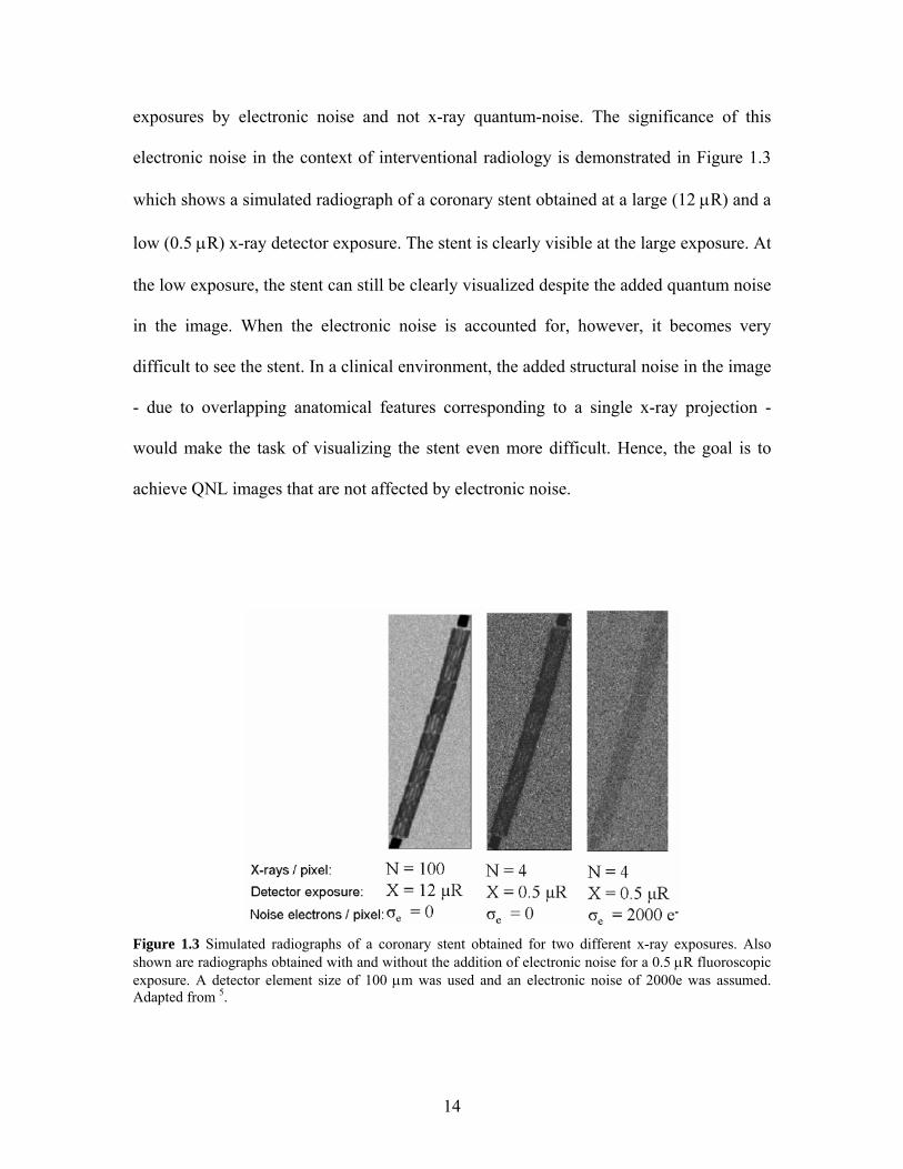
exposures by electronic noise and not x-ray quantum-noise. The significance of this
electronic noise in the context of interventional radiology is demonstrated in Figure 1.3
which shows a simulated radiograph of a coronary stent obtained at a large (12 µR) and a
low (0.5 µR) x-ray detector exposure. The stent is clearly visible at the large exposure. At
the low exposure, the stent can still be clearly visualized despite the added quantum noise
in the image. When the electronic noise is accounted for, however, it becomes very
difficult to see the stent. In a clinical environment, the added structural noise in the image
- due to overlapping anatomical features corresponding to a single x-ray projection -
would make the task of visualizing the stent even more difficult. Hence, the goal is to
achieve QNL images that are not affected by electronic noise.
Figure 1.3 Simulated radiographs of a coronary stent obtained for two different x-ray exposures. Also shown are radiographs obtained with and without the addition of electronic noise for a 0.5 µR fluoroscopic exposure. A detector element size of 100 µm was used and an electronic noise of 2000e was assumed. Adapted from 5.
14

1.5 Possible solutions for quantum noise limited AMFPIs
We have therefore demonstrated that significant reductions of electronic noise are
unlikely. Thus, techniques for overcoming it must involve the production of a large
amount of charge for each x-ray interaction. There have been essentially three solutions
proposed towards this end, as summarized in Table 1.2. The first involves the use of
high-gain photoconductors22,23 which generate larger numbers of EHPs for each incident
x-ray photon, thus providing a stronger signal than a-Se or amorphous silicon, the two
predominantly used materials in direct and indirect conversion AMFPIs, respectively. As
well as higher gain, the new materials being developed (eg. PbI2, PbO or HgI2) have
higher atomic numbers (Z), which in addition enables better x-ray absorption per unit
thickness than a-Se, and as such they are being developed for use as direct-conversion
imagers. Because of the relatively small thickness of these high-gain photoconductors (~
100 – 300 µm) required for a reasonable quantum efficiency, a considerably lower high
voltage (HV) bias may be used than what is being used in current direct-conversion
imagers with a relatively small Z (~10 kV).23 Many of these materials can also be directly
deposited on TFT arrays using techniques such as physical vapor deposition. A
disadvantage with high-gain photoconductors is that, although they can provide adequate
gain to overcome electronic noise at low fluoroscopic exposures, the fixed internal gain
may be too high at the larger exposures used in cine acquisitions and especially in
radiography. The large amount of image charge produced in these modes of operation
will produce a large voltage across the small del storage capacitance, leading to
breakdown of the dielectric (usually an oxide layer). High-gain photoconductors also are
difficult to deposit into large defect-free areas, suffer from limited charge range, have
15

considerably large dark currents in the polycrystalline state and raise environmental
concerns. Thus, there are still many challenges to be overcome before these materials can
be used in practical x-ray imagers.
A second method for overcoming electronic noise consists of using readout circuits
known as active pixels which incorporate low-noise amplifiers at each del.24 Unlike most
current AMFPIs in which a single TFT is used at each del as a switch that is either open
or closed, active pixel circuits combine several TFTs of which at least one operates as an
analog amplifier. These amplifiers provide the necessary gain for QNL operation in x-ray
imagers. Active pixels are compatible with existing photoconductors and photodiodes, so
they can be used in both direct and indirect conversion imagers. Specialized designs of
the active pixel circuit enable each del to be read out multiple times allowing electronic
noise to be further reduced by signal averaging.25 Similar to high-gain photoconductors,
they have also typically had a fixed internal gain, leading to the development of
undesirably large del voltages in cine and radiography (del saturation). However, a new
design has recently been proposed that enables the amplifier function to be disabled at
sufficiently large x-ray exposures. In this state, each del can be made to function as a
simple charge storage and switch, as is the case in most existing AMFPI designs (known
as the passive pixel sensor approach).25 The major disadvantage of active pixels is the
significantly increased complexity caused by the presence of multiple TFTs at each del,
rendering the manufacturing process significantly more difficult and hence costlier than
for passive pixel designs. They may also require the use of re-crystallized amorphous
silicon (a-Si) or “poly-silicon” instead of the more commonly available a-Si.26 Because
16

one or more TFTs at each del operate as an analog amplifier, these devices are also
significantly more prone to radiation damage than passive pixel devices in which each
TFT is either in an On or Off state. Furthermore, the TFTs have varying electrical
characteristics and corrections are often required so that they produce the same analog
signals for identical exposure conditions.
The third approach, and the one investigated in this thesis takes advantage of the physical
process of avalanche multiplication in a-Se.18,27 which is a very well characterized
material used in a number of current AMFPI systems, particularly in mammography, and
has a long history of use in radiographic imaging plates.28-30 It has recently been
developed for use in a low-cost laser readout imager by Fujifilm. a-Se has been the
photoconductor of choice for direct-conversion imagers, due to its high intrinsic imaging
resolution, low dark current and good charge transport of both holes and electrons.31 The
manufacturing process, which uses large-area thermal evaporation, is well established
and relatively inexpensive. Furthermore, because it is a low-temperature process, a-Se
can be directly evaporated on the TFT readout array without affecting the operation of the
array. The avalanche gain, which strongly depends on the applied HV bias, is adjustable
to a very large degree. Hence, the gain can be increased at very low fluoroscopic x-ray
exposures -- by increasing the bias -- to overcome electronic noise and reduced or
eliminated – by reducing the bias – prior to radiographic exposures to prevent del
saturation. The main disadvantages with the use of a-Se as a photoconductor have to do
with the large bias voltages that need to be applied to achieve a reasonable effective work
function Weff (the required amount of absorbed x-ray energy to produce a single EHP that
17

survives recombination and whose charge is collected). Typically, an electric field of 10
V/µm is required to achieve a Weff of about 40 eV for diagnostic x-ray energies.32 A
significantly lower Weff (about 4 times) - approaching that of high-gain photoconductors
discussed above - may be obtained by increasing the field to 75 V/µm.18 An electric field
exceeding 75 V/µm is required to initiate avalanche multiplication. Furthermore thick
films (~ 1000 µm) of a-Se are required to obtain a reasonable quantum efficiency at
radiographic x-ray energies. Despite these limitations, the low dark current, compatibility
with existing TFT array technology, adjustable avalanche gain and good charge transport
properties make a-Se a very promising photoconductor material for QNL AMFPIs.
Furthermore, a-Se can also be used as an avalanche photoreceptor in indirect-conversion
AMFPIs.33 In this case, thin films of a-Se (~ 10 µm) may be used to detect light photons
generated by a phosphor.
Table 1.2. Summary of the advantages and disadvantages of three different approaches for overcoming electronic noise at low x-ray exposures in AMFPIs. Advantages Disadvantages High-gain photoconductors (PbI2, PbO or HgI2)
• high Z materials offer better x-ray absorption than a-Se for direct-conversion
• lower bias voltage required compared to a-Se for direct-conversion
• compatible with existing TFT arrays
• fixed high-gain • limited charge range • difficult to deposit into
large defect-free areas • considerably large
dark current • environmental
concerns Active pixels • compatible with existing
photoconductor/photodiode technologies
• specialized designs enable multiple readouts of each del
• fixed high-gain • more TFTs per del • prone to radiation
damage
Avalanche a-Se multiplication gain
• good charge transport of both holes and electrons
• adjustable avalanche gain • compatible with existing TFT
arrays • largely scalable deposition • very low dark current
• large bias voltages required
• thick films required for direct-conversion
• depth gain fluctuation noise for direct-conversion
18

1.6 High-gain avalanche rushing photoconductor (HARP) technology 1.6.1 HARP camera
Soon after the discovery of avalanche multiplication in a-Se in 1980 34, Tanioka and co-
workers at the Japanese Broadcasting Corporation (NHK) Science and Technology
Laboratories developed and later commercialized the HARP broadcasting camera in
conjunction with companies such as Hamamatsu Corp.35 The key component in the
camera is a layered HARP structure which consists of a-Se and blocking layers, as
depicted in Figure 1.4. The hole and electron blocking layers enable the application of a
very large electric field E while minimizing the amount of charge injected into the a-Se at
both contacts. Optical photons create EHPs in the a-Se layer. Holes undergo avalanche
multiplication as they are swept through the layer under the influence of E. A scanning
electron beam is used to raster scan the free surface of the HARP. In regions on the
surface where photon-generated holes have accumulated, more electrons will be drawn
from the electron beam to neutralize the charge in that region, thus temporarily increasing
the beam current. By monitoring the current entering the HARP through the readout
electrode during the scanning process, the spatial distribution of photon-generated holes
can be inferred. This distribution corresponds to the distribution of light photons (i.e. the
optical image) absorbed in the a-Se near the transparent conductive electrode. Low-noise
operation of the HARP is strongly reliant on the blocking contacts. This is because
charge injection at the electrodes contributes to dark current and this produces a form of
noise known as shot noise which is caused by the statistical fluctuations of charge in the
electric current.16 The hole blocking contact is particularly important, since injected holes
can experience the same degree of avalanche multiplication as photon-generated holes,
19

producing a very large degree of shot noise. Hence, the amount of avalanche gain that
can be obtained from a HARP layer with any given thickness of a-Se is limited by the
largest electric field strength that can be applied without producing a significant amount
of dark current shot noise. Tanioka and colleagues demonstrated avalanche gains as high
as one thousand in a HARP camera with a 15 µm thick a-Se layer.36 Shown in Figure 1.4
(b) are optical images taken with a HARP camera showing a portion of an oscilloscope
panel in a nearly completely dark room. As the electric field is increased beyond 100
V/µm, the image becomes very clear. This demonstrates that avalanche gain can be used
for imaging objects in photon-starved conditions (eg. very low-light conditions).
free surface
readout electrode (a)
Figure 1.4 (a) Diagram illustrating the principle of operation of a HARP camera tube. Optical photons create electron hole pairs in the a-Se layer. Holes undergo avalanche multiplication as they are swept through the layer under the influence of an electric field E. A scanning electron beam is used to read out the resulting charge image on the free surface (i.e. no conducting electrode). (b) Optical images (showing five buttons on an oscilloscope panel) obtained from a HARP camera for different applied electric fields. These images were obtained in a nearly completely dark room.
20

Recently, Hunt has theoretically investigated the use of HARP technology for
applications in fluoroscopy.18,27 It has been identified that a HARP layer could provide
adjustable gain at the photodetector stage and that a gain of ~50 is required to completely
overcome the electronic noise at the lowest fluoroscopic exposures and thus yield a QNL
AMFPI.37 However, theoretically it is expected and experimental work on direct
interaction of diagnostic energy X rays with HARP layers has recently revealed the
presence of substantial depth-dependent gain fluctuation noise. This type of noise is
caused by the absorption of X rays at different depths in the a-Se, producing holes that
undergo largely varying degrees of avalanche gain depending on how far they have to
travel through the a-Se to reach the negative electrode (i.e. the farther the travel path, the
larger the resulting avalanche gain due to an increased number of impact ionizations). As
a result, HARP technology itself is not directly compatible with a direct-conversion x-ray
detection scheme. It has been established, however, that specialized direct-conversion
imager architectures could, in principle eliminate depth-dependent gain fluctuation
noise.27,38 A promising imager architecture consists of a thick (~ 1 mm) a-Se layer having
a low electric field strength (10 V/µm) used for x-ray charge production coupled to a
HARP layer used for avalanche multiplication of the x-ray-produced charge.
1.6.2 The need for a solid-state HARP
Although current HARP camera systems provide excellent image quality and sensitivity
and are well adapted for video and broadcasting applications, their direct applicability to
AMFPIs is greatly limited because radiological imaging applications require a large
21
photosensitive area (commensurate with the anatomical region being imaged). Clearly,
using a scanning electron beam readout approach would result in a device similar in size
to a cathode ray tube television, which is undesirable. A more compact approach, known
as field emission array39, involves the use of a number of electron emitting tips (known as
Spindt tips) at each del. The electrons emitted from these tips are focused using a mesh
electrode onto the free surface of the HARP. This approach has been demonstrated for a
small area detector.40 It remains to be seen, however, whether this technology is truly
scalable as the challenge of establishing a necessary thin vacuum gap between the
electron-emitting tips and the HARP layer over a large area is substantial.
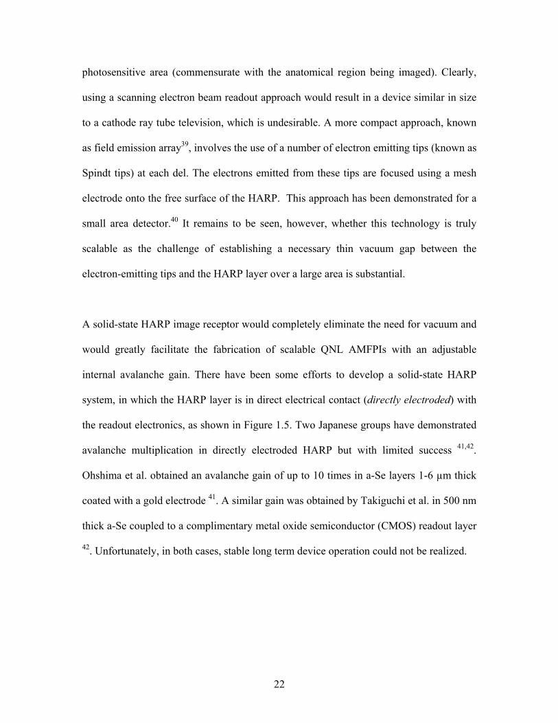
A solid-state HARP image receptor would completely eliminate the need for vacuum and
would greatly facilitate the fabrication of scalable QNL AMFPIs with an adjustable
internal avalanche gain. There have been some efforts to develop a solid-state HARP
system, in which the HARP layer is in direct electrical contact (directly electroded) with
the readout electronics, as shown in Figure 1.5. Two Japanese groups have demonstrated
avalanche multiplication in directly electroded HARP but with limited success 41,42.
Ohshima et al. obtained an avalanche gain of up to 10 times in a-Se layers 1-6 µm thick
coated with a gold electrode 41. A similar gain was obtained by Takiguchi et al. in 500 nm
thick a-Se coupled to a complimentary metal oxide semiconductor (CMOS) readout layer
42. Unfortunately, in both cases, stable long term device operation could not be realized.
22

Figure 1.5 Diagram of a directly electroded HARP. The HARP consists of a transparent indium tin oxide (ITO) electrode deposited on a glass substrate (not shown). The hole blocking contact, a-Se and electron blocking contact are deposited on the ITO electrode. Discrete del electrodes are next deposited on top of the HARP structure.
1.7 Rationale and problem formulation
The key clinical requirements for a solid-state x-ray imager for interventional radiology
are, as recapitulated from section 1.3: (1) quantum-noise limited (QNL) operation at the
lowest clinical fluoroscopic x-ray exposures (in conformance with the ALARA
principle), (2) capability for modes of operation that require significantly higher x-ray
exposures and (3) capability of imaging fine features of interventional devices or lesions.
No existing solid-state imaging system simultaneously satisfies all three requirements.
Avalanche multiplication of charge in a-Se can provide sufficient gain to satisfy
requirement (1) and the highly adjustable avalanche gain should also satisfy requirement
(2). Furthermore, the high intrinsic imaging resolution of a-Se should also answer
requirement (3). This suggests that a-Se is a very good candidate as a photoconductor for
23

use in x-ray imaging in interventional radiology. However, the following problems need
to be addressed, and they establish the three major questions which this thesis shall
answer: (A) can a-Se reliably provide avalanche multiplication gain in the solid state? (B)
how can a solid-state avalanche a-Se photoreceptor be used for imaging X-rays? (C) can
a solid-state avalanche a-Se photoreceptor practically satisfy all the four imager
requirements for interventional radiology?
1.8 Thesis outline
First, a method is developed which enables the application of avalanche-grade electric
fields across a-Se layers in the solid state (Chapter 2). This method is aimed at addressing
the problematic occurrence of electrical discharges seen in prior attempts to directly
electrode a-Se photoconductors. The electrical breakdown properties and gain
characteristics of this solid-state avalanche device are experimentally investigated. Once
it is demonstrated that sufficient avalanche multiplication gain can be obtained for QNL
operation, the next step is to investigate suitable detector architectures for imaging X-rays
(Chapter 3). Both indirect and direct conversion architectures are examined and
compared. However, since a feasibility study of an indirect-conversion detector has
already been completed, the central focus of this chapter will be on the feasibility of a
direct-conversion x-ray detector with a built-in avalanche layer. This consists of a
theoretical investigation of several key figures of merit which evaluate the detector’s
imaging performance. At this point in the thesis, it will become clear that a solid-state
24

avalanche a-Se photoreceptor can be realized and that it can be used as a direct or indirect
x-ray detector with sufficient spatial resolution for advanced interventional radiology
applications. However, it remains to be seen whether the avalanche a-Se photoreceptor
meets all the specific requirements for use as an interventional radiology imager (Chapter
4). Hence, the last major thesis chapter will investigate such topics as the photoreceptor
noise (for proper QNL operation), x-ray exposure range of operation (for cine and
radiographic imaging modes), and compatibility with existing solid-state image readout
electronics (for realization of a compact imaging system). Lastly, the thesis results are
summarized and future research opportunities are identified. It should be noted that both
Chapters 2 and 4 are largely comprised of experimental work and Chapter 3 is entirely
theoretical.
25

References
1 T. S. Curry, J. E. Dowdey, and R. C. Murry, Christensen's Physics of Diagnostic
Radiology. (Lipnicott Williams & Wilkins, 1990), fourth ed.
2 J-M. Correas, L. Bridal, A. Lesavre, A. Méjean, M. Claudon, and O. Hélénon,
"Ultrasound contrast agents: properties, principles of action, tolerance, and
artifacts," European Radiology 11, 1316-1328 (2001).
3 M. Yumi, M. Kenji, Y. Shusaku, and N. Hiromu, "Early clinical experience on
cone-beam CT," Journal of Digital Imaging 11 (Suppl 1), 211-213 (1998).
4 U. Missler, C. Hundt, M. Wiesmann, T. Mayer, and H. Brückmann, "Three-
dimensional reconstructed rotational digital subtraction angiography in planning
treatment of intracranial aneurysms," European Radiology 10, 564-568 (2000).
5 S. Rudin, W. Ye, I. S. Kyprianou, C. N. Ionita, Z. Wang, A. Ganguly, and D. R.
Bednarek, "Micro-angiographic detector with fluoroscopic capability," Proc. SPIE
4682, 344-354 (2002).
6 L. Wexler, B. Brundage, J. Crouse, R. Detrano, V. Fuster, J. Maddahi, J.
Rumberger, W. Stanford, R. White, and K. Taubert, "Coronary Artery
Calcification: Pathophysiology, Epidemiology, Imaging Methods, and Clinical
Implications," Circulation 94, 1175-1181 (1996).
7 J. M. Hernandez and F. S. Laso, "Coronary Angiography with Flat Panel Digital
Detectors Significantly Increases the Sensitivity for Calcium Detection in
Relation to Conventional Fluoroscopy: Comparison of Both Systems with
Intravascular Ultrasound," Journal of Invasive Cardiology 17 (7), 365-372 (2005).
26

8 P. Zwet, D. Meyer, and J. Reiber, "Automated and accurate assessment of the
distribution, magnitude and direction of pin-cushion distortion in angiographic
images.," Invest Radiol 30, 204-213 (1995).
9 D. Holmes, W. Laskey, M. Wondrow, and J. Cusma, "Flat-panel detectors in the
cardiac catheterization laboratory: Revolution or evolution - What are the
issues?," Catheter Cardiovasc Interv 63, 324-334 (2004).
10 S. Rudin, D. Bednarek, and R. Wong, "Accurate characterization of image
intensifier distortion," Med. Phys. 18, 1145-1151 (1991).
11 M. Spahn, V. Heer, and R. Freytag, "Flat-panel detectors in X-ray systems,"
Radiologe 43, 340-351 (2003).
12 J. Seibert, "Flat-panel detectors: how much better are they?," Pediatr. Radiol. 36,
173-181 (2006).
13 J.A. Rowlands and J. Yorkston, "Flat Panel Detectors for Digital Radiography," in
Handbook of Medical Imaging, edited by J. Beutel, H. Kundel, and R. Van Metter
(SPIE, Bellingham, Washington, 2000), Vol. I.
14 J. Jesneck, R. Saunders, E. Samei, J. Xia, and J. Lo, "Detector evaluation of a
prototype amorphous selenium-based full field digital mammography system,"
Proc. SPIE 5745, 478-485 (2005).
15 F. Bochud, F. Verdun, C. Hessler, and J-F. Valley, "Detectability of radiological
images: the influence of anatomical noise," Proc. SPIE 2436, 156-164 (1995).
16 H. Ott, Noise Reduction Techniques in Electronic Systems. (Wiley Interscience,
1988), Second ed.
27
17 L. Antonuk, K. Jee, Y. El-Mohri, M. Maolinbay, J. Siewerdsen, S. Nassif, X.
Rong, Q. Zhao, R. Street, and K. Shah, "Strategies to improve the signal and noise
performance of active matrix, flat-panel imagers for diagnostic x-ray
applications," Med. Phys. 27, 289-306 (2000).
18 D. Hunt, S. Kirby, and J. Rowlands, "X-ray imaging with amorphous selenium:
X-ray to charge conversion gain and avalanche multiplication gain," Med. Phys.
29, 2464-2471 (2002).
19 J. H. Siewerdsen, L.E. Antonuk, Y. El-Mohri, J. Yorkston, W. Huang, and I.A.
Cunningham, "Signal, noise power spectrum, and detective quantum efficiency of
indirect-detection flat-panel imagers for dagnostic radiology," Med. Phys. 25,
614-628 (1998).
20 D. C. Hunt, S. S. Kirby, and J. A. Rowlands, "X-ray imaging with amorphous
selenium: X-ray to charge conversion gain and avalanche multiplication gain,"
Medical Physics 29 (11), 2464-2475 (2002).
21 Z. S. Huang, G. DeCrescenzo, and J. A. Rowlands, "Signal and noise analysis
using transmission line model for larger area flat-panel x-ray imaging sensors,"
Proc. SPIE 3659, 76-89 (1999).
22 R. A. Street, "High resolution, direct detection X-Ray imagers," Proc. SPIE 3977,
418-425 (2000).
23 G. Zentai, "Mercuric iodide and lead iodide x-ray detectors for radiographic and
fluoroscopic medical imaging," Proc. SPIE 5030, 77-88 (2003).
28

24 K. S. Karim, Y. K. Vygranenko, D. A. Striakhilev, A. Nathan, S. Germann, J. A.
Rowlands, G. Belev, K. Koughia, R. Johanson, and S. O. Kasap, "Active pixel
image sensor for large-area medical imaging," Proc. SPIE 5030, 38-47 (2003).
25 K.S. Karim, M.H. Izadi, F. Taghibakhsh, and G. Sanaie, "Intelligent pixel
architectures for digital medical imaging applications," ECS Transactions 8, 289-
293 (2007).
26 L. Antonuk, M. Koniczek, Y. El-Mohri, and Q. Zhao, "Active pixel and photon
counting imagers based on poly-Si TFTs: rewriting the rule book on large area
flat panel x-ray devices," Proc. SPIE 7258, 725810-725814 (2009).
27 D. C. Hunt, "Investigation of Avalanche Multiplication in Amorphous Selenium
for Use in Digital Fluoroscopy", PhD Thesis, University of Toronto (2005).
28 H. Guilleminot, "Use of selenium in the radiometry of Rontgen rays," Archives
d'Electricite Medicale 23, 168-173 (1915).
29 C. Luraschi, "New apparatus for measuring the intensity and quantity of Rontgen
rays," Archives d'Electricite Medicale 16, 14-26 (1908).
30 A. Nemet, A. W. Balls, and W. F. Cox, "Xeroradiography applied to the
inspection of electrical equipment," Proc. Inst. Electr. Eng. 109A, 184-188
(1962).
31 J. A. Rowlands and G. DeCrescenzo, "X-ray imaging using amorphous selenium:
Determination of x-ray sensitivity by pulse height spectroscopy," Med. Phys. 19,
1065-1069 (1992).
29

32 J.A. Rowlands and J. Yorkston, "Flat Panel Detectors for Digital Radiography," in
Handbook of Medical Imaging, edited by J. Beutel, H. Kundel, and R. Van Metter
(SPIE, Bellingham, Washington, 2000), Vol. I.
33 W. Zhao, D. Li, A. Reznik, B. J. M. Lui, D. C. Hunt, J. A. Rowlands, Y. Ohkawa,
and K. Tanioka, "Indirect flat-panel detector with avalanche gain: Fundamental
feasibility investigation for SHARP-AMFPI (scintillator HARP active matrix flat
panel imager)," Med. Phys. 32, 2954-2966 (2005).
34 G. Juska and K. Arlauskas, "Impact Ionization and Mobilities of Charge Carriers
at High Electric Fields in Amorphous Selenium," Phys. Stat. Sol. 59, 389-395
(1980).
35 K. Miyakawa, Y. Ohkawa, T. Matsubara, T. Takahata, S. Suzuki, and M. Kubota,
"Ultrahigh-sensitivity HDTV New Super-HARP Camera," Proc. SPIE 5677, 26
(2005).
36 K. Tanioka, T. Matsubara, Y. Ohkawa, K. Miyakawa, S. Suzuki, T. Takahata, N.
Egami, K. Ogusu, A. Kobayashi, T. Hirai, T. Kawai, M. Hombo, and T. Yoshida,
"Ultra-high-sensitivity new super-HARP pickup tube and its camera," IEICE
Trans. on Elec. E86C, 1790-1795 (2003).
37 W. Zhao, D. Li, A. Reznik, B. Lui, D. C. Hunt, Kenkichi Tanioka, and J. A.
Rowlands, "Indirect flat-panel detector with avalanche gain: Design and operation
of the avalanche photoconductor," Proc. SPIE 5745, 352-364 (2005).
38 D. C. Hunt, K. Tanioka, and J. A. Rowlands, "X-ray imaging using avalanche
multiplication in amorphous selenium: Investigation of depth dependent
avalanche noise," Med. Phys. 34, 976-986 (2007).
30

39 D. Li and W. Zhao, "Avalanche detector with field emitter readout," in IEEE
Bioengineering Conference (2007), pp. 67-68.
40 D. Li and W. Zhao, "SAPHIRE (scintillator avalanche photoconductor with high
resolution emitter readout) for low dose x-ray imaging: Spatial resolution," Med.
Phys. 35, 3151-3161 (2008).
41 T. Ohshima, K. Tsuji, K. Sameshima, T. Hirai, K. Shidara, and K. Taketoshi,
"Excess Noise in Amorphous Selenium Avalanche " Japanese Journal of Applied
Physics 30 (6B), L1071-L1074 (1991).
42 Y. Takiguchi, H. Maruyama, M. Kosugi, F. Andoh, T. Kato, and K. Tanioka, "A
CMOS Imager Hybridized to an Avalanche Multiplied Film," IEEE Trans.
Electronic Devices 44 (10), 1783-1788 (1997).
31

Chapter 2 Development of a solid-state amorphous selenium avalanche photoreceptor 2.1 Introduction 2.2 Theory 2.3 Methods 2.3.1 Distributed resistive layer 2.3.2 Experimental setup 2.3.3 Linearity 2.3.4 Gain and dark current 2.3.5 Carrier transport 2.4 Results
2.4.1 Breakdown characteristics 2.4.2 Linearity 2.4.3 Gain and dark current 2.4.4 Carrier transport
2.5 Discussion 2.5.1 Breakdown characteristics 2.5.2 Linearity 2.5.3 Gain and dark current 2.5.4 Carrier transport
2.6 Conclusions
This chapter combines selected material from the following: • U.S.A. Provisional Patent No. 61/129389 Matthew M. Wronski et al.
Photodetector/Imaging Device with Avalanche Gain, filing date: June 23, 2008 • M. Wronski et al., “A solid-state amorphous selenium avalanche technology for large
area photon counting and photon starved imaging applications” to be submitted as a letter to Med. Phys.
• M. Wronski et al., “A solid-state avalanche photoreceptor for low-exposure x-ray imaging applications” to be submitted to Med. Phys.
32

2.1 Introduction The X-ray image intensifier is able to overcome electronic noise because it provides an
internal gain. One of the objectives of this thesis, and the purpose of this chapter, is to
develop a solid-state device, based on amorphous selenium (a-Se), with a similar
capability.
The principal challenge with realizing avalanche multiplication in a-Se is that it requires
the application of a large electric field (E ~ 100 V/µm). HARP technology has been
shown to provide avalanche gains gav ~ 10 with metal contacts deposited on the HARP
(electroded HARP).1,2 This, however, was the maximum gain that could be achieved
prior to failure of the device. The amount of avalanche gain required for quantum noise
limited (QNL) operation throughout the entire clinical range of fluoroscopic x-ray
exposures is approximately 50.3 Since avalanche multiplication gain is exponentially
dependent on E, only a slight improvement in the HARP structure is required to provide
the required gain for QNL operation.
To better understand the failure process in electroded HARP, we first develop a model
that estimates the maximum amount of energy in a spontaneous electric discharge. The
model provides insight into how this energy may be limited, leading to the development
of an experimental method which enables the practical application of significantly larger
electric field strengths across the HARP. The application of larger electric field strengths
in turn enables much larger avalanche gains. Prior to measuring the gain, however, the
linear range of operation is identified for the avalanche detector such that its response
33

remains unaffected by the significant amounts of charge produced by avalanche
multiplication. This enables an accurate gain and dark current characterization, providing
an indication on whether the avalanche detector can achieve a sufficient degree of
sensitivity for QNL operation. The final goal of this chapter is to confirm the presence of
avalanche multiplication in the newly-developed solid-state detector. This is done by
examining the transport of electric charge carriers inside the detector at both sub-
avalanche and avalanche electric field strengths. This analysis also enables the
measurement of carrier mobility (holes in particular), providing a useful point of
comparison between HARP a-Se and standard a-Se used in conventional radiographic
imaging plates.
2.2 Theory
Thus far, electroded HARP has been limited1 to avalanche gains gav < 10. Much larger
gains have been achieved in the HARP camera tube (gav ~ 103). This suggests that there
is no limitation in the HARP structure itself to achieving high gain. Rather, the means by
which the HARP is electrically contacted needs improvement to accomplish a completely
solid state solution.
There are two important mechanisms that potentially underlie the breakdown process in
electroded HARP. The first has to do with the electric field enhancement near the sharp
edges of conductive electrodes. This large field can cause excessive charge injection at
34

the electrode, despite the presence of blocking contacts, causing high localized current
densities. The second mechanism is a positive feedback process in which a large current
density resulting from either excessive charge injection or simply from an electric
discharge results in a localized deposition of heat (Joule heating), causing the a-Se to
crystallize. Since crystalline selenium has a larger electrical conductivity than a-Se, the
discharge region begins to draw a larger current which in turn produces yet more heat.
Due to sustained heating, this process causes the crystallization to spread to a larger area
over time.
Hence, in principle, failure in electroded HARP can be mitigated by (1) eliminating the
electric field enhancement near the sharp edges of conductive electrodes and (2)
quenching electrical discharges or excessive charge injection which ultimately lead to
crystallization of the a-Se. In principle, problems (1) and (2) stated above may be
addressed by introducing a distributed resistance layer (DRL), as shown in Figure 2.1.
This layer, which can be deposited on top of the HARP structure should (1) reduce the
electric field in the vicinity of electrode edges and (2) provide a mechanism to limit the
current flow in regions of incipient failure.
35

Figure 2.1. (b) Diagram of the directly electroded HARP where the photon-generated charge is collected by means of conductive del electrodes. The dashed horizontal lines represent electric field lines. The bending of field lines near the del electrode edges produces regions of electric field enhancement (stress points) (c) In DRL-HARP, the addition of a distributed resistive layer (DRL) eliminates stress points near del electrodes - due to the negligible electric field in the DRL - and enables the significant reduction of discharge currents (Idis) - due to the series resistance of the DRL - while maintaining the same voltage bias VHARP across the HARP.
A model is now developed to better understand the failure process and quantify the
current-limiting effect of the DRL. One could use Joule’s first law which relates the
amount of heat produced by a current flowing through a resistance, however the exact
current and resistance in the discharge region are unknown and change rapidly during a
discharge event. Rather, an energy model can be used to estimate the upper bound on the
energy available for instantaneous heating during an electric discharge. The energy Ed
accumulated on the del capacitance Cd with an applied voltage Vd is 2
21
ddVC .
When an electrical discharge occurs over some small area ∆A of the HARP, this region
provides a conductive path for Ed (Figure 2.3). Assuming a reasonable ∆A =10 µm x 10
µm, Cd = 1 pF (for a 1 mm2 PEDOT (Poly(3,4-ethylenedioxythiophene)) electrode) an a-
Se heat capacity and density of 25 J/mol·K and 5 g/cm3, respectively, and adiabatic
conditions, then if Ed was entirely dissipated as heat, it would raise the temperature in the
discharge region by over 600 degrees Kelvin. Since heat would not be removed fast
36

enough from the a-Se, this could lead to a-Se crystallization. From a materials science
perspective this can be conveniently represented in the form of a time-temperature-
crystallization (TTC) diagram as shown in Figure 2.2. This diagram shows how the
duration of an electrical discharge in a-Se affects the occurrence of phase transformation.
In the case of a rapid discharge, the a-Se temperature rises quickly. During the slow
cooling process in which the a-Se temperature returns to room temperature, there is
sufficient time and thermal energy for the a-Se to undergo a phase transformation and
assume the lower energy crystalline state. However, if the electrical discharge is slow,
heat generation is distributed in time and because cooling occurs simultaneously, the
maximum a-Se temperature reached is much lower. If the discharge is sufficiently slow,
the a-Se will not crystallize.
Figure 2.2. Time-temperature-crystallization (TTC) diagram showing how the duration of an electrical discharge in a-Se affects the occurrence of phase transformation. In the case of a rapid discharge, the a-Se temperature (T) rises quickly. During the following slow cooling process in which T returns to room termperature, there is sufficient time (t) and thermal energy for the a-Se to undergo a phase transformation and assume the lower energy crystalline state. If the electrical discharge is slow, however, heat generation is distributed in time and because cooling occurs simultaneously, the maximum a-Se temperature reached is much lower. If the discharge is sufficiently slow, the a-Se will not undergo a phase transformation.
37

Using the right-hand circuit diagram in Figure 2.3, we can develop a model that takes
into account the slower rate of discharge due to the DRL. In this case, the discharge
current traverses through a resistance-capacitance (RC) network whose time constant can
be approximated as follows:
effd
DRL
N
x xSe
N
xxSe
RC
RR
C≈
∆+
∆
∆≈
−= −
=−
∑
∑
12
2
11τ , Eq. 2.1
where N is the number of distributed RC elements, Reff is the effective series resistance in
the discharge region and the ∆RSe-x term can be ignored because the a-Se resistance is
very high (> 100 TΩ/mm2). Within τ, the amount of heat ∆Q dissipated from the
discharge region (to the underlying glass substrate) can be calculated as follows:
dTAkQ ∆
∆⋅⋅=∆ τ , Eq. 2.2
where k is the thermal conductivity of a-Se, ∆T is the difference between the temperature
in the discharge region and room temperature and d is the a-Se thickness (i.e. the longest
distance the heat must travel to exit the discharge region into the glass substrate). Then,
Ed/∆Q can be used to express the ratio between the heat generating and heat sinking
processes. Using Eqs. 2.1 and 2.2 above, this gives:
TAkRdV
TAkRC
dVC
QE
eff
d
effd
ddd
∆⋅∆⋅∆⋅∆⋅=
∆
22
~21
, Eq. 2.3
38

Figure 2.3. Diagrams illustrating the electrical discharge paths in electroded HARP (left) and electroded DRL-HARP (right). A distributed resistance-capacitance network is assumed with an arbitrarily large series current limiting resistance RS. The HARP and DRL are modeled as cells (numbered 1 through x) each consisting of a capacitance ∆C and resistance ∆R in parallel. When a discharge occurs (i.e. ∆R 0 in one or more of the HARP cells), the total energy E stored in the HARP flows through one or more cells. When a DRL layer is present, the discharge current is forced through a narrow region of the DRL having a very large resistance.
It can be appreciated from Eq. 2.3 that for a discharge region size ∆A ~ 10 µm x 10 µm,
using RDRL ~ 10 GΩ/mm2 and thus Reff >> 1 TΩ and Vd = 1500 V, then even for an
arbitrarily small temperature gradient ∆T = 1 deg K, Ed/∆Q << 1. Furthermore, it can be
seen that for this to remain true, RDRL > 0.1 GΩ/mm2. According to this conservative
model, this would be a sufficient (although not necessary) resistance for the DRL to
prevent a-Se crystallization, because the heat produced by the discharge is removed from
the a-Se at a faster rate than it is generated and so it does not accumulate.
39

2.3 Methods
2.3.1 Distributed resistive layer
In addition to preventing a-Se crystallization as discussed in section 2.2, the material for
the DRL needs to be chosen such that (1) during normal operation, essentially all of the
HV bias is applied across the a-Se layer and (2) there is no significant lateral conduction
(leakage) of charge between neighboring dels. If we assume a del size and capacitance of
100 µm x 100 µm and 0.5 pF, respectively, and a dark current of 10 pA/mm2, then an
insignificant potential drop across the DRL = 0.1 V per micrometer of thickness
would require a material with a volume resistivity of the order
DRLV
≈RLρ 1012 Ω·cm, thus
satisfying the first condition. Assuming a DRL thickness of the order of 1 µm, this would
be equivalent to a lateral (sheet) resistance ≈latR 1016 Ω/square. Assuming a 10 µm
spacing between dels, this translates into a time constant for lateral charge conduction
≈latτ 600 s. Since the time during which the latent image charge is stored at each del of
the imager prior to being converted into a digital signal is on the order of 10 ms,4 lateral
charge leakage between neighboring dels should be negligible, thus satisfying the second
condition.
Cellulose acetate (CA) satisfies the resistivity requirements outlined above
( Ω·cm). CA films having a thickness of 1 µm or more would have an
estimated series resistance R
105 12⋅=CAρ
DRL > 50 GΩ/mm2, which, according to the model in section
2.2 should be more than sufficient to quench electrical discharges leading to a-Se
crystallization. Furthermore, CA bonds well to a-Se and has been used as a protective
40

overcoating in a-Se xeroradiographic plates and in this application was shown5 to extend
the plate life by about a factor of 10. For these reasons, it is a good choice for the DRL.
In order to optimize the thickness and electrical performance of the CA layer
experimentally, we used different concentrations of CA in an acetone solvent and then
measured the resulting film thickness and tested its capability of eliminating adverse
electrical discharges. The CA polymer was obtained in powder form from Eastman
Chemical. It was dissolved in CMOS grade acetone (J. T. Baker) in the following
concentrations: 2%, 4% and 8% by weight. The CA solution was then cast onto the
HARP samples. This process consisted of applying a controlled amount (2 mL) of CA
solution onto the surface of the HARP sample and the rate of evaporation of the solvent
was controlled by using an enclosure with a controlled ventilation (Figure 2.4). This was
found to prevent the denaturation (specifically, an increase in opacity) of the polymer and
enabled the fabrication of high-quality transparent films whose thickness scales with the
concentration of the CA solution. A profilometer (Dektak) was used to measure the
thickness of the CA layer. Conductive electrodes were formed on the CA layer by
applying a conductive polymer (PEDOT). A spring-loaded gold-plated pin was used to
form a pressure contact with the conductive electrode. When not in use, the coated
samples were stored in the dark in a dessicator at 23 0C.
41

Figure 2.4. Diagram illustrating the cellulose acetate (CA) casting process. A controlled amount of CA solution is first dispensed on the HARP target which is mounted on a copper plate. This is done such that the entire plate is coated with the solution. Next, the solvent in the CA solution is given time to evaporate. This is performed in an enclosure with a small opening to control the rate of evaporation. The HARP target is then removed from the plate by cutting the CA around its edge.
2.3.2 Experimental setup
For the purposes of gain measurements (described in section 2.3.4), optical excitation
using a light emitting diode (LED) was used. Since a-Se has a quantum efficiency > 95%
at blue wavelengths, a blue LED was used.3 The experimental setup is shown in Figure
2.5. There are several advantages of using this setup: (1) an optical fiber bundle is used to
couple the excitation light to the HARP. This eliminates any electrical interference that
could potentially be caused by the pulse generator; (2) blue light photons are absorbed in
a very shallow region at the HARP surface (first several-hundred nanometers). This
results in negligible gain-depth fluctuation noise;6 (3) the relative pulse intensity of the
LED can easily be calibrated using an auxiliary photon detector such as a photomultiplier
tube (PMT); (4) the LED pulse intensity can be varied over a very wide range (i.e. 6
orders of magnitude).
42

Figure 2.5. Diagram illustrating the experimental setup used for basic characterization of directly electroded HARP and DRL-HARP. Dark current measurements are performed by replacing the charge amplifier with an electrometer.
The HARP photocurrent was measured as a function of the applied voltage using a low-
noise current amplifier (Stanford Research) and the voltage was supplied from a high
voltage (HV) generator (Stanford Research). A fiber optic bundle (Thor Labs) was used
to channel the LED excitation to the HARP, and a photomultiplier tube (PMT)
(Hamamatsu) biased in the linear region of operation was used to quantify the intensity of
the LED source and ensure that the output signal from the device is linear with the LED
intensity.
2.3.3 Linearity
Since avalanche multiplication can produce a large amount of charge even for relatively
low exposures, this can result in an effect known as ghosting. This is usually manifested
as a change (usually a reduction) in sensitivity of a photoreceptor due to prior exposures.4
It is generally caused by the trapping of charge either in the bulk of the photoreceptor or
at interfaces between the photoreceptor and other materials and it typically produces
artifacts in images that are manifested as latent images from previous exposures (ghosts).
43

Any effect such as ghosting that changes the a-Se sensitivity as a result of prior exposures
affects the linearity of the photoreceptor response, that is the relationship between the
signal produced by the photoreceptor and the number of photons interacting with it.
Clearly, this can also affect the measurement of avalanche gain.
To determine the conditions in which gain measurements can be made accurately and
unaffected by any non-linearities, two experiments were performed using the setup
shown in Figure 2.5. In the first, the peak DRL-HARP photon-generated current was
measured as a function of LED pulse intensity at several different biases in the avalanche
regime. This would provide the range of LED intensities for which the detector response
remains linear, at avalanche electric field strengths. In the second experiment, the LED
pulse intensity remained constant and the transient response was recorded at different HV
biases, once again in the avalanche regime. In both experiments, 1 ms LED excitation
pulses were used.
2.3.4 Gain and dark current
The setup shown in Figure 2.5 was used to measure the gain of HARP-DRL as a function
of the applied electric field strength E. The amount of charge produced by a single optical
pulse in the HARP-DRL was controlled by reducing the source LED pulse intensity in
steps (thus maintaining it in the linear response range) as the HV bias – and thus the
avalanche gain – was increased. By recording the reduction factor in source intensity for
each step, the entire photocurrent gain characteristic was reconstructed. The DRL-HARP
44
gain data were compared with gain data obtained from HARP camera tubes with HARP
targets having the same a-Se layer thickness (15 µm).
Two models were used to fit the DRL-HARP gain characteristics. A three parameter
model was used to fit the conversion gain gc (for ESe < 75 V/µm) and McIntyre theory
was used to model the avalanche gain (ga) characteristics (for ESe > 75 V/µm). We
assumed that only holes avalanche in the a-Se which is a reasonable assumption for a-Se
biased near 100 V/µm.7,8 The models for the conversion and avalanche gains gc and ga
are given by the following two equations, respectively:
baEEgSe
Sec += , Eq. 2.4
SeESe ed
a eg/2
1ββ −
= Eq. 2.5
where 1/a is the value of gc at infinite field, b is the electron-hole pair recombination
term, dSe is the a-Se thickness and β1 and β2 are the impact ionization factors of a-Se.
Dark current was measured using the setup shown in Figure 2.5, with an electrometer
(Keithley) in place of the charge amplifier. Each measurement was taken several minutes
after a change in the HV bias to allow the dark current to stabilize.
2.3.5 Carrier transport The transport of electric charge carriers in DRL-HARP is examined to confirm the
presence of avalanche multiplication in the detector. Towards this end, we employed a
time of flight (TOF) characterization method which measures the transient (function of
45

time) photon-generated current in DRL-HARP immediately following a very short
excitation pulse (impulse). This technique provides the mobility of carriers inside the
device as well as information regarding trapping effects associated with non-uniformities
in the electric field distribution.
The experimental setup was the same as that shown in Figure 2.5, except that a nitrogen
laser was used in place of the LED. The laser produced 0.8 ns pulses at 337 nm. These
pulses were coupled into a 40 meter long ultraviolet-grade optical fiber which produced
sufficient delay (~ 200 ns) so that the electro-magnetic interference (EMI) spike produced
by the laser on the oscilloscope could be clearly differentiated from the photon-generated
signal. Also, the charge amplifier was not used since the laser produced sufficient signal
for a low impedance (50 Ω) oscilloscope termination, which also permitted a higher
frequency response (~ 1 GHz).
First, TOF measurements were performed on electroded HARP and DRL-HARP at non-
avalanche electric field strengths (E < 75 V/µm). This enabled: (1) investigation of the
effect of the DRL on hole transport in DRL-HARP and (2) the measurement of the a-Se
mobility of holes. Lastly, TOF traces were obtained for DRL-HARP at avalanche electric
field strengths (E > 75 V/µm).
46

2.4 Results 2.4.1 Breakdown characteristics
Figure 2.6 shows the measured dark current in an electroded 15 µm HARP with a 1 mm2
PEDOT contact (left). Shown on the right is an optical microscope image (in
transmission mode) of the contact and surrounding region on the HARP surface. The
measured dark current characteristic before and after breakdown is shown in Figure 2.7.
The contact damage shown in Figure 2.6 could be prevented by including a large (100
GΩ) series resistance in the current path, however even with this resistance in place, a
significant shift in the dark current characteristic occurs, similar to that shown in Figure
2.7.
Figure 2.6. Left: measured dark current in electroded HARP (15 µm thick) for increasing voltage steps. Failure or breakdown (BD) of the device typically occurs as the applied voltage is increased from 1100 V to 1300 V. Each transient in dark current is due to the increasing of the voltage by 100 V. Right: Optical transmission image of the HARP surface after breakdown.
0 200 400 600 800 1000 1200 1400 160010
-14
10-13
10-12
10-11
10-10
10-9
10-8
10-7
10-6
time (s)
dark
cur
rent
(A/m
m2 )
FI 15 µm no CA
200 V500 V
800 V 1100 V
BD
1300 V
47

1
10
100
1000
10000
100000
1000000
0 20 40 60 80 100
E a-Se (V/um)
I dc
( pA
/mm
2 ) Before breakdown
After breakdown
Figure 2.7. Measured dark current (idc) as a function of the a-Se electric field strength (Ea-Se) before and after breakdown of the HARP.
The measured series resistance for a DRL layer fabricated as described in section 2.3.1
and having a measured thickness of 0.9±0.2 µm using a (1±0.5 mm)2 electrical contact
was RDRL = 10±4 GΩ. This resistance is lower than the expected series resistance of 50
GΩ/mm2 per micrometer of film thickness calculated using the manufacturer’s specified
resistivity. The discrepancy could be due to impurities in the cellulose acetate or the
acetone, which could lower the effective resistivity of the material by introducing mobile
ions. The measured electrical properties of a 15 µm HARP layer with DRLs of varying
thicknesses are summarized in Table 2.1.
48

Table 2.1. Measured characteristics of DRL-HARP with and without a DRL. The DRL is a cellulose acetate (CA) polymer film having a thickness of 1, 2 or 4 µm and the HARP structure consists of a 15 µm thick a-Se layer. Shown are values of the DRL resistance (RDRL), the DRL-HARP dark current (idc), and the maximum attainable bias (Vmax), electric field (Emax) and avalanche gain (ga_max). No DRL DRL 1 µm 2 µm 4 µm Vmax (V) 1260 1435 1575 > 1800 RDRL (Ω/mm2) 0 1x10¹⁰ 2x10¹⁰ 4x10¹⁰
idc (pA) 8 8.5 15 > 5x10³
Emax (V/µm) 84 95 105 105 ga_max 2 40 ~10,000 ~10,000 Shown in Table 2.2 is a summary of the maximum electric field strength Ea-Se-max and the
device operating time (without breakdown) at Ea-Se-max for electroded HARP with
sputtered platinum (Pt) and gold (Au) contacts, a PEDOT contact and the CA/PEDOT
combination (DRL-HARP).
Table 2.2. Maximum electric field in a-Se layer and operating time at this field for several different types of contacts. The HARP sample used had a 15 µm thick a-Se layer. The Pt and Au contacts were deposited using a sputtering process. Contact Type Ea-Se-max Operating time at Ea-Se-max Pt 53 V/µm ~ 10 s Au 59 V/µm ~ 10 s PEDOT 84 V/µm ~ 10 s CA/PEDOT 105 V/µm 10 000 s +
Shown in Figure 2.8 is the number of electrical discharges occurring in DRL-HARP with
a 2 µm CA layer within a 15 minute time interval (chosen arbitrarily).
49

0
1
2
3
4
7 13 20 27 33 40 47 53 60 67 73 80 83 87 90 93 97
Electric Field (V/um)
Num
ber o
f dis
char
ges
in 1
5 m
in
inte
rval
l
Figure 2.8. Graph showing the number of electrical discharges occurring in DRL-HARP with a 2 µm CA layer and a 15 µm a-Se layer within a 15 minute time interval.
2.4.2 Linearity
Shown in Figure 2.9 is the peak DRL-HARP photon-generated current (photocurrent) as
a function of LED intensity and three HV biases. Figure 2.10 shows the photocurrent
transient as a function of the HV bias. The results in Figures 2.9 and 2.10 were obtained
by measuring the photocurrent from the same PEDOT contact at different times.
Figure 2.9. Graph showing the peak measured photocurrent from DRL-HARP as a function of LED source intensity at three different biases in the avalanche regime.
50

Figure 2.10. Graph of photocurrent transients obtained from DRL-HARP for a 1 ms long source excitation pulse and for varying applied biases in the avalanche regime.
2.4.3 Gain and dark current
The measured DRL-HARP gain and room temperature dark current are shown in Figure
2.11. The fitting parameters a and b used in the conversion gain model (see section 2.3.4)
were 6.6 and 440 respectively, which are the same as the published values,9 and the
impact ionization coefficients β1 and β2 were 1000 and 800 which are very close to the
published values.8,10 The measured gain agrees very well with both the conversion (for
HV < 1100 V) and avalanche (HV > 1100 V) gain models.
51
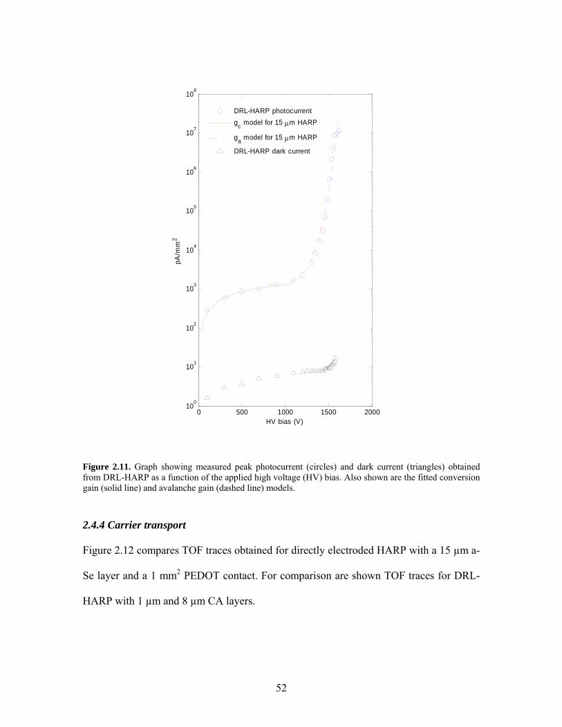
0 500 1000 1500 200010
0
101
102
103
104
105
106
107
108
HV bias (V)
pA/m
m2
DRL-HARP photocurrentgc model for 15 µm HARP
ga model for 15 µm HARP
DRL-HARP dark current
Figure 2.11. Graph showing measured peak photocurrent (circles) and dark current (triangles) obtained from DRL-HARP as a function of the applied high voltage (HV) bias. Also shown are the fitted conversion gain (solid line) and avalanche gain (dashed line) models.
2.4.4 Carrier transport
Figure 2.12 compares TOF traces obtained for directly electroded HARP with a 15 µm a-
Se layer and a 1 mm2 PEDOT contact. For comparison are shown TOF traces for DRL-
HARP with 1 µm and 8 µm CA layers.
52

-2 0 2 4 6 8 10
x 10-7
-5
0
5
10x 10-3
-2 0 2 4 6 8 10
x 10-7
-2
0
2
4x 10⁻³
-3 -2 -1 0 1 2 3 4 5 6 7
x 10-7
-2
0
2
4x 10⁻³
Reference (no CA)PEDOT contact220 V bias
UHSe1 (15% CA, 2mL)PEDOT contact220 V bias
UHSe2 (1% CA, 2mL)PEDOT contact220 V bias
phot
ocur
rent
(mA
)
time (s)
phot
ocur
rent
(mA
)
time (s)
phot
ocur
rent
(mA
)
time (s)
Figure 2.12. Graph showing measured photocurrent transient in (a) directly electroded HARP, (b) DRL-HARP with 8 µm CA layer and (c) DRL-HARP with 1 µm CA layer. A PEDOT electrode was used in all three cases and the applied bias was 220 V.
TOF traces were also obtained for DRL-HARP with a 2 µm CA layer and a 1 mm2
PEDOT contact for electric field strengths in the range of 2-20 V/µm. This enabled the
calculation of hole mobility in a-Se for DRL-HARP as a function of electric field. The
mobility was calculated from the TOF traces by measuring the transit time of holes. The
effective hole velocity in the a-Se could be deduced by dividing the a-Se thickness (15
µm) by the hole transit time. The hole mobility is then obtained by dividing the effective
hole velocity by the magnitude of the electric field in the a-Se. The room-temperature
53
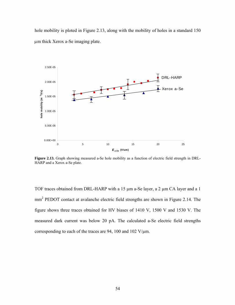
hole mobility is ploted in Figure 2.13, along with the mobility of holes in a standard 150
µm thick Xerox a-Se imaging plate.
0.00E+00
5.00E-06
1.00E-05
1.50E-05
2.00E-05
2.50E-05
0 5 10 15 20 25
E a-Se (V/um)
hole
mob
ility
(m2 /V
s)
Xerox a-Se plate
DRL-HARP
DRL-HARP
Xerox a-Se
Figure 2.13. Graph showing measured a-Se hole mobility as a function of electric field strength in DRL-HARP and a Xerox a-Se plate.
TOF traces obtained from DRL-HARP with a 15 µm a-Se layer, a 2 µm CA layer and a 1
mm2 PEDOT contact at avalanche electric field strengths are shown in Figure 2.14. The
figure shows three traces obtained for HV biases of 1410 V, 1500 V and 1530 V. The
measured dark current was below 20 pA. The calculated a-Se electric field strengths
corresponding to each of the traces are 94, 100 and 102 V/µm.
54

0 50 100 150 200
0
5
10
15
20
25
time (ns)
sign
al (m
V)
E = 94 V/µm
E = 100 V/µm
E = 102 V/µm
Figure 2.14. Measured time-of-flight traces obtained for three different electric field strengths in the avalanche regime.
2.5 Discussion
2.5.1 Breakdown characteristics
We begin by discussing the breakdown characteristics of a directly electroded HARP
layer. As shown in Figure 2.6 (left panel), after each HV step, the dark current idc
stabilizes. This reduction in idc has previously been observed in a-Se structures with metal
contacts and is thought to be caused by interfacial charge trapping which can
significantly influence the amount of injected charge near the contact.11 However, once
the HV is increased beyond 1200 V, idc rises instantly by over four orders of magnitude,
suggesting the presence of an electrical discharge. As seen in Figure 2.6, an optical
microscope image reveals clear damage along the periphery of the circular electrode
55

(right panel in Figure 2.6). This suggests there is an electric field strength enhancement
near the edges of the PEDOT electrode leading to electrical discharges which occur at the
larger electric fields in this region.
The macroscopic damage shown in Figure 2.6 can be prevented by including a 100 GΩ
series resistance in the current path. This resistance limits the current traversing the
HARP. However, using the large series resistance does not prevent the occurrence of
breakdown which is manifested as an irreversible change in the dark current
characteristic after the electroded HARP has been biased with HV > 1200 V (Figure 2.7).
Hence, breakdown in electroded HARP must be caused by microscopic changes in the
state of the a-Se as a result of an electric discharge. The increased current density within
the region of an electric discharge (or a defective spot which causes an increase in
current) likely produces localized Joule heating which causes crystallization of the a-Se
and an associated increase in its electrical conductivity. These observations confirm that
two key limitations with electroded HARP, as identified earlier in section 2.2, are (1)
electric field enhancement near electrode edges and (2) deposition of heat due to high
localized current densities.
As seen in Table 2.2, metallized contacts consisting of Pt or Au cannot sustain the high
electric field strengths necessary for avalanche multiplication in electroded HARP. It can
be appreciated that the conductive polymer PEDOT contact enables the application of a
significantly larger E (84 V/µm). This is likely due to differences in the microstructure at
the interface between the HARP and the conductive contact. Unlike sputtered or
56

thermally evaporated metallization layers which are prone to diffusion through the
amorphous photoconductive material, the conductive polymer material (PEDOT) is
comprised of large cross-linked molecular chains that cannot diffuse into the
photoconductive material and alter its electrical properties over time. Kasap has also
suggested that the interface at a metal-Se junction is complicated by the formation of
metal selenides.11 It can thus be appreciated that a polymer overcoating on the HARP
provides a chemically stable contact that protects the a-Se surface from environmental
insults. It is likely one of the reasons that Xerox used protective polymer overcoatings in
a-Se xeroradiographic plates.5
We shall now discuss the effect of incorporating a CA polymer layer into the HARP
structure. The CA layer acts as the DRL. As seen in Table 2.1, the DRL thickness is
crucial in determining the maximum electric field strength that can be applied across the
HARP. With no DRL, a maximum avalanche gain 2max_ =ag could be obtained. It has
been previously determined that an avalanche gain 50≈ag is sufficient to overcome the
presence of electronic noise over the entire R/F range of exposures.3,7 A DRL thickness
of 2 µm thus enables much more gain (ga < 104) than is required. Although a thicker
DRL (4 µm) enables the application of even larger biases without causing breakdown
(i.e. V > 1800 V), there was no further apparent increase in ga_max. This is likely due to
the large dark current (several nA) which generates a voltage drop across the DRL and
limits the potential difference across the HARP structure. This dramatic increase in dark
current is probably caused by an inefficiency of the hole blocking contact at very high
electric field strengths, resulting in holes being injected into the a-Se layer from the
57

electrode. These holes avalanche to the same extent as photon-generated holes and
strongly contribute to the dark current, in turn causing a reduction in the avalanche
electric field strength. This negative feedback process results in the gain characteristic
flattening out at very large HV biases. These observations suggest that an improvement in
the hole blocking contact could dramatically increase ga_max for large biases.
The high electric field strengths required for avalanche multiplication in DRL-HARP
increase the probability of electrical discharges. The chart shown in Figure 2.8 provides a
good indication of the rate of occurrence of discharges in DRL-HARP. It can be seen that
below Ea-Se = 50 V/µm, the occurrence of discharges is relatively rare. For 50 < Ea-Se < 80
V/µm, one discharge occurs on average within the 15 minute period. For Ea-Se > 80
V/µm, the discharge rate is two to three times greater. Electric discharges can potentially
introduce noise into the integrated charge signal at each del. The pulse repetition rate in
fluoroscopy, however, is on the order of 10 Hz. Hence the likelihood of a discharge
occurring within the duration of a single fluoroscopic pulse (corresponding to a single
image frame) is negligible.
2.5.2 Linearity
It can be seen that for a bias of 1500 V (corresponding to Ea-Se = 100 V/µm), the DRL-
HARP response is linear over a relatively wide range. At larger biases however (1600
and 1700 V), the linear regime becomes limited and the photocurrent tends to saturate at
larger LED intensities. This is likely due to the increased dependence of avalanche gain
on a built-in bias caused by trapped charge, which is a form of ghosting. It can be argued
58

that two counter-opposing effects influence ghosting in the avalanche regime: (1) the
larger field strength reduces the probability of charge trapping and hence the amount of
trapped charge, leading to a reduction of ghosting, and (2) a built-in bias resulting from
trapped charge can strongly affect the avalanche multiplication gain, since the gain is
strongly dependent on the net electric field in the a-Se, leading to an enhancement of
ghosting. The results in Figure 2.9 suggest that the second effect dominates over the first.
Figure 2.10 provides more insight on how this ghosting is manifested: at lower biases
(HV < 1560 V), the top of the photocurrent pulse remains flat, indicating that Ea-Se does
not change during the pulse duration. At larger biases (HV > 1560 V), the signal is
increased due to avalanche multiplication. The distinctive shape of the pulses suggests a
change in Ea-Se throughout the duration of the pulse: a larger initial signal due to the
presence of a large Ea-Se and a large associated avalanche gain gav, followed by a
decaying signal resulting from the reduction of gav due to the progressive accumulation of
trapped charge. This effect is more prominent at larger biases since more charge is
initially produced and gav is more sensitive to trapped charge.
These results indicate that gain measurements should be performed carefully such that the
amount of charge produced inside the DRL-HARP is controlled. These results also
suggest that the linear dynamic range of DRL-HARP may be limited. The temporal
response and dynamic range, as they apply specifically to fluoroscopy, will be examined
in detail in Chapter 4.
59

2.5.3 Gain and dark current
The measured photocurrent as a function of applied HV bias demonstrates that DRL-
HARP enables avalanche multiplication gains as high as 104. This is the first time such
high avalanche gains are reported in an electroded solid-state amorphous
photoreceptor in the linear (proportional) regime.12 The good agreement between the
theoretical and experimentally-measured conversion and avalanche gains confirms that
only avalanche multiplication of holes is occurring at the electric fields involved in the
experiment (Ea-Se 105 V/µm). ≤
The measured dark current in DRL-HARP (Fig. 2.11) is Id ≤ 20 pA/mm2 at room
temperature for Ea-Se 105 V/µm. This is significantly lower than the dark current in
crystalline silicon (c-Si) detectors (
≤
≈dI 1 nA/mm2) because of the relatively large
bandgap energy of a-Se ( =−SeaEG 2.3 eV compared to =−SicEG 1.1 eV for c-Si) and the
associated low thermal generation of carriers in the a-Se bulk. Dark current produces a
type of noise known as shot noise which is caused by the stochastic fluctuations of
electrons traversing a conductor.13 The shot noise in conventional a-Se flat panel
detectors biased at 10 V/µm (and having dark currents Id ≤ 1 pA/mm2) is negligible.
Since shot noise is proportional to the square root of the dark current, we anticipate in the
worst case an increase in shot noise by a factor of only approximately 4 in the case of the
DRL-HARP, which should also be negligible.
60
2.5.4 Carrier transport
The TOF traces shown in Figure 2.12 reveal no significant difference at sub-avalanche
electric field strengths between hole transport for electroded HARP and DRL-HARP with
a 1 µm CA layer. However, when the CA layer thickness is increased to 8 µm - which
corresponds to approximately half the thickness of the HARP - there is an apparent
effect. In this case, the TOF trace consists of two distinct signals: a short pulse, which
corresponds to the movement of holes across the a-Se and a long exponential tail which
corresponds to the much slower movement of holes in the CA. When the thickness of the
CA layer approaches the thickness of the HARP, a significant amount of the total signal
remains to be slowly discharged through the CA layer. The upward inclination in the
pulses of the TOF traces in Figure 2.12 is likely due to trapped holes in the a-Se bulk due
to previous exposures. Such trapped charge can result in electric field non-uniformities
across the a-Se. For the purposes of the present investigation, it is sufficient to observe
that for CA layers which are substantially thinner than the 15 µm HARP – which is the
case for the 2 µm layers employed throughout this thesis – hole transport is not
significantly affected.
It can be seen in Figure 2.13 that the measured mobility of holes in a-Se for DRL-HARP
increases with increasing field strength. This is due to the lower probability of holes
being trapped at larger fields. More importantly, the measured mobility of holes in a-Se is
essentially the same in both DRL-HARP and standard Xerox a-Se. This is an expected,
but nonetheless important observation since it suggests that the DRL deposition process
does not significantly alter the hole transport properties in the a-Se layer in the HARP. It
61
is known that organic solvents - such as acetone which is used in the CA deposition
process described in section 2.3.1 – may act as catalysts for phase transformations in a-
Se, leading to partial crystallization14 and thus altering its electrical properties. Although
significant a-Se phase transformations are unlikely, the formation of microscopic regions
of crystallization, particularly at the a-Se surface is possible. A materials characterization
technique such as differential scanning calorimetry or X-ray diffraction could be used to
obtain the degree of crystallization in a-Se before and after the CA deposition, however
this is not within the scope of this thesis.
Direct evidence of avalanche mulitiplication is provided by the TOF traces obtained at
avalanche electric field strengths shown in Figure 2.14. The traces reveal a sharp initial
peak, which corresponds to the avalanche multiplication of photon-generated holes. The
remaining signal, which is manifested as a plateau followed by a decaying exponential
tail is due to electrons, which have a lower mobility in a-Se.15 The rapidly-increasing
magnitude of the hole peak as a function of E as well as the production of electrons
throughout the bulk of the a-Se confirm that avalanche multiplication of holes is indeed
taking place in DRL-HARP.
2.6 Conclusions
An experimental method was developed which enabled the practical application of
avalanche-grade electric field strengths in a-Se. The method consists of casting a resistive
polymer layer on an existing HARP structure. Avalanche gains as high as 104 were
62

obtained in the DRL-HARP device. This is the first time such high avalanche gains have
been reported in a solid-state amorphous photoreceptor in the linear (proportional)
regime. The measured dark current in DRL-HARP was found to be less than 20 pA/mm2
at room temperature for electric fields less than 105 V/µm. This is significantly lower
than the dark current in crystalline silicon detectors and the corresponding dark current
shot noise is negligible. A TOF analysis revealed an expected a-Se hole mobility of ~
1.5x10⁻⁵ m2/Vs (at 10 V/µm) in DRL-HARP and the DRL was found to have a negligible
effect on hole transport. The TOF analysis was also used to confirm the presence of
avalanche multiplication gain in DRL-HARP.
63

References
1 T. Ohshima, K. Tsuji, K. Sameshima, T. Hirai, K. Shidara, and K. Taketoshi,
"Excess noise in amorphous selenium avalanche photodiodes," Jap. J. of App.
Phys. 30, L1071 - L1074 (1991).
2 M. Yamauchi, T. Hayashida, M. Kosugi, K. Moroboshi, T. Watabe, Y. Ishiguro,
K. Yamano, H. Ohtake, T. Tajima, T. Watanabe, H. Kokubun, M. Abe, and K.
Tanioka, " CMOS image sensor overlaid with a HARP photoconversion film," in
Optoelectronic and Microelectronic Materials and Devices (COMMAD, 2000),
pp. 89-92.
3 W. Zhao, D. Li, A. Reznik, B. J. M. Lui, D. C. Hunt, J. A. Rowlands, Y. Ohkawa,
and K. Tanioka, "Indirect flat-panel detector with avalanche gain: Fundamental
feasibility investigation for SHARP-AMFPI (scintillator HARP active matrix flat
panel imager)," Med. Phys. 32, 2954-2966 (2005).
4 J.A. Rowlands and J. Yorkston, "Flat Panel Detectors for Digital Radiography," in
Handbook of Medical Imaging, edited by J. Beutel, H. Kundel, and R. Van Metter
(SPIE, Bellingham, Washington, 2000), Vol. I.
5 T. S. Curry, J. E. Dowdey, and R. C. Murry, Christensen's Physics of Diagnostic
Radiology. (Lipnicott Williams & Wilkins, 1990), fourth ed.
6 D. C. Hunt, K. Tanioka, and J. A. Rowlands, "X-ray imaging using avalanche
multiplication in amorphous selenium: Investigation of depth dependent
avalanche noise," Med. Phys. 34, 976-986 (2007).
64

7 Dylan C. Hunt, "Investigation of Avalanche Multiplication in Amorphous
Selenium for Use in Digital Fluoroscopy", PhD Thesis, University of Toronto
(2005).
8 D. C. Hunt, S. S. Kirby, and J. A. Rowlands, "X-ray imaging with amorphous
selenium: X-ray to charge conversion gain and avalanche multiplication gain,"
Med. Phys. 29, 2464-2471 (2002).
9 S.O. Kasap, Optoelectronics and Photonics: Principles and Practices with
CDROM Optoelectronics and Photonics. (Prentice Hall, Upper Saddle River,
2000).
10 K. Tsuji, Y. Takasaki, T. Hirai, J. Yamazaki, and K. Tanioka, "Avalanche
phenomenon in amorphous selenium," Optoelectron., Devices Technol. 9, 367-
378 (1994).
11 R. Johanson, S. Kasap, J. Rowlands, and B. Polischuk, "Metallic electrical
contacts to stabilized amorphous selenium for use in X-ray image detectors,"
Journal of Non-Crystalline Solids 227-230, 1359-1362 (1998).
12 M.M. Wronski, W. Zhao, J.A. Rowlands, A. Reznik, G. Decrescenzo, and J.
Segui, USA patent Patent No. 61/129389 (2008).
13 S. M. Sze, Physics of Semiconductor Devices. (John Wiley & Sons, 1981).
14 T. Ohtani, N. Takayama, K. Ikeda, and M. Araki, "Unusual crystallization
behavior of selenium in the presence of organic molecules at room temperature,"
Chemistry Letters 33, 100-106 (2004).
65

15 C. Juhasz, S.M. Vaezinejad, and S.O. Kasap, "Electron and hole drift mobility in
amorphous selenium-based photoreceptors," Journal of Imaging Science 29, 144-
147 (1985).
66

Chapter 3 Theory of x-ray imaging with avalanche amorphous selenium in the solid state 3.1 Introduction 3.2 Background 3.2.1 Indirect-conversion HARP imager 3.2.2 Depth-dependent gain fluctuation noise 3.3 Proposed direct-conversion HARP imager 3.4 Calculation methods 3.4.1 MTF, NPS and DQE 3.4.2 Avalanche gain, gain nonuniformities and fill factor 3.4.3 Del response 3.5 Results
3.5.1 MTF, NPS and DQE 3.5.2 Avalanche gain, gain nonuniformities and fill factor 3.5.3 Del response
3.6 Discussion 3.6.1 MTF, NPS and DQE 3.6.2 Avalanche gain, gain nonuniformities and fill factor 3.6.2.1 Average gain and fill-factor 3.6.2.2 Avalanche multiplication noise 3.6.2.3 Gain nonuniformities
3.6.3 Del response 3.6.4 Response at high spatial frequencies 3.6.5 Dark current 3.6.6 Direct x-ray interaction in the gain region
3.7 Conclusions
A paper based on this chapter has been published as: M. Wronski et al., "Direct-conversion flat-panel imager with avalanche gain: Feasibility investigation for HARP-AMFPI (HARP active matrix flat panel imager)”, Med. Phys. (2008) 35: 5207-5218
67

3.1 Introduction In the previous chapter, a method was developed which enables the application of large
electric fields across a-Se layers in the solid state and without breakdown. The gain and
dark current characteristics of the resulting avalanche device, known as DRL-HARP were
measured and it was determined that it could provide sufficient gain for QNL operation.
The goal of this chapter is to investigate suitable detector architectures based on DRL-
HARP for x-ray imaging. Both indirect and direct conversion architectures are examined,
however, since a feasibility study of an indirect-conversion imager has already been
completed1, the central focus of this chapter will be on the feasibility of a direct-
conversion x-ray imager with a built-in HARP avalanche layer. The present study is
theoretical and a significant part will focus on the spatial frequency-dependent detective
quantum efficiency (DQE) of the imager. Although a physical implementation of the
imager is beyond the scope of this thesis, the present investigation is focused on a solid-
state avalanche x-ray imager suited for deploying advanced endovascular instrumentation
in interventional radiology.
In what follows, we will briefly review the expected imaging performance of an indirect-
conversion HARP x-ray imager as well as the general problem of depth-dependent gain
fluctuation noise that affects most direct-conversion imagers. An imager architecture will
next be proposed for a direct-conversion HARP x-ray imager which overcomes depth-
dependent noise. We will next perform a theoretical investigation of the detective
quantum efficiency (DQE) for the direct-conversion imager and examine other important
68

characteristics such as the mean avalanche gain, avalanche gain nonuniformities, fill
factor and linearity. We will finish the investigation by discussing the significance of
dark current and the effect of direct x-ray interaction in the HARP layer.
3.2 Background 3.2.1 Indirect-conversion HARP imager
A feasibility investigation of an indirect-conversion HARP x-ray imager has recently
been conducted by Zhao et al. It is called SHARP-AMFPI (scintillator HARP active
matrix flat panel imager) and consists of a structured CsI phosphor optically coupled to a
HARP layer (Figure 3.1). The phosphor is used to absorb diagnostic X-rays and convert
their energy into optical photons. The optical photons are next absorbed at the HARP
surface where they produce electron-hole pairs (EHPs). The holes undergo avalanche
multiplication in the HARP and an active matrix array is used to collect and store the
charge on del electrodes. Thin film transistors (TFT) are used at each pixel to read out the
stored image charge.
69

Figure 3.1. Diagram showing the concept of SHARP-AMFPI in which an avalanche a-Se photoconductor is used to detect light photons produced in a CsI phosphor. A mushroom TFT structure is used to maximize the geometrical fill factor. Reproduced from Reference 1.
The investigation showed that in SHARP-AMFPI, the optical quantum efficiency of the
HARP at a wavelength of 540 nm -- which corresponds to the peak emission wavelength
of a CsI:Tl phosphor – is in the range 20-30% at avalanche electric field strengths. This is
significantly lower than the quantum efficiency of 80% for an amorphous silicon
photodiode used in most existing indirect-conversion flat panel detectors. Despite this
low quantum efficiency, however, it was found that SHARP-AMFPI could provide x-ray
quantum noise limited (QNL) imaging performance by employing an avalanche
multiplication gain of 46 during fluoroscopy. This would require an electric field strength
of 110 V/µm in the 8 µm thick HARP layer. It was also shown that direct x-ray
interaction in the HARP did not hinder the imaging performance and that the HARP
thickness uniformity should be kept within 4% to maintain the signal within the dynamic
range of the readout electronics and within the capability of gain correction algorithms.
70

Figure 3.2. Calculated DQE(f) for SHARP-AMFPI for an x-ray exposure of 0.1 µR and assuming a 200 µm pixel pitch, 1500 noise electrons (rms) and a 600 µm thick CsI:Tl phosphor with a reflective layer. Reproduced from Reference 1.
This previous investigation did not take into account the practical means to establish an
electrode connection to the HARP layer. Thus a distributed resistive layer (DRL) – as
discussed in Chapter 2 -- should be incorporated in between the HARP and the active
matrix array. This layer is not expected to affect the overall modulation transfer function
(MTF) of the imager because (1) the DRL thickness is ~ 1 µm while the del pitch is ~
100 µm so all charge produced within a single del will arrive at the del electrode and not
spread to adjacent del electrodes and (2) according to the analysis in section 2.3.1, the
time constant associated with charge leakage between neighboring dels is on the order of
1000 s, while the charge integration time at each del is on the order of only 10 ms.
Experimental results from Chapter 2 have shown that a 2 µm cellulose acetate (CA) DRL
is sufficient to prevent breakdown in HARP, however it remains to be seen whether
proper operation of the low-voltage (~10 V) thin film transistors (TFT) in the active
matrix array can be maintained while the array is in direct electrical contact with the high
71

voltage (~1000 V) HARP. The TFT and DRL-HARP compatibility will be examined
experimentally in Chapter 4.
3.2.2 Depth-dependent gain fluctuation noise
Avalanche multiplication has been used in radiographic gas imagers as early as 1965,
when Reiss developed an image-forming chamber which relied on avalanche
multiplication of electrons in a gas.2 The associated gain helped overcome the low
sensitivity of previous imagers and it provided better sensitivity than a-Se imaging plates.
However, it was later recognized by Boag3 that the avalanche process produces a
‘random assortment of large charge deposits’, which significantly degrade the image
quality.3 This was attributed to secondary electrons initiating avalanche multiplication at
various depths in the gas, thus contributing to a depth-dependent gain fluctuation noise.
The depth-dependent gain problem may be overcome, in principle, by dividing the
imaging chamber into a conversion or drift region in which impinging radiation ionizes
the gas and generates free electrons and an amplification or gain region in which the
electrons avalanche. Two CERN developments, the micro-mesh gaseous structure
(MICROMEGAS)4 and the gas electron multiplier (GEM)5,6 use this approach. A
conceptual diagram of both devices is shown in Figure 3.3. The depth-dependent gain
problem has been overcome so successfully in these devices that they can provide
excellent energy resolutions.7 However, high gas pressures (several atmospheres) and
thick layers of gas (several centimeters) are required to provide reasonable quantum
efficiencies at radiographic energies. The window of the imaging chamber needs to be
72

made sufficiently thick to support the high gas pressures. The window attenuates the
incident x-rays before they enter the gas, thus limiting the quantum efficiency of the
imaging chamber. The large gas thickness also leads to a degradation of imaging
resolution for obliquely-incident x-rays. This may, in principle, be corrected by using a
spherical detector geometry 3, however this is often impractical.
Figure 3.3. Cross sectional diagrams showing the concept of (a) MICROMEGAS and (b) GEM, where X rays ionize a gas and the resulting electrons undergo avalanche in a gain region. (c) Cross sectional diagram showing a solid state a-Se structure proposed by Lee (Ref. 13) in which the a-Se layer is partitioned into drift and gain regions. Shaded areas denote region of a single del.
The solid state HARP-DRL avalanche device introduced in Chapter 2 overcomes many
of the problems of gas imaging chambers. However, it shares the problem of gas
detectors in that higher energy photons on average penetrate deeper into the active
medium (gas or a-Se) prior to absorption and generation of EHPs. At diagnostic x-ray
energies, an a-Se layer thickness of 200-1000 µm is required in order to achieve a
reasonable quantum efficiency.8 Establishing avalanche multiplication throughout such
thick layers of a-Se is problematic because very high potentials (20-100 kV) need to be
applied to reach avalanche fields (~100 V/µm), and absorption of x-rays at varying
73

depths in the a-Se produces depth-dependent gain fluctuation noise.9-11 To reduce the
potentials required for avalanche multiplication and suppress the depth-dependent gain
fluctuation noise, the a-Se layer could be partitioned into a low-field drift region and a
high-field gain region, analogously to the MICROMEGAS gaseous detector4 shown in
Figure 3.3(a). The general concept of such a dual-layered a-Se structure has been
presented earlier12,13, and here we will expand on this concept to inquire in more detail
what is required to make this concept practical.
Most of the remainder of this chapter will focus on the feasibility of a direct-conversion
HARP X-ray imager. In the discussion section, we will compare the key aspects of the
direct-conversion and indirect-conversion imagers.
3.3 Proposed device structure
In light of what has been discussed in section 3.2.2, we propose the HARP-AMFPI
structure shown in Figure 3.4. Figure 3.4 (a) shows a cross section of the device. It
consists of a thick (~1000 µm) a-Se drift region, in which x-rays are absorbed and
generate EHPs. The electric field in this region is comparable to what is currently used in
direct-conversion a-Se imagers (10 V/µm).14,15 A mesh electrode sets up a higher electric
field (70-110 V/µm) in the thin (~10-50 µm) gain region. As shown, the electric field
lines are shaped in such a way that most holes that drift towards the mesh electrode enter
the gain region and undergo avalanche multiplication. The top view of the device is
shown in Figure 3.4 (b).
74

The top and mesh electrodes have blocking contacts to prevent holes from being injected.
The x-ray generated holes entering the gain region are tightly focused and are collected
by the del electrodes, in which the charge is stored on del capacitors and is periodically
read out by a TFT array (i.e. once every 30 ms). Guard electrodes are used to establish a
uniform potential in the readout plane of the AMFPI. Blocking contacts on the guard and
del electrodes prevent electrons from being injected into the high-field region.
Lee et al. have recently proposed a solid-state avalanche imager using a-Se13, shown in
Figure 3.3 (c), consisting of distinct drift and gain regions. Our structure in Figure 3.4,
however, improves on this in two important ways. First, the mesh electrode apertures are
larger (on the same order as the del size) and are aligned with the del electrodes. Second,
guard electrodes are used in the readout plane of the imager. Both these differences in
structure enable a significant reduction in dark current and the amount of noise resulting
from direct x-ray interaction in the gain region, as will be discussed in sections 3.6.5 and
3.6.6.
For the same reasons as those stated in section 3.2.1, the DRL is not expected to affect
the spatial frequency response of the imager. Temporal artifacts and exposure limitations
caused by the DRL will be characterized experimentally in Chapter 4 on a single del
basis.
75
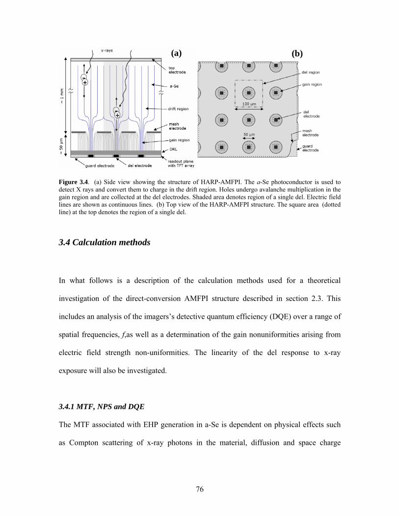
(a) (b)
Figure 3.4. (a) Side view showing the structure of HARP-AMFPI. The a-Se photoconductor is used to detect X rays and convert them to charge in the drift region. Holes undergo avalanche multiplication in the gain region and are collected at the del electrodes. Shaded area denotes region of a single del. Electric field lines are shown as continuous lines. (b) Top view of the HARP-AMFPI structure. The square area (dotted line) at the top denotes the region of a single del.
3.4 Calculation methods
In what follows is a description of the calculation methods used for a theoretical
investigation of the direct-conversion AMFPI structure described in section 2.3. This
includes an analysis of the imagers’s detective quantum efficiency (DQE) over a range of
spatial frequencies, f,as well as a determination of the gain nonuniformities arising from
electric field strength non-uniformities. The linearity of the del response to x-ray
exposure will also be investigated.
3.4.1 MTF, NPS and DQE
The MTF associated with EHP generation in a-Se is dependent on physical effects such
as Compton scattering of x-ray photons in the material, diffusion and space charge
76

effects. The model developed by Que et al.16 was used to obtain the a-Se MTF used in
this work.
The DQE model was obtained from cascaded linear systems theory.17 Our
implementation ignores second-order effects such as K-fluorescence reabsorption. Shown
in Figure 3.5 is a flow diagram of the signal and noise propagation through the various
stages of the complete imaging system in Figure 3.4. The noise at the output of the
system prior to aliasing and the addition of electronic noise is given by:
)()(1)()( 22206 fTfT
AggfTqgfS aavb
Secavbc ⎥
⎦
⎤⎢⎣
⎡+= σβηβ , Eq. 1
where Tb(f) and Ta(f) are the MTFs associated with EHP generation in a-Se and the del
aperture function, respectively. The number of incident x-ray photons per unit area and
the charge coupling efficiency between the drift and gain regions are denoted by q0 and β.
ASe, η and gc are the Swank factor, x-ray quantum absorption efficiency and x-ray to
charge conversion gain of amorphous selenium, respectively. The avalanche gain and its
variance are denoted by gav and σav2, respectively.
Figure 3.5. Flow diagram showing the stages of the cascaded linear system model for HARP-AMFPI.
77

Both charge conversion and avalanche multiplication of charge are non-deterministic
processes and hence have a certain amount of noise associated with them. Each x-ray
generates a variable number of EHPs in the a-Se layer, and this variation in conversion
gain is characterized by ASe. Each hole that dissociates from an electron, in turn,
undergoes a variable amount of avalanche multiplication. The variance of this process is
represented by σ2av. In the case where only holes avalanche, which is a valid assumption
for a-Se biased near 100 V/µm,9,18 Tager19 derived the relationship for the avalanche
variance,
avavav gg −= 22σ , Eq. 2
used in our model. The holes generated by a single x-ray photon interaction each undergo
avalanche multiplication, and the avalanche Swank factor Aav, which can be expressed as
)(
22
2
fTgAg
gA
bc
Seavav
avav
βσ
+= Eq. 3
denotes the overall variation in avalanche gain associated with this single x-ray
interaction. This, however, is under the assumption that each hole that undergoes
avalanche multiplication travels along the same path through the a-Se. In practice, holes
travel along different paths in the gain region of the AMFPI and are subject to varying
electric field strengths along these paths. This effect is characterized by the secondary
78

Swank factor Asec which accounts for avalanche gain variations due to differences in
travel paths for holes generated by a single x-ray interaction. Table 3.1 summarizes these
various factors used to quantify the conversion and avalanche gain variation. Using Eq. 1
and Eq. 3 and including the effect of path length variation, the noise may simply be
expressed as
sec
222220
6)()()(
AAAfTfTggqfS
avSe
abavc βη= Eq. 4
The aliased noise variance S7(f) is given by aliasing the noise power spectrum (NPS)
given by Eq. 4 with respect to the Nyquist frequency 1/2ap, where ap is the imager del
size. The output NPS, Sout(f) is given by the addition of the electronic noise variance Sn to
the aliased noise variance. The normalized output NPS is then given by
( )20
)()(qgg
fSfNScav
outout ηβ
= Eq. 5
and the DQE is taken as
)()()()(
0
22
fNSqfTfTfDQE
out
ab= . Eq. 6
Table 3.2 summarizes the values of all AMFPI design parameters and operating
conditions chosen for R/F applications.
79

Table 3.1. Summary of factors used to characterize nonuniformities in conversion and avalanche gain. N/A denotes that no information is available. afrom Ref. 9. bfrom Tager’s derivation, given by Eq. (2), assuming that only holes avalanche (from Ref. 19). cAssuming gc = 1000. dresults for proposed detector structure in Fig. 3.4. efrom Ref. 10 for a 25 µm a-Se layer due to variable depths of x-ray interaction in the selenium bulk, for 73.8 keV photons.
Table 3.2. Detector operating conditions and design parameters chosen for fluoroscopy and radiography. afrom Ref. 9. bfrom Ref. 15. cfrom Refs. 10 and 22. d75 kVp, 21 mm Al filtration. efrom Ref. 12.
3.4.2 Avalanche gain, gain nonuniformities and fill-factor
Numerical calculations based on the finite element method (FEM) were done in Matlab
(Mathworks, Natic, MA) and used to obtain the distribution of the electric field in the
proposed AMFPI structure. The imager parameters of interest were the mesh electrode
aperture size, the separation between the mesh electrode and the image readout plane and
the electric field in the drift and gain regions. Key AMFPI metrics were calculated and
plotted. These include the average avalanche gain, the nonuniformities in avalanche gain
80

arising from electric field strength nonuniformities and the fill factor, which is the
fraction of x-ray generated holes that is collected by the del electrodes. Our model
enabled the investigation of a large parameter space and DQE optimization.
The currently accepted model for charge transport in a-Se states that charge in a-Se
acquires energy when subjected to an external electric field and, in doing so, undergoes
both elastic and inelastic collisions.20 The bend radius of the electric field lines in our
proposed AMFPI structure is on the order of micrometers, which is much larger than the
mean free paths of elastic and inelastic collisions, 0.6 and 7.2 nm, respectively.20,21
Hence, the field lines obtained from our FEM analysis will coincide with the charge
carrier travel paths. The avalanche gain gav is obtained by integrating the incremental
gains experienced by a single charge traveling along a given field line according to
( ) ⎥⎦
⎤⎢⎣
⎡⎟⎟⎠
⎞⎜⎜⎝
⎛ −= ∫
d
av dssE
g0
21 expexp ββ , Eq. 7
where d is the total path length along the field line, E(s) is the electric field strength at a
point s along the path and β1 and β2 are the impact ionization coefficients for a-Se.18,22
The nonuniformity of the avalanche gain due to field strength nonuniformities was
assessed by comparing the avalanche gain experienced by charge traveling along the
central and lateral field lines arriving at the same del electrode.
81

3.4.3 Del response
For R/F, the imager signal should have a piecewise linear response as a function of
exposure over a range of up to five orders of magnitude. At the largest exposures, or with
high avalanche gain, the amount of charge generated at each del can lead to an increase in
del potential to the point of dielectric breakdown of the TFT gate oxide.
This problem can be adressed by protecting the TFTs from high voltage damage using a
dual-gate TFT structure.23 While this will lead to del saturation, meaning that no useful
signal may be obtained, it will prevent permanent damage if an inappropriate
combination of gain and exposure parameters were to be selected. Also, close to
saturation, linearity can be affected because the increase in del potential during the
exposure can decrease the electric field strength in the del gain region. This, in turn, can
potentially reduce the avalanche gain, which is very sensitive to the field strength and
result in a nonlinear del response.
To determine potential nonlinearities in the del response, each del of the AMFPI may be
modeled as two series capacitors, namely the intrinsic a-Se capacitance occurring
between the top and del electrodes (see Figure 3.4 (a)), and the del storage capacitance
used to integrate the signal charge. The a-Se capacitance in our proposed AMFPI
structure is very small (~ 0.5 fF) due to the large thickness of the a-Se layer (1000 µm).
Hence the much larger del storage capacitance (≥ 200 fF) largely determines the del
response. In modeling the latter, we assume that an x-ray pulse produces holes which
avalanche and produce more holes. These holes accumulate on the del storage
82

capacitance and decrease the avalanche field, which decreases the gain, thus reducing the
amount of charge generated for an identical successive x-ray pulse.
3.5 Results
3.5.1 MTF, NPS and DQE
Shown in Figure 3.6 is the MTF associated with direct x-ray interaction in a-Se obtained
from our numerical model.16 The noise power spectrum was obtained using Eq. 4 and is
presented in Figure 3.7, for an average fluoroscopic exposure of 10-6 R/frame. The DQE,
calculated using Eq. 6, is shown for different avalanche gain factors in Figure 3.8 for
several exposures ranging from the lowest exposure to the detector occurring in
fluoroscopy (10-7 R/frame) to a radiographic exposure of 3x10⁻⁶ R/frame. Figure 3.9, also
obtained using Eq. 6, demonstrates the relationship between DQE(0) and the per-frame
exposure at different avalanche gains throughout the fluoroscopic exposure range.
Figure 3.6. Calculated MTF for a-Se and aperture function for detector with 100 x 100 µm del size.
83

Figure 3.7. Comparison of the NPS for a direct-conversion a-Se AMFPI before and after the addition of electronic noise at an average fluoroscopic exposure of 10−6 R/frame and for operating conditions shown in Table 3.2.
Figure 3.8. DQE(f) for a direct-conversion a-Se AMFPI calculated using the detector parameters and operating conditions shown in Table 3.2 for an x-ray exposure of (a) 1x10⁻⁷, (b) 1x10⁻⁶, and (c) 3x10⁻⁵ R/frame and varying levels of gain. For large enough gains, DQE(f) approaches the theoretical limit where there is no electronic noise (top-most curve in each graph). This represents the quantum noise limited DQE(f).
84

Figure 3.9. DQE(0) for a direct-conversion a-Se AMFPI calculated as a function of x-ray exposure using the detector parameters and operating conditions shown in Table 3.2 and varying levels of gain. For large gains, DQE(0) approaches the theoretical limit where there is no electronic noise (top-most curve). This represents the quantum noise limited DQE(0).
3.5.2 Avalanche gain, gain nonuniformities and fill-factor
The average avalanche gain of the direct-conversion a-Se AMFPI device, obtained using
Eq. 7, varies as a function of aperture size and mesh distance and is shown in Figure 3.10.
The effect of changing the electric field strength in the drift region is also shown. Figure
3.11 depicts the distribution of the electric field strength in the direction normal to the
readout plane and calculated at different distances from the mesh electrode. Shown are
the field distributions at the del center and 15 µm away from the center. Calculated fill
factors are presented in Figure 3.12 and Figure 3.13 shows how the gain nonuniformity,
associated with this nonuniform field-strength distribution, changes as a function of
aperture size, mesh distance and the electric field strength in the drift region. The relative
significance of the conversion and avalanche gains gc and gav is shown in Figure 3.14 for
the case where the imager is quantum noise limited and at an exposure of 10-5 R/frame.
85

Figure 3.10. Average avalanche gain for a direct-conversion a-Se AMPFI calculated as a function of aperture size, mesh distance, and the electric field strength in the drift region. The detector parameters and operating conditions used are shown in Table 3.2.
Figure 3.11. Comparison between the electric field strength experienced by a charge that travels from the drift region (region A) into the gain region (region B) along an axis that crosses the del center (denoted by the thick solid line) and along an axis 15 µm from the del center (denoted by the thin solid line), as shown in the inset at the top left. The x-axis provides the position of the charge along these axes. Negative values indicate the charge is in region A and positive values indicate it is in region B. The numerical value refers to how far the charge is situated from the horizontal mesh electrode plane (denoted by the dashed line).
86

Figure 3.12. Effective fill factor for a direct-conversion a-Se AMFPI calculated as a function of aperture size, mesh distance, and the electric field strength in the drift region. The detector parameters and operating conditions used are shown in Table 3.2.
Figure 3.13. Gain nonuniformity for a direct-conversion a-Se AMFPI calculated as a function of aperture size, mesh distance, and the electric field strength in the drift region. The detector parameters and operating conditions used are shown in Table 3.2.
87
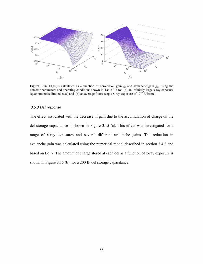
Figure 3.14. DQE(0) calculated as a function of conversion gain gc and avalanche gain gav using the detector parameters and operating conditions shown in Table 3.2 for (a) an infinitely large x-ray exposure (quantum noise limited case) and (b) an average fluoroscopic x-ray exposure of 10−6 R/frame.
3.5.3 Del response
The effect associated with the decrease in gain due to the accumulation of charge on the
del storage capacitance is shown in Figure 3.15 (a). This effect was investigated for a
range of x-ray exposures and several different avalanche gains. The reduction in
avalanche gain was calculated using the numerical model described in section 3.4.2 and
based on Eq. 7. The amount of charge stored at each del as a function of x-ray exposure is
shown in Figure 3.15 (b), for a 200 fF del storage capacitance.
88

Figure. 3.15. (a) Avalanche gain calculated as a function of x-ray exposure for varying levels of nominal avalanche gain gav. A del storage capacitor Cp of 200 fF was assumed. (b) Calculated image charge on each del electrode as a function of x-ray exposure for varying levels of nominal avalanche gain gav (Cp=200 fF was assumed).
3.6 Discussion
We shall discuss the theoretical effects of electronic noise in HARP-AMFPI with 100 µm
dels, and how the presence of the avalanche gain stage changes DQE(f) at fluoroscopic
and radiographic exposures. Next, we will examine the significance of various noise
sources introduced in HARP-AMFPI. We will also examine the fill factor, del response,
dark current as well as the effect of direct x-ray interaction in the gain layer of the imager
and compare the imaging performance of HARP-AMFPI with the indirect-conversion
SHARP-AMPFI.
89

3.6.1 MTF, NPS and DQE
Amorphous selenium has been used in direct-conversion AMFPIs because it is a well-
characterized material and has a high intrinsic imaging resolution.8,12,16,24 As seen in the
calculated MTF curve (Figure 3.6), despite Compton scattering, charge diffusion and
space charge effects, the degradation of the a-Se MTF is less than 15% at a spatial
frequency of 10 mm-1. In comparison, the aperture function drops more rapidly, thus, for
the HARP-AMFPI, the spatial resolution is limited not by the photoconductor, but rather
by the del size (100 µm) and the associated del aperture function. This is not the case for
SHARP-AMFPI where the MTF of a CsI:Tl phosphor is worse than a 100 µm del
aperture function and so the phosphor plays a key role in reducing the imager DQE at
high spatial frequencies.
Applying the cascaded linear system model in Figure 3.5 we obtain the NPS in Figure 3.7
for a conventional direct-conversion a-Se AMFPI with 100 x 100 µm dels at an average
fluoroscopic exposure of 10-6 R/frame. The presence of an output electronic noise of
1500 electrons per del (rms) increases the NPS at all spatial frequencies by over 40%.
Electronic noise is thus a significant component of the NPS at 10-6 R/frame.
Using the calculated MTF(f) and NPS(f), we obtain the spatial frequency dependent DQE
for HARP-AMFPI in Figure 3.8 for a range of x-ray exposures. As expected, we see that
the presence of an avalanche gain stage provides a significant improvement in DQE: an
avalanche gain of 20 at a fluoroscopic exposure of 10-7 R/frame increases the DQE by
nearly an order of magnitude in the 0-5 mm-1 spatial frequency range (Figure 3.9).
90

Furthermore, optimal DQE(0) is sustained throughout the entire fluoroscopic exposure
range and a reduction of only 18% occurs at an exposure of 10-8 R/frame, as observed in
Figure 3.9. Thus, for HARP-AMFPI with 100 x 100 µm dels, an avalanche gain of 20 is
sufficient for quantum noise limited operation at all clinically relevant R/F exposures.
Zhao and co-workers1 found that an avalanche gain of 46 is required for quantum noise
limited operation in SHARP-AMFPI. Compared to HARP-AMFPI, the larger (46 > 20)
required avalanche gain is likely due to optical coupling losses at the interface between
the CsI:Tl phosphor and the HARP layer.
3.6.2 Avalanche gain, gain nonuniformities and fill-factor
3.6.2.1. Average gain and fill-factor
Numerical calculations of the avalanche gain and fill factor in HARP-AMFPI, shown in
Figs. 3.10 and 3.11, indicate that these imager characteristics are largely dependent on the
aperture size and the mesh spacing (spacing between the mesh electrode and readout
plane). The average gain drops as the aperture size is increased from 10 to 70 µm, since
the transition in the electric field strength between the drift and gain regions becomes
more gradual. As expected, increasing the mesh spacing has the opposite effect, since
avalanche multiplication gain is exponentially dependent on the thickness of the gain
layer.
The results of the numerical calculations indicate that a number of configurations exist
that have desirable operating characteristics. For example, an aperture size and mesh
spacing of 45 µm and field strengths of 104 and 8 V/µm in the gain and drift regions
91

respectively, enable avalanche gains of up to 50 with a 100% fill factor. As discussed in
section 3.6.1, this is enough gain to produce a DQE which is independent of exposure in
both the radiographic and fluoroscopic modes of operation.
In comparison with SHARP-AMFPI in which the del electrode size should be maximized
relative to the total del size to improve the fill factor, HARP-AMFPI does not suffer from
this problem. Because of the focusing effect of the electric field lines in HARP-AMFPI, a
fill factor of 100% may be achieved using small del electrodes (as shown in Figure 3.12).
However, as guard electrodes are required, the mushroom TFT structure shown in Figure
3.1 should be used for HARP-AMFPI.
It should be noted that, in comparison with SHARP-AMFPI, a disadvantage of HARP-
AMFPI is the significantly thicker HARP layer required to achieve the necessary
avalanche gain for quantum noise limited operation. This is caused by a reduced electric
field strength near the apertures of the mesh electrode. The thicker HARP layer will
require larger voltage biases to be applied.
3.6.2.2 Avalanche multiplication noise
The noise associated with avalanche multiplication can adversely affect the DQE under
unfavorable conditions. Figure 3.14 (a) shows the dependence of DQE(0) on the
avalanche and conversion gains gav and gc, respectively, for the case where the imager is
quantum noise limited. For conversion gains gc greater than 10, the DQE(0) is largely
insensitive to the mean avalanche gain gav and is only limited by the quantum efficiency
92
of the AMFPI. However, as gc is reduced, DQE(0) increasingly depends on gav: in this
regime, higher avalanche gains result in a lower DQE(0). At an average fluoroscopic
exposure of 1 µR/frame, the imager is no longer quantum noise limited and the presence
of avalanche gain unconditionally improves the DQE(0) (Figure 3.14 (b)), however the
maximum attainable DQE(0) remains limited by gc. These results are consistent with a
previous characterization of avalanche multiplication noise in a-Se.9
Hence, avalanche multiplication noise reduces the DQE for small conversion gains.
However, at beam energies which are clinically relevant to most R/F applications (50
keV and higher), gc in a-Se is at least several hundred, thus the effect of avalanche
multiplication noise is negligible. Furthermore, the imager would be unaffected by
avalanche multiplication noise in low energy x-ray applications such as mammography,
tomosynthesis or protein crystallography, all of which operate at energies greater than 1
keV (corresponding to a gc on the order of 10). In these applications, avalanche
multiplication would still be an effective means of overcoming the electronic noise - at
low frame exposures in tomosynthesis or in low exposure regions in protein
crystallography – without any associated degradation of DQE. These results apply
equally to both SHARP-AMFPI and HARP-AMFPI as they have no bearing on the front
end of the detector (i.e. the phosphor or the drift regions) and the conversion efficiency of
a CsI phosphor and a-Se (at 10 V/µm) are comparable.
93

3.6.2.3 Gain nonuniformities
HARP-AMFPI consists of a mesh electrode that partitions the imager into two distinct
regions and establishes a different field strength in each region, as seen in Figure 3.3.
Electric charge traverses from the drift region into the gain region through apertures in
the mesh electrode. The presence of apertures produces electric field strength
nonuniformities at the interface between the two regions. Here, we discuss the effect of
these nonuniformities on the DQE of the imager. These nonuniformities only concern
HARP-AMFPI and not SHARP-AMFPI.
The electric field strength distribution along an axis that traverses the centre of a single
AMFPI del is shown in Figure 3.11. The field strength rises over a distance of 80 µm,
whereas the rise along an axis 15 µm away from the del center occurs over only half that
distance. This distortion of the field is due to the proximity of the mesh electrode. The
associated lateral field strength nonuniformities in HARP-AMFPI reach up to 30%.
Shown in Figure 3.13, are the simulated gain nonuniformities resulting from electric field
strength nonuniformities for different imager configurations. We have identified in
section 3.6.2.1 that certain HARP-AMFPI configurations can produce a fill factor of
100% and avalanche gains of up to 50 enabling quantum noise limited operation over the
entire range of clinically-relevant R/F exposures. The results in Figure 3.13 indicate that,
for this configuration, charges generated at different lateral positions in HARP-AMFPI
experience at most an 18% gain nonuniformity in the avalanche region. This corresponds
to a secondary avalanche variance of approximately 3 which is much less than the
94

selenium avalanche variance (90 for an avalanche gain of 10, refer to Table 3.1)
associated with avalanche multiplication noise. Thus, the field strength nonuniformities
in HARP-AMFPI have essentially no effect on the DQE.
The rationale behind the HARP-AMFPI structure is to enable direct conversion of x-rays
and avalanche multiplication of charge while overcoming the problem of depth-
dependent gain fluctuation noise. In a single layer of a-Se operating in the avalanche
multiplication regime, depth-dependent gain fluctuations can significantly degrade the
DQE: in previous work, Lui measured a secondary avalanche Swank factor of
approximately 0.5 for a 25 µm thick layer of a-Se biased at 100 V/µm and subjected to
monoenergetic x-rays in the 30.9 – 73.8 keV energy range.10 By contrast, HARP-AMFPI
has a predicted secondary avalanche Swank factor of unity. This demonstrates that, in
principle, decoupling the charge conversion and avalanche gain regions is an effective
means of overcoming the depth-dependent gain fluctuation noise, while maintaining a
high quantum efficiency. It should be noted that the HARP-AMFPI and SHARP-AMFPI
detector structures are conceptually very similar in the sense that most X-rays are
absorbed at the front end of the detector (i.e. the drift region or the CsI:Tl phosphor) and
direct x-ray interactions in the relatively thin avalanche region are extremely rare (this
will be examined in more detail in section 3.6.6).
95
3.6.3 Del response
The del response for HARP-AMFPI is shown in Figure 3.15. For a del storage
capacitance Cp of 200 fF, the response ceases to be linear for gains greater than 20 and
exposures larger than 300 µR/frame and this is associated with a steep drop in avalanche
gain. For a gain of 50, the del response is linear within the regular fluoroscopic region of
10-7 – 10-5 R/frame and saturates at an exposure of 10-3 R/frame, with a maximum
accumulated electric charge of 7x10⁷ electrons, corresponding to a maximum del
potential Pp of 56 V.
Hence, for a del storage capacitance of 200 fF, the linearity of the imager will remain
uncompromised over the entire range of clinically-relevant fluoroscopic and radiographic
exposures. In typical TFT designs, however, del potentials greater than 10 V could
produce excessive current leakage.25 To eliminate this leakage, the del capacitance should
be increased (eg. Cp = 2 pF, Pp < 10 V).
3.6.4 Response at high spatial frequencies
As seen in Figure 3.8, the predicted response of HARP-AMFPI at high spatial
frequencies is excellent (DQE ~ 0.4 at 5 cycles/mm) and should provide good detection
of very narrow (~100 µm diameter) high-contrast objects used in clinical interventions
such as stent struts (individual stent wires). Zhao1 estimated a DQE of 0.3 at 2.5
cycles/mm for the indirect-conversion SHARP-AMFPI with a 200 µm del pitch and a
600 µm thick CsI phosphor with a reflective layer (Figure 3.2). This is less than optimal
for advanced clinical interventions – such as imaging guidewires or stent struts having a
96

100 µm diameter --, however the DQE at high spatial frequencies could be significantly
improved by using a 100 µm del pitch. Furthermore, a thinner phosphor could be used
with no reflective layer, yielding an improved spatial resolution at the expense of a lower
quantum efficiency.
3.6.5 Dark current
Dark current is reduced in two ways in HARP-AMFPI. First, specialized blocking layers
are used in the gain region to limit hole and electron injection. Blocking layers between
the a-Se and electrodes consisting of polycrystalline CeO2 and AsSe3 have been shown to
efficiently control the injection of holes and electrons at the anode and cathode.26,27
Unlike the original HARP structure which operates in the optical regime and thus
requires an optically transparent anode blocking layer,27 the anode blocking layer could
be made slightly thicker in HARP-AMFPI – since x-rays are more penetrating than
optical photons – in order to improve the blocking efficiency.
Second, the combination of guard electrodes and small del electrodes on the AMFPI can
significantly reduce the amount of dark current entering the imager signal path. Without
guard electrodes, injection of holes at the mesh electrode would be an important source of
dark current, because of avalanche multiplication of holes. In HARP-AMFPI, however,
holes injected from the mesh electrode into the high-field gain region are absorbed by the
guard electrodes. Thus, since they are not collected by the del electrodes, they do not
contribute to the signal.
97

Electron injection is less of a concern, because electrons do not avalanche at the electric
field strengths employed in this work. However, the presence of guard electrodes in
HARP-AMFPI also reduces the dark current associated with electron injection: electrons
are, to a large extent, injected from the guard electrodes. The expected reduction in
electron dark current is in fact directly related to the area of the del electrodes relative to
the total del area. Hence, for a del size of 100 µm and a del electrode size of 10 µm, we
would expect a reduction of electron dark current by two orders of magnitude.
Localized high electric field regions near the edges of the mesh electrode apertures can be
a strong source of dark current injection. Lee et al. have proposed to insulate the mesh
electrode, such that it is not in direct electrical contact with the a-Se photoconductor.13
Although this approach entirely reduces dark current injection from the mesh electrode,
charge trapping and accumulation at the interface between the photoconductor and
dielectric can produce unpredictable space charge effects leading to unexpected
avalanche conditions. Perhaps a better way is to control the electrode fabrication process
in such a way as to produce a mesh electrode with smooth rounded edges which do not
induce excessively high localized electric fields.
3.6.6 Direct x-ray interaction in the gain region
Direct interaction of x-rays in the gain region of HARP-AMFPI is a potential source of
added noise because of interaction depth dependent gain fluctuations, however we will
show that it is in fact negligible in practice. The significance of this noise is expected to
be similar at all spatial frequencies, because the spatial frequency response of the drift
98

and gain regions is the same, to a first approximation: the amount of electron trapping in
the a-Se varies with the applied electric field strength, and this can influence the
frequency response, but generally not more than by 20%.28 Hence, we can estimate the
significance of direct x-ray interaction simply by comparing the relative number of x-rays
that interact in each region. For a drift region thickness of 1000 µm, a 45 µm gain region
and an RQA5 x-ray spectrum, 26.3% of x-rays are transmitted through the drift region,
out of which 7% interact in the gain region. Hence, only 1.8% of incident x-rays are
absorbed in the gain region. On average, the charge generated by these x-rays
experiences less avalanche gain than the signal charge generated in the drift region. Also,
a large proportion (i.e. 100 to 1) of charge directly generated in the gain region is
absorbed by the guard and mesh electrodes and does not enter the signal path. Thus, the
estimated proportion of image signal that is subjected to depth dependent gain fluctuation
noise through direct x-ray interaction in the gain region is at most 0.02% of the total
image signal, which is negligible.
3.7 Conclusions
In this chapter, we have reviewed the feasibility of SHARP-AMFPI, an indirect-
conversion HARP x-ray imager and investigated the feasibility of HARP-AMFPI, a novel
solid-state direct-conversion imager with avalanche gain. The direct-conversion imager
consists of an a-Se photoconductor which is partitioned into a thick drift region for x-ray-
to-charge conversion and a much thinner gain region in which the charge undergoes
avalanche multiplication. This approach eliminates depth-dependent gain fluctuation
99

noise. Design considerations were made towards optimizing the imaging performance of
HARP-AMFPI for R/F applications. We examined and modeled the effects on the imager
DQE due to electronic noise, avalanche noise, electric field strength nonuniformities and
direct interaction of x-rays in the gain region. Our results showed that avalanche gains of
20 enable x-ray quantum noise limited performance for fluoroscopy. It was shown that
HARP-AMFPI can provide the required gain while maintaining a 100% fill factor and a
piecewise dynamic range of up to five orders of magnitude, while only requiring four
orders of magnitude for fluoroscopy and radiography. We have also shown that imaging
performance for both indirect and direct conversion detectors is not affected by avalanche
noise for x-ray energies above 1 keV. For HARP-AMFPI, it was shown that the effects of
electric field strength nonuniformities and direct x-ray interaction in the gain region are
negligible. As expected, the spatial frequency response of HARP-AMFPI was found to be
significantly superior to that of SHARP-AMFPI (f > 5 cycles/mm). However, with proper
optimization, both imagers should provide adequate imaging resolution for advanced
interventional radiology applications.
100

References
1 W. Zhao, D. Li, A. Reznik, B. J. M. Lui, D. C. Hunt, J. A. Rowlands, Y. Ohkawa,
and K. Tanioka, "Indirect flat-panel detector with avalanche gain: Fundamental
feasibility investigation for SHARP-AMFPI (scintillator HARP active matrix flat
panel imager)," Med. Phys. 32, 2954-2966 (2005).
2 K. H. Reiss and G. Lange, "Electroradiography: some remarks on its technique
and future," Phys. Med. Biol. 18, 695-703 (1973).
3 J. W. Boag, "New ways with x-rays: Xeroradiography and ionography," Phys.
Technol. 6, 209-216 (1975).
4 Y. Giomataris, Ph. Rebourgeard, J. P. Robert, and G. Charpak, "MICROMEGAS:
a high-granularity position-sensitive gaseous detector for high particle-flux
environments," Nucl. Instrum. Methods A. 376, 29-35 (1996).
5 F. Sauli, "GEM: A new concept for electron amplification in gas detectors," Nucl.
Instrum. Methods A. 386, 531-534 (1997).
6 F. Sauli, "Imaging with the gas electron multiplier," Nucl. Instrum. Methods A.
580, 971-973 (2007).
7 M. Li, M. S. Dixit, and P. C. Johns, "Photon-counting digital radiography using
high-pressure xenon filled detectors," Nucl. Instrum. Methods A. 471, 215-221
(2001).
8 M. Z. Kabir, S. O. Kasap, W. Zhao, and J. A. Rowlands, "Direct conversion X-ray
sensors: Sensitivity, DQE and MTF," IEE Proc.-Circuits Devices Syst. 150, 258-
266 (2003).
101
9 Dylan C. Hunt, "Investigation of Avalanche Multiplication in Amorphous
Selenium for Use in Digital Fluoroscopy", PhD Thesis, University of Toronto
(2005).
10 B. J. M. Lui, D. C. Hunt, A. Reznik, K. Tanioka, and J. A. Rowlands, "X-ray
imaging with amorphous selenium: Pulse height measurements of avalanche gain
fluctuations," Med. Phys. 33, 3183-3192 (2006).
11 D. C. Hunt, K. Tanioka, and J. A. Rowlands, "X-ray imaging using avalanche
multiplication in amorphous selenium: Investigation of depth dependent
avalanche noise," Med. Phys. 34, 976-986 (2007).
12 J.A. Rowlands and J. Yorkston, "Flat Panel Detectors for Digital Radiography," in
Handbook of Medical Imaging, edited by J. Beutel, H. Kundel, and R. Van Metter
(SPIE, Bellingham, Washington, 2000), Vol. I.
13 D. L. Y. Lee, "Selenium detector with a grid for selenium charge gain," Proc.
SPIE 5745, 216-222 (2005).
14 O. Tousignant, M. Choquette, Y. Demers, L. Laperriere, J. Leboeuf, M. Honda,
M. Nishiki, A. Takahashi, and A. Tsukamoto, "Progress report on the
performance of real-time selenium flat-panel detectors for direct X-ray imaging "
Proc. SPIE 4682, 503-510 (2002).
15 J. A. Rowlands and G. DeCrescenzo, "X-ray imaging using amorphous selenium:
Determination of x-ray sensitivity by pulse height spectroscopy," Med. Phys. 19,
1065-1069 (1992).
16 W. Que and J. A. Rowlands, "X-ray imaging using amorphous selenium: Inherent
spatial resolution," Med. Phys. 22, 365-374 (1995).
102

17 I. A. Cunningham and R. Shaw, "Signal-to-noise optimization of medical imaging
systems," J. Opt. Soc. Am. A 16, 621-632 (1999).
18 D. C. Hunt, S. S. Kirby, and J. A. Rowlands, "X-ray imaging with amorphous
selenium: X-ray to charge conversion gain and avalanche multiplication gain,"
Med. Phys. 29, 2464-2471 (2002).
19 A. S. Tager, "Current fluctuations in a semiconductor (dielectric) under the
conditions of impact ionization and avalanche breakdown," Soviet Physics-Solid
State 6, 1919-1925 (1965).
20 A. Reznik, S.D. Baranovskii, O.Rubel, G. Juska, S.O. Kasap, Y.Ohkawa, K.
Tanioka, and J. A. Rowlands, "Avalanche multiplication phenomenon in
amorphous semiconductors: a-Se vs a-Si:H," Journal of Applied Physics 102,
53711-53715 (2007).
21 A. Reznik, S.D. Baranovskii, O. Rubel, K. Jandieri, S.O. Kasap, Y. Ohkawa, M.
Kubota, K. Tanioka, and J. A. Rowlands, "Avalanche multiplication in
amorphous selenium and its utilization in imaging," Journal of Non-Crystalline
Solids 354, 2691-2696 (2008).
22 K. Tsuji, Y. Takasaki, T. Hirai, J. Yamazaki, and K. Tanioka, "Avalanche
phenomenon in amorphous selenium," Optoelectron., Devices Technol. 9, 367-
378 (1994).
23 W. Zhao, J. Law, D. Waechter, Z. Huang, and J. A. Rowlands, "Digital radiology
using active matrix readout of amorphous selenium: Detectors with high voltage
protection," Med. Phys. 25, 539-549 (1998).
103

24 H. Guilleminot, "Use of selenium in the radiometry of Rontgen rays," Archives
d'Electricite Medicale 23, 168-173 (1915).
25 L. E. Antonuk, K.-W. Jee, Y. El-Mohri, M. Maolinbay, S. Nassif, X. Rong, Q.
Zhao, R. A. Street, and K. S. Shah, "Strategies to improve the signal and noise
performance of active matrix, flat-panel imagers for diagnostic x-ray
applications," Med. Phys. 27, 289-306 (1999).
26 K. Miyakawa, Y. Ohkawa, T. Matsubara, T. Takahata, S. Suzuki, and M. Kubota,
"Ultrahigh-sensitivity HDTV new Super-HARP camera," Proc. SPIE 5677, 26-34
(2005).
27 K. Tanioka, J. Yamazaki, K. Shidara, K. Taketoshi, T. Kawamura, S. Ishioka,
and Y. Takasaki, "An avalanche-mode amorphous selenium photoconductive
layer for use as a camera tube target," IEEE Electron. Device Letters 8, 392-394
(1987).
28 L. Chowdhury, O. Tousignant, G. DeCrescenzo, P. Gauthierb, J. Leboeufb, and J.
A. Rowlands, "Effect of ghosting on the modulation transfer function of
amorphous selenium based flat panel detectors," Proc. SPIE 6142, 1S1 - 1S7
(2006).
104

Chapter 4 Experimental characterization of DRL-HARP for interventional radiology applications 4.1 Introduction 4.2 Methods
4.2.1 Noise characterization 4.2.2 X-ray sensitivity 4.2.3 Dynamic range 4.2.4 Temporal response
4.2.5 Compatibility with active matrix technology 4.3 Results
4.3.1 Noise characterization 4.3.2 X-ray sensitivity 4.3.3 Dynamic range 4.3.4 Temporal response 4.3.4.1 RC and ghosting 4.3.4.2 Lag 4.3.4.3 Predicted response for a DRL-HARP FPD
4.3.5 Compatibility with active matrix technology 4.3.5.1 Reverse structure 4.3.5.2 HARP thickness 4.3.5.3 TFT compatibility
4.4 Discussion 4.4.1 Noise characterization
4.4.2 X-ray sensitivity 4.4.3 Dynamic range 4.4.4 Temporal response 4.4.4.1 RC and ghosting 4.4.4.2 Lag 4.4.4.3 Predicted response for a DRL-HARP FPD
4.4.5 Compatibility with active matrix technology 4.4.5.1 Reverse structure 4.4.5.2 HARP thickness 4.4.5.3 TFT compatibility
4.5 Conclusions
This chapter combines selected material from the following: • M. Wronski et al., “A solid-state avalanche photoreceptor for low-exposure x-ray
imaging applications” to be submitted to Med. Phys. • A. Sultana, M. Wronski et al., “Digital X-ray Imaging Using an Avalanche a-Se
Photoconductor” submitted to IEEE Sensors.
105

4.1 Introduction
The general requirements for a solid-state fluoroscopic imaging system in interventional
radiology are (1) quantum-noise limited operation at the lowest clinical x-ray exposures,
(2) compatibility with modes of operation that require significantly larger exposures
(radiography) and (3) capability of imaging fine features of complex interventional
devices. The imager should also be able to operate at up to 30 frames per second.
In Chapter 2, a solid-state amorphous photoreceptor known as DRL-HARP has been
developed and has shown to produce very large avalanche multiplication gains (gav ~ 104)
and it has been shown theoretically that its added noise during avalanche multiplication
should be negligible. It has also been shown that, by virtue of the strong electric field
strength dependence of the avalanche multiplication gain, the DRL-HARP should be able
to accommodate a very wide range of x-ray exposures. Although constructing an x-ray
imager based on the DRL-HARP is beyond the scope of this thesis, we shall investigate
whether, in conformity with requirement (1) the measured noise in DRL-HARP is indeed
as low as expected and demonstrate its sensitivity to diagnostic X rays at the lowest mean
exposures encountered in fluoroscopy. We shall next characterize the dynamic range
within the entire range of x-ray exposures employed in interventional radiology and the
temporal charge response of DRL-HARP. Lastly, we will discuss the compatibility of
DRL-HARP with low-voltage thin film transistor (TFT) image readout arrays which are
currently being used in FPD systems and investigate several alternative device structures.
106

4.2 Methods In all of the experiments described in this section, a light emitting diode (LED) was used
as the radiation source to probe the DRL-HARP. The only exception was an experiment
designed to measure the x-ray sensitivity of the device, in which an R/F x-ray source was
used (section 4.2.2). The rationale behind this is that important properties such as noise,
linearity or temporal characteristics largely depend on the effects of the electric charge -
directly or indirectly resulting from x-ray interaction – which experiences the full extent
of avalanche multiplication gain throughout the a-Se thickness. An important assumption
is that direct x-ray interaction in DRL-HARP does not substantially affect these
properties. This is a reasonable assumption based on previous investigations showing that
the NPS and DQE are not substantially affected by direct x-ray interaction.1,2
Furthermore only 1-2% of all x-rays transmitted through the patient will directly interact
in DRL-HARP.2 Only a small fraction of them will contribute to generation of traps that
could potentially affect device linearity or temporal response and the charge generated by
directly-interacting x-rays will on average experience less avalanche gain than the x-ray-
generated charge produced at or entering the top surface of the HARP.
4.2.1 Noise characterization The experimental setup used to measure the noise characteristics of a DRL-HARP with a
15 µm thick HARP layer and a 2 µm thick cellulose acetate (CA) layer was the same as
that shown in Figure 2.5 (Chapter 2). The measurement device was a multi-channel
analyzer and a spectroscopy amplifier (with pulse shaping) was used in place of the
107

charge amplifier. A generalized linear cascaded noise model can be obtained using the
stages shown in Figure 4.1. This is a simplified model that applies to a single pixel and
hence does not take into account any spatial frequency dependencies.
σ2
N = (ga2-ga)gc
2ηq0/Ac + ga2gcηq0
N = gcηq0conversion
G = ga
avalanche multiplication
N = q0
σ2N = q0
absorption N = ηq0
σ2N = ηq0
selection stochastic gain, Ac
electronic noise
stochastic gain, ga
2-ga
σ2N = gc
2ηq0/Ac
N = gagcηq0
σ2N = (ga
2-ga)gc2ηq0/Ac + ga
2gcηq0 + σe2
N = gagcηq0
photon source
G = gcG = η
noise addition, σe2
Figure 4.1. Flow chart showing the linear cascaded noise model used to calculate the expected noise variance σ2
N and signal N for a DRL-HARP device with conversion and avalanche gains gc and ga, a quantum efficiency η, a Swank factor Ac and an electronic noise variance σe
2. The initial number of input photons is q0.
In the case where the photon source is an optical source (i.e. LED), the conversion gain gc
and the Swank factor Ac associated with the conversion gain are unity. The total noise
variance is then given by:
σ2N = (ga
2-ga)ηq0 + ga2ηq0 + σe
2 . Eq. 4.1
For large ga, the avalanche multiplication variance ga2 - ga can be approximated as ga
2.
The total noise variance then simplifies to:
σ2N = 2ga
2ηq0 + σe2 . Eq. 4.2
The noise measured using the setup in Figure 2.5 can now be compared with the noise
predicted by equation 4.2.
108

4.2.2 X-ray sensitivity
The x-ray sensitivity of DRL-HARP was measured by coupling it to a CsI:Tl phosphor
(Hammamatsu) and using the experimental setup shown in Figure 4.2. The DRL-HARP
consisted of a 15 µm a-Se layer and a 2 µm CA layer. A 75 kVp x-ray beam was used in
continuous fluoroscopy mode, with 2 mm of aluminum filtration and a patient phantom
consisting of a 30 cm thick block of acrylic. A low-pass filter (3 Hz) was used to reduce
noise in the direct current (DC) signal. The distance between the x-ray source and the
DRL-HARP was 1.5 meters. An ionization chamber (Keithley) and dosimeter (Keithley)
were used to measure the detector exposure at the DRL-HARP.
The x-ray sensitivity is expected to be the same for both the direct and indirect
conversion implementations of DRL-HARP discussed in Chapter 3. The rationale behind
this reasoning is as follows: in the direct-conversion case, a-Se has a Wa-Se (absorbed x-
ray energy in the photoconductor necessary to produce a single electron-hole pair that
does not immediately recombine) of approximately 40 eV at 10 V/µm.3 In the indirect-
conversion case, the CsI:Tl phosphor has a WCsI:Tl (absorbed x-ray energy in the phosphor
necessary to produce a single light photon) of 18 eV. Taking into account optical losses
within the phosphor, the coupling losses between the phosphor and a-Se and the non-
ideal quantum efficiency of a-Se at a 560 nm wavelength (peak emission wavelength of
CsI:Tl), the effective WCsI:Tl can be considerably larger (i.e. 2-4 times). Thus, in both
cases, the amount of charge quanta produced in a-Se biased at 10 V/µm for each
interacting diagnostic X-ray (i.e. 70 kVp) is on the order of 103.
109

As the x-ray sensitivity is expected to be the same for both direct and indirect conversion
implementations of DRL-HARP, it will suffice to experimentally demonstrate the
required x-ray sensitivity for QNL operation at fluoroscopic x-ray exposures using the
indirect conversion implementation, as shown in Figure 4.2. This implementation only
requires a phosphor to be optically coupled to the DRL-HARP, and is simpler to realize
in practice than the direct-conversion implementation which requires a mesh electrode
and an a-Se x-ray conversion or drift region.
Figure 4.2. Diagram showing the experimental setup used to characterize x-ray sensitivity. The a-Se detector (top) consisted of a DRL-HARP device with a a 15 µm HARP layer and a 2 µm CA layer which was coupled to a structured CsI:Tl phosphor and exposed to diagnostic X-rays. The x-ray setup (bottom) was similar to that used in interventional radiology. An x-ray tube with 75 kVp, 1.5 mA current and 2 mm of Al filtration was used as the source. The x-ray beam was attenuated using a 30 cm acrylic (lucite) phantom (radiological equivalent to a patient). An ion chamber was used to measure the detector exposure.
110

4.2.3 Dynamic range
The experimental setup shown in Figure 2.5 was used to determine the linear range of
operation of a DRL-HARP with a 15 µm a-Se layer and a 2 µm CA layer. A
photomultiplier tube (PMT) was used to relate the intensity of the light emitting diode
(LED) to the amount of charge produced in a-Se biased at 10 V/µm. Assuming a constant
value of Wa-Se or WCsI:Tl (see section 4.2.2), the amount of charge produced in DRL-
HARP with an a-Se layer biased at 10 V/µm may then be related to an equivalent x-ray
exposure at a typical radiographic energy (i.e. 70 kVp). In this way, the PMT reading can
provide the equivalent x-ray exposure at the detector for any given LED intensity.
4.2.4 Temporal response
HARP technology is currently in use in high-definition cameras employed in
broadcasting applications. As such, it can support real-time imaging rates of 30 frames/s
or more. The DRL could potentially degrade the temporal response and reduce the rate at
which images are acquired using the DRL-HARP. This is possible through three
mechanisms: (1) Resistance/Capacitance (RC) effects, (2) ghosting and (3) lag. The
specific aim here is to characterize the relative importance of these effects.
The photocurrent from DRL-HARP was measured as a function of time for an applied
electric field strength of 10 V/µm. This was compared with the photocurrent in an
electroded HARP biased at the same field strength. Next, the field strength was increased
to 70 V/µm – which corresponds to field strength just prior to the onset of avalanche
111

multiplication - and the photocurrent trace was obtained again from the DRL-HARP. The
rationale behind this experiment is that any similarities between the traces obtained at
both fields are indicative of RC effects. Any dissimilarities, on the other hand could be
indicative of mechanisms associated with charge trapping such as ghosting. Lag, which is
manifested as an increase in the signal rise or fall times is also caused by trapped charge
and can be identified by comparing the measured photocurrent with the theoretical RC
response.
The circuit model used to evaluate the RC effects of DRL-HARP is shown in Figure 4.3
(a) and assumes a del size of 1 x 1 mm. The model includes the HV power supply and
filter -- which removes the noise from the power supply – as well as a current limiting
resistance and the RC loading of the oscilloscope. The a-Se layer is modeled as a current
source in parallel with the selenium capacitance CSe and resistance RSe. The DRL is
modeled as a parallel combination of DRL resistance RDRL and capacitance RDRL. The two
key time constants of this circuit are associated with the RC interactions between (1) CSe
and RDRL and (2) CDRL and RDRL. The respective time constants (the time required to
charge or discharge CSe or CDRL to 63% of the final steady-state value) are:
τ1 = RDRL CSe Eq. 4.1
τ2 = RDRL CDRL Eq. 4.2
Of these two, τ2 is dominant for the HARP and DRL layers used in this thesis, because
the dielectric constants ε of a-Se and the cellulose acetate DRL are approximately the
112

same (ε ≈ 6) and the thickness of the DRL (2 µm) is significantly smaller than that of the
a-Se (15 µm) leading to CDRL > CSe.
The theoretical output voltage Vout measured by the oscilloscope may then be calculated
using the capacitor charge and discharge equations,
2/)( τtpout eVtV −= Eq. 4.3
)1()( 2/τtpout eVtV −−= Eq. 4.4
, where t is time and Vp is a constant and corresponds to the peak voltage across the
capacitance.
The RC behavior of an integrated DRL-HARP in a flat panel detector with 100 x 100 µm
dels is expected to be the same as that for the DRL-HARP in our laboratory model
(Figure 4.3 (a)) . The reason for this is that CDRL and CSe scale linearly with del area and
RDRL scales inversely with del area, so that the RC product remains constant regardless of
del size. There could however be second-order effects caused by RC interactions between
the a-Se or DRL and other circuit elements such as those loading the DRL. For this
reason, a numerical circuit simulation tool known as SPICE (Simulation Program with
Integrated Circuit Emphasis) is used to verify that τ2 is indeed the dominant time constant
and there are no significant second-order effects. The program uses numerical integration
methods in the time domain to approximate the state of each circuit element as a function
of time.4 For the purposes of simulation, a second circuit model is used (Figure 4.3 (b)) to
113

include the effects of the flat panel detector readout electronics. These include a charge
storage capacitance, a TFT and a charge readout amplifier.
(a)
t
(b)
t
Figure 4.3. Circuit diagrams used to model the electrical behaviour of (a) the laboratory Dexperimental prototype with a 1 x 1 mm electrode and oscilloscope signal readout and (b) anDRL-HARP in a flat panel detector with 100 x 100 µm dels and signal readout elements consiststorage capacitance, a TFT and a charge readout amplifier. The voltage at the oscilloscope ostorage capacitance is denoted by Vout. In both cases a 15 µm HARP layer and a 2 µm CAassumed.
114
Vou
Vou
RL-HARP integrated ing of a del r at the del
layer are

4.2.5 Compatibility with TFT technology
4.2.5.1 Reverse structure
Most experiments in this thesis were performed using HARP targets obtained from NHK-
STRL very similar in structure to the ones used in HARP camera tubes Figure 4.4 (a).
The key difference was in the electron blocking contact. In conventional HARP camera
targets, a porous layer of Sb2S3 is used. For our purposes, however this was replaced by
NHK-STRL with a solid layer which is better suited for DRL deposition since it provides
better protection of the underlying a-Se layer which may be sensitive to organic solvents
(section 2.5.4).
Unfortunately, the structure in Figure 4.4 (a) cannot be easily integrated into a flat panel
imager device which involves an electronic readout layer such as an active matrix of thin
film transistors. Since the HARP is normally deposited on a glass substrate with a
transparent conductive (ITO) electrode, it cannot be easily coupled to an image readout
array. Rather, it would be desirable to deposit the HARP directly on top of the readout
array. This is facilitated by the fact that a-Se deposition is a relatively low temperature
process and hence should not adversely affect the readout array. Since the charge
resulting from avalanche multiplication should accumulate at each del of the readout
array, the avalanche multiplication process should occur in the other direction (i.e.
starting at the free surface). This requires the positions of the hole and electron blocking
contacts to be reversed. The reverse HARP structure is shown in Figure 4.4 (b).
115

A 15 µm HARP target having a reverse structure was obtained from NHK, Japan and it
was coated with a 2 µm thick CA layer using the casting process described in section
2.3.1. The gain and dark current were measured using methods described in section 2.3.4.
(a)
(b)
Figure 4.4. Diagrams of (a) the regular HARP structure and (b) the reverse HARP structure. In the regular structure, the indium tin oxide (ITO) electrode near the glass faceplate is biased positively and radiation traverses the faceplate and interacts inside the a-Se. In the reverse structure, the radiation arrives from the opposite side and may directly interact with the a-Se without traversing the faceplate. Hence, if the faceplate is replaced with an active matrix TFT array and the Sb2S3, a-Se, LiF doped a-Se and CeO2 layers as deposited as shown in (b), this yields a practical FPD device structure where the radiation sensitive side is located on the end of the device opposite of the active matrix.
116

4.2.5.2 HARP thickness
The same avalanche gain may be obtained in HARP layers of different thicknesses by
adjusting the applied electric field strength. The key advantage of using a thinner HARP
is that it enables lower biases to be used. A 4 µm thick HARP target was obtained from
NHK-STRL, Japan and it was coated with a 1 µm thick CA layer using the casting
process described in section 2.3.1. Its gain and dark current characteristics were obtained
using the experimental methods described in section 2.3.5.
4.2.5.3 TFT compatibility (in collaboration with A. Sultana at U. of Waterloo)
Thin film transistors used in active matrix image readout arrays are low-voltage (~ 15 V)
devices. Even for a 1 µm thick HARP layer, the voltage bias required for avalanche
multiplication (~ 100 V) is enough to damage the TFTs, in the event of an electrical
discharge in the HARP. We have demonstrated in Chapter 2 that the DRL is sufficient to
prevent breakdown of the HARP. The goal in this section is to demonstrate
experimentally that the DRL can also prevent TFT breakdown. Towards this end, a single
a-Si:H readout element (RE) integrated on a small piece (5mm x 5mm) of silicon
(referred to as a die) containing an array of REs was electrically connected to a DRL-
HARP consisting of a 15 µm HARP and a 2 µm CA layer. The die was obtained from the
Giga to Nano Electronics Laboratory, at the University of Waterloo. The experimental
setup is shown in Figure 4.5.
117

The RE consists of a readout electrode, a TFT, a storage capacitor and gate and data
lines. It has a mushroom architecture, meaning that the readout electrode is positioned
overtop of the actual TFT, storage capacitor and the gate and data lines. This enables a fill
factor (relative fraction of the active matrix array area that is used for charge collection)
of 95%.5 The RE size is 175 x 175 µm, the TFT has an inverted staggered structure with
an aspect ratio (W/L) of 54 µm/18 µm and the storage capacitance has a value of 5 pF.
The TFT is fabricated using standard lithography with five masks.5 The die including the
REs was diced and wire bonded in a ceramic package. A micrograph of a single RE is
shown in Figure 4.5.
50 µm
Figure 4.5. Left: diagram showing the experimental setup used to investigate the electrical compatibility of DRL-HARP with a readout element consisting of an integrated thin film transistor (TFT) and storage capacitor Cst. An LED was used as the excitation source and was coupled through a fiber optic cable to the DRL-HARP. A signal generator was used to switch the TFT on and off and the output signal was amplified using a charge amplifier and displayed on an oscilloscope. Right: Micrograph of the readout element. Please refer to text for fabrication details.
118

4.3 Results
4.3.1 Noise characterization
Shown in Figure 4.6 (a) is the magnitude of the photocurrent of DRL-HARP exposed to
LED light pulses as well as the mean total input-referred noise plotted as a function of the
avalanche multiplication gain ga. The DRL-HARP consisted of a 15 µm thick HARP
layer, a 2 µm thick CA layer and a 2 mm2 PEDOT contact. Figure 4.6 shows the signal to
noise ratio (SNR) calculated using the same data. The source intensity has been adjusted
such that the signal and noise are represented by the same number of electrons in the
absence of avalanche gain (ga = 1). The measured dark current at an avalanche gain of
100 was approximately 1 nA.
100
101
102
102
103
104
105
avalanche multiplication gain ga
rms
elec
trons
measured signalsignal linear fitmeasured noisetheory (σ2 = M2 - M)
electronic noise
(a)
100
101
102
100
101
102
avalanche multiplication gain ga
SN
R
measured SNRtheory
(b)
Figure 4.6. (a) graph showing the measured charge signal and noise produced by DRL-HARP for avalanche multiplication gains in the range 1-100. The experimental setup used is shown in Figure 2.5. Measured data are shown as squares and circles and solid lines represent theoretical models. The noise model is shown in Figure 4.1. (b) graph showing the corresponding signal-to-noise ration (SNR) as a function of avalanche multiplication. The DRL-HARP consisted of a 15 µm thick HARP layer, a 2 µm thick CA layer and a 2 mm2 PEDOT contact. It should be noted that SNR is dimensionless.
119

4.3.2 X-ray sensitivity
Shown in Figure 4.7 is the measured photocurrent resulting from x-ray exposures using
the setup in Figure 4.2. The photocurrent corresponding to the optical measurement is
also shown. The avalanche characteristic associated with the x-ray dataset was limited in
avalanche multiplication gain because of an increase in dark current, likely due to
premature degradation (i.e. crystallization) of the HARP which was made of high purity
a-Se and not stabilized a-Se. The x-ray dataset was obtained in two parts. For high
voltage (HV) biases below 1100V, an x-ray tube current of 20 mA was used,
corresponding to a measured exposure at the DRL-HARP of 20 µR per x-ray pulse. In the
avalanche region, the tube current was reduced to 1 mA (corresponding to a 1 µR x-ray
exposure) to avoid saturating the HARP with charge resulting from the increased
avalanche gain.
120

0 500 1000 1500 200010
0
101
102
103
104
105
106
107
108
HV bias (V)
phot
ocur
rent
(A.U
.)
CsI+EHARP data for 75 kVp x-raysEHARP data for fiber-coupled LEDconversion gain model
avalanche gain modelEHARP data for leakage current
signal level required to overcome electronic noise
signal level of current FPD systems
Figure 4.7. Graph showing the measured dark current (triangles) and DRL-HARP photocurrent using an optical (circles) and x-ray (squares) source excitation. The solid and dashed lines represent the conversion and avalanche gain models, respectively given by Equations 2.4 and 2.5.
4.3.3 Dynamic range
Shown in Figure 4.8 is the measured charge produced by DRL-HARP as a function of the
equivalent x-ray exposure. The DRL-HARP consisted of a 15 µm a-Se layer, a 2 µm CA
layer and a 1 mm2 PEDOT electrode. The equivalent x-ray exposures used in the
fluoroscopy and radiography modes of operation are shown, as well as the electronic
121

noise level. The LED light pulses were applied at a repetition rate of 30 pulses per second
with a pulse duration of 2 ms. This closely mimics the timing of the x-ray pulse sequence
delivered by most modern fluoroscopic x-ray delivery systems.
10-8
10-6
10-4
10-2
100
104
105
106
107
108
109
1010
equivalent X-ray exposure (R/frame)
outp
ut c
harg
e (e
- /mm
2 )
10 V/µm (g = 1)73 V/µm (g = 6)87 V/µm (g = 20)93 V/µm (g = 80)10 V/µm (g = 1) DC
electronic noise level
fluoroscopy radiography
Figure 4.8. Graph showing the measured output charge from DRL-HARP as a function of the equivalent x-ray exposure at different electric field strenghts. The corresponding total gain g is also shown (relative to HARP biased at 10 V/µm). All data were obtained using an excitation source repetition rate of 30 Hz except for the 10 V/µm series with the DC descriptor, which was obtained using an interval of 1 minute between sucessive pulses.
4.3.4 Temporal response
4.3.4.1 RC and ghosting
Shown in Figure 4.9 (a) is the photocurrent in directly electroded HARP (red trace) and
DRL-HARP (green trace) as a function of time, for a continuous 150 ms LED exposure,
equivalent to a 12 mR X-ray exposure (assuming a 60 kVp source). The DRL-HARP
consisted of a 15 µm a-Se layer, a 2 µm CA layer and a 1 mm2 PEDOT electrode. The
122

thin blue line shows the calculated photocurrent using the circuit model shown in Figure
4.3 (a) with a DRL capacitance of 25 pF and resistance of 1.5 GΩ and a HARP
capacitance of 4 pF and resistance of 10 TΩ. The thick black line shows the calculated
photocurrent using the same circuit model and including the effect of hole trapping at the
a-Se-CA interface. Figure 4.9 (b) shows the measured photocurrent at 10 V/µm and at 67
V/µm.
-0.05 0 0.05 0.1 0.15 0.2 0.25 0.3 0.35 0.4-1
0
1
2
3
4
5x 10⁻³
150 V bias1000 V bias
(b)
-0.05 0 0.05 0.1 0.15 0.2 0.25 0.3 0.35 0.4-1
0
1
2
3
4
5x 10⁻³
time (s)
phot
ocur
rent
(nA
with
out t
he e
xpon
ent)
No CA4% CAPSPICE mo
phot
ocur
rent
(nA
)
12 mR equivalent X-rayexposure150 ms LED pulseA = 1 mm2
CCA = 25 pF/mm2
RCA = 1.5 GΩ /mm2
CSe = 4 pF/mm2
1 MΩ scope no LR150 V bias
phot
ocur
rent
(nA
)
(a) del
time (s)
Figure 4.9. (a): Graph showing the measured photocurrent as a function of time obtained for directly electroded HARP (red) and DRL-HARP (green) for a 150 ms excitation. In both cases a 15 µm HARP layer was used and was biased at 10 V/µm. The DRL-HARP consisted of the HARP layer and a 2 µm layer of CA. The thin blue and thick black solid traces show the modelled photocurrent without and with accounting for ghosting. (b): graph showing the measured photocurrent as a function of time obtained for DRL-HARP at 10 V/µm and at 67 V/µm. All experimental data were obtained using a 12 mR equivalent x-ray exposure.
123
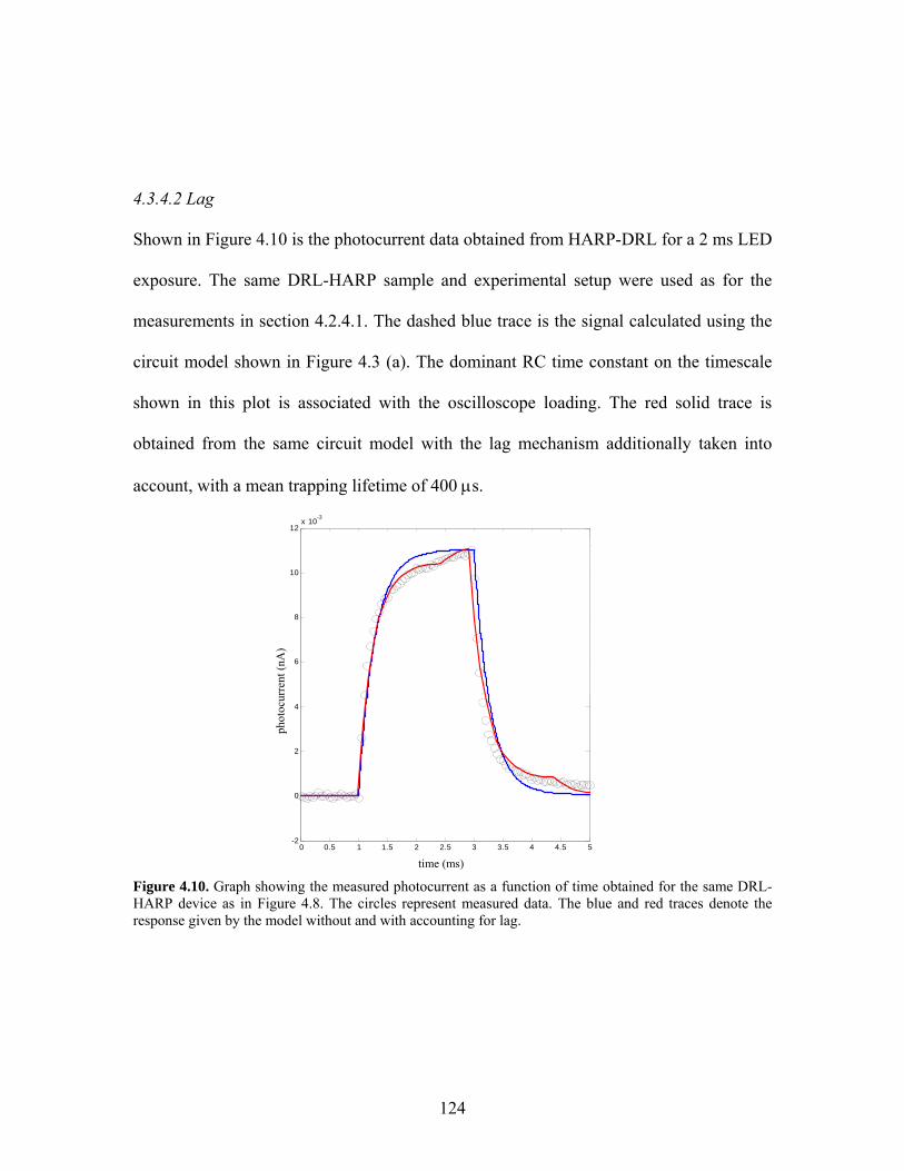
4.3.4.2 Lag
Shown in Figure 4.10 is the photocurrent data obtained from HARP-DRL for a 2 ms LED
exposure. The same DRL-HARP sample and experimental setup were used as for the
measurements in section 4.2.4.1. The dashed blue trace is the signal calculated using the
circuit model shown in Figure 4.3 (a). The dominant RC time constant on the timescale
shown in this plot is associated with the oscilloscope loading. The red solid trace is
obtained from the same circuit model with the lag mechanism additionally taken into
account, with a mean trapping lifetime of 400 µs.
0 0.5 1 1.5 2 2.5 3 3.5 4 4.5 5
x 10-3
-2
0
2
4
6
8
10
12x 10
-3
0.5 mR equivalent X-ray exposure2 ms LED pulseA = 1 mm2
CCA = 25 pF/mm2
RCA = 1.5 GΩ /mm2
CSe = 4 pF/mm2
1 MΩ scope no LR150 V bias
lag.m with:tf = 20a = 1.4lb = 15
time (ms)
phot
ocur
rent
(nA
)
Figure 4.10. Graph showing the measured photocurrent as a function of time obtained for the same DRL-HARP device as in Figure 4.8. The circles represent measured data. The blue and red traces denote the response given by the model without and with accounting for lag.
124

4.3.4.3 Predicted timing response for a DRL-HARP FPD Shown in Figure 4.11 is the timing response (output voltage as a function of time) of the
integrated DRL-HARP circuit model in Figure 4.3 (b) to 5 ms pulses of exposure at 33
Hz (corresponding to a nominal 33 frame-per-second fluoroscopic imaging rate). Two
traces are shown, one for the DRL-HARP and one for the HARP only showing the
voltage at the del storage capacitance. This model takes into account the smaller del size
as well as the periodic charge transfer and readout. The RC circuit parameters were taken
from section 4.2.4.1., however scaled appropriately to reflect the smaller del size: a DRL
capacitance of 0.25 pF and resistance of 1.5 TΩ and a HARP capacitance of 0.04 pF were
used. For each pulse, the leading edge corresponds to charging of the del storage
capacitance by the HARP, which acts as a current source. The top portion of the pulse
corresponds to charge storage on the del capacitance and slight leakage through the Off
resistance of the TFT (the equivalent drain-to-source resistance of the TFT in the Off
state). The trailing edge of each pulse corresponds to a rapid redistribution of charge
between the small (~ 1 pF) del storage capacitance and the much larger (~ 500 pF) input
capacitance of the charge amplifier.
125
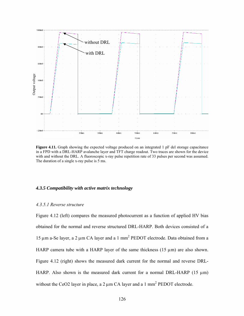
L
Out
put v
olta
ge
Figure 4.11. Graph showing in a FPD with a DRL-HARP with and without the DRL. AThe duration of a single x-ray
4.3.5 Compatibility with
4.3.5.1 Reverse structure
Figure 4.12 (left) compa
obtained for the normal
15 µm a-Se layer, a 2 µm
HARP camera tube with
Figure 4.12 (right) show
HARP. Also shown is
without the CeO2 layer i
with DR
without DRL
the expected voltage produced on an integrated 1 pF del storage capacitance avalanche layer and TFT charge readout. Two traces are shown for the device fluoroscopic x-ray pulse repetition rate of 33 pulses per second was assumed. pulse is 5 ms.
active matrix technology
res the measured photocurrent as a function of applied HV bias
and reverse structured DRL-HARP. Both devices consisted of a
CA layer and a 1 mm2 PEDOT electrode. Data obtained from a
a HARP layer of the same thickness (15 µm) are also shown.
s the measured dark current for the normal and reverse DRL-
the measured dark current for a normal DRL-HARP (15 µm)
n place, a 2 µm CA layer and a 1 mm2 PEDOT electrode.
126

0 500 1000 1500 200010
2
103
104
105
106
107
108
HV bias (V)
phot
ocur
rent
(A.U
.)
15 µm DRL-HARP15 µm HARP + camera15 µm DRL-HARP(reverse structure)
0 500 1000 1500 200010
0
101
102
103
104
HV bias (V)
dark
cur
rent
(pA
/mm
2 )
15 µm DRL-HARP
15 µm DRL-HARP(reverse structure)
15 µm DRL-HARP w/o CeO2
(a) (b)
Figure 4.12. (a): Graph showing the measured photocurrent as a function of high voltage (HV) bias for DRL-HARP (circles) and the reverse-structured DRL-HARP (diamonds). In both cases, 15 µm and 2 µm HARP and CA layers were used. Data is also shown for the measured photocurrent for a HARP camera with a 15 µm HARP target (solid squares). (b): graph showing the measured dark current as a function of HV for DRL-HARP (circles), the reverse-structured DRL-HARP (diamonds) and DRL-HARP without the CeO2 film.
4.3.5.2 HARP thickness
Figure 4.13 shows the measured photocurrent and dark current for a reverse structure
DRL-HARP with a 4 µm thick a-Se layer, a 1 µm CA layer and a 1 mm2 PEDOT
electrode. Photocurrent data obtained from a HARP camera tube with a 4 µm thick a-Se
layer are also shown, as well as a fit obtained using the conversion and avalanche gain
127

models described in section 2.34. The impact ionization factors used to fit the avalanche
characteristic were β1 = 1004 and β2 = 802. The best agreement between the DRL-HARP
data and the model could be achieved assuming a 4.5 µm thick a-Se thickness rather than
a 4 µm thickness.
0 200 400 600 80010
0
101
102
103
104
105
HV bias (V)
curre
nt (p
A/m
m2 )
4 µm DRL-HARPgc model for 4.5 µm HARP
ga model for 4.5 µm HARP
4 µm HARP + camera4 µm DRL-HARP (dark current)
Figure 4.13. Graph showing the measured photocurrent (circles) and dark current (triangles) as a function of high voltage (HV) bias for a DRL-HARP device with a 4 µm HARP layer and a 1 µm CA layer. The conversion and avalanche gain models are showed as solid and dashed traces. Also shown is the photocurrent for a HARP camera with a 4 µm HARP target.
4.3.5.3 TFT compatibility (experiments performed with Afrin Sultana U Waterloo)
Shown in Figure 4.14 is the characteristic of the TFTs manufactured at Waterloo.
Figure 4.15 shows the recorded oscilloscope traces using the experimental setup shown in
Figure 4.5. The signal used to drive the excitation LED is shown in blue. It is a periodic
30 Hz pulse sequence with a pulse width of several milliseconds, representative of a
128

fluoroscopic pulse sequence. The signal used to drive the gate of the TFT (i.e. VGS) is
shown in green. It is also a periodic 30 Hz pulse sequence with a swing from -10 to +5 V,
effectively switching the TFT on and off. The TFT output signal is shown in magenta.
It was also observed (but not shown here) that the excitation pulse produced a very small
output signal in the Off state.
Shown in Figure 4.15 is magnitude of the TFT output signal as a function of the HV bias
across the DRL-HARP and the excitation source intensity. The measured TFT
characteristic after this experiment was essentially unchanged (i.e. almost identical to that
shown in Figure 4.14).
Figure 4.14. Graph showing the measured drain-source current as a function of gate-source voltage for the thin film transistor shown in Figure 4.5. Characteristics are shown for drain-source voltages of 1 V and 10 V.
129

Figure 4.15. Graph showing the applied LED and TFT gate pulses and the TFT output current using the experimental setup shown in Figure 4.5 consisting of a DRL-HARP electrically coupled to a TFT.
4.4 Discussion
4.4.1 Noise characterization
From Figure 4.6, which shows the DRL-HARP photocurrent magnitude and variance as a
function of avalanche multiplication gain ga, it can be seen that as the avalanche gain ga
is increased, the signal rises linearly and the noise remains largely unaffected for ga < 10.
However for ga >10, the noise starts to increase linearly with gain. As ga approaches 100,
there is an apparent drop in SNR relative to the model (Figure 4.6). Based on the dark
current measurement and discussion in section 2.5.3, we would not expect this to be
caused by dark current shot noise for ga < 104. The measured dark current of 1 nA,
however, suggests that shot noise could in fact be causing this drop in SNR. The
particular HARP target used in this experiment did not contain stabilized a-Se. It is
130

possible that it had started to crystallize, resulting in much larger dark currents and
thereby limiting the maximum achievable ga.
Nonetheless, for the purposes of noise characterization, we can see that within the range
of avalanche gains investigated ( 1< ga <100) – which includes the ga = 50 required for
quantum noise limited (QNL) operation at the lowest fluoroscopic exposures - the noise
measurements agree well with our avalanche noise model described in section 4.2.1. This
is an important finding since it experimentally confirms that the solid-state electroded
DRL-HARP does not produce significant additional noise, while providing sufficient
avalanche multiplication gain for QNL operation, as speculated in section 2.5.3.
It should be noted that, using the linear cascade model shown in Figure 4.1, the maximum
theoretical DQE can be calculated as follows:
ηηηηη
ηηη
ccc
c
c
c
cac
ca
ca
in
out
gAgA
gg
qqggA
qggqgg
SNRSNRDQE 11
112
22
00
2022
20
222
2
2
max
+=
+=
+== Eq. 4.5
In the optical case, gc = 1, leading to a maximum DQE of 0.5. Thus, in this case, the
penalty due to avalanche multiplication gain corresponds to a reduction in DQE by a
factor of 2. Fortunately, in the x-ray case, in which each X-ray produces many secondary
quanta (charge in the direct-conversion case and optical photons in the indirect-
conversion case), gc >> 1 and the maximum DQE now approaches unity.
131

4.4.2 X-ray sensitivity
From the x-ray sensitivity measurement shown in Figure 4.7, it can be seen that there is
very good correlation between the gain measured using x-ray and optical methods. This is
despite the difference in peak emission wavelengths of the LED (blue) and CsI:Tl
phosphor (green). This is as expected, since the quantum efficiency of a-Se is very high
(> 95 %) at both wavelengths for a-Se biased at high electric field strengths (E > 70
V/µm).1 Furthermore, the x-ray-generated signal exceeded the minimum level required to
overcome electronic noise by over an order of magnitude. It is very encouraging that such
a distinct signal could be obtained at an x-ray exposure of 1 µR, which corresponds to the
lowest mean fluoroscopic exposure at the detector used in interventional radiology. As
suggested earlier in section 4.2.2, these results are sufficient to demonstrate the required
sensitivity of DRL-HARP to overcome the effects of electronic noise throughout the
entire clinical fluoroscopic exposure range for both indirect and direct conversion flat
panel detector implementations.
4.4.3 Dynamic range
From Figure 4.8 which shows the measured DRL-HARP output charge as a function of
equivalent x-ray exposure at different electric field strengths Ea-Se, it can be seen that for
Ea-Se = 10 V/µm and at 30 frames/second, the DRL-HARP response is linear up to an
exposure of approximately 1 mR/frame. At larger exposures, distinct signal saturation
occurs. For radiography however, a rapid imaging rate is not necessary. When the
experiment was repeated at a much lower imaging rate of 1 frame/second, the response
132

remained linear beyond the radiographic exposure range. It is interesting to note that at a
larger Ea-Se = 73 V/µm which is the highest electric field strength at which avalanche
multiplication does not occur, the linear range of operation at 30 frames/s was
significantly extended and encompassed most of the radiographic region. This suggests
that an important mechanism behind the signal saturation involves charge trapping, since
the probability of charge trapping increases with decreasing electric field. However, the
total gain g (relative to a-Se biased at 10 V/µm) at Ea-Se = 73 V/µm is only 6 and is due
only to an increase in conversion gain. This is not enough to overcome electronic noise,
since at an exposure of 10-7 R/frame, the extrapolated output charge produced by DRL-
HARP is the same as the electronic noise charge (Figure 4.8). Hence, a larger Ea-Se is
required to overcome the electronic noise.
The datasets obtained for Ea-Se = 87 V/µm and Ea-Se = 93 V/µm reveal the presence of
signal saturation and the onset of saturation occurs at lower exposures with increasing Ea-
Se. In other words, an increase in avalanche multiplication gain is causing larger signal
saturation at the same level of exposure. This is expected, since the same amount of
uncollected charge inside the device will reduce the avalanche multiplication gain more
prominently at larger fields since the avalanche gain characteristic is steeper at these
fields.
This saturation effect can be thought of as a self-limiting mechanism that restricts the
total amount of charge produced in the device for each radiation pulse. It is, in fact, an
133

important advantage for a flat panel detector used in interventional radiology applications
since the entire sensitive region of the panel may not necessarily be behind the patient. In
other words, certain portions of the panel may be exposed to the direct diagnostic x-ray
beam. The attenuation factor Ap of the x-ray beam through the patient is given by Beer’s
law:
tp eA ⋅−= µ Eq. 4.6
where µ is the linear attenuation coefficient of the patient (we can approximate using a µ
for water of 0.22/cm) and t is the patient thickness. Thus, for a 30 cm patient, the direct x-
ray beam will have a 103 times larger exposure than the mean exposure of the beam
exiting the patient. It can now be appreciated from Figure 4.8, that if a direct exposure
were to occur in the fluoroscopic mode with the detector having some arbitrary amount of
avalanche gain, the sudden increase in photon-generated charge would reduce the
avalanche gain to unity, meaning that the response would be similar to the response at 73
V/µm. Thus, a 103 time increase in radiation exposure would result in a maximum output
charge of 1010 e/mm2. Assuming a del size and capacitance of 100 µm x 100 µm and 2
pF, respectively, this would result in a maximum voltage across the del storage
capacitance VC of 8 V. In typical TFT designs, it is desirable to maintain a VC less than 10
V to prevent excessive current leakage through the TFT.6 VC could be restricted further
by increasing the size of the del storage capacitance. Clearly, without the self-limiting
avalanche gain mechanism however, either a much larger VC or a specialized TFT such as
a dual-gate TFT7 would be required, which might significantly complicate the active
matrix manufacturing process.
134

4.4.4 Temporal response
4.4.4.1 RC and ghosting
From the photocurrent transients shown in Figure 4.9, it can be seen that the DRL-HARP
signal (green trace) differs from the HARP signal (red trace) in two ways: (1) during
exposure, the DRL-HARP signal decreases in time and (2) after exposure, an exponential
tail is apparent. The first effect cannot be explained by using the capacitor charge and
discharge equations 4.3 and 4.4. It is likely due to ghosting, which is a reduction in
sensitivity of the a-Se due to trapped charge. Since this effect in apparent only in the
DRL-HARP, the charge trapping does not predominantly occur in the a-Se bulk. Rather,
holes are likely being trapped at the a-Se-CA interface and this generates an electric field
inside the a-Se layer which opposes the main applied electric field. The circuit model in
Figure 4.3 (a) does not take charge trapping into account and this explains the
discrepancy between the green trace and blue trace throughout the duration of the pulse in
Figure 4.9. By including the effect of hole trapping at the a-Se-CA interface in addition to
the charge/discharge effects, excellent agreement is obtained between the model and
experimental data (see black trace in Figure 4.9 (a)). The sensitivity reduction due to
ghosting during the 150 ms exposure can be estimated by subtracting the relative area
between the blue and green traces shown in Figure 4.9 (b), yielding a reduction factor of
8%.
135
With regards to the second effect (exponential tail), the circuit model approximated by
Equations 4.3 and 4.4 agrees well with the measured DRL-HARP photocurrent. This
confirms that the exponential tail is due to resistance-capacitance (RC) effects caused by
the DRL. The time constant corresponding to the exponential tail in Figure 4.9 is on the
order of 10 ms, which is in good agreement with the time constant (τ2 in Eq. 4.2) of the
CA layer used for the DRL.
As seen in Figure 4.9 (b), when a significantly larger electric field strength is applied in
the DRL-HARP (E = 67 V/µm), the ghosting effect becomes insignificant (blue trace).
The inherent symmetry of the photocurrent response in this case (along the rising and
falling edges) re-confirms that the rounded edges of the photocurrent pulse are due to the
RC mechanism.
4.4.4.2 Lag
There is good correlation between the model and experimental data for the rising and
falling edges of the pulse, however a discrepancy exists during and after the pulse: during
the pulse, there is less photocurrent than expected and the opposite is true immediately
following the pulse. This suggests that there is a lag mechanism at play, in which some
charge is being temporarily trapped in the bulk of the a-Se, reducing the current and is
subsequenty released, leading to an increase in current. Taking the lag mechanism into
account in the model and using a mean charge trapping lifetime of 1000 µs yields the red
trace in Figure 4.10, which is in good agreement with the experimental data. The mean
136

bulk trapping lifeftime of holes in a-Se is 400 µs which is on the same order as the value
used in the model.
4.4.4.3 Predicted timing response for a DRL-HARP FPD
The relative significance of ghosting and lag is expected to remain the same in a DRL-
HARP FPD with 100 times smaller dels (100 x 100 µm) than those characterized in this
work. This is because both the amount of trapped charge per del Qt as well as the del
capacitance Cd will be reduced by the same factor (100) and so the built-in bias resulting
from the trapped charge, which is simply given by the ratio Qt/ Cd should remain
constant. Hence, we would not expect charge trapping to degrade the linearity of DRL-
HARP beyond what is shown in Figure 4.8.
The RC effects are slightly more complex, in the sense that the del resistance and
capacitance can interact with other resistances and capacitances which are external to the
del such as those present in the HV filter. We can use the results of the circuit model in
Figure 4.3 (b) to understand the particular significance of RC effects introduced by the
DRL for an integrated DRL-HARP with 100 x 100 µm dels. Shown in Figure 4.11 is the
timing response of the integrated DRL-HARP circuit model to 5 ms pulses of exposure at
30 Hz (corresponding to a nominal 30 frame-per-second imaging rate). This model not
only takes into account the smaller del size but also the perdiodic charge transfer and
readout. It provides a reasonably good approximation of the RC response in a HARP-
DRL FPD. As seen, the presence of the DRL results in a reduction of the peak signal by
15%. More importantly, however, the difference between the magnitude of the first peak
137

and subsequent peaks in the pulse sequence is negligible, indicating that the exponential
tail associated with the RC discharge observed in Figure 4.9 has no adverse effects on the
timing response. Stated another way, there is no apparent shift in the signal baseline,
indicating that nearly all the charge produced by each light pulse can be removed from
the device prior to the next pulse. This is a reasonable result, since for pulses much
shorter in duration than the 150 ms pulse shown in Figure 4.9, we would expect most of
the charge signal to be coupled through the capacitance of the DRL, leaving only a
minute fraction to discharge through the resistance of the DRL.
4.4.5 Compatibility with active matrix technology
4.4.5.1 Reverse structure
As shown in the gain measurement of the reverse-structured DRL-HARP in Figure 4.12
(a), it can be seen that there is generally good agreement between the gain characteristics
of the normal and reverse DRL-HARP devices up to HV = 1200 V. For larger biases (i.e.
the avalanche multiplication region), the reverse DRL-HARP avalanche gain
characteristic rises slower than for the normal DRL-HARP. A maximum avalanche gain
of 30 could be obtained at 1575 V which is much lower than the gain of 104 obtained for
the normal DRL-HARP at the same bias. The photocurrent data obtained from the HARP
camera followed the normal DRL-HARP data more closely, however a significant
discrepancy is also observed, in both the conversion and avalanche gain regions.
It can be seen that the dark current for both the normal and reverse DRL-HARP
structures (with CeO2) is very similar (within a factor of 1.5), however there is a marked
138

increase in dark current for the DRL-HARP without CeO2 at HV = 1470V (Figure 4.12
(b)). This result confirms that CeO2 effectively acts as a blocking contact. Further studies
should be performed to understand how the CeO2 thickness affects its hole blocking
efficiency at high electric field strengths.
The reason for the discrepancies between the avalanche gain characteristics in Figure
4.12 is unclear. In the case of the normal and reverse DRL-HARP devices, the significant
difference in gain cannot be due to voltage drops across the DRL, since the dark current
for both devices is approximately the same (Figure 4.12 (b)). The discrepancies are likely
due to differences in the a-Se impact ionization factors (IIF) for the different devices. The
IIF is very dependent on the material properties of the a-Se. These, in turn can vary
considerably depending on the material deposition process. Since a-Se is organized in the
form of chains that grow in an orthogonal direction outward from the substrate plane8, the
structure of these chains can also depend on the nature of the substrate on which the a-Se
is deposited. The resulting change in the IIFs can lead to a significant difference in
avalanche gain, since the gain is exponentially dependent on these factors.
The sharp rise in dark current for the DRL-HARP without the CeO2 layer confirms the
importance of this as a hole-blocking layer. It is reasonable to expect a thicker CeO2 layer
to block holes at larger field strengths, however the CeO2 layer in the HARP samples
used in this work was limited to 400 nm. The reason for this was to allow sufficient
transparency so as to maintain a high optical quantum efficiency. For the direct-
conversion avalanche detector structure proposed in Chapter 3, however, optical
139

transparency is not required, since electric charge is coupled directly into the HARP layer
from the drift region. In this case, significantly thicker CeO2 layers could be used,
potentially enabling better blocking efficiency.
4.4.5.2 HARP thickness
As seen in Figure 4.13 which shows the gain and dark current measurements for the
DRL-HARP with a 4 µm thick HARP layer, there is also (as previously seen in section
4.2.5.1), a very significant discrepancy between the HARP camera and the DRL-HARP
data, and the reverse DRL-HARP once again produces significantly less avalanche gain
than expected.
It can be seen that the dark current, when considered as a function of ESe is very similar
for the measurements involving both the 4 and 15 µm HARP layers. However, a much
larger electric field strength could be applied across the 4 µm DRL-HARP than across the
15 µm DRL-HARP (E = 170 V/µm). Interestingly, the dark current at this field
(corresponding to HV = 700 V), is only 45 pA/mm2 and the avalanche gain saturates at
gav = 10. This suggests that there is a drop in E somewhere within the DRL-HARP
structure such that ESe is significantly lower than the nominal field (E ) applied across the
entire structure. Assuming a resistance of 20 GΩ/mm2 for the 2 µm CA layer (as
measured in section 2.4.1) used as the DRL, the total potential drop across the DRL is not
expected to exceed 1 V. This is not sufficient to warrant a sharp decrease in avalanche
gain. Hence there must be a mechanism within the reverse HARP structure which leads
to a decrease in ESe. Since the materials used in the reverse HARP are the same as those
140

used in the normal HARP (except for the Au contact, however this is a conductor so it
should not produce any potential drop), it is most likely that the cause of this ESe
reduction is a space charge mechanism caused by significant interfacial trapping. This
could include, for instance, hole trapping within the a-Se/a-Se:LiF or a-Se:LiF/CeO2
interfaces or electron trapping within the a-Se/Sb2S3 or Sb2S3/Au interfaces. Although
most of these interfaces also exist in the normal HARP, their material properties may be
different in the reverse HARP because of the different material deposition sequence. For
example, CeO2 deposited on a-Se:LiF could produce an interface with a significantly
larger number of electron traps than a-Se:LiF deposited on CeO2.
4.4.5.3 TFT compatibility
It can be seen from the oscilloscope traces in Figure 4.14 that the potential applied at the
gate of the transistor (VGS) determines the state of the transistor: for negative potentials,
the TFT is in the Off state and has a very high resistance (ROff ~ 10 TΩ) and for VGS > 5
V, the TFT is in the On state and has a much lower resistance (ROn ~ 10 MΩ). This
switch-like behaviour enables photon-generated charge to be integrated in the Off state
and be transferred to the charge amplifier in the On state. It can also be seen in Figure
4.15 that, as expected, the TFT output signal is strongly modulated by the gate pulse.
Futhermore, even though the gate pulse that switches the TFT into the On state occurs
many milliseconds after the excitation pulse, the signal is still present. These observations
indicate the proper functioning of the TFT and storage capacitance.
141

It was also observed (but not shown here) that the excitation pulse produced a very small
output signal in the Off state (less than 5% of the signal produced during the On state).
This is likely due to signal coupling through the drain-source capacitance of the TFT.
This effect is present in any TFT and can be thought of as a source of noise in the readout
electronics. The results in Figure 4.16, which show the response of the TFT/DRL-HARP
system are very similar to the results of output charge as a function of input exposure
shown in Figure 4.8 and demonstrate a piece-wise linear mode of operation and a clear
increase in signal due to avalanche multiplication gain. Most importantly, however,
proper operation of the DRL-HARP and TFT could be maintained without any adverse
effects to either of the devices, even when HV biases as large as 1485 V were applied
across the DRL-HARP.
The measured TFT characteristic after this experiment was almost identical to that shown
in Figure 4.14. This indicates that the high-voltage DRL-HARP is compatible with low-
voltage TFT readout technology. In particular, any electrical discharges produced in the
DRL-HARP are not sufficiently large to cause breakdown of the TFT gate oxide.
These results are very encouraging and are an important step towards the realization of a
practical avalanche FPD. Considering that, as discussed in section 4.2.5.2, thinner HARP
layers could be used to achieve the same amount of gain for QNL operation, the
likelihood of breakdown of the TFT gate oxide is expected to be even further reduced.
142

4.5 Conclusion
We have demonstrated in this chapter that there are no fundamental obstacles preventing
the use of a DRL-HARP avalanche photoreceptor for FPD applications in interventional
radiology. Experimental results have confirmed that, for the avalanche multiplication
gains required for quantum noise limited operation in fluoroscopy, DRL-HARP does not
introduce any additional noise beyond that theoretically predicted in Chapter 3. The high
x-ray sensitivity of DRL-HARP in an indirect conversion implementation has been
demonstrated at the lowest clinical exposure levels and it has been discussed that a direct-
conversion implementation would provide an equally high sensitivity. DRL-HARP was
found to have a very wide piecewise linear range of operation extending over five orders
of magnitude and encompassing both the clinically-relevant fluoroscopic and
radiographic x-ray exposures. It has been identified that the key mechanisms leading to
nonlinear operation in the avalanche regime are due to resistive-capacitive effects of the
DRL and ghosting due to charge trapping at the DRL-a-Se interface. These effects,
however, are negligible at the low exposures encountered in fluoroscopy and at imaging
rates of 33 frames per second or less. Finally, it has been demonstrated that DRL-HARP
is compatible with existing active matrix technology used in FPDs; a reverse HARP
structure -- facilitating the deposition of HARP on active matrix arrays -- has been
proposed and tested and electrical compatibility of DRL-HARP with integrated TFT
readout elements has been demonstrated.
143

References
1 W. Zhao, D. Li, A. Reznik, B. J. M. Lui, D. C. Hunt, J. A. Rowlands, Y. Ohkawa,
and K. Tanioka, "Indirect flat-panel detector with avalanche gain: Fundamental
feasibility investigation for SHARP-AMFPI (scintillator HARP active matrix flat
panel imager)," Med. Phys. 32, 2954-2966 (2005).
2 M.M. Wronski and J.A. Rowlands, "Direct-conversion flat panel imager with
avalanche gain: Feasibility investigation for HARP-AMFPI," Med. Phys. 35 (12),
5207-5218 (2008).
3 J.A. Rowlands and J. Yorkston, "Flat Panel Detectors for Digital Radiography," in
Handbook of Medical Imaging, edited by J. Beutel, H. Kundel, and R. Van Metter
(SPIE, Bellingham, Washington, 2000), Vol. I.
4 P. W. Tuinenga, SPICE: a Guide to Circuit Simulation and Analysis Using
PSpice. (Prentice-Hall, 1988).
5 K.S. Karim, M.H. Izadi, F. Taghibakhsh, and G. Sanaie, "Intelligent pixel
architectures for digital medical imaging applications," ECS Transactions 8, 289-
293 (2007).
6 L. E. Antonuk, K.-W. Jee, Y. El-Mohri, M. Maolinbay, J. H. Siewerdsen, S.
Nassif, X. Rong, Q. Zhao, R. A. Street, and K. S. Shah, "Strategies to improve the
signal and noise performance of active matrix, flat-panel imagers for diagnostic x-
ray applications," Med. Phys. 27, 289-306 (2000).
144

7 W. Zhao, J. Law, D. Waechter, Z. Huang, and J. A. Rowlands, "Digital radiology
using active matrix readout of amorphous selenium: Detectors with high voltage
protection," Med. Phys. 25, 539-549 (1998).
8 J. Hegedüs and S. Kugler, "Growth of amorphous selenium thin films: classical
versus quantum mechanical molecular dynamics simulation," J. Phys.: Condens.
Matter 17, 6459-6468 (2005).
145

Chapter 5 Conclusions 5.1 Brief summary 5.2 Summary of major results 5.3 Original contributions 5.4 Future work
146
5.1 Brief summary
Current AMFPIs are not x-ray quantum noise limited at the lowest fluoroscopic
exposures used in interventional radiology. This is due to the presence of substantial
electronic noise in the active matrix which is used to read out the x-ray-generated charge
image. In this work, the feasibility of an AMFPI with internal gain has been
demonstrated. With sufficient gain, the electronic noise can be overcome throughout the
entire clinical x-ray exposure range.
The work has focused on avalanche multiplication in an a-Se photoconductor. The
motivation behind this approach was twofold: first, a-Se is a well characterized
photoconductor currently in use in a number of AMFPI systems. Secondly, high
sensitivity a-Se layers with internal avalanche multiplication gain (HARP) are currently
being used in specialized broadcasting cameras for very low light imaging applications.
The overarching goal of this thesis was to bridge the gap between the AMFPI and HARP
technologies. There are currently two key limitations with HARP: first, it operates inside
a vaccum tube with a scanning electron beam for readout of the charge image, and second
it is used for imaging of visible light photons. Towards this end, it was necessary to: (1)
demonstrate a fully solid-state implementation of HARP; (2) investigate how this solid-
state avalanche detector could be used to image X-rays with sufficient spatial resolution
for the imaging of specialized endovascular devices or important anatomical features
such as coronary microcalcifications; (3) demonstrate that a HARP-AMFPI imager would
147

satisfy not only the high x-ray sensitivity and spatial resolution requirements of
interventional radiology, but would also satisfy other important requirements such as
being able to accommodate a very wide range of x-ray exposures and having a linear
response at real-time imaging frame rates.
These three specific aims were addressed in each of the three major chapters of the thesis.
In Chapter 2, it was shown that HARP could provide sufficient avalanche gain in the
solid state to overcome electronic noise in AMFPIs by incorporating an additional layer
into its structure. Next, an investigation in Chapter 3 demonstrated the feasibility of using
HARP in the solid state for the imaging of X-rays using both indirect and direct
conversion approaches. The main focus of the chapter was on a high spatial resolution
direct conversion implementation of HARP-AMFPI. Finally, the last major chapter of the
thesis (Chapter 4) demonstrated that HARP-AMFPI could accommodate the very wide
clinical range of exposures used in interventional radiology and could provide a linear
response to incident X-rays at the highest imaging frame rates used in fluoroscopy.
Once implemented in a clinical system, AMFPIs with internal avalanche gain will
provide the highest physically possible image quality at the lowest possible patient doses
of ionizing radiation. These systems, particularly direct-conversion implementations, will
also provide very high spatial resolutions facilitating the deployment of intricate
endovascular devices with extremely small wire diameters.
148

5.2 Summary of major results
5.2.1 Solving the breakdown problem of electroded HARP
It was experimentally confirmed that the two key limitations of electroded HARP are: (1)
electric field enhancement near electrode edges and (2) deposition of heat due to high
localized current densities during electrical discharges. These effects caused irreversible
breakdown of HARP despite the presence of a large series current-limiting resistance. It
was found that conductive polymer electrodes (PEDOT) directly deposited on HARP
were able to sustain significantly higher electric field strengths across the HARP than
metallized contacts (Au or Pt) of the same size, possibly due to the relatively large size of
polymer molecules which cannot diffuse into the a-Se and the absence of free electrons in
PEDOT.
The incorporation of a polymer distributed resistance layer (DRL) into the HARP
structure was shown to essentially eliminate the breakdown problem and enabled the
HARP to sustain electric field strengths as high as 105 V/µm. A casting process was
developed for depositing layers of a cellulose acetate polymer on existing HARP layers
in a reproducible fashion. The cellulose acetate polymer was chosen based on its
resistivity (ρ = 5x10¹² Ωcm), excellent transparency and adhesion to a-Se. It served as a
DRL and its primary functions were to (1) reduce the electric field in the vicinity of
electrode edges and (2) provide a current limiting mechanism to limit localized discharge
currents.
149

It was found that a cellulose acetate (DRL) thickness of 2 µm enabled avalanche
multiplication gains as high as 104 in a 15 µm thick HARP layer for an applied high
voltage bias of 1575 V (ESe = 105 V/µm). This gain in DRL-HARP was attributed solely
to impact ionization of holes. Furthermore, it was found that increasing the thickness of
the DRL and applying biases larger than 1575 V did not yield consistently larger
avalanche gains. This was attributed to failure of the hole blocking contact for E > 105
V/µm. To completely overcome the electronic noise in either direct or indirect AMFPI, a
maximum avalanche gain of only 50 is required (corresponding to a bias of 1450 V for a
15 µm HARP layer). For these conditions, an average electrical discharge rate of 1
discharge per 7 minutes was observed. As such, electrical discharges are not expected to
add any noise during fluoroscopy in which images are acquired only once every 100 ms
or less.
The measured dark current in DRL-HARP was less than 20 pA/mm2 at room temperature
for ESe < 105 V/µm. The measured a-Se hole mobility in DRL-HARP was found to be
same as in standard Xerox a-Se. Direct evidence of avalanche multiplication in DRL-
HARP was obtained using a time of flight analysis.
150

5.2.2 X-ray imaging with HARP-AMFPI
A direct-conversion HARP-AMFPI flat panel imager structure was proposed. It consists
of a thick a-Se drift region in which X-rays are absorbed and generate charge and a thin
avalanche multiplication region (HARP). This structure consists of guard electrodes and
this enables a significant reduction of dark current compared to similar dual-layered
structures proposed earlier.1
A model based on the finite element method was implemented and used to demonstrate
that the direct-conversion HARP-AMFPI imager can provide the required amount of
avalanche gain for quantum noise limited operation, while overcoming the problem of
depth-dependent gain fluctuation noise. The concept of secondary Swank factor was
introduced and was used to quantify the degradation of DQE due to differences in charge
travel path variation throughout a non-uniform electric field distribution.
It was found that the predicted imaging response of HARP-AMFPI at high spatial
frequencies is excellent (DQE ~ 0.4 at 5 cycles/mm) and should provide good detection
of very narrow (~100 µm diameter) high-contrast objects used in clinical interventions
such as stent struts (individual stent wires). Furthermore, it was found that the presence of
electric field nonuniformities does not affect the DQE of the detector, that 100% fill
factors could be obtained and that avalanche multiplication noise is negligible for x-ray
energies greater than 1 keV, which is the case at the diagnostic energies used in
interventional radiology.
151
5.2.3 Addressing the requirements of interventional radiology
It was first experimentally confirmed that DRL-HARP does not produce significant
additional noise while providing sufficient avalanche multiplication gain for x-ray
quantum noise limited operation. The high sensitivity to diagnostic energy X-rays at low
fluoroscopic exposures was experimentally demonstrated. Next, it was shown that DRL-
HARP has a very wide piecewise linear exposure range which encompasses both the
clinically relevant fluoroscopic and radiographic x-ray exposures. Both ghosting and
resistive-capacitive effects have been identified as dominant effects leading to signal
saturation at large x-ray exposures, however this should not limit the detector linearity for
fluoroscopic (30 frames/second or less) or radiographic modes of operation. In fact, it
was suggested that signal saturation during avalanche multiplication at unexpectedly
large detector exposures (such as an exposure to the direct x-ray beam un-attenuated by
the patient) is a beneficial effect which can alleviate the overproduction of charge leading
to potential damage of the thin film transistors or storage capacitors in the active matrix.
It was investigated how DRL-HARP could be made more amenable to the AMFPI
manufacturing process. Towards this end, a reverse HARP structure was proposed,
fabricated and experimentally characterized. It was found to produce sufficient avalanche
gain for quantum noise limited operation at low fluoroscopic x-ray exposures, however
the measured gain was much lower than for a regular HARP structure of the same
thickness. Two potential underlying causes have been identified: (1) possible differences
in the a-Se impact ionization factors which are dependent on the material properties of
152

the a-Se and can vary considerably depending on the material deposition process; (2)
possible space charge mechanism caused by enhanced interfacial trapping in the reverse
structure, also resulting from changes in the material deposition process.
It was experimentally determined that CeO2 plays a key role in limiting hole injection in
15 µm HARP targets for field strengths exceeding 98 V/µm. It was discussed that
although existing CeO2 blocking structures are sufficient for the gain requirements of
interventional radiology using 15 µm thick HARP layers, improved blocking layers could
potentially enable similar avalanche gains (i.e. 50) using significantly thinner HARP
layers (4 µm or less). This would translate into substantially lower high voltage
requirements which would facilitate integration with low-voltage active matrix
technology.
As a proof of concept, it was experimentally demonstrated that DRL-HARP consisting of
a 15 µm HARP and a 2 µm cellulose acetate DRL could be electrically contacted to a
low-voltage integrated thin film transistor (TFT) and that proper operation of the TFT
could be maintained while the DRL-HARP was biased at avalanche electric field
strengths (~100 V/µm). These results have shown that there are no fundamental physical
problems standing in the way of an integrated DRL-HARP-AMFPI device for
interventional radiology applications.
153

5.3 Original contributions
1. The work in this thesis has led to the development of the first solid-state detector
capable of producing linear avalanche gains as high as 104. The detector is based
on an amorphous selenium photoconductor which can be fabricated inexpensively
over large areas. As a result, this detector holds great promise for very high
sensitivity medical imagers. This contribution has provided a basis for U.S.A.
Patent No. 61/129389, Photodetector/Imaging Device with Avalanche Gain, filing
date: June 23, 2008. It has also provided the basis for the letter submitted to
Medical Physics under the name “A solid-state amorphous selenium avalanche
technology for large area photon counting and photon starved imaging
applications”.
2. A potentially largely scalable and low-cost cellulose acetate casting process was
developed. The process can provide uniform, optically transparent resistive
polymer layers of controllable thickness which provide a chemically stable
electrical contact to amorphous chalcogenide photodonductors. This enables the
elimination of electric field strength enhancement near conductive electrode edges
at the surface of such photoconductors and provides an electrical quenching
mechanism. Both functions prevent undesirable crystallization of the amorphous
chalcogenide photoconductor. This contribution has provided a basis for U.S.A.
Patent No. 61/129389, Photodetector/Imaging Device with Avalanche Gain, filing
date: June 23, 2008.
154

3. This work has demonstrated that, in principle, decoupling the charge conversion
and avalanche gain regions is an effective means of overcoming depth-dependent
gain fluctuation noise, while maintaining a high detective quantum efficiency.
This opens the door to a new generation of direct-conversion flat panel imagers
with internal gain which simultaneously provide both quantum noise limited x-ray
sensitivity and very high spatial resolution imaging. This contribution has
provided a basis for the paper: "Direct-conversion flat-panel imager with
avalanche gain: Feasibility investigation for HARP-AMFPI (HARP active matrix
flat panel imager)”, Med. Phys. (2008) 35: 5207-5218
4. This work has demonstrated that there are no fundamental physical problems
precluding the integration of high-voltage HARP and low-voltage AMFPI
technologies. This contribution has provided the basis for the paper submitted to
IEEE Sensors under the name: “Digital x-ray imaging using an avalanche a-Se
photoconductor”.
155

5.4 Future work
The work in this thesis has been largely exploratory and a number of material and device
engineering challenges have yet to be overcome before a-Se avalanche layers can be
successfully used in robust clinical flat panel imagers. Several key considerations will
now be outlined for future work.
5.4.1 Materials characterization
The polymer deposition process described in this work makes use of an acetone solvent
which could potentially crystallize a-Se. A materials characterization technique such as
differential scanning calorimetry or X-ray diffraction should be used to obtain the degree
of crystallization in a-Se before and after the deposition of cellulose acetate. If
crystallization is observed, then an alternative process should be developed, possibly
using a different resistive material.
Studies should be performed to understand how the thickness of the CeO2 layer affects its
hole blocking efficiency at high electric field strengths. Thicker (> 400 nm) CeO2 layers
could be used for the direct-conversion detector structure proposed in Chapter 3,
however, for indirect-conversion detectors, the hole blocking efficiency of this layer
should be balanced against its optical transparency to ensure that a thicker CeO2 layer
does not substantially degrade the optical quantum efficiency of the HARP layer.
156

It is crucial to better understand how the effects of HARP defects can be mitigated. The
main goal is to contain defects and prevent them from spreading to adjacent dels. It will
be necessary to investigate the growth dynamics of defects as a function of the magnitude
of current density traversing the del and determine if the DRL can be used to keep the
current density sufficiently low.
The avalanche gain discrepancies between the normal- and reverse-structured HARP
should be understood. A time-of-flight analysis could be carried out on both types of
samples and this could help determine whether the discrepancies are due to space charge
effects. If no substantial differences are noted, then it is possible that the a-Se ionization
factors are different. An improved deposition process may be required for the reverse-
structured HARP.
5.4.2 Device optimization
The HARP and DRL thicknesses should be optimized for interventional radiology
applications. Thinner HARP layers will require lower biases and this should enable
thinner DRLs as well which could potentially improve the temporal response. However,
the avalanche gain will also be more sensitive to any HARP thickness non-uniformities.
Thinner HARP layers may also require improved blocking contacts because the electric
field inside the a-Se will need to be made larger to sustain a sufficiently large avalanche
multiplication gain.
157

The design of the active matrix should be optimized such that it can support dels with and
without a-Se defects. For instance, the size and maximum tolerable potential of the del
storage capacitors should be carefully considered such that any defective del drawing an
unusually large current would be able to quench this current by reducing the electric field
strength and associated avalanche gain in the HARP.
5.4.3 Imager prototype fabrication
A DRL-HARP-AMFPI prototype should be fabricated, initially for optical imaging.
Stabilized a-Se should be used. A sandwich approach could initially be used in which a
regular-structured HARP could be coupled to an active matrix array with a DRL layer in
between them. Spacers may be necessary to control the thickness of the DRL. A better
approach would be to deposit the reverse-structured HARP on an active matrix array
coated with a DRL. The imager could then be used at both non-avalanche and avalanche
electric field strengths. It should be confirmed that the DRL does not affect the spatial
resolution of the imager and the defect kinetics should also be studied.
Next, the indirect-conversion SHARP-AMFPI should be realized. The focus should be on
improving the spatial resolution. This could be done by using a structured CsI:Tl
phosphor with no reflective layer and a sufficiently small del pitch such that the del
aperture function does not degrade the overall MTF of the imager.
158
Significant technical challenges remain to be overcome in order to realize the direct-
conversion HARP-AMFPI. These include, for instance, developing an a-Se deposition
process which allows for the deposition of a mesh electrode and controlling the electrode
fabrication process in such as way as to produce smooth rounded electrode edges which
do not induce excessively high localized electric fields. However, the fundamental results
presented here, along with preliminary experiments indicate that the method is robust and
practical and that the necessary developments are therefore worthwhile.
1 D. L. Y. Lee, "Selenium detector with a grid for selenium charge gain," Proc.
SPIE 5745, 216-222 (2005).
159

160