Design and Evaluation of Cell Interaction Based Vedic ... - MDPI
15
electronics Article Design and Evaluation of Cell Interaction Based Vedic Multiplier Using Quantum-Dot Cellular Automata Nuriddin Safoev and Jun-Cheol Jeon * Department of Computer Engineering, Kumoh National Institute of Technology 61, Daehak-ro, Gumi, Gyeongbuk 39177, Korea; [email protected] * Correspondence: [email protected]; Tel.: +82-54-478-7534 Received: 9 June 2020; Accepted: 19 June 2020; Published: 23 June 2020 Abstract: A multiplier is one of the main units for digital signal processing and communication systems. In this paper, a high speed and low complexity multiplier is designed on the basis of quantum-dot cellular automata (QCA), which is considered promising nanotechnology. We focus on Vedic multiplier architectures according to Vedic mathematics from ancient Indian sculptures. In fact, an adder is an important block in the design of almost all types of multipliers and a ripple carry adder is used to design simple multiplier implementations. However, a high-speed multi-bit multiplier requires high-speed adder owing to carry propagation. Cell-interaction-based QCA adders have better improvements over conventional majority-gate-based adders. Therefore, a two-bit Vedic multiplier is proposed in QCA and it is used to implement a four-bit form of the multiplier. The proposed architecture has a lower cell count and area compared to other existing structures. Moreover, simulation results demonstrate that the proposed design is sustainable and can be used to realize complex circuit designs for QCA communication networks. Keywords: nano communication; multiplier; quantum-dot cellular automata; ripple carry adder; vedic mathematics 1. Introduction High energy consumption is one of the major limitations for transistor-based complementary metal-oxide-semiconductor (CMOS) technology. This limitation cannot be solved completely by scaling down the size of the transistor. Quantum-dot cellular automata (QCA) [1], a type of self-reproduction cellular automata [2–4], is one remarkable nanotechnology that can be a possible solution to solve this problem. The energy efficiency and high-speed switching features of this technology is great motivation for developing this paradigm [5–9]. In this technology, logical states can be represented by two antipodal polarization levels in a QCA cell configuration. The square-shaped cell includes a pair of electrons with four quantum dots. QCA offers a new computation method and is based on the fundamental principle of quantum confinement [10–12]. There are some challenges for the physical implementation of a QCA cell at room temperature. In previous experiments, the cells were found to operate only at cryogenic temperatures. Recently, the fabrication of a QCA cell using the nano-damascene process has been successful [13]. This potentially enables the room temperature operation of QCA-based circuits. Array multipliers have been extensively investigated in QCA technology. However, there are also mathematical operations using the Vedic method that are very fast and require less hardware architecture. This can be used to improve the computational speed of processors. A huge number of adders are used to perform partial product addition for higher order multiplications. This method of Electronics 2020, 9, 1036; doi:10.3390/electronics9061036 www.mdpi.com/journal/electronics
-
Upload
khangminh22 -
Category
Documents
-
view
0 -
download
0
Transcript of Design and Evaluation of Cell Interaction Based Vedic ... - MDPI
electronics
Article
Design and Evaluation of Cell Interaction Based VedicMultiplier Using Quantum-Dot Cellular Automata
Nuriddin Safoev and Jun-Cheol Jeon *
Department of Computer Engineering, Kumoh National Institute of Technology 61, Daehak-ro, Gumi,Gyeongbuk 39177, Korea; [email protected]* Correspondence: [email protected]; Tel.: +82-54-478-7534
Received: 9 June 2020; Accepted: 19 June 2020; Published: 23 June 2020�����������������
Abstract: A multiplier is one of the main units for digital signal processing and communicationsystems. In this paper, a high speed and low complexity multiplier is designed on the basis ofquantum-dot cellular automata (QCA), which is considered promising nanotechnology. We focuson Vedic multiplier architectures according to Vedic mathematics from ancient Indian sculptures.In fact, an adder is an important block in the design of almost all types of multipliers and a ripplecarry adder is used to design simple multiplier implementations. However, a high-speed multi-bitmultiplier requires high-speed adder owing to carry propagation. Cell-interaction-based QCAadders have better improvements over conventional majority-gate-based adders. Therefore, a two-bitVedic multiplier is proposed in QCA and it is used to implement a four-bit form of the multiplier.The proposed architecture has a lower cell count and area compared to other existing structures.Moreover, simulation results demonstrate that the proposed design is sustainable and can be used torealize complex circuit designs for QCA communication networks.
Keywords: nano communication; multiplier; quantum-dot cellular automata; ripple carry adder;vedic mathematics
1. Introduction
High energy consumption is one of the major limitations for transistor-based complementarymetal-oxide-semiconductor (CMOS) technology. This limitation cannot be solved completely by scalingdown the size of the transistor. Quantum-dot cellular automata (QCA) [1], a type of self-reproductioncellular automata [2–4], is one remarkable nanotechnology that can be a possible solution to solvethis problem. The energy efficiency and high-speed switching features of this technology is greatmotivation for developing this paradigm [5–9].
In this technology, logical states can be represented by two antipodal polarization levels in aQCA cell configuration. The square-shaped cell includes a pair of electrons with four quantum dots.QCA offers a new computation method and is based on the fundamental principle of quantumconfinement [10–12].
There are some challenges for the physical implementation of a QCA cell at room temperature.In previous experiments, the cells were found to operate only at cryogenic temperatures. Recently,the fabrication of a QCA cell using the nano-damascene process has been successful [13]. This potentiallyenables the room temperature operation of QCA-based circuits.
Array multipliers have been extensively investigated in QCA technology. However, there arealso mathematical operations using the Vedic method that are very fast and require less hardwarearchitecture. This can be used to improve the computational speed of processors. A huge number ofadders are used to perform partial product addition for higher order multiplications. This method of
Electronics 2020, 9, 1036; doi:10.3390/electronics9061036 www.mdpi.com/journal/electronics
Electronics 2020, 9, 1036 2 of 15
multiplication is based on 16 Vedic sutras and describes the natural ways of solving a whole series ofmathematical problems [14–16].
In this paper, a new design for a two-bit multiplier using QCA technology is presented. We alsopropose a half adder for the implementation of a Vedic multiplier. It is implemented using acell-interaction-based exclusive-OR (XOR) structure [17]. Meanwhile, the energy dissipation of theproposed half adder is also analyzed. The proposed half adder plays an important role in theimplementation of the two-bit Vedic multiplier design. On the basis of this two-bit multiplier, a four-bitVedic multiplier design is proposed. Simulations and a comparison with prior designs are conductedwith the simulation tool QCADesigner 2.0.3 and QCAPro. The proposed designs have a lower cellcount, smaller area, lower latency, and smaller energy consumption features in comparison.
This paper is organized as follows. Section 2 introduces the basic concepts of QCA. In Section 3,the proposed designs, 2 × 2 and 4 × 4 Vedic multipliers are presented with their implementationsin QCA. The simulations and comparison are discussed in Section 4, with a brief explanation of theanalysis. Finally, Section 5 concludes the paper.
2. Related Works
2.1. Basic QCA
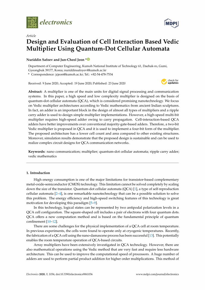
The basic element of QCA is a cell that holds quantum dots and two excess electrons. The positionsof the electrons in a cell are a logical state. The cell has a square-shaped nanostructure that containsfour quantum dots and two electrons, as shown in Figure 1. The electrons can move through a tunneljunction owing to their Coulombic repulsion. The existing Coulombic interaction between the electronsforces them to occupy positions at opposite corners of the cell by the concept of polarization. As a result,two stable states (binary zero and one) are represented in the cell [18–20]. Polarization, P, is determinedby one of two diagonals depending on the distribution of charges, and the value is measured [18].If the cell specifies ρi as the electron density of the i-th point for the four points i = 1 to 4 clockwisefrom the top right, then P is defined as follows.
P = ((ρ1 + ρ3) − (ρ2 + ρ4))/(ρ1 + ρ2 + ρ3 + ρ4) (1)
Electronics 2020, 9, x FOR PEER REVIEW 3 of 15
was applied well, and the blue short two arrows indicate the parts that were not applied due to the surrounding repulsive forces.
Figure 1. QCA cell with two possible polarizations.
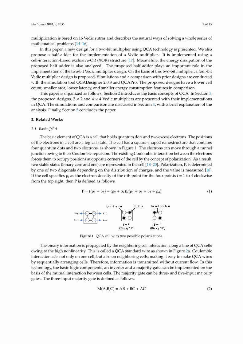
Figure 2. Quantum-dot cellular automata (QCA) basics: (a) wire; (b) three-input majority gate; (c) five-input majority gate; (d) simple inverter; and (d) robust inverter.
2.2. QCA Clocking
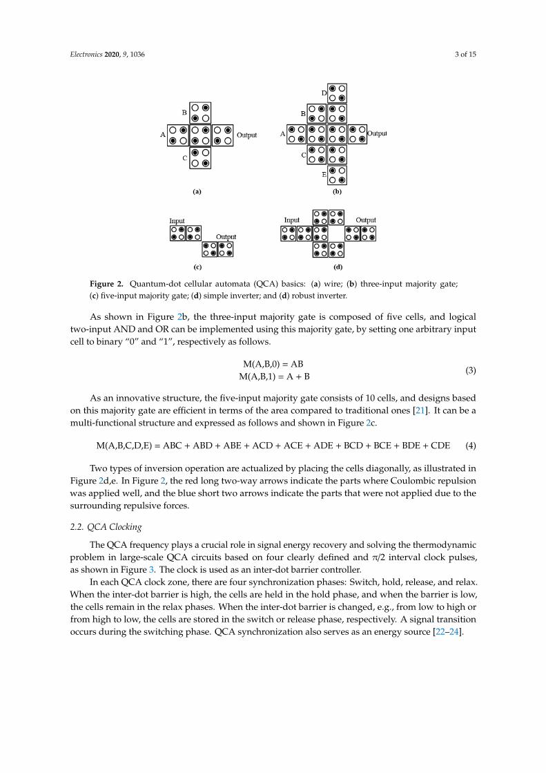
The QCA frequency plays a crucial role in signal energy recovery and solving the thermodynamic problem in large-scale QCA circuits based on four clearly defined and π/2 interval clock pulses, as shown in Figure 3. The clock is used as an inter-dot barrier controller.
In each QCA clock zone, there are four synchronization phases: Switch, hold, release, and relax. When the inter-dot barrier is high, the cells are held in the hold phase, and when the barrier is low, the cells remain in the relax phases. When the inter-dot barrier is changed, e.g., from low to high or from high to low, the cells are stored in the switch or release phase, respectively. A signal transition occurs during the switching phase. QCA synchronization also serves as an energy source [22–24].
Figure 1. QCA cell with two possible polarizations.
The binary information is propagated by the neighboring cell interaction along a line of QCA cellsowing to the high nonlinearity. This is called a QCA standard wire as shown in Figure 2a. Coulombicinteraction acts not only on one cell, but also on neighboring cells, making it easy to make QCA wiresby sequentially arranging cells. Therefore, information is transmitted without current flow. In thistechnology, the basic logic components, an inverter and a majority gate, can be implemented on thebasis of the mutual interaction between cells. The majority gate can be three- and five-input majoritygates. The three-input majority gate is defined as follows.
M(A,B,C) = AB + BC + AC (2)
Electronics 2020, 9, 1036 3 of 15
Electronics 2020, 9, x FOR PEER REVIEW 3 of 15
was applied well, and the blue short two arrows indicate the parts that were not applied due to the surrounding repulsive forces.
Figure 1. QCA cell with two possible polarizations.
Figure 2. Quantum-dot cellular automata (QCA) basics: (a) wire; (b) three-input majority gate; (c) five-input majority gate; (d) simple inverter; and (d) robust inverter.
2.2. QCA Clocking
The QCA frequency plays a crucial role in signal energy recovery and solving the thermodynamic problem in large-scale QCA circuits based on four clearly defined and π/2 interval clock pulses, as shown in Figure 3. The clock is used as an inter-dot barrier controller.
In each QCA clock zone, there are four synchronization phases: Switch, hold, release, and relax. When the inter-dot barrier is high, the cells are held in the hold phase, and when the barrier is low, the cells remain in the relax phases. When the inter-dot barrier is changed, e.g., from low to high or from high to low, the cells are stored in the switch or release phase, respectively. A signal transition occurs during the switching phase. QCA synchronization also serves as an energy source [22–24].
Figure 2. Quantum-dot cellular automata (QCA) basics: (a) wire; (b) three-input majority gate;(c) five-input majority gate; (d) simple inverter; and (d) robust inverter.
As shown in Figure 2b, the three-input majority gate is composed of five cells, and logicaltwo-input AND and OR can be implemented using this majority gate, by setting one arbitrary inputcell to binary “0” and “1”, respectively as follows.
M(A,B,0) = ABM(A,B,1) = A + B
(3)
As an innovative structure, the five-input majority gate consists of 10 cells, and designs basedon this majority gate are efficient in terms of the area compared to traditional ones [21]. It can be amulti-functional structure and expressed as follows and shown in Figure 2c.
M(A,B,C,D,E) = ABC + ABD + ABE + ACD + ACE + ADE + BCD + BCE + BDE + CDE (4)
Two types of inversion operation are actualized by placing the cells diagonally, as illustrated inFigure 2d,e. In Figure 2, the red long two-way arrows indicate the parts where Coulombic repulsionwas applied well, and the blue short two arrows indicate the parts that were not applied due to thesurrounding repulsive forces.
2.2. QCA Clocking
The QCA frequency plays a crucial role in signal energy recovery and solving the thermodynamicproblem in large-scale QCA circuits based on four clearly defined and π/2 interval clock pulses,as shown in Figure 3. The clock is used as an inter-dot barrier controller.
In each QCA clock zone, there are four synchronization phases: Switch, hold, release, and relax.When the inter-dot barrier is high, the cells are held in the hold phase, and when the barrier is low,the cells remain in the relax phases. When the inter-dot barrier is changed, e.g., from low to high orfrom high to low, the cells are stored in the switch or release phase, respectively. A signal transitionoccurs during the switching phase. QCA synchronization also serves as an energy source [22–24].
Electronics 2020, 9, 1036 4 of 15Electronics 2020, 9, x FOR PEER REVIEW 4 of 15
Figure 3. Four distinct QCA clock stages.
2.3. Wire Crossing in QCA
Four types of implementations can be used for the physical fabrication of QCA, such as metal-dot, semiconductor, molecular, and magnetic QCA implementations. If material production can be efficiently addressed, the next practical problem for a QCA circuit is its operating temperature (7K). This temperature is considered to be extremely low, and a QCA circuit needs to be optimized for room-temperature operation [25].
Cross-over technology is also considered as one of the problems in QCA technology. According to this concept, there are three types of cross methods: Coplanar, multi-layered, and logical crossover. The coplanar intersection of a wire is carried out using an inverter chain. The inverter chain represents a line of rotating (45˚) cells. A multi-layered crossover is a stereoscopic structure, which is built of several layers. The logical intersection of the wires is updated on the basis of QCA synchronization; namely, the cells in the switch and hold phases can cross cells in the release and relax phases, respectively [26–28]. The logical method of crossing wires is more reliable and tolerant than other crossover methods in the modelling process.
3. The Proposed Structures
3.1. Half Adder for the Multiplier
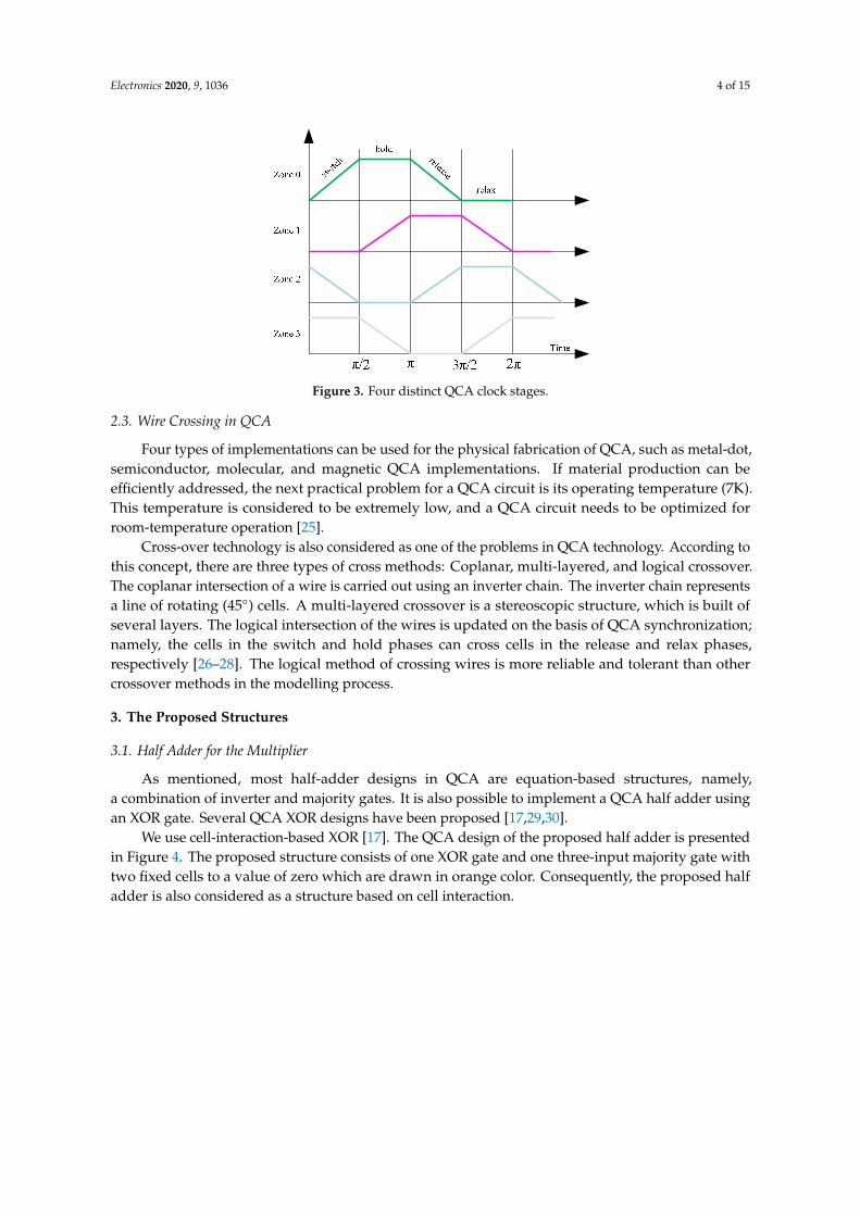
As mentioned, most half-adder designs in QCA are equation-based structures, namely, a combination of inverter and majority gates. It is also possible to implement a QCA half adder using an XOR gate. Several QCA XOR designs have been proposed [17,29,30].
We use cell-interaction-based XOR [17]. The QCA design of the proposed half adder is presented in Figure 4. The proposed structure consists of one XOR gate and one three-input majority gate with two fixed cells to a value of zero which are drawn in orange color. Consequently, the proposed half adder is also considered as a structure based on cell interaction.
Figure 3. Four distinct QCA clock stages.
2.3. Wire Crossing in QCA
Four types of implementations can be used for the physical fabrication of QCA, such as metal-dot,semiconductor, molecular, and magnetic QCA implementations. If material production can beefficiently addressed, the next practical problem for a QCA circuit is its operating temperature (7K).This temperature is considered to be extremely low, and a QCA circuit needs to be optimized forroom-temperature operation [25].
Cross-over technology is also considered as one of the problems in QCA technology. According tothis concept, there are three types of cross methods: Coplanar, multi-layered, and logical crossover.The coplanar intersection of a wire is carried out using an inverter chain. The inverter chain representsa line of rotating (45◦) cells. A multi-layered crossover is a stereoscopic structure, which is built ofseveral layers. The logical intersection of the wires is updated on the basis of QCA synchronization;namely, the cells in the switch and hold phases can cross cells in the release and relax phases,respectively [26–28]. The logical method of crossing wires is more reliable and tolerant than othercrossover methods in the modelling process.
3. The Proposed Structures
3.1. Half Adder for the Multiplier
As mentioned, most half-adder designs in QCA are equation-based structures, namely,a combination of inverter and majority gates. It is also possible to implement a QCA half adder usingan XOR gate. Several QCA XOR designs have been proposed [17,29,30].
We use cell-interaction-based XOR [17]. The QCA design of the proposed half adder is presentedin Figure 4. The proposed structure consists of one XOR gate and one three-input majority gate withtwo fixed cells to a value of zero which are drawn in orange color. Consequently, the proposed halfadder is also considered as a structure based on cell interaction.
Electronics 2020, 9, 1036 5 of 15Electronics 2020, 9, x FOR PEER REVIEW 5 of 15
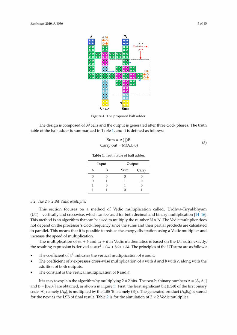
Figure 4. The proposed half adder.
The design is composed of 39 cells and the output is generated after three clock phases. The truth table of the half adder is summarized in Table 1, and it is defined as follows:
Sum = A⨁B Carry out = M(A,B,0) (5)
Table 1. Truth table of half adder.
Input Output A B Sum Carry 0 0 0 0 0 1 1 0 1 0 1 0 1 1 0 1
3.2. The 2 × 2 Bit Vedic Multiplier
This section focuses on a method of Vedic multiplication called, Urdhva-Tiryakbhyam (UT)—vertically and crosswise, which can be used for both decimal and binary multiplication [14–16]. This method is an algorithm that can be used to multiply the number N × N. The Vedic multiplier does not depend on the processor’s clock frequency since the sums and their partial products are calculated in parallel. This means that it is possible to reduce the energy dissipation using a Vedic multiplier and increase the speed of multiplication.
The multiplication of ax + b and cx + d in Vedic mathematics is based on the UT sutra exactly; the resulting expression is derived as acx2 + (ad + bc)x + bd. The principles of the UT sutra are as follows:
• The coefficient of x2 indicates the vertical multiplication of a and c. • The coefficient of x expresses cross-wise multiplication of a with d and b with c, along with the
addition of both outputs. • The constant is the vertical multiplication of b and d.
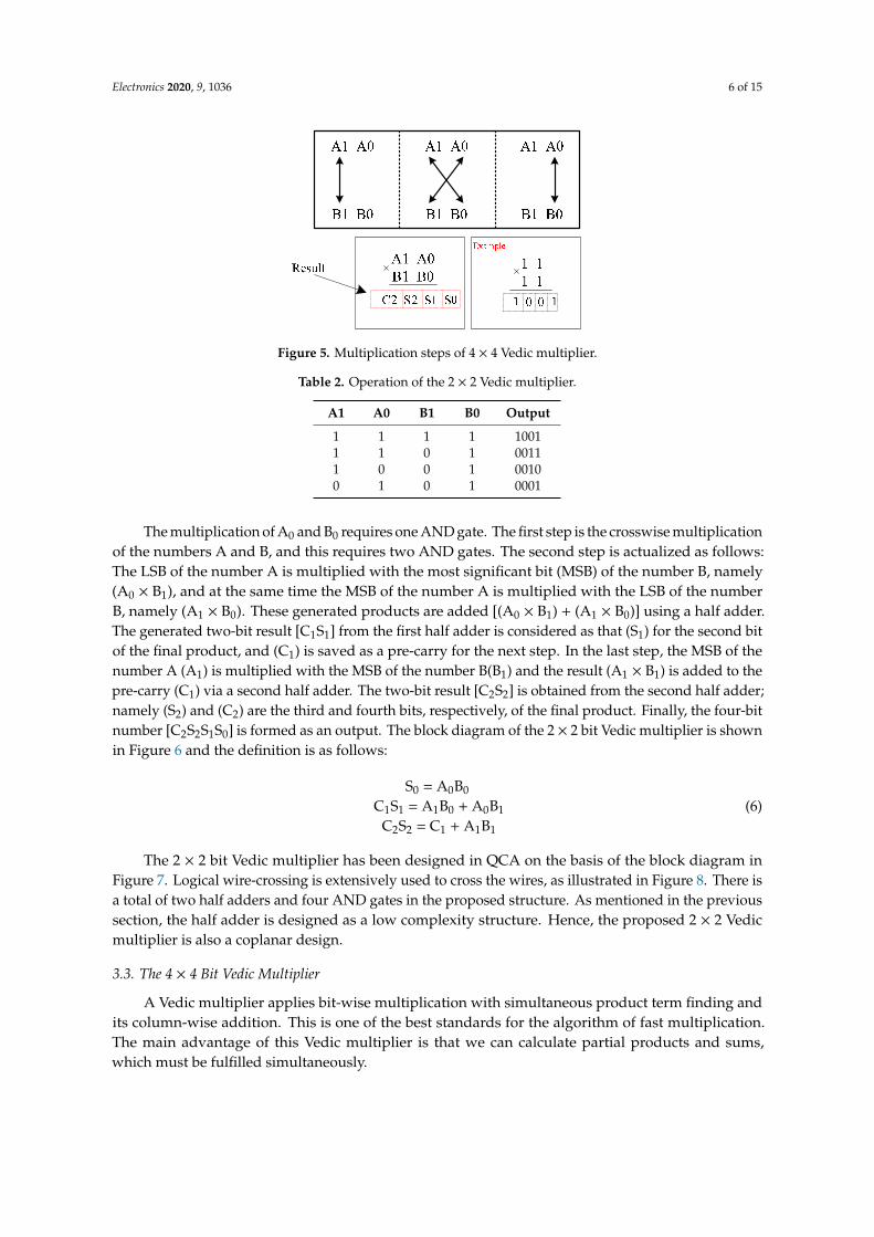
It is easy to explain the algorithm by multiplying 2 × 2 bits. The two-bit binary numbers A = [A1A0] and B = [B1B0] are obtained, as shown in Figure 5. First, the least significant bit (LSB) of the first binary code ‘A’, namely (A0), is multiplied by the LBS ‘B’, namely (B0). The generated product (A0B0) is stored for the next as the LSB of final result. Table 2 is for the simulation of 2 × 2 Vedic multiplier.
Figure 4. The proposed half adder.
The design is composed of 39 cells and the output is generated after three clock phases. The truthtable of the half adder is summarized in Table 1, and it is defined as follows:
Sum = A⊕
BCarry out = M(A,B,0)
(5)
Table 1. Truth table of half adder.
Input Output
A B Sum Carry
0 0 0 00 1 1 01 0 1 01 1 0 1
3.2. The 2 × 2 Bit Vedic Multiplier
This section focuses on a method of Vedic multiplication called, Urdhva-Tiryakbhyam(UT)—vertically and crosswise, which can be used for both decimal and binary multiplication [14–16].This method is an algorithm that can be used to multiply the number N ×N. The Vedic multiplier doesnot depend on the processor’s clock frequency since the sums and their partial products are calculatedin parallel. This means that it is possible to reduce the energy dissipation using a Vedic multiplier andincrease the speed of multiplication.
The multiplication of ax + b and cx + d in Vedic mathematics is based on the UT sutra exactly;the resulting expression is derived as acx2 + (ad + bc)x + bd. The principles of the UT sutra are as follows:
• The coefficient of x2 indicates the vertical multiplication of a and c.• The coefficient of x expresses cross-wise multiplication of a with d and b with c, along with the
addition of both outputs.• The constant is the vertical multiplication of b and d.
It is easy to explain the algorithm by multiplying 2× 2 bits. The two-bit binary numbers A = [A1A0]and B = [B1B0] are obtained, as shown in Figure 5. First, the least significant bit (LSB) of the first binarycode ‘A’, namely (A0), is multiplied by the LBS ‘B’, namely (B0). The generated product (A0B0) is storedfor the next as the LSB of final result. Table 2 is for the simulation of 2 × 2 Vedic multiplier.
Electronics 2020, 9, 1036 6 of 15Electronics 2020, 9, x FOR PEER REVIEW 6 of 15
Figure 5. Multiplication steps of 4 × 4 Vedic multiplier.
Table 2. Operation of the 2 × 2 Vedic multiplier.
A1 A0 B1 B0 Output 1 1 1 1 1001 1 1 0 1 0011 1 0 0 1 0010 0 1 0 1 0001
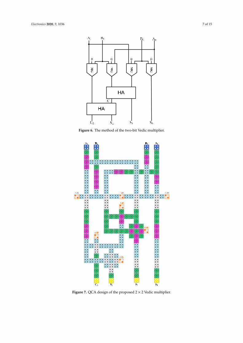
The multiplication of A0 and B0 requires one AND gate. The first step is the crosswise multiplication of the numbers A and B, and this requires two AND gates. The second step is actualized as follows: The LSB of the number A is multiplied with the most significant bit (MSB) of the number B, namely (A0 × B1), and at the same time the MSB of the number A is multiplied with the LSB of the number B, namely (A1 × B0). These generated products are added [(A0 × B1) + (A1 × B0)] using a half adder. The generated two-bit result [C1S1] from the first half adder is considered as that (S1) for the second bit of the final product, and (C1) is saved as a pre-carry for the next step. In the last step, the MSB of the number A (A1) is multiplied with the MSB of the number B(B1) and the result (A1 × B1) is added to the pre-carry (C1) via a second half adder. The two-bit result [C2S2] is obtained from the second half adder; namely (S2) and (C2) are the third and fourth bits, respectively, of the final product. Finally, the four-bit number [C2S2S1S0] is formed as an output. The block diagram of the 2 × 2 bit Vedic multiplier is shown in Figure 6 and the definition is as follows:
S0 = A0B0
C1S1 = A1B0 + A0B1 C2S2 = C1 + A1B1
(6)
The 2 × 2 bit Vedic multiplier has been designed in QCA on the basis of the block diagram in Figure 7. Logical wire-crossing is extensively used to cross the wires, as illustrated in Figure 8. There is a total of two half adders and four AND gates in the proposed structure. As mentioned in the previous section, the half adder is designed as a low complexity structure. Hence, the proposed 2 × 2 Vedic multiplier is also a coplanar design.
Figure 5. Multiplication steps of 4 × 4 Vedic multiplier.
Table 2. Operation of the 2 × 2 Vedic multiplier.
A1 A0 B1 B0 Output
1 1 1 1 10011 1 0 1 00111 0 0 1 00100 1 0 1 0001
The multiplication of A0 and B0 requires one AND gate. The first step is the crosswise multiplicationof the numbers A and B, and this requires two AND gates. The second step is actualized as follows:The LSB of the number A is multiplied with the most significant bit (MSB) of the number B, namely(A0 × B1), and at the same time the MSB of the number A is multiplied with the LSB of the numberB, namely (A1 × B0). These generated products are added [(A0 × B1) + (A1 × B0)] using a half adder.The generated two-bit result [C1S1] from the first half adder is considered as that (S1) for the second bitof the final product, and (C1) is saved as a pre-carry for the next step. In the last step, the MSB of thenumber A (A1) is multiplied with the MSB of the number B(B1) and the result (A1 × B1) is added to thepre-carry (C1) via a second half adder. The two-bit result [C2S2] is obtained from the second half adder;namely (S2) and (C2) are the third and fourth bits, respectively, of the final product. Finally, the four-bitnumber [C2S2S1S0] is formed as an output. The block diagram of the 2 × 2 bit Vedic multiplier is shownin Figure 6 and the definition is as follows:
S0 = A0B0
C1S1 = A1B0 + A0B1
C2S2 = C1 + A1B1
(6)
The 2 × 2 bit Vedic multiplier has been designed in QCA on the basis of the block diagram inFigure 7. Logical wire-crossing is extensively used to cross the wires, as illustrated in Figure 8. There isa total of two half adders and four AND gates in the proposed structure. As mentioned in the previoussection, the half adder is designed as a low complexity structure. Hence, the proposed 2 × 2 Vedicmultiplier is also a coplanar design.
3.3. The 4 × 4 Bit Vedic Multiplier
A Vedic multiplier applies bit-wise multiplication with simultaneous product term finding andits column-wise addition. This is one of the best standards for the algorithm of fast multiplication.The main advantage of this Vedic multiplier is that we can calculate partial products and sums,which must be fulfilled simultaneously.
Electronics 2020, 9, 1036 7 of 15Electronics 2020, 9, x FOR PEER REVIEW 7 of 15
Figure 6. The method of the two-bit Vedic multiplier.
Figure 7. QCA design of the proposed 2 × 2 Vedic multiplier.
Figure 6. The method of the two-bit Vedic multiplier.
Electronics 2020, 9, x FOR PEER REVIEW 7 of 15
Figure 6. The method of the two-bit Vedic multiplier.
Figure 7. QCA design of the proposed 2 × 2 Vedic multiplier. Figure 7. QCA design of the proposed 2 × 2 Vedic multiplier.
Electronics 2020, 9, 1036 8 of 15Electronics 2020, 9, x FOR PEER REVIEW 8 of 15
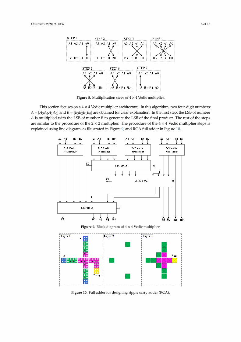
Figure 8. Multiplication steps of 4 × 4 Vedic multiplier.
3.3. The 4 × 4 Bit Vedic Multiplier
A Vedic multiplier applies bit-wise multiplication with simultaneous product term finding and its column-wise addition. This is one of the best standards for the algorithm of fast multiplication. The main advantage of this Vedic multiplier is that we can calculate partial products and sums, which must be fulfilled simultaneously.
This section focuses on a 4 × 4 Vedic multiplier architecture. In this algorithm, two four-digit numbers: A = [A3A2A1A0] and B = [B3B2B1B0] are obtained for clear explanation. In the first step, the LSB of number A is multiplied with the LSB of number B to generate the LSB of the final product. The rest of the steps are similar to the procedure of the 2 × 2 multiplier. The procedure of the 4 × 4 Vedic multiplier steps is explained using line diagram, as illustrated in Figure 9, and RCA full adder in Figure 10.
By the general concept, the generated carry (Cn) is forwarded to the next step in each step. The process goes on until the last step. The outputs C6 and S6 are taken at the last step. Finally, all of the generated results are obtained as form of [C6 S6 S5 S4 S3 S2 S1 S0]. The process is defined as follows:
S0 = A0B0 C1S1 = A1B0 + A0B1
C2S2 = C1 + A0 B2 + A2 B0 + A1 B1 C3S3 = C2 + A0 B3 + A3 B0 + A1B2 + A2B1
C4S4 = C3 + A1B3 + A3B1 + A2B2 C5S5 = C4 + A3B2 + A2B3
C6S6 = C5 + A3B3
(7)
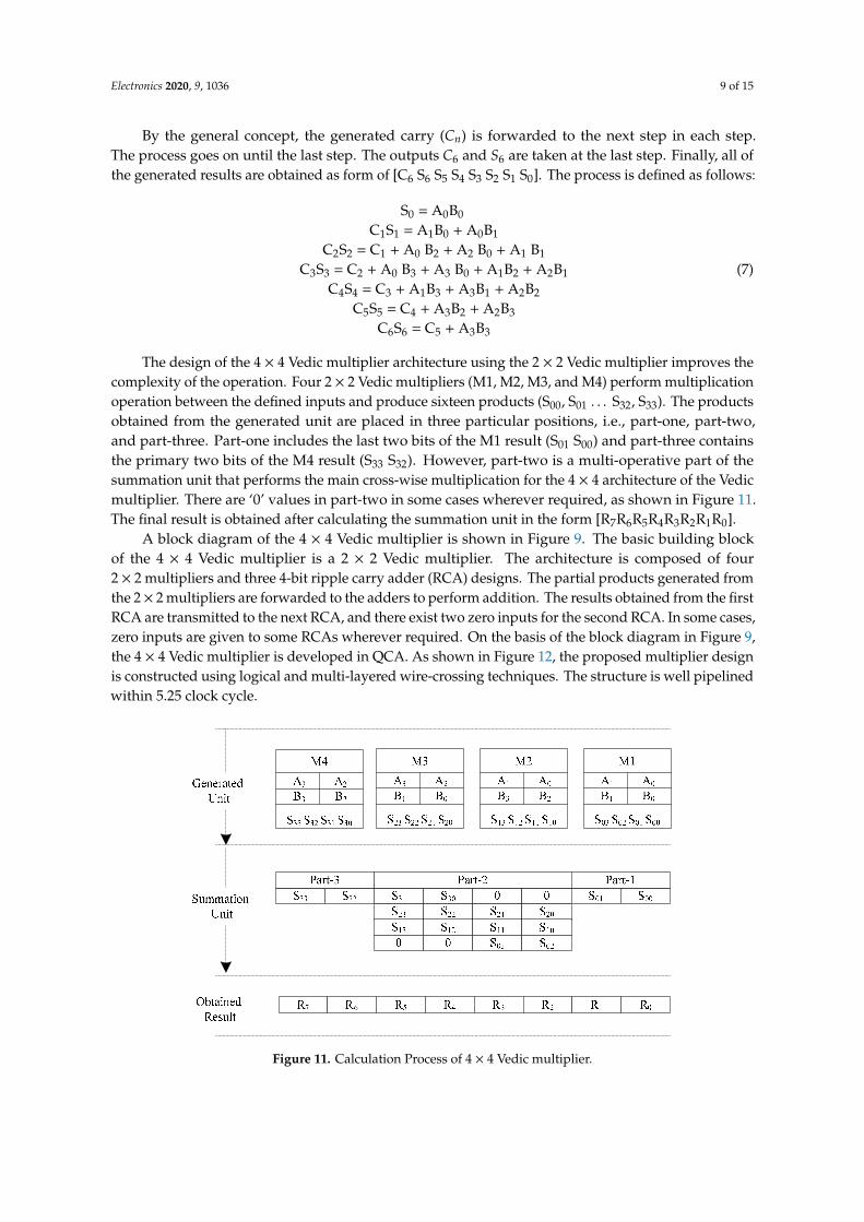
The design of the 4 × 4 Vedic multiplier architecture using the 2 × 2 Vedic multiplier improves the complexity of the operation. Four 2 × 2 Vedic multipliers (M1, M2, M3, and M4) perform multiplication operation between the defined inputs and produce sixteen products (S00, S01…S32, S33). The products obtained from the generated unit are placed in three particular positions, i.e., part-one, part-two, and part-three. Part-one includes the last two bits of the M1 result (S01 S00) and part-three contains the primary two bits of the M4 result (S33 S32). However, part-two is a multi-operative part of the summation unit that performs the main cross-wise multiplication for the 4 × 4 architecture of the Vedic multiplier. There are ‘0’ values in part-two in some cases wherever required, as shown in Figure 11. The final result is obtained after calculating the summation unit in the form [R7R6R5R4R3R2R1R0].
Figure 8. Multiplication steps of 4 × 4 Vedic multiplier.
This section focuses on a 4 × 4 Vedic multiplier architecture. In this algorithm, two four-digit numbers:A = [A3A2A1A0] and B = [B3B2B1B0] are obtained for clear explanation. In the first step, the LSB of numberA is multiplied with the LSB of number B to generate the LSB of the final product. The rest of the stepsare similar to the procedure of the 2 × 2 multiplier. The procedure of the 4 × 4 Vedic multiplier steps isexplained using line diagram, as illustrated in Figure 9, and RCA full adder in Figure 10.Electronics 2020, 9, x FOR PEER REVIEW 9 of 15
Figure 9. Block diagram of 4 × 4 Vedic multiplier.
Figure 10. Full adder for designing ripple carry adder (RCA).
Figure 11. Calculation Process of 4 × 4 Vedic multiplier.
A block diagram of the 4 × 4 Vedic multiplier is shown in Figure 9. The basic building block of the 4 × 4 Vedic multiplier is a 2 × 2 Vedic multiplier. The architecture is composed of four 2 × 2 multipliers and three 4-bit ripple carry adder (RCA) designs. The partial products generated from the 2 × 2 multipliers are forwarded to the adders to perform addition. The results obtained from the first
Figure 9. Block diagram of 4 × 4 Vedic multiplier.
Electronics 2020, 9, x FOR PEER REVIEW 9 of 15
Figure 9. Block diagram of 4 × 4 Vedic multiplier.
Figure 10. Full adder for designing ripple carry adder (RCA).
Figure 11. Calculation Process of 4 × 4 Vedic multiplier.
A block diagram of the 4 × 4 Vedic multiplier is shown in Figure 9. The basic building block of the 4 × 4 Vedic multiplier is a 2 × 2 Vedic multiplier. The architecture is composed of four 2 × 2 multipliers and three 4-bit ripple carry adder (RCA) designs. The partial products generated from the 2 × 2 multipliers are forwarded to the adders to perform addition. The results obtained from the first
Figure 10. Full adder for designing ripple carry adder (RCA).
Electronics 2020, 9, 1036 9 of 15
By the general concept, the generated carry (Cn) is forwarded to the next step in each step.The process goes on until the last step. The outputs C6 and S6 are taken at the last step. Finally, all ofthe generated results are obtained as form of [C6 S6 S5 S4 S3 S2 S1 S0]. The process is defined as follows:
S0 = A0B0
C1S1 = A1B0 + A0B1
C2S2 = C1 + A0 B2 + A2 B0 + A1 B1
C3S3 = C2 + A0 B3 + A3 B0 + A1B2 + A2B1
C4S4 = C3 + A1B3 + A3B1 + A2B2
C5S5 = C4 + A3B2 + A2B3
C6S6 = C5 + A3B3
(7)
The design of the 4 × 4 Vedic multiplier architecture using the 2 × 2 Vedic multiplier improves thecomplexity of the operation. Four 2 × 2 Vedic multipliers (M1, M2, M3, and M4) perform multiplicationoperation between the defined inputs and produce sixteen products (S00, S01 . . . S32, S33). The productsobtained from the generated unit are placed in three particular positions, i.e., part-one, part-two,and part-three. Part-one includes the last two bits of the M1 result (S01 S00) and part-three containsthe primary two bits of the M4 result (S33 S32). However, part-two is a multi-operative part of thesummation unit that performs the main cross-wise multiplication for the 4 × 4 architecture of the Vedicmultiplier. There are ‘0’ values in part-two in some cases wherever required, as shown in Figure 11.The final result is obtained after calculating the summation unit in the form [R7R6R5R4R3R2R1R0].
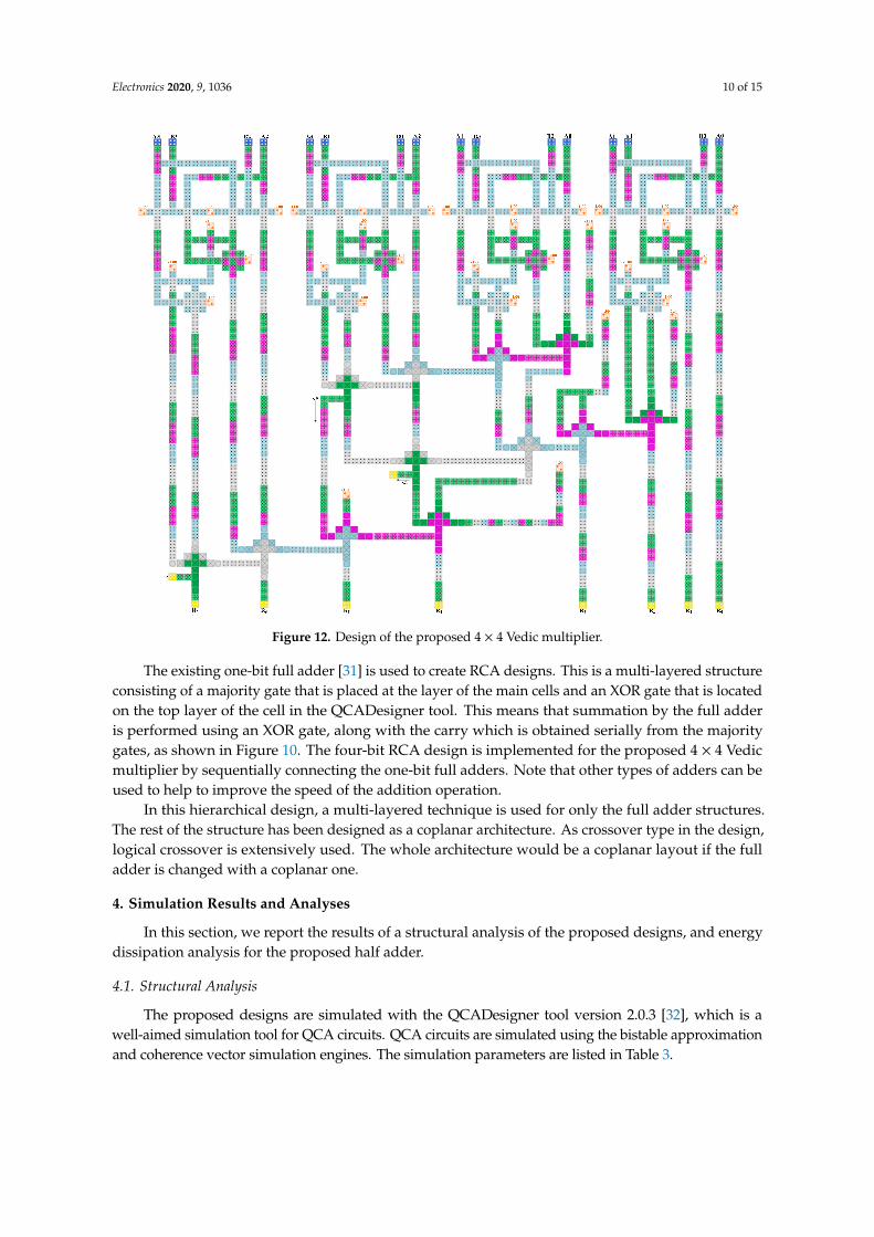
A block diagram of the 4 × 4 Vedic multiplier is shown in Figure 9. The basic building blockof the 4 × 4 Vedic multiplier is a 2 × 2 Vedic multiplier. The architecture is composed of four2 × 2 multipliers and three 4-bit ripple carry adder (RCA) designs. The partial products generated fromthe 2× 2 multipliers are forwarded to the adders to perform addition. The results obtained from the firstRCA are transmitted to the next RCA, and there exist two zero inputs for the second RCA. In some cases,zero inputs are given to some RCAs wherever required. On the basis of the block diagram in Figure 9,the 4 × 4 Vedic multiplier is developed in QCA. As shown in Figure 12, the proposed multiplier designis constructed using logical and multi-layered wire-crossing techniques. The structure is well pipelinedwithin 5.25 clock cycle.
Electronics 2020, 9, x FOR PEER REVIEW 9 of 15
Figure 9. Block diagram of 4 × 4 Vedic multiplier.
Figure 10. Full adder for designing ripple carry adder (RCA).
Figure 11. Calculation Process of 4 × 4 Vedic multiplier.
A block diagram of the 4 × 4 Vedic multiplier is shown in Figure 9. The basic building block of the 4 × 4 Vedic multiplier is a 2 × 2 Vedic multiplier. The architecture is composed of four 2 × 2 multipliers and three 4-bit ripple carry adder (RCA) designs. The partial products generated from the 2 × 2 multipliers are forwarded to the adders to perform addition. The results obtained from the first
Figure 11. Calculation Process of 4 × 4 Vedic multiplier.
Electronics 2020, 9, 1036 10 of 15
Electronics 2020, 9, x FOR PEER REVIEW 10 of 15
RCA are transmitted to the next RCA, and there exist two zero inputs for the second RCA. In some cases, zero inputs are given to some RCAs wherever required. On the basis of the block diagram in Figure 9, the 4 × 4 Vedic multiplier is developed in QCA. As shown in Figure 12, the proposed multiplier design is constructed using logical and multi-layered wire-crossing techniques. The structure is well pipelined within 5.25 clock cycle.
Figure 12. Design of the proposed 4 × 4 Vedic multiplier.
The existing one-bit full adder [31] is used to create RCA designs. This is a multi-layered structure consisting of a majority gate that is placed at the layer of the main cells and an XOR gate that is located on the top layer of the cell in the QCADesigner tool. This means that summation by the full adder is performed using an XOR gate, along with the carry which is obtained serially from the majority gates, as shown in Figure 10. The four-bit RCA design is implemented for the proposed 4 × 4 Vedic multiplier by sequentially connecting the one-bit full adders. Note that other types of adders can be used to help to improve the speed of the addition operation.
In this hierarchical design, a multi-layered technique is used for only the full adder structures. The rest of the structure has been designed as a coplanar architecture. As crossover type in the design, logical crossover is extensively used. The whole architecture would be a coplanar layout if the full adder is changed with a coplanar one.
4. Simulation Results and Analyses
In this section, we report the results of a structural analysis of the proposed designs, and energy dissipation analysis for the proposed half adder.
4.1. Structural Analysis
The proposed designs are simulated with the QCADesigner tool version 2.0.3 [32], which is a well-aimed simulation tool for QCA circuits. QCA circuits are simulated using the bistable
Figure 12. Design of the proposed 4 × 4 Vedic multiplier.
The existing one-bit full adder [31] is used to create RCA designs. This is a multi-layered structureconsisting of a majority gate that is placed at the layer of the main cells and an XOR gate that is locatedon the top layer of the cell in the QCADesigner tool. This means that summation by the full adderis performed using an XOR gate, along with the carry which is obtained serially from the majoritygates, as shown in Figure 10. The four-bit RCA design is implemented for the proposed 4 × 4 Vedicmultiplier by sequentially connecting the one-bit full adders. Note that other types of adders can beused to help to improve the speed of the addition operation.
In this hierarchical design, a multi-layered technique is used for only the full adder structures.The rest of the structure has been designed as a coplanar architecture. As crossover type in the design,logical crossover is extensively used. The whole architecture would be a coplanar layout if the fulladder is changed with a coplanar one.
4. Simulation Results and Analyses
In this section, we report the results of a structural analysis of the proposed designs, and energydissipation analysis for the proposed half adder.
4.1. Structural Analysis
The proposed designs are simulated with the QCADesigner tool version 2.0.3 [32], which is awell-aimed simulation tool for QCA circuits. QCA circuits are simulated using the bistable approximationand coherence vector simulation engines. The simulation parameters are listed in Table 3.
Electronics 2020, 9, 1036 11 of 15
Table 3. Simulation parameters.
Parameters Bistable Approximation Coherence Vector
Cell size 18 nm 18 nmDot diameter 5 nm 5 nm
Cell separation 2 nm 2 nmLayer separation 11.5 nm 11.5 nm
Clock high 9.8×10⁻²² J 9.8×10⁻²² JClock low 3.8×10⁻²³ J 3.8×10⁻²³ JClock shift 0 0
Clock amplitude factor 2.0 2.0Relative permittivity 12.9 12.9
Radius of effect 65 nm 80 nm
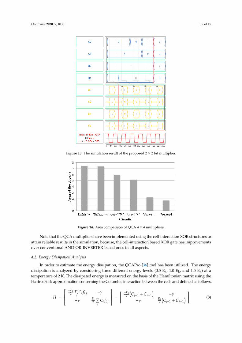
Figure 13 shows a simulation result of the proposed 2 × 2 Vedic multiplier. The simulation resultsconfirm that the binary numbers obtained from the simulation match the values in Table 2. This isexplained as follows; the input-output value is shown in the red rectangles in Figure 13; namely,multiplication of the binary number ‘11’ (A1 A0) by ‘11’ (B1 B0) is equal to the binary number ‘1001’(C2 S2 S1 S0). It is clearly seen that the first dashed-line-based rectangle in the input is generatedcorrectly below the first dashed-line-based rectangle in the output, and so on, as shown in Figure 13.
The 4 × 4 Vedic multiplier architecture was designed on the basis of the proposed Vedic2 × 2 multiplier. In the designs, we use a logical intersection scheme, because of the reliable and stablesignal propagation throughout the QCA wires.
A multi-layered cross-over technique is used only in the full adder. The proposed designs havebeen compared with previous multiplier designs. In this comparison, QCA parallel 4 × 4 multipliershave been also chosen for comparison with the Vedic multipliers. The comparison results aresummarized in Table 4, in terms of the cell count, total area, and latency.
According to the comparison, the proposed designs have achieved significant improvements.The chart in Figure 14 indicates that the proposed 4 × 4 Vedic multiplier has great achievements interms of the area in comparison to previously designed QCA multipliers [33–35].
Table 4. Comparison of QCA multipliers.
Circuit Cell Count Area Delay Cross-Over
4 × 4Array I [33] 2956 5.18 14 Multilayer4 × 4Array II [33] 3738 6.02 14 Multilayer4 × 4 Dadda [34] 3384 7.51 12 Coplanar4 × 4 Wallace [34] 3295 7.39 10 Coplanar4 × 4 Vedic [35] 1955 2.25 4.25 Multilayer4 × 4 Proposed 1726 1.74 5.25 Multilayer2 × 2 Proposed 194 0.17 2.25 Coplanar
Electronics 2020, 9, 1036 12 of 15
Electronics 2020, 9, x FOR PEER REVIEW 11 of 15
approximation and coherence vector simulation engines. The simulation parameters are listed in Table 3.
Table 3. Simulation parameters.
Parameters Bistable Approximation Coherence Vector Cell size 18 nm 18 nm
Dot diameter 5 nm 5 nm Cell separation 2 nm 2 nm
Layer separation 11.5 nm 11.5 nm Clock high 9.8×10⁻²² J 9.8×10⁻²² J Clock low 3.8×10⁻²³ J 3.8×10⁻²³ J Clock shift 0 0
Clock amplitude factor 2.0 2.0 Relative permittivity 12.9 12.9
Radius of effect 65 nm 80 nm
Figure 13 shows a simulation result of the proposed 2 × 2 Vedic multiplier. The simulation results confirm that the binary numbers obtained from the simulation match the values in Table 2. This is explained as follows; the input-output value is shown in the red rectangles in Figure 13; namely, multiplication of the binary number ‘11’ (A1 A0) by ‘11’ (B1 B0) is equal to the binary number ‘1001’ (C2
S2 S1 S0). It is clearly seen that the first dashed-line-based rectangle in the input is generated correctly below the first dashed-line-based rectangle in the output, and so on, as shown in Figure 13.
Figure 13. The simulation result of the proposed 2 × 2 bit multiplier.
The 4 × 4 Vedic multiplier architecture was designed on the basis of the proposed Vedic 2 × 2 multiplier. In the designs, we use a logical intersection scheme, because of the reliable and stable signal propagation throughout the QCA wires.
Figure 13. The simulation result of the proposed 2 × 2 bit multiplier.
Electronics 2020, 9, x FOR PEER REVIEW 12 of 15
A multi-layered cross-over technique is used only in the full adder. The proposed designs have been compared with previous multiplier designs. In this comparison, QCA parallel 4 × 4 multipliers have been also chosen for comparison with the Vedic multipliers. The comparison results are summarized in Table 4, in terms of the cell count, total area, and latency.
According to the comparison, the proposed designs have achieved significant improvements. The chart in Figure 14 indicates that the proposed 4 × 4 Vedic multiplier has great achievements in terms of the area in comparison to previously designed QCA multipliers [33–35].
Note that the QCA multipliers have been implemented using the cell-interaction XOR structures to attain reliable results in the simulation, because, the cell-interaction based XOR gate has improvements over conventional AND-OR-INVERTER-based ones in all aspects.
Table 4. Comparison of QCA multipliers.
Circuit Cell Count Area Delay Cross-Over 4 × 4Array I [33] 2956 5.18 14 Multilayer 4 × 4Array II [33] 3738 6.02 14 Multilayer 4 × 4 Dadda [34] 3384 7.51 12 Coplanar
4 × 4 Wallace [34] 3295 7.39 10 Coplanar 4 × 4 Vedic [35] 1955 2.25 4.25 Multilayer 4 × 4 Proposed 1726 1.74 5.25 Multilayer 2 × 2 Proposed 194 0.17 2.25 Coplanar
Figure 14. Area comparison of QCA 4 × 4 multipliers.
4.2. Energy Dissipation Analysis
In order to estimate the energy dissipation, the QCAPro [36] tool has been utilized. The energy dissipation is analyzed by considering three different energy levels (0.5 Ek, 1.0 Ek, and 1.5 Ek) at a temperature of 2 K. The dissipated energy is measured on the basis of the Hamiltonian matrix using the HartreeFock approximation concerning the Columbic interaction between the cells and defined as follows.
𝐻 = ⎣⎢⎢⎡−𝐸2 𝐶 𝑓 , −𝛾−𝛾 𝐸2 𝐶 𝑓 , ⎦⎥⎥
⎤ = −𝐸2 𝐶 + 𝐶 −𝛾−𝛾 𝐸2 𝐶 + 𝐶 (8)
In the above equation, polarization of i-th juxtaposed cell is represented by 𝐶 and the geometrical factor identifying electrostatic interaction between cells i and j is represented by 𝑓 , due to geometrical distance where 𝐸 is the kink energy between the cells. This kink energy is related to the energy cost of two cells with the opposite polarization γ—the electron tunneling energy inside
Figure 14. Area comparison of QCA 4 × 4 multipliers.
Note that the QCA multipliers have been implemented using the cell-interaction XOR structures toattain reliable results in the simulation, because, the cell-interaction based XOR gate has improvementsover conventional AND-OR-INVERTER-based ones in all aspects.
4.2. Energy Dissipation Analysis
In order to estimate the energy dissipation, the QCAPro [36] tool has been utilized. The energydissipation is analyzed by considering three different energy levels (0.5 Ek, 1.0 Ek, and 1.5 Ek) at atemperature of 2 K. The dissipated energy is measured on the basis of the Hamiltonian matrix using theHartreeFock approximation concerning the Columbic interaction between the cells and defined as follows.
H =
−Ek
2∑i
Ci fi, j −γ
−γ Ek2
∑i
Ci fi, j
=
−Ek2
(C j−1 + C j+1
)−γ
−γ Ek2
(C j−1 + C j+1
) (8)
Electronics 2020, 9, 1036 13 of 15
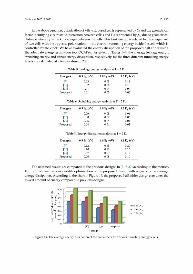
In the above equation, polarization of i-th juxtaposed cell is represented by Ci and the geometricalfactor identifying electrostatic interaction between cells i and j is represented by fi, j due to geometricaldistance where Ek is the kink energy between the cells. This kink energy is related to the energy costof two cells with the opposite polarization γ—the electron tunneling energy inside the cell, which iscontrolled by the clock. We have evaluated the energy dissipation of the proposed half adder usingthe adequate energy estimation tool QCAPro. As given in Tables 5–7, the average leakage energy,switching energy, and circuit energy dissipation, respectively, for the three different tunneling energylevels are calculated at a temperature of 2 K.
Table 5. Leakage energy analysis at T = 2 K.
Designs 0.5 Ek (eV) 1.0 Ek (eV) 1.5 Ek (eV)
[7] 0.03 0.08 0.14[15] 0.02 0.06 0.10[29] 0.01 0.04 0.07
Proposed 0.01 0.03 0.06
Table 6. Switching energy analysis at T = 2 K.
Designs 0.5 Ek (eV) 1.0 Ek (eV) 1.5 Ek (eV)
[7] 0.09 0.08 0.06[15] 0.08 0.07 0.06[29] 0.06 0.05 0.04
Proposed 0.04 0.04 0.03
Table 7. Energy dissipation analysis at T = 2 K.
Designs 0.5 Ek (eV) 1.0 Ek (eV) 1.5 Ek (eV)
[7] 0.12 0.15 0.20[15] 0.10 0.12 0.15[29] 0.07 0.09 0.12
Proposed 0.06 0.08 0.10
The obtained results are compared to the previous designs in [7,15,29] according to the metrics.Figure 15 shows the considerable optimization of the proposed design with regards to the averageenergy dissipation. According to the chart in Figure 15, the proposed half adder design consumes thelowest amount of energy compared to previous designs.
Electronics 2020, 9, x FOR PEER REVIEW 13 of 15
the cell, which is controlled by the clock. We have evaluated the energy dissipation of the proposed half adder using the adequate energy estimation tool QCAPro. As given in Tables 5–7, the average leakage energy, switching energy, and circuit energy dissipation, respectively, for the three different tunneling energy levels are calculated at a temperature of 2 K.
The obtained results are compared to the previous designs in [7], [15], [29] according to the metrics. Figure 15 shows the considerable optimization of the proposed design with regards to the average energy dissipation. According to the chart in Figure 15, the proposed half adder design consumes the lowest amount of energy compared to previous designs.
Table 5. Leakage energy analysis at T = 2 K.
Designs 0.5 Ek (eV) 1.0 Ek (eV) 1.5 Ek (eV) [7] 0.03 0.08 0.14
[15] 0.02 0.06 0.10 [29] 0.01 0.04 0.07
Proposed 0.01 0.03 0.06
Table 6. Switching energy analysis at T = 2 K.
Designs 0.5 Ek (eV) 1.0 Ek (eV) 1.5 Ek (eV) [7] 0.09 0.08 0.06
[15] 0.08 0.07 0.06 [29] 0.06 0.05 0.04
Proposed 0.04 0.04 0.03
Table 7. Energy dissipation analysis at T = 2 K.
Designs 0.5 Ek (eV) 1.0 Ek (eV) 1.5 Ek (eV) [7] 0.12 0.15 0.20
[15] 0.10 0.12 0.15 [29] 0.07 0.09 0.12
Proposed 0.06 0.08 0.10
Figure 15. The average energy dissipation of the half adders for various tunneling energy levels.
5. Conclusions
In this paper, a technique for designing Vedic multiplier with cell-interaction QCA structures based on QCA technology is presented. First, a coplanar 2 × 2 Vedic multiplier has been designed and simulated with QCADesigner. The energy dissipation was also calculated for the circuit by QCAPro. Then, the architecture of a 4 × 4 Vedic multiplier has been designed by applying the 2 × 2 Vedic multiplier. The proposed QCA layouts have been compared with prior works in terms of the cell count, area, and latency. A comparison demonstrated that the proposed structures are implemented
Figure 15. The average energy dissipation of the half adders for various tunneling energy levels.
Electronics 2020, 9, 1036 14 of 15
5. Conclusions
In this paper, a technique for designing Vedic multiplier with cell-interaction QCA structuresbased on QCA technology is presented. First, a coplanar 2 × 2 Vedic multiplier has been designed andsimulated with QCADesigner. The energy dissipation was also calculated for the circuit by QCAPro.Then, the architecture of a 4× 4 Vedic multiplier has been designed by applying the 2× 2 Vedic multiplier.The proposed QCA layouts have been compared with prior works in terms of the cell count, area,and latency. A comparison demonstrated that the proposed structures are implemented with significantimprovements. According to this study, the use of the cell-interaction technique and clock-zone-basedcrossover can considerably improve the performance of the final structure.
Author Contributions: Conceptualization, J.-C.J. and J.-C.J.; methodology, J.-C.J.; software, N.S.; validation, J.-C.J.;formal analysis, N.S.; investigation, N.S.; resources, N.S.; data curation, N.S.; writing—original draft preparation,N.S.; writing—review and editing, J.-C.J.; visualization, N.S.; supervision, J.-C.J.; project administration, J.-C.J.;funding acquisition, J.-C.J. All authors have read and agreed to the published version of the manuscript.
Funding: This work was supported by the National Research Foundation of Korea (NRF) grant funded by theKorea government (MSIP) (NO. NRF-2017R1D1A3B03034346).
Conflicts of Interest: The authors declare no conflict of interest.
References
1. Lent, C.S.; Tougaw, P.D.; Porod, W.; Bernstein, G.H. Quantum cellular automata. Nanotechnology 1993, 4, 49–57.[CrossRef]
2. Jeon, J.C. Five-Input Majority Gate Based QCA Decoder. Adv. Sci. Technol. Lett. 2016, 122, 95–99.3. Safoev, N.; Jeon, J.C. A novel controllable inverter and adder/subtractor in quantum-dot cellular automata
using cell interaction based XOR gate. Microelectron. Eng. 2020, 222, 111197. [CrossRef]4. Safoev, N.; Jeon, J.C. Design of high-performance QCA incrementer/decrementer circuit based on
adder/subtractor methodology. Microprocess. Microsyst. 2020, 72, 102927. [CrossRef]5. Lent, C.S.; Snider, G.L. The development of quantum-dot cellular automata. In Field-Coupled Nanocomputing;
Springer: Berlin/Heidelberg, Germany, 2014; Volume 8280, pp. 3–20.6. You, Y.W.; Jeon, J.C. Two Dimensional QCA XOR Logic Using NNI Gate. Int. J. Control Autom. 2017, 10, 217–226.
[CrossRef]7. Cho, H.; Swartzlander, E.E. Adder designs and analyses for quantum-dot cellular automata.
IEEE Trans. Nanotechnol. 2007, 6, 374–383. [CrossRef]8. Jeon, J.C. Low Complexity QCA Universal Shift Register Design Using Multiplexer and D Flip-Flop Based
on Electronic Correlations. J. Supercomput. 2019, 1–15. [CrossRef]9. Erniyazov, S.; Jeon, J.C. Carry save adder and carry look ahead adder using inverter chain based coplanar
QCA full adder for low energy dissipation. Microelectron. Eng. 2019, 211, 37–43. [CrossRef]10. Jeon, J.C. Extendable Quantum-dot Cellular Automata Decoding Architecture Using 5-input Majority Gate.
Int. J. Control Autom. 2015, 8, 107–118. [CrossRef]11. Safoev, N.; Jeon, J.C. Low area complexity demultiplexer based on multilayer Quantum-dot Cellular
Automata. Int. J. Control Autom. 2016, 9, 165–178. [CrossRef]12. Safoev, N.; Jeon, J.C. Peres Gate Realization in QCA for Reversible Binary Incrementer. Adv. Sci. Lett. 2017,
23, 9812–9817. [CrossRef]13. DiLabio, G.A.; Wolkow, R.A.; Pitters, J.L.; Piva, P.G. Atomistic Quantum Dots. U.S. Patent Application No.
8,816,479, 26 August 2014.14. Tiwari, H.D.; Gankhuyag, G.; Kim, C.M. Multiplier design based on ancient Indian Vedic
Mathematics. In Proceedings of the 2008 International SoC Design Conference: (ISOCC), Busan, Korea,24–25 November 2008.
15. Chudasama, A.; Sasamal, T.N.; Yadav, J. An efficient design of Vedic multiplier using ripple carry adder inQuantum-dot Cellular Automata. Comput. Electr. Eng. 2017, 65, 527–542. [CrossRef]
16. Thapliyal, H.; Arabnia, H.R. A Time-Area-Power Efficient Multiplier and Square Architecture Based onAncient Indian Vedic Mathematics. In Proceedings of the International Conference on VLSI (VLSI ‘04),Las Vegas, NV, USA, 21–24 June 2004; pp. 434–439.
Electronics 2020, 9, 1036 15 of 15
17. Safoev, N.; Jeon, J.C. QCA XOR gate for Arithmetic and Logic Circuit Design. In Proceedings of the IIERInternational Conference, Tokyo, Japan, 25–28 September 2017.
18. Ahmadpour, S.S.; Mosleh, M. New Designs of Fault-tolerant adders in Quantum-Dot Cellular Automata.Nano Commun. Netw. 2019, 19, 10–25. [CrossRef]
19. Kalogeiton, V.S.; Papadopoulos, D.P.; Liolis, O.; Mardiris, V.A.; Sirakoulis, G.C.; Karafyllidis, I.G. ProgrammableCrossbar Quantum-Dot Cellular Automata Circuits. IEEE Trans. Comp. Int. Syst. 2016, 36, 1367–1380. [CrossRef]
20. Lu, L.; Liu, W.; O’Neill, M.; Swartzlander, E.E. QCA systolic array design. IEEE Trans. Comput. 2013, 62, 548–560.[CrossRef]
21. Sasamal, T.N.; Singh, A.K.; Mohan, A. An optimal design of full adder based on 5-input majority gate incoplanar quantum-dot cellular automata. Optik 2016, 127, 8576–8591. [CrossRef]
22. Vankamamidi, V.; Ottavi, M.; Lombardi, F. Two-Dimensional Schemes for Clocking/Timing of QCA Circuits.IEEE Trans. Comput. Aided Des. Integr. Circuits Syst. 2008, 27, 34–44. [CrossRef]
23. Das, J.C.; De, D. Circuit Switching with Quantum-Dot Cellular Automata. Nano Commun. Netw. 2017, 14,16–28. [CrossRef]
24. Lent, C.S.; Liu, M.; Lu, Y. Bennett Clocking of Quantum-Dot Cellular Automata and the Limits to BinaryLogic Scaling. Nanotechnology 2006, 17, 4240–4251. [CrossRef]
25. Farazkish, R.; Khodaparast, F. Design and characterization of a new fault-tolerant full-adder for quantum-dotcellular automata. Microprocess. Microsyst. 2015, 39, 426–433. [CrossRef]
26. Jeon, J.C. Designing nanotechnology QCA-multiplexer using majority function-based NAND for quantumcomputing. J. Supercomput. 2020. [CrossRef]
27. You, Y.W.; Jeon, J.C. Multilayered Design of Clocked SR Flip-Flop Using Quantum-Dot Cellular Automata.Adv. Sci. Lett. 2017, 23, 9835–9840. [CrossRef]
28. Safoev, N.; Jeon, J.C. Cell Interaction Based QCA Multiplexer for Complex Circuit Design.J. Comput. Theor. Nanosci. 2017, 23, 10097–10101. [CrossRef]
29. Balali, M.; Rezai, A.; Balali, H.; Rabiei, F.; Emadi, S. Towards coplanar quantum-dot cellular automata addersbased on efficient three-input XOR gate. Results Phys. 2017, 7, 1389–1395. [CrossRef]
30. Ahmad, F.; Bhat, G.M.; Khademolhosseini, H.; Azimi, S.; Angizi, S.; Navi, K. Towards single layer quantum-dotcellular automata adders based on explicit interaction of cells. J. Comput. Sci. 2016, 16, 8–15. [CrossRef]
31. Safoev, N.; Jeon, J.C. Compact RCA Based on Multilayer Quantum-dot Cellular Automata. In InformationSystems Design and Intelligent Applications; Springer: Berlin/Heidelberg, Germany, 2018; pp. 515–524.
32. Walus, K.; Dysart, T.J.; Jullien, G.A.; Budiman, R.A. QCADesigner: A Rapid Design and Simulation Tool forQuantum-Dot Cellular Automata. IEEE Trans. Nanotechnol. 2004, 3, 26–31. [CrossRef]
33. Kim, S.W. Design of Parallel Multipliers and Dividers in QCA. UT Electronic Theses and Dissertations.University of Texas at Austin, Austin, TX, USA, May 2011.
34. Kim, S.W.; Swartzlander, E.E. Parallel Multipliers for Quantum-Dot Cellular Automata. In Proceedings of theIEEE Nanotechnology Materialsand Devices Conference, Traverse City, MI, USA, 2–5 June 2009; pp. 68–72.
35. Chudasama, A.; Sasamal, T.N. Implementation of 4x4 Vedic Multiplier using Carry Save Adder inQuantum-Dot Cellular Automata. In Proceedings of the 2016 International Conference on Communicationand Signal Processing (ICCSP), Melmaruvathur, India, 6–8 April 2016; pp. 1260–1264.
36. Srivastava, S.; Asthana, A.; Bhanja, S.; Sarkar, S. QCAPro-an error-power estimation tool for QCA circuitdesign. In Proceedings of the 14th IEEE International Symposium on Design and Diagnostics of ElectronicCircuits and Systems, Cottbus, Germany, 13–15 April 2011; pp. 2377–2380.
© 2020 by the authors. Licensee MDPI, Basel, Switzerland. This article is an open accessarticle distributed under the terms and conditions of the Creative Commons Attribution(CC BY) license (http://creativecommons.org/licenses/by/4.0/).