Defect Detection in Printed Circuit Boards Using You-Only ...
16
electronics Article Defect Detection in Printed Circuit Boards Using You-Only-Look-Once Convolutional Neural Networks Venkat Anil Adibhatla 1,2 , Huan-Chuang Chih 2 , Chi-Chang Hsu 2 , Joseph Cheng 2 , Maysam F. Abbod 3, * and Jiann-Shing Shieh 1 1 Department of Mechanical Engineering, Yuan Ze University, Taoyuan 32003, Taiwan; [email protected] (V.A.A.); [email protected] (J.-S.S.) 2 Department of Advanced Manufacturing System, Boardtek Electronics Corporation, Taoyuan 328454, Taiwan; [email protected] (H.-C.C.); [email protected] (C.-C.H.); [email protected] (J.C.) 3 Department of Electronic and Computer Engineering, Brunel University London, Uxbridge UB8 3PH, UK * Correspondence: [email protected] Received: 31 July 2020; Accepted: 18 September 2020; Published: 22 September 2020 Abstract: In this study, a deep learning algorithm based on the you-only-look-once (YOLO) approach is proposed for the quality inspection of printed circuit boards (PCBs). The high accuracy and efficiency of deep learning algorithms has resulted in their increased adoption in every field. Similarly, accurate detection of defects in PCBs by using deep learning algorithms, such as convolutional neural networks (CNNs), has garnered considerable attention. In the proposed method, highly skilled quality inspection engineers first use an interface to record and label defective PCBs. The data are then used to train a YOLO/CNN model to detect defects in PCBs. In this study, 11,000 images and a network of 24 convolutional layers and 2 fully connected layers were used. The proposed model achieved a defect detection accuracy of 98.79% in PCBs with a batch size of 32. Keywords: convolution neural network; YOLO; deep learning; printed circuit board 1. Introduction Printed circuit boards (PCBs) are a crucial component in most electronic devices. For decades, PCBs have been adapted for industrial and domestic use. PCBs are the primary component of any electronic design and have been used in fields such as logistics, defence, and aeronautics as well as for applications in the automobile and medical industries, among others. PCBs are solid thin plates prepared from laminated materials, fibreglass, or composite epoxy and form a physical base that supports chips and electronic components [1–4]. These boards are designed with conductive pathways, which form circuits and power electronic devices attached to the PCBs. Therefore, PCB inspection processes have continually improved to meet the ever-increasing demands of modern manufacturing. Production and manufacturing industries have attempted to achieve 100% quality assurance for all PCBs. Automated visual inspection of PCBs has advanced considerably [5,6]. Studies [7] have revealed that deep learning outperforms traditional machine-based classification and feature extraction algorithms. Defect detection in PCBs during quality inspection is critical. In the conventional method, defects are initially detected by an automatic inspection (AOI) machine. A skilled quality inspection engineer then verifies each PCB. Many boards classified as defective by the AOI machine may not be defective. The machine can erroneously classify a PCB as defective because of a scratch or small hole or the presence of nanoparticles such as dust, paper fragments, or small air bubbles. Slight variation from the reference sample may result in the AOI machine classifying PCBs as defective. However, reliance on Electronics 2020, 9, 1547; doi:10.3390/electronics9091547 www.mdpi.com/journal/electronics
-
Upload
khangminh22 -
Category
Documents
-
view
4 -
download
0
Transcript of Defect Detection in Printed Circuit Boards Using You-Only ...
electronics
Article
Defect Detection in Printed Circuit Boards UsingYou-Only-Look-Once ConvolutionalNeural Networks
Venkat Anil Adibhatla 1,2, Huan-Chuang Chih 2, Chi-Chang Hsu 2, Joseph Cheng 2,Maysam F. Abbod 3,* and Jiann-Shing Shieh 1
1 Department of Mechanical Engineering, Yuan Ze University, Taoyuan 32003, Taiwan;[email protected] (V.A.A.); [email protected] (J.-S.S.)
2 Department of Advanced Manufacturing System, Boardtek Electronics Corporation, Taoyuan 328454,Taiwan; [email protected] (H.-C.C.); [email protected] (C.-C.H.);[email protected] (J.C.)
3 Department of Electronic and Computer Engineering, Brunel University London, Uxbridge UB8 3PH, UK* Correspondence: [email protected]
Received: 31 July 2020; Accepted: 18 September 2020; Published: 22 September 2020�����������������
Abstract: In this study, a deep learning algorithm based on the you-only-look-once (YOLO) approachis proposed for the quality inspection of printed circuit boards (PCBs). The high accuracy andefficiency of deep learning algorithms has resulted in their increased adoption in every field. Similarly,accurate detection of defects in PCBs by using deep learning algorithms, such as convolutional neuralnetworks (CNNs), has garnered considerable attention. In the proposed method, highly skilledquality inspection engineers first use an interface to record and label defective PCBs. The data arethen used to train a YOLO/CNN model to detect defects in PCBs. In this study, 11,000 images and anetwork of 24 convolutional layers and 2 fully connected layers were used. The proposed modelachieved a defect detection accuracy of 98.79% in PCBs with a batch size of 32.
Keywords: convolution neural network; YOLO; deep learning; printed circuit board
1. Introduction
Printed circuit boards (PCBs) are a crucial component in most electronic devices. For decades,PCBs have been adapted for industrial and domestic use. PCBs are the primary component of anyelectronic design and have been used in fields such as logistics, defence, and aeronautics as well asfor applications in the automobile and medical industries, among others. PCBs are solid thin platesprepared from laminated materials, fibreglass, or composite epoxy and form a physical base thatsupports chips and electronic components [1–4]. These boards are designed with conductive pathways,which form circuits and power electronic devices attached to the PCBs. Therefore, PCB inspectionprocesses have continually improved to meet the ever-increasing demands of modern manufacturing.Production and manufacturing industries have attempted to achieve 100% quality assurance forall PCBs. Automated visual inspection of PCBs has advanced considerably [5,6]. Studies [7] haverevealed that deep learning outperforms traditional machine-based classification and feature extractionalgorithms. Defect detection in PCBs during quality inspection is critical. In the conventional method,defects are initially detected by an automatic inspection (AOI) machine. A skilled quality inspectionengineer then verifies each PCB. Many boards classified as defective by the AOI machine may not bedefective. The machine can erroneously classify a PCB as defective because of a scratch or small hole orthe presence of nanoparticles such as dust, paper fragments, or small air bubbles. Slight variation fromthe reference sample may result in the AOI machine classifying PCBs as defective. However, reliance on
Electronics 2020, 9, 1547; doi:10.3390/electronics9091547 www.mdpi.com/journal/electronics

Electronics 2020, 9, 1547 2 of 16
inspection engineers requires considerable human resources as well as sufficient training. Furthermore,even skilled operators can make errors during inspection. Therefore, robust deep learning systems canreplace skilled operators to a certain extent. Machines programmed with deep learning algorithms canbe used to verify defects. Deep learning methods are faster and more accurate than skilled operatorsare. Thus, the objective of this study was to develop a deep learning-based PCB recognition systemthat reduces the false detection rate and increases the production rate.
With the increasing popularity of consumer electronics products, such as laptops, smartphones,and tablets, accurate PCB manufacturing is critical [8]. Because of this surge in the demand for PCBs inthe market, manufacturers are required to produce PCBs in large quantities. Therefore, maintainingthe quality of such large numbers of PCBs is challenging. Accurate automated inspection systems canprove helpful in quality maintenance. Such systems overcome the limitations of manual inspection for alarge number of PCBs. Automated visual PCB inspection can provide fast and quantitative informationof defects and therefore can prove to be an asset in manufacturing processes. A few examples ofPCB defect detection methods can be found in the literature [8–10]. Typically, the template-matchingmethod [11] is used to detect defects in PCBs. Another method for PCB defect detection is OPENCVfollowed by image subtraction [12]. However, these detection algorithms are limited to a specific typeof defect in PCBs. Remarkable progress has been made in the use of convolutional neural networks(CNNs) in several applications, such as image recognition [13,14] and object detection. In particular,object detection is achieved by implementing object recognition methods [15] and region-basedCNNs [16]. In this study, a CNN classifier was trained to recognise various electrical components on aPCB and then detect and localise defects on the PCB components by using Tiny-YOLO-v2, an effectiveand accurate object detector.
Quality inspection engineers are employed to ensure minimum defects. Manual inspection anddiagnosis of defects is challenging. Defect inspection encompasses detection of several types of defects,an extremely low tolerance for errors, and considerable expertise to reliably recognise and handleflawed units.
Researchers have applied various you-only-look-once (YOLO) approaches to art data sets andachieved excellent accuracy. YOLO, an object detection algorithm, differs from other classificationmethods. Unlike conventional classification mechanisms, YOLO can classify more than one object in asingle picture. Because YOLO is based on CNNs, it has a unique method of object detection. In thealgorithm, a single neural network is used for an image separated into different regions. The probabilityof each region is then predicted, and predicted probabilities determine the location of bounding boxes.
YOLO is becoming increasingly popular because of its high accuracy and efficiency. As the namesuggests, an image is checked just once; that is, a single forward propagation pass is performed by theneural network to generate predictions. Following the nonmax suppression technique, the algorithmoutputs the recognised objects using the bounding box. The YOLO algorithm with a single CNNpredicts several bounding boxes and the class probability for those boxes. This algorithm uses fullimages for training and optimises its detection performance. YOLO is quick and considers the wholeimage during processing. Therefore, it encrypts circumstantial details regarding class. The YOLOalgorithm is faster than other object detection algorithms because it learns general representations ofobjects during training.
However, the YOLO algorithm has some drawbacks, such as more localisation errors than FastR-CNN. Furthermore, YOLO has a lower recall than other region proposal–based methods. Thus,the objective of this study was to improve recall and localisation while maintaining high classificationaccuracy. Currently, deep networks are preferred for computer vision [17–19]. Excellent results canbe achieved using large networks and different methods. YOLO is preferred because of its accuratedetection within a limited time frame. The performance of YOLO has been continually improvedover time.
Networks that can achieve fast and precise detection are always preferred. Several applications,such as self-driving cars and robotics, require low latency prediction. Thus, YOLO-v2 is designed to

Electronics 2020, 9, 1547 3 of 16
be fast. Most object detection or classification frameworks use VGG-16 as the basic feature extractoralgorithm [19] because of its high accuracy and robustness. However, VGG-16 is highly complex andrequires 30.69 billion floating point operations per second (FLOP) for a single pass over to achieve animage resolution of 224 × 224. A custom network based on the Google Net architecture is typicallypreferable for YOLO frameworks [20]. This model is faster than VGG-16 and requires only 8.52 billionFLOP for a forward pass. However, its accuracy is slightly lower than that of VGG-16. Therefore,on the basis of these parameter comparisons, we used Tiny-YOLO-v2 (a modified and compact versionof YOLO).
Using Microsoft visual studio, we developed an interface to collect images from the AOI machine.The interface enables the quality inspection engineer to label the defective region on individual PCBs.Deep learning is then applied on the gathered image data. This study implemented the Tiny-YOLO-v2model with a CNN to improve the accuracy and reduce the error rate.
2. Materials and Methods
2.1. PCB Data Set
The PCB data set was obtained from the AOI machine to generate an image of the referencePCB sample in RGB format, which was then converted into JPEG format and saved. In additionto images of the reference sample, images of defective samples were also collected using the AOImachine. The images were extracted and cropped. Almost 11,000 images were collected for training.An interface was developed (as shown in Figure 1) to enable quality inspection engineers to label thedefective regions of PCBs, which were then compared with the same location on the reference sample.
Electronics 2020, 9, x FOR PEER REVIEW 3 of 17
be fast. Most object detection or classification frameworks use VGG-16 as the basic feature extractor algorithm [19] because of its high accuracy and robustness. However, VGG-16 is highly complex and requires 30.69 billion floating point operations per second (FLOP) for a single pass over to achieve an image resolution of 224 × 224. A custom network based on the Google Net architecture is typically preferable for YOLO frameworks [20]. This model is faster than VGG-16 and requires only 8.52 billion FLOP for a forward pass. However, its accuracy is slightly lower than that of VGG-16. Therefore, on the basis of these parameter comparisons, we used Tiny-YOLO-v2 (a modified and compact version of YOLO).
Using Microsoft visual studio, we developed an interface to collect images from the AOI machine. The interface enables the quality inspection engineer to label the defective region on individual PCBs. Deep learning is then applied on the gathered image data. This study implemented the Tiny-YOLO-v2 model with a CNN to improve the accuracy and reduce the error rate.
2. Materials and Methods
2.1. PCB Data Set
The PCB data set was obtained from the AOI machine to generate an image of the reference PCB sample in RGB format, which was then converted into JPEG format and saved. In addition to images of the reference sample, images of defective samples were also collected using the AOI machine. The images were extracted and cropped. Almost 11,000 images were collected for training. An interface was developed (as shown in Figure 1) to enable quality inspection engineers to label the defective regions of PCBs, which were then compared with the same location on the reference sample.
Figure 1. User interface for data collection.
Figure 2 illustrates this process. Figure 2a displays six identical PCBs with a defect at the bottom. Figure 2b is an enlarged image of the defective region, and Figure 2c displays the defective region and the same region on the reference sample. The images were 420 × 420 pixels and were placed adjacent to each other to enable a quality inspection engineer to compare the defective and reference samples. The inspection engineer then labelled the defective area in the image. Images of 11 defect types were collected. However, because of the small amount of data, all the defect types were labelled as a single type of defect.
Figure 1. User interface for data collection.
Figure 2 illustrates this process. Figure 2a displays six identical PCBs with a defect at the bottom.Figure 2b is an enlarged image of the defective region, and Figure 2c displays the defective region andthe same region on the reference sample. The images were 420 × 420 pixels and were placed adjacentto each other to enable a quality inspection engineer to compare the defective and reference samples.The inspection engineer then labelled the defective area in the image. Images of 11 defect types werecollected. However, because of the small amount of data, all the defect types were labelled as a singletype of defect.

Electronics 2020, 9, 1547 4 of 16Electronics 2020, 9, x FOR PEER REVIEW 4 of 17
(a) (b)
(c)
Figure 2. Sections of the user interface. (a) Printed circuit board (PCB) panels. (b) Cropped or enlarged section of the defective region. (c) Cropped or enlarged area of the reference sample.
2.2. Architecture of Tiny-YOLO-v2
The unique object detection algorithm [21] developed using Tiny-YOLO-v2 [22,23] is explained in this section. For a single image, Tiny-YOLO-v2 predicts several bounding boxes with the class probability by using a single CNN. Figure 3 displays the structure of Tiny-YOLO-v2, which includes convolutional layers, various activation function blocks—such as a rectified linear unit (ReLU) and batch normalisation, within the region layer—and six max pooling layers. An image of 416 × 416 pixels is used as the input for the classifier. The output is a (125 × 13 × 13) tensor with 13 × 13 grid cells. Each grid cell corresponds to 125 channels, consisting of five bounding boxes predicted by the grid cell and the 25 data elements that describe each bounding box (5 × 25 = 125).
Figure 3. Tiny-YOLO (you-only-look-once)-v2 Architecture.
Figure 2. Sections of the user interface. (a) Printed circuit board (PCB) panels. (b) Cropped or enlargedsection of the defective region. (c) Cropped or enlarged area of the reference sample.
2.2. Architecture of Tiny-YOLO-v2
The unique object detection algorithm [21] developed using Tiny-YOLO-v2 [22,23] is explainedin this section. For a single image, Tiny-YOLO-v2 predicts several bounding boxes with the classprobability by using a single CNN. Figure 3 displays the structure of Tiny-YOLO-v2, which includesconvolutional layers, various activation function blocks—such as a rectified linear unit (ReLU) andbatch normalisation, within the region layer—and six max pooling layers. An image of 416 × 416 pixelsis used as the input for the classifier. The output is a (125 × 13 × 13) tensor with 13 × 13 grid cells.Each grid cell corresponds to 125 channels, consisting of five bounding boxes predicted by the grid celland the 25 data elements that describe each bounding box (5 × 25 = 125).
Electronics 2020, 9, x FOR PEER REVIEW 4 of 17
(a) (b)
(c)
Figure 2. Sections of the user interface. (a) Printed circuit board (PCB) panels. (b) Cropped or enlarged section of the defective region. (c) Cropped or enlarged area of the reference sample.
2.2. Architecture of Tiny-YOLO-v2
The unique object detection algorithm [21] developed using Tiny-YOLO-v2 [22,23] is explained in this section. For a single image, Tiny-YOLO-v2 predicts several bounding boxes with the class probability by using a single CNN. Figure 3 displays the structure of Tiny-YOLO-v2, which includes convolutional layers, various activation function blocks—such as a rectified linear unit (ReLU) and batch normalisation, within the region layer—and six max pooling layers. An image of 416 × 416 pixels is used as the input for the classifier. The output is a (125 × 13 × 13) tensor with 13 × 13 grid cells. Each grid cell corresponds to 125 channels, consisting of five bounding boxes predicted by the grid cell and the 25 data elements that describe each bounding box (5 × 25 = 125).
Figure 3. Tiny-YOLO (you-only-look-once)-v2 Architecture.
Figure 3. Tiny-YOLO (you-only-look-once)-v2 Architecture.

Electronics 2020, 9, 1547 5 of 16
2.3. Convolutional Layer
The convolutional layer in Tiny-YOLO-v2 occupies 90% of the feed-forward computation time [24].Therefore, the performance of the classifier is improved through the optimisation of the convolutionallayer. Hundreds of millions of addition and multiplication operations are performed between the localregions and filters for a single image. The function is presented as follows:
X(i) =n∑
i=1
(X( j)×W(k)
)+ b (1)
where X(i) = output pixel feature, X( j) = input pixel feature, W(k) = convolution weights, and b =
convolution bias.The number of functions involved in the convolution layer is calculated according to Equation (2).
The number of operations for batch normalisation and the leaky activation function for each layer areignored in this equation.
Operations = 2×Nim×K ×K ×Nout ×Hout ×Wout (2)
where Nim = the number of channels of the input feature, K = the filter size; Nout = the number of filters;Hout = the output feature height; Wout = the output feature width. The required memory is a challengebecause of the paucity of space. The weight used in the convolutional layer is the primary parameterin the Tiny-YOLO-v2. Equation (3) expresses the weights involved in the convolutional layer:
Weights = Nin × K × K × Nout (3)
where Nin = the number of channels for the input feature, K = the filter size, and Nout = the numberof filters. Approximately 7 billion operations and 15 million weights are simultaneously inputted inTiny-YOLO-v2 for an input image in Pascal VOC. Furthermore, 5.7 billion operations with 12 millionweights are inputted in Tiny-YOLO-v2 for a single input image in the COCO data set.
2.4. Activation Function
In the CNN architecture, the activation function is used to correct the input. Sigmoidal activationfunctions are the most used activation function and are limited to the maximum and minimum values;thus, they lead saturated neurons to higher layers of the neural network. The leaky ReLU functionupdates weights, which are never reactivated on any data point, as shown in Figure 4.
Electronics 2020, 9, x FOR PEER REVIEW 5 of 17
2.3. Convolutional Layer
The convolutional layer in Tiny-YOLO-v2 occupies 90% of the feed-forward computation time [24]. Therefore, the performance of the classifier is improved through the optimisation of the convolutional layer. Hundreds of millions of addition and multiplication operations are performed between the local regions and filters for a single image. The function is presented as follows:
𝑋( ) = 𝑋( ) × 𝑊( ) + 𝑏 (1)
where 𝑋( ) = output pixel feature, 𝑋( ) = input pixel feature, 𝑊( ) = convolution weights, and b = convolution bias.
The number of functions involved in the convolution layer is calculated according to Equation (2). The number of operations for batch normalisation and the leaky activation function for each layer are ignored in this equation.
Operations = 2 × 𝑁 × 𝐾 × 𝐾 × 𝑁 × 𝐻 × 𝑊 (2)
where 𝑁 = the number of channels of the input feature, K = the filter size; 𝑁 = the number of filters; 𝐻 = the output feature height; 𝑊 = the output feature width. The required memory is a challenge because of the paucity of space. The weight used in the convolutional layer is the primary parameter in the Tiny-YOLO-v2. Equation (3) expresses the weights involved in the convolutional layer:
Weights = 𝑁 × 𝑲 × 𝑲 × 𝑁 (3)
where 𝑁 = the number of channels for the input feature, K = the filter size, and 𝑁 = the number of filters. Approximately 7 billion operations and 15 million weights are simultaneously inputted in Tiny-YOLO-v2 for an input image in Pascal VOC. Furthermore, 5.7 billion operations with 12 million weights are inputted in Tiny-YOLO-v2 for a single input image in the COCO data set.
2.4. Activation Function
In the CNN architecture, the activation function is used to correct the input. Sigmoidal activation functions are the most used activation function and are limited to the maximum and minimum values; thus, they lead saturated neurons to higher layers of the neural network. The leaky ReLU function updates weights, which are never reactivated on any data point, as shown in Figure 4.
Figure 4. Leaky rectified linear unit.
2.5. Pooling Layer
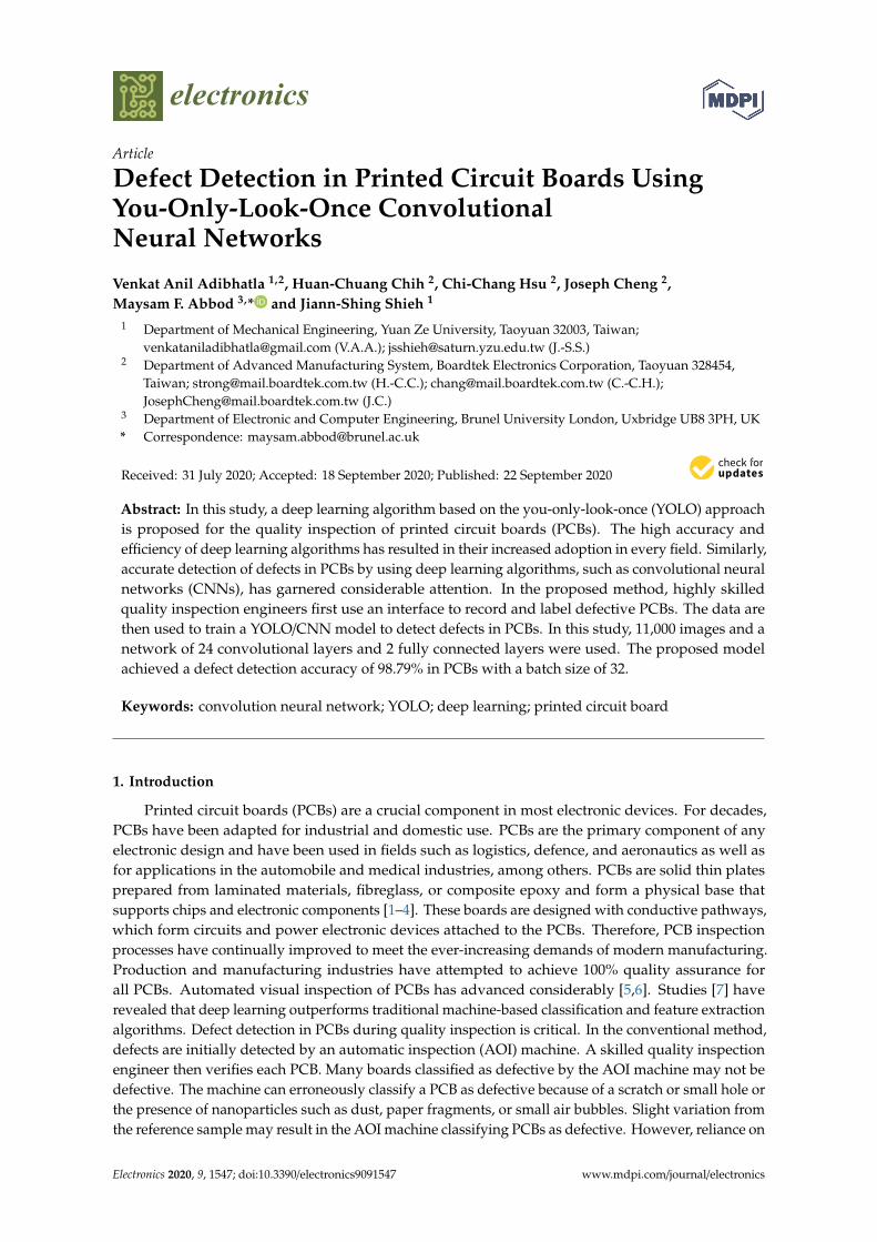
The pooling layer is used to reduce the dimensions of images. The main objective of the pooling layer is to eliminate unnecessary information and preserve only vital parameters. Often used are maximum pooling, which considers the maximum value from the input, and average pooling, which considers the average value, expressed as follows:
s[i, j] = max {S[i;, j’]:i ≤ i’ < i + ,j ≤ j’ < j + p} (4)
s[i, j] = average {S[i;, j’]:i ≤ i’ < i + ,j ≤ j’ < j + p} (5)
Figure 4. Leaky rectified linear unit.
2.5. Pooling Layer
The pooling layer is used to reduce the dimensions of images. The main objective of thepooling layer is to eliminate unnecessary information and preserve only vital parameters. Often used
Electronics 2020, 9, 1547 6 of 16
are maximum pooling, which considers the maximum value from the input, and average pooling,which considers the average value, expressed as follows:
s[i, j] = max {S[i;, j’]:i ≤ i’ < i + ,j ≤ j’ < j + p} (4)
s[i, j] = average {S[i;, j’]:i ≤ i’ < i + ,j ≤ j’ < j + p} (5)
Layers in Tiny-YOLO-v2 can be accessed after the application of the batch normalisation layerto convolutional layers. Inputs with zero mean and unit variance are used. Batch normalisation isexpressed in Equation (6). The earlier output of the convolutional layer is normalised through removalof the batch mean and dissection of the batch variance. The output after batch normalisation is shiftedaccording to bias and scaled. CNNs consist of variables such as variance, mean, scale, and bias causedduring the CNN training stage. These parameters permit individual layers to learn independently andprevent overfitting through their regularisation effect.
x( j) =(x(i) − µ)√
σ2 + ξ(6)
where x( j) = the output pixel after batch normalisation, x(i) = the output pixel after convolution, µ =
the mean, σ = variance, ξ = constant.
3. Results
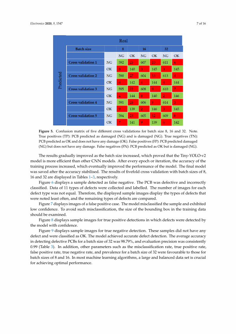
Efficient computing is necessary to achieve optimal performance of the Tiny-YOLO-v2 model.Therefore, a NVidia TITAN V graphics processing unit (GPU) (NVidia, Santa Clara, CA, USA) wasused for this experiment, which reduced the training time to 10% (i.e., 34 to 4 h). The Tiny-YOLO-v2model was trained with the Keras framework running on the NVidia TITAN V GPU by using theLinux operating system. The early stop criteria were implemented, which achieved the highestvalidation accuracy. A batch size of 32 was used, which is a standard maximum batch size. Here,8 GB of memory was used. Initially, during the training stage, a small data set was selected for testingthe basic performance of these networks. The network settings and parameters were adjusted andtuned gradually using the trial-and-error method. The parameter batch size was changed. Initially,5000 images of PCBs labelled as defective were used. Next, 11,000 images of defective PCBs wereused. This procedure was implemented to improve the accuracy of the Tiny-YOLO-v2 model andregulate the parameters of the model to attain the most advantageous implementation of the trainingmodel. The epoch size is based on the training data set. After parameters were selected for the model,an initial ideal start for training was initiated. Moreover, with the callback function, a model checkpointinstruction was used to tune the training process. Its primary purpose is to save the Tiny-YOLO-v2model with all the weight after each epoch so that finally model framework and weights can save itsoptimal performance.
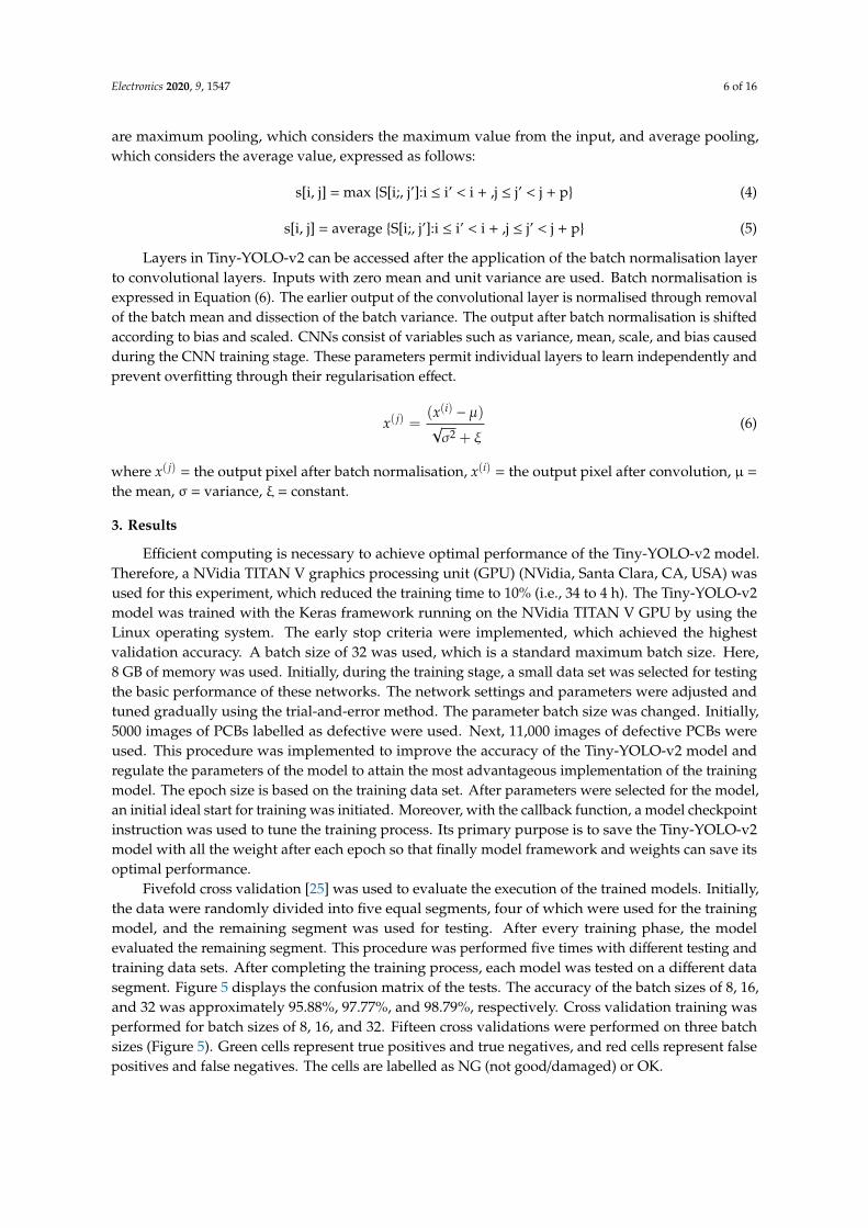
Fivefold cross validation [25] was used to evaluate the execution of the trained models. Initially,the data were randomly divided into five equal segments, four of which were used for the trainingmodel, and the remaining segment was used for testing. After every training phase, the modelevaluated the remaining segment. This procedure was performed five times with different testing andtraining data sets. After completing the training process, each model was tested on a different datasegment. Figure 5 displays the confusion matrix of the tests. The accuracy of the batch sizes of 8, 16,and 32 was approximately 95.88%, 97.77%, and 98.79%, respectively. Cross validation training wasperformed for batch sizes of 8, 16, and 32. Fifteen cross validations were performed on three batchsizes (Figure 5). Green cells represent true positives and true negatives, and red cells represent falsepositives and false negatives. The cells are labelled as NG (not good/damaged) or OK.
Electronics 2020, 9, 1547 7 of 16Electronics 2020, 9, x FOR PEER REVIEW 7 of 17
Figure 5. Confusion matrix of five different cross validations for batch size 8, 16 and 32. Note. True positives (TP): PCB predicted as damaged (NG) and is damaged (NG). True negatives (TN): PCB predicted as OK and does not have any damage (OK). False positives (FP): PCB predicted damaged (NG) but does not have any damage. False negatives (FN): PCB predicted as OK but is damaged (NG).
The results gradually improved as the batch size increased, which proved that the Tiny-YOLO-v2 model is more efficient than other CNN models. After every epoch or iteration, the accuracy of the training process increased, which eventually improved the performance of the model. The final model was saved after the accuracy stabilised. The results of fivefold cross validation with batch sizes of 8, 16 and 32 are displayed in Tables 1–3, respectively.
Figure 5. Confusion matrix of five different cross validations for batch size 8, 16 and 32. Note.True positives (TP): PCB predicted as damaged (NG) and is damaged (NG). True negatives (TN):PCB predicted as OK and does not have any damage (OK). False positives (FP): PCB predicted damaged(NG) but does not have any damage. False negatives (FN): PCB predicted as OK but is damaged (NG).
The results gradually improved as the batch size increased, which proved that the Tiny-YOLO-v2model is more efficient than other CNN models. After every epoch or iteration, the accuracy of thetraining process increased, which eventually improved the performance of the model. The final modelwas saved after the accuracy stabilised. The results of fivefold cross validation with batch sizes of 8,16 and 32 are displayed in Tables 1–3, respectively.
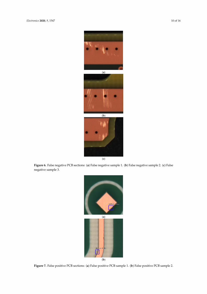
Figure 6 displays a sample detected as false negative. The PCB was defective and incorrectlyclassified. Data of 11 types of defects were collected and labelled. The number of images for eachdefect type was not equal. Therefore, the displayed sample images display the types of defects thatwere noted least often, and the remaining types of defects are compared.
Figure 7 displays images of a false positive case. The model misclassified the sample and exhibitedlow confidence. To avoid such misclassification, the size of the bounding box in the training datashould be examined.
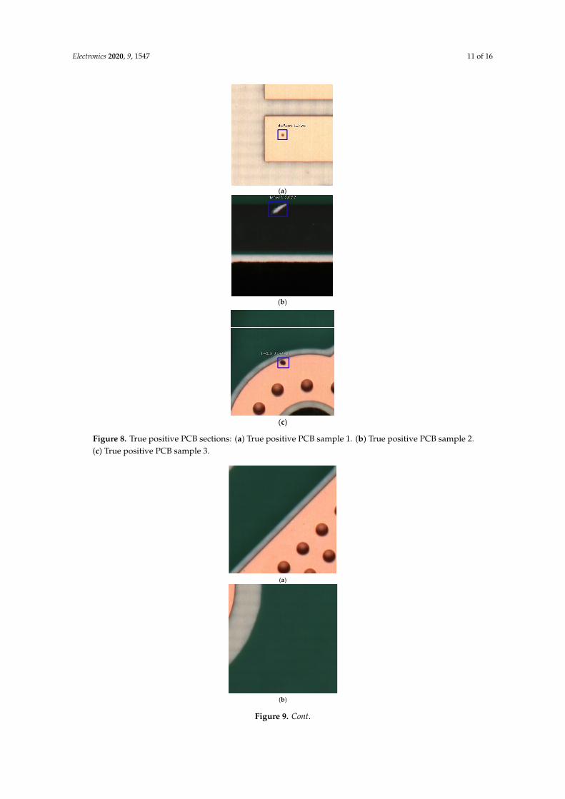
Figure 8 displays sample images for true positive detections in which defects were detected bythe model with confidence.
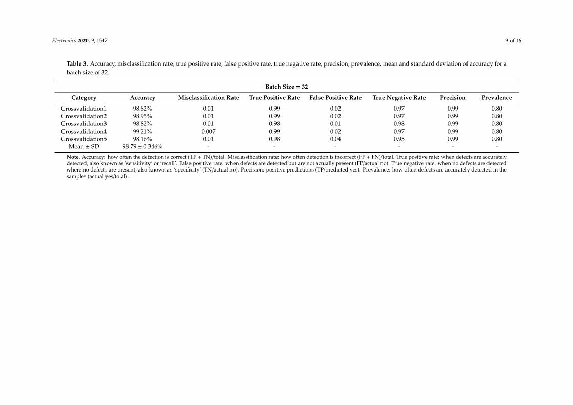
Figure 9 displays sample images for true negative detection. These samples did not have anydefect and were classified as OK. The model achieved accurate defect detection. The average accuracyin detecting defective PCBs for a batch size of 32 was 98.79%, and evaluation precision was consistently0.99 (Table 3). In addition, other parameters such as the misclassification rate, true positive rate,false positive rate, true negative rate, and prevalence for a batch size of 32 were favourable to those forbatch sizes of 8 and 16. In most machine learning algorithms, a large and balanced data set is crucialfor achieving optimal performance.
Electronics 2020, 9, 1547 8 of 16
Table 1. Accuracy, misclassification rate, true positive rate, false positive rate, true negative rate, precision, prevalence, and mean and standard deviation of accuracyfor a batch size of 8.
Batch Size = 8
Category Accuracy Misclassification Rate True Positive Rate False Positive Rate True Negative Rate Precision Prevalence
Cross validation 1 95.68% 0.04 0.95 0.05 0.94 0.98 0.80Cross validation 2 95.67% 0.04 0.95 0.04 0.95 0.98 0.80Cross validation 3 96.60% 0.03 0.96 0.02 0.97 0.99 0.80Cross validation 4 95.42% 0.04 0.95 0.06 0.93 0.98 0.80Cross validation 5 96.07% 0.03 0.96 0.09 0.95 0.98 0.80
Mean ± SD 95.88 ± 0.412% - - - - - -
Note. Accuracy: how often the detection is correct (TP + TN)/total. Misclassification rate: how often detection is incorrect (FP + FN)/total. True positive rate: when defects are accuratelydetected, also known as ‘sensitivity’ or ‘recall’. False positive rate: when defects are detected but are not actually present (FP/actual no). True negative rate: when no defects are detectedwhere no defects are present, also known as ‘specificity’ (TN/actual no). Precision: positive predictions (TP/predicted yes). Prevalence: how often defects are accurately detected in thesamples (actual yes/total).
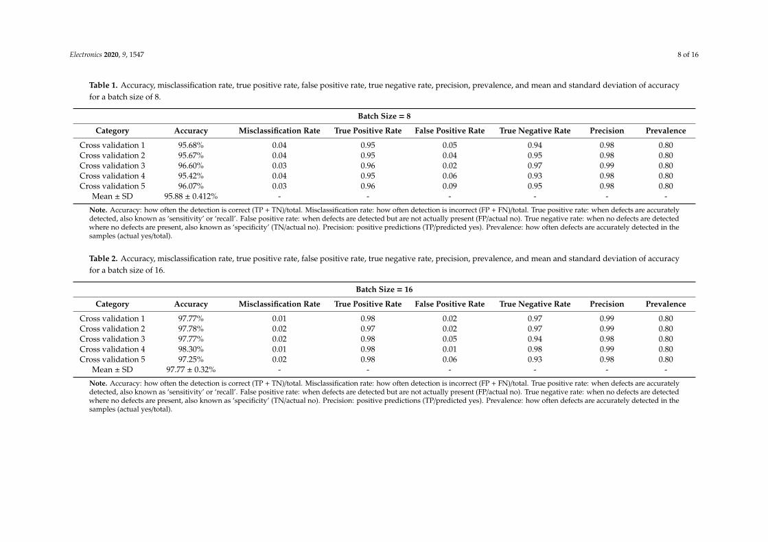
Table 2. Accuracy, misclassification rate, true positive rate, false positive rate, true negative rate, precision, prevalence, and mean and standard deviation of accuracyfor a batch size of 16.
Batch Size = 16
Category Accuracy Misclassification Rate True Positive Rate False Positive Rate True Negative Rate Precision Prevalence
Cross validation 1 97.77% 0.01 0.98 0.02 0.97 0.99 0.80Cross validation 2 97.78% 0.02 0.97 0.02 0.97 0.99 0.80Cross validation 3 97.77% 0.02 0.98 0.05 0.94 0.98 0.80Cross validation 4 98.30% 0.01 0.98 0.01 0.98 0.99 0.80Cross validation 5 97.25% 0.02 0.98 0.06 0.93 0.98 0.80
Mean ± SD 97.77 ± 0.32% - - - - - -
Note. Accuracy: how often the detection is correct (TP + TN)/total. Misclassification rate: how often detection is incorrect (FP + FN)/total. True positive rate: when defects are accuratelydetected, also known as ‘sensitivity’ or ‘recall’. False positive rate: when defects are detected but are not actually present (FP/actual no). True negative rate: when no defects are detectedwhere no defects are present, also known as ‘specificity’ (TN/actual no). Precision: positive predictions (TP/predicted yes). Prevalence: how often defects are accurately detected in thesamples (actual yes/total).
Electronics 2020, 9, 1547 9 of 16
Table 3. Accuracy, misclassification rate, true positive rate, false positive rate, true negative rate, precision, prevalence, mean and standard deviation of accuracy for abatch size of 32.
Batch Size = 32
Category Accuracy Misclassification Rate True Positive Rate False Positive Rate True Negative Rate Precision Prevalence
Crossvalidation1 98.82% 0.01 0.99 0.02 0.97 0.99 0.80Crossvalidation2 98.95% 0.01 0.99 0.02 0.97 0.99 0.80Crossvalidation3 98.82% 0.01 0.98 0.01 0.98 0.99 0.80Crossvalidation4 99.21% 0.007 0.99 0.02 0.97 0.99 0.80Crossvalidation5 98.16% 0.01 0.98 0.04 0.95 0.99 0.80
Mean ± SD 98.79 ± 0.346% - - - - - -
Note. Accuracy: how often the detection is correct (TP + TN)/total. Misclassification rate: how often detection is incorrect (FP + FN)/total. True positive rate: when defects are accuratelydetected, also known as ‘sensitivity’ or ‘recall’. False positive rate: when defects are detected but are not actually present (FP/actual no). True negative rate: when no defects are detectedwhere no defects are present, also known as ‘specificity’ (TN/actual no). Precision: positive predictions (TP/predicted yes). Prevalence: how often defects are accurately detected in thesamples (actual yes/total).
Electronics 2020, 9, 1547 10 of 16
Electronics 2020, 9, x FOR PEER REVIEW 10 of 17
Figure 6 displays a sample detected as false negative. The PCB was defective and incorrectly classified. Data of 11 types of defects were collected and labelled. The number of images for each defect type was not equal. Therefore, the displayed sample images display the types of defects that were noted least often, and the remaining types of defects are compared.
(a)
(b)
(c)
Figure 6. False negative PCB sections: (a) False negative sample 1. (b) False negative sample 2. (c) False negative sample 3.
Figure 7 displays images of a false positive case. The model misclassified the sample and exhibited low confidence. To avoid such misclassification, the size of the bounding box in the training data should be examined.
Figure 6. False negative PCB sections: (a) False negative sample 1. (b) False negative sample 2. (c) Falsenegative sample 3.Electronics 2020, 9, x FOR PEER REVIEW 11 of 17
(a)
(b)
Figure 7. False positive PCB sections: (a) False positive PCB sample 1. (b) False positive PCB sample 2.
Figure 8 displays sample images for true positive detections in which defects were detected by the model with confidence.
(a)
(b)
Figure 7. False positive PCB sections: (a) False positive PCB sample 1. (b) False positive PCB sample 2.
Electronics 2020, 9, 1547 11 of 16
Electronics 2020, 9, x FOR PEER REVIEW 11 of 17
(a)
(b)
Figure 7. False positive PCB sections: (a) False positive PCB sample 1. (b) False positive PCB sample 2.
Figure 8 displays sample images for true positive detections in which defects were detected by the model with confidence.
(a)
(b)
Electronics 2020, 9, x FOR PEER REVIEW 12 of 17
(c)
Figure 8. True positive PCB sections: (a) True positive PCB sample 1. (b) True positive PCB sample 2. (c) True positive PCB sample 3.
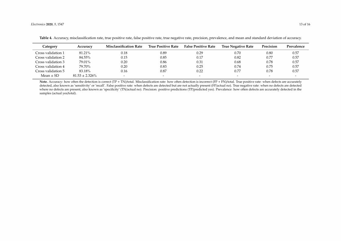
Figure 9 displays sample images for true negative detection. These samples did not have any defect and were classified as OK. The model achieved accurate defect detection. The average accuracy in detecting defective PCBs for a batch size of 32 was 98.79%, and evaluation precision was consistently 0.99 (Table 3). In addition, other parameters such as the misclassification rate, true positive rate, false positive rate, true negative rate, and prevalence for a batch size of 32 were favourable to those for batch sizes of 8 and 16. In most machine learning algorithms, a large and balanced data set is crucial for achieving optimal performance.
(a)
(b)
Figure 8. True positive PCB sections: (a) True positive PCB sample 1. (b) True positive PCB sample 2.(c) True positive PCB sample 3.
Electronics 2020, 9, x FOR PEER REVIEW 12 of 17
(c)
Figure 8. True positive PCB sections: (a) True positive PCB sample 1. (b) True positive PCB sample 2. (c) True positive PCB sample 3.
Figure 9 displays sample images for true negative detection. These samples did not have any defect and were classified as OK. The model achieved accurate defect detection. The average accuracy in detecting defective PCBs for a batch size of 32 was 98.79%, and evaluation precision was consistently 0.99 (Table 3). In addition, other parameters such as the misclassification rate, true positive rate, false positive rate, true negative rate, and prevalence for a batch size of 32 were favourable to those for batch sizes of 8 and 16. In most machine learning algorithms, a large and balanced data set is crucial for achieving optimal performance.
(a)
(b)
Figure 9. Cont.

Electronics 2020, 9, 1547 12 of 16
Electronics 2020, 9, x FOR PEER REVIEW 13 of 17
(c)
Figure 9. True negative PCB sections: (a) True negative PCB sample 1. (b) True negative PCB sample 2. (c) True negative PCB sample 3.
A vanilla version of the CNN [26] was used to compare the results of the proposed model. The vanilla CNN was trained using 15,823 images. Fivefold cross validation was implemented to evaluate the execution of the trained models. Figure 10 displays the results of testing in the form of a confusion matrix (Figure 5); green cells represent true positives and true negatives, and red cells represent false positives and false negatives.
Figure 10. Vanilla convolutional neural network (CNN) confusion matrix of five cross validations. Note. True positive (TP): Cases in which damage is detected (NG) in the PCB and the PCB is defective (NG). True negative (TN): the PCB is predicted as OK and does not have any damage (OK). False positive (FP): damage is detected (NG) but the PCB does not actually have any damage. False negative (FN): the PCB is predicted as OK but is actually damaged (NG).
The cross validation results of the Vanilla CNN are presented in Table 4. The mean and standard deviation of accuracy was approximately 81.53 ± 2.326%, and precision was less than 0.8, which is less than that of Tiny-YOLO-v2. The vanilla CNN is an image classifier that could not identify the location of defects. Furthermore, it considers the background as a class, which increased misclassification, unlike Tiny-YOLO-v2, which detects multiple defects in a single image and locates the defects with a bounding box.
Figure 9. True negative PCB sections: (a) True negative PCB sample 1. (b) True negative PCB sample 2.(c) True negative PCB sample 3.
A vanilla version of the CNN [26] was used to compare the results of the proposed model.The vanilla CNN was trained using 15,823 images. Fivefold cross validation was implemented toevaluate the execution of the trained models. Figure 10 displays the results of testing in the form ofa confusion matrix (Figure 5); green cells represent true positives and true negatives, and red cellsrepresent false positives and false negatives.
Electronics 2020, 9, x FOR PEER REVIEW 13 of 17
(c)
Figure 9. True negative PCB sections: (a) True negative PCB sample 1. (b) True negative PCB sample 2. (c) True negative PCB sample 3.
A vanilla version of the CNN [26] was used to compare the results of the proposed model. The vanilla CNN was trained using 15,823 images. Fivefold cross validation was implemented to evaluate the execution of the trained models. Figure 10 displays the results of testing in the form of a confusion matrix (Figure 5); green cells represent true positives and true negatives, and red cells represent false positives and false negatives.
Figure 10. Vanilla convolutional neural network (CNN) confusion matrix of five cross validations. Note. True positive (TP): Cases in which damage is detected (NG) in the PCB and the PCB is defective (NG). True negative (TN): the PCB is predicted as OK and does not have any damage (OK). False positive (FP): damage is detected (NG) but the PCB does not actually have any damage. False negative (FN): the PCB is predicted as OK but is actually damaged (NG).
The cross validation results of the Vanilla CNN are presented in Table 4. The mean and standard deviation of accuracy was approximately 81.53 ± 2.326%, and precision was less than 0.8, which is less than that of Tiny-YOLO-v2. The vanilla CNN is an image classifier that could not identify the location of defects. Furthermore, it considers the background as a class, which increased misclassification, unlike Tiny-YOLO-v2, which detects multiple defects in a single image and locates the defects with a bounding box.
Figure 10. Vanilla convolutional neural network (CNN) confusion matrix of five cross validations. Note.True positive (TP): Cases in which damage is detected (NG) in the PCB and the PCB is defective (NG).True negative (TN): the PCB is predicted as OK and does not have any damage (OK). False positive(FP): damage is detected (NG) but the PCB does not actually have any damage. False negative (FN):the PCB is predicted as OK but is actually damaged (NG).
The cross validation results of the Vanilla CNN are presented in Table 4. The mean and standarddeviation of accuracy was approximately 81.53 ± 2.326%, and precision was less than 0.8, which is lessthan that of Tiny-YOLO-v2. The vanilla CNN is an image classifier that could not identify the locationof defects. Furthermore, it considers the background as a class, which increased misclassification,unlike Tiny-YOLO-v2, which detects multiple defects in a single image and locates the defects with abounding box.
Electronics 2020, 9, 1547 13 of 16
Table 4. Accuracy, misclassification rate, true positive rate, false positive rate, true negative rate, precision, prevalence, and mean and standard deviation of accuracy.
Category Accuracy Misclassification Rate True Positive Rate False Positive Rate True Negative Rate Precision Prevalence
Cross validation 1 81.21% 0.18 0.89 0.29 0.70 0.80 0.57Cross validation 2 84.55% 0.15 0.85 0.17 0.82 0.77 0.57Cross validation 3 79.01% 0.20 0.86 0.31 0.68 0.78 0.57Cross validation 4 79.70% 0.20 0.83 0.25 0.74 0.75 0.57Cross validation 5 83.18% 0.16 0.87 0.22 0.77 0.78 0.57
Mean ± SD 81.53 ± 2.326% - - - - - -
Note. Accuracy: how often the detection is correct (TP + TN)/total. Misclassification rate: how often detection is incorrect (FP + FN)/total. True positive rate: when defects are accuratelydetected, also known as ‘sensitivity’ or ‘recall’. False positive rate: when defects are detected but are not actually present (FP/actual no). True negative rate: when no defects are detectedwhere no defects are present, also known as ‘specificity’ (TN/actual no). Precision: positive predictions (TP/predicted yes). Prevalence: how often defects are accurately detected in thesamples (actual yes/total).
Electronics 2020, 9, 1547 14 of 16
4. Discussion
A novel user interface was developed to collect data. Skilled engineers labelled the defects usingthe interface. The simple method achieved an excellent PCB defect detection accuracy of 98.79%,which is considerably better than that of other algorithms involving complex feature extraction [27–29].The effectiveness of the proposed method was investigated using various CNN layers. To avoid thedelay resulting from the nonspecificity of a single CNN model and insufficient storage capacity, a GPUenvironment was established. The model was trained using different batch sizes to improve accuracy.
The YOLO strategy is a powerful and quick approach that achieves a higher FPS rate thancomputationally expensive two-stage detectors (e.g., faster R-CNN) and some single-stage detectors(e.g., RetinaNet and SSD). Tiny-YOLO-v2 was used in this study to increase the execution speedbecause it is approximately 442% faster than the standard YOLO model, achieving 244 FLOP on asingle GPU. A small model size (<50 MB) and fast inference renders the Tiny-YOLO-v2 naturallysuitable for embedded computer vision.
Compared with other simple classifiers, YOLO is widely used in practice. It is a simple unifiedobject detection model and can be trained directly using full images. Unlike classifier-based approaches,YOLO is trained using a loss function that directly influences detection performance. Furthermore,the entire model is trained at one time. Fast YOLO is the fastest general-purpose object detector.YOLO-v2 provides the best tradeoff between real-time speed and accuracy for object detection comparedwith other detection systems across various detection data sets.
Multilayer neural networks or tree-based algorithms are deemed insufficient for modernadvanced computer vision tasks. The disadvantage of fully connected layers, in which eachperceptron is connected to every other perceptron, is that the number of parameters can increaseconsiderably, which results in redundancy in such high dimensions, rendering the system inefficient.Another disadvantage is that spatial information is disregarded because flattened vectors are used asinputs. However, the key difference distinguishing YOLO from other methods is that the completeimage is viewed at one time rather than only a generated region, and this contextual information helpsto avoid false positives.
In this study, a modified YOLO model was developed and combined with an advanced CNNarchitecture. However, some challenges remain to be overcome. Although the proposed systemincorporates a smart structure and an advanced CNN method, the model accuracy is not perfect,particularly when operated with unbalanced data sets. The used data sets are collected by experiencedPCB quality inspection teams. Moreover, traditional deep learning methods [30–32] are based onclassifying or detecting particular objects in an image. Therefore, the model structure was tested withthree batch sizes. As elaborated elsewhere [33], these structures exhibit high precision for a classicalCNN model but unpredictable performance for the PCB data set. According to research on deep learning,the types of network layer parameters, linear unit activation parameters, regularisation strategies,optimisation algorithms, and approach to batch normalisation of the CNN training process should befocused on for improving the PCB defect detection performance of CNNs. As depicted in Figure 5,the proposed model can accurately detect defects on PCBs and can therefore be used for PCB qualityinspection on a commercial scale.
The three models achieved excellent results with an accuracy reaching 99.21% (Table 3). This provesthat the modified YOLO model with deep CNNs is suitable for detecting PCB defects and can achieveaccurate results. CNNs can automatically perform the learning process of the target after appropriatetuning of the model parameters. During training, the CNN weights are automatically fine-tuned toextract features from the images. However, further research, such as experimental evaluation andperformance analysis, should be conducted to enhance CNN performance, describe PCB defects inmore detail, and classify defects into predefined categories.
Electronics 2020, 9, 1547 15 of 16
5. Conclusions
This study proves that the proposed CNN object detection algorithm combined with theTiny-YOLO-v2 algorithm can accurately detect defects in PCBs with an accuracy of 98.82%.
In the future, the system should be improved for detecting other types of defects. Additionally,more types of defects and more data should be included to achieve group balancing. Other CNNalgorithms, such as Rateninet, ResNet, and GoogleNet [17,20,34], should be implemented usingGPU hardware for increased learning speed. Finally, the transfer learning approach [35] should beconsidered for a pretrained YOLO model.
Author Contributions: Conceptualization V.A.A., J.-S.S., C.-C.H., H.-C.C. and J.C.; formal analysis V.A.A.;investigation, V.A.A., J.-S.S., C.-C.H. and H.-C.C.; methodology, V.A.A., J.-S.S., C.-C.H., H.-C.C. and J.C.; software,V.A.A., C.-C.H. and H.-C.C.; supervision J.-S.S., M.F.A. and J.C.; validation V.A.A., J.-S.S., C.-C.H., H.-C.C. and J.C.;visualization, V.A.A., J.-S.S., C.-C.H., H.-C.C. and J.C.; writing, V.A.A., J.-S.S. and M.F.A. All authors have read andagreed to the published version of the manuscript.
Funding: This research was funded by the Ministry of Science and Technology (MOST) of Taiwan (grant number:MOST 108-2622-E-155-010-CC3) and Boardtek Electronics Corporation, Taiwan.
Conflicts of Interest: The authors declare no conflict of interest.
References
1. Suzuki, H.; Junkosha Co Ltd. Official Gazette of the United States Patent and Trademark. Printed CircuitBoard. U.S. Patent US 4,640,866, 16 March 1987.
2. Matsubara, H.; Itai, M.; Kimura, K.; NGK Spark Plug Co Ltd. Patents assigned to NGK spark plug.Printed Circuit Board. U.S. Patent US 6,573,458, 12 September 2003.
3. Magera, J.A.; Dunn, G.J.; Motorola Solutions Inc. The Printed Circuit Designer’s Guide to Flex and Rigid-FlexFundamentals. Printed Circuit Board. U.S. Patent US 7,459,202, 21 August 2008.
4. Cho, H.S.; Yoo, J.G.; Kim, J.S.; Kim, S.H.; Samsung Electro Mechanics Co Ltd. Official Gazette of the UnitedStates Patent and Trademark. Printed Circuit Board. U.S. Patent US 8,159,824, 16 March 2012.
5. Chauhan, A.P.S.; Bhardwaj, S.C. Detection of bare PCB defects by image subtraction method using machinevision. In Proceedings of the World Congress on Engineering, London, UK, 6–8 July 2011; Volume 2, pp. 6–8.
6. Khalid, N.K.; Ibrahim, Z. An Image Processing Approach towards Classification of Defects on Printed CircuitBoard. Ph.D. Thesis, University Technology Malaysia, Johor, Malaysia, 2007.
7. Bengio, Y.; Courville, A.; Vincent, P. Representation Learning: A Review and New Perspectives. IEEE Trans.Pattern Anal. Mach. Intell. 2013, 35, 1798–1828. [CrossRef] [PubMed]
8. Malge, P.S. PCB Defect Detection, Classification and Localization using Mathematical Morphology andImage Processing Tools. Int. J. Comput. Appl. 2014, 87, 40–45.
9. Takada, Y.; Shiina, T.; Usami, H.; Iwahori, Y. Defect Detection and Classification of Electronic Circuit BoardsUsing Keypoint Extraction and CNN Features. In Proceedings of the Ninth International Conferences onPervasive Patterns and Applications Defect, Athens, Greece, 19–23 February 2017; pp. 113–116.
10. Anitha, D.B.; Mahesh, R. A Survey on Defect Detection in Bare PCB and Assembled PCB using ImageProcessing Techniques. In Proceedings of the 2017 International Conference on Wireless Communications,Signal Processing and Networking (WiSPNET), Chennai, India, 22–24 March 2017; pp. 39–43.
11. Crispin, A.J.; Rankov, V. Automated inspection of PCB components using a genetic algorithmtemplate-matching approach. Int. J. Adv. Manuf. Technol. 2007, 35, 293–300. [CrossRef]
12. Raihan, F.; Ce, W. PCB Defect Detection USING OPENCV with Image Subtraction Method. In Proceedingsof the 2017 International Conference on Information Management and Technology (ICIMTech), Singapore,27–29 December 2017; pp. 204–209.
13. Hosseini, H.; Xiao, B.; Jaiswal, M.; Poovendran, R. On the Limitation of Convolutional Neural Networks inRecognizing Negative Images. In Proceedings of the 2017 16th IEEE International Conference on MachineLearning and Applications (ICMLA), Cancun, Mexico, 18–21 December 2017; pp. 352–358.
14. Tao, X.; Wang, Z.; Zhang, Z.; Zhang, D.; Xu, D.; Gong, X.; Zhang, L. Wire Defect Recognition of Spring-WireSocket Using Multitask Convolutional Neural Networks. IEEE Trans. Compon. Packag. Manuf. Technol. 2018,8, 689–698. [CrossRef]
Electronics 2020, 9, 1547 16 of 16
15. Uijlings, J.R.R.; Van De Sande, K.E.A.; Gevers, T.; Smeulders, A.W.M. Selective Search for Object Recognition.Int. J. Comput. Vis. 2012, 104, 154–171. [CrossRef]
16. Girshick, R.; Donahue, J.; Darrell, T.; Malik, J. Rich feature hierarchies for accurate object detection andsemantic segmentation. In Proceedings of the 2014 IEEE Conference on Computer Vision and PatternRecognition, Columbus, OH, USA, 23–28 June 2014; pp. 580–587.
17. He, K.; Zhang, X.; Ren, S.; Sun, J. Deep residual learning for image recognition. arXiv 2015, arXiv:1512.03385.18. Simonyan, K.; Zisserman, A. Very deep convolutional networks for large-scale image recognition. arXiv
2014, arXiv:1409.1556.19. Szegedy, C.; Ioffe, S.; Vanhoucke, V. Inception-v4, inception-resnet and the impact of residual connections on
learning. arXiv 2016, arXiv:1602.07261.20. Szegedy, C.; Liu, W.; Jia, Y.; Sermanet, P.; Reed, S.; Anguelov, D.; Erhan, D.; Vanhoucke, V.; Rabinovich, A.
Going deeper with convolutions. arXiv 2014, arXiv:1409.4842.21. Suda, N.; Chandra, V.; Dasika, G.; Mohanty, A.; Ma, Y.; Vrudhula, S.; Seo, J.S.; Cao, Y. Throughput-optimized
OpenCL-based FPGA accelerator for large-scale convolutional neural networks. In Proceedings ofthe ACM/SIGDA International Symposium on Field-Programmable Gate Arrays, Monterey, CA, USA,21–23 February 2016; pp. 16–25.
22. Zhang, J.; Li, J. Improving the performance of OpenCL-based FPGA accelerator for convolutional neuralnetwork. In Proceedings of the 2017 ACM/SIGDA International Symposium on Field-Programmable GateArrays, Monterey, CA, USA, 22 February 2017; pp. 25–34.
23. Wang, D.; An, J.; Xu, K. Pipe CNN: An OpenCL-Based FPGA Accelerator for Large-Scale ConvolutionNeuron Networks. arXiv 2016, arXiv:1611.02450.
24. Cong, J.; Xiao, B. Minimizing computation in convolutional neural networks. In Proceedings of theInternational Conference on Artificial Neural Networks, Hamburg, Germany, 15–19 September 2014;pp. 281–290.
25. Pritt, M.; Chern, G. Satellite Image Classification with Deep Learning. In Proceedings of the 2017 IEEEApplied Imagery Pattern Recognition Workshop (AIPR), Washington, DC, USA, 10–12 October 2017.
26. Hastie, T.; Tibshirani, R.; Friedman, J. The Elements of Statistical Learning: Data Mining, Inference, and Prediction;Springer: New York, NY, USA, 2009.
27. Zhang, X.S.; Roy, R.J.; Jensen, E.W. EEG complexity as a measure of depth of anesthesia for patients.IEEE Trans. Biomed. Eng. 2001, 48, 1424–1433. [CrossRef] [PubMed]
28. Lalitha, V.; Eswaran, C. Automated detection of anesthetic depth levels using chaotic features with artificialneural networks. J. Med. Syst. 2007, 31, 445–452. [CrossRef] [PubMed]
29. Peker, M.; Sen, B.; Gürüler, H. Rapid Automated Classification of Anesthetic Depth Levels using GPU BasedParallelization of Neural Networks. J. Med. Syst. 2015, 39, 18. [CrossRef] [PubMed]
30. Callet, P.L.; Viard-Gaudin, C.; Barba, D. A convolutional neural network approach for objective video qualityassessment. IEEE Trans. Neural Netw. 2006, 17, 1316–1327. [CrossRef] [PubMed]
31. Dan, C.C.; Meier, U.; Gambardella, L.M.; Schmidhuber, R. Convolu- tional neural network committees forhandwritten character classification. In Proceedings of the 2011 International Conference on DocumentAnalysis and Recognition, Beijing, China, 18–21 September 2011; pp. 1135–1139.
32. Kalchbrenner, N.; Grefenstette, E.; Blunsom, P. A convolutional neural network for modelling sentences.arXiv 2014, arXiv:1404.2188.
33. Devarakonda, A.; Naumov, M.; Garland, M. AdaBatch: Adaptive batch sizes for training deep neuralnetworks. arXiv 2017, arXiv:1712.02029.
34. Lin, T.; Goyal, P.; Girshick, R.; He, K.; Dollár, P. Focal Loss for Dense Object Detection. In Proceedingsof the 2017 IEEE International Conference on Computer Vision (ICCV), Venice, Italy, 22–29 October 2017;pp. 2999–3007.
35. Shao, L.; Zhu, F.; Li, X. Transfer Learning for Visual Categorization: A Survey. IEEE Trans. Neural Netw.Learn. Syst. 2015, 26, 1019–1034. [CrossRef] [PubMed]
© 2020 by the authors. Licensee MDPI, Basel, Switzerland. This article is an open accessarticle distributed under the terms and conditions of the Creative Commons Attribution(CC BY) license (http://creativecommons.org/licenses/by/4.0/).