
Cobra 148GTL-DX 120-Channel Solid State, Citizens Band ...
85
Cobra 148GTL-DX 120-Channel Solid State, Citizens Band SSB/CW/AM/FM 2-Way Mobile Radio Cobra Communications Product Group DYNASCAN CORPORATION 6460 W. Cortland Street Chicago, Illinois 60635
-
Upload
khangminh22 -
Category
Documents
-
view
0 -
download
0
Transcript of Cobra 148GTL-DX 120-Channel Solid State, Citizens Band ...

Cobra 148GTL-DX 120-Channel
Solid State, Citizens Band SS B/CW/AM/FM 2-Way
Mobile Radio
Cobra Communications Product Group DYNASCAN CORPORATION
6460 W. Cortland Street Chicago, Illinois 60635

Instruction Manual for
Cobra 148GTL-DX 120-Channel
Solid State, Citizens Band SSB/CW/AM/FM2-Way
Mobile Radio
о s
Cobra Communications Product Group
DYNASCAN CORPORATION 6460 W. Cortland Street Chicago, Illinois 60635

TABLE OF CONTENTSPage
Section I: IntroductionFrequency R an g e ...................................................................... 4
Section II: Spécifications.....................................................................................6
Section III: InstallationLocation................................................... ................................... » ............ - -8Mounting the Connection.................................................... 8
' IgnitionNoise Interférence . ............................................................. .9A ntenna................ ..................... ........................................ .. .9Tuning the Antenna for Optimum SWR.......................................................10Base Station Operation.............................................................. 11External Speaker. .......................................................................... .11
Section IV: OperationControls and Iridicators................................................................................ 12A. Control Functions..................................................................................... 12B. Indicator Functions...................................... . . . . . . . . . ...................14Operating Procedure to Receive.......... .......................................... 14Operating Procedure to Transmit.............................................................. 15Receiving SSB signais......................................................... 15Operating Procedure to CW MODE.............................................................. 17Roger В еер ...................................................................................................17Alternate Microphones and Installation............................................... 18
Section V: Maintenance and Adjustment............................................. 21
Section VI: AppendixTen C ode;............. ........................................................................................ 22A Few Rules That Should Be Obeyed...................... .23How your CB Can Serve You................................................ .. . . ............. 24Use Channel 9 for Emergency Message Only.................... ................... .. . 25
Warranty Service Instructions ............................. ................. ........................... 26
Limited One Year Warranty.......................................................... . t ............. 27
- 2 -

TH EC B STO R Y
The Citizens Band lies between the shortwave broadcast and 10-meter amateur radio bands, and was established by law in 1949. Two-way communications service was opened in 1959.
HAVEA GOOD DAY
TODAY AND
A BETTER DAY TOMORROW!
- 3 -

Section IIntroduction
FREQUENCY RANGEThe COBRA 148GTL-DX transceiver représente one of the most advanced
SSB/CW/AM/FM two-way radios ever designed for use as the Citizens Radio Service. This unit features advanced Phase Lock Loop (PLL) circuitry, which is used in the AM/FM mode, in the upper and lower single sideband modes and in the CW mode providing complété coverage of ail 120 channels shown below.
CORRECTION
CHANNEL LOW BAND MID BAND HI BAND1 . , 26.515 26.965 '■ 27.4152 .525 .975 .4253 .535 .985 .4354 .555 27.005 .4555 .565 .015 .4656 .575 .025 .4757 .585 .035 .4858 .605 .055 .5059 .615 .065 .515
10 .625 .075 .52511 .635 .085 .53512 .655 .105 .55513 .665 .115 .56514 .675 .125 .57515 .685 .135 .58516 .705 .155 .60517 .715 . .165 .61518 .725 .175 . .62519 .735 .185 .63520 .755 .205 .65521 .765 .215 .66522 .775 .225 .67523 .805 .255 .70524 .785 .235 .68525 .795 .245 .695
- 4 -

CHANNEL LOW BAND MID BAND HI BAND26 26.815 27.265 27.71527 .825 .275 .72528 .835 '■ .285 .73529 .845 .295 .74530 .855 .305 .75531 .865 .315 .76532 .875 .325 .77533 .885 .335 .78534 .895 .345 .79535 .905 .355 .80536 .915 .365 .81537 .925 .375 .82538 .935 .385 .83539 .945 .395 .84540 .955 .405 .855
The COBRA 148GTL-DX has a vastly superior receiver which includes an RF gain control and noise blanker circuitry effective in both AM/FM and SSB/CW modesr and- an aut=omatie-n0ise4knker-effective in the AM mode. The receiver also features increased protection against cross modulation and strong adjacent channel signais.
To obtain maximum performance from your transceiver, please read carefully the following descriptions and operating instructions.
- 5 -

Section IISpécifications
GENERALChannels
Frequency Range
Frequency Control Frequency Tolérance Frequency Stability Operating Température Range Microphone
120 FM, 120 AM, 120 LSB, 120 USB,120 CW.Low Band, 26.515 to 26.955 MHz.Mid Band, 26.965 to 27.405 MHz.Hi Band, 27.415 to 27.855 MHz.Phase Lock Loop (PLL) Synthesizer.0.005%.0.001%.-30°C to +50°C.Plug-in dynamie; with push-to-talk switch and coiled cord. , .
Input Voltage 13.8V DC nominal, 15.9V max., 11.7V min.(positive or negative ground).Transmit: AM full mod., 2.2A.
SSB 12 watts PEP output, 2Â. Receiver: Squelched, 0.3 A.
Maximum audio output, 0.7A.2-3/8 "(H) x 7-7/8"(W) x 9-l/4"(D).5 lbs.UHF, S0239.Illuminated; indicates relative output power, received signal strength, and SWR.
SizeWeightAntenna Connector Meter (3-in-l)
TRANSMITTERPower Output AM/FM/CW, 5. watts.
SSB, 12 watts, PEP.Modulation High-and low-level Class B, Amplitude Modu
lation: AM. Variable capacitance Frequency Modulation: FM.
Intermodulation Distortion SSB: 3rd order, more than-25 dB.5th order, more than -35 dB.
SSB Carrier Suppression 55 dBUnwanted Sideband 50 dB
- 6 -

Frequency Response Output Impédance Output Indicators •
AM and FM: 450 to 2500 Hz.50 ohms, unbalanced.Meter shows relative RF output power and SWR. Transmit LED glows red when transm ite r is in operation.
RECEIVERSensitivity
Selectivity
Image Rejection IF Frequency
Adjacent-Channel RejectionAM/FM and SSB/CW/RF Gain ControlAutomatic Gain Control
(AGC)SquelchANLXoise Blanker Voice Lock Range
Audio Output.Power Frequency Response Built-in SpeakerExtemal Speaker
(Not Supplied)
SSB/CW: 0.25 jaV for 10 dB (S+N)/N at greater than й -watt of audio output.AM: 0.5 ßV for 10 dB (S+N)/N at greater than Й-watt of audio output.FM: 1.0 jaV for 20 dB (S+N)/N at greater than й -watt of audio output.AM/FM: 6 dB @3 KHz, 50 dB @9 KHz. SSB/CW: 6 dB @2.1 KHz, 60 dB @3.3 KHz.More than 65 dB.AM/FM: 10.695 MHz Ist IF, 455 KHz 2nd
IFSSB/CW: 10.695 MHz.60 dB AM/FM & 70 dB SSB/CW.45 dB adjustable for optimum signal réception.Less than 10 dB change in audio output for inputs from 10 to 100,000 microvolts.Adjustable; threshold less than 0.5 ßV. Switchable.RF type, effective on AM/FM and SSB/CW.Coarse (TX/RX) ±7 KHz.Fine (RX) ±1 KHz.4 watts into 8. ohms.300 to 2800 Hz.8 ohms, round.8 ohms; disables internal speaker when connected.
- 7 -

LOCATIONPlan the location of the transceiver and microphone bracket before starting
the installation. Select a location that is convenient for operation and does not interfère with the driver or passengers in the vehicle. In automobiles, the transceiver is usually mounted below the dash panel, with the microphone bracket beside it.
Section IIIInstallation
MOUNTING THE CONNECTIONThe COBRA 148GTL-DX is supplied with a universal mounting bracket.
When mounting the bracket and radio to your car, make sure it is mechanically strong. Also provide a good electrical connection to the chassis of the vehicle. Proceed as follows to mount the transceiver:__. ........ ..1. After y ou. hâve determined the most convenient location in your vehicle, hold
the COBRA 148GTL-DX with mounting bracket irt the exact location de-■ sired. If nothing will interfère with mounting it in the desired position,
remove the mounting bolts. Before drilling the.holes, make sure nothing will interfère with the installation of the mounting bolts.
2. Connect the antenna cable plug to the standard réceptacle on the rear panel., Most CB antennas are terminated with a type PL-259 plug and mate with the
réceptacle.3. Connect the red DC power input wire (with the fuse) to +13.8V DC. This
wire éxtends from the rear panel. In automobile installation, +13.8V DC is usually obtained from the accessory contact on the ignition switch. This prevents the set being left on accidentally when the driver leaves the car and also permits operating the unit without the engine running. Locate the accessory contact on most ignition switches by tracing-the power wire from the AM broadeast receiver in the car.
4. Connect the black lead to -13.8V DC. This is usually the chassis of the car. Any convenient location with good electrical contact (remove paint) may be used.
5. Mount the microphone bracket on the right side of the transceiver or near the transceiver, using two screws supplied. When mounting in an automobile, place the bracket under the dash so the microphone is readily accessible.

IGNITION NOISE INTERFERENCEUse of a mobile receiver at low signal levels is normally limited by the
presence of electrical noise. The primary source of noise in automobile installations is from the generator and ignition system in the vehicle. Under most operating conditions, when signal level is adéquate, the background noise does not présent a serious problem. Also, when extremely low level signais are being received, the transceiver may be operated with vehicle engine tumed off. The unit requires very little current and therefore will not sigmfîcantly discharge the vehicle battery.
Even though the COBRA 148GTL-DX has ANL and NB Controls, in some installations ignition interférence may be high enough to make good communications impossible. The electrical noise may corne from several sources. Many possibilities exist and variations between vehicles require different solutions to reduce the noise. Consult your COBRA dealer or a 2-way radio technician for help in locating and correcting the source of severe noise.
ANTENNASince the maximum allowable power output of the transmitter is limited by
the FCC, the antenna is one important factor affecting transmission distance. Only a properly matched antenna system will allow maximum power transfer from the 50 ohm transmission line to the radiating element. In mobile installations (cars, trucks, boats, etc.), an antenna system that is non-directional should be used.
A vertically polarized, quarter-wavelength whip antenna provides the most reliable operation and greatest range. Shorter, loaded-type whip antennas are more attractive, compact and adéquate for applications where. the maximum possible distance is not required. Also, the loaded whips do not present the Problems of height imposed by a füll quarter-wavelength whip.
Mobile whip antennas utilize the metal body of the vehicle as a ground plane. When mounted at a corner of the vehicle they are slightly directional, in the direction of the body of the vehicle. For ah practical purpose, however, the radiation pattern is nondirectional. The slight directional characteristic will be observed only at extreme distances. A standard antenna connector (type SO 239) is provided on the transceiver for easy connection to a standard PL 259 cable termination.
If the transceiver is not mounted on a metal surface, it is necessa'ry to run a separate ground wire from the unit to a good metal electrical ground in the vehicle. When installed in a boat, the transceiver will' not operate at maximum efficiency without a ground plate, unless the vessel has a Steel hull.
Before installing the transceiver in a boat, consult your dealer for information regarding an adéquate grounding system and prévention of electrolysis between fïttings in the hull and water.
- 9 -

TUNING THE ANTENNA FOR OPTIMUM SWRSince there is such a wide vaiiety of base and mobile antennas, this section
will strictly concern itself to the various types of mobile adjustable antennas.Because the abtenna length is directly related to the channel frequency, if
must be tuned to resonate optimally all 120 channels of the transceiver. Channel 1 requires a longer antenna than Channel 120 because it is lower in frequency.
Due to the various methods of adjusting antennas for proper SWR we have chosen what we think is the optimum method:
A. Antennas with adjusîment screws (set screws).1. Start with the antenna extended and.tighten the set screw lightly enough so
that the antenna can be lightly tapped with your finger for easy adjustment.2. Set your COBRA 148GTL-DX to Channel 21 @ Mid band. Press the PTT
(push-to-talk) switch, and tap the antenna (making it shorter). The SWR meter will show a lower reading each time the antenna is tapped. By continu- ing to shorten the antenna you will notice the SWR reading will reach a low print and then start rising again. This means that you have passed the optimum point for Channel 21. Extend the antenna a short distance and againfollow the procedure above._ __ _______ _________________When the lowest point has been reached, switch to Channel @ Low band and then to Channel 40 @ Hi band and compare SWR readings. They sould he almost equal.
B. Antennas which must be eut to proper length.1. Follow the same procedure as above, but adjust the length by cutting in 1/8"
incréments until a good match is obtained.2. Be very careful not to eut too much at one time, as one it is eut, it сап по
longer be lengthed.3. The whip is easily eut by filing a notch all the way around and breaking the
piece off with pliers.
--------------------------------- ------- NOTE-----------------------------------------THE PROPER SETTING IS ACHIEVED WHEN THE SWR IS 1.5 OR BELOW, AND WHEN IT HAS THE SAME READING FOR CHANNELS LOW BAND 1 AND HI BAND 40.
If you are having difficulties in adjusting your antenna, check the following:A. AU doors must be closed when adjusting the antenna.B. Make sure the antenna base is grounded.C. Check your coaxial cable routing (it may be pinched when routed into the
car).
- 1 0 -
D. Try a different location on your car (keeping in mind the radiation pattern youwish).
E. Is the antenna perfectly vertical?F. Try a different location in your neighbortiood. Stay away from large metal
objęcts when adjusting (metal téléphoné or light posts, fences, etc.)
------------------------------------------ NOTE----------- :-------------------------------The COBRA 148GTL-DX will operate into an SWR of 2 to 1 indefmite- ly and sustain an SWR of 20:1 for a maximum of 5 minutes at rated operating conditions.
BASE STATION OPERATION (Operating from 120V AC House Current)
To operate your transceiver from your home or office, using the regulär house current as the power source, you will require the DYNASCAN Model CA- 20 Power-Pak which has been specially designed for the purpose. It is available as optional equipment from your dealer. It consists of a precision-built AC-DC power Converter that delivers the required power for the operation of the transceiver. The CA-20 operates from any 120-volt, 60 Hz power source. Simply connect the red (+) and black (-) leads of the transceiver to the, corresponding terminais of the CA-20.
---------------------------------------- NOTE----- ------------------------------------Do not attempt to operate. this transceiver by connecting directly to 120 volts AC.
When the CA-20 Power-Pak is used with the transceiver for base station operation, any Citizens Band beam, dipole, ground plane or vertical antenna may be used. A ground plane vertical antenna will provide the most uniform horizontal coverage.
Extemal SpeakerThe extemal speaker jack (EXT. SPK.) on the rear panel is used"for remote
receiver monitoring. The external speaker should have 8 ohms impédance and be able to handle at least 4 watts. When the external speaker is plugged in, the internal speaker is disconnected.
CW KEYThis jack is for Morse code operation; To operate, connect a CW Key to this
jack and place the CW/FM/AM/USB/LSB switch in the CWposition.
- 11 -
CONTROLS AND INDICATORSThere are thirteen Controls and three indicators on the front panel of your
COBRA 148GTL-DX.
Section IVOperation
A, CONTROL FUNCTIONS1. MIKE GAIN, (inner dual concentric) Ad justs the microphone gain in the
transmit and PA modes. This Controls the gain to the extent that fuli talk power is available several inches away from the microphone.
2. OFF/ON/VOLUME (inner dual concentric). Turn clockwise to apply power to the unit and to set the desired listening level. During normal CB operation, the VOLUME control is used to adjust the output level obtained either at the transceiver speaker or the extemal speaker, if used.
3. SQUELCH (outer dual concentric). This control is used to eut off or elimi- nate receiver background noise in the absence of an incoming signal. For maximum receiver sensitivity it is desired that the control be'Idjusted only to the point where the receiver background noise or ambient background noise is eliminated. Tum fully counterclockwise then slowly clockwise until the receiver noise disappears. Any signal to be received must now be slightly stronger than the average received noise. Further clockwise rotation will increase the threshold level which a signal must overcome in order to be heard. Only strong signais will be heard at a maximum clockwise setting.
4. RF GAIN CONTROL (outer dual concentric). Used to reduce the gain of the RF amplifier under strong signal conditions.
- 12 -

5. SWR CAL CONTROL In order for you to ächieve maximum radiated po- wer and the longest range, it is important that your antenna be in good condition, properły adjusted and matched to your trans ceiver. The built-in SWR (standing wave ratio) meter lets you easüy measure your antenna condition. To operate- this function, connect your antenna to the transceiver antenna output connector. Select a channel near the middle pf the band such as 21 or the channel you plan to use most frequently. Turn the power on and set the meter function switch to the CAL position. Press and hold the microphone push-to-talk button and using the SWR CAL control, adjust the meter to read the CAL position indicate'd on the meter face. Then, without releasing the microphone button, switch the meter func - tion switch to the SWR position and read the SWR indicated. The lower the fifgure, the better, with 1 being ideal. Generally speaking, readings up to 3 are acceptable, but over 3 indicates that you are losing radiated power and antenna adjustment may be advisable.
6. S-RF/SWR/CAL SWITCH. When in the S-RF position, the meter swings proportionally to the strength of the received sighal. When transmitting, the meter indicates relative RF output power.When in the “CAL” position, the SWR meter can be calibrated by adjustingthe “SWR CAL” control to the. “CAL” mark on the meter'face. ____When in the “SWR” position, the standing wave ratio is measured.
7. MODE (CW/FM/AM/USB/LSB) SWITCH. This switch is used to select CW, FM, AM, LSB or USB mode of operation. Unless the station with which communication is desired is equipped with SSB, the AM or FM mode is normally used. The mode selector switch changes the mode of operation of both transmitter and receiver simultaneously. Turn to “Receiving SSB signais” for a further explanation of single sideband.
8. VOICE LOCK. Allows variation of the receiver operating frequencies above and below the assigned frequency. Although this control is intended primarily to .tune in SSB/CW signais, it may be used to optimize AM/FM signais as described in the Operating Procedure paragraphs. Coarse operates both TX/RX but Fine only in RX.
9. CHANNEL SELECTOR. This switch selects any one of the forty Citizens Band channels desired. The selected channel appears on the LED readout directly above the Channel Selector knob.
10. CHANNEL 9 SWITCH. Channel 9 has been reserved emergenpycommunications involving the immédiate safety of life of individuals or immédiate protection of properly. Channel 9 may also be used to render assistance to a motórist.
11. OFF-NB/ANL SWITCH. In the NB/ANL position, the RF noise blanker is activated and automatic noise limiter in the audio circuits is also activated. The RF noise blanker is.very effective for répétitive impulse noise such as ignition interférence..
- ■ 13 -

12. TONE SWITCH-HI/LOW. This switch is used to shape the audio response to the operator’s preference. Bass is increased in the LOW position and treble is increased in the HI position.
13. BAND SELECTOR. This switch selects HI, MID or LOW band of operation.
В. INDICATOR FUNCTIONS1. S-METER. Swings proportionally to the strength of the incoming signal.2. RF METER. Swings proportionally to the RF output power.3. SWR METER. Swings proportionally to the ratio of standing wave voltage
and RF output. Used to properly adjust the length of the antenna, and to monitor the quality of the coaxial cable and all RF electrical connections. If there is any dégradation whatsoever in any of the above, due to humidity, salt spray, vibration or corrosion, the SWR meter reading will rise, thereby indi- cating that a problem exists.To calibrate, .switch to the “CAL” position transmit by pressing the mike switch,^andWdju¥tAhWSWRWontroTto the “CAL” mark on the meter then switch to “SWR” position for the SWR measurement.
4. CHANNEL INDICATOR. Numbered LED indicates the selected channel you wish to operate on. LED indicates “9” when CH-9 is switched on.
5. RECEIVER/TRANSMIT INDICATOR. The receiver/transmit LED indicator is located next to the channel indicator. When in receive, the LED will be green. When in transmit the LED will be red.
6. PRESS-TO-TALK MICROPHONE. The receiver and transmitter are con- trolled by the press-to-talk switch on the microphone. Press the switch and the transmitter is activated, release switch to receive. When transmitting, hołd the microphone two inches from the mouth and speak clearly in a normal “voice” . The radios corne complété with low-impedance (500 ohm) dynamie microphone. For installation instructions on o.ther microphones, see next section, “ALTERNATE MICROPHONES AND INSTALLATION.”
OPERATING PROCEDURE TO RECEIVE1. Be sure that power source, microphone and antenna are connected to the
proper connectors before going to the next step.2. Tum unit on by tuning VOL control clockwise on COBRA 148GTL-DX.3. Set the VOLUME for a Comfortable listening level.4. Set the MODE switch to the desire mode.
- 1 4 -

5. Listen to the background noise from the speaker. Turn the SQUELCH contr ol slowly clockwise until the noise JUST disappears (no signal should be present). Leave the control at this setting. The SQUELCH is now properly adjusted. The receiver will remain quiet until a signal is actually received. Do not advance the control too far, or some. of the weaker signais will not be heard.
6. Set the CHANNEL selector switch to the desired channel.7. Set the RF gain control fully clockwise for maximum RF gain.8. Adjust the VOICE LOCK control to clarify the SSB/CW signais or to opti-
mize AM/FM signais.
OPERATING PROCEDURE TO TRANSMIT1. Select the desired channel of transmission.2. Set the MIKE GAIN control fully clockwise.3. If the channel is elear, depress the push-to-talk switch on the microphone and
speak in a normal voice.
RECEIVING SSB SIGNALSThere are four types of signais presently used for communications in the
Citizens Band: FM, AM, USB, and LSB. When the MODE switch on your unit is placed in the AM position, only standard double-sideband and in FM position, only frequency déviation, full carrier signais will be detected. An SSB signal may be recognized while in the AM or FM mode by its characteristic “Donald Duck” sound and the inability of the AM or FM detector to produce an intelligible output. The USB and LSB modes will detect upper sideband and lower sideband respectively, and standard AM signais.
SSB réception differs from Standard AM réception in that SSB receiver does not require a carrier or opposite sideband to produce an intelligible signal. A single-sideband transmitted signal consists only of the upper or the lower sideband and no carrier is transmitted. The élimination of the carrier from the AM signal helps to eliminate the biggest cause of whistles and tones heard on chan- nels which make even moderately strong AM signais unreadable. Also, SSB takes only half of an AM channel, therefore two SSB conversations wilFfit into each channel, expanding the 120 AM channels to 240 SSB channels. The réduction in channel space required also helps in the receiver bęcause only half of the noise and interférence can be received with 100% of the SSB signal.
An SSB signal may be received only when the listening receiver is functioning in the same mode. In other words, an upper sideband signal (USB) may be made intelligible only if the receiver is functioning in the USB position.
If a lower sideband (LSB) signal is heard when the receiver is in the USB mode, no amount of tuning will make the signal intelligible. The reason for this
- 15 -

may be understood if you consider that when modulation is applied to the transmitter’s microphone in the USB mode, the transmit)er’s output frequency is increased whereas in the LSB mode the transmitter’s output frequency is de- creased. The result in listening to the receiver is that when the MODE switch is in the proper position (either USB or LSB), a true reproduction of single tone of modulation will result, and if the tone is increased in frequency (such as a low- pitched whistle a high-pitched whistle) you will hear the increase in the output tone of the receiver. If the incorrect mode is selected, an increase in tone of a whistle applied to the transmitter will cause a decrease in the résultant tone from the receiver.
Thus when a vöice is used in place of a whistle or tone, in the proper listening ' mode the voice will be received correctly whereas in the incorrect mode, the voice will be translated backwards and cannot be made intelligible by the voice lock control. When listening to an AM transmission, a correct sideband is heard in either mode since both upper and lower sideband are received.
Once the desired SSB mode has been selected, frequency adjustment may be necessary in order to make the incoming signal intelligible, the VOICE LOCK control allows the operator to vary frequency above and below the exact-center frequency of the received signal. If the sound of the incoming signal is high or low pitched, adjust the operation of the VOICE LOCK. Consider it as performing the same function as a phonograph speed control. When the speed is set to high, voices will be high-pitched and if set too low, voices will be low-pitched. Also, there is only one correct speed that will make a particular record produce the same sound that was recorded. If the record is played on a turntable that rotates in the wrong direction (opposite sideband) no amount of speed control (VOICE LOCK) will produce an intelligible sound.
An AM signal received while listening in one of the SSB modes will produce a steady tone (carrier) in addition to the intelligence, unless the SSB receiver is tuned to exactly the same frequency by the VOICE LOCK control. For simplici- ty it is recommended that the AM modes be used to listen to AM signais.
- 16 -

OPERATING PROCEDURE TO CW(CARRIER WAVE) MODEThis is communicated by MORSE-CODE. This can be advantageously used
especially while channels in busy or communication in long distance.1. TRANSMIT. Press CW KEY by MORSE-CODE switching Selector to CW
MODE and connecting CW KEY to CW KEY JACK. Your COBRA 148GTL- DX transceiver is automatically changed from RX to TX when CW KEY is in (MARK) and keeping the transmitting condition without being transmitted MORSE-CODE during 0.15-second even if CW KEY is in (SPACE). And, thereafter the unit is set in RX condition automatically. Be sure that the CODE transmitted from your station is heard as monitor sound from internai speaker (see Fig. 1).
I 1 i 2 i 1 i 2« ► < -------1 : MARK TX.
SIGNAL ON
TX.NO SIGNAL
RX
'•"CAUTION : 1. MARK when CW KEY is closed.2. SPACE when CW KEY is opened.
2. RECEIVE. Adjust FINE CONTROL of VOICE LOCK for your desired sound when your transceiver is received MORSE-CODE Signal.
ROGER ВЕЕРWhen this switch is placed in the ROGER ВЕЕР position, your radio auto
matically transmits the audio sign at the end of your transmission. The listener can note easily that your transmission is over through the sign. Please note that this ROGER ВЕЕР transmits 0.15-second at the moment PRESS-TO-TALK SWITCH KNOB is off.
PRESS-TO-TALK OFF

ALTERNATE MICROPHONES AND INSTALLATIONFor best results, the user should select a low-impedance dynamie type micro
phone or a transistorized microphone. Transistorized type microphones hâve a low output impédance characteristic. The microphones must be provided with a five-lead cable. The audio conductor and its shielded lead comprise two of the leads. The third lead is for receive control, the forth is for grounding and fifth is for transmit control.The microphone should provide the fonctions shown in schematic below.
4WIREMIC CABLEPin Number
1234
Mic Cable LeadAudio Shield Audio Lead Transmit Control Receive Control
If the microphone to be used is provided with pre-cut leads, they must be revised as follows.1. Cut leads so that they extend 7/16” beyond the plastic insulating jacket of
the microphone cable.2. Ail leads shoudl be cut to the same length. Strip the ends of each wire 1/8"
and tin the exposed wire.Before begining the aefoal wiring réad carefolly, the circuit and wiring infor
mation provided with the microphone you select. Use the minimum head re- quired in soldering the connections. Keep the exposed wire. lengths to a minimum to avoid shorting when the microphone plug is reassembled.
- 1 8 -
1. Remove the retaining screw.2. Unscrew the housing from the pin réceptacle body.3. Loosen the two cable clamp retainer screws.4. Feed the microphone cable through the housing, knurled ring and washer as
shown Fig. 4.5. The wires must now be soldered to the pins as indicated in the above wiring
tables. If a vise or clamping tool is available it should be used to hold the pin réceptacle body during the soldering operation, so that both hands are free to perform the soldering. If a vise or clamping tool is not available, the pin réceptacle body сап be held in a stationary position by inserting it into the microphone jack of the front panel. The numbers of the pins of the microphone plug are shown in Fig. 5, as viewed from the back of the plug. Before soldering the wire to the pins, pre-tin the wire réceptacle of eàch pin of the Plug.
- 19 -

Fig. 5. Microphone plug pin numbers viewed from rear of pin réceptacle.
Be sure that the housing and the knurled ring of Fig. 3 are pushed back onto the microphone cable before starting to solder. If the washer is not captive to the pin réceptacle body, make sure that it is placed on the threaded portion of the pin réceptacle body before soldering.If the microphone jack is used to hold the pin réceptacle during the soldering operation, best results are obtained when the connections to pins 1 and 3 are made fïrst and then the connections to pins 2, 4 and 5. Use a minimum amount of solder and be careful to prevent excessive solder accumulation on pins, which could cause a short between the pin and the microphone plug housing.
6. When ail soldering connections to the pins of the microphone plug are complété, push the knurled ring and the housing forward and screw the housing onto the threaded portion of the pin receptade body. Note the location of the screw clearance hole in the plug housing with respect to the threaded hole in the pin réceptacle b'ody. When the housing is completely threaded into the pin réceptacle body, a final fraction of a tiim either clockwise or counter- clockwise may be required to align the screw hole with the threaded hole in the pin réceptacle body. When these are aligned, the retaining screw is then screwed into the place to secure the housing to the pin réceptacle body.
7. The two cable clamp retainer screws should now be tightened to secure the housing to the microphone cord. If the cutting directions hâve been carefully followed, the cable clamp should secure to. the insulating jacket of the microphone cable.
8. Upon completion of the microphone plug wiring, connect and secure the microphone plug in the transceiver.
- 2 0 -
Section VMaintenance and Adjustment
The COBRA 148GTL-DX transceiver is specifically designed for the environment encountered in mobile installations. The use of all solid state circuitry and its light weight resuit in high reliability. Should a failure occur, however, replace parts only with identical parts. Do not substitute. Refer to the sehcmatic diagram and parts list.
----------------------------------- N0TE------------------------------------------
If the performance described in the OPERATION and MAINTENANCE AND ADJUSTMENT sections is not obtained, review the operating instructions to insure that proper procedures were followed. If a problem still exists, refer to WARRANTY SERVICE INSTRUCTIONS elsewherre in this manuał.
- 2 1 -

Section VI Appendix
Citizens Band radio operators hâve largely adopted the “ 10-code” for standard questions and answers. Its use permits faster communications and better understanding in noisy areas. The following table lists some of the more common codes and their meanings.
10 CODE
Code Meaning Code Meaning
10-1 Receiving poorly 10-29 Time is up for contact10-2 Receiving well10-3 Stop transmitting. 10-30 Does not conform to FCC10-4 OK, message received tules10-5 Relay message 10-32 I will give you a radio check10-6 Busy, stand by 10-33 EMERGENCY TRAFFIC10-7 Out of service, leaving air 10-34 Trouble at this station10-8 In service, subject to call 10-35 Confidentiel information10-9 Repeat message 10-36 Correct time is
10-37 Wrecker needed at10-10 Transmission completed, 10-38 Ambulance needed at
standing by 10-39 Your message delivered10-11 Taking too rapidly10-12 Visitors present 10-41 Please tum to channel10-13 Advise Weather/Road 10-42 Traffic accident at
conditions 1043 Traffïc Tie up at10-16 Make pick up at 1044 I hâve a message for you10-17 Urgent business 1045 AU units within range please10-18 Anything for us? report10-19 Nothing for you, return to
base 10-50 Break channel
10-20 My location is 10-60 What'is next message number?10-21 Call by téléphoné 10-62 Unable to сору, use phone10-22 Report in person to 10-63 Net directed to10-23 Stand by 10-64 Net elear10-24 Completed. last assignment 10-65 Awaiting your next10-25 Сап you contact Message/assignment10-26 Disregard last information 10-67 Ail units comply10-27 I am moving to channel10-28 Identify your station 10-70 Fire at
- 2 2

10 CODE (Continued)
Code Meaning Code Meaning
10-71 Proceed with transmission in 10-91 Talk doser to mikęsequence 10-93 Check my. frequency on this
10-77 Negative contact channel10-94 Please give me a long count
10-81 Reserve hotel ro om for 10-99 Mission completed, all units10-82 Reserve room for secure10-84 My téléphoné number is10-85 My address is 10-200 Police needed at
A FEW RULES THAT SHOULD BE OBÈYED
1. You must identify your official licensed call sign at the beginning and end of every conversation.
2. You are not allowed to carry on a conversation with another station for morethan five minutes at a time without taking a one-minute break, to give others a chance to use the channel. .
3. You are not allowed to blast others off the air by over-powering them with illegally amplified transmitter power, or illegally high antennas.
4. You can’t use. CB to promote illegal activities.
5. You are not allowed to use profanity,
6. You may not play musie in your CB.
7. You may not use your CB to sell merchandise or Professional services.
23 -

• Wam of traffîc tie ups ahead.
• Provide weather and road information.
• Provide help fast in event of emergency or breakdown.
• Suggest good sports to eat and sleep.
• Make long trips more interesting and help keep you awake.
• Provide direct contact with your office or home.
• Make friends for you as you travel.
• Provide “local information” to find your destination.
• Help law enforcement officers by reporting drunk and reckless drivers.
HOW YOUR CB CAN SERVICE YOU
Colonel Samuel S. Smith of the Missouri Highway Patrol called the numbers of drunken drivers, wrong-way drivers and speeders reported by CBers as “amaz- ing.” Не said, that even the “Smokey Bear” warnings don’t shake their beliefs that “the potential benefits of CB radio to law enforcement are so great that they far outweight the disadvantages.” In regards to CB radar warnings to other CBers, Colonel Smith said cheerfully that “We’ve overheard warnings being relayed to truckers long after our operations hâve been discontinued...so we actually receive a residual benefit from these warnings.”
- 2 4 -

U SE CH A N N EL 9 F O R EM ERGENCY M ESSAGES O NLY
FCC gives the following examples of permitted and prohibited types of communications for use on Channel 9. These are guidelines and are not intended to be ail-inclusive.
Permitted Example Message
Yes “A tornado sighted six miles north of town.”
No “This is observation post numb er 10. No tornado sighted.”
Yes “I am out of gas on Interstate 95.”
No “I am out of gas in my driveway.”
Yes “There is a four-car collision at Exit 10 on the Beltway, send police and ambulance.”
No ‘fTraffic-is-moving-smoo-thly-on-the=-BeItway.” ---------
Yes “Base to Unit 1, the Weather Bureau has just issued a thunderstorm warning. Bring the sailboat into port.”
No “Attention all motorists. The Weather Bureau advises that the snów tomorrow will accumulate 4 to 6 inches.”
Yes “There is a fire in the building on the corner of 6th and Main Streets.”
No “This is Halloween patrol unit number 3. Everything is quiet here.”
- 2 5 -

1. Refer to the MAINTENANCE section of your Cobra instruction manuał foradjustments that may be applicable. '•
2. If the above-mentioned procedures do not correct the problem you are ex- periencing with your unit, pack it securely (preferably in the original carton or double-packed). Enclose a letter describing the problem and include your name and address. DeUver to, or ship PREPAID (UPS preferred) to the nearest Cobra authorized service agency (see list enclosed with unit).
If your list of authorized Cobra service agencie s has been misplaced, contactyour local dealer for the name of your nearest service agency, or Write to:
WARRANTY SERVICE INSTRUCTIONS
Service DepartmentCohra-Product Group
DYNASCAN CORPORATION 6460 W. C ortland S treet
Chicago, Illinois 60635
- 2 6 -

90 DAY LIMITED WĄRRANTY WITH 1 YEAR FREE PARTS
DYNASCAN CORPORATION warrants to the original purchaser that.its COBRA GTL Citizens Band Radios, and the component parts thereof, will be free from defects in workmanship and materials for a period of 90 days from the date of purchase. Component parts are warranted for one (1) year from the date of purchase.
DYNASCAN will, without charge, repair or replace, at its option, defective radios or component parts upon delivery to an authorized COBRA service station or the factory service départaient, accompanied by proof of the date of purchase in the form of a sales receipt. After 90 days parts will be supplied at no charge up to one'year from date, of purchase, the original purchaser being responsible for ail labor and other charges.
Exclusions: This warranty does not apply in the event of misuse or abuse of the produet or as a resuit of unauthorized alterations or repairs. It is void if the serial number is altered, defaced or removed.
As indicated in your produet instruction booklet, certain COBRA models are suitable for dashboard installation without modification of the dash. In other cases Professional installation is recommended.. In either event. DYNASCAN is not responsibleJojudanaages to the produet or the automobile resulting from improper installation.
DYNASCAN shall not be liable for any consequential damages, including without limitation damages resulting from loss of use or cost of installation. Some States do not allow limitation of incidental or consequential damages, so the above limitation or exclusion may not apply to you.
This warranty gives you specific rights and you may also hâve other rights which vary from State to State.
For your convenience we suggest you contact your dealer, who may be authorized to make repairs or can refer you to the nearest service station. If warranty service cannot be obtained locally, please send the unit to Cobra Communications Service 6460 West Cortland Avenue, Chicago, Illinois 60635, properly packaged to avoid damage in shipment.
NOTEFor future référencé* jot down the serial number (shown on the FCC identification plate of your COBRA 148GTL-DX) below:
SERIL NO. ' _________________________
- 2 7 -

obr
Cobra Com m unications P roduct Group
DYNASCAN CORPORATION6460 W. Cortland S treet
Chicago, Illinois 60635
480-234-9-001 Printed in Ta iw an

SERVICE MANUAL
148 GTLDX(EARLY & LATE VERSIONS)
COBRA COMMUNICATIONS PRODUCTION GROUP
DYNASCAN CORPORATION 6460 W. CORTLAND ST.
CHICAGO, ILLINOIS 60635

TABLE OF CONTENTS
Page3
4-56-78-1314-1516-17181920 21
22-2526-31
3233-3435-3637-4142-4344-454647484950
51-5556-6162-63
Early VersionDescriptionBlock DiagramSchematic DiagramWiring DiagramAlignment ProcedureParts Layout Top ViewCopper Pattern Main PCB Bottcm ViewAdded Parts Main PCB Bottcm ViewCopper Pattem SWR PCB CH SW PCB LED PCBParts Layout Sub. Assy PCB's Top ViewSemi Conductor Pin ConfigurationInternal Diagrams ICsVoltage Charts
Late VersionBlock DiagramSchematic DiagramWiring DiagramAlignment ProcedureCopper Pattem Main PCBParts Layout Main PCB Top ViewAdded Parts Main PCBParts Layout Sub. Assy PCBsCopper Pattern Sub. Assy PCBsParts Layout Mic JackSemi Conductor Pin ConfigurationInternal Diagrams ICsVoltage ChartsUnit Spécifications & Frequency Listings

со
SO AOJ VR2
BLOCK DI AGRAM

SCHEMATIC DIAGRAM

WIRING DIAGRAM
OFF
LOW
OFF
CAL
P C - 8 8 I P C - 8 8 0
Y Y - 027
Wl YEL 1 5 - 4 0 - 3 ____
•; •
J 503 ANT
J 502
6 -7
C148GTL DX ALIGNMENT PROCEDURE
ALIGNENT OF PLL AND CARRIER OSCILLATOR SECTION.1. Test Equipment Required:
a) Oscilloscopeb) DC Voltmeterc) Frequency Counter
2. Alignment Procedure.
STEP PRESET ТО ADJUSTMENT REMARKS
1 CH :19 RX Mode Mode AM Voice Lock: Center
Band: MID
LI 4 Connect Oscilloscope to TP4 (lead of R83). Adjust for maximum indication on Oscilloscope.
2 Same as above, except:CH : 40
L15 Connect DC Voltmeter to TP2 (lead of R93). Adjust for 5.4V reading on DC Voltmeter.
3 Same as Step 1 L16 Connect Oscilloscope to TP3 (lead of R101). Adjust for maximum indication on Oscilloscope.
4 Same as Step 1 L31 Connect Frequency Counter to TP3 (lead of R101). Adjust for 16.490MHz + or - 20Hz.
5 Same as Step 1 CH : 40 Mode : USB
L32 Adjust for 16.4925MHz + or - 20Hz.
6 Same as Step 1 CH : 40 Mode : LSB
L33 Adjust for 16.4875MHz + or - 20Hz.
7 Same as Step 6, CH : 40 TX Mode
VR6 Adjust for 16.4875MHz + or - 20Hz.
8 Same as Step 1 CH : 40 Band : Lew
L22 Adjust for 16.040MHz + or - 20Hz.
Effectivity: S/N 03000001-4498S/N 13000001-1504
EARLYVERSION
Note: Two TP4 are noted on procedure. One is R83 and the other one is R114.8

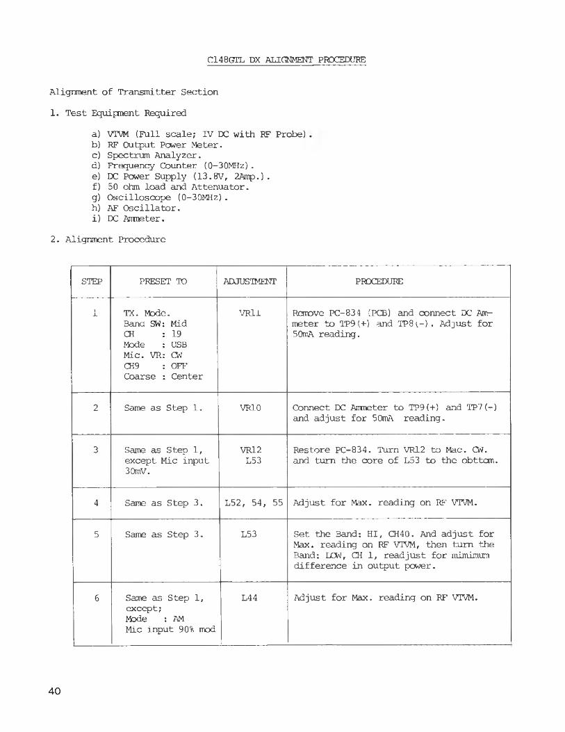
C148G7TL DX ALIGNMENT PROCEDURE
STEP PRESET ТО ADJUSTMENT REMARKS
9 Same as Step 8, CH : 40 Mode : USB
L23 Adjust for 16.0425MHz + or - 20Hz.
10 Same as Step 9, CH : 40 Mode : LSB
L24 Adjust for 16.0375MHz + or - 20Hz.
11 Same as Step 1 CH : 40 Band : HI
L40 Adjust for 16.940MHz + or - 20Hz.
12 Same as Step 11 CH : 40 Mode : USB
L41 Adjust for 16.9425MHz + or - 20Hz.
13 Same as Step 12 CH : 40 Mode : LSB
L42 Adjust for 16.9375MHz + or - 20Hz.
14 Same as Step 1 Π: 40 TX Mode
L47 Connect Frequency Counter to TP4 (R114). Adjust for 10.695MHz + or - 5Hz.
15 Same as Step 1 CH : 40 Mode : USB
L48 Connect Frequency Counter to TP5 (lead of R39). Adjust for 10.6925MHz +5Hz - 0Hz.
16 Same as Step 15 CH : 40 Mode : LSB
L49 Adjust for 10.6975MHz +0Hz -5Hz.
Note: Two TP4 are noted on Precedure. One is R83 and the other one is R114.
9

C148GLT DX A U G M E N T PROCEDURE
AUGMENT OF RECEIVER PORTION1. Test Equipment Required
a) SG, 27NHz Band.b) Osci lloscop>e.c) AF VTVM (Across 8oz. speaker).d) Deviation Meter.
2. Alignment Procedure
STEP PRESET ТО ADJUSTMENT REMARKS
1 CH : 19 Band : Mid AM Mode Tone : HI NB/ANL : OFF AF VR : CW RF Gain: CW Coarse : Center SQ VR : CCW CH 9 SW: OFF
Set the VR settings as noted in left.
2 Same as Step 1 L4 Tum the Core of L4 to the bottom.
3 Same as Step 1 L3, L5, L6 L7, L8, L17, L18 and L4.
Adjust for maximum reading and readjust L4 for maximum reading.
4 Same as Step 1 except:NB/ANL : ON
LI and L2 Set the SG on Mid, Œ18, 27.175MHz (unit is CH19) with no modulation. Connect Oscilloscope to lead of D2 and adjust coils for maximum reading. Then set the level of SG to 5uV, then readjust this step (D2 is TP1).
5 Same as Step 1 except:SQ VR: CW
VR2 Set the SG to Mid, CH19, 27.185MHz, 30%AM modulation with lOOOuV. Then tum the VR2, so that the AF signal will appear on Oscilloscope (Tight squelch Adj.).
10

C148GTL DX ALIGNMENT PROCEDURE
STEP PRESET ТО ADJUSTMENT REMARKS
6 Same as Step 1 VRll Set the SG output level to lOOuV with Nomodulation. Then adjust VRl for S-9 reading on radio's meter.
7 Same as step 1 except:Mode: FM
L9 and L10 Set the SG to lOuV with No-Modulation. Connect Oscilloscope to lead of R279, and adjust ooils for maximum reading(Pin 1&2 of IC 2).
8 Same as Step 7 L U Set the SG to ImV with 1.5kHz déviation of 1kHz. Adjust Lll for maximum sign-wave output on Oscilloscope.
ALIQMENT OF TRANSMITTER PORTION.
1. Test Equipment Requireda) DC Arrmeter.b) Power meter.c) RF VTVMd) Oscilloscope.e) Deviation Meter.f) 50 ohm Dummy Load.g) Frequency counter.
2. Alignment Precedure
STEP PRESET TO ADJUSTMENT REMARKS
1 CH : 19 TX Mode Mode : USB Mic Gain: Min.
VR10 Remove PC-843 (PCB) and connect Arrmeter to TP8 (+) and TP7 (-). Adjust for 8mA reading.
2 Same as Step 1 VR9 Connect DC Anmeter to TP8 (+) and TP6 (-) and adjust for 100mA reading.

C148CTL DX ALIGNMENT PROCEDURE
STEP PRESET ТО ADJUSTMENT REMARKS
3 Same as Step 1, except:Mic Input: 30mV
lKHz
L65 Restore PC-834. Turn the oore to the bottom.
4 Same as Step 3 L64, L66, and L67.
Adjust for maximum reading on RF VTVM (across 50ohm Dummy Load) .
5 Same as Step 3 L65 Set the Band: HI, CH 40. And adjust for maximum reading on RF VTVM. Then turn the Band: Low, CH 1. Readjust for equalized output pcwer.
6 Same as Step 1, except:Mode : AM Mic Input 90%
L54 Adjust for maximum reading on RF VTVM (Final Output Adj.).
7 Same as Step 3 VR7 Adjust ALC for 24.5V reading on RF VTVM (12w/50ohm Single tone).
8 Same as Step 1 VR4 Adjust for minimum reading on Oscilloscope for both USB abd LSB (minimum carrier Adj.).
9 Same as Step 1, except:Mode : AM
VR11 Adjust for 5.0W reading on RF Pcwer Meter (AM carrier output adj.).
10 Mic Input: 30mV lKHz
VR8 Set the meter SWto S/RF position. Adjust the VR8 so that the radio's meter reads 5W (between Green zone sind Red zone) , "S" meter adj.
11 Same as Step 1, except:AM ModeMic Input: 30mV
lKHz
VR5 Adjust for 90% modulation on Oscilloscope (AM modulation adj.).

C148GTL DX ALIGNENT PROCEDURE
STEP PRESET ТО ADJUSTMENT REMARKS
12 Same as Step 1, except:Mode : FM Band : Low 40 Mic Input: 30mV
1kHz
VR3 Adjust for 4.5kHz déviation (FM Deviation Adj.).
13 Same as Step 12 except:Mode : CW
VR12 Adjust 0.2V reading on AF VTVM when CW key is keyed. Side tone adj.
14 Same as Step 1, except:CH 9 CW: CH 9
Check that the output frequency is 27.065 MHz on Frequency Counter.
P arts L ayout T op V iew
Î37 2SB525C
1 4 - 1 5

PARTS LAYOUT (Top View)

ADDED PARTS - MAIN PCB (Bottom View)PC-879AB

COPPER PATTERN SWR PCB CH SW PCB LED PCBCD

PARTS LAYOUT SUB. ASSY. PCB’s (Top View)
P C — 8 8 0 AA CH SW P C B
P C 95 8А Д
ж
CDCNCOCOI
CMШ
P C - 9 S $ A A SWR P C B
20

SEMI CONDUCTOR PIN CONFIGURATION
TRANSISTOR
n o t e : ВЕС:
MARKING
BASEEMITTERCOLLECTOR
2SC945A-Q2SC1674L2SC1675L2SC1730L2SA733P
ANODECDCATHODE
1N60-AM1SS971S2075KMC-3011S2688EBMV-201RD75EB2KB262
MARKING
2SC1312F2SC2086D2SB525C
ANODE CATHODE
TLRG-101
1N4003
MARKINGSIDE
\В С Еa cd а
L U
2SC1969B2SC2166C2SA47302SA1012O
iGREEN)
UR-202
MV1Y
MARKING CATHODE
ANODE 8
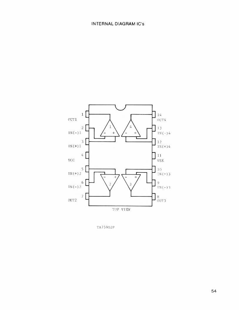
INTERNAL DIAGRAM - IC’s
SCHEMATIC DIAGRAM
CONNECTION INFORMATION
OB and DC Dual In-Lin« Р к к а д м
(Top View)
Order Part No*LM124D. LM224D. LM324D. LM2902D, LM224N. LM324N. LM2902N

гоw
INTERNAL DIAGRAM - IC’s
MB87I9

INTERNAL DIAGRAM - IC’s
гоА

INTERNAL DIAGRAM - IC’s
S 0 4 2 P
25

VOLTAGE CHART
148GTL-DX E a rly V ersion
Mode Base Co H e c to r E in itte r
TR 1 RX CW 0 0 0Ж 0 0 0AM 0 0 0USB 0 0 0LSB 0 0 0NB/ON 1*8 7 .8 1 .1
TX CW 0 0 0FM 0 0 0AM 0 0 0USB 0 0 0LSB 0 0 0
TR 2 RX CW 0 0 0FM 0 0 0AM 0 0 0USB 0 0 0LSB 0 0 0NB/ON 0 .7 2 .5 0
TX CW 0 0 0FM 0 0 0AM 0 0 0USB 0 0 0LSB 0 0 0
TR 3 RX CW 0 0 0FM 0 0 0AM 0 0 0USB 0 0 0LSB 0 0 0NB/ON 2 .6 7 .8 1 .8
TX CW 0 0 0FM 0 0 0AM 0 0 0USB 0 0 0LSB 0 0 0
TR 4 RX CW 0 8 .2 0FM 0 0 0AM 0 0 0USB 0 0 0LSB 0 0 0NB/ON 0 0 1 .1
TX CW 0 0.1 0FM 0 0 .2 0AM 0 0 0USB 0 0.1 0LSB 0 0 0
îtode Base Collecter EinitterTR 5 RX CW 0 0 0FM 0 0 0
AM 0 0 0USB 0 0 0LSB 0 0 0NB/ON 0 7.6 0
TX CW 0 0 0FM 0 0 0AM 0 0 0USB 0 0 0ISB 0 0 0
iTR 6 RX CW 0 0
\0
FM 0 0 0AM 0 0 0USB 0 0 0LSB 0 0 0NB/ON 7.6 11 8.3
TX CW 0 0 1 'FM 0 0 0AM 0 0 0USB 0 0 0ISB 0 0 0
TR 7 RX CW 0 0 0FM 0 0 0AM 0 0 0USB 0 0 оLSB 0 0 0NB/ON 0 0 0
TX CW 0 0 0FM 0 0 0AM 0 0 0USB 0 0 0LSB 0 0 0
TR 8 RX CW 0.7 0 0FM 0 0 0AM 0 0 0USB 0.7 0 0ISB 0 0 0TX CW 0.T 0 0FM 0 0 0AM 0 0 0USB 0.7 0 0LSB 0 0 0
*
Mode ' Base C o lle c te r E in itte r
TR 9 RX CW 1 .3 5 .0 0 .7FM 1 .3 5.0 0 .7AM 1 .3 5 .0 0 .7USB 1 .3 5 .0 0 .7LSB 1 .3 5 .0 0 .7
TX CK 1 .3 5.0 0 .7FM 1.3 5.0 0 .7AM 1 .3 5 .0 0 .7USB 1 .3 5 .0 0 .7ISB 1 .3 5.0 0 .7
TR 10 RX CW 0 0 0FM 0 0 0AM 0 0 0USB 0 0 0ISB 0 0 0SQ(CW) 0 .7 0 0
TX CW 0 0 0FM 0 0 0AM 0 0 0USB 0 0 0ISB 0 0 0
TR 11 PX CW 2 .1 7 ,8 1 .4FM 2.1 7 .8 1 .4AM 2 .1 7 .8 1 .4USB 2 .1 7 .8 1.4LSB 2 ,1 7 .8 1 .4
TX CW 0 0.1 0FM 0 0.1 0AM 0 0.1 0USB 0 0.1 0ISB 0 0.1 0
TR 12 RX CW 1.0 7 .9 0 .3FM 1.0 7 .9 0 .3AM 1.0 7 .9 0 .3USB 1.0 7 .9 0 .3ISB 1.0 7 .9 0 .3
TX CW 0 0.1 0FM 0 0.1 0AM 0 0.1 0USB 0 0 ,1 0LSB 0 0.1 0
Mode Base Co H e c to r B td t te r
TR 13 RX CW 0 0 0FM 0 .7 7 .7 0 .1AM 0 0 0USB 0 0 0LSB 0 0 0
TX CW 0 0 0ж 0 .6 7 .6 0 .1AM 0 0 0USB • 0 0 0ISB 0 0 0
TR 14 RX CW 0 0 0ж 0 .7 2 .4 0AM 0 0 0USB 0 0 0LSB 0 0 0
TX CW 0 0 0ж 0 .7 2 .1 0AM 0 0 0USB 0 0 0ISB 0 0 0
TR 15 RX CW 0 0 0ж 2 .4 8 .1 1 .7AM 0 0 0USB 0 0 0ISB 0 0 0
TX CW Ö “ 1 0 0FM 2 .1 7 .9 1 .8AM 0 0 0USB 0 0 0LSB 0 0 0
TR 16 RX CW 1 ,4 4 ,5 1 .2L Ж 1 .4 4 .5 1 .20 AM 1.4 4 .5 1 .2w USB 1 .4 4 .5 1 .2
ISB 1*4 4 .5 1 .2CW Ï .4 4 .5 1 .1
M ж 1.4 4 ,5 1 .1I AM 1.4 4 .5 1 .1D USB 1.4 4 .5 1 .1
ISB 1 .4 4 .5 1 .1CW 1.4 4 .6 1 .1
H ж 1,4 4 .6 1 .1I AM 1.4 4 .6 1 .1
USB 1.4 4 .6 1 .1ISB 1 .4 4 .6 1 .1
гоСП

ww
VOLTAGE CHART
ftode B ase C o l l e c t e r Q u i t t e r 1 Mode B ase Со H e c t o r Q u i t t e r >âe B ase C o l l e c t e r E m it te r
TR 16 т х CW 1 .4 4 .5 , 2 TR 18 RX CW 2 .3 7 .8 1 .9 TR 20 RX CW 1 .6 8 .1 0 .9L FM 1 .3 4 .5 1 .2 L FM 2 .3 7 .8 1 .9 FM 1 .6 8 .1 0 .9
О m 1 .3 4 .5 1 .2 0 AM 2 .3 7 .8 1 .9 AM 1 .6 8 .1 0 .9W USB 1 .4 4 ,5 1 .2 W USB 2 .3 7 .8 1 .9 USB 1 .6 8 .1 0 .9
LSB 1 .4 4 .5 1 .2 LSB 2 .3 7 .8 1 .9 LSB 1 .6 8 .1 0 .9CW 1 .4 4 .5 1 .1 CW 2 .3 7 .8 1 .9 та CW 2 .3 8 .2 7 .4
N FM 1 .3 4 .5 1 .1 M FM 2 .3 7 .8 1 .9 ж 2 .3 8 .2 7 .4
I AM 1 .3 4 .5 1 .1 1 AM 2 .3 7 .8 1 .9 AM 2 .3 8 .2 7 .4
D USB 1 .4 4 .5 1 .1 D USB 2 .3 7 .8 1 .9 USB 2 .3 8 .2 7 .4LSB 1 .4 4 .5 1 .1 LSB 2 .3 7 .8 1 .9 LSB 2 .3 8 .2 7 .4CW 1 .4 4 .6 — Г Л - CW 2 .5 7 .8 1 .9
H PM 1 .4 4 .6 1 .1 H EM 2 .3 7 .8 1 .9I AM 1 .4 4 .6 1 .1 I AM 2 .3 7 .8 1 .9 TR 21 RX CW 0 .7 3 .6 0
USB 1 .4 4 .6 1 .1 USB 2 .3 7 .8 1 .9 FM 0 .7 3 .6 0LSB 1 .4 4 .6 1 .1 LSB 2 .3 7 .8 - 1 .9 AM 0 .7 3 .6 0
USB 0 .7 3 .6 0LSB 0 .7 3 .6 0
TR 17 RX CW 2 .1 7 .3 1 .5 TX CW 2 .2 7 .7 1 ,9 TX CW 0 0 .1 0 •L FM 2 .1 7 .3 1 .5 L ж 2 .4 7 .4 1 .8 ж 0 0 .1 00 AM 2 .1 7 .3 1 .5 0 AM 2 .4 7 .4 1 .8 AM 0 0 .1 0W USB 2 .1 7 .3 1 .5 wUSB 2 ,2 7 .7 1 .9 USB 0 0 .1 0
LSB 2 .1 , 7 .3 1 .5 LSB 2 .2 7 .7 1 .9 LSB 0 0 .1 ! оCW 2 .1 — о — 1 .5 CW 2 .5 7 .7 1 .9
M FM 2 .1 7 .3 1 .5 M FM 2 .4 7 ,4 1 .8I AM 2 .1 7 .3 1 .5 I AM 2 .4 7 ,4 1 .8 TR 22 RX CW 3 .6 7 .1 3 .0D USB 2 .1 7 .3 1 .5 D USB 2 .5 7 .7 1 .9 Ж 3 .6 7 .1 3 .0
LSB 2 .1 7 .3 1 .5 LSB 2 .5 7 .7 1 ,9 AM 3 .6 7 ,1 3 .0CW Ż .1 7 .4 1 .5 CW 2 .5 7 .8 1 .9 USB 3 .6 7 ,1 3 .0
H 2 .1 7 .4 1 .5 H FM 2 .4 7 ,5 1 .8 LSB 3 .6 7 .1 3 ,0ï AM 2 .1 7 .4 1 .5 1 AM 2 .4 7 .5 1 .8 TX CW 0 .1 0 .1 0
USB 2 .1 7 .4 1 .5 USB 2 .5 7 .8 1 ,9 Ж 0 .1 0 .1 0LSB 2 ,1 7 .4 1 .5 LSB 2 .5 7 .8 1 .9 AM 0 .1 0 .1 0
USB 0 .1 0 .1 0LSB 0 .1 0 .1 0
TX CW 2 .1 7 .3 1 .5 TR 19 RX CW 0 0 0L FM 2 .1 7 .1 1 .4 FM 6 .5 8 .2 5 .90 AM 2 .1 7 .1 1 .4 AM 0 0 0 TR 23 RX CW 3 .0 7 .2 2*3W USB 2 .1 7 .3 1 .5 USB 0 0 0 Ж 3 .0 7 .2 2 .3
LSB 2 .1 7 .3 1 ,5 LSB 0 a 0 AM 3 .0 7 .2 2 .3CW 2 .1 7 .3 1 .5 TX CW 0 0 Ö USB 3 .0 7 .2 2 .3FM 2 ,1 7 .1 1 ,4 ж 6 .4 8 .2 6 ,0 LSB 3 .0 7 .2 2 .3
I AM 2 ,1 7 .1 1 ,4 AM 0 a 0 TX CW 0 0 .1 0D USB 2 .1 7 .3 1 .5 USB 0 0 0 Ж 0 0 .1 0
LSB 2 ,1 7 .3 1 .5 LSB 0 0 0 AM 0 0 .1 0CW 2 .1 7 .4 1 .5 USB 0 0 .1 0
H FM 2 .1 7 .1 1 ,4 LSB 0 0 .1 0AM 2 .1 7 .1 1 .4USB 2 .1 7 .1 1 .5LSB 2 .1 7 .1 1 .5
Mode B ase C o l l e c t e r E m it te r
TR 24 RX CW 0 1 .0 0ж 0 1 .2 0AM 0 .7 0 0USB 0 1 .0 0LSB 0 1 .0 0
TX CW 0 0 0Ж 0 0 0AM 0 ,7 0 0USB 0 0 0LSB 0 0 0
TR 25 RX CW 3 .8 6 .5 3 .1Ж 3 .8 6 .5 3 .1AM 3 .8 6 .5 3 .1USB 3 .8 6 .5 3 .1LSB 3 .8 6 .5 3 .1
TX CW 3 .8 6 .5 5.1FM 3 .8 6 .5 3 .1AM 3 .8 6 .5 3 .1USB 3 .8 6 .5 3 .1LSB 3 .8 6 ,5 3 .1
TR 26 RX CW 8 .2 8 .2 7 .8ж 0 0 0 .2AM 0 0 0 .2USB 0 0 0 .2LSB 0 0 0 .2
TX CW 8 .2 8 .2 7 .6Ж 0 0 0 .2AM 0 0 0 .2USB 0 0 0 .1LSB 0 0 0 .1
TR 27 RX CW 0 .7 0 0Ж 0 .7 0 0AM 0 .7 0 0USB 0 3 .0 0I£B 0 3 .0 0
TX CW 0 .7 0 0ж 0 .7 0 0AM 0 .7 0 0USB 0 2 .9 0LSB 0 2 .9 0

VOLTAGE CHART
i Mode B ase C o l l e c t e r E łn i t t e r 1 Mode B ase C o l l e c t e r E m it te r—
TR 28------1--------------RX 1 CW 1 .7 3 .6 l . i \ TR 32 RX CW 1 ,1 8 .3 4 .1
та 1 .7 3 .6 i - i ! та 1 .1 8 .3 4 .1
AM 1 .7 3 .6 1 .1 1 AM 1 .1 8 .3 4 .1
USB 1 .7 3 .6 1 .1 USB 1 .1 8 .3 4 .3
LSB 1 .7 3 .6 i i LSB 1 .1 8 .3 4 .3
TX CW 1 .7 3 .6 i . i TX CW 1 ,1 8 .3
та 1 .6 3 .6 1 .1 та 1 .1 8 .1 3 .5
AM 1 .6 3 .6 1 .1 AM 1 ,1 8 .1 3 .5
USB 1 .7 3 .6 1 .1 USB 1 .1 8 .3 4 .3
LSB 1 .7 3 .6 1 .1 ISB 1 .1 8 .3 4 .3
TR 29 RX CW 1 .0 1 .7 0 .4 TR 33 RX CW 0 .7 1 .5 0
та 1 .0 1 .7 0 .4 т а 0 .7 1 . 5
AM 1 .0 1 .7 0 .4 AM 0 .7 1 . 5 0
USB 1 .0 1 .7 0 .4 USB 0 .7 1 . 5 0
LSB 1 .0 1 .7 0 .4 ISB 0 ,7 1 .5 0
TX CW 1 .0 1 .7 0 .4 TX CW 0 0 0
та 1 .0 1 .6 0 .4 та 0 0 0
AM 1 .0 1 .6 0 .4 AM 0 0 0
USB 1 .0 1 .7 0 .4 USB 0 0 0
LSB 1 .0 1 .7 0 .4 ISB 0 0 0
TR 30 RX CW 0 .6 0 0 TR 34 RX CW 7 .6 8 .2 8 .3
та 0 .6 0 0 та 7 .6 8 .2 8 .3
AM 0 .6 0 0 AM 7 .6 8 .2 8 .3
USB 0 .6 0 0 USB 7 .6 8 .2 8 .3
ISB 0 .6 0 0 LSB 7 .6 8 .2 8 ,3
TX CW 0 0 0 TX CW 7 .7 0 .1 8 .3
та 0 0 0 i та 7 ,6 0 8 .0
AM 0 0 0 [ AM 7 .6 0 8 .0
USB 0 0 0 i USB 7 .7 0 .1 8 .3
ISB 0 0 0 ; ISB 7 .7 0 .1 8 .3
TR 31 RX CW 8 .3 0 .7 8 .3 TR 35 RX CW 4 .1 7 .6 3 .5
та 8 .3 0 .7 8 .3 EM 4 .1 7 .6 3 .5
AM 8 .3 0 .7 8 .3 AM 4 .1 7 .6 3 .5
USB 8 .3 0 .7 8 .3 USB 4 .1 7 .6 3 .5
ISB 8 .3 0 .7 8 .3 ISB 4 .1 7 .6 24TX CW B.3 0 8 .3 TX CW 4 .2 7 .7 7 .5
FM 8 .1 0 8 .1 та 4 .1 7 .6 7 .4
AM 8 .1 0 8 .1 AM 4 .1 7 .6 7 .4
USB 8 .3 0 8 .3 USB 4 .2 7 .7 7 .5
ISB 8 .3 0 8 .3 ILSB 4.2 7 .7 7 .5
Mode B ase Co H e c t o r E m it te r t Mode B ase E m it te r
TR 36 RX CW 5 .5 7 .8 7 .5 TR 40 RX CW 0 .9 3 .2 0 .3та 5 ,5 7 .8 та 0 .9 3 .2 0 .3AM 5 .5 7 .8 7 .5 AM 0 .9 3 .2 0 .3USB 5 .5 7 .8 USB 0 .9 3 .2 0 .3LSB 5 .5 7 ,8 ISB 0 .9 3 .2 0 .3
TX CW 1 .4 0 .8 0 ,7 TX от 0 .9 3 .2 0 .3та 1 .4 0 .8 0 .7 та 0 ,9 3 .2 0 .3AM 1 ,4 0 .8 0 .7 AM 0 .9 3 .2 0 .3USB 1 .4 0 .8 USB 0 ,9 3 ,2 0 .3ISB 1 .4 0 .8 0 ,7
—
ISB 0 ,9 3 .2 0 .3
TR 37 RX CW 7 .8 0 8 .2 TR 41 RX от 3 .1 6 .9—
2 .6та 7 .8 0 та 0 0 0AM 7 .8 0 AM 0 0 0USB 7 ,8 0 8 .2 USB 3 .1 6 .0 2 .6LSB 7 ,8 0 ISB 3 -1 6 .9 2 .6
TX h CW 7 .5 8 .2 3 .2 TX CW ■ ' 3 . 1 6 .9 2 .6та 7 .5 8 .2 8 .2 т а 3 .1 6 .6 2 .6AM 7 .5 8 .2 8 ,2 AM 3 .1 6 .6 2 .6USB 7 .5 8 .2 USB 3 .1 6 .9 2 .6ISB 7 .5 8 .2 8 .2 ISB 3 .1 6 .9 2 .6
TR 38 RX CW 1 .6 1 3 .0 1 .0 TR 42 RX CW 0 0 .8 7 .0та 1 .6 1 3 ,0 1 .0 т а 0 0 .8 5 .1AM 1 .6 1 3 .0 1 .0 AM 0 0 .8 5 .7USB 1 .6 1 3 .0 1 .0 USB 0 0 .8 7 .0ISB 1 .6 1 3 .0 1 .0 ISB 0 0 .8 7 .0
TX CW 1 .6 1 2 .8 1 .0 TX от 0 0 -8 7 .0FM 1 .6 1 2 .8 1 .0 т а 0 • 0 .8 4 .5AM 1 .6 1 2 .8 1 .0 AM 0 0 .8 4 .7USB 1 .6 1 2 .8 1 .0 USB 0 0 ,8 7 .0LSB 1 .6 1 2 .8 1 .0 LSB 0 f 0 .8 7 .0
TR 39 RX CW 1 3 .0 8 .3 1 3 .8 TR 43 RX CW 0 1 3 .2 0та 1 3 .0 8 ,3 1 3 .8 та 0 1 3 .2 0AM 1 3 .0 8 .3 1 3 .8 AM 0 ( 1 3 .2 0USB 1 3 .0 8 .3 1 3 .8 USB 0 f 1 3 .8 0ISB 1 3 ,0 8 ,3 1 3 ,8 l£B 0 1 3 .8 0
TX CW 1 2 .8 8 ,3 1 3 .7 TX СИ 0 .7 1 1 2 .4 0та 1 2 .8 8 .3 1 3 .0 i Ж 2 ,8 1 0 .2 0AM 1 2 .8 8 .3 1 3 .0 AM 2 .8 1 0 .2 0USB 1 2 .8 8 .3 1 3 .7 USB 0 .7 i 1 3 .7 0ISB 1 2 .8 8 .3 1 3 .7
____ISB 0 .7 j 1 3 .7 0
IV»СО

г\эСО
VOLTAGE CHART
Mode B ase C o l l e c t e r E in i t t e r
TR 44 RX cw 0 1 3 .2 0FM 0 1 3 .2 0AM 0 1 3 .2 0USB 0 1 3 .8 0LSB 0 1 3 .8 0
TX CW 0 .6 1 2 .4 0FM 0 .5 1 0 .2 0AM 0 .5 1 0 .2 0USB 0 .6 1 3 .7 0LSB 0 .6 1 3 .7 0
TR 45 RX CW 0 0 0EM 0 0 0AM 0 0 0USB 0 0 0LSB 0 0 0
TX CW Ï . 4 8 .1 0 .8EM 1 .3 7 .8 0 .8AM 1 .3 7 .8 0 .8USB 1 .4 8 .1 0 .8LSB 1 .4 8 .1 0 .8
TR 46 RX CW 0 0 0FM 0 0 0AM 0 0 0USB 0 0 0LSB 0 0 0
TX CW 1 .4 6 .6 0 .7FM 1 .4 6 .5 0 .7AM 1 .4 6 .5 0 .7USB 1 .4 6 .6 0 .7LSB 1 .4 6 .6 0 .7
TR 47 RX CW 6 .1 1 3 .2 1 3 .2FM 6 .1 1 3 .2 1 3 .2AM 6 .1 1 3 .2 1 3 .2USB 6 .1 1 3 .8 1 3 .8LSB 6 .1 1 3 .8 1 3 .8
TX CW 6 .1 Ï 2 .4 1 2 .4FM 6 .1 1 1 .5 1 1 .3
• AM 6 .1 1 1 .5 1 1 .3USB 6 .1 1 3 .7 1 3 .7
i LSB 6 .1 1 3 .7 1 3 .7
Mode B ase C o l l e c t e r E in i t te r № d e B ase C o l l e c t e r E in i t te r
TR 48 RX CW 1 3 .2 1 3 .2 1 3 .3 TR 52 RX CW 0 7 .5 0FM 1 3 .2 1 3 .2 1 3 .3 FM 0 7 .5 0AM 1 3 .2 1 3 .2 1 3 .3 AM 0 7 .5 0USB 1 3 .8 1 3 .8 1 3 .1 USB 0 7 .5 0LSB 1 3 .8 1 3 .8 1 3 .1 LSB 0 7 .5 0
TX CW 1 2 .4 1 2 .4 1 3 .1 TX CW 0 0 .7 0FM 1 1 .3 1 1 .3 1 1 .8 FM 0 0 Л 0AM 1 1 .3 1 1 .3 1 1 .8 AM 0 0 .7 0USB 1 3 .7 1 3 .7 1 3 .0 USB 0 0 .7 0LSB 1 3 .7 1 3 .7 1 3 .0 LSB 0 0 .7 0
TR 49 RX cw 1 3 .3 1 3 .2 1 3 .8 TR 53 RX cw 0 0 0FM 1 3 .3 1 3 .2 1 3 .8 FM 0 0 0AM 1 3 .3 1 3 .2 1 3 .8 AM 0 0 0USB 1 3 .1 1 3 .8 1 3 .8 USB 0 0 0LSB 1 3 .1 1 3 .8 1 3 .8 LSB 0 0 0
TX CW 1 3 .1 1 2 .4 1 3 .7 TX CW 0 0 0FM 1 1 .8 1 1 .3 1 3 .2 FM 0 0 0AM 1 1 .8 1 1 .3 1 3 .2 AM 0 0 0USB 1 3 .0 1 3 .7 1 3 .7 USB 0 0 0LSB 1 3 .0 1 3 .7 1 3 .7 LSB 0 0 0
TR 50 RX CW 0 .7 0 0 TR 54 RX CW 0 1 3 .3 0FM 0 .7 0 0 FM 0 1 3 .3 0AM 0 0 0 AM 0 1 3 .3 €USB 0 .6 0 0 USB 6 .5 1 3 .1 5 .8LSB 0 .6 0 0 LSB 6 .5 1 3 .1 5 .8
TX CW 0 .7 0 0 TX CW 0 1 3 .1 0FM 0 .6 0 0 FM 0 1 1 .8 0AM 0 0 0 AM 0 1 1 .8 0USB 0 .6 0 0 USB 6 .5 1 3 .0 5 .8LSB 0 .6 0 0 LSB 6 .5 1 3 .0 5 .8
TR 51 RX CW 0 7 .5 0 TR 55 RX CW 8 .0 8 ,2 8 .2FM 0 7 .5 0 FM 0 0 0AM 0 7 .5 0 AM 0 0 0USB 0 7 .5 0 USB 0 0 0LSB 0 7 .5 0 LSB 0 0 0
TX CW 0 0 .7 0 TX CW 8 .0 8 .2 8 .2FM 0 0 .7 0 FM 0 0 0AM 0 0 .7 0 AM 0 0 0USB 0 0 .7 0 USB 0 0 0
1 LSB 0 0 .7 0 LSB 0 0 0
Mode B ase Co H e c t o r E in i t te r
TR 56 RX CW 7 .7 1 .1 6 .2EM 7 ,6 1 .1 6 .2AM 7 .6 1 .1 6 .2USB 7 .6 1 .1 6 .2LSB 7 .6 1 .1 6 .2
TX cw 7 .7 1 .1 0 .2FM 4 .0 4 .6 4 .6AM 4 .0 4 .6 4 .6USB 4 .0 4 .6 4 .6
1 LSB 4 .0 4 .6 4 .6
VOLTAGE CHART
Mode 1 2 3 4 5 6 7 8 9 10 11 12 13 14 15 16 17 18
IC 1 RX CW _ . _ 8 .3 0 0 0 0 2 .8 1 .4 0 0 .3 0 .3 0 .6FM - - - 8 .3 0 .1 0 .1 0 .2 0 2 .8 1 .4 0 0 .3 0 ,3 0 .6AM - - - 8 .3 0 0 0 0 2 .8 1 .4 0 0 .3 0 .3 0 .6USB - - - 8 .3 0 0 0 0 2 .8 1 .4 0 0 .3 0 .3 0 .6LSB - - - 8 .3 0 0 0 0 2 .8 1 .4 0 0 .3 0 .3 0 .6SQ(CW) - - - - - - - 6 .9 - 4 .0 - - - -
TX CW - - - 8 .3 0 0 0 0 2 .8 1 .0 0 0 .3 0 .3 0 .6FM - - - 8 .0 0 0 0 0 2 .8 1 .0 0 0 .3 0 .3 0 .6AM - - 8 .0 0 0 0 0 2 .8 1 .0 0 0 .3 0 .3 0 .6USB - - - 8 .3 0 0 0 0 2 .8 1 ,0 0 0 .3 0 ,3 0 .6LSB - “ “ 8 .0 0 0 0 0 2 .8 1 .0 0 0 .3 0 .3 0 .6
IC 2 RX CW 0 0 1 .9 0 0 .6 0 .6 0FM 1 .3 1 .3 7 .1 0 3 .2 3 .3 0AM 0 0 0 0 0 0 0USB 0 0 1 .9 0 0 .6 0 .6 0LSB 0 0 1 .9 0 0 .6 0 .6 0
TX CW 0 0 1 .9 0 0 ,6 0 .6 0FM 1 .3 1 .4 6 .8 0 3 .3 3 .3 4 .3AM 0 0 0 0 0 0 0USB 0 0 1 .9 0 0 .6 0 .6 0LSB 0 0 1 .9 0 0 .6 0 .6 0
IC 3 RX CW 3 .0 4 .6 6 .1 3 .4 3 .4 8 .2 4 .5 4 .9 8 .2 8 .2 0 0 8 .2 0 .5 8 .2 3 .8 0L FM 3 .0 4 .6 6 .1 3 .4 3 .4 8 .2 4 .5 4 .9 8 .2 - 8 .2 0 0 8 .2 0 .5 8 .2 3 .8 00 AM 3 .0 4 .6 6 .1 3 .4 3 .4 8 .2 4 .5 4 .9 8 .2 - 8 .2 0 0 8 .2 0 .5 8 .2 3 .8 0W USB 3 .0 4 .6 6 .1 3 .4 3 .4 8 .2 4 .5 4 .9 8 .2 - 8 .2 0 0 8 .2 0 .5 8 .2 3 .8 0
LSB 3 .0 4 .6 6 .1 3 .4 3 .4 8 .2 4 .5 4 .9 8 .2 - 8 .2 0 0 8 .2 0 .5 8 .2 3 .8 0TX CW 4 .2 4 .3 4 .4 3 .8 3 .8 8 .2 4 .5 4 .9 8 .2 - 8 .2 0 0 8 .2 0 .5 У.2 3 .8 0
M FM 4 .2 4 .3 4 .4 3 .8 3 .8 8 .2 4 .5 4 .9 8 .2 - 8 .2 0 0 8 .2 0 .5 8 .2 3 .3 0I AM 4 .2 4 .3 4 .4 3 .8 3 .8 8 .2 4 .5 4 .9 8 .2 - 8 ,2 0 0 8 .2 0 .5 8 .2 3 .8 0D USB 4 .2 4 .3 4 .4 3 .8 3 .8 8 .2 4 .5 4 .9 8 .2 - 8 .2 0 0 8 .2 0 .5 8 .2 3 .8 0
LSB 4 .2 4 .3 4 .4 3 .8 3 .8 8 .2 4 .5 4 .9 8 .2 - 8 .2 0 0 8 .2 0 ,5 8 .2 3 .8 0
Mode 1 2 3 4 5 6 7 8 9 10 11 12 13 14 15 16 17 18
IC 3 RX CW 3 .4 4 .5 5 .5 3 .6 3 .6 8 .2 4 .5 4 .9 8 .2 . 8 .2 0 0 8 ,2 0 .5 8 .2 3 .8 0( o o n 't ) H FM 3 ,4 4 .5 5 ,5 3 .6 3 .6 8 .2 4 .5 4 .9 8 .2 - 8 .2 0 0 8 .2 0 .5 8 .2 3 .8 0
I AM 3 .4 4 .5 5 .5 3 .6 3 .6 8 .2 4 .5 4 .9 8 .2 - 8 .2 0 0 8 ,2 0 .5 8 .2 3 ,8 0USB 3 .4 4 .5 5 .5 3 .6 3 .6 8 ,2 4 ,5 4 ,9 8 ,2 - 8 ,2 0 0 8 ,2 0 .5 8 .2 3 .8 0LSB 3 .4 4 .5 5 ,5 3 .6 3 .6 8 .2 4 .5 4 .9 8 ,2 - 8 .2 0 0 8-Ï 0 .5 6 .2 3 .8 Q-
ТЯ- TS!------- l.G~ 4 .6 6 .1 T T Tr 8 .2 4 .5 4 .9 8 .2 - 8 .2 0 0 8 ,2 0 .5 3 .2 3 .8 0L FM 3 .0 4 .5 5 .9 3 .3 3 .3 8 .0 4 .5 4 .9 7 ,8 - 8 .0 0 0 7 .9 0 .5 7 .9 3 .8 00AM 3 .0 4 .5 5 .9 3 .3 3 .3 8 .0 4 .5 4 .9 7 .8 - 8 .0 0 0 7 .9 0 .5 7 .9 3 .8 0w USB 3 .0 4 .6 6 .1 3 .4 3 .4 8 .2 4 .5 4 .9 8 .2 - 8 ,2 0 0 8 .2 0 .5 8 .2 3 .8 0
LSB 3 .0 4 .6 6 .1 3 .4 3 .4 8 .2 4 .5 4 .9 8 .2 8 .2 0 0 8 .2 0 .5 8 .2 3 .8 0CW 4 .2 4 . J 4 .4 3 .6 3 .6 8 .2 4 ,5 4 .9 8 .2 - 8 ,2 0 0 8 .T 0 .5 8 .2 j . a 0
M FM 4 .2 4 .2 4 .2 3 .7 3 .7 8 ,0 4 .5 4 .9 7 .9 8 .0 0 0 8 .0 0 ,5 7 .9 3 .8 0I AM 4 .2 4 .2 4 .2 3 .7 3 .7 8 ,0 4 .5 4 .9 7 .9 - 8 .0 0 0 8 .0 0 ,5 7 .9 3 .8 0D USB 4 .2 4 .3 4 .4 3 ,8 3 .8 8 .2 4 .5 4 .9 8 .2 - 8 .2 0 0 8 .2 0 .5 8 .2 3 .8 0
LSB 4 .2 4 .2 4 .4 3 .8 3 .8 8 .2 4 .5 4 .9 8 .2 - 8 .2 0 _ f l _ . Ł 2 Q,5. 8,2 . 3 .Ł - 0Ш T X x x ~ Т Г Г X 6 “ 3 .6 8 .2 4 .5 4 .9 8 .2 - 8 .2 0 0 8 .2 0 .5 8 .2 3 .8 0
H FM 3 ,4 4 .4 5 .4 3 .5 3 .6 8 .1 4 .5 4 .9 8 .0 - 8 .1 0 0 8 .1 0 .5 8 .0 3 .8 0I AM 3 .4 4 .4 5 .4 3 .5 3 .6 8 .1 4 .5 4 .9 8 .0 - 8 .1 0 0 8 ,1 0 .5 8 .0 3 .8 0
USB 3 .4 4 .5 5 .5 3 .É 3 .6 8 .2 4 .5 4 .9 e . 2 - 8 .2 0 0 8 ,2 0 .5 8 ,2 3 .8 0LSB 3 .4 4 .5 5 .5 3 .6 3 .6 8 .2 4 .5 4 .9 8 .2 ‘ 8 .2 0 0 8 .2 0 ,5 8 ,2 3 .8 0
IC 4 RX CW 0 3 .4 3 .4 0 6 .0 7 .5 7 .6FM 0 3 .4 3 .4 0 6 .0 7 .5 7 .6AM 0 3 .4 3 .4 0 6 .0 7 .5 7 .6USB 3 .0 3 .4 3 .4 0 6 ,0 7 .5 7 .6LSB 3 .0 3 .4 3 .4 0 _j 6 .0 7 .5 7 ,6
TX CW 0 3 .3 3 .3 0 5 .9 7 ,4 7 ,0FM 0 3 .3 3 .3 0 5 .8 7 .0 3 .7AM 0 3 .3 3 .3 0 5 ,8 7 .0 3 .7USB 2 .9 3 .3 3 .3 0 5 .9 7 .4 4 ,0LSB 2 9 13 .3 3 .3 0 5 .9 7 .4 4 ,0

VOLTAGE CHARTw
Mode 1 2 3 4 5 6 7 8 9 10----------------------
11—
12 13 14
IC 5 RX cw 13.8 6.6 0 0 1.1 1.1 0 0 7.0 13.1FM 13.8 6.6 0 0 1.1 1.1 0 0 7.0 13.1AM 13.8 6.6 0 0 1.1 1.1 0 0 7.0 13.1USB 13.8 6.6 0 0 1.1 1.1 0 0 7.0 13.1LSB 13.8 6.6 0 0 1.1 1.1 0 0 7.0 13.1
TX CW 13.7 6.6 0 0 1.1 1.1 0 0 6.9 13.0FM 13.4 6.0 0 0.4 1.8 1.8 0 0 0 10.9AM 13.4 6.0 0 0.4 1.8 1.8 0 0 0 10.9USB 13.7 6.6 0 0.3 1.8 1.8 0 0 0 11.4LSB 13.7 6.6 0 0.3 1.8 1.8 0 0 0 11.4
IC 6 RX CW 0 0 0 0 0 0 0 0 0 0 -0.5 0 -0.5 0FM 0 0 0 0 0 0 0 0 0 0 -0.5 0 -0.5 0AM 0 0 0 0 0 0 0 0 0 0 -0.5 0 -0.5 0USB 0 0 0 0 0 0 0 0 0 0 -0.5 0 -0.5 0LSB 0 0 0 0 0 0 0 0 0 0 -0.5 0 -0.5 0
TX CW 0 7.8 7.8 0 7.9 0 2.8 2.8 0 1.3 1.3 1.3 1.3 0FM 0 7.8 7.8 0 7.8 0 2.7 2.7 0 1.3 1.3 1.3 1.3 0AM 0 7.8 7.8 0 7.8 0 2.7 2.7 0 1.3 1.3 1.3 1.3 0USB 0 7.8 7.8 0 7.9 0 2.8 2.8 0 1.3 1.3 1.3 1.3 / 0LSB 0 7.8 7.8 0 7.9 0 2.8 2.8 0 1.3 1.3 1.3 1.3 0
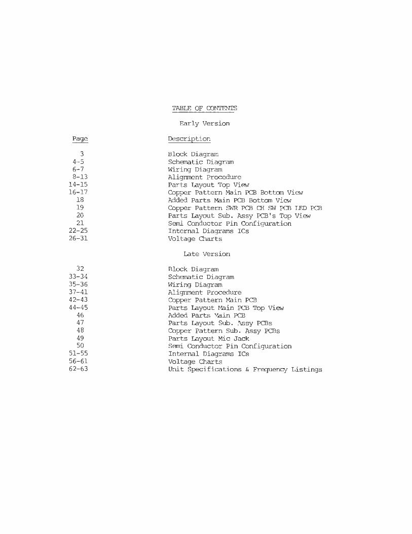
TABLE OF CONTENTS
Page3
4 -56 -78-13
14-1516-17
181920 21
22-2526-31
3233-3435-3637-4142-4344-45
4647484950
51-555 6-6162-63
Early VersionDescriptionBlock DiagramSchematic DiagramWiring DiagramAlignment ProcedureParts Layout Top ViewCopper Pattern Main PCB Bottcm ViewAdded Parts Main PCB Bottcm ViewCopper Pattem SWR PCB CH SW PCB LED PCBParts Layout Sub. Assy PCB's Top ViewSemi Conductor Pin ConfigurationInternal Diagrams ICsVoltage Charts
Late VersionBlock DiagramSchematic DiagramWiring DiagramAlignment ProcedureCopper Pattem Main PCBParts Layout Main PCB Top ViewAdded Parts Main PCBParts Layout Sub. Assy PCBsCopper Pattern Sub. Assy PCBsParts Layout Mic JackSemi Conductor Pin ConfigurationInternal Diagrams ICsVoltage ChartsUnit Spécifications & Frequency Listings

сого
BLOCK DI AGRAM

PB-O IOSCHEMATIC DIAGRAM

WiRING DIAGRAM
3 5 - 3 6
P C - 881 P C - 8 8 0
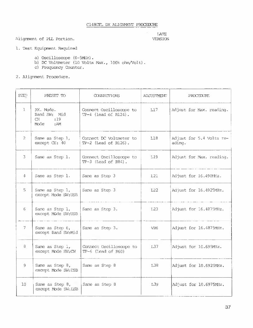
C148GTL DX ALIGNIMENT PROCEDURE
1. Test Equipment Requireda) Oscilloscope (0-5MHz).b) DC Voltmeter (10 Volts Max., 100k ohm/Volt).c) Frequency Counter.
2. Aiignment Procedure.
Aiignment of PLL Portion.LATE
VERSION
STEP PRESET ТО CONNECTIONS ADJUSTMENT PROCEDURE
1 RX. Mode.Band SW: Mid CH :19 Mode :AM
Connect Oscilloscope to TP-4 (lead of R124).
L17 Adjust for Max. reading.
2 Same as Step 1, except CH: 40
Connect DC Voltmeter to TP-2 (Lead of R126) .
L18 Adjust for 5.4 Volts reading .
3 Saine as Step 1. Connect Oscilloscope to TP-3 (Lead of R84).
L19 Adjust for Max. reading.
4 Same as Step 1. Same as Step 3 L21 Adjust for 16.490MHz.
5 Same as Step 1, except Mode SW:USB
Same as Step 3 L22 Adjust for 16.4925MHz.
6 Same as Step 1, except Mode SW:USB
Same as Step 3. L23 Adjust for 16.4875MHz.
7 Same as Step 6, except Band SW:Mid
Same as Step 3. VR6 Adjust for 16.4875MHz.
8 Same as Step 1, except Mode SW:CW
Connect Oscilloscope to TP-6 (Lead of R60)
L37 Adjust for 10.695MHz.
9 Same as Step 8, except Mode SW:USB
Same as Step 8 L38 Adjust for 10.6925MHz.
10 Same as Step 8, except Mode SW:If>B
Same as Step 8 L39 Adjust for 10.6975MHz.
37

C148GTL DX ALIGNMENT PROCEDURE
1. Test Equipment Requireda) VTVM (Fuli scalę; IV DC with RF Probe)b) RF Output Pcwer Meter.c) Spectrum Analyzer.d) Frequency Counter (0-30MHz).e) DC Pcwer Supply (13.8V, 2Amp.).f) 50 ohm load and Attenuator.g) Oscilloscope (0-30MHz).h) AF Oscillator.i) DC Anmeter.
2. Alignment Procedure
Alignment of Transmitter Section
STEP PRESET ТО ADJUSTMENT PROCEDURE
1 TX. Mode.Band SW: Mid CH : 19 Mode : USB Mic. VR: CW CH9 : OFF Coarse : Center
VRll Remove PC-834 (PCB) and connect DC Ammeter to TP9(+) and TP8(-). Adjust for 50mA reading.
2 Same as Step 1. VR10 Connect DC Ammeter to TP9(+) and TP7(-) and adjust for 50mA reading.
3 Same as Step 1, except Mic input 30mV.
VR12L53
Restore PC-834. Tum VR12 to Mac. CW. and tum the core of L53 to the obttcm.
4 Same as Step 3. L52, 54, 55 Adjust for Max. reading on RF VTVM.
5 Same as Step 3. L53 Set the Band: HI, CH40. And adjust for Max. reading on RF VTVM, then tum the Band: 1Ш, CH 1, readjust for mimimum différence in output pcwer.
6 Same as Step 1, except;Mode : AM Mic input 90% mod
L44 Adjust for Max. reading on RF VTVM.
38

C148GTL DX ALIGNMENT PROCEDURE
STEP PRESET ТО ADJUSIMENT REMARKS
7 Same as Step 3. VR12 Adjust for 24.5V reading on RF VTVM.
8 Same as Step 1. VR 7 Adjust for Min. reading on Spectrum Analyzer for both USB and LSB.
9 Same as Step 1, except:Mode :AM
VR13 Adjust for 5.0W reading on RF Power Meter.
10 Same as Step 9. VR 8 Set the meter SW to S.RF position. Adjust the VR 8, so that the radio's meter reads 5W (Between Green zone and Red zone).
11 Same as Step 9, except Mic input 30mV.
VR14 Adjust 90% modulation on Oscilloscope
12 Same as Step 1, except:Mode SW: Ш Band : 40 Mic input 30mV
VR 5 Adjust for 5kHz déviation.
13 Same as Step 12, except:Mode : CW
VR15 Adjust 0.2V reading on AF VTVM when CW key is keyed.
14 Same as Step 1, except:CH9 SW : CH9
Check that the output frequency is 27.065MHz.
C148GTL DX ALIGNMENT PROCEDURE
1. Test Equipment Requireda) VTVM (Fuli scalę; IV DC with RF Probe)b) RF Output Power Meter.c) Spectrum Analyzer.d) Frequency Counter (0-30MHz).e) DC Pcwer Supply (13.8V, 2Amp>.) .f) 50 ohm load and Attenuator.g) Oscilloscope (0-30MHz).h) AF Oscillator.i) DC Ammeter.
2. Alignment Procedure
Alignment of Transmitter Section
STEP PRESET ТО ADJUSTMENT PROCEDURE
1 TX. Mode.Band SW: Mid CH : 19 Mode : USB Mic. VR: CW CH9 : OFF Coarse : Center
VRll Rénové PC-834 (PCB) and connect DC Ammeter to TP9(+) and TP8(-). Adjust for 50mA reading.
2 Same as Step 1. VR10 Connect DC Ammeter to TP9(+) and TP7(-) and adjust for 50mA reading.
3 Same as Step 1, except Mic input 30mV.
VR12L53
Restore PC-834. Tu m VR12 to Mac. CW. and tum the core of L53 to the obttcm.
4 Same as Step 3. L52, 54, 55 Adjust for Max. reading on RF VTVM.
5 Same as Step 3. L53 Set the Band: HI, CH40. And adjust for Max. reading on RF VTVM, then tum the Band: LOW, CH 1, readjust for mimimum différence in output power.
6 Same as Step 1, except;Mode : AM Mic input 90% irod
L44 Adjust for Max. reading on RF VTVM.
40

C148CTL DX ALIGNMENT PROCEDURE
STEP PRESET ТО ADJUSTMENT REMARKS
6 Same as Step 1. VR4 for AM/FM VR3 for SSB/CW
Set the SG to 40CH, 27.405MHz, 30% AM modulation with lOOOuV. Then tum the VR4, so that the AF signal will appear on Oscilloscope. Repeat it for SSB/CW Mode with VR3.
7 Same as Step 1. VR1 for AM/FM VR2 for SSB/CW
Set the SG to 40CH, 27.405MHz with Nomodulation. Level of SG is lOOuV. Then adjust VRl for S-9 reading on radio's meter for AM mode. Repeat it for SSB/CW mode with VR2.
8 Same as Step 1, Mode : Ш
L6 Set the SG tl lrnv with 1.5kHz déviation of 1kHz. Adjust Lb for Max. signwave output on Oscilloscope.

COPPER PATTERN - MAIN PCB

PARTS LAYOUT - MAIN PCB (Top View)
4 4 -4 5
C2350.047/ZF
RES'ST AfOTHERWi 3E NOTEE ; к ' К i
RESISTOR WATTAGES ARE NOTEE
C A »A Ci TA N С E v A L и E S A R rj n l e s s o t h e r w i s e n o t e s
A l l CAPAC i TORS TEMPERA ARE SL ( LES S TP AN 10(0.1000 PE. aNLE S S O’-p Fr w
C27I 0047/Z F
K "
. . . . ---- i----S û о ,й
" ! c 7 Q.'O ' l ' MCI4008BCP
'T ^ !b<?ü. JP65 l lO)
045 *
iS J |
VJ/R! 59 47K , T 2 ^ r s i ' s 447K е й t:i-3 S
CO ■'Oc iCt' * î ^
f iIA? * •' -
♦ * -< ♦ O
0 5 4 soo sk0 5 5
S2075K

PB
-OIO
ADDED PARTS - MAIN PCB
H» fs il!)? 8(
46

-рь-nI
PARTS LAYOUT SUB. ASSY. PCB’s
T3r»It pm
S
4»Ï
X
tОГО
"Оогогоо3>>
f “33оо
о*ого
R 4 0 Ö
R 414 680G----
Е2А-3724

COPPER PATTERN SUB. ASSY. PCB’s

PARTS LAYOUT - MIC JACK
49

SEMI CONDUCTOR PIN CONFIGURATION
2SA733-P 2SC945A-Q 2SC1674-L 2SC1675-L 2SC1730-L
2SA473-02SA1012-02SC2166-C2SC2312-C
2SB525-C2SC2086-D
C A T HODE MARK
ANODE /C A TH O D E 1N60-AMMC-3011N4003MV-2011S2339GRD5.1EB2RD7.5EB2KB2621S2075K
N 4 Y
TLRG 101 UR202
50

INTERNAL DIAGRAM-IC ’s
DIFFERENTIALPEAK DETECTOR
Ł BIAS CIRCUIT
T T ul- И Г Ш(+) LU,.) ЫINPUT BYPASS Vcc GND DET 1NPUT DET INPUT OUTPUT
UPC1028H
51

INTERNAL DIAGRAM IC’s
MC14008B
14Cou l
13S4
13S3
11S2
10S1
16 15 14 13 12 11 10 9
52

слСО
INTERNAL DIAGRAM IC’s
OSC out Г-2 out FS
PO PI P2 P3 PA P5 P6 P7 P8
MC145106
INTERNAL DIAGRAM IC’s
140UT413I N ( - ) 4
12lN(+)4
11VEE10IN(+)3
9I N { - ) 3
80UT3
TA75902P
54

INTERNAL DIAGRAM IC’s
S 0 4 2 P
55

VOLTAGE CHART
148GTL-DX L a te v e r s i o n
Mode B ase Co H e c t o r E in i t t e r
TR 13 RX cw 0 0 .1 0fm 0 ,7 0 0AM 0 .7 0 0USB - 0 . 1 0 .1 0LSB - 0 ,1 0 ,1 0
TX cw o" 0 0FM 0 .7 0 0AM 0 -7 0 0USB - 0 . 5 0 0LSB - 0 - 5 0 0
TR 14 RX cw 0 .7 0 0FM 0 0 0AM 0 0 0USB 0 -7 0 0LSB 0 .7 0 0
TX CW 0 .7 0 0FM 0 0 0AM 0 0 0USB 0 .7 0 0LSB 0 .7 0 0
TR 15 RX CW 1 .3 5 .3 0 .7FM 1 .3 5 ,4 0 .7AM 1 .3 5 .4 0 .7USB 1 .3 5 .3 0 .7LSB 1 .3 5 .3 0 .7
TX CW 1 .3 5 .3 0 .7FM 1 .3 5 .3 0 .7AM 1 .3 5 .3 0 .7USB 1 .3 5 .2 0 .7LSB 1 .3 5 .2 0 .7
TR 16 RX CW 0 0 0FM 0 0 0AM 0 0 0USB 0 0 0LSB 0 0 0SQ(CW) 0 .8 0 0
TX CW 0 .8 0 0FM 0 .8 0 0AM 0 .8 0 0USB 0 ,8 0 0LSB 0 .8 0 0
Mode B ase C o l l e c t e r E in i t te r
TR 9 RX CW 0 .8 0 0FM 0 .7 3 .2 0AM 0 .7 3 .2 0USB 0 .8 0 0LSB 0 .8 0 0
TX cw 0 .7 0 0FM 0 .7 0 0AM 0 .7 0 0USB 0 -7 0 0LSB 0 .7 0 0
TR 10 RX cw 0 8 .4 0FM 3 .2 7 .4 2 .4AM 3 .2 7 .4 2 .4USB 0 8 .4 0LSB 0 8 .4 0
TX CW 0 0 0FM 0 0 0AM 0 0 0USB 0 0 0LSB 0 0 0
TR 11 RX CW 0 8 ,4 0FM 2 .4 7 .2 1 .7AM 2 .4 7 .2 1 .7USB 0 8 .4 0LSB 0 8 .4 0
TX CW 0 0 0FM 0 0 0AM 0 0 0USB 0 0 0LSB 0 0 0
TR 12 RX CW 0 .7 0 0FM 0 0 0AM 0 0 0USB 0 .7 0 0LSB 0 ,7 0 0
TX CW " 0 . 7 0 0FM 0 0 0AM 0 0 0USB 0 .7 0 0LSB 0 .7 0 0
Mode B ase Co H e c t o r E in i t t e r
TR 5 RX c w 0 7 .7 0FM 0 7 .7 0AM 0 7 .7 0USB 0 7 .7 0LSB 0 7 .7 nNB/ON 0 7 .7 0
TX CW 0 0 0FM 0 0 0AM 0 0 0USB 0 0 0LSB 0 0 0
TR 6 RX CW 7 . 7 0 8 .3FM 7 .7 0 8 .3AM 7 .7 0 8 .3USB 7 ,7 0 8 .3LSB 7 .7 0 8 .3NB/ON 7 .7 0 8 .3
TX CW 0 0 0FM 0 0 0AM 0 0 0USB 0 0 0LSB 0 0 0
TR 7 RX c w 0 0 0FM 0 0 0AM 0 0 0USB 0 0 0LSB 0 0 0NB/ON 0 0 0
TX CW 0 0 0FM 0 0 0AM 0 0 0USB 0 0 0LSB 0 0 0
TR 8 RX CW 0 .8 8 .4 0 . 7EM 0 .7 7 .4 0 .2AM 0 .7 7 .4 0 .2USB 0 .8 8 .4 0 .7LSB 0 .8 8 .4 0 .7
TX CW 0 0 0 .7FM 0 0 0 .7AM 0 0 0 .7USB 0 0 0 . 7LSB 0 0 0 .7
УЬd e B ase Co H e c t o r E in i t t e r
TR 1 RX CW 0 0 0FM 0 0 0AM 0 0 0USB 0 0 0LSB 0 0 0NS/CN 1 ,9 8 .0 1 .1
TX CW 0 Ü 0FM 0 0 0AM 0 0 0USB 0 0 0LSB 0 0 0
TR 2 RX CW 0 0 0EM 0 0 0AM 0 0 0USB 0 0 0LSB 0 0 0NB/ON 0 .7 2 .6 0
TX CW 0 0 0FM 0 0 0AM 0 0 0USB 0 0 0LSB 0 0 0
TR 3 RX CW 0 0 0FM 0 0 0AM 0 0 0USB 0 0 0LSB 0 0 0NB/ON 2 .6 8 .0 1 .8
TX CW 0 0 0FM 0 0 0AM 0 0 0USB 0 0 0LSB 0 0 0
TR 4 RX CW 0 8 .3 0FM 0 8 .3 0AM 0 8 .3 0USB 0 8 .3 0LSB 0 8 .3 0NB/ON 0 8 .3 1 .1 2
TX CW 0 0 0FM 0 0 0AM 0 0 0USB 0 0 0LSB 0 0 0
СЛО)

VOLTAGE CHART ел--J
Mode B ase C o l l e c t e r Q u i t t e r
TR 21 RX cw 3 .6 6 .1 2 .9FW 1 .9 1 .2 1 .2AM 1 .9 1 .2 1 .2USB 3 .6 6 .1 2 .9LSB 3 .6 6 .1 2 .9
TX CW 0 6 .8 0FM 0 2 .1 0AM 0 2 .1 0USB 0 6 .8 0I£B 0 6 .8 0
TR 22 RX CW 0 2 .9 7 .4FM 0 1 .2 8 .2AM 0 1 .2 8 .2USB 0 2 .9 7 .4LSB 0 2 .9 7 .4
TX cw 0 0 0FM 0 0 0AM 0 0 0USB 0 0 0LSB 0 0 0
TR 23 RX CW 0 0 .5 0FM 0 0 .5 0AM 0 .7 0 0USB 0 0 .5 0LSB 0 0 .5 0
TX ОТ 0 0 0FM 0 0 .2 0AM 0 .7 0 0USB 0 0 0LSB 0 0 0
TR 24 RX ОТ 2 .5 6 .4 1 .8FM 2 .5 6 .4 1 .8AM 2 .5 6 .4 1 .8USB 2 .5 6 .4 1 .8LSB 2 .5 6 .4 1 .8
TX CW 2 .5 6 .4 1 .8FM 2 .5 6 .4 1 .8AM 2 .5 6 .4 1 .8USB 2 .5 6 .4 1 .8
____1LSB 2 .5 6 .4 1 .8
Mode B ase C o l l e c t e r E in i t t e r
TR 17 RX CW 2 .2 8 .0 1 .5FM 2 .2 8 ,0 1 .5AM 2 .2 a .o 1 .5USB 2 .2 8 .0 1 .5LSB 2 ,2 8 .0 1 .5
TX ОТ 0 0 0FM 0 0 0AM 0 0 0USB 0 0 0LSB 0 0 0
TR 18 RX CW 0 .8 8 .3 0 .1FM 0 .8 8 .3 0 .1AM 0 .8 8 .3 0 .1USB 0 .8 8 .3 0 .1LSB 0 .8 8 .3 0 .1
TX ОТ 0 0 0FM 0 0 0AM 0 0 0USB 0 0 0LSB 0 0 0
TR 19 RX CW 1 .6 6 .6 0 .8FM 0 .8 0 .1 0AM 0 .8 0 .1 0USB 1 .6 6 .6 0 .8LSB 1 .6 6 .6 0 .8
TX CW 2 ,3 6 .8 7 .5EM 2 ,9 2 .0 7 .4AM 2 .9 2 .0 7 .4USB 2 .3 6 .8 7 .5LSB 2 .3 6 .8 7 .5
TR 20 RX ОТ 0 .7 3 ,6 0EM 0 .4 1 .9 0AM 0 .4 1 .9 0USB 0 .7 3 .6 0LSB 0 .7 3 .6 0
TX CW 0 0 0FM 0 0 0AM 0 0 0USB 0 0 0LSB 0 0 0
Mode B ase C o l l e c t o r E in it te r
TR 25 RX cw 1 .4 4 .8 0 ,9EM 1 .4 4 ,8 0 .9AM 1 .4 4 ,8 0 .9USB 1 .4 4 .8 0 .9LSB 1 .4 4 .8 0 .9
TX CW 1 .4 4 .8 0 .9FM 1 .4 4 .8 0 .9AM 1 .4 4 .8 0 .9USB 1 .4 4 .8 0 .9LSB 1 .4 4 .8 0 .9
TR 26 RX CW 2 .1 7 .3 1 .4FM 2 .1 7 .3 1 .4AM 2 .1 7 .3 1 .4USB 2 .1 7 .3 1 .4LSB 2 .1 7 .3 1 .4
TX CW 2 ,1 7 .3 1 .4EM 2 .1 7 .2 1 .4AM 2 .1 7 .2 1 .4USB 2 .1 7 .3 1 .4LSB 2 .1 7 .3 1 .4
TR 27 RX О Т 0 .6 3 .8 0FM 0 .6 3 .8 0AM 0 .6 3 .8 0USB 0 .6 3 .8 0LSB 0 .6 3 ,8 0
TX CW 0 .6 3 .8 0FM 0 .6 3 .8 0AM 0 .6 3 .8 0USB 0 .6 3 .8 0LSB 0 .6 3 .8 0
TR 28 RX CW _ _ _
FM - - -
AM - - -
USB - - -
LSB - - -
TX CW - - -
FM - - -
AM - - -
USB - - -
LSB “ “ "
№jde B a se C o l l e c t o r E in i t t e r
TR 29 RX cw 1 .3 7 ,7 0 .6FM 1 .3 7 .7 0 .6AM 1 .3 7 .7 0 .6USB 1 .3 7 .7 0 ,6LSB 1 .3 7 .7 0 .6
TX CW 1 .3 ? .7 0 .6FM 1 .3 7 .7 0 .6AM 1 .3 7 .7 0 .6USB 1 .3 7 .7 0 .6LSB 1 .3 7 .7 0 .6
TR 30 RX CW 3 .0 6 .4 2 .4FM 0 0 0AM 0 0 0USB 3 .0 6 .4 2 .4LSB 3 ,0 6 .4 2 .4
TX CW 3 .2 6 .9 2 .7FM 3 .2 6 .9 2 .7AM 3 .2 6 .9 2 .7USB 3 .2 6 .9 2 .7LSB 3 .2 6 .9 2 .7
TR 31 RX ОТ 0 3 .0 0FM 0 .7 0 0AM 0 .7 0 0USB 0 3 .0 0LSB 0 3 .0 0
TX CW 0 3 .0 0FM 0 .7 0 0AM 0 .7 0 0USB 0 3 .0 0LSB 0 3 .0 0
TR 32 RX CW 0 .7 0 0FM 0 .7 0 0AM 0 .7 0 0USB 0 .7 0 0LSB 0 .7 0 0
TX CW 0 .7 0 0FM 0 0 0AM 0 0 0USB 0 0 0LSB 0 0 0

VOLTAGE CHART
Mode B ase Co H e c t o r E in i t t e r Mode B ase Co H e c t o r E in i t t e r Mode B ase C o ll e c t o r E m it te r Mode B ase Co H e c t o r E in i t t e r
TR 33 RX cw 0 0 0 TR 37 RX CW 0 .6 6 0 .1 0 TR 41 RX CW 1 3 .1 8 ,5 1 3 .8 TR 45 RX CW 0 5 .7 0FM 0 0 0 FM 0 .6 6 0 .1 0 ж 1 3 .1 8 .5 1 3 .8 ж 0 5 .7 0AM 0 0 0 AM 0 .6 6 0 .1 0 AM 1 3 .1 8 .5 1 3 .8 AM 0 5 .7 0USB 0 0 0 USB 0 .6 6 0 .1 0 USB 1 3 .1 8 .5 1 3 .8 USB 0 1 3 .8 0LSB 0 0 0 LSB 0 .6 6 0 .1 0 LSB 1 3 .1 8 .5 1 3 .8 LSB 0 1 3 .8 0
TX cw 0 .6 0 .6 0 TX CW 0 7 .8 0 TX CW ~ П Т о Ô.4 1 3 .6 TX CW 0 .7 ü .e 0FM 0 .5 0 .6 0 FM 0 7 .8 0 FM 1 2 .1 8 .4 1 3 .0 ж 0 .6 5 ,6 0AM 0 .5 0 .6 0 AM 0 7 .8 0 AM 1 2 .1 8 .4 1 3 .0 AM 0 .6 5 .6 0USB 0 .6 0 .6 0 USB 0 7 .8 0 USB 1 3 .0 8 .4 1 3 ,6 USB 0 ,7 1 3 .7 0LSB 0 .6 0 .6 0 LSB 0 7 .8 0 LSB 1 3 .0 8 .4 1 3 .6 LSB 0 .7 1 3 .7 0
TR 34 RX CW 7 .8 8 .2 8 .3 TR 38 RX CW 7 ,9 0 8 ,4 TR 42 RX CW 1 .2 3 .2 0 .6 TR 46 RX CW 0 0 0IM 7 .8 8 .2 8 .3 FM 7 .9 0 8 .4 EM 1 .2 3 .2 0 .6 Ж 0 0 0AM 7 .8 8 .2 8 .3 AM 7 .9 0 8 .4 AM 1 .2 3 .2 0 .6 AM 0 0 0USB 7 .8 8 .2 8 .3 USB 7 .9 0 8 .4 USB 1 .2 3 .2 0 .6 USB 0 0 0LSB 7 .8 8 .2 8 .3 I£B 7 .9 0 8 .4 LSB 1 .2 3 .2 0 .6 LSB 0 0 0та CW 7 .8 8 .1 8 .3 TX CW 7 .6 8 .2 8 .4 та CW 1 .2 3 .2 0 .6 RX CW 1 .4 8 .1 0 .8EM 7 .8 0 .6 8 .3 FM 7 .6 8 .2 8 .4 Ж 1 .2 3 .2 0 .6 Ж 1 .4 7 .4 0 .8AM 7 .8 0 .6 8 .3 AM 7 ,6 8 .2 8 .4 AM 1 .2 3 .2 0 ,6 AM 1 .4 7 .4 0 .8USB 7 .8 0 .6 8 .3 USB 7 .6 8 .2 8 .4 USB 1 .2 3 .2 0 ,6 USB 1 .4 8 .1 0 .8LSB 7 .8 0 .6 8 .3 LSB 7 .6 8 .2 8 .4 LSB 1 .2 3 .2 0 .6 LSB 1 .4 8 .1 0 .8
TR 35 RX cw 8 .2 8 .3 7 .7 TR 39 RX CW 0 .6 9 0 0 TR 43 RX CW TR 47 RX CW 0 0 0FM 0 0 7 .7 FM 0 0 0 FM - - - ж 0 0 0AM 0 0 7 .7 AM 0 0 0 AM - - - AM 0 0 0USB 0 0 7 .7 USB 0 0 0 USB - - - USB 0 0 0LSB 0 0 7 .7 LSB 0 0 0 LSB - - - LSB 0 0 0
TX cw 8 .2 8 .3 7 .7 TX CW 0 .7 0 0 TX CW - - - TX CW 1 .4 6 .1 0 .7FM 0 0 7 .7 FM 0 2 ,7 0 Ж - * - ж 1 .4 6 .1 0 .7AM 0 0 7 .7 AM 0 2 .7 0 AM - - - AM 1 .4 6 .1 0 .7USB 0 0 7 .7 USB 0 2 .8 0 USB - - - USB 1 .4 6 ,1 0 .7LSB 0 0 7 .7 LSB 0 2 .8 0 LSB “ - - LSB 1 .4 6 .1 0 .7
TR 36 RX CW 7 .7 8 .4 8 .4 TR 40 RX CW 1 .6 1 2 .9 1 .0 TR 44 RX cw 0 5 .7 0 TR 48 RX CW 0 7 .8 0 .5FM 7 .7 8 .4 8 .4 FM 1 .6 1 2 .9 1 .0 ж 0 5 .7 0 Ж 0 7 .8 3 .6AM 7 .7 8 .4 8 .4 AM 1 .6 1 2 .9 1 .0 AM 0 5 .7 0 AM 0 7 .8 3 .6USB 7 .7 8 .4 8 .4 USB 1 .6 1 2 .9 1 .0 USB 0 1 3 .8 0 USB 0 7 .8 0 .5LSB 7 .7 8 .4 8 .4 LSB 1 .6 1 2 .9 1 .0 LSB 0 1 3 .8 0 LSB 0 7 .8 0 .5
TX CW 7 .8 0 8 .3 TX CW 1 .6 1577 1.Û TX cw 0 .7 5 .6 0 TX CW 0 7 .7 0 .5FM 7 .8 0 8 .3 FM 1 .6 1 1 .9 1 .0 ж 0 .6 5 .6 0 FM 0 7 .7 3 .6AM 7 .8 0 8 ,3 AM 1 .6 1 1 .9 1 .0 AM 0 .6 5 .6 0 AM 0 7 .7 3 .6USB 7 .8 0 8 .3 USB 1 .6 1 2 .7 1 .0 USB 0 .7 1 3 .7 0 USB 0 7 .7 0 ,5LSB 7 .8 0 8 .3 LSB 1 .6 1 2 .7
Lü !LSB 0 .7 1 3 .7 0 LSB 0 7 .7 0 .5
сл00

VOLTAGE CHART
OlCD
Mode B ase C o l l e c t o r E m it te r
TR 49 RX cw 6 .2 1 3 .2 5 .7FM 6 .2 1 3 .2 5 .7AM 6 .2 1 3 .2 5 .7USB 1 2 .9 1 3 .2 1 3 .5LSB 1 2 .9 1 3 .2 1 3 .5
TX CW 6 .1 1 2 .6 5 .6FM 6 .1 1 2 .1 5 .6AM 6 .1 1 2 .1 5 .6USB 1 2 .8 1 3 .2 1 3 .4LSB 1 2 .8 1 3 .2 1 3 .4
TR 50 RX CW 1 3 .2 5 .7 1 3 .3FM 1 3 .2 5 .7 1 3 .3AM 1 3 .2 5 .7 1 3 .3USB 1 3 .3 1 3 .8 1 3 ,1LSB 1 3 .3 1 3 .8 1 3 .1
TX CW 1 2 .6 5 .6 1 3 .1FM 1 2 .1 5 .5 1 2 .5AM 1 2 .1 5 .5 1 2 ,5USB 1 3 .2 1 3 .7 1 3 .0LSB 1 3 .2 1 3 .7 1 3 .0
TR 51 RX cw 1 3 .3 5 .7 1 3 .8FM 1 3 .3 5 .7 1 3 .8AM 1 3 .3 5 .7 1 3 .8USB 1 3 .1 1 3 .8 1 3 .8LSB 1 3 .1 1 3 .8 1 3 .8
TX cw 5 ,6 1 3 .7FM 1 2 .5 5 ,5 1 3 .0AM 1 2 .5 5 .5 1 3 .0USB 1 3 .0 1 3 ,7 1 3 .7LSB 1 3 .0 1 3 .7 1 3 .7
TR 52 RX CW 0 5 .7 0FM 0 5 .7 0AM 0 5 .7 0USB 7 .9 1 3 .8 7 .2LSB 7 .9 1 3 .8 7 .2
TX CW 0 5 .6 0FM 0 5 .5 0AM 0 5 ,5 0USB 7 .8 1 3 .7 7 .1LSB 7 .8 1 3 .7 7 .1
Mode B ase Co H e c t o r Q u i t t e r
TR 53 RX CW 0 .9 7 .7 1 .7FM 0 .9 7 .7 1 .7AM 0 .9 7 .7 1 .7USB 0 .9 7 .7 4 .2LSB 0 .9 7 .7 4 .2
TX CW 0 .9 7 .7 1 .7FM 0 .9 7 .7 1 .7AM 0 .9 7 .7 i.-iUSB 0 .9 7 .7 4 .2LSB 0 .9 7 .7 4 .2
TR 54 RX CW 0 0 0FM 0 .7 0 0AM 0 0 0USB 0 0 0LSB 0 0 0
TX CW 0 0 0FM 0 .7 0 0AM 0 0 0USB 0 0 0LSB 0 0 0
TR 55 RX CW 0 .7 0 0FM 0 .7 0 0AM 0 .7 0 0USB 0 .7 0 0LSB 0 .7 0 0
TX CW 0 .7 0 0FM 0 .7 0 0AM 0 Л 0 0USB 0 .7 0 0LSB 0 .7 0 0
Mode 1 2 3 4 5 6 7 8 9 10 11 12 13 14 15 16 17 18
IC 1 RX CW 8.4 0.1 0.1 0,3 0 1.9 1.5 0 0.3 0,3 0.6FM _ _ _ 8.4 0 0 0 0 1.9 1.5 0 0.3 0.3 0.6AM _ _ - 8.4 0 0 0 0 1.9 1,5 0 0.3 0.3 0.6USB _ - - 0.4 0.1 0.1 0.2 0 1.9 1.5 0 0.3 0.3 0.6ISB _ - - 8.4 0.2 0,2 0.3 0 1.9 1.2 0 0.3 0.3 0.6SQ(CW) - - - - - - - 0.9 - 3.2 - - - -
TX CW - - - 8,4 0 0 0 /.4 1.9 1.5 0 0.3 0.3 0.6FM _ _ _ 8.4 0 0 0 7.4 1.9 1.5 0 0.3 0.3 0,6AM - - - 8.4 0 0 0 7.4 1.9 1.5 0 0.3 0,3 0.6USB _ _ 8.4 0 0 0 7.4 1.9 1.5 0 0.3 0.3 0.6LSB " ~ - 8.4 0 0 0 7.4 1.9 1.5 0 0.3 0.3 0,6
IC 2 RX CW 0 0 0 0 0 0 0FM 1.2 1,3 7.1 0 3.2 3.3 5.1AM 0 0 0 0 0 0 0USB 0 0 0 0 0 0 0LSB 0 0 0 0 0 0 0
TX CW 0 0 0 0 0 0 0FM 1.2 1.3 7.1 0 3.4 3.4 3.9AM 0 0 0 0 0 0 0USB 0 0 0 0 0 0 0LSB 0 0 0 0 0 0 0
IC 3 RX CW 3.0 3,4 3.4 0 6.0 7,7 7.8FM 0 3.4 3.4 0 6.0 7.6 7.8AM 0 3.4 3,4 0 6.0 7.6 7,8USB 3.0 3.4 3.4 0 6.0 7.7 7.8LSB 3.0 3.4 3.4 0 6.0 7.7 7.8
TX CW 3.0 3.4 3.4 0 6.0 7,5 4.0FM 0 3.4 3.4 0 6,0 7.5 3.7AM 0 3.4 3.4 0 6.0 7.5 4,0USB 3.0 3.4 3.4 0 6.0 7.5 4.0
1 LSB 3.0 3.4 3.4 0 6,0 7.5 4.0

VOLTAGE CHART
Mode 1 2 3 4 5 6 7 8 9 10 u 12 13 14 I1516 17 18
IC 4 RX cw 4 -4 4 ,4 4 .4 0 4 .4 3 .2 7 .5 8 .1FM 4 -4 4 .4 4 .4 0 4 .4 3 .2 7 .5 8 .1AM 4 ,4 4 .4 4 .4 0 4 .4 3 .2 7 .5 8 .1USB 4 ,4 4 .4 4 .4 0 4 .4 3 .2 7 .5 8 .1LSB 4 .4 4 .4 4 .4 0 4 .4 3 .2 7 .5 8 .1
TX CW 4 .4 4 .4 4 .4 0 2 .2 3 .2 2 .3 $ . iFM 4 .4 4 .4 4 .4 0 2 .1 3 .2 2 .3 8 ,1AM 4 .4 4 .4 4 .4 0 2.X 3 .2 2 .3 8 .1USB 4 .4 4 .4 4 .4 0 2 .2 3 .2 2 .3 8 ,1LSB 4 .4 4 .4 4 .4 0 2 ,2 3 ,2 2 .3 8 .1
IC 5 RX CW 8 .4 4 .3 4 .3 4 .3 . . 3 .2 8 .3 0 0 0 0 0 8 ,3 0 8 .3 8 .3 0L FM 8 .4 4 .3 4 .3 4 .3 - - 3 .2 8 ,3 0 0 0 0 0 8 .3 0 8 .3 8 .3 00 AM 8 .4 4 .3 4 .3 4 .3 - - 3 .2 8 .3 0 0 0 0 0 8 .3 0 8 .3 8 .3 0W USB 8 .4 4 .3 4 .3 4 .3 - - 3 .2 8 .2 0 0 0 0 0 8 .3 0 8 .3 8 .3 0
LSB 8 .4 4 .3 4 .3 4 ,3 - - 3 .2 8 .2 0 0 0 0 0 8 .3 0 8 .3 8 .3 0CW 8 .4 4 .3 4 J 4 .3 - - 4 .7 8 .2 0 0 8 .3 0 B.3 0 8 .3 0 0 8 .3
M FM 8 .4 4 ,3 4 .3 4 .3 - - 4 .7 8 .2 0 0 8 .3 0 8 .3 0 8 .3 0 0 8 .3I AM 8 .4 4 .3 4 .3 4 .3 - - 4 ,7 8 .2 0 0 8 .3 0 8 .3 0 8 .3 0 0 8 .3D USB 8 .4 4 .3 4 .3 4 .3 - - 4 .7 8 .2 0 0 8 .3 0 8 .3 0 8 .3 0 0 8 .3
LSB 8 .4 4 .3 4 .3 4 .3 - - 4 .7 8 .2 0 0 8 .3 0 8 .3 0 8 .3 0 0 8 .3CW У. 4 4 .3 4 .3 4 .3 - - 4 .0 8 .2 0 0 0 8 .3 0 0 0 0 8 ,3 8 .3
H FM 8 .4 4 .3 4 .3 4 .3 - - 4 .0 8 .2 0 0 0 8 .3 0 0 0 0 8 .3 8 .3I AM 8 .4 4 .3 4 .3 4 .3 - - 4 .0 8 .2 0 0 0 8 .3 0 0 0 0 8 .3 8 .3
USB 8 .4 4 .3 4 .3 4 .3 - - 4 .0 8 .2 0 0 0 8 .3 0 0 0 0 8 .3 8 .3LSB 8 .4 4 .3 4 .3 4 .3 - - 4 .0 8 .2 0 0 0 8 .3 0 0 0 0 8 .3 8 .3
Mode 1 2 3 4 5 6 7 8 9 10 11 12 13 14 15 16 17 18
IC 5 TX cw 8 .3 4 .3 4 .3 4 .3 . . 3 .2 8 .3 0 0 0 0 0 8 .3 0 8 .3 8 .3 0( c o n 't ) L FM 8 .3 4 .3 4 .3 4 .3 - - 3 .2 8 .3 0 0 0 0 0 8 .3 0 8 .3 8 ,3 0
0 AM 8 .3 4 .3 4 ,3 4 .3 - - 3 .2 8 .3 0 0 0 0 0 8 ,3 0 8 .3 8 .3 0W USB 8 .3 4 .3 4 .3 4 .3 - - 3 .2 8 .3 0 0 0 0 0 8 .3 0 8 .3 8 ,3 0
LSB 8 .3 4 .3 4 .3 4 .3 - - 3 .2 8 .3 0 0 0 0 0 8 .3 0 8 .3 8 .3 0CW Ô.3 4 .3 4 .3 4 .3 - - 4 .7 8 .2 0 0 8 .3 0 ä . J 0 8 .3 0 0 8 .3
M FM 8 .3 4 .3 4 .3 4 .3 - - 4 .7 8 .2 0 0 8 .3 0 8 .3 0 8 .3 0 0 8 .31 AM 8 .3 4 .3 4 .3 4 .3 - - 4 .7 8 .2 0 0 8 .3 0 8 .3 0 8 .3 0 0 8 .3D USB 8 .3 4 .3 4 .3 4 .3 * - 4 .7 8 .2 0 0 8 .3 0 8 .3 0 8 .3 0 0 8 .3
LSB 8 .3 4 ,3 4 .3 4 ,3 - - 4 .7 8 .2 0 0 8 .3 0 8 .3 0 8 .3 0 0 8 .3CW 8 .3 4 .3 4 .3 4 ,3 - - 4 .0 8 .2 0 0 0 8 .3 0 0 0 0 s . j 8 .3
H FM 8 .3 4 .3 4 .3 4 .3 - - 4 .0 8 .2 0 0 0 8 .3 0 0 0 0 8 .3 8 .3I AM 8 .3 4 ,3 4 .3 4 .3 - - 4 .0 8 .2 0 0 0 8 .3 0 0 0 0 8 .3 8 .3
USB 8 .3 4 .3 4 .3 4 .3 - - 4 .0 8 .2 0 0 0 8 .3 0 0 0 0 8 .3 8 .3LSB 8 .3 4 .3 4 .3 4 .3 - - 4 ,0 8 .2 0 0 0 8 .3 0 0 0 0 8 .3 8 .3
IC 6 RX CW 0 0 8 .3 7 ,9 0 .5 7 .9 8 .3 0 0 0 0 0 8 .3 0 0 8 .3FM 0 0 8 ,3 7 ,9 0 .5 7 ,9 8 ,3 0 0 0 0 0 8 .3 0 0 8 .3
L AM 0 0 8 .3 7 .9 0 .5 7 .9 8 .3 0 0 0 0 0 B.3 0 0 8 ,30 USB 0 0 8 .3 7 .9 0 .5 7 .9 8 .3 0 0 0 0 0 8 .3 0 0 8 .3w LSB 0 0 8 .3 7 .9 0 .5 7 .9 8 .3 0 0 0 0 0 8 .3 0 0 8 .3
CW 0 0 " O “ 0 0 .5 0 Ś .3 0 0 8 .3 0 8 .3 0 0 0 8 .3M FM 0 0 8 .3 0 0 .5 0 8 .3 0 0 8 .3 0 8 .3 0 0 0 8 .3I AM 0 0 8 .3 0 0 .5 0 8 .3 0 0 8 .3 0 8 .3 0 0 0 8 .3D USB 0 0 8 .3 0 0 .5 0 8 .3 0 0 8 .3 0 8 .3 0 0 0 8 .3
LSB 0 0 8 .3 0 0 .5 0 8 .3 0 0 8 .3 0 8 .3 0 0 0 8 ,3CW 0 7 .9 8 .3 0 0 .5 7 .9 8 .3 0 0 0 8 .3 0 0 8 .3 7 .9 8 .3
H FM 0 7 .9 8 .3 0 0 .5 7 .9 8 .3 0 0 0 8 .3 0 0 8 .3 7 .9 8 .3I AM 0 7 .9 8 .3 0 0 .5 7 .9 8 .3 0 0 0 8 .3 0 0 8 .3 7 .9 8 .3
USB 0 7 .9 8 .3 0 0 ,5 7 .9 8 .3 0 0 0 8 .3 0 0 8 .3 7 .9 8 .3LSB 0 7 .9 8 .3 0 0 .5 7 .9 8 .3 0 0 0 8 .3 0 0 8 .3 7 .9 8 .3

VOLTAGE CHARTMode 1 2 3 4 s 6 7 8 9 10 11 12 13 14 15 16 17 18
TX CW 0 0 8.3 7.9 0.5 7.9 8.3 0 0 0 0 0 8.3 0 0 8.3L FM 0 0 8.3 7.9 0.5 7.9 8.3 0 0 0 0 0 8.3 0 0 8.3
0 0 8.3 7.9 0.5 7.9 8,3 0 0 0 0 0 8.3 0 0W USB 0 0 8.3 7.9 0.5 7,9 8,3 0 0 0 0 0 8.3 0 0 8.3
LSB 0 0 8.3 7,9 0.5 7.9 8.3 0 0 0 0 0 8.3 0 0 8.30 6 8.S 0 0.5 0 “ITT 0 0 8.3 0 8,3 0 0 0 8,3
FM 0 0 8.3 0 0.5 0 8.3 0 0 8,3 0 8.3 0 0 0 8.30 0 8.3 0 0.5 0 8.3 0 0 8.3 0 8.3 0 0 0 8.30 0 8.3 0 8.3 0 8.3 0 0 8.3 0 8.3 0 0 0 8.3
LSB 0 0 8.3 0 8.3 0 8.3 0 0 8,3 0 8.3 0 0 0 8.3CW 0 7.9 8.3 0 0.5 7.9 è.3 0 0 0 8.3 0 0 8.3 7.9 8.3FM 0 7*9 8.3 0 0.5 7.9 8.3 0 0 0 8.3 0 0 8.3 7.9 8.3
0 7,9 8.3 0 0.5 7.9 8.3 0 0 0 8.3 0 0 8.3 7.9 8.3USB 0 7.9 0.3 0 0.5 7.9 8.3 0 0 0 8.3 0 0 8.3 7,9 8.3LSB 0 7.9 8.3 0 0.5 7,9 8.3 0 0 0 8.3 0 0 8.3 7.9 8.3
IC 7 RX CW 0 7.9 0 0 8.3 0 0 0 0 0 8.3 8.3 0 - 0 8.3FM 0 7.9 0 Cl 8.3 0 0 0 0 0 8.3 8.3 0 0
О AM 0 7.9 0 0 8.3 0 0 0 0 0 8.3 8.3 0 - 0 8.3W USB 0 7.9 0 0 8.3 0 0 0 0 0 B.3 8.3 0 ■
LSB 0 7.9 0 0 8.3 0 0 0 0 0 8.3 8.3 0 “ 0CW 0 7.9 0 7.9 B.S ■7. 0 0 0 0 8.3 0 0 8.3 - 0 8 .3
м PM 0 7.9 0 7.9 8.3 7.9 0 0 0 8.3 0 0 8.3 - 0 8.30 7.9 0 7.9 8.3 7.9 0 0 0 8.3 0 0 8.3 “ 0 8.3
D USB 0 7,9 0 7.9 8.3 7.9 0 0 0 8.3 0 0 8.3 - 0 8.3LSB 0 7.9 0 7.9 8.3 7.9 0 0 0 8.3 0 0 8.3 - 0 8.3CW 0 0 0 0 Й.T 7.9 0 0 8 .3 0 0 8.J 8.3 - 7 .9 8 .3
H FM 0 0 0 0 8.3 7.9 0 0 8.3 0 0 8.3 8.3 - 7 .9 8.3AM 0 0 0 0 8,3 7.9 0 0 8.3 0 0 8.3 8.3 - 7 .9USB 0 0 0 0 8.3 7.9 0 0 8.3 0 0 8.3 8.3 - 7 .9 8.3LSB 0 0 0 0 8.3 7.9 0 0 8.3 0 0 8.3 8.3 7 .9 8 .3
Mode 1 2 3 4 5 6 7 8 9 10 11 12 13 14 15 16 17 18
IC 7 TX CW 0 7.9 0 0 8.3 0 0 0 0 0 8.3 8.3 0 _ 0 8.3(oon't) L FM 0 7,9 0 0 8.3 0 0 0 0 0 0.3 8.3 0 - 0 8.3
0 AM 0 7.9 0 0 8.3 0 0 0 0 0 8.3 8.3 0 - 0 8.3w USB 0 7.9 0 0 8.3 0 0 0 0 0 0.3 8,3 0 - 0 8.3
LSB 0 7.9 0 0 8.3 0 0 0 0 0 8.3 8.3 0 - 0 8.3CW 0 "7.9 0 7.9 Ö.3 7.9 0 0 0 " O " 0 0 8.3 - 0 6.3
M FM 0 7.9 0 7.9 8.3 7.9 0 0 0 8.3 0 0 8.3 - 0 8.3I AM 0 7.9 0 7.9 8.3 7.9 0 0 0 8,3 0 0 8.3 - 0 8,3D USB 0 7.9 0 7.9 8.3 7.9 0 0 0 8.3 0 0 a.3 - 0 8.3
LSB 0 7.9 0 7.9 8.3 7.9 0 0 0 8.3 0 0 8.3 0 8.3CW 0 0 0 0 0.3 7.9 0 0 3.3 0 0 6.3 6.3 - 7.9 8.3
H FM 0 0 0 0 8.3 7.9 0 0 8.3 0 0 8.3 8.3 » 7.9 8.3I AM 0 0 0 0 8.3 7.9 0 0 8.3 0 0 Й.З 8.3 - 7.9 8.3
USB 0 0 0 0 0.3 7,9 0 0 8.3 0 0 8.3 8.3 - 7.9 8,3LSB 0 0 0 0 8.3 7.9 0 O 8.3 0 0 8.3 8.3 _ 7.9 8.3
IC 8 RX CW 13.8 6.6 0 0 1.1 1.1 0 0 7.0 13.1FM 13.8 6.6 0 0 1.1 1.1 0 0 7.0 13.1AM 13.8 6.6 0 0 1.1 1.1 0 0 7.0 13.1USB 13.8 6.6 0 0 1.1 1.1 0 0 7.0 13.1LSB 13.8 6.6 0 0 1.1 1.1 0 0 7.0 13.1
TX CW 13.7 6-6 0 0 T T 1.1 Ó 0 6.9 13.0FM 13.0 6.3 0 0.5 2.2 2.2 0 0 0 10.9AM 13.0 6.3 0 0.5 2.2 2,2 0 0 0 10.9USB 13.7 6.6 0 0.5 2.2 2.2 0 0 0 11.6LSB 13.7 6.6 0 0.5 2.2 2.2 0 0 0 11.6
IC 9 RX CW 0 0 0 0 0 0 0 0 0 0 -0.3 0 -0.3 0FM 0 0 0 0 0 0 0 0 0 0 -0.3 0 -0.3 0AM 0 0 0 0 0 0 0 0 0 0 -0.3 0 -0.3 0USB 0 0 0 0 0 0 0 0 0 0 -0.3 0 -0.3 0LSB 0 0 0 0 0 0 0 0 0 0 -0.3 0 -0.3 0CW 0 8.0 8.0 0 6.0 0 Ż.7 2.7 0 1.0 1.4 1.0 1.4 0FM 0 8.0 8.0 0 8.0 0 2.7 2.7 0 1.0 1.4 1.0 1.4 0AM 0 8.0 8.0 0 8.0 0 2.7 2.7 0 1.0 1.4 1 . 0 1.4 0USB 0 7.9 8.0 0 8.0 0 2.7 2.7 0 1.0 1.4 1.0 1.4 0
_ L LSB 0 7.9 8.0 0 8,0 0 2.7 2.7 0 1 . 0 1.4 1 . 0 1.4 0

C148GTL DX
GENERÄLChannels Frequency Range
Frequency Control Frequency Tolérance Frequency Stability Operating Temerature Range MicrophoneInput Voltage
SizeVfeightAntenna Connector Meter (3-in-l)
TRANSMITTER Pcwer Output Modulation
Intermodulation DistortionSSB Carrier Suppression Unwanted Sideband Frequency Response Output Impédance Output Indicators
RECEIVERSensitivity
Selectivity Image Rejection
SPECIFICATIONS
120FM, 120AM, 120 LSB, 120 USB, 120CW.Lew Band, 26.515 to 26.955 MHz.Mid Band, 26.965 to 27.405 MHz.Hi Band, 27.415 to 27,855 MHz;Phase Lock Loop (PLL) Synthesizer.0.005%0.001%-30 C to +50 C.Plug-in dynamie: with push-to-talk switch and ooiled cord.13.8 DC nominal 15.9 max., 11.TV min. (positive or negative ground).Transmit: AM full mod., 2.2A.
SSB 12 watts PEP output, 2A. Receiver: Squelched, 0.3 A.
Maximum audio output, 0.7 A.2-3/8"(H) x 7-7/8"(W) x 9-1/4"(D).5 lbs.UHF, S0239Illuminated; indicates relative output power, received signal strenght, and SWR.
AM/FM/CW, 5 watts.SSB, 12 watts, PEPHigh-and lcw-level Class B, Anplitude Modulation: AM, Variable capacitance FrequencyModulation: FM.SSB: 3rd order, more than -25 dB.
5th order, more than -35 dB.55 dB 50 dBAM and FM: 450 to 2500 Hz.50 ohms, unbalancedMeter shews relative RF output power and SWR. Transmit LED glcws red when transmit ter is in operation.
O Ü D / V— » » • V/ • O VA V A V J A __________% __
greater than Ц-watt of audio output.AM: 0.5 uV for 10 dB (S+N)/N at greaterthan Ц-watt of audio output.FM: 1.0 uV for 20 dB (S+N)/N at greaterthan Ц-watt of audio output.AM/FM: 6 dB @3 KHz, 50 dB @9 KHz.SSB/CW: 6 dB @2.1 KHz, 60 dB @3.3 KHz.More than 65 dB.
62

IF Frequency
Adjacent-Channel Rejection АМ/БМ and SSB/CW/RF Gain Control Automatic Gain Control
(AGC)SquelchANLNoise Blanker Voice Lock RangeAudio Output Power Frequency Response Built-in Speaker Extemal Speaker (Not Supplied)
АМ/Ш: 10.695 MHz Ist IL, 455 KHz 2ndIF
SSB/CW: 10.695 MHz.60 dB AM/FM & 70 dB SSB/CW.45 dB adjustable for optimum signal réception.Less than 10 dB change in audio output for inputs from 10 to 100,000 microvolts.Adjustable; thereshold less than 0.5 uV. Switchable.RF type, effective on АМ/Ш and SSB/CW.Coarse (TX/RX) + or - 7KHz.Fine (RX) + or - 1 KHz.4 watts into 8 ohms.300 to 2800 Hz.8 ohms, round.8 ohms; disables internai speaker when connected.
FREQUENCYCHANNEL ùOW BAND MID BAND HI ВАШ CHANNEL LCW BAND MID BAND HI BAND
1 26.515 26.965 27.4152 .525 .975 .4253 .535 .985 .4354 .555 27.005 .4555 .565 .015 .4656 .575 .025 .4757 .585 .035 .4858 .605 .055 .5059 .615 .065 .51510 .625 .075 .52511 .635 .085 .53512 .655 .105 .55513 .665 .115 .56514 .675 .125 .57551 .685 .135 .58516 .705 .155 .60517 .715 .165 .61518 .725 .175 .62519 .735 .185 .63520 .755 .205 .655
21 26.765 27.215 27.66522 .775 .225 .67523 .805 .255 .70524 .785 .235 .68525 .795 .245 .69526 .815 .265 .71527 .825 .275 .72528 .835 .285 .73529 .845 .295 .74530 .855 .305 ,75531 .865 .315 ,76532 .875 .325 .77533 .885 .335 .78534 .895 .345 .79535 .905 .355 .80536 .915 .365 .81537 .925 .375 .82538 .935 .385 .83539 .945 .395 .84540 .955 .405 .855
63