CC3135 SimpleLink™ Wi-Fi® Dual-Band Network Processor ...
83
CC3135 SimpleLink™ Wi-Fi ® Dual-Band Network Processor Solution for MCU Applications 1 Features • Integrated dual-band Wi-Fi ® and internet protocols • 802.11a/b/g/n: 2.4 GHz and 5 GHz • FIPS 140-2 Level 1 certification • Rich set of IoT security features helps developers protect data • Low-power modes for battery powered application • Coexistence with 2.4-GHz radios • Industrial temperature: –40°C to +85°C • Transferable Wi-Fi Alliance ® certification • Wi-Fi network processor subsystem: – Wi-Fi core: • 802.11a/b/g/n 2.4 GHz and 5 GHz • Modes: – Access point (AP) – Station (STA) – Wi-Fi Direct ® (only supported on 2.4 GHz) • Security: – WEP – WPA ™ / WPA2 ™ PSK – WPA2 Enterprise – WPA3 ™ Personal – WPA3 ™ Enterprise – Internet and application protocols: • HTTPs server, mDNS, DNS-SD, DHCP • IPv4 and IPv6 TCP/IP stack • 16 BSD sockets (fully secured TLS v1.2 and SSL 3.0) – Built-in power management subsystem: • Configurable low-power profiles (always, intermittent, tag) • Advanced low-power modes • Integrated DC/DC regulators • Multilayered security features: – Separate execution environments – Networking security – Device identity and key – Hardware accelerator cryptographic engines (AES, DES, SHA/MD5, CRC) – Application-level security (encryption, authentication, access control) – Initial secure programming – Software tamper detection – Secure boot – Certificate signing request (CSR) – Unique per device key pair • Application throughput: – UDP: 16 Mbps, TCP: 13 Mbps – Peak: 72 Mbps • Power-management subsystem – Integrated DC/DC converters support a wide range of supply voltage: • VBAT wide-voltage mode: 2.1 V to 3.6 V • VIO is always tied with VBAT – Advanced low-power modes: • Shutdown: 1 µA, hibernate: 4 µA • Low-power deep sleep (LPDS): 120 µA • Idle connected (MCU in LPDS): 710 µA • RX traffic (MCU active): 53 mA • TX traffic (MCU active): 223 mA • Wi-Fi TX power: – 2.4 GHz: 18.0 dBm at 1 DSSS – 5 GHz: 18.1 dBm at 6 OFDM • Wi-Fi RX sensitivity: – 2.4 GHz: –96 dBm at 1 DSSS – 5 GHz: –92 dBm at 6 OFDM • Clock source: – 40.0-MHz crystal with internal oscillator – 32.768-kHz crystal or external RTC • RGK package – 64-pin, 9-mm × 9-mm very thin quad flat nonleaded (VQFN) package, 0.5-mm pitch • Device supports SimpleLink™ MCU Platform developer's ecosystem 2 Applications • For Internet of Things applications, such as: – Building and Home Automation: • HVAC Systems & Thermostat • Video Surveillance, Video Doorbells, and Low-Power Camera • Building Security Systems & E-locks – Appliances – Asset Tracking – Factory Automation – Medical and Healthcare – Grid Infrastructure CC3135 SWAS037B – FEBRUARY 2019 – REVISED MAY 2021 An IMPORTANT NOTICE at the end of this data sheet addresses availability, warranty, changes, use in safety-critical applications, intellectual property matters and other important disclaimers. PRODUCTION DATA.
-
Upload
khangminh22 -
Category
Documents
-
view
1 -
download
0
Transcript of CC3135 SimpleLink™ Wi-Fi® Dual-Band Network Processor ...

CC3135 SimpleLink™ Wi-Fi® Dual-Band Network Processor Solution for MCU Applications
1 Features• Integrated dual-band Wi-Fi® and internet protocols• 802.11a/b/g/n: 2.4 GHz and 5 GHz• FIPS 140-2 Level 1 certification• Rich set of IoT security features helps developers
protect data• Low-power modes for battery powered application• Coexistence with 2.4-GHz radios• Industrial temperature: –40°C to +85°C• Transferable Wi-Fi Alliance® certification• Wi-Fi network processor subsystem:
– Wi-Fi core:• 802.11a/b/g/n 2.4 GHz and 5 GHz• Modes:
– Access point (AP)– Station (STA)– Wi-Fi Direct® (only supported on 2.4
GHz)• Security:
– WEP– WPA™/ WPA2™ PSK– WPA2 Enterprise– WPA3™ Personal– WPA3™ Enterprise
– Internet and application protocols:• HTTPs server, mDNS, DNS-SD, DHCP• IPv4 and IPv6 TCP/IP stack• 16 BSD sockets (fully secured TLS v1.2 and
SSL 3.0)– Built-in power management subsystem:
• Configurable low-power profiles (always, intermittent, tag)
• Advanced low-power modes• Integrated DC/DC regulators
• Multilayered security features:– Separate execution environments– Networking security– Device identity and key– Hardware accelerator cryptographic engines
(AES, DES, SHA/MD5, CRC)– Application-level security (encryption,
authentication, access control)– Initial secure programming– Software tamper detection– Secure boot– Certificate signing request (CSR)– Unique per device key pair
• Application throughput:– UDP: 16 Mbps, TCP: 13 Mbps
– Peak: 72 Mbps• Power-management subsystem
– Integrated DC/DC converters support a wide range of supply voltage:• VBAT wide-voltage mode: 2.1 V to 3.6 V• VIO is always tied with VBAT
– Advanced low-power modes:• Shutdown: 1 µA, hibernate: 4 µA• Low-power deep sleep (LPDS): 120 µA• Idle connected (MCU in LPDS): 710 µA• RX traffic (MCU active): 53 mA• TX traffic (MCU active): 223 mA
• Wi-Fi TX power:– 2.4 GHz: 18.0 dBm at 1 DSSS– 5 GHz: 18.1 dBm at 6 OFDM
• Wi-Fi RX sensitivity:– 2.4 GHz: –96 dBm at 1 DSSS– 5 GHz: –92 dBm at 6 OFDM
• Clock source:– 40.0-MHz crystal with internal oscillator– 32.768-kHz crystal or external RTC
• RGK package– 64-pin, 9-mm × 9-mm very thin quad flat
nonleaded (VQFN) package, 0.5-mm pitch• Device supports SimpleLink™ MCU Platform
developer's ecosystem
2 Applications• For Internet of Things applications, such as:
– Building and Home Automation:• HVAC Systems & Thermostat• Video Surveillance, Video Doorbells, and
Low-Power Camera• Building Security Systems & E-locks
– Appliances– Asset Tracking– Factory Automation– Medical and Healthcare– Grid Infrastructure
CC3135SWAS037B – FEBRUARY 2019 – REVISED MAY 2021
An IMPORTANT NOTICE at the end of this data sheet addresses availability, warranty, changes, use in safety-critical applications, intellectual property matters and other important disclaimers. PRODUCTION DATA.
3 DescriptionConnect any microcontroller (MCU) to the Internet of Things (IoT) with the CC3135 device, a dual-band wireless network processor from Texas Instruments. The CC3135 Wi-Fi® Internet-on-a chip™ device contains an Arm®
Cortex®-M3 MCU dedicated to Wi-Fi® and internet protocols, in order to offload networking activities from the host MCU. The subsystem includes a dual-band 802.11a/b/g/n radio, baseband, and MAC with a powerful crypto engine for fast, secure Internet connections with 256-bit encryption and a built in power management for best in class low power performance.
The Wi-Fi CERTIFIED® CC3135 device dramatically simplifies the implementation of low-power, with the integrated Wi-Fi Alliance® IoT low power feature.
This generation introduces new capabilities that further simplify the connectivity of things to the Internet. The main new features include:• 802.11a (5 GHz) support• BLE/2.4 GHz radio coexistence• Antenna selection• Enhanced security with FIPS 140-2 Level 1 certification and more. For exact status of FIPS certification for a
specific part number, refer to https://csrc.nist.gov/publications/fips.• Up to 16 concurrent secure sockets• Certificate sign request (CSR)• Online certificate status protocol (OCSP)• Wi-Fi Alliance® certified for IoT applications with low-power capabilities and more• Hostless mode for offloading template packet transmissions• Improved fast scan
The CC3135 device is delivered with a slim and user-friendly host driver to simplify the integration and development of networking applications. The host driver can easily be ported to most platforms and operating systems (OS). The driver has a small memory footprint and can run on 8-bit, 16-bit, or 32-bit microcontrollers with any clock speed (no performance or real-time dependency).
The CC3135 device is part of the SimpleLink™ MCU platform, a common, easy-to-use development environment based on a single core software development kit (SDK), rich tool set, reference designs and E2E™ community which supports Wi-Fi®, Bluetooth® low energy, Sub-1 GHz and host MCUs. For more information, visit www.ti.com/simplelink.
Device Information(1)
PART NUMBER PACKAGE BODY SIZECC3135RNMRGKR VQFN (64) 9.00 mm × 9.00 mm (nom)
(1) For more information, see the Mechanical, Packaging, and Orderable Information section.
CC3135SWAS037B – FEBRUARY 2019 – REVISED MAY 2021 www.ti.com
2 Submit Document Feedback Copyright © 2021 Texas Instruments Incorporated
Product Folder Links: CC3135

4 Functional Block DiagramFunctional Block Diagram shows the CC3135 device functional block diagram.
CC3135
40 MHzXTAL
SPI Flash
Wi-FiRF Switch
5 GHzBPF
Diplexer / SPDT RF
Switch
BLEDEVICE
Wi-Fi / BLE RF Switch
2.4 GHz BPF
VCC (2.1 to 3.6V)
MCU
32.768 kHzXTAL
32 kHz
nHIB
HOST_INTR
SPI/UART
HM_IOs
SSPIA_TX
A_RX
RF_BG
COEX_IO
Output GPIOs
Dual band Ant.
Dual band Ant.
SOP0
SOP1
NOTE: The diplexer is used for the signal antenna solution. When using the antenna selection feature (dual antenna), an SPDT switch and 2 GPIO lines are required after the diplexer.
Figure 4-1. Functional Block Diagram
www.ti.comCC3135
SWAS037B – FEBRUARY 2019 – REVISED MAY 2021
Copyright © 2021 Texas Instruments Incorporated Submit Document Feedback 3
Product Folder Links: CC3135

Figure 4-2 shows the CC3135 hardware overview.
External MCU
SPI or UART Driver
SimpleLink Driver APIs
SPI /
UART
Wi-Fi Network Processor
Host Interface
1 x SPI 1 x UART
Network Processor POWER
Management
Cry
pto
En
gin
es
Application
Protocols
RAM
ROM
Wi-Fi Driver
TCP/IP Stack
Ba
se
ba
nd
MA
C
Pro
ce
sso
r
Ra
dio
Synthesizer
(ARM CortexTM)
Oscillators
DC2DC
RTC
Figure 4-2. CC3135 Hardware Overview
CC3135SWAS037B – FEBRUARY 2019 – REVISED MAY 2021 www.ti.com
4 Submit Document Feedback Copyright © 2021 Texas Instruments Incorporated
Product Folder Links: CC3135

Figure 4-3 shows an overview of the CC3135 embedded software.
Customer Applicationin external MCU
SimpleLink Driver APIs
Host Interface
NetworkApps
TCP/IP Stack
WLAN Security &
Management
WLAN MAC & PHY
NetApp BSD Socket Wi-Fi
Figure 4-3. CC3135 Software Overview
www.ti.comCC3135
SWAS037B – FEBRUARY 2019 – REVISED MAY 2021
Copyright © 2021 Texas Instruments Incorporated Submit Document Feedback 5
Product Folder Links: CC3135

Table of Contents1 Features............................................................................12 Applications..................................................................... 13 Description.......................................................................24 Functional Block Diagram.............................................. 35 Revision History.............................................................. 66 Device Comparison......................................................... 7
6.1 Related Products........................................................ 87 Terminal Configuration and Functions..........................9
7.1 Pin Diagram................................................................ 97.2 Pin Attributes.............................................................107.3 Signal Descriptions................................................... 147.4 Connections for Unused Pins................................... 16
8 Specifications................................................................ 178.1 Absolute Maximum Ratings...................................... 178.2 ESD Ratings............................................................. 178.3 Power-On Hours (POH)............................................ 178.4 Recommended Operating Conditions.......................188.5 Current Consumption Summary: 2.4 GHz RF
Band............................................................................188.6 Current Consumption Summary: 5 GHz RF Band.... 198.7 TX Power Control for 2.4 GHz Band.........................198.8 TX Power Control for 5 GHz..................................... 218.9 Brownout and Blackout Conditions........................... 228.10 Electrical Characteristics for DIO Pins.................... 238.11 Electrical Characteristics for Pin Internal Pullup
and Pulldown...............................................................258.12 WLAN Receiver Characteristics..............................258.13 WLAN Transmitter Characteristics..........................268.14 WLAN Transmitter Out-of-Band Emissions.............278.15 BLE/2.4 GHz Radio Coexistence and WLAN
Coexistence Requirements......................................... 28
8.16 Thermal Resistance Characteristics for RGK Package...................................................................... 28
8.17 Timing and Switching Characteristics..................... 298.18 External Interfaces.................................................. 39
9 Detailed Description......................................................439.1 Overview................................................................... 439.2 Device Features........................................................439.3 FIPS 140-2 Level 1 Certification............................... 489.4 Power-Management Subsystem...............................489.5 Low-Power Operating Modes................................... 499.6 Memory..................................................................... 509.7 Restoring Factory Default Configuration...................519.8 Hostless Mode.......................................................... 52
10 Applications, Implementation, and Layout............... 5310.1 Application Information........................................... 5310.2 PCB Layout Guidelines...........................................64
11 Device and Documentation Support..........................6811.1 Third-Party Products Disclaimer............................. 6811.2 Tools and Software .............................................. 6811.3 Firmware Updates...................................................6911.4 Device Nomenclature..............................................7011.5 Documentation Support ...................................... 7111.6 Support Resources................................................. 7211.7 Trademarks............................................................. 7211.8 Electrostatic Discharge Caution.............................. 7311.9 Export Control Notice.............................................. 7311.10 Glossary................................................................ 73
12 Mechanical, Packaging, and Orderable Information.................................................................... 7412.1 Packaging Information............................................ 7412.2 Package Option Addendum....................................74
5 Revision HistoryChanges from May 5, 2020 to May 13, 2021 (from Revision A (May 2020) to Revision B (May 2021)) Page• Updated the numbering format for tables, figures, and cross-references throughout the document..................1• Added "WPA3™ Enterprise" to Wi-Fi core security in Section 1 ........................................................................ 1• Added Section 8.18.3, Host UART .................................................................................................................. 41• Added WPA3 to list of supported features in Section 9.1 ................................................................................ 43• Added footnote to Section 9.1 ......................................................................................................................... 43• Added "WPA3™ personal and enterprise security" to Section 9.1 ................................................................... 43• Added WPA3 Personal to list of Wi-Fi security features in Section 9.2.1 ........................................................ 43• Added "WPA3 Enterprise" to Section 9.2.1. .....................................................................................................43• Added WPA3 personal to list of Wi-Fi security features in Table 9-1 ...............................................................44• Added footnote to Table 9-1 .............................................................................................................................44• Added "WPA3 enterprise" to "Wi-Fi security" in Table 9-1. .............................................................................. 44
CC3135SWAS037B – FEBRUARY 2019 – REVISED MAY 2021 www.ti.com
6 Submit Document Feedback Copyright © 2021 Texas Instruments Incorporated
Product Folder Links: CC3135

6 Device ComparisonTable 6-1 lists the features supported across different CC3x35 devices.
Table 6-1. Comparison of Device Features
FEATUREDEVICE
CC3135 CC3235S CC3235SF
Classification Network processor Wireless microcontroller Wireless microcontroller
Standard 802.11a/b/g/n 802.11a/b/g/n 802.11a/b/g/n
TCP/IP stack IPv4, IPv6 IPv4, IPv6 IPv4, IPv6
Sockets 16 16 16
Package 9-mm × 9-mm VQFN 9-mm × 9-mm VQFN 9-mm × 9-mm VQFN
ON-CHIP APPLICATION MEMORY
Flash — — 1MB
RAM — 256KB 256KB
RF FEATURES
Frequency 2.4 GHz, 5 GHz 2.4 GHz, 5 GHz 2.4 GHz, 5 GHz
Coexistence with BLE Radio Yes Yes Yes
SECURITY FEATURES
Additional networking security
Unique device identityTrusted root-certificate catalogTI Root-of-trust public keyOnline certificate status protocol (OCSP)Certificate signing request (CSR)Unique per-device key pair
Unique device identityTrusted root-certificate catalogTI Root-of-trust public keyOnline certificate status protocol (OCSP)Certificate signing request (CSR)Unique per-device key pair
Unique device identityTrusted root-certificate catalogTI Root-of-trust public keyOnline certificate status protocol (OCSP)Certificate signing request (CSR)Unique per-device key pair
Hardware acceleration Hardware crypto engines Hardware crypto engines Hardware crypto engines
Secure boot — Yes Yes
Enhanced application level security —
File system securitySecure key storageSoftware tamper detectionCloning protectionInitial secure programming
File system securitySecure key storageSoftware tamper detectionCloning protectionInitial secure programming
FIPS 140-2 Level 1 Certification(1) Yes Yes Yes
(1) For exact status of FIPS certification for a specific part number, please refer to https://csrc.nist.gov/publications/fips.
www.ti.comCC3135
SWAS037B – FEBRUARY 2019 – REVISED MAY 2021
Copyright © 2021 Texas Instruments Incorporated Submit Document Feedback 7
Product Folder Links: CC3135
6.1 Related ProductsFor information about other devices in this family of products or related products see the links below.
The SimpleLink™ MCU Portfolio
This portfolio offers a single development environment that delivers flexible hardware, software, and tool options for customers developing wired and wireless applications. With 100 percent code reuse across host MCUs, Wi-Fi®, Bluetooth® low energy, Sub-1 GHz devices and more, choose the MCU or connectivity standard that fits your design. A one-time investment with the SimpleLink™ software development kit (SDK) allows you to reuse often, opening the door to create unlimited applications.
SimpleLink™ Wi-Fi®
Family This device platform offers several Internet-on-a chip™ solutions, which address the need of battery-operated, security-enabled products. Texas Instruments offers a single-chip wireless microcontroller and a wireless network processor that can be paired with any MCU, allowing developers to design new Wi-Fi® products or upgrade existing products with Wi-Fi® capabilities.
MSP432™ Host MCU features the Arm® Cortex®-M4 processor offering ample processing capability with floating point unit and memory footprint for advanced processing algorithm, communication protocols as well as application needs, while incorporating a 14-bit 1-msps ADC14 that provides a flexible and low-power analog with best-in-class performance to enable developers to add differentiated sensing and measurement capabilities to their Wi-Fi applications. For more information, visit www.ti.com/product/MSP432P401R.
Reference Designs for CC3135 Device
TI Designs Reference Design Library is a robust reference design library spanning analog, embedded processor and connectivity. Created by TI experts to help you jump start your system design, all TI Designs include schematic or block diagrams, BOMs and design files to speed your time to market. Search and download designs at ti.com/tidesigns.
The SimpleLink™ Wi-Fi® SDK Plug-in
The SDK contains drivers, sample applications for Wi-Fi features and Internet, and documentation required to use the CC3135 solution.
CC3135SWAS037B – FEBRUARY 2019 – REVISED MAY 2021 www.ti.com
8 Submit Document Feedback Copyright © 2021 Texas Instruments Incorporated
Product Folder Links: CC3135
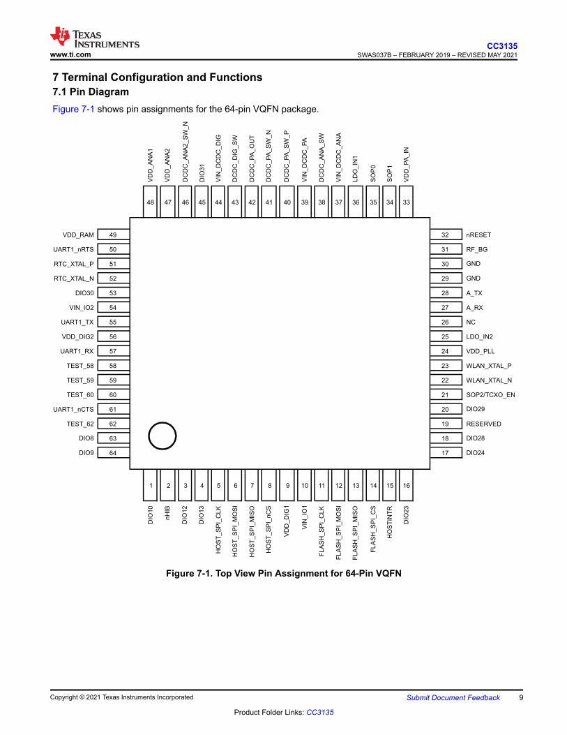
7 Terminal Configuration and Functions7.1 Pin DiagramFigure 7-1 shows pin assignments for the 64-pin VQFN package.
48 47 46 45 44 43 42 41 40 39 38 37 36 35 34 33
VDD_RAM 49 32 nRESET
UART1_nRTS 50 31 RF_BG
RTC_XTAL_P 51 30 GND
RTC_XTAL_N 52 29 GND
DIO30 53 28 A_TX
VIN_IO2 54 27 A_RX
UART1_TX 55 26 NC
VDD_DIG2 56 25 LDO_IN2
UART1_RX 57 24 VDD_PLL
TEST_58 58 23 WLAN_XTAL_P
TEST_59 59 22 WLAN_XTAL_N
TEST_60 60 21 SOP2/TCXO_EN
UART1_nCTS 61 20 DIO29
TEST_62 62 19 RESERVED
DIO8 63 18 DIO28
DIO9 64 17 DIO24
1 2 3 4 5 6 7 8 9 10 11 12 13 14 15 16
DIO
12
SO
P0
DIO
23
HO
ST
INT
R
FL
AS
H_
SP
I_C
S
DC
DC
_P
A_
OU
T
DC
DC
_D
IG_
SW
VIN
_D
CD
C_
AN
A
DC
DC
_A
NA
_S
W
VIN
_D
CD
C_
PA
DC
DC
_P
A_
SW
_P
DC
DC
_P
A_
SW
_N
FL
AS
H_
SP
I_C
LK
VIN
_IO
1
VD
D_
DIG
1
HO
ST
_S
PI_
nC
S
HO
ST
_S
PI_
MIS
O
SO
P1
FL
AS
H_
SP
I_M
ISO
FL
AS
H_
SP
I_M
OS
I
VD
D_
AN
A1
VD
D_
AN
A2
DC
DC
_A
NA
2_
SW
_N
DIO
31
VIN
_D
CD
C_
DIG
DIO
10
VD
D_
PA
_IN
LD
O_
IN1
HO
ST
_S
PI_
MO
SI
HO
ST
_S
PI_
CL
K
DIO
13
nH
IB
Figure 7-1. Top View Pin Assignment for 64-Pin VQFN
www.ti.comCC3135
SWAS037B – FEBRUARY 2019 – REVISED MAY 2021
Copyright © 2021 Texas Instruments Incorporated Submit Document Feedback 9
Product Folder Links: CC3135
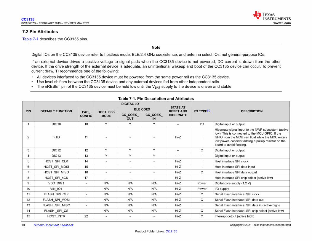
7.2 Pin AttributesTable 7-1 describes the CC3135 pins.
Note
Digital IOs on the CC3135 device refer to hostless mode, BLE/2.4 GHz coexistence, and antenna select IOs, not general-purpose IOs.
If an external device drives a positive voltage to signal pads when the CC3135 device is not powered, DC current is drawn from the other device. If the drive strength of the external device is adequate, an unintentional wakeup and boot of the CC3135 device can occur. To prevent current draw, TI recommends one of the following:• All devices interfaced to the CC3135 device must be powered from the same power rail as the CC3135 device.• Use level shifters between the CC3135 device and any external devices fed from other independent rails.• The nRESET pin of the CC3135 device must be held low until the VBAT supply to the device is driven and stable.
Table 7-1. Pin Description and Attributes
PIN DEFAULT FUNCTION
DIGITAL I/OSTATE AT
RESET AND HIBERNATE
I/O TYPE(1) DESCRIPTIONPAD_CONFIG
HOSTLESS MODE
BLE COEXCC_COEX_
OUTCC_COEX_
IN1 DIO10 10 Y Y Y – I/O Digital input or output
2 nHIB 11 - - - Hi-Z I
Hibernate signal input to the NWP subsystem (active low). This is connected to the MCU GPIO. If the GPIO from the MCU can float while the MCU enters low power, consider adding a pullup resistor on the board to avoid floating.
3 DIO12 12 Y Y Y – O Digital input or output
4 DIO13 13 Y Y Y – – Digital input or output
5 HOST_SPI_CLK 14 - - - Hi-Z I Host interface SPI clock
6 HOST_SPI_MOSI 15 - - - Hi-Z I Host interface SPI data input
7 HOST_SPI_MISO 16 - - - Hi-Z O Host interface SPI data output
8 HOST_SPI_nCS 17 - - - Hi-Z I Host interface SPI chip select (active low)
9 VDD_DIG1 - N/A N/A N/A Hi-Z Power Digital core supply (1.2 V)
10 VIN_IO1 - N/A N/A N/A Hi-Z Power I/O supply
11 FLASH_SPI_CLK - N/A N/A N/A Hi-Z O Serial Flash interface: SPI clock
12 FLASH_SPI_MOSI - N/A N/A N/A Hi-Z O Serial Flash interface: SPI data out
13 FLASH _SPI_MISO - N/A N/A N/A Hi-Z I Serial Flash interface: SPI data in (active high)
14 FLASH _SPI_CS - N/A N/A N/A Hi-Z O Serial Flash interface: SPI chip select (active low)
15 HOST_INTR 22 - - - Hi-Z O Interrupt output (active high)
CC3135SWAS037B – FEBRUARY 2019 – REVISED MAY 2021 www.ti.com
10 Submit Document Feedback Copyright © 2021 Texas Instruments Incorporated
Product Folder Links: CC3135

Table 7-1. Pin Description and Attributes (continued)
PIN DEFAULT FUNCTION
DIGITAL I/OSTATE AT
RESET AND HIBERNATE
I/O TYPE(1) DESCRIPTIONPAD_CONFIG
HOSTLESS MODE
BLE COEXCC_COEX_
OUTCC_COEX_
IN16 DIO23 23 Y Y Y Hi-Z Digital input or output
17 DIO24 24 Y Y Y Hi-Z Digital input or output
18 DIO28 40 Y Y Y – – Digital input or output
19 Reserved 28 - - - Hi-Z – Connect a 100-kΩ pulldown resistor to ground.
20 DIO29 29 Y Y Y Hi-Z Digital input or output
21 SOP2/TCXO_EN(2) 25 Y(3) Y - Hi-Z OControls restore to default mode. Enable signal for external TCXO. Add a 10-kΩ pulldown resistor to ground.
22 WLAN_XTAL_N - N/A N/A N/A Hi-Z Analog Connect the WLAN 40-MHz crystal here.
23 WLAN_XTAL_P - N/A N/A N/A Hi-Z Analog Connect the WLAN 40-MHz crystal here.
24 VDD_PLL - N/A N/A N/A Hi-Z Power Internal PLL power supply (1.4 V nominal)
25 LDO_IN2 - N/A N/A N/A Hi-Z Power Input to internal LDO
26 NC - N/A N/A N/A – – No Connect
27 A_RX - N/A N/A N/A – RF 5 GHz RF RX
28 A_TX - N/A N/A N/A – RF 5 GHz RF TX
29 GND - N/A N/A N/A – Power GND
30 GND - N/A N/A N/A – Power GND
31 RF_BG - N/A N/A N/A Hi-Z RF 2.4 GHz RF TX, RX
32 nRESET - N/A N/A N/A Hi-Z IRESET input for the device. Active low input. Use RC circuit (100 kΩ || 0.01 µF) for power on reset (POR).
33 VDD_PA_IN - N/A N/A N/A Hi-Z Power Power supply for the RF power amplifier (PA)
34 SOP1 - N/A N/A N/A Hi-Z –SOP[2:0] used for factory restore. Add 100-kΩ pulldown to ground. See Section 9.7. SOP1 used for 5 GHz switch control
35 SOP0 - N/A N/A N/A Hi-Z –SOP[2:0] used for factory restore. Add 100-kΩ pulldown to ground. See Section 9.7. SOP0 used for 5GHz switch control
36 LDO_IN1 - N/A N/A N/A Hi-Z Power Input to internal LDO
37 VIN_DCDC_ANA - N/A N/A N/A Hi-Z Power Power supply for the DC/DC converter for analog section
38 DCDC_ANA_SW - N/A N/A N/A Hi-Z Power Analog DC/DC converter switch output
39 VIN_DCDC_PA - N/A N/A N/A Hi-Z Power PA DC/DC converter input supply
www.ti.comCC3135
SWAS037B – FEBRUARY 2019 – REVISED MAY 2021
Copyright © 2021 Texas Instruments Incorporated Submit Document Feedback 11
Product Folder Links: CC3135

Table 7-1. Pin Description and Attributes (continued)
PIN DEFAULT FUNCTION
DIGITAL I/OSTATE AT
RESET AND HIBERNATE
I/O TYPE(1) DESCRIPTIONPAD_CONFIG
HOSTLESS MODE
BLE COEXCC_COEX_
OUTCC_COEX_
IN40 DCDC_PA_SW_P - N/A N/A N/A Hi-Z Power PA DC/DC converter switch output +ve
41 DCDC_PA_SW_N - N/A N/A N/A Hi-Z Power PA DC/DC converter switch output –ve
42 DCDC_PA_OUT - N/A N/A N/A Hi-Z Power PA DC/DC converter output. Connect the output capacitor for DC/DC here.
43 DCDC_DIG_SW - N/A N/A N/A Hi-Z Power Digital DC/DC converter switch output
44 VIN_DCDC_DIG - N/A N/A N/A Hi-Z Power Power supply input for the digital DC/DC converter
45 DIO31 31 Y Y Y Hi-Z – Network Scripter I/O
46 DCDC_ANA2_SW_N - N/A N/A N/A Hi-Z Power Analog2 DC/DC converter switch output –ve
47 VDD_ANA2 - N/A N/A N/A Hi-Z Power Analog2 power supply input
48 VDD_ANA1 - N/A N/A N/A Hi-Z Power Analog1 power supply input
49 VDD_RAM - N/A N/A N/A Hi-Z Power Power supply for the internal RAM
50 UART1_nRTS 0 - - - Hi-Z O UART host interface (active low)
51 RTC_XTAL_P - N/A N/A N/A Hi-Z Analog 32.768-kHz XTAL_P or external CMOS level clock input
52 RTC_XTAL_N 32 Y Y Y Hi-Z Analog 32.768-kHz XTAL_N or 100-kΩ external pullup for external clock
53 DIO30 30 Y Y Y Hi-Z – Network Scripter I/O
54 VIN_IO2 N/A N/A N/A Hi-Z Power I/O power supply. Same as battery voltage.
55 UART1_TX 1 - - - Hi-Z O UART host interface. Connect to test point on prototype for Flash programming.
56 VDD_DIG2 - N/A Hi-Z Power Digital power supply (1.2 V)
57 UART1_RX 2 - - - Hi-Z I UART host interface; connect to test point on prototype for Flash programming.
58 TEST_58 3 Y Y Y Hi-Z O Test signal; connect to an external test point.
59 TEST_60 4 Y Y Y Hi-Z O Test signal; connect to an external test point.
60 TEST_60 5 Y Y Y Hi-Z O Test signal; connect to an external test point.
61 UART1_nCTS 6 - - - Hi-Z I UART host interface (active low)
62 TEST_62 7 - - - Hi-Z O Test signal; connect to an external test point.
63 DIO8 8 Y Y Y Hi-Z Digital input or output
64 DIO9 9 Y Y Y Hi-Z – Digital input or output
CC3135SWAS037B – FEBRUARY 2019 – REVISED MAY 2021 www.ti.com
12 Submit Document Feedback Copyright © 2021 Texas Instruments Incorporated
Product Folder Links: CC3135
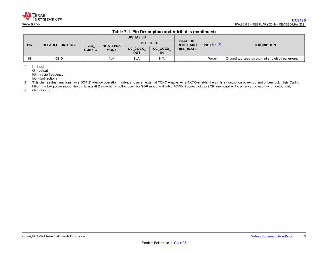
Table 7-1. Pin Description and Attributes (continued)
PIN DEFAULT FUNCTION
DIGITAL I/OSTATE AT
RESET AND HIBERNATE
I/O TYPE(1) DESCRIPTIONPAD_CONFIG
HOSTLESS MODE
BLE COEXCC_COEX_
OUTCC_COEX_
IN65 GND - N/A N/A N/A – Power Ground tab used as thermal and electrical ground
(1) I = inputO = outputRF = radio frequencyI/O = bidirectional
(2) This pin has dual functions: as a SOP[2] (device operation mode), and as an external TCXO enable. As a TXCO enable, the pin is an output on power up and driven logic high. During hibernate low-power mode, the pin is in a Hi-Z state but is pulled down for SOP mode to disable TCXO. Because of the SOP functionality, the pin must be used as an output only.
(3) Output Only
www.ti.comCC3135
SWAS037B – FEBRUARY 2019 – REVISED MAY 2021
Copyright © 2021 Texas Instruments Incorporated Submit Document Feedback 13
Product Folder Links: CC3135

7.3 Signal Descriptions
Table 7-2. Signal DescriptionsFUNCTION SIGNAL NAME PIN
NO.PIN
TYPESIGNAL
DIRECTION DESCRIPTION
Antenna selection
DIO10 1 I/O O
Antenna selection control
DIO12 3 I/O O
DIO13 4 I/O O
DIO23 16 I/O O
DIO24 17 I/O O
DIO28 18(1) I/O O
DIO29 20 I/O O
DIO25 21 O O
DIO31 45(1) I/O O
DIO32 52(1) I/O O
DIO30 53(1) I/O O
DIO3 58 I/O O
DIO4 59 I/O O
DIO5 60 I/O O
DIO8 63 I/O O
DIO9 64 I/O O
BLE/2.4 GHz Radio coexistence
DIO10 1 I/O I/O
Coexistence inputs and outputs
DIO12 3 I/O I/O
DIO13 4 I/O I/O
DIO23 16 I/O I/O
DIO24 17 I/O I/O
DIO28 18(1) I/O I/O
DIO29 20 I/O I/O
DIO25 21 O O
DIO31 45(1) I/O I/O
DIO32 52(1) I/O I/O
DIO30 53(1) I/O I/O
DIO3 58 I/O I/O
DIO4 59 I/O I/O
DIO5 60 I/O I/O
DIO8 63 I/O I/O
DIO9 64 I/O I/O
Clock
WLAN_XTAL_N 22 — — 40-MHz crystal; pull down if external TCXO is used
WLAN_XTAL_P 23 — — 40-MHz crystal or TCXO clock input
RTC_XTAL_P 51 — — Connect 32.768-kHz crystal or force external CMOS level clock
RTC_XTAL_N 52 — — Connect 32.768-kHz crystal or connect 100-kΩ resistor to supply voltage
CC3135SWAS037B – FEBRUARY 2019 – REVISED MAY 2021 www.ti.com
14 Submit Document Feedback Copyright © 2021 Texas Instruments Incorporated
Product Folder Links: CC3135
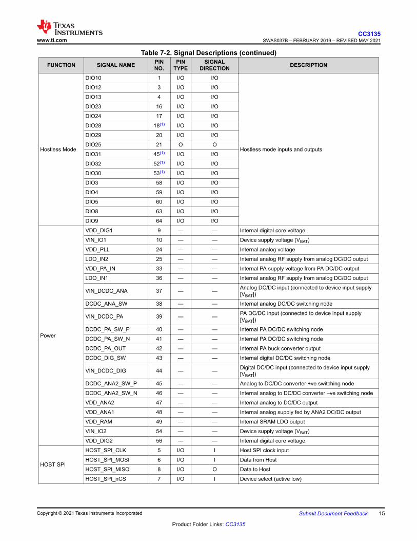
Table 7-2. Signal Descriptions (continued)FUNCTION SIGNAL NAME PIN
NO.PIN
TYPESIGNAL
DIRECTION DESCRIPTION
Hostless Mode
DIO10 1 I/O I/O
Hostless mode inputs and outputs
DIO12 3 I/O I/O
DIO13 4 I/O I/O
DIO23 16 I/O I/O
DIO24 17 I/O I/O
DIO28 18(1) I/O I/O
DIO29 20 I/O I/O
DIO25 21 O O
DIO31 45(1) I/O I/O
DIO32 52(1) I/O I/O
DIO30 53(1) I/O I/O
DIO3 58 I/O I/O
DIO4 59 I/O I/O
DIO5 60 I/O I/O
DIO8 63 I/O I/O
DIO9 64 I/O I/O
Power
VDD_DIG1 9 — — Internal digital core voltage
VIN_IO1 10 — — Device supply voltage (VBAT)
VDD_PLL 24 — — Internal analog voltage
LDO_IN2 25 — — Internal analog RF supply from analog DC/DC output
VDD_PA_IN 33 — — Internal PA supply voltage from PA DC/DC output
LDO_IN1 36 — — Internal analog RF supply from analog DC/DC output
VIN_DCDC_ANA 37 — — Analog DC/DC input (connected to device input supply [VBAT])
DCDC_ANA_SW 38 — — Internal analog DC/DC switching node
VIN_DCDC_PA 39 — — PA DC/DC input (connected to device input supply [VBAT])
DCDC_PA_SW_P 40 — — Internal PA DC/DC switching node
DCDC_PA_SW_N 41 — — Internal PA DC/DC switching node
DCDC_PA_OUT 42 — — Internal PA buck converter output
DCDC_DIG_SW 43 — — Internal digital DC/DC switching node
VIN_DCDC_DIG 44 — — Digital DC/DC input (connected to device input supply [VBAT])
DCDC_ANA2_SW_P 45 — — Analog to DC/DC converter +ve switching node
DCDC_ANA2_SW_N 46 — — Internal analog to DC/DC converter –ve switching node
VDD_ANA2 47 — — Internal analog to DC/DC output
VDD_ANA1 48 — — Internal analog supply fed by ANA2 DC/DC output
VDD_RAM 49 — — Internal SRAM LDO output
VIN_IO2 54 — — Device supply voltage (VBAT)
VDD_DIG2 56 — — Internal digital core voltage
HOST SPI
HOST_SPI_CLK 5 I/O I Host SPI clock input
HOST_SPI_MOSI 6 I/O I Data from Host
HOST_SPI_MISO 8 I/O O Data to Host
HOST_SPI_nCS 7 I/O I Device select (active low)
www.ti.comCC3135
SWAS037B – FEBRUARY 2019 – REVISED MAY 2021
Copyright © 2021 Texas Instruments Incorporated Submit Document Feedback 15
Product Folder Links: CC3135

Table 7-2. Signal Descriptions (continued)FUNCTION SIGNAL NAME PIN
NO.PIN
TYPESIGNAL
DIRECTION DESCRIPTION
FLASH SPI
FLASH_SPI_CLK 11 O O Clock to SPI serial flash (fixed default)
FLASH_SPI_DOUT 12 O O Data to SPI serial flash (fixed default)
FLASH_SPI_DIN 13 I I Data from SPI serial flash (fixed default)
FLASH_SPI_CS 14 O O Device select to SPI serial flash (fixed default)
UART
UART1_nRTS 50 I/O O UART1 request-to-send (active low)
UART1_TX 55 I/O I UART TX data
UART1_RX 57 I/O O UART RX data
UART1_nCTS 61 I/O I UART1 clear-to-send (active low)
Sense-On-Power
SOP2 21(2) O I Sense-on-power 2
SOP1 34 I I Configuration sense-on-power 1
SOP0 35 I I Configuration sense-on-power 0
Reset nRESET 32 I I Global master device reset (active low)
nHIB nHIB 2 I I Hibernate signal input to the NWP subsystem (active low)
RF
A_RX 27 I I WLAN analog A-band receive
A_TX 28 O O WLAN analog A-band transmit
RF_BG 31 I/O I/O WLAN analog RF 802.11 b/g bands
Test Port
TEST_58 58 O O Test Signal
TEST_59 59 I I Test Signal
TEST_60 60 O O Test Signal
TEST_62 62 O O Test Signal
(1) LPDS retention unavailable.(2) This pin has dual functions: as a SOP[2] (device operation mode), and as an external TCXO enable. As a TXCO enable, the pin is an
output on power up and driven logic high. During hibernate low-power mode, the pin is in a Hi-Z state but is pulled down for SOP mode to disable TCXO. Because of the SOP functionality, the pin must be used as an output only.
7.4 Connections for Unused PinsAll unused pin should be configured as stated in Table 7-3.
Table 7-3. Connections for Unused PinsFUNCTION SIGNAL DESCRIPTION PIN
NUMBER ACCEPTABLE PRACTICE PREFERRED PRACTICE
DIO Digital input or output
Wake up I/O source should not be floating during hibernate.All the I/O pins will float while in Hibernate and Reset states. Ensure pullup and pulldown resistors are available on board to maintain the state of the I/O.Leave unused DIOs as NC
No Connect NC 26 Unused pin, leave as NC. Unused pin, leave as NC
SOP Configuration sense-on-power
Ensure pulldown resistors are available on unused SOP pins
69.8K Pull down resistor on SOP0 and SOP1 used as switch control pins, 100K pull down on SOP2
Reset RESET input for the device Never leave the reset pin floating
ClockRTC_XTAL_N When using an external oscillator,
add a 100-kΩ pullup resistor to VIO
WLAN_XTAL_N When using an external oscillator, connect to ground if unused
CC3135SWAS037B – FEBRUARY 2019 – REVISED MAY 2021 www.ti.com
16 Submit Document Feedback Copyright © 2021 Texas Instruments Incorporated
Product Folder Links: CC3135

8 SpecificationsAll measurements are referenced at the device pins, unless otherwise indicated. All specifications are over process and voltage, unless otherwise indicated.
8.1 Absolute Maximum RatingsAll measurements are referenced at the device pins unless otherwise indicated. All specifications are over process and overvoltage unless otherwise indicated.Over operating free-air temperature range (unless otherwise noted)(1) (2)
MIN MAX UNIT
Supply voltageVBAT and VIO Pins: 37, 39, 44 –0.5 3.8 V
VIO – VBAT (differential) Pins: 10, 54 VBAT and VIO should be tied together V
Digital inputs –0.5 VIO + 0.5 V
RF pins –0.5 2.1 V
Analog pins, Crystal Pins: 22, 23, 51, 52 –0.5 2.1 V
Operating temperature, TA –40 85 °C
Storage temperature, Tstg –55 125 °C
(1) Stresses beyond those listed under Absolute Maximum Ratings may cause permanent damage to the device. These are stress ratings only, and functional operation of the device at these or any other conditions beyond those indicated under Recommended Operating Conditions is not implied. Exposure to absolute-maximum-rated conditions for extended periods may affect device reliability.
(2) All voltage values are with respect to VSS, unless otherwise noted.
8.2 ESD RatingsVALUE UNIT
VESD Electrostatic dischargeHuman body model (HBM), per ANSI/ESDA/JEDEC JS-001(1) ±2000
VCharged device model (CDM), per ANSI/ESDA/JEDEC JS-002(2) ±500
(1) JEDEC document JEP155 states that 500-V HBM allows safe manufacturing with a standard ESD control process.(2) JEDEC document JEP157 states that 250-V CDM allows safe manufacturing with a standard ESD control process.
8.3 Power-On Hours (POH)This information is provided solely for your convenience and does not extend or modify the warranty provided under TI's standard terms and conditions for TI semiconductor products.
OPERATING CONDITION POWER-ON HOURS [POH] (hours)
TA up to 85°C(1) 87,600
(1) The TX duty cycle (power amplifier ON time) is assumed to be 10% of the device POH. Of the remaining 90% of the time, the device can be in any other state.
www.ti.comCC3135
SWAS037B – FEBRUARY 2019 – REVISED MAY 2021
Copyright © 2021 Texas Instruments Incorporated Submit Document Feedback 17
Product Folder Links: CC3135
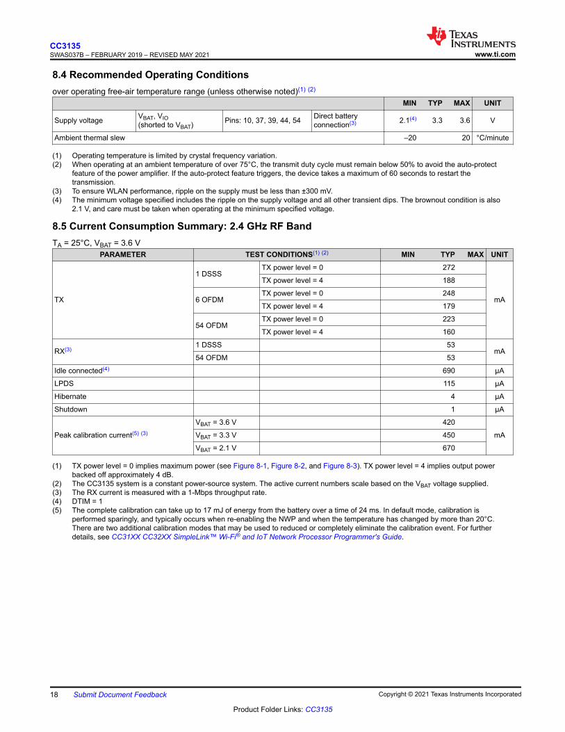
8.4 Recommended Operating Conditionsover operating free-air temperature range (unless otherwise noted)(1) (2)
MIN TYP MAX UNIT
Supply voltage VBAT, VIO(shorted to VBAT) Pins: 10, 37, 39, 44, 54 Direct battery
connection(3) 2.1(4) 3.3 3.6 V
Ambient thermal slew –20 20 °C/minute
(1) Operating temperature is limited by crystal frequency variation.(2) When operating at an ambient temperature of over 75°C, the transmit duty cycle must remain below 50% to avoid the auto-protect
feature of the power amplifier. If the auto-protect feature triggers, the device takes a maximum of 60 seconds to restart the transmission.
(3) To ensure WLAN performance, ripple on the supply must be less than ±300 mV.(4) The minimum voltage specified includes the ripple on the supply voltage and all other transient dips. The brownout condition is also
2.1 V, and care must be taken when operating at the minimum specified voltage.
8.5 Current Consumption Summary: 2.4 GHz RF BandTA = 25°C, VBAT = 3.6 V
PARAMETER TEST CONDITIONS(1) (2) MIN TYP MAX UNIT
TX
1 DSSSTX power level = 0 272
mA
TX power level = 4 188
6 OFDMTX power level = 0 248
TX power level = 4 179
54 OFDMTX power level = 0 223
TX power level = 4 160
RX(3)1 DSSS 53
mA54 OFDM 53
Idle connected(4) 690 µA
LPDS 115 µA
Hibernate 4 µA
Shutdown 1 µA
Peak calibration current(5) (3)
VBAT = 3.6 V 420
mAVBAT = 3.3 V 450
VBAT = 2.1 V 670
(1) TX power level = 0 implies maximum power (see Figure 8-1, Figure 8-2, and Figure 8-3). TX power level = 4 implies output power backed off approximately 4 dB.
(2) The CC3135 system is a constant power-source system. The active current numbers scale based on the VBAT voltage supplied.(3) The RX current is measured with a 1-Mbps throughput rate.(4) DTIM = 1(5) The complete calibration can take up to 17 mJ of energy from the battery over a time of 24 ms. In default mode, calibration is
performed sparingly, and typically occurs when re-enabling the NWP and when the temperature has changed by more than 20°C. There are two additional calibration modes that may be used to reduced or completely eliminate the calibration event. For further details, see CC31XX CC32XX SimpleLink™ Wi-Fi® and IoT Network Processor Programmer's Guide.
CC3135SWAS037B – FEBRUARY 2019 – REVISED MAY 2021 www.ti.com
18 Submit Document Feedback Copyright © 2021 Texas Instruments Incorporated
Product Folder Links: CC3135

8.6 Current Consumption Summary: 5 GHz RF BandTA = 25°C, VBAT = 3.6 V
PARAMETER TEST CONDITIONS(1) (2) MIN TYP MAX UNIT
TX6 OFDM 318
mA54 OFDM 293
RX(3) 54 OFDM 61 mA
Idle connected(4) 690 µA
LPDS 115 µA
Hibernate 4 µA
Shutdown 1 µA
Peak calibration current(5) (3)
VBAT = 3.6 V 290
mAVBAT = 3.3 V 310
VBAT = 2.7 V 310
VBAT = 2.1 V 400
(1) TX power level = 0 implies maximum power (see Figure 8-1, Figure 8-2, and Figure 8-3). TX power level = 4 implies output power backed off approximately 4 dB.
(2) The CC3135 system is a constant power-source system. The active current numbers scale based on the VBAT voltage supplied.(3) The RX current is measured with a 1-Mbps throughput rate.(4) DTIM = 1(5) The complete calibration can take up to 17 mJ of energy from the battery over a time of 24 ms. In default mode, calibration is
performed sparingly, and typically occurs when re-enabling the NWP and when the temperature has changed by more than 20°C. There are two additional calibration modes that may be used to reduced or completely eliminate the calibration event. For further details, see CC31XX, CC32XX SimpleLink™ Wi-Fi® and IoT Network Processor Programmer's Guide.
8.7 TX Power Control for 2.4 GHz BandThe CC3135 has several options for modifying the output power of the device when required. For the 2.4 GHz band it is possible to lower the overall output power at a global level using the global TX power level setting. In addition, the 2.4 GHz band allows the user to enter additional back-offs 1, per channel, region 2and modulation rates 3, via Image creator (see the UniFlash CC31xx, CC32xx SimpleLink™ Wi-Fi® and Internet-on-a chip™ Solution ImageCreator and Programming Tool User's Guide for more details).
Figure 8-1, Figure 8-2, and Figure 8-3 show TX power and IBAT versus TX power level settings for the CC3135 device at modulations of 1 DSSS, 6 OFDM, and 54 OFDM, respectively.
1 The back-off range is between -6 dB to +6 dB in 0.25 dB increments.2 FCC/ISED, ETSI (Europe), and Japan are supported.3 Back-off rates are grouped into 11b rates, high modulation rates (MCS7, 54 OFDM and 48 OFDM), and lower modulation rates (all
other rates).
www.ti.comCC3135
SWAS037B – FEBRUARY 2019 – REVISED MAY 2021
Copyright © 2021 Texas Instruments Incorporated Submit Document Feedback 19
Product Folder Links: CC3135

In Figure 8-1, the area enclosed in the circle represents a significant reduction in current during transition from TX power level 3 to level 4. In the case of lower range requirements (14-dBm output power), TI recommends using TX power level 4 to reduce the current.
TX power level setting
TX
Pow
er
(dB
m)
19.00
17.00
15.00
13.00
11.00
9.00
7.00
5.00
3.00
1.00
0 1 2 3 4 5 6 7 8 9 10 11 12 13 14 15
280.00
264.40
249.00
233.30
218.00
202.00
186.70
171.00
155.60
140.00
1 DSSS
IBA
T(V
BA
T@
3.6
V)(
mA
mp)
Color by
TX Power (dBm)
IBAT (VBAT @ 3.6 V)
Figure 8-1. TX Power and IBAT vs TX Power Level Settings (1 DSSS)
TX power level setting
TX
Pow
er
(dB
m)
19.00
17.00
15.00
13.00
11.00
9.00
7.00
5.00
3.00
1.00
0 1 2 3 4 5 6 7 8 9 10 11 12 13 14 15
IBA
T(V
BA
T@
3.6
V)(
mA
mp)
280.00
264.40
249.00
233.30
218.00
202.00
186.70
171.00
155.60
140.00
6 OFDM
Color by
TX Power (dBm)
IBAT (VBAT @ 3.6 V)
Figure 8-2. TX Power and IBAT vs TX Power Level Settings (6 OFDM)
CC3135SWAS037B – FEBRUARY 2019 – REVISED MAY 2021 www.ti.com
20 Submit Document Feedback Copyright © 2021 Texas Instruments Incorporated
Product Folder Links: CC3135

TX power level setting
TX
Pow
er
(dB
m)
19.00
17.00
15.00
13.00
11.00
9.00
7.00
5.00
3.00
1.00
0 1 2 3 4 5 6 7 8 9 10 11 12 13 14 15
54 OFDM
280.00
264.40
249.00
233.30
218.00
202.00
186.70
171.00
155.60
140.00
IBA
T(V
BA
T@
3.6
V)(
mA
mp)
Color by
TX Power (dBm)
IBAT (VBAT @ 3.6 V)
Figure 8-3. TX Power and IBAT vs TX Power Level Settings (54 OFDM)
8.8 TX Power Control for 5 GHz5 GHz power control is done via Image Creator where the maximum transmit power is provided 4. Within Image Creator power control is possible per channel, region 5, and modulation rates 6. In addition, it is possible to enter an additional back-off 7factor per channel and modulation rate for further margin to regulatory requirements.
Finally, it is also possible to set the TX and RX trace losses to the antenna per band 8. The peak antenna gain 9can also be provided, thus allowing further control. For a full description of options and capabilities see the UniFlash CC31xx, CC32xx SimpleLink™ Wi-Fi® and Internet-on-a chip™ Solution ImageCreator and Programming Tool User's Guide.
4 The maximum transmit power range is 18 dBm to 0.125 dBm in 0.125 dBm decrements.5 FCC/ISED, ETSI (Europe), and Japan are supported.6 Rates are grouped into high modulation rates (MCS7, 54 OFDM and 48 OFDM) and lower modulation rates (all other rates).7 The back-off range is 0 dBm to 18 dBm in 0.125 dBm increments, with the maximum back-off not exceed that of the maximum transmit
power.8 The range of losses if from 0 dBm to 7.75 dBm in 0.125 dBm increments.9 The antenna gain has a range of -2 dBi to 5.75 dBi in 0.125 dBi increments.
www.ti.comCC3135
SWAS037B – FEBRUARY 2019 – REVISED MAY 2021
Copyright © 2021 Texas Instruments Incorporated Submit Document Feedback 21
Product Folder Links: CC3135
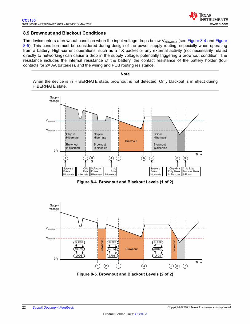
8.9 Brownout and Blackout ConditionsThe device enters a brownout condition when the input voltage drops below Vbrownout (see Figure 8-4 and Figure 8-5). This condition must be considered during design of the power supply routing, especially when operating from a battery. High-current operations, such as a TX packet or any external activity (not necessarily related directly to networking) can cause a drop in the supply voltage, potentially triggering a brownout condition. The resistance includes the internal resistance of the battery, the contact resistance of the battery holder (four contacts for 2× AA batteries), and the wiring and PCB routing resistance.
Note
When the device is in HIBERNATE state, brownout is not detected. Only blackout is in effect during HIBERNATE state.
1 2 3 4 5 6 7 8 9
Supply
Voltage
Vbrownout
Vblackout
Chip in
Hibernate
Brownout
is disabled
Chip in
Hibernate
Brownout
is disabled
Brownout
Chip in
Hibernate
Brownout
is disabled
Software
Enters
Hibernate
Chip
Exits
Hibernate
Software
Enters
Hibernate
Chip
Exits
Hibernate
Software
Enters
Hibernate
Chip Exits
Blackout Reset
& Boots
Chip Gets
Fully Reset
In Blakcout
Time
0 V
Figure 8-4. Brownout and Blackout Levels (1 of 2)
1 2 3 4 5 6 7
Supply
Voltage
Vbrownout
Vblackout
Brownout
Time
0 V
Bro
wn
ou
t
Bro
wn
ou
t
SLEEP
ACTIVE
LPDS
SLEEP
ACTIVE
LPDS
SLEEP
ACTIVE
LPDS
Figure 8-5. Brownout and Blackout Levels (2 of 2)
CC3135SWAS037B – FEBRUARY 2019 – REVISED MAY 2021 www.ti.com
22 Submit Document Feedback Copyright © 2021 Texas Instruments Incorporated
Product Folder Links: CC3135

In the brownout condition, all sections of the device (including the 32-kHz RTC) shut down except for the Hibernate module, which remains on. The current in this state can reach approximately 400 µA. The blackout condition is equivalent to a hardware reset event in which all states within the device are lost.
Table 8-1 lists the brownout and blackout voltage levels.
Table 8-1. Brownout and Blackout Voltage LevelsCONDITION VOLTAGE LEVEL UNIT
Vbrownout 2.1 V
Vblackout 1.67 V
8.10 Electrical Characteristics for DIO Pins
Table 8-2. Electrical Characteristics: DIO Pins Except 52 and 53TA = 25°C, VBAT = 2.1 V to 3.3 V.(1)
PARAMETER TEST CONDITIONS MIN TYP MAX UNITCIN Pin capacitance 4 pF
VIH High-level input voltage 0.65 × VDD VDD + 0.5 V V
VIL Low-level input voltage –0.5 0.35 × VDD V
IIH High-level input current 5 nA
IIL Low-level input current 5 nA
VOH High-level output voltage
IL = 2 mA; configured I/O drive strength = 2 mA;2.4 V ≤ VDD < 3.6 V
VDD × 0.8
V
IL = 4 mA; configured I/O drive strength = 4 mA;2.4 V ≤ VDD < 3.6 V
VDD × 0.7
IL = 6 mA; configured I/O drive strength = 6 mA;2.4 V ≤ VDD < 3.6 V
VDD × 0.7
IL = 2 mA; configured I/O drive strength = 2 mA;2.1 V ≤ VDD < 2.4 V
VDD × 0.75
VOL Low-level output voltage
IL = 2 mA; configured I/O drive strength = 2 mA;2.4 V ≤ VDD < 3.6 V
VDD × 0.2
V
IL = 4 mA; configured I/O drive strength = 4 mA;2.4 V ≤ VDD < 3.6 V
VDD × 0.2
IL = 6 mA; configured I/O drive strength = 6 mA;2.4 V ≤ VDD < 3.6 V
VDD × 0.2
IL = 2 mA; configured I/O drive strength = 2 mA;2.1 V ≤ VDD < 2.4 V
VDD × 0.25
IOH
High-level source current
2-mA drive 2
mA4-mA drive 4
6-mA drive 6
IOLLow-level sink current
2-mA drive 2
mA4-mA drive 4
6-mA drive 6
(1) TI recommends using the lowest possible drive strength that is adequate for the applications. This recommendation minimizes the risk of interference to the WLAN radio and reduces any potential degradation of RF sensitivity and performance. The default drive strength setting is 6 mA.
www.ti.comCC3135
SWAS037B – FEBRUARY 2019 – REVISED MAY 2021
Copyright © 2021 Texas Instruments Incorporated Submit Document Feedback 23
Product Folder Links: CC3135

Table 8-3. Electrical Characteristics: DIO Pins 52 and 53TA = 25°C, VBAT = 2.1 V to 3.6 V.(1)
PARAMETER TEST CONDITIONS MIN TYP MAX UNITCIN Pin capacitance 7 pF
VIH High-level input voltage 0.65 × VDD VDD + 0.5 V V
VIL Low-level input voltage –0.5 0.35 × VDD V
IIH High-level input current 50 nA
IIL Low-level input current 50 nA
VOH High-level output voltage
IL = 2 mA; configured I/O drive strength = 2 mA;2.4 V ≤ VDD < 3.6 V
VDD × 0.8
V
IL = 4 mA; configured I/O drive strength = 4 mA;2.4 V ≤ VDD < 3.6 V
VDD × 0.7
IL = 6 mA; configured I/O drive strength = 6 mA;2.4 V ≤ VDD < 3.6 V
VDD × 0.7
IL = 2 mA; configured I/O drive strength = 2 mA;2.1 V ≤ VDD < 2.4 V
VDD × 0.75
VOL Low-level output voltage
IL = 2 mA; configured I/O drive strength = 2 mA;2.4 V ≤ VDD < 3.6 V
VDD × 0.2
V
IL = 4 mA; configured I/O drive strength = 4 mA;2.4 V ≤ VDD < 3.6 V
VDD × 0.2
IL = 6 mA; configured I/O drive strength = 6 mA;2.4 V ≤ VDD < 3.6 V
VDD × 0.2
IL = 2 mA; configured I/O drive strength = 2 mA;2.1 V ≤ VDD < 2.4 V
VDD × 0.25
IOH
High-level source current, VOH = 2.4
2-mA drive 1.5
mA4-mA drive 2.5
6-mA drive 3.5
IOLLow-level sink current
2-mA drive 1.5
mA4-mA drive 2.5
6-mA drive 3.5
VIL nRESET 0.6 V
(1) TI recommends using the lowest possible drive strength that is adequate for the applications. This recommendation minimizes the risk of interference to the WLAN radio and reduces any potential degradation of RF sensitivity and performance. The default drive strength setting is 6 mA.
CC3135SWAS037B – FEBRUARY 2019 – REVISED MAY 2021 www.ti.com
24 Submit Document Feedback Copyright © 2021 Texas Instruments Incorporated
Product Folder Links: CC3135

8.11 Electrical Characteristics for Pin Internal Pullup and PulldownTA = 25°C, VBAT = 3.0 V.
PARAMETER TEST CONDITIONS MIN TYP MAX UNITIOH Pullup current, VOH = 2.4 (VDD = 3.0 V) 5 10 µA
IOLPulldown current, VOL = 0.4 (VDD = 3.0 V) 5 µA
8.12 WLAN Receiver Characteristics
Table 8-4. WLAN Receiver Characteristics: 2.4 GHz BandTA = 25°C, VBAT = 2.1 V to 3.6 V. Parameters are measured at the SoC pin on channel 6 (2437 MHz).
PARAMETER TEST CONDITIONS (Mbps) MIN TYP MAX UNIT
Sensitivity(8% PER for 11b rates, 10% PER for 11g/11n rates)(1)
1 DSSS –96.0
dBm
2 DSSS –94.0
11 CCK –88.0
6 OFDM –90.5
9 OFDM –90.0
18 OFDM –86.5
36 OFDM –80.5
54 OFDM –74.5
MCS7 (GF)(2) –71.5
Maximum input level(10% PER)
802.11b –4.0dBm
802.11g –10.0
(1) Sensitivity is 1-dB worse on channel 13 (2472 MHz).(2) Sensitivity for mixed mode is 1-dB worse.
Table 8-5. WLAN Receiver Characteristics: 5 GHz BandTA = 25°C, VBAT = 2.1 V to 3.6 V. Parameters measured at SoC pin are the average of channels 40, 56, 120, and 157.
PARAMETER TEST CONDITIONS (Mbps) MIN TYP MAX UNIT
Sensitivity(10% PER for 11g/11n rates)
6 OFDM -92.0
dBm
9 OFDM -91.0
18 OFDM -88.0
36 OFDM -81.5
54 OFDM -75.0
MCS7 (GF)(1) -71.0
Maximum input level 802.11a -20 dBm
(1) Sensitivity for mixed mode is 1-dB worse.
www.ti.comCC3135
SWAS037B – FEBRUARY 2019 – REVISED MAY 2021
Copyright © 2021 Texas Instruments Incorporated Submit Document Feedback 25
Product Folder Links: CC3135

8.13 WLAN Transmitter Characteristics
Table 8-6. WLAN Transmitter Characteristics: 2.4 GHz BandTA = 25°C, VBAT = 2.1 V to 3.6 V. Parameters measured at SoC pin on channel 6 (2437 MHz).(1) (2)
PARAMETER TEST CONDITIONS MIN TYP MAX UNITOperating frequency range(3) (4) 2412 2472 MHz
Maximum RMS output power measured at 1 dB from IEEE spectral mask or EVM
1 DSSS 18.0
dBm
2 DSSS 18.0
11 CCK 18.3
6 OFDM 17.3
9 OFDM 17.3
18 OFDM 17.0
36 OFDM 16.0
54 OFDM 14.5
MCS7 13.0
Transmit center frequency accuracy –25 25 ppm
(1) The OFDM and MCS7 edge channels (2412 and 2462 MHz) have reduced TX power to meet FCC emission limits.(2) Power of 802.11b rates are reduced to meet ETSI requirements in Europe.(3) Channels 1 (2142 MHz) through 11 (2462 MHz) are supported for FCC.(4) Channels 1 (2142 MHz) through 13 (2472MHz) are supported for Europe and Japan. Note that channel 14 is not supported for Japan.
Table 8-7. WLAN Transmitter Characteristics: 5 GHz BandTA = 25°C, VBAT = 2.1 V to 3.6 V.(1) Parameters measured at SoC pin are the average of channels 40, 56, 120, and 157.(2)
PARAMETER TEST CONDITIONS MIN TYP MAX UNITOperating frequency range(3) (4) (5) 5180 5825 MHz
Maximum RMS output power measured at 1 dB from IEEE spectral mask or EVM
6 OFDM 18.1
dBm
9 OFDM 18.1
18 OFDM 18.1
36 OFDM 16.6
54 OFDM 15.0
MCS7 14.0
Transmit center frequency accuracy -20 20 ppm
(1) Transmit power will be reduced by 1.5dB for VBAT < 2.8V(2) FCC, Europe, and Japan channel power limits per modulation rates can be found in the Uniflash with Image Creator User Guide.(3) FCC band covers U-NII-1, U-NII-2A, U-NII-2C, and U-NII-3 20-MHz BW modulations.(4) Europe bands 1, 2 and 3, 20-MHz BW modulations are supported.(5) For Japan, W52, W53 and W56, 20-MHz BW modulations are supported.
CC3135SWAS037B – FEBRUARY 2019 – REVISED MAY 2021 www.ti.com
26 Submit Document Feedback Copyright © 2021 Texas Instruments Incorporated
Product Folder Links: CC3135

8.14 WLAN Transmitter Out-of-Band EmissionsBoth the 2.4 GHz and the 5 GHz RF paths require an external band-pass filter to meet the various emission standards, including FCC. Table 8-8 and Table 8-9 presents the minimum attenuation requirements for the 2.4 GHz and 5 GHz band-pass filter, respectively. TI recommends using the same filter, switch, diplexer, and so on, used in the reference design to ease the process of certification.
Table 8-8. WLAN 2.4 GHz Filter RequirementsPARAMETER FREQUENCY (MHz) MIN TYP MAX UNIT
Return loss 2412 to 2484 10 dB
Insertion loss(1) 2412 to 2484 1 1.5 dB
Attenuation
804 to 828 30 42
dB
1608 to 1656 20 23
3216 to 3312 30 49
4020 to 4140 40 52
4824 to 4968 20 30
5628 to 5796 20 27
6432 to 6624 20 42
7200 to 7500 35 44
7500 to 10000 20 30
Reference impendence 2412 to 2484 50 Ω
Filter type Bandpass
(1) Insertion loss directly impacts output power and sensitivity. At customer discretion, insertion loss can be relaxed to meet attenuation requirements.
Table 8-9. WLAN 5 GHz Filter RequirementsPARAMETER FREQUENCY (MHz) MIN TYP MAX UNIT
Return loss 5150 to 5925 10 dB
Insertion loss(1) 5150 to 5925 1 2 dB
Attenuation
600 to 2700 41 42
dB
2950 to 3850 27 31
4400 to 4600 20 27
6600 to 6900 20 28
7000 to 7775 20 27
10300 to 11850 25 37
Reference impendence 5150 to 5925 50 Ω
Filter type Bandpass
(1) Insertion loss directly impacts output power and sensitivity. At customer discretion, insertion loss can be relaxed to meet attenuation requirements.
www.ti.comCC3135
SWAS037B – FEBRUARY 2019 – REVISED MAY 2021
Copyright © 2021 Texas Instruments Incorporated Submit Document Feedback 27
Product Folder Links: CC3135

8.15 BLE/2.4 GHz Radio Coexistence and WLAN Coexistence RequirementsFor proper BLE/2.4 GHz radio coexistence, the following requirements needs to met:
Table 8-10. COEX Isolation RequirementPARAMETER Band MIN TYP MAX UNIT
Port-to-port isolationSingle antenna 20(1)
dBDual antenna Configuration 20(2)
(1) WLAN/BLE switch used must provide a minimum of 20 dB isolation between ports.(2) For dual antenna configuration antenna placement must be such that isolation between the BLE and WLAN ports is at least 20 dB.
8.16 Thermal Resistance Characteristics for RGK PackageTHERMAL METRICS(1) °C/W(2) (3) AIR FLOW (m/s)(4)
RΘJC Junction-to-case 6.3 0.0051
RΘJB Junction-to-board 2.4 0.0051
RΘJA Junction-to-free air 23 0.0051
RΘJMA Junction-to-moving air
14.6 0.765
12.4 1.275
10.8 2.55
PsiJT Junction-to-package top
0.2 0.0051
0.2 0.765
0.3 1.275
0.1 2.55
PsiJB Junction-to-board
2.3 0.0051
2.3 0.765
2.2 1.275
2.4 2.55
(1) For more information about traditional and new thermal metrics, see Semiconductor and IC Package Thermal Metrics.(2) °C/W = degrees Celsius per watt.(3) These values are based on a JEDEC-defined 2S2P system (with the exception of the Theta JC [RΘJC] value, which is based on
a JEDEC-defined 1S0P system) and will change based on environment as well as application. For more information, see these EIA/JEDEC standards:• JESD51-2, Integrated Circuits Thermal Test Method Environmental Conditions - Natural Convection (Still Air)• JESD51-3, Low Effective Thermal Conductivity Test Board for Leaded Surface Mount Packages• JESD51-7, High Effective Thermal Conductivity Test Board for Leaded Surface Mount Packages• JESD51-9, Test Boards for Area Array Surface Mount Package Thermal Measurements
Power dissipation of 2 W and an ambient temperature of 70°C is assumed.(4) m/s = meters per second.
CC3135SWAS037B – FEBRUARY 2019 – REVISED MAY 2021 www.ti.com
28 Submit Document Feedback Copyright © 2021 Texas Instruments Incorporated
Product Folder Links: CC3135

8.17 Timing and Switching Characteristics8.17.1 Power Supply Sequencing
For proper operation of the CC3135 device, perform the recommended power-up sequencing as follows:
1. Tie the following pins together on the board:• VBAT (pins 37, 39, and 44)• VIO (pins 54 and 10)
2. Hold the RESET pin low while the supplies are ramping up. TI recommends using a simple RC circuit (100 K ||, 0.01 µF, RC = 1 ms).
3. For an external RTC, ensure that the clock is stable before RESET is deasserted (high).
For timing diagrams, see Section 8.17.3.
8.17.2 Device Reset
When a device restart is required, the user may issue a negative pulse to the nRESET pin. The user must follow one of the following alternatives to ensure the reset is properly applied:
• A negative reset pulse (on pin 32) of at least 200-ms duration• If the 200-ms pulse duration cannot be ensured, a pulldown resistor of 2 MΩ must be connected to pin 52
(RTC_XTAL_N). If implemented, a shorter pulse of at least 100 µs can be used.
To ensure a proper reset sequence, the user must call the sl_stop function prior to toggling the reset. When a reset is required, it is preferable to use the software reset instead of an external trigger.
8.17.3 Reset Timing8.17.3.1 nRESET (32-kHz Crystal)
Figure 8-6 shows the reset timing diagram for the 32-kHz crystal first-time power-up and reset removal.
POWEROFF
HW INIT FW INITDevice Ready toserve API calls
VBAT
VIO
nRESET
STATE
32-kHz
XTAL
T1 T2 T3
nHIB
RESET
Figure 8-6. First-Time Power-Up and Reset Removal Timing Diagram (32-kHz Crystal)
Table 8-11 describes the timing requirements for the 32-kHz crystal first-time power-up and reset removal.
Table 8-11. First-Time Power-Up and Reset Removal Timing Requirements (32-kHz Crystal)ITEM NAME DESCRIPTION MIN TYP MAX UNIT
T1 nReset time nReset timing after VBAT and VIO supply are stable 1 ms
T2 Hardware wake-up time 25 ms
T3 Initialization time 32-kHz crystal settling plus firmware initialization time plus radio calibration 1.35 s
www.ti.comCC3135
SWAS037B – FEBRUARY 2019 – REVISED MAY 2021
Copyright © 2021 Texas Instruments Incorporated Submit Document Feedback 29
Product Folder Links: CC3135

8.17.3.2 nRESET (External 32-kHz Crystal)
Figure 8-7 shows the reset timing diagram for the external 32-kHz crystal first-time power-up and reset removal.
POWEROFF HW INIT FW INIT
Device Ready toserve API calls
VBAT
VIO
nRESET
STATE
T1 T2 T3
nHIB
RESET
32-kHz
RTC CLK
Figure 8-7. First-Time Power-Up and Reset Removal Timing Diagram (External 32-kHz Crystal)
Table 8-12 describes the timing requirements for the external first-time power-up and reset removal.
Table 8-12. First-Time Power-Up and Reset Removal Timing Requirements (External 32-kHz Crystal)ITEM NAME DESCRIPTION MIN TYP MAX UNIT
T1 nReset time nReset timing after VBAT and VIO supply are stable 1 ms
T2 Hardware wake-up time 25 ms
T3 Initialization time Firmware initialization time plus radio calibration 250 ms
CC3135SWAS037B – FEBRUARY 2019 – REVISED MAY 2021 www.ti.com
30 Submit Document Feedback Copyright © 2021 Texas Instruments Incorporated
Product Folder Links: CC3135

8.17.4 Wakeup From HIBERNATE Mode
Note
The 32.768-kHz crystal is kept enabled by default when the chip goes into HIBERNATE mode in response to nHIB being pulled low.
Figure 8-8 shows the timing diagram for wakeup from HIBERNATE mode.
32-kHz
XTAL/CXO
VBAT
VIO
nRESET
nHIB
ACTIVE HIBERNATE HW WAKEUP+FW INIT ACTIVE HIBERNATE
Thib_min Twake_from_hib
Figure 8-8. nHIB Timing Diagram
Table 8-13 describes the timing requirements for nHIB.
Table 8-13. nHIB Timing RequirementsITEM NAME DESCRIPTION MIN TYP MAX UNIT
Thib_min Minimum hibernate time Minimum pulse width of nHIB being low(1) 10 ms
Twake_from_hibHardware wakeup time plus firmware initialization time See(2) 50 ms
(1) Ensure that the nHIB pulse width is kept above the minimum requirement under all conditions (such as power up, MCU reset, and so on).
(2) If temperature changes by more than 20°C, initialization time from HIB can increase by 200 ms due to radio calibration.
www.ti.comCC3135
SWAS037B – FEBRUARY 2019 – REVISED MAY 2021
Copyright © 2021 Texas Instruments Incorporated Submit Document Feedback 31
Product Folder Links: CC3135

8.17.5 Clock Specifications
The CC3135 device requires two separate clocks for its operation:
• A slow clock running at 32.768 kHz is used for the RTC.• A fast clock running at 40 MHz is used by the device for the internal processor and the WLAN subsystem.
The device features internal oscillators that enable the use of less-expensive crystals rather than dedicated TCXOs for these clocks. The RTC can also be fed externally to provide reuse of an existing clock on the system and to reduce overall cost.
8.17.5.1 Slow Clock Using Internal Oscillator
The RTC crystal connected on the device supplies the free-running slow clock. The accuracy of the slow clock frequency must be 32.768 kHz ±150 ppm. In this mode of operation, the crystal is tied between RTC_XTAL_P (pin 51) and RTC_XTAL_N (pin 52) with a suitable load capacitance to meet the ppm requirement.
Figure 8-9 shows the crystal connections for the slow clock.
RTC_XTAL_P
RTC_XTAL_N
51
52
32.768 kHz
10 pF
GND
GND
10 pF
Copyright © 2017, Texas Instruments Incorporated
Figure 8-9. RTC Crystal Connections
Table 8-14 lists the RTC crystal requirements.
Table 8-14. RTC Crystal RequirementsCHARACTERISTICS TEST CONDITIONS MIN TYP MAX UNIT
Frequency 32.768 kHz
Frequency accuracy Initial plus temperature plus aging ±150 ppm
Crystal ESR 32.768 kHz 70 kΩ
CC3135SWAS037B – FEBRUARY 2019 – REVISED MAY 2021 www.ti.com
32 Submit Document Feedback Copyright © 2021 Texas Instruments Incorporated
Product Folder Links: CC3135

8.17.5.2 Slow Clock Using an External Clock
When an RTC oscillator is present in the system, the CC3135 device can accept this clock directly as an input. The clock is fed on the RTC_XTAL_P line, and the RTC_XTAL_N line is held to VIO. The clock must be a CMOS-level clock compatible with VIO fed to the device.
Figure 8-10 shows the external RTC input connection.
RTC_XTAL_P
RTC_XTAL_N
Host system
32.768 kHz
VIO
100 KΩ
Copyright © 2017, Texas Instruments Incorporated
Figure 8-10. External RTC Input
Table 8-15 lists the external RTC digital clock requirements.
Table 8-15. External RTC Digital Clock RequirementsCHARACTERISTICS TEST CONDITIONS MIN TYP MAX UNIT
Frequency 32768 Hz
Frequency accuracy(Initial plus temperature plus aging) ±150 ppm
tr, tfInput transition time tr, tf(10% to 90%) 100 ns
Frequency input duty cycle 20% 50% 80%
Vih Slow clock input voltage limits Square wave, DC coupled0.65 × VIO VIO V
Vil 0 0.35 × VIO Vpeak
Input impedance Resistance 1 MΩ
Capacitance 5 pF
www.ti.comCC3135
SWAS037B – FEBRUARY 2019 – REVISED MAY 2021
Copyright © 2021 Texas Instruments Incorporated Submit Document Feedback 33
Product Folder Links: CC3135

8.17.5.3 Fast Clock (Fref) Using an External Crystal
The CC3135 device also incorporates an internal crystal oscillator to support a crystal-based fast clock. The crystal is fed directly between WLAN_XTAL_P (pin 23) and WLAN_XTAL_N (pin 22) with suitable loading capacitors.
Fast Clock Crystal Connections shows the crystal connections for the fast clock.
WLAN_XTAL_P
WLAN_XTAL_N
23
22
40 MHzGND
GND
6.2 pF
6.2 pF
SWAS031-030
NOTE: The crystal capacitance must be tuned to ensure that the PPM requirement is met. See CC31xx & CC32xx Frequency Tuning for information on frequency tuning.
Figure 8-11. Fast Clock Crystal Connections
Table 8-16 lists the WLAN fast-clock crystal requirements.
Table 8-16. WLAN Fast-Clock Crystal RequirementsCHARACTERISTICS TEST CONDITIONS MIN TYP MAX UNIT
Frequency 40 MHz
Frequency accuracy Initial plus temperature plus aging ±20 ppm
Crystal ESR 40 MHz 60 Ω
CC3135SWAS037B – FEBRUARY 2019 – REVISED MAY 2021 www.ti.com
34 Submit Document Feedback Copyright © 2021 Texas Instruments Incorporated
Product Folder Links: CC3135

8.17.5.4 Fast Clock (Fref) Using an External Oscillator
The CC3135 device can accept an external TCXO/XO for the 40-MHz clock. In this mode of operation, the clock is connected to WLAN_XTAL_P (pin 23). WLAN_XTAL_N (pin 22) is connected to GND. The external TCXO/XO can be enabled by TCXO_EN (pin 21) from the device to optimize the power consumption of the system.
If the TCXO does not have an enable input, an external LDO with an enable function can be used. Using the LDO improves noise on the TCXO power supply.
Figure 8-12 shows the connection.
CC3135R
WLAN_XTAL_P
WLAN_XTAL_N
XO (40 MHz)
82 pF
TCXO_EN EN
OUT
Vcc
C
Figure 8-12. External TCXO Input
Table 8-17 lists the external Fref clock requirements.
Table 8-17. External Fref Clock Requirements (–40°C to +85°C)CHARACTERISTICS TEST CONDITIONS MIN TYP MAX UNIT
Frequency 40.00 MHz
Frequency accuracy(Initial plus temperature plus aging) ±20 ppm
Frequency input duty cycle 45% 50% 55%
Vpp Clock voltage limits Sine or clipped sine wave,AC coupled 0.7 1.2 Vpp
Phase noise at 40 MHz
at 1 kHz –125
dBc/Hzat 10 kHz –138.5
at 100 kHz –143
Input impedanceResistance 12 kΩ
Capacitance 7 pF
www.ti.comCC3135
SWAS037B – FEBRUARY 2019 – REVISED MAY 2021
Copyright © 2021 Texas Instruments Incorporated Submit Document Feedback 35
Product Folder Links: CC3135

8.17.6 Interfaces
This section describes the interfaces that are supported by the CC3135 device:
• Host SPI• Flash SPI• Digital IO
8.17.6.1 Host SPI Interface Timing
Figure 8-13 shows the Host SPI interface timing diagram.
T2
T6 T7
T9
CLK
MISO
MOSI
T8
Figure 8-13. Host SPI Interface Timing
Table 8-18 lists the Host SPI interface timing parameters.
Table 8-18. Host SPI Interface Timing ParametersPARAMETERNUMBER
DESCRIPTION MIN MAX UNIT
T1 F(1)Clock frequency at VBAT = 3.3 V 20
MHzClock frequency at VBAT ≤ 2.1 V 12
T2 tclk (1) (2) Clock period 50 ns
T3 tLP (1) Clock low period 25 ns
T4 tHT (1) Clock high period 25 ns
T5 D(1) Duty cycle 45% 55%
T6 tIS (1) RX data setup time 4 ns
T7 tIH (1) RX data hold time 4 ns
T8 tOD (1) TX data output delay 20 ns
T9 tOH (1) TX data hold time 24 ns
(1) The timing parameter has a maximum load of 20 pF at 3.3 V.(2) Ensure that nCS (active-low signal) is asserted 10 ns before the clock is toggled. nCS can be deasserted 10 ns after the clock edge.
CC3135SWAS037B – FEBRUARY 2019 – REVISED MAY 2021 www.ti.com
36 Submit Document Feedback Copyright © 2021 Texas Instruments Incorporated
Product Folder Links: CC3135

8.17.6.2 Flash SPI Interface Timing
Figure 8-14 shows the Flash SPI interface timing diagram.
T2
T6 T7
T9
CLK
MISO
MOSI
T8
Figure 8-14. Flash SPI Interface Timing
Table 8-19 lists the Flash SPI interface timing parameters.
Table 8-19. Flash SPI Interface Timing ParametersPARAMETERNUMBER
DESCRIPTION MIN MAX UNIT
T1 F Clock frequency 20 MHz
T2 tclk Clock period 50 ns
T3 tLP Clock low period 25 ns
T4 tHT Clock high period 25 ns
T5 D Duty cycle 45% 55%
T6 tIS RX data setup time 1 ns
T7 tIH RX data hold time 2 ns
T8 tOD TX data output delay 8.5 ns
T9 tOH TX data hold time 8 ns
www.ti.comCC3135
SWAS037B – FEBRUARY 2019 – REVISED MAY 2021
Copyright © 2021 Texas Instruments Incorporated Submit Document Feedback 37
Product Folder Links: CC3135

8.17.6.3 DIO Interface Timing
Note
Digital IOs on CC3135 refers to antenna select, hostless mode, and BLE/2.4 GHz coexistence IOs not general purpose IOs
Figure 8-15 shows the DIO timing diagram.
SWAS037
VDD
80%
20%
tDIOF
tDIOR
Figure 8-15. DIO Timing Diagram
8.17.6.3.1 DIO Output Transition Time Parameters (Vsupply = 3.3 V)
Table 8-20 lists the DIO output transition times for Vsupply = 3.3 V.
Table 8-20. DIO Output Transition Times (Vsupply = 3.3 V)(1)
DRIVE STRENGTH (mA)
DRIVE STRENGTH CONTROL BITS
tr tf UNITMIN NOM MAX MIN NOM MAX
2(2)2MA_EN=1
8.0 9.3 10.7 8.2 9.5 11.0 ns4MA_EN=0
4(2)2MA_EN=0
6.6 7.1 7.6 4.7 5.2 5.8 ns4MA_EN=1
62MA_EN=1
3.2 3.5 3.7 2.3 2.6 2.9 ns4MA_EN=1
(1) Vsupply = 3.3 V, T = 25°C, total pin load = 30 pF(2) The 2-mA and 4-mA drive strength does not apply to the COEX I/O pins. Pins configured as COEX lines are invariably driven at 6 mA.
8.17.6.3.2 DIO Input Transition Time Parameters
Table 8-21 lists the input transition time parameters.
Table 8-21. DIO Input Transition Time ParametersPARAMETERS MIN MAX UNITtr Input transition time (tr, tf), 10% to 90%
1 3 ns
tf 1 3 ns
CC3135SWAS037B – FEBRUARY 2019 – REVISED MAY 2021 www.ti.com
38 Submit Document Feedback Copyright © 2021 Texas Instruments Incorporated
Product Folder Links: CC3135

8.18 External Interfaces8.18.1 SPI Flash Interface
The external serial Flash stores the user profiles and firmware patch updates. The CC3135 device acts as a master in this case; the SPI serial Flash acts as the slave device. This interface can work up to a speed of 20 MHz.
Figure 8-16 shows the SPI Flash interface.CC3135R (master) Serial flash
FLASH_SPI_CLK
FLASH_SPI_CS
FLASH_SPI_MISO
FLASH_SPI_MOSI
SPI_CLK
SPI_CS
SPI_MISO
SPI_MOSI
Figure 8-16. SPI Flash Interface
Table 8-22 lists the SPI Flash interface pins.
Table 8-22. SPI Flash InterfacePIN NAME DESCRIPTION
FLASH_SPI_CLK Clock (up to 20 MHz) CC3135 device to serial Flash
FLASH_SPI_CS CS signal from CC3135 device to serial Flash
FLASH_SPI_MISO Data from serial Flash to CC3135 device
FLASH_SPI_MOSI Data from CC3135 device to serial Flash
www.ti.comCC3135
SWAS037B – FEBRUARY 2019 – REVISED MAY 2021
Copyright © 2021 Texas Instruments Incorporated Submit Document Feedback 39
Product Folder Links: CC3135
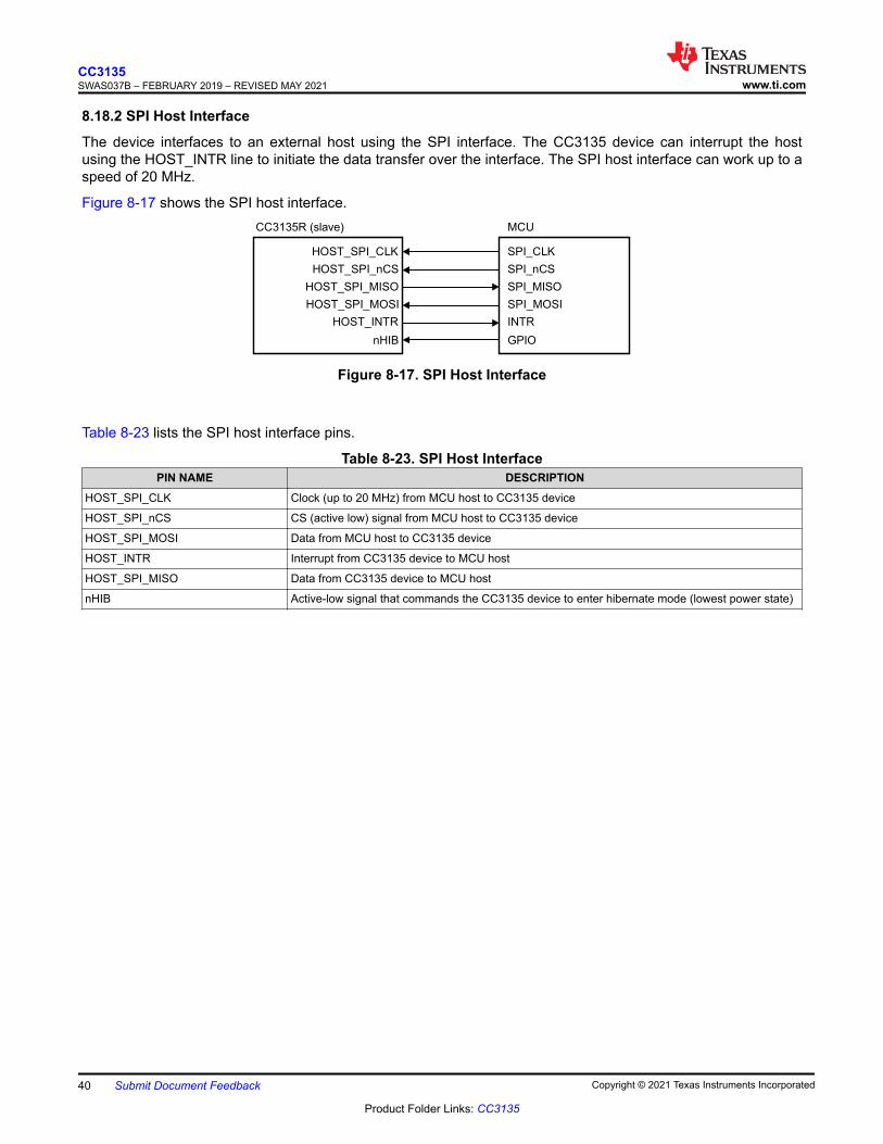
8.18.2 SPI Host Interface
The device interfaces to an external host using the SPI interface. The CC3135 device can interrupt the host using the HOST_INTR line to initiate the data transfer over the interface. The SPI host interface can work up to a speed of 20 MHz.
Figure 8-17 shows the SPI host interface.MCU
HOST_SPI_CLK
HOST_SPI_nCS
HOST_SPI_MISO
HOST_SPI_MOSI
HOST_INTR
SPI_CLK
SPI_nCS
SPI_MISO
SPI_MOSI
INTR
GPIOnHIB
CC3135R (slave)
Figure 8-17. SPI Host Interface
Table 8-23 lists the SPI host interface pins.
Table 8-23. SPI Host InterfacePIN NAME DESCRIPTION
HOST_SPI_CLK Clock (up to 20 MHz) from MCU host to CC3135 device
HOST_SPI_nCS CS (active low) signal from MCU host to CC3135 device
HOST_SPI_MOSI Data from MCU host to CC3135 device
HOST_INTR Interrupt from CC3135 device to MCU host
HOST_SPI_MISO Data from CC3135 device to MCU host
nHIB Active-low signal that commands the CC3135 device to enter hibernate mode (lowest power state)
CC3135SWAS037B – FEBRUARY 2019 – REVISED MAY 2021 www.ti.com
40 Submit Document Feedback Copyright © 2021 Texas Instruments Incorporated
Product Folder Links: CC3135

8.18.3 Host UART Interface
The SimpleLink device requires the UART configuration described in Table 8-24.
Table 8-24. SimpleLink™ UART ConfigurationPROPERTY SUPPORTED CC3135 CONFIGURATION
Baud rate 115200 bps, no auto-baud rate detection, can be changed by the host up to 3 Mbps using a special command
Data bits 8 bits
Flow control CTS/RTS
Parity None
Stop bits 1
Bit order LSBit first
Host interrupt polarity Active high
Host interrupt mode Rising edge or level 1
Endianness Little-endian only(1)
(1) The SimpleLink device does not support automatic detection of the host length while using the UART interface.
8.18.3.1 5-Wire UART Topology
Figure 8-18 shows the typical 5-wire UART topology comprised of four standard UART lines plus one IRQ line from the device to the host controller to allow efficient low-power mode.
This topology is recommended because the configuration offers the maximum communication reliability and flexibility between the host and the SimpleLink device.
HOST MCUUART
nRTS
nCTS
TX
RX
HOST_INTR(IRQ)
nRTS
nCTS
TX
RX
HOST_INTR(IRQ)
CC3135R SLUART
Figure 8-18. 5-Wire UART Topology
8.18.3.2 4-Wire UART Topology
The 4-wire UART topology eliminates the host IRQ line (see Figure 8-19). Using this topology requires meeting one of the following conditions:
• The host is always awake or active.• The host goes to sleep, but the UART module has receiver start-edge detection for auto wakeup and does
not lose data.
HOST MCUUART
nRTS
nCTS
TX
RX
H_IRQ
CC3135R SLUART
nRTS
nCTS
TX
RX
H_IRQX
Figure 8-19. 4-Wire UART Configuration
www.ti.comCC3135
SWAS037B – FEBRUARY 2019 – REVISED MAY 2021
Copyright © 2021 Texas Instruments Incorporated Submit Document Feedback 41
Product Folder Links: CC3135
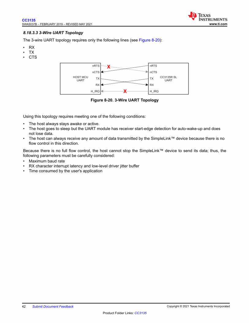
8.18.3.3 3-Wire UART Topology
The 3-wire UART topology requires only the following lines (see Figure 8-20):
• RX• TX• CTS
HOST MCUUART
nRTS
nCTS
TX
RX
H_IRQ
CC3135R SLUART
nRTS
nCTS
TX
RX
H_IRQX
X
Figure 8-20. 3-Wire UART Topology
Using this topology requires meeting one of the following conditions:
• The host always stays awake or active.• The host goes to sleep but the UART module has receiver start-edge detection for auto-wake-up and does
not lose data.• The host can always receive any amount of data transmitted by the SimpleLink™ device because there is no
flow control in this direction.
Because there is no full flow control, the host cannot stop the SimpleLink™ device to send its data; thus, the following parameters must be carefully considered:• Maximum baud rate• RX character interrupt latency and low-level driver jitter buffer• Time consumed by the user's application
CC3135SWAS037B – FEBRUARY 2019 – REVISED MAY 2021 www.ti.com
42 Submit Document Feedback Copyright © 2021 Texas Instruments Incorporated
Product Folder Links: CC3135

9 Detailed Description9.1 OverviewConnect any microcontroller (MCU) to the Internet of Things (IoT) with the CC3135 device, a dual-band wireless network processor from Texas Instruments™. The CC3135 Wi-Fi® Internet-on-a chip™ device contains an Arm®
Cortex®-M3 MCU dedicated to wi-fi and internet protocols, in order to offload networking activities from the host MCU. The subsystem includes a dual band 802.11a/b/g/n radio, baseband, and MAC with a powerful crypto engine for fast, secure Internet connections with 256-bit encryption and built in power management for best in class low power performance. The CC3135 device supports station, AP, and Wi-Fi Direct® modes. The device also supports WPA2™ personal and enterprise security, WPS 2.0, and WPA3™ personal and enterprise security 10. The Wi-Fi network processor includes an embedded IPv6 and IPv4 TCP/IP stack.
9.2 Device Features9.2.1 WLAN
The WLAN features are as follows:
• 802.11a/b/g/n integrated radio, modem, and MAC supporting WLAN communication as a BSS station, AP, Wi-Fi Direct® client, and group owner with CCK and OFDM rates in the 2.4 GHz ISM band (channels 1 through 13), and the 5 GHz 20-MHz BW U-NII bands (U-NII-1, U-NII-2A, U-NII-2C, and U-NII-3).
Note
802.11n is supported only in Wi-Fi® station and Wi-Fi Direct®.• The automatically calibrated radio with a single-ended 50-Ω interface enables easy connection to the antenna
without requiring expertise in radio circuit design.• Advanced connection manager with multiple user-configurable profiles stored in serial flash allows automatic
fast connection to an access point without user or host intervention.• Supports all common Wi-Fi security modes for personal and enterprise networks with on-chip security
accelerators, including: WEP, WPA/WPA2 PSK, WPA2 Enterprise (802.1x), and WPA3 Personal and WPA3 Enterprise.
• Smart provisioning options deeply integrated within the device providing a comprehensive end-to-end solution. With elaborate events notification to the host, enabling the application to control the provisioning decision flow. The wide variety of Wi-Fi provisioning methods include:– Access Point with HTTP server– WPS - Wi-Fi Protected Setup, supporting both push button and pin code options.– SmartConfig™ Technology: TI proprietary, easy to use, one-step, one-time process used to connect a
CC3135-enabled device to the home wireless network.• 802.11 transceiver mode allows transmitting and receiving of proprietary data through a socket The 802.11
transceiver mode provides the option to select the working channel, rate, and transmitted power. The receiver mode works with the filtering options.
• Antenna selection for best connection• BLE/2.4 GHz radio coexistence mechanism to avoid interference
10 Supported from Service Pack v4.5.0.11-3.1.0.5-3.1.0.25. Limited to STA mode only.
www.ti.comCC3135
SWAS037B – FEBRUARY 2019 – REVISED MAY 2021
Copyright © 2021 Texas Instruments Incorporated Submit Document Feedback 43
Product Folder Links: CC3135

9.2.2 Network Stack
The Network Stack features are as follows:
• Integrated IPv4, IPv6 TCP/IP stack with BSD socket APIs for simple Internet connectivity with any MCU, microprocessor, or ASIC
Note
Not all APIs are 100% BSD compliant. Not all BSD APIs are supported.• Support of 16 simultaneous TCP, UDP, RAW, SSL\TLS sockets• Built-in network protocols:
– Static IP, LLA, DHCPv4, DHCPv6 with DAD and stateless autoconfiguration– ARP, ICMPv4, IGMP, ICMPv6, MLD, ND– DNS client for easy connection to the local network and the Internet
• Built-in network applications and utilities:– HTTP/HTTPS
• Web page content stored on serial flash• RESTful APIs for setting and configuring application content• Dynamic user callbacks
– Service discovery: Multicast DNS service discovery lets a client advertise its service without a centralized server. After connecting to the access point, the CC3135 device provides critical information, such as device name, IP, vendor, and port number.
– DHCP server– Ping
Table 9-1 describes the NWP features.
CC3135SWAS037B – FEBRUARY 2019 – REVISED MAY 2021 www.ti.com
44 Submit Document Feedback Copyright © 2021 Texas Instruments Incorporated
Product Folder Links: CC3135
Table 9-1. NWP FeaturesFeature Description
Wi-Fi standards802.11a/b/g/n station802.11a/b/g AP supporting up to four stationsWi-Fi Direct client and group owner
Wi-Fi channels 2.4 GHz ISM and 5 GHz U-NII Channels
Channel Bandwidth 20 MHz
Wi-Fi security WEP, WPA/WPA2 PSK, WPA2 enterprise (802.1x), WPA3 personal and enterprise (1)
Wi-Fi provisioning SmartConfig technology, Wi-Fi protected setup (WPS2), AP mode with internal HTTP web server
IP protocols IPv4/IPv6
IP addressing Static IP, LLA, DHCPv4, DHCPv6 with DAD
Cross layer ARP, ICMPv4, IGMP, ICMPv6, MLD, NDP
TransportUDP, TCPSSLv3.0/TLSv1.0/TLSv1.1/TLSv1.2RAW
Network applications and utilities
PingHTTP/HTTPS web servermDNSDNS-SDDHCP server
Host interface UART/SPI
SecurityDevice identityTrusted root-certificate catalogTI root-of-trust public key
Power management Enhanced power policy management uses 802.11 power save and deep-sleep power modes
OtherTransceiverProgrammable RX filters with event-trigger mechanismRx Metrics for tracking the surrounding RF environment
(1) Supported from Service Pack v4.5.0.11-3.1.0.5-3.1.0.25. Limited to STA mode only.
www.ti.comCC3135
SWAS037B – FEBRUARY 2019 – REVISED MAY 2021
Copyright © 2021 Texas Instruments Incorporated Submit Document Feedback 45
Product Folder Links: CC3135

9.2.3 Security
The SimpleLink Wi-Fi CC3135 Internet-on-a chip device enhances the security capabilities available for development of IoT devices, while completely offloading these activities from the MCU to the networking subsystem. The security capabilities include the following key features:
Code and Data Security:
• Secured network information: Network passwords and certificates are encrypted• Secured and authenticated service pack: SP is signed based on TI certificate
Wi-Fi and Internet Security:
• Personal and enterprise Wi-Fi security– Personal standards
• AES (WPA2-PSK)• TKIP (WPA-PSK)• WEP
– Enterprise standards• EAP Fast• EAP PEAPv0 MSCHAPv2• EAP PEAPv0 TLS• EAP PEAPv1 TLS EAP LS• EAP TTLS TLS• EAP TTLS MSCHAPv2
• Secure HTTP server (HTTPS)• The Trusted root-certificate catalog verifies that the CA used by the application is trusted and known secure
content delivery• The TI root-of-trust public key is a hardware-based mechanism that allows authenticating TI as the genuine
origin of a given content using asymmetric keys• Secure content delivery allows file transfer to the system in a secure way on any unsecured tunnel
CC3135SWAS037B – FEBRUARY 2019 – REVISED MAY 2021 www.ti.com
46 Submit Document Feedback Copyright © 2021 Texas Instruments Incorporated
Product Folder Links: CC3135

• Secure sockets– Protocol versions: SSL v3/TLS 1.0/TLS 1.1/TLS 1.2– On-chip powerful crypto engine for fast, secure Wi-Fi and internet connections with 256-bit AES
encryption for TLS and SSL connections– Ciphers suites
• SL_SEC_MASK_SSL_RSA_WITH_RC4_128_SHA• SL_SEC_MASK_SSL_RSA_WITH_RC4_128_MD5• SL_SEC_MASK_TLS_RSA_WITH_AES_256_CBC_SHA• SL_SEC_MASK_TLS_DHE_RSA_WITH_AES_256_CBC_SHA• SL_SEC_MASK_TLS_ECDHE_RSA_WITH_AES_256_CBC_SHA• SL_SEC_MASK_TLS_ECDHE_RSA_WITH_RC4_128_SHA• SL_SEC_MASK_TLS_RSA_WITH_AES_128_CBC_SHA256• SL_SEC_MASK_TLS_RSA_WITH_AES_256_CBC_SHA256• SL_SEC_MASK_TLS_ECDHE_RSA_WITH_AES_128_CBC_SHA256• SL_SEC_MASK_TLS_ECDHE_ECDSA_WITH_AES_128_CBC_SHA256• SL_SEC_MASK_TLS_ECDHE_ECDSA_WITH_AES_128_CBC_SHA• SL_SEC_MASK_TLS_ECDHE_ECDSA_WITH_AES_256_CBC_SHA• SL_SEC_MASK_TLS_RSA_WITH_AES_128_GCM_SHA256• SL_SEC_MASK_TLS_RSA_WITH_AES_256_GCM_SHA384• SL_SEC_MASK_TLS_DHE_RSA_WITH_AES_128_GCM_SHA256• SL_SEC_MASK_TLS_DHE_RSA_WITH_AES_256_GCM_SHA384• SL_SEC_MASK_TLS_ECDHE_RSA_WITH_AES_128_GCM_SHA256• SL_SEC_MASK_TLS_ECDHE_RSA_WITH_AES_256_GCM_SHA384• SL_SEC_MASK_TLS_ECDHE_ECDSA_WITH_AES_128_GCM_SHA256• SL_SEC_MASK_TLS_ECDHE_ECDSA_WITH_AES_256_GCM_SHA384• SL_SEC_MASK_TLS_ECDHE_ECDSA_WITH_CHACHA20_POLY1305_SHA256• SL_SEC_MASK_TLS_ECDHE_RSA_WITH_CHACHA20_POLY1305_SHA256• SL_SEC_MASK_TLS_DHE_RSA_WITH_CHACHA20_POLY1305_SHA256
– Server authentication– Client authentication– Domain name verification– Socket upgrade to secure socket – STARTTLS
9.2.4 Host Interface and Driver
• Interfaces over a 4-wire serial peripheral interface (SPI) with any MCU or a processor at a clock speed of 20 MHz.
• Interfaces over UART with any MCU with a baud rate up to 3 Mbps. A low footprint driver is provided for TI MCUs and is easily ported to any processor or ASIC.
• Simple APIs enable easy integration with any single-threaded or multithreaded application.
9.2.5 System
• Works from a single preregulated power supply or connects directly to a battery• Ultra-low leakage when disabled (hibernate mode) with a current of less than 4 µA with the RTC running• Integrated clock sources
www.ti.comCC3135
SWAS037B – FEBRUARY 2019 – REVISED MAY 2021
Copyright © 2021 Texas Instruments Incorporated Submit Document Feedback 47
Product Folder Links: CC3135

9.3 FIPS 140-2 Level 1 CertificationThe Federal Information Processing Standard (FIPS) Publication 140-2 is a U.S. government computer security standard. It is commonly referred to as FIPS 140-2 and is used to accredit the design and implementation of cryptographic modules. A cryptographic module within a security system is necessary to maintain the confidentiality and integrity of the information protected by the device.
The security engines of the CC3135 device is FIPS validated for FIPS 140-2 level 1 certification 11. This certification involves testing the device for all areas related to the secure design and implementation of the cryptographic modules and covers topics such as: cryptographic specifications, ports and interfaces, a finite state model for the cryptographic module, the operational environment of the module, and how cryptographic keys are managed.
9.4 Power-Management SubsystemThe CC3135 power-management subsystem contains DC/DC converters to accommodate the different voltage or current requirements of the system.
• Digital DC/DC (Pin 44): Input: VBAT wide voltage (2.1 to 3.6 V)• ANA1 DC/DC (Pin 38): Input: VBAT wide voltage (2.1 to 3.6 V)• PA DC/DC (Pin 39): Input: VBAT wide voltage (2.1 to 3.6 V)
The CC3135 device is a single-chip WLAN radio solution used on an embedded system with a wide-voltage supply range. The internal power management, including DC/DC converters and LDOs, generates all of the voltages required for the device to operate from a wide variety of input sources. For maximum flexibility, the device can operate in the modes described in Section 9.4.1.
9.4.1 VBAT Wide-Voltage Connection
In the wide-voltage battery connection, the device is powered directly by the battery or preregulated 3.3-V supply. All other voltages required to operate the device are generated internally by the DC/DC converters. This scheme supports wide-voltage operation from 2.1 to 3.6 V and is thus the most common mode for the device.
11 For exact status of FIPS certification for a specific part number, please refer to https://csrc.nist.gov/publications/fips.
CC3135SWAS037B – FEBRUARY 2019 – REVISED MAY 2021 www.ti.com
48 Submit Document Feedback Copyright © 2021 Texas Instruments Incorporated
Product Folder Links: CC3135
9.5 Low-Power Operating ModesThis section describes the low-power modes supported by the device to optimize battery life.
9.5.1 Low-Power Deep Sleep
The low-power deep-sleep (LPDS) mode is an energy-efficient and transparent sleep mode that is entered automatically during periods of inactivity based on internal power optimization algorithms. The device can wake up in less than 3 ms from the internal timer or from any incoming host command. Typical battery drain in this mode is 115 µA. During LPDS mode, the device retains the software state and certain configuration information. The operation is transparent to the external host; thus, no additional handshake is required to enter or exit LPDS mode. Advanced features of long sleep interval and IoT low power for extending LPDS time for up to 22 seconds while maintaining Wi-Fi connection is also supported
9.5.2 Hibernate
The hibernate mode is the lowest power mode in which all of the digital logic is power-gated. Only a small section of the logic powered directly by the main input supply is retained. The RTC is kept running and the device wakes up once the nHIB line is asserted by the host driver. The wake-up time is longer than LPDS mode at approximately 50 ms. The typical battery drain in this mode is 4.5 µA.
Note
Wake-up time can be extended depending on the service-pack size.
9.5.3 Shutdown
The shutdown mode is the lowest power-mode system-wise. All device logics are off, including the real-time clock (RTC). The wake-up time in this mode is longer than hibernate at approximately 1.1 s. The typical battery drain in this mode is 1 µA.
www.ti.comCC3135
SWAS037B – FEBRUARY 2019 – REVISED MAY 2021
Copyright © 2021 Texas Instruments Incorporated Submit Document Feedback 49
Product Folder Links: CC3135

9.6 Memory9.6.1 External Memory Requirements
The CC3135 device maintains a proprietary file system on the sFLASH. The CC3135 file system stores the service pack file, system files, configuration files, certificate files, web page files, and user files. By using a format command through the API, users can provide the total size allocated for the file system. The starting address of the file system cannot be set and is always at the beginning of the sFLASH. The applications microcontroller must access the sFLASH memory area allocated to the file system directly through the CC3135 file system. The applications microcontroller must not access the sFLASH memory area directly.
The file system manages the allocation of sFLASH blocks for stored files according to download order, which means that the location of a specific file is not fixed in all systems. Files are stored on sFLASH using human-readable filenames rather than file IDs. The file system API works using plain text, and file encryption and decryption is invisible to the user. Encrypted files can be accessed only through the file system.
All file types can have a maximum of 100 supported files in the file system. All files are stored in 4-KB blocks and thus use a minimum of 4KB of Flash space. Fail-safe files require twice the original size and use a minimum of 8KB. Encrypted files are counted as fail-safe in terms of space. The maximum file size is 1MB.
Table 9-2 lists the minimum required memory consumption under the following assumptions:• System files in use consume 64 blocks (256KB).• Vendor files are not taken into account.• Gang image:
– Storage for the gang image is rounded up to 32 blocks (meaning 128-KB resolution).– Gang image size depends on the actual content size of all components. Additionally, the image should
be 128-KB aligned so unaligned memory is considered lost. Service pack, system files, and the 128-KB aligned memory are assumed to occupy 256KB.
• All calculations consider that the restore-to-default is enabled.
Table 9-2. Recommended Flash SizeITEM CC3135 [KB]
File system allocation table 20
System and configuration files 256
Service Pack 264
Gang image size 256
Total 796
Minimal Flash size 8MBit
Recommended Flash size 16MBit
Note
The maximum supported serial flash size is 32MB (256Mb) (see Using Serial Flash on CC3135/CC3235 SimpleLink™ Wi-Fi® and Internet-of-Things Devices).
CC3135SWAS037B – FEBRUARY 2019 – REVISED MAY 2021 www.ti.com
50 Submit Document Feedback Copyright © 2021 Texas Instruments Incorporated
Product Folder Links: CC3135

9.7 Restoring Factory Default ConfigurationThe device has an internal recovery mechanism that allows rolling back the file system to its predefined factory image or restoring the factory default parameters of the device. The factory image is kept in a separate sector on the sFLASH in a secure manner and cannot be accessed from the host processor. The following restore modes are supported:
• None – no factory restore settings• Enable restore of factory default parameters• Enable restore of factory image and factory default parameters
The restore process is performed by pulling or forcing SOP[2:0] = 110 pins and toggling the nRESET pin from low to high.
The process is fail-safe and resumes operation if a power failure occurs before the restore is finished. The restore process typically takes about 8 seconds, depending on the attributes of the serial Flash vendor.
www.ti.comCC3135
SWAS037B – FEBRUARY 2019 – REVISED MAY 2021
Copyright © 2021 Texas Instruments Incorporated Submit Document Feedback 51
Product Folder Links: CC3135

9.8 Hostless ModeThe SimpleLink™ Wi-Fi® CC3135 device incorporates a scripting ability that enables offloading of simple tasks from the host processor. Using simple and conditional scripts, repetitive tasks can be handled internally, which allows the host processor to remain in a low-power state. In some cases where the scripter is being used to send packets, it reduces code footprint and memory consumption. The if-this-then-that style conditioning can include anything from GPIO toggling to transmitting packets.
The conditional scripting abilities can be divided into conditions and actions. The conditions define when to trigger actions. Only one action can be defined per condition, but multiple instances of the same condition may be used, so in effect multiple actions can be defined for a single condition. In total, 16 condition and action pairs can be defined. The conditions can be simple, or complex using sub-conditions (using a combinatorial AND condition between them). The actions are divided into two types, those that can occur during runtime and those that can occur only during the initialization phase.
The following actions can only be performed when triggered by the pre-initialization condition:• Set roles AP, station, P2P, and Tag modes• Delete all stored profiles• Set connection policy• Hardware GPIO indication allows an I/O to be driven directly from the WLAN core hardware to indicate
internal signaling
The following actions may be activated during runtime:• Send transceiver packet• Send UDP packet• Send TCP packet• Increment counter increments one of the user counters by 1• Set counter allows setting a specific value to a counter• Timer control• Set GPIO allows GPIO output from the device using the internal networking core• Enter Hibernate state
Note
Consider the following limitations:• Timing cannot be ensured when using the network scripter because some variable latency will
apply depending on the utilization of the networking core.• The scripter is limited to 16 pairs of conditions and reactions.• Both timers and counters are limited to 8 instances each. Timers are limited to a resolution of 1
second. Counters are 32 bits wide.• Packet length is limited to the size of one packet and the number of possible packet tokens is
limited to 8.
CC3135SWAS037B – FEBRUARY 2019 – REVISED MAY 2021 www.ti.com
52 Submit Document Feedback Copyright © 2021 Texas Instruments Incorporated
Product Folder Links: CC3135

10 Applications, Implementation, and LayoutNote
Information in the following applications sections is not part of the TI component specification, and TI does not warrant its accuracy or completeness. TI’s customers are responsible for determining suitability of components for their purposes, as well as validating and testing their design implementation to confirm system functionality.
10.1 Application Information10.1.1 BLE/2.4 GHz Radio Coexistence
The CC3135 device is designed to support BLE/2.4 GHz radio coexistence. Because WLAN is inherently more tolerant to time-domain disturbances, the coexistence mechanism gives priority to the Bluetooth® low energy entity over the WLAN. Bluetooth® low energy operates in the 2.4 GHz band, therefore the coexistence mechanism does not affect the 5 GHz band. The CC3135 device can operate normally on the 5 GHz band, while the Bluetooth® low energy works on the 2.4 GHz band without mutual interference.
The following coexistence modes can be configured by the user:
• Off mode or intrinsic mode
– No BLE/2.4 GHz radio coexistence, or no synchronization between WLAN and Bluetooth® low energy—in case Bluetooth® low energy exists in this mode, collisions can randomly occur.
• Time Division Multiplexing (TDM, Single Antenna)– 2.4 GHz Wi-Fi band (see Figure 10-1)
In this mode, the two entities share the antenna through an RF switch using two GPIOs (one input and one output from the WLAN perspective).
– 5 GHz Wi-Fi band (see Figure 10-2)
In this mode, the WLAN operates on the 5 GHz band and Bluetooth® low energy operates on the 2.4 GHz band. A 2.4- or 5 GHz diplexer is required for sharing the single antenna.
• Time Division Multiplexing (TDM, Dual Antenna)– 2.4 GHz Wi-Fi Band (see Figure 10-3)
In this mode, the two entities have separate antennas. No RF switch is required and only a single GPIO (one input from the WLAN perspective).
– 5 GHz Wi-Fi band (see Figure 10-4)
In this mode, the WLAN operates on the 5 GHz band and Bluetooth® low energy operates on the 2.4 GHz band. No diplexer is required for the dual-antenna solution.
www.ti.comCC3135
SWAS037B – FEBRUARY 2019 – REVISED MAY 2021
Copyright © 2021 Texas Instruments Incorporated Submit Document Feedback 53
Product Folder Links: CC3135
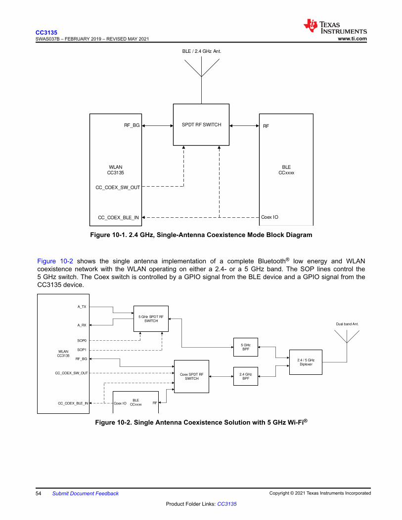
WLAN
CC3135
BLE
CCxxxx
SPDT RF SWITCH
CC_COEX_SW_OUT
CC_COEX_BLE_IN Coex IO
RF_BG RF
BLE / 2.4 GHz Ant.
Figure 10-1. 2.4 GHz, Single-Antenna Coexistence Mode Block Diagram
Figure 10-2 shows the single antenna implementation of a complete Bluetooth® low energy and WLAN coexistence network with the WLAN operating on either a 2.4- or a 5 GHz band. The SOP lines control the 5 GHz switch. The Coex switch is controlled by a GPIO signal from the BLE device and a GPIO signal from the CC3135 device.
BLECCxxxx
WLANCC3135
Coex SPDT RF SWITCH
5 GHz SPDT RF SWITCH
5 GHzBPF
2.4 / 5 GHz Diplexer
2.4 GHzBPF
Dual band Ant.
A_TX
A_RX
SOP0
SOP1
RF_BG
CC_COEX_SW_OUT
CC_COEX_BLE_IN Coex IO RF
Figure 10-2. Single Antenna Coexistence Solution with 5 GHz Wi-Fi®
CC3135SWAS037B – FEBRUARY 2019 – REVISED MAY 2021 www.ti.com
54 Submit Document Feedback Copyright © 2021 Texas Instruments Incorporated
Product Folder Links: CC3135

Figure 10-3 shows the dual antenna implementation of a complete Bluetooth® low energy and WLAN coexistence network with the WLAN operating on either a 2.4- or a 5 GHz band. Note in this implementation no Coex switch is required and only a single GPIO from the BLE device to the CC3135 device is required.
WLAN
CC3135BLE
CCxxxx
RF_BG
CC_COEX_BLE_IN Coex IO
RF
2.4 GHz Ant. BLE Ant.
Figure 10-3. Dual-Antenna Coexistence Mode Block Diagram
www.ti.comCC3135
SWAS037B – FEBRUARY 2019 – REVISED MAY 2021
Copyright © 2021 Texas Instruments Incorporated Submit Document Feedback 55
Product Folder Links: CC3135

Figure 10-4 shows the dual antenna implementation of a complete Bluetooth® low energy and WLAN coexistence network with the WLAN operating on either a 2.4- or a 5 GHz band. In this case, the 2.4 GHz and 5 GHz Wi-Fi share an antenna and the BLE has it's own dedicated antenna. The SOP lines control the 5 GHz switch. Note in this implementation no Coex switch is required and only a single GPIO from the BLE device to the CC3135 device is required.
BLECCxxxx
WLANCC3135
5 GHz SPDT RF SWITCH
5 GHzBPF
2.4 / 5 GHz Diplexer
2.4 GHzBPF
A_TX
A_RX
SOP0
SOP1
RF_BG
CC_COEX_SW_OUT
CC_COEX_BLE_IN Coex IO RF
BLE Ant.
Dual Band Ant.
Figure 10-4. Dual Antenna Coexistence Solution with 5 GHz Wi-Fi®
CC3135SWAS037B – FEBRUARY 2019 – REVISED MAY 2021 www.ti.com
56 Submit Document Feedback Copyright © 2021 Texas Instruments Incorporated
Product Folder Links: CC3135

10.1.2 Antenna Selection
The CC3135 device is designed to also support antenna selection and is controlled from Image Creator. When enabled, there are 3 options possible options:
• ANT 1: When selected, the GPIOs that are defined for antenna selection with set the RF path for antenna 1.• ANT 2: When selected, the GPIOs that are defined for antenna selection will set the RF path for antenna 2.• Autoselect: When selected, during a scan and prior to connecting to an AP, CC3135 device will determine the
best RF path and select the appropriate antenna 12 13. The result is the saved as port of the profile.
Figure 10-5 shows the implementation of a complete Bluetooth® low energy and WLAN coexistence network with the WLAN operating on either a 2.4- or a 5 GHz band with antenna selection. The SOP lines control the 5 GHz switch. The Coex switch is controlled by a GPIO signal from the BLE device and a GPIO signal from the CC3135 device. The Antenna switch is controlled by 2 GPIO lines from the CC3135 device.
BLECCxxxx
WLANCC3135
5 GHz SPDT RF SWITCH
5 GHzBPF
2.4 / 5 GHz Diplexer
2.4 GHzBPF
A_TX
A_RX
SOP0
SOP1
RF_BG
CC_COEX_SW_OUT
CC_COEX_BLE_IN Coex IO RF
Dual Band Ant. 1
Coex SPDT RF SWITCH
Antenna Selection SPDT RF Switch
Dual Band Ant. 2
ANT_SEL_1 ANT_SEL_2
Figure 10-5. Antenna Selection Solution with Coexistence Solution and 5 GHz Wi-Fi®
12 When selecting Autoselect via the API, a reset is required in order for the CC3135 device to determine the best antenna for use.13 Refer to the UniFlash CC31xx, CC32xx SimpleLink™ Wi-Fi® and Internet-on-a chip™ Solution ImageCreator and Programming Tool
User's Guide for more information.
www.ti.comCC3135
SWAS037B – FEBRUARY 2019 – REVISED MAY 2021
Copyright © 2021 Texas Instruments Incorporated Submit Document Feedback 57
Product Folder Links: CC3135

Figure 10-6 shows the antenna selection implementation for Wi-Fi®, with BLE operating on it's own antenna. The SOP lines control the 5 GHz switch. Note in this implementation no Coex switch is required and only a single GPIO from the BLE device to the CC3135 device is required. The Antenna switch is controlled by 2 GPIO lines from the CC3135 device.
BLECCxxxx
WLANCC3135
5 GHz SPDT RF SWITCH
5 GHzBPF
2.4 / 5 GHz Diplexer
2.4 GHzBPF
A_TX
A_RX
SOP0
SOP1
RF_BG
CC_COEX_SW_OUT
CC_COEX_BLE_IN Coex IO RF
Dual Band Ant. 1
Antenna Selection SPDT RF Switch
Dual Band Ant. 2
ANT_SEL_1 ANT_SEL_2
BLE Ant.
Figure 10-6. Coexistence Solution with Wi-Fi Antenna Selection and Dedicated BLE Antenna
CC3135SWAS037B – FEBRUARY 2019 – REVISED MAY 2021 www.ti.com
58 Submit Document Feedback Copyright © 2021 Texas Instruments Incorporated
Product Folder Links: CC3135

10.1.3 Typical Application
Figure 10-7 shows the schematic of the engine area for the CC3135 device in the wide-voltage mode of operation, with the corresponding bill of materials show in Table 10-1. Figure 10-8 provides the schematic for the RF implementation with and without BLE/2.4 GHz coexistence, with the corresponding bill of materials shown in Table 10-2. For a full operation reference design, see the CC3135 SimpleLink™ WI-Fi® BoosterPack™ Design Files.
GND
0.1µFC12
GND GND
2.2uHL1
10uFC11
VDD_ANA
GND
1uHL2
22uFC16
22uFC17
1µFC18
GND
0.1µFC20
0.1µFC21
10uFC19
GND GND
GND
GND
10uFC24
0.1µF
C22GND GND
GND
0.1µFC9
0.1µFC84.7uF
C34.7uFC5
4.7uFC6
VBAT_CC
GND GND GND
GND GND
12Y1
32.768kHz
10pFC28
10pFC27
GND
100kR11
0.01µFC26
GND
VBAT_CC
GND
GND GND
6.2pFC30
6.2pFC29
CC_nHIB
CC_IRQ
CC_SPI_DOUT
CC_SPI_DIN
CC_SPI_CLK
CC_SPI_CS
CC_WLRS232_TX
CC_WLRS232_RX
CC_WL_UART_TX
CC_NWP_UART_TX
CC_UART1_CTS
CC_UART1_RTS
CC_UART1_TX
CC_UART1_RX
0.1µFC10
GND
100kR2
VBAT_CC
10k
R1
SFL_CS
SFL_CLK
SFL_MISO
SFL_MOSI
GND
100kR7
100kR5
100kR6
VBAT_CC
GND
2.2uHL3
GND
CC_nRESET
CC_nHIB
CC_IRQ
CC_SPI_DIN
CC_SPI_DOUT
CC_SPI_CLK
CC_SPI_CS
CC_UART1_RTS
CC_UART1_TX
CC_UART1_CTS
CC_UART1_RX
RF_BG
A_TX
A_RX
GND
270R8
SOP0
SOP1
100kR15
3 2 1
J3
SOP2
GND
69.8kR10
69.8kR9
69.8kR16
69.8kR17
3 2 1
J2
3 2 1
J1
VBAT_CC
GND
1 3
2 4G G
Y2
40MHz
P4_DIO_13
100kR4
100kR3
GND GND
0.6pFC25
GND
0.5pFC7
0.6pFC4
GND
0.6pFC15
GND
0.1uFC14
0.1uF
C23
0.2pFC13
CC3135RNM2RGKR
3DIO12
4DIO13
2nHIB
8HOST_SPI_nCS
5HOST_SPI_CLK
6
9
HOST_SPI_MOSI
VDD_DIG1
10VIN_IO1
11FLASH_SPI_CLK
12FLASH_SPI_MOSI
13FLASH _SPI_MISO
14FLASH _SPI_CS
7HOST_SPI_MISO
16DIO23
17DIO24
15HOST_INTR
19Reserved
20DIO29
21SOP2/TCXO_EN
22WLAN_XTAL_N
23WLAN_XTAL_P
24VDD_PLL
25LDO_IN2
NC26
27A_RX
A_TX28
53DIO30
GND30
31RF_BG
32nRESET
33VDD_PA_IN
SOP134
SOP035
36LDO_IN1
37VIN_DCDC_ANA
38DCDC_ANA_SW
39VIN_DCDC_PA
40DCDC_PA_SW_P
41DCDC_PA_SW_N
42DCDC_PA_OUT
43DCDC_DIG_SW
44VIN_DCDC_DIG
45DIO31
NC46
47VDD_ANA2
48VDD_ANA1
49VDD_RAM
61UART1_nCTS
51RTC_XTAL_P
52RTC_XTAL_N
18DIO28
54VIN_IO2
50UART1_nRTS
56VDD_DIG2
55UART1_TX
57UART1_RX
58TEST_58
59TEST_59
60TEST_60
62TEST_62
DIO863
DIO964
GND65
1DIO10
GND29
U2
VBAT_CC
P3_DIO_12
P1_DIO_10
GND
See Figure 7.8 ForRF Configuration Options
CS1
MX25R1635FM1IL0
2SO/SIO1
3WP/SIO2
4GND
5SI/SIO0
6SCLK
7
8VCC
RESET/SIO3
U1
Flash Programming /
TP1
Host Control
TP2TP3TP4
R7 is needed only ifUART is used as thehost interface
HOST INTERFACE
(Ensure that nHIBline does
Optional:
not float at any time.)
Consider adding extra decoupling
100kR12
the peakcurrents.capacitors if the battery cannot source
GND
VBAT_CC
C1100µF
C2100µF
GND GND
100kR13
GND
100kR14
GND
VDD_PA
VDD_DIG
VBAT_CC
P16_DIO_23
P17_DIO_24
P20_DIO_29
P45_DIO_31
P18_DIO_28
P53_DIO_30
P63_DIO_8
P64_DIO_9
GND
Figure 10-7. CC3135 Engine Area
www.ti.comCC3135
SWAS037B – FEBRUARY 2019 – REVISED MAY 2021
Copyright © 2021 Texas Instruments Incorporated Submit Document Feedback 59
Product Folder Links: CC3135

Table 10-1. Bill of Materials for CC3135 Engine AreaQuantity Designator Value Manufacturer Part Number Description
2 C1, C2 100 µF Taiyo Yuden LMK325ABJ107MMHT CAP, CERM, 100 µF, 10 V,+/- 20%, X5R, AEC-Q200 Grade 3, 1210
3 C3, C5, C6 4.7 µF Taiyo Yuden JMK105BC6475MV-F CAP, CERM, 4.7 uF, 6.3 V,+/- 20%, X6S, 0402
3 C4, C15, C25 0.6 pF MuRata GJM0335C1ER60BB01D CAP, CERM, 0.6pF, 25 V,+/- 16%, C0G/NP0, 0201
1 C7 0.5 pF Murata GJM0335C1ER50BB01D CAP, CERM, 0.5 pF, 25 V,+/- 20%, C0G/NP0, 0201
6 C8, C9, C10, C12, C21, C22 0.1 µF Walsin CL05B104KO5NNNC CAP, CERM, 0.1 µF, 16 V,
+/- 10%, X7R, 0402
1 C26 0.01 µF Walsin 0402B103K500CT CAP, CERM, 0.01 µF, 50 V,+/- 10%, X7R, 0402
3 C11, C19, C24 10 µF Taiyo Yuden LMK107BC6106MA-T CAP, CERM, 10 uF, 10 V,+/- 20%, X6S, 0603
1 C13 0.2 pF MuRata GJM0335C1ER20BB01D CAP, CERM, 0.2pF, 25 V,+/- 50%, C0G/NP0, 0201
2 C14, C23 0.1 µF Samsung Electro-Mechanics CL03A104KP3NNNC CAP, CERM, 0.1 uF, 10 V,+/- 10%, X5R, 0201
2 C16, C17 22 µF MuRata GRM188C80G226ME15J CAP, CERM, 22 uF, 4 V,+/- 20%, X6S, 0603
1 C18 1 µF Walsin CL05A105MP5NNNC CAP, CERM, 1 µF, 10 V,+/- 20%, X5R, 0402
2 C27, C28 10 pF Walsin 0402N100J500CT CAP, CERM, 10 pF, 50 V,+/- 5%, C0G/NP0, 0402
2 C29, C30 6.2 pF Walsin 0402N6R2C500CT CAP, CERM, 6.2 pF, 50 V,+/- 4%, C0G/NP0, 0402
3 J1, J2, J3 Wurth Elektronik 61300311121 Header, 2.54 mm, 3x1, Gold, TH
2 L1, L3 2.2 µH MuRata LQM2MPN2R2NG0 Inductor, Multilayer, Ferrite, 2.2 uH, 1.2 A, 0.11 ohm, SMD
1 L2 1 µH MuRata LQM2HPN1R0MG0L Inductor, Multilayer, Ferrite, 1 uH, 1.6 A, 0.055 ohm, SMD
1 R1 Vishay-Dale CRCW040210K0JNED RES, 10 k, 5%, 0.063 W, AEC-Q200 Grade 0, 0402
10 R2, R3, R4, R5, R6, R7, R11, R13, R14, R15 100k Vishay-Dale CRCW0402100KJNED RES, 100 k, 5%, 0.063 W,
AEC-Q200 Grade 0, 0402
1 R8 270 Vishay-Dale CRCW0402270RJNED RES, 270, 5%, 0.063 W,AEC-Q200 Grade 0, 0402
1 R12 100k Yageo America RC0201JR-07100KL RES, 100 k, 5%, 0.05 W, 0201
CC3135SWAS037B – FEBRUARY 2019 – REVISED MAY 2021 www.ti.com
60 Submit Document Feedback Copyright © 2021 Texas Instruments Incorporated
Product Folder Links: CC3135

Table 10-1. Bill of Materials for CC3135 Engine Area (continued)Quantity Designator Value Manufacturer Part Number Description
4 R9, R10, R16, R17 69.8k Vishay-Dale CRCW040269K8FKED RES, 69.8 k, 1%, 0.063 W,AEC-Q200 Grade 0, 0402
1 U1 Macronix International Co., LTD MX25R3235FM1IL0Ultra low power, 32M-bit[x 1/x 2/x 4] CMOS MXSMIO (serial multi I/O) Flash memory, SOP-8
1 U2 Texas Instruments CC3135RNMRGKRSimpleLink Wi-Fi, Dual-Band Network Processor, RGK0064B(VQFN-64)
1 Y1 Abracon Corporation ABS07-32.768KHZ-9-T Crystal, 32.768 kHz, 9PF, SMD
1 Y2 TXC Corporation 8Y40072002 Crystal, 40 MHz, 8 pF, SMD
www.ti.comCC3135
SWAS037B – FEBRUARY 2019 – REVISED MAY 2021
Copyright © 2021 Texas Instruments Incorporated Submit Document Feedback 61
Product Folder Links: CC3135

GND
13 26 5 4
E1
Fe
ed
1RF1
2GND
3RF2
4VC2
RFC5
VC16
U5
RTC6608OSP
RF_BG
A_RX
A_TX
GND
GND
GND
SOP1
SOP0
100pFC42
100pFC43
GND GND
GND GND
GND
2.7nHL5
8.2pF
C36
4.7pF
C40
4.7pF
C41
1.6pF
C38
1.9pF
C39
3.9nHL4
2.2pF
C37
1IN
2GND
OUT3
DEA202450BT-1294C1-H
4GND
FL1
1IN
2GND
3OUT
DEA165538BT-2236B1-H
FL2
1LBP
2GND
DPX165950DT-8148A1
3HBP
4GND
CP5
6GND
U4
Antenna match. Pinetwork might berequired depending on
1RF1
2GND
type of antenna.
RF23
VC24
5RFC
VC16
U3
RTC6608OSP
GND
68pF
C31
68pF
C32
100kR18
GND
100pFC34
GND GND
100kR19
100pFC35
GND
RF_BLE
GND
Circuit configuration for BLE/2.4-GHzCOEX only. Iff eature is not being usedthese components are not required.
68pF
C33
Fine tuning of DC blocking capacitorvalues for C31, C32, and C33 may berequired for optimal performance.
A DC blocking capacitor is required. Ifthe antenna match contains a seriescapacitor, this is sufficient to meet therequirement and thus C36 is notrequired.
Figure 10-8. CC3135 RF Schematic Implementation With and Without Coexistence
Note
The Following guidelines are recommended for implementation of the RF design:• Ensure an RF path is designed with an impedance of 50 Ω• Tuning of the antenna impedance π matching network is recommended after manufacturing of the PCB to account for PCB parasitics• π or L matching and tuning may be required between cascaded passive components on the RF path
CC3135SWAS037B – FEBRUARY 2019 – REVISED MAY 2021 www.ti.com
62 Submit Document Feedback Copyright © 2021 Texas Instruments Incorporated
Product Folder Links: CC3135

Table 10-2. Bill of Materials For CC3135 RF SectionQuantity Designator Value Manufacturer Part Number Description
3 C31(1), C32(1), C33(1) 68 pF Murata GRM0335C1H680JA1D CAP, CERM, 68 pF, 50 V, +/- 5%, C0G/NP0, 0201
4 C34(1), C35(1), C42, C43 100 pF Yageo CC0201JRNPO8BN101 CAP, CERM, 100 pF, 25 V, +/- 5%, C0G/NP0, 0201
1 C36 8.2 pF Walsin 0402N8R2C500CT CAP, CERM, 8.2 pF, 50 V, +/- 3%, C0G/NP0, 0402
1 C37 2.2 pF MuRata GJM1555C1H2R2BB01D CAP, CERM, 2.2 pF, 50 V, +/- 4.5%, C0G/NP0, 0402
1 C38 1.6 pF MuRata GRM0335C1H1R6BA01D CAP, CERM, 1.6 pF, 50 V, +/- 7%, C0G/NP0, 0201
1 C39 1.9 pF MuRata GJM1555C1H1R9WB01D CAP, CERM, 1.9 pF, 50 V, +/- 2.6%, C0G/NP0, 0402
2 C40, C41 4.7 pF MuRata GRM0335C1H4R7BA01D CAP, CERM, 4.7 pF, 50 V, +/- 3%, C0G/NP0, 0201
1 E1 Ethertronics M830520 WLAN ANTENNA 802.11, SMD
1 FL1 TDK DEA202450BT-1294C1-H Multilayer Chip Band Pass Filter For 2.4GHz W-LAN/Bluetooth, SMD
1 FL2 TDK DEA165538BT-2236B1-H Multilayer Band Pass Filter For 5GHz W-LAN/LTE-U
1 L4 3.9 nH MuRata LQG15HS3N9S02D Inductor, Multilayer, Air Core,3.9 nH, 0.75 A, 0.14 ohm, SMD
1 L5 2.7 nH MuRata LQG15WH2N7C02DInductor, Multilayer, Air Core,2.7 nH, 0.9 A, 0.07 ohm, AEC-Q200 Grade 1, SMD
2 R18(1), R19(1) 100k Vishay-Dale CRCW0402100KJNED RES, 100 k, 5%, 0.063 W,AEC-Q200 Grade 0, 0402
2 U3(1), U5 Richwave RTC6608OSP 0.03 GHz-6 GHz SPDT Switch
1 U4 TDK DPX165950DT-8148A1 Multilayer Diplexer for 2.4 GHzW-LAN & Bluetooth / 5 GHz W-LAN
(1) If the BLE/2.4 GHz Coexistence features is not used, these components are not required.
www.ti.comCC3135
SWAS037B – FEBRUARY 2019 – REVISED MAY 2021
Copyright © 2021 Texas Instruments Incorporated Submit Document Feedback 63
Product Folder Links: CC3135

10.2 PCB Layout GuidelinesThis section details the PCB guidelines to speed up the PCB design using the CC3135 VQFN device. Follow these guidelines ensures that the design will minimize the risk with regulatory certifications including FCC, ETSI, and CE. For more information, see CC3135 and CC3235 SimpleLink™ Wi-Fi® and IoT Solution Layout Guidelines.
10.2.1 General PCB Guidelines
Use the following PCB guidelines:• Verify the recommended PCB stackup in the PCB design guidelines, as well as the recommended layers for
signals and ground.• Ensure that the VQFN PCB footprint follows the information in .• Ensure that the VQFN PCB GND and solder paste follow the recommendations provided in CC3135 and
CC3235 SimpleLink™ Wi-Fi® and IoT Solution Layout Guidelines.• Decoupling capacitors must be as close as possible to the VQFN device.
10.2.2 Power Layout and Routing
Three critical DC/DC converters must be considered for the CC3135 device.• Analog DC/DC converter• PA DC/DC converter• Digital DC/DC converter
Each converter requires an external inductor and capacitor that must be laid out with care. DC current loops are formed when laying out the power components.
10.2.2.1 Design Considerations
The following design guidelines must be followed when laying out the CC3135 device:
• Ground returns of the input decoupling capacitors (C12, C14, and C21) should be routed on Layer 2 using thick traces to isolate the RF ground from the noisy supply ground. This step is also required to meet the IEEE spectral mask specifications.
• Maintain the thickness of power traces to be greater than 12 mils. Take special consideration for power amplifier supply lines (pin 33, 40, 41, and 42), and all input supply pins (pin 37, 39, and 44).
• Ensure the shortest grounding loop for the PLL supply decoupling capacitor (pin 24).• Place all decoupling capacitors as close to the respective pins as possible.• Power budget—the CC3135 device can consume up to 450 mA for 3.3 V, 670 mA for 2.1 V, for
24 ms during the calibration cycle.• Ensure the power supply is designed to source this current without any issues. The complete calibration (TX
and RX) can take up to 17 mJ of energy from the battery over a time of 24 ms.• The CC3135 device contains many high-current input pins. Ensure the trace feeding these pins can handle
the following currents:– VIN_DCDC_PA input (pin 39) maximum 1 A– VIN_DCDC_ANA input (pin 37) maximum 600 mA– VIN_DCDC_DIG input (pin 44) maximum 500 mA– DCDC_PA_SW_P (pin 40) and DCDC_PA_SW_N (pin 41) switching nodes maximum 1 A– DCDC_PA_OUT output node (pin 42) maximum 1 A– DCDC_ANA_SW switching node (pin 38) maximum 600 mA– DCDC_DIG_SW switching node (pin 43) maximum 500 mA– VDD_PA_IN supply (pin 33) maximum 500 mA
CC3135SWAS037B – FEBRUARY 2019 – REVISED MAY 2021 www.ti.com
64 Submit Document Feedback Copyright © 2021 Texas Instruments Incorporated
Product Folder Links: CC3135

Figure 10-9 shows the ground routing for the input decoupling capacitors.
Figure 10-9. Ground Routing for Input Decoupling Capacitors
Note
The ground returns for the input capacitors are routed on layer two to reduce the EMI and improve the spectral mask. This routing must be strictly followed because it is critical for the overall performance of the device.
Ground
Traces
Pin 37
Pin 37
Pin 37
Figure 10-10. Ground Returns for Input Capacitors
www.ti.comCC3135
SWAS037B – FEBRUARY 2019 – REVISED MAY 2021
Copyright © 2021 Texas Instruments Incorporated Submit Document Feedback 65
Product Folder Links: CC3135
10.2.3 Clock Interface Guidelines
The following guidelines are for the slow clock:• The 32.768-kHz crystal must be placed close to the VQFN package.• Ensure that the load capacitance is tuned according to the board parasitics to the frequency tolerance within
±150 ppm.• The ground plane on layer two is solid below the trace lanes, and there is ground around these traces on the
top layer.
The following guidelines are for the fast clock:• The 40-MHz crystal must be placed close to the VQFN package.• Ensure that the load capacitance is tuned according to the board parasitics to the frequency tolerance within
±10 ppm at room temperature. The total frequency across parts, temperature, and with aging must be ±20 ppm to meet the WLAN specification.
• To avoid noise degradation, ensure that no high-frequency lines are routed close to the routing of the crystal pins.
• Ensure that crystal tuning capacitors are close to the crystal pads.• Both traces (XTAL_N and XTAL_P) should be as close as possible to parallel and approximately the same
length.• The ground plane on layer two is solid below the trace lines, and there should be ground around these traces
on the top layer.• For frequency tuning, see CC31xx & CC32xx Frequency Tuning.
10.2.4 Digital Input and Output Guidelines
The following guidelines are for the digital I/Os:• Route SPI and UART lines away from any RF traces.• Keep the length of the high-speed lines as short as possible to avoid transmission line effects.• Keep the line lower than 1/10 of the rise time of the signal to ignore transmission line effects (required if
the traces cannot be kept short). Place the resistor at the source end closer to the device that is driving the signal.
• Add a series-terminating resistor for each high-speed line (for example, SPI_CLK or SPI_DATA) to match the driver impedance to the line. Typical terminating-resistor values range from 27 to 36 Ω for a 50-Ω line impedance.
• Route high-speed lines with a continuous ground reference plane below it to offer good impedance throughout. This routing also helps shield the trace against EMI.
• Avoid stubs on high-speed lines to minimize the reflections. If the line must be routed to multiple locations, use a separate line driver for each line.
• If the lines are longer compared to the rise time, add series-terminating resistors near the driver for each high-speed line to match the driver impedance to the line. Typical terminating-resistor values range from 27 to 36 Ω for a 50-Ω line impedance.
CC3135SWAS037B – FEBRUARY 2019 – REVISED MAY 2021 www.ti.com
66 Submit Document Feedback Copyright © 2021 Texas Instruments Incorporated
Product Folder Links: CC3135

10.2.5 RF Interface Guidelines
The following guidelines are for the RF interface. Follow guidelines specified in the vendor-specific antenna design guides (including placement of the antenna). Also see CC3135 and CC3235 SimpleLink™ Wi-Fi® and IoT Solution Layout Guidelines for general antenna guidelines.• Ensure that the antenna is matched for 50-Ω. A π-matching network is recommended. Ensure that the π pad
is available for tuning the matching network after PCB manufacture.• A DC blocking capacitor is required before the antenna. If the antenna matching network contains a series
capacitor, this is sufficient to meet the requirement.• Ensure that the area underneath the BPFs pads have a solid plane on layer 2 and that the minimum filter
requirements are met.• Ensure that the area underneath the RF switch pads have a solid plane on layer 2 and that the minimum
switch isolation requirements are met.• Ensure that the area underneath the diplexer pads have a solid plane on layer 2 and that the minimum
diplexer requirements are met.• Verify that the Wi-Fi RF trace is a 50-Ω, impedance-controlled trace with a reference to solid ground.• The RF trace bends must be made with gradual curves. Avoid 90-degree bends.• The RF traces must not have sharp corners.• There must be no traces or ground under the antenna section.• The RF traces must have via stitching on the ground plane beside the RF trace on both sides.• For optimal antenna performance, ensure adequate ground plane around the antenna on all layers.• Ensure RF connectors for conducted testing are isolated from the top layer ground using vias.• Maintain a controlled pad to trace shapes using filleted edges if necessary to avoid mismatch.• Diplexers, switches, BPF, and other elements on the RF route should be isolated from the top layer ground
using vias.
www.ti.comCC3135
SWAS037B – FEBRUARY 2019 – REVISED MAY 2021
Copyright © 2021 Texas Instruments Incorporated Submit Document Feedback 67
Product Folder Links: CC3135

11 Device and Documentation Support11.1 Third-Party Products DisclaimerTI'S PUBLICATION OF INFORMATION REGARDING THIRD-PARTY PRODUCTS OR SERVICES DOES NOT CONSTITUTE AN ENDORSEMENT REGARDING THE SUITABILITY OF SUCH PRODUCTS OR SERVICES OR A WARRANTY, REPRESENTATION OR ENDORSEMENT OF SUCH PRODUCTS OR SERVICES, EITHER ALONE OR IN COMBINATION WITH ANY TI PRODUCT OR SERVICE.
11.2 Tools and SoftwareTI offers an extensive line of development tools. Tools and software to evaluate the performance of the device, generate code, and develop solutions are listed in this section.
For the most up-to-date list of development tools and software, see the CC3135 Tools & Software product page. Users can also click the "Alert Me" button on the top right corner of the CC3135 Tools & Software page to stay informed about updates related to the CC3135 device.
Development Tools
SimpleLink™ Wi-Fi®
Starter Pro The supported devices are: CC3100, CC3200, CC3120R, CC3220x, CC3135, and CC3235x.
The SimpleLink™ Wi-Fi® Starter Pro mobile App is a new mobile application for SimpleLink™ provisioning. The app goes along with the embedded provisioning library and example that runs on the device side (see SimpleLink™ Wi-Fi® SDK plugin and TI SimpleLink™ CC32XX Software Development Kit (SDK)). The new provisioning release is a TI recommendation for Wi-Fi provisioning using SimpleLink™ Wi-Fi® products. The provisioning release implements advanced AP mode and SmartConfig™ technology provisioning with feedback and fallback options to ensure successful process has been accomplished. Customers can use both embedded library and the mobile library for integration to their end products.
SimpleLink™ Wi-Fi®
SDK plugin The CC3135 device is supported.
The CC3135 SDK contains drivers, many sample applications for Wi-Fi® features and internet, and documentation needed to use the CC3135 Internet-on-a chip™ solution. This SDK can be used with TI’s MSP432P401R LaunchPad™, or SimpleLink™ Studio, a PC tool that allows MCU development with the CC3135 device. You can also use the SDK as example code for any platform. All sample applications in the SDK are supported on TI’s MSP432P401R ultra-low power MCUs with Code Composer Studio™
IDE and TI RTOS. In addition, many of the applications support IAR.
SimpleLink™ Studio for CC31xx
The CC31xx device is supported.
SimpleLink™ Studio for CC31xx is a Windows®-based software tool used to aid in the development of embedded networking applications and software for microcontrollers. Using SimpleLink™ Studio for CC31xx, embedded software developers can develop and test applications using any desktop IDE, such as Visual Studio or Eclipse, and connect their applications to the cloud using the CC31xx BoosterPack™ Plug-in Module. The application can then be easily ported to any microcontroller. With the SimpleLink™ Wi-Fi® CC31xx solution, customers now have the flexibility to add Wi-Fi® to any microcontroller (MCU). This Internet-on-a-chip solution contains all you need to easily create IoT solutions: security, quick connection, cloud support, and more. For more information on CC31xx devices, visit SimpleLink™ Wi-Fi® solutions.
CC3135SWAS037B – FEBRUARY 2019 – REVISED MAY 2021 www.ti.com
68 Submit Document Feedback Copyright © 2021 Texas Instruments Incorporated
Product Folder Links: CC3135

SimpleLink™ Wi-Fi®
Radio Testing Tool The supported devices are: CC3100, CC3200, CC3120R, CC3220, CC3135 and CC3235x.
The SimpleLink™ Wi-Fi® Radio Testing Tool is a Windows-based software tool for RF evaluation and testing of SimpleLink™ Wi-Fi® CC3x20 and CC3x35 designs during development and certification. The tool enables low-level radio testing capabilities by manually setting the radio into transmit or receive modes. Using the tool requires familiarity and knowledge of radio circuit theory and radio test methods.
Created for the internet-of-things (IoT), the SimpleLink™ Wi-Fi® CC31xx and CC32xx family of devices include on-chip Wi-Fi®, Internet, and robust security protocols with no prior Wi-Fi® experience needed for faster development. For more information on these devices, visit SimpleLink™ Wi-Fi® family, Internet-on-a chip™ solutions.
UniFlash Standalone Flash Tool for TI Microcontrollers (MCU), Sitara™ Processors and SimpleLink™ Devices
CCS UniFlash is a standalone tool used to program on-chip flash memory on TI MCUs and on-board flash memory for Sitara™ processors. UniFlash has a GUI, command line, and scripting interface. CCS UniFlash is available free of charge.
TI Designs and Reference Designs
The TI Designs Reference Design Library is a robust reference design library spanning analog, embedded processor, and connectivity. Created by TI experts to help you jumpstart your system design, all TI Designs include schematic or block diagrams, BOMs, and design files to speed your time to market.
11.3 Firmware UpdatesTI updates features in the service pack for this module with no published schedule. Due to the ongoing changes, TI recommends that the user has the latest service pack in their module for production.
To stay informed, click the SDK “Alert me” button the top right corner of the product page, or visit SimpleLink™ Wi-Fi® SDK plugin.
www.ti.comCC3135
SWAS037B – FEBRUARY 2019 – REVISED MAY 2021
Copyright © 2021 Texas Instruments Incorporated Submit Document Feedback 69
Product Folder Links: CC3135

11.4 Device NomenclatureTo designate the stages in the product development cycle, TI assigns prefixes to the part numbers of the CC3135 device and support tools (see Figure 11-1).
PREFIX
X = Preproduction deviceNull = Production device
DEVICE FAMILY
CC = Wireless Connectivity
SERIES NUMBER
3 = Wi-Fi CentricMEMORY SIZE
NM = No Memory
PACKAGE
RGK = 9 mm × 9 mm VQFN
PACKAGING
R = Large Reel
R = Default
DEVICE VARIANTS
X CC 3 1 3 5 R xx xxx x
MCU / HOST1 = No MCU2 = MCU
DEVICE GENERATION
0 = Gen 12 = Gen 23 = Gen 3 0 = 2.4 GHz only
5 = 2.4 GHz and 5 GHz supported
FREQUENCY BAND
Figure 11-1. CC3135 Device Nomenclature
CC3135SWAS037B – FEBRUARY 2019 – REVISED MAY 2021 www.ti.com
70 Submit Document Feedback Copyright © 2021 Texas Instruments Incorporated
Product Folder Links: CC3135

11.5 Documentation SupportTo receive notification of documentation updates—including silicon errata—go to the product folder for your device on ti.com (CC3135). In the upper right corner, click the "Alert me" button. This registers you to receive a weekly digest of product information that has changed (if any). For change details, check the revision history of any revised document. The current documentation that describes the processor, related peripherals, and other technical collateral follows.
The following documents provide support for the CC3135 device.
Application Reports
CC3135 and CC3235 SimpleLink™ Wi-Fi® Embedded Programming User Guide
CC3135 and CC3235 SimpleLink Wi-Fi Embedded Programming User Guide
SimpleLink™ CC3135, CC3235 Wi-Fi® Internet-on-a chip™ Networking Sub-System Power Management
This application report describes the best practices for power management and extended battery life for embedded low-power Wi-Fi devices such as the SimpleLink Wi-Fi Internet-on-a chip solution from Texas Instruments.
SimpleLink™ CC31xx, CC32xx Wi-Fi® Internet-on-a chip™ Solution Built-In Security Features
The SimpleLink Wi-Fi CC31xx and CC32xx Internet-on-a chip family of devices from Texas Instruments offer a wide range of built-in security features to help developers address a variety of security needs, which is achieved without any processing burden on the main microcontroller (MCU). This document describes these security-related features and provides recommendations for leveraging each in the context of practical system implementation.
SimpleLink™ CC3135, CC3235 Wi-Fi® and Internet-of-Things Over-the-Air Update
This document describes the OTA library for the SimpleLink Wi-Fi CC3x35 family of devices from Texas Instruments and explains how to prepare a new cloud-ready update to be downloaded by the OTA library.
SimpleLink™ CC3135, CC3235 Wi-Fi® Internet-on-a chip™ Solution Device Provisioning
This guide describes the provisioning process, which provides the SimpleLink Wi-Fi device with the information (network name, password, and so forth) needed to connect to a wireless network.
Transfer of TI's Wi-Fi® Alliance Certifications to Products Based on SimpleLink™
This document explains how to employ the Wi-Fi® Alliance (WFA) derivative certification transfer policy to transfer a WFA certification, already obtained by Texas Instruments, to a system you have developed.
Using Serial Flash on SimpleLink™ CC3135 and CC3235 Wi-Fi® and Internet-of-Things Devices
This application note is divided into two parts. The first part provides important guidelines and best- practice design techniques to consider when choosing and embedding a serial Flash paired with the CC3135 and CC3235 (CC3x35) devices. The second part describes the file system, along with guidelines and considerations for system designers working with the CC3x35 devices.
www.ti.comCC3135
SWAS037B – FEBRUARY 2019 – REVISED MAY 2021
Copyright © 2021 Texas Instruments Incorporated Submit Document Feedback 71
Product Folder Links: CC3135

User's Guides
SimpleLink™ Wi-Fi® and Internet-of-Things CC31xx and CC32xx Network Processor
This document provides software (SW) programmers with all of the required knowledge for working with the networking subsystem of the SimpleLink Wi-Fi devices. This guide provides basic guidelines for writing robust, optimized networking host applications, and describes the capabilities of the networking subsystem. The guide contains some example code snapshots, to give users an idea of how to work with the host driver. More comprehensive code examples can be found in the formal software development kit (SDK). This guide does not provide a detailed description of the host driver APIs.
SimpleLink™ Wi-Fi® CC3135 and CC3235 and IoT Solution Layout Guidelines
This document provides the design guidelines of the 4-layer PCB used for the CC3135 and CC3235 SimpleLink Wi-Fi family of devices from Texas Instruments. The CC3135 and CC3235 devices are easy to lay out and are available in quad flat no-leads (QFNS) packages. When designing the board, follow the suggestions in this document to optimize performance of the board.
SimpleLink™ Wi-Fi® CC3135 BoosterPack™ Development Kit (BOOSTXL-CC3135)
The SimpleLink Wi-Fi CC3135 wireless network processor from Texas Instruments™ provides users the flexibility to add Wi-Fi to any MCU. This user's guide explains the various configurations of the CC3135 BoosterPack™ Plug-In Module.
SimpleLink™ Wi-Fi® and Internet-on-a chip™ CC3135 and CC3235 Solution Radio Tool
The Radio Tool serves as a control panel for direct access to the radio, and can be used for both the radio frequency (RF) evaluation and for certification purposes. This guide describes how to have the tool work seamlessly on Texas Instruments evaluation platforms such as the BoosterPack plus FTDI emulation board for CC3235 devices, and the LaunchPad for CC3235 devices.
SimpleLink™ Wi-Fi® CC3135 and CC3235 Provisioning for Mobile Applications
This guide describes TI’s SimpleLink Wi-Fi provisioning solution for mobile applications, specifically on the usage of the Android™ and IOS® building blocks for UI requirements, networking, and provisioning APIs required for building the mobile application.
More Literature
CC3x35 SimpleLink™ Wi-Fi® Hardware Design Checklist CC3135 SimpleLink™ WI-Fi® BoosterPack™ Design Files
11.6 Support ResourcesTI E2E™ support forums are an engineer's go-to source for fast, verified answers and design help — straight from the experts. Search existing answers or ask your own question to get the quick design help you need.
Linked content is provided "AS IS" by the respective contributors. They do not constitute TI specifications and do not necessarily reflect TI's views; see TI's Terms of Use.
11.7 TrademarksWPA3™, WPA™, WPA2™, are trademarks of Wi-Fi Alliance.SimpleLink™, Internet-on-a chip™, Texas Instruments™, SmartConfig™, LaunchPad™, Code Composer Studio™, BoosterPack™, Sitara™, and TI E2E™ are trademarks of Texas Instruments.Android™ is a trademark of Google LLC.Wi-Fi®, Wi-Fi Alliance®, and Wi-Fi Direct® are registered trademarks of Wi-Fi Alliance.Arm® and Cortex® are registered trademarks of Arm Limited.Windows® is a registered trademark of Microsoft Inc.IOS® is a registered trademark of Cisco.All trademarks are the property of their respective owners.
CC3135SWAS037B – FEBRUARY 2019 – REVISED MAY 2021 www.ti.com
72 Submit Document Feedback Copyright © 2021 Texas Instruments Incorporated
Product Folder Links: CC3135

11.8 Electrostatic Discharge CautionThis integrated circuit can be damaged by ESD. Texas Instruments recommends that all integrated circuits be handled with appropriate precautions. Failure to observe proper handling and installation procedures can cause damage.ESD damage can range from subtle performance degradation to complete device failure. Precision integrated circuits may be more susceptible to damage because very small parametric changes could cause the device not to meet its published specifications.
11.9 Export Control NoticeRecipient agrees to not knowingly export or re-export, directly or indirectly, any product or technical data (as defined by the U.S., EU, and other Export Administration Regulations) including software, or any controlled product restricted by other applicable national regulations, received from disclosing party under nondisclosure obligations (if any), or any direct product of such technology, to any destination to which such export or re-export is restricted or prohibited by U.S. or other applicable laws, without obtaining prior authorization from U.S. Department of Commerce and other competent Government authorities to the extent required by those laws.
11.10 GlossaryTI Glossary This glossary lists and explains terms, acronyms, and definitions.
www.ti.comCC3135
SWAS037B – FEBRUARY 2019 – REVISED MAY 2021
Copyright © 2021 Texas Instruments Incorporated Submit Document Feedback 73
Product Folder Links: CC3135
12 Mechanical, Packaging, and Orderable Information12.1 Packaging InformationThe following pages include mechanical, packaging, and orderable information. This information is the most current data available for the designated devices. This data is subject to change without notice and revision of this document. For browser-based versions of this data sheet, refer to the left-hand navigation.
12.2 Package Option Addendum
CC3135SWAS037B – FEBRUARY 2019 – REVISED MAY 2021 www.ti.com
74 Submit Document Feedback Copyright © 2021 Texas Instruments Incorporated
Product Folder Links: CC3135

12.2.1 Packaging Information
Orderable Device Status (1) Package Type
Package Drawing Pins Package
Qty Eco Plan (2) Lead/Ball Finish(3) MSL Peak Temp (4) Op Temp (°C) Device Marking(5) (6)
CC3135RNMRGKR ACTIVE VQFN RGK 64 2500 Green (RoHS & no Sb/Br)
CU NIPDAU | CU NIPDAUAG Level-3-260C-168 HR -40 to 85 CC3135RNM
(1) The marketing status values are defined as follows:ACTIVE: Product device recommended for new designs.LIFEBUY: TI has announced that the device will be discontinued, and a lifetime-buy period is in effect.NRND: Not recommended for new designs. Device is in production to support existing customers, but TI does not recommend using this part in a new design.PRE_PROD Unannounced device, not in production, not available for mass market, nor on the web, samples not available.PREVIEW: Device has been announced but is not in production. Samples may or may not be available.OBSOLETE: TI has discontinued the production of the device.space
(2) Eco Plan - The planned eco-friendly classification: Pb-Free (RoHS), Pb-Free (RoHS Exempt), or Green (RoHS & no Sb/Br) - please check http://www.ti.com/productcontent for the latest availability information and additional product content details.TBD: The Pb-Free/Green conversion plan has not been defined.Pb-Free (RoHS): TI's terms "Lead-Free" or "Pb-Free" mean semiconductor products that are compatible with the current RoHS requirements for all 6 substances, including the requirement that lead not exceed 0.1% by weight in homogeneous materials. Where designed to be soldered at high temperatures, TI Pb-Free products are suitable for use in specified lead-free processes.Pb-Free (RoHS Exempt): This component has a RoHS exemption for either 1) lead-based flip-chip solder bumps used between the die and package, or 2) lead-based die adhesive used between the die and leadframe. The component is otherwise considered Pb-Free (RoHS compatible) as defined above.Green (RoHS & no Sb/Br): TI defines "Green" to mean Pb-Free (RoHS compatible), and free of Bromine (Br) and Antimony (Sb) based flame retardants (Br or Sb do not exceed 0.1% by weight in homogeneous material)space
(3) Lead/Ball Finish - Orderable Devices may have multiple material finish options. Finish options are separated by a vertical ruled line. Lead/Ball Finish values may wrap to two lines if the finish value exceeds the maximum column width.space
(4) MSL, Peak Temp. -- The Moisture Sensitivity Level rating according to the JEDEC industry standard classifications, and peak solder temperature.space
(5) There may be additional marking, which relates to the logo, the lot trace code information, or the environmental category on the devicespace
(6) Multiple Device markings will be inside parentheses. Only on Device Marking contained in parentheses and separated by a "~" will appear on a device. If a line is indented then it is a continuation of the previous line and the two combined represent the entire Device Marking for that device.
Important Information and Disclaimer: The information provided on this page represents TI's knowledge and belief as of the date that it is provided. TI bases its knowledge and belief on information provided by third parties, and makes no representation or warranty as to the accuracy of such information. Efforts are underway to better integrate information from third parties. TI has taken and continues to take reasonable steps to provide representative and accurate information but may not have conducted destructive testing or chemical analysis on incoming materials and chemicals. TI and TI suppliers consider certain information to be proprietary, and thus CAS numbers and other limited information may not be available for release.
In no event shall TI's liability arising out of such information exceed the total purchase price of the TI part(s) at issue in this document sold by TI to Customer on an annual basis.
www.ti.comCC3135
SWAS037B – FEBRUARY 2019 – REVISED MAY 2021
Copyright © 2021 Texas Instruments Incorporated Submit Document Feedback 75
Product Folder Links: CC3135

12.2.2 Tape and Reel Information
Reel Width (W1)
REEL DIMENSIONS
A0
B0
K0
W
Dimension designed to accommodate the component length
Dimension designed to accommodate the component thickness
Overall width of the carrier tape
Pitch between successive cavity centers
Dimension designed to accommodate the component width
TAPE DIMENSIONS
K0 P1
B0 W
A0Cavity
QUADRANT ASSIGNMENTS FOR PIN 1 ORIENTATION IN TAPE
Pocket Quadrants
Sprocket Holes
Q1 Q1Q2 Q2
Q3 Q3Q4 Q4
ReelDiameter
User Direction of Feed
P1
Device PackageType
Package Drawing Pins SPQ
ReelDiameter
(mm)
ReelWidth W1
(mm)
A0(mm)
B0(mm)
K0(mm)
P1(mm)
W(mm)
Pin1Quadrant
CC3135RNMRGKR VQFN RGK 64 2500 330.0 16.4 9.3 9.3 1.1 1.1 12.0 16.0 Q2
CC3135SWAS037B – FEBRUARY 2019 – REVISED MAY 2021 www.ti.com
76 Submit Document Feedback Copyright © 2021 Texas Instruments Incorporated
Product Folder Links: CC3135

TAPE AND REEL BOX DIMENSIONS
Width (mm)
WL
H
Device Package Type Package Drawing Pins SPQ Length (mm) Width (mm) Height (mm)CC3135RNMRGKR VQFN RGK 64 2500 367.0 367.0 38.0
www.ti.comCC3135
SWAS037B – FEBRUARY 2019 – REVISED MAY 2021
Copyright © 2021 Texas Instruments Incorporated Submit Document Feedback 77
Product Folder Links: CC3135

PACKAGE OPTION ADDENDUM
www.ti.com 20-Jul-2021
Addendum-Page 1
PACKAGING INFORMATION
Orderable Device Status(1)
Package Type PackageDrawing
Pins PackageQty
Eco Plan(2)
Lead finish/Ball material
(6)
MSL Peak Temp(3)
Op Temp (°C) Device Marking(4/5)
Samples
CC3135RNMRGKR ACTIVE VQFN RGK 64 2500 RoHS & Green NIPDAU | NIPDAUAG Level-3-260C-168 HR -40 to 85 CC3135RNM
(1) The marketing status values are defined as follows:ACTIVE: Product device recommended for new designs.LIFEBUY: TI has announced that the device will be discontinued, and a lifetime-buy period is in effect.NRND: Not recommended for new designs. Device is in production to support existing customers, but TI does not recommend using this part in a new design.PREVIEW: Device has been announced but is not in production. Samples may or may not be available.OBSOLETE: TI has discontinued the production of the device.
(2) RoHS: TI defines "RoHS" to mean semiconductor products that are compliant with the current EU RoHS requirements for all 10 RoHS substances, including the requirement that RoHS substancedo not exceed 0.1% by weight in homogeneous materials. Where designed to be soldered at high temperatures, "RoHS" products are suitable for use in specified lead-free processes. TI mayreference these types of products as "Pb-Free".RoHS Exempt: TI defines "RoHS Exempt" to mean products that contain lead but are compliant with EU RoHS pursuant to a specific EU RoHS exemption.Green: TI defines "Green" to mean the content of Chlorine (Cl) and Bromine (Br) based flame retardants meet JS709B low halogen requirements of <=1000ppm threshold. Antimony trioxide basedflame retardants must also meet the <=1000ppm threshold requirement.
(3) MSL, Peak Temp. - The Moisture Sensitivity Level rating according to the JEDEC industry standard classifications, and peak solder temperature.
(4) There may be additional marking, which relates to the logo, the lot trace code information, or the environmental category on the device.
(5) Multiple Device Markings will be inside parentheses. Only one Device Marking contained in parentheses and separated by a "~" will appear on a device. If a line is indented then it is a continuationof the previous line and the two combined represent the entire Device Marking for that device.
(6) Lead finish/Ball material - Orderable Devices may have multiple material finish options. Finish options are separated by a vertical ruled line. Lead finish/Ball material values may wrap to twolines if the finish value exceeds the maximum column width.
Important Information and Disclaimer:The information provided on this page represents TI's knowledge and belief as of the date that it is provided. TI bases its knowledge and belief on informationprovided by third parties, and makes no representation or warranty as to the accuracy of such information. Efforts are underway to better integrate information from third parties. TI has taken andcontinues to take reasonable steps to provide representative and accurate information but may not have conducted destructive testing or chemical analysis on incoming materials and chemicals.TI and TI suppliers consider certain information to be proprietary, and thus CAS numbers and other limited information may not be available for release.
In no event shall TI's liability arising out of such information exceed the total purchase price of the TI part(s) at issue in this document sold by TI to Customer on an annual basis.

www.ti.com
PACKAGE OUTLINE
C
9.18.9
9.18.9
1.00.8
0.050.00
2X 7.5
60X 0.5
2X 7.5
64X 0.50.3
64X 0.300.18
6.3 0.1(0.2) TYP
VQFN - 1 mm max heightRGK0064BPLASTIC QUAD FLATPACK - NO LEAD
4222201/B 03/2018
0.08 C
0.1 C A B0.05
NOTES: 1. All linear dimensions are in millimeters. Any dimensions in parenthesis are for reference only. Dimensioning and tolerancing per ASME Y14.5M. 2. This drawing is subject to change without notice. 3. The package thermal pad must be soldered to the printed circuit board for thermal and mechanical performance.
PIN 1 INDEX AREA
SEATING PLANE
PIN 1 ID
SYMM
EXPOSEDTHERMAL PAD
SYMM
1
1617 32
33
484964
65
SCALE 1.500
AB
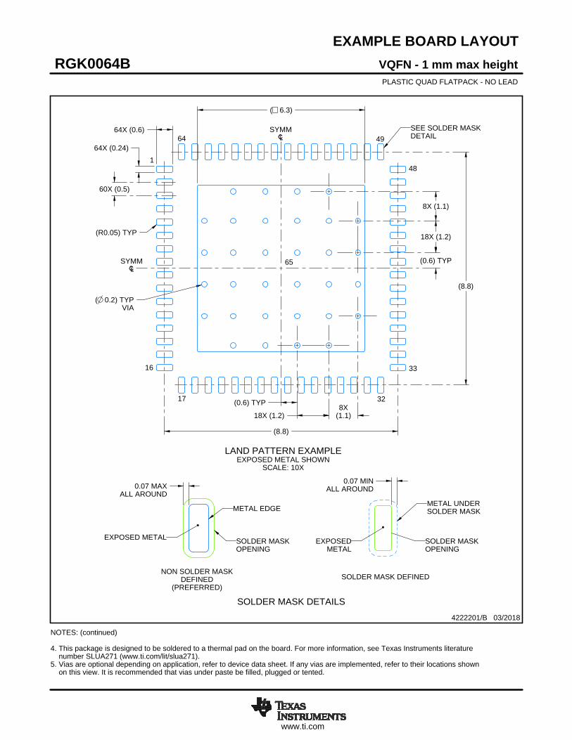
www.ti.com
EXAMPLE BOARD LAYOUT
60X (0.5)
( 0.2) TYPVIA
(R0.05) TYP
0.07 MAXALL AROUND
0.07 MINALL AROUND
64X (0.6)
64X (0.24)
(8.8)
(8.8)
( 6.3)
(0.6) TYP
18X (1.2)
8X (1.1)
(0.6) TYP
18X (1.2)8X
(1.1)
VQFN - 1 mm max heightRGK0064BPLASTIC QUAD FLATPACK - NO LEAD
4222201/B 03/2018
NOTES: (continued) 4. This package is designed to be soldered to a thermal pad on the board. For more information, see Texas Instruments literature number SLUA271 (www.ti.com/lit/slua271).5. Vias are optional depending on application, refer to device data sheet. If any vias are implemented, refer to their locations shown on this view. It is recommended that vias under paste be filled, plugged or tented.
SYMM
SYMM
LAND PATTERN EXAMPLEEXPOSED METAL SHOWN
SCALE: 10X
SEE SOLDER MASKDETAIL
1
16
17 32
33
48
4964
65
METAL EDGE
SOLDER MASKOPENING
EXPOSED METAL
METAL UNDERSOLDER MASK
SOLDER MASKOPENING
EXPOSEDMETAL
NON SOLDER MASKDEFINED
(PREFERRED)SOLDER MASK DEFINED
SOLDER MASK DETAILS

www.ti.com
EXAMPLE STENCIL DESIGN
64X (0.6)
64X (0.24)
60X (0.5)
(8.8)
(8.8)
25X ( 1)
(R0.05) TYP
(1.2) TYP
(1.2) TYP
VQFN - 1 mm max heightRGK0064BPLASTIC QUAD FLATPACK - NO LEAD
4222201/B 03/2018
NOTES: (continued) 6. Laser cutting apertures with trapezoidal walls and rounded corners may offer better paste release. IPC-7525 may have alternate design recommendations.
SOLDER PASTE EXAMPLEBASED ON 0.1 MM THICK STENCIL
SCALE: 10X
EXPOSED PAD 6563% PRINTED SOLDER COVERAGE BY AREA UNDER PACKAGE
SYMM
SYMM
1
16
17 32
33
48
4964
65
METALTYP

IMPORTANT NOTICE AND DISCLAIMERTI PROVIDES TECHNICAL AND RELIABILITY DATA (INCLUDING DATASHEETS), DESIGN RESOURCES (INCLUDING REFERENCEDESIGNS), APPLICATION OR OTHER DESIGN ADVICE, WEB TOOLS, SAFETY INFORMATION, AND OTHER RESOURCES “AS IS”AND WITH ALL FAULTS, AND DISCLAIMS ALL WARRANTIES, EXPRESS AND IMPLIED, INCLUDING WITHOUT LIMITATION ANYIMPLIED WARRANTIES OF MERCHANTABILITY, FITNESS FOR A PARTICULAR PURPOSE OR NON-INFRINGEMENT OF THIRDPARTY INTELLECTUAL PROPERTY RIGHTS.These resources are intended for skilled developers designing with TI products. You are solely responsible for (1) selecting the appropriateTI products for your application, (2) designing, validating and testing your application, and (3) ensuring your application meets applicablestandards, and any other safety, security, or other requirements. These resources are subject to change without notice. TI grants youpermission to use these resources only for development of an application that uses the TI products described in the resource. Otherreproduction and display of these resources is prohibited. No license is granted to any other TI intellectual property right or to any third partyintellectual property right. TI disclaims responsibility for, and you will fully indemnify TI and its representatives against, any claims, damages,costs, losses, and liabilities arising out of your use of these resources.TI’s products are provided subject to TI’s Terms of Sale (https:www.ti.com/legal/termsofsale.html) or other applicable terms available eitheron ti.com or provided in conjunction with such TI products. TI’s provision of these resources does not expand or otherwise alter TI’sapplicable warranties or warranty disclaimers for TI products.IMPORTANT NOTICE
Mailing Address: Texas Instruments, Post Office Box 655303, Dallas, Texas 75265Copyright © 2021, Texas Instruments Incorporated