Carlos Miguel Marques do Rosário Processos de condução ...
190
Universidade de Aveiro 2020 Carlos Miguel Marques do Rosário Processos de condução eletrónica em células de memória ReRAM do tipo VCM com óxidos metálicos Electronic conduction processes in VCM-type metal-oxide ReRAM cells
-
Upload
khangminh22 -
Category
Documents
-
view
5 -
download
0
Transcript of Carlos Miguel Marques do Rosário Processos de condução ...

Universidade de Aveiro2020
Carlos MiguelMarques do Rosário
Processos de condução eletrónica em células dememória ReRAM do tipo VCM com óxidosmetálicosElectronic conduction processes in VCM-typemetal-oxide ReRAM cells


Universidade de Aveiro2020
Carlos MiguelMarques do Rosário
Processos de condução eletrónica em células dememória ReRAM do tipo VCM com óxidosmetálicosElectronic conduction processes in VCM-typemetal-oxide ReRAM cells
Dissertação apresentada à Universidade de Aveiro para cumprimento dosrequisitos necessários à obtenção do grau de Doutor em Engenharia Física,realizada sob a orientação científica do Professor Doutor Nikolai AndreevitchSobolev, Professor Associado do Departamento de Física da Universidadede Aveiro e co-orientação do Professor Doutor Rainer Waser, ProfessorCatedrático da Faculdade de Engenharia Electrotécnica e de Tecnologias deInformação da Universidade Técnica da Renânia-Vestfália (RWTH Aachen).
Apoio financeiro da FCT atravésda bolsa de doutoramentoPD/BD/105917/2014 (ProgramaDoutoral DAEPHYS).
O trabalho foi desenvolvido noâmbito do projecto i3N,UID/CTM/50025/2013,UIDB/50025/2020 &UIDP/50025/2020, financiado porfundos nacionais através daFCT/MEC.
Apoio financeiro do CRUP emparceria com a DAAD através daAção Integrada Luso-AlemãA-14/17.
Financial support from the DFGthrough the Collaborative ResearchCentre SFB 917 “Nanoswitches”.


I dedicate this work to my mother,Maria Gabriela.


o júri / the jury
presidente / president Prof. Doutor Aníbal Manuel de Oliveira Duarte MonteiroProfessor Catedrático da Universidade de Aveiro
vogais / examiners committee Prof.ª Doutora Regina DittmannProfessora da Universidade de RWTH Aachen
Prof. Doutor Luís Manuel Cadillon Martins CostaProfessor Associado com Agregação da Universidade de Aveiro
Prof. Doutor Henrique Leonel GomesProfessor Associado da Universidade de Coimbra
Doutora Asal KiazadehInvestigadora da Universidade Nova de Lisboa
Prof. Doutor Nikolai Andreevitch Sobolev (Orientador)Professor Associado da Universidade de Aveiro


acknowledgements I feel the need to thank many people, without whom my work would nothave been possible. First, I wish to express my gratitude to my supervisorProfessor Nikolai Sobolev for all the support, guidance, shared experienceand opportunities given to me, not only during my PhD but since 2012.I also want to express my gratitude to my co-supervisor Professor RainerWaser for giving me the opportunity to work in his group in Aachen/Jülich,providing me with one of the best, most challenging and most rewardingprofessional and personal experiences of my life. A very special thank youto Dr. Dirk Wouters for supervising my work in Aachen, for always beinginterested in my results and motivating me to pursue solutions whenever Iencountered obstacles.I wish to thank Professor Valeri Afanas’ev from KU Leuven and ProfessorCarlo Ricciardi from the Polytechnic University of Turin for agreeing toreview my thesis and for writing a report for my European Doctorate.I thank the Physics Department of the University of Aveiro and the I3Nfor the institutional and financial support. Likewise, I must thank all theinstitutional support from the IWE 2 at RWTH Aachen University andfrom PGI-7 at Forschungszentrum Jülich, especially to Dr. Ulrich Böttger,Martina Heins and Maria Garcia.I must thank Alexander Schönhals for most of the sample fabrication, forsharing his fabrication methods and discussing of the experimental results.I would like to thank Bo Thöner and Professor Matthias Wuttig from theI. Institute of Physics (IA) in Aachen for the low temperature transportmeasurements. Their interest in the work was invaluable for both the ex-periments and the discussion of the results. A special thank you to BoThöner for his availability and for the always constructive and critical com-ments in our many discussions. I wish to thank Dr. Stephan Menzel for hisincisive comments and overall discussion of the work. I wish to thank Dr.Alexander Meledin and Professor Joachim Mayer from the Central Facilityfor Electron Microscopy in Aachen for the STEM measurements, and Dr.Nuno Barradas and Professor Eduardo Alves from Campus Tecnológico eNuclear in Sacavém for the RBS measurements. I thank Thomas Heisig,Dr. Christoph Bäumer and Professor Regina Dittmann for the XPS mea-surements and Felix Hensling for the help with the sputtering tool in Jülich.I thank Andreas Kindsmüller for the help in sputtering and the analysis ofthe XPS results. I would like to thank Marco Moors and Maria Glößforthe LC-AFM measurements. I thank Stephan Aussen for the XRR measure-ments in Jülich. I thank Professor António Cunha for the UV-Vis absorptionspectroscopy measurements. I wish to thank Dr. Susanne Hoffmann-Eifertfor the enthusiastic discussions whenever I was in Jülich, and Dr. VikasRana for the access to the electrical measurement setups in PGI-7.

I would like to acknowledge all the technical support at the different loca-tions where I worked. From the Aachen site, thank you Daliborka Erdoglijafor the preparation of the samples in the clean room, Petra Grewe for theXRD and XRR measurements, and Dagmar Leisten for sawing the samples.From Jülich, I must thank René Borowksi, Marcel Gerst, Stephan Mass-berg, Jochen Freidrich and Georg Pickartz for all the help with the cryostat,in setting up the measurement tools and with sputtering. From Aveiro, Iwould like to thank Ivo Mateus and Miguel Rocha for the assistance in themechanical workshop, and David Furtado for the help in setting up the newearthing system in the magnetic resonance lab.The great atmosphere at IWE 2 was something that I valued deeply andwhich had a really positive impact on everyday work at the Institute. There-fore, I would like to thank all the colleagues at the Institute in Aachen. Aspecial thank you to Marcel and Tyler, for being the best office mates, forthe support in the hard times and for “drooping the snoot” like no others.Another special thank you to Jonathan, for the many Aachen-Jülich com-mutes in good company and for the 1000+ hours of discussions of whatis Mott and what is not(t). Thank you Andi, Daniel and Sebastian forthe “classy jazzy” moments. Thank you fellow DSA Helden for integratinga foreign fisherman and lutenist in your party. Thank you Tyler, Moritz,Carsten, Jan and fellow supporters for “going the right way” out. Thankyou Anne and Toto for always lightening the mood. Thank you, Camilla,for the German lessons and the challenging Adventskalender. Thank youAndrea, for being the Luigi to my Mario. Thank you Thomas, for the kind-ness and for the photos. Also, a word of gratitude to all the colleagues atPGI-7 in Jülich for the comradeship.I would also like to extend my thanks to my lab colleagues in Aveiro for thegood times at the lab. I thank Bruno for the company and for sharing thestruggles and difficulties, especially in the last two years. I want to thankJaime for working with me during his third year project and his masterthesis, and for his critical assessment of the experimental results. Thankyou, Nuno, for always lightening the mood with a good joke. I also thankAndrey and João for the help in the lab. I would like to thank all mycolleagues turned good friends that have accompanied me during my yearsat the University of Aveiro. Thank you all for the companionship, numerousdiscussions during lunch breaks, occasional snack grabbing and for all thefun moments we shared. I also wish to thank Professor Teresa Monteiro forencouraging me to complete this long endeavour.To my family and extended family, thank you for supporting me throughall the hardships and for encouraging me to go further. Thank you tomy friends of old, Amaral, André, Barros, Bernardo, Maria, Pedro andSarnadas. To Denis for being my brother away from home. To Olívia,Lino and Mariana for always receiving me with a big smile. To Cristinafor the support and the advice. To my father José Rui for inciting myscientific curiosity and for (lately) feeding me with his veggies and to mysister Bárbara for feeding my artistic side. Lastly, I am very grateful toMaria for the constant encouragement, for believing in me when I failed toand especially for being herself.Muito obrigado e bem hajam! Vielen Dank!

Palavras-chave Transporte elétrico, resistive switching, ReRAM, filamentos condutores,TaOx, metal desordenado
Resumo Novas aplicações, tais como computação neuromórfica, e as limitações datecnologia de semicondutores atual exigem uma revolução nos dispositivoseletrónicos. Sendo uma peça chave para um novo paradigma da eletrónica,a memória ReRAM (redox-based resistive switching random access mem-ory) tem sido alvo de muita investigação e desenvolvimento. O Ta2O5 é umdos materiais mais populares para usar em dispositivos ReRAM, permitindoalta durabilidade e velocidades de comutação elevadas. As ReRAM comTa2O5 baseiam-se na mudança não volátil da resistência elétrica atravésda modulação da quantidade de oxigénio em filamentos condutores, comoé descrito no mecanismo de alteração de valência (valence change mecha-nism). No entanto, a estrutura dos filamentos e a sua composição químicaexata, são ainda alvo de intenso debate, limitando o desenvolvimento demelhores receitas de fabricação de dispositivos. Os dois modelos atuais naliteratura consideram filamentos compostos por lacunas de oxigénio e fila-mentos com Ta metálico. Este trabalho procura resolver esta disputa aoreportar um estudo detalhado do transporte elétrico através de filamentoscondutores em dispositivos ReRAM de Ta2O5. Paralelamente, foi estudadoem detalhe o transporte elétrico e a estrutura de filmes finos de TaOx sub-estequiométrico, depositados de forma a emular o material dos filamentos.Foi encontrada uma forte correlação entre os mecanismos de transportenos filamentos condutores dentro dos dispositivos ReRAM de Ta2O5 e nosfilmes finos de TaOx com x ∼ 1. Isto estabelece uma ligação clara en-tre as propriedades físicas dos materiais que compõem tanto os filamentoscomo os filmes finos de TaOx. A análise estrutural efetuada nos filmes deTaOx revela a presença de aglomerados de Ta. Por outro lado, o transporteelétrico em filmes finos de Ta é dominado pelos mesmos mecanismos decondução observados nos filmes de TaOx com x ∼ 1, para a maior parte dagama de temperatura de 2 K a 300 K. Ambos os casos partilham ainda umaconcentração de portadores da ordem de 1022 cm−3 e uma magnetoresistên-cia positiva associada a anti-localização fraca para T < 30 K. Portanto, éconcluído que o transporte em filmes de TaOx com x ∼ 1 é dominado poruma cadeia de percolação de aglomerados de Ta embutidos numa matrizisoladora de Ta2O5. Estes aglomerados exibem um comportamento típicode metais desordenados, para os quais a condução é dominada por correçõesquânticas ao transporte de Boltzmann.Em conclusão, o transporte elétrico em filamentos condutores dentro dedispositivos ReRAM baseados em Ta2O5 é dominado pela percolação deaglomerados de Ta, o que corrobora observações independentes de Tametálico nos filamentos. Assim, este trabalho suporta o modelo baseado nofilamento metálico de Ta.


Keywords Electrical transport, resistive switching, ReRAM, conductive filaments,TaOx, disordered metal
Abstract New applications, such as neuromorphic computing, and the limitations ofcurrent semiconductor technologies demand a revolution in electronic de-vices. As one of the key enablers of a new electronics paradigm, redox-basedresistive switching random access memory (ReRAM) has been the focus ofmuch research and development. Among the ReRAM research community,Ta2O5 has emerged as one of the most popular materials, for enabling highendurance and high switching speed. Ta2O5-based ReRAM rely on the non-volatile change of the resistance via the modulation of the oxygen contentin conductive filaments, as it is described in the valence change mechanism.However, the filaments’ structure and exact composition are currently un-der intense debate, which hinders the development of better device designrules. The two current models in the literature consider filaments composedof oxygen vacancies and those containing metallic Ta. This work attemptsto solve this dispute by reporting a detailed study of the electrical transportthrough the conductive filaments inside Ta2O5-based ReRAM. In parallel,the electrical transport and structure of substoichiometric TaOx thin films,grown to try and match the material of the filaments, was studied in detail.A strong correlation between the transport mechanisms in the conductive fil-aments inside the Ta2O5 ReRAM and in the TaOx thin films with x ∼ 1 wasfound. This clearly links the physical properties of the materials composingthe filaments and the substoichiometric TaOx thin films. Structural analy-sis performed on the TaOx films reveals the presence of Ta clusters insidethe films. Moreover, the electrical transport of metallic Ta films shows thesame transport mechanism as TaOx with x ∼ 1, for most of the measuredtemperature range, from 2 K to 300 K. Beyond the transport mechanisms,both cases share a carrier concentration on the order of 1022 cm−3 and apositive magnetoresistance associated with weak antilocalization at T < 30K. Therefore, it is concluded that the transport in the TaOx films withx ∼ 1 is dominated by a percolation chain of Ta clusters embedded in aninsulating Ta2O5 matrix. These clusters exhibit disordered metal-like be-haviour, where quantum corrections to the Boltzmann transport dominatethe conduction.In conclusion, the electrical transport in the conductive filaments insideTa2O5-based ReRAM devices is determined by percolation through Ta clus-ters, which is in line with independent observations of metallic Ta in thefilaments. This work strongly supports the metallic Ta filament model.


“It is good to have an end to journey towards;but it is the journey that matters, in the end”
— Ursula K. Le Guin,The Left Hand of Darkness

Contents
Contents i
List of Figures v
List of Tables xvii
Acronyms xix
Introduction 1
1 Resistive switching and ReRAM 51.1 Definition and terminology . . . . . . . . . . . . . . . . . . . . . . . . . . . . 51.2 Brief history of resistive switching . . . . . . . . . . . . . . . . . . . . . . . . 61.3 The memristor and memristive systems . . . . . . . . . . . . . . . . . . . . . 81.4 Redox-based resistive switching mechanisms . . . . . . . . . . . . . . . . . . . 10
1.4.1 TCM - Thermochemical Mechanism . . . . . . . . . . . . . . . . . . . 111.4.2 ECM - Electrochemical Mechanism . . . . . . . . . . . . . . . . . . . . 131.4.3 VCM - Valence Change Mechanism . . . . . . . . . . . . . . . . . . . . 14
1.5 The particular case of TaOx-based ReRAM . . . . . . . . . . . . . . . . . . . 171.5.1 From TiOx to TaOx . . . . . . . . . . . . . . . . . . . . . . . . . . . . 171.5.2 Overview of TaOx-based ReRAM . . . . . . . . . . . . . . . . . . . . . 18
1.6 Introduction of the thesis in the presented framework . . . . . . . . . . . . . . 191.7 Applications of ReRAM . . . . . . . . . . . . . . . . . . . . . . . . . . . . . . 19
1.7.1 Memory . . . . . . . . . . . . . . . . . . . . . . . . . . . . . . . . . . . 201.7.2 Neuromorphic computing . . . . . . . . . . . . . . . . . . . . . . . . . 211.7.3 Other applications . . . . . . . . . . . . . . . . . . . . . . . . . . . . . 24
2 Theory and other relevant background 252.1 Electron transport . . . . . . . . . . . . . . . . . . . . . . . . . . . . . . . . . 25
2.1.1 Boltzmann equation and its limits . . . . . . . . . . . . . . . . . . . . 262.1.2 Quantum corrections to the conductivity . . . . . . . . . . . . . . . . 292.1.3 Hopping transport . . . . . . . . . . . . . . . . . . . . . . . . . . . . . 362.1.4 Granular metals . . . . . . . . . . . . . . . . . . . . . . . . . . . . . . 39
2.2 The Ta-O material system . . . . . . . . . . . . . . . . . . . . . . . . . . . . . 432.2.1 Phase diagram of the Ta-O system . . . . . . . . . . . . . . . . . . . . 432.2.2 The oxide: Ta2O5 . . . . . . . . . . . . . . . . . . . . . . . . . . . . . 432.2.3 The metal: Ta . . . . . . . . . . . . . . . . . . . . . . . . . . . . . . . 45
i

ii Contents
2.2.4 Metastable suboxide phases . . . . . . . . . . . . . . . . . . . . . . . . 45
3 Experimental techniques 473.1 Fabrication techniques . . . . . . . . . . . . . . . . . . . . . . . . . . . . . . . 47
3.1.1 Sputtering . . . . . . . . . . . . . . . . . . . . . . . . . . . . . . . . . . 473.1.2 Photolithography and lift-off . . . . . . . . . . . . . . . . . . . . . . . 48
3.2 Structural characterization techniques . . . . . . . . . . . . . . . . . . . . . . 513.2.1 X-ray diffraction (XRD) and X-ray reflectometry (XRR) . . . . . . . . 513.2.2 Rutherford backscattering spectrometry (RBS) . . . . . . . . . . . . . 553.2.3 Transmission electron microscopy (TEM) . . . . . . . . . . . . . . . . 58
3.3 Electrical characterization techniques . . . . . . . . . . . . . . . . . . . . . . . 613.3.1 Current-Voltage measurements . . . . . . . . . . . . . . . . . . . . . . 613.3.2 Resistivity measurements . . . . . . . . . . . . . . . . . . . . . . . . . 623.3.3 Hall and magnetoresistance measurements . . . . . . . . . . . . . . . . 633.3.4 Temperature and magnetic field dependence . . . . . . . . . . . . . . . 64
3.4 Auxiliary techniques . . . . . . . . . . . . . . . . . . . . . . . . . . . . . . . . 653.4.1 X-ray photoelectron spectroscopy (XPS) . . . . . . . . . . . . . . . . . 653.4.2 Local conductivity atomic force microscopy (LC-AFM) . . . . . . . . . 663.4.3 Optical absorption spectroscopy . . . . . . . . . . . . . . . . . . . . . 66
3.5 Sample fabrication details . . . . . . . . . . . . . . . . . . . . . . . . . . . . . 673.5.1 ReRAM devices . . . . . . . . . . . . . . . . . . . . . . . . . . . . . . 673.5.2 Substoichiometric thin films . . . . . . . . . . . . . . . . . . . . . . . . 68
4 Correlation between the transport mechanisms in Ta2O5-based ReRAMdevices and in TaOx thin films 714.1 Resistive switching in Ta/Ta2O5/Pt ReRAM devices . . . . . . . . . . . . . . 71
4.1.1 Electroforming . . . . . . . . . . . . . . . . . . . . . . . . . . . . . . . 724.1.2 Bipolar resistive switching . . . . . . . . . . . . . . . . . . . . . . . . . 734.1.3 "Intrinsinc" resistive switching curve . . . . . . . . . . . . . . . . . . . 734.1.4 Cyclability and endurance . . . . . . . . . . . . . . . . . . . . . . . . . 75
4.2 Temperature dependence of the transport in Ta2O5-based ReRAM devices . . 774.2.1 Low resistance state (LRS) . . . . . . . . . . . . . . . . . . . . . . . . 774.2.2 High resistance state (HRS) . . . . . . . . . . . . . . . . . . . . . . . . 83
4.3 Transport in the substoichiometric TaOx thin films . . . . . . . . . . . . . . . 854.3.1 Fit to conduction mechanisms . . . . . . . . . . . . . . . . . . . . . . . 87
4.4 . . . . . . . . . . . . . . . . . . . . . . . . . . . . . . . . . . . . . . . . . . . . 88
5 Understanding the transport in substoichiometric TaOx thin films 935.1 Composition and structure of the TaOx thin films . . . . . . . . . . . . . . . . 93
5.1.1 Composition determination . . . . . . . . . . . . . . . . . . . . . . . . 935.1.2 GI-XRD . . . . . . . . . . . . . . . . . . . . . . . . . . . . . . . . . . . 955.1.3 HAADF-STEM . . . . . . . . . . . . . . . . . . . . . . . . . . . . . . . 975.1.4 Other auxiliary techniques . . . . . . . . . . . . . . . . . . . . . . . . . 985.1.5 Discussion . . . . . . . . . . . . . . . . . . . . . . . . . . . . . . . . . . 102
5.2 Temperature dependence of the resistivity . . . . . . . . . . . . . . . . . . . . 1035.3 Hall measurements . . . . . . . . . . . . . . . . . . . . . . . . . . . . . . . . . 1065.4 Magnetoresistance . . . . . . . . . . . . . . . . . . . . . . . . . . . . . . . . . 110

Contents iii
5.5 Discussion of a possible model for the transport in the TaOx thin films . . . . 1155.5.1 Structure model for the transport . . . . . . . . . . . . . . . . . . . . . 1155.5.2 Transport mechanisms . . . . . . . . . . . . . . . . . . . . . . . . . . . 1165.5.3 Magnetoresistance . . . . . . . . . . . . . . . . . . . . . . . . . . . . . 118
5.6 Insight into the conductive filaments of ReRAM devices . . . . . . . . . . . . 118
Conclusions and outlook 121
Appendices 126
A On the representativeness of the samples 127A.1 Transport in Ta2O5 ReRAM devices in the LRS . . . . . . . . . . . . . . . . 127A.2 Transport in substoichiometric TaOx thin films . . . . . . . . . . . . . . . . . 127
B Numerical method to calculate the reduced activation energy 131
C Transport in Ta thin films: effect of film thickness and substrate 133
Bibliography 137

iv Contents

List of Figures
1 General scheme of the thesis. Starting from the main questions that weretargeted, the work was divided in two parallel roads of experimental work.The results of the two paths were compared in order to gain information andattempt to answer the initial questions. On the right side of the scheme, theschematic blocks are mapped to the different thesis chapters. Chapters 4 and5, containing the main experimental results and discussion, are highlighted incolour to match the colour of the blocks in the scheme. . . . . . . . . . . . . . 3
1.1 Illustration of the different current-voltage (I −V ) characteristics obtained forthe different types of resistive switching: (a) Unipolar resistive switching (URS)(b) Bipolar resistive switching (BRS) (c) Complementary resistive switching(CRS), using two anti-serially connected devices (d) Complementary switching(CS) using only one device. The I − V characteristics are accompanied bytypical materials stacks used to obtain the different behaviour in Ta2O5-basedReRAM. The BRS with the polarity shown in (b), with a positive SET andnegative RESET, is obtained when the voltage is applied to the Ta top elec-trode, while grounding the Pt electrode. As can be seen, the stacks in (b)and (d) are identical in terms of the employed layers. However, the obtainedbehaviour can be controlled by tuning the thickness of the Ta layer, as will bediscussed in section 1.5.2. . . . . . . . . . . . . . . . . . . . . . . . . . . . . . 7
1.2 (a) Schematic picture of the four fundamental passive circuit elements: theresistor, the capacitor, the inductor and the memristor, according to LeonChua. (b) Typical pinched hysteresis loop in the I − V characteristic of anideal memristor response to an AC voltage signal for two different frequencies,0.5 and 1 Hz. Taken from [16] and adapted from [18], respectively. . . . . . . 9
1.3 Survey of the different types of memristive phenomena. Taken from [26]. . . . 10
1.4 (a) Ellingham diagram. Adapted from [35]. (b) Model of the thermochemicalmechanism for the prototypical structure Pt/NiO/Pt: in the centre there isa plot of the typical I − V characteristics observed in TCM systems; aroundthe central plot there are schematic depictions of the evolution of the atomicconfiguration throughout the different stages of the RS process. The greenspheres represent the Ni ions, while the blue spheres represent Ni atoms (or atleast NiO with lower oxygen content). Adapted from [2]. . . . . . . . . . . . . 12
v

vi List of Figures
1.5 Schematic model of the electrochemical mechanism: in the center there is a plotof the typical I−V characteristics observed in ECM systems, here exemplifiedfor a Ag/solid electrolyte/Pt system where the Pt electrode is grounded andAg is the biased electrode; sketches of the different stages of the RS in ECMsystems are depicted around the central graph. The green spheres representAg+ cations, while the blue spheres represent Ag atoms. Taken from [39]. . . 13
1.6 Schematics of the proposed mechanism for filamentary C8W VCM switchingalong with a typical I−V characteristic measured for a Pt/ZrO2/Zr cell wherethe AE Pt is biased and Zr, the OE, is grounded. Around the central plot,the different stages of the RS process are schematically depicted. These stagesare: (a) HRS (b) SET process (c) LRS (d) RESET process. The green spheresrepresent the mobile oxygen vacancies and the purple spheres the immobile Zrions with a lower valence state. The configuration of the cell after EF is alsoschematically depicted with the plug and disc regions that are the responsiblefor the RS. Taken from [2]. . . . . . . . . . . . . . . . . . . . . . . . . . . . . 16
1.7 Qualitative plot of the access time as a function of the production cost per diefor the main memory technologies, illustrating the emergence of the (speed)performance-cost gap and the storage class memory as a new memory class tofill this gap. The emergent memory technologies are naturally positioned inthe SCM domain and, therefore, are promising for this application. While therelative positioning of the three groups is the main information of the figure,the relative positioning of the different technologies inside each group is notnecessarily meant to be real and accurate. The figure was drawn based on afigure designed by Western Digital and published in PC Mag [111]. . . . . . . 22
1.8 Summary of the different kinds of computing mentioned in the text: con-ventional computing, using the traditional von Neumman architecture, withclearly separated memory and processor (CPU); in-memory computing, alsoknown as stateful logic computing, that utilizes emerging devices that can actboth for processing and data storage; neuromorphic computing, where there isno distinction between memory and processing unit, and a new brain-inspiredarchitecture is used, thus avoiding the von Neumann architecture completely. 23
1.9 (a) Schematic illustration of a synapse between two neurons and of a crosspointmemristive device as a possible artificial synapse. (b) Demonstration of STDPin a memristive device with the change in the synaptic weight as a functionof the relative timing of the neuron spikes. (c) Measurement of the excitatorypostsynaptic current of rat hippocampal neurons after repetitive correlatedspiking as a function of the relative spike timing. Adapted from [124]. . . . . 24
2.1 (a) Possible closed diffusion path of an electron. The electron propagates theclosed path in both directions: 0→1→2→...→11→0 and 0→1′ →2′ →...→11′→0, indicated by the black and red arrows, respectively. (b) Plot of the proba-bility function given by Eq. 2.17 for two-dimensional diffusion (d = 2) at timest1 < τφ and t2 = 2t1 > τφ. For time t1 the increase of the probability due to theweak localization (WL) is clearly observed, while for time 2t1 the probabilityat the origin is already the same as in the classical picture. For the case wherethe spin-orbit coupling is strong, weak antilocalization (WAL) occurs, givingthe decreased probability shown in orange. . . . . . . . . . . . . . . . . . . . . 30

List of Figures vii
2.2 Resistance as a function of temperature (on a logarithmic scale) for thin filmsof Au (left) and Cu (right), evidencing the upturn of the resistance at lowtemperatures characteristic of weak localization. Taken from [135]. . . . . . . 31
2.3 Plot of the base function underlying the HLN formula expressed in Eq. 2.21. 32
2.4 Temperature coefficient of the resistance (TCR), here represented with α as afunction of the resistivity for different disordered metallic alloys, showing a clearcorrelation between the two quantities. For a resistivity below approximately150 µΩcm, the TCR is positive, while above this value the TCR is negative.This experimental correlation is called Mooij’s rule. The different symbolsrepresent different types of samples, as indicated in the legend of the figure.Adapted from [135]. . . . . . . . . . . . . . . . . . . . . . . . . . . . . . . . . 36
2.5 Schematics showing the change of hopping transport mechanisms as temper-ature is decreased for a lightly-doped semiconductor. The small inset plotsrepresent the density of states (DOS) around the Fermi level EF and are notdepicted in the same scale. ED represents the minimum of the conductionband, kBT represents the thermal energy at temperature T , δE represents theenergy width of the Coulomb gap, while the other symbols retain the samemeaning as in the text. Based on a figure from [135]. . . . . . . . . . . . . . . 38
2.6 Scanning electron microscopy pictures of In deposited on top of Si for differentaverage In film thickness (δ), showing different kinds of coverage of the surface,exemplifying a granular metal in the insulating regime in (a) and in the metallicregime (b). Adapted from [135]. . . . . . . . . . . . . . . . . . . . . . . . . . . 40
2.7 (a) Resistivity of a granular metal as a function of the metallic fraction x forthe example system Au + Al2O3. The solid lines and symbols are obtained atroom temperature, while the dashed line shows the data obtained at heliumtemperature, where a much steeper transition with decreasing x is observed.Adapted from [135]. (b) Scheme of percolating channel in the vicinity of aweak link between larger metallic regions. Gmetal is the conductance throughthe percolating cluster of metal granules and Ghop corresponds to the hoppingconductance over separated granules; (c) Simplified band diagram showing theenergy levels splitting owing to QSE in the small granule and energy barrier∆E for conduction electrons within the constriction. . . . . . . . . . . . . . . 42
2.8 Phase diagram of the Ta-O system with: (a) Atomic percent of oxygen on thehorizontal axis scale; (b) Weight percent of oxygen on the horizontal axis scale.Taken from [156]. . . . . . . . . . . . . . . . . . . . . . . . . . . . . . . . . . . 44
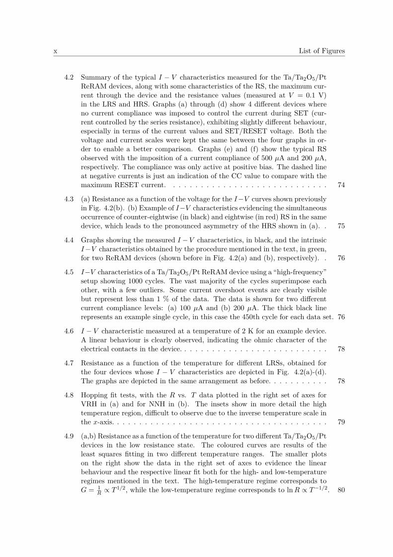
3.1 (a) Simple schematic depiction of the sputtering of surface atoms by an accel-erated incident ion. (b) Simplified schematic representation of the magnetronsputtering process inside a vacuum chamber with Ar gas. The violet regionindicates the plasma with Ar+ ions represented with green dots, the electronsare represented by the small black dots and the yellow dots represent the atomssputtered from the target (on top) that can be deposited onto the substrate(on the bottom). . . . . . . . . . . . . . . . . . . . . . . . . . . . . . . . . . . 48

viii List of Figures
3.2 Schematic diagram of a negative lithography process used in this work for thefabrication of the samples: (a) the solution with the photoresist (AZ5214E) isspin-coated on top of a previously cleaned substrate at 6000 RPM during 30s; (b) the photoresist is dried during a heating step at 90 C for 5 min; (c)After proper alignment of the substrate relatively to the transfer mask, thephotoresist and the mask are exposed to UV radiation for 4.5 s, leading tothe photochemical change of the exposed regions of the photoresist. (d) Theradiation exposure is followed by a second heating step, this time at 115 C for 2min; (e) the photoresist is exposed to UV radiation a second time now withoutthe mask for 14.5 s (flood exposure); (f) finally the photoresist is developed ina chemical bath (developer: AZ826MIF) and afterwards cleaned in deionizedwater, resulting in the inverse pattern of the transfer mask solidly drawn bythe photoresist layer; (g) the desired thin film can be deposited on the wholesurface of the substrate with the lithographically defined resist pattern; (h) thefinal step is the lift-off with the stripping of the resist by acetone. The finalresult shows the deposited film remaining only in the regions that are definedin the transfer mask. In the case of a positive process, the exposure time in (c)is increased to 7 s and steps (d) and (e) are skipped. . . . . . . . . . . . . . . 50
3.3 Schematic representation of the wave interference of X-rays that leads toBragg’s law. The lines in red indicate the path difference between the tworeflected X-ray beams, which must be a multiple of the wavelength of theX-rays in order for constructive interference to occur. This condition is statedas Bragg’s law. . . . . . . . . . . . . . . . . . . . . . . . . . . . . . . . . . . . 51
3.4 Schematic illustrations of two different experimental configurations to measureX-ray diffraction: (a) Bragg-Brentano configuration. (b) Grazing incidenceconfiguration. . . . . . . . . . . . . . . . . . . . . . . . . . . . . . . . . . . . . 53
3.5 (a) Schematic illustration of the X-ray reflection and refraction at the air-filminterface, showing the path of the X-rays and the origin of the intereferencethat gives rise to the fringes in the X-ray reflectometry data. (b) Sketch of theexperimental configuration used to measure the X-ray reflectometry. It is sym-metrical just like the Bragg-Brentano configuration for XRD measurements,but as it is dealing with very small angles of incidence, takes the necessary in-strumentation considerations used in the GIXRD configuration. (c) Exampleof XRR data, showing how the film density and thickness can be retrieved fromthe data. The data refers to a 36 nm-thick Pt thin film on top of SiO2 with a6 nm-thick Ta adhesion layer. . . . . . . . . . . . . . . . . . . . . . . . . . . . 54
3.6 (a) Simplified schematic illustration of the RBS configuration in the Cornellgeometry. The incident beam, the detected backscattered beam and the sam-ple rotation axis lie in the same plane. The RBS detector is positioned in thebackward region, while the ERDA detector is positioned in the forward regionrelatively to the ion beam incident on the sample. (b) Illustration of the sim-plified kinematic approach to the backscattering of accelerated ions by atomsof the target (sample), where the ion and the atom are considered hard sphereswith mass M1 and M2, respectively. (c) Simulation of the RBS signal from aAu/TaOx/Si stack obtained using the simulation tool RUMP. . . . . . . . . . 57

List of Figures ix
3.7 (a) Simplified scheme of a TEM with an EDX detector, showing the main com-ponents used to form an image of a thin sample. The rays indicated are relativeto the image formation and not to the diffraction pattern. (b) Scheme illus-trating the image formation in STEM, highlighting the main instrumentationdifferences relatively to traditional TEM shown in (a). For the specific case ofHAADF STEM imaging the signal is collected at the high-angle annular darkfield (HAADF) detector and used to produce the image of the sample. . . . . 59
3.8 (a) Illustration of an arbitrarily shaped sample where 4 electrical contacts A,B, C and D are made to measure the resistivity through the van der Pauw(vdP) method. (b) Illustration of a possible symmetrical vdP configuration,the one used in this work. (c) Schematic of one of the individual measurementsrequired for obtaining the resistivity by the vdP method, where the current isapplied between adjacent contacts (A,B) and the voltage is measured betweenthe two remaining contacts (C,D). (d) Schematic of the wiring configurationneeded for a Hall measurement using the vdP method, where the current isapplied between diagonally opposite contacts (B,D) and the Hall voltage ismeasured between the two remaining contacts (A,C). . . . . . . . . . . . . . . 62
3.9 (a) Crosspoint geometry used in the fabrication of the Ta2O5-based ReRAMdevices. (b) Layout of the 1 × 1 cm2 samples used in the cryostats, each onewith 27 ReRAM devices (3 of the devices were grown without the oxide layerto use as a reference). (c) Layout of the 1 × 1 inch2 samples from which the1× 1 cm2 samples were cut. . . . . . . . . . . . . . . . . . . . . . . . . . . . . 68
3.10 Schematic diagram illustrating the main fabrication processes of: (a) theTa2O5-based ReRAM devices; (b) the van der Pauw samples with the TaOx
thin films. The column in the left shows a perspective of the samples’ surfacein order to schematically show the evolution of the deposited structures, whilethe column in the right shows the evolution of the layer stacks. BE = bottomelectrode and TE = top electrode. . . . . . . . . . . . . . . . . . . . . . . . . 69
3.11 (a) Schematic depiction of the van der Pauw structure used to fabricate theTaOx samples for electrical measurements, with some relevant geometric di-mensions. (b) Illustration of the layer stack used in the van der Pauw structures. 70
4.1 (a) Typical quasi-static current-voltage (I − V ) sweeps obtained during elec-troforming (EF) of the ReRAM devices, with the current axis on a logarithmicscale. The legend links the EF data to the switching data shown in Fig. 4.2:e.g., (a) corresponds to the device of Fig. 4.2(a). (b) Comparison of the I − Vcurves during and after electroforming, evidencing the big difference betweenthe resistance in the virgin state and in the HRS. . . . . . . . . . . . . . . . . 72
x List of Figures
4.2 Summary of the typical I − V characteristics measured for the Ta/Ta2O5/PtReRAM devices, along with some characteristics of the RS, the maximum cur-rent through the device and the resistance values (measured at V = 0.1 V)in the LRS and HRS. Graphs (a) through (d) show 4 different devices whereno current compliance was imposed to control the current during SET (cur-rent controlled by the series resistance), exhibiting slightly different behaviour,especially in terms of the current values and SET/RESET voltage. Both thevoltage and current scales were kept the same between the four graphs in or-der to enable a better comparison. Graphs (e) and (f) show the typical RSobserved with the imposition of a current compliance of 500 µA and 200 µA,respectively. The compliance was only active at positive bias. The dashed lineat negative currents is just an indication of the CC value to compare with themaximum RESET current. . . . . . . . . . . . . . . . . . . . . . . . . . . . . 74
4.3 (a) Resistance as a function of the voltage for the I−V curves shown previouslyin Fig. 4.2(b). (b) Example of I−V characteristics evidencing the simultaneousoccurrence of counter-eightwise (in black) and eightwise (in red) RS in the samedevice, which leads to the pronounced asymmetry of the HRS shown in (a). . 75
4.4 Graphs showing the measured I −V characteristics, in black, and the intrinsicI−V characteristics obtained by the procedure mentioned in the text, in green,for two ReRAM devices (shown before in Fig. 4.2(a) and (b), respectively). . 76
4.5 I−V characteristics of a Ta/Ta2O5/Pt ReRAM device using a “high-frequency”setup showing 1000 cycles. The vast majority of the cycles superimpose eachother, with a few outliers. Some current overshoot events are clearly visiblebut represent less than 1 % of the data. The data is shown for two differentcurrent compliance levels: (a) 100 µA and (b) 200 µA. The thick black linerepresents an example single cycle, in this case the 450th cycle for each data set. 76
4.6 I − V characteristic measured at a temperature of 2 K for an example device.A linear behaviour is clearly observed, indicating the ohmic character of theelectrical contacts in the device. . . . . . . . . . . . . . . . . . . . . . . . . . . 78
4.7 Resistance as a function of the temperature for different LRSs, obtained forthe four devices whose I − V characteristics are depicted in Fig. 4.2(a)-(d).The graphs are depicted in the same arrangement as before. . . . . . . . . . . 78
4.8 Hopping fit tests, with the R vs. T data plotted in the right set of axes forVRH in (a) and for NNH in (b). The insets show in more detail the hightemperature region, difficult to observe due to the inverse temperature scale inthe x-axis. . . . . . . . . . . . . . . . . . . . . . . . . . . . . . . . . . . . . . . 79
4.9 (a,b) Resistance as a function of the temperature for two different Ta/Ta2O5/Ptdevices in the low resistance state. The coloured curves are results of theleast squares fitting in two different temperature ranges. The smaller plotson the right show the data in the right set of axes to evidence the linearbehaviour and the respective linear fit both for the high- and low-temperatureregimes mentioned in the text. The high-temperature regime corresponds toG = 1
R ∝ T1/2, while the low-temperature regime corresponds to lnR ∝ T−1/2. 80

List of Figures xi
4.10 (a) Quasi-static current-voltage (I−V ) characteristics of a device with 30 nm-thick Pt electrodes, and with a series resistance of ca. 300 Ω. The maximumvalue of the current that passed through the filament was 2.2 mA. The black lineshows the measured data, measured in a 2-wire configuration, while the greencurve was measured in a 4-wire configuration, thus showing the “intrinsic”switching curve (without the voltage drop over the series resistance). Theinset plot shows the data with a logarithmic current scale. (b) Temperaturedependence of the resistance in the LRS for the device shown in (a), where apositive TCR is clearly observed. . . . . . . . . . . . . . . . . . . . . . . . . . 81
4.11 Overview of possible parasitic effects in the measurement of the electrical trans-port in the Ta2O5-based ReRAM devices: (a) Resistivity as a function of thetemperature for a 15 nm-thick Ta film on top of 5 nm-thick Ta2O5, to evidencethe transport behaviour of the Ta film in the same conditions as the one inthe stack of the ReRAM devices. (b) Resistance as a function of the temper-ature for a 10 µm-wide Pt line used as metallic line in the crosspoint Ta2O5ReRAM devices studied. (c) Resistance as a function of the temperature fora stack with no Ta2O5 layer (Pt/Ta/Pt). (d) Resistance as a function of thetemperature for a device after hard breakdown was induced. . . . . . . . . . . 82
4.12 (a-b) Magnetoresistance (MR) as a function of the applied magnetic field fora Ta/Ta2O5/Pt ReRAM device in the LRS (same device as in Fig. 4.7(a))fordifferent temperatures from 2 K up to 26 K. The magnetic field was applied inparallel to the plane of the layer stack (perpendicular to the vertical currentflow in the filament, θ = 90) in (a), while for (b) the field is perpendicular tothe layer stack (θ = 0). The insets clarify the orientation of the magnetic field(B). The light coloured lines represent the (noisy) raw data, while the colouredlines are a result of smoothing using a Savitsky-Golay filter. (c) Comparisonof the MR measured in the two configurations shown in (a) and (b) at T = 2K. (d) MR as a function of the applied magnetic field for different orientationsof the magnetic field relatively to the device. (e) MR for a different ReRAMdevice at T = 2 K and T = 6K, showing very similar results to the deviceshown in (a-d). The inset shows the temperature dependence of the resistancefor this device. . . . . . . . . . . . . . . . . . . . . . . . . . . . . . . . . . . . 84
4.13 (a,b) Resistance as a function of the temperature in the HRS for two differentdevices, with different active area and with different resistance values. (c)Resistance as a function of the applied magnetic field at T = 2 K, evidencingrandom telegraph noise (RTN) for the device shown in (a). The effect ofthe noise is greater than the effect of the magnetic field, which can be seenfor one of the RTN branches in the inset. The multiple data points for thesame magnetic field value are due to the magnetic field sweep used in themeasurement, where the field was swept from 0 T up to 3 T, then down to-3 T and finally back up to zero. (d) Change in resistance due to RTN asa function of the temperature for the HRS of the device shown in (b). Thechange was calculated by subtracting the resistance data shown in (b) froma filtered version of the same data following only the main branch observed ,which does not have the noise component. . . . . . . . . . . . . . . . . . . . . 86

xii List of Figures
4.14 (a) Room temperature resistivity as a function of x for the TaOx films with x =1, 1.3 and 1.5, a sputtered Ta film and literature values for Ta2O5 from Baker[219]. The dashed line connecting the data points is a visual guide for the trendof the resistivity as a function of the composition. (b) Resistivity as a functionof temperature for TaOx films with x = 1, 1.3 and 1.5. The individual data ofthese films is plotted in (c), (d) and (e), respectively, showing the evolution ofthe resistivity with temperature with a linear scale for the resistivity. . . . . 87
4.15 (a) Resistivity data for the TaOx film with x = 1 plotted in order to showlinearity for the case of Mott’s VRH conduction in 3D (similar results for the1D and 2D versions). (b) Same data as in (a) plotted in the right set of axisto show linear behaviour in the case of temperature activated NNH conduction. 88
4.16 Temperature dependence of the resistivity for the TaOx films with: (a) x = 1, (d) x = 1.3 and (g) x = 1.5. For each line, the pairs of graphs on the rightshow the linearised plots for the two fitting regions identified in the graphs onthe left, for each TaOx sample, along with the result of the linear least squaresfit to the data. The high-temperature regime corresponds to σ = 1
ρ ∝ T 1/2,while the low-temperature regime corresponds to ln ρ ∝ T−1/2 . . . . . . . . . 89
4.17 Reduced activation energy plots, where the reduced activation energy calcu-lated via equation (4.2) is plotted as a function of the temperature, for: (a)the two ReRAM devices in the LRS shown in Fig. 4.9 and the TaOx thin filmwith x ∼ 1; (b) the TaOx film with x ∼ 1.5. . . . . . . . . . . . . . . . . . . . 90
4.18 Schematic depiction of a simplified filament with a cylindrical geometry usedfor the resistance calculations based on the resistivity of the TaOx film withx = 1. . . . . . . . . . . . . . . . . . . . . . . . . . . . . . . . . . . . . . . . . 91
5.1 (a) X-ray reflectivity data for four samples: Ta, TaOx with x = 1, TaOx sput-tered for in-situ measurements and Ta2O5. (b) RBS spectrum for a TaOx filmwith x = 0.97 (determined by the RBS experiment) taken at an incident angleof 78. The blue line represents the total fitting curve, while the black linesrepresent the individual elemental contributions to the fit. (c) RBS spectrumfor a Ta2O5 film taken at an incident angle of 80.(d) TaOx films’ density asdetermined by the XRR plotted against the x index in TaOx obtained by RBS.The circle data points represent the mean value of the density, while the errorbars indicate the highest deviation from the mean value. The red line is theleast squares fit to the experimental data. For comparison, the data publishedby Waterhouse et al. [222] for films with thicknesses between 140 nm and620 nm is also included. The inset shows the layer stack used in the samplesmeasured with RBS to determine the composition. . . . . . . . . . . . . . . . 96
5.2 (a) X-ray diffractograms of TaOx samples with different compositions (x), in-cluding two reference samples, a sputtered Ta film and a sputtered Ta2O5 film.The values on the right side of the plot indicate the film density of the mea-sured samples as determined by XRR measurements. (b) Evolution of the 2θvalue of the (202) reflection with the film density (composition). . . . . . . . 97

List of Figures xiii
5.3 (a) HAADF STEM Z-contrast image with an overview of the sample comprisinga TaOx film with x ∼ 1.3. (b) HAADF STEM Z-contrast image of the TaOx
film with x ∼ 1.3 showing the area where the EDX mapping was performed.(c) Elemental mapping by EDX showing the distribution of Ta, O and Al in thearea shown in (b). (d,e) Individual elemental maps of Ta and O, respectively.The individual mapping of aluminium is not shown because its presence onthe TaOx film is vestigial, and thus it is concluded that aluminium is notincorporated in the TaOx film. . . . . . . . . . . . . . . . . . . . . . . . . . . 98
5.4 (a) HAADF STEM Z-contrast image of a Ta2O5 film showing the area wherethe EDX mapping was performed. (b) Elemental mapping by EDX showingthe distribution of Ta, O and Al in the area shown in (a). (c-e) Individualelemental maps of O, Ta and Al, respectively. . . . . . . . . . . . . . . . . . . 99
5.5 (a) HAADF STEM Z-contrast image of a Ta film showing the area where theEDX mapping was performed. (b) Elemental mapping by EDX showing thedistribution of Ta and O in the area shown in (a). (c-e) Individual elementalmaps of Ta, O and Al, respectively. . . . . . . . . . . . . . . . . . . . . . . . . 99
5.6 (a) XPS data for an in-situ sputtered TaOx film with x ∼ 1. A fit to the data isshown in red, with the individual fitting contributions from the different valencestates shown in green and orange. (b) Comparison of the XPS measurementperformed on an in-situ sample and an ex-situ sample (grown in the sameconditions as the main samples described in the text). . . . . . . . . . . . . . 100
5.7 AFM topography image (a) and the correspondent current map measured byLCAFM (b) for an in-situ sputtered sample with x ∼ 1. For the current map,a voltage of 8 V relative to the grounded sample holder was used to measurethe current through the sample. . . . . . . . . . . . . . . . . . . . . . . . . . . 101
5.8 (a) Optical absorption spectra, i.e., absorbance as a function of the wavelengthof the light for the TaOx thin films with different densities, and thus, oxygencontent. (b) Indirect bandgap test plot, used to visualize the indirect bandgap,with the data from the TaOx films shown in (a). α represents the absorptioncoefficient, obtained from the absorbance (A) and the sample thickness (t) by:α = 1
t ln(10A
). The dashed lines are linear fits to the linear portion of the
data, indicating the indirect bandgap of the samples where the fit line intersectsthe energy axis. . . . . . . . . . . . . . . . . . . . . . . . . . . . . . . . . . . . 102
5.9 (a) Resistivity vs. temperature for three thin TaOx films with x = 1.0, 1.3and 1.5 and the Ta film. (b) Comparison of the temperature dependence ofthe resistivity of the TaOx film with x = 1 and of the Ta film. Data for aTa/Ta2O5/Pt device in the LRS is also plotted. (c) Conductivity plotted as afunction of T 1/2 showing linear fits for both films and the device in the LRS inthe high-temperature region. (d) Logarithm of the resistivity as a function ofT−1/2 for the three TaOx films, to evidence the Efros-Schlovskii-like hoppingmechanism at the lowest temperatures. (e) Zabrodskii plot, with the reducedactivation energy plotted against the temperature on the double logarithmicscale, for the Ta film and the TaOx films with x = 1.0 and 1.5. (f) Plot of thereduced activation energy exhibiting a linear dependence on T 1/2 for both theTa and the TaOx film with x = 1, thus evidencing a power-law behaviour ofthe conductivity. . . . . . . . . . . . . . . . . . . . . . . . . . . . . . . . . . . 104

xiv List of Figures
5.10 Temperature dependence of the resistivity for different applied magnetic fieldsup to 9 T for: (a) TaOx film with x = 1.0; (b) Ta film. The magnetic field stepbetween every ρ vs. T data set is 0.5 T. (c) and (d) show the same data as (a)and (b) but in a VRH plot, where the ln(ρ) is plotted against T−1/4. . . . . . 107
5.11 (a) Hall resistance (Hall voltage divided by the applied current) as a functionof the magnetic field for the Ta film and the TaOx film with x = 1 at T = 1.8K (coloured symbols) and T = 300 K (light coloured symbols). (b) Same asin (a) but at T = 22 K and for a smaller magnetic field range, evidencing anabnormal behaviour of the Hall resistance (Hall voltage) at this temperature. 108
5.12 (a) Temperature dependence of the carrier concentration and mobility obtainedfrom the Hall measurements performed on the Ta film. The lines are visualguides connecting the experimental data points. (b) Temperature dependenceof the carrier concentration and mobility obtained from the Hall measurementsperformed on the TaOx film with x = 1. (c) Comparison of the Hall resultsobtained for the TaOx films with x = 1, x = 1.3 and the Ta film. . . . . . . . 109
5.13 (a) MR of the Ta film as a function of the applied magnetic field at varioustemperatures from 1.8 K to 30 K (b) Magnetoresistance (MR) of the TaOx
film with x = 1 as a function of the applied external magnetic field at differenttemperatures ranging from 1.8 K to 30 K. (c) Decay with temperature of theMR at B = 9 T of the Ta film. The inset shows the same data but on alogarithmic y-axis evidencing an exponential decay, at least in some range,as shown by the linear fit (red line). (d) Same as in (c) but for the TaOx
film with x = 1. (e) Normalized MR as a function of the magnetic fieldfor the Ta film, where the normalization was performed for each individualtemperature, enabling a comparison of the field dependence of the MR at thedifferent temperatures. (f) Same as in (e) for the TaOx film with x = 1. . . . 111
5.14 MR as a function of the magnetic field at T = 1.8 K for the TaOx film withx = 1.0 and for the Ta film, and at T = 2 K for the TaOx film with x = 1.3. . 112
5.15 (a) Change in conductance (normalized by G0 = 2e2/h, the conductance quan-tum) as a function of the applied magnetic field at 1.8 K ≤ T ≤ 8 K for the Tafilm. The lines show the least-squares fit to the simplified 2D Hikami-Larkin-Nagaoka formula shown in Eq. 2.22. (b) Change in resistivity as a function ofthe applied magnetic field at 10 K ≤ T ≤ 26 K for the Ta film. The lines showthe least-squares fit to the 3D weak antilocalization formula shown in Eq. 2.25.(c) Same as (b) for the TaOx film with x = 1.0 for T ≤ 26 K. (d) Decay of thePBL (Lφ) obtained from the fits shown in (a)-(c) for all temperatures. Thelines show a power-law fit to the full data points, with the indicated exponentp. For the Ta sample (on the right), two fits were performed, with the datadivided in two ranges: T ≤ 8 K and T ≥ 10 K. (e-f) Remaining parameters αand LSO resultant from the fits using the weak antilocalization formulas for Taand TaOx with x = 1, respectively. The parameter b in the inset of (e) is thetrue fitting parameter from which LSO is calculated. . . . . . . . . . . . . . . 114

List of Figures xv
5.16 Schematic model (as it would be seen from the top view of the film’s surfacearea) of the microstructure evolution in the TaOx films with increasing oxygenconcentration x. The blue region represents Ta(O), while the beige fields rep-resent Ta2O5. The increasing oxygen concentration leads to a higher Ta2O5content, eventually breaking the percolation of Ta granules and thus, inhibitingthe metallic behaviour. . . . . . . . . . . . . . . . . . . . . . . . . . . . . . . . 115
5.17 Schematic model of the conductive filament in Ta2O5-based ReRAM devices,showing its structure, composed of granules of metallic Ta in an insulatingTa2O5 matrix. The blue region represents Ta, while the beige region representsTa2O5. . . . . . . . . . . . . . . . . . . . . . . . . . . . . . . . . . . . . . . . . 119
A.1 Temperature dependence of the resistance in the LRS for the devices with theswitching shown in Fig. 4.2(c) and (d), respectively in (a) and (b). The data isshown in the linearized plot to observe the linear behaviour of the conductancewith
√T . The red lines show a linear fit to the data. . . . . . . . . . . . . . 128
A.2 (a) Temperature dependence of the resistivity for a TaOx film with x ∼ 1 anda thickness of 100 nm. The insets show the fitting to the two regions mentionedin the main text. (b) and (e) show the temperature dependence of the resis-tivity for different TaOx vdP structures obtained with the process for x ∼ 1,deposited at different times and with different thicknesses (approximately 50nm for (b) and 20 nm for (e)). (c-d) and (f-g) show plots of the data in theaxis used for the fitting procedures mentioned in the text. . . . . . . . . . . . 129
A.3 Magnetoresistance and Hall data for the sample with the resistivity shownin Fig. A.2(b): (a) Magnetoresistance as a function of the externally appliedmagnetic field for different temperatures from 1.8 K up to 30 K. (b) Hall carrierconcentration as a function of the temperature. (c) Hall mobility as a functionof the temperature. . . . . . . . . . . . . . . . . . . . . . . . . . . . . . . . . . 130
B.1 Reduced activation energy for a TaOx thin film with x = 1, exemplifying theneed for a smoothing procedure to make the numerical differentiation resultsclearer. . . . . . . . . . . . . . . . . . . . . . . . . . . . . . . . . . . . . . . . . 131
C.1 (a) Resistivity of the Ta thin films as a function of the film thickness. The blacksymbols indicate the data for the Ta films grown on top of the SiO2 substrate,while the red symbols represent the data obtained for the Ta films grown ontop of the 5 nm-thick Ta2O5 layer. The lines are connecting the experimentaldata points and serve as a visual guide of the data trend. (b) Temperaturecoefficient of the resistance (TCR) of the Ta films as a function of the filmthickness. (c) TCR as a function of the resistivity for the data shown in (a)and (b). The horizontal dashed line indicates the zero TCR value, while thevertical dashed line indicates the limit of the Mooijs rule of 150 µΩcm. . . . . 134

xvi List of Figures
C.2 (a) Illustration of the sample layout, with the sample divided in two areas,one where there is only the SiO2 layer underneath the Hall bar structure, andanother where there is an additional Ta2O5 layer on top of SiO2. The Ta isrepresented in light blue, while the electrodes are composed of Au. (b) Schemeof the Hall bar with the indication of the electrical contacting configuration,where four electrical contacts were used. The current is sourced and the voltageis measured. . . . . . . . . . . . . . . . . . . . . . . . . . . . . . . . . . . . . . 135

List of Tables
1.1 Comparison of different emergent memory technologies based on the generaldevice requirements and main performance parameters. The data for the emer-gent memories was taken from [110], while for DRAM and NAND-Flash theinformation was taken from [21, 114–117]. . . . . . . . . . . . . . . . . . . . . 22
3.1 Summary of the reactive magnetron RF sputtering conditions used in the de-position of the different thin films used in this work, which include the metalliclayers of Pt and Ta, the substoichiometric TaOx films, the stoichiometric Ta2O5and Al2O3. . . . . . . . . . . . . . . . . . . . . . . . . . . . . . . . . . . . . . 70
5.1 Summary of the important parameters associated with the fits shown in Fig.5.9. . . . . . . . . . . . . . . . . . . . . . . . . . . . . . . . . . . . . . . . . . . 106
xvii

xviii List of Tables

Acronyms
8W Eightwise.
AE Active Electrode.
AFM Atomic force microscopy.
AI Artificial Intelligence.
BE Bottom Electrode.
C8W Counter-eightwise.
CBA Crossbar array.
CC Current Compliance.
CMOS Complementary Metal-Oxide-Semiconductor.
CPU Central Processing Unit.
CRS Complementary Resistive Switching.
CS Complementary Switching.
DC Direct current.
DRAM Dynamic Random Access Memory.
ECM Electrochemical Mechanism.
EDX Energy dispersive X-ray spectroscopy.
EF Electroforming.
ERDA Elastic recoil detection analysis.
ESH Efros-Shklovskii hopping.
FeRAM Ferroelectric Random Access Memory.
GI-XRD Grazing incidence X-ray diffraction.
xix

xx Acronyms
HAADF High angle annular dark field.
HLN Hikami-Larkin-Nagaoka.
HRS High Resistance State.
HRTEM High Resolution Transmission Electron Microscopy.
LC-AFM Local conductivity atomic force microscopy.
LRS Low Resistance State.
MIM Metal-Insulator-Metal.
MR Magnetoresistance.
MRAM Magnetoresistive Random Access Memory.
NNH Nearest-neighbour hopping.
OE Ohmic Electrode.
PBL Phase breaking length.
PCM Phase-Change Memory.
QSE Quantum-size effects.
RAM Random Access Memory.
RBS Rutherford backscattering spectrometry.
ReRAM Redox-based Resistive Random Access Memory.
RF Radiofrequency.
RS Resistive Switching.
RTN Random telegraph noise.
SCLC Space-Charge Limited Current.
SCM Storage Class Memory.
STDP Spike-timing-dependent-plasticity.
STEM Scanning transmission electron microscopy.
STT Spin-transfer torque.
TCM Thermochemical Mechanism.
TCR Temperature coefficient of the resistance.

Acronyms xxi
TE Top Electrode.
TEM Transmission Electron Microscopy.
UV Ultraviolet.
VCM Valence Change Mechanism.
vdP Van der Pauw.
VRH Variable Range Hopping.
WAL Weak antilocalization.
WL Weak localization.
XPS X-ray photoelectron spectroscopy.
XRD X-ray diffraction.
XRR X-ray reflectivity.

xxii Acronyms

Introduction
The technological advancements of the last decades in the field of electronics revolution-ized the world as we conceive it today. The youngest generations can hardly imagine livingwithout computers, smartphones and touchscreens. Ubiquitous to all these applications is thetransfer of huge amounts of data between the different components of each individual techproduct or between each other. Every time, everywhere. Moreover, the increasing demandfor artificial intelligence, machine learning and other data-centric applications will soon makethe total energy consumption reach the total amount of electrical energy produced in theworld. The situation will soon be unsustainable. In order to continue this trend of techno-logical development, it is then absolutely crucial to change the paradigm and invest in newtechnologies with a higher energy efficiency.
The largely advertised end of Moore’s law catalysed the research on emerging technolo-gies that could overcome the limitations of the current semiconductor memories based on thecomplementary metal-oxide-semiconductor (CMOS) fabrication process. However, the persis-tence and inertia of CMOS technology is maintaining the new technologies’ emerging status.Initially pointed out to surpass the CMOS-based memories, such as dynamic random accessmemory (DRAM) and Flash, these emerging technologies have been kept at research level orrelegated to niche applications. Realizing the potential of emerging memories to bridge thegap between the fast, volatile DRAM and the slow, non-volatile Flash, researchers developedthe concept of Storage Class Memory and started to advocate the emerging technologies forthis purpose.
On the other hand, the devices underlying these emerging memories are now understoodas examples of memristive systems. These are named after the memristor, a passive funda-mental circuit element theoretically proposed in the 1970s. The response of such memristivesystems/devices closely resembles the biochemical behaviour of synapses between neurons.This characteristic promoted the idea of achieving neuromorphic computing at the hardwarelevel, in stark contrast with software-based artificial intelligence (AI), most common nowa-days. The paradigm shift from software-based AI to hardware-based AI is extremely relevantin terms of energy efficiency, taking advantage of the efficient architecture of the brain whencompared to software-based AI in brain-like computing applications.
One of the top contenders in the emerging memory category is the redox-based resistiverandom access memory (ReRAM). The technology relies on the non-volatile change of theresistance of a metal-insulator-metal structure upon application of an electric field, a phe-nomenon known as resistive switching. The switching is most commonly triggered by redoxreactions that create a filamentary path inside the oxide with a higher conductivity. Thelocalized disruption and restoration of this filament enables the change in resistance.
Asymmetric structures with transition metal oxides and two different metal electrodes,in which one of these is more affine to oxygen, normally lead to the so-called valence change
1

2
mechanism (VCM) type of resistive switching. The vast majority of the cases involve theformation of oxygen-deficient conductive filaments. A particularly popular insulator materialfor VCM-based resistive switching is Ta2O5, as it holds the record for highest endurance andhighest switching speed devices among transition metal oxides. Research on VCM-specificsystems led to many important conclusions. The key role of the movement of oxygen speciesinside the oxide enabled by both local heating and electric field acceleration, and the conse-quent changes of the valence states of the metal cations in the oxide are examples of suchconclusions. There is, however, no consensus in the exact nature of the filaments: are theycomposed of an oxygen deficient oxide phase, such as a suboxide, or is there a precipitationof metallic phases? Most device models assume the existence of oxygen vacancies in the oxidephase and all the other physical properties (such as electrical transport) are explained bythese defects. Despite this theory, electron microscopy and spectromicroscopy studies indi-cate the occurrence of metallic particles inside the oxide layer of resistive switching devices.The work reported in this thesis aimed at unravelling this question through a thorough elec-trical transport study of conductive filaments in Ta2O5-based ReRAM devices. The chosenapproach focused not only on studying the transport in the filaments inside Ta2O5-basedresistive switching devices, but also on producing and studying TaOx in thin film form thatcould mirror the material of the filament. After having achieved this, the latter can then besubject to further analytical studies in order to clarify the origin of the transport mechanismsexhibited by the conductive filaments. Therefore, the work is naturally divided in two roads: a"device-oriented road", where operating Ta2O5-based resistive switching devices are the focusof the experiments, and a "fundamental physics-oriented road", where the substoichiometricTaOx thin films are analysed.
This thesis is divided in five main chapters and a final chapter where the main conclu-sions are summarized and future work is discussed. Chapter 1 largely extends and supportsthis introduction. The phenomenon of resistive switching is described, including a brief his-tory of important events in the field, the most relevant physical mechanisms discussed inthe literature are presented, and the main applications are introduced. The thesis topic isthen properly contextualized in the presented framework. Chapter 2 reviews the theoreticalframework needed for the analysis of the transport experiments carried out in this work. Thischapter also includes a general overview of the Ta-O material system, with an introduction ofsome specific material phases that are relevant for the discussion. Chapter 3 introduces andbriefly describes the experimental techniques used in the course of the reported work. Empha-sis is naturally given to the main techniques employed, while auxiliary techniques are mostlygiven a very brief definition. The original contribution of this thesis is then presented in thetwo following chapters. Chapter 4 focuses firstly on the resistive switching obtained in theTa/Ta2O5/Pt ReRAM devices under study, and later characterizes the electrical transport inthe different resistance states. The focus then switches slightly to the other road, where theelectrical transport data for the TaOx thin films is presented and compared to the data of thedevices. A correlation between the transport mechanisms is clearly observed. Taking advan-tage of this last point, Chapter 5 delves deeper into the structure and electrical transportproperties of the TaOx films. This enabled a discussion of the transport mechanisms in lightof the microscopic characteristics of the materials involved. The thesis is completed with asummary of the main conclusions and a description of possible future developments.
Fig. 1 shows a schematic diagram that summarizes the research approach reported in thisthesis, hopefully making the organization of the thesis clearer.

0. Introduction 3
Figure 1: General scheme of the thesis. Starting from the main questions that were targeted,the work was divided in two parallel roads of experimental work. The results of the two pathswere compared in order to gain information and attempt to answer the initial questions. Onthe right side of the scheme, the schematic blocks are mapped to the different thesis chapters.Chapters 4 and 5, containing the main experimental results and discussion, are highlightedin colour to match the colour of the blocks in the scheme.

4

Chapter 1
Resistive switching and ReRAM
This chapter introduces the physical phenomenon of resistive switching, the related tech-nologies and their most relevant applications. It starts with a definition of resistiveswitching and the necessary terminology. A brief summary of the most important mile-stones in the history of resistive switching research are then described, followed by theintroduction of the concept of memristor and memristive systems, closely tied with re-sistive switching. The chapter continues with the introduction of the main redox-basedswitching mechanisms, of which the valence change mechanism is highlighted. The par-ticular case of TaOx-based ReRAM devices is then discussed and the experimental workof the thesis is introduced in the presented framework. Finally the main applications ofresistive switching devices are introduced.
1.1 Definition and terminology
The phenomenon of resistive switching (RS) consists in the change of the resistance of amaterial induced by an electrical stimulus through atomic reconfigurations and/or nanoscaleredox processes [1, 2]. This term is mostly ascribed to a non-volatile change, in the sense thatthe resistance is retained if the electrical stimulus is removed. Nevertheless, the change canalso be volatile, phenomenon normally termed threshold switching. The simplest and morecommon case of resistive switching occurs between two different resistance states, a low-resistance state (LRS) and a high-resistance state (HRS). In many systems, multiple statescan be achieved and even quasi-analogue behaviour can be obtained, with a very gradualchange of the resistance. The operation causing the switching from the HRS to the LRSis termed SET, while the transition from the LRS to the HRS is called RESET. The SEToperation is normally controlled by the imposition of a current compliance (CC) that limitsthe maximum current through the resistive switch.
The RS is distinguished in different types in terms of the relative polarity of the electricalstimulus necessary to induce SET and RESET. Fig. 1.1 shows the typical current-voltage(I − V ) characteristics that can be observed when the RS elements are subjected to a quasi-static voltage sweep. This is the most common way of electrically characterizing the RS, andconsists in the successive application of a fixed voltage during a short amount of time fordifferent voltage values. In the most common approach, one measures a full cycle, where thevoltage is swept from 0 V to a maximum value, then to a minimum (negative) value crossing 0
5

6 1.2. Brief history of resistive switching
V and then finally back to 0 V (or vice-versa). For practical applications, a pulsed operationis preferred, where a single (or multiple) voltage pulse(s) of a specific value is(are) used toswitch the resistance. In the case that both SET and RESET can be induced by the samevoltage polarity, the RS is said to be unipolar (Fig. 1.1a). If, on the contrary, the SET andRESET occur for different voltage polarities, then the RS is said to be bipolar (Fig. 1.1b).More recently, other kinds of RS have been reported where the overall I − V curves show amore complicated shape. This is the case for complementary resistive switching (CRS) andcomplementary switching (CS), shown in Fig. 1.1(c) and (d). The small difference in the twonames is used here to highlight the origin of the complementary behaviour: as can be seenin Fig. 1.1, the material stack used for both cases is different. The CRS was first proposedto solve the sneak current path problem in crossbar arrays [3] and involves the use of twoRS elements stacked anti-serially. On the other hand, the CS allows a similar I − V curvebut it can be obtained in a single stack [4, 5], therefore decreasing the number of fabricationsteps needed. The CRS and CS can look like volatile switching because of the appearanceof a hysteresis at higher voltage and the non-existence of one at low voltage. However, theswitching is indeed non-volatile, although the state must be read in a specific way [6].
Unipolar RS is advantageous in terms of the peripheral circuitry involved in integratedsystems. However, the differences in the physical mechanisms involved in the RS for redox-based systems make the bipolar RS more reliable and durable, when compared to the unipolarcase. This will be highlighted in a following section where the main model mechanisms ofredox-based RS are introduced.
1.2 Brief history of resistive switching
The first reports of the RS phenomenon go way back to the 1960s. In 1962, Hickmottshowed negative differential resistance in metal-oxide-metal structures for five different oxides,some of which are still the most used RS materials nowadays: SiO, Al2O3, Ta2O5, ZrO2 andTiO2 [7]. In the next two years, Bashara and Nielsen showed reversible voltage-inducedresistance change in Au/SiO/Au structures and suggested the use of this device structure asa memory element [8, 9]. In 1964, NiO was also introduced as switching oxide and shownto switch its resistance between 100-200 Ω and 10-20 MΩ with switching times as low as100 ns [10]. By the end of the 1960s, the term “resistive memory” had already been coinedand even analogue memory behaviour had been shown [11]. However, RS memories basedon these earlier studies were never developed because of problems in stability and scaling ofthe devices, but also mainly due to the emergence and consequent explosion of the Si-basedmemories, which still dominate the memory market nowadays.
By the end of the 1990s, the resistive switching phenomenon reappeared in the litera-ture, sometimes as a side effect in structures for magnetic applications, like magnetoresistivemanganites [12]. The research into resistive switching had then a revival in the 1990s. In2000, a group from IBM Zürich showed important improvements in the resistive memorytechnology by presenting reproducible non-volatile switching with voltage pulses with timeduration shorter than 100 ns [13]. In 2002, the term RRAM, standing for Resistance RandomAccess Memory, was coined and a 1D1R (1 diode, 1 resistor) structure was proposed [14]. In2004, a group from Samsung showed the first integration of resistive switching devices withCMOS technology, showing the feasibility of the integration of these devices and showinggood prospects in terms of scalability [15]. This work was done with NiO and also coined the

1. Resistive switching and ReRAM 7
Figure 1.1: Illustration of the different current-voltage (I−V ) characteristics obtained for thedifferent types of resistive switching: (a) Unipolar resistive switching (URS) (b) Bipolar re-sistive switching (BRS) (c) Complementary resistive switching (CRS), using two anti-seriallyconnected devices (d) Complementary switching (CS) using only one device. The I − Vcharacteristics are accompanied by typical materials stacks used to obtain the different be-haviour in Ta2O5-based ReRAM. The BRS with the polarity shown in (b), with a positiveSET and negative RESET, is obtained when the voltage is applied to the Ta top electrode,while grounding the Pt electrode. As can be seen, the stacks in (b) and (d) are identical interms of the employed layers. However, the obtained behaviour can be controlled by tuningthe thickness of the Ta layer, as will be discussed in section 1.5.2.

8 1.3. The memristor and memristive systems
term OxRAM to define transition metal oxide-based RRAM.An even bigger interest in the field was raised by a paper in 2008 from a group in HP Labs
that established a link between the long known resistive switching effect and the memristor[16], a fundamental passive circuit element theoretically predicted by Leon Chua in 1971 [17].
1.3 The memristor and memristive systems
The memristor, acronym for memory resistor, is a fundamental passive circuit elementtheoretically predicted by Leon Chua in 1971 [17]. Chua analysed the mathematical relationsbetween the four fundamental electric circuit quantities: the voltage v, the current i, theelectric charge q and the magnetic flux φ. With these four variables it is possible to obtainsix different mathematical relations, of which only five were already known: the relationbetween q and i, the relation between φ and v (Faraday’s law) and the axiomatic definitionsof the resistance (relation between v and i), the capacitor (q and v) and the inductor (φ andi), the three known fundamental circuit elements. Chua stated in his paper that from thelogical, as well as axiomatic, point of view, it is necessary, for the sake of completeness, toconsider a fourth fundamental circuit element that he named memristor. This element isthen defined by the relation between φ and q and its name stems from its behaviour, whichresembles a nonlinear resistor with memory. Fig. 1.2(a) summarizes the representation of theaforementioned quantities, their inter-relations and the four fundamental circuit elements.
The memristor is characterized by a quantity with dimensions of resistance named mem-ristance, defined as:
M(q) = dφ(q)dq
. (1.1)
This expression can be transformed considering the other fundamental relations, in order toshow a relation between the voltage and the current involving the memristance:
V = R (q) Iq = I,
(1.2)
where the resistance R(q) represents the memristance M .The concept of the memristor is purely mathematical and thus, ideal. By the time of
its conception, no simple physical device fulfilled all the requirements to be classified as amemristor. However, the concept was further generalized to a class of dynamical systems,called memristive systems, for which some physical devices were immediately associated with:thermistors, the Hodgkin-Huxley membrane circuit model and discharge tubes [19]. Thememristive systems are described by:
x = f (x, u, t)y = g (x, u, t)u,
(1.3)
where u and y represent the input and output of a system and x is the state variable. For acurrent-controlled memristive system, these equations transform into:
x = f (x, I, t)V (t) = R (x, I, t) I (t) ,
(1.4)

1. Resistive switching and ReRAM 9
Figure 1.2: (a) Schematic picture of the four fundamental passive circuit elements: the re-sistor, the capacitor, the inductor and the memristor, according to Leon Chua. (b) Typicalpinched hysteresis loop in the I − V characteristic of an ideal memristor response to an ACvoltage signal for two different frequencies, 0.5 and 1 Hz. Taken from [16] and adapted from[18], respectively.
A characteristic of these systems is the fact that they exhibit Lissajous figures with hystere-sis in the current-voltage (I − V ) plot, like the ones shown in Fig. 1.2(b). This characteristicfingerprint helped the group at HP Labs to establish the link between the memristor andthe already known resistive switching phenomenon [16]. More recently, Chua himself statedthat all two-terminal non-volatile memory devices based on resistive switching are memris-tors, regardless of the device material and physical mechanisms [20]. Despite this, a part ofthe scientific community is still sceptic regarding this link, especially because of the formalmathematical definition initially given by Chua that does not seem to be directly related tothe experimentally reported RS [21]. Some have claimed that the memristor has indeed notbeen found and may not be even possible [22]. Other groups claim that the fourth element isa different one named transtor, where the link between the magnetic flux and the charge ismore evident [23, 24]. Corinto et al. have also clarified that φ can be understood as voltage-momentum so that it does not necessarily have to be a magnetic flux [25]. Nevertheless,the popularity of the name memristor led to its almost indiscriminate use in the scientificcommunity. All the different phenomena that induce similar change in the resistance of ma-terials now fit under the denomination “memristive phenomena” and are presented in Fig.1.3. In this thesis, the term “memristive device” will be used to describe electronic devicesthat exhibit some kind of memristive phenomena and that can be understood as memristivesystems under certain additional conditions. For non-volatile resistive switching devices, theadditional conditions are [26]:
1. The state variable x must have a material-dependent component, for example the mag-netization (in MRAM), the crystallographic phase (PCM), or the length of a conductingfilament formed by an internal redox process (ReRAM);
2. The state variable x must have a lower and upper limit, xmin < x < xmax;
3. Since x describes the kinetics of the switching process, the function f in x = f (x, I, t)must be highly nonlinear due to the voltage-time dilemma [27].

10 1.4. Redox-based resistive switching mechanisms
Figure 1.3: Survey of the different types of memristive phenomena. Taken from [26].
1.4 Redox-based resistive switching mechanisms
Most of the research done in RS is based on oxides and higher chalchogenides. In themajority of these systems, reduction-oxidation (redox) reactions play a pivotal role in the RSphenomenon [28]. The systems, either elements, cells or devices that function on this basisare generally termed redox-based resistive switching random access memory (ReRAM), whichwill be a generic term frequently used throughout this document. However, there are manyphenomena that also lead to similar switching in the resistance of materials stacks via verydifferent physical mechanisms. Fig. 1.3 summarizes the majority of phenomena that can beconsidered. These include magnetic memories such as spin-transfer torque magnetic randomaccess memory (STT-MRAM), ferroelectric memory based on ferroelectric tunnel junctions,as well as phase change memory (PCM). All these emergent memory technologies have beenproposed as alternatives to the current memory paradigm. Other interesting phenomena arebased on purely electronic effects that include charge trapping- and Mott transition-inducedRS [29]. A particular case of charge trapping is the so-called nanometallic resistive switching,where the insulator layer is “doped” with metallic particles [30–32]. Here, the charge trappinginduces a metal-insulator transition. The Mott transition is also based on a metal-insulatortransition. However, for this case, the transition is induced by electronic correlations thatare only possible for a restricted group of materials. Two of the most popular for resistiveswitching applications are the metal oxides Cr:V2O3 and NbOx [33, 34]. Although verydifferent physics underlies these technologies, the overall result is a change of the electricalresistance of the device. For clarification, the term resistive switching (RS) will be usedthroughout the text to refer to the redox-based phenomena only.
The RS is normally obtained in metal-insulator-metal (MIM) structures. Metal oxidesare the most common choice for the insulator layer. Three major classes of redox-based RSmechanisms were identified [28]: the thermochemical mechanism (TCM), the electrochemical

1. Resistive switching and ReRAM 11
mechanism (ECM) and the valence change mechanism (VCM). The dominant mechanismis determined by the balance between thermochemical and electrochemical redox reactions[35]. In these mechanisms, the change in resistance is normally ascribed to the formation ofconductive filaments in the insulator layer. Although all three redox-based mechanisms arebeing widely studied, two of them seem more suitable for applications: the ECM and theVCM. The RS associated with these two mechanisms is favoured since it shows lower powerconsumption and superior reliability compared to the TCM-based RS devices [36]. However,the ECM is much better understood than the VCM due to the more elaborated existingphysics-based device models [37].
All the three mechanisms share some common features. Namely, the RS is caused byatomic reconfiguration and redox reactions at the nanoscale. Also, the RS is preceded byan initiation step known as electroforming (EF, or just forming), which redistributes theatoms/ions in the insulator layer and enables the RS. The RS is most of the times filamentaryin nature, in that a filament with a higher conductivity is formed in the insulator layer duringEF and is the main enabler of the RS process.
1.4.1 TCM - Thermochemical Mechanism
When thermochemical redox reactions dominate the switching, it can be understoodthrough the thermochemical mechanism (TCM). The TCM is based on redox reactions andstoichiometry changes driven by high temperatures achieved via the Joule effect [35]. Due toinhomogeneities in the material it is more probable that these reactions occur very locally,giving rise to the formation of a filament with a higher conductivity. This establishes theLRS. The disruption of the filament and consequent transition to the HRS, is also achievedwith local heating of the filament. The RS is thus intrinsically unipolar, because it dependsonly on the square of the current through the Joule effect. Limiting the maximum current isvery important to control the SET transition, especially the dimensions of the filament thatis created and to prevent a total breakdown of the oxide that would otherwise ruin the device.
In more detail, the RS is preceded by a thermally induced electroforming process, whichcorresponds to the first SET transition. As the current is flowing through the insulator, theJoule heating promotes a local increase in the temperature T , according to the equation:
σE 2 = cV∂T
∂t−∇ · (κ∇T ) , (1.5)
where σ and κ represent, respectively, the electrical and thermal conductivities of the insula-tor, cV is the specific heat of the same material and E the applied electric field. The last termof the equation represents the heat conduction in the insulator. The electrical conductivityin insulators and semiconductors is generically given as a function of the temperature as
σ ∝ exp(− EakBT
), (1.6)
where Ea represents the activation energy of the process that promotes the conduction andkB is the Boltzmann constant. The combination of the processes described by equations (1.5)and (1.6) leads to an uncontrolled increase of the electrical current, which is called thermalrunaway. This runaway induces a soft dielectric breakdown, controllable via the CC, thatoccurs in a filamentary way, as already mentioned. The temperature increase promotes theformation of transition metal oxides with lower valence of the cations through the motion of

12 1.4. Redox-based resistive switching mechanisms
oxygen anions out of the heated region. The Ellingham diagram, shown in Fig. 1.4, whichrepresents a plot of the Gibbs free energy of formation of the oxides as a function of thetemperature, helps predict the behaviour of the transition metal oxides with the increasein temperature [35]. In TiO2, for example, Magnéli phases of the type TinO2n−1, which arethermodynamically more stable above a critical temperature, were observed in the conductivefilament through high resolution transmission electron microscopy [38].
TCM-type ReRAM cells are normally achieved with symmetrical MIM structures withoxides that show a lower resistivity in reduced states such as ZrOx, TiOx, Fe2O3, CoO, CuO,NiO, Al2O3 and SiO2 and with inert metallic electrodes such as Pt or Ir. In this mechanismthe role of the electrodes is not as significant as for the other two, so in principle almostall metals or electron conductors can be used, except electrochemically active metals, whichshould give rise to the ECM. The most prominent structure has been the Pt/NiO/Pt stack[2].
Figure 1.4: (a) Ellingham diagram. Adapted from [35]. (b) Model of the thermochemicalmechanism for the prototypical structure Pt/NiO/Pt: in the centre there is a plot of thetypical I − V characteristics observed in TCM systems; around the central plot there areschematic depictions of the evolution of the atomic configuration throughout the differentstages of the RS process. The green spheres represent the Ni ions, while the blue spheresrepresent Ni atoms (or at least NiO with lower oxygen content). Adapted from [2].

1. Resistive switching and ReRAM 13
Figure 1.5: Schematic model of the electrochemical mechanism: in the center there is a plotof the typical I−V characteristics observed in ECM systems, here exemplified for a Ag/solidelectrolyte/Pt system where the Pt electrode is grounded and Ag is the biased electrode;sketches of the different stages of the RS in ECM systems are depicted around the centralgraph. The green spheres represent Ag+ cations, while the blue spheres represent Ag atoms.Taken from [39].
1.4.2 ECM - Electrochemical Mechanism
The electrochemical mechanism (ECM) is proposed to explain the bipolar RS in a MIMstructure composed of an electrochemically active electrode, a solid electrolyte as the insulatorlayer and an electrochemically inert electrode. A solid electrolyte is a good ionic conductor,a material where the ions have a high ionic mobility. In this case, the filament responsiblefor the RS is metallic and is formed as a result of electrochemical reactions occurring alongthe structure. While one polarity reconstitutes the filament, leading to the LRS, the oppositepolarity induces its dissolution, resulting in the HRS [39]. Fig. 1.5 shows a typical I − Vcharacteristic obtained in ECM systems, as well as schematic depictions of the switchingmechanism.
The SET transition is initiated with the anodic dissolution of the electrochemically activemetal Ma, described by the reaction
Ma →M z+a + ze−, (1.7)
where M z+a represents the metallic cations in the solid electrolyte and z defines the total
charge of the cation. Under the action of the high electric field, the M z+a ions drift across
the solid electrolyte towards the inert electrode. On the surface of the latter electrode, thereis the reduction and electro-crystallization of the metal according to the cathodic depositionreaction given by
M z+a + ze− →Ma. (1.8)
This last process is electric-field-enhanced and leads to the formation of a metallic filamentthat grows in the direction of the active electrode, eventually bridging the two electrodes and

14 1.4. Redox-based resistive switching mechanisms
leaving the resistive cell in the LRS. This state is maintained until a sufficiently high voltageof the opposite polarity is applied between the electrodes. This induces the dissolution of thefilament, which corresponds to the RESET process. The first creation of the filament, duringthe EF, differs from the subsequent SET operations, usually showing different switchingparameters, such as higher voltage. One suggestion is that the EF creates a channel in theelectrolyte that later serves as a template for the following filaments [39].
Typical ECM structures use a reactive metal, such as Ag, Cu or Ni, as active electrode,while non-reactive metals such as Pt, Au or Ir are common for the inert electrode. For theinsulator layer, either a solid electrolyte or an oxide is needed. Common examples of theformer are Ag2S, amorphous Si, C, GeSe, GeS, (Zn,Cd)S, while popular oxides are SiO2,ZrO2, Al2O3, Ta2O5 and WO3 [1, 28].
The RS based on the ECM is likely the most mature for large scale industrial imple-mentation. This type of ReRAM is also known as Conductive Bridge RAM (CB-RAM) orProgrammable Metallization Cells [39].
1.4.3 VCM - Valence Change Mechanism
Similarly to the ECM, the valence change mechanism (VCM) is based on ion migration.The RS is thus also bipolar, caused by the motion of the charged ions under the electric field.The main ionic species responsible for the RS are the oxygen anions, which induce redoxprocesses [28]. However, it is now understood that also the metal cations can play a role inthe switching process [40]. The motion of the oxygen anions is more commonly described bythe opposite motion of oxygen vacancies, represented by V••O , according to the Kröger-Vinknotation [41]. The cations most probably occur as interstitials in the oxide [40]. Both oxygenvacancies and cation interstitials can act as mobile donors in the metal oxide [40], thus givingrise to an increased conductivity in the conductive filament. Similarly to the ECM case,also an assymetrical MIM structure is normally required. In this case, a transition metaloxide is sandwiched between an active electrode (AE) and an ohmic electrode (OE), wherethe AE has a low oxygen affinity and a high work function, and the OE has a high oxygenaffinity and a low work function. Examples for AE are Pt, Ir and TiN, whereas for the OEit is common to use metals such as Ta, Hf, W or Ti. It is very common to use the metallicelement correspondent to the metal oxide as OE, for example, Hf for a HfO2 insulator layerand Ta for a Ta2O5 layer.
The VCM owes its name to the change of the valence state of the metal cations in metaloxide-based RS. This was directly observed several times through techniques based on X-rays that are sensitive to the local chemical environment, such as X-ray absorption near-edgestructure spectroscopy (XANES) [42], or X-ray photoemission electron microscopy (XPEEM),a spectromicroscopy technique [43, 44]. The valence change occurs due to the redistributionof the defects in the insulator layer, such as the oxygen vacancies and the cation interstitials.Direct experimental evidences of the existence of conductive filaments in VCM systems havebeen obtained via spectromicroscopy [45], atomic force microscopy-related techniques [46, 47]and transmission electron microscopy [48, 49].
Besides the more frequent filamentary-type switching, some VCM systems exhibit a ho-mogeneous change of the resistance along the whole area of the active interface [50]. Thisarea-dependent or interfacial RS is normally obtained in bi-layered structures, for exam-ple in devices based on Sm0.7Ca0.3MnO3/La0.7Sr0.3MnO3 [51], Pr1−xCaxMnO3/ZrO2(Y) orTaOx/HfOx heterostructures [52]. In some cases both filamentary and area-dependent switch-

1. Resistive switching and ReRAM 15
ing can be observed in the same structure [53, 54]. An additional feature that distinguishesdifferent kinds of VCM systems is the polarity of the bipolar RS, i.e. the voltage polarity thatinduces the SET or RESET transitions. The polarity can be distinguished by the way theRS I − V curve is obtained. Some groups use the designations eightwise (8W) and counter-eightwise (C8W) in relation to the way we hand draw a figure of “8” [26]. Equivalently, onecan use the designations “positive-set-negative-reset” and “negative-set-positive-reset”, if thevoltage is applied to the active electrode and the ohmic electrode is grounded, in the samesense as 8W and C8W, respectively [55]. Coexistence of both 8W and C8W has also beenreported several times [53–58]. The more common switching mode, and the one that will beof interest to the discussion of this work, is the filamentary C8W switching. Therefore, thisspecific mode will be introduced in more detail.
Mechanism for filamentary C8W-switching
The proposed mechanism for the filamentary C8W VCM switching is schematically de-picted in Fig. 1.6, along with a typical I − V characteristic obtained in a Pt/ZrOx/Zr RScell. As can be seen in the lower right corner of Fig. 1.6, after the EF the cell is composedof two main components: the plug and the disc. The plug is the formed filament, composedof a highly oxygen deficient material, that does not change significantly thereafter. The disccorresponds to the interfacial region between the plug and the active electrode where theswitching takes place. As pointed out already, the switching occurs due to the motion ofoxygen vacancies in the oxide during the SET and RESET processes, respectively (b) and (d)in Fig. 1.6. The accumulation of oxygen vacancies in the disc leads to the LRS, shown in (c)of Fig. 1.6. Their depletion from the same region leads to the HRS, shown in (a) of Fig. 1.6[2].
According to this mechanism, the oxygen vacancies play a key role in the RS. The filamentthat constitutes the plug is rich in oxygen vacancies, which serve as donors in transition metaloxides. A higher concentration of oxygen vacancies leads to a change of the valence statesof the transition metal cations, through reduction of the oxide, and consequently to a highern-type conductivity. This type of conductivity is favoured because for most MOx oxides, thenative donors, V••O , have shallow energy levels, while the native acceptors, such as V′′M, haveenergy levels which are deep in the band gap [2]. The oxygen ions move by hopping fromsite to vacant site within the oxide layer. The hopping is achieved by overcoming an energybarrier ∆Ghop. The ionic transport can be mathematically described by the Mott-Gurneylaw of ion hopping:
jhop = 2zecaf exp(−∆Ghop
kBT
)sinh
(aze
2kBTE
), (1.9)
where a is the mean hopping distance, f the attempt frequency, z the charge number ofthe hopping ion, c the ion concentration and E the electric field. This expression, however,overestimates the ion mobility in very high electric fields, which can probably occur locallyduring resistive switching. In such cases, an extension of this law is more adequate [59]. Thehopping distance varies with the structural order of the oxide and is in the range of atomicdistances in crystals [60]. The degree of the structural order of the oxides used in the MIMstructures is also an important aspect for the understanding of other processes involved in theRS. The amorphous, polycrystalline or single crystalline character of the oxides should leadto differences in the mechanisms, specially on the diffusion and on the electrical and thermal

16 1.4. Redox-based resistive switching mechanisms
Figure 1.6: Schematics of the proposed mechanism for filamentary C8W VCM switching alongwith a typical I−V characteristic measured for a Pt/ZrO2/Zr cell where the AE Pt is biasedand Zr, the OE, is grounded. Around the central plot, the different stages of the RS processare schematically depicted. These stages are: (a) HRS (b) SET process (c) LRS (d) RESETprocess. The green spheres represent the mobile oxygen vacancies and the purple spheres theimmobile Zr ions with a lower valence state. The configuration of the cell after EF is alsoschematically depicted with the plug and disc regions that are the responsible for the RS.Taken from [2].
conductivity [61]. For example, the electromigration of the oxygen vacancies in SrTiO3 singlecrystals can occur through dislocations [62].
At the AE/oxide interface, there is normally a Schottky barrier due to the high workfunction of the metal and/or to the higher or lower capacity of the metal to reduce the oxide.The change of the oxygen vacancy concentration in the disc leads to a modulation of the heightof the Schottky barrier. A higher concentration of these defects on the interface decreases thebarrier height, resulting in the LRS. On the other hand, the HRS is obtained with a lowerconcentration of the same species of defects at the interface [63]. RS models based on themodulation of this Schottky barrier have enabled very good prediction of the RS behaviour[64, 65].
The VCM is not only an electric field-induced phenomenon, as the temperature also playsa key role in enabling the switching. Simulations of VCM cells with typical materials indicatea drastic increase of the temperature in the plug and in the disc relatively to the remainingcell [27]. This temperature increase strongly affects the mobility of the oxygen vacancies,leading to the highly nonlinear switching kinetics observed for VCM cells. The electric fieldacceleration is not enough to explain the kinetics data. Both field and temperature accel-erations are needed to explain the experimental data. The SET time varies many orders ofmagnitude as the voltage is increased [27]. Experimentally, temperatures over 1000 K due toJoule heating in the conductive filaments have been measured [66–70].

1. Resistive switching and ReRAM 17
Electroforming
The electroforming (EF) is also an important first step towards the achievement of VCM-type RS. It enables the creation of oxygen vacancies in the oxide and the formation of theplug that comes in the vicinity of the AE, as was directly observed by conductive atomicforce microscopy [53]. The generation of oxygen vacancies can happen simultaneously withthe release of oxygen gas, according to the oxygen exchange reaction in the Kröger-Vinknotation given by [28]:
OO 12O2 (g) + V••O + 2e′. (1.10)
This reaction occurs in a localized region at the oxide/OE interface and corresponds to areduction of the oxide [28]. The release of oxygen gas has actually been observed, with theaccumulation of gas bubbles underneath the surface of the MIM structures [62, 71]. Dependingon the voltage polarity used during the EF, the device can end up in the LRS or in the HRS,due to the polarity-dependent motion of the oxygen vacancies [72]. The presence of the V••Ochanges the valence state of the neighbouring metal cations of the metal oxide film, givingthe name to the mechanism [73].
Additionally, the forming procedure can be facilitated by promoting an oxygen exchangebetween the oxide layer and the OE. The oxygen is extracted from the oxide and oxidises theOE metal. This reaction introduces oxygen vacancies in the oxide film close to the interfacewith the OE, which reduces the voltage needed for the EF. This exchange reaction shouldoccur during deposition of the OE on top of the oxide layer [73]. For some cases, the rightengineering of the layers’ thickness can even avoid the need for the EF, enabling a forming-freedevice, as shown for SrTiO3 with a Ti OE [57]. This is very relevant for practical applicationsdue to the normally high voltages needed to form the devices, the inherent stochasticityimposed by the EF and the sometimes irreversible degradation caused by the procedure.The EF can also be avoided if the device stack includes a highly oxygen-deficient oxide layeradjacent to the stoichiometric oxide where the RS occurs. The former serves as an oxygenvacancy reservoir, avoiding the need for the defect generation [74]. Other ways to eliminatethe need for EF include special annealing procedures, creating impurity doping profiles [57]and decreasing the dimensions of the oxide layer, as shown for HfOx with a thickness below2.5 nm [75]. Ion implantation is another useful tool to prepare forming-free devices, eitherduring device fabrication [76] or as a post-fabrication treatment [77].
1.5 The particular case of TaOx-based ReRAM
1.5.1 From TiOx to TaOx
The 2008 paper by Strukov et al. [16] linking the experimentally observed RS phenomenonto the memristor theoretical framework increased the visibility of the research topic. Besidesthat, the material that was used to produce the RS devices shown in the paper was TiO2.This, in conjunction with the vast literature on the electronic and crystallographic structuresof this material, led to it being considered a prototypical memristive material [61]. However,the rich phase diagram of the Ti-O material system, with multiple intermediate phases, couldbe responsible for the big variability and low endurance observed in TiOx-based ReRAM[78, 79]. Therefore, the research on this system has decreased lately. On the other hand,TaOx-based ReRAM got the focus of the RS community due to the very high endurance

18 1.5. The particular case of TaOx-based ReRAM
and fast switching speed obtained in such devices. First, Wei et al. from Panasonic showedan endurance of up to 109 cycles in Pt/TaOx/Pt [80]. This record was later surpassed byYang et al. that reported 1.5 × 10¹⁰ cycles [78]. The absolute maximum so far in TaOx-based devices was achieved by Lee et al. in 2011, with over 1012 cycles obtained in bi-layered Pt/Ta2O5−x/TaO2−xPt structures [81]. The high endurance of TaOx-based ReRAMis probably related to its more stable amorphous phase and adaptive lattice rearrangementsof the oxygen vacancies when compared to other metal oxides [82]. On the other hand, theTaOx proved to be not only reliable in terms of switching endurance, but also in terms ofoperation speed. Torrezan et al. reported sub-nanosecond switching in Ta/Ta2O5/Pt devices,with SET and RESET being achieved with pulses as short as 105 and 120 ps, respectively [83].These high performance characteristics made TaOx the most popular RS material systemsin the research environment. The popularity of TaOx devices culminated in the world’s firstmass production of ReRAM-based products implemented by Panasonic in 2013, where TaOx
ReRAM was used as memory in 8-bit microcontroller units for embedded applications [84,85].
1.5.2 Overview of TaOx-based ReRAM
TaOx is thus a highly popular material to be used as the insulator layer in ReRAM devices.Although it is also sometimes used as the solid electrolyte layer in ECM devices [39], most ofthe times, the switching mechanism involved in TaOx-based devices is the VCM.
Pt is by far the most used active electrode material [46, 73, 86, 87]. Due to its compatibilitywith the CMOS fabs, TiN is also used several times [48, 88]. Regarding the ohmic electrode, anoxygen scavenging layer (oxygen exchange layer) is normally the choice. The material chosenfor this layer is important in defining the retention properties of the devices. Electrodes suchas Ti lead to short retention, as the HRS drifts to the LRS due to the constant movement ofoxygen towards the Ti electrode. This occurs because it is thermodynamically more favourableto form TiOx than TaOx [88]. A similar behaviour occurs with a Hf electrode [73]. On theother hand, using Ta as the ohmic electrode enables good retention, especially for a sufficientlythick Ta layer [88]. Therefore, the structure Ta/Ta2O5/Pt is one of the standard structures forTaOx-based VCM-type RS. Besides having a determinant effect on controlling the retentionproperties, the thickness of the Ta electrode can toggle the switching mode in Ta/Ta2O5devices. For a fixed Ta2O5 layer thickness of 5 nm, a 15 nm-thick Ta electrode leads tobipolar resistive switching, while a 5 nm-thick Ta layer induces complementary switching[89].
In terms of the switching, the Ta/Ta2O5/Pt structure follows the filamentary C8W-VCMmode described in section 1.4.3. The RS proceeds typically between two different resistancestates: the LRS and the HRS. In the LRS there is a conductive filament connecting theelectrodes. Most of the literature considers the formation of a single conductive filament,which has been observed, for example, via spectromiscroscopy [45]. The diameter of suchfilaments normally ranges between approximately 10 nm and 100 nm [46, 65, 90]. On theother hand, bilayer structures with two TaOx layers differing in composition, show multiplefilaments in the same device [91]. There are also studies that show different geometries ofthe conductive region. For example, Skaja et al. clearly report the formation of dendrite-like conductive paths, whose appearance was linked to the presence of an adsorbate layerwith moisture and hydrocarbons [44]. But the debate continues, because there is still noconsensus on the exact composition and structure of the conductive filaments. Many studies

1. Resistive switching and ReRAM 19
refer to filaments composed of oxygen vacancies [86, 92–94], whereas others mention filamentsconsisting of very Ta-rich phases or even metallic Ta phases [46, 91, 95, 96].
1.6 Introduction of the thesis in the presented framework
As it was mentioned, the exact structure and composition of the conductive filaments inTa2O5-based ReRAM devices is not clear. This has obvious implications for the transportproperties of the ReRAM devices, therefore there are also different types of conduction mech-anisms that have been considered. On the other hand, due to the nanoscale dimensions of thefilaments, it proves very challenging to study these objects using conventional methods forcomposition and structure determination. For these reasons, this work focuses on the elec-tronic transport properties as a tool to gain information on the filaments, more specificallyon the conduction mechanisms involved and their composition and structure. The ReRAMstructure selected to perform the study was the Ta/Ta2O5/Pt, for the reasons describedearlier.
One thing that is rather accepted by the community is the key role of the movementof oxygen in the oxide layer. Starting from the stoichiometric Ta2O5, it is straightforwardto admit that the filament will then be composed of some oxygen-deficient phase based onTa and O. Although there are studies on the electrical transport in substoichiometric TaOx,these mostly focus on films with x > 2 where the conductivity stems from phonon-assistedtunnelling between traps [97–99], or on films where the TaOx behaves as a Fermi glass withcharge carriers hopping between conduction centers identified as neutral oxygen vacancies [79,100]. These models should, however, fail in the interesting region where TaOx has low valuesof x, as it is expected for the material that composes the conductive filaments.
Taking advantage of this link between the material that composes the filament inside theTa/Ta2O5/Pt ReRAM devices and the substoichiometric TaOx films, the work presented inthis thesis aims at experimentally studying the electrical transport properties of these twosystems. The work then naturally divides itself in two parallel roads, a “device road”, wherethe transport in the conductive filaments inside Ta2O5 ReRAM devices is assessed, and a“fundamental physics road”, where the transport in substoichiometric TaOx thin films isstudied. The flexibility in designing the geometry of the latter samples enables the use ofother experimental techniques that cannot assess the conductive filaments, such as typicalstructure characterization techniques. The objective is to verify if the roads intertwine andif there are correlations between the transport in both systems, with the final objective ofretrieving relevant information about the conductive filament material and conduction. Thepreceding Fig. 1 in the introduction schematically shows the above mentioned approach tothe experimental work developed in the framework of the thesis and connects the differentparts of the work to the different chapters of the text, for an easier navigation.
1.7 Applications of ReRAM
Memristive devices in general, and ReRAM in particular, show excellent prospects fornumerous applications. The two biggest drivers of research in this topic are the memoryindustry and neuromorphic computing. The former was acknowledged early on, while thelatter has been pointed out more recently and has evolved to be the main focus of researchin the last couple of years.

20 1.7. Applications of ReRAM
1.7.1 Memory
The use of RS for the development of a memory technology was put forth in the 1960s [8, 9].However, technological difficulties and the rapid development of Si-based technologies led toa decrease in interest, until the idea was later revived in the 1990s. Another reason for the re-cent increase in research in emergent memories like ReRAM is the scaling limitations that theestablished complementary metal-oxide-semiconductor (CMOS) transistor-based technologiesare facing. Moore’s law [101], which states that the number of transistors that can be inte-grated on a chip of fixed area doubles every 12 months (later amended to doubling every 18-24months), is indeed coming to an end in the near future [102]. This is mostly related to theproblems in continuing with the miniaturization of the transistors, which leads to increasedheating and high leakage current through the gate oxide. An early sign that Moore’s law wasin its final stages came with the end of Dennard’s scaling rules in around 2004. Up until then,Moore’s law ran in conjunction with Dennard’s scaling [103], which showed how to keep powerconsumption of the integrated circuits constant while increasing their density. To maintainthe performance of the transistors with further miniaturization (according to Moore’s law),it was necessary to limit the power density in the chips [104].
The great majority of the memory devices used nowadays are Dynamic Random AccessMemory (DRAM) to act as main memory and NAND-Flash for storage. These are based onthe CMOS technology, which means they too are facing the physical limits of miniaturizationand related consequences. Therefore, ReRAM, as well as other memristive phenomena-basedmemory technologies, are promising as substitutes to enable the next generation of memo-ries. Due to the excellent scaling prospects and competitive switching speed and endurancecompared to the DRAM technology, it was expected that ReRAM would grow to eventuallyreplace DRAM [21, 105], at least in some applications [106]. However, the still-low reliability[107], limited endurance and operation speed of the ReRAM do not favour the immediatetransition from DRAM to ReRAM [21]. On the other hand, the NAND-Flash communitysolved the problem so far with the exploration of the third spatial dimension, with the adventof the 3D vertical NAND-Flash, which can be envisioned as a stack of layers of NAND-Flasharrays. This disruptive transition enabled a change of focus from the continuing miniaturiza-tion of the transistors to the stacking of the arrays [108].
In terms of performance, there is still a big difference between DRAM and NAND-Flash.While the former enables very fast operation speed at a high cost, the latter is very cheapto produce at a loss of operation speed. To bridge this performance/cost gap, a new type ofmemory was put forth, called Storage Class Memory (SCM). The idea of the SCM is to fill thisgap between the fast, volatile DRAM, used for memory and computation, and the slower, non-volatile NAND-Flash, used for storage [109]. Fig. 1.7 illustrates the emergence of the SCM bycomparing the main memory technologies in a plot of the access time vs. the cost of a die. Thisvacant position for a SCM offers a great opportunity for the emergent memory technologiesbased on resistance change, as these technologies are non-volatile, present operation speedbetween that of DRAM and NAND-Flash and can, in principle, be cost-effective. Table 1.1lists the main performance parameters of four of the emergent memories: ReRAM, phase-change memory (PCM), spin-transfer-torque magnetic random access memory (STT-MRAM)and ferroelectric random access memory (FeRAM). The table includes also the values for thetwo established technologies, DRAM and NAND-Flash. All of the emergent memories canalmost reach DRAM in terms of speed and endurance offering at the same time non-volatility,while they operate much faster and endure much more operation cycles than NAND-Flash.

1. Resistive switching and ReRAM 21
Beyond that, ReRAM offers very high density and simple fabrication (associated with lowcost) as the main advantages, while lacking the maturity of PCM and the high enduranceand performance of STT-MRAM. As main drawbacks the ReRAM technology still has a lowreliability and cycling endurance. On the other hand, PCM demands a higher switchingpower, STT-MRAM technology faces difficulties in the fabrication of the magnetic tunneljunctions, mainly patterning and etching issues, as well as a back-end-of-the-line thermalbudget, and FeRAM also struggles with reliability issues. Therefore, ReRAM is in a goodposition to fill the role of SCM [110].
Recently, Intel and Micron have partnered in the development of a new technology coined“3D X-Point”, with Intel releasing the first product that fits in the SCM typology, called"Optane", based on this technology [112, 113].
1.7.2 Neuromorphic computing
The need for alternative forms of computing stems from the inefficiency of traditionalcomputing architectures to deal with the big data paradigm we are facing nowadays. Thecomputing architecture has suffered few changes since the initial modern computers and isbased on the pioneering work of the mathematician and physicist John von Neumann [118].According to the traditional von Neumman architecture, the central processing unit (CPU),responsible for processing the data, is physically separated from the memory unit, where boththe data and the processing instructions are stored. Therefore, to transfer the data betweenthe CPU and the memory, a communication lane, termed “bus”, is needed. This paradigmis labeled “conventional computing” in Fig. 1.8 where different computing approaches arepresented. The problem of using conventional computing for data intensive applications isthat the data transfer rate of the bus effectively limits the computing speed and increasesthe energy cost. This is known as the “von Neumann bottleneck". While this problemhas been traditionally solved by optimizing specific characteristics of this architecture or byemploying parallel computation, a much more radical and ingenious approach is to redesignthe architecture so that the CPU and the memory are no longer separated. This allows for“in-memory” or “stateful logic” computing, as is also shown in Fig. 1.8. For this purpose,devices that can function both as memory and as logic devices for computations are needed.Interestingly enough, the brain computes in a similar fashion but with a totally differentarchitecture. The neurons in the brain establish many connection between themselves andform a neural network, which acts both as memory and processing unit. This establishes thethird computing paradigm in Fig. 1.8, known as neuromorphic computing.
So far, brain-like computing has been achieved mainly by software emulation of severalbrain functionalities by using the established CMOS technology. This approach is largelybased on artificial neural networks and machine learning algorithms such as deep learning,which enabled very important steps in the demonstration of the potential of this kind ofcomputing [119]. Examples are IBM’s supercomputer Watson that beat the champions of theAmerican quiz show “Jeopardy!” in 2011 [120, 121] and the Google DeepMind’s AlphaGocomputer program that beat the world champion in the strategy game Go in 2016 [122, 123].These are two very complex tasks for computers. The main issue is that these artificial brainsconsume much more energy than the natural brain they take as a model. While the brain runsat a power of approximately 20 W, these computers need several tens of kW to MW [119]. Itis then clear that new approaches are required to enable energy-efficient brain-like computing.This can be achieved when the neuromorphic computing is achieved at the hardware level.

22 1.7. Applications of ReRAM
Figure 1.7: Qualitative plot of the access time as a function of the production cost per die forthe main memory technologies, illustrating the emergence of the (speed) performance-cost gapand the storage class memory as a new memory class to fill this gap. The emergent memorytechnologies are naturally positioned in the SCM domain and, therefore, are promising forthis application. While the relative positioning of the three groups is the main informationof the figure, the relative positioning of the different technologies inside each group is notnecessarily meant to be real and accurate. The figure was drawn based on a figure designedby Western Digital and published in PC Mag [111].
Table 1.1: Comparison of different emergent memory technologies based on the general devicerequirements and main performance parameters. The data for the emergent memories wastaken from [110], while for DRAM and NAND-Flash the information was taken from [21,114–117].
Technology ReRAM PCM STT-MRAM FeRAM DRAM NAND-Flash
Cell size 4-12F 2 4-30F 2 6-50F 2 15-34F 2 6F 2 5F 2
Multibit 2 2 1 1 Yes 4
Voltage < 3 V < 3 V < 1.5 V < 4 V < 1 V > 5 V
Read time < 10 ns < 10 ns < 10 ns < 10 ns 10 ns 10 µs
Write time < 10 ns ≈ 50 ns 1-10 ns ≈ 30 ns < 10 ns 100 µs
Write current 10-100 µA 80-200 µA > 50 µA < 100 µA —– —–
Retention 10 years 10 years 10 years 10 years 64 ms 10 years
Endurance > 106 − 1012 > 109 > 1015 ≈ 1010 > 3× 10¹⁶ > 105
ON/OFF ratio 101−4 101−4 TMR = 100− 200% 102−3 —– —–
Write energy 0.1-1 pJ per bit 10 pJ per bit ≈ 0.1 pJ per bit ≈ 0.1 pJ per bit < 1 pJ per bit 100 pJ per bit
F represents the minimum feature size of the technology.

1. Resistive switching and ReRAM 23
Figure 1.8: Summary of the different kinds of computing mentioned in the text: conventionalcomputing, using the traditional von Neumman architecture, with clearly separated memoryand processor (CPU); in-memory computing, also known as stateful logic computing, thatutilizes emerging devices that can act both for processing and data storage; neuromorphiccomputing, where there is no distinction between memory and processing unit, and a newbrain-inspired architecture is used, thus avoiding the von Neumann architecture completely.
Neuromorphic computing architectures using memristive devices, such as ReRAM, canrevolutionize the brain-like computing paradigm by enabling an energy efficient approach. Therelationship between memristive devices and neurons was pointed early on due to the similarbehaviour to the Hodgkin-Huxley circuit model of the neuron [19]. Later on it was realizedthat memristive devices behave very similarly to the biological synapses between neurons [16,124]. The key feature of the memristive device that allows this comparison is the possibilityto tune its resistance values, thus allowing the modification of the synaptic weights betweenneurons, what in biology is known as synaptic plasticity. It is widely understood that it is thisplasticity that enables learning in biological systems [124]. The biological process responsiblefor this tuning of the weights is known as spike-timing-dependent-plasticity (STDP). STDPcan be obtained (or rather emulated) in memristive devices, as shown, for example, in Fig.1.9(c), which compares fairly well to the STDP measured in biological systems, as shownin Fig. 1.9(b). This allows the development of spiking neural networks, one of the ways toachieve neuromorphic computing.
Ideally, pure analog behaviour of the memristive device, where all the resistance statesbetween two values are available, would be the best choice for artificial synapses. However,in real devices it is much easier to obtain discrete resistance values due to the high variabilityassociated, for example, with the inherent stochasticity of the conductive filament formation[125]. Therefore, neural networks based on crossbar arrays of devices operated in a binaryway, with just two discrete resistance states, have also been proposed [126].
This kind of computing is particularly important for data-centric applications such asautonomous vehicles, real-time image recognition and natural language processing [127, 128].The requirements of ReRAM for neuromorphic computing are less strict in comparison to theapplication in memory and storage, in terms of operation speed, retention time and device

24 1.7. Applications of ReRAM
Figure 1.9: (a) Schematic illustration of a synapse between two neurons and of a crosspointmemristive device as a possible artificial synapse. (b) Demonstration of STDP in a memristivedevice with the change in the synaptic weight as a function of the relative timing of the neuronspikes. (c) Measurement of the excitatory postsynaptic current of rat hippocampal neuronsafter repetitive correlated spiking as a function of the relative spike timing. Adapted from[124].
density, which can further boost the practical implementation of the ReRAM technology.
1.7.3 Other applications
Besides these two main applications, ReRAM is also being investigated for new applica-tions in logics [86, 129], modular arithmetics [130] and reconfigurable radiofrequency devices[131, 132]. Due to the stochastic nature of the switching, which enables the construction oftrue random number generators, memristive devices can also be used in security applications[110].

Chapter 2
Theory and other relevantbackground
This chapter deals with the background information that is essential for the analysis anddiscussion of the electrical transport data that will be presented in the following chapters.The content includes some important theoretical aspects related to electronic transportand also a general review of the materials of interest to this study. Starting with thesemi-classical transport theory for metals based on the Boltzmann equation, the limitsof its application are then discussed, and the quantum corrections needed in some limitcases are introduced. For the cases where the Boltzmann formalism is invalid, hoppingtransport is presented. Afterwards, the transport characteristics of some relevant specificsystems are introduced. These systems include granular metals, metal-insulator-metalstructures and quantum point contacts. Finally, the Ta-O material system is presented,with important material aspects of the different phases that can be obtained.
2.1 Electron transport
In terms of the electrical properties, materials are normally divided into three categories:metals, semiconductors and insulators. In fact, the last two can be put in the same categoryand just be called insulators. The physical quantity used to distinguish between the differentcategories is the electrical conductivity σ. The electrical conductivity appears naturally asthe proportionality constant between the current density j and the electric field EEE :
j = σEEE . (2.1)
For the simple case of single-channel transport, the conductivity is determined by the chargecarrier concentration n and the charge carrier mobility µ through:
σ = eµn. (2.2)
The conductivity can be substituted by its inverse quantity, known as resistivity ρ = 1/σ.There are two criteria to distinguish between metals and insulators [133]. The first is
25

26 2.1. Electron transport
based on the temperature dependence of the resistivity:∂ρ∂T < 0 −→ insulator
∂ρ∂T > 0 −→ metal.
(2.3)
The second criterion is based on the limit of the conductivity when the temperature ap-proaches 0 K:
limT→0 K σ(T ) = 0 −→ insulator
limT→0 K σ(T ) 6= 0 −→ metal.(2.4)
However, the first criterion is not unambiguous, because there are metals that do exhibit the∂ρ∂T < 0 behaviour. These particular metals will be the focus of section 2.1.2.
2.1.1 Boltzmann equation and its limits
The electrical transport in solids is the net result of the driving force of external fieldsand the dissipative effect of the scattering of charge carriers by phonons and defects. Theinterplay of these two mechanisms is described by the Boltzmann equation. It assumes aperiodic potential in a crystalline solid and thus, that the electrons propagate as Bloch waves.The equation describes how the distribution of carriers in thermal equilibrium changes withthese mechanisms [134]. At thermal equilibrium, the distribution of the carriers is defined bythe Fermi-Dirac distribution:
f0 [E (k)] = 1exp
(E(k)−EFkBT
)+ 1
, (2.5)
where E (k) represents the energy for the wave vector k and EF is the Fermi energy. In thepresence of external electric and magnetic fields, EEE and B, and/or a temperature gradient,the non-equilibrium distribution f (r,k, t) is space- and time-dependent and is given by:
f
(r + vdt,k + F
~dt, t+ dt
)= f (r,k, t) +
(∂f
∂t
)scatt
dt, (2.6)
where v = 1~∇kE (k) is the group velocity of the Bloch wave, and F = −q
(EEE + 1
cv ×B)is
the electromagnetic force caused by the external electric and magnetic fields. The Boltzmannequation is obtained by performing a Taylor expansion up to the first order of the term onthe left side of equation 2.6, leading to:
∂f
∂t+ v · ∇rf −
e
~
(EEE + 1
cv ×B
)· ∇kf =
(∂f
∂t
)scatt
. (2.7)
The terms on the left side of the Boltzmann equation are called the drift terms and describethe influence of the external fields on the distribution of the charge carriers. The term onthe right is the scattering term, which takes into account the different scattering mechanisms.The sources of the scattering are deviations from the strict periodicity in the lattice caused bydefects (impurities, vacancies, dislocations, etc.), phonons and other electrons. However, theelectron-electron scattering is neglected in most cases, because the probability is much lower

2. Theory and other relevant background 27
than that of electron-defect or electron-phonon scattering. Still, the Boltzmann equation is arather complicated one to solve due to the scattering term. Therefore, this term is normallysimplified by using the relaxation time approximation/ansatz. This approximation assumesthat the rate at which f returns to the equilibrium distribution f0 is proportional to thedeviation of f from f0. This assumption is mathematically described by:(
∂f
∂t
)scatt
= −f (r,k, t)− f0 (r,k, t)τ (r,k) , (2.8)
where τ (r,k) is the relaxation time for position r and wave vector k. For small electronscattering rates and considering that the scattering mechanisms are independent of eachother, the relaxation time can be given by:
1τ
= 1τe-def
+ 1τe-ph
+ 1τe-e
, (2.9)
where τe-def, τe-ph and τe-e are the relaxation times for the different scattering mechanisms:electron-defect, electron-phonon and electron-electron, respectively. The last term disappearswhen this last interaction is neglected.
According to the Drude model, the conductivity of a metal is given by:
σ = e2τ(EF )m∗
n, (2.10)
where m∗ is the effective mass of the electrons in the metal. With the relaxation timeapproximation, the resistivity of a metal can then be rewritten into:
ρ = ρdef + ρph (T ) + ρe-e (T ) ≈ ρdef + ρph (T ) . (2.11)
This is known as Matthiesen’s rule and was first identified experimentally. In the limit whentemperature approaches 0 K, the resistivity tends to ρdef, as the scattering by phonons islargely reduced.
The phonon scattering was theoretically approached by Grüneisen, who obtained thefollowing resistivity component:
ρph (T ) = A
(T
θD
)5 ∫ θDT
0
x5
(ex − 1) (1− e−x)dx, (2.12)
where A is a constant and θD is the Debye temperature. This expression is simplified fortemperatures far away from θD, such that the resistivity simplifies to:
ρ = ρdef + βT 5, T θD
ρ = αT, T θD,(2.13)
with α and β being constants [135]. The T θD regime gives the "normal" metallic behaviour,i.e. a linearly increasing resistivity with increasing temperature.
The Boltzmann equation is very good to describe the resistivity of these "typical" metals.However, for some cases, this formalism loses its validity. One remarkable example of acase where the Boltzmann equation fails to explain the experimental data is the temperaturedependence of the resistivity of a variety of metallic alloys as shown extensively by Mooij [136],

28 2.1. Electron transport
which will be described later. He showed that the temperature coefficient of the resistance(TCR), defined as:
TCR = 1R
dRdT , (2.14)
changed its sign when the alloys reached a certain resistivity value. Alloys with a resistivitybelow (100− 150) µΩ·cm showed a positive TCR, while the alloys with resistivity above thesame range exhibited a negative TCR. This empirical knowledge became known as Mooijrule. In light of the Boltzmann equation, the negative TCR would translate into a scatteringmechanism where the respective relaxation time would increase with increasing temperature.Such a scattering mechanism does not seem to exist in metals, therefore the Boltzmannformalism fails to predict this behaviour.
Clearly there must be a way to know if the Boltzmann equation can be applied or not.The key to understand the applicability limit of this equation is directly related to the as-sumption that the electrons propagate as Bloch waves with the Fermi wave vector kF andFermi wavelength λF = 2π
kF. The mean free path Le of the electrons is defined as the dis-
tance travelled by the electron between two successive and independent scattering events.The Boltzmann equation is only valid if the mean free path is much longer than the Fermiwavelength. Translating this mathematically, apart from some numerical factors of the orderof unity, leads to the relation:
kF · Le 1. (2.15)
The same condition can be derived purely from quantum mechanics by invoking Heisen-berg’s uncertainty principle: ∆k∆x ∼ 1. ∆k should be much less than kF , so ∆x & 1
kF. The
mean free path should be greater than the minimum uncertainty, so we reach kF · Le & 1.Eq. 2.15 is known as the Ioffe-Regel limit or criterion [135]. Based on this criterion it ispossible to understand if the Boltzmann equation is valid or not, i.e, if it can be applied tothe situation under study or not. Namely, three different situations arise:
1. kF · Le < 1 Strong localization - Boltzmann equation is invalid.
2. kF · Le & 1 Weak localization - Boltzmann equation is valid at high T but quantumcorrections are needed at low T .
3. kF · Le 1 Ordinary metal - Boltzmann equation is valid.
Therefore, an estimation of kF ·Le is an important thing to consider in the analysis of theexperimental results. It can be estimated from experimental values of resistivity and carrierconcentration obtained from Hall measurements. The resistivity of a metal can be obtainedfrom Eq. 2.10. Approximating the Fermi surface of the metals to a sphere, the Fermi wavevector is kF =
(3π2n
)1/3, so the Ioffe-Regel parameter returns:
kF · l ∼(3π2
)2/3 ~e2n1/3
ρ. (2.16)
For the case no. 2, the Boltzmann equation is valid for high temperatures, but there isthe need to consider quantum corrections to the conductivity at low temperatures in orderto properly describe the transport. These quantum corrections will be discussed in the nextsubsection.

2. Theory and other relevant background 29
2.1.2 Quantum corrections to the conductivity
It is now important to consider the different types of scattering processes possible. Thereare two types of processes, depending on the kinetic energy of the electron being conservedor not. In elastic scattering processes, both the electron energy and the phase are conserved,while in inelastic scattering processes, the energy is not conserved and the phase of the electronwave is changed stochastically (the electron "forgets" the phase it had prior to the collision).The electron-defect scattering fits in the first group, while the electron-phonon and electron-electron scattering processes fit in the second. There is an additional scattering process, thespin-flip scattering, where the energy might not be conserved and the phase might be lost.The spin-flip scattering only becomes important when the spin-orbit coupling is strong. Forboth types of processes the respective mean free paths can be associated, being Le and Lin,for elastic and inelastic scattering, respectively.
The phase-breaking length Lφ is defined as the spatial distance after which the phase ofthe electron is changed stochastically. It can be related to the probability of losing the phasememory 1/τφ, through the diffusion coefficient D by Lφ =
√Dτφ. If there are no spin-flip
scattering events: Lin = Lφ.The quantum corrections presuppose that Lφ Le, i.e. that the elastic scattering from
static disorder occurs much more frequently than the inelastic processes. Additionally, thetransport has to be diffusive.
Weak localization and weak anti-localization
During the diffusive transport, an electron that at t = 0 was at the origin, the positionr = 0, can be later found at the point r with probability p (r, t), given by:
p (r, t) = (4πDt)−d/2 exp(− r2
4Dt
), with r2 =
d∑1x2i and
∫p (r, t) dr = 1, (2.17)
where d is the dimensionality of the space where the diffusion takes place. Interestingly, thequantum mechanical approach to p differs from the classical approach at the particular pointr = 0. Considering the wave properties of the electron, there is an increase in the probabilityof finding the electron at the origin. Fig. 2.1(a) illustrates an electron moving diffusively andreturning to the origin through a particular path. For classical diffusion, the probability ofthe electron propagating on the same path but in the opposite direction is the same. Thesum of these two equal probabilities gives the total probability of 1/ (4πDt). However, in thequantum mechanical interpretation, considering the wave-like character of the electron, thetwo partial waves that propagate in both directions interfere constructively at the origin andincrease the probability by a factor of 2. This happens because the probability is obtained bythe square of the sum of the amplitudes of both waves, not by the sum of the squares, as itis calculated in the classical case. For points in space other than the origin, the partial wavesare generally incoherent and only their intensities add. The increase in the probability offinding the electron in the origin can be seen in figure 2.1(b). The width of the peak at r = 0is determined by the uncertainty principle. This phenomenon was thought to be a precursorof localization, because the electron tends to remain at a fixed position (the origin), so it iscalled weak localization [137].
Obviously the constructive interference only happens if the electron remembers its phase,therefore, only when the electron returns to the origin within time t < τφ. The quantum

30 2.1. Electron transport
Figure 2.1: (a) Possible closed diffusion path of an electron. The electron propagates theclosed path in both directions: 0→1→2→...→11→0 and 0→1′ →2′ →...→11′ →0, indicatedby the black and red arrows, respectively. (b) Plot of the probability function given by Eq.2.17 for two-dimensional diffusion (d = 2) at times t1 < τφ and t2 = 2t1 > τφ. For time t1the increase of the probability due to the weak localization (WL) is clearly observed, whilefor time 2t1 the probability at the origin is already the same as in the classical picture. Forthe case where the spin-orbit coupling is strong, weak antilocalization (WAL) occurs, givingthe decreased probability shown in orange.
correction depends on the dimensionality of the transport. The dimensionality is determinedby comparing the sample size where the transport takes place to the phase-breaking length,while the dimensionality for diffusion is determined by comparing it to the mean free path.For the different dimensions d, the quantum corrections to the conductivity are [135]:
d = 3 : ∆σ3D ≈ −const. +(e2
~
)L−1φ
d = 2 : ∆σ2D ≈ −(e2
~
)ln(LφLe
)
d = 1 : ∆σ1D ≈ const.−(e2
~
)Lφ.
(2.18)
The temperature dependence of these corrections is linked to the temperature dependenceof Lφ. Normally, it is considered that τφ ∝ T−p, where p is an index that depends on thescattering mechanism and on the dimensionality [138]. The conductivity corrections as afunction of temperature then are calculated to be [138]:
d = 3 : ∆σ3D = σ0 + e2
~π31aT p/2
d = 2 : ∆σ2D = σ0 + p
2e2
~π2 ln(T
T0
)d = 1 : ∆σ1D = σ0 −
ae2
~πT−p/2
(2.19)

2. Theory and other relevant background 31
Figure 2.2: Resistance as a function of temperature (on a logarithmic scale) for thin filmsof Au (left) and Cu (right), evidencing the upturn of the resistance at low temperaturescharacteristic of weak localization. Taken from [135].
The 2D correction is normally sufficient for thin films, because at the low temperatures, atwhich the weak localization is normally observed, the thickness of the film is lower than Lφ.∆σ2D ∝ ln (T ) is thus the most well known signature of weak localization. This temperaturedependence is then used to identify a possible occurrence of this quantum interference effectas it leads to a pronounced increase in the resistivity at low temperature. Fig. 2.2 shows anexample of this feature for thin films of Au and Cu below 10 K.
When the spin-orbit coupling is strong, the partial waves are no longer coherent at theorigin because of the loss of phase information with spin-flip scattering. The constructiveinterference ceases to exist. In fact, there is a reduction in the backscattering probability thatleads to the exact opposite behaviour of the resistivity, which is named weak anti-localization(WAL).
Another important characteristic of WL and WAL is the effect of the magnetic field. Ifan electron travels along a loop in a magnetic field B, its wave function Ψ gets an additionalphase factor [135]:
Ψ −→ Ψ exp(ie
~c
∫Adl
)= Ψ exp
(± iπΦ
Φ0
), (2.20)
where A represents the vector potential of the magnetic field, defined by B = ∇ × A,Φ0 = π~c/e is the magnetic flux quantum and Φ is the total magnetic flux. The plus andminus signs represent the two different partial waves, one for each direction of motion alongthe closed loop. These two partial waves will now have a phase difference at the origin of∆φ = 2π (Φ/Φ0) due to the magnetic field, which will break the constructive interferencebetween the two waves at this point. It effectively changes the “strength” of the WL effect bydecreasing the probability of finding the electron at the origin. For a certain magnetic field theeffect will even be completely destroyed. Therefore, the increase of the resistance associatedwith WL will disappear with the magnetic field, leading to a negative magnetoresistance(MR). On the contrary, the decrease of the resistance observed in case WAL is taking placewill vanish, which translates into a positive MR.
The MR due to WL or WAL was theoretically calculated by Hikami, Larkin and Nagaoka(HLN) [139]. The HLN formalism enables a quantitative fit to the MR data, so the MR

32 2.1. Electron transport
Figure 2.3: Plot of the base function underlying the HLN formula expressed in Eq. 2.21.
measurements can be used as a tool to measure basic solid state properties of materials [138].According to this formalism, the change in the conductance due to a magnetic field B is givenby:
∆G(B) =− e2
2πh
[ψ
(BφB
+ 12
)− ln
(BφB
)]− e2
πh
[ψ
(Bso +Be
B+ 1
2
)− ln
(Bso +Be
B
)]+ 3e2
2πh
[ψ
( 43Bso +Bφ
B+ 1
2
)− ln
( 43Bso +Bφ
B
)],
(2.21)
where Bi = ~4eL2
iare the characteristic fields for the different scattering channels, i = φ, so, e,
associated with the respective characteristic lengths Li: the phase-breaking length Lφ, thespin-orbit scattering length Lso and the elastic scattering length or mean free path Le [139,140]. This original formula can be approximated by a simpler form in the case of smallfields. Under this condition, the phase-breaking term clearly dominates, because the asso-ciated length is much longer than both the spin-orbit and elastic scattering lengths, andthe underlying function decreases with the increase of the argument (see Fig. 2.3). Takingthis into consideration, the change in conductance caused by an applied magnetic field B isapproximated to [140]:
∆G(B) = −α2De2
πh
[ψ
(~
4eL2φB
+ 12
)− ln
(~
4eL2φB
)]+ bB2, (2.22)
where α2D is a factor included to account for possible contributions from the top and bottomsurface of the films and other effects, and b is the quadratic coefficient that includes notonly the classical component arising from the cyclotronic MR (bc), but also the simplifiedcomponents of the spin-orbit and elastic terms of the HLN model (bq) [140]. The classicalcyclotronic MR term arises from the deviation of the electrons’ trajectories due to the Lorentzforce in the applied magnetic field. It comes as:
bc = −µ2MRG0, (2.23)

2. Theory and other relevant background 33
where µMR is the MR mobility and G0 is the zero-field conductance [140]. The MR mobilityis related to the Hall mobility µH through the magnetoresistance scattering factor, but totake µMR = µH is normally a good approximation [141]. The other components that add tob are the approximated components from the HLN formula that deal with the spin-orbit andelastic scattering. These can be simplified to bq:
bq = − e2
24πh
( 1Bso +Be
)2+ 3e2
48πh
(1
43Bso +Bφ
)2
. (2.24)
In the case where Lso > Le, the ∆G arising from this last term is positive. The completeterm is then b = bc + bq [140].
If, however, the quantum interference occurs in 3D, the change in resistivity is describedby: [142]
∆ρρ2 (B) = α3D
e2
2π2~
(eB
~
) 12[(1
2 + β
)f3
(B
Bφ
)− 3
2f3
(B
B4
)], (2.25)
with
f3 (h) =+∞∑n=0
2[(n+ 1 + 1
h
) 12−(n+ 1
h
) 12]− 1(
n+ 12 + 1
h
) 12
≈
h
32
48
(1− 7h2
64 + 91h4
2048 −3h6
160
), h ≤ 0.6
0.6049− 2h
12
+ 2.389h − 2.355
h2 , h ≥ 25
, (2.26)
where α3D is again a fitting parameter. The field B4 is given by B4 = Bφ + 2BSO. The factorβ is related to the quenching of the superconducting fluctuations, where β ≈ 0 if T Tc,with Tc being the superconducting transition temperature.
Electron-electron interference
Whereas WL andWAL emerge as a consequence of the electron wave interfering with itself,there is an additional effect stemming from the interference of different electron waves. Thisis known as electron-electron interference or interaction and it also gives rise to a correctionto the conductivity. The problem was theoretically assessed by Al’tshuler and Aronov andtherefore is also known as Al’tshuler-Aronov effect [143].
In order for the waves of different electrons to interfere, the electrons must be close toone another for a sufficient period of time. When the transport is diffusive, the electronsstay close to one another, as the mean distance between electrons increases more slowly withtime than in the ballistic transport regime. Analogously to the weak localization case, wherethe main factor is the phase-breaking length Lφ, for interelectron interference, there is alsoa phase-breaking length Lee and the respective phase-breaking time τee. The phase of anelectron with the initial energy Ei as a function of time is described by exp (iEi/~) t. Twoelectrons with an energy difference of ∆E with the same phase at t = 0 will have at time t aphase difference of ∆Φ12 = ∆E
~ t. Therefore, after a time ~/∆E the phase difference is on theorder of unity. The electrons that take part in the diffusive transport are the ones that canreach unoccupied states at temperature T , which have energies in the range:
EF − kBT . E . EF + kBT. (2.27)

34 2.1. Electron transport
Therefore, the difference in energy of two electrons is ∆E ≈ kBT . This gives an approximationof the phase-breaking time as:
τee ≈~
kBT(2.28)
From this, it is concluded that the lower the temperature, the longer the phase-breaking time,i.e. electron-electron interactions are favoured at low temperatures. The phase-breakinglength for this interaction can be obtained by:
lee ≈ Le√τeeτe≈
√~DT
(2.29)
The corrections to the conductivity due to electron-electron interactions have the sameform of the ones shown in equation 2.18, with Lφ substituted by the phase-breaking lengthlee:
d = 3 : ∆σ3D ≈ −const. +(e2
~
)l−1ee
d = 2 : ∆σ2D ≈ −(e2
~
)ln(leeLe
)
d = 1 : ∆σ1D ≈ const.−(e2
~
)lee.
(2.30)
Substituting relation 2.29 in equations 2.30, it is possible to get the temperature depen-dence of the conductivity correction due to electron-electron interactions. For 3D, ∆σ3D ∝√T , while for 2D, ∆σ2D ∝ lnT . The temperature dependence of the 2D case is exactly the
same as the one obtained for the weak localization. This becomes problematic in the dis-tinction between the two quantum interference effects. The effect of the magnetic field thenbecomes particularly important, as it destroys the weak localization, but has a much smallereffect on the electron-electron interaction. Another important method to experimentally iden-tify the occurrence of electron-electron interactions is tunnelling spectroscopy. Through thistechnique, the density of states is measured, which is sensitive to the occurrence or not of thementioned interactions.
The corrections to the conductivity can be quantitatively obtained using the Kubo for-malism. The corrections are [138]:
d = 3 : ∆σ3D = e2
2πh1.3√
2
(43 −
32 Fσ
)√T
D
d = 2 : ∆σ2D = e2
2πh
(2− 3
2 Fσ)
ln (Tτe)
d = 1 : ∆σ1D = − 1A
e2
h
1.3√2
(4− 3
2 Fσ)√
D
2T
(2.31)
A is the wire cross-section area in the 1D case. The quantity Fσ is given by:Fσ = 8
(1 + F
2
) ln(1+F2 )
F − 4, for d = 2
Fσ = −32d (d− 2)
[1 + d
4F −(1 + F
2
)d/2]F, for d 6= 2,
(2.32)

2. Theory and other relevant background 35
where F is the Hartree term that quantifies the strength of the screening between electrons.According to Eqs. 2.31, disordered metals where electron-electron interactions occur
should exhibit a σ ∝√T behaviour for transport in 3D, if the associated quantum correction
is dominating the temperature dependence.
Disordered metals
From the previous sections, it is now clear that disorder can induce very distinctive be-haviour in the electrical transport of materials. This condition is verified in a group of metalsknown as disordered metals, sometimes also called dirty metals. These materials serve asa good playground to observe the effects of disorder on the conductivity, and share somecommon characteristics among themselves.
As it was already mentioned, J. H. Mooij found a correlation between the resistivity ofdisordered metals and their TCR (see Eq. 2.14). Mooij published a plot with data for manydifferent metallic alloys (such as NiCr or AlTi) in both bulk and thin film form, which isreproduced in Fig. 2.4 [136]. This led to the so-called Mooij’s rule, which states that metallicalloys having a resistivity lower than 100-150 µΩcm usually have a positive TCR, while thosewith resistivity exceeding 100-150 µΩcm have a negative TCR [135].
The√T dependence of the conductivity is observed in many of these disordered metals.
Initially, the community tried to explain this behaviour within the Boltzmann transport the-ory, but it is clear that the Ioffe-Regel criterion is violated for these systems, inhibiting itsuse. Later, it was clarified that the observed behaviour had to be related with quantum cor-rections to the Boltzmann transport. Howson and Greig proposed that the weak localizationexplains the
√T behaviour at high temperatures [144, 145]. According to these authors, the
conductivity of the amorphous metallic alloys is given by [146]:
σ ∝ T, T θD
σ ∝√T , T & θD,
(2.33)
with θD being the Debye temperature. However, the effect of the electron-electron interferencealso leads to the same temperature dependence of the conductivity with the
√T term. To
which the authors mention that this effect appears only at very low temperatures [146]. Onthe other hand, the WL shows a dependence with a higher power of the temperature, takingthe form T p/2, where p is greater than 1 and depends on the scattering mechanisms thatdestroy the phase coherence (thus decreasing the WL effect). If the Coulomb electron-electronscattering dominates in the dirty limit, p = 3/2; if the electron-electron scattering occurs inthe clean limit, p = 2; if, on the other hand, the electron-phonon scattering dominates, p = 3[138].
In summary, for 3D disordered metals, the conductivity corrections are described by [138,147]:
∆σ3D = AWLTp/2 +Ae−e
√T (2.34)
where the first term is due to the weak localization effect and the second term originates inthe electron-electron interactions. AWL and Ae−e contain all the factors detailed in Eqs. 2.19and 2.31.

36 2.1. Electron transport
Figure 2.4: Temperature coefficient of the resistance (TCR), here represented with α as afunction of the resistivity for different disordered metallic alloys, showing a clear correlationbetween the two quantities. For a resistivity below approximately 150 µΩcm, the TCR ispositive, while above this value the TCR is negative. This experimental correlation is calledMooij’s rule. The different symbols represent different types of samples, as indicated in thelegend of the figure. Adapted from [135].
2.1.3 Hopping transport
In the regime of strong localization, as described in section 2.1.1, the Boltzmann transportequation is not valid. In this regime, the wave function of the states is concentrated in a verysmall region of space, decaying exponentially outside of this region. This decay of the wavefunction as r →∞ can be described by [135]:
ψ (r) = f (r) exp(−rξ
), (2.35)
where ξ is termed localization radius or localization length. In solids, impurity centres, suchas shallow donors and acceptors, are normally described as hydrogen-like centres with a Bohrradius dependent on the effective electron mass m∗ and the electric permittivity ε:
aB = ε~2
m∗e2 . (2.36)
Transport between the localized states is called hopping transport and occurs throughcarrier hopping from occupied to free states. Hopping transport considers that all the stateshave different energies, i.e., that two states with the same energy are infinitely spaced fromeach other. As there is an energy difference, the hopping must be accompanied by emission orabsorption of phonons [135]. These processes are rate determining, therefore, the conductivitycontains an activation energy Ea and takes the form [148]:
σ = σ0 exp (−Ea/kBT ) . (2.37)

2. Theory and other relevant background 37
The conductivity tends to zero at low temperatures, which is a behaviour of insulators, ac-cording to criterion 2.4.
The simplest form of hopping occurs via transitions between sites that are closest in space,i.e. nearest neighbours. If ED is the energy of the localized states, the probability that thisstate is free depends on its energy with respect to the Fermi level, which is proportionalto exp (−|EF − ED|/kBT ). Substituting this exponential term in equation 2.37 leads to thenearest-neighbour hopping (NNH) conductivity:
σ = σ0 exp(−|EF − ED|
kBT
). (2.38)
If the temperature drops, so that kBT |EF −ED|, the number of empty sites among thenearest neighbours is too small, and the NNH freezes out. In this scenario, localized statesthat are further away in space become increasingly important, as these states should be closerin energy to the Fermi level. The lower the temperature, the longer the hopping distance.Therefore, this kind of hopping is called variable-range hopping (VRH). The expression forthe conductivity is different from the one for NNH:
σ = σ0 exp[−(TMT
)1/4], (2.39)
where TM represents Mott’s temperature, which is inversely proportional to the density ofstates at EF and to the cube of the localization length. The pre-factor σ0 is different fromthe one in equation 2.38 and is a power function of the temperature, although this is usuallyneglected [135]. This expression, however, is only valid for 3D transport. The VRH is depen-dent on the dimensionality of the transport d. The general expression for the conductivityis:
σ = σ0 exp[−(TMT
)1/(d+1)]. (2.40)
This returns the exponents 12 ,
13 and 1
4 for 1D, 2D and 3D transport, respectively.The density of states in the vicinity of the Fermi level is assumed constant in order to derive
the expression for VRH. When electron correlations play an important role, the density ofstates vanishes at the Fermi level. This is caused by the Coulomb repulsion between electrons,and is called the Coulomb gap. This phenomenon changes the VRH conductivity into theexpression:
σ = σ0 exp[−(TEST
)1/2], (2.41)
where TES ≈ e2/ (εaB), with aB being the Bohr radius. This variant is named Efros-Schklosvkii hopping (ESH) after the physicists that first proposed it. The Coulomb gapplays an important role in the low temperature conductivity of insulator materials [149].
The temperature plays a significant role in hopping. As the temperature decreases fromroom temperature down to very low temperatures on the order of mK, it is possible to gothrough all the discussed types of hopping mechanisms. Figure 2.5 illustrates this possibilityfor a lightly-doped semiconductor, where the Fermi level lies in an impurity band formed bythe localized states. Besides the different mathematical expressions, also a schematics of theevolution of the density of states with decreasing temperature is shown.

38 2.1. Electron transport
Figure 2.5: Schematics showing the change of hopping transport mechanisms as temperatureis decreased for a lightly-doped semiconductor. The small inset plots represent the density ofstates (DOS) around the Fermi level EF and are not depicted in the same scale. ED representsthe minimum of the conduction band, kBT represents the thermal energy at temperature T ,δE represents the energy width of the Coulomb gap, while the other symbols retain the samemeaning as in the text. Based on a figure from [135].

2. Theory and other relevant background 39
2.1.4 Granular metals
The different transport mechanisms presented up to this point all consider that the chargecarriers are moving in a homogeneous material. When a material is not homogeneous andis rather composed of different phases with different electrical transport properties, a goodpicture of the electrical transport in the material as a whole can be hard to envision. Thetask of understanding the transport becomes simplified in the case where there are only twophases with very different conductivity values, however. This is normally the case for amixture of metallic and insulating phases. Granular metals are arrays of metallic particles(granules) embedded into an insulating matrix. The metallic granules usually range from afew to hundreds of nanometers in size. It is important that the granules are sufficiently largein order to possess a distinct electronic structure, but also small enough to be consideredmesoscopic and to exhibit quantization of the electronic levels of the confined electrons. Thisclass of artificial materials enables a tuning of the electronic properties with a control on thenanoscale. On the other hand, it offers a good playground for the study of the effects ofdisorder on the transport properties [150]. Granular metals are a particular case of a systemwhere a percolation threshold occurs, and therefore some of the results are based on thepercolation theory [151].
An example of the evolution of the morphology of a granular metal with the change inconcentration of the metal component is shown in Fig. 2.6, where In was deposited on top ofSi. The In does not wet the Si, therefore, the In atoms tend to coalesce in the form of individualgranules. For a sufficiently high amount of In, the resulting clusters are isolated from eachother, as in Fig. 2.6(a). For a higher amount of In, there are almost no isolated clustersand there is a continuous region of metal on the surface of Si, which forms percolation pathsfor conduction. This highlights that there are two very distinct regimes in granular metals:the insulating regime and the metallic regime. In the former, the granules are isolated fromeach other leading to an insulating behaviour. In the latter case, there is enough metal toform a percolation of metallic granules or form large regions of metal, thus allowing metallictransport.
The theoretical models devised to understand the transport in granular metals considermetallic granules identical in size and shape, which is radically different from the real granularmetals. Nevertheless, the theory still enables accurate predictions. The electron couplingbetween different granules is described via a tunneling matrix. Within this framework, thekey parameter determining most of the physical properties of the array of granules is theaverage tunnelling conductance G between neighbouring granules [150]. It is useful to considerthe dimensionless conductance g = G/
(2e2/~
). This parameter allows an easy distinction
between the insulating regime with g . 1 and the metallic regime with g & 1. A secondimportant parameter is the Coulomb charging energy of a single granule EC , which is equalto the change in energy of the granule when one electron is removed or added.
Metallic regime
Deep in the metallic regime, with g 1, the electrons tunnel easily between granulesand the granular metal behaves similarly to a homogeneous metal. Also here, the quantuminterference effects described in section 2.1.2 play a decisive role, as normally the metallicgranules present sufficient disorder. The electron transport across the granular metal is diffu-sive, because on a scale larger than the granule size there is always scattering at least at the

40 2.1. Electron transport
Figure 2.6: Scanning electron microscopy pictures of In deposited on top of Si for differentaverage In film thickness (δ), showing different kinds of coverage of the surface, exemplifyinga granular metal in the insulating regime in (a) and in the metallic regime (b). Adapted from[135].
boundary of the granules, even though the intragranular transport can be ballistic. Ballistictransport will not lead to quantum corrections to the conductivity. The effective diffusioncoefficient is given by:
Deff = Γa2, (2.42)
where Γ is called the characteristic energy and a is the average size of the granule (for exampleits diameter for spherical granules). Using the Einstein relation to retrieve the mobility as afunction of the diffusion coefficient, the conductivity of the granular metal is:
σ0 = 2e2N (EF )Deff, (2.43)
where N (EF ) is the density of states at the Fermi level in the region inside the granule. As theconductivity can also be affected by interference effects such as electron-electron interactions,the final conductivity is given by:
σ = σ0 + δσ1 + δσ2. (2.44)
The correction δσ1 is caused by the granularity of the system and arises from the Coulombinteraction between electrons at scales smaller than the granule’s size. This is possible due tothe diminished electronic screening enabled by the granularity of the system, which largelyreduces the amount of electrons moving around the granules. This increases the Coulombinteraction between the electrons in the granules. The correction is given by:
δσ1σ0
= − 12πdg ln
[gEC
max (T,Γ)
](2.45)

2. Theory and other relevant background 41
When the coherent electron motion on scales larger than the grain size a dominates thephysics, there is the correction δσ2:
δσ2σ0
=
α
12π2g
√TΓ , d = 3
− 14π2g ln Γ
T , d = 2− β
4πg
√ΓT , d = 1
=
α
12π2ga√
TDeff
, d = 3− 1
4π2g ln ΓT , d = 2
− β4πga
√DeffT , d = 1
(2.46)
with d representing here the dimensionality of the array of granules, and α ≈ 1.83 andβ ≈ 3.13 being numerical constants. The expression has the same temperature dependenceas in the homogeneous disordered metal case shown in Eq. 2.31. This term dominates thetemperature dependence of the conductivity at low temperatures. However, for granularmetals the
√T dependence has been observed up to room temperature. This is related to the
small mean free path of the electrons in granular metals caused by the strong disorder and thehigher probability of interaction between electrons in the reduced space of the granule. Thisenables a stronger effect of the electron-electron interaction on the conductivity relatively tohomogeneous disordered metals [152]. Although widely observed and theoretically studied,the ascription of the
√T behaviour to the Al’tshuler-Arononv effect is still considered by some
authors as not satisfactory [153].
Insulating regime
In the insulating regime, there is a weak coupling between the granules, and no metallictransport is possible. The transport then occurs similarly to the hopping case described in sec-tion 2.1.3, with the hopping occurring between neighbouring granules. However, the chargedmetallic granule induces an electric field in the space between it and another neighbouringgranule. This creates an electrostatic energy barrier, also known as Coulomb blockade, thatmust be overcome in order for the hopping to occur. This results in the resistivity [135]:
ρ = ρ0 exp(T0T
)1/2. (2.47)
This situation is very similar to the Efros-Schklovskii hopping case, where there is theappearance of a Coulomb gap (see section 2.1.3). More recent studies point toward a differentorigin for this exp
(T−1/2
)behaviour [150, 154]. The electrostatic disorder causes fluctuations
in the electrostatic energy of the granules and lifts the Coulomb blockade at some of thegranules. Then, the transport is not possible between neighbouring granules, but it is in avariable range sense. The electrostatic disorder is most likely caused by charged defects inthe insulating matrix. The transport between granules occurs through tunneling via virtualelectron levels in a sequence of granules, which is called co-tunneling, which can be elasticand inelastic. Elastic co-tunneling occurs when tunneling in and out of the granule deals withthe same intra-granule electron state, while inelastic co-tunneling leaves behind an excitedelectron-hole pair. Inelastic co-tunneling prevails at higher temperatures and elastic at lowertemperatures [154]. The tunneling probability decays exponentially with the distance betweenthe granules, simulating the effect of the exponentially decaying probability between hops withsimilar energies of the variable range hopping, and thus gives rise to the same temperaturedependence of Eq. 2.47.

42 2.1. Electron transport
Metal-insulator transition in granular metals
The transport regime of the granular metal is determined by the metallic fraction x. Fig.2.7(a) shows the evolution of the resistivity of a granular system with x. The rapid increase ofρ as x decreases indicates the metal-insulator transition. The x value for which this transitionoccurs is related to the percolation threshold.
Figure 2.7: (a) Resistivity of a granular metal as a function of the metallic fraction x for theexample system Au + Al2O3. The solid lines and symbols are obtained at room temperature,while the dashed line shows the data obtained at helium temperature, where a much steepertransition with decreasing x is observed. Adapted from [135]. (b) Scheme of percolatingchannel in the vicinity of a weak link between larger metallic regions. Gmetal is the conduc-tance through the percolating cluster of metal granules and Ghop corresponds to the hoppingconductance over separated granules; (c) Simplified band diagram showing the energy levelssplitting owing to QSE in the small granule and energy barrier ∆E for conduction electronswithin the constriction.
Close to the percolation threshold, there is another effect that causes a kind of a metal-insulator transition. This is determined by temperature and is due to the emergence ofquantum size effects (QSE) [147, 155]. Near the percolation threshold on the metallic side, thechain of metallic granules can have joining points where the contact is minimum. This formsconstrictions that act as bottlenecks to the electron transport. A schematic depiction of such asituation is shown in Fig. 2.7(b). The constriction at the contact between granules confines theelectron motion and therefore splits the electronic energy levels at the contact. In its turn this

2. Theory and other relevant background 43
leads to an energy barrier for the electrons. At sufficiently high temperatures, the electrons canovercome the barrier, and metallic conductivity is possible. At lower temperatures, when theelectrons cannot be thermally excited above the barrier, the transport occurs via tunnelling,and the metallic conductivity is broken. Hence, a change in the temperature can also inducea metal-insulator transition in granular metals [152].
In Fe-SiO2 granular metals, the transition from metal to insulator due to QSE occursat approximately 70 K and leads to a decrease of one order of magnitude of the carrierconcentration [147]. In PdxC1−x granular metals it was shown that the transition temperaturewas always roughly the same, independently of the film thickness and metal fraction x [155].
2.2 The Ta-O material systemIn order to understand the material dynamics during the resistive switching in the Ta2O5-
based ReRAM devices it is necessary to introduce the relevant Ta-O material system. Thissystem includes, naturally, the stable oxide Ta2O5 as well as other possible substoichiometricTaOx phases and the metallic Ta phases.
2.2.1 Phase diagram of the Ta-O system
The phase diagram of the Ta-O system is presented in Fig. 2.8, as reported by Garg etal. [156]. Several important things can be understood from the phase diagram. Namely:
1. Only two stable compounds exist: the stoichiometric oxide Ta2O5 and a solid solutionof Ta and O, i.e. Ta(O).
2. From the previous point, it is straightforward to conclude that there are no stablesuboxide phases of TaOx.
3. The Ta metal is able to accommodate a significant amount of oxygen without formingthe oxide Ta2O5.
In the following subsections, the main phases of the Ta-O material system, Ta metal andTa2O5, will be introduced in more detail. An overview of the more relevant metastable phaseswill be also presented.
2.2.2 The oxide: Ta2O5
The stoichiometric tantalum oxide Ta2O5 is an electrical insulator with a band gap ofaround 4 eV [97], although values up to 5.38 eV have also been reported [157].
Ta2O5 has two main crystallographic phases: α-Ta2O5 and β-Ta2O5, which are also namedH-Ta2O5 and L-Ta2O5, respectively, referring to a high (H) and a low (L) temperature phase.The transformation occurs at a temperature around 1320 C [156]. The H form has beenreported as tetragonal, hexagonal and monoclinic, while the L form has been reported mostlyas orthorhombic and sometimes as monoclinic [156]. Most of the structures are very similarand can easily be interchanged by small variations of the ion positions [158] and the exactsymmetries of the structures are still unclear. Nowadays, however, the α phase is said to betetragonal, while the β phase is reported as orthorhombic. A third phase, the metastableδ-Ta2O5, with an hexagonal structure, was also reported more recently [158]. However, in

44 2.2. The Ta-O material system
Figure 2.8: Phase diagram of the Ta-O system with: (a) Atomic percent of oxygen on thehorizontal axis scale; (b) Weight percent of oxygen on the horizontal axis scale. Taken from[156].
most of the relevant applications, including ReRAM, the Ta2O5 is amorphous in nature. Thisis the normally obtained oxide when the material is deposited at room temperature. Thetransition from amorphous to the β phase occurs at approximately 650 C [159].
In terms of optical properties, it is known to have a high dielectric constant of around25 (measured at high frequency, probably around 1 MHz) and a refractive index between 2.1and 2.2 (for ~ω = 2 eV) [160, 161].
The defect chemistry of β-Ta2O5 can be described by the following reactions that showthe intrinsic formation of defects [162]:
O×O −−−− V••O + 2e′ + 12O2(g) (2.48)
O×O −−−− O′′i + V••O (2.49)
nil −−−− e′ + h•. (2.50)
The different species are written using the Kröger-Vink notation [41]. O×O represents anoxygen ion in its right place in the β-Ta2O5 lattice, with neutral charge relatively to thelattice indicated by ×. V••O represents a vacancy (V) in the oxygen (O) position of the latticewith two positive charges relatively to the lattice given by the two •. O′′i represents oxygen inan interstitial position (i) with two negative charges indicated by the two ′. The same rulesare used for the electron (e) and hole (h).
The electroneutrality condition for this situation is given by:
2[O′′i]
+ n = 2 [V••O ] + p. (2.51)
that for the case of low oxygen partial pressure simplifies to
n = 2 [V••O ] . (2.52)

2. Theory and other relevant background 45
The existence of oxygen interstitials is not clear, as there is a lack of experimental proof [163].However, a recent work by Gries et al. suggests that oxygen interstitials play a major role inthe ionic conductivity of β-Ta2O5 under oxidizing conditions [164].
2.2.3 The metal: Ta
The tantalum metal occurs naturally in the body-centred cubic (BCC) phase. This phaseis called α-Ta and is the thermodynamically stable phase at the ambient conditions. However,when Ta is deposited in the form of a thin film, the most common phase is the metastableβ-Ta phase, which has a tetragonal structure.
The origin of the β phase stabilization over the α phase in thin films is still not completelyunderstood [165]. Some works point to the importance of carefully controlling the oxygencontent in the atmosphere of the deposition chamber [166, 167]. The α phase is only obtainedvia sputtering when the oxygen content is low enough. Others point to the importance ofthe substrate material, as β-Ta seems to be favoured when the growth occurs on amorphousoxide substrates [165, 168], or substrates that easily form surface oxides [168]. Crystallinesubstrates, such as clean Si(100) or crystalline Mo, induce the formation of α-Ta [165, 169].The α phase is also promoted by having a seed layer of face-centred cubic (FCC) TaN grown onsubstrates with native oxides of Ti and Si [170]. These examples show the importance of theinitial nucleation of Ta for the final phase of the thin film. Other deposition parameters of themagnetron sputtering process, such as chamber pressure during deposition and temperature,also play an important role [169–171]. The post-growth β- to α-Ta transformation is normallyachieved with thermal annealing in vacuum of the as-grown films at temperatures in the rangefrom 400-650 C [165], or at lower temperatures of 300-400 C in oxygen-free films in ultra-high vacuum [172].
The bulk phase, α-Ta, has a BCC structure with a lattice constant a = 3.306 Å andbelongs to the space group Im3m [165].
The β-Ta crystallographic structure is quite complex, and only in 2002 it was finallystudied in proper single crystals obtained at normal pressure conditions [173]. The structureis tetragonal and belongs to the σ-type Frank-Kasper structures that are also observed inβ-U and binary intermetallic compounds. The unit-cell parameters are a = 10.211 Å andc = 5.3064 Å, while the space group is P 421m.
The two different phases are also easily distinguishable in terms of their electrical proper-ties, namely in terms of resistivity and temperature coefficient of the resistance (TCR). Theα-Ta phase has a lower resistivity of approximately 1.5− 2.5× 10⁻⁷ Ωm and a positive TCRof 1500 × 10−6 K−1 [171]. On the other hand, the β-Ta phase shows an order of magnitudehigher resistivity of around 2× 10⁻⁶ Ωm and a negative TCR of −150× 10−6 K−1 [174].
2.2.4 Metastable suboxide phases
As mentioned in the previous subsection, the phase diagram of the Ta-O material systemshows that only two compounds are thermodynamically stable, excluding suboxide phases.These can, nevertheless, occur in conditions of metastability. Garg et al. mentioned thatnone of the metastable forms have been isolated in pure form and that the reported synthesismethods have poor reproducibility [156]. Still, they found 25 different reported phases. Themetastable phases are usually obtained after devitrification and thermal annealing underoxidizing conditions [175–177]. The metastable phases eventually transform into Ta2O5 if the

46 2.2. The Ta-O material system
conditions are kept for a longer time and there is enough oxygen in the environment. Recentworks report the observation of metastable suboxide phases such as TaO2, crystallizing inthe rutile phase [40], and Ta2O showing a metallic transport behaviour [175], among otherphases, such as Ta2O2.2 and γ-TaOx, which is supposed to have a composition of Ta12O [176].
Particularly relevant to the resistive switching in Ta2O5-based devices is the TaO2 phasereported by Wedig et al. [40]. The authors claim that TaO2 forms in the Ta/Ta2O5 inter-face and mediates the ionic movement and consequently the oxidation of Ta, and thus, theswitching.
The Ta2O phase reported by Donaldson et al. is electrically conducting with a roomtemperature resistivity of approximately (1.5− 3.3) × 10−4 Ωcm [176]. Hall measurementsshowed a carrier concentration of (1.9− 3.0) × 1020 cm−3 with a mobility in the range of62− 110 cm2V−1s−1. Optical measurements show transparency in the visible light range forfilms up to 100 nm-thick and a bandgap between 2.04 and 2.17 eV. These films were depositedby sputtering on a crystalline saphire substrate at temperatures in the range from 600-700 Cand then subjected to a first thermal annealing for a few minutes at 700 C under 0.5− 1 Paof oxygen gas, followed sometimes by a second annealing in vacuum at the same temperature.

Chapter 3
Experimental techniques
In the first part of the chapter, the main experimental techniques used during the ex-perimental work are described, as well as some auxiliary techniques. The second part ofthe chapter describes the fabrication process of the investigated samples.
3.1 Fabrication techniques
3.1.1 Sputtering
In materials science, sputtering is defined as the physical vaporization of atoms fromthe surface of a material by momentum transfer from bombarding energetic atomic-sizedparticles, which are normally ions accelerated in an electric field. The sputtered atoms can bedeposited onto a substrate in a process named sputter deposition, which is normally known bysputtering [178, 179]. Different ways of bombarding the surface of the target (source of atoms)and different conditions lead to different variants of sputter deposition. The most commonare known as DC sputtering, radiofrequency (RF) sputtering and ion-beam sputtering. Thefirst two make use of a plasma, a quasi-neutral gas of charged and neutral particles (atoms,molecules, electrons and ions), as the source of the ions for the bombardment, while the thirddirectly uses ions to bombard the target. The sputtered atoms travel from the target to thesubstrate where there is condensation and deposition.
The plasma is created by applying a sufficiently high electric field between two electrodesin a chamber with adequate gas pressure (after vacuum was made). The gas will breakdowninto a plasma discharge, and afterwards inelastic electron-atom collisions sustain the plasma.In DC sputtering, the plasma is created by a DC electric field. The substrate is the anodeand the target is the cathode. However, using a DC field becomes problematic when thetarget is an insulator, because there is accumulation of charge on the surface of the target.To circumvent this problem, RF sputtering employs an alternating current, usually with afrequency of 13.56 MHz, which is applied to the target, while the substrate is grounded.Additionally, a magnetron is commonly employed, enabling a magnetic field underneath thetarget that limits the movement of the electrons and restrains the plasma to the target region.This increases the sputter rate and impedes the heating of the substrate by the plasma.
Reactive sputtering enables the deposition of thin films of compound materials by sput-tering from an elemental target in a partial pressure of a reactive gas. For example, a reactiveatmosphere containing O2 is used while sputtering from a transition metal target to produce
47
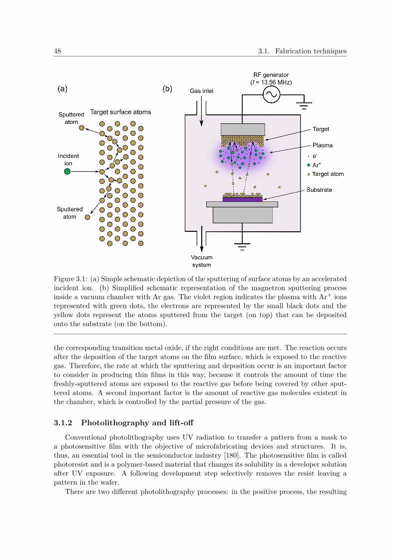
48 3.1. Fabrication techniques
Figure 3.1: (a) Simple schematic depiction of the sputtering of surface atoms by an acceleratedincident ion. (b) Simplified schematic representation of the magnetron sputtering processinside a vacuum chamber with Ar gas. The violet region indicates the plasma with Ar+ ionsrepresented with green dots, the electrons are represented by the small black dots and theyellow dots represent the atoms sputtered from the target (on top) that can be depositedonto the substrate (on the bottom).
the corresponding transition metal oxide, if the right conditions are met. The reaction occursafter the deposition of the target atoms on the film surface, which is exposed to the reactivegas. Therefore, the rate at which the sputtering and deposition occur is an important factorto consider in producing thin films in this way, because it controls the amount of time thefreshly-sputtered atoms are exposed to the reactive gas before being covered by other sput-tered atoms. A second important factor is the amount of reactive gas molecules existent inthe chamber, which is controlled by the partial pressure of the gas.
3.1.2 Photolithography and lift-off
Conventional photolithography uses UV radiation to transfer a pattern from a mask toa photosensitive film with the objective of microfabricating devices and structures. It is,thus, an essential tool in the semiconductor industry [180]. The photosensitive film is calledphotoresist and is a polymer-based material that changes its solubility in a developer solutionafter UV exposure. A following development step selectively removes the resist leaving apattern in the wafer.
There are two different photolithography processes: in the positive process, the resulting

3. Experimental techniques 49
photoresist pattern after development is the same pattern of the mask, while in the negativeprocess the inverted pattern is obtained after development.
A positive lithography process can be condensed into four different stages:
1. Photoresist application into the wafer/substrate
2. Alignment of the mask and the wafer/substrate
3. Exposure of the photoresist to the UV radiation
4. Chemical development of the pattern
In stage 1, the photoresist, which normally comes in the form of a solution, is spin-coated ontop of the substrate and is dried in a heating step. Afterwards, in stage 2, the mask must bealigned in respect to the substrate in the exposure system. The alignment is essential whenmultiple photolithograpy steps are required to obtain the final structure, enabling the correcttranslation of the desired result. The alignment is normally achieved by designing structuresin the mask that enable easy orientation of the substrate in the alignment system. After thealignment, in step 3, the photoresist is exposed to the UV radiation according to the maskpattern. The simplest way to perform the exposure is by bringing the mask and the substrateinto contact for exposure. Finally, the substrate is immersed in a chemical developer thatremoves the unexposed regions of the resist. The final result is the exact transfer of thepattern from the mask into the substrate in the form of a resist layer. For the negativeprocess, two additional stages are needed before the development. After the exposure withthe mask the substrate must be heated again and then exposed to the UV radiation withoutthe mask (flood exposure). When the development is then applied, the resist regions thatwere previously exposed to the UV radiation during the exposure with the mask, are now theones being removed by the chemical bath.
The transferred pattern can be used for different purposes in microfabrication. The pat-tern can be used as a mask for wet or dry etching, as a mask for ion implantation or it canbe used to selectively deposit thin films. The latter application is called lift-off and is the oneused in this work. The material deposited on top of the resist is later washed away during thestripping of the resist, leaving only the regions without the resist covered by the depositedfilm. For lift-off, the thickness of the film to be deposited must be less than the resist thick-ness and the deposition process should not exceed 120 C due to the thermal limitation ofthe resist. The stripping of the resist is achieved with acetone.
Figure 3.2 depicts a possible negative lithography process followed by lift-off used todeposit a thin film only in certain regions and enable microstructuring of electronic devices.
The photolithography system used in this work was the Karl Suss MA6 Mask Aligner. Thephotoresist was the AZ5214E and the developer was the AZ826MIF. UV radiation with awavelength of 365 nm was used for the exposure.
Experimental conditions for this work

50 3.1. Fabrication techniques
Figure 3.2: Schematic diagram of a negative lithography process used in this work for thefabrication of the samples: (a) the solution with the photoresist (AZ5214E) is spin-coatedon top of a previously cleaned substrate at 6000 RPM during 30 s; (b) the photoresist isdried during a heating step at 90 C for 5 min; (c) After proper alignment of the substraterelatively to the transfer mask, the photoresist and the mask are exposed to UV radiation for4.5 s, leading to the photochemical change of the exposed regions of the photoresist. (d) Theradiation exposure is followed by a second heating step, this time at 115 C for 2 min; (e) thephotoresist is exposed to UV radiation a second time now without the mask for 14.5 s (floodexposure); (f) finally the photoresist is developed in a chemical bath (developer: AZ826MIF)and afterwards cleaned in deionized water, resulting in the inverse pattern of the transfermask solidly drawn by the photoresist layer; (g) the desired thin film can be deposited onthe whole surface of the substrate with the lithographically defined resist pattern; (h) thefinal step is the lift-off with the stripping of the resist by acetone. The final result shows thedeposited film remaining only in the regions that are defined in the transfer mask. In thecase of a positive process, the exposure time in (c) is increased to 7 s and steps (d) and (e)are skipped.

3. Experimental techniques 51
Figure 3.3: Schematic representation of the wave interference of X-rays that leads to Bragg’slaw. The lines in red indicate the path difference between the two reflected X-ray beams, whichmust be a multiple of the wavelength of the X-rays in order for constructive interference tooccur. This condition is stated as Bragg’s law.
3.2 Structural characterization techniques
3.2.1 X-ray diffraction (XRD) and X-ray reflectometry (XRR)
X-ray diffraction
The classical and most used technique for the assessment of the crystal structure of ma-terials is the X-ray diffraction (XRD) [181]. The technique is based on the diffraction ofX-rays in crystals that was discovered by Max von Laue in 1912. The diffraction results wereexplained in a very simple way by W. H. Bragg and his son W. L. Bragg in 1913. WhileLaue envisaged crystals in terms of a three-dimensional network of rows of atoms, the Braggsthought of crystals as layers or planes of atoms that acted as reflecting planes for the X-rays,analogously to optics. Although not physically correct, the geometrical framework madesense, and the simplicity of the system led to the famous Bragg law:
nλ = 2dhkl sin θ, (3.1)
where λ is the wavelength of the X-rays, n is the order of diffraction, dhkl is the lattice planespacing for (hkl) planes and θ is the angle of incidence (and reflection) relatively to the latticeplanes, also known as Bragg’s angle. The hkl indices are called Miller indices and representa set of lattice planes. The expression 3.1 is a condition for constructive interference of thewaves scattered by atoms from adjacent (hkl) lattice planes, and can be calculated from thegeometrical analysis of the scheme in Fig. 3.3.
Bragg’s law enables the identification of the lattice planes of a crystal that produce diffrac-tion in a certain configuration and their inter-planar spacing. This carries information on thelattice parameters, and therefore on the size and shape of the unit cell of the crystal struc-ture. A typical XRD diffraction pattern shows not only the geometry of the diffraction, butalso contains information on the intensity of the diffraction spots. For the latter, expression3.1 does not provide explanation, however. The intensity of the diffraction depends on theatoms where the X-rays scatter, more specifically on the number of electrons, which are themain contributors to the scattering, and also on the position of the atoms in the unit cell.Therefore, this already gives information of the chemical nature of the material. The atomic

52 3.2. Structural characterization techniques
scattering factor represents the scattering amplitude of an atom. By summing the atomicscattering factors of all the atoms in the unit cell of the crystal structure, the structure factorFhkl is obtained. The structure factor then modulates the intensity of the diffracted beams.
In practice, the X-ray beams have a finite breadth and are not perfectly parallel. Theseinstrumental factors give rise to a broadening of the diffracted X-ray beams, which translatesin a broadening of the diffraction peaks in a diffractogram. But the broadening can alsostem from the material under study, and is due to the crystallite size and its state of strain,particularly important for thin films over substrates. The broadening of the X-ray beam dueto the crystal size is given by Scherrer equation:
β = λ
t cos θ , (3.2)
where the broadening β is the width at half the maximum peak intensity and t is the size ofthe crystallite.
The more common experimental configuration for the measurement of XRD from poly-crystalline samples is the Bragg-Brentano symmetrical arrangement. The X-ray source andX-ray detector are positioned so that the incident and reflected beams make equal angles tothe specimen surface. For example, the sample is fixed while the source and detector arerotated in opposite sense. It is geometrically identical to fix the source while rotating thesample and the detector with double the angular speed of the sample. In this arrangement,only the d-spacings of the planes that are parallel to the sample surface are measured. There-fore, for a single crystal only one diffraction peak is obtained. For a powder sample, however,due to the random orientation of the crystals, it is possible to obtain many more diffractionpeaks. A scheme of the Bragg-Brentano configuration is shown in Fig. 3.4(a).
For a sample with very thin films, the signal from the substrate can become problematicdue to the high penetration depth of the X-rays. In light of this, a different configurationis better suited, where the angle of incidence of the X-ray relatively to the sample surfaceis very small. This configuration decreases the interaction of the X-rays with the substrateand largely increases the interaction length in the thin films. This approach is called grazingincidence X-ray diffraction (GIXRD). Fig. 3.4(b) shows a typical geometrical configuration tomeasure the GIXRD. The X-ray beam is made very parallel, for example using a mirror, andis incident at a very small angle to the sample surface that is kept constant, while the detectoris swept along the arc centred on the sample. The scattering vector Q in the figure indicatesthe (hkl) planes that are detected for each 2θ angle, which are the ones perpendicular to thescattering vector [182, 183].
X-ray reflectometry
Beyond diffraction, the X-rays can be used to obtain more information on thin films. Whenconsidering a sample composed of a thin film on top of a substrate, as depicted in Fig. 3.5(a),the incident X-ray beam can be reflected on the surface of the thin film, can be transmittedthrough it, or even be absorbed in the thin film or in the substrate bulk. There is, however,a critical angle of incidence, relatively to the surface, below which there is no transmissiondue to total reflection. The total reflection occurs because, for the majority of materials, therefraction index for X-rays is below 1, the refraction index of air. This angle is normallyaround 0.1. The X-rays that are transmitted through the thin film can be again reflectedat the film/substrate interface and be transmitted back to the air. This transmitted ray will

3. Experimental techniques 53
Figure 3.4: Schematic illustrations of two different experimental configurations to measureX-ray diffraction: (a) Bragg-Brentano configuration. (b) Grazing incidence configuration.
interfere with the reflected one, constructively or destructively, depending on the thickness ofthe thin film. The mathematical treatment of this situation is based on the Fresnel reflectionand transmission coefficients as derived in the electromagnetic wave propagation theory. Bychanging the angle of incidence, successive destructive and constructive interference conditionscan be achieved. By measuring the periodicity of the fringes pattern in the reflectivity vs.incident angle plot, such as the one in Fig. 3.5(c), the thickness of the thin film can beretrieved [184].
The critical angle of incidence, below which total reflection is observed, carries informationon the density of the thin film material. The complex refractive index is described by adeviation from unity with a real dispersive part δ and an imaginary dissipative part relatedto absorption β [185]:
n = 1− δ − iβ. (3.3)
The dissipative part β is usually much smaller than the dispersive part δ, so it normally isneglected, giving n = 1− δ. The latter term is given by:
δ = λ2re2π ρe (3.4)
where λ is the wavelength of the incident X-rays, re ≈ 2.818×10⁻¹⁵ m is the classical electronradius and ρe the electron density. The electron density can be used to calculate the massdensity ρm of the material by:
ρm =∑i xiAi
NA∑i xi (Zi + fi)
ρe, (3.5)
with xi the atomic (or molar) ratio, Ai the atomic mass, Zi the atomic number and fi theatomic scattering factor, all for the ith atom, and NA is Avogadro’s number. Using Snell’slaw for refraction and the knowledge that δ 1, one arrives at the condition for the criticalangle θc for total reflection:
θc ≈√
2δ. (3.6)
Therefore, the measurement of the critical angle enables the determination of the density ofthe thin film.

54 3.2. Structural characterization techniques
Figure 3.5: (a) Schematic illustration of the X-ray reflection and refraction at the air-filminterface, showing the path of the X-rays and the origin of the intereference that gives riseto the fringes in the X-ray reflectometry data. (b) Sketch of the experimental configurationused to measure the X-ray reflectometry. It is symmetrical just like the Bragg-Brentanoconfiguration for XRD measurements, but as it is dealing with very small angles of incidence,takes the necessary instrumentation considerations used in the GIXRD configuration. (c)Example of XRR data, showing how the film density and thickness can be retrieved from thedata. The data refers to a 36 nm-thick Pt thin film on top of SiO2 with a 6 nm-thick Taadhesion layer.

3. Experimental techniques 55
The equipment used for the XRD and XRR measurements was the PANalytical “X’PertPRO” X-ray diffractometer. The characteristic Cu Kα radiation with λ = 1.5406 Å wasused in all measurements. The analysis of the layers by XRR with the determination of thethickness and film density was performed by fitting the experimental data to a layer modelusing a commercial software from PANalytical.
Experimental conditions for this work
3.2.2 Rutherford backscattering spectrometry (RBS)
Ernest Rutherford developed a model of the atom in 1911 based on the experimentalobservation of backscattering of alpha particles from a gold foil, which was not compatiblewith the “plum-pudding” model of the atom, put forth in 1904 by J. J. Thomson. Ruther-ford’s experimental setup was later adapted into a technique for the analysis of solids namedRutherford backscattering spectrometry (RBS) [186].
The technique consists in the irradiation of solid materials with accelerated light ions(normally 4He+) and the detection of the backscattered ions due to collisions with the atomsfrom the material. The energy lost by the backscattered ions gives quantitative informationon the chemical composition of the material and the depth profiling of individual elements.
In the Cornell geometry, the incident beam, the exit beam and the sample rotation axisare in the same plane, as illustrated in Fig. 3.6(a). This geometry has the advantage ofcombining a large scattering angle, which enables a better mass resolution, with the possibilityto irradiate the sample in a grazing incidence, which increases the depth resolution.
The determination of the energy of the backscattered ions is based on the classical kine-matics of elastic collisions, with conservation of energy and momentum, where the ions areconsidered hard spheres. The situation is schematically depicted in Fig. 3.6(b). Given anion with incident energy E0 and mass M1, its energy after the elastic collision is given in thelaboratory system by:
E1 = KE0, (3.7)
where K is the kinematic factor given by:
K = M21
(M1 +M2)2
cos θ ±
√(M2M1
)2− sin2 θ
2
, (3.8)
with θ the scattering angle andM2 the mass of the target nucleus, considered to be initially atrest. This is enough to determine the elements that compose the sample material. However,this simple classical kinematic approach to the problem does not enable the quantitativeanalysis of the material composition. For that, the model of the collision has to be enhancedby considering the scattering due to the Coulomb repulsion between the charged ion and thecharged nucleus of the atom where the first scatters.
To quantify the number of atoms in the target per unit of cross section area, one needsto know the probability of collision between the incident ion and the atoms of the target.This can be obtained by measuring the total number of detected ions for a certain numberof incident ions. The effective scattering section describes the probability of an atom fromthe target to scatter an ion at an angle θ inside a solid angle dΩ centred around θ. In a RBS

56 3.2. Structural characterization techniques
system, the solid angle of the detector is small, so that the mean scattering section is givenby
σ (θ) = 4(Z1Z2e
2
16πε0E0
)2
[√1−
(M1M2
sin θ)2
+ cos θ]2
sin4 θ
√1−
(M1M2
sin θ)2
(m2sr−1
), (3.9)
with Z1 and Z2 the atomic numbers of the incident ion and of the target atom, respectivelyand ε0 the electrical permittivity of the vacuum. This formula takes into account the recoilof the target atom due to the Coulomb repulsion. The original formula by Rutherford didnot consider this recoil and comes simply as:
σ (θ) =(Z1Z2e
2
16πε0E0
)2 1sin4
(θ2
) . (3.10)
The depth profiling is possible due to the inelastic scattering with electrons (electronstopping) and target nuclei (nuclear stopping).
Complementary methods
The sensitivity of RBS for light elements is low, therefore it is often required to combine thetechnique with other methods such as nuclear reaction analysis (NRA) and/or elastic recoildetection analysis (ERDA). While NRA detects the ions that were inelastically scattered andthat took part in nuclear reactions, ERDA detects recoil atoms from the sample after thecollision at forward angles (Also shown in Fig. 3.6(a)). Depth profiling is also possible inERDA due to the same stopping effects mentioned before.
RBS measurements were made in the universal chamber, at grazing angle (78° or 80°) andat 45°. ERDA spectra were collected at 24° forward angle. The RBS detector is locatedat a scattering angle of 160° in the Cornell geometry. Spectra were collected for 2 MeV4He+. The RBS data were analysed with the IBA DataFurnace NDF v9.6i [187]. Doublescattering was calculated with the algorithms given in ref. [188]. Pileup was calculated withthe algorithms given in ref. [189].
The TaOx films used for the RBS measurements had a thickness of approximately 50 nmbut were not the same as the ones used in the XRD study due to a special structure usedto optimize the oxygen signal from the TaOx layer in the RBS spectra. A study based onsimulations of RBS spectra using the RUMP software [190] revealed that for the materialsavailable in the deposition tools used, the TaOx layers should be covered with an Au layer.This metallic layer is preferred to the Al2O3 used throughout the work, because the oxygensignal stemming from the Al2O3 would decrease the sensitivity of the technique to thedetermination of the oxygen content of the underlying TaOx layer. The same argument wasused against the use of the SiO2 insulating layer beneath the TaOx. So, a Si substrate withjust the natural oxide on the surface was preferred. The layer structure used for the RBSsamples is shown in Fig. 3.6(c), while the simulated RBS spectrum is shown in Fig. 3.6(d).
Experimental conditions for this work

3. Experimental techniques 57
Figure 3.6: (a) Simplified schematic illustration of the RBS configuration in the Cornellgeometry. The incident beam, the detected backscattered beam and the sample rotation axislie in the same plane. The RBS detector is positioned in the backward region, while theERDA detector is positioned in the forward region relatively to the ion beam incident onthe sample. (b) Illustration of the simplified kinematic approach to the backscattering ofaccelerated ions by atoms of the target (sample), where the ion and the atom are consideredhard spheres with mass M1 and M2, respectively. (c) Simulation of the RBS signal from aAu/TaOx/Si stack obtained using the simulation tool RUMP.

58 3.2. Structural characterization techniques
3.2.3 Transmission electron microscopy (TEM)
The smallest distance that can be resolved with a microscope is given by
δ = 0.61λn sinα, (3.11)
where λ is the wavelength of the radiation used in the microscope, n is the refractive index ofthe viewing medium and α is the semi-angle of collection of the magnifying lens. The denom-inator is known as the numerical aperture of the lens. Therefore, a smaller distance can beresolved if the numerical aperture is increased and/or the wavelength decreased. Transmissionelectron microscopy takes advantage of the fact that accelerated electrons have a very shortwavelength [191]. The wavelength of the electrons is determined by their kinetic energy Ecthrough:
λ = 12.2√Ec(eV)
(Å), (3.12)
ignoring relativistic effects. This relation means that with a higher accelerating voltage, ahigher resolution is achieved, i.e. a smaller distance can be resolved.
There are two main phenomena that are used to obtain a source for electrons in anelectron microscope: the thermionic emission and the field emission. In analogy with anoptical microscope, TEM also needs lenses to magnify and form the image. The lenses of theoptical microscope are substituted by magnetic lenses, normally based on the magneticallyinduced deviation of the electron trajectory. There are different types of lenses in the TEMand they control all the basic operations of the TEM. Either they act to demagnify the sourceimage onto the specimen or they magnify the image (or electron diffraction pattern) from thespecimen. Each lens is often accompanied by an aperture that can be inserted above, in, orbelow the plane of the lens. Its objective is to limit the collection angle of the lens, i.e. theelectrons that will form the image. The aperture of the objective lens controls the resolutionof the image, the image contrast, the depth of field, the depth of focus, among other things.The aperture of the condenser lens can select the electrons that illuminate the sample andthus form a more parallel beam when a smaller aperture is used, at the cost of decreasingthe electron current. The apertures are usually circular holes made in refractory metal disks.The placement of the objective aperture also allows to choose between two different types ofTEM images that can be acquired, a bright-field image or a dark-field image. For bright-fieldimaging the aperture is centred on the direct beam, while for dark-field imaging it is centredon a diffracted beam. Another approach to obtain dark-field is to tilt the electron beamincident on the sample so that the diffracted beam is on the optical axis, which reduces theeffect of aberrations (greater effect in off-optical axis beams).
The images are formed due to contrast, which is the difference in intensity between twoadjacent areas. In TEM, the contrast arises from the scattering of electrons by the sample.There are two distinct types of contrast, the amplitude contrast and the phase contrast. In theamplitude contrast there are two main mechanisms of contrast, the mass-thickness contrastand the diffraction contrast, so that in total there are three main mechanisms of contrast. Themass-thickness contrast is related to the stronger scattering of the electrons by more dense(higher mass of the elements) and thicker samples, which translates into higher scatteringangles and gives rise to a darker region in the bright-field image [192]. The diffraction contrastarises from the differing amplitudes of the undiffracted and diffracted beams, which resultsin different intensity variations in the image formed by the different beams. It is the major

3. Experimental techniques 59
Figure 3.7: (a) Simplified scheme of a TEM with an EDX detector, showing the main com-ponents used to form an image of a thin sample. The rays indicated are relative to the imageformation and not to the diffraction pattern. (b) Scheme illustrating the image formationin STEM, highlighting the main instrumentation differences relatively to traditional TEMshown in (a). For the specific case of HAADF STEM imaging the signal is collected at thehigh-angle annular dark field (HAADF) detector and used to produce the image of the sample.
contrast mechanism in crystalline samples. The diffracted beams are used to form dark-fieldimages. Microstructural features like bends, variations in the thickness and crystal defectsshow strong diffraction contrast. The phase contrast is due to the interference of electronswith different phases and is specially important for high-resolution TEM (HRTEM). Thepossibility of imaging the atomic structure comes from the dependence of the interference ofthe electrons on the periodicity of the lattice.
The microscope
The TEM is normally composed by three main parts: the illumination system, the ob-jective lens and stage and the imaging system. A simplified scheme is presented in figure3.7(a).
The illumination system includes the electron gun and all the lenses that exist prior to thesample, and its function is precisely to illuminate the sample. This system can be operatedin the parallel beam mode, used for TEM imaging and diffraction (selected-area), and inthe convergent-beam mode, used for scanning TEM (STEM) and auxiliary techniques suchas energy dispersive X-ray spectroscopy (EDX or EDS) and electron energy loss spectrome-try (EELS). The illumination system operating in the parallel beam mode has at least twocondenser lenses that adjust the electron beam to be parallel as it illuminates the sample.With only two condenser lenses, the second condenser lens is underfocused, so that the focusplane is under the sample and the beam is approximately parallel as it hits the sample. By

60 3.2. Structural characterization techniques
decreasing the size of the condenser aperture the beam can be made more parallel, at theexpense of the electron current. The inclusion of a third condenser lens makes it easier toobtain of a parallel beam at the sample. For operation in the convergent beam mode, thesecond or the third condenser lens is focused on the sample.
The objective lens and stage are the most important components as it is where the beam-sample interactions occur. Also, the quality of the objective lens defines the quality of theretrieved information as it is responsible for the creation of both the image and the electrondiffraction pattern. These can be obtained in the image plane and in the back focal planeof the objective lens, respectively. The stage is used to fix the sample after the focusing hasbeen achieved and the eucentricity set. The eucentric plane is a reference plane for side-entrysample holders where a tilt of the sample along the holder axis does not laterally move a pointin the optic axis. This simplifies the acquisition of the images and the diffraction patterns.
After the objective lens the image and diffraction patterns need to be magnified beforereaching the screen/detector, which is achieved with the imaging system that contains at leasttwo more lenses: an intermediate lens and a projector lens. If the selected area diffractionpattern is wanted, an aperture, known as selected area aperture, is inserted in the image planeof the objective lens in order to virtually select the area of the sample that is illuminated. Ifthe image is to be acquired, another aperture, known as the objective aperture, is inserted inthe back focal plane of the objective lens. The location of this aperture can be changed inorder to obtain a bright- or dark-field image.
Finally, the image is formed by transforming the transmitted electron beam into vis-ible light through cathodoluminescence. Traditionally this was performed with a fluores-cent screen, but this has evolved into detectors based on semiconductors or scintillator-photomultiplier systems, such as a charge-coupled devices (CCD).
Scanning transmission electron microscopy
Scanning TEM (STEM) is obtained when the incident beam is scanned over the sample,instead of being static and incident on a larger area as in the traditional TEM described[191]. The beam is controlled by scan coils that deflect it into a point in the sample. Thesignal generated from the transmission of this beam is then displayed in the final image atan equivalent point. STEM uses double deflection scan coils in order to guarantee that theincident beam is always parallel to the optical axis, so that the diffraction is achieved in thesame conditions for every scanning point.
In a STEM all the lenses after the objective lens are dispensed, as the detector is placedon a conjugate plane of the back focal plane of the objective lens in the direct beam or adiffracted beam, if a bright- or dark-field image is to be acquired, respectively. But a bettersolution for dark-field imaging is to use an annular detector that surrounds the bright-fielddetector, eliminating the need for the detector’s displacement. This establishes the annulardark field imaging. If the electrons scattered at higher angles are collected by a detectorsurrounding the first annular detector, the technique is called high-angle annular dark field(HAADF) STEM. The scattering at higher angles is mostly caused by Rutherford scatteringof the electrons at the nucleus of the atoms of the sample. This enables a different contrastmechanism, comparatively to the normal TEM, which is called Z-contrast (Z stands for theatomic number). In this high-angle collection mode, the Z-contrast should superimpose thediffraction contrast from crystalline parts of the sample, which is more prominent for lowerangles. The Z-contrast is highly chemically sensitive because the elastic cross section of the

3. Experimental techniques 61
scattering is highly dependent on Z, resulting in a higher signal (brighter image) from heavyelements.
EDX
The interaction of the electrons with matter leads to the generation of different types ofsignals that can be detected accordingly by auxiliary techniques and give useful information toaid the sample analysis. The accelerated electrons of the beam can induce electron transitionsin the atoms, which upon relaxing will emit characteristic X-rays. This characteristic radiationcan be collected in a detector in order to retrieve information about the chemical compositionof the sample. Combined with the STEM imaging, this allows a chemical mapping of thesample. The technique associated with the detection and analysis of these X-rays is calledenergy-dispersive X-ray spectroscopy (EDX or EDS).
The HAADF STEM imaging combined with EDX spectroscopy mapping was carried outon a FEI Titan ChemiSTEM probe Cs-corrected TEM operated at 200 kV and equippedwith a Bruker “Super-X” wide solid angle EDX detector. The microscope is thoroughlydescribed in [193].
Experimental conditions for this work
3.3 Electrical characterization techniques
3.3.1 Current-Voltage measurements
An important way to characterize the electrical behaviour of an electronic device or elec-trical circuit is achieved by measuring its current-voltage (I−V ) characteristic, which depictsthe current response of a device/circuit when an electric potential difference (voltage) is ap-plied at its terminals. A simple I − V measurement can immediately distinguish differenttypes of devices, such as resistors, diodes, solar cells or memristive devices. The I−V charac-terization is, in fact, an essential procedure in the study of the RS. Although memory devicesare meant to be operated in a pulsed voltage/current scheme, the I−V characteristics enablethe study of the memory operation [2]. Typically, continuous voltage sweeps are used to mea-sure the I−V characteristics, but pulsed sweeps are also common, where the voltage increaseor decrease is performed by pulses interleaved by a time interval where no voltage is applied.By analysing the I − V characteristics, the different resistance states can be distinguishedand the main RS characteristics can be obtained, namely the SET and RESET voltages,the ohmic or rectifying character of the curves, as well as the resistance in each state. TheI − V curves, at least for a certain voltage range, also contain information on the conductionmechanisms involved in the different resistance states.
The I − V measurements were carried out using a SourceMeter from Keithley. Differentmodels were used with little relevant changes in their specifications between them for themeasurements performed: either 2611A, 6440 or 2440. The measurements were automatedvia in-house written software, written in LUA (RWTH) or Matlab® (UAveiro). The deviceswere probed in a suitable probestation equipped with micropositioners, a microscope and
Experimental conditions for this work

62 3.3. Electrical characterization techniques
Figure 3.8: (a) Illustration of an arbitrarily shaped sample where 4 electrical contacts A,B, C and D are made to measure the resistivity through the van der Pauw (vdP) method.(b) Illustration of a possible symmetrical vdP configuration, the one used in this work. (c)Schematic of one of the individual measurements required for obtaining the resistivity bythe vdP method, where the current is applied between adjacent contacts (A,B) and thevoltage is measured between the two remaining contacts (C,D). (d) Schematic of the wiringconfiguration needed for a Hall measurement using the vdP method, where the current isapplied between diagonally opposite contacts (B,D) and the Hall voltage is measured betweenthe two remaining contacts (A,C).
tunsgten needles for electrical contacting (RWTH), or in a in-house-made sample holder withwire-bonding via gold wires (UAveiro). The voltage was swept in a quasi-static (continuous)regime with a sweeping rate of approximately 0.5 V/s.
3.3.2 Resistivity measurements
In a two-point measurement the sample is measured by using two contacts, which serveas both current and voltage probes. While being the most simple measurement method, thisconfiguration leads to a measured resistance that includes not only that of the sample but alsothe contact resistance and the resistance from the wires/probes that connect the sample tothe measurement equipment. This problem can be largely avoided by employing a four-pointconfiguration. Two additional contacts are made, separating the current probes, throughwhich a current is imposed into the sample, from the voltage probes, where the voltage dropin the sample is measured. Due to the normally high input impedance of a voltmeter, thecurrent flowing through the voltage path is very low, greatly decreasing the voltage drops dueto the contact and wire resistances.
Typical 4-point methods to measure the resistivity (ρ) of materials include the collinear4-probe method and the Hall test bar.
The van der Pauw method
An additional method for the measurement of the resistivity was developed by van derPauw in 1958 [194]. This is now known as the van der Pauw method, and it is particularlyuseful for the measurement of the resistivity and Hall effect of arbitrarily shaped samples,such as the example illustrated in Fig. 3.8. Applying a current IAB between the contacts A

3. Experimental techniques 63
and B and measuring the potential difference VDC between contacts D and C, the measuredresistance is:
RAB,DC = VDCIAB
. (3.13)
Analagously, we can writeRAD,BC = VBC
IAD. (3.14)
The van der Pauw method is based on the theorem that there is a relation between these tworesistances, expressed as:
exp(−πRAB,DC
RS
)+ exp
(−πRAD,BC
RS
)= 1, (3.15)
where RS = ρ/t is the sheet resistance, from which the resistivity can be directly obtained withthe knowledge of the thickness t of the sample. This equation has to be solved numerically toobtain RS . However, if the sample is symmetrical, so that RAB,DC = RAD,BC = R, equation(3.15) is simplified, and the sheet resistance can be directly calculated by:
RS = π
ln 2R ≈ 4.532R. (3.16)
The accuracy of the resistivity determination can be enhanced if the reciprocal values ofresistance are also measured, i.e. if the current and voltage probes are switched for each ofthe resistances indicated above. An average of these resistances for each pair of contacts isthen calculated:
Rh = RAB,DC +RDC,AB2 and Rv = RAD,BC +RBC,AD
2 , (3.17)
which are then introduced in eq. (3.15):
exp(−πRh
RS
)+ exp
(−π Rv
RS
)= 1. (3.18)
Further accuracy is obtained when the direction of the current is reversed, leading to a totalof 8 resistance measurements. This is important for the case of strong voltage offsets due, forexample, to thermoelectric effects. Eq. (3.18) can be solved numerically, e.g. with Newton’smethod, in order to obtain RS and consequently the resistivity ρ.
The van der Pauw method is based on the assumption of negligibly small contacts locatedon the sample periphery. Not taking this into consideration largely increases the experimentalerror and compromises the resistivity value obtained [141]. For this work, a symmetricalsquare sample with electrical contacts at the 4 vertices was chosen, as depicted in Fig. 3.8(b).The contact configuration to measure the resistivity is shown in Fig. 3.8(c).
3.3.3 Hall and magnetoresistance measurements
Hall measurements are based on the Hall effect and enable the determination of the chargecarrier sign, density and mobility [141]. The Hall effect was discovered by Edwin Hall in 1879.It describes the appearance of an electric field when a magnetic field is applied perpendicularlyto the current flow in the conductor. The electric field develops perpendicularly to both thecurrent and the magnetic field and is caused by the accumulation of charge carriers on one

64 3.3. Electrical characterization techniques
of the sides of the sample due to the deflection imposed by the magnetic field. The voltageassociated with the produced electric field is called the Hall voltage and, considering thatelectrons are the only charge carriers, it is given by:
VH = − tRHBI
, (3.19)
with t the film thickness, B the external magnetic field, I the current and RH the Hallcoefficient, which carries the information on the carrier concentration (n):
RH = − r
qn, (3.20)
where r is the Hall scattering factor, which is dependent on the scattering mechanism of thecharge carriers, but that normally ranges between 1 and 2 at low magnetic fields. Therefore,r is normally taken as unity. However, in some cases, it may be needed to account for theactual value of r [195]. The Hall mobility differs from the conductivity mobility (as definedin eq. (2.2)) and is given by:
µH = |RH |ρ
= 1qnρ
. (3.21)
The drift mobility is obtained by dividing the Hall mobility by the Hall scattering factor r.The Hall effect is normally measured in a bridge-shaped sample. However, the van der
Pauw geometry enables an easier approach to measure the Hall effect. The measurementconfiguration differs from that of the resistivity measurements as the measurement has to bedone diagonally. For the symmetric arrangement of Fig. 3.8(b), this means that the voltageis measured betweeen contacts A and C (VAC), while sourcing current through the contactsD and B (IDB), as can be seen in Fig. 3.8(d).
The application of an external magnetic field can also have an effect in the resistivity.The change in resistance induced by a magnetic field is called magnetoresistance (MR) andis calculated by:
MR = RB −R0R0
, (3.22)
with RB being the resistance for an applied magnetic field B and R0 being the resistancewithout an applied magnetic field.
3.3.4 Temperature and magnetic field dependence
To further characterize the electrical transport, resistivity, Hall and MR measurements areperformed in the temperature range from 1.8 K to 300 K. These measurements play a centralrole in the study presented in this work, because the transport mechanisms have differenttemperature fingerprints that are visible through the characteristic temperature dependenceof the resistivity, the Hall parameters and the MR. The access to the lowest temperatures isespecially relevant and may give useful information regarding the local disorder resulting inquantum interference effects (as presented in chapter 2). These disorder-induced effects, suchas weak (anti)localization and electron-electron interactions, are normally only observableat very low temperatures. Recently, this kind of analysis was successfully applied to phase-change materials [196]. In order to have access to the low temperatures, a cryostat is needed.

3. Experimental techniques 65
The electrical measurements performed in this work were mainly carried out in two cryostatsfrom Quantum Design, Inc.: the PPMS® and the PPMS® Dynacool™, where PPMS standsfor Physical Property Measurement System. The major differences between the two systemsare the lowest available temperature and the cooling technology. While the PPMS usesliquid helium to refrigerate down to 2 K, the Dynacool uses a cryogen-free pulse tubecryocooler to reach the lower temperature of 1.8 K. Both cryostats enable the applicationof a magnetic field of up to 9 T to the samples. The magnetic field is provided by asuperconducting coil incorporated inside the cyostats. The magnetic field direction is fixedwith respect to the cryostat, but for angular dependence of the magnetic field, a rotatingsample stage was available. All samples were wire-bonded with Al wires to establish theelectrical contacting inside the cryostats. The temperature was measured directly at thesample holder, minimizing the temperature offset, and it was swept at a maximum rate of4 K/min. The magnetic field was swept at a maximum sweep rate of 10 mT/s.
For additional measurements, a third cryostat was employed: the TTP4 cryoprobesta-tion from Lake Shore®. This cryostat uses liquid nitrogen to provide a flow of cooled Hegas to a metallic sample stage, where a minimum temperature of 80 K is achieved. Thisenabled in-situ electrical contacting via four micropositioners equipped with tungsten nee-dles, making it possible to change the device being measured while in vacuum and at lowtemperature.
Experimental conditions for this work
3.4 Auxiliary techniques
3.4.1 X-ray photoelectron spectroscopy (XPS)
The photoelectric effect, famously explained by Albert Einstein in one of his annusmirabilis papers of 1905, consists in the ejection of electrons from atoms of a solid throughbombardment with photons of sufficient energy. The ejected electrons are then called photo-electrons. There is a minimum energy necessary to produce photoelectrons that is defined bythe work function of the solid Φ. This minimum energy is related to a threshold frequencyνt, which is then given by:
hνt = Φ. (3.23)
For photons with a higher frequency, there is an excess of energy that is converted into kineticenergy of the photoelectrons:
hν = Φ + 12mev
2, (3.24)
where me and v are their mass and velocity. Photoelectron spectroscopy (also known as pho-toemission spectroscopy) makes use of this effect in order to retrieve information of materials’surfaces by the analysis of the ejected photoelectrons’ kinetic energy [197]. Compared to theeasily ionizable alkali metals, for which ultraviolet radiation was sufficient to eject electrons,normal solid surfaces demand higher energy photons. The X-ray photoelectron spectroscopy(XPS) is a particular kind of photoelectron spectroscopy, where X-rays are used to excite thephotoelectrons. XPS can induce the ejection of electrons not only from the valence orbitalsbut also from the core orbitals of the atoms. Therefore, XPS may be used to retrieve chemical

66 3.4. Auxiliary techniques
information of the materials under study, namely the valence state of the cations in transitionmetal oxides and chemical changes that occur in interfaces.
The photoelectrons are inelastically scattered in the material, which largely reduces theirmean free path, and therefore the depth from which these electrons can reach the vacuum.Therefore this technique is only surface sensitive and does not provide information of the bulkof the materials or deep layers buried below the surface. This is particularly important insamples where the surface is prone to be modified by atmospheric exposure.
The XPS measurements were carried out in a NanoESCA Photoemission electron microscopefrom Scienta Omicron GmbH (described in detail in ref. [198]). The machine is equippedwith a monochromatic aluminum Kα source with an excitation energy of 1486.6 eV. Forobtaining regular, non spatially resolved, photoelectron spectra a single channeltron detectorwas used.
Experimental conditions for this work
3.4.2 Local conductivity atomic force microscopy (LC-AFM)
Atomic force microscopy (AFM) is a powerful tool for materials research at the nanoscale.It makes use of a small sharp tip to analyse the surface of materials with a high lateralspatial resolution of the order of nm. The physical principle behind the technique is theforce exerted on the small tip by the atoms of the surface. This force is attractive or repulsivedepending on the distance between the tip and the surface, and can be qualitatively describedby the Lennard-Jones potential. This mechanism allows the mapping of a sample’s surfacetopography.
The AFM is quite versatile, as the tip can be designed to enable measurement of otherphysical properties of the sample’s surface. When the tip is carefully designed in order to beconductive, the microscope can be used for local conductivity AFM (LC-AFM), also knownjust as conductive AFM (CAFM) [199]. With this technique, when a voltage is appliedbetween the tip and the sample, the current through the sample can be mapped, along withthe topography of the surface. For measuring the current, the microscope needs to be operatedin contact mode.
The LC-AFM was applied for the first time to analyse the electrical properties of gateoxides in the 1990s [200]. More recently it has been widely used to study the RS phenomenonin oxides [201, 202].
The LC-AFM measurements were conducted in a VT-SPM XA microscope from ScientaOmicron GmbH. An ultrananocrystalline diamond (UNCD) cantilever with a tip diametersmaller than 150 nm was employed and a force of 2 nN was used for the contact modeoperation of the LC-AFM. The base pressure of the chamber was 10−9 mbar.
Experimental conditions for this work
3.4.3 Optical absorption spectroscopy
Electromagnetic radiation interacts with matter in different ways. When light, a particularcase of electromagnetic radiation, shines on the surface of a material, it can be reflected,

3. Experimental techniques 67
transmitted or absorbed. From these different types of light-matter interaction it is possibleto obtain valuable information of the materials. In particular, the absorbed light carriesinformation on the electronic properties of the material, namely the energy bandgap andother possible in-gap electronic states [203].
The absorption needs to be measured indirectly, by measuring the transmitted and re-flected light. The most common approach limits the experiment to the measurement of theintensity of the transmitted light and to its comparison with the intensity of the incidentlight. The absorbance A is then given by the Beer-Lambert law:
A = log10
(I0I
), (3.25)
where I0 is the intensity of the light incident on the sample surface, which is measured withoutthe sample in the beam path, and I is the intensity transmitted through the sample.
The absorption spectroscopy measurements were performed in a Shimadzu UV-3600 UV-Vis-NIR spectrophotometer. The subtrate was measured first, so its signal could be sub-tracted from the data collected for the different samples with the thin films deposited ontop of the substrate.
Experimental conditions for this work
3.5 Sample fabrication details
Radiofrequency (RF) magnetron sputtering was used to deposit all the layers during thefabrication of the samples. All the samples were grown on top of thermally oxidized p-doped (100)-oriented Si substrates with approximately 430 nm of SiO2. The as-purchased Sisubstrates (6 ” wafers) were cleaned and afterwards the SiO2 layer was formed via thermaloxidation. The base pressure of the sputtering chamber was always lower than 10−5 mbar andhigher than 10−7 mbar before the deposition of the layers, and the sputtering was performedat room temperature.
3.5.1 ReRAM devices
The ReRAM devices were fabricated in a crosspoint geometry. This not only allowedthe investigation of microdevices, but also enabled remote contacting of the devices withoutsignificantly disturbing the active device area. This last point was particularly important forthe low temperature measurements performed in the cryostats, where wire bonding to thesamples was needed. To allow an easier bonding to the contact pads, these were designed as300 µm-wide squares. On the other hand, the sample holder for the cryostats demanded amaximum sample size of 1× 1 cm. Therefore, a special photolithography mask was producedin order to abide to these conditions. A schematic depiction of the device geometry andlayout can be found in Fig. 3.9. UV photolithography and lift-off (as described in section3.1.2, and more specifically in Fig. 3.2), were used to pattern the devices in the crosspointgeometry with active cell areas of 5× 5 µm2, 10× 10 µm2 and 25× 25 µm2. The fabricationwas performed on top of 1” substrates and the devices were distributed evenly in four 1 × 1cm2 samples (Fig. 3.9(c)).

68 3.5. Sample fabrication details
Figure 3.9: (a) Crosspoint geometry used in the fabrication of the Ta2O5-based ReRAMdevices. (b) Layout of the 1× 1 cm2 samples used in the cryostats, each one with 27 ReRAMdevices (3 of the devices were grown without the oxide layer to use as a reference). (c) Layoutof the 1× 1 inch2 samples from which the 1× 1 cm2 samples were cut.
The layer stack and thickness of the different layers of the fabricated ReRAM devices werechosen based on a previous optimization process, in order to guarantee the obtention of thedesired bipolar counter-eightwise VCM-type switching [89]. The layer stack is composed of20 nm Pt as a bottom electrode (BE), a 5 nm-thick Ta2O5 layer, a Ta layer of 15 nm as topelectrode (TE) and a Pt capping layer of 20 nm. This capping layer prevents the oxidation ofthe Ta TE caused by exposure to the atmosphere. A second series of samples differed in thethickness of the Pt layers, which was increased to 30 nm while maintaining the thickness ofthe remaining layers. By changing the thickness of Pt, it is possible to tune slightly the seriesresistance. The metallic layers, Ta and Pt, were sputtered in an inert Ar atmosphere. A Tior TiOx adhesion layer of 5 to 15 nm was sputtered prior to the sputtering of the Pt bottomelectrodes. The Ta2O5 layer was reactively sputtered from a Ta target (99.95 % purity) in areactive atmosphere composed of a mixture of Ar and O2. The produced Ta2O5 films wereall amorphous. A schematic flowchart with the main steps in the fabrication of the Ta2O5crosspoint structures is depicted in Fig. 3.10(a). The main deposition parameters used forthe sputtering processes are shown in table 3.1.
3.5.2 Substoichiometric thin films
For the electrical transport measurements, the TaOx layers were patterned in a van derPauw structure with 30 nm-thick Pt electrodes using UV lithography and lift-off. The TaOx
layers have been sputtered with a thickness of 20 nm, mainly to keep a similar order ofmagnitude to the thickness of the oxide layer in the ReRAM devices. To avoid oxidationwhen exposed to air, the TaOx films were in-situ capped with a 20 nm-thick Al2O3 layer,which is a good oxygen diffusion barrier [204]. This layer should not oxidize the TaOx layer,because Al2O3 is a more stable oxide than Ta2O5 [82]. Fig. 3.10(b) schematically showsthe main fabrication steps used to obtain the van der Pauw TaOx samples. The layer stackand sample geometry are illustrated in Fig. 3.11. For the composition calibration, XRD andTEM measurements, the samples were sputtered without any patterning and with a thickerTaOx layer of approximately 50 nm. For the absorption measurements, the TaOx layers weresputtered on top of sapphire substrates.

3. Experimental techniques 69
Figure 3.10: Schematic diagram illustrating the main fabrication processes of: (a) the Ta2O5-based ReRAM devices; (b) the van der Pauw samples with the TaOx thin films. The columnin the left shows a perspective of the samples’ surface in order to schematically show theevolution of the deposited structures, while the column in the right shows the evolution ofthe layer stacks. BE = bottom electrode and TE = top electrode.

70 3.5. Sample fabrication details
Figure 3.11: (a) Schematic depiction of the van der Pauw structure used to fabricate theTaOx samples for electrical measurements, with some relevant geometric dimensions. (b)Illustration of the layer stack used in the van der Pauw structures.
Table 3.1: Summary of the reactive magnetron RF sputtering conditions used in the depositionof the different thin films used in this work, which include the metallic layers of Pt and Ta,the substoichiometric TaOx films, the stoichiometric Ta2O5 and Al2O3.
Filmcomposition
Power density[W/cm2]
Ar contenta)
[%]O2 contenta)
[%]Pressure[mbar]
O2 partialpressure [bar]
Pt 15.79 100 0 0.005 0Ta 19.74 100 0 0.004 0TaOx, x ∼ 1 29.60 99.98 0.02 0.01 2× 10⁻⁹
TaOx, x ∼ 1.3 17.76 99.98 0.02 0.01 2× 10⁻⁹
TaOx, x ∼ 1.5 9.87 99.96 0.04 0.01 4× 10⁻⁹
Ta2O5 19.74 60 40 0.04 16× 10−6
Al2O3 9.87 100 0 0.005 0
a)Percentage of the gas in the atmosphere inside the sputtering chamber.
The Pt contacts were sputtered in an inert Ar atmosphere. The TaOx layers were reac-tively sputtered from a Ta target (99.95 % purity) in a reactive atmosphere composed of amixture of Ar and O2 in different proportions. The oxygen content in the TaOx thin filmswas tuned by modifying the O2-to-Ar ratio, the chamber pressure (operating pressure) andthe RF power. This influences two main parameters: the oxygen partial pressure and thedeposition rate. To allow the needed low oxygen partial pressure, a gas bottle with a mixtureof 1% O2 and 99 % Ar was used to obtain the TaOx films with the lowest oxygen content.Also the deposition rate should not be too low, as increasing it increases the probability of thereaction of sputtered Ta with the oxygen in the chamber. On the other hand, to guarantee thedeposition of the stoichiometric Ta2O5, it is important to have a high oxygen partial pressureand a low deposition rate. For comparison of the experimental results obtained for the TaOx
samples, films of Ta and Ta2O5 were also sputtered. For the former, no O2 was introducedin the deposition chamber. Finally, the capping layer of Al2O3 was sputtered from a ceramicAl2O3 target in Ar atmosphere. The sputtering conditions for the five main compositionsused in this work are summarized in table 3.1.

Chapter 4
Correlation between the transportmechanisms in Ta2O5-basedReRAM devices and in TaOx thinfilms
This chapter deals, in most part, with the electrical properties of the conductive fila-ments in Ta2O5-based ReRAM devices and their relation to the in-plane transport insubstoichiometric TaOx thin films. First, the resistive switching in the Ta/Ta2O5/PtReRAM devices used throughout the work is characterized. The ReRAM devices with15 nm-thick Ta top electrodes and 5 nm-thick Ta2O5 show the typical bipolar RS ofVCM systems. Afterwards, the temperature dependence of the resistance in differentresistance states (low and high) of the ReRAM devices is shown. For comparison, thetemperature dependence of the resistivity of substoichiometric TaOx thin films is pre-sented. Finally, a correlation between the transport in the conductive filaments in thedevices and the in-plane transport in TaOx thin films with x ∼ 1 is highlighted anddiscussed.
The major results and conclusions presented in this chapter were published in: CarlosM. M. Rosário, et al., Applied Physics Letters 112(21): 213504 (2018). https://doi.org/10.1063/1.5024504
4.1 Resistive switching in Ta/Ta2O5/Pt ReRAM devices
As previously mentioned in chapter 1, Ta2O5 is one of the most popular insulators in MIMstructures for ReRAM devices as it enables high endurance and fast switching. To use theadvantage of having an oxygen exchange layer in the device stack, a Ta layer was chosen forthe top electrode, which also serves as the ohmic electrode. The second electrode was chosento be Pt, due to its low affinity to oxygen needed for its use as active electrode. The samplesfabricated and studied in the framework of this thesis were based on previously optimizedfabrication processes, work mainly done by Alexander Schönhals [205]. The balance betweenthe thickness of the Ta and Ta2O5 layers defines the polarity mode of the RS obtained.Schönhals et al. showed that for a 5 nm-thick Ta2O5 layer, a 15 nm-thick Ta layer provides
71

72 4.1. RS in Ta/Ta2O5/Pt ReRAM devices
Figure 4.1: (a) Typical quasi-static current-voltage (I − V ) sweeps obtained during electro-forming (EF) of the ReRAM devices, with the current axis on a logarithmic scale. The legendlinks the EF data to the switching data shown in Fig. 4.2: e.g., (a) corresponds to the deviceof Fig. 4.2(a). (b) Comparison of the I−V curves during and after electroforming, evidencingthe big difference between the resistance in the virgin state and in the HRS.
a bipolar RS, while a 5 nm-thick Ta layer induces complementary switching [89].
4.1.1 Electroforming
Before the RS is observable in the devices, an initial electroforming step is necessary.For the 15 nm-thick Ta devices, the forming is typically achieved at around +2 V. Fig.4.1 shows some examples of forming I − V curves obtained. The forming voltage shows adependence on the initial resistance of the device, which varies a few orders of magnitudefrom device to device. This variability can be due to variations in thickness of the Ta2O5thin film along the sample, or to differences in the size of the oxygen exchange region betweenTa and Ta2O5, which should be responsible for a decrease in the forming voltage (refer tosection 1.4.3). In order to limit the maximum current, a current compliance (CC) of 10 or50 µA is always used, with no significant differences observed between devices formed withthese two different CC values. However, the measurement equipment cannot follow the fastelectroforming process, so that the main control of the current is achieved with the seriesresistance. This series resistance is obtained from the crosspoint electrode lines. It has beenshown that the best way to control the maximum current through the ReRAM device is byputting a transistor in series. However, an integrated resistor, such as the one achieved by thelines’ series resistance in this case, is a good solution, still better than to rely exclusively on acurrent compliance from the measurement equipment or on an external series resistor [206].The current overshoot that exists when the current is not efficiently limited (i.e., on time)is known to affect the filament’s size and the subsequent operation of the devices [207–209].After the electroforming, the typical filamentary C8W VCM-type RS is obtained. As can beseen in Fig. 4.1b, the current in the HRS after forming is several orders of magnitude higherthan the initial current in the virgin (pre-forming) state. The voltage needed to induce theSET transition, from LRS to HRS, is also significantly lower than the voltage needed for theelectroforming, which can be understood as the first SET.

4. Correlation between the transport mech.: Ta2O5 ReRAM vs. TaOx thin films 73
4.1.2 Bipolar resistive switching
The typical I − V characteristics measured in the Ta/Ta2O5/Pt devices are summarizedin Fig. 4.2, showing the I − V characteristics measured for six different devices. Fig. 4.2(a)-(d) show four devices where no CC was applied and the current was controlled by the seriesresistance, either stemming from the line resistance, such as in cases (a)-(c), or from someother internal resistance, as it seems to be the case for (d). Not having a CC normally leadsto less variability in the SET voltage, especially when the CC is of the order of 100 µA.Having a CC normally leads to higher resistances in both LRS and HRS. For most of thecases, the devices show a linear I − V characteristic in the LRS, while for the HRS it isalways nonlinear. In a few cases, such as the one shown in Fig. 4.2(c), the LRS shows amore nonlinear behaviour, paired with a higher variability in the resistance. The linearityof the LRS indicates an ohmic behaviour and precludes a strong nonlinear effect of contactresistances and other interface effects. There is, thus, no rectifying behaviour dominating theconduction through the ReRAM device in the LRS. This is important for the analysis of thetransport data, therefore, the subsequent electrical measurements were mainly based on thedevices showing the ohmic behaviour in the LRS.
Besides the nonlinearity, the HRS also exhibits a pronounced asymmetry of the I − Vcurve, with a lower current (higher resistance) being observed at positive bias in comparisonwith the same HRS when negatively biased. This is better observed in a R−V plot, where theresistance is plotted as a function of the voltage. It can be clearly seen in Fig. 4.3(a), in theregion marked by the red square, that the resistance increases with increasing positive voltageup until the threshold for the SET transition, contrarily to the decrease of the resistance fordecreasing negative voltage. This has been explained by a competitive switching processtaking place in an 8W fashion, i.e. with contrary polarity comparatively to the main RSprocess. In the 8W switching, the RESET occurs for the same polarity where the SET of themain RS process takes place. The full 8W cycle is sometimes clearly visible, as in the caseshown in Fig. 4.3(b), where both switching modes are observable in the same device, after aC8W SET failure up to +1 V in the measurement of the data represented in red led to theobservation of the 8W cycle. The 8W RS has been associated with the exchange of oxygenwith the Pt active electrode, which can accommodate some oxygen while creating furtheroxygen vacancies in the conductive filament [55]. The existence of this competitive processlimits the RESET of the C8W RS. Similar oxygen exchange with the Pt electrode has alsobeen reported for SrTiO3-based ReRAM cells [210].
4.1.3 "Intrinsinc" resistive switching curve
To obtain an estimate of the real “intrinsic” switching I − V characteristics, the volt-age drop over the series resistance can be subtracted. The procedure is based on a paperby Fantini et al. [211], where the authors conclude that the SET transition takes place ata constant voltage. During this time, the applied voltage is still being increased, and theremaining voltage (applied voltage minus the intrinsic SET voltage) drops at the series re-sistance. Therefore, we can estimate the series resistance by calculating the resistance valuenecessary to make the SET transition vertical in the I−V plot. Two examples of the intrinsicI−V characteristics obtained by this method are shown in Fig. 4.4, along with the measureddata, for the first two cases of Fig. 4.2. Besides the change in the SET voltage, also theRESET voltage changes significantly after the subtraction, relatively to the applied voltage,

74 4.1. RS in Ta/Ta2O5/Pt ReRAM devices
Figure 4.2: Summary of the typical I − V characteristics measured for the Ta/Ta2O5/PtReRAM devices, along with some characteristics of the RS, the maximum current throughthe device and the resistance values (measured at V = 0.1 V) in the LRS and HRS. Graphs (a)through (d) show 4 different devices where no current compliance was imposed to control thecurrent during SET (current controlled by the series resistance), exhibiting slightly differentbehaviour, especially in terms of the current values and SET/RESET voltage. Both thevoltage and current scales were kept the same between the four graphs in order to enable abetter comparison. Graphs (e) and (f) show the typical RS observed with the imposition ofa current compliance of 500 µA and 200 µA, respectively. The compliance was only active atpositive bias. The dashed line at negative currents is just an indication of the CC value tocompare with the maximum RESET current.

4. Correlation between the transport mech.: Ta2O5 ReRAM vs. TaOx thin films 75
Figure 4.3: (a) Resistance as a function of the voltage for the I − V curves shown previouslyin Fig. 4.2(b). (b) Example of I − V characteristics evidencing the simultaneous occurrenceof counter-eightwise (in black) and eightwise (in red) RS in the same device, which leads tothe pronounced asymmetry of the HRS shown in (a).
revealing an almost symmetrical switching curve, with SET and RESET occurring at roughlythe same absolute value of the voltage. The voltage for which these transitions occur is knownto be around 0.4 − 0.6 V for typical VCM systems, independently of the materials used, forrelatively slow sweeping rates as used in the quasi-static measurements1 [212]. Even thoughthe origin of this universal voltage is not yet completely clarified, it should be local and/orrelated to the interface where the switching takes place, because the voltage does not dependon the thickness of the insulating layer [212].
For most of the measured devices, such as the examples shown in Fig. 4.4, the seriesresistance calculated by using the procedure to obtain the intrinsic I − V curves comparesfairly well with the expected series resistance from the electrode lines. Therefore, this furtherconfirms that the lines’ resistance is the main origin of the series resistance. Other possiblecauses for the series resistance, such as internal resistance in the Ta layer due to redistributionof oxygen during the oxygen exchange reaction at the Ta/Ta2O5 interface, seem thus to havea negligible effect for the cases shown. The same should not be applicable, however, to thecase shown in Fig. 4.2(c), where there should be an additional resistance limiting the currentduring SET.
On the other hand, the procedure described is equivalent to a measurement performed ina 4-wire configuration, where only the voltage at the ReRAM device terminals is measured,avoiding the voltage dropped at the series resistance.
4.1.4 Cyclability and endurance
Extensive endurance and retention tests were not carried out for these samples. However,the devices can be cycled a lot of times, as can be seen in Fig. 4.5 for two different CC levels,and 100 and 200 µA. These measurements were, however, done using a different apparatuscompared to the rest of the measurements. Here, a signal generator and an oscilloscope wereused, in order to enable fast sweeping using a triangular wave with a frequency of 100 Hz.
1Sweep rates of the order of 1 V/s, for example.
76 4.1. RS in Ta/Ta2O5/Pt ReRAM devices
Figure 4.4: Graphs showing the measured I − V characteristics, in black, and the intrinsicI − V characteristics obtained by the procedure mentioned in the text, in green, for twoReRAM devices (shown before in Fig. 4.2(a) and (b), respectively).
Figure 4.5: I − V characteristics of a Ta/Ta2O5/Pt ReRAM device using a “high-frequency”setup showing 1000 cycles. The vast majority of the cycles superimpose each other, with afew outliers. Some current overshoot events are clearly visible but represent less than 1 % ofthe data. The data is shown for two different current compliance levels: (a) 100 µA and (b)200 µA. The thick black line represents an example single cycle, in this case the 450th cyclefor each data set.

4. Correlation between the transport mech.: Ta2O5 ReRAM vs. TaOx thin films 77
By measuring 100 cycles/s the voltage was swept with a rate of approximately 300 V/s. Theplots show approximately 1000 cycles without severe degradation, apart from some events ofcurrent overshoot (less than 10 %) that lead to a lower LRS resistance and higher RESETcurrent. The higher frequency of cycling leads to an increase in SET voltage, as it is predictedby the very nonlinear switching kinetics of RS, where a shorter time leads to an increase inthe voltage necessary to induce switching [27].
4.2 Temperature dependence of the transport in Ta2O5-basedReRAM devices
4.2.1 Low resistance state (LRS)
After at least 10 switching cycles, the devices were set to the LRS, and their resistancewas measured as a function of temperature from 300 K down to 2 K in a cryostat. Theresistance was measured at a fixed current value in a 4-wire configuration to exclude the seriesresistance and only probe the Ta/Ta2O5 stack. Having ohmic contacts is very important forall the implemented analysis. The I−V data at 300 K already showed that the LRS exhibitsa clear linear behaviour, for the majority of the devices. The linearity is an indication ofthe ohmic nature of the electrical contacts between the conductive filaments (CFs) and themetal electrodes in the LRS. The I − V characteristics also show a linear behaviour in theLRS at the lowest temperature of 2 K and up to the current values that were used for themeasurements. An example for the device presented in Fig. 4.2(a) is shown in Fig. 4.6.
The typical temperature dependence of the resistance observed is exemplified by the datafor four different devices presented in Fig. 4.9. To enable a better comparison, the data isshown for the four devices that exhibit the RS shown in Fig. 4.2(a)-(d). For all the cases, theresistance decreases with increasing temperature, exhibiting a negative temperature coefficientof resistance (TCR). The temperature dependence is very weak, with the resistance changingby less than 10% from 300 K to 2 K. Also, the resistance is clearly not diverging stronglyat low temperatures, evidencing metal-like behaviour. By visual inspection of the data, onecan see a slight change of behaviour of the temperature dependence in graphs (a) and (c) ata temperature around 50 K, while in graphs (b) and (d), the resistance seems to follow thesame temperature dependence for the whole temperature range.
Fit to conduction mechanisms
In the literature, the main “bulk”, non-interfacial-dominated, conduction mechanisms as-sociated with the conductive filaments have been hopping-based processes, such as nearestneighbour hopping (NNH) and Mott’s 3D variable range hopping (VRH) [94, 96]. Thesemechanisms are identified by their characteristic temperature dependences, which were pre-sented in section 2.1.3. By plotting the data in the right set of axes to observe the dependencepredicted by these mechanisms, one can graphically assess their suitability to describe themeasured data. For the two mechanisms mentioned, the plots that should return a linearbehaviour are:
NNH : ln (1/ρ) vs. 1/T3D VRH : ln (1/ρ) vs. T−1/4.
(4.1)

78 4.2. T -dep. of the transport in Ta2O5-based ReRAM devices
Figure 4.6: I − V characteristic measured at a temperature of 2 K for an example device. Alinear behaviour is clearly observed, indicating the ohmic character of the electrical contactsin the device.
Figure 4.7: Resistance as a function of the temperature for different LRSs, obtained for thefour devices whose I − V characteristics are depicted in Fig. 4.2(a)-(d). The graphs aredepicted in the same arrangement as before.

4. Correlation between the transport mech.: Ta2O5 ReRAM vs. TaOx thin films 79
Figure 4.8: Hopping fit tests, with the R vs. T data plotted in the right set of axes for VRH in(a) and for NNH in (b). The insets show in more detail the high temperature region, difficultto observe due to the inverse temperature scale in the x-axis.
Testing these mechanisms does not prove satisfactory, as can be seen in Fig. 4.8 for thedata depicted in Fig. 4.7(b). In the VRH plot shown in Fig. 4.8(a), there is just a limitedtemperature range where the linear behaviour could exist near room temperature and at thelowest temperatures. On the other hand, in the NNH plot presented in 4.8(b), the relationshipappears linear also just for a very limited temperature range in the vicinity of 300 K. Theobtained activation energy for the NNH fit is approximately 1.1 meV, which seems to bea very small value for this kind of hopping process. Beyond this, the hopping mechanismslead to unrealistic parameters that are reported in the literature. More specifically, onework assumes hopping distances such as 0.16 nm [96], which are smaller than the reportedminimum interatomic distance of 0.19 nm in amorphous Ta2O5 [213]. In another case, thedistance between oxygen vacancies, considered to be the hopping sites, is 0.3 nm [94], whichcontradicts the hopping mechanisms involving localized energy levels, as for such a smalldistance already small energy band should form and lead to a different kind of transport.Therefore, it was concluded that the hopping mechanisms were not suitable to describe themeasured transport. This means that different mechanisms for the transport in conductivefilaments should be considered.
Going back to the measured temperature dependence of the resistance, for some of thedevices, (a) and (c) in Fig. 4.7, a distinctive change in the behaviour of the R vs. T curve isobserved at approximately 50 K, as already noted. This divides the R vs. T curve into tworegions. In the high-temperature regime, for 50 K < T < 300 K, a very good fit to the data isobtained with a
√T dependence of the conductance. In the low-temperature regime, at T < 50
K, an exp(T−1/2
)dependence gives a good fit for the resistance. The motivation behind the
choice of these particular mechanisms and their respective mathematical expressions used inthe fitting procedure will be clearly presented in the next chapter. Fig. 4.9(a) shows theresults of the fitting procedure with these two expressions, with the linear fits evidenced inthe graphs shown in Fig. 4.9(b) and (c). For other devices, as exemplified by the curve inFig. 4.9(d), the same low temperature regime is less clearly observed. However, the high-temperature regime is maintained until lower temperatures (below 50 K), indicating that, ifexistent, the transition between the two regions is slightly shifted down on the temperature

80 4.2. T -dep. of the transport in Ta2O5-based ReRAM devices
Figure 4.9: (a,b) Resistance as a function of the temperature for two different Ta/Ta2O5/Ptdevices in the low resistance state. The coloured curves are results of the least squares fittingin two different temperature ranges. The smaller plots on the right show the data in the rightset of axes to evidence the linear behaviour and the respective linear fit both for the high- andlow-temperature regimes mentioned in the text. The high-temperature regime correspondsto G = 1
R ∝ T1/2, while the low-temperature regime corresponds to lnR ∝ T−1/2.
scale.The data shown so far was measured in the devices with 20 nm-thick Pt electrodes.
Measurements were also performed on a second series of devices, with a higher thickness ofthe Pt electrode of 30 nm. For the same active device area, the increase of the thicknessof the Pt layers decreases the series resistance. This allows higher currents through thedevices for the same voltage, considering that no CC is used. An example of such devices isshown in Fig. 4.10(a). This particular device shows a temperature dependence of the LRSresistance quite different than the one shown before in Fig. 4.7. As can be seen in Fig.4.10(b), the TCR is positive, strongly contrasting with the negative TCR observed for theother devices. Interestingly, the positive TCR is also observed for devices in both series thatsuffered a hard breakdown, which creates a very low resistance state and impedes further RS.This means that the positive value of the TCR is clearly a product of high currents throughthe conductive filament, and consequent high temperatures achieved via Joule heating. Theresistance changes less than 10 % in the whole temperature range. At low temperatures there

4. Correlation between the transport mech.: Ta2O5 ReRAM vs. TaOx thin films 81
Figure 4.10: (a) Quasi-static current-voltage (I − V ) characteristics of a device with 30 nm-thick Pt electrodes, and with a series resistance of ca. 300 Ω. The maximum value of thecurrent that passed through the filament was 2.2 mA. The black line shows the measureddata, measured in a 2-wire configuration, while the green curve was measured in a 4-wireconfiguration, thus showing the “intrinsic” switching curve (without the voltage drop overthe series resistance). The inset plot shows the data with a logarithmic current scale. (b)Temperature dependence of the resistance in the LRS for the device shown in (a), where apositive TCR is clearly observed.
is again a change of the R vs. T behaviour with an upturn of the resistance, similar to thechange observed for the devices with negative TCR.
Parasitic effects
In a two-terminal device like ReRAM, which consists of layered stacks of different mate-rials, it is hard to ascribe the conduction to the desired object of study [214]. Through themeasurement in a 4-wire configuration, it is possible to avoid the measurement of the seriesresistance and only measure the Ta/Ta2O5 stack. However, there could still be additionalparasitic contributions involved.
In order to know the possible contribution from the vertical conduction in the Ta topelectrode, we measured a Ta layer with the same thickness of 15 nm used in the devices, alsosputtered on top of a 5 nm-thick Ta2O5 layer, in order to keep the same condition as the Talayers in the measured ReRAM devices. Fig. 4.11(a) shows the resistivity of the Ta layer asa function of the temperature between 2 K and 300 K. A positive TCR is observed for thewhole temperature range.
The Pt layers also show a positive TCR, as can be seen in Fig. 4.11(b) for a Pt line asused in the devices For this, small Hall bars with the Pt layers were fabricated on the samewafer where the devices were grown in order to check the Pt resistivity.
Thirdly, a crosspoint structure with no Ta2O5 layer was measured. This allows for thestack of Pt/Ta/Pt to be measured in the same configuration as in the fully functional ReRAMdevices. The results are shown in Fig. 4.11(c), where also a positive TCR is observed.
Another possible contribution for the temperature dependence of the resistance of theReRAM devices in the LRS can arise from the interfacial contact resistance. Following Wanget al. [215], the possible contribution from the contact resistance was checked by measuring

82 4.2. T -dep. of the transport in Ta2O5-based ReRAM devices
Figure 4.11: Overview of possible parasitic effects in the measurement of the electrical trans-port in the Ta2O5-based ReRAM devices: (a) Resistivity as a function of the temperature fora 15 nm-thick Ta film on top of 5 nm-thick Ta2O5, to evidence the transport behaviour ofthe Ta film in the same conditions as the one in the stack of the ReRAM devices. (b) Resis-tance as a function of the temperature for a 10 µm-wide Pt line used as metallic line in thecrosspoint Ta2O5 ReRAM devices studied. (c) Resistance as a function of the temperaturefor a stack with no Ta2O5 layer (Pt/Ta/Pt). (d) Resistance as a function of the temperaturefor a device after hard breakdown was induced.

4. Correlation between the transport mech.: Ta2O5 ReRAM vs. TaOx thin films 83
a device after breakdown, in order to reduce the contribution from the conduction throughthe conductive filament. The resistance was also measured in the temperature range from 2K up to 300 K. As can be seen in Fig. 4.11(e), a positive TCR is measured as well as a veryweak temperature dependence.
This analysis makes it clear that the negative TCR measured in most of the devices inthe LRS is caused by the transport in conductive filaments in the Ta2O5 layer and not by theTa electrode layer or any contact resistance. However, a positive TCR could be originatedin part by the conduction in the Ta top electrode or affected by the contact resistance. Thismakes the ascription of the positive TCR solely to the conductive filament more complicated.
Magnetoresistance
To study the effect of an externally applied magnetic field in the electrical transport inthe LRS, the magnetoresistance was measured for different temperatures and for differentdirections of the magnetic field relatively to the devices. Fig. 4.12(a) and (b) show the MRfor the same device in two different configurations. In Fig. 4.12(a) the magnetic field isapplied in parallel to the layer stack of the device, i.e. perpendicular to the vertical currentflow in the filament. In the case of a pure vertical flow of the current, this would maximizethe MR. However, as can be seen in Fig. 4.12(b), there is also a significant MR when thefield is perpendicular to the layer stack and thus parallel to the filament. Indeed the value ofthe MR is almost the same as the one measured in the previous configuration, as can be seenin Fig. 4.12(c). For a different measurement, there is a more pronounced anisotropy of theMR, as can be seen in Fig. 4.12(d). These measurements were performed on the same devicebut at a different time, with a slightly different resistance RT=2 K,B=0 T = 330 Ω, comparedto 260 Ω for (a-c). But still, there is no abrupt decrease of the MR as the angle is decreasedfrom 90 to 0. Similar MR data is obtained for different devices, as shown in Fig. 4.12(d).
The MR decreases rapidly with temperature as can be seen in both Fig. 4.12(a) and (b).After approximately 30 K the change in the resistance is lower than the noise level, therefore,no MR is measurable in the setup used.
The seamlessly low anisotropy of the MR can provide information on the geometry of thecurrent path, and thus, of the filament. As the interaction of the electrons with the magneticfield is highly dependent on the relative direction of the electron’s velocity and the magneticfield, the results indicate that the electrons responsible for the measured current probablydo not follow a strictly vertical path in the filament. The electron transport could be ratherdirectionally random in space, with significant movement perpendicular to the filament axis,but with a vertical net flow.
4.2.2 High resistance state (HRS)
Besides the LRS, where the study of the transport in the conductive filament was themain goal, also the HRS was measured as a function of the temperature in the same rangefrom 300 K down to 2 K. Fig. 4.13 shows two examples of the temperature dependence ofthe resistance in the HRS. The resistance was measured at a fixed current of 1 µA. Similarlyto the LRS case, also a negative TCR is observed, but the dependence on the temperature ishigher. However, when compared to thermally assisted processes such as the ones observedin typical insulators and semiconductors, the observed dependence seems rather weak.
The nonlinearity of the I−V characteristics in the HRS indicates, however, that interfacial

84 4.2. T -dep. of the transport in Ta2O5-based ReRAM devices
Figure 4.12: (a-b) Magnetoresistance (MR) as a function of the applied magnetic field for aTa/Ta2O5/Pt ReRAM device in the LRS (same device as in Fig. 4.7(a))for different temper-atures from 2 K up to 26 K. The magnetic field was applied in parallel to the plane of thelayer stack (perpendicular to the vertical current flow in the filament, θ = 90) in (a), whilefor (b) the field is perpendicular to the layer stack (θ = 0). The insets clarify the orientationof the magnetic field (B). The light coloured lines represent the (noisy) raw data, while thecoloured lines are a result of smoothing using a Savitsky-Golay filter. (c) Comparison ofthe MR measured in the two configurations shown in (a) and (b) at T = 2 K. (d) MR as afunction of the applied magnetic field for different orientations of the magnetic field relativelyto the device. (e) MR for a different ReRAM device at T = 2 K and T = 6K, showing verysimilar results to the device shown in (a-d). The inset shows the temperature dependence ofthe resistance for this device.

4. Correlation between the transport mech.: Ta2O5 ReRAM vs. TaOx thin films 85
or other nonlinear I − V effects have a dominant role in limiting the current. Therefore, thetemperature dependence of the resistance, measured for a single current value, offers a limitedview of the transport processes taking place in the HRS.
Random telegraph noise
The data obtained for the HRS show evidences of random telegraph noise (RTN). Atthe lowest temperature of 2 K, the device in the HRS for which the R vs. T data of Fig.4.13(a) was obtained was subject to an applied magnetic field. The change of the resistancein the HRS as a function of the magnetic field is rather small, however a bigger change of theresistance in time was measured, which was not caused by the magnetic field. This can be seenin Fig. 4.13(c). The inset shows the change in resistance with the application of an externalmagnetic field of the middle branch of the resistance, which gives a MR of approximately0.02%, and therefore not very significant. However, there are at least 3 distinct resistancelevels, with two more frequent, which is a strong experimental evidence of RTN. Anotherexample of RTN behaviour is shown in Fig. 4.13(d), where the data from Fig. 4.13(b) wassubtracted by a filtered version of the data that passes only through the points at the mainresistance branch. This allows the observation of the RTN effect.
The origin of the RTN is, however, not clear. RTN is commonly observed in ReRAMdevices, but its interpretation is based on the physical mechanisms used to understand theswitching and conduction in the devices. For example, for HfO2-based structures, the RTN isrelated to the activation and deactivation of traps responsible for the charge transport throughthe oxide according to trap-assisted tunneling [216]. The traps are normally considered tobe the oxygen vacancies [217]. RTN can also be caused by atomic hopping in and out of theconductive filament, as discussed in the framework of the Quantum Point Contact model byDegraeve et al. [218].
4.3 Transport in the substoichiometric TaOx thin filmsThe substoichiometric TaOx thin films show an increase of the (room temperature) re-
sistivity with increasing oxygen content. Fig. 4.14(a) displays the three TaOx films with x= 1, 1.3, 1.5. According to earlier studies, the resistivity is expected to start changing moredrastically at around x ∼ 1.5 [80]. For the films sputtered in order to obtain higher oxygencontents the resistivity ran out of the measurement range of the van der Pauw setup and theused equipment, therefore there is no available data for more oxidized films. The stoichio-metric Ta2O5 is highly insulating and has a resistivity between 105-107 Ωm, according to theliterature [219].
Fig. 4.14(b) shows the resistivity as a function of temperature for the three differentcompositions mentioned before. The temperature dependence of the resistivity is qualitativelysimilar for all compositions shown. The resistivity increases monotonically with decreasingtemperature. The dependence is rather weak for most of the temperature range from 300 Kdown to approximately 50 K, temperature at which it gets stronger. The increase at lowertemperatures seems to scale with the oxygen content, because a more pronounced increaseis observed for a higher x value. With increasing x the behaviour gets more similar to aninsulator according to criterion number 2 (as defined in chapter 2), dealing with the divergenceof the resistivity (conductivity tends to 0) as the temperature decreases towards absolute zero.An inspection of the individual curves in Fig. 4.14(c)-(e), where the resistivity is plotted in

86 4.3. Transport in the substoichiometric TaOx thin films
Figure 4.13: (a,b) Resistance as a function of the temperature in the HRS for two differentdevices, with different active area and with different resistance values. (c) Resistance as afunction of the applied magnetic field at T = 2 K, evidencing random telegraph noise (RTN)for the device shown in (a). The effect of the noise is greater than the effect of the magneticfield, which can be seen for one of the RTN branches in the inset. The multiple data points forthe same magnetic field value are due to the magnetic field sweep used in the measurement,where the field was swept from 0 T up to 3 T, then down to -3 T and finally back up to zero.(d) Change in resistance due to RTN as a function of the temperature for the HRS of thedevice shown in (b). The change was calculated by subtracting the resistance data shown in(b) from a filtered version of the same data following only the main branch observed , whichdoes not have the noise component.

4. Correlation between the transport mech.: Ta2O5 ReRAM vs. TaOx thin films 87
Figure 4.14: (a) Room temperature resistivity as a function of x for the TaOx films with x= 1, 1.3 and 1.5, a sputtered Ta film and literature values for Ta2O5 from Baker [219]. Thedashed line connecting the data points is a visual guide for the trend of the resistivity asa function of the composition. (b) Resistivity as a function of temperature for TaOx filmswith x = 1, 1.3 and 1.5. The individual data of these films is plotted in (c), (d) and (e),respectively, showing the evolution of the resistivity with temperature with a linear scale forthe resistivity.
a linear scale, enables a more detailed look at the data. The resistivity of the film with x= 1 is particularly interesting, because it has a striking resemblance with the temperaturedependence of the resistance of the ReRAM devices in the LRS that showed a negative TCR.
4.3.1 Fit to conduction mechanisms
The conduction in TaOx has been associated with Fermi glass behaviour and VRH [79].However, for the sputtered TaOx thin films once again, similarly to the LRS case, hoppingmechanisms do not enable a sound fit of the data. As can be seen in Fig. 4.15, the dataapproaches a linear behaviour in very limited regions.
Following the visible similarities between the temperature dependence of the resistivity ofthe TaOx thin film with x = 1 and of the resistance in the LRS of the Ta/Ta2O5 ReRAMdevices, the same approach was attempted. Fig 4.16(a) shows the data along with the re-sults of the least squares fit. Once more, the conductivity follows the
√T and exp
(−T 1/2
)dependences. It can be observed, however, that in the very low temperature range, below 10K, a deviation from the exp
(−T 1/2
)behaviour occurs for the TaOx film with x = 1, which
is not observed for the LRS. The origin of this deviation will be explored further in the next

88 4.4. Correlations between the transport mech.: CFs vs. TaOx thin films
Figure 4.15: (a) Resistivity data for the TaOx film with x = 1 plotted in order to showlinearity for the case of Mott’s VRH conduction in 3D (similar results for the 1D and 2Dversions). (b) Same data as in (a) plotted in the right set of axis to show linear behaviour inthe case of temperature activated NNH conduction.
chapter.The films with x = 1.3 and x = 1.5, although presenting a higher resistivity and more
pronounced increase of the resistivity below 50 K, are also well described by the same mech-anisms as the film with x = 1, as shown in Fig. 4.16(b) and (c). For the film with x = 1.3there is also a deviation at the lower temperatures from the exp
(T−1/2
)behaviour, just like
in the film with x = 1. For the film with x = 1.5, the low temperature regime seems to holdup to a higher temperature than in the film with x = 1.
4.4 Correlations between the transport mechanisms in theconductive filaments and in the TaOx thin films
The data presented in the previous sections clearly establish a link between the transportmechanisms in the conductive filaments in the Ta/Ta2O5/Pt ReRAM devices and in theTaOx thin films, especially the film with x = 1. These correlations are further supportedif one plots the reduced activation energy as a function of the temperature. The reducedactivation energy was popularized by Zabrodskii [220], and is defined as:
w = d ln σd lnT = − d ln ρ
d lnT . (4.2)
The limiting behaviour as T tends to the absolute zero further informs of the metallic orinsulating behaviour of the sample, where divergence to high values indicates an insulatorand convergence to zero indicates a metal [221]. The numerical method used to calculate thereduced activation energy from the data is described in detail in appendix B. The calculatedreduced activation energies are plotted in Fig. 4.17 for the two ReRAM devices in the LRSof Fig. 4.9 and the TaOx film with x = 1. The different samples show the exact same trendfor most of the temperature range of the measurement. The change in the sign of the slope ataround 25 K is clearly seen in both the TaOx film and the LRS represented in red (device Ain Fig. 4.17). For the other LRS (device B) the change in the sign of the slope is not visible,

4. Correlation between the transport mech.: Ta2O5 ReRAM vs. TaOx thin films 89
Figure 4.16: Temperature dependence of the resistivity for the TaOx films with: (a) x = 1 ,(d) x = 1.3 and (g) x = 1.5. For each line, the pairs of graphs on the right show the linearisedplots for the two fitting regions identified in the graphs on the left, for each TaOx sample,along with the result of the linear least squares fit to the data. The high-temperature regimecorresponds to σ = 1
ρ ∝ T1/2, while the low-temperature regime corresponds to ln ρ ∝ T−1/2

90 4.4. Correlations between the transport mech.: CFs vs. TaOx thin films
Figure 4.17: Reduced activation energy plots, where the reduced activation energy calculatedvia equation (4.2) is plotted as a function of the temperature, for: (a) the two ReRAM devicesin the LRS shown in Fig. 4.9 and the TaOx thin film with x ∼ 1; (b) the TaOx film withx ∼ 1.5.
as expected due to the non-observation of the transition in Fig. 4.9(b) already. However,it is clear that down to the lowest measured temperature the samples do not diverge as thetemperature decreases to zero, and thus show a behaviour more typical of a metal. On theother hand, the more oxidized TaOx film with x = 1.5, in Fig. 4.17(b), already shows cleardifferences relatively to the first three and exhibits an insulating behaviour at low temperature.The negative slope is the dominant feature at temperatures up to approximately 50 K, fromwhere the reduced activation energy stabilizes at around 0.6 up to around 250 K.
The observed correlations between the transport in conductive filaments in Ta2O5 devicesand TaOx thin films can seem rather strange at first sight, as the dimensionality for trans-port could be different. However, firstly, the relatively high current measured in the devicesindicates a rather thick filament, possibly enabling 3D “bulk”-like transport. Actually, mag-netoresistance measurements (see chapter 5) seem to imply that the mean free path of theelectrons is quite small in these systems, maybe even below 1 nm, so that even a rather thinfilament of a few tens of nm is large enough for the charge carriers to enable 3D transport.This also applies to the TaOx thin films, where 2D transport was expected, but that dueto the very small mean free path also exhibits 3D transport. The origin of the transportmechanisms will be the main concern of the next chapter, which focuses on the TaOx thinfilms, especially on the region with x ∼ 1.
The observed correlations indicate that the material composing the conductive filamentsin Ta/Ta2O5/Pt ReRAM devices is probably very similar to the deposited films of TaOx withx ∼ 1. In order to get a quick verification if such a material makes sense in terms of theresistance values obtained for the ReRAM devices, it is assumed that the filaments have acylindrical shape, as illustrated in Fig. 4.18. The filaments in such VCM-type systems arenormally considered to have a diameter of the order of 10 nm in the simulation models [65].Considering the thickness of the Ta2O5 layer of 5 nm and the measured resistivity for the TaOx
film with x = 1, a resistance of approximately 1.5 kΩ is calculated. Higher diameters leadto a lower resistance, such as a value of approximately 620 Ω for a diameter of 20 nm, whichis a value quite similar to the ones measured for the LRS. Therefore, this quick calculation

4. Correlation between the transport mech.: Ta2O5 ReRAM vs. TaOx thin films 91
Figure 4.18: Schematic depiction of a simplified filament with a cylindrical geometry used forthe resistance calculations based on the resistivity of the TaOx film with x = 1.
further reinforces the assumption of the filament material as being very close to that of thethin films of TaOx with x = 1.

92 4.4. Correlations between the transport mech.: CFs vs. TaOx thin films

Chapter 5
Understanding the transport insubstoichiometric TaOx thin films
In the previous chapter, a correlation between the electrical transport mechanisms in theconductive filaments inside Ta2O5-based ReRAM devices and in substoichiometric TaOx
thin films with x ∼ 1 was shown. This is a clear indication that the electrical transportis dominated by the same underlying physical processes in both cases. In order to un-derstand the origin of the electrical transport, a detailed study of the TaOx thin filmsand also of metallic Ta is presented in this chapter. First, a structural study by means ofgrazing incidence X-ray diffraction, electron microscopy and other auxiliary techniques isreported. Secondly, the electrical transport was probed by measurements of the resistiv-ity as a function of temperature besides Hall and magnetoresistance measurements. Allthis information is then used in the development of a model for the electrical transportin the substoichiometric TaOx thin films. Finally, the impact of this transport model onthe conductive filaments in the Ta2O5 ReRAM devices is discussed.
The major results and conclusions presented in this chapter were published in: CarlosM. M. Rosário, et al., Nanoscale 11(36): 16978 (2019). https://doi.org/10.1063/1.5024504
5.1 Composition and structure of the TaOx thin films
5.1.1 Composition determination
The sputtering processes used to deposit the TaOx thin films were obtained by an initialstudy of the dependence of the density of the thin films with the different process parameters.The final process parameters used for the majority of the studied films are shown in table3.1 in chapter 3. The film density serves as a relative measure of the composition of thefilms, because of the different amounts of the tantalum and oxygen chemical elements, whichhave drastically different atomic masses. The oxide Ta2O5 presents the lower density, whilethe Ta metal presents the higher density. In order to get a quantitative value of the film’scomposition, RBS measurements were performed in a set of films for which the density wasalso measured. From the correlation between both quantities, film density measured byXRR and composition (x in TaOx) measured by RBS, a calibration curve was obtained. Allsubsequent compositions were calculated based on this initial calibration and XRR data.
93

94 5.1. Composition and structure of the TaOx thin films
X-ray reflectivity
The film density can be obtained from the critical angle for total reflection for X-rayby measuring the XRR. The critical angle is easily spotted in the XRR plot of Fig. 5.1(a),where the intensity first starts decreasing abruptly, an indication that the X-rays are partiallytransmitted through the sample/air interface. A higher density leads to a higher critical angle.As can be seen in the same plot, the Ta film shows the highest critical angle and the Ta2O5film the lowest. TaOx with x = 1 sits in between the two extremes.
The interference of the X-rays from successive reflections and transmissions in the variousinterfaces of the layer stack is observed for angles higher than the critical angle. The peri-odicity of the constructive (destructive) interference maxima (minima) informs of the layerthickness, enabling the experimental determination of the TaOx films. For later sputtering,the sputter time needed to obtain the desired thickness of the films was calculated from thesputtering rate obtained from calibration processes for which the thickness was determinedin this way.
Rutherford backscattering spectrometry
RBS spectra were measured for a set of calibration samples spanning a composition rangefrom x = 0.97 up to stoichiometric Ta2O5. In order to optimize the oxygen signal from theTaOx layer, a different stack was used. As the oxygen signal from other oxide layers wouldsuperimpose on top of the signal stemming from the TaOx layer, the 50 nm-thick TaOx filmwas deposited on top of a Si substrate with just the native oxide layer (approximately 4 nmin thickness) and a Au capping layer was used instead of the Al2O3 used in the rest of thework. Au was preferred in favour of Pt because of the atomic mass and the correspondingsuperposition of the Pt signal with the signal from Ta that is also critical to capture in orderto determine the O/Ta ratio. The inset of Fig. 5.1(d) shows the layer stack used in the RBSmeasurements, chosen to maximize the relative oxygen signal stemming from the TaOx layer.
Fig. 5.1(b) and (c) show the RBS spectra for the TaOx film with x = 0.97 and the stoi-chiometric Ta2O5 film, respectively. The oxygen signal is superimposed on the Si signal fromthe substrate, and is quite weak, but still visible for both samples. It is clear that the amountof oxygen in (c) is higher than in (b) by comparing the relative intensities of the O and the Tasignals for each sample. The quantitative analysis of the composition was performed by fittingthe measured spectra using specialized software that also made use of other measurementssuch as elastic recoil detection analysis (ERDA), which is particularly useful to improve theprecision of the oxygen quantification (see details in chapter 3.) According to the data, thereis no pronounced O profile along the thickness of the TaOx film, indicating a homogeneouslydistribution of the oxygen.
Calibration
Fig. 5.1(d) shows the obtained data of the film density determined by XRR as a functionof the x value in TaOx determined by RBS. The calibration line, shown in red, is a linear fitused to determine the composition of the TaOx films. The composition in terms of the x indexwas obtained from RBS measurements performed on a set of calibration samples. Using thesame sputtering processes as used for these calibration samples, five samples were depositedfor each process and their XRR was measured. The density of the films was extracted fromthe XRR data. In the graph of Fig. 5.1, the mean density is represented with the error bar

5. Understanding the transport in substoich. TaOx thin films 95
representing the highest deviation from the mean density value. The x index in TaOx is thencalculated from the experimentally obtained density (ρV ) via the formula:
x = (14.50± 0.34)− ρV2.96± 0.18 (5.1)
The obtained data and linear fit are in agreement with the density vs. composition datafrom the work of Waterhouse et al., also shown in the plot of Fig. 5.1 [222].
5.1.2 GI-XRD
Grazing incidence X-ray diffraction (GI-XRD) measurements were performed on the TaOx
films to study the dependence of the structural properties with the oxygen content. Forcomparison, the measurements were also performed for two reference samples at the twoextremes of the Ta-O material system, a Ta film and a Ta2O5 film, both sputtered in thesame deposition tool as the TaOx films. Fig. 5.2 shows the obtained diffractograms for thetwo reference samples and three TaOx films with intermediate oxygen content.
The Ta2O5 film shows a broad signal at small angles with no clear peaks from 2θ = 15° to2θ = 40° and another one at higher angles centred at around 2θ = 54°. The absence of clearpeaks is characteristic of amorphous materials. Ta2O5 typically requires temperatures above650°C to crystallize, [158, 223] so amorphous Ta2O5 is expected from sputtering on top ofa SiO2 substrate at room temperature. The broad features observed are in good agreementwith previously published data for amorphous Ta2O5 [158, 223].
On the other hand, the sputtered Ta film shows a diffraction pattern characteristic of thecrystalline tetragonal β-Ta phase. This phase is commonly observed for magnetron sputteredthin Ta films grown on top of an amorphous oxide [165, 166]. The diffraction pattern showsno evidence of the cubic α-Ta phase, the stable phase of bulk Ta when crystallized underequilibrium conditions [165]. The clearly visible diffraction peaks corresponding to the β-Taphase are indexed in Fig. 5.2.
For the TaOx films with compositions between Ta2O5 and Ta, the diffraction peaks tendto get broader and eventually disappear with increasing oxygen content. The TaOx film withx = 1 shows a diffraction pattern that is very similar to the one observed for the Ta film,with the difference of exhibiting broader peaks shifted to lower angles. As the oxygen contentis further increased to x = 1.5, the features observed for the films with x = 1 decrease inintensity, and a small-angle broad contribution becomes more prominent. This contribution ismost likely associated with amorphous Ta2O5, as it appears in the same range of 2θ. However,the diffraction pattern of the TaOx films cannot be explained solely by a combination of thediffractograms of the pure Ta and Ta2O5 samples as they appear in 5.2. The presence ofsuboxide phases could be one explanation, however, as discussed in section 2.2, the Ta-Osystem is reported to have only two stable phases: Ta2O5 and the Ta(O) solid solution [156].Indeed, the presence of oxygen in the tantalum seems to play a decisive role. Several worksreport that the oxygen can occupy interstitial positions in the β-Ta lattice [222, 224]. Theincorporation of oxygen should lead to an expansion of the unit cell of the β-Ta lattice, andwould thus explain the observed decrease in the Bragg angle of the diffraction peaks for theTaOx films due to an increase of the interplanar distances. The broadening of the diffractionpeaks is probably associated with a decrease of the crystallite size of the Ta grains withincreasing oxygen content.

96 5.1. Composition and structure of the TaOx thin films
Figure 5.1: (a) X-ray reflectivity data for four samples: Ta, TaOx with x = 1, TaOx sputteredfor in-situ measurements and Ta2O5. (b) RBS spectrum for a TaOx film with x = 0.97 (de-termined by the RBS experiment) taken at an incident angle of 78. The blue line representsthe total fitting curve, while the black lines represent the individual elemental contributionsto the fit. (c) RBS spectrum for a Ta2O5 film taken at an incident angle of 80.(d) TaOx
films’ density as determined by the XRR plotted against the x index in TaOx obtained byRBS. The circle data points represent the mean value of the density, while the error barsindicate the highest deviation from the mean value. The red line is the least squares fit tothe experimental data. For comparison, the data published by Waterhouse et al. [222] forfilms with thicknesses between 140 nm and 620 nm is also included. The inset shows the layerstack used in the samples measured with RBS to determine the composition.

5. Understanding the transport in substoich. TaOx thin films 97
Figure 5.2: (a) X-ray diffractograms of TaOx samples with different compositions (x), includ-ing two reference samples, a sputtered Ta film and a sputtered Ta2O5 film. The values onthe right side of the plot indicate the film density of the measured samples as determinedby XRR measurements. (b) Evolution of the 2θ value of the (202) reflection with the filmdensity (composition).
5.1.3 HAADF-STEM
HAADF STEM Z-contrast imaging was employed to enable the direct observation of aTaOx film with x ∼ 1.3. As shown before in the previous chapter, this film exhibits a transportbehaviour similar to that of the TaOx films with x ∼ 1, namely the transport mechanismsinvolved. So, it is considered that this film is representative of the structure of TaOx films inthis composition range.
Fig. 5.3 shows an overview micrograph of this TaOx film sandwiched between SiO2 andAl2O3 layers. The TaOx film appears brighter than the two other oxide layers due to thepresence of the heavy element Ta, as expected with the Z-contrast mechanism. The filmexhibits a columnar structure with columns in the growth direction having a width from 2 to5 nm. To map the elemental distribution along the TaOx film, EDX spectroscopy mappingwas performed in the area shown in the micrograph of Fig. 5.3(b). The general map withthe distribution of the elements Ta, O and Al is shown in Fig. 5.3(c), while the individualmaps for the elements Ta and O are shown in Fig. 5.3(d) and Fig. 5.3(e), respectively.Tantalum is present in most of the TaOx film, while oxygen tends to accumulate along theboundaries between the different columns observed in the HAADF micrograph in the lessbright areas. However, there seems to be oxygen along the columns as well, albeit with aclearly lower concentration relatively to tantalum in the columnar area. In this scenario, thebright columns visible in Fig. 5.3(a) and (b) should be related to tantalum grains with someoxygen, while the darker intercolumnar space may be related to stoichiometric Ta2O5. Thesefindings are consistent with the GI-XRD results that support the existence of both Ta(O)and Ta2O5 in the TaOx films.
The same procedure was also adopted for films of Ta2O5 and Ta and the results aredisplayed in Fig. 5.4 and Fig. 5.5, respectively. The distribution of Ta and O in the Ta2O5layer is much more homogeneous when compared to the TaOx film discussed above and thefilm shows no apparent structural inhomogeneities either, further supporting its amorphouscharacter. Contrarily, the Ta film shows evidences of a polycrystalline character with grains

98 5.1. Composition and structure of the TaOx thin films
Figure 5.3: (a) HAADF STEM Z-contrast image with an overview of the sample comprising aTaOx film with x ∼ 1.3. (b) HAADF STEM Z-contrast image of the TaOx film with x ∼ 1.3showing the area where the EDX mapping was performed. (c) Elemental mapping by EDXshowing the distribution of Ta, O and Al in the area shown in (b). (d,e) Individual elementalmaps of Ta and O, respectively. The individual mapping of aluminium is not shown becauseits presence on the TaOx film is vestigial, and thus it is concluded that aluminium is notincorporated in the TaOx film.
of approximately 20 nm in width in the cross section, therefore much larger than the columnsobserved in the TaOx film. The grains’ composition is clearly dominated by Ta, however, oncemore it is possible to see that O is present in the film and prefers to lodge in the intergranularregions. The existence of oxygen can be one of the reasons to the occurrence of the β-Taphase in favour of the stable α-Ta phase.
5.1.4 Other auxiliary techniques
XPS
Further experimental evidences of the existence of both Ta and Ta2O5 in the TaOx filmswere obtained by X-ray photoelectron spectroscopy (XPS). As the TaOx films’ surface iseasily oxidized when exposed to air, and XPS measures only the surface of the film, themeasurements had to be performed in-situ, making it necessary to sputter the films in adifferent sputtering equipment. The sputtering process was, however, tuned in order to min-imize the possible differences in the deposition, and once again the density obtained fromthe XRR measurements was used to check the composition. In-situ XPS measurements wereperformed on TaOx samples with x ∼ 1, grown in conditions similar to the ones studied interms of the electrical transport. The XRR data in Fig. 5.1(a) enables a comparison betweena TaOx film with x = 1 grown normally and the in− situ deposited sample used for the XPSmeasurements. Although the latter shows a slightly higher density (higher Ta content) thecomposition is very close to that of TaOx with x ∼ 1 and is representative of the films studiedin the rest of the work.
The measured Ta4f XPS signal is shown in Fig. 5.6(a). A simulation with contribu-tions from the two stable oxidation states is able to provide a good fit to the experimentaldata. The data shows a strong contribution from the metallic peak associated with Ta0, andalso a contribution from the Ta5+ state, which is associated with the stoichiometric oxide

5. Understanding the transport in substoich. TaOx thin films 99
Figure 5.4: (a) HAADF STEM Z-contrast image of a Ta2O5 film showing the area where theEDX mapping was performed. (b) Elemental mapping by EDX showing the distribution ofTa, O and Al in the area shown in (a). (c-e) Individual elemental maps of O, Ta and Al,respectively.
Figure 5.5: (a) HAADF STEM Z-contrast image of a Ta film showing the area where the EDXmapping was performed. (b) Elemental mapping by EDX showing the distribution of Ta andO in the area shown in (a). (c-e) Individual elemental maps of Ta, O and Al, respectively.

100 5.1. Composition and structure of the TaOx thin films
Figure 5.6: (a) XPS data for an in-situ sputtered TaOx film with x ∼ 1. A fit to the data isshown in red, with the individual fitting contributions from the different valence states shownin green and orange. (b) Comparison of the XPS measurement performed on an in-situ sampleand an ex-situ sample (grown in the same conditions as the main samples described in thetext).
Ta2O5. During the fitting procedure, the Ta0 peaks were chosen to be asymmetrical becausetransition metal XPS spectra are normally considered to have an asymmetry [225]. The Tametallic peaks are thus also normally fitted to asymmetrical curves [226]. The asymmetri-cal contribution provides a good fit to the XPS data. A good fit is also obtained when theTa0 contribution is considered symmetrical, but there is the need to consider an additionaloxidation state, Ta2+. The Ta2+ contribution could arise because of a suboxide TaO phase.However, it does not necessarily indicate the presence of this suboxide phase, because thecontribution could arise from the interfaces between Ta and Ta2O5. At these interfaces, thebonding differs from that in pure Ta and Ta2O5 clusters. However, the main contributionsare clearly from the Ta0 and Ta5+ states. Therefore, the XPS data indicate the existence ofboth Ta and Ta2O5 inside the TaOx films with x ∼ 1.
A comparison between the in-situ measurements and ex-situ data obtained on a samplegrown in the same conditions as the samples studied for the electrical transport is displayedin Fig. 5.6(b). It is possible to conclude that the oxidation on the surface is responsible forthe increase in the relative contribution of the signal arising from the Ta5+ oxidation state.Nevertheless, it is still possible to observe the contribution from the Ta0 oxidation state inthe ex-situ sample, corroborating the existence of Ta and Ta2O5 concluded from the analysisof the XPS performed on the in-situ sample.
LC-AFM
The two stable phases in the Ta-O material system, Ta2O5 and the Ta(O) solid solutionshould be easily distinguishable in terms of conductivity. While the former is an insulator, thelatter should exhibit a metallic behaviour. As shown before, the TaOx thin films appear to becomposed of a mixture of these two phases. Therefore, by using an AFM with a conductivetip, it should be possible to see this phase segregation. As the TaOx films’ surface is easilyoxidized when exposed air, the measurements had to be performed in-situ, just as in the caseof the XPS measurements.

5. Understanding the transport in substoich. TaOx thin films 101
Figure 5.7: AFM topography image (a) and the correspondent current map measured byLCAFM (b) for an in-situ sputtered sample with x ∼ 1. For the current map, a voltage of8 V relative to the grounded sample holder was used to measure the current through thesample.
Fig. 5.7 shows a topography image of the surface of a film with x ∼ 1 and the correspond-ing current map. This film was deposited on top of a SiO2/Si substrate with 430 nm of oxide.The topography image shows a granular structure with grains with an approximate diameterof 50 nm. The current map shows the existence of dark regions with low current embeddedin a purple and yellow matrix where the current is higher. There is no direct correlationbetween the topography and current maps, as can be seen by comparing the same regions inboth images (shown as coloured marked circumferences). In some cases the regions with lowcurrent correspond to the highest grains, while in others, the contrary is observed.
Optical absorption spectroscopy
Optical absorption spectroscopy also reveals the existence of a component with high ab-sorption in the TaOx films. Fig. 5.8(a) shows the experimental results of the absorptionmeasurements in terms of absorbance as a function of the wavelength of the light. The re-duction of the oxygen content increases the absorbance and promotes the appearance of anUrbach’s tail. For the Ta2O5 sample, the existence of a bandgap is clearly visible, evidencedby the sudden increase of the absorbance below 300 nm. The graphical representation shownin Fig. 5.8(b) indicates an indirect bandgap of approximately 4.3 eV for the Ta2O5 film,while a direct bandgap would have a value of 4.9 eV (respective plot not shown). This valueis in good agreement with the literature, where amorphous Ta2O5 is said to have a bandgapvalue of 4.3 that decreases to 4.0 for substoichiometric oxide [227, 228], among other studieswhere its value is higher and in the range from 4.4 to 4.9 [228–230]. As can be seen in Fig.5.8(b), the thin films studied in this work also exhibit a monotonically decreasing bandgapwith decreasing oxygen content, until it disappears completely due to the high absorption ofthe samples with lower oxygen concentration. This is another indication of the presence ofthe metallic granules in the samples with less oxygen.

102 5.1. Composition and structure of the TaOx thin films
Figure 5.8: (a) Optical absorption spectra, i.e., absorbance as a function of the wavelengthof the light for the TaOx thin films with different densities, and thus, oxygen content. (b)Indirect bandgap test plot, used to visualize the indirect bandgap, with the data from theTaOx films shown in (a). α represents the absorption coefficient, obtained from the absorbance(A) and the sample thickness (t) by: α = 1
t ln(10A
). The dashed lines are linear fits to the
linear portion of the data, indicating the indirect bandgap of the samples where the fit lineintersects the energy axis.
5.1.5 Discussion
The measured XRD patterns of the TaOx films indicate the presence of the β-Ta phasewith oxygen interstitials and amorphous Ta2O5. Different mixtures of these two phases lead todifferent overall oxygen concentrations in the TaOx films, as measured by X-ray reflectometryand Rutherford backscattering spectrometry, which provide an average over a relatively largesample area compared to the size of possible inhomogeneities. Considering this, it is morelikely that the TaOx films are composed of a mixture of Ta with oxygen interstitials andTa2O5. The columnar structures observed in the HAADF STEM Z-contrast micrographsare associated with the β-Ta phase, while a higher concentration of oxygen between columnsindicates accumulation of Ta2O5 between the metallic columns. Besides these experimentalevidences, also the other experimental data shown in the preceding sections corroborate thephase seggregation in the TaOx thin films, with the appearance of a metallic Ta(O) phase andan insulating Ta2O5 phase. This is perfectly in line with the Ta-O material system presentedbefore in chapter 2. The phase diagram of the Ta-O system only has the mentioned twostable phases: a Ta(O) solid solution and the fully oxidized Ta2O5 [156]. So the presenceof suboxides are not foreseen in thermodynamic equilibrium, even though some works doreport the obsevance of some of the metastable suboxide phases, mostly obtained at hightemperature either during deposition or through post-deposition annealing [40, 175–177].The room temperature processing used for the deposition of the TaOx films should impedethe formation of these suboxide phases.
The experimental results obtained are further supported by a first-principles study usingmolecular dynamics to investigate amorphous TaOx in a wide composition range of 0.75 ≤x ≤ 2.85 performed by Xiao and Watanabe [231]. This study has shown that as the oxygenconcentration in TaOx is decreased, the Ta atoms tend to coalesce together and form Taclusters where Ta-Ta bonds prevail [231]. For x = 2.25, the Ta clusters are isolated and, thus,

5. Understanding the transport in substoich. TaOx thin films 103
do not form a continuous conduction path. In this case, the transport is mainly carried out byhopping between the localized electrons at the metallic clusters. For a lower oxygen contentsuch as in the case with x = 0.75, the number of Ta-Ta bonds is high enough to enable acontinuous metallic conduction path with delocalized electrons.
The XRD of the Ta film indicates that the dominating structure is the one from the β-Taphase, with no evidences of the α-Ta phase. The appearance of the β phase instead of themore thermodynamically stable α phase can be explained by the more favourable growth ofthe β phase on amorphous oxide substrates [165, 168]. The base pressure in the sputteringchamber was also not lower than 10−6 mbar prior to the sputtering, probably leaving enoughoxygen to promote the formation of β-Ta, as according to the literature the presence of oxygenduring the deposition can be one of the causes for the formation of β-Ta instead of the αphase [167].
It is important to emphasize that the increase in the oxygen content is not only reflectedin the appearance of the amorphous Ta2O5 phase, but also in the increase of the amount ofoxygen interstitials in the Ta granules. The presence of oxygen along the grains observed inthe EDX maps corroborates the existence of oxygen in the β-Ta lattice. This is also concludedfrom the shift of the diffraction peaks observed in the XRD data, caused by a change in thelattice parameter of the Ta granules induced by the presence of interstitial oxygen atoms andthe respective expansion of the unit cell. The shift increases with increasing x index of theTaOx films, showing that the solubility limit of the oxygen in the β-Ta grains may not yet bereached in the films with oxygen content around x ∼ 1.5. Waterhouse et al. [222] report a10% increase of the (202) interplanar distances for an oxygen content of approximately 60%.Cheng et al. [224] report a 5.4 Å3 volume expansion of the unit cell after annealing β-Ta filmsat 400°C in air, and also attribute this expansion to the presence of interstitial oxygen. Thesimultaneous occurrence of Ta and Ta2O5 in the TaOx films is crucial for the understandingof the electrical transport in the TaOx thin films.
5.2 Temperature dependence of the resistivity
The structural analysis revealed the existence of Ta clusters in the substoichiometric TaOx
thin films. Therefore, in order to gain more insight into the transport properties of the TaOx
films, the transport in Ta films was also measured and compared to the former. As forTa2O5, no transport measurements were possible in the configuration used, due to the veryhigh resistivity. This was also the case for samples with x > 1.5, which proved too resistiveas well.
Resistivity measurements using the vdP configuration were performed on the TaOx thinfilms with different oxygen contents and on the Ta film. The temperature dependence ofthe resistivity of the TaOx films is replotted in Fig. 5.9(a), now with the inclusion of thedata measured for the Ta film. The Ta film has a resistivity that is one order of magnitudelower than the one from the TaOx film with x = 1. A close inspection of the temperaturedependence of the resistivity of the Ta film reveals that for most of the temperature range theoverall behaviour is very similar to the one exhibited by the TaOx film with x = 1. The plotin Fig. 5.9(b) reflects exactly this similarity in a qualitative way (note that the resistivityscale is different for each sample). This also shared with the ReRAM devices in the LRS witha negative TCR, as it was previously highlighted in the preceding chapter and can also beseen in the same plot. The similarity is further reinforced when the conductivity is plotted

104 5.2. Temperature dependence of the resistivity
Figure 5.9: (a) Resistivity vs. temperature for three thin TaOx films with x = 1.0, 1.3 and 1.5and the Ta film. (b) Comparison of the temperature dependence of the resistivity of the TaOx
film with x = 1 and of the Ta film. Data for a Ta/Ta2O5/Pt device in the LRS is also plotted.(c) Conductivity plotted as a function of T 1/2 showing linear fits for both films and the devicein the LRS in the high-temperature region. (d) Logarithm of the resistivity as a function ofT−1/2 for the three TaOx films, to evidence the Efros-Schlovskii-like hopping mechanism atthe lowest temperatures. (e) Zabrodskii plot, with the reduced activation energy plottedagainst the temperature on the double logarithmic scale, for the Ta film and the TaOx filmswith x = 1.0 and 1.5. (f) Plot of the reduced activation energy exhibiting a linear dependenceon T 1/2 for both the Ta and the TaOx film with x = 1, thus evidencing a power-law behaviourof the conductivity.

5. Understanding the transport in substoich. TaOx thin films 105
as a function of√T for these three cases in Fig. 5.9(c). All of them show this dependence
in a wide temperature range from room temperature down to approximately 50 K. Belowthis temperature, the TaOx films can be reasonably fitted by using an Efros-Schlovskii-likehopping mechanism, where ln(ρ) ∝ T−1/2. The best fit is obtained for the film with x = 1.5,while both the film with x = 1 and the one with x = 1.3 show clear deviations from thisbehaviour at the lowest temperatures. On the other hand, this mechanism cannot explainthe Ta data below 50 K.
The reduced activation energy plot of Fig. 5.9(e) also shows the same behaviour for the Taand TaOx film with x = 1 and enables a better determination of the temperature where thebehaviour of the samples start to diverge, which happens at approximately 25 K. The moreoxidized film with x = 1.5 already shows noticeable differences in the temperature dependence,even though its resistivity can also be explained by the same transport mechanisms. The signof the slope in the w vs. T plots is an important parameter in selecting the conductionmechanisms eligible to explain the observed temperature dependence. An activated process,such as hopping, normally described in the form σ = σ0 exp [(T0/T )α], has a reduced activationenergy given by:
w = (T0/T )α . (5.2)
This means that w should decrease with increasing temperature, which is observed at T < 25K in the TaOx films. For x = 1, this trend is again interrupted at T < 10 K, where w startsdecreasing again with decreasing temperature. However, for x = 1.5, which shows a morepronounced activated part, the trend lasts down to the lowest measured temperatures. On theother hand, a positive slope in the w vs. T plot, with w increasing with rising temperature, istypical of metallic systems, where the conductivity is dominated by a power law of the kindσ = a+ bT p [221], for which:
w = pbT p
a+ bT p. (5.3)
The plot of w vs. T 1/2 in Fig. 5.9(f) shows a linear behaviour of the data, thus p = 1/2 is agood exponent for the power-law temperature dependence of the conductivity for Ta and theTaOx film with x = 1. This agrees well with the
√T behaviour of the resistivity observed at
T > 50 K. For the TaOx film with x = 1.5, also shown in Fig. 5.9(e), w has a constant valueof approximately 0.58 from 50 K almost up to room temperature. This should be expected fora power-law dependence when a bT p, which gives w ≈ p. So, the TaOx film with x = 1.5also demonstrates the presence of a power-law dependence with an exponent close to 1/2. Allthis analysis clearly links the transport in the TaOx films with x ∼ 1 with the transport inthe metallic Ta film.
Interestingly, the Ta film does not show the typical positive TCR observed for ordinarymetals, indeed showing a negative TCR. However, as shown before in Fig. 4.11(a), a 15nm-thick Ta film sputtered on top of a 5 nm-thick Ta2O5 layer does show a positive TCR.Indeed, the sign of the TCR as well as the resistivity value is highly dependent on the substratematerial and the thickness of the Ta film. A more detailed study of the dependence of theresistivity and the TCR of the Ta films with different thickness on top of Ta2O5 and SiO2 ispresented in appendix C.
As mentioned in the preceding chapter, the temperature dependence of the resistivity ofthe TaOx films can be divided into two regions. For the high temperature region (region I),a very good fit of the data is obtained with a
√T dependence of the conductivity, while for
the low temperature region (region II), an exponential behaviour of the kind ρ ∝ exp(1/√T)

106 5.3. Hall measurements
Table 5.1: Summary of the important parameters associated with the fits shown in Fig. 5.9.
Film Region I slope (Sm−1K1/2) Region II slope (dimensionless)Ta 1955± 2 —–
TaOx=1 431.1± 0.5 0.05874± 0.00007TaOx=1.3 243.3± 0.2 0.677± 0.002TaOx=1.5 84.88± 0.03 8.321± 0.007
enables a good fit of the measured data. These two functions allow a good fitting of thedata for all three TaOx films. For the Ta film, only the high temperature regime is observed.The slope of the linear fit for region I decreases as x increases, i.e., with increasing oxygenconcentration in the films. Table 5.1 lists the slopes obtained from the linear fits in bothregions, obtained for the different TaOx films measured and also Ta, showing the evolutionof the slope with the oxygen concentration. With the increase of the oxygen concentration,the slope from region I decreases, while the slope from region II increases. Among all thesamples, the highest slope for region I is obtained for the Ta film, which is the sample withthe lowest oxygen concentration, further confirming the trend.
However, there is one clear difference between Ta and TaOx films, which is the behaviourat the lowest temperatures measured. While for the TaOx films the resistivity keeps increasingat the lowest temperatures, for the Ta film the resistivity has a pronounced downturn below10 K, as can be observed in Fig. 5.9(b). This downturn is a typical signature of weakantilocalization, one of the quantum interference effects presented in chapter 2. To confirmthe existence of this effect, a magnetic filed can be applied to modulate the interference andeventually destroy it, for a sufficiently high magnetic field. By decreasing the strength ofthe weak antilocalization, the resistivity of the sample should increase. Fig. 5.10(a) showsthe temperature dependence of the resistivity for the Ta film for T < 50 K for differentmagnitudes of an externally applied magnetic field up to 9 T. It is clearly visible that theapplication of the magnetic field leads to the disappearance of the resistivity downturn at thelowest temperatures. This magnetoresistance effect will be further explored in a subsequentsection. The same magnetic field test was applied to the TaOx film with x ∼ 1, with theresults shown in Fig. 5.10(b). Again, the application of the magnetic field leads to an increasein the resistivity in the same fashion as for the Ta. This establishes another link betweenthe transport in TaOx films and the transport in Ta and reveals that weak antilocalizationcan also be occurring in the TaOx films, although no clear characteristic downturn of theresistivity is observed.
As the magnetic field is increased, the temperature dependence of the Ta and TaOx filmsbelow 25 K changes significantly. For TaOx, the resistivity data approaches the characteristictemperature dependence associated with VRH, when ln(ρ) ∝ T 1/4 , as can be seen for thehigher magnetic field values in Fig. 5.10(d). The same is not observed for the Ta film in Fig.5.10(c), where at 9 T there is no linearity of the data in the same set of axes.
5.3 Hall measurements
The use of the van der Pauw geometry for the study of the thin films of substoichiometricTaOx enables further measurements of the transport properties that are not possible to per-form on the conductive filaments inside the ReRAM devices. A particular example is the Hall

5. Understanding the transport in substoich. TaOx thin films 107
Figure 5.10: Temperature dependence of the resistivity for different applied magnetic fieldsup to 9 T for: (a) TaOx film with x = 1.0; (b) Ta film. The magnetic field step between everyρ vs. T data set is 0.5 T. (c) and (d) show the same data as (a) and (b) but in a VRH plot,where the ln(ρ) is plotted against T−1/4.
effect, which was performed in the temperature range from 1.8 K up to 300 K. In the nextsections, the TaOx film with x = 1 is highlighted because it shows the biggest correlationswith the transport in the conductive filaments of the Ta2O5 resistive switching devices andalso with the transport in the Ta films.
For each temperature, the magnetic field was swept starting from 0 T, going up to +9 Tand then down to −9 T before finishing back at 0 T, with a small step of 10 mT and a slowsweeping rate. This allowed the measurement of the Hall resistance, i.e. the ratio betweenthe Hall voltage and the applied current (measured in the correct vdP configuration), for abroad range of the magnetic field. The Hall carrier concentration was then calculated fromthe slope of the linear dependence of the resistance as a function of the magnetic field. TheMR contribution had to be subtracted in order to observe the linear dependence of the Hallresistance. The magnetic field dependence of the Hall resistance measured for the Ta film andfor the TaOx film with x = 1 at T = 1.8 K is shown in Fig. 5.11(a). As can be seen, there isno big change in the slope between the two samples, indicating similar carrier concentrations.
The measurement of the Hall resistance as a function of magnetic field also enabled theobservation of an abnormal behaviour for temperatures around T = 22 K in the TaOx films.

108 5.3. Hall measurements
Figure 5.11: (a) Hall resistance (Hall voltage divided by the applied current) as a functionof the magnetic field for the Ta film and the TaOx film with x = 1 at T = 1.8 K (colouredsymbols) and T = 300 K (light coloured symbols). (b) Same as in (a) but at T = 22 K andfor a smaller magnetic field range, evidencing an abnormal behaviour of the Hall resistance(Hall voltage) at this temperature.
When subtracting the MR contribution from the Hall resistance and a voltage offset (prob-ably due to small asymmetries in the vdP structure), the resistance depends linearly on themagnetic field, as expected. However, for temperatures around T = 22 K, and only aroundthis temperature, a different dependence is observed for the lower magnetic fields, as can beseen in Fig. 5.11(b). The Hall resistance barely changes for |B| < 0.3 T. This observationsuggests the critical nature of this temperature, indicating a possible transition between con-duction mechanisms. This coincides with the temperature range where the transition in thetemperature dependence of the resistivity observed in the resistivity data occurs. This abnor-mal behaviour of the Hall resistance is not observed, however, for the Ta film, as can also beseen in Fig. 5.11(b) showing a clear difference between the metallic film and the TaOx films.This seems to corroborate the non-observance of the low temperature region dependence inthe Ta films.
From the Hall resistance dependence with the magnetic field the values of the Hall carrierconcentration and the Hall mobility were obtained. It is considered that only one type ofcharge carriers is responsible for the electrical transport, namely electrons, as concluded fromthe signal of the measured Hall voltage and as expected for the metal. The Hall mobility iscalculated from the carrier concentration and the resistivity by:
µHall = 1nHalleρ
, (5.4)
with e the elementary charge. Fig. 5.12(a) shows the two quantities as a function of thetemperature for the Ta film. It shows a carrier concentration of around 6 × 1022 cm−3,in relative good agreement with literature values of 5.2 × 10²² [232]. The Hall mobilityis, however, rather low for a metallic sample. The temperature dependence of both thecarrier concentration and the mobility is very weak, being slightly more visible in the carrierconcentration, which increases for most of the temperature range from 1.8 K up to 300 K.The mobility seems to exhibit an increase as the temperature decreases from 25 K down to1.8 K, but remains constant for the rest of the temperature range. Fig. 5.12(b) shows the

5. Understanding the transport in substoich. TaOx thin films 109
Figure 5.12: (a) Temperature dependence of the carrier concentration and mobility obtainedfrom the Hall measurements performed on the Ta film. The lines are visual guides connectingthe experimental data points. (b) Temperature dependence of the carrier concentration andmobility obtained from the Hall measurements performed on the TaOx film with x = 1. (c)Comparison of the Hall results obtained for the TaOx films with x = 1, x = 1.3 and the Tafilm.

110 5.4. Magnetoresistance
temperature dependence of the carrier concentration and Hall mobility for the TaOx filmwith x = 1. The Hall measurements show again a very high carrier concentration of around2.6×1022 cm−3 with a weak temperature dependence in the measured range. The temperaturedependence is stronger for T < 25 K, which coincides with the change of the temperaturedependence of the resistivity shown in the preceding section. The mobility does not show astrong dependence on temperature either, increasing slightly as the temperature is increasedand similarly to the Ta case, increasing also with decreasing temperature for T < 25 K.
The comparison of the data between the two samples, Ta and TaOx, clearly evidences thesimilarities. Both show a similar carrier concentration of the order of 1022 cm−3 and a weaktemperature dependence of the carrier concentration and mobility. For a better comparison,the data are replotted in Fig. 5.12(c) and joined by a third set of data corresponding to aTaOx film with x = 1.3. The latter shows similar values of the carrier concentration andmobility relatively to the film with x = 1, although a smaller mobility is clearly measured.This indicates that with increasing oxygen content both the carrier concentration as well asthe mobility decrease, which corresponds to the increase in the resistivity presented before.For the TaOx films with higher oxygen content the data was too noisy to retrieve the Hallcarrier concentration and mobility.
5.4 MagnetoresistanceThe MR as a function of the applied magnetic field for the Ta film as well as for the TaOx
film with x = 1 is shown at different temperatures in Fig. 5.13(a) and (b), respectively. TheMR is calculated through the expression:
MR = RB −RB=0RB=0
, (5.5)
with RB the resistance with an external magnetic field B applied and RB=0 the resistancemeasured with no externally applied magnetic field. The measured MR is positive, i.e. theresistance increases when a magnetic field is applied. The MR is only measurable for temper-atures below approximately 30 K, because for T > 30 K the MR is lower than the noise level.For a fixed magnetic field, the MR decays exponentially with the increase of temperature ascan be seen in Fig. 5.13(d), with the MR at T = 25 K decaying to less than 1 % of the initialvalue at 1.8 K. The temperature for which the MR becomes too small to measure, coincideswith the transition temperature between the two transport mechanisms in the TaOx films.
The two films show a very similar MR behaviour. Noticeable differences are the shape ofthe MR, which exhibits a steeper increase of the MR for low fields compared to the TaOx
film. The plots in Fig. 5.13(e) and (f), where the MR was normalized for each temperature,enable a better view of the evolution of the MR dependence with the magnetic field as thetemperature is changed. Interestingly, the normalized MR of the Ta film at temperaturesaround 10 K has an almost identical shape to the one measured for the TaOx film at 1.8K, although having a clearly different magnitude of the effect. This is another qualitativeindication that the underlying physical mechanism responsible for the MR is the same in bothcases. Another visible feature is the broadening of the field dependence of the MR as thetemperature increases, which in both cases, evolves from a cusp-like shape into a parabolicdependence.
Additional evidences for the evolution of the MR as the oxygen content increases is pro-vided by the comparison plot of Fig. 5.14, where the data for the aforementioned samples

5. Understanding the transport in substoich. TaOx thin films 111
Figure 5.13: (a) MR of the Ta film as a function of the applied magnetic field at varioustemperatures from 1.8 K to 30 K (b) Magnetoresistance (MR) of the TaOx film with x = 1as a function of the applied external magnetic field at different temperatures ranging from1.8 K to 30 K. (c) Decay with temperature of the MR at B = 9 T of the Ta film. The insetshows the same data but on a logarithmic y-axis evidencing an exponential decay, at least insome range, as shown by the linear fit (red line). (d) Same as in (c) but for the TaOx filmwith x = 1. (e) Normalized MR as a function of the magnetic field for the Ta film, where thenormalization was performed for each individual temperature, enabling a comparison of thefield dependence of the MR at the different temperatures. (f) Same as in (e) for the TaOx
film with x = 1.

112 5.4. Magnetoresistance
Figure 5.14: MR as a function of the magnetic field at T = 1.8 K for the TaOx film withx = 1.0 and for the Ta film, and at T = 2 K for the TaOx film with x = 1.3.
at T = 1.8 K is accompanied by the MR of a TaOx film with x = 1.3 at T = 2 K. As theoxygen concentration in the film increases, the MR decreases for the same magnetic fieldamplitude, i.e. the effect causing the MR tends to get weaker. Besides that, the shape of theMR vs. B curve also changes, with the effect becoming progressively broader as the oxygenconcentration is increased.
With the positive cusp-like shaped MR just presented, and the decrease of the resistivityat the lower temperatures that is destroyed with the application of an external magnetic field,as shown before in Fig. 5.10, the samples show two distinctive fingerprints of weak antilo-calization (WAL). WAL arises from a quantum correction to the classical metal conductivityobtained from the Boltzmann transport equation, and is directly linked to the manifesta-tion of the wave properties of the charge carriers when they scatter elastically from staticdisorder [135]. The occurrence of WAL, and not weak localization, is explained by the highspin-orbit coupling of the heavy Ta atoms (Z = 73). The change in the conductivity dueto the localization phenomena is mathematically described by the Hikami-Larkin-Nagaoka(HLN) formalism (Eq. 2.21), which can be used to fit the magnetoconductance data [139].The mathematical formula of the HLN formalism were presented in chapter 2. However, thisformula was originally developed for a 2D case. The dimensionality of the effect is deter-mined by the phase breaking length (PBL) and the thickness of the film. When the PBL isconsiderably higher than the film thickness, the WAL is then described by the 2D formuladeveloped by HLN (Eq. 2.21). For the case the effect takes place in 3D, the 3D formula isbetter suited to describe the data (Eq. 2.25). In the case that the PBL is much higher thanthe spin-orbit scattering length and the mean free path, the HLN formalism in 2D can besimplified to depend only on the PBL (Eq. 2.22).
The data measured in the Ta film is accurately described with the simplified 2D formulaof Eq. 2.22 for T < 10 K, as can be verified in Fig. 5.15(a). The obtained PBL is considerablyhigher than the film thickness, validating the used formula. The original HLN formula of Eq.2.21 was initially used to fit the data, but the best fits were always achieved when only thecomponent associated with the PBL was considered, which indicated that the assumptionsleading to the simplified Eq. 2.22 are reasonable. For T > 10 K, the 3D formula is used withsuccess, as can be seen in Fig. 5.15(b), because the PBL becomes smaller than the thickness

5. Understanding the transport in substoich. TaOx thin films 113
of the Ta film. As for the TaOx thin film with x = 1, the data is best described by the 3Dexpression from Eq. 2.25 for all temperatures from 1.8 K up to 26 K, as can be seen in Fig.5.15(c). This is justified by the obtained PBL, which is smaller than the film thickness of 20nm for the whole temperature range.
The sound fit of the WAL formalism to the experimental data both for Ta and the TaOx
establishes a clear link between the MR behaviour of the two films. The major difference isthe magnitude of the PBL, which not only affects the dimensionality but also the shape of theMR vs B curve. At T = 1.8 K, the Ta film has a PBL of 95 nm, while for the TaOx film withx = 1.0 the value is reduced to 19 nm, i.e., five times smaller. The higher PBL in the Ta filmindicates that the charge carriers can keep their phase over a longer spatial distance, whichpromotes WAL. In the TaOx film, as the PBL is smaller, the inelastic scattering events, likeelectron-electron or electron-phonon collisions, occur more frequently, leading to the loss ofthe phase and weaker interference. The PBL values obtained at different temperatures fromthe fitting procedure are displayed in Fig. 5.15d for both samples. The PBL follows a power-law decay with increasing temperature with an exponent of −0.55 ± 0.02 and −0.76 ± 0.02for the TaOx and Ta films, respectively. For the Ta film and at temperatures above 10 K, theexponent seems to decrease to −1.1± 0.2.
The remaining parameters obtained from the fits can be seen in Fig. 5.15(e) and (f). Thesimplified formula of Eq. 2.22 includes a quadratic component b that relates not only with theclassic cyclotronic term but also with the simplified components of the spin-orbit and elasticterms of the general Hikami-Larkin-Nagaoka model, giving b = bc + bq, with bc and bq beingthe classical and quantum terms, respectively. The classical term arising from the cyclotronicMR is given by [140]:
bc = −µ2MRG0, (5.6)
where µMR is the MR mobility that can be approximated by the Hall mobility [140], andG0 = (2e2)/h is the conductance quantum. On the other hand, the quantum term is givenby:
bq = − e2
24πh
( 1BSO +Be
)2+ 3e2
48πh
(1
43BSO +Bφ
)2
. (5.7)
Considering the measured Hall mobility for the Ta film, the classical term b is much lowerthan the parameter b obtained from the fits, therefore the quantum term is the dominatingone, and b ≈ bq. Considering also that the mean free path Le is much smaller than LSO, theexpression relating BSO = ~
4eL2SO
with the fitting parameters Bφ = ~4eL2
φand b can be derived,
giving:
BSO ≈38
(B2φ − 4Bφ + e2
4πhb
)1/2
−Bφ
. (5.8)
The fit parameter Lφ is already shown in Fig. 5.15(d). The parameters α and LSO resultingfrom the fit of the 3D WAL formalisms to the data measured on the Ta film and on the TaOx
film with x = 1 are shown in Fig. 5.15(e) and (f), respectively. For the 2D case, the LSO wasdetermined from the fitting parameter b using Eq. 5.8 and added to the plot of Fig. 5.15(e).As can also be seen in the plot, the change of the fitting formula (from 2D to 3D) did notcreate big discontinuities in the temperature dependence of both the α and LSO parameters.

114 5.4. Magnetoresistance
Figure 5.15: (a) Change in conductance (normalized by G0 = 2e2/h, the conductance quan-tum) as a function of the applied magnetic field at 1.8 K ≤ T ≤ 8 K for the Ta film. The linesshow the least-squares fit to the simplified 2D Hikami-Larkin-Nagaoka formula shown in Eq.2.22. (b) Change in resistivity as a function of the applied magnetic field at 10 K ≤ T ≤ 26 Kfor the Ta film. The lines show the least-squares fit to the 3D weak antilocalization formulashown in Eq. 2.25. (c) Same as (b) for the TaOx film with x = 1.0 for T ≤ 26 K. (d) Decayof the PBL (Lφ) obtained from the fits shown in (a)-(c) for all temperatures. The lines showa power-law fit to the full data points, with the indicated exponent p. For the Ta sample(on the right), two fits were performed, with the data divided in two ranges: T ≤ 8 K andT ≥ 10 K. (e-f) Remaining parameters α and LSO resultant from the fits using the weakantilocalization formulas for Ta and TaOx with x = 1, respectively. The parameter b in theinset of (e) is the true fitting parameter from which LSO is calculated.

5. Understanding the transport in substoich. TaOx thin films 115
Figure 5.16: Schematic model (as it would be seen from the top view of the film’s surfacearea) of the microstructure evolution in the TaOx films with increasing oxygen concentrationx. The blue region represents Ta(O), while the beige fields represent Ta2O5. The increasingoxygen concentration leads to a higher Ta2O5 content, eventually breaking the percolation ofTa granules and thus, inhibiting the metallic behaviour.
5.5 Discussion of a possible model for the transport in theTaOx thin films
5.5.1 Structure model for the transport
The temperature dependent data of the resistivity of the Ta and TaOx films revealedthe same transport mechanisms, especially at temperatures above 25 K. Nevertheless, theresistivity of the TaOx films with x = 1 is one order of magnitude higher than the resistivityof the Ta films. Hall measurements revealed a high carrier concentration in the TaOx filmswith x = 1.0 and x = 1.3, only approximately 2.7 times lower than the that measured in theTa film. And finally, the MR observed in the TaOx films with x = 1 at low temperaturesis accurately described by the same quantum interference effect as that observed in the Tafilm. These three experiments add to the structural analysis discussed before in favour of thedecisive role of metallic Ta in defining the electrical transport in the TaOx thin films.
Given a sufficient metal concentration in the films, provided by the Ta(O) phase, it ispossible to form a percolation path for transport consisting of metallic Ta granules. Thisseems to be the case for TaOx films with x ≤ 1.5, as the films with higher oxygen contentproved too resistive for the methodology implemented in this work. A schematic model of theevolution of the structure of the TaOx films with increasing x is shown in Fig. 5.16. At stages1 and 2 of the schematics, representing the situation for lower x values, it is still possibleto have a continuous conduction path through the Ta granules. Considering this percolationmodel, it is also understandable why the resistance of the samples with x > 1.5 is so highthat we could not measure it with the used setup. Most probably, the amount of oxygen washigh enough to form a sufficient quantity of the oxide phase to impede a percolation path, asschematically depicted in the third stage of the schematics in Fig. 5.16. As the resistivity ofTa2O5 is very high, the resistance of such a film would be dramatically higher than the oneobtained in films where the metallic percolation is achieved.

116 5.5. Discussion of a possible model for the transport
5.5.2 Transport mechanisms
High temperature regime
The behaviour observed in the Ta and TaOx films, with the negative TCR and the power-law temperature dependence of the conductivity with an exponent of 1/2, is typical of disor-dered metals [138, 144], also known as dirty metals. An example of this is the transport of themetal alloys studied by Mooij. The same is also observed in other disordered systems, such asn-type nanocrystalline silicon with electron density above 1019 cm−3 [233]. The temperaturedependence of the conductivity in these metals, where disorder dominates the transport be-haviour, is related to electron-electron interactions and weak localization [138]. These effectsare not considered when solving the Boltzmann transport equation for typical metals. How-ever, they become important when the disorder is high, i.e., when the Ioffe-Regel criterion isnot fulfilled. The criterion is based on the calculation of the quantity kF ·Le, where kF is theFermi wave vector. kF · Le can be estimated based on the experimentally determined chargecarrier concentration and resistivity. For that an approximation to the Drude model and aspherical Fermi surface is considered, which returns [135]:
kF · Le =(3π2
)2/3 ~e2n−1/3
ρ. (5.9)
Based on the experimental results, kF ·Le is 4.4, for the Ta film, while for the TaOx film withx = 1, it is approximately 0.58. As expected, the value is greater in the Ta film, indicatinga smaller degree of disorder relatively to the TaOx films. With these values, the Ioffe-Regelcriterion kF ·Le 1 is not fulfilled, and the Boltzmann transport equation cannot be appliedwithout significant prediction error. Thus, the quantum corrections to the conductivity playa decisive role in determining the electrical transport.
From the quantum corrections presented in chapter 2 there is one that stands out dueto the explicit dependence on
√T : the electron-electron interference. This effect leads to a
correction to the metal conductivity known as the Aronov-Alt’shuler effect [143], which for3D-transport is mathematically described by [138]:
∆σ = 1.3√2
e2
4π2~
(43 −
32 Fσ
)√T
D, (5.10)
where Fσ = −323 F
[1 + 3
4F −(1 + F
2
) 32], F is the Hartree term that quantifies the strength
of the screening between electrons, and D is the electron diffusion constant. This correctionfits very well to the measured transport temperature dependence for the Ta and TaOx thinfilms at T > 25 K. Furthermore, the analysis of the MR data suggests that the mean freepath is very small, very probably smaller than units of nm, enabling 3D transport in the 20nm-thick films. Despite this good framework to understand the transport in the TaOx films,it is observed that, from sample to sample, the slope in the σ vs
√T plots (Fig. 5.9) changes
considerably. Considering Eq. 5.10, the only parameters that can change with the sample areF and D. The linear fits indicate a decrease of the slope by a factor of 4.6 from Ta to TaOx.The F term should take a value close to 0.44 for Ta, as reported in the literature [232], and itshould decrease going from Ta to TaOx. However, going to higher oxygen concentration, theslope decreases further. This makes it problematic to explain the data solely in this framework

5. Understanding the transport in substoich. TaOx thin films 117
because the screening term F should not vary by orders of magnitude, unless there is a bigchange in the carrier concentration [232], which is definitely not the case.
Electron-electron interference is also commonly observed in granular metals, where metal-lic granules are surrounded by insulating domains [147, 150, 155]. For the TaOx films, con-sidering the proposed model (Fig. 5.16), the increasing oxygen concentration leads to the for-mation of the insulating oxide. Therefore, the granular-metal scenario in the metallic regimecould provide a better framework to explain the transport data. In this case, the correctiondue to the electron-electron interference preserves the
√T dependence for 3D transport but
would be directly proportional to the size of the granules a through the expression (calculatedfrom Ref. [150]):
∆σσ0
= α
12π2ga
√T
Deff, (5.11)
where α = 1.83 is a numerical constant, g is the tunnelling conductance between granules, andDeff is an effective diffusion constant related to the transport on scales much larger than thegranule size. Therefore, the decrease in the granule size with increasing oxygen concentrationcan explain the decreasing slope. It should be noted, nevertheless, that the ascription of theelectron-electron interactions to the observed dependence up to room temperature is still acontroversial topic in literature, and thus still lacking a more consensual explanation.
Low temperature regime
The experimental resistivity data for the TaOx films show that the√T behaviour breaks
at low temperatures, especially below 25 K. Another mechanism should then be responsiblefor the observed temperature dependence. The fits were fairly good with the Efros-Schlovskiihopping mechanism.
It is also reasonable to think that in the granular metal scenario, the Ta granules are some-times separated by a region of insulating Ta2O5, so that the electrons could have to overcomeor tunnel through a potential barrier during inter-granular transport. In fact, Eq. 5.11 al-ready includes g, the tunnelling conductance between granules. This inter-granular transportcould, very probably, become the bottleneck for the transport below a critical temperature.The situation is very similar to the case of a granular metal in the insulating regime, wherethe granules are separated in space and no percolation is possible. In the insulating regime,the transport is characterized by a temperature dependence with the exact same form of theEfros-Schlosvkii hopping mechanism. Therefore, this offers a decent explanation for the lowtemperature regime, especially for the film with x = 1.5. The application of a magnetic fieldchanges the behaviour for the TaOx film with x = 1, leading to a shift from the ln(ρ) ∝ T−1/2
dependence to a ln(ρ) ∝ T−1/4 dependence, which is characteristic of Mott’s VRH. Thiscould mean that the carriers become strongly localized at low temperature under the effectof the magnetic field, thus breaking the metallic transport observed for higher temperatures.However, the reduced activation energy plot does not clearly classify this particular sampleas insulating, because there is no obvious divergence to high resistivity down to 1.8 K. Al-though a similar trend with the application of a magnetic field is observed also for Ta, theVRH regime is not yet obtained at 9 T, and does not seem to evolve further, as the MR isalready saturated for this value of the magnetic field. Probably, the reason for this differencecomes from the lower amount of oxygen in the Ta film, which is not sufficient to break thecontinuous path of Ta throughout the sample.

118 5.6. Insight into the conductive filaments of ReRAM devices
Other possibility for the deviation from the√T behaviour was reported for other material
systems, such as Fe-SiO2 nanocomposite films behaving like a granular metal [147]. Theauthors explain the deviation at low temperature with an emergence of quantum size effects.These occur due to the small contact volume between neighbouring granules that createnano-sized constrictions. However, this transition is accompanied by a decrease of the carrierconcentration of one order of magnitude. This does not seem to be the case for the measuredTaOx films, although a slightly stronger change of the carrier concentration is observed belowthe transition temperature.
5.5.3 Magnetoresistance
The observed decrease of the PBL from the Ta to the TaOx films should be associatedwith the increase of the oxygen concentration in the films. This increase is translated into anincrease of the interstitial oxygen concentration in the Ta granules, as well as into a reductionof the size of the Ta granules due to the formation of Ta2O5. Both lead to an increase of theinelastic scattering probability, thus reducing the PBL.
The decay exponent of the PBL with temperature provides information on the dominatingdephasing mechanisms involved. According to Assaf et al. and references therein [140, 234,235], the exponents −0.5 and −0.75 are associated with inelastic electron-electron collisions in2D and 3D, respectively. Electron-phonon collisions result in a faster decay with an exponentof at least −1. For the TaOx film, the fitted exponent of −0.55 ± 0.02 indicates that thedominating dephasing mechanism involves 2D electron-electron collisions. For the Ta film, atlower temperatures the exponent of −0.76 ± 0.02 indicates that the scattering is dominatedby 3D electron-electron collisions, while at higher temperatures, electron-phonon collisionsbecome the dominant scattering mechanism giving an exponent of −1.1± 0.2.
5.6 Insight into the conductive filaments of ReRAM devices
Transport model for the filament
Chapter 4 presented a correlation between the transport mechanisms in the substoichio-metric TaOx films with x ∼ 1 and in the Ta2O5-based RS devices in the LRS. The experimen-tal evidences presented in this chapter enabled the understanding of the physical origin of thetransport properties of the TaOx thin films. Piecing these two parts of the puzzle togetherreveals some insight into the physical properties of the conductive filaments inside the Ta2O5ReRAM devices. The overall conclusion is that the transport in the conductive filaments isalso dominated by the metallic Ta(O) phase. There should indeed be a Ta percolation pathin the filament that is responsible for the transport behaviour. This is schematically depictedin Fig. 5.17, where the filament body includes Ta clusters that enable metallic transportbetween the two electrodes in the LRS.
This model describes well the Ta2O5-based ReRAM devices where the LRS shows a lowresistance, up to units of kΩ, and an ohmic I − V characteristic. However, it could fail fordevices where the resistance in the LRS is of the order of 10 kΩ, where potential barriers atthe Pt/Ta2O5 interface could play a key role [65, 80]. Considering our conductivity data, acylindrical filament of TaOx with x = 1 and a length of 5 nm returns a resistance of 1.5 kΩand 5.8 kΩ for diameters of 10 and 5 nm, respectively. These values should indicate an upper

5. Understanding the transport in substoich. TaOx thin films 119
Figure 5.17: Schematic model of the conductive filament in Ta2O5-based ReRAM devices,showing its structure, composed of granules of metallic Ta in an insulating Ta2O5 matrix.The blue region represents Ta, while the beige region represents Ta2O5.
limit of the resistance for the validity of the proposed model. In our case, devices with anLRS of 3.5 kΩ still exhibit metallic behaviour.
Besides LRSs exhibiting negative TCR, there are also LRSs which show a positive TCR.This is actually in agreement with other previously published works [90, 96, 236]. The positiveTCR in the LRS was observed in RS devices where a higher current (typically above 2 mA)was allowed through the conductive filaments. The positive TCR could be related with astructural change of the Ta phase in the filament. Indeed, the TCR is normally used todistinguish the two phases of Ta. While the bulk α-Ta phase exhibits a positive TCR, thedisordered β-Ta phase is known to exhibit a negative TCR [171, 174]. Additionally, for asufficient quantity of the α phase, a mixture of both phases can also lead to a positive TCR[174]. For thin films, the β-Ta to α-Ta transformation is achieved via thermal annealingin vacuum of the as-grown films at temperatures in the range from 400 − 650°C [165]. Onthe other hand, it is widely understood that operation of the RS devices induces very highlocal temperatures that can surpass 1000 K due to Joule heating in the conductive filaments[27, 66–70]. Therefore, it is possible that during electroforming and during SET (switchingfrom the high-resistance state to the LRS) at a high current level, the local temperature inthe conductive filament is high enough to induce the structural change of the Ta granulesfrom the β- to the α-phase. The mixture of α-Ta and β-Ta would then enable the positiveTCR observed. Crystalline α-Ta and β-Ta phases have been observed in conductive filamentsin Ta/TaOx/Pt devices by means of electron diffraction, along with a positive TCR in theLRS [236]. When the current through the filament is limited to lower values, the structuraltransformation can be impeded, at least to a certain extent, and a negative TCR is obtained.Another important thing to consider in the phase transformation is the amount of oxygen inthe Ta granules. The disordered β-Ta phase appears to be able to accommodate much moreoxygen than α-Ta. Structural studies of sputtered Ta films in a chamber with controlledoxygen content reveal the phase transformation from α to β as soon as 4% of oxygen isused, with the α-Ta disappearing completely after 10% of oxygen [222]. Based on this, themovement of oxygen in and out of the conductive filaments during the RESET and SET could,thus, also play a role in the β to α transition and vice-versa. The increase in current throughthe conductive filaments is commonly perceived also as an increase in the filament’s diameter.Other molecular dynamics studies show that the phase stability is dependent on the size ofthe Ta clusters. The beta phase is more stable for smaller clusters (smaller than 200 atoms),while the α phase is more stable for bigger clusters [237]. It is not possible, nevertheless,

120 5.6. Insight into the conductive filaments of ReRAM devices
to completely disregard the parasitic effects at play when discussing the positive TCR, asdiscussed in chapter 4. Although the measurements performed in the breakdown devices,which show a significantly lower resistance, increase the confidence in that the positive TCReffect stems from the conductive filament.
Model in the framework of the literature
The metallic Ta-rich filament model is supported by first-principles studies reported byXiao and Watanabe [231]. The authors suggest that the Ta-Ta bonds are the main con-tributors to the formation of the conductive filaments in TaOx-based RS devices, instead ofoxygen vacancies. This theoretical study also reports that above 1400 K the Ta atoms tendto arrange in a layered structure, crystallizing in the α-Ta phase with interstitial O atoms.This last statement supports the β to α evolution obtained at higher currents.
Experimentally, Ta-rich conductive filaments have been observed in RS devices by meansof different techniques. However, the authors sometimes refrain from claiming the metal-lic nature of such Ta-rich filaments. Strachan et al. imaged the conductive filaments inTa/Ta2O5/Pt devices with X-ray spectromicroscopy, which revealed a localized region lessthan 150 nm in diameter with a Ta-rich composition sorrounded by nano-crystalline Ta2O5[45]. These results highlight the role a material change in the insulating Ta2O5 to the re-sistive switching phenomenon in TaOx-based ReRAM devices. High-resolution TEM andrelated techniques have also been instrumental in revealing the Ta-richness of the conductivefilaments. Park et al. verified in-situ the formation and annihilation of conducting channels ina more complicated TaOx-based structure with the Pt/SiO2/Ta2O5−x/TaO2−x/Pt layer stack[91]. But the results also support internal atomic rearrangements that lead to the formationof Ta-rich regions, with the authors reporting a probable composition of TaO1−x inside theconducting channels that form in the SiO2 layer, while Ta-rich clusters form a percolationpath in the Ta2O5−x layer. More recently, the Skowronski group published two papers re-vealing the atomic composition of the conductive filaments in TiN/TaO2.0/TiN structuresby HAADF STEM coupled with EDX and electron energy loss spectroscopy [48, 49]. Theyshow that the composition of the filaments can reach TaO0.4, a very high degree of oxygendeficiency. The authors argue that the lateral motion of Ta and O driven by temperaturegradients (Soret effect) is a particularly important driving force for the re-distribution of thesetwo elements in the switching region. The conduction model put forth in this thesis intro-duces a possible physical transport mechanism that is compatible with the metallic filamentpicture supported by the experimental works mentioned. This picture is not compatible withcommonly reported oxygen vacancy-based transport mechanisms.

Conclusions and outlook
Summary of the conclusions
This work started with the objective of performing a detailed study of the electrical trans-port in conductive filaments of valence change mechanism-based ReRAM devices. Ta2O5 waschosen as the insulator material for being a popular choice among the resistive switching com-munity, due to its resistive switching performance. Starting with the study of transport in theTa2O5 ReRAM devices, the work evolved in parallel to the structural and electrical transportcharacterization of substoichiometric TaOx thin films, to recreate in a better geometry (forresearch purposes) the material of the filaments.
The ohmic behaviour of the I − V characteristics in the low-resistance state (LRS), andthe weak temperature dependence of the resistance in the temperature range from 2 K upto 300 K indicate that the conduction in this state is mainly determined by the conductivefilament. This precludes a strong influence from the interfacial effects. The weak temperaturedependence is accompanied by a negative temperature coefficient of the resistance (TCR),typically observed in insulators. However, the small value for the TCR is more commonin metals and the resistance does not diverge strongly at the lowest temperature, whichis one of the conditions for being an insulator. On the other hand, in the high-resistancestate (HRS) I − V characteristics do show a more pronounced non-linearity, impeding theanalysis employed for the LRS. Interestingly, different HRSs show evidence for the occurrenceof random telegraph noise (RTN). Transport measurements in the substoichiometric TaOx
thin films show that resistivity evolves similarly with temperature for x = 1− 1.5. Moreover,a clear correlation between the electrical transport mechanisms in conductive filaments inTa2O5-based ReRAM devices in the LRS and the in-plane transport in substoichiometricTaOx thin films with x ∼ 1 was shown. At T > 50 K, the conductivity follows a
√T
dependence for both cases. This also indicates that the dimensionality of conduction is similarin both systems. The correlations provide strong evidence that both systems share commonmaterial properties at microscopic level. This finding motivated further detailed analyticalstudies on substoichiometric TaOx films, as they may provide a much needed insight into thecomposition and structure of the conductive filaments in Ta2O5 ReRAM devices.
In order to clarify the origin of the observed electrical transport in the TaOx thin films,the study was extended also to metallic Ta and Ta2O5, the two known stable phases of theTa-O material system. Grazing incidence X-ray diffraction (GIXRD) of the TaOx films re-veals a mixture of the disordered β-Ta phase and amorphous Ta2O5. The change of the latticeparameters relatively to the metallic Ta film evidences the existence of oxygen interstitials,responsible for the expansion of the unit cell. The relative contributions from the β-Ta andthe amorphous Ta2O5 change with increasing x in TaOx, where the metallic peaks decreasein intensity relatively to the broad features of the oxide phase. These findings agree well
121

122 5.7. Future work
with the columnar structure and elemental distribution observed by scanning transmissionelectron microscopy (STEM) using Z-contrast coupled with EDX. The microscopy experi-ments also showed that there is an accumulation of oxygen in the space between the Ta-richcolumns. The temperature dependence of the conductivity in the TaOx films with x ∼ 1is dominated by disorder-induced effects that lead to a power-law temperature dependencewith an exponent of 1/2. The same dependence was observed in sputtered β-Ta films. Thisbehaviour probably originates from electron-electron interactions. The Hall data shows a veryhigh carrier concentration of approximately 2.6× 1022 cm−3 and a rather low mobility on theorder of 0.1 cm2 V−1s−1 for the films with 1 ≤ x ≤ 1.3. This carrier concentration is onlyhalf that which was measured in the Ta film. Magnetoresistance measurements on the TaOx
films indicate weak antilocalization at temperatures below 30 K. Once again, the Hall andMR results establish a clear link between the TaOx films and the β-Ta film, which shows thesame characteristic magnetotransport behaviour. Therefore, the transport in TaOx films isunderstood as conduction through a percolation path formed by disordered Ta granules.
Based on the correlations between the transport mechanisms in conductive filaments inTa2O5-based ReRAM devices and in substoichiometric TaOx thin films with x ∼ 1, it ispossible to infer that the transport in the conductive filaments also occurs by percolationthrough metallic Ta granules. This agrees with previous literature results where metallic Taor a very Ta-rich material has been observed in the filaments. This understanding allows for amore correct interpretation of the electrical transport in the scenario of a filament composed ofvery O-poor TaOx, compared to the oxygen vacancy-based transport models. The transportin the filaments is also dominated by disorder-induced effects that lead to a negative TCRHowever, for sufficiently high currents, the conductive filaments show a positive TCR thatcould be associated with an ordering of the disordered Ta phase to α-Ta.
These conclusions could possibly be applied to other material systems where similar fila-mentary resistive switching is observed, such as HfO2.
Future work
This thesis clarified some aspects regarding the filamentary conduction in Ta2O5-basedReRAM devices. However, it also opens various different roads for possible future work.
Although technically challenging to pursue, the direct observation of the conductive fil-aments in operating ReRAM devices has been achieved by other research groups, mainlythrough transmission electron microscopy and other microscopy techniques. Some recentstudies on Ta2O5-based devices point to the very Ta-rich conductive filaments, corroboratingthe transport studies carried out in this work. Applying this kind of techniques to the samesamples used for the transport study could strengthen and reinforce these conclusions.
While the transport in the LRS was clarified in detail in this thesis, the transport in theHRS still requires further investigation. It is clear that the emergence of the non-linearity ofthe HRS is related to the atomic reconfigurations that cause the resistive switching. However,these reconfigurations could occur in the filament, close to the active electrode interface, atthe interface itself or even at all these locations. A detailed study to uncover the origin of thedifferences in transport between the LRS and the HRS could provide a much needed insightinto this topic. Towards this goal, a more systematic study of the random telegraph noiseeffect, observed during this work, could also be useful.
With the objective of turning the input from this thesis into more significant information

5. Conclusions and outlook 123
for the ReRAM community and industry, it is important to discuss the impact of the findingson the state of the art models of the valence change mechanism. The metallic nature of thefilament could impose significant changes in the switching dynamics, mobility of the mobilespecies, among other important electrochemistry and materials aspects. This could lead tobetter physics-based dynamic models and compact models that can more accurately describethe behaviour of the ReRAM devices and provide better device design rules.
This work also uncovered interesting questions of a more fundamental physics nature.One such example is the obtained magnetoresistance results in the measured Ta and TaOx
samples. The main variable in the study was the oxygen concentration in the sample, andthe magnetoresistance showed considerable differences between the samples. However, thephysical origin of the changes in magnetoresistance with increasing oxygen concentration wasnot completely clarified. A more systematic and detailed study could provide an answer tothis question. This should comprise not only the relevant transport and magnetotransportmeasurements but also structural characterisation and theoretical simulations. This lastpoint is particularly relevant in evaluating the possible impact of the increase in oxygen onthe electrical transport.

124 5.7. Future work

Appendices
125

126

Appendix A
On the representativeness of thesamples
To simplify the discussion in the main text of the thesis, only a few representative sampleswere chosen to show the overall trend and results of the experimental work. In this appendix,additional data is presented in order to clarify the representativeness of the samples high-lighted throughout the thesis.
A.1 Transport in Ta2O5 ReRAM devices in the LRSAs it was shown in chapter 4, the temperature dependence of the resistance of the LRS
of the studied Ta2O5 ReRAM devices shows a clear linear relationship of the conductancewith
√T (identified as region I in the main text). As can also be seen in the same chapter,
in Fig. 4.7, sometimes the resistance clearly shows a transition at around 50 K. However,this transition is not observed in other devices, where the temperature dependence of regionI is maintained until a lower temperature. Region I, however, always appears for the deviceswhere the LRS shows a negative TCR. Fig. A.1 shows additional data, evidencing the linearrelationship typical of region I also for the devices shown in Fig. 4.7(c) and (d).
A.2 Transport in substoichiometric TaOx thin filmsFor the case of the electrical transport in the sputtered substoichiometric TaOx thin films,
the same behaviour as a function of the temperature was observed. Fig. A.2 shows additionaldata to support this. In Fig. A.2(a) resistivity data for a TaOx film with x ∼ 1 with athickness of approximately 100 nm. The data shows the same behaviour that was observedfor the samples shown in the main text for the same oxygen content. Again, the data canbe divided in the same two regions, where the two characteristic temperature dependenciesare clearly seen. The absolute value of the resistivity is, however, slightly different whencompared to the value obtained for the film with a thickness of 20 nm shown in the maintext. But the overall trend and behaviour with temperature is exactly the same.
In Fig. A.2(b) and (e), additional data for TaOx films obtained with the same sputteringprocess as the film with x ∼ 1 shown in the main text at different times (in a period spanning2 to 3 years). Again, the same behaviour is observed, with the resistivity exhibiting thesame characteristic temperature dependence of the two regions mentioned above, as can
127

128 A.2. Transport in substoichiometric TaOx thin films
Figure A.1: Temperature dependence of the resistance in the LRS for the devices with theswitching shown in Fig. 4.2(c) and (d), respectively in (a) and (b). The data is shown in thelinearized plot to observe the linear behaviour of the conductance with
√T . The red lines
show a linear fit to the data.
be seen in the linearized plots shown in Fig. A.2(c-d) and (f-g). The difference in theabsolute values of the resistivity can stem from small variations of the exact composition ofthe films. This is probably due to the not exact repeatability of the sputtering processes atroom temperature. This clearly shows that the electrical transport properties of the TaOx
samples with x ∼ 1 shown in the main text is representative of the behaviour of differentsamples with approximately the same composition.
In terms of magnetoresistance and Hall data, the trend is similar to the one observedfor the resistivity. All the sputtered TaOx samples with x ∼ 1 show the same characteristicmagnetotransport, with positive magnetoresistance that can be explained by weak antilocal-ization, and the high values of the Hall carrier concentration. As an example, Fig. A.3 showsthe magnetoresistance and Hall data for the sample with the resistivity shown in Fig. A.2(b).Once more, the absolute values, in this case of the MR and the Hall data, show a deviationfrom the ones obtained for the sample highlighted in the main text. This variation is probablydue to the same reasons discussed above for the case of the resistivity.

A. On the representativeness of the samples 129
Figure A.2: (a) Temperature dependence of the resistivity for a TaOx film with x ∼ 1 and athickness of 100 nm. The insets show the fitting to the two regions mentioned in the maintext. (b) and (e) show the temperature dependence of the resistivity for different TaOx vdPstructures obtained with the process for x ∼ 1, deposited at different times and with differentthicknesses (approximately 50 nm for (b) and 20 nm for (e)). (c-d) and (f-g) show plots ofthe data in the axis used for the fitting procedures mentioned in the text.

130 A.2. Transport in substoichiometric TaOx thin films
Figure A.3: Magnetoresistance and Hall data for the sample with the resistivity shown inFig. A.2(b): (a) Magnetoresistance as a function of the externally applied magnetic field fordifferent temperatures from 1.8 K up to 30 K. (b) Hall carrier concentration as a function ofthe temperature. (c) Hall mobility as a function of the temperature.

Appendix B
Numerical method to calculate thereduced activation energy
The reduced activation energy is defined as [220]:
w = d ln σd lnT = − d ln ρ
d lnT (B.1)
The numerical differentiation needed to calculate w from the measured temperature depen-dence resistivity data enhances the noise of the measurement, and thus can be problematic.To minimize this problem, a centred moving average with an odd number of points n wasapplied to the resistivity data, and then the reduced activation energy was obtained by cal-culating the divided differences between adjacent points after the averaging procedure. nvaried between 10 and 15 for the used data. An additional moving average filtering was usedafter the numerical differentiation, while keeping the same temperature dependence observedprior to the smoothing procedure in order to make the dependence clearer. An example ofthe effect of the smoothing procedure is shown in Fig. B.1, where the smoothed results arecompared with the raw numerical differentiation data.
Figure B.1: Reduced activation energy for a TaOx thin film with x = 1, exemplifying theneed for a smoothing procedure to make the numerical differentiation results clearer.
131

132

Appendix C
Transport in Ta thin films: effect offilm thickness and substrate
The different electrical properties, namely the temperature coefficient of the resistance(TCR), of the Ta thin films on top of SiO2 and Ta2O5, motivated further studies. Therefore,Ta layers of different thickness were deposited on top of an insulating SiO2/Si substrate and,simultaneously, Ta layers with the same thickness values were also deposited on top of 5 nm-thick Ta2O5 layer (itself deposited on top of the same insulating SiO2/Si substrate mentionedbefore). The samples were structured in a Hall bar configuration, where for each 1 inchsubstrate, there were two Hall bars, one with the Ta2O5 additional layer, and one without,as can be seen in Fig. C.2. Through this method, the Ta layer is deposited at the sametime for both cases, therefore allowing for a better comparison. All layers were capped by a20 nm-thick Al2O3, to avoid oxidation of the Ta from the atmospheric exposure. For eachsample, the resistance was measured in the temperature range between 230 K and 300 K.This allowed for the calculation of the resistivity and TCR for each sample. The thicknessof the Ta films varied from 2 nm up to 100 nm, while the focus was on films with a lowerthickness, closer to the thickness values employed in the ReRAM devices shown in this work.A calibration was routinely performed in order to tune the deposition parameters to achievea desired thickness. Just like described before, in chapter 3, this calibration was achievedthrough XRR measurements to determine the deposition rate.
The experimental data for the resistivity and TCR of the Ta thin films is summarizedin Fig. C.1. The room temperature resistivity decreases with increasing thickness up toapproximately 20 nm, where it stabilizes and does not show significant changes for higherthickness values. This is observed for both substrates. However, by comparing the resistivityas a function of the film thickness for the two substrates, it can be seen that the rate ofchange is different. There is even a crossing at around 6 nm. Below that thickness the Tafilms deposited on top of Ta2O5 show a higher resistivity, while for a higher thickness, theTa films deposited directly on top of SiO2 present a higher resistivity. Interestingly, the TCRshows a similar crossing at around the same thickness value of 4 nm. But the real difference isthat the TCR for the films on top of SiO2 is always negative, while for the case of the Ta2O5substrate it starts being negative for lower thickness values but changes at around 7 nm topositive. After peaking at around 20 nm, the TCR starts dropping again as the thicknessincreases, even reaching a small negative value for a thickness of 100 nm. However, thereis always a quite distinct value of the TCR between the two substrates after the crossing
133

134
thickness. This shows more clearly the differences in the TCR sign observed in chapters 4and 5 for the Ta films deposited on SiO2 and the ones deposited on top of Ta2O5/SiO2.
Plotting the TCR as a function of the resistivity at T = 293 K in Fig. C.1(c), it is visiblethat there seems to be a correlation between the two values. As the resistivity increases,the TCR decreases, even changing sign. The resistivity value for which the TCR changesfrom negative to positive values is of approximately 150 µΩcm. As seen in chapter 2, thiscorresponds to the resistivity value defined by Mooij for the change of the TCR sign indisordered metallic alloys [136]. This is another indication that the transport in the depositedTa thin films is strikingly similar to the one observed in disordered metals.
Figure C.1: (a) Resistivity of the Ta thin films as a function of the film thickness. The blacksymbols indicate the data for the Ta films grown on top of the SiO2 substrate, while the redsymbols represent the data obtained for the Ta films grown on top of the 5 nm-thick Ta2O5layer. The lines are connecting the experimental data points and serve as a visual guide of thedata trend. (b) Temperature coefficient of the resistance (TCR) of the Ta films as a functionof the film thickness. (c) TCR as a function of the resistivity for the data shown in (a) and(b). The horizontal dashed line indicates the zero TCR value, while the vertical dashed lineindicates the limit of the Mooijs rule of 150 µΩcm.

C. Transport in Ta thin films: effect of film thickness and substrate 135
Figure C.2: (a) Illustration of the sample layout, with the sample divided in two areas, onewhere there is only the SiO2 layer underneath the Hall bar structure, and another wherethere is an additional Ta2O5 layer on top of SiO2. The Ta is represented in light blue, whilethe electrodes are composed of Au. (b) Scheme of the Hall bar with the indication of theelectrical contacting configuration, where four electrical contacts were used. The current issourced and the voltage is measured.

136

Bibliography
[1] R. Waser and M. Aono. “Nanoionics-based resistive switching memories”. Nature Ma-terials 6(11): 833–40, 2007.
[2] R. Waser, R. Bruchhaus, and S. Menzel. “Redox-based resistive switching memories”.Nanoelectronics and Information Technology. Ed. by R. Waser. 3rd ed. Weinheim:Wiley-VCH, 2012. Chap. 30, pp. 685–710.
[3] E. Linn, R. Rosezin, C. Kügeler, and R. Waser. “Complementary resistive switches forpassive nanocrossbar memories”. Nature materials 9(5): 403–406, 2010.
[4] F. Nardi, S. Balatti, S. Larentis, and D. Ielmini. “Complementary switching in metaloxides: Toward diode-less crossbar RRAMs”. 2011 IEEE International Electron De-vices Meeting (IEDM) Technical Digest, 709–712, 2011.
[5] F. Nardi, S. Balatti, S. Larentis, D. C. Gilmer, and D. Ielmini. “Complementary switch-ing in oxide-based bipolar resistive-switching random memory”. IEEE Transactions onElectron Devices 60(1): 70–77, 2013.
[6] R. Waser, D. Ielmini, H. Akinaga, H. Shima, H.-S. Phillip Wong, J. J. Yang, and S. Yu.“Introduction to Nanoionic Elements for Information Technology”. Resistive Switching.Ed. by D. Ielmini and R. Waser. Weinheim: Wiley-VCH Verlag, 2016. Chap. 1, pp. 1–29.
[7] T. W. Hickmott. “Low Frequency Negative Resistance in Thin Anodic Oxide Films”.Journal of Applied Physics 33(9): 2669–2682, 1962.
[8] N. M. Bashara and P. H. Nielsen. “Memory effects in thin film negative resistancestructures”. Annual Report 1963 Conference on Electrical Insulation. White SulphurSprings, WV, 1963, pp. 29–32.
[9] P. Nielsen and N. Bashara. “The reversible voltage-induced initial resistance in thenegative resistance sandwich structure”. IEEE Transactions on Electron Devices 11(5):243–244, 1964.
[10] J. Gibbons and W. Beadle. “Switching properties of thin Nio films”. Solid-State Elec-tronics 7(11): 785–790, 1964.
[11] J. Simmons and R. Verderber. “New thin-film resistive memory”. Radio and ElectronicEngineer 34(2): 81–89, 1967.
[12] A. Asamitsu, Y. Tomioka, H. Kuwahara, and Y. Tokura. “Current switching of resistivestates in magnetoresistive manganites”. Nature 388(6637): 50–52, 1997.
[13] A. Beck, J. G. Bednorz, C. Gerber, C. Rossel, and D. Widmer. “Reproducible switchingeffect in thin oxide films for memory applications”. Applied Physics Letters 77(1): 139–141, 2000.
137

138 Bibliography
[14] W. Zhuang, W. Pan, B. Ulrich, J. Lee, L. Stecker, A. Burmaster, D. Evans, S. Hsu, M.Tajiri, A. Shimaoka, K. Inoue, T. Naka, N. Awaya, A. Sakiyama, Y. Wang, S. Liu, N.Wu, and A. Ignatiev. “Novel colossal magnetoresistive thin film nonvolatile resistancerandom access memory (RRAM)”. 2002 IEEE International Electron Devices Meeting(IEDM) Technical Digest, 193–196, 2002.
[15] I. Baek, M. Lee, S. Sco, M. Lee, D. Seo, D.-S. Suh, J. Park, S. Park, H. Kim, I. Yoo,U.-I. Chung, and J. Moon. “Highly scalable non-volatile resistive memory using simplebinary oxide driven by asymmetric unipolar voltage pulses”. 2004 IEEE InternationalElectron Devices Meeting (IEDM) Technical Digest, 587–590, 2004.
[16] D. B. Strukov, G. S. Snider, D. R. Stewart, and R. S. Williams. “The missing memristorfound”. Nature 453(7191): 80–83, 2008.
[17] L. Chua. “Memristor - The missing circuit element”. IEEE Transactions on CircuitTheory CT-18(5): 507–519, 1971.
[18] M. Di Ventra, Y. V. Pershin, and L. O. Chua. “Circuit Elements With Memory : Mem-ristors, Memcapacitors and Meminductors”. Proceedings of the IEEE 97(10): 1717–1724, 2009.
[19] L. O. Chua and S. M. Kang. “Memristive Devices and Systems”. Proceedings of theIEEE 64(2): 209–223, 1976.
[20] L. Chua. “Resistance switching memories are memristors”. Applied Physics A 102(4):765–783, 2011.
[21] D. S. Jeong, R. Thomas, R. S. Katiyar, J. F. Scott, H. Kohlstedt, A. Petraru, andC. S. Hwang. “Emerging memories: resistive switching mechanisms and current status”.Reports on Progress in Physics 75(7): 076502, 2012.
[22] S. Vongehr and X. Meng. “The missing memristor has not been found”. ScientificReports 5, 11657, 2015.
[23] D. S. Shang, Y. S. Chai, Z. X. Cao, J. Lu, and Y. Sun. “Toward the complete relationalgraph of fundamental circuit elements”. Chinese Physics B 24(6): 068402, 2015.
[24] J. Shen, J. Cong, Y. Chai, D. Shang, S. Shen, K. Zhai, Y. Tian, and Y. Sun. “Non-volatile Memory Based on Nonlinear Magnetoelectric Effects”. Physical Review Applied6(2): 021001, 2016.
[25] F. Corinto, P. P. Civalleri, and L. O. Chua. “A complete classification of memristordevices”. 2015 European Conference on Circuit Theory and Design (ECCTD 2015).Trondheim: IEEE, 2015.
[26] R. Waser, R. Dittmann, S. Menzel, and T. Noll. “Introduction to new memory para-digms: Memristive phenomena and neuromorphic applications”. Faraday Discussions213, 11–27, 2019.
[27] S. Menzel, M. Waters, A. Marchewka, U. Böttger, R. Dittmann, and R. Waser. “Ori-gin of the Ultra-nonlinear Switching Kinetics in Oxide-Based Resistive Switches”. Ad-vanced Functional Materials 21(23): 4487–4492, 2011.
[28] R. Waser, R. Dittmann, G. Staikov, and K. Szot. “Redox-Based Resistive SwitchingMemories - Nanoionic Mechanisms, Prospects, and Challenges”. Advanced Materials21(25-26): 2632–2663, 2009.

Bibliography 139
[29] A. Chen. “Electronic Effect Resistive Switching Memories”. Emerging NanoelectronicDevices. Ed. by A. Chen, J. Hutchby, V. Zhirnov, and G. Bourianoff. Chichester, WestSussex: John Wiley & Sons, Ltd, 2015. Chap. 9, pp. 162–180.
[30] A. B. Chen, S. G. Kim, Y. Wang, W. S. Tung, and I. W. Chen. “A size-dependentnanoscale metal-insulator transition in random materials”. Nature Nanotechnology6(4): 237–241, 2011.
[31] B. J. Choi, A. B. Chen, X. Yang, and I. W. Chen. “Purely electronic switching withhigh uniformity, resistance tunability, and good retention in Pt-dispersed SiO2 thinfilms for ReRAM”. Advanced Materials 23(33): 3847–3852, 2011.
[32] Y. Lu, A. Alvarez, C.-H. Kao, J.-S. Bow, S.-Y. Chen, and I.-W. Chen. “An electronicsilicon-based memristor with a high switching uniformity”. Nature Electronics 2(Feb-ruary): 66–74, 2019.
[33] J. A. Rupp, M. Querré, A. Kindsmüller, M. P. Besland, E. Janod, R. Dittmann, R.Waser, and D. J. Wouters. “Different threshold and bipolar resistive switching mecha-nisms in reactively sputtered amorphous undoped and Cr-doped vanadium oxide thinfilms”. Journal of Applied Physics 123(4): 044502, 2018.
[34] S. Kumar, J. P. Strachan, and R. S. Williams. “Chaotic dynamics in nanoscale NbO2Mott memristors for analogue computing”. Nature 548(7667): 318–321, 2017.
[35] D. Ielmini, R. Bruchhaus, and R. Waser. “Thermochemical resistive switching: mate-rials, mechanisms, and scaling projections”. Phase Transitions 84(7): 570–602, 2011.
[36] D. J. Wouters, R. Waser, and M. Wuttig. “Phase-Change and Redox-Based ResistiveSwitching Memories”. Proceedings of the IEEE 103(8): 1274–1288, 2015.
[37] S. Menzel, E. Linn, and R. Waser. “Redox-based Resistive Memory”. Emerging Na-noelectronic Devices. Ed. by A. Chen, J. Hutchby, V. Zhirnov, and G. Bourianoff.Chichester, West Sussex: Wiley, 2015. Chap. 8, pp. 137–161.
[38] D.-H. Kwon, K. M. Kim, J. H. Jang, J. M. Jeon, M. H. Lee, G. H. Kim, X.-S. Li, G.-S.Park, B. Lee, S. Han, M. Kim, and C. S. Hwang. “Atomic structure of conductingnanofilaments in TiO2 resistive switching memory”. Nature Nanotechnology 5, 148–153, 2010.
[39] I. Valov, R. Waser, J. R. Jameson, and M. N. Kozicki. “Electrochemical metallizationmemories - fundamentals, applications, prospects”. Nanotechnology 22(25): 254003,2011.
[40] A. Wedig, M. Luebben, D. Y. Cho, M. Moors, K. Skaja, V. Rana, T. Hasegawa, K. K.Adepalli, B. Yildiz, R. Waser, and I. Valov. “Nanoscale cation motion in TaOx, HfOx
and TiOx memristive systems”. Nature Nanotechnology 11(1): 67–74, 2016.[41] D. M. Smyth. The defect chemistry of metal oxides. New York: Oxford University
Press, 2000.[42] G. I. Meijer, U. Staub, M. Janousch, S. L. Johnson, B. Delley, and T. Neisius. “Va-
lence states of Cr and the insulator-to-metal transition in Cr-doped SrTiO3”. PhysicalReview B 72(15): 155102, 2005.

140 Bibliography
[43] C. Baeumer, C. Schmitz, A. H. Ramadan, H. Du, K. Skaja, V. Feyer, P. Muller, B.Arndt, C. L. Jia, J. Mayer, R. A. De Souza, C. Michael Schneider, R. Waser, and R.Dittmann. “Spectromicroscopic insights for rational design of redox-based memristivedevices”. Nature Communications 6, 8610, 2015.
[44] K. Skaja, C. Bäumer, O. Peters, S. Menzel, M. Moors, H. Du, M. Bornhöfft, C. Schmitz,V. Feyer, C. L. Jia, C. M. Schneider, J. Mayer, R. Waser, and R. Dittmann. “Avalanche-Discharge-Induced Electrical Forming in Tantalum Oxide-Based Metal-Insulator-MetalStructures”. Advanced Functional Materials 25(46): 7154–7162, 2015.
[45] J. P. Strachan, G. Medeiros-Ribeiro, J. J. Yang, M. X. Zhang, F. Miao, I. Goldfarb, M.Holt, V. Rose, and R. S. Williams. “Spectromicroscopy of tantalum oxide memristors”.Applied Physics Letters 98(24): 242114, 2011.
[46] F. Miao, J. P. Strachan, J. J. Yang, M.-X. Zhang, I. Goldfarb, A. C. Torrezan, P.Eschbach, R. D. Kelley, G. Medeiros-Ribeiro, and R. S. Williams. “Anatomy of ananoscale conduction channel reveals the mechanism of a high-performance memris-tor.” Advanced Materials 23(47): 5633–40, 2011.
[47] U. Celano, L. Goux, R. Degraeve, A. Fantini, O. Richard, H. Bender, M. Jurczak, andW. Vandervorst. “Imaging the three-dimensional conductive channel in filamentary-based oxide resistive switching memory”. Nano Letters 15(12): 7970–7975, 2015.
[48] Y. Ma, D. Li, A. A. Herzing, D. A. Cullen, B. T. Sneed, K. L. More, N. T. Nuhfer, J. A.Bain, and M. Skowronski. “Formation of the Conducting Filament in TaOx-ResistiveSwitching Devices by Thermal-Gradient-Induced Cation Accumulation”. ACS AppliedMaterials & Interfaces 10(27): 23187–23197, 2018.
[49] Y. Ma, J. M. Goodwill, D. Li, D. A. Cullen, J. D. Poplawsky, K. L. More, J. A.Bain, and M. Skowronski. “Stable Metallic Enrichment in Conductive Filaments inTaOx-Based Resistive Switches Arising from Competing Diffusive Fluxes”. AdvancedElectronic Materials 5(7): 1800954, 2019.
[50] A. Sawa. “Resistive switching in transition metal oxides”. Materials Today 11(6): 28–36, 2008.
[51] A. Sawa, T. Fujii, M. Kawasaki, and Y. Tokura. “Interface resistance switching ata few nanometer thick perovskite manganite active layers”. Applied Physics Letters88(23): 232112, 2006.
[52] C. Baeumer, T. Heisig, B. Arndt, K. Skaja, F. Borgatti, F. Offi, F. Motti, G. Panac-cione, R. Waser, S. Menzel, and R. Dittmann. “Spectroscopic elucidation of ionic mo-tion processes in tunnel oxide-based memristive devices”. Faraday Discussions 213,215–230, 2019.
[53] R. Muenstermann, T. Menke, R. Dittmann, and R. Waser. “Coexistence of Filamen-tary and Homogeneous Resistive Switching in Fe-Doped SrTiO3 Thin-Film MemristiveDevices”. Advanced Materials 22(43): 4819–4822, 2010.
[54] K. Shibuya, R. Dittmann, S. Mi, and R. Waser. “Impact of Defect Distribution onResistive Switching Characteristics of Sr2TiO4 Thin Films”. Advanced Materials 22(3):411–414, 2010.

Bibliography 141
[55] A. Schoenhals, C. M. M. Rosário, S. Hoffmann-Eifert, R. Waser, S. Menzel, and D. J.Wouters. “Role of the Electrode Material on the RESET Limitation in Oxide ReRAMDevices”. Advanced Electronic Materials 4(2): 1700243, 2018.
[56] J. J. Yang, J. Borghetti, D. Murphy, D. R. Stewart, and R. S. Williams. “A Family ofElectronically Reconfigurable Nanodevices”. Advanced Materials 21(37): 3754–3758,2009.
[57] S. Stille, C. Lenser, R. Dittmann, A. Koehl, I. Krug, R. Muenstermann, J. Perlich,C. M. Schneider, U. Klemradt, and R. Waser. “Detection of filament formation informing-free resistive switching SrTiO3 devices with Ti top electrodes”. Applied PhysicsLetters 100(22): 223503, 2012.
[58] H. Zhang, S. Yoo, S. Menzel, C. Funck, F. Cueppers, D. J. Wouters, C. Seong Hwang,R. Waser, and S. Hoffmann-Eifert. “Understanding the Coexistence of Two Bipolar Re-sistive Switching Modes with Opposite Polarity in Pt/TiO2/Ti/Pt Nanosized ReRAMDevices”. ACS Applied Materials & Interfaces 10(35): 29766–29778, 2018.
[59] A. R. Genreith-Schriever and R. A. De Souza. “Field-enhanced ion transport in solids:Reexamination with molecular dynamics simulations”. Physical Review B 94(22):224304, 2016.
[60] I. Valov. “Redox-Based Resistive Switching Memories (ReRAMs): Electrochemical Sys-tems at the Atomic Scale”. ChemElectroChem 1(1): 26–36, 2014.
[61] K. Szot, M. Rogala, W. Speier, Z. Klusek, A. Besmehn, and R. Waser. “TiO2–a pro-totypical memristive material”. Nanotechnology 22(25): 254001, 2011.
[62] K. Szot, W. Speier, G. Bihlmayer, and R. Waser. “Switching the electrical resistanceof individual dislocations in single-crystalline SrTiO3”. Nature Materials 5(4): 312–20,2006.
[63] J. J. Yang, J. P. Strachan, F. Miao, M.-X. Zhang, M. D. Pickett, W. Yi, D. A. A.Ohlberg, G. Medeiros-Ribeiro, and R. S. Williams. “Metal/TiO2 interfaces for mem-ristive switches”. Applied Physics A 102(4): 785–789, 2011.
[64] A. Marchewka, R. Waser, and S. Menzel. “Physical simulation of dynamic resistiveswitching in metal oxides using a Schottky contact barrier model”. 2015 InternationalConference on Simulation of Semiconductor Processes and Devices (SISPAD). Wash-ington, D.C., 2015, pp. 297–300.
[65] A. Marchewka, B. Roesgen, K. Skaja, H. Du, C. L. Jia, J. Mayer, V. Rana, R. Waser,and S. Menzel. “Nanoionic Resistive Switching Memories: On the Physical Nature ofthe Dynamic Reset Process”. Advanced Electronic Materials 2(1): 1500233, 2016.
[66] E. Yalon, A. Gavrilov, S. Cohen, D. Mistele, B. Meyler, J. Salzman, and D. Ritter.“Resistive Switching in HfO2 Probed by a Metal - Insulator - Semiconductor BipolarTransistor”. IEEE Electron Device Letters 33(1): 11–13, 2012.
[67] E. Yalon, I. Riess, and D. Ritter. “Heat Dissipation in Resistive Switching Devices:Comparison of Thermal Simulations and Experimental Results”. IEEE Transactionson Electron Devices 61(4): 1137–1144, 2014.
[68] E. Yalon, A. A. Sharma, M. Skowronski, J. A. Bain, D. Ritter, and I. V. Karpov.“Thermometry of Filamentary RRAM Devices”. IEEE Transactions on Electron De-vices 62(9): 2972–2977, 2015.

142 Bibliography
[69] J. Kwon, A. A. Sharma, C. Y. Chen, A. Fantini, M. Jurczak, A. A. Herzing, J. A.Bain, Y. N. Picard, and M. Skowronski. “Transient Thermometry and High-ResolutionTransmission Electron Microscopy Analysis of Filamentary Resistive Switches”. ACSApplied Materials & Interfaces 8(31): 20176–20184, 2016.
[70] M. von Witzleben, K. Fleck, C. Funck, B. Baumkötter, M. Zuric, A. Idt, T. Breuer, R.Waser, U. Böttger, and S. Menzel. “Investigation of the Impact of High Temperatureson the Switching Kinetics of Redox-Based Resistive Switching Cells using a High-SpeedNanoheater”. Advanced Electronic Materials 3(12): 1700294, 2017.
[71] H. Schroeder, R. Pandian, and J. Miao. “Resistive switching and changes in microstruc-ture”. Physica Status Solidi (a) 208(2): 300–316, 2011.
[72] C. Nauenheim, C. Kuegeler, A. Ruediger, and R. Waser. “Investigation of the elec-troforming process in resistively switching TiO2 nanocrosspoint junctions”. AppliedPhysics Letters 96(12): 122902, 2010.
[73] W. Kim, S. Menzel, D. J. Wouter, Y. Guo, J. Robertson, B. Roesgen, R. Waser, andV. Rana. “Impact of oxygen exchange reaction at the ohmic interface in Ta2O5-basedReRAM devices”. Nanoscale 8(41): 17774–17781, 2016.
[74] J. P. Strachan, J. J. Yang, L. A. Montoro, C. A. Ospina, A. J. Ramirez, A. L. D. Kil-coyne, G. Medeiros-Ribeiro, and R. S. Williams. “Characterization of electroforming-free titanium dioxide memristors”. Beilstein Journal of Nanotechnology 4(1): 467–473,2013.
[75] B. Govoreanu, G. S. Kar, Y. Y. Chen, V. Paraschiv, S. Kubicek, A. Fantini, I. P. Radu,L. Goux, S. Clima, R. Degraeve, N. Jossart, O. Richard, T. Vandeweyer, K. Seo, P.Hendrickx, G. Pourtois, H. Bender, L. Altimime, D. J. Wouters, J. A. Kittl, and M.Jurczak. “10x10 nm2 Hf/HfOx crossbar resistive RAM with excellent performance, re-liability and low-energy operation”. 2011 IEEE International Electron Devices Meeting(IEDM) Technical Digest, 729–732, 2011.
[76] W. Kim, A. Hardtdegen, C. Rodenbuecher, S. Menzel, D. J. Wouters, S. Hoffmann-Eifert, D. Buca, R. Waser, and V. Rana. “Forming-free metal-oxide ReRAM by oxygenion implantation process”. 2017 IEEE International Electron Devices Meeting (IEDM)Technical Digest 5, 91–94, 2017.
[77] J. L. Pacheco, D. L. Perry, D. R. Hughart, M. Marinella, and E. Bielejec. “Electro-forming-free TaOx memristors using focused ion beam irradiations”. Applied PhysicsA 124(9): 626, 2018.
[78] J. J. Yang, M.-X. Zhang, J. P. Strachan, F. Miao, M. D. Pickett, R. D. Kelley, G.Medeiros-Ribeiro, and R. S. Williams. “High switching endurance in TaOx memristivedevices”. Applied Physics Letters 97(23): 232102, 2010.
[79] I. Goldfarb, F. Miao, J. J. Yang, W. Yi, J. P. Strachan, M. X. Zhang, M. D. Pickett, G.Medeiros-Ribeiro, and R. S. Williams. “Electronic structure and transport measure-ments of amorphous transition-metal oxides: Observation of Fermi glass behavior”.Applied Physics A: Materials Science and Processing 107(1): 1–11, 2012.

Bibliography 143
[80] Z. Wei, Y. Kanzawa, K. Arita, Y. Katoh, K. Kawai, S. Muraoka, S. Mitani, S. Fujii,K. Katayama, M. Iijima, T. Mikawa, T. Ninomiya, R. Miyanaga, Y. Kawashima, K.Tsuji, A. Himeno, T. Okada, R. Azuma, K. Shimakawa, H. Sugaya, T. Takagi, R.Yasuhara, K. Horiba, H. Kumigashira, and M. Oshima. “Highly reliable TaOx ReRAMand direct evidence of redox reaction mechanism”. 2008 IEEE International ElectronDevices Meeting (IEDM) Technical Digest, 293–296, 2008.
[81] M.-J. Lee, C. B. Lee, D. Lee, S. R. Lee, M. Chang, J. H. Hur, Y.-B. Kim, C.-J. Kim,D. H. Seo, S. Seo, U.-I. Chung, I.-K. Yoo, and K. Kim. “A fast, high-endurance andscalable non-volatile memory device made from asymmetric Ta2O5−x/TaO2−x bilayerstructures”. Nature Materials 10(8): 625–630, 2011.
[82] Y. Guo and J. Robertson. “Materials selection for oxide-based resistive random accessmemories”. Applied Physics Letters 105(22): 223516, 2014.
[83] A. C. Torrezan, J. P. Strachan, G. Medeiros-Ribeiro, and R. S. Williams. “Sub-nanosec-ond switching of a tantalum oxide memristor”. Nanotechnology 22(48): 485203, 2011.
[84] Panasonic Starts World’s First Mass Production of ReRAM Mounted Microcomputers.2013. url: http://news.panasonic.com/press/news/official.data/data.dir/2013/07/en130730-2/en130730-2.html (visited on 06/15/2015).
[85] A. Kawahara, R. Azuma, Y. Ikeda, K. Kawai, Y. Katoh, Y. Hayakawa, K. Tsuji, S.Yoneda, A. Himeno, K. Shimakawa, T. Takagi, and T. Mikawa. “An 8 Mb Multi-Layered Cross-Point ReRAM Macro With 443 MB / s Write Throughput”. IEEEJournal of Solid-State Circuits 48(1): 178–185, 2013.
[86] Y. Wang, Y. Yan, C. Wang, Y. Chen, J. Li, J. Zhao, and C. S. Hwang. “Controlling thethin interfacial buffer layer for improving the reliability of the Ta/Ta2O5/Pt resistiveswitching memory”. Applied Physics Letters 113(7): 072902, 2018.
[87] N. Sedghi, H. Li, I. F. Brunell, K. Dawson, R. J. Potter, Y. Guo, J. T. Gibbon, V. R.Dhanak, W. D. Zhang, J. F. Zhang, J. Robertson, S. Hall, and P. R. Chalker. “Therole of nitrogen doping in ALD Ta2O5 and its influence on multilevel cell switching inRRAM”. Applied Physics Letters 110(10): 102902, 2017.
[88] L. Goux, A. Fantini, Y. Y. Chen, A. Redolfi, R. Degraeve, and M. Jurczak. “Evidencesof Electrode-Controlled Retention Properties in Ta2O5-Based Resistive-Switching Me-mory Cells”. ECS Solid State Letters 3(11): Q79–Q81, 2014.
[89] A. Schönhals, D. Wouters, A. Marchewka, T. Breuer, K. Skaja, V. Rana, S. Menzel,and R. Waser. “Critical ReRAM Stack Parameters Controlling Complimentary versusBipolar Resistive Switching”. 2015 IEEE 7th International Memory Workshop (IMW).Monterey, CA, 2015, pp. 1–4.
[90] F. Miao, W. Yi, I. Goldfarb, J. J. Yang, M. X. Zhang, M. D. Pickett, J. P. Strachan,G. Medeiros-Ribeiro, and R. S. Williams. “Continuous electrical tuning of the chemicalcomposition of TaOx-based memristors”. ACS Nano 6(3): 2312–2318, 2012.
[91] G. S. Park, Y. B. Kim, S. Y. Park, X. S. Li, S. Heo, M. J. Lee, M. Chang, J. H. Kwon,M. Kim, U. I. Chung, R. Dittmann, R. Waser, and K. Kim. “In situ observation of fil-amentary conducting channels in an asymmetric Ta2O5−x/TaO2−x bilayer structure”.Nature Communications 4, 2382, 2013.

144 Bibliography
[92] S. Kim, S. Choi, and W. Lu. “Comprehensive physical model of dynamic resistiveswitching in an oxide memristor”. ACS Nano 8(3): 2369–2376, 2014.
[93] S. U. Sharath, M. J. Joseph, S. Vogel, E. Hildebrandt, P. Komissinskiy, J. Kurian,T. Schroeder, and L. Alff. “Impact of oxygen stoichiometry on electroforming andmultiple switching modes in TiN/TaOx/Pt based ReRAM”. Applied Physics Letters109(17): 173503, 2016.
[94] C. E. Graves, N. Dávila, E. J. Merced-Grafals, S. T. Lam, J. P. Strachan, and R. S.Williams. “Temperature and field-dependent transport measurements in continuouslytunable tantalum oxide memristors expose the dominant state variable”. Applied -Physics Letters 110(12): 123501, 2017.
[95] P. R. Mickel, A. J. Lohn, B. Joon Choi, J. Joshua Yang, M.-X. Zhang, M. J. Marinella,C. D. James, and R. Stanley Williams. “A physical model of switching dynamics intantalum oxide memristive devices”. Applied Physics Letters 102(22): 223502, 2013.
[96] Y. Zhang, N. Deng, H. Wu, Z. Yu, J. Zhang, and H. Qian. “Metallic to hoppingconduction transition in Ta2O5−x/TaOy resistive switching device”. Applied PhysicsLetters 105(2014): 063508, 2014.
[97] R. M. Fleming, D. V. Lang, C. D. Jones, M. L. Steigerwald, D. W. Murphy, G. B.Alers, Y. H. Wong, R. B. Van Dover, J. R. Kwo, and A. M. Sergent. “Defect dominatedcharge transport in amorphous Ta2O5 thin films”. Journal of Applied Physics 88(2):850–862, 2000.
[98] V. A. Gritsenko, T. V. Perevalov, V. A. Voronkovskii, A. A. Gismatulin, V. N. Kru-chinin, V. S. Aliev, V. A. Pustovarov, I. P. Prosvirin, and Y. Roizin. “Charge Transportand the Nature of Traps in Oxygen Deficient Tantalum Oxide”. ACS Applied Materialsand Interfaces 10(4): 3769–3775, 2018.
[99] T. Perevalov, V. Gritsenko, A. Gismatulin, V. Voronkovskii, A. Gerasimova, V. Aliev,and I. Prosvirin. “Electronic structure and charge transport in nonstoichiometric tan-talum oxide”. Nanotechnology 29(26): 264001, 2018.
[100] I. Goldfarb and R. S. Williams. “Conduction centers in a Ta2O5-δ Fermi glass”. AppliedPhysics A 114(2): 287–289, 2014.
[101] G. E. Moore. “Cramming More Components onto Integrated Circuits”. Proceedings ofthe IEEE 86(1): 82–85, 1998.
[102] M. M. Waldrop. “More than moore”. Nature 530, 144–147, 2016.[103] R. H. Dennard, F. H. Gaensslen, V. L. Rideout, E. Bassous, and A. R. LeBlanc. “Design
of ion-implanted MOSFET’s with very small physical dimensions”. IEEE Journal ofSolid-State Circuits 9(5): 256–268, 1974.
[104] I. L. Markov. “Limits on fundamental limits to computation”. Nature 512(7513): 147–154, 2014.
[105] S. Adee. Memristor Inside: HP partners with Hynix to commercialize memristors inan all-purpose memory. 2010. url: http://spectrum.ieee.org/semiconductors/devices/memristor-inside (visited on 08/29/2019).
[106] R. Waser. “Redox-Based Resistive Switching Memories”. Journal of Nanoscience andNanotechnology 12(10): 7628–7640, 2012.

Bibliography 145
[107] D. Ielmini. “Resistive switching memories based on metal oxides: mechanisms, relia-bility and scaling”. Semiconductor Science and Technology 31(6): 63002, 2016.
[108] C. Monzio Compagnoni, A. Goda, A. S. Spinelli, P. Feeley, A. L. Lacaita, and A.Visconti. “Reviewing the Evolution of the NAND Flash Technology”. Proceedings ofthe IEEE 105(9): 1609–1633, 2017.
[109] G. W. Burr, B. N. Kurdi, J. C. Scott, C. H. Lam, K. Gopalakrishnan, and R. S. Shenoy.“Overview of candidate device technologies for storage-class memory”. IBM Journalof Research and Development 52(4/5): 449–464, 2008.
[110] R. Carboni and D. Ielmini. “Stochastic Memory Devices for Security and Computing”.Advanced Electronic Materials 5(9): 1900198, 2019.
[111] M. J. Miller. Storage Class Memory: The Coming Revolution. 2016. url: https ://forwardthinking.pcmag.com/hard-drives/346999-storage-class-memory-the-coming-revolution (visited on 05/23/2019).
[112] Intel Corporation. Intel Optane Technology. 2017. url: https://www.intel.com/content/www/us/en/architecture-and-technology/intel-optane-technology.html (visited on 08/29/2019).
[113] M. Technology. 3D XPoint Technology. url: https://www.micron.com/products/advanced-solutions/3d-xpoint-technology (visited on 08/29/2019).
[114] J. J. Yang, D. B. Strukov, and D. R. Stewart. “Memristive devices for computing.”Nature Nanotechnology 8(1): 13–24, 2013.
[115] W.-S. Khwa, D. Lu, C.-M. Dou, and M.-F. Chang. “Emerging NVM Circuit Techniquesand Implementations for Energy-Efficient Systems”. Beyond-CMOS Technologies forNext Generation Computer Design. Ed. by R. O. Topaloglu and H.-S. Philip Wong.Cham: Springer, 2019. Chap. 4, pp. 85–132.
[116] S. Tanakamaru and K. Takeuchi. “A 0.5 V Operation VTH Loss Compensated DRAMWord-Line Booster Circuit for Ultra-Low Power VLSI Systems”. IEEE Journal ofSolid-State Circuits 46(10): 2406–2415, 2011.
[117] J. S. Meena, S. M. Sze, U. Chand, and T.-Y. Tseng. “Overview of emerging nonvolatilememory technologies”. Nanoscale Research Letters 9, 526, 2014.
[118] J. von Neumann. “First draft of a report on the EDVAC”. IEEE Annals of the Historyof Computing 15(4): 27–75, 1993.
[119] D. S. Jeong, K. M. Kim, S. Kim, B. J. Choi, and C. S. Hwang. “Memristors for Energy-Efficient New Computing Paradigms”. Advanced Electronic Materials 2(9): 1600090,2016.
[120] D. Ferrucci, E. Brown, J. Chu-Carroll, J. Fan, D. Gondek, A. A. Kalyanpur, A. Lally,J. W. Murdock, E. Nyberg, J. Prager, N. Schlaefer, and C. Welty. “Building watson:An overview of the deepQA project”. AI Magazine 31(3): 59–79, 2011.
[121] D. Ferrucci, A. Levas, S. Bagchi, D. Gondek, and E. T. Mueller. “Watson: Beyondjeopardy!” Artificial Intelligence 199-200, 93–105, 2013.

146 Bibliography
[122] D. Silver, A. Huang, C. J. Maddison, A. Guez, L. Sifre, G. van den Driessche, J.Schrittwieser, I. Antonoglou, V. Panneershelvam, M. Lanctot, S. Dieleman, D. Grewe,J. Nham, N. Kalchbrenner, I. Sutskever, T. Lillicrap, M. Leach, K. Kavukcuoglu, T.Graepel, and D. Hassabis. “Mastering the game of Go with deep neural networks andtree search”. Nature 529, 484–489, 2016.
[123] D. Silver, J. Schrittwieser, K. Simonyan, I. Antonoglou, A. Huang, A. Guez, T. Hubert,L. Baker, M. Lai, A. Bolton, Y. Chen, T. Lillicrap, F. Hui, L. Sifre, G. van denDriessche, T. Graepel, and D. Hassabis. “Mastering the game of Go without humanknowledge”. Nature 550(7676): 354–359, 2017.
[124] S. H. Jo, T. Chang, I. Ebong, B. B. Bhadviya, P. Mazumder, and W. Lu. “Nanoscalememristor device as synapse in neuromorphic systems”. Nano Letters 10(4): 1297–1301, 2010.
[125] N. K. Upadhyay, H. Jiang, Z. Wang, S. Asapu, Q. Xia, and J. J. Yang. “Emerg-ing Memory Devices for Neuromorphic Computing”. Advanced Materials Technologies4(4): 1800589, 2019.
[126] Y. Kim, W. H. Jeong, S. B. Tran, H. C. Woo, J. Kim, C. S. Hwang, K.-S. Min, andB. J. Choi. “Memristor crossbar array for binarized neural networks”. AIP Advances9(4): 045131, 2019.
[127] G. W. Burr, R. M. Shelby, A. Sebastian, S. Kim, S. Kim, S. Sidler, K. Virwani, M.Ishii, P. Narayanan, A. Fumarola, L. L. Sanches, I. Boybat, M. Le Gallo, K. Moon,J. Woo, H. Hwang, and Y. Leblebici. “Neuromorphic computing using non-volatilememory”. Advances in Physics: X 2(1): 89–124, 2017.
[128] Q. Xia and J. J. Yang. “Memristive crossbar arrays for brain-inspired computing”.Nature Materials 18(April): 309–323, 2019.
[129] A. Siemon, T. Breuer, N. Aslam, S. Ferch, W. Kim, J. Van Den Hurk, V. Rana,S. Hoffmann-Eifert, R. Waser, S. Menzel, and E. Linn. “Realization of Boolean LogicFunctionality Using Redox-Based Memristive Devices”. Advanced Functional Materials25(40): 6414–6423, 2015.
[130] W. Kim, A. Chattopadhyay, A. Siemon, E. Linn, R. Waser, and V. Rana. “MultistateMemristive Tantalum Oxide Devices for Ternary Arithmetic”. Scientific Reports 6,36652, 2016.
[131] S. Pi, M. Ghadiri-Sadrabadi, J. C. Bardin, and Q. Xia. “Nanoscale memristive ra-diofrequency switches”. Nature Communications 6(May): 7519, 2015.
[132] N. Wainstein and S. Kvatinsky. “A Lumped RF Model for Nanoscale Memristive De-vices and Nonvolatile Single-Pole Double-Throw Switches”. IEEE Transactions onNanotechnology 17(5): 873–883, 2018.
[133] M. Wuttig. “Electron Transport: Disorder and Correlations”. Memristive Phenomena- From Fundamental Physics to Neuromorphic Computing (Lecture Notes of the 47thIFF Spring School 2016). Ed. by R. Waser and M. Wuttig. Jülich: ForschungszentrumJülich GmbH, 2016. Chap. A7, pp. 209–253.
[134] H. Ibach and H. Lüth. Solid-State Physics: An introduction to Principles of MaterialsScience. 2nd ed. Berlin Heidelberg: Springer-Verlag, 1995.

Bibliography 147
[135] V. F. Gantmakher. Electrons and Disorder in Solids. 1st ed. New York: Oxford Uni-versity Press, 2005.
[136] J. H. Mooij. “Electrical conduction in concentrated disordered transition metal alloys”.Physica Status Solidi (a) 17(2): 521–530, 1973.
[137] G. Bergmann. “Physical interpretation of weak localization: A time-of-flight experi-ment with conduction electrons”. Physical Review B 28(6): 2914–2920, 1983.
[138] P. A. Lee and T. V. Ramakrishnan. “Disordered electronic systems”. Reviews of Mod-ern Physics 57, 287–337, 1985.
[139] S. Hikami, A. I. Larkin, and Y. Nagaoka. “Spin-Orbit Interaction and Magnetoresis-tance in the Two Dimensional Random System”. Progress of Theoretical Physics 63(2):707–710, 1980.
[140] B. A. Assaf, T. Cardinal, P. Wei, F. Katmis, J. S. Moodera, and D. Heiman. “Linearmagnetoresistance in topological insulator thin films: Quantum phase coherence effectsat high temperatures”. Applied Physics Letters 102(1): 012102, 2013.
[141] D. K. Schroder. Semiconductor Material and Device Characterization. Hoboken, NewJersey: John Wiley & Sons, 2006.
[142] J. C. Ousset, S. Askenazy, H. Rakoto, and J. M. Broto. “Analytic expressions of themagnetoresistance due to localization and electron-electron interaction effects. Appli-cation to the amorphous alloys La3Al and La3Ga”. Journal de Physique 46(12): 2145–2149, 1985.
[143] B. L. Altshuler and A. G. Aronov. “Zero bias anomaly in tunnel resistance and electron-electron interaction”. Solid State Communications 30, 115–117, 1979.
[144] M. A. Howson. “Incipient localisation and electron-electron correlation effects in metal-lic glass alloys”. Journal of Physics F: Metal Physics 14(3): L25–L31, 1984.
[145] M. A. Howson and D. Greig. “Temperature dependence of conductivity arising fromelectron-electron interaction effects in amorphous metals”. Physical Review B 30(8):4805–4806, 1984.
[146] M. A. Howson and D. Greig. “Localisation and interaction effects in the temperatureand magnetic field dependence of the resistivity of metallic glasses”. Journal of PhysicsF: Metal Physics 16, 989–1004, 1986.
[147] B. Raquet, M. Goiran, N. Nègre, J. Léotin, B. Aronzon, V. Rylkov, and E. Meilikhov.“Quantum size effect transition in percolating nanocomposite films”. Physical ReviewB 62(24): 17144–17150, 2000.
[148] N.F.Mott and E.A. Davis. Electronic Processes in Non-Crystalline Materials. 2nd.New York: Oxford University Press, 1979.
[149] A. L. Efros and B. I. Shklovskii. “Coulomb gap and low temperature conductivity ofdisordered systems”. Journal of Physics C: Solid State Physics 8, L49–L51, 1975.
[150] I. S. Beloborodov, A. V. Lopatin, V. M. Vinokur, and K. B. Efetov. “Granular elec-tronic systems”. Reviews of Modern Physics 79(2): 469–518, 2007.
[151] S. Kirkpatrick. “Percolation and Conduction”. Reviews of Modern Physics 45(4): 574–588, 1973.

148 Bibliography
[152] B. A. Aronzon, S. V. Kapelnitsky, and A. S. Lagutin. “Transport and Magnetic Proper-ties of Nanogranular Metals”. Physico-Chemical Phenomena in Thin Films and at SolidSurfaces - Thin Films and Nanostructures vol. 34. Ed. by L. I. Trakhtenberg, S. H.Lin, and O. J. Ilegbusi. Amsterdam: 10.1016/S1079-4050(06)34011-2, 2007. Chap. 11,pp. 581–637.
[153] M. Huth, D. Klingenberger, C. Grimm, F. Porrati, and R. Sachser. “Conductanceregimes of W-based granular metals prepared by electron beam induced deposition”.New Journal of Physics 11, 033032, 2009.
[154] M. V. Feigel’man and A. S. Ioselevich. “Variable-range cotunneling and conductivityof a granular metal”. Journal of Experimental and Theoretical Physics Letters 81(6):277–283, 2005.
[155] A. Carl, G. Dumpich, and E. F. Wassermann. “Significance of quantum size effectsin the conductivity of granular PdxC1-x films”. Physical Review B 50(7): 4802–4810,1994.
[156] S. P. Garg, N. Krishnamurthy, A. Awasthi, and M. Venkatraman. “The O-Ta (Oxygen-Tantalum) system”. Journal of Phase Equilibria 17(1): 63–77, 1996.
[157] C. Chaneliere, J. L. Autran, R. A. Devine, and B. Balland. “Tantalum pentoxide(Ta2O5) thin films for advanced dielectric applications”. Materials Science and Engi-neering R: Reports 22(6): 269–322, 1998.
[158] R. Hollerweger, D. Holec, J. Paulitsch, M. Bartosik, R. Daniel, R. Rachbauer, P. Polcik,J. Keckes, C. Krywka, H. Euchner, and P. H. Mayrhofer. “Complementary ab initioand X-ray nanodiffraction studies of Ta2O5”. Acta Materialia 83, 276–284, 2015.
[159] C. Joseph, P. Bourson, and M. D. Fontana. “Amorphous to crystalline transformationin Ta2O5 studied by Raman spectroscopy”. Journal of Raman Spectroscopy 43(8):1146–1150, 2012.
[160] S. Ezhilvalavan and T. Y. Tseng. “Preparation and properties of Ta2O5 thin filmsfor ultra large scale integrated circuits”. Journal of Materials Science: Materials inElectronics 10, 9–31, 1999.
[161] V. A. Shvets, V. S. Aliev, D. V. Gritsenko, S. S. Shaimeev, E. V. Fedosenko, S. V.Rykhlitski, V. V. Atuchin, V. A. Gritsenko, V. M. Tapilin, and H. Wong. “Electronicstructure and charge transport properties of amorphous Ta2O5 films”. Journal of Non-Crystalline Solids 354(26): 3025–3033, 2008.
[162] G. Gregori. “Defect Structure of Metal Oxides”. Resistive Switching. Ed. by D. Ielminiand R. Waser. Weinheim: Wiley-VCH, 2016. Chap. 4, pp. 95–124.
[163] K. Skaja. “Redox processes and ionic transport in resistive switching binary metaloxides”. PhD thesis. RWTH Aachen University, 2016.
[164] U. N. Gries, H. Schraknepper, K. Skaja, and F. Gunkel. “A SIMS study of cation andanion diffusion in tantalum oxide”. Physical Chemistry Chemical Physics 20, 989–996,2018.
[165] J. J. Colin, G. Abadias, A. Michel, and C. Jaouen. “On the origin of the metastableβ-Ta phase stabilization in tantalum sputtered thin films”. Acta Materialia 126, 481–493, 2017.

Bibliography 149
[166] W. D. Westwood and N. Waterhouse. “Structural and electrical properties of tantalumfilms sputtered in oxygen-argon mixtures”. Journal of Applied Physics 42(7): 2946–2952, 1971.
[167] C. F. Almeida Alves, C. Mansilla, L. Pereira, F. Paumier, T. Girardeau, and S. Car-valho. “Influence of magnetron sputtering conditions on the chemical bonding, struc-tural, morphological and optical behavior of Ta1−xOx coatings”. Surface and CoatingsTechnology 334, 105–115, 2018.
[168] L. G. Feinstein and R. D. Huttemann. “Factors controlling the structure of sputteredTa films”. Thin Solid Films 16(2): 129–145, 1973.
[169] A. Javed and J. B. Sun. “An investigation of structural phase transformation andelectrical resistivity in Ta films”. Applied Surface Science 257(4): 1211–1215, 2010.
[170] D. Bernoulli, U. Mueller, M. Schwarzenberger, R. Hauert, and R. Spolenak. “Mag-netron sputter deposited tantalum and tantalum nitride thin films: An analysis ofphase, hardness and composition”. Thin Solid Films 548, 157–161, 2013.
[171] M. Grosser and U. Schmid. “The impact of sputter conditions on the microstructureand on the resistivity of tantalum thin films”. Thin Solid Films 517(16): 4493–4496,2009.
[172] R. Knepper, B. Stevens, and S. P. Baker. “Effect of oxygen on the thermomechanicalbehavior of tantalum thin films during the β-α Phase transformation”. Journal ofApplied Physics 100(12): 123508, 2006.
[173] A. Arakcheeva, G. Chapuis, and V. Grinevitch. “The self-hosting structure of β-Ta”.Acta Crystallographica Section B B58, 1–7, 2002.
[174] N. Schwartz, W. A. Reed, P. Polash, and M. H. Read. “Temperature coefficient ofresistance of beta-tantalum films and mixtures with b.c.c.-tantalum”. Thin Solid Films14(2): 333–346, 1972.
[175] S. Gnanarajan, S. K. H. Lam, and C. P. Foley. “Optically transparent and electricallyconducting epitaxial Ta2O films”. Journal of Applied Physics 101(6): 063535, 2007.
[176] O. K. Donaldson, K. Hattar, J. R. Trelewicz, and E. I. Johnson. “Metastable TantalumOxide Formation During the Devitrification of Amorphous Tantalum Thin Films”.Journal of the American Ceramic Society 99(11): 3775–3783, 2016.
[177] R. Chandrasekharan, I. Park, R. I. Masel, and M. A. Shannon. “Thermal oxidationof tantalum films at various oxidation states from 300 to 700 C”. Journal of AppliedPhysics 98(11): 114908, 2005.
[178] D. M. Mattox. Handbook of Physical Vapor Deposition (PVD) Processing. New Jersey:Noyes Publications, 1998.
[179] S. Rossnagel. “Sputtering and Sputter Deposition”. Handbook of Thin Film Deposition:Processes and Technologies. Ed. by K. Seshan. 2nd ed. Norwich, New York: NoyesPublications, 2002. Chap. 8.
[180] S. Franssila. Introduction to Microfabrication. Chichester, West Sussex: John Wiley &Sons, Ltd, 2004.
[181] C. Hammond. The Basics of Crystallography and Diffraction. 3rd ed. Oxford: OxfordUniversity Press, 2009.

150 Bibliography
[182] G. Renaud and A. Barbier. “Atomic structure of oxide surfaces by surface X-ray scat-tering”.Oxide Surfaces - Chemical Physics of Solid Surfaces vol. 9. Ed. by D. Woodruff.Amsterdam: Elsevier Science B.V., 2001. Chap. 6, pp. 256–300.
[183] T. Ryan. “The development of instrumentation for thin-film X-ray diffraction”. Journalof Chemical Education 78(5): 613–616, 2001.
[184] K. N. Stoev and K. Sakurai. “Review on grazing incidence X-ray spectrometry andreflectometry”. Spectrochimica acta, Part B: Atomic spectroscopy 54(1): 41–82, 1999.
[185] S. A. Veldhuis, P. Brinks, T. M. Stawski, O. F. Göbel, and J. E. Ten Elshof. “A facilemethod for the density determination of ceramic thin films using X-ray reflectivity”.Journal of Sol-Gel Science and Technology 71(1): 118–128, 2014.
[186] M. Mayer. Rutherford backscattering spectrometry (RBS). Tech. rep. The Abdus SalamInternational Centre for Theoretical Physics, 2003, pp. 59–80.
[187] N. P. Barradas, C. Jeynes, R. P. Webb, U. Kreissig, and R. Grötzschel. “Unambiguousautomatic evaluation of multiple Ion Beam Analysis data with Simulated Annealing”.Nuclear Instruments and Methods in Physics Research, Section B: Beam Interactionswith Materials and Atoms 149(1-2): 233–237, 1999.
[188] N. P. Barradas and C. Pascual-Izarra. “Double scattering in RBS analysis of PtSi thinfilms on Si”. Nuclear Instruments and Methods in Physics Research, Section B: BeamInteractions with Materials and Atoms 228(1-4 SPEC. ISS.): 378–382, 2005.
[189] N. P. Barradas and M. A. Reis. “Accurate calculation of pileup effects in PIXE spectrafrom first principles”. X-Ray Spectrometry 35, 232–237, 2006.
[190] RUMP: RBS Analysis and Plotting. url: http://www.genplot.com/doc/rump.htm(visited on 12/20/2019).
[191] D. B. Williams and C. B. Carter. Transmission Electron Microscopy. 2nd ed. NewYork, NY: Springer, 2009.
[192] R. M. Brydson and C. Hammond. “Generic methodologies for nanotechnology: char-acterization”. Nanoscale Science and Technology. Ed. by R. W. Kelsall, I. W. Hamley,and M. Geoghegan. Chichester: John Wiley & Sons, Ltd, 2005. Chap. 2.
[193] A. Kovács, R. Schierholz, and K. Tillmann. “FEI Titan G2 80-200 CREWLEY”. Jour-nal of large-scale research facilities 2, A43, 2016.
[194] L. J. van der Pauw. “A method of measuring the resistivity and Hall coefficient onlamellae of arbitrary shape”. Philips Technical Review 20, 220–224, 1958.
[195] N. Apsley, D. A. Anderson, and J. B. Morrison. “The Hall scattering factor in InP”.Semiconductor Science and Technology 2(1): 44–49, 1987.
[196] N. P. Breznay, H. Volker, A. Palevski, R. Mazzarello, A. Kapitulnik, and M. Wuttig.“Weak antilocalization and disorder-enhanced electron interactions in annealed filmsof the phase-change compound GeSb2Te4”. Physical Review B 86(20): 205302, 2012.
[197] J. M. Hollas. “Photoelectron and Related spectroscopies”. Modern Spectroscopy.4th ed. Chichester, West Sussex: John Wiley & Sons, Ltd, 2004. Chap. 8, pp. 289–336.
[198] C. Wiemann, M. Patt, I. P. Krug, N. B. Weber, M. Escher, M. Merkel, and C. M.Schneider. “A new nanospectroscopy tool with synchrotron radiation: NanoESCA-@Elettra”. e-Journal of Surface Science and Nanotechnology 9, 395–399, 2011.

Bibliography 151
[199] A. Avila and B. Bhushan. “Electrical measurement techniques in atomic force mi-croscopy”. Critical Reviews in Solid State and Materials Sciences 35(1): 38–51, 2010.
[200] M. P. Murrell, M. E. Welland, S. J. O’Shea, T. M. H. Wong, J. R. Barnes, A. W. McK-innon, M. Heyns, and S. Verhaverbeke. “Spatially resolved electrical measurements ofSiO2 gate oxides using atomic force microscopy”. Applied Physics Letters 62(7): 786–788, 1993.
[201] M. Lanza. “A review on resistive switching in high-k dielectrics: A nanoscale point ofview using conductive atomic force microscope”. Materials 7(3): 2155–2182, 2014.
[202] S. Brivio, J. Frascaroli, and M. H. Lee. “Electrical AFM for the analysis of resistiveswitching”. Electrical Atomic Force Microscopy for Nanoelectronics - NanoScience andTechnology. Ed. by U. Celano. Springer, Cham, 2019. Chap. 7, pp. 205–229.
[203] J. M. Hollas. “Electromagnetic Radiation and its Interaction with Atoms and Mol-ecules”. Modern Spectroscopy. 4th ed. Chichester, West Sussex: John Wiley & Sons,Ltd, 2004. Chap. 2, pp. 27–39.
[204] R. Nakamura, T. Toda, S. Tsukui, M. Tane, M. Ishimaru, T. Suzuki, and H. Nakajima.“Diffusion of oxygen in amorphous Al2O3, Ta2O5, and Nb2O5”. Journal of AppliedPhysics 116(3): 033504, 2014.
[205] A. Schoenhals. “Non-Standard Switching Phenomena and Interface Effects in ResistiveSwitching Devices”. PhD thesis. RWTH Aachen University, 2018.
[206] Y.-S. Fan, L. Zhang, D. Crotti, T. Witters, M. Jurczak, and B. Govoreanu. “DirectEvidence of the Overshoot Suppression in Ta2O5-Based Resistive Switching MemoryWith an Integrated Access Resistor”. IEEE Electron Device Letters 36(10): 1027–1029,2015.
[207] H. J. Wan, P. Zhou, L. Ye, Y. Y. Lin, T. A. Tang, H. M. Wu, and M. H. Chi. “Insitu observation of compliance-current overshoot and its effect on resistive switching”.IEEE Electron Device Letters 31(3): 246–248, 2010.
[208] P. Shrestha, D. Nminibapiel, J. P. Campbell, K. P. Cheung, H. Baumgart, S. Deora, andG. Beruker. “Dependence of Maximum RESET Current on the Duration of CurrentOvershoot”. 2013 IEEE International Integrated Reliability Workshop. 2013, pp. 55–58.
[209] S. Ambrogio, V. Milo, Z. Q. Wang, S. Balatti, and D. Ielmini. “Analytical Modelingof Current Overshoot in Oxide-Based Resistive Switching Memory (RRAM)”. IEEEElectron Device Letters 37(10): 1268–1271, 2016.
[210] D. Cooper, C. Baeumer, N. Bernier, A. Marchewka, C. La Torre, R. E. Dunin-Borkows-ki, S. Menzel, R. Waser, and R. Dittmann. “Anomalous Resistance Hysteresis in OxideReRAM: Oxygen Evolution and Reincorporation Revealed by In Situ TEM”. AdvancedMaterials 29(23): 1700212, 2017.
[211] A. Fantini, D. J. Wouters, R. Degraeve, L. Goux, L. Pantisano, G. Kar, Y. Y. Chen,B. Govoreanu, J. A. Kittl, L. Altimime, and M. Jurczak. “Intrinsic switching behaviorin HfO 2 RRAM by fast electrical measurements on novel 2R test structures”. 20124th IEEE International Memory Workshop (IMW). Milan, 2012, pp. 1–4.

152 Bibliography
[212] D. J. Wouters, S. Menzel, J. A. Rupp, T. Hennen, and R. Waser. “On the universalityof I-V switching characteristics in non-volatile and volatile resistive switching oxides”.Faraday Discussions 213, 183–196, 2018.
[213] R. Bassiri, F. Liou, M. R. Abernathy, A. C. Lin, N. Kim, A. Mehta, B. Shyam, R. L.Byer, E. K. Gustafson, M. Hart, I. Maclaren, I. W. Martin, R. K. Route, S. Rowan,J. F. Stebbins, and M. M. Fejer. “Order within disorder: The atomic structure of ion-beam sputtered amorphous tantala (a-Ta2O5)”. APL Materials 3(3): 036103, 2015.
[214] Y. Lu and I.-W. Chen. “Probing material conductivity in two-terminal devices byresistance difference”. Applied Physics Letters 111(8): 083501, 2017.
[215] M. Wang, C. Bi, L. Li, S. Long, Q. Liu, H. Lv, N. Lu, P. Sun, and M. Liu. “Thermoelec-tric seebeck effect in oxide-based resistive switching memory”. Nature Communications5, 4598, 2014.
[216] F. M. Puglisi, P. Pavan, A. Padovani, and L. Larcher. “A study on HfO2 RRAM inHRS based on I-V and RTN analysis”. Solid-State Electronics 102, 69–75, 2014.
[217] N. Raghavan, R. Degraeve, A. Fantini, L. Goux, S. Strangio, B. Govoreanu, D. J.Wouters, G. Groeseneken, and M. Jurczak. “Microscopic origin of random telegraphnoise fluctuations in aggressively scaled RRAM and its impact on read disturb vari-ability”. 2013 IEEE International Reliability Physics Symposium Proceedings (IRPS).Anaheim, CA, 2013, 5E.3.1–5E.3.7.
[218] R. Degraeve, A. Fantini, N. Raghavan, L. Goux, S. Clima, Y. Chen, A. Belmonte,S. Cosemans, B. Govoreanu, D. Wouters, P. Roussel, G. Kar, G. Groeseneken, andM. Jurczak. “Hourglass concept for RRAM: a dynamic and statistical device model”.Proceedings of the 21th International Symposium on the Physical and Failure Analysisof Integrated Circuits (IPFA). Marina Bay Sands, Singapore, 2014, pp. 245–249.
[219] P. N. Baker. “Preparation and properties of tantalum thin films”. Thin Solid Films14(1): 3–25, 1972.
[220] A. G. Zabrodskii and K. N. Zinov’eva. “Low-temperature conductivity and metal-insulator transition in compensate n-Ge”. Sov. Phys. JETP 59(July 1983): 425–433,1984.
[221] A. Moebius, C. Frenzel, and R. Thielsch. “Metal-insulator transition in amorphousSi1−xNix: Evidence for Mott’s minimum metallic conductivity”. Physical Review B60(20): 18–22, 1999.
[222] N. Waterhouse, P. S. Wilcox, and D. J. Willmott. “Effect of oxygen on the electrical andstructural properties of triode-sputtered tantalum films”. Journal of Applied Physics42(13): 5649–5653, 1971.
[223] S. Sathasivam, B. A. D. Williamson, A. Kafizas, S. A. Althabaiti, A. Y. Obaid, S. N.Basahel, D. O. Scanlon, C. J. Carmalt, and I. P. Parkin. “Computational and Exper-imental Study of Ta2O5 Thin Films”. The Journal of Physical Chemistry C 121(1):202–210, 2017.
[224] M. H. Cheng, T. C. Cheng, W. J. Huang, M. N. Chang, and M. K. Chung. “Influenceof oxygen diffusion on residual stress for tantalum thin films”. Journal of VacuumScience & Technology B 25(1): 147, 2007.

Bibliography 153
[225] E. Sacher. “Asymmetries in transition metal XPS spectra: Metal nanoparticle struc-ture, and interaction with the graphene-structured substrate surface”. Langmuir 26(6):3807–3814, 2010.
[226] O. Kerrec, D. Devilliers, H. Groult, and P. Marcus. “Study of dry and electrogeneratedTa2O5 and Ta/Ta2O5/Pt structures by XPS”. Materials Science and Engineering B55, 134–142, 1998.
[227] M. Cevro and G. Carter. “Ion-beam and dual-ion-beam sputter deposition of tantalumoxide films”. Optical Engineering 34(2): 596–606, 1995.
[228] E. Franke, M. Schubert, C. L. Trimble, M. J. DeVries, and J. A. Woollam. “Opticalproperties of amorphous and polycrystalline tantalum oxide thin films measured byspectroscopic ellipsometry from 0.03 to 8.5 eV”. Thin Solid Films 388(1-2): 283–289,2001.
[229] J. H. Thomas. “Defect photoconductivity of anodic Ta2O5 films”. Applied PhysicsLetters 22(8): 406–408, 1973.
[230] E. Franke, C. L. Trimble, M. J. DeVries, J. A. Woollam, M. Schubert, and F. Frost.“Dielectric function of amorphous tantalum oxide from the far infrared to the deepultraviolet spectral region measured by spectroscopic ellipsometry”. Journal of AppliedPhysics 88(9): 5166–5174, 2000.
[231] B. Xiao and S. Watanabe. “Oxygen vacancy effects on an amorphous-TaOx -basedresistance switch: a first principles study”. Nanoscale 6(17): 10169, 2014.
[232] R. Rosenbaum, M. Ben-Shlomo, S. Goldsmith, and R. L. Boxman. “Low-temperatureelectronic transport properties of W, Mo, Ta, and Zr thin films”. Physical Review B39(14): 10009–10019, 1989.
[233] M. Taguchi, Y. Tsutsumi, R. N. Bhatt, and S. Wagner. “Nanocrystalline silicon - fromdisordered insulator to dirty metal”. Journal of Non-Crystalline Solids 198-200, 899–902, 1996.
[234] B. L. Altshuler, A. G. Aronov, and D. E. Khmelnitsky. “Effects of electron-electroncollisions with small energy transfers on quantum localisation”. Journal of Physics C:Solid State Physics 15(36): 7367–7386, 1982.
[235] G. Bergmann. “Weak localization in thin films”. Physics Reports 107(1): 1–58, 1984.[236] M. K. Yang, H. Ju, G. H. Kim, J. K. Lee, and H. C. Ryu. “Direct evidence on Ta-metal
phases igniting resistive switching in TaOx thin film”. Scientific Reports 5(September):14053, 2015.
[237] A. Jiang, T. A. Tyson, and L. Axe. “The stability of the β-phase of tantalum: Amolecular dynamics study”. Journal of Physics Condensed Matter 17(12): 1841–1850,2005.