Battery management systems with active loading and ...
238
Battery management systems with active loading and decentralised control Damien Francis Frost Department of Engineering Science University of Oxford This dissertation is submitted for the degree of Doctor of Philosophy Jesus College Trinity Term 2017
-
Upload
khangminh22 -
Category
Documents
-
view
5 -
download
0
Transcript of Battery management systems with active loading and ...

Battery management systems with
active loading and decentralised
control
Damien Francis Frost
Department of Engineering Science
University of Oxford
This dissertation is submitted for the degree of
Doctor of Philosophy
Jesus College Trinity Term 2017


To my family at home, my family who helped make me feel at home, and my new
family members.


Acknowledgements
The doctoral journey is never straightforward. For me, it has been an organic experience,
evolving constantly throughout my time in Oxford. I have been extremely lucky to
have been supported by amazing friends and family who have helped me and inspired
me throughout this journey, an experience that I am very glad that I embarked upon.
My journey began with an unsolicited email to Dr. David Howey, my supervisor.
I would like to thank Dave for responding to my email, thereby kick-starting this
unforgettable journey. Dave has been very supportive and flexible throughout my
studies, allowing me to pursue my passions in and out of the lab, in whatever direction
they took me. Dave was also instrumental in helping secure my funding, for which
I would like to acknowledge my funders: Newtons 4th Limited (N4L), Jesus College
Oxford, the Natural Sciences and Engineering Research Council of Canada, and Oxford
Sciences Innovation. Stuart and Allan from N4L were particularly wonderful to work
with.
You can’t love what you do unless you love the people you are doing it with and the
EPG Group is no exception to this mantra. It has been a real pleasure working with
so many friendly, sociable, and active researchers. In particular, the Howey Research
Group has been a real treat to be a part of. To the original three: Chris, Rob, and
Adrien, thanks for welcoming me right on the first day. To the rest of the DPhils (in
order of matriculation): Pietro, Jorn, and Trishna, thanks for putting up with my
craziness.

vi
Oxford is a special place because of the college system and I have been very fortunate
with the support I have received from Jesus College and its staff. I will miss Jesus
breakfast! I would particularly like to thank my college advisor, Dr. Stephen Morris,
for our regular chats over tea. In addition to support, I have made some long lasting
friendships through the MCR, with graduate students from disciplines I would have
probably never met elsewhere.
Sport has always played a part of my version of a balanced lifestyle. For helping me
achieve this, I would like to thank the Oxford University Ice Hockey Club for my great
time with them and bringing a bit of Canada to Oxford. I would also like to thank the
men and women of Jesus College Boat Club for some unforgettable years, friendships,
and the passion to bleed green. A big thanks to Angus for pushing me to perform my
best on the water and accompanying me through our DPhil journey together.
I have always missed Canada and I would like to thank my friends across the pond
who always welcome me back with open arms and a Canadian beer as if I never left.
I have dedicated this thesis to my family, because I would be lost without them.
I would like to thank my extended family here in Europe who have always kept the
door open to me. I had a great time visiting them and also having the opportunity to
work closely with my uncle Tim - thank you! To my parents Sam (Bert) and Geraldine
(Gerbear): thank you so much for your 100% support throughout my degree, it meant
a lot to have you on my team. To my siblings Geoffrey and Louise: I have missed you
two and I am so proud of what you both have achieved. I will now have to catch up!
To my girlfriend fiancé wife Carolyn: thank you so much for you love, support, and
joining me on this incredible journey. I am so proud of you for also earning an Oxford
degree. I can’t wait to see what the future has in store for us!

vii
My final acknowledgement goes to you, the reader. I hope you will enjoy reading
this thesis, because I have had a blast pursuing the research herein.
Damien F. Frost
August 2017


Abstract
This thesis presents novel battery pack designs and control methods to be used with
battery packs enhanced with power electronics. There are two areas of focus: 1)
intelligent battery packs that are constructed out of many hot swappable modules
and 2) smart cells that form the foundation of a completely decentralised battery
management system (BMS). In both areas, the concept of active loading/charging is
introduced. Active loading/charging balances the cells in a battery pack by loading each
cell in proportion to its capacity. In this way, the state of charge of all cells in a series
string remain synchronized at all times and all of the energy storage potential from
every cell is utilized, despite any differences in capacity there may be. Experimental
results from the intelligent battery show how the capacity of a pack of variably degraded
cells can be increased by 46% from 97 Wh to 142 Wh using active loading/charging.
Engineering design challenges of building a practical intelligent battery pack are
addressed. Start up and shut down procedures, and their respective circuits, were
carefully designed to ensure zero current draw from the battery cells in the off state,
yet also provide a simple mechanism for turning on. Intra-pack communication was
designed to provide adequate information flow and precise control. Thus, two intra-pack
networks were designed: a real time communication network, and a data communication
network.
The decentralised control algorithms of the smart cell use a small filtering inductor
as a multi-purpose sensor. By analysing the voltage across this filtering inductor, the

x
switching actions of a string of smart cells can be optimised. Experimental results
show that the optimised switching actions reduce the output voltage ripple by 83%
and they synchronize the terminal voltages of the smart cells, and by extension, their
states of charge. This forms the basis of a decentralised BMS that does not require
any communication between cells or with a centralised controller, but can still achieve
cell balancing through active loading/charging.

Table of contents
List of figures xvii
List of tables xxi
Nomenclature xxiii
1 Introduction 1
1.1 Battery states . . . . . . . . . . . . . . . . . . . . . . . . . . . . . . . . 2
1.2 The importance of battery management . . . . . . . . . . . . . . . . . 4
1.3 Parallel cell balancing . . . . . . . . . . . . . . . . . . . . . . . . . . . . 6
1.4 Serial cell balancing . . . . . . . . . . . . . . . . . . . . . . . . . . . . . 8
1.4.1 Active battery cell balancing . . . . . . . . . . . . . . . . . . . . 10
1.5 Scalability of serial cell balancing . . . . . . . . . . . . . . . . . . . . . 12
1.6 Accessing all of the energy . . . . . . . . . . . . . . . . . . . . . . . . . 17
1.6.1 Calculating the discharge energy . . . . . . . . . . . . . . . . . . 17
1.6.2 Comparison . . . . . . . . . . . . . . . . . . . . . . . . . . . . . 22
1.6.3 Discussion . . . . . . . . . . . . . . . . . . . . . . . . . . . . . . 23
1.7 Second life lithium-ion batteries . . . . . . . . . . . . . . . . . . . . . . 26
1.8 Practical considerations of large battery packs . . . . . . . . . . . . . . 27
1.9 Summary and thesis outline . . . . . . . . . . . . . . . . . . . . . . . . 29

xii Table of contents
2 Intelligent battery system design 31
2.1 Design requirements . . . . . . . . . . . . . . . . . . . . . . . . . . . . 31
2.2 Mechanical design . . . . . . . . . . . . . . . . . . . . . . . . . . . . . . 32
2.2.1 Module design . . . . . . . . . . . . . . . . . . . . . . . . . . . . 33
2.2.2 Battery pack design . . . . . . . . . . . . . . . . . . . . . . . . . 34
2.3 Electrical design . . . . . . . . . . . . . . . . . . . . . . . . . . . . . . . 35
2.3.1 Topology . . . . . . . . . . . . . . . . . . . . . . . . . . . . . . . 36
2.3.2 Switching states . . . . . . . . . . . . . . . . . . . . . . . . . . . 38
2.3.3 Microcontroller selection . . . . . . . . . . . . . . . . . . . . . . 43
2.3.4 Module power supply . . . . . . . . . . . . . . . . . . . . . . . . 45
2.3.5 Module power stage design . . . . . . . . . . . . . . . . . . . . . 46
2.3.6 Inductor sizing . . . . . . . . . . . . . . . . . . . . . . . . . . . 51
2.3.7 Output capacitor sizing . . . . . . . . . . . . . . . . . . . . . . . 52
2.3.8 Transient voltage suppressor design . . . . . . . . . . . . . . . . 53
2.3.9 Communication . . . . . . . . . . . . . . . . . . . . . . . . . . . 55
2.3.10 Start circuit . . . . . . . . . . . . . . . . . . . . . . . . . . . . . 59
2.4 Scalability . . . . . . . . . . . . . . . . . . . . . . . . . . . . . . . . . . 61
2.5 Controller design . . . . . . . . . . . . . . . . . . . . . . . . . . . . . . 63
2.5.1 Voltage regulation . . . . . . . . . . . . . . . . . . . . . . . . . 64
2.5.2 Current regulation . . . . . . . . . . . . . . . . . . . . . . . . . 68
2.5.3 State of charge control . . . . . . . . . . . . . . . . . . . . . . . 72
2.5.4 Charging algorithm . . . . . . . . . . . . . . . . . . . . . . . . . 73
2.6 Summary and discussion . . . . . . . . . . . . . . . . . . . . . . . . . . 76
3 Intelligent battery simulation and experimental results 79
3.1 Simulations . . . . . . . . . . . . . . . . . . . . . . . . . . . . . . . . . 79
3.1.1 Switched model . . . . . . . . . . . . . . . . . . . . . . . . . . . 80
Table of contents xiii
3.1.2 Averaged model . . . . . . . . . . . . . . . . . . . . . . . . . . . 84
3.1.3 Limitations . . . . . . . . . . . . . . . . . . . . . . . . . . . . . 88
3.1.4 Discussion . . . . . . . . . . . . . . . . . . . . . . . . . . . . . . 91
3.2 Experimental results . . . . . . . . . . . . . . . . . . . . . . . . . . . . 91
3.2.1 Set-up . . . . . . . . . . . . . . . . . . . . . . . . . . . . . . . . 93
3.2.2 Transient experiments . . . . . . . . . . . . . . . . . . . . . . . 94
3.2.3 Efficiency . . . . . . . . . . . . . . . . . . . . . . . . . . . . . . 101
3.2.4 SOC synchronization . . . . . . . . . . . . . . . . . . . . . . . . 107
3.2.5 Discussion . . . . . . . . . . . . . . . . . . . . . . . . . . . . . . 110
3.3 Summary . . . . . . . . . . . . . . . . . . . . . . . . . . . . . . . . . . 113
4 Decentralised battery management 115
4.1 Optimal Switching Pattern . . . . . . . . . . . . . . . . . . . . . . . . . 118
4.1.1 Problem and Assumptions . . . . . . . . . . . . . . . . . . . . . 119
4.1.2 Determine ILac−rms . . . . . . . . . . . . . . . . . . . . . . . . . 120
4.2 Simplifying the problem . . . . . . . . . . . . . . . . . . . . . . . . . . 122
4.3 Extracting information from vL . . . . . . . . . . . . . . . . . . . . . . 123
4.4 Phase Controller Design . . . . . . . . . . . . . . . . . . . . . . . . . . 125
4.5 Phase Controller Stability Analysis . . . . . . . . . . . . . . . . . . . . 127
4.6 SOC Controller Design . . . . . . . . . . . . . . . . . . . . . . . . . . . 130
4.7 Summary and discussion . . . . . . . . . . . . . . . . . . . . . . . . . . 132
5 Smart cell simulations and experimental results 135
5.1 Simulation results . . . . . . . . . . . . . . . . . . . . . . . . . . . . . . 135
5.1.1 Implementation of the control algorithm . . . . . . . . . . . . . 136
5.1.2 Continuous time simulation study of the phase controller . . . . 138
5.1.3 Discrete time simulation study of the phase controller . . . . . . 145

xiv Table of contents
5.1.4 Stability of the phase controller with limited sampling rate . . . 151
5.2 Experimental Results . . . . . . . . . . . . . . . . . . . . . . . . . . . . 154
5.2.1 Hardware Set-up . . . . . . . . . . . . . . . . . . . . . . . . . . 154
5.2.2 Phase Controller Performance . . . . . . . . . . . . . . . . . . . 155
5.2.3 SOC Controller Performance . . . . . . . . . . . . . . . . . . . . 158
5.3 Challenges . . . . . . . . . . . . . . . . . . . . . . . . . . . . . . . . . . 160
5.4 Summary and discussion . . . . . . . . . . . . . . . . . . . . . . . . . . 163
6 Conclusions 165
6.1 Contributions . . . . . . . . . . . . . . . . . . . . . . . . . . . . . . . . 165
6.1.1 Intelligent battery pack . . . . . . . . . . . . . . . . . . . . . . . 166
6.1.2 Smart cells . . . . . . . . . . . . . . . . . . . . . . . . . . . . . 167
6.2 Future work . . . . . . . . . . . . . . . . . . . . . . . . . . . . . . . . . 169
6.2.1 Intelligent battery pack . . . . . . . . . . . . . . . . . . . . . . . 172
6.2.2 Smart Cells . . . . . . . . . . . . . . . . . . . . . . . . . . . . . 173
6.3 Final thoughts . . . . . . . . . . . . . . . . . . . . . . . . . . . . . . . . 175
References 179
Appendix A Lower Bound on ILac−rms 191
A.1 Base Cases . . . . . . . . . . . . . . . . . . . . . . . . . . . . . . . . . . 191
A.1.1 Two smart cells . . . . . . . . . . . . . . . . . . . . . . . . . . . 191
A.2 Three or more smart cells . . . . . . . . . . . . . . . . . . . . . . . . . 194
A.2.1 Three or more smart cells, tighter bounds . . . . . . . . . . . . 195
Appendix B Smart cell code 199
B.1 Simulink block diagram . . . . . . . . . . . . . . . . . . . . . . . . . . . 199
B.2 Inputs and outputs . . . . . . . . . . . . . . . . . . . . . . . . . . . . . 203

Table of contents xv
B.2.1 Inputs . . . . . . . . . . . . . . . . . . . . . . . . . . . . . . . . 203
B.2.2 Outputs . . . . . . . . . . . . . . . . . . . . . . . . . . . . . . . 208


List of figures
1.1 Battery management failure of RoboSimian droid. . . . . . . . . . . . . 5
1.2 Parallel connection of four cells. . . . . . . . . . . . . . . . . . . . . . . 7
1.3 Graphical summary of cell balancing technologies. . . . . . . . . . . . . 9
1.4 Cell balancing topologies. . . . . . . . . . . . . . . . . . . . . . . . . . 10
1.5 Normalized scalability figures versus number of cells. . . . . . . . . . . 16
1.6 Simplified cell balancing models. . . . . . . . . . . . . . . . . . . . . . . 18
1.7 MOSFET data from Digikey. . . . . . . . . . . . . . . . . . . . . . . . 23
1.8 Accessible energy from simplified cell balancing topologies. . . . . . . . 24
1.9 Variable loading/charging efficiency under ARTEMIS. . . . . . . . . . . 25
2.1 Exploded view of a module. . . . . . . . . . . . . . . . . . . . . . . . . 33
2.2 Side view of a module. . . . . . . . . . . . . . . . . . . . . . . . . . . . 34
2.3 3D Drawings of the intelligent battery pack. . . . . . . . . . . . . . . . 35
2.4 Intelligent battery schematic. . . . . . . . . . . . . . . . . . . . . . . . 36
2.5 Active switching states of a module. . . . . . . . . . . . . . . . . . . . . 38
2.6 Extraction switching states during charge. . . . . . . . . . . . . . . . . 41
2.7 Extraction switching states during discharge. . . . . . . . . . . . . . . . 42
2.8 Insertion switching states. . . . . . . . . . . . . . . . . . . . . . . . . . 44
2.9 Module inductor ripple current. . . . . . . . . . . . . . . . . . . . . . . 49
2.10 Module output capacitor connection. . . . . . . . . . . . . . . . . . . . 55

xviii List of figures
2.11 Intra-pack communication schematic of the intelligent battery. . . . . . 57
2.12 Start circuit schematic of the intelligent battery. . . . . . . . . . . . . . 60
2.13 The start-up flow chart of the intelligent battery pack. . . . . . . . . . 62
2.14 Normalized scalability figures with proposed solution. . . . . . . . . . . 63
2.15 Simplified topology of the intelligent battery. . . . . . . . . . . . . . . . 64
2.16 Voltage control loop of the intelligent battery. . . . . . . . . . . . . . . 65
2.17 Sampling and control timing diagram. . . . . . . . . . . . . . . . . . . . 66
2.18 Uncompensated loop gain bode plots of the intelligent battery. . . . . . 68
2.19 Bode plots of the compensated voltage loop gain. . . . . . . . . . . . . 69
2.20 Current control loop of the intelligent battery. . . . . . . . . . . . . . . 70
2.21 Uncompensated current loop gain bode plots of the intelligent battery. 70
2.22 Bode plots of the compensated current loop gain. . . . . . . . . . . . . 71
2.23 Schematic of parallel cell operation. . . . . . . . . . . . . . . . . . . . . 73
2.24 Flow chart of the CCpCV algorithm. . . . . . . . . . . . . . . . . . . . 75
3.1 Dynamic loading of intelligent battery simulation results. . . . . . . . . 85
3.2 Intelligent battery cycling simulation results. . . . . . . . . . . . . . . . 87
3.3 Normalized capacities and duties from simulation of intelligent battery. 88
3.4 Photograph of intelligent battery experimental set-up. . . . . . . . . . . 92
3.5 Intelligent battery experimental set-up schematic. . . . . . . . . . . . . 93
3.6 Battery server screen shot. . . . . . . . . . . . . . . . . . . . . . . . . . 94
3.7 Probe placements for transient experiments. . . . . . . . . . . . . . . . 96
3.8 Intelligent battery load increasing experimental results. . . . . . . . . . 97
3.9 Intelligent battery load decreasing experimental results. . . . . . . . . . 97
3.10 Experiments from module extraction during discharge. . . . . . . . . . 99
3.11 Experiments from module insertion during discharge. . . . . . . . . . . 100
3.12 Experiments from module extraction during charge. . . . . . . . . . . . 101

List of figures xix
3.13 Module and efficiency test rig. . . . . . . . . . . . . . . . . . . . . . . . 102
3.14 Module efficiency for various output powers. . . . . . . . . . . . . . . . 103
3.15 Efficiency of the intelligent battery pack. . . . . . . . . . . . . . . . . . 104
3.16 Power losses in the intelligent battery. . . . . . . . . . . . . . . . . . . . 105
3.17 Photograph of battery lid. . . . . . . . . . . . . . . . . . . . . . . . . . 106
3.18 SOC Evolution of new cells. . . . . . . . . . . . . . . . . . . . . . . . . 109
3.19 SOC Evolution of recycled cells. . . . . . . . . . . . . . . . . . . . . . . 111
3.20 Average of duty cycle distribution of recycled cells. . . . . . . . . . . . 112
4.1 Smart cell schematic. . . . . . . . . . . . . . . . . . . . . . . . . . . . . 116
4.2 Two smart cell simulation. . . . . . . . . . . . . . . . . . . . . . . . . . 117
4.3 Switching pattern simulations of two cell packs. . . . . . . . . . . . . . 118
4.4 Output voltage waveform of a smart cell. . . . . . . . . . . . . . . . . . 120
4.5 Representing the switching action of the kth smart cell as a vector. . . . 123
4.6 Graphical representation of the weighted vectors v′k and v′
i. . . . . . . . 126
5.1 Control block diagram of a smart cell built in MATLAB-Simulink. . . . 137
5.2 Continuous time simulation results of a three smart cell system. . . . . 139
5.3 Continuous time simulation results of a five smart cell system. . . . . . 140
5.4 Continuous time simulation results of a ten smart cell system. . . . . . 141
5.5 Continuous time simulation results of a twenty smart cell system. . . . 142
5.6 Discrete time simulation results of a three smart cell system. . . . . . . 146
5.7 Discrete time simulation results of a five smart cell system. . . . . . . . 147
5.8 Discrete time simulation results of a ten smart cell system. . . . . . . . 148
5.9 Discrete time simulation results of a twenty smart cell system. . . . . . 149
5.10 Schematic example of sampling the vL waveform. . . . . . . . . . . . . 152
5.11 A three smart cell system operating in the laboratory. . . . . . . . . . . 155
5.12 Experimental results of the smart cell phase controller. . . . . . . . . . 157

xx List of figures
5.13 Transient experimental results of the smart cell phase controller. . . . . 157
5.14 Smart cell SOC controller experimental results. . . . . . . . . . . . . . 158
5.15 Cell voltage with SOC controller switched off. . . . . . . . . . . . . . . 160
5.16 Smart cells with large parasitic ground capacitance. . . . . . . . . . . . 161
5.17 Smart cells with common mode choke. . . . . . . . . . . . . . . . . . . 162
5.18 Smart cells operating with common mode choke and battery cells. . . . 162
6.1 3D Rendering of a future smart cell. . . . . . . . . . . . . . . . . . . . . 175
A.1 Equivalent smart cell pack example. . . . . . . . . . . . . . . . . . . . . 197
B.1 Top level Simulink block diagram of a three smart cell system. . . . . . 200
B.2 Simulink block diagram of SC1, of Fig. B.1. . . . . . . . . . . . . . . . 201
B.3 Screen shot of smart cell simulation monitor. . . . . . . . . . . . . . . . 202
B.4 Voltage across a smart cell inductor. . . . . . . . . . . . . . . . . . . . 209

List of tables
1.1 Charge throughput of variably aged cells from [1]. . . . . . . . . . . . . 7
1.2 Review of cell balancing currents found in the literature. . . . . . . . . 14
1.3 Values used to compare three cell balancing strategies. . . . . . . . . . 23
2.1 Specifications of the intelligent battery pack. . . . . . . . . . . . . . . . 32
2.2 Parameters used to design the controllers of the intelligent battery pack. 67
2.3 Voltage controller constants for the intelligent battery pack. . . . . . . 69
2.4 Current controller constants for the intelligent battery pack. . . . . . . 71
3.1 Simulation parameters of the intelligent battery pack. . . . . . . . . . . 81
3.2 Cv (s) Control parameters. . . . . . . . . . . . . . . . . . . . . . . . . . 83
3.3 CSOC (s) Control parameters. . . . . . . . . . . . . . . . . . . . . . . . 85
3.4 List of cells used to populate the blue intelligent battery. . . . . . . . . 95
3.5 Measured resistances inside the intelligent battery pack. . . . . . . . . . 104
3.6 Intelligent battery settings for the SOC synchronization experiments. . 107
5.1 Smart cell phase controller simulation parameters. . . . . . . . . . . . . 138
5.2 Performance improvements using the smart cell phase controller. . . . . 144
5.3 Discrete time phase controller simulation parameters. . . . . . . . . . . 145
5.4 Summary of phase controller simulation results. . . . . . . . . . . . . . 150
5.5 Cell capacities used to test three smart cells. . . . . . . . . . . . . . . . 154

xxii List of tables
5.6 Cell voltages at the end of the smart cell SOC experiment. . . . . . . . 159
B.1 Control bits of BatCalcFlag. . . . . . . . . . . . . . . . . . . . . . . . 208
B.2 Summary of int32_Status values. . . . . . . . . . . . . . . . . . . . . 210

Nomenclature
There are a few symbols with multiple meanings, such as the letter “D”. It is used to
label diodes and it is used to represent duty cycle. In these situations, the definition
should be clear based on the context in which the symbol is used.
Abbreviations
AB Active Balancing
ac Alternating Current
ADC Analogue to digital converter
BMS Battery Management System
CAN Controller Area Network
CCCV Constant Current, Constant Voltage
CCpCV Constant Current, Pseudo Constant Voltage
dc Direct Current
DIN Deutsches Institut für Normung (German Institute for Standardization)
EES Electrical Energy Storage
EV Electric Vehicle
FPU Floating Point Unit
GaN Gallium Nitride

xxiv Nomenclature
HEV Hybrid Electric Vehicle
HVDC High Voltage Direct Current
Li-ion Lithium-ion
Mbps Mega Bits Per Second
MCU micro-controller
MMC Modular Multilevel Converter
MOSFET Metal Oxide Semiconductor Field Effect Transistor
PB Passively Balanced
PE Power Electronics
PWM Pulse Width Modulator
SiC Silicon Carbide
SOC State of Charge
SOH State of Health
SPDT Single Pole, Double Throw
VL Variable Loading/charging
Wh Watt-hours
Roman
Bk battery of the kth module or smart cell
C C-rate [A/Ah]
C capacitance [Farads]
Ck capacity of the kth module or smart cell [Ah]
C (s) controller transfer function
d ac duty cycle

xxv
D diode
D duty cycle
E energy [J] or [Wh]
fs switching frequency [Hz]
G (s) control to output transfer function
I current [A]
K Kuramoto controller gain
Kp proportional gain
Ki integral gain
L inductance [H]
L Hessian matrix
M total number of modules or smart cells in a pack
n counter
N a total number of elements
Q MOSFET
QH , QL smart cell MOSFETs
QH,k, QL,k MOSFETs of the kth module
R resistance [Ω]
RLYk kth relay
s Laplace variable
SA,x active switching state x
SE-C,x extraction switching state x during charge
SE-D,x extraction switching state x during discharge
SI,x insertion switching state x

xxvi Nomenclature
t time [s]
Th time [h]
Ts switching period [s]
T (s) loop gain
vL voltage across the smart cell inductor, Lsc [V]
Vnom nominal battery cell voltage [V]
Xu random number uniformly distributed between 0 and 1
Greek
δ phase shift [radians]
γ phase in rotated reference frame [radians]
ω frequency [radians/s]
φk phase shift of the kth smart cell or module [s]
σ standard deviation
θ phase [radians]
Subscripts
B balance
d duty cycle
i, j counters
i current
IB intelligent battery
k used to specify a single module or smart cell
m module

xxvii
M number of series connected modules or cells
sc smart cell
v voltage
Superscripts
C capacitors
L inductors
S switches
T transformers


Chapter 1
Introduction
Power electronics is the workhorse of our energy-craved society, burdened with the
loads of our machines. It is used everywhere - from the single watt converters found in
cell phones [2], all the way up to the gigawatt converters used in High Voltage Direct
Current (HVDC) transmission lines [3]. Power electronics is also playing a key role
in the reduction of green house gas emissions through the integration of green energy
technologies with the grid [4, 5].
As energy generation on the electricity grid becomes increasingly decentralized,
there will be an even greater penetration of power electronics into our daily lives. It is
estimated that by 2030, 80% of all grid power will use power electronics between its
generation and consumption [6]. Therefore, power electronics engineers must develop
efficient, reliable power converters to ensure the robustness of the electrical energy
distribution system [7].
One area of increased power electronics penetration is electrical energy storage
(EES) [8], where the market is growing very rapidly [9–11]. For example, the EES
market in the United States of America is expected to grow from 231 MW in 2016 to
2.5 GW in 2017 [12]. This rapid adoption of grid-connected EES requires state of the
art power electronic converters and energy management systems. Furthermore, since

2 Introduction
the energy storage device (battery cells, for example) is the most expensive component
[13], the power electronics should be designed to maximise their performance and
lifetime whilst ensuring safety [14], [15].
The integration of power electronics into energy storage systems is the main topic
of this thesis. The following chapters will explore how power electronics can be more
tightly integrated with energy storage systems to yield improved system reliability and
performance. The remainder of this chapter is dedicated to motivating research into
this subject area and a review of the current state of the art.
1.1 Battery states
When discussing batteries or cells, the terms state of charge (SOC) and state of
health (SOH) are frequently used, and it is important to define what they mean. For
the remainder of this subsection, “batteries or cells” will be referred to as “cells”.
Throughout this thesis, the SOC of a cell will be defined as the percentage of the
remaining energy for a given normalized current rate, or C-rate:
SOC = ER-Cx
ET -Cx
× 100%, (1.1)
where ER-Cx is the energy remaining in the cell at a C-rate of Cx and ET -Cx is the total
amount of energy that the cell can store if discharged at a C-rate of Cx. The C-rate
Cx is defined as:
Cx = Ix
CAh
, (1.2)
where Ix is the current through the cell and CAh is the rated capacity of the cell
measured in Amp-hours. In applications where the C-rate varies with time, the total
amount of remaining energy can be calculated as:
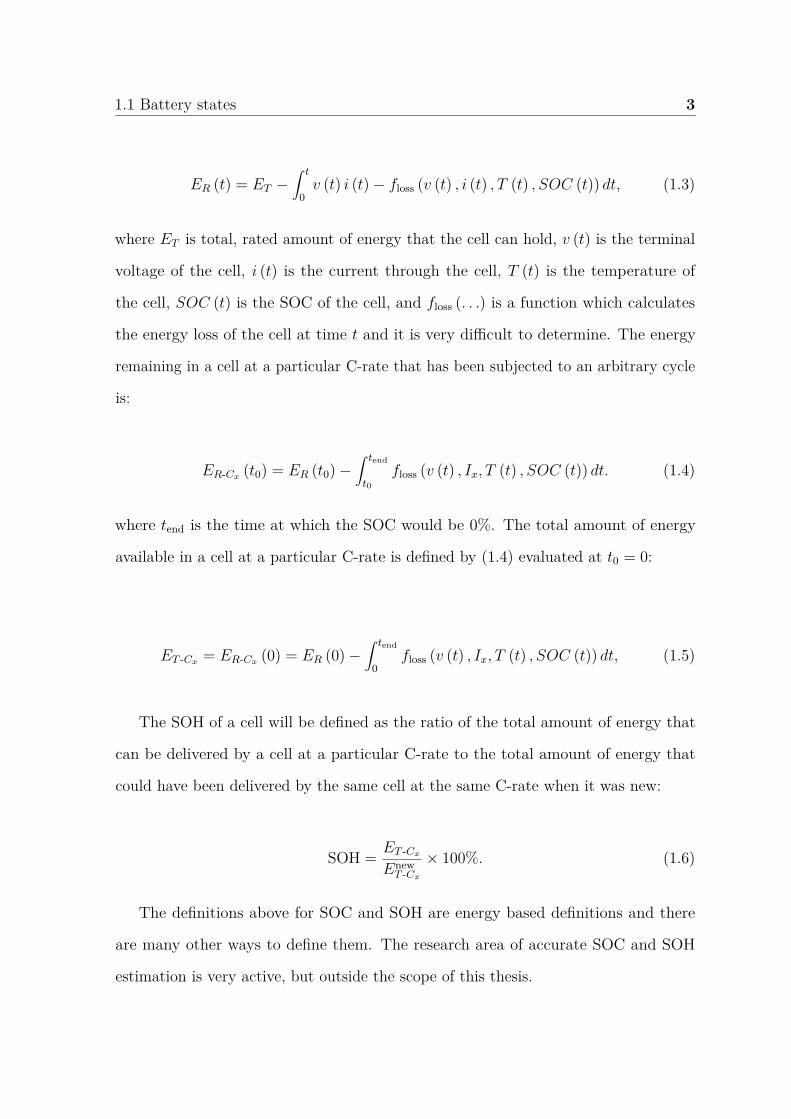
1.1 Battery states 3
ER (t) = ET −∫ t
0v (t) i (t) − floss (v (t) , i (t) , T (t) , SOC (t)) dt, (1.3)
where ET is total, rated amount of energy that the cell can hold, v (t) is the terminal
voltage of the cell, i (t) is the current through the cell, T (t) is the temperature of
the cell, SOC (t) is the SOC of the cell, and floss (. . .) is a function which calculates
the energy loss of the cell at time t and it is very difficult to determine. The energy
remaining in a cell at a particular C-rate that has been subjected to an arbitrary cycle
is:
ER-Cx (t0) = ER (t0) −∫ tend
t0floss (v (t) , Ix, T (t) , SOC (t)) dt. (1.4)
where tend is the time at which the SOC would be 0%. The total amount of energy
available in a cell at a particular C-rate is defined by (1.4) evaluated at t0 = 0:
ET -Cx = ER-Cx (0) = ER (0) −∫ tend
0floss (v (t) , Ix, T (t) , SOC (t)) dt, (1.5)
The SOH of a cell will be defined as the ratio of the total amount of energy that
can be delivered by a cell at a particular C-rate to the total amount of energy that
could have been delivered by the same cell at the same C-rate when it was new:
SOH = ET -Cx
EnewT -Cx
× 100%. (1.6)
The definitions above for SOC and SOH are energy based definitions and there
are many other ways to define them. The research area of accurate SOC and SOH
estimation is very active, but outside the scope of this thesis.

4 Introduction
1.2 The importance of battery management
Electrochemical energy storage systems release electrical energy as a consequence of
chemical reactions that take place inside of cells. Unfortunately, individual battery
cells have restrictive voltages which is a result of their chemical composition. For
example, one of the most established chemistries, lithium manganese cobalt oxide cells,
commonly known as NMC, cycles between 2.5 V and 4.2 V [16]. In [17], they report
on a lithium vanadium fluorophosphate cell which was cycled between 3.0 V and 4.5 V.
A lead acid cell will cycle between 1.75 V and 2.1 V [18]. As it stands, electrochemical
cells will be low voltage devices. Furthermore, these cells are limited in their capacity
due to their physical size. The most popular cylindrical cell on the market today is
the lithium-ion 18650 cell, a cylindrical cell with a diameter of 18 mm, and a length
of 65 mm. They now have capacities greater than 3 Ah. In order to truly overcome
the voltage and capacity limitations of small electrochemical cells, most applications
will connect several cells in series and in parallel to create a battery pack of sufficient
capacity with the appropriate voltage and current ratings. Battery cells of the same
chemistry and impedance connected in parallel will easily share the load current and
maximize the amount of energy delivered to the load from the available energy stored
in the cells [19]. However, this is only possible because the cell voltages of battery
cells of the same chemistry are theoretically identical. It is impossible to connect
cells of different chemistries in parallel and achieve the best performance from all cells
because each battery chemistry will have its own unique output voltage for a given
capacity, temperature, and current value. Battery cells connected in series are limited
by the weakest cell [20], thus a single cell in a series string of cells can become fully
charged before the rest of the pack and continuing to charge the pack will result in
overcharging of one or more cells, which can lead to a catastrophic failure of the entire

1.2 The importance of battery management 5
(a) Going. . . (b) Going. . . (c) Gone.
Fig. 1.1: Battery management failure of a RoboSimian droid at the Jet Propulsion Laboratory[21].
pack. Fig. 1.1 shows the consequences of charging a lithium-ion battery pack without
proper management. It was later discovered that the power management systems were
not properly enabled, leading to an overcharged failure mode of the robot’s lithium-ion
battery. In order to avoid failures and prolong battery pack lifetime, battery packs
have integrated systems which are designed to continuously monitor the pack and
ensure that the electrochemical energy storage devices are operated safely. The systems
that monitor electrochemical cells and battery packs are called battery management
systems (BMS’s).
Battery management systems come in many different forms, with many different
features. In the most general sense, a BMS should be able ensure that every cell
in a battery pack is kept within its safe operating area to avoid catastrophic failure.
However, this is only possible with global information about the system, which means
accurate knowledge of temperature, voltage, current, and other future measurements
such as pressure that may yield necessary information, throughout the entire battery
pack. Furthermore, the fundamental chemical reactions that take place in commercial
cells can vary over the lifetime of a battery pack due to manufacturing differences
and external factors. In many situations it is impractical or too costly to install
sensors everywhere to measure all of the required quantities, thus a BMS with reduced
functionality is realized.
6 Introduction
There are many different battery chemistries available on the market today and
many others are the subject of intense research. In this thesis, the focus will be on
the lithium-ion (Li-ion) chemistry, one of the most popular battery chemistries due
to its high energy density [22], low weight [22], increasingly low cost [23], and long
life [24]. Despite these many benefits, Li-ion batteries are a “Goldilocks chemistry”.
Temperature extremes will accelerate degradation [25], along with high currents [25]
and high voltages [25]. During storage, Li-ion batteries should be kept at a reduced
state of charge (SOC), to reduce the ageing effects known as “calendar ageing” [25].
Over discharging a Li-ion battery may cause the growth of dendrites which can puncture
the separator between the positive and negative electrode [26], causing an internal
short circuit within the cell, which can lead to thermal runaway and catastrophic cell
failure. Overcharging a Li-ion battery increases the rate at which the active material
is lost, in this case cyclable lithium, thus accelerating capacity fade [25]. Overcharging
(Fig. 1.1) can also cause the electrolyte to oxidise at the cathode producing several
types of gases which increase the internal pressure of the cell [27] and can lead to cell
rupture [22, 28], another catastrophic failure mode. In summary, in order to safely
extract the full energy storage potential out of a pack of Li-ion cells, they must be
carefully managed with a BMS.
1.3 Parallel cell balancing
As mentioned previously, parallel connected cells of the same chemistry will self balance
[22, 29]. In most applications, large packs are constructed out of series connections of
parallel modules to yield the largest pack capacity [30] and the parallel modules are
considered to be balanced. Although this is sufficient from the short term (a single
charge/discharge cycle) point of view of a BMS, recent research has highlighted the
increased degradation rates of parallel connected cells.
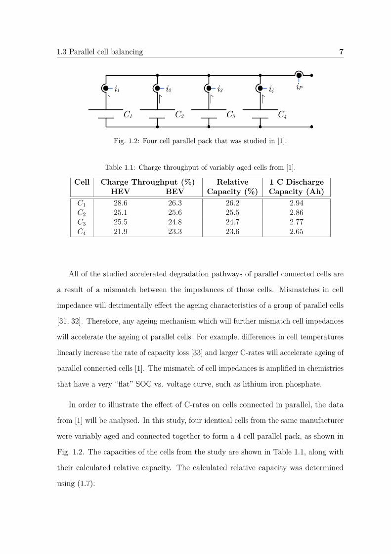
1.3 Parallel cell balancing 7
i1
C1
i2
C2
i3
C3
i4
C4
iP
Fig. 1.2: Four cell parallel pack that was studied in [1].
Table 1.1: Charge throughput of variably aged cells from [1].
Cell Charge Throughput (%) Relative 1 C DischargeHEV BEV Capacity (%) Capacity (Ah)
C1 28.6 26.3 26.2 2.94C2 25.1 25.6 25.5 2.86C3 25.5 24.8 24.7 2.77C4 21.9 23.3 23.6 2.65
All of the studied accelerated degradation pathways of parallel connected cells are
a result of a mismatch between the impedances of those cells. Mismatches in cell
impedance will detrimentally effect the ageing characteristics of a group of parallel cells
[31, 32]. Therefore, any ageing mechanism which will further mismatch cell impedances
will accelerate the ageing of parallel cells. For example, differences in cell temperatures
linearly increase the rate of capacity loss [33] and larger C-rates will accelerate ageing of
parallel connected cells [1]. The mismatch of cell impedances is amplified in chemistries
that have a very “flat” SOC vs. voltage curve, such as lithium iron phosphate.
In order to illustrate the effect of C-rates on cells connected in parallel, the data
from [1] will be analysed. In this study, four identical cells from the same manufacturer
were variably aged and connected together to form a 4 cell parallel pack, as shown in
Fig. 1.2. The capacities of the cells from the study are shown in Table 1.1, along with
their calculated relative capacity. The calculated relative capacity was determined
using (1.7):
8 Introduction
Relative Capacity of Cx = Cx∑4i=1 Ci
× 100%. (1.7)
The parallel pack was then subjected to a cycling profile from a hybrid electric
vehicle (HEV) and a cycling profile from a battery electric vehicle (BEV). The HEV
cycling profile had a higher C-rate on average than the BEV. During these experiments,
the current from each cell was recorded and each cell’s relative throughput could be
calculated using (1.8):
Relative Throughput of Cx =∫
cycle |ix| dt∫cycle |iP | dt
× 100%. (1.8)
As shown in Table 1.1, the batteries more equally shared the load current in
proportion to their capacities during the BEV cycling profile, which on average had
lower C-rates, than in the HEV cycling profile. This shows that under low C-rates,
variably aged cells connected in parallel will discharge and charge in proportion to
their respective capacities.
1.4 Serial cell balancing
Due to the weakest cell problem, one method to prolong the life of a battery pack
is to implement cell balancing in series connected cells. In [34], a summary of the
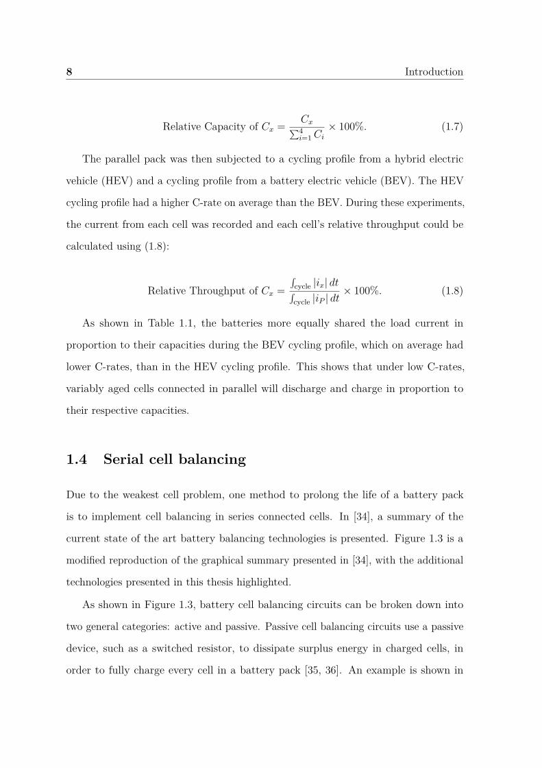
current state of the art battery balancing technologies is presented. Figure 1.3 is a
modified reproduction of the graphical summary presented in [34], with the additional
technologies presented in this thesis highlighted.
As shown in Figure 1.3, battery cell balancing circuits can be broken down into
two general categories: active and passive. Passive cell balancing circuits use a passive
device, such as a switched resistor, to dissipate surplus energy in charged cells, in
order to fully charge every cell in a battery pack [35, 36]. An example is shown in
1.4 Serial cell balancing 9
Battery Cell Balancing Circuits
Active Passive
· Zener diode· Bleeding resistor
· Shunt resistor and switch
Cell to cell balancing
Pack to cell balancing
Variable loading/charging
· Single switched capacitor· DC-link capacitor· Single inductor
· Coupled inductor
· Switched capacitor· Buck-boost based
· Cuk base
Directcell to cell
Adjacentcell to cell
· Multiple transformer· Multi-output transformer
· Switched transformer
Autonomous battery cells
Energy re-allocation
Central pack management
Fig. 1.3: Summary of cell balancing technologies based on the graphical summary originallypresented in [34]. The area highlighted in orange (Autonomous battery cells) is a newtechnology presented in this thesis. The areas highlighted in blue are new categories addedto the original diagram.
Figure 1.4(a). Passive cell balancing is a popular balancing technique because it is
very cheap and easy to implement, and therefore, it is very scalable. However, passive
cell balancing can only occur during charging, energy is wasted which is undesirable
in applications where the energy source is limited, and passive heat dissipation may
cause unwanted battery heating [37].
Active cell balancing circuits instead employ power electronic circuits to balance
the energy between cells.
10 Introduction
(a) Passive balancing. (b) Adjacent cell tocell balancing.
(c) Direct cell to cellbalancing.
(d) Pack to cell bal-ancing.
Fig. 1.4: Simplified examples of balancing circuit topologies from the literature.
1.4.1 Active battery cell balancing
Active cell balancing circuits fall within two main categories as redefined in this thesis:
energy re-allocation and variable loading/charging. The most basic active cell balancing
topology re-allocates energy between adjacent cells using a switched capacitor system
[38, 35, 39, 40], an example of which is shown in Figure 1.4(b), the most scalable active
balancing topology of those shown in Fig. 1.4. This topology has been improved with
the addition of a second tier of switched capacitors [41], a central voltage source [42],
and a chain structure of capacitors [43] to dramatically decrease the balancing time.
Soft switching [44] and quasi-resonant switching [45] was introduced to increase the
efficiency of the system. Individual voltage sensing is not required for any of these
topologies, making them immune to sensor variations [43] and more easily scalable
to large packs.. Even so, the balancing time is still quite considerable since it relies
on voltage differences between cells to drive the balancing currents and is subject to
temperature gradients across the battery pack [46].
Cell balancing time can be reduced using direct cell to cell balancing [47]. An
example of this is the flying capacitor topology as shown in Figure 1.4(c). Using

1.4 Serial cell balancing 11
a bidirectional, isolated converter for each cell, direct cell to cell balancing can be
achieved by connecting the outputs of all the converters together to form a common dc
bus, as demonstrated in [48]. A reduction of magnetic components can be achieved by
using a buck-boost type architecture [49] and can even be reduced to a single inductor
[50, 51] using many switching components.
Pack to cell balancing is also much quicker than switched capacitor balancing
circuits [47]. The multi-winding flyback topology is a good example of pack to cell
balancing [52, 53], where every cell has a switch and winding, and the entire pack is
connected to the input of the flyback, as shown in Fig. 1.4(d). However, Fig. 1.4(d)
is the least scalable of the topologies shown in Fig. 1.4 due to the need for a coupled
transformer between all of the series connections, a switch for each series connected cell,
and a single high voltage switch for the pack winding. Both the transformer and high
voltage switch will have to scale in voltage isolation rating and kVA, respectively, as
the number of cells in the series string increases. The number of transformer windings
can be reduced by introducing more switching components [54–56], or the winding
outputs can be implemented as simple rectifiers for more simple control [57]. In [58] a
multi-winding flyback converter with added switching components is able to completely
isolate a failed cell and prolong the life of the entire battery pack.
All of the topologies discussed thus far re-allocate energy within the battery pack -
essentially discharging one battery to charge another. This introduces charge/discharge
losses and has a maximum efficiency limited by the energy efficiency of the chemistry
used. A more direct approach to cell balancing variably loads and variably charges
each individual cell in a series string of batteries. This can be accomplished using a
central controller to manage a large array of switches to ensure all cells are discharged
at the same rate [59, 60]. A reduction in the complexity and control requirements leads
to placing a small buck-boost converter on each cell and connecting all of their outputs
12 Introduction
in series [61, 62] or parallel [63–65]. In [53], a current equalization circuit was employed
to balance cells. The largest drawback of variably loaded balancing topologies, is that
the power electronics must process all of the power flowing through the battery cell.
Conversely, energy re-allocation topologies need only to process a fraction of the power.
In all active balancing topologies, the power electronic devices must be low cost,
highly efficient, and easily integrated into a large battery pack. Recent advancements
in wide band gap switching devices, whose cost is expected to decrease over time, will
increase conversion efficiencies (and reduce power losses) and reduce overall system
costs through higher power density [66–68] and decreased cooling requirements [69].
There are two types of wide band gap devices currently available on the market today:
1) silicon carbide (SiC), and 2) gallium nitride (GaN). The SiC devices are primarily
designed for high voltage applications (650 V to 1700 V blocking voltage) and are
unsuitable for most balancing circuit switches, with the exception of topologies which
require a high voltage switch such as the one shown in Fig. 1.4(d). GaN devices show
some promise for low voltage switching as there are GaN MOSFETs with drain to
source breakdown voltages as low as 15 V currently available. However, the cost of
GaN devices are still prohibitively expensive with a 30 V, 60 A device costing six times
more than an equivalent silicon MOSFET of the same rating and equivalent drain
to source on resistance. Therefore, for low voltage power electronic switches, silicon
devices will be the primary device of choice in the near future.
1.5 Scalability of serial cell balancing
Throughout the literature, and indeed during this review, balancing circuits are
commonly evaluated on the “speed” at which they balance series connected cells.
However, this approach is slightly misguided for real world battery packs. Although
directly related, balancing circuits should be evaluated based on the normalized current,

1.5 Scalability of serial cell balancing 13
or C-rate, at which they can balance a string of cells. The C-rate of a given cell is
defined as the current flowing through the cell in amps divided by its capacity in
amp-hours. Define the maximum balancing C-rate as CB:
CB = IB,max
Cavg(1.9)
where IB,max is the maximum balancing current in amps and Cavg is the average capacity
of the series connected cells in amp-hours. Evaluating balancing circuits with a CB,
allows a designer to better estimate the spread in cell capacities that the balancing
circuit can handle and thus, the estimated lifetime of a battery pack.
Table 1.2 calculates the CB rates for some of the balancing circuits found in
literature. Note that when calculating CB rates for switched capacitor circuits, their
maximum current as reported in each study was taken. In reality, this maximum
current can only be achieved with a minimum voltage difference between cells, thus
they will appear more favourable in Table 1.2. In addition, the peak balancing current
was taken for IB,max, despite restrictions on some topologies where this current is only
achieved between two cells at a time, thus the rest of the pack is not able to balance
while energy is being transferred.
As shown in Table 1.2, the balancing rate varied dramatically across the literature
demonstrating that different CB rates are required for different situations. However, in
order to compare the balancing circuits on equal terms, the scalability of each circuit
was also analysed. Scalability is an important metric as larger battery packs are being
built and commissioned. The scalability of each balancing topology was calculated by
normalising the component ratings of each circuit to their maximum balancing current.
By doing this, all of the balancing circuits were normalised to the same balancing
performance. In this thesis, there are two metrics to define scalability: 1) a normalized
kVA rating, and 2) a normalized passives energy rating. Both of these quantities are
14 Introduction
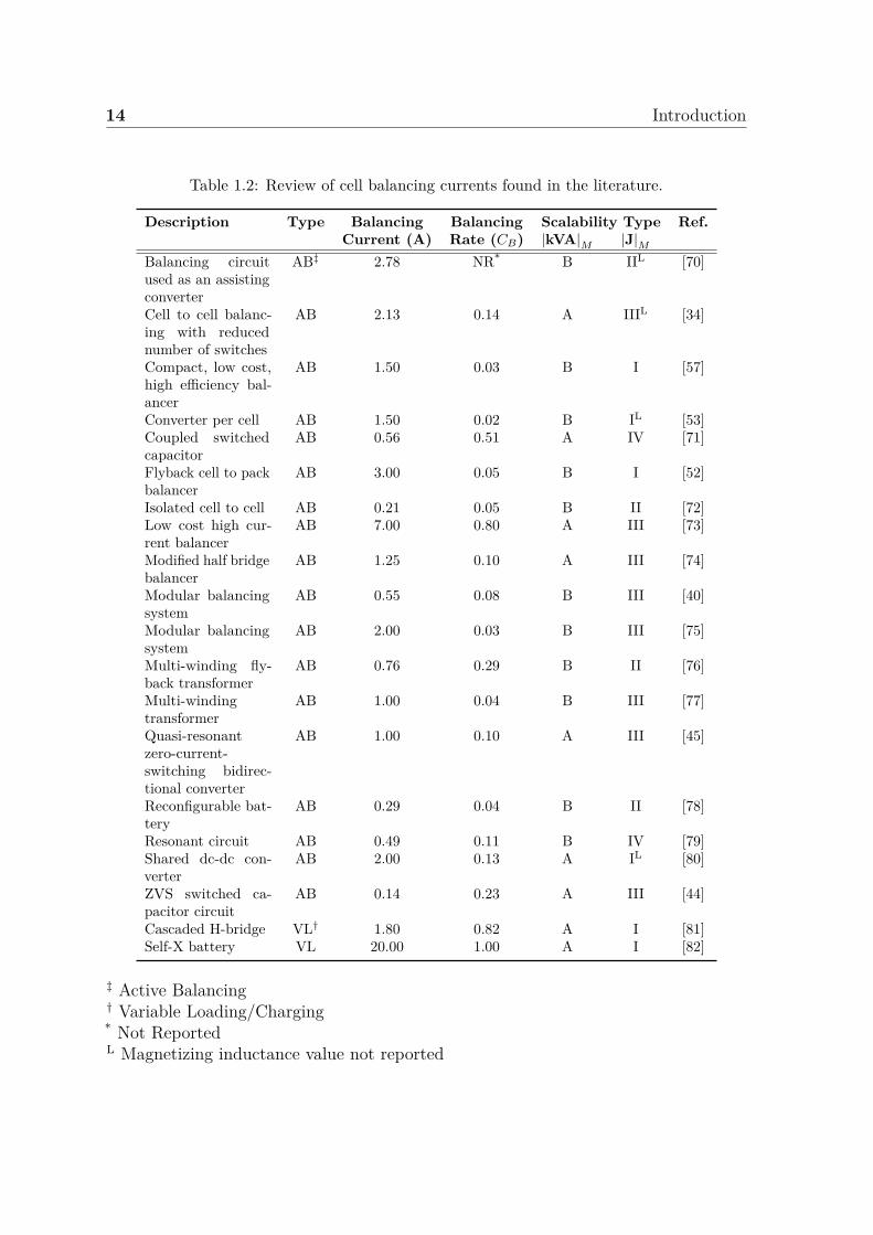
Table 1.2: Review of cell balancing currents found in the literature.
Description Type Balancing Balancing Scalability Type Ref.Current (A) Rate (CB) |kVA|M |J|M
Balancing circuitused as an assistingconverter
AB‡ 2.78 NR* B IIL [70]
Cell to cell balanc-ing with reducednumber of switches
AB 2.13 0.14 A IIIL [34]
Compact, low cost,high efficiency bal-ancer
AB 1.50 0.03 B I [57]
Converter per cell AB 1.50 0.02 B IL [53]Coupled switchedcapacitor
AB 0.56 0.51 A IV [71]
Flyback cell to packbalancer
AB 3.00 0.05 B I [52]
Isolated cell to cell AB 0.21 0.05 B II [72]Low cost high cur-rent balancer
AB 7.00 0.80 A III [73]
Modified half bridgebalancer
AB 1.25 0.10 A III [74]
Modular balancingsystem
AB 0.55 0.08 B III [40]
Modular balancingsystem
AB 2.00 0.03 B III [75]
Multi-winding fly-back transformer
AB 0.76 0.29 B II [76]
Multi-windingtransformer
AB 1.00 0.04 B III [77]
Quasi-resonantzero-current-switching bidirec-tional converter
AB 1.00 0.10 A III [45]
Reconfigurable bat-tery
AB 0.29 0.04 B II [78]
Resonant circuit AB 0.49 0.11 B IV [79]Shared dc-dc con-verter
AB 2.00 0.13 A IL [80]
ZVS switched ca-pacitor circuit
AB 0.14 0.23 A III [44]
Cascaded H-bridge VL† 1.80 0.82 A I [81]Self-X battery VL 20.00 1.00 A I [82]
‡ Active Balancing† Variable Loading/Charging* Not ReportedL Magnetizing inductance value not reported
1.5 Scalability of serial cell balancing 15
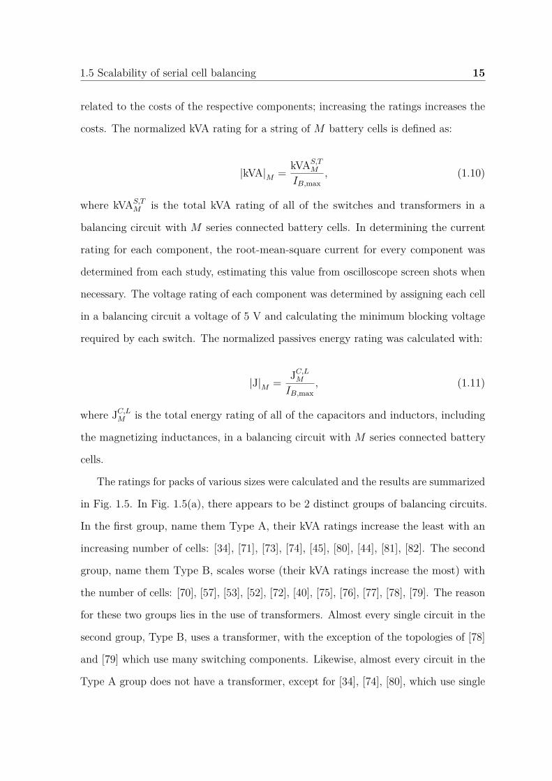
related to the costs of the respective components; increasing the ratings increases the
costs. The normalized kVA rating for a string of M battery cells is defined as:
|kVA|M = kVAS,TM
IB,max, (1.10)
where kVAS,TM is the total kVA rating of all of the switches and transformers in a
balancing circuit with M series connected battery cells. In determining the current
rating for each component, the root-mean-square current for every component was
determined from each study, estimating this value from oscilloscope screen shots when
necessary. The voltage rating of each component was determined by assigning each cell
in a balancing circuit a voltage of 5 V and calculating the minimum blocking voltage
required by each switch. The normalized passives energy rating was calculated with:
|J|M = JC,LM
IB,max, (1.11)
where JC,LM is the total energy rating of all of the capacitors and inductors, including
the magnetizing inductances, in a balancing circuit with M series connected battery
cells.
The ratings for packs of various sizes were calculated and the results are summarized
in Fig. 1.5. In Fig. 1.5(a), there appears to be 2 distinct groups of balancing circuits.
In the first group, name them Type A, their kVA ratings increase the least with an
increasing number of cells: [34], [71], [73], [74], [45], [80], [44], [81], [82]. The second
group, name them Type B, scales worse (their kVA ratings increase the most) with
the number of cells: [70], [57], [53], [52], [72], [40], [75], [76], [77], [78], [79]. The reason
for these two groups lies in the use of transformers. Almost every single circuit in the
second group, Type B, uses a transformer, with the exception of the topologies of [78]
and [79] which use many switching components. Likewise, almost every circuit in the
Type A group does not have a transformer, except for [34], [74], [80], which use single

16 Introduction
101
102
Number of cells
10-2
10-1
100
101
102
103
104
|kV
A|
[73][82][44]
[45][74][81][71][34][80][76][40][70][52][53][77][72][78][57][79][75]
(a) Normalized kVA of switches and trans-formers.
101
102
Number of cells
10-8
10-6
10-4
10-2
100
102
104
|J|
[74][76][72][70][78][40][73][75][34][45][44][77][79]
[71]
(b) Normalized energy in inductors andcapacitors.
Fig. 1.5: Normalized total kVA and total energy in passives versus the number of series cellsin a pack.
transformers for small groups of cells. The |kVA|M scalability type for each study is
listed in Table 1.2. In conclusion, by looking at Fig. 1.5(a) alone, the most scalable
balancing topologies are the ones that do not use transformers.
Fig. 1.5(b) shows the scalability of the circuits based on the energy ratings of
the passives required for each of them, and should be considered in conjunction with
Fig. 1.5(a). In Fig. 1.5(b) there are four distinct groups. The first group, name them
Type I, are the topologies that do not require any passives: [57], [53], [52], [80], [81],
[82][57], [53], [52], [80], [81], [82]. The second group, name them Type II, do not scale
at all with an increase in the number of cells because the energy carrier between cells
is a single passive component: [76], [72], [70], [78]. The third group, name them Type
III, scales slightly with the number of cells because there is a passive component for
every cell: [74], [40], [73], [75], [34], [45], [44], [77]. The fourth group, name them Type
IV, is formed of topologies that do not scale well with the number of cells because
their passives scale with voltage: [71], [79]. The |J|M scalability type for each study is
listed in Table 1.2.
1.6 Accessing all of the energy 17
In conclusion, using the normalizations of (1.10) and (1.11) the most scalable
topologies are those that are Type A and Type I: [80], [81], [82]. However, it should
be noted that their are other factors that were not included in this analysis that will
also effect the scalability of these circuits. For example, the intra-pack communication,
sensing, and control requirements.
The next section will investigate how limited balancing current limits the amount
of energy that can be extracted out of a battery pack with cells of varying capacities.
1.6 Accessing all of the energy
The preceding sections have highlighted the different balancing topologies in literature.
This section will compare simplified models of three balancing topologies to see how
much energy can be extracted during a single discharge. Comparing the amount of
energy that is available during discharge determines how long each battery pack will
last. In an application such as an electric vehicle, this directly translates into the
distance that the EV can travel.
Simplified schematics of the three topologies that will be analysed are given in
Fig. 1.6: passive balancing topology in Fig. 1.6(a), active balancing topology in
Fig. 1.6(b), and variable loading/charging topology in Fig. 1.6(c).
1.6.1 Calculating the discharge energy
The three topologies of Fig. 1.6 will be analysed to determine the maximum amount of
energy that can be extracted during a single discharge. In the following analysis, all
energy is calculated in Watt-hours (Wh), Ck refers to the capacity of the kth battery
cell in amp-hours (Ah), Th is time in hours (h), Vnom is the nominal voltage of each
cell in volts (V), and M is the total number of battery cells in the series string.
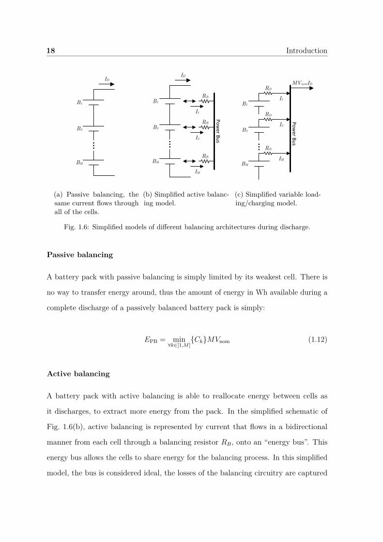
18 Introduction
B1
B2
BM
ID
(a) Passive balancing, thesame current flows throughall of the cells.
B1
B2
BM
ID
Po
wer B
us
RB
RB
RB
I1
I2
IM
(b) Simplified active balanc-ing model.
B1
B2
BM
MVnomID
Po
wer B
us
RD
I2
RD
IM
RD
I1
(c) Simplified variable load-ing/charging model.
Fig. 1.6: Simplified models of different balancing architectures during discharge.
Passive balancing
A battery pack with passive balancing is simply limited by its weakest cell. There is
no way to transfer energy around, thus the amount of energy in Wh available during a
complete discharge of a passively balanced battery pack is simply:
EPB = min∀k∈[1,M ]
CkMVnom (1.12)
Active balancing
A battery pack with active balancing is able to reallocate energy between cells as
it discharges, to extract more energy from the pack. In the simplified schematic of
Fig. 1.6(b), active balancing is represented by current that flows in a bidirectional
manner from each cell through a balancing resistor RB, onto an “energy bus”. This
energy bus allows the cells to share energy for the balancing process. In this simplified
model, the bus is considered ideal, the losses of the balancing circuitry are captured
1.6 Accessing all of the energy 19
entirely by RB, and there is a limit on the balancing current: Ik < IB,max, k ∈ [1, M ].
However, there is no limit on the amount of energy that can flow through the energy
bus.
When discharging a pack with active balancing, there are two scenarios to consider:
(1) the energy storage is the limiting factor, and (2) the balancing circuit is the limiting
factor, and thus the pack is limited by its weakest cell in addition to the energy that
can be transferred to it. The point at which the balancing circuit becomes the limiting
factor is determined by the discharge rate: quickly discharging the pack means that
the balancing circuit will have to move more current around to maintain cell balance.
(1) Energy storage is the limiting factor
In this scenario, the battery pack is able to use all of the energy stored in every single
cell, but has lost some energy to the losses associated with cell balancing. Equation
(1.13) summarizes this observation:
EAB =M∑
k=1VnomCk − EAB,losses (1.13)
where
EAB,losses =M∑
k=1I2
kRBTh. (1.14)
Th is the time in hours that the pack is discharging. In this perfectly balanced case,
this time will be the same for all of the cells, and an equation for Th can be written:
Th = Ck −∫ Th
0 Ikdh
ID
(1.15)
Th = Ck
ID (1 + Ik/ID) (1.16)

20 Introduction
where ID is the discharge current of the pack. Since all cells will discharge in Th hours,
(1.13) can be re-written with all known quantities:
VnomIDThM =M∑
k=1VnomCk −
M∑k=1
I2kRBTh. (1.17)
Finally, a constraint equation on the power bus of Fig. 1.6(b) can be written, since
the power into the bus plus the losses, must always equal the power out of the bus:
0 =M∑
k=1I2
kRB +M∑
k=1IkVnom (1.18)
Unfortunately, we now have to solve a non-linear system of M + 1 equations with
M + 1 unknowns (Th, I1, I2, ...,IM) with the constraint equation of (1.18). It is very
difficult, if not impossible, to find an analytical solution to this problem, however,
numerical methods will be used in the following section to find appropriate solutions.
(2) Balancing circuit is the limiting factor
The balancing circuit becomes the limiting factor when any of the Ik solved above are
greater than IB,max. In this scenario, the battery pack is limited by the energy in the
weakest cell plus the energy that can be reallocated to it during discharge. In this
scenario, the equation for Th becomes:
Th = mink∈[1,M ]Ck −∫ Th
0 IB,maxdh
ID
(1.19)
Th = mink∈[1,M ]CkID (1 + IB,max/ID) (1.20)
and therefore the total energy that can be extracted from the pack is:
EAB,limited =(
mink∈[1,M ]
Ck − IB,maxTh
)MVnom. (1.21)

1.6 Accessing all of the energy 21
Variable loading/charging
A battery pack with variable loading/charging is able to continuously discharge all
cells proportional to their capacity. The simplified model for this scenario is depicted
in Fig. 1.6(c). In this model, each cell is discharged into a power bus through a resistor
RD. In a similar manner to the active balancing analysis, RD represents all of the
losses associated with the power electronics which make the active loading possible.
All of the power that is put into the power bus is extracted as useful energy to power
a load.
Active loaded topologies will always discharge all of the cells in a pack, thus we can
write an equation for the output energy of an actively loaded battery pack:
EVL =M∑
k=1CkVnom − EVL,losses (1.22)
where
EVL,losses =M∑
k=1I2
kRDTh. (1.23)
Th is simply the amount of time to discharge a cell with ID whose capacity is the
average capacity of the pack:
Th =avgk∈[1,M ]Ck
ID
(1.24)
Similarly, the current out of each cell is adjusted by the average capacity:
Ik = IDCk
avgk∈[1,M ]Ck. (1.25)

22 Introduction
1.6.2 Comparison
The amount of energy that can be extracted during a single discharge of a passively
balanced pack, actively balanced pack, and variably loaded/charged pack will now
be compared for various pack configurations and discharge rates. Table 1.3 lists the
parameters and their respective values used in this study. The values of RD and RB
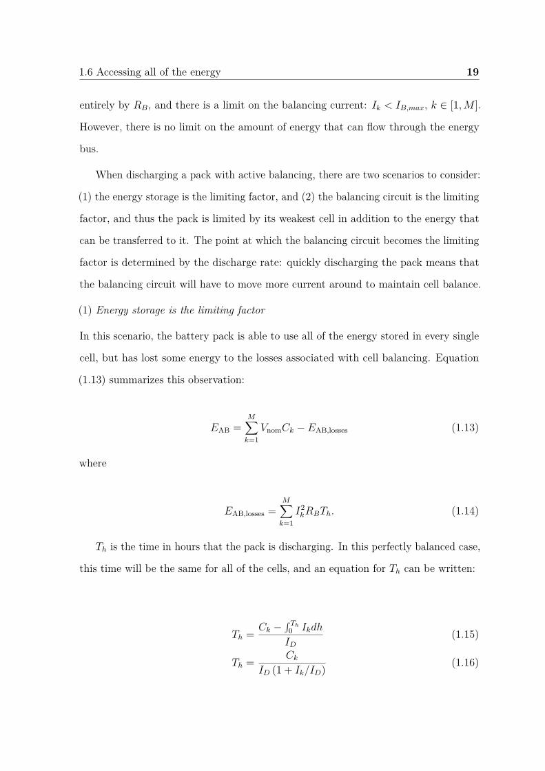
were selected by first surveying the MOSFETs available from an online retailer, Digikey,
with the following filters applied: a drain to source voltage rating of 20 V, in stock
and active, silicon MOSFET technology, N-Channel FET type, and cut tape packaging
to remove duplicate part numbers. The collected data is shown in Fig. 1.7, along
with a best fit curve to the data. The equation for this best fit curve is shown in
(1.26). Equation (1.26) does not follow an inverse square relationship, as might be
expected due to the squared relationship between power and current through a resistor:
P = I2R. This is because as the devices handle more current they physically get larger
and therefore, they are able to dissipate more power. This is also shown in Fig. 1.7,
where the maximum power that can be dissipated by each device is also plotted. When
fitting a curve to the maximum dissipation power, the power is proportional to the
current to the power of 0.579. This value is lower than the theoretically expected value
of 1/1.241 = 0.806, the inverse slope of (1.26) on a log-log plot, which indicates that
with increasing current requirements, MOSFETs should be increasingly over rated for
the same safety factor. The current rating for RD and RB was taken as two times the
maximum current that could be seen by each device; that is two times 50 A and 1 A,
respectively.
RDS-on = 254.1I−1.241DS- max mΩ (1.26)
1.6 Accessing all of the energy 23
10-1 100 101 102
Continuous drain current (A)
10-1
100
101
102
103
104
Dra
in t
o s
ourc
e on r
esis
tance
(m
Ohm
)
10-3
10-2
10-1
100
101
102
Pow
er d
issi
pat
ion (
W)
Drain to source on resitance
Fitted curve to drain to source on resistance
Maximum power dissipation
Fig. 1.7: Drain to source on resistance and maximum power dissipation for various availableMOSFETs from Digikey.
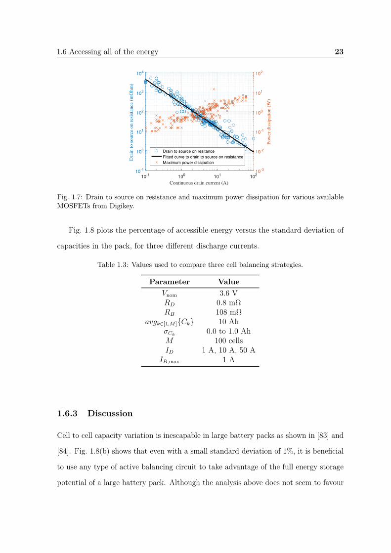
Fig. 1.8 plots the percentage of accessible energy versus the standard deviation of
capacities in the pack, for three different discharge currents.
Table 1.3: Values used to compare three cell balancing strategies.
Parameter ValueVnom 3.6 VRD 0.8 mΩRB 108 mΩ
avgk∈[1,M ]Ck 10 AhσCk
0.0 to 1.0 AhM 100 cellsID 1 A, 10 A, 50 A
IB,max 1 A
1.6.3 Discussion
Cell to cell capacity variation is inescapable in large battery packs as shown in [83] and
[84]. Fig. 1.8(b) shows that even with a small standard deviation of 1%, it is beneficial
to use any type of active balancing circuit to take advantage of the full energy storage
potential of a large battery pack. Although the analysis above does not seem to favour

24 Introduction
0 2 4 6 8 10
Standard Deviation of Capacities (%)
50
60
70
80
90
100
Acc
essi
ble
En
erg
y (
%)
Passive balancing
Active balancing
Variable loading/charging
(a) 1 A (0.1 C) discharge cur-rent.
0 2 4 6 8 10
Standard Deviation of Capacities (%)
50
60
70
80
90
100
Acc
essi
ble
En
erg
y (
%)
Passive balancing
Active balancing
Variable loading/charging
(b) 10 A (1 C) discharge cur-rent.
0 2 4 6 8 10
Standard Deviation of Capacities (%)
50
60
70
80
90
100
Acc
essi
ble
En
erg
y (
%)
Passive balancing
Active balancing
Variable loading/charging
(c) 50 A (5 C) discharge cur-rent.
Fig. 1.8: Accessible energy under different discharge currents for the three balancing topologiesof Fig. 1.6.
the proportional discharge topology, in a real application there would be a variable
C-rate over time. Fig. 1.9(a) shows the percentage of time spent at different C-rates
during various ARTEMIS drive cycles. In order to generate this plot, the ARTEMIS
velocity profile was converted to a current profile as described in Appendix B of [85]
for the urban and motorway drive cycles, and [86] for the extra-urban drive cycle. The
absolute value of the resulting currents was taken, and converted to a C-rate to result
in a maximum C-rate of 4.51 C. This maximum C-rate is the maximum C-rate of a
Tesla Model S P100D [87].
Using the plots of Fig. 1.9(a), the amount of energy lost in the power electronics
of the variable loading/charging battery pack can be determined for the three drive
cycles. The amount of energy lost was calculated by calculating the efficiency of the
variable loading/charging battery pack for all C-rates between 0 and 5 and for all
standard deviations of cell capacities. Then, for each drive cycle and standard deviation
of cell capacities, the percentage of time spent at each C-rate was multiplied by the
efficiency of the pack at that C-rate and standard deviation of cell capacities. Finally,
these multiplied values were summed over all of the C-rates to determine a “weighted
efficiency” of the variable loading/charging topology for each drive cycle. From this
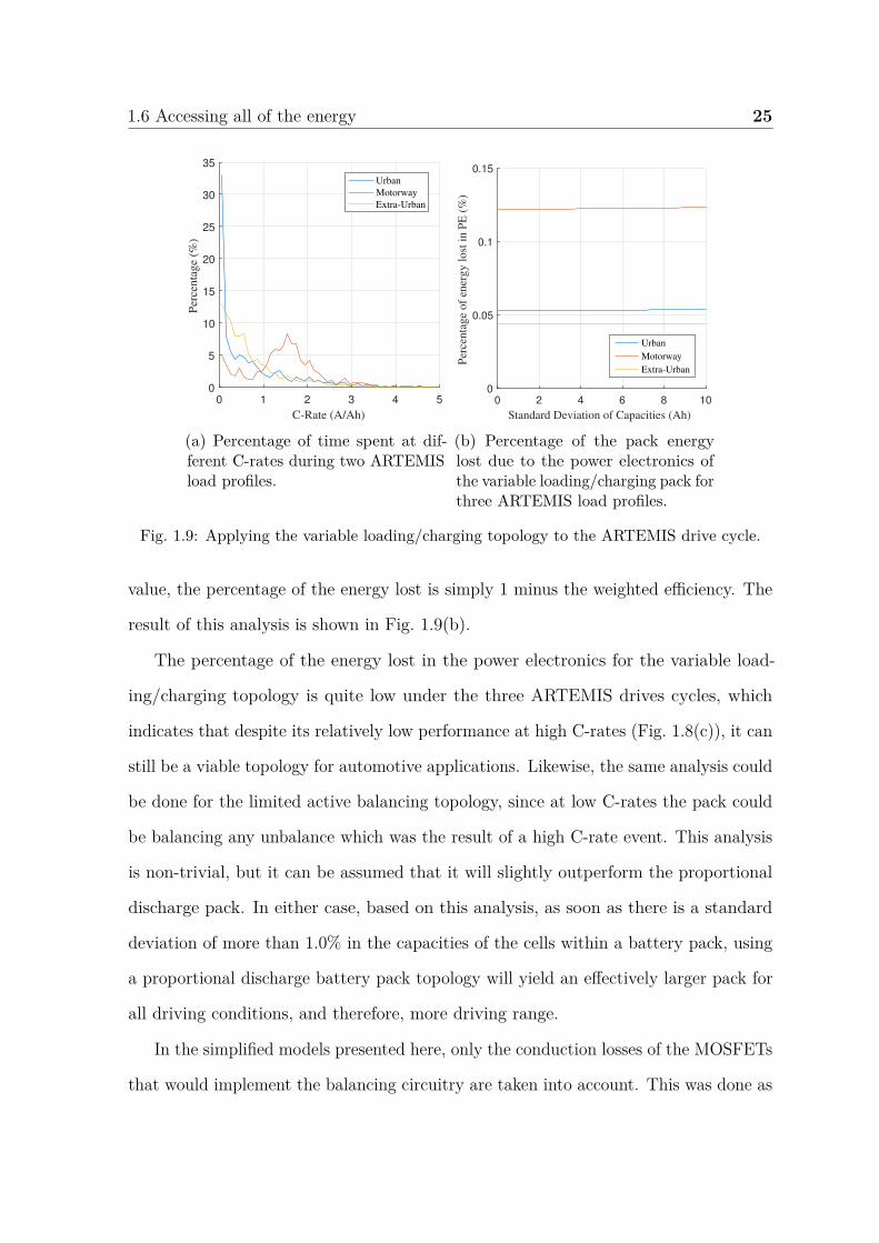
1.6 Accessing all of the energy 25
0 1 2 3 4 5
C-Rate (A/Ah)
0
5
10
15
20
25
30
35
Per
cen
tag
e (%
)Urban
Motorway
Extra-Urban
(a) Percentage of time spent at dif-ferent C-rates during two ARTEMISload profiles.
0 2 4 6 8 10
Standard Deviation of Capacities (Ah)
0
0.05
0.1
0.15
Per
centa
ge
of
ener
gy l
ost
in P
E (
%)
Urban
Motorway
Extra-Urban
(b) Percentage of the pack energylost due to the power electronics ofthe variable loading/charging pack forthree ARTEMIS load profiles.
Fig. 1.9: Applying the variable loading/charging topology to the ARTEMIS drive cycle.
value, the percentage of the energy lost is simply 1 minus the weighted efficiency. The
result of this analysis is shown in Fig. 1.9(b).
The percentage of the energy lost in the power electronics for the variable load-
ing/charging topology is quite low under the three ARTEMIS drives cycles, which
indicates that despite its relatively low performance at high C-rates (Fig. 1.8(c)), it can
still be a viable topology for automotive applications. Likewise, the same analysis could
be done for the limited active balancing topology, since at low C-rates the pack could
be balancing any unbalance which was the result of a high C-rate event. This analysis
is non-trivial, but it can be assumed that it will slightly outperform the proportional
discharge pack. In either case, based on this analysis, as soon as there is a standard
deviation of more than 1.0% in the capacities of the cells within a battery pack, using
a proportional discharge battery pack topology will yield an effectively larger pack for
all driving conditions, and therefore, more driving range.
In the simplified models presented here, only the conduction losses of the MOSFETs
that would implement the balancing circuitry are taken into account. This was done as

26 Introduction
they represent all of the losses of an ideal variable loading/charging topology. However,
as will be shown in Section 3.2.3, a practical variable loading/charging topology has
other losses that must be accounted for. Likewise, the simplified model of the active
balancing battery pack does not take into account any system losses, such as losses in
the active balancing network which would arise from the additional cabling needed
to physically get energy around the pack. Despite this simplification, the results in
this section are useful to quickly analyse that variable loading/charging topologies are
worthwhile for further exploration.
In [84], Schuster et al. analysed 484 new and 1908 aged lithium ion battery cells to
determine their spread in capacity over time. During their analysis they removed outlier
cells. The cells used in the study had previously been used in electric vehicles and the
aged cells came from two separate vehicles. They found that the standard deviation
of new cells was 0.8%, in the aged cells from one vehicle the standard deviation was
2.25% after 124 equivalent full cycles, and from the second vehicle it was 1.57% after
174 equivalent full cycles. The average cell capacity in the aged cells was degraded by
3.0% and 6.1%, respectively. In both of these scenarios, the cells were far from their
end of life and yet they both would have benefited from active balancing or variable
loading/charging to increase their respective vehicle’s range.
1.7 Second life lithium-ion batteries
The previous section derived a method to quickly determine how much energy can be
extracted from a pack of cells of varying capacities during a single discharge. This
analysis is extremely relevant in the growing market of second life lithium-ion batteries,
whose capacity distribution will be much larger than first life cells due to variable
ageing.

1.8 Practical considerations of large battery packs 27
Second life applications of lithium-ion batteries are growing because they are
economically feasible [88] and the recycling of lithium-ion batteries into raw materials
is currently not economically feasible [89, 90]. Furthermore, governments such as the
government in the United Kingdom require producers and vendors of batteries to pay
for waste battery collection, treatment, recycling, and disposal [91]. The fees which
these governments collect are passed on to the battery recyclers who use the funds to
finance the expensive battery recycling operations. However, battery recyclers and
producers are becoming more incentivised to find alternative methods to recycle lithium
ion batteries, because they are the most expensive chemistry to recycle. Conversely,
lead acid battery recycling is very easy and low cost, where 70% by weight of lead acid
batteries sent for recycling is recoverable as valuable lead that can be resold onto the
market [89]. Recently, there have been announcements from Nissan [92], BMW [93],
and GM [94], who are all experimenting with energy storage systems using batteries
recovered from their EVs and HEVs. In the automotive industry, packs from EVs and
HEVs are replaced when their SOH reaches 70% to 80% [95], which is the SOH of the
weakest series connected module in a pack. Thus there are many cells remaining in
these large packs that are prematurely going to waste.
1.8 Practical considerations of large battery packs
Battery management systems do not scale well in large battery packs. As the number of
cells increase, an increased amount of cabling is required for all of the sensors. If a pack
employs one of the cell balancing circuits of Section 1.4, even more cabling is required
to control the gating signals of the power electronic components. Furthermore, in high
voltage packs, cell voltages must be measured with the accuracy of millivolts when
differential cell voltage measurements can have a common mode offset of hundreds of
volts.

28 Introduction
A reduction in the amount of cabling within a pack can be reduced by locating
a sensor and communication device physically close to the device being measured.
The communication device can use a common bus communication network such as a
Controller Area Network bus (CAN bus) to transmit information around the pack,
which requires less wiring than a wire to every sensor. Cabling can be further reduced
by implementing communication devices that use power line communication techniques
[96]. Wireless intra-pack communication networks have also been studied as a means
to reduce cabling [97, 98], however, the environment within the battery pack presents
unique challenges due to all of the reflective surfaces (cans of batteries, metal enclosure
of packs, etc.) that affect the quality of the radio signals [98]. A wireless communication
medium has also been proposed to implement advanced cell level monitoring using
impedance spectroscopy [99].
Wireless communication and power line communication techniques still do not
provide an accurate and reliable enough solution to drive the gating signals of power
electronic devices. In [99], the authors developed their own triggering mechanism in
hardware and software that reduced their timing jitter to 1 µs. Although impressive,
this is still not good enough for all applications. A method to simplify the distribution
of many gating signals within physically large systems is an active research area of
modular multi-level converters (MMCs). In order to address this issue, increasingly
decentralised control schemes have been introduced [100, 101] where the gating signals
for the power electronics components are generated locally. However, all of these
solutions still require a centralised controller for global synchronisation.
Completely decentralized synchronisation of gating signals across multiple power
electronic converters has yet to be achieved, however, a solution to this problem can
be found in the theory of Kuramoto oscillators [102]. Kuramoto oscillators were first
proposed by Yoshiki Kuramoto in 1975 to model systems of coupled oscillators who are
1.9 Summary and thesis outline 29
able to synchronise despite differences in phase and natural frequency: pacemaker cells
in the heart, flashing fireflies, chirping crickets; to name but a few [103]. Kuramoto
oscillators can be modelled with:
θk = ω + K
M
N∑i=1
sin (θi − θk) , (1.27)
where θx is the phase of the xth oscillator, ω is the average frequency of the system, M
is the number of oscillators in the system, and K is the controller gain of the system
and can be interpreted as the coupling strength between oscillators. For a sufficiently
large K, the oscillators will synchronize [102]. The study of Kuramoto oscillators has
been a very active and fruitful area of research with many unexplored avenues and
applications [103, 104].
In a power electronics system, the oscillators are the gating signals of the converter
which can have locally generated gating signals. By introducing some form a coupling,
gating synchronisation can be achieved. Therefore, a global synchronization signal
to each converter is not required, simplifying the design of systems with physically
disparate switching devices.
1.9 Summary and thesis outline
Electrical energy storage will play a crucial role the in future of energy systems [105].
As battery packs get larger, it is crucial to have intelligent and efficient BMS’s in place
to properly manage and utilize the expensive electrical energy storage devices that make
up the pack. One of the main roles of any BMS is cell balancing of series connected
cells. An unbalanced pack will be limited by its weakest cell, thus limiting the overall
performance of the pack by trapping the unused stored energy of the healthier cells.

30 Introduction
The full energy storage potential of large battery packs can be unlocked with active
balancing and variable loading/charging.
Actively balanced packs will still be limited by their weakest cell when a pack
degrades. Therefore, variably loading/charging a series string of battery cells is the
only way to ensure every joule of energy storage potential can be utilized throughout
the entire lifetime of a pack. The rest of this thesis will focus on the author’s research
into variable loading/charging topologies and control algorithms. It is broken down
into two main projects: the intelligent battery and the smart cell.
A variable loading/charging battery pack is introduced in Chapter 2 and it presents
the design of a an intelligent battery with hot-swappable modules. Chapter 3 summa-
rizes the simulation and experimental results of the intelligent battery.
The intelligent battery uses a centralised controller to manage the entire battery
pack, which requires significant hardware overhead for intra-pack communication.
To address this issue, the concept of a smart cell, having no communication bus, is
presented in Chapter 4. This chapter focuses on the theory behind decentralised battery
management. Chapter 5 presents simulation and experimental results which confirm
that decentralised battery management is possible.
The thesis concludes with Chapter 6, where the major contributions of this work
are summarized and a number of exciting avenues of research and development are
proposed.

Chapter 2
Intelligent battery system design
The main goal of building an intelligent battery pack was to create a research platform
where new battery management ideas could be tested on a real system composed of
any type of electrical energy storage elements. In this chapter, the main mechanical
and electrical design features of a research grade intelligent battery pack are discussed.
The designed pack has 24 hot-swappable modules, can be configured with up to 192
battery cells, and is integrated with 25 ARM Cortex M4 micro-controllers with floating
point units.
2.1 Design requirements
The general design requirements for the intelligent battery were as follows:
• Power and capacity rating large enough to power medium sized (around 1 kW)
household loads.
• Easy cell replacement, so that a new battery pack would not have to be built for
every cell configuration.
• Mechanically sound so that it could function as a demonstrator unit at conferences
and trade shows.

32 Intelligent battery system design
Table 2.1: Specifications of the intelligent battery pack.
Description ValueNominal output voltage 48 VMaximum output current 25 AMaximum charging current 25 ANumber of modules 24Maximum number of 18650 cells 192Maximum cell voltage 5 V
• Module level control, meaning the energy in and out of every series connected
module can be controlled.
Using the above design requirements, the electrical specifications of the intelligent
battery were set, and are listed in Table 2.1. The intelligent battery pack has 2 kWh
of energy storage when fully populated with 3.6 V, 3 Ah battery cells. Its maximum
rated output power is 1.2 kW. Therefore, to achieve higher C-rates, fewer cells can be
populated.
2.2 Mechanical design
The mechanical design of the intelligent battery was developed to deliver a platform
where individual cells can be easily replaced. This enables users of the system to easily
reconfigure the battery pack with different energy storage elements. In addition, each
series connected energy storage element is contained within a module, which can be
physically removed from the battery pack. The module and pack electronics were
designed so that the modules can be hot-swapped: they can be removed from, and
replaced into, the battery pack while it is operating.
The electrical details of the intelligent battery pack are discussed in Section 2.3.

2.2 Mechanical design 33
Aluminium threaded rod
Knob
Top battery holder PCB
Fuse
Lid
8x 18650 battery cells
Module PCB
Fig. 2.1: An exploded view of a module of the intelligent battery.
2.2.1 Module design
The intelligent battery pack is comprised of 24 individual modules. Fig. 2.1 shows
an exploded view of a single module of the intelligent battery pack. Each module is
capable of housing up to eight 18650 battery cells. The battery cells are all connected
in parallel, thus each module emulates one large cell.
The modules are constructed out of printed circuit boards, 3D printed parts, and
fastening hardware. A module measures 157 mm deep, 78 mm wide, and 106 mm tall,
overall.
Easy cell exchange is achieved with spring loaded contacts mounted on PCBs, which
are mounted onto the 3D printed parts. The spring contacts are rated at 6 A per cell.
As shown in the exploded view, a knob is used to mechanically fasten a “lid” onto the
battery cells. This lid is made up of a 3D printed part, and the “top battery holder
PCB” (see Fig. 2.1). The lid connects all of the positive terminals of the cells together
and is where the module’s safety fuse is located. The knob has an aluminium insert
which makes contact with a trace on the PCB, electrically connecting the positive
terminals of the batteries to the aluminium threaded rod which holds the lid in place.
The aluminium threaded rod carries current out of the positive terminal of the battery,
down to the “bottom battery holder PCB”. The aluminium alloy used for the threaded
rod and knob insert was the 6082 alloy, which has a conductivity of 3.8 × 10⁻⁸ Ω·m,

34 Intelligent battery system design
Bottom battery holder PCB
Aluminium threaded rod
DIN Connector
Fig. 2.2: A bottom view of a battery module. The aluminium threaded rod is visible inbetween the battery cells. It is used to mechanically and electrically connect the cells to themodule PCB.
versus 2.65 × 10⁻⁸ Ω·m for pure aluminium. The bottom battery holder PCB connects
all of the negative terminals of the batteries together and connects both the positive
and negative terminals of the battery to the “module PCB”. Fig. 2.2 shows a bottom
view of a module with the lid and knob in place. Each module connects to a backplane
PCB via a three row DIN 41612 connector.
Although designed for 18650 battery cells, this design could be easily adjusted to
accommodate different sized cells by redesigning the 3D printed parts and the battery
holder PCBs.
2.2.2 Battery pack design
Fig. 2.3(a) shows a 3D drawing of the battery pack itself, with no modules inserted.
On its own, the battery pack consists of an aluminium frame with clear acrylic shelves
that support the modules. The modules connect to the three backplane PCBs, which
are visible in Fig. 2.3(a). Each backplane PCB can accommodate up to 8 modules. The
modules are connected in series on the backplanes, and the backplanes are connected
in series. There is a 20 pin link cable which connects each backplane to its neighbour
and the top backplane to the “master PCB”, which is the top most PCB in Fig. 2.3(a).
The master PCB manages all of the communication throughout the pack and to the
outside world. It also generates the control signals for the modules to regulate the
voltage and current of the intelligent battery pack.
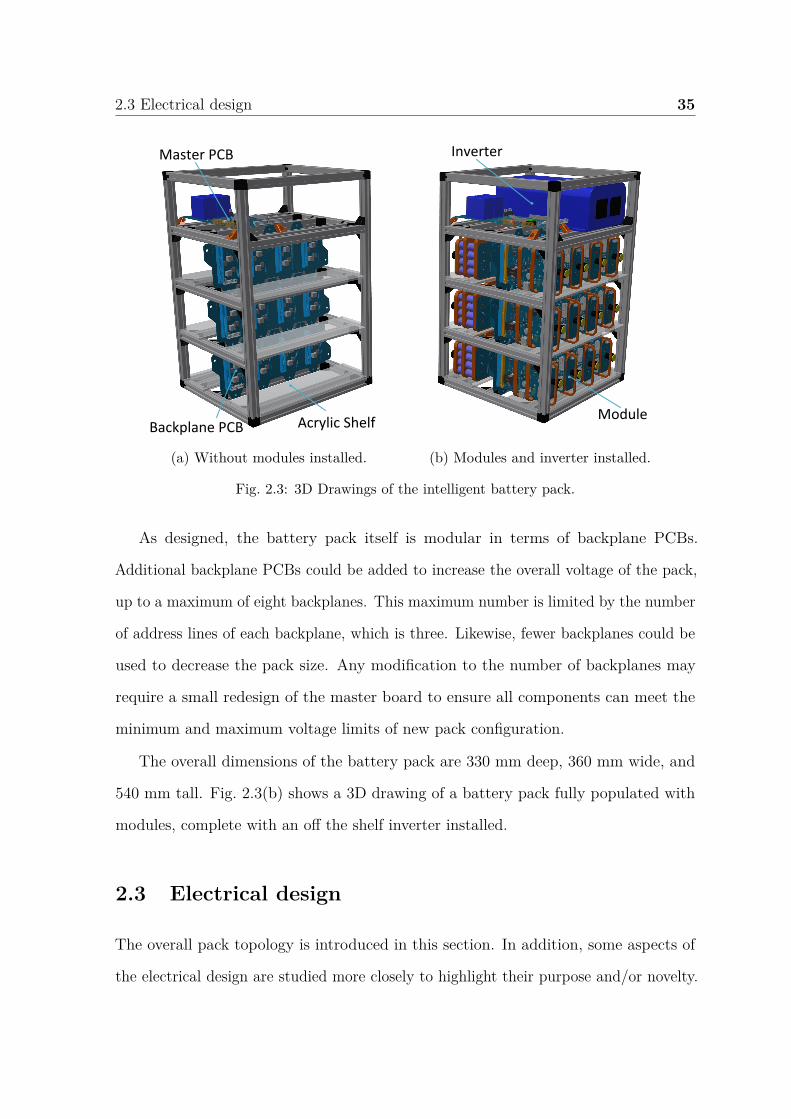
2.3 Electrical design 35
Backplane PCB
Master PCB
Acrylic Shelf
(a) Without modules installed.
Inverter
Module
(b) Modules and inverter installed.
Fig. 2.3: 3D Drawings of the intelligent battery pack.
As designed, the battery pack itself is modular in terms of backplane PCBs.
Additional backplane PCBs could be added to increase the overall voltage of the pack,
up to a maximum of eight backplanes. This maximum number is limited by the number
of address lines of each backplane, which is three. Likewise, fewer backplanes could be
used to decrease the pack size. Any modification to the number of backplanes may
require a small redesign of the master board to ensure all components can meet the
minimum and maximum voltage limits of new pack configuration.
The overall dimensions of the battery pack are 330 mm deep, 360 mm wide, and
540 mm tall. Fig. 2.3(b) shows a 3D drawing of a battery pack fully populated with
modules, complete with an off the shelf inverter installed.
2.3 Electrical design
The overall pack topology is introduced in this section. In addition, some aspects of
the electrical design are studied more closely to highlight their purpose and/or novelty.
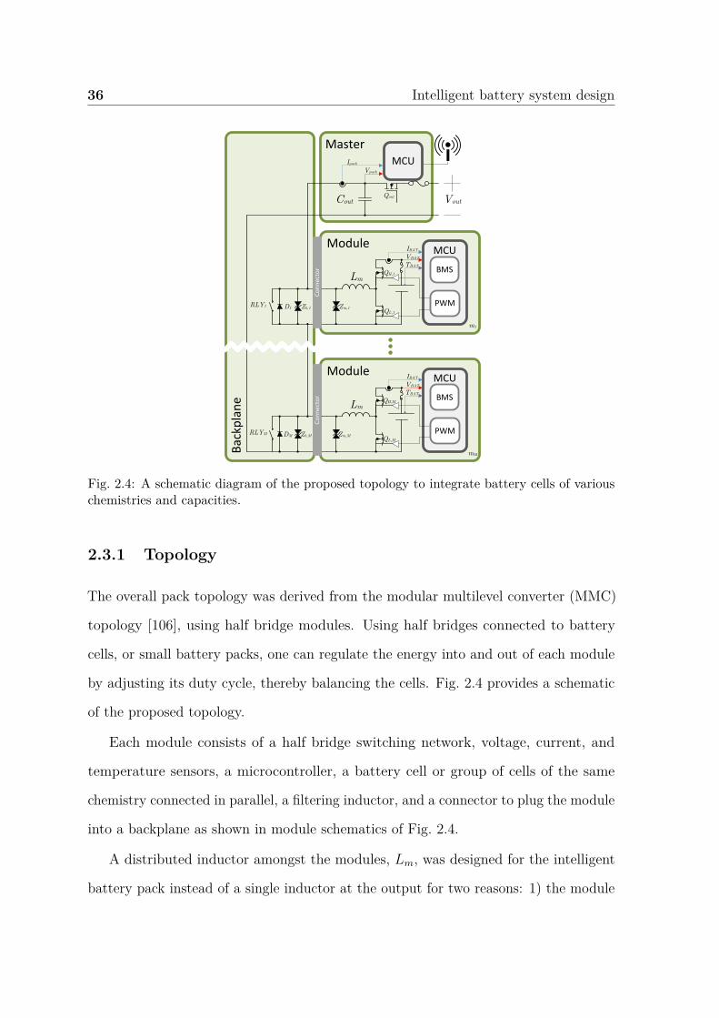
36 Intelligent battery system design
Backplane
Cout Vout
MasterIpack
Vpack
MCU
D1RLY1 Zb,1
IBAT
VBAT
QH,1
QL,1
ModuleMCU
Connector
TBATBMS
m1
PWMZm,1
Lm
IBAT
VBAT
QH,M
QL,M
ModuleMCU
TBATBMS
mM
PWMZm,M
Lm
DMRLYM Zb,M
Connector
Qout
Fig. 2.4: A schematic diagram of the proposed topology to integrate battery cells of variouschemistries and capacities.
2.3.1 Topology
The overall pack topology was derived from the modular multilevel converter (MMC)
topology [106], using half bridge modules. Using half bridges connected to battery
cells, or small battery packs, one can regulate the energy into and out of each module
by adjusting its duty cycle, thereby balancing the cells. Fig. 2.4 provides a schematic
of the proposed topology.
Each module consists of a half bridge switching network, voltage, current, and
temperature sensors, a microcontroller, a battery cell or group of cells of the same
chemistry connected in parallel, a filtering inductor, and a connector to plug the module
into a backplane as shown in module schematics of Fig. 2.4.
A distributed inductor amongst the modules, Lm, was designed for the intelligent
battery pack instead of a single inductor at the output for two reasons: 1) the module

2.3 Electrical design 37
inductor will be used in future work that will involve applying the decentralised battery
management algorithms discussed in Chapter 4, and 2) the module inductor is also used
as the inductor for the small boost converter that can provide 5 V via a USB connector
on the module. Thus, when a module is extracted from the intelligent battery pack, it
can still be used as a useful energy storage device itself.
The backplane exists to provide a way to plug modules in and out of the system
and to bypass missing or failed modules. As shown in Fig. 2.4, every power connection
to each module has a bypass diode (Dk) and relay (RLYk) connected in parallel. In
addition to these, there are a few digital signal lines which are not shown in Fig. 2.4,
but were also used to ensure safe operation of the intelligent battery. These digital
signal lines were:
• Digital input to master of a hardware present signal from each module. When
plugged in, each module pulled a digital line to the master low.
• Isolated digital enable signal from master to module, which was set by the master
and read by the module to ensure the module could operate safely.
• Digital input signal to module from the relay, RLYk, which was a single pole,
double throw (SPDT) type. When the relay was open, it pulls a digital pin
connected to the module MCU low.
The relay is controlled by the master and will only close if the master cannot get
a response from the module and the hardware present signal of the module is high
(inserted modules pull the hardware present signal low). The addition of the bypass
diode enables the intelligent pack to continue to provide power to a load when a module
is removed and is only used until the master can confirm that it can close the bypass
relay. During charging, module removal will interrupt the current path, however this

38 Intelligent battery system design
DkRLYk Zb,k
IBAT
VBAT
QH,k
QL,k
ModuleMCU
TBATBMS
mk
PWMZm,k
Lm
Ipack
Connector
(a) Active switching state 1, SA,1. QH is onand QL is off, connecting the current of thepack, Ipack, to the battery cell.
DkRLYk Zb,k
IBAT
VBAT
QH,k
QL,k
ModuleMCU
TBATBMS
mk
PWMZm,k
Lm
Ipack
Connector
(b) Active switching state 2, SA,2. QL is onand QH is off, bypassing the current of thepack, Ipack around the battery cell.
Fig. 2.5: The two active switching states of the kth module, SA,1 and SA,2.
drawback is negligible since it would not result in the loss of power to a load and
charging is resumed shortly afterwards.
The master communicates with all modules, regulates the output voltage, filters
the switching noise of the modules with Cout, and controls the module bypass relays.
External control and monitoring of the entire battery pack is possible via a wifi module,
which is also controlled by the master.
2.3.2 Switching states
There are a number of switching states for each module in the proposed system. They
can broken down into two categories: (1) active switching states, and (2) module
extraction and insertion switching states.
Active switching states
During normal operation of a module, which is defined as when a module is plugged
into the system and regulating the energy into and out of its battery cell, there are
two active switching states, shown in Fig. 2.5.

2.3 Electrical design 39
In active switching state 1, SA,1, QH,k is on, and QL,k is off. The current path is
highlighted in Fig. 2.5(a) and it shows how the pack’s current, Ipack, flows through the
battery cell. In the case of positive current, this will discharge the cell.
In active switching state 2, SA,2, QL,k is on, and QH,k is off. The current path is
highlighted in Fig. 2.5(b) and it shows how the pack’s current, Ipack, bypasses the
battery cell.
By varying the duty cycle, Dk, between these two states, the energy flow out of,
and into, the battery cell can be controlled. By having full control of the energy flow,
each module will discharge its energy storage element proportional to its capacity. In
this way, every module in the entire pack will traverse its SOC curve together, at the
same time, during charge and discharge.
Module extraction and insertion switching states
During module extraction and insertion, the module and intelligent battery pack must
work together to ensure the proper sequence of switching states are accomplished. Each
module has a dedicated “enable” signal which is driven by the master PCB. This line
is driven high to indicate to the module that it can turn on and it is driven low to
indicate to the module that it cannot turn on.
Module extraction
The three module extraction switching states during charge are shown in Fig. 2.6 and
the three module extraction switching states during discharge are shown in Fig. 2.7.
These two sets of switching states are very similar in their operation.
During either charge or discharge, right before extraction, the module can be in
either one of its active switching states (SA,1 or SA,2), as shown by Fig. 2.6(a), showing
switching state SE-C,1, and Fig. 2.7(a), showing switching state SE-D,1.
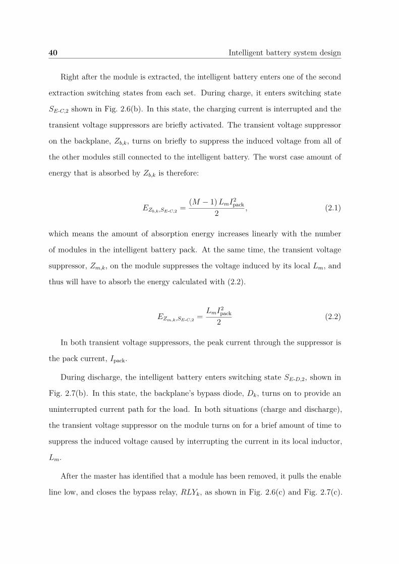
40 Intelligent battery system design
Right after the module is extracted, the intelligent battery enters one of the second
extraction switching states from each set. During charge, it enters switching state
SE-C,2 shown in Fig. 2.6(b). In this state, the charging current is interrupted and the
transient voltage suppressors are briefly activated. The transient voltage suppressor
on the backplane, Zb,k, turns on briefly to suppress the induced voltage from all of
the other modules still connected to the intelligent battery. The worst case amount of
energy that is absorbed by Zb,k is therefore:
EZb,k,SE-C,2 =(M − 1) LmI2
pack
2 , (2.1)
which means the amount of absorption energy increases linearly with the number
of modules in the intelligent battery pack. At the same time, the transient voltage
suppressor, Zm,k, on the module suppresses the voltage induced by its local Lm, and
thus will have to absorb the energy calculated with (2.2).
EZm,k,SE-C,2 =LmI2
pack
2 (2.2)
In both transient voltage suppressors, the peak current through the suppressor is
the pack current, Ipack.
During discharge, the intelligent battery enters switching state SE-D,2, shown in
Fig. 2.7(b). In this state, the backplane’s bypass diode, Dk, turns on to provide an
uninterrupted current path for the load. In both situations (charge and discharge),
the transient voltage suppressor on the module turns on for a brief amount of time to
suppress the induced voltage caused by interrupting the current in its local inductor,
Lm.
After the master has identified that a module has been removed, it pulls the enable
line low, and closes the bypass relay, RLYk, as shown in Fig. 2.6(c) and Fig. 2.7(c).

2.3 Electrical design 41
DkRLYk Zb,k
IBAT
VBAT
QH,k
QL,k
ModuleMCU
TBATBMS
mk
PWMZm,k
Lm
Connector
Icharge
(a) module extraction dur-ing charge switching state1, SE-C,1. In this state,the module can be in ei-ther active switching state,right before a module is ex-tracted.
DkRLYk Zb,k
Icharge
IBAT
VBAT
QH,k
QL,k
ModuleMCU
TBATBMS
mk
PWMZm,k
Lm
Co
nn
ecto
r
Co
nn
ecto
r
Module extraction during charge
(b) module extraction dur-ing charge switching state2, SE-C,2. Right after mod-ule extraction, the tran-sient voltage suppressor,Zb,k briefly turns on to sup-press the induced voltagecreated by all of the in-ductors, Lm, of the othermodules still in the batterypack. On the module side,its transient voltage suppres-sor Zm,k will turn on for abrief amount of time to sup-press the induced voltage ofLm on the extracted mod-ule.
DkRLYk Zb,k
Icharge
IBAT
VBAT
QH,k
QL,k
ModuleMCU
TBATBMS
mk
PWMZm,k
Lm
Connector
Connector
(c) module extraction dur-ing charge switching state3, SE-C,3. The relay cor-responding to this module,RLYk, closes after the mas-ter board verifies that amodule has indeed been ex-tracted.
Fig. 2.6: The three module extraction switching states during charging of the kth module,SE-C,1, SE-C,2, and SE-C,3.
If the intelligent battery was charging, i.e. Ipack < 0 prior to the extraction, then the
charging process would be resumed.
Module insertion
The three module insertion switching states are shown in Fig. 2.8. Prior to module
insertion, the module is in its off state, and its corresponding bypass relay, RLYk, is
closed as shown in module insertion state 1, SI,1, in Fig. 2.8(a).
After insertion, the master will keep the enable line low, but instruct the module to
turn on, and enter a bypass mode as shown in Fig. 2.8(b). This is the second module
insertion switching state, SI,2. The module begins to share some of the current going
through the bypass relay, RLYk.
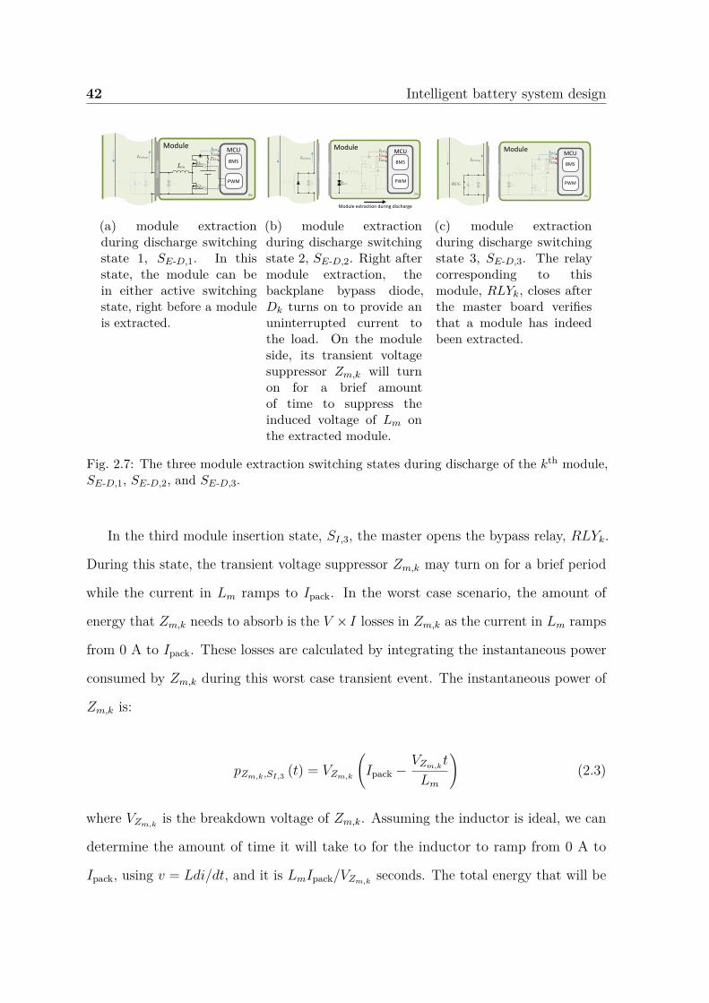
42 Intelligent battery system design
DkRLYk Zb,k
IBAT
VBAT
QH,k
QL,k
ModuleMCU
TBATBMS
mk
PWMZm,k
Lm
Connector
Idischarge
(a) module extractionduring discharge switchingstate 1, SE-D,1. In thisstate, the module can bein either active switchingstate, right before a moduleis extracted.
DkRLYk Zb,k
IBAT
VBAT
QH,k
QL,k
ModuleMCU
TBATBMS
mk
PWMZm,k
Lm
Co
nn
ecto
r
Co
nn
ecto
r
Module extraction during discharge
Idischarge
(b) module extractionduring discharge switchingstate 2, SE-D,2. Right aftermodule extraction, thebackplane bypass diode,Dk turns on to provide anuninterrupted current tothe load. On the moduleside, its transient voltagesuppressor Zm,k will turnon for a brief amountof time to suppress theinduced voltage of Lm onthe extracted module.
DkRLYk Zb,k
Idischarge
IBAT
VBAT
QH,k
QL,k
ModuleMCU
TBATBMS
mk
PWMZm,k
Lm
Connector
Connector
(c) module extractionduring discharge switchingstate 3, SE-D,3. The relaycorresponding to thismodule, RLYk, closes afterthe master board verifiesthat a module has indeedbeen extracted.
Fig. 2.7: The three module extraction switching states during discharge of the kth module,SE-D,1, SE-D,2, and SE-D,3.
In the third module insertion state, SI,3, the master opens the bypass relay, RLYk.
During this state, the transient voltage suppressor Zm,k may turn on for a brief period
while the current in Lm ramps to Ipack. In the worst case scenario, the amount of
energy that Zm,k needs to absorb is the V × I losses in Zm,k as the current in Lm ramps
from 0 A to Ipack. These losses are calculated by integrating the instantaneous power
consumed by Zm,k during this worst case transient event. The instantaneous power of
Zm,k is:
pZm,k,SI,3 (t) = VZm,k
(Ipack −
VZm,kt
Lm
)(2.3)
where VZm,kis the breakdown voltage of Zm,k. Assuming the inductor is ideal, we can
determine the amount of time it will take to for the inductor to ramp from 0 A to
Ipack, using v = Ldi/dt, and it is LmIpack/VZm,kseconds. The total energy that will be

2.3 Electrical design 43
absorbed by Zm,k will be the integral of (2.3) between 0 and LmIpack/VZm,kseconds.
The result is:
EZm,k,SI,3 =LmI2
pack
2 . (2.4)
The peak current during this transient event occurs right at the begining of the
event, and in the worst case it is simply the pack current, Ipack.
In the final module insertion state, SI,4, the master instructs the module to start
gating as shown in Fig. 2.8(d). At this point, the module will be in one of its active
switching states, SA,1 or SA,2.
Discussion
An advantage of the switching states presented here is that the relay switches close to
zero volts, with the breakdown voltage of Zm,k being the maximum voltage that will
be seen across it. As a consequence, it can be implemented with a relatively low cost
relay.
2.3.3 Microcontroller selection
There are a numerous criteria by which to select a microcontroller (MCU). For the
design of the intelligent battery, the main focus was on the available peripherals
and performance of the MCU. Furthermore, due to the author’s familiarity with the
STMicroelectronics’ STM32 series of MCUs, the search space was primarily limited to
this family. Consequently, the STM32F446RE was chosen as the module MCU, and to
simplify the programming tasks, it was also chosen for the Master MCU as well. Some
of the features of this MCU that were critical to the intelligent battery project include:
• 512 kB of flash memory, to implement large programs,
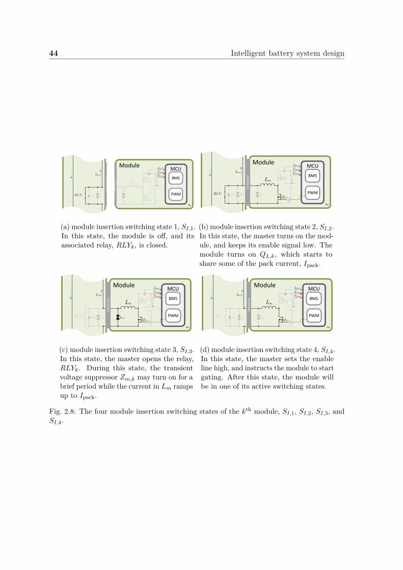
44 Intelligent battery system design
DkRLYk Zb,k
IBAT
VBAT
QH,k
QL,k
ModuleMCU
TBATBMS
mk
PWMZm,k
Lm
Connector
Connector
Ipack
(a) module insertion switching state 1, SI,1.In this state, the module is off, and itsassociated relay, RLYk, is closed.
DkRLYk Zb,k
IBAT
VBAT
QH,k
QL,k
ModuleMCU
TBATBMS
mk
PWMZm,k
Lm
Ipack
Connector
(b) module insertion switching state 2, SI,2.In this state, the master turns on the mod-ule, and keeps its enable signal low. Themodule turns on QL,k, which starts toshare some of the pack current, Ipack.
DkRLYk Zb,k
IBAT
VBAT
QH,k
QL,k
ModuleMCU
TBATBMS
mk
PWMZm,k
Lm
Ipack
Connector
(c) module insertion switching state 3, SI,3.In this state, the master opens the relay,RLYk. During this state, the transientvoltage suppressor Zm,k may turn on for abrief period while the current in Lm rampsup to Ipack.
DkRLYk Zb,k
IBAT
VBAT
QH,k
QL,k
ModuleMCU
TBATBMS
mk
PWMZm,k
Lm
Ipack
Connector
(d) module insertion switching state 4, SI,4.In this state, the master sets the enableline high, and instructs the module to startgating. After this state, the module willbe in one of its active switching states.
Fig. 2.8: The four module insertion switching states of the kth module, SI,1, SI,2, SI,3, andSI,4.

2.3 Electrical design 45
• ARM 32-bit Cortex-M4 CPU with FPU clocked at 180 MHz, for future work to
implement battery models designed in MATLAB,
• 2x advanced timers for PWM generation with multiple output channels, to
implement the PWM and timing,
• 3x 12 bit ADC that can operate up to 2.4 MSPS, and
• multiple communication interfaces including I2C, and CAN Bus.
2.3.4 Module power supply
The ironic thing about any converter design is the need for power supplies to power
the micro-controllers, analogue circuitry, and gate drivers for the converter itself. The
intelligent battery pack design is no different, and perhaps an even more demanding
challenge.
Every module in the intelligent battery is referenced to a different potential, which
means that at some point in the circuit, isolation will be required to facilitate inter-
module communication and master to module communication. In order to simplify
the analogue circuit design, and to take advantage of local ADCs available on micro-
controllers, the isolation point was chosen to be along the communication bus. As a
consequence, each module required its own, locally referenced, 3.3 V and 12 V supply.
The decision was made to add a local boost converter to every module that would
be able to provide 12 V from the local cell voltage. The design of this converter was
based on Intersil’s PWM step-up regulator, part number: ISL97519AIUZ. This part
features an enable pin and integrated power MOSFET. The 12 V supply was connected
in series to another dc/dc converter to create a 3.3 V supply. The series connection
of these two power supplies was chosen so that the downstream 3.3 V supply could
be a simple, low cost buck converter. A Murata Power Solutions’ buck converter was

46 Intelligent battery system design
chosen as the 3.3 V converter, part number: OKI-78SR-3.3/1.5-W36H-C. This part is
a drop-in replacement for a linear voltage regulator.
Finally, to reduce the amount of current drawn by each module to effectively zero
when it is in an off state, the input to the boost converter, and even the battery voltage
sensor, are controlled with a P-channel MOSFET.
2.3.5 Module power stage design
The module power stage consists of the module inductor Lm, the half bridge switching
network QH and QL, and the gate drivers.
Gate driver design
The modules of the intelligent battery pack have high current power electronic switches
that are able to handle the full rated current of the pack. These switches require
dedicated gate drivers to ensure rapid switching and to increase efficiency. The one
challenge with half bridge designs, such as the one depicted for the modules in Fig. 2.4,
is their need for a high side gate driver for QH .
There are a number of solutions to drive high side switches, however, each module
of the intelligent battery pack should be able to output a duty cycle of 100% for
an indefinite amount of time. Furthermore, in order to operate the module’s 5 V
USB power supply, QH must be on continuously. For these reasons, the gate drivers
for QL and QH are both low side drivers, powered by the local 12 V supply. Using
this configuration, QH can be turned on indefinitely and its gate will be driven by a
minimum of 7 V when it is connected to a battery cell that can provide 5 V. This gate
driver design limits the the maximum voltage that can be connected to the module to
(12 − Vth) volts where Vth is the threshold voltage of QH .

2.3 Electrical design 47
The gate drivers chosen for the module are from Fairchild Semiconductor, part
number: FAN3122TMX. They have a peak sinking current of 11.4 A and a peak
sourcing current of 10.6 A, ideal for driving large, high current MOSFETs. This gate
driver also features an enable input which is held low (the gate driver is held in a
disabled state) during turn on, to avoid spurious gating of the power MOSFETs while
the microcontroller is booting up1.
QH and QL selection
QH and QL need to be rated for the full current of the intelligent battery, which was
designed for 25 A. However, in order to minimize losses, MOSFETs with a low RDS-on
value should be selected, but not at the expense of a large gate charge which would
increase the switching losses.
The MOSFETs need also to be able to withstand the blocking voltages that will be
seen in the module. During each active switching state, SA,1 and SA,2, each switch will
have to block the maximum rated input voltage, which was designed for 5 V.
There are numerous MOSFETs are the market today which are low cost and meet
the above criteria, however, most of them have a larger than required drain to source
breakdown voltage. For larger current MOSFETs, the lowest rate drain to source
voltage readily available is 20 V. As a result, the switches will be under utilized
throughout the intelligent battery. After a conversation with Infineon, lower voltage
high current MOSFETs are not going to be manufactured because they would be just
as expensive to a customer as their 20 V counterparts.
MOSFETs from Infineon’s OptiMOS series were chosen for QH and QL, part number:
BSC009NE2LS. These MOSFETs have a maximum RDS-on of 0.9 mΩ, and have a total1This was a serious problem in an early prototype, as the gating signal for QH is connected to a
pin which will output a clock signal from the microcontroller during start-up. The clock signal has afrequency of 16 MHz, and would result in a significant load on the 12 V supply, as the QH gate driverwould be driving QH at this very high frequency.

48 Intelligent battery system design
gate charge of 126 nC, when driven2 with a VGS of 10 V. They are rated for a maximum
current of 100 A. They are designed for switch mode power supply applications, and
have an extremely small footprint of 5.15 mm × 6.15 mm in a PG-TDSON-8 package.
Switching frequency
The switching frequency of the modules will determine the output voltage ripple for
given filter parameters (Lm and Cout). It cannot be as high as possible to minimize
the output voltage ripple because the switching losses increase linearly with switching
frequency. However, in the intelligent battery the modules are phase shifted with
respect to each other to help minimize the output voltage ripple. Their phase shifts
are determined by:
φk = 2πk
M. (2.5)
Using (2.5), the output voltage ripple is greatly reduced in a similar manner to
how interleaved parallel converters reduce their output voltage ripple. If we assume
the duty cycles of all of the modules are equal, which is a reasonable assumption when
all of the modules have the same capacity, an estimate of the output voltage ripple can
be calculated using the small ripple approximation in the inductors Lm and the output
capacitor, Cout. The duty cycles of the modules are calculated with:
D1 = D2 = . . . = DM = Dr = Vout
MVcell, (2.6)
where Vout is the nominal output voltage of the intelligent battery and Vcell is the
voltage of the cell in each module, which for simplicity, is the same for all modules.
Using the current ripple diagram shown in Fig. 2.9, the peak to peak ripple current in
the module inductors, Ip-p, is:2The data sheet does not supply figures for VGS > 10 V. The maximum VGS is ± 20 V.
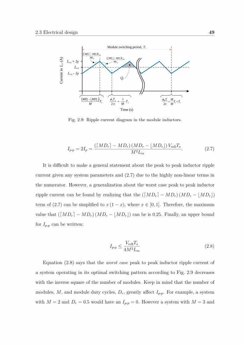
2.3 Electrical design 49
m
cellrr
ML
VMDMD
m
cellrr
ML
VMDMD
Iavg
Iavg + Ip
Iavg - Ip
ss T
M
T 1
2
1
s
rr TM
MDMD ss
sM TTM
MT
2
Qr
Module switching period, Ts
Time (s)
Curr
ent
in L
m (
A)
Fig. 2.9: Ripple current diagram in the module inductors.
Ip-p = 2Ip = (⌈MDr⌉ − MDr) (MDr − ⌊MDr⌋) VcellTs
M2Lm
. (2.7)
It is difficult to make a general statement about the peak to peak inductor ripple
current given any system parameters and (2.7) due to the highly non-linear terms in
the numerator. However, a generalization about the worst case peak to peak inductor
ripple current can be found by realizing that the (⌈MDr⌉ − MDr) (MDr − ⌊MDr⌋)
term of (2.7) can be simplified to x (1 − x), where x ∈ [0, 1]. Therefore, the maximum
value that (⌈MDr⌉ − MDr) (MDr − ⌊MDr⌋) can be is 0.25. Finally, an upper bound
for Ip-p can be written:
Ip-p ≤ VcellTs
4M2Lm
(2.8)
Equation (2.8) says that the worst case peak to peak inductor ripple current of
a system operating in its optimal switching pattern according to Fig. 2.9 decreases
with the inverse square of the number of modules. Keep in mind that the number of
modules, M , and module duty cycles, Dr, greatly affect Ip-p. For example, a system
with M = 2 and Dr = 0.5 would have an Ip-p = 0. However a system with M = 3 and
50 Intelligent battery system design
Dr = 0.5 would have an Ip-p = (VcellTs) / (4M2Lm), an increase in peak to peak ripple
current despite and increase in M .
The output voltage ripple can be estimated by assuming the ripple current of the
inductor is absorbed by Cout. From Fig. 2.9, this is equivalent to the charge Qr being
absorbed and provided by Cout. Therefore, the peak to peak output voltage ripple,
Vp-p, is:
Vp-p = Qr
Cout(2.9)
Vp-p = Ip-pTs
8MCout. (2.10)
Equations (2.7) and (2.10) show that the ripple current and ripple voltage decreased
proportionally with switching period, as expected. Using the worst case Ip-p, (2.10)
shows that the worst case ripple voltage of the intelligent battery is reduced by a factor
of M3 due to the interleaved switching of the modules. By choosing module phase
shifts according to (2.5), the effective switching frequency of the intelligent battery
is increased. Therefore, smaller passive components can be used to achieve the same
ripple specifications.
As the number of series connected modules increase, the inductor ripple current
and output voltage ripple will decrease. Therefore, as the intelligent battery is scaled
in voltage, the passive filtering components (Lm and Cout) can be reduced in size and
only the voltage rating of Cout needs to be increased.
The switching frequency of the modules was chosen to be 20 kHz. This frequency
will result in extremely low output voltage ripple and shorter control loop latency.
Given the filtering components that will be designed in the following subsections, the
2.3 Electrical design 51
estimated peak to peak ripple current is Ip-p = 12 mA and the estimated output voltage
ripple is Vp-p = 2.7 µV.
The ripple current and voltage are extremely low and the filtering components,
switching frequency, and control loop latency requirements should be optimized in
future designs. A peak to peak output voltage ripple of 0.1% (0.048 V) could be a
good starting design criteria.
2.3.6 Inductor sizing
The inductance of the module level inductor was chosen to meet ripple specifications
in the worst case switching conditions. The peak to peak ripple current specifications
were chosen to be 20% to 40% of the maximum current rating of the battery pack,
as suggested in an application note[107]. The worst case switching conditions occur
during start-up, when the modules are not yet synchronized and their local battery
cells are at 100% SOC. Using the small ripple approximation, the peak to peak ripple
current on the module level inductors can be calculated with the following equation:
∆ILmp-p = M · Vcell − Vout
M · Lm
· Vout
M · Vcell· 1
Ts
(2.11)
where M is the number of modules, in this case M = 24. In the worst case switching
conditions, Vcell = 5 V, Vout = 48 V, and Ts = 50 µs. Solving for Lm, this yields
an inductance range of 6 µH to 12 µH as suggested by [107]. Leaning towards the
conservative side, an inductance of 10 µH was chosen for the module’s inductor.
The inductor’s current sizing must take into account the maximum current of the
intelligent battery, plus the worst case ripple current. Using a 10 µH inductor, the
nominal peak current through the inductor is 28 A. Searching available off the shelf
parts, an inductor from Wurth Electronics was chosen, part number 7443641000. Its
current rating is 30 A and it has a saturation current of 37 A.

52 Intelligent battery system design
2.3.7 Output capacitor sizing
The output capacitor, Cout, of the intelligent battery pack needs to be able to handle
large ripple currents, voltages of at least 5 × 24 = 120 V dc, and be large enough
to be connected to loads with large input capacitors without completely discharg-
ing. These requirements were met with a parallel combination of film capacitors
and aluminium electrolytic capacitors. The film capacitors were chosen from Epcos’
(TDK) line of capacitors designed for high frequency switch mode power supplies, part
number: B32778G4107K. The capacitor chosen has a voltage rating of 450 V dc, and
a capacitance of 100 µF. Two of these capacitors connected in parallel were used in
the intelligent battery pack. The aluminium electrolytic capacitors were chosen from
Dubilier, part number: DEA 1000 63. This capacitor has a capacitance of 1000 µF,
and two of them were placed in parallel. Therefore, the total output capacitance of
the intelligent battery pack was designed to be 2200 µF. This capacitance value is
very large and results in a very low peak to peak output voltage ripple of 2.7 µV as
calculated in a previous subsection. In a future design, the size of this capacitor would
be greatly reduced to take advantage of the interleaved switching of the intelligent
battery.
Using this capacitor and the module inductors, we can calculate the cut-off frequency
of the output LC filter of the intelligent battery pack:
f0 = 12π
√M · LmCout
= 219 Hz. (2.12)
The cut-off frequency of the intelligent battery pack will dictate its controller
bandwidth. This value of 219 Hz means that the controller will not be able to respond
extremely quickly (less than 1 ms) to load changes.
2.3 Electrical design 53
2.3.8 Transient voltage suppressor design
The energy absorption requirements of the voltage suppressors were derived in Section
2.3.2. Using those equations and the design specifications of the intelligent battery
pack, the maximum amount of energy that the module voltage suppressors must absorb
is:
EZm,k,max =LmI2
pack
2 (2.13)
EZm,k,max = 3.125 × 10⁻³ J, (2.14)
and the maximum amount of energy that the backplane voltage suppressors must
absorb is:
EZb,k,max =(M − 1) LmI2
pack
2 (2.15)
EZb,k,max = 71.875 × 10⁻³ J, (2.16)
where Lm = 50 µH, M = 24, and Ipack = 25 A.
The backplane transient voltage suppressors were chosen from Littelfuse Inc., part
number: 1.5SMC24CA. This part has minimum varistor voltage of 22.8 V with a peak
pulse current of 45.8 A, well within the requirements of Ipack = 25 A, and can absorb
1 J of energy. The varistor voltage was chosen based on the maximum voltage that
the bypass diode, Dk, can withstand, which is 45 V. Therefore, the chosen part has a
maximum varistor voltage of 33.2 V.
The module transient voltage suppressors were chosen from EPCOS (TDK), part
number: B72530T0060M062. These devices have a minimum varistor voltage of 8.8 V
54 Intelligent battery system design
and can absorb up to 0.7 J of energy. Their peak surge current is 300 A. These devices
were over designed to minimize failures in the prototype. The varistor voltage was
chosen to be as high as possible without damaging the analogue circuitry on the module
PCB and therefore, the maximum varistor voltage of this device is 13.2 V.
In addition to the transient voltage suppressor on the module, each module also
has a bank of capacitors that forms part of an auxiliary 5 V dc to dc converter. The
connection of these capacitors is shown as C5V in Fig. 2.10. The capacitors also help
absorb the energy from Lm during transient events, and could be used as a substitute
for the transient voltage suppressor. In order to keep the same clamping voltage of
8.8 V, the capacitance must be larger than:
EZb,k,max ≤ 12C5V V 2
clamp − 12C5V V 2
out-max (2.17)
C5V ≥2EZb,k,max
V 2clamp − V 2
out-max(2.18)
C5V ≥ 119 µF, (2.19)
where Vout-max = 5 V in the absolute worst case scenario. However, during normal
operation, Vout-max = 2 V and in this scenario the minimum capacitance required by
C5V is 85 µF. In the current design of the modules, C5V = 100 µF and therefore, during
normal operation the transient voltage suppressors will not be triggered, as all of the
energy of Lm will be absorbed by C5V .
In future designs that may not have C5V , it is still more economical to introduce
a transient voltage suppressor instead of a bank of output capacitors to absorb the
energy of Lm. Furthermore, a bank of capacitors will also require a discharge resistor,
and if not completely discharged before the next transient event, the clamping voltage
may increase beyond the desired limits.

2.3 Electrical design 55
DkRLYk Zb,k
IBAT
VBAT
QH,k
QL,k
ModuleMCU
TBATBMS
mk
PWMZm,k
Lm
Ipack
Connector
C5V
Fig. 2.10: 5 V capacitor, 55V , connection in modules.
2.3.9 Communication
Intra-pack communication is important to relay information back to the master board,
which will in turn relay commands to the modules. However, the communication
network should also be able to provide real time commands to maintain tight output
voltage regulation. Therefore, the intelligent battery pack uses two communication
paths to the modules: 1) a bi-directional, data communication bus over an internal
CAN bus, and 2) a uni-directional, real time single wire communication bus from the
master to the modules which synchronizes their switching actions and provides the
ac component of the duty cycle, d. d is the control signal from the master which is
used to regulate the output voltage of the intelligent battery. Each module calculates
its own “dc” value of the duty cycle, Dk, via their state of charge controllers. Every
module combines Dk and d to output a switching signal that regulates the energy of
their connected cell and regulates the output voltage. The details of d are explained in
the subsection: “Sync and data signal”.
CAN bus
CAN bus was chosen for the bi-directional, data communication bus within the
intelligent battery pack, as it is an industry standard for automotive and other industrial
applications. Furthermore, the CAN bus protocol is a master-less protocol, which

56 Intelligent battery system design
would enable future work on the intelligent battery that does not involve a central
master board for communication.
The MCU was specifically chosen because it has a hardware implementation of two
CAN bus modules. One CAN bus module is used for intra-pack communication and
the other is used for external communication.
Sync and data signal3
The sync and data signal combines a synchronization pulse and the ac component of
the duty cycle, d, together into a single signal. Furthermore, it is implemented entirely
in hardware, freeing up the MCUs for other tasks. Fig. 2.11 is a schematic of how the
signal is created by the master and how is it decoded in the module.
At the master, the output voltage is regulated with a voltage controller, Cv (s),
which outputs the ac component of the duty cycle, d. The master MCU uses one of
its PWM modules to output a synchronization signal, as shown in Fig. 2.11. At the
moment the synchronization signal goes high, the UART module transfers the value
d. The outputs of the UART module and the PWM module are fed through an AND
gate. The output of the AND gate is the sync and data signal which is connected to
all of the modules.
The module uses the sync and data signal to adjust its duty cycle and synchronize
its local PWM counter with all of the other modules in the pack. The sync and data
signal is routed directly into the module’s UART module to receive d. The sync and
data signal is also routed to an OR gate, whose other input is a blanking signal from
the module’s PWM module. The output of the OR gate is a synchronization signal
which is in phase with the master’s synchronization signal. The synchronization signal3Due to time constraints, initial work on the intelligent battery was supported by a consultant,
FrostNet, for 36 days. The sync and data signal was developed in collaboration with FrostNet. Theauthor originally suggested to design the sync and data signal with a variable duty cycle. FrostNetimproved the design by suggesting the use of a digital signal, rather then a variable duty cycle. Theauthor designed and implemented the hardware and overall architecture for the sync and data signal.
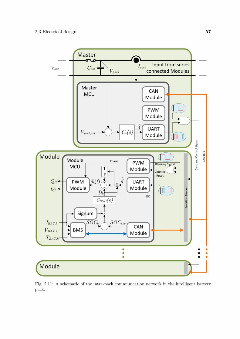
2.3 Electrical design 57
Vpack,ref
Ipack
Cv(s)d
CounterReset
Blanking Signal
Iso
lati
on
Bar
rier
Syn
c an
d C
on
tro
l Sig
nal
CA
N B
us
RX
TX
dQH
QL
Phase
VBAT,k
IBAT,k
TBAT,k
CoutVout
Master
Module
Master MCU
Module MCU
Module
Input from series connected Modules
^
^
Dk
SOCk SOCavg
CSOC(s)
Vpack
PWM Module
UART Module
1s
PWM Module
BMSCAN
Module
PWM Module
UART Module
CAN Module
dk(t)
Signum
Fig. 2.11: A schematic of the intra-pack communication network in the intelligent batterypack.

58 Intelligent battery system design
is then used to reset the counter of the module’s PWM module to synchronize all of
the PWM modules in the pack and generate the blanking signal.
The module calculates its duty cycle according to (2.20):
dk (t) = Dk + Dkd +∫ ∞
0Dkd dt, (2.20)
which is also represented schematically in Fig. 2.11. The “dc”, or slowly changing,
part of the duty cycle is Dk. This value is calculated by the module’s SOC controller,
CSOC (s). The ac component of the duty cycle, d, adjusts the module’s duty cycle in
proportion to the dc duty cycle so that cells with larger capacities increase their loads
proportionally when the duty cycle increases, and visa versa with smaller capacity cells.
The second term of (2.20) is the component which will vary the most in response to
the master’s voltage controller. The third term of (2.20) is a slow integrator which
will gradually integrate any non-zero value of d, so that the average value of d is zero.
It is advantageous for d to be zero in instances where the connection to the master
controller is lost or the master controller is suddenly reset. In both of these cases, the
module’s duty cycle will not change, thus avoiding any large transients at the output
of the intelligent battery pack. The integrator operates on the seconds time scale,
meaning it takes about 1-2 seconds for the integrator to integrate d to 0. At this rate,
it does not effect the voltage or current control loops which operate at the millisecond
time scale and nor does it effect the SOC control loop which operates at the tens of
minutes time scale.
The module’s PWM module applies any necessary phase shift and outputs the
appropriate gating signals to QH and QL.
In this way, all of the PWM counters in all of the modules will be synchronized
and the duty cycles of all of the modules can be updated every switching cycle which
allows for tight output voltage regulation and controlled output voltage ripple. The
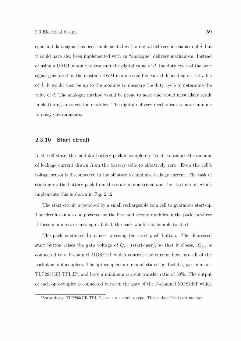
2.3 Electrical design 59
sync and data signal has been implemented with a digital delivery mechanism of d, but
it could have also been implemented with an “analogue” delivery mechanism. Instead
of using a UART module to transmit the digital value of d, the duty cycle of the sync
signal generated by the master’s PWM module could be varied depending on the value
of d. It would then be up to the modules to measure the duty cycle to determine the
value of d. The analogue method would be prone to noise and would most likely result
in chattering amongst the modules. The digital delivery mechanism is more immune
to noisy environments.
2.3.10 Start circuit
In the off state, the modular battery pack is completely “cold” to reduce the amount
of leakage current drawn from the battery cells to effectively zero. Even the cell’s
voltage sensor is disconnected in the off state to minimize leakage current. The task of
starting up the battery pack from this state is non-trivial and the start circuit which
implements this is shown in Fig. 2.12.
The start circuit is powered by a small rechargeable coin cell to guarantee start-up.
The circuit can also be powered by the first and second modules in the pack, however
if these modules are missing or failed, the pack would not be able to start.
The pack is started by a user pressing the start push button. The depressed
start button raises the gate voltage of Qs-u (start-user), so that it closes. Qs-u is
connected to a P-channel MOSFET which controls the current flow into all of the
backplane optocouplers. The optocouplers are manufactured by Toshiba, part number:
TLP293(GB-TPL,E4, and have a minimum current transfer ratio of 50%. The output
of each optocoupler is connected between the gate of the P-channel MOSFET which
4Surprisingly, TLP293(GB-TPL,E does not contain a typo. This is the official part number.
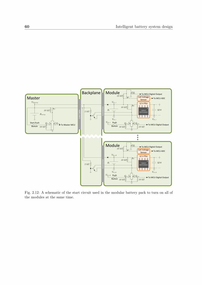
60 Intelligent battery system design
10 kΩ
10 kΩ
12 V
VB+,1
VB-,1
B1
VB+,1
10 kΩ To MCU Digital Output
VB-,1
2 kΩ Bstartup
10 kΩ
Start Push
Button 10 kΩ
VBstartup
To Master MCUPush
Button
ModuleBackplane
Co
nn
ecto
r
Master
Lin
k C
able
Qs-u Qs-m Qp-mQp-u
10 kΩ
Qs
IntersilISL97519AIUZ
12 V PSU
To MCU Digital Output
To MCU ADCCell Voltage
Sensor
10 kΩ
10 kΩ
12 V
VB+,M
VB-,M
B1
VB+,M
10 kΩ To MCU Digital Output
VB-,M
Push
Button
Module
Qp-mQp-u
10 kΩ
Qs
IntersilISL97519AIUZ
12 V PSU
To MCU Digital Output
To MCU ADCCell Voltage
Sensor
2 kΩ
Co
nn
ecto
r
Fig. 2.12: A schematic of the start circuit used in the modular battery pack to turn on all ofthe modules at the same time.

2.4 Scalability 61
controls the current flowing into the 12 V supply of a module, and the local ground
point of each module.
Once on, each module will follow the start-up flow chart shown in Fig. 2.13. The
first step in this start-up procedure is to turn on MOSFET Qp-m (psu-mcu), which keeps
the module power supply on and MOSFET Qs (sensor), which closes the P-channel
MOSFET used to disconnect the module’s voltage sensor from the cell. Next, the
module MCUs start gating, which in turn powers the point of load converters on the
master PCB, which will start-up the master MCU.
MOSFET Qs-m (start-mcu) is used by the master MCU to start modules that have
been inserted into the backplane whilst the intelligent battery has already been turned
on. MOSFET Qp-u (psu-user) is used by the user to turn on the module.
2.4 Scalability
Using the intelligent battery design of Section 2.3, its scalability can be evaluated in
the same manner as the balancing circuits of Table 1.2. Fig. 2.14 shows an updated
Fig. 1.5 with the proposed intelligent battery scalability figures added.
Using the terminology developed in Section 1.5, the scalability of the intelligent
battery places it as a Type A and Type IV topology. It is not surprising that it is
a Type A topology since it is based on an MMC topology, which places low voltage
switching components in series to meet output voltage requirements.
The intelligent battery’s classification as a Type IV topology does not tell the whole
story. The Type IV classification is due to the output capacitor which exists to filter
the ripple current of the inductors. The capacitor’s size depends on each application’s
ripple voltage requirements and the capacitance required will change as the number of
cells increases. As derived in (2.7) and (2.10), the worst case ripple voltage varies with
the cubed inverse of the number of cells. For the same peak to peak output voltage
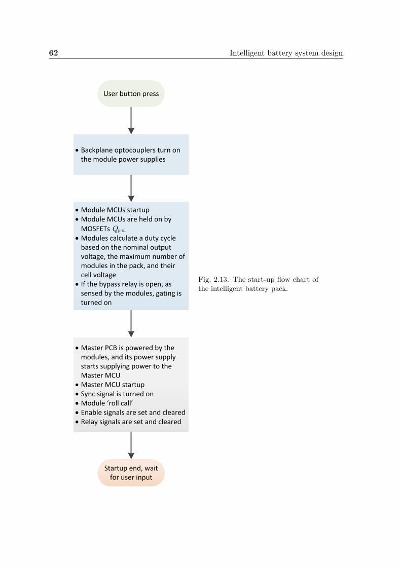
62 Intelligent battery system design
User button press
· Backplane optocouplers turn on the module power supplies
· Module MCUs startup· Module MCUs are held on by
MOSFETs Qp-m
· Modules calculate a duty cycle based on the nominal output voltage, the maximum number of modules in the pack, and their cell voltage
· If the bypass relay is open, as sensed by the modules, gating is turned on
· Master PCB is powered by the modules, and its power supply starts supplying power to the Master MCU
· Master MCU startup· Sync signal is turned on· Module ‘roll call’· Enable signals are set and cleared· Relay signals are set and cleared
Startup end, wait for user input
Fig. 2.13: The start-up flow chart ofthe intelligent battery pack.
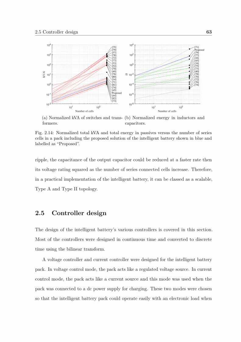
2.5 Controller design 63
101
102
Number of cells
10-2
10-1
100
101
102
103
104
|kV
A|
[73][82][44]Proposed[45][74][81][71][34][80][76][40][70][52][53][77][72][78][57][79][75]
(a) Normalized kVA of switches and trans-formers.
101
102
Number of cells
10-8
10-6
10-4
10-2
100
102
104
|J|
[74][76][72][70][78][40][73][75][34][45][44][77][79]Proposed[71]
(b) Normalized energy in inductors andcapacitors.
Fig. 2.14: Normalized total kVA and total energy in passives versus the number of seriescells in a pack including the proposed solution of the intelligent battery shown in blue andlabelled as “Proposed”.
ripple, the capacitance of the output capacitor could be reduced at a faster rate then
its voltage rating squared as the number of series connected cells increase. Therefore,
in a practical implementation of the intelligent battery, it can be classed as a scalable,
Type A and Type II topology.
2.5 Controller design
The design of the intelligent battery’s various controllers is covered in this section.
Most of the controllers were designed in continuous time and converted to discrete
time using the bilinear transform.
A voltage controller and current controller were designed for the intelligent battery
pack. In voltage control mode, the pack acts like a regulated voltage source. In current
control mode, the pack acts like a current source and this mode was used when the
pack was connected to a dc power supply for charging. These two modes were chosen
so that the intelligent battery pack could operate easily with an electronic load when
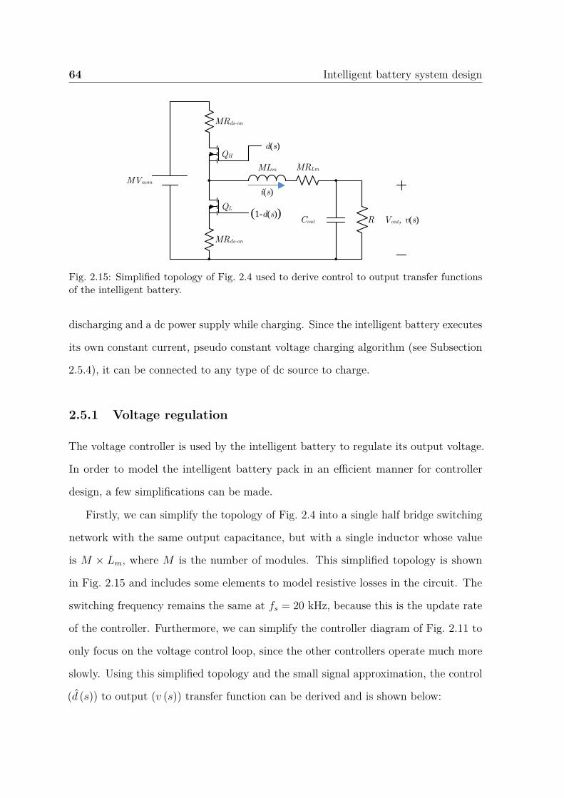
64 Intelligent battery system design
QH
MLm
Cout Vout, v(s)
MRLm
QL
MRds-on
MRds-on
R
MVnom
i(s)
d(s)
(1-d(s))
Fig. 2.15: Simplified topology of Fig. 2.4 used to derive control to output transfer functionsof the intelligent battery.
discharging and a dc power supply while charging. Since the intelligent battery executes
its own constant current, pseudo constant voltage charging algorithm (see Subsection
2.5.4), it can be connected to any type of dc source to charge.
2.5.1 Voltage regulation
The voltage controller is used by the intelligent battery to regulate its output voltage.
In order to model the intelligent battery pack in an efficient manner for controller
design, a few simplifications can be made.
Firstly, we can simplify the topology of Fig. 2.4 into a single half bridge switching
network with the same output capacitance, but with a single inductor whose value
is M × Lm, where M is the number of modules. This simplified topology is shown
in Fig. 2.15 and includes some elements to model resistive losses in the circuit. The
switching frequency remains the same at fs = 20 kHz, because this is the update rate
of the controller. Furthermore, we can simplify the controller diagram of Fig. 2.11 to
only focus on the voltage control loop, since the other controllers operate much more
slowly. Using this simplified topology and the small signal approximation, the control
(d (s)) to output (v (s)) transfer function can be derived and is shown below:

2.5 Controller design 65
sG IBvd
sv sd
sTse
2
refv sCv
^
Fig. 2.16: Voltage control loop of the intelligent battery.
Gvd-IB (s) = v (s)d (s)
(2.21)
Gvd-IB (s) = VnomR
(Rds-on + RLm) + RM
+ s (Lm + CoutR (Rds-on + RLm)) + s2RLmCout
(2.22)
where Rds-on is the on resistance of the MOSFETs (QH,k and QL,k), and RLm is the
dc resistance of each inductor, Lm. Fig. 2.16 shows the voltage control loop of the
intelligent battery pack, which includes the control loop delay in the feedback loop.
Gvd-IB (s) is also the loop gain of the system when the voltage controller, Cv (s),
has unity gain. Let Tv (s) = Gvd-IB (s) be the loop gain of the system. The bode plot
of the intelligent battery system can be drawn using the parameters listed in Table 2.2,
and the plot is shown in Fig. 2.18(a). However, before controller design can commence,
it is important to include the delay caused by the digital control loop. Fig. 2.17 is
a timing diagram showing the events that occur during the execution of the voltage
control loop.
Using Fig. 2.17 as a reference, the master board of the intelligent pack takes two
samples of the output voltage at TS1 and TS2 during each iteration of the voltage control
loop. Two samples are taken to yield an improved measurement of the output voltage.
Since the modules will be varying their duty cycles, it is difficult to choose a sample
time that will always be at the peak or trough of the output voltage ripple. Ideally,
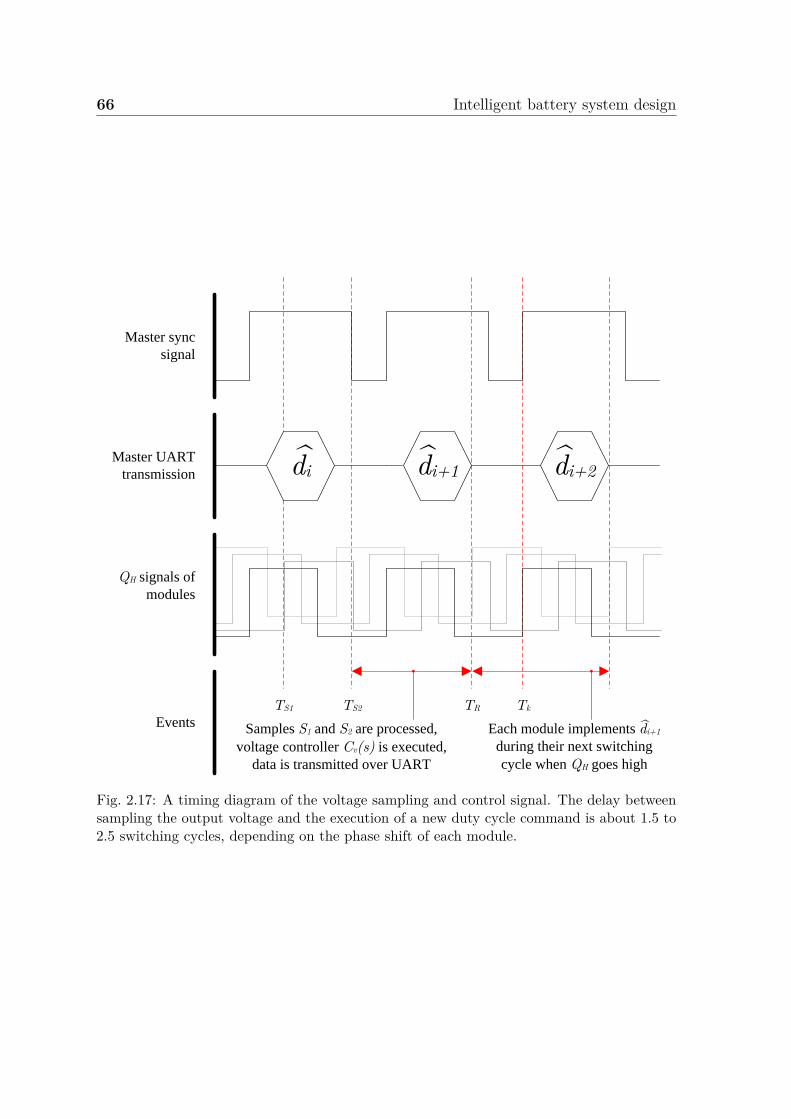
66 Intelligent battery system design
di di+1
TS1 TS2
Samples S1 and S2 are processed,
voltage controller Cv(s) is executed,
data is transmitted over UART
TR Tk
Master sync
signal
Master UART
transmission
QH signals of
modules
Events
di+2^^
Each module implements di+1
during their next switching
cycle when QH goes high
^
Fig. 2.17: A timing diagram of the voltage sampling and control signal. The delay betweensampling the output voltage and the execution of a new duty cycle command is about 1.5 to2.5 switching cycles, depending on the phase shift of each module.
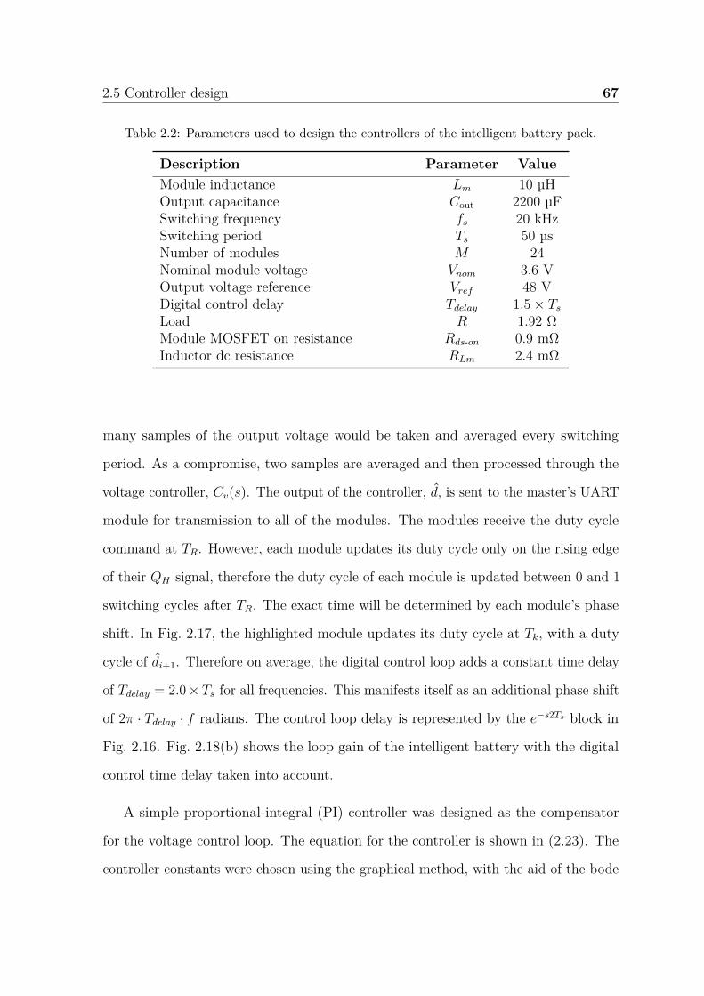
2.5 Controller design 67
Table 2.2: Parameters used to design the controllers of the intelligent battery pack.
Description Parameter ValueModule inductance Lm 10 µHOutput capacitance Cout 2200 µFSwitching frequency fs 20 kHzSwitching period Ts 50 µsNumber of modules M 24Nominal module voltage Vnom 3.6 VOutput voltage reference Vref 48 VDigital control delay Tdelay 1.5 × Ts
Load R 1.92 ΩModule MOSFET on resistance Rds-on 0.9 mΩInductor dc resistance RLm 2.4 mΩ
many samples of the output voltage would be taken and averaged every switching
period. As a compromise, two samples are averaged and then processed through the
voltage controller, Cv(s). The output of the controller, d, is sent to the master’s UART
module for transmission to all of the modules. The modules receive the duty cycle
command at TR. However, each module updates its duty cycle only on the rising edge
of their QH signal, therefore the duty cycle of each module is updated between 0 and 1
switching cycles after TR. The exact time will be determined by each module’s phase
shift. In Fig. 2.17, the highlighted module updates its duty cycle at Tk, with a duty
cycle of di+1. Therefore on average, the digital control loop adds a constant time delay
of Tdelay = 2.0 × Ts for all frequencies. This manifests itself as an additional phase shift
of 2π · Tdelay · f radians. The control loop delay is represented by the e−s2Ts block in
Fig. 2.16. Fig. 2.18(b) shows the loop gain of the intelligent battery with the digital
control time delay taken into account.
A simple proportional-integral (PI) controller was designed as the compensator
for the voltage control loop. The equation for the controller is shown in (2.23). The
controller constants were chosen using the graphical method, with the aid of the bode
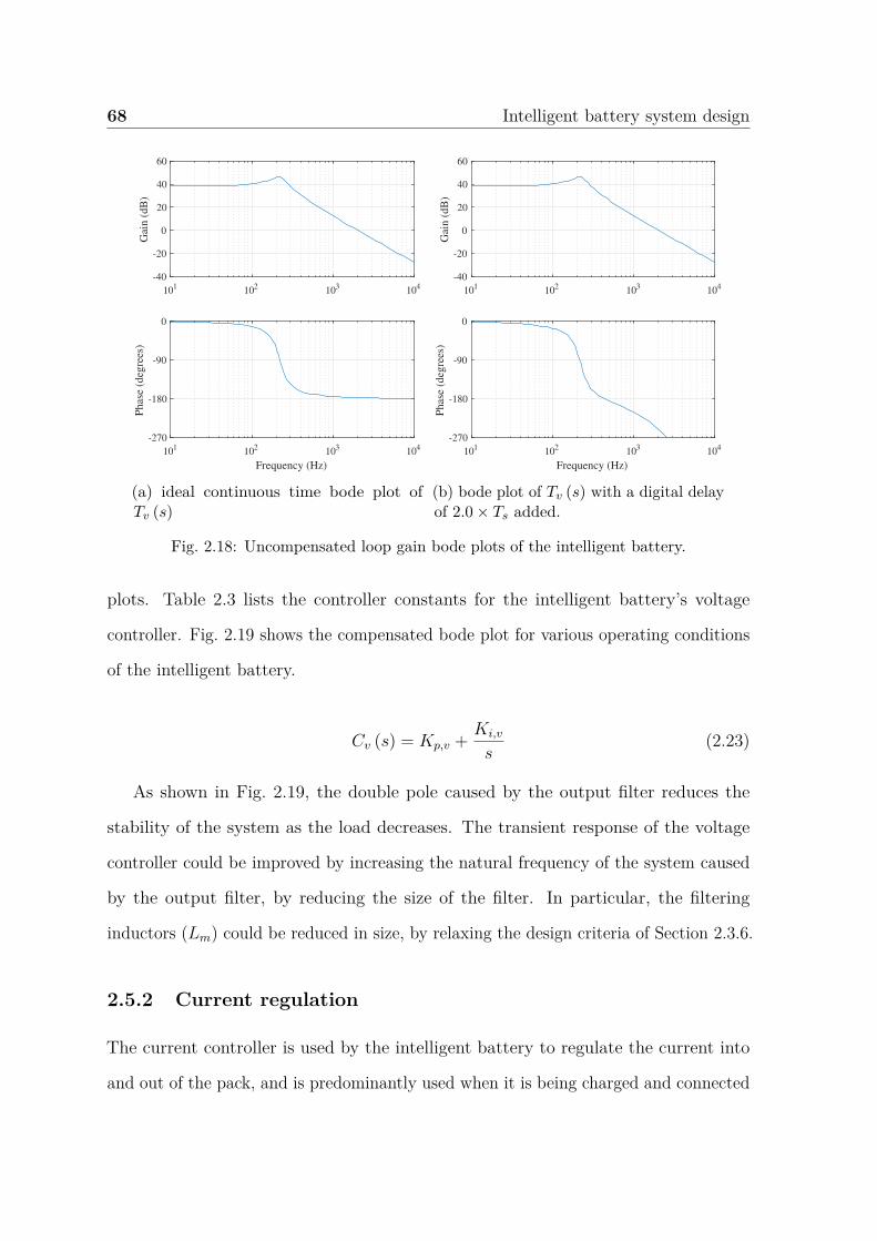
68 Intelligent battery system design
101 102 103 104-40
-20
0
20
40
60
Gai
n (
dB
)
101 102 103 104
Frequency (Hz)
-270
-180
-90
0
Phas
e (d
egre
es)
(a) ideal continuous time bode plot ofTv (s)
101 102 103 104-40
-20
0
20
40
60
Gai
n (
dB
)101 102 103 104
Frequency (Hz)
-270
-180
-90
0
Phas
e (d
egre
es)
(b) bode plot of Tv (s) with a digital delayof 2.0 × Ts added.
Fig. 2.18: Uncompensated loop gain bode plots of the intelligent battery.
plots. Table 2.3 lists the controller constants for the intelligent battery’s voltage
controller. Fig. 2.19 shows the compensated bode plot for various operating conditions
of the intelligent battery.
Cv (s) = Kp,v + Ki,v
s(2.23)
As shown in Fig. 2.19, the double pole caused by the output filter reduces the
stability of the system as the load decreases. The transient response of the voltage
controller could be improved by increasing the natural frequency of the system caused
by the output filter, by reducing the size of the filter. In particular, the filtering
inductors (Lm) could be reduced in size, by relaxing the design criteria of Section 2.3.6.
2.5.2 Current regulation
The current controller is used by the intelligent battery to regulate the current into
and out of the pack, and is predominantly used when it is being charged and connected
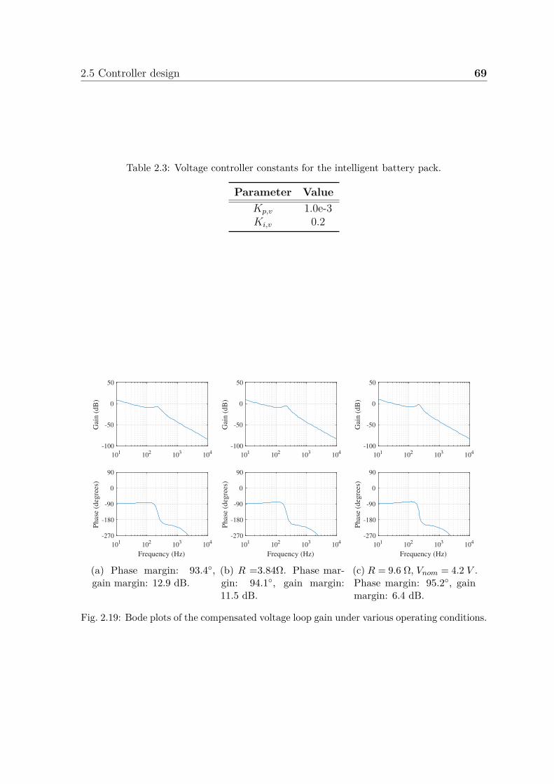
2.5 Controller design 69
Table 2.3: Voltage controller constants for the intelligent battery pack.
Parameter ValueKp,v 1.0e-3Ki,v 0.2
101 102 103 104-100
-50
0
50
Gai
n (
dB
)
101 102 103 104
Frequency (Hz)
-270
-180
-90
0
90
Ph
ase
(deg
rees
)
(a) Phase margin: 93.4,gain margin: 12.9 dB.
101 102 103 104-100
-50
0
50
Gai
n (
dB
)
101 102 103 104
Frequency (Hz)
-270
-180
-90
0
90
Ph
ase
(deg
rees
)
(b) R =3.84Ω. Phase mar-gin: 94.1, gain margin:11.5 dB.
101 102 103 104-100
-50
0
50
Gai
n (
dB
)
101 102 103 104
Frequency (Hz)
-270
-180
-90
0
90
Ph
ase
(deg
rees
)
(c) R = 9.6 Ω, Vnom = 4.2 V .Phase margin: 95.2, gainmargin: 6.4 dB.
Fig. 2.19: Bode plots of the compensated voltage loop gain under various operating conditions.
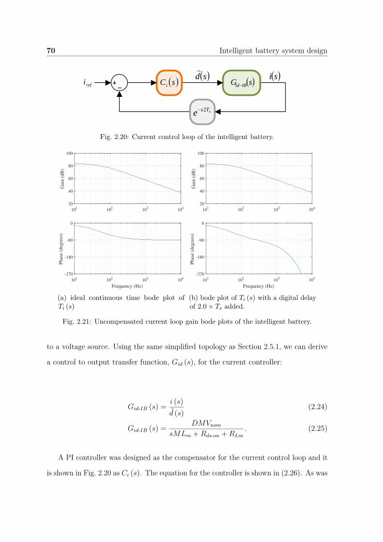
70 Intelligent battery system design
sG IBid
si sd
sTse
2
refi sC i
^
Fig. 2.20: Current control loop of the intelligent battery.
101 102 103 10420
40
60
80
100
Gai
n (
dB
)
101 102 103 104
Frequency (Hz)
-270
-180
-90
0
Phas
e (d
egre
es)
(a) ideal continuous time bode plot ofTi (s)
101 102 103 10420
40
60
80
100
Gai
n (
dB
)
101 102 103 104
Frequency (Hz)
-270
-180
-90
0
Phas
e (d
egre
es)
(b) bode plot of Ti (s) with a digital delayof 2.0 × Ts added.
Fig. 2.21: Uncompensated current loop gain bode plots of the intelligent battery.
to a voltage source. Using the same simplified topology as Section 2.5.1, we can derive
a control to output transfer function, Gid (s), for the current controller:
Gid-IB (s) = i (s)d (s)
(2.24)
Gid-IB (s) = DMVnom
sMLm + Rds-on + RLm
. (2.25)
A PI controller was designed as the compensator for the current control loop and it
is shown in Fig. 2.20 as Ci (s). The equation for the controller is shown in (2.26). As was
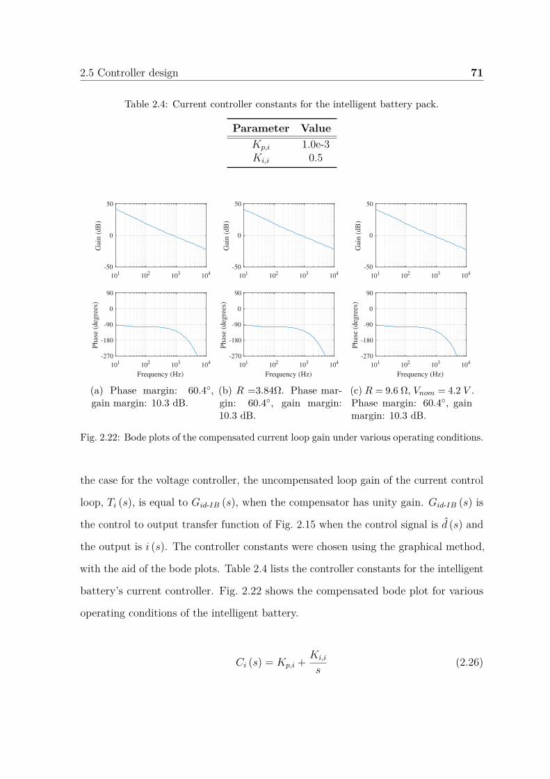
2.5 Controller design 71
Table 2.4: Current controller constants for the intelligent battery pack.
Parameter ValueKp,i 1.0e-3Ki,i 0.5
101 102 103 104-50
0
50
Gai
n (
dB
)
101 102 103 104
Frequency (Hz)
-270
-180
-90
0
90
Ph
ase
(deg
rees
)
(a) Phase margin: 60.4,gain margin: 10.3 dB.
101 102 103 104-50
0
50
Gai
n (
dB
)
101 102 103 104
Frequency (Hz)
-270
-180
-90
0
90
Ph
ase
(deg
rees
)
(b) R =3.84Ω. Phase mar-gin: 60.4, gain margin:10.3 dB.
101 102 103 104-50
0
50
Gai
n (
dB
)101 102 103 104
Frequency (Hz)
-270
-180
-90
0
90
Ph
ase
(deg
rees
)
(c) R = 9.6 Ω, Vnom = 4.2 V .Phase margin: 60.4, gainmargin: 10.3 dB.
Fig. 2.22: Bode plots of the compensated current loop gain under various operating conditions.
the case for the voltage controller, the uncompensated loop gain of the current control
loop, Ti (s), is equal to Gid-IB (s), when the compensator has unity gain. Gid-IB (s) is
the control to output transfer function of Fig. 2.15 when the control signal is d (s) and
the output is i (s). The controller constants were chosen using the graphical method,
with the aid of the bode plots. Table 2.4 lists the controller constants for the intelligent
battery’s current controller. Fig. 2.22 shows the compensated bode plot for various
operating conditions of the intelligent battery.
Ci (s) = Kp,i + Ki,i
s(2.26)
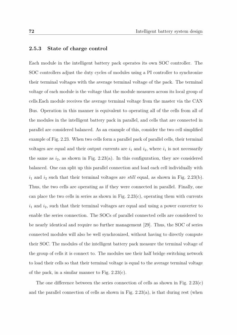
72 Intelligent battery system design
2.5.3 State of charge control
Each module in the intelligent battery pack operates its own SOC controller. The
SOC controllers adjust the duty cycles of modules using a PI controller to synchronize
their terminal voltages with the average terminal voltage of the pack. The terminal
voltage of each module is the voltage that the module measures across its local group of
cells.Each module receives the average terminal voltage from the master via the CAN
Bus. Operation in this manner is equivalent to operating all of the cells from all of
the modules in the intelligent battery pack in parallel, and cells that are connected in
parallel are considered balanced. As an example of this, consider the two cell simplified
example of Fig. 2.23. When two cells form a parallel pack of parallel cells, their terminal
voltages are equal and their output currents are i1 and i2, where i1 is not necessarily
the same as i2, as shown in Fig. 2.23(a). In this configuration, they are considered
balanced. One can split up this parallel connection and load each cell individually with
i1 and i2 such that their terminal voltages are still equal, as shown in Fig. 2.23(b).
Thus, the two cells are operating as if they were connected in parallel. Finally, one
can place the two cells in series as shown in Fig. 2.23(c), operating them with currents
i1 and i2, such that their terminal voltages are equal and using a power converter to
enable the series connection. The SOCs of parallel connected cells are considered to
be nearly identical and require no further management [29]. Thus, the SOC of series
connected modules will also be well synchronized, without having to directly compute
their SOC. The modules of the intelligent battery pack measure the terminal voltage of
the group of cells it is connect to. The modules use their half bridge switching network
to load their cells so that their terminal voltage is equal to the average terminal voltage
of the pack, in a similar manner to Fig. 2.23(c).
The one difference between the series connection of cells as shown in Fig. 2.23(c)
and the parallel connection of cells as shown in Fig. 2.23(a), is that during rest (when
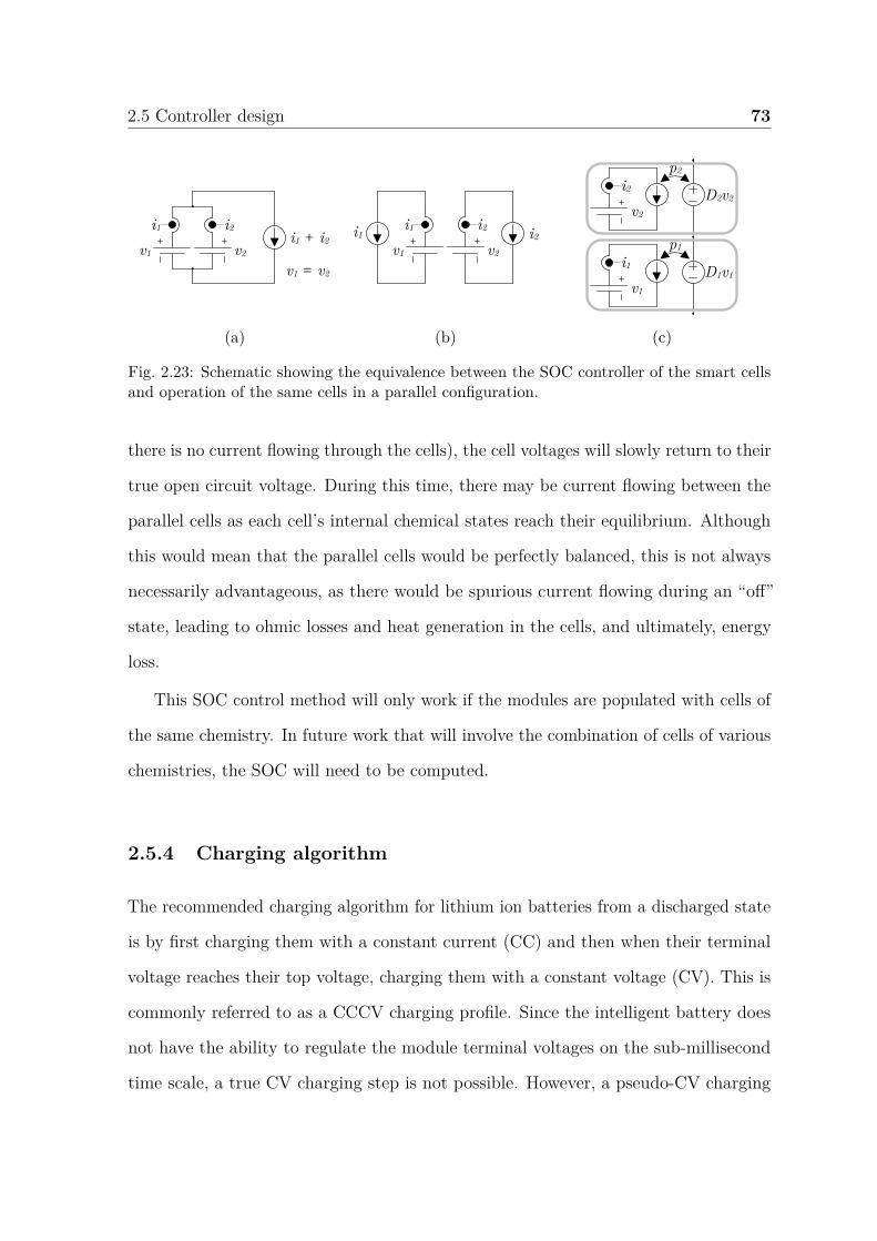
2.5 Controller design 73
i2
v2
i1 + i2
v1 = v2
i1
v1
(a)
i2
v2
i2i1
v1
i1
(b)
i2
v2
D2v2
p2
i1
v1
D1v1
p1
(c)
Fig. 2.23: Schematic showing the equivalence between the SOC controller of the smart cellsand operation of the same cells in a parallel configuration.
there is no current flowing through the cells), the cell voltages will slowly return to their
true open circuit voltage. During this time, there may be current flowing between the
parallel cells as each cell’s internal chemical states reach their equilibrium. Although
this would mean that the parallel cells would be perfectly balanced, this is not always
necessarily advantageous, as there would be spurious current flowing during an “off”
state, leading to ohmic losses and heat generation in the cells, and ultimately, energy
loss.
This SOC control method will only work if the modules are populated with cells of
the same chemistry. In future work that will involve the combination of cells of various
chemistries, the SOC will need to be computed.
2.5.4 Charging algorithm
The recommended charging algorithm for lithium ion batteries from a discharged state
is by first charging them with a constant current (CC) and then when their terminal
voltage reaches their top voltage, charging them with a constant voltage (CV). This is
commonly referred to as a CCCV charging profile. Since the intelligent battery does
not have the ability to regulate the module terminal voltages on the sub-millisecond
time scale, a true CV charging step is not possible. However, a pseudo-CV charging

74 Intelligent battery system design
step is possible and a flow chart of the constant current, pseudo constant voltage
(CCpCV) algorithm that is implemented in the master is show in Fig. 2.24.
During the pseudo-CV phase of charging, the intelligent battery remains in current
control mode. As soon as the voltage of one of the modules reaches a threshold value,
the charging current is reduced by I∆pCV = 0.5 A. This is shown by the block called
“Decrease charging current by I∆pCV A” in Fig. 2.24. The voltage threshold is computed
by:
mink
∆Vtop,k < ∆Vtop,limit-cc (2.27)
where:
∆Vtop,k = Vtop- max,k − VBat,k (2.28)
∆Vtop,limit-cc = 0.050 V. (2.29)
Vtop- max,k is the maximum top voltage of the module k, and VBat,k is the terminal
voltage of the cells connected to module k.
Once the charging current reaches a minimum current, IpCV,min, then the charging
rate is limited by time and a minimum module threshold value defined by (2.30):
mink
∆Vtop,k < ∆Vtop,limit-cv (2.30)
where:
∆Vtop,limit-cv = 0.0 V. (2.31)
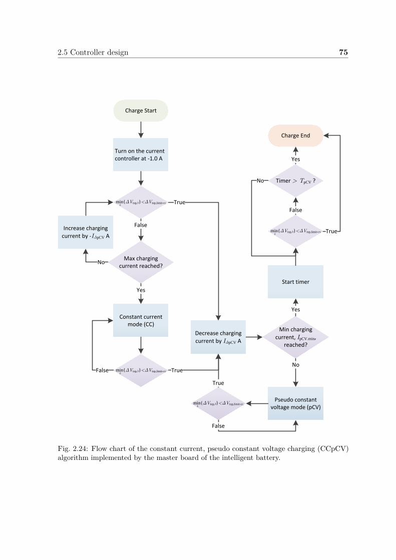
2.5 Controller design 75
Charge Start
Turn on the current controller at -1.0 A
Constant current mode (CC)
Max charging current reached?
Increase charging
current by -IΔpCV A
Yes
No
False
False
Decrease charging
current by IΔpCV A
True
True
Pseudo constant voltage mode (pCV)
Min charging
current, IpCV,min, reached?
No
True
Start timer
Yes
Timer > TpCV ?
False
Charge End
Yes
True
No
False
minΔVtop,k<ΔVtop,limit-cc
minΔVtop,k<ΔVtop,limit-cc
minΔVtop,k<ΔVtop,limit-cc
minΔVtop,k<ΔVtop,limit-cv
k
k
k
k
Fig. 2.24: Flow chart of the constant current, pseudo constant voltage charging (CCpCV)algorithm implemented by the master board of the intelligent battery.

76 Intelligent battery system design
All of the parameters that are used to define the CCpCV charging profile are easily
modified in the intelligent battery and can be customized for the type and number of
cells installed in each module.
2.6 Summary and discussion
Mechanically, the ability to easily replace individual cells throughout the pack is made
possible through the innovative module design. However, this design will introduce
increased conduction losses as compared to a conventional pack design, whose cells
are normally welded together. A break down of these conduction losses are presented
in Section 3.2.3. Conduction losses could be reduced by increasing the quality of the
spring contacts, but at a cost.
The hot-swappable modular design of the intelligent battery pack is also an innova-
tive approach to battery pack construction. The intelligent battery pack designed in
this chapter is based on modules that contain cells in parallel. However, the modules
could easily be small battery packs themselves to increase the scalability of the system,
especially if such a design was implemented for a much larger battery pack (greater than
300 V, 10 kWh). This modular design introduces the idea of battery pack maintenance,
where packs could be repaired instead of replaced when a series connected energy
storage device fails. The ability to repair battery packs would be very advantageous
for companies who must maintain battery packs in remote areas. Technicians could
carry many small modules with them that would facilitate the repair of many battery
packs, instead of carrying a single battery pack to replace in the event of a failure.
The dual communication channels to the modules solves the need for a real time
synchronization signal and a data bus between the modules and the master. The
CAN bus can provide the bandwidth necessary (up to 1 Mbps) to monitor all of the
states of the modules with ease. Its inherent master-less architecture will be ideal

2.6 Summary and discussion 77
for future work that dissolves the need for master control. The sync and control
signal is an elegant solution to provide two pieces of information with a single wire:
1) a synchronization pulse, and 2) a regular digital value for precise control actions.
By choosing a digital delivery mechanism for the control action, the system is more
immune to noise. Granted, the dual communication channels increase the system
complexity and cost, but for a research grade battery pack, this was an acceptable
trade-off. Furthermore, with both communication channels now in place, different
intra-pack communication architectures may be investigated.
The intelligent pack has been built with research in mind and thus almost every
variable in all of the modules and the master can be modified using a the serial, CAN,
or WiFi interface.


Chapter 3
Intelligent battery simulation and
experimental results
Chapter 2 introduced the intelligent battery design. In this chapter, results are
presented from the simulations and laboratory testing of the device. The results
indicate the improvements made possible by additional power electronics in multi-cell
battery packs.
3.1 Simulations
The intelligent battery pack was simulated in MATLAB’s Simulink environment using
two different models: a switched model and an averaged model.
The switched model was used to design the voltage controller, Cv (s), of Fig. 2.11.
This model takes into account the delays in the communication network and models
the switching actions of all 24 modules.
The averaged model was used to design the SOC controller, CSOC (s), of Fig. 2.11.
The averaged model does not simulate any of the high frequency actions and therefore,
can run hundreds of times faster than the switched model. Using battery models

80 Intelligent battery simulation and experimental results
available in the Simulink environment, the charge and discharge characteristics of the
intelligent battery pack can be simulated.
In both models, the 24 cell capacities were randomly generated using MATLAB’s
pseudo random number generator. The equation for each module’s capacity is shown
below:
Ck = 10.0 + Xu × 10.0, (3.1)
where:
Xu ∼ (0, 1) . (3.2)
Equation (3.2) defines Xu as a uniformly distributed random number between 0
and 1. Therefore, the capacities of the simulated modules varied between 10 Ah and
20 Ah.
Simulation Parameters
Unless otherwise stated, the parameters listed in Table 3.1 were used throughout the
simulation study.
3.1.1 Switched model
The switched model was used to verify the operation of the intelligent battery pack at
the millisecond time scale. It was used to design and tune the output voltage controller,
Cv (s).
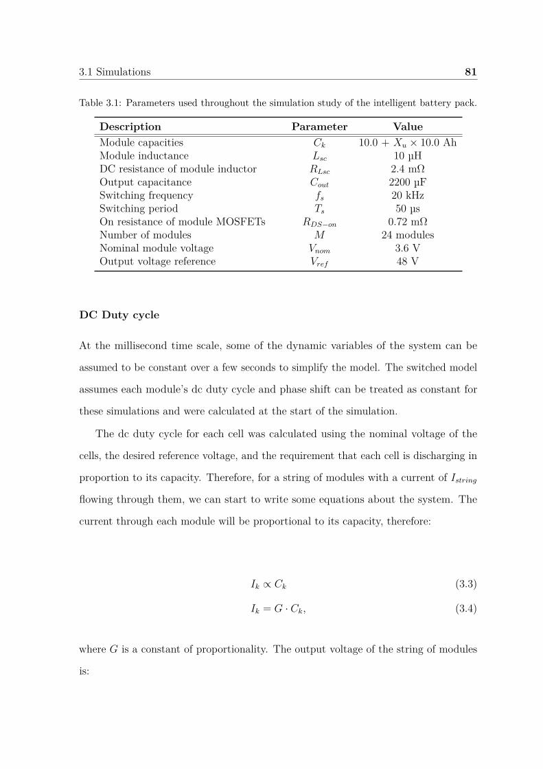
3.1 Simulations 81
Table 3.1: Parameters used throughout the simulation study of the intelligent battery pack.
Description Parameter ValueModule capacities Ck 10.0 + Xu × 10.0 AhModule inductance Lsc 10 µHDC resistance of module inductor RLsc 2.4 mΩOutput capacitance Cout 2200 µFSwitching frequency fs 20 kHzSwitching period Ts 50 µsOn resistance of module MOSFETs RDS−on 0.72 mΩNumber of modules M 24 modulesNominal module voltage Vnom 3.6 VOutput voltage reference Vref 48 V
DC Duty cycle
At the millisecond time scale, some of the dynamic variables of the system can be
assumed to be constant over a few seconds to simplify the model. The switched model
assumes each module’s dc duty cycle and phase shift can be treated as constant for
these simulations and were calculated at the start of the simulation.
The dc duty cycle for each cell was calculated using the nominal voltage of the
cells, the desired reference voltage, and the requirement that each cell is discharging in
proportion to its capacity. Therefore, for a string of modules with a current of Istring
flowing through them, we can start to write some equations about the system. The
current through each module will be proportional to its capacity, therefore:
Ik ∝ Ck (3.3)
Ik = G · Ck, (3.4)
where G is a constant of proportionality. The output voltage of the string of modules
is:

82 Intelligent battery simulation and experimental results
Vout = Vref = Vnom
M∑i=1
Di (3.5)
Finally, the duty cycle of each module can be related to each module’s current:
Ik = DkIstring (3.6)
Using equations (3.4) and (3.6), a expression for Dk/Ck is obtained:
Dk
Ck
= G
Istring
(3.7)
Solving (3.7) for Dk, and substituting the result into (3.5) yields:
G
Istring
M∑i=1
Ci = Vref
Vnom
(3.8)
Finally, we can use (3.7) and (3.8) to find an expression for Dk, the dc duty cycle
for the kth module:
Dk = Vref · Ck
Vnom ·∑Mi=1 Ci
. (3.9)
Equation (3.9) was used to calculate the starting duty cycles of each module for
the switched model simulations.
Phase shift
The output voltage ripple can be greatly reduced by phase shifting the modules with
respect to each other. The modules in the intelligent battery pack were spaced evenly
in time throughout the switching cycle. This is represented by (3.10):
φk = 2πk
M(3.10)

3.1 Simulations 83
Table 3.2: Cv (s) Control parameters.
Parameter ValueKp,v 1.0e-3Ki,v 0.2
where φk is the phase shift of the kth module in radians.
Time delay modelling
In the experimental version of the intelligent battery pack there are non negligible time
delays in the voltage control loop that must be modelled in order to accurately model
its behaviour, as described in Section 2.5.1.
In the switched model of the intelligent battery pack, the sampling and commu-
nication delay was implemented with delay blocks, for a total delay of 1.5 × Ts. The
variable delay caused by the different phase shifts of each module that will introduce
another delay of 0.0 × Ts to 1.0 × Ts was accurately modelled with sample and hold
blocks triggered by each module’s gating signal of QH .
Results
The voltage controller was implemented with a simple proportional integral controller
(PI). The continuous time version of the controller implemented in MATLAB is shown
in (3.11).
Cv (s) = Kp,v + Ki,v
s(3.11)
The gain values used in the controller were designed in the previous chapter, but
are repeated here in Table 3.2 for convenience.

84 Intelligent battery simulation and experimental results
Fig. 3.1 shows the simulation results of two circuits undergoing a series of load
changes: 1) the 24 module intelligent battery pack and 2) an equivalent half bridge
converter with the same controller as shown in Fig. 2.15. At 400 ms, the load is
increased by 100% from 12.5 A to 25 A. At 800 ms, the load is decreased by 50% from
25 A to 12.5 A. At both load transitions the natural frequency of the module inductors
and the output capacitor is excited. This is largely due to the very large inductor
designed for the intelligent battery and the very low impedance of the inductors and
switches that would dampen this oscillation. A more advanced control technique could
be employed to reduce these deviations from the reference value of 48 V, however this
is not the focus of this work.
As expected, both models are nearly identical in their simulation results, validating
the simplifications of Fig. 2.15 where the intelligent battery pack was modelled as a
single half bridge switching network in order to simplify controller design. The largest
difference between the two simulations is the voltage and current ripple. The phase of
each module of the intelligent battery pack was phase shifted according to (3.10), and
this has the effect of reducing the output voltage ripple, as shown in the inset graphs
of Fig. 3.1.
3.1.2 Averaged model
The averaged model was used to verify the operation of the intelligent battery pack
at the minute time scale. It was also used to tune the SOC controller, CSOC (s). The
continuous time version of the controller implemented in MATLAB is shown in (3.12)
and the values of the controller are shown in Table 3.3.
CSOC (s) = Kp,SOC + Ki,SOC
s(3.12)
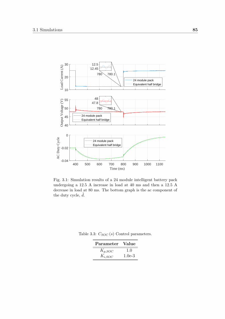
3.1 Simulations 85
10
20
30L
oad
Cur
rent
(A
)
24 module packEquivalent half bridge
780 780.1
12.4512.5
40
45
50
55
Out
put V
olta
ge (
V)
24 module packEquivalent half bridge
780 780.1
47.848
400 500 600 700 800 900 1000 1100Time (ms)
-0.04
-0.02
0
AC
Dut
y C
ycle
24 module packEquivalent half bridge
Fig. 3.1: Simulation results of a 24 module intelligent battery packundergoing a 12.5 A increase in load at 40 ms and then a 12.5 Adecrease in load at 80 ms. The bottom graph is the ac component ofthe duty cycle, d.
Table 3.3: CSOC (s) Control parameters.
Parameter ValueKp,SOC 1.0Ki,SOC 1.0e-3

86 Intelligent battery simulation and experimental results
In the following simulation of the averaged model, a simulated intelligent battery
pack was subjected to a ± 25 A current whose polarity changes when any one of the
modules reaches its terminal voltage limits. For the simulation, the lower limit was
set to 3.1 V and the upper limit was set to 4.1 V. The intelligent battery pack was
initialized with 24 random capacities as defined in Table 3.1; the initial SOC of each
module was defined by (3.13):
SOCk = 25 + Xu × 50. (3.13)
Capacity regulation
In this simulation, a 24 module intelligent battery pack was initialized with 24 random
capacities as defined in Table 3.1. The state of charge of each module at the start
of the simulation was randomly calculated using (3.13). Each module was unaware
of its random capacity and thus they were all initialized to the same duty cycle,
Di = 48/ (3.6 × 24) = 0.56. The SOC controller used only the cell’s local terminal
voltage and subtracted the average terminal voltage of the pack for its error calculation.
Fig. 3.2 shows how the states of intelligent battery pack evolved over the course of
the simulation, driving the SOCs of the modules to a state of synchronization. In the
top plot, the total amount of energy delivered to the load was also calculated and as
expected, this amount grows each cycle until all of the SOCs were synchronized.
Fig. 3.3 compares the normalized capacities and normalized ending duty cycles
from the modules simulated in Fig. 3.2. As expected, the normalized duty cycles were
all almost perfectly equal to the normalized capacities. Discrepancies exist due to the
component loses which were not modelled in determining each module’s Dk using (3.9).
These results are very good considering the SOC controller used only the terminal
voltages of the local cell and the average terminal voltage of the pack in its calculations.

3.1 Simulations 87
-50
0
50
Pac
k C
urr
ent
(A)
0
0.5
1
Du
ty c
ycl
es
0 2 4 6 8 10 12
Time (hours)
0
50
100
SO
C (
%)
0.47kWh
1.02kWh
1.13kWh
1.17kWh
1.19kWh
1.21kWh
Fig. 3.2: Simulation results of a 24 module intelligent battery pack under a ±25 A load. Eachmodule is initialized with an initial duty cycle of 0.56 and is connected to a battery cell ofrandom capacity as described in Table 3.1.
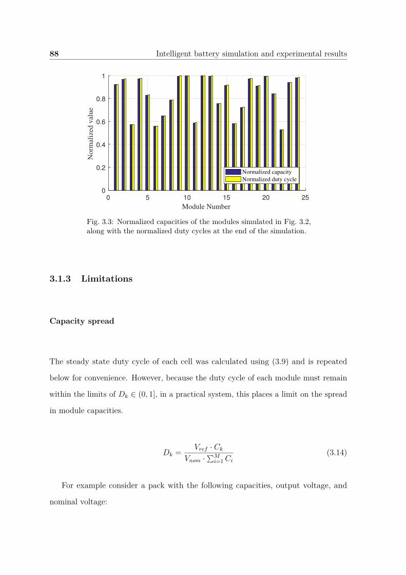
88 Intelligent battery simulation and experimental results
0 5 10 15 20 25
Module Number
0
0.2
0.4
0.6
0.8
1
No
rmal
ized
val
ue
Normalized capacity
Normalized duty cycle
Fig. 3.3: Normalized capacities of the modules simulated in Fig. 3.2,along with the normalized duty cycles at the end of the simulation.
3.1.3 Limitations
Capacity spread
The steady state duty cycle of each cell was calculated using (3.9) and is repeated
below for convenience. However, because the duty cycle of each module must remain
within the limits of Dk ∈ (0, 1], in a practical system, this places a limit on the spread
in module capacities.
Dk = Vref · Ck
Vnom ·∑Mi=1 Ci
(3.14)
For example consider a pack with the following capacities, output voltage, and
nominal voltage:

3.1 Simulations 89
C =
10
1
1
(3.15)
Vref = 6 V (3.16)
Vmax = 4.2 V (3.17)
Vnom = 3.6 V (3.18)
Vmin = 2.8 V (3.19)
The calculated duty cycles are:
D =
1.39
0.14
0.14
(3.20)
Clearly, this set of duty cycles is invalid because D1 is greater than 1. Using (3.14),
a boundary condition for the capacities can be derived:
maxCi ≤ Vnom∑M
i=1 Ci
Vref
(3.21)
Equation (3.21) is only valid at Vnom, whereas this equation must hold at any
operating point along the voltage curve of the battery cells being used. Despite this
caveat, (3.21) is a good starting point when designing a system.
The only way to remain within the bounds of (3.21) for a given set of capacities,
is to adjust Vref . Lowering the output voltage of the intelligent battery pack relaxes
the bounds. Using the capacities of (3.15) and the worst case cell voltage, Vmin, the
maximum Vref that can be achieved with that combination of cells can be determined:

90 Intelligent battery simulation and experimental results
10 ≤ 2.8 (10 + 1 + 1)Vref
(3.22)
Vref ≤ 3.36 V (3.23)
Using the value for Vref calculated above, the new duty cycles in the worst case
scenario are:
D =
1.00
0.10
0.10
(3.24)
Changing the voltage reference to 3.36 V as calculated with (3.23) results in a
system which discharges all three cells in proportion to their capacities, but a system
where the output voltage of the pack is significantly lower that simply connecting the
three cells in series. In a real system, this type of extreme case should be avoided by
replacing the under performing cells. Alternatively, if confronted with a system as
specified by (3.15), a different control algorithm could be applied. The new control
algorithm could discharge the cells at the same rate to yield the maximum possible
output voltage. When cells 2 and 3 are discharged, they can be bypassed until cell 1 is
completely discharged.
The only way to discharge all three cells of (3.15) in proportion to their capacities
while maintaining a higher output voltage than calculated with (3.23) is to change the
topology of the intelligent battery pack. Implementing each module with some type of
buck-boost topology would solve the low output voltage issue.
Despite the low output voltage calculated with (3.23), the intelligent battery would
be able to extract all of the energy out of this three cell pack. Using this pack in a

3.2 Experimental results 91
standard configuration, without any cell balancing during discharge, would mean that
only 25% of the energy in the pack would be accessible during a single discharge.
3.1.4 Discussion
The averaged and switched models of the intelligent battery have demonstrated the
theory of its basic operation. The switched model confirmed that the controller design
of Section 2.5 will provide basic voltage regulation. The controller itself could be
improved with more advanced controllers; notwithstanding, the approach presented is
a simple, efficient solution.
The averaged model demonstrated that even with a simple PI controller operating
on the terminal voltages of the battery cells, the SOCs of a random pack of cells can
be well synchronized. The controller took a number of cycles to settle to the correct
duty cycles as shown in Fig. 3.2. However, once the cells are synchronized, they will
remain perfectly balanced. Therefore, this momentary loss of synchronization will only
be temporary.
3.2 Experimental results
This section will highlight some of the experimental results conducted with the intelligent
battery. Two intelligent batteries were constructed: a blue one and a yellow one, where
the colour refers to the colour of the 3D printed parts. Fig. 3.4 shows a photo of both
intelligent batteries in the lab.
The yellow intelligent battery was fully populated with new 18650 battery cells
from Samsung, model number: INR18650-25R [108]. They have a nominal capacity
of 2.5 Ah per cell, thus the yellow pack can store a total of 1728 Wh of energy. The
blue intelligent battery was populated with 48 recycled 18650 cells, 2 cells per module,
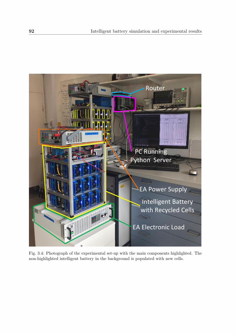
92 Intelligent battery simulation and experimental results
EA Power Supply
Intelligent Battery with Recycled Cells
EA Electronic Load
PC Running Python Server
Router
Fig. 3.4: Photograph of the experimental set-up with the main components highlighted. Thenon-highlighted intelligent battery in the background is populated with new cells.
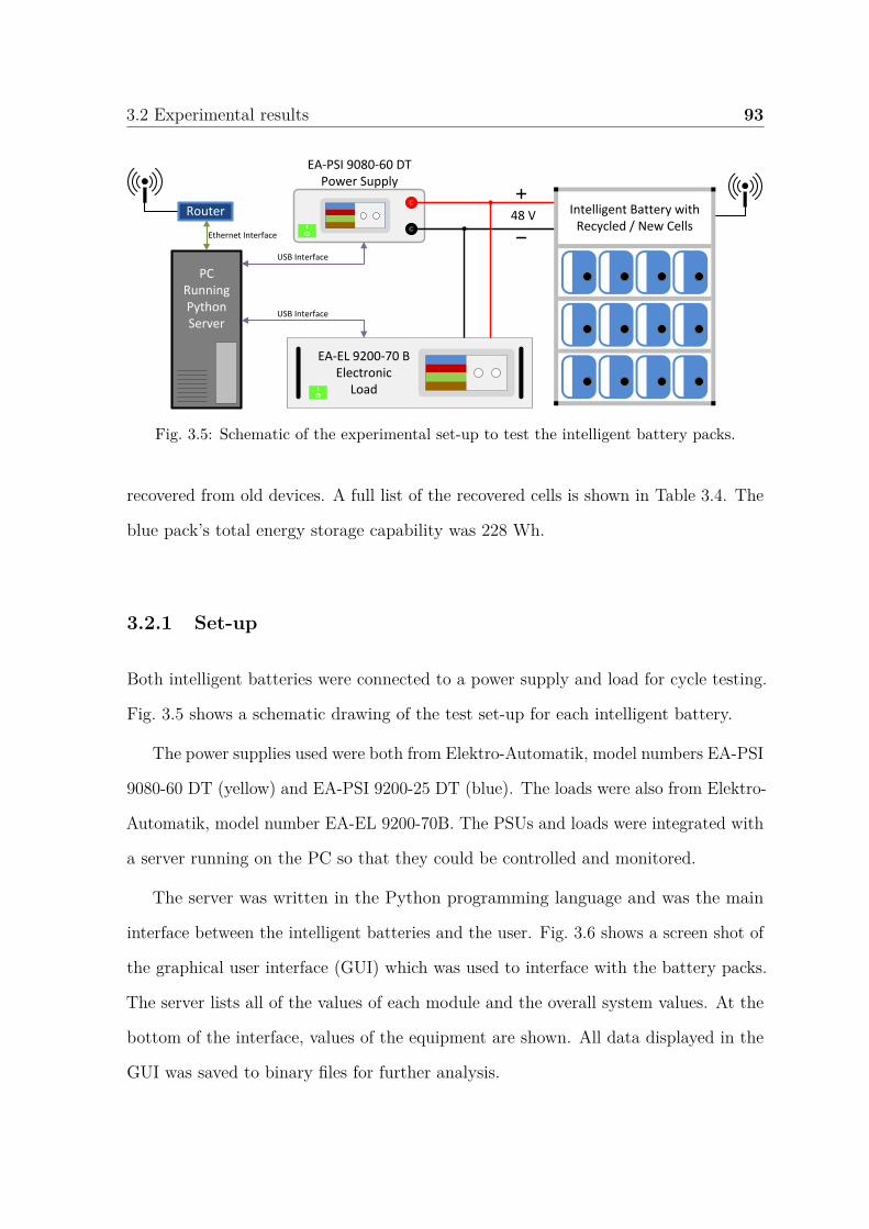
3.2 Experimental results 93
EA-PSI 9080-60 DTPower Supply
EA-EL 9200-70 BElectronic
Load
Intelligent Battery with Recycled / New Cells
USB Interface
USB Interface
PCRunning Python Server
Router
Ethernet Interface
48 V
Fig. 3.5: Schematic of the experimental set-up to test the intelligent battery packs.
recovered from old devices. A full list of the recovered cells is shown in Table 3.4. The
blue pack’s total energy storage capability was 228 Wh.
3.2.1 Set-up
Both intelligent batteries were connected to a power supply and load for cycle testing.
Fig. 3.5 shows a schematic drawing of the test set-up for each intelligent battery.
The power supplies used were both from Elektro-Automatik, model numbers EA-PSI
9080-60 DT (yellow) and EA-PSI 9200-25 DT (blue). The loads were also from Elektro-
Automatik, model number EA-EL 9200-70B. The PSUs and loads were integrated with
a server running on the PC so that they could be controlled and monitored.
The server was written in the Python programming language and was the main
interface between the intelligent batteries and the user. Fig. 3.6 shows a screen shot of
the graphical user interface (GUI) which was used to interface with the battery packs.
The server lists all of the values of each module and the overall system values. At the
bottom of the interface, values of the equipment are shown. All data displayed in the
GUI was saved to binary files for further analysis.
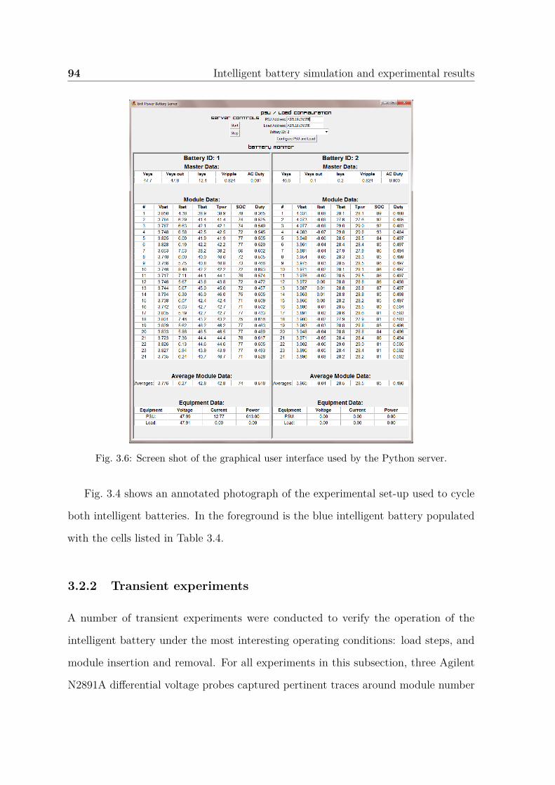
94 Intelligent battery simulation and experimental results
Fig. 3.6: Screen shot of the graphical user interface used by the Python server.
Fig. 3.4 shows an annotated photograph of the experimental set-up used to cycle
both intelligent batteries. In the foreground is the blue intelligent battery populated
with the cells listed in Table 3.4.
3.2.2 Transient experiments
A number of transient experiments were conducted to verify the operation of the
intelligent battery under the most interesting operating conditions: load steps, and
module insertion and removal. For all experiments in this subsection, three Agilent
N2891A differential voltage probes captured pertinent traces around module number
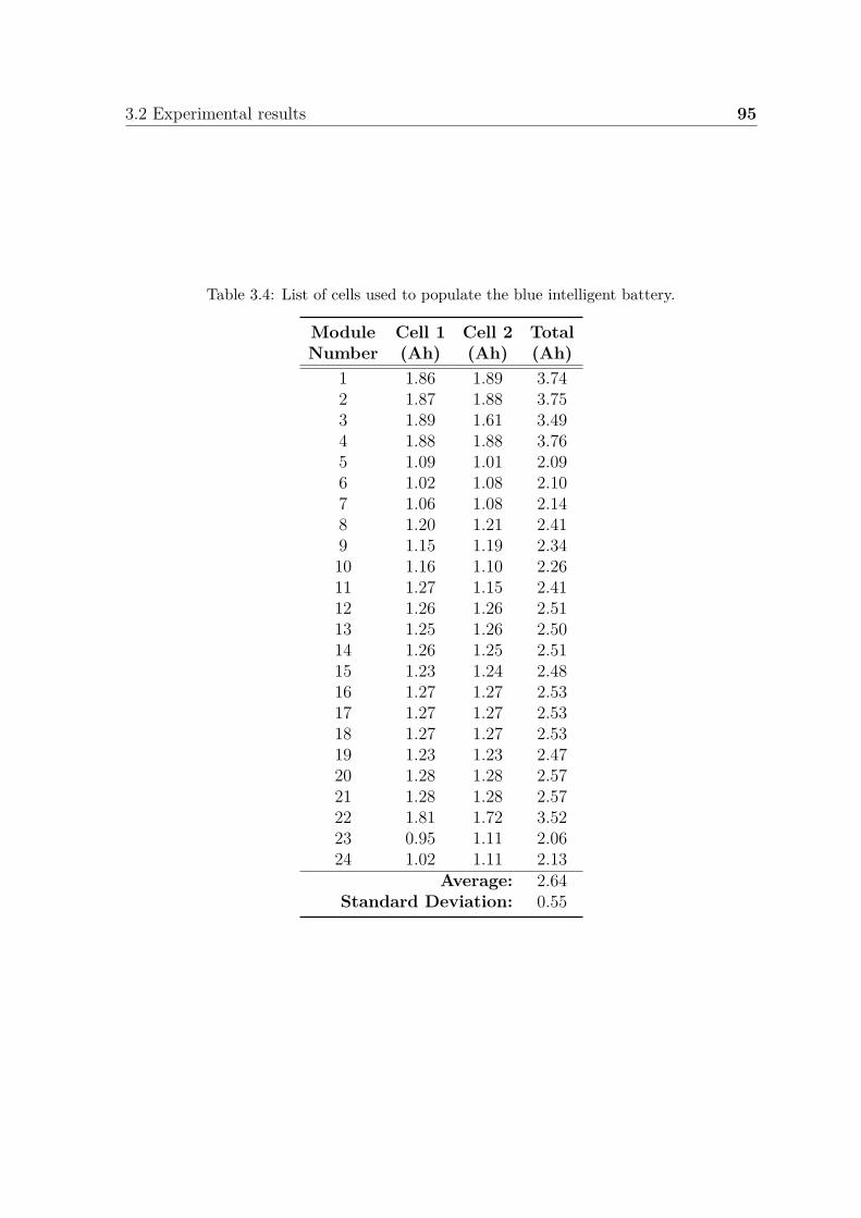
3.2 Experimental results 95
Table 3.4: List of cells used to populate the blue intelligent battery.
Module Cell 1 Cell 2 TotalNumber (Ah) (Ah) (Ah)
1 1.86 1.89 3.742 1.87 1.88 3.753 1.89 1.61 3.494 1.88 1.88 3.765 1.09 1.01 2.096 1.02 1.08 2.107 1.06 1.08 2.148 1.20 1.21 2.419 1.15 1.19 2.3410 1.16 1.10 2.2611 1.27 1.15 2.4112 1.26 1.26 2.5113 1.25 1.26 2.5014 1.26 1.25 2.5115 1.23 1.24 2.4816 1.27 1.27 2.5317 1.27 1.27 2.5318 1.27 1.27 2.5319 1.23 1.23 2.4720 1.28 1.28 2.5721 1.28 1.28 2.5722 1.81 1.72 3.5223 0.95 1.11 2.0624 1.02 1.11 2.13
Average: 2.64Standard Deviation: 0.55
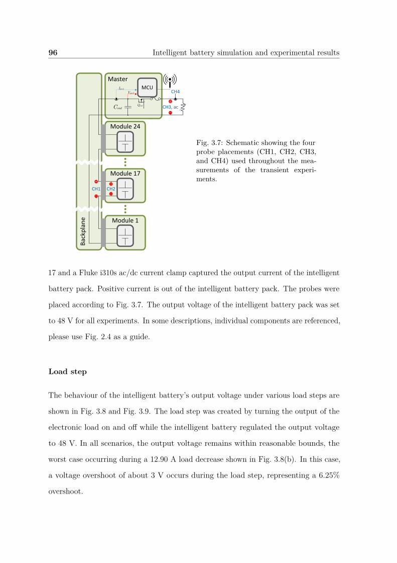
96 Intelligent battery simulation and experimental results
Bac
kpla
ne
Cout
MasterIpack
Vpack
MCU
Qout
Module 1
Module 17
Module 24
CH1 CH2
CH3, ac
CH4
Fig. 3.7: Schematic showing the fourprobe placements (CH1, CH2, CH3,and CH4) used throughout the mea-surements of the transient experi-ments.
17 and a Fluke i310s ac/dc current clamp captured the output current of the intelligent
battery pack. Positive current is out of the intelligent battery pack. The probes were
placed according to Fig. 3.7. The output voltage of the intelligent battery pack was set
to 48 V for all experiments. In some descriptions, individual components are referenced,
please use Fig. 2.4 as a guide.
Load step
The behaviour of the intelligent battery’s output voltage under various load steps are
shown in Fig. 3.8 and Fig. 3.9. The load step was created by turning the output of the
electronic load on and off while the intelligent battery regulated the output voltage
to 48 V. In all scenarios, the output voltage remains within reasonable bounds, the
worst case occurring during a 12.90 A load decrease shown in Fig. 3.8(b). In this case,
a voltage overshoot of about 3 V occurs during the load step, representing a 6.25%
overshoot.
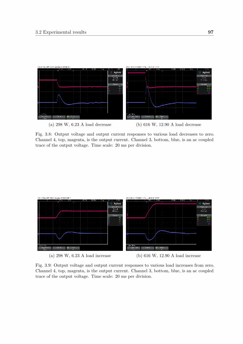
3.2 Experimental results 97
(a) 298 W, 6.23 A load decrease (b) 616 W, 12.90 A load decrease
Fig. 3.8: Output voltage and output current responses to various load decreases to zero.Channel 4, top, magenta, is the output current. Channel 3, bottom, blue, is an ac coupledtrace of the output voltage. Time scale: 20 ms per division.
(a) 298 W, 6.23 A load increase (b) 616 W, 12.90 A load increase
Fig. 3.9: Output voltage and output current responses to various load increases from zero.Channel 4, top, magenta, is the output current. Channel 3, bottom, blue, is an ac coupledtrace of the output voltage. Time scale: 20 ms per division.

98 Intelligent battery simulation and experimental results
Module extraction during discharge
Fig. 3.10 shows the voltage traces around module 17 and the output during an extraction
event of module 17. Channels 1 and 2 show the switching action of module 17, which
is occurring at 20 kHz and therefore cannot be discerned at the zoom level of Fig. 3.10.
However, as soon as the module is extracted, the output current drops, along with the
output voltage. This is because the positive output voltage provided by module 17 was
extracted from the pack and was replaced by a slightly negative voltage of the bypass
diode, D17, turning on and taking over the current flow. The initial 2.5 A drop in the
output current is due to the large output capacitance of the electronic load charging
the large output capacitance of the intelligent battery at the moment when module 17
is extracted. About 110 ms after the extraction event, there was a small overshoot in
the output voltage. This occurs because the relay closes and the voltage drop across
D17 was reduced to ≈ 0 V. Despite the different currents being provided by the pack,
Fig. 3.10(a) and Fig. 3.10(b) show that the transient response at the output is almost
identical in both cases.
What was also crucial in this experiment was that the voltage across the module does
not exceed 13.2 V, the maximum varistor voltage of the transient voltage suppressor
located on the output of the module. As expected, the output voltage of the module
did not reach 13.2 V, or even the minimum varistor voltage of 8.8 V, due to the bank
of capacitors, C5V , used for the auxiliary 5 V dc to dc converter as described in Section
2.3.8. In addition to C5V , the energy in the inductor is also absorbed by the diode
which connects the output of the module to C5V and the body diode of QL,17 which
together form the discharge path of Lm right after the extraction event. This also
explains why the output voltage across module 17 after the extraction event remained
well within limits.

3.2 Experimental results 99
(a) 298 W, 6.22 A load (b) 616 W, 12.912 A load
Fig. 3.10: Waveforms measured around module 17 during extraction under various dischargingconditions. Channel 1, yellow, is the voltage across the backplane slot of module 17. Channel2, green, is the voltage across the output of module 17. Channel 3, blue, is an ac coupledtrace of the output voltage. Channel 4, magenta, is the output current. Time scale: 20 msper division.
Module insertion during discharge
Fig. 3.11 shows the voltage traces around module 17 and the output during an insertion
event of module 17. In both current loads, there is an almost identical output voltage
overshoot of 0.5 V when module 17 started gating again.
Module extraction during charge
Fig. 3.12 shows the voltages around module 17 during extraction under various charging
currents. These waveforms were important to analyse to ensure that none of the voltage
ratings of any of the devices were exceeded during these extraction events. During
charge, the current through the pack is abruptly interrupted, thus the inductors of the
23 other modules that are still in the pack will cause an increase in voltage around the
module that is being extracted. It is important to keep this voltage to a minimum for
two reasons: 1) to avoid component damage - the bypass diodes Dk are rated to 45 V,
and 2) to avoid arcing as the module is physically removed from the backplane.
As shown in Fig. 3.12, the voltage across the module 17’s slot on the backplane
spiked to about 25 V in both scenarios. 25 V is right in between the minimum (22.8 V)
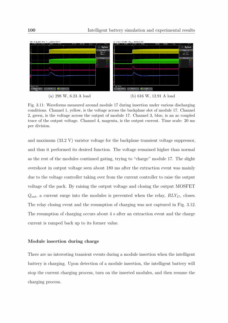
100 Intelligent battery simulation and experimental results
(a) 298 W, 6.23 A load (b) 616 W, 12.91 A load
Fig. 3.11: Waveforms measured around module 17 during insertion under various dischargingconditions. Channel 1, yellow, is the voltage across the backplane slot of module 17. Channel2, green, is the voltage across the output of module 17. Channel 3, blue, is an ac coupledtrace of the output voltage. Channel 4, magenta, is the output current. Time scale: 20 msper division.
and maximum (33.2 V) varistor voltage for the backplane transient voltage suppressor,
and thus it performed its desired function. The voltage remained higher than normal
as the rest of the modules continued gating, trying to “charge” module 17. The slight
overshoot in output voltage seen about 180 ms after the extraction event was mainly
due to the voltage controller taking over from the current controller to raise the output
voltage of the pack. By raising the output voltage and closing the output MOSFET
Qout, a current surge into the modules is prevented when the relay, RLY17, closes.
The relay closing event and the resumption of charging was not captured in Fig. 3.12.
The resumption of charging occurs about 4 s after an extraction event and the charge
current is ramped back up to its former value.
Module insertion during charge
There are no interesting transient events during a module insertion when the intelligent
battery is charging. Upon detection of a module insertion, the intelligent battery will
stop the current charging process, turn on the inserted modules, and then resume the
charging process.
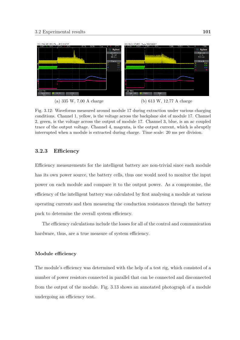
3.2 Experimental results 101
(a) 335 W, 7.00 A charge (b) 613 W, 12.77 A charge
Fig. 3.12: Waveforms measured around module 17 during extraction under various chargingconditions. Channel 1, yellow, is the voltage across the backplane slot of module 17. Channel2, green, is the voltage across the output of module 17. Channel 3, blue, is an ac coupledtrace of the output voltage. Channel 4, magenta, is the output current, which is abruptlyinterrupted when a module is extracted during charge. Time scale: 20 ms per division.
3.2.3 Efficiency
Efficiency measurements for the intelligent battery are non-trivial since each module
has its own power source, the battery cells, thus one would need to monitor the input
power on each module and compare it to the output power. As a compromise, the
efficiency of the intelligent battery was calculated by first analysing a module at various
operating currents and then measuring the conduction resistances through the battery
pack to determine the overall system efficiency.
The efficiency calculations include the losses for all of the control and communication
hardware, thus, are a true measure of system efficiency.
Module efficiency
The module’s efficiency was determined with the help of a test rig, which consisted of a
number of power resistors connected in parallel that can be connected and disconnected
from the output of the module. Fig. 3.13 shows an annotated photograph of a module
undergoing an efficiency test.
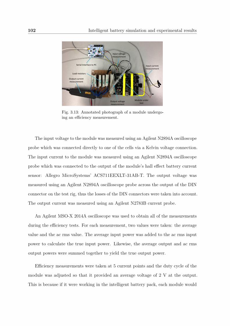
102 Intelligent battery simulation and experimental results
Serial Interface to PC
Output current measurement
Output voltage measurement
Input current measurement
Input voltage measurement
Module under test
Load resistors
Fig. 3.13: Annotated photograph of a module undergo-ing an efficiency measurement.
The input voltage to the module was measured using an Agilent N2894A oscilloscope
probe which was connected directly to one of the cells via a Kelvin voltage connection.
The input current to the module was measured using an Agilent N2894A oscilloscope
probe which was connected to the output of the module’s hall effect battery current
sensor: Allegro MicroSystems’ ACS711EEXLT-31AB-T. The output voltage was
measured using an Agilent N2894A oscilloscope probe across the output of the DIN
connector on the test rig, thus the losses of the DIN connectors were taken into account.
The output current was measured using an Agilent N2783B current probe.
An Agilent MSO-X 2014A oscilloscope was used to obtain all of the measurements
during the efficiency tests. For each measurement, two values were taken: the average
value and the ac rms value. The average input power was added to the ac rms input
power to calculate the true input power. Likewise, the average output and ac rms
output powers were summed together to yield the true output power.
Efficiency measurements were taken at 5 current points and the duty cycle of the
module was adjusted so that it provided an average voltage of 2 V at the output.
This is because if it were working in the intelligent battery pack, each module would
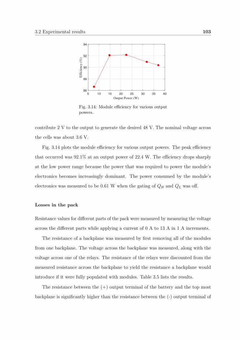
3.2 Experimental results 103
5 10 15 20 25 30 35 40
Output Power (W)
86
88
90
92
94
Eff
icie
ncy
(%
)
Fig. 3.14: Module efficiency for various outputpowers.
contribute 2 V to the output to generate the desired 48 V. The nominal voltage across
the cells was about 3.6 V.
Fig. 3.14 plots the module efficiency for various output powers. The peak efficiency
that occurred was 92.1% at an output power of 22.4 W. The efficiency drops sharply
at the low power range because the power that was required to power the module’s
electronics becomes increasingly dominant. The power consumed by the module’s
electronics was measured to be 0.61 W when the gating of QH and QL was off.
Losses in the pack
Resistance values for different parts of the pack were measured by measuring the voltage
across the different parts while applying a current of 0 A to 13 A in 1 A increments.
The resistance of a backplane was measured by first removing all of the modules
from one backplane. The voltage across the backplane was measured, along with the
voltage across one of the relays. The resistance of the relays were discounted from the
measured resistance across the backplane to yield the resistance a backplane would
introduce if it were fully populated with modules. Table 3.5 lists the results.
The resistance between the (+) output terminal of the battery and the top most
backplane is significantly higher than the resistance between the (-) output terminal of
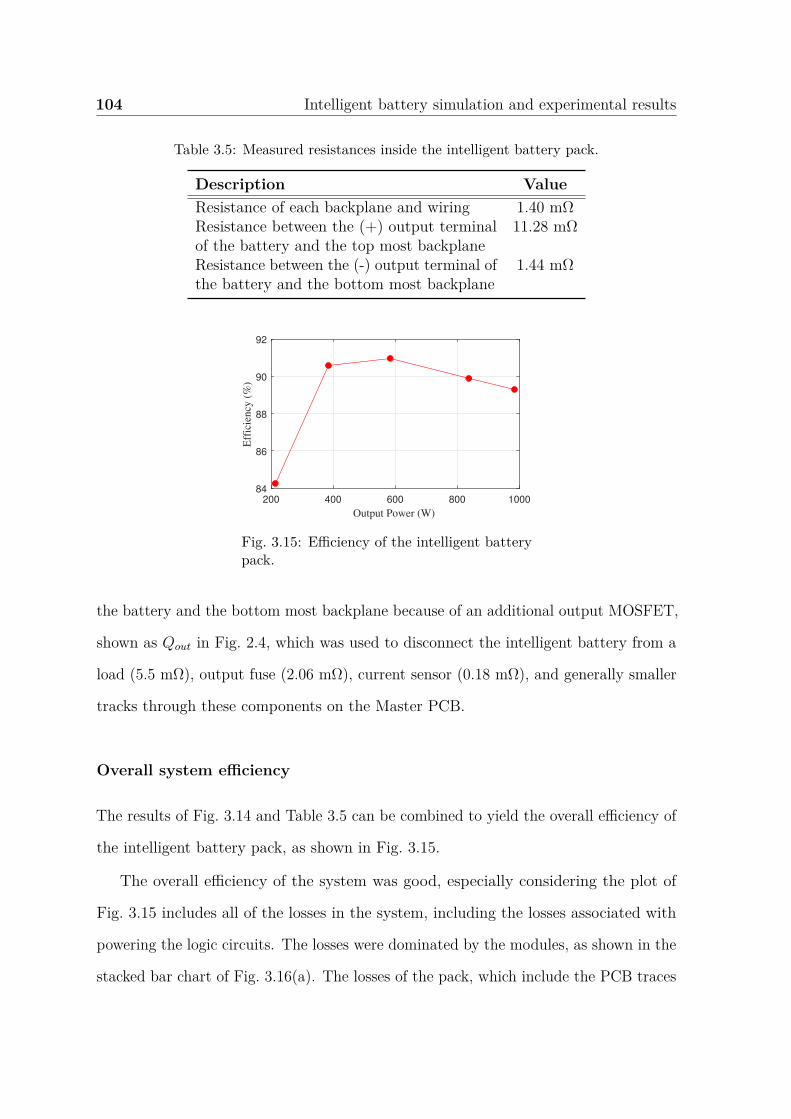
104 Intelligent battery simulation and experimental results
Table 3.5: Measured resistances inside the intelligent battery pack.
Description ValueResistance of each backplane and wiring 1.40 mΩResistance between the (+) output terminalof the battery and the top most backplane
11.28 mΩ
Resistance between the (-) output terminal ofthe battery and the bottom most backplane
1.44 mΩ
200 400 600 800 1000
Output Power (W)
84
86
88
90
92
Eff
icie
ncy
(%
)
Fig. 3.15: Efficiency of the intelligent batterypack.
the battery and the bottom most backplane because of an additional output MOSFET,
shown as Qout in Fig. 2.4, which was used to disconnect the intelligent battery from a
load (5.5 mΩ), output fuse (2.06 mΩ), current sensor (0.18 mΩ), and generally smaller
tracks through these components on the Master PCB.
Overall system efficiency
The results of Fig. 3.14 and Table 3.5 can be combined to yield the overall efficiency of
the intelligent battery pack, as shown in Fig. 3.15.
The overall efficiency of the system was good, especially considering the plot of
Fig. 3.15 includes all of the losses in the system, including the losses associated with
powering the logic circuits. The losses were dominated by the modules, as shown in the
stacked bar chart of Fig. 3.16(a). The losses of the pack, which include the PCB traces
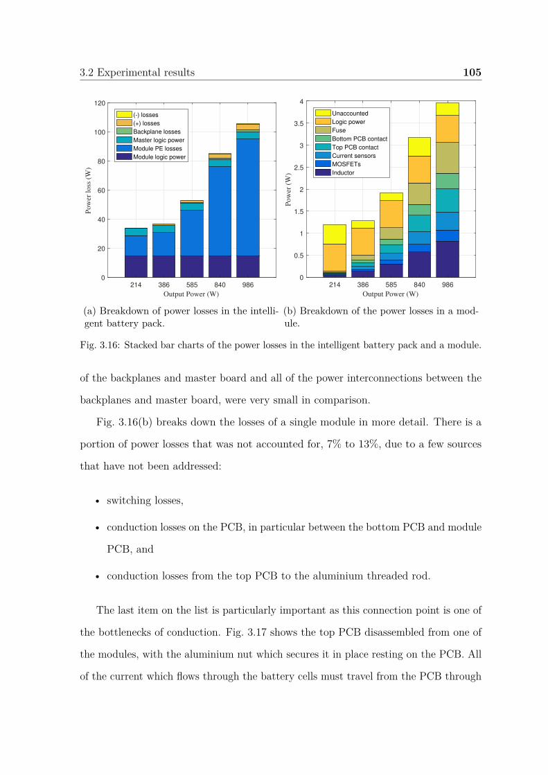
3.2 Experimental results 105
214 386 585 840 986
Output Power (W)
0
20
40
60
80
100
120
Pow
er l
oss
(W
)
(-) losses
(+) losses
Backplane losses
Master logic power
Module PE losses
Module logic power
(a) Breakdown of power losses in the intelli-gent battery pack.
214 386 585 840 986
Output Power (W)
0
0.5
1
1.5
2
2.5
3
3.5
4
Po
wer
(W
)
Unaccounted
Logic power
Fuse
Bottom PCB contact
Top PCB contact
Current sensors
MOSFETs
Inductor
(b) Breakdown of the power losses in a mod-ule.
Fig. 3.16: Stacked bar charts of the power losses in the intelligent battery pack and a module.
of the backplanes and master board and all of the power interconnections between the
backplanes and master board, were very small in comparison.
Fig. 3.16(b) breaks down the losses of a single module in more detail. There is a
portion of power losses that was not accounted for, 7% to 13%, due to a few sources
that have not been addressed:
• switching losses,
• conduction losses on the PCB, in particular between the bottom PCB and module
PCB, and
• conduction losses from the top PCB to the aluminium threaded rod.
The last item on the list is particularly important as this connection point is one of
the bottlenecks of conduction. Fig. 3.17 shows the top PCB disassembled from one of
the modules, with the aluminium nut which secures it in place resting on the PCB. All
of the current which flows through the battery cells must travel from the PCB through
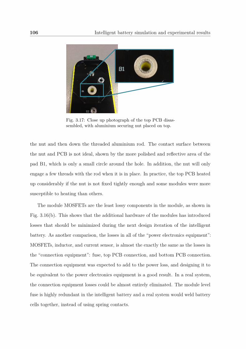
106 Intelligent battery simulation and experimental results
Fig. 3.17: Close up photograph of the top PCB disas-sembled, with aluminium securing nut placed on top.
the nut and then down the threaded aluminium rod. The contact surface between
the nut and PCB is not ideal, shown by the more polished and reflective area of the
pad B1, which is only a small circle around the hole. In addition, the nut will only
engage a few threads with the rod when it is in place. In practice, the top PCB heated
up considerably if the nut is not fixed tightly enough and some modules were more
susceptible to heating than others.
The module MOSFETs are the least lossy components in the module, as shown in
Fig. 3.16(b). This shows that the additional hardware of the modules has introduced
losses that should be minimized during the next design iteration of the intelligent
battery. As another comparison, the losses in all of the “power electronics equipment”:
MOSFETs, inductor, and current sensor, is almost the exactly the same as the losses in
the “connection equipment”: fuse, top PCB connection, and bottom PCB connection.
The connection equipment was expected to add to the power loss, and designing it to
be equivalent to the power electronics equipment is a good result. In a real system,
the connection equipment losses could be almost entirely eliminated. The module level
fuse is highly redundant in the intelligent battery and a real system would weld battery
cells together, instead of using spring contacts.
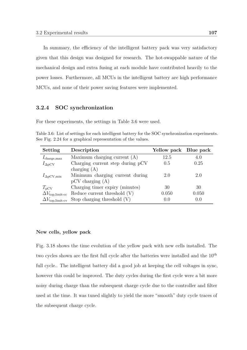
3.2 Experimental results 107
In summary, the efficiency of the intelligent battery pack was very satisfactory
given that this design was designed for research. The hot-swappable nature of the
mechanical design and extra fusing at each module have contributed heavily to the
power losses. Furthermore, all MCUs in the intelligent battery are high performance
MCUs, and none of their power saving features were implemented.
3.2.4 SOC synchronization
For these experiments, the settings in Table 3.6 were used.
Table 3.6: List of settings for each intelligent battery for the SOC synchronization experiments.See Fig. 2.24 for a graphical representation of the values.
Setting Description Yellow pack Blue packIcharge,max Maximum charging current (A) 12.5 4.0I∆pCV Charging current step during pCV
charging (A)0.5 0.25
I∆pCV,min Minimum charging current duringpCV charging (A)
2.0 2.0
TpCV Charging timer expiry (minutes) 30 30∆Vtop,limit-cc Reduce current threshold (V) 0.050 0.050∆Vtop,limit-cv Stop charging threshold (V) 0.0 0.0
New cells, yellow pack
Fig. 3.18 shows the time evolution of the yellow pack with new cells installed. The
two cycles shown are the first full cycle after the batteries were installed and the 10th
full cycle.. The intelligent battery did a good job at keeping the cell voltages in sync,
however this could be improved. The duty cycles during the first cycle were a bit more
noisy during charge than the subsequent charge cycle due to the controller and filter
used at the time. It was tuned slightly to yield the more “smooth” duty cycle traces of
the subsequent charge cycle.

108 Intelligent battery simulation and experimental results
It is important to remember that the modules had no prior knowledge of the cells
that were installed and were simply operating to match their terminal voltage with
the average terminal voltage of the pack. During the first cycle, the cells started with
different terminal voltages, as is shown by the voltage error plot during the first hour.
1.3 kWh of energy was delivered to the load during this first cycle. Conversely during
the subsequent cycle shown, the voltage error during this time period (hour 6 to 7),
was much lower and 1.4 kWh was delivered to the load. In both cycles, the SOC
controller struggled to maintain synchronisation near the bottom voltage. This is
because the voltage would have been changing very rapidly at this point, especially
with the constant power load that was applied. During the very short rest period
shown, the the module voltages recover to different values shortly after the 6 hour
mark. Although this indicates there is more energy left in some cells, they are all
practically exhausted. In order to extract the maximum amount of energy from the
pack, it is more important that the module voltages reach the “roll-off” point near the
end of the cycle at the same time.
In a well matched pack with new cells, the intelligent battery pack topology would
not increase the amount of energy that can be delivered to a load. However, as the
cells age, the intelligent battery pack topology would enable the extraction of all of the
energy from all of the degraded cells, as will be shown in the next subsection.
Recycled cells, blue pack
The enhanced performance of the intelligent battery pack is much more noticeable
when used with recycled cells, as was done with the blue pack. Fig. 3.19 shows the
time evolution of the system after two consecutive full cycles of the pack. During the
first full cycle, the SOC controller was on and the pack delivered 142 Wh to a 334
W load. In the next cycle, the SOC controller was turned off and all of the modules
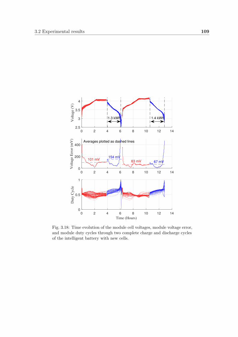
3.2 Experimental results 109
0 2 4 6 8 10 12 142.5
3
3.5
4
Volt
age
(V)
0 2 4 6 8 10 12 140
200
400
Volt
age
Err
or
(mV
)
0 2 4 6 8 10 12 14
Time (Hours)
0
0.5
1
Duty
Cycl
e
1.3 kWh 1.4 kWh
101 mV154 mV
63 mV 67 mV
Averages plotted as dashed lines
Fig. 3.18: Time evolution of the module cell voltages, module voltage error,and module duty cycles through two complete charge and discharge cyclesof the intelligent battery with new cells.

110 Intelligent battery simulation and experimental results
output the same duty cycle. In this scenario, the pack was limited by its weakest cell
and could only deliver 97 Wh to the 334 W load. In the following cycle, which is not
shown, the SOC controller was turned back on and the battery delivered 144 Wh to a
192 W load.
This experiment clearly shows the effectiveness of adding power electronics to a
battery pack to take advantage of all of the energy storage potential of all of the
individual cells. Furthermore, although simplistic in nature, the SOC controller was
able to take advantage of most of the energy storage potential without any prior
knowledge of the cells. Therefore, packs of recycled cells of the same chemistry can be
quickly assembled, without having to fully characterise all of the cells within.
Fig. 3.20 shows the normalized duty cycle distribution within the pack. The duty
cycles were calculated by taking their average values over the first three half cycles
of Fig. 3.19. The duty cycles should be proportional to the capacities, thus Fig. 3.20
suggests that further controller tuning is required. With more advanced controllers,
each module could start to learn the behaviour of the cells it is connected to and adjust
its output accordingly to optimize its performance. This will be discussed further in
the future work section of Chapter 6.
3.2.5 Discussion
The performance of the intelligent battery pack designed in Chapter 2 was verified.
The efficiency of the battery pack was quite good considering efficiency was not a
targeted design criteria for this design iteration. Furthermore, the unique ability to
hot-swap modules and easily replace cells added extra series resistance that does not
normally exist in a typical battery pack or dc to dc converter.
When using variably degraded cells, the benefits of integrating power electronics
into a battery pack are clear. In the experimental results presented here, the useful
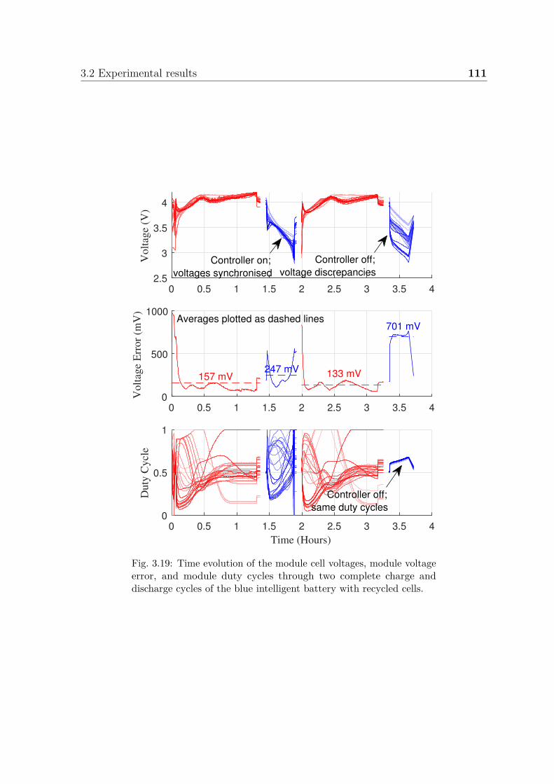
3.2 Experimental results 111
0 0.5 1 1.5 2 2.5 3 3.5 42.5
3
3.5
4
Vo
ltag
e (V
)
0 0.5 1 1.5 2 2.5 3 3.5 40
500
1000
Vo
ltag
e E
rro
r (m
V)
0 0.5 1 1.5 2 2.5 3 3.5 4
Time (Hours)
0
0.5
1
Du
ty C
ycl
e
157 mV247 mV 133 mV
701 mVAverages plotted as dashed lines
Controller on;
voltages synchronised
Controller off;
voltage discrepancies
Controller off;
same duty cycles
Fig. 3.19: Time evolution of the module cell voltages, module voltageerror, and module duty cycles through two complete charge anddischarge cycles of the blue intelligent battery with recycled cells.
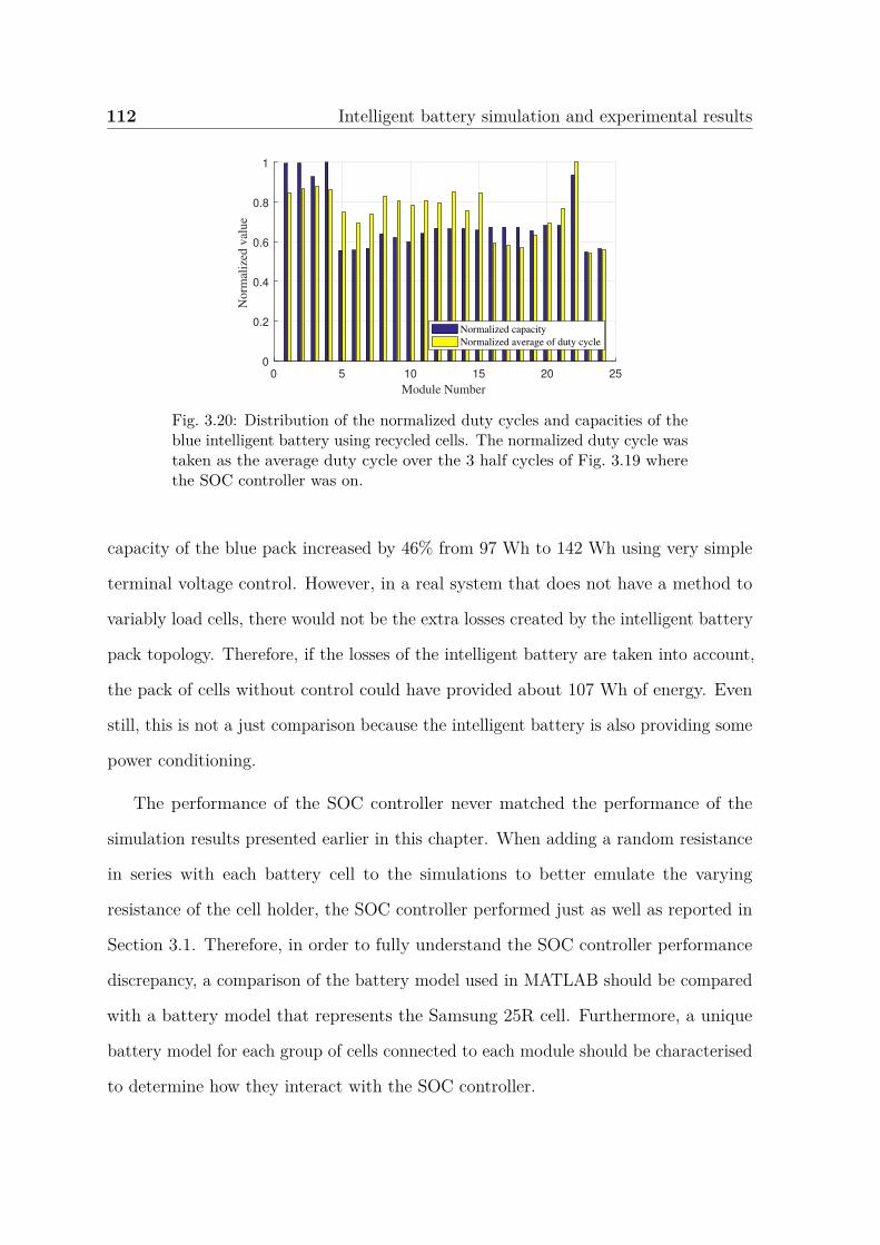
112 Intelligent battery simulation and experimental results
0 5 10 15 20 25
Module Number
0
0.2
0.4
0.6
0.8
1
No
rmal
ized
val
ue
Normalized capacity
Normalized average of duty cycle
Fig. 3.20: Distribution of the normalized duty cycles and capacities of theblue intelligent battery using recycled cells. The normalized duty cycle wastaken as the average duty cycle over the 3 half cycles of Fig. 3.19 wherethe SOC controller was on.
capacity of the blue pack increased by 46% from 97 Wh to 142 Wh using very simple
terminal voltage control. However, in a real system that does not have a method to
variably load cells, there would not be the extra losses created by the intelligent battery
pack topology. Therefore, if the losses of the intelligent battery are taken into account,
the pack of cells without control could have provided about 107 Wh of energy. Even
still, this is not a just comparison because the intelligent battery is also providing some
power conditioning.
The performance of the SOC controller never matched the performance of the
simulation results presented earlier in this chapter. When adding a random resistance
in series with each battery cell to the simulations to better emulate the varying
resistance of the cell holder, the SOC controller performed just as well as reported in
Section 3.1. Therefore, in order to fully understand the SOC controller performance
discrepancy, a comparison of the battery model used in MATLAB should be compared
with a battery model that represents the Samsung 25R cell. Furthermore, a unique
battery model for each group of cells connected to each module should be characterised
to determine how they interact with the SOC controller.

3.3 Summary 113
3.3 Summary
This chapter analysed the performance of the intelligent battery in theory and in
practice. The hardware and software designs of Chapter 2 worked as designed, enabling
low latency voltage and current control at the pack level, pack level monitoring via the
CAN bus, and hot-swappable modules.
The simulation results showed that excellent SOC synchronization can be achieved
by synchronizing the terminal voltages of all of the modules. Using only the terminal
voltage could greatly simplify BMS design, as a complex battery model would not
be required. Furthermore, it would allow the easy recombination of recycled cells
into packs, whose individual battery models would be largely unknown. However, the
experimental results showed that more work needs to be done to understand why the
same level of synchronization could not be achieved in practice.
The control strategy of the intelligent battery presented was based on a current
sinking load and a voltage controlled charging source. It is not limited to this single
operating scenario. The intelligent battery is also capable of emulating a real battery
pack, which can be connected to a bi-directional source-sink.
This chapter brings the discussion about the intelligent battery to a close. The
following two chapters will explore how the integration of power electronics into battery
packs can be simplified.


Chapter 4
Decentralised battery management
In this chapter, the possibility of a decentralised battery management system for series
connected cells with the same architecture as Fig. 2.4 is explored. However, the system
will not have any any inter-module communication, or any communication to a master
controller. A schematic of the proposed decentralized battery management system is
shown in Fig. 4.1.
In this schematic, the system is constructed out of three “smart cells”, each
containing a half bridge switching network identical to the switching network in the
modules of the intelligent battery pack. Therefore, it has the same scalability metrics
as the intelligent battery pack. Each smart cell has two distinct features that make it
different from the modules of the intelligent battery pack:
1. There exists an independent, decentralized controller in each smart cell.
2. The filter inductor in each smart cell, Lsc, is used as a multi-purpose sensor.
The decentralized controller manages the state of charge (SOC) and monitors the
state of health (SOH) of its locally connected battery cell. This information is used to
apply a duty cycle to the switches QL and QH , such that the connected battery cell
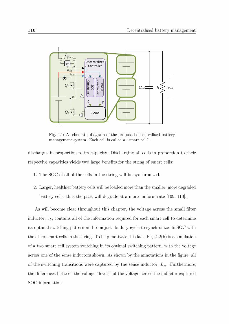
116 Decentralised battery management
Cout R vout
vL
ibatvbat
vL
Decentralized Controller
QH
QL
Lsc
vi
d ϕ
Ph
aseC
on
troller
SOC
Co
ntro
ller
PWM
Fig. 4.1: A schematic diagram of the proposed decentralised batterymanagement system. Each cell is called a “smart cell”.
discharges in proportion to its capacity. Discharging all cells in proportion to their
respective capacities yields two large benefits for the string of smart cells:
1. The SOC of all of the cells in the string will be synchronized.
2. Larger, healthier battery cells will be loaded more than the smaller, more degraded
battery cells, thus the pack will degrade at a more uniform rate [109, 110].
As will become clear throughout this chapter, the voltage across the small filter
inductor, vL, contains all of the information required for each smart cell to determine
its optimal switching pattern and to adjust its duty cycle to synchronize its SOC with
the other smart cells in the string. To help motivate this fact, Fig. 4.2(b) is a simulation
of a two smart cell system switching in its optimal switching pattern, with the voltage
across one of the sense inductors shown. As shown by the annotations in the figure, all
of the switching transitions were captured by the sense inductor, Lsc. Furthermore,
the differences between the voltage “levels” of the voltage across the inductor captured
SOC information.
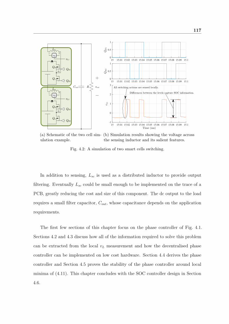
117
Cout R vout
vL
vL1
QH
QL
Lsc
vi
QH1
QH1
vL
vL2
QH
QL
Lsc
vi
QH2
QH2
(a) Schematic of the two cell sim-ulation example.
15 15.01 15.02 15.03 15.04 15.05 15.06 15.07 15.08 15.09 15.1
0
0.5
1
15 15.01 15.02 15.03 15.04 15.05 15.06 15.07 15.08 15.09 15.1
0
0.5
1
15 15.01 15.02 15.03 15.04 15.05 15.06 15.07 15.08 15.09 15.1
-1
0
1
2
3
(b) Simulation results showing the voltage acrossthe sensing inductor and its salient features.
Fig. 4.2: A simulation of two smart cells switching.
In addition to sensing, Lsc is used as a distributed inductor to provide output
filtering. Eventually Lsc could be small enough to be implemented on the trace of a
PCB, greatly reducing the cost and size of this component. The dc output to the load
requires a small filter capacitor, Cout, whose capacitance depends on the application
requirements.
The first few sections of this chapter focus on the phase controller of Fig. 4.1.
Sections 4.2 and 4.3 discuss how all of the information required to solve this problem
can be extracted from the local vL measurement and how the decentralised phase
controller can be implemented on low cost hardware. Section 4.4 derives the phase
controller and Section 4.5 proves the stability of the phase controller around local
minima of (4.11). This chapter concludes with the SOC controller design in Section
4.6.
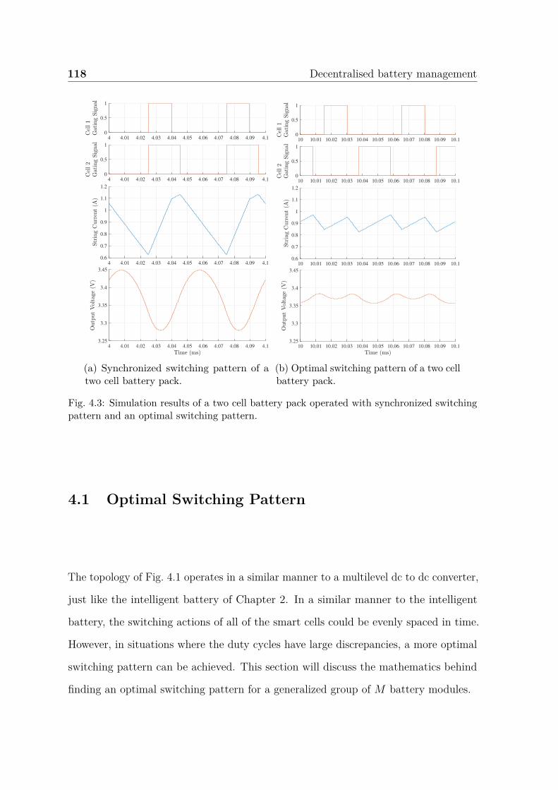
118 Decentralised battery management
4 4.01 4.02 4.03 4.04 4.05 4.06 4.07 4.08 4.09 4.1
0
0.5
1
4 4.01 4.02 4.03 4.04 4.05 4.06 4.07 4.08 4.09 4.1
0
0.5
1
4 4.01 4.02 4.03 4.04 4.05 4.06 4.07 4.08 4.09 4.1
0.6
0.7
0.8
0.9
1
1.1
1.2
4 4.01 4.02 4.03 4.04 4.05 4.06 4.07 4.08 4.09 4.1
3.25
3.3
3.35
3.4
3.45
(a) Synchronized switching pattern of atwo cell battery pack.
10 10.01 10.02 10.03 10.04 10.05 10.06 10.07 10.08 10.09 10.1
0
0.5
1
10 10.01 10.02 10.03 10.04 10.05 10.06 10.07 10.08 10.09 10.1
0
0.5
1
10 10.01 10.02 10.03 10.04 10.05 10.06 10.07 10.08 10.09 10.1
0.6
0.7
0.8
0.9
1
1.1
1.2
10 10.01 10.02 10.03 10.04 10.05 10.06 10.07 10.08 10.09 10.1
3.25
3.3
3.35
3.4
3.45
(b) Optimal switching pattern of a two cellbattery pack.
Fig. 4.3: Simulation results of a two cell battery pack operated with synchronized switchingpattern and an optimal switching pattern.
4.1 Optimal Switching Pattern
The topology of Fig. 4.1 operates in a similar manner to a multilevel dc to dc converter,
just like the intelligent battery of Chapter 2. In a similar manner to the intelligent
battery, the switching actions of all of the smart cells could be evenly spaced in time.
However, in situations where the duty cycles have large discrepancies, a more optimal
switching pattern can be achieved. This section will discuss the mathematics behind
finding an optimal switching pattern for a generalized group of M battery modules.

4.1 Optimal Switching Pattern 119
4.1.1 Problem and Assumptions
Given set of M battery cells Bi = B1, B2, . . . , BM with capacities Ci = C1, C2, . . . ,
CM, our objective is to find a set of phases, φi = φ1, φ2, . . . , φM for the turn-on of
each smart cell which will minimize the ripple current in the local inductor Lsc, thus
minimizing the output ripple voltage.
For simplicity, the nominal voltages of all of the battery cells will be Vnom = V1 =
V2 = . . . = VM , which is a reasonable assumption if the SOCs of all of the battery
cells are synchronized. The duty cycle of each smart cell can be calculated using the
following equation:
Di = Ci
CMAX
(4.1)
where CMAX is the maximum capacity expected amongst all of the battery cells, or
ideally, the maximum value found in the capacity array such that 0 < Di ≤ 1 for all i.
In a series string of smart cells, the voltage applied to each inductor, Lsc, will be
identical. Thus, we can group all of the distributed inductors together into a single
inductor, L = MLsc. The voltage across L will be determined by the sum of all of
the vi voltages of the smart cells and the output dc voltage. The output dc voltage is
given by (4.2):
Vout =M∑
i=1DiVnom =
M∑i=1
Ci
CMAX
Vnom = Vnom
CMAX
M∑i=1
Ci. (4.2)
The ac root mean squared (rms) value of the inductor ripple current can be expressed
by (4.3):
ILac−rms =√
1Ts
∫ Ts
0
[I (s) + 1
L
∫ t
s(vout (τ) − Vout) dτ
]2dt (4.3)
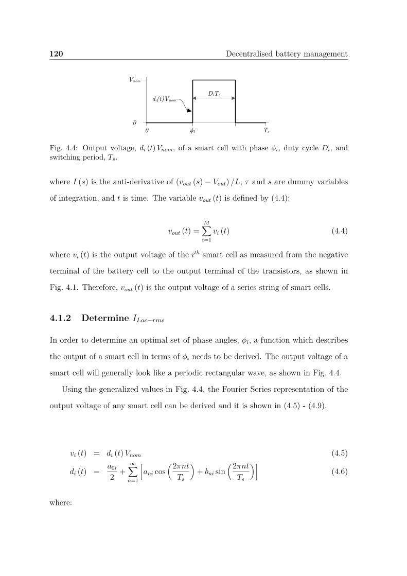
120 Decentralised battery management
Vnom
00 Tsϕi
DiTs
di(t)Vnom
Fig. 4.4: Output voltage, di (t) Vnom, of a smart cell with phase φi, duty cycle Di, andswitching period, Ts.
where I (s) is the anti-derivative of (vout (s) − Vout) /L, τ and s are dummy variables
of integration, and t is time. The variable vout (t) is defined by (4.4):
vout (t) =M∑
i=1vi (t) (4.4)
where vi (t) is the output voltage of the ith smart cell as measured from the negative
terminal of the battery cell to the output terminal of the transistors, as shown in
Fig. 4.1. Therefore, vout (t) is the output voltage of a series string of smart cells.
4.1.2 Determine ILac−rms
In order to determine an optimal set of phase angles, φi, a function which describes
the output of a smart cell in terms of φi needs to be derived. The output voltage of a
smart cell will generally look like a periodic rectangular wave, as shown in Fig. 4.4.
Using the generalized values in Fig. 4.4, the Fourier Series representation of the
output voltage of any smart cell can be derived and it is shown in (4.5) - (4.9).
vi (t) = di (t) Vnom (4.5)
di (t) = a0i
2 +∞∑
n=1
[ani cos
(2πnt
Ts
)+ bni sin
(2πnt
Ts
)](4.6)
where:

4.1 Optimal Switching Pattern 121
a0i = 2Di (4.7)
ani = 1nπ
(sin
(2πn
(Di + φi
Ts
))− sin
(2πn
φi
Ts
))(4.8)
bni = 1nπ
(cos
(2πn
φi
Ts
)− cos
(2πn
(Di + φi
Ts
)))(4.9)
Now we can substitute (4.5) into (4.4) and solve for I2Lac−rms using (4.3). It can be
shown that the result is:
I2Lac−rms = 1
2
(VnomTs
2πL
)2 ∞∑n=1
M∑i=1
M∑j=1
4π2n4[
sin (πnDi) sin (πnDj) cos(
πn
(Di − Dj + 2 φi
Ts
− 2φj
Ts
))](4.10)
Now let θx = 2πφx/Ts, so that the switching angles can be measured in radians
instead of time:
I2Lac−rms = 1
2
(VnomTs
2πL
)2 ∞∑n=1
M∑i=1
M∑j=1
4π2n4 ·
[sin (πnDi) sin (πnDj) cos (πn (Di − Dj) + n (θi − θj))] (4.11)
Equation (4.11) can now be minimized to determine an optimal set θi that will
minimize the ac rms current in the inductor Lsc and, therefore, the output voltage
ripple in vout.

122 Decentralised battery management
4.2 Simplifying the problem
In the previous section, an expression for the ac rms ripple current in the intelligent
battery’s inductors in terms of each module’s duty cycle and phase shift was derived
in (4.11).
Examining (4.11), we see that solving for an optimal set θ to minimize ILac−rms is
non trivial and difficult to achieve without significant computational power and global
information about the system. Therefore, in this section we present a way to identify
a set θ which will yield a satisfactory solution, with significantly less computational
requirements and in a decentralized fashion.
First, let us represent the switching action of the kth smart cell as a vector, vk, in
the unit circle as depicted in Fig. 4.5. The kth smart cell will turn on at θk and turn
off at θk + 2πDk. Now define a new vector, v′k, which will be known as the weighted
vector, whose phase places the vector half way between the turn on and turn off times
and whose length is sin (πDk). Therefore, the phase and length of the weighted vector,
v′k, are given by:
∠v′k , θ′
k = θk + πDk (4.12)
|v′k| , sin (πDk) . (4.13)
Applying the transformation described in (4.12) and (4.13) to all of the smart cells,
and summing all v′k, we can find the square of the magnitude of the total sum vector,
|v′Σ|2:
|v′Σ|2 =
M∑i=1
M∑j=1
sin (πDi) sin (πDj) cos (π (Di − Dj) + θi − θj) . (4.14)
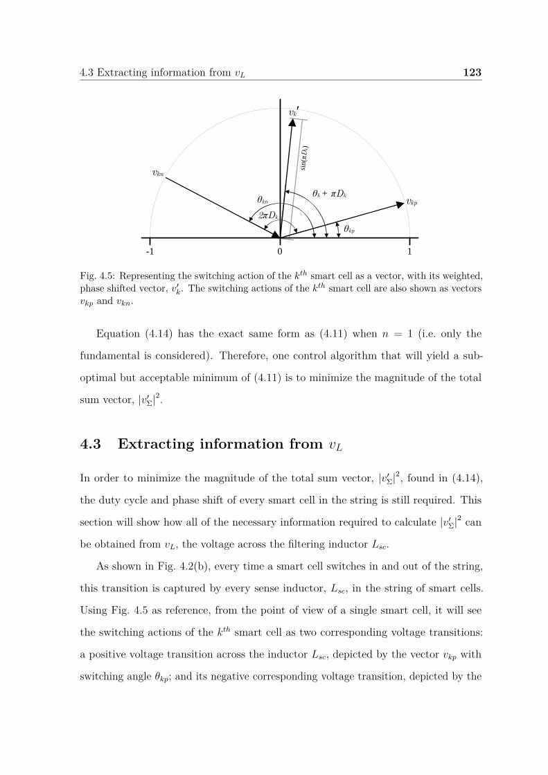
4.3 Extracting information from vL 123
θkp
θk + πDk vkp
vk′
θkn
2πDk
vkn
0 1-1
sin(π
Dk)
Fig. 4.5: Representing the switching action of the kth smart cell as a vector, with its weighted,phase shifted vector, v′
k. The switching actions of the kth smart cell are also shown as vectorsvkp and vkn.
Equation (4.14) has the exact same form as (4.11) when n = 1 (i.e. only the
fundamental is considered). Therefore, one control algorithm that will yield a sub-
optimal but acceptable minimum of (4.11) is to minimize the magnitude of the total
sum vector, |v′Σ|2.
4.3 Extracting information from vL
In order to minimize the magnitude of the total sum vector, |v′Σ|2, found in (4.14),
the duty cycle and phase shift of every smart cell in the string is still required. This
section will show how all of the necessary information required to calculate |v′Σ|2 can
be obtained from vL, the voltage across the filtering inductor Lsc.
As shown in Fig. 4.2(b), every time a smart cell switches in and out of the string,
this transition is captured by every sense inductor, Lsc, in the string of smart cells.
Using Fig. 4.5 as reference, from the point of view of a single smart cell, it will see
the switching actions of the kth smart cell as two corresponding voltage transitions:
a positive voltage transition across the inductor Lsc, depicted by the vector vkp with
switching angle θkp; and its negative corresponding voltage transition, depicted by the

124 Decentralised battery management
vector vkn with switching angle θkn. For a smart cell detecting only one other smart
cell, the problem is trivial and it is easy to determine not only when the other smart
cell is switching, but its duty cycle as well.
The challenge arises when multiple smart cells start switching. As soon as a single
smart cell needs to determine the switching angles and duty cycles of two or more other
smart cells, it is impossible to match every “on” transition with its corresponding “off”
transition. We will now show that this is not necessary to yield the optimal solution as
defined by (4.14).
First, use (4.15) and (4.16) to replace all of the Dx’s and θx’s with the notation of
Fig. 4.5.
θi = θip (4.15)
πDi =(
θin − θip
2
)(4.16)
This yields an expression in terms of measured quantities:
|v′Σ|2 =
M∑i=1
M∑j=1
sin(
θin − θip
2
)sin
(θjn − θjp
2
)cos
((θin + θip
2
)−(
θjn + θjp
2
)).
(4.17)
Equation (4.17) gives the magnitude of the total vector in terms of quantities
measured by each smart cell. However, this equation still seems to imply that the “on”
transitions must be correctly paired with each of their corresponding “off” transitions.
We will now show that this is not the case by first considering the case where only one
set of “on” transitions are swapped. Consider a set of M smart cells, where the kth and

4.4 Phase Controller Design 125
lth positive transitions are paired with the lth and kth negative transitions, respectively.
Using MATLAB’s Syms toolbox, it can be shown that:
|v′Σ|2 =
M∑i=1
i =k,i=l
M∑j=1
j =k,j =l
[sin
(θin − θip
2
)sin
(θjn − θjp
2
)cos
((θin + θip
2
)−(
θjn + θjp
2
))]
+sin2(
θkn − θlp
2
)+sin
(θln − θkp
2
)sin
(θkn − θlp
2
)cos
((θln + θkp
2
)−(
θkn + θlp
2
))
+sin2(
θln − θkp
2
)+sin
(θ1n − θkp
2
)sin
(θln − θkp
2
)cos
((θkn + θlp
2
)−(
θln + θkp
2
))
=M∑
i=1
M∑j=1
sin(
θin − θip
2
)sin
(θjn − θjp
2
)cos
((θin + θip
2
)−(
θjn + θjp
2
)). (4.18)
By extension, we can swap any pair and any number of transitions with each other
and get the same result. Therefore, in order to minimize the total sum vector of (4.14),
each smart cell need only know when the positive and negative transitions occur to
determine its local optimal switching pattern. Moreover, it can be shown that these
results are also true for all harmonics, 1 to n.
4.4 Phase Controller Design
The smart cell controller needs to be designed such that a group of cells working
together will minimize (4.14). By taking the derivative of (4.14) with respect to
the phase angles and setting it to zero, the local minima can be found. The partial
derivative of (4.14) with respect to θk is shown below:
∂ |v′Σ|2
∂θk
= 2 sin (πDk)M∑
i=1;i =k
sin (πDi) sin (π (Di − Dk) + θi − θk) (4.19)
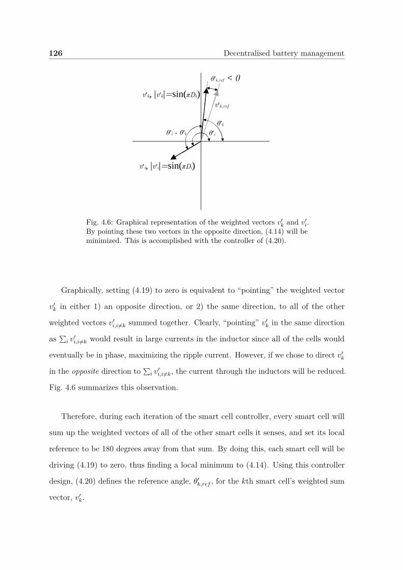
126 Decentralised battery management
θ′k,ref < 0
θ′i
θ′k
v′i, |v′i|=sin(πDi)
θ′i - θ′k
v′k, |v′k|=sin(πDk)v′k,ref
Fig. 4.6: Graphical representation of the weighted vectors v′k and v′
i.By pointing these two vectors in the opposite direction, (4.14) will beminimized. This is accomplished with the controller of (4.20).
Graphically, setting (4.19) to zero is equivalent to “pointing” the weighted vector
v′k in either 1) an opposite direction, or 2) the same direction, to all of the other
weighted vectors v′i,i =k summed together. Clearly, “pointing” v′
k in the same direction
as ∑i v′i,i =k would result in large currents in the inductor since all of the cells would
eventually be in phase, maximizing the ripple current. However, if we chose to direct v′k
in the opposite direction to ∑i v′i,i =k, the current through the inductors will be reduced.
Fig. 4.6 summarizes this observation.
Therefore, during each iteration of the smart cell controller, every smart cell will
sum up the weighted vectors of all of the other smart cells it senses, and set its local
reference to be 180 degrees away from that sum. By doing this, each smart cell will be
driving (4.19) to zero, thus finding a local minimum to (4.14). Using this controller
design, (4.20) defines the reference angle, θ′k,ref , for the kth smart cell’s weighted sum
vector, v′k.

4.5 Phase Controller Stability Analysis 127
θ′k,ref = −2 sin (πDk)
M∑i=1;i =k
sin (πDi) sin (π (Di − Dk) + θi − θk) (4.20)
Note the negative sign in (4.20), this ensures that that the angle between θ′k,ref
and ∑i v′
i,i =k is driven to π. Using (4.20) and the angle transformation of (4.12), a
non-linear model for the phase (θ′k) of the kth smart cell can be constructed and is
shown below:
θ′k = ωk − 2 K
Msin (πDk)
M∑i=1;i =k
sin (πDi) sin (θ′i − θ′
k) (4.21)
where ωk is the switching frequency, and K is a controller constant.
4.5 Phase Controller Stability Analysis
Using the smart cell controller model developed in Section 4.4, the stability of a group
of smart cells around local minima of (4.19) will be investigated. First note that the
controller chosen in (4.21) is very similar to the Kuramoto Model of coupled oscillators
[102], which is repeated in (4.22):
θk = ω + K
M
N∑i=1
sin (θi − θk) , (4.22)
where ω is the nominal switching frequency of the system, M is the number of agents,
and K is a global controller constant, identical for all agents (coupled oscillators).
Second, consider the dynamics of the system described by (4.21) in a rotating
reference frame, where all of the ωk’s are equal, thus ωk = ω, and let
θ′k = ωt + γ′
k. (4.23)
Equation (4.21) becomes:

128 Decentralised battery management
γ′k = −2 K
Msin (πDk)
M∑i=1;i =k
sin (πDi) sin (γ′i − γ′
k) = fk (Γ′) (4.24)
where Γ′ = γ′1, γ′
2, . . . γ′M. Linearise fk (Γ′) around the equilibrium point Γ′⋆ =
γ′⋆1 , γ′⋆
2 , . . . γ′⋆M to assess the stability of a group of smart cells around a local minimum
of 4.14.
γ′k = fk (Γ′) ≈ fk (Γ′⋆) +
M∑j=1
∂fk (Γ′)∂γ′
j
∣∣∣∣∣∣Γ′⋆
(γ′
j − γ′⋆j
)(4.25)
γ′k ≈ −2 K
Msin (πDk)
M∑i=1;i =k
sin (πDi) sin (γ′⋆i − γ′⋆
k ) +
M∑j=1
∂
∂γ′j
−2 K
Msin (πDk)
M∑i=1;i =k
sin (πDi) sin (γ′i − γ′
k)∣∣∣∣∣∣
Γ′⋆
(γ′
j − γ′⋆j
)(4.26)
The first term of 4.26 is zero because the function fk (Γ′) is evaluated at the
equilibrium point Γ′⋆, which by definition, is zero. The second term of 4.26 must be
considered in two cases: one where j = k, and another where j = k. This is written
explicitly as:
γ′k ≈
M∑j=1;j =k
(−2 K
Msin (πDk) sin (πDj) cos
(γ′⋆
j − γ′⋆k
) (γ′
j − γ′⋆j
))+
2 K
Msin (πDk)
M∑i=1;i =k
(sin (πDi) cos (γ′⋆i − γ′⋆
k )) (γ′k − γ′⋆
k ) . (4.27)
Perform another change of variables to centre the equilibrium point of 4.27 about
the origin. Let:
δ′x = γ′
x − γ′⋆x , (4.28)

4.5 Phase Controller Stability Analysis 129
it follows that:
δ′x = γ′
x. (4.29)
Therefore:
δ′k ≈
M∑j=1;j =k
(−2 K
Msin (πDk) sin (πDj) cos
(γ′⋆
j − γ′⋆k
)δ′
j
)+
2 K
Msin (πDk)
M∑i=1;i =k
(sin (πDi) cos (γ′⋆i − γ′⋆
k )) δ′k. (4.30)
Put 4.30 in matrix form, using sx as a short-hand for sin (πDx):
∆′ ≈
2 KM
s1∑M
i=1;i =1 (si cos (γ′⋆i − γ′⋆
1 )) −2 KM
s1s2 cos (γ′⋆2 − γ′⋆
1 )
−2 KM
s2s1 cos (γ′⋆1 − γ′⋆
2 ) 2 KM
s2∑M
i=1;i =1 (si cos (γ′⋆i − γ′⋆
2 ))...
...
−2 KM
sMs1 cos (γ′⋆1 − γ′⋆
M) −2 KM
sMs2 cos (γ′⋆2 − γ′⋆
M)
· · · −2 KM
s1sM cos (γ′⋆M − γ′⋆
1 )
· · · −2 KM
s2sM cos (γ′⋆M − γ′⋆
2 ). . .
...
· · · 2 KM
sM∑M
i=1;i =1 (si cos (γ′⋆i − γ′⋆
M))
·
δ′1
δ′2...
δ′M
. (4.31)
This creates the linear system:
∆′ = − K
ML · ∆′, (4.32)

130 Decentralised battery management
where each element, Lij, of the matrix L is defined explicitly as:
Lij =
−2 sin (πDj)
∑Mi=1;i =j sin (πDi) cos
(γ⋆
i − γ⋆j
), i = j
2 sin (πDj) sin (πDi) cos(γ⋆
i − γ⋆j
), i = j
. (4.33)
The matrix L can also be represented by the partial derivatives of (4.14). Letting
Θ⋆ = θ⋆1, θ⋆
2, · · · , θ⋆M be the corresponding equilibrium point of Γ′⋆ yields:
L =
∂2|v′Σ|2
∂θ21
∣∣∣∣∣Θ⋆
∂2|v′Σ|2
∂θ1∂θ2
∣∣∣∣∣Θ⋆
· · · ∂2|v′Σ|2
∂θ1∂θM
∣∣∣∣∣Θ⋆
∂2|v′Σ|2
∂θ2∂θ1
∣∣∣∣∣Θ⋆
∂2|v′Σ|2
∂θ22
∣∣∣∣∣Θ⋆
· · · ∂2|v′Σ|2
∂θ2∂θM
∣∣∣∣∣Θ⋆
......
. . ....
∂2|v′Σ|2
∂θM ∂θ1
∣∣∣∣∣Θ⋆
∂2|v′Σ|2
∂θM ∂θ2
∣∣∣∣∣Θ⋆
· · · ∂2|v′Σ|2
∂θ2M
∣∣∣∣∣Θ⋆
. (4.34)
Equation (4.34) is the Hessian of the total sum vector, |v′Σ|2 of (4.14) evaluated
at Θ⋆. Since we chose Θ⋆ to be a local minimum of (4.14), we also know that (4.34)
is positive semi-definite. Therefore, all of the eigenvalues of −L are all less than or
equal to zero. As a consequence, the local minimum point, Θ⋆, is an asymptotically
attracting equilibrium point and therefore, a stable operating point.
It is not possible for L to be positive definite. This is due to the cyclic nature of
oscillatory systems. For example, if Θ⋆ is a local minimum, then so is Θ⋆ + x, where x
is any angle. However, since we are only concerned about the relative angle between
the smart cells to minimize (4.14), this is expected.
4.6 SOC Controller Design
The SOC of each smart cell is regulated by synchronizing its SOC with the average
SOC of a series string of smart cells, which is determined by analysing vL, the voltage
across the sense inductor, Lsc. The SOC controller relies on the string of smart cells

4.6 SOC Controller Design 131
being composed of cells of the same chemistry, so that there is a consistent relationship
between the SOC and cell terminal voltage throughout the string.
As shown in Fig. 4.2(b), every time a smart cell switches in and out of the string,
the voltage that it switches will be sensed by all of the sense inductors in the string of
smart cells. Therefore, by calculating the differences in the levels of the vL waveform,
the terminal voltage of the cell that switched in or out can be extracted by each smart
cell. Averaging all of these differences yields an average terminal voltage for the series
string of smart cells. In order to yield an accurate average voltage measurement, two
parasitic properties of the inductor must be overcome: 1) non-linear inductance due to
inductor saturation, and 2) variations in inductance.
Real inductors suffer from non-linear inductance as the current through them
increases beyond their rated saturation current. This non-linear inductance will
manifest itself as a variable gain in the measurements of the levels vL waveform, which
is undesirable. Therefore, the smart cell inductors should be designed in a manner
such that they are operated within their linear region. Operation in the linear region is
assisted by the phase controller, which will minimize the ripple current in the inductors,
and thus minimize their peak current.
In order to account for variations in the inductance of LSC and the sensing hardware,
the gain of the vL sensor is measured and adjusted every time the SOC controller is
executed. Since the local cell knows its duty cycle and phase, it can determine which
transitions in the vL waveform are caused by its cell switching in and out of the circuit.
Using these transitions, along with the local cell voltage measurement, the local cell
can calculate the gain of its vL sensor to accurately determine the voltages of the other
cells switching in and out of the circuit.
The SOC controller adjusts the duty cycle of the local cell using a simple proportional-
integral (PI) controller to synchronize its terminal voltage with the string’s average

132 Decentralised battery management
terminal voltage. The PI controller was tuned in the lab through a number of experi-
ments.
4.7 Summary and discussion
This chapter presented the theory behind converting an intelligent battery with a
centralized controller into a group of smart cells which does not rely on any inter-cell
communication. In order to achieve this, a small filtering inductor has been introduced
into each cell and augmented to be a multi-purpose sensor. There are two tasks the
smart cell controller must accomplish: 1) synchronize its switching actions with the
string of smart cells it is connected to, with a phase shift that minimizes the output
voltage ripple; and 2) synchronize its terminal voltage with the terminal voltages of
the other smart cells in the series string.
The output voltage minimization task was simplified to only include the first
harmonic and this simplification will be studied in more detail in the next section.
However, a detailed analysis of the theoretical implications of the simplification are
shown in Appendix A, where a conservative lower bound on ILac-rms is derived and
repeated here for convenience:
ILac−rms =(
(⌈MDeq⌉ − MDeq) Vn
MLsc
)((MDeq − ⌊MDeq⌋) Ts
2M
)(1√3
)(4.35)
where:
MDeq =M∑
i=1Di. (4.36)
Although the stability analysis of a group of smart cells was limited to proving that
a group of smart cells is stable around local minima of (4.14), theoretical analyses of

4.7 Summary and discussion 133
systems described by Kuramoto oscillators is a challenging subject that has been an
on-going area of research since its introduction in 1975 [103].


Chapter 5
Smart cell simulations and
experimental results
This chapter puts the theory of Chapter 4 into practice. Simulations to verify the smart
cell algorithms are presented, followed by experimental results on low cost hardware.
The chapter concludes with a discussion which highlights, in particular, some of the
challenges that arose in building the experimental set-up.
5.1 Simulation results
Simulation results of the decentralised control strategies of Chapter 4 were conducted
using MATLAB’s Simulink environment. This development environment was ideal to
develop and debug the complex control algorithms and, once completed, export the
algorithms as generated C-code for implementation on experimental hardware in the
laboratory.

136 Smart cell simulations and experimental results
5.1.1 Implementation of the control algorithm
A MATLAB-Simulink model of a smart cell using the theory developed in this work
was built using the SimPowerSystems toolbox. The model uses the Simscape battery
model and MOSFETs to simulate the power circuit. The controller was implemented
as an embedded MATLAB function and was executed once per switching cycle when
the upper MOSFET, QH , was switched on.
Fig. 5.1 illustrates the algorithm the controller implemented as a block diagram.
Steps 1 through 5 were implemented by the embedded MATLAB function.
1. Signal Processor: Detects all of the positive and negative transitions that
occur during every switching cycle, Ts. The local cell voltage, Vlocal, and the
average cell voltage, Vavg, are measured using the levels of the vL waveform. The
edge detector also counts the number of transitions, divides the total by two, and
feeds the result through a low pass filter to keep track of the number of smart
cells in the string. The output of this low pass filter is also used to verify that
all of the edges have been detected. Using the low pass filter output and the
differences between the levels in the vL waveform, transition points where more
than one smart cell switches on or off at the same time can be detected and
properly accounted for.
2. Calculate θ′k,ref : A new reference phase shift is calculated using (4.20).
3. Calculate θ′k,new: The new phase that is sent to the PWM generator is calculated
by the phase controller.
4. Apply limits: ±2π is added to θ′k,ref until it lies between −π and π.
5. SOC Controller: A new duty cycle is computed using Vlocal and Vavg. The
updated duty cycle, Dk, is sent to the PWM module.
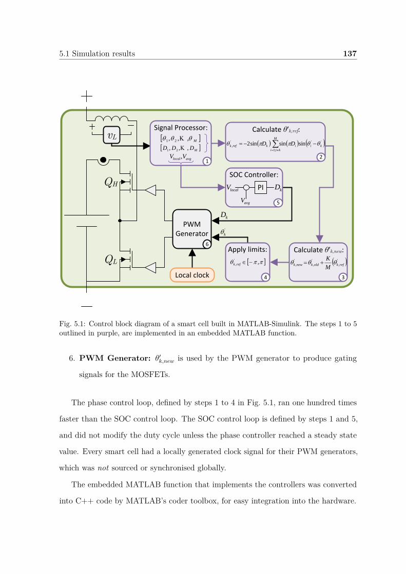
5.1 Simulation results 137
vL
PWMGenerator
6
QH
QL
Calculate θ′k,ref:
2
M
kii
kiikrefk DD;1
'''
, sinsinsin2
1
M ,,, 21
MDDD ,,, 21
avglocal VV ,
Signal Processor:
3
'
,
'
,
'
, refkoldknewkM
K
Calculate θ′k,new:
SOC Controller:
5
localV
avgV
PI kD
Apply limits:
,'
, refk
4
'
k
kD
Local clock
Fig. 5.1: Control block diagram of a smart cell built in MATLAB-Simulink. The steps 1 to 5outlined in purple, are implemented in an embedded MATLAB function.
6. PWM Generator: θ′k,new is used by the PWM generator to produce gating
signals for the MOSFETs.
The phase control loop, defined by steps 1 to 4 in Fig. 5.1, ran one hundred times
faster than the SOC control loop. The SOC control loop is defined by steps 1 and 5,
and did not modify the duty cycle unless the phase controller reached a steady state
value. Every smart cell had a locally generated clock signal for their PWM generators,
which was not sourced or synchronised globally.
The embedded MATLAB function that implements the controllers was converted
into C++ code by MATLAB’s coder toolbox, for easy integration into the hardware.

138 Smart cell simulations and experimental results
5.1.2 Continuous time simulation study of the phase controller
This subsection describes the testing of the phase controller implemented in Section
5.1.1 with a number of different system configurations, using “continuous time”. The
term continuous time is used in this context to describe a system of smart cells not
limited by hardware sampling rates and resolutions, something that will be explored in
the next subsection.
Four configurations were considered for this study: 3, 5, 10, and 20 smart cells
in series. For each configuration, two plots are shown: 1) a time evolution plot; and
2) a bar chart comparing the ac rms ripple current reduction in the inductors. The
common system configurations are listed in Table 5.1, recalling that Xu is a random
number uniformly distributed between 0 and 1.. The cell capacities simulated for each
configuration are listed in the legend of each time evolution plot.
Table 5.1: Parameters used throughout the continuous time simulation studies of the smartcell phase controller.
Description Parameter ValueModule inductance Lsc 100 µHOutput capacitance Cout 54.7 µFSwitching frequency fs 20 kHzSwitching period Ts 50 µsOn resistance of module MOSFETs RDS−on 10 mΩNominal cell voltage Vnom 3.6 VState of charge SOCk 100%Phase controller activation time tph−on 1 msCell capacity Ck Xu × 4 AhMaximum cell capacity Cmax 4.0 AhPhase controller gain K 2.0

5.1 Simulation results 139
3 smart cells
0 5 10 15 20-100
0
100
200
300
400
Phas
e Sh
ift (
degr
ees)
0.75 Ah, 63.7 deg1.20 Ah, -37.0 deg3.00 Ah, 266.3 deg
0 5 10 15 204.9
4.95
5
5.05
5.1
5.15
Out
put V
olta
ge (
V)
19.8
5.1
5.12
5.14
0.2
5.1
5.12
5.14
0 5 10 15 20Time (ms)
0.6
0.8
1
1.2
Indu
ctor
Cur
rent
(A
)
19.8
1
1.1
1.2
0.2
1
1.1
1.2
(a) Time evolution of the system. Thesmart cell controllers are turned on at 1.0ms. The peak-to-peak ripple voltage onthe capacitor is improved from 44 mV to6 mV. The ac rms current in the inductoris improved from 104 mA rms to 26 mArms.
Worst Case Smart cell Fourier10-2
10-1
100
IL a
c rm
s (A
)
Theory
Simulation
(b) A comparison of ILac-rms values ofa three smart cell pack in the worstcase switching pattern and the smart cellswitching pattern. The theoretical min-imum ILac-rms is also calculated, and la-belled “Fourier”.
Fig. 5.2: Continuous time simulation results of a three smart cell system.
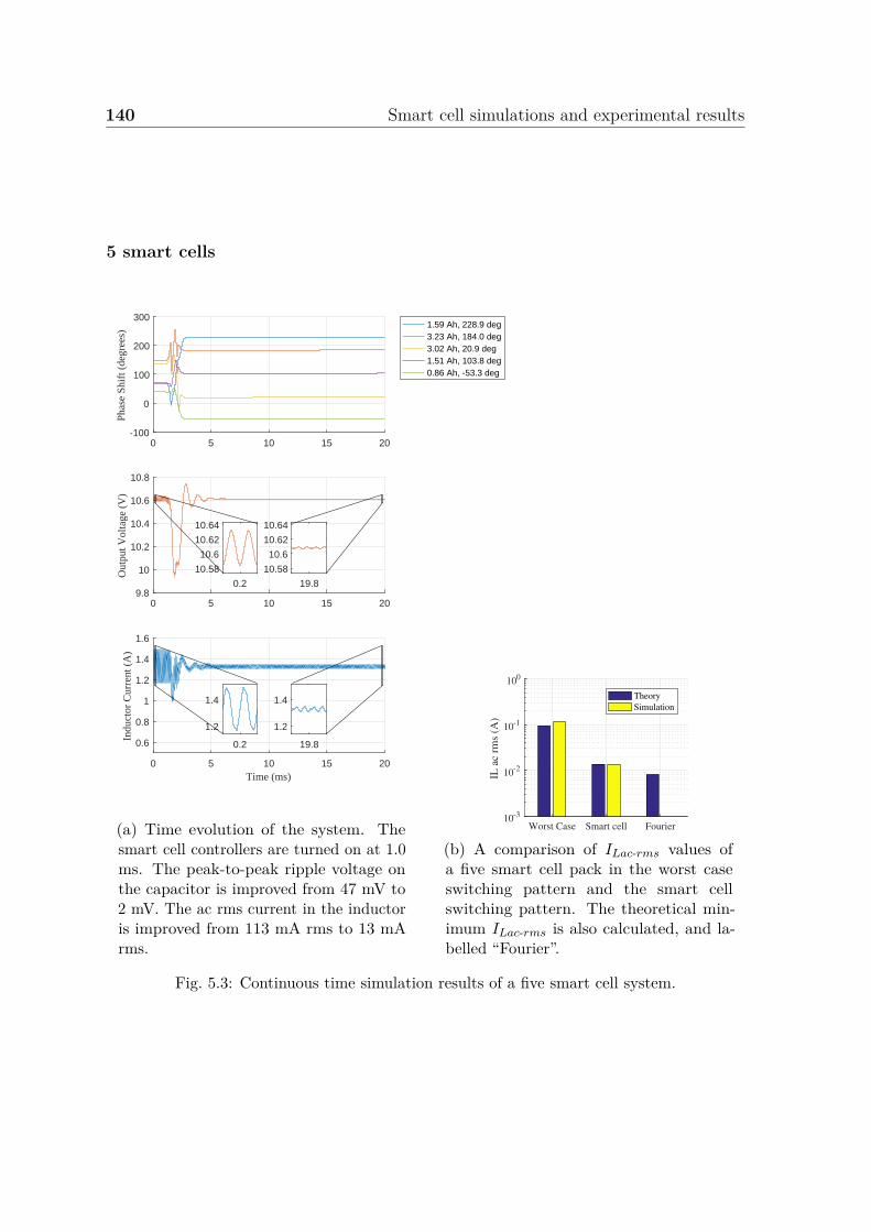
140 Smart cell simulations and experimental results
5 smart cells
0 5 10 15 20-100
0
100
200
300
Phas
e Sh
ift (
degr
ees)
1.59 Ah, 228.9 deg3.23 Ah, 184.0 deg3.02 Ah, 20.9 deg1.51 Ah, 103.8 deg0.86 Ah, -53.3 deg
0 5 10 15 209.8
10
10.2
10.4
10.6
10.8
Out
put V
olta
ge (
V)
19.8
10.58
10.6
10.62
10.64
0.2
10.58
10.6
10.62
10.64
0 5 10 15 20Time (ms)
0.6
0.8
1
1.2
1.4
1.6
Indu
ctor
Cur
rent
(A
)
19.8
1.2
1.4
0.2
1.2
1.4
(a) Time evolution of the system. Thesmart cell controllers are turned on at 1.0ms. The peak-to-peak ripple voltage onthe capacitor is improved from 47 mV to2 mV. The ac rms current in the inductoris improved from 113 mA rms to 13 mArms.
Worst Case Smart cell Fourier10-3
10-2
10-1
100
IL a
c rm
s (A
)
Theory
Simulation
(b) A comparison of ILac-rms values ofa five smart cell pack in the worst caseswitching pattern and the smart cellswitching pattern. The theoretical min-imum ILac-rms is also calculated, and la-belled “Fourier”.
Fig. 5.3: Continuous time simulation results of a five smart cell system.
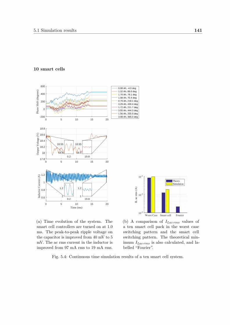
5.1 Simulation results 141
10 smart cells
0 5 10 15 20-200
0
200
400
600
Phas
e Sh
ift (
degr
ees)
0.08 Ah, -4.0 deg1.32 Ah, 89.0 deg1.70 Ah, 79.1 deg1.08 Ah, 70.4 deg0.79 Ah, 218.1 deg3.29 Ah, 430.4 deg1.72 Ah, 211.7 deg3.55 Ah, 444.3 deg1.56 Ah, 255.5 deg3.08 Ah, 365.0 deg
0 5 10 15 2017.8
18
18.2
18.4
18.6
18.8
Out
put V
olta
ge (
V)
19.8
18.5
18.55
0.2
18.5
18.55
0 5 10 15 20Time (ms)
0.6
0.8
1
1.2
Indu
ctor
Cur
rent
(A
)
19.81
1.2
0.21
1.2
(a) Time evolution of the system. Thesmart cell controllers are turned on at 1.0ms. The peak-to-peak ripple voltage onthe capacitor is improved from 40 mV to 5mV. The ac rms current in the inductor isimproved from 97 mA rms to 19 mA rms.
Worst Case Smart cell Fourier10-3
10-2
10-1
IL a
c rm
s (A
)
Theory
Simulation
(b) A comparison of ILac-rms values ofa ten smart cell pack in the worst caseswitching pattern and the smart cellswitching pattern. The theoretical min-imum ILac-rms is also calculated, and la-belled “Fourier”.
Fig. 5.4: Continuous time simulation results of a ten smart cell system.
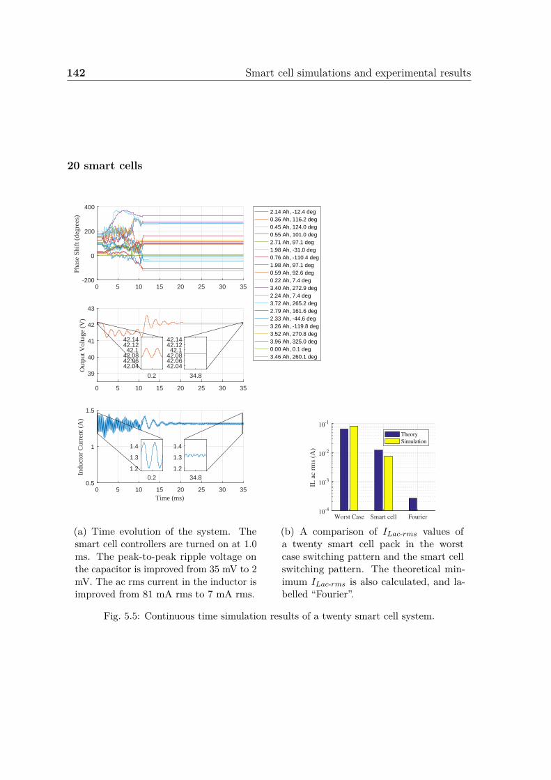
142 Smart cell simulations and experimental results
20 smart cells
0 5 10 15 20 25 30 35-200
0
200
400
Phas
e Sh
ift (
degr
ees)
2.14 Ah, -12.4 deg0.36 Ah, 116.2 deg0.45 Ah, 124.0 deg0.55 Ah, 101.0 deg2.71 Ah, 97.1 deg1.98 Ah, -31.0 deg0.76 Ah, -110.4 deg1.98 Ah, 97.1 deg0.59 Ah, 92.6 deg0.22 Ah, 7.4 deg3.40 Ah, 272.9 deg2.24 Ah, 7.4 deg3.72 Ah, 265.2 deg2.79 Ah, 161.6 deg2.33 Ah, -44.6 deg3.26 Ah, -119.8 deg3.52 Ah, 270.8 deg3.96 Ah, 325.0 deg0.00 Ah, 0.1 deg3.46 Ah, 260.1 deg
0 5 10 15 20 25 30 35
39
40
41
42
43
Out
put V
olta
ge (
V)
34.8
42.0442.0642.0842.1
42.1242.14
0.2
42.0442.0642.0842.1
42.1242.14
0 5 10 15 20 25 30 35Time (ms)
0.5
1
1.5
Indu
ctor
Cur
rent
(A
)
34.8
1.2
1.3
1.4
0.2
1.2
1.3
1.4
(a) Time evolution of the system. Thesmart cell controllers are turned on at 1.0ms. The peak-to-peak ripple voltage onthe capacitor is improved from 35 mV to 2mV. The ac rms current in the inductor isimproved from 81 mA rms to 7 mA rms.
Worst Case Smart cell Fourier10-4
10-3
10-2
10-1
IL a
c rm
s (A
)
Theory
Simulation
(b) A comparison of ILac-rms values ofa twenty smart cell pack in the worstcase switching pattern and the smart cellswitching pattern. The theoretical min-imum ILac-rms is also calculated, and la-belled “Fourier”.
Fig. 5.5: Continuous time simulation results of a twenty smart cell system.

5.1 Simulation results 143
Summary and discussion
In the simulation results of Fig. 5.2, Fig. 5.3, Fig. 5.4, and Fig. 5.5, each smart cell
within each set was operating completely independently of each other. At the start
of the simulation, the cells were configured into their worst case switching pattern,
where all of their weighted vectors (defined by (4.12) and (4.13)) were in phase with
each other. The phase controller was turned on 1.0 ms into the simulation. A value of
CMAX = 4.00 Ah was pre-programmed into each smart cell, in order for each smart
cell to calculate its local duty cycle according to (4.1). Table 5.2 summarizes the
improvements to the peak-to-peak output voltage ripple and ac rms ripple current in
the inductor made when the smart cell phase controller was engaged during the phase
controller simulation study. These improvements can also be seen in the inset graphs
from each simulation result.
The elegance of the phase controller comes from its fairly simple task of calculating
its reference phase shift according to (4.20). When all smart cells were executing this
control algorithm, they were effectively solving the minimization problem of (4.14)
together.
In all four cases, the system of smart cells was able to stabilize around a local
minima. The local minima found by the simulations is sometimes different from the
theoretical results in the bar graphs. This is because the theoretical results use the
interior point algorithm implemented by MATLAB’s fmincon function to minimize
(4.14) and is therefore able to find better solutions more easily. The simulation results
are more likely to settle into a local minima depending on their starting state, as the
system evolves smoothly over time. The smart cell controllers are like a ball rolling over
the solution space together: when they find a valley, they stay there. In contrast, an
interior point algorithm is able to move around the solution space more easily, before
converging to a final solution.

144 Smart cell simulations and experimental results
The bar graphs also included a theoretical result labelled “Fourier”. This result was
calculated using MATLAB’s fmincon function, but it minimized (4.11) using the first
500 harmonics. Therefore, this theoretical result is an indication of how much more of
an improvement to the ripple voltage and current can be achieved if the simplification of
using only the fundamental harmonic was not undertaken. As expected, the theoretical
“Fourier” result is increasingly superior as the number of cells increase. In Fig. 5.2 and
Fig. 5.3 the ripple current of the smart cell controller is very similar to the Fourier
result. However, in the 20 cell simulation of Fig. 5.5 the Fourier result is almost 10
times better than the smart cell result. This is because the high frequency components
of (4.11) are necessary to capture the increasing number of switching events. Even so,
there is an order of magnitude improvement in the ripple current by just using the first
harmonic. Furthermore, not only is there a ripple current reduction by using the phase
controller, the ripple current is also stable and predictable. In a real system where the
switching frequencies will not be exactly the same, the ripple current will fluctuate
during operation, which is undesirable. This will be discussed further in Section 5.2.2..
The amount of ripple current and ripple voltage reduction will depend heavily on
the duty cycles of the smart cells, thus a different group of smart cells may have less
or more ripple reduction than shown here.
Table 5.2: Summary of performance improvements using the smart cell phase controller.
Number of Cells Worst Case Smart Cell ControlVout-pp ILac-rms Vout-pp ILac-rms
3 44 mV 104 mA rms 6 mV 26 mA rms5 47 mV 113 mA rms 2 mV 13 mA rms10 40 mV 97 mA rms 5 mV 19 mA rms20 35 mV 81 mA rms 2 mV 7 mA rms
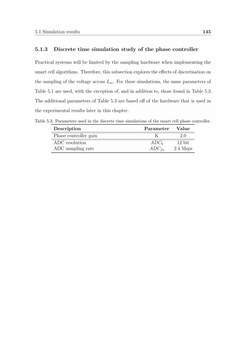
5.1 Simulation results 145
5.1.3 Discrete time simulation study of the phase controller
Practical systems will be limited by the sampling hardware when implementing the
smart cell algorithms. Therefore, this subsection explores the effects of discretisation on
the sampling of the voltage across Lsc. For these simulations, the same parameters of
Table 5.1 are used, with the exception of, and in addition to, those found in Table 5.3.
The additional parameters of Table 5.3 are based off of the hardware that is used in
the experimental results later in this chapter.
Table 5.3: Parameters used in the discrete time simulations of the smart cell phase controller.Description Parameter ValuePhase controller gain K 2.0ADC resolution ADCb 12 bitADC sampling rate ADCfs 2.4 Msps
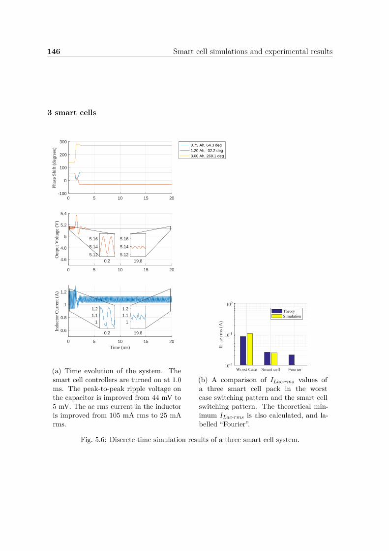
146 Smart cell simulations and experimental results
3 smart cells
0 5 10 15 20-100
0
100
200
300
Phas
e Sh
ift (
degr
ees)
0.75 Ah, 64.3 deg1.20 Ah, -32.2 deg3.00 Ah, 269.1 deg
0 5 10 15 20
4.6
4.8
5
5.2
5.4
Out
put V
olta
ge (
V)
19.85.12
5.14
5.16
0.25.12
5.14
5.16
0 5 10 15 20Time (ms)
0.6
0.8
1
1.2
Indu
ctor
Cur
rent
(A
)
19.8
1
1.1
1.2
0.2
1
1.1
1.2
(a) Time evolution of the system. Thesmart cell controllers are turned on at 1.0ms. The peak-to-peak ripple voltage onthe capacitor is improved from 44 mV to5 mV. The ac rms current in the inductoris improved from 105 mA rms to 25 mArms.
Worst Case Smart cell Fourier10-2
10-1
100
IL a
c rm
s (A
)
Theory
Simulation
(b) A comparison of ILac-rms values ofa three smart cell pack in the worstcase switching pattern and the smart cellswitching pattern. The theoretical min-imum ILac-rms is also calculated, and la-belled “Fourier”.
Fig. 5.6: Discrete time simulation results of a three smart cell system.
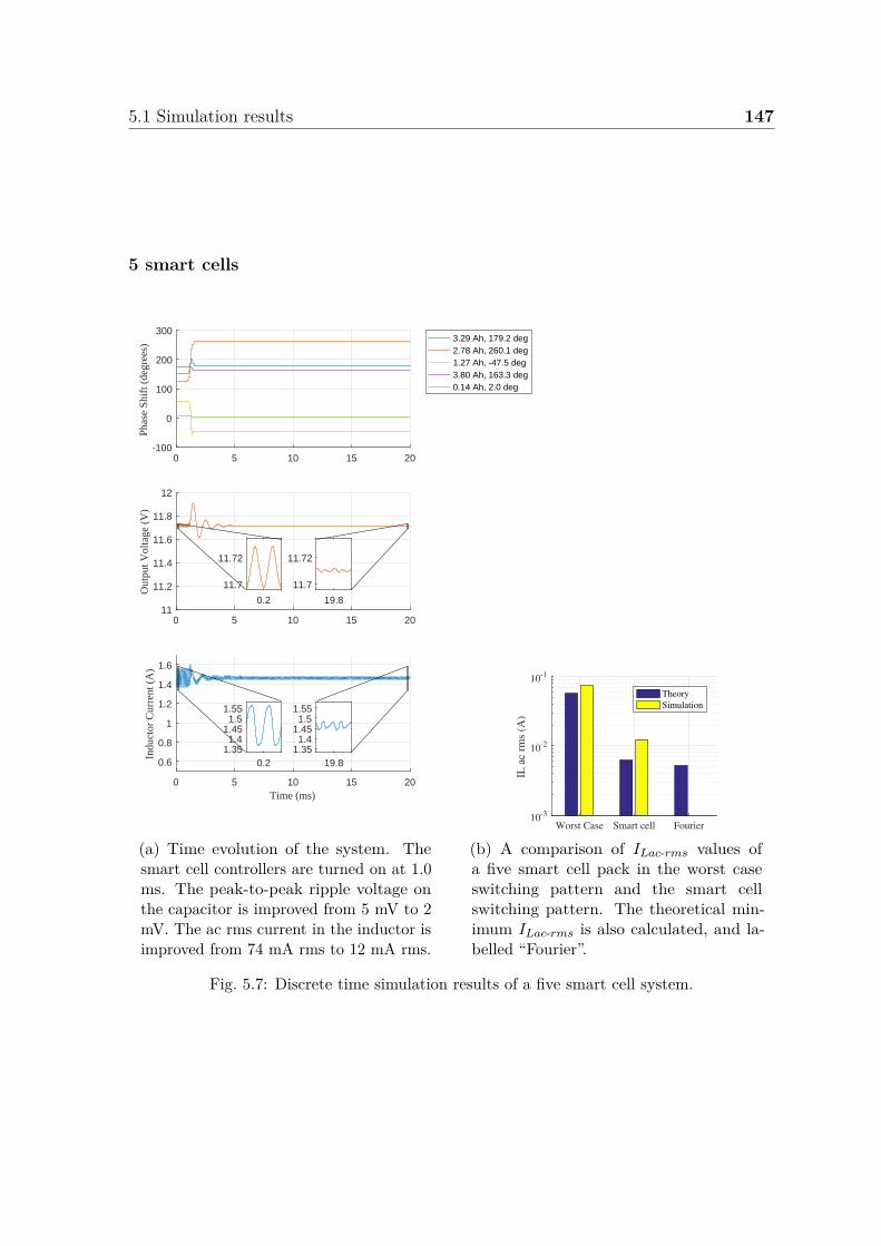
5.1 Simulation results 147
5 smart cells
0 5 10 15 20-100
0
100
200
300
Phas
e Sh
ift (
degr
ees)
3.29 Ah, 179.2 deg2.78 Ah, 260.1 deg1.27 Ah, -47.5 deg3.80 Ah, 163.3 deg0.14 Ah, 2.0 deg
0 5 10 15 2011
11.2
11.4
11.6
11.8
12
Out
put V
olta
ge (
V)
19.8
11.7
11.72
0.2
11.7
11.72
0 5 10 15 20Time (ms)
0.6
0.8
1
1.2
1.4
1.6
Indu
ctor
Cur
rent
(A
)
19.81.351.4
1.451.5
1.55
0.21.351.4
1.451.5
1.55
(a) Time evolution of the system. Thesmart cell controllers are turned on at 1.0ms. The peak-to-peak ripple voltage onthe capacitor is improved from 5 mV to 2mV. The ac rms current in the inductor isimproved from 74 mA rms to 12 mA rms.
Worst Case Smart cell Fourier10-3
10-2
10-1
IL a
c rm
s (A
)
Theory
Simulation
(b) A comparison of ILac-rms values ofa five smart cell pack in the worst caseswitching pattern and the smart cellswitching pattern. The theoretical min-imum ILac-rms is also calculated, and la-belled “Fourier”.
Fig. 5.7: Discrete time simulation results of a five smart cell system.
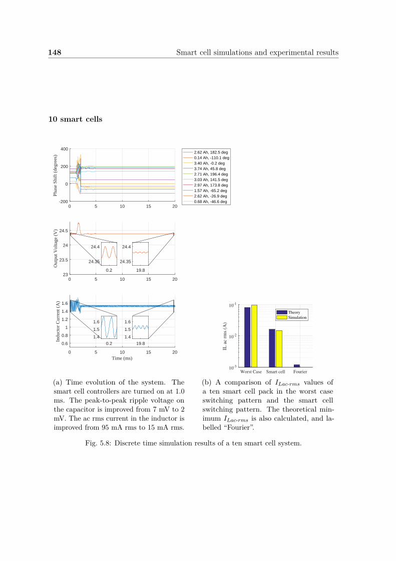
148 Smart cell simulations and experimental results
10 smart cells
0 5 10 15 20-200
0
200
400
Phas
e Sh
ift (
degr
ees)
2.62 Ah, 182.5 deg0.14 Ah, -110.1 deg3.40 Ah, -0.2 deg3.74 Ah, 45.8 deg2.71 Ah, 196.4 deg3.03 Ah, 141.5 deg2.97 Ah, 173.8 deg1.57 Ah, -65.2 deg2.62 Ah, -26.9 deg0.68 Ah, -46.6 deg
0 5 10 15 2023
23.5
24
24.5
Out
put V
olta
ge (
V)
19.8
24.35
24.4
0.2
24.35
24.4
0 5 10 15 20Time (ms)
0.6
0.8
1
1.2
1.4
1.6
Indu
ctor
Cur
rent
(A
)
19.8
1.4
1.5
1.6
0.2
1.4
1.5
1.6
(a) Time evolution of the system. Thesmart cell controllers are turned on at 1.0ms. The peak-to-peak ripple voltage onthe capacitor is improved from 7 mV to 2mV. The ac rms current in the inductor isimproved from 95 mA rms to 15 mA rms.
Worst Case Smart cell Fourier10-3
10-2
10-1
IL a
c rm
s (A
)
Theory
Simulation
(b) A comparison of ILac-rms values ofa ten smart cell pack in the worst caseswitching pattern and the smart cellswitching pattern. The theoretical min-imum ILac-rms is also calculated, and la-belled “Fourier”.
Fig. 5.8: Discrete time simulation results of a ten smart cell system.
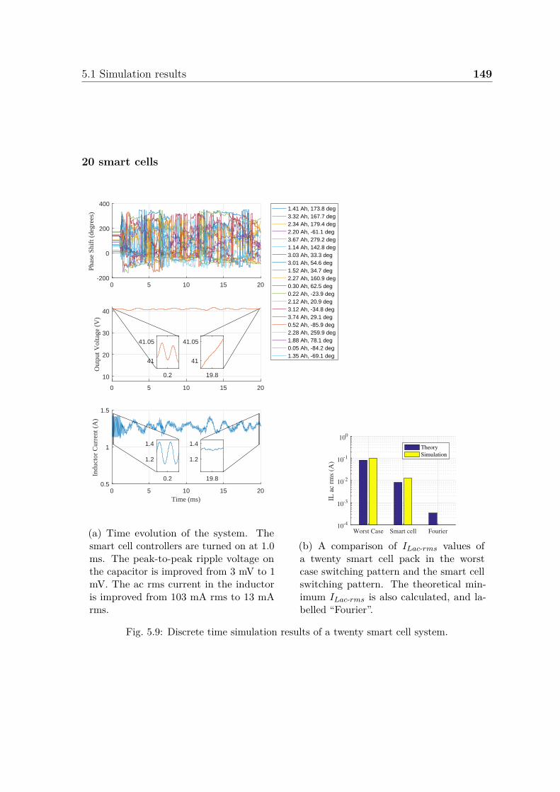
5.1 Simulation results 149
20 smart cells
0 5 10 15 20-200
0
200
400
Phas
e Sh
ift (
degr
ees)
1.41 Ah, 173.8 deg3.32 Ah, 167.7 deg2.34 Ah, 179.4 deg2.20 Ah, -61.1 deg3.67 Ah, 279.2 deg1.14 Ah, 142.8 deg3.03 Ah, 33.3 deg3.01 Ah, 54.6 deg1.52 Ah, 34.7 deg2.27 Ah, 160.9 deg0.30 Ah, 62.5 deg0.22 Ah, -23.9 deg2.12 Ah, 20.9 deg3.12 Ah, -34.8 deg3.74 Ah, 29.1 deg0.52 Ah, -85.9 deg2.28 Ah, 259.9 deg1.88 Ah, 78.1 deg0.05 Ah, -84.2 deg1.35 Ah, -69.1 deg
0 5 10 15 20
10
20
30
40
Out
put V
olta
ge (
V)
19.8
41
41.05
0.2
41
41.05
0 5 10 15 20Time (ms)
0.5
1
1.5
Indu
ctor
Cur
rent
(A
)
19.8
1.2
1.4
0.2
1.2
1.4
(a) Time evolution of the system. Thesmart cell controllers are turned on at 1.0ms. The peak-to-peak ripple voltage onthe capacitor is improved from 3 mV to 1mV. The ac rms current in the inductoris improved from 103 mA rms to 13 mArms.
Worst Case Smart cell Fourier10-4
10-3
10-2
10-1
100
IL a
c rm
s (A
)
Theory
Simulation
(b) A comparison of ILac-rms values ofa twenty smart cell pack in the worstcase switching pattern and the smart cellswitching pattern. The theoretical min-imum ILac-rms is also calculated, and la-belled “Fourier”.
Fig. 5.9: Discrete time simulation results of a twenty smart cell system.

150 Smart cell simulations and experimental results
Summary and discussion
In the discrete time simulations of Fig. 5.6, Fig. 5.7, Fig. 5.8, and Fig. 5.9, each smart
cell operated completely independently of one another. The phase controller was turned
on 1.0 ms into the simulation. A value of CMAX = 4.00 Ah was pre-programmed into
each smart cell, in order for each smart cell to calculate its local duty cycle according
to (4.1). Table 5.4 summarizes the improvements to the peak-to-peak output voltage
ripple and ac rms ripple current in the inductor made when the smart cell phase
controller was enabled. These improvements can also be seen in the inset graphs from
each simulation result.
Table 5.4: Summary of performance improvements using the smart cell phase controller indiscrete time simulations.
Number of Cells Worst Case Smart Cell ControlVout-pp ILac-rms Vout-pp ILac-rms
3 44 mV 105 mA rms 5 mV 25 mA rms5 5 mV 74 mA rms 2 mV 12 mA rms10 7 mV 95 mA rms 2 mV 15 mA rms20 3 mV 103 mA rms 1 mV1 13 mA rms2
The smart cell controller was implemented as a MATLAB function block in Simulink.
This block has multiple inputs and outputs that were used to configure the smart cell
controller. Details of the smart cell Simulink model can be found in Appendix B.
The discrete time smart cell controller developed for these discrete time simulations
was implemented in hardware using MATLAB’s coder toolbox. Using this tool, the
MATLAB code was directly converted to C++ code, which could be compiled in the
smart cell hardware. This yielded to large advantages during the development process:
1) the smart cell controller could be debugged in simulation and 2) potential errors
from importing the code from MATLAB to C++ manually were eliminated.1Phase controller stability not achieved.2See footnote 1.

5.1 Simulation results 151
As compared to the continuous time smart cell simulations, the discrete time
simulations performed similarly in terms of the ripple reduction and were able to reduce
the inductor’s ripple current by about a factor of 10 in all cases. The one difference
was in the 20 cell case. In the discrete time simulation, stability was not achieved. This
is because the limited sampling frequency could not decipher all of the information
necessary at all times. The following subsection discusses this in more detail.
5.1.4 Stability of the phase controller with limited sampling rate
As Sections 5.1.2 and 5.1.3 showed, the ability of the phase controller to find a stable
operating point depends heavily on the sampling rate of vL, or more accurately, the
number of samples of vL during each smart cell switching period. Define this as Nsample:
Nsample = fsample
fs
(5.1)
In this subsection, an upper bound on the number of smart cells that can be put in
a series string given a system’s Nsample will be calculated. In order to calculate this
upper bound, the processing of the vL waveform must be better understood.
Fig. 5.10 shows a schematic representation of the ADC sampling the vL waveform
during a transient event (when a smart cell is switching). Using this figure as a guide,
the process by which the smart cell algorithm finds levels and edges in the vl waveform
is described as follows:
1. A large dvL/dt event is detected between samples 4 and 5.
2. The two samples preceding this event are used to calculated the value of the level
prior to the switching event. Thus, samples 2 and 3 are averaged to become the
“front” level calculation.

152 Smart cell simulations and experimental results
VLsc
0 1 2 3 4 5 6 7 8 9
ADC Sample Number
Fig. 5.10: Schematic example of sampling the vL waveform.
3. Another large dvL/dt event is detected between samples 5 and 6. However, since
this event came right after the first one, it is ignored.
4. The two samples following the initial switching event and its glitches are used to
calculate the value of the level. Thus, samples 7 and 8 are averaged to become
the “back” level calculation.
The number of samples used to calculate the levels (2 in the above example), and
the glitch threshold (1 in the above example) can be configured in software. See
Appendix B for more details. However, a minimum of 6 samples are required around
each switching event in order to properly sense the switching event and the levels
around it. In Fig. 5.10, 7 samples were used due to the glitch measured in the vL
waveform.
In an ideal scenario using the same smart cell controller settings of the simulations
of Section 5.1.3, where each switching event is captured with two samples, and the
switching events are evenly spaced so that there are 2 samples between each switching
event (thus the “front” and “back” level measurements will be identical), 4 samples
are required for every switching event. Therefore, keeping in mind that there are two

5.1 Simulation results 153
switching events for every smart cell, the theoretical maximum number of smart cells
that can be sensed in a series string is:
Nsample
2 × 4 = 1402 × 4 = 17.5. (5.2)
Equation 5.2 represents the absolute upper bound on the number of smart cells
in a series string given the controller and hardware settings and is the reason why
the discrete time simulation of 20 smart cells in Fig. 5.9 was unable to find a stable
operating point. However, 5.2 does not take into account:
• Glitches: Measuring and removing glitches will effectively reduce the number
of cells in a string that can be measured.
• SOC control: During operation, the duty cycles of the smart cells may vary in
order to synchronize their SOCs. In the above idealized example, any change
in duty cycle of a single smart cell will perturb the perfectly spaced switching
events and, thus, not all levels will be able to be accurately measured.
A more generalized expression for the maximum number of smart cells in a series
string can be derived:
Nsc- max = Nsample
Nlevel + Nsw-avg
(5.3)
where:
Nlevel = Number of samples required per level, (5.4)
Nsw-avg = Average number of samples per switching event. (5.5)
Equation (5.3) limits the control scalability of a smart cell system.

154 Smart cell simulations and experimental results
5.2 Experimental Results
5.2.1 Hardware Set-up
The theory developed in this work was tested in the laboratory with an experimental
set-up consisting of three smart cells in series, as shown in Fig. 4.1 using the parameters
listed in Table 5.1. The hardware was built around ARM’s mbed platform, where each
smart cell was implemented with the NUCLEO-F401RE board and a custom printed
circuit board (PCB) containing the power stage. The inputs of each smart cell PCB
was connected to a small pack of parallel connected 18650 lithium-ion cells, in order
to simulate battery cells of varying capacities. Table 5.5 lists the capacities of the
equivalent cell connected to each smart cell, as measured by a Neware battery tester 8
channel 5V20A-NTFA. The cells used were manufactured by Samsung, model number
INR18650-29E [111]. The outputs of the smart cells were connected in series, and
attached to a 4.8 Ω resistive load. Fig. 5.11 shows a photograph of the three smart
cells built in the laboratory.
Table 5.5: Cell capacities used to test three smart cell PCBs in the laboratory.
Cell Number of 18650 Cells Measured Capacity1 3 7.97 Ah2 3 8.10 Ah3 2 5.31 Ah
The NUCLEO-F401RE board was chosen for its relatively powerful micro-controller,
the STM32F401RET6, in order to focus attention on how the smart cell controller
could be implemented in hardware. The STM32F401RET6 is based on the ARM 32-bit
Cortex-M4 CPU and has a floating point unit. The analogue to digital converter of
the STM32F401RET6 was configured to its highest sample rate of 2.8 MHz while
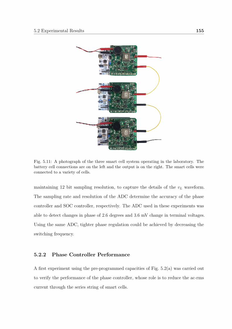
5.2 Experimental Results 155
Fig. 5.11: A photograph of the three smart cell system operating in the laboratory. Thebattery cell connections are on the left and the output is on the right. The smart cells wereconnected to a variety of cells.
maintaining 12 bit sampling resolution, to capture the details of the vL waveform.
The sampling rate and resolution of the ADC determine the accuracy of the phase
controller and SOC controller, respectively. The ADC used in these experiments was
able to detect changes in phase of 2.6 degrees and 3.6 mV change in terminal voltages.
Using the same ADC, tighter phase regulation could be achieved by decreasing the
switching frequency.
5.2.2 Phase Controller Performance
A first experiment using the pre-programmed capacities of Fig. 5.2(a) was carried out
to verify the performance of the phase controller, whose role is to reduce the ac-rms
current through the series string of smart cells.

156 Smart cell simulations and experimental results
Fig. 5.12(b) shows an oscilloscope screen shot of the three smart cells operating
and finding their optimal switching pattern. The peak-to-peak voltage ripple from the
experiments was reduced to 23 mV from 145 mV and the ac-rms Lsc ripple current was
reduced to 25 mA rms from 95 mA rms. The worst case switching pattern is shown
in Fig. 5.12(a), where the difference in ripple voltage and current is clearly visible.
Note that the peak to peak values calculated by the oscilloscope (shown in Fig. 5.12)
includes some switching noise, which was ignored for the peak to peak output voltage
measurements.
Fig. 5.13 shows the transient behaviour of the phase controller. Fig. 5.13(a) shows
how the ripple current in the inductor and output ripple voltage vary slowly over time
due to the small discrepancies in the switching frequencies of the smart cell hardware.
This is because each smart cell generated its own clock and there was not a global
timing signal, or any signal, running to every cell. In this figure, the phase controllers
were turned on at about 1 s and they were able to overcome the discrepancies in
switching frequencies by continually phase shifting themselves so that they all remained
in their optimal phase position within the string. As shown in the latter half of the
oscilloscope screen shot of Fig. 5.13(a), the smart cells maintained their stable switching
pattern until the end of the capture and beyond. The stability analysis of Section 4.5
assumed all of the switching frequencies of each smart cell were identical (Equation
(4.23)) which was a reasonable assumption for small discrepancies that are found in real
systems such as the experimental set-up used in this chapter as shown by Fig. 5.13(a).
Fig. 5.13(b) shows the point at which the phase controller is turned on at a higher
time resolution. The phase controller was turned on at about 40 ms and it took about
150 ms to reach a steady state value. The transition to the steady state value is
executed in a smooth manner, with a gradual reduction in output voltage ripple.
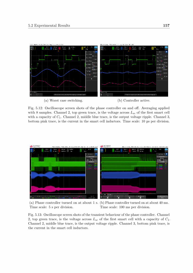
5.2 Experimental Results 157
(a) Worst case switching. (b) Controller active.
Fig. 5.12: Oscilloscope screen shots of the phase controller on and off. Averaging appliedwith 8 samples. Channel 2, top green trace, is the voltage across Lsc of the first smart cellwith a capacity of C1. Channel 2, middle blue trace, is the output voltage ripple. Channel 3,bottom pink trace, is the current in the smart cell inductors. Time scale: 10 µs per division.
(a) Phase controller turned on at about 1 s.Time scale: 5 s per division.
(b) Phase controller turned on at about 40 ms.Time scale: 100 ms per division.
Fig. 5.13: Oscilloscope screen shots of the transient behaviour of the phase controller. Channel2, top green trace, is the voltage across Lsc of the first smart cell with a capacity of C1.Channel 2, middle blue trace, is the output voltage ripple. Channel 3, bottom pink trace, isthe current in the smart cell inductors.
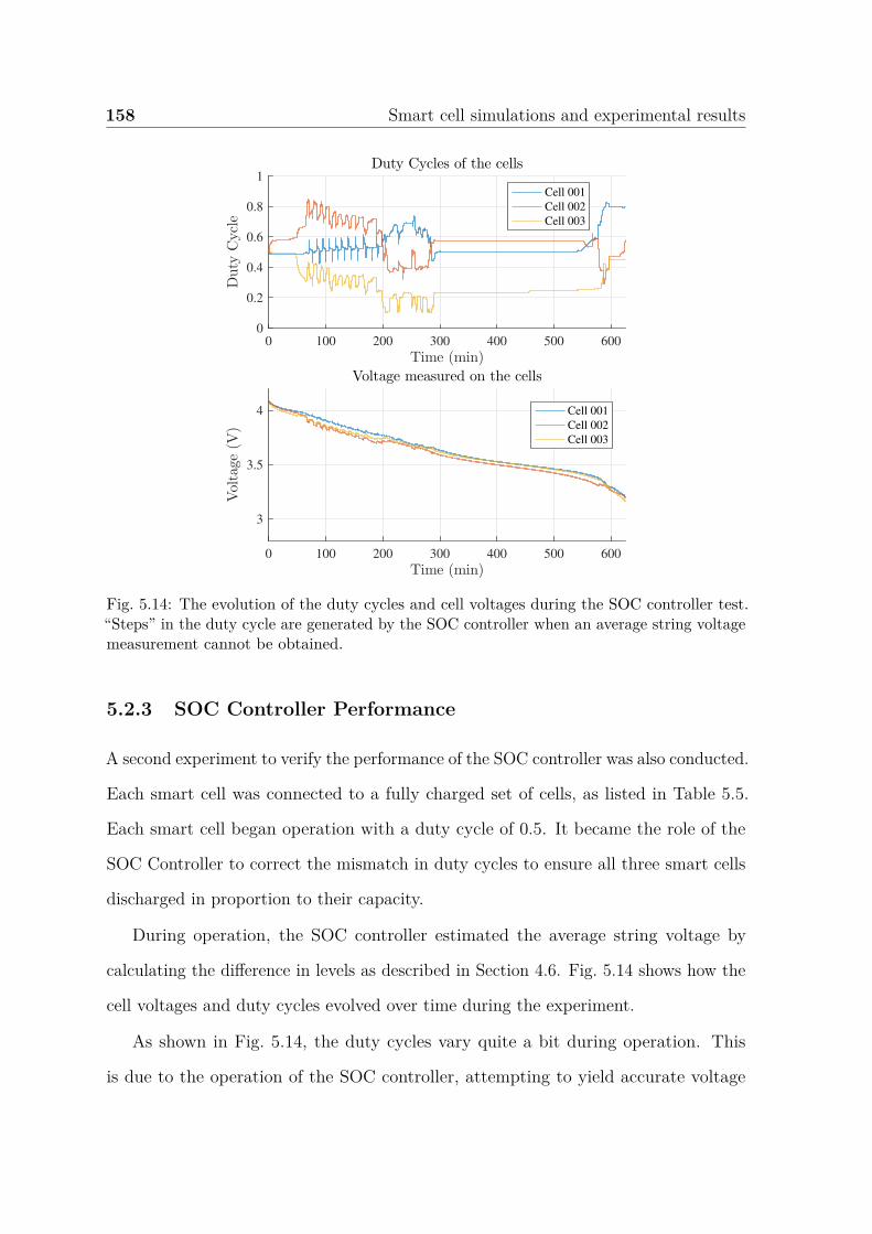
158 Smart cell simulations and experimental results
0 100 200 300 400 500 600
Time (min)
0
0.2
0.4
0.6
0.8
1
Duty
Cycle
Duty Cycles of the cells
Cell 001
Cell 002
Cell 003
0 100 200 300 400 500 600
Time (min)
3
3.5
4
Voltage
(V)
Voltage measured on the cells
Cell 001
Cell 002
Cell 003
Fig. 5.14: The evolution of the duty cycles and cell voltages during the SOC controller test.“Steps” in the duty cycle are generated by the SOC controller when an average string voltagemeasurement cannot be obtained.
5.2.3 SOC Controller Performance
A second experiment to verify the performance of the SOC controller was also conducted.
Each smart cell was connected to a fully charged set of cells, as listed in Table 5.5.
Each smart cell began operation with a duty cycle of 0.5. It became the role of the
SOC Controller to correct the mismatch in duty cycles to ensure all three smart cells
discharged in proportion to their capacity.
During operation, the SOC controller estimated the average string voltage by
calculating the difference in levels as described in Section 4.6. Fig. 5.14 shows how the
cell voltages and duty cycles evolved over time during the experiment.
As shown in Fig. 5.14, the duty cycles vary quite a bit during operation. This
is due to the operation of the SOC controller, attempting to yield accurate voltage

5.2 Experimental Results 159
information from the string of switching smart cells. Since the controller relies on
measuring the difference between levels to measure the average string voltage, there are
moments during operation where these levels are non-existent. For example, when all
of the duty cycles sum to a positive integer. Therefore, to counteract this possibility, if
a cell senses that it has not been able to measure the string voltage for more than 2.5
minutes, it increases or decreases its duty cycle by a fixed amount. This will introduce
levels into the voltage measured across Lsc and the cells will be able to measure the
average string waveform. This is exactly what is happening from about 75 minutes to
200 minutes in the experimental results of Fig. 5.14. Cell 001 was modifying its duty
cycle to get a better string measurement.
Due to the limited sampling resolution of the analogue to digital converter, each
cell implements a ±10 mV dead zone [112] around its reference voltage.
At the end of the experiment, the cells were allowed to rest for 10 minutes and
their voltages were measured. The results are shown in Table 5.6 and they are all
within 50 mV of each other. This was a very good result considering there was no
communication between any of the smart cells. Furthermore, if the SOC controller had
not been operating, the string imbalance would have been much greater as shown in
Fig. 5.15, where the smallest capacity cell discharges in around 450 minutes, clearly
limiting the pack performance compared to the SOC controlled case.
Table 5.6: Cell voltages at the end of the SOC controller experiment after 10 minutes of rest.
Cell Voltage (V)1 3.1622 3.1403 3.113

160 Smart cell simulations and experimental results
0 100 200 300 400 500 600
Time (min)
3
3.5
4
Voltage
(V)
Cell 001
Cell 002
Cell 003
Fig. 5.15: The evolution of the cell voltages when the SOC controller is disabled, and aconstant duty cycle of 0.5 is used by all cells.
5.3 Challenges
Accurate phase and SOC control is only possible through an accurate measurement of
the vL waveform. However, this waveform can be perturbed by parasitic capacitances
from every smart cell to ground.
Fig. 5.16 shows the switching actions of two smart cells connected in series. In
this case, there was a large parasitic capacitance from each cell to ground caused by
the laboratory power supply that was used to emulate each electrochemical cell. The
bottom trace of this figure shows the output of the vL sensing circuit and two things
are immediately striking: 1) the crisp “staircase” waveforms that were seen in the
simulations are no longer present, and 2) the switching action of the second smart cell
(measured by channel 1, yellow, top), is not captured by the inductor being measured
by channel 2 (green, bottom).
This parasitic effect can be greatly reduced by introducing a common mode choke
at the input of every smart cell. Fig. 5.17 shows three smart cells in series gating, each
cell connected to a channel of a dSPACE Battery Emulator. Although the staircase
nature of vL has returned, it is not as crisp as the simulations. As a consequence, smart
cells that use a common mode choke are able to implement the phase controller, but
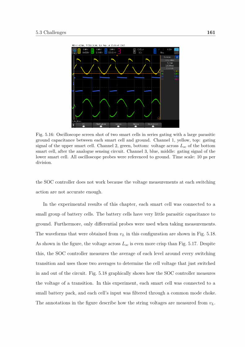
5.3 Challenges 161
Fig. 5.16: Oscilloscope screen shot of two smart cells in series gating with a large parasiticground capacitance between each smart cell and ground. Channel 1, yellow, top: gatingsignal of the upper smart cell. Channel 2, green, bottom: voltage across Lsc of the bottomsmart cell, after the analogue sensing circuit. Channel 3, blue, middle: gating signal of thelower smart cell. All oscilloscope probes were referenced to ground. Time scale: 10 µs perdivision.
the SOC controller does not work because the voltage measurements at each switching
action are not accurate enough.
In the experimental results of this chapter, each smart cell was connected to a
small group of battery cells. The battery cells have very little parasitic capacitance to
ground. Furthermore, only differential probes were used when taking measurements.
The waveforms that were obtained from vL in this configuration are shown in Fig. 5.18.
As shown in the figure, the voltage across Lsc is even more crisp than Fig. 5.17. Despite
this, the SOC controller measures the average of each level around every switching
transition and uses those two averages to determine the cell voltage that just switched
in and out of the circuit. Fig. 5.18 graphically shows how the SOC controller measures
the voltage of a transition. In this experiment, each smart cell was connected to a
small battery pack, and each cell’s input was filtered through a common mode choke.
The annotations in the figure describe how the string voltages are measured from vL.
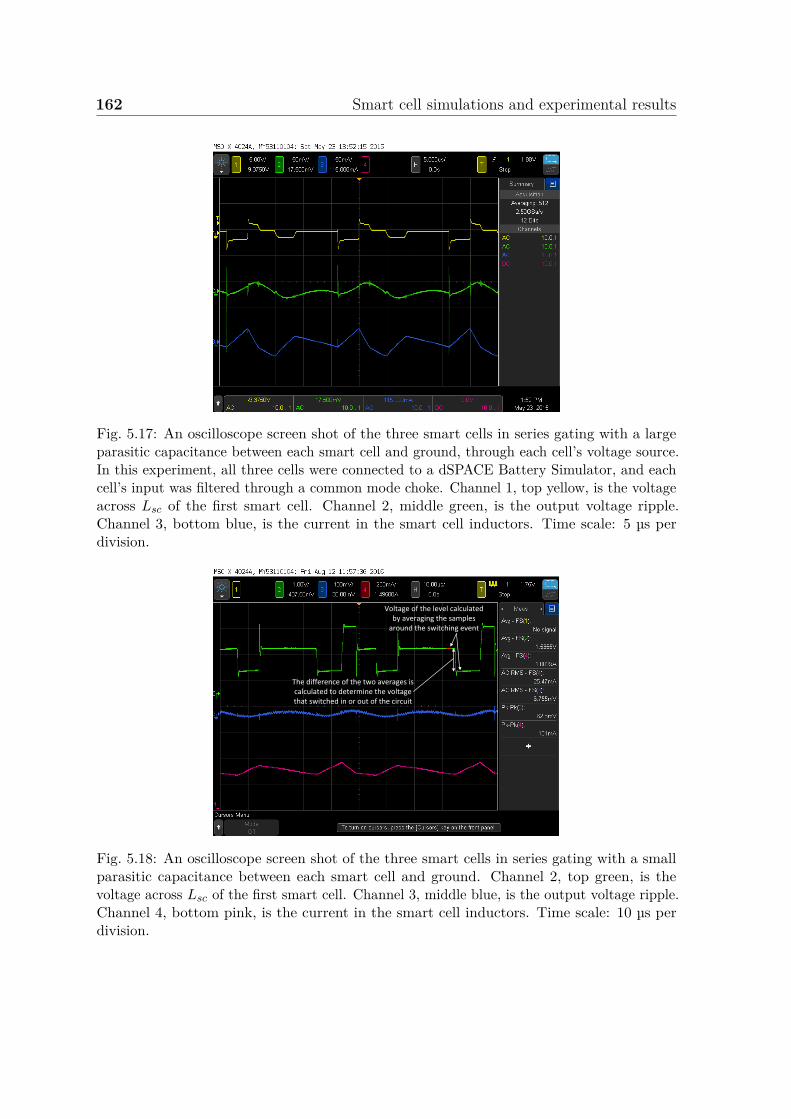
162 Smart cell simulations and experimental results
Fig. 5.17: An oscilloscope screen shot of the three smart cells in series gating with a largeparasitic capacitance between each smart cell and ground, through each cell’s voltage source.In this experiment, all three cells were connected to a dSPACE Battery Simulator, and eachcell’s input was filtered through a common mode choke. Channel 1, top yellow, is the voltageacross Lsc of the first smart cell. Channel 2, middle green, is the output voltage ripple.Channel 3, bottom blue, is the current in the smart cell inductors. Time scale: 5 µs perdivision.
Voltage of the level calculated by averaging the samples
around the switching event
The difference of the two averages is calculated to determine the voltage that switched in or out of the circuit
Fig. 5.18: An oscilloscope screen shot of the three smart cells in series gating with a smallparasitic capacitance between each smart cell and ground. Channel 2, top green, is thevoltage across Lsc of the first smart cell. Channel 3, middle blue, is the output voltage ripple.Channel 4, bottom pink, is the current in the smart cell inductors. Time scale: 10 µs perdivision.

5.4 Summary and discussion 163
Finally, the notion of parasitic capacitances has applications beyond smart cells. In
higher frequency MMC converters (switching frequencies greater than line frequency)
[113, 114], the issue of parasitic capacitances to ground could introduce losses that
could be mitigated by a common mode choke between the energy storage source and
switching network. To date, this has not been addressed, most likely because the
switching frequencies are still low (350 Hz in [113], and 1 kHz in [114]), as compared
with the smart cells (20 kHz).
5.4 Summary and discussion
The simulation results focused on the phase controller and showed how a digital system
with a finite sampling frequency places an upper bound to the number of smart cells
that can be theoretically in a series string.
The experimental results of this chapter showed that a completely decentralized
load management system is possible, paving the way towards a completely decentralized
battery management system. The experimental results of Fig. 5.14 worked well to
synchronize the terminal voltages of the three smart cells. During the mid-point of the
experiment, the duty cycles of the two larger cells, Cell 001 and Cell 002, were larger
than Cell 003, as expected.
Despite the theoretical maximum of 17 smart cells with the current hardware set-up,
the current hardware set-up was never operated with more than 4 cells. In particular,
the SOC controller operated reliably with up to three cells. This was due to difficulties
in measuring the average string voltage by analysing the vL waveform. One large
challenge with yielding good measurements of vL was the parasitic ground capacitance
between each cell and ground.
The magnitude of the difference between the levels of the vL waveform is determined
solely by the ratio of the voltage of the cell that is switching and the number of smart

164 Smart cell simulations and experimental results
cells in the string. Therefore, the magnitude of this signal will decrease at a rate
inversely proportional to the number of cells in the string. In a practical system, this
means that the vL sensor could be built with a variable gain that is increased depending
on the number of cells is senses. A detailed study of the how the signal to noise ratio
of the voltage across vL changes with an increasing number of smart cells would need
to be carried out to determine the absolute maximum number of cells that is possible
in a string with conventional hardware.
As the number of smart cells increases, the filtering requirements of Lsc also change.
Adding a smart cell to a string has a two fold effect: 1) it increases the filtering
inductance and 2) it increases the effective switching frequency. Therefore, in an ideal
scenario the Lsc should be redesigned if the same ripple specifications are required
for a different number of smart cells. This is not desirable, thus a proposed control
method of “transitions per second” is presented as future work in Section 6.2.2. In the
experimental results of this chapter, the smart cell hardware was implemented with
large inductances for Lsc. In a practical system, Lsc can be as small as possible as long
as it is still operating in its linear region.

Chapter 6
Conclusions
This thesis has a number of significant contributions to the fields of decentralised
battery management and battery pack design. This chapter will summarize those
contributions and conclude with areas of future work that can be explored.
6.1 Contributions
The main contributions of this thesis are grouped by the two projects presented:
the intelligent battery pack and the smart cells, and summarized in the following
subsections. The remainder of this section will discuss the scalability criteria created
in this thesis and its application to both projects.
Balancing circuit scalability
Section 1.5 introduced a scalability criteria which normalised the performance of
balancing circuits and evaluated them on their normalized kVA ratings and normalized
passives energy ratings. Within each rating, there were clear “Types” of circuits shown
in Fig. 1.5. The scalability Types for a number of balancing circuits presented in the
literature were summarized in Table 1.2. Using this metric, the intelligent battery and

166 Conclusions
smart cell were evaluated with the same criteria, and they were found to be Type A
and Type II circuits due to the inverse cubed relationship between peak to peak ripple
voltage and number of cells.
Using this scalability criteria, circuits like the intelligent battery and the smart
cells are viable options for large battery packs. This is a good result, because these
circuits are more effective when used with many cells as there is more likely to be large
variations between series connected cells as the number of cells increases.
6.1.1 Intelligent battery pack
Hot-swappable intelligent battery pack design
Chapter 2 introduced a design of a hot-swappable intelligent battery pack, a first of its
kind.
A hot-swappable battery pack introduces the concept of battery pack maintenance.
Instead of replacing an entire pack when it fails, individual modules can be replaced as
the cells eventually fail. This type of system architecture could be useful to companies
who have many battery packs spread across a wide area that need maintenance. Instead
of equipping a maintenance team with a few new packs as part of their tool kit, they
could be equipped with few packs worth of modules, that could be used to maintain
several battery packs in the field, instead of just a few. As an example, hot-swappable
battery packs could be used as back-up power sources for telecommunication towers,
which can be spread over vast areas.
Low latency in digital control
One challenge that has always daunted distributed power electronics, is how to physically
manage the electrical signals required for sensing and control. In the intelligent battery,
most of the control was done at the module level. Each module was responsible for

6.1 Contributions 167
managing its own phase shift and state of charge. This was done via the low bandwidth
CAN bus and it was not time sensitive - the module could tolerate late and lost data
and still accurately manage its phase shift and SOC. The master was responsible for
current and voltage control at the output. In order to synchronize the switching events
of all of the modules and to provide a low latency, low noise signal to control the
output current and voltage, a single wire sync and control signal was developed, as
shown in Fig. 2.11. This signal provided a 2 × Ts latency in the current and voltage
control loops and synchronizes all of the switching actions of the modules. In summary,
the intelligent battery separated the real time signals from the “soft” time signals and
distributed the control tasks to better manage all of the electrical signals within the
pack.
The low latency of the current and voltage control loops meant that the intelligent
battery is closer in similarity to a dc to dc converter than a battery pack. With this
type of architecture, the intelligent battery can replace a normally two stage system of
a standard battery pack and dc to dc converter with a single, combined stage of the
intelligent battery pack. Future work involving this type of system is discussed in the
next section.
6.1.2 Smart cells
Broadly speaking, smart cells start to address the practical issues of building intelli-
gent battery packs: intelligent battery packs require a large amount of overhead to
control and monitor the entire pack. Therefore, eliminating the need for intra-pack
communication can simplify an intelligent pack’s design and implementation, further
bolstering the case for power electronics integrated into battery pack designs. Smart
cells are also a unique approach to battery management: completely decentralised
battery management.
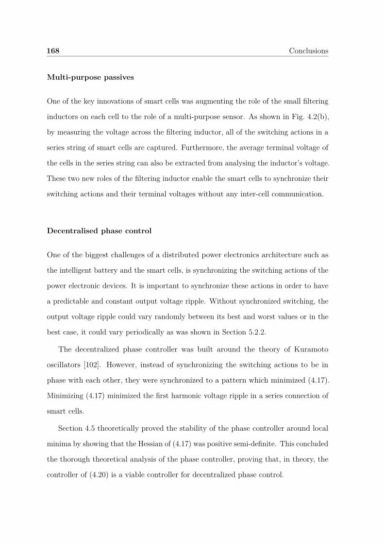
168 Conclusions
Multi-purpose passives
One of the key innovations of smart cells was augmenting the role of the small filtering
inductors on each cell to the role of a multi-purpose sensor. As shown in Fig. 4.2(b),
by measuring the voltage across the filtering inductor, all of the switching actions in a
series string of smart cells are captured. Furthermore, the average terminal voltage of
the cells in the series string can also be extracted from analysing the inductor’s voltage.
These two new roles of the filtering inductor enable the smart cells to synchronize their
switching actions and their terminal voltages without any inter-cell communication.
Decentralised phase control
One of the biggest challenges of a distributed power electronics architecture such as
the intelligent battery and the smart cells, is synchronizing the switching actions of the
power electronic devices. It is important to synchronize these actions in order to have
a predictable and constant output voltage ripple. Without synchronized switching, the
output voltage ripple could vary randomly between its best and worst values or in the
best case, it could vary periodically as was shown in Section 5.2.2.
The decentralized phase controller was built around the theory of Kuramoto
oscillators [102]. However, instead of synchronizing the switching actions to be in
phase with each other, they were synchronized to a pattern which minimized (4.17).
Minimizing (4.17) minimized the first harmonic voltage ripple in a series connection of
smart cells.
Section 4.5 theoretically proved the stability of the phase controller around local
minima by showing that the Hessian of (4.17) was positive semi-definite. This concluded
the thorough theoretical analysis of the phase controller, proving that, in theory, the
controller of (4.20) is a viable controller for decentralized phase control.

6.2 Future work 169
The phase controller was studied extensively in simulations, first in continuous time
in Section 5.1.2, then in discrete time in Section 5.1.3. The continuous time study was
conducted to confirm the theoretical analysis of Chapter 4. The discrete time study
was conducted to evaluate the effects of using hardware with limited sampling rates
and latency on the performance of a string of smart cells. In Section 5.1.4, a method
to determine the maximum number of smart cells that is theoretically possible in a
series string was derived in (5.3). All of these results confirmed that decentralized
phase control is possible in practice.
Section 5.2.2 demonstrated the performance of the phase controller in practice with
three smart cells operating together. The phase controllers performed very well to
synchronize the switching actions of the three cells to a local minima of (4.17).
Decentralised SOC control
As a further step towards a completely decentralised BMS, a completely decentralised
SOC controller was developed in theory and tested in the laboratory. The controller
used voltage differences of the vL waveform to synchronize the terminal voltages of all
cells in a series string of smart cells. When the cells are of the same chemistry, this is
equivalent to running the cells in parallel, as shown in Fig. 2.23.
The experimental results of Fig. 5.14 showed good SOC control for the three smart
cell system that was tested, and clearly outperformed the case without SOC control
shown in Fig. 5.15.
6.2 Future work
There are many exciting avenues of research and development that can be explored
from the research presented in this thesis. The rest of this subsection will discuss future
work that has come out of both projects. Following that, project specific future work

170 Conclusions
will be discussed. Future work on the intelligent battery focuses on how to exploit its
features in new projects. For the smart cells, future work focuses on how to augment
the foundation of the decentralized BMS presented here, to a fully-fledged BMS ready
for a real world application.
Battery models and machine learning
The SOC controller of both the intelligent battery and the smart cells relied on
synchronizing the terminal voltages of all of the series connected cells. The SOC
controller from these projects can be further developed using battery models available
in the literature. Furthermore, these models could be enhanced with machine learning
principles, so that each module or smart cell learns how the cells it is connected to
behave, in order to better predict its SOC and SOH.
Battery passport
A battery passport is the idea that every battery pack or cell contains a small microchip
which keeps track of the pack’s or cell’s history. The idea of a battery passport is not
new, but something that can be explored with the hardware developed in this thesis.
Companies such as Dukosi [115] are developing chips that can be integrated with
battery cells to track their performance over their lifetime. Both the intelligent battery
and the smart cells could be used as platforms to further develop the battery passport
idea and standards to make it a reality. Using these platforms, further research into the
type and quantity of information that should be stored can be investigated. Recording
a lot of data will yield a very accurate picture of a battery’s history, but it will cost
more to store this data. The research questions will revolve around how to minimize
the quantity of data without comprimising on the accuracy of the battery’s history
and SOH. This has large ramifications in the second life market of lithium ion cells, a
6.2 Future work 171
market that is growing rapidly, because as cells leave their first application they can be
easily grouped into appropriate second life applications using their battery passport.
Decentralised phase control, centralised BMS
A project that could further develop the battery management system presented in this
thesis into a commercial product is one that takes advantage of the best aspects of the
smarts cells and the intelligent battery pack. The project could use the decentralised
phase controller from the smart cells in combination with a wireless centralised controller
for pack level battery management. Both the intelligent battery hardware and smart
cell hardware developed in this work can be used to develop this idea further.
The theory developed for the smart cells also has applicability in other areas such
as super capacitors and solar photovoltaics. In both of these applications, series strings
of devices need to be balanced and managed over time. A super capacitor application
would be similar to the smart cell application presented here. However, for the solar
photovoltaic application, further research on how the decentralised controller could be
extended to include a maximum power point tracking algorithm is required.
Transitions per second control
Both projects had very low output voltage ripple and due to their topology, the voltage
ripple would decrease as more modules were added. Therefore, an interesting research
project would involve a new control method which varies the switching frequency
inversely proportional to the number of modules or smart cells that are in the series
string. This would be similar to controlling the number of transitions, as in module or
smart cell switching events, per second.
Implementing this in the intelligent battery would be relatively straightforward
since there is a master which synchronizes all of the module PWM modules. However,

172 Conclusions
as the number of modules increases, the frequency will decrease, and the control loop
latency with also increase. Therefore, care should be taken to ensure the desired system
performance is still met. At low switching frequencies, the sync and data signal could
send two values of d during every switching period to reduce the control latency.
The implementation of the transitions per second control on the smart cells will be
a greater research challenge. There will need to be a method or controller that can
gaurantee that all of the smart cells will end up at the same frequency. The theoretical
analysis of this system will also be very challenging, and would involve Kuramoto
analysis where each agent, or smart cell, does not have the same switching frequency.
6.2.1 Intelligent battery pack
Lifetime enhancement
The intelligent battery adjusts the energy flow through every series connected module
to ensure that each module discharges proportional to capacity. This will have a
positive impact on ageing, as weaker cells will be loaded less than healthier cells
[109, 110]. Therefore, an obvious research question to solve is to verify this hypothesis
in a real system. The research should be carried out under different prototypical
cycling profiles to determine which applications this technology is best suited for.
Using the two intelligent battery packs built for this thesis, such an experiment would
be straightforward to conduct. One of the packs could run in a “standard” mode,
where the duty cycle of each module is the same, and the other pack could run in
“intelligent” mode. Using the two identical packs with different control algorithms will
also remove the effects of the extra power electronics in the study, thus the results will
be purely an indication of the improvements in battery pack life that can be obtained
with module level management.

6.2 Future work 173
Intelligent battery as part of an integrated system
As mentioned in Section 6.1.1, the intelligent battery is more closely related to a dc
to dc converter than a standard battery pack. An intelligent battery is “more than
just a pack”. Therefore, future research should investigate new applications where a
battery pack and dc to dc converter can be replaced with a single intelligent battery.
In addition to a system study, a cost benefit analysis taking into account the increased
lifetime of the battery pack would also need to be undertaken.
One such application could be in solar home systems. Typically a charge controller
is required to extract the maximum power out of a solar array. An intelligent battery
pack could easily integrate the functions of a maximum power point tracker into its
master controller and could operate as a solar charger.
6.2.2 Smart Cells
Analysis of the vL waveform
The largest computational burden on the smart cell controller is the analysis of the
voltage across Lsc. The algorithm that was used is one that is based on traditional
if· · · else· · · logic. As the number of cells or sample points increase, the execution
time of the algorithm also increases linearly. However, analysing the voltage across
Lsc is similar to analysing photographs. Through machine learning, computers are
able to identify individuals and objects in photographs. Further research should be
undertaken to determine how machine learning techniques could be applied to the
voltage across Lsc to extract the average SOC of the string and the switching events, or
more directly, the control signals. This research would be very interesting in contrast to
the traditional machine vision applications since the data is quite sparse in comparison
to a photograph. Instead of inputting a matrix of red, green, and blue values, the

174 Conclusions
inputs would simply be a vector of voltages. This also implies that the computational
power required to compute such an algorithm should be reduced, which is ideal for low
power applications such as the smart cell.
Ripple reduction
The phase controller of (4.20) used only the fundamental harmonic to minimize the
output voltage ripple. However, in some applications this may not be enough. Therefore,
extending the algorithm to higher order harmonics should be considered. A short
investigation was done into this early on in the smart cell work, however a simple
controller like the one of (4.20) was not stable in simulation.
Computational smart cell algorithm improvement
The smart cell algorithm implemented for the thesis was optimised for debugging
purposes only. Therefore, further development into improving its execution time would
improve the performance and power requirements of the smart cell algorithm. Since the
controller uses the Fourier transform, the same techniques which reduce the discrete
Fourier transform algorithm from an order n2 problem to an order n log n problem
could be applied here.
Measurement of the vL waveform
Another method to improve the analysis of the vL waveform is to further develop its
measurement hardware. In the current realization, an ADC is used to sample vL for
an entire switching cycle, and the conversion results are analysed later to extract the
level and switch timing information. Some of this analysis could be done in hardware.
As a first iteration, an FPGA could be programmed to detect the switch timing events.
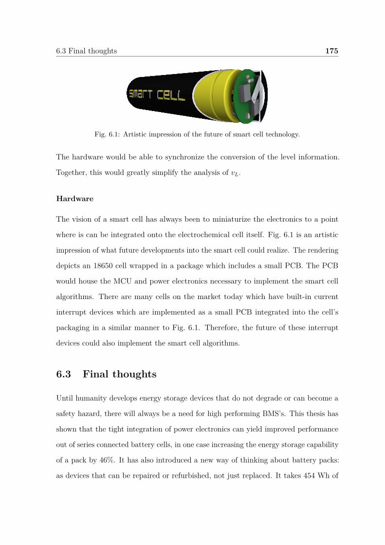
6.3 Final thoughts 175
Fig. 6.1: Artistic impression of the future of smart cell technology.
The hardware would be able to synchronize the conversion of the level information.
Together, this would greatly simplify the analysis of vL.
Hardware
The vision of a smart cell has always been to miniaturize the electronics to a point
where is can be integrated onto the electrochemical cell itself. Fig. 6.1 is an artistic
impression of what future developments into the smart cell could realize. The rendering
depicts an 18650 cell wrapped in a package which includes a small PCB. The PCB
would house the MCU and power electronics necessary to implement the smart cell
algorithms. There are many cells on the market today which have built-in current
interrupt devices which are implemented as a small PCB integrated into the cell’s
packaging in a similar manner to Fig. 6.1. Therefore, the future of these interrupt
devices could also implement the smart cell algorithms.
6.3 Final thoughts
Until humanity develops energy storage devices that do not degrade or can become a
safety hazard, there will always be a need for high performing BMS’s. This thesis has
shown that the tight integration of power electronics can yield improved performance
out of series connected battery cells, in one case increasing the energy storage capability
of a pack by 46%. It has also introduced a new way of thinking about battery packs:
as devices that can be repaired or refurbished, not just replaced. It takes 454 Wh of

176 Conclusions
energy to produce 1 Wh of Lithium-ion battery storage [116], therefore we should use
each cell until it is truly exhausted before it is sent for recycling.
Publications
[I] Damien F. Frost and David A. Howey, Completely decentralised active balancing
battery management system, in IEEE Transactions on Power Electronics, vol.
33, no. 1, pp. 729-738, January 2018. Publisher copy.
[II] Damien F. Frost and David A. Howey, High-Speed Peltier Calorimeter for the
Calibration of High-Bandwidth Power Measurement Equipment, in IEEE Trans-
actions on Instrumentation and Measurement, vol. 65, no. 1, pp. 155-163,
January 20161. Publisher copy.
[III] Damien F. Frost and David A. Howey, Novel MMC control for active balancing and
minimum ripple current in series-connected battery strings, 2015 17th European
Conference on Power Electronics and Applications (EPE’15 ECCE-Europe),
Geneva, 2015, pp. 1-10. Publisher copy.
[IV] Christoph R. Birkl, Damien F. Frost, Adrien M. Bizeray, Robert R. Richardson
and David A. Howey, Modular converter system for low-cost off-grid energy
storage using second life li-ion batteries, IEEE Global Humanitarian Technology
Conference (GHTC 2014), San Jose, CA, 2014, pp. 192-199. Publisher copy.
1During the first year of my DPhil, I designed, built, and programmed a calorimeter for one ofmy project sponsors, Newtons 4th Limited (N4L). This work is not related to the decentralised BMSwork presented in the main body of this thesis.


References
[1] T. Bruen and J. Marco, “Modelling and experimental evaluation ofparallel connected lithium ion cells for an electric vehicle battery system,”Journal of Power Sources, vol. 310, pp. 91 – 101, 2016. [Online]. Available:http://www.sciencedirect.com/science/article/pii/S0378775316300015
[2] J. Xiao, A. Peterchev, J. Zhang, and S. Sanders, “An ultra-low-power digitally-controlled buck converter IC for cellular phone applications,” in Applied PowerElectronics Conference and Exposition, 2004. APEC ’04. Nineteenth AnnualIEEE, vol. 1, 2004, pp. 383–391 Vol.1.
[3] S. Engel, M. Stieneker, N. Soltau, S. Rabiee, H. Stagge, and R. De Doncker,“Comparison of the modular multilevel dc converter and the dual-active bridgeconverter for power conversion in hvdc and mvdc grids,” Power Electronics, IEEETransactions on, vol. PP, no. 99, pp. 1–1, 2014.
[4] B. Bose, “Global warming: Energy, environmental pollution, and the impact ofpower electronics,” Industrial Electronics Magazine, IEEE, vol. 4, no. 1, pp. 6–17,March 2010.
[5] ——, “Power electronics and motor drives recent progress and perspective,”Industrial Electronics, IEEE Transactions on, vol. 56, no. 2, pp. 581–588, Feb2009.
[6] L. M. Tolbert, T. J. King, B. Ozpineci, J. B. Campbell, G. Muralidharan, D. T.Rizy, A. S. Sabau, H. Zhang, W. Zhang, Y. Xu, H. F. Huq, and H. Liu, “Powerelectronics for distributed energy systems and transmission and distributionapplications,” Report, December 2005.
[7] H. Wang, M. Liserre, and F. Blaabjerg, “Toward reliable power electronics:Challenges, design tools, and opportunities,” Industrial Electronics Magazine,IEEE, vol. 7, no. 2, pp. 17–26, June 2013.
[8] S. Vazquez, S. Lukic, E. Galvan, L. Franquelo, and J. Carrasco, “Energy stor-age systems for transport and grid applications,” Industrial Electronics, IEEETransactions on, vol. 57, no. 12, pp. 3881–3895, Dec 2010.
[9] S. Wilkinson. The grid-connected energy storage market is set to explode, reachinga total of over 40 gw of installations by 2022. IHS Technology. [Online]. Available:https://technology.ihs.com/483008/the-grid-connected-energy-storage-market-is-set-to-explode-reaching-a-total-of-over-40-gw-of-installations-by-2022
180 References
[10] W. Steel. (2017, February) Energy storage market outlook 2017: Stateof play. Renewable Energy World. Accessed: 2017-06-22. [Online]. Avail-able: http://www.renewableenergyworld.com/articles/print/volume-20/issue-1/features/storage/energy-storage-market-outlook-2017-state-of-play.html
[11] M. Munsell. (2015, March) US energy storage market grew 243% in 2015,largest year on record. Green Tech Media. Accessed: 2017-06-22. [Online].Available: https://www.greentechmedia.com/articles/read/us-energy-storage-market-grew-243-in-2015-largest-year-on-record
[12] Greentech Media, “U.S. Energy Storage Monitor: Q2 2017 Executive Summary,”no. June, 2017.
[13] H. Chen, T. N. Cong, W. Yang, C. Tan, Y. Li, and Y. Ding,“Progress in electrical energy storage system: A critical review,” Progressin Natural Science, vol. 19, no. 3, pp. 291 – 312, 2009. [Online]. Available:http://www.sciencedirect.com/science/article/pii/S100200710800381X
[14] D. Andrea, Battery Management Systems for Large Lithium-Ion Battery Packs.Artech House Publishers, October 2010.
[15] J. Kimball, B. Kuhn, and P. Krein, “Increased performance of battery packs byactive equalization,” in Vehicle Power and Propulsion Conference, 2007. VPPC2007. IEEE, Sept 2007, pp. 323–327.
[16] N. Nitta, F. Wu, J. T. Lee, and G. Yushin, “Li-ion battery materials: presentand future,” Materials Today, vol. 18, no. 5, pp. 252 – 264, 2015. [Online].Available: http://www.sciencedirect.com/science/article/pii/S1369702114004118
[17] J. Barker, R. Gover, P. Burns, A. Bryan, M. Saidi, and J. Swoyer, “Structuraland electrochemical properties of lithium vanadium fluorophosphate, LiVPO4F,”Journal of Power Sources, vol. 146, no. 1, pp. 516 – 520, 2005, selected paperspressented at the 12th International Meeting on Lithium Batteries. [Online].Available: http://www.sciencedirect.com/science/article/pii/S0378775305004507
[18] T. Reddy, Linden’s Handbook of Batteries, 4th Edition. McGraw-Hill Education,2010. [Online]. Available: https://books.google.co.uk/books?id=MXzwCfmoihYC
[19] M.-S. Wu, C.-Y. Lin, Y.-Y. Wang, C.-C. Wan, and C. Yang, “Numericalsimulation for the discharge behaviors of batteries in series and/or parallel-connected battery pack,” Electrochimica Acta, vol. 52, no. 3, pp. 1349 – 1357,2006. [Online]. Available: http://www.sciencedirect.com/science/article/pii/S0013468606007717
[20] J. Zhang, S. Ci, H. Sharif, and M. Alahmad, “Modeling discharge behavior ofmulticell battery,” Energy Conversion, IEEE Transactions on, vol. 25, no. 4, pp.1133–1141, Dec 2010.
[21] D. Cooper. (2016, October) Lithium battery failure wipes out darpa robot atnasa. Accessed: 2017-08-05. [Online]. Available: https://www.engadget.com/2016/10/28/lithium-battery-failure-wipes-out-darpa-robot-at-nasa/

References 181
[22] L. Lu, X. Han, J. Li, J. Hua, and M. Ouyang, “A review on the keyissues for lithium-ion battery management in electric vehicles,” Journal ofPower Sources, vol. 226, no. 0, pp. 272 – 288, 2013. [Online]. Available:http://www.sciencedirect.com/science/article/pii/S0378775312016163
[23] S. M. Knupfer, R. Hensley, P. Hertzke, and P. Schaufuss. (2017,January) Electrifying insights: How automakers can drive electrifiedvehicle sales and profitability. Accessed: 2017-07-04. [Online]. Available:http://www.mckinsey.com/industries/automotive-and-assembly/our-insights/electrifying-insights-how-automakers-can-drive-electrified-vehicle-sales-and-profitability
[24] X. Han, M. Ouyang, L. Lu, J. Li, Y. Zheng, and Z. Li, “A comparative study ofcommercial lithium ion battery cycle life in electrical vehicle: Aging mechanismidentification,” Journal of Power Sources, vol. 251, pp. 38 – 54, 2014. [Online].Available: http://www.sciencedirect.com/science/article/pii/S0378775313018569
[25] J. Vetter, P. Novák, M. Wagner, C. Veit, K.-C. Möller, J. Besenhard,M. Winter, M. Wohlfahrt-Mehrens, C. Vogler, and A. Hammouche,“Ageing mechanisms in lithium-ion batteries,” Journal of Power Sources,vol. 147, no. 1, pp. 269 – 281, 2005. [Online]. Available: http://www.sciencedirect.com/science/article/pii/S0378775305000832
[26] P. Arora, R. E. White, and M. Doyle, “Capacity fade mechanismsand side reactions in lithium-ion batteries,” Journal of The ElectrochemicalSociety, vol. 145, no. 10, pp. 3647–3667, 1998. [Online]. Available:http://jes.ecsdl.org/content/145/10/3647.abstract
[27] T. Ohsaki, T. Kishi, T. Kuboki, N. Takami, N. Shimura, Y. Sato, M. Sekino,and A. Satoh, “Overcharge reaction of lithium-ion batteries,” Journal of PowerSources, vol. 146, no. 1, pp. 97 – 100, 2005, selected papers pressentedat the 12th International Meeting on Lithium Batteries. [Online]. Available:http://www.sciencedirect.com/science/article/pii/S0378775305005112
[28] R. A. Leising, M. J. Palazzo, E. S. Takeuchi, and K. J. Takeuchi, “Abuse testingof lithium-ion batteries: Characterization of the overcharge reaction of LiCoO2graphite cells,” Journal of The Electrochemical Society, vol. 148, no. 8, pp.A838–A844, 2001.
[29] L. Zhong, C. Zhang, Y. He, and Z. Chen, “A method for the estimationof the battery pack state of charge based on in-pack cells uniformityanalysis,” Applied Energy, vol. 113, pp. 558 – 564, 2014. [Online]. Available:http://www.sciencedirect.com/science/article/pii/S0306261913006430
[30] F. Baronti, R. D. Rienzo, N. Papazafiropulos, R. Roncella, and R. Saletti,“Investigation of series-parallel connections of multi-module batteries for electrifiedvehicles,” in 2014 IEEE International Electric Vehicle Conference (IEVC), Dec2014, pp. 1–7.
[31] W. Shi, X. Hu, C. Jin, J. Jiang, Y. Zhang, and T. Yip, “Effects of imbalancedcurrents on large-format lifepo4/graphite batteries systems connected in parallel,”

182 References
Journal of Power Sources, vol. 313, pp. 198 – 204, 2016. [Online]. Available:http://www.sciencedirect.com/science/article/pii/S0378775316301951
[32] R. Gogoana, M. B. Pinson, M. Z. Bazant, and S. E. Sarma, “Internal resistancematching for parallel-connected lithium-ion cells and impacts on battery packcycle life,” Journal of Power Sources, vol. 252, pp. 8 – 13, 2014. [Online].Available: http://www.sciencedirect.com/science/article/pii/S0378775313019447
[33] N. Yang, X. Zhang, B. Shang, and G. Li, “Unbalanced discharging and agingdue to temperature differences among the cells in a lithium-ion battery packwith parallel combination,” Journal of Power Sources, vol. 306, pp. 733 – 741,2016. [Online]. Available: http://www.sciencedirect.com/science/article/pii/S0378775315306911
[34] M.-Y. Kim, J.-H. Kim, and G.-W. Moon, “Center-cell concentration structureof a cell-to-cell balancing circuit with a reduced number of switches,” PowerElectronics, IEEE Transactions on, vol. 29, no. 10, pp. 5285–5297, Oct 2014.
[35] B. Lindemark, “Individual cell voltage equalizers (ice) for reliable battery perfor-mance,” in Telecommunications Energy Conference, 1991. INTELEC ’91., 13thInternational, Nov 1991, pp. 196–201.
[36] D. Y. Jung, Y. H. Kim, S. W. Kim, and S.-H. Lee, “Development ofultracapacitor modules for 42-v automotive electrical systems,” Journal ofPower Sources, vol. 114, no. 2, pp. 366 – 373, 2003. [Online]. Available:http://www.sciencedirect.com/science/article/pii/S0378775302007085
[37] C. Bonfiglio and W. Roessler, “A cost optimized battery management systemwith active cell balancing for lithium ion battery stacks,” in Vehicle Power andPropulsion Conference, 2009. VPPC ’09. IEEE, Sept 2009, pp. 304–309.
[38] C. Pascual and P. Krein, “Switched capacitor system for automatic series batteryequalization,” in Applied Power Electronics Conference and Exposition, 1997.APEC ’97 Conference Proceedings 1997., Twelfth Annual, vol. 2, Feb 1997, pp.848–854 vol.2.
[39] S. W. Moore and P. J. Schneider, “A review of cell equalization methods forlithium ion and lithium polymer battery systems,” SAE Technical Paper, Tech.Rep., 2001.
[40] H. sun Park, C.-E. Kim, C.-H. Kim, G.-W. Moon, and J.-H. Lee, “A modularizedcharge equalizer for an hev lithium-ion battery string,” Industrial Electronics,IEEE Transactions on, vol. 56, no. 5, pp. 1464–1476, May 2009.
[41] A. Baughman and M. Ferdowsi, “Double-tiered switched-capacitor battery chargeequalization technique,” Industrial Electronics, IEEE Transactions on, vol. 55,no. 6, pp. 2277–2285, June 2008.
[42] M. young Kim, J.-W. Kim, C.-H. Kim, S.-Y. Cho, and G.-W. Moon, “Automaticcharge equalization circuit based on regulated voltage source for series connectedlithium-ion batteries,” in Power Electronics and ECCE Asia (ICPE ECCE), 2011IEEE 8th International Conference on, May 2011, pp. 2248–2255.
References 183
[43] M.-Y. Kim, C.-H. Kim, J.-H. Kim, and G.-W. Moon, “A chain structure ofswitched capacitor for improved cell balancing speed of lithium-ion batteries,”Industrial Electronics, IEEE Transactions on, vol. 61, no. 8, pp. 3989–3999, Aug2014.
[44] Y. Yuanmao, K. W. E. Cheng, and Y. P. B. Yeung, “Zero-current switchingswitched-capacitor zero-voltage-gap automatic equalization system for seriesbattery string,” Power Electronics, IEEE Transactions on, vol. 27, no. 7, pp.3234–3242, July 2012.
[45] Y.-S. Lee and G.-T. Cheng, “Quasi-resonant zero-current-switching bidirectionalconverter for battery equalization applications,” Power Electronics, IEEE Trans-actions on, vol. 21, no. 5, pp. 1213–1224, Sept 2006.
[46] M. D. Zolot, K. Kelly, M. Keyser, M. Mihalic, A. Pesaran, and A. Hieronymus,“Thermal evaluation of the honda insight battery pack,” in Intersociety EnergyConversion Engineering Conference, vol. 2. SAE; 1999, 2001, pp. 923–928.
[47] M. Daowd, N. Omar, P. Van den Bossche, and J. Van Mierlo, “Passive and activebattery balancing comparison based on matlab simulation,” in Vehicle Powerand Propulsion Conference (VPPC), 2011 IEEE, Sept 2011, pp. 1–7.
[48] C. Karnjanapiboon, K. Jirasereeamornkul, and V. Monyakul, “High efficiencybattery management system for serially connected battery string,” in IndustrialElectronics, 2009. ISIE 2009. IEEE International Symposium on, July 2009, pp.1504–1509.
[49] T. H. Phung, J.-C. Crebier, A. Chureau, A. Collet, and T. Van Nguyen, “Opti-mized structure for next-to-next balancing of series-connected lithium-ion cells,”in Applied Power Electronics Conference and Exposition (APEC), 2011 Twenty-Sixth Annual IEEE, March 2011, pp. 1374–1381.
[50] S.-H. Park, T.-S. Kim, J.-S. Park, G.-W. Moon, and M.-J. Yoon, “A newbuck-boost type battery equalizer,” in Applied Power Electronics Conferenceand Exposition, 2009. APEC 2009. Twenty-Fourth Annual IEEE, Feb 2009, pp.1246–1250.
[51] N. Kutkut, “Nondissipative current diverter using a centralized multi-windingtransformer,” in Power Electronics Specialists Conference, 1997. PESC ’97Record., 28th Annual IEEE, vol. 1, Jun 1997, pp. 648–654 vol.1.
[52] M. Einhorn, W. Roessler, and J. Fleig, “Improved performance of serially con-nected li-ion batteries with active cell balancing in electric vehicles,” VehicularTechnology, IEEE Transactions on, vol. 60, no. 6, pp. 2448–2457, July 2011.
[53] M. Einhorn, W. Guertlschmid, T. Blochberger, R. Kumpusch, R. Permann,F. Conte, C. Kral, and J. Fleig, “A current equalization method for seriallyconnected battery cells using a single power converter for each cell,” VehicularTechnology, IEEE Transactions on, vol. 60, no. 9, pp. 4227–4237, Nov 2011.
184 References
[54] A. Imtiaz, F. Khan, and H. Kamath, “A low-cost time shared cell balancingtechnique for future lithium-ion battery storage system featuring regenerativeenergy distribution,” in Applied Power Electronics Conference and Exposition(APEC), 2011 Twenty-Sixth Annual IEEE, March 2011, pp. 792–799.
[55] C.-H. Kim, M. young Kim, H. sun Park, and G.-W. Moon, “A modularized two-stage charge equalizer with cell selection switches for series-connected lithium-ionbattery string in an hev,” Power Electronics, IEEE Transactions on, vol. 27,no. 8, pp. 3764–3774, Aug 2012.
[56] H. sun Park, C.-E. Kim, G.-W. Moon, J.-H. Lee, and J. K. Oh, “Two-stagecell balancing scheme for hybrid electric vehicle lithium-ion battery strings,” inPower Electronics Specialists Conference, 2007. PESC 2007. IEEE, June 2007,pp. 273–279.
[57] Y.-H. Hsieh, T.-J. Liang, S.-M. Chen, W.-Y. Horng, and Y.-Y. Chung, “Anovel high-efficiency compact-size low-cost balancing method for series-connectedbattery applications,” Power Electronics, IEEE Transactions on, vol. 28, no. 12,pp. 5927–5939, Dec 2013.
[58] W. Du, X. Huang, S. Yang, F. Zhang, X. Wu, and Z. Qian, “A novel equalizationmethod with defective-battery-replacing for series-connected lithium batterystrings,” in Energy Conversion Congress and Exposition, 2009. ECCE 2009.IEEE, Sept 2009, pp. 1806–1811.
[59] S. Mandal, P. Bhojwani, S. Mohanty, and R. Mahapatra, “Intellbatt: Towardssmarter battery design,” in Design Automation Conference, 2008. DAC 2008.45th ACM/IEEE, June 2008, pp. 872–877.
[60] T. Stuart and W. Zhu, “Fast equalization for large lithium ion batteries,”Aerospace and Electronic Systems Magazine, IEEE, vol. 24, no. 7, pp. 27–31,July 2009.
[61] W. Hong, K.-S. Ng, J.-H. Hu, and C.-S. Moo, “Charge equalization of bat-tery power modules in series,” in Power Electronics Conference (IPEC), 2010International, June 2010, pp. 1568–1572.
[62] C. Moo, K. Ng, and Y.-C. Hsieh, “Parallel operation of battery power modules,”in Power Electronics and Drives Systems, 2005. PEDS 2005. InternationalConference on, vol. 2, Nov 2005, pp. 983–988.
[63] P. Weicker, A Systems Approach to Lithium-Ion Battery Management. ArtechHouse Publishers, October 2013.
[64] C. Birkl, D. Frost, A. Bizeray, R. Richardson, and D. Howey, “Modular convertersystem for low-cost off-grid energy storage using second life li-ion batteries,” inGlobal Humanitarian Technology Conference (GHTC), 2014 IEEE, Oct 2014.
[65] K. Y. Lo, Y. M. Chen, and Y. R. Chang, “Bidirectional single-stage grid-connectedinverter for a battery energy storage system,” IEEE Transactions on IndustrialElectronics, vol. 64, no. 6, pp. 4581–4590, June 2017.

References 185
[66] M. Rodriguez, Y. Zhang, and D. Maksimovic, “High-frequency pwm buck convert-ers using gan-on-sic hemts,” Power Electronics, IEEE Transactions on, vol. 29,no. 5, pp. 2462–2473, May 2014.
[67] D. Reusch, D. Gilham, Y. Su, and F. Lee, “Gallium nitride based 3d integratednon-isolated point of load module,” in Applied Power Electronics Conference andExposition (APEC), 2012 Twenty-Seventh Annual IEEE, Feb 2012, pp. 38–45.
[68] T. McDonald and V. President, “Gan based power technology stimulates revolu-tion in conversion electronics,” Electronics in Motion and Conversion, pp. 2–4,2009.
[69] J. Millan, P. Godignon, X. Perpina, A. Perez-Tomas, and J. Rebollo, “A sur-vey of wide bandgap power semiconductor devices,” Power Electronics, IEEETransactions on, vol. 29, no. 5, pp. 2155–2163, May 2014.
[70] M. Shousha, T. McRae, A. Prodic, V. Marten, and J. Milios, “Design andimplementation of high power density assisting step-up converter with integratedbattery balancing feature,” IEEE Journal of Emerging and Selected Topics inPower Electronics, vol. PP, no. 99, pp. 1–1, 2017.
[71] Y. Shang, B. Xia, F. Lu, C. Zhang, N. Cui, and C. C. Mi, “A switched-coupling-capacitor equalizer for series-connected battery strings,” IEEE Transactions onPower Electronics, vol. 32, no. 10, pp. 7694–7706, Oct 2017.
[72] K. M. Lee, S. W. Lee, Y. G. Choi, and B. Kang, “Active balancing of li-ion battery cells using transformer as energy carrier,” IEEE Transactions onIndustrial Electronics, vol. 64, no. 2, pp. 1251–1257, Feb 2017.
[73] P. Cassani and S. Williamson, “Design, testing, and validation of a simplifiedcontrol scheme for a novel plug-in hybrid electric vehicle battery cell equalizer,”Industrial Electronics, IEEE Transactions on, vol. 57, no. 12, pp. 3956–3962, Dec2010.
[74] C. Hua and Y. H. Fang, “A charge equalizer with a combination of apwm andpfm control based on a modified half-bridge converter,” IEEE Transactions onPower Electronics, vol. 31, no. 4, pp. 2970–2979, April 2016.
[75] S. Narayanaswamy, M. Kauer, S. Steinhorst, M. Lukasiewycz, and S. Chakraborty,“Modular active charge balancing for scalable battery packs,” IEEE Transactionson Very Large Scale Integration (VLSI) Systems, vol. 25, no. 3, pp. 974–987,March 2017.
[76] Y. Shang, B. Xia, C. Zhang, N. Cui, J. Yang, and C. C. Mi, “An automaticequalizer based on forward-flyback converter for series-connected battery strings,”IEEE Transactions on Industrial Electronics, vol. 64, no. 7, pp. 5380–5391, July2017.
[77] S. Li, C. C. Mi, and M. Zhang, “A high-efficiency active battery-balancing circuitusing multiwinding transformer,” IEEE Transactions on Industry Applications,vol. 49, no. 1, pp. 198–207, Jan 2013.
186 References
[78] M. Momayyezan, B. Hredzak, and V. G. Agelidis, “A load-sharing strategyfor the state of charge balancing between the battery modules of integratedreconfigurable converter,” IEEE Transactions on Power Electronics, vol. 32,no. 5, pp. 4056–4063, May 2017.
[79] K. M. Lee, Y. C. Chung, C. H. Sung, and B. Kang, “Active cell balancing ofli-ion batteries using lc series resonant circuit,” IEEE Transactions on IndustrialElectronics, vol. 62, no. 9, pp. 5491–5501, Sept 2015.
[80] C. H. Kim, M. Y. Kim, and G. W. Moon, “A modularized charge equalizer usinga battery monitoring IC for series-connected li-ion battery strings in electricvehicles,” IEEE Transactions on Power Electronics, vol. 28, no. 8, pp. 3779–3787,Aug 2013.
[81] E. Chatzinikolaou and D. J. Rogers, “Cell soc balancing using a cascaded full-bridge multilevel converter in battery energy storage systems,” IEEE Transactionson Industrial Electronics, vol. 63, no. 9, pp. 5394–5402, Sept 2016.
[82] T. Kim, W. Qiao, and L. Qu, “Power electronics-enabled self-x multicell batteries:A design toward smart batteries,” IEEE Transactions on Power Electronics,vol. 27, no. 11, pp. 4723–4733, Nov 2012.
[83] T. Baumhöfer, M. Brühl, S. Rothgang, and D. U. Sauer, “Production causedvariation in capacity aging trend and correlation to initial cell performance,”Journal of Power Sources, vol. 247, pp. 332 – 338, 2014. [Online]. Available:http://www.sciencedirect.com/science/article/pii/S0378775313014584
[84] S. F. Schuster, M. J. Brand, P. Berg, M. Gleissenberger, and A. Jossen,“Lithium-ion cell-to-cell variation during battery electric vehicle operation,”Journal of Power Sources, vol. 297, pp. 242 – 251, 2015. [Online]. Available:http://www.sciencedirect.com/science/article/pii/S0378775315301555
[85] C. Birkl, Diagnosis and prognosis of degradation of lithium-ion batteries. Uni-versity of Oxford, January 2017.
[86] M. Porru, A. Serpi, A. Floris, and A. Damiano, “Modelling and real-timesimulations of electric propulsion systems,” in 2016 International Conferenceon Electrical Systems for Aircraft, Railway, Ship Propulsion and Road VehiclesInternational Transportation Electrification Conference (ESARS-ITEC), Nov2016, pp. 1–6.
[87] Wikipedia, “Tesla model s — Wikipedia, the free encyclopedia,” 2004, accessed:2017-08-01. [Online]. Available: https://en.wikipedia.org/wiki/Tesla_Model_S
[88] A. Kirmas and R. Madlener, “Economic viability of second-life electric vehiclebatteries for energy storage in private households,” Institute for Future EnergyConsumer Needs and Behavior, RWTH Aachen University, July 2016, FCNWorking Paper No. 7/2016. [Online]. Available: http://www.fcn.eonerc.rwth-aachen.de/global/show_document.asp?id=aaaaaaaaaavjwdd
References 187
[89] J. Petersen. (2011, May) Why advanced lithium ion batteries won’tbe recycled. Alt Energy Stocks. Accessed: 2017-06-22. [Online]. Avail-able: http://www.altenergystocks.com/archives/2011/05/why_advanced_lithium_ion_batteries_wont_be_recycled.html
[90] M. McCormick. (2016, December) Lithium recycling still ’too expensive’.Industrial Minerals. Accessed: 2017-06-22. [Online]. Available: http://www.indmin.com/Article/3648970/Lithium-recycling-still-too-expensive.html
[91] (2016, February) Waste batteries: producer responsibility. GOV.UK. Accessed:2017-06-22. [Online]. Available: https://www.gov.uk/guidance/waste-batteries-producer-responsibility
[92] P. Bennett. (2015, June) Nissan to recycle electric vehicle batteriesfor commercial energy storage products. Clean Energy News. [Online].Available: http://www.cleanenergynews.co.uk/news/storage/nissan-to-recycle-electric-vehicle-batteries-for-commercial-energy-storage
[93] P. Kelly-Detwiler. (2014, January) BMW’s i3: A new kind of electric vehicle.Forbes Energy. [Online]. Available: http://www.forbes.com/sites/peterdetwiler/2014/01/29/bmws-i3-a-new-kind-of-electric-vehicle/#53035c3c5996
[94] (2012, November) GM, ABB demonstrate chevrolet voltbattery reuse unit. General Motors. [Online]. Avail-able: http://media.gm.com/media/us/en/gm/news.detail.html/content/Pages/news/us/en/2012/Nov/electrification/1114_reuse.html
[95] V. V. Viswanathan and M. Kintner-Meyer, “Second use of transportation bat-teries: Maximizing the value of batteries for transportation and grid services,”IEEE Transactions on Vehicular Technology, vol. 60, no. 7, pp. 2963–2970, Sept2011.
[96] O. Opalko, D. Alonso, and K. Dostert, “Measurements on rogowski coils ascoupling elements for power line communication in traction lithium-ion batteries,”in 2015 IEEE International Symposium on Power Line Communications and ItsApplications (ISPLC), March 2015, pp. 29–34.
[97] Y. Wu, X. Liao, W. Chen, and D. Chen, “A battery management system forelectric vehicle based on zigbee and can,” in 2011 4th International Congress onImage and Signal Processing, vol. 5, Oct 2011, pp. 2517–2521.
[98] D. Alonso, O. Opalko, M. Sigle, and K. Dostert, “Towards a wireless batterymanagement system: Evaluation of antennas and radio channel measurementsinside a battery emulator,” in 2014 IEEE 80th Vehicular Technology Conference(VTC2014-Fall), Sept 2014, pp. 1–5.
[99] V. Roscher, M. Schneider, P. Durdaut, N. Sassano, S. Pereguda, E. Mense,and K. R. Riemschneider, “Synchronisation using wireless trigger-broadcast forimpedance spectroscopy of battery cells,” in 2015 IEEE Sensors ApplicationsSymposium (SAS), April 2015, pp. 1–6.

188 References
[100] B. McGrath, D. Holmes, and W. Kong, “A decentralized controller architec-ture for a cascaded h-bridge multilevel converter,” Industrial Electronics, IEEETransactions on, vol. 61, no. 3, pp. 1169–1178, March 2014.
[101] S. Yang, Y. Tang, M. Zagrodnik, G. Amit, and P. Wang, “A novel distributedcontrol strategy for modular multilevel converters,” in 2017 IEEE Applied PowerElectronics Conference and Exposition (APEC), March 2017, pp. 3234–3240.
[102] Y. Kuramoto, Self-entrainment of a population of coupled non-linear oscillators.Berlin, Heidelberg: Springer Berlin Heidelber, 1975, pp. 420–422. [Online].Available: https://doi.org/10.1007/BFb0013365
[103] S. H. Strogatz, “From Kuramoto to Crawford: exploring the onset of synchro-nization in populations of coupled oscillators,” Physica D: Nonlinear Phenomena,vol. 143, no. 1-4, pp. 1–20, 2000.
[104] J. A. Acebrón, L. L. Bonilla, C. J. P. Vicente, F. Ritort, and R. Spigler, “TheKuramoto model: A simple paradigm for synchronization phenomena,” Reviewsof Modern Physics, vol. 77, no. 1, pp. 137–185, 2005.
[105] I. Hadjipaschalis, A. Poullikkas, and V. Efthimiou, “Overview of current andfuture energy storage technologies for electric power applications,” Renewableand Sustainable Energy Reviews, vol. 13, no. 6–7, pp. 1513 – 1522, 2009. [Online].Available: http://www.sciencedirect.com/science/article/pii/S1364032108001664
[106] R. Marquardt and A. Lesnicar, “A new modular voltage source inverter topology,”in Conf. Rec. EPE, 2003, pp. 0–50.
[107] E. Wang, “Current Ripple Factor of a Buck Converter,” Richtek, Tech. Rep.April, 2014.
[108] I.-Y. Jang, Lithium-ion rechargeable cell for power tools, Model name: INR18650-25R, March 2014.
[109] S. S. Choi and H. S. Lim, “Factors that affect cycle-life and possibledegradation mechanisms of a li-ion cell based on licoo2,” Journal ofPower Sources, vol. 111, no. 1, pp. 130 – 136, 2002. [Online]. Available:http://www.sciencedirect.com/science/article/pii/S0378775302003051
[110] G. Ning and B. N. Popov, “Cycle life modeling of lithium-ion batteries,” Journalof The Electrochemical Society, vol. 151, no. 10, pp. A1584–A1591, 2004. [Online].Available: http://jes.ecsdl.org/content/151/10/A1584.abstract
[111] Samsung INR18650-29E Datasheet, September 2012.
[112] A. Prodic, D. Maksimovic, and R. Erickson, “Dead-zone digital controllers forimproved dynamic response of low harmonic rectifiers,” Power Electronics, IEEETransactions on, vol. 21, no. 1, pp. 173–181, Jan 2006.
[113] T. Lüth, M. M. C. Merlin, T. C. Green, F. Hassan, and C. D. Barker, “High-frequency operation of a dc/ac/dc system for hvdc applications,” IEEE Transac-tions on Power Electronics, vol. 29, no. 8, pp. 4107–4115, Aug 2014.

References 189
[114] Y. Liu, A. Escobar-Mejía, C. Farnell, Y. Zhang, J. C. Balda, and H. A. Mantooth,“Modular multilevel converter with high-frequency transformers for interfacinghybrid dc and ac microgrid systems,” in 2014 IEEE 5th International Symposiumon Power Electronics for Distributed Generation Systems (PEDG), June 2014,pp. 1–6.
[115] Dukosi | the future of batteries. Dukosi. Accessed: 2017-10-22. [Online]. Available:http://www.dukosi.com/
[116] C. J. Barnhart and S. M. Benson, “On the importance of reducing the energeticand material demands of electrical energy storage,” Energy Environ. Sci., vol. 6,pp. 1083–1092, 2013. [Online]. Available: http://dx.doi.org/10.1039/C3EE24040A
[117] A. S. Nastase. How to derive the RMS value of a triangular waveform. MasteringElectronics Design. [Online]. Available: http://masteringelectronicsdesign.com/how-to-derive-the-rms-value-of-a-triangle-waveform


Appendix A
Lower Bound on ILac−rms
A lower bound on ILac−rms will now be derived. This will give an indication of how
well a system of smart cells will perform when their phase angles are optimized by
minimizing the total sum vector of (4.14), instead of minimizing the infinite harmonic
sum of (4.11). Throughout this analysis, the duty cycles of all of the cells are assumed
to be less than 1.0 and greater than 0.0.
A.1 Base Cases
The analysis will start by considering some base cases of smart cell systems. It is most
interesting to start with a system with at least two smart cells. For this analysis, the
duty cycles of each smart cell within each system are considered to be unique, unless
otherwise stated.
A.1.1 Two smart cells
In the case of two smart cells, there will be two switching cells. Intuitively, we expect
that the optimal switching pattern will evenly space any “on” or “off” times. Setting
M = 2, equation (4.11) reduces to:

192 Lower Bound on ILac−rms
I2Lac−rms = 1
2
(VnomTs
2πL
)2 ∞∑n=1
4π2n4
[sin2 (πnD1) + sin2 (πnD2) +
2 sin (πnD1) sin (πnD2) cos (πn (D1 − D2) + n (θ1 − θ2))] . (A.1)
Equation (A.1) can be minimized by minimizing the last term. This means that the
cosine term in (A.1) should be set to −1. Since only the relative phase shift between
cell 1 and cell 2 is of concern, θ2 can be set to 0. Now a solution for θ1 can be found:
cos (πn (D1 − D2) + n (θ1 − 0)) = −1 (A.2)
πn (D1 − D2) + nθ1 = (2k + 1) π (A.3)
θ1 = π
n(2k + 1) − π (D1 − D2) , (A.4)
where k ∈ Z. Since there can only be one solution for θ1, consider the case where
n = 1:
θ1 = π (2k + 1) − π (D1 − D2) . (A.5)
The solution for θ1 as defined by (A.5) is consistent with our intuition, for every
value of k. To prove that this value of θ1 is the minimum of (A.1), substitute (A.5),
into the first and second derivatives of (A.1). For the first derivative:
d(I2
Lac−rms
)dθ1
= 12
(VnomTs
2πL
)2 ∞∑n=1
4π2n4 [2n sin (πnD1) sin (πnD2) ·
sin (πn (D1 − D2) + n (θ1 − θ2))] . (A.6)

A.1 Base Cases 193
Substitute (A.5) into (A.6) and set θ2 = 0:
d(I2
Lac−rms
)dθ1
∣∣∣∣∣∣θ1=π(2k+1)−π(D1−D2)
= 12
(VnomTs
2πL
)2 ∞∑n=1
4π2n4 [2n sin (πnD1) ·
sin (πnD2) sin (πn (2k + 1))] = 0. (A.7)
Equation (A.7) shows that (A.5) is a local minimum or maximum of (4.11) because
the last term, sin (πn (2k + 1)), is zero for all values of n and k. Now calculate the
second derivative of (4.11):
d2(I2
Lac−rms
)dθ2
1= 1
2
(VnomTs
2πL
)2 ∞∑n=1
− 4π2n4
[2n2 sin (πnD1) sin (πnD2) ·
cos (πn (D1 − D2) + n (θ1 − θ2))] . (A.8)
Substitute (A.5) into (A.8) and set θ2 = 0:
d2(I2
Lac−rms
)dθ2
1
∣∣∣∣∣∣θ1=π(2k+1)−π(D1−D2)
= 12
(VnomTs
2πL
)2 ∞∑n=1
− 4π2n4
[2n2 sin (πnD1) ·
sin (πnD2) cos (πn (2k + 1))] (A.9)
d2(I2
Lac−rms
)dθ2
2
∣∣∣∣∣∣θ1=π(2k+1)−π(D1−D2)
= 12
(VnomTs
2πL
)2 ∞∑n=1
− 4π2n4
[2n2 sin (πnD1) ·
sin (πnD2) (−1)n] . (A.10)

194 Lower Bound on ILac−rms
The sign of (A.10) will determine if θ1 describes a local maxima or minima. The
terms sin (πnD1) and sin (πnD2) will both be greater than zero since D1 and D2 are
within (0, 1). Everything else in the expression is constant, therefore, we need only to
determine the sign of the infinite sum:
∞∑n=1
−(−1)n
n2 = π2
12 , (A.11)
which is positive. Therefore, minimizing (4.14) or (4.11) will yield the same result of in
the two cell case because θ1 was determined using only the first harmonic of ILac−rms,
and has also been shown to be a local minimum of ILac−rms.
A.2 Three or more smart cells
In the general case of three or more smart cells, it is very difficult if not impossible,
to come up with an analytical solution. Therefore, a lower bound on (4.11) is desired
when it is minimized using only the fundamental harmonic, by minimizing (4.14). The
analysis will start with (4.11), which is repeated here for convenience:
I2Lac−rms = 1
2
(VnomTs
2πL
)2 ∞∑n=1
M∑i=1
M∑j=1
4π2n4 ·
[sin (πnDi) sin (πnDj) cos (πn (Di − Dj) + n (θi − θj))] . (A.12)
When (A.12) is minimized with (4.14), only the fundamental harmonic is considered.
Therefore, separate the fundamental harmonic from A.12.
I2Lac−rms = 1
2
(VnomTs
2πL
)2 M∑
i=1
M∑j=1
4π2 [sin (πDi) sin (πDj) cos (π (Di − Dj) + (θi − θj))]

A.2 Three or more smart cells 195
+∞∑
n=2
M∑i=1
M∑j=1
4π2n4 [sin (πnDi) sin (πnDj) cos (πn (Di − Dj) + n (θi − θj))]
(A.13)
I2Lac−rms = 1
2
(VnomTs
2πL
)2 [ 4π2 |v′
Σ|2
+∞∑
n=2
M∑i=1
M∑j=1
4π2n4 [sin (πnDi) sin (πnDj) cos (πn (Di − Dj) + n (θi − θj))]
(A.14)
A lower bound for I2Lac−rms can be found by assuming the transcendental functions
of (A.14) equal −1:
I2Lac−rms ≥ 1
2
(VnomTs
2πL
)2 4
π2 |v′Σ|2 +
∞∑n=2
M∑i=1
M∑j=1
4π2n4 [−1]
(A.15)
I2Lac−rms ≥ 1
2
(VnomTs
2πL
)2 [ 4π2 |v′
Σ|2 +∞∑
n=2
4M2
π2n4 [−1]]
(A.16)
I2Lac−rms ≥ 1
2
(VnomTs
2πL
)2 [ 4π2 |v′
Σ|2 − 4M2
π2
(π4
90 − 1)]
(A.17)
I2Lac−rms ≥ 1
2
(VnomTs
π2L
)2 [|v′
Σ|2 − M2(
π4
90 − 1)]
(A.18)
Equation (A.18) is a lower bound for I2Lac−rms, which can be easily computable.
However, this lower bound is very conservative, and M2 (π4/90 − 1) can be larger than
|v′Σ|2.
A.2.1 Three or more smart cells, tighter bounds
The lower bound of (4.11) calculated in (A.18) is too conservative to be of use in many
situations, thus a tighter bound in derived in this subsection using a combination of
intuition and maths. This will be done by building an equivalent pack of smart cells of

196 Lower Bound on ILac−rms
which we can easily calculate a minimum value of I2Lac−rms without the need of Fourier
Series.
First, construct an equivalent pack of M smart cells by setting all of their duty
cycles to be the same, such that the duty cycle of every smart cell in the new pack is
Deq, where:
MDeq =M∑
i=1Di. (A.19)
Intuitively, an M cell pack of smart cells with the same duty cycle will have a
minimum value of I2Lac−rms when the phase shifts of the smart cells are distributed
evenly over the switching period, namely:
θi = 2π
Mi, i ∈ [1, M ] . (A.20)
In this situation, using the small ripple approximation technique, the inductor
current waveform will be a periodic triangle wave with a period of Ts/M as shown
in Fig. A.1. Therefore, I2Lac−rms can be easily calculated by calculating the ac-rms
value of this triangular wave. In [117], the ac-rms value of an arbitrary triangular
waveform with peaks at ±Ip is derived, and it is: ILac−rms = Ip/√
3. Therefore, using
the quantities in Fig. A.1, the ILac−rms of the equivalent system of smart cells is (note
that it is not squared):
ILac−rms =(
(⌈MDeq⌉ − MDeq) Vn
MLsc
)((MDeq − ⌊MDeq⌋) Ts
2M
)(1√3
)(A.21)
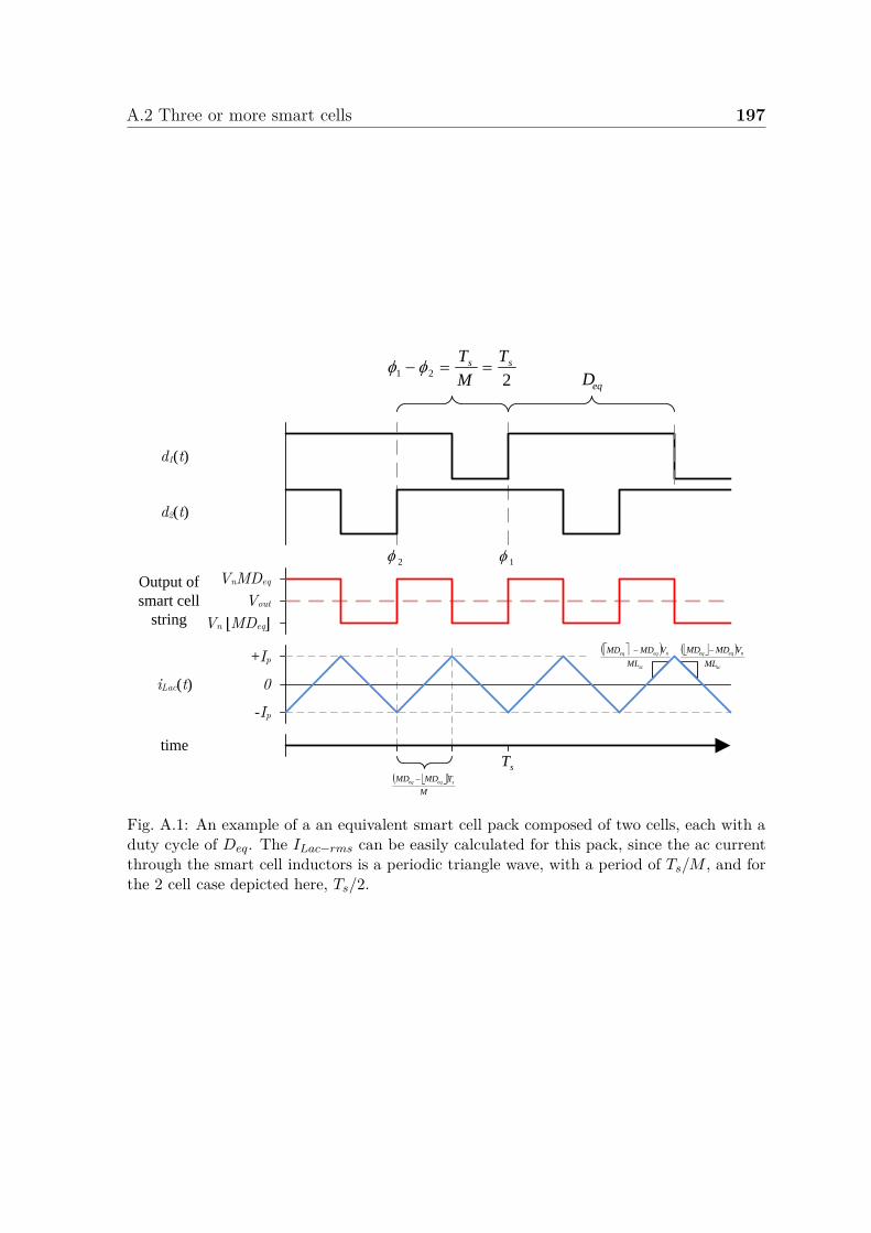
A.2 Three or more smart cells 197
sc
neqeq
ML
VMDMD
0
-Ip
+Ip
iLac(t)
VnMDeq
Vn ⌊MDeq⌋
Vout
Output of
smart cell
string
d1(t)
d2(t)
time
221
ss T
M
T
12
sT
eqD
M
TMDMD seqeq
sc
neqeq
ML
VMDMD
Fig. A.1: An example of a an equivalent smart cell pack composed of two cells, each with aduty cycle of Deq. The ILac−rms can be easily calculated for this pack, since the ac currentthrough the smart cell inductors is a periodic triangle wave, with a period of Ts/M , and forthe 2 cell case depicted here, Ts/2.


Appendix B
Smart cell code
This appendix describes all of the inputs to the smart cell controller function that was
used in the discrete time simulation results of Section 5.1.3, and in the experimental
hardware via MATLAB’s coder toolbox.
B.1 Simulink block diagram
Fig. B.1 shows the top level Simulink block diagram used in the three cell, discrete
time simulations of Section 5.1.3.The three dark green blocks represent each smart cell.
The electrical connections can be traced by following the +Vsc and -Vsc ports of each
smart cell block.
Fig. B.2 shows the Simulink block diagram of a smart cell, one of the dark green
blocks of Fig. B.1. The orange block, called SCKDCS1, contains the smart cell code,
implemented as a MATLAB function. The many inputs and outputs of this block are
used to fine tune the algorithm.
The yellow block, called Plot System Vectors, was used to visualize outputs of
the smart cell controller during the simulation. Fig. B.3 shows a screen shot of the
figure that is produces by all three of the Plot System Vectors blocks. The top row
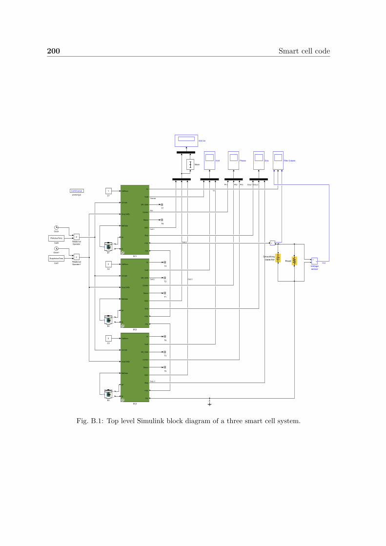
200 Smart cell code
FilterOutputs
v+-
Voltagesensor
+
Smoothingcapacitor
Continuous
powergui
i+ -
1
C1
2
C2
3
C3
Phases
Clock
RelationalOperator
PhActiveTime
Cell4
Vcell
Clock1
RelationalOperator1
DutyActiveTime
Cell1
SOCAll
T2
T3
+
Rload
Duty
Mean
+
_m
B1
+
_m
B2
+
_m
B3
T1
T5
T6
T7
T8
CellNum
CtrlEN
DutyCtrlEn
BatData
VL
Vcell
QH_Gate
Control
Status
SOC
DutyB+
B-
+Vsc
-Vsc
SC1
T4CellNum
CtrlEN
DutyCtrlEn
BatData
VL
Vcell
QH_Gate
Control
Status
SOC
DutyB+
B-
+Vsc
-Vsc
SC2
CellNum
CtrlEN
DutyCtrlEn
BatData
VL
Vcell
QH_Gate
Control
Status
SOC
DutyB+
B-
+Vsc
-Vsc
SC3
Vout
IL
VL
Cell1
Vsense
Ph1
Ph1 Duty1
Cell2
Cell2
Ph2 Duty2Ph3
Duty3
Cell3
Fig. B.1: Top level Simulink block diagram of a three smart cell system.
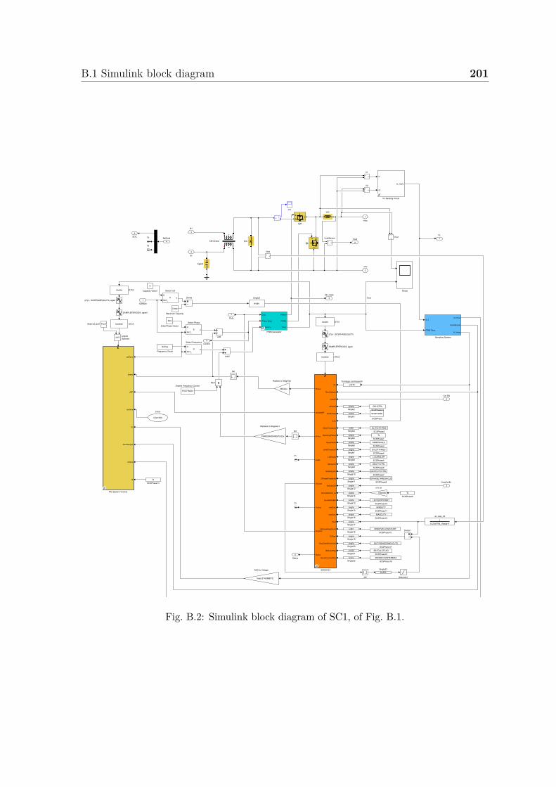
B.1 Simulink block diagram 201
VL1
PWMTimer
VLTime
NumSample
VLArray
SamplingSystem
g DS
QL
g
DS
QH
Isrc
i+ -
Divide
Cmax
MaximumCapacity
+
Lsc
U
Idx11YS
SelectCell
C
CapacityVector
Ph0
InitialPhaseVector U
Idx11YS
SelectPhase
v+ -
VLsc
Scope
Add
Duty
Phase(deg)
Frequency
PWMH
PWML
Timer
PWMGenerator
M0
+
Cgnd
+
Cin
12
++
CMChoke
U
Idx11YS
SelectFrequency
fsArray
FrequencyVector
v+-
V2
v+-
V1
V1
V2
VL_MCU
VLSensingCircuit
Vadc/2^NUMBITS
ADCtoVoltage
LogicalOperator
PLOTShallweplot1
double DTC3
boolean DTC4
cellNum
phase
vMP
simtime
VL
NumSample
VLtime
fs
PlotSystemVectors
0.0e+000
Clock
SAMPLEPERIOD/4,again
double DTC1
boolean DTC2
SAMPLEPERIOD/4,again1
360/2/pi
RadianstoDegrees
(2*pi-SCSPHASE)/2/pi*Ts
(2*pi-SCSPHASE)/2/pi*Ts,again
SCSPHASE
SCSPhase
singleSingle1
singleSingle2
single
Single3
uint16ToInteger,andbeyond!
int32Single4
singleSingle5
Ts
SCSPhase1
GLITCHTHRES
SCSPhase2M1
PHRESRADIANS/Ts/2/pi
RadianstoDegrees1
Add2
Mult
FSCTRLEN
EnableFrequencyControl
SAMPSCALE
SCSPhase3
singleSingle6
T1
v+-
VcellSensor
VL
NumSample
enable
GPhCtrl
SCSPhase
duty
GlitchThreshold
SwitchingPeriod
SampScale
DvldtThreshold
LvlSimilar
GDutyCtrl
GIntDutyCtrl
DPhaseThreshold
EnDutyCtrl
SamplePeriod_us
LevelRatioBat
minDuty
maxDuty
Vbat
MinLevelAvgCount
VLGain
DutyDeadZoneVolts
BatCalcFlag
SenseCounterMax
Phase
vectorsMP
dFreq
ncells
VcLocal
VcAvg
DutyOut
Status
SCKDCS1
T3
singleSingle7
singleSingle8
singleSingle9
singleSingle10
singleSingle11
DVLDTTHRES
SCSPhase4
LVLSIMILAR
SCSPhase5
GDUTYCTRL
SCSPhase6
GINTDUTYCTRL
SCSPhase7
DPHASETHRESHOLD
SCSPhase8
singleSingle12
singleSingle13
singleSingle14
singleSingle15
singleSingle16
singleSingle17
Ts
SCSPhase9
1000000
stous
LEVELRATIOBAT
SCSPhase10
MINDUTY
SCSPhase11
MAXDUTY
SCSPhase12
fs
SCSPhase14
1CellNum
2CtrlEN
3DutyCtrlEn
1VL
2Vcell
3QH_Gate
4Control
5Status
1
+Vsc
2
-Vsc
3
B+
4
B-
4BatData
int32Single18
singleSingle19
singleSingle20
uint32Single21
singleSingle22
MINLEVELAVGCOUNT
SCSPhase15
DUTYDEADZONEVOLTS
SCSPhase17
BATCALCFLAG
SCSPhase18
SENSECOUNTERMAX
SCSPhase19
v+-
Vbat
11/(2*pi*Ffilt_Vbat)s+1
ac_duty_filt
GPHCTRL
SCSPhase13
T4
T5
6SOC
7Duty
Divide1
doubleSingle23
M2 Saturation
Timer
Fig. B.2: Simulink block diagram of SC1, of Fig. B.1.
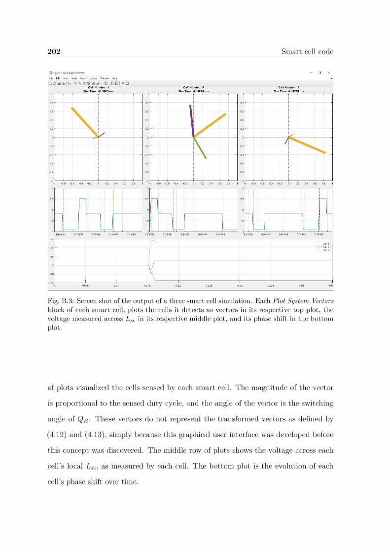
202 Smart cell code
Fig. B.3: Screen shot of the output of a three smart cell simulation. Each Plot System Vectorsblock of each smart cell, plots the cells it detects as vectors in its respective top plot, thevoltage measured across Lsc in its respective middle plot, and its phase shift in the bottomplot.
of plots visualized the cells sensed by each smart cell. The magnitude of the vector
is proportional to the sensed duty cycle, and the angle of the vector is the switching
angle of QH . These vectors do not represent the transformed vectors as defined by
(4.12) and (4.13), simply because this graphical user interface was developed before
this concept was discovered. The middle row of plots shows the voltage across each
cell’s local Lsc, as measured by each cell. The bottom plot is the evolution of each
cell’s phase shift over time.

B.2 Inputs and outputs 203
B.2 Inputs and outputs
The smart cell controller has many inputs, which are used to fine tune several aspects
of the controller, and many outputs, which are used for status and debugging purposes.
This section will explain each one in detail.
The function call looks like this:1 function [phase , dFreq , vectorsMP , f_ncells , VcLocal , VcAvg , duty_out , int32_Status ]
= SCSController (VL , NumSample , enable , duty , GPhCtrl , switchingPeriod , SCSPhase ,GlitchThreshold , SampScale , DvldtThreshold , LvlSimilar , GDutyCtrl , GIntDutyCtrl ,dphase_threshold , en_duty_ctrl , SamplePeriod_us , LevelRatioBat , minDuty , maxDuty ,
Vbat , VLGain , MinLevelAvgCount , DutyDeadZoneVolts , BatCalcFlag ,int32_SenseCounterMax )
B.2.1 Inputs
VL
An array of 16 bit unsigned integers from the ADC of the sampled voltage across Lsc.
The size of the array should be the same as MAXBUFF = 256, which is defined on line
23 of the function.
NumSample
A 32 bit integer that indicates the number of samples that were taken be the ADC.
enable
A boolean value that enables and disables the phase controller. Set to true to enable
the phase controller. Set to false to disable the phase controller.
duty
A float value between 0 and 1 that indicates the duty cycle that has been applied to
the switching network.

204 Smart cell code
GPhCtrl
A float value that corresponds to the gain of the phase controller.
switchingPeriod
A float value which defines the switching period in seconds.
SCSPhase
A float value which defines the phase angle between the rising edge of QH and the first
sample of the ADC, in radians. It is used to fine tune the timing between these two
events to ensure the phase controller timing is accurate. Normally set to (10/102) 2π.
GlitchThreshold
A 32 bit integer that indicates the number of samples after a switching event has
been detected that must be free of switching events before another switching event is
recorded. Normally set to 1.
SampScale
A float value which is used to fine tune the number of samples in a switching period,
and is used when calculating duty cycles and phase angles from the switching events.
Normally set to 0.997. Equation B.1 demonstrates its usage.
Di = abs ((Index of positive transition) − (Index of negative transition))NumSample · SampScale
(B.1)

B.2 Inputs and outputs 205
DvldtThreshold
A float value indicating the dVLsc/dt threshold at which to record a switching event.
The units are raw ADC values, and it is normally set to 192.
LvlSimilar
A float value indicating the minimum difference between two adjacent levels to ensure
that the adjacent levels are unique. The units are raw ADC values, and it is normally
set to 192.
GDutyCtrl
A float value used as the proportional gain of the SOC controller.
GIntDutyCtrl
A float value used as the integral gain of the SOC controller.
dphase_threshold
A float value indicating the maximum value of change in phase from the phase controller
that is permitted while the SOC controller is running. The state of charge controller
outputs a constant duty cycle when the change in phase from the phase controller is
larger than this value. It is normally set to 0.1.
en_duty_ctrl
A float value that enables and disables the SOC controller. Set to 1 to enable the SOC
controller. Set to 0 to disable the SOC controller.
206 Smart cell code
SamplePeriod_us
A float value of the sampling period. The units are µs. Normally set to 40/111.5, and
measured using the oscilloscope.
LevelRatioBat
A float value which determines the number of samples between switching events to
average. This average becomes the voltage values of that level. When LevelRatioBat
is less than 1, a ratio of the number of samples is used. For example, if LevelRatioBat
= 0.5, 0.5 × (the number of samples between two consecutive switching events) =
(the number of samples used in the average). When LevelRatiobat is greater than or
equal to 1, that many number of samples are used in the average. Normally set to 0.5.
minDuty
A float value between 0 and 1 that determines the minimum duty cycle that can be
output by the SOC controller.
maxDuty
A float value between 0 and 1 that determines the maximum duty cycle that can be
output by the SOC controller.
Vbat
A float value which is the voltage reading of the local battery cell. Units of volts.
VLGain
A float value which is the gain of the VLsc sensor. It is calculated outside of this
function, and is used to convert the raw ADC values to voltage value.

B.2 Inputs and outputs 207
MinLevelAvgCount
A 32 bit signed integer which indicates the minimum number of samples that must
have been averaged in order to consider a level measurement as valid. Normally set to
2.
DutyDeadZoneVolts
A float value which determines the dead zone used for the SOC controller. Units of
volts. When the difference between the local cell voltage and the average string voltage
is within ±DutyDeadZoneVolts, the error fed into the SOC controller is 0. Normally
set to 0.01.
BatCalcFlag
A 32 bit unsigned integer whose bits are used as flags to determine which level
measurements to use when calculating the voltage differences between levels. There
are two level measurements (or averages) for each level: 1) a “front” measurement,
and 2) a “back” measurement. The length of the front and back measurements are
the same, and are determined by LevelRatioBat. Fig. B.4 graphically illustrates the
front and back level for one of the levels of the VLsc waveform. Table B.1 lists what
the active bits control. All of the other bits are ignored. Normally set to 257.
int32_SenseCounterMax
A 32 bit signed integer used to indicate the maximum number of times the duty cycle
controller can execute without being able to make a good measurement. This is used
to adjust the time before a large step in duty cycle is introduced so that the SOC
controller can make voltage measurements on the string. Normally set to 12000, which
corresponds to about 2.5 minutes.

208 Smart cell code
Table B.1: Control bits of BatCalcFlag.
Bit Value Description9 1 If the transition is negative, use the front level calculation for the
level measurement before the transition.0 If the transition is negative, use the back level calculation for the
level measurement before the transition.8 1 If the transition is negative, use the front level calculation for the
level measurement after the transition.0 If the transition is negative, use the back level calculation for the
level measurement after the transition.1 1 If the transition is positive, use the front level calculation for the
level measurement before the transition.0 If the transition is positive, use the back level calculation for the
level measurement before the transition.0 1 If the transition is positive, use the front level calculation for the
level measurement after the transition.0 If the transition is positive, use the back level calculation for the
level measurement after the transition.
B.2.2 Outputs
phase
A float value which indicates the phase of the PWM module. Units of radians. Its
value is restricted to the closed interval [π, −π].
dFreq
A float value which can be added to the switching frequency to synchronize the clock
signals of all of the smart cells. Due to the relatively coarse sampling of the hardware
used in this thesis, this output was not used.
vectorsMP
A MAXBUFF × 2 array of floats which stores the weighted sum vectors, as described in
Section 4.2, of all of the smart cells detected in the last execution of the controller.
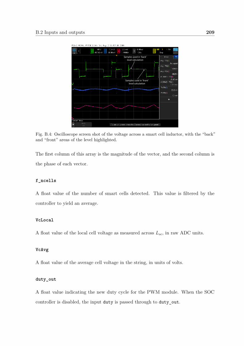
B.2 Inputs and outputs 209
Samples used in ‘back’ level calculation
Samples used in ‘front’ level calculation
Fig. B.4: Oscilloscope screen shot of the voltage across a smart cell inductor, with the “back”and “front” areas of the level highlighted.
The first column of this array is the magnitude of the vector, and the second column is
the phase of each vector.
f_ncells
A float value of the number of smart cells detected. This value is filtered by the
controller to yield an average.
VcLocal
A float value of the local cell voltage as measured across Lsc, in raw ADC units.
VcAvg
A float value of the average cell voltage in the string, in units of volts.
duty_out
A float value indicating the new duty cycle for the PWM module. When the SOC
controller is disabled, the input duty is passed through to duty_out.

210 Smart cell code
int32_Status
A 32 bit integer indicating the status of the SOC controller. The possible values and
their meanings are summarized in Table B.2.
Table B.2: Summary of int32_Status values.
Value Description0 Successful execution of the SOC controller.1 Local cell voltage is out of expected range.2 Only the turn on time of the local cell was found, and used to
calculate the local value.3 Only the turn off time of the local cell was found, and used to
calculate the local value.4 Neither the turn on or turn off time of the local cell was found.5 dphase_threshold is exceeded.6 BV_weight = 0, the weight attributed to the local cell.7 There are too many zero weights, cannot compute the average
cell voltage.8 f_AvgBatVoltsWeights == 0.9 Only the turn on time of the local cell was found, but the gain
was zero, or multiple transitions occurred.10 Only the turn off time of the local cell was found, but the gain
was zero, or multiple transitions occurred.11 Both transition were found, but only the turn on transition can
be used.12 Both transitions were found, but only the turn off one can be
used.