
All-optical 4-bit Gray code to binary coded decimal converter
10
All-optical 4-bit Gray code to binary coded decimal converter Young Jin Jung* a , Seok Lee b , Namkyoo Park a a Dept. of EECS, Seoul Nat’l Univ. / Seoul, Korea, 151-742; b Korea Institute of Science and Technology / Seoul, Korea, 130-791 ABSTRACT All-optical 4-bit Gray code to binary coded decimal (BCD) converter was demonstrated, for the first time in our knowledge, with the number of 12 SOAs by means of commercially available numerical analysis tool (VPI). Circuit design approach was modified appropriately in order to fit the electrical method on an all-optical logic circuit based on cross gain modulation (XGM) process so that signal degradation due to the non-ideal optical logic gates can be minimized. In our approach, only using XGM process as a nonlinear function, the maximum number of XGM process serially underwent by input signals is twice at the most insuring signal quality. Without regenerations, Q-factor of around 4 was obtained for the most severely degraded output bit (least significant bit - LSB) with 2.5Gbps clean input signals having 20dB extinction ratio. It is worth to note that, implementing this LSB is complex enough to give it as an example of a 4-bit conversion system. While modifying two-level simplification method and Karnaugh map method to design Gray code to BCD converter, general design concept was also founded in this research not only for the Gray code to BCD converter but also for any general applications such as encoder / decoder, multiplexer / demultiplexer, and read only memory so that readers can develop their own all-optical logic device easily using XGM process in SOAs. Keywords: all optical converter, binary coded decimal, combinational logic circuit, cross gain modulation, gray code, one level simplification method, semiconductor optical amplifier, two level simplification method 1. INTRODUCTION All optical signal processing has attracted attention for a long time and various all optical Boolean logic gates has been implemented [1, 2, 3, 4, 5, 6] by means of cross phase modulation (XPM; employing Nonlinear Optical Loop Mirror [7], Terahertz Optical Asymmetric Demultiplexer [8], Mach-Zehnder Interferometer, Ultrafast Nonlinear Interferometer [9]) cross gain modulation (XGM), four wave mixing and Kerr effect at high-Q cavity. Even though there are some demonstrated combinational (memory-less) logic circuit such as adder and subtractor [10, 11, 12], more complex all optical combinational logic circuit has not been reported yet. Because, it is still hard to implement complex combinational logic circuit all-optically by the reasons of many problems which are arose due to large system scale and non-ideal all optical logic gate elements. For example, accumulations of noise and extinction ratio degradation can prevent implementation of complex all optical combinational logic circuits. Thus, study on implementation of more complex all optical combinational logic circuits such as coder / decoder should be done. All-optical Gray code to binary coded decimal (BCD) which has not been demonstrated yet seems complex enough to study for this issues as a kinds of coder / decoder system (BCD to Gray code is much easier to implement). BCD is an encoding for decimal numbers in which each digit is represented by its own binary sequence and Gray code is another binary numeral system where two successive values differ in only one digit. In this paper, first of all, studies are carried out about implementation of an all-optical 4-bit Gray code to BCD converter directly employing digital electronic method termed as NOR-NOR two-level simplification method. It should be noted that whole demonstrations in this paper are made by logic gates based on XGM process. This is because its simplicity makes circuit implementation much easier though its performance is worse than that of the case based on XPM when it comes to operation speed and extinction ratio. It is possible to construct circuit utilizing only XGM process because all of the Boolean logic gates can be implemented all-optically by means of XGM in semiconductor optical amplifiers (SOAs). Secondly, one-level simplification method is proposed which is well-fitted on the optical circuit. Third, we implement an all-optical 4-bit Gray code to BCD converter utilizing above proposed one-level simplification method. Fourth, comparisons between two-level simplification method and one-level simplification method are provided with results and additional issues associated with one-level simplification method are discussed. Optical Components and Materials V, edited by Michel J. F. Digonnet, Shibin Jiang, John W. Glesener, J. Christopher Dries Proc. of SPIE Vol. 6890, 68900S, (2008) · 0277-786X/08/$18 · doi: 10.1117/12.762429 Proc. of SPIE Vol. 6890 68900S-1
-
Upload
khangminh22 -
Category
Documents
-
view
1 -
download
0
Transcript of All-optical 4-bit Gray code to binary coded decimal converter

All-optical 4-bit Gray code to binary coded decimal converter
Young Jin Jung*a, Seok Leeb, Namkyoo Parka
aDept. of EECS, Seoul Nat’l Univ. / Seoul, Korea, 151-742; bKorea Institute of Science and Technology / Seoul, Korea, 130-791
ABSTRACT
All-optical 4-bit Gray code to binary coded decimal (BCD) converter was demonstrated, for the first time in our knowledge, with the number of 12 SOAs by means of commercially available numerical analysis tool (VPI). Circuit design approach was modified appropriately in order to fit the electrical method on an all-optical logic circuit based on cross gain modulation (XGM) process so that signal degradation due to the non-ideal optical logic gates can be minimized. In our approach, only using XGM process as a nonlinear function, the maximum number of XGM process serially underwent by input signals is twice at the most insuring signal quality. Without regenerations, Q-factor of around 4 was obtained for the most severely degraded output bit (least significant bit - LSB) with 2.5Gbps clean input signals having 20dB extinction ratio. It is worth to note that, implementing this LSB is complex enough to give it as an example of a 4-bit conversion system. While modifying two-level simplification method and Karnaugh map method to design Gray code to BCD converter, general design concept was also founded in this research not only for the Gray code to BCD converter but also for any general applications such as encoder / decoder, multiplexer / demultiplexer, and read only memory so that readers can develop their own all-optical logic device easily using XGM process in SOAs.
Keywords: all optical converter, binary coded decimal, combinational logic circuit, cross gain modulation, gray code, one level simplification method, semiconductor optical amplifier, two level simplification method
1. INTRODUCTION All optical signal processing has attracted attention for a long time and various all optical Boolean logic gates has been implemented [1, 2, 3, 4, 5, 6] by means of cross phase modulation (XPM; employing Nonlinear Optical Loop Mirror [7], Terahertz Optical Asymmetric Demultiplexer [8], Mach-Zehnder Interferometer, Ultrafast Nonlinear Interferometer [9]) cross gain modulation (XGM), four wave mixing and Kerr effect at high-Q cavity. Even though there are some demonstrated combinational (memory-less) logic circuit such as adder and subtractor [10, 11, 12], more complex all optical combinational logic circuit has not been reported yet. Because, it is still hard to implement complex combinational logic circuit all-optically by the reasons of many problems which are arose due to large system scale and non-ideal all optical logic gate elements. For example, accumulations of noise and extinction ratio degradation can prevent implementation of complex all optical combinational logic circuits. Thus, study on implementation of more complex all optical combinational logic circuits such as coder / decoder should be done. All-optical Gray code to binary coded decimal (BCD) which has not been demonstrated yet seems complex enough to study for this issues as a kinds of coder / decoder system (BCD to Gray code is much easier to implement). BCD is an encoding for decimal numbers in which each digit is represented by its own binary sequence and Gray code is another binary numeral system where two successive values differ in only one digit.
In this paper, first of all, studies are carried out about implementation of an all-optical 4-bit Gray code to BCD converter directly employing digital electronic method termed as NOR-NOR two-level simplification method. It should be noted that whole demonstrations in this paper are made by logic gates based on XGM process. This is because its simplicity makes circuit implementation much easier though its performance is worse than that of the case based on XPM when it comes to operation speed and extinction ratio. It is possible to construct circuit utilizing only XGM process because all of the Boolean logic gates can be implemented all-optically by means of XGM in semiconductor optical amplifiers (SOAs). Secondly, one-level simplification method is proposed which is well-fitted on the optical circuit. Third, we implement an all-optical 4-bit Gray code to BCD converter utilizing above proposed one-level simplification method. Fourth, comparisons between two-level simplification method and one-level simplification method are provided with results and additional issues associated with one-level simplification method are discussed.
Optical Components and Materials V, edited by Michel J. F. Digonnet, Shibin Jiang, John W. Glesener, J. Christopher DriesProc. of SPIE Vol. 6890, 68900S, (2008) · 0277-786X/08/$18 · doi: 10.1117/12.762429
Proc. of SPIE Vol. 6890 68900S-1

8
T 0 UT
r T 0 TTJD GL
0 T 0 TO
0 T 0 00
UT TT TO 00
c-i
x
'I X X 0 0 UT 1
r 0 0 TT JD GL
x T 0 0 TO
X T 0 0 00
UT TT TO 00
c-i V
M
C-)
-K
—I—
01
0 °i
— _I
0 H
-H
—I—
2
DD
L
cC-
C)
NJ
——
Ic ci
0
——
2. DESIGN WITH TWO-LEVEL SIMPLIFCATION METHOD The design procedure of Gray code to BCD converter with two-level simplification using electronic components is well known in the fields of digital electronics and also it is described well in many electronic textbooks [13]. To design gray code to BCD converter with optical components brief illustration of a part of well known design procedures developed for electronics are presented especially which can be used for the optical design. And then details are explored about design considerations arisen by using optical components.
2.1 Digital electronic theory for all-optical Gray code to BCD converter
In our design, NOR-NOR two-level simplification method will be chosen due to its simplicity of optical structure and ability of accepting multiple input ports as will be described later. To do this, first of all, Karnaugh map [14] was drawn as it is shown in the Fig. 1 with the truth table shown in the Table 1. Above the decimal number of ‘9’ was designated as ‘Don’t care condition’ which means that user don’t care whether the output value of the system becomes 1-velvel or 0-level [13]. And, each bit of the 4-bit Gray code is labeled as “A” to “D” starting from the MSB (most significant bit) to the LSB (least significant bit) and each bit of the BCD is labeled as “W” to “Z” starting from the MSB to the LSB.
Table 1. Truth table for the Gray code to BCD converter
Gray Code BCDDecimal A B C D W X Y Z
0 0 0 0 0 0 0 0 0 1 0 0 0 1 0 0 0 1 2 0 0 1 1 0 0 1 0 3 0 0 1 0 0 0 1 1 4 0 1 1 0 0 1 0 0 5 0 1 1 1 0 1 0 1 6 0 1 0 1 0 1 1 0 7 0 1 0 0 0 1 1 1 8 1 1 0 0 1 0 0 0 9 1 1 0 1 1 0 0 1 10 X X X X X X X X 11 X X X X X X X X 12 X X X X X X X X 13 X X X X X X X X 14 X X X X X X X X 15 X X X X X X X X
Fig. 1. Karnaugh map for the NOR-NOR two-level simplification method to design Gray code to BCD converter
Proc. of SPIE Vol. 6890 68900S-2

A B CD
7 :NOTgate
NOR gate
wx
y
z
From the above drawn Karnaugh map two-level simplified Boolean equation was obtained as product of sums (AND of OR) form for the each output as the Eq. 1.
AW = (1a)
BAX = (1b)
))(( CBCBAY ++= (1c)
))()()()(( DCBDCBDCBADCADCBZ +++++++++++= (1d)
Then, NOR-NOR two-level simplified Boolean equation can be obtained as the Eq. 2 by utilizing DeMorgan’s theorem [13] from the Eq. 1.
AW = (2a)
BAX += (2b)
)()( CBCBAY ++++= (2c)
)()()()()( DCBDCBDCBADCADCBZ +++++++++++++++= (2d)
From the Eq. 2 schematic circuit was obtained with NOT and NOR gates as in the Fig. 2.
Fig. 2. Schematic diagram of designed Gray code to BCD converter utilizing the NOR-NOR two-level simplification
method.
Proc. of SPIE Vol. 6890 68900S-3

0 flock
B ABC
Ack0CB
ABC
A OR
B—A+B+C -_LAff1jn(B)=A+B+ B + C
A—flO4t Clock-A tABC-tEkBA+B+C Bck
BC Clock to.
Clockz
V
.ç-e Bp.x
2.2 All-optical implementation
In order to implement this circuit with optical components, all-optical NOT and NOR gates are required. As we know the NOT gate has the simplest structure thus we did not show its structure. And, other type of all-optical logic gates that accept three input port were constructed in the Fig. 3 (a) to show their complexity. As we mentioned earlier NOR-gates have the simplest structure in general while it is accepting multiple input-port as you can see in the Fig. 3 (a). Also it should be noted that a NOR gate can be constructed using a single SOA [6] for multiple input ports whereas two SOAs are required for the construction of AND [1], OR [3], XOR [4], or NAND gates [5] even for two input ports. That is the reason why NOR-NOR two-level simplification is the most suitable for all-optical implementation among various method (There are other ways to construct combinational logic circuits such as AND-OR or OR-NOR or NAND-NAND two-level simplification method [13]).The above designed structure for the all-optical Gray code to BCD converter was constructed all optically as Fig. 3 (b) directly using all optical NOR gates shown in the Fig. 3 (a) as the basic building block.
Fig. 3. (a) Structures of various all-optical logic gates accepting three input ports utilizing XGM in SOAs. (b) Designed
Structure for all-optical Gray code to BCD converter utilizing NOR-NOR two-level simplification method
3. PROPOSAL OF ONE-LEVEL SIMPLIFCATION METHOD Here the one-level simplification method which is more suitable to the all-optical circuit is proposed. Details are described with an example for arbitrary functional system in which output is obtained corresponding to the input combination of signal A, B, and C as shown in Table 2 (Boolean operation of CBAF )( += ).
Table 2. Truth table for arbitrary functional system that will be used to illustrate one-level simplification method as an example
A 0 0 0 0 1 1 1 1
B 0 0 1 1 0 0 1 1 Input
C 0 1 0 1 0 1 0 1
Output F 0 0 0 0 1 1 1 0
(a) Various all optical logic gates (b) Designed all-optical Gray code to BCD converter
Proc. of SPIE Vol. 6890 68900S-4

C
ThRB CC
A-Q-ji- Clock
C ci 1AJ—. F
A B C
F
AABB CC Power sum
When this arbitrary example (Boolean operation of CBAF )( += ) is designed utilizing conventional NOR-NOR two-level simplification method, procedure is same as above described Gray code to BCD converter. And its implementation was shown in the Fig. 4 (a) with an eye diagram result for given SOA parameters set of Table 3. After optimization of XGM process in SOAs the Q factor of around 3.8 was observed with the 20dB extinction ratio input RZ signal at 2.5Gbps (To focusing on the theory of one-level simplification method, detail optimization process is skipped and will be presented in the next chapter).
Now in order to reduce the number of logic gate cascades (so that accumulation of signal quality degradation can be suppressed), the conventional two-level simplification was modified as one-level to best corresponds to the properties of all-optical logic circuits. The Fig. 4 (b) shows implementation of the system with the one-level simplification method and an eye diagram result shows Q factor improvement resulting in the value of around 5. Design procedure is summarized as follow:
(A) Draw a Karnaugh map for the given operation/truth table.
(B) Follow the conventional AND-OR two-level simplification procedure to draw a digital circuit while avoiding the symbol selection overlaps (i.e., avoid “1” OR “1” in the Karnaugh map) [14].
(C) Substitute the OR gates with optical power sums. Further, convert the AND gates to NOR by utilizing DeMorgan’s theorem [13].
In step (B), it should be noted that two or more input symbols “1” entering the OR gates at the same time can be prevented by removing the selection overlaps. The OR gates thereby can be safely replaced by simple optical power sums. Then, signal degradation can be efficiently reduced by removing non-ideal optical element level in the circuit while make it simple to implement.
Table 3. SOA Parameters for numerical simulation
Fig. 4. Comparison of (a) conventional two-level simplification method and (b) proposed one-level simplification method
structures and their performances. RZ signals were assumed to be 2.5 Gbps.
Name Value Name value Driving current 200 mA Transparent carrier density 1.5 × 1024 m–3 Active region length 350 �m Material gain coefficient 3 × 10–20 m2 Active region width 2.5 �m Internal loss 3,000 m–1 Active region thickness 0.04�m Group effective index 3.7 ASE spectral width 1 THz Facet reflectivity 0.0001
00 01 11 10
0 0 0 1 1
1 0 0 0 1
(a) Conventional method (two-level simplification) (b) Proposed one-level simplification method
CBA
CBA
CABAF
++=
+=
+=
)( DeMorgan’stheorem
)()(
)()(
CAsumCBA
CAsumCBA
CACBAF
+++=
=
+= ‘OR’ can be substituted
DeMorgan’stheorem
Karnaugh Map
C A
B
AB
Karnaugh Map
00 01 11 10
0 0 0 1 1
1 0 0 0 1
CA
B
AB
Power sum
Proc. of SPIE Vol. 6890 68900S-5

C-)
—00
o 0
o o
0 0
o 0
0 0
2
cC-
C)
><
—00
o 0
o o
0 0
wE
H
—
—H
2 kk
oo
cC-
C-)
-K
—I—
01
0 °I
— I°
W
°H
C)
NJ
—I—
Ic
c
k k
H k
cC-
As you can see in the Fig. 4, in the one-level simplification method, the NOR gate cascade in the structure of conventional two-level simplification method is replaced with just NOR gate structure avoiding the ER penalty accumulation in SOA cascades. It can be observed form the designed optical circuit that it is possible to construct same system with the reduced number of NOR cascades with a better eye (and also better extinction) for the final data. It should be noted that for any type of combinational logic circuit, the maximum number of XGM cascades required in the one-level simplification method and two-level simplification method are two and three, respectively. It is also worth to mention that any general applications such as encoder / decoder, multiplexer / demultiplexer, and read only memory are suitable to this proposed one-level simplification method.
4. DESIGN WITH ONE-LEVEL SIMPLIFICATION METHOD Following above mentioned step (A) and (B), first of all, Karnaugh map [14] was drawn as it is shown in the Fig. 5 with the truth table shown in the Table 1. And symbols were selected carefully without overlap differently against the conventional two-level simplification method.
Fig. 5. Karnaugh map for the one-level simplification method to design Gray code to BCD converter
From the above drawn Karnaugh map two-level simplified Boolean equation was obtained as sum of products (OR of AND) for the each output as the Eq. 3.
AW = (3a)
BAX = (3b)
CBCBAY += (3c)
DCBDCABCDDCBADCBAZ ++++= (3d)
Then, following step (C), the OR gate was converted as the optical power sum and this yield following Eq. 4.
AW = (4a)
BAX += (4b)
)()( CBsumCBAY = (4c)
)()()()()( DCBsumDCAsumBCDsumDCBAsumDCBAZ = (4d)
Proc. of SPIE Vol. 6890 68900S-6
A
:NOTgate
NOR gate
w
Y
z
A —t!2__. xw
z
Further, AND operation in Eq. 4 was converted as NOR operation by utilizing DeMorgan’s theorem [13] as the Eq. 5.
AW = (5a)
)( BAX += (5b)
)()( CBsumCBAY +++= (5c)
)()()()()( DCBsumDCAsumDCBsumDCBAsumDCBAZ ++++++++++++= (5d)
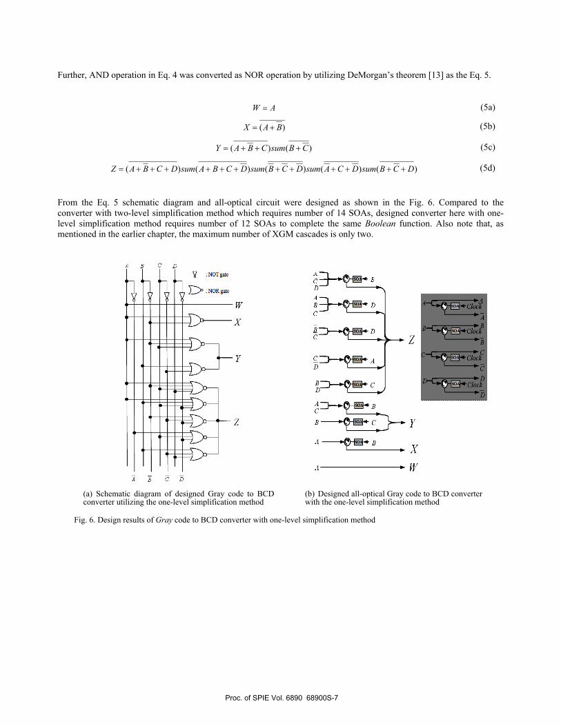
From the Eq. 5 schematic diagram and all-optical circuit were designed as shown in the Fig. 6. Compared to the converter with two-level simplification method which requires number of 14 SOAs, designed converter here with one-level simplification method requires number of 12 SOAs to complete the same Boolean function. Also note that, as mentioned in the earlier chapter, the maximum number of XGM cascades is only two.
Fig. 6. Design results of Gray code to BCD converter with one-level simplification method
(a) Schematic diagram of designed Gray code to BCD converter utilizing the one-level simplification method
(b) Designed all-optical Gray code to BCD converterwith the one-level simplification method
Proc. of SPIE Vol. 6890 68900S-7

j w
Time Ens]
-
A
F ems r Em mi]
—
i:T£Wi Wi W
5. RESULTS The XGM process should be optimized to evaluate designed all-optical Gray code to BCD converter. Attenuators and EDFAs were used even it was not shown in Fig. 3 and Fig. 6 to optimize the power levels of the propagating signals for an efficient XGM process, which is in general dependent on the signal power level, pulse shape, and SOA injection current [15]. Optimal condition could be found as following. First of all, we employed RZ signal format (RZ signal format is generally faster than NRZ format in the application of optical logic gates based on XGM process [6]. This is because guard time for the carrier recovery can be guaranteed with RZ. And also note that RZ signal has the advantage of hiding static “1” hazard compared to NRZ signal). And RZ signal pulse width was set ~ 30% of the bit duration. And signal power level was determined utilizing the steady state response data of XGM process. In our whole simulations SOA parameters were also set as same with the Table 3. Based on the steady state in Fig. 7 (a), (b) and (c), we used the pump power of -10dBm (0-level) & 10dBm (1-level), together with the probe input power of -20dBm (0-level) & 0dBm (1-level) to get the wide open eyes. And then, SOA driving current was adjusted to control the carrier lifetime referring to the dynamic response of XGM process shown in Fig. 7 (d). We selected 200mA as an injection current for the operation speed of 2.5Gbps.
Fig. 7. Steady state (a), (b), (c) and dynamic (d) response of XGM characteristics of given SOA
-20 -10 0 10 200
10
20
30
40
350µm, 100mA
Pro
be O
utpu
t (m
W)
Pump Power(dBm)
Probe Input 10dBm 0dBm -10dBm -20dBm
-20 -10 0 10 200
10
20
350µm, 50mA
Pro
be O
utpu
t (m
W)
Pump Power(dBm)
Probe Input 10dBm 0dBm -10dBm -20dBm
(a) Steady state response with 50mA i j i
Time (ns/div)
Pow
er (a
u.)
(b) Steady state response with 100mA
(c) Steady state response with 200mA
-20 -10 0 10 200
102030405060708090
350µm, 200mA
Pro
be O
utpu
t (m
W)
Pump Power(dBm)
Probe Input 10dBm 0dBm -10dBm -20dBm
(d) Dynamic response with 200mA
Proc. of SPIE Vol. 6890 68900S-8

Decima' Dl 23 45 67 BY
A
Gray BCode C
D
DO DO 00 00 II0 0 0 I I I I I I
0 I I I I 0 0 0DI ID DI ID DI
wxBCD,z
DO DO DO DO II00 00 II II DOo I I 0 I I 0DI DI DI DI DI
Output data traces (Fig. 8 (c), (d)) of the Gray code to BCD converter are shown in the Fig. 8 for the 2.5Gbps input signals (Fig. 8 (b)) which are injecting serially form decimal numbers “0” to “9” in Gray code expression (A higher operation speed would be possible with a shorter active region length or higher bias current [16]). Eye-diagrams are also shown in Fig. 8 (e) for the input patterns of 27–1 PRBS (pseudo-random bit sequence) while each input of “A”, “B”, “C” and “D” takes the different seed values for the generation of PRBS.
From the eye-diagrams for random input sequence of Gray code, bit pattern effects could be considered. As you can see in the Fig. 8, more clear output is observed with one-level simplification method. In contrast, severe degradation can be observed form the data in the case of the two-level simplification method approach. The measured Q factors were 7, 7, and 4 for each output of X, Y, and Z, respectively in the case of the one-level simplification method and 7, 2.8, and 2.4 in the case of the two-level simplification method.
Fig. 8. Data traces and eye diagrams of the Gray code to BCD converter constructed using the conventional two-level
simplification method and proposed one-level simplification method
(b) Input - gray code
(c) Output - BCD with two-level (d) Output - BCD with one-level
(e) Eye diagrams of converter outputs
Two-
leve
l O
ne-le
vel
(a) Truth table
05 0 05
0 1 2 3 4
0.0
0.0
0.0
0.0
T im e (n s)
A
B
C
D
0 1 2 3 4
0.0
0.0
0.0
0.0
T im e (n s)
W
X
Y
Z
0 1 2 3 4
0.0
0.0
0.0
0.0
T im e (n s)
W
X
Y
Z
W X Y Z
W X Y Z
Proc. of SPIE Vol. 6890 68900S-9

6. CONCLUSION All-optical Gray code to BCD converter has been numerically constructed for the first time utilizing our proposed photonic-specific one-level simplification method developed from the conventional two-level simplification method used in the fields of digital electronics. We have proven that proposed one-level simplification method show better performances even reducing circuit complexity. Numerical assessment results for the Gray code to BCD converter show that the Q factor of above 4 can be obtained for the input signals having 20dB extinction ratio at 2.5Gbps. This research has guided readers to design all-optical combinational logic circuits so that anyone can construct any types of all-optical combinational logic circuits by presenting the detail process of designing the Gray code go BCD converter.
REFERENCES
1. J. H. Kim, B. C. Kim, Y. T. Byun, Y. M. Jhon, S. Lee, D. H. Woo, and S. H. Kim, “All-optical AND gate using cross-gain modulation in semiconductor optical amplifiers,” Japanese J. Appl. Physics, 43(2), 608-610 ( 2004).
2. Zhi-Hong Zhu, Wei-Min Ye, Jia-Rong Ji, Xiao-Dong Yuan, Chun Zen, "High-contrast light-by-light switching and AND gate based on nonlinear photonic crystals", Optics Express,14(5), 1783-1788 (2006 ).
3. Y. T. Byun, K. S. Choi, Y. M. Jhon, D. H. Woo, S. Lee, S. H. Kim, and J. W. Park, “All-optical OR gate using cross gain modulation in semiconductor optical amplifier,” CLEO Europe, pp. 493, June. 2005..
4. J. H. Kim, Y. M. Jhon, Y. T. Byun, S. Lee, D. H. Woo, and S. H. Kim, “All-optical XOR gate using semiconductor optical amplifiers without additional input beam,” IEEE Photonics Technology Letters, 14(10), 1436-1438 (2002).
5. S. H. Kim, J. H. Kim, B. G. Yu, Y. T. Byun, Y. M. Jeon, S. Lee, D. H. Woo, and S. H. Kim, “All-optical NAND gate using crossgain modulation in semiconductor optical amplifiers,” IEE Electronics Letter, 41(18), 1027-1028 (2005).
6. Y. T. Byun, J. H. Kim, Y. M. Jhon, S. Lee, D. H. Woo, and S. H. Kim, “High-speed all-optical NOR gate using semiconductor optical amplifier,” CLEO Europe, pp. 536, Jun. 2003.
7. N. J. Doran and David Wood, "Nonlinear-optical loop mirror", Optics Letter 13(1), 56-58 (1988). 8. J. P. Sokoloff, P. R. Prucnal, I. Glesk, and M. Kane, "A Terahertz Optical Asymmetric Demultiplexer (TOAD)",
IEEE Photonics Technology Letters, 5(7), 787-790 (1993). 9. N. S. Patel, K. A. Rauschenbach, and K. L. Hall, "40-Gb/s Demultiplexing Using an Ultrafast Nonlinear
Interferometer (UNIT)", IEEE Photonics Technology Letters, 8(12), 1695- 1697 (1996). 10. A.J. Poustie , K.J. Blow, A.E. Kelly, R.J. Manning, "All-optical full adder with bit-differential delay", Optics
Communications 168, 89-93 (1999). 11. Jitendra Nath Roy and Dilip Kumar Gayen, "Integrated all-optical logic and arithmetic operations with the help of a
TOAD-based interferometer device—alternative approach" Applied Opitcs, 46(22), 5304-5310 (2007). 12. S. H. Kim, J. H. Kim, J. W. Choi, C. W. Son, Y. T. Byun, Y. M. Jhon, S. Lee, D. H. Woo, and S. H. Kim, “All-
optical half adder using cross gain modulation in semiconductor optical amplifiers,” Optics Express, 14(22), 10693-10698 (2006).
13. R. H. Katz and G. Borriello, Contemporary Logic Design, 2nd ed. Prentice Hall, 1993. 14. M. Karnaugh, “The map method for synthesis of combinational logic circuits,” AIEE Trans., 72(part I), 593-598
(1953). 15. Y. J. Jung, J. Park, and N. Park, “Wavelength-transparent nonlinear optical gate based on self-seeded gain
modulation in folded tandem-SOA,” Optics Express, 15(8), 4929-4934 (2007). 16. F. Girardin, G. Guekos, and A. Houbavlis, “Gain recovery of bulk semiconductor optical amplifiers,” IEEE
Photonics Technology Letters, 10(6), 784-786 (1998).
Proc. of SPIE Vol. 6890 68900S-10