
Al Imam Mohammad Ibn Saud Islamic University College of ...
127
Al Imam Mohammad Ibn Saud Islamic University College of Engineering Department of Electrical Engineering Communication -1 Lab –EE 452
-
Upload
khangminh22 -
Category
Documents
-
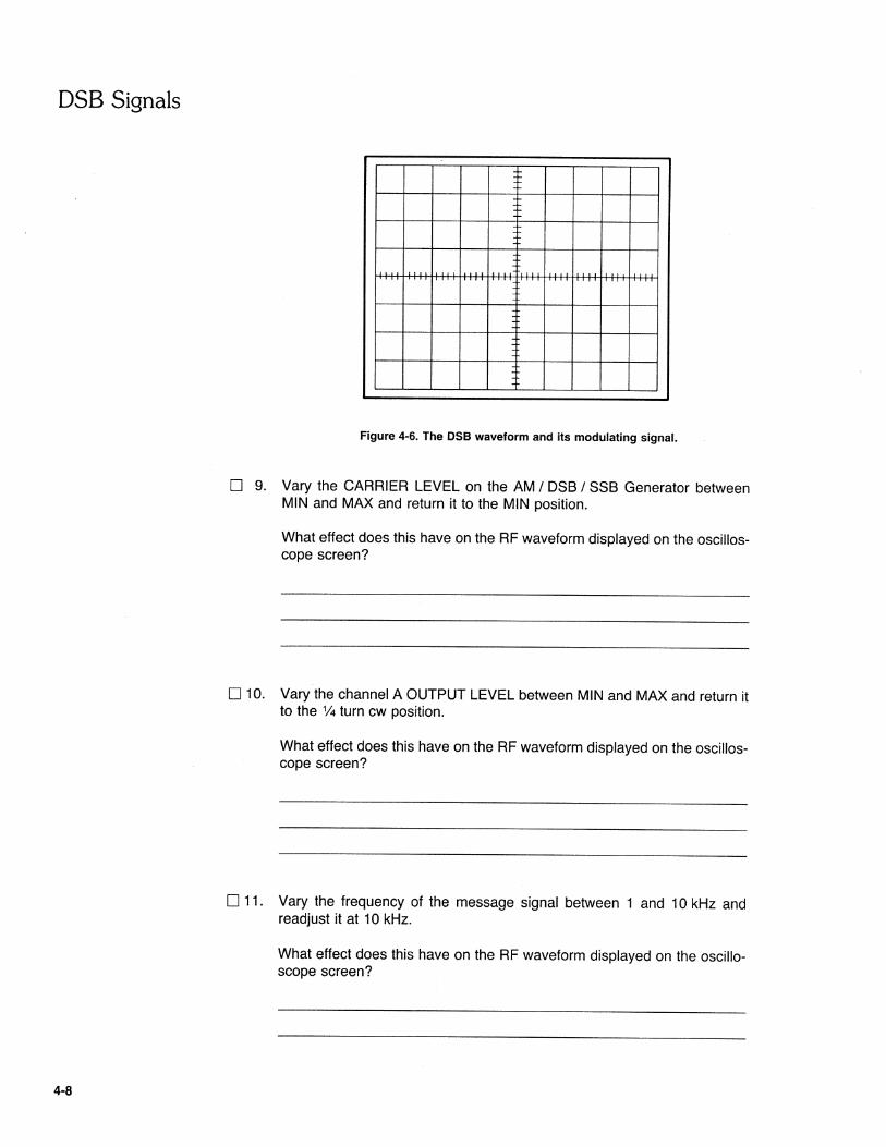
view
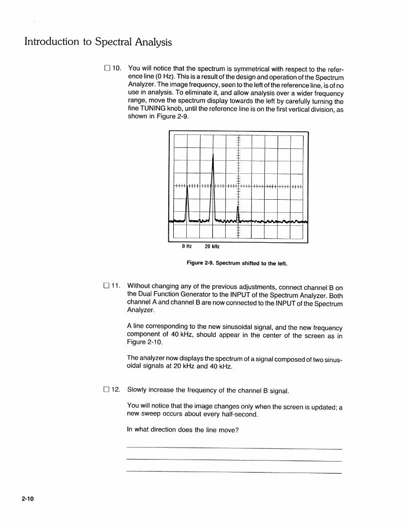
1 -
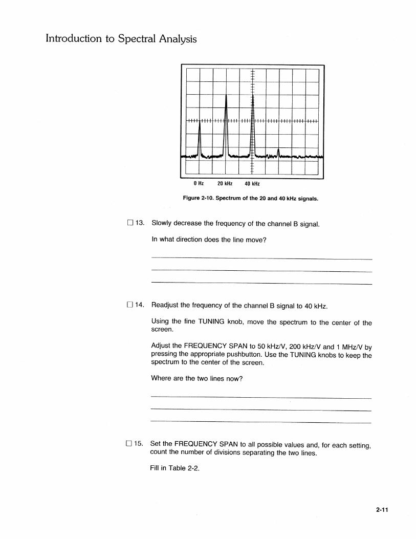
download
0
Transcript of Al Imam Mohammad Ibn Saud Islamic University College of ...

Al Imam Mohammad Ibn Saud Islamic University
College of Engineering
Department of Electrical Engineering
Communication -1 Lab –EE 452
Al Imam Mohammad Ibn Saud Islamic University
College of Engineering
Department of Electrical Engineering
EE 452
Communication 1 Lab
Experiment # 1
“ Introduction to Spectral Analysis”


Al Imam Mohammad Ibn Saud Islamic University
College of Engineering
Department of Electrical Engineering
EE 452
Communication 1 Lab
Experiment # 2
“ Generation of AM Signals”


Al Imam Mohammad Ibn Saud Islamic University
College of Engineering
Department of Electrical Engineering
EE 452
Communication 1 Lab
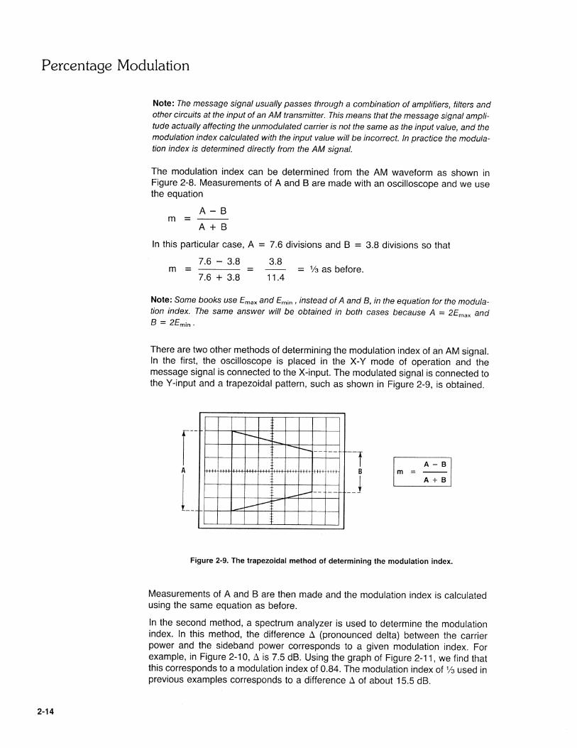
Experiment # 3
“ Percentage Modulation”


Al Imam Mohammad Ibn Saud Islamic University
College of Engineering
Department of Electrical Engineering
EE 452
Communication 1 Lab
Experiment # 4
“ Reception of AM Signals”


Al Imam Mohammad Ibn Saud Islamic University
College of Engineering
Department of Electrical Engineering
EE 452
Communication 1 Lab
Experiment # 5
“ Double side band Modulation”


Al Imam Mohammad Ibn Saud Islamic University
College of Engineering
Department of Electrical Engineering
EE 452
Communication 1 Lab
Experiment # 6
“ Generation of FM Signal”


Al Imam Mohammad Ibn Saud Islamic University
College of Engineering
Department of Electrical Engineering
EE 452
Communication 1 Lab
Experiment # 7
“ Reception of FM Signal”


Al Imam Mohammad Ibn Saud Islamic University
College of Engineering
Department of Electrical Engineering
EE 452
Communication 1 Lab
Introduction to FACET Board
iii
Introduction
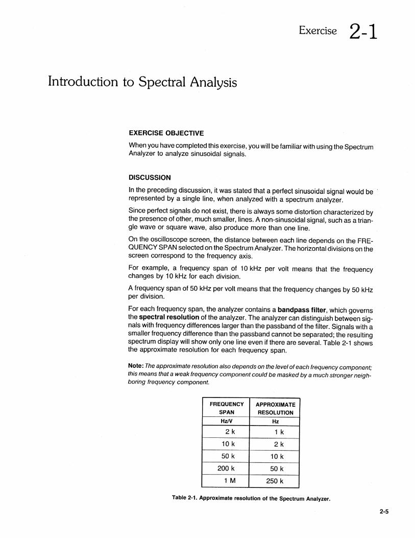
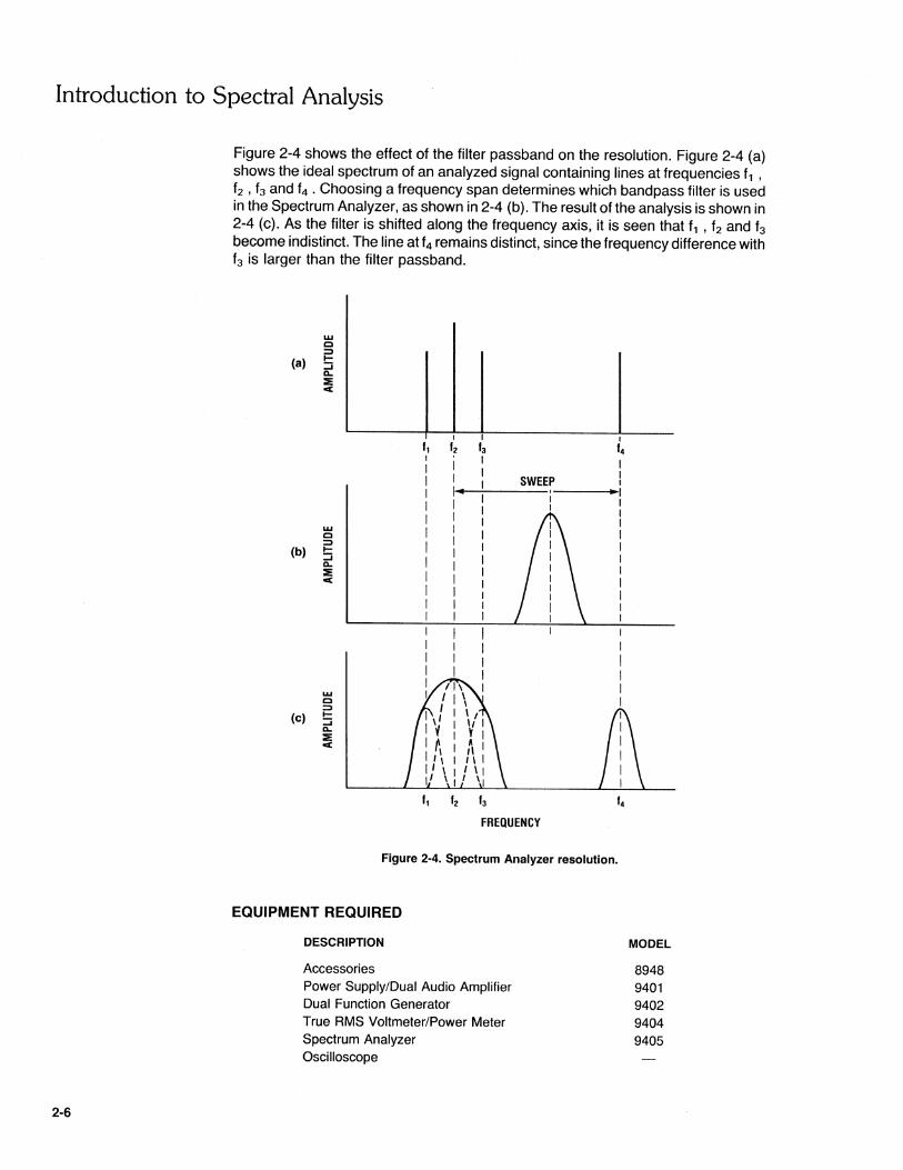
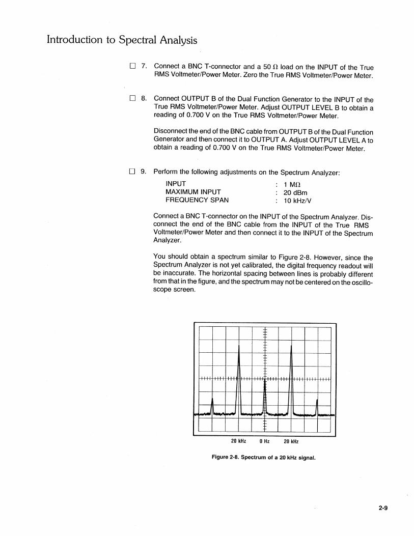
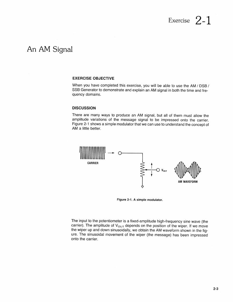
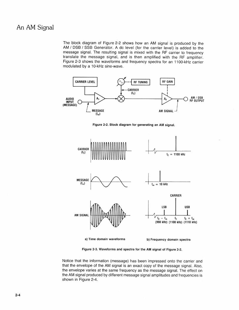
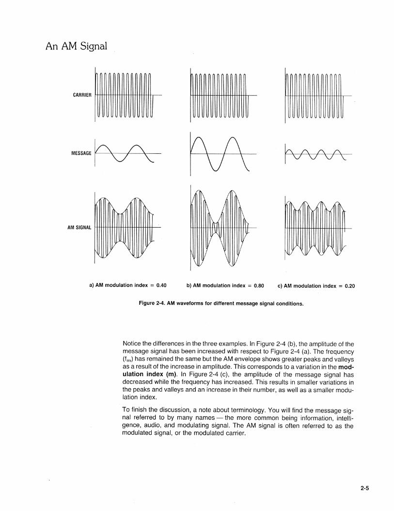
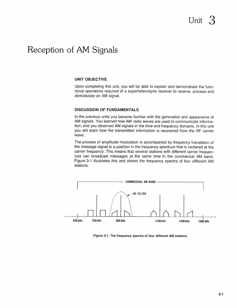
This Student Workbook provides a unit-by-unit outline of the Fault Assisted Circuits for Electronics Training (F.A.C.E.T.) curriculum. The following information is included together with space to take notes as you move through the curriculum. ♦ The unit objective ♦ Unit fundamentals ♦ A list of new terms and words for the unit ♦ Equipment required for the unit ♦ The exercise objectives ♦ Exercise discussion ♦ Exercise notes The Appendix includes safety information.

iv
THIS
Digital Communications 1 Unit 1 – Introduction to Digital Communications 1
1
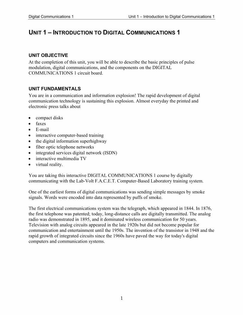
UNIT 1 – INTRODUCTION TO DIGITAL COMMUNICATIONS 1
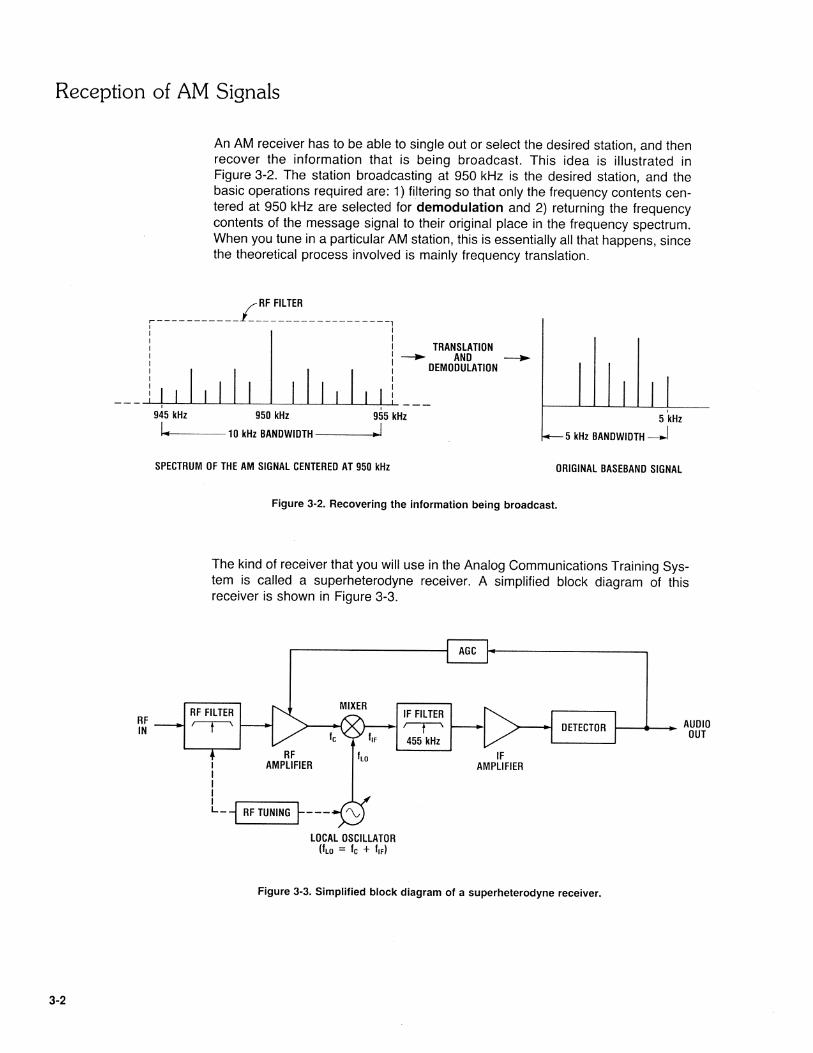
UNIT OBJECTIVE At the completion of this unit, you will be able to describe the basic principles of pulse modulation, digital communications, and the components on the DIGITAL COMMUNICATIONS 1 circuit board.
UNIT FUNDAMENTALS You are in a communication and information explosion! The rapid development of digital communication technology is sustaining this explosion. Almost everyday the printed and electronic press talks about • compact disks • faxes • E-mail • interactive computer-based training • the digital information superhighway • fiber optic telephone networks • integrated services digital network (ISDN) • interactive multimedia TV • virtual reality. You are taking this interactive DIGITAL COMMUNICATIONS 1 course by digitally communicating with the Lab-Volt F.A.C.E.T. Computer-Based Laboratory training system. One of the earliest forms of digital communications was sending simple messages by smoke signals. Words were encoded into data represented by puffs of smoke. The first electrical communications system was the telegraph, which appeared in 1844. In 1876, the first telephone was patented; today, long-distance calls are digitally transmitted. The analog radio was demonstrated in 1895, and it dominated wireless communication for 50 years. Television with analog circuits appeared in the late 1920s but did not become popular for communication and entertainment until the 1950s. The invention of the transistor in 1948 and the rapid growth of integrated circuits since the 1960s have paved the way for today's digital computers and communication systems.
Digital Communications 1 Unit 1 – Introduction to Digital Communications 1
2
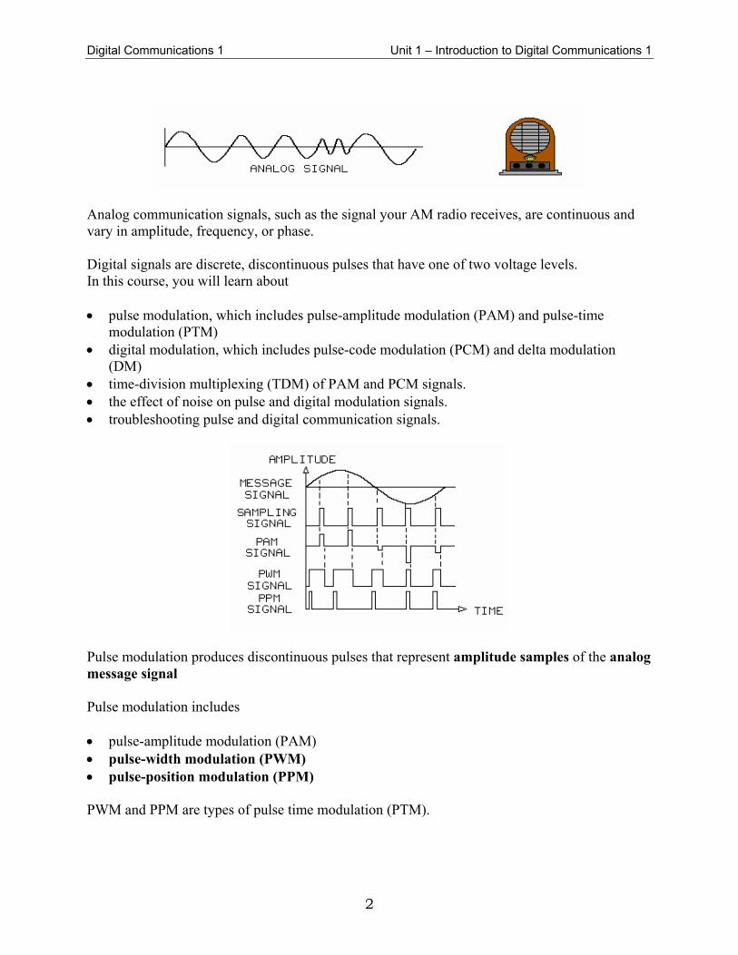
Analog communication signals, such as the signal your AM radio receives, are continuous and vary in amplitude, frequency, or phase. Digital signals are discrete, discontinuous pulses that have one of two voltage levels. In this course, you will learn about • pulse modulation, which includes pulse-amplitude modulation (PAM) and pulse-time
modulation (PTM) • digital modulation, which includes pulse-code modulation (PCM) and delta modulation
(DM) • time-division multiplexing (TDM) of PAM and PCM signals. • the effect of noise on pulse and digital modulation signals. • troubleshooting pulse and digital communication signals.
Pulse modulation produces discontinuous pulses that represent amplitude samples of the analog message signal Pulse modulation includes • pulse-amplitude modulation (PAM) • pulse-width modulation (PWM) • pulse-position modulation (PPM) PWM and PPM are types of pulse time modulation (PTM).
Digital Communications 1 Unit 1 – Introduction to Digital Communications 1
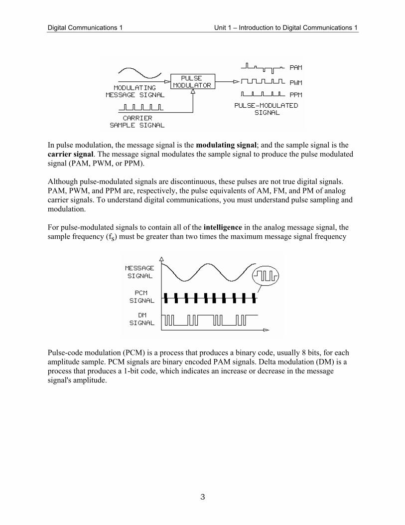
3
In pulse modulation, the message signal is the modulating signal; and the sample signal is the carrier signal. The message signal modulates the sample signal to produce the pulse modulated signal (PAM, PWM, or PPM). Although pulse-modulated signals are discontinuous, these pulses are not true digital signals. PAM, PWM, and PPM are, respectively, the pulse equivalents of AM, FM, and PM of analog carrier signals. To understand digital communications, you must understand pulse sampling and modulation. For pulse-modulated signals to contain all of the intelligence in the analog message signal, the sample frequency (fs) must be greater than two times the maximum message signal frequency
Pulse-code modulation (PCM) is a process that produces a binary code, usually 8 bits, for each amplitude sample. PCM signals are binary encoded PAM signals. Delta modulation (DM) is a process that produces a 1-bit code, which indicates an increase or decrease in the message signal's amplitude.
Digital Communications 1 Unit 1 – Introduction to Digital Communications 1
4
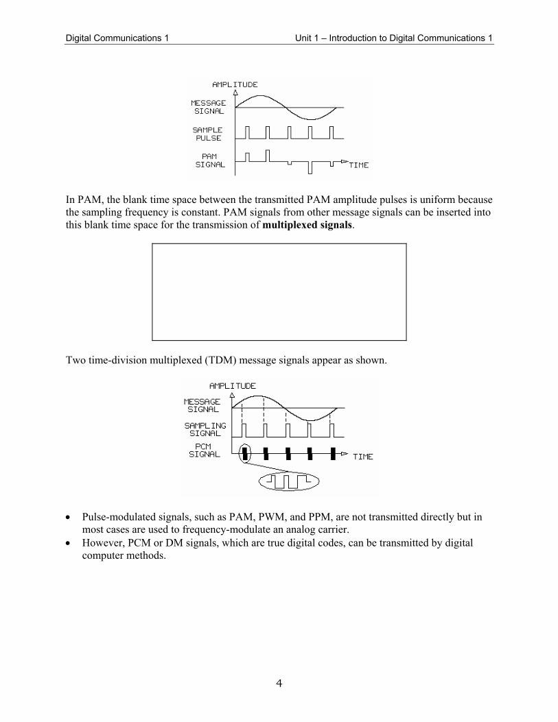
In PAM, the blank time space between the transmitted PAM amplitude pulses is uniform because the sampling frequency is constant. PAM signals from other message signals can be inserted into this blank time space for the transmission of multiplexed signals.
Two time-division multiplexed (TDM) message signals appear as shown.
• Pulse-modulated signals, such as PAM, PWM, and PPM, are not transmitted directly but in
most cases are used to frequency-modulate an analog carrier. • However, PCM or DM signals, which are true digital codes, can be transmitted by digital
computer methods.
Digital Communications 1 Unit 1 – Introduction to Digital Communications 1
5
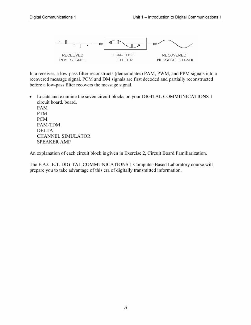
In a receiver, a low-pass filter reconstructs (demodulates) PAM, PWM, and PPM signals into a recovered message signal. PCM and DM signals are first decoded and partially reconstructed before a low-pass filter recovers the message signal. • Locate and examine the seven circuit blocks on your DIGITAL COMMUNICATIONS 1
circuit board. board. PAM PTM PCM PAM-TDM DELTA CHANNEL SIMULATOR SPEAKER AMP
An explanation of each circuit block is given in Exercise 2, Circuit Board Familiarization. The F.A.C.E.T. DIGITAL COMMUNICATIONS 1 Computer-Based Laboratory course will prepare you to take advantage of this era of digitally transmitted information.
Digital Communications 1 Unit 1 – Introduction to Digital Communications 1
6
NEW TERMS AND WORDS pulse-amplitude modulation (PAM) - a modulation method in which the amplitude of each pulse sample is proportional to the amplitude of the message signal at the time of sampling. pulse-time modulation (PTM) - a type of pulse modulation where the timing of the pulse varies with the message signal's amplitude. pulse-code modulation (PCM) - a modulation process that produces binary serial codes for amplitude samples of the analog message signal. delta modulation (DM) - a modulation process that produces 1-bit codes that indicate an increase or decrease in the message signal's amplitude. time-division multiplexing (TDM) - a process that transmits two or more message signals over the same line by using a different time interval (slot) for each signal. noise - an unwanted signal that interferes with a communication signal. pulse-width modulation (PWM) - a type of PTM where the pulse width varies with the message signal's amplitude. pulse-position modulation (PPM) - a type of PTM where the pulse position varies with the message signal's amplitude. modulating signal - a signal that varies some characteristic (amplitude, frequency, or phase) of a carrier signal; in pulse modulation, the modulating signal is the message signal. carrier signal - a high-frequency transmission signal that is modulated by a message signal; in pulse modulation, the carrier signal is the sample signal. amplitude samples - periodic pulses whose amplitudes are directly proportional to a message signal. analog message signal - an analog signal that contains information (intelligence). multiplexed signals - signals from different sources combined on a single transmission channel in a maner that permits independent recovery of each signal in a receiver. intelligence - the information contained in a message signal. frame - a period of time equal to the sampling period that is divided into smaller equal periods called time slots. time slots - periods of time within a frame that are equal to the period of the samples. full-duplex transmission - transmission that can occur simultaneously in both directions between communicators.
EQUIPMENT REQUIRED In order to complete the following exercises, you will need: F.A.C.E.T. base unit Oscilloscope, dual trace DIGITAL COMMUNICATIONS 1 circuit board

Digital Communications 1 Unit 1 – Introduction to Digital Communications 1
7
NOTES ______________________________________________________________________________ ______________________________________________________________________________ ______________________________________________________________________________ ______________________________________________________________________________ ______________________________________________________________________________ ______________________________________________________________________________ ______________________________________________________________________________ ______________________________________________________________________________ ______________________________________________________________________________ ______________________________________________________________________________
Al Imam Mohammad Ibn Saud Islamic University
College of Engineering
Department of Electrical Engineering
EE 452
Communication 1 Lab
Experiment # 8
“ Pulse Amplitude Modulation”

Digital Communications 1 Unit 2 – Pulse-Amplitude Modulation
13
UNIT 2 – PULSE-AMPLITUDE MODULATION
UNIT OBJECTIVE At the completion of this unit, you will be able to generate a pulse-amplitude modulation (PAM) signal and demodulate the PAM signal by using the PAM circuit block on the DIGITAL COMMUNICATIONS 1 circuit board.
UNIT FUNDAMENTALS
An analog message signal, representing voice for example, has continuous amplitude and frequency values that vary with time. Analog communications systems transmit the complete analog waveform.
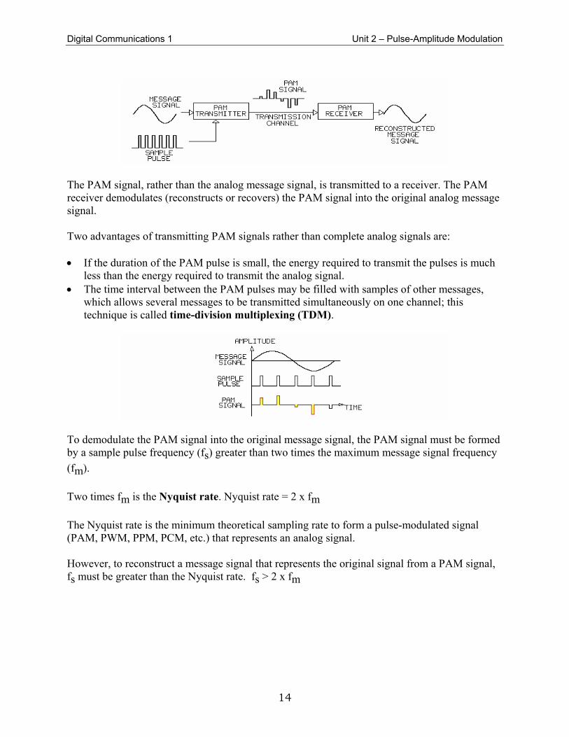
Instead of transmitting the analog waveform, it is possible to transmit pulses that represent the message signal's waveform. Samples of the analog message signal can be taken at regular intervals. In pulse-amplitude modulation (PAM), the amplitude of each pulse sample is proportional to the amplitude of the message signal at the time of sampling.
Digital Communications 1 Unit 2 – Pulse-Amplitude Modulation
14
The PAM signal, rather than the analog message signal, is transmitted to a receiver. The PAM receiver demodulates (reconstructs or recovers) the PAM signal into the original analog message signal. Two advantages of transmitting PAM signals rather than complete analog signals are: • If the duration of the PAM pulse is small, the energy required to transmit the pulses is much
less than the energy required to transmit the analog signal. • The time interval between the PAM pulses may be filled with samples of other messages,
which allows several messages to be transmitted simultaneously on one channel; this technique is called time-division multiplexing (TDM).
To demodulate the PAM signal into the original message signal, the PAM signal must be formed by a sample pulse frequency (fs) greater than two times the maximum message signal frequency (fm). Two times fm is the Nyquist rate. Nyquist rate = 2 x fm The Nyquist rate is the minimum theoretical sampling rate to form a pulse-modulated signal (PAM, PWM, PPM, PCM, etc.) that represents an analog signal. However, to reconstruct a message signal that represents the original signal from a PAM signal, fs must be greater than the Nyquist rate. fs > 2 x fm
Digital Communications 1 Unit 2 – Pulse-Amplitude Modulation
15
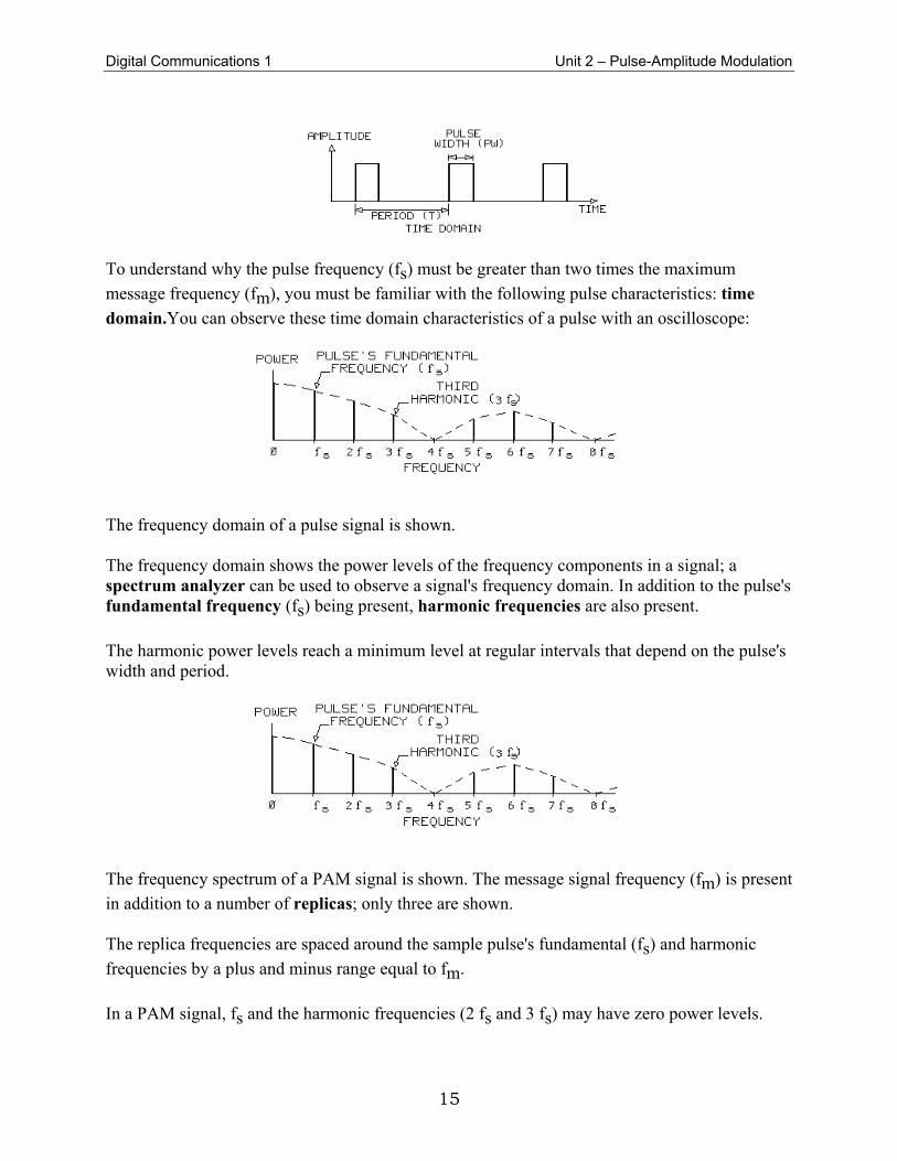
To understand why the pulse frequency (fs) must be greater than two times the maximum message frequency (fm), you must be familiar with the following pulse characteristics: time domain.You can observe these time domain characteristics of a pulse with an oscilloscope:
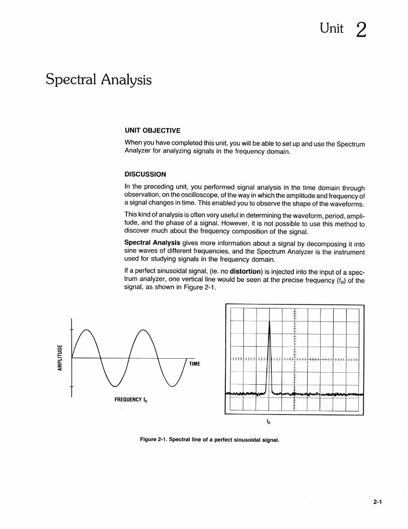
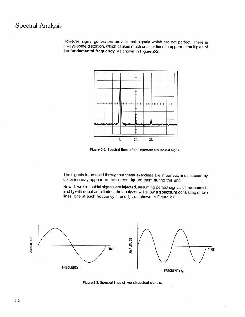
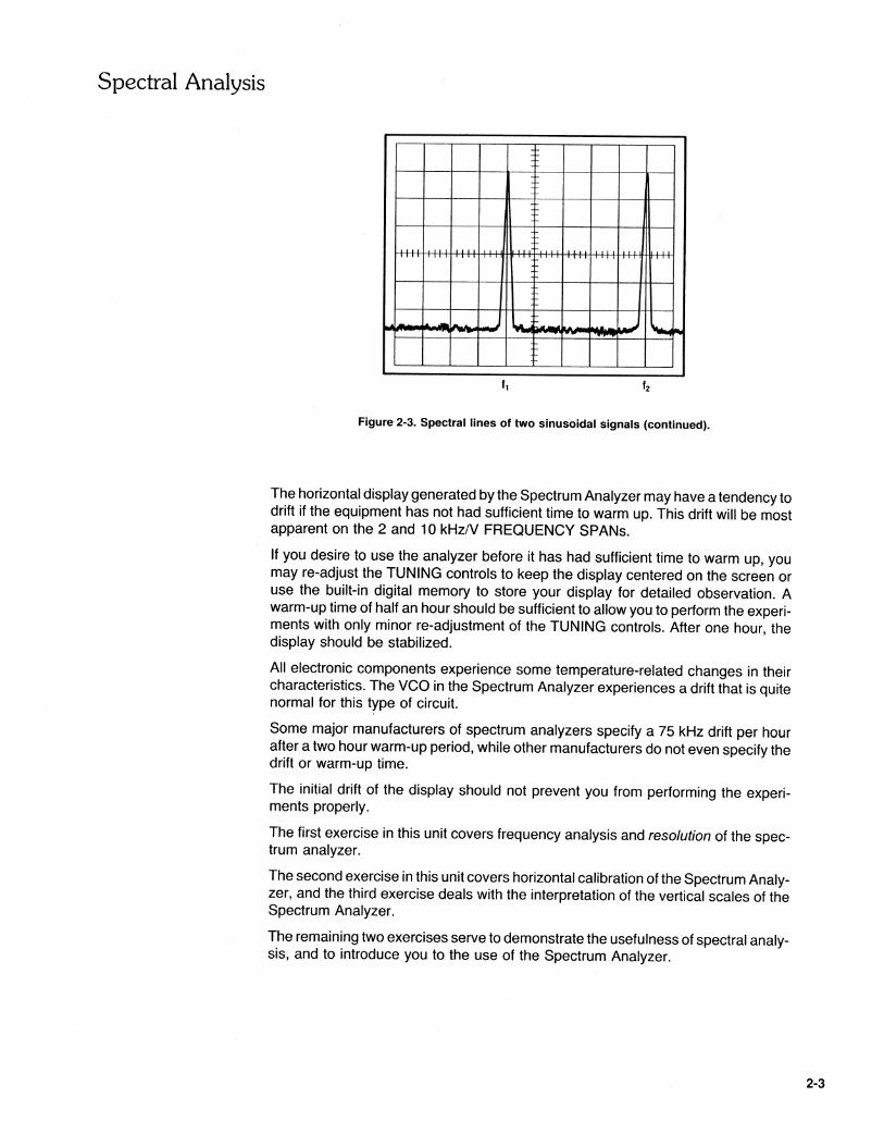
The frequency domain of a pulse signal is shown. The frequency domain shows the power levels of the frequency components in a signal; a spectrum analyzer can be used to observe a signal's frequency domain. In addition to the pulse's fundamental frequency (fs) being present, harmonic frequencies are also present. The harmonic power levels reach a minimum level at regular intervals that depend on the pulse's width and period.
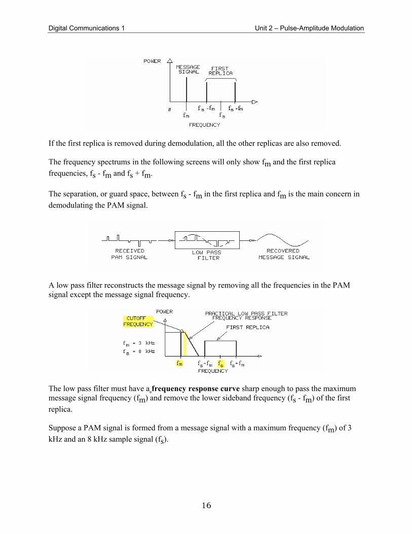
The frequency spectrum of a PAM signal is shown. The message signal frequency (fm) is present in addition to a number of replicas; only three are shown. The replica frequencies are spaced around the sample pulse's fundamental (fs) and harmonic frequencies by a plus and minus range equal to fm. In a PAM signal, fs and the harmonic frequencies (2 fs and 3 fs) may have zero power levels.
Digital Communications 1 Unit 2 – Pulse-Amplitude Modulation
16
If the first replica is removed during demodulation, all the other replicas are also removed. The frequency spectrums in the following screens will only show fm and the first replica frequencies, fs - fm and fs + fm. The separation, or guard space, between fs - fm in the first replica and fm is the main concern in demodulating the PAM signal.
A low pass filter reconstructs the message signal by removing all the frequencies in the PAM signal except the message signal frequency.
The low pass filter must have a frequency response curve sharp enough to pass the maximum message signal frequency (fm) and remove the lower sideband frequency (fs - fm) of the first replica. Suppose a PAM signal is formed from a message signal with a maximum frequency (fm) of 3 kHz and an 8 kHz sample signal (fs).
Digital Communications 1 Unit 2 – Pulse-Amplitude Modulation
17
NEW TERMS AND WORDS pulse-amplitude modulation (PAM) - a modulation method in which the amplitude of each pulse sample is proportional to the amplitude of the message signal at the time of sampling. time-division multiplexing (TDM) - a method of transmitting many digital message signals over the same line by assigning time slots that are synchronized on the transmitting and receiving ends. Nyquist rate - the minimum theoretical sampling rate to form a pulse-modulated signal (PAM, PWM, PPM, PCM, etc). that represents an analog signal . The Nyquist rate equals two times the maximum message signal frequency. time domain - a signal's amplitude as a function of time. frequency domain - the amplitude of a signal's frequency components as a function of frequency. duty cycle fraction (PW/T) - the ratio of the pulse duration (PW) to the period (T). spectrum analyzer - an instrument that shows the relative power distribution of a signal as a function of frequency. fundamental frequency - the principal frequency component of a waveform or pulse signal; the frequency with the greatest amplitude. harmonic frequencies - a frequency component of a periodic waveform or pulse signal; the frequency of each harmonic is a multiple of the fundamental frequency. replicas - frequencies that are spaced around the sample pulse's fundamental (fs) and harmonic frequencies by a plus and minus range equal to the maximum message signal frequency (fm). frequency response curve - a graphical representation of a circuit's response to different frequencies within its operating range. cutoff frequency - the frequency at which the output amplitude of a circuit (filter) is attenuated by -3dB (0.707 of the input). sampler circuit - a circuit in which the output is a series of discrete values (pulses) representing the value of the input at sampling points in time. natural PAM signals - a type of sampling in which the amplitude of each pulse follows the amplitude of the message signal at the sampling time. flat-top PAM signals - a type of sampling in which the amplitude of each pulse remains constant during the sampling time. sample/hold circuit - a circuit that holds the amplitude of each output pulse at a constant level between the input sampling times staircase PAM signals - signals that are output from a sample/hold circuit; the amplitude of each output pulse remains at a constant level between the input sampling times. aliasing - a condition in a PAM signal where the lower sideband frequency (fs-fm) is less than the maximum message signal frequency (fm); aliasing is also called fold-over distortion.

Digital Communications 1 Unit 2 – Pulse-Amplitude Modulation
18
EQUIPMENT REQUIRED In order to complete the following exercises, you will need: F.A.C.E.T. base unit DIGITAL COMMUNICATIONS 1 circuit board Oscilloscope, dual trace Signal Generator, sine wave
NOTES ______________________________________________________________________________ ______________________________________________________________________________ ______________________________________________________________________________ ______________________________________________________________________________ ______________________________________________________________________________ ______________________________________________________________________________ ______________________________________________________________________________ ______________________________________________________________________________ ______________________________________________________________________________ ______________________________________________________________________________

Digital Communications 1 Unit 2 – Pulse-Amplitude Modulation
19
Exercise 1 – PAM Signal Generation
EXERCISE OBJECTIVE When you have completed this exercise, you will be able to: • describe the process and circuits for generating PAM signals. • describe the characteristics of PAM signals. • demonstrate the effect of sampling pulse rates on PAM signals. • calculate the power of a PAM signal. You will use an oscilloscope to make observations and measurements.
DISCUSSION • In pulse-amplitude modulation (PAM), a pulse signal periodically samples an analog
message signal. • The result is a train of constant-width pulses with amplitudes proportional to the message
signal amplitude at the time of sampling. • A sample signal causes an electronic switch to close and open. • When the top of the PAM pulse follows the curvature of the message signal, the process is
natural sampling. When a sampler closes, it produces a natural PAM sample. • To produce flat-top PAM signals, a sample/hold circuit holds the amplitude of each pulse at a
constant level. • Staircase PAM signals are output from the sample/hold circuit; the sampler circuit converts
them to flat-top PAM signals. • The sample pulse frequency (fs) must be more than the Nyquist rate to produce a PAM signal
that clearly represents the message signal. When fm is 3.5 kHz, fs must be 8 kHz to produce a PAM signal that clearly represents the message signal.
• If PAM pulses are narrow, little power is required for transmission. Power in a PAM signal that represents a 2 kHz sine wave signal is about 15 percent of the sine wave power.
• The power (Ps) that a sine wave signal produces equals its rms voltage [Vrms (s)] squared, divided by the impedance (Z) where: Vrms (s) = 0.707 x Vpeak (s)
• Voltage Vrms (p) of a pulse signal is pulse voltage (Vp) times the square root of the ratio of the PAM signal pulse width (PW) divided by its period (T). Vrms (p) = Vp x PW/T.
• Theoretical rms value of a PAM signal formed from a cyclical signal is calculated as Vrms (p) = PW/T x Vrms (s)
• The rms value [Vrms (p)] of the PAM signal for Vrms (s) equals Vrms (p) = PW/T x Vrms (s); the theoretical power of a PAM signal formed from a sine wave is PW/T times the power of the sine wave (Ps): Pp = PW/T x Ps
• Measure voltages and the PW/T fraction of the PAM pulses and calculate pulse rms values to experimentally determine the rms voltage of a PAM signal
• The rms voltage of a PAM signal equals the square root of the sum of the squares of the individual pulse rms values.

Digital Communications 1 Unit 2 – Pulse-Amplitude Modulation
20
NOTES ______________________________________________________________________________ ______________________________________________________________________________ ______________________________________________________________________________ ______________________________________________________________________________ ______________________________________________________________________________ ______________________________________________________________________________ ______________________________________________________________________________ ______________________________________________________________________________ ______________________________________________________________________________ ______________________________________________________________________________
Al Imam Mohammad Ibn Saud Islamic University
College of Engineering
Department of Electrical Engineering
EE 452
Communication 1 Lab
Experiment # 9
“ Pulse Code Modulation”
Digital Communications 1 Unit 5 – Pulse-Code Modulation (PCM)
41
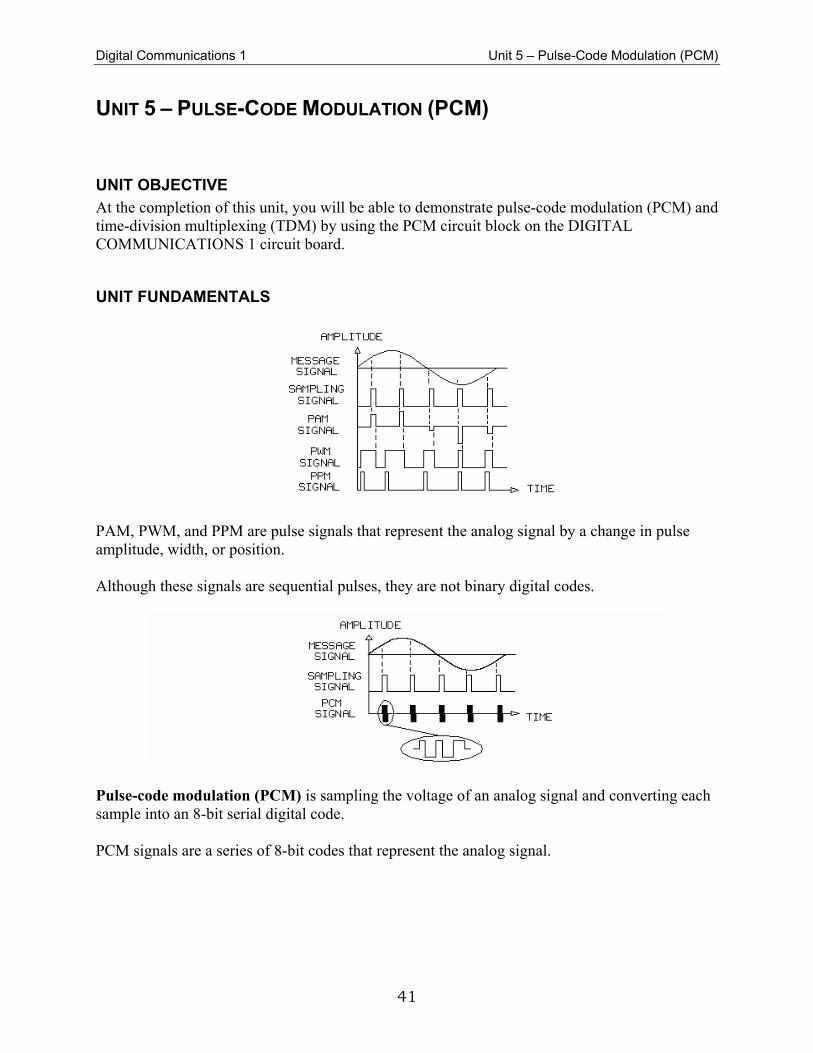
UNIT 5 – PULSE-CODE MODULATION (PCM)
UNIT OBJECTIVE At the completion of this unit, you will be able to demonstrate pulse-code modulation (PCM) and time-division multiplexing (TDM) by using the PCM circuit block on the DIGITAL COMMUNICATIONS 1 circuit board.
UNIT FUNDAMENTALS
PAM, PWM, and PPM are pulse signals that represent the analog signal by a change in pulse amplitude, width, or position. Although these signals are sequential pulses, they are not binary digital codes.
Pulse-code modulation (PCM) is sampling the voltage of an analog signal and converting each sample into an 8-bit serial digital code. PCM signals are a series of 8-bit codes that represent the analog signal.
Digital Communications 1 Unit 5 – Pulse-Code Modulation (PCM)
42
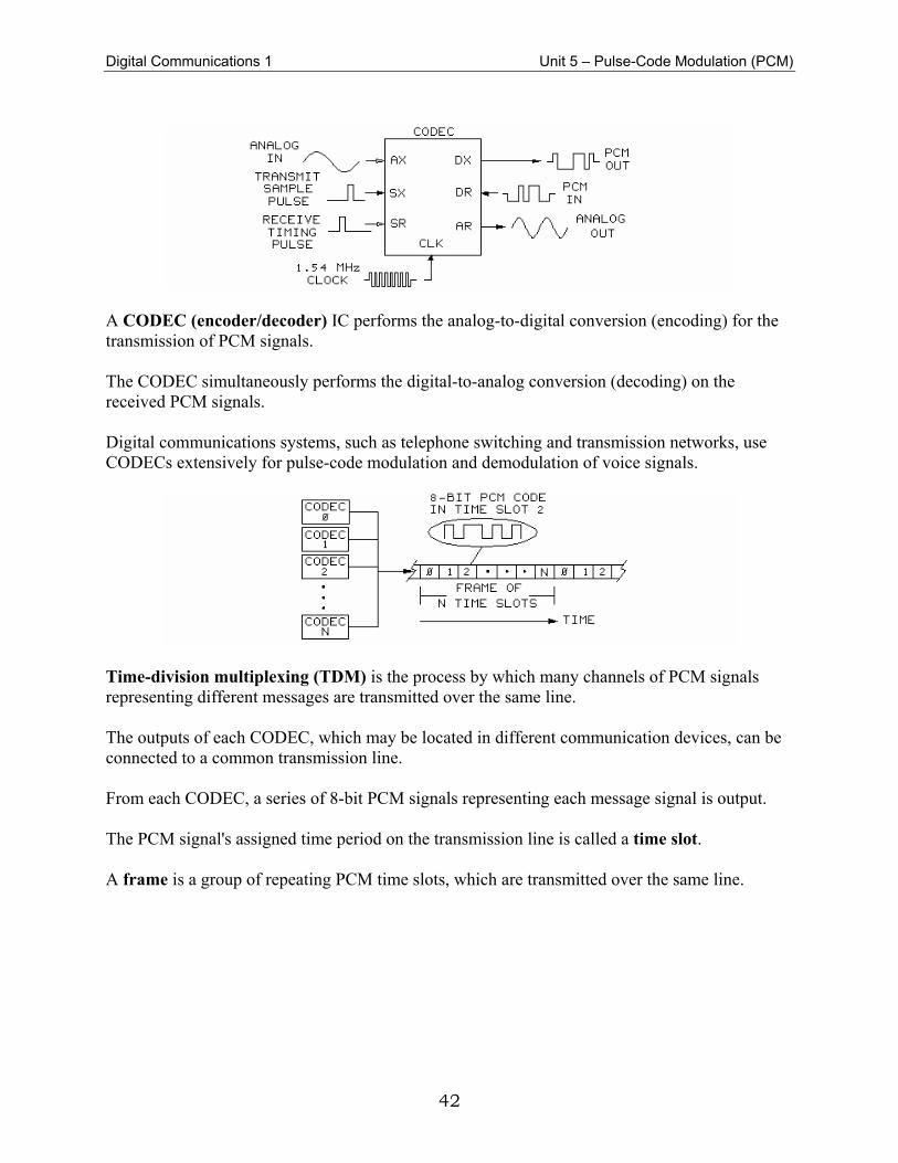
A CODEC (encoder/decoder) IC performs the analog-to-digital conversion (encoding) for the transmission of PCM signals. The CODEC simultaneously performs the digital-to-analog conversion (decoding) on the received PCM signals. Digital communications systems, such as telephone switching and transmission networks, use CODECs extensively for pulse-code modulation and demodulation of voice signals.
Time-division multiplexing (TDM) is the process by which many channels of PCM signals representing different messages are transmitted over the same line. The outputs of each CODEC, which may be located in different communication devices, can be connected to a common transmission line. From each CODEC, a series of 8-bit PCM signals representing each message signal is output. The PCM signal's assigned time period on the transmission line is called a time slot. A frame is a group of repeating PCM time slots, which are transmitted over the same line.

Digital Communications 1 Unit 5 – Pulse-Code Modulation (PCM)
43
Some advantages of PCM transmission are: • lower cost • ease of multiplexing • ease of switching • less noise problems Overall, the advantages outweigh the disadvantages. The industry trend is toward 100% digital communications networks.
NEW TERMS AND WORDS pulse-code modulation (PCM) - a modulation process that produces binary serial codes for amplitude samples of the analog message signal. CODEC (encoder/decoder) - a device that can simultaneously perform analog-to-digital conversion (encoding) and digital-to-analog conversion (decoding). time-division multiplexing (TDM) - a process that transmits two or more message signals over the same line by using a different time interval for each signal. time slot - period of time within a frame that is equal to the period of the samples. frame - a period of time, equal to the sampling period, that is divided into smaller equal periods called time slots. quantum - a number assigned to a particular quantized value. companding - a compression and expansion process that improves the overall signal-to-noise ratio during PCM encoding and decoding quantization - the process of converting a sampled amplitude into a numbered level called a quantum based on the number of bits in the PCM signal. companding law - a compression and expansion process that improves the overall signal-to-noise ratio during PCM encoding and decoding a logarithmic relationship used for companding. full duplex - a transmission system that permits communication signals to flow simultaneously in both directions µ-law - a companding law used in North America and Japan. A-law - a companding law used mainly in Europe. local loop - the two-wire loop that connects the telephone set to the central office. simplex - a transmission system that restricts communication signals to only one direction.
EQUIPMENT REQUIRED In order to complete the following exercises, you will need: F.A.C.E.T. base unit DIGITAL COMMUNICATIONS 1 circuit board Oscilloscope, dual trace Signal Generator, sine wave

Digital Communications 1 Unit 5 – Pulse-Code Modulation (PCM)
44
NOTES ______________________________________________________________________________ ______________________________________________________________________________ ______________________________________________________________________________ ______________________________________________________________________________ ______________________________________________________________________________ ______________________________________________________________________________ ______________________________________________________________________________ ______________________________________________________________________________ ______________________________________________________________________________ ______________________________________________________________________________
Digital Communications 1 Unit 5 – Pulse-Code Modulation (PCM)
45
Exercise 1 – Generation and Demodulation
EXERCISE OBJECTIVE When you have completed this exercise you will be able to • describe the process for converting analog signals to PCM signals. • describe how PCM signals are demodulated. • read and decode PCM signals. You will verify your results by observing and measuring the signals with an oscilloscope.
DISCUSSION • An analog message signal (AX) is encoded into a digital PCM signal (DX) by a CODEC. • The acronym CODEC means encoder/decoder • There is an 8 kHz transmit sample (timing) pulse (SX), which occurs one clock cycle before
a time slot assigned to the transmitted PCM signal, that keys a CODEC to sample its message signal and generate a PCM signal.
• The CODEC decodes the received digital PCM signal (DR) into a recovered analog message signal (AR).
• There is an 8 kHz receive timing pulse (SR), which occurs one clock cycle before a time slot assigned to the received PCM signal that, keys a CODEC to decode an 8-bit PCM code.
• Encoding sections consist of a transmit filter, a sample/hold circuit, an ADC, a register, and a parallel-to-serial converter.
• The timing and control circuit synchronizes the CODEC's operation. • SX is the 8 kHz transmit sample pulse. • SR is the 8 kHz receive timing pulse, which usually occurs in a time slot different from SX. • The analog message signal is applied to the transmit filter at AX. • The sample/hold circuit samples the amplitude of the filtered analog signal 8000 times per
second. • The sample/hold circuit output is a staircase PAM signal. • Quantization simplifies the conversion of the step voltage into a binary code. • Overall signal-to-noise ratio is improved during quantization by companding
(compressing/expanding).
Digital Communications 1 Unit 5 – Pulse-Code Modulation (PCM)
46
• The higher signal-amplitudes are compressed during encoding and expanded during decoding.
• With S-shaped companding, smaller step-voltages receive higher quantum values than higher step voltages.
• A CODEC uses a companding law to determine the output code where the MSB is the sign bit. The MSB for a positive step voltage is 1. The MSB for a negative step voltage is 0. The remaining 7 bits designate one of the 128 quantum levels.
• An ADC encodes quantum values into an 8-bit parallel digital code, which is temporarily stored in a register.
• Parallel code from the output register is converted to an 8-bit serial digital code that is output, one bit at a time, by a 1.54 MHz clock.
• Operation of decoder circuitry is the reverse of the encoder.

Digital Communications 1 Unit 5 – Pulse-Code Modulation (PCM)
47
NOTES ______________________________________________________________________________ ______________________________________________________________________________ ______________________________________________________________________________ ______________________________________________________________________________ ______________________________________________________________________________ ______________________________________________________________________________ ______________________________________________________________________________ ______________________________________________________________________________ ______________________________________________________________________________ ______________________________________________________________________________
Al Imam Mohammad Ibn Saud Islamic University
College of Engineering
Department of Electrical Engineering
EE 452
Communication 1 Lab
Experiment 10
“Delta Modulation”
Digital Communications 1 Unit 6 – Delta Modulation (DM)
51
UNIT 6 – DELTA MODULATION (DM)
UNIT OBJECTIVE At the completion of this unit, you will be able to demonstrate delta modulation and demodulation by using the DELTA circuit block on the DIGITAL COMMUNIATIONS 1 circuit board.
UNIT FUNDAMENTALS
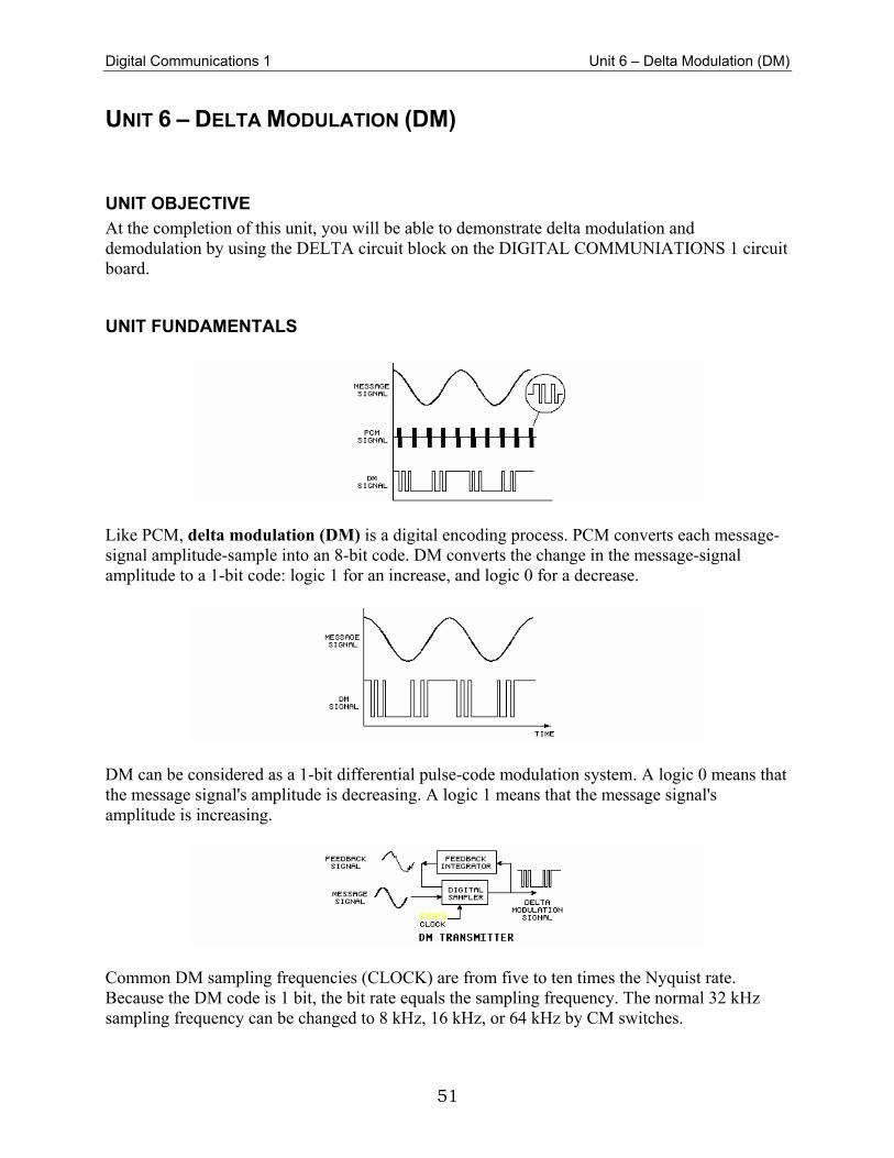
Like PCM, delta modulation (DM) is a digital encoding process. PCM converts each message-signal amplitude-sample into an 8-bit code. DM converts the change in the message-signal amplitude to a 1-bit code: logic 1 for an increase, and logic 0 for a decrease.
DM can be considered as a 1-bit differential pulse-code modulation system. A logic 0 means that the message signal's amplitude is decreasing. A logic 1 means that the message signal's amplitude is increasing.
Common DM sampling frequencies (CLOCK) are from five to ten times the Nyquist rate. Because the DM code is 1 bit, the bit rate equals the sampling frequency. The normal 32 kHz sampling frequency can be changed to 8 kHz, 16 kHz, or 64 kHz by CM switches.
Digital Communications 1 Unit 6 – Delta Modulation (DM)
52
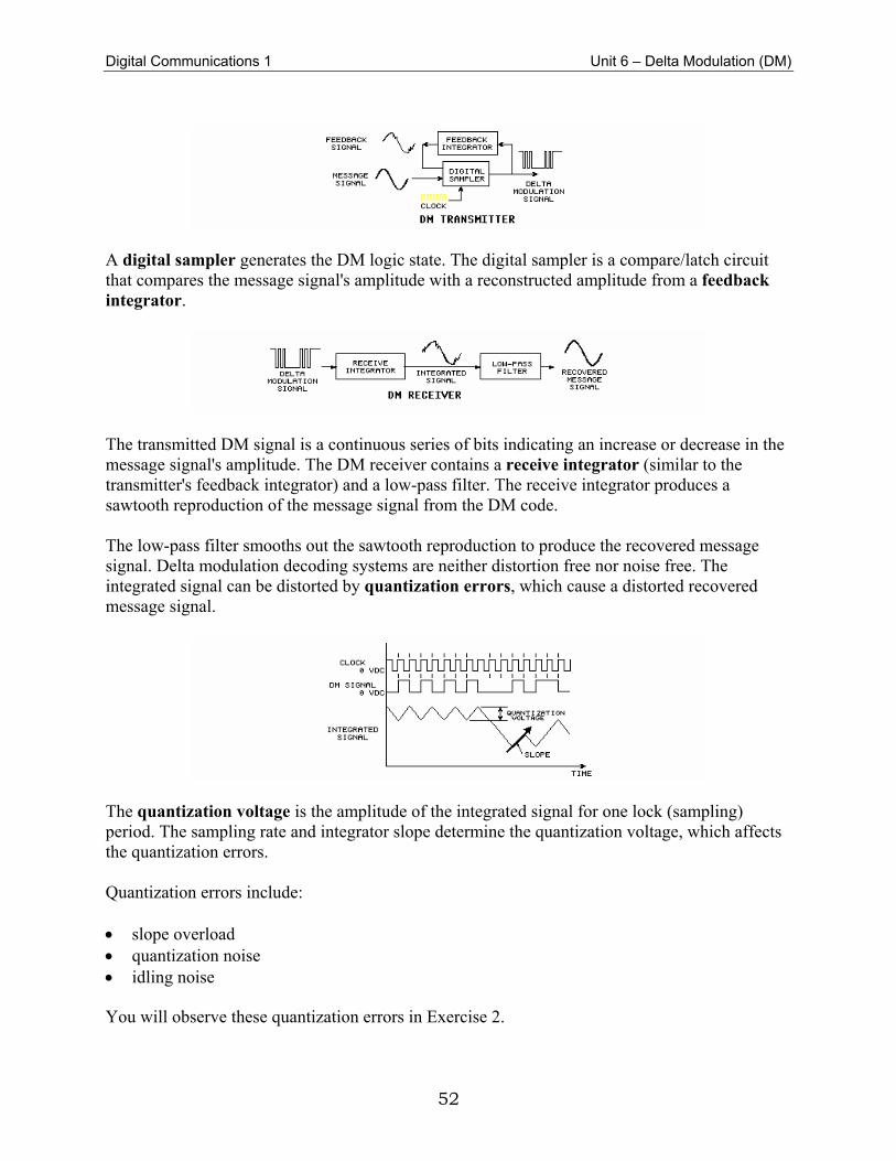
A digital sampler generates the DM logic state. The digital sampler is a compare/latch circuit that compares the message signal's amplitude with a reconstructed amplitude from a feedback integrator.
The transmitted DM signal is a continuous series of bits indicating an increase or decrease in the message signal's amplitude. The DM receiver contains a receive integrator (similar to the transmitter's feedback integrator) and a low-pass filter. The receive integrator produces a sawtooth reproduction of the message signal from the DM code. The low-pass filter smooths out the sawtooth reproduction to produce the recovered message signal. Delta modulation decoding systems are neither distortion free nor noise free. The integrated signal can be distorted by quantization errors, which cause a distorted recovered message signal.
The quantization voltage is the amplitude of the integrated signal for one lock (sampling) period. The sampling rate and integrator slope determine the quantization voltage, which affects the quantization errors. Quantization errors include: • slope overload • quantization noise • idling noise You will observe these quantization errors in Exercise 2.
Digital Communications 1 Unit 6 – Delta Modulation (DM)
53
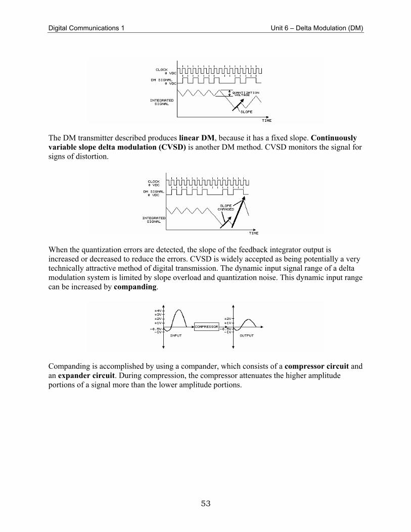
The DM transmitter described produces linear DM, because it has a fixed slope. Continuously variable slope delta modulation (CVSD) is another DM method. CVSD monitors the signal for signs of distortion.
When the quantization errors are detected, the slope of the feedback integrator output is increased or decreased to reduce the errors. CVSD is widely accepted as being potentially a very technically attractive method of digital transmission. The dynamic input signal range of a delta modulation system is limited by slope overload and quantization noise. This dynamic input range can be increased by companding.
Companding is accomplished by using a compander, which consists of a compressor circuit and an expander circuit. During compression, the compressor attenuates the higher amplitude portions of a signal more than the lower amplitude portions.

Digital Communications 1 Unit 6 – Delta Modulation (DM)
54
During expansion, the expander amplifies the larger signal amplitudes more than the lower signal amplitudes. Companding improves the system performance since a larger range of input signals can be transmitted and received.
NEW TERMS AND WORDS delta modulation (DM) - a 1 bit encoding process that outputs a logic 1 bit for an increase in the message signal's amplitude and a logic 0 bit for a decrease. digital sampler - a circuit composed of a comparator and D-type flip flop that compares the message signal amplitude with the amplitude of an integrated feedback signal to output a DM signal. feedback integrator - an integrator circuit in a DM transmitter that integrates the DM signal and outputs a sawtooth reproduction whose amplitude is compared to the message signal's amplitude. receive integrator - an integrator circuit in a DM receiver that integrates the DM signal and outputs a sawtooth reproduction to a low-pass filter. quantization errors - DM signal errors (slope overload, idling noise, and quantization noise) that cause distortion in the recovered message signal. quantization voltage - the amplitude of the integrated signal for one clock (sampling) period. linear DM - a DM system that has a fixed quantization voltage; the slope of the integrated signal is constant. continuously variable slope delta modulation (CVSD) - a DM system that detects quantization errors and changes the slope of the integrated signal to reduce the errors. companding - a process that contains a compressor circuit and an expander circuit to improve the dynamic range of a DM system. compressor circuit - a circuit, usually in a transmitter, that attenuates the higher amplitude portions of a signal more than the lower amplitude portions. expander circuit - a circuit, usually in a receiver, that amplifies the higher amplitude portions of a signal more than the lower amplitude portions.
EQUIPMENT REQUIRED F.A.C.E.T. Computer-Interface Base Unit DIGITAL COMMUNICATION 1 Circuit Board Signal Generator, (sine/square) Multimeter Oscilloscope, dual trace

Digital Communications 1 Unit 6 – Delta Modulation (DM)
55
NOTES ______________________________________________________________________________ ______________________________________________________________________________ ______________________________________________________________________________ ______________________________________________________________________________ ______________________________________________________________________________ ______________________________________________________________________________ ______________________________________________________________________________ ______________________________________________________________________________ ______________________________________________________________________________ ______________________________________________________________________________

Digital Communications 1 Unit 6 – Delta Modulation (DM)
56
Exercise 1 – DM Transmitter
EXERCISE OBJECTIVE When you have completed this exercise you will be able to • describe how DM signals represent the analog message signal. • demonstrate the operation of a digital sampler. • describe the function and operation of a feedback integrator. • explain how clock frequency affects the DM bit rate and the feedback integrator's output
signal. You will verify your results by observing and measuring the signals with an oscilloscope.
DISCUSSION • To produce a DM signal, a digital sampler compares the message signal's amplitude with the
amplitude of a feedback signal, which is a partially reconstructed message signal from a feedback integrator.
• A DM sample of the message signal's increase or decrease contains 1 bit. • A comparator and a D-type flip flop constitute the digital sampler in the DELTA circuit
block. • The feedback integrator is the integrate 1 circuit. • The comparator compares the amplitude of the message and feedback signal amplitude to
determine if message signal amplitude is increasing or decreasing. • Ideally, the feedback amplitude should be a close approximation of what the message-signal
amplitude was at the previous clock pulse. • When the message signal is greater than the feedback signal, the comparator output is high,
which indicates an amplitude increase. • When the feedback signal is greater than the message signal, the comparator output voltage is
low. • The comparator output is the D input of the flip flop. • The 32 kHz CLK signal, the sampling signal, is the flip flop's CLK input. • If the comparator output (flip flop D input) is high at the rising edge of the CLK signal, the Q
output of the flip flop becomes logic 1. • If the comparator output is low at the rising edge of the CLK signal, the Q output of the flip
flop becomes logic 0. • The flip flop's Q output is latched to a logic state until the next rising edge of the signal
occurs?

Digital Communications 1 Unit 6 – Delta Modulation (DM)
57
• The logic state of the flip flop Q output will remain the same or change at every rising edge of the clock signal depending upon the voltage at the D input.
• The flip flop Q output is the delta modulation (DM) signal. • The INTEGRATE 1 circuit integrates the DM signal to produce the feedback signal. • The REF voltage determines how closely the feedback signal resembles the message signal.
Adjust the REF voltage input with the POSITIVE SUPPLY voltage potentiometer on the base unit.
• An RC time constant sets the positive and negative slope of the integrator output voltage. • Each logic 1 DM signal causes the integrator output voltage to increase by a fixed amount. • A logic 0 DM signal causes the integrator output voltage to decrease. • Baud is the number of signal-changes per second and is equal to the reciprocal of the period
of the smallest signaling element. • In DM, baud equals the number of bits per second. • The DM signal is output from the digital sampler at a bit rate equal to the frequency of the
clock signal. • If the clock frequency to the digital sampler is 32 kHz, the bit rate in baud is 32,000.

Digital Communications 1 Unit 6 – Delta Modulation (DM)
58
NOTES ______________________________________________________________________________ ______________________________________________________________________________ ______________________________________________________________________________ ______________________________________________________________________________ ______________________________________________________________________________ ______________________________________________________________________________ ______________________________________________________________________________ ______________________________________________________________________________ ______________________________________________________________________________ ______________________________________________________________________________
Digital Communications 1 Unit 6 – Delta Modulation (DM)
59
Exercise 2 – DM Receiver and Noise
EXERCISE OBJECTIVE When you have completed this exercise you will be able to: • describe how DM signals are demodulated. • identify and explain the cause of slope overload, idling noise, and quantization noise. • describe how companding improves the dynamic range of DM. You will verify your results by observing and measuring the signals with an oscilloscope.
DISCUSSION • Compare the M1 message signal to the INTEGRATE 2 and recovered message signals. • The delta modulation receiver contains simple hardware for decoding the DM signal. • Only a receive integrator and low-pass filter compose the receiver. • On the circuit board, the receive integrator is the INTEGRATE 2 circuit, and the low-pass
filter is the FILTER 1 circuit in the PAM-TDM circuit block. • The receive integrator converts the DM signal into an integrated signal that approximates the
original intelligence signal. • The low-pass filter recovers the message signal from the integrated signal by removing the
high frequency components. • Clock and synchronization signals are not required for the DM receiver to recover the
message signal? • Delta modulation communication systems are not distortion or noise free. • The recovered message signal can be distorted by quantization errors including slope
overload, quantization noise or granular noise, and idling noise • The exercise procedure explains and demonstrates each of these quantization errors. • Companding, which permits an increase in the dynamic range (greater change of amplitude)
of the DM message signal and reduces quantization errors, is discussed and demonstrated in this procedure.
• Companding permits greater changes in the amplitude of the DM message signal?

Digital Communications 1 Unit 6 – Delta Modulation (DM)
60
NOTES ______________________________________________________________________________ ______________________________________________________________________________ ______________________________________________________________________________ ______________________________________________________________________________ ______________________________________________________________________________ ______________________________________________________________________________ ______________________________________________________________________________ ______________________________________________________________________________ ______________________________________________________________________________ ______________________________________________________________________________


![[IJET-V1I3P7] Authors : Prateek Joshi, Mohammad UmairZaki](https://static.fdokumen.com/doc/165x107/63330122576b626f850dab29/ijet-v1i3p7-authors-prateek-joshi-mohammad-umairzaki.jpg)