
A Project Report at CELL PHONE DETECTOR Department of Electronics Engineering Session (2012-2013)...
125
A Project Report at CELL PHONE DETECTOR Submitted by: Name (Roll no.) Aadil Amaan (0905330001) Mahesh Kumar Sahu (0905330040) Pranay Ranjan Maurya (0905330056) Puneet Kumar Gupta (0905330060) AZAD INSTITUTE OF ENGINEERING & TECHNOLOGY, LUCKNOW
-
Upload
independent -
Category
Documents
-
view
0 -
download
0
Transcript of A Project Report at CELL PHONE DETECTOR Department of Electronics Engineering Session (2012-2013)...
A
Project Report
at
CELL PHONE DETECTOR
Submitted by:
Name (Roll no.)
Aadil Amaan (0905330001) Mahesh Kumar Sahu (0905330040) Pranay Ranjan Maurya (0905330056) Puneet Kumar Gupta (0905330060)
AZAD INSTITUTE OF ENGINEERING &TECHNOLOGY, LUCKNOW

(Affiliated to Gautam Buddha Technical University,Lucknow)
Department of Electronics EngineeringSession (2012-2013)
1

ACKNOWLEDGEMENT
Our sincerest appreciation must be extended by our
faculties. We also want to thank faculties of the College.
They have been very kind and helpful to us. We want to thank
all teaching and non‐teaching staff to support us. Especially
we are thankful to Mr. S. K. Mishra (HOD) for providing this
golden opportunity to work on this project, inspiration during
the course of this project and to complete the project within
stipulated time duration and four walls of College Lab. We
would like to express our sincere gratitude to our Guide Ms.
Sonal Mam for their help during the course of the project
right from selection of the project, their constant
encouragement, expert academic and practical guidance.
2

ABSTRACT
This handy, pocket-size mobile transmission detector or
sniffer can sense the presence of an activated mobile cell
phone from a distance of one and-a-half meters. So it can be
used to prevent use of mobile phones in examination halls,
confidential rooms, etc. It is also useful for detecting the
use of mobile phone for Spying and unauthorized video
transmission. The circuit can detect the incoming and outgoing
calls, SMS and video transmission even if the mobile phone is
kept in the silent mode. The moment the Bug detects RF
transmission signal from an activated mobile phone, it starts
sounding a beep alarm and the LED blinks. The alarm continues
until the signal transmission ceases. Assemble the circuit on
a general purpose PCB as compact as possible and enclose in a
small box like junk mobile case. As mentioned earlier,
capacitor C3 should have a lead length of 18 mm with lead
spacing of 8 mm. Carefully solder the capacitor in standing
position with equal spacing of the leads. The response can be
3

optimized by trimming the lead length of C3 for the desired
frequency. You may use a short telescopic type antenna.
Use the miniature 12V battery of a remote control and a
small buzzer to make the gadget pocket-size. The unit will
give the warning indication if someone uses Mobile phone
within a radius of 1.5 meters.
CONTENTS
PAGE NO.
CHAPTER ONE
1.1 Introduction
(5) 4

1.2 Cellular Phone Technology
(7)
1.2.1 Cellular Phone Features (7)
1.2.2 Cellular Phone Communication Standards
(8)
1.3 Overview of Cell Phone Detector
(9)
1.3.1 Mobile Bug (11)
1.4 Circuit Diagram
(12)
1.5 Description of Circuit Diagram
(13)
CHAPTER TWO2.1 Introduction
(14)
2.2 Block Diagram
(18)
2.3 Block Diagram Explanation
(18)
2.3.1 Transmission Lines
(19)
2.4 PCB Layout
(20)
2.5 PCB Fabrication
(20)
2.5.1 The Printed Circuit Board
(21)
5

2.5.2 Copper-clad Laminates
(21)
2.5.3 Board Cleaning Before Pattern Transfer
(22)
2.5.4 Screen Printing
(22)
2.5.5 Etching
(22)
2.5.6 Chemistry
(22)
2.5.7 Drilling
(23)
2.5.8 Component Mounting
(24)
2.5.9 Soldering
(24)
2.5.10 Soldering Steps
(25)
CHAPTER THREE3.1 Introduction
(26)
3.2 List of Components
(30)
3.3 Components Description
(31)
6

3.3.1 Resistor
(31)
3.3.2 Capacitor
(34)
3.3.3 Transistor
(38)
3.3.4 LED
(45)
3.3.5 Piezo Buzzer
(57)
3.4 Pin Diagram of ICs
(62)
3.4.1 IC CA3130
(62)
3.4.2 IC NE555
(63)
3.5 Working, Applications, and Features of IC CA3130
(63)
3.6 Working, Applications, and Features of IC NE555
(66)
CHAPTER FOUR4.1 Introduction
(71)
4.2 Circuit Testing on Breadboard
(72)
4.3 Working of Cell Phone Detector
(73)
7
4.3.1 Purpose of the circuit
(73)
4.3.2 Concept
(73)
4.3.3 How the circuit works?
(73)
4.3.4 Uses of the capacitor
(74)
4.3.5 How the capacitor senses the RF?
(74)
CHAPTER FIVE5.1 Introduction
(75)
5.2 Applications
(76)
5.3 Advantages
(77)
5.3 Limitations
(78)
5.4 Future Scope
(78)
5.5 References
(79)
CHAPTER ONE
1.1 INTRODUCTION:8

In this chapter we will discuss the overview of
Cell Phone Detector and see its demo circuits. We will also
discuss about circuit diagram and description of the circuit
diagram. But before we discuss the above we have to know about
the previous detection techniques which has been introduced
already in the market.
The first signal detection technique, an existing design
utilizing discrete component is difficult to implement. They
are very affordable to construct, but require precision
tuning. This design is analyzed and found to be inaccurate.
The second signal detection technique, a design using a
down converter, voltage controlled oscillator (VCO), and a
bandpass filter was investigated for cellular phone detection.
The performance of this technique through hardware and
computer modeling is discussed and the results are presented.
The new system is accurate and a practical solution for
detecting cellular phone in a secure facility.
A mobile phone (also known as a cellular phone, cell
phone, and a hand phone) is a device that can make and
receive telephone calls over a radio link while moving around
a wide geographic area. It does so by connecting to a cellular
network provided by a mobile phone operator, allowing access
to the public telephone network. By contrast, a cordless
telephone is used only within the short range of a single,
private base station.
9
In addition to telephony, modern mobile phones also
support a wide variety of other services such as text
messaging, MMS, email, Internet access, short-range wireless
communications (infrared, Bluetooth), business applications,
gaming and photography. Mobile phones that offer these and
more general computing capabilities are referred to as smart
phones.
A cellular network or mobile network is a radio network
distributed over land areas called cells, each served by at
least one fixed-location transceiver known as a cell
site or base station. In a cellular network, each cell uses a
different set of frequencies from neighboring cells, to avoid
interference and provide guaranteed bandwidth within each
cell.
When joined together these cells provide radio coverage
over a wide geographic area. This enables a large number of
portable transceivers (e.g., mobile phones, pagers, etc.) to
communicate with each other and with fixed transceivers and
telephones anywhere in the network, via base stations, even if
some of the transceivers are moving through more than one cell
during transmission.
In a cellular radio system, a land area to be supplied
with radio service is divided into regular shaped cells, which
can be hexagonal, square, circular or some other regular
10

shapes, although hexagonal cells are conventional. Each of
these cells is assigned multiple frequencies (f1 – f6) which
have corresponding radio base stations. The group of
frequencies can be reused in other cells, provided that the
same frequencies are not reused in adjacent neighboring cells
as that would cause co-channel interference.
The increased capacity in a cellular network, compared
with a network with a single transmitter, comes from the fact
that the same radio frequency can be reused in a different
area for a completely different transmission. If there is a
single plain transmitter, only one transmission can be used on
any given frequency. Unfortunately, there is inevitably some
level of interference from the signal from the other cells
which use the same frequency. This means that, in a standard
FDMA system, there must be at least a one cell gap between
cells which reuse the same frequency.
In the simple case of the taxi company, each radio had a
manually operated channel selector knob to tune to different
frequencies. As the drivers moved around, they would change
from channel to channel. The drivers knew which frequency
covered approximately what area. When they did not receive a
signal from the transmitter, they would try other channels
until they found one that worked. The taxi drivers would only
speak one at a time, when invited by the base station operator
(this is, in a sense, time division multiple access (TDMA).
11
Practically every cellular system has some kind of
broadcast mechanism. This can be used directly for
distributing information to multiple mobiles, commonly, for
example in mobile telephony systems, the most important use of
broadcast information is to set up channels for one to one
communication between the mobile transceiver and the base
station. This is called paging. The three different paging
procedures generally adopted are sequential, parallel and
selective paging.
The details of the process of paging vary somewhat from
network to network, but normally we know a limited number of
cells where the phone is located (this group of cells is
called a Location Area in the GSM or UMTS system, or Routing
Area if a data packet session is involved; in LTE, cells are
grouped into Tracking Areas). Paging takes place by sending
the broadcast message to all of those cells. Paging messages
can be used for information transfer. This happens in pagers,
in CDMA systems for sending SMS messages, and in
the UMTS system where it allows for low downlink latency in
packet-based connections.
In a cellular system, as the distributed mobile
transceivers move from cell to cell during an ongoing
continuous communication, switching from one cell frequency to
a different cell frequency is done electronically without
interruption and without a base station operator or manual
switching. This is called the handover or handoff. Typically,
12

a new channel is automatically selected for the mobile unit on
the new base station which will serve it. The mobile unit then
automatically switches from the current channel to the new
channel and communication continues.
1.2 CELLULAR PHONE TECHNOLOGY:
Cellular Phone Technology is rapidly changing. Features
like Bluetooth, USB, high resolution cameras, microphones,
Internet, 802.11 wireless, and memory cards added every year.
Also, the communication technology a cellular phone uses such
as CDMA, GSM, 3G and 4G are rapidly changing.
1.2.1 CELLULAR PHONE FEATURES:
Bluetooth is a secure wireless protocol that operates at
2.4GHz. The protocol uses a master slave structure and is very
similar to having a wireless USB port on your cellular phone.
Device like a printer, keyboard, mouse, audio device, and
storage device can be connected wirelessly. This feature is
only use for hands-free devices but can also be used for file
transfer of picture, music, and other data.
Universal Serial Bus (USB) is a way for cellular phone to
connect to a computer for data transfer. This feature is very
similar to Bluetooth for cellular phone with the exception of
using a cable. On today’s cellular phones this feature is
mainly used for charging the battery or programming by the
manufacturer. It can also be used to transfer picture, music,
and other data.
13
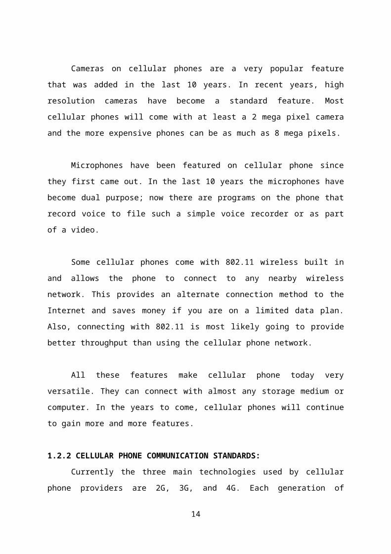
Cameras on cellular phones are a very popular feature
that was added in the last 10 years. In recent years, high
resolution cameras have become a standard feature. Most
cellular phones will come with at least a 2 mega pixel camera
and the more expensive phones can be as much as 8 mega pixels.
Microphones have been featured on cellular phone since
they first came out. In the last 10 years the microphones have
become dual purpose; now there are programs on the phone that
record voice to file such a simple voice recorder or as part
of a video.
Some cellular phones come with 802.11 wireless built in
and allows the phone to connect to any nearby wireless
network. This provides an alternate connection method to the
Internet and saves money if you are on a limited data plan.
Also, connecting with 802.11 is most likely going to provide
better throughput than using the cellular phone network.
All these features make cellular phone today very
versatile. They can connect with almost any storage medium or
computer. In the years to come, cellular phones will continue
to gain more and more features.
1.2.2 CELLULAR PHONE COMMUNICATION STANDARDS:
Currently the three main technologies used by cellular
phone providers are 2G, 3G, and 4G. Each generation of
14

technology uses a different transmission protocol. The
transmission protocols dictate how a cellular phone
communicates with the tower. Some examples are: frequency
division multiple access (FDMA), time division multiple access
(TDMA), code division multiple access (CDMA), Global System
for Mobile Communication (GSM), CDMA2000, wide-band code
division multiple access (WCDMA), and time division
synchronous code division multiple access (TD-SCDMA). All of
these protocols typically operates in the 824-894 MHz band in
the United States. Some protocols such as GSM (depending on
the provider) will use the 1800-2000 MHz band.
1.3 OVERVIEW OF CELL PHONE DETECTOR:
Demo Circuit:
IC1 is designed as a differential
amplifier Non inverting input is connected
to the potential divider R1, R2. Capacitor
15
R1 1M
R2 100K
C1 0.22
C2 47 UF
R3 1M
LED
IC 3130
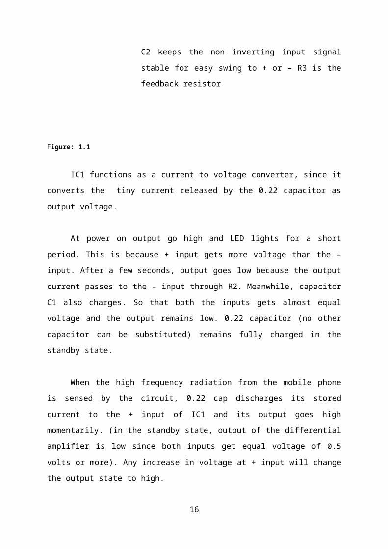
C2 keeps the non inverting input signal
stable for easy swing to + or – R3 is the
feedback resistor
Figure: 1.1
IC1 functions as a current to voltage converter, since it
converts the tiny current released by the 0.22 capacitor as
output voltage.
At power on output go high and LED lights for a short
period. This is because + input gets more voltage than the –
input. After a few seconds, output goes low because the output
current passes to the – input through R2. Meanwhile, capacitor
C1 also charges. So that both the inputs gets almost equal
voltage and the output remains low. 0.22 capacitor (no other
capacitor can be substituted) remains fully charged in the
standby state.
When the high frequency radiation from the mobile phone
is sensed by the circuit, 0.22 cap discharges its stored
current to the + input of IC1 and its output goes high
momentarily. (in the standby state, output of the differential
amplifier is low since both inputs get equal voltage of 0.5
volts or more). Any increase in voltage at + input will change
the output state to high.
16

The circuit can detect both the incoming and outgoing
calls, SMS and video transmission even if the mobile phone is
kept in the silent mode. The moment the bug detects RF
transmission signal from an activated mobile phone, it starts
sounding a beep alarm and the LED blinks. The alarm continues
until the signal transmission ceases. An ordinary RF detector
using tuned LC circuits is not suitable for detecting signals
in the GHz frequency band used in mobile phones. The
transmission frequency of mobile phones ranges from 0.9 to 3
GHz with a wavelength of 3.3 to 10 cm. So a circuit detecting
gigahertz signals required for a mobile bug.
Here the circuit uses a 0.22μF disk capacitor (C3) to
capture the RF signals from the mobile phone. The lead length
of the capacitor is fixed as 18 mm with a spacing of 8 mm
between the leads to get the desired frequency. The disk
capacitor along with the leads acts as a small gigahertz loop
antenna to collect the RF signals from the mobile phone.
Op-amp IC CA3130 (IC1) is used in the circuit as a
current-to-voltage converter with capacitor C3 connected
between its inverting and non-inverting inputs. It is a CMOS
version using gate-protected p-channel MOSFET transistors in
the input to provide very high input impedance, very low input
current and very high speed of performance. The output CMOS
transistor is capable of swinging the output voltage to within
10 mV of either supply voltage terminal.
17
Capacitor C3 in conjunction with the lead inductance acts
as a transmission line that intercepts the signals from the
mobile phone. This capacitor creates a field, stores energy
and transfers the stored energy in the form of minute current
to the inputs of IC1.This will upset the balanced input of IC1
and convert the current into the corresponding output voltage.
Capacitor C4 along with high-value resistor R1 keeps the
non-inverting input stable for easy swing of the output to
high state. Resistor R2 provides the discharge path for
capacitor C4.Feedback resistor R3 makes the inverting input
high when the output becomes high. Capacitor C5 (47pF) is
connected across ‘strobe’ (pin 8) and ‘null’ inputs (pin 1) of
IC1 for phase compensation and gain control to optimise the
frequency response.
When the mobile phone signal is detected by C3, the
output of IC1 becomes high and low alternately according to
the frequency of the signal as indicated by LED1. This
triggers mono stable timer IC2 through capacitor C7. Capacitor
C6 maintains the base bias of transistor T1 for fast switching
action. The low-value timing components R6 and C9 produce very
short time delay to avoid audio nuisance.
Assemble the circuit on PCB and enclose in a small box
like junk mobile case. As mentioned earlier, capacitor C3
should have a lead length of 18 mm with lead spacing of 8 mm.
Carefully solder the capacitor in standing position with equal
18
spacing of the leads. The response can be optimised by
trimming the lead length of C3 for the desired frequency. You
may use a short telescopic type antenna.
1.3.1 Mobile Bug:
Normally IC1 is off. So IC2 will be also off.
When the power is switched on, as stated above, IC1 will give
a high output and T1 conducts to trigger LED and Buzzer .This
can be a good indication for the working of the circuit.
19

1.4 CIRCUIT DIAGRAM:
Figure 1.2: Circuit Diagram of Cell Phone Detector
20
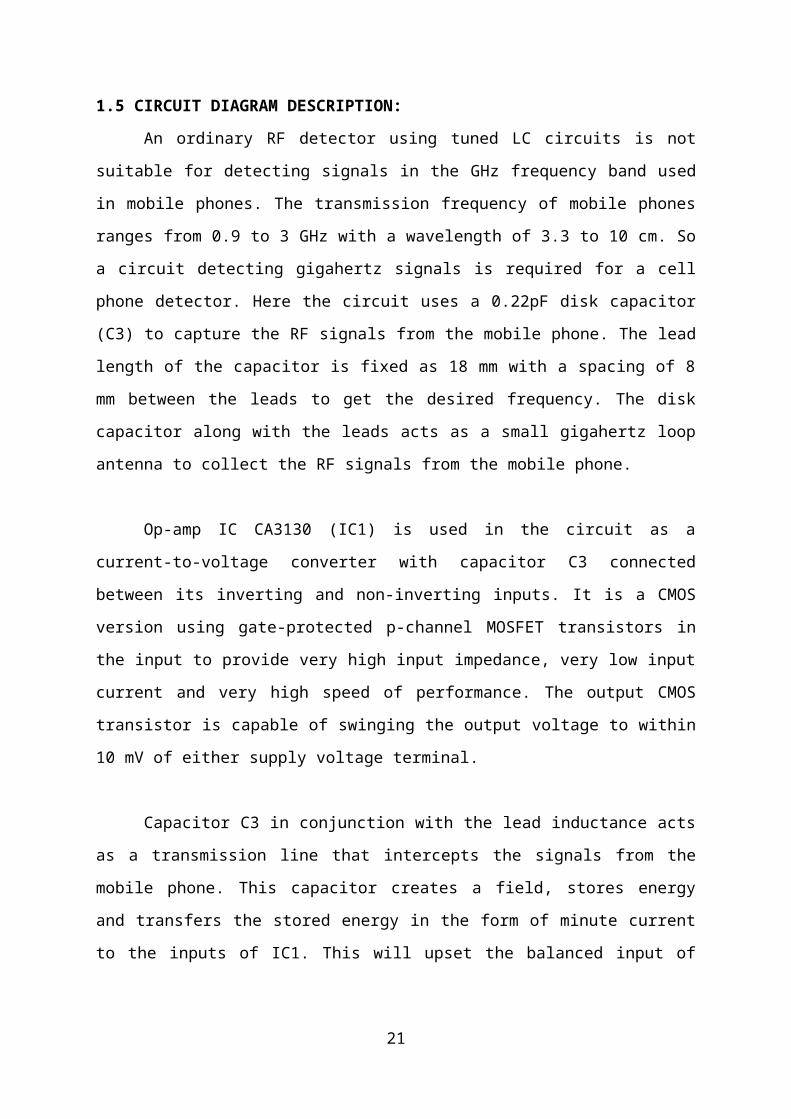
1.5 CIRCUIT DIAGRAM DESCRIPTION:
An ordinary RF detector using tuned LC circuits is not
suitable for detecting signals in the GHz frequency band used
in mobile phones. The transmission frequency of mobile phones
ranges from 0.9 to 3 GHz with a wavelength of 3.3 to 10 cm. So
a circuit detecting gigahertz signals is required for a cell
phone detector. Here the circuit uses a 0.22pF disk capacitor
(C3) to capture the RF signals from the mobile phone. The lead
length of the capacitor is fixed as 18 mm with a spacing of 8
mm between the leads to get the desired frequency. The disk
capacitor along with the leads acts as a small gigahertz loop
antenna to collect the RF signals from the mobile phone.
Op-amp IC CA3130 (IC1) is used in the circuit as a
current-to-voltage converter with capacitor C3 connected
between its inverting and non-inverting inputs. It is a CMOS
version using gate-protected p-channel MOSFET transistors in
the input to provide very high input impedance, very low input
current and very high speed of performance. The output CMOS
transistor is capable of swinging the output voltage to within
10 mV of either supply voltage terminal.
Capacitor C3 in conjunction with the lead inductance acts
as a transmission line that intercepts the signals from the
mobile phone. This capacitor creates a field, stores energy
and transfers the stored energy in the form of minute current
to the inputs of IC1. This will upset the balanced input of
21

IC1 and convert the current into the corresponding output
voltage.
Capacitor C4 along with high-value resistor R1 keeps the
non-inverting input stable for easy swing of the output to
high state. Resistor R2 provides the discharge path for
capacitor C4. Feedback resistor R3 makes the inverting input
high when the output becomes high. Capacitor C5 (47pF) is
connected across ‘strobe’ (pin 0 and ‘null’ inputs (pin 1) of
IC1 for phase compensation and gain control to optimise the
frequency response.
When the mobile phone signal is detected by C3, the
output of IC1 becomes high and low alternately according to
the frequency of the signal as indicated by LED1. This
triggers monostable timer IC2 through capacitor C7. Capacitor
C6 maintains the base bias of transistor T1 for fast switching
action. The low-value timing components R6 and C9 produce very
short time delay to avoid audio nuisance.
CHAPTER TWO
2.1 INTRODUCTION:
In this chapter we will discuss about the block diagram
of the cell phone detector and also the description of it, PCB
layout and PCB fabrication also included in this chapter to
explain the description of cell detector thoroughly in a
suitable manner. But before this we have to see the main
aspects about this which performs an important role.
22

Using a down converter, voltage controlled oscillator
(VCO), and a bandpass filter in the second technique explored
for cellular phone detection. Two signals inputted in the down
converter. The first signal is from the antenna and is between
829-835 MHz depending on the cellular phone (832 MHz for this
experiment). The signal is from the VCO, which is tuned to 800
MHz band. The down converter multiplies the two signals
together producing the sum and the difference. This is then
filtered by a bandpass filter with the passband lower and
upper edges respectively at 28 MHz and 36 MHz band. Filtering
eliminates the sum of the signals and any environmental noise.
Now all the remains is the difference, a 29-35 MHz signal that
indicates an active cellular phone is in the area. This can
easily be converted using analog to digital converters and
output to an alarm or a computer. Let us see the PCB layout
introduction it will help us in this chapter.
Schematic driven layout is the concept in IC
Layout or PCB layout where the EDA software links the
schematic and layout databases. It was one of the first big
steps forward in layout software from the days when editing
tools were simply handling drawn polygons.
Schematic driven layout allows for several features that make
the layout designer's job easier and faster. One of the most
important is that changes to the circuit schematic are easily
translated to the layout. Another is that the connections
23
between components in the schematic are graphically displayed
in the layout ensuring work is correct by construction.
A printed circuit board, or PCB, is used to mechanically
support and electrically connect electronic components using
components pathways. When the board has only copper tracks and
features, and no circuit elements such as capacitors,
resistors or active devices have been manufactured into the
actual substrate of the board, it is more correctly referred
to as printed wiring board (PWB) or etched wiring board. Use
of the term PWB or printed wiring board although more accurate
and distinct from what would be known as a true printed
circuit board, has generally fallen by the wayside for many
people as the distinction between circuit and wiring has
become blurred. Today printed wiring (circuit) boards are used
in virtually all but the simplest commercially produced
electronic devices, and allow fully automated assembly
processes that were not possible or practical in earlier era
tag type circuit assembly processes.
A PCB populated with electronic components is called
a printed circuit assembly (PCA), printed circuit board
assembly or PCB Assembly (PCBA). In informal use the term
"PCB" is used both for bare and assembled boards, the context
clarifying the meaning.
Alternatives to PCBs include wire wrap and point-to-point
construction. PCBs must initially be designed and laid out,
24

but become cheaper, faster to make, and potentially more
reliable for high-volume production since production and
soldering of PCBs can be automated. Much of the electronics
industry's PCB design, assembly, and quality control needs are
set by standards published by the IPC organization.
Excluding exotic products using special materials or
processes, all printed circuit boards manufactured today can
be built using the following four items which are usually
purchased from manufacturers:
(i) Laminates
(ii) Copper-clad Laminates
(iii) Resin impregnated B-stage cloth (pre-preg)
(iv) Copper foil
Laminates are manufactured by curing under pressure and
temperature layers of cloth or paper with thermo set resin to
form an integral final piece of uniform thickness. The size
can be up to 4 by 8 feet (1.2 by 2.4 m) in width and length.
Varying cloth weaves (threads per inch or cm), cloth
thickness, and resin percentage are used to achieve the
desired final thickness and dielectric characteristics.
Each trace consists of a flat, narrow part of
the copper foil that remains after etching. The resistance,
determined by width and thickness, of the traces must be
sufficiently low for the current the conductor will carry.
Power and ground traces may need to be wider than signal
25
traces. In a multi-layer board one entire layer may be mostly
solid copper to act as a ground plane for shielding and power
return. For microwave circuits, transmission lines can be laid
out in the form of striplines and micro strips with carefully
controlled dimensions to assure a consistent impedance.
In radio-frequency and fast switching circuits
the inductance and capacitance of the printed circuit board
conductors become significant circuit elements, usually
undesired; but they can be used as a deliberate part of the
circuit design, obviating the need for additional discrete
components.
"Multi layer" printed circuit boards have trace layers
inside the board. One way to make a 4-layer PCB is to use a
two-sided copper-clad laminate, etch the circuitry on both
sides, then laminate to the top and bottom pre-preg and copper
foil. Lamination is done by placing the stack of materials in
a press and applying pressure and heat for a period of time.
This results in an inseparable one piece product. It is then
drilled, plated, and etched again to get traces on top and
bottom layers.
Finally the PCB is covered with solder mask, marking
legend, and a surface finish may be applied. Multi-layer PCB's
allows for much higher component density.
26

Block Diagam:
27

Above diagram shows how a cellular phone detector works
by using Down Converter, Bandpass Filter, and Voltage
Controlled Oscillator (VCO). Now we will see how our cell
phone detector works without using above devices.
2.2 BLOCK DIAGRAM OF CELL PHONE DETECTOR:
28
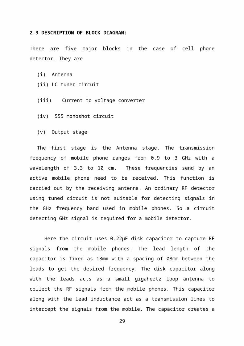
2.3 DESCRIPTION OF BLOCK DIAGRAM:
There are five major blocks in the case of cell phone
detector. They are
(i) Antenna
(ii) LC tuner circuit
(iii) Current to voltage converter
(iv) 555 monoshot circuit
(v) Output stage
The first stage is the Antenna stage. The transmission
frequency of mobile phone ranges from 0.9 to 3 GHz with a
wavelength of 3.3 to 10 cm. These frequencies send by an
active mobile phone need to be received. This function is
carried out by the receiving antenna. An ordinary RF detector
using tuned circuit is not suitable for detecting signals in
the GHz frequency band used in mobile phones. So a circuit
detecting GHz signal is required for a mobile detector.
Here the circuit uses 0.22µF disk capacitor to capture RF
signals from the mobile phones. The lead length of the
capacitor is fixed as 18mm with a spacing of 08mm between the
leads to get the desired frequency. The disk capacitor along
with the leads acts as a small gigahertz loop antenna to
collect the RF signals from the mobile phones. This capacitor
along with the lead inductance act as a transmission lines to
intercept the signals from the mobile. The capacitor creates a
29

field, stores energy and transfers the stored energy in the
form of minute current to the input of a current to voltage
converter circuit. This forms the second stage which is LC
Tuner stage.
The current coming to the input of the converter IC,
upset its balanced input and then convert the current into
corresponding output voltage. When the mobile phone signals
are detected by the input capacitor, the output of the
converter IC, becomes high and low as indicated by the LED.
This triggers the monostable circuit also. The low value
timing components R and C produce very short time delay to
avoid audio nuisance. A buzzer is triggered by using the
output of the monoshot timer. The buzzer along with the LEDF
forms the output stage that provide us the indication as sound
and light respectively.
2.3.1 TRANSMISSION LINE:
A transmission line conveys electromagnetic waves. A pair
of parallel wires and coaxial cables is the commonly employed
transmission lines. It is used to connect transmitter and
antenna, receiver and antenna etc. At low frequency the energy
loss in the connecting wires is negligible. But for higher
frequency the loss can be reduced by using two parallel wires,
one for forward connection and the other for return current. A
transmission line is characterized by its lumped parameter as
described below.
30

Series Resistance:
Due to finite conductivity of the conductors, there is a
uniform distributed resistance. There is also power loss due
to radiation from the lines. Thus the finite conductivity and
radiation loss can be modeled as a series resistance per loop
of length.
Series Inductance:
A current carrying conductor has an associated magnetic
field. Both, the grow and decay of the current is opposed, and
hence it possesses inductance. This inductance is distributed
throughout the line. It acts in series.
Series Capacitance:
The two conducting wires is separated by a distance,
situated in a dielectric medium gives rise to a capacitance
that acts parallel with the wires.
Shunt Leakage Conductance:
Since the wires are separated by a dielectric medium that
cannot be perfect in its insulation, current leaks through it
when the lines carry a current. This leakage of current
through the dielectric between the wires is represented by a
shunt conductance per unit length.
2.4 PCB Layout of the Cell Phone Detector Circuit:
31
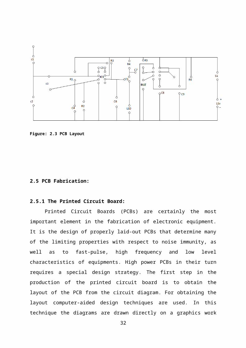
Figure: 2.3 PCB Layout
2.5 PCB Fabrication:
2.5.1 The Printed Circuit Board:
Printed Circuit Boards (PCBs) are certainly the most
important element in the fabrication of electronic equipment.
It is the design of properly laid-out PCBs that determine many
of the limiting properties with respect to noise immunity, as
well as to fast-pulse, high frequency and low level
characteristics of equipments. High power PCBs in their turn
requires a special design strategy. The first step in the
production of the printed circuit board is to obtain the
layout of the PCB from the circuit diagram. For obtaining the
layout computer-aided design techniques are used. In this
technique the diagrams are drawn directly on a graphics work
32

station. The software then checks for any design and layout
rules error. After correction of errors, if any, the layout is
obtained based on this layout the printed circuit boards are
fabricated from copper-clad laminates.
2.5.2 Copper-Clad Laminates:
A laminate can be simply described as the product
obtained by pressing layers of a filler material impregnated
with resin under heat and pressure. The commonly used fillers
are a variety of papers, or glass in various forms such as
cloths and continuous filament mat. The resigns could be
phenolic, epoxy, polyester, PTFE (Polytetrafluroethylene),
etc. Each of this fillers and resins contributes intrinsically
to the characteristic properties of the finished copper-clad
laminates. It is further possible to manipulate the properties
of copper clad laminates by fine variations in the
manufacturing process. The large range of possible copper clad
laminates has been standardized in the national and
international specifications. Thus, there are exactly laid
down specification for each copper-clad laminate grade, being
defined by the resin/filler system and the minimum/maximum
limits of the properties. A copper-clad laminate must have a
good copper-to-base laminate bond strength. The appearance of
copper side must be smooth and uniform. All these properties
must be retained during the production of PCB and also under
its working conditions. All electrical and mechanical
properties of the laminates are affected by the environmental
conditions such as humidity, temperature corrosive atmosphere
33

etc. Similarly most of the electrical properties vary with
changing in frequency. Thus while choosing the copper-clad
laminates the various environmental conditions likely to be
encountered are to be considered.
2.5.3 Board Cleaning Before Pattern Transfer:
After choosing the copper-clad laminate it should be
cleaned. The cleaning of the copper-clad prior to resist
application is an essential step for any PCB process using
etch or plating resist. Insufficient cleaning is one of the
reasons most often encountered for difficulties in PCB
fabrication although it might not always be immediately
recognized as this. But it is quite often the reason for poor
resist-adhesion, uneven photo resist-film, pinholes, poor
plating-adhesion, etc. The first step in cleaning process is
scrubbing with a pumice/salt solution. This removes inorganic
matters like particulates and oxide and also performs
degreasing up to a certain extent. The pumice used is of a
very fine grade to minimize deep scratches. After scrubbing
with the abrasive, a water rinse is done to remove slurry.
This is followed by a strong acid dip in hydrochloric acid (10
vol %) which will residual alkali and metallic oxides and
prepare the surface for maximum resist adhesion. A final rinse
using de-ionized gives guarantees that no fresh contamination
is brought on to the surface. The time span until the next
processing step which is screen-printing is made as short as
possible to minimize the formation of fresh oxides.
34

2.5.4 Screen Printing:
Screen-printing is the process by which the conductor
pattern which is on the film master is transferred on to the
copper-clad laminates. With the screen-printing process one
can produce PCBs with a conductor width as low as 2.5mm and
registration error of just 0.1mm on an industrial scale with a
high reliability.
In its basis form the screen-printing process is very
simple. A screen fabric with uniform meshes and openings is
stretched and fixed on a solid frame of a metal or wood. The
circuit pattern is photographically transferred on to the
screen, leaving the meshes in pattern area open, while meshes
in the rest of area are closed. In the actual printing step,
ink is forced by the moving squeegee through the open meshes
on to the surface of material to be printed. The ink
deposition in a magnified cross-section shows the shape of
trapezoid. The ideal screen printing ink should have many
features which cannot be combined. It should dry rapidly on
the PCB but dry slowly on the screen. It should be highly
resistant against all the chemicals but easy to be stripped.
2.5.5 Etching:
After drying of the resist of the copper-clad laminate
the next process is etching. The final copper pattern is
formed by selective removal of all unwanted copper, which is
not protected by etch resist. For small scale PCB production
35
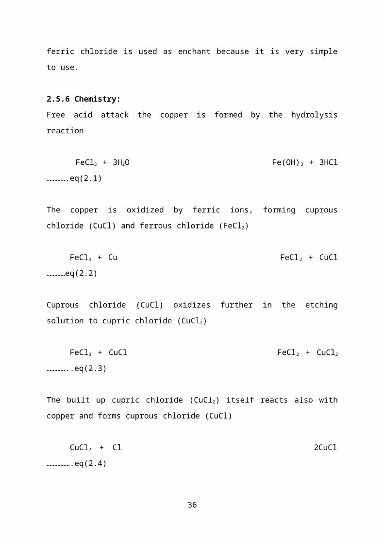
ferric chloride is used as enchant because it is very simple
to use.
2.5.6 Chemistry:
Free acid attack the copper is formed by the hydrolysis
reaction
FeCl3 + 3H2O Fe(OH)3 + 3HCl
………….eq(2.1)
The copper is oxidized by ferric ions, forming cuprous
chloride (CuCl) and ferrous chloride (FeCl2)
FeCl3 + Cu FeCl2 + CuCl
…………eq(2.2)
Cuprous chloride (CuCl) oxidizes further in the etching
solution to cupric chloride (CuCl2)
FeCl3 + CuCl FeCl2 + CuCl2
…………..eq(2.3)
The built up cupric chloride (CuCl2) itself reacts also with
copper and forms cuprous chloride (CuCl)
CuCl2 + Cl 2CuCl
…………….eq(2.4)
36

After etching is over the ferric chloride, contaminated
surface should be cleaned. After a simple spray water rinse, a
dip in a 5% (volume) oxalic acid solution is done to remove
the copper and iron salt. A vigorous final water rinse has to
flow.
2.5.7 Drilling:
After the etching operation the next step is drilling of
component mounting holes in the PCBs. Holes are made by
drilling whenever a superior holes finish or plated-through
holes process is required and where the tool costs for a
punching tool cannot be justified. Therefore drilling is
applied by all the professional grade PCB manufacturer and
generally and in all the smaller PCB production plan and in
laboratories. The importance of holes drilling into PCBs has
further gone up with electronic component miniaturization and
is need for smaller diameters (diameter less than half the
board thickness) and higher package density where hole
punching is practically ruled out. This is done using drilling
machines with suitable size drill bits. To compensate for
laminate resilience the drill bit diameter is chosen 0.05mm
bigger than the holes diameter expected. The usual size of
hole is 0.8 mm and for bigger components like preset and power
devices the size is 1.2 mm. The production of holes with
diameter and tolerances as specified above should not need any
special attention: a suitable drilling machine with a
correctly sharpened drill bit will provide these results.
After drilling the required number of holes of specified
37
dimensions the next step is mounting the components on the
PCB.
2.5.8 Component Mounting:
Component mounting on the PCB in such a way to minimize
the cracking of solder joints due to mechanical stress on the
joint. This can be ensured by bending of the axial component
lead in a manner to guarantee and optimum retention of the
component on the PCB while a minimum stress is introduced on
the solder joint. Bending is done with care taken not to
damage the component or its leads. The lead bending radius is
chosen to be approximately two times the lead diameter. The
bent leads should fit into the holes perpendicular to the
board so that any stress on the component lead junction is
minimized. The component lead bending is done using a bending
tool for easy but perfect component preparation.
2.5.9 Soldering:
Soldering is the process of joining metals by using lower
melting point metal or alloy with joining surface.
Solder:
Soldering is the process of joining materials. Soldered
joints in electronics switches will establish strong
electrical connection between components leads. The popularly
used solders are alloys of tin and lead melt below the melting
point of the tin.
38
Flux:
In order to make the surface accept to make the solder
readily, the component terminals should be free from oxide and
other obstructing films. The leads should be cleaned
chemically or by abrasion using blades or knives.
A small amount of lead coating can be done on cleaned
portion of the lead using soldered iron. This process is
called thinning. Zink Chloride or Ammonium Chloride separately
or in combination is mostly used as fluxes. These are
available in petroleum jelly as paste flux. The residue which
remains after soldering may be washed out with more water
accompanied by brushing.
Soldering Iron:
It is tool used to melt solder and apply at the joint in
the circuit. It operates at 230v supply. The iron bit at the
tip of it gets heated within few minutes. 50W or 25W soldering
irons are commonly used for soldering purpose.
2.5.10 Soldering Steps:
For proper soldering on PCBs the soldering steps are:
(i) Make the layout of component in the circuit. Plug in the
cord of the soldering iron into the mains to get heated.
(ii) Straighten and remove the coating of components leads
using a blade or knife. Apply a little flux on the leads. Take
39

a little solder on soldering iron and apply the molten solder
on the leads. Care must be taken to avoid the components to
getting heated up.
(iii) Mount the components on PCB by bending the leads of
components using noise pliers.
(iv) Apply flux on the joints and solder the joints. Soldering
must be done in minimum to avoid the dry soldering and heating
up of components.
(v) Wash the residue using water and brush.
CHAPTER THREE
3.1 Introduction:
40
In this chapter we will see the components used in the
cell phone detector and also discuss about the main aspects of
their working and features. But before the discussing of above
let us see about some quality of the semiconductor devices.
Semiconductor devices are electronic components that
exploit the electronic properties of semiconductor materials,
principally silicon, germanium, and gallium arsenide, as well
as organic semiconductors. Semiconductor devices have
replaced thermionic devices (vacuum tubes) in most
applications. They use electronic conduction in the solid
state as opposed to the gaseous state or thermionic
emission in a high vacuum.
Semiconductor devices are manufactured both as single
discrete devices and as integrated circuits(ICs), which
consist of a number—from a few (as low as two) to billions—of
devices manufactured and interconnected on a single
semiconductor substrate, or wafer.
Semiconductor materials are so useful because their behavior
can be easily manipulated by the addition of impurities, known
as doping. Semiconductor conductivity can be controlled by
introduction of an electric or magnetic field, by exposure
to light or heat, or by mechanical deformation of a doped mono
crystalline grid; thus, semiconductors can make excellent
sensors.
41
Current conduction in a semiconductor occurs via mobile
or "free" electrons and holes, collectively known as charge
carriers. Doping a semiconductor such as silicon with a small
amount of impurity atoms, such as phosphorus or boron, greatly
increases the number of free electrons or holes within the
semiconductor. When a doped semiconductor contains excess
holes it is called "p-type", and when it contains excess free
electrons it is known as “n-type”, where p (positive
for holes) or n (negative for electrons) is the sign of the
charge of the majority mobile charge carriers. The
semiconductor material used in devices is doped under highly
controlled conditions in a fabrication facility.
By far, silicon (Si) is the most widely used material in
semiconductor devices. Its combination of low raw material
cost, relatively simple processing, and a useful temperature
range make it currently the best compromise among the various
competing materials. Silicon used in semiconductor device
manufacturing is currently fabricated into bowls that are
large enough in diameter to allow the production of 300 mm (12
in.) wafers.
Germanium (Ge) was a widely used early semiconductor
material but its thermal sensitivity makes it less useful than
silicon. Today, germanium is often alloyed with silicon for
use in very-high-speed SiGe devices.
42
Gallium arsenide (GaAs) is also widely used in high-speed
devices but so far, it has been difficult to form large-
diameter bowls of this material, limiting the wafer diameter
to sizes significantly smaller than silicon wafers thus making
mass production of GaAs devices significantly more expensive
than silicon. Other less common materials are also in use or
under investigation.
Silicon carbide (SiC) has found some application as the
raw material for blue light-emitting diodes (LEDs) and is
being investigated for use in semiconductor devices that could
withstand very high operating temperatures and environments
with the presence of significant levels of ionizing radiation.
Various indium compounds (indium arsenide,
indium antimonde, and indium phosphide) are also being used in
LEDs and solid state laser diodes. Selenium sulfide is being
studied in the manufacture of photovoltaic solar cells. The
most common use for organic semiconductors is Organic light-
emitting diodes.
Semiconductors are the foundation of modern electronics,
including radio, computers, and telephones. Semiconductor-
based electronic components include transistors, solar cells,
many kinds of diodes including the light-emitting diode (LED),
the silicon controlled rectifier, photo-diodes, and digital
and analog integrated circuits. Increasing understanding of
semiconductor materials and fabrication processes has made
43

possible continuing increases in the complexity and speed of
semiconductor devices, an effect known as Moore's law.
Semiconductors are defined by their unique electric
conductive behavior. Metals are good conductors because at
their Fermi level, there is a large density of energetically
available states that each electron can occupy. Electrons can
move quite freely between energy levels without a high energy
cost. Metal conductivity decreases with temperature increase
because thermal vibrations of crystal lattice disrupt the free
motion of electrons. Insulators, by contrast, are very poor
conductors of electricity because there is a large difference
in energies (called a band gap) between electron-occupied
energy levels and empty energy levels that allow for electron
motion.
In the classic crystalline semiconductors, electrons can
have energies only within certain bands (ranges). The range of
energy runs from the ground state, in which electrons are
tightly bound to the atom, up to a level where the electron
can escape entirely from the material. Each energy band
corresponds to a large number of discrete quantum states of
the electrons. Most of the states with low energy (closer to
the nucleus) are occupied, up to the valence band.
Semiconductors and insulators are distinguished
from metals by the population of electrons in each band. The
valence band in any given metal is nearly filled with
44
electrons under usual conditions, and metals have many free
electrons with energies in the conduction band. In
semiconductors, only a few electrons exist in the conduction
band just above the valence band, and an insulator has almost
no free electrons.
The ease with which electrons in the semiconductor can be
excited from the valence band to the conduction band depends
on the band gap. The size of this energy gap (band gap)
determines whether a material is semiconductor or
an insulator (nominally this dividing line is roughly 4 eV).
In a crystal, many atoms are adjacent and many energy
levels are possible for electrons. Since there are so many (on
the order of 1022) atoms in a macroscopic crystal, the
resulting energy states available for electrons are very
closely spaced. Since the Heisenberg principle limits the
precision of any measurement of the combination of an
electron's momentum (related to energy) and its position, in a
crystal effectively the available energy levels form a
continuous band of allowed energy levels.
The concept of holes can also be applied to metals, where
the Fermi level lies within the conduction band. With most
metals the Hall effect indicates electrons are the charge
carriers. However, some metals have a mostly filled conduction
band. In these, the Hall effect reveals positive charge
carriers, which are not the ion-cores, but holes. In the case
45

of a metal, only a small amount of energy is needed for the
electrons to find other unoccupied states to move into, and
hence for current to flow. Sometimes even in this case it may
be said that a hole was left behind, to explain why the
electron does not fall back to lower energies: It cannot find
a hole. In the end in both materials electron-
phonon scattering and defects are the dominant causes
for resistance.
The conductivity of semiconductors may easily be modified
by introducing impurities into their crystal lattice. The
process of adding controlled impurities to a semiconductor is
known as doping. The amount of impurity, or dopant, added to
an intrinsic (pure) semiconductor varies its level of
conductivity. Doped semiconductors are referred to
as extrinsic. By adding impurity to pure semiconductors, the
electrical conductivity may be varied by factors of thousands
or millions.
A 1 cm3 specimen of a metal or semiconductor has of the
order of 1022 atoms. In a metal, every atom donates at least
one free electron for conduction, thus 1 cm3 of metal contains
on the order of 1022 free electrons. Whereas a 1 cm3 of sample
pure germanium at 20 °C, contains about 4.2×10²² atoms but only
2.5×10¹³ free electrons and 2.5×10¹³ holes. The addition of
0.001% of arsenic (an impurity) donates an extra 1017 free
electrons in the same volume and the electrical conductivity
is increased by a factor of 10,000.
46

ICs were made possible by experimental discoveries
showing that semiconductor devices could perform the functions
of vacuum tubes and by mid-20th-century technology
advancements in semiconductor device fabrication. The
integration of large numbers of tiny transistors into a small
chip was an enormous improvement over the manual assembly of
circuits using discrete electronic components. The integrated
circuits, mass production capability, reliability, and
building-block approach to circuit design ensured the rapid
adoption of standardized Integrated Circuits in place of
designs using discrete transistors.
There are two main advantages of ICs over discrete
circuits: cost and performance. Cost is low because the chips,
with all their components, are printed as a unit
by photolithography rather than being constructed one
transistor at a time. Furthermore, much less material is used
to construct a packaged IC die than to construct a discrete
circuit. Performance is high because the components switch
quickly and consume little power (compared to their discrete
counterparts) as a result of the small size and close
proximity of the components. As of 2012, typical chip areas
range from a few square millimeters to around 450 mm2, with up
to 9 million transistors per mm2. The electrical resistance of
an electrical conductor is the opposition to the passage of
an electric current through that conductor; the inverse
quantity is electrical conductance, the ease at which an
47

electric current passes. Electrical resistance shares some
conceptual parallels with the mechanical notion of friction.
The SI unit of electrical resistance is the ohm (Ω), while
electrical conductance is measured in siemens (S).
An object of uniform cross section has a resistance
proportional to its resistivity and length and inversely
proportional to its cross-sectional area. All materials show
some resistance, except for superconductors, which have a
resistance of zero.
Objects such as wires that are designed to have low
resistance so that they transfer current with the least loss
of electrical energy are called conductors. Objects that are
designed to have a specific resistance so that they can
dissipate electrical energy or otherwise modify how a circuit
behaves are called resistors. Conductors are made of high-
conductivity materials such as metals, in particular copper
and aluminium. Resistors, on the other hand, are made of a
wide variety of materials depending on factors such as the
desired resistance, amount of energy that it needs to
dissipate, precision, and costs.
3.2 List of Components:
RESISTORS1. R1 ________2.2M2. R2 ________100K3. R3 ________2.2M4. R4 ________1K
48
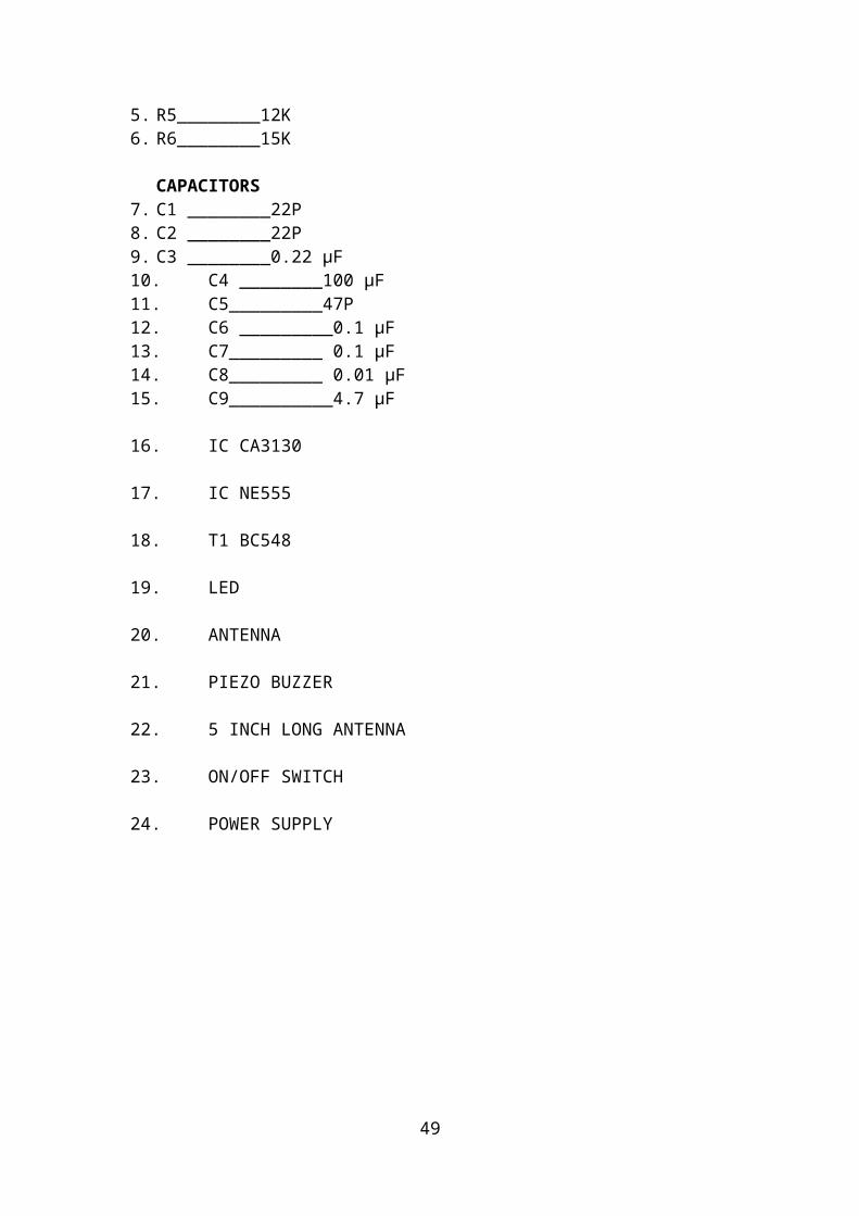
5. R5________12K6. R6________15K
CAPACITORS7. C1 ________22P8. C2 ________22P9. C3 ________0.22 µF10. C4 ________100 µF11. C5_________47P12. C6 _________0.1 µF13. C7_________ 0.1 µF14. C8_________ 0.01 µF15. C9__________4.7 µF
16. IC CA3130
17. IC NE555
18. T1 BC548
19. LED
20. ANTENNA
21. PIEZO BUZZER
22. 5 INCH LONG ANTENNA
23. ON/OFF SWITCH
24. POWER SUPPLY
49

3.3 Components Description:
3.3.1 Resistors:
Figure 3.1: Resistors
A resistor is a two-terminal electronic component that
produces a voltage across its terminals that is proportional
to the electric current through it in accordance with Ohm's
law:
V = IR
Resistors are elements of electrical networks and
electronic circuits and are ubiquitous in most electronic
equipment. Practical resistors can be made of various
50
compounds and films, as well as resistance wire (wire made of
a high-resistivity alloy, such as nickel/chrome).The primary
characteristics of a resistor are the resistance, the
tolerance, maximum working voltage and the power rating. Other
characteristics include temperature coefficient, noise, and
inductance. Less well-known is critical resistance, the value
below which power dissipation limits the maximum permitted
current flow, and above which the limit is applied voltage.
Critical resistance depends upon the materials constituting
the resistor as well as its physical dimensions; it's
determined by design. Resistors can be integrated into hybrid
and printed circuits, as well as integrated circuits. Size,
and position of leads (or terminals) are relevant to equipment
designers; resistors must be physically large enough not to
overheat when dissipating their power.
Significance:
Resistors are found in nearly every circuit because their
ability to limit current allows them to protect electronics
from circuit overload or destruction. Diodes, for example, are
current sensitive and so are almost always coupled with a
resistor when they are placed inside of a circuit. Resistors
are also combined with other electrical components to form
important fundamental circuits. They can be paired with
capacitors to perform as filters or voltage dividers. Another
role is that of the formation of oscillatory AC circuits when
they are coupled with capacitors and inductors.
51
Construction:
Resistors are typically formed from carbon encased in
lacquer but may be made from conductors or semiconductors.
Wire-wound ones are made from coils of metal wire and are
extremely accurate and heat resistant. Carbon film resistors
are made from carbon on a ceramic cylinder and photo
resistors, also called photocells, are made from materials
such as cadmium-sulfide.
Function:
Because resistors convert electrical energy into heat
they form heating elements in irons, toasters, heaters,
electric stoves, hair dryers and similar devices. Their
resistive properties cause them to generate light and are used
to create filaments in light bulbs.
As voltage dividers, resistors are placed in series with
each other. Their function is to produce a particular voltage
from an input that is fixed or variable. The output voltage is
proportional to that of the input and is usually smaller.
Voltage dividers are useful for components that need to
operate at a lesser voltage than that supplied by the input.
Resistors also help filter signals and are used in
oscillatory circuits in televisions and radios.
52

Resistors are used with transducers to make sensor
subsystems. Transducers are electronic components which
convert energy from one form into another, where one of the
forms of energy is electrical. A light dependent resistor,
or LDR, is an example of an input transducer. Changes in the
brightness of the light shining onto the surface of the LDR
result in changes in its resistance. As will be explained
later, an input transducer is most often connected along with
a resistor to make a circuit called a potential divider. In
this case, the output of the potential divider will be a
voltage signal which reflects changes in illumination.
Microphones and switches are input transducers. Output
transducers include loudspeakers, filament lamps and LEDs. Can
you think of other examples of transducers of each type?
In other circuits, resistors are used to direct current
flow to particular parts of the circuit, or may be used to
determine the voltage gain of an amplifier. Resistors are used
with capacitors to introduce time delays.
Most electronic circuits require resistors to make them
work properly and it is obviously important to find out
something about the different types of resistor available, and
to be able to choose the correct resistor value, in , , or
M , for a particular application.
53
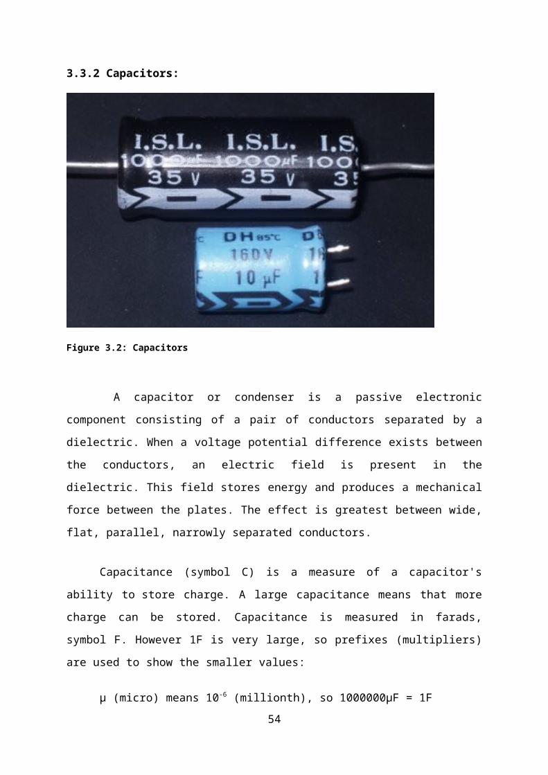
3.3.2 Capacitors:
Figure 3.2: Capacitors
A capacitor or condenser is a passive electronic
component consisting of a pair of conductors separated by a
dielectric. When a voltage potential difference exists between
the conductors, an electric field is present in the
dielectric. This field stores energy and produces a mechanical
force between the plates. The effect is greatest between wide,
flat, parallel, narrowly separated conductors.
Capacitance (symbol C) is a measure of a capacitor's
ability to store charge. A large capacitance means that more
charge can be stored. Capacitance is measured in farads,
symbol F. However 1F is very large, so prefixes (multipliers)
are used to show the smaller values:
µ (micro) means 10-6 (millionth), so 1000000µF = 1F54
n (nano) means 10-9 (thousand-millionth), so 1000nF = 1µF
p (pico) means 10-12 (million-millionth), so 1000pF = 1nF
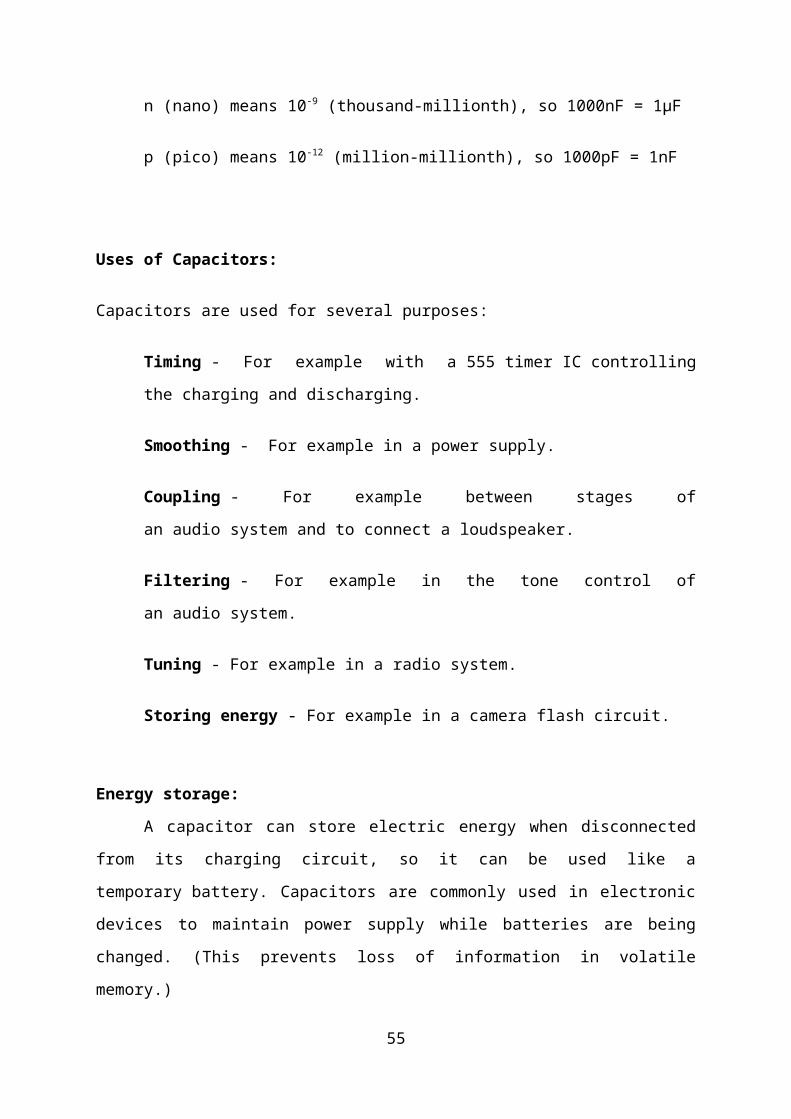
Uses of Capacitors:
Capacitors are used for several purposes:
Timing - For example with a 555 timer IC controlling
the charging and discharging.
Smoothing - For example in a power supply.
Coupling - For example between stages of
an audio system and to connect a loudspeaker.
Filtering - For example in the tone control of
an audio system.
Tuning - For example in a radio system.
Storing energy - For example in a camera flash circuit.
Energy storage:
A capacitor can store electric energy when disconnected
from its charging circuit, so it can be used like a
temporary battery. Capacitors are commonly used in electronic
devices to maintain power supply while batteries are being
changed. (This prevents loss of information in volatile
memory.)
55

Conventional electrostatic capacitors provide less than
360 joules per kilogram of energy density, while capacitors
using developing technology can provide more than
2.52 kilojoules per kilogram. In car audio systems, large
capacitors store energy for the amplifier to use on demand.
Power conditioning:
Reservoir capacitors are used in power supplies where
they smooth the output of a full or half wave rectifier. They
can also be used in charge pump circuits as the energy storage
element in the generation of higher voltages than the input
voltage.
Capacitors are connected in parallel with the power
circuits of most electronic devices and larger systems (such
as factories) to shunt away and conceal current fluctuations
from the primary power source to provide a "clean" power
supply for signal or control circuits. Audio equipment, for
example, uses several capacitors in this way, to shunt away
power line hum before it gets into the signal circuitry. The
capacitors act as a local reserve for the DC power source, and
bypass AC currents from the power supply. This is used in car
audio applications, when a stiffening capacitor compensates
for the inductance and resistance of the leads to the lead-
acid car battery.
Power factor correction:
56

In electric power distribution, capacitors are used
for power factor correction. Such capacitors often come as
three capacitors connected as a three phase load. Usually, the
values of these capacitors are given not in farads but rather
as a reactive power in volt-amperes reactive (VAr). The
purpose is to counteract inductive loading from devices
like electric motors and transmission lines to make the load
appear to be mostly resistive. Individual motor or lamp loads
may have capacitors for power factor correction, or larger
sets of capacitors (usually with automatic switching devices)
may be installed at a load center within a building or in a
large utility substation.
Noise filters and snubbers:
When an inductive circuit is opened, the current through
the inductance collapses quickly, creating a large voltage
across the open circuit of the switch or relay. If the
inductance is large enough, the energy will generate
an electric spark, causing the contact points to oxidize,
deteriorate, or sometimes weld together, or destroying a
solid-state switch. A snubber capacitor across the newly
opened circuit creates a path for this impulse to bypass the
contact points, thereby preserving their life; these were
commonly found in contact breaker ignition systems, for
instance. Similarly, in smaller scale circuits, the spark may
not be enough to damage the switch but will
still radiate undesirable radio frequency interference (RFI),
which a filter capacitor absorbs. Snubber capacitors are
57
usually employed with a low-value resistor in series, to
dissipate energy and minimize RFI. Such resistor-capacitor
combinations are available in a single package.
Capacitors are also used in parallel to interrupt units
of a high-voltage circuit breaker in order to equally
distribute the voltage between these units. In this case they
are called grading capacitors.
In schematic diagrams, a capacitor used primarily for DC
charge storage is often drawn vertically in circuit diagrams
with the lower, more negative, plate drawn as an arc. The
straight plate indicates the positive terminal of the device,
if it is polarized.
An ideal capacitor is characterized by a single constant
value, capacitance, which is measured in farads. This is the
ratio of the electric charge on each conductor to the
potential difference between them. In practice, the dielectric
between the plates passes a small amount of leakage current.
The conductors and leads introduce an equivalent series
resistance and the dielectric has an electric field strength
limit resulting in a breakdown voltage.
Capacitors are widely used in electronic circuits to
block the flow of direct current while allowing alternating
current to pass, to filter out interference, to smooth the
output of power supplies, and for many other purposes. They
are used in resonant circuits in radio frequency equipment to
58

select particular frequencies from a signal with many
frequencies.
(1) Ceramic capacitor:
In electronics ceramic capacitor is a capacitorconstructed of alternating layers of metal and ceramic, withthe ceramic material acting as the dielectric. The temperaturecoefficient depends on whether the dielectric is Class 1 orClass 2. A ceramic capacitor (especially the class 2) oftenhas high dissipation factor, high frequency coefficient ofdissipation.
Figure 3.3: ceramic capacitors
A ceramic capacitor is a two-terminal, non-polar device.The classical ceramic capacitor is the "disc capacitor". Thisdevice pre-dates the transistor and was used extensively invacuum-tube equipment (e.g., radio receivers) from about 1930through the 1950s, and in discrete transistor equipment fromthe 1950s through the 1980s. As of 2007, ceramic disccapacitors are in widespread use in electronic equipment,providing high capacity & small size at low price compared toother low value capacitor types.
Ceramic capacitors come in various shapes and styles,including:
(i) disc, resin coated, with through-hole leads
(ii) multi-layer rectangular block, surface mount
(iii) bare leadless disc, sits in a slot in the PCB and issoldered in place, used for UHF applications
(iv) tube shape, not popular now
59
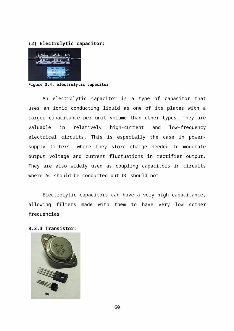
(2) Electrolytic capacitor:
Figure 3.4: electrolytic capacitor
An electrolytic capacitor is a type of capacitor that
uses an ionic conducting liquid as one of its plates with a
larger capacitance per unit volume than other types. They are
valuable in relatively high-current and low-frequency
electrical circuits. This is especially the case in power-
supply filters, where they store charge needed to moderate
output voltage and current fluctuations in rectifier output.
They are also widely used as coupling capacitors in circuits
where AC should be conducted but DC should not.
Electrolytic capacitors can have a very high capacitance,
allowing filters made with them to have very low corner
frequencies.
3.3.3 Transistor:
60

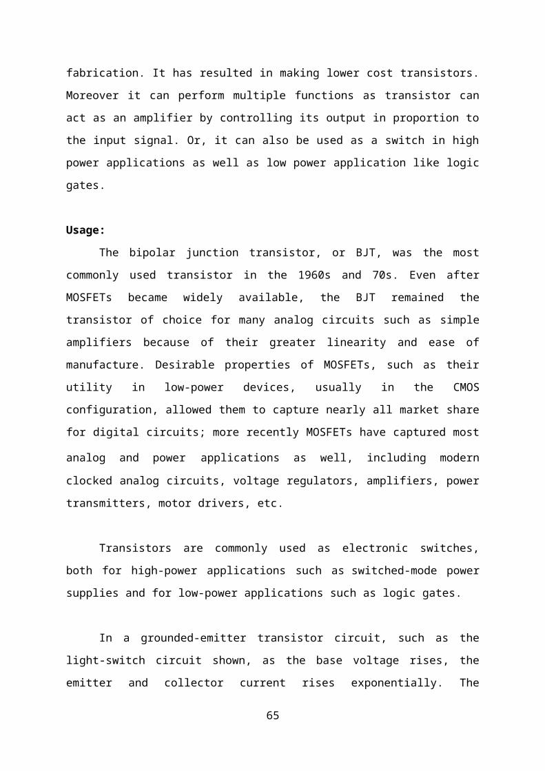
Figure 3.5: Transistors
A transistor is a semiconductor device commonly used to
amplify or switch electronic signals. A transistor is made of
a solid piece of a semiconductor material, with at least three
terminals for connection to an external circuit. A voltage or
current applied to one pair of the transistor's terminals
changes the current flowing through another pair of terminals.
Because the controlled (output) power can be much more than
the controlling (input) power, the transistor provides
amplification of a signal. Some transistors are packaged
individually but most are found in integrated circuits.
The transistor is the fundamental building block of
modern electronic devices, and its presence is ubiquitous in
modern electronic systems.
The first BJTs were made
from germanium (Ge). Silicon (Si) types currently predominate
but certain advanced microwave and high performance versions
now employ the compound semiconductor material gallium
arsenide (GaAs) and the semiconductor alloy silicon
germanium(SiGe). Single element semiconductor material (Ge and
Si) is described as elemental.
Rough parameters for the most common semiconductor materials
used to make transistors are given in the table to the right;
these parameters will vary with increase in temperature,
electric field, impurity level, strain, and sundry other
factors.
61

The junction forward voltage is the voltage applied to
the emitter-base junction of a BJT in order to make the base
conduct a specified current. The current increases
exponentially, as the junction forward voltage is increased.
The values given in the table are typical for a current of 1
mA (the same values apply to semiconductor diodes). The lower
the junction forward voltage the better, as this means that
less power is required to "drive" the transistor. The junction
forward voltage for a given current decreases with increase in
temperature. For a typical silicon junction the change is −2.1
mV/°C. In some circuits special compensating elements
(sensistors) must be used to compensate for such changes.
The density of mobile carriers in the channel of a MOSFET
is a function of the electric field forming the channel and of
various other phenomena such as the impurity level in the
channel. Some impurities, called dopants, are introduced
deliberately in making a MOSFET, to control the MOSFET
electrical behavior.
The electron mobility and hole mobility columns show the
average speed that electrons and holes diffuse through the
semiconductor material with an electric field of 1 volt per
meter applied across the material. In general, the higher the
electron mobility the faster the transistor can operate. The
table indicates that Ge is a better material than Si in this
62

respect. However, Ge has four major shortcomings compared to
silicon and gallium arsenide:
Its maximum temperature is limited; it has relatively
high leakage current; it cannot withstand high voltages; it is
less suitable for fabricating integrated circuits.
Because the electron mobility is higher than the hole
mobility for all semiconductor materials, a given bipolar NPN
transistor tends to be swifter than an equivalent PNP
transistor type. GaAs has the highest electron mobility of the
three semiconductors. It is for this reason that GaAs is used
in high frequency applications. A relatively recent FET
development, the high electron mobility transistor (HEMT), has
a hetero structure (junction between different semiconductor
materials) of aluminium gallium arsenide (AlGaAs)-gallium
arsenide (GaAs) which has twice the electron mobility of a
GaAs-metal barrier junction. Because of their high speed and
low noise, HEMTs are used in satellite receivers working at
frequencies around 12 GHz.
Maximum junction temperature values represent a cross
section taken from various manufacturers' data sheets. This
temperature should not be exceeded or the transistor may be
damaged.
Al–Si junction refers to the high-speed (aluminum–
silicon) metal–semiconductor barrier diode, commonly known as
a Schottky diode. This is included in the table because some
silicon power IGFETs have a parasitic reverse Schottky diode
63

formed between the source and drain as part of the fabrication
process. This diode can be a nuisance, but sometimes it is
used in the circuit.
Transistor works in such a manner that a current is
applied at one end consisting of one pair of terminals; it
brings changes in the current flowing through another pair of
terminals at other end. Since, the controlled power can be
much more than the controlling power, there takes place the
amplification of a signal. Info to know about transistor is
that there are some transistors which are packaged
individually however; normally the transistors are embedded in
integrated circuits.
One gets an idea about the importance of transistor from
the fact that nowadays, the use of transistor is almost there
in every electronic device. It won’t be inappropriate to say
about transistor that it has become the fundamental building
block of modern electronic devices, and its presence is
everywhere in modern electronic systems.
The transistor considered as the main component in almost
all walks of modern electronics, and is termed as one of the
greatest inventions of modern times.
The importance of transistor in today's life resides on
its capability to be mass produced using a highly automated
process which is possible due to semiconductor device
64
fabrication. It has resulted in making lower cost transistors.
Moreover it can perform multiple functions as transistor can
act as an amplifier by controlling its output in proportion to
the input signal. Or, it can also be used as a switch in high
power applications as well as low power application like logic
gates.
Usage:
The bipolar junction transistor, or BJT, was the most
commonly used transistor in the 1960s and 70s. Even after
MOSFETs became widely available, the BJT remained the
transistor of choice for many analog circuits such as simple
amplifiers because of their greater linearity and ease of
manufacture. Desirable properties of MOSFETs, such as their
utility in low-power devices, usually in the CMOS
configuration, allowed them to capture nearly all market share
for digital circuits; more recently MOSFETs have captured most
analog and power applications as well, including modern
clocked analog circuits, voltage regulators, amplifiers, power
transmitters, motor drivers, etc.
Transistors are commonly used as electronic switches,
both for high-power applications such as switched-mode power
supplies and for low-power applications such as logic gates.
In a grounded-emitter transistor circuit, such as the
light-switch circuit shown, as the base voltage rises, the
emitter and collector current rises exponentially. The
65

collector voltage drops because of reduced resistance from
collector to emitter. If the voltage difference between the
collector and emitter were zero (or near zero), the collector
current would be limited only by the load resistance (light
bulb) and the supply voltage. This is
called saturation because current is flowing from collector to
emitter freely. When saturated the switch is said to be on.
Providing sufficient base drive current is a key problem
in the use of bipolar transistors as switches. The transistor
provides current gain, allowing a relatively large current in
the collector to be switched by a much smaller current into
the base terminal. The ratio of these currents varies
depending on the type of transistor, and even for a particular
type, varies depending on the collector current. In the
example light-switch circuit shown, the resistor is chosen to
provide enough base current to ensure the transistor will be
saturated.
In any switching circuit, values of input voltage would
be chosen such that the output is either completely off, or
completely on. The transistor is acting as a switch, and this
type of operation is common in digital circuits where only
"on" and "off" values are relevant.
The common-emitter amplifier is designed so that a small
change in voltage (Vin) changes the small current through the
base of the transistor; the transistor's current amplification
66
combined with the properties of the circuit mean that small
swings in Vin produce large changes in Vout.
Various configurations of single transistor amplifier are
possible, with some providing current gain, some voltage gain,
and some both.
From mobile phones to televisions, vast numbers of
products include amplifiers for sound reproduction, radio
transmission, and signal processing. The first discrete
transistor audio amplifiers barely supplied a few hundred
milliwatts, but power and audio fidelity gradually increased
as better transistors became available and amplifier
architecture evolved. Modern transistor audio amplifiers of up
to a few hundred watts are common and relatively inexpensive.
Advantages:
The key advantages that have allowed transistors to replace
their vacuum tube predecessors in most applications are:
(i) Small size and minimal weight, allowing the development ofminiaturized electronic devices.
(ii) Highly automated manufacturing processes, resulting inlow per-unit cost.
(iii) Lower possible operating voltages, making transistorssuitable for small, battery-powered applications.
(iv) No warm-up period for cathode heaters required afterpower application.
67

(v) Lower power dissipation and generally greater energyefficiency.
(vi) Higher reliability and greater physical ruggedness.
(vii) Extremely long life. Some transistorized devices havebeen in service for more than 30 years.
(viii) Complementary devices available, facilitating thedesign of complementary-symmetry circuits, something notpossible with vacuum tubes.
(ix) Insensitivity to mechanical shock and vibration, thusavoiding the problem of microphonics in audio applications.
Limitations:
(i) Silicon transistors do not operate at voltages higher thanabout 1,000 volts (SiC devices can be operated as high as3,000 volts). In contrast, electron tubes have been developedthat can be operated at tens of thousands of volts.
(ii) High power, high frequency operation, such as used inover-the-air television broadcasting, is better achieved inelectron tubes due to improved electron mobility in a vacuum.
(iii) On average, a higher degree of amplification linearitycan be achieved in electron tubes as compared to equivalentsolid state devices, a characteristic that may be important inhigh fidelity audio reproduction.
(iv) Silicon transistors are much more sensitive than electrontubes to an electromagnetic pulse, such as generated by anatmospheric nuclear explosion.
Bipolar junction transistor:The bipolar junction transistor (BJT) was the first type
of transistor to be mass-produced. Bipolar transistors are so
named because they conduct by using both majority and minority
68

carriers. The three terminals of the BJT are named emitter,
base, and collector. The BJT consists of two p-n junctions:
the base–emitter junction and the base–collector junction,
separated by a thin region of semiconductor known as the base
region (two junction diodes wired together without sharing anintervening semiconducting region will not make a transistor).
"The [BJT] is useful in amplifiers because the currents at the
emitter and collector are controllable by the relatively small
base current.
In an NPN transistor operating in the active region, the
emitter-base junction is forward biased (electrons and holes
recombine at the junction), and electrons are injected into
the base region. Because the base is narrow, most of these
electrons will diffuse into the reverse-biased (electrons and
holes are formed at, and move away from the junction) base-
collector junction and be swept into the collector; perhaps
one-hundredth of the electrons will recombine in the base,
which is the dominant mechanism in the base current.
By controlling the number of electrons that can leave the
base, the number of electrons entering the collector can be
controlled.[14] Collector current is approximately β (common-
emitter current gain) times the base current. It is typically
greater than 100 for small-signal transistors but can be
smaller in transistors designed for high-power applications.
69

3.3.4 LED:
A light-emittingdiode (LED) is anelectronic lightsource. LEDs areused as indicatorlamps in manykinds ofelectronics andincreasingly forlighting. LEDswork by theeffect of
electroluminescence, discovered by accident in 1907. TheLEDwas introduced as a practical electronic component in 1962.All early devices emitted low-intensity red light, but modernLEDs are available across the visible, ultraviolet and infrared wavelengths, with very high brightness.
LEDs are based on the semiconductor diode. When the diode isforward biased (switched on), electrons are able to recombinewith holes and energy is released in the form of light. Thiseffect is called electroluminescence and the color of thelight is determined by the energy gap of the semiconductor.The LED is usually small in area (less than 1 mm2) with
70
Electronic symbol
Figure 3.6: LED

integrated optical components to shape its radiation patternand assist in reflection.
LEDs present many advantages over traditional lightsources including lower energy consumption, longer lifetime,improved robustness, smaller size and faster switching.However, they are relatively expensive and require moreprecise current and heat management than traditional lightsources.
Applications of LEDs are diverse. They are used as low-energy indicators but also for replacements for traditionallight sources in general lighting, automotive lighting andtraffic signals. The compact size of LEDs has allowed new textand video displays and sensors to be developed, while theirhigh switching rates are useful in communications technology.
Figure 3.7: Various types LEDs
A light-emitting diode (LED) is a semiconductor light
source. LEDs are used as indicator lamps in many devices and
are increasingly used for other lighting. Appearing as
practical electronic components in 1962, early LEDs emitted
low-intensity red light, but modern versions are available
across the visible, ultraviolet, and infrared wavelengths,
with very high brightness.71

When a light-emitting diode is switched on, electrons are
able to recombine with holes within the device, releasing
energy in the form of photons. This effect is
called electroluminescence and the color of the light
(corresponding to the energy of the photon) is determined by
the energy band gap of the semiconductor. An LED is often
small in area (less than 1 mm2), and integrated optical
components may be used to shape its radiation pattern. LEDs
present many advantages over incandescent light sources
including lower energy consumption, longer lifetime, improved
physical robustness, smaller size, and faster switching.
However, LEDs powerful enough for room lighting are relatively
expensive and require more precise current and heat management
than compact fluorescent lamp sources of comparable output.
Light-emitting diodes are used in applications as diverse
as aviation lighting, automotive lighting, advertising,
general lighting, and traffic signals. LEDs have allowed new
text, video displays, and sensors to be developed, while their
high switching rates are also useful in advanced
communications technology. Infrared LEDs are also used in the
remote control units of many commercial products including
televisions, DVD players and other domestic appliances. LEDs
are also used in seven-segment display.
The LED consists of a chip of semiconducting
material doped with impurities to create a p-n junction. As in
72
other diodes, current flows easily from the p-side, or anode,
to the n-side, or cathode, but not in the reverse direction.
Charge-carriers electrons and holes flow into the junction
from electrodes with different voltages. When an electron
meets a hole, it falls into a lower energy level, and
releases energy in the form of a photon.
The wavelength of the light emitted, and thus its color
depends on the band gap energy of the materials forming the p-
n junction. In silicon or germanium diodes, the electrons and
holes recombine by a non-radiative transition, which produces
no optical emission, because these are indirect band
gap materials. The materials used for the LED have a direct
band gap with energies corresponding to near-infrared,
visible, or near-ultraviolet light.
LED development began with infrared and red devices made
with gallium arsenide. Advances in materials science have
enabled making devices with ever-shorter wavelengths, emitting
light in a variety of colors.
LEDs are usually built on an n-type substrate, with an
electrode attached to the p-type layer deposited on its
surface. P-type substrates, while less common, occur as well.
Many commercial LEDs, especially GaN/InGaN, also
use sapphire substrate.
73
Most materials used for LED production have very
high refractive indices. This means that much light will be
reflected back into the material at the material/air surface
interface. Thus, light extraction in LEDs is an important
aspect of LED production, subject to much research and
development.
Typical indicator LEDs are designed to operate with no
more than 30–60 milliwatts (mW) of electrical power. Around
1999, Philips Lumileds introduced power LEDs capable of
continuous use at one watt. These LEDs used much larger
semiconductor die sizes to handle the large power inputs.
Also, the semiconductor dies were mounted onto metal slugs to
allow for heat removal from the LED die. LED power densities
up to 300W/cm2 have been achieved.
One of the key advantages of LED-based lighting sources
is high luminous efficiency. White LEDs quickly matched and
overtook the efficacy of standard incandescent lighting
systems. In 2002, Lumileds made five-watt LEDs available with
a luminous efficacy of 18–22 lumens per watt (lm/W). For
comparison, a conventional incandescent light bulb of 60–100
watts emits around 15 lm/W, and standard fluorescent
lights emit up to 100 lm/W. A recurring problem is that
efficacy falls sharply with rising current. This effect is
known as droop and effectively limits the light output of a
given LED, raising heating more than light output for higher
current.
74

As of 2012, the Lumiled catalog gives the following as
the best efficacy for each color:
This method involves coating LEDs of one color (mostly
blue LEDs made of InGaN) with phosphors of different colors to
form white light; the resultant LEDs are called phosphor-based
white LEDs. A fraction of the blue light undergoes the Stokes
shift being transformed from shorter wavelengths to longer.
Depending on the color of the original LED, phosphors of
different colors can be employed. If several phosphor layers
of distinct colors are applied, the emitted spectrum is
broadened, effectively raising the color rendering index (CRI)
value of a given LED.
Phosphor-based LED efficiency losses are due to the heat
loss from the Stokes shift and also other phosphor-related
degradation issues. Their efficiencies compared to normal LEDs
depend on the spectral distribution of the resultant light
output and the original wavelength of the LED itself. For
example, the efficiency of a typical YAG yellow phosphor based
white LED ranges from 3 to 5 times the efficiency of the
original blue LED because of the greater luminous efficacy of
yellow compared to blue light. Due to the simplicity of
manufacturing the phosphor method is still the most popular
method for making high-intensity white LEDs. The design and
production of a light source or light fixture using a
monochrome emitter with phosphor conversion is simpler and
75
cheaper than a complex RGB system, and the majority of high-
intensity white LEDs presently on the market are manufactured
using phosphor light conversion.
Among the challenges being faced to improve the
efficiency of LED-based white light sources is the development
of more efficient phosphors. Today the most efficient yellow
phosphor is still the YAG phosphor, with less than 10% Stoke
shift loss. Losses attributable to internal optical losses due
to re-absorption in the LED chip and in the LED packaging
itself account typically for another 10% to 30% of efficiency
loss. Currently, in the area of phosphor LED development, much
effort is being spent on optimizing these devices to higher
light output and higher operation temperatures. For instance,
the efficiency can be raised by adapting better package design
or by using a more suitable type of phosphor. Conformal
coating process is frequently used to address the issue of
varying phosphor thickness.
White LEDs can also be made by coating near-
ultraviolet (NUV) LEDs with a mixture of high-
efficiency europium-based phosphors that emit red and blue,
plus copper and aluminium-doped zinc sulfide (ZnS:Cu, Al) that
emits green. This is a method analogous to the way fluorescent
lamps work. This method is less efficient than blue LEDs with
YAG:Ce phosphor, as the Stokes shift is larger, so more energy
is converted to heat, but yields light with better spectral
characteristics, which render color better. Due to the higher
76
radiative output of the ultraviolet LEDs than of the blue
ones, both methods offer comparable brightness. A concern is
that UV light may leak from a malfunctioning light source and
cause harm to human eyes or skin.
LEDs are used increasingly in aquarium lights. In
particular for reef aquariums, LED lights provide an efficient
light source with less heat output to help maintain optimal
aquarium temperatures. LED-based aquarium fixtures also have
the advantage of being manually adjustable to emit a specific
color-spectrum for ideal coloration of corals, fish, and
invertebrates while optimizing photosynthetically active
radiation (PAR), which raises growth and sustainability of
photosynthetic life such as corals, anemones, clams, and
macroalgae. These fixtures can be electronically programmed to
simulate various lighting conditions throughout the day,
reflecting phases of the sun and moon for a dynamic reef
experience. LED fixtures typically cost up to five times as
much as similarly rated fluorescent or high-intensity
discharge lighting designed for reef aquariums and are not as
high output to date.
The lack of IR or heat radiation makes LEDs ideal
for stage lights using banks of RGB LEDs that can easily
change color and decrease heating from traditional stage
lighting, as well as medical lighting where IR-radiation can
be harmful. In energy conservation, the lower heat output of
77

LEDs also means air conditioning (cooling) systems have less
heat to dispose of, reducing carbon dioxide emissions.
LEDs are small, durable and need little power, so they
are used in hand held devices such as flashlights. LED strobe
lights or camera flashes operate at a safe, low voltage,
instead of the 250+ volts commonly found in xenon flashlamp-
based lighting. This is especially useful in cameras on mobile
phones, where space is at a premium and bulky voltage-raising
circuitry is undesirable.
LEDs are used for infrared illumination in night
vision uses including security cameras. A ring of LEDs around
a video camera, aimed forward into a retro
reflective background, allows chroma keying in video
productions.
LEDs are now used commonly in all market areas from commercial
to home use: standard lighting, AV, stage, theatrical,
architectural, and public installations, and wherever
artificial light is used.
LEDs are increasingly finding uses in medical and
educational applications, for example as mood enhancement, and
new technologies such as AmBX, exploiting LED versatility.
NASA has even sponsored research for the use of LEDs to
promote health for astronauts.
78
Applications:
(i) Flashing LEDs are used as attention seeking indicators
without requiring external electronics. Flashing LEDs resemble
standard LEDs but they contain an
integrated multivibrator circuit that causes the LED to flash
with a typical period of one second. In diffused lens LEDs
this is visible as a small black dot. Most flashing LEDs emit
light of one color, but more sophisticated devices can flash
between multiple colors and even fade through a color sequence
using RGB color mixing.
(ii) Bi-color LEDs are two different LED emitters in one case.
There are two types of these. One type consists of two dies
connected to the same two leads anti parallel to each other.
Current flow in one direction emits one color, and current in
the opposite direction emits the other color. The other type
consists of two dies with separate leads for both dies and
another lead for common anode or cathode, so that they can be
controlled independently.
(iii) Tri-color LEDs are three different LED emitters in one
case. Each emitter is connected to a separate lead so they can
be controlled independently. A four-lead arrangement is
typical with one common lead (anode or cathode) and an
additional lead for each color.
79
(iv) RGB LEDs are Tri-color LEDs with red, green, and blue
emitters, in general using a four-wire connection with one
common lead (anode or cathode). These LEDs can have either
common positive or common negative leads. Others however, have
only two leads (positive and negative) and have a built in
tiny electronic control unit.
(v) Alphanumeric LED displays are available in seven-
segment and starburst format. Seven-segment displays handle
all numbers and a limited set of letters. Starburst displays
can display all letters. Seven-segment LED displays were in
widespread use in the 1970s and 1980s, but rising use
of liquid crystal displays, with their lower power needs and
greater display flexibility, has reduced the popularity of
numeric and alphanumeric LED displays.
Other applications:The light from LEDs can be modulated very quickly so they
are used extensively in optical fiber and free space
optics communications. This includes remote controls, such as
for TVs, VCRs, and LED Computers, where infrared LEDs are
often used. Opto-isolators use an LED combined with
a photodiode or phototransistor to provide a signal path with
electrical isolation between two circuits. This is especially
useful in medical equipment where the signals from a low-
voltage sensor circuit (usually battery-powered) in contact
with a living organism must be electrically isolated from any
possible electrical failure in a recording or monitoring
device operating at potentially dangerous voltages. An opto80
isolator also allows information to be transferred between
circuits not sharing a common ground potential.
Many sensor systems rely on light as the signal source.
LEDs are often ideal as a light source due to the requirements
of the sensors. LEDs are used as movement sensors, for example
in optical computer mice. The Nintendo Wii’s sensor bar uses
infrared LEDs. Pulse oxi-meters use them for measuring oxygen
saturation. Some flatbed scanners use arrays of RGB LEDs
rather than the typical cold-cathode fluorescent lamp as the
light source. Having independent control of three illuminated
colors allows the scanner to calibrate itself for more
accurate color balance, and there is no need for warm-up.
Further, its sensors only need be monochromatic, since at any
one time the page being scanned is only lit by one color of
light.
(i) Touch sensing:
Since LEDs can also be used as photodiodes, they can be
used for both photo emission and detection. This could be
used, for example, in a touch-sensing screen that registers
reflected light from a finger orstylus.
Many materials and biological systems are sensitive to or
dependent on light. Grow lights use LEDs to
increase photosynthesis in plants and bacteria and viruses can
be removed from water and other substances using UV LEDs
81
for sterilization. Other uses are as UV curing devices for
some ink and coating methods, and in LED printers.
Plant growers are interested in LEDs because they are
more energy-efficient, emit less heat (can damage plants close
to hot lamps), and can provide the optimum light frequency for
plant growth and bloom periods compared to currently used grow
lights: HPS (high-pressure sodium), metal-halide (MH)
or CFL/low-energy. However, LEDs have not replaced these grow
lights due to higher price. As mass production and LED kits
develop, the LED products will become cheaper.
LEDs have also been used as a medium-quality voltage
reference in electronic circuits. The forward voltage drop
(e.g., about 1.7 V for a normal red LED) can be used instead
of a Zener diode in low-voltage regulators. Red LEDs have the
flattest I/V curve above the knee. Nitride-based LEDs have a
fairly steep I/V curve and are useless for this purpose.
Although LED forward voltage is far more current-dependent
than a good Zener, Zener diodes are not widely available below
voltages of about 3 V.
(ii) Light sources for machine vision systems:Machine vision systems often require bright and
homogeneous illumination, so features of interest are easier
to process. LEDs are often used for this purpose, and this is
likely to remain one of their major uses until price drops low
enough to make signaling and illumination uses more
widespread. Barcode scanners are the most common example of
82

machine vision, and many low cost ones use red LEDs instead of
lasers. Optical computer mice are also another example of LEDs
in machine vision, as it is used to provide an even light
source on the surface for the miniature camera within the
mouse. LEDs constitute a nearly ideal light source for machine
vision systems for several reasons:
The size of the illuminated field is usually
comparatively small and machine vision systems are often quite
expensive, so the cost of the light source is usually a minor
concern. However, it might not be easy to replace a broken
light source placed within complex machinery, and here the
long service life of LEDs is a benefit.
LED elements tend to be small and can be placed with high
density over flat or even-shaped substrates (PCBs etc.) so
that bright and homogeneous sources that direct light from
tightly controlled directions on inspected parts can be
designed. This can often be obtained with small, low-cost
lenses and diffusers, helping to achieve high light densities
with control over lighting levels and homogeneity. LED sources
can be shaped in several configurations (spot lights for
reflective illumination; ring lights for coaxial illumination;
back lights for contour illumination; linear assemblies; flat,
large format panels; dome sources for diffused, omni
directional illumination).
83

LEDs can be easily strobed (in the microsecond range and
below) and synchronized with imaging. High-power LEDs are
available allowing well-lit images even with very short light
pulses. This is often used to obtain crisp and sharp “still”
images of quickly moving parts.
LEDs come in several different colors and wavelengths,
allowing easy use of the best color for each need, where
different color may provide better visibility of features of
interest. Having a precisely known spectrum allows tightly
matched filters to be used to separate informative bandwidth
or to reduce disturbing effects of ambient light. LEDs usually
operate at comparatively low working temperatures, simplifying
heat management and dissipation. This allows using plastic
lenses, filters, and diffusers. Waterproof units can also
easily be designed, allowing use in harsh or wet environments
(food, beverage, oil industries).
Advantages:
(i) Efficiency: LEDs emit more light per watt
than incandescent light bulbs. The efficiency of LED lighting
fixtures is not affected by shape and size, unlike fluorescent
light bulbs or tubes.
84
(ii) Color: LEDs can emit light of an intended color without
using any color filters as traditional lighting methods need.
This is more efficient and can lower initial costs.
(iii) Size: LEDs can be very small (smaller than 2 mm) and are
easily attached to printed circuit boards.
(iv) On/Off time: LEDs light up very quickly. A typical red
indicator LED will achieve full brightness in under
a microsecond. LEDs used in communications devices can have
even faster response times.
(v) Cycling: LEDs are ideal for uses subject to frequent on-
off cycling, unlike fluorescent lamps that fail faster when
cycled often, or HID lamps that require a long time before
restarting.
(vi) Dimming: LEDs can very easily be dimmed either by pulse-
width modulation or lowering the forward current.
(vii) Cool light: In contrast to most light sources, LEDs
radiate very little heat in the form of IR that can cause
damage to sensitive objects or fabrics. Wasted energy is
dispersed as heat through the base of the LED.
(viii) Slow failure: LEDs mostly fail by dimming over time,
rather than the abrupt failure of incandescent bulbs.
85
(ix) Lifetime: LEDs can have a relatively long useful life.
One report estimates 35,000 to 50,000 hours of useful life,
though time to complete failure may be longer. Fluorescent
tubes typically are rated at about 10,000 to 15,000 hours,
depending partly on the conditions of use, and incandescent
light bulbs at 1,000 to 2,000 hours. Several DOE
demonstrations have shown that reduced maintenance costs from
this extended lifetime, rather than energy savings, is the
primary factor in determining the payback period for an LED
product.
(x) Shock resistance: LEDs, being solid-state components, are
difficult to damage with external shock, unlike fluorescent
and incandescent bulbs, which are fragile.
(xi) Focus: The solid package of the LED can be designed
to focus its light. Incandescent and fluorescent sources often
require an external reflector to collect light and direct it
in a usable manner. For larger LED packages total internal
reflection (TIR) lenses are often used to the same effect.
However, when large quantities of light is needed many light
sources are usually deployed, which are difficult to focus
or collimate towards the same target.
Disadvantages:
(i) High initial price:
LEDs are currently more expensive, price per lumen, on an
initial capital cost basis, than most conventional lighting
86
technologies. As of 2010, the cost per thousand lumens (kilo
lumen) was about $18. The price is expected to reach $2/kilo
lumen by 2015. The additional expense partially stems from the
relatively low lumen output and the drive circuitry and power
supplies needed.
(ii) Temperature dependence:
LED performance largely depends on the ambient
temperature of the operating environment – or "thermal
management" properties. Over-driving an LED in high ambient
temperatures may result in overheating the LED package,
eventually leading to device failure. An adequate heat sink is
needed to maintain long life. This is especially important in
automotive, medical, and military uses where devices must
operate over a wide range of temperatures, which require low
failure rates.
(iii) Voltage sensitivity:
LEDs must be supplied with the voltage above the
threshold and a current below the rating. This can involve
series resistors or current-regulated power supplies.
(iv) Light quality: Most cool-white LEDs have spectra that
differ significantly from a black body radiator like the sun
or an incandescent light. The spike at 460 nm and dip at
500 nm can cause the color of objects to be perceived
differently under cool-white LED illumination than sunlight or
87

incandescent sources, due to metamerism, red surfaces being
rendered particularly badly by typical phosphor-based cool-
white LEDs. However, the color rendering properties of common
fluorescent lamps are often inferior to what is now available
in state-of-art white LEDs.
(v) Area light source:
Single LEDs do not approximate a point source of light
giving a spherical light distribution, but rather
a lambertian distribution. So LEDs are difficult to apply to
uses needing a spherical light field, however different fields
of light can be manipulated by the application of different
optics or "lenses". LEDs cannot provide divergence below a few
degrees. In contrast, lasers can emit beams with divergences
of 0.2 degrees or less.
(vi) Electrical polarity:
Unlike incandescent light bulbs, which illuminate
regardless of the electrical polarity, LEDs will only light
with correct electrical polarity. To automatically match
source polarity to LED devices, rectifiers can be used.
(vii) Blue hazard:
There is a concern that blue LEDs and cool-white LEDs are
now capable of exceeding safe limits of the so-called blue-
light hazard as defined in eye safety specifications such as
ANSI/IESNA RP-27.1–05: Recommended Practice for Photo
biological Safety for Lamp and Lamp Systems.
88
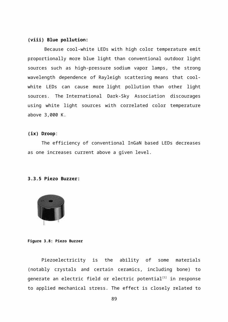
(viii) Blue pollution:
Because cool-white LEDs with high color temperature emit
proportionally more blue light than conventional outdoor light
sources such as high-pressure sodium vapor lamps, the strong
wavelength dependence of Rayleigh scattering means that cool-
white LEDs can cause more light pollution than other light
sources. The International Dark-Sky Association discourages
using white light sources with correlated color temperature
above 3,000 K.
(ix) Droop:
The efficiency of conventional InGaN based LEDs decreases
as one increases current above a given level.
3.3.5 Piezo Buzzer:
Figure 3.8: Piezo Buzzer
Piezoelectricity is the ability of some materials
(notably crystals and certain ceramics, including bone) to
generate an electric field or electric potential[1] in response
to applied mechanical stress. The effect is closely related to
89
a change of polarization density within the material's volume.
If the material is not short-circuited, the applied stress
induces a voltage across the material. The word is derived
from the Greek piezo or piezein, which means to squeeze or
press.
A buzzer or beeper is a signaling device, usually
electronic, typically used in automobiles, household
appliances such as microwave ovens, or game shows.
It most commonly consists of a number of switches or sensors
connected to a control unit that determines if and which
button was pushed or a preset time has lapsed, and usually
illuminates a light on the appropriate button or control
panel, and sounds a warning in the form of a continuous or
intermittent buzzing or beeping sound.
Initially this device was based on an electromechanical
system which was identical to an electric bell without the
metal gong (which makes the ringing noise). Often these units
were anchored to a wall or ceiling and used the ceiling or
wall as a sounding board. Another implementation with some AC-
connected devices was to implement a circuit to make the AC
current into a noise loud enough to drive a loudspeaker and
hook this circuit up to an 8-ohm speaker. Nowadays, it is more
popular to use a ceramic-based piezoelectric sounder which
makes a high-pitched tone. Usually these were hooked up to
"driver" circuits which varied the pitch of the sound or
pulsed the sound on and off.
90

In game shows it is also known as a "lockout system"
because when one person signals ("buzzes in"), all others are
locked out from signaling. Several game shows have large
buzzer buttons which are identified as "plungers". The buzzer
is also used to signal wrong answers and when time expires on
many game shows, such as Wheel of Fortune, Family Feud and The
Price is Right.
The word "buzzer" comes from the rasping noise that
buzzers made when they were electromechanical devices,
operated from stepped-down AC line voltage at 50 or 60 cycles.
Other sounds commonly used to indicate that a button has been
pressed are a ring or a beep.
Early devices were based on an electromechanical system
identical to an electric bell without the metal gong.
Similarly, a relay may be connected to interrupt its own
actuating current, causing the contacts to buzz. Often these
units were anchored to a wall or ceiling to use it as a
sounding board. The word "buzzer" comes from the rasping noise
that electromechanical buzzers made.
A piezoelectric element may be driven by
an oscillating electronic circuit or other audio
signal source, driven with a piezoelectric audio amplifier.
Sounds commonly used to indicate that a button has been
pressed are a click, a ring or a beep.
91

(i) What is piezoelectric effect?
Every day use of this phenomenon is used in load cells.
Load cells are used on large weigh scales for trucks and large
bin scales where materials need to be weighed. The signals
from the cells are calibrated to compensate for the weight of
the scale so that the scale can be zeroed out. The cell
signal, because it is very small, is sent to an amplifier head
where is can be read by the operator in units of weight. The
head unit can be set to read in metric or imperial weights.
(ii) Advantages:
As explained in your above question on weigh scales the
load cells do away with all the mechanical linkages that the
old systems had to use. These linkages were always prone to
mechanical damage where as the load cells are self contained
sealed units. There are four units per scale, one under each
corner.
A Piezo buzzer is made from two conductors that are
separated by Piezo crystals. When a voltage is applied to
these crystals, they push on one conductor and pull on the
other. The result of this push and pull is a sound wave. These
buzzers can be used for many things, like signaling when a
period of time is up or making a sound when a particular
button has been pushed. The process can also be reversed to
use as a guitar pickup. When a sound wave is passed, they
92

create an electric signal that is passed on to an audio
amplifier.
(iii) Uses:
(i) Annunciator panels
(ii) Electronic metronomes
(iii) Game shows
(iv) Microwave ovens and other household appliances
(v) Sporting events such as basketball games
(vi) Electrical alarms
(iv) Piezoelectric Sound Generators (Transducers and Buzzers):
The heart of all piezoelectric sound generators is a
simple piezoceramic disc, consisting of a metal plate, glued
together with a ceramic layer. If the disc is driven by an
external oscillating circuit, the piezo sound generator is
called piezoelectric transducer. If the disc is driven by a
built-in oscillating circuit it‘s called piezoelectric
buzzer. The advantages of these simple structured, acoustic
components are their robustness and cost-efficient sound
solution. Piezo sound generators are the ideal choice for
applications, which need a simple sound signal within a small
frequency range, e. g. warning and control sound signals of
kitchen devices, medical and health care products.
The dimension range of piezo sound generators starts from
the miniaturized size of 11 mm × 9 mm × 1.7 mm up to ø 45 mm
and covers sound pressures between low soft sound and
93

aggressive noisy sound. The design of almost all piezoelectric
sound generators is adjusted to meet the most popular
frequencies in the range between 2000 Hz and 5000 Hz.
Operation temperature range is available from -40°C to +120°C.
Standard voltage range is between 3 V and 12 V, in special
cases higher, according to customer’s demand. Piezoelectric
sound generators are available with pins, wires or SMD pads.
(v) Applications of Piezoelectric Ceramics:
A piezoelectric system can be constructed for virtually
any application for which any other type of electromechanical
transducer can be used. For any particular application,
however, limiting factors include the size, weight, and cost
of the piezoelectric system. Piezo ceramic devices fit into
four general categories: piezo generators, sensors, piezo
actuators, and transducers.
(i) Piezoelectric Generators:
Piezoelectric ceramics can generate voltages sufficient
to spark across an electrode gap, and thus can be used as
ignitors in fuel lighters, gas stoves, welding equipment, and
other such apparatus. Piezoelectric ignition systems are small
and simple -- distinct advantages relative to alternative
systems that include permanent magnets or high voltage
transformers and capacitors.
Alternatively, the electrical energy generated by a
piezoelectric element can be stored. Techniques used to make
multilayer capacitors have been used to construct multilayer
94

piezoelectric generators. Such piezo generators are excellent
solid state batteries for electronic circuits.
(ii) Piezoelectric Sensors:
A piezoelectric sensor converts a physical parameter,
such as acceleration or pressure, into an electrical signal.
In some sensors the physical parameter acts directly on the
piezoelectric element; in other devices an acoustical signal
establishes vibrations in the element and the vibrations are,
in turn, converted into an electrical signal. Often, the
system provides a visual, audible, or physical response to the
input from the piezo sensor -- automobile seatbelts lock in
response to a rapid deceleration, for example.
(iii) Piezo Actuators: Multilayer, Stack, Bending, Stripe:
A piezo actuator converts an electrical signal into a
precisely controlled physical displacement, to finely adjust
precision machining tools, lenses, or mirrors. Piezoelectric
actuators also are used to control hydraulic valves, act as
small-volume pumps or special-purpose motors, and in other
applications. Piezoelectric motors are unaffected by energy
efficiency losses that limit the miniaturization of
electromagnetic motors, and have been constructed to sizes of
less than 1 cm3. A potentially important additional advantage
to piezoelectric motors is the absence of electromagnetic
noise.
95
There are two different types of piezo actuators / piezo
multi layers. The first is a stack actuator. A stack
actuator is constructed in one of two ways: discrete stacking
or co-firing depending on the user’s requirements.
The other type of piezo actuator is a stripe actuator or
bending actuator, in which thin layers of piezoelectric
ceramics are bonded together; the thin layers allow the
actuator to bend with a greater deflection but a lower
blocking force than a stack actuator. Alternatively, if
physical displacement is prevented, a piezo actuator will
develop a usable force.
(iv) Piezoelectric Transducer:
Piezoelectric transducers convert electrical energy into
vibrational mechanical energy, often sound or ultra sound,
that is used to perform a task.
Piezoelectric transducers that generate audible sounds afford
significant advantages, relative to alternative
electromagnetic devices -- they are compact, simple, and
highly reliable, and minimal energy can produce a high level
of sound. These characteristics are ideally matched to the
needs of battery-powered equipment.
Because the piezoelectric effect is reversible, a
transducer can both generate an ultrasound signal from
electrical energy and convert incoming sound into an
electrical signal. Some devices designed for measuring
distances, flow rates, or fluid levels incorporate a single96

piezoelectric transducer in the signal sending and receiving
roles, other designs incorporate two transducers and separate
these roles.
Piezoelectric transducers also are used to generate
ultrasonic vibrations for cleaning, atomizing liquids,
drilling or milling ceramics or other difficult materials,
welding plastics, medical diagnostics, or for other purposes.
3.4 Pin Configuration of ICs:
3.4.1 IC CA3130:
97

Figure 3.9: IC CA31303.4.2 IC NE555:
Figure 3.10: IC NE555
98

3.5 Working, Applications, and Features of IC CA3130:
General Description:
CA3130 are op amps that combine the advantage of both
CMOS and bipolar transistors.
Gate-protected P-Channel MOSFET (PMOS) transistors are used
in the input circuit to provide very-high-input impedance,
very-low-input current, and exceptional speed performance. The
use of PMOS transistors in the input stage results in common-
mode input-voltage capability down to 0.5V below the negative-
supply terminal, an important attribute in single-supply
applications.
A CMOS transistor-pair, capable of swinging the output
voltage to within 10mV of either supply-voltage terminal (at
very high values of load impedance), is employed as the output
circuit.
CA3130A and CA3130 are op amps that combine the advantage
of both CMOS and bipolar transistors. Gate protected P-Channel
MOSFET (PMOS) transistors are used in the input circuit to
provide very-high-input impedance, very-low-input current, and
exceptional speed performance. The use of PMOS transistors in
99
the input stage results in common-mode input-voltage
capability down to 0.5V below the negative-supply terminal, an
important attribute in single-supply applications.
A CMOS transistor-pair, capable of swinging the output
voltage to within 10mV of either supply-voltage terminal (at
very high values of load impedance), is employed as the output
circuit. The CA3130 Series circuits operate at supply voltages
ranging from 5V to 16V, (}2.5V to }8V). They can be phase
compensated with a single external capacitor, and have
terminals for adjustment of offset voltage for applications
requiring offset-null capability. Terminal provisions are also
made to permit striding of the output stage. The CA3130A
offers superior input characteristics over those of the
CA3130.
The CA3130 op amp has the following pinouts:
1. Offset null
2. Inv. input
3. Non-inv. input
4. V- and case
5. Offset null
6. Output
7. V+
8. Strobe
100

(i) Role of IC CA3130:
This IC is a 15 MHz BiMOS Operational amplifier with
MOSFET inputs and Bipolar output. The inputs contain MOSFET
transistors to provide very high input impedance and very low
input current as low as 10pA. It has high speed of performance
and suitable for low input current applications.
CA3130A and CA3130 are op amps that combine the advantage
of both CMOS and bipolar transistors. Gate-protected P-Channel
MOSFET (PMOS) transistors are used in the input circuit to
provide very-high-input impedance, very-low-input current,
and exceptional speed performance. The use of PMOS transistors
in the input stage results in common-mode input-voltage
capability down to0.5V below the negative-supply terminal, an
important attribute in single-supply applications.
A CMOS transistor-pair, capable of swinging the output
voltage to within 10mV of either supply-voltage terminal (at
very high values of load impedance), is employed as the output
circuit.
The CA3130 Series circuits operate at supply voltages
ranging from 5V to 16V, (2.5V to 8V). They can be phase
compensated with a single external capacitor, and have
terminals for adjustment of offset voltage for applications
requiring offset-null capability. Terminal provisions are
also made to permit striding of the output stage. The
101

CA3130A offers superior input characteristics over those of
the CA3130.
(ii) Features:
(i) MOSFET Input Stage Provides:
Very High ZI = 1.5 T
Very Low current . . . . . . =5pA at 15V Operation
(ii) Ideal for Single-Supply Applications
(iii) Common-Mode Input-Voltage Range Includes Negative Supply
Rail; Input Terminals can be Swung 0.5VBelow Negative
Supply Rail
(iv) CMOS Output Stage Permits Signal Swing to Either (or
both) Supply Rails.
(iii) Applications:
(i) Ground-Referenced Single Supply Amplifiers
(ii) Fast Sample-Hold Amplifiers
(iii) Long-Duration Timers/ Mono stables
(iv) High-Input-Impedance Comparators (Ideal Interface with
Digital CMOS)
(v) High-Input-Impedance Wideband Amplifiers
(vi)Voltage Followers (e.g. Follower for Single-Supply D/A
Converter )
(vii) Voltage Regulators (Permits Control of Output Voltage
Down to 0V)
(viii) Peak Detectors
(ix) Single-Supply Full-Wave Precision Rectifiers
102
(x) Photo-Diode Sensor Amplifiers.
3.6 Working, Applications and Features of IC NE555:
The NE555 IC is a highly stable controller capable of
producing accurate timing pulses. With a monostable operation,
the time delay is controlled by one external resistor and one
capacitor. With an astable operation, the frequency and duty
cycle are accurately controlled by two external resistors and
one capacitor.
(i) Details of Pin:Ground, is the input pin of the source of the negative DC
voltage trigger, negative input from the lower comparators
(comparator B) that maintain oscillation capacitor voltage in
the lowest 1 / 3 Vcc and set RS flip-flop output, the output
pin of the IC 555.
Reset, the pin that serves to reset the latch inside the IC
to be influential to reset the IC work. This pin is connected
to a PNP-type transistor gate, so the transistor will be
active if given a logic low. Normally this pin is connected
directly to Vcc to prevent reset control voltage, this pin
serves to regulate the stability of the reference voltage
negative input (comparator A). This pin can be left hanging,
but to ensure the stability of the reference comparator A,
usually associated with a capacitor of about 10nF to berorde
103

pin ground threshold, this pin is connected to the positive
input (comparator A) which will reset the RS flip-flop when
the voltage on the capacitor from exceeding 2 / 3 V discharge,
this pin is connected to an open collector transistor Q1 is
connected to ground emitter. Switching transistor serves to
clamp the corresponding node to ground on the timing of
certain vcc, pin it to receive a DC voltage supply. Usually it
will work optimally if given a 5-15V. the current supply can
be seen in the datasheet, which is about 10-15mA.
One of the most versatile linear ICs is the 555 timer which
was first introduced in early 1970 by Signetic Corporation
giving the name as SE/NE 555 timer. This IC is a monolithic
timing circuit that can produce accurate and highly stable
time delays or oscillation. Like other commonly used op-amps,
this IC is also very much reliable, easy to use and cheaper in
cost. It has a variety of applications
including monostable and astable multivibrators, dc-dc
converters, digital logic probes, waveform generators, analog
frequency meters and tachometers, temperature measurement and
control devices, voltage regulators etc. The timer basically
operates in one of the two modes either as a monostable (one-
shot) multivibrator or as an astable (free-running)
multivibrator. The SE 555 is designed for the operating
temperature range from – 55°C to 125° while the NE
555 operates over a temperature range of 0° to 70°C.
(ii) The important features of the 555 timer are :
104

(i) It operates from a wide range of power supplies ranging
from + 5 Volts to + 18 Volts supply voltage.
(ii) Sinking or sourcing 200 mA of load current.
(iii) The external components should be selected properly so
that the timing intervals can be made into several minutes
Proper selection of only a few external components allows
timing intervals of several minutes along with the frequencies
exceeding several hundred kilo hertz.
(iv) It has a high current output; the output can drive TTL.
(v) It has a temperature stability of 50 parts per million
(ppm) per degree Celsius change in temperature, or
equivalently 0.005 %/ °C.
(vi) The duty cycle of the timer is adjustable with the
maximum power dissipation per package is 600 mW and its
trigger and reset inputs are logic compatible.
Pin Configuration:
Pin 1: Grounded Terminal: All the voltages are measured with
respect to this terminal.
Pin 2: Trigger Terminal: This pin is an inverting input to a
comparator that is responsible for transition of flip-
flop from set to reset. The output of the timer depends on the
amplitude of the external trigger pulse applied to this pin.
105

Pin 3: Output Terminal: Output of the timer is available at
this pin. There are two ways in which a load can be connected
to the output terminal either between pin 3 and ground pin
(pin 1) or between pin 3 and supply pin (pin 8). The load
connected between pin 3 and ground supply pin is called
the normally on load and that connected between pin 3 and
ground pin is called the normally off load.
Pin 4: Reset Terminal: To disable or reset the timer a
negative pulse is applied to this pin due to which it is
referred to as reset terminal. When this pin is not to be used
for reset purpose, it should be connected to + VCC to avoid any
possibility of false triggering.
Pin 5: Control Voltage Terminal: The function of this terminal
is to control the threshold and trigger levels. Thus either
the external voltage or a pot connected to this pin determines
the pulse width of the output waveform. The external voltage
applied to this pin can also be used to modulate the output
waveform. When this pin is not used, it should be connected to
ground through a 0.01 micro Farad to avoid any noise problem.
Pin 6: Threshold Terminal: This is the non-inverting input
terminal of comparator 1, which compares the voltage applied
to the terminal with a reference voltage of 2/3 VCC. The
amplitude of voltage applied to this terminal is responsible
for the set state of flip-flop.
106

Pin 7: Discharge Terminal: This pin is connected internally to
the collector of transistor and mostly a capacitor is
connected between this terminal and ground. It is called
discharge terminal because when transistor saturates,
capacitor discharges through the transistor. When the
transistor is in cut-off region, the capacitor charges at a
rate determined by the external resistor and capacitor.
Pin 8: Supply Terminal: A supply voltage of + 5 V to + 18 V
is applied to this terminal with respect to ground (pin 1).
Figure illustrate some basic ideas that will prove useful
in coming blog posts of the 555 timer. Assuming output Q high,
the transistor is saturated and the capacitor voltage is
clamped at ground i.e. the capacitor C is shorted and cannot
charge.
The non-inverting input voltage of the comparator is
referred to as the threshold voltage while the inverting input
voltage is referred to as the control voltage. With R-S flip
flop set, the saturated transistor holds the threshold voltage
at zero. The control voltage, however, is fixed at 2/3
VCC (i.e. at 10 V) because of the voltage divider.
Suppose that a high voltage is applied to the R input.
This resets the flip-flop R-Output Q goes low and the
transistor is cut-off. Capacitor C is now free to charge. As
this capacitor C charges, the threshold voltage rises.
107

Eventually, the threshold voltage becomes slightly greater
than (+ 10 V). The output of the comparator then goes
high, forcing the R S flip-flop to set. The high Q output
saturates the transistor, and this quickly discharges the
capacitor. The two waveforms are depicted in figure. An
exponential rise is across the capacitor C, and a positive
going pulse appears at the output Q. Thus capacitor voltage
VC is exponential while the output is rectangular.
(iii) Working Principle:Comparator 1 has a threshold input (pin 6) and a control
input (pin 5). In most applications, the control input is not
used, so that the control voltage equals +2/3 VCC. Output of
this comparator is applied to set (S) input of the flip-flop.
Whenever the threshold voltage exceeds the control voltage,
comparator 1 will set the flip-flop and its output is high.
A high output from the flip-flop saturates the discharge
transistor and discharge the capacitor connected externally to
pin 7. The complementary signal out of the flip-flop goes to
pin 3, the output. The output available at pin 3 is low. These
conditions will prevail until comparator 2 triggers the flip-
flop. Even if the voltage at the threshold input falls below
2/3 VCC, that is comparator 1 cannot cause the flip-flop to
change again. It means that the comparator 1 can only force
the flip-flop’s output high.
To change the output of flip-flop to low, the voltage at
the trigger input must fall below + 1/3 Vcc. When this occurs,
comparator 2 triggers the flip-flop, forcing its output108
low. The low output from the flip-flop turns the discharge
transistor off and forces the power amplifier to output a high.
These conditions will continue independent of the voltage on
the trigger input. Comparator 2 can only cause the flip-flop
to output low.
From the above discussion it is concluded that for the
having low output from the timer 555, the voltage on the
threshold input must exceed the control voltage or + 2/3 VCC.
They also turn the discharge transistor on. To force the
output from the timer high, the voltage on the trigger input
must drop below +1/3 VCC. This also turns the discharge
transistor off.
A voltage may be applied to the control input to change
the levels at which the switching occurs. When not in use, a
0.01 nano Farad capacitor should be connected between pin 5
and ground to prevent noise coupled onto this pin from causing
false triggering.
Connecting the reset (pin 4) to a logic low will place a
high on the output of flip-flop. The discharge transistor will
go on and the power amplifier will output a low. This
condition will continue until reset is taken high. This allows
synchronization or resetting of the circuit’s operation. When
not in use, reset should be tied to +VCC.
(iv) Features:
109
(i) High Current Drive Capability (200mA)
(ii) Adjustable Duty Cycle
(iii) Temperature Stability of 0.005%C
(iv) Timing From Sec to Hours
(v) Turn off Time Less Than 2mSec
(v) Applications:
(i) Precision Timing
(ii) Pulse Generation
(iii) Time Delay Generation
(iv) Sequential Timing
CHAPTER FOUR
4.1 Introduction:
In this chapter we will see mainly the circuit testing on
bread-board and working of cell phone detector in brief. The
first test with this cellular phone detector was to just have
an active cellular phone in the room. So the cellular phone
was turned on and a phone call was placed with the detector
nearby. Absolutely nothing came out of the connected
headphones. To troubleshoot this problem, the circuit was
tested with a spectrum analyzer and signal generator. The
antenna was connected to the signal generator at 900 MHz with
10dB of amplitude and the spectrum analyzer was connected to
the headphone jack using the available probes (only 500 MHz
110

was available). Injecting the 900 MHz signal into the antennas
resulted in a lower amplitude signal on the output.
To test whether the circuit was resonating at 900MHz, a
bandpass test was performed by stepping the frequency at 100
MHz intervals from 600 MHz to 1.2GHz. The amplitude changed at
each interval, but was actually lower at 900 MHz than anywhere
else and didn't have a bandpass response. The wire wrapped
connections may have changed the impedance of the circuit.
While testing this cellular phone detector it was
discovered that the spectrum analyzer was able to detect the
cellular phone only using a 500 MHz probe. When talking on the
cellular phone, the spectrum analyzer spiked at 832 MHz. This
frequency range to design around for this cellular phone and
is in the range of a GSM phones.
4.2 Circuit Testing on Bread-Board:
111

Figure 4.1: Circuit testing
Before the assembling of circuit on PCB we tested it onthe bread-board using the components, connecting wires, and a9V battery.
112

4.3 Working of Cell Phone Detector:
4.3.1 Purpose of the circuit:This circuit is intended to detect unauthorized use of
mobile phones in examination halls, confidential rooms etc. Italso helps to detect unauthorized video and audio recordings.It detects the signal from mobile phones even if it is kept inthe silent mode. It also detects SMS.
4.3.2 Concept:Mobile phone uses RF with a wavelength of 30cm at 872 to
2170 MHz. That is the signal is high frequency with hugeenergy. When the mobile phone is active, it transmits thesignal in the form of sine wave which passes through thespace. The encoded audio/video signal contains electromagneticradiation which is picked up by the receiver in the basestation. Mobile phone system is referred to as “CellularTelephone system” because the coverage area is divided into“cells” each of which has a base station. The transmitterpower of the modern 2G antenna in the base station is 20-100watts.
When a GSM (Global System of Mobile communication)digital phone is transmitting, the signal is time shared with7 other users. That is at any one second, each of the 8 userson the same frequency is allotted 1/8 of the time and thesignal is reconstituted by the receiver to form the speech.Peak power output of a mobile phone corresponds to 2 wattswith an average of 250 milli watts of continuous power. Eachhandset with in a ‘cell’ is allotted a particular frequencyfor its use. The mobile phone transmits short signals atregular intervals to register its availability to the nearestbase station. The network data base stores the informationtransmitted by the mobile phone. If the mobile phone movesfrom one cell to another, it will keep the connection with thebase station having strongest transmission. Mobile phonealways tries to make connection with the available basestation. That is why, the back light of the phone turns on
113

intermittently while traveling. This will cause severe batterydrain. So in long journeys, battery will flat with in a fewhours.
AM Radio uses frequencies between 180 kHz and 1.6 MHz. FMradio uses 88 to 180 MHz. TV uses 470 to 854 MHz. Waves athigher frequencies but within the RF region is called Microwaves. Mobile phone uses high frequency RF wave in the microwave region carrying huge amount of electromagnetic energy.That is why burning sensation develops in the ear if themobile is used for a long period. Just like a micro wave oven,mobile phone is ‘cooking’ the tissues in the ear. RF radiationfrom the phone causes oscillation of polar molecules likewater in the tissues. This generates heat through frictionjust like the principle of microwave oven. The strongestradiation from the mobile phone is about 2 watts which canmake connection with a base station located 2 to 3 km away.
4.3.3 How the circuit works?Ordinary LC (Coil-Capacitor) circuits are used to detect
low frequency radiation in the AM and FM bands. The tuned tankcircuit having a coil and a variable capacitor retrieve thesignal from the carrier wave. But such LC circuits cannotdetect high frequency waves near the microwave region. Hencein the circuit, a capacitor is used to detect RF from mobilephone considering that, a capacitor can store energy even froman outside source and oscillate like LC circuit.
114

R1 3.9 M
R2 100K R3 1 M
LEDRed
9 V Battery
+
C1
0.22 UF
C2100
25VUF
IC1
IC1
CA 3130
2
3
4
76
0.1
R4 100 R
R5 100R BUZZER
C
Figure 4.2 Circuitry operation
4.3.4 Use of capacitor:A capacitor has two electrodes separated by a
‘dielectric’ like paper, mica etc. The non polarized disccapacitor is used to pass AC and not DC. Capacitor can storeenergy and pass AC signals during discharge. 0.22pF capacitoris selected because it is a low value one and has largesurface area to accept energy from the mobile radiation. Todetect the signal, the sensor part should be like an aerial.So the capacitor is arranged as a mini loop aerial (similar tothe dipole antenna used in TV).In short with this arrangement,the capacitor works like an air core coil with ability tooscillate and discharge current.
4.3.5 How the capacitor senses RF?One lead of the capacitor gets DC from the positive rail
and the other lead goes to the negative input of IC1. So thecapacitor gets energy for storage. This energy is applied tothe inputs of IC1 so that the inputs of IC are almost balancedwith 1.4 volts. In this state output is zero. But at any timeIC can give a high output if a small current is induced to itsinputs. There a natural electromagnetic field around thecapacitor caused by the 50Hz from electrical wiring. When the
115

mobile phone radiates high energy pulsations, capacitoroscillates and release energy in the inputs of IC. Thisoscillation is indicated by the flashing of the LED andbeeping of Buzzer. In short, capacitor carries energy and isin an electromagnetic field. So a slight change in fieldcaused by the RF from phone will disturb the field and forcesthe capacitor to release energy.
CHAPTER FIVE
5.1 Introduction:
In this chapter we will see applications, advantages, limitation, future scope, and the conclusions of cell phone detector. Basically this circuit can be used anywhere for detecting the cell phones. Since today is the generation of advanced communication devices and cell phone is the very first need of this. But somehow reasons there is a misuse of these devices. So we have to stop this for our safety. And by using cell phone detectors we can do this very simply. We can use cell phone detector even at our working place, confidential halls, prisons, court room and at many other places where cell phone is not allowed.
But there is a limitation of this device that it can detect only in the range of 1.5-2 meters. So we have to place a number of detectors in a large room. But beyond of this we can simply detect the cells in a range which can covered by the detector.
In future we will increase the range of the detector so that we can detect the cells over a hundreds of meter. So thisis the first step to avoid the unwanted activities using the cell phones.
116

5.1 Applications:
(i) Colleges and Universities:During tests and exams the use of mobile phones is
prohibited, for the students could use it to send answers among each other.
By using a GSM-detector this kind of fraud is prohibited.The presence of a GSM-detector can work in a preventing way, because when a GSM-detector is present, the use of mobile phones does not stay unnoticed.
117

(ii) Cinemas:In a cinema the use of a mobile phone is undesired. Being
called by someone during a movie is of course very bothering for other people.
With a GSM-detector the use of mobile phones is detected,so the visitor can be informed that this is not allowed.
(iii) Theatres:Just like with a cinema, in theatres the use of mobile
phones is not allowed. The gsm-detector can be used to preventuse.
(iv) Restaurants / Hotels:In hotels and restaurants it is often undesired that a
mobile phone is used at the table or in other areas. A GSM-detector can be installed in these areas to notify guests.
(v) Petrol stations:When tanking at a petrol station, the use of mobile
phones is prohibited, because the mobile signals can interferewith the tanking equipment and because a small spark within the mobile phone could set fire to possible gasoline vapour. With the GSM-detector this prohibition is pointed out to the tanking customer.
(vi) Airplanes:In airplanes the use of mobile phones is prohibited, for
it could interfere with the equipment in the airplane. All thewhile phones are still used illegally, especially in restrooms. By installing a GSM-detector there, this can be prevented.
(vii) Conference rooms:It is often distracting to be called during a meeting.
Also, confidential conversation could be overheard by using
118

cell phones, especially by those with a spy function (when someone calls that phone it automatically is picked up withoutringing, so that the person on the other end of the line can hear conversations in the room where the spy phone is placed).By using a GSM-detector you can be assured that this is not the case.
(viii) Hospitals:The signals emitted by mobile phones can interfere with
some electronic equipment inside the hospital. This could havefatal consequences.
The GSM-detector can be placed in any area where the useof mobile phones could interfere with sensitive devices. Theaudio alarm will sound when a phone is used and this way, theperson should immediately switch off his/her phone
(ix) Prisons:In prisons the use of mobile phones is not allowed. It
could occur anyway. By using the gsm-detector the staff can benotified when a mobile phone is used inside the facility.
(x) Power plants:Power plants contain -just like hospitals- a lot of
electronic devices that are sensitive for interference bymobile phones. Therefore, it is prohibited to use mobilephones there. Use a GSM-detector to inspect this.
5.2 Advantages:
Our mission is to be the leading provider of cellular
phone detection capabilities to both business and government
institutions around the world. We are striving to bring a
national debate to the growing proliferation of cell phone use
119

in our society today. Using our state of the art products we
are hoping to provide individuals and businesses the tools to
detect and prevent the use of cell phone in sensitive areas.
This product was created in reaction to the growing use
of cell phones around the world, and how that use was
beginning to interfere with our daily lives. When businesses
tried to find solutions to problems involving cell phones,
they found a huge shortcoming in products and services.
Hence, our solution was created to supply this need. To
date we have sold thousands of products to a very wide
audience of businesses and government institutions. Many of
these include prisons, casinos, embassies, classrooms and
testing facilities, oil rigs, conferences, golf clubhouses,
computer-rooms, data centers, hospitals, and restaurants, to
name just a small few of the vast capabilities of our product.
.
5.3 Limitation:
Range of the circuit:The prototype version has only limited range of 2 meters.
But if a preamplifier stage using JFET or MOSFET transistor isused as an interface between the capacitor and IC, range canbe increased.
5.4 Future scope:
120

Trying to increase the detecting range of mobile bug to fewmore meters for observing wide ranges of area. In the futuretime this detector will be improved in all ways.
In future we could be able to detect any range offrequency over a meters of range and this will be very usefulto detect the cell phones where the cell phones areprohibited.
5.5 Conclusion:
This pocket-size mobile transmission detector or sniffer
can sense the presence of an activated mobile cellphone from a
distance of one and-a-half meters. So it can be used to
prevent use of mobile phones in examination halls,
confidential rooms, etc. It is also useful for detecting the
use of mobile phone for spying and unauthorised video
transmission.
In this project we made an attempt to design a mobile
detector which can detect both the incoming and outgoing calls
as well as video transmission even if the mobile is kept at
the silent mode. Our circuit has detected the presence of an
active mobile phone even at a distance of about one and half a
meter. It gave the indication of an active mobile phone by
glowing the LED, according to the receiving frequency and by
buzzing the sound of the buzzer. The alarm continues until the
signal is ceases.
121

5.6 References:
(i) www.google.com
(ii) www.wikipedia.org
(iii) www.pdfmachine.com
(iv) www.ecproject.com
(v) www.datasheets4u.com
122

123

124


![10 11 Session HR Session Seri Management[1]](https://static.fdokumen.com/doc/165x107/6314ba61fc260b71020fb0ee/10-11-session-hr-session-seri-management1.jpg)