
A novel architecture for efficient protocol processing in high speed communication environments
8
A Novel Architecture for Efficient Protocol Processing in High Speed Communication Environments 1 George KONSTANTOULAKIS, Vassilis NELLAS, Christos GEORGOPOULOS, Theofanis ORPHANOUDAKIS, Nick ZERVOS Ellemedia Technologies, Syggrou Av. 223, 17121 Athens, Greece Matthias STECK Hyperstone electronics GmbH, Am Seerhein 8, 78467 Konstanz, Germany Diederik VERKEST Interuniversity Microelectronics Centre (IMEC), Kapeldreef 75, 3001 Leuven, Belgium Gregory DOUMENIS National Technical University of Athens (NTUA), H. Polytechniou 9, 15773 Athens, Greece Dionysis REISIS University of Athens, Department of Physics, Panepistimiopolis, Athens, Greece Nikos NIKOLAOU, Jorge-A. SANCHEZ-P. Lucent Technologies, FLW EMEA, Botterstraat 45, Room HE317, 1270 AA Huizen, The Netherlands Telephone: +31 35 687 4797, Facsimile: +31 35 687 5954, Email: [email protected] 1 The work presented in this paper is carried out in the Protocol Processor Project (PRO 3 ) that is co-funded by the European Community under the IST Programme [6]. The PRO 3 project started on January 2000 and is currently on the detailed specifi- cations and architecture phase. The project will deliver the PRO 3 chip, applications demonstrating it as well as a tool suite for programming, compilation and debugging. Abstract: In this paper, the architecture, system modules and functional design of a reconfigurable Protocol Proc- essor are presented. The protocol processor aims in accel- erating execution of telecom transport protocols by ex- tending a high-performance RISC core with reconfigur- able pipelined hardware. CPU demanding and (hard) real- time protocol functions will be handled by the program- mable hardware, while the remaining functions as well as higher layer protocols will be handled by the on-chip RISC in an integrated way. Applications that may take advantage of the protocol processor are also presented. Furthermore, the codesign techniques, followed for the implementation of the component, are analysed. Keywords: protocol processor, protocol acceleration, high-speed communications. 1. Introduction The rapid growth in the dimension and diversity of net- works and telecom systems, along with the always increas- ing users' demands for networking services, has imposed the development and deployment of high-capacity tele- communication systems. Such systems involve modules of high throughput, which have their time critical functions realised in hardware. The concept of improving the com- putation performance of protocols by mapping the lower protocol layer functionality onto VLSI structures, origi- nated during the evolution of ATM. Currently, the trend is to apply this concept to routers, servers and multi-layer switching systems required to support efficiently multiple links and connections with total capacity of up to several Gbps. Often today, the switching systems employ more than one high performance processing unit to execute the higher protocol functions as well as other functions like connection admission control, and traffic and resource management. In such systems, the processing units are in- adequate in supporting the protocol processing require- ments for the entire set of active sessions. This constitutes a major system resource bottleneck, because the complex- ity of the protocol algorithms requires higher computa- tional power than that offered by today's processor tech- nology [1, 2, 3, 4]. An example illustrating this situation is the ATM network, where each switch is required to proc- ess an active signalling stack (with two transport protocol stacks instances – SAR 5, CPCS, SSCOP and one signal- ling protocol instance – Q.2391) per user connection. The performance degradation results in assigning tasks, such as lower level protocol functions, to the line card con- troller. These computations involve bit and byte wise op- erations on the headers and the payload of the packets, thus exhausting the processing power of the unit. There- fore, the system protocol processor unit fails in processing
Transcript of A novel architecture for efficient protocol processing in high speed communication environments

A Novel Architecture for Efficient Protocol Processing in High Speed Communication Environments1
George KONSTANTOULAKIS, Vassilis NELLAS, Christos GEORGOPOULOS, Theofanis ORPHANOUDAKIS, Nick ZERVOS
Ellemedia Technologies, Syggrou Av. 223, 17121 Athens, Greece
Matthias STECK Hyperstone electronics GmbH, Am Seerhein 8, 78467 Konstanz, Germany
Diederik VERKEST Interuniversity Microelectronics Centre (IMEC), Kapeldreef 75, 3001 Leuven, Belgium
Gregory DOUMENIS National Technical University of Athens (NTUA), H. Polytechniou 9, 15773 Athens, Greece
Dionysis REISIS University of Athens, Department of Physics, Panepistimiopolis, Athens, Greece
Nikos NIKOLAOU, Jorge-A. SANCHEZ-P. Lucent Technologies, FLW EMEA, Botterstraat 45, Room HE317, 1270 AA Huizen, The Netherlands
Telephone: +31 35 687 4797, Facsimile: +31 35 687 5954, Email: [email protected]
1 The work presented in this paper is carried out in the Protocol Processor Project (PRO3) that is co-funded by the European Community under the IST Programme [6]. The PRO3 project started on January 2000 and is currently on the detailed specifi-cations and architecture phase. The project will deliver the PRO3 chip, applications demonstrating it as well as a tool suite for programming, compilation and debugging.
Abstract: In this paper, the architecture, system modules and functional design of a reconfigurable Protocol Proc-essor are presented. The protocol processor aims in accel-erating execution of telecom transport protocols by ex-tending a high-performance RISC core with reconfigur-able pipelined hardware. CPU demanding and (hard) real-time protocol functions will be handled by the program-mable hardware, while the remaining functions as well as higher layer protocols will be handled by the on-chip RISC in an integrated way. Applications that may take advantage of the protocol processor are also presented. Furthermore, the codesign techniques, followed for the implementation of the component, are analysed.
Keywords: protocol processor, protocol acceleration, high-speed communications.
1. Introduction
The rapid growth in the dimension and diversity of net-works and telecom systems, along with the always increas-ing users' demands for networking services, has imposed the development and deployment of high-capacity tele-communication systems. Such systems involve modules of high throughput, which have their time critical functions realised in hardware. The concept of improving the com-putation performance of protocols by mapping the lower
protocol layer functionality onto VLSI structures, origi-nated during the evolution of ATM. Currently, the trend is to apply this concept to routers, servers and multi-layer switching systems required to support efficiently multiple links and connections with total capacity of up to several Gbps. Often today, the switching systems employ more than one high performance processing unit to execute the higher protocol functions as well as other functions like connection admission control, and traffic and resource management. In such systems, the processing units are in-adequate in supporting the protocol processing require-ments for the entire set of active sessions. This constitutes a major system resource bottleneck, because the complex-ity of the protocol algorithms requires higher computa-tional power than that offered by today's processor tech-nology [1, 2, 3, 4]. An example illustrating this situation is the ATM network, where each switch is required to proc-ess an active signalling stack (with two transport protocol stacks instances – SAR 5, CPCS, SSCOP and one signal-ling protocol instance – Q.2391) per user connection.
The performance degradation results in assigning tasks, such as lower level protocol functions, to the line card con-troller. These computations involve bit and byte wise op-erations on the headers and the payload of the packets, thus exhausting the processing power of the unit. There-fore, the system protocol processor unit fails in processing
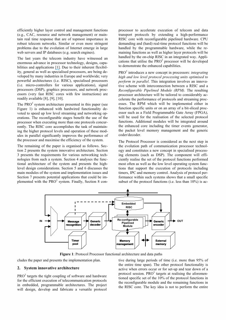
efficiently higher layer control and management functions (e.g., CAC, resource and network management) or main-tain real time response that are of topmost importance in robust telecom networks. Similar or even more stringent problems due to the evolution of Internet emerge in large web servers and IP databases (e.g. search engines). The last years the telecom industry have witnessed an enormous advance in processor technology, designs, capa-bilities and applications [1]. Due to their inherent flexibil-ity, general as well as specialised processors, are being de-veloped by many industries in Europe and worldwide; very powerful architectures (i.e. RISC), specialised processors (i.e. micro-controllers for various applications), signal processors (DSP), graphics processors, and network proc-essors (very fast RISC cores with few instructions) are readily available [8], [9], [10]. The PRO3 system architecture presented in this paper (see Figure 1) is enhanced with hardwired functionality de-voted to speed up low level streaming and networking op-erations. The reconfigurable stages benefit the use of the processor when executing more than one protocols concur-rently. The RISC core accomplishes the task of maintain-ing the higher protocol levels and operation of these mod-ules in parallel significantly improves the performance of the processor and maximise the efficiency of the system. The remaining of the paper is organised as follows. Sec-tion 2 presents the system innovative architecture. Section 3 presents the requirements for various networking tech-nologies from such a system. Section 4 analyses the func-tional architecture of the system and presents the high-level design considerations. Section 5 and 6 discusses the main modules of the system and implementation issues and Section 7 presents potential applications that could be im-plemented with the PRO3 system. Finally, Section 8 con-
cludes the paper and presents the implementation plan.
2. System innovative architecture
PRO3 targets the tight coupling of software and hardware for the efficient execution of telecommunication protocols in embedded, programmable architectures. The project will design, develop and fabricate a versatile protocol
processor to accelerate execution of telecom and data transport protocols by extending a high-performance RISC core with reconfigurable pipelined hardware. CPU demanding and (hard) real-time protocol functions will be handled by the programmable hardware, while the re-maining functions as well as higher layer protocols will be handled by the on-chip RISC in an integrated way. Appli-cations that utilise the PRO3 processor will be developed to demonstrate the enhanced capabilities.
PRO3 introduces a new concept in processors: integrating high and low level protocol processing units optimised to perform in parallel. This integration involves an innova-tive scheme with interconnection between a RISC and a Reconfigurable Pipelined Module (RPM). The resulting processor architecture will be tailored to considerably ac-celerate the performance of protocols and streaming proc-esses. The RPM which will be implemented either in function specific units or on an array of a bit-sliced proc-essor such as a Field Programmable Gate Array (FPGA), will be used for the realisation of the selected protocol functions. Additional modules will be integrated around the enhanced core including the timer events generator, the packet level memory management and the generic coder/decoder.
The Protocol Processor is considered as the next step in the evolution path of communication processor technol-ogy and constitutes a new concept in specialised process-ing elements (such as DSP). The component will effi-ciently realise the set of the protocol functions performed most often as well as the low level operating system func-tions that support the execution of protocols including timers, IPC and memory control. Analysis of protocol per-formance within such systems shows that a small specific subset of the protocol functions (i.e. less than 10%) is ac-
tive during large periods of time (i.e. more than 95% of the entire time span). The other protocol functionality is active when errors occur or for set-up and tear down of a protocol session. PRO3 targets at realising the aforemen-tioned specific set of the 10% of the protocol functions in the reconfigurable module and the remaining functions in the RISC core. The key idea is not to perform the entire
Embedded RISC
Re-configurablePipelinedModule
GenericencoderGenericencoder
GenericdecoderGenericdecoder
Messagerecognition
Messagerecognition
Timerpool
Timerpool
Memorymanagement
Memorymanagement
ExternalmemoryExternalmemory
IN OUT
Figure 1: Protocol Processor functional architecture and data paths

protocol on the fly (since it is very expensive) but to ac-celerate it considerably.
The following is a list of PRO3 innovative aspects:
• Integration of a state-of-the-art RISC with a re-configurable module able to deliver the needed process-ing power to support efficiently many thousands of (dif-ferent) protocol instances. The RISC will be integrated with a unit performing of the normal (error free) protocol operations. The integration point of these two modules is one of the main research issues of this work.
• Introduction of message recognition information coming from the input module in order to reconfigure RPM. Inclusion of logic for fast lookup tables in hardware and high-speed interfaces.
• Provision of a pool of timer resources for the reali-sation of the (many) thousands of active watch-dog tim-ers. This module requires a thorough study since timer re-sources are required from almost all protocols. Since it must be able to support thousands of active instances of protocol FSMs, special circuitry should be designed.
• Provision of generic coding-decoding functions for the bit or byte level handling of protocol streams. Each protocol has unique and distinct coding-decoding rules at its lower interface. A protocol receives a byte stream from its lower interface and gives another byte stream at its up-per interface. In order for a protocol execution machine to extract the information fields, the received stream is usu-ally parsed at bit level.
• Memory management features for the real time context switching, memory allocation and stream buffer-ing (for segmentation/reassembly).
• Realisation of high performance and demanding applications that efficiently utilise the PRO3 system.
In summary, the PRO3 architecture involves an independ-ent pipelined data path (protocol messages and data pass through) and a control interface (realised as a simple mas-ter/slave processor bus) to fetch software to the RISC/DSP and communicate with the host system. Special attention in the proposed design is given to the efficient support of multiple instances of the same protocol stack by the im-plemented logic, as well as the ability to improve on the performance of a diversity of CPU demanding network protocols.
3. Requirements analysis
The PRO3 system can be utilised for the efficient imple-mentation of various networking applications. Following is a list of the specific functions required by a network ele-ment (i.e. terminal or switching node) for the support of different protocols and technologies.
Table 1: Requirements analysis
Protocols or Technologies
Function
Processing of lower layer pro-tocols (LLC/MAC, PPP/HDLC/SONNET, ATM)
Synchronisation Arbitrary length field extraction CRC calculation Scrambling/De-scrambling
Processing of higher layer pro-tocols
PDU reassembly Queue management Arbitrary length field extraction CRC/Checksum calculation Connection state handling (connection ori-ented protocols) Timer management (connection oriented protocols)
Security Packet classification Flow classification and connection state handling (state-full inspection) Higher layer PDU reassembly (application level firewalls, packet decryption) Encryption/Decryption
Packet routing Routing protocol message processing Routing algorithms execution Packet header processing and routing table lookup execution
Packet switching Header extraction Complex packet classification and determi-nation of egress port according to protocol information of layers 2 and 3 Header modification
QoS provision Complex packet classification and determi-nation of flow according to the IntServ or DiffServ mechanisms for IP based applica-tions Policing of flows or aggregation of flows ei-ther for cell based or packet based forward-ing Per flow queuing (either for cell based or packet based forwarding) Per flow scheduling (either for cell based or packet based forwarding) Execution of several algorithms according to the supported Traffic Management speci-fication
Support of sig-nalled connec-tions/flows
Handling of state information for multiple connections Queue management Timer management
4. Functional design
The functional architecture of the Protocol Processor is depicted in Figure 1. The component consists of a central processing unit (the RISC core and the RPM) as well as a set of on-chip peripherals, common to protocols and streaming tasks. Thus, the same component with different configuration will be able to perform many different pro-tocol Finite State Machines (FSMs) that require high per-formance execution and handling of messages with low

propagation/processing delay. The feedback bus returns messages to the input of the component in case a multi-protocol stack is implemented. Certain priority rules will be applied along with specific access to/from the system.
The component, depicted in Figure 1, has a pipelined data path where the high bandwidth streaming messages are in-jected (and being processed) and a control interface for software fetching. In this functional architecture the fol-lowing message/data flows are foreseen (see Table 2).
Table 2: Message/data flows
IN => OUT A message stream arrives at the “In” inter-face, is being processed and the resulting message stream leaves out from the “Out” interface. In this case the processor is inter-faced to a next component that processes the result (e.g. to a graphics processor).
IN => CONTROL
A message stream arrives at the “In” inter-face, being processed and the resulting message stream leaves out from the “Con-trol” interface. The processor terminates a protocol stack and the result is sent to the host system through the typical bus (i.e. re-ceiver terminal system).
CONTROL => OUT
This is similar to the above but concerns the transmit path.
Message Loop Back
The component performs a stack of at least two protocol layers. The result of protocol layer A is looped back and processed by the protocol layer B engine.
5. System modules
The peripherals of the protocol processor consists of the following modules: Input/Output, Message Recognition, Generic Encoder/Decoder, Timer Pool, and Memory Man-ager; which are discussed in the following paragraphs.
The input/output module of the system is a general pur-pose parallel peripheral interface. The actual load of this interface depends on the application.
Message Recognition: The main function of this module is to recognise the incoming message and to assign an in-ternal handler for subsequent processing. The handler is important not only for PRO3, but can also be sent to the application to aid further processing/classification of higher layer messages. As presented in Figure 1, a direct communication path is foreseen from the Message Recog-nition block to the mixed core. This signal will inform in advance the core on the message to be processed so that, if needed, the RISC will be able to reconfigure the entire reconfigurable module or part of it.
Generic Encoder/Decoder: This module acts both at the receiver and the transmitter side of PRO3. On the receiver, it decodes the incoming byte stream and extracts the re-
spective protocol information fields. The parsing rules de-pend on the realised protocol and will be based on simple description commands. For simplicity the module may apply only to the high speed and low propagation delay messages that are processed by the RPM and not to those forwarded to the RISC core.
Timers pool: Time-out timers and watch dog timers are an important part in implementation since they generally run independently of the protocol FSM and normal mes-sage reception flow. Having in mind that each protocol in-stance needs at least a few timers (of different time scales), a high end system supporting thousands of proto-col instances, spends considerable part of its processing power only to keep track of time for all of them. An effi-cient method based on a virtual clock queue mechanism is being studied to maintain time tracking and produce time-out events.
Memory management: The module assigns memory blocks of variable size to each protocol in order to store either data structures, received messages or parts of pay-loads in case of higher layer message re-assembly. Fur-thermore, efficient memory management is needed for fast context switching of protocol FSMs, FIFOs creation, etc. The memory management and control module will realise some low-level functions in hardware that are provided typically by operating systems. The module buffer will be shared to minimise resources and costs. For cost and scal-ability reasons the buffer will be outside the system using cost effective DRAM whilst the logic for memory man-agement will be inside.
The processing core is the most important as well as in-novative point of the architecture. This unit is the integra-tion of an available RISC core [5] with the RPM that will provide the mixed hardware and software processing heart of the system. The unit will perform the FSM of each pro-tocol. These two modules operate in parallel in an inte-grated mode. New instructions will be defined for the RPM and mixed instructions for both units. The ongoing work concentrates on how specific commands of the RISC are passed to the reconfigurable unit and how the unit and the RISC core are integrated to one functional module. An additional technical challenge is the reconfiguration and on-line re-programming of the RPM.
5.1. RPM component analysis
During the normal message exchange period between pro-tocols, the processing time of the protocol control informa-tion as well as the support by the operating system become a serious bottleneck when the throughput increases. The latter applies mainly to broadband applications with high bandwidth requirements and to high-end systems (i.e. web servers, large switches controllers). Under normal operat-ing conditions the set of functions performed most of the time, form a small portion of the entire protocol function-ality. This small portion of functionality is proposed to be realised in the RPM of the PRO3 system.

In other words considering a protocol described by a tree of SDL branches (an SDL branch is a trace of functions within the FSM, starting from an FSM state, processing a message and arriving to another FSM state), it is foreseen that the PRO3 system will perform the following scenarios:
1. RPM executes some specific protocol SDL branches (traces within the FSM).
2. RPM executes a part of a specific branch while the rest is performed by the RISC core (a part of a new in-struction)
3. The RISC core performs the rest of the protocol FSM (normal SW execution).
In the first two cases, RPM performs a part of an integral process (protocol), thus the integration point between the RISC core and RPM is of major importance for the proper operation of the task and of key research interest. In this context, the RISC core may have also to be enhanced in-ternally so as to fit better in the new environment.
The internal processing core will be able to configure the RPM depending on the application. Furthermore, since the system will be able to execute more than one protocol with the same configuration, it is required to partition the RPM into parts that can be used standalone or in combination depending on the complexity of the performed functions.
This integration/interconnection point between the RISC core and RPM is of major importance. A message (or even a command) may have to be processed partially by the module. New instructions will be defined that allow the application (through appropriate software tools) to pro-gram and use the module. These tools include a C com-piler, linker, and debugger. Furthermore, a profiler will be modified so as to be able to present performance accelera-tion to the programmer when he puts specific functions in the RPM. The latter of course can be achieved using a codesign tool, which is exactly the approach followed within PRO3 for the realisation of applications.
5.2. Processing core
The PRO3 central processing unit will be realised by ex-tending Hyperstone’s RISC/DSP core [5]. Particular archi-tecture and design issues include the integration of the RISC/DSP core and the reconfigurable module (RPM) and their interconnection with the on-chip peripherals. The main features of the RISC/DSP core that will be used are presented in Table 3.
The high level architecture of this core is shown in the bot-tom side of Figure 2; the interface on the right side of Fig-ure 2 is also assumed to connect the RISC to the software storage memory. The reconfigurable module is shown di-
rectly attached to the RISC/DSP core. Its interconnection with the RISC/DSP will allow the module to act as an in-tegral part of the core and not as a typical on-chip periph-eral. On the other hand, the functional modules presented in the previous section will be realised as on-chip periph-erals of the PRO3 processing unit.
Table 3: PRO3 RISC/DSP characteristics
Core specifications 80 MHz @ 5V, 80 MIPS, 240 MOPS 1 k CFFT in less than 0.5 ms
Power-Down Current < 1.1 mA @ 2.7 V
Sleep Mode Current < 100 µA
8 KB on-chip RAM
80 mW @ 50 MHz (2.7 V)
700 MIPS / Watt
16 mm2 total die-size excl. pads (0.5 µm 2 ML CMOS)
Package types: 144 pin TQFP, 100 pin TQFP, 160 pin QFP Also available as Verilog Macro cell Core architecture
Single issue architecture
Large register file
Overlapping stack frames
Single-cycle instructions
16 bit subword processing
16 / 32 bit complex DSP arithmetic
Latency based parallelism of ALU - Ld/St – DSP
Variable instruction length
32 / 64 bit accumulator
The RISC/DSP core will be upgraded according to the fol-lowing:
1. Integration of an interface to directly connect synchro-nous DRAMs (SDRAM) to the core. This is necessary to comply with emerging constraints regarding avail-ability of EDO RAMs.
2. The existing internal memory, which requires refresh cycles, will be replaced by a fully static memory. The memory size will be 8 kByte or 16 kByte, depending on pad limitation considerations. This step is necessary to reduce power consumption to a minimum. Further-more, in sleep mode, the RISC/DSP core where clock is switched off, the memory contents will remain intact, thus being available after switch into full operating mode.

3. Transfer of the RISC/DSP core to the 0.35um or 0.25
um fabrication process. The transfer will include the following steps: transfer of standard cells, circuit and gate level simulation, placement and routing for mini-mum die size and maximum performance, critical path alignment, back annotation, and optimisation.
6. PRO3 implementation
The PRO3 system is being designed in a way to be appli-cable to a wide range of networking and streaming appli-cations with high performance requirements, either high processing needs, or low propagation delay requirements. To accomplish a large variety of applications, the compo-nent will provide a memory interface, to which the user is able to attach an external memory buffer. The input/output of the system will be realised as a parallel interface. Ac-cording to the PRO3 architecture, the component has the following main interfaces:
• Input/Output interface, that needs about 32 to 64 con-trol pins (depending on the application).
• Interface to the external buffer, that needs about 100 pins for data and control
• Interface to external memory, in case that the other blocks of the component need it, which requires ap-proximately 50 pins
• A microprocessor interface, the interface of the RISC core for software and data storage
According to the above a single chip realisation is feasible using a normal BGA package. However the chip package will result from the component detail analysis and design phase after taking into account for the power supply pins needed.
6.1. HW-SW codesign issues
The increasing complexity of embedded systems necessi-
tates design approaches that scale up to more complicated systems. Since a detailed description of a component such as the PRO3 system can be as complex as the system im-plementation itself, it is considered important to employ decomposition techniques and abstractions to keep system analysis to tractable limits. A hardware/software codesign methodology will be employed in the project design proc-ess that will support the following capabilities:
• Integration of the hardware and software design proc-ess
• Exploration of hardware/software trade-offs and evaluation of hardware/software alternatives
• Model continuity
The term codesign as applied in the PRO3 design process can be defined as the integrated development of the hard-ware and software portions of the PRO3 reflecting the ex-ploration of hardware/software trade-offs throughout the design process.
Hardware/software trade-offs will take place during hard-ware/software partitioning and refinement. For example, a software function may be transferred into dedicated hard-ware during refinement. In general, numerous hard-ware/software trade-offs are possible, allowing for the as-signment of several alternatives to a particular function. The design process will employ the creation and evalua-tion of several hardware/software alternatives and the se-lection of an implementation for each particular function and block based on criteria such as execution speed, multi-protocol support, ease of implementation, power consump-tion, other design and package constraints, etc.
In the design and development process during the per-formance of the PRO3 project, the consortium will employ
32 bit ALUShifter
Load/Store
Register File
DSP Unit16 / 32 bit
I-CacheI-CacheDSP Registers
Interrupt, I/O32 bitTimerWatchdog
etc.
Interrupt, I/O32 bitTimerWatchdog
etc.
Bus Interface
On-chip RAMOn-chipPeripheralsOn-chipPeripherals
Off-chip Memory & Peripherals
PLLPower downSleep mode
HyperstoneRISC core
ReconfigurablePipelined Module
PRO3On-chip
Peripherals
Protocol support logic
PRO3 data I/O and external storage buffer I/F
Figure 2: PRO3 RISC/DSP core, RPM and peripherals

hardware/software codesign techniques:
1. To accelerate the entire application design process and optimise design and development for execution speed, flexibility and multi-protocol support. The activity will allow us to perform an extensive simulation of the PRO3 architecture by modelling the PRO3 system to be designed (combined RISC/DSP, peripheral mod-ules) as well as the e.g. ATM protocol stack applica-tion.
2. To realise the targeted applications (TCP/IP and ATM stacks implementation) by identifying and optimising the trade-off between the hardware and software func-tions. The hardware functions are going to be imple-mented in the RPM and the software functions in the RISC core.
System representation
System partitioning
Codesign
Synthesis
System Integration
Decomposition
Hardware/softwarepartioning
Decomposition
Refinement
Alternativeevaluation
Uni
fyin
g re
pres
enta
tion
(e.g
. C, C
++, V
HD
L)
Analysis
Codesign
Figure 3. System design based on codesign methodology
The methodology is iterative in nature (see Figure 3) and serves to guide codesign exploration with the uninter-preted/interpreted modelling approach. This approach in-tegrates performance (uninterpreted) models and func-tional (interpreted) models in a common simulation envi-ronment. Using this approach, models are constructed with a collection of primitive elements. The primitives use to-kens to model the flow of information through a system and communicate via a uniform, well-defined handshaking protocol. Each primitive is described as code fragment in C or C++ or using a VHSIC hardware description lan-guage (VHDL or Verilog). As shown in the left side of Figure 3, the primitives provide a unifying representation for several stages of the design process. Within the context of codesign a unifying representation (or model) can de-scribe both hardware and software. Examples include Petri nets, data/control flow graphs, concurrent processes, and finite-state machines.
In a traditional system design methodology for a mixed hardware/software system, the development of hardware and software is done separately after partitioning. The hardware and software implementation can only be tested together after the hardware development is complete. By using an advanced codesign methodology, the integration problems are avoided and elimination of iterations is pos-sible. The above concerns not only the PRO3 system de-
velopment but also the realisation of the application to be executed. As soon as the PRO3 modules are frozen, the codesign work will continue on how to partition and im-plement the protocol stacks using PRO3.
By using C/C++ models for the hardware and software de-scriptions, co-simulations will be performed, making use of a special multi-threading library that allows synchroni-sation of threads based on simulated time. Using this li-brary the designer can make models of the complete sys-tem in which the software is "artificially delayed" to repre-sent the slower execution of the software on the embedded processor target. As the design proceeds, the C++ models of the hardware can be linked with an instruction-set simu-lator for the embedded processor target, to yield a more accurate co-simulation. When HDL models of the hard-ware blocks become available, these can be co-simulated with the instruction-set simulator for the embedded proces-sor target using commercial co-simulation environments such as Mentor Graphics CVE, Synopsys EagleI, or Ca-dence's Affirma HW/SW verifier.
According to this methodology, the refinement of an inte-grated hardware/software model supports model continuity and maintains consistency between the software and hard-ware descriptions. As hardware/software refinement pro-ceeds, evaluation and hardware/software trade-off explora-tion can be performed at various stages of the design proc-ess. For example, evaluation of different implementations of algorithms of a software function on a given hardware configuration (and vice versa) is possible. Also, different interfaces (for example, various instruction set architec-tures) can be evaluated.
7. Applications
Two of the applications that are under consideration to demonstrate and validate the protocol processor concept and assess protocol related performance issues are an ATM control protocol stack application and a TCP/IP net-work interface card application.
ATM control protocol stack application: A typical ATM/IP switch has a controller port to communicate with the system controller and exchange control/management information. Considering a multi-gigabit switch with many ports, it is evident that the interface towards the sys-tem controller is loaded with many messages that address different protocol stacks and require different processing load. The PRO3 system could be employed in the efficient execution of the lower layers of the control/management plane software of the switch controller (see Figure 4).

SSCS
SSCF
Q.2931
CPCS
SAR 5
CAC & High level SW
Signaling Stackperformed by Pro3
RPM
RIS
C
ATM SAP
Figure 4: ATM signalling stack performed within PRO3
TCP/IP network interface card application: In IP net-works there is a considerable number of protocols running on workstations or servers. The performance of these pro-tocols is important for the performance of the systems. For example, due to protocol and adapter performance, it is not evident that a gigabit Ethernet link can actually carry giga-bit traffic. In reality it will only be able to carry a portion of the traffic it was designed for. In this application it will be possible to remove the host CPU and the host OS from the critical communication path. This is necessary for the design of the next generation large network elements and components, especially switches and servers..
Ethernet, ATM core
IP network layer (or other network layer)
TCP / UDP transport layers (or other transports)
Interface to higher layers (e.g. sockets)
Actual physical interface to the system (PCI etc.)
Encapsulations (LLC, etc.)
Operating System
Applications (File servers, Web servers)
Previously upper layers (sockets)
User Interfaces
PRO3
Figure 5: TCP/IP protocol layers performed within PRO3
The protocol processor in this application will run on sev-eral layers of a network interface controller including the data link, the network and the transport layer at the net-work side while providing a standard microprocessor inter-face to the host CPU. This makes the host independent of the load of the network controller and relieves the host CPU of the intensive tasks related to the protocol stack processing of hundreds of concurrent connections
8. Conclusions
In conclusion, the PRO3 system will advance the state-of-
the-art in communication processors and will introduce a new concept in high-performance processor architectures by integrating a RISC and a RPM. Furthermore, the proc-essor will open a new roadmap in developing special processors able to support large number of networking applications. It is expected that the processor will acceler-ate considerably the execution of protocols thus allowing the realisation of advanced and cost effective telecommu-nication applications.
Acknowledgement: The authors would like to acknowl-edge the contributions of their colleagues from Lucent Technologies, Hyperstone electronics, IMEC, National Technical University of Athens and Ellemedia Technolo-gies.
9. References
[1] D. Liu, U. Nordqvist, C. Svensson, “Configuration based architecture for high speed and general purpose pro-tocol processing,” IEEE Workshop on Signal Processing Systems, October 1999.
[2] D. Niehaus, A. Battou, A. McFaralnd, B. Decina, H. Dardy, V. Sirkay, B. Edwards, “Performance benchmark-ing of signalling in ATM networks,” IEEE Comm. Mag., August 1997.
[3] C. Maeda, B. Bershad “Protocol service decomposition for high performance networks,” Proceedings of he 14th ACM Symposium on Operating Systems Principles, De-cember, 1993.
[4] D. Feldmeier, A. McAuley, J. Smith, D. Bakin, W. Marcus, T. Raleigh, “Protocol boosters,” IEEE Journal on Selected Areas in Comm., vol. 16, No. 3, April 1998.
[5] Hyperstone Electronics E1-32X RISC/DSP, http://www.hyperstone-electronics.com.
[6] PRO3, IST project 99-11449 presentation, http://www.cordis.lu/ist/projects/99-11449.htm.
[7] D. Verkest, J. da Silva, C. Ykman, K. Croes, M. Miranda, S. Wuytack, G. de Jong, F. Catthoor, and H. De Man. “Matisse: A system-on-chip design methodology emphasizing dynamic memory management,” Journal of VLSI Signal Processing, 21(3): 277-291, July 1999.
[8] Level One “IXP1200 Network Processor”, Advance datasheet.
[9] C-Port Corporation, “C-5 Digital Communications Processors,” Product Brief.
[10] Solidum Systems Corp. “PAX.port 1100 16-Channel Multi-Gbps Classifier,” Product Brief.