A near-threshold 7T SRAM cell with high write and read margins and low write time for sub-20nm...
11
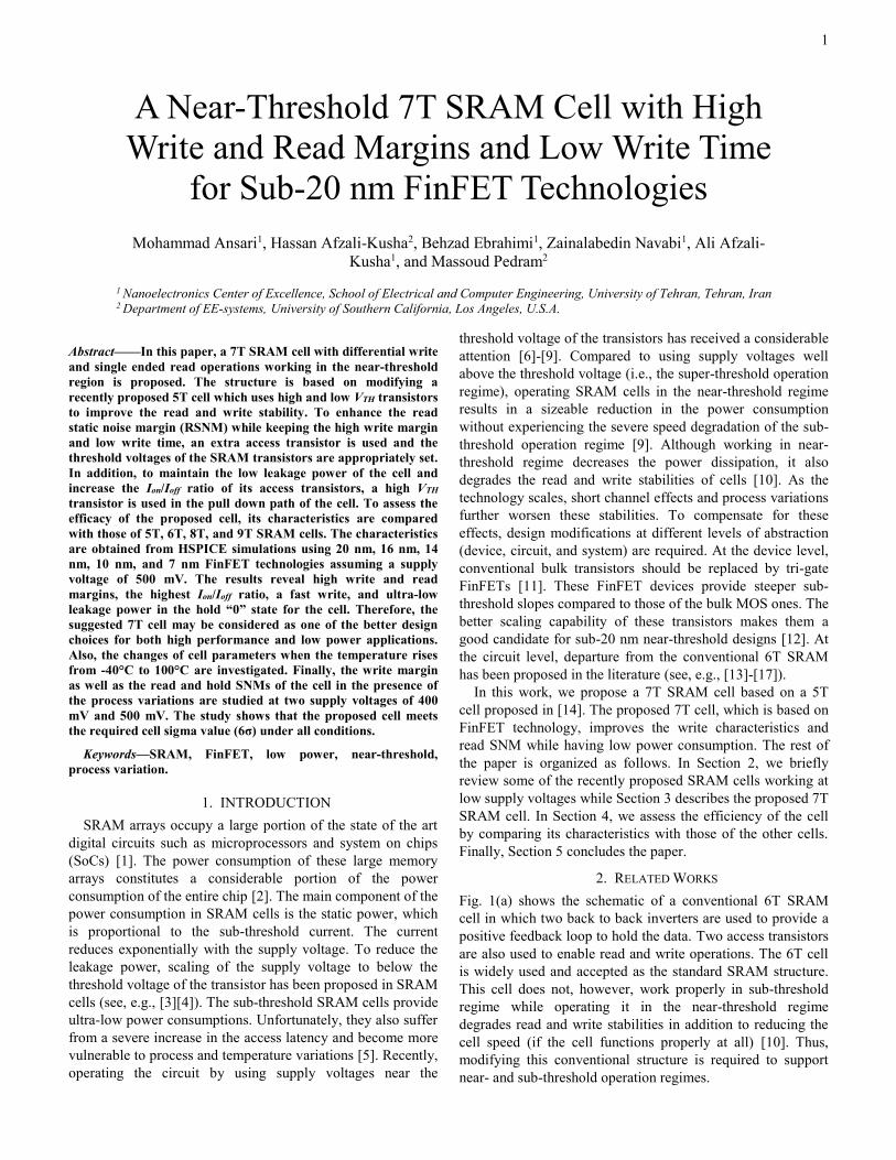
1 Abstract——In this paper, a 7T SRAM cell with differential write and single ended read operations working in the near-threshold region is proposed. The structure is based on modifying a recently proposed 5T cell which uses high and low VTH transistors to improve the read and write stability. To enhance the read static noise margin (RSNM) while keeping the high write margin and low write time, an extra access transistor is used and the threshold voltages of the SRAM transistors are appropriately set. In addition, to maintain the low leakage power of the cell and increase the Ion/Ioff ratio of its access transistors, a high VTH transistor is used in the pull down path of the cell. To assess the efficacy of the proposed cell, its characteristics are compared with those of 5T, 6T, 8T, and 9T SRAM cells. The characteristics are obtained from HSPICE simulations using 20 nm, 16 nm, 14 nm, 10 nm, and 7 nm FinFET technologies assuming a supply voltage of 500 mV. The results reveal high write and read margins, the highest Ion/Ioff ratio, a fast write, and ultra-low leakage power in the hold “0” state for the cell. Therefore, the suggested 7T cell may be considered as one of the better design choices for both high performance and low power applications. Also, the changes of cell parameters when the temperature rises from -40°C to 100°C are investigated. Finally, the write margin as well as the read and hold SNMs of the cell in the presence of the process variations are studied at two supply voltages of 400 mV and 500 mV. The study shows that the proposed cell meets the required cell sigma value (6σ) under all conditions. Keywords—SRAM, FinFET, low power, near-threshold, process variation. 1. INTRODUCTION SRAM arrays occupy a large portion of the state of the art digital circuits such as microprocessors and system on chips (SoCs) [1]. The power consumption of these large memory arrays constitutes a considerable portion of the power consumption of the entire chip [2]. The main component of the power consumption in SRAM cells is the static power, which is proportional to the sub-threshold current. The current reduces exponentially with the supply voltage. To reduce the leakage power, scaling of the supply voltage to below the threshold voltage of the transistor has been proposed in SRAM cells (see, e.g., [3][4]). The sub-threshold SRAM cells provide ultra-low power consumptions. Unfortunately, they also suffer from a severe increase in the access latency and become more vulnerable to process and temperature variations [5]. Recently, operating the circuit by using supply voltages near the threshold voltage of the transistors has received a considerable attention [6]-[9]. Compared to using supply voltages well above the threshold voltage (i.e., the super-threshold operation regime), operating SRAM cells in the near-threshold regime results in a sizeable reduction in the power consumption without experiencing the severe speed degradation of the sub- threshold operation regime [9]. Although working in near- threshold regime decreases the power dissipation, it also degrades the read and write stabilities of cells [10]. As the technology scales, short channel effects and process variations further worsen these stabilities. To compensate for these effects, design modifications at different levels of abstraction (device, circuit, and system) are required. At the device level, conventional bulk transistors should be replaced by tri-gate FinFETs [11]. These FinFET devices provide steeper sub- threshold slopes compared to those of the bulk MOS ones. The better scaling capability of these transistors makes them a good candidate for sub-20 nm near-threshold designs [12]. At the circuit level, departure from the conventional 6T SRAM has been proposed in the literature (see, e.g., [13]-[17]). In this work, we propose a 7T SRAM cell based on a 5T cell proposed in [14]. The proposed 7T cell, which is based on FinFET technology, improves the write characteristics and read SNM while having low power consumption. The rest of the paper is organized as follows. In Section 2, we briefly review some of the recently proposed SRAM cells working at low supply voltages while Section 3 describes the proposed 7T SRAM cell. In Section 4, we assess the efficiency of the cell by comparing its characteristics with those of the other cells. Finally, Section 5 concludes the paper. 2. RELATED WORKS Fig. 1(a) shows the schematic of a conventional 6T SRAM cell in which two back to back inverters are used to provide a positive feedback loop to hold the data. Two access transistors are also used to enable read and write operations. The 6T cell is widely used and accepted as the standard SRAM structure. This cell does not, however, work properly in sub-threshold regime while operating it in the near-threshold regime degrades read and write stabilities in addition to reducing the cell speed (if the cell functions properly at all) [10]. Thus, modifying this conventional structure is required to support near- and sub-threshold operation regimes. A Near-Threshold 7T SRAM Cell with High Write and Read Margins and Low Write Time for Sub-20 nm FinFET Technologies Mohammad Ansari 1 , Hassan Afzali-Kusha 2 , Behzad Ebrahimi 1 , Zainalabedin Navabi 1 , Ali Afzali- Kusha 1 , and Massoud Pedram 2 1 Nanoelectronics Center of Excellence, School of Electrical and Computer Engineering, University of Tehran, Tehran, Iran 2 Department of EE-systems, University of Southern California, Los Angeles, U.S.A.
Transcript of A near-threshold 7T SRAM cell with high write and read margins and low write time for sub-20nm...
1
Abstract——In this paper, a 7T SRAM cell with differential write
and single ended read operations working in the near-threshold
region is proposed. The structure is based on modifying a
recently proposed 5T cell which uses high and low VTH transistors
to improve the read and write stability. To enhance the read
static noise margin (RSNM) while keeping the high write margin
and low write time, an extra access transistor is used and the
threshold voltages of the SRAM transistors are appropriately set.
In addition, to maintain the low leakage power of the cell and
increase the Ion/Ioff ratio of its access transistors, a high VTH
transistor is used in the pull down path of the cell. To assess the
efficacy of the proposed cell, its characteristics are compared
with those of 5T, 6T, 8T, and 9T SRAM cells. The characteristics
are obtained from HSPICE simulations using 20 nm, 16 nm, 14
nm, 10 nm, and 7 nm FinFET technologies assuming a supply
voltage of 500 mV. The results reveal high write and read
margins, the highest Ion/Ioff ratio, a fast write, and ultra-low
leakage power in the hold “0” state for the cell. Therefore, the
suggested 7T cell may be considered as one of the better design
choices for both high performance and low power applications.
Also, the changes of cell parameters when the temperature rises
from -40°C to 100°C are investigated. Finally, the write margin
as well as the read and hold SNMs of the cell in the presence of
the process variations are studied at two supply voltages of 400
mV and 500 mV. The study shows that the proposed cell meets
the required cell sigma value (6σ) under all conditions.
Keywords—SRAM, FinFET, low power, near-threshold,
process variation.
1. INTRODUCTION
SRAM arrays occupy a large portion of the state of the art
digital circuits such as microprocessors and system on chips
(SoCs) [1]. The power consumption of these large memory
arrays constitutes a considerable portion of the power
consumption of the entire chip [2]. The main component of the
power consumption in SRAM cells is the static power, which
is proportional to the sub-threshold current. The current
reduces exponentially with the supply voltage. To reduce the
leakage power, scaling of the supply voltage to below the
threshold voltage of the transistor has been proposed in SRAM
cells (see, e.g., [3][4]). The sub-threshold SRAM cells provide
ultra-low power consumptions. Unfortunately, they also suffer
from a severe increase in the access latency and become more
vulnerable to process and temperature variations [5]. Recently,
operating the circuit by using supply voltages near the
threshold voltage of the transistors has received a considerable
attention [6]-[9]. Compared to using supply voltages well
above the threshold voltage (i.e., the super-threshold operation
regime), operating SRAM cells in the near-threshold regime
results in a sizeable reduction in the power consumption
without experiencing the severe speed degradation of the sub-
threshold operation regime [9]. Although working in near-
threshold regime decreases the power dissipation, it also
degrades the read and write stabilities of cells [10]. As the
technology scales, short channel effects and process variations
further worsen these stabilities. To compensate for these
effects, design modifications at different levels of abstraction
(device, circuit, and system) are required. At the device level,
conventional bulk transistors should be replaced by tri-gate
FinFETs [11]. These FinFET devices provide steeper sub-
threshold slopes compared to those of the bulk MOS ones. The
better scaling capability of these transistors makes them a
good candidate for sub-20 nm near-threshold designs [12]. At
the circuit level, departure from the conventional 6T SRAM
has been proposed in the literature (see, e.g., [13]-[17]).
In this work, we propose a 7T SRAM cell based on a 5T
cell proposed in [14]. The proposed 7T cell, which is based on
FinFET technology, improves the write characteristics and
read SNM while having low power consumption. The rest of
the paper is organized as follows. In Section 2, we briefly
review some of the recently proposed SRAM cells working at
low supply voltages while Section 3 describes the proposed 7T
SRAM cell. In Section 4, we assess the efficiency of the cell
by comparing its characteristics with those of the other cells.
Finally, Section 5 concludes the paper.
2. RELATED WORKS
Fig. 1(a) shows the schematic of a conventional 6T SRAM
cell in which two back to back inverters are used to provide a
positive feedback loop to hold the data. Two access transistors
are also used to enable read and write operations. The 6T cell
is widely used and accepted as the standard SRAM structure.
This cell does not, however, work properly in sub-threshold
regime while operating it in the near-threshold regime
degrades read and write stabilities in addition to reducing the
cell speed (if the cell functions properly at all) [10]. Thus,
modifying this conventional structure is required to support
near- and sub-threshold operation regimes.
A Near-Threshold 7T SRAM Cell with High
Write and Read Margins and Low Write Time
for Sub-20 nm FinFET Technologies
Mohammad Ansari1, Hassan Afzali-Kusha2, Behzad Ebrahimi1, Zainalabedin Navabi1, Ali Afzali-
Kusha1, and Massoud Pedram2
1 Nanoelectronics Center of Excellence, School of Electrical and Computer Engineering, University of Tehran, Tehran, Iran 2 Department of EE-systems, University of Southern California, Los Angeles, U.S.A.
2
(a) (b)
(c) (d)
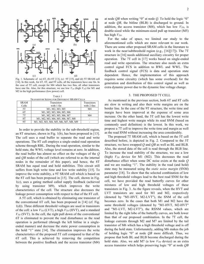
Fig. 1. Schematic of (a) 6T, (b) 8T [13], (c) 9T [15], and (d) 5T SRAM cell
[14]. In this work, for 6T, 8T, and 9T cells, all the transistors have one fin. In
the case of 5T cell, except for M4 which has two fins, all other transistors have one fin. Also, for this structure, we use low VTH (high VTH) for M1 and
M2 in the high performance (low power) cell.
TABLE 1
TRANSISTOR SIZING FOR DIFFERENT SRAM CELLS
SRAM Cells
Transistors with 1 fin
Transistors with 2 fins
5T M1, M2, M3, M5 M4
6T M1, M2, M3, M4, M5, M6 -
7T M1, M2, M3, M5, M6, M7 M4
8T M1, M2, M3, M4, M5, M6, M7, M8 -
9T M1, M2, M3, M4, M5, M6, M7, M8, M9 -
In order to provide the stability in the sub-threshold region,
an 8T structure, shown in Fig. 1(b), has been proposed in [13].
The cell uses a read buffer to separate the read and write
operations. The 8T cell employs a single-ended read operation
scheme through RBL. During the read operation, similar to the
hold state, the WWL voltage level remains at zero. In addition,
the read buffer has almost no effect on the voltages of the Q
and QB nodes of the cell (which are referred to as the internal
nodes in the remainder of this paper), and hence, the 8T
SRAM has equal read and hold stabilities. This circuit still
suffers from high write time and low write stability [15]. To
improve the write stability, a 9T SRAM cell which is based on
the 8T cell has been proposed in [15]. The cell, shown in Fig.
1(c), uses a gating method called supply feedback (achieved
by using transistor M9), which improves the write
characteristics of the cell. The structure also decreases the
leakage power consumption with respect to that of the 8T cell.
A 5T cell, which is obtained by eliminating one transistor of
the conventional 6T cell, has been proposed in [14] (cf. Fig.
1(d)). Three different threshold voltages are used in transistors
of the cell: a low VTH (LVT), a high VTH (HVT), and a standard
VTH (SVT). In the cell, the right pull down of the conventional
6T is eliminated to prevent the read disturbance as the read
operation is performed (through the left bitline in a single-
ended manner) and decrease the static power consumption in
the hold “1” state [14]. The elimination improves the write
characteristics of the proposed 5T cell compared to that of the
6T cell. This is achieved by removing the competition
between the positive feedback and the access transistor (M4)
at node QB when writing “0” at node Q. To hold the logic “0”
at node QB, the bitline (BLB) is discharged to ground. In
addition, the access transistor (M4), which has low VTH, is
double-sized while the minimum-sized pull up transistor (M5)
has high VTH.
For the sake of space, we limited our study to the
aforementioned cells which are more relevant to our work.
There are some other proposed SRAM cells in the literature to
work in the near/subthreshold region (e.g., [16][17]). The 7T
structure in [16] needs additional auxiliary circuitry for proper
operation. The 7T cell in [17] works based on single-ended
read and write operations. The structure also needs an extra
control signal FCS in addition to RWL and WWL. The
feedback control signal (FCS) is data and operation state
dependent. Hence, the implementation of this approach
requires some circuitry (which has some overhead) for the
generation and distribution of this control signal as well as
extra dynamic power due to the dynamic line voltage change.
3. THE PROPOSED 7T CELL
As mentioned in the previous section, both 6T and 8T cells
are slow in writing and also their write margins are on the
border line. In the case of the 9T structure, the write time and
margin have been improved at the expense of some area
increase. On the other hand, the 5T cell has the lowest write
time and highest write margin while its read SNM (based on
commonly used definition) is the lowest. In this work, we
propose a 7T cell to improve the write time and margin as well
as the read SNM without increasing the area considerably.
The proposed 7T SRAM cell, which is based on the 5T cell
described before, is depicted in Fig. 2. Compared to the 5T
structure, we have swapped Q and QB as well as BL and BLB.
Also, the stored data of the cell is read through the BLB line.
To increase the read stability of the structure, we use a low
(high) VTH device for M1 (M2). This decreases the read
disturbance effect when some DC noise exists at the node Q
and we are reading “1”. The stability in the read (and hold)
state may be measured using the static noise margin (SNM)
parameter [18]. To show that the selected combination of low
and high threshold voltages lead to the best read SNM for the
cell, we have provided the read butterfly curves for other
mixtures of low and high threshold voltages of these
transistors in Fig. 3. As the figure reveals, when the HVT and
LVT transistors are used for M1 and M2, respectively
(denoted by "M1-HVT, M2-LVT"), the SNM of the cell
becomes zero. In the cases that both M1 and M2 have the
same threshold voltages (denoted by "M1-HVT, M2-HVT"
and "M1-LVT, M2-LVT"), the RSNM values, which are
limited by the right lobe of the butterfly curves, are both lower
than that of our proposed combination. In the 7T cell, the
leakage currents through M2 and M7 are limited by the tail
transistor of M6 which has a high threshold voltage and is off
during the hold state. Unfortunately, adding M6 makes the job
of holding logic “0” at node QB more difficult. Thus, we
propose that both BL and BLB become discharged during the
hold state. Also, we add M7 (a low VTH device) as an extra
access transistor which helps preserving logic “0” at node QB

3
Fig. 2. Schematic of our proposed 7T SRAM cell.
Fig. 3. Effect of low and high threshold voltage combinations of M1 and M2 on the RSNM of the 7T cell.
using the transistor leakage current to the ground. Notice that
M7 also improves the write characteristics by increasing the
write current. Table 2 shows the cell signaling scheme in
different states for our proposed structure.
4. RESULTS AND DISCUSSION
In this section, we study the efficacy of the proposed SRAM
cell in terms of its key characteristics. For the realization of
the cell, the FinFET technology, which exhibits better short
channel effects, is utilized. It is predicted to be the device of
the choice for sub 14 nm nodes [1]. Fig. 4 shows the 3D
schematic of the FinFET structure whose parameters including
the gate length (Lg), fin width (tsi) and fin height (Hfin) are
given in the table in the inset of the figure. The study is
performed by comparing the characteristics by those of the
other cells obtained from HSPICE simulations by using the
sub-20 nm technologies (20, 16, 14, 10, and 7 nm) as provided
in the Predictive Technology Model [19].
The available technology models included low power and
high performance transistor models. Since in the cases of the
5T and the proposed 7T cell structures (see Fig. 1(d) and Fig.
2), the right pull down transistor has been eliminated, for the
proper operation of the cell, both low and high VTH devices
from high performance and low power technology models of
[19] have been used. In addition, as listed in Table 1, except
for the access transistor M4 in both the 5T and 7T structures
which is double-sized (two fins are used), all other
TABLE 2 CELL SIGNALING SCHEME IN DIFFERENT STATES FOR THE PROPOSED
STRUCTURE
State BL BLB WWL RWL
Hold 0 0 0 0
Write “0” 0 VDD VDD VDD
Write “1” VDD 0 VDD VDD
Read “0” 0 VDD 0 VDD
Read “1” 0 VDD →0 0 VDD
HSPICE simulation parameters [19]
Tech.
Node
20
nm
16
nm
14
nm
10
nm
7
nm
Lg (nm) 24 20 18 14 11
tsi (nm) 15 12 10 9 7
Hfin (nm) 28 26 23 21 18
Fig. 4. The 3D schematic of a FinFET structure.
transistors in all the structures have one fin. For the 5T
structure, the threshold voltages of M3-M5 were assigned
based on Fig. 1(d). The transistors M1 and M2 use standard
VTH (SVT) in the original proposal of the cell [14]. However,
as SVT is not available for the considered technology, for M1
and M2, we considered two cases of high performance (HP)
and low power (LP) cells where low and high VTH devices
were exploited, respectively. We also investigated the effect of
using SVT transistors for M1 and M2 by adjusting their gate
work functions in the technology file. The simulation results
for this case resided between the corresponding results of the
HP and LP cases as could be expected. Obviously, the
availability of the third threshold voltage in a technology
could be achieved at the price of a higher fabrication cost.
For a better comparison, in the cases of the 6T, 8T, and 9T
structures, we used only low (high) VTH devices for HP (LP)
cells. In the technologies considered here, the nominal supply
voltages ranged from 0.7 V to 0.9 V (for super-threshold
operation regime). Given the threshold voltage of about 0.4 V
for the low power technologies, we set the supply voltage of
0.5 V for all the simulations targeting near-threshold operation
regime. The study includes both nominal and under process
variation cases.
4.1. Nominal Study
4.1.1. Write State
First, we consider the write stability metric (i.e., the write
margin) for which different definitions have been suggested in
the literature [20]. In this work, we use the difference between
VDD and the minimum wordline voltage that can cause a
successful write operation as the metric. This is called the
combined wordline margin (CWLM) [20]. For the asymmetric
cell structures considered in this work, there are different write
“0” and write “1” margins. Similar to [21], we consider the
minimum of these two margins as the write margin. For
measuring the write margin of the 6T, 8T, 9T (5T and 7T)
cells, based on their write operations, we sweep the WWL
(RWL and WWL) with the same voltage from zero up to the
voltage where the write operation occurs. The values of this
metric for different structures at different technology nodes
are shown in Fig. 5 for both LP and HP cells. The write
stability metric for the proposed cell (which has no separate
HP or LP implementation) is given in both LP and HP cell
plots such that its performance can be compared to those of
both types of the cells. It is evident that the proposed 7T cell

4
has the highest write margin among all the cells. The write “0”
(“1”) margin for the 5T (7T) cell is VDD since there is no active
feedback in this case. The 7T cell has a higher write “0”
margin (approximately equal to VDD) compared to the write
“1” margin of the 5T cell due to use of the write assisting
transistor (M7 in Fig. 2). Recall that this transistor turns on
only in the write mode improving the write operation. The 6T
and 8T cells, which perform the write “0” and “1” operations
symmetrically, have the lowest write margins because of the
race between the access transistor and the transistors forming
the feedback loop. The use of the supply feedback transistor
M9 in the 9T cell (Fig. 1(c)) makes the feedback loop weaker
when the WWL signal is asserted. Hence, the 9T cell has a
higher write margin than those of the 6T and 8T cells. Fig. 5
also shows that, there is no considerable change in the write
margins as a function of physical scaling. This is justified by
noting that the threshold voltages and more importantly the
strength ratios (relative strengths) of transistors in the SRAM
cells remain more or less the same in these technologies. The
write margins of the HP cells are higher than those for the LP
ones. This is due to the lower threshold voltages of (some of)
the transistors involved in the write operation of the HP cells.
In other words, for a given VDD level, the required voltage on
WWL is lower (due to the use of lower threshold access
transistors) making CWLM larger. It is worth noting that
because the write margin of the proposed cell is almost equal
to VDD, one may be concerned about unwanted write to the
half-selected cells in the same column of the cell that is being
written to. This may not happen due to the fact that the half-
selected cells require a substantially higher write time than
that of the selected cell. Our simulation results show that, e.g.,
in the case of the 20 nm technology, the write “1” time is
about 38 μs which is about 7 orders of magnitude larger than
6.7 ps required for the same operation in the case of the
selected cell. This time is even substantially larger in the case
of the write “0”. Additionally, to avoid the half-selected issue
for the cells in the selected row (which is a common problem
for near- and sub-threshold structures), it has been suggested
that the whole row be written simultaneously [22].
Alternatively, one may use column-decoupled SRAM array in
which the unselected cells in the same row have an inactive
wordline [23].
Another important metric in the write state is the write time.
The write time is measured from the point that the WL
(a) (b)
Fig. 5. Write margin (minimum of the write “0” and “1” margins) at different technology nodes for different SRAM structures in the cases of (a) LP and (b)
HP cells.
(WWL) signal is asserted to the point that the cell flips (Q and
QB voltage values cross each other on their way to assume the
opposite logic levels). Since the asymmetric cells have
different write “0” and “1” times, we consider the maximum
of the write “0” and “1” times as the write time for these cells.
This metric is shown in Fig. 6 for different cells realized using
different technologies. Again, both LP and HP cells are
included in the study. Evidently as the technology scales
down, the write time decreases due to the reduction of the
capacitances. Furthermore, as expected, the HP cells have
lower write times compared to those of the LP cells. In our
proposed cell, the write operation is performed differentially
through three access transistors, which makes the write
operation very fast. Write “1” is performed very easily in our
structure because it has no pull down transistor connected to
node Q, which has stored “0”. The elimination of the pull
down transistor reduces the node capacitance and increases the
current that charges this node. For our proposed cell, write “0”
is accomplished through two parallel access racing two series
pull down transistors. Thus, node QB is rapidly charged to
“1”, resulting in a short write time. Among these two write
times, the write “0” takes longer for our proposed cell, and
hence, its values are the ones that are reported in Fig. 6.
Compared to the 6T cell, the 8T structure has a larger write
time due to the higher parasitic capacitance at node QB (see
Fig. 1(b)). In the 9T cell (see Fig. 1(c)), M9 helps achieving a
faster write operation. During the write “1” operation, the
node Q, which is connected to the gate of M9, becomes
charged, weakening M9 (by reducing the absolute value of its
overdrive voltage). Therefore, the source voltage of M6,
which is the virtual VDD (VVDD), decreases while its gate
voltage increases. This weakening of M6 helps obtaining a
shorter time for M5 to discharge QB, which, in turn, initiates
the positive feedback. At the start of the write “0”, M2 and M3
compete intensively. Because M9 is initially off, VVDD is low
making M3 weak which in turn yields a faster write operation.
Therefore, the addition of M9 decreases the write time
compared to that of the 8T cell. It is, however, more than that
of the 6T cell due to the higher parasitic capacitances.
4.1.1. Read State
In the conventional 6T cell, during the read operation when
Q = “0”, the voltage of node Q rises. If this voltage becomes
larger than the trip point of the right inverter (M2-M4) the
(a) (b)
Fig. 6. Write time (maximum of the write “0” and “1” times) at different technology nodes for different SRAM structures in the cases of (a) LP and (b)
HP cells.
5
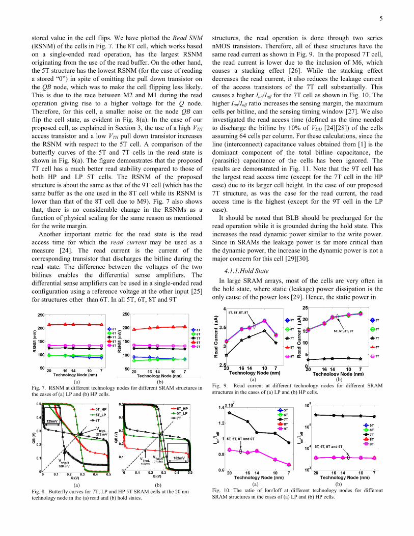
stored value in the cell flips. We have plotted the Read SNM
(RSNM) of the cells in Fig. 7. The 8T cell, which works based
on a single-ended read operation, has the largest RSNM
originating from the use of the read buffer. On the other hand,
the 5T structure has the lowest RSNM (for the case of reading
a stored “0”) in spite of omitting the pull down transistor on
the QB node, which was to make the cell flipping less likely.
This is due to the race between M2 and M1 during the read
operation giving rise to a higher voltage for the Q node.
Therefore, for this cell, a smaller noise on the node QB can
flip the cell state, as evident in Fig. 8(a). In the case of our
proposed cell, as explained in Section 3, the use of a high VTH
access transistor and a low VTH pull down transistor increases
the RSNM with respect to the 5T cell. A comparison of the
butterfly curves of the 5T and 7T cells in the read state is
shown in Fig. 8(a). The figure demonstrates that the proposed
7T cell has a much better read stability compared to those of
both HP and LP 5T cells. The RSNM of the proposed
structure is about the same as that of the 9T cell (which has the
same buffer as the one used in the 8T cell while its RSNM is
lower than that of the 8T cell due to M9). Fig. 7 also shows
that, there is no considerable change in the RSNMs as a
function of physical scaling for the same reason as mentioned
for the write margin.
Another important metric for the read state is the read
access time for which the read current may be used as a
measure [24]. The read current is the current of the
corresponding transistor that discharges the bitline during the
read state. The difference between the voltages of the two
bitlines enables the differential sense amplifiers. The
differential sense amplifiers can be used in a single-ended read
configuration using a reference voltage at the other input [25]
for structures other than 6T. In all 5T, 6T, 8T and 9T
(a) (b) Fig. 7. RSNM at different technology nodes for different SRAM structures in
the cases of (a) LP and (b) HP cells.
(a) (b) Fig. 8. Butterfly curves for 7T, LP and HP 5T SRAM cells at the 20 nm
technology node in the (a) read and (b) hold states.
structures, the read operation is done through two series
nMOS transistors. Therefore, all of these structures have the
same read current as shown in Fig. 9. In the proposed 7T cell,
the read current is lower due to the inclusion of M6, which
causes a stacking effect [26]. While the stacking effect
decreases the read current, it also reduces the leakage current
of the access transistors of the 7T cell substantially. This
causes a higher Ion/Ioff for the 7T cell as shown in Fig. 10. The
higher Ion/Ioff ratio increases the sensing margin, the maximum
cells per bitline, and the sensing timing window [27]. We also
investigated the read access time (defined as the time needed
to discharge the bitline by 10% of VDD [24][28]) of the cells
assuming 64 cells per column. For these calculations, since the
line (interconnect) capacitance values obtained from [1] is the
dominant component of the total bitline capacitance, the
(parasitic) capacitance of the cells has been ignored. The
results are demonstrated in Fig. 11. Note that the 9T cell has
the largest read access time (except for the 7T cell in the HP
case) due to its larger cell height. In the case of our proposed
7T structure, as was the case for the read current, the read
access time is the highest (except for the 9T cell in the LP
case).
It should be noted that BLB should be precharged for the
read operation while it is grounded during the hold state. This
increases the read dynamic power similar to the write power.
Since in SRAMs the leakage power is far more critical than
the dynamic power, the increase in the dynamic power is not a
major concern for this cell [29][30].
4.1.1. Hold State
In large SRAM arrays, most of the cells are very often in
the hold state, where static (leakage) power dissipation is the
only cause of the power loss [29]. Hence, the static power in
(a) (b) Fig. 9. Read current at different technology nodes for different SRAM
structures in the cases of (a) LP and (b) HP cells.
(a) (b)
Fig. 10. The ratio of Ion/Ioff at different technology nodes for different
SRAM structures in the cases of (a) LP and (b) HP cells.
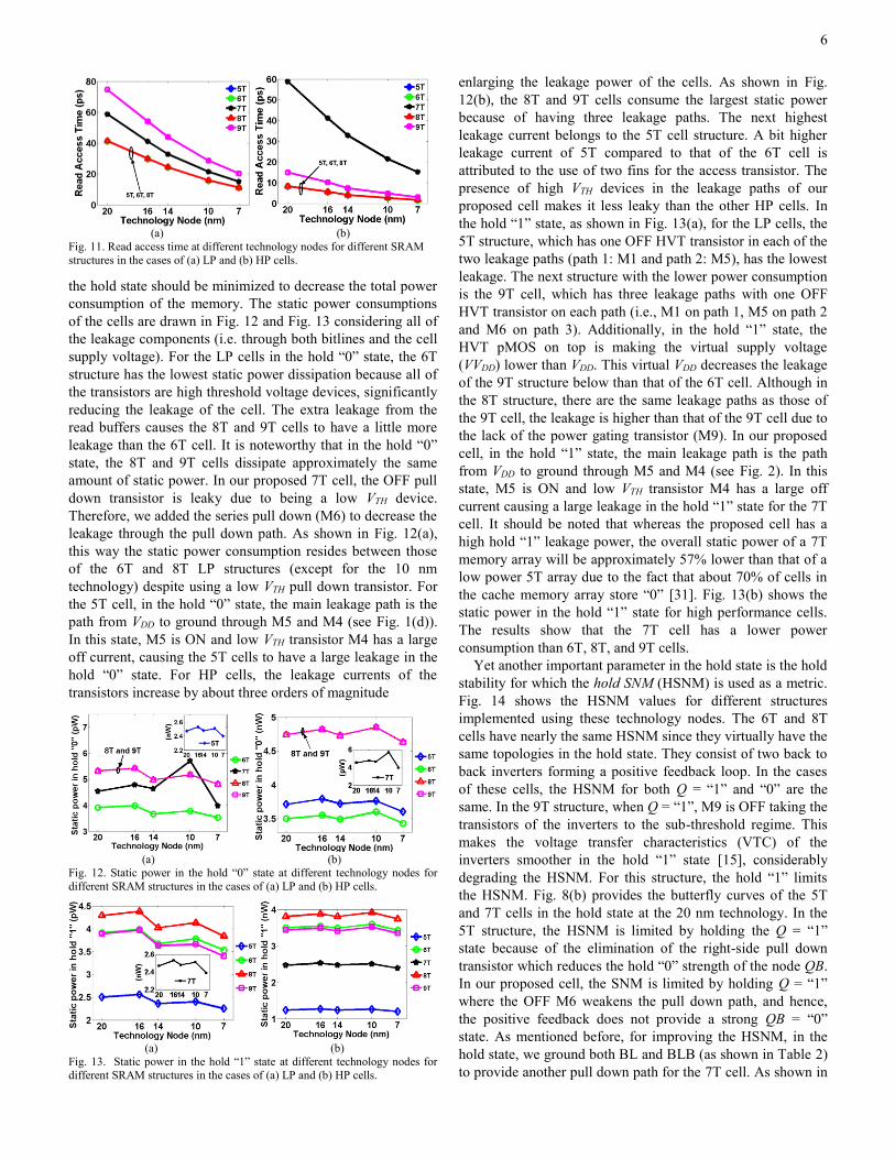
6
(a) (b)
Fig. 11. Read access time at different technology nodes for different SRAM
structures in the cases of (a) LP and (b) HP cells.
the hold state should be minimized to decrease the total power
consumption of the memory. The static power consumptions
of the cells are drawn in Fig. 12 and Fig. 13 considering all of
the leakage components (i.e. through both bitlines and the cell
supply voltage). For the LP cells in the hold “0” state, the 6T
structure has the lowest static power dissipation because all of
the transistors are high threshold voltage devices, significantly
reducing the leakage of the cell. The extra leakage from the
read buffers causes the 8T and 9T cells to have a little more
leakage than the 6T cell. It is noteworthy that in the hold “0”
state, the 8T and 9T cells dissipate approximately the same
amount of static power. In our proposed 7T cell, the OFF pull
down transistor is leaky due to being a low VTH device.
Therefore, we added the series pull down (M6) to decrease the
leakage through the pull down path. As shown in Fig. 12(a),
this way the static power consumption resides between those
of the 6T and 8T LP structures (except for the 10 nm
technology) despite using a low VTH pull down transistor. For
the 5T cell, in the hold “0” state, the main leakage path is the
path from VDD to ground through M5 and M4 (see Fig. 1(d)).
In this state, M5 is ON and low VTH transistor M4 has a large
off current, causing the 5T cells to have a large leakage in the
hold “0” state. For HP cells, the leakage currents of the
transistors increase by about three orders of magnitude
(a) (b) Fig. 12. Static power in the hold “0” state at different technology nodes for
different SRAM structures in the cases of (a) LP and (b) HP cells.
(a) (b)
Fig. 13. Static power in the hold “1” state at different technology nodes for
different SRAM structures in the cases of (a) LP and (b) HP cells.
enlarging the leakage power of the cells. As shown in Fig.
12(b), the 8T and 9T cells consume the largest static power
because of having three leakage paths. The next highest
leakage current belongs to the 5T cell structure. A bit higher
leakage current of 5T compared to that of the 6T cell is
attributed to the use of two fins for the access transistor. The
presence of high VTH devices in the leakage paths of our
proposed cell makes it less leaky than the other HP cells. In
the hold “1” state, as shown in Fig. 13(a), for the LP cells, the
5T structure, which has one OFF HVT transistor in each of the
two leakage paths (path 1: M1 and path 2: M5), has the lowest
leakage. The next structure with the lower power consumption
is the 9T cell, which has three leakage paths with one OFF
HVT transistor on each path (i.e., M1 on path 1, M5 on path 2
and M6 on path 3). Additionally, in the hold “1” state, the
HVT pMOS on top is making the virtual supply voltage
(VVDD) lower than VDD. This virtual VDD decreases the leakage
of the 9T structure below than that of the 6T cell. Although in
the 8T structure, there are the same leakage paths as those of
the 9T cell, the leakage is higher than that of the 9T cell due to
the lack of the power gating transistor (M9). In our proposed
cell, in the hold “1” state, the main leakage path is the path
from VDD to ground through M5 and M4 (see Fig. 2). In this
state, M5 is ON and low VTH transistor M4 has a large off
current causing a large leakage in the hold “1” state for the 7T
cell. It should be noted that whereas the proposed cell has a
high hold “1” leakage power, the overall static power of a 7T
memory array will be approximately 57% lower than that of a
low power 5T array due to the fact that about 70% of cells in
the cache memory array store “0” [31]. Fig. 13(b) shows the
static power in the hold “1” state for high performance cells.
The results show that the 7T cell has a lower power
consumption than 6T, 8T, and 9T cells.
Yet another important parameter in the hold state is the hold
stability for which the hold SNM (HSNM) is used as a metric.
Fig. 14 shows the HSNM values for different structures
implemented using these technology nodes. The 6T and 8T
cells have nearly the same HSNM since they virtually have the
same topologies in the hold state. They consist of two back to
back inverters forming a positive feedback loop. In the cases
of these cells, the HSNM for both Q = “1” and “0” are the
same. In the 9T structure, when Q = “1”, M9 is OFF taking the
transistors of the inverters to the sub-threshold regime. This
makes the voltage transfer characteristics (VTC) of the
inverters smoother in the hold “1” state [15], considerably
degrading the HSNM. For this structure, the hold “1” limits
the HSNM. Fig. 8(b) provides the butterfly curves of the 5T
and 7T cells in the hold state at the 20 nm technology. In the
5T structure, the HSNM is limited by holding the Q = “1”
state because of the elimination of the right-side pull down
transistor which reduces the hold “0” strength of the node QB.
In our proposed cell, the SNM is limited by holding Q = “1”
where the OFF M6 weakens the pull down path, and hence,
the positive feedback does not provide a strong QB = “0”
state. As mentioned before, for improving the HSNM, in the
hold state, we ground both BL and BLB (as shown in Table 2)
to provide another pull down path for the 7T cell. As shown in

7
Fig. 8(b), the lower threshold voltages cause a lower left trip
point (VtripL) for the VTC in the HP 5T cell. This is translated
to a smaller HSNM. The same trend is also observed in 6T and
8T structures when comparing the LP and HP counterparts. In
the case of the 9T cell, the lower threshold voltage of M9
improves the feedback strength, and hence, the HSNM for
both types of the cell are about the same. Fig. 14 also shows
that, there is no large change in the HSNMs as a function of
physical scaling. Again, this may be justified using the reasons
as stated for the cases of the read and write margins.
4.1.2. Area
The layouts of the cells, drawn based on the design rules for
the FinFET technology reported in [32], are shown in Fig. 15.
The area of each structure is reported in the table in the inset
of Fig. 15 where λ is the minimum feature size assumed to be
1/2 of the gate length. The non-minimum sized transistor M4
(two fins) in the 5T and 7T cells as well as their asymmetrical
structure of 5T, 7T, and 9T cause larger areas than expected
(i.e., proportional to the transistor count) for these cells. The
figures in the table show a smaller area/transistor for the
proposed cell among these three asymmetric cell structures. It
should be noted that LP and HP structures have the same
layouts as the difference between the LVT and HVT
transistors is only due to their gate work functions.
4.1.3. SRAM Figure of Merit
The diversity of SRAM parameters makes it difficult to
designate a clear winner among all the ones that we have
considered. A possible approach is to use a composite figure
of merit for the SRAM cells. For instance, an SRAM electrical
quality factor (SEQF) which considers only stability and
power has been suggested in [32]. This expression, however,
does not consider the effect of the speed and area. Also, an
SRAM quality factor (Q) has been proposed in [33]. Although
this factor considered the power, stability, speed, and area
metrics, it suffers from humongous variations of the Q values
due to temperature changes. Here, we suggest a SRAM figure
of merit (denoted by SFOM) which considers read access time
(tread) as the read speed metric, RSNM as the read stability
metric, write time (twrite) as the write speed metric, and write
margin (WM) as the write stability metric. The standby power
and area (A) are also taken into account.
(a) (b)
Fig. 14. HSNM at different technology nodes for different SRAM structures
in the cases of (a) LP and (b) HP cells.
Fig. 15. Bit cells layouts in FinFET technology for (a) 5T, (b) 6T, (c) 7T, (d) 8T and (e) 9T.
SFOM is defined as
( )
( ) (log( ))write read avg
WM RSNMSFOM
t t P A
(1)
where Pavg is the average of the hold “0” and “1” power in pW.
Table 3 lists the SFOM values of the 5T, 7T, 8T, and 9T cells
normalized to the SFOM of the 6T cell for different
technologies. It should be noted that two sets of results have
been presented for the 7T cell due to two different
normalization factors of the 6T cell (LP and HP).
TABLE 3 NORMALIZED SRAM FIGURE OF MERIT (SFOM)
Technology Temp.
(°C) 5T 7T 8T 9T
20nm HP 25 2.16 1.80 1.37 0.64
100 3.35 2.58 1.73 0.94
20nm LP 25 2.43 7.68 1.28 0.54
100 3.32 7.34 1.50 0.71
16nm HP 25 2.07 1.76 1.37 0.62
100 3.04 2.50 1.69 0.90
16nm LP 25 2.43 8.09 1.28 0.54
100 3.24 7.90 1.51 0.71
14nm HP 25 1.98 1.67 1.36 0.60
100 2.82 2.40 1.65 0.84
14nm LP 25 2.40 8.62 1.28 0.54
100 3.13 8.41 1.52 0.71
10nm HP 25 1.72 1.69 1.36 0.61
100 2.67 2.42 1.63 0.85
10nm LP 25 2.34 9.08 1.29 0.53
100 3.06 8.77 1.54 0.72
7nm HP 25 1.85 1.67 1.37 0.61
100 2.56 2.36 1.63 0.84
7nm LP 25 2.45 10.73 1.30 0.55
100 3.12 9.91 1.54 0.73
Active Gate Metal Metal 1 Metal 2
(e)
(a)
(d) (b)
Bit cells area and area per transistor (A/Tr.)
Cell Width
(λ)
Height
(λ)
Area (A)
(λ2) A/Tr.
5T 37 20 740 148
6T 35 20 700 117
7T 37 25 925 132
8T 47 20 940 118
9T 36 41 1476 164
(c)
8
As shown in the table, in the case of the HP cells, our structure
is the second best cell while for the LP cells, the 7T cell
outperforms all others. Therefore, the suggested 7T cell could
be considered as one of the better options for both high
performance and low power technologies. We also included
the results for the 100°C temperature. As the results reveal,
unlike the Q factor, the temperature increase, does not change
the SFOM substantially.
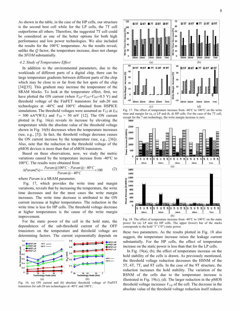
4.2. Study of Temperature Effect
In addition to the environmental parameters, due to the
workloads of different parts of a digital chip, there can be
large temperature gradients between different parts of the chip
which may be close to or far from the hot spots of the chip
[34][35]. This gradient may increase the temperature of the
SRAM blocks. To look at the temperature effect, first, we
have plotted the ON current (when VGS=VDS=VDD=0.5 V) and
threshold voltage of the FinFET transistors for sub-20 nm
technologies at -40°C and 100°C obtained from HSPICE
simulations. The threshold voltages were assumed as VGS at IDS
= 300 nA*(W/L) and VDS = 50 mV [12]. The ON current
plotted in Fig. 16(a) reveals its increase by elevating the
temperature while the absolute value of the threshold voltage
shown in Fig. 16(b) decreases when the temperature increases
(see, e.g., [5]). In fact, the threshold voltage decrease causes
the ON current increase by the temperature (see, e.g., [36]).
Also, note that the reduction in the threshold voltage of the
pMOS devices is more than that of nMOS transistors.
Based on these observations, now, we study the metric
variations caused by the temperature increase from -40°C to
100°C. The results were obtained from
@100 @ 40(%) 100
@ 40
Param C Param CParam
Param C
(2)
where Param is a SRAM parameter.
Fig. 17, which provides the write time and margin
variations, reveals that by increasing the temperature, the write
time decreases and for the most cases the write margin
increases. The write time decrease is attributed to the ON
current increase at higher temperatures. The reduction in the
write time is less for HP cells. The threshold voltage decrease
at higher temperatures is the cause of the write margin
improvement.
For the static power of the cell in the hold state, the
dependences of the sub-threshold current of the OFF
transistors on the temperature and threshold voltage are
determining factors. The current exponentially depends on
(a) (b)
Fig. 16. (a) ON current and (b) absolute threshold voltage of FinFET transistors for sub-20 nm technologies at -40°C and 100°C.
(a) (b)
(c) (d)
Fig. 17. The effect of temperature increase from -40°C to 100°C on the write time and margin for (a, c) LP and (b, d) HP cells. For the case of the 7T cell,
except for the 7 nm technology, the write margin increase is zero.
(a)
(b)
Fig. 18. The effect of temperature increase from -40°C to 100°C on the static
power for (a) LP and (b) HP cells. The upper (lower) bar of the stacks
corresponds to the hold “1” (“0”) static power.
these two parameters. As the results plotted in Fig. 18 also
suggest, the temperature increase raises the leakage current
substantially. For the HP cells, the effect of temperature
increase on the static power is less than that for the LP cells.
In Fig. 19(a), (b), the effect of temperature increase on the
hold stability of the cells is drawn. As previously mentioned,
the threshold voltage reduction decreases the HSNM of the
5T, 6T, 7T, and 8T cells. In the case of the 9T structure, the
reduction increases the hold stability. The variation of the
RSNM of the cells due to the temperature increase is
illustrated in Fig. 19(c), (d). The larger reduction in the pMOS
threshold voltage increases Vtrip of the cell. The decrease in the
absolute value of the threshold voltage reduction itself reduces
9
the RSNM [18] while the increase in Vtrip increases the RSNM
[24]. As the technology scales, because of the increase in the
absolute value of the threshold voltage (see Fig. 16(b)), the
effect of the Vtrip becomes more increasing the RSNM.
As shown in Fig. 20, the temperature rise causes the read
current enlargement which is due to the ON current increase
by the temperature (see also Fig. 9). Since we are working in
the near-threshold region for high VTH transistors, the
temperature effect is more dominant (the ON current has a
relation to the threshold voltage which is similar to the sub-
threshold exponential relation) and hence a large read current
increment is seen. For low VTH transistors, however, the ON
current mainly follows the linear relation with the threshold
voltage (for velocity saturated devices) and hence the increase
is smaller.
4.3. Study of Process Variation Effect
In this section, we study the impact of process variations on
the SRAM cell characteristics discussed in this work. To
account for the global process variation, we consider Gaussian
distributions for Lg, tsi, and Hfin with 3σ = 10% of their
nominal values and for the gate oxide thickness with 3σ = 5%
of its nominal value [1][37][38]. Additionally, the local
variability is only assumed for tsi and Lg due to line edge
roughness (LER) [37].
(a) (b)
(c) (d)
Fig. 19. The effect of temperature increase from -40°C to 100°C on the hold
SNM for (a) LP cells and (b) HP cells as well as read SNM for (c) LP cells
and (d) HP cells.
(a) (b)
Fig. 20. The effect of temperature increase from -40°C to 100°C on the read
current for LP and HP cells.
The required values for LER are taken from ITRS [1][37]. It
should be noted that we assumed the gate last process in which
the variability of the gate work function is negligible [39].
Also, the experimental results presented in [38][40] show that
random dopant fluctuations can be ignored for FinFETs. To
compare the variability of the cells, we used the cell sigma
(CS) which is defined by dividing the mean of a parameter by
its standard deviation [38]. Its value determines the minimum
variation (e.g., 1σ or 2σ from the mean) needed to cause a
write, read, or hold failure. Nowadays, six-sigma (6σ) yield or
larger is required for large SRAM arrays [38]. The study was
performed for both LP and HP cells at 25°C. The results were
obtained after 5,000 Monte Carlo simulations using HSPICE.
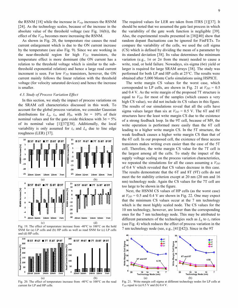
The write margin CS values for the worst case, which
corresponded to LP cells, are shown in Fig. 21 at VDD = 0.5
and 0.4 V. As the write margin of the proposed 7T structure is
equal to VDD for most of the samples (which causes a very
high CS value), we did not include its CS values in this figure.
The results of our simulations reveal that all the cells have
sigma values larger than six at VDD = 0.5 V. The 6T and 8T
structures have the least write margin CS due to the existence
of a strong feedback loop. In the 9T cell, because of M9, the
write operation is performed more easily than the 6T cell
leading to a higher write margin CS. In the 5T structure, the
weak feedback causes a higher write margin CS than that of
the 6T cell. In our proposed cell, the existence of three access
transistors makes writing even easier than the case of the 5T
cell. Therefore, the write margin CS value for the 7T cell is
the largest among all the cells. To study the impact of the
supply voltage scaling on the process variation characteristics,
we repeated the simulations for all the cases assuming a VDD
of 0.4 V which revealed that CS values decrease in this case.
The results demonstrate that the 6T and 8T (9T) cells do not
meet the 6σ stability criterion except at 20 nm (20 nm and 16
nm) technology node. Again the CS values for the 7T cell are
too large to be shown in the figure.
Next, the HSNM CS values of HP cells (as the worst case)
at VDD = 0.5 and 0.4 V are shown in Fig. 22. One may expect
that the minimum CS values occur at the 7 nm technology
which is the most highly scaled node. The CS values for the
10 nm technology, however, are lower than the corresponding
ones for the 7 nm technology node. This may be attributed to
different parameters of the technologies such as Lg to tsi ratios
(see Fig. 4) which reduces the effect of process variation in the
7 nm technology node (see, e.g., [41][42]). Since in the 9T
(a) (b)
Fig. 21. Write margin cell sigma at different technology nodes for LP cells at
VDD equal to (a) 0.5 V and (b) 0.4 V.

10
(a) (b)
Fig. 22. HSNM cell sigma at different technology nodes for HP cells at VDD
equal to (a) 0.5 V and (b) 0.4 V.
(a) (b) Fig. 23. The histograms of the write disturb to write time ratio of the 7T cell in
10 nm technology at VDD equal to (a) 0.5 V and (b) 0.4 V.
structure, the feedback is weaker than the 6T and 8T cells, the
CS is less than those of these cells. The 5T and 7T cells have
the least HSNM CS values while the minimum values are still
above six even at VDD = 0.4 V.
In Addition, we did Monte Carlo simulations to assess the
dynamic stability of the half-selected cells in the same column
of the cell in which the opposite data is being written. The
histogram of (twrite disturb/ twrite) ratio for our 7T proposed cell for
the worst case condition (the 10 nm technology node) is
shown in Fig. 23. As shown in the figure, the time for the
unwanted data to be written in the cell in the hold state (twrite-
disturb) is at least six order of magnitudes larger than the write
time (twrite) of the cell in the write state. Hence, by choosing an
appropriate signal time during write, the write disturb may be
eliminated completely.
In the case of RSNM, the CS values for the worst case (HP
cells) at VDD = 0.5 and 0.4 V are shown in Fig. 24. In the case
of VDD = 0.5 V, the 8T cell has the highest CS value due to
using the read buffer. In the 9T cell, because of the weaker
feedback, the RSNM CS (which is equal to its HSNM) is less
than that of the 8T structure. On the other hand, in the 6T cell,
due to the lack of a read buffer, the RSNM CS is considerably
less than that of the 8T cell. The 5T structure has the least
RSNM CS values because of not using the pull down
transistor and read buffer. Its RSNM CS becomes lower than
six at 10 nm and 7 nm technologies. Our proposed cell CS is
higher than the 5T and 6T cells due to the higher average
RSNM value. For the case of VDD = 0.4 V, the same
explanations are valid. For this case, however, the 5T and 6T
cells do not meet the stability criterion.
Finally, we present the results for the minimum operating
voltage (Vmin) for each cell in each technology in Table 4. This
voltage corresponds to the minimum supply voltage at which
the CS values of the stability metrics including HSNM,
RSNM, and write margin are above six [41].
(a) (b)
Fig. 24. RSNM cell sigma at different technology nodes for HP cells at VDD
equal to (a) 0.5 V and (b) 0.4 V.
TABLE 4 VMIN AND THE WORST CASE CONDITION FOR VARIABILITY OF THE CELLS
(1RSNM, 2HSNM, AND 3WRITE MARGIN)
Cell 20nm 16nm 14nm 10nm 7nm
5T-LP 0.42V1 0.46V1 0.5V1 0.56V1 0.54V1
5T-HP 0.44V1 0.46V1 0.5V1 0.56V1 0.54V1
6T-LP 0.36V3 0.42V3 0.46V3 0.46V3 0.48V3
6T-HP 0.44V1 0.46V1 0.46V1 0.5V1 0.5V1
7T 0.32V2 0.34V2 0.36V2 0.4V2 0.4V2
8T-LP 0.36V3 0.42V3 0.46V3 0.46V3 0.48V3
8T-HP 0.18V3 0.26V3 0.3V3 0.32 V3 0.32V3
9T-LP 0.26V3 0.36V3 0.42V3 0.44V3 0.42V3
9T-HP 0.18V1 0.24V1 0.32V1 0.28V1 0.34V1
The superscript number shows the parameter which violates
the 6-sigma minimum stability requirement. As the figures in
the table indicate, except for the 20 nm technology, the 7T cell
has the lowest Vmin among the LP cells. For the 20 nm
technology, the 9T LP cell has the minimum Vmin among the
LP cells at the price of a higher area of 59%. For this
technology, the 7T has the next lowest Vmin. It should be noted
that while the 8T and 9T HP cells have lower Vmin values
compared to that of the 7T cell, their power consumptions are
still about 2X higher than that of the 7T cell.
5. CONCLUSIONS
In this paper, we suggested a 7T SRAM cell structure for
high stability and write speed. Additionally, the cell, which
was based on a recently proposed 5T cell, had an extra access
transistor as well as a footer transistor to reduce the static
power. To assess the efficiency of the cell, its characteristics
were compared to those of the 5T, 6T, 8T, and 9T structures.
The comparative study was performed using HSPICE
simulations at sub-20 nm FinFET technologies at temperatures
of 25°C, -40°C and 100°C. The simulations results showed
that the cell had superior write speed and stability while
decreased (increased) average static power consumption
(RSNM) by at least 57% (22%) as compared to that of the 5T
cell. Also, our structure had a moderate area among structures
while having read SNM values around that of 9T cell and
higher than those of the 6T cells. Also, we compared the
characteristics of the cells in the presence of the process
variations at two supply voltages of 0.4 V and 0.5 V. While
the 5T and 6T (6T, 8T, and 9T) cells did not meet the read
(write) stability yield requirement in some cases, suggested 7T
structure met the 6 yield requirement in all the cases. Finally,
our proposed structure had the lowest minimum operating
voltage among the low power cells for the 16, 14, 10, and 7
nm technologies.

11
REFERENCES
[1] International Technology Roadmap for Semiconductors, 2012. [On-
line]. Available: http://www.itrs.net/Links/2012ITRS/Home2012.htm [2] H. Pilo, I. Arsovski, K. Batson, G. Braceras, J. Gabric, R. Houle, S.
Lamphier, C. Radens, and A. Seferagic, A 64 Mb SRAM in 32 nm high-
k metal-gate SOI technology with 0.7 V operation enabled by stability, write-ability and read-ability enhancements, IEEE J. Solid-State Circuits
47 (1) (2012) 97–106.
[3] S. W. Chang, P. W. Chou, and W. C. Wu, A 130mV SRAM with expanded write and read margins for subthreshold applications, IEEE J.
Solid-State Circuits 46 (2) (2011) 520–529.
[4] B. Calhoun and A. Chandrakasan, A 256 kb sub-threshold SRAM in 65 nm CMOS, in: Proceedings of IEEE ISSCC, 2006, pp. 480–481.
[5] A. Wang, B. H. Calhoun, and A. P. Chandrakasan, Sub-threshold design
for ultra low-power systems. Springer, 2006. [6] G. Chen, D. Sylvester, D. Blaauw, and T. Mudge, Yield-driven near-
threshold SRAM design, IEEE Trans. VLSI Syst. 18 (11) (2010) 1590–
1598. [7] U. R. Karpuzcu, A. Sinkar, N. S. Kim, and J. Torrellas, EnergySmart:
toward energy-efficient manycores for near-threshold computing, in:
Proceedings of IEEE HPCA, 2013, pp. 542–553.
[8] R. G. Dreslinski, M. Wieckowski, D. Blaauw, D. Sylvester, and T.
Mudge, Near-threshold computing: Reclaiming Moore’s law through
energy efficient integrated circuits, Proceedings of the IEEE 98 (2) (2010) 253–266.
[9] B. H. Calhoun and D. Brooks, Can subthreshold and near-threshold
circuits go mainstream?, IEEE Micro 30 (4) (2010) 80–85. [10] A.-R. Ahmadimehr, B. Ebrahimi, and A. Afzali-Kusha, A high speed
subthreshold SRAM cell design, in: Proceedings of the ASQED, 2009,
pp. 9–13. [11] J. Cartwright, Intel enters the third dimension, nature news, 2011.
[12] S. Sinha, G. Yeric, V. Chandra, B. Cline, and Y. Cao, Exploring sub-
20nm FinFET design with predictive technology models, in Proceedings of DAC, 2012, pp. 283–288.
[13] L. Chang, D. M. Fried, J. Hergenrother, J. W. Sleight, R. H. Dennard, R.
K. Montoye, L. Sekaric, S. J. McNab, A. W. Topol, and C. D. Adams, Stable SRAM cell design for the 32 nm node and beyond, in:
Proceedings of Symp. VLSI Technology, 2005, pp. 128–129.
[14] A. Teman, A. Mordakhay, J. Mezhibovsky, and A. Fish, A 40-nm sub-threshold 5T SRAM bit cell with improved read and write stability,
IEEE Trans. Circuits Syst. II: Brief Express 59 (12) (2012) 873 – 877.
[15] A. Teman, L. Pergament, O. Cohen, and A. Fish, A 250 mV 8 kb 40 nm ultra-low power 9T supply feedback SRAM (SF-SRAM), IEEE J. Solid-
State Circuits 46 (11) (2011) 2713–2726.
[16] Y. L. Yeoh, B. Wang, X. Yu, et al. A 0.4V 7T SRAM with write through virtual ground and ultra-fine grain power gating switches, in:
Proceedings of IEEE ISCAS, 2013, pp.3030–3033.
[17] C. B. Kushwah, S. K. Vishvakarma, D. Dwivedi, Single-ended sub-threshold finfet 7T SRAM cell without boosted supply, in: Proceedings
of IEEE ICICDT, 2014, pp.28–30.
[18] E. Seevinck, F. J. List, and J. Lohstroh, Static-noise margin analysis of MOS SRAM cells, IEEE J. Solid-State Circuits 22 (5) (1987) 748–754.
[19] Predictive Technology Model (PTM), 2012, [Online]. Available: http://www.eas.asu.edu/~PTM/.
[20] H. Makino, S. Nakata, H. Suzuki, S. Mutoh, M. Miyama, T. Yoshimura,
S. Iwade, and Y. Matsuda, Reexamination of SRAM Cell Write Margin Definitions in View of Predicting the Distribution, IEEE Trans. Circuits
Syst. II: Brief Express 58 (4) (2011) 230–234.
[21] J. Wang and B. H. Calhoun, Minimum supply voltage and yield
estimation for large SRAMs under parametric variations, IEEE Trans.
VLSI Syst. 19 (11) (2011) 2120–2125.
[22] K. C. Chun, P. Jain, J. H. Lee, and C. H. Kim, A 3T gain cell embedded DRAM utilizing preferential boosting for high density and low power
ondie caches, IEEE J. Solid-State Circuits, 46 (6) (2011) 1495–1505.
[23] R. Kanj, R. Joshi, R. Williams, and S. Nassif, Statistical evaluation of split gate opportunities for improved 8T/6T column-decoupled SRAM
cell yield, in: Proceedings of the ISQED, 2008, pp. 702-707.
[24] B. Ebrahimi, M. Rostami, A. Afzali-Kusha, and M. Pedram, Statistical Design Optimization of FinFET SRAM Using Back-Gate Voltage, IEEE
Trans. VLSI Syst. 19 (10) (2011) 1911–1916.
[25] M. E. Sinangil, N. Verma, and A. Chandrakasan, A reconfigurable 8T Ultra-Dynamic Voltage Scalable (U-DVS) SRAM in 65 nm CMOS,
IEEE J. Solid-State Circuits 44 (11) (2009) 3163–3173.
[26] S. Narendra, S. Borkar, V. De, D. Antoniadis, and A. Chandrakasan,
Scaling of stack effect and its application for leakage reduction, in: Proceedings of the ISPLED, 2001, pp. 195–200.
[27] Q. Li, T. T. Kim, A 9T subthreshold SRAM bitcell with data-
independent bitline leakage for improved bitline swing and variation tolerance, in: Proceedings of the APCCAS, 2010, pp. 260-26.
[28] A. Bosio, L. Dilillo, P. Girard, et al., Advanced Test Methods for
SRAMs: Effective Solutions for Dynamic Fault Detection in Nanoscaled Technologies, fist ed., Springer, New York, 2009.
[29] C. H. Kim, J.-J. Kim, S. Mukhopadhyay, and K. Roy, A forward body-
biased low-leakage SRAM cache: device and architecture considerations, in: Proceedings of the ISPLED, 2003, pp. 6–9.
[30] A. Tang and N. K. Jha, Design space exploration of FinFET cache,
ACM Journal on Emerging Technologies in Computing Systems (JETC) 9 (2013) 20.
[31] T. Jin, and S. Wang, Aging-aware instruction cache design by duty cycle
balancing, in: Proceedings of the ISVLSI, 2012, pp.195-200. [32] S. Salahuddin, H. Jiao, and V. Kursun, A novel 6T SRAM cell with
asymmetrically gate underlap engineered FinFETs for enhanced read
data stability and write ability, in: Proceedings of the ISQED, 2013, pp. 353–358.
[33] A. Goel, S. K. Gupta, and K. Roy, Asymmetric drain spacer extension
(ADSE) FinFETs for low-power and robust SRAMs, IEEE Trans. Electron Devices 58 (2) (2011) 296–308.
[34] A. N. Nowroz and S. Reda, Thermal and power characterization of field-
programmable gate arrays, in: Proceedings of the ISFPGA, 2011, pp. 111–114.
[35] J. L. Ayala, A. Sridhar, and D. Cuesta, Thermal modeling and analysis of 3D multi-processor chips, Integration, the VLSI Journal 43 (4) (2010)
327–341
[36] S.-Y. Kim, Y.-M. Kim, K.-H. Baek, B.-K. Choi, K.-R. Han, K.-H. Park, J.-H. Lee, Temperature dependence of substrate and drain–currents in
bulk FinFETs, IEEE Trans. Electron Devices 54 (5) (2007) 1259–1264.
[37] V. B. Kleeberger, H. Graeb, and U. Schlichtmann, Predicting future product performance: modeling and evaluation of standard cells in
FinFET technologies, in: Proceedings of DAC, 2013, pp. 1-6.
[38] D. D. Lu, C.-H. Lin, S. Yao, W. Xiong, F. Bauer, C. R. Cleavelin, A. M. Niknejad, and C.Hu, Design of FinFET SRAM cells using a statistical
compact model, in: Proceedings of the SISPAD, 2009, pp. 1–4.
[39] Matsukawa T, Y. Lue, W. Mizubayashi, et al., Suppressing Vt and Gm variability of FinFETs using amorphous metal gates for 14 nm and
beyond, in: Proceedings of IEEE IEDM, 2012. pp. 8.2.1–8.2.4.
[40] Endo K, S. O’uchi, Y. Liu, et al. Variability analysis of TiN metal-gate FinFETs, IEEE Electron Device Lett. 31 (6) (2010) 546–548.
[41] A. Carlson, Z. Guo, S. Balasubramanian, R. Zlatanovici, T.-J. K. Liu,
and B. Nikolic, SRAM read/write margin enhancements using FinFETs, IEEE Trans. VLSI Syst. 18 (6) (2010) 887–900.
[42] J. P. Colinge, FinFETs and Other Multi-Gate Transistors, Springer-
Verlag, NewYork, 2008.