9600 Service Manual - Meditegic
546
SERIES9600 ™ SERVICE MANUAL SCHEMATICS PERIODIC MAINTENANCE ERROR CODES PROCEDURES INSTALLATION ILLUSTRATED PARTS C-Arm Workstation © April 1997 BLOCK DIAGRAMS FIELD SERVICE BULLETINS COMPREHENSIVE PARTS LIST
-
Upload
khangminh22 -
Category
Documents
-
view
0 -
download
0
Transcript of 9600 Service Manual - Meditegic
SERIES9600™ SERVICE MANUAL
SCHEMATICS
PERIODICMAINTENANCE
ERROR CODES
PROCEDURES
INSTALLATION
ILLUSTRATED PARTSC-Arm Workstation
© April 1997
BLOCK DIAGRAMS
FIELD SERVICEBULLETINSCOMPREHENSIVEPARTS LIST

PROCEDURESSeries 9600 Mobile C-Arm Imaging System
Click on the desireds topic to go to that section in the 9600 C-Arm Service Manual.
Explosion Hazards
COVER REMOVAL
Control Panel
Workstation Covers
Keyboard
Keyboard Reassembly
Replacing a Cover (Card Rack Assemb. - C-Arm Control)
WORKSTATION ISOLATION TRANSFORMER
WORKSTATION DC MEASUREMENTS AND ADJUSTMENTS
Circuit Breakers
C-ARM DC MEASUREMENTS AND ADJUSTMENTS
BATTERY CHARGER OUTPUT ADJUSTMENT
Battery Pack Evaluation
Battery Charger Evaluation
Battery Pack Replacement
START-UP AND SOFTWARE BOOT
Loading Application Software
Periodic Functions and Actions
Boot Sequence
ACCESSING THE MAINFRAME MENU
COPY FILES FROM 3 1/2-INCH FLOPPY DISK TO SRAM
COPY FILES FROM SRAM TO 3 1/2-INCH FLOPPY DISK
SRAM Battery Replacement
INTERLOCKS
Fast Stop
+24v Interlock
Interlock Fault Conditions
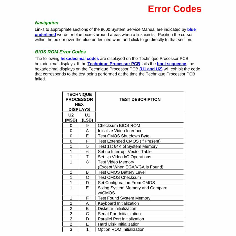
Error CodesNavigationLinks to appropriate sections of the 9600 System Service Manual are indicated by blueunderlined words or blue boxes around areas when a link exists. Position the cursorwithin the box or over the blue underlined word and click to go directly to that section.
BIOS ROM Error CodesThe following hexadecimal codes are displayed on the Technique Processor PCBhexadecimal displays. If the Technique Processor PCB fails the boot sequence , thehexadecimal displays on the Technique Processor PCB (U1 and U2) will exhibit the codethat corresponds to the test being performed at the time the Technique Processor PCBfailed.
TECHNIQUEPROCESSOR
HEXDISPLAYS
TEST DESCRIPTION
U2(MSB)
U1(LSB)
0 9 Checksum BIOS ROM0 A Initialize Video Interface0 E Test CMOS Shutdown Byte0 F Test Extended CMOS (If Present)1 5 Test 1st 64K of System Memory1 6 Set up Interrupt Vector Table1 7 Set Up Video I/O Operations1 8 Test Video Memory
(Except When EGA/VGA is Found)1 B Test CMOS Battery Level1 C Test CMOS Checksum1 D Set Configuration From CMOS1 E Sizing System Memory and Compare
w/CMOS1 F Test Found System Memory2 A Keyboard Initialization2 B Diskette Initialization2 C Serial Port Initialization2 D Parallel Port Initialization2 E Hard Disk Initialization3 1 Option ROM Initialization

SRAM Card Error CodesIf an error occurs while the system is attempting to load software from the SRAM card,one of the error codes listed below will be displayed on the Technique Processor PCBhexadecimal displays.
TECHNIQUEPROCESSOR
HEXDISPLAYS
TEST DESCRIPTION
U2(MSB)
U1(LSB)
5 1 Invalid function error5 2 Address Mark Not Found5 3 Write Protect Error5 4 Sector Not Found5 5 Diskette Change Line Active5 6 DMA Overrun5 7 DMA Boundary Error5 8 Media Type Not Available5 9 Bad CRC5 A Diskette Controller5 B Seek Failed5 C Time-out
Refer to the following C-Arm Software sections:
Overview SRAM Files
Start-up and Software Boot SRAM Card
Loadfing Application Software SRAM Battery Replacement
Boot Sequence
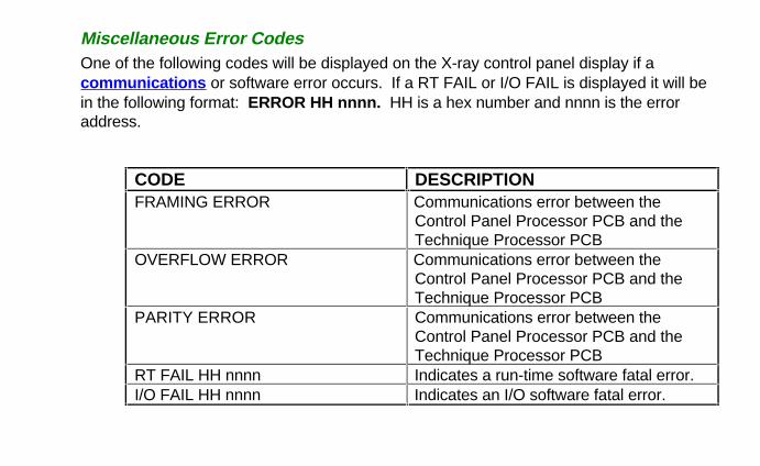
Miscellaneous Error CodesOne of the following codes will be displayed on the X-ray control panel display if acommunications or software error occurs. If a RT FAIL or I/O FAIL is displayed it will bein the following format: ERROR HH nnnn. HH is a hex number and nnnn is the erroraddress.
CODE DESCRIPTIONFRAMING ERROR Communications error between the
Control Panel Processor PCB and theTechnique Processor PCB
OVERFLOW ERROR Communications error between theControl Panel Processor PCB and theTechnique Processor PCB
PARITY ERROR Communications error between theControl Panel Processor PCB and theTechnique Processor PCB
RT FAIL HH nnnn Indicates a run-time software fatal error.I/O FAIL HH nnnn Indicates an I/O software fatal error.

Event Codes & MessagesThe software executed on the Technique Processor PCB monitors operating conditionsand hardware states. Transitions in conditions and states are signaled by software eventcodes.
The most recent 128 event codes are stored in a buffer to provide a record of the eventsleading up to a failure. The event buffer can be examined using the STATUS mode. TheHexadecimal number indicates the two right digits of the event code. These twohexadecimal digits indicate the specific event. Many event codes signal events whichoccur during normal operation.
Some event codes are also written to the Control Panel display as error and warningmessages. Events that are written to the display as messages are designated as fatal --they cease system operation -- or as non-fatal. Not all of the events are written to thedisplay as error messages. Event codes and the corresponding messages written to thedisplay are listed in the following table. The type of event/error message is defined as:
• Event = E• Fatal = F• Non Fatal = N
CODE EVENT / MESSAGE TYPE DESCRIPTION01 ENGLISH N/A Message only to indicate language02 N/A N/A N/A03 N/A N/A N/A04 N/A N/A N/A05 FOOTSWITCH STUCK E, F X-ray ON switch, footswitch, or
handswitch has been sensed closedduring the boot sequence. Refer toX-ray On/Disable section.
06 PRECHARGE FAIL E, F System has not completed prechargecycle, sensed by Analog Interface PCBfrom +200V (B+) onGenerator Driver PCB .Refer to Interlocks/Stator section.
07 HV INVERTER ON E, F High Voltage generator sensed on withno X-ray command initiated. Refer toX-ray On/Disable and kV Generationsections.
08 30 MINUTES E Time marker groups events in Event file09 MAIN PRGM LOADED E Main program is loaded to RAM0A INIT COMPLETE E Hardware initialization complete0B IFB RESET E, F The Image Function PCB has lost
communication with the TechniqueProcessor PCB and the watchdog timerhas reset the IF PCB. Refer to theC-Arm Control and Image Systemsections.
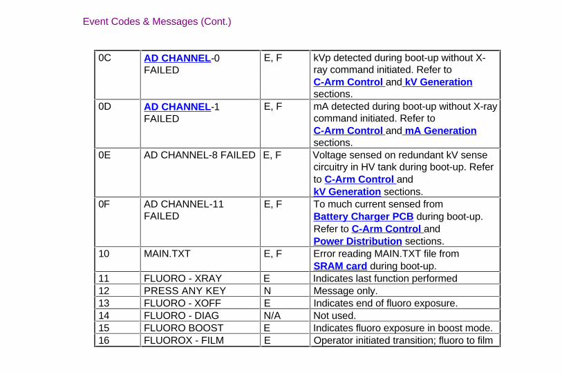
Event Codes & Messages (Cont.)
0C AD CHANNEL -0FAILED
E, F kVp detected during boot-up without X-ray command initiated. Refer toC-Arm Control and kV Generationsections.
0D AD CHANNEL -1FAILED
E, F mA detected during boot-up without X-raycommand initiated. Refer toC-Arm Control and mA Generationsections.
0E AD CHANNEL-8 FAILED E, F Voltage sensed on redundant kV sensecircuitry in HV tank during boot-up. Referto C-Arm Control andkV Generation sections.
0F AD CHANNEL-11FAILED
E, F To much current sensed fromBattery Charger PCB during boot-up.Refer to C-Arm Control andPower Distribution sections.
10 MAIN.TXT E, F Error reading MAIN.TXT file fromSRAM card during boot-up.
11 FLUORO - XRAY E Indicates last function performed12 PRESS ANY KEY N Message only.13 FLUORO - XOFF E Indicates end of fluoro exposure.14 FLUORO - DIAG N/A Not used.15 FLUORO BOOST E Indicates fluoro exposure in boost mode.16 FLUOROX - FILM E Operator initiated transition; fluoro to film

Event Codes & Messages (Cont.)
CODE EVENT / MESSAGE TYPE DESCRIPTION17 COLLIMATOR STUCK E, N The collimator iris can't open or close.
Refer to the Image System section.18 IRIS JITTER E, N Collimator cannot maintain specified field
size.19 FLUOROS - FILM E Operator initiated transition; standby to
film1A FP DEAD E, F Communication loss between Control
Panel Processor PCB and TechniqueProcessor PCB . Refer to C-ArmControl section.
1B N/A N/A N/A1C BAD IRIS POT E, F The collimator iris potentiometer voltage
is incorrect or out of range. Refer toImage System section.
1D BAD IRIS CAL E, F The collimator iris calibration datacontained in the EEPROM on theImage Function PCB is not valid. Referto the Image System andImage System Calibration sections.
1E BOOST OVERTIME E, N The boost exposure has been terminatedafter exceeding the preset time limit.Refer toSystem Configuration in the C-ArmSoftware section.
1F HOUSING IS WARM E, N Housing temperature is atapproximately 60% of its rated heatcapacity.
20 HOUSING IS HOT E, N Housing temperature is at approximately80% of its rated heat capacity.
21 ANODE IS WARM E, N The anode is at 60% of its rated heatcapacity.
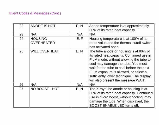
Event Codes & Messages (Cont.)
22 ANODE IS HOT E, N Anode temperature is at approximately80% of its rated heat capacity.
23 N/A N/A N/A24 HOUSING
OVERHEATEDE, F Housing temperature is at 100% of its
rated value and the thermal cutoff switchhas activated open.
25 WILL OVERHEAT E, N The tube anode or housing is at 80% ofits rated heat capacity. Continued use inFILM mode, without allowing the tube tocool may damage the tube. You mustwait for the tube to cool before the nextFILM exposure is allowed, or select asufficiently lower technique. The displaywill also present the message WAIT.
26 N/A N/A N/A27 NO BOOST - HOT E, N The X-ray tube anode or housing is at
80% of its rated heat capacity. Continueduse in fluoro boost, without cooling, maydamage the tube. When displayed, theBOOST ENABLE LED turns off.
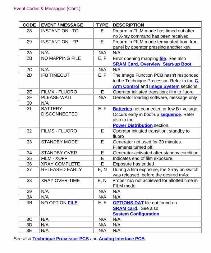
Event Codes & Messages (Cont.)
CODE EVENT / MESSAGE TYPE DESCRIPTION28 INSTANT ON - TO E Prearm in FILM mode has timed out after
no X-ray command has been received.29 INSTANT ON - FP E Prearm in FILM mode terminated from front
panel by operator pressing another key.2A N/A N/A N/A2B NO MAPPING FILE E, F Error opening mapping file . See also
SRAM Card , Overview , Start-up Boot .2C N/A N/A N/A2D IFB TIMEOUT E, F The Image Function PCB hasn't responded
to the Technique Processor. Refer to the C-Arm Control and Image System sections.
2E FILMX - FLUORO E Operator initiated transition; film to fluoro2F PLEASE WAIT N/A Generator loading software, message only30 N/A31 BATTERY
DISCONNECTEDE, F Batteries not connected or low B+ voltage.
Occurs early in boot-up sequence . Referalso to thePower Distribution section.
32 FILMS - FLUORO E Operator initiated transition; standby tofluoro
33 STANDBY MODE E Generator not used for 30 minutes.Filaments turned off.
34 STANDBY OVER E Generator activated after standby condition.35 FILM - XOFF E Indicates end of film exposure.36 XRAY COMPLETE E Exposure has ended37 RELEASED EARLY E, N During a film exposure, the X-ray on switch
was released, before the desired mAs.38 XRAY OVER-TIME E, N Proper mA not achieved for allotted time in
FILM mode.39 N/A N/A N/A3A N/A N/A N/A3B NO OPTION FILE E, F OPTIONS.DAT file not found on
SRAM card . See alsoSystem Configuration
3C N/A N/A N/A3D N/A N/A N/A3E N/A N/A N/A
See also Technique Processor PCB and Analog Interface PCB .
Event Codes & Messages (Cont.)
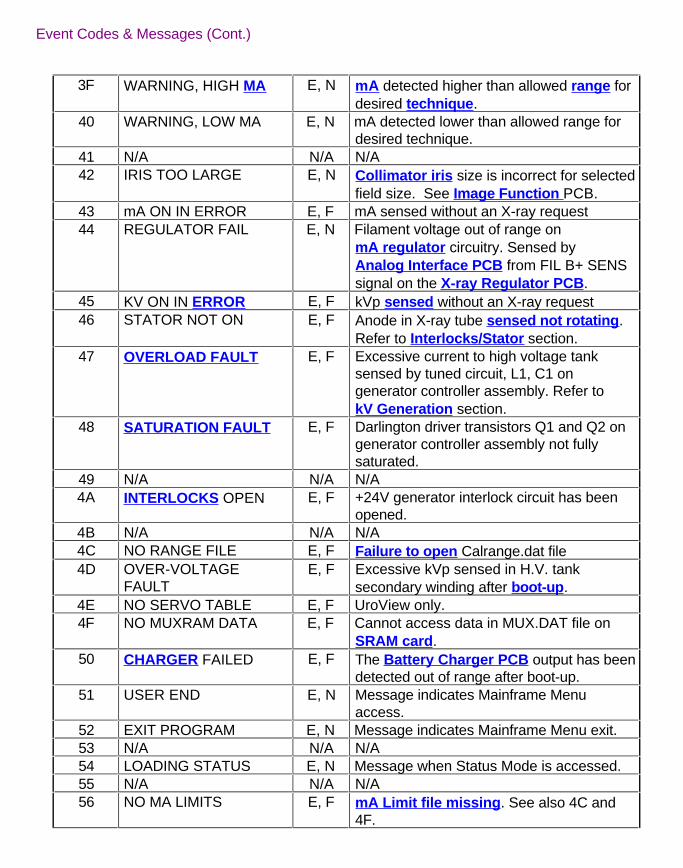
3F WARNING, HIGH MA E, N mA detected higher than allowed range fordesired technique .
40 WARNING, LOW MA E, N mA detected lower than allowed range fordesired technique.
41 N/A N/A N/A42 IRIS TOO LARGE E, N Collimator iris size is incorrect for selected
field size. See Image Function PCB.43 mA ON IN ERROR E, F mA sensed without an X-ray request44 REGULATOR FAIL E, N Filament voltage out of range on
mA regulator circuitry. Sensed byAnalog Interface PCB from FIL B+ SENSsignal on the X-ray Regulator PCB .
45 KV ON IN ERROR E, F kVp sensed without an X-ray request46 STATOR NOT ON E, F Anode in X-ray tube sensed not rotating .
Refer to Interlocks/Stator section.47 OVERLOAD FAULT E, F Excessive current to high voltage tank
sensed by tuned circuit, L1, C1 ongenerator controller assembly. Refer tokV Generation section.
48 SATURATION FAULT E, F Darlington driver transistors Q1 and Q2 ongenerator controller assembly not fullysaturated.
49 N/A N/A N/A4A INTERLOCKS OPEN E, F +24V generator interlock circuit has been
opened.4B N/A N/A N/A4C NO RANGE FILE E, F Failure to open Calrange.dat file4D OVER-VOLTAGE
FAULTE, F Excessive kVp sensed in H.V. tank
secondary winding after boot-up .4E NO SERVO TABLE E, F UroView only.4F NO MUXRAM DATA E, F Cannot access data in MUX.DAT file on
SRAM card .50 CHARGER FAILED E, F The Battery Charger PCB output has been
detected out of range after boot-up.51 USER END E, N Message indicates Mainframe Menu
access.52 EXIT PROGRAM E, N Message indicates Mainframe Menu exit.53 N/A N/A N/A54 LOADING STATUS E, N Message when Status Mode is accessed.55 N/A N/A N/A56 NO MA LIMITS E, F mA Limit file missing . See also 4C and
4F.

Event Codes & Messages (Cont.)
57 WARNING, HIGH KV E, N kV detected higher than allowed rangefor desired technique.
58 WARNING, LOW KV E, N kV detected lower than allowed range fordesired technique.
59 WAIT N/A Message only, displayed alternately withWILL OVERHEAT
5A ?? PCT CHARGE E Used as a message with battery chargestate, 50 or 70 percent.
5B STANDARD 5R/MIN N/A Message only, ABS table display name5C LOW DOSE N/A Message only, ABS table display name5D CHEST 5R/MIN N/A Message only, ABS table display name5E EXTREMITIES 5R/MIN N/A Message only, ABS table display name5F STANDARD N/A Message only, ABS table display name60 CHEST N/A Message only, ABS table display name61 EXTREMITIES N/A Message only, ABS table display name62 N/A N/A63 CHECKSUM ERROR N/A Message only. During boot, a checksum
routine is run on the MAIN software. Ifchecksum is in error this message will bedisplayed.
64 BOOT-UP TERMINATED N/A Message only. Displayed afterCHECKSUM ERROR (see above).
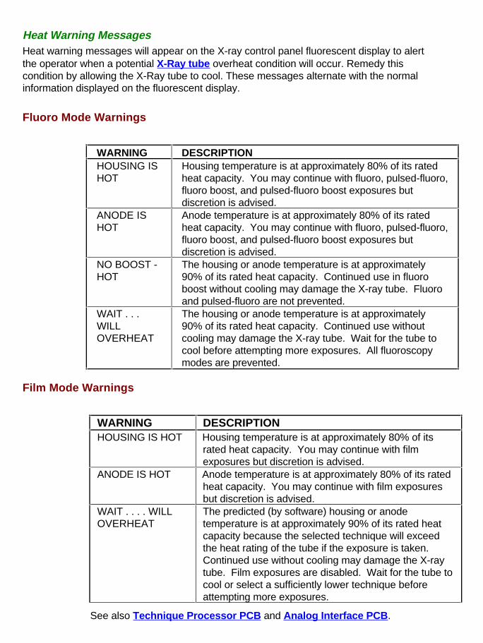
Heat Warning MessagesHeat warning messages will appear on the X-ray control panel fluorescent display to alertthe operator when a potential X-Ray tube overheat condition will occur. Remedy thiscondition by allowing the X-Ray tube to cool. These messages alternate with the normalinformation displayed on the fluorescent display.
Fluoro Mode Warnings
WARNING DESCRIPTIONHOUSING ISHOT
Housing temperature is at approximately 80% of its ratedheat capacity. You may continue with fluoro, pulsed-fluoro,fluoro boost, and pulsed-fluoro boost exposures butdiscretion is advised.
ANODE ISHOT
Anode temperature is at approximately 80% of its ratedheat capacity. You may continue with fluoro, pulsed-fluoro,fluoro boost, and pulsed-fluoro boost exposures butdiscretion is advised.
NO BOOST -HOT
The housing or anode temperature is at approximately90% of its rated heat capacity. Continued use in fluoroboost without cooling may damage the X-ray tube. Fluoroand pulsed-fluoro are not prevented.
WAIT . . .WILLOVERHEAT
The housing or anode temperature is at approximately90% of its rated heat capacity. Continued use withoutcooling may damage the X-ray tube. Wait for the tube tocool before attempting more exposures. All fluoroscopymodes are prevented.
Film Mode Warnings
WARNING DESCRIPTIONHOUSING IS HOT Housing temperature is at approximately 80% of its
rated heat capacity. You may continue with filmexposures but discretion is advised.
ANODE IS HOT Anode temperature is at approximately 80% of its ratedheat capacity. You may continue with film exposuresbut discretion is advised.
WAIT . . . . WILLOVERHEAT
The predicted (by software) housing or anodetemperature is at approximately 90% of its rated heatcapacity because the selected technique will exceedthe heat rating of the tube if the exposure is taken.Continued use without cooling may damage the X-raytube. Film exposures are disabled. Wait for the tube tocool or select a sufficiently lower technique beforeattempting more exposures.
See also Technique Processor PCB and Analog Interface PCB .
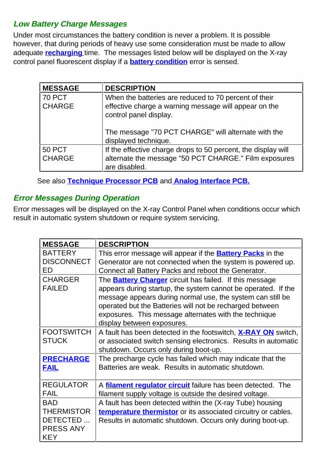
Low Battery Charge MessagesUnder most circumstances the battery condition is never a problem. It is possiblehowever, that during periods of heavy use some consideration must be made to allowadequate recharging time. The messages listed below will be displayed on the X-raycontrol panel fluorescent display if a battery condition error is sensed.
MESSAGE DESCRIPTION70 PCTCHARGE
When the batteries are reduced to 70 percent of theireffective charge a warning message will appear on thecontrol panel display.
The message "70 PCT CHARGE" will alternate with thedisplayed technique.
50 PCTCHARGE
If the effective charge drops to 50 percent, the display willalternate the message "50 PCT CHARGE." Film exposuresare disabled.
See also Technique Processor PCB and Analog Interface PCB.
Error Messages During OperationError messages will be displayed on the X-ray Control Panel when conditions occur whichresult in automatic system shutdown or require system servicing.
MESSAGE DESCRIPTIONBATTERYDISCONNECTED
This error message will appear if the Battery Packs in theGenerator are not connected when the system is powered up.Connect all Battery Packs and reboot the Generator.
CHARGERFAILED
The Battery Charger circuit has failed. If this messageappears during startup, the system cannot be operated. If themessage appears during normal use, the system can still beoperated but the Batteries will not be recharged betweenexposures. This message alternates with the techniquedisplay between exposures.
FOOTSWITCHSTUCK
A fault has been detected in the footswitch, X-RAY ON switch,or associated switch sensing electronics. Results in automaticshutdown. Occurs only during boot-up.
PRECHARGEFAIL
The precharge cycle has failed which may indicate that theBatteries are weak. Results in automatic shutdown.
REGULATORFAIL
A filament regulator circuit failure has been detected. Thefilament supply voltage is outside the desired voltage.
BADTHERMISTORDETECTED ...PRESS ANYKEY
A fault has been detected within the (X-ray Tube) housingtemperature thermistor or its associated circuitry or cables.Results in automatic shutdown. Occurs only during boot-up.
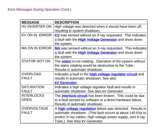
Error Messages During Operation (Cont.)
MESSAGE DESCRIPTIONHV INVERTER ON High voltage was detected when it should have been off,
resulting in system shutdown.KV ON IN ERROR KV was sensed without an X-ray requested. This indicates
a fault with the High Voltage Generator and shuts downthe system.
MA ON IN ERROR MA was sensed without an X-ray requested. This indicatesa fault with the High Voltage Generator and shuts downthe system.
STATOR NOT ON The stator is not rotating. Operation of the system withoutthe stator rotating would be destructive to the Tube.Results in automatic shutdown.
OVERLOADFAULT
Indicates a fault in the high voltage regulator circuit andresults in automatic shutdown. See alsokV Generator .
SATURATIONFAULT
Indicates a high voltage regulator fault and results inautomatic shutdown. See also kV Generator.
INTERLOCKSOPEN
The interlock circuit has been broken. This could be dueto a fault sensed by software or a direct hardware failure.Results in automatic shutdown.
OVERVOLTAGEFAULT
A high voltage regulation failure was detected. Results inautomatic shutdown. (This fault occurs at about 140 kVp toprotect X-ray cables, high voltage power supply, and X-rayTube.) See Also kV Generator.

Error Messages During Operation (Cont.)
WARNING,HIGH KV
kV detected higher than allowed range for desiredtechnique.
WARNING,LOW KV
kV detected lower than allowed range for desiredtechnique.
WARNING,HIGH MA
mA detected higher than allowed range for desiredtechnique.
WARNING,LOW MA
mA detected lower than allowed range for desiredtechnique.
BOOSTOVERTIME
The boost exposure will automatically terminate after 30seconds, even if the BOOST footswitch is still depressed.Release the BOOST footswitch completely and then pressit again to resume boost exposures. See also SystemConfiguration .
RELEASEDEARLY
During a film exposure, the X-RAY ON switch wasreleased early, before the desired mAs was reached.Press the switch again and hold it down until exposure timeis complete.
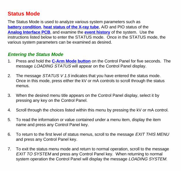
Status ModeThe Status Mode is used to analyze various system parameters such asbattery condition , heat status of the X-ray tube , A/D and PIO status of theAnalog Interface PCB , and examine the event history of the system. Use theinstructions listed below to enter the STATUS mode. Once in the STATUS mode, thevarious system parameters can be examined as desired.
Entering the Status Mode1. Press and hold the C-Arm Mode button on the Control Panel for five seconds. The
message LOADING STATUS will appear on the Control Panel display.
2. The message STATUS V 1.5 indicates that you have entered the status mode.Once in this mode, press either the kV or mA controls to scroll through the statusmenus.
3. When the desired menu title appears on the Control Panel display, select it bypressing any key on the Control Panel.
4. Scroll through the choices listed within this menu by pressing the kV or mA control.
5. To read the information or value contained under a menu item, display the itemname and press any Control Panel key.
6. To return to the first level of status menus, scroll to the message EXIT THIS MENUand press any Control Panel key.
7. To exit the status menu mode and return to normal operation, scroll to the messageEXIT TO SYSTEM and press any Control Panel key. When returning to normalsystem operation the Control Panel will display the message LOADING SYSTEM.
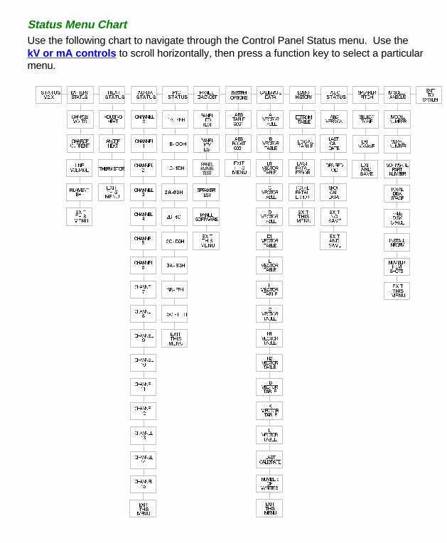
Status Menu ChartUse the following chart to navigate through the Control Panel Status menu. Use thekV or mA controls to scroll horizontally, then press a function key to select a particularmenu.
BATTERY
STATUS
HEAT
STATUS
AD/DA
STATUS
PIO
STATUS
PANEL
DIAGNOST
CALIBRATE
DATA
EVENT
HISTORY
AEC
STATUS
SPEAKER
PITCH
CHARGE
VOLTS
HOUSING
HEAT
CHANNEL
0 1A - FFHPANEL
LEDTEST
ABS
TABLE
0001
A
VECTOR
TABLE
EEPROM
TABLE
SELECT
TONE
MODEL
NUMBER
MISCELL-
ANEOUS
CHARGE
CURRENT
ANODE
HEAT
CHANNEL
11B - OOH
ABS
BOOST
0001
B
VECTOR
TABLE
LOCAL
TABLE
SERIAL
NUMBER
LINE
VOLTAGE THERMISTORCHANNEL
2
EXIT
THIS
MENU
B1
VECTOR
TABLE
LAST
FATAL
ERROR
EXIT
NO SAVE
EXITAND
SAVE
FILAMENTB+
EXIT
THIS
MENU
CHANNEL3
SPEAKER
TEST
C
VECTOR
TABLE
TOTAL
FATAL
ERROR
EXIT
THIS
MENU
CHANNEL
4PANEL
SOFTWARE
D
VECTOR
TABLE
EXIT
THIS
MENU
TOTAL
DISK
SPACE
CHANNEL
5
EXIT
THIS
MENU
D1
VECTOR
TABLE
FREE
DISK
SPACE
CHANNEL
6
E
VECTOR
TABLE
INSTALLINFORM
CHANNEL
73B - FFH
F
VECTOR
TABLE
NUMBERFILM
SHOTS
CHANNEL
83C - FFH
G
VECTOR
TABLE
EXIT
THIS
MENU
CHANNEL
9
EXIT
THIS
MENU
CHANNEL
10
H1
VECTORTABLE
H2
VECTORTABLE
CHANNEL
11
CHANNEL
12
CHANNEL
13
H3
VECTOR
TABLE
LAST
CALIBRATE
NUMBER
OF
WRITES
CHANNEL
14
CHANNEL
15
EXIT
THISMENU
EXIT
THISMENU
STATUS
V2.XSYSTEM
OPTIONS
K
VECTORTABLE
L
VECTOR
TABLE
AEC
VERSION
LAST
CAL
DATE
DESIRED
OD
SPOT
CAL
DATA
EXIT
NO
SAVE
EXIT
AND
SAVE
SOFTWARE
PARTNUMBER
EXIT
TO
SYSTEM
1C - 1DH
2B - 4OH
2C - D0H
3A - B3H
PANELKV/MATEST
PANEL
KEY
TEST
2A-03H

Status MenusThe available status menus and the items contained under each are listed below. Notethat a typical readout is listed for all applicable menu items.
Battery Status CHARGE VOLTS |==> Refer to the Power Distribution
CHARGE CURRENT | section; Battery Charger PCB , andLINE VOLTAGE _| Batteries .FILAMENT B+ ==> See Filament Regulator SetupEXIT THIS MENU
Heat StatusHOUSING HEAT Refer to X-Ray TubeANODE HEATTHERMISTOREXIT THIS MENU
AD/DA StatusUse this menu to read the AD/DA information being received by theAnalog Interface PCB.
After selecting this menu, scroll through the AD/DA channels listed below. To read thevoltage measured on the selected channel, press any key. The display will change toshow the channel number and the associated voltage.
CHANNEL NUMBER:0 MEASURED KVP1 MEASURED MA2 FILAMENT B+3 VIDEO LEVEL4 HOUSING THER.5 DOSIMETER (not used)6 CAMERA POSITION7 CAMERA IRIS WIPER8 TAP VOLTAGE9 LINE VOLTAGE10 CHARGE CURRENT11 CHARGE VOLT12 FILAMENT CURRENT13 SPARE14 SPARE15 SPAREEXIT THIS MENU
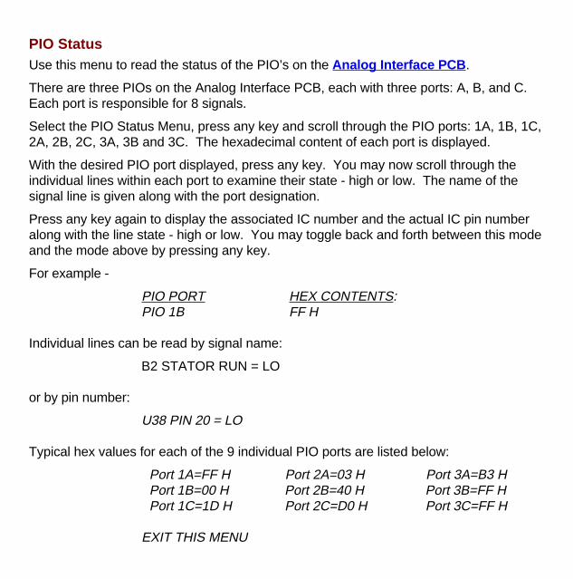
PIO StatusUse this menu to read the status of the PIO’s on the Analog Interface PCB .
There are three PIOs on the Analog Interface PCB, each with three ports: A, B, and C.Each port is responsible for 8 signals.
Select the PIO Status Menu, press any key and scroll through the PIO ports: 1A, 1B, 1C,2A, 2B, 2C, 3A, 3B and 3C. The hexadecimal content of each port is displayed.
With the desired PIO port displayed, press any key. You may now scroll through theindividual lines within each port to examine their state - high or low. The name of thesignal line is given along with the port designation.
Press any key again to display the associated IC number and the actual IC pin numberalong with the line state - high or low. You may toggle back and forth between this modeand the mode above by pressing any key.
For example -
PIO PORT HEX CONTENTS:PIO 1B FF H
Individual lines can be read by signal name:
B2 STATOR RUN = LO
or by pin number:
U38 PIN 20 = LO
Typical hex values for each of the 9 individual PIO ports are listed below:
Port 1A=FF H Port 2A=03 H Port 3A=B3 HPort 1B=00 H Port 2B=40 H Port 3B=FF HPort 1C=1D H Port 2C=D0 H Port 3C=FF H
EXIT THIS MENU
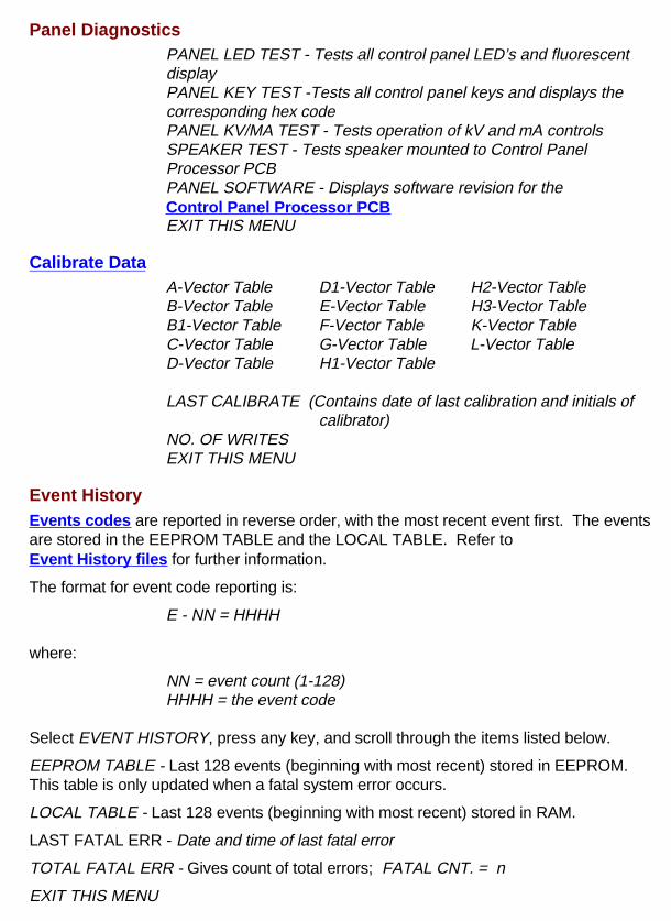
Panel DiagnosticsPANEL LED TEST - Tests all control panel LED’s and fluorescentdisplayPANEL KEY TEST -Tests all control panel keys and displays thecorresponding hex codePANEL KV/MA TEST - Tests operation of kV and mA controlsSPEAKER TEST - Tests speaker mounted to Control PanelProcessor PCBPANEL SOFTWARE - Displays software revision for theControl Panel Processor PCBEXIT THIS MENU
Calibrate DataA-Vector Table D1-Vector Table H2-Vector TableB-Vector Table E-Vector Table H3-Vector TableB1-Vector Table F-Vector Table K-Vector TableC-Vector Table G-Vector Table L-Vector TableD-Vector Table H1-Vector Table
LAST CALIBRATE (Contains date of last calibration and initials of calibrator)
NO. OF WRITESEXIT THIS MENU
Event HistoryEvents codes are reported in reverse order, with the most recent event first. The eventsare stored in the EEPROM TABLE and the LOCAL TABLE. Refer toEvent History files for further information.
The format for event code reporting is:
E - NN = HHHH
where:
NN = event count (1-128)HHHH = the event code
Select EVENT HISTORY, press any key, and scroll through the items listed below.
EEPROM TABLE - Last 128 events (beginning with most recent) stored in EEPROM.This table is only updated when a fatal system error occurs.
LOCAL TABLE - Last 128 events (beginning with most recent) stored in RAM.
LAST FATAL ERR - Date and time of last fatal error
TOTAL FATAL ERR - Gives count of total errors; FATAL CNT. = n
EXIT THIS MENU
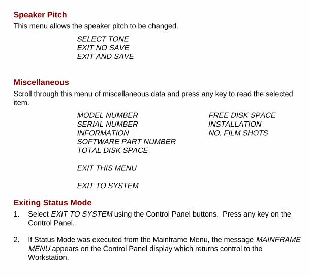
Speaker PitchThis menu allows the speaker pitch to be changed.
SELECT TONEEXIT NO SAVEEXIT AND SAVE
MiscellaneousScroll through this menu of miscellaneous data and press any key to read the selecteditem.
MODEL NUMBER FREE DISK SPACESERIAL NUMBER INSTALLATIONINFORMATION NO. FILM SHOTSSOFTWARE PART NUMBERTOTAL DISK SPACE
EXIT THIS MENU
EXIT TO SYSTEM
Exiting Status Mode1. Select EXIT TO SYSTEM using the Control Panel buttons. Press any key on the
Control Panel.
2. If Status Mode was executed from the Mainframe Menu, the message MAINFRAMEMENU appears on the Control Panel display which returns control to theWorkstation.

Workstation Boot and Error CodesThe following section contains a listing of the checkpoint codes written to the twocharacter display on the Series 9600 Workstation's Communications PCB .
During the boot process, the alphanumeric LEDs on the rear panel displays two digitcodes indicating the status of the boot sequence. Since these codes do not normallyindicate an error, they are referred to as progress codes. Typically, these codes will bereplaced by an E0 code once normal program operation has begun. If the program doesnot complete the boot process, a code will remain on the LED display, indicating the pointwhere an error occurred.
A description of these codes is provided in the following tables and links are provided tothe appropriate sections in the manual describing troubleshooting and service information.
See also: 386 AT Motherboard ; Boot and Diagnostic LEDs ; Workstation Software Overview; Start-up and Software Boot ,
Workstation Boot Sequence .
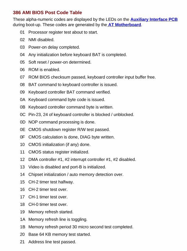
386 AMI BIOS Post Code TableThese alpha-numeric codes are displayed by the LEDs on the Auxiliary Interface PCBduring boot-up. These codes are generated by the AT Motherboard .
01 Processor register test about to start.
02 NMI disabled.
03 Power-on delay completed.
04 Any initialization before keyboard BAT is completed.
05 Soft reset / power-on determined.
06 ROM is enabled.
07 ROM BIOS checksum passed, keyboard controller input buffer free.
08 BAT command to keyboard controller is issued.
09 Keyboard controller BAT command verified.
0A Keyboard command byte code is issued.
0B Keyboard controller command byte is written.
0C Pin-23, 24 of keyboard controller is blocked / unblocked.
0D NOP command processing is done.
0E CMOS shutdown register R/W test passed.
0F CMOS calculation is done, DIAG byte written.
10 CMOS initialization (if any) done.
11 CMOS status register initialized.
12 DMA controller #1, #2 interrupt controller #1, #2 disabled.
13 Video is disabled and port-B is initialized.
14 Chipset initialization / auto memory detection over.
15 CH-2 timer test halfway.
16 CH-2 timer test over.
17 CH-1 timer test over.
18 CH-0 timer test over.
19 Memory refresh started.
1A Memory refresh line is toggling.
1B Memory refresh period 30 micro second test completed.
20 Base 64 KB memory test started.
21 Address line test passed.
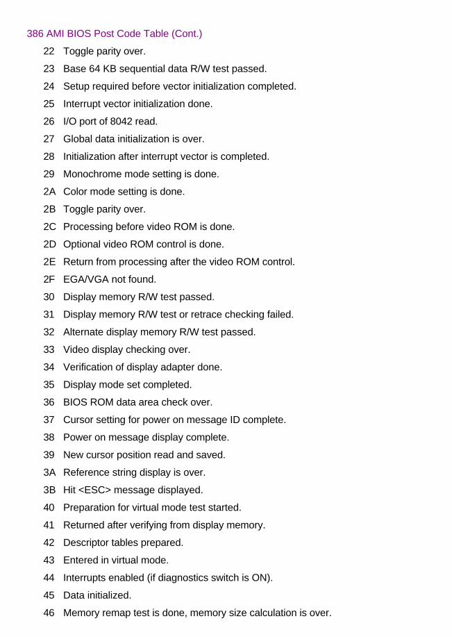
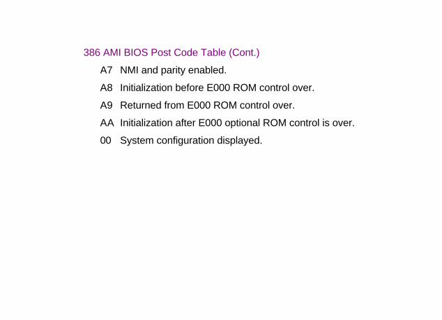
386 AMI BIOS Post Code Table (Cont.)
22 Toggle parity over.
23 Base 64 KB sequential data R/W test passed.
24 Setup required before vector initialization completed.
25 Interrupt vector initialization done.
26 I/O port of 8042 read.
27 Global data initialization is over.
28 Initialization after interrupt vector is completed.
29 Monochrome mode setting is done.
2A Color mode setting is done.
2B Toggle parity over.
2C Processing before video ROM is done.
2D Optional video ROM control is done.
2E Return from processing after the video ROM control.
2F EGA/VGA not found.
30 Display memory R/W test passed.
31 Display memory R/W test or retrace checking failed.
32 Alternate display memory R/W test passed.
33 Video display checking over.
34 Verification of display adapter done.
35 Display mode set completed.
36 BIOS ROM data area check over.
37 Cursor setting for power on message ID complete.
38 Power on message display complete.
39 New cursor position read and saved.
3A Reference string display is over.
3B Hit <ESC> message displayed.
40 Preparation for virtual mode test started.
41 Returned after verifying from display memory.
42 Descriptor tables prepared.
43 Entered in virtual mode.
44 Interrupts enabled (if diagnostics switch is ON).
45 Data initialized.
46 Memory remap test is done, memory size calculation is over.

386 AMI BIOS Post Code Table (Cont.)
47 Pattern to be tested written in extended memory.
48 Patterns written in base memory.
49 Amount of memory below 1 MB found and verified.
4A Amount of memory above 1 MB found and verified.
4B BIOS ROM data area check over.
4C Memory below 1 MB cleared (soft reset).
4D Memory above 1 MB cleared (soft reset).
4E Memory test started (no soft reset).
4F Memory size display started. This will be updated during memory test.
50 Memory test below 1 MB completed.
51 Memory size adjusted due to relocation / shadow.
52 Memory test above 1 MB completed.
53 CPU registers are saved, including memory size.
54 Shutdown successful, CPU in real mode.
55 Registers restored.
56 A20 address line disable successful.
57 BIOS ROM data area check halfway.
58 BIOS ROM data area check over.
59 Hit <ESC> message cleared. <Wait...> message displayed.
60 DMA page register test passed.
61 Display memory verification over.
62 DMA #1 base register test passed.
63 DMA #2 base register test passed.
64 BIOS ROM data area check halfway.
65 BIOS ROM data area check over.
66 DMA unit 1 and 2 programming over.
67 8259 initialization over.
80 Keyboard test started.
81 Keyboard reset error / stuck key found.
82 Keyboard controller interface test over.
83 Command byte written. Global data init done.
84 Lock key check over.
85 Memory size check done.
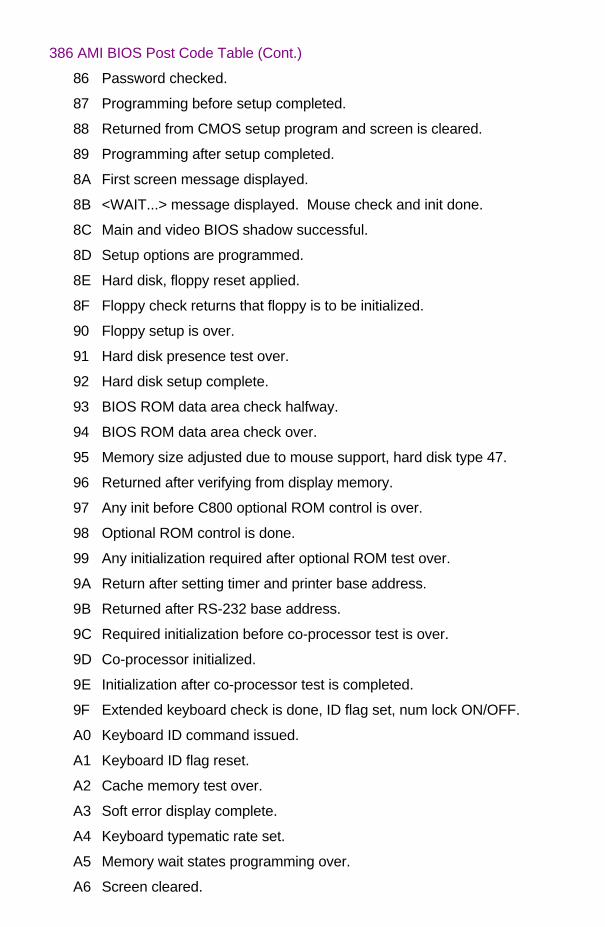
386 AMI BIOS Post Code Table (Cont.)
86 Password checked.
87 Programming before setup completed.
88 Returned from CMOS setup program and screen is cleared.
89 Programming after setup completed.
8A First screen message displayed.
8B <WAIT...> message displayed. Mouse check and init done.
8C Main and video BIOS shadow successful.
8D Setup options are programmed.
8E Hard disk, floppy reset applied.
8F Floppy check returns that floppy is to be initialized.
90 Floppy setup is over.
91 Hard disk presence test over.
92 Hard disk setup complete.
93 BIOS ROM data area check halfway.
94 BIOS ROM data area check over.
95 Memory size adjusted due to mouse support, hard disk type 47.
96 Returned after verifying from display memory.
97 Any init before C800 optional ROM control is over.
98 Optional ROM control is done.
99 Any initialization required after optional ROM test over.
9A Return after setting timer and printer base address.
9B Returned after RS-232 base address.
9C Required initialization before co-processor test is over.
9D Co-processor initialized.
9E Initialization after co-processor test is completed.
9F Extended keyboard check is done, ID flag set, num lock ON/OFF.
A0 Keyboard ID command issued.
A1 Keyboard ID flag reset.
A2 Cache memory test over.
A3 Soft error display complete.
A4 Keyboard typematic rate set.
A5 Memory wait states programming over.
A6 Screen cleared.
386 AMI BIOS Post Code Table (Cont.)
A7 NMI and parity enabled.
A8 Initialization before E000 ROM control over.
A9 Returned from E000 ROM control over.
AA Initialization after E000 optional ROM control is over.
00 System configuration displayed.
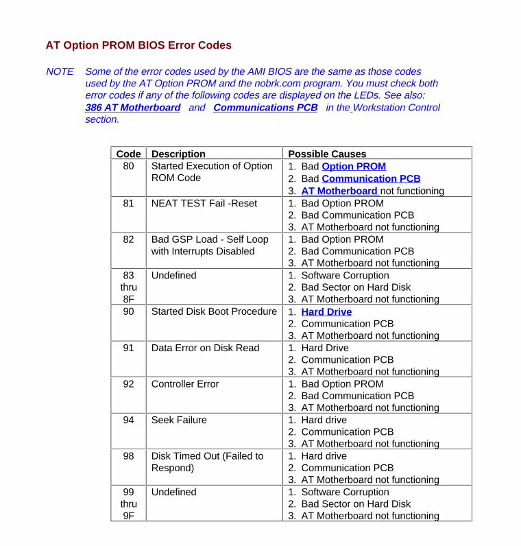
AT Option PROM BIOS Error Codes
NOTE Some of the error codes used by the AMI BIOS are the same as those codesused by the AT Option PROM and the nobrk.com program. You must check botherror codes if any of the following codes are displayed on the LEDs. See also:386 AT Motherboard and Communications PCB in the Workstation Controlsection.
Code Description Possible Causes80 Started Execution of Option
ROM Code1. Bad Option PROM2. Bad Communication PCB3. AT Motherboard not functioning
81 NEAT TEST Fail -Reset 1. Bad Option PROM2. Bad Communication PCB3. AT Motherboard not functioning
82 Bad GSP Load - Self Loopwith Interrupts Disabled
1. Bad Option PROM2. Bad Communication PCB3. AT Motherboard not functioning
83thru8F
Undefined 1. Software Corruption2. Bad Sector on Hard Disk3. AT Motherboard not functioning
90 Started Disk Boot Procedure 1. Hard Drive2. Communication PCB3. AT Motherboard not functioning
91 Data Error on Disk Read 1. Hard Drive2. Communication PCB3. AT Motherboard not functioning
92 Controller Error 1. Bad Option PROM2. Bad Communication PCB3. AT Motherboard not functioning
94 Seek Failure 1. Hard drive2. Communication PCB3. AT Motherboard not functioning
98 Disk Timed Out (Failed toRespond)
1. Hard drive2. Communication PCB3. AT Motherboard not functioning
99thru9F
Undefined 1. Software Corruption2. Bad Sector on Hard Disk3. AT Motherboard not functioning
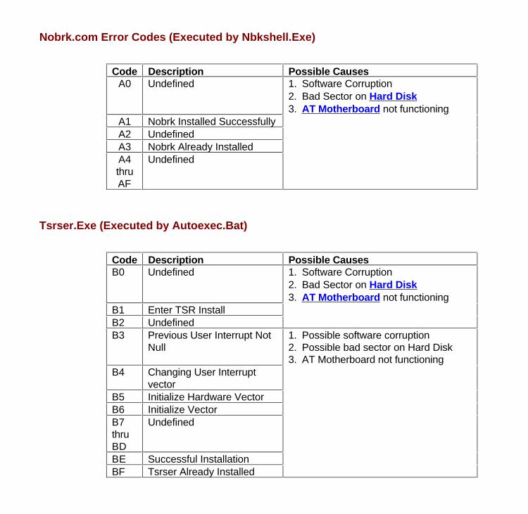
Nobrk.com Error Codes (Executed by Nbkshell.Exe)
Code Description Possible CausesA0 Undefined 1. Software Corruption
2. Bad Sector on Hard Disk3. AT Motherboard not functioning
A1 Nobrk Installed SuccessfullyA2 UndefinedA3 Nobrk Already InstalledA4thruAF
Undefined
Tsrser.Exe (Executed by Autoexec.Bat)
Code Description Possible CausesB0 Undefined 1. Software Corruption
2. Bad Sector on Hard Disk3. AT Motherboard not functioning
B1 Enter TSR InstallB2 UndefinedB3 Previous User Interrupt Not
Null1. Possible software corruption2. Possible bad sector on Hard Disk3. AT Motherboard not functioning
B4 Changing User Interruptvector
B5 Initialize Hardware VectorB6 Initialize VectorB7thruBD
Undefined
BE Successful InstallationBF Tsrser Already Installed
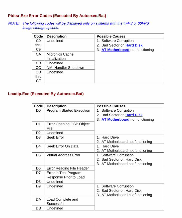
Ptdtsr.Exe Error Codes (Executed By Autoexec.Bat)
NOTE: The following codes will be displayed only on systems with the 4FPS or 30FPSimage storage options.
Code Description Possible CausesC0thruC9
Undefined 1. Software Corruption2. Bad Sector on Hard Disk3. AT Motherboard not functioning
CA Micronics CacheInitialization
CB UndefinedCC NMI Handler ShutdownCDthruCF
Undefined
Loadip.Exe (Executed By Autoexec.Bat)
Code Description Possible CausesD0 Program Started Execution 1 Software Corruption
2. Bad Sector on Hard Disk3. AT Motherboard not functioning
D1 Error Opening GSP ObjectFile
D2 UndefinedD3 Seek Error 1. Hard Drive
2. AT Motherboard not functioningD4 Seek Error On Data 1. Hard Drive
2. AT Motherboard not functioningD5 Virtual Address Error 1. Software Corruption
2. Bad Sector on Hard Disk3. AT Motherboard not functioning
D6 Error Reading File HeaderD7 Error in Test Program
Response Prior to LoadD8 UndefinedD9 Undefined 1. Software Corruption
2. Bad Sector on Hard Disk3. AT Motherboard not functioning
DA Load Complete andSuccessful
DB Undefined

Loadip.Exe (Executed By Autoexec.Bat) (Cont.)
DC No Acknowledge from GSP 1. Software Corruption2. Image Processor PCB3. AT Motherboard not functioning
DD Error Reading GSP ReadyFlag
DE Error Reading GSP ErrorFlag
DF GSP Program Load Failed
Cart.Exe (Executed By Autoexec.Bat)
Code Description Possible CausesE0 Workstation Program
Executing1. Software Corruption2. Bad Sector on Hard Disk3. AT Motherboard not functioning
E1thruEB
Undefined
EE Unexpected ProcessorException
EF UndefinedF0 Workstation Program Exited
to DOSF1thruFA
Undefined
FB GSP is not Ready 1. Software Corruption2. Image Processor PCB3. AT Motherboard not functioning
FC GSP is not respondingFD Front Panel is not
Functioning1. Connectors2. Front Panel Processor3. AT Motherboard not functioning
FE UndefinedFF Int 19H Boot
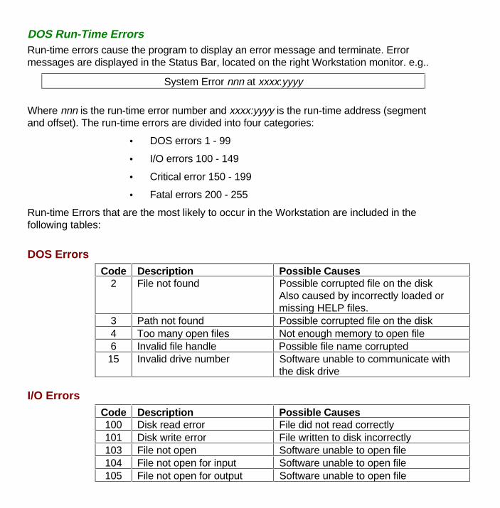
DOS Run-Time ErrorsRun-time errors cause the program to display an error message and terminate. Errormessages are displayed in the Status Bar, located on the right Workstation monitor. e.g..
System Error nnn at xxxx:yyyy
Where nnn is the run-time error number and xxxx:yyyy is the run-time address (segmentand offset). The run-time errors are divided into four categories:
• DOS errors 1 - 99
• I/O errors 100 - 149
• Critical error 150 - 199
• Fatal errors 200 - 255
Run-time Errors that are the most likely to occur in the Workstation are included in thefollowing tables:
DOS ErrorsCode Description Possible Causes
2 File not found Possible corrupted file on the diskAlso caused by incorrectly loaded ormissing HELP files.
3 Path not found Possible corrupted file on the disk4 Too many open files Not enough memory to open file6 Invalid file handle Possible file name corrupted15 Invalid drive number Software unable to communicate with
the disk drive
I/O ErrorsCode Description Possible Causes100 Disk read error File did not read correctly101 Disk write error File written to disk incorrectly103 File not open Software unable to open file104 File not open for input Software unable to open file105 File not open for output Software unable to open file

Critical ErrorsCode Description Possible Causes152 Drive not ready Software unable to communicate with
the disk drive153 Unknown command Software does not recognize command154 CRC error in data Checksum incorrect156 Disk seek error Disk hardware fault158 Sector not found Disk hardware fault159 Printer out of paper160 Device write fault Error while writing to the disk drive161 Device read fault Error while reading from the disk drive162 Hardware failure Possible fault on AT Motherboard
Fatal ErrorsCode Description Possible Causes201 Range check error A numerical value exceeded the limits of
the software202 Stack overflow error Possible memory error on the AT
Motherboard203 Heap overflow error Possible memory error on the AT
Motherboard204 Invalid pointer operation Possible memory error on the AT
Motherboard.250thru252
Communication error Workstation control panel PCB orcable fault. See also WorkstationCommunications.
253* Communications error See below.254thru260
Communications error Workstation control panel PCB orcable fault.
*Error 253 occurs when the system does not boot fully and displays the "system error#253" message. This message is associated with a loss of serial communication.
If an error message, such as "system error 253 at 0000:01F0" is displayed, the numbersindicate the memory location where software detected the error.

SERIES 9600
System ServiceManual878772-01
Date of Issue: December 1995
OEC Medical Systems, Inc.384 Wright Brothers DriveSalt Lake City, UT. 84116

ii 9600 System Service Manual
December 1995
OEC Medical Systems, Inc.384 Wright Brothers Drive
Salt Lake City, UT. 84116-4007
The Mobile Digital Imaging Systemis manufactured under the following U.S.
Patents:
4.768.216; 4.797.907; 4.209.706Other Patents Pending.
This manual contains descriptions, instructionsand
procedures which apply to the Series 9600Mobile Digital Imaging System only.
Software diskettes provided with this systemcontain Microsoft
MS-DOS V 5.0MICROSOFT CORPORATION 1991
All rights reserved
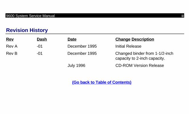
9600 System Service Manual iii
Revision History
Rev Dash Date Change Description
Rev A -01 December 1995 Initial Release
Rev B -01 December 1995 Changed binder from 1-1/2-inch capacity to 2-inch capacity.
July 1996 CD-ROM Version Release
(Go back to Table of Contents)
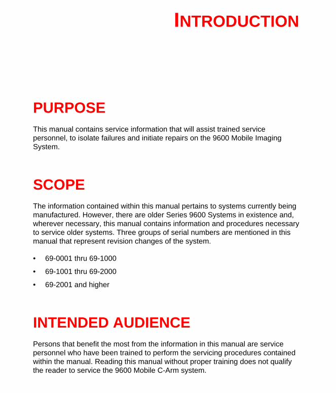
INTRODUCTION
PURPOSEThis manual contains service information that will assist trained servicepersonnel, to isolate failures and initiate repairs on the 9600 Mobile ImagingSystem.
SCOPEThe information contained within this manual pertains to systems currently beingmanufactured. However, there are older Series 9600 Systems in existence and,wherever necessary, this manual contains information and procedures necessaryto service older systems. Three groups of serial numbers are mentioned in thismanual that represent revision changes of the system.
• 69-0001 thru 69-1000
• 69-1001 thru 69-2000
• 69-2001 and higher
INTENDED AUDIENCEPersons that benefit the most from the information in this manual are servicepersonnel who have been trained to perform the servicing procedures containedwithin the manual. Reading this manual without proper training does not qualifythe reader to service the 9600 Mobile C-Arm system.

2 Introduction
HOW TO USE THIS MANUAL
SECTIONS
The Mobile C-Arm has been divided into sections. The sections are separated byindex tab dividers. Each index tab divider has a Table of Contents for thatsection printed on the inside to help locate information.
APPENDIX
An appendix is provided which lists specifications, tolerances, recommendedtools, and test equipment.
INDEX
An index is provided at the end of the manual. The index can be used in additionto the table of contents to locate information. The index entries include the nameof the section and the page number where the information is located.
WARNINGS, CAUTIONS & NOTES
The following warning, caution and note conventions are used throughout themanual to indicate where death, serious injury, or equipment damage may beincurred. It is essential to strictly follow the procedures provided in warning andcautions.
WARNING... Warnings indicate the threat of death or serious personal injury andare colored bright red.
CAUTION: Cautions indicate the threat of minor personal injury or equipmentdamage and are colored dark red.
NOTE: Notes indicate useful information that should be taken into consideration.Notes are colored blue, but are not underlined. An underline indicates a linkto another section or subject from the general text.

Introduction 3
SAFETY PRECAUTIONS
TRAINED SERVICE PERSONNEL
Personal injury or property damage can result from incorrectly performed serviceprocedures. Observe all operating and safety procedures contained within thismanual.
WARNING... Procedures should be performed by service personnel specificallytrained by OEC Medical Systems, Inc. to service or calibrate theSeries 9600 System.
INGRESS OF WATER AND SOLUTIONS
Always unplug the AC power cable from the wall outlet before cleaning theequipment. Do not allow water, soap, or other liquids to drip into the equipmentand possibly cause short circuits, electric shock and fire hazards.
The system must never be operated or stored in locations where conductivefluids, like water or saline solution, might spill on the equipment unless thesystem is properly draped or bagged.
ELECTRICAL SHOCK
Electrical circuits inside the equipment use voltages that are capable of causingserious injury or death from electrical shock.
WARNING... This equipment contains high power electrical components andshould be serviced only by personnel familiar with the circuitry andits operation. At certain locations these voltages are present EVENWHEN THE POWER CORD IS DISCONNECTED.
Areas where dangerous voltages exist include:
• High voltage generator (located in the Mobile C-Arm), high voltage cableand X-Ray tube assemblies - 125,000 volts
• Image Intensifier Assembly - 25,000 - 30,000 volts
• Line Voltage - 120 VAC
• Batteries (located in the C-arm) - 225 - 230 Volts DC
• Monitors in Workstation (15KV)
4 Introduction
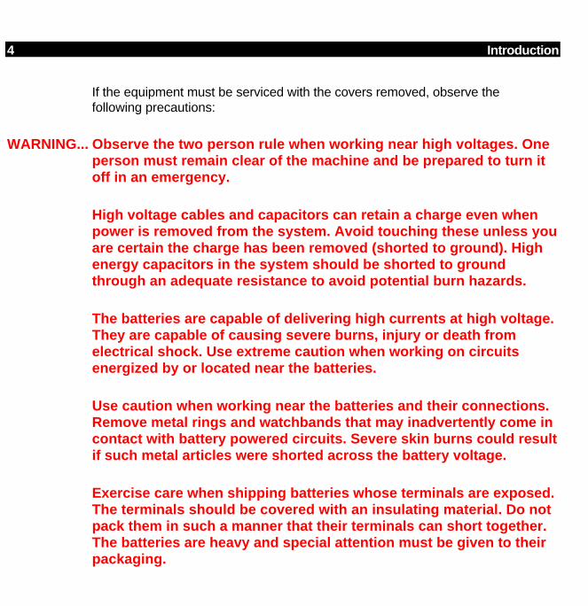
If the equipment must be serviced with the covers removed, observe thefollowing precautions:
WARNING... Observe the two person rule when working near high voltages. Oneperson must remain clear of the machine and be prepared to turn itoff in an emergency.
High voltage cables and capacitors can retain a charge even whenpower is removed from the system. Avoid touching these unless youare certain the charge has been removed (shorted to ground). Highenergy capacitors in the system should be shorted to groundthrough an adequate resistance to avoid potential burn hazards.
The batteries are capable of delivering high currents at high voltage.They are capable of causing severe burns, injury or death fromelectrical shock. Use extreme caution when working on circuitsenergized by or located near the batteries.
Use caution when working near the batteries and their connections.Remove metal rings and watchbands that may inadvertently come incontact with battery powered circuits. Severe skin burns could resultif such metal articles were shorted across the battery voltage.
Exercise care when shipping batteries whose terminals are exposed.The terminals should be covered with an insulating material. Do notpack them in such a manner that their terminals can short together.The batteries are heavy and special attention must be given to theirpackaging.

Introduction 5
EXPLOSION HAZARDS
WARNING... The system must never be operated in the presence of flammableanesthetics, or other flammable or explosive liquids, vapors, or gases.Vapors and gases can be ignited by electrical arcs that can occur during thenormal operation of switches, circuit breakers, push buttons, and othercircuit components.
If flammable substances are present before the system is turned ON:
1. Do not plug the system in.
2. Do not turn the system ON.
If flammable substances are detected after the Mobile C-Arm has been turnedON perform the following:
1. Do not touch any of the controls, or switches.
2. Do not turn it OFF; do not unplug it.
3. Evacuate all personnel immediately.
4. Ventilate the room to clear the air of the flammable vapor or gas.
5. Remove any volatile liquids which are producing flammable vapors to a safestorage area.
6 Introduction
X-RADIATION HAZARD
The X-ray tube assembly produces X-radiation when energized. Never operatethis device without X-ray shielding in place. Use lead shielding and draping toprotect personnel.
MOTORIZED MECHANICAL MOTION HAZARD
The Vertical Column and L-arm are motorized. Observe them continuously whileoperating these features to avoid collision with people and equipment.
If covers are removed use extreme care when operating motorized features. Donot wear loose clothing that may be caught by gears or chains. Do not operatemotorized features when fingers and hands are in the vicinity of motorizedequipment.
SAFETY INTERLOCK
Under no circumstances should the safety interlock in the system be bypassed,jumpered, or otherwise disabled.
WARNING LABELS
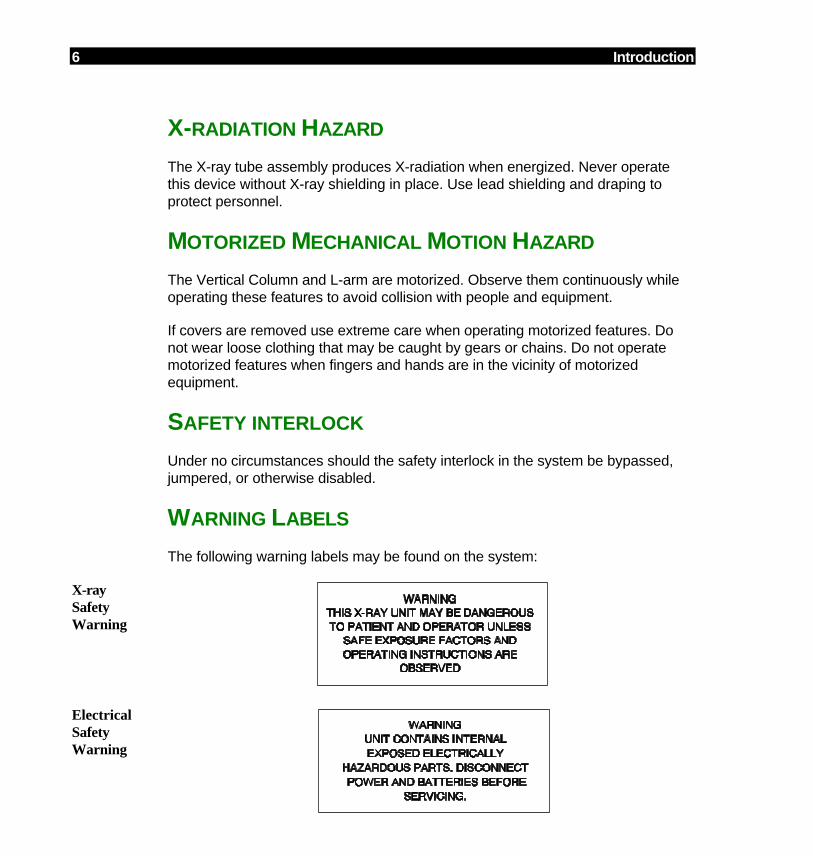
The following warning labels may be found on the system:
X-raySafetyWarning
ElectricalSafetyWarning
Introduction 7
WARNING SYMBOLS
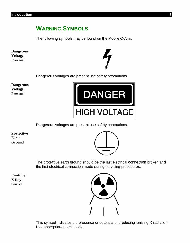
The following symbols may be found on the Mobile C-Arm:
DangerousVoltagePresent
Dangerous voltages are present use safety precautions.
DangerousVoltagePresent
Dangerous voltages are present use safety precautions.
ProtectiveEarthGround
The protective earth ground should be the last electrical connection broken andthe first electrical connection made during servicing procedures.
EmittingX-RaySource
This symbol indicates the presence or potential of producing ionizing X-radiation.Use appropriate precautions.
8 Introduction
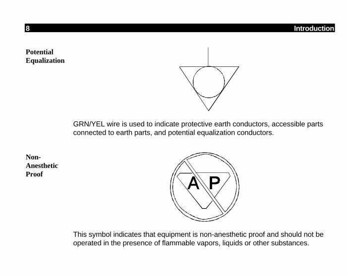
PotentialEqualization
GRN/YEL wire is used to indicate protective earth conductors, accessible partsconnected to earth parts, and potential equalization conductors.
Non-AnestheticProof
This symbol indicates that equipment is non-anesthetic proof and should not beoperated in the presence of flammable vapors, liquids or other substances.
Introduction 9
UNAUTHORIZED MODIFICATIONSUnauthorized changes or modifications could have hazardous consequences.Changes or modifications must not be made unless specifically authorized byOEC.
Modification requests can be made by obtaining a field modification request formfrom OEC Mecical Systems.
NOTE: All OEC 9600 systems comply with International ElectrotechnicalCommission safety standard IEC-601. Do not connect any external device tothe system that does not meet the requirements of IEC-601. Only devicesprovided or approved by OEC Medical Systems, Inc. should be connected tothe system.
When properly assembled with a compatible beam limiting device, thisdiagnostic source assembly will fully meet the Federal Performance Standardsfor Diagnostic X-Ray Systems and Their Components (21CFR 1020.30-32)provided no components or parts are removed from the unit and no unauthorizedadjustments are made in the beam limiting device or tube housing assembly.
• Never remove any part of the housing or beam limiting device.
• Never adjust any part of the beam limiting device unless under the directionof the manufacturer.
• All hardware (i.e. screws, nuts, bolts, etc.) must be re-installed on theequipment.
• All EMI-RFI shielding components must be re-installed on the equipment.Any damaged shielding gasket must be replaced to ensure that the systemcomplies with EMI-RFI regulations.
10 Introduction
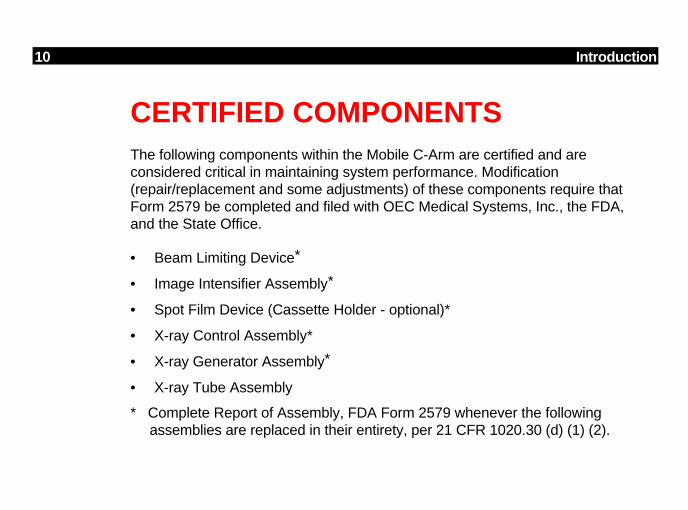
CERTIFIED COMPONENTSThe following components within the Mobile C-Arm are certified and areconsidered critical in maintaining system performance. Modification(repair/replacement and some adjustments) of these components require thatForm 2579 be completed and filed with OEC Medical Systems, Inc., the FDA,and the State Office.
• Beam Limiting Device*
• Image Intensifier Assembly*
• Spot Film Device (Cassette Holder - optional)*
• X-ray Control Assembly*
• X-ray Generator Assembly*
• X-ray Tube Assembly
* Complete Report of Assembly, FDA Form 2579 whenever the followingassemblies are replaced in their entirety, per 21 CFR 1020.30 (d) (1) (2).
SYSTEM OVERVIEW
OVERVIEWThis section will familiarize you with the 9600 Mobile C-Arm and Workstation. Thefollowing topics are discussed and provide an introduction to the system:
• Technical Specifications
• System Configurations and Options
• System Operation
• Cover Removal
• Component Locations
• Circuit Board Functions
TECHNICAL SPECIFICATIONS
APPLICATIONS
The OEC Medical Systems Series 9600 Mobile Digital Imaging System is a multi-application system that provides solutions to the demanding needs of today’s hospitalenvironment. The system has the capacity to handle the most challenging procedures,from orthopedics to interventional neurosurgery, and everything in between.
Orthopedic Surgery - 12 mA boost capability for visualizing dense anatomy. The laseraimer gives the surgeon pin-point accuracy for pedicular screws and interlocking nails.
Laparoscopic Surgery - The large "C" gives wide clearance around the patient and thetable, allowing more room for protruding instruments.
Endoscopic Studies - Fixed room quality imaging with a Mobile C-Arm allows theendoscopist the convenience and safety of working in their own department with theirown staff and equipment.
Vascular Surgery - Integrated dynamic image storage lets the vascular surgeoninstantly play back the recorded run to check the integrity of graft anastomosis andvessel patency.
Pain Management - The 25° overscan of the Series 9600 allows positioning flexibilityfor increased viewing options, and because the system plugs into a standard 110V 15Aoutlet, no site planning is required.
NOTE
Click on a yellow box to go directly to the block diagram for this section. Do not use this link to return to a block diagram from this point. Click on the << button in the Tool Bar to return to this point.

2 System Overview
Emergency And Trauma - Because of its ability to move from room to room, the Series9600 can be used in the ER for everything from angiography to foreign body localizationwithout moving the patient.
Chest And EP Imaging - The EP imaging capabilities of the Series 9600 include arotating anode X-ray tube that allows longer fluoro-on times without the worry of systemshutdown due to overheated tubes.
Neurosurgery - The advanced image processing capabilities of the Series 9600 allowthe neurosurgeon the advantages of performing intra-operative angiography androadmapping, as well as confirming procedural results.
SELECTED SPECIAL FEATURES
• Both C-Arm and Workstation are light and compact for easy transportation andmaneuverability. Ideal 90:10 weight distribution and unique multi-position lockingwheels provide for "push or pull" operation.
• Connects to any available 110V 15A or 220V 8A outlet with single power cable andsingle keyswitch for quick operation.
• Flash S-RAM memory card transfers software code for fast start-up time.
• EasyOp user-friendly one-button operation of all functions.
• More space due to large 26" depth of "C" and extra-large 31" free space betweenX-ray tube and image intensifier gives greater room for protruding instruments andoperating room tables.
• Handles, variable-friction locks and the control panel are duplicated on both sidesof the system for ease-of-use.
• Motorized iso-centric arcing movements minimize unnecessary repositioning.
• Large 8-inch diameter wheels with integrated cable pushers allow for easymaneuverability and positioning.
• Selectable ABS tables vary mA, kVp and camera gain.
• Extra-long continuous fluoro-on times are possible due to high heat dissipation ofthe rotating anode X-ray tube.
• Motor-driven iris collimation and dual opposing semi-transparent shutters providewedge filtration allowing enhanced control of difficult images.
• Compact custom-designed CCD video camera with rapid cooling ensures highsignal-to-noise ratio, lag-free, high sensitivity image acquisition.
• Motor-driven 360° image rotation within the CCD camera ensures correctlypositioned image annotation on hardcopy documentation.
• On-screen orientation icon allows image rotation to indicated position withoutgenerating X-rays.
• Image intensifier and X-ray tube incorporate easy to reach positioning handles.
System Overview 3
• Digital image processing options include variable edge enhancement, motionartifact reduction (MARS), variable frame averaging, window/level control and real-time auto histogramming.
• Real-time subtraction option with roadmapping, peak opacification, re-registration,variable landmarking, mask save/recall and dynamic digital storage.
• Digital image storage from 4 to 9,000 images via RAM, 3½" disk HD or hard diskoptions.
• 16-inch square, black etched, anti-static, anti-glare FastScan monitors operate at73Hz non-interlaced providing flicker-free viewing.
• Keyboard and control panels incorporate icon, language and color codingidentification for precise and accurate system operation. Panels are waterproof,and offer raised keys with tactile and audible feedback. Custom-designed optionalTrackPad allows rapid and precise system control.
• Ambient room light sensor automatically adjusts monitor brightness regardless ofroom illumination.
• Multi-LED X-ray "ON" indicator located above monitor displaying real-time fluoro.
• Optional SteriQuick draping system quickly attaches to X-ray tube, II and "C" toensure sterility.
• Laser Aimer/localizer option, projects a light beam from the image intensifier,enabling exact positioning and site marking in orthopedics and many otherprocedures.
• All models from ESP and up can be equipped with "Digital Spot" capability.Speed-up your procedure while reducing costs by documenting results via ultra-high quality laser or standard camera hardcopies.
• Digital laser camera interface provides direct connection to cameras meeting the3M 952 protocol, for the highest quality film reproduction.
4 System Overview
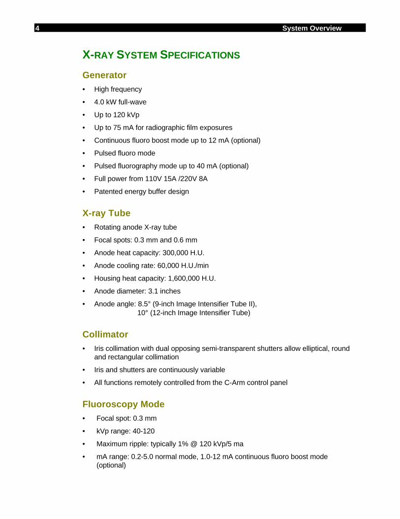
X-RAY SYSTEM SPECIFICATIONS
Generator• High frequency
• 4.0 kW full-wave
• Up to 120 kVp
• Up to 75 mA for radiographic film exposures
• Continuous fluoro boost mode up to 12 mA (optional)
• Pulsed fluoro mode
• Pulsed fluorography mode up to 40 mA (optional)
• Full power from 110V 15A /220V 8A
• Patented energy buffer design
X-ray Tube• Rotating anode X-ray tube
• Focal spots: 0.3 mm and 0.6 mm
• Anode heat capacity: 300,000 H.U.
• Anode cooling rate: 60,000 H.U./min
• Housing heat capacity: 1,600,000 H.U.
• Anode diameter: 3.1 inches
• Anode angle: 8.5° (9-inch Image Intensifier Tube II), 10° (12-inch Image Intensifier Tube)
Collimator• Iris collimation with dual opposing semi-transparent shutters allow elliptical, round
and rectangular collimation
• Iris and shutters are continuously variable
• All functions remotely controlled from the C-Arm control panel
Fluoroscopy Mode• Focal spot: 0.3 mm
• kVp range: 40-120
• Maximum ripple: typically 1% @ 120 kVp/5 ma
• mA range: 0.2-5.0 normal mode, 1.0-12 mA continuous fluoro boost mode(optional)
System Overview 5
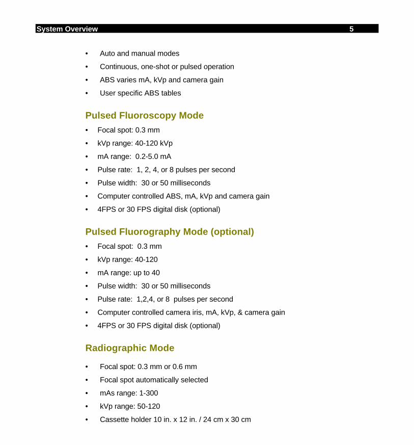
• Auto and manual modes
• Continuous, one-shot or pulsed operation
• ABS varies mA, kVp and camera gain
• User specific ABS tables
Pulsed Fluoroscopy Mode• Focal spot: 0.3 mm
• kVp range: 40-120 kVp
• mA range: 0.2-5.0 mA
• Pulse rate: 1, 2, 4, or 8 pulses per second
• Pulse width: 30 or 50 milliseconds
• Computer controlled ABS, mA, kVp and camera gain
• 4FPS or 30 FPS digital disk (optional)
Pulsed Fluorography Mode (optional)• Focal spot: 0.3 mm
• kVp range: 40-120
• mA range: up to 40
• Pulse width: 30 or 50 milliseconds
• Pulse rate: 1,2,4, or 8 pulses per second
• Computer controlled camera iris, mA, kVp, & camera gain
• 4FPS or 30 FPS digital disk (optional)
Radiographic Mode
• Focal spot: 0.3 mm or 0.6 mm
• Focal spot automatically selected
• mAs range: 1-300
• kVp range: 50-120
• Cassette holder 10 in. x 12 in. / 24 cm x 30 cm
6 System Overview
VIDEO IMAGING SYSTEM SPECIFICATIONS
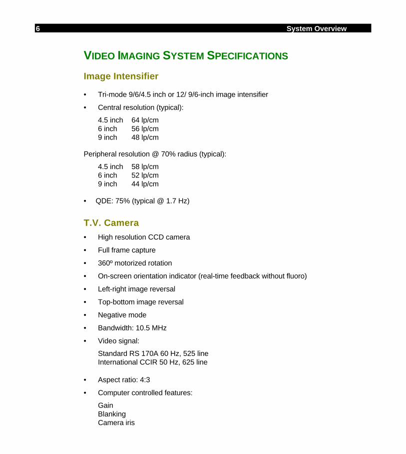
Image Intensifier
• Tri-mode 9/6/4.5 inch or 12/ 9/6-inch image intensifier
• Central resolution (typical):
4.5 inch 64 lp/cm6 inch 56 lp/cm9 inch 48 lp/cm
Peripheral resolution @ 70% radius (typical):
4.5 inch 58 lp/cm6 inch 52 lp/cm9 inch 44 lp/cm
• QDE: 75% (typical @ 1.7 Hz)
T.V. Camera• High resolution CCD camera
• Full frame capture
• 360º motorized rotation
• On-screen orientation indicator (real-time feedback without fluoro)
• Left-right image reversal
• Top-bottom image reversal
• Negative mode
• Bandwidth: 10.5 MHz
• Video signal:
Standard RS 170A 60 Hz, 525 lineInternational CCIR 50 Hz, 625 line
• Aspect ratio: 4:3
• Computer controlled features:
GainBlankingCamera iris
System Overview 7
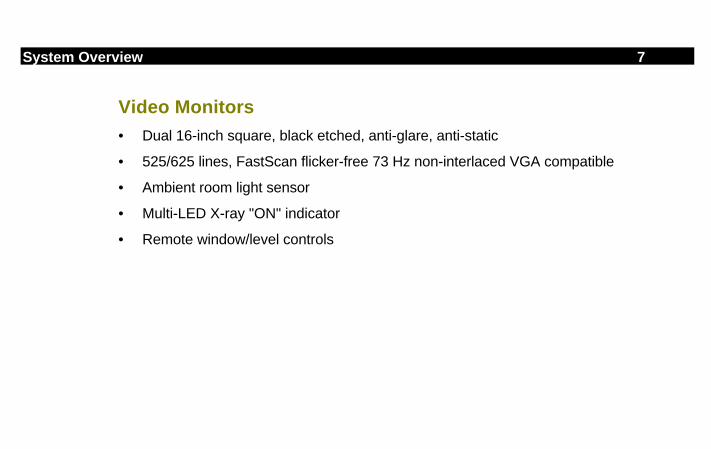
Video Monitors• Dual 16-inch square, black etched, anti-glare, anti-static
• 525/625 lines, FastScan flicker-free 73 Hz non-interlaced VGA compatible
• Ambient room light sensor
• Multi-LED X-ray "ON" indicator
• Remote window/level controls
8 System Overview
PHYSICAL SPECIFICATIONS
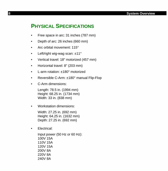
• Free space in arc: 31 inches (787 mm)
• Depth of arc: 26 inches (660 mm)
• Arc orbital movement: 115°
• Left/right wig-wag scan: ±11°
• Vertical travel: 18" motorized (457 mm)
• Horizontal travel: 8" (203 mm)
• L-arm rotation: ±180° motorized
• Reversible C-Arm: ±180° manual Flip-Flop
• C-Arm dimensions:
Length: 78.5 in. (1994 mm)Height: 68.25 in. (1734 mm)Width: 33 in. (838 mm)
• Workstation dimensions:
Width: 27.25 in. (692 mm)Height: 64.25 in. (1632 mm)Depth: 27.25 in. (692 mm)
• Electrical:
Input power (50 Hz or 60 Hz):100V 15A110V 15A120V 15A200V 8A220V 8A240V 8A
System Overview 9
System Configurations and OptionsThere is one standard model 9600 system available; the SP (Surgical Platform) model.The Extended Surgical Package (ESP) offers features and module options that expandthe capabilities of the standard package. Peripheral equipment such as VCRs and othermedia storage devices are available with the SP and ESP packages.
SURGICAL PLATFORM (SP)• 4 image storage with last image hold, 640 x 512 x 10 bit
• Frame averaging (low, medium, high)
• One-shot frame integration (low, medium, high)
• Enhanced integration (low, medium, high)
• MARS (motion artifact reduction)
• Patient annotation keyboard
• Digital window/level
• Real-time auto-histogramming
• Negate
• On-line help menus
• Integrated 2-on-1 or 1-on-1 hardcopy camera (optional)
ORTHOPEDIC MODULE (OPTIONAL)
Available only with the Surgical Platform (SP)
• 16 image storage with last image hold
• 16 image collage
• Laser Aimer/localizer accessory (standard)
• Continuous fluoro boost mode up to 12 mA (standard)
• Pulsed fluorography mode up to 40 mA (standard)
EXPANDED SURGICAL PLATFORM (ESP) (OPTIONAL)Available only with the Surgical Platform (SP)
• 100 image storage with last image hold
• 6 image storage on 3½-inch disk (removable)
• 16 image collage of 100 image disk
• TrackPad with superkey
10 System Overview
• Variable edge enhancement (TrackPad)
• Variable zoom & roam (TrackPad)
• Patient directory with minified image scroll (TrackPad)
• Anatomical markers
• Procedural dose log (mA, kVp, time, patient)
• Integrated S-VHS VCR (optional)
• Multi-function infra-red remote control (optional)
• 4 FPS digital disk (optional)
DIGITAL SPOT (CHOLE) MODULE (OPTIONAL)Available only with the Expanded Surgical Platform (ESP)
• Enhanced digital fluorographic one-shot with 12 mA boost
• Automatically terminates exposure and stores enhanced image to 100 imagestorage archival disk
• Digital laser camera interface, 3M 952 protocol (optional)
• 4 FPS or 30 FPS digital disk (optional)
VASCULAR MODULE (OPTIONAL)Available only with the Expanded Surgical Platform (ESP)
• Continuous fluoro boost mode up to 12 mA
• Pulsed Fluorography mode up to 40 mA
• Real-time subtraction
• Roadmapping
• Peak opacification
• Re-registration (TrackPad)
• Variable landmarking (TrackPad)
• Mask save/recall
• Integrated S-VHS VCR (optional)
• 4 fps digital disk (optional)
System Overview 11
NEUROVASCULAR MODULE (OPTIONAL)
Available only with the Expanded Surgical Platform (ESP)
• Continuous fluoro boost mode up to 12 mA
• Pulsed fluorography mode up to 40 mA
• Real-time subtraction
• Roadmapping
• Peak opacification
• Re-registration (TrackPad)
• Variable landmarking (TrackPad)
• Mask save/recall
• Integrated S-VHS VCR (optional)
• 30 FPS digital disk
• Record/play rate: 1, 2, 4, 8, 15 or 30 fps
• Record time: 150, 75, 40, 20, 10 or 5 minutes
• Image storage: 9,000 digital images (60 Hz)
• Instant image access with TrackPad
• Synchronized to pulse with generator, CCD camera and image processor
4 FRAMES/SECOND DIGITAL DISK (OPTIONAL)
Available only with the Expanded Surgical Platform (ESP), Digital Spot (Chole) orVascular Modules
• Record/play rate: 1, 2 or 4 FPS
• Record time: 22, 11 or 6 minutes
• Image storage: 1,350 digital images (60 Hz)
• Instant image access with TrackPad
• Synchronized to pulse with generator, CCD camera and image processor
12 System Overview
IMAGE STORAGE• Last image hold (all configurations)
• Digital memory capacity:
Surgical Platform (SP): 4 imagesOrthopedic Module: 16 imagesExpanded Surgical Platform (ESP): 100 images, 6 images (3½" disk)4 FPS digital disk: 1,350 images (60 Hz)30 FPS digital disk: 9,000 images (60 Hz)
• Analog memory options:
Integrated S-VHS VCR
HARDCOPY OPTIONS• Radiographic film capability
• Integrated hardcopy camera - 8 in. x 10 in. 2-on-1 or 1-on-1 formats
• Thermal printer
SYSTEM CONTROLS• Entire system is computer controlled software upgradeable
• Multi-function infra-red remote control (optional)
• Hand held X-ray remote control
• Multi-function footswitch
System Overview 13
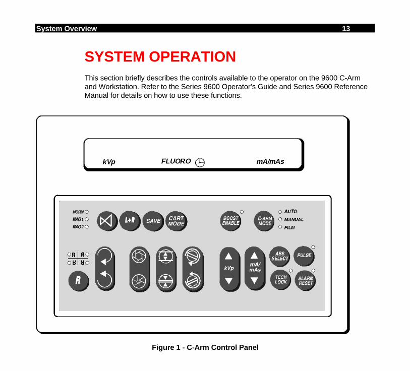
SYSTEM OPERATIONThis section briefly describes the controls available to the operator on the 9600 C-Armand Workstation. Refer to the Series 9600 Operator’s Guide and Series 9600 ReferenceManual for details on how to use these functions.
mA/mAsFLUOROkVp
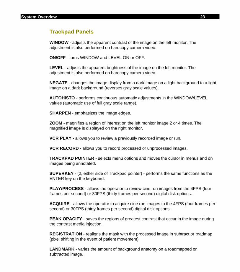
Figure 1 - C-Arm Control Panel
14 System Overview
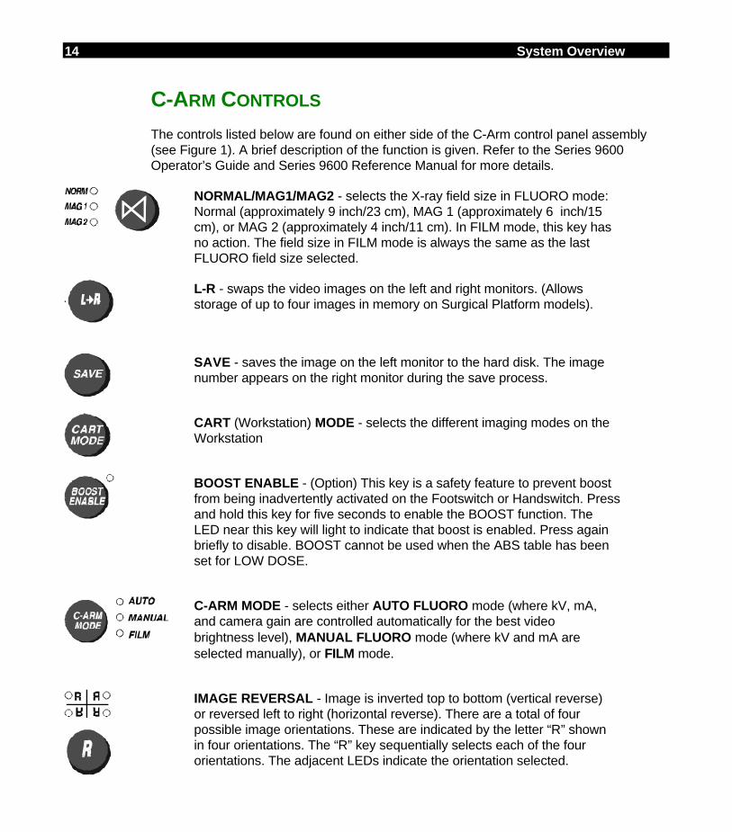
C-ARM CONTROLS
The controls listed below are found on either side of the C-Arm control panel assembly(see Figure 1). A brief description of the function is given. Refer to the Series 9600Operator’s Guide and Series 9600 Reference Manual for more details.
NORMAL/MAG1/MAG2 - selects the X-ray field size in FLUORO mode:Normal (approximately 9 inch/23 cm), MAG 1 (approximately 6 inch/15cm), or MAG 2 (approximately 4 inch/11 cm). In FILM mode, this key hasno action. The field size in FILM mode is always the same as the lastFLUORO field size selected.
L-R - swaps the video images on the left and right monitors. (Allowsstorage of up to four images in memory on Surgical Platform models).
SAVE - saves the image on the left monitor to the hard disk. The imagenumber appears on the right monitor during the save process.
CART (Workstation) MODE - selects the different imaging modes on theWorkstation
BOOST ENABLE - (Option) This key is a safety feature to prevent boostfrom being inadvertently activated on the Footswitch or Handswitch. Pressand hold this key for five seconds to enable the BOOST function. TheLED near this key will light to indicate that boost is enabled. Press againbriefly to disable. BOOST cannot be used when the ABS table has beenset for LOW DOSE.
C-ARM MODE - selects either AUTO FLUORO mode (where kV, mA,and camera gain are controlled automatically for the best videobrightness level), MANUAL FLUORO mode (where kV and mA areselected manually), or FILM mode.
IMAGE REVERSAL - Image is inverted top to bottom (vertical reverse)or reversed left to right (horizontal reverse). There are a total of fourpossible image orientations. These are indicated by the letter “R” shownin four orientations. The “R” key sequentially selects each of the fourorientations. The adjacent LEDs indicate the orientation selected.
System Overview 15
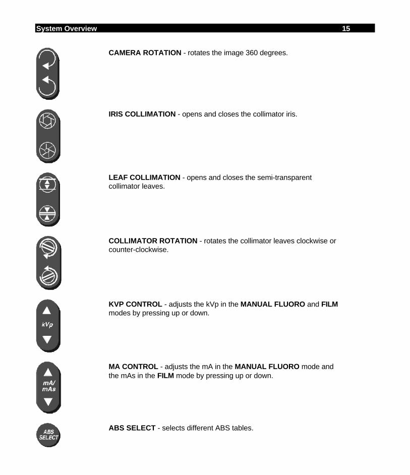
CAMERA ROTATION - rotates the image 360 degrees.
IRIS COLLIMATION - opens and closes the collimator iris.
LEAF COLLIMATION - opens and closes the semi-transparentcollimator leaves.
COLLIMATOR ROTATION - rotates the collimator leaves clockwise orcounter-clockwise.
KVP CONTROL - adjusts the kVp in the MANUAL FLUORO and FILMmodes by pressing up or down.
MA CONTROL - adjusts the mA in the MANUAL FLUORO mode andthe mAs in the FILM mode by pressing up or down.
ABS SELECT - selects different ABS tables.
16 System Overview
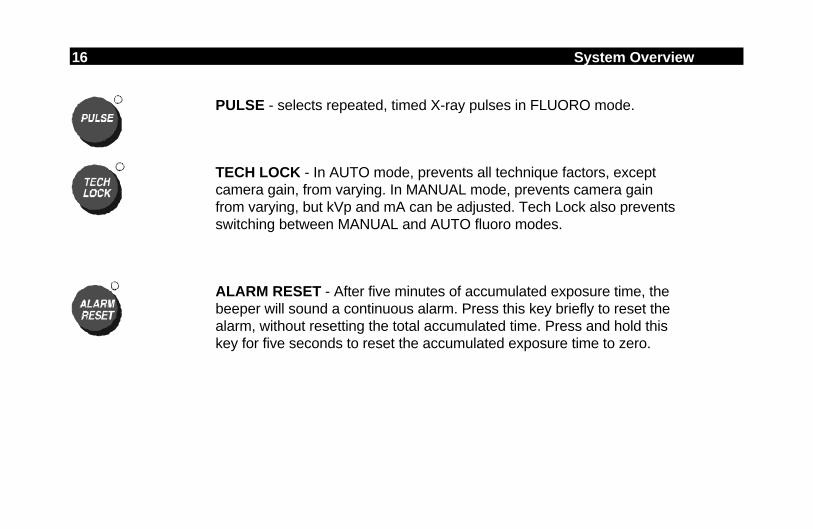
PULSE - selects repeated, timed X-ray pulses in FLUORO mode.
TECH LOCK - In AUTO mode, prevents all technique factors, exceptcamera gain, from varying. In MANUAL mode, prevents camera gainfrom varying, but kVp and mA can be adjusted. Tech Lock also preventsswitching between MANUAL and AUTO fluoro modes.
ALARM RESET - After five minutes of accumulated exposure time, thebeeper will sound a continuous alarm. Press this key briefly to reset thealarm, without resetting the total accumulated time. Press and hold thiskey for five seconds to reset the accumulated exposure time to zero.
System Overview 17
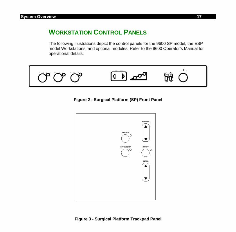
WORKSTATION CONTROL PANELS
The following illustrations depict the control panels for the 9600 SP model, the ESPmodel Workstations, and optional modules. Refer to the 9600 Operator’s Manual foroperational details.
A V E R A G I N G L RF L U O R O O N E - S H O T E N H A N C E D
Figure 2 - Surgical Platform (SP) Front Panel
WINDOW
AUTO HISTO ON/OFF
NEGATE
LEVEL
Figure 3 - Surgical Platform Trackpad Panel
18 System Overview
A V E R A G I N GL RF L U O R O O N E - S H O T R E C A L L S A V ED I G . S P O T
Figure 4 - Expanded Surgical Platform (ESP) Front Panel
TRACKPAD
VCR RECORD
VCR PLAY
ZOOM
SHARPEN
WINDOW
AUTO HISTO ON/OFF
NEGATE
LEVEL
Figure 5 - Expanded Surgical Platform (ESP) Trackpad Panel
System Overview 19
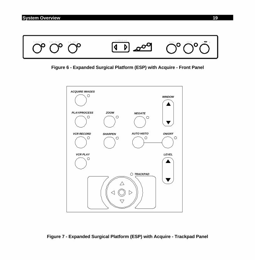
A V E R A G I N GL RF L U O R O O N E - S H O T R E C A L L S A V ED I G . S P O T
Figure 6 - Expanded Surgical Platform (ESP) with Acquire - Front Panel
TRACKPAD
ACQUIRE IMAGES
PLAY/PROCESS
VCR RECORD
VCR PLAY
ZOOM
SHARPEN
WINDOW
AUTO HISTO ON/OFF
NEGATE
LEVEL
Figure 7 - Expanded Surgical Platform (ESP) with Acquire - Trackpad Panel
20 System Overview
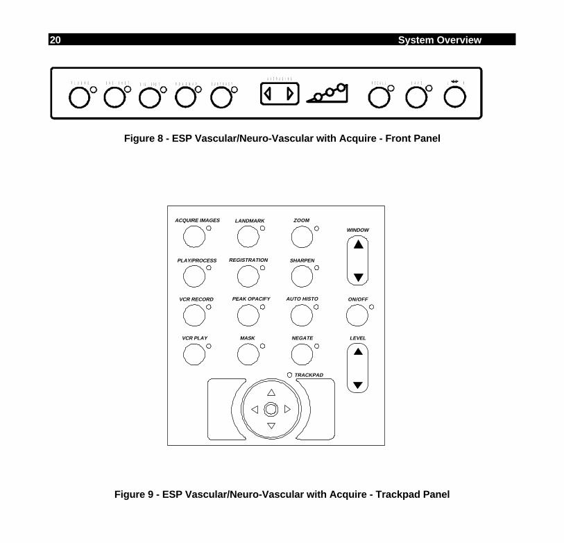
A V E R A G I N GL RF L U O R O O N E - S H O T R E C A L L S A V ER O A D M A P S U B T R A C TD I G . S P O T
Figure 8 - ESP Vascular/Neuro-Vascular with Acquire - Front Panel
TRACKPAD
MASK
ACQUIRE IMAGES LANDMARK
PLAY/PROCESS
VCR RECORD
VCR PLAY
REGISTRATION
ZOOM
SHARPEN
WINDOW
PEAK OPACIFY AUTO HISTO ON/OFF
NEGATE LEVEL
Figure 9 - ESP Vascular/Neuro-Vascular with Acquire - Trackpad Panel
System Overview 21
Shift
tab
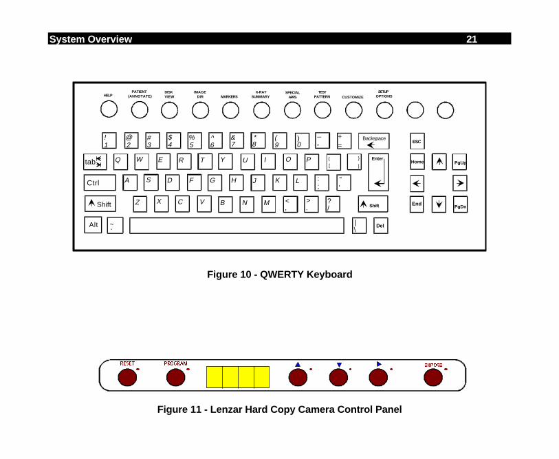
ESC
`~
!1 2
@3# $
4 5%
6^
7& *
8 0)
9(
_
-+=
Q W E R T Y U I O P
Ctrl
Shift
Enter
][
{
"'
A S D F G H J K L
Z X C V B N M <,
>.
?/
Alt
}
;:
\|
DISKVIEW
PATIENT(ANNOTATE)HELP
IMAGEDIR MARKERS
X-RAYSUMMARY
TEST PATTERN
SPECIALAPPS CUSTOMIZE
SETUPOPTIONS
PgUp
PgDn
Backspace
Home
End
Del
Figure 10 - QWERTY Keyboard
Figure 11 - Lenzar Hard Copy Camera Control Panel

22 System Overview
WORKSTATION CONTROLS
The controls listed below are found on the various 9600 Workstations. A brief descriptionof the function is given as an overview. Refer to the Series 9600 Operator’s Guide andSeries 9600 Reference Manual For more details. The controls available depend on thesystem model as follows:
• Surgical Platform (SP) - see Figures 2 and 3
• Expanded Surgical Platform (ESP) - see Figures 4 and 5
• Expanded Surgical Platform (ESP) with Acquire - see Figures 6 and 7
• ESP Vascular/Neuro-Vascular with Acquire - see Figures 8 and 9
Front Panels
FLUORO - basic real time fluoroscopic imaging mode.
ONE-SHOT - obtains an image which has been averaged over a number of imageframes. X-rays are on only during the integration.
DIGITAL SPOT - (Vascular and Expanded Surgical Platform models only) - combinesBOOST and ONE-SHOT. Images are automatically saved at the end of the exposure.
ROADMAP - (Vascular model only) - provides a subtracted image on the left monitorthat is the difference between the current fluoroscopic image and a mask image.
SUBTRACT - (Vascular model only) - provides images that are the difference betweencurrent images and a mask image obtained at the start of the subtraction process.
ENHANCED ONE-SHOT - (Surgical Platform model only) - combines integration withfurther image sharpening to emphasize the image edges.
AVERAGING - selects the level of averaging: LOW, MEDIUM, OR HIGH. Displaysegments illuminate in succession to indicate the amount of averaging.
No segments.................. MINIMUM averagingSegment 1...................... LOW averagingSegment 2...................... MEDIUM averagingSegment 3...................... HIGH averaging
RECALL - recalls a stored image saved since bootup to the left monitor.
SAVE - saves the image on the left monitor to the hard disk. (Duplicates the L/R functionon Surgical Platform models models not equipped with the hard disk option).
L - R - swaps left and right monitor images. Allows storage of up to four images in short-term memory on Surgical Platform models.
System Overview 23
Trackpad Panels
WINDOW - adjusts the apparent contrast of the image on the left monitor. Theadjustment is also performed on hardcopy camera video.
ON/OFF - turns WINDOW and LEVEL ON or OFF.
LEVEL - adjusts the apparent brightness of the image on the left monitor. Theadjustment is also performed on hardcopy camera video.
NEGATE - changes the image display from a dark image on a light background to a lightimage on a dark background (reverses gray scale values).
AUTOHISTO - performs continuous automatic adjustments in the WINDOW/LEVELvalues (automatic use of full gray scale range).
SHARPEN - emphasizes the image edges.
ZOOM - magnifies a region of interest on the left monitor image 2 or 4 times. Themagnified image is displayed on the right monitor.
VCR PLAY - allows you to review a previously recorded image or run.
VCR RECORD - allows you to record processed or unprocessed images.
TRACKPAD POINTER - selects menu options and moves the cursor in menus and onimages being annotated.
SUPERKEY - (2, either side of Trackpad pointer) - performs the same functions as theENTER key on the keyboard.
PLAY/PROCESS - allows the operator to review cine run images from the 4FPS (fourframes per second) or 30FPS (thirty frames per second) digital disk options.
ACQUIRE - allows the operator to acquire cine run images to the 4FPS (four frames persecond) or 30FPS (thirty frames per second) digital disk options.
PEAK OPACIFY - saves the regions of greatest contrast that occur in the image duringthe contrast media injection.
REGISTRATION - realigns the mask with the processed image in subtract or roadmap(pixel shifting in the event of patient movement).
LANDMARK - varies the amount of background anatomy on a roadmapped orsubtracted image.
24 System Overview
Qwerty Keyboard
HELP - displays an index of help topics on the right screen of the Workstation.
PATIENT (ANNOTATE) - displays the Annotation Editor on the right screen of theWorkstation. The Annotation Editor is used for labeling images with patient name,hospital ID number, doctor, etc.
DISK VIEW - displays a page on the right screen of the Workstation containing a collageof sixteen of the one hundred minified images stored on the hard disk. These imagescan be scrolled thru or selected using the arrow and enter keys or the trackpad pointerand superkeys on the trackpad panel.
IMAGE DIRECTORY - displays an alphabetical directory of patient or doctor names onthe right Workstation screen.
MARKERS - displays the MARKERS screen. Markers are used as an aid to patientannotation.
X-RAY SUMMARY - displays a summary file of the X-ray exposures made during aprocedure.
SPECIAL APPS - There are currently no special applications installed on this system.
TEST PATTERN - Brings up a gray scale test pattern.
CUSTOMIZE - displays the Customize menu, which allows the pulse rates and VCRconfigurations to be customized.
SETUP OPTIONS - used to set current time and date, display the software ID screen,and access level 2 servicing menus.
ESC - Press this key to exit from a function screen or menu.
PGUP/PGDN - Press either of these keys to scroll through help screens, or the diskview screens, one screen at a time.
ARROW KEYS - Press these keys as an alternative to the trackpad pointer to move thecursor or arrow pointer around the screen.
System Overview 25
Lenzar Hardcopy Camera Control Panel
RESET - this key resets the camera to its READY state for EXP1 (exposure 1).
PROGRAM - allows the operator to program the various settings.
LED DISPLAY - displays the current user number or exposure number.
EXPOSE - initiates the hard copy camera exposure.
ARROW KEYS - increments, decrements, and advances the camera settings.

26 System Overview
COVER REMOVAL
MOBILE C-ARM COVERS
To remove the Mobile C-Arm covers perform the following steps and refer to Figure 12.
WARNING Electrical circuits inside the equipment use voltages that are capable ofcausing serious injury or death from electrical shock.
1. Unplug the system from AC power.
2. Remove the Rear Handle Cover by removing 3 (A) screws located behind the coverdoor and one screw (B) on each side at bottom, front of cover.
3. Remove the Front Cover by removing 2 screws (C) near the top of the vertical shaftunder the rubber cover.
4. Remove the Front Leg Cover by removing 8 screws: 2 (D) underneath the toe of thecover, 2 (E) underneath each cross beam, and 2 (F) from the top front of the cover.
5. Remove the Left Front Cover and Right Front Cover by removing the 3 screws (G)on each side.
LEFT FRONT COVER
FRONT COVER
FRONT LEG COVER
RIGHT FRONT COVERREAR COVER HANDLE ASSEMBLY
A
G
G
E
E
F
C
D
B
Figure 12 - C-Arm Cover Removal
NOTE
Click on the top colored square to go directly to the Illustrated Parts Manual for systems bearing serial numbers 69-001 thru 69-999. Click on the bottom colored square for systems bearing serial numbers 69-1000 and higher. Click on the << button oin the Tool Bar to return to this point.
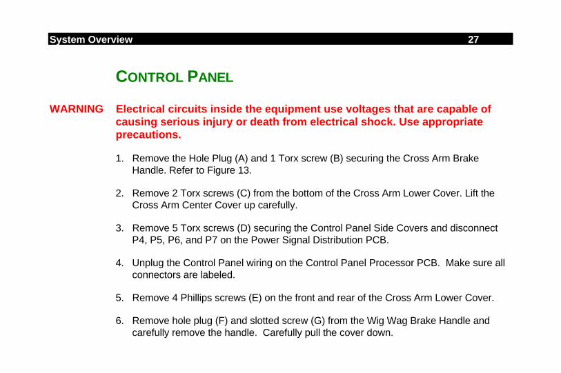
System Overview 27
CONTROL PANEL
WARNING Electrical circuits inside the equipment use voltages that are capable ofcausing serious injury or death from electrical shock. Use appropriateprecautions.
1. Remove the Hole Plug (A) and 1 Torx screw (B) securing the Cross Arm BrakeHandle. Refer to Figure 13.
2. Remove 2 Torx screws (C) from the bottom of the Cross Arm Lower Cover. Lift theCross Arm Center Cover up carefully.
3. Remove 5 Torx screws (D) securing the Control Panel Side Covers and disconnectP4, P5, P6, and P7 on the Power Signal Distribution PCB.
4. Unplug the Control Panel wiring on the Control Panel Processor PCB. Make sure allconnectors are labeled.
5. Remove 4 Phillips screws (E) on the front and rear of the Cross Arm Lower Cover.
6. Remove hole plug (F) and slotted screw (G) from the Wig Wag Brake Handle andcarefully remove the handle. Carefully pull the cover down.
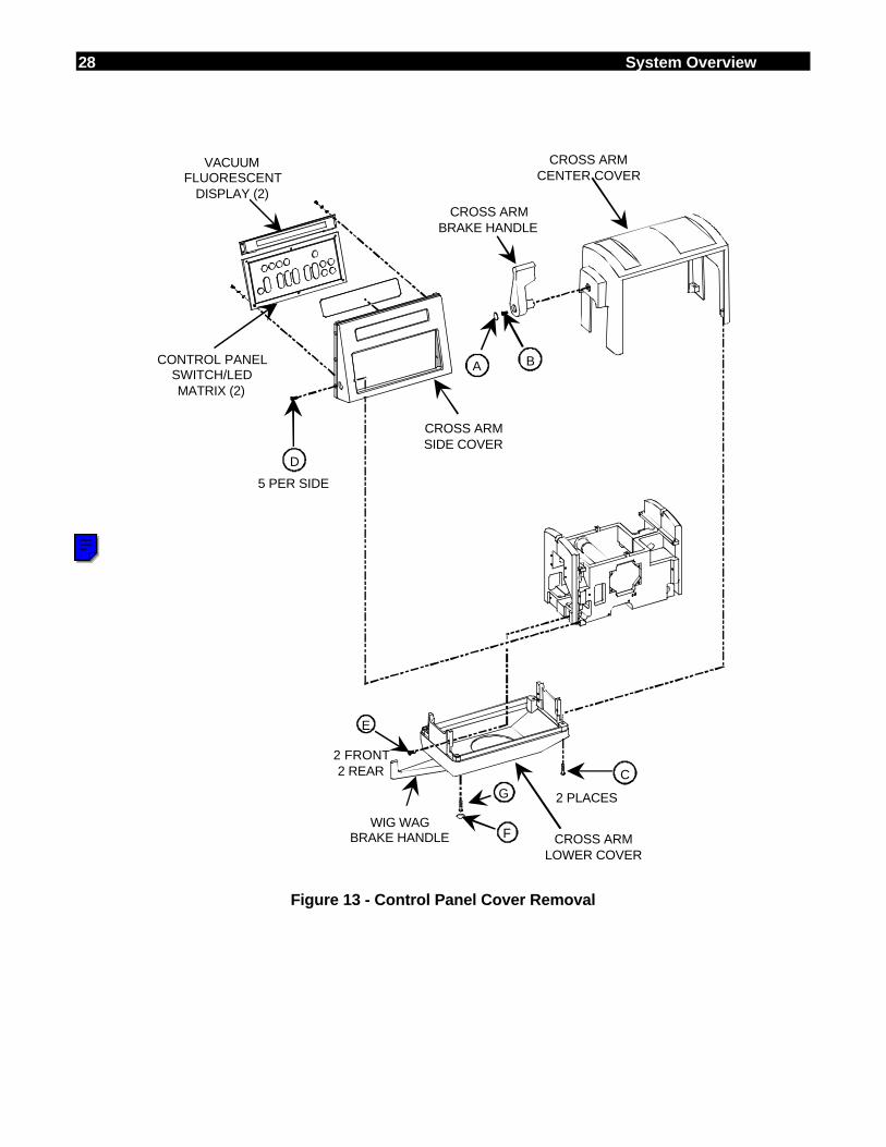
28 System Overview
CONTROL PANELSWITCH/LEDMATRIX (2)
VACUUMFLUORESCENT
DISPLAY (2)
A B
C
D
5 PER SIDE
2 FRONT2 REAR
F
G 2 PLACES
CROSS ARMCENTER COVER
CROSS ARMSIDE COVER
CROSS ARMBRAKE HANDLE
WIG WAGBRAKE HANDLE CROSS ARM
LOWER COVER
E
Figure 13 - Control Panel Cover Removal
NOTE
Click on the top square to go directly to the Illustrated Parts Manual for systems bearing serial numbers 69-001 thru 69-999, Click on the bottom square to go directly to the Illustrated Parts Manual for systems bearing serial numbers 69-1000 and higher.

System Overview 29
WORKSTATION COVERS
To remove the Workstation covers perform the following steps. Refer to Figures 14-20.
WARNING Electrical circuits inside the equipment use voltages that are capable ofcausing serious injury or death from electrical shock.
1. Rotate each of the eight 1/4-turn fasteners on each side of the rear cover as shownin Figure 14.
Figure 14 - Loosening Rear Cover Screws
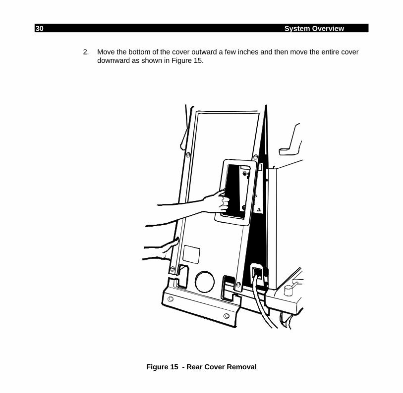
30 System Overview
2. Move the bottom of the cover outward a few inches and then move the entire coverdownward as shown in Figure 15.
Figure 15 - Rear Cover Removal
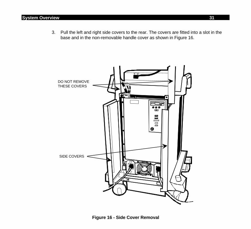
System Overview 31
3. Pull the left and right side covers to the rear. The covers are fitted into a slot in thebase and in the non-removable handle cover as shown in Figure 16.
DO NOT REMOVETHESE COVERS
SIDE COVERS
Figure 16 - Side Cover Removal
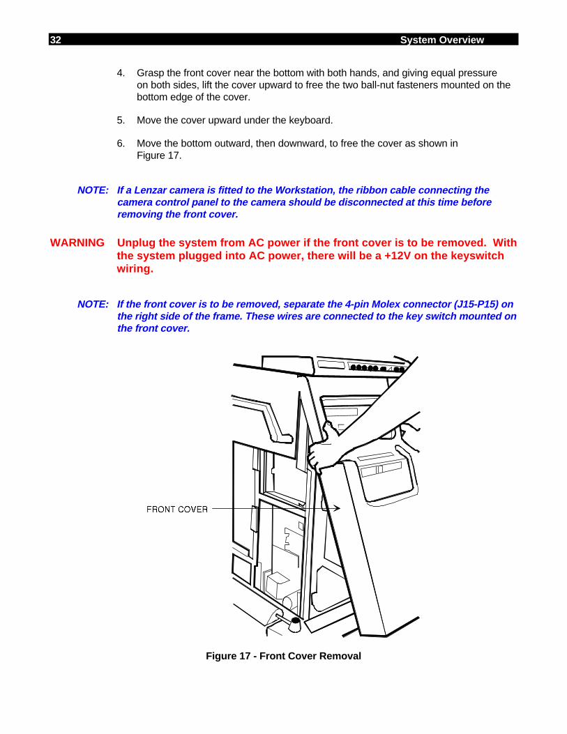
32 System Overview
4. Grasp the front cover near the bottom with both hands, and giving equal pressureon both sides, lift the cover upward to free the two ball-nut fasteners mounted on thebottom edge of the cover.
5. Move the cover upward under the keyboard.
6. Move the bottom outward, then downward, to free the cover as shown inFigure 17.
NOTE: If a Lenzar camera is fitted to the Workstation, the ribbon cable connecting thecamera control panel to the camera should be disconnected at this time beforeremoving the front cover.
WARNING Unplug the system from AC power if the front cover is to be removed. Withthe system plugged into AC power, there will be a +12V on the keyswitchwiring.
NOTE: If the front cover is to be removed, separate the 4-pin Molex connector (J15-P15) onthe right side of the frame. These wires are connected to the key switch mounted onthe front cover.
Figure 17 - Front Cover Removal
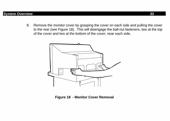
System Overview 33
8. Remove the monitor cover by grasping the cover on each side and pulling the coverto the rear (see Figure 18). This will disengage the ball-nut fasteners, two at the topof the cover and two at the bottom of the cover, near each side.
Figure 18 - Monitor Cover Removal
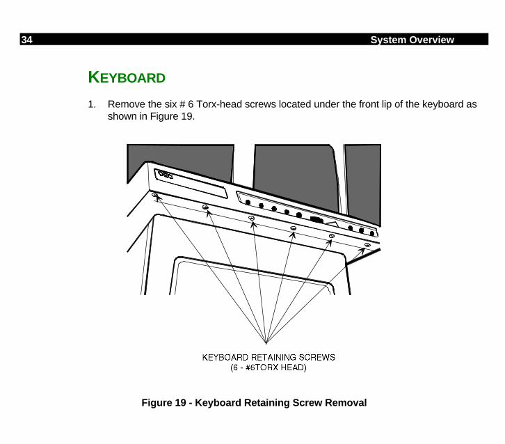
34 System Overview
KEYBOARD
1. Remove the six # 6 Torx-head screws located under the front lip of the keyboard asshown in Figure 19.
Figure 19 - Keyboard Retaining Screw Removal
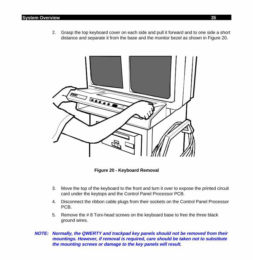
System Overview 35
2. Grasp the top keyboard cover on each side and pull it forward and to one side a shortdistance and separate it from the base and the monitor bezel as shown in Figure 20.
Figure 20 - Keyboard Removal
3. Move the top of the keyboard to the front and turn it over to expose the printed circuitcard under the keytops and the Control Panel Processor PCB.
4. Disconnect the ribbon cable plugs from their sockets on the Control Panel ProcessorPCB.
5. Remove the # 8 Torx-head screws on the keyboard base to free the three blackground wires.
NOTE: Normally, the QWERTY and trackpad key panels should not be removed from theirmountings. However, if removal is required, care should be taken not to substitutethe mounting screws or damage to the key panels will result.
36 System Overview
Keyboard Reassembly
The keyboard should be replaced in the opposite manner to the above disassembly.When replacing the keyboard assembly, be sure the cables and ground wires are foldedback over the top of the Control Panel Processor PCB and are not pinched.
1. Place the keyboard assembly against the bottom of the monitor bezel and push firmlyto seat the keyboard assembly between the bezel and flat spring attached to themonitor base plate.
NOTE: The cutout on the lower rear lip of the keyboard assembly should slip between thespring and the bezel. The raised ridges along the top rear of the keyboard assemblyshould be under the monitor bezel when the assembly is firmly seated.
2. Replace the screws under the front lip of the keyboard assembly (see Figure 19)and test system operation from the keyboard.
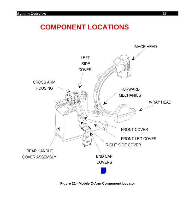
System Overview 37
COMPONENT LOCATIONS
IMAGE HEAD
X-RAY HEAD
CROSS ARMHOUSING
END CAPCOVERS
FRONT LEG COVER
FORWARDMECHANICS
RIGHT SIDE COVERREAR HANDLE
COVER ASSEMBLY
FRONT COVER
LEFT SIDE
COVER
Figure 21 - Mobile C-Arm Component Locator
NOTE
Click on the colored square to go directly to the Illustrated Parts Manual.
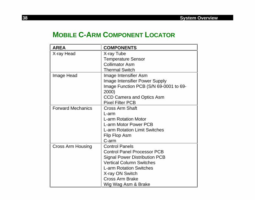
38 System Overview
MOBILE C-ARM COMPONENT LOCATOR
AREA COMPONENTSX-ray Head X-ray Tube
Temperature SensorCollimator AsmThermal Switch
Image Head Image Intensifier AsmImage Intensifier Power SupplyImage Function PCB (S/N 69-0001 to 69-2000)CCD Camera and Optics AsmPixel Filter PCB
Forward Mechanics Cross Arm ShaftL-armL-arm Rotation MotorL-arm Motor Power PCBL-arm Rotation Limit SwitchesFlip Flop AsmC-arm
Cross Arm Housing Control PanelsControl Panel Processor PCBSignal Power Distribution PCBVertical Column SwitchesL-arm Rotation SwitchesX-ray ON SwitchCross Arm BrakeWig Wag Asm & Brake
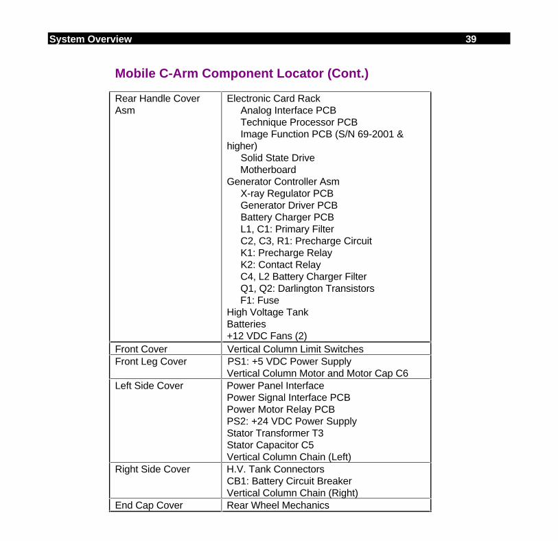
System Overview 39
Mobile C-Arm Component Locator (Cont.)
Rear Handle CoverAsm
Electronic Card Rack Analog Interface PCB Technique Processor PCB Image Function PCB (S/N 69-2001 &higher) Solid State Drive MotherboardGenerator Controller Asm X-ray Regulator PCB Generator Driver PCB Battery Charger PCB L1, C1: Primary Filter C2, C3, R1: Precharge Circuit K1: Precharge Relay K2: Contact Relay C4, L2 Battery Charger Filter Q1, Q2: Darlington Transistors F1: FuseHigh Voltage TankBatteries+12 VDC Fans (2)
Front Cover Vertical Column Limit SwitchesFront Leg Cover PS1: +5 VDC Power Supply
Vertical Column Motor and Motor Cap C6Left Side Cover Power Panel Interface
Power Signal Interface PCBPower Motor Relay PCBPS2: +24 VDC Power SupplyStator Transformer T3Stator Capacitor C5Vertical Column Chain (Left)
Right Side Cover H.V. Tank ConnectorsCB1: Battery Circuit BreakerVertical Column Chain (Right)
End Cap Cover Rear Wheel Mechanics
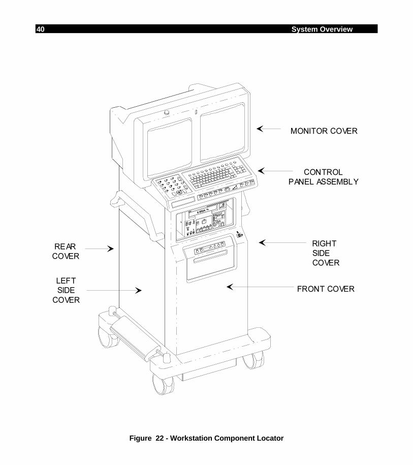
40 System Overview
MONITOR COVER
CONTROL
PANEL ASSEMBLY
FRONT COVER
REAR
COVER
RIGHT
SIDE
COVER
LEFT
SIDE
COVER
Figure 22 - Workstation Component Locator
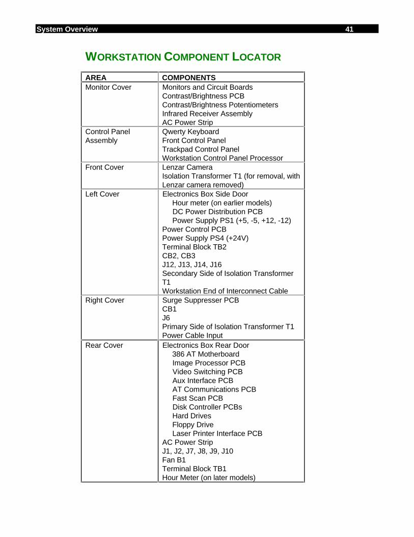
System Overview 41
WORKSTATION COMPONENT LOCATOR
AREA COMPONENTSMonitor Cover Monitors and Circuit Boards
Contrast/Brightness PCBContrast/Brightness PotentiometersInfrared Receiver AssemblyAC Power Strip
Control PanelAssembly
Qwerty KeyboardFront Control PanelTrackpad Control PanelWorkstation Control Panel Processor
Front Cover Lenzar CameraIsolation Transformer T1 (for removal, withLenzar camera removed)
Left Cover Electronics Box Side Door Hour meter (on earlier models) DC Power Distribution PCB Power Supply PS1 (+5, -5, +12, -12)Power Control PCBPower Supply PS4 (+24V)Terminal Block TB2CB2, CB3J12, J13, J14, J16Secondary Side of Isolation TransformerT1Workstation End of Interconnect Cable
Right Cover Surge Suppresser PCBCB1J6Primary Side of Isolation Transformer T1Power Cable Input
Rear Cover Electronics Box Rear Door 386 AT Motherboard Image Processor PCB Video Switching PCB Aux Interface PCB AT Communications PCB Fast Scan PCB Disk Controller PCBs Hard Drives Floppy Drive Laser Printer Interface PCBAC Power StripJ1, J2, J7, J8, J9, J10Fan B1Terminal Block TB1Hour Meter (on later models)
42 System Overview
CIRCUIT BOARD FUNCTIONS
MOBILE C-ARM
Control Panel Processor PCBSch. #00-875601 - Asy. #00-875603 - S/N 69-0001 thru 69-2000Sch. #00-878486 - Asy. #00-878488 - S/N 69-2001 and up
Interfaces left and right control panelsInterfaces X-ray switch and Fast Stop switches to systemDrives LEDs on control panelsDrives left and right fluorescent displays
Control Panel Processor I/O PCBSch. #00-878489 - Asy. #00-878491 - S/N 69-2001 and up
Connection point for new Control Panel Processor PCB (Asy. #00-878488)
Column I/O PCBSch. #00-878492 - Asy. #00-878494 - S/N 69-2001 and up
Cabling connection point - no active circuitry
Technique Processor PCBSch. #00-876735 - Asy. #00-876737 - S/N 69-0001 thru 69-1000Sch. #00-877742 - Asy. #00-877744 - S/N 69-1001 and up
Controls C-ArmLoads and runs DOS and Applications Software from Solid State Disk DriveSerial communications to C-Arm and Workstation Control Panel Processor andImage Function PCB
Analog Interface PCBSch. #00-876738 - Asy. #00-876740 - All S/N
“Slave” to Technique Processor PCBAnalog to digital conversionDigital to Analog conversionPIO control outputs and status inputsCounter/timer circuitry for generator drive signals
Mainframe MotherboardSch. #00-875539 - Asy. #00-900588 - S/N 69-0001 thru 69-2000Sch. #00-878396 - Asy. #00-900970 - S/N 69-2001 and up
Backplane of generator cardrackPower and signal interconnection and distribution
NOTE:
Click on the drawing number to go directly to that Electrical Schematic diagram or Assembly drawing. Click on the << button in the Tool Bar to return to this point. HINT: You must click on the << in the Tool Bar the same number of times to return to the text as the number of links you have activated.
System Overview 43
Power/Motor Relay PCBSch. #00-875997 - Asy. #00-875999 - All S/N
Stator start and run relaysStator current sense circuitryC-Arm lift and rotation motor relaysGenerator +24V interlock relayImage intensifier relay
Power/Signal Interface PCBSch. #00-876001 - Asy. #00-876003 - S/N 69-0001 thru 69-1000Sch. #00-877998 - Asy. #00-878000 - S/N 69-1001 and up
Interfaces AC and DC powerInterfaces control signals and serial communications signals
X-ray Regulator PCBSch. #00-877458 - Asy. #00-877460 - All S/N
KV control and senseMA control and senseFault PAL circuitry
Generator Driver PCBSch. #00-877461 - Asy. #00-877463 - All S/N
Filament regulator circuitry for MAInverter driver circuitry for KVSaturation fault detector circuitry
Battery Charger PCBSch. #00-876643 - Asy. #00-876644 - S/N 69-0001 thru 69-1000Sch. #00-877995 - Asy. #00-877997 - S/N 69-1001 and up
Charges batteriesProvides precharge voltage
Image Functions PCBSch. #00-874750 - Asy. #00-874752 - S/N 69-0001 thru 69-2000Sch. #00-878398 - Asy. #00-878400 - S/N 69-2001 and up
Interfaces controls from Technique Processor to collimator , CCD camera , andImage Intensifier TubeStores collimator iris field size calibration information
Pixel Filter PCBSch. #00-877789 - Asy. #00-877791
Filters white pixel noise from video signal
44 System Overview
Pixel/Column Filter PCBSch. #00-878045 - Asy. #00-878047
Filters white pixel noise and CCD column shading variations from video signal
WORKSTATION
DC Power Distribution PCBSch. #00-876839 - Asy. #00-876841 - All S/N
Distributes +5, -5, +12, -12 volts to various locations on the Workstation.Generates system reset signal (SYSRST*) with power fail circuitry .
Surge Suppressor PCBSch. #00-876784 - Asy. #00-876786 - All S/N
Suppresses voltage spikes on the line voltage for system protection
Power Control PCBSch. #00-876547 - Asy. #00-876549 S/N 69-0001 thru 69-1000Sch. #00-878001 - Asy. #00-878003 - S/N 69-1001 and up
Provides AC interfacing and safety circuits from the isolation transformer to the C-arm and Workstation.
Workstation Control Panel Processor PCBSch. #00-876611 - Asy. #00-876613 - All S/N
Interfaces front panel keys and LEDs to/from Communications PCBInterfaces trackpad keys, LEDs, and pointer circuitry to/from Communications PCBInterfaces window/level circuitry to/from Communications PCBDrives audio speaker.Interfaces IR signals to system.Serial communications to Communications PCB via Aux Interface PCB
Contrast/Brightness Control PCBSch. #00-876351 - Asy. #00-876353 - All S/N
Contrast & brightness control circuitryAuto brightness & contrast signal interfacing
IR Transmitter PCBSch. #00-873936 - Asy. #00-873938 - All S/N
Contained in the IR remote hand controlsGenerates IR control signals
System Overview 45
IR Receiver PCBSch. #00-874220 - Asy. #00-874222 - All S/N
Receives, demodulates, and amplifies IR signals for system interfacingContains photocell for auto brightness/contrast circuits
Auxiliary Interface PCBSch. #00-876502 - Asy. #00-876504 - All S/N
Cabling interconnection to interface and distribute signals in Workstation.Provides hospital room interfacing for:
Room in use lightX-ray on lightPower dye injection systemsDoor interlock
LED displays (2) for status & diagnostic information.
Video Switching PCBSch. #00-872237 - Asy. #00-872239 - All S/N
Video crosspoint switch - 8 input to 6 outputLogarithmic video amplifier used in subtraction proceduresAnti-aliasing filterGen-Lock circuitry
386 AT MotherboardAsy. #00-900658 - All S/N
Controls Workstation - OEM board
Image Processor PCBSch. #00-875952 - Asy. #00-875954 - All S/N
Performs all image processing functionsGraphics processor for text/graphics/circular blanking/ROI (region of interest)Interfaces high speed transfer and storage of digital video images
Communications PCBSch. #00-872125 - Asy. #00-872127 - All S/N
Serial communications to C-Arm and Workstation Control Panel PCBVCR controls interfaceCOM 1 and COM 2 communications portsParallel printer portOption PROMHex display drive to Aux Interface PCB for status and error conditions
46 System Overview
High Rate Scan Converter PCBSch. #00-876397 - Asy. #00-876399 - All S/N
Upscans interlaced digital video signal from the Image Processor , converts to a non-interlaced analog video signal and sends it to the left and right monitors
POWER DISTRIBUTION
OVERVIEWThe information provided in this section is most easily understood when referencingschematics from the schematic manual. Use the correct interconnect diagrams andcircuit board schematics for your system indicated below.
C-Arm Interconnect Diagram
Schematic # 00-875500 - System S/N 69-0001 thru 69-1000Schematic # 00-877972 - System S/N 69-1001 thru 69-2000Schematic # 00-878376 - System S/N 69-2001 and higher
Image System Interconnect Diagram
Schematic # 00-875410 - System S/N 69-0001 thru 69-1000Schematic # 00-877971 - System S/N 69-1001 thru 69-2000Schematic # 00-878377 - System S/N 69-2001 and higher
Workstation Interconnect Diagram
Schematic # 00-876158 - System S/N 69-0001 thru 69-1000Schematic # 00-877970 - System S/N 69-1001 and higher
Surge Suppressor PCB
Schematic # 00-876784 - All S/N
Power Control PCB
Schematic # 00-876547 - System S/N 69-0001 thru 69-1000Schematic # 00-878001 - System S/N 69-1001 and higher
DC Power Distribution PCB
Schematic # 00-876839 - All S/N
Power/Signal Interface PCB
Schematic # 00-876001 - System S/N 69-0001 thru 69-1000Schematic # 00-877998 - System S/N 69-1001 and higher
Battery Charger PCB
Schematic # 00-876643 - System S/N 69-0001 thru 69-1000Schematic # 00-877995 - System S/N 69-1001 and higher
Power/Motor Relay PCB
Schematic # 00-875997 - All S/N
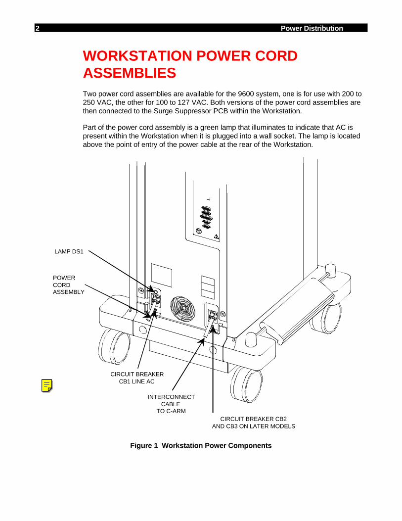
2 Power Distribution
WORKSTATION POWER CORDASSEMBLIESTwo power cord assemblies are available for the 9600 system, one is for use with 200 to250 VAC, the other for 100 to 127 VAC. Both versions of the power cord assemblies arethen connected to the Surge Suppressor PCB within the Workstation.
Part of the power cord assembly is a green lamp that illuminates to indicate that AC ispresent within the Workstation when it is plugged into a wall socket. The lamp is locatedabove the point of entry of the power cable at the rear of the Workstation.
POWER CORD ASSEMBLY
LAMP DS1
CIRCUIT BREAKER CB1 LINE AC
INTERCONNECT CABLE
TO C-ARMCIRCUIT BREAKER CB2
AND CB3 ON LATER MODELS
Figure 1 Workstation Power Components
NOTE
Click on a yellow box to go directly to the block diagram for this section. Do not use this link to return to a block diagram from this point. Click on the << button in the Tool Bar to return to any starting point.
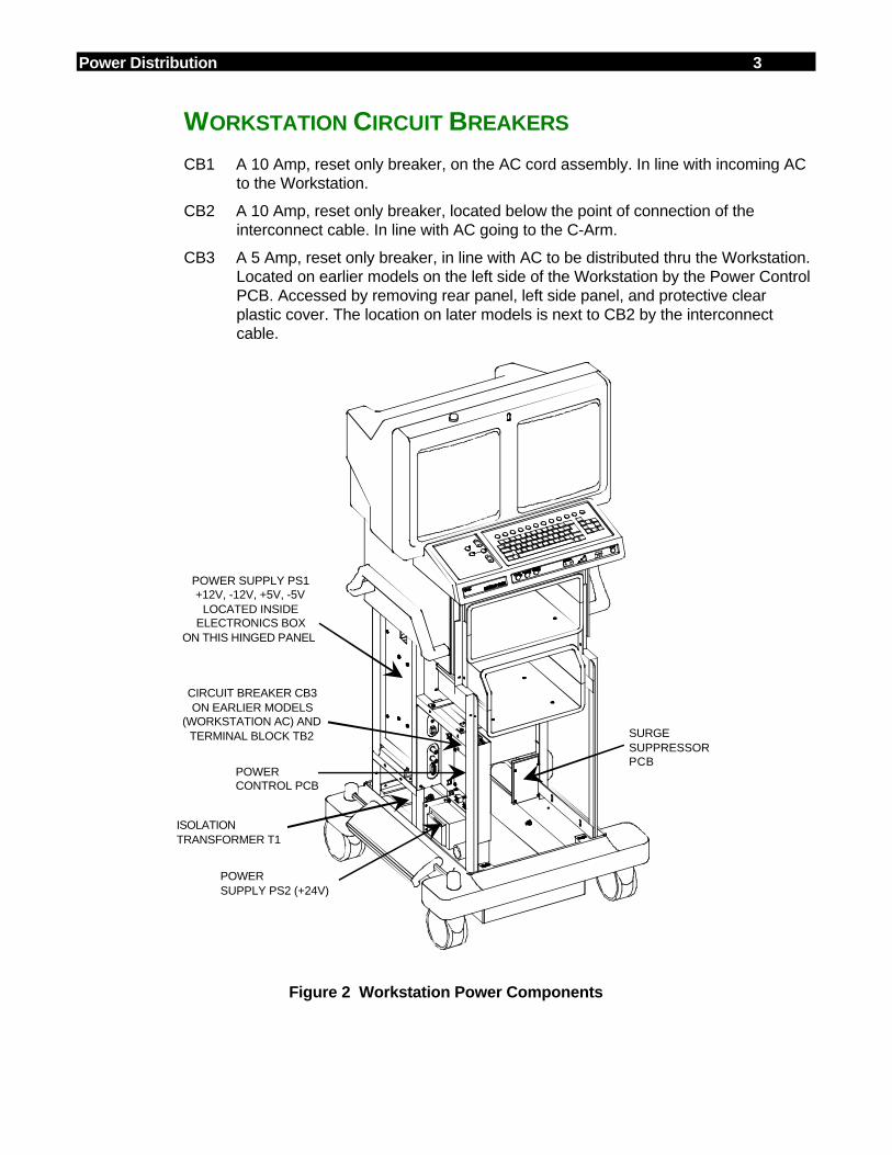
Power Distribution 3
WORKSTATION CIRCUIT BREAKERS
CB1 A 10 Amp, reset only breaker, on the AC cord assembly. In line with incoming ACto the Workstation.
CB2 A 10 Amp, reset only breaker, located below the point of connection of theinterconnect cable. In line with AC going to the C-Arm.
CB3 A 5 Amp, reset only breaker, in line with AC to be distributed thru the Workstation.Located on earlier models on the left side of the Workstation by the Power ControlPCB. Accessed by removing rear panel, left side panel, and protective clearplastic cover. The location on later models is next to CB2 by the interconnectcable.
SURGE SUPPRESSOR PCB
POWER CONTROL PCB
POWER SUPPLY PS2 (+24V)
POWER SUPPLY PS1+12V, -12V, +5V, -5V
LOCATED INSIDEELECTRONICS BOX
ON THIS HINGED PANEL
ISOLATION TRANSFORMER T1
CIRCUIT BREAKER CB3 ON EARLIER MODELS
(WORKSTATION AC) ANDTERMINAL BLOCK TB2
Figure 2 Workstation Power Components
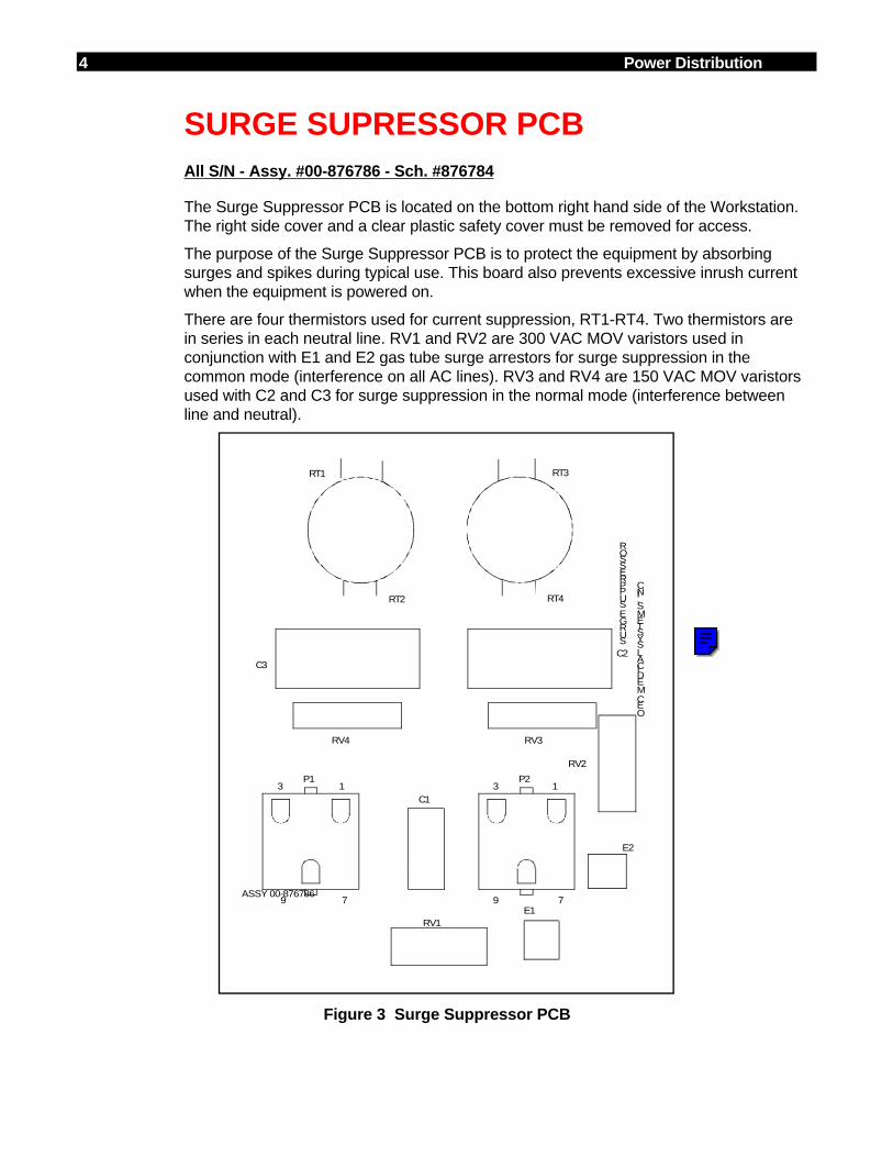
4 Power Distribution
SURGE SUPRESSOR PCBAll S/N - Assy. #00-876786 - Sch. #876784
The Surge Suppressor PCB is located on the bottom right hand side of the Workstation.The right side cover and a clear plastic safety cover must be removed for access.
The purpose of the Surge Suppressor PCB is to protect the equipment by absorbingsurges and spikes during typical use. This board also prevents excessive inrush currentwhen the equipment is powered on.
There are four thermistors used for current suppression, RT1-RT4. Two thermistors arein series in each neutral line. RV1 and RV2 are 300 VAC MOV varistors used inconjunction with E1 and E2 gas tube surge arrestors for surge suppression in thecommon mode (interference on all AC lines). RV3 and RV4 are 150 VAC MOV varistorsused with C2 and C3 for surge suppression in the normal mode (interference betweenline and neutral).
SURGE SUPPRESSOR
OEC MEDICAL SYSTEMS, INC
RV4 RV3
RV2
RV1
79
13
79
13
E2
E1
RT1
RT2
RT3
RT4
P2P1
C3C2
C1
ASSY 00-876786
Figure 3 Surge Suppressor PCB
NOTE:
Click in the blue box to go directly to the Electrical Schematic Diagram for the PCB shown on this page. Click the << button on the Tool Bar to return to this page.
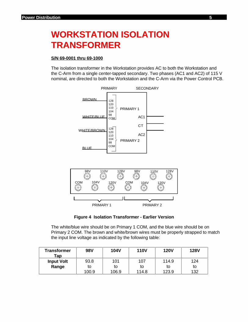
Power Distribution 5
WORKSTATION ISOLATIONTRANSFORMERS/N 69-0001 thru 69-1000
The isolation transformer in the Workstation provides AC to both the Workstation andthe C-Arm from a single center-tapped secondary. Two phases (AC1 and AC2) of 115 Vnominal, are directed to both the Workstation and the C-Arm via the Power Control PCB.
PRIMARY 1
PRIMARY 2
WHITE/BLUE
BLUE
BROWN
WHITE/BROWN
PRIMARY SECONDARY
12812011010498COM
12812011010498COM
AC1
CT
AC2
COM COM
PRIMARY 2
98V 98V110V 110V128V 128V
104V 104V120V 120V
PRIMARY 1
Figure 4 Isolation Transformer - Earlier Version
The white/blue wire should be on Primary 1 COM, and the blue wire should be onPrimary 2 COM. The brown and white/brown wires must be properly strapped to matchthe input line voltage as indicated by the following table:
TransformerTap
98V 104V 110V 120V 128V
Input VoltRange
93.8to
100.9
101to
106.9
107to
114.8
114.9to
123.9
124to
132
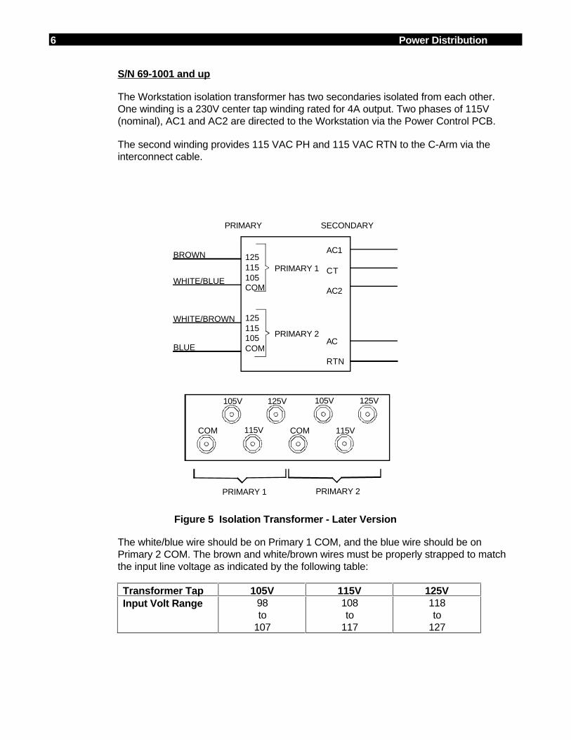
6 Power Distribution
S/N 69-1001 and up
The Workstation isolation transformer has two secondaries isolated from each other.One winding is a 230V center tap winding rated for 4A output. Two phases of 115V(nominal), AC1 and AC2 are directed to the Workstation via the Power Control PCB.
The second winding provides 115 VAC PH and 115 VAC RTN to the C-Arm via theinterconnect cable.
AC1
CT
AC2
AC
RTN
125115105COM
125115105COM
PRIMARY 1
PRIMARY 2
WHITE/BLUE
BLUE
BROWN
WHITE/BROWN
PRIMARY SECONDARY
105V
COM 115V
125V 125V
115V
105V
COM
PRIMARY 1 PRIMARY 2
Figure 5 Isolation Transformer - Later Version
The white/blue wire should be on Primary 1 COM, and the blue wire should be onPrimary 2 COM. The brown and white/brown wires must be properly strapped to matchthe input line voltage as indicated by the following table:
Transformer Tap 105V 115V 125VInput Volt Range 98
to107
108to
117
118to
127

Power Distribution 7
POWER CONTROL PCBS/N 69-0001 thru 69-1000 - Assy. #00-876549 - Sch. #00-876547
The Power Control PCB is located in the bottom of the Workstation on the left hand sideas shown in Figure 2. Access is gained by removing the left side panel and a clearplastic, protective shield.
AC1 and AC2 from the T1 isolation transformer enters at P1 and is used by both theWorkstation and C-Arm. See Figure 4 for details of the isolation transformer windings.
A +12 VDC is created on this board using AC1 through circuit breaker CB1, transformerT1, bridge CR1, and voltage regulator U1. This +12V is sent to the keyswitch on thefront of the Workstation, to K3 and K4 relays on the Power Control PCB, and to thedelay circuit, U2.
When the keyswitch is closed, the +12V (Key_Pwr) is sent to K10 on the Power/MotorRelay PCB located within the C-Arm. This switches Phase 1 AC to Power Supplies PS1(+5V, +15V, -15V) and PS2 (+24V) also located within the C-Arm. The +12V is also sentto activate K1 and K2 on the Power Control PCB. K1 connects AC1 and AC2 to theWorkstation. K2 connects +24V from PS4 to the left and right monitors.
POWER-ON DELAY CIRCUIT
The purpose of the delay circuit is to remove AC from the interconnect cable if it is notplugged into the C-Arm and the Workstation is plugged into the AC wall socket. K3 andK4 relays connect AC1 and AC2 from the Workstation to the C-Arm via the interconnectcable. These two relays are turned on by +12V from U1. This occurs whenever theWorkstation is plugged into an AC outlet and the interconnect cable is plugged into theC-Arm. This facilitates charging the batteries when the system electronics are switchedoff.
The return paths for the coils of K3 and K4 are controlled by the U2 delay circuit. The U2delay circuit is controlled by connections from the interconnect cable.
When the interconnect cable is connected to the C-Arm and the Workstation is pluggedinto a wall outlet, the CNCT ON line is grounded on the C-Arm at the Power/Motor RelayPCB. This forces U2-1 on the Power Control PCB to a logic low. Resistor R2 andcapacitor C3 charge to a logic high in approximately 540 mS. This high is placed on U2-2 and is then cascaded through the rest of the transistor array finally placing a low onU2-13 and U2-12. This low is fed through LOOP2 to the C-Arm and back to the PowerControl PCB through LOOP1, resulting in a low on K3-8 and K4-8. With the +12 Voutput of regulator U1 on K3-1 and K4-1 both of these relays are then energized.
If the interconnect cable is disconnected from the C-Arm while the Workstation remainsconnected to a wall receptacle, the CNCT ON line is no longer grounded through theinterconnect cable. This causes R5 and R1 to pull up U2-1 to a logic high. This, in turncauses the following logic pattern to occur: pin 16 low, pin 15 high, pin 14 low, and pins

8 Power Distribution
12 and 13 remain off. With pins 12 and 13 off, K3 and K4 will de-energize, removing ACpower from the interconnect cable. Pins 6 and 3 of both relays are switched to groundpotential after a 15 - 20 ms. delay.
S/N 69-1001 and up - Assy. #00-878003 - Sch. #00-878001
This version of the Power Control PCB accomodates the two sources of AC from thesecondary of the new isolation transformer. A separate winding (“AC” and “RTN”) on theisolation transformer provides the AC (115 VAC_PH and 115 VAC_RTN) to the C-Arm.This AC is kept separate from that used in the Workstation (“AC1”, “AC2”, and “CT”).See Figure 5 for details of the isolation transformer windings.
WARNING... The AC return (RTN) lines carry a voltage potential of 60 VAC and 80 VDCrelative to ground.
K3 and K4 relays connect 115 VAC_PH and 115 VAC_RTN to the C-Arm via theinterconnect cable. K1 connects AC1 and AC2 to the Workstation. K2 functions thesame, providing +24V to the monitors from power supply PS4. The relays are energizedin the same manner as previously described for the earlier version.
The power-on delay circuit operates exactly as described for the earlier version of thisPCB.
CIRCUIT BREAKERS AND FUSES
CB1 A 0.2 Amp push button breaker, in line with AC to T1 used to provide the +12V forkeypower circuitry.
CB2 A 3 Amp push button breaker, in line with +24V to the right monitor.
CB3 A 3 Amp push button breaker, in line with +24V to the left monitor.
F1 A 2 Amp, 125 V, metric sized, slow-blow fuse, in line with AC to PS4 the +24Vpower supply for the monitors. Contained in a spring-loaded fuse holder with aquarter turn cap (a thin blade screw driver is required to remove cap).
TEST POINTS
TP1 AC from Isolation Transformer T1 (AC2_T1) to C-Arm (AC2_GEN) located incircuit between K3 and K4, typically 115 to 120 VAC.
TP2 AC from Isolation Transformer T1 (AC1_T1) to C-Arm (AC1_GEN) located incircuit between K3 and K4, typically 115 to 120 VAC.

Power Distribution 9
CB1
CB2
CB3
F1
Figure 6 Power Control PCB Assembly Drawing
NOTE: The assembly drawing in Figure 6 can be used for all S/N. Component locations vary onlyslightly between versions.
NOTE
Click in the blue box to go directly to the Electrical Schematic Diagram for the PCB shown on this page. Click the << button on the Tool Bar to return to this page.

10 Power Distribution
WORKSTATION POWER DISTRIBUTIONS/N 69-0001 thru 69-1000
AC1_CART and AC2_CART pass through K1 and leave the Power Control PCB atconnector P4. These AC signals pass thru CB3 (5 Amp reset only breaker) and are thendistributed from terminal block TB2.
AC1_CART provides power to fan B1 and the Workstation power supply PS1 (+5V, -5V,+12V, -12V). AC2_CART provides power for fans B2 and B3 and for the Lenzar hardcopy camera option.
Both phases provide power to a 120/240 VAC outlet strip used for connection ofperipheral equipment such as the VCR and thermal image printer options. The powerstrip is located inside the Workstation and is accessed by removing the rear cover asshown in Figure 7.
The DC outputs of PS1 (+5V, -5V, +12V, -12V) are inputs to the DC Power DistributionPCB, located in the Workstation electronics box (see Figure 7). These voltages are thendistributed throughout the Workstation. PS1 is mounted on the inside of the electronicsbox on the hinged side panel as shown in Figure 7.
PS4 (+24 VDC) is located near the bottom of the Workstation on the left hand side asshown in Figure 2. It provides the left and right monitors with +24 VDC via the PowerControl PCB.
S/N 69-1001 and up
AC1_CART and AC2_CART leave the Power Control PCB at connector P4 and aredistributed by terminal block TB2. Circuit breaker CB3 is in-line between isolationtransformer T1 and the Power Control PCB. In earlier models CB3 was located after thePower Control PCB.
AC1_CART provides power to fan B1 and the Workstation power supply PS1 (+5V, -5V,+12V, -12V). AC2_CART provides power for fans B2 and B3 and the Lenzar hard copycamera option.
AC1_CART and AC2_CART provide power to a 115/230 VAC outlet strip used forconnection of peripheral equipment such as the VCR and thermal image printer options.The power strip is located inside the Workstation and is accessed by removing the rearcover as shown in Figure 7.
The DC outputs of PS1 (+5V, -5V, +12V, -12V) are inputs to the DC Power DistributionPCB, located in the Workstation electronics box. These voltages are then distributedthroughout the Workstation. PS1 is mounted on the inside of the electronics box on thehinged side panel.
NOTE
Click on the yellow box to go directly to the block diagram for this section. Do not use this link to return to a block diagram from this point. Click on the << button in the Tool Bar to return to this point.
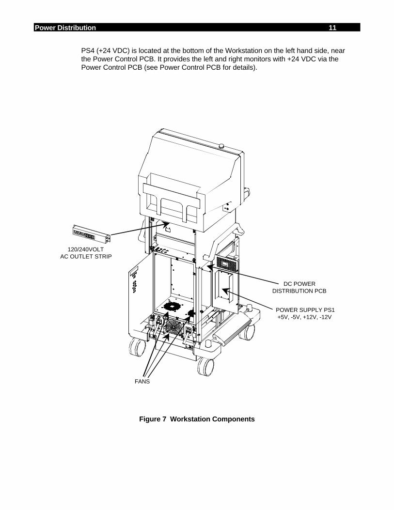
Power Distribution 11
PS4 (+24 VDC) is located at the bottom of the Workstation on the left hand side, nearthe Power Control PCB. It provides the left and right monitors with +24 VDC via thePower Control PCB (see Power Control PCB for details).
DC POWERDISTRIBUTION PCB
POWER SUPPLY PS1+5V, -5V, +12V, -12V
120/240VOLTAC OUTLET STRIP
FANS
Figure 7 Workstation Components

12 Power Distribution
DC POWER DISTRIBUTION PCB
All S/N - Assy. #00-876841 - Sch. #876839
The information for this PCB applies to all system serial numbers. The function of theDC Power Distribution PCB is to distribute the DC outputs from PS1 throughout theWorkstation. It is located inside the Workstation electronics box in the upper rear corner.It is accessed by removing the rear cover, the left side cover, the clear plastic protectiveshield, and opening the side panel of the electronics box. Outputs from PS1 (+5V, -5V,+12V, -12V) are input at P9 and distributed as follows:
P1 - Aux Interface PCB, Video Switching PCB, and Image Processor PCB
P2 - AT Motherboard
P3 - Control Panel Processor PCB, and Contrast/Brightness Control PCB
P4 - Hard Drives
P6 - Floppy Drive
P8 - Elapsed Time Meter
U1 monitors the +5V. If the +5V falls below +4.65V the SYSRST* (System Reset) signalwill go low and reset the AT Motherboard. SYSRST* will stay low until the +5V line risesabove +4.7V. U1 is also active at power up/down. Failure of U1 could be indicated by arecycling of the Workstation boot sequence or lockup of the AT Motherboard duringboot-up.
TEST POINTSTP1 Ground TP2 +5V TP3 +12V TP4 -12V TP5 -5V
CIRCUIT BREAKERSCircuit Breakers 1 thru 9 are all 5 Amp, SPST, 250 VAC, horizontal PCB mounted.
CB1 +5 VDC to AT Motherboard
CB2 +12 VDC to AT Motherboard
CB3 +5 VDC to hard drives
CB4 +12 VDC to hard drives
CB5 +5 VDC to floppy drive and hard drives
CB6 +5 VDC to Control Panel Processor PCB and Contrast/Brightness Control PCB
CB7 +12 VDC to floppy drive and elapsed time meter
CB8 +12 VDC to Control Panel Processor PCB, Contrast/Brightness Control PCB, AuxInterface PCB, Video Switching PCB, and Image Processor PCB
CB9 +5 VDC to Aux Interface PCB, Video Switching PCB, and Image Processor PCB
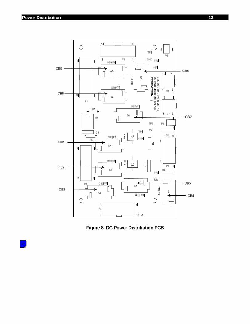
Power Distribution 13
Figure 8 DC Power Distribution PCB
NOTE
Click in the blue box to go directly to the Electrical Schematic Diagram for the PCB shown on this page. Click the << button on the Tool Bar to return to this page.
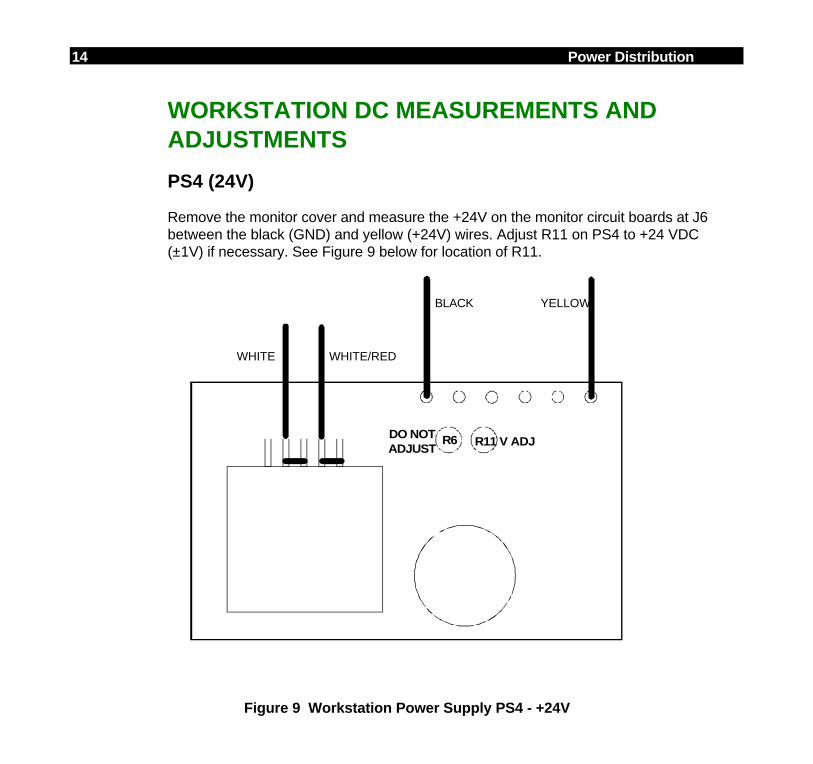
14 Power Distribution
WORKSTATION DC MEASUREMENTS ANDADJUSTMENTS
PS4 (24V)
Remove the monitor cover and measure the +24V on the monitor circuit boards at J6between the black (GND) and yellow (+24V) wires. Adjust R11 on PS4 to +24 VDC(±1V) if necessary. See Figure 9 below for location of R11.
WHITE/REDWHITE
BLACK YELLOW
R11 V ADJR6DO NOTADJUST
Figure 9 Workstation Power Supply PS4 - +24V
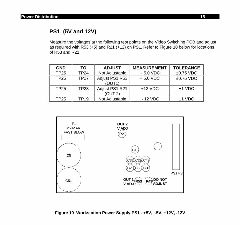
Power Distribution 15
PS1 (5V and 12V)
Measure the voltages at the following test points on the Video Switching PCB and adjustas required with R53 (+5) and R21 (+12) on PS1. Refer to Figure 10 below for locationsof R53 and R21.
GND TO ADJUST MEASUREMENT TOLERANCETP25 TP24 Not Adjustable - 5.0 VDC ±0.75 VDCTP25 TP27 Adjust PS1 R53
(OUT1)+ 5.0 VDC ±0.75 VDC
TP25 TP28 Adjust PS1 R21(OUT 2)
+12 VDC ±1 VDC
TP25 TP19 Not Adjustable - 12 VDC ±1 VDC
F1250V 4A
FAST BLOW
PS1 P3
OUT 1V ADJ
R53 DO NOTADJUST
R43
C28 C30
C32 C29 C42
C31
C18
OUT 2V ADJ
R21
C5
C51
Figure 10 Workstation Power Supply PS1 - +5V, -5V, +12V, -12V

16 Power Distribution
C-ARM POWER DISTRIBUTIONS/N 69-0001 thru 69-1000
AC1_GEN and AC2_GEN leave the Power Control PCB at connector P5, travel thruCB2, a 10 Amp, reset only breaker and then leave the Workstation at J0 over theinterconnect cable. They enter the C-Arm at J1 and are routed to connector P12 of thePower Signal Interface PCB. They are now identified as 120V_PH1 and 120V_PH2.
120V_PH1 leaves the Power/Signal Interface PCB at connector P6 and enters thePower/Motor Relay PCB at connector P7 where it is routed to K10 relay (see Figure 12).K10 relay is activated by the signal KEY_PWR, the +12V from the keyswitch. After120V_PH1 passes thru K10 it is designated as 120V_PH1 SWITCHED. It is thendirected to power supply PS1 (+5V, +15V, -15V) and PS2 (+24V).
120V_PH2 also leaves the Power/Signal Interface PCB at connector P6 and enters thePower/Motor Relay PCB at connector P7 where it is used for C-Arm rotation, elevation,and stator circuitry. See the appropriate section of this service manual for further detailsof these circuits.
Both 120V_PH1 and 120V_PH2 also leave the Power/Signal Interface PCB atconnector P1 and enter the Battery Charger PCB at connector P2 where they areconnected to CR1 to be rectified and used for charging the battery packs.
DS2 is a green lamp located on the power panel assembly and labeled “Charger”. DS2is connected at P6 across Neutral and 120V_PH2 to indicate when AC is present for theBattery Charger PCB.
S/N 69-1001 and up
WARNING... The AC return (RTN) lines carry a voltage potential of 60 VAC and 80 VDCrelative to ground.
The difference in the distribution from that previously discussed is that this AC comesfrom a separate winding on the Workstation isolation transformer. There is no longer a“Neutral” center-tap connection, but rather an “AC return” line that does carry a potential.Also, circuit breaker CB2 is in line between isolation transformer T1 and the PowerControl PCB, whereas in earlier models it was after the Power Control PCB.
115VAC_PH and 115VAC_RTN leave the Power Control PCB at connector P5 and thenleave the Workstation at P1 over the interconnect cable. They enter the C-Arm at J1 andare routed to connector P12 of the Power Signal Interface PCB.
115VAC_PH leaves the Power/Signal Interface PCB at connector P6 and enters thePower/Motor Relay PCB at connector P7 as 115VAC_PH_IN where it is routed to K10relay. K10 relay is activated by the signal KEY_PWR, the +12V from the keyswitch.After 115VAC_PH_IN passes thru K10 it is designated as 115VAC_PH_SW (switched).It is then directed to power supply PS1 (+5V, +15V, and -15V) and PS2 (+24V).
NOTE
Click on a yellow box to go directly to the block diagram for this section. Do not use this link to return to a block diagram from this point. Click on the << button in the Tool Bar to return to this point.
Power Distribution 17
115VAC_PH_SW also leaves the Power/Signal Interface PCB at connector P6 andenters the Power/Motor Relay PCB at connector P7 as 115VAC_PH_MTR where it isused for C-Arm rotation, elevation, and stator circuitry. See the appropriate section ofthis service manual for further details of these circuits.
115VAC _PH also leaves the Power/Signal Interface PCB at connector P1 and entersthe Battery Charger PCB at connector P2 where it is connected to CR1 to be rectifiedand used for charging the battery packs.
DS2 is a green lamp located on the power panel assembly and labeled “Charger”. DS2is connected at P6 across Neutral and 120V_PH2 to indicate when AC is present for theBattery Charger PCB.
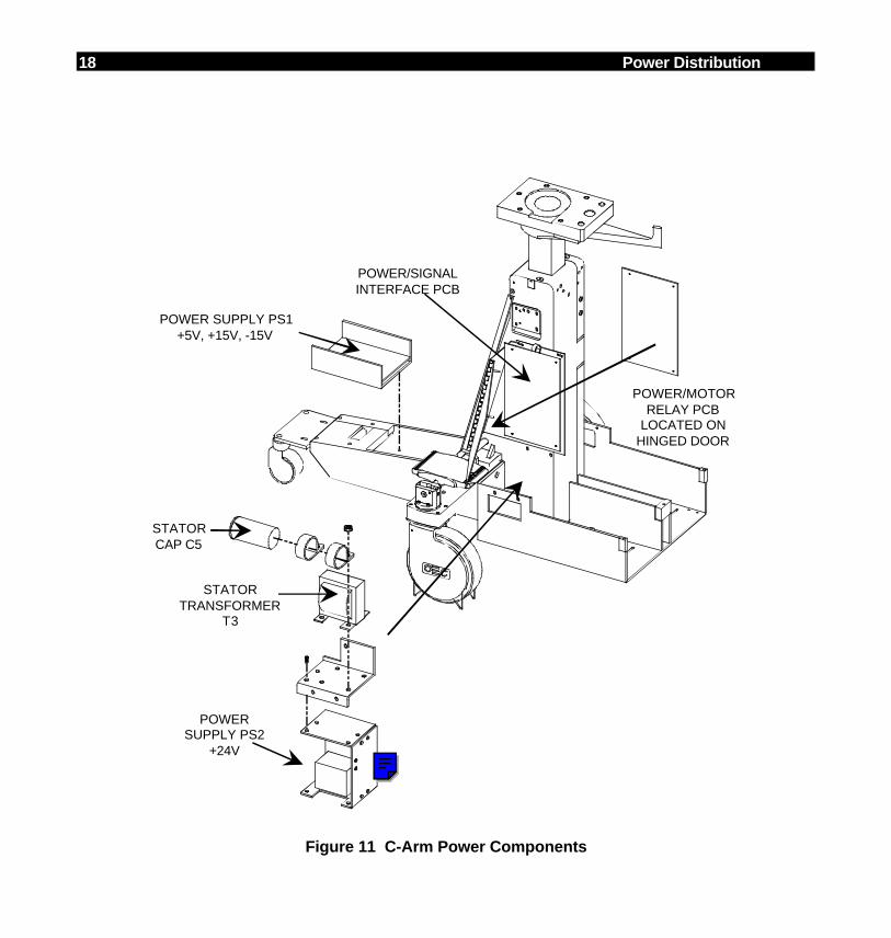
18 Power Distribution
POWER/MOTORRELAY PCB
LOCATED ONHINGED DOOR
POWER/SIGNALINTERFACE PCB
POWER SUPPLY PS1+5V, +15V, -15V
POWER SUPPLY PS2
+24V
STATORTRANSFORMER
T3
STATORCAP C5
Figure 11 C-Arm Power Components
NOTE
Click on the colored square to go directly to the Illustrated Parts Manual. Click on the << button in the Tool Bar to return to this point.
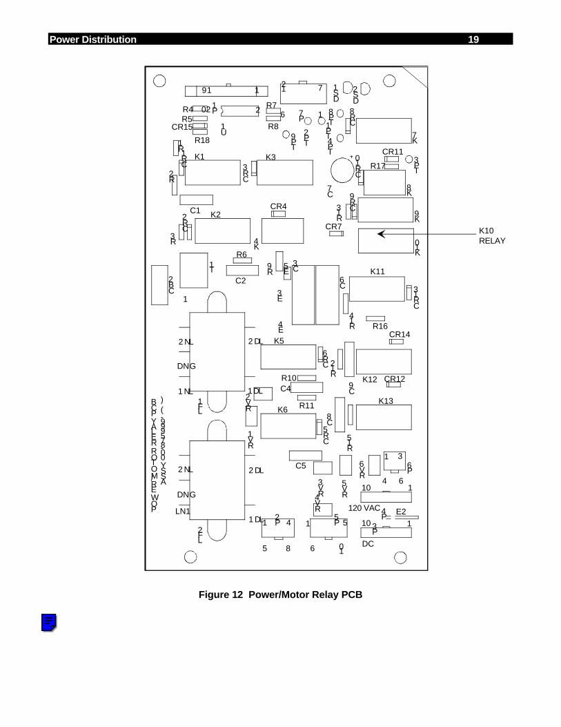
Power Distribution 19
120 VAC
DC
712
6 1
64
31
10
5
6
1
85
41
POWER/MOTOR RELAY PCB
ASSY 00-875999- ( )
110
LN1
GND
LN2 LD2
LD1
LN1
GND
LN2 LD2
LD1
1
110
2
119
20
CR15
RV4
RV1
RV2
RV3
RV5
RV6
P4
LF2
LF1
K10
K1
K2
K3
K5
K6
K11
K12
K13
R9
E5
K4
K8
TP9
TP8
TP4
TP3
TP2 T
P1
DS2
DS1
E2
CB2
C3
C6
E3
E4
C1
C4
C2
C5
C8
C9
T1
C7
CR4
CR14
CR3
CR9
CR8
CR6
CR1
CR10
CR2
CR7
CR13
CR5
CR12
CR11
P6
P2
P5
P7
R6
R14
R16
R2
R10
R11
R15
R12
P3
P1
K7
K9
U1
R18
R17
R5
R13
R3
R1
R4 R7
R8
K10RELAY
Figure 12 Power/Motor Relay PCB
NOTE
Click in the blue box to go directly to the Electrical Schematic Diagram for the PCB shown on this page. Click the << button on the Tool Bar to return to this page.
20 Power Distribution
POWER/SIGNAL INTERFACE PCB
The function of the Power Signal Interface PCB is to serve as an interconnect anddistribution point for AC and DC powers and for communication signals between theTechnique Processor PCB and Control Panel Processor PCB. The communicationssection of this PCB is discussed in the Control section of this manual.
Circuit Breakers
S/N 69-0001 thru 69-1000 - Asy. #00-876003 - Sch. #00-876001
See Figure 13 for circuit breaker locations.
CB1 AC input to PS2 - +24V Power Supply - 2Amp 250 VAC
CB2 AC input to Battery Charger PCB - 5 Amp 250 VAC
CB3 AC input to Battery Charger PCB - 5 Amp 250 VAC
CB4 -15 VDC Output from PS1 - 5 Amp 250 VAC
CB5 +15 VDC Output from PS1 - 5 Amp 250 VAC
CB6 +5 VDC Output from PS1 - 5 Amp 250 VAC
CB7 +24 VDC Output from PS2 - 3 Amp 250 VAC
CB8 AC Output to K10 on Power/Motor Relay PCB for switched AC 3 Amp 250 VAC
CB9 AC output to Power/Motor Relay PCB for rotation, elevation, and stator. 4 Amp250 VAC
Power Distribution 21
S/N 69-1001 and up - Asy. #00-877998 - Sch. #878000
See Figure 14 for circuit breaker locations.
CB1 AC input to PS2 - +24V Power Supply - 2 Amp 250 VAC
CB2 AC input to Battery Charger PCB - 10 Amp 250 VAC
CB3 AC input to Battery Charger PCB - 10 Amp 250 VAC
CB4 -15 VDC Output from PS1 - 5 Amp 250 VAC
CB5 +15 VDC Output from PS1 - 5 Amp 250 VAC
CB6 +5 VDC Output from PS1 - 5 Amp 250 VAC
CB7 +24 VDC Output from PS2 - 3 Amp 250 VAC
CB8 AC Output to K10 on Power/Motor Relay PCB for switched AC 4Amp 250 VAC
CB9 AC output to Power/Motor Relay PCB for rotation, elevation, and stator. 3 Amp250 VAC
CB10 AC return line for PS1 and PS2 - 3 Amp, 250 VAC
CB11 AC return line to Power/Motor Relay PCB for rotation, elevation, and stator 4 Amp250 VAC
CB12 +5 VDC Output to Control Panel Processor - 3 Amp, 250 VAC
NOTE:
The correct Assembly number for this PCB is 00-878000 and the correct Electrical Schematic Diagram number is 00-878998. These numbers are reversed on the displayed manual page. The numbers are linked to the proper drawing, however.
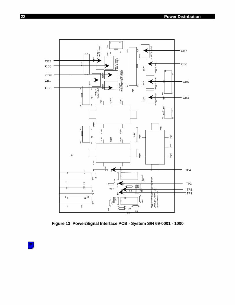
22 Power Distribution
LN1
LD1
GND
LD2
LN2
LN1
LN2
LD1
GND
LD2
LN1
LN2
LD1
GND
LD2
120V PH2
5 AMP +15V
5 AMP -15V
5 AMP +5V
3 AMP +24V
1
12
13
24
1
7
8
14
1
3
4
6
1
5
4
8
120V PH1
2 AMP
PS2 120V1
6
7
1
5
6
10
12
00-876003- ( )
POWER/SIGNAL INTERFACE
5 AMP
5 AMP
1
21
2
1
2 20
19
20
1920
19
120V
MOTORS
PH2
120V PH1
KEY_PWR
OEC MEDICAL INC
B
LF3
LF1
LF2
RT1
RT2
P6
P2
P5
P7
P1
P8
CB1
CB2
CB3
CB4
CB5
CB6
CB7
P9
P10
P11
U1
U2
R1
R2
R3
R4
R5
R6
R7
C1
R8
C2
TP1 T
P2
TP3
TP4
C3
C4
P12
CB8
CB9
R9R10
CB2
CB8
CB9
CB1
CB3
CB7
CB6
CB5
CB4
TP3
TP4
TP2TP1
Figure 13 Power/Signal Interface PCB - System S/N 69-0001 - 1000
NOTE
Click in the blue box to go directly to the Electrical Schematic Diagram for the PCB shown on this page. Click the << button on the Tool Bar to return to this page.
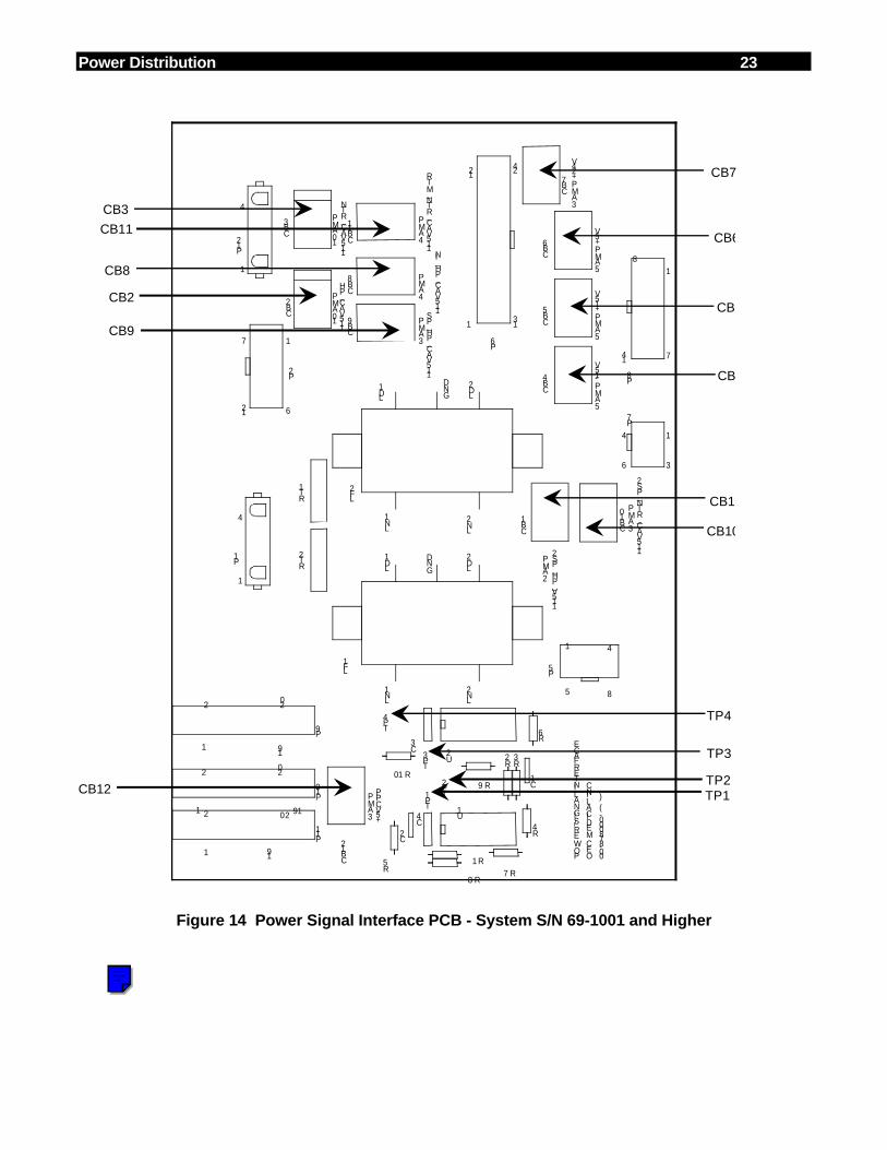
Power Distribution 23
LN1
LD1
GND
LD2
LN2
LN1
LN2
LD1
GND
LD2
5 AMP +15V
5 AMP -15V
5 AMP +5V
3 AMP +24V
1
12
13
24
1
7
8
14
1
3
4
6
1
5
4
8
2 AMP
1
6
7
12
POWER/SIGNAL INTERFACE
1
21
2
1
2 20
19
20
1920
19 OEC MEDICAL INC
3 AMP
10 AMP
10 AMP
4 AMP
115VAC_RTN_MTR
115VAC_PH_IN
3 AMP
+5VCPP
00-878000- ( )
115VAC_PH
115VAC_RTN
115VAC_RTN_PS2
3 AMP
4 AMP
115VAC_PH_PS
115V_PH_PS2
1
4
1
4
RT1
RT2
P6
P2
P5
P7
P8
CB1
CB2
CB3
CB4
CB5
CB6
CB7
P9
P10
P11
U1
U2
R1
R2
R3
R4
R5
R6
R7
C1
R8
C2
TP1 T
P2
TP3
TP4
C3
C4
P12
CB8
CB9
R9R10
LF1
LF2
CB10
CB11
P1
CB12
CB3
CB11
CB8
CB2
CB9
CB7
CB6
CB5
CB4
CB1
CB10
CB12
TP4
TP3
TP2TP1
Figure 14 Power Signal Interface PCB - System S/N 69-1001 and Higher
NOTE
Click in the blue box to go directly to the Electrical Schematic Diagram for the PCB shown on this page. Click the << button on the Tool Bar to return to this page.
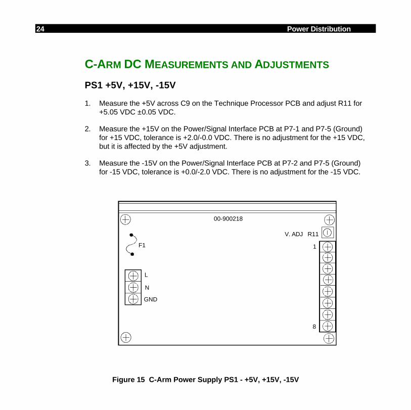
24 Power Distribution
C-ARM DC MEASUREMENTS AND ADJUSTMENTS
PS1 +5V, +15V, -15V
1. Measure the +5V across C9 on the Technique Processor PCB and adjust R11 for+5.05 VDC ±0.05 VDC.
2. Measure the +15V on the Power/Signal Interface PCB at P7-1 and P7-5 (Ground)for +15 VDC, tolerance is +2.0/-0.0 VDC. There is no adjustment for the +15 VDC,but it is affected by the +5V adjustment.
3. Measure the -15V on the Power/Signal Interface PCB at P7-2 and P7-5 (Ground)for -15 VDC, tolerance is +0.0/-2.0 VDC. There is no adjustment for the -15 VDC.
F1
L
N
GND
00-900218
V. ADJ R11
1
8
Figure 15 C-Arm Power Supply PS1 - +5V, +15V, -15V
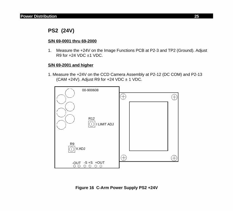
Power Distribution 25
PS2 (24V)
S/N 69-0001 thru 69-2000
1. Measure the +24V on the Image Functions PCB at P2-3 and TP2 (Ground). AdjustR9 for +24 VDC ±1 VDC.
S/N 69-2001 and higher
1. Measure the +24V on the CCD Camera Assembly at P2-12 (DC COM) and P2-13(CAM +24V). Adjust R9 for +24 VDC ± 1 VDC.
00-900608
R12
I LIMIT ADJ
R9V.ADJ
-OUT -S +S +OUT
Figure 16 C-Arm Power Supply PS2 +24V

26 Power Distribution
BATTERY CHARGER PCB
S/N 69-0001 thru 69-1000 - Asy. #00-876644 - Sch. #876643
WARNING... With the keyswitch OFF, AC power is present on the C-Arm when theWorkstation is connected to AC power and the interconnect cable isconnected to the C-Arm.
AC Input Voltage
The Battery Charger PCB receives 120V_PH1 and 120V_PH2 from the Workstation viathe interconnect cable whenever the workstation is plugged into AC and the interconnectcable is connected to the C-Arm.
120V_PH1 and 120V_PH2 pass through the Power/Signal Interface PCB where circuitbreakers CB2 and CB3, line filters LF1 and LF3, and current limiters RT1 and RT2,provide protection and filtering before arriving at the Battery Charger PCB.
The two phases of AC are connected to bridge rectifier CR1. On the Battery ChargerPCB, there is no connection to the minus (-) connnection of CR1, both phases are halfwave rectified. The nominal output of CR1 at the plus (+) connection is approximately160 VDC. As well as being used for charging the batteries, this voltage is scaled downby R7 and sent back to the Analog Interface PCB as line voltage sense (LVOLTSEN).
Low Voltage Power Supply
120V_PH1 and Neutral are also connected to transformer T1 to drive a low voltagepower supply to provide +12V and -12V for use only on the Battery Charger PCB topower the circuitry so that battery charging can occur while the system is off. T1 drivesrectifier VR3 which in turn provides power to be regulated to + 12SEP (separate) and -12SEP by VR1 and VR2 respectively.
Regulation
A boost type switching regulator is powered from the DC voltage output of CR1. Theregulator is comprised of transistor Q1, inductor L2 located on the generator controllerassembly (connected at P1), output filter capacitors C10, C11 and L1. Q1 is turned offand on by the pulse width modulator in voltage regulator U2. The oscillation frequency ofU2 is 20 KHz. and is set by R23 and C19. Voltage feedback to U2 is provided by voltagedivider R6, R9 and R10. Current sense resistor R1 provides an indication of theinstantaneous current through FET Q1 to PWM U2 which removes the drive from thebase of Q1 on a pulse-by-pulse basis for current limit control. The basic idea of thiscircuit is to charge up the inductor L2 and then collapse the field and direct the boostedvoltage ( 225V - 235V) thru CR2 to the output fuse F1 (located on the generatorcontroller assembly) and the battery packs.
NOTE
Click on the yellow box to go directly to the block diagram for this section. Do not use this link to return to a block diagram from this point. Click on the << button in the Tool Bar to return to any starting point.

Power Distribution 27
Current Sensing
Charger current is sensed in the output line by T2. One side of T2 is tied to an ideal orzero drop diode, comprised of U4, CR8, Q9, and associated circuitry. The other side isconnected to current to voltage converter U4. The output of U4 goes to U7 which drivesDS2, a yellow bar graph to indicate charger current output with a scale from 25 to 625milliamps. When the output load current gets above 500 mA, comparator U5 outputswitches high, turning Q7 on, and placing R26 in parallel with the series combination ofR9 and R10, changing the feedback divider such that the output voltage goes up byabout 12 VDC. This puts the charger in “High Charge Mode”.
The signal, HICHGMOD (high charge mode), is in an input from kV control circuitry onthe X-ray Regulator PCB that can also put the charger into high charge mode.“HICHGMOD” goes high whenever the measured KVP is above 30 KVP. CHGISEN(charger current sense) is sent to the Analog Interface PCB where charger activity canbe monitored.
Voltage Sensing
The charging voltage bargraph indicator, U6, is driven by the VOLTAGE SENSE linewhich is adjusted by the combination of R11, R28, R29, and R32 (potentiometer). Thered bargraph indicator DS1, reads in 10 linear steps from 160 VDC to 250 VDC.
The Battery Charger output voltage is also sensed on the Generator Driver PCB at theresistor network of R11 and R10. This signal, “+200VSEN”, is used in the pre-chargecycle (see Boot Sequence section of this manual). It is also used to monitor the batterycharger status.
Overvoltage Protection
To guard against battery damage and/or venting, an overvoltage protection circuit isprovided. If the last segment (250V) of the voltage bargraph indicator lights, Q8 is turnedon, U1 output is set low, turning Q6 ON. This results in both activating the “shutdown”control of the PWM chip and shunting the drive to Q1 to ground, resulting in chargershutdown.
The charger can also be disabled by the Technique Processor PCB via PIO U27-18 onthe Analog Interface PCB, this happens during the boot sequence to check for thepresence and condition of the batteries and during a FILM exposure. A logic high assertsCharger Disable and a logic low resets the disabled condition.
Under Voltage Protection
A low voltage cutout circuit is provided by Q10 and Q2 to prevent over-current conditionsin the event the battery is discharged below 160 VDC. If biasing for Q10 is lost by theoutput line dropping near 160 VDC, Q2 is turned off and power from CR1 cannot get toL2. With the Battery Charger in the “shut down” condition, the charge in the batteries isslowly restored by a 5-20 mA current limited trickle charger comprised of C26, CR9, and

28 Power Distribution
CR10. When the battery voltage reaches approximately 160 VDC, Q2 turns on againand the charging of the batteries proceeds as normal.
Test Points
TP1 Volt Feedback - feedback voltage from charger output adjust circuitry to U2, pulsewidth modulator IC.
TP2 Volt Sense - voltage from voltage display adjust circuitry to U6, driver for DS1,voltage bar graph indicator. The charger output voltage is monitored by theAnalog Interface PCB via the “+200VSEN” line on the Generator Driver PCB.
TP3 Current Sense - voltage from current sensing circuitry to Analog InterfacePCB/Technique Processor PCB to give indication of battery charger current.
Battery Charger Output Fuse F1
The Battery Charger output fuse is located on the generator controller assembly asindicated in Figure 20. It is a 3 Amp, 250 VDC, Slo-Blow fuse contained in a spring-loaded holder with a removable cap. The fuse can be accessed by removing the rearcover of the C-Arm.
WARNING... High DC voltages are present at fuse F1 and circuit breaker CB1. Usecaution when making voltage measurements on these components.
Circuit Breaker CB1
CB1 is a 30 Amp switch, circuit breaker that disconnects the positive and negative sidesof the battery packs from other circuitry. It is located on the right side of the chassis justinside from the wheel (see Figure 20). The switch lever is accessible through a hole inthe chassis. No covers need to be removed to operate the switch.
Battery Charger Output Adjustment
1. Connect a DVM from J1-1 to chassis ground.
2. Adjust R10 for 220 Volts on the DVM.
3. Adjust R32 until the 220 Volt segment on DS1 goes off and the 210 Volt segmentlights.
4. Adjust R32 until the 210 Volt segment goes off and the 220 Volt segment just lights.
5. Adjust R10 for 225 Volts on the DVM

Power Distribution 29
Battery Charger Error Messages
RECHARGE NEEDED - ALLOW 24 HOURS - PRESS ANY KEY TO CONTINUE
This message is displayed during boot-up if the system has not been turned for 6months. If 6 months have past since the system has been plugged in and turned on, letthe system run without making X-rays for 24 hours to allow the batteries to recharge andthe image tube to de-gas. This error may also be displayed after installing a copy of thebackup generator software. In this case, press any key on the control panel and continueuse as normal.
WARM-UP NEEDED - ALLOW 4 HOURS - PRESS ANY KEY TO CONTINUE
This message is displayed during boot-up if the system has not been turned on for 2months. If 2 months have past since the system has been plugged in and turned on, letthe system run without making X-rays for 4 hours to allow the batteries to recharge andthe image tube to de-gas. This error may also be displayed after installing a copy of thebackup generator software. In this case, press any key on the control panel and continueas normal.
BATTERY DISCONNECTED
This message is displayed during boot-up if the software thinks the batteries aredisconnected. This will occur when all but one of the arrows are lit on the control paneldisplay. This is checked by disabling the battery charger, waiting for 2 seconds, andreading the +200V sense line. If 180 Volts or less is read, the software issues ashutdown command and displays this message. If the batteries are disconnected or CB1is open, the error “Pre-charge Fail” may be displayed instead of “BatteriesDisconnected”.
CHARGER FAILED
This message is displayed if the software senses that the battery voltage is less than225 volts and the charger output current is less than 1.0 Amp. The software check forcharger failure runs in the background all the time except during X-rays.
70% CHARGE
This message is displayed if the software thinks that the charge capacity of the batterieshas been depleted to 70% or less. The 70% charge message is displayed intermittentlyon the control panel display and does not affect system operation.
50% CHARGE
This message is displayed if the software thinks that the charge capacity of the batterieshas been depleted to 50% or less. The 50% charge message is displayed intermittentlyon the control panel display. System operation in fluoro mode is allowed but filmexposures are suspended until the calculated charge of the batteries rises above 50%.
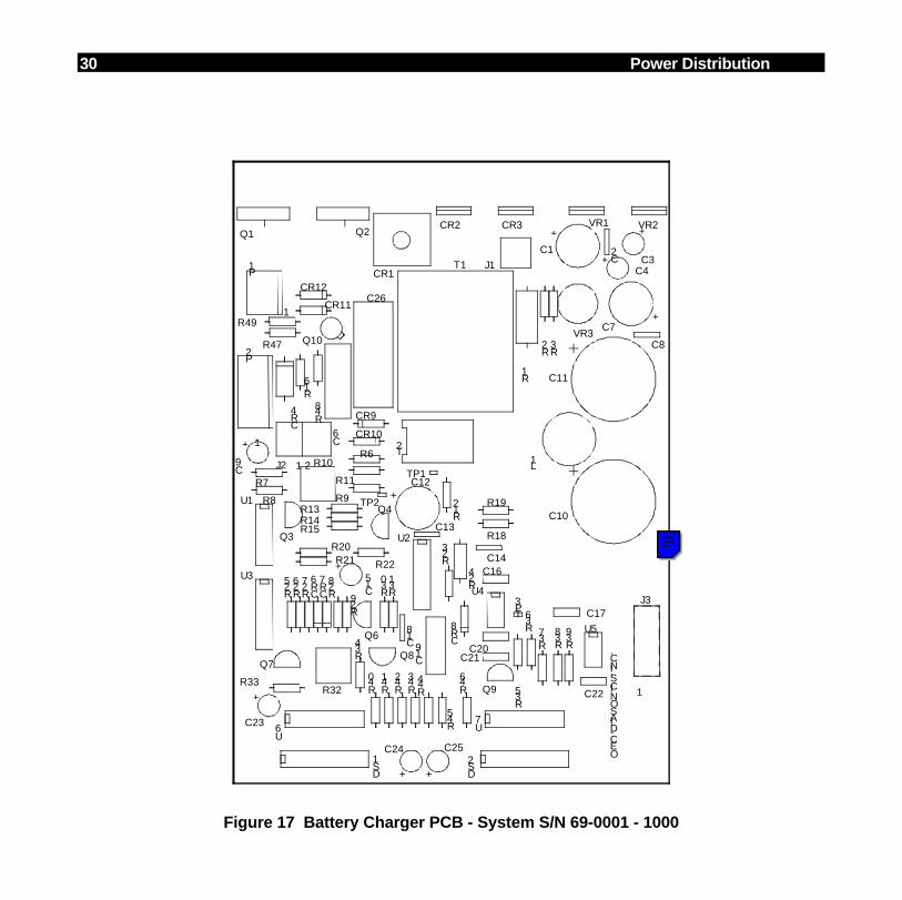
30 Power Distribution
OEC-DIASONICS,INC.
J3
1 2
1
1
1
VR3
VR2VR1CR2 CR3
CR1
T2
T1
U6 U
7
DS1
DS2
U5
U4
U3
U1
U2
TP3
TP1
TP2
R30
R45
R37
R42
R34
R41
R40
R43
R44 R
46
R21R20
R31
R23
R39
R38
R26
R22
R35
R18
R25
R27
R19
R36
R28
R29
R9
R6
R11
R2
R8
R7
R15R14R13
R12
R33
C24 C25
C23
C19
C18
C15
C10
C11
C14
C9
C3C2
C4
C8
C13
R1
R24
R10
R32
CR8
CR6
CR7
L1
C22
C21C20
C16
C17
C12
C7
C1
P2
P1
Q8
Q3
Q1 Q2
R16
R3
CR4
C6
J2
J1
Q4
Q6
Q7
Q9
CR9
CR10
CR11
R47
R48
R49
Q10
C26CR12
Figure 17 Battery Charger PCB - System S/N 69-0001 - 1000
NOTE
Click on the blue box to go directly to the Electrical Schematic Diagram for the PCB shown on this page. Click the << button on the Tool Bar to return to this page.
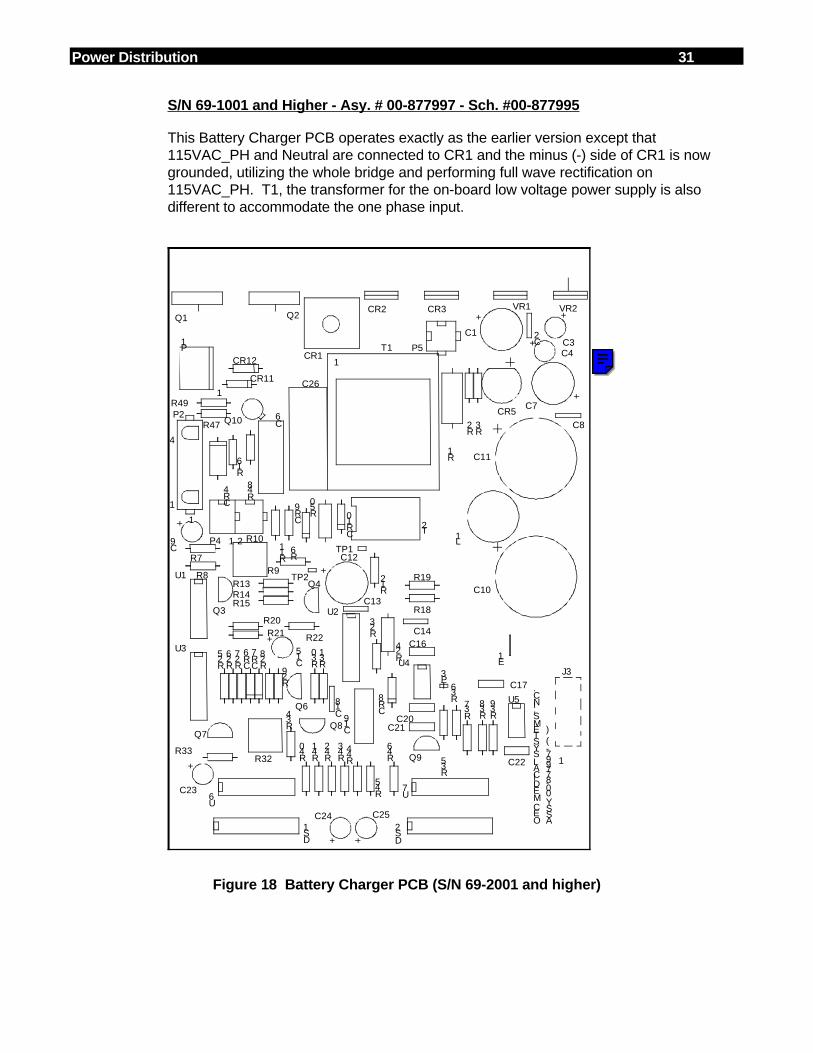
Power Distribution 31
S/N 69-1001 and Higher - Asy. # 00-877997 - Sch. #00-877995
This Battery Charger PCB operates exactly as the earlier version except that115VAC_PH and Neutral are connected to CR1 and the minus (-) side of CR1 is nowgrounded, utilizing the whole bridge and performing full wave rectification on115VAC_PH. T1, the transformer for the on-board low voltage power supply is alsodifferent to accommodate the one phase input.
J3
1 2
1
1
1
OEC MEDICAL SYSTEMS, INC.
ASSY 00-877997- ( )
1
1
4
CR5
VR2VR1CR2 CR3
CR1
T2
T1
U6 U
7
DS1
DS2
U5
U4
U3
U1
U2
TP3
TP1
TP2
R30
R45
R37
R42
R34
R41
R40
R43
R44 R
46
R21R20
R31
R23
R39
R38
R26
R22
R35
R18
R25
R27
R19
R36
R28
R29
R9
R6
R11
R2
R8
R7
R15R14R13
R12
R33
C24 C25
C23
C19
C18
C15
C10
C11
C14
C9
C3C2
C4
C8
C13
R1
R24
R10
R32
CR8
CR6
CR7
L1
C22
C21C20
C16
C17
C12
C7
C1
P2
P1
Q8
Q3
Q1 Q2
R16
R3
CR4
C6
P4
P5
Q4
Q6
Q7
Q9
CR9
CR10
CR11
R47
R48
R49
Q10
C26
CR12
E1
R50
Figure 18 Battery Charger PCB (S/N 69-2001 and higher)
NOTE
Click on the blue box to go directly to the Electrical Schematic Diagram for the PCB shown on this page. Click the << button on the Tool Bar to return to this page.
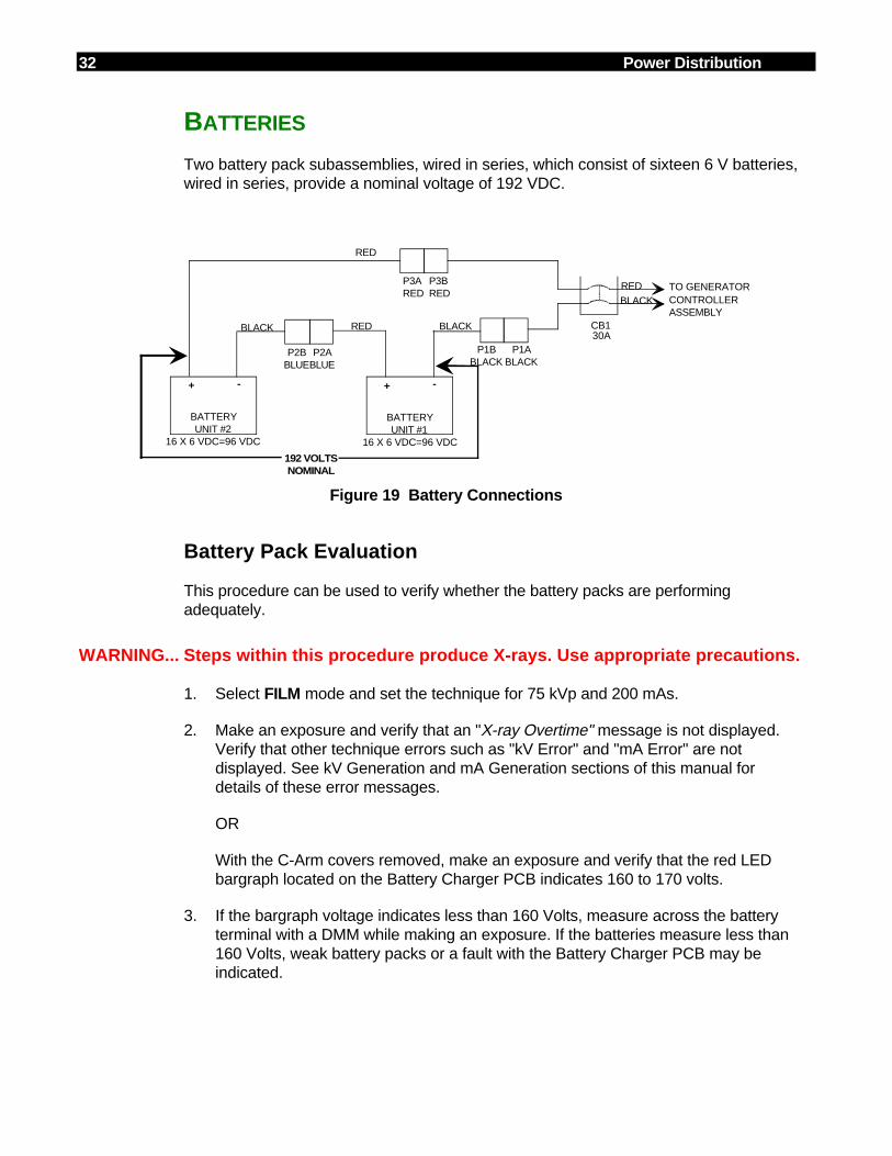
32 Power Distribution
BATTERIES
Two battery pack subassemblies, wired in series, which consist of sixteen 6 V batteries,wired in series, provide a nominal voltage of 192 VDC.
30ACB1
P3BRED
P3ARED
P1ABLACK
P1BBLACK
P2ABLUE
P2BBLUE
+ -+ -
REDBLACK
BLACKREDBLACK
RED
TO GENERATORCONTROLLERASSEMBLY
BATTERYUNIT #2
16 X 6 VDC=96 VDC
BATTERYUNIT #1
16 X 6 VDC=96 VDC
192 VOLTSNOMINAL
Figure 19 Battery Connections
Battery Pack Evaluation
This procedure can be used to verify whether the battery packs are performingadequately.
WARNING... Steps within this procedure produce X-rays. Use appropriate precautions.
1. Select FILM mode and set the technique for 75 kVp and 200 mAs.
2. Make an exposure and verify that an "X-ray Overtime" message is not displayed.Verify that other technique errors such as "kV Error" and "mA Error" are notdisplayed. See kV Generation and mA Generation sections of this manual fordetails of these error messages.
OR
With the C-Arm covers removed, make an exposure and verify that the red LEDbargraph located on the Battery Charger PCB indicates 160 to 170 volts.
3. If the bargraph voltage indicates less than 160 Volts, measure across the batteryterminal with a DMM while making an exposure. If the batteries measure less than160 Volts, weak battery packs or a fault with the Battery Charger PCB may beindicated.

Power Distribution 33
Battery Charger Evaluation
NORMAL CHARGE MODE
WARNING... Dangerous voltages are present when the covers are removed. Observe allsafety precautions.
S/N 69-0001 thru 69-1000
1. Remove the Mobile C-Arm covers and connect a Digital Multimeter to the batteries(set to read DC).
2. Measure J1-1 on the Battery Charger PCB and verify a charging voltage of 225VDC. The voltage bargraph indicator on the Battery Charger PCB Should alsoindicate approximately 220 VDC.
NOTE: If the battery charge is complete, an indication of less than 200 mA is normal
3. The Current bargraph indicator should read less than 450 mA.
S/N 69-1001 and up
Measure at J5-1 on the Battery Charger PCB when performing step 2.
HIGH CHARGE MODE
WARNING... Dangerous voltages are present when the covers are removed. Observe allsafety precautions.
S/N 69-0001 thru 69-1000
1. Remove the Mobile C-Arm covers and connect a Digital Multimeter to the batteries(set to read DC).
2. Select FLUORO MANUAL mode and observe the voltage bargraph indicator whiletaking a 60 kVp @ 1 mA exposure . Verify that approximately 235 VDC is indicated.
3. Measure J1-1 on the Battery Charger PCB and verify a charging voltage ofapproximately 235 VDC.
4. Verify the current bargraph indicator displays a charging current greater than 450mA.

34 Power Distribution
S/N 69-1001 and up
1. Measure at J5-1 on the Battery Charger PCB when performing step 3.
Battery Pack Replacement
WARNING... The batteries are capable of delivering high currents at high voltages andshould be considered fully charged at all times. Remove jewelry such asrings and watches when working around dangerous voltages.
Refer to Figure 20 for component locations.
1. Verify that the Workstation keyswitch is turned to the OFF position and the ACpower plug is disconnected from the wall receptacle.
2. Remove the Rear Handle Cover Assembly by removing 3 screws located behindthe assembly door and one screw on each side.
3. Remove the Front Cover by removing 2 screws near the top of the vertical shaft.
4. Remove the Right Front Cover by removing the 3 screws securing the cover to theMobile C-Arm.
CAUTION! Do not turn CB1 to the OFF position unless the AC power cord has beenunplugged.
5. Turn circuit breaker CB1 to the OFF position.
6. Cut the cable tie that secures the wiring near CB1 and unplug the batteryconnectors.
7. Remove the spacer from the top of each battery pack.
8. Lift the battery pack straight up and then pull the pack straight out.
NOTE: When installing batteries, reconnect battery connectors black to black, red to red, andblue to blue. Refer to Figure 19. Reset CB1 after the battery connections are made bymoving the switch position to ON.

Power Distribution 35
BATTERYPACKS CB1
BATTERYRETAINERS
BATTERY CHARGEROUTPUT FUSE F1
Figure 20 - C-Arm Battery Pack Replacement (Location of F1 and CB1)
NOTE
Click on the top colored box to go directly to the Illustrated Parts Manual for systems bearing serial numbers 69-001 thru 69-999. Click on the bottom colored box to go directly to the Illustrated Parts Manual for systems bearing serial numbers 69-1000 and higher. Click the << button on the Tool Bar to return to this point.
C-ARM CONTROL
OVERVIEWThis section describes how the following circuit boards and components controlthe C-Arm.
• Technique Processor PCB
• Analog Interface PCB
• Control Panel Processor PCB
• Control Panel Processor I/O PCB
The Technique Processor PCB is the controlling circuit board and the AnalogInterface PCB is the slave. The Control Panel Processor PCB serves as an input/ display liaison for the two control panels and vacuum fluorescent displays(VFD) used by the operator of the system.
When a switch closure is made at either of the two control panels, it is encodedby the Control Panel Processor which sends this information to the TechniqueProcessor via a serial link. The Technique Processor responds to this, sendingthe data back to the Control Panel Processor to update the VFD and/or turn onthe associated LED. The Technique Processor also communicates over a digitalbus to the Analog Interface PCB. The Tecnnique Processor PCB alsocommunicates with the Workstation via RS232 serial communications.
The information given in this section is most easily understood while refering tothe following schematics. Use the correct interconnect diagrams and circuitboard schematics for your system as indicated by the S/N.
• • Control Panel Processor PCB
Schematic # 00-875601 - System S/N 69-0001 thru 69-2000Schematic # 00-878486 - System S/N 69-2001 and up
• • Control Panel Processor I/O PCB
Schematic # 00-878489 - System S/N 69-2001 and up
• • Technique Processor PCB
Schematic # 00-876735 - System S/N 69-0001 thru 69-1000Schematic # 00-877742 - System S/N 69-1001 and up
• • Analog Interface PCB - Schematic # 00-876738 - All S/N
2 C-Arm Control
• • Mainframe Motherboard
Schematic # 00-875539 - System S/N 69-0001 thru 69-2000Schematic # 00-878396 - System S/N 69-2001 and up
• • C-Arm Interconnect Diagram
Schematic # 00-875500 - System S/N 69-0001 thru 69-1000Schematic # 00-877972 - System S/N 69-1001 thru 69-2000Schematic # 00-878376 - System S/N 69-2001 and up
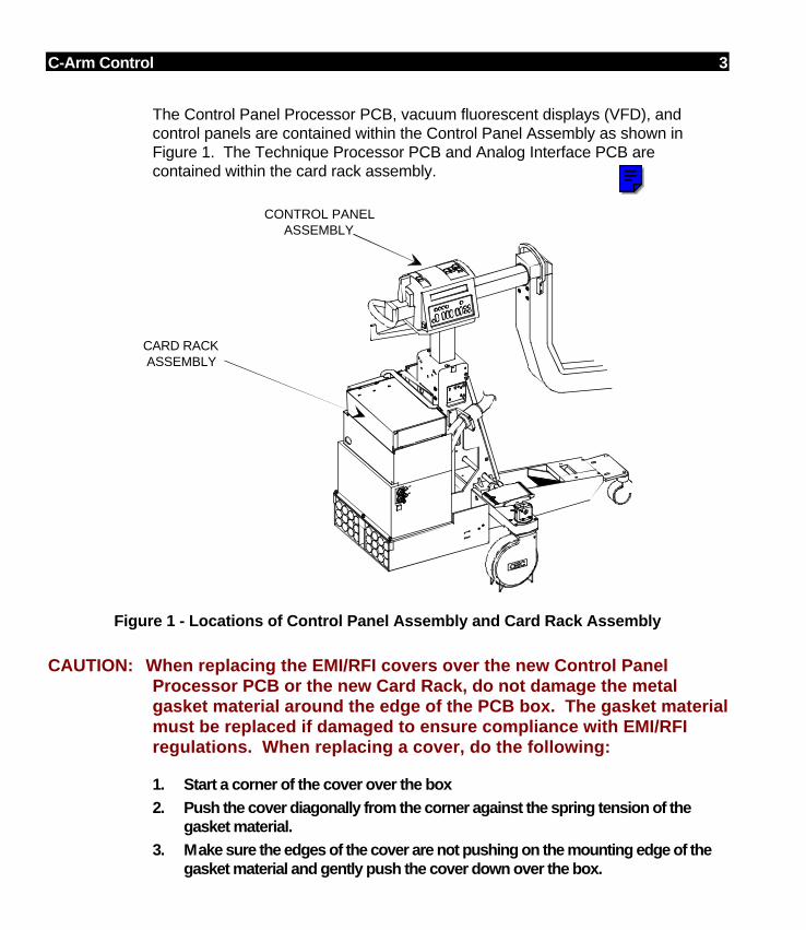
C-Arm Control 3
The Control Panel Processor PCB, vacuum fluorescent displays (VFD), andcontrol panels are contained within the Control Panel Assembly as shown inFigure 1. The Technique Processor PCB and Analog Interface PCB arecontained within the card rack assembly.
CARD RACKASSEMBLY
CONTROL PANELASSEMBLY
Figure 1 - Locations of Control Panel Assembly and Card Rack Assembly
CAUTION: When replacing the EMI/RFI covers over the new Control PanelProcessor PCB or the new Card Rack, do not damage the metalgasket material around the edge of the PCB box. The gasket materialmust be replaced if damaged to ensure compliance with EMI/RFIregulations. When replacing a cover, do the following:
1. Start a corner of the cover over the box2. Push the cover diagonally from the corner against the spring tension of the
gasket material.3. Make sure the edges of the cover are not pushing on the mounting edge of the
gasket material and gently push the cover down over the box.
NOTE
Click on the top colored box to go directly to the Illustrated Parts Manual for systems bearing serial numbers 69-001 thru 69-999. Click on the top colored box to go directly to the Illustrated Parts Manual for systems bearing serial numbers 69-1000 and higher. Click the << button on the TOOL Bar to return to this point.
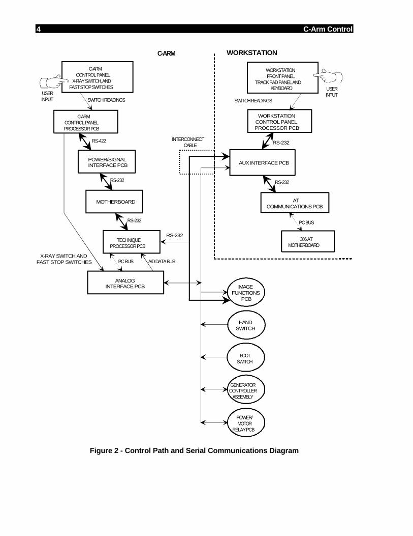
4 C-Arm Control
TECHNIQUE PROCESSOR PCB
USERINPUT SWITCH READINGS
ANALOGINTERFACE PCB
PC BUS
GENERATORCONTROLLER
ASSEMBLY
FOOTSWITCH
HANDSWITCH
A/D DATA BUS
POWER/MOTOR
RELAY PCB
X-RAY SWITCH ANDFAST STOP SWITCHES
MOTHERBOARD
USERINPUT
SWITCH READINGS
C-ARM CONTROL PANEL
X-RAY SWITCH, ANDFAST STOP SWITCHES
C-ARMCONTROL PANELPROCESSOR PCB
WORKSTATIONFRONT PANEL
TRACK PAD PANEL ANDKEYBOARD
WORKSTATIONCONTROL PANELPROCESSOR PCB
AUX INTERFACE PCB
386 ATMOTHERBOARD
AT COMMUNICATIONS PCB
IMAGEFUNCTIONS
PCB
PC BUS
RS-422
RS-232
RS-232
RS-232
RS-232
RS-232
C-ARM WORKSTATION
INTERCONNECTCABLE
POWER/SIGNALINTERFACE PCB
Figure 2 - Control Path and Serial Communications Diagram
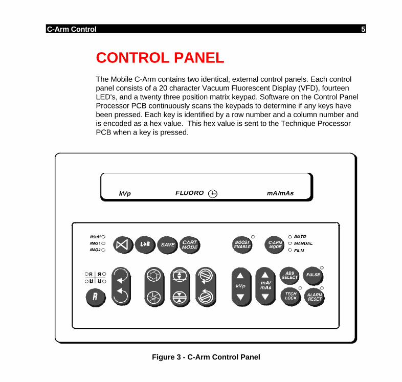
C-Arm Control 5
CONTROL PANELThe Mobile C-Arm contains two identical, external control panels. Each controlpanel consists of a 20 character Vacuum Fluorescent Display (VFD), fourteenLED's, and a twenty three position matrix keypad. Software on the Control PanelProcessor PCB continuously scans the keypads to determine if any keys havebeen pressed. Each key is identified by a row number and a column number andis encoded as a hex value. This hex value is sent to the Technique ProcessorPCB when a key is pressed.
mA/mAsFLUOROkVp
Figure 3 - C-Arm Control Panel

6 C-Arm Control
CONTROL PANEL PROCESSOR PCB
OVERVIEW
S/N 69-0001 thru 69-2000 - Assy. #00-875603 - Sch. #00-875601
S/N 62-0001/69-2001 and higher - Assy. #00-878488 - Sch. #00-878486
There are 2 versions of this circuit board (see Figures 6 and 7). The functionalityof the two boards is the same. The circuitry on the earlier version (Assy. #00-875603, see Figure 6 ) was divided to form two new circuit boards; the newControl Panel Processor PCB (assy. #00-878488, see Figure7 ) and the ControlPanel Processor I/O PCB (see Figure 8 ).
The circuitry on the new Control Panel Processor PCB consists of the activecircuitry that required EMI/RFI shielding. The circuitry on the Control PanelProcessor I/O PCB consists of cabling connectors and passive components thatdid not need shielding.
The theory of operation that follows applies to both Control Panel ProcessorPCBs, however, component designators are different. Designators betweenbrackets, [ ] refer to the newer boards.
MICROPROCESSOR SECTION
U5 [U11] is an 80C196KC microcontroller running at 10 MHz Y1 is a10 MHzcrystal oscillator. DS1 indicates that EPROM code is being executed blinking attwo different rates: 200ms if waiting for communcations to be established, and530ms after communications have been established.
U14 [U3] and associated circuitry create an external watch-dog circuit that mustsee a falling edge every 150 ms or less. If the falling edge is not detected at pin 7it will time out and generate a reset to both the micro-controller and PAL U7 [U8].
The Reset* signal goes low for 250 ms to generate a reset. U14 [U3] alsomonitors the power supply voltage. It will hold the RESET output pin lowwhenever VCC is below 4.62 volts (typically). A reset can also be generated byMRESET* at pin 1 of U14 [U3] from the Technique Processor.
LS1 [on Control Panel I/O PCB] is a tone generator driven by U5 [U11] throughQ1 to indicate when X-rays are being produced and to indicate oyher keyclosures.E4 - configuration jumpers, currently not used.
NOTE
Click on the yellow box to go directly to the block diagram for this section. The top box is linked to the drawing covering the lower serial numbers, while the bottom box is linked to the drawing covering the higher serial numbers. Do not use this link to return to a block diagram from this point. Click on the << button in the Tool Bar to return to any starting point.
C-Arm Control 7
MEMORY AND ADDRESSING
U2 [U9] is the boot PROM for microprocessor U5 [U11]. When microprocessorU5 [U11] boots it will read and execute the code contained in boot PROM U2[U9] and then wait for further instructions from the Technique Processor PCB viaserial communication.
Port 3 of microprocessor U5 [U11] is a multiplexed address/data bus. Theaddress is driven on the bus on the rising edge of ALE (address latch enable,U5-62 [U11-62]). U9 [U12] latches the low address byte on the falling edge ofALE. Port 4 is used only for the high address byte by tying U5-64 [U11-64](BUSWIDTH) low.U7 [U8] and U3 [U1] are used for chip select signals for address decoding.
U4 [10] is 32Kx8 static RAM used for storage of VFD messages.
U1 [U16], is currently not installed.
CONTROLS AND DISPLAY INTERFACE
U13 [U14] is the keyboard input latch. U12 [U7] is the keyboard output latch.These devices comprise the row/column decoding.
U6 [U13] is a data bus buffer added to prevent a failure in a VFD from hangingup the micro-controller's bus.
U16 [U5] & U11 [U6] are octal latches used to sink the LED currents. Writing a"0" to the appropriate bit turns on an LED.
P1 & P2 connect to the left and right control panels respectively for the left andright keypad matrices, VFDs, and LEDs. [J1 and J2 connect to the ControlPanel Processor I/O PCB and distribute all signals to and from the new ControlPanel Processor PCB].
SERIAL COMMUNICATIONS
Refer to System Communications in this section for details of serialcommunications.
FAST STOP SWITCHES
The signals EMEROFF_HI and EMEROFF_LO are wired in series through P6and P7 of the Control Panel Processor PCB. Their source and destination arefrom the Power Motor Relay PCB, via the Power Signal Interface PCB and theMainframe Motherboard. When pressed these switches open the +24V interlockcircuit, prohibiting C-Arm elevation, L-Arm rotation, and the production of X-rays.See the Interlocks/Stator section of this manual for details of this circuit.
8 C-Arm Control
X-RAY SWITCH
The signals X-RAY_SWITCH and SECURITY connect at P5 on the ControlPanel Processor PCB and are sent to the Analog Interface PCB via thePower/Signal Interface PCB and Mainframe Motherboard. See the X-rayOn/Disable section in this manual for details of these signals.
X-RAY_LAMP also connects at P5 and is sourced from the Power Motor RelayPCB. This signal provides the return path for the lamp in the X-ray switch and isderived through U1 from the signal X-RAY_ON which is the enabling signal forX-ray production. X-RAY_LAMP also goes to the Workstation to drive the LEDarray above the monitors.
On systems with serial number 69-2001 and higher, X-RAY_SWITCH,SECURITY, and X-RAY_LAMP pass from the X-ray switch, through the newColumn I/O PCB directly to the Power/Signal Interface PCB. See the X-rayOn/Disable section for details of these signals.
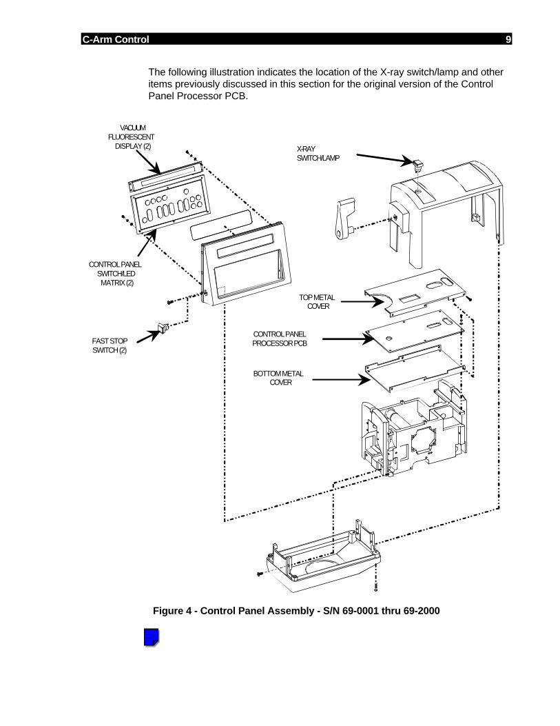
C-Arm Control 9
The following illustration indicates the location of the X-ray switch/lamp and otheritems previously discussed in this section for the original version of the ControlPanel Processor PCB.
CONTROL PANELPROCESSOR PCB
TOP METALCOVER
BOTTOM METALCOVER
X-RAYSWITCH/LAMP
FAST STOPSWITCH (2)
CONTROL PANELSWITCH/LEDMATRIX (2)
VACUUMFLUORESCENT
DISPLAY (2)
Figure 4 - Control Panel Assembly - S/N 69-0001 thru 69-2000
NOTE
Click on the top colored box to go directly to the Illustrated Parts Manual for systems bearing serial numbers 69-001 thru 69-999. Click on the top colored box to go directly to the Illustrated Parts Manual for systems bearing serial numbers 69-1000 and higher. Click the << button on the Tool Bar to return to this point.
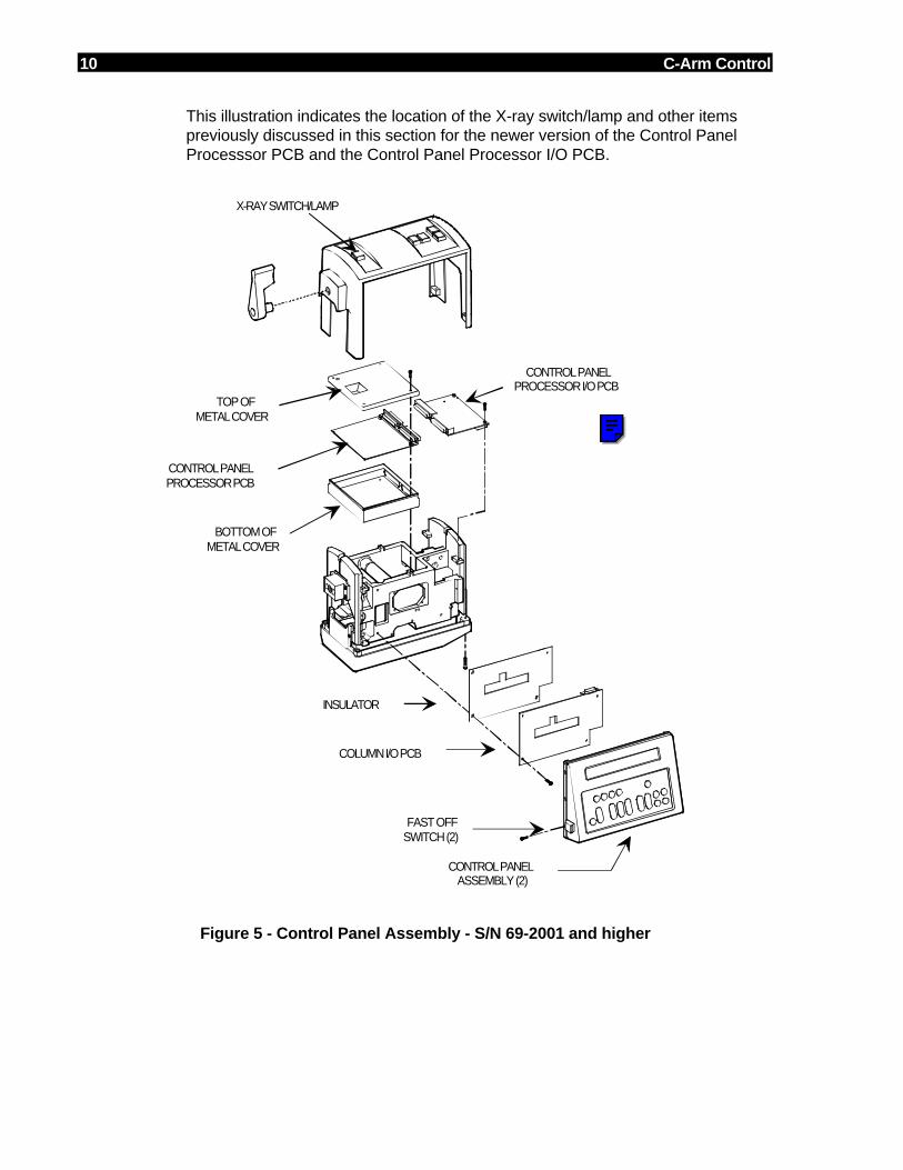
10 C-Arm Control
This illustration indicates the location of the X-ray switch/lamp and other itemspreviously discussed in this section for the newer version of the Control PanelProcesssor PCB and the Control Panel Processor I/O PCB.
CONTROL PANELPROCESSOR I/O PCB
CONTROL PANELPROCESSOR PCB
COLUMN I/O PCB
BOTTOM OFMETAL COVER
TOP OFMETAL COVER
INSULATOR
X-RAY SWITCH/LAMP
FAST OFFSWITCH (2)
CONTROL PANEL ASSEMBLY (2)
Figure 5 - Control Panel Assembly - S/N 69-2001 and higher
NOTE
Click on the colored box to go directly to the Illustrated Parts Manual for systems bearing serial numbers 69-2000 and higher. Click the << button on the Tool Bar to return to this point.
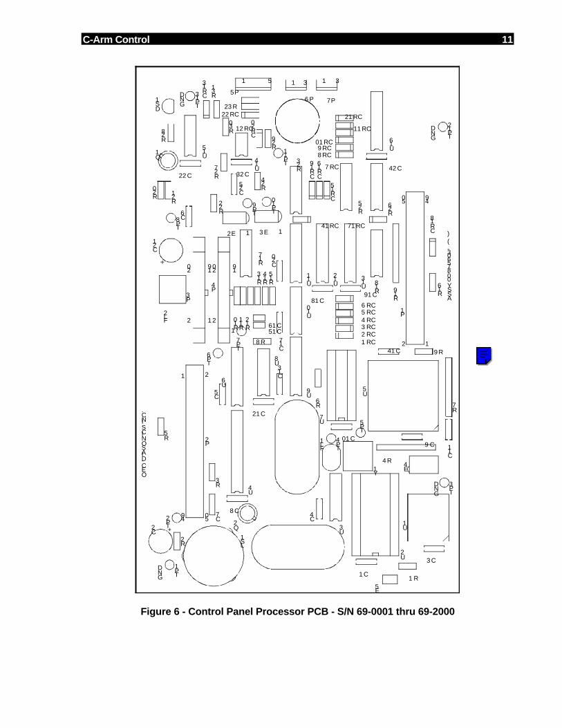
C-Arm Control 11
OEC-DIASONICS INC.
ASSY 00-875603- ( )
GND
GND
31 31
GND
1 5
2 1
1920
2
1
1920
1 2
5049
12
50 49
11
GND
CR22
CR21
P5P7P6
FL2
E5
FL1
U14
P3
P4
LS1
TP6
TP10
TP9
TP7
TP4
TP11
TP3
TP12
TP13
TP8
TP2
TP1
TP5
R19
R4
R7
DS1
R32
R9
R27
R16
R5
R8
R13
R20
R11
R21
R15
R31
R6
R10
R12
R14
R30
R28
R2
R3
R1
R22
R24
R29
U4
U12
U16
U11
U13
U9
U6
U5
U1
C25
C6
C12
C10
C14
C9
C3
C17
C11
C8
C13
C18
C1
C5
C20
C4
C23C22
C19
C24
R18
R17
R26
R23
R25
U3
U8
U10
U15
Q2
Q1
CR20
CR19
CR18
CR17
CR16
CR15
CR14
CR1
CR3
CR5
CR11
CR7
CR2
CR12
CR10
CR4
CR8
CR6
CR9
CR13
P2
P1
C21
C2
E4
E3E2
Y1
C16C15
U2
C7
U7
Figure 6 - Control Panel Processor PCB - S/N 69-0001 thru 69-2000
NOTE
Click in the blue box to go directly to the Electrical Schematic Diagram for the PCB shown on this page. Click the << button on the Tool Bar to return to this page.
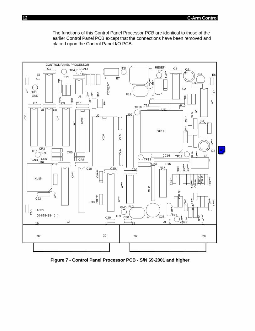
12 C-Arm Control
The functions of this Control Panel Processor PCB are identical to those of theearlier Control Panel PCB except that the connections have been removed andplaced upon the Control Panel I/O PCB.
RESET*
+5V
GND
GND
GND
GND
NORMAL
XU16
XU11
CONTROL PANEL PROCESSOR
00-878488- ( )
ASSY
2037
119
2037
119
1
1
1
XU8
XU9
J2 J1
U13
E6E5
TP13TP12
TP11
TP10
TP9
TP8
TP7
TP6
TP5TP4
TP3
TP1
R16
R15
R9
DS1
R23 R
21
R4
R18
R14
R3
R13
R10
R20
R2
R5
R24
R22
R19
R1
R8
R7
R6
R11
R12
U7U
5
U6
U14
U12
Y1
U3
R17
U1
U15
U4
U2
Q2
Q1
CR20
CR14
CR4
CR19
CR3
CR17
CR7
CR12
CR5
CR9
CR15
CR6
CR10
CR16
CR8
CR18 C
R11
CR13
CR2
CR1
C15 E4
E7
E3
E2
E1
C22
C20C19
C9
C24
C2
C11C7
C6
C12
C14
C1
C10
C17
C8
C13
C23
C4
C16
C18
C3
C5
C27
C29 C30
C26C
25 C21
FL2
FL1
U8
U16
U9
C28
U10
U11
Figure 7 - Control Panel Processor PCB - S/N 69-2001 and higher
NOTE
Click on the blue box to go directly to the Electrical Schematic Diagram for the PCB shown on this page. Click the << button on the Tool Bar to return to this page.
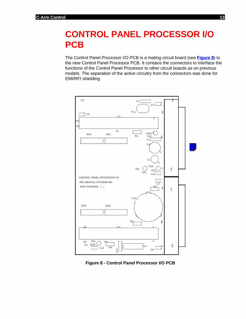
C-Arm Control 13
CONTROL PANEL PROCESSOR I/OPCBThe Control Panel Processor I/O PCB is a mating circuit board (see Figure 8 ) tothe new Control Panel Processor PCB. It contains the connectors to interface thefunctions of the Control Panel Processor to other circuit boards as on previousmodels. The separation of the active circuitry from the connectors was done forEMI/RFI shielding.
GND
GND
+12V+5V
CONTROL PANEL PROCESSOR I/O
ASSY 00-878491- ( )
OEC MEDICAL SYSTEMS INC
20
37
1
19
20
37
1
19
4 91
2
5 0
4 9 1
25 0
U 1
P4
P5
E 2
E 1
RP4 RP3
RP2 RP1
C10
C 9
C 8
C 7
C 6
C 5
C 4
R 4
R 1
R 2
R 3
LS1
TP4
TP3
TP2
TP1
P 1
P 2
C11
C 2
C 3
FL1
C 1
Figure 8 - Control Panel Processor I/O PCB
NOTE
Click in the blue box to go directly to the Electrical Schematic Diagram for the PCB shown on this page. Click the << button on the Tool Bar to return to this page.
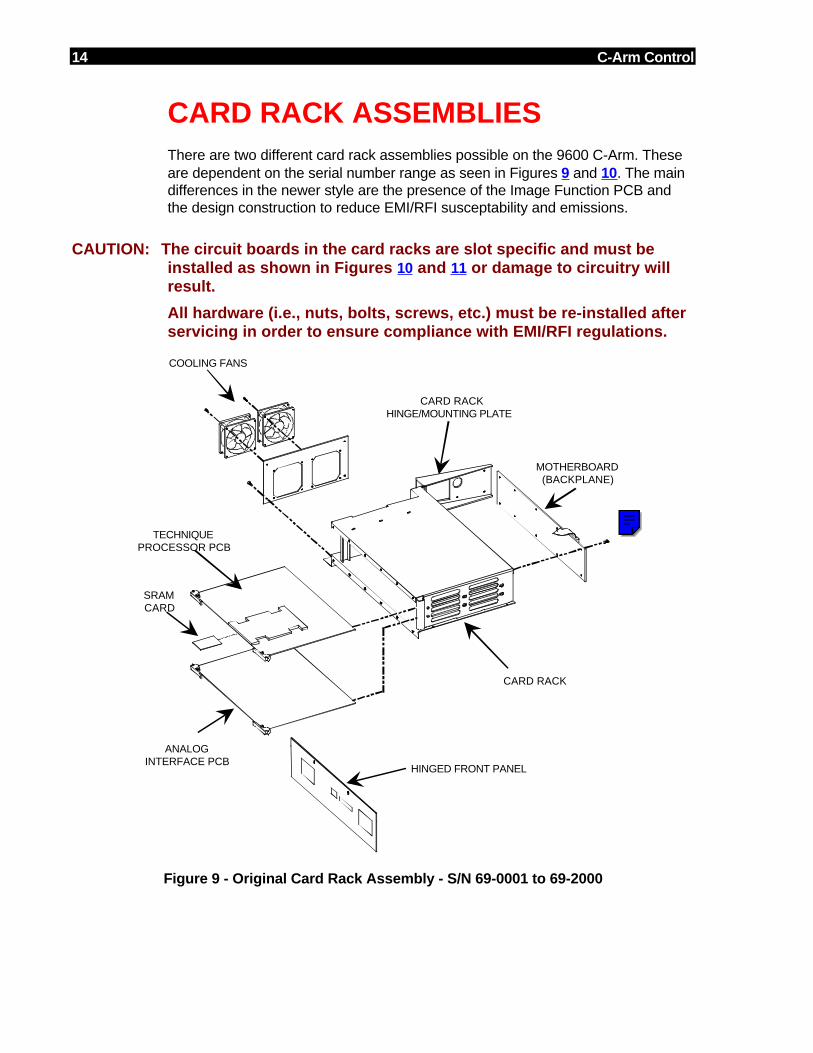
14 C-Arm Control
CARD RACK ASSEMBLIESThere are two different card rack assemblies possible on the 9600 C-Arm. Theseare dependent on the serial number range as seen in Figures 9 and 10. The maindifferences in the newer style are the presence of the Image Function PCB andthe design construction to reduce EMI/RFI susceptability and emissions.
CAUTION: The circuit boards in the card racks are slot specific and must beinstalled as shown in Figures 10 and 11 or damage to circuitry willresult.
All hardware (i.e., nuts, bolts, screws, etc.) must be re-installed afterservicing in order to ensure compliance with EMI/RFI regulations.
TECHNIQUEPROCESSOR PCB
ANALOGINTERFACE PCB
SRAMCARD
MOTHERBOARD(BACKPLANE)
CARD RACK
HINGED FRONT PANEL
CARD RACKHINGE/MOUNTING PLATE
COOLING FANS
Figure 9 - Original Card Rack Assembly - S/N 69-0001 to 69-2000
NOTE
Click on the colored box to go to the Illustrated Parts Manual for systems with serial numbers from 69-0001 to 69-2000. Click the << button on the Tool Bar to return to this point.

C-Arm Control 15
TECHNIQUEPROCESSOR
PCB
SRAMCARD
MOTHERBOARD(BACKPLANE)
CARD RACKREAR COVER
CARD RACK
CARD RACKFRONT COVER
ANALOGINTERFACE PCB
IMAGEFUNCTIONS
PCB
Figure 10 - Newer Card Rack Assembly - S/N 69-2001 and Higher
CAUTION: When replacing the EMI/RFI covers over the new Control PanelProcessor PCB or the new Card Rack, do not damage the metalgasket material around the edge of the PCB box. The gasket materialmust be replaced if damaged to ensure compliance with EMI/RFIregulations. When replacing a cover, do the following:1. Start a corner of the cover over the box2. Push the cover diagonally from the corner against the spring tension of the
gasket material.3. Make sure the edges of the cover are not pushing on the mounting edge of the
gasket material and gently push the cover down over the box.
NOTE
Click on the colored square to go directly to the Illustrated Parts manual for systems with serial numbers 69-2000 and higher. Click on the << button in the Tool Bar to return to this point.

16 C-Arm Control
TECHNIQUE PROCESSOR PCBAssy. #00-876737 - Sch. #00-876735
Assy. #00-877744 - Sch. #00-877742
OVERVIEW
The Technique Processor PCB (see Figures 12 and 13) is responsible forinitializing and controlling the 9600 C-Arm. Application software for the systemresides on the SRAM card located in the on-board solid state disk drive U13.
The Technique Processor PCB plugs into the Motherboard which serves as thebackplane of the card rack (see Figures 1, 9, and 10). The Analog Interface PCBis a slave to the Technique Processor, carrying out commands received on thePC bus.
Two versions of this PCB exist and either of these boards may be used in asystem. The difference between the two PCBs, is the communication circuitrywhich is discussed in System Communications in this section.
RESET CIRCUITRY AND WATCHDOG TIMER
When power is applied to the Technique Processor, power-on reset circuitry(U34 & U9) cause the 80C188 microprocessor (U30) to be reset. An externalreset pulse on pin 57 is also generated. This external reset pulse (RST and*RST via U10) is sent to the real-time clock U29, Dual-Port RAM control PALU4, the Control Panel Processor PCB, and to the PIOs located on the AnalogInterface PCB which sets these items to a default state. Switch S2 is used tomanually reset the Technique Processor.
U34 also serves as a “Watchdog Timer” for microprocessor U30. Pin 30 (PCS4)from the microcprocessor must reset U34 at pin 1 every 1.2 seconds or else U34will reset the microprocessor via U9 as described above. The purpose of the“Watchdog” is to interrupt the microprocessor from any unwanted software loopsthat may occur.
CPU & BUS INTERFACE
Once reset, microprocessor U30 retrieves instructions from the Boot EPROMU14 used to initialize the Technique Processor. This is accomplished via theinternal bus interface circuitry composed of address and I/O decoding circuitsU44 - U47 and signal buffer U36. The bus interface circuitry also enables theTechnique Processor to interface with other on-board devices such as SRAM(U16 - U19), EEPROM (U20), and a serial communications controller U39.
NOTE
Click on a yellow box to go directly to the block diagram for this section. The top box is linked to the drawing covering the lower serial numbers, while the bottom box is linked to the drawing covering the higher serial numbers. Do not use this link to return to a block diagram from this point. Click on the << button in the Tool Bar to return to any starting point.

C-Arm Control 17
U51 is an interrupt controller which causes microcontroller U30 to service one ofseveral items including the on-board solid state disk drive, floppy drive controlleror serial controller chip.
An external bus interface allows the Technique Processor to access the AnalogInterface PCB, and the remaining generator electronics. This external businterface is composed of address latches/buffers U23 - U28 and a bi-directionaldata buffer U50.Clock timer chip U29 contains a small portion of internal NVRAM which containscertain setup parameters such as the Technique Processor’s memory map, sizeallocation, and other items. An internal battery backup allows the timer chip tocontinuously run, monitoring X-ray exposure lengths and time out periods forspecific software routines.
MEMORY
The Technique Processor uses three basic groups of memory; SRAM, EEPROM(Non-Volatile RAM), and EPROM. The 512k SRAM (U16 - U19) is used fortemporary storage of application code and contains an area for “scratchpad” dataused in normal operation.
U20 is a 2k EEPROM that contains calibration and configuration data unique toeach generator assembly. If the Technique Processor PCB needs to bereplaced, this chip (unless suspected defective) should be installed on thereplacement PCB due to its contents for that particular generator assembly. If thecontents of the EEPROM are corrupted, the EEPROM can be down-loaded withback-up software as described in the C-Arm Software section of this manual.
A 512k EPROM (U14) contains data used to initialize the Technique Processor.The Option ROM (U15) contains instructions for the operation of the solid statedisk drive.
I/O DEVICES
Solid State Drive
U13 is a solid state disk drive capable of reading and writing PCMCIA memorycard devices. Installed in the drive is a 1 megabyte battery backed SRAM cardcontaining the C-Arm software. Refer to the C-Arm Software section of thismanual for details of the SRAM card and software files.
Floppy Disk Controller
Floppy disk controller chip U48 is not used on the 9600 C-Arm.
18 C-Arm Control
7-Segment Displays
Two 7-segment LED displays (U1 & U2) are used to indicate the status of theTechnique Processor PCB.
NOTE: The hex value 00 is displayed after the Technique Processor has completelybooted.
For a complete listing of these hexadecimal status codes, refer to the BIOS ROMCode in the C-Arm Software Section of this manual.
Switch S1
S1 is a four position DIP Switch used for selection of communications and disktype. Switches 1 and 2 must be on (on -02 PCBs and higher) to enable serialcommunications on the 9600 C-Arm. Switches 3 and 4 are not used.
Jumper E1
Configuration jumper E1 is not used.
COMMUNICATIONS
Refer to System Communications in this section for details of thecommunications circuitry.
DUAL PORT RAM (A/D INTERFACE)
U31 is a Dual Port RAM used to store bytes of data representing analog signalsdigitized by circuitry on the Analog Interface PCB as shown in Figure 11.
The Technique Processor selects one of the sixteen analog input signals via a 4-bit address (AMUXSEL0-3) via U11, U40, and U41. After an address has beengenerated, the SAMPLE signal is made active. This signal latches the selectedanalog signal into U8, a sample and hold chip.
Simultaneously, U9 on the Analog Interface PCB inverts the logic level of theSAMPLE signal for U7, the A/D converter. This inverted signal is applied to the“Convert” control line for U7. This A/D chip digitizes this analog signal into an 8-bit digital byte. This byte of data is sent back to the Technique Processor and isstored in the Dual Port RAM.
Since this is a continuous process, the Dual Port RAM contains byte values forall sixteen analog signals. By using the Dual Port RAM, the TechniqueProcessor can access the status of any of these analog signals without having to
C-Arm Control 19
wait for the A/D process to occur. Other functions of the Analog Interface PCBare described in the Analog Interface section.
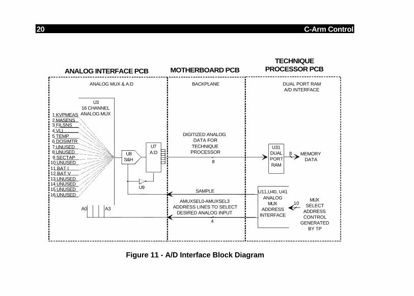
20 C-Arm Control
DUAL PORT RAMA/D INTERFACE
U31DUALPORTRAM
8U8S&H 8
U7A:D
U316 CHANNELANALOG MUX1 KVPMEAS
2 MASENS3 FILSNS4 VLI5 TEMP6 DOSIMTR7 UNUSED8 UNUSED9 SECTAP
11 BAT I12 BAT V13 UNUSED14 UNUSED15 UNUSED
10 UNUSED
16 UNUSED
U9
A0 A3
SAMPLE
ANALOG MUX & A:D
4
U11,U40, U41ANALOG
MUXADDRESS
INTERFACE
BACKPLANE
10MUX
SELECTADDRESSCONTROL
GENERATEDBY TP
DIGITIZED ANALOGDATA FOR
TECHNIQUE PROCESSOR
AMUXSEL0-AMUXSEL3ADDRESS LINES TO SELECT
DESIRED ANALOG INPUT
ANALOG INTERFACE PCB MOTHERBOARD PCBTECHNIQUE
PROCESSOR PCB
MEMORYDATA
Figure 11 - A/D Interface Block Diagram
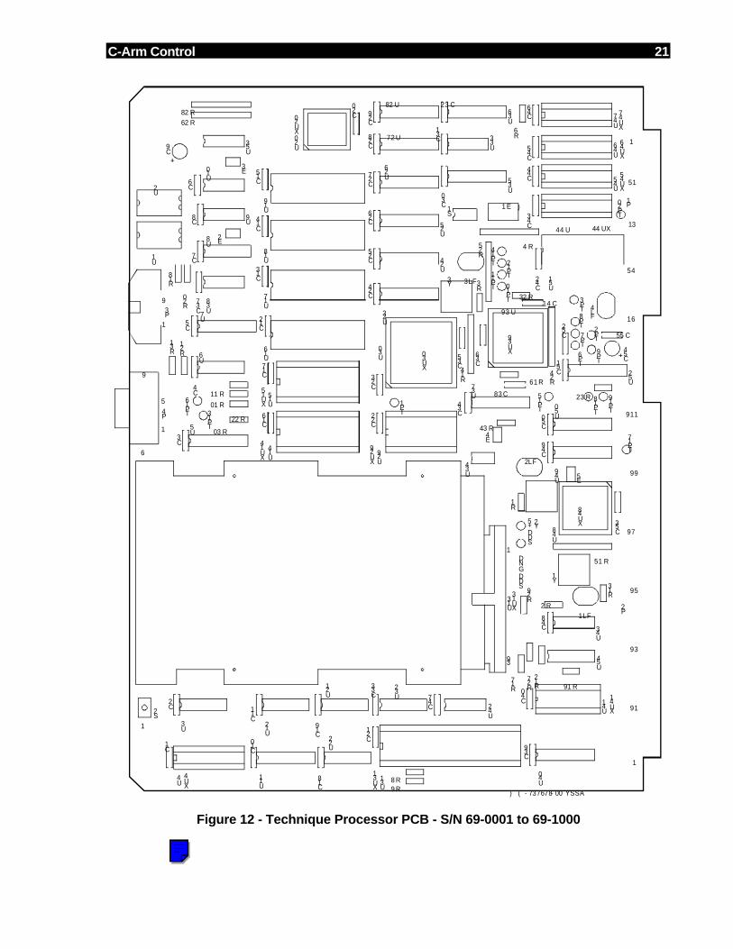
C-Arm Control 21
XU44
XU20
XU30 X
U39
XU48
XU46
ASSY 00-876737- ( )
1
39
XU13
1
5
6
9
XU14
XU15
1
61
31
15
45
XU45
XU47
XU4
1
19
39
59
79
99
119
1
XU29
XU31
1
9
XU41
U13
U30
C9
C54
P4
U14
U15
U16
U17
U18
U19
S1
U34
U20
P1
U44
U46
U45
U47
U4
FL4
FL1
FL2
FL3
P2
C6
C37
C31
C29
C26
C24
C30
C27
C32
C28
C47 C
40
C19
C11
C39
C2
C10
C33
C18
C49
C50
C1
C21
C16
C17
C12
C13
C14
C15
C48
C53
C51
C42
C34
C43
C44
C45
C46
C25
C4
C5
C7
C8
C3
C22
C35
C36
C20
C23
C38
C41
C52
C55
E5
E4
E2
E3
E1
S2
U29
U53
U43
U9
U10
U33
U38
U42
U51
U54
U8
U6
U21
U12U
3
U32
U22
U31
P3
U48
U7
U52
U5
U37
U28
U25
U35U
26
U36
U40
U11
U49
U23
U24
U27
U50
U2
U1
U41
Y3
Y2
Y1
R34
R32
R31
R30
R27
R29
R23
R22
R21
R20
R19
R18
R1
R2
R3
R6
R8R9
R10
R11
R12
R13
R16
R17
R28R26
R25
R24
R4
R14
R15
SDD GND
SDD +5
TP20
TP19
TP18
TP17
TP16
TP15
TP14
TP13
TP12
TP11
TP10
TP9
TP8
TP7
TP6
TP1
TP2
TP3
U39
Figure 12 - Technique Processor PCB - S/N 69-0001 to 69-1000
NOTE
Click in the blue box to go directly to the Electrical Schematic Diagram for the PCB shown on this page. Click the << button on the Tool Bar to return to this page.
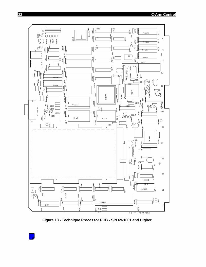
22 C-Arm Control
XU48
XU20
XU30 X
U39
XU44
+5V
GND
GND
GND
GND
XU46
ASSY 00-877744- ( )
1
39
XU13
1
5
6
9
XU14
XU15
1
61
31
15
45
XU38
XU53
XU45
XU47
XU4 1
19
39
59
79
99
119
1
XU29
XU31
XU41
U13
U30
C56
C9
P4
U14
U15
U16
U17
U18
U19
S1
U34
U20
P1
U38
U53
U44
U46
U45
U47
U4
FL4
FL1
FL2
FL3
P2
C54
C6
C37
C31
C29
C26
C24
C30
C27
C32
C28
C47 C
40
C19
C11
C39
C2
C10
C33
C18
C49
C50
C1
C21
C16
C17
C12
C13
C14
C15
C48
C53
C51
C42
C34
C43
C44C45
C46
C25
C4
C5
C7
C8
C3
C22
C35 C
36
C20
C23
C38
C41
C52
C55
E2
E1
S2
U29
U43
U9
U10
U33
U42
U51
U54
U8
U6
U21
U12U
3
U32
U22
U31
U48
U7
U52
U5
U37
U28
U25
U35
U26
U36
U40
U11
U49
U23
U24
U27
U50
U2
U1
U41
Y3
Y2
Y1
R29
R5
R1
R34
R33
R32
R31
R30
R27
R23
R22
R21
R20
R19
R18
R2
R3
R6
R8R9
R10R11
R12
R16
R17
R28R26
R25
R24
R4
R14
R15
SDD GND
SDD +5
TP2
TP41
TP40TP39TP38
TP37
TP36
TP35
TP34
TP33
TP32
TP31
TP30
TP21
TP20
TP19
TP18
TP17 T
P16
TP15
TP14
TP13
TP12
TP11
TP10
TP9
TP8
TP7
TP6
TP1
TP3
U39
Figure 13 - Technique Processor PCB - S/N 69-1001 and Higher
NOTE
Click in the blue box to go directly to the Electrical Schematic Diagram for the PCB shown on this page. Click the << button on the Tool Bar to return to this page.

C-Arm Control 23
ANALOG INTERFACE PCBAll S/N - Assy. #00-876738 - Sch. 876740
OVERVIEW
The Analog Interface PCB is the link between the Technique Processor PCB(primarily a digital board) and the rest of the generator assembly (primarilyanalog functions). The Technique Processor PCB and Analog Interface PCBplug into the Motherboard which serves as the backplane of the card rack (seeFigures 1, 9, and 10). They communicate via a PC bus and the A/D Data bus onthe Motherboard.
Analog Interface PCB circuitry can be divided into the following sections:
A/D Section - Samples and digitizes signals from the X-ray Regulator PCB to beread by the Technique Processor PCB.
D/A Section - Converts data bytes from the Technique Processor into analogsignals for such functions as camera gain, kVp control, mA control, and filamentcontrol.CTC Section - Generates the high voltage drive and filament drive signals.
PIO Section - Provides a digital interface between the Technique Processor anddiscrete digital signals.
Interlock Section - Interfaces the processor's interlock keep-alive signal with therelay controlled interlock circuits.
X-ray Switch Logic - Interfaces X-ray switch closure information from the controlpanel, footswitch, and handswitch.
Stator Sense - Circuitry to sense current flow to the stator windings.
NOTE
Click on a yellow box to go directly to the block diagram for this section. Do not use this link to return to a block diagram from this point. Click on the << button in the Tool Bar to return to any starting point.

24 C-Arm Control
A/D SECTIONThe A/D section is comprised of sample mux U3, sample/hold IC U8, and analogto digital converter U7(AD573). Sixteen A/D inputs (0-10 VDC) are monitored bythe Technique Processor CPU. The analog output of MUX U3 whose is fed to U8which holds the level for digitization by U7, a 10 bit A/D converter. Refer toFigure 11 .
The Technique Processor then stores this digitized data value in its DUAL PORTRAM (U31) for each analog MUX input signal, shown below. Sample MUX U3 isaddressed by the AMUXSEL lines generated by sequencing circuits on theTechnique Processor PCB. Analog Mulitplexer (U3) input pin assignments arelisted below in Table 1. Refer to the C-Arm Software section in this manual fortypical results of these signals using the Control Panel Status software.
SOFTWARECHANNEL & PIN
SIGNAL FUNCTION SOURCE
Channel 0 - Pin 19 KVPMEAS kV measure for high voltageservo 1 volt/20kV nominal
Tank (1:10,000)Capacitive Sense
Channel 1 - Pin 20 MASNS &MASNSREF
mA measure for tube currentservoFLUORO = 125 mV/mA (±3%)FILM = 6.25 mV/mA (±3%)
Tank100 Turn Anode SenseWinding
Channel 2 - Pin 21 FILSNS Filament B+ Sense“Regulator Fail” if this voltageincorrect
Generator Driver PCB(via R42) P2 pin 11
Channel 3 - Pin 22 VLI Video Level Indicator; ABS &Camera Gain satisfy this signalfor tracking
Camera Assy.
Channel 4 - Pin 23 HOUSTEMP
Housing Temperature(Thermistor)
X-ray Tube Assy.
Channel 5 - Pin 24 DOSIMTR not used ---------------Channel 6 - Pin 25 CAMROT Camera Rotation Indicator Potentiometer on CCD
cameraChannel 7 - Pin 26 AD_SPARE not used ---------------Channel 8 - Pin 11 SECTAPV Redundant kV Sense for
software≅0.22 volts (± 0.02 volts)/kVp
Tank1 Turn Windings(1:4,300)
Channel 9 - Pin 10 LINE_SNS Line Voltage Sensing Battery Charger PCBChannel 10 - Pin 9 CHGR_I Charger Current Sense Charger via Generator
Driver PCBChannel 11 - Pin 8 200V_SNS Battery Voltage Sense Charger via Generator
Driver PCBChannel 12 - Pin 7 ADSPARE1 not used ---------------Channel 13 - Pin 6 ADSPARE2 not used ---------------Channel 14 - Pin 5 --------------- not used ---------------Channel 15 - Pin 4 --------------- not used ---------------
Table 1 - Inputs to A/D Section
C-Arm Control 25
D/A SECTION
U18 and U31 are quad D/A converters (DAC 8408) which provide analog currentoutput signals. These four current output channels are labeled as IOUT1A -IOUT1D. The current outputs from the D/As are converted to a voltage (0-10VDC) by current to voltage converters U28, U29, and U33.
The analog outputs for U18 and U31 are described below.
D/A U18 Pin Assignments
CHA - Pin 4 - Not Used
CHB - FILCNTRL - Pin 6 - This is a control voltage for the filament B+ circuitryused to regulate the tube current (mA); see TP10. Refer to mA GenerationSection for more information about this signal.
CHC - CAM_GAIN - Pin 25 - This signal controls the video camera gain; seeTP13. Refer to the Image System section for more information about thissignal.
CHD - Pin 23 - Not Used (CAM_BLK)
D/A U31 pin assignments
CHA - Pin 4 - Not Used (Target)
CHB - Pin 6 - Not Used
CHC - KVCONT - Pin 25 - This is a control voltage for the high voltage circuitrythat is proportional to the desired kV; see TP19. Refer to the kV Generationsection for more information about this signal.
CHD - MACONT - Pin 23 - This is a control voltage for the tube current circuitrythat is proportional to the desired mA; see TP18. Refer to the mA Generationsection for more information about this signal.
Negative 10 Volt Reference
The -10 VDC reference, VR1, provides the necessary voltage reference for thedigital to analog conversion. Its output is buffered by U30A, Q14 and otherrelated components.
NOTE: Loss of the reference voltage will give a “Regulator Fail” error message on theControl Panel Display after an exposure has been made.

26 C-Arm Control
COUNTER/TIMER (CTC) SECTION
The counter/timer section is comprised of a programmable counter/timer chipU12, flip-flop U15, counter U16, PAL U17 (Programmable Array Logic), anddrivers U42 and U40.
The timebase (40 kHz, buffered ± 10 volt level) for the X-ray generator invertercircuits is derived from the CPU clock (7.16 MHz). The CPU clock is applied toU12, a programmable counter timer chip, and is divided by 179 to provide the 40kHz output of counter 0 on pin 10.
The 2.5 kHz inverter drive signals HVDRVA and HVDRVB are derived bydividing the 40 kHz clock by 16 in U16, a 4 bit binary counter. Its output is fed toU17, a PAL programmed to provide two complimentary 2.5 kHz outputs of 43%duty cycle (active low). These outputs are buffered by U40 and U42 to provide± 12 volt logic levels for extra noise immunity and fed to the X-ray RegulatorPCB. See the kV Generation section for details of these signals.
The filament drive signals are derived from the outputs above, and the secondoutput of the counter timer chip. This timer is triggered from U17-16 which has a5 kHz output. The timer provides a variable pulse width 5 kHz signal, which afterAND-gating with HVDRVA and HVDRVB generates FILDRVA and FILDRVBrespectively. The result is then a pair of complimentary drives with variable dutycycles. These outputs are buffered by U40 to provide ± 12 volt logic levels forextra noise immunity and are then routed to the X-ray Regulator PCB. See themA Generation section for details of these signals.
C-Arm Control 27
PIO SECTIONSeveral digital inputs and outputs are provided for software interface throughPIOs (Parallel Input/Out) U22, U27, and U38. They are connected to the PC busshared by the Technique Processor PCB and the Analog Interface PCB. Eachof the PIO chips have 3 eight bit ports; A, B, and C. The ports are configured bysoftware as either inputs or outputs. These devices monitor status bits and issuevarious commands via software control. PIO pin assignments are listed below.Refer to the C-Arm Software section for typical results for these signals usingthe Control Panel Status software.
NOTE: Not all of these signals can be tested using Control Panel Status.
BIT # PIN # SIGNAL FUNCTION COMMENT
PA0-2,
4-7
2-4, 37-40 --------------- not used ---------------
PA3 1 INTEGRATE
(S3)
Integrate function on CCD camera, via
Image Function PCB
LO= CCD sensor not being
scanned
PB0 18 CONTACT Turn on relay K2 for Pre-Charge HI = turn on Q5
PB1 19 Output PRECHRG Turn on relay K1 for Pre-Charge HI = turn on Q4
PB2 20 -
Output
STAT_RUN 40 VAC for Stator Run. After 5 min.
[sleep mode]; this signal goes LO
HI = turn on Q3
PB3 21 --------------- not used ---------------
PB4 22 --------------- not used ---------------
PB5 23 -
Output
STATSTRT 120 VAC (2 sec) for Stator Start HI = turn on Q7 (2 sec)
PB6 24 -
Output
II_ON 24 VDC to Image Intensifier
in FLUORO MODE only
HI = FLUORO MODE
LO = FILM MODE
PB7 25 --------------- not used ---------------
PC0 14 --------------- not used ---------------
PC1 15 - Input SECURITY Verification signal to ensure an
X-ray switch has been pressed
HI = When CPP X-ray or any
footswitch is pressed
PC2 16 --------------- not used ---------------
PC3 17 --------------- not used ---------------
PC4 13 - Input L/R Detects when SAVE Footswitch has
been pressed
LO = Save Footswitch
Pressed
PC5 12 - Input FLORONLY Detects when SCOUT FLUORO
Footswitch has been pressed
HI = Scout Fluoro
Footswitch Pressed
PC6 11 - Input BOOST Detects when BOOST/DIG. SPOT
footswitch has been pressed
HI = Boost/Dig. Spot
Footswitch Pressed
PC7 10 - Input XRAYSW Detects when CPP X-ray Switch or
DIGITAL PROCESS FLUORO footswitch
is pressed
HI = X-ray Switch Pressed
Table 2 - U38 - PIO 1 Pin Assignments
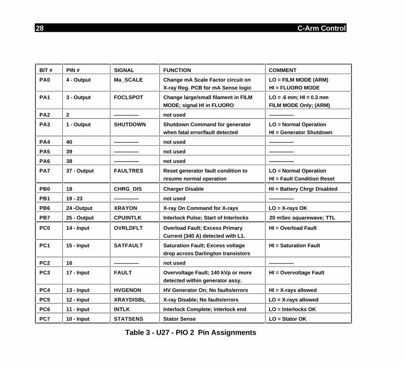
28 C-Arm Control
BIT # PIN # SIGNAL FUNCTION COMMENT
PA0 4 - Output Ma_SCALE Change mA Scale Factor circuit on
X-ray Reg. PCB for mA Sense logic
LO = FILM MODE (ARM)
HI = FLUORO MODE
PA1 3 - Output FOCLSPOT Change large/small filament in FILM
MODE; signal HI in FLUORO
LO = .6 mm; HI = 0.3 mm
FILM MODE Only; (ARM)
PA2 2 --------------- not used ---------------
PA3 1 - Output SHUTDOWN Shutdown Command for generator
when fatal error/fault detected
LO = Normal Operation
HI = Generator Shutdown
PA4 40 --------------- not used ---------------
PA5 39 --------------- not used ---------------
PA6 38 --------------- not used ---------------
PA7 37 - Output FAULTRES Reset generator fault condition to
resume normal operation
LO = Normal Operation
HI = Fault Condition Reset
PB0 18 CHRG_DIS Charger Disable HI = Battery Chrgr Disabled
PB1 19 - 23 --------------- not used ---------------
PB6 24 -Output XRAYON X-ray On Command for X-rays LO = X-rays OK
PB7 25 - Output CPUINTLK Interlock Pulse; Start of Interlocks 20 mSec squarewave; TTL
PC0 14 - Input OVRLDFLT Overload Fault; Excess Primary
Current (340 A) detected with L1.
HI = Overload Fault
PC1 15 - Input SATFAULT Saturation Fault; Excess voltage
drop across Darlington transistors
HI = Saturation Fault
PC2 16 --------------- not used ---------------
PC3 17 - Input FAULT Overvoltage Fault; 140 kVp or more
detected within generator assy.
HI = Overvoltage Fault
PC4 13 - Input HVGENON HV Generator On; No faults/errors HI = X-rays allowed
PC5 12 - Input XRAYDISBL X-ray Disable; No faults/errors LO = X-rays allowed
PC6 11 - Input INTLK Interlock Complete; interlock end LO = Interlocks OK
PC7 10 - Input STATSENS Stator Sense LO = Stator OK
Table 3 - U27 - PIO 2 Pin Assignments
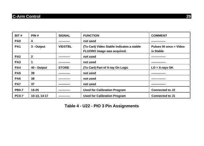
C-Arm Control 29
BIT # PIN # SIGNAL FUNCTION COMMENT
PA0 4 ------------ not used ---------------
PA1 3 - Output VIDSTBL (To Cart) Video Stable indicates a stable
FLUORO image was acquired.
Pulses HI once = Video
is Stable
PA2 2 ------------ not used ---------------
PA3 1 ------------ not used ---------------
PA4 40 - Output STORE (To Cart) Part of X-ray On Logic LO = X-rays OK
PA5 39 ------------ not used ---------------
PA6 38 ------------ not used ---------------
PA7 37 ------------ not used ---------------
PB0-7 18-25 ------------ Used for Calibration Program Connected to J2
PC0-7 10-13, 14-17 ------------ Used for Calibration Program Connected to J1
Table 4 - U22 - PIO 3 Pin Assignments
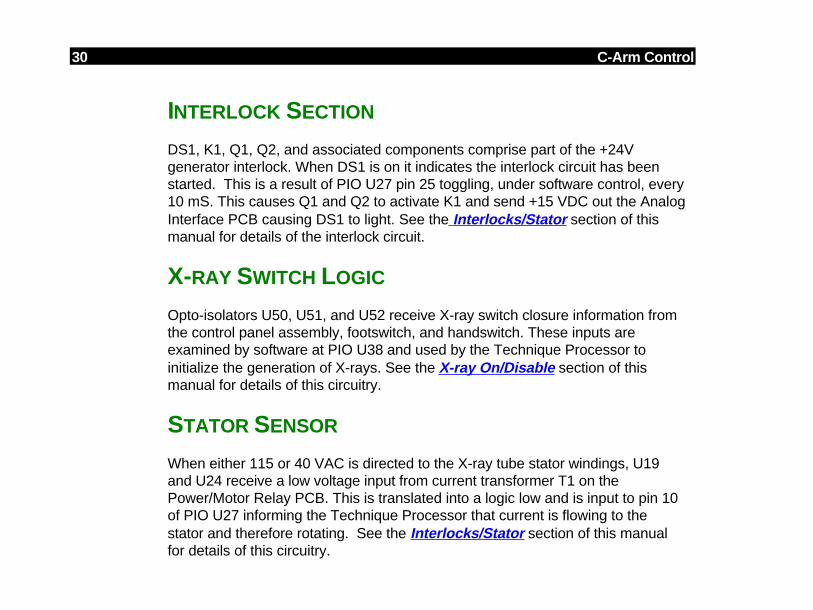
30 C-Arm Control
INTERLOCK SECTION
DS1, K1, Q1, Q2, and associated components comprise part of the +24Vgenerator interlock. When DS1 is on it indicates the interlock circuit has beenstarted. This is a result of PIO U27 pin 25 toggling, under software control, every10 mS. This causes Q1 and Q2 to activate K1 and send +15 VDC out the AnalogInterface PCB causing DS1 to light. See the Interlocks/Stator section of thismanual for details of the interlock circuit.
X-RAY SWITCH LOGIC
Opto-isolators U50, U51, and U52 receive X-ray switch closure information fromthe control panel assembly, footswitch, and handswitch. These inputs areexamined by software at PIO U38 and used by the Technique Processor toinitialize the generation of X-rays. See the X-ray On/Disable section of thismanual for details of this circuitry.
STATOR SENSOR
When either 115 or 40 VAC is directed to the X-ray tube stator windings, U19and U24 receive a low voltage input from current transformer T1 on thePower/Motor Relay PCB. This is translated into a logic low and is input to pin 10of PIO U27 informing the Technique Processor that current is flowing to thestator and therefore rotating. See the Interlocks/Stator section of this manualfor details of this circuitry.
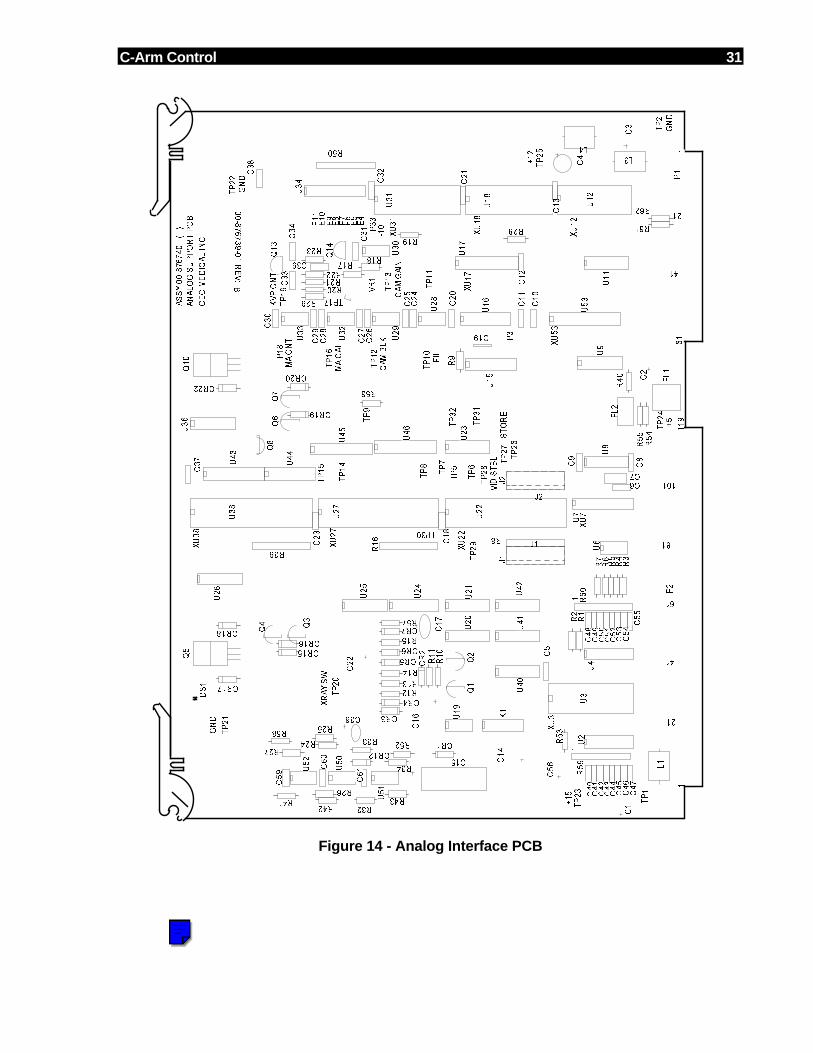
C-Arm Control 31
MA
CN
T
GN
D
KV
P C
NT
MA
CA
L
FIL
CA
M G
AIN
CA
M B
LK
+1
2
+5
GN
D
+1
5
GN
D
XR
AY
SW
ST
OR
EV
ID S
TB
L
-10
AN
AL
OG
SU
PP
OR
T P
CB
XU
3
XU
7
XU
22
XU
27
XU
38
XU
17
XU
31
XU
18
XU
12
00
-876
73
9-0
1 R
EV
:
AS
SY
00
-876
74
0-
(
)
XU
53
11
OE
C M
ED
ICA
L IN
C
J1J2
1
21
41
61
11
91
21
41
61
81
101B
C1
C1
0
C1
1C
12
C1
3
C1
4
C15
C1
6
C1
7C
18
C19
C2
C2
0
C2
1
C2
2
C2
3
C2
4C
25
C2
6C
27
C2
8C
29
C3
C3
0
C3
1
C3
2
C3
3C
34
C36
C3
7
C3
8
C39
C4
C5
C6C7
C8
C9
CR1CR12
CR15CR16
CR17
CR18
CR19
CR
2
CR20
CR22
CR3
CR4
CR5
CR6
CR7
DS
1
E1
0E
11
E4
E5
E6
E7
E8
E9
J1
J2K
1
L1
L3
L4
P1
Q1
Q1
0
Q1
3
Q1
4
Q2
Q3
Q4
Q5
Q6
Q7
Q8
R1
R1
0R
11
R12R13
R14
R15
R1
6
R17R18
R2
R20R21R22
R23
R24
R25
R26
R27
R3
R32
R33
R34
R39
R4
R5
R50
R52 R5
3
R5
4R
55
R56
R57
R58
R6
R7
R8
R9
TP
1
TP
10
TP
11
TP
12
TP
13
TP
14
TP
15
TP
16
TP17
TP
18
TP
19
TP
2
TP
20
TP
21
TP
22
TP
23
TP
24
TP
25
TP
26
TP
27
TP
28
TP
29
TP
3TP30
TP
31
TP
32
TP
5
TP
6
TP
7
TP
8
TP
9
U1
1
U1
2
U1
5U
16
U1
7
U1
8
U1
9
U2
U2
0
U2
2
U2
3
U2
4
U2
5
U2
7
U2
8
U2
9
U3
U3
0U
31
U3
2
U3
3U
34
U3
8
U4
U4
0U
41
U4
2
U4
3
U4
4
U4
5
U4
6
U6
U7
U8
U9
VR
1T
P3
3
P2
U2
6
U3
6
R19
R28
R29
C4
0C
41
C4
2C
43
C4
4C
45
C4
6C
47
C4
8C
49
C5
0C
51
C5
2C
53
C5
4
C5
5
C5
6
FL
1
U5
0
U5
1
U5
2
FL
2R
40
R41R42
R43
C5
9
C6
0
C6
1
U2
1
U5
3R
59
R6
0
R61
R62Figure 14 - Analog Interface PCB
NOTE
Click in the blue box to go directly to the Electrical Schematic Diagram for the PCB shown on this page. Click the << button on the Tool Bar to return to this page.
32 C-Arm Control
C-ARM MOTHERBOARD
S/N 69-0001 through 69-2000 - Assy. #00-900588 - Sch. #00-875539
S/N 69-2001 and higher - Assy. #00-900970 - Sch. #00-878396
The C-Arm Motherboard is the backplane of the card rack as illustrated inFigures 10 and 11 . It serves as a connecting point for the Technique ProcessorPCB, Analog Interface PCB and on newer models, the Image Function PCB.Also, there are many cables that connect to the back of the circuit board. Thereare two versions of the Motherboard as shown in Figures 15 and 16 .
VR1 and VR2
VR1 regulates the -15VDC from power supply PS1 down to -12VDC. VR2regulates the +15VDC down to +12VDC. These voltages are used in variousplaces in theC-Arm.
VR3
Voltage regulator VR3 is only on the newer Motherboard (assy. #900970). It isnot used at this time.

C-Arm Control 33
P 7
MODEL 9400 MOTHERBOARD
12
P6
12
394
0
1
34
P3
P2
1
34
P8
6
1
ASSY 00-900588- ( )
+15V
-15V
+5V
GND
-5V
CR1
+
+
3
4
3334
2
33
2
33
2
P 1 1
220
20
19
119
VR2
VR1
C 4
C 3
C 2
OEC-MEDICAL SYSTEMS INC.
P4
C1
11
61
6261
119
120119
22
2
120
62
1 2 1
1
3 4
J5J6
2
J2J3
J5J6
P5
E1
E2
E3
E4
E5
E6
E7
E8
E9
E10
C 5
C 6
C 7
C8
C 9
C10
C11
C12
C13
C14
FL1
INSIDE CARDRACK REAR OUTSIDE CARDRACK
Figure 15 - C-Arm Motherboard - S/N 69-0001 to 69-2000
NOTE
Click in the blue box to go directly to the Electrical Schematic Diagram for the PCB shown on this page. Click the << button on the Tool Bar to return to this page.
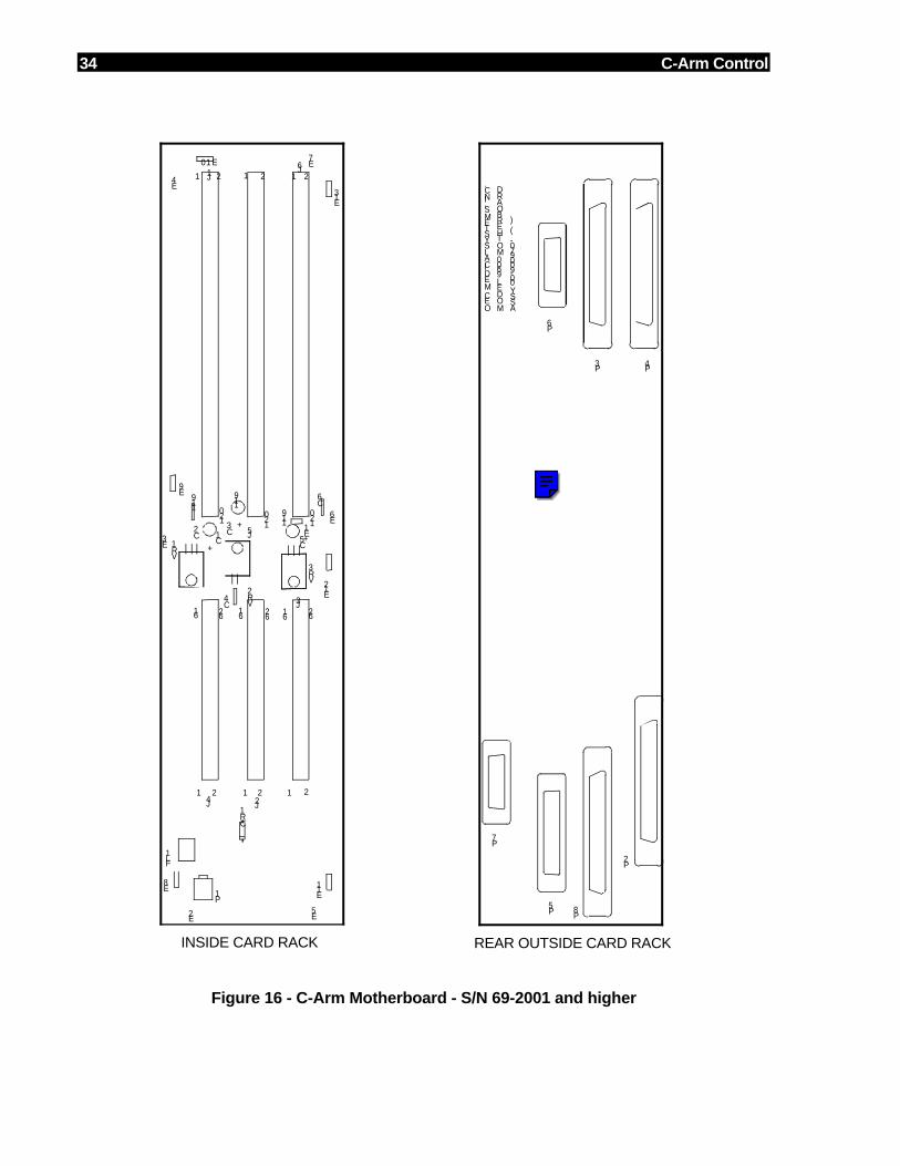
34 C-Arm Control
CR1
+
+
C4
C3
C2
ASSY 00-900970- ( )
OEC MEDICAL SYSTEMS, INC.
MODEL 9600 MOTHERBOARD
P7
P5
P6
VR1
VR2
C1
P3
P2
P4
P8
1 1
1
2
119
2 21
120
119
61 62 61
62
2
119
120
1 2
120
61 62
1 2
+
J2
J3
J5
J6
E2
E3
E4
E5
E6
E7
E8
E9
E10
E11
E12
E13
FL1
J1
J4
P1
C5
C6
VR3
E1
REAR OUTSIDE CARD RACKINSIDE CARD RACK
Figure 16 - C-Arm Motherboard - S/N 69-2001 and higher
NOTE
Click in the blue box to go directly to the Electrical Schematic Diagram for the PCB shown on this page. Click the << button on the Tool Bar to return to this page.
C-Arm Control 35
SYSTEM COMMUNICATIONSThe Technique Processor PCB within the C-Arm and the 386 AT Motherboardwithin the Workstation are the communication managers of the system. RS232is used throughout the system except for the RS422 link between the C-ArmControl Panel Processor and Power/Signal Interface PCB.
The following acronymns are used as part of signal names along withdesignators to specify the channel, source, etc.:
• TXD = Transmit Data - connected to RXD of receiving PCB
• RXD = Receive Data - connected to TXD of sending PCB
• RTS = Request To Send - connected to CTS of receiving PCB
• CTS = Clear To Send - connected to RTS of sending PCB
C-ARM COMMUNICATION
The Technique Processor PCB manages the serial communications for the C-Arm utilizing U39-a four channel serial communication controller. The TechniqueProcessor communicates with the following:
• C-Arm Control Panel Processor PCB.
• Image Functions PCB.
• Workstation.
There are two versions of the Technique Processor PCB. They differ in theassociated communication circuitry that is used in conjunction withcommunication controller U39. The newer version, assembly # 00-877744, uses2 GALs, U53 and U38, to control port selection and communication type.
NOTE: Switches 1 and 2 of S1 on the Technique Processor PCB (-02 and higher) mustbe “ON”(closed) to enable serial communications on the 9600 system.
1 2 3 4
OFF
NOTE: RTS (Request To Send) and CTS (Clear To Send) lines on U39 (pins 21, 23, 25,27, 29, 31, 33 & 35) all become a logic low on the Technique Processor during theboot process.
NOTE
Click on a yellow box to go directly to the block diagram for this section. The top box is linked to the drawing covering the lower serial numbers, while the bottom box is linked to the drawing covering the higher serial numbers. Do not use this link to return to a block diagram from this point. Click on the << button in the Tool Bar to return to any starting point.
36 C-Arm Control
Technique Processor to and from Control Panel Processor
Communication between the Technique Processor PCB and the Control PanelProcessor is established during the boot process. When communication isestablished all of the segments on the Control Panel Display will be illuminatedas shown below.
During normal operation, this communication link enables the Control Panel tosend commands such as kV, mA, and other user defined input to the TechniqueProcessor. The TXD and RTS signals from Port A of the serial communicationscontroller U39 on the Technique Processor PCB are sent to microprocessor U5on the Control Panel Processor PCB. They pass through buffer U37 on theTechnique Processor PCB, through the Mainframe Motherboard and then to thePower/Signal Interface PCB. RS422 driver U2, on the Power/Signal InterfacePCB, translates the signals to RS422 communication signals (see Figure 17).The signals then leave the Power/Signal Interface PCB at P10 and enter theControl Panel Processor PCB at P4. RS422 serial receiver U10 on thePower/Signal PCB then converts the signals back to RS232 and they arereceived by microprocessor U5 at pins 17 (RXD) and 44 (CTS).
TXD (pin 18) and RTS (39) from microprocessor U5 on the Control PanelProcessor PCB are translated to RS422 communication signals by RS422 driverU8 on the Control Panel processor. These signals then leave the Control PanelProcessor at P4 and enter the Power/Signal Interface board at P10. RS422receiver U1, translates the signals back to RS232 and they leave thePower/Signal Interface PCB at P9. The signals then pass through the MainframeMotherboard and enter the Technique Processor PCB at P2.
On the older Technique Processor PCB (Assy. #876735) the signals then passthrough buffer U37 and AND gate U38 and are received by serialcommunications controller U39 at pins 19 (RXD) and 27 (CTS).
On the newer Technique Processor PCB (Assy. #877744) the signals then passthrough buffer U37 and COM SELECT GAL U38 and are received by serialcommunications controller U39 at pins 19 (RXD) and 27 (CTS).
RS422 DRIVER TRUTH TABLE RS422 RECEIVER TRUTH TABLE
3487
3487
3486
3486< .05V
< .05V< .05V
< .05V
> 2.5V
> 2.5V > 2.5V
> 2.5V
H H
LL
Figure 17 - RS-422 Driver/Receiver Logic

C-Arm Control 37
Technique Processor to and from Image Function PCB
Communication with the Image Function PCB is established during the bootprocess. The Control Panel Display will display 10 arrows as shown below atthis point in the boot process.
During normal operation, this communication link enables the TechniqueProcessor to send commands such as:
• Request for Status
• Reset Image Function PCB
• Commands to control Camera and Collimator Motors
• Commands to change the Image Intensifier field size
• Commands to control Camera modes such as Unity Gamma, Anti-vignetting
• Commands to control collimator modes such as Normal, MAG1 and MAG2
On the older Technique Processor PCB, the port D RXD and TXD lines fromcommunications controller U39 pass through U5, an RS-232 driver/receiver andleave the Technique Processor PCB at P2. These signals then pass through theMotherboard and enter the Image Function PCB at P2. They pass throughRS232 driver/receiver U17 and are then received by microcontroller U16.
On the newer Technique Processor PCB, the port C TXD line passes throughPort Select GAL U53 and then to RS232 Driver/Receiver U5. The signalreceived at the port C RXD input comes through U5, makes its way through ComSelect GAL U38, Port Select GAL U53, and finally to pin 36 (RXD) ofcommunications controller U39.The signals pass through RS232 Driver/Receiver U17 on the Image FunctionPCB and enter microcontroller U16, which in turn issues commands on the databus to perform the desired function.
NOTE: The CTS and RTS signals are not used in this communication link.
The Technique Processor sends a request for status to the Image Function PCBat least once a second to check for errors and to confirm that the Image FunctionPCB is still functioning.
NOTE: Refer to the Image System section of this manual for error codes that relate to theImage Function PCB.
38 C-Arm Control
COMMUNICATION BETWEEN C-ARM AND WORKSTATION
Communication between the C-Arm and Workstation is established during theboot process. All of the arrows will be displayed on the Control Panel Display asshown below during this part of the boot process.
During normal operation, the Technique Processor and 386 AT Motherboardsend information such as:
• Shot log file information from the C-Arm to the Workstation
• Commands such as L>R, SAVE and CART MODE from the Control Panelto the Workstation
• “Enable Boost” command to the C-Arm when CHOLE/DIGITAL SPOT isselected on the Workstation
The TXD and RTS signals from Port B of the serial communications controllerU39 on the Technique Processor PCB are sent to the 386 AT Motherboard onthe Workstation. They pass through RS232 driver/receiver U52 on theTechnique Processor PCB and then pass through the Mainframe Motherboard,the interconnect cable, and enter the Aux Interface PCB in the Workstation.They pass through the Aux Interface PCB to the AT Communications PCBwhere they are inverted by U15 and enter DUART U27. U27 interfaces thesignals to the data bus of the AT Motherboard.
The 386 AT Motherboard communicates over the data bus to DUART U27 on theAT Communications PCB. TXDA (pin 30) and RTS (pin 29) leave DUART U27,pass through RS232 line driver U16 and leave the AT Communications PCB atP3. They then pass through the Aux Interface PCB, the Interconnect Cable andenter the C-Arm at J1 on the Power Panel. They pass through the MainframeMotherboard and enter the Technique Processor PCB at P2.
On the older Technique Processor PCB (Assy. #876735) the signals then passthrough RS-232 driver/receiver U52 and are received by serial communicationscontroller U39 at pins 8 (RXD) and 23 (CTS).
On the newer Technique Processor PCB (Assy. #877744) the signals then passthrough RS232 driver/receiver U52 and COM SELECT GAL U38 and arereceived by serial communications controller U39 at pins 8 (RXD) and 23 (CTS).

C-ARM SOFTWARE
OVERVIEWThe 9600 C-Arm software is loaded from a PCMCIA style SRAM card to RAM locatedon the Technique Processor PCB, during system start-up. The software remainsresident in the RAM until the generator is turned off. The SRAM card is located in thesolid state disk drive on the Technique Processor PCB .
START-UP AND SOFTWARE BOOTThe key events which occur during start-up are:
1. Power supplies stabilize at the proper voltage levels and power is applied to all themicroprocessor circuits.
2. Microprocessors are reset and program control is transferred to the boot EPROM(U14) on the Technique Processor PCB .
3. Technique Processor PCB boot EPROM (U14) software performs critical hardwaresetups, executes various hardware tests, and loads the boot sectors from theSRAM card.
Critical hardware setup includes initializing all DMA, memory, I/O and bus-orienteddevices on the Technique Processor PCB. This setup involves the following steps:
A. Initialize hardware lines to a defined state
B. Initialize and test memory
C. Display boot codes
4. Software routines in the Technique Processor PCB boot EPROM (U14) load theboot sectors from the SRAM card.
5. Boot sectors, once loaded into the Technique Processor PCB RAM (U16-U19), loadthe operating system into memory. After the operating system is initialized itassumes program control.
2 C-Arm Software
LOADING APPLICATION SOFTWARE
Application software is by entered utilizing the operating system or from a program suchas STATUS. The key events which occur are:
1. Technique Processor PCB EEPROM (U20) is checked.
2. Default Fluoro and Film parameters are loaded and the system is configured by theOPTIONS.DAT file. Options such as Boost and 40 mA pulsed mode are initialized.
3. The 40 kHz clock on the Analog Interface PCB is started.
4. Hardware is again initialized as a precaution.
5 The MALIMIT.DAT file and ABS tables are loaded.
6. Tests are run to determine if the system is capable of functioning.
7. Footswitch is checked (for "footswitch stuck" fault).
8. Generator Interlock (+24V) is made.
9. Capacitors C2 and C3 on Generator Controller Assembly are charged by Battery B+voltage through pre-charge circuitry.
10. The stator line is pulsed.
11. Check for disconnected batteries and check B+ voltage.
12. The small filament is preheated.
13. Generator and X-ray tube control signals are initialized.
14. Heat units are computed for the anode and housing.
15. If no problems are found, operator input is accepted from the control panel.
PERIODIC FUNCTIONS AND ACTIONS
These are functions executed periodically by the software program, which includeControl Panel Processor PCB polling and error checking. Items checked include:
1. X-ray tube heating.
2. Battery voltage and current.
3. Hardware faults - such as overloads, saturation, and filaments, stator, collimator,HV inverter, interlocks, communications to Image Function PCB and Control PanelProcessor PCB.

C-Arm Software 3
EEPROM USAGE
The electrically-erasable PROM (EEPROM) on the Technique Processor PCB (U20)stores historical data about the system for later use by service, marketing, andengineering. Associated with the EEPROM is an SRAM data file that contains an imageof the EEPROM contents. Contents of the EEPROM may be accessed by using theSTATUS mode. The EEPROM contents consist of:
• Reserved area.
• Event Code array - contains the last 128 event codes.
• Highest anode heat - records the highest X-ray tube anode heat produced on thesystem.
• Anode heat conditions.
• Current anode heat data with time.
• Highest X-ray tube housing heat ever recorded.
• Current housing heat data with time.
• Highest housing thermistor reading ever encountered.
• Current battery charge state with time.
• Highest battery voltage ever encountered.
• Lowest battery voltage ever encountered.
• Maximum continuous fluoro on-time ever encountered.
• Maximum cumulative fluoro on-time ever encountered.
• Total film exposures taken on the system.
• System serial number.
• System calibration factors.
A local event table is copied from EEPROM after system start-up. A fatal event willcause the local event table to be copied to EEPROM.
DEFAULT PARAMETER (OPTIONS.DAT) FILE
The default parameter file (OPTIONS.DAT) defines the generator configuration. It canbe accessed via the Mainframe Menu. Refer to Mainframe Menu heading in this sectionof the manual for information on accessing this menu.
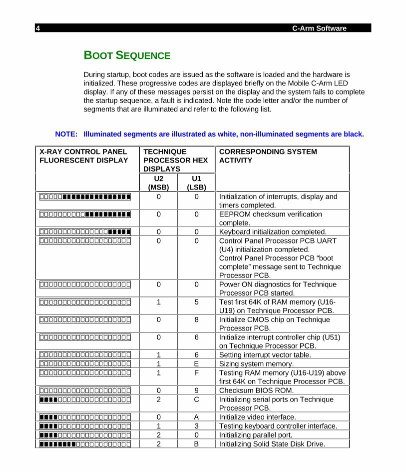
4 C-Arm Software
BOOT SEQUENCE
During startup, boot codes are issued as the software is loaded and the hardware isinitialized. These progressive codes are displayed briefly on the Mobile C-Arm LEDdisplay. If any of these messages persist on the display and the system fails to completethe startup sequence, a fault is indicated. Note the code letter and/or the number ofsegments that are illuminated and refer to the following list.
NOTE: Illuminated segments are illustrated as white, non-illuminated segments are black.
X-RAY CONTROL PANELFLUORESCENT DISPLAY
TECHNIQUEPROCESSOR HEXDISPLAYS
CORRESPONDING SYSTEMACTIVITY
U2(MSB)
U1(LSB)
0 0 Initialization of interrupts, display andtimers completed.
0 0 EEPROM checksum verificationcomplete.
0 0 Keyboard initialization completed.0 0 Control Panel Processor PCB UART
(U4) initialization completed.Control Panel Processor PCB “bootcomplete” message sent to TechniqueProcessor PCB.
0 0 Power ON diagnostics for TechniqueProcessor PCB started.
1 5 Test first 64K of RAM memory (U16-U19) on Technique Processor PCB.
0 8 Initialize CMOS chip on TechniqueProcessor PCB.
0 6 Initialize interrupt controller chip (U51)on Technique Processor PCB.
1 6 Setting interrupt vector table.1 E Sizing system memory.1 F Testing RAM memory (U16-U19) above
first 64K on Technique Processor PCB.0 9 Checksum BIOS ROM.2 C Initializing serial ports on Technique
Processor PCB.0 A Initialize video interface.1 3 Testing keyboard controller interface.2 0 Initializing parallel port.2 B Initializing Solid State Disk Drive.
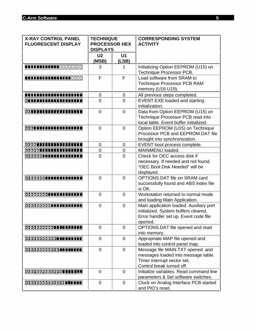
C-Arm Software 5
X-RAY CONTROL PANELFLUORESCENT DISPLAY
TECHNIQUEPROCESSOR HEXDISPLAYS
CORRESPONDING SYSTEMACTIVITY
U2(MSB)
U1(LSB)
3 1 Initializing Option EEPROM (U15) onTechnique Processor PCB.
F F Load software from SRAM toTechnique Processor PCB RAMmemory (U16-U19).
0 0 All previous steps completed.0 0 EVENT.EXE loaded and starting
initialization.0 0 Data from Option EEPROM (U15) on
Technique Processor PCB read intolocal table. Event buffer initialized.
0 0 Option EEPROM (U15) on TechniqueProcessor PCB and EEPROM.DAT filebrought into synchronization.
0 0 EVENT boot process complete.0 0 MAINMENU loaded.0 0 Check for OEC access disk if
necessary. If needed and not found,“OEC Boot Disk Needed” will bedisplayed.
0 0 OPTIONS.DAT file on SRAM cardsuccessfully found and ABS index fileis OK.
0 0 Workstation returned to normal modeand loading Main Application.
0 0 Main application loaded. Auxiliary portinitialized. System buffers cleared.Error handler set up. Event code fileopened.
0 0 OPTIONS.DAT file opened and readinto memory.
0 0 Appropriate MAP file opened andloaded into control panel map.
0 0 Message file MAIN.TXT opened andmessages loaded into message table.Timer interrupt vector set.Control break turned off.
0 0 Initialize variables. Read command lineparameters & Set software switches.
0 0 Clock on Analog Interface PCB startedand PIO’s reset.
6 C-Arm Software
X-RAY CONTROL PANELFLUORESCENT DISPLAY
TECHNIQUEPROCESSOR HEXDISPLAYS
CORRESPONDING SYSTEMACTIVITY
U2(MSB)
U1(LSB)
0 0 Control panel key pulse rates set.Data files opened and loaded.MUX RAM addresses set & A/Dconversion data set.
0 0 Read calibration coefficients fromEEPROM.Open ABS index file and store inmemory.Find and open default ABS table.Servo to center of default ABS table.Open and load MALIMIT.DAT file.
0 0 Set default values and set variables tothe values in OPTIONS.DAT file.
0 0 Hardware integrity checked andinterlocks started.
0 0 Cart communications initialized.Table communications initialized.Stator started.Filaments started.Interlocks checked.Faults checked.
0 0 Checked for disconnected batteries.Set Analog Interface PCB to AUTOFLUORO.Set Workstation to AUTO FLUORO.Set speaker pitch.Set control panel to default values,send the default technique to AnalogInterface PCB, set up standby timers.Clear control panel and Workstationbuffers.Tell Workstation that generator isready.Open camera iris.Initialize heat parameters.Initialize charger.
0 2 .7 1 3 0 0 kV and mA values displayed on X-raycontrol panel.
For a listing of Errors and their associated Error Codes, refer to the Error CodeSection .

C-Arm Software 7
MAINFRAME MENUThe Mainframe Menu (Error Section) is accessed using the Workstation. TheWorkstation is used as a terminal since the generator assembly does not have its owndirect serial link for using this program. This service software contains several optionswhich are explained in the next few pages. Perform the following steps to access thisgenerator service software.
ACCESSING THE MAINFRAME MENU
1. With the system powered on, insert the OEC access disk into the floppy drive atthe rear of the Workstation.
2. Press the SETUP OPTIONS key on the Workstation.
3. Use the cursor control keys (or trackpad) to highlight the Access Level 2 (Service)sub-menu and press ENTER (or superkey).
4. Select Access Mainframe Menu. When this option is selected, the following menuappears on the left monitor.
****** MAINFRAME MENU ******
A. Run Applications (Take X-rays)B. Run Applications with ParametersC. Run CalibrationD. System ConfigurationE. mA Limit File EditorF. Examine Event FileG. Run StatusH. Collimator Calibration (System will reboot)I. Language OptionsJ. ABS Index File Editor
<ESC> - Return to DOS
Enter command letter:
NOTE: When this service software is activated, the generator interlocks are broken in orderto prevent X-rays.
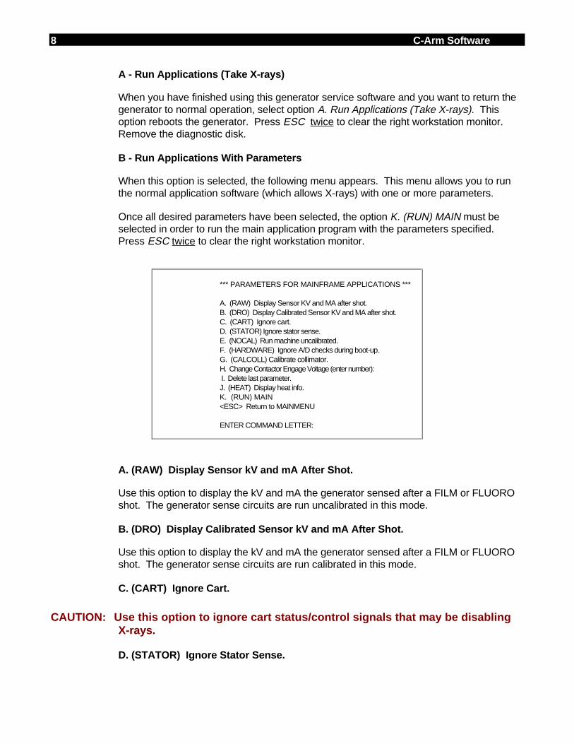
8 C-Arm Software
A - Run Applications (Take X-rays)
When you have finished using this generator service software and you want to return thegenerator to normal operation, select option A. Run Applications (Take X-rays). Thisoption reboots the generator. Press ESC twice to clear the right workstation monitor.Remove the diagnostic disk.
B - Run Applications With Parameters
When this option is selected, the following menu appears. This menu allows you to runthe normal application software (which allows X-rays) with one or more parameters.
Once all desired parameters have been selected, the option K. (RUN) MAIN must beselected in order to run the main application program with the parameters specified.Press ESC twice to clear the right workstation monitor.
*** PARAMETERS FOR MAINFRAME APPLICATIONS ***
A. (RAW) Display Sensor KV and MA after shot.B. (DRO) Display Calibrated Sensor KV and MA after shot.C. (CART) Ignore cart.D. (STATOR) Ignore stator sense.E. (NOCAL) Run machine uncalibrated.F. (HARDWARE) Ignore A/D checks during boot-up.G. (CALCOLL) Calibrate collimator.H. Change Contactor Engage Voltage (enter number): I. Delete last parameter.J. (HEAT) Display heat info.K. (RUN) MAIN<ESC> Return to MAINMENU
ENTER COMMAND LETTER:
A. (RAW) Display Sensor kV and mA After Shot.
Use this option to display the kV and mA the generator sensed after a FILM or FLUOROshot. The generator sense circuits are run uncalibrated in this mode.
B. (DRO) Display Calibrated Sensor kV and mA After Shot.
Use this option to display the kV and mA the generator sensed after a FILM or FLUOROshot. The generator sense circuits are run calibrated in this mode.
C. (CART) Ignore Cart.
CAUTION: Use this option to ignore cart status/control signals that may be disablingX-rays.
D. (STATOR) Ignore Stator Sense.
C-Arm Software 9
CAUTION: Use this option to ignore the stator sense circuit.
E. (NOCAL) Run machine uncalibrated.
Do not use this option.
F. (HARDWARE) Ignore A/D checks during boot-up.
CAUTION: Use this option to ignore A/D failures.
G. (CALCOLL) Calibrate collimator.
Use this option to calibrate the collimator. See the Image Calibration section for detailson this procedure.
H. Change Contactor Engage Voltage (enter number):
CAUTION: Do not use this option under any circumstances.
I. Delete last parameter.
Use this option to delete the last parameter that appears on the same line as option K.(RUN).
J. (HEAT) Display Heat Info.
Do not use this option.
K. (RUN) MAIN
Use this option to start the generator application software when the desired parametershave been selected. This parameters appear on this same line.
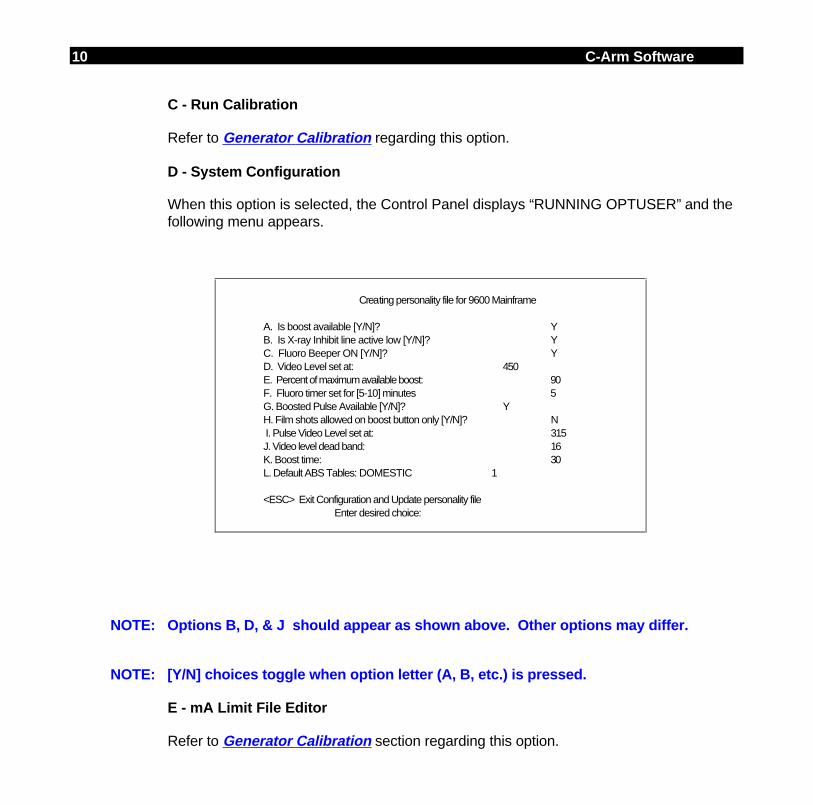
10 C-Arm Software
C - Run Calibration
Refer to Generator Calibration regarding this option.
D - System Configuration
When this option is selected, the Control Panel displays “RUNNING OPTUSER” and thefollowing menu appears.
Creating personality file for 9600 Mainframe
A. Is boost available [Y/N]? YB. Is X-ray Inhibit line active low [Y/N]? YC. Fluoro Beeper ON [Y/N]? YD. Video Level set at: 450E. Percent of maximum available boost: 90F. Fluoro timer set for [5-10] minutes 5G. Boosted Pulse Available [Y/N]? YH. Film shots allowed on boost button only [Y/N]? N I. Pulse Video Level set at: 315J. Video level dead band: 16K. Boost time: 30L. Default ABS Tables: DOMESTIC 1
<ESC> Exit Configuration and Update personality file Enter desired choice:
NOTE: Options B, D, & J should appear as shown above. Other options may differ.
NOTE: [Y/N] choices toggle when option letter (A, B, etc.) is pressed.
E - mA Limit File Editor
Refer to Generator Calibration section regarding this option.
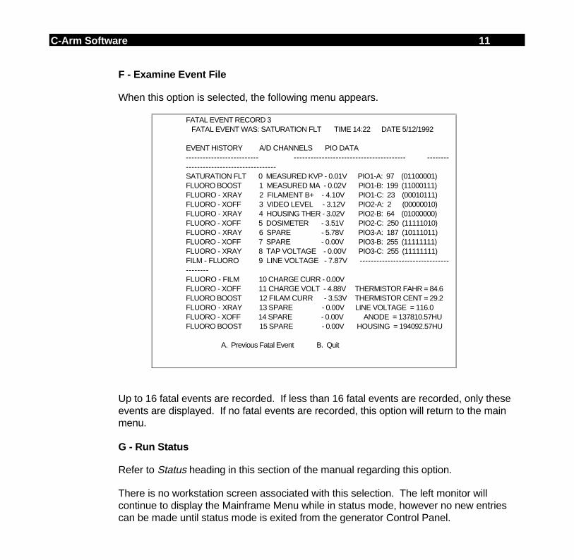
C-Arm Software 11
F - Examine Event File
When this option is selected, the following menu appears.
FATAL EVENT RECORD 3 FATAL EVENT WAS: SATURATION FLT TIME 14:22 DATE 5/12/1992
EVENT HISTORY A/D CHANNELS PIO DATA-------------------------- ---------------------------------------- ----------------------------------------SATURATION FLT 0 MEASURED KVP - 0.01V PIO1-A: 97 (01100001)FLUORO BOOST 1 MEASURED MA - 0.02V PIO1-B: 199 (11000111)FLUORO - XRAY 2 FILAMENT B+ - 4.10V PIO1-C: 23 (00010111)FLUORO - XOFF 3 VIDEO LEVEL - 3.12V PIO2-A: 2 (00000010)FLUORO - XRAY 4 HOUSING THER - 3.02V PIO2-B: 64 (01000000)FLUORO - XOFF 5 DOSIMETER - 3.51V PIO2-C: 250 (11111010)FLUORO - XRAY 6 SPARE - 5.78V PIO3-A: 187 (10111011)FLUORO - XOFF 7 SPARE - 0.00V PIO3-B: 255 (11111111)FLUORO - XRAY 8 TAP VOLTAGE - 0.00V PIO3-C: 255 (11111111)FILM - FLUORO 9 LINE VOLTAGE - 7.87V ----------------------------------------FLUORO - FILM 10 CHARGE CURR - 0.00VFLUORO - XOFF 11 CHARGE VOLT - 4.88V THERMISTOR FAHR = 84.6FLUORO BOOST 12 FILAM CURR - 3.53V THERMISTOR CENT = 29.2FLUORO - XRAY 13 SPARE - 0.00V LINE VOLTAGE = 116.0FLUORO - XOFF 14 SPARE - 0.00V ANODE = 137810.57HUFLUORO BOOST 15 SPARE - 0.00V HOUSING = 194092.57HU
A. Previous Fatal Event B. Quit
Up to 16 fatal events are recorded. If less than 16 fatal events are recorded, only theseevents are displayed. If no fatal events are recorded, this option will return to the mainmenu.
G - Run Status
Refer to Status heading in this section of the manual regarding this option.
There is no workstation screen associated with this selection. The left monitor willcontinue to display the Mainframe Menu while in status mode, however no new entriescan be made until status mode is exited from the generator Control Panel.

12 C-Arm Software
H - Collimator Calibration (System will reboot)
There is no Workstation screen associated with this selection. When this selection ischosen, the system will reboot so that the iris collimator field sizes can be calibrated andthe data stored in the EEPROM on the Image Function PCB. Refer to the ImageSystem Calibration section in this manual for details of using this selection.
I - Language Options
When this option is selected the following menu will appear on the left Workstationmonitor and “RUNNING LANGOPT” will be displayed on the C-Arm control paneldisplay:
LANGUAGE OPTIONS Current language is ENGLISHA ENGLISHB FRENCHC GERMAND ITALIANE SPANISH
<ESC> - ExitEnter Command letter:
After a letter has been entered from the keyboard and the ESCAPE key has beenpressed, the C-Arm will reboot and the messages will be displayed in the selectedlanguage.
J - ABS Index File Editor
When this option is selected the following menu will appear on the left Workstationmonitor and “RUNNING ABS INDEX” will be displayed on the C-Arm control paneldisplay:
ABS INDEX TABLE EDITOR
A. Edit ABS Index FileB. Edit In Use ABS Records
<ESC> - ExitEnter Command Letter:
A. Edit ABS Index File
NOTE: Do not edit the VLI Offset and PVLI Offset values. These are factory set and mustnot be changed.
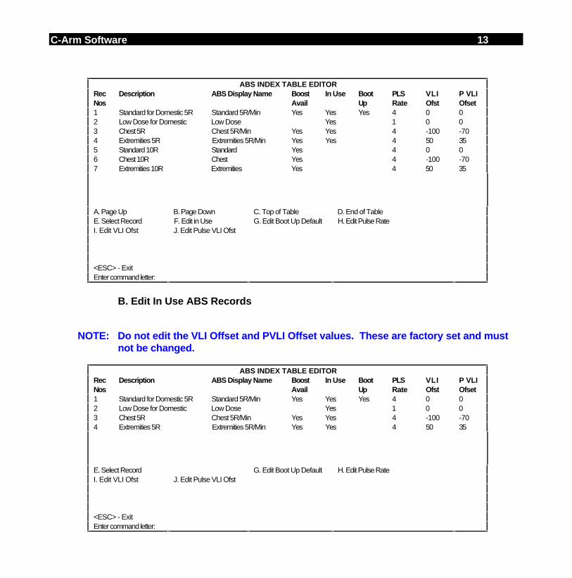
C-Arm Software 13
ABS INDEX TABLE EDITORRecNos
Description ABS Display Name BoostAvail
In Use BootUp
PLSRate
VLIOfst
P VLIOfset
1 Standard for Domestic 5R Standard 5R/Min Yes Yes Yes 4 0 02 Low Dose for Domestic Low Dose Yes 1 0 03 Chest 5R Chest 5R/Min Yes Yes 4 -100 -704 Extremities 5R Extremities 5R/Min Yes Yes 4 50 355 Standard 10R Standard Yes 4 0 06 Chest 10R Chest Yes 4 -100 -707 Extremities 10R Extremities Yes 4 50 35
A. Page Up B. Page Down C. Top of Table D. End of TableE. Select Record F. Edit in Use G. Edit Boot Up Default H. Edit Pulse RateI. Edit VLI Ofst J. Edit Pulse VLI Ofst
<ESC> - ExitEnter command letter:
B. Edit In Use ABS Records
NOTE: Do not edit the VLI Offset and PVLI Offset values. These are factory set and mustnot be changed.
ABS INDEX TABLE EDITORRecNos
Description ABS Display Name BoostAvail
In Use BootUp
PLSRate
VLIOfst
P VLIOfset
1 Standard for Domestic 5R Standard 5R/Min Yes Yes Yes 4 0 02 Low Dose for Domestic Low Dose Yes 1 0 03 Chest 5R Chest 5R/Min Yes Yes 4 -100 -704 Extremities 5R Extremities 5R/Min Yes Yes 4 50 35
E. Select Record G. Edit Boot Up Default H. Edit Pulse RateI. Edit VLI Ofst J. Edit Pulse VLI Ofst
<ESC> - ExitEnter command letter:

14 C-Arm Software
SRAM FILESThe following software files are found on the SRAM card:
IO.SYS DOS System FileMSDOS.SYS DOS SystemCOMMAND.COM DOS System9600.MAP Control Panel Map FileAUTOEXEC.BAT EVENT, MAINMENUABSINDEX.EXE Executable file - “J” ABS INDEX FILE EDITORABSINDEX.TXT Text file for ABS index file editorABSINDEX.DOM Domestic ABS index fileABSINDEX.EUR European ABS index fileABSINDEX.OPT Optional ABS index fileCAL-COEF.EXE Executable file -“C” RUN CALIBRATIONCALRANGE.DAT Defines calibration parametersCARM.DC Filament Duty Cycle Characterization DataCARM.CAL kV & mA Calibration DataCARM.VER kV & mA Calibration DataCHECKSUM.EXE Checksum program fileCSUMERR.EXE Checksum program fileEDITMA.EXE Executable file -“E” mA LIMIT FILE EDITOREEPROM.DAT mAs and Calibration DataEVENTEXT.ENG English text for event fileEVENT.EXE Captures fatal eventsEVENTEXT.FRE French text for event fileEVENTEXT.GER German text for event fileEVENTEXT.ITA Italian text for event fileEVENTEXT.SPA Spanish text for event fileEVENTEXT.TXT Text for event fileEXAMINE.EXE Executable file -“G” EXAMINE EVENTFILELANGOPT.EXE Executable file - “I” LANGUAGE OPTIONSMALIMIT.DAT mA Limit File Data - Created by EDITMA.EXEMAIN.EXE Executable file for C-Arm applications softwareMAIN.ENG English text for MAIN.EXEMAIN.FRE French text for MAIN.EXEMAIN.GER German text for MAIN.EXEMAIN.ITA Italian text for MAIN.EXEMAIN.SPA Spanish text for MAIN.EXEMAIN.TXT Main applications text fileMUX.DAT Analog MUX dataMAINMENU.EXE Executable file for Main MenuOPTIONS.DAT Options data - created by OPTUSER.EXEOPTIONS.FXD Used by OPTUSER.EXEOPTUSER.EXE Executable file - “D” SYSTEM CONFIGURATION5R_STD.ABS ABS Table for 5R/min Standard TableLOW-DOSE.ABS ABS Table for Low Dose10R_EXT.ABS ABS Table for 10R/min Extremities10R_STD.ABS ABS Table for 10R/min Standard Table

C-Arm Software 15
EUR_STD.ABS ABS Table for European Standard TableEUR_LOW.ABS ABS Table for European Low DoseOPT_STD.ABS ABS Table for Optional Standard TableOPT_LOW.ABS ABS Table for Optional Low Dose TableSTATUS.EXE Executable file - “H” CONTROL PANEL STATUSCHECKSUM.CHK Checksum program fileCSUMCHEK.CHK Checksum program fileFILECHEK.DAT In house file check dataLABEL.RPT In house use onlyRESULT.RPT In house use onlyALL.DAT Created at end of calibration by merging CARM.DC,
CARM.CAL, and CARM.VER

16 C-Arm Software
SRAM CARD
COPY FILES FROM 3 1/2-INCH FLOPPY DISK TO SRAM
A 3 1/2” floppy disk containing generator backup software is shipped with every 9600system. The disk contains the same files as contained on the SRAM card from theTechnique Processor PCB. If a problem arises with the SRAM card, the files can becopied from the floppy disk to the card using the following procedure.
Equipment required:
• Computer with PCMCIA port
• Software (loaded on computer) to recognize PCMCIA port(OEC P/N 00-900876-01)
• Generator backup software (3 1/2-inch disk)
NOTE: The 3 1/2-inch floppy disk contains data that is unique (calibration data, serialnumber) to that system. Do not use backup software from another system for thisprocedure.
1. Boot computer, insuring that the PCMCIA port is recognized by software.
2. Install SRAM card from Technique Processor PCB in PCMCIA port on computer,listen for beep from computer that indicates recognition of card.
3. Install 3 1/2-inch floppy backup disk on computer.
4. Format the SRAM card with the following command:
Format F:/U/S
5. Use the following command to copy the files from the floppy to the SRAM card:
copy A:*.* F:
NOTE: Assuming F drive as the PCMCIA port and A drive as the 3 1/2 “ floppy drive.
C-Arm Software 17
COPY FILES FROM SRAM TO 3 1/2-INCH FLOPPY DISK
Whenever a generator calibration is performed (see Generator Calibration section inthis manual), the new calibration data must be copied from the SRAM card on theTechnique Processor PCB to the 3 1/2” backup disk. This preserves the calibration datain the event of an SRAM card failure.
Equipment required:
• Computer with PCMCIA port
• Software (loaded on computer) to recognize PCMCIA port(OEC P/N 00-900876-01)
• Generator backup software (3 1/2-inch disk)
1. Boot computer, insuring that the PCMCIA port is recognized by software.
2. Install SRAM card from Technique Processor PCB in PCMCIA port on computer,listen for beep from computer that indicates recognition of card.
3. Install 3 1/2-inch floppy backup disk on computer.
4. Use the following command to copy the files from the SRAM card to the floppy disk:
copy F:*.* A:
NOTE: Assuming F drive as the PCMCIA port and A drive as the 3 1/2-inch floppy drive.
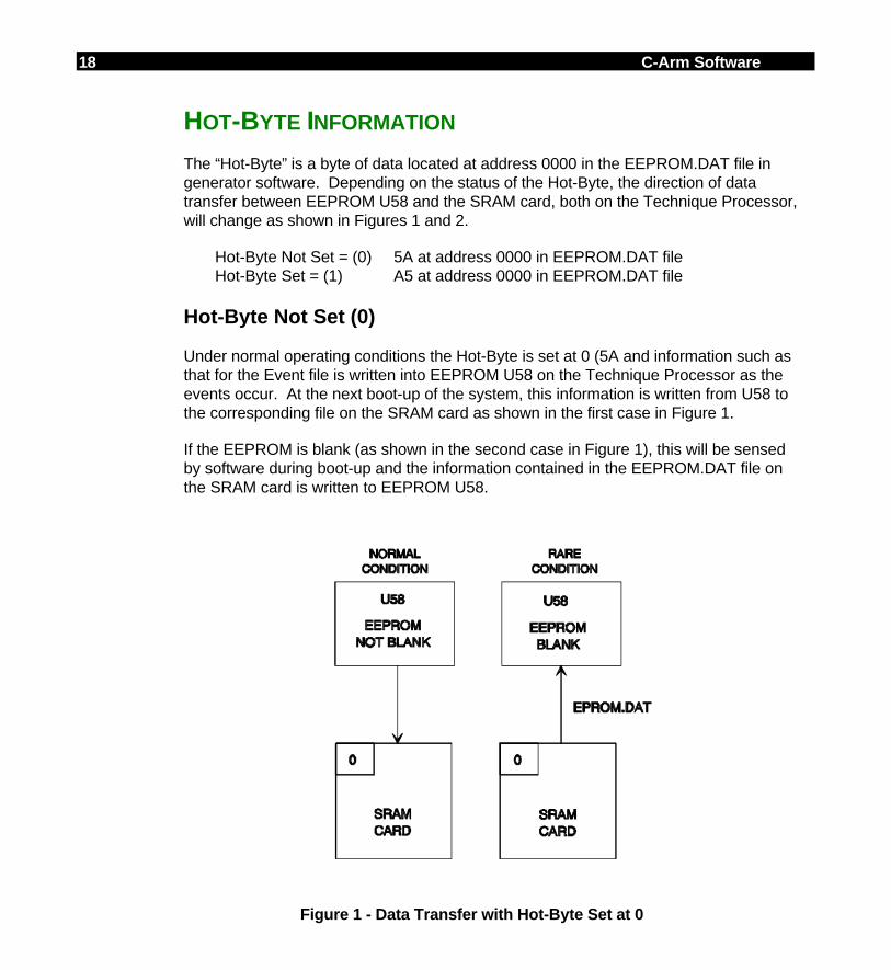
18 C-Arm Software
HOT-BYTE INFORMATION
The “Hot-Byte” is a byte of data located at address 0000 in the EEPROM.DAT file ingenerator software. Depending on the status of the Hot-Byte, the direction of datatransfer between EEPROM U58 and the SRAM card, both on the Technique Processor,will change as shown in Figures 1 and 2.
Hot-Byte Not Set = (0) 5A at address 0000 in EEPROM.DAT fileHot-Byte Set = (1) A5 at address 0000 in EEPROM.DAT file
Hot-Byte Not Set (0)
Under normal operating conditions the Hot-Byte is set at 0 (5A and information such asthat for the Event file is written into EEPROM U58 on the Technique Processor as theevents occur. At the next boot-up of the system, this information is written from U58 tothe corresponding file on the SRAM card as shown in the first case in Figure 1.
If the EEPROM is blank (as shown in the second case in Figure 1), this will be sensedby software during boot-up and the information contained in the EEPROM.DAT file onthe SRAM card is written to EEPROM U58.
Figure 1 - Data Transfer with Hot-Byte Set at 0
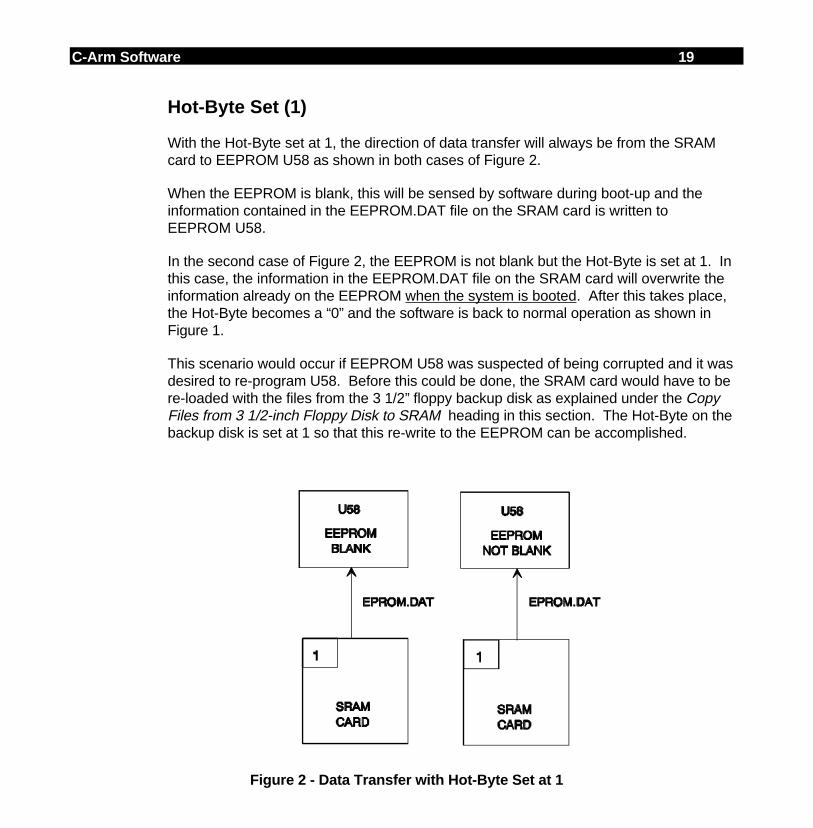
C-Arm Software 19
Hot-Byte Set (1)
With the Hot-Byte set at 1, the direction of data transfer will always be from the SRAMcard to EEPROM U58 as shown in both cases of Figure 2.
When the EEPROM is blank, this will be sensed by software during boot-up and theinformation contained in the EEPROM.DAT file on the SRAM card is written toEEPROM U58.
In the second case of Figure 2, the EEPROM is not blank but the Hot-Byte is set at 1. Inthis case, the information in the EEPROM.DAT file on the SRAM card will overwrite theinformation already on the EEPROM when the system is booted. After this takes place,the Hot-Byte becomes a “0” and the software is back to normal operation as shown inFigure 1.
This scenario would occur if EEPROM U58 was suspected of being corrupted and it wasdesired to re-program U58. Before this could be done, the SRAM card would have to bere-loaded with the files from the 3 1/2” floppy backup disk as explained under the CopyFiles from 3 1/2-inch Floppy Disk to SRAM heading in this section. The Hot-Byte on thebackup disk is set at 1 so that this re-write to the EEPROM can be accomplished.
Figure 2 - Data Transfer with Hot-Byte Set at 1

20 C-Arm Software
SRAM BATTERY REPLACEMENT
The SRAM card contains 2 batteries, an internal NI-CAD battery that is not replaceableand a 3 Volt Lithium battery which must be replaced annually to prevent loss of theSRAM files. The NI-CAD battery serves as a backup if the Lithium battery should fail.
There are two LEDs on the Solid State Drive that give an indication of the operation ofthe drive and the status of the Lithium battery. The LED closest to the SRAM is a“Status” LED. It will illuminate RED during disk access if the Lithium battery needs to bereplaced. The second LED is a “Busy” LED that indicates when the SRAM is beingaccessed. If both LEDs illuminate RED during disk access, the lithium battery is notcharged adequately.
WARNING... Do not remove the SRAM from the Solid State Drive when performing thisprocedure.
1. With the system booted and the SRAM in the Solid State Drive, remove the batteryholder and the battery as shown in Figure 3.
2. Replace the battery with a new 3 Volt, Lithium , 165 mAH battery.(OEC P/N 74-122904-00). Verify that the + sign is pointing up.
Figure 3 - SRAM Battery Replacement

INTERLOCK/STATOR
OVERVIEWThis section describes the operation of the following circuits:
• Generator Interlock• • Pre-charge• • Stator
These circuits are initialized and checked by the Technique Processor during the bootsequence. If a failure is detected during boot-up, the system will hang, not completing theboot sequence. An error message may be displayed on the Control Panel Display.
After system boot, the Technique Processor continues to monitor these circuits. An errormessage is displayed on the Control Panel Display and X-rays are prohibited, if a failureis detected.
REFERENCE DIAGRAMSThe theory in this section is most easily understood when using the following figures andschematics. Use the correct schematics for your system.
Generator Controller Assembly Drawing
Drawing # 00-875392 - All serial numbers
Analog Interface PCB
Schematic #00-876738 - Assembly #00-876740 - All system serial numbers
Mainframe Motherboard
Schematic #00-875539 - Assembly #00-900588System serial numbers 69-0001 thru 69-2000
Schematic #00-878396 - Assembly #00-900970System serial numbers 69-2001 and up
Power Motor Relay PCB
Figure 4Figure 5Schematic #00-875997 - Assembly #875999
All serial numbers
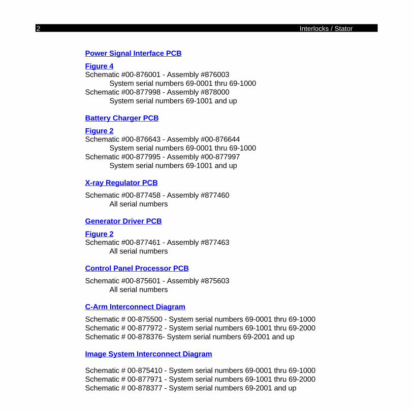
2 Interlocks / Stator
Power Signal Interface PCB
Figure 4Schematic #00-876001 - Assembly #876003
System serial numbers 69-0001 thru 69-1000Schematic #00-877998 - Assembly #878000
System serial numbers 69-1001 and up
Battery Charger PCB
Figure 2Schematic #00-876643 - Assembly #00-876644
System serial numbers 69-0001 thru 69-1000Schematic #00-877995 - Assembly #00-877997
System serial numbers 69-1001 and up
X-ray Regulator PCB
Schematic #00-877458 - Assembly #877460All serial numbers
Generator Driver PCB
Figure 2Schematic #00-877461 - Assembly #877463
All serial numbers
Control Panel Processor PCB
Schematic #00-875601 - Assembly #875603All serial numbers
C-Arm Interconnect Diagram
Schematic # 00-875500 - System serial numbers 69-0001 thru 69-1000Schematic # 00-877972 - System serial numbers 69-1001 thru 69-2000Schematic # 00-878376- System serial numbers 69-2001 and up
Image System Interconnect Diagram
Schematic # 00-875410 - System serial numbers 69-0001 thru 69-1000Schematic # 00-877971 - System serial numbers 69-1001 thru 69-2000Schematic # 00-878377 - System serial numbers 69-2001 and up
Interlocks / Stator 3
GENERATOR INTERLOCK
OVERVIEW
The interlock circuit provides a means to halt system operation through software when theTechnique Processor detects a major system fault or through hardware when a FASTSTOP switch is pressed.
The FAST STOP switches are located on either side of the control panel housing. Themessage, INTERLOCKS OPEN , will appear on both control panel displays when eitherFAST STOP switch is pressed. This is considered a fatal error and is recorded in theEVENT.DAT file. The system is still powered at this time and a system re-boot can becommanded by pressing any key on the control panel.
The interlock circuit is comprised of the following circuits:
• CPU INTERLOCK• FAST STOP• +24V INTERLOCK• JUMPER E5 / RELAY K4
CPU INTERLOCK
During the boot sequence the Technique Processor software toggles PIO U27-25, on theAnalog Interface PCB, at a 10 mS rate. Eighteen arrows are displayed on the ControlPanel display at the point in the boot sequence that this occurs.
This 10 mS interlock pulse is detected by pulse detector Q1, Q2 and associated circuitryon the Analog Interface PCB. As long as the interlock pulses are present, the pulsedetector holds relay K1 energized. This allows +15 VDC to pass through relay K1contacts 1 & 7 illuminating LED DS1 on the Analog Interface PCB. DS1 indicates that thesignal CPU INTERLOCK (+15V) is present.
The CPU INTERLOCK signal passes through the Motherboard to the Power Motor RelayPCB where it can be measured on TP3. CPU INTERLOCK momentarily energizes relayK8 on the Power Motor Relay PCB through the C7/R17 circuit. The CPU INTERLOCKsignal also passes through to the FAST STOP circuit described next.
NOTE
Click on a yellow box to go directly to the block diagram for this section. Do not use this link to return to a block diagram from this point. Click on the << button in the Tool Bar to return to any starting point.

4 Interlocks / Stator
FAST STOP
The CPU INTERLOCK signal passes through both normally closed FAST STOP switchesS1 & S2 and then back to the Power Motor Relay PCB. If a FAST STOP switch ispressed the interlock circuit is disabled preventing X-ray generation and motor movement.The path that the CPU INTERLOCK signal takes is described below.
1. The CPU INTERLOCK passes through the energized relay K10contacts 3 & 4 on the Power Motor Relay PCB. Relay K10 is energizedby +12V (KEY_PWR) when the system is turned on. (See PowerDistribution section for more information.)
2. CPU INTERLOCK then passes through the de-energized relay K4contacts 11 & 13 on the Power Motor Relay PCB and becomesEMERGENCY_OFF_B (+15V).
3. EMERGENCY_OFF_B passes through the Motherboard, Power SignalInterface PCB and Control Panel Processor PCB where it becomesEMEROF_HI (+15V).
4. EMEROF_HI passes through both normally closed FAST STOPswitches S1 & S2. After passing through S2 it becomes EMEROF_LO(+15V).
5. EMEROF_LO is then fed back through the Control Panel ProcessorPCB, Power Signal Interface PCB and Motherboard to the Power MotorRelay PCB where it becomes EMERGENCY_OFF_ A (+15V).
EMERGENCY_OFF _A then passes through the momentarily energized relay K8contacts 4 & 8, on the Power Motor Relay PCB energizing relay K9. When relay K9energizes EMERGENCY_OFF _A passes through the hold-in contacts 4 & 5 back to thecoil. This holds relay K9 energized after the momentary relay K8 de-energizes. Also,+24V (+24V_IN) passes through contacts 10 & 11 of relay K9 and becomes+24V_INTERLOCK. The +24V_INTERLOCK circuit is described next.
Interlocks / Stator 5
+24V INTERLOCK
The +24V_INTERLOCK signal passes through the Battery Charger PCB to the X-rayRegulator PCB where it turns on transistor Q1. When Q1 turns on, the signal INTLK goeslow. The logic low INTLK signal goes through the Motherboard to the Analog InterfacePCB where it passes through buffer U45 pins 13 & 7 to PIO U27-11. The PIO U27 passesthe logic low INTLK signal to the Technique Processor via the data bus. This informs theTechnique Processor that the interlock circuit is complete.
In addition, the +24V_INTERLOCK supplies power to other relays in various circuits aslisted below.
• Relay K2 - The HVDRA & HVDRB safety relay in the kV circuit on the GeneratorDriver PCB
• Relay K1 - The filament select relay in the mA circuit on the Generator Driver PCB.
• Relays K1 & K2 - The pre-charge relays.
INTERLOCK FAULT CONDITIONS
DURING THE SYSTEM BOOT SEQUENCE
The system will hang with 18 arrows on the Control Panel display if the TechniqueProcessor PCB does not receive the logic low INTLK signal indicating a successfulinterlock complete.
AFTER A SUCCESSFUL SYSTEM BOOT
INTERLOCKS OPEN - This message will appear on the Control Panel display if there is afailure in the interlock circuit that causes the INTLK signal to the Technique ProcessorPCB to go high. This is a fatal error that prevents X-rays and motor movements. Thismessage will also occur if one of the FAST STOP switches is pressed. The system is stillpowered at this time and a system re-boot can be commanded by pressing any key on thecontrol panel.

6 Interlocks / Stator
JUMPER E5/RELAY K4 - POWER MOTOR RELAY PCB
Jumper E5 on the Power Motor Relay PCB is not installed during normal operation.However, when installed, it gives service personnel the ability to elevate or rotate theC-Arm in the event that the C-Arm will not boot.
Normally relay K4 on the Power Motor Relay PCB is de-energized allowing the interlockcircuit to function properly, as described previously. When jumper E5 is installed, the+24V_IN signal is connected to relay K4’s coil, energizing it. The +24V_IN signal thenpasses through contacts 6 & 4 of relay K4. This energizes relay K3 in the C-Arm lift androtation circuit applying power to the motors. (See the lift and rotation sections of theMechanical section for more information on the motor circuits)
Interlocks / Stator 7
PRE-CHARGE
OVERVIEW
After detecting the interlock is complete during the boot sequence, The TechniqueProcessor PCB initiates the pre-charge circuit. The pre-charge capacitors C2 & C3 arecharged to the B+ voltage, (approximately 221 VDC). The pre-charge capacitors C2 &C3, located in the Generator Controller Assembly, provide a buffer between the kV/mAregulation circuits and the batteries/battery charger.
Nineteen arrows are displayed on the Control Panel display at the point in the bootsequence that the pre-charge circuit is initialized.
The pre-charge circuit is comprised of the following circuits:
• Current Limited Pre-Charging• Normal Pre-Charging• Pre-Charge Voltage Sensing• Capacitor Discharge
CURRENT LIMITED PRE-CHARGING
The Technique Processor PCB initiates the pre-charge sequence by commanding PIOU38-19 on the Analog Interface PCB to go high. This high passes through buffer U45 pins4 & 16, turning on transistor Q4 which places a low on the signal PRECHARGE.
The PRECHARGE signal passes through the Motherboard and X-ray Regulator PCB,energizing Relay K1 located in the Generator Controller Assembly. This allows chargingof the pre-charge capacitors C2 & C3 from the batteries/battery charger through relay K1contacts 6 & 9 and resistor R1. Resistor R1 limits the initial in-rush current to thecapacitors.
NOTE
Click on a yellow box to go directly to the block diagram for this section. Do not use this link to return to a block diagram from this point. Click on the << button in the Tool Bar to return to any starting point.

8 Interlocks / Stator
NORMAL PRE-CHARGING
The Technique Processor commands the PIO U38-18, on the Analog Interface PCB, togo high after detecting an approximate charge of 185 VDC across the pre-chargecapacitors C2 & C3. (See PRE-CHARGE VOLTAGE SENSING for a description of howthe Technique Processor PCB senses the voltage across the pre-charge capacitors). Thishigh passes through buffer U45 pins 17 & 3, turning on transistor Q5 which places a lowon the signal CONTACT.
The CONTACT signal passes through the Motherboard and X-ray Regulator PCB,energizing Relay K2 located in the Generator Controller Assembly. This allows thecontinued charging of pre-charge capacitors C2 & C3 directly from the batteries andbattery charger through relay K2 contacts 5 & 6, bypassing current limiting resistor R1.
PRE-CHARGE VOLTAGE SENSING
The voltage across the pre-charge capacitors C2 & C3 is applied through fuse F3 on theGenerator Driver PCB to the voltage divider R10/R11. This voltage divider scales the pre-charge capacitor voltage to approximately 2.5% of the original value. This scaled voltagebecomes the +200VSNS signal. The +200VSNS signal is monitored by the TechniqueProcessor PCB through A/D Mux U3-8 on the Analog Interface PCB.
When the Technique Processor detects approximately 4.5 VDC on the +200VSNS line(185 VDC across the pre-charge capacitors C2 & C3) it energizes relay K2 as describedpreviously in the Normal Pre-Charging section.
If the Technique processor never sees the +200VSNS signal reach approximately 4.5VDC during the boot sequence, a pre-charge error is detected.(See Pre-Charge Error)
PRE-CHARGE ERROR
The message PRE-CHARGE FAIL will be displayed on the Control Panel display if theTechnique Processor PCB does not see the +200VSNS signal reach approximately 4.5VDC during the boot sequence (Approximately 185 VDC across pre-charge capacitors).This is a fatal error that prevents the system boot from completing.
CAPACITOR DISCHARGE
When the system is powered off or the +24 interlock is lost, relay K1 is deactivated. Thisplaces resistor R1 between the positive and negative sides of pre-charge capacitors C2 &C3 through relay K1 contacts 3 & 9. Resistor R1 discharges the capacitors.
Interlocks / Stator 9
STATOR
OVERVIEW
After the completion of the pre-charge cycle during the boot sequence, the TechniqueProcessor PCB initiates the stator motor in the X-ray tube. The stator motor is started byapplying 115VAC to it for two seconds. After the two second interval, the voltage appliedto the stator motor drops to a continuous 40VAC which maintains the stator speed atapproximately 3500 RPM.
Nineteen arrows are displayed on the Control Panel display at the point in the bootsequence that the stator is initialized.
To reduce heat and power consumption, power to the stator motor is terminated after fiveminutes of no activity sensed on the Control Panel. Power to the stator motor can berestored by pressing a switch (except X-ray switch) on the control panel.
The stator circuit is comprised of the following circuits:
• Stator Start• Stator Run• Stator Current Sense• Stator Thermal Cutoff Switch
NOTE
Click on the yellow box to go directly to the block diagram for this section. Do not use this link to return to a block diagram from this point. Click on the << button in the Tool Bar to return to any starting point.
10 Interlocks / Stator
STATOR START
The Technique Processor PCB initiates the stator circuit by commanding the AnalogInterface PCB PIO U38 pin 20 & 23 to go high.
The high out of PIO U38-20 passes through buffer U45 pins 15 & 5, turning on transistorQ3, causing the STAT_RUN signal to go low. This low passes through the Motherboard,energizing relay K1 and illuminating LED DS1 on the Power Motor Relay PCB.
The high out of PIO U38-23 passes through buffer U45 pins 13 & 7, turning on transistorQ7, causing the STATSTRT signal to go low. This low passes through the Motherboard,energizing relay K2 and illuminating LED DS2 on the Power Motor Relay PCB.
This applies 115VAC to the stator motor through relay K1 contacts 5 & 6, relay K2contacts 5 & 6, current sense transformer T1 and circuit breaker CB2. The 115VAC isapplied to the stator motor for two seconds, starting the stator and bringing it up to speed.
STATOR RUN
After the initial two second start sequence, the Technique Processor PCB commands theAnalog Interface PCB PIO U38-23 low. This low passes through buffer U45 pins13 & 7, turning off transistor Q7, causing the STATSTRT signal to go high. This highpasses through the Motherboard, de-energizing relay K2 and turning off LED DS2 on thePower Motor Relay PCB.
Relay K1 on the Power Motor Relay PCB is still energized at this time, allowing 115VACto pass through contacts 5 & 6 to the stator transformer T3. (See figure 4 ) Statortransformer T3 steps the 115VAC down to 40VAC. This 40VAC is applied to the statormotor through the de-energized relay K2 contacts 7 & 6, current sense transformer T1 andcircuit breaker CB2. The 40VAC is applied to the stator motor continuously, keeping thestator spinning at approximately 3500 RPM.

Interlocks / Stator 11
STATOR CURRENT SENSE
As discussed previously, the stator current passes through the current sense transformerT1 on the Power Motor Relay PCB. Operational amplifier U19 pins 2 & 3 on the AnalogInterface PCB monitors the stator current by sensing the induced current on thesecondary of the current sense transformer T1 (STATOR SENSE).
U19 amplifies the STATOR SENSE signal and the output on pin 1 is fed to a voltageclipping circuit comprised of diodes CR5, CR6, CR7, resistor R15, and capacitor C17.The clipping circuit converts the AC waveform from U19-1 to a +5 VDC voltage whenstator current is present.
The +5 VDC is inverted by U24 pins 5 & 4 to a logic low signal that is monitored by theTechnique Processor PCB through Analog Interface PIO U27-10.
STATOR NOT ON ERROR
When the stator is drawing current, the signal on the Analog Interface PCB PIO U27-10 islow. The error message STATOR NOT ON will be displayed on the Control Panel displayif the Technique Processor detects a high on PIO U27-10 indicating that the stator is notdrawing current. This is a fatal error that prevents X-rays and motor movement.
STATOR THERMAL CUTOFF SWITCHA thermal cutoff switch, located in the X-ray tube housing assembly, is wired in series withthe Stator Neutral. If the temperature within the X-ray Tube Housing exceeds safeoperating conditions, the thermal switch opens, interrupting current to the stator motor.This is detected by the Technique Processor PCB through the stator current sense circuitas described previously and a STATOR NOT ON error condition is detected.
THERMAL CUTOFF SWITCH
COLLIMATOR
HIGH VOLTAGE CABLE CONNECTORS
X-RAY TUBE ASSEMBLY
Figure 1 X-ray Tube Housing
NOTE
Click on the top colored box to go directly to the Illustrated Parts Manual for systems bearing serial numbers 69-001 thru 69-999. Click on the top colored box to go directly to the Illustrated Parts Manual for systems bearing serial numbers 69-1000 and higher. Click the << button on the TOOL Bar to return to this point.
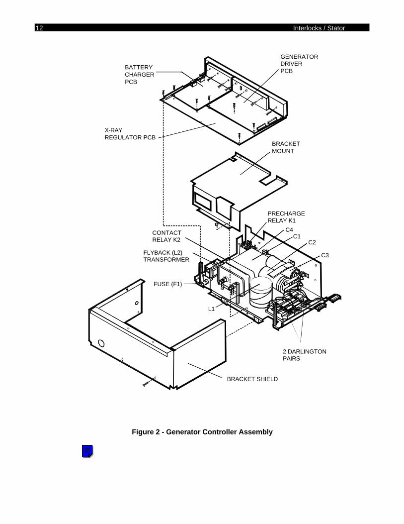
12 Interlocks / Stator
BATTERYCHARGERPCB
X-RAY REGULATOR PCB
CONTACTRELAY K2
FLYBACK (L2)TRANSFORMER
FUSE (F1)
L1
BRACKET SHIELD
2 DARLINGTONPAIRS
PRECHARGERELAY K1
C4C1
C2
C3
BRACKETMOUNT
GENERATORDRIVERPCB
Figure 2 - Generator Controller Assembly
NOTE
Click on the top colored box to go directly to the Illustrated Parts Manual for systems bearing serial numbers 69-001 thru 69-999. Click on the bottom colored box to go directly to the Illustrated Parts Manual for systems bearing serial numbers 69-1000 and higher. Click the << button on the TOOL Bar to return to this point.
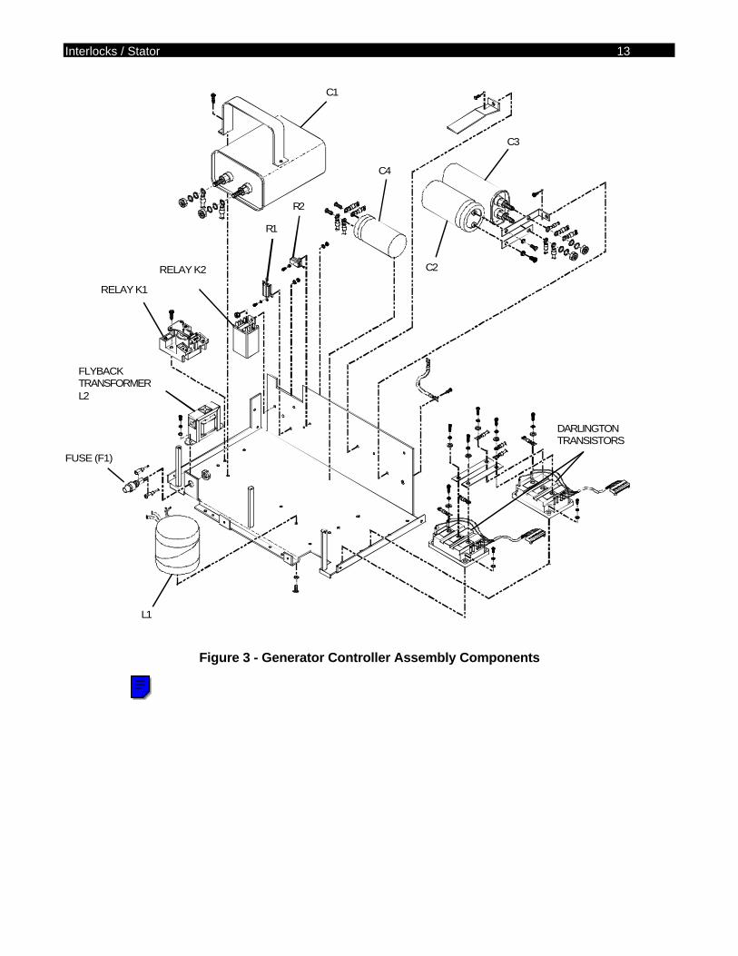
Interlocks / Stator 13
FUSE (F1)
FLYBACKTRANSFORMERL2
RELAY K1
RELAY K2
C1
C2
C3
L1
DARLINGTONTRANSISTORS
C4
R1
R2
Figure 3 - Generator Controller Assembly Components
NOTE
Click on the top colored box to go directly to the Illustrated Parts Manual for systems bearing serial numbers 69-001 thru 69-999. Click on the bottom colored box to go directly to the Illustrated Parts Manual for systems bearing serial numbers 69-1000 and higher. Click the << button on the TOOL Bar to return to this point.
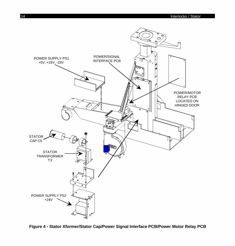
14 Interlocks / Stator
POWER/MOTORRELAY PCB
LOCATED ONHINGED DOOR
POWER/SIGNALINTERFACE PCB
POWER SUPPLY PS1+5V, +15V, -15V
POWER SUPPLY PS2+24V
STATORTRANSFORMER
T3
STATORCAP C5
Figure 4 - Stator Xformer/Stator Cap/Power Signal Interface PCB/Power Motor Relay PCB
NOTE
Click on the top colored box to go directly to the Illustrated Parts Manual for systems bearing serial numbers 69-001 thru 69-999. Click on the bottom colored box to go directly to the Illustrated Parts Manual for systems bearing serial numbers 69-1000 and higher. Click the << button on the TOOL Bar to return to this point.
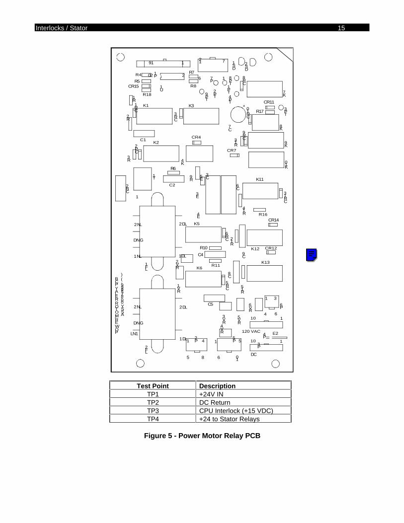
Interlocks / Stator 15
120 VAC
DC
712
6 1
64
31
10
5
6
1
85
41
POWER/MOTOR RELAY PCB
ASSY 00-875999- ( )
110
LN1
GND
LN2 LD2
LD1
LN1
GND
LN2 LD2
LD1
1
110
2
119
20
CR15
RV4
RV1
RV2
RV3
RV5
RV6
P4
LF2
LF1
K10
K1
K2
K3
K5
K6
K11
K12
K13
R9
E5
K4
K8
TP9
TP8
TP4
TP3
TP2 T
P1
DS2
DS1
E2
CB2
C3
C6
E3
E4
C1
C4
C2
C5
C8
C9
T1
C7
CR4
CR14
CR3
CR9
CR8
CR6
CR1
CR10
CR2
CR7
CR13
CR5
CR12
CR11
P6
P2
P5
P7
R6
R14
R16
R2
R10
R11
R15
R12
P3
P1
K7
K9
U1
R18
R17
R5
R13
R3
R1
R4R7
R8
Test Point DescriptionTP1 +24V INTP2 DC ReturnTP3 CPU Interlock (+15 VDC)TP4 +24 to Stator Relays
Figure 5 - Power Motor Relay PCB
NOTE
Click in the blue box to go directly to the Electrical Schematic Diagram for the PCB shown on this page. Click the << button on the Tool Bar to return to this page.

X-RAY ON/DISABLE
OVERVIEWThis section describes the following circuits:
• X-ray Enable
• X-ray On
• X-ray Disable
X-rays can be initiated from the control panel, handswitch or the footswitch. Switchclosures are monitored by the Technique Processor PCB via the Analog Interface PCB.When an X-ray switch is pressed, the XRAYEN and XRAYON signals go active,enabling the kV and mA servo loops, resulting in the production of X-rays.
The Technique Processor PCB also monitors the XRYDISBL signal from theWorkstation, via the Analog Interface PCB. This gives the Workstation the capability ofprohibiting X-rays by disabling the XRAYON signal.
REFERENCE SCHEMATICSThe theory in this section is best understood when using the following schematics. Usethe correct schematics for your system.
Analog Interface PCB
Schematic #00-876738 - Assembly #00-876740All system serial numbers
Mainframe Motherboard
Schematic #00-875539 - Assembly #00-900588System serial numbers 69-0001 thru 69-2000Schematic #00-878396 - Assembly #00-900970System serial numbers 69-2001 and up
Power Motor Relay PCB
Schematic #00-875997 - Assembly #875999All serial numbers
NOTE
Click on a yellow box to go directly to the block diagram for this section. Do not use this link to return to a block diagram from this point. Click on the << button in the Tool Bar to return to any starting point.
2 X-ray On / Disable
Power Signal Interface PCB
Schematic #00-876001 - Assembly #876003System serial numbers 69-0001 thru 69-1000Schematic #00-877998 - Assembly #878000System serial numbers 69-1001 and up
X-ray Regulator PCB
Schematic #00-877458 - Assembly #877460 - All serial numbers
Control Panel Processor PCB
Schematic #00-875601 - Assembly #875603 - All serial numbers
C-Arm Interconnect Diagram
Schematic # 00-875500 - System serial numbers 69-0001 thru 69-1000Schematic # 00-877972 - System serial numbers 69-1001 thru 69-2000Schematic # 00-878376 - System serial numbers 69-2001 and up
Workstation Interconnect Diagram
Schematic # 00-876158 - System serial numbers 69-0001 thru 69-1000Schematic # 00-877970 - System serial numbers 69-1001 thru 69-2000
Video Switching PCB
Schematic # 00-872237 - All serial numbers
Image Processor PCB
Schematic # 00-875952 - All serial numbers
Auxiliary Interface PCB
Schematic # 00-876502 - All serial numbers
Communications PCB
Schematic # 00-872125 - All serial numbers

X-ray On / Disable 3
X-RAY ENABLE
SECURITY SIGNAL
When any X-ray mode switch from the control panel, handswitch or footswitch ispressed, a logic high is placed on the SECURITY signal. The logic high SECURITYsignal passes through the Motherboard to the Analog Interface PCB optocoupler U51-1.
The logic low output from optoicoupler U51-7 passes through a 300mS delay circuitcomprised of R33 and C36 to Inverter U25-1 on the Analog Interface PCB. The logichigh SECURITY signal output from inverter U25-2 informs the Technique ProcessorPCB, through the Analog Interface PCB PIO U38-15, that an X-ray mode switch ispressed. See the X-RAYON for additional information.
X-RAYEN SIGNAL
The logic high SECURITY signal output from inverter U25-2 also passes throughinverter U24 pins 3 & 2 and nand gate U41 pins 9,10 & 8 on the Analog Interface PCB.The logic high output from nand gate U41-8 is called XRAYEN and is applied to inverterU6-1 on the X-ray Regulator PCB.
The logic low XRAYEN signal output from inverter U6-3 is applied to the kV Drive PALU7-5 and FIL Drive PAL U10-3 on the X-ray Regulator PCB. The logic low XRAYENsignal, along with X-RAYON enables the kV and mA servo loops. See the XRAYON foradditional information.

4 X-ray On / Disable
X-RAY ON
X-RAY MODE SWITCH MONITORING
The Technique Processor PCB is informed that an X-ray mode switch is pressed bymonitoring the SECURITY signal discussed previously. In addition, the TechniqueProcessor needs to determine what X-ray mode switch is pressed. The TechniqueProcessor accomplishes this by monitoring the Analog Interface PCB PIO U38pins 10, 11 & 12 according to Table 1.
SWITCH NAME SOURCE SIGNAL NAMEPIOU38PIN
SWITCHPRESSED
LOGICLEVEL
X-ray Control X-RAY SWITCH 10 HighProcess Fluoro Footswitch X-RAY SWITCH 10 HighBoost Footswitch BOOST 11 HighScout Fluoro Footswitch FLUORO ONLY 12 HighProcess Boost Handswitch BOOST 11 HighScout Fluoro Handswitch FLUORO ONLY 12 High
Table 1 X-ray Mode Switch Monitoring
When an X-ray mode switch is pressed, the corresponding signals listed in Table 1becomes a logic high. This high passes through inverting optocouplers U50 and U52 onthe Analog Interface PCB and becomes a logic low. This low is inverted to a logic highby inverter U25 on the Analog Interface PCB and is read by the Technique ProcessorPCB through PIO U38 as indicated in Table 1 above.
X-RAYON SIGNAL
Provided there is no X-ray disable command from the Workstation (See X-RAYDISABLE for additional information), the Technique Processor PCB acknowledges thatit has identified what X-ray mode switch is pressed and has received the SECURITYsignal by sending a logic low through the Analog Interface PCB PIO U27-24 to ‘or’ gateU2-2. Since the SECURITY signal out of inverter U24-2 on the Analog Interface PCB isalso a logic low at this time, ‘or’ gate U21-3 output goes low. See SECURITY foradditional information.
This low signal is inverted by ‘nand’ gate U41 pins 12,13 &11 on the Analog InterfacePCB. The logic high output of ‘nand’ gate U41-11 is called XRAYON and is applied toinverter U6-13 on the X-ray Regulator PCB.
The logic low XRAYON signal output from inverter U6-11 is applied to GAL U35-2. Thelogic high output of GAL U35-12 is applied to the kV Drive PAL U7-4 and FIL Drive PALU10-2 on the X-ray Regulator PCB. The logic low XRAYON signal, along withXRAYEN, enables the kV and mA servo loops. See the XRAYEN for additionalinformation.
X-ray On / Disable 5
X-RAY DISABLE
NOTE: Refer to Table 2 for signal logic levels while reading the following theory.
DISABLE FROM WORKSTATION GSP
The Workstation GSP has the ability to disable X-rays if no camera sync is detected.Camera video/sync enters the Workstation through the Auxiliary Interface PCB to TP10of the Video Switching PCB. The camera video/sync signal is fed through the VideoSwitching PCB mux U13 pins 5 & 20 to sync stripper U6-2. The camera sync out of syncstripper U6-1 becomes SEPINCSY and is applied to flip-flops U38 pins 9 & 5 andU28 pins 2 & 13 on the Video Switching PCB. The output of flip-flop U28-13,SYNCDET, will be a logic high if camera sync is present and a logic low if camera syncis not present.
SYNCDET is monitored by the Image Processor PCB GSP through PIO U3-18. TheGSP will now enable or disable X-rays depending on the logic level of the SYNCDETsignal. The GSP accomplishes this by generating a serial control word, VMDAT, out ofImage Processor PIO U3-14 that is applied to the serial to parallel shift registerU33-14 (TP35) on the Video Switching PCB. Shift register U33-1 is the output bit thatrepresents the SYNCDET logic level and is buffered through ‘and’ gate U42pins 4,5 & 6 on the Video Switching PCB.
The output of U42-6 becomes XRAYDIS and is applied to the Auxiliary Interface PCB‘nand’ gate U5-13 through inverter U1 pins 13 & 12. The other input to ‘nand’ gate U5-12is the output of the door interlock circuit (See Disable From Workstation Room Interfacebelow for additional information). The output of nand gate U5-11 becomes the XRAYINHsignal, measured on TP14 of the Auxiliary Interface PCB.
XRAYINH is applied through the generator Motherboard to the Analog Interface PCBPIO U27-12 where it becomes XRYDISBL and is monitored by the Technique ProcessorPCB. If XRYDISBL is low, X-rays are enabled. If XRYDISBL is high, X-rays aredisabled.
DISABLE FROM WORKSTATION ROOM INTERFACE
The Workstation will allow a room interface, such as a door interlock, to disable X-rays.The input from the room interface is applied to ‘nand’ gate U5-12 through inverter U1pins 9 & 8, U1 pins 5 & 6 and U1 pins 1 & 2 on the Auxiliary Interface PCB. Jumper E1configures the inverter circuit U1 to accommodate either a low or a high input
The output of ‘nand’ gate U5-11 becomes the XRAYINH signal as described previously.(See the Disable From Workstation GSP above for more information).
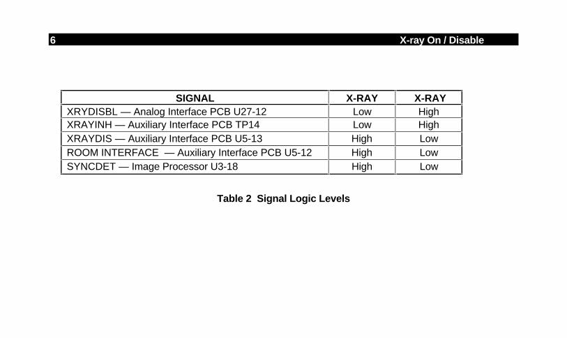
6 X-ray On / Disable
SIGNAL X-RAY X-RAYXRYDISBL — Analog Interface PCB U27-12 Low HighXRAYINH — Auxiliary Interface PCB TP14 Low HighXRAYDIS — Auxiliary Interface PCB U5-13 High LowROOM INTERFACE — Auxiliary Interface PCB U5-12 High LowSYNCDET — Image Processor U3-18 High Low
Table 2 Signal Logic Levels

KV GENERATION
OVERVIEWkV is regulated by a dynamic, self correcting servo control loop comprised of a dutycycle controlled high voltage drive circuit, drive PAL, control amplifier, error amplifier andsense circuits
In the Auto mode, the Technique Processor PCB varies the kV according to the videolevel signal received from the CCD camera until the proper level is achieved.
In the Manual mode, the operator varies the kV
Power for X-ray generation is buffered by battery packs. This allows the generator to runon standard single phase AC power.
REFERENCE SCHEMATICSThe theory given in this section is most easily understood while using the followingschematics. Use the correct interconnect diagrams and circuit board schematics for yoursystem.
• • Analog Interface PCB
Schematic # 00-876738 - All serial numbers
• • Mainframe Motherboard
Schematic # 00-875539 - System serial numbers 69-0001 thru 69-2000
Schematic # 00-878396 - System serial numbers 69-2001 and up
• • X-ray Regulator PCB
Schematic # 00-877458 - All serial numbers
• • Generator Driver PCB
Schematic # 00-877461 - All serial numbers
• • C-Arm Interconnect Diagram
Schematic # 00-875500 - System serial numbers 69-0001 thru 69-1000Schematic # 00-877972 - System serial numbers 69-1001 thru 69-2000Schematic # 00-878376 - System serial numbers 69-2001 and higher
NOTE
Click on a yellow box to go directly to the block diagram for this section. Do not use this link to return to a block diagram from this point. Click on the << button in the Tool Bar to return to any starting point.

2 kV Generation
CONTROL INPUTSInitializes the kV circuits by providing a control voltage and two timing (drive) signals.The Technique Processor PCB initializes the Analog Interface PCB to create threeprimary control and timing signals which control the X-ray Regulator PCB. These signalsare:
• • kVp Control
• • HVDRVA
• • HVDRVB
KVP CONTROL
The KVP CONTROL signal is a current signal from the Analog Interface A/D U31. Thiscurrent signal is converted to a positive DC voltage proportional to the desiredkV (75mV/kVp) by the current to voltage converter U33-6 and 7. This signal is softwarecontrolled in response to the kV selected and corrected by the calibration parameters.This signal will vary with different kV settings.
The KVP CONTROL voltage is then inverted to a negative DC voltage by U20-6 and 7on the X-ray Regulator PCB. This negative voltage, proportional to the desired kV, isthen applied to the R25/U23-2 summing point to be compared with the actual kV sensed(KVP MEASURED). See KV ERROR CORRECTION, later in this section for moreinformation.
HVDRVA AND HVDRVB
The HVDRVA and HVDRVB signals are out of phase, fixed duty cycle, 2.5 kHz timingsignals from the Analog Interface PAL U17. The duty cycle of these signals will not varyeven as different kV settings are selected. These signals serve as timing signals for theX-ray Regulator high voltage drive PAL U7.
KV DRIVEGenerates kV by providing the drive signals to the Darlington Driver transistors. Whenan X-ray switch is pressed, the X-ray On logic activates the high voltage drive PAL U7on the X-ray Regulator. U7 then generates its own out of phase, variable duty cycle, 2.5Khz HVDRVA (pin 12) and HVDRVB (pin 13) drive signals. These drive signals are thenapplied to the Generator Driver PCB where they are amplified by Q5, Q6 (HVDRVA)and Q7, Q8 (HVDRVB) to approximate 15 VDC drive signals. These amplified drivesignals then drive transformers T3 (HVDRVA) and T1 (HVDRVB).
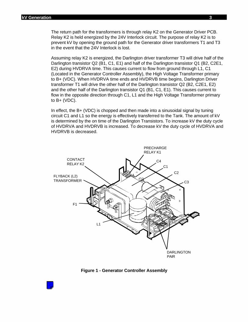
kV Generation 3
The return path for the transformers is through relay K2 on the Generator Driver PCB.Relay K2 is held energized by the 24V Interlock circuit. The purpose of relay K2 is toprevent kV by opening the ground path for the Generator driver transformers T1 and T3in the event that the 24V Interlock is lost.
Assuming relay K2 is energized, the Darlington driver transformer T3 will drive half of theDarlington transistor Q2 (B1, C1, E1) and half of the Darlington transistor Q1 (B2, C2E1,E2) during HVDRVA time. This causes current to flow from ground through L1, C1(Located in the Generator Controller Assembly), the High Voltage Transformer primaryto B+ (VDC). When HVDRVA time ends and HVDRVB time begins, Darlington Drivertransformer T1 will drive the other half of the Darlington transistor Q2 (B2, C2E1, E2)and the other half of the Darlington transistor Q1 (B1, C1, E1). This causes current toflow in the opposite direction through C1, L1 and the High Voltage Transformer primaryto B+ (VDC).
In effect, the B+ (VDC) is chopped and then made into a sinusoidal signal by tuningcircuit C1 and L1 so the energy is effectively transferred to the Tank. The amount of kVis determined by the on time of the Darlington Transistors. To increase kV the duty cycleof HVDRVA and HVDRVB is increased. To decrease kV the duty cycle of HVDRVA andHVDRVB is decreased.
CONTACT RELAY K2
FLYBACK (L2) TRANSFORMER
F1
L1
DARLINGTONPAIR
PRECHARGERELAY K1
C4
C1
C2
C3
Figure 1 - Generator Controller Assembly
NOTE
Click on the top colored box to go directly to the Illustrated Parts Manual for systems bearing serial numbers 69-001 thru 69-999. Click on the bottom colored box to go directly to the Illustrated Parts Manual for systems bearing serial numbers 69-1000 and higher. Click the << button on the TOOL Bar to return to this point.

4 kV Generation
KV SENSEDetects the actual kV generated by the kV drive circuit. The actual kV generated in theHigh Voltage Tank is detected by a capacitive sense circuit in the Tank. This KVSENSE signal is a sine wave with a 1V/10 kV ratio which is applied to the X-rayRegulator TP10 through buffer U16-3 and U16-1.
The positive peak of the KV SENSE sine wave is then measured by the positive peakdetector made up of U18, U22 and U26. The output of this peak detector can bemeasured on TP12 which has a scale factor of +1 VDC /10 kV. This represents the kVapplied to the anode of the X-ray tube.
The negative portion of the KV SENSE sine wave is inverted by inverting buffer U16-6and U16-7 and measured by the negative peak detector made up of U18, U25 and U26.The output of this peak detector can be measured on TP13 which also has a scale factorof +1 VDC /10 kV. This represents the kV applied to the cathode of the X-ray tube.
The two outputs from the peak detectors are then combined through buffer U20-3and U20-1. This output can be measured on TP9 which has a scale factor of+1 VDC /20 kV and is called KVP MEASURED. This dc voltage represents the actualkV generated by the High Voltage Tank which is applied across the cathode and anodeof the X-ray tube. This actual kV sensed signal (KVP MEASURED) is then applied tothe R25 and error amp U23-2 summing point to be compared with the desired kV (KVPCONTROL) from the Analog Interface D/A U31. It is also sent to the TechniqueProcessor via the Analog Interface A/D Mux U3 to be monitored by software for variouserror conditions.
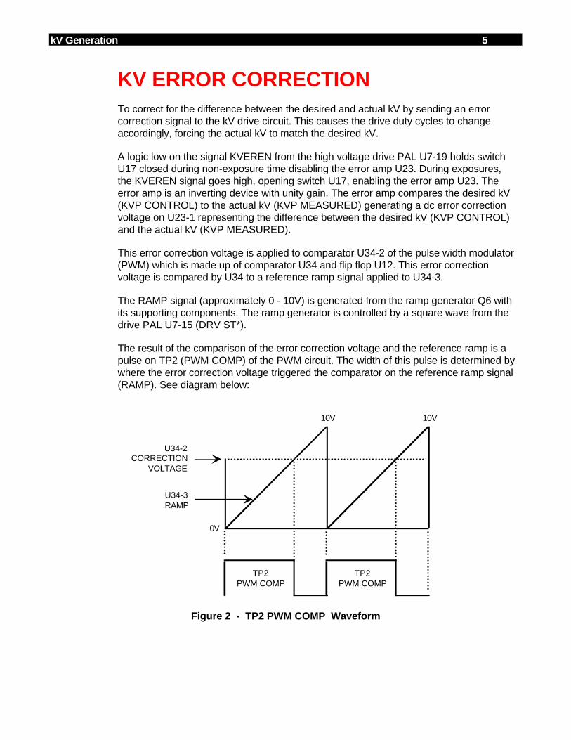
kV Generation 5
KV ERROR CORRECTIONTo correct for the difference between the desired and actual kV by sending an errorcorrection signal to the kV drive circuit. This causes the drive duty cycles to changeaccordingly, forcing the actual kV to match the desired kV.
A logic low on the signal KVEREN from the high voltage drive PAL U7-19 holds switchU17 closed during non-exposure time disabling the error amp U23. During exposures,the KVEREN signal goes high, opening switch U17, enabling the error amp U23. Theerror amp is an inverting device with unity gain. The error amp compares the desired kV(KVP CONTROL) to the actual kV (KVP MEASURED) generating a dc error correctionvoltage on U23-1 representing the difference between the desired kV (KVP CONTROL)and the actual kV (KVP MEASURED).
This error correction voltage is applied to comparator U34-2 of the pulse width modulator(PWM) which is made up of comparator U34 and flip flop U12. This error correctionvoltage is compared by U34 to a reference ramp signal applied to U34-3.
The RAMP signal (approximately 0 - 10V) is generated from the ramp generator Q6 withits supporting components. The ramp generator is controlled by a square wave from thedrive PAL U7-15 (DRV ST*).
The result of the comparison of the error correction voltage and the reference ramp is apulse on TP2 (PWM COMP) of the PWM circuit. The width of this pulse is determined bywhere the error correction voltage triggered the comparator on the reference ramp signal(RAMP). See diagram below:
0V
10V
TP2PWM COMP
U34-3RAMP
U34-2CORRECTION
VOLTAGE
10V
TP2PWM COMP
Figure 2 - TP2 PWM COMP Waveform
6 kV Generation
This corrected pulse (PWM COMP) is then applied to the drive PAL U7-8. Drive PAL U7will respond by varying the duty cycle of its drive signals (HVDRVA and HVDRVB)accordingly, resulting in the actual kV (KVP MEASURED) equaling the desired kV (KVPCONTROL).
KV ERROR LOOP EXAMPLE 1
Lets assume that the actual kV exceeds the desired kV so it needs to be turned down. Inthis case the error amp U23 detects that the actual kV (KVP MEASURED) is greaterthan the desired kV (KVP CONTROL) and the dc voltage output of the error amp U23-1will decrease. This causes the trip point to the PWM comparator U34, as compared tothe ramp signal (RAMP), to decrease.
Because the trigger point on the ramp has decreased, the pulse out of the PWM circuitU12-5 (PWM COMPARATOR) also decreases. This shortened pulse is tracked by thedrive PAL U7-8.
Since the pulse width of the PWM COMP signal has decreased, drive PAL U7decreases the duty cycle of its drive signals (HVDRVA and HVDRVB). The on-time ofthe Darlington driver transistors is therefore decreased resulting in less energytransferred to the high voltage tank and the actual kV decreasing to equal the desiredkV.
KV ERROR LOOP EXAMPLE 2
Lets assume that the actual kV is less than the desired kV so it needs to be turned up. Inthis case the error amp U23 detects that the actual kV (KVP MEASURED) is less thanthe desired kV (KVP CONTROL) and the dc voltage output of the error amp U23-1 willincrease. This causes the trip point to the PWM comparator U34, as compared to theramp signal (RAMP), to increase.
Because the trigger point on the ramp has increased, the pulse out of the PWM circuitU12-5 (PWM COMP) also increases. This lengthened pulse is tracked by the drive PALU7-8.
Since the pulse width of the PWM COMP signal has increased, drive PAL U7 increasesthe duty cycle of its drive signals (HVDRVA and HVDRVB). The on-time of theDarlington driver transistors is therefore increased resulting in more energy transferredto the high voltage tank and the actual kV increases to equal the desired kV.
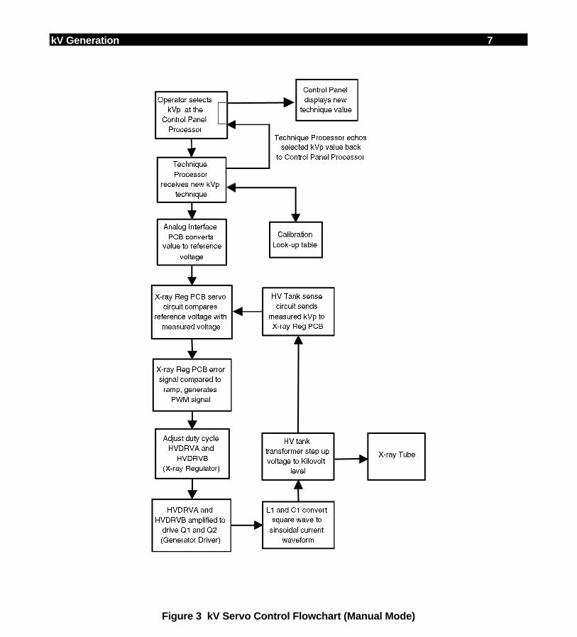
kV Generation 7
Figure 3 kV Servo Control Flowchart (Manual Mode)
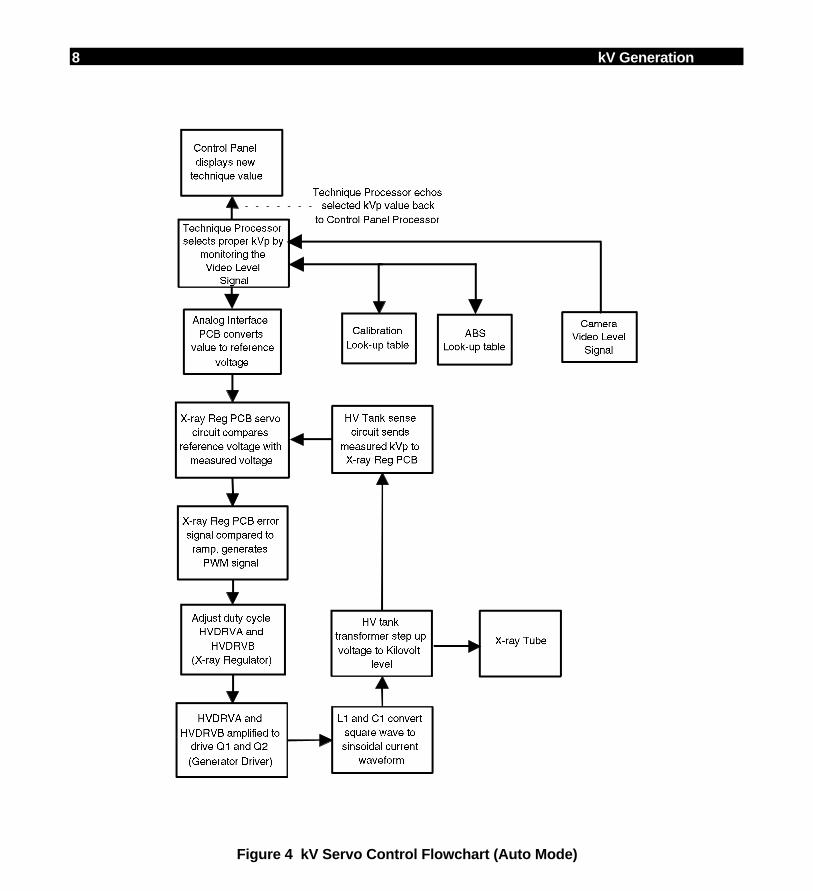
8 kV Generation
Figure 4 kV Servo Control Flowchart (Auto Mode)

kV Generation 9
KV GENERATOR FAULTS
FAULT PAL OVERVIEW
Fault PAL U2 monitors the system for the following fatal fault conditions:
• Saturation Fault• Overvoltage Fault• Overload Fault
During any of these fault conditions, the FAULT signal which is fed to the HV Drive PALU7-9 prevents X-rays by disabling the HVDRA and HVDRB signals. The outputs of thefault PAL U2 are also fed to the Technique Processor for software monitoring throughthe Analog Interface PIO U27. When software detects a fault, the Technique Processorshuts the system down by disabling the 24V interlock circuit. The Technique Processoralso displays the appropriate error message on the generator control panel display.
SATURATION FAULT
The Darlington power transistors Q1 and Q2 drive the primary winding of the highvoltage transformer contained within the tank assembly. Normally, the voltage dropacross the Darlington’s output, when turned-on, is minimal indicating a completelysaturated transistor.
However, if a Darlington transistor becomes weak (or if too much current passes througha Darlington transistor) a relatively large voltage is dropped across its output during theon-time. This excess voltage drop is detected by the system and defines a SaturationFault.
If a fault occurs, the message SATURATION FAULT is displayed on the Control Panel.This is a fatal error resulting in a system shut down preventing X-rays.
Saturation Fault Circuit
The bridge rectifier VR1 and Q9 on the Generator Driver PCB samples the voltage dropof which-ever of the two upper transistors of the H-Bridge is turned on at the time. Thisvoltage is referenced to ground level by Q9 at R19. In effect, the voltage across R19represents the voltage across the Darlington power transistor. This voltage is fedthrough CR23 to TP7 and then to TP3 and comparator U14 on the X-ray Regulator PCB.VR1’s negative output samples the drop on the “lower half” of the H-Bridge for the samepurpose.
On the X-ray Regulator PCB, this sense voltage (SATDET) is monitored by comparatorU14-2. A reference voltage derived by R35 and R36 of approximately 8 VDC is appliedto U14-3. This voltage is the comparator’s threshold voltage which represents themaximum allowable voltage drop across the Darlington’s output during their on-time. A
NOTE
Click on a yellow box to go directly to the block diagram for this section. Do not use this link to return to a block diagram from this point. Click on the << button in the Tool Bar to return to any starting point.

10 kV Generation
Saturation Fault occurs when the SATDET voltage on U14-2 exceeds the referencevoltage on U14-3 causing U14-7 to go high.
A high output from comparator U14-7 (FAULT 1) causes the Fault PAL U2-14(SATURATION FAULT) and U2-13 (FAULT) to go high.
The logic high FAULT output of Fault PAL U2-13 prevents X-rays by disabling theHVDRVA and HVDRVB signals from the high voltage drive PAL U7.
The logic high SATURATION FAULT output of U2-14 and the logic high FAULT outputof U2-13 are also monitored by the Technique Processor PCB via the Analog InterfacePIO U27. This condition is a fatal error and causes a system shutdown. The messageSATURATION FAULT is displayed on the generator control panel display.
The DRVON signal (U11-8) disables the sample voltage during Darlington off-time,preventing a Saturation Fault from occurring. DRVON is active high when eitherHVDRVA or HVDRVB is active and floats to the sample voltage during this period.DRVON is low (open-collector output to ground) during the off-time of the Darlingtonsand pulls the sample voltage to ground. This is necessary because when any transistoris turned off, the voltage drop across its output is typically large.
OVERVOLTAGE FAULT
High voltage in excess of approximately 140 kVp defines an Overvoltage Fault. If a faultoccurs, the message OVERVOLTAGE FAULT is displayed on the Control Panel. This isa fatal error resulting in a system shutdown preventing X-rays.
Overvoltage Fault Circuit
The high voltage transformer, within the tank assembly, incorporates a one-turn tap ineach of its secondary windings. The sinewave from these taps are sent to the X-rayRegulator PCB on P4-4 (TAP2) and P4-5 (TAP1). the ratio for the TAP1 and TAP2signals are approximately 1V/4.5 kV.
The TAP1 signal is monitored by comparator U32-2. A reference voltage ofapproximately 5 VDC is applied to U32-3. This is the comparator’s threshold voltagewhich represents the maximum 140 kVp allowed for safe operation.
When the voltage on U32-2 exceeds that of the voltage U32-3, the output of U32-7 goeshigh indicating an Overvoltage condition. This logic high is felt at the fault PAL U2-5causing the PAL’s output U2-13 (FAULT) to go high.
This high on the FAULT output of fault PAL U2-13 prevents X-rays by disabling theHVDRA and HVDRB signals from the high voltage drive PAL U7. The FAULT signal isalso monitored by the Technique Processor software via the Analog Interface PIO U27.This condition is a fatal error and causes a system shutdown. The messageOVERVOLTAGE FAULT is displayed on the generator control panel display.
kV Generation 11
NOTE If the secondary TAP1 and TAP2 signals carried through P4 on the X-ray RegulatorPCB are disconnected, pull-up resistors R90 and R100 will cause comparator U16to trip the OVERVOLTAGE line. This is an important safety factor: all signal lines onP4 must be connected for the Generator to operate without damage.
OVERLOAD FAULT
Peak currents in excess of 200 Amps in the primary winding of the high voltage tankdefine an Overload Fault. If a fault occurs, the message OVERLOAD FAULT isdisplayed on the Control Panel. This is a fatal error resulting in a system shutdown,preventing X-rays.
Overload Fault Circuit
A sense winding is incorporated in the output-tuning inductor L1, in series with theprimary winding of the high voltage transformer which senses the differential voltageacross the inductor. This CURRENT LOOP signal is sent to the X-ray Regulator PCB onP2-3 where it is integrated by R7 and C9 to derive a voltage proportional to the currentthrough L1. This voltage can be measured on TP1.
This voltage is monitored by comparator U1-2 and compared to a reference voltage ofapproximately 1.6 VDC applied to U1-3. This reference voltage is the comparator’sthreshold, representing the maximum primary input current allowed for safe operation.
When the voltage on U1-2 exceeds that of the voltage on U1-3, the output on U1-7 goeshigh indicating an Overload condition. This logic high is felt at the fault PAL U2-2causing the PAL’s outputs U2-17 (OVERLOAD) and U2-13 (FAULT) to also go high.
The logic high FAULT output of Fault PAL U2-13 prevents X-rays by disabling theHVDRVA and HVDRVB signals from the high voltage drive PAL U7.
The logic high OVERLOAD output of U2-17 and the logic high FAULT output ofU2-13 are also monitored by the Technique Processor PCB via the Analog Interface PIOU27. This condition is a fatal error and causes a system shutdown. The messageOVERLOAD FAULT is displayed on the generator control panel display.
KV ON IN ERROR MESSAGE
With no X-ray switch engaged, the Technique Processor software detected voltage onthe KVP MEASURED line indicating high voltage was present but not commanded. Themessage is displayed and the system is shut down.
HIGH KV AND LOW FLUORO KV ERRORS
The detected kV (KVP MEASURED) and the selected kV technique do not agree within20%. The message is displayed and the system shuts down for two seconds after theexposure.

12 kV Generation
KV TROUBLESHOOTING
KV CONTROL
Without making X-rays, select 80 kV in the MANUAL FLUORO mode. You shouldmeasure approximately -6 VDC (-75 mV/kV) on amp U20-7 of the X-ray Regulator PCB.As kV is increased, this voltage becomes more negative. As kV is decreased, thisvoltage becomes less negative.
Without making X-rays, verify the HVDRVA and HVDRVB drive signals at PALU7-2 and U7-3 are out of phase, 2.5 kHz signals. The duty cycle should not change asdifferent kV settings are selected.
KV DRIVE
With 80 kV selected in the manual Fluoro mode you should measure approximately 15V,out of phase, drive signals on TP5 and TP6 of the Generator Driver PCB. The duty cycleshould increase as the kV setting is increased and decrease as the kV setting isdecreased.
KV SENSE
With 80 kV selected in the manual Fluoro mode, you should measure an approximate8V peak-peak sine wave on TP10 (1V/10 kV ratio) of the X-ray Regulator.
TP9 (1 VDC/20 KV) should indicate approximately 4 VDC. TP10 and TP9 should bothincrease in amplitude as the kV setting is increased and decrease in amplitude as thekV setting is decreased.

kV Generation 13
KV ERROR CORRECTION TRUTH TABLES
Actual kV Detected is Greater than Desired kV
• X-ray Regulator U23-1 error voltage decreases
• X-ray Regulator TP2 pulse width decreases
• Generator Driver TP6 duty cycle decreases
• Generator Driver TP5 duty cycle decreases
• Actual kV decreases
Actual kV Detected is Less than Desired kV
• X-ray Regulator U23-1 error voltage increases
• X-ray Regulator TP2 pulse width increases
• Generator Driver TP6 duty cycle increases
• Generator Driver TP5 duty cycle increases
• Actual kV increases
KV DIAGNOSTIC SOFTWARE
• DRO - Run Applications with Parameters. See C-Arm Software section for moreinformation.

MA GENERATION
OVERVIEWTube current (mA) is regulated by a dynamic, self correcting servo control loopcomprised of a drive PAL, control amplifier, error amplifier, sense circuit, variablefilament voltage regulator, and a duty-cycle controlled filament drive circuit.
In the Auto mode, the Technique Processor PCB varies the mA according to the videolevel signal received from the CCD camera until the proper video level is achieved.
In the Manual mode, the operator varies the mA.
Power for X-ray generation is buffered by battery packs which enable the generator tobe powered by standard single phase AC power.
The theory in this section is most easily understood while using the followingschematics. Use the correct interconnect diagrams and circuit board schematics for yoursystem.
REFERENCE SCHEMATICSAnalog Interface PCB
Schematic # 00-876738 - All S/N
Mainframe Motherboard
Schematic # 00-875539 - System S/N 69-0001 thru 69-2000Schematic # 00-878396 - System S/N 69-2001 and up
X-ray Regulator PCB
Schematic # 00-877458 - All S/N
Generator Driver PCB
Schematic # 00-877461 - All S/N
C-Arm Interconnect Diagram
Schematic # 00-875500 - System S/N 69-0001 thru 69-1000Schematic # 00-877972 - System S/N 69-1001 thru 69-2000Schematic # 00-878376 - System S/N 69-2001 and up
NOTE
Click on a yellow box to go directly to the block diagram for this section. Do not use this link to return to a block diagram from this point. Click on the << button in the Tool Bar to return to any starting point.
2 mA Generation
CONTROL INPUTSThe Technique Processor commands the Analog Interface to generate four primarycontrol signals to the X-ray Regulator PCB. Their purpose is to initialize and control themA servo loop. These signals are:
• FIL B CONTROL
• MA CONTROL
• FILDRVA
• FILDRVB
FIL B CONTROL
This is a current signal from the Analog Interface PCB A/D U18-6. This current signal isconverted to a positive DC voltage by the current to voltage converter U28 (pins 2 & 1).This signal is software controlled in response to the X-ray mode currently selected. It isused to set up the Filament Regulator on the Generator Driver PCB for the proper outputvoltage as shown in Table 1. The Filament Regulator output voltage can be measured atthe collector of Q4 or at R8 on the Generator Driver PCB.
Fluoro =160 VDC with X-rays off
0.3 mm Film = 175 VDC, Armed 160 VDC
0.6 mm Film = 185 VDC, Armed 140 VDC
Table 1 - Approximate Filament Regulator Output Voltage
The ratio between the FIL B CONTROL voltage and the Filament Regulator outputvoltage is approximately 1:40, for every +1VDC on TP10 of the Analog Interface, thefilament regulator’s output will be approximately +40 VDC. See Filament RegulatorSetup, later in this section, for more information.
mA Generation 3
MA CONTROL
This signal is a current signal from the Analog Interface PCB, A/D U31-23. This currentsignal is converted to a positive DC voltage proportional to the desired mA by the currentto voltage converter U33 (pins 2 & 1). Measured on TP18 of the Analog Interface PCBthe ratio is approximately +350 mV/mA Fluoro mode and +70 mV/mA Film mode. Thissignal is software controlled in response to the mA selected and corrected by thecalibration parameters. This signal will vary with different mA settings.
The mA CONTROL voltage from the Analog Interface PCB is inverted to a negative DCvoltage by U15 (pins 2 & 1) on the X-ray Regulator PCB and can be measured on TP8.This negative voltage, proportional to the desired mA, is then applied, via switch U13(pins 6 & 7), to the R27/U13-6 summing point to be compared with the actual mAsensed (MA MEASURED). See mA Error Correction, later in this section for moreinformation.
FILDRVA AND FILDRVB
These signals are out of phase, variable duty cycle, 2.5 Khz drive signals from theAnalog Interface PAL U17 (pins 14 & 15). The duty cycle of these drive signals varies,under system software control, in response to the mA technique selected. The dutycycle increases as selected mA increases. The duty cycle decreases as selected mAdecreases.
These drive signals are applied to the X-ray Regulator PCB filament drive PAL U10(pins 5 & 6), The filament drive PAL U10 (pins 12 & 13) responds by generating its ownFILDRA and FILDRB drive signals with the duty cycle commanded by the AnalogInterface PCB. See mA Drive and Filament Pre-Heat, later in this section for moreinformation.
4 mA Generation
FILAMENT REGULATOR SETUPProvides the initial setup, regulation and monitoring of the filament regulator outputvoltage. The filament regulator is located on the Generator Driver PCB.
When the system is booted, but no X-rays are commanded, the X-ray Regulator kV drivePAL U7-16 will be a logic low. This disables error amp U15 by holding the contacts (pins10 & 11) of switch U13 closed. The output of the error amp applied to TP4 should be 0VDC at this time.
The FIL B CONTROL signal is now applied to the X-ray Regulator R82/U27-6 summingpoint unaffected by the output of the error amp. The FIL B CNTRL voltage at TP10 onthe X-ray Regulator PCB and U27-6 of the Generator Driver PCB are shown in Table 2.
Fluoro = 4 VDC with X-rays OFF
0.3 mm Film = 4.4 VDC, Armed 4 VDC
0.6 mm Film = 4.6VDC, Armed 3.5 VDC
Table 2 - Approximate Control Voltages
U27-7, on the X-ray Regulator, provides an approximate +3 to +5 VDC signal (FILREG)to the filament regulator on the Generator Driver PCB. The Filament Regulator iscomprised of Q10, Q1, Q2 and associated components. The filament regulator supply isthe B+ voltage from the batteries and can be measured at fuse F3on the Generator Driver PCB.
The FILREG signal from the X-ray Regulator controls the filament regulator output to theproper voltage for the selected X-ray mode as described in Table 1. The filamentregulator output supplies power to the filament transformers in the High Voltage Tankthrough the filament drive transistors Q3 and Q4.
The regulated filament voltage is scaled down by R8 and applied to U27-5 on the X-rayRegulator PCB. This feedback loop is intended to regulate the filament regulator outputto within 15%.
The scaled down filament regulator voltage is also applied to U27-3. The output on U27-1 (FIL B+ SENSE) is then sent to the Technique Processor, via the Analog InterfacePCB, to be monitored by the system software for abnormal filament regulator voltages.See Regulator Fail error message at the end of this section for more information.
mA Generation 5
MA DRIVE AND FILAMENT PRE-HEATGenerates the filament current needed for filament pre-heating and initial tube current.
When a specific mA technique is selected, the system software commands the AnalogInterface PCB to generate the FILDRVA and FILDRVB signals out of PAL U17(pins 14 & 15) with a duty cycle that the software determines will produce the selectedmA. This occurs immediately in the Fluoro mode. In the Film mode this occurs in the twoseconds prior to an exposure after the X-ray switch is pressed. The duty cycle of thedrive signals, once selected by the software, remains constant throughout the exposure.
These drive signals are then applied to the filament drive PAL U10 (pins 5 and 6) on theX-ray Regulator PCB. The filament drive PAL U10 then generates its own FILDRA andFILDRB signals on pins 12 and 13 with the duty cycle commanded by the AnalogInterface PCB.
FILDRA and FILDRB (TP3 and TP2-Generator Driver PCB) drive transformer T2 whichin turn drives the filament drive transistors Q3 and Q4, chopping the regulated filamentvoltage (See Table 1) across these transistors. This chopped filament regulator voltageis transferred to the proper filament transformer in the tank via filament select relay K1.The amount of filament pre-heat and the initial tube current are determined by the on-time of these filament drive transistors which are controlled by the duty cycle of theFILDRA and FILDRB signals. This is the initial setup of the mA loop known as coarsetuning.
FILAMENT SELECTIONThe small 0.3 mm filament is always selected in the fluoro mode and at film modetechniques of 100 mAs and lower. Software selects the large .6 mm filament when filmmode techniques of greater than 100 mAs are selected.
Filament selection is controlled by the 1 mm MODE signal from the filament drive PALU10-14 on the X-ray Regulator PCB. The 1 mm MODE signal controls the filamentselect relay K1, on the X-ray Regulator PCB, through transistor Q11.
6 mA Generation
MA SENSEDetects the actual mA generated by the mA drive circuit.
Since the filaments are pre-heated with filament current prior to the exposure, tubecurrent will flow in the X-ray tube once the exposure is initiated and the high voltagecomes up. The actual tube current generated (mA) is sensed by windings locatedaround the anode socket inside the High Voltage Tank. Current pulses from thesewindings (MA SENSE) are applied to the transimpedance amp U31-6 on the X-rayRegulator PCB. Amp U31 converts and scales these current pulses into correspondingmA sense voltage pulses.
The average DC value of the mA sense voltage pulses (as referenced to ground)represents the actual tube current (mA) detected. This DC voltage is passed throughbuffer U30 (pins 3 & 1) and can be measured on TP7 of the X-ray Regulator PCB. Thescale factor on TP7 is 40 mA/Volt in all X-ray modes.
Buffer U30-1 mA sense voltage output is then applied to the low pass filter U30-5. TheDC voltage output from low pass filter U30-7 can be measured on TP6 which also has ascale factor of 40 mA/Volt in all X-ray modes.
Low pass filter U30-7 output is then applied to scaling amp U31-3 on theX-ray Regulator PCB. The DC voltage out of scaling amp U31-1 can be measured onTP11 on the X-ray Regulator PCB. The scale factor on TP11 (MA MEASURED) is 40mA/Volt in the Fluoro mode and 8 mA/Volt in the Film mode.
Scaling for TP11 (MA MEASURED) is determined by selecting the proper feedbackresistor for scaling amp U31 through switch U21 on the X-ray Regulator PCB. Relay K1and associated scaling circuitry for low fluoro scaling are not currently used.
Switch U21 is controlled by the signal MaRANGE which is derived from the signal MASCALE (High = Fluoro mode, Low = Film mode), from the Analog Interface PIO U27-4.MA SCALE is applied to the X-ray Regulator PCB PAL U2 which responds bygenerating the Ma RANGE signal on pin 15.
The MA MEASURED signal represents the actual tube current (mA) detected. Thissignal is applied to the R27 and switch U13-6 summing point to be compared with thedesired mA (MA CONTROL) from the Analog Interface PCB. It is also sent to theTechnique processor via the Analog Interface PCB to be monitored by the systemsoftware for various error conditions. See Generator Errors later in this section for moreinformation.
mA Generation 7
MA ERROR CORRECTIONDynamically corrects for the difference between desired and actual tube current (mA) bysending an error correction voltage to the filament regulator circuit. This causes thefilament regulator voltage output to change accordingly, forcing the actual tube current(mA) to equal the desired tube current (mA).
Remember, during non-exposure time, error amp U15 on the X-ray regulator is disabledbecause switch U13 ( pins 10 & 11) are held closed as previously discussed in theFilament Regulator Setup section. In addition, there is no input to the error amp U15-6because U5- 4 is a logic high at this time, holding switch U13 (pins 6 & 7) open.
When an X-ray switch is pressed, kV drive PAL U7-16 on the X-ray Regulator PCB goesto a logic high, enabling error amp U15 by opening pins 10 and 11 of switch U13. As thehigh voltage applied to the X-ray tube reaches approximately 30 kV, the output ofcomparator U19-7 goes high applying a logic low through U5 (TP21), on the X-rayRegulator PCB, to switch U13-8. This logic low closes pins 6 and 7 of switch U13,allowing the desired and actual mA summing point to be felt at the error amp input U15-6.
The error amp is an inverting device that compares the desired mA (MA CONTROL)with the actual mA detected (MA MEASURED). This results in a DC error correctionvoltage on TP4, on the X-ray Regulator PCB, representing the difference between thedesired mA (MA CNTRL) and the actual mA (MA MEASURED). The error correctionvoltage on TP4 may vary between ± 6 VDC depending on the amount of error detected.A positive voltage on TP4 indicates that the desired mA was greater then the actual mA.A negative voltage on TP4 indicates that the desired mA was less than the actual mA.The closer this voltage is to ground, the smaller the difference was between the desiredand actual mA.
A proportional amount of the error correction voltage on TP4 is summed with the FIL BCONTROL voltage at the R82 and U27-6 summing point. This causes the output of U27-7 (FILREG) to increase or decrease accordingly. The typical voltage range for U27-7(FILREG) is approximately 3-5VDC. The FILREG signal controls the filament regulatoron the Generator Driver PCB. As the FILREG signal changes, it results in a change ofthe filament regulator output voltage that is applied to the filament drive transistors Q3and Q4 on the Generator Driver PCB. The change in the filament regulator outputvoltage results in a corresponding change in the actual tube current (mA). Remember,the FILDRA and FILDRB duty cycle, once selected by the system software for a givenmA, is held constant during an exposure as previously discussed in the mA Drive andFilament Pre-Heat section of the theory.
This dynamic correction of the filament regulator output voltage during the exposureresults in the actual mA equaling the desired mA. This completes the fine tuning of themA servo loop.
8 mA Generation
MA ERROR LOOP EXAMPLE 1
Assuming that the actual mA exceeds the desired mA so the actual mA needs to bedecreased. In this case, error amp U15 detects that the actual mA (MA MEASURED)exceeds the desired mA (MA CONTROL) and the error correction output voltage on TP4will go more negative. How negative this voltage goes is determined by the amount ofdifference detected between the desired and actual mA, the greater the difference, themore negative this voltage becomes.
The voltage on U27-6 (FIL B CONTROL and error correction voltage summing point)becomes less positive. The FIL REG voltage will then go more positive causing theoutput of the filament regulator to decrease. This results in less filament current whichdecreases the tube current (mA) until it equals the desired mA.
MA ERROR LOOP EXAMPLE 2
Assuming that the actual mA is less than the desired mA so the actual mA needs to beincreased. In this case, error amp U15 detects that the actual mA (MA MEASURED) isless than the desired mA (MA CONTROL) and the error correction output voltage onTP4 will go positive. How positive this voltage goes is determined by the amount ofdifference detected between the desired and actual mA, the greater the difference, themore positive this voltage becomes.
The voltage on U27-6 (FIL B CONTROL and error correction voltage summing point)becomes more positive. The FIL REG voltage will then go less positive causing theoutput of the filament regulator to increase. This results in more filament current whichincreases the tube current (mA) until it equals the desired mA.
MAS INTEGRATORIn the film mode the operator chooses the kV and mAs. The system software thendetermines what mA to use. During the exposure the system software integrates the mAwith respect to time until the desired mAs is reached. Once this happens the systemsoftware terminates the exposure.
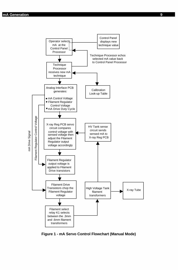
mA Generation 9
to Control Panel Processor
Control Panel Processor
Operator selects
Technique Processor
technique
Control Panel displays new
technique value
X-ray Reg PCB servo circuit compares HV Tank sense
circuit sends
X-ray Tube
mA at the
Technique Processor echosselected mA value back
control voltage with
Filament Regulatoroutput voltage is
applied to FilamentDrive transistors
Filament DriveTransistors chop the Filament Regulator
voltage
Filament selectrelay K1 selects
between the .3mmand .6mm filament
transformers
High Voltage Tankfilament
transformers
sensed mA to
receives new mA
sensed voltage thenadjust the FilamentRegulator outputvoltage accordingly
X-ray Reg PCB
Analog Interface PCB generates:
mA Control VoltageFilament Regulator
Control Voltage mA Drive Duty Cycle
CalibrationLook-up Table
mA
Driv
e S
igna
l
Fila
men
t Reg
ulat
or C
ontr
ol V
olta
ge
Figure 1 - mA Servo Control Flowchart (Manual Mode)
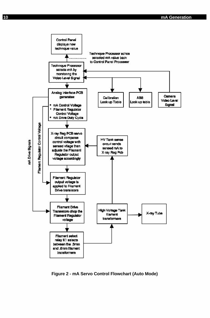
10 mA Generation
Figure 2 - mA Servo Control Flowchart (Auto Mode)

mA Generation 11
MA GENERATOR ERRORS
NO MA L IMITS
This message appears if the MALIMIT.DAT file is not found. This file must be copied tothe SRAM disk. (See the SRAM Backup and Restore sections in the C-Arm SoftwareSection of this manual for procedures.)
REGULATOR FAIL
By monitoring the FILSNS voltage through the Analog Interface during an exposure, theTechnique Processor software detected that the filament regulator output voltage hasexceeded its voltage range by ±15% (See Table 1 for voltage ranges). This is a non-fatal error, the system shuts down for two seconds after the exposure, X-rays can thenbe resumed.
FILAMENT FAULT
With an X-ray switch engaged, the Technique Processor software has detected novoltage on the MA MEASURED line indicating little or no tube current. This is a fatalerror and results in a system shut down.
MA ON IN ERROR
With no X-ray switch engaged, the Technique Processor software detected a voltage onthe MA MEASURED line indicating tube current was present but not commanded. Thisis a fatal error and results in a system shut down.
WARNING, HIGH MA
The Technique Processor software has determined that the actual mA(MA MEASURED) exceeds the selected mA by more than 20%. This is a non-fatal error,the system shuts down for two seconds after the exposure, X-rays can then be resumed.
12 mA Generation
LOW FLUORO MA
The Technique Processor software has determined that the actual mA(MA MEASURED) is less than the selected mA by more than 20%. This is a non-fatalerror, the system shuts down for two seconds after the exposure, X-rays can then beresumed.
X-RAY OVERTIME
The Technique Processor system software has determined that the elapsed exposuretime (Film mode) has exceeded 10% of the expected exposure time and the exposure isterminated. This is a non-fatal error, the system shuts down for two seconds after theexposure, X-rays can then be resumed.
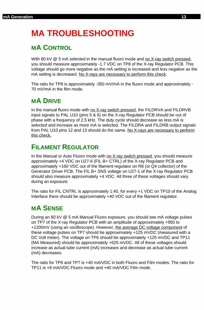
mA Generation 13
MA TROUBLESHOOTING
MA CONTROL
With 80 kV @ 5 mA selected in the manual fluoro mode and no X-ray switch pressed,you should measure approximately -1.7 VDC on TP8 of the X-ray Regulator PCB. Thisvoltage should go more negative as the mA setting is increased and less negative as themA setting is decreased. No X-rays are necessary to perform this check.
The ratio for TP8 is approximately -350 mV/mA in the fluoro mode and approximately -70 mV/mA in the film mode.
MA DRIVEIn the manual fluoro mode with no X-ray switch pressed, the FILDRVA and FILDRVBinput signals to PAL U10 (pins 5 & 6) on the X-ray Regulator PCB should be out ofphase with a frequency of 2.5 kHz. The duty cycle should decrease as less mA isselected and increase as more mA is selected. The FILDRA and FILDRB output signalsfrom PAL U10 pins 12 and 13 should do the same. No X-rays are necessary to performthis check.
FILAMENT REGULATORIn the Manual or Auto Fluoro mode with no X-ray switch pressed, you should measureapproximately +4 VDC on U27-6 (FIL B+ CTRL) of the X-ray Regulator PCB andapproximately +160 VDC out of the filament regulator on R8 (or Q4 collector) of theGenerator Driver PCB. The FIL B+ SNS voltage on U27-1 of the X-ray Regulator PCBshould also measure approximately +4 VDC. All three of these voltages should varyduring an exposure.
The ratio for FIL CNTRL is approximately 1:40, for every +1 VDC on TP10 of the AnalogInterface there should be approximately +40 VDC out of the filament regulator.
MA SENSEDuring an 80 kV @ 5 mA Manual Fluoro exposure, you should see mA voltage pulseson TP7 of the X-ray Regulator PCB with an amplitude of approximately +950 to+1200mV (using an oscilloscope). However, the average DC voltage component ofthese voltage pulses on TP7 should be approximately +125 mVDC (measured with aDC Volt meter). The voltage on TP6 should be approximately +125 mVDC and TP11(MA Measured) should be approximately +625 mVDC. All of these voltages shouldincrease as actual tube current (mA) increases and decrease as actual tube current(mA) decreases.
The ratio for TP6 and TP7 is +40 mA/VDC in both Fluoro and Film modes. The ratio forTP11 is +8 mA/VDC Fluoro mode and +40 mA/VDC Film mode.
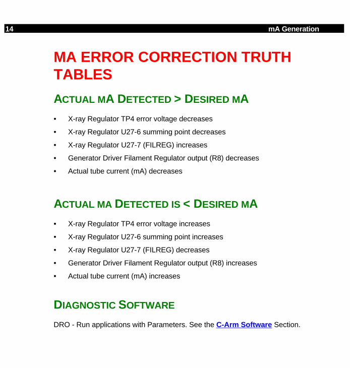
14 mA Generation
MA ERROR CORRECTION TRUTHTABLES
ACTUAL MA DETECTED > DESIRED MA
• X-ray Regulator TP4 error voltage decreases
• X-ray Regulator U27-6 summing point decreases
• X-ray Regulator U27-7 (FILREG) increases
• Generator Driver Filament Regulator output (R8) decreases
• Actual tube current (mA) decreases
ACTUAL MA DETECTED IS < DESIRED MA
• X-ray Regulator TP4 error voltage increases
• X-ray Regulator U27-6 summing point increases
• X-ray Regulator U27-7 (FILREG) decreases
• Generator Driver Filament Regulator output (R8) increases
• Actual tube current (mA) increases
DIAGNOSTIC SOFTWARE
DRO - Run applications with Parameters. See the C-Arm Software Section.

GENERATOR CALIBRATION
The procedures contained in this section are used to test and calibrate the 9600 MobileC-Arm. The following procedures are included:
• X-ray Calibration
• Entrance Exposure
These procedures assume that all parts are installed and are wired correctly. It is alsoassumed that all subassemblies are either known to be operational or were previouslytested at the factory.
X-RAY CALIBRATION
OVERVIEW
This section describes the X-ray generator calibration procedure for the 9600 MobileImaging System. The 9600 C-Arm generator is a precise instrument that is softwarecontrolled for exceptional accuracy and repeatability. Each generator is calibrated sothat the individual characteristics of the X-ray tube and generator components can beaccounted for by software to produce the desired techniques. Please note thatgenerator software is not interchangeable between different 9600 C-Arm systems.
Calibration of the generator is a semi-automatic process once the proper equipment hasbeen installed. The individual performing the calibration is required to press keys,change Dynalyzer settings, and zero Dynalyzer offsets at various times during thecalibration process. The operator will be prompted by the software to perform theappropriate actions when needed. The system should never be left unattended duringthe calibration process.
The following stages have been determined to be the best procedure for performing thecalibration:
1. Setup Equipment - The calibration equipment is connected to the C-Arm and setupfor the calibration procedure.
2. Access Calibration Software - Generator calibration software is accessed from theMainframe Menu.
3. Duty Cycle calibration - Calibration software automatically makes approximately250 exposures at various kV and mA levels to determine the characteristics of theX-ray tube filaments. This data is written to a file (CARM.DC) for calculations afterthe exposures have been completed. Calculations are made and the information iswritten to the EEPROM on the Technique Processor PCB.

2 Generator Calibration
During the Duty Cycle the mA servo circuitry on the X-Ray Regulator PCB isdisabled by installing the E2 jumper. This insures that the hardware servo will haveno affect on tube mA. The kV servo circuitry remains enabled because the kVcharacteristics of the X-ray tube are well documented and easy to reproduce.
When Duty Cycle starts the X-ray tube is in the 0.3 mm focal spot and is driven by anarrow filament waveform at a constant 40 kV for the first exposure. The “DutyCycle” for this first shot is designated as 400. For the next exposure the filamentwaveform is slightly wider while the kV remains at 40, which results in increasedtube mA. The “Duty Cycle” for this second shot is 425. For consecutive shots thefilament waveform width is increased slightly and the “Duty Cycle” designatorincreased by 25. The kV is kept at a constant 40 kV until the tube mA is 45 mA orgreater. At this point the Duty Cycle switches to the 60 kV portion of the program.If the Duty Cycle reaches 1225 before 45 mA is reached, the Duty Cycle will defaultto the 60 kV portion of the program.
The tube is again driven by a narrow filament waveform, but kV is increased to 60kV. The “Duty Cycle” for this first shot is again designated as 400. The filamentwaveform width is increased for subsequent shots as described in the precedingparagraph until the tube mA is 50 mA or greater. The Duty Cycle program thenswitches to the 80 kV station where shots are taken in the same manner describedabove.
This Duty Cycle process continues at 100 kV and 120 kV in the 0.3 mm focal spotand then switches to the .6 mm large focal spot. Table 1 illustrates how the entireDuty Cycle program functions from start to finish. Note that at each kV station the“Duty Cycle Designator” starts at 400 and exposures are taken until an ending mAvalue is reached. When the ending mA value is reached for a particular kV stationthe program changes to the next kV station.
At the completion of the entire Duty Cycle program the system software processesthe data and calculates the H1, H2, and H3 coefficients. These coefficients areused to compile mA/Duty Cycle curves for each focal spot of the X-ray tube. Thisdata will be used in the next step of the calibration process to produce exposures ofa specific kV and mA.
4. kV/mA Calibration - Calibration software automatically makes approximately 40exposures at various techniques to determine the characteristics of the generatorelectronics. This data is written to a file (CARM.CAL) for calculations after theexposures have been completed. Calculations are made and correction vectors arewritten to the EEPROM on the Technique Processor PCB.
During this step the mA servo circuitry is enabled by removing the E2 jumper on theX-Ray Regulator PCB. Specific kV and mA exposures are taken during this step ofthe calibration. The system software knows what duty cycle will produce theapproximate desired mA from the mA/Duty Cycle curves obtained earlier.
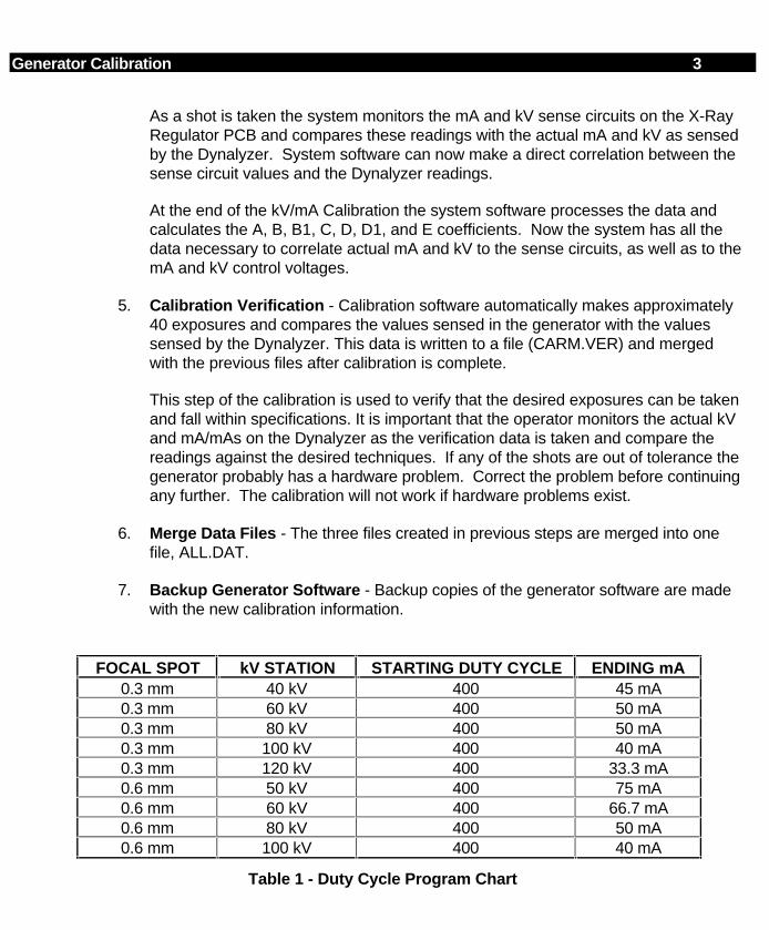
Generator Calibration 3
As a shot is taken the system monitors the mA and kV sense circuits on the X-RayRegulator PCB and compares these readings with the actual mA and kV as sensedby the Dynalyzer. System software can now make a direct correlation between thesense circuit values and the Dynalyzer readings.
At the end of the kV/mA Calibration the system software processes the data andcalculates the A, B, B1, C, D, D1, and E coefficients. Now the system has all thedata necessary to correlate actual mA and kV to the sense circuits, as well as to themA and kV control voltages.
5. Calibration Verification - Calibration software automatically makes approximately40 exposures and compares the values sensed in the generator with the valuessensed by the Dynalyzer. This data is written to a file (CARM.VER) and mergedwith the previous files after calibration is complete.
This step of the calibration is used to verify that the desired exposures can be takenand fall within specifications. It is important that the operator monitors the actual kVand mA/mAs on the Dynalyzer as the verification data is taken and compare thereadings against the desired techniques. If any of the shots are out of tolerance thegenerator probably has a hardware problem. Correct the problem before continuingany further. The calibration will not work if hardware problems exist.
6. Merge Data Files - The three files created in previous steps are merged into onefile, ALL.DAT.
7. Backup Generator Software - Backup copies of the generator software are madewith the new calibration information.
FOCAL SPOT kV STATION STARTING DUTY CYCLE ENDING mA0.3 mm 40 kV 400 45 mA0.3 mm 60 kV 400 50 mA0.3 mm 80 kV 400 50 mA0.3 mm 100 kV 400 40 mA0.3 mm 120 kV 400 33.3 mA0.6 mm 50 kV 400 75 mA0.6 mm 60 kV 400 66.7 mA0.6 mm 80 kV 400 50 mA0.6 mm 100 kV 400 40 mA
Table 1 - Duty Cycle Program Chart

4 Generator Calibration
CALIBRATION TIPS
1. At all times the Dynalyzer digital readout should equal the readout on the leftmonitor of the Workstation.
2. During calibration of the .3 mm and .6 mm focal spots, the duty cycle should neverreach 1225.
3. All shots of less than 1 mA are rejected.
4. The system should not take more than eight shots to achieve 1 mA.
5. The 0.3 mm focal spot calibration should follow these guidelines:
A. 40 kV, mA≅45 With each increment of 25 for duty cycle mAshould increment by 2 to 3.
B. 60 kV, mA≅50 With each increment of 25 for duty cycle mAshould increment by 3 to 4.
C. 80 kV, mA≅50 With each increment of 25 for duty cycle mAshould increment by 3.
D. 100 kV, mA≅40 With each increment of 25 for duty cycle mAshould increment by 3.
E. 120 kV, mA≅33.3 With each increment of 25 for duty cycle mAshould increment by 3.
6. The 0.6 mm focal spot calibration should follow these guidelines;
A. 50 kV, mA≅75 With each increment of 25 for duty cycle mA shouldincrement by 8.
B. 60 kV, mA≅66.7 With each increment of 25 for duty cycle mA shouldincrement by 8 or 9.
C. 80 kV, mA≅50 With each increment of 25 for duty cycle mA shouldincrement by 8 or 9.
D. 100 kV, mA≅40 With each increment of 25 for duty cycle mA shouldincrement by 9 or 10.
7. During the verification run, shots will have a duration of 1500 mS. If the batteries areweak this is where they will cave in.
8. At the end of the calibration, the duty cycle, calibration coefficients and theverification data are merged to create the ALL.DAT file.
9. Before sending the generator diskette to OEC for archiving make sure that thefollowing files were created in the following order:
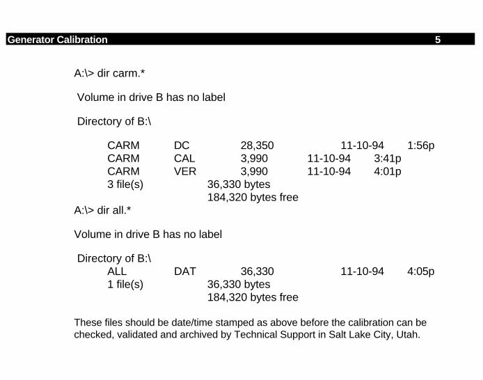
Generator Calibration 5
A:\> dir carm.*
Volume in drive B has no label
Directory of B:\
CARM DC 28,350 11-10-94 1:56pCARM CAL 3,990 11-10-94 3:41pCARM VER 3,990 11-10-94 4:01p3 file(s) 36,330 bytes
184,320 bytes freeA:\> dir all.*
Volume in drive B has no label
Directory of B:\ALL DAT 36,330 11-10-94 4:05p1 file(s) 36,330 bytes
184,320 bytes free
These files should be date/time stamped as above before the calibration can bechecked, validated and archived by Technical Support in Salt Lake City, Utah.
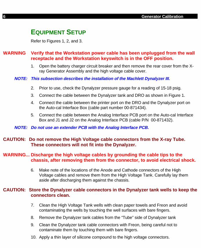
6 Generator Calibration
EQUIPMENT SETUPRefer to Figures 1, 2, and 3.
WARNING Verify that the Workstation power cable has been unplugged from the wallreceptacle and the Workstation keyswitch is in the OFF position.
1. Open the battery charger circuit breaker and then remove the rear cover from the X-ray Generator Assembly and the high voltage cable cover.
NOTE: This subsection describes the installation of the Machlett Dynalyzer III.
2. Prior to use, check the Dynalyzer pressure gauge for a reading of 15-18 psig.
3. Connect the cable between the Dynalyzer tank and DRO as shown in Figure 1.
4. Connect the cable between the printer port on the DRO and the Dynalyzer port onthe Auto-cal Interface Box (cable part number 00-871434).
5. Connect the cable between the Analog Interface PCB port on the Auto-cal InterfaceBox and J1 and J2 on the Analog Interface PCB (cable P/N 00-871432).
NOTE: Do not use an extender PCB with the Analog Interface PCB.
CAUTION: Do not remove the High Voltage cable connectors from the X-ray Tube.These connectors will not fit into the Dynalyzer.
WARNING... Discharge the high voltage cables by grounding the cable tips to thechassis, after removing them from the connector, to avoid electrical shock.
6. Make note of the locations of the Anode and Cathode connectors of the HighVoltage cables and remove them from the High Voltage Tank. Carefully lay themaside after discharging them against the chassis.
CAUTION: Store the Dynalyzer cable connectors in the Dynalyzer tank wells to keep theconnectors clean.
7. Clean the High Voltage Tank wells with clean paper towels and Freon and avoidcontaminating the wells by touching the well surfaces with bare fingers.
8. Remove the Dynalyzer tank cables from the “Tube” side of Dynalyzer tank
9. Clean the Dynalyzer tank cable connectors with Freon, being careful not tocontaminate them by touching them with bare fingers.
10. Apply a thin layer of silicone compound to the high voltage connectors.
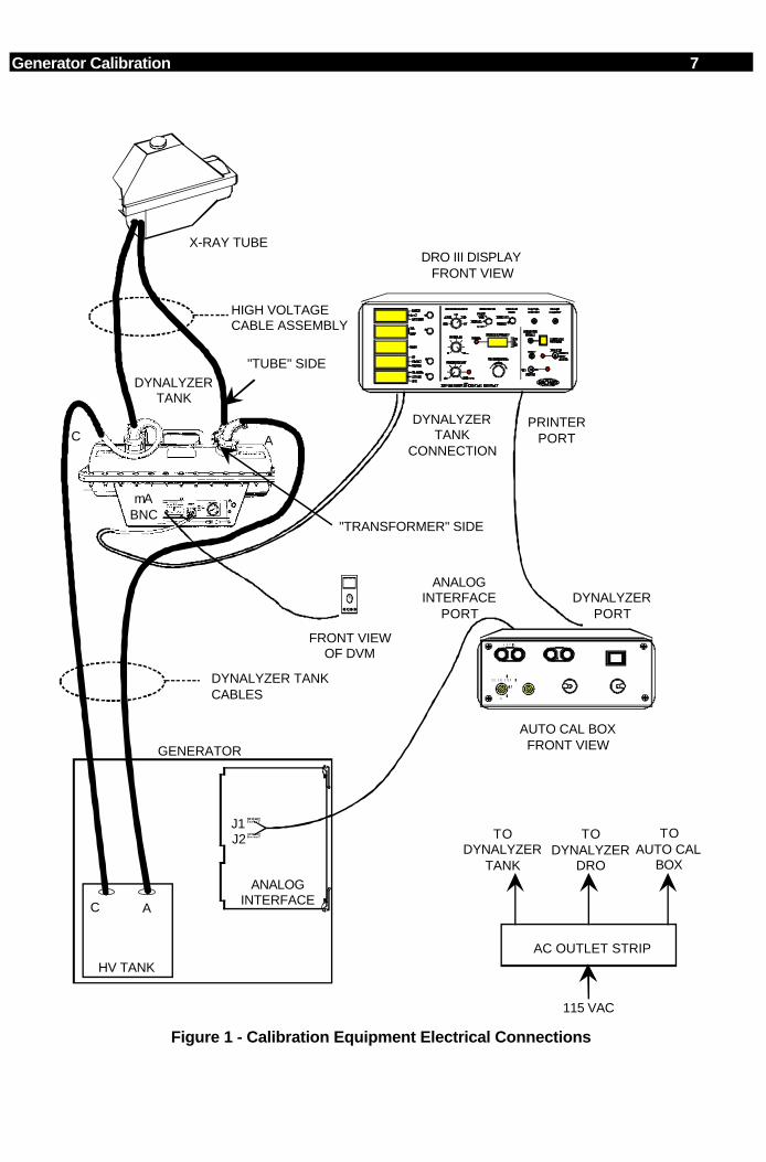
Generator Calibration 7
POWER
AMP OUTA M P I N
D O S I M E T E R EXT TRIG
I N
D/ADosimeterOffOn
X-RAY SWITCH
OVERRIDE
ANALOGINTERFACE
PORT
X-RAY TUBE
DYNALYZERPORT
PRINTERPORT
FRONT VIEWOF DVM
AC OUTLET STRIP
TOAUTO CAL
BOX
TODYNALYZER
TANK
TODYNALYZER
DRO
C A
J1J2
HV TANK
C A
GENERATOR
DRO III DISPLAYFRONT VIEW
HIGH VOLTAGECABLE ASSEMBLY
DYNALYZER TANKCABLES
AUTO CAL BOXFRONT VIEW
ANALOGINTERFACE
"TUBE" SIDE
"TRANSFORMER" SIDE
115 VAC
mABNC
DYNALYZERTANK
DYNALYZERTANK
CONNECTION
Figure 1 - Calibration Equipment Electrical Connections
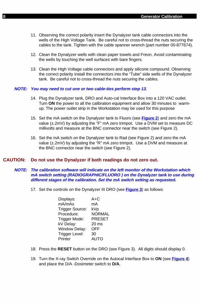
8 Generator Calibration
11. Observing the correct polarity insert the Dynalyzer tank cable connectors into thewells of the High Voltage Tank. Be careful not to cross-thread the nuts securing thecables to the tank. Tighten with the cable spanner wrench (part number 00-877674).
12. Clean the Dynalyzer wells with clean paper towels and Freon. Avoid contaminatingthe wells by touching the well surfaces with bare fingers.
13. Clean the High Voltage cable connectors and apply silicone compound. Observingthe correct polarity install the connectors into the “Tube” side wells of the Dynalyzertank. Be careful not to cross-thread the nuts securing the cables.
NOTE: You may need to cut one or two cable-ties perform step 13.
14. Plug the Dynalyzer tank, DRO and Auto-cal Interface Box into a 120 VAC outlet.Turn ON the power to all the calibration equipment and allow 30 minutes to warm-up. The power outlet strip in the Workstation may be used for this purpose
15. Set the mA switch on the Dynalyzer tank to Fluoro (see Figure 2 ) and zero the mAvalue (±.2mV) by adjusting the “F” mA zero trimpot. Use a DVM set to measure DCmillivolts and measure at the BNC connector near the switch (see Figure 2).
16. Set the mA switch on the Dynalyzer tank to Rad (see Figure 2) and zero the mAvalue (±.2mV) by adjusting the “R” mA zero trimpot. Use a DVM and measure atthe BNC connector near the switch (see Figure 2).
CAUTION: Do not use the Dynalyzer if both readings do not zero out.
NOTE: The calibration software will indicate on the left monitor of the Workstation whichmA switch setting (RADIOGRAPHIC/FLUORO ) on the Dynalyzer tank to use duringdifferent stages of the calibration. Set the mA switch setting as requested.
17. Set the controls on the Dynalyzer III DRO (see Figure 3 ) as follows:
Displays: A+CmA/mAs mATrigger Source: kVpProcedure: NORMALTrigger Mode: PRESETkV Delay: 20 msWindow Delay: OFFTrigger Level: 30Printer AUTO
18. Press the RESET button on the DRO (see Figure 3). All digits should display 0.
19. Turn the X-ray Switch Override on the Autocal Interface Box to ON (see Figure 4 )and place the D/A -Dosimeter switch to D/A.

Generator Calibration 9
20. Remove the necessary covers to access the X-ray Regulator PCB and jumperacross E1 on the X-ray Regulator PCB with a shorting plug to disable the mA servo.
21. Plug the system into the AC outlet. Turn on the battery circuit breaker and power upthe system.
22. Make an exposure in the MANUAL FLUORO mode and verify that the DRO isworking.
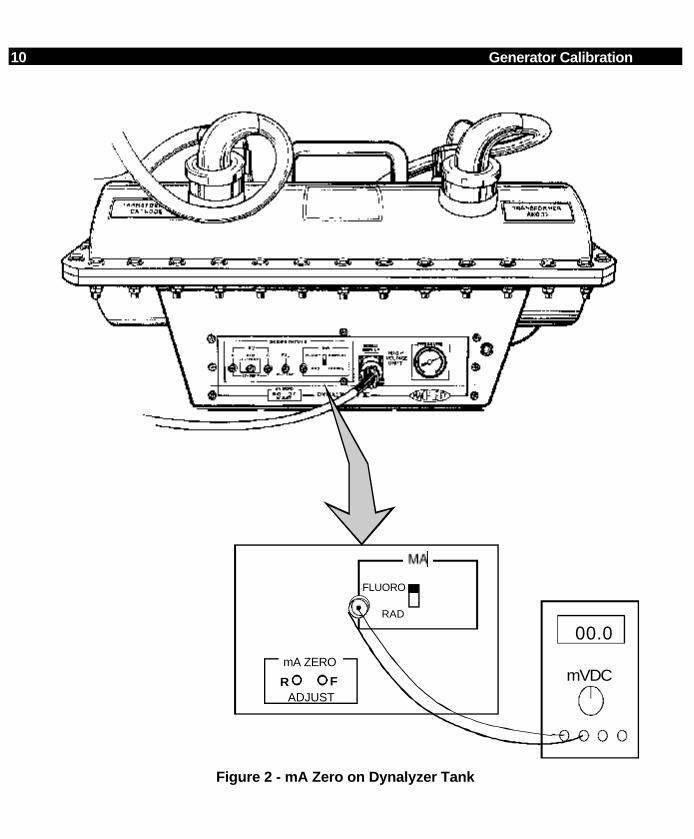
10 Generator Calibration
mA ZERO
ADJUST
00.0
mVDC
FLUORO
RAD
R F
Figure 2 - mA Zero on Dynalyzer Tank
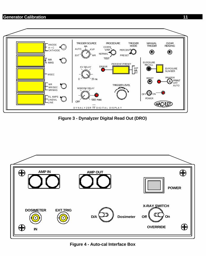
Generator Calibration 11
D Y N A L Y Z E R I II D IG IT A L D IS P L A Y
TRIGGER SOURCE
KVP
MR
AUTO
EXT
KV DELAY
WINDOW DELAY
OFF
PROCEDURE TRIGGERMODE
NORMAL
TEST
COEFFVAR
PERCENT/PRESET
PERCENT
PRESET
ERROR
TRIGGER LEVEL
MANUALTRIGGER
CLEARREADING
KVPMAEXT
EX POSURENUM BER
EX POSURERECALL
RESET PRINTER
POWER
OFF ON
PRINTOFFAUTO
ANODEA + CCATHODE
MAMAS
MSEC
MRMR/SECMR/MAS
FIL AMPSLINENILLINE
Figure 3 - Dynalyzer Digital Read Out (DRO)
POWER
AMP OUTAMP IN
DOSIMETER EXT TRIG
IN
D/A Dosimeter Off On
X-RAY SWITCH
OVERRIDE
Figure 4 - Auto-cal Interface Box

12 Generator Calibration
ACCESS CALIBRATION SOFTWARE
1. Press The SETUP OPTIONS key on the Workstation keyboard. The SetupOptions screen will appear.
2. Insert the OEC service access disk into the floppy disk drive on the rear of theWorkstation.
3. Select Access Level 2 and press the ENTER key.
4. Select the Access Mainframe Menu and press the ENTER key.
The Mainframe Menu will appear on the left monitor. The Control Panel Display willdisplay “MAINFRAME MENU.”
MAINFRAME MENU
A - Run Applications (Take X-rays)B - Run Calibration With ParametersC - Run CalibrationD - System ConfigurationE - mA Limit File EditorF - Examine Event FileG - Run StatusH - Collimator Calibration I - Language Options J - ABS Index File Editor
<ESC> - Return to DOS
Enter Command Letter :
5. From the Mainframe Menu select: C - Run Calibration . The Control Panel Displaywill display “CALIBRATION”.
6. Enter your initials when prompted: "Enter Initials Please".
7. Answer the following question when it appears on the monitor by entering Y andpressing the ENTER key:
Is your Dynalyzer (if any) wired internally for automatic reset?
Enter (Y/N): Y

Generator Calibration 13
8. The Model 9600 Calibration Menu will appear:
**** Model 9600 Calibration Menu ****
The following commands are available:
*Duty Cycle Calibration Options*
A - Take Duty Cycle DataB - Calculate Duty Cycle Coefficients to EEPROMC - Write Duty Cycle Coefficients to EEPROM *kV/mA Calibration Options*D - Acquire Calibration DataE - Calculate Calibration CoefficientsF - Update Coefficients to EEPROM *Verification Option*G - Acquire Data for Calibration Verification *BRH Test Option*H - Take BRH DataI - Return to main menu and merge existing data files
<ESC> - To abort without change
Enter Command Letter ___
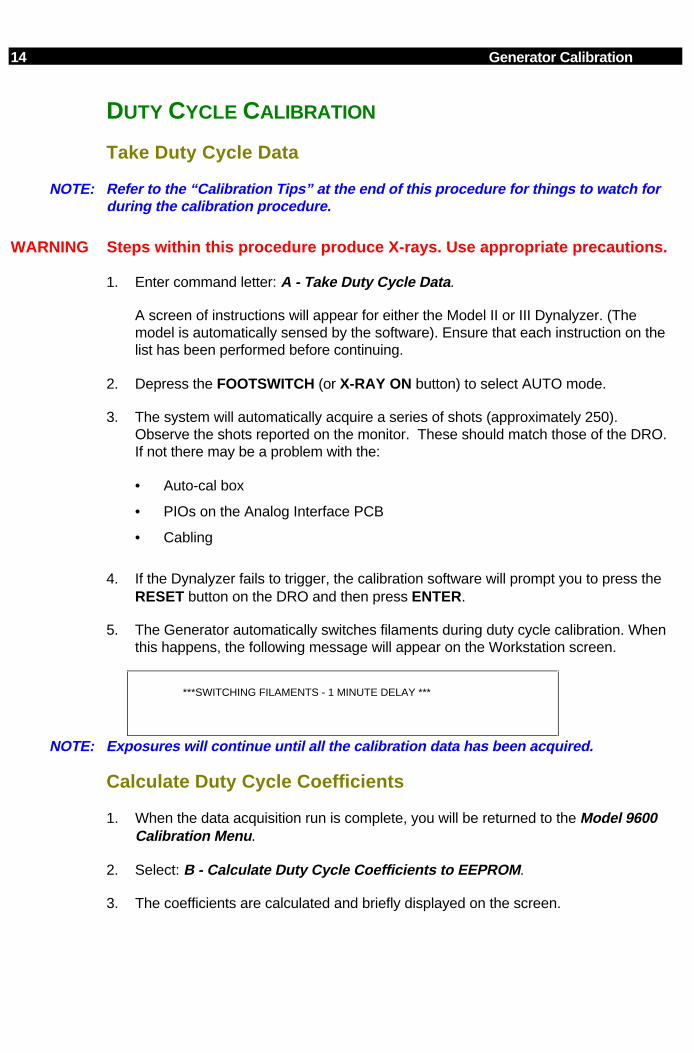
14 Generator Calibration
DUTY CYCLE CALIBRATION
Take Duty Cycle Data
NOTE: Refer to the “Calibration Tips” at the end of this procedure for things to watch forduring the calibration procedure.
WARNING Steps within this procedure produce X-rays. Use appropriate precautions.
1. Enter command letter: A - Take Duty Cycle Data .
A screen of instructions will appear for either the Model II or III Dynalyzer. (Themodel is automatically sensed by the software). Ensure that each instruction on thelist has been performed before continuing.
2. Depress the FOOTSWITCH (or X-RAY ON button) to select AUTO mode.
3. The system will automatically acquire a series of shots (approximately 250).Observe the shots reported on the monitor. These should match those of the DRO.If not there may be a problem with the:
• Auto-cal box
• PIOs on the Analog Interface PCB
• Cabling
4. If the Dynalyzer fails to trigger, the calibration software will prompt you to press theRESET button on the DRO and then press ENTER.
5. The Generator automatically switches filaments during duty cycle calibration. Whenthis happens, the following message will appear on the Workstation screen.
***SWITCHING FILAMENTS - 1 MINUTE DELAY ***
NOTE: Exposures will continue until all the calibration data has been acquired.
Calculate Duty Cycle Coefficients
1. When the data acquisition run is complete, you will be returned to the Model 9600Calibration Menu .
2. Select: B - Calculate Duty Cycle Coefficients to EEPROM .
3. The coefficients are calculated and briefly displayed on the screen.
Generator Calibration 15
Write Duty Cycle Coefficients to EEPROM
1. When the calculations are complete, you will be returned to the Model 9600Calibration Menu .
2. Select: C - Write Duty Cycle Coefficients To EEPROM .
3. The following message will appear briefly and then the software returns to theModel 9600 Calibration Menu .
Writing duty cycle coefficients to EEPROM.
Duty cycle coefficients have been written to EEPROM.
16 Generator Calibration
KV/MA TECHNIQUE CALIBRATION
Acquire Calibration Data
WARNING... Steps within this procedure produce X-rays. Use appropriate precautions.
1. From the Model 9600 Calibration Menu select: D - Acquire Calibration Data.
2. Remove the mA Servo-Disable jumper E1 on the X-ray Regulator PCB and changethe tank setting to Radiographic mode for LARGE SPOT calibration.
3. Depress the FOOTSWITCH (or X-RAY ON) to select AUTO mode and beginacquisition run.
4. The system automatically acquires data for approximately three minutes and thendisplays the following screen:
*** SWITCHING FILAMENTS ***
Change tank setting to Fluoro mode for small spot calibration.
Press {ENTER} on keyboard to continue.
NOTE: When the *** Switching Filaments *** screen appears an audible tone will be hearduntil the ENTER key is pressed.
5. Change the switch on the Dynalyzer to Fluoro mode and press Enter. Anotherseries of exposures will be taken, taking about five minutes.
Calculate Calibration Coefficients
1. After completion of the acquisition run, the Model 9600 Calibration Menu isdisplayed; select E - Calculate Calibration Coefficients .
2. The coefficients will be displayed briefly and then the Model 9600 CalibrationMenu is displayed.
Update Coefficients to EEPROM
1. From the Calibration Menu select: F - Update Coefficients To EEPROM .
2. When step one is completed the Model 9600 Calibration Menu is displayed.

Generator Calibration 17
VERIFICATION
General Information
Calibration must be verified during regular Periodic Maintenance procedures or whencertified components are replaced. Refer to the Appendix for a list of certifiedcomponents and information concerning when to file Report of Assembly, FDA Form2579.
The measurement values used for these tests are not the design specifications. The testspecifications used here take into account measurement limitations; their use will ensurethat the design specifications are met. All reference to specifications below are to theseTEST specifications.
NOTE: The following tests for kVp and mAs accuracy require installation of a Dynalyzer;the Autocal Interface Unit is not required.
Acquire Data for Calibration Verification
WARNING... Steps within this procedure produce X-rays. Use appropriate precautions.
1. From the Calibration Menu select G - Acquire Data For Calibration Verification.
2. Follow the menu instructions which appear on the computer terminal beforecontinuing with the procedure.
3. Zero the Dynalyzer (in both FLUORO and RAD on the model III). Set the Dynalyzertank to RAD.
4. Depress the FOOTSWITCH (or X-RAY ON switch) to select AUTO mode and beginacquisition run. This screen will appear on the left monitor.
Change Tank Setting to RAD Mode
20 Second Delay
5. The system automatically acquires data for about two minutes. The software willprompt you to change the Dynalyzer III setting with the following message:
*** SWITCHING FILAMENTS ***
Change Tank Setting to Fluoro Mode For Small Spot Calibration.
Press {ENTER} on Keyboard to Continue.
6. X-rays begin after a 20 second delay. When the acquisition run is complete(approximately 5 minutes), you will be returned to the Model 9600 CalibrationMenu .

18 Generator Calibration
MERGE EXISTING DATA FILES
1. From the Calibration Menu, select I - Return To Main Menu And Merge ExistingData Files.
NOTE: Option “H” is not for service use. Skip this option.
2. The message "Merging files, recreated All.Dat" will be displayed followed by amessage stating that the "EEPROM. Dat file has been updated". The software thenreturns you to the Mainframe Menu .
BACKUP GENERATOR SOFTWARE
NOTE: Do not reboot the system from the Mobile C-Arm Menu or cycle power to reboot thesystem until the generator software has been backed up. Rebooting the system atthis time affects the “Hot Byte” as explained in the “ C-Arm Software” section of thismanual.
1. Remove the SRAM card from the Technique Processor PCB and power off thesystem.
2. Locate the generator software backup disk (3 1/2-inch HD floppy located on the C-Arm in an anti-static bag).
3. Make two 3 1/2-inch floppy backup copies of the C-Arm disk per the procedure inthe C-Arm Software section of this manual. Return one backup diskette to the C-Arm and return the other to the Technical Support Office for evaluation andarchiving.
4. Reinstall the SRAM card in the Technique Processor and remove the cables fromthe Analog Interface PCB.
5. Power on the system. Confirm operation.
Generator Calibration 19
ENTRANCE EXPOSURE CALIBRATION
OVERVIEW
Entrance exposure is the amount of radiation available at the entrance point of patientanatomy. Entrance exposure is measured 12" (or 30 cm) above the surface of theImage Intensifier in the center of the X-ray beam. This measurement is used torepresent the average thickness of patient anatomy.
5R and 10R Systems
FDA requirement 80-8035, Section 1020.32, part D2 states the maximum FLUOROentrance exposure is either 5R/min or 10R/min depending on the manufacturing date. Ifa system was manufactured before May 19, 1995, the maximum entrance exposureallowed is 5R/min. On or after May 19, 1995, the maximum entrance exposure allowedis 10R/min. This impacts 9600s as indicated by the following system serial numbers:
• 5R systems = S/N 69-0001 to 69-1160
• 10R systems = S/N 69-1161 and higher
The remainder of this chapter is divided into two sections for both groups of systemserial numbers as described above. These two sections include theory and calibrationinformation.
NOTE: Be sure to refer to the correct Entrance Exposure documentation (5R or 10R)contained within this chapter depending upon the serial number of your system.
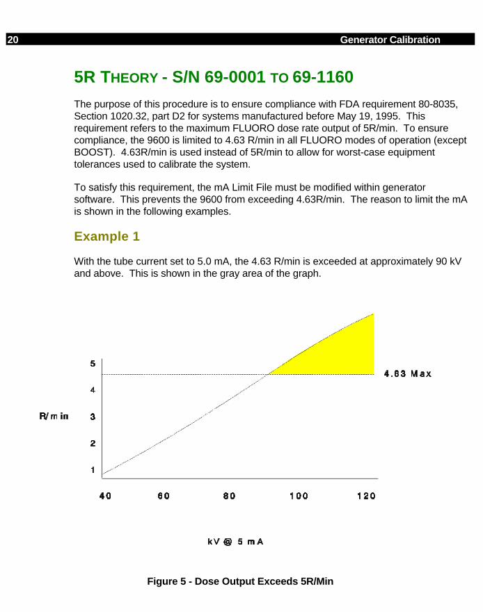
20 Generator Calibration
5R THEORY - S/N 69-0001 TO 69-1160
The purpose of this procedure is to ensure compliance with FDA requirement 80-8035,Section 1020.32, part D2 for systems manufactured before May 19, 1995. Thisrequirement refers to the maximum FLUORO dose rate output of 5R/min. To ensurecompliance, the 9600 is limited to 4.63 R/min in all FLUORO modes of operation (exceptBOOST). 4.63R/min is used instead of 5R/min to allow for worst-case equipmenttolerances used to calibrate the system.
To satisfy this requirement, the mA Limit File must be modified within generatorsoftware. This prevents the 9600 from exceeding 4.63R/min. The reason to limit the mAis shown in the following examples.
Example 1
With the tube current set to 5.0 mA, the 4.63 R/min is exceeded at approximately 90 kVand above. This is shown in the gray area of the graph.
Figure 5 - Dose Output Exceeds 5R/Min
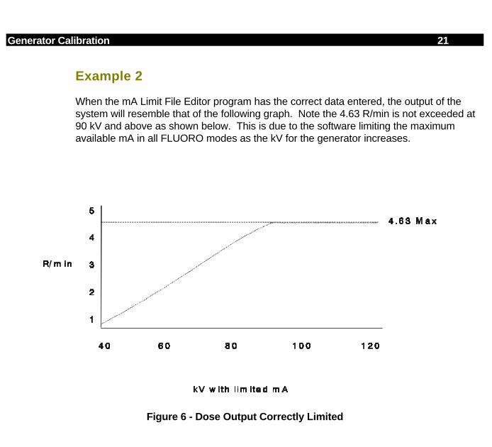
Generator Calibration 21
Example 2
When the mA Limit File Editor program has the correct data entered, the output of thesystem will resemble that of the following graph. Note the 4.63 R/min is not exceeded at90 kV and above as shown below. This is due to the software limiting the maximumavailable mA in all FLUORO modes as the kV for the generator increases.
Figure 6 - Dose Output Correctly Limited
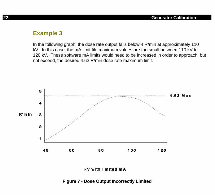
22 Generator Calibration
Example 3
In the following graph, the dose rate output falls below 4 R/min at approximately 110kV. In this case, the mA limit file maximum values are too small between 110 kV to120 kV. These software mA limits would need to be increased in order to approach, butnot exceed, the desired 4.63 R/min dose rate maximum limit.
Figure 7 - Dose Output Incorrectly Limited
Generator Calibration 23
CONFIRM 5R ABS TABLES
You can confirm your system has the correct 5R ABS tables by performing the followingtest:
1. Power on the system and allow it to boot completely.
2. Press the ABS SELECT button on the mainframe control panel. Using this key,toggle through the four available ABS tables comparing them to the following:
• Standard for Domestic 5R
• Low dose for domestic
• Chest 5R
• Extremities 5R
If these options do not appear, select the correct ABS tables as described in the"5R ABS Table Configuration" procedure located on the next page.
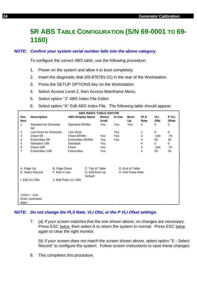
24 Generator Calibration
5R ABS TABLE CONFIGURATION (S/N 69-0001 TO 69-1160)
NOTE: Confirm your system serial number falls into the above category.
To configure the correct ABS table, use the following procedure:
1. Power on the system and allow it to boot completely.
2. Insert the diagnostic disk (00-876781-01) in the rear of the Workstation.
3. Press the SETUP OPTIONS key on the Workstation.
4. Select Access Level 2, then Access Mainframe Menu.
5. Select option "J" ABS Index File Editor.
6. Select option "A" Edit ABS Index File. The following table should appear:
ABS INDEX TABLE EDITORRecNos
Description ABS Display Name BoostAvail
In Use BootUp
PLSRate
VLIOfst
P VLIOfset
1 Standard for Domestic5R
Standard 5R/Min Yes Yes Yes 4 0 0
2 Low Dose for Domestic Low Dose Yes 1 0 03 Chest 5R Chest 5R/Min Yes Yes 4 -100 -704 Extremities 5R Extremities 5R/Min Yes Yes 4 50 355 Standard 10R Standard Yes 4 0 06 Chest 10R Chest Yes 4 -100 -707 Extremities 10R Extremities Yes 4 50 35
A. Page Up B. Page Down C. Top of Table D. End of TableE. Select Record F. Edit in Use G. Edit Boot Up
DefaultH. Edit Pulse Rate
I. Edit VLI Ofst J. Edit Pulse VLI Ofst
<ESC> - ExitEnter commandletter:
NOTE: Do not change the PLS Rate, VLI Ofst, or the P VLI Ofset settings.
7. (a) If your screen matches that the one shown above, no changes are necessary.Press ESC twice, then select A to return the system to normal. Press ESC twiceagain to clear the right monitor.
(b) If your screen does not match the screen shown above, select option "E - SelectRecord" to configure the system. Follow screen instructions to save these changes.
8. This completes this procedure.
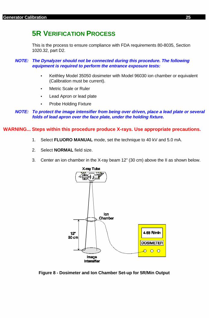
Generator Calibration 25
5R VERIFICATION PROCESS
This is the process to ensure compliance with FDA requirements 80-8035, Section1020.32, part D2.
NOTE: The Dynalyzer should not be connected during this procedure. The followingequipment is required to perform the entrance exposure tests:
• Keithley Model 35050 dosimeter with Model 96030 ion chamber or equivalent(Calibration must be current).
• Metric Scale or Ruler
• Lead Apron or lead plate
• Probe Holding Fixture
NOTE: To protect the image intensifier from being over driven, place a lead plate or severalfolds of lead apron over the face plate, under the holding fixture.
WARNING... Steps within this procedure produce X-rays. Use appropriate precautions.
1. Select FLUORO MANUAL mode, set the technique to 40 kV and 5.0 mA.
2. Select NORMAL field size.
3. Center an ion chamber in the X-ray beam 12” (30 cm) above the II as shown below.
Figure 8 - Dosimeter and Ion Chamber Set-up for 5R/Min Output

26 Generator Calibration
3. Increase the kV slowly up to 120 kV allowing the dosimeter to stabilize its readingas kV increases. At no point should the Actual Dose Rate (See note below)exceed 4.63 R/min. Notice how the mA decreases as the kV increases atapproximately 90 kV.
NOTE: If you are using an open air ion chamber , the measured dose rate (MDR) read on thedosimeter should be corrected for atmospheric pressure. This is know as theActual Dose Rate (ADR). Calculate the ADR using the following formula.
ADR = (760/P) (273.15 + T/295.15) * MDR
P = Absolute Pressure in Millimeters of Mercury
T = Temperature in degrees Celsius
4. Perform the 5R Entrance Exposure Calibration beginning on the next page if theADR reading exceeds 4.63 R/min or if you have a condition similar to example 3 ofthe previous page.
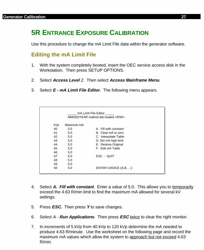
Generator Calibration 27
5R ENTRANCE EXPOSURE CALIBRATION
Use this procedure to change the mA Limit File data within the generator software.
Editing the mA Limit File
1. With the system completely booted, insert the OEC service access disk in theWorkstation. Then press SETUP OPTIONS.
2. Select Access Level 2. Then select Access Mainframe Menu .
3. Select E - mA Limit File Editor . The following menu appears.
_____ mA Limit File Editor _____MM/DD/YEAR malimit.dat loaded <R/W>
kVp Maximum mA40 5.0 A. Fill with constant41 5.0 B. Clear mA to zero42 5.0 C. Interpolate Table43 5.0 D. Set mA high limit44 5.0 E. Restore Original45 5.0 F. Edit mA Table46 5.047 5.0 ESC - QUIT48 5.049 5.050 5.0 ENTER CHOICE (A,B, . .):
4. Select A. Fill with constant . Enter a value of 5.0. This allows you to temporarilyexceed the 4.63 R/min limit to find the maximum mA allowed for several kVsettings.
5. Press ESC. Then press Y to save changes.
6. Select A - Run Applications . Then press ESC twice to clear the right monitor.
7. In increments of 5 kVp from 40 kVp to 120 kVp determine the mA needed toproduce 4.63 R/minute. Use the worksheet on the following page and record themaximum mA values which allow the system to approach but not exceed 4.63R/min.
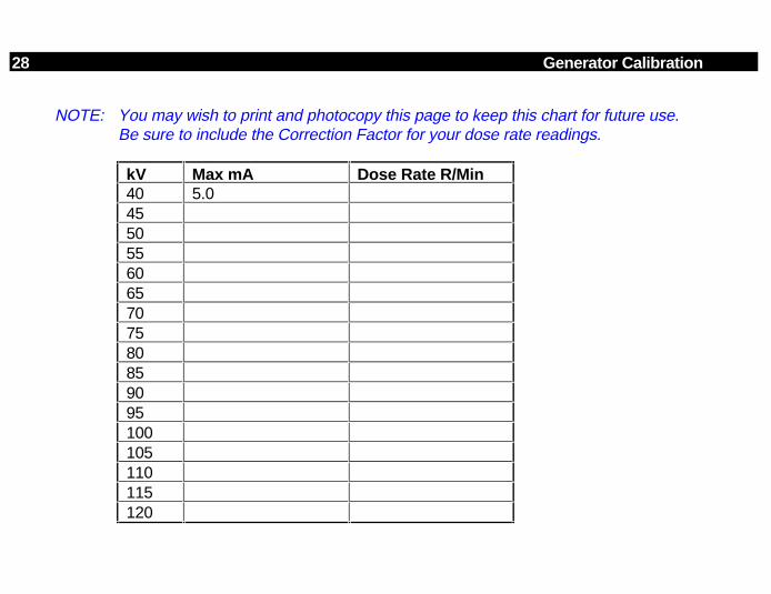
28 Generator Calibration
NOTE: You may wish to print and photocopy this page to keep this chart for future use.Be sure to include the Correction Factor for your dose rate readings.
kV Max mA Dose Rate R/Min40 5.04550556065707580859095100105110115120
Generator Calibration 29
8. After the chart is completed, press SETUP OPTIONS on the Workstation.
9. Select Access Level 2 . Then select Access Mainframe Menu .
10. Select E - mA Limit File Editor .
11. Select B - Clear mA to Zero .
12. Select F - Edit mA Table . The following menu appears.
_____ mA Limit File Editor _____<malimit.dat loaded> <R/W>
kVp Maximum mA40 0.0 A. Previous Line41 ___ B. Next Line42 ___ C. Page Up43 ___ D. Page Down44 ___ E. Beginning of Table45 ___ F. End of Table46 ___ G. Refresh Screen47 ___48 ___49 ___50 ___ ESC - QUIT
13. Enter the data from the worksheet starting with 5.0 mA at the 40 kV entry. Make thenext entry at the kV station which required less than 5.0 mA to not exceed themaximum dose rate allowed. From this kV data point, mA limits are entered at 5 kVintervals.
NOTE: Observe the following A, B, C, D, & E conditions while entering mA limit data.
A. No two entries can have the same mA values. This is shown as an error in theright column with 5.0 mA entered both 40 and 90 kV.
CORRECT INCORRECTkVp Max mA kVp Max mA40 5.0 40 5.0. . . .. . . .90 4.9 90 5.0. . . .. . . .. . . .120 2.9 120 2.9
30 Generator Calibration
B. mA limits cannot exceed previous entries. This is shown as an error in the rightcolumn for entry 95 kV. The 4.9 mA value exceeds the previous 4.8 mA value.
CORRECT INCORRECTkVp Max mA kVp Max mA40 5.0 40 5.0. . . .. . . .90 4.9 90 4.8. . . .95 4.4 95 4.9. . . .120 2.9 120 2.9
C. A minimum of three entries must be entered. This is shown as an error in theright column with only two entries at 40 and 120 kV and nothing for the 90 kVentry.
CORRECT INCORRECTkVp Max mA kVp Max mA
40 5.0 40 5.0. . . .. . . .90 4.9 90 .. . . .. . . .. . . .120 2.9 120 2.9
NOTE: Even though three entries will allow the software to interpolate the mA Limit File forthe rest of the values, values must be entered at every 5 kV point to ensure betterresolution of the mA limiting.
D. The 120 kV entry must contain a value. This is shown as an error in the rightcolumn.
CORRECT INCORRECTkVp Max mA kVp Max mA40 5.0 40 5.0. . . .. . . .90 4.9 90 4.9. . . .. . 95 4.4. . . .120 2.9 120 .
Generator Calibration 31
E. One of the entries must contain a 5.0 mA value. This is shown as an error in theright column at 40 kV.
CORRECT INCORRECTkVp Max mA kVp Max mA40 5.0 40 4.9. . . .. . . .90 4.9 90 4.8. . . .. . . .. . . .120 2.9 120 2.9
14. Press ESC when the preceding conditions (A - E) are met and all mA limits areentered.
15 Select C - Interpolate Table . The following menu appears if the interpolationprocess was successful . Your coefficients will more than likely be different fromthose shown in this example.
mA Entrance Exposure Interpolation Function
1: 1.42000002: 0.13016673: -0.0010167
Press any key to continue ....
OR - If the interpolation process was unsuccessful an Interpolation Error messageappears. (see associated A, B, C, D, or E error shown on previous pages)
16. Then press ESC. Then press Y to save, or N to exit with no save.
17. Select A - Run Applications . Then press ESC twice to clear the right monitor.
18. Using the verification portion of this procedure from the previous page to ensurecompliance.
NOTE: If any kV station exceeds the 4.63 R/min limit, record the mA value for that stationwhich corrects for this error. Then use the mA Limit File Editor to changeindividual kV stations. Do not re-interpolate the mA file after changing individual kVstations.
32 Generator Calibration
19. Without powering off the system, copy the MALIMIT.DAT file from the SRAM to thegenerator backup software diskette as follows:
A. Power on laptop. Select AMICARDZ icon in Windows.
B. Remove necessary covers to access the Technique Processor PCB
C. Remove the SRAM from the Technique Processor PCB.
D. Insert SRAM into PCMCIA slot.
E. After the message "Card Inserted in Socket 1" appears, select OK.
F. Exit to DOS and go to the F:\ drive.
G. Insert backup generator diskette in the floppy.
H. Enter the command "COPY MALIMIT.DAT A:"
I. Replace the SRAM in the Technique Processor
J. Remove the floppy diskette.
20. This completes the 5R Entrance Exposure Calibration procedure.
Generator Calibration 33
10R THEORY - S/N 69-1161 AND HIGHER
The purpose of this procedure is to ensure compliance with FDA requirement 80-8035,Section 1020.32, part D2 for systems manufactured on or after May 19, 1995. Thisrequirement refers to the maximum FLUORO dose rate output of 10R/min.
To ensure compliance, the 9600 is limited to 9.26 R/min in all FLUORO modes ofoperation (except BOOST). 9.26R/min is used instead of 10R/min to allow for worst-case equipment tolerances used to calibrate the system.
To satisfy this requirement, the mA Limit File must be modified within generator softwareto allow all kV stations a 5.0 mA maximum tube current.
CONFIRM 10R ABS TABLES
You can confirm your system has the correct 10R ABS tables by performing thefollowing test:
1. Power on the system and allow it to boot completely.
2. Press the ABS SELECT button on the mainframe control panel. Using this key,toggle through the four available ABS tables comparing them to the following:
STANDARD
CHEST
EXTREMITIES
LOW DOSE
If these options do not appear, select the correct ABS tables as described in the"10R ABS Table Configuration" procedure located on the next page.

34 Generator Calibration
10R ABS TABLE CONFIGURATION (S/N 69-1161 AND
HIGHER)
NOTE: Confirm your system serial number falls into the above category.
To configure the correct ABS table, use the following procedure:
1. Power on the system and allow it to boot completely.
2. Insert the diagnostic disk (00-876781-01) in the rear of the Workstation.
3. Press the SETUP OPTIONS key on the Workstation.
4. Select Access Level 2, then Access Mainframe Menu.
5. Select option "J" ABS Index File Editor.
6. Select option "A" Edit ABS Index File. The following table should appear:
ABS INDEX TABLE EDITOR
RecNos
Description ABS Display Name BoostAvail
In Use BootUp
PLSRate
VLIOfst
P VLIOfset
1 Standard for Domestic5R
Standard 5R/Min Yes 4 0 0
2 Low Dose forDomestic
Low Dose Yes 1 0 0
3 Chest 5R Chest 5R/Min Yes 4 -100 -704 Extremities 5R Extremities 5R/Min Yes 4 50 355 Standard 10R Standard Yes Yes Yes 4 0 06 Chest 10R Chest Yes Yes 4 -100 -707 Extremities 10R Extremities Yes Yes 4 50 35
A. Page Up B. Page Down C. Top of Table D. End of TableE. Select Record F. Edit in Use G. Edit Boot Up
DefaultH. Edit Pulse Rate
I. Edit VLI Ofst J. Edit Pulse VLI Ofst
<ESC> - ExitEnter commandletter:
NOTE: Do not change the PLS Rate, VLI Ofst, or the P VLI Ofset settings.
7(A). If your screen matches that the one shown above, no changes are necessary.Press ESC twice, then select A to return the system to normal. Press ESC twiceagain to clear the right monitor.
7(b). If your screen does not match the screen shown above, select option "E - SelectRecord" to configure the system. Follow screen instructions to save thesechanges.
8. This completes this procedure.
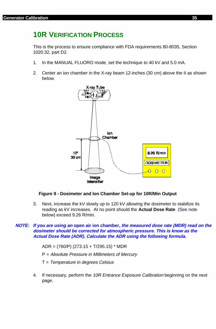
Generator Calibration 35
10R VERIFICATION PROCESS
This is the process to ensure compliance with FDA requirements 80-8035, Section1020.32, part D2.
1. In the MANUAL FLUORO mode, set the technique to 40 kV and 5.0 mA.
2. Center an ion chamber in the X-ray beam 12-inches (30 cm) above the II as shownbelow.
Figure 9 - Dosimeter and Ion Chamber Set-up for 10R/Min Output
3. Next, increase the kV slowly up to 120 kV allowing the dosimeter to stabilize itsreading as kV increases. At no point should the Actual Dose Rate (See notebelow) exceed 9.26 R/min.
NOTE: If you are using an open air ion chamber , the measured dose rate (MDR) read on thedosimeter should be corrected for atmospheric pressure. This is know as theActual Dose Rate (ADR). Calculate the ADR using the following formula.
ADR = (760/P) (273.15 + T/295.15) * MDR
P = Absolute Pressure in Millimeters of Mercury
T = Temperature in degrees Celsius
4. If necessary, perform the 10R Entrance Exposure Calibration beginning on the nextpage.
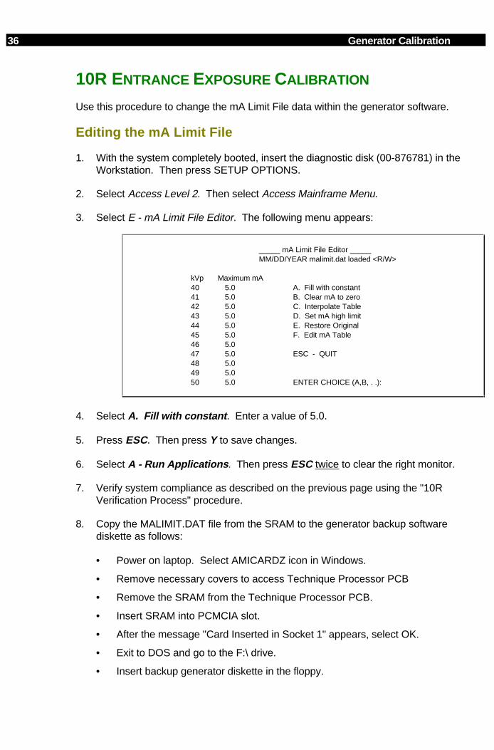
36 Generator Calibration
10R ENTRANCE EXPOSURE CALIBRATION
Use this procedure to change the mA Limit File data within the generator software.
Editing the mA Limit File
1. With the system completely booted, insert the diagnostic disk (00-876781) in theWorkstation. Then press SETUP OPTIONS.
2. Select Access Level 2. Then select Access Mainframe Menu.
3. Select E - mA Limit File Editor. The following menu appears:
_____ mA Limit File Editor _____MM/DD/YEAR malimit.dat loaded <R/W>
kVp Maximum mA40 5.0 A. Fill with constant41 5.0 B. Clear mA to zero42 5.0 C. Interpolate Table43 5.0 D. Set mA high limit44 5.0 E. Restore Original45 5.0 F. Edit mA Table46 5.047 5.0 ESC - QUIT48 5.049 5.050 5.0 ENTER CHOICE (A,B, . .):
4. Select A. Fill with constant . Enter a value of 5.0.
5. Press ESC. Then press Y to save changes.
6. Select A - Run Applications . Then press ESC twice to clear the right monitor.
7. Verify system compliance as described on the previous page using the "10RVerification Process" procedure.
8. Copy the MALIMIT.DAT file from the SRAM to the generator backup softwarediskette as follows:
• Power on laptop. Select AMICARDZ icon in Windows.
• Remove necessary covers to access Technique Processor PCB
• Remove the SRAM from the Technique Processor PCB.
• Insert SRAM into PCMCIA slot.
• After the message "Card Inserted in Socket 1" appears, select OK.
• Exit to DOS and go to the F:\ drive.
• Insert backup generator diskette in the floppy.
Generator Calibration 37
• Enter the command "COPY MALIMIT.DAT A:"
• Replace the SRAM in the Technique Processor
• Remove the floppy diskette.
9. This completes the 10R Entrance Exposure procedure.

MECHANICAL ASSEMBLIES
OVERVIEWThe following mechanical assemblies are discussed in this section, refer toFigure 1 as a location guide for the assemblies:
• Horizontal Cross Arm Bearings and Brake Assembly
• C-Arm Rear Capture Bearings and Brake Assembly
• Flip-Flop Assembly
• Wig-Wag Brake Assembly
• Front and Rear Steering Assemblies
• L-Arm Rotation Assembly
• Vertical Lift Assembly
NOTE
Click on the yellow box to go directly to the block diagram for this section. Do not use this link to return to a block diagram from this point. Click on the << button in the Tool Bar to return to any starting point.
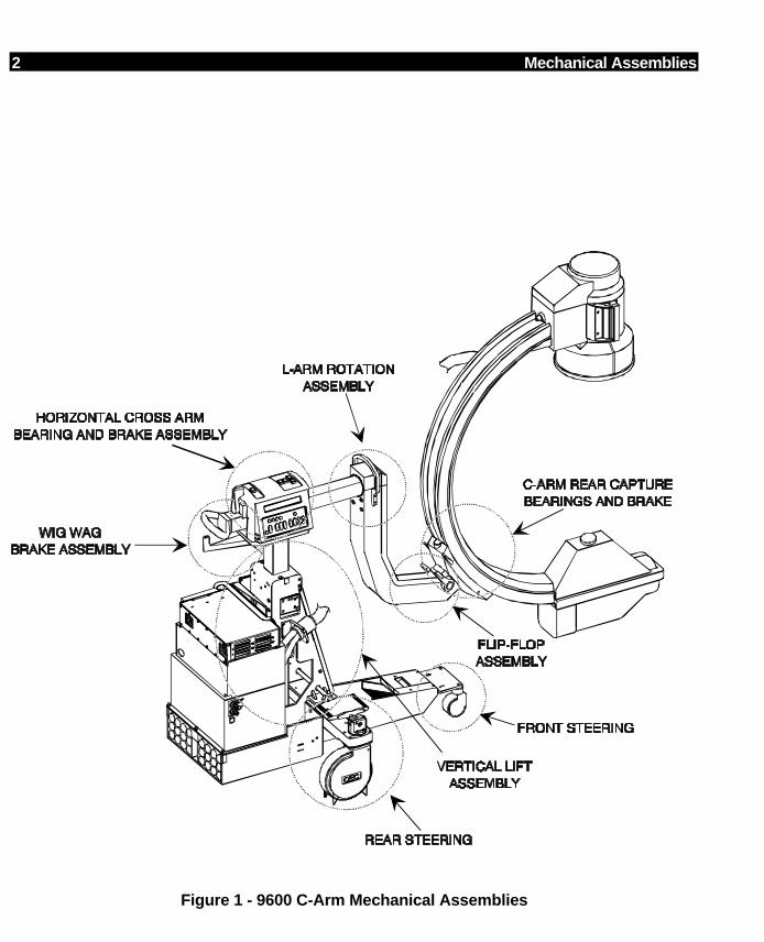
2 Mechanical Assemblies
Figure 1 - 9600 C-Arm Mechanical Assemblies

Mechanical Assemblies 3
HORIZONTAL CROSS ARM
OVERVIEW
The Horizontal Cross Arm assembly allows the forward mechanics to bemanually extended approximately 8 inches (20 cm). Extension and retraction canbe accomplished by releasing the cross arm brake, grasping the handle mountedat the end of the cross arm and manually positioning the cross arm in the desiredlocation.
Position indicator labels that indicate the length of extension can be found on tworecessed areas of the cross arm. Tick marks indicate each centimeter andnumbers occur in 5 cm increments to a maximum of 20 cm.
HORIZONTAL CROSS ARM BRAKE
The Horizontal Cross Arm brake may be engaged to prevent the cross arm frommoving. When the brake is engaged a brake pad restricts movement of a bearingin the Cross Arm Housing which in turn prevents the cross arm from moving.Refer to Figures 1 and 2.
To remove the brake, perform the following:
1. Remove the hole plug.
2. Remove 1 Torx screw securing the Cross Arm Brake Handle.
3. Remove 2 Torx screws from the bottom of the Cross Arm Lower Cover.
4. Lift the Cross Arm Center Cover up carefully and set aside.
5. Remove 4 Torx screws that secure the Cross Arm Brake Mount to thehousing.
6. Remove the Cross Arm Brake Pad.

4 Mechanical Assemblies
Figure 2 - Horizontal Cross Arm Brake Assembly
ROBOT CABLE ASSEMBLY
The robot cable routes 115 VAC to the L-arm Rotation Motor. The robot cable isrouted from the Power/Signal Distribution PCB or Column I/O PCB, through thehollow Horizontal Cross Arm, to the L-arm Motor Power PCB.
When the robot cable leaves the Power Signal/Distribution PCB or Column I/OPCB it enters the horizontal cross arm through a plate that has been designed toslide in a slot cut in the bottom of the Horizontal Cross Arm.
When the cross arm is extended and retracted through the Cross Arm Housingthe plastic plate slides in the slot and thus prevents damage to the robot cabledue to mechanical stresses and friction.
Figure 3 - Mechanical Stops and Robot Cable
NOTE
Click on the top colored box to go directly to the Illustrated Parts Manual for systems bearing serial numbers 69-001 thru 69-999. Click on the bottom colored box to go directly to the Illustrated Parts Manual for systems bearing serial numbers 69-1000 and higher. Click the << button on the TOOL Bar to return to this point.

Mechanical Assemblies 5
MECHANICAL STOPS
The cross arm has mechanical stops mounted in the Cross Arm to limit motion.The mechanical stops consist of metal screws mounted in the Cross Arm itselfand polyurethane plugs mounted in the Cross Arm Housing. The polyurethaneplugs absorb the shock when the Cross Arm is fully extended or fully retracted.
Perform the following to replace a polyurethane plug in the Cross Arm Housing:
1. Remove the Control Panel Housing.
2. Remove the plug using a pair of vise grips. Twist the plug out of its mounting(they are glued).
3. Replace the plug leaving approximately 1/2 inch exposed. Use Loctite BlackMax ZZLAH, OEC P/N - 88-299614-00.
CROSS ARM SHAFT & L-A RM DRIVER ASSEMBLY
Refer to Figures 4 and 5.
CAUTION: Do not separate the Horizontal Cross Arm and the L-arm DriverAssembly in the field due to the precision mechanical adjustmentsrequired during reassembly.
WARNING... Electrical circuits inside the equipment use voltages that are capableof causing serious injury or death from electrical shock. Useappropriate precautions.
NOTE: The L-arm motor, limit switches, L-arm Motor Power PCB & capacitormay be replaced individually.
1. Remove the L-Arm and forward mechanics as described in the L-ArmRotation Assembly heading of this section of the manual.
2. Disassemble the Control Panel Assembly by performing the following:
A. Remove the hole plug and Torx screw securing the Cross Arm BrakeHandle.
B. Remove the Cross Arm Brake Handle.
C. Remove 2 Torx screws from the bottom of the Cross Arm Lower Cover.
D. Carefully lift the Cross Arm Center Cover and set aside.
E. Remove the Control Panel Side Covers.

6 Mechanical Assemblies
F. Remove the metal covers and circuit boards from the top of the crossarm housing.
G. Disconnect necessary cabling. Make note of orientation for re-assembly.
3. Disconnect cabling from the Power/Signal Distribution PCB or Column I/OPCB and remove the PCB from the side of the Cross Arm Housing.
4. Remove the tie wraps securing the cabling to the side of the Cross ArmHousing.
NOTE: It is necessary to remove the snap rings from the top rear rollerbearing and move the bearing from side to side to access 2 of thehex bolts in the next step.
CAUTION: Ensure that the cross arm is fully retracted while removing the 4 hexbolts that secure the Control Panel Housing to the Vertical ColumnFlange. The L-arm Driver Assembly weighs approximately 60 lbs andthe weight is not balanced on the flange.
5. Remove 4 hex bolts securing the Control Panel Housing to the VerticalColumn Flange.
6. Remove the Cross Arm Housing and L-arm Driver Assembly and place theassembly on it's side.
7. Remove the two Torx head screws securing the round metal flange in thebottom of the Cross Arm shaft and remove the round metal flange.
8. Disconnect the wires from the TB1 Terminal block on the L-arm MotorPower PCB. Refer to the Interconnect Schematic when rewiring.
9. Pull the robot cable through the Cross Arm shaft.
10. Disconnect the limit switches by removing 2 allen head screws from eachlimit switch.
NOTE: Pull the motor away from the rubber motor mount as you arebacking out the flat head screws. This will increase the spacerequired for the allen ball drivers.
11. Remove 4 flat head bolts securing the L-arm Rotation Motor to the L-armgear box and remove the L-arm Rotation Motor, Limit Switches, and metalbracket as an assembly.
NOTE: Use Loctite 222 when reassembling.
12. Use a center punch to drive the pin in the Cross Arm Handle out, andremove the handle.

Mechanical Assemblies 7
HORIZONTAL CROSS ARM BEARING ADJUSTMENT
The following bearing assemblies in the Cross Arm Housing can be adjusted toremove any binding or loose play of the cross arm travel:
• Lower rear bearings
• Upper front bearings
• Right front bearings
• Left rear bearings
The Control Panel covers and circuit boards must be removed to make theadjustments. To adjust the bearing assemblies, perform the following:
1. Loosen the accompanying set screw.
2. Place the screwdriver in the slot at the end of the shaft and turn the shaftuntil the there is .003” clearance between the bearing and the Cross Arm.
3. Use Loctite 222 and re-tighten the set screw.
4. Check for smooth travel of the Cross Arm.
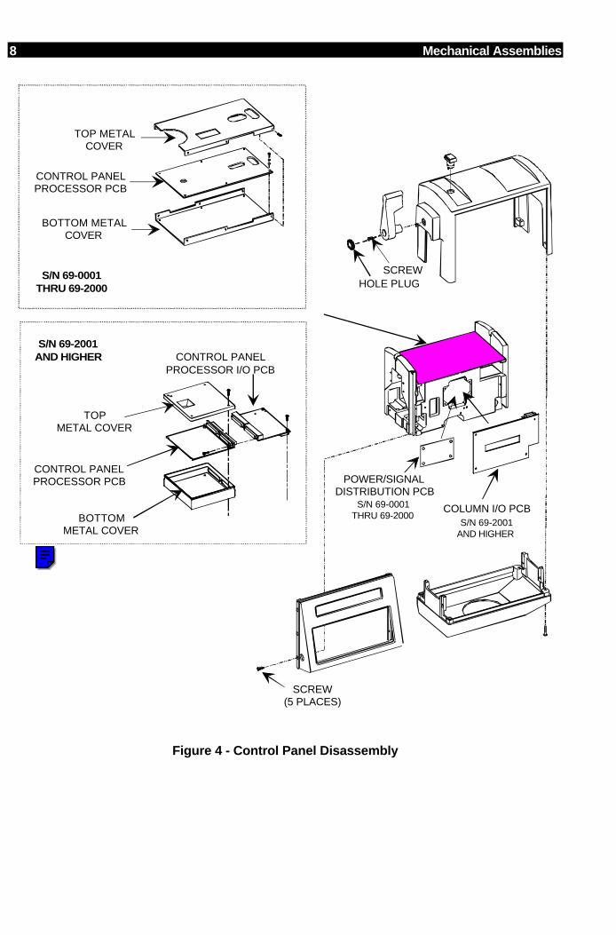
8 Mechanical Assemblies
HOLE PLUGSCREW
POWER/SIGNALDISTRIBUTION PCB
SCREW(5 PLACES)
CONTROL PANELPROCESSOR PCB
TOP METALCOVER
BOTTOM METALCOVER
CONTROL PANELPROCESSOR I/O PCB
CONTROL PANELPROCESSOR PCB
COLUMN I/O PCBS/N 69-2001
AND HIGHER
S/N 69-0001THRU 69-2000
TOP METAL COVER
BOTTOM METAL COVER
S/N 69-2001AND HIGHER
S/N 69-0001THRU 69-2000
Figure 4 - Control Panel Disassembly
NOTE
Click on the top colored box to go directly to the Illustrated Parts Manual for systems bearing serial numbers 69-001 thru 69-999. Click on the bottom colored box to go directly to the Illustrated Parts Manual for systems bearing serial numbers 69-1000 and higher. Click the << button on the Tool Bar to return to this point.
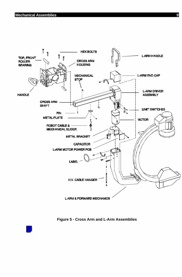
Mechanical Assemblies 9
Figure 5 - Cross Arm and L-Arm Assemblies
NOTE
Click on the top colored button to go directly to the drawing of systems bearing serial numbers 69-001 thru 69-999. Click on the bottom colored button to go directly to the drawing of systems bearing serial numbers 69-1000 and higher. Click on the << button in the Tool Bar to return to this point.

10 Mechanical Assemblies
FLIP FLOP ASSEMBLY
OVERVIEW
The Flip Flop allows the C-arm to be rotated 180° clockwise or counterclockwise. This movement "flips" the position of the C-arm and allows for A/P(Anterior/Posterior) Lateral positioning.
The C-arm connects to the Mobile C-Arm via the Flip Flop assembly and the rearcapture bearing design. The rear capture design consists of 8 axial rollerbearings and 8 radial roller bearings. These bearings ensure smooth axial andradial movement of the C-Arm in relation to the Flip Flop assembly. The FlipFlop bearings require no lubrication.
C-ARM REMOVAL
WARNING... Observe safety procedures when operating motorized mechanicalfeatures.
Electrical circuits inside the equipment use voltages that are capableof causing serious injury or death from electrical shock. Useappropriate precautions.
1. Rotate the L-arm until the C-arm is parallel with the floor and then rest the C-arm on a gurney. Be sure that the assembly is fully supported without anybinds or stress on any of the welded seams.
2. Turn the Workstation keyswitch to the OFF position.
CAUTION: Attempting to remove the “C” by removing the X-ray Tube andCollimator and then sliding the “C” out of the nylon rollers in theFlip Flop assembly could result in severe damage to the nylonrollers..
3. Remove 4 hex screws that secure the metal plate behind the Flip Flop pivot,of the L-arm.
4. Bend the washer fingers out and then using the Flip Flop spanner wrenchloosen and remove the Flip Flop nut.
5. Back the gurney away and separate the Flip Flop Assembly from the L-arm.
6. Remove the X-ray Tube and Collimator.
7. Slide the Flip Flop Assembly off the end of the C-arm.
8. After reassembling, perform the Beam Alignment Test procedure containedin the Image System Calibration section of this manual.
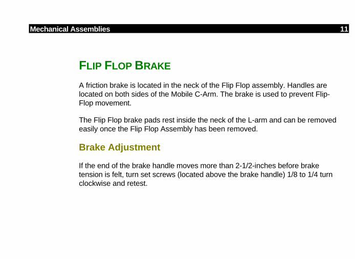
Mechanical Assemblies 11
FLIP FLOP BRAKE
A friction brake is located in the neck of the Flip Flop assembly. Handles arelocated on both sides of the Mobile C-Arm. The brake is used to prevent Flip-Flop movement.
The Flip Flop brake pads rest inside the neck of the L-arm and can be removedeasily once the Flip Flop Assembly has been removed.
Brake Adjustment
If the end of the brake handle moves more than 2-1/2-inches before braketension is felt, turn set screws (located above the brake handle) 1/8 to 1/4 turnclockwise and retest.
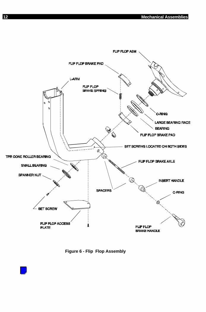
12 Mechanical Assemblies
Figure 6 - Flip Flop Assembly
NOTE
Click on the top colored button to go directly to the drawing of systems bearing serial numbers 69-001 thru 69-999. Click on the bottom colored button to go directly to the drawing of systems bearing serial numbers 69-1000 and higher. Click on the << button in the Tool Bar to return to this point.

Mechanical Assemblies 13
C-ARM BEARINGS AND BRAKE
OVERVIEW
The C-arm connects to the Mobile C-Arm via the Flip Flop assembly and the rearcapture bearing design. The C-arm is manually positioned on its radius and thebrake, when engaged, prevents radial C-arm movement.
The rear capture design consists of 8 axial roller bearings and 8 radial rollerbearings. These bearings ensure smooth axial and radial movement of the C-Arm in relation to the Flip Flop assembly.
C-ARM BRAKE
The cam-levered C-arm brake is contained in the Flip Flop Assembly. Removethe C-arm as described in the Flip Flop Assembly. Separate the Flip Flop fromthe C-arm to inspect the brake.
REAR CAPTURE C-ARM BEARINGS
The axial and radial bearings are contained in the Flip Flop Assembly. Removethe C-arm as described in the Flip Flop Assembly heading of this section of themanual. Separate the Flip Flop and C-arm from the L-arm and then separate theFlip Flop from the C-arm. Inspect nylon rollers for cracks or excessive wear.Check for smooth bearing operation. Repair or replace bearings and nylonrollers as required.
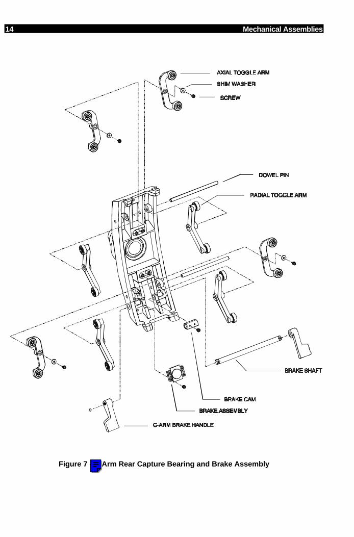
14 Mechanical Assemblies
Figure 7 - C-Arm Rear Capture Bearing and Brake Assembly
NOTE
Click on the top colored button to go directly to the drawing of systems bearing serial numbers 69-001 thru 69-999. Click on the bottom colored button to go directly to the drawing of systems bearing serial numbers 69-1000 and higher. Click on the << button in the Tool Bar to return to this point.

Mechanical Assemblies 15
WIG WAG BRAKE ASSEMBLY
OVERVIEW
The Wig Wag Assembly allows the forward mechanics to move sideways 11° ineither direction.
The Wig Wag Assembly should not move when the friction brake is fullyengaged. The Wig-Wag brake is non-binding and is easily released andengaged. The brake design allows the user to partially engage the brake for easeof use or fully engage the brake to prevent travel.
The Wig Wag assembly does not have any marked or labeled position indicators.
WIG WAG BRAKE ADJUSTMENT
If the brake fails to lock the forward mechanics in position (e.g. the brake handleturns without engaging the brake) perform the following:
1. Remove the Hole Plug and remove the screw in the brake handle. Removethe Wig Wag brake handle.
2. Loosen the set screw.
3. Using a standard screwdriver turn the actuator screw approximately 1/4 turncounter-clockwise.
4. Reassemble and functionally test the brake.
5. If this adjustment fails, disassemble the Wig Wag assembly and inspect thewashers and brake pad. Check for worn or damaged parts.

16 Mechanical Assemblies
CONTROL PANEL HOUSING REMOVAL
The Control Panel Housing must be removed before the Wig Wag Assembly canbe accessed.
WARNING... Electrical circuits inside the equipment use voltages that are capableof causing serious injury or death from electrical shock. Useappropriate precautions.
1. Turn the Workstation keyswitch to the OFF position.
2. Remove the Hole Plug and 1 Torx screw securing the Cross Arm BrakeHandle.
3. Remove 2 Torx screws from the bottom of the Cross Arm Lower Cover.
4. Lift the Cross Arm Center Cover up carefully and unplug switch wiring on theControl Panel Processor PCB and the Distribution PCB.
5. Remove 4 Torx screws securing the Cross Arm Lower Cover and lower thecover so that the Wig Wag Assembly can be accessed.
6. Remove the Hole Plug from the bottom of the Wig Wag brake handle andloosen the screw.
7. Remove the Wig Wag brake handle.
8. Remove 2 flathead Allen screws in the bottom of the retaining plate andremove the retaining plate.
9. Loosen the set screw.
10. Turn the actuator screw clockwise using a standard slotted screwdriver untilthe brake assembly can be removed.
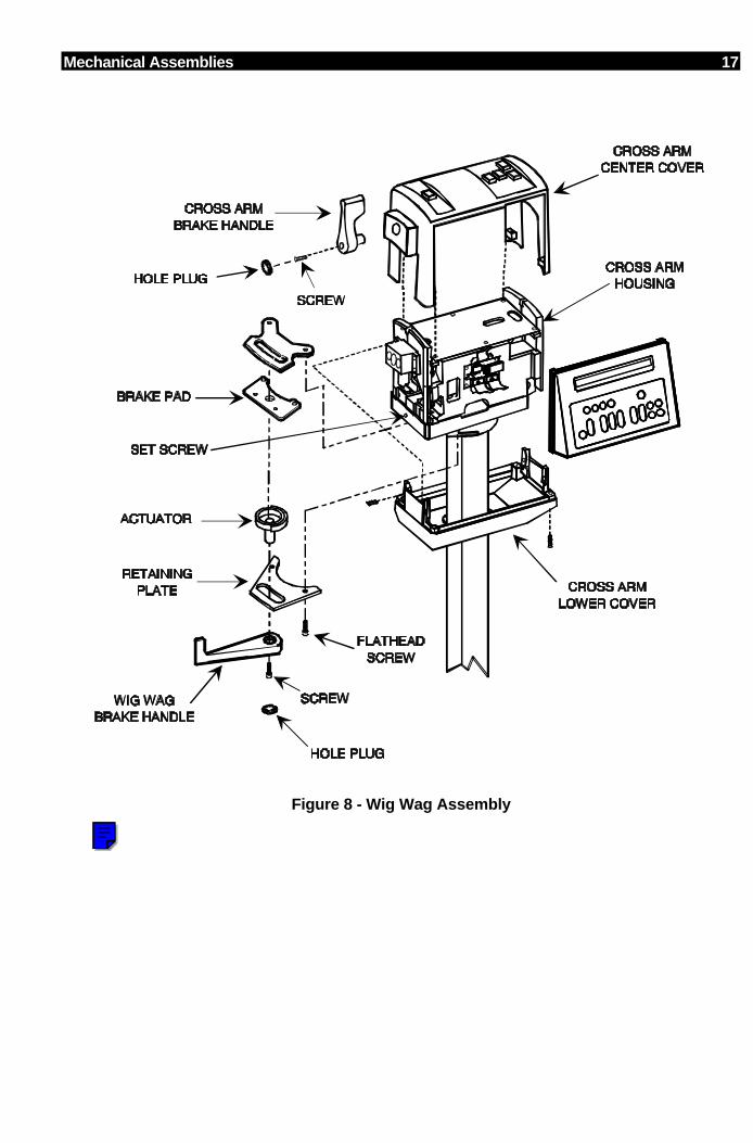
Mechanical Assemblies 17
Figure 8 - Wig Wag Assembly
NOTE
Click on the top colored button to go directly to the drawing of systems bearing serial numbers 69-001 thru 69-999. Click on the bottom colored button to go directly to the drawing of systems bearing serial numbers 69-1000 and higher. Click on the << button in the Tool Bar to return to this point.

18 Mechanical Assemblies
STEERING
OVERVIEW
The 9600 Mobile C-Arm is supported by four wheels with offset casters. Thisincludes two front wheel casters and two rear wheel casters. In addition there isa balance wheel located underneath the battery tray that will prevent the MobileC-Arm from tipping backwards while transporting the system over an incline.
Four possible versions of the rear caster may be found in the field. The originalSurgi-glide I (-01) with side scan installed, an interim Surgi-glide version that hadside scan removed (-02), a third version (-03) with side scan reinstalled and thelatest version, Surgi-glide II.
Information concerning older versions will be found in shaded boxes throughoutthis section.
Figure 9 - Series 9600 C-Arm Rear Caster
NOTE
Click on the top colored box to go to the 9600 Center Pivot Steering Update in the Illustrated Parts Manual. Click on the middle colored box to go directly to the drawing of systems bearing serial numbers 69-001 thru 69-999. Click on the bottom colored box to go directly to the drawing of systems bearing serial numbers 69-1000 and higher. Click on the << button in the Tool Bar to return to this point.

Mechanical Assemblies 19
REAR CASTERS
Unlike the front wheels the two rear wheels have three modes of operation. Allthree modes of operation are selected by steering pedals located above eachrear wheel. Engaging either pedal drives a cam operated actuator shaft thatoperates both rear wheels. The following modes of operation are selectable:
Free Swivel Mode - allows the rear wheel's casters to move in any direction andthe wheels turn freely.
Steering Mode -locks the rear wheel casters in the forward steering position orthe lateral (side-to-side) steering position. The forward steering position improvestracking down corridors and steering around corners and the lateral steeringposition improves tracking during side-to-side positioning in the operating room.
Lock Mode - locks the caster in its current position and engages a brake padwhich stops wheel movement.
Older Versions
Steering pedals on -01 versions operate in reverse from later versions. A lateral(side-to-side) movement is standard on all systems except the -02 version. The -02 version of the Surgi-glide I steering system does not have side scan.
The lateral (side-to-side) feature may be engaged on rear casters equipped withside scan, by placing the pedal in steering mode while the rear casters arepointed perpendicular to the Mobile C-Arm.
FRONT CASTERS
Two front wheel casters support the Mobile C-Arm and allow movement in anydirection, much like a shopping cart. Refer to the Repair Replacement sectionfor an illustration.
BALANCE WHEEL
A balance wheel is located underneath the battery trays. The balance wheel hasbeen designed to prevent the Mobile C-Arm from tipping backwards and pinchingan operators foot or toe. Refer to the Repair Replacement section for anillustration.
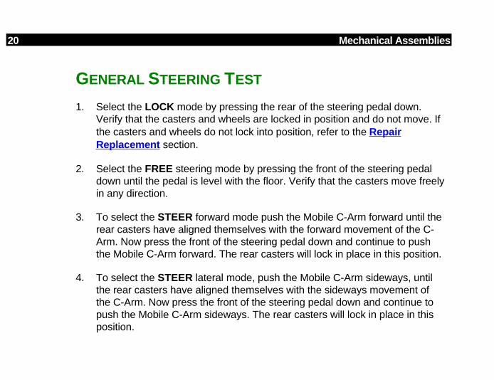
20 Mechanical Assemblies
GENERAL STEERING TEST
1. Select the LOCK mode by pressing the rear of the steering pedal down.Verify that the casters and wheels are locked in position and do not move. Ifthe casters and wheels do not lock into position, refer to the RepairReplacement section.
2. Select the FREE steering mode by pressing the front of the steering pedaldown until the pedal is level with the floor. Verify that the casters move freelyin any direction.
3. To select the STEER forward mode push the Mobile C-Arm forward until therear casters have aligned themselves with the forward movement of the C-Arm. Now press the front of the steering pedal down and continue to pushthe Mobile C-Arm forward. The rear casters will lock in place in this position.
4. To select the STEER lateral mode, push the Mobile C-Arm sideways, untilthe rear casters have aligned themselves with the sideways movement ofthe C-Arm. Now press the front of the steering pedal down and continue topush the Mobile C-Arm sideways. The rear casters will lock in place in thisposition.

Mechanical Assemblies 21
FRONT WHEEL REMOVAL
1. Place the C-arm in the vertical position and engage the C-arm rotationbrake. Retract the C-arm through the Cross Arm Housing and engage theCross Arm brake.
2. Back the Mobile C-Arm until the rear casters swing into the backing position,then tilt the Mobile C-Arm onto the balance wheel. Block the front of theMobile C-Arm chassis.
3. Remove the decal from the right side of the caster.
4. Unscrew the screw and then remove the wheel. Remove the mountingscrew and remove the caster.
5. Replace the caster and reassemble. Install new decals.
Figure 10 - Front Wheel Removal (Earlier Style Cable Pushers)
NOTE
Click on the colored box to go directly to the drawing of systems bearing serial numbers 69-001 thru 69-999. Click on the << button in the Tool Bar to return to this point.
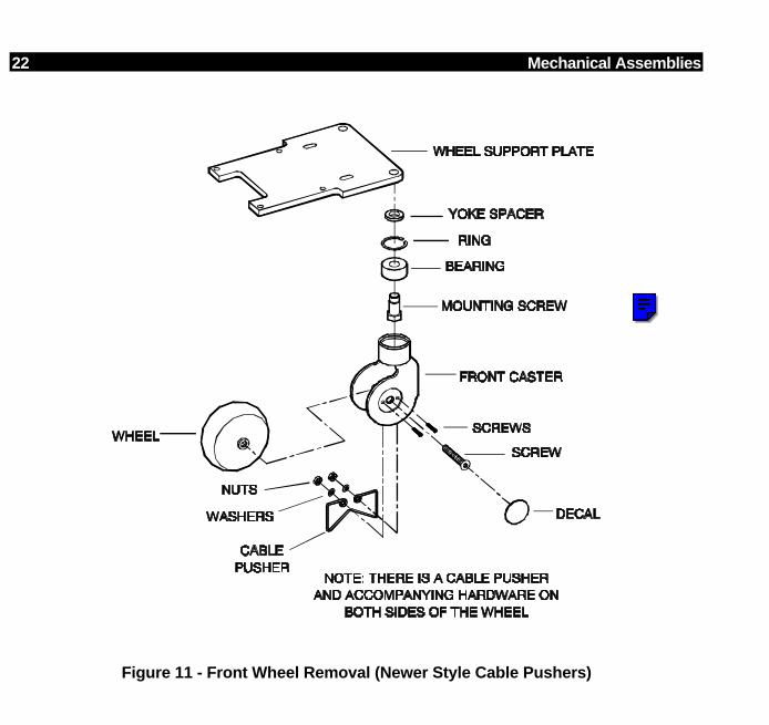
22 Mechanical Assemblies
Figure 11 - Front Wheel Removal (Newer Style Cable Pushers)
NOTE
Click on the colored box to go directly to the drawing of systems bearing serial numbers 69-1000 and higher. Click on the << button in the Tool Bar to return to this point.
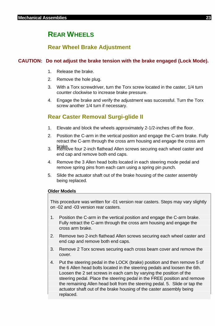
Mechanical Assemblies 23
REAR WHEELS
Rear Wheel Brake Adjustment
CAUTION: Do not adjust the brake tension with the brake engaged (Lock Mode).
1. Release the brake.
2. Remove the hole plug.
3. With a Torx screwdriver, turn the Torx screw located in the caster, 1/4 turncounter clockwise to increase brake pressure.
4. Engage the brake and verify the adjustment was successful. Turn the Torxscrew another 1/4 turn if necessary.
Rear Caster Removal Surgi-glide II
1. Elevate and block the wheels approximately 2-1/2-inches off the floor.
2. Position the C-arm in the vertical position and engage the C-arm brake. Fullyretract the C-arm through the cross arm housing and engage the cross armbrake.3. Remove four 2-inch flathead Allen screws securing each wheel caster andend cap and remove both end caps.
4. Remove the 3 Allen head bolts located in each steering mode pedal andremove spring pins from each cam using a spring pin punch.
5. Slide the actuator shaft out of the brake housing of the caster assemblybeing replaced.
Older Models
This procedure was written for -01 version rear casters. Steps may vary slightlyon -02 and -03 version rear casters.
1. Position the C-arm in the vertical position and engage the C-arm brake.Fully retract the C-arm through the cross arm housing and engage thecross arm brake.
2. Remove two 2-inch flathead Allen screws securing each wheel caster andend cap and remove both end caps.
3. Remove 2 Torx screws securing each cross beam cover and remove thecover.
4. Put the steering pedal in the LOCK (brake) position and then remove 5 ofthe 6 Allen head bolts located in the steering pedals and loosen the 6th.Loosen the 2 set screws in each cam by varying the position of thesteering pedal. Place the steering pedal in the FREE position and removethe remaining Allen head bolt from the steering pedal. 5. Slide or tap theactuator shaft out of the brake housing of the caster assembly beingreplaced.

24 Mechanical Assemblies
NOTE: Elevating the C-Arm, may first be required, in order to alleviate shafttension.
6. Elevate and block the C-Arm so the wheels are approximately 2-1/2”off the floor.
7. Remove the 1/2-inch flathead Allen screw from the caster assemblyand remove the caster assembly.
Wheel Removal Surgi-glide II
1. Verify the C-arm is positioned in the vertical position and the C-arm brake isfully engaged. Fully retract the C-arm through the cross arm housing andengage the cross arm brake.
2. Elevate and block the C-arm so that the wheel doesn't touch the floor.
3. Remove the labels from each side of the caster.
4. Remove the axle screw.
5. Remove the wheel from the caster.
Older Models
This procedure was written for -01 version rear casters. Steps may vary slightlyon -02 and -03 version rear casters.
1. Verify the C-Arm is positioned in the vertical position and the C-Arm brakeis fully engaged. Fully retract the C-arm through the Cross Arm Housingand engage the Cross Arm brake.
2. Elevate and block the C-Arm so that the wheel doesn't touch the floor.
3. Remove the labels from each side of the caster.
4. Remove the axle screw and axle nut.
5. Remove the wheel from the caster.
Wheel Replacement Surgi-glide II
1. Position the wheel inside the caster and connect the Axle Screw. UseLoctite 242.2. Re-label each side of the caster.
3. Remove the blocks and lower the C-arm to the floor.
4. Check the brake.
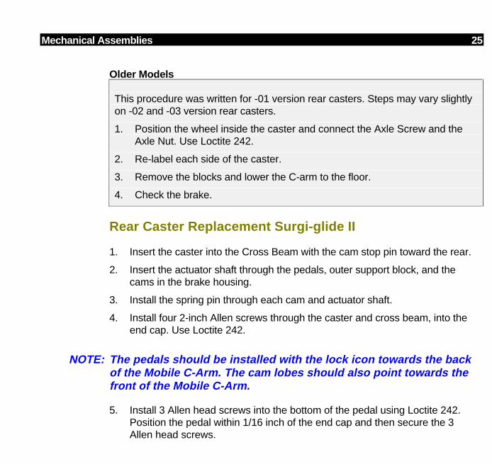
Mechanical Assemblies 25
Older Models
This procedure was written for -01 version rear casters. Steps may vary slightlyon -02 and -03 version rear casters.
1. Position the wheel inside the caster and connect the Axle Screw and theAxle Nut. Use Loctite 242.
2. Re-label each side of the caster.
3. Remove the blocks and lower the C-arm to the floor.
4. Check the brake.
Rear Caster Replacement Surgi-glide II
1. Insert the caster into the Cross Beam with the cam stop pin toward the rear.
2. Insert the actuator shaft through the pedals, outer support block, and thecams in the brake housing.
3. Install the spring pin through each cam and actuator shaft.
4. Install four 2-inch Allen screws through the caster and cross beam, into theend cap. Use Loctite 242.
NOTE: The pedals should be installed with the lock icon towards the backof the Mobile C-Arm. The cam lobes should also point towards thefront of the Mobile C-Arm.
5. Install 3 Allen head screws into the bottom of the pedal using Loctite 242.Position the pedal within 1/16 inch of the end cap and then secure the 3Allen head screws.
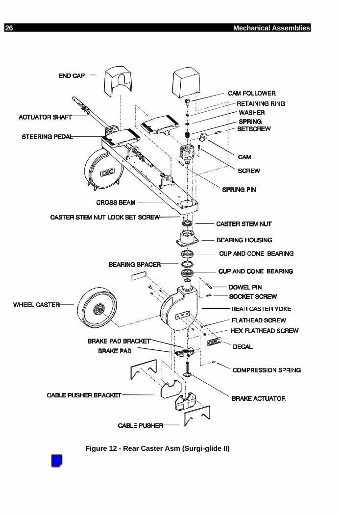
26 Mechanical Assemblies
Figure 12 - Rear Caster Asm (Surgi-glide II)
NOTE
Click on the colored box to go directly to the same assembly in the Illustrated Parts Manual. Click on the << button on the Tool Bar to return to this point.
Mechanical Assemblies 27
Older Models
This procedure was written for -01 version rear casters. Steps may vary slightlyon -02 and -03 version rear casters.
1. Insert the caster into the Cross Beam with the open end of the slot facingforward.
2. Install the 1/2-inch Allen screw through the caster and into the cross beamusing Loctite 242.
NOTE: The pedals should be installed with the lock icon towards the frontof the Mobile C-Arm. The cam lobes should also point towards thefront of the Mobile C-Arm. Ensure the cam follower and shim areinstalled in the new caster assembly before proceeding.
3. Insert the actuator shaft through the pedals, outer support block, and thecams in the brake housing.
4. Loosely install one Allen head screw into the bottom of one pedal. Placethe steering pedal in the LOCK (brake) position. Position each pedal within1/32” of the outer support block. Install the other five Allen head screws andreinstall the first using Loctite 242.
5. Rotate the pedal to the FREE position and center the cam within the brakehousing. Install the top cam set screw on each cam using Loctite 222.Rotate the pedal to the LOCK position and install the rear cam set screw ineach cam using Loctite 222.
6. Place the steering pedal in the FREE, LOCK, and STEER positions andtest for proper operation.
NOTE: The rear wheel brake adjustment may need to be performed on thenew caster assembly.
7. Reinstall the Cross Beam Covers with the Torx screws.
8. Reinstall the End Caps with the 2-inch flathead Allen screws using Loctite242.
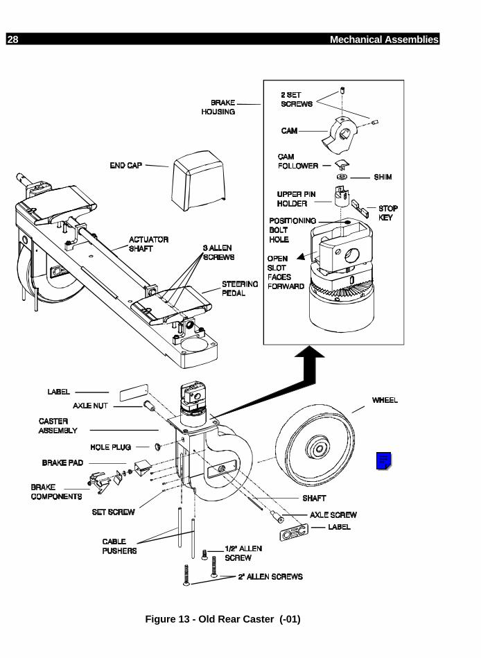
28 Mechanical Assemblies
Figure 13 - Old Rear Caster (-01)
NOTE
Click on the colored box to go directly to the assembly drawing in the Illustrated Parts Manual. Click on the << button on the Tool Bar to return to this point.
Mechanical Assemblies 29
Shim Adjustment
Older Models
This procedure was written for -01 version rear casters. Steps may vary slightlyon -02 and -03 version rear casters.
1. Install a 1/4 - 20 x 2-1/4-inch (1-inch minimum thread) bolt into the threadedhole on the top of the brake housing. This bolt is used for positioning onlyand will be referred to as the "positioning bolt."
2. Access the cam followers via the backside of the brake housing by placingthe pedals in the Steering Lock position. Then clamp the upper swivel lockin position by tightening the positioning bolt.
3. Install the Cam Follower and the Shims.
4. Loosen the positioning bolt several turns.
5. Carefully rotate the pedal towards the locked position to check for propershimming. If there is too much shim thickness the pedal will not rotateeasily into this position.
A. Do not force the pedal into this position or the cam follower may bedamaged.
B. Proper shimming has been obtained when there is no free play orpreload between the upper and lower swivel locks and minimal freeplay in the caster swivel rotation.
C. When peeling shims; peel the shim from the round side and discardthe shim that was peeled off.
6. Remove the 1/4" positioning bolt.
7. Remove the temporary 5/16-inch nuts and install the End Caps usingLoctite 242.

30 Mechanical Assemblies
BALANCE WHEEL REMOVALWARNING... Electrical circuits inside the equipment use voltages that are capable
of causing serious injury or death from electrical shock. Useappropriate precautions.
1. Verify that the Workstation keyswitch is turned to the OFF position and theAC power plug is disconnected from the wall receptacle.
2. Remove the Rear Handle Cover Assembly by removing 3 screws locatedbehind the assembly door and one screw on each side.
3. Remove the Front Cover by removing 2 screws near the top of the vertical shaft.
4. Remove the Right Front Cover by removing the 3 screws securing the coverto the Mobile C-Arm.
5. Turn circuit breaker CB1 to the OFF position.
Figure 14 - Balance Wheel Removal
6. Cut the cable tie that secures the wiring near CB1 and unplug the batteryconnectors.
WARNING... The batteries are capable of delivering high currents at high voltagesand should be considered fully charged at all times. Remove jewelrysuch as rings and watches when working around dangerousvoltages.
7. Remove the spacer from the top of the right battery pack.
8. Lift the battery pack straight up and then pull the pack straight out.
9. Elevate the Mobile C-Arm approximately 4 inches from the floor.
10. Remove the bolt (axle) and balance wheel.
NOTE
Click on the colored box to go directly to the Illustrated Parts Manual and view this assembly. Click on the << button on the Tool Bar to return to this point.
Mechanical Assemblies 31
L-ARM ROTATION ASSEMBLY
OVERVIEW
L-arm Rotation is accomplished using an AC motor with a worm drive. Limitswitches are provided to stop L-arm Rotation at approximately 365 degrees(stop-to-stop). An L-arm Rotation scale is provided that indicates the L-armsposition relative to the vertical and horizontal plane. Zero degrees of rotationhave occurred when the L-arm is in the vertical position near the floor. Tickmarks on the scale indicate every 15 degrees of rotation and numberingindicates every 90 degrees.
DURING BOOT SEQUENCE
During the Mobile C-Arm boot sequence the +24V Interlock circuit completes,energizing relay K3 on the Power Motor Relay PCB. When K3 is energized 115VAC PH is routed to L-arm rotation relays K5 and K6 on the Power/Motor RelayPCB. The +24 VDC is also routed to relays K5 and K6 for their control by theswitches located on top of the control panel housing.
CLOCKWISE ROTATION
When the L-arm rotation clockwise (CW) switch is pressed the +24 VDC at K6pin 8 completes a circuit to the DC return line (pin 1) and energizes relay K6.When K6 is energized 115 VAC is switched (pin 5 to pin 6) to the L-arm rotationmotor via the Power/Signal Distribution PCB and the L-Arm Motor Power PCB.At the same time, +24 VDC is removed from pin 8 of K5, the counter clockwise(CCW), relay to prevent damage to the motor in case both switches wereaccidentally pressed at the same time.
COUNTER-CLOCKWISE ROTATION
When the L-arm rotation counter clockwise (CCW) switch is pressed the +24VDC at K5 pin 8 completes a circuit to the DC return line (pin 1) and energizesrelay K5. When K5 is energized 115 VAC is switched (pin 5 to pin 6) to the L-armrotation motor via the Power/Signal Distribution PCB and the L-Arm Motor PowerPCB. At the same time, +24 VDC is removed from pin 8 of K6, the CW relay, toprevent damage to the motor in case both switches were accidentally pressed atthe same time.

32 Mechanical Assemblies
FORWARD MECHANICS
If the L-arm bearings are suspect the Horizontal Cross Arm and the L-arm DriverAssembly should be replaced as an assembly. The L-arm motor, limit switches,L-arm Motor Power PCB & capacitor may be replaced individually if they fail.Refer to Figure 15 .
CAUTION: Due to the weight of the forward mechanics it is recommended thattwo people perform this procedure together.
WARNING... Electrical circuits inside the equipment use voltages that are capableof causing serious injury or death from electrical shock. Useappropriate precautions.
1. Turn the Workstation keyswitch to the OFF position and disconnect the ACplug from the wall receptacle.
2. Disconnect the Interconnect cable from the Mobile C-Arm.
3. Place the steering pedal in the FREE position so that the Mobile C-Arm canbe moved sideways.
4. Remove the L-Arm handle by removing two hex bolts.
5. Remove the L-Arm end cap by removing the L-Arm Rotation Scale label andScale ring.
6. Using a large standard screwdriver rotate the worm gear until the forwardmechanics are parallel with the floor.
CAUTION: Make sure the forward mechanics are evenly balanced and will not fallfrom the supporting surface when the L-arm Drive Assembly iswithdrawn from the L-arm casting. Be sure that the assembly is fullysupported without any binds or stress on any of the welded seams.
7. Rest the forward mechanics on a flat surface such as a gurney or table (padthe surface if necessary to prevent scratching the paint).
8. Remove 3 large hex bolts securing the L-arm casting and forwardmechanics to the L-arm Drive Assembly
9. Push the Mobile C-Arm sideways and slide the casting off the driveassembly, being careful not to damage the wiring to the L-arm motor.
10. With the L-arm Drive Assembly exposed individual components such as themotor, limit switches and PCBs may be removed.
11. With the L-arm Drive Assembly exposed, individual components such as therotation motor, limit switches, and L-Arm Motor Power PCB can be removed.
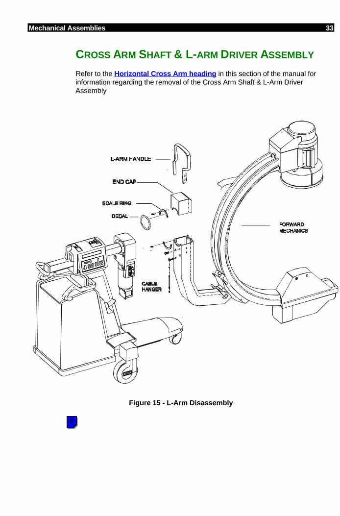
Mechanical Assemblies 33
CROSS ARM SHAFT & L-ARM DRIVER ASSEMBLY
Refer to the Horizontal Cross Arm heading in this section of the manual forinformation regarding the removal of the Cross Arm Shaft & L-Arm DriverAssembly
Figure 15 - L-Arm Disassembly
NOTE
Click on the colored boxes to go to exploded views of the L-Arm Assembly in the Illustrated Parts Manual. Click on the << button on the Tool Bar to return to this point.

34 Mechanical Assemblies
VERTICAL COLUMN ASSEMBLY
OVERVIEW
Raising and lowering of the C-Arm is accomplished by an AC motor that drivestwo sets of chains, a set (1 horizontal, 1 vertical) on both sides of the verticalcolumn (see Figure 15). The 18 inch travel of the column is restricted at bothends by an upper and lower limit switch. A scale on either side of the column isprovided to give an indication of the C-Arm height. Switches on top of the controlpanel assembly are provided for the operation of the motor.
INITIALIZATION
During the Mobile C-Arm boot sequence the +24 V Interlock circuit completes,energizing relay K3 on the Power/Motor Relay PCB. When K3 energizes 115VAC is routed to relays K12 and K13 on the Power Motor Relay PCB. The+24VDC from PS2 is also routed to relays K12 and K13 for their control by thecontrol panel switches located on top of the cross arm housing.
VERTICAL COLUMN UP
When the Vertical Column lift switch is pressed the +24VDC completes a circuitto the DC return line (pin 1) and energizes relay K12. When K12 is energized115 VAC is switched (pin 5 to pin 6) to the vertical lift motor via the LIFT_115VAC_B line. At the same time, +24 VDC is removed from pin 8 of K13, thevertical column down relay to prevent damage to the motor in case both switcheswere accidentally pressed at the same time.
VERTICAL COLUMN DOWN
When the Vertical Column down switch is pressed the +24VDC completes acircuit to the DC return line (pin 1) and energizes relay K13. When K13 isenergized 115 VAC is switched (pin 5 to pin 6) to the vertical lift motor via theLIFT_115 VAC_A line. At the same time, +24 VDC is removed from pin 8 of K12the Vertical Column lift relay to prevent damage to the motor in case bothswitches were accidentally pressed at the same time.
LIMIT SWITCHES
Two limit switches (LS1 and LS2) are used; one engages near full extension ofthe Vertical Column and one engages near full retraction. When opened the limitswitches remove electrical power from the lift motor and stop the vertical columnmotion.
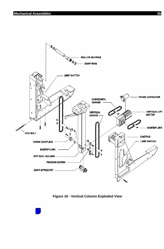
Mechanical Assemblies 35
Figure 16 - Vertical Column Exploded View
NOTE
Click on the colored box to go directly to the exploded assembly drawing in the Illustrated Parts Manual. Click on the << button on the Tool Bar to return to this point.

36 Mechanical Assemblies
VERTICAL COLUMN MOTOR REPLACEMENT
Refer to Figure 16 .
WARNING... Circuits inside this equipment contain voltages capable of causingserious injury or death from electrical shock.Observe safety procedures when operating motorized mechanicalfeatures.
1. Remove the Front Cover, Front Leg Cover and Right Front Cover.
2. Turn the Workstation keyswitch to the ON position. After the Mobile C-Armhas completed the boot sequence press the Vertical Column switch andraise the Vertical Column approximately 12 inches.
3. Block the Vertical Column at the 12-inch height so that the chain linkage iseasily accessible through the casting access port.
4. Turn the Workstation keyswitch to the OFF position.
5. Remove PS1 (+5V Power Supply) contained in the forward cavity of thecasting.
NOTE: If necessary block the Mobile C-Arm and elevate approximately 3inches to access the bolt referenced in the next step.
6. Release the tension from the horizontal chains by reaching underneath thecabinet with an open ended, 1/2-inch box wrench and loosen the hex boltapproximately 1-1/2-inch.
7. Remove 4 hex bolts from the bottom of the casting that secure the motorgear box to the casting.
8. Disconnect the Vertical Column motor wiring.
9. Remove the horizontal chains from the vertical drive sprockets (be carefulnot to expose the chains to dirt or debris).
10. Remove the motor and the gear box and replace as an assembly.
NOTE: When installing the vertical lift motor tighten the hex bolt until thereis 1/8 to 3/16-inch slack in both horizontal chains.

Mechanical Assemblies 37
VERTICAL COLUMN CHAIN REPLACEMENT
WARNING... Verify that the Workstation keyswitch is in the OFF position.
Observe safety procedures when operating motorized mechanicalfeatures.
Electrical circuits inside the equipment use voltages that are capableof causing serious injury or death from electrical shock. Useappropriate precautions.
Refer to Figure 16 .
1. Remove the Vertical Column motor and horizontal chains (perform theVertical Column Motor Replacement procedure).
2. To remove the left chain perform the following procedure:
A. Remove the +24 VDC Power Supply.
B. Disconnect wiring harness's P1 and P8 from the Power/Motor Relay PCB.
C. Remove Torx screws (4 screws total) from all four corners of the PowerPanel mounting assembly to expose the left Vertical Column chain.
D. Loosen the chain tension screw until there is sufficient slack to loosen the 2hex bolts that secure the upper chain coupling to the vertical column.
E. Remove the upper sprocket access plate by removing 2 horizontalsupport pins secured with snap rings and the 4 outside hex bolts thatsecure the plate to the casting.
F. Remove the master links from both ends of the chain and remove the chain.
3. To remove the right chain perform the following procedure:
A. Loosen the chain tension screw until there is sufficient slack to removethe master links from both ends of the chain.
B. Remove the upper sprocket access plate by removing 2 horizontalsupport pins secured with snap rings and the 4 outside hex bolts thatsecure the plate to the casting.
C. Remove the master links from both ends of the chain and remove the chain.
4. When installing either chain perform the following:
A. Route the chain over the top and bottom sprockets and reattach thechain to the chain coupling with the master links.
WARNING... Do not over tension either the vertical or horizontal chains.

38 Mechanical Assemblies
WARNING... Do not over tension either the vertical or horizontal chains.
B. Tighten the tension screw until chain tension is proportional betweenthe left and right chain.
C. Tighten the hex bolts on the upper chain coupling.
D. Remove the vertical column block and operate the vertical columnuntil the upper limit switch is reached.
E. Press the forward portion of the exposed vertical chain with your indexfinger and verify that there is 1/4 - 1/2-inch of chain tension.
F. Press the bottom portion of the exposed horizontal chain with yourindex finger and verify that there is 1/4 - 1/2-inch of chain tension.
LIMIT SWITCHES
WARNING... Circuits inside this equipment contain voltages capable of causingserious injury or death from electrical shock.
Observe safety procedures when operating motorized mechanicalfeatures.
1. Turn the Workstation keyswitch to the OFF position.
2. Remove the Front Cover, Front Leg Cover and Right Side Cover.
3. Access the limit switches through the front casting access port. Removeeither limit switch by performing the following:
A. Disconnect the limit switch wiring and remove 2 Allen screws securingthe limit switch.
B. Remove the limit switch
UPPER ROLLER BEARING
WARNING... Circuits inside this equipment contain voltages capable of causingserious injury or death from electrical shock.
Observe safety procedures when operating motorized mechanicalfeatures.
1. Remove the Front Cover, Left Side Cover and Right Side Cover.
2. Check the roller bearing surface for flat spots, irregularities, and abnormalwear.
Mechanical Assemblies 39
3. Remove the preload from the upper roller bearing by lowering the forwardmechanics onto a sturdy surface.
4. Remove the snap ring on the roller bearing and pull the pin out of the sideand the roller out of the front.
IMAGE SYSTEM
OVERVIEWThe following components produce the video signal used by the Image Processor. Thissection describes their operation and in addition, describes the ABS (AutomaticBrightness System) circuit.
• Image Function PCB
• Iris Collimation and Leaf Control
• Image Intensifier
• CCD Camera
The information given in this section is most easily understood while referencing thefollowing schematics from the schematic manual. Use the correct schematics anddiagrams for your system.
C-Arm Interconnect Diagram
Schematic # 00-875500 - System S/N 69-0001 thru 69-1000Schematic # 00-877972 - System S/N 69-1001 thru 69-2000Schematic # 00-878376 - System S/N 69-2001 and higher
Image System Interconnect Diagram
Schematic # 00-875410 - System S/N 69-0001 thru 69-1000Schematic # 00-877971 - System S/N 69-1001 thru 69-2000Schematic # 00-878377 - System S/N 69-2001 and higher
Workstation Interconnect Diagram
Schematic # 00-876158 - System S/N 69-0001 thru 69-1000Schematic # 00-877970 - System S/N 69-1001 thru 69-2000
Technique Processor PCB
Schematic # 00-876735 - System S/N 69-0001 thru 69-1000Schematic # 00-877742 - System S/N 69-1001 thru 69-2000
Analog Interface PCB
Schematic # 00-876738 - All S/N
Power/Motor Relay PCB
Schematic # 00-875997 - All S/N
NOTE
- Click on a yellow box to go directly to the block diagram for this section. Do not use this link to return to a block diagram from this point. - Click on the << button in the Tool Bar to return to any starting point.

2 Image System
Mainframe Motherboard
Schematic # 00-875539 - System S/N 69-0001 thru 69-2000Schematic # 00-878396 - System S/N 69-2001 and higher
Image Function PCB
Schematic # 00-874750 - System S/N 69-0001 thru 69-2000Schematic # 00-878398 - System S/N 69-2001 and higher
Pixel/Column Filter PCB
Schematic # 00-878045
Pixel Filter PCB
Schematic # 00-877789
Auxiliary Interface PCB
Schematic #00-876502 - All S/N
AT Communications PCB
Schematic #00-872125 - All S/N
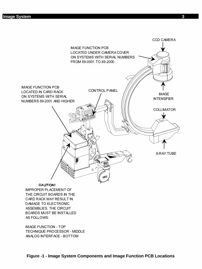
Image System 3
CONTROL PANEL
X-RAY TUBE
COLLIMATOR
IMAGE
INTENSIFIER
CCD CAMERA
IMAGE FUNCTION PCB
LOCATED UNDER CAMERA COVER
ON SYSTEMS WITH SERIAL NUMBERS
FROM 69-0001 TO 69-2000
IMAGE FUNCTION PCB
LOCATED IN CARD RACK
ON SYSTEMS WITH SERIAL
NUMBERS 69-2001 AND HIGHER
IMPROPER PLACEMENT OF
THE CIRCUIT BOARDS IN THE
CARD RACK MAY RESULT IN
DAMAGE TO ELECTRONIC
ASSEMBLIES. THE CIRCUIT
BOARDS MUST BE INSTALLED
AS FOLLOWS:
IMAGE FUNCTION - TOP
TECHNIQUE PROCESSOR - MIDDLE
ANALOG INTERFACE - BOTTOM
CAUTION!
Figure -1 - Image System Components and Image Function PCB Locations
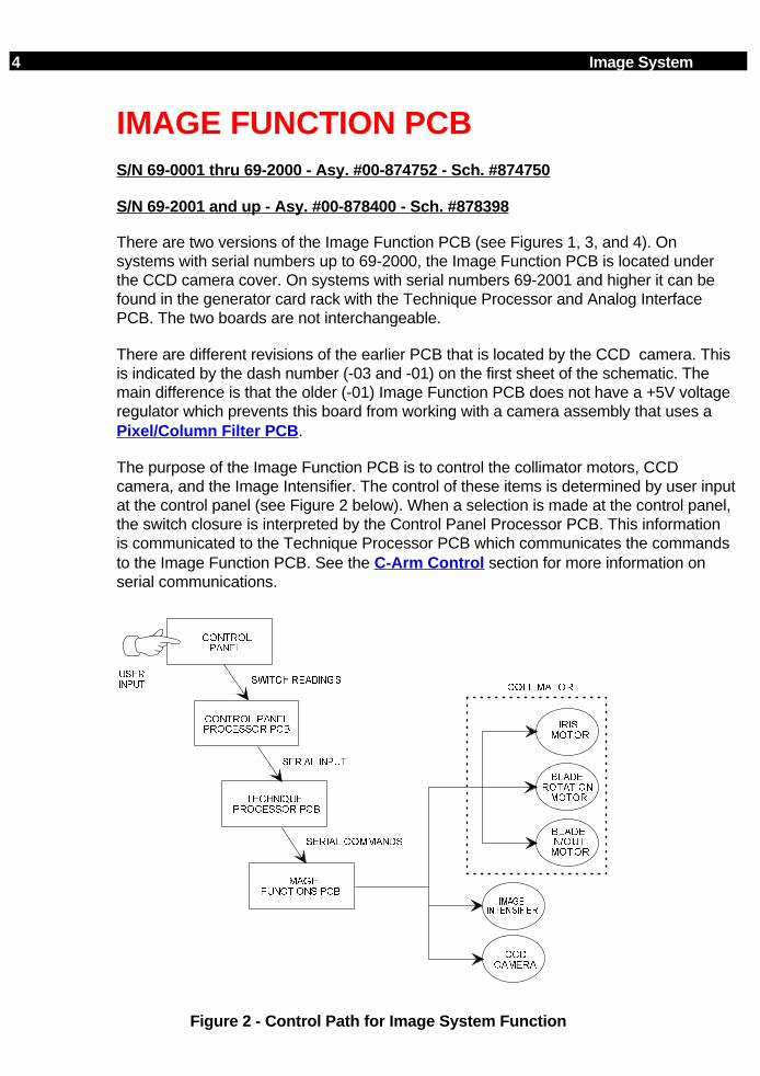
4 Image System
IMAGE FUNCTION PCBS/N 69-0001 thru 69-2000 - Asy. #00-874752 - Sch. #874750
S/N 69-2001 and up - Asy. #00-878400 - Sch. #878398
There are two versions of the Image Function PCB (see Figures 1, 3, and 4). Onsystems with serial numbers up to 69-2000, the Image Function PCB is located underthe CCD camera cover. On systems with serial numbers 69-2001 and higher it can befound in the generator card rack with the Technique Processor and Analog InterfacePCB. The two boards are not interchangeable.
There are different revisions of the earlier PCB that is located by the CCD camera. Thisis indicated by the dash number (-03 and -01) on the first sheet of the schematic. Themain difference is that the older (-01) Image Function PCB does not have a +5V voltageregulator which prevents this board from working with a camera assembly that uses aPixel/Column Filter PCB .
The purpose of the Image Function PCB is to control the collimator motors, CCDcamera, and the Image Intensifier. The control of these items is determined by user inputat the control panel (see Figure 2 below). When a selection is made at the control panel,the switch closure is interpreted by the Control Panel Processor PCB. This informationis communicated to the Technique Processor PCB which communicates the commandsto the Image Function PCB. See the C-Arm Control section for more information onserial communications.
CCD
CAMERA
IMAGE
INTENSIFIER
TECHNIQUE
PROCESSOR PCB
IMAGE
FUNCTIONS PCB
CONTROL PANEL
PROCESSOR PCB
COLLIMATOR
CONTROL
PANEL
USER
INPUT
SERIAL INPUT
SERIAL COMMANDS
SWITCH READINGS
BLADE
ROTATION
MOTOR
IRIS
MOTOR
BLADE
IN/OUT
MOTOR
Figure 2 - Control Path for Image System Function
Image System 5
MICROCONTROLLERU16 is a CHMOS 16 bit 80C196KC microcontroller. The 8 MHz. reference is provided bycrystal oscillator Y1. LED DS1 blinks on and off during normal operation providing avisual indication that the microcontroller is operating and executing code.
Port 3 (pins 53-60) of the microcontroller is a multiplexed address/data bus. U12 latchesthe low address byte (A0-A7) on the falling edge of ALE, address latch enable (pin 62 ofU16). Port 4 (pins 45-52) is permanently selected for the high address byte (A8-A15) bygrounding the signal “BUSWIDTH” (pin 64 of U16).
EPROMU15 is a 32K x 8 EPROM programmed with operating code for the microcontroller.
GALU13 is a GAL (gate array logic) used in address decoding to provide the chip select (CS)signals for the following:
EPROM - U15EEPROM - U7SRAM - U10INPUT LATCH - U14OUTPUT LATCH - U6MOTOR LATCH - U11
STATIC RAMU10 is a 32K x 8 static ram, used by software for storage of variables. It was added toenhance the amount of memory available for the microcontroller.
EEPROMU7 is a 2K x 8 EEPROM used to store the calibration data for the Normal, MAG1, andMAG2 field sizes of the collimator iris. E5 is used in the iris calibration procedure.Details of this circuitry are discussed in the Collimator Motors and Collimator IrisCalibration sections that follow.
WATCHDOGU8 provides the reset and “Watchdog” functions. Microcontroller U16 is reset when pin16 is pulled low during power-up, power-down and during low-voltage brown-outconditions. Pin 7 of U8 is toggled by the output of microcontroller U16 pin 23 every 150ms to prevent the watchdog from timing out. If a software failure should cause thewatchdog to time-out, the reset output from U8 pin 6 will go low for 250 ms and reset themicrocontroller. The Master Reset signal (MRESET*) from the Technique ProcessorPCB can also initiate a reset. This would occur if the reset switch on the TechniqueProcessor PCB was pressed. Jumper E8 is removed only in the factory for testing andmust be in place for proper operation.
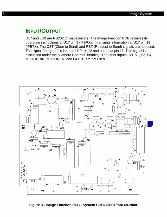
6 Image System
INPUT/OUTPUTU17 and U19 are RS232 driver/receivers. The Image Function PCB receives itsoperating instructions at U17 pin 9 (IFBRX), it transmits information at U17 pin 19(IFBTX). The CST (Clear to Send) and RST (Request to Send) signals are not used.The signal “Integrate” is input to U19 pin 12 and output at pin 11. This signal isdiscussed under the “Camera Controls” heading. The other inputs, S0, S1, S2, S4,MOTORDIR, MOTOREN, and LATCH are not used.
AS
SY
00
-87
47
52
- (
)
IMA
GE
FU
NC
TIO
N P
CB
1
2
9
10
1
2
23
24
2
123
24 17P3
P4
P2 P1
Q3
U9
OE
C M
ED
ICA
L S
YS
TE
MS
, IN
C.
U20
P5
1
U14
U16
U13U12
U15
C11
RP3
RP2
E5 E6 E7E4
E3
R1
0
R8
C6
C9
C8
C10
C2
6
C2
5
C18
C22
C1
2
C16
C13
C17
C4
C15
C2
C3
C2
4
C5
R2
U5
U11
U3
U4
U18
U6
U1
RP
1
R6R5
CR
3C
R4
CR2
CR1
CR5
Q2Q1
K1
K2
TP2
TP1
R3
DS1
R1
C1
Y1
U7
R1
5
R1
3
E1
CR7CR8
U10
C14
U8
R11R
12
C7
C27C28
C1
9
C20
CR
6
R1
4
FL3
FL4
FL1
U19
U17
U2
R9
R4
R7
Q3
E2
C2
3
C21
FL2
C2
9
C3
0
C34
C3
5
C36
C37
C3
8
C3
9
R1
6
R1
7
TP
3
DS2
R18
R1
9
K3
TP4
E8
R20
CR
9
C4
0
C42
FL
5
R2
1
R2
2
R2
3
E9
L1
C4
1
VR
1
E10
Figure 3 - Image Function PCB - System S/N 69-0001 thru 69-2000
NOTE
Click in the blue box to go directly to the Electrical Schematic Diagram for the PCB shown on this page. Click the << button on the Tool Bar to return to this page.
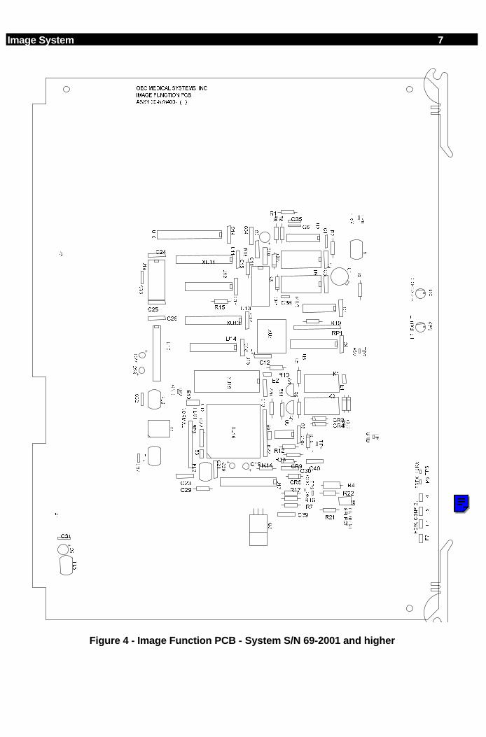
Image System 7
IMAGE FUNCTION PCB
OEC MEDICAL SYSTEMS, INC.
ASSY 00-878400- ( )
IFBRX
IFBTX
XU
16
XU
15
XU13
XU
7
XU11
TE
ST
mP
GO
OD
+5V
+15V
GN
D
I.F
. F
AU
LT
GN
D
RESET*
CURRENT
SE
LE
CT
HD
W.
CO
NF
IG.
CO
OL
_O
N
NO
RM
AL
1
U14
U16
U13
U1
2
U1
5C11
RP
3
RP2
E5
E6
E7
E4
E3
R10
R8
C6C9
C8
C10
C26
C25
C1
8
C2
2
C12
C1
6
C1
3
C1
7
C4
C1
5
C2
C3
C24
C5
R2
U5
U1
1
U3
U4
U18
U6
U1
RP1
R6
R5
CR3
CR4
CR
2C
R1
CR
5
Q2
Q1
K1
K2
TP
2
TP
1
R3
DS
1
R1
C1
Y1
U7
R15
R13
E1
CR
7CR8
U1
0
C1
4
U8
R1
1
R12
C7
C2
7C
28
C19
C20
CR6
R14
FL
3
FL
4
FL
1
U1
9
U1
7
U2
R9
R4
R7
Q3
E2
C23
C2
1
FL
2
C29
C30
C3
4
C35
C3
6C
37
C38
C39
R16
R17
TP3
DS
2
R18
R19
K3
TP
4
E8
R20
CR9C40
FL
5
R21
R22
E9
P1
C31
C3
2
P2
E1
0
TP
5T
P6
TP
7T
P8
Figure 4 - Image Function PCB - System S/N 69-2001 and higher
NOTE
Click in the blue box to go directly to the Electrical Schematic Diagram for the PCB shown on this page. Click the << button on the Tool Bar to return to this page.
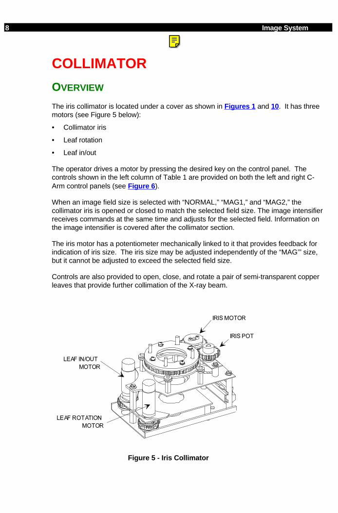
8 Image System
COLLIMATOR
OVERVIEW
The iris collimator is located under a cover as shown in Figures 1 and 10. It has threemotors (see Figure 5 below):
• Collimator iris
• Leaf rotation
• Leaf in/out
The operator drives a motor by pressing the desired key on the control panel. Thecontrols shown in the left column of Table 1 are provided on both the left and right C-Arm control panels (see Figure 6 ).
When an image field size is selected with “NORMAL,” “MAG1,” and “MAG2,” thecollimator iris is opened or closed to match the selected field size. The image intensifierreceives commands at the same time and adjusts for the selected field. Information onthe image intensifier is covered after the collimator section.
The iris motor has a potentiometer mechanically linked to it that provides feedback forindication of iris size. The iris size may be adjusted independently of the “MAG’” size,but it cannot be adjusted to exceed the selected field size.
Controls are also provided to open, close, and rotate a pair of semi-transparent copperleaves that provide further collimation of the X-ray beam.
LEAF IN/OUT
MOTOR
LEAF ROTATION
MOTOR
IRIS POT
IRIS MOTOR
Figure 5 - Iris Collimator
NOTE
Click on a yellow box to go directly to the block diagram for this section. Do not use this link to return to a block diagram from this point. Click on the << button in the Tool Bar to return to any starting point.
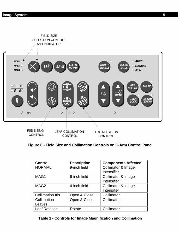
Image System 9
FIELD SIZE
SELECTION CONTROL
AND INDICATOR
IRIS SIZING
CONTROLLEAF COLLIMATION
CONTROL
LEAF ROTATION
CONTROL
Figure 6 - Field Size and Collimation Controls on C-Arm Control Panel
Control Description Components AffectedNORMAL 9-inch field Collimator & Image
IntensifierMAG1 6-inch field Collimator & Image
IntensifierMAG2 4-inch field Collimator & Image
IntensifierCollimation Iris Open & Close CollimatorCollimationLeaves
Open & Close Collimator
Leaf Rotation Rotate Collimator
Table 1 - Controls for Image Magnification and Collimation
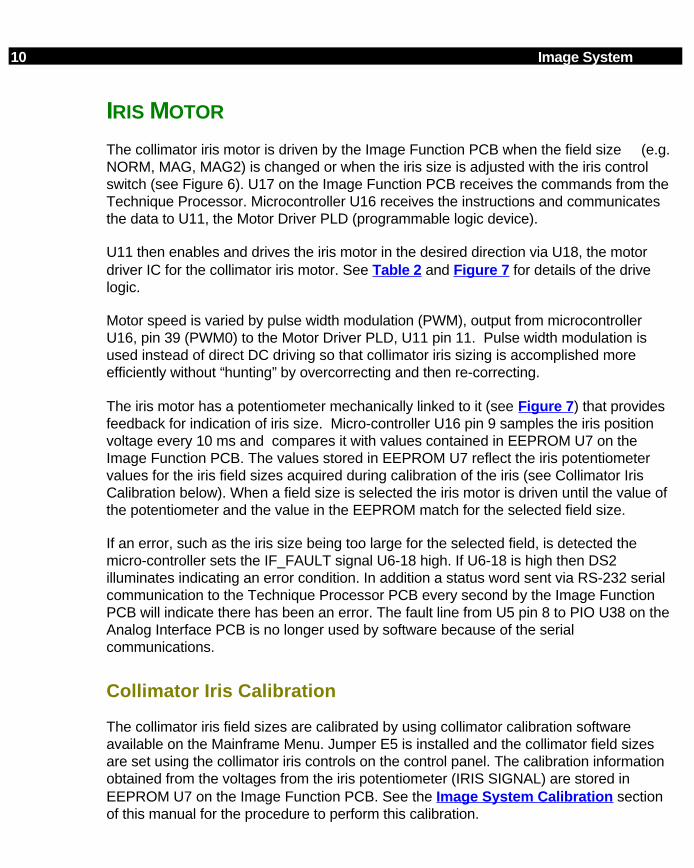
10 Image System
IRIS MOTOR
The collimator iris motor is driven by the Image Function PCB when the field size (e.g.NORM, MAG, MAG2) is changed or when the iris size is adjusted with the iris controlswitch (see Figure 6). U17 on the Image Function PCB receives the commands from theTechnique Processor. Microcontroller U16 receives the instructions and communicatesthe data to U11, the Motor Driver PLD (programmable logic device).
U11 then enables and drives the iris motor in the desired direction via U18, the motordriver IC for the collimator iris motor. See Table 2 and Figure 7 for details of the drivelogic.
Motor speed is varied by pulse width modulation (PWM), output from microcontrollerU16, pin 39 (PWM0) to the Motor Driver PLD, U11 pin 11. Pulse width modulation isused instead of direct DC driving so that collimator iris sizing is accomplished moreefficiently without “hunting” by overcorrecting and then re-correcting.
The iris motor has a potentiometer mechanically linked to it (see Figure 7 ) that providesfeedback for indication of iris size. Micro-controller U16 pin 9 samples the iris positionvoltage every 10 ms and compares it with values contained in EEPROM U7 on theImage Function PCB. The values stored in EEPROM U7 reflect the iris potentiometervalues for the iris field sizes acquired during calibration of the iris (see Collimator IrisCalibration below). When a field size is selected the iris motor is driven until the value ofthe potentiometer and the value in the EEPROM match for the selected field size.
If an error, such as the iris size being too large for the selected field, is detected themicro-controller sets the IF_FAULT signal U6-18 high. If U6-18 is high then DS2illuminates indicating an error condition. In addition a status word sent via RS-232 serialcommunication to the Technique Processor PCB every second by the Image FunctionPCB will indicate there has been an error. The fault line from U5 pin 8 to PIO U38 on theAnalog Interface PCB is no longer used by software because of the serialcommunications.
Collimator Iris Calibration
The collimator iris field sizes are calibrated by using collimator calibration softwareavailable on the Mainframe Menu. Jumper E5 is installed and the collimator field sizesare set using the collimator iris controls on the control panel. The calibration informationobtained from the voltages from the iris potentiometer (IRIS SIGNAL) are stored inEEPROM U7 on the Image Function PCB. See the Image System Calibration sectionof this manual for the procedure to perform this calibration.

Image System 11
Input 1Pin 2
Input 2Pin 7
EnablePin 1
Output 1Pin 3
Output2 Pin 6
State
L L H L L Motor Off - Brake ModeL H H L H Motor On - OpenH L H H L Motor On - Close
Table 2 - Truth Table to Drive Collimator Iris Motor
IRIS
MOTOR
+
-
COLLIMATOR
OUTPUT 1
OUTPUT 2
INPUT 1
INPUT 2
ENABLE 1 1
2
7
3
6
L293D MOTOR DRIVER IC
+5VTO MICROCONTROLLER
IMAGE FUNCTIONS PCB
IRIS
POT
GEARS
Figure 7 - Diagram of Iris Motor Drive Path

12 Image System
LEAF IN/OUT MOTOR
The collimator has a set of semi-transparent copper leaves (or shutter blades) that aredriven in and out of the beam by using the leaf sizing controls on the control panel (seeFigure 6 ). U17 on the Image Function PCB receives the commands from the TechniqueProcessor. Microcontroller U16 on the Image Function PCB receives the instructionsand communicates the data to U11, the Motor Driver PLD (programmable logic device).
U11 then enables and drives the leaf in/out motor in the desired direction via U4, themotor driver IC for the leaf in/out and leaf rotation motors. See Table 3 and Figure 8 fordetails of the drive logic.
Motor speed is varied by pulse width modulation (PWM), output from microcontrollerU16, pin 39 (PWM0) to the Motor Driver PLD, U11 pin 11. Pulse width modulationcontrol was selected because the speed required to operate the leaf in/out motor aloneis different than the speed required to operate it when the leaves are rotating. This is aresult of the mechanical linking of these two motors. The software and microcontrollercan therefore vary the speed of the collimator motors via the PWM signal.
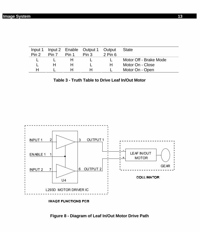
Image System 13
Input 1Pin 2
Input 2Pin 7
EnablePin 1
Output 1Pin 3
Output2 Pin 6
State
L L H L L Motor Off - Brake ModeL H H L H Motor On - CloseH L H H L Motor On - Open
Table 3 - Truth Table to Drive Leaf In/Out Motor
+
-
COLLIMATOR
OUTPUT 1
OUTPUT 2
INPUT 1
INPUT 2
ENABLE 1 1
2
7
3
6
L293D MOTOR DRIVER IC
LEAF IN/OUT
MOTOR
U4
IMAGE FUNCTIONS PCB
GEAR
Figure 8 - Diagram of Leaf In/Out Motor Drive Path

14 Image System
LEAF ROTATION MOTOR
The collimator has a set of semi-transparent copper leaves (or shutter blades) that arerotated by using the leaf rotation controls on the control panel (see Figure 6 ). U17 on theImage Function PCB receives the commands from the Technique Processor.Microcontroller U16 receives the instructions and communicates the data to U11, theMotor Driver PLD (programmable logic device).
U11 then enables and drives the leaf rotation motor in the desired direction via U4, themotor driver IC for the leaf in/out and leaf rotation motors. See Table 4 and Figure 9 fordetails of the drive logic.
Motor speed is varied by pulse width modulation, output from microcontroller U16, pin 39(PWM0) to the Motor Driver PLD, U11 pin 11. Pulse width modulation control wasselected because the speed required to operate the leaf in/out motor when operatedalone is different than the speed required to operate it when the leaves are rotating. Thisis a result of the mechanical linking of these two motors.
Relay K3 provides a direct short through its normally closed contacts across the leafrotate motor to provide a high degree of dynamic braking to the motor when it is notbeing driven. This is done because the mechanical linkage between the motors will tendto back drive the leaf rotation motor when the leaf in/out motor is driven. When the leafrotation motor is driven, the shorting path through relay K3 is opened by the output ofmotor driver U18, pin 14.
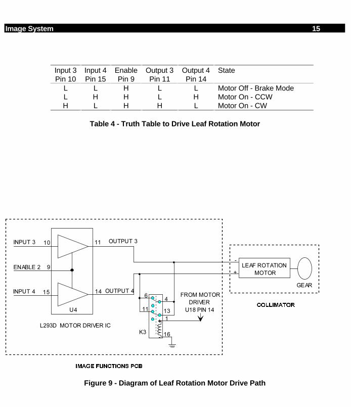
Image System 15
Input 3Pin 10
Input 4Pin 15
EnablePin 9
Output 3Pin 11
Output 4Pin 14
State
L L H L L Motor Off - Brake ModeL H H L H Motor On - CCWH L H H L Motor On - CW
Table 4 - Truth Table to Drive Leaf Rotation Motor
+
-
COLLIMATOR
L293D MOTOR DRIVER IC
U4
IMAGE FUNCTIONS PCB
LEAF ROTATION
MOTOR
11 OUTPUT 310INPUT 3
ENABLE 2
INPUT 4 OUTPUT 41415
9
+
-K3
4
13
6
11
1
16
FROM MOTOR
DRIVER
U18 PIN 14
GEAR
Figure 9 - Diagram of Leaf Rotation Motor Drive Path
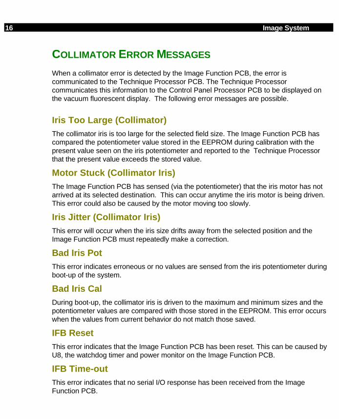
16 Image System
COLLIMATOR ERROR MESSAGES
When a collimator error is detected by the Image Function PCB, the error iscommunicated to the Technique Processor PCB. The Technique Processorcommunicates this information to the Control Panel Processor PCB to be displayed onthe vacuum fluorescent display. The following error messages are possible.
Iris Too Large (Collimator)The collimator iris is too large for the selected field size. The Image Function PCB hascompared the potentiometer value stored in the EEPROM during calibration with thepresent value seen on the iris potentiometer and reported to the Technique Processorthat the present value exceeds the stored value.
Motor Stuck (Collimator Iris)The Image Function PCB has sensed (via the potentiometer) that the iris motor has notarrived at its selected destination. This can occur anytime the iris motor is being driven.This error could also be caused by the motor moving too slowly.
Iris Jitter (Collimator Iris)This error will occur when the iris size drifts away from the selected position and theImage Function PCB must repeatedly make a correction.
Bad Iris PotThis error indicates erroneous or no values are sensed from the iris potentiometer duringboot-up of the system.
Bad Iris CalDuring boot-up, the collimator iris is driven to the maximum and minimum sizes and thepotentiometer values are compared with those stored in the EEPROM. This error occurswhen the values from current behavior do not match those saved.
IFB ResetThis error indicates that the Image Function PCB has been reset. This can be caused byU8, the watchdog timer and power monitor on the Image Function PCB.
IFB Time-outThis error indicates that no serial I/O response has been received from the ImageFunction PCB.

Image System 17
COLLIMATOR REPLACEMENT
1. Turn the Workstation keyswitch to the OFF position.
2. Remove 2 hole plugs and Torx screws (A) securing the X-ray Tube Cover.
3. Remove 2 Torx screws (B) securing the collimator cover.
4. Remove collimator cover (C) by sliding forward.
5. Loosen 4 Torx head screws and metal clamps (D) located on the lateral sides of thecollimator and alignment bracket.
6. Turn the metal clamps to the side while holding collimator.
7. Lift and remove the collimator off the 2 guide pins on the alignment bracket.
8. Unplug the collimator wiring connector and ground wire.
9. Remove the 4 screws that secure the collimator alignment bracket if necessary.
10. Install in reverse order.
11. Check beam alignment and perform alignment procedure if necessary (see ImageSystem Calibration section for procedure).
. .
COLLIMATOR COVER
VARIABLE COLLIMATOR
ALIGNMENT BRACKET
X-RAY TUBE
BB
A
A
C
D4 PLACES
X-RAY TUBE COVER
Figure 10 - Collimator and Alignment Bracket Removal
NOTE
Click on the colored box to go directly to the exploded assembly in the Illustrated Parts Manual. Click on the << button on the Tool Bar to return to this point.

18 Image System
IMAGE INTENSIFIER
OVERVIEW
The 9600 Mobile C-Arm uses a Thomson tri-mode (9, 6, 4.5-inch or 12, 9, 6-inch) imageintensifier. The user selects the mode with the NORM, MAG 1, and MAG 2 keys on theMobile C-Arm Control Panel as shown in Figure 11 below. The collimator iris is adjustedto the proper field size.
FIELD SIZE
SELECTION CONTROL
AND INDICATOR
Figure 11 - Image Intensifier Controls on C-Arm Control Panel
Control Description Components AffectedNORMAL 12 or 9-inch field Collimator & Image
IntensifierMAG1 9 or 6-inch field Collimator & Image
IntensifierMAG2 6 or 4 1/2-inch
fieldCollimator & ImageIntensifier
Table 5 - Controls for Image Intensifier Field Size Selection
NOTE
Click on the yellow box to go directly to the block diagram for this section. Do not use this link to return to a block diagram from this point. Click on the << button in the Tool Bar to return to any starting point.

Image System 19
IMAGE INTENSIFIER POWER
Power to the Image Intensifier is supplied during the boot sequence, after the +24Vinterlock is complete. The interlocked +24V is placed on the high side of the coil of K7on the Power/Motor Relay PCB. The return path for the coil is pulled low by the signal“II_ON” from the collector of Q6 on the Analog Interface PCB. The output at pin 24 ofPIO U38 turns on transistor Q6. With Q6 turned on, the ground path is created throughthe emitter of Q6. K7 is then energized and +24V from PS2 passes through to theimage intensifier power supply. The Image Intensifier is turned off during the FILM modeby placing a low at the base of Q6.
FIELD SELECTION
Field size instructions are written over the serial communications link from theTechnique Processor to the Image Function PCB. They are input to U17 and thencommunicated to the microcontroller. The information is sent to the output latch, U6.
The relays K1 and K2 on the Image Function PCB are used to set up the MAG1 andMAG2 field sizes on the Image Intensifier. Both K1 and K2 coils (pin 1) are provided with+24V (+24/II) after K7 on the Power/Motor Relay PCB is energized. The return path forthe coils is described below.
Normal Mode
The NORMAL (9”) field size is the default at boot-up of the system. Neither K1 nor K2 isactivated when the NORMAL mode is selected and the II receives +24V (+24/II) fromthe Image Function PCB at P4 pin 7 (Asy. #00-874752) or P2 pin 110 (Asy. #00-878400).
MAG 1 ModeWhen MAG1 is selected, output latch U6-15 goes high, turning on transistor Q2. RelayK2 is energized and +24 VDC passes through K2 pins 2 to 4, and through K1 pins 7 to6, leaving the Image Function PCB at P4 pin 6 (Asy. #00-874752) or P2 pin 5 (Asy. #00-878400). The +24V is then routed to J7 pin 3 for the internal II high voltage power supplywhere it configures the II for the 6-inch field size. Jumper E1 must be in place for properoperation of the MAG1 and MAG2 field selection.
MAG 2 ModeWhen the MAG2 is selected, output latch U6-14 goes high, turning on transistor Q1.Relay K1 energizes and +24 VDC passes through K1 pins 4 to 2, leaving the ImageFunction PCB at P4 pin 5 (Asy. #00-874752) or P2 pin 9 (Asy. #00-878400). The +24Vis then routed to J7 pin 7 for the internal II high voltage power supply where it configuresthe II for the 4.5-inch field size. Jumper E1 must be in place for proper operation of theMAG1 and MAG2 field selection.
IMAGE INTENSIFIER / POWER SUPPLY REMOVAL

20 Image System
WARNING... Image intensifier tubes may implode if struck or subjected to severemechanical shock. Minimize the risk of injury from flying glass by wearingprotective clothing and safety goggles when servicing this component.
Voltages used inside the II are capable of causing serious injury or deathfrom electrical shock. Use appropriate precautions.
CAUTION: Always wear a properly grounded static protection wristband when workingwith the CCD camera.
1. Verify that the Workstation keyswitch is in the OFF position. Refer to Figure 12.
2. Remove the 2 screws securing the camera cover (A).
3. Remove the Camera and Optics assembly (B). See CCD camera information inthis section.
4. Remove the Image Function PCB and mounting plate (can be removed as oneassembly).
5. Disconnect the wiring between the Image Intensifier and the Image IntensifierPower Supply as indicated in Figure 13 and Table 6.
6. Disconnect the D style connector (+24 VDC, DC/Com, MEDFLD, SMALLFLD).
7. Remove the 6 hex bolts (C) securing the Image Intensifier to the C-arm weldmentand remove the Image Intensifier from the C-arm.
8. Remove the hardware (D) (5 places) securing the power supply to the C-Armweldment.
NOTE: When replacing the Image Intensifier assembly it may be necessary to re-calibrate the light level at the CCD by calibrating the Camera Iris. Refer tothe Camera Iris Calibration procedure in the Image System CalibrationSection.
COLOR DESCRIPTION CONNECTORE Blue Active Getter
Cathode"Fast On"
PC Red Tube Photo Cathode "Fast On"GND Green/Yello
wGround Fork Lug
G1 Green Electrode Twist OnG2 Black Electrode Twist OnG3 Black Electrode Twist OnG4 Black Electrode Twist OnA White Cable Anode Twist On
Table 6 - Image Intensifier Power Supply Wiring
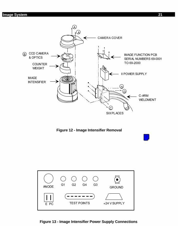
Image System 21
II POWER SUPPLY
CAMERA COVER
CCD CAMERA
& OPTICS
COUNTER
WEIGHT
IMAGE
INTENSIFIER
C-ARM
WELDMENT
C
SIX PLACES
A
A
B
D
D
IMAGE FUNCTION PCB
SERIAL NUMBERS 69-0001
TO 69-2000
Figure 12 - Image Intensifier Removal
G1 G2 G4 G3
E PC
ANODE
TEST POINTS
GROUND
+24 V SUPPLY
Figure 13 - Image Intensifier Power Supply Connections
NOTE
Click on the colored box to go directly to the exploded assembly in the Illustrated Parts Manual. Click on the << button on the Tool Bar to return to this point.

22 Image System
CCD CAMERA
OVERVIEW
Refer to Figures 1 and 21 for the location of the CCD camera.
The 9600 uses a CCD (Charge Coupled Device) Camera which produces a video signalof the image it receives from the image intensifier output. The CCD sensor is an analogIC that uses an array of photosensitive elements to convert a variety of light levels into aproportional electrical charge. The brighter the light, the greater the electrical charge.Each photo element in the array stores an electrical charge. Electronic circuitry on theCCD camera PCB sequentially shifts these electrical charges to an output gate creatingan output signal. The output signal is an analog representation of the image displayedon the output of the I.I. The analog video signal is combined with the sync signals on theCCD PCB, creating a composite video signal. This composite video signal leaves thecamera at P2 for processing and display.
Figure 14 - CCD Camera
NOTE
Click on a yellow box to go directly to the block diagram for this section. Do not use this link to return to a block diagram from this point. Click on the << button in the Tool Bar to return to any starting point.

Image System 23
CAMERA CONTROLS
The following controls are provided on both the left and right control panels:
Control Description Affected ComponentsInvert/ReverseImage
Flips Image vertically andhorizontally
Image Processor
Rotate Image Rotates Image Camera Prism OpticsBoost Enable &Pulse
Enables Pulsed Fluorography Camera Iris (duringexposure)
Table 7 - CCD Camera Controls
INVERT/REVERSE IMAGE
CONTROL
CAMERA ROTATION
CONTROL
BOOST ENABLE
CONTROLPULSE MODE
CONTROL
Figure 15 - CCD Camera Controls on the C-Arm Control Panel
NOTE
Click on a yellow box to go directly to the block diagram for this section. Do not use this link to return to a block diagram from this point. Click on the << button in the Tool Bar to return to any starting point.
24 Image System
Invert Image/ Reverse Image
The invert/reverse image select switch on the Control Panel toggles between fourpossible states: normal, invert, reverse, and invert/reverse.
Commands to invert or reverse the image are sent to the Technique Processor. TheTechnique Processor communicates the instruction to the Workstation via theinterconnect cable. The Workstation processes the image and displays the results onthe left monitor.
Camera Rotation
The camera rotation controls allow the image to be rotated 360 degrees in eitherdirection. The camera rotation motor drives a potentiometer that provides a voltagefeedback to the Workstation (via the Analog Interface PCB and Technique ProcessorPCB). This voltage is used by the image processor to provide a visual indication ofcamera rotation on the left monitor. As the image is rotated, a pointer icon is displayedwith a stop sign icon to indicate the direction of rotation and the approaching end oftravel.
Boost & Pulse Mode Enable
The pulsed Fluorography mode is selected when both the Boost and Pulse modes areselected on the control panel. In this mode, the mA can increase up to 40 mA. Toaccommodate for the extra light output from the Image Intensifier, the camera iris motorwill stop down the camera iris during an exposure in this mode.
Boost and Pulse modes may also be operated separately, but the camera iris motor isnot driven.
Image System 25
CAMERA ROTATION MOTOR
The operator drives the camera rotation motor by pressing the desired key on the controlpanel. The Technique Processor receives this information from the Control PanelProcessor PCB and communicates it via U17 to microcontroller U16 on the ImageFunction PCB. U16 in turn communicates over its data bus to U11, the Motor Driver PLD(programmable logic device). U11 then enables and drives the rotation motor in thedesired direction via U3, the motor driver IC for the camera. See Table 8 and Figure 16for details of the drive logic.
The rotation motor physically rotates the prism optics assembly inside the camera toachieve the image rotation. One degree of optics rotation will accomplish two degrees ofimage rotation. The camera motors are not PWM driven like the collimator motors due tothe potential for noise in the high gain camera circuits. Motor driver U3 on the ImageFunction PCB supplies direct current to the camera motors.
The potentiometer linked to the rotation motor is provided with a +10V supply fromvoltage regulator U1 on the Image Function PCB. As the camera rotation motor turns,the voltage signal (CAMERA _ROT_WIPER) from the wiper of the potentiometer willvary between 0 and 6.8 VDC. This voltage is routed to sample mux U3 on the AnalogInterface PCB.
It is then converted to a digital value and the Technique Processor communicates thisinformation via serial communications to the image processor on the Workstation. Theimage processor uses this information to generate the position of the camera rotationicons on the left monitor of the Workstation.

26 Image System
Input 1Pin 2
Input 2Pin 7
EnablePin 1
Output 1Pin 3
Output2 Pin 6
State
L L H L L Motor Off - Brake ModeL H H L H Motor On - CCWH L H H L Motor On - CW
Table 8 - Truth Table to Drive Camera Rotation Motor
+
-
OUTPUT 1
OUTPUT 2
INPUT 1
INPUT 2
ENABLE 1 1
2
7
3
6
L293D MOTOR DRIVER IC
TO MICROCONTROLLER
IMAGE FUNCTIONS PCB
CAMERA
ROTATION MOTOR
ROTATION
POT
U1+15V +10V
CCD CAMERAU3
GEARS
Figure 16 - Diagram of Camera Rotation Motor Drive Path
Image System 27
CAMERA IRIS MOTOR
The camera iris motor is driven by software only during boot-up and when the system isin the Pulsed Fluorography mode (boosted pulse). In this mode, the mA can reach ashigh as 40 mA. To accommodate the extra light output from the image intensifier at thistime, the Technique Processor will stop down the iris during the exposure and then openit back up at the termination of the exposure. During boot-up the software will drive themotor to ensure the iris is in its fully open position.
The Technique Processor communicates the instructions via U17 to microcontroller U16on the Image Function PCB. U16 in turn communicates over its data bus to U11, theMotor Driver PLD (programmable logic device). U11 then enables and drives the irismotor in the desired direction via U3, the motor driver IC for the camera. See Table 9and Figure 17 for details of the drive logic.
The voltage signal (CAM_IRIS_WIPER) from the wiper of the iris motor potentiometer isnot used at this time.
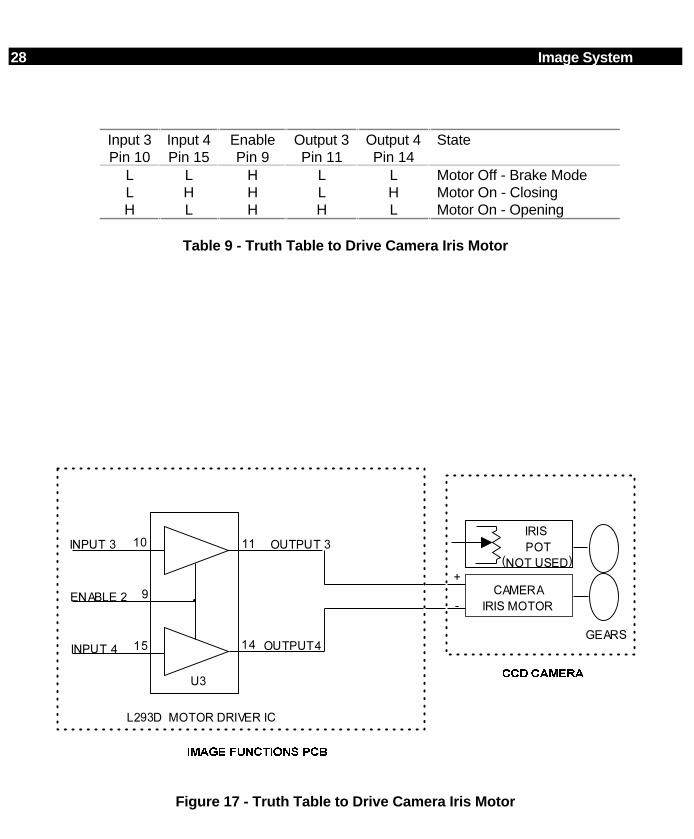
28 Image System
Input 3Pin 10
Input 4Pin 15
EnablePin 9
Output 3Pin 11
Output 4Pin 14
State
L L H L L Motor Off - Brake ModeL H H L H Motor On - ClosingH L H H L Motor On - Opening
Table 9 - Truth Table to Drive Camera Iris Motor
+
-
L293D MOTOR DRIVER IC
IMAGE FUNCTIONS PCB
CCD CAMERAU3
14 OUTPUT4
11 OUTPUT 3
CAMERA
IRIS MOTOR
10INPUT 3
ENABLE 2 9
INPUT 4 15
IRIS
POT
(NOT USED)
GEARS
Figure 17 - Truth Table to Drive Camera Iris Motor
Image System 29
CCD CAMERA CONTROL SIGNALS
The Technique Processor communicates camera control signals to the Image FunctionPCB via RS-232 serial communication, where receiver U17 communicates them tomicrocontroller U16. From the data bus of U16, the control signals are latched by outputlatch U6. The signal “Integrate” is the exception. It is sourced from PIO U38 on theAnalog Interface PCB, not from serial communications. The following controls andvoltages are directed to the camera from the Image Function PCB:
• Integrate
• Unity Gamma
• Anti-Vignetting
• Test Pattern
• • +24 Volts
• DC Common
• Cooler +
• Cooler Return
Integrate
The Integrate function is sent from the Technique Processor PCB to the AnalogInterface PCB via the micro-computer bus. PIO U38 pin 40 on the Analog Interface PCBoutputs the signal to U26 pins 12 and 13. U26 pin 11 buffers the output and shifts thevoltage level to ±12 VDC for extra noise protection. The signal is then routed to theImage Function PCB where it is received by RS-232 receiver U19 pin 12. The logicoutput of U19 pin 11 is buffered by U5 (pins 11 and 10) and sent to the CCD Camera.
Integration is provided to halt scanning on the CCD sensor in the camera when in thepulsed mode. The image from the image intensifier is “Integrated” onto the CCD sensorduring the X-ray pulse. The signal is TTL "low" during the integration expose phase.
Unity Gamma
The unity gamma signal is sent directly from the Technique Processor PCB to the ImageFunction PCB via RS-232 serial communication. The command is received by receiverU17 pin 9 and output (pin 10) directly to micro-processor U16 pin 17. Once processedby U16, output latch U6 pin 13 sends the signal to the CCD Camera via buffer U5 (pins3 and 4).
In normal imaging this input is high (gamma = 0.7) to enhance gain in the dark areas.During subtraction or roadmap it is switched low (gamma = 1.0, unity).

30 Image System
Anti-Vignetting
A selectable anti-vignetting correction input is provided (TTL active low). This featureprovides parabolic correction in both the vertical and horizontal axis. The amount ofcompensation is adjustable up to a minimum of 50% vertically and horizontally over thecircular area equal in diameter to the height of the sensor (6.6 mm). This signaldynamically boosts the gain of the video amplifier at the periphery of the image withoutaffecting black level. This is done to accomplish an even shading over the entire area ofthe image.
The anti-vignetting signal is sent directly from the Technique Processor PCB to theImage Function PCB via RS-232 serial communication. The command is received byreceiver U17 pin 9 and output (pin 10) directly to micro-processor U16 pin 17. Onceprocessed by U16, output latch U6 pin 16 sends the signal to the CCD Camera viabuffer U5 (pins 13 and 12).
Test Pattern
A test pattern has not been implemented at this time. An intermittent problem of asquare black box appearing on the left monitor of the Workstation can be remedied bycutting pin 6 of U5 on the Image Function PCB , which is the “Test Pattern” output to theCCD camera.
+24 Volts and DC Common
The +24V for the camera comes directly from the C-Arm +24V power supply PS2. Itpasses through the Power Motor Relay PCB P7-7 to P5-1. It can be measured on thatPCB at test point TP1. After leaving the Power Motor Relay PCB, it passes through theImage Function PCB P2-3 to P3-22 and enters the camera at P1-2.
The DC common connection for the camera is made on the Power Motor Relay PCB. Itleaves that board at P5-2, and is connected to the camera at P1-1 via the ImageFunction PCB P2-4 to P3-19.

Image System 31
CCD Thermo-Electric Cooling Circuit (TEC)
The CCD sensor is cooled by a thermo-electric cooling (TEC) and heat sinkingapparatus. The cooling module attempts to maintain the CCD temperature at the sametemperature as the image intensifier housing. Poor image quality may indicate that theTEC circuit is not working properly.
The heat sinking apparatus is turned off and on periodically by firmware located on theImage Function PCB. The ON and OFF cycle times depend on how long the processorhas been running.
A +5 VDC is applied to R4 on the Image Function PCB. Current flows through R4 to thethermo-electric cooler, back into the Image Function PCB and through transistor Q3 toDC common ground. Micro-controller U16 pin 19 controls the base of transistor Q3. Ahigh on pin 19 turns the cooler ON and a low turns the cooler OFF. These times havebeen determined experimentally and are stored in a look-up table (LUT) on the ImageFunction PCB. To determine proper operation of the TEC circuit, measure TP3 on theImage Function PCB for a drop to +2.4 VDC ± 0.75 V. The E9 jumpers are not used atthis time.
SYNCHRONIZATION STANDARDS
A 60 Hz and 50 Hz model CCD Camera is available.
Domestic Models - RS-170A Video Waveform Standard, 60 Hz.
International Models - CCIR or PAL compatible with 576 lines centered in theunblanked area of the CCIR standard, 50 Hz.

32 Image System
PIXEL/COLUMN FILTER PCBAsy. #00-878047 - Sch. #878045
The Pixel/Column Filter PCB is mounted on the CCD camera assembly (see Figures 1and 22). The video signal from the camera passes through the circuitry on this PCB andthen on to the Workstation image processor. The Pixel/Column Filter PCB has twofunctional sections; a column artifact cancellation filter and a pixel artifact filter. The pixelfilter section filters out noise from the camera video that appears as white pixels in theimage. The column filter circuitry is used to cancel out inherent blemishes of the CCDsensor that appear as columns in the image.
NOTE: Some systems may have a Pixel Filter PCB instead of a Pixel/Column FilterPCB. The main difference is the lack of column filter circuitry on the PixelFilter PCB. Later systems may have neither of these PCBs. Also, a -03revision Image Function PCB must be used with the Pixel/Column FilterPCB. Systems with S/N 69-2001 and higher are expected to have the PixelFilter PCB only.
Pixel Filter CircuitryThe Pixel Filter section of the PCB is comprised of U4, Q1 and the interconnectingresistors. The circuitry was designed to attenuate pixel blemishes (noise) from the output(P2) of the CCD Camera. The video signal from the CCD camera enters at J1 and isapplied to the base of transistor Q1 at pin 2. The signal is also routed through a 60 nSdelay IC U4. The 60 nS delayed video signal is applied to the base of transistor Q1 atpin 6. Both transistors are wired to function as emitter followers. In order to match thetransistor’s characteristics, both transistors are located on the same integrated circuit die(Q1). The emitters of the two transistors are connected to the output resistor R12. Thevideo output signal becomes the more negative voltage of either the delayed or non-delayed video signal. Thus any positive noise glitches (or white pixels) are attenuated asshown in Figure 18 below. The resultant video signal is sent to the Workstation via theMotherboard and the Interconnect Cable.
Power (+5 VDC) is supplied to the Pixel Filter portion of the PCB by the camera (+5P) atJ3 pin 6. It is filtered by series resistor R11 and capacitors C10 and C11 to decrease thepotential of noise entering the PCB through the power supply.
VIDEO INPUTNORMAL AND DELAYED
NOISEGLITCH
VIDEO OUTPUT
Figure 18 - Noise Filtering Function of Pixel Filter Circuitry
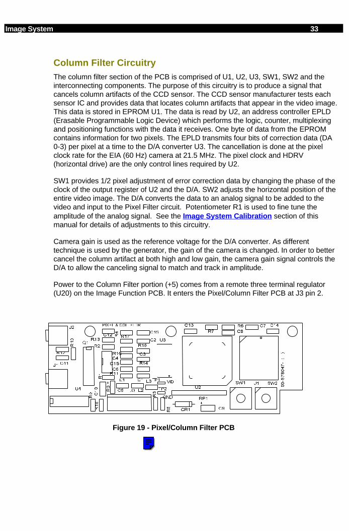
Image System 33
Column Filter CircuitryThe column filter section of the PCB is comprised of U1, U2, U3, SW1, SW2 and theinterconnecting components. The purpose of this circuitry is to produce a signal thatcancels column artifacts of the CCD sensor. The CCD sensor manufacturer tests eachsensor IC and provides data that locates column artifacts that appear in the video image.This data is stored in EPROM U1. The data is read by U2, an address controller EPLD(Erasable Programmable Logic Device) which performs the logic, counter, multiplexingand positioning functions with the data it receives. One byte of data from the EPROMcontains information for two pixels. The EPLD transmits four bits of correction data (DA0-3) per pixel at a time to the D/A converter U3. The cancellation is done at the pixelclock rate for the EIA (60 Hz) camera at 21.5 MHz. The pixel clock and HDRV(horizontal drive) are the only control lines required by U2.
SW1 provides 1/2 pixel adjustment of error correction data by changing the phase of theclock of the output register of U2 and the D/A. SW2 adjusts the horizontal position of theentire video image. The D/A converts the data to an analog signal to be added to thevideo and input to the Pixel Filter circuit. Potentiometer R1 is used to fine tune theamplitude of the analog signal. See the Image System Calibration section of thismanual for details of adjustments to this circuitry.
Camera gain is used as the reference voltage for the D/A converter. As differenttechnique is used by the generator, the gain of the camera is changed. In order to bettercancel the column artifact at both high and low gain, the camera gain signal controls theD/A to allow the canceling signal to match and track in amplitude.
Power to the Column Filter portion (+5) comes from a remote three terminal regulator(U20) on the Image Function PCB. It enters the Pixel/Column Filter PCB at J3 pin 2.
GND
VID
00
-87
80
47
- (
)
PIXEL & COL. FLTR
+
+
J3
L1
L2
L3
R5
R6
R7
R8
R9
R1
0
R11
R12
R13
R14
R15
R16
R17
C1
C2
C3
C4
C5
C6
C7
C8
CR1
J1
J2
C9
C1
0
C11
U4
Q1
C12
C13
R1
8
RP1
U2
SW1 SW2
U3
U1TP1
TP2
R1
C14
R2
C15
C16
R3
R4
Figure 19 - Pixel/Column Filter PCB
NOTE
Click in the blue box to go directly to the Electrical Schematic Diagram for the PCB shown on this page. Click the << button on the Tool Bar to return to this page.

34 Image System
PIXEL FILTER PCB
Asy. #00-877791- Sch. #877789
Some early 9600 systems and systems with serial number 69-2001 and higher will beequipped with a Pixel Filter PCB which does not have column filter circuitry. The circuitfunctions exactly as the pixel filter circuitry described above for the Pixel/Column FilterPCB. Component designators differ between the two PCBs however. The Pixel FilterPCB obtains power (+5 VDC) from the camera.
ASSY 00-877791- ( )
PIXEL FILTER
C1
C2
R1
R2 R3
R4
J1 J2
U1
Q1
E1
E2
Figure 20 - Pixel Filter PCB
NOTE
Click in the blue box to go directly to the Electrical Schematic Diagram for the PCB shown on this page. Click the << button on the Tool Bar to return to this page.
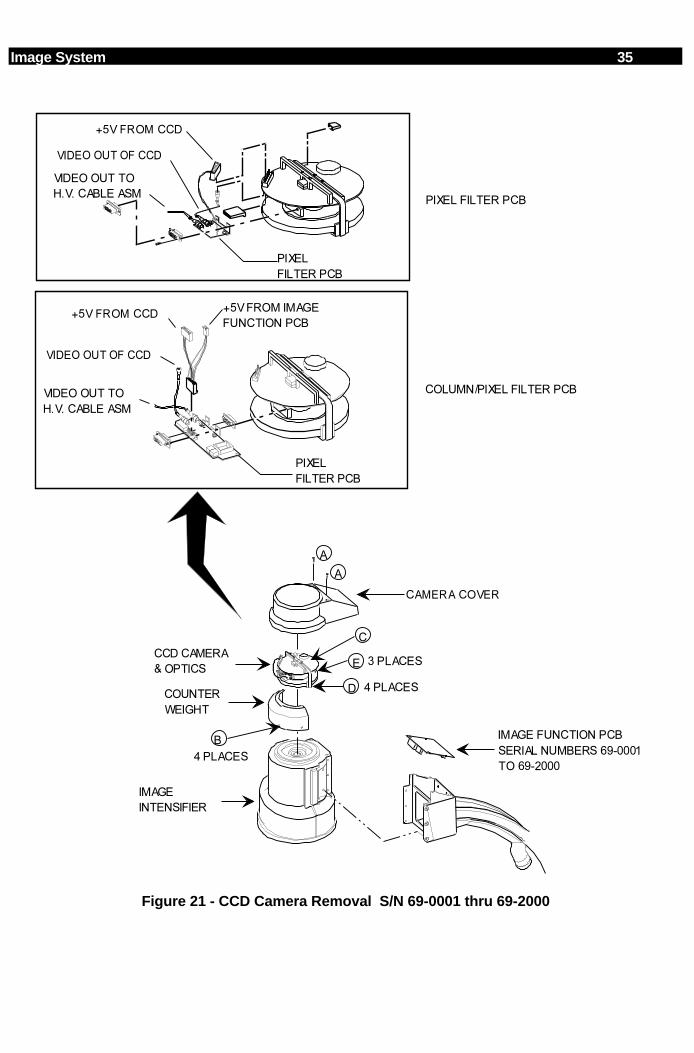
Image System 35
PIXEL
FILTER PCB
+5V FROM CCD
VIDEO OUT TO
H.V. CABLE ASM
VIDEO OUT OF CCD
PIXEL
FILTER PCB
+5V FROM CCD
VIDEO OUT OF CCD
VIDEO OUT TO
H.V. CABLE ASM
+5V FROM IMAGE
FUNCTION PCB
COLUMN/PIXEL FILTER PCB
PIXEL FILTER PCB
CAMERA COVER
CCD CAMERA
& OPTICS
COUNTER
WEIGHT
IMAGE
INTENSIFIER
C
A
A
B
D
4 PLACES
E
4 PLACES
3 PLACES
IMAGE FUNCTION PCB
SERIAL NUMBERS 69-0001
TO 69-2000
Figure 21 - CCD Camera Removal S/N 69-0001 thru 69-2000
NOTE
Click on the colored box to go directly to the exploded drawing in the Illustrated Parts Manual. Click on the << button in the Tool Bar to return to this point.
36 Image System
CCD CAMERA REPLACEMENT
S/N 69-0001 thru 69-2000
WARNING... Electrical circuits inside the equipment use voltages that are capable ofcausing serious injury or death from electrical shock. Use appropriateprecautions.
CAUTION: Always wear a properly grounded static protection wristband when workingwith the CCD camera.
Refer to Figure 21.
1. Turn the Workstation keyswitch to the OFF position.
2. Remove two screws (A) retaining the Camera cover and remove the cover.
3. Remove 4 screws (B) securing the counter-weight and remove the counter-weight.
4. Unplug wiring connectors (C) from the camera.
5. Remove 4 screws (D) that secure the heat pipe to the Image Intensifier.
7. Remove 3 bolts (E) securing the CCD Camera assembly to the Image Intensifier.
8. Remove the CCD Camera assembly from the Image Intensifier.
NOTE: When replacing the CCD camera assembly, remove the protective filmcovering the new CCD camera's lens before installing the new CCD cameraassembly.
When replacing the CCD camera assembly it may be necessary to re-calibrate the light level at the CCD by calibrating the Camera Iris. Refer tothe Camera Iris Calibration procedure in the Image System CalibrationSection.
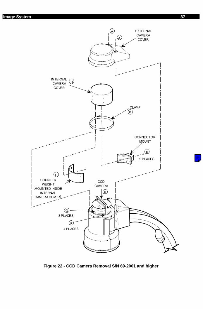
Image System 37
CLAMP
CONNECTOR
MOUNT
B
9 PLACES
INTERNAL
CAMERA
COVER
D
A
A
EXTERNAL
CAMERA
COVER
F
4 PLACES
G
3 PLACES
CCD
CAMERA
E
COUNTER
WEIGHT
(MOUNTED INSIDE
INTERNAL
CAMERA COVER)
D
Figure 22 - CCD Camera Removal S/N 69-2001 and higher
NOTE
Click on the colored box to go directly to the exploded assembly in the Illustrated Parts Manual. Click on the << button on the Tool Bar to return to this point.

38 Image System
CCD CAMERA REPLACEMENT
S/N 69-2001 and higher
WARNING... Electrical circuits inside the equipment use voltages that are capable ofcausing serious injury or death from electrical shock. Use appropriateprecautions.
CAUTION: Always wear a properly grounded static protection wristband when workingwith the CCD camera.
Refer to Figure 22.
1. Turn the Workstation keyswitch to the OFF position.
2. Remove two screws (A) retaining the external camera cover and remove the cover.
3. Remove the 9 screws (B) from the connector mount that secure it to the internalcamera cover.
4. Loosen the clamp (C) around the camera cover.
5. Carefully remove the internal camera cover/counter weight assembly (D).
6. Re-tighten the clamp to secure the connector mount.
7. Unplug wiring connectors from the camera (E).
8. Remove 4 screws (F) that secure the heat pipe to the Image Intensifier.
9. Remove 3 bolts (G) securing the CCD Camera assembly to the Image Intensifier.
10. Remove the CCD Camera assembly from the Image Intensifier.
NOTE: When replacing the CCD camera assembly, remove the protective filmcovering the new CCD camera's lens before installing the new CCD cameraassembly.
When replacing the CCD camera assembly, it may be necessary to re-calibrate the light level at the CCD by calibrating the Camera Iris. Refer tothe Camera Iris Calibration procedure in the Image System CalibrationSection.

Image System 39
ABS
OVERVIEWThe Auto Brightness System (ABS) is a combination of software and hardware thatautomatically adjusts kVp, mA, and camera gain for an optimal image. An analogvoltage from the camera (VIDEO_ LEVEL) is digitized and compared to a referencelevel in the ABS software. If VIDEO_LEVEL does not equal the reference voltage, theABS tables located in software are used to regulate kV, mA, and camera gain until itmatches. The functions adjusted are dependent on the Fluoro mode selected as shownin Tables 10 through 13.
ABS TABLE SELECTION CONTROLVarious ABS tables reside in software, but their availability for selection at the controlpanel must be setup in system configuration files. Refer to the C-Arm Software sectionin this manual for details of system configuration.
The operator selects the desired ABS table by pressing the “ABS SELECT” control onthe C-Arm control panel (see Figure 23 below). When the control is pressed, the currentABS table will be displayed for 2 seconds on the control panel display. The other tablesare displayed if the control is pressed again during the two seconds. If the control is notpressed again, the ABS table that is displayed will be loaded for use if not alreadyactive.
ABS TABLE SELECTION
CONTROL
Figure 23 - ABS Table Selection Control on the C-Arm Control Panel
NOTE
Click on a yellow box to go directly to the block diagram for this section. Do not use this link to return to a block diagram from this point. Click on the << button in the Tool Bar to return to any starting point.
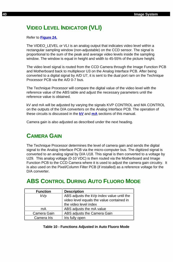
40 Image System
VIDEO LEVEL INDICATOR (VLI)
Refer to Figure 24.
The VIDEO_LEVEL or VLI is an analog output that indicates video level within arectangular sampling window (non-adjustable) on the CCD sensor. The signal isproportional to the sum of the peak and average video levels inside the samplingwindow. The window is equal in height and width to 45-55% of the picture height.
The video level signal is routed from the CCD Camera through the Image Function PCBand Motherboard back to multiplexor U3 on the Analog Interface PCB. After beingconverted to a digital signal by A/D U7, it is sent to the dual port ram on the TechniqueProcessor PCB via the A/D 0-7 bus.
The Technique Processor will compare the digital value of the video level with thereference value of the ABS table and adjust the necessary parameters until thereference value is obtained.
kV and mA will be adjusted by varying the signals KVP CONTROL and MA CONTROLon the outputs of the D/A converters on the Analog Interface PCB. The operation ofthese circuits is discussed in the kV and mA sections of this manual.
Camera gain is also adjusted as described under the next heading.
CAMERA GAIN
The Technique Processor determines the level of camera gain and sends the digitalsignal to the Analog Interface PCB via the micro-computer bus. The digitized signal isconverted to an analog signal by D/A U18. This signal is then converted to a voltage byU29. This analog voltage (0-10 VDC) is then routed via the Motherboard and ImageFunction PCB to the CCD Camera where it is used to adjust the camera gain circuitry. Itis also used on the Pixel/Column Filter PCB (if installed) as a reference voltage for theD/A converter.
ABS CONTROL DURING AUTO FLUORO MODE
Function DescriptionkVp ABS adjusts the kVp index value until the
video level equals the value contained inthe video level index
mA ABS adjusts the mA valueCamera Gain ABS adjusts the Camera GainCamera Iris Iris fully open
Table 10 - Functions Adjusted in Auto Fluoro Mode

Image System 41
ABS CONTROL DURING MANUAL FLUORO MODE
Function DescriptionkVp Manual adjustment of the kVp valuemA Manual adjustment of the mA value
Camera Gain ABS adjusts the Camera gain until thevideo level equals the value contained inthe video level index
Camera Iris Iris fully open
Table 11 - Functions Adjusted in Manual Fluoro Mode
ABS CONTROL DURING PULSED BOOST FLUORO MODE
Function DescriptionkVp kVp is frozen at it's current value by
softwaremA mA is incremented until the video level
equals the video level indexCamera Gain Camera gain is reduced, and ABS system
adjusts mA to achieve correct video level.If the correct level is not reached beforethe mA limit is reached, the camera gain isincreased.
Camera iris Iris fully closed
Table 12 - Functions Adjusted in Pulsed Boost Fluoro Mode
ABS CONTROL DURING BOOST FLUORO MODE
Function DescriptionkVp kVp is frozen at it's current value by
softwaremA mA is incremented until the video level
equals the video level indexCamera Gain Camera gain is reduced, and ABS system
adjusts mA to achieve correct video level.If the correct level is not reached beforethe mA limit is reached, the camera gain isincreased.
Camera iris Iris fully open
Table 13 - Functions Adjusted in Boost Fluoro Mode
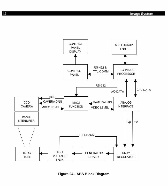
42 Image System
RS-232
CONTROL
PANEL
DISPLAY
ABS LOOKUP
TABLE
TECHNIQUE
PROCESSOR
CONTROL
PANEL
RS-422 &
TTL COMM
CCD
CAMERA
IMAGE
INTENSIFIER
IMAGE
FUNCTION
ANALOG
INTERFACE
IRIS
CAMERA GAIN
VIDEO LEVEL
CAMERA GAIN
VIDEO LEVEL
kVp mA
A/D DATACPU DATA
FEEDBACK
X-RAY
TUBE
HIGH
VOLTAGE
TANK
GENERATOR
DRIVER
X-RAY
REGULATOR
Figure 24 - ABS Block Diagram
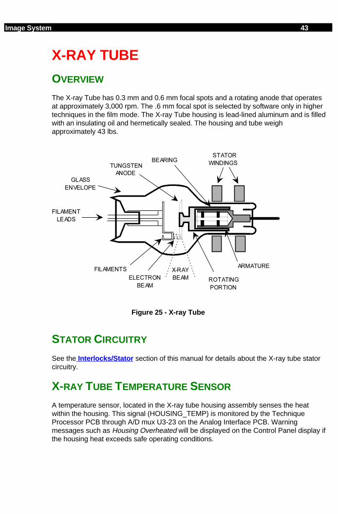
Image System 43
X-RAY TUBE
OVERVIEW
The X-ray Tube has 0.3 mm and 0.6 mm focal spots and a rotating anode that operatesat approximately 3,000 rpm. The .6 mm focal spot is selected by software only in highertechniques in the film mode. The X-ray Tube housing is lead-lined aluminum and is filledwith an insulating oil and hermetically sealed. The housing and tube weighapproximately 43 lbs.
GLASS
ENVELOPE
TUNGSTEN
ANODE
BEARINGSTATOR
WINDINGS
ARMATURE
ROTATING
PORTION
X-RAY
BEAMELECTRON
BEAM
FILAMENT
LEADS
FILAMENTS
Figure 25 - X-ray Tube
STATOR CIRCUITRY
See the Interlocks/Stator section of this manual for details about the X-ray tube statorcircuitry.
X-RAY TUBE TEMPERATURE SENSOR
A temperature sensor, located in the X-ray tube housing assembly senses the heatwithin the housing. This signal (HOUSING_TEMP) is monitored by the TechniqueProcessor PCB through A/D mux U3-23 on the Analog Interface PCB. Warningmessages such as Housing Overheated will be displayed on the Control Panel display ifthe housing heat exceeds safe operating conditions.

44 Image System
STATOR THERMAL CUTOFF SWITCH
A thermal cutoff switch, is wired in series with the Stator Neutral. If the temperaturewithin the X-ray Tube Housing exceeds safe operating conditions, the thermal switchopens, interrupting current to the stator motor. This is detected by the TechniqueProcessor PCB via the stator current sense circuit as described in the INTERLOCK /STATOR section of the service manual.
REPLACEMENT OF X-RAY TUBE
Refer to Figure 26 .
WARNING... Electrical circuits inside the equipment use voltages that are capable ofcausing serious injury or death from electrical shock. Use appropriateprecautions.
1. Verify the Workstation keyswitch is turned to the OFF position and the AC powerplug is disconnected from the AC receptacle.
2. Position the C-arm in the vertical beam position and lock the brake pedals so theMobile C-Arm will not move.
WARNING... The X-ray Tube housing can cause severe burns. Do not touch the housinguntil the housing has cooled.
3. Remove the 2 screws (A) securing the X-ray tube connector housing cover andremove the cover.
4. Use a spanner wrench (OEC part # 00-877674) to disconnect the anode andcathode cable connectors. Remove the cable nuts and strain relief.
WARNING... Discharge the high voltage cables by grounding the connector tips to thechassis to prevent possible electrical shock.
5. Unplug wiring connector J15 (stator motor power & temperature sensor).
6. Disconnect the ground wires from the rear of the X-ray tube.
7. Remove the collimator cover, collimator, and collimator alignment bracket asdescribed in Collimator Replacement .
8. Remove the four bolts (B) that secure the X-ray Tube housing and remove thehousing and tube.
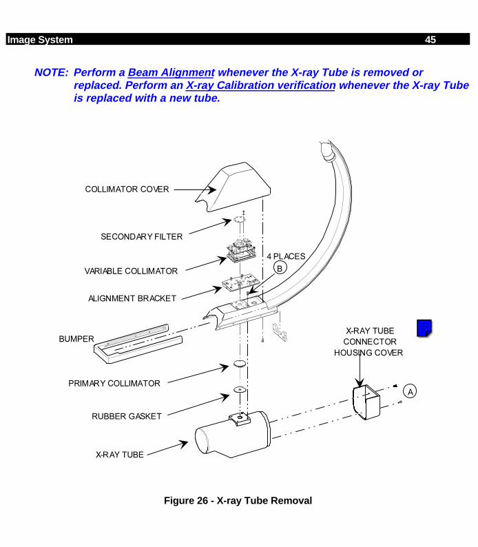
Image System 45
NOTE: Perform a Beam Alignment whenever the X-ray Tube is removed orreplaced. Perform an X-ray Calibration verification whenever the X-ray Tubeis replaced with a new tube.
COLLIMATOR COVER
SECONDARY FILTER
VARIABLE COLLIMATOR
ALIGNMENT BRACKET
BUMPER
RUBBER GASKET
X-RAY TUBE
PRIMARY COLLIMATORA
B
4 PLACES
X-RAY TUBE
CONNECTOR
HOUSING COVER
Figure 26 - X-ray Tube Removal
NOTE
Click on the colored box to go directly to the exploded assembly in the Illustrated Parts Manual. Click on the << button on the Tool Bar to return to this point.

46 Image System
REPLACEMENT OF HIGH VOLTAGE CABLES
WARNING... Electrical circuits inside the equipment use voltages that are capable ofcausing serious injury or death from electrical shock. Use appropriateprecautions.
1. Verify the Workstation keyswitch is in the OFF position and the AC power plug isdisconnected from the wall socket.
WARNING... Apply only a small amount of silicon grease to High Voltage cable plugs atthe X-ray Tube end and then wipe them off to leave just a very thin layer ofgrease.
2. Remove the X-ray Tube housing cover.
3. Remove the collimator cover, collimator and alignment bracket. Refer to CollimatorReplacement .
4. Use the spanner wrench (OEC part # 00-877674) to disconnect the anode andcathode high voltage cables from the X-ray tube.
5. Unplug wiring connector J15 (stator motor power & temperature sensor).
6. Disconnect the ground wires from the X-ray tube.
7. Remove the High Voltage cable nuts and strain relief.
8. Remove the 4 bolts securing the X-ray tube assembly and remove it from the C-armweldment.
9. Release the C-arm brake and position the C-arm horizontal to floor.
10. Remove 2 Torx screws securing the camera cover.
11. Remove 4 Torx screws securing the Image Function PCB to the C-arm weldment ifnecessary (Image Function PCB is in generator card rack on later models).
12. Remove 6 hex bolts securing the Image Intensifier. Lift the Image Intensifier andplace it on a chair while disconnecting 5 Torx screws securing the Image Intensifierpower supply. Refer to Image Intensifier/Power Supply Removal .
13. Remove 2 set screws securing the main trunk of the High Voltage Cable at thecables injection point into the C-arm and then pull the cable out 4-5 inches.
14. Pull the High Voltage cables out until tension is felt and then push the cables backin the cable injection point, towards the II end of the C-arm. Then reach in the II endof the C-arm, grasp the loop of cable and pull the cables out the II end of the C-arm.
Image System 47
NOTE: H.V. cables entering the C-arm turn immediately and are routed to the X-rayTube. The cables can't be removed without pulling the cables out the II endof the C-arm first.
15. Once the cable connectors have been pulled out of the II end of the C-arm, removethe strain relief and pull the cables out one at a time.
16. Remove the Front Cover (2 Torx screws) and the Right Front Cover (3 Torx) andthen remove 2 screws securing the C-clamp strain relief.
17. Remove the High Voltage Cable ground wires from the chassis and remove theA1J3 connector from the Motherboard PCB.
18. Remove the Left Front Cover and disconnect the A4J5 connector from the PowerMotor Relay PCB.
19. Disconnect the High Voltage connectors from the High Voltage Tank using thespanner wrench.
20. To route the High Voltage Cable through the hole in the Right Front Coverdisassemble the candlestick cable nut assembly and pull the cables andconnectors.

IMAGE SYSTEM CALIBRATION
The procedures contained in this section are used to test and calibrate the 9600 MobileC-Arm. The following procedures are included:
• • Beam Alignment
• Collimator Iris Calibration (Field Size)
• Camera Iris Calibration (Tracking)
• Pixel/Column Filter PCB Adjustments
CALIBRATION OVERVIEWThese procedures assume that all parts are installed and are wired correctly. It is alsoassumed that all subassemblies are either known to be operational or were previouslytested at the factory.
BEAM ALIGNMENTThis portion of the procedure aligns the X-ray beam, collimation assemblies, and cameraimaging system in-line with each other. This section includes the setup of the C-Armand equipment necessary to perform a beam alignment. Also included in this portion ofthe Image System Calibration is the camera mechanical/electrical alignments andverifying the calibration of the Workstation monitors.
COLLIMATOR IRIS CALIBRATIONThis section includes sizing the collimator iris to all three image intensifier sizes in fluoromodes. A film used for Beam Alignment Verification is created in this section and isused as hard copy proof that a system has met specifications.
CAMERA IRIS CALIBRATIONA long and short method for calibrating the tracking (ABS loop) in the fluoro mode isperformed in this section.
PIXEL/COLUMN FILTER PCB ADJUSTMENTSThis adjustment corrects for any shading imperfections that may appear as columns inthe image. Vignetting is also corrected during this portion of the procedure.
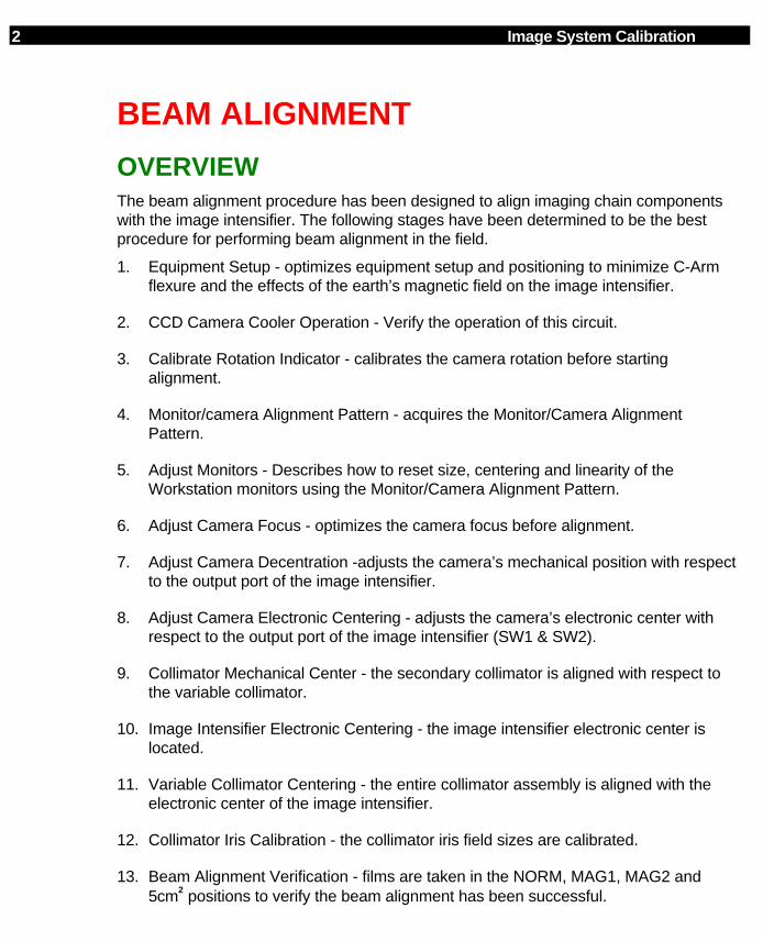
2 Image System Calibration
BEAM ALIGNMENT
OVERVIEWThe beam alignment procedure has been designed to align imaging chain componentswith the image intensifier. The following stages have been determined to be the bestprocedure for performing beam alignment in the field.
1. Equipment Setup - optimizes equipment setup and positioning to minimize C-Armflexure and the effects of the earth’s magnetic field on the image intensifier.
2. CCD Camera Cooler Operation - Verify the operation of this circuit.
3. Calibrate Rotation Indicator - calibrates the camera rotation before startingalignment.
4. Monitor/camera Alignment Pattern - acquires the Monitor/Camera AlignmentPattern.
5. Adjust Monitors - Describes how to reset size, centering and linearity of theWorkstation monitors using the Monitor/Camera Alignment Pattern.
6. Adjust Camera Focus - optimizes the camera focus before alignment.
7. Adjust Camera Decentration -adjusts the camera’s mechanical position with respectto the output port of the image intensifier.
8. Adjust Camera Electronic Centering - adjusts the camera’s electronic center withrespect to the output port of the image intensifier (SW1 & SW2).
9. Collimator Mechanical Center - the secondary collimator is aligned with respect tothe variable collimator.
10. Image Intensifier Electronic Centering - the image intensifier electronic center islocated.
11. Variable Collimator Centering - the entire collimator assembly is aligned with theelectronic center of the image intensifier.
12. Collimator Iris Calibration - the collimator iris field sizes are calibrated.
13. Beam Alignment Verification - films are taken in the NORM, MAG1, MAG2 and5cm2 positions to verify the beam alignment has been successful.
Image System Calibration 3
TOOLSThe following tools are required to perform the procedures in this section:
• OEC Boot Disk OEC P/N 00-877444 or 00-876781
• Wisconsin mesh resolution tool OEC P/N 00-900040-01
• Converging line resolution tool (LP/mm) OEC P/N 00-900860-01
• Beam alignment tool OEC P/N 00-878105-01
• Bore sight tool OEC P/N 00-877589-01
• Bristol spline driver (Xcelite 99-61) OEC P/N 00-900920-01
• (QTY of 3) 1mm copper plates OEC P/N 00-877682-01
NOTE: All quantities are one except where indicated.
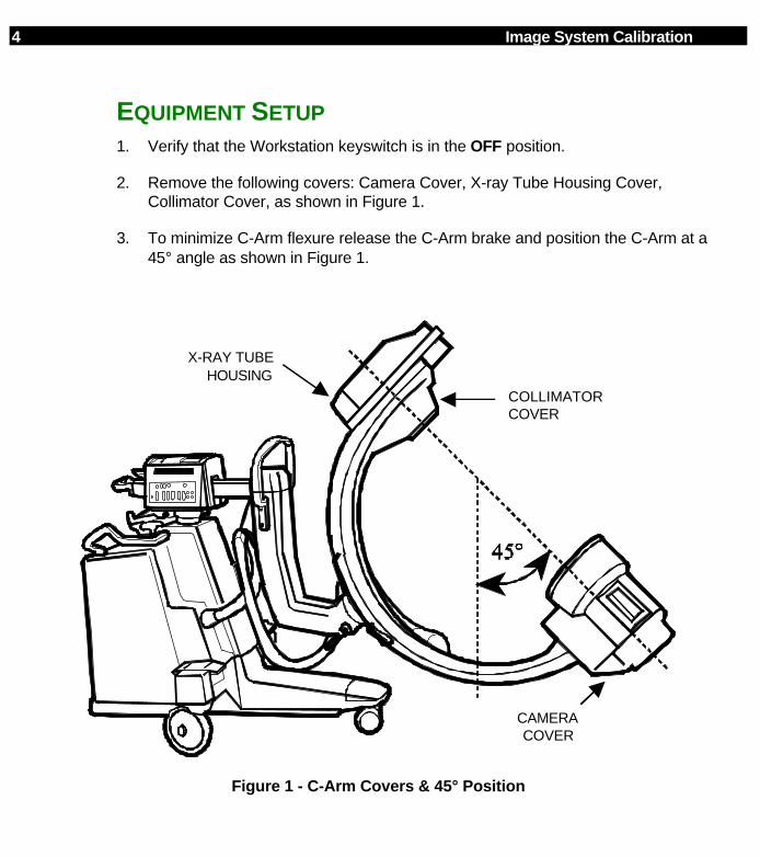
4 Image System Calibration
EQUIPMENT SETUP1. Verify that the Workstation keyswitch is in the OFF position.
2. Remove the following covers: Camera Cover, X-ray Tube Housing Cover,Collimator Cover, as shown in Figure 1.
3. To minimize C-Arm flexure release the C-Arm brake and position the C-Arm at a45° angle as shown in Figure 1.
X-RAY TUBEHOUSING
COLLIMATORCOVER
CAMERACOVER
Figure 1 - C-Arm Covers & 45° Position
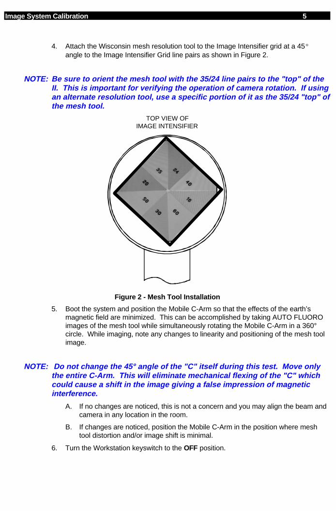
Image System Calibration 5
4. Attach the Wisconsin mesh resolution tool to the Image Intensifier grid at a 45§angle to the Image Intensifier Grid line pairs as shown in Figure 2.
NOTE: Be sure to orient the mesh tool with the 35/24 line pairs to the "top" of theII. This is important for verifying the operation of camera rotation. If usingan alternate resolution tool, use a specific portion of it as the 35/24 "top" ofthe mesh tool.
TOP VIEW OFIMAGE INTENSIFIER
Figure 2 - Mesh Tool Installation
5. Boot the system and position the Mobile C-Arm so that the effects of the earth’smagnetic field are minimized. This can be accomplished by taking AUTO FLUOROimages of the mesh tool while simultaneously rotating the Mobile C-Arm in a 360°circle. While imaging, note any changes to linearity and positioning of the mesh toolimage.
NOTE: Do not change the 45° angle of the "C" itself during this test. Move onlythe entire C-Arm. This will eliminate mechanical flexing of the "C" whichcould cause a shift in the image giving a false impression of magneticinterference.
A. If no changes are noticed, this is not a concern and you may align the beam andcamera in any location in the room.
B. If changes are noticed, position the Mobile C-Arm in the position where meshtool distortion and/or image shift is minimal.
6. Turn the Workstation keyswitch to the OFF position.
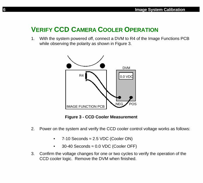
6 Image System Calibration
VERIFY CCD CAMERA COOLER OPERATION1. With the system powered off, connect a DVM to R4 of the Image Functions PCB
while observing the polarity as shown in Figure 3.
0.0 VDC
DVM
IMAGE FUNCTION PCBNEG POS
R4
Figure 3 - CCD Cooler Measurement
2. Power on the system and verify the CCD cooler control voltage works as follows:
• 7-10 Seconds ≈ 2.5 VDC (Cooler ON)
• 30-40 Seconds ≈ 0.0 VDC (Cooler OFF)
3. Confirm the voltage changes for one or two cycles to verify the operation of theCCD cooler logic. Remove the DVM when finished.
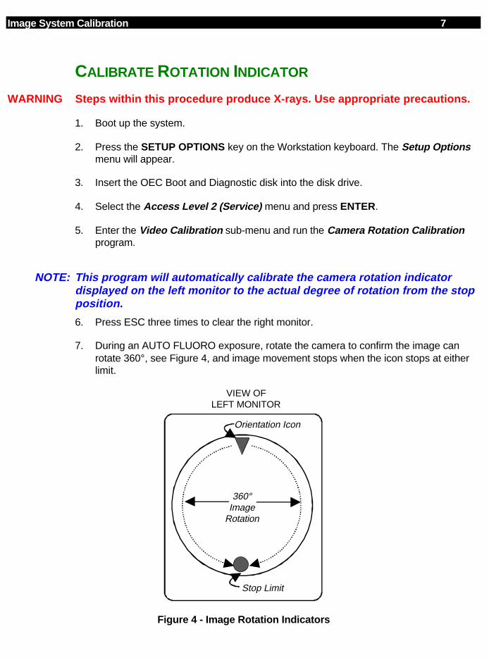
Image System Calibration 7
CALIBRATE ROTATION INDICATOR
WARNING Steps within this procedure produce X-rays. Use appropriate precautions.
1. Boot up the system.
2. Press the SETUP OPTIONS key on the Workstation keyboard. The Setup Optionsmenu will appear.
3. Insert the OEC Boot and Diagnostic disk into the disk drive.
4. Select the Access Level 2 (Service) menu and press ENTER.
5. Enter the Video Calibration sub-menu and run the Camera Rotation Calibrationprogram.
NOTE: This program will automatically calibrate the camera rotation indicatordisplayed on the left monitor to the actual degree of rotation from the stopposition.
6. Press ESC three times to clear the right monitor.
7. During an AUTO FLUORO exposure, rotate the camera to confirm the image canrotate 360°, see Figure 4, and image movement stops when the icon stops at eitherlimit.
VIEW OFLEFT MONITOR
Orientation Icon
360°Image
Rotation
Stop Limit
Figure 4 - Image Rotation Indicators
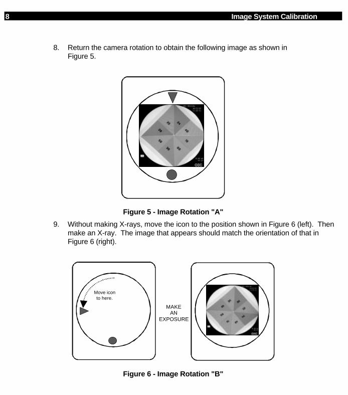
8 Image System Calibration
8. Return the camera rotation to obtain the following image as shown inFigure 5.
Figure 5 - Image Rotation "A"
9. Without making X-rays, move the icon to the position shown in Figure 6 (left). Thenmake an X-ray. The image that appears should match the orientation of that inFigure 6 (right).
Move iconto here.
MAKEAN
EXPOSURE
Figure 6 - Image Rotation "B"
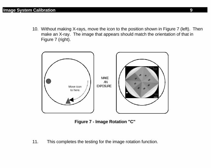
Image System Calibration 9
10. Without making X-rays, move the icon to the position shown in Figure 7 (left). Thenmake an X-ray. The image that appears should match the orientation of that inFigure 7 (right).
Move iconto here.
MAKEAN
EXPOSURE
Figure 7 - Image Rotation "C"
11. This completes the testing for the image rotation function.
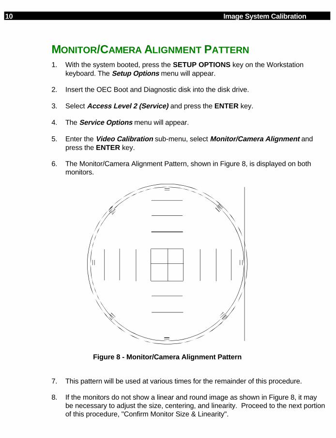
10 Image System Calibration
MONITOR/CAMERA ALIGNMENT PATTERN1. With the system booted, press the SETUP OPTIONS key on the Workstation
keyboard. The Setup Options menu will appear.
2. Insert the OEC Boot and Diagnostic disk into the disk drive.
3. Select Access Level 2 (Service) and press the ENTER key.
4. The Service Options menu will appear.
5. Enter the Video Calibration sub-menu, select Monitor/Camera Alignment andpress the ENTER key.
6. The Monitor/Camera Alignment Pattern, shown in Figure 8, is displayed on bothmonitors.
Figure 8 - Monitor/Camera Alignment Pattern
7. This pattern will be used at various times for the remainder of this procedure.
8. If the monitors do not show a linear and round image as shown in Figure 8, it maybe necessary to adjust the size, centering, and linearity. Proceed to the next portionof this procedure, "Confirm Monitor Size & Linearity".
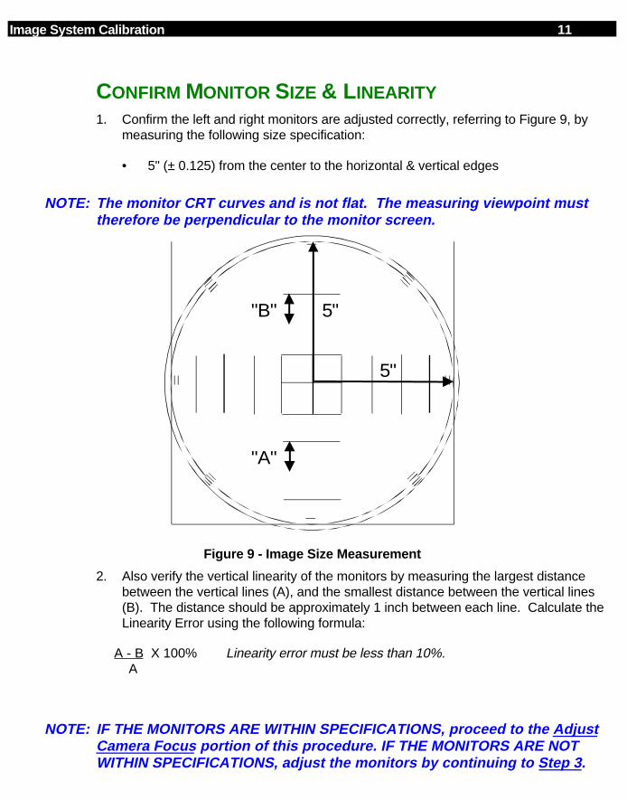
Image System Calibration 11
CONFIRM MONITOR SIZE & L INEARITY1. Confirm the left and right monitors are adjusted correctly, referring to Figure 9, by
measuring the following size specification:
• 5" (± 0.125) from the center to the horizontal & vertical edges
NOTE: The monitor CRT curves and is not flat. The measuring viewpoint musttherefore be perpendicular to the monitor screen.
5"
5"
"B"
"A"
Figure 9 - Image Size Measurement
2. Also verify the vertical linearity of the monitors by measuring the largest distancebetween the vertical lines (A), and the smallest distance between the vertical lines(B). The distance should be approximately 1 inch between each line. Calculate theLinearity Error using the following formula:
A - B X 100% Linearity error must be less than 10%. A
NOTE: IF THE MONITORS ARE WITHIN SPECIFICATIONS, proceed to the AdjustCamera Focus portion of this procedure. IF THE MONITORS ARE NOTWITHIN SPECIFICATIONS, adjust the monitors by continuing to Step 3.
12 Image System Calibration
3. Remove the rear cover of the Workstation (8 screws) then slide the monitor coveroff by pulling it straight towards the rear of the unit.
4. Use the controls, shown in Figure 10, and adjust the monitors.
NOTE: The following adjustments are interactive.
VERTICAL HORIZONTALVLIN - R10 HLIN (No Adjustment)VSIZE - R7 HSIZE - L1VCENT - R17 HCENT - R57 (Phase)
MONITOR SIDE VIEW
HSIZE
VFRQV
SIZE
VLIN
HCENT
HFRQ
SUBCONT
VCENT
ACCESS FROMTHE TOP
MONITOR PCB
FOCUS
G2 SUB BRIGHTNESS
MONITOR BOTTOM VIEW
ACCESS HOLES LOCATEDIN MONTOR MOUNTINGPLATE
Figure 10 - Monitor Adjustment Controls
5. Set the Vertical Linearity Pot R10 to less than 10% of the Linearity Error.
6. Adjust the Vertical Size pot (R7) and Horizontal Size coil (L1) on the Monitor PCBfor 10 ± 0.15 inches measured perpendicular to the CRT surface.
7. Adjust the Vertical Center pot (R17) and the Horizontal Phase pot (R57) to centerthe Monitor/Camera Alignment Pattern.
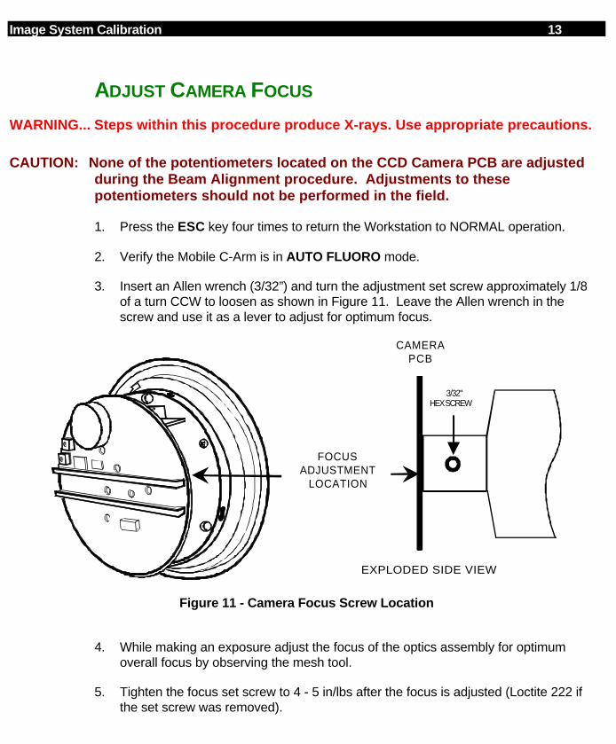
Image System Calibration 13
ADJUST CAMERA FOCUS
WARNING... Steps within this procedure produce X-rays. Use appropriate precautions.
CAUTION: None of the potentiometers located on the CCD Camera PCB are adjustedduring the Beam Alignment procedure. Adjustments to thesepotentiometers should not be performed in the field.
1. Press the ESC key four times to return the Workstation to NORMAL operation.
2. Verify the Mobile C-Arm is in AUTO FLUORO mode.
3. Insert an Allen wrench (3/32”) and turn the adjustment set screw approximately 1/8of a turn CCW to loosen as shown in Figure 11. Leave the Allen wrench in thescrew and use it as a lever to adjust for optimum focus.
FOCUSADJUSTMENT
LOCATION
3/32"HEX SCREW
CAMERAPCB
EXPLODED SIDE VIEW
Figure 11 - Camera Focus Screw Location
4. While making an exposure adjust the focus of the optics assembly for optimumoverall focus by observing the mesh tool.
5. Tighten the focus set screw to 4 - 5 in/lbs after the focus is adjusted (Loctite 222 ifthe set screw was removed).
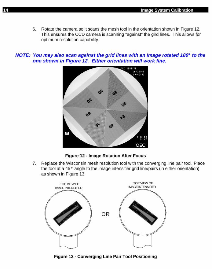
14 Image System Calibration
6. Rotate the camera so it scans the mesh tool in the orientation shown in Figure 12.This ensures the CCD camera is scanning "against" the gird lines. This allows foroptimum resolution capability.
NOTE: You may also scan against the grid lines with an image rotated 180 °° to theone shown in Figure 12. Either orientation will work fine.
Figure 12 - Image Rotation After Focus
7. Replace the Wisconsin mesh resolution tool with the converging line pair tool. Placethe tool at a 45§§ angle to the image intensifier grid line/pairs (in either orientation)as shown in Figure 13.
TOP VIEW OFIMAGE INTENSIFIER
TOP VIEW OFIMAGE INTENSIFIER
OR
Figure 13 - Converging Line Pair Tool Positioning
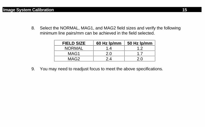
Image System Calibration 15
8. Select the NORMAL, MAG1, and MAG2 field sizes and verify the followingminimum line pairs/mm can be achieved in the field selected.
FIELD SIZE 60 Hz lp/mm 50 Hz lp/mmNORMAL 1.4 1.2
MAG1 2.0 1.7MAG2 2.4 2.0
9. You may need to readjust focus to meet the above specifications.
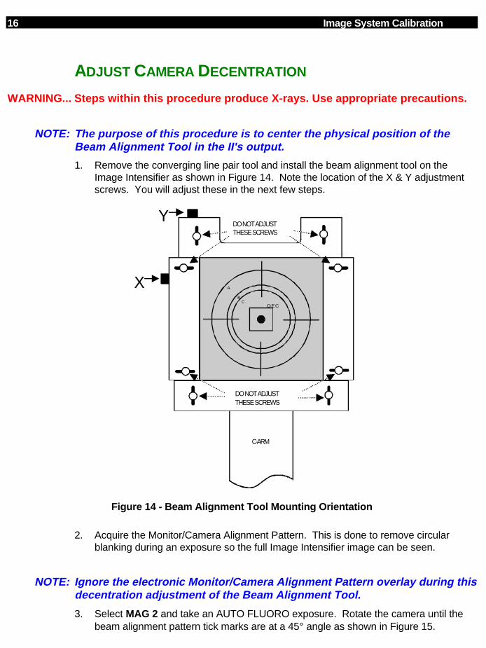
16 Image System Calibration
ADJUST CAMERA DECENTRATION
WARNING... Steps within this procedure produce X-rays. Use appropriate precautions.
NOTE: The purpose of this procedure is to center the physical position of theBeam Alignment Tool in the II's output.
1. Remove the converging line pair tool and install the beam alignment tool on theImage Intensifier as shown in Figure 14. Note the location of the X & Y adjustmentscrews. You will adjust these in the next few steps.
OEC
A
BC
X
YDO NOT ADJUSTTHESE SCREWS
DO NOT ADJUSTTHESE SCREWS
C-ARM
Figure 14 - Beam Alignment Tool Mounting Orientation
2. Acquire the Monitor/Camera Alignment Pattern. This is done to remove circularblanking during an exposure so the full Image Intensifier image can be seen.
NOTE: Ignore the electronic Monitor/Camera Alignment Pattern overlay during thisdecentration adjustment of the Beam Alignment Tool.
3. Select MAG 2 and take an AUTO FLUORO exposure. Rotate the camera until thebeam alignment pattern tick marks are at a 45° angle as shown in Figure 15.
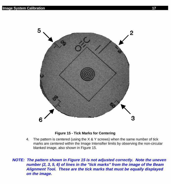
Image System Calibration 17
Figure 15 - Tick Marks for Centering
4. The pattern is centered (using the X & Y screws) when the same number of tickmarks are centered within the Image Intensifier limits by observing the non-circularblanked image, also shown in Figure 15.
NOTE: The pattern shown in Figure 15 is not adjusted correctly. Note the unevennumber (2, 3, 5, 6) of lines in the "tick marks" from the image of the BeamAlignment Tool. These are the tick marks that must be equally displayedon the image.
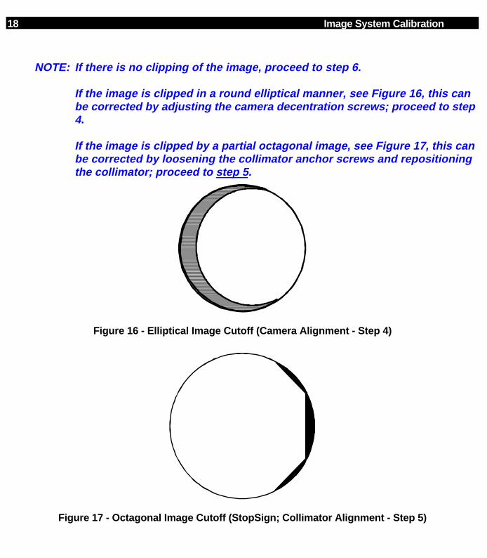
18 Image System Calibration
NOTE: If there is no clipping of the image, proceed to step 6.
If the image is clipped in a round elliptical manner, see Figure 16, this canbe corrected by adjusting the camera decentration screws; proceed to step4.
If the image is clipped by a partial octagonal image, see Figure 17, this canbe corrected by loosening the collimator anchor screws and repositioningthe collimator; proceed to step 5.
Figure 16 - Elliptical Image Cutoff (Camera Alignment - Step 4)
Figure 17 - Octagonal Image Cutoff (StopSign; Collimator Alignment - Step 5)
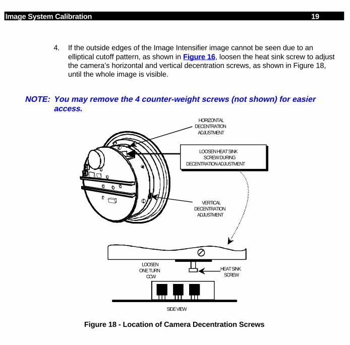
Image System Calibration 19
4. If the outside edges of the Image Intensifier image cannot be seen due to anelliptical cutoff pattern, as shown in Figure 16 , loosen the heat sink screw to adjustthe camera’s horizontal and vertical decentration screws, as shown in Figure 18,until the whole image is visible.
NOTE: You may remove the 4 counter-weight screws (not shown) for easieraccess.
HORIZONTALDECENTRATION
ADJUSTMENT
VERTICALDECENTRATION
ADJUSTMENT
HEAT SINKSCREW
SIDE VIEW
LOOSEN HEAT SINKSCREW DURING
DECENTRATION ADJUSTMENT
LOOSENONE TURN
CCW
Figure 18 - Location of Camera Decentration Screws
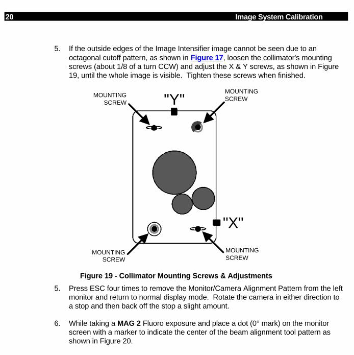
20 Image System Calibration
5. If the outside edges of the Image Intensifier image cannot be seen due to anoctagonal cutoff pattern, as shown in Figure 17 , loosen the collimator's mountingscrews (about 1/8 of a turn CCW) and adjust the X & Y screws, as shown in Figure19, until the whole image is visible. Tighten these screws when finished.
"Y"
"X"
MOUNTINGSCREW
MOUNTINGSCREW
MOUNTINGSCREW
MOUNTINGSCREW
Figure 19 - Collimator Mounting Screws & Adjustments
5. Press ESC four times to remove the Monitor/Camera Alignment Pattern from the leftmonitor and return to normal display mode. Rotate the camera in either direction toa stop and then back off the stop a slight amount.
6. While taking a MAG 2 Fluoro exposure and place a dot (0° mark) on the monitorscreen with a marker to indicate the center of the beam alignment tool pattern asshown in Figure 20.

Image System Calibration 21
0°
90°
180°
270°
CENTER MARK
Figure 20 - Rotation Points on Monitor
7. Rotate the camera 90°, 180°, and 270° and mark each center point to indicate thecenter of the beam alignment tool pattern.
8. Draw a cross between the four marks and place a mark at the intersection of thecross.
9. While making an exposure, adjust the decentration screws to align the center of thebeam alignment tool pattern to the mark at the intersection of the four marks asshown in Figure 21 .
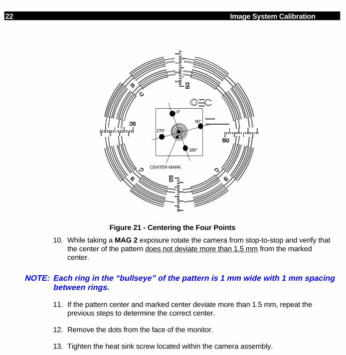
22 Image System Calibration
0°
90°
180°
270°
CENTER MARK
Figure 21 - Centering the Four Points
10. While taking a MAG 2 exposure rotate the camera from stop-to-stop and verify thatthe center of the pattern does not deviate more than 1.5 mm from the markedcenter.
NOTE: Each ring in the “bullseye” of the pattern is 1 mm wide with 1 mm spacingbetween rings.
11. If the pattern center and marked center deviate more than 1.5 mm, repeat theprevious steps to determine the correct center.
12. Remove the dots from the face of the monitor.
13. Tighten the heat sink screw located within the camera assembly.
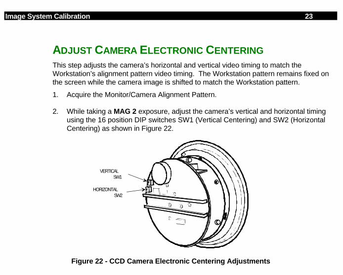
Image System Calibration 23
ADJUST CAMERA ELECTRONIC CENTERINGThis step adjusts the camera’s horizontal and vertical video timing to match theWorkstation’s alignment pattern video timing. The Workstation pattern remains fixed onthe screen while the camera image is shifted to match the Workstation pattern.
1. Acquire the Monitor/Camera Alignment Pattern.
2. While taking a MAG 2 exposure, adjust the camera’s vertical and horizontal timingusing the 16 position DIP switches SW1 (Vertical Centering) and SW2 (HorizontalCentering) as shown in Figure 22.
VERTICALSW1
HORIZONTALSW2
Figure 22 - CCD Camera Electronic Centering Adjustments
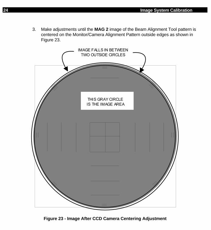
24 Image System Calibration
3. Make adjustments until the MAG 2 image of the Beam Alignment Tool pattern iscentered on the Monitor/Camera Alignment Pattern outside edges as shown inFigure 23.
IMAGE FALLS IN BETWEEN
TWO OUTSIDE CIRCLES
THIS GRAY CIRCLE
IS THE IMAGE AREA
Figure 23 - Image After CCD Camera Centering Adjustment
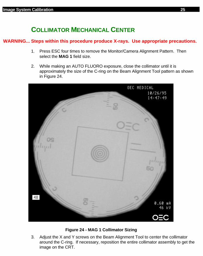
Image System Calibration 25
COLLIMATOR MECHANICAL CENTER
WARNING... Steps within this procedure produce X-rays. Use appropriate precautions.
1. Press ESC four times to remove the Monitor/Camera Alignment Pattern. Thenselect the MAG 1 field size.
2. While making an AUTO FLUORO exposure, close the collimator until it isapproximately the size of the C-ring on the Beam Alignment Tool pattern as shownin Figure 24.
Figure 24 - MAG 1 Collimator Sizing
3. Adjust the X and Y screws on the Beam Alignment Tool to center the collimatoraround the C-ring. If necessary, reposition the entire collimator assembly to get theimage on the CRT.
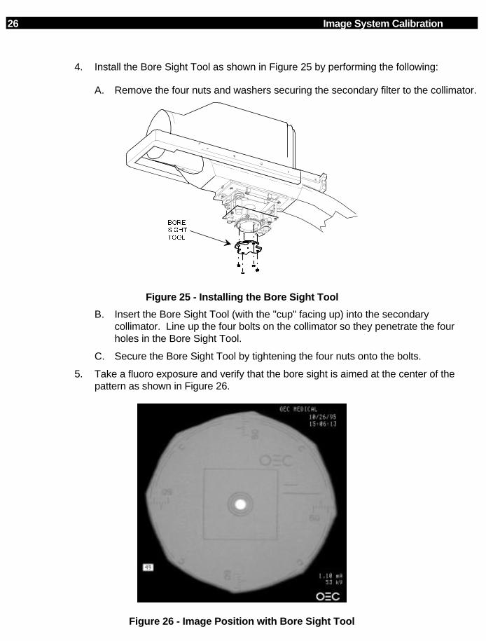
26 Image System Calibration
4. Install the Bore Sight Tool as shown in Figure 25 by performing the following:
A. Remove the four nuts and washers securing the secondary filter to the collimator.
BORE
SIGHT
TOOL
Figure 25 - Installing the Bore Sight Tool
B. Insert the Bore Sight Tool (with the "cup" facing up) into the secondarycollimator. Line up the four bolts on the collimator so they penetrate the fourholes in the Bore Sight Tool.
C. Secure the Bore Sight Tool by tightening the four nuts onto the bolts.
5. Take a fluoro exposure and verify that the bore sight is aimed at the center of thepattern as shown in Figure 26.
Figure 26 - Image Position with Bore Sight Tool
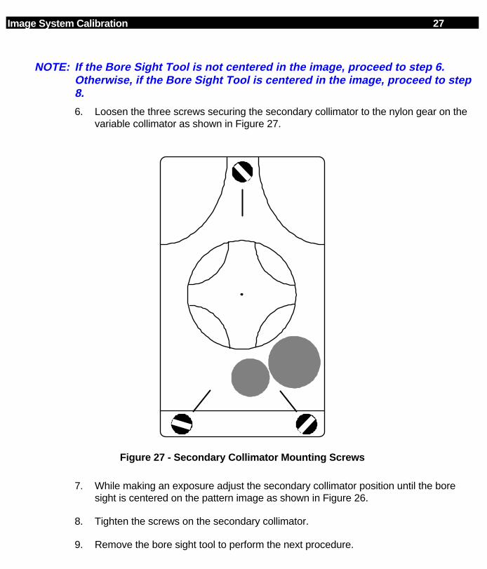
Image System Calibration 27
NOTE: If the Bore Sight Tool is not centered in the image, proceed to step 6.Otherwise, if the Bore Sight Tool is centered in the image, proceed to step8.
6. Loosen the three screws securing the secondary collimator to the nylon gear on thevariable collimator as shown in Figure 27.
Figure 27 - Secondary Collimator Mounting Screws
7. While making an exposure adjust the secondary collimator position until the boresight is centered on the pattern image as shown in Figure 26.
8. Tighten the screws on the secondary collimator.
9. Remove the bore sight tool to perform the next procedure.

28 Image System Calibration
IMAGE INTENSIFIER ELECTRONIC CENTER1. In the AUTO FLUORO mode, take a MAG 2 exposure. Mark the monitor at the
center of the Beam Alignment Tool pattern.
2. Make a NORMAL field exposure and mark the monitor at the center of the BeamAlignment Tool pattern.
3. While making a NORMAL field exposure, use the target on the beam alignment toolto measure the distance between the MAG 2 and NORMAL marks. Verify thedistance is less than or equal to 9 mm.
NOTE: Note that each ring on the target is 1 mm wide with a 1 mm space betweenrings.
4 Make a mark on the monitor midway between the MAG 2 and NORMAL points. Thepoint marked is the “average electronic center”.
5. Make a NORMAL field exposure. Re-adjust the Beam Alignment Mask X and Yscrews until the image is centered on the average electronic center (marked in theprevious step).
6. Leave the Beam Alignment Mask in this position for the remainder of the BeamAlignment procedure.
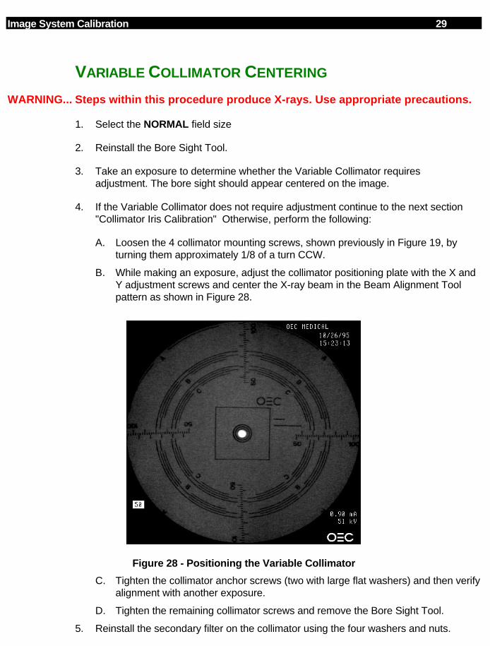
Image System Calibration 29
VARIABLE COLLIMATOR CENTERING
WARNING... Steps within this procedure produce X-rays. Use appropriate precautions.
1. Select the NORMAL field size
2. Reinstall the Bore Sight Tool.
3. Take an exposure to determine whether the Variable Collimator requiresadjustment. The bore sight should appear centered on the image.
4. If the Variable Collimator does not require adjustment continue to the next section"Collimator Iris Calibration" Otherwise, perform the following:
A. Loosen the 4 collimator mounting screws, shown previously in Figure 19, byturning them approximately 1/8 of a turn CCW.
B. While making an exposure, adjust the collimator positioning plate with the X andY adjustment screws and center the X-ray beam in the Beam Alignment Toolpattern as shown in Figure 28.
Figure 28 - Positioning the Variable Collimator
C. Tighten the collimator anchor screws (two with large flat washers) and then verifyalignment with another exposure.
D. Tighten the remaining collimator screws and remove the Bore Sight Tool.
5. Reinstall the secondary filter on the collimator using the four washers and nuts.
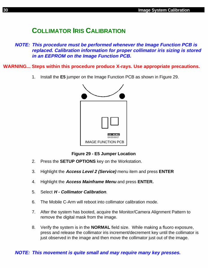
30 Image System Calibration
COLLIMATOR IRIS CALIBRATION
NOTE: This procedure must be performed whenever the Image Function PCB isreplaced. Calibration information for proper collimator iris sizing is storedin an EEPROM on the Image Function PCB.
WARNING... Steps within this procedure produce X-rays. Use appropriate precautions.
1. Install the E5 jumper on the Image Function PCB as shown in Figure 29.
E4 E5 E6 E7
IMAGE FUNCTION PCB
Figure 29 - E5 Jumper Location
2. Press the SETUP OPTIONS key on the Workstation.
3. Highlight the Access Level 2 (Service) menu item and press ENTER
4. Highlight the Access Mainframe Menu and press ENTER.
5. Select H - Collimator Calibration .
6. The Mobile C-Arm will reboot into collimator calibration mode.
7. After the system has booted, acquire the Monitor/Camera Alignment Pattern toremove the digital mask from the image.
8. Verify the system is in the NORMAL field size. While making a fluoro exposure,press and release the collimator iris increment/decrement key until the collimator isjust observed in the image and then move the collimator just out of the image.
NOTE: This movement is quite small and may require many key presses.
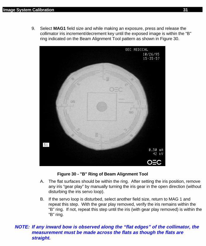
Image System Calibration 31
9. Select MAG1 field size and while making an exposure, press and release thecollimator iris increment/decrement key until the exposed image is within the “B”ring indicated on the Beam Alignment Tool pattern as shown in Figure 30.
Figure 30 - "B" Ring of Beam Alignment Tool
A. The flat surfaces should be within the ring. After setting the iris position, removeany iris “gear play” by manually turning the iris gear in the open direction (withoutdisturbing the iris servo loop).
B. If the servo loop is disturbed, select another field size, return to MAG 1 andrepeat this step. With the gear play removed, verify the iris remains within the“B” ring. If not, repeat this step until the iris (with gear play removed) is within the“B” ring.
NOTE: If any inward bow is observed along the “flat edges” of the collimator, themeasurement must be made across the flats as though the flats arestraight.
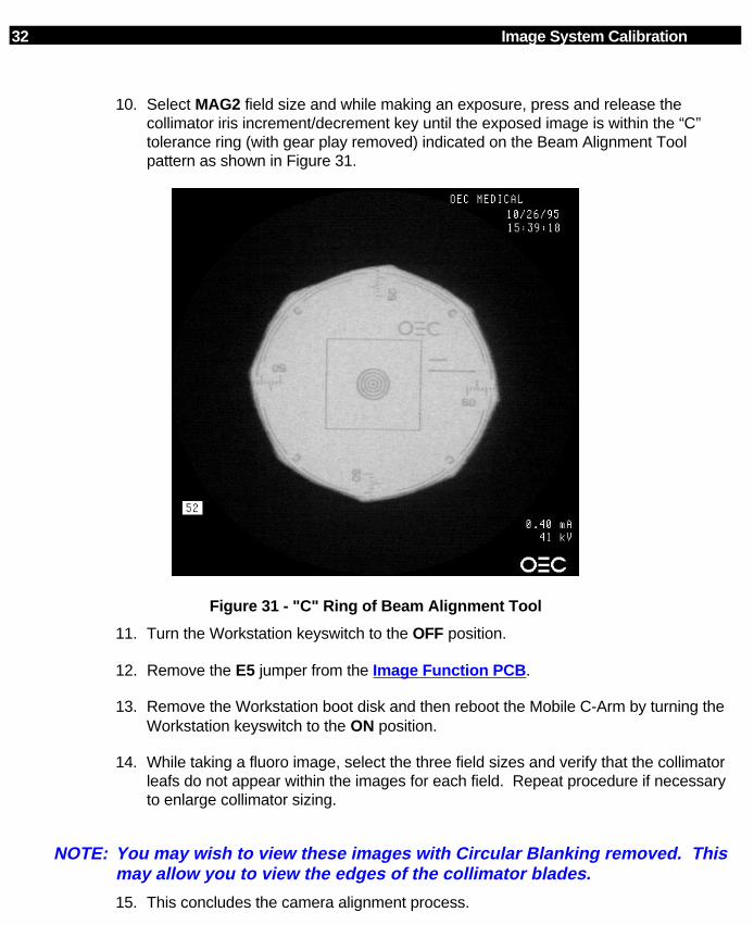
32 Image System Calibration
10. Select MAG2 field size and while making an exposure, press and release thecollimator iris increment/decrement key until the exposed image is within the “C”tolerance ring (with gear play removed) indicated on the Beam Alignment Toolpattern as shown in Figure 31.
Figure 31 - "C" Ring of Beam Alignment Tool
11. Turn the Workstation keyswitch to the OFF position.
12. Remove the E5 jumper from the Image Function PCB .
13. Remove the Workstation boot disk and then reboot the Mobile C-Arm by turning theWorkstation keyswitch to the ON position.
14. While taking a fluoro image, select the three field sizes and verify that the collimatorleafs do not appear within the images for each field. Repeat procedure if necessaryto enlarge collimator sizing.
NOTE: You may wish to view these images with Circular Blanking removed. Thismay allow you to view the edges of the collimator blades.
15. This concludes the camera alignment process.

Image System Calibration 33
BEAM ALIGNMENT VERIFICATION1. Insert a film cassette into the Beam Alignment Tool.
2. Select MANUAL FLUORO mode.
3. Select the NORMAL field size and set the technique to 50 kVp @ 0.5 mA. Pressthe X-ray ON key for 2 seconds.
4. Select MAG 1 field size and press the X-ray ON key for 2 seconds.
5. Select MAG 2 field size and press the X-ray ON key for 2 seconds.
6. Manually collimate to the minimum field size and press the X-ray ON key for 2seconds.
7. Develop the film and confirm the field sizes match the following specifications:
FIELD SIZE RANGE9" mode (NORMAL) A
6" mode (MAG1) B4" mode (MAG2) C
8. Verify that the minimum field size is less than 5 cm2.
9. Use a ruler and verify the center of the image is centered on the sheet of film (inboth the X and Y axis) within 20 mm or 13/16”.
10. Verify the line pair resolution.
FIELD SIZE 60 Hz lp/mm 50 Hz lp/mmNORMAL 1.4 1.2
MAG1 2.0 1.7MAG2 2.4 2.0
11. Send the films to OEC Medical Systems, Inc. Attention: Technical Support, 384Wright Brothers Drive, Salt Lake City, UT. 84116.
12. Remove the Beam Alignment Tool.

34 Image System Calibration
CAMERA IRIS CALIBRATION (LONG METHOD)1. Set the camera gain to minimum by:
A. In NORMAL field size, select MANUAL FLUORO mode with a technique of 80kVp @ 3 mA.
B. Make an exposure for approximately 3 seconds.
C. Press the TECH LOCK switch. This freezes the camera gain at minimum.
D. Verify the “CAM GAIN” output on the Analog Interface is 0.0 VDC ñ 0.1 VDC.
2. Place the dosimeter's ion chamber (150 cc only) in the center and on the surface ofthe Image Intensifier contrast grid.
3. Establish a reference radiation level by:
A. Placing a 1 mm copper plate near the X-ray Tube (in the beam path).
B. Set the technique to 72 kVp and adjust the mA as required to achieve a radiationlevel of 12.0 mR/minute.
NOTE: The mA is typically 1.2 mA @ 72 kVp. However, varying kVp may help inachieving this level accurately, but stay between 69 and 75 kVp.
4. Set the iris and the open iris stop, as shown in Figure 32, to produce 600 mV ofvideo for the reference radiation level as follows:
A. Using a 0.048” spline driver, loosen both iris stops. This will allow a full range ofadjustment.
STOP PIN
CLOSEDSTOP
BRASSGEAR
IRIS MOTOR GEAR
IRIS POT GEAR
SET SCREW
SETSCREW
OPENSTOP
END VIEW
BRASSGEAR
SETSCREW
STOP PIN
SIDE VIEW
OPENSTOP
CLOSEDSTOP
Figure 32 - Camera Iris Locations
B. While making an exposure adjust the lens iris to produce 600 mV (blanking topeak) video at TP10 on the Video Switching PCB.

Image System Calibration 35
C. Swing the "open iris" stop against the stop pin and tighten and Loctite 222 theset screw. Do not over-tighten the set screw. Check gears to make sure theymove easily.
5. Increase the radiation level to 48.0 mR/minute (4 x the reference radiation levelpreviously established):
A. While taking an exposure increase the mA to produce a radiation level of 48.0mR/minute.
B. If maximum mA is reached the kVp may be increased slightly but must notexceed 75 kVp.
6. Set the iris and “closed iris stop” to produce 600 mV of video:
A. While taking an exposure adjust the iris to produce 600 mV of video (blanking topeak) at TP10 on the Video Switching PCB.
B. Swing the "closed iris" stop against the stop pin and tighten and Loctite 222 theset screw. Do not over-tighten the set screw. Check gears to make sure theymove easily.
7. Manually open the iris back to the "open iris" stop position.
8. Verify proper kV tracking by placing 1 mm copper filters (OEC P/N 00-877682-01) inthe beam (under collimator). The following specifications must be met:
1 copper filter = 60 kV ± 3kV
2 copper filters = 70kV ± 3kV
3 copper filters = 78kV ± 3kV
NOTE: After completing this alignment, proceed to the Pixel/Column FilterAdjustment section.

36 Image System Calibration
CAMERA IRIS CALIBRATION (SHORT METHOD)
NOTE: This method may be used instead of the "Long Method" as long as theconfidence tests are successful.
Confidence Tests
The confidence tests confirms the radiation output of the system (and therefore theaccuracy of the generator's kV and mA circuits) and also the functionality of the ABSloop. Perform the confidence tests as described on this page.
VERIFY ENTRANCE EXPOSURE
1. Place a lead apron over the II.
2. Place an Ion Chamber 12" (30 cm) above and centered in the II.
3. In the MANUAL FLUORO mode, select 120 kVp & maximum available mA.
4. Verify the radiation output is ≅ 4.6 R/min using a 5R ABS table for system serialnumbers 69-0001 to 69-1160, or verify the radiation output is less than 9.26 R/minusing a 10R ABS table for system serial numbers 69-1161 or higher.
NOTE: If this radiation level is not met, refer to the Entrance Exposure procedure.This may be out of adjustment and/or may indicate the generator is out ofcalibration.
VERIFY AUTO GAIN
1. Selecting the AUTO FLUORO mode with Auto Histo OFF. Make an exposure andallow the image to stabilize.
2. Select MANUAL FLUORO and select TECH LOCK to turn it ON.
3. Make an exposure and verify that the image stays the same.
4. Reduce the mA by one-half the current value and make an exposure. Observe theimage becomes darker.
5. Select TECH LOCK to turn it OFF.
6. Make an exposure and confirm the image returns to normal brightness.
NOTE: If not, verify the ABS loop is functioning by examining camera adjustments(VLI & Camera Gain) to and from the generator.
This concludes the confidence tests. Proceed to the next page to beginthe short method.
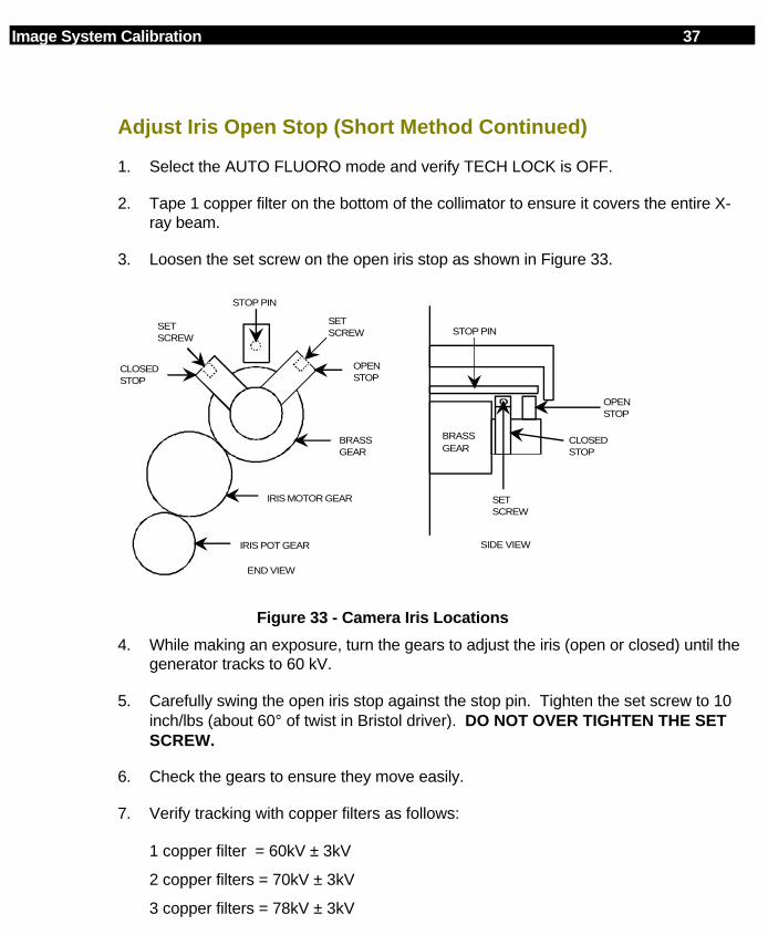
Image System Calibration 37
Adjust Iris Open Stop (Short Method Continued)
1. Select the AUTO FLUORO mode and verify TECH LOCK is OFF.
2. Tape 1 copper filter on the bottom of the collimator to ensure it covers the entire X-ray beam.
3. Loosen the set screw on the open iris stop as shown in Figure 33.
STOP PIN
CLOSEDSTOP
BRASSGEAR
IRIS MOTOR GEAR
IRIS POT GEAR
SET SCREW
SETSCREW
OPENSTOP
END VIEW
BRASSGEAR
SETSCREW
STOP PIN
SIDE VIEW
OPENSTOP
CLOSEDSTOP
Figure 33 - Camera Iris Locations
4. While making an exposure, turn the gears to adjust the iris (open or closed) until thegenerator tracks to 60 kV.
5. Carefully swing the open iris stop against the stop pin. Tighten the set screw to 10inch/lbs (about 60° of twist in Bristol driver). DO NOT OVER TIGHTEN THE SETSCREW.
6. Check the gears to ensure they move easily.
7. Verify tracking with copper filters as follows:
1 copper filter = 60kV ± 3kV
2 copper filters = 70kV ± 3kV
3 copper filters = 78kV ± 3kV
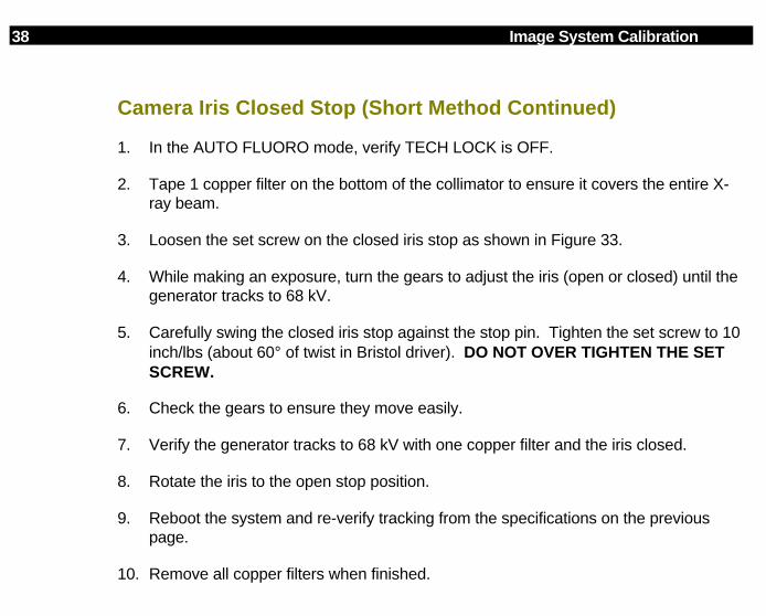
38 Image System Calibration
Camera Iris Closed Stop (Short Method Continued)
1. In the AUTO FLUORO mode, verify TECH LOCK is OFF.
2. Tape 1 copper filter on the bottom of the collimator to ensure it covers the entire X-ray beam.
3. Loosen the set screw on the closed iris stop as shown in Figure 33.
4. While making an exposure, turn the gears to adjust the iris (open or closed) until thegenerator tracks to 68 kV.
5. Carefully swing the closed iris stop against the stop pin. Tighten the set screw to 10inch/lbs (about 60° of twist in Bristol driver). DO NOT OVER TIGHTEN THE SETSCREW.
6. Check the gears to ensure they move easily.
7. Verify the generator tracks to 68 kV with one copper filter and the iris closed.
8. Rotate the iris to the open stop position.
9. Reboot the system and re-verify tracking from the specifications on the previouspage.
10. Remove all copper filters when finished.
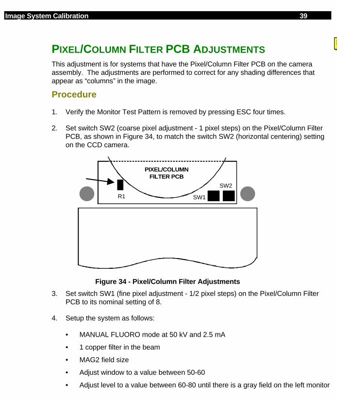
Image System Calibration 39
PIXEL/COLUMN FILTER PCB ADJUSTMENTSThis adjustment is for systems that have the Pixel/Column Filter PCB on the cameraassembly. The adjustments are performed to correct for any shading differences thatappear as “columns” in the image.
Procedure
1. Verify the Monitor Test Pattern is removed by pressing ESC four times.
2. Set switch SW2 (coarse pixel adjustment - 1 pixel steps) on the Pixel/Column FilterPCB, as shown in Figure 34, to match the switch SW2 (horizontal centering) settingon the CCD camera.
PIXEL/COLUMNFILTER PCB
R1 SW1
SW2
Figure 34 - Pixel/Column Filter Adjustments
3. Set switch SW1 (fine pixel adjustment - 1/2 pixel steps) on the Pixel/Column FilterPCB to its nominal setting of 8.
4. Setup the system as follows:
• MANUAL FLUORO mode at 50 kV and 2.5 mA
• 1 copper filter in the beam
• MAG2 field size
• Adjust window to a value between 50-60
• Adjust level to a value between 60-80 until there is a gray field on the left monitor
NOTE
Click on a yellow box to go directly to the block diagram for this section. Do not use this link to return to a block diagram from this point. Click on the << button in the Tool Bar to return to any starting point.
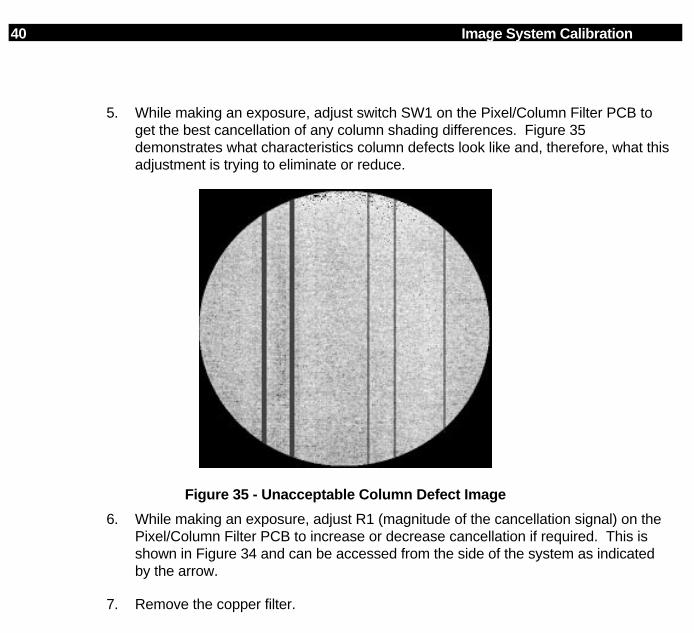
40 Image System Calibration
5. While making an exposure, adjust switch SW1 on the Pixel/Column Filter PCB toget the best cancellation of any column shading differences. Figure 35demonstrates what characteristics column defects look like and, therefore, what thisadjustment is trying to eliminate or reduce.
Figure 35 - Unacceptable Column Defect Image
6. While making an exposure, adjust R1 (magnitude of the cancellation signal) on thePixel/Column Filter PCB to increase or decrease cancellation if required. This isshown in Figure 34 and can be accessed from the side of the system as indicatedby the arrow.
7. Remove the copper filter.
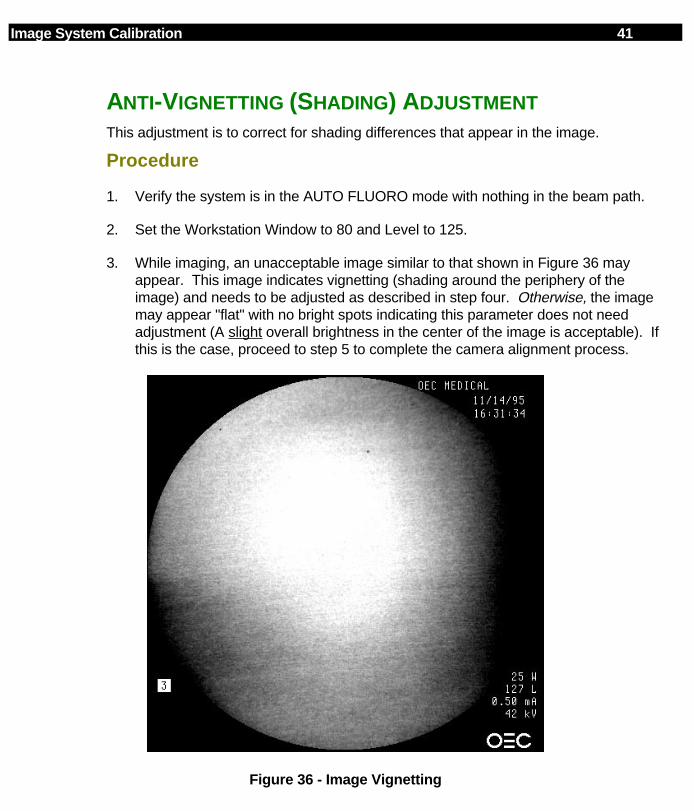
Image System Calibration 41
ANTI-VIGNETTING (SHADING) ADJUSTMENTThis adjustment is to correct for shading differences that appear in the image.
Procedure
1. Verify the system is in the AUTO FLUORO mode with nothing in the beam path.
2. Set the Workstation Window to 80 and Level to 125.
3. While imaging, an unacceptable image similar to that shown in Figure 36 mayappear. This image indicates vignetting (shading around the periphery of theimage) and needs to be adjusted as described in step four. Otherwise, the imagemay appear "flat" with no bright spots indicating this parameter does not needadjustment (A slight overall brightness in the center of the image is acceptable). Ifthis is the case, proceed to step 5 to complete the camera alignment process.
Figure 36 - Image Vignetting
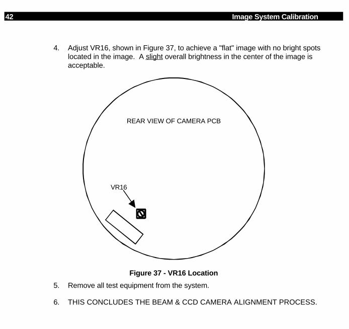
42 Image System Calibration
4. Adjust VR16, shown in Figure 37, to achieve a "flat" image with no bright spotslocated in the image. A slight overall brightness in the center of the image isacceptable.
VR16
REAR VIEW OF CAMERA PCB
Figure 37 - VR16 Location
5. Remove all test equipment from the system.
6. THIS CONCLUDES THE BEAM & CCD CAMERA ALIGNMENT PROCESS.
WORKSTATION CONTROL
OVERVIEWThis section includes all the printed circuit cards and assemblies that have beendesigned to perform a Workstation control function or that support such a function. Thecircuit boards and signals used in the control or processing of video signals arediscussed in the Video Path and Video Control sections of the manual.
Refer to Figure 1 for an overview of control signal flow and serial communications.
The information given in this section is most easily understood while using the followingschematics. Use the correct interconnect diagrams and circuit board schematics foryour system.
• • 9600 Workstation Interconnect
Schematic # 00-876158 - System serial numbers 69-0001 thru 69-1000Schematic # 00-877970 - System serial numbers 69-1001 and higher
• • Auxiliary Interface PCB
Schematic # 00-876502 - All serial numbers
• • Communications PCB
Schematic # 00-872125 - All serial numbers
• • Control Panel Processor PCB
Schematic # 00-876611 - All serial numbers
• • IR Transmitter PCB
Schematic # 00-873936
• • IR Receiver PCB
Schematic # 00-874220
NOTE
Click on a yellow box to go directly to the block diagram for this section. Do not use this link to return to a block diagram from this point. Click on the << button in the Tool Bar to return to any starting point.
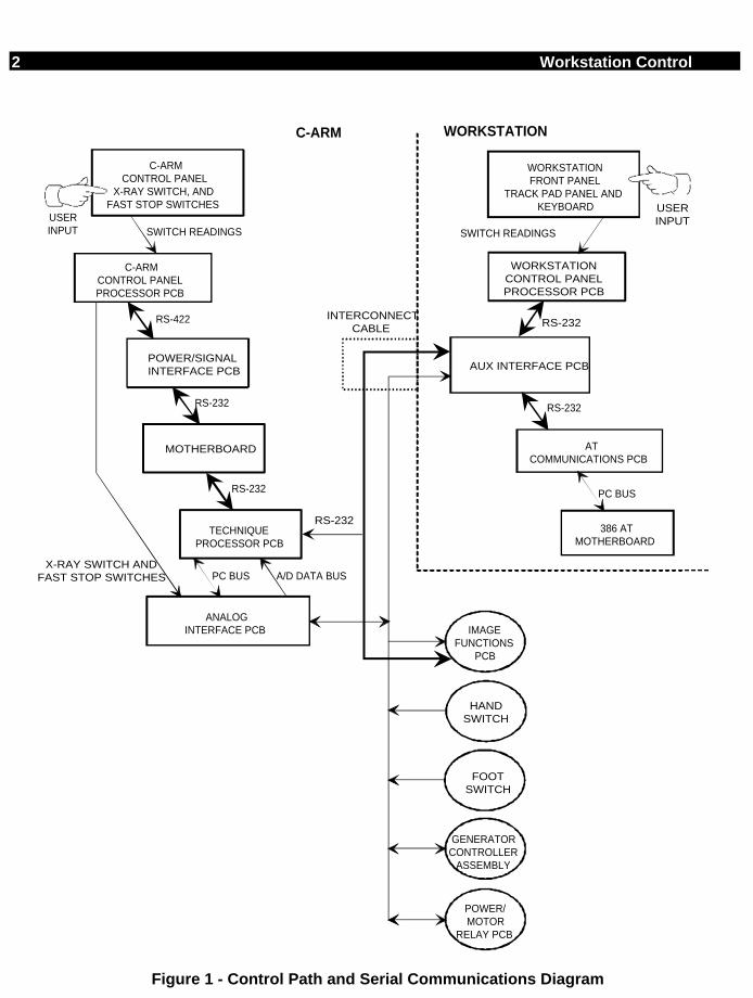
2 Workstation Control
TECHNIQUE PROCESSOR PCB
USERINPUT SWITCH READINGS
ANALOGINTERFACE PCB
PC BUS
GENERATORCONTROLLER
ASSEMBLY
FOOTSWITCH
HANDSWITCH
A/D DATA BUS
POWER/MOTOR
RELAY PCB
X-RAY SWITCH ANDFAST STOP SWITCHES
MOTHERBOARD
USERINPUT
SWITCH READINGS
C-ARM CONTROL PANEL
X-RAY SWITCH, ANDFAST STOP SWITCHES
C-ARMCONTROL PANELPROCESSOR PCB
WORKSTATIONFRONT PANEL
TRACK PAD PANEL ANDKEYBOARD
WORKSTATIONCONTROL PANELPROCESSOR PCB
AUX INTERFACE PCB
386 ATMOTHERBOARD
AT COMMUNICATIONS PCB
IMAGEFUNCTIONS
PCB
PC BUS
RS-422
RS-232
RS-232
RS-232
RS-232
RS-232
C-ARM WORKSTATION
INTERCONNECTCABLE
POWER/SIGNALINTERFACE PCB
Figure 1 - Control Path and Serial Communications Diagram

Workstation Control 3
CONTROL PANEL ASSEMBLYThe Control Panel Assembly includes the following components (see Figure 2):
• Front Panel
• Trackpad
• Keyboard
• Control Panel Processor PCB
Refer to the System Overview section of the manual for disassembly of the ControlPanel Assembly.
Figure 2 - Workstation Control Panel Assembly

4 Workstation Control
FRONT PANEL
The following functions are controlled from the Front Panel Switches:
• Averaging
• Fluoro
• One-shot
• Enhanced One-shot(Digital Spot)
• Recall
• Save
• L<>R
This panel cannot be repaired in the field. If problems arise, it must be replaced. Thedefective panel should be sent to the factory for repair. Refer to the Illustrated PartsManual for part numbers.
Diagnostics are included in the system software that allow testing of the front panelcontrols.
KEYBOARD
The QWERTY Keyboard is similar to the keyboard used on a computer, but containsspecially labeled keys that control system functions. The alpha-numeric keys are usedfor patient annotation and system control. A drawing of the QWERTY keyboard iscontained in the System Overview section of the manual.
This keyboard cannot be repaired in the field. If problems arise, it must be replaced. Thedefective keyboard should be sent to the factory for repair. Refer to the Illustrated PartsManual for part numbers.
TRACK PAD
The Track Pad contains function keys for control of system operations, along with aforce-sensitive-resistor array (FSR) analog interface that acts as an electronic trackball.Drawings of the Track Pad Panels are contained in the System Overview section of themanual.
This panel cannot be repaired in the field. If problems arise, it must be replaced. Thedefective panel should be sent to the factory for repair. Refer to the Illustrated PartsManual for part numbers.
The Track Pad Panel contains buttons which control specific system operations. Apressure-sensitive Track Pad is used to control cursor movement on the monitorscreens. Diagnostics are included in the system software that allow testing of theTrackPad panel.

Workstation Control 5
CONTROL PANEL PROCESSOR PCB
Microprocessor
U5 is an 80C196KC microcontroller running at 12Mhz. Y1 is the crystal oscillatorproviding the 12MHz clock signal. This can be measured at TP11.
U24 and associated circuitry comprise a watchdog circuit driven from microcontroller U5,pin 20. This line must be toggled every 1.6 seconds to keep the watchdog from timingout and issuing a reset to the microcontroller. Power monitor U24 is also used as a resetgenerator to monitor the +5 volt supply to microcontroller U5. The reset output is heldlow when the +5 supply is less than approximately 4.65 volts. This low will generate areset to microcontroller U5 and also PAL U4.
U13 is a four channel push-pull driver used to drive an externally mounted piezo-electric tone generator. It is driven from microcontroller U5 pin 28 through inverter U11pin 12.
A beep is sounded when the Boot process is complete and the Control Panel InterfacePCB, QWERTY keyboard, front panel, and TrackPad panel are successfully enabled.
Memory and Addressing
PAL U4, and latches U2 and U14 are used for address decoding.
U10 is the boot EPROM (32K bytes) containing the code for microcontroller U5.
U1 is read and write Static RAM .
Control Inputs and LEDs
The Control Panel Processor PCB receives command and text signals from the:
• QWERTY Keyboard
• Track Pad Panel
• Front Panel
The force sensitive resistor (FSR) on the Track Pad pointing device provides four analogsignals (S, E, N, W). These signals are input directly to microcontroller U5.
The microprocessor scans the Qwerty Keyboard, Front Panel keys, and Track PadPanel keys through the row output latches U18 and U22. The microprocessor detectswhich switch is pressed through keyboard column input latches U15 and U23. Softwarecontinuously scans the keypad to determine if any keys have been pressed.
NOTE
Click on a yellow box to go directly to the block diagram for this section. Do not use this link to return to a block diagram from this point. Click on the << button in the Tool Bar to return to any starting point.

6 Workstation Control
U20 & 21, U12, 16, 17, & 19 are octal latches used to sink LED currents. Writing an "0"to the appropriate bit will turn the addressed LED on. U20 & 21 are used to control theLEDs on DS1 which is a diagnostic/status bargraph. U12, 16, 17, & 19 are used tocontrol the LEDs on the Track panel and the Front panel. R29, 30, 37, 36, 28, & 24 arecurrent limiting resistors for the LEDs.
Serial Communications
As the Control Panel Processor PCB receives instructions from the Keyboard, FrontPanel, and Track Pad panel, it sends data to the 386 AT Motherboard via U7, an RS232serial transceiver. These signals then pass through the Auxiliary Interface PCB to theAT Communications PCB where they are received by DUART U27. U27 then places theinformation on the 386 AT Motherboard data bus. The Motherboard passes instructionsback through DUART U27 to the appropriate circuit board.
E2-E5 are jumpers to configure the serial communications signals for either RS422 orRS232. They are presently configured for RS232.
Diagnostic Bargraph
DS1 is a diagnostic bargraph used to indicate various operating conditions in theWorkstation. Refer to the Workstation Software section for details.
Infrared Input
U9 is an opto-isolator that receives IR signals from the IR Receiver PCB. The output ofU9 passes through AND gate U3 and is then input to microcontroller U5 at pin 15. Theincoming infrared signals can be measured at test point TP5. Refer to the InfraredTransmitter/Receiver heading in this section for details.
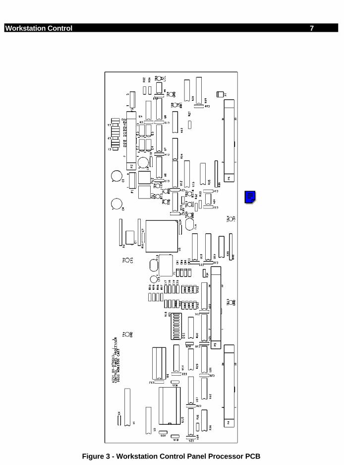
Workstation Control 7
Figure 3 - Workstation Control Panel Processor PCB
NOTE
Click in the blue box to go directly to the Electrical Schematic Diagram for the PCB shown on this page. Click the << button on the Tool Bar to return to this page.

8 Workstation Control
AT COMMUNICATIONS PCB
386 ATMOTHERBOARD
AUXILIARYINTERFACE PCB
ELAPSED TIMEMETER
ELAPSED TIMEMETER
FAN (2)
FAN GUARD (2)
Figure 4 - Workstation Electronics Box
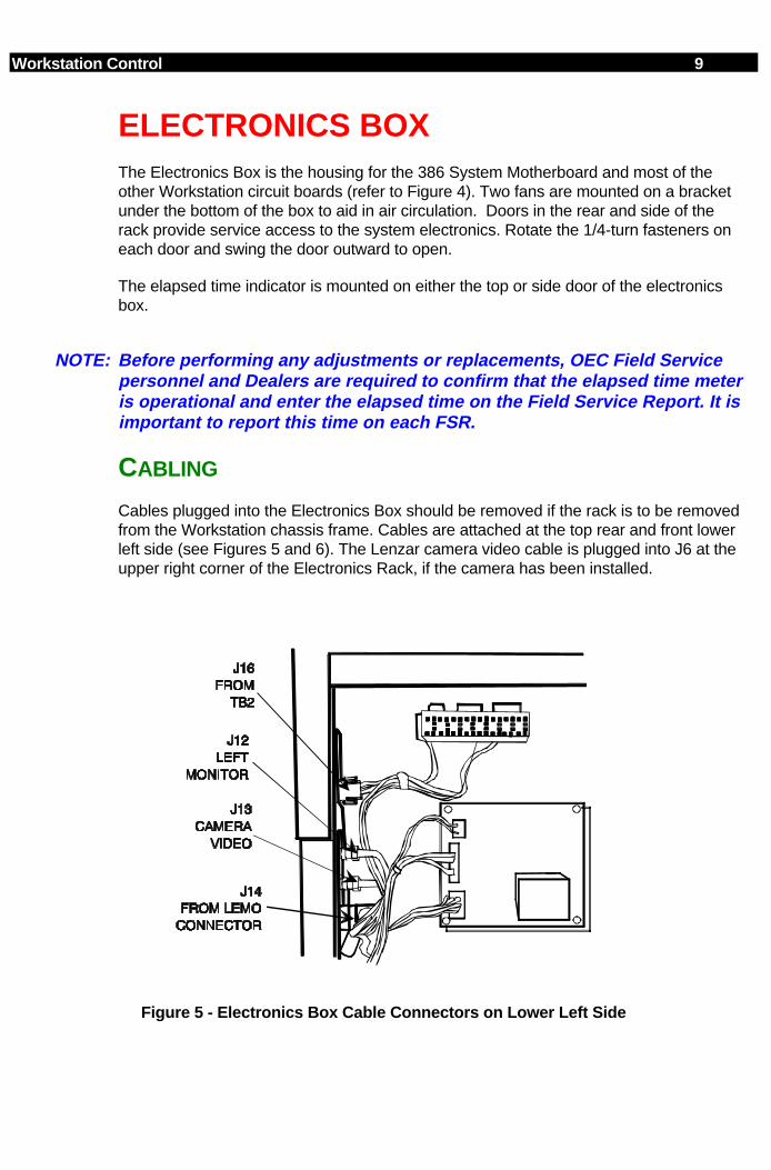
Workstation Control 9
ELECTRONICS BOXThe Electronics Box is the housing for the 386 System Motherboard and most of theother Workstation circuit boards (refer to Figure 4). Two fans are mounted on a bracketunder the bottom of the box to aid in air circulation. Doors in the rear and side of therack provide service access to the system electronics. Rotate the 1/4-turn fasteners oneach door and swing the door outward to open.
The elapsed time indicator is mounted on either the top or side door of the electronicsbox.
NOTE: Before performing any adjustments or replacements, OEC Field Servicepersonnel and Dealers are required to confirm that the elapsed time meteris operational and enter the elapsed time on the Field Service Report. It isimportant to report this time on each FSR.
CABLING
Cables plugged into the Electronics Box should be removed if the rack is to be removedfrom the Workstation chassis frame. Cables are attached at the top rear and front lowerleft side (see Figures 5 and 6). The Lenzar camera video cable is plugged into J6 at theupper right corner of the Electronics Rack, if the camera has been installed.
Figure 5 - Electronics Box Cable Connectors on Lower Left Side
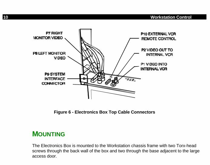
10 Workstation Control
Figure 6 - Electronics Box Top Cable Connectors
MOUNTING
The Electronics Box is mounted to the Workstation chassis frame with two Torx-headscrews through the back wall of the box and two through the base adjacent to the largeaccess door.
Workstation Control 11
AUXILIARY INTERFACE PCBAssy. # 00-876504 - Sch. # 00-876502
The Auxiliary Interface PCB is a primary connection and distribution point for signalswithin the Workstation. The connector side (see Figure 8 ) of the circuit board providesexternal connection points at the rear panel of the Workstation.
CONNECTORS
The following table outlines the cabling connections on the Auxiliary Interface PCB:
AuxiliaryInterface
PCBConnector
Signal(s)
P1 Camera Video Output to J6 on Video Switching PCB, from P10(Aux Int.), from C-Arm
P2 not usedP3 Parallel Printer Interface from AT Communications PCB (P4),
to P18 (Aux Interface PCB)P4 not usedP5 COM 2 Communications Port on Rear Panel, from P13 (Aux
Interface PCB), from AT Communications PCB (P5)P6 Room Interface Connection on Rear PanelP7 VCR Serial Interface (optional)P8 To X-ray On LED array on top of Workstation via J9/P9 and
J11/P11P9 Connects to J8 on Video Switching PCB, interface for
“XRAYDIS1*” and “STORE*” signalsP10 Connecting point for interconnect cable (signals) from C-ArmP11 DC Power for Aux Interface PCB from DC Power Distribution
PCBP12 Connection to Workstation Control Panel Processor PCBP13 Connects to P5 on AT Communications PCB, for COM 1, COM
2, and drive signals for diagnostic LEDs (U3 and U4) on AuxInterface PCB

12 Workstation Control
AuxiliaryInterface
PCBConnector
Signal(s)
P14 Connects to P3 on AT Communications PCB, for VCRcontrols, Serial Communications, other discrete signals
P15 VCR control signals, connects to internal VCRP16 VCR control signals, connects to Rear Panel for external VCRP17 COM 1 Communications Port on Rear Panel, from P13 (Aux
Interface PCB), from AT Communications PCB (P5)P18 Parallel printer connection on Rear Panel, to P3 (Aux Interface
PCB), to AT Communications (P4)P19 Video to/from Video Switching PCB for external VCR (VCR 2)P20 Video from external VCR (VCR 2) to Video Switching PCB via
P19 (Aux Interface PCB)P21 Video to external VCR (VCR 2) from Video Switching PCB via
P19 (Aux Interface PCB)
Table 1 - Auxiliary Interface PCB Connectors
K1 - K4 ROOM INTERFACE RELAYS
Relays K1-K4 are provided to interface an “X-ray On Light” and “Room In Use Light.”Call the OEC Tech Support office for more information.
X-RAY ON LED ARRAY DRIVER
The LED array on top of the Workstation illuminates when X-rays are being produced.The signal “X-RAY LAMP” (active Low) from the Power/Motor Relay PCB on the C-Arm is interfaced to the Aux Interface PCB via the interconnect cable. “X-RAY LAMP”enters inverter U1 pin 3 on the Aux Interface PCB. The output at pin 4 (active HI) turnson Q1, which provides a return path for the LED array current. The power for the array is+5V, jumpered through E3 pins 2 and 3.
WARNING... Damage to the LED array will occur if E3 pins 1 to 2 are jumpered together.
BOOT AND DIAGNOSTIC LEDS
LED displays U3 (MSB) and U4 (LSB) provide boot and diagnostic codes from the 386AT Motherboard on the Workstation. They are driven from the AT Motherboard via theAT Communications PCB. Refer to the Workstation Software section for a listing ofthese codes.
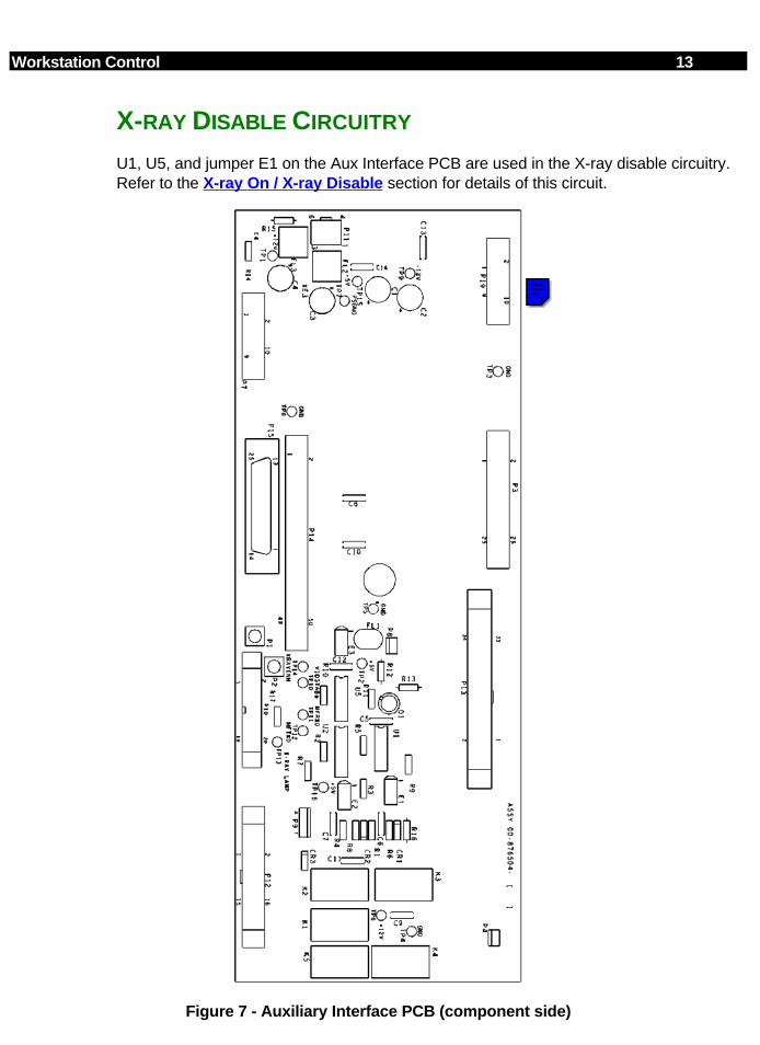
Workstation Control 13
X-RAY DISABLE CIRCUITRY
U1, U5, and jumper E1 on the Aux Interface PCB are used in the X-ray disable circuitry.Refer to the X-ray On / X-ray Disable section for details of this circuit.
Figure 7 - Auxiliary Interface PCB (component side)
NOTE
Click in the blue box to go directly to the Electrical Schematic Diagram for the PCB shown on this page. Click the << button on the Tool Bar to return to this page.
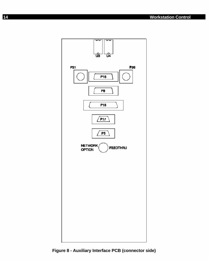
14 Workstation Control
Figure 8 - Auxiliary Interface PCB (connector side)
Workstation Control 15
COMMUNICATIONS PCBAssy. #00-872127 - Sch. #00-872125
The Communications PCB provides serial and parallel communications capabilities forthe Motherboard with external devices, such as a printer. Internal systemcommunications with the Control Panel Processor PCB and the C-Arm are also handledby the PCB. The circuit board plugs directly into the AT Motherboard (see Figure 4 ).
SERIAL COMMUNICATIONS
The Communications PCB handles all of the serial communications for the ATMotherboard to the Workstation Control Panel Processor PCB and the C-Arm.
AT Motherboard to Control Panel Processor
Signals from the 386 AT Motherboard are received by DUART U27 on the ATCommunications PCB via the data bus. U27 converts this information to RS232 serialdata. The serial data then passes through the Aux Interface PCB, through RS232transceiver U7 on the Control Panel Processor and to microcontroller U5. MicrocontrollerU5 on the Control Panel Processor PCB communicates over the same path to the ATMotherboard
UART U26 on the AT Motherboard handles discrete signals for the room interface relayson the Aux Interface PCB when they are used.
AT Motherboard to C-Arm
Communication between the C-Arm and Workstation is established during the bootprocess. All 20 arrows will be displayed on the Control Panel Display, as shown below,during this part of the boot process.
During normal operation, the Technique Processor and 386 AT Motherboard sendinformation such as:
• Shot log file information from the C-Arm to the Workstation
• Commands such as L>R, SAVE and CART MODE from the Control Panel to theWorkstation
• “Enable Boost” command to the C-Arm when (CHOLE)/DIGITAL SPOT is selected onthe Workstation
The TXD and RTS signals from Port B of the serial communications controller U39 onthe Technique Processor PCB are sent to the 386 AT Motherboard on the Workstation.They pass through RS232 driver/receiver U52 on the Technique Processor PCB andthen pass through the Mainframe Motherboard, the Interconnect cable, and enter the
16 Workstation Control
Aux Interface PCB in the Workstation. They pass through the Aux Interface PCB to theAT Communications PCB where they are inverted by U15 and enter DUART U27. U27interfaces the signals to the data bus of the AT Motherboard.
The 386 AT Motherboard communicates over the data bus to DUART U27 on the ATCommunications PCB. TXDA (pin 30) and RTS (pin 29) leave DUART U27, passthrough RS232 line driver U16 and leave the AT Communications PCB at P3. Theythen pass through the Aux Interface PCB, the Interconnect Cable and enter the C-Armat J1 on the Power Panel. They pass through the Mainframe Motherboard and enter theTechnique Processor PCB at P2.
On the older Technique Processor PCB (Assy. #876735) the signals then pass throughRS232 driver/receiver U52 and are received by serial communications controller U39 atpins 8 (RXD) and 23 (CTS).
On the newer Technique Processor PCB (Assy. #877744) the signals then pass throughRS232 driver/receiver U52 and COM SELECT GAL U38 and are received by serialcommunications controller U39 at pins 8 (RXD) and 23 (CTS).
VCR CONTROLS
Control signals for the VCRs are interfaced to the AT Motherboard via the ATCommunications PCB at P3. Refer to the Peripherals section for details.
PARALLEL PRINTER INTERFACE
The port for a parallel printer is interfaced through the AT Communications PCB atconnector P4. Refer to the Peripherals section for details.
COM 1 AND COM 2 COMMUNICATION PORTS
COM 1 and COM 2 communication ports are currently not used on the 9600 system.
Workstation Control 17
OPTION PROM
Option PROM U25 on the Communications PCB is accessed by the AT Motherboardduring the boot process for information such as:
• CGA graphics driver software, used until the Image Processor PCB is initialized.
• CMOS setup.
• OEC software signature stamp, if a diskette is found in the 3 1/2-inch floppy drive.
CLOCK
Oscillator Y1 and counter U36 provide clock signals for DUARTS U26 and U27 (3.6864MHz), UARTS U22 and U20 (1.8432 MHz), and the boot and diagnostic LEDs (230.4Khz) on the Aux Interface PCB.
JUMPERS E1, E2, E3
Jumpers E1, E2, and E3 on the AT Communications PCB are used to configure thesystem for the hard drive disk type installed in the Workstation. Refer to the ImageStorage section for details.
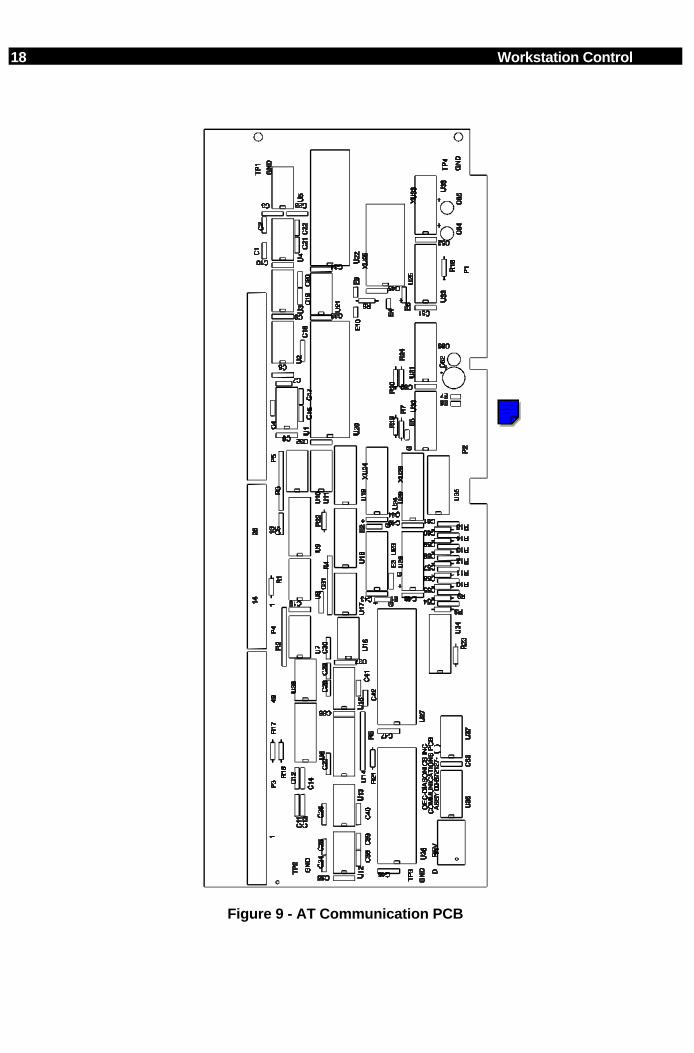
18 Workstation Control
Figure 9 - AT Communication PCB
NOTE
Click in the blue box to go directly to the Electrical Schematic Diagram for the PCB shown on this page. Click the << button on the Tool Bar to return to this page.

Workstation Control 19
386 AT MOTHERBOARDThe System 386 AT Motherboard contains the main system microprocessor. Itcommunicates with the following circuit boards:
• Image Processor PCB
• Communications PCB
These interface boards plug directly into connectors on the Motherboard.
386SX MB JUMPER SETTINGS
JUMPER POSITION DESCRIPTIONW1 1 - 2 COM 2/4 IRQW2 1 - 2 COM 1/3 IRQW3 1 - 2 FLASHW5 1 - 2 LPT IRQW4 2 - 3 COLOR/MONOW6 1 - 2 MICROSOFTW7 OFF MOUSE INTW8 1 - 2 CMOS RESETW9 1 - 2 FREQ SELW10 2 - 3 FREQ SELW11 1 - 2 CMOS BATTERY SEL
(EXTERNAL)
Table 2 - 386 AT Motherboard Jumper Settings
NOTE: The CMOS Battery Jumper, W11, must be in the 1-2 position for the 9600,due to use of an external battery (P/N 74-122854-00, 5.5V Alkaline). Theexternal battery is placed above the System 386 Motherboard and securedto the Electronics Box with double-sided tape.
NOTE
Click on a yellow box to go directly to the block diagram for this section. Do not use this link to return to a block diagram from this point. Click on the << button in the Tool Bar to return to any starting point.
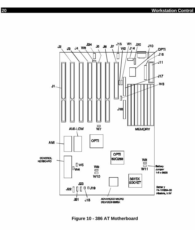
20 Workstation Control
Figure 10 - 386 AT Motherboard
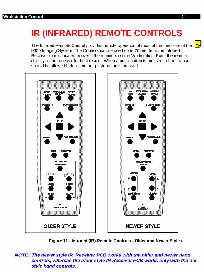
Workstation Control 21
IR (INFRARED) REMOTE CONTROLSThe Infrared Remote Control provides remote operation of most of the functions of the9600 Imaging System. The Controls can be used up to 20 feet from the InfraredReceiver that is located between the monitors on the Workstation. Point the remotedirectly at the receiver for best results. When a push-button is pressed, a brief pauseshould be allowed before another push-button is pressed.
AAAAAAAAAAAAAAAAAAAAAAAAAAAAAAAAAAAAAAAAAAAAAAAAAAAAAAAAAAAAAAAAAAAAAAAAAAAAAAAAAAAAAAAAAAAAAAAAAAAAAAAAAAAAAAAAAAAAAAAAAAAAAAAAAAAAAAAAAAAAAAAAAAAAAAAAAAAAAAAAAAAAAAAAAAAAAAAAAAAA
AAAAAAAAAAAAAAAAAAAAAAAAAAAAAAAAAAAAAAAAAAAAAAAAAAAAAAAAAAAAAAAAAAAAAAAAAAAAAAAAAAAAAAAAAAAAAAAAAAAAAAAAAAAAAAAAAAAAAAAAAAAAAAAAAAAAAAAAAAAAAAAAAAAAAAAAAAAAAAAAAAAAAAAAAAAAAAAAAAAA
AAAAAAAAAAAAAAAAAAAAAAAAAAAAAAAAAAAAAAAAAAAAAAAAAAAAAAAAAAAAAAAAAAAAAAAAAAAAAAAAAAAAAAAAAAAAAAAAAAAAAAAAAAAAAAAAAAAAAAAAAAAAAAAAAAAAAAAAAAAAAAAAAAAAAAAAAAAAAAAAAAAAAAAAAAAAAAAAAAAA
AAAAAAAAAAAAAAAAAAAAAAAAAAAAAAAAAAAAAAAAAAAAAAAAAAAAAAAAAAAAAAAAAAAAAAAAAAAAAAAAAAAAAAAAAAAAAAAAAAAAAAAAAAAAAAAAAAAAAAAAAAAAAAAAAAAAAAAAAAAAAAAAAAAAAAAAAAAAAAAAAAAAAAAAAAAAAAAAAAAA
AAAAAAAA
AAAAAAAA
AAAAAAAAAAAAAAAAAAAAAAAAAAAAAAAAAAAAAAAAAAAAAAAAAAAAAAAAAAAAAAAAAAAAAAAAAAAAAAAAAAAAAAAAAAAAAAAAAAAAAAAAAAAAAAAAAAAAAAAAAAAAAAAAAAAAAAAAAAAAAAAAAAAAAAAAAAAAAAAAAAAAAAAAAAAAAAAAAAAA
AAAAAAAAAAAAAAAAAAAAAAAAAAAAAAAAAAAAAAAAAAAAAAAAAAAAAAAAAAAAAAAAAAAAAAAAAAAAAAAAAAAAAAAAAAAAAAAAAAAAAAAAAAAAAAAAAAAAAAAAAAAAAAAAAAAAAAAAAAAAAAAAAAAAAAAAAAAAAAAAAAAAAAAAAAAAAAAAAAAA
AAAAAAAAAAAAAAAAAAAAAAAAAAAAAAAAAAAAAAAAAAAAAAAAAAAAAAAAAAAAAAAAAAAAAAAAAAAAAAAAAAAAAAAAAAAAAAAAAAAAAAAAAAAAAAAAAAAAAAAAAAAAAAAAAAAAAAAAAAAAAAAAAAAAAAAAAAAAAAAAAAAAAAAAAAAAAAAAAAAA
AAAAAAAAAAAAAAAAAAAAAAAAAAAAAAAAAAAAAAAAAAAAAAAAAAAAAAAAAAAAAAAAAAAAAAAAAAAAAAAAAAAAAAAAAAAAAAAAAAAAAAAAAAAAAAAAAAAAAAAAAAAAAAAAAAAAAAAAAAAAAAAAAAAAAAAAAAAAAAAAAAAAAAAAAAAAAAAAAAAA
Figure 11 - Infrared (IR) Remote Controls - Older and Newer Styles
NOTE: The newer style IR Receiver PCB works with the older and newer handcontrols, whereas the older style IR Receiver PCB works only with the oldstyle hand controls.
NOTE
Click on the yellow box to go directly to the block diagram for this section. Do not use this link to return to a block diagram from this point. Click on the << button in the Tool Bar to return to any starting point.
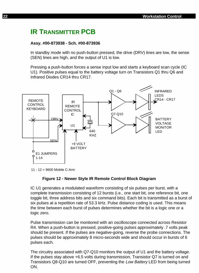
22 Workstation Control
IR TRANSMITTER PCB
Assy. #00-873938 - Sch. #00-873936
In standby mode with no push-button pressed, the drive (DRV) lines are low, the sense(SEN) lines are high, and the output of U1 is low.
Pressing a push-button forces a sense input low and starts a keyboard scan cycle (ICU1). Positive pulses equal to the battery voltage turn on Transistors Q1 thru Q6 andInfrared Diodes CR14 thru CR17.
REMOTE CONTROLKEYBOARD
IRREMOTE
CONTROLIC
BATTERYVOLTAGEMONITORLED
E1 JUMPERS1-14
SEN
DRV
640KHZ
+9 VOLTBATTERY
Q7-Q10
Q1 - Q6
11 - 12 = 9600 Mobile C-Arm
INFRAREDLEDSCR14 - CR17
U1
Figure 12 - Newer Style IR Remote Control Block Diagram
IC U1 generates a modulated waveform consisting of six pulses per burst, with acomplete transmission consisting of 12 bursts (i.e., one start bit, one reference bit, onetoggle bit, three address bits and six command bits). Each bit is transmitted as a burst ofsix pulses at a repetition rate of 53.3 kHz. Pulse distance coding is used. This meansthe time between each burst of pulses determines whether the bit is a logic one or alogic zero.
Pulse transmission can be monitored with an oscilloscope connected across ResistorR4. When a push-button is pressed, positive-going pulses approximately .7 volts peakshould be present. If the pulses are negative-going, reverse the probe connections. Thepulses should be approximately 8 micro-seconds wide and should occur in bursts of 6pulses each.
The circuitry associated with Q7-Q10 monitors the output of U1 and the battery voltage.If the pulses stay above +6.5 volts during transmission, Transistor Q7 is turned on andTransistors Q8-Q10 are turned OFF, preventing the Low Battery LED from being turnedON.
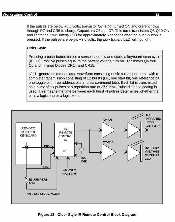
Workstation Control 23
If the pulses are below +6.5 volts, transistor Q7 is not turned ON and current flowsthrough R7 and CR5 to charge Capacitors C6 and C7. This turns transistors Q8-Q10 ONand lights the Low Battery LED for approximately 5 seconds after the push-button ispressed. If the pulses are below +3.5 volts, the Low Battery LED will not light.
Older Style
Pressing a push-button forces a sense input low and starts a keyboard scan cycle(IC U1). Positive pulses equal to the battery voltage turn on Transistors Q4 thruQ6 and Infrared Diodes CR14 and CR15.
IC U1 generates a modulated waveform consisting of six pulses per burst, with acomplete transmission consisting of 12 bursts (i.e., one start bit, one reference bit,one toggle bit, three address bits and six command bits). Each bit is transmittedas a burst of six pulses at a repetition rate of 37.9 Khz. Pulse distance coding isused. This means the time between each burst of pulses determines whether thebit is a logic one or a logic zero.
REMOTE CONTROLKEYBOARD
IRREMOTE
CONTROLIC
BATTERYVOLTAGEMONITORLED
E1 JUMPERS1-14
SEN
DRV
455KHZ
+9 VOLTBATTERY
Q7-Q10
Q4-Q6
13 - 14 = Mobile C-Arm
TOINFRAREDLEDS CR14 & 15
U1
Figure 13 - Older Style IR Remote Control Block Diagram
24 Workstation Control
BATTERY REPLACEMENT
1. A standard +9-volt alkaline battery is used by the Infrared remote control unit.
2. Remove the four screws securing the case of the control and lift off the rear half ofthe case from the front half.
3. Remove the 9-volt battery by unplugging the snap fasteners and replace it with anew battery.
4. Replace the cover and tighten the screws securely.
STRAPPING
NOTE: E1 jumpers 1-2 through 13-14 select the sub-system address whichdetermines if the unit is to operate with a C-Arm system or UroViewsystem.
For 9600 Mobile C-Arms jumper E1 11 - 12.
Older Style
For a 9600 Series Mobile C-Arm system, jumper E1 13-14.
Only one jumper should be placed on the E1 header.
Workstation Control 25
IR RECEIVER PCB
Assy. #00-874222 - Sch. #00-874220
The Infrared Receiver PCB consists primarily of IC U1, an infrared preamplifierconfigured as a narrow band amplifier. The Infrared Receiver PCB assembly is housedin a metal box that is located between the monitors on top of the Workstation.
Transmitted data from the IR Remote Control is detected by infrared diode CR3 and isapplied to the IR pre-amp U1-1. The negative going pulses of U1-9 are inverted bytransistor Q1 and applied to pin 1 of opto-isolator U9 on the Control Panel ProcessorPCB. These data pulses (measured at TP 5) are then sent to microcontroller U5 pin 15through AND gate U3. Microcontroller U5 then passes the data to the 386 ATMotherboard as discussed in the Control Panel Processor PCB serial communicationssection.
By tuning L2 and C8, the frequency of the IR receiver circuit is tuned to 53.3 Khz onnewer style controls and 37.9 Khz on older style controls.

26 Workstation Control
FUNCTIONAL TEST
1. From a distance greater than 20 ft press a push-button on the IR Remote anddetermine if the receiver has received the signal by watching the Workstationcontrol panel indicators.
NOTE: If the IR Remote doesn’t work at a distance greater than 20 feet but worksat a distance closer to the Workstation, a problem with the 9 Volt batterymay be indicated. The IR Remote can operate the system when the infraredbeam is bounced off ceilings, walls and other surfaces. If this effect is notnoted, it may indicate a problem with the infrared diodes or 9 Volt battery.If the +9 volt battery voltage drops to between 6.5 volts and 3.5 volts, theLow Battery LED will light for about 5 seconds after each push-buttonpress. If the battery is below 3.5 volts, the LED will not be illuminated andloss of remote infrared functions will occur.
2. Verify the push-buttons on the IR Remote operate with a definite clicking action. If abutton does not exhibit the click action, the internal dome could be collapsed. If thebutton is damaged, the entire unit keyboard must be replaced.
DIAGNOSTIC TEST
If a problem is suspected with a push-button, perform the following test:
1. Press the SETUP OPTIONS switch and select Access Level 2 (Service) .
2. Select Run System Diagnostics .
3. Select Front Panel Tests .
4. From a distance of twenty feet aim the transmitter at the receiver and press eachtransmitter switch. Verify that the value displayed on the right monitor equals thevalues listed:
Disk View = 52 Averaging Select = 28Acquire Images = 37 Image Dir = 7Play/process = 12 Recall = 10Registration = 26 Zoom = 25Sharpen = 2 Window/Level On/Off = 49Window = 0 - 80 Level = 0 - 80Auto Histo = 32 Negate = 40
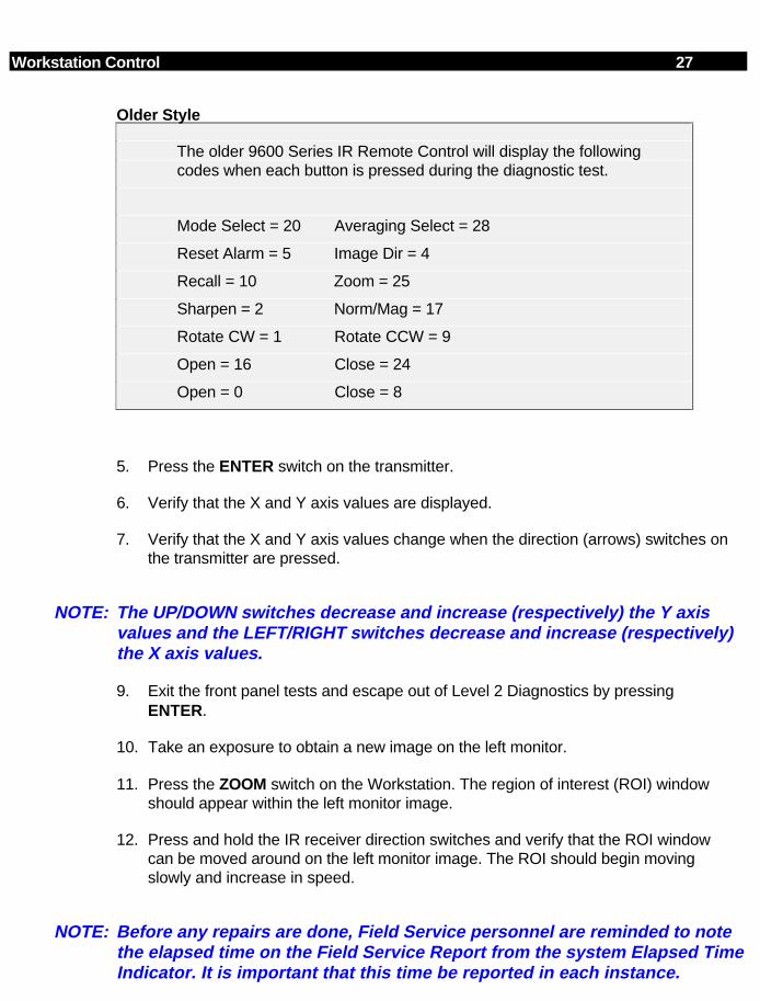
Workstation Control 27
Older Style
The older 9600 Series IR Remote Control will display the followingcodes when each button is pressed during the diagnostic test.
Mode Select = 20 Averaging Select = 28
Reset Alarm = 5 Image Dir = 4
Recall = 10 Zoom = 25
Sharpen = 2 Norm/Mag = 17
Rotate CW = 1 Rotate CCW = 9
Open = 16 Close = 24
Open = 0 Close = 8
5. Press the ENTER switch on the transmitter.
6. Verify that the X and Y axis values are displayed.
7. Verify that the X and Y axis values change when the direction (arrows) switches onthe transmitter are pressed.
NOTE: The UP/DOWN switches decrease and increase (respectively) the Y axisvalues and the LEFT/RIGHT switches decrease and increase (respectively)the X axis values.
9. Exit the front panel tests and escape out of Level 2 Diagnostics by pressingENTER.
10. Take an exposure to obtain a new image on the left monitor.
11. Press the ZOOM switch on the Workstation. The region of interest (ROI) windowshould appear within the left monitor image.
12. Press and hold the IR receiver direction switches and verify that the ROI windowcan be moved around on the left monitor image. The ROI should begin movingslowly and increase in speed.
NOTE: Before any repairs are done, Field Service personnel are reminded to notethe elapsed time on the Field Service Report from the system Elapsed TimeIndicator. It is important that this time be reported in each instance.
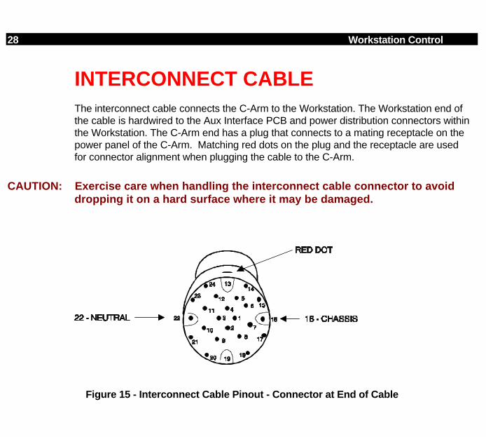
28 Workstation Control
INTERCONNECT CABLEThe interconnect cable connects the C-Arm to the Workstation. The Workstation end ofthe cable is hardwired to the Aux Interface PCB and power distribution connectors withinthe Workstation. The C-Arm end has a plug that connects to a mating receptacle on thepower panel of the C-Arm. Matching red dots on the plug and the receptacle are usedfor connector alignment when plugging the cable to the C-Arm.
CAUTION: Exercise care when handling the interconnect cable connector to avoiddropping it on a hard surface where it may be damaged.
Figure 15 - Interconnect Cable Pinout - Connector at End of Cable
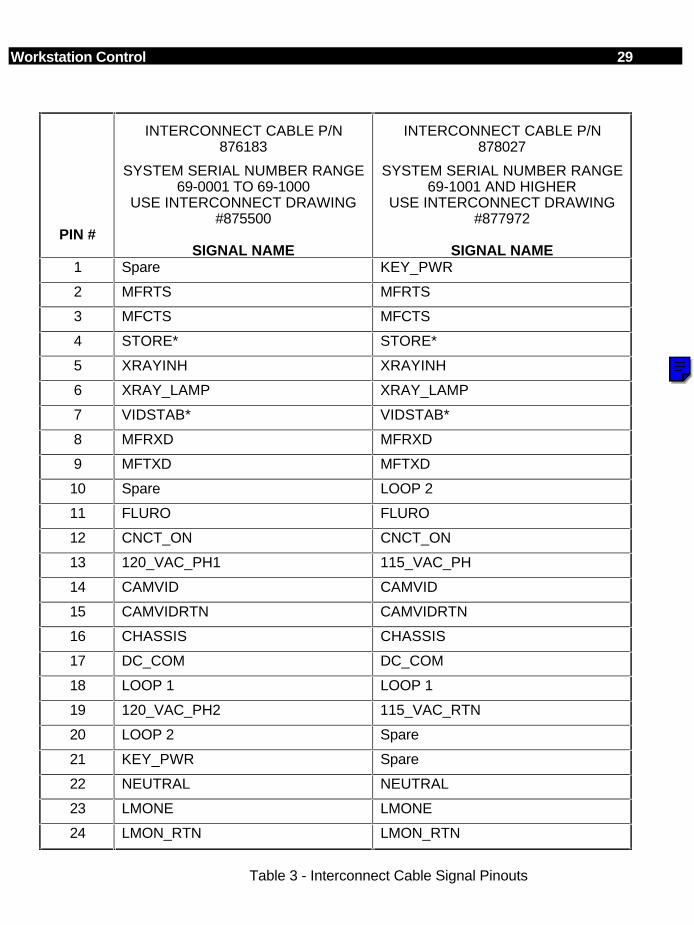
Workstation Control 29
PIN #
INTERCONNECT CABLE P/N876183
SYSTEM SERIAL NUMBER RANGE69-0001 TO 69-1000
USE INTERCONNECT DRAWING#875500
SIGNAL NAME
INTERCONNECT CABLE P/N878027
SYSTEM SERIAL NUMBER RANGE69-1001 AND HIGHER
USE INTERCONNECT DRAWING#877972
SIGNAL NAME1 Spare KEY_PWR
2 MFRTS MFRTS
3 MFCTS MFCTS
4 STORE* STORE*
5 XRAYINH XRAYINH
6 XRAY_LAMP XRAY_LAMP
7 VIDSTAB* VIDSTAB*
8 MFRXD MFRXD
9 MFTXD MFTXD
10 Spare LOOP 2
11 FLURO FLURO
12 CNCT_ON CNCT_ON
13 120_VAC_PH1 115_VAC_PH
14 CAMVID CAMVID
15 CAMVIDRTN CAMVIDRTN
16 CHASSIS CHASSIS
17 DC_COM DC_COM
18 LOOP 1 LOOP 1
19 120_VAC_PH2 115_VAC_RTN
20 LOOP 2 Spare
21 KEY_PWR Spare
22 NEUTRAL NEUTRAL
23 LMONE LMONE
24 LMON_RTN LMON_RTN
Table 3 - Interconnect Cable Signal Pinouts
NOTE
Click on the colored box to go directly to the Interconnection diagrams in the Illustrated Parts Manual. Click on the << button on the Tool Bar to return to this point.

WORKSTATION SOFTWARE
OVERVIEWSoftware files for the Workstation reside on a hard disk located within the electronicsbox in the Workstation. This section discusses the following Workstation softwaretopics:
• Start-up and Software Boot
• Diagnostics
START-UP AND SOFTWARE BOOT
POWER-ON SELF TEST
When the system is initially powered up, the System 386 Motherboard performs Power-On Self Tests (POST). If the POSTs are successful, the Workstation 386 Motherboardcontinues through the boot process. LED readouts on the rear panel of the Workstationindicate the status of the boot process. The Boot Sequence and Error Codes displayedare listed and detailed in this section. If the boot sequence stops, note the readout andrefer to the boot sequence and error codes section for references to possible reasonsand locations of the fault.
The following menu shows the information displayed on the monitor screen as theWorkstation is booted:
OEC MEDICAL SYSTEMS OPTION ROM P/N 0-877002-02COPYRIGHT (C) 1993, 1994, OEC MEDICAL SYSTEMS’
(c) American Megatrends, Inc.
2 Workstation Software
WORKSTATION BOOT SEQUENCE
The following procedure describes the Workstation boot sequence that occurs atWorkstation power up:
1. The AT Processor resets and vectors to 386 AMI BIOSTM software. BIOSTMidentifies any Option ROMs and finds the OEC Option PROM on the ATCommunications PCB. The date and version of the Option PROM is displayedbriefly on the left monitor.
2. The CGA video drivers are loaded and the floppy drive is checked (for the presenceof a system boot disk) by the AT Option PROM.
3. The 386 AMI BIOSTM copyright information is displayed briefly on the monitor.(Award BIOSTM controls information which tells the CPU how and when to accessthe disk, read the keyboard, load video drivers, run video screens, etc.)
4. Workstation performs Power On Self Tests (POST). If all internal motherboarddiagnostics pass, the boot sequence continues. If failures occur, the boot sequencestops at the point of failure and an error message appears on the monitor
5. The AT Communications PCB initializes the Image Processor.
6. The following messages appear briefly on the monitor:
• FASTOPEN installed: This program speeds up disk access time bykeeping track of all files which have been opened.
• NOBRK installed: This program ensures the boot process cannot beaborted prematurely by the operator and disables NumLock.
• 4FPSTSR installed: This software enables Workstation communicationsto the 4FPS or 30FPS disk, if installed. This message does not appear ifthe Workstation is not equipped with either of these options.
7. The Image Processor's GSP (Graphics System Processor) software is reloaded.Both monitors go blank at this point.
8. Front panel/pointing device panel communications are enabled. An audible tone canbe heard from speaker SP1 when this phase of boot up is complete.
9. The Workstation software begins running. The initial Workstation menu appears onthe right monitor when the boot up process is complete.
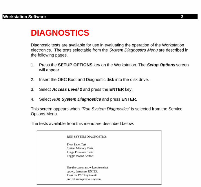
Workstation Software 3
DIAGNOSTICSDiagnostic tests are available for use in evaluating the operation of the Workstationelectronics. The tests selectable from the System Diagnostics Menu are described inthe following pages.
1. Press the SETUP OPTIONS key on the Workstation. The Setup Options screenwill appear.
2. Insert the OEC Boot and Diagnostic disk into the disk drive.
3. Select Access Level 2 and press the ENTER key.
4. Select Run System Diagnostics and press ENTER.
This screen appears when "Run System Diagnostics" is selected from the ServiceOptions Menu.
The tests available from this menu are described below:
RUN SYSTEM DIAGNOSTICS
Front Panel TestSystem Memory TestsImage Processor TestsToggle Motion Artifact
Use the cursor arrow keys to selectoption, then press ENTER.Press the ESC key to exitand return to previous screen.

4 Workstation Software
FRONT PANEL TEST
Selecting "Front Panel Test" from the System Diagnostics Menu brings up a screensimilar to the one below. (This display will contain only the instructions at the bottom ofthe screen until the keys are pressed.)
Descriptions for each portion of the screen are given below:
kbd = 0 led = 3 >*< ifr = 16 X = 118, Y = 20, SW = 0
Level = 19 > > > > > > > > > > > > > > > >
Window = 49> > > > > > > > > > > > > > >
Press Function Buttons, twiddleTrackPad, twist window and level.Arrow keys on keyboard light LEDs.[ESC] Exits
KBD - Press each key on the Front Panel and the TrackPad Panel. The kbd valueshould display a different number (which represents the hex keycode) for each keypressed. The value is displayed when each key is released. A different audible toneshould also be heard for each key pressed.
LED - Use the left and right cursor keys to turn on each LED on the Front Panel and theTrackpad Panel. The LED value shown on the screen will change to represent eachLED as it lights up.
IR - Press each key on the infrared (IR) transmitter. The ifr value should display adifferent keycode for each key pressed.
X & Y - These numbers represent the X and Y axis for the TrackPad. The X axis valuechanges from 80 - 120 as the TrackPad is rotated from left to right. The Y axis valuechanges from 0 - 48 as the TrackPad is rotated from top to bottom.
SW & >*< - The SW value represents the TrackPad superkey and toggles from 0 to 1when the superkey is pressed. The >*< symbol represents trackball movement. Itsrepresentative motion is limited to a small area in the upper right corner of the display.
Level & Window - These values change with adjustment of Level and Window,respectively. Both values will change from 0 - 80.
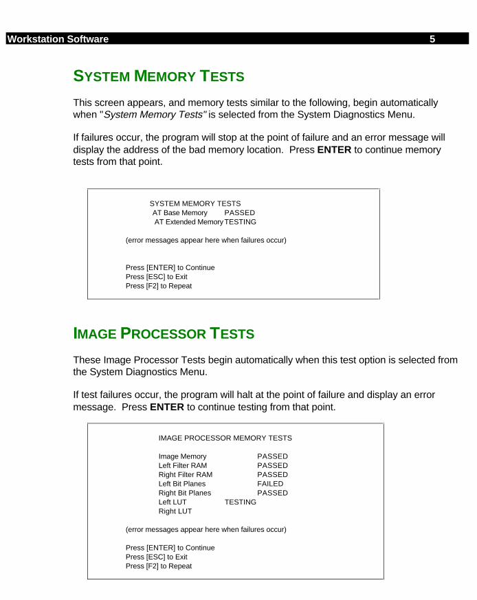
Workstation Software 5
SYSTEM MEMORY TESTS
This screen appears, and memory tests similar to the following, begin automaticallywhen "System Memory Tests" is selected from the System Diagnostics Menu.
If failures occur, the program will stop at the point of failure and an error message willdisplay the address of the bad memory location. Press ENTER to continue memorytests from that point.
SYSTEM MEMORY TESTS AT Base Memory PASSED AT Extended Memory TESTING
(error messages appear here when failures occur)
Press [ENTER] to ContinuePress [ESC] to ExitPress [F2] to Repeat
IMAGE PROCESSOR TESTS
These Image Processor Tests begin automatically when this test option is selected fromthe System Diagnostics Menu.
If test failures occur, the program will halt at the point of failure and display an errormessage. Press ENTER to continue testing from that point.
IMAGE PROCESSOR MEMORY TESTS
Image Memory PASSEDLeft Filter RAM PASSEDRight Filter RAM PASSEDLeft Bit Planes FAILEDRight Bit Planes PASSEDLeft LUT TESTINGRight LUT
(error messages appear here when failures occur)
Press [ENTER] to ContinuePress [ESC] to ExitPress [F2] to Repeat

6 Workstation Software
TOGGLE MOTION ARTIFACT
MOTION ARTIFACT ON
MOTION ARTIFACT OFF
This menu selection is an ON/OFF toggle function.
Motion Artifact Reduction (MARS) provides a built-in reduction of motion artifactsdisplayed in the averaged image. The result is that noise is averaged, but movementsare seen without the usual amount of lag. This allows higher levels of averaging to beused for better noise reduction in many situations.
NOTE: Averaging can only be used in the Continuous X-Ray mode. The use of Averaging inthe Pulse mode is not allowed.
CONTROL PANEL TESTS
NOTE: To run these tests, the Control Panel Processor Board located under the ControlPanel must be exposed to allow viewing of the Diagnostics LED array.
The Control Panel Processor PCB diagnostic program is called if the diagnostic switchis closed by installing a shorting jumper on E1, pins 7-8. This diagnostic tests the LEDdrivers and the key matrices and provides visual indications of the integrity of both aseach key is pressed.
Diagnostic Key Code Display
The row and column of any key pressed is displayed on the LED diagnostic array (DS1)with the LSB to the left and the MSB to the right; the row in bits 0-3 and the column inbits 4-7.
0 1 2 3 4 5 6 7 8 9
R C C C CR R R
Segment #9 always blinksexcept during RESET.
BL
NOTE: The Diagnostic Display is oriented on the PCB with the least significant bit on theleft. When the PCB is oriented so that the PCB annotation can be read, the binarydisplay will appear backwards (LSB to the left, MSB to the right).
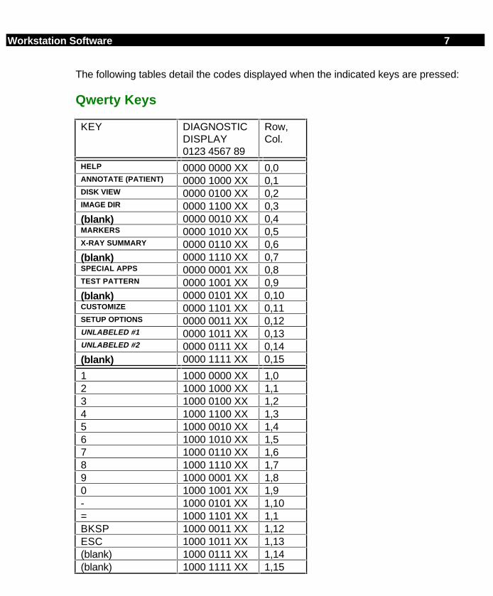
Workstation Software 7
The following tables detail the codes displayed when the indicated keys are pressed:
Qwerty Keys
KEY DIAGNOSTICDISPLAY0123 4567 89
Row,Col.
HELP 0000 0000 XX 0,0ANNOTATE (PATIENT) 0000 1000 XX 0,1DISK VIEW 0000 0100 XX 0,2IMAGE DIR 0000 1100 XX 0,3(blank) 0000 0010 XX 0,4MARKERS 0000 1010 XX 0,5X-RAY SUMMARY 0000 0110 XX 0,6(blank) 0000 1110 XX 0,7SPECIAL APPS 0000 0001 XX 0,8TEST PATTERN 0000 1001 XX 0,9(blank) 0000 0101 XX 0,10CUSTOMIZE 0000 1101 XX 0,11SETUP OPTIONS 0000 0011 XX 0,12UNLABELED #1 0000 1011 XX 0,13UNLABELED #2 0000 0111 XX 0,14(blank) 0000 1111 XX 0,15
1 1000 0000 XX 1,02 1000 1000 XX 1,13 1000 0100 XX 1,24 1000 1100 XX 1,35 1000 0010 XX 1,46 1000 1010 XX 1,57 1000 0110 XX 1,68 1000 1110 XX 1,79 1000 0001 XX 1,80 1000 1001 XX 1,9- 1000 0101 XX 1,10= 1000 1101 XX 1,1BKSP 1000 0011 XX 1,12ESC 1000 1011 XX 1,13(blank) 1000 0111 XX 1,14(blank) 1000 1111 XX 1,15

8 Workstation Software
Qwerty Keys (Cont.)
KEY DIAGNOSTICDISPLAY0123 4567 89
Row,Col.
TAB 0100 0000 XX 2,0q 0100 1000 XX 2,1w 0100 0100 XX 2,2e 0100 1100 XX 2,3r 0100 0010 XX 2,4t 0100 1010 XX 2,5y 0100 0110 XX 2,6u 0100 1110 XX 2,7i 0100 0001 XX 2,8o 0100 1001 XX 2,9p 0100 0101 XX 2,10[ 0100 1101 XX 2,11] 0100 0011 XX 2,12HOME 0100 1011 XX 2,13UP 0100 0111 XX 2,14PGUP 0100 1111 XX 2,15
CTRL 1100 0000 XX 3,0a 1100 1000 XX 3,1s 1100 0100 XX 3,2d 1100 1100 XX 3,3f 1100 0010 XX 3,4g 1100 1010 XX 3,5h 1100 0110 XX 3,6j 1100 1110 XX 3,7k 1100 0001 XX 3,8l 1100 1001 XX 3,9; 1100 0101 XX 3,10' 1100 1101 XX 3,11CR 1100 0011 XX 3,12LFT 1100 1011 XX 3,13(blank) 1100 0111 XX 3,14RT 1100 1111 XX 3,15
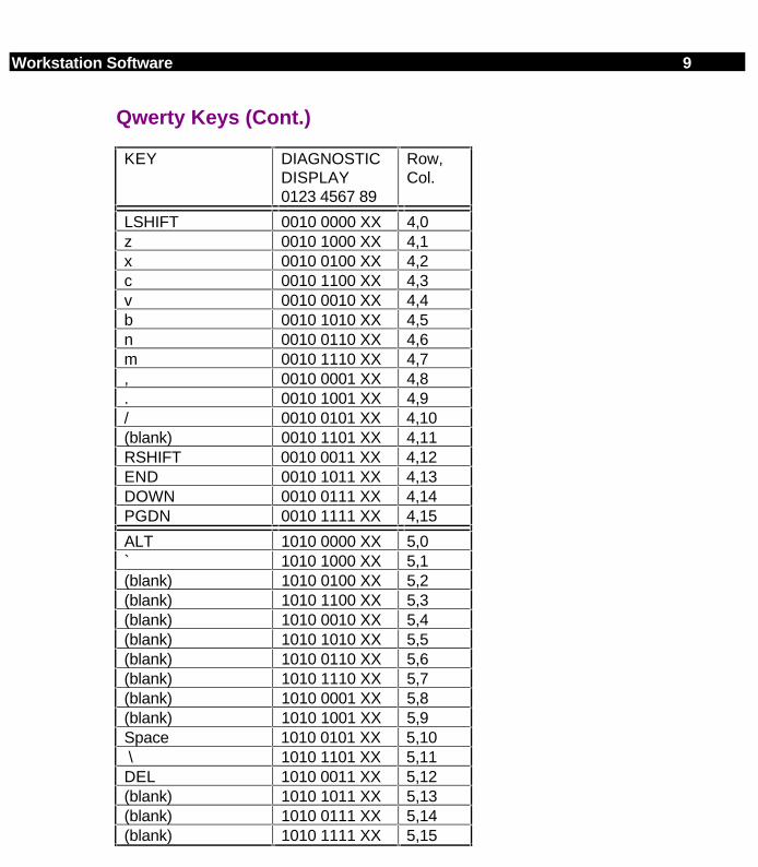
Workstation Software 9
Qwerty Keys (Cont.)
KEY DIAGNOSTICDISPLAY0123 4567 89
Row,Col.
LSHIFT 0010 0000 XX 4,0z 0010 1000 XX 4,1x 0010 0100 XX 4,2c 0010 1100 XX 4,3v 0010 0010 XX 4,4b 0010 1010 XX 4,5n 0010 0110 XX 4,6m 0010 1110 XX 4,7, 0010 0001 XX 4,8. 0010 1001 XX 4,9/ 0010 0101 XX 4,10(blank) 0010 1101 XX 4,11RSHIFT 0010 0011 XX 4,12END 0010 1011 XX 4,13DOWN 0010 0111 XX 4,14PGDN 0010 1111 XX 4,15
ALT 1010 0000 XX 5,0` 1010 1000 XX 5,1(blank) 1010 0100 XX 5,2(blank) 1010 1100 XX 5,3(blank) 1010 0010 XX 5,4(blank) 1010 1010 XX 5,5(blank) 1010 0110 XX 5,6(blank) 1010 1110 XX 5,7(blank) 1010 0001 XX 5,8(blank) 1010 1001 XX 5,9Space 1010 0101 XX 5,10 \ 1010 1101 XX 5,11DEL 1010 0011 XX 5,12(blank) 1010 1011 XX 5,13(blank) 1010 0111 XX 5,14(blank) 1010 1111 XX 5,15
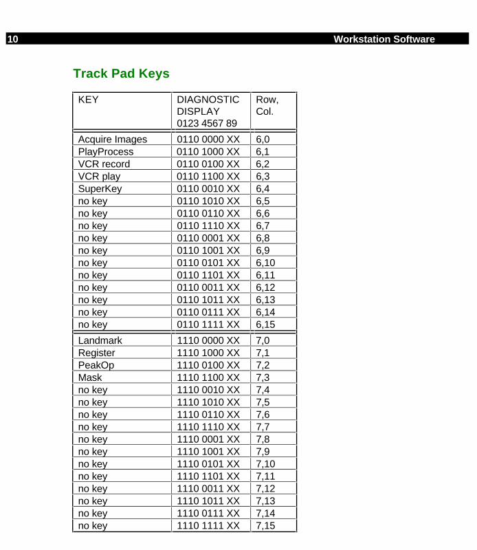
10 Workstation Software
Track Pad Keys
KEY DIAGNOSTICDISPLAY0123 4567 89
Row,Col.
Acquire Images 0110 0000 XX 6,0PlayProcess 0110 1000 XX 6,1VCR record 0110 0100 XX 6,2VCR play 0110 1100 XX 6,3SuperKey 0110 0010 XX 6,4no key 0110 1010 XX 6,5no key 0110 0110 XX 6,6no key 0110 1110 XX 6,7no key 0110 0001 XX 6,8no key 0110 1001 XX 6,9no key 0110 0101 XX 6,10no key 0110 1101 XX 6,11no key 0110 0011 XX 6,12no key 0110 1011 XX 6,13no key 0110 0111 XX 6,14no key 0110 1111 XX 6,15
Landmark 1110 0000 XX 7,0Register 1110 1000 XX 7,1PeakOp 1110 0100 XX 7,2Mask 1110 1100 XX 7,3no key 1110 0010 XX 7,4no key 1110 1010 XX 7,5no key 1110 0110 XX 7,6no key 1110 1110 XX 7,7no key 1110 0001 XX 7,8no key 1110 1001 XX 7,9no key 1110 0101 XX 7,10no key 1110 1101 XX 7,11no key 1110 0011 XX 7,12no key 1110 1011 XX 7,13no key 1110 0111 XX 7,14no key 1110 1111 XX 7,15
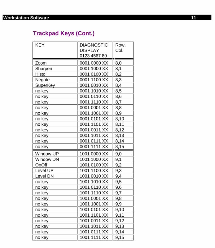
Workstation Software 11
Trackpad Keys (Cont.)
KEY DIAGNOSTICDISPLAY0123 4567 89
Row,Col.
Zoom 0001 0000 XX 8,0Sharpen 0001 1000 XX 8,1Histo 0001 0100 XX 8,2Negate 0001 1100 XX 8,3SuperKey 0001 0010 XX 8,4no key 0001 1010 XX 8,5no key 0001 0110 XX 8,6no key 0001 1110 XX 8,7no key 0001 0001 XX 8,8no key 0001 1001 XX 8,9no key 0001 0101 XX 8,10no key 0001 1101 XX 8,11no key 0001 0011 XX 8,12no key 0001 1011 XX 8,13no key 0001 0111 XX 8,14no key 0001 1111 XX 8,15
Window UP 1001 0000 XX 9,0Window DN 1001 1000 XX 9,1OnOff 1001 0100 XX 9,2Level UP 1001 1100 XX 9,3Level DN 1001 0010 XX 9,4no key 1001 1010 XX 9,5no key 1001 0110 XX 9,6no key 1001 1110 XX 9,7no key 1001 0001 XX 9,8no key 1001 1001 XX 9,9no key 1001 0101 XX 9,10no key 1001 1101 XX 9,11no key 1001 0011 XX 9,12no key 1001 1011 XX 9,13no key 1001 0111 XX 9,14no key 1001 1111 XX 9,15
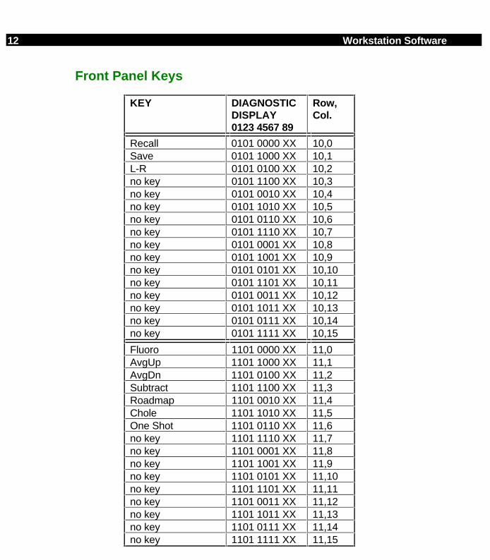
12 Workstation Software
Front Panel Keys
KEY DIAGNOSTICDISPLAY0123 4567 89
Row,Col.
Recall 0101 0000 XX 10,0Save 0101 1000 XX 10,1L-R 0101 0100 XX 10,2no key 0101 1100 XX 10,3no key 0101 0010 XX 10,4no key 0101 1010 XX 10,5no key 0101 0110 XX 10,6no key 0101 1110 XX 10,7no key 0101 0001 XX 10,8no key 0101 1001 XX 10,9no key 0101 0101 XX 10,10no key 0101 1101 XX 10,11no key 0101 0011 XX 10,12no key 0101 1011 XX 10,13no key 0101 0111 XX 10,14no key 0101 1111 XX 10,15
Fluoro 1101 0000 XX 11,0AvgUp 1101 1000 XX 11,1AvgDn 1101 0100 XX 11,2Subtract 1101 1100 XX 11,3Roadmap 1101 0010 XX 11,4Chole 1101 1010 XX 11,5One Shot 1101 0110 XX 11,6no key 1101 1110 XX 11,7no key 1101 0001 XX 11,8no key 1101 1001 XX 11,9no key 1101 0101 XX 11,10no key 1101 1101 XX 11,11no key 1101 0011 XX 11,12no key 1101 1011 XX 11,13no key 1101 0111 XX 11,14no key 1101 1111 XX 11,15
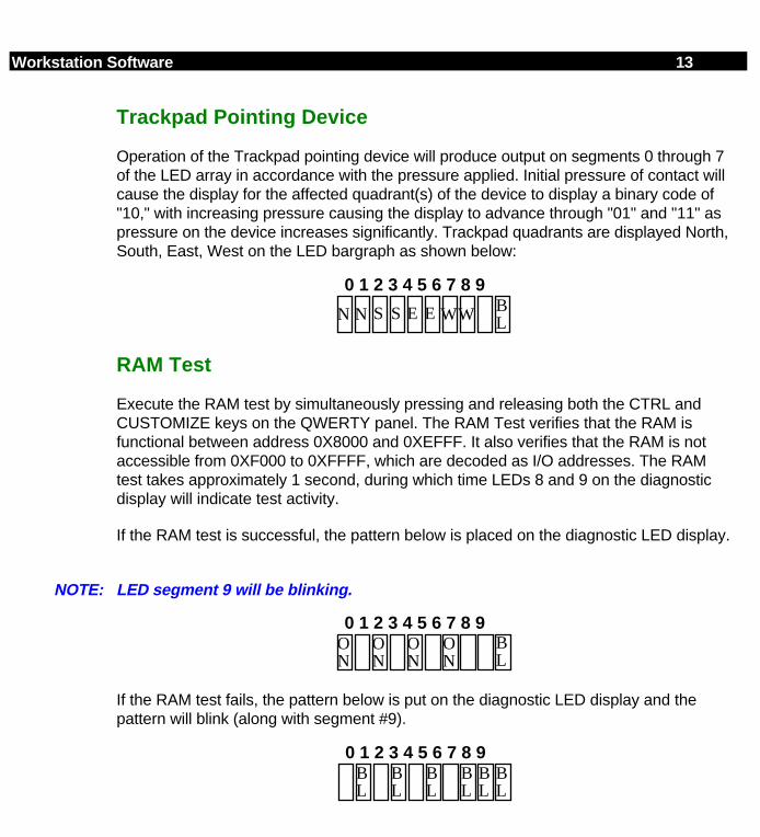
Workstation Software 13
Trackpad Pointing Device
Operation of the Trackpad pointing device will produce output on segments 0 through 7of the LED array in accordance with the pressure applied. Initial pressure of contact willcause the display for the affected quadrant(s) of the device to display a binary code of"10," with increasing pressure causing the display to advance through "01" and "11" aspressure on the device increases significantly. Trackpad quadrants are displayed North,South, East, West on the LED bargraph as shown below:
0 1 2 3 4 5 6 7 8 9BLN S E WN S E W
RAM Test
Execute the RAM test by simultaneously pressing and releasing both the CTRL andCUSTOMIZE keys on the QWERTY panel. The RAM Test verifies that the RAM isfunctional between address 0X8000 and 0XEFFF. It also verifies that the RAM is notaccessible from 0XF000 to 0XFFFF, which are decoded as I/O addresses. The RAMtest takes approximately 1 second, during which time LEDs 8 and 9 on the diagnosticdisplay will indicate test activity.
If the RAM test is successful, the pattern below is placed on the diagnostic LED display.
NOTE: LED segment 9 will be blinking.
0 1 2 3 4 5 6 7 8 9ON
ON
ON
ON
BL
If the RAM test fails, the pattern below is put on the diagnostic LED display and thepattern will blink (along with segment #9).
0 1 2 3 4 5 6 7 8 9BL
BL
BL
BL
BL
BL
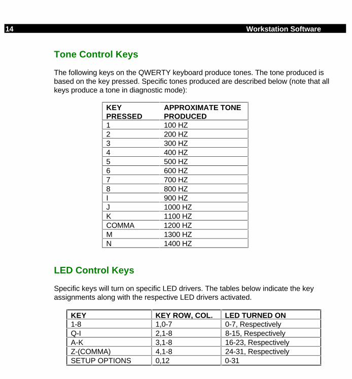
14 Workstation Software
Tone Control Keys
The following keys on the QWERTY keyboard produce tones. The tone produced isbased on the key pressed. Specific tones produced are described below (note that allkeys produce a tone in diagnostic mode):
KEYPRESSED
APPROXIMATE TONEPRODUCED
1 100 HZ2 200 HZ3 300 HZ4 400 HZ5 500 HZ6 600 HZ7 700 HZ8 800 HZI 900 HZJ 1000 HZK 1100 HZCOMMA 1200 HZM 1300 HZN 1400 HZ
LED Control Keys
Specific keys will turn on specific LED drivers. The tables below indicate the keyassignments along with the respective LED drivers activated.
KEY KEY ROW, COL. LED TURNED ON1-8 1,0-7 0-7, RespectivelyQ-I 2,1-8 8-15, RespectivelyA-K 3,1-8 16-23, RespectivelyZ-(COMMA) 4,1-8 24-31, RespectivelySETUP OPTIONS 0,12 0-31
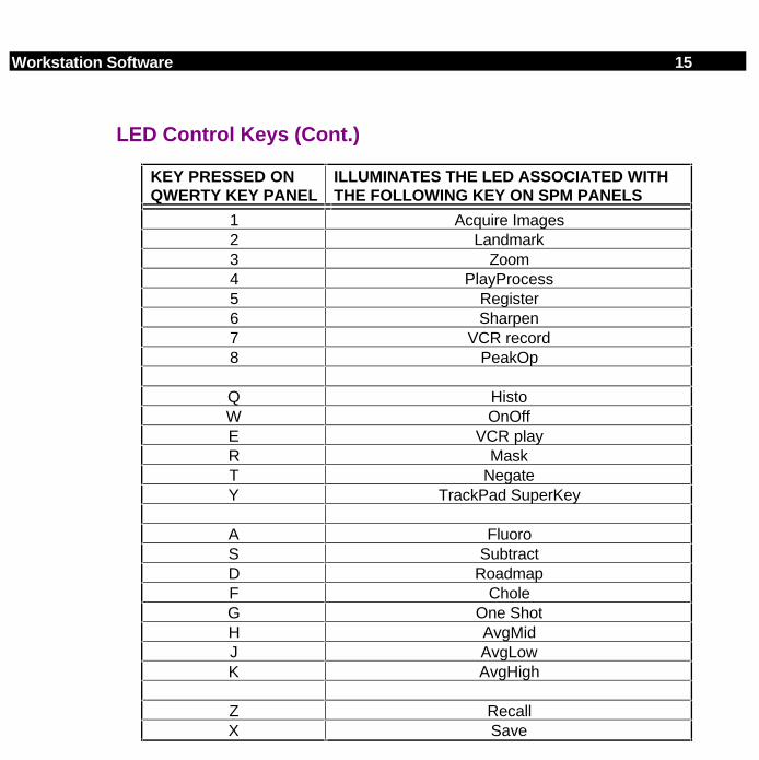
Workstation Software 15
LED Control Keys (Cont.)
KEY PRESSED ONQWERTY KEY PANEL
ILLUMINATES THE LED ASSOCIATED WITHTHE FOLLOWING KEY ON SPM PANELS
1 Acquire Images2 Landmark3 Zoom4 PlayProcess5 Register6 Sharpen7 VCR record8 PeakOp
Q HistoW OnOffE VCR playR MaskT NegateY TrackPad SuperKey
A FluoroS SubtractD RoadmapF CholeG One ShotH AvgMidJ AvgLowK AvgHigh
Z RecallX Save
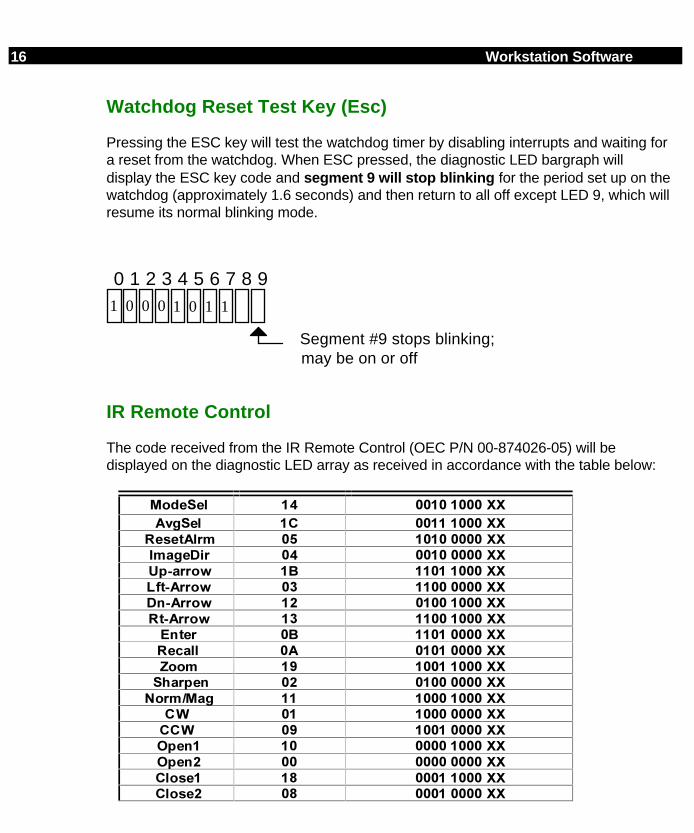
16 Workstation Software
Watchdog Reset Test Key (Esc)
Pressing the ESC key will test the watchdog timer by disabling interrupts and waiting fora reset from the watchdog. When ESC pressed, the diagnostic LED bargraph willdisplay the ESC key code and segment 9 will stop blinking for the period set up on thewatchdog (approximately 1.6 seconds) and then return to all off except LED 9, which willresume its normal blinking mode.
0 1 2 3 4 5 6 7 8 91 1 0 1 10 0 0
Segment #9 stops blinking;may be on or off
IR Remote Control
The code received from the IR Remote Control (OEC P/N 00-874026-05) will bedisplayed on the diagnostic LED array as received in accordance with the table below:
ModeSel 14 0010 1000 XX
AvgSel 1C 0011 1000 XX
ResetAlrm 05 1010 0000 XX
ImageDir 04 0010 0000 XX
Up-arrow 1B 1101 1000 XX
Lft-Arrow 03 1100 0000 XX
Dn-Arrow 12 0100 1000 XX
Rt-Arrow 13 1100 1000 XX
Enter 0B 1101 0000 XX
Recall 0A 0101 0000 XX
Zoom 19 1001 1000 XX
Sharpen 02 0100 0000 XX
Norm/Mag 11 1000 1000 XX
CW 01 1000 0000 XX
CCW 09 1001 0000 XX
Open1 10 0000 1000 XX
Open2 00 0000 0000 XX
Close1 18 0001 1000 XX
Close2 08 0001 0000 XX

VIDEO PATH
OVERVIEWThis section contains information regarding video signals used in the 9600 system. Thefollowing topics will be presented:
• Types of Video signals• The Video Path• Video Path Peripherals
NOTE
Click on the yellow square to go directly to the block diagram for this section. Do not use this link to return to a block diagram from this point. Click on the << in the Tool Bar to return to any starting point
NOTE
Click on a yellow box to go directly to the block diagram for this section. Click on the << button in the Tool Bar to return to this point.
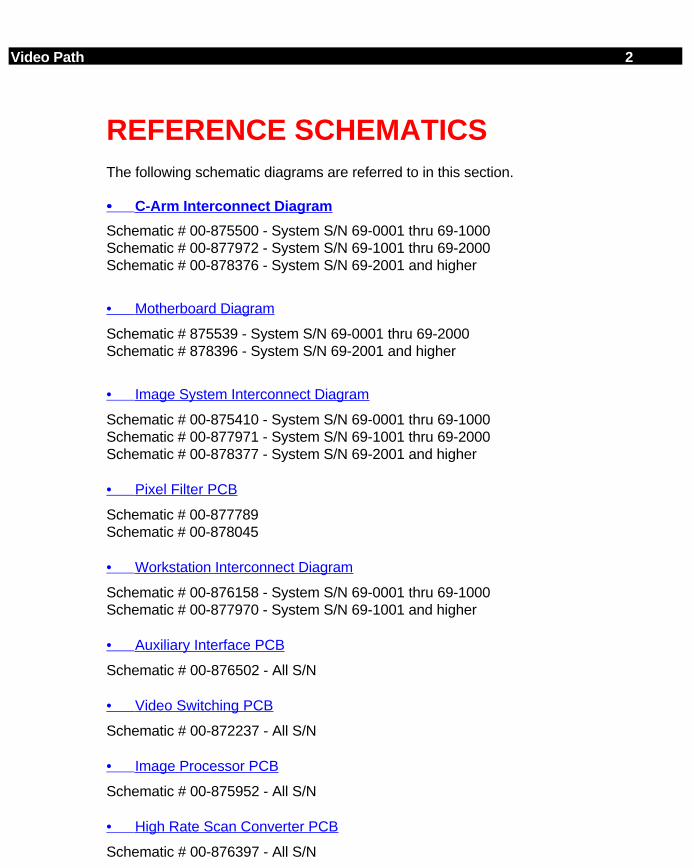
Video Path 2
REFERENCE SCHEMATICSThe following schematic diagrams are referred to in this section.
• • C-Arm Interconnect Diagram
Schematic # 00-875500 - System S/N 69-0001 thru 69-1000Schematic # 00-877972 - System S/N 69-1001 thru 69-2000Schematic # 00-878376 - System S/N 69-2001 and higher
• Motherboard Diagram
Schematic # 875539 - System S/N 69-0001 thru 69-2000Schematic # 878396 - System S/N 69-2001 and higher
• Image System Interconnect Diagram
Schematic # 00-875410 - System S/N 69-0001 thru 69-1000Schematic # 00-877971 - System S/N 69-1001 thru 69-2000Schematic # 00-878377 - System S/N 69-2001 and higher
• Pixel Filter PCB
Schematic # 00-877789Schematic # 00-878045
• Workstation Interconnect Diagram
Schematic # 00-876158 - System S/N 69-0001 thru 69-1000Schematic # 00-877970 - System S/N 69-1001 and higher
• Auxiliary Interface PCB
Schematic # 00-876502 - All S/N
• Video Switching PCB
Schematic # 00-872237 - All S/N
• Image Processor PCB
Schematic # 00-875952 - All S/N
• High Rate Scan Converter PCB
Schematic # 00-876397 - All S/N
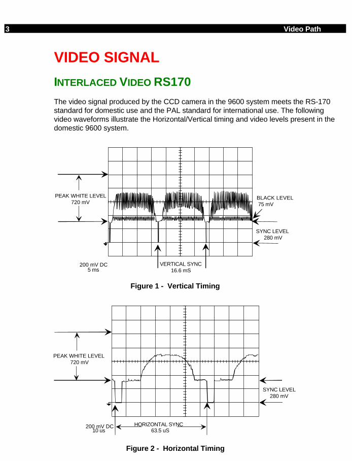
3 Video Path
VIDEO SIGNAL
INTERLACED VIDEO RS170
The video signal produced by the CCD camera in the 9600 system meets the RS-170standard for domestic use and the PAL standard for international use. The followingvideo waveforms illustrate the Horizontal/Vertical timing and video levels present in thedomestic 9600 system.
WaveformsScreen Image
200 mV DC5 ms
VERTICAL SYNC16.6 mS
BLACK LEVEL 75 mV
SYNC LEVEL 280 mV
PEAK WHITE LEVEL720 mV
Figure 1 - Vertical Timing
200 mV DC10 us
PEAK WHITE LEVEL 720 mV
SYNC LEVEL 280 mV
HORIZONTAL SYNC 63.5 uS
Figure 2 - Horizontal Timing
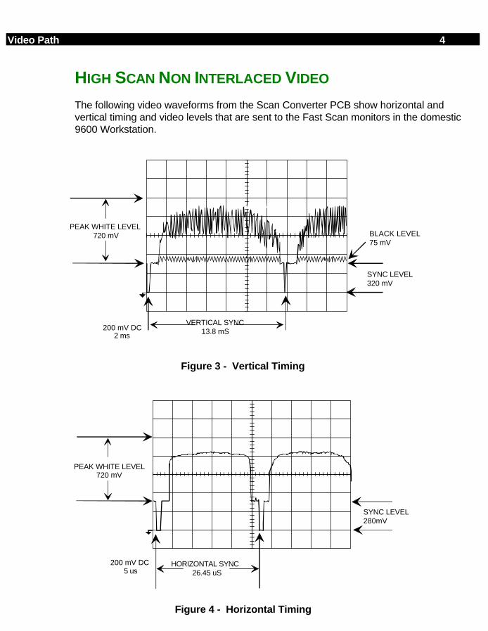
Video Path 4
HIGH SCAN NON INTERLACED VIDEO
The following video waveforms from the Scan Converter PCB show horizontal andvertical timing and video levels that are sent to the Fast Scan monitors in the domestic9600 Workstation.
200 mV DC2 ms
Waveforms
VERTICAL SYNC13.8 mS
BLACK LEVEL75 mV
PEAK WHITE LEVEL 720 mV
SYNC LEVEL320 mV
Figure 3 - Vertical Timing
Waveforms
200 mV DC5 us
HORIZONTAL SYNC 26.45 uS
SYNC LEVEL 280mV
PEAK WHITE LEVEL720 mV
Figure 4 - Horizontal Timing
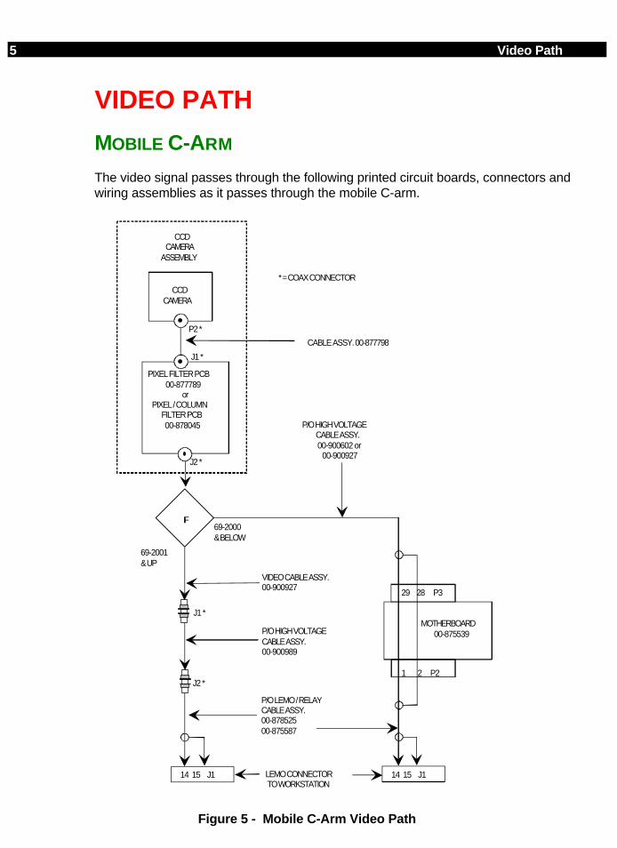
5 Video Path
VIDEO PATH
MOBILE C-ARM
The video signal passes through the following printed circuit boards, connectors andwiring assemblies as it passes through the mobile C-arm.
CCDCAMERA
69-2001& UP
P2 *
J2 *
J1 *
J2 *
* = COAX CONNECTOR
CABLE ASSY. 00-877798
P/O HIGH VOLTAGECABLE ASSY.00-900989
LEMO CONNECTORTO WORKSTATION
69-2000& BELOW
MOTHERBOARD00-875539
29 28 P3
1 2 P2
VIDEO CABLE ASSY.00-900927
PIXEL FILTER PCB 00-877789
orPIXEL / COLUMN
FILTER PCB 00-878045
CCDCAMERA
ASSEMBLY
P/O HIGH VOLTAGECABLE ASSY.00-900602 or
00-900927
P/O LEMO / RELAYCABLE ASSY.00-87852500-875587
IF
14 15 J1 14 15 J1
J1 *
Figure 5 - Mobile C-Arm Video Path
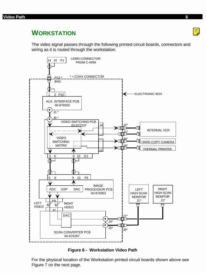
Video Path 6
WORKSTATION
The video signal passes through the following printed circuit boards, connectors andwiring as it is routed through the workstation.
P13 *BNC
* = COAX CONNECTOR
J1 *
J6 *
AUX. INTERFACE PCB00-876502
VIDEO SWITCHING PCB00-872237
IMAGE PROCESSOR PCB
00-875952
SCAN CONVERTER PCB00-876397
1 2 P10
HARD COPY CAMERA
THERMAL PRINTER
5 6 9 10 J11
8 8LEFTVIDEO
RIGHTVIDEO
P9
J2
DAC
J4*
J5*
LEFT HIGH SCAN MONITOR
J1*
RIGHTHIGH SCAN MONITOR
J1*
J8*
J7*
ADC GSP DAC
5 6 9 10 P4
VIDEOSWITCHING
MATRIX
J3
J4
14 15 P1
J6*
J4*
*
*
*
LEMO CONNECTORFROM C-ARM
ELECTRONIC BOX
*J2*
J1* INTERNAL VCR
Figure 6 - Workstation Video Path
For the physical location of the Workstation printed circuit boards shown above seeFigure 7 on the next page.
NOTE
Click on the yellow box to go directly to the block diagram for this section. Do not use this link to return to a block diagram from this point. Click on the << button in the Tool Bar to return to this point.
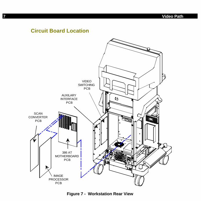
7 Video Path
Circuit Board Location
SCANCONVERTER
PCB
IMAGEPROCESSOR
PCB
386 ATMOTHERBOARD
PCB
VIDEO SWITCHING
PCB
AUXILARYINTERFACE
PCB
Figure 7 - Workstation Rear View
Video Path 8
Auxiliary Interface PCB
The purpose of the Auxiliary Interface PCB is to distribute control and video signals tovarious locations within the electronic box in the Workstation.
Camera video enters the Workstation from the C-Arm through the interconnect cable,connector P1 on pins 14 and 15. The video signal enters the Workstation electronics boxat J13. The video signal enters the Auxiliary Interface PCB at connector P10 on pin 1and exits on coax connector J1. The video signal goes to J6 on the Video SwitchingPCB.
Video Switching PCB
The purpose of the Video Switching PCB is to route video signals to various locations inthe Workstation. Video signals are distributed to the Hard Copy camera, internal VCRand Thermal Printer. The routing is accomplished by an 8 input, 6 output, crosspointswitch matrix on the Video Switching PCB and is controlled by a serial to parallel controlcircuit that originates in the Image Processor PCB. The Video Switching PCB alsocontains a video clamp, log amplifier, anti-alias filter and Genlock circuits. Refer to theVideo Control Section for more information.
The video signal enters the Video Switching PCB at J6 and is buffered by U4 and runsthrough a DC restoration clamp (U7) to restore the video sync tips to ground. The videocan be monitored at TP10. The video signal is sent to the video switching matrix to muxchip U13 IN0 (pin 5). The video signal leaves U13 at VOUT (pin 20). The video signalruns through another DC restoration clamp and is buffered by U15. The video signal canbe monitored at TP16 (A/D VIDEO). The video signal is then sent back to the videoswitching matrix where it can be directed to, or bypass, a logarithmic amplifier (U46 andU26) which can be turned on for subtraction mode. The video signal is then sent back tothe video switching matrix where it can be directed to an anti-alias filter (U25 and U24).The anti-alias filter limits the video signal to 5 MHz. The video signal from the anti-aliasfilter circuit can be monitored at TP18 (A/D VIDEO). The video signal leaves the VideoSwitching PCB at connector J11 pin 5 and is sent to the Image Processor PCB, P4 pin5. See the Video Control Section for more information on video routing.

9 Video Path
Image Processor PCB
The Image Processor PCB is the image data processor that contains a Graphic SystemProcessor or GSP. All Workstation functions are controlled by the GSP on the ImageProcessor PCB. Because the Image Processor PCB is multi layer and uses surfacemount circuits, repair of this PCB outside of the factory is not recommended. Todetermine the functionality of the Image Processor PCB, the use of system leveldiagnostics are used. See the Video Control Section for more information.
The video signal enters the Image Processor PCB via connector P4 pin 5. The videosignal can be monitored at TP3 on the Image Processor PCB. The video signal is sentto A/D converter U17 where each pixel is converted to an 8 bit digital number. The digitalvideo signal is then processed according to the functions selected on the Workstation.Left and right digital video signals are routed out of the Image Processor PCB as an 8 bitdigital signal via connector P8 to the Scan Converter PCB. Video to the internal VCR,Hard Copy Camera and Thermal Printer is supplied as analog video from D/A convertersU2 and U16 in the Image Processor PCB and exit via P4 pin 9 which goes back to theVideo Switching PCB.
Scan Converter PCB
The Scan Converter PCB receives left and right digital video data from the ImageProcessor PCB in interlace scan format at a horizontal frequency of 15.750 kHz and avertical frequency of 60 Hz. (domestic) or 50 Hz. (international).
The Scan Converter PCB receives horizontal sync, vertical sync, odd and even fieldidentification, and pixel clock timing signals along with the left and right 8 bit video datafrom the Image Processor PCB. The signals leave the Image Processor PCB atconnector P9 and goes to the Scan Converter PCB via a 40 pin ribbon cable thatconnects to J2 on the Scan Converter PCB.
The Scan Converter PCB then converts the digital video signal from interlace format toprogressive scan format and upscales the horizontal frequency to 37.8 kHz. and thevertical frequency to 72 Hz. (domestic use) or 61 Hz (international use). The left andright digital video is then converted to an analog video signal by D/A converters U20 andU21. The analog video signals from the D/A converters can be monitored at TP4 (leftvideo) and TP1 (right video). The video signals exit the board at J5 (left video) and J4(right video) and are sent out of the Electronics Box at J8 (left video) and J7 (right video)to the Fast Scan Monitors. An additional left video output is available at J8 on the ScanConverter PCB which can be monitored at TP2. This video signal is sent to J17 (FASTSCAN VIDEO) on the rear panel of the Workstation as an additional video output for anexternal fast scan monitor.
Fast Scan Monitors
The Fast Scan monitors receive analog video signals from the Scan Converter PCB inprogressive high scan format for image display. See figures 3 and 4 and the VideoControl Section for more information.

Video Path 10
Peripherals
Analog interlace video is provided to the internal VCR, hard copy camera and thermalprinter via the Video Switching PCB.
VCR
Video to and from the Internal VCR is routed through the Video Switching PCB. Thevideo to the VCR can be supplied as unprocessed or processed which can be selectedby the Workstation software. (See Customize VCR Options in the Peripherals Section .)
Unprocessed Input Video to VCR - With the VCR configured for unprocessed inputvideo, the video signal is supplied by the CCD Camera via the Video Switching PCB(See Figures 5 and 6). The video signal enters the Video Switching PCB at J6 and isbuffered by U4 and runs through a DC Restoration Clamp (U7) to restore the video synctips to ground. The video signal can be monitored at TP10. The video signal is sent tothe video switching matrix where it is routed to mux chip U10 IN0 (pin 5). The videosignal leaves U10 at VOUT (pin 20). See the Video Control Section for moreinformation on video routing. The video signal to the VCR can be monitored at TP6(TOVCR1). The video signal leaves the Video Switching PCB at connector J4 pin 3. Thevideo signal exits the Electronics Box at BNC connector J2 located at the top left rearcorner. The video runs from J2 on the Electronics Box to the VIDEO IN BNC connectoron the back of the VCR. See the Peripherals Section for VCR video connections.
Processed Input Video to VCR - With the VCR configured for processed input videothe video signal is supplied by the Image Processor PCB via D/A converter U2. Thevideo signal leaves the Image Processor PCB at P4 pin 9 and is sent to J11 pin 9 on theVideo Switching PCB. The video signal runs through a DC Restoration Clamp (U17) torestore the video sync tips to ground. The video can be monitored at TP20 (LDAC) onthe Video Switching PCB. The video signal is sent to the video switching matrix where itis routed to mux chip U10 IN2 (pin 9), the video signal leaves U10 at VOUT (pin 20). Thevideo signal to the VCR can be monitored at TP7 (TOVCR1). The video signal leavesthe Video Switching PCB at connector J4 pin 3. The video signal exits the ElectronicsBox at BNC connector J2 located at the top left rear corner. The video runs from J2 onthe Electronics Box to the VIDEO IN BNC connector on the back of the VCR. See theVideo Control Section for more information on video routing.

11 Video Path
VCR Output Video - When the Workstation is configured for post processing from theinternal VCR, the video leaves the VCR at the Video Out BNC connector. The videosignal enters the Workstation electronics box at BNC connector J1 located at the back ofthe electronics box in the upper left hand corner. The VCR video signal enters the VideoSwitching PCB at connector J4 on pin 3. A DC Restoration clamp (Q2) restores thevideo sync tips to ground.
The incoming VCR video can be monitored at TP13 (VCR1). The video signal is sent tothe video switching matrix to mux chip U13 IN0 (pin 5). The video signal leaves U13 atVOUT (pin 20). The video signal runs through another DC restoration clamp and isbuffered by U15. The video signal can be monitored at TP16 (A/D VIDEO). The videosignal is then sent back to the video switching matrix where it can be directed to, orbypass a logarithmic amplifier (U46 and U26) which can be turned on for subtractionmodes.
The video signal is then sent back to the video switching matrix where it can be directedto an anti-alias filter (U25 and U24). The anti-alias filter limits the video signal to 5 MHz.The video signal from the anti-alias filter circuit can be monitored at TP18 (A/D VIDEO).The video signal leaves the Video Switching PCB at connector J11 pin 5 and is sent tothe Image Processor PCB, connector P4 pin 5.
Video Path 12
HARD COPY CAMERA
Video to the internal Hard Copy Camera comes from two different sources. The sourcedepends on whether fluoro x-rays are on or off.
X-Ray Off Condition - In the X-Ray off condition the video signal is supplied by theImage Processor PCB via D/A converter U2. The video leaves the Image ProcessorPCB at P4 pin 9 and is sent to J11 pin 9 on the Video Switching PCB. The video signalruns through a DC Restoration Clamp (U17) to restore the video sync tips to ground.The video can be monitored at TP20 (LDAC) on the Video Switching PCB. The videosignal is sent to the video switching matrix where it is routed to mux chip U8 IN2 (pin 9).The video signal leaves U8 at VOUT (pin 20). See the Video Control Section for moreinformation on video routing. The video signal from U8 is buffered by amplifier U1 and issent to connector J3 pin 9. The video signal can be monitored at TP5 (HCO). The videosignal exits the front of the electronics box at J6 (BNC connector) near the top on theright side. The video signal runs from J6 on the electronics box to the VIDEO IN BNCconnector located on the front of the Hard Copy Camera. See the Peripherals Sectionfor more information.
X-Ray On Condition - In the X-Ray on condition the video signal is supplied by theCCD Camera via the Video Switching PCB (See Figures 5 and 6). The video signalenters the Video Switching PCB at J6 and is buffered by U4 and runs through a DCRestoration Clamp (U7) to restore the video sync tips to ground. The video can bemonitored at TP10. The video signal is sent to the video switching matrix where it isrouted to mux chip U8 IN0 (pin 5). The video signal leaves U8 at VOUT (pin 20). See theVideo Control Section for more information on video routing. The video signal from U8is buffered by amplifier U1 and is sent to connector J3 pin 9. The video signal can bemonitored at TP5 (HCO). The video signal exits the front of the electronics box at J6(BNC connector) near the top on the right side. The video signal runs from J6 on theelectronics box to the VIDEO IN BNC connector located on the front of the Hard CopyCamera. See the Peripherals Section for more information.
13 Video Path
THERMAL PRINTER
Video to the Thermal Printer comes from two different sources. The source depends onwhether fluoro x-rays are on or off.
X-Ray Off Condition - In the X-Ray off condition the video signal is supplied by theImage Processor PCB via D/A converter U2. The video leaves the Image ProcessorPCB at P4 pin 9 and is sent to J11 pin 9 on the Video Switching PCB. The video signalruns through a DC Restoration Clamp (U17) to restore the video sync tips to ground.The video can be monitored at TP20 (LDAC) on the Video Switching PCB. The videosignal is sent to the video switching matrix where it is routed to mux chip U8 IN2 (pin 9).The video signal leaves U8 at VOUT (pin 20). See the Video Control Section for moreinformation on video routing. The video signal from U8 is buffered by amplifier U1 and issent to connector J3 pin 5. The video signal can be monitored at TP2 (LVID). The videosignal exits the rear of the electronics box at BNC connector J4 labeled VIDEO belowthe 3.5-inch floppy disk drive. The video signal runs from J4 to the Thermal Printer. Seethe Peripherals Section for more information.
X-Ray On Condition - In the X-Ray on condition the video signal is supplied by theCCD Camera via the Video Switching PCB (See Figures 5 and 6). The video signalenters the Video Switching PCB at J6, is buffered by U4 and runs through a DCRestoration Clamp (U7) to restore the video sync tips to ground. The video signal can bemonitored at TP10. The video signal is sent to the video switching matrix where it isrouted to mux chip U8 IN0 (pin 5). The video signal leaves U8 at VOUT (pin 20). See theVideo Control Section for more information on video routing. The video signal from U8is buffered by amplifier U1 and is sent to connector J3 pin 5. The video signal can bemonitored at TP2 (LVID). The video signal exits the rear of the electronics box at J4(BNC connector) labeled VIDEO below the 3.5-inch floppy disk drive. The video signalruns from J4 to the Thermal Printer. See the Peripherals Section for more information.
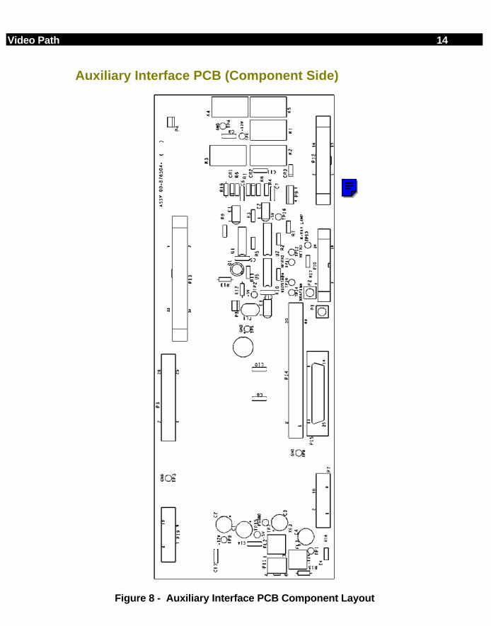
Video Path 14
Auxiliary Interface PCB (Component Side)
Figure 8 - Auxiliary Interface PCB Component Layout
NOTE
Click in the blue box to go directly to the Electrical Schematic Diagram for the PCB shown on this page. Click the << button on the Tool Bar to return to this page.
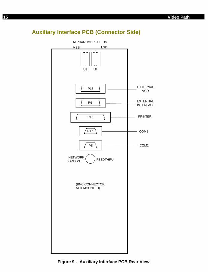
15 Video Path
Auxiliary Interface PCB (Connector Side)
EXTERNALINTERFACE
P16
P6
P18
P17
P5
NETWORKOPTION FEEDTHRU
PRINTER
COM1
COM2
ALPHANUMERIC LEDS
MSB LSB
(BNC CONNECTORNOT MOUNTED)
EXTERNALVCR
U3 U4
Figure 9 - Auxiliary Interface PCB Rear View
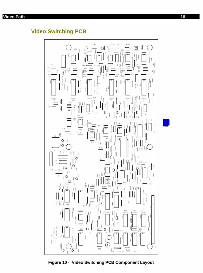
Video Path 16
Video Switching PCB
OEC-DIASONICS
ASSY 00-872239- ( )R
EV:
+12V
+5V
DGND
-5V AGND
AGND
CVO
RVID
HCO
TOVCR2
LVID
LMON
TOVCR1
AUXVOUT
A/DVIDEO
A/DV
RDAC
-12V
+5VA
+5VR
CSYOUT
DGND
U2CSOT
VMDAT
VMLCLKVMDCLK
LDAC
E
+
+
++
+
+
+
+
12
33
34
2
10
1
Q2 Q
3Q5
V R 1
TP10
TP20
TP17
TP13
TP12
TP11
TP14
TP16
TP3
TP2
TP4
TP6
TP7
TP8
TP19
TP31
TP30
TP28
TP25
TP23
U17
U5
U13
U8
U9
U10
U11
U12
U33
U34
U35
U6
U15
R1
R 2
R 3
R 4
R 5
R6
R7
R8
R9
R10
R11
R12
R13
R14
R15
R16
R17
R18
R19
R20 R
21
R22
R23
R24
R 2 5R 2 6
R 2 7R 2 8R 2 9
R30
R 3 1R 3 2
R 3 3
R 3 4R 3 5
R 3 6R 3 7R 3 8
R 3 9R 4 0R 4 1
R42
R43
R44
L 1
L 2
L 3
L 4
L 5
L 6
U7
R45
C2
C 3
C 8
C 9
C 1 1
C 1 2
C 1 4
C 1 5
C 1 7
C 1 8
C 2 0
C 2 1
C 2 3
C 2 4
C 2 6
C 2 7
C 2 8
C 2 9
C 3 0
C 3 1
C 3 2
C 3 3
C 3 4
C35
C36
C37
C38
C39
C40
C41
U26
U19
U18
U25
U24
U45
U30
U37
U42
U43
U36
U40
U39
U41
D S 1
DS2
TP22
TP21
TP18
TP9
TP32
TP33
R 4 6
R47
R 4 8
R50
R51
R151 R
54
R60
R61
R63
R64 R
65
R66
R67
R68
R69
R70
R 7 1
R 7 2
R73
R74
R75
R76
R 7 7
R78
R79
R 8 0
R 8 1
R 8 2
R 8 3
R86
R87
R88
R89
R90
R91
R92
R93
R94
R95
R 9 6
R97
R98
R99
R100
R101
R102
R103
R104
R105
R106
R107
R108
R109
R110
R111
C 4 2
C 4 3
C 4 4
C 4 5
C46
C 4 7
C 4 8
C49
C 5 5
C 5 6
C 5 9
C 6 0
C61
C62
C 6 3
C 6 4
C 6 5
C66
C68
C 6 9
C 7 0
C 7 1
C73
C74
C 7 6
C 7 7C 7 9
Q8
L11
C83
C 8 4
C86
C 8 7
C89
U32
U38
U44
R112
R113
R114
TP27
TP26
TP24
TP15
Q9
C1
C4
C5
C 6
C7
C10
C 1 3
C16
C19
C22
C25
C50
C52
C53
C54
C57
C58
C 6 7C 7 2
C 7 5C 7 8 C 8 2C 8 5
C 8 8
C90
C91
C92
C93
C 9 4
C 9 5C 9 6C 9 7
C 9 8
C 9 9
TP34
Y1
TP29
L12
P6
J11
P3
U3
C 1 0 0
C 1 0 1
C102
R 1 1 5
R116
TP1
TP5
E1
U31
J1
J2
J3
J4
J5
C104
R117
R118
R119
R120
R121
R122
C108C
109
C110
C 1 1 1
C 1 1 5R 1 2 3
R 1 2 4
U4
R128
R 1 2 9
R130
C116
E 2
R131
C117
J6
Q10
E 3
U14
U16
R 1 3 2
R133
R 1 3 4
C118
C 1 1 9
R135
R137
J7
R 1 3 8J 8
U29
U28
C 1 2 3R139
E4
R140
R141
R142R
143
U1
U2
C103
C113
R125
R126
R 1 2 7R 1 3 6
R144
R145
CR2
CR4 U
27
J9
R146
R 1 4 7
R148
R149
R150
C114
C120
U22
L15 X
U1
C 1 2 1 R 1 5 2
R 1 5 3
TP35
TP36
TP37
R154
R 1 5 5
TP38
J10
U46
CR5
CR6
C R 7
CR8
CR9
C 1 2 2
C 1 2 4
C 1 2 5
TP39
TP40
CR1
Y2
L13
L14
L9
L10
R156
R 1 5 7
Figure 10 - Video Switching PCB Component Layout
NOTE
Click in the blue box to go directly to the Electrical Schematic Diagram for the PCB shown on this page. Click the << button on the Tool Bar to return to this page.
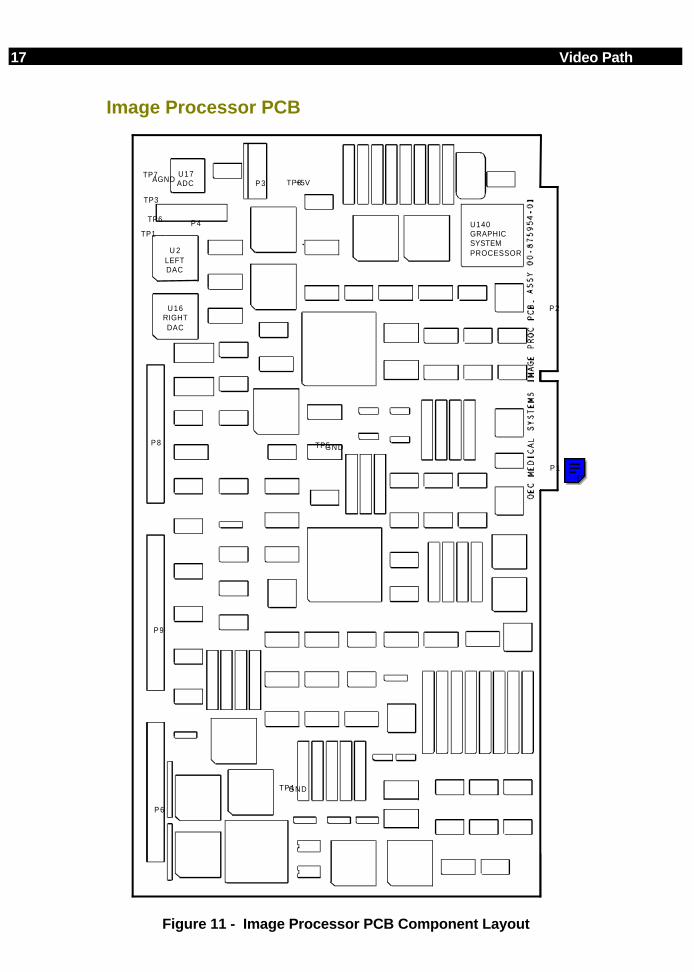
17 Video Path
Image Processor PCB
P 6
P 9
TP4GND
P 8 TP5GND
P 4TP1
TP6
TP7AGND
TP3
P 3 TP8+5V
P 2
P 1
U17ADC
U 2LEFTDAC
U16RIGHTDAC
U140GRAPHICSYSTEMPROCESSOR
Figure 11 - Image Processor PCB Component Layout
NOTE
Electrical Schematic Diagram, 00-875952 Image Processor PCB, is not included in this package. The diagram is not available in electronic form.

Video Path 18
Scan Converter PCB
Figure 12 - Scan Converter PCB Component Layout
NOTE
Click in the blue box to go directly to the Electrical Schematic Diagram for the PCB shown on this page. Click the << button on the Tool Bar to return to this page.

VIDEO CONTROL
OVERVIEWThis section contains information regarding signals that control video within the 9600Workstation. The following topics will be covered:
• The Image Processor PCB
• The Video Switching PCB
• The Scan Converter PCB
• Fast Scan Monitors
REFERENCE SCHEMATICSThe following schematic diagrams will be referred to in this section.
Workstation Interconnect Diagram
Schematic # 00-876158 - System S/N 69-0001 thru 69-1000Schematic # 00-877970 - System S/N 69-1001 and higher
Auxiliary Interface PCB
Schematic # 00-876502 - All S/N
Video Switching PCB
Schematic # 00-872237 - All S/N
Image Processor PCB
Schematic # 00-875952 - All S/N
High Rate Scan Converter PCB
Schematic # 00-876397 - All S/N
High Scan Brightness / Contrast Control PCB
Schematic # 00-876351 - All S/N
IR Receiver PCB
Schematic # 00-874220 - All S/N
2 Video Control
IMAGE PROCESSOR PCBThe Image Processor PCB is the image data processor that contains a Graphic SystemProcessor (GSP) which is driven by a 50 MHz clock. All Workstation image processingfunctions are controlled by the Image Processor. The GSP provides control signals tothe Video Switching PCB, and Scan Converter PCB. Because the Image ProcessorPCB is multi layer and uses surface mount circuits, repair of this board outside of thefactory is not recommended. Functionality of the Image Processor PCB is determinedby the use of system based diagnostic test programs.
A/D CONVERTER
The video signal enters the Image Processor PCB via connector P4 pin 5. The videosignal can be monitored at TP3 on the Image Processor PCB. The video signal is sentto A/D converter U17 where it is converted to an 8 bit digital number. The digital videodata is then sent to the scan converter section of the Image Processor PCB.
SCAN CONVERTER
The Scan Converter section consists of a two video frame memory that receives thedigital video data from the A/D converter U17. The video data is written into one frameof memory at a time. When the first frame of memory is full, video data is written into thesecond frame of memory. The first frame of video data is read out to the ImageProcessor circuitry while the second frame of video data is read in. By changing theway the video data is read out of the frame memory, the scan converter is able toprovide horizontal and vertical image reversal control for the images displayed on themonitors and peripherals. This scan converter function is provided because the CCDcamera does not offer horizontal and vertical image reversal control.
D/A CONVERTERS
After the video data has been processed by the Image Processor circuitry, left and rightvideo data is sent to the D/A converters U2 (LVID) and U16 (RVID). The D/A convertersconvert the processed digital video data into an analog video signal. The left videosignal is used by the internal VCR, Hard Copy Camera and Thermal Printer. The leftvideo signal exits the Image Processor PCB via P4 pin 9 where it goes back to theVideo Switching PCB. The right video signal exits the Image Processor PCB via P4 pin1 which also goes back to the Video Switching PCB. The right video signal is not beingused.
Video Control 3
SCAN CONVERTER PCB INTERFACE
After the video data has been processed by the Image Processor circuitry, left and rightvideo data is also sent to the scan converter interface circuitry. The scan converterinterface buffers the left and right video data out of the Image Processor PCB viaconnector P9 to the Scan Converter PCB.
PIO
The Image Processor PCB contains two PIO chips. PIO U4 provides internal controlsignals used within the Image Processor PCB. PIO U3 provides external control signalswhich go to the Video Switching PCB. Input signals from the Video Switching PCB areread by PIO U3. The Image Processor creates a 24 bit serial data output from PIO U3that controls the Video Switching PCB. The 24 bit serial data output from U3 to theVideo Switching PCB controls the following items:
• Video Crosspoint Switch
• Genlock
• Anti-Alias Filter
• Logarithmic Amplifier
• X-Ray Disable

4 Video Control
IMAGE PROCESSOR TEST DIAGNOSTICS
Diagnostic tests are available for use in evaluating the operation of the Image ProcessorPCB. The tests are selectable from the System Diagnostics Menu and are described inthe following procedure.
Press the SETUP OPTIONS key on the Workstation. The Setup Options screen willappear.
1. Insert the OEC Boot and Diagnostic disk into the disk drive.
2. Select Access Level 2 and press ENTER.
3. Select Run System Diagnostics and press ENTER.
This screen appears when "Run System Diagnostics" is selected from the ServiceOptions Menu. Select the Image Processor Tests from the menu shown below:
RUN SYSTEM DIAGNOSTICS
Front Panel TestSystem Memory TestsImage Processor TestsToggle Motion Artifact
Use the cursor arrow keys to selectoption, then press ENTER.Press the ESC key to exitand return to previous screen.

Video Control 5
These Image Processor Tests begin automatically when this test option is selected fromthe System Diagnostics Menu.
If test failures occur, the program will halt at the point of failure and display an errormessage. Press ENTER to continue testing from that point.
IMAGE PROCESSOR MEMORY TESTS
Image Memory PASSEDLeft Filter RAM PASSEDRight Filter RAM PASSEDLeft Bit Planes FAILEDRight Bit Planes PASSEDLeft LUT TESTINGRight LUT
(error messages appear here when failures occur)
Press [ENTER] to ContinuePress [ESC] to ExitPress [F2] to Repeat
Because the Image Processor PCB is multi layer and uses surface mount circuits, donot attempt to repair this PCB outside of the factory.

6 Video Control
VIDEO SWITCHING PCBThe Video Switching PCB is controlled by the Image Processor PCB utilizing a 24 bitserial data control word. The 24 bit serial control word (VMDATA) can be monitored atTP35. VMDATA is sent to the Video Switching PCB at P6 pin 11. VMDATA goes intothe first of three serial to parallel shift registers operating in cascade (U33 - U35).VMDATA is clocked into the three serial to parallel converters by VM-DTCLK at pin 11on each shift register. VM-DTCLK can be monitored at TP37. After the serial controlword has been clocked into the shift registers, VM-LTCLK is applied to the each shiftregister at pin 12. VM-LTCLK can be monitored at TP36. VM-LTCLK latches the controlword to the parallel output of the shift registers. The shift register outputs are used toturn on and off control functions on the Video Switching PCB. 18 bits of the control wordare used to route video signals in the crosspoint switch circuit. The remaining 6 bits areused to turn on or off the following circuits:
• Logarithmic amplifier
• Anti-Alias Filter
• Genlock
• X-Ray Disable
• 60 / 50 Hz Video
VIDEO SWITCHING CONTROL
Each of the multiplexers (U8 -U13) in the crosspoint switch circuit have 8 video inputs,one of which is selected at a time. The states of the address control inputs, A0 -A2 ofeach of the multiplexers control which video input is selected. The input video signal isamplified by an internal video amplifier, and output at pin 20 of each multiplexor. Theamplifiers in the multiplexers have a gain of 2, allowing for the proper video terminationof each video output.
LOGARITHMIC AMPLIFIER CONTROL
A logarithmic amplifier is used in subtraction. U46, CR5 and CR6 comprise thelogarithmic amplifier. The following amplifier, U26 restores the signal polarity andprovides an offset adjustment needed to offset the losses caused by the diodes. Thelogarithmic amplifier is switched in and out of the video path by multiplexor U19. U19 iscontrolled by VMDATA bit 20 which comes from serial to parallel shift register U33 pin 4.
Video Control 7
ANTI-ALIAS FILTER CONTROL
The anti-alias filter is designed to eliminate alias artifacts and prevent high frequencynoise in the video signal from being sampled by the A/D converter. R73, C57, C54, L9,C52, L10, C16, and R75 comprise the anti-alias filter. The anti alias filter is designed topass frequencies to 5 MHz The anti-alias filter can be switched in an out of the videopath by multiplexor U18. U18 is controlled by VMDATA bit 19 which comes from serialto parallel shift register U33 pin 5. The anti-alias filter is in the video path at all times.
GENLOCK CONTROL
The Genlock circuitry provides timing synchronization between the Image ProcessorPCB and the incoming video signal from the CCD camera. Genlock control isaccomplished by comparing the sync signal from the sync generator U40 located on theVideo Switching PCB with the incoming sync signal from the CCD camera. The phaseof the internally generated horizontal sync from U40, and that of the incoming videosignal from the CCD camera are compared in phase comparator U44. The output ofU44 is applied through a low pass filter which forms a control voltage, which is sent totuning diode CR1 controlling the frequency of voltage controlled oscillator U43 (VCO).The output of the VCO is divided by ten by PAL U29 and is sent to the OS2 input of thesync generator (U40). The CCD camera is the (master) sync source to which theGenlock circuitry synchronizes the sync generator U40 (slave) on the Video SwitchingPCB. VCO U43 provides the clock for the sync generator U40 under normal conditionswhen an incoming video signal is present. When no CCD camera sync is present in theVideo Switching PCB, sync detector U28, sets PIO U3 pin 18 low on the ImageProcessor PCB to turn off the Genlock circuit. The Image Processor turns off theGenlock circuit using serial to parallel shift register U33 pin 2 (VMDATA bit 22). WhenU33 pin 2 is set low, PAL U29 removes the VCO clock signal from sync chip U40 andreplaces it with a clock from Y1 (60 Hz operation) or Y2 (50 Hz operation). X-RayDisable (VMDATA bit 23) is also set HI and is sent to the Generator to override all X-Ray on commands.
The Genlock circuit is adjusted with sync from the CCD camera present. The Genlockadjustment is made by turning C89 on the Video Switching PCB until LED’s DS1 andDS2 both illuminate equally. In this condition the VCO output at TP33 should be runningat approximately 25.8 MHz and the voltage at TP38 (correction voltage) should beapproximately 2.5 volts.
8 Video Control
50/60 HZ VIDEO CONTROL
50 / 60 Hz video operation is controlled by the system configuration in the Workstationsoftware. The Workstation software sets the condition of serial to parallel shift registerU33 pin 3 (VMDATA bit 21). In 60 Hz configuration U33 pin 3 is set low, in 50 Hzconfiguration U33 pin 3 is set high. The signal from U33 pin 3 is sent to sync generatorU40 pin 2 which sets the sync generator to run in 50 Hz or 60 Hz mode. The signalfrom U33 pin 3 is also sent to pal U29 pin 5 which enables either crystal Y1 for 60 Hztiming or crystal Y2 for 50 Hz timing. Y1 and Y2 are both disabled when the Genlockcircuit is turned on. Only in the stand alone condition when no camera video is presentfrom the CCD camera is timing from Y1 or Y2 enabled. The signal from U33 pin 3 isalso sent to Image Processor PCB where it is used to configure the scan convertercircuit for 50 or 60 Hz operation.
Video Control 9
SCAN CONVERTER PCB
SCAN CONVERTER TIMING CONTROL
The Scan Converter PCB receives the following timing signals from the ImageProcessor PCB:
• HDRV
• VDRV
• FIELD
• PIXCL
These signals enter the Scan Converter PCB via connector J2 and are sent to the timinggenerator U22 and U24. The timing generator produces address and control signalsused by the Scan Converter PCB to convert the digital video signal from interlace formatto high rate progressive scan format.
VIDEO MEMORY
The Scan Converter receives left and right digital interlaced video data from the ImageProcessor PCB via connector J2. The digital interlaced video data is written into left andright video memory. The digital high rate progressive scan video data is read out fromthe left and right video memory and is sent to the left and right D/A converters U20 andU21.
VIDEO OUTPUT
D/A converters (U20 and U21) convert the high rate progressive scan video data into leftand right analog video signals, that are sent to the Fast Scan monitors. The analog videosignals from the D/A converters can be monitored at TP4 (left video) and TP1 (rightvideo). The left and right video signals exit the board at J5 and J4 and are sent out ofthe Electronics Box at J8 (left video) and J7 (right video) to the Fast Scan Monitors.
SCAN CONVERTER TEST
1. Power up the system and press the “TEST PATTERN” key on the keyboard.
2. Press the L<>R key on the front control panel. The gray scale test pattern should bedisplayed on both monitors.
3. Verify that the test pattern on both monitors is crisp and well defined.
4. Visually verify that pixels in the test pattern do not flicker.

10 Video Control
FAST SCAN MONITORS
HIGH SCAN BRIGHTNESS / CONTRAST CONTROL PCB.
MONITOR PCB
BRIGHTNESSAND
CONTRASTCONTROLS
AMBIENT ROOM LIGHT
SENSOR
Figure 1 - Component Locations
NOTE
Click on the top colored box to go directly to the Illustrated Parts Manual for systems bearing serial numbers 69-001 thru 69-999. Click on the bottom colored box to go directly to the Illustrated Parts Manual for systems bearing serial numbers 69-1000 and higher. Click the << button on the TOOL Bar to return to this point.
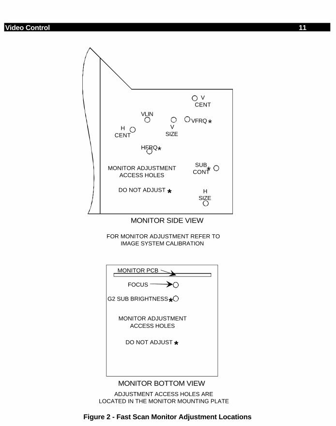
Video Control 11
HSIZE
VFRQV
SIZE
VLIN
HCENT
HFRQ
SUBCONT
VCENT
DO NOT ADJUST *
*
*
*
*DO NOT ADJUST
MONITOR ADJUSTMENT ACCESS HOLES
FOR MONITOR ADJUSTMENT REFER TO IMAGE SYSTEM CALIBRATION
MONITOR ADJUSTMENT ACCESS HOLES
MONITOR BOTTOM VIEW
ADJUSTMENT ACCESS HOLES ARE LOCATED IN THE MONITOR MOUNTING PLATE
MONITOR PCB
FOCUS
G2 SUB BRIGHTNESS *
MONITOR SIDE VIEW
Figure 2 - Fast Scan Monitor Adjustment Locations

12 Video Control
CONTRAST AND BRIGHTNESS CONTROL
Brightness and contrast adjustment is provided to allow the service technician to set upthe monitor brightness and contrast. The brightness and contrast of the Fast Scanmonitors are controlled by the left and right contrast and brightness pots located behindthe top cover of the Workstation as shown in Figure 1. Brightness and contrast pots R2and R1 from the left monitor, and R4 and R3 from the right monitor, are supplied with +5volts on one side and DC common on the other. The control voltage is obtained fromthe wiper on each pot. The control voltage is sent to the High Scan Brightness /Contrast Control PCB where it is summed with portions of the voltage from the ambientroom light sensor. The resultant voltage is applied to pins 3, 5, 10, and 12 of U2 on theHigh Scan Brightness / Contrast Control PCB, where it is amplified. The brightness andcontrols drive voltages exit the High Scan Brightness / Contrast Control PCB atconnector P4 and goes to the monitors.
AMBIENT ROOM LIGHT CONTROL
Ambient Room Light Control is provided to adjust the brightness and contrast of themonitors as lighting conditions vary. Ambient Room Light Control is obtained from theIR Receiver PCB that is located between the two monitors at the top of the front bezel ofthe Workstation. The sensor consists of a photocell which provides a variableresistance, depending on the light level entering the sensor through the clear plasticwindow in the bezel. The sensor is supplied with +12 volts, the output voltage of thephotocell is applied to resistor network R13 and R11 on the High Scan Brightness /Contrast Control PCB. The voltage from the photo cell can be monitored at TP1. Thephoto cell voltage is summed with the voltage from the contrast and brightness pots R2and R1 from the left monitor and R4 and R3 from the right monitor.
NOTE
Click on the yellow box to go directly to the block diagram for this section. Do not use this link to return to a block diagram from this point. Click on the << button in the Tool Bar to return to any starting point.
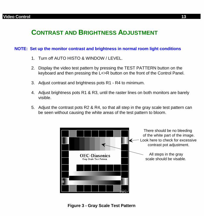
Video Control 13
CONTRAST AND BRIGHTNESS ADJUSTMENT
NOTE: Set up the monitor contrast and brightness in normal room light conditions
1. Turn off AUTO HISTO & WINDOW / LEVEL.
2. Display the video test pattern by pressing the TEST PATTERN button on thekeyboard and then pressing the L<>R button on the front of the Control Panel.
3. Adjust contrast and brightness pots R1 - R4 to minimum.
4. Adjust brightness pots R1 & R3, until the raster lines on both monitors are barelyvisible.
5. Adjust the contrast pots R2 & R4, so that all step in the gray scale test pattern canbe seen without causing the white areas of the test pattern to bloom.
All steps in the gray scale should be visable.
There should be no bleedingof the white part of the image.
Look here to check for excessivecontrast pot adjustment.
Figure 3 - Gray Scale Test Pattern
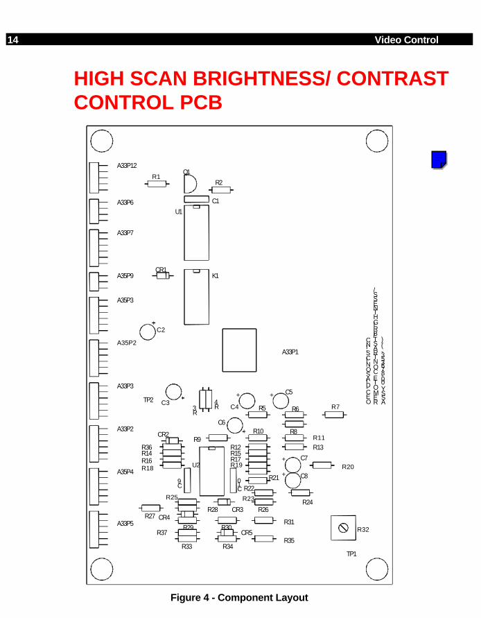
14 Video Control
HIGH SCAN BRIGHTNESS/ CONTRASTCONTROL PCB
OEC-DIASONICS,INC
REMOTE CONTRAST/BRIGHTNESS/
ASSY 00-876353- ( )
R21
R35
R30
R10
R20
R32
R12
R24
R17
R23
R14
R19
R8
R3 R7
R27R31
R25
R15R16R18
R28
R4
C4
C2
C3
K1A35P9
A33P2
A33P3
A33P6
A33P7
A33P5
U1
R5 R6
R9
A33P1
R2R1
Q1
TP1
TP2
A33P12
CR1
U2
A35P2
A35P3
A35P4
R13R11
C6
C5
C8
C7
C9
C10
C1
R34
R26
R29
R33
CR2
CR4
CR5
CR3
R22
R36
R37
Figure 4 - Component Layout
NOTE
Click in the blue box to go directly to the Electrical Schematic Diagram for the PCB shown on this page. Do not use this link to return to a block diagram from this point. Click the << button on the Tool Bar to return to any starting page.
IMAGE STORAGE
OVERVIEWA standard Workstation comes equipped with an IDE Hard Disk Drive anda 1.44 MB Floppy Disk Drive. The IDE Hard Disk Drive may be replacedby either of the following options.
•• 4FPS SCSI Disk Optio n•• 30FPS SCSI Disk Option
The Workstation can also contain one or more of the following options.Please refer to the Peripheral section of this manual for details of theseoptions.
• • Internal VCR Option• • Lenzar Hard Copy Camera Option• • Laser Camera Interface Option• • Thermal Printer Option
2 Image Storage
IDE HARD DISK DRIVEThe basic 9600 system contains one hard disk with two DOS partitions.One 10 megabyte partition (C: drive) is for Workstation program storageand a 30 Megabyte partition (D: drive) is for the 100 image storage. Thehard disk is an IDE-type drive and is controlled by an imbedded controlleron the Workstation 386 Motherboard. Jumpers on the CommunicationPCB must be configured to select between this drive and the SCSI typehard drive.
1.44 MB FLOPPY DISK DRIVEThe 1.44 MB High Density Floppy Disk Drive (A drive) is used by theWorkstation AT Motherboard and requires a 3 1/2-inch high density floppydisk for data storage and transfer. The floppy disk drive is installed in allWorkstation configurations.
Figure 1 - IDE Hard Drive Block Diagram
Image Storage 3
4FPS SCSI DISK OPTIONThe Four Frames Per Second (4FPS) option is intended for cine runs up tofour frames per second. It contains two SCSI Disk Controllers and a SCSIdisk drive. The IDE drive is not present with this option. The disk is 400 MBor larger and is DOS-formatted with a 10MB (C drive) and a 30 MB (Ddrive) partition. Drive C contains the Workstation application software.Drive D is used to store the 100 static images. The portion of the driveused for cine runs does not have a drive designator.
The DOS-SCSI controller performs all of the DOS functions,communicating with the 10 MB and 30 MB partitions. The IP-SCSIcontroller transfers data to or from the Image Processor and the SCSI diskin the non-DOS (cine loop) area of the disk. Image data is transferredbetween the Image Processor and the IP-SCSI controller at the fourframes per second rate. Image data is then transferred between the IP-SCSI controller and the SCSI disk as 8-bit image data at approximately 1MB per second.
Figure 2 - 4 FPS Block Diagram
NOTE
Click on the yellow box to go directly to the block diagram for this section. Do not use this link to return to a block diagram from this point. Click on the << button in the Tool Bar to return to any starting point.
4 Image Storage
30FPS SCSI DISK OPTIONThe 30FPS option contains three SCSI Disk Controllers and two SCSI diskdrives. The IDE drive is not present with this option. The disks are 1 GB orlarger and one is DOS-formatted with 10 and 30 MB partitions. One SCSIcontroller (DOS-SCSI) performs all of the DOS functions, communicatingwith the 10 MB and 30 MB partitions. The other two SCSI controllers (IP-SCSI) transfer data to or from the Image Processor and the SCSI disks inthe non-DOS area of the disk. Image data is transferred between theImage Processor and the IP-SCSI controllers at the 30 fps rate. Imagedata is then transferred between each IP-SCSI controller and itsassociated disk as 8-bit image data at approximately 3.5 MB per second.Each IP-SCSI controller transfers image data for every other image frame.Even numbered frames are stored on SCSI disk (1) and odd numberedframes are stored to SCSI disk (2).
Figure 3 - 30 FPS Block Diagram
NOTE
Click on a yellow box to go directly to the block diagram for this section. Do not use this link to return to a block diagram from this point. Click on the << button in the Tool Bar to return to any starting point.
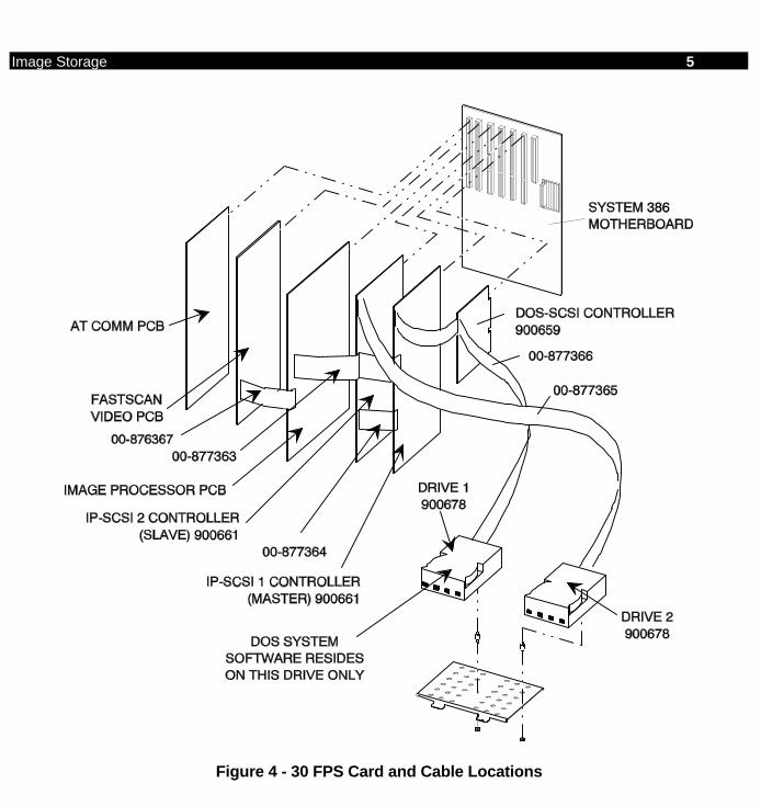
Image Storage 5
Figure 4 - 30 FPS Card and Cable Locations
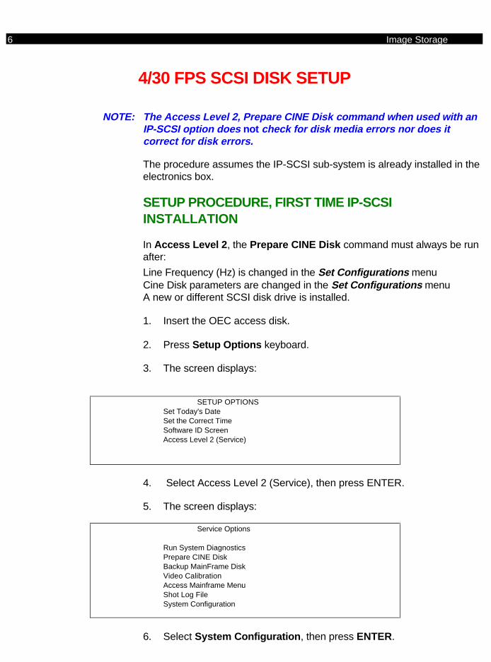
6 Image Storage
4/30 FPS SCSI DISK SETUP
NOTE: The Access Level 2, Prepare CINE Disk command when used with anIP-SCSI option does not check for disk media errors nor does itcorrect for disk errors.
The procedure assumes the IP-SCSI sub-system is already installed in theelectronics box.
SETUP PROCEDURE, FIRST TIME IP-SCSIINSTALLATION
In Access Level 2 , the Prepare CINE Disk command must always be runafter:
Line Frequency (Hz) is changed in the Set Configurations menuCine Disk parameters are changed in the Set Configurations menuA new or different SCSI disk drive is installed.
1. Insert the OEC access disk.
2. Press Setup Options keyboard.
3. The screen displays:
SETUP OPTIONSSet Today's DateSet the Correct TimeSoftware ID ScreenAccess Level 2 (Service)
4. Select Access Level 2 (Service), then press ENTER.
5. The screen displays:
Service Options
Run System DiagnosticsPrepare CINE DiskBackup MainFrame DiskVideo CalibrationAccess Mainframe MenuShot Log FileSystem Configuration
6. Select System Configuration , then press ENTER.

Image Storage 7
7. The screen displays:
SYSTEM Configuration
Set System ConfigurationsImaging Defaults
8. Select Set System Configuration s, then press ENTER.
9. The screen displays:
SET CONFIGURATION
Line Frequency (Hz) 60System Model VASCine Disk NONELanguage EnglishVCR1 SonyVCR2 Sony
NOTE: This screen display is only one example; yours may differ accordingto your system configuration.
10. Select the Cine Disk menu item, and then using the left or rightarrow keys, toggle through to ALTA4 or ALTA30 , whichever isappropriate.
OR, if changing the line frequency:
Select the Line Frequency (Hz) configuration, then with the left or rightarrow keys, select 50 Hz or 60 Hz frequency.
IMPORTANT... THE FOLLOWING STEPS (11 - 30) MUST BE PERFORMED IN THE ORDERPRESENTED.
11. After selecting Cine Disk , or Line Frequenc y, press ENTER.
12. The following will be displayed at the bottom of the configurationmenu:
PRESS SETUP TO CONFIRM
13. Press the Setup Option s key.
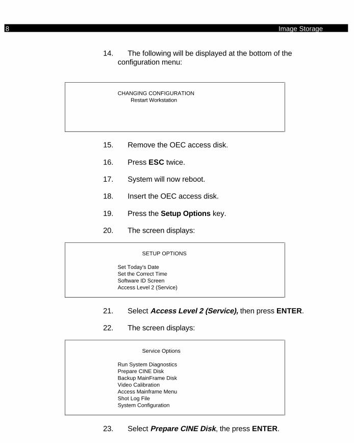
8 Image Storage
14. The following will be displayed at the bottom of theconfiguration menu:
CHANGING CONFIGURATION Restart Workstation
15. Remove the OEC access disk.
16. Press ESC twice.
17. System will now reboot.
18. Insert the OEC access disk.
19. Press the Setup Options key.
20. The screen displays:
SETUP OPTIONS
Set Today's DateSet the Correct TimeSoftware ID ScreenAccess Level 2 (Service)
21. Select Access Level 2 (Service), then press ENTER.
22. The screen displays:
Service Options
Run System DiagnosticsPrepare CINE DiskBackup MainFrame DiskVideo CalibrationAccess Mainframe MenuShot Log FileSystem Configuration
23. Select Prepare CINE Disk , the press ENTER.
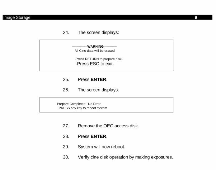
Image Storage 9
24. The screen displays:
---------------WARNING------------- All Cine data will be erased
-Press RETURN to prepare disk-
-Press ESC to exit-
25. Press ENTER.
26. The screen displays:
Prepare Completed: No Error. PRESS any key to reboot system
27. Remove the OEC access disk.
28. Press ENTER.
29. System will now reboot.
30. Verify cine disk operation by making exposures.

10 Image Storage
DEBUGGING USING IP-SCSI LEDSAdditional diagnostic information is available from the LEDs located on theIP-SCSI Controller(s). Before switching on the power, open the door of theelectronics rack so that the bottom edge of the IP-SCSI is visible and notethe 3 LEDs on each PCB.
Switch on the power and notice that after the system completes its bootprocess, the LEDs are as follows, indicating that the system has stabilizedand is ready for normal operation.
Green Yellow RedOFF ON OFF
NORMAL OPERATION - The green LED will flash each time a commandis received from the AT host. For a 30FPS system, all commands arereceived by the Master IP-SCSI Controller (A11). The yellow LEDindicates the controller is ready to accept a command.
Green Yellow RedFlash ON OFF
INVALID SYSTEM CONFIGURATION OR IP-SCSI HARDWAREFAILURE INDICATION - If the LEDs do not change from their power-on(random) state, the IP-SCSI controller is not being initialized. CheckSystem Configuration (Level 2 Service) and the IP-SCSI PCB.
GENERAL 4/30FPS SCSI DISK SUBSYSTEM FAILURE INDICATION -If the yellow LED stays OFF for several seconds during boot or systemoperation, a 4/30FPS SCSI disk system hardware failure is indicated.Check the following: IP cable from IP PCB to IP-SCSI, IP PCB or IP-SCSIcontroller.
Green Yellow RedOFF OFF OFF
SCSI PROBLEM INDICATION - If the red LED goes ON during the initialboot process, a problem with the SCSI bus is indicated. Check the SCSIhard disk, the SCSI cable which connects the SCSI hard disk to the IP-SCSI, or the IP-SCSI itself .
Green Yellow RedOFF ON ON
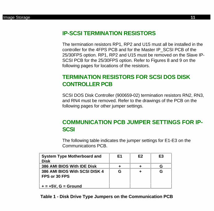
Image Storage 11
IP-SCSI TERMINATION RESISTORS
The termination resistors RP1, RP2 and U15 must all be installed in thecontroller for the 4FPS PCB and for the Master IP_SCSI PCB of the25/30FPS option. RP1, RP2 and U15 must be removed on the Slave IP-SCSI PCB for the 25/30FPS option. Refer to Figures 8 and 9 on thefollowing pages for locations of the resistors.
TERMINATION RESISTORS FOR SCSI DOS DISKCONTROLLER PCB
SCSI DOS Disk Controller (900659-02) termination resistors RN2, RN3,and RN4 must be removed. Refer to the drawings of the PCB on thefollowing pages for other jumper settings.
COMMUNICATION PCB JUMPER SETTINGS FOR IP-SCSI
The following table indicates the jumper settings for E1-E3 on theCommunications PCB.
System Type Motherboard andDisk
E1 E2 E3
386 AMI BIOS With IDE Disk + + G386 AMI BIOS With SCSI DISK 4FPS or 30 FPS
G + G
+ = +5V, G = Ground
Table 1 - Disk Drive Type Jumpers on the Communication PCB
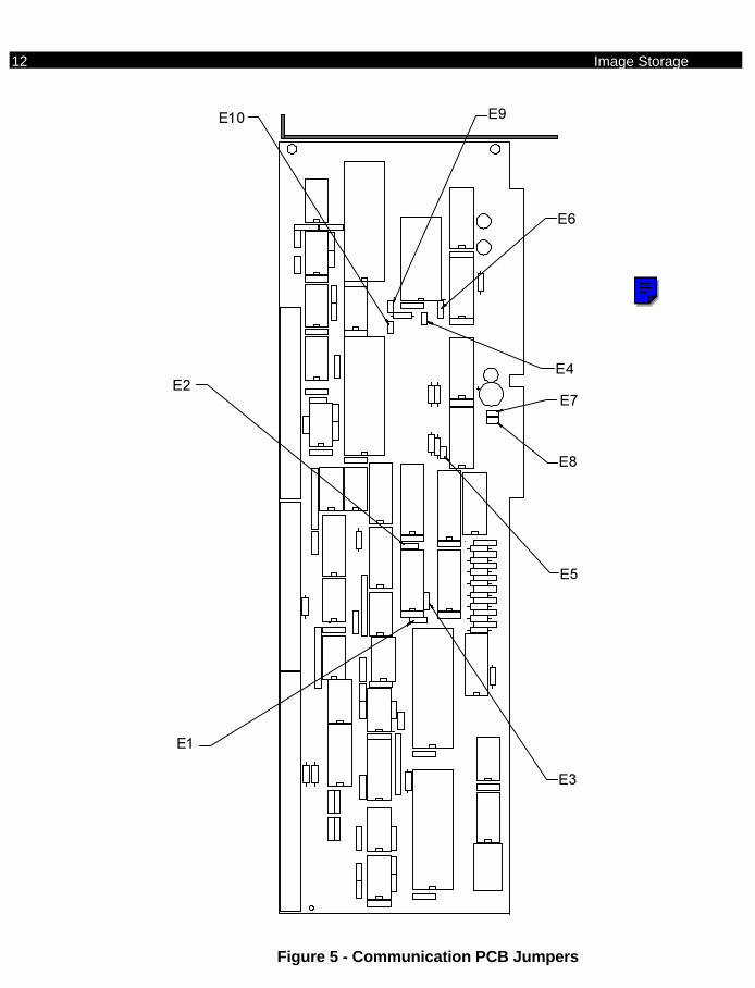
12 Image Storage
E1
E2
E3
E4
E5
E6
E7
E8
E9E10
Figure 5 - Communication PCB Jumpers
NOTE
Click in the blue box to go directly to the Electrical Schematic Diagram for the PCB shown on this page. Click the << button on the Tool Bar to return to this page.
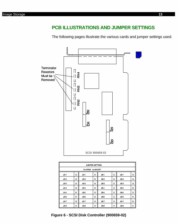
Image Storage 13
PCB ILLUSTRATIONS AND JUMPER SETTINGS
The following pages illustrate the various cards and jumper settings used.
SCSI 900659-02
Figure 6 - SCSI Disk Controller (900659-02)
NOTE:
There are no electrical schematics for the disk drive controller cards in this package. If difficulty is experienced with any of these cards, contact the OEC Medical Systems, Inc., Field Service Department.
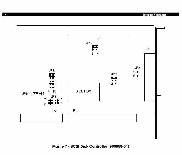
14 Image Storage
Figure 7 - SCSI Disk Controller (900659-04)
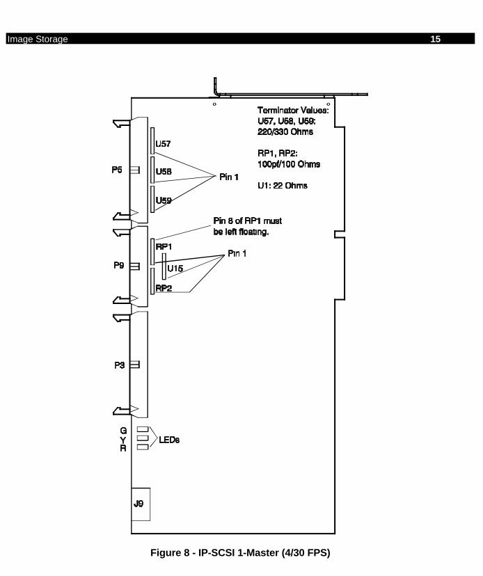
Image Storage 15
Figure 8 - IP-SCSI 1-Master (4/30 FPS)
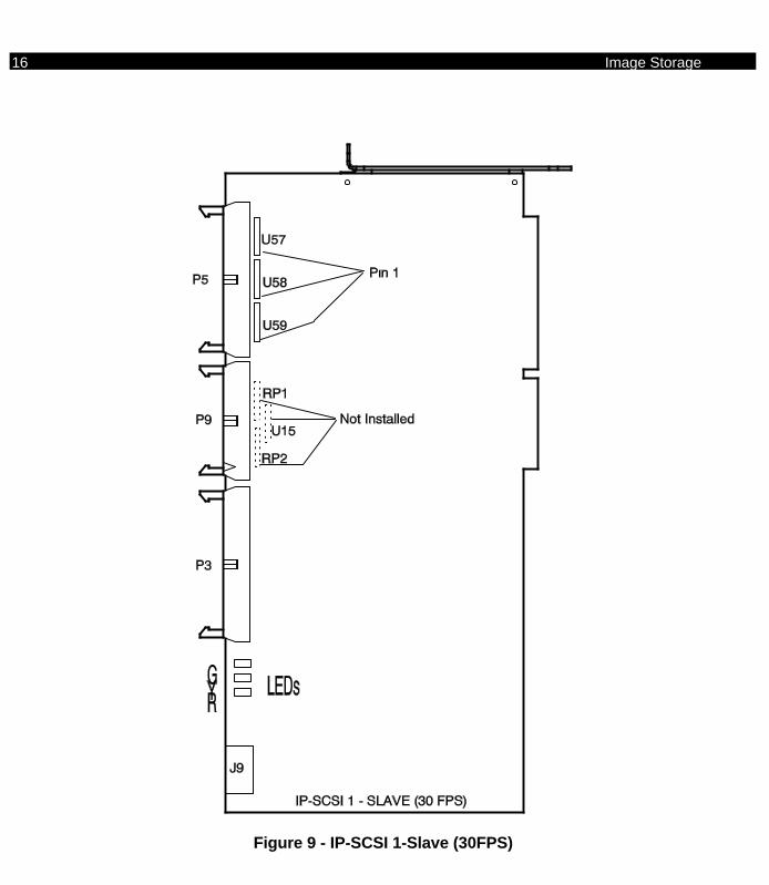
16 Image Storage
Figure 9 - IP-SCSI 1-Slave (30FPS)
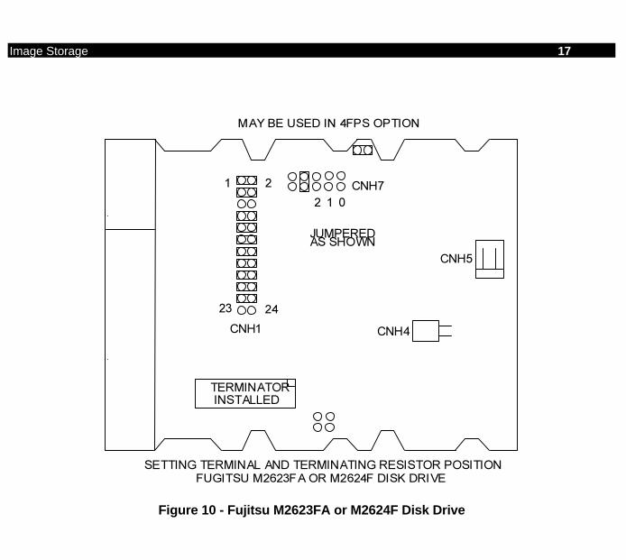
Image Storage 17
1 2
23 24
CNH1
JUMPEREDAS SHOWN
TERMINATOR
INSTALLED
2 1 0
CNH5
CNH4
SETTING TERMINAL AND TERMINATING RESISTOR POSITION
CNH7
MAY BE USED IN 4FPS OPTION
FUGITSU M2623FA OR M2624F DISK DRIVE
Figure 10 - Fujitsu M2623FA or M2624F Disk Drive
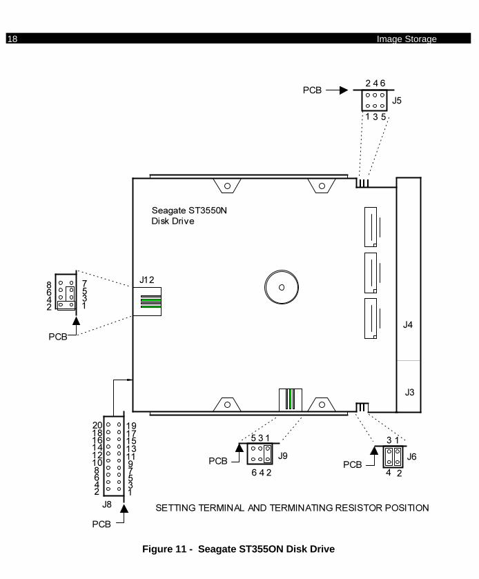
18 Image Storage
PCBPCB
1357
2468
1234567891011121314151617181920
J12
PCB
PCB
J4
J3
135
246
13
24
J9 J6
SETTING TERMINAL AND TERMINATING RESISTOR POSITION
J5
1 3 5
2 4 6
PCB
J8
Seagate ST3550N
Disk Drive
Figure 11 - Seagate ST355ON Disk Drive
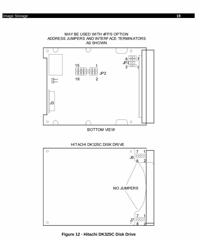
Image Storage 19
15
16
1
2
JP2
JP3
6
2
7
1
J3
BOTTOM VIEW
1
2
7
8J6
J7
17
8 2
NO JUMPERS
MAY BE USED WITH 4FPS OPTION
ADDRESS JUMPERS AND INTERFACE TERMINATORS
AS SHOWN
HITACHI DK325C DISK DRIVE
Figure 12 - Hitachi DK325C Disk Drive
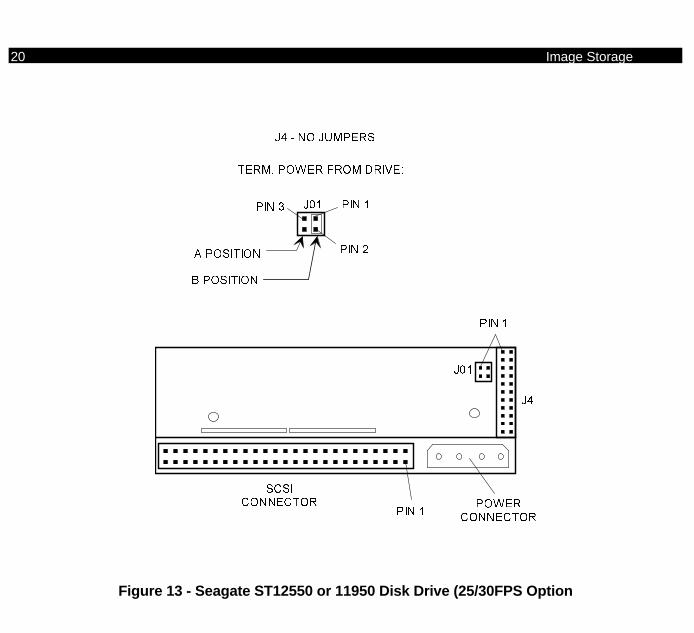
20 Image Storage
J01
J4
J01
SCSI
CONNECTORPIN 1
POWER
CONNECTOR
PIN 1
J4 - NO JUMPERS
TERM. POWER FROM DRIVE:
PIN 3 PIN 1
PIN 2A POSITION
B POSITION
Figure 13 - Seagate ST12550 or 11950 Disk Drive (25/30FPS Option

PERIPHERALS
OVERVIEWThere are several peripherals available for the 9600 Workstation. These include:
• • VCR
• • Hard Copy Camera
• • Digital Laser Camera Interface
• • Thermal Printer
• • Paper Printer
This section provides general information on how these peripherals are used and alsoprovides basic service information including configuration & troubleshooting notes.These peripherals (except the VCR and Hard Copy Camera) are connected to the rearpanel as shown in Figure 1.
NOTE: The COM2 Serial Port and the ETHERNET IN/OUT BNCs are not currentlyused.
NOTE
Click on a yellow box to go directly to the block diagram for this section. Do not use this link to return to a block diagram from this point. Click on the << button in the Tool Bar to return to any starting point.
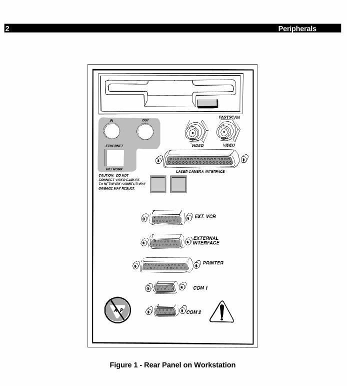
2 Peripherals
Figure 1 - Rear Panel on Workstation
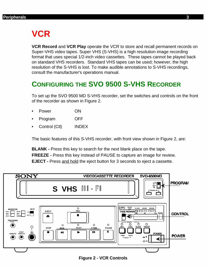
Peripherals 3
VCRVCR Record and VCR Play operate the VCR to store and recall permanent records onSuper-VHS video tapes. Super VHS (S-VHS) is a high resolution image recordingformat that uses special 1/2-inch video cassettes. These tapes cannot be played backon standard VHS recorders. Standard VHS tapes can be used; however, the highresolution of the S-VHS is lost. To make audible annotations to S-VHS recordings,consult the manufacturer's operations manual.
CONFIGURING THE SVO 9500 S-VHS RECORDER
To set up the SVO 9500 MD S-VHS recorder, set the switches and controls on the frontof the recorder as shown in Figure 2.
• Power ON
• Program OFF
• Control (Ctl) INDEX
The basic features of this S-VHS recorder, with front view shown in Figure 2, are:
BLANK - Press this key to search for the next blank place on the tape.FREEZE - Press this key instead of PAUSE to capture an image for review.EJECT - Press and hold the eject button for 3 seconds to eject a cassette.
REC
PAUSEF FWDPLAYREW
EJECT
STOP
MONITOR HI-FI
TRACKINGF I X E D
O N
OFF
S VHS
AUTOOFF S-VHS MARK ERASE
TAPE REMAINCTL
MENU
INDEX100 50 0% RESET
REV FWD BLANK FREEZE
SEARCH
ITEM DATAPOWER
OFF
MENU
CH 1MIXCH 2
MIXHI-FI
NORM
REMOTEFOOT
SWITCHMIC
A
B
MARK-INA B
Figure 2 - VCR Controls

4 Peripherals
RECORD UNPROCESSED VIDEO (VCR 1
To record to the VCR:
1. Insert an S-VHS tape cassette into the recorder.
2. Position the tape to the starting point for the recording. Press VCR Play to reviewthe tape if necessary to determine the index number of the new starting point. Resetthe index counter or make note of the index reading.
3. Press the VCR RECORD key. The recorder LED is lit. Press the SUPERKEY tostart or stop processing images.
4. Proceed with the desired surgical procedure. The recorder records imageswhenever the X-ray On switch or Process Fluoro footswitch is pressed. The VCRautomatically goes to PAUSE when the footswitch is released.
NOTE: During the recording process, the monitor displays the processed image. Theimage recorded on the tape, however, depends on the VCR configuration. Thedefault configuration is unprocessed video, that is, undigitized video output. Referto Configuring VCR Options later in this section.
5. Record the tape index counter reading when the recording session is completed.
REVIEW THE RECORDING
To review the video recording:
1. Load the recorded S-VHS cassette into the recorder.
2. Position the tape at the start of the recording with the recorder’s positioning keys(REV, PLAY and FORWARD).
3. Press VCR Play on the TrackPad panel. The LED is lit.
4. Press the SuperKey to start or stop processing images.
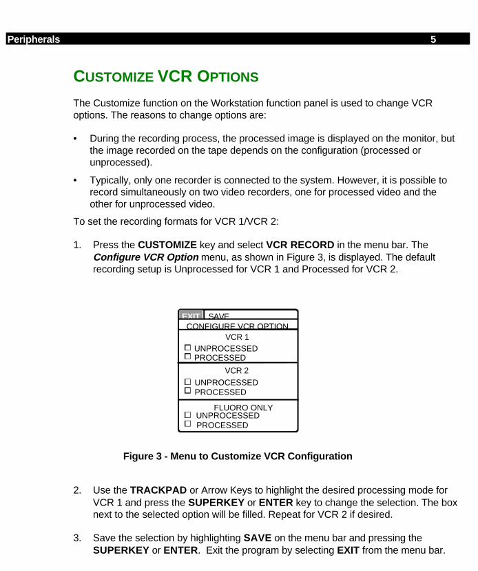
Peripherals 5
CUSTOMIZE VCR OPTIONS
The Customize function on the Workstation function panel is used to change VCRoptions. The reasons to change options are:
• During the recording process, the processed image is displayed on the monitor, butthe image recorded on the tape depends on the configuration (processed orunprocessed).
• Typically, only one recorder is connected to the system. However, it is possible torecord simultaneously on two video recorders, one for processed video and theother for unprocessed video.
To set the recording formats for VCR 1/VCR 2:
1. Press the CUSTOMIZE key and select VCR RECORD in the menu bar. TheConfigure VCR Option menu, as shown in Figure 3, is displayed. The defaultrecording setup is Unprocessed for VCR 1 and Processed for VCR 2.
SAVECONFIGURE VCR OPTION
VCR 1
VCR 2
FLUORO ONLY
EXIT
UNPROCESSEDPROCESSED
UNPROCESSEDPROCESSED
UNPROCESSEDPROCESSED
Figure 3 - Menu to Customize VCR Configuration
2. Use the TRACKPAD or Arrow Keys to highlight the desired processing mode forVCR 1 and press the SUPERKEY or ENTER key to change the selection. The boxnext to the selected option will be filled. Repeat for VCR 2 if desired.
3. Save the selection by highlighting SAVE on the menu bar and pressing theSUPERKEY or ENTER. Exit the program by selecting EXIT from the menu bar.

6 Peripherals
VCR CONNECTIONS
To ensure proper operation, confirm the rear of the VCR is connected as shown inFigure 4.
ACPOWER
POWER OUTLET STRIP
REAR VIEW OFVCR UNIT
P10
FROM P15OF AUX. INT. PCB
CONTROL CABLE
P2 P1
FROM J4 TO J1OF VID. SWITCH. PCB
~ A C I N
Figure 4 - VCR Connections
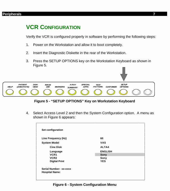
Peripherals 7
VCR CONFIGURATION
Verify the VCR is configured properly in software by performing the following steps:
1. Power on the Workstation and allow it to boot completely.
2. Insert the Diagnostic Diskette in the rear of the Workstation.
3. Press the SETUP OPTIONS key on the Workstation Keyboard as shown inFigure 5.
APPSSPECIAL
PATTERNTEST
VIEWDISK
(ANNOTATE)PATIENT
HELP DIRIMAGE
MARKERS CUSTOMIZESUMMARY
X-RAY SETUPOPTIONS
Figure 5 - “ SETUP OPTIONS” Key on Workstation Keyboard
4. Select Access Level 2 and then the System Configuration option. A menu asshown in Figure 6 appears:
Set configuration
Line Frequency (Hz) 60
System Model VAS
Cine Disk ALTA4
Language ENGLISHVCR1 SonyVCR2 SonyDigital Print YES
Serial Number: xx-xxxxHospital Name:
Figure 6 - System Configuration Menu

8 Peripherals
HARD COPY CAMERAImages recorded on the Hard Copy Camera are film copies of left monitor images.Window and Level optimize the left monitor image before making the Hard Copyexposure. The EXPOSE key on the Hard Copy Camera Control on the Workstationmakes the exposure as shown in Figure 7.
RESET PROGRAM EXPOSE
Figure 7 - Hard Copy Camera Controls
USING THE HARD COPY CAMERA
Refer to the Operator's Manual for detailed operation of this unit. To make a film imagewith the Hard Copy Camera:
1. Display the image to be copied on the left monitor.
2. Adjust Window and Level to optimize the image.
3. Insert the film cassette in the Hard Copy Camera and remove the lower protectiveslide from the cassette. EXP 1 appears on the camera display.
4. Press the EXPOSE key on the Hard Copy Camera. When Expose is pressed, thecamera displays BUSY. A tone beeps at the end of the exposure and EXP 2displays.
5. Press the EXPOSE key again to take the second image. BUSY displays, and atone beeps at the end of the exposure. Replace the protective slide beforeremoving the cassette. Reverse cassette for additional images.
Additional Features
The following are additional features of the Hard Copy camera:
VIEW-PORT - Displays the image on the Hard Copy or when the Program key ispressed.
RESET - Prepares the camera for the next set of exposures. Press the Reset key to goto EXP 1.
PROG - The Program key performs these functions:
• Press to view the image as it will appear in the exposure.
• Hold down to change settings.
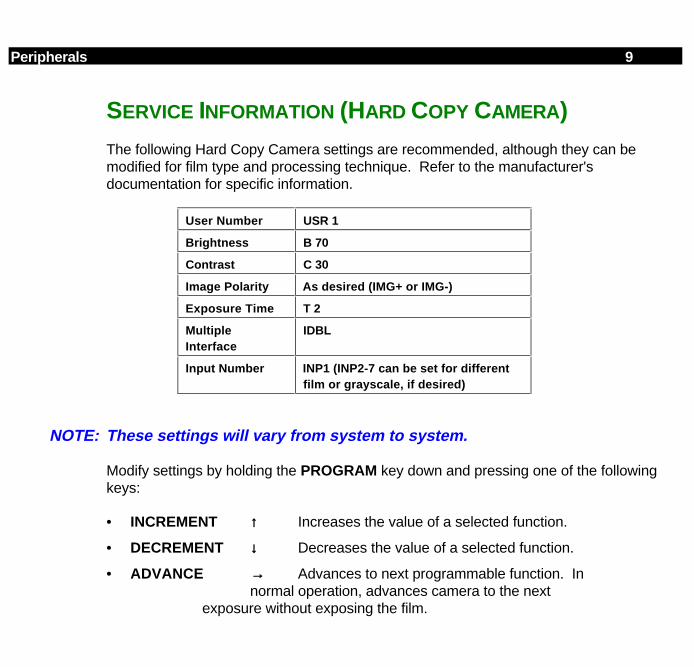
Peripherals 9
SERVICE INFORMATION (HARD COPY CAMERA)
The following Hard Copy Camera settings are recommended, although they can bemodified for film type and processing technique. Refer to the manufacturer'sdocumentation for specific information.
User Number USR 1
Brightness B 70
Contrast C 30
Image Polarity As desired (IMG+ or IMG-)
Exposure Time T 2
MultipleInterface
IDBL
Input Number INP1 (INP2-7 can be set for differentfilm or grayscale, if desired)
NOTE: These settings will vary from system to system.
Modify settings by holding the PROGRAM key down and pressing one of the followingkeys:
• INCREMENT ↑↑ Increases the value of a selected function.
• DECREMENT ↓↓ Decreases the value of a selected function.
• ADVANCE →→ Advances to next programmable function. In normal operation, advances camera to the next
exposure without exposing the film.
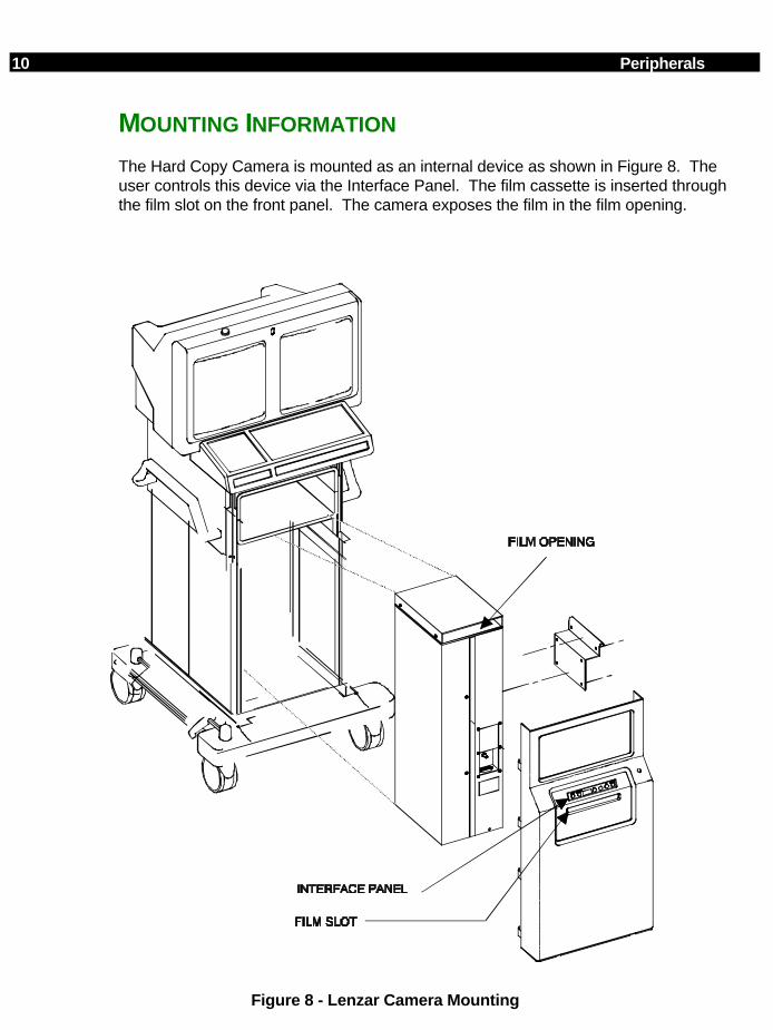
10 Peripherals
MOUNTING INFORMATION
The Hard Copy Camera is mounted as an internal device as shown in Figure 8. Theuser controls this device via the Interface Panel. The film cassette is inserted throughthe film slot on the front panel. The camera exposes the film in the film opening.
Figure 8 - Lenzar Camera Mounting
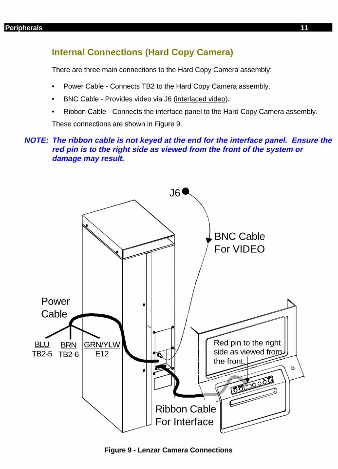
Peripherals 11
Internal Connections (Hard Copy Camera)
There are three main connections to the Hard Copy Camera assembly:
• Power Cable - Connects TB2 to the Hard Copy Camera assembly.
• BNC Cable - Provides video via J6 (interlaced video).
• Ribbon Cable - Connects the interface panel to the Hard Copy Camera assembly.
These connections are shown in Figure 9.
NOTE: The ribbon cable is not keyed at the end for the interface panel. Ensure thered pin is to the right side as viewed from the front of the system ordamage may result.
J6
BNC CableFor VIDEO
Red pin to the rightside as viewed fromthe front.
Ribbon CableFor Interface
BLUTB2-5
BRNTB2-6
GRN/YLWE12
PowerCable
Figure 9 - Lenzar Camera Connections

12 Peripherals
DIGITAL LASER CAMERA INTERFACEThe Laser Camera Interface system uses specially designed software and circuitrywhich enables the operator to print multiple X-ray images with a laser camera. The X-ray images print out in a selected matrix format determined by the type of laser camera.The Interface system supports the following laser cameras:
• 3M Laser Imager (P831) with Protocol MMU920
• 3M Laser Imager Plus (M952) restricted to Protocol MMU920
• Kodak Ektascan Laser Printer, with KCL protocol supports models 100, 100-XLP,1120 and 2180
• Kodak Ektascan Image Manager (KEIM)
The user selects the number of images and their printed format. Each film sheetcontains the images in a specified number of rows and columns.
Note that selecting fewer images than the total number of slots on a film sheet results inblank frames. Selecting more images than number of slots results in extra images, andblank frames, printed on the last sheet of film.
Before printing X-ray images, ensure proper cable connections. The 37-pin D-subparallel connector, labeled LASER CAMERA INTERFACE, and the 9-pin serialconnector, labeled COM 1, are located on the rear of the Workstation panel as shown inFigure 12.
Figure 10 - Laser Camera Interface and COM 1 Connections on Rear Panel
Peripherals 13
DIGITAL LASER CAMERA INTERFACE PRINTING
Follow the steps beginning on the next page to print X-ray images on a laser camera.
NOTE: The screen displays shown here may vary slightly from those displayed onyour Workstation depending on your system. The following example usesa 3M laser camera.
1. Switch on the main power to the Workstation with the keyswitch and wait for theOEC logo to display on the right monitor.
2. Press the CUSTOMIZE key on the Workstation keyboard to display theCUSTOMIZE OPERATION menu.
3. Press the down arrow key to select DEFINE PRINTER, then press ENTER todisplay the DEFINE PRINTERS menu.
4. Enter data for each of the four DEFINE PRINTERS parameters. The followingexample uses configuration #1 for a 3M laser camera (printer) with a 3x2 film matrix.
CONFIGURATION = 1This is the designated number for one set of printing configurations; note that #1 is thedefault. The system supports a total of 4 different configurations, hence theconfiguration can only be 1, 2, 3, or 4. Pressing the right arrow key toggles to eachconsecutive number. Select the desired configuration, then press the down arrow key.
NAME = 3M 3X2The name will be used later when you’re asked to select the configuration for printing theX-ray images (in step 11). You should create a name that you recognize as designatingthe configuration parameters of the previously selected configuration (in this case, #1).Type in an appropriate name, then press ENTER.
PRINTER TYPE = 3MPress the right arrow key as many times as necessary to select the correct printer type,then press the down arrow key.
FILM MATRIX = 3X2The film matrix determines the printed format for the X-ray images in rows x columns .The matrix choices are limited to those available from the selected printer. The totalnumber of images printed on one film sheet is the product of the two numbers. In thisexample, the 3M printer will print a sheet with 6 images, in 3 rows and 2 columns, 2images per row, 3 images per column. Press the right arrow key as many times asnecessary to select the desired matrix, then press ENTER.
5. Press ENTER again to store the previously entered data into configuration #1 (orBACKSPACE to delete), then press ESC to get out of the DEFINE PRINTERSmenu and back to CUSTOMIZE OPERATION.

14 Peripherals
6. When CUSTOMIZE OPERATION displays, press the IMAGE DIR key to displaythe IMAGE DIRECTORY menu.
7. Select LIST BY with the right arrow key, then press ENTER to display the threeoptions for selecting X-ray images.
8. This example uses images selected by DATE. Select the desired option with thedown arrow key, then press ENTER.
9. Select the appropriate date with the down arrow key, then press ENTER.
10. Note that the images display in consecutive order from the bottom up. SelectPRINT with the up arrow key, then press ENTER to display the names.
11. The names created display in consecutive order from the top down. This exampleused 3M 3x2 (created in step 4) for the configuration 1 name. Select the desiredname with the down arrow key, then press ENTER.
12. With the up or down arrow key, position the arrow icon next to each image to beprinted, then press the spacebar.
13. Note the “print” icon to the left of the image selected. Pressing the spacebar asecond time on the same image removes the image from print selection. The aboveexample shows three images selected so far. Select the desired number of images,then press ENTER.
14. The number of each image being prepared to print displays at the lower right of thescreen. (In this example, assume 6 images were selected; recall that a total of 6could be printed on one sheet of film in the selected 3 x 2 matrix.) Note that theimage being prepared displays on the left monitor.
Printing Image(s) Please Wait
15. When all the images have been sent to the printer, the screen displays the abovemessage. When this message is gone, the printing is complete.

Peripherals 15
Digital Laser Camera Interface - Internal Connections
Electrical connections for the Digital Laser Camera Interface are shown in Figure 11.Item "A50" resides in the J7 slot of the AT Motherboard.
Figure 11
The Laser Interface PCB (00-900938) occupies slot J7 of the AT Motherboard and isshown in Figure 12 with its connection from J2 of the PCB to J19 of the rear panel.
Figure 12 - Laser Interface PCB
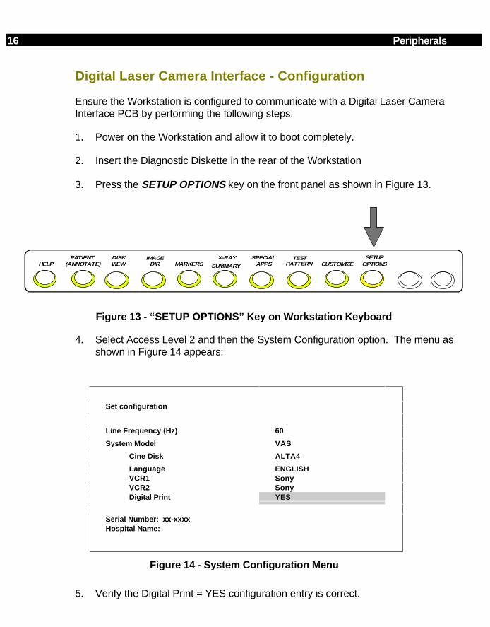
16 Peripherals
Digital Laser Camera Interface - Configuration
Ensure the Workstation is configured to communicate with a Digital Laser CameraInterface PCB by performing the following steps.
1. Power on the Workstation and allow it to boot completely.
2. Insert the Diagnostic Diskette in the rear of the Workstation
3. Press the SETUP OPTIONS key on the front panel as shown in Figure 13.
APPSSPECIAL
PATTERNTEST
VIEWDISK
(ANNOTATE)PATIENT
HELP DIRIMAGE
MARKERS CUSTOMIZESUMMARY
X-RAY SETUPOPTIONS
Figure 13 - “ SETUP OPTIONS” Key on Workstation Keyboard
4. Select Access Level 2 and then the System Configuration option. The menu asshown in Figure 14 appears:
Set configuration
Line Frequency (Hz) 60
System Model VAS
Cine Disk ALTA4
Language ENGLISHVCR1 SonyVCR2 SonyDigital Print YES
Serial Number: xx-xxxxHospital Name:
Figure 14 - System Configuration Menu
5. Verify the Digital Print = YES configuration entry is correct.
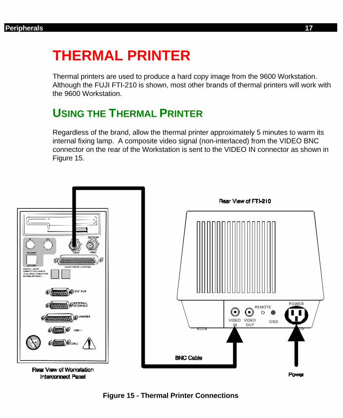
Peripherals 17
THERMAL PRINTERThermal printers are used to produce a hard copy image from the 9600 Workstation.Although the FUJI FTI-210 is shown, most other brands of thermal printers will work withthe 9600 Workstation.
USING THE THERMAL PRINTER
Regardless of the brand, allow the thermal printer approximately 5 minutes to warm itsinternal fixing lamp. A composite video signal (non-interlaced) from the VIDEO BNCconnector on the rear of the Workstation is sent to the VIDEO IN connector as shown inFigure 15.
VIDEOIN
VIDEOOUT
REMOTE
GND
POWER
Figure 15 - Thermal Printer Connections
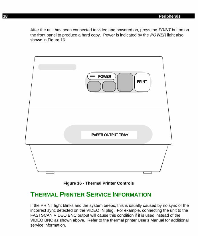
18 Peripherals
After the unit has been connected to video and powered on, press the PRINT button onthe front panel to produce a hard copy. Power is indicated by the POWER light alsoshown in Figure 16.
Figure 16 - Thermal Printer Controls
THERMAL PRINTER SERVICE INFORMATION
If the PRINT light blinks and the system beeps, this is usually caused by no sync or theincorrect sync detected on the VIDEO IN plug. For example, connecting the unit to theFASTSCAN VIDEO BNC output will cause this condition if it is used instead of theVIDEO BNC as shown above. Refer to the thermal printer User's Manual for additionalservice information.
Peripherals 19
PAPER PRINTERA parallel printer can be used to printout a Patient Summary. This summary includesthe patient's name, date of imaging, doctor's name, and exposure information. To obtaina Patient Summary, perform the following steps.
1. With Workstation power off, connect a parallel printer to the printer port as shown inFigure 17. Use a standard parallel printer cable available from most computerstores.
Figure 17 - Printer Connection
NOTE: Most parallel printers work with this configuration.
2. Power on the system. After it has booted, press the X-ray Summary button asshown in Figure 18.
ID#:
APPSSPECIAL
PATTERNTEST
VIEWDISK
(ANNOTATE)PATIENT
HELP DIRIMAGE
MARKERS CUSTOMIZESUMMARY
X-RAY SETUPOPTIONS
Figure 18 - “ X-ray Summary” Key on Workstation Keyboard
20 Peripherals
3. Then, select a specific patient. Move the cursor to the top of the screen and pressPRINT. Data similar to that shown in Figure 19 will be produced.
SHOT SUMMARY FOR:
DOE, JOHN 10/18/95 12:55123-45-6789 PHYSICIAN: SMITHCOMMENTS: HAND
TOTALS: SHOTS = 4 TIME =10.0 mAs = 5.0Exposure Type kVp mA Time(Secs) mAsFLUOR-PROCESSED 42 0.5 3.7 1.9FLUOR-PROCESSED 42 0.5 2.2 1.1FLUOR-PROCESSED 42 0.5 0.8 0.4FLUOR-PROCESSED 42 0.5 3.3 1.6
Figure 19 - Patient Shot Summary
NOTE: This data may also be acquired using the FILE option which, using theabove example, would create a "TXT format" file called DOE001.PAT byusing a formatted floppy in the rear floppy drive of the Workstation.
Peripherals 21
PRINTING THE SHOT LOG FILE (SERVICE OPTION)
By connecting the printer as described on the previous page, service personnel canobtain a hard copy printout of the shot log file which contains exposure dates and times,kVp, mA, anode and housing temperature, and a other information that may aid introubleshooting the system.
After the printer has been connected and the system powered on, perform the followingsteps to obtain a printout of the shot log file.
1. Insert Diagnostic Diskette into rear of Workstation.
2. Select the Setup Options button as shown in Figure 20.
APPSSPECIAL
PATTERNTEST
VIEWDISK
(ANNOTATE)PATIENT
HELP DIRIMAGE
MARKERS CUSTOMIZESUMMARY
X-RAY SETUPOPTIONS
Figure 20 - “ SETUP OPTIONS” Key on Workstation Keyboard
3. Next, select Access Level 2. Then select the Shot Log File option.
22 Peripherals
4. Move the cursor to the top of the screen and press PRINT. Data similar to thatshown in Figure 21 will be produced.
This Header Text is located in the ASCII file SHOTDUMP.HDR.Log Key:Abbreviations Generator Modes: PRC = Processed Fluoro
ONL = Fluoro OnlyPUL = Pulsed FluoroFLM = Film
Pat - Patient
Fld - Field
Ano - AnodeHsg - Housing Field Size: L = Largekhu - kilo Heat Units S = SmallFl - Fluoro TimeSR - ServoTB - TableSN - SenseVID - VideoSTAT - StatusMode - Generator ModeType - Shot Type
FLUORO Pat Fld Ano Hsg Hsg Auto FlSR SN SNDate Time Index Mode kVp mA || khu khu Tmp Gain Secs TB kV mA10/18/95 12:54 0 ONL 42 0.5 L 0 4 305 22 6.1 1 41 010/18/95 12:55 1 PRC 42 0.5 L 0 4 305 20 3.7 1 41 110/18/95 12:55 1 PRC 42 0.5 L 0 4 306 20 2.2 1 41 1
Figure 21 Printing the Shot Log File
NOTE: This data may also be acquired using the FILE option which creates a "TXTformat" file called SHOTDUMP.TXT by using a formatted floppy in the rearfloppy drive of the Workstation.

APPENDIX
TOOLS AND TEST EQUIPMENT• Common hand tools
• Torx Screwdriver Set
• Spline Driver, .048”, OEC P/N 00-900920-01
• Oscilloscope Tektronix 2236 or equivalent
• Digital Volt-Ohm-Meter
• Auto Cal Interface Box, OEC P/N 00-871350-01
• Auto Cal Box to Analog Interface PCB cable, OEC P/N 00-871432-01
• Auto Cal Box to Dynalyzer III DRO’s, OEC P/N 00-871434-02
• Dosimeter (Keithley Model 35050, PMX II non-invasive meter or equivalent)
• Model 96030 ion chamber
• Ion Chamber Holding Fixture
• Dynalyzer III
• High Voltage Cable Spanner Wrench, OEC P/N 00-877674
• Mobile C-Arm Extender Card, OEC P/N 00-870775-01
• Bore Sight Tool, OEC P/N 00-877589
• Resolution Tool, Converging Line Pair (LP/mm), OEC P/N 00-900860
• Resolution Tool, Mesh (LP/Inch), OEC P/N 00-900040
• Lead Apron
• 1 mm Copper Filter (3 each req’d), OEC P/N 00-877682-01
• 9600 Boot and Diagnostic Disk (software), OEC P/N 00-877444-01
• Beam Alignment Tool, OEC P/N 00-878105-01
• SRAM (PCMCIA) Software, OEC P/N 00-900876

2 Appendix
PAINT KITSPART NUMBER DESCRIPTION900524-11 Paint Kit, Elite Gray, Texture900524-12 Paint Kit, Rhinestone, Texture900524-13 Paint Kit, Windswept, Texture
TORX CRESTCUP TORQUE SPECSCAUTION: The torque specifications given in the table below apply only for hardware
being installed into steel or aluminum. When installing hardware intoplastic mounted fasteners, tighten only until snug.
TORX SCREWSIZE
NOMINALTORQUE VALUE
ACCEPTABLERANGE
4-40 6 lbs./in 5-8 lbs./in
6-32 15 lbs./in 13-16 lbs./in
8-32 22 lbs./in 21-24 lbs./in
10-32 30 lbs./in 28-31 lbs./in
MATERIAL SAFETY DATA SHEETSRefer to the 9600 Operators Manual for MSDS sheet information.
CERTIFIED COMPONENTSCertified components used in the 9600 Mobile Imaging System include the following:
Beam Limiting Device*Image Intensifier Assembly*Spot Film Device (Cassette Holder - optional) *X-ray Control Assembly*X-ray Generator Assembly*X-ray Tube Assembly
* Complete Report of Assembly, FDA Form 2579 whenever the followingassemblies are replaced in their entirety, per 21 CFR 1020.30 (d) (1) and (2).
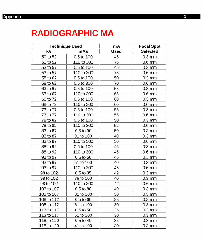
Appendix 3
RADIOGRAPHIC MATechnique Used mA Focal Spot
kV mAs Used Selected50 to 52 0.5 to 100 45 0.3 mm50 to 52 110 to 300 75 0.6 mm53 to 57 0.5 to 100 45 0.3 mm53 to 57 110 to 300 75 0.6 mm58 to 62 0.5 to 100 50 0.3 mm58 to 62 0.5 to 300 70 0.6 mm63 to 67 0.5 to 100 55 0.3 mm63 to 67 110 to 300 65 0.6 mm68 to 72 0.5 to 100 60 0.3 mm68 to 72 110 to 300 60 0.6 mm73 to 77 0.5 to 100 55 0.3 mm73 to 77 110 to 300 55 0.6 mm78 to 82 0.5 to 100 50 0.3 mm78 to 82 110 to 300 52 0.6 mm83 to 87 0.5 to 90 50 0.3 mm83 to 87 91 to 100 40 0.3 mm83 to 87 110 to 300 50 0.6 mm88 to 92 0.5 to 100 45 0.3 mm88 to 92 110 to 300 45 0.6 mm93 to 97 0.5 to 50 45 0.3 mm93 to 97 51 to 100 40 0.3 mm93 to 97 110 to 300 45 0.6 mm98 to 102 0.5 to 35 42 0.3 mm98 to 102 36 to 100 40 0.3 mm98 to 102 110 to 300 42 0.6 mm103 to 107 0.5 to 80 40 0.3 mm103 to 107 81 to 100 30 0.3 mm108 to 112 0.5 to 60 38 0.3 mm108 to 112 61 to 100 30 0.3 mm113 to 117 0.5 to 50 36 0.3 mm113 to 117 51 to 100 30 0.3 mm118 to 120 0.5 to 40 35 0.3 mm118 to 120 41 to 100 30 0.3 mm
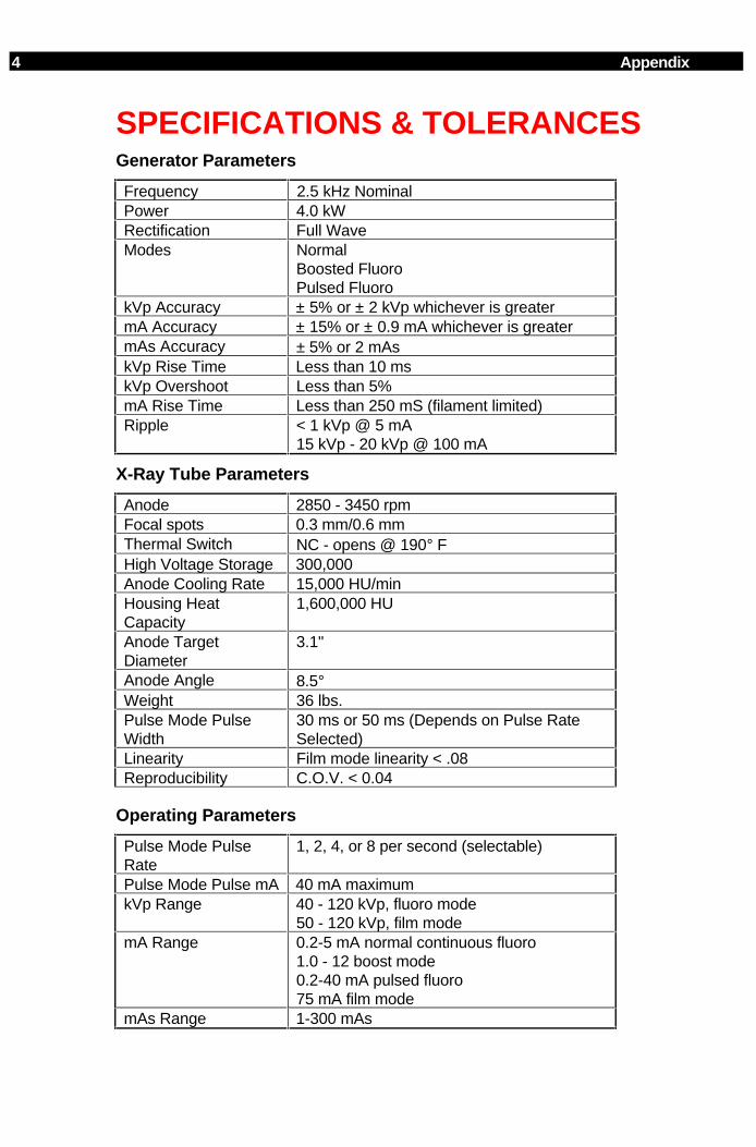
4 Appendix
SPECIFICATIONS & TOLERANCESGenerator Parameters
Frequency 2.5 kHz NominalPower 4.0 kWRectification Full WaveModes Normal
Boosted FluoroPulsed Fluoro
kVp Accuracy ± 5% or ± 2 kVp whichever is greatermA Accuracy ± 15% or ± 0.9 mA whichever is greatermAs Accuracy ± 5% or 2 mAskVp Rise Time Less than 10 mskVp Overshoot Less than 5%mA Rise Time Less than 250 mS (filament limited)Ripple < 1 kVp @ 5 mA
15 kVp - 20 kVp @ 100 mA
X-Ray Tube Parameters
Anode 2850 - 3450 rpmFocal spots 0.3 mm/0.6 mmThermal Switch NC - opens @ 190° FHigh Voltage Storage 300,000Anode Cooling Rate 15,000 HU/minHousing HeatCapacity
1,600,000 HU
Anode TargetDiameter
3.1"
Anode Angle 8.5°Weight 36 lbs.Pulse Mode PulseWidth
30 ms or 50 ms (Depends on Pulse RateSelected)
Linearity Film mode linearity < .08Reproducibility C.O.V. < 0.04
Operating Parameters
Pulse Mode PulseRate
1, 2, 4, or 8 per second (selectable)
Pulse Mode Pulse mA 40 mA maximumkVp Range 40 - 120 kVp, fluoro mode
50 - 120 kVp, film modemA Range 0.2-5 mA normal continuous fluoro
1.0 - 12 boost mode0.2-40 mA pulsed fluoro75 mA film mode
mAs Range 1-300 mAs
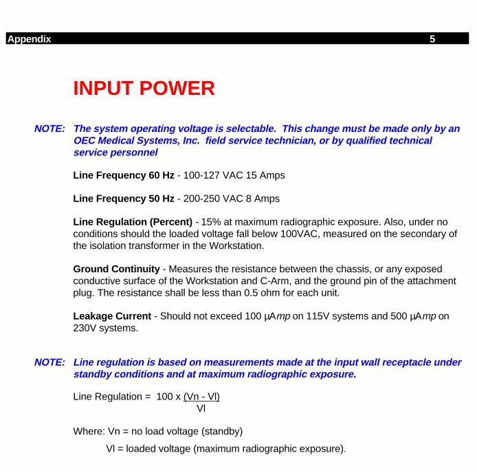
Appendix 5
INPUT POWER
NOTE: The system operating voltage is selectable. This change must be made only by anOEC Medical Systems, Inc. field service technician, or by qualified technicalservice personnel
Line Frequency 60 Hz - 100-127 VAC 15 Amps
Line Frequency 50 Hz - 200-250 VAC 8 Amps
Line Regulation (Percent) - 15% at maximum radiographic exposure. Also, under noconditions should the loaded voltage fall below 100VAC, measured on the secondary ofthe isolation transformer in the Workstation.
Ground Continuity - Measures the resistance between the chassis, or any exposedconductive surface of the Workstation and C-Arm, and the ground pin of the attachmentplug. The resistance shall be less than 0.5 ohm for each unit.
Leakage Current - Should not exceed 100 µAmp on 115V systems and 500 µAmp on230V systems.
NOTE: Line regulation is based on measurements made at the input wall receptacle understandby conditions and at maximum radiographic exposure.
Line Regulation = 100 x (Vn - Vl) Vl
Where: Vn = no load voltage (standby)
Vl = loaded voltage (maximum radiographic exposure).
UPDATE12-INCH IMAGE SYSTEM
9600 SYSTEM SERVICEMANUAL
00-878871-01
Rev. B
NOTE
Click on the colored box to go directly to the 12-inch Image Intensifier Update in the Illustrated Parts Manual. Click on the << button on the Tool Bar to return to this point.
ii 9600 Imaging Workstation Service Manual
Revision History
Rev Dash Date Change Description
Rev A -01 January 1996 Initial Release
Rev B -01 February 1996 Changes to physical spec. dimensions, camera cover & coverscrews, II mounting screws, and Image Function board
July 1996 CD-ROM Release
Date of Issue: January 1996
OEC Medical Systems, Inc.384 Wright Brothers DriveSalt Lake City, UT. 84116
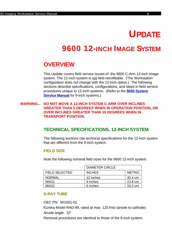
9600 Imaging Workstation Service Manual iii
UPDATE
9600 12-INCH IMAGE SYSTEM
OVERVIEWThis Update covers field service issues of the 9600 C-Arm 12-inch imagesystem. The 12-inch system is not field retrofittable. (The Workstationconfiguration does not change with the 12-inch option.) The followingsections describe specifications, configurations, and steps in field serviceprocedures unique to 12-inch systems. (Refer to the 9600 SystemService Manual for 9-inch systems.)
WARNING... DO NOT MOVE A 12-INCH SYSTEM C-ARM OVER INCLINESGREATER THAN 5 DEGREES WHEN IN OPERATION POSITION, OROVER INCLINES GREATER THAN 10 DEGREES WHEN INTRANSPORT POSITION.
TECHNICAL SPECIFICATIONS, 12-INCH SYSTEM
The following sections cite technical specifications for the 12-inch systemthat are different from the 9-inch system.
FIELD SIZE
Note the following nominal field sizes for the 9600 12-inch system:
DIAMETER CIRCLE
FIELD SELECTED INCHES METRIC
NORMAL 12 inches 30.4 cmMAG1 9 inches 22.8 cmMAG2 6 inches 15.2 cm
X-RAY TUBE
OEC PN: 901001-01
Eureka Model RAD-99, rated at max. 125 kVp (anode to cathode)
Anode angle: 10o
Removal procedures are identical to those of the 9-inch system.
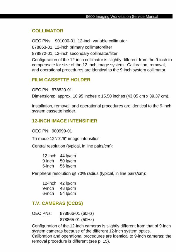
iv 9600 Imaging Workstation Service Manual
COLLIMATOR
OEC PNs: 901000-01, 12-inch variable collimator
878863-01, 12-inch primary collimator/filter
878872-01, 12-inch secondary collimator/filter
Configuration of the 12-inch collimator is slightly different from the 9-inch tocompensate for size of the 12-inch image system. Calibration, removal,and operational procedures are identical to the 9-inch system collimator.
FILM CASSETTE HOLDER
OEC PN: 878820-01
Dimensions: approx. 16.95 inches x 15.50 inches (43.05 cm x 39.37 cm).
Installation, removal, and operational procedures are identical to the 9-inchsystem cassette holder.
12-INCH IMAGE INTENSIFIER
OEC PN: 900999-01
Tri-mode 12″/9″/6″ image intensifier
Central resolution (typical, in line pairs/cm):
12-inch 44 lp/cm9-inch 50 lp/cm6-inch 56 lp/cm
Peripheral resolution @ 70% radius (typical, in line pairs/cm):
12-inch 42 lp/cm9-inch 48 lp/cm6-inch 54 lp/cm
T.V. CAMERAS (CCDS)
OEC PNs: 878866-01 (60Hz)
878865-01 (50Hz)
Configuration of the 12-inch cameras is slightly different from that of 9-inchsystem cameras because of the different 12-inch system optics.Calibration and operational procedures are identical to 9-inch cameras; theremoval procedure is different (see p. 15).
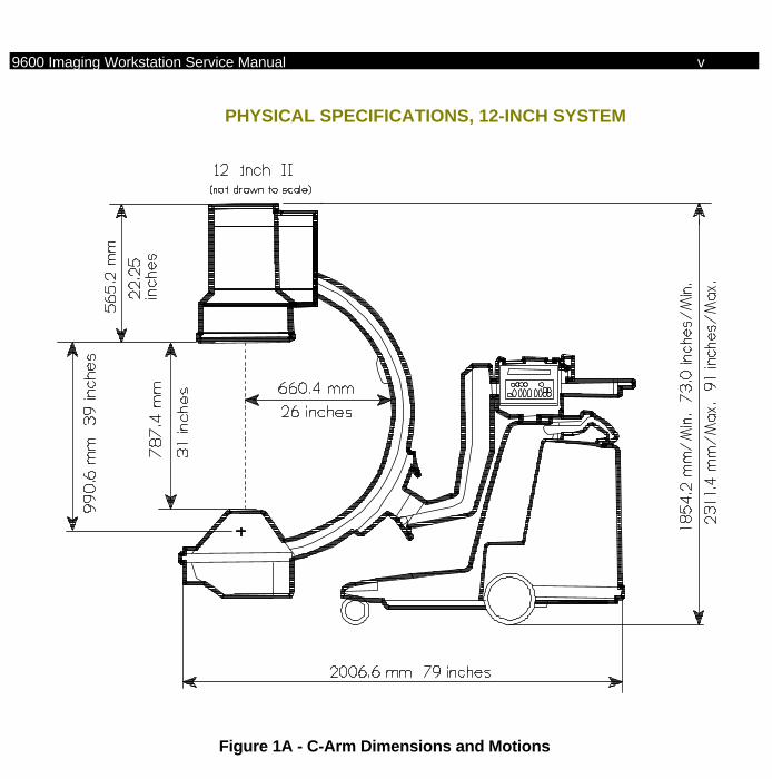
9600 Imaging Workstation Service Manual v
PHYSICAL SPECIFICATIONS, 12-INCH SYSTEM
Figure 1A - C-Arm Dimensions and Motions
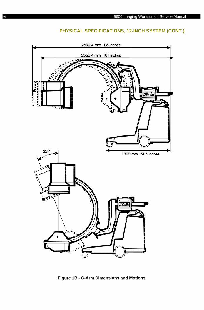
vi 9600 Imaging Workstation Service Manual
PHYSICAL SPECIFICATIONS, 12-INCH SYSTEM (CONT.)
Figure 1B - C-Arm Dimensions and Motions
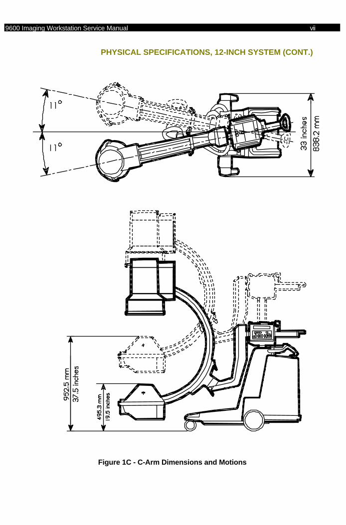
9600 Imaging Workstation Service Manual vii
PHYSICAL SPECIFICATIONS, 12-INCH SYSTEM (CONT.)
Figure 1C - C-Arm Dimensions and Motions

viii 9600 Imaging Workstation Service Manual
COMPONENT LOCATIONS
IMAGE FUNCTION PCB
The image function PCB, pn 878400, is located in the card rack assemblyon a 12-inch system; it is not located under the camera cover next to theimage intensifier as in older systems. For procedures that requireaccessing the image function board (for example, camera coolerverification), follow the steps below.
ACCESSING AND REMOVING IMAGE FUNCTION PCB
1. Switch off the main power.
2. Remove the rear cover assembly. (Refer to the “Cover Removal”section in the System Overview chapter, 9600 System ServiceManual .)
3. (a) Remove the 4 screws on the card rack cover, then (b) remove thecard rack cover (see Figure 2A next page).
NOTE: The call-out numbers on Figures 2A and 2B correspond to thesame-numbered steps here.
4. (a) Grasp the image function board’s ejector levers and pull themoutward to unlock, then (b) pull the PCB out of the card rack (it shouldunplug from the motherboard and slide out from the snap guides).See Figure 2B .
5. To re-install, make sure the PCB’s ejector levers are in the openposition, align the PCB in the snap guides, then perform the abovesteps in reverse order.

9600 Imaging Workstation Service Manual ix
Figure 2A - Removing the Card Rack Cover
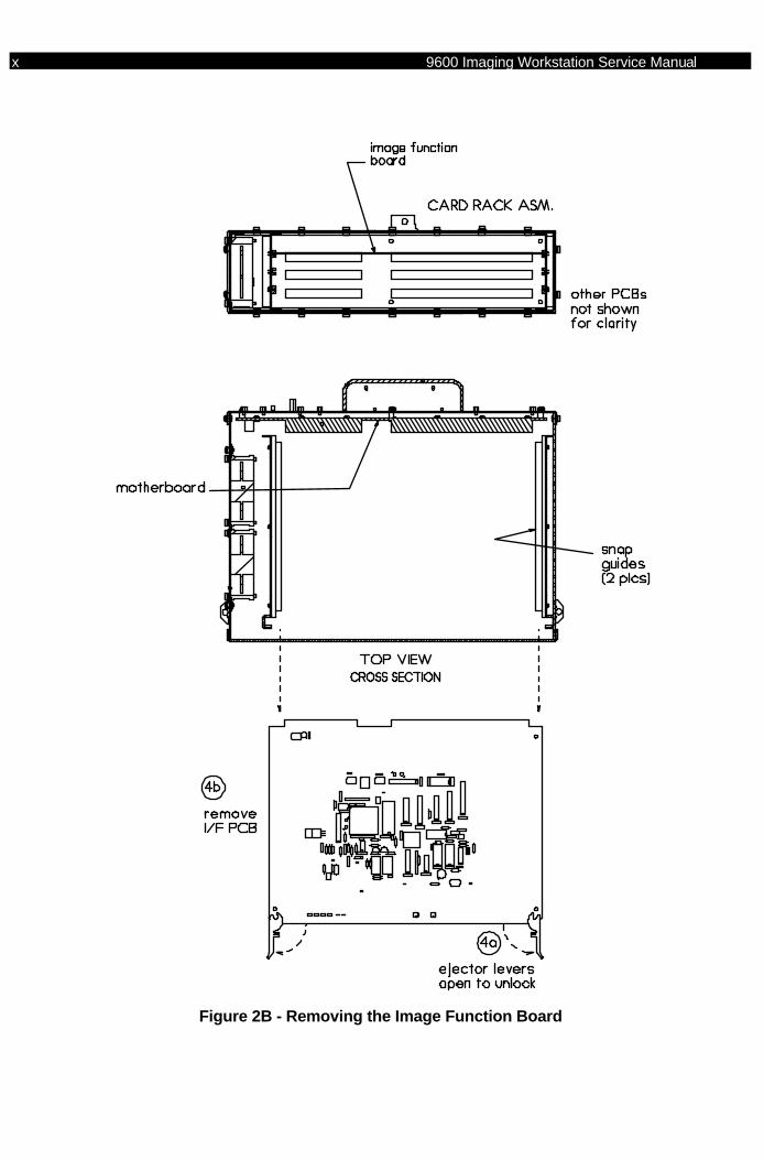
x 9600 Imaging Workstation Service Manual
Figure 2B - Removing the Image Function Board
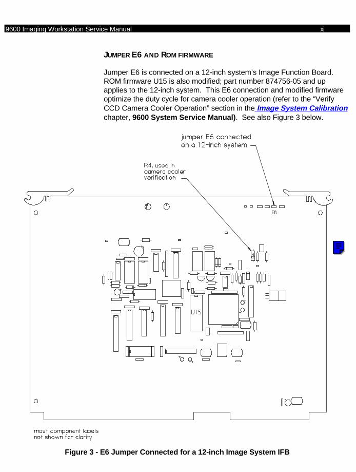
9600 Imaging Workstation Service Manual xi
JUMPER E6 AND ROM FIRMWARE
Jumper E6 is connected on a 12-inch system’s Image Function Board.ROM firmware U15 is also modified; part number 874756-05 and upapplies to the 12-inch system. This E6 connection and modified firmwareoptimize the duty cycle for camera cooler operation (refer to the “VerifyCCD Camera Cooler Operation” section in the Image System Calibrationchapter, 9600 System Service Manual) . See also Figure 3 below.
Figure 3 - E6 Jumper Connected for a 12-inch Image System IFB
NOTE
Click in the blue box to go dirctly to the Electrical Schematic diagram for the PCB shown on this page. Click the << button on the Tool Bar to return to this page.
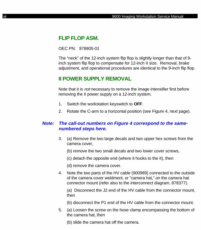
xii 9600 Imaging Workstation Service Manual
FLIP FLOP ASM.
OEC PN: 878805-01
The “neck” of the 12-inch system flip flop is slightly longer than that of 9-inch system flip flop to compensate for 12-inch II size. Removal, brakeadjustment, and operational procedures are identical to the 9-inch flip flop.
II POWER SUPPLY REMOVAL
Note that it is not necessary to remove the image intensifier first beforeremoving the II power supply on a 12-inch system.
1. Switch the workstation keyswitch to OFF.
2. Rotate the C-arm to a horizontal position (see Figure 4, next page).
Note: The call-out numbers on Figure 4 correspond to the same-numbered steps here.
3. (a) Remove the two large decals and two upper hex screws from thecamera cover,
(b) remove the two small decals and two lower cover screws,
(c) detach the opposite end (where it hooks to the II), then
(d) remove the camera cover.
4. Note the two parts of the HV cable (900989) connected to the outsideof the camera cover weldment, or “camera hat,” on the camera hatconnector mount (refer also to the interconnect diagram, 878377).
(a) Disconnect the J2 end of the HV cable from the connector mount,then
(b) disconnect the P1 end of the HV cable from the connector mount.
5. (a) Loosen the screw on the hose clamp encompassing the bottom ofthe camera hat, then
(b) slide the camera hat off the camera.
9600 Imaging Workstation Service Manual xiii
6. Lift off the camera hat and set it aside.
7. Disconnect all cables from the power supply (see the table and Figure5).
8. (a) Remove the two screws from the power supply bracket, then
(b) lift out the power supply.
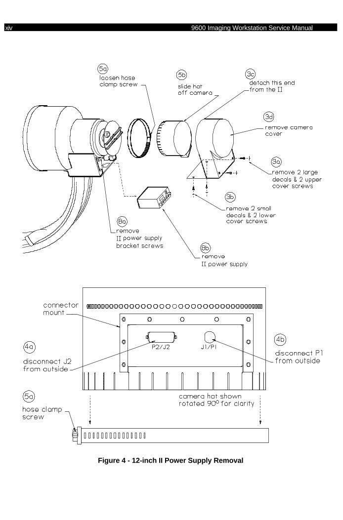
xiv 9600 Imaging Workstation Service Manual
Figure 4 - 12-inch II Power Supply Removal

9600 Imaging Workstation Service Manual xv
Figure 5 - 12-inch II Power Supply Cable Connections
Image Intensifier Power Supply Wiring
COLOR DESCRIPTION CONNECTORE Blue Active Getter Cathode Fork LugPC Red Tube Photo Cathode Fork LugGND Green/Yellow Ground Fork LugG1 Green Electrode Twist OnG2 Black Electrode Twist OnG3 Black Electrode Twist OnG4 Black Electrode Twist OnA White Cable Anode Twist On
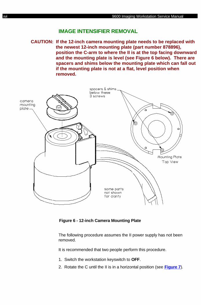
xvi 9600 Imaging Workstation Service Manual
IMAGE INTENSIFIER REMOVAL
CAUTION: If the 12-inch camera mounting plate needs to be replaced withthe newest 12-inch mounting plate (part number 878896),position the C-arm to where the II is at the top facing downwardand the mounting plate is level (see Figure 6 below). There arespacers and shims below the mounting plate which can fall outif the mounting plate is not at a flat, level position whenremoved.
Figure 6 - 12-inch Camera Mounting Plate
The following procedure assumes the II power supply has not beenremoved.
It is recommended that two people perform this procedure.
1. Switch the workstation keyswitch to OFF.
2. Rotate the C until the II is in a horizontal position (see Figure 7 ).

9600 Imaging Workstation Service Manual xvii
NOTE: The call-out numbers on Figure 7 correspond to the same-numbered steps here.
3. (a) Remove the two large decals and two upper hex screws from thecamera cover,
(b) remove the two small decals and the two lower cover screws,
(c) detach the opposite end (where it hooks to the II), then
(d) remove the camera cover.
4. Note the two parts of the HV cable (900989) connected to the outsideof the camera cover weldment, or “camera hat,” on the camera hatconnector mount (refer also to the interconnect diagram, 878377 ).
(a) Disconnect the J2 end of the HV cable from the connector mount,then
(b) disconnect the P1 end of the HV cable from the connector mount.(See Figure 4. p. 11.)
5. Disconnect the J7 end of the HV cable from the power supply (seeFigure 5 ).
6. Disconnect the green/yellow chassis ground wire from the powersupply (see Figure 5).
7. Hold the II in place, then
(a) remove the two upper flat-head socket screws, then
(b) remove the two large decals and the two lower flat-head socketscrews that secure the II to the C mounting.
8. Lift off the II.
NOTE When replacing the Image Intensifier, it may be necessary tore-calibrate the light level at the CCD by calibrating the CameraIris. Refer to the Camera Iris Calibration procedure in theImage System Calibration section, 9600 System ServiceManual.
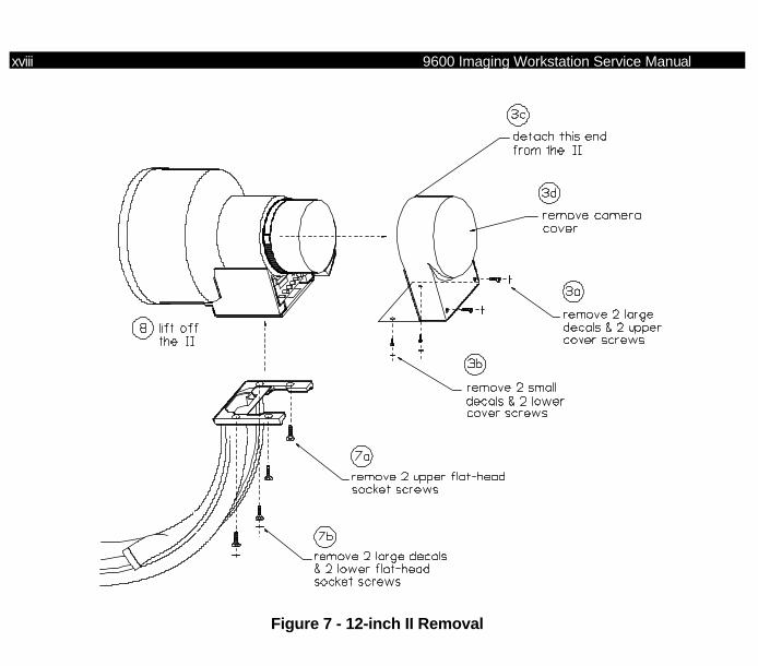
xviii 9600 Imaging Workstation Service Manual
Figure 7 - 12-inch II Removal
9600 Imaging Workstation Service Manual xix
CCD CAMERA REMOVAL
To remove the CCD camera, perform steps 1 - 7 of the previous “II PowerSupply Removal” section (p. 10) to access the camera, then refer to the“CCD Camera Replacement” section in the Image System chapter, 9600System Service Manual .
COLLIMATOR REMOVAL
Collimator removal and replacement procedures are identical to those ofthe 9-inch system. Refer to the “Collimator Replacement” section in theImage System chapter, 9600 System Service Manual .
X-RAY TUBE REMOVAL
X-ray tube removal and replacement procedures are identical to those ofthe 9-inch system. Refer to the “Replacement of the X-ray Tube” section inthe Image System chapter, 9600 System Service Manual .
BEAM ALIGNMENT
Follow the procedures in “Beam Alignment” in the Image SystemCalibration chapter (9600 System Service Manual ), but note thefollowing different components for the 12-inch system. Refer also to Figure8 (next page) for the beam alignment tool.
TOOLS
• Beam alignment tool, OEC P/N 00-878867-01(includes 12-inch alignment grid, p/n 00-878862-01)
• (QTY of 3) 1mm copper plates, OEC P/N 00-877682-02
• Film Cassette Holder Asm., 12-inch, OEC P/N 00-878820-01
• Bore sight alignment tool, 12-inch, OEC P/N 00-877589-02
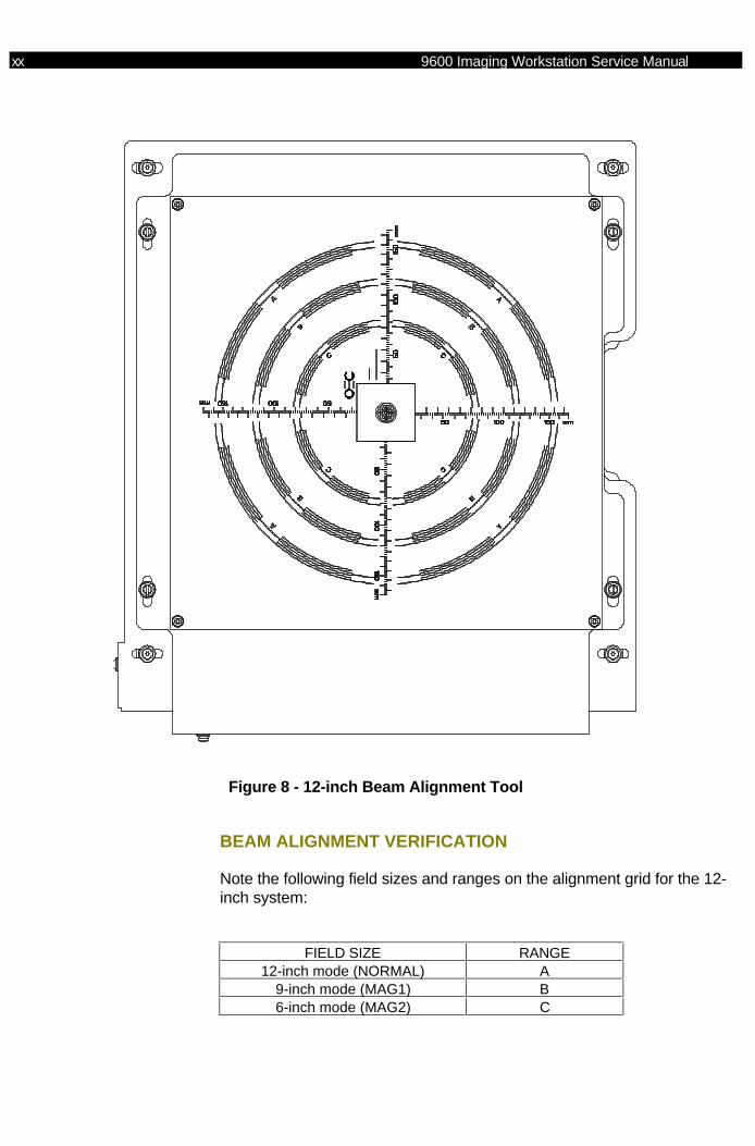
xx 9600 Imaging Workstation Service Manual
Figure 8 - 12-inch Beam Alignment Tool
BEAM ALIGNMENT VERIFICATION
Note the following field sizes and ranges on the alignment grid for the 12-inch system:
FIELD SIZE RANGE12-inch mode (NORMAL) A
9-inch mode (MAG1) B6-inch mode (MAG2) C
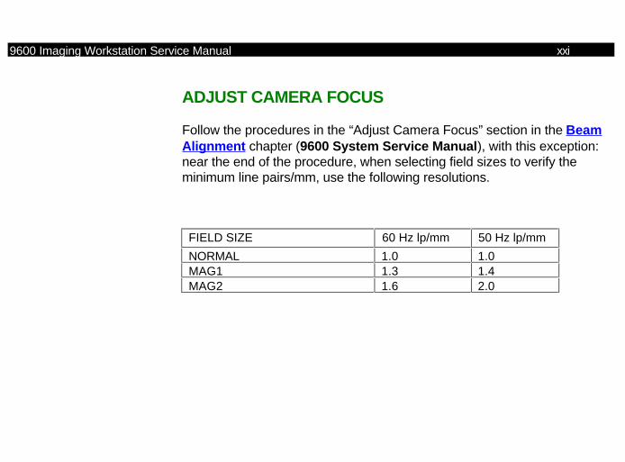
9600 Imaging Workstation Service Manual xxi
ADJUST CAMERA FOCUS
Follow the procedures in the “Adjust Camera Focus” section in the BeamAlignment chapter (9600 System Service Manual ), with this exception:near the end of the procedure, when selecting field sizes to verify theminimum line pairs/mm, use the following resolutions.
FIELD SIZE 60 Hz lp/mm 50 Hz lp/mm
NORMAL 1.0 1.0MAG1 1.3 1.4MAG2 1.6 2.0
9600 Mobile Digital C-Arm - Workstation Block Diagrams, Test Points, and Waveforms
This CD-ROM made at:OEC Medical Systems, Inc.384 Wright Bros. DriveSalt Lake City, Utah 84112
Electronic files converted for CD use and hypertext linked by:Lon StuartOEC Technical Publications Department
Section heading illustrations by:Tammy MaikowskiOEC Technical Publications DepartmentGraphic Designer
Illustrated Parts Manual drawn and converted for CD use by:Marilyn BanningOEC Technical Publications DepartmentIllustrator