
Bit-by-bit optical code scrambling technique for secure optical communication
Upload
khangminh22Category
view
2download
0
8-bit Microcontroller for Smart Card Readers
AT90SCR100
Datasheet Preliminary
TPR0327AY–SMS–30Jan09
General Features• High Performance, Low Power AVR® 8-Bit Microcontroller• Advanced RISC Architecture
– 132 Powerful Instructions - Most Single Clock Cycle Execution– 32 x 8 General Purpose Working Registers– Up to 16MIPS Throughput at 16Mhz– On-chip 2-cycle Multiplier
• Non-volatile Program and Data Memories– 64K Bytes of In-System Self-Programmable Flash
• Endurance: 10,000 Write/Erase Cycles– 4K Bytes EEPROM
• Contains 128 Bytes of One Time Programmable Memory• Endurance: 100,000 Write/Erase Cycles
– 4K Bytes Internal SRAM– Optional Boot Code Section
• In-System Programming by On-chip Bootloader program• JTAG (IEEE std. 1149.1 compliant) Interface
– Boundary-scan Capabilities According to the JTAG Standard– Extensive On-chip Debug Support– Programming of Flash, EEPROM, Fuses, and Locks Bits through JTAG Interface– Locking JTAG for Software Security (using OTP programmation)
• ISO7816 UART Interface Fully compliant with EMV, GIE-CB and WHQL Standards– Programmable ISO clock from 1 Mhz to 4.8, 6, 8 or 12Mhz– Card insertion/removal detection with automatic deactivation sequence– Programmable Baud Rate Generator from 372 to 3 clock cycles– Synchronous/Asynchronous Protocols T=0 and T=1 with Direct or Inverse
Convention– Automatic character repetition on parity errors– 32 Bit Waiting Time Counter– 16 Bit Guard Time Counter/Block Guard Time Counter– Internal Step Up/Down Converter with Programmable Voltage Output if DC/DC
embedded:• Class A: 5V +/-8% at 60mA, Vcc>2.85 (50mA if Vcc >2.7)• Class B: 3V +/-8% at 60mA, Vcc>2.85 (50mA if Vcc >2.7)• Class C: 1.8V +/-8% at 35mA
– ISO7816-12 USB Host controller for card interface• Supports up to 60mA USB Smart Cards• Supports limited cable length to Smart Card Connector (~50cm)
– 4 kV ESD (MIL/STD 833 Class 3) protection on whole Smart Card Interface• USB 2.0 Full-speed Device Module
– Complies fully with:• Universal Serial Bus Specification Rev 2.0
– Supports data transfer rates up to 12 Mbit/s– Endpoint 0 for Control Transfers : up to 64-bytes– 8 Programmable Endpoints with IN or OUT Directions and with Bulk, Interrupt or
Isochronous Transfers• 3 Programmable Endpoints with double buffering of 64x2 bytes
– Suspend/Resume Interrupts, and Remote Wake-up Support– Power-on Reset and USB Bus Reset

– 48 Mhz clock for Full-speed Bus Operation– USB Bus Disconnection on Microcontroller Request
• Peripheral Features– One 8-bit Timer/Counter with Separate Prescaler, Compare Mode and PWM Channel– One 8-bit Timer/Counter with Separate Prescaler, Compare Mode and Real Time Counter on Separate Oscillator– One 16-bit Timer/Counter with Separate Prescaler and Compare Mode– Hardware Watchdog– Hardware AES 128/256 Engine– Random Number Generator (RNG)
• Communication Peripherals– High Speed Master/Slave SPI Serial Interface (Up to 20Mhz)– 2-Wire Serial Interface– USART interface (up to 2Mbps)– Standard SPI Interface (to ease the communication with most RF front end chips)
• Special Microcontroller Feature– Power-on Reset and Brown-out Detection– Internal Callibrated Oscillator– External and Internal Interrupt Sources– Five Sleep Modes: Idle, Power-save, Power-down, Standby and Extended Standby– Supply Monitoring with Interrupt Generation below a fixed level.
• Keyboard Interface with up to 5x4 Matrix Management Capability with Interrupts and Wake-Up on Key Pressed Event• Up to 4 x I/O Ports: Programmable I/O Port• Up to 4 x LED Outputs with Programmable Current Sources: 2 or 4 mA (not usable in emulation mode)• Specific and Unique Serial Number per IC in production.• Operating Temperature
– Industrial (-40°C to +85°C)• Core Operating Voltages
– 2.4 - 5.5V• DC/DC Operating Voltages (See “Smart Card Interface Characteristics” for details)
– 2.7 - 5.5V• Maximum Frequency
– 8MHz Clock Input
2TPR0327AY–SMS–30Jan09
AT90SCR100

AT90SCR100
1. Block Diagram
Figure 1-1. Block Diagram
Except for the PORTC, all the other ports are connected to a Pin Change InterruptController.
SupplyMonitor
Vcc
XTAL1
XTAL2
TOSC1
TOSC2
InterruptController
Watchdog
On-chip Debug
KeyboardInterface
48MHzUSB
AES 256 RNG
PowerManagement
SRAM4 KB
EEPROM4 KB Data
FLASH64 KB Code
cpu
SPI DMA
USB DMA
PO
RT
AP
OR
T E
PO
RT
D
High-SpeedSPI
USART
PO
RT
B
SPI
PO
RT
C
LED port
TWI
JTAG
8bit T/C 0 16bit T/C 1 8bit T/C 2
Timers/Counters
PWMRTC
USB deviceClock
Management
Smart Card InterfaceStandardISO7816
USB HostController
PA7, KbIN7, PCINT7PA6, KbIN6, PCINT6PA5, KbIN5, PCINT5PA4, KbIN4, PCINT4PA3, KbIN3, PCINT3PA2, KbIN2, PCINT2PA1, KbIN1, PCINT1PA0, KbIN0, PCINT0
CPRES
CCLKCRST
D-
CIO CC4, DP
CC8, DM
UCapD+
PE7, KbO7, PCINT31PE6, KbO6, PCINT30PE5, KbO5, PCINT29PE4, KbO4, PCINT28PE3, KbO3, PCINT27PE2, KbO2, PCINT26PE1, KbO1, PCINT25PE0, KbO0, PCINT24
PD7, HSMISO, PCINT23PD6, HSMOSI, PCINT22
PD5, HSSCK, PCINT21PD4, HSSS, PCINT20PD3, INT1, PCINT19
PD2, INT0, OC1B, PCINT18PD1, TXD, PCINT17PD0, RXD, PCINT16
PB7, SCK, OC2A, PCINT15PB6, MISO, OC2B, PCINT14PB5, MOSI, OC1A, PCINT13
PB4, SS, OC0B, PCINT12PB3, PWM, OC0A, PCINT11
PB2, ICP1, PCINT10PB1, T1, CKO, PCINT9PB0, T0, XCK, PCINT8
PC5, JTGTDI, LED3PC4, JTGTDO, LED2PC3, JTGTMS, LED1PC2, JTGTCK, LED0
PC1, SDA, INT3bPC0, SCL, INT2b
Note
3TPR0327AY–SMS–30Jan09

4TPR0327AY–SMS–30Jan09
AT90SCR100

AT90SCR100
2. Pin List Configuration• 2 package configurations to answer different needs
– 32pins: LowPinCount package: for small package size, useful for small embedded systems (AT90SCR100L and AT90SCR100LS)
– 64pins: FullPinCount: For full performance advanced reader (AT90SCR100H)
On Full Pin Count (FPC) package, the only supported package type is QFN, andall the Vss signals are connected to the e-pad. It is important to have it fully sol-dered on groundplane of final PCB.
• USBReg refers to 3.3V USB specific regulator• PCINTx refer to Pin Change Interrupts. See “External Interrupt Registers” on
page 69.
Beware of the multiple functionality supported on each port. All functionnality maybe active at the same time. The only way to disable a feature is to deactive it insidethe corresponding peripheral block.
Caution!
Note
Caution!
Table 2-1. Pin List Configuration
Port
map
ID SCR
100L
SD
SCR
100L
HS
SCR
100H
Supp
ly
Configuration, Role
Unm
appe
d, g
ener
ic p
ins
Vcc x x x
-
Vcc Voltage Supply
Vss1 x x e(1) Vss1 Ground
AVss x x e(1) AVss PLL Ground
RST x x x
Vcc
RST Reset signal: Drive low to reinitialize the chip
Xtal1 x x x XTAL1Clock Input: Support up to 8 Mhz crystals
Xtal2 x x x XTAL2
DVcc x x x DVcc Digital Vcc:Used for internal regulator decoupling
Vcc2 x x x
-
Vcc2 Voltage Supply: To be tied to same supply voltage as Vcc
Vcc3 - - x Vcc3 Voltage Supply: To be tied to same supply voltage as Vcc
Vcc4 - - x Vcc4 Voltage Supply: To be tied to same supply voltage as Vcc
Vcc5 - - x Vcc5 Voltage Supply: To be tied to same supply voltage as Vcc
Vdcdc x x x Vdcdc Voltage Supply for DC/DC Converter.
Vss2 x x e(1) Vss2 Second Vss: To be tied to Vss
Vss3 x x e(1) Vss3 Third Vss: To be tied to Vss
D+ x x x
USBReg
D+USB Interface
D- x x x D-
UCap x x x UCapUSB Decoupling: Used for specific USB regulator
decoupling
5TPR0327AY–SMS–30Jan09

RTC1 - - x Vcc TOSC1 TOSCx: 32.768 Khz crystals input for Real Time Clock. (Please note that these pins are not GPIO accessible).RTC2 - - x TOSC2
POR
T A
PA7 - - x
Vcc
KbIN7 PCINT7
KbINx: Input for “Keyboard Interface”
PA6 - - x KbIN6 PCINT6
PA5 - - x KbIN5 PCINT5
PA4 - - x KbIN4 PCINT4
PA3 - - x KbIN3 PCINT3
PA2 - - x KbIN2 PCINT2
PA1 - - x KbIN1 PCINT1
PA0 - - x KbIN0 PCINT0
POR
T B
PB7 x - x
Vcc
SCK OC2A PCINT15 SS, MISO, MOSI, SCK: Standard “SPI - Serial Peripheral Interface”
OCxx: Output Comparator outputs. See “Timers” on page 87.ICP1: Input Capture. See “16-bit Timer/Counter1 with PWM”
PWM: Output from “8-bit Timer/Counter0 with PWM” Tx: Clock input for “Timers” 0 and 1
XCK: Clock input for synchronous “USART” INTx: “External Interrupts” , default configuration
CLKO: System clock output. (only active if CKOUT fuse is enabled). “Fuse Low Byte” .
PB6 x - x MISO OC2B PCINT14
PB5 x - x MOSI OC1A PCINT13
PB4 x - x SS OC0B PCINT12
PB3 - - x PWM OC0A PCINT11
PB2 - - x ICP1 PCINT10
PB1 - - x INT3 T1 CLKO PCINT9
PB0 - - x INT2 T0 XCK PCINT8
POR
T C
(3)
PC5 - - x
Vcc
JTGTDI LED3
JTGxxx: “JTAG Interface and On-chip Debug System” SDA, SCL: “2-wire Serial Interface _ TWI” signals
LEDx: “LED” Outputs (IO driving current)INTxb: “External Interrupts” , bis configuration
PC4 - - x JTGTDO LED2
PC3 - - x JTGTMS LED1
PC2 x x x JTGTCK LED0
PC1 - - x SDA INT3b
PC0 - - x SCL INT2b
POR
T D
PD7 - x x
Vcc
HSMISO PCINT23
HSxxxx: “High-Speed SPI Controller” (MISO, MOSI, SCK, SS)
INTx: “External Interrupts” , default configurationTXD, RXD: “USART” signals
OCxB: Output Comparators: See “Timers” on page 87.
PD6 - x x HSMOSI PCINT22
PD5 - x x HSSCK PCINT21
PD4 - x x HSSS PCINT20
PD3 - - x INT1 PCINT19
PD2 - - x INT0 OC1B PCINT18
PD1 x x x TXD PCINT17
PD0 x x x RXD PCINT16
Table 2-1. Pin List Configuration
Port
map
ID SCR
100L
SD
SCR
100L
HS
SCR
100H
Supp
ly
Configuration, Role
6TPR0327AY–SMS–30Jan09
AT90SCR100

AT90SCR100
Notes: 1. Should be connected to e-pad underneath QFN package2. According to the current configuration, these pins are supplied either by USB regulator or CVcc3. PORT C is not complete, due to RTC pins, dedicated to oscillator pads
POR
T E
PE7 - - x
Vcc
KbO7 PCINT31
KbOx: Output for “Keyboard Interface”
PE6 - - x KbO6 PCINT30
PE5 - - x KbO5 PCINT29
PE4 - - x KbO4 PCINT28
PE3 - - x KbO3 PCINT27
PE2 - - x KbO2 PCINT26
PE1 - - x KbO1 PCINT25
PE0 - - x KbO0 PCINT24
Smar
t Car
d PO
RT
x x x Vcc CPRES
Cx: “Smart Card Interface Block (SCIB)” : Standard ISO7816 port and “USB Host Controller” .
x x x
CVcc
CCLK
x x x CRST
x x x CIO
x x x (2) CC4, DP
x x x CC8, DM
x x x
CVcc
CVcc
Smart Card Interface: “DC/DC Converter” Supply Signals
x x x CVSense
x x e(1) CVss
x x x LI
x x x LO
Table 2-1. Pin List Configuration
Port
map
ID SCR
100L
SD
SCR
100L
HS
SCR
100H
Supp
ly
Configuration, Role
7TPR0327AY–SMS–30Jan09

8TPR0327AY–SMS–30Jan09
AT90SCR100

AT90SCR100
3. ResourcesA comprehensive set of development tools, application notes and datasheets are available fordownload on http://www.atmel.com/avr.
9TPR0327AY–SMS–30Jan09

10TPR0327AY–SMS–30Jan09
AT90SCR100

AT90SCR100
4. About Code ExamplesThis documentation contains simple code examples that briefly show how to use various parts ofthe device. Be aware that not all C compiler vendors include bit definitions in the header filesand interrupt handling in C is compiler dependent. Please confirm with the C compiler documen-tation for more details.
The code examples assume that the part specific header file is included before compilation. ForI/O registers located in extended I/O map, "IN", "OUT", "SBIS", "SBIC", "CBI", and "SBI" instruc-tions must be replaced with instructions that allow access to extended I/O. Typically "LDS" and"STS" combined with "SBRS", "SBRC", "SBR", and "CBR".
11TPR0327AY–SMS–30Jan09

12TPR0327AY–SMS–30Jan09
AT90SCR100

AT90SCR100
5. AVR CPU Core
5.1 IntroductionThis section discusses the AVR core architecture in general. The main function of the CPU coreis to ensure correct program execution. The CPU must therefore be able to access memories,perform calculations, control peripherals, and handle interrupts.
5.2 Architectural Overview
Figure 5-1. Block Diagram of the AVR Architecture
In order to maximize performance and parallelism, the AVR uses a Harvard architecture – withseparate memories and buses for program and data. Instructions in the program memory areexecuted with a single level pipelining. While one instruction is being executed, the next instruc-tion is pre-fetched from the program memory. This concept enables instructions to be executedin every clock cycle. The program memory is In-System Reprogrammable Flash memory.
FlashProgramMemory
InstructionRegister
InstructionDecoder
ProgramCounter
Control Lines
32 x 8GeneralPurpose
Registrers
ALU
Statusand Control
I/O Lines
EEPROM
Data Bus 8-bit
DataSRAM
Dire
ct A
ddre
ssin
g
Indi
rect
Add
ress
ing
InterruptUnit
SPIUnit
WatchdogTimer
I/O Module 2
I/O Module1
I/O Module n
13TPR0327AY–SMS–30Jan09

The fast-access Register File contains 32 x 8-bit general purpose working registers with a singleclock cycle access time. This allows single-cycle Arithmetic Logic Unit (ALU) operation. In a typ-ical ALU operation, two operands are output from the Register File, the operation is executed,and the result is stored back in the Register File – in one clock cycle.
Six of the 32 registers can be used as three 16-bit indirect address register pointers for DataSpace addressing – enabling efficient address calculations. One of the these address pointerscan also be used as an address pointer for look up tables in Flash program memory. Theseadded function registers are the 16-bit X-, Y-, and Z-register, described later in this section.
The ALU supports arithmetic and logic operations between registers or between a constant anda register. Single register operations can also be executed in the ALU. After an arithmetic opera-tion, the Status Register is updated to reflect information about the result of the operation.
Program flow is provided by conditional and unconditional jump and call instructions, able todirectly address the whole address space. Most AVR instructions have a single 16-bit word for-mat. Every program memory address contains a 16- or 32-bit instruction.
Program Flash memory space is divided in two sections, the Boot Program section and theApplication Program section. Both sections have dedicated Lock bits for write and read/writeprotection. The SPM instruction that writes into the Flash memory must reside in the Boot Pro-gram section.
During interrupts and subroutine calls, the return address Program Counter (PC) is stored on theStack. The Stack is effectively allocated in the general data SRAM, and consequently the Stacksize is only limited by the total SRAM size and the usage of the SRAM. All user programs mustinitialize the SP in the Reset routine (before subroutines or interrupts are executed). The StackPointer (SP) is read/write accessible in the I/O space. The data SRAM can easily be accessedthrough the five different addressing modes supported in the AVR architecture.
The memory spaces in the AVR architecture are all linear and regular memory maps.
A flexible interrupt module has its control registers in the I/O space with an additional GlobalInterrupt Enable bit in the Status Register. All interrupts have a separate Interrupt Vector in theInterrupt Vector table. The interrupts have priority in accordance with their Interrupt Vector posi-tion. The lower the Interrupt Vector address, the higher the priority.
The I/O memory space contains 64 addresses for CPU peripheral functions as Control Regis-ters, SPI, and other I/O functions. The I/O Memory can be accessed directly, or via the DataSpace locations following those of the Register File, 0x20 - 0x5F. In addition, the AT90SCR100has Extended I/O space from 0x60 - 0xFF in SRAM where only the ST/STS/STD andLD/LDS/LDD instructions can be used.
5.3 ALU – Arithmetic Logic UnitThe high-performance AVR ALU operates in direct connection with all the 32 general purposeworking registers. Within a single clock cycle, arithmetic operations between general purposeregisters or between a register and an immediate operand are executed. The ALU operationsare divided into three main categories – arithmetic, logical, and bit-functions. This implementa-tion of the architecture also provides a powerful multiplier supporting both signed/unsignedmultiplication and fractional format. See the “Instruction Set” section for a detailed description.
14TPR0327AY–SMS–30Jan09
AT90SCR100

AT90SCR100
5.4 Status RegisterThe Status Register contains information about the result of the most recently executed arithme-tic instruction. This information can be used for altering program flow in order to performconditional operations. Note that the Status Register is updated after all ALU operations, asspecified in the Instruction Set Reference. This will in many cases remove the need for using thededicated compare instructions, resulting in faster and more compact code.
The Status Register is not automatically stored when entering an interrupt routine and restoredwhen returning from an interrupt. This must be handled by software.
5.4.1 SREG – Status RegisterThe AVR Status Register – SREG – is defined as:
• Bit 7 – I: Global Interrupt EnableThe Global Interrupt Enable bit must be set for the interrupts to be enabled. The individual inter-rupt enable control is then performed in separate control registers. If the Global Interrupt EnableRegister is cleared, none of the interrupts are enabled independent of the individual interruptenable settings. The I-bit is cleared by hardware after an interrupt has occurred, and is set bythe RETI instruction to enable subsequent interrupts. The I-bit can also be set and cleared bythe application with the SEI and CLI instructions, as described in the instruction set reference.
• Bit 6 – T: Bit Copy StorageThe Bit Copy instructions BLD (Bit LoaD) and BST (Bit STore) use the T-bit as source or desti-nation for the operated bit. A bit from a register in the Register File can be copied into T by theBST instruction, and a bit in T can be copied into a bit in a register in the Register File by theBLD instruction.
• Bit 5 – H: Half Carry Flag The Half Carry Flag H indicates a Half Carry in some arithmetic operations. Half Carry Is usefulin BCD arithmetic. See the “Instruction Set Description” for detailed information.
• Bit 4 – S: Sign Bit, S = N ⊕ VThe S-bit is always an exclusive OR between the Negative Flag N and the Two’s ComplementOverflow Flag V. See the “Instruction Set Description” for detailed information.
• Bit 3 – V: Two’s Complement Overflow FlagThe Two’s Complement Overflow Flag V supports two’s complement arithmetic. See the“Instruction Set Description” for detailed information.
• Bit 2 – N: Negative FlagThe Negative Flag N indicates a negative result in an arithmetic or logic operation. See the“Instruction Set Description” for detailed information.
• Bit 1 – Z: Zero Flag
Bit 7 6 5 4 3 2 1 0
0x3F (0x5F) I T H S V N Z C SREGRead/write R/W R/W R/W R/W R/W R/W R/W R/W
Initial value 0 0 0 0 0 0 0 0 0x00
15TPR0327AY–SMS–30Jan09

The Zero Flag Z indicates a zero result in an arithmetic or logic operation. See the “InstructionSet Description” for detailed information.
• Bit 0 – C: Carry FlagThe Carry Flag C indicates a carry in an arithmetic or logic operation. See the “Instruction SetDescription” for detailed information.
5.5 General Purpose Register FileThe Register File is optimized for the AVR Enhanced RISC instruction set. In order to achievethe required performance and flexibility, the following input/output schemes are supported by theRegister File:
• One 8-bit output operand and one 8-bit result input• Two 8-bit output operands and one 8-bit result input• Two 8-bit output operands and one 16-bit result input• One 16-bit output operand and one 16-bit result input
Figure 5-2 shows the structure of the 32 general purpose working registers in the CPU.
Figure 5-2. AVR CPU General Purpose Working Registers
Most of the instructions operating on the Register File have direct access to all registers, andmost of them are single cycle instructions.
As shown in Figure 5-2, each register is also assigned a data memory address, mapping themdirectly into the first 32 locations of the user Data Space. Although not being physically imple-mented as SRAM locations, this memory organization provides great flexibility in access of theregisters, as the X-, Y- and Z-pointer registers can be set to index any register in the file.
5.5.1 The X-register, Y-register, and Z-registerThe registers R26..R31 can also be used as 16-bit address pointers for indirect addressing ofthe data space. The three indirect address registers X, Y, and Z are defined as described in Fig-ure 5-3.
7 0 Addr.R0 0x00R1 0x01R2 0x02…
R13 0x0DGeneral R14 0x0EPurpose R15 0x0FWorking R16 0x10Registers R17 0x11
…R26 0x1A X-register Low ByteR27 0x1B X-register High ByteR28 0x1C Y-register Low ByteR29 0x1D Y-register High ByteR30 0x1E Z-register Low ByteR31 0x1F Z-register High Byte
16TPR0327AY–SMS–30Jan09
AT90SCR100

AT90SCR100
Figure 5-3. The X-, Y-, and Z-registers
In the different addressing modes these address registers have fixed displacement, automaticincrement, and automatic decrement functionality (see the instruction set reference for details).
5.6 Stack PointerThe Stack is mainly used for storing temporary data, for storing local variables and for storingreturn addresses after interrupts and subroutine calls. The Stack Pointer Register always pointsto the top of the Stack. Note that the Stack is implemented as growing from higher memory loca-tions to lower memory locations. This implies that a Stack PUSH command decreases the StackPointer.
The Stack Pointer points to the data SRAM Stack area where the Subroutine and InterruptStacks are located. This Stack space in the data SRAM must be defined by the program beforeany subroutine calls are executed or interrupts are enabled. The Stack Pointer must be set topoint above 0x0100. The initial value of the stack pointer is the highest address of the internalSRAM. The Stack Pointer is decremented by one when data is pushed onto the Stack with thePUSH instruction, and it is decremented by two when the return address is pushed onto theStack with subroutine call or interrupt. The Stack Pointer is incremented by one when data ispopped from the Stack with the POP instruction, and it is incremented by two when data ispopped from the Stack with return from subroutine RET or return from interrupt RETI.
The AVR Stack Pointer is implemented as two 8-bit registers in the I/O space. The number ofbits actually used is implementation dependent.
5.7 Instruction Execution TimingThis section describes the general access timing concepts for instruction execution. The AVRCPU is driven by the CPU clock clkCPU, directly generated from the selected clock source for thechip. No internal clock division is used.
15 XH XL 0
X-register 7 0 7 0
R27 (0x1B) R26 (0x1A)
15 YH YL 0
Y-register 7 0 7 0
R29 (0x1D) R28 (0x1C)
15 ZH ZL 0
Z-register 7 0 7 0
R31 (0x1F) R30 (0x1E)
Bit 15 14 13 12 11 10 9 8
0x3E (0x5E) - - - SP12 SP11 SP10 SP9 SP8 SPH0x3D (0x5D) SP7 SP6 SP5 SP4 SP3 SP2 SP1 SP0 SPH
7 6 5 4 3 2 1 0
Read/write R R R R/W R/W R/W R/W R/W
R/W R/W R/W R/W R/W R/W R/W R/W
Initial value 0 0 0 1 0 0 0 0 0x10
1 1 1 1 1 1 1 1 0xFF
17TPR0327AY–SMS–30Jan09
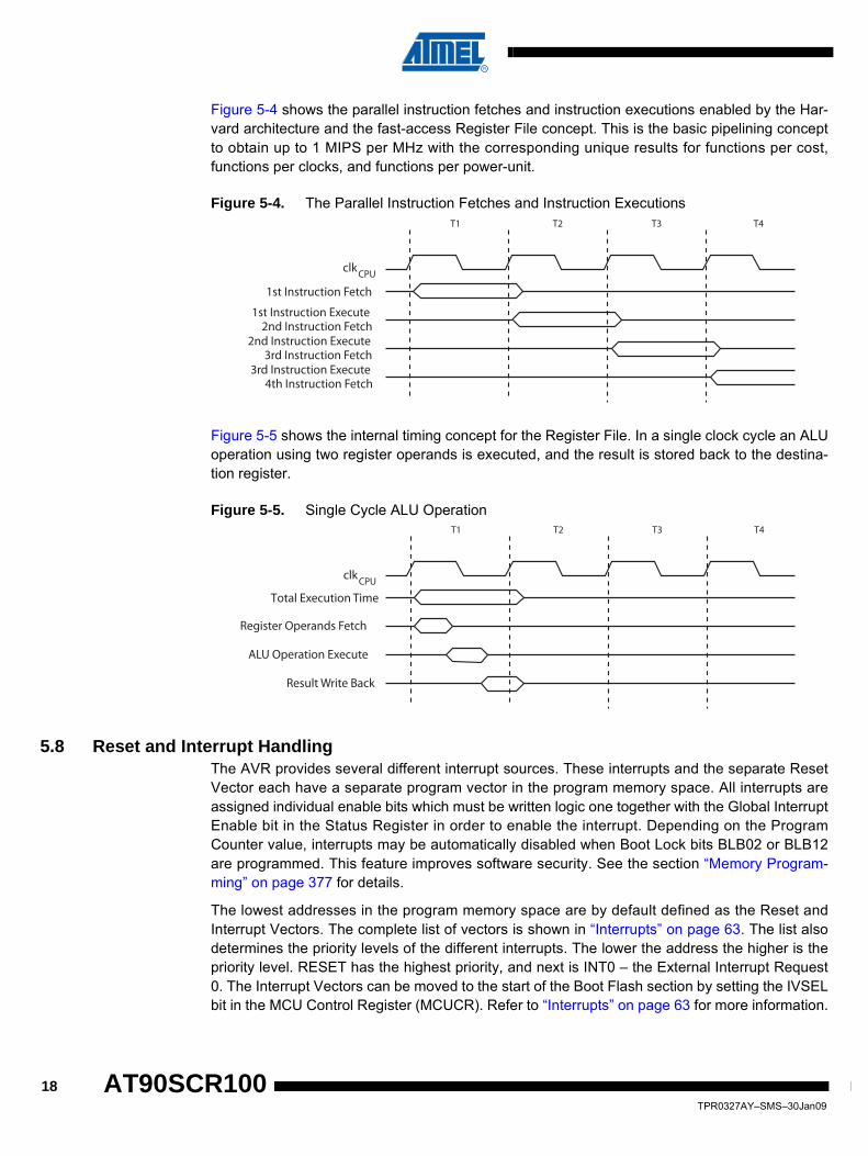
Figure 5-4 shows the parallel instruction fetches and instruction executions enabled by the Har-vard architecture and the fast-access Register File concept. This is the basic pipelining conceptto obtain up to 1 MIPS per MHz with the corresponding unique results for functions per cost,functions per clocks, and functions per power-unit.
Figure 5-4. The Parallel Instruction Fetches and Instruction Executions
Figure 5-5 shows the internal timing concept for the Register File. In a single clock cycle an ALUoperation using two register operands is executed, and the result is stored back to the destina-tion register.
Figure 5-5. Single Cycle ALU Operation
5.8 Reset and Interrupt HandlingThe AVR provides several different interrupt sources. These interrupts and the separate ResetVector each have a separate program vector in the program memory space. All interrupts areassigned individual enable bits which must be written logic one together with the Global InterruptEnable bit in the Status Register in order to enable the interrupt. Depending on the ProgramCounter value, interrupts may be automatically disabled when Boot Lock bits BLB02 or BLB12are programmed. This feature improves software security. See the section “Memory Program-ming” on page 377 for details.
The lowest addresses in the program memory space are by default defined as the Reset andInterrupt Vectors. The complete list of vectors is shown in “Interrupts” on page 63. The list alsodetermines the priority levels of the different interrupts. The lower the address the higher is thepriority level. RESET has the highest priority, and next is INT0 – the External Interrupt Request0. The Interrupt Vectors can be moved to the start of the Boot Flash section by setting the IVSELbit in the MCU Control Register (MCUCR). Refer to “Interrupts” on page 63 for more information.
clk
1st Instruction Fetch
1st Instruction Execute2nd Instruction Fetch
2nd Instruction Execute3rd Instruction Fetch
3rd Instruction Execute4th Instruction Fetch
T1 T2 T3 T4
CPU
ime
Register Operands Fetch
ALU Operation Execute
rite Back
T1 T2 T3 T4
clkCPU
Total Execution T
Result W
18TPR0327AY–SMS–30Jan09
AT90SCR100

AT90SCR100
The Reset Vector can also be moved to the start of the Boot Flash section by programming theBOOTRST Fuse, see “Memory Programming” on page 377.
When an interrupt occurs, the Global Interrupt Enable I-bit is cleared and all interrupts are dis-abled. The user software can write logic one to the I-bit to enable nested interrupts. All enabledinterrupts can then interrupt the current interrupt routine. The I-bit is automatically set when aReturn from Interrupt instruction – RETI – is executed.
There are basically two types of interrupts. The first type is triggered by an event that sets theInterrupt Flag. For these interrupts, the Program Counter is vectored to the actual Interrupt Vec-tor in order to execute the interrupt handling routine, and hardware clears the correspondingInterrupt Flag. Interrupt Flags can also be cleared by writing a logic one to the flag bit position(s)to be cleared. If an interrupt condition occurs while the corresponding interrupt enable bit iscleared, the Interrupt Flag will be set and remembered until the interrupt is enabled, or the flag iscleared by software. Similarly, if one or more interrupt conditions occur while the Global InterruptEnable bit is cleared, the corresponding Interrupt Flag(s) will be set and remembered until theGlobal Interrupt Enable bit is set, and will then be executed by order of priority.
The second type of interrupts will trigger as long as the interrupt condition is present. Theseinterrupts do not necessarily have Interrupt Flags. If the interrupt condition disappears before theinterrupt is enabled, the interrupt will not be triggered.
When the AVR exits from an interrupt, it will always return to the main program and execute onemore instruction before any pending interrupt is served.
Note that the Status Register is not automatically stored when entering an interrupt routine, norrestored when returning from an interrupt routine. This must be handled by software.
When using the CLI instruction to disable interrupts, the interrupts will be immediately disabled.No interrupt will be executed after the CLI instruction, even if it occurs simultaneously with theCLI instruction. The following example shows how this can be used to avoid interrupts during thetimed EEPROM write sequence.
When using the SEI instruction to enable interrupts, the instruction following SEI will be exe-cuted before any pending interrupts, as shown in this example.
Assembly Code Example
in r16, SREG ; store SREG value
cli ; disable interrupts during timed sequence
sbi EECR, EEMPE ; start EEPROM write
sbi EECR, EEPE
out SREG, r16 ; restore SREG value (I-bit)
C Code Example
char cSREG;
cSREG = SREG; /* store SREG value */
/* disable interrupts during timed sequence */
__disable_interrupt();
EECR |= (1<<EEMPE); /* start EEPROM write */
EECR |= (1<<EEPE);
SREG = cSREG; /* restore SREG value (I-bit) */
19TPR0327AY–SMS–30Jan09

5.8.1 Interrupt Response TimeThe interrupt execution response for all the enabled AVR interrupts is five clock cycles minimum.After five clock cycles the program vector address for the actual interrupt handling routine is exe-cuted. During these five clock cycle periods, the Program Counter is pushed onto the Stack. Thevector is normally a jump to the interrupt routine, and this jump takes three clock cycles. If aninterrupt occurs during execution of a multi-cycle instruction, this instruction is completed beforethe interrupt is served. If an interrupt occurs when the MCU is in sleep mode, the interrupt exe-cution response time is increased by five clock cycles. This increase comes in addition to thestart-up time from the selected sleep mode.
A return from an interrupt handling routine takes five clock cycles. During these five clock cycles,the Program Counter (three bytes) is popped back from the Stack, the Stack Pointer is incre-mented by three, and the I-bit in SREG is set.
Assembly Code Example
sei ; set Global Interrupt Enable
sleep; enter sleep, waiting for interrupt
; note: will enter sleep before any pending
; interrupt(s)
C Code Example
__enable_interrupt(); /* set Global Interrupt Enable */
__sleep(); /* enter sleep, waiting for interrupt */
/* note: will enter sleep before any pending interrupt(s) */
20TPR0327AY–SMS–30Jan09
AT90SCR100
AT90SCR100
6. AT90SCR100 MemoriesThis section describes the different memories in the AT90SCR100. The AVR architecture hastwo main memory spaces: the Data Memory and the Program Memory spaces. In addition, theAT90SCR100 features an EEPROM Memory for data storage. All three memory spaces are lin-ear and regular.
6.1 In-System Reprogrammable Flash Program Memory The AT90SCR100 contains 64K bytes On-chip In-System Reprogrammable Flash memory forprogram storage. As all AVR instructions are 16 or 32 bits wide, the Flash is organized as 32K x16. For software security, the Flash Program memory space is divided into two sections, BootProgram section and Application Program section. See “Application and Boot Loader Flash Sec-tions” on page 363.
The Flash memory has an endurance of at least 10,000 write/erase cycles. The AT90SCR100Program Counter (PC) is 15/16 bits wide, which permits to address the 32/64K program memorylocations. The operation of Boot Program section and associated Boot Lock bits for softwareprotection are described in detail in “Memory Programming” on page 377. “Memory Program-ming” on page 377 contains a detailed description of Flash data serial downloading using theSPI pins or the JTAG interface.
Constant tables can be allocated within the entire program memory address space (see the LPM– Load Program Memory instruction description).
Timing diagrams for instruction fetch and execution are presented in “Instruction Execution Tim-ing” on page 17.
21TPR0327AY–SMS–30Jan09

Figure 6-1. Full Memory Map
6.2 SRAM Data MemoryFigure 6-1 shows how the AT90SCR100 SRAM Memory is organized.
The AT90SCR100 is a complex microcontroller with more peripheral units than can be sup-ported within the 64 locations reserved in the Opcode of the IN and OUT instructions. For theExtended I/O space from 0x0060 - 0x00FF in SRAM, only the ST/STS/STD and LD/LDS/LDDinstructions can be used.
The address range $00 - $10FF Data Memory address the Register File, the I/O Memory,Extended I/O Memory, and the internal data SRAM. The first 32 locations address the Registerfile, the next 64 location the standard I/O Memory, then 160 locations of Extended I/O memoryand the next 4,096 locations address the internal data SRAM.
The five different addressing modes for the data memory cover: Direct, Indirect with Displace-ment, Indirect, Indirect with Pre-decrement, and Indirect with Post-increment. In the Register file,registers R26 to R31 feature the indirect addressing pointer registers.
The direct addressing reaches the entire data space.
The Indirect with Displacement mode reaches 63 address locations from the base address givenby the Y- or Z-register.
Application Flash Section
16 bits
0x0000
0x001F0x0020
0x005F0x0060
0x00FF0x0100
0x10FF
0x1000
0x0000
0x0000
0x6FFF0x7000
0x7FFF
Boot Flash Section
Program Memory
SRAM Memory
IO Registers
32 General Purpose Working Registers
Peripheral Registers
EEPROM Data Memory
EEPROM Memory
Data Memory
8 bits
22TPR0327AY–SMS–30Jan09
AT90SCR100

AT90SCR100
When using register indirect addressing modes with automatic pre-decrement and post-incre-ment, the address registers X, Y, and Z are decremented or incremented.
The 32 general purpose working registers, 64 I/O registers, 160 Extended I/O Registers and the4096 bytes of internal data SRAM in the AT90SCR100 are all accessible through all theseaddressing modes. The Register File is described in “General Purpose Register File” on page16.
6.2.1 Data Memory Access TimesThis section describes the general access timing concepts for internal memory access. Theinternal data SRAM access is performed in two clkCPU cycles as described in Figure 6-2.
Figure 6-2. On-chip Data SRAM Access Cycles
6.3 EEPROM Data MemoryThe AT90SCR100 contains 4K bytes of data EEPROM memory. It is organized as a separatedata space, in which single bytes can be read and written. The EEPROM has an endurance of atleast 100,000 write/erase cycles. The access between the EEPROM and the CPU is describedin the following section, specifying the EEPROM Address Registers, the EEPROM Data Regis-ter, and the EEPROM Control Register.
For a detailed description of SPI and JTAG downloading to the EEPROM, see page 381, andpage 385 respectively.
6.3.1 EEPROM Read/Write AccessThe EEPROM Access Registers are accessible in the I/O space.
The write access time for the EEPROM is given in Table 6-2. This is a self-timing function, wichallows the user software to detect when the next byte can be written. If the user code containsinstructions that write the EEPROM, some precautions must be taken. In heavily filtered powersupplies, VCC is likely to rise or fall slowly on power-up/down. This causes the device, for someperiod of time, to run at a voltage lower than specified as minimum, for the clock frequency used.For details on how to avoid problems in these situations, See “Preventing EEPROM Corruption”on page 28.
clk
WR
RD
Data
Data
Address Address valid
T1 T2 T3
Compute Address
Read
Writ
e
CPU
Memory Access Instruction Next Instruction
23TPR0327AY–SMS–30Jan09

In order to prevent unintentional EEPROM writes, a specific write procedure must be followed.Refer to the description of the EEPROM Control Register for details on this.
When the EEPROM is read, the CPU is halted for four clock cycles before the next instruction isexecuted. When the EEPROM is written, the CPU is halted for two clock cycles before the nextinstruction is executed.
6.3.2 EEARH and EEARL – The EEPROM Address Register
• Bits 15..12 – Res : Reserved BitsThese bits are reserved bits in the AT90SCR100 and will always read as zero.
• Bits 11..0 – EEAR8..0 : EEPROM AddressThe EEPROM Address Registers – EEARH and EEARL specify the EEPROM address in the 4Kbytes EEPROM space. The EEPROM data bytes are addressed linearly between 0 and 4096.The initial value of EEAR is undefined. A proper value must be written before the EEPROM maybe accessed.
6.3.3 EEDR – The EEPROM Data Register
• Bits 7..0 – EEDR7..0 : EEPROM DataFor the EEPROM write operation, the EEDR Register contains the data to be written to theEEPROM in the address specified by the EEAR Register. For the EEPROM read operation, theEEDR contains the data read out from the EEPROM at the address specified by EEAR.
6.3.4 EECR – The EEPROM Control Register
• Bits 7..6 – Res: Reserved BitsThese bits are reserved bits in the AT90SCR100 and will always read as zero.
Bit 15 14 13 12 11 10 9 8
0x22 (0x42) - - - - EEAR [11..8] EEARH0x21 (0x41) EEAR [7..0] EEARLBit 7 6 5 4 3 2 1 0
Read/write R R R R R/W R/W R/W R/W
R/W R/W R/W R/W R/W R/W R/W R/W
Initial value 0 0 0 0 x x x x
x x x x x x x x
Bit 7 6 5 4 3 2 1 0
0x20 (0x40) EEDR [7..0] EEDRRead/write R/W R/W R/W R/W R/W R/W R/W R/W
Initial value 0 0 0 0 0 0 0 0 0x00
Bit 7 6 5 4 3 2 1 0
0x1F (0x3F) - - EEPM1 EEPM0 EERIE EEMPE EEPE EERE EECRRead/write R R R/W R/W R/W R/W R/W R/W
Initial value 0 0 x x 0 0 x 0
24TPR0327AY–SMS–30Jan09
AT90SCR100

AT90SCR100
• Bits 5..4 – EEPM1..0 : EEPROM Programming Mode BitsThe EEPROM Programming mode bit setting defines which programming action will be trig-gered when writing EEPE. It is possible to program data in one atomic operation (erase the oldvalue and program the new value) or to split the Erase and Write operations in two differentoperations. The Programming times for the different modes are shown in Table 6-1.
While EEPE is set, any write to EEPMn will be ignored. During reset, the EEPMn bits will bereset to 00 unless the EEPROM is busy programming.
• Bit 3 – EERIE: EEPROM Ready Interrupt EnableWriting EERIE to one enables the EEPROM Ready Interrupt if the I bit in SREG is set. WritingEERIE to zero disables the interrupt. The EEPROM Ready interrupt generates a constant inter-rupt when EEPE is cleared.
• Bit 2 – EEMPE: EEPROM Master Programming EnableThe EEMPE bit determines whether setting EEPE to one causes the EEPROM to be written ornot.
If EEMPE is set, setting EEPE within four clock cycles will write data to the EEPROM at theselected address.
If EEMPE is clear, setting EEPE will have no effect. When EEMPE has been written to one bysoftware, hardware clears the bit to zero after four clock cycles. See the description of the EEPEbit for the EEPROM write procedure.
• Bit 1 – EEPE: EEPROM Programming EnableThe EEPROM Write Enable Signal EEPE is the write strobe to the EEPROM. When addressand data are correctly set up, the EEPE bit must be written to one to write the value into theEEPROM. The EEMPE bit must be written to one before a logical one is written to EEPE, other-wise no EEPROM write takes place. The following procedure should be followed when writingthe EEPROM (the order of steps 3 and 4 is not essential):
1. Wait until EEPE becomes zero.2. Wait until SELFPRGEN in SPMCSR becomes zero.3. Write new EEPROM address to EEAR (optional).4. Write new EEPROM data to EEDR (optional).5. Write a logical one to the EEMPE bit while writing a zero to EEPE in EECR.6. Within four clock cycles after setting EEMPE, write a logical one to EEPE.
The EEPROM can not be programmed during a CPU write to the Flash memory. The softwaremust check that the Flash programming is completed before initiating a new EEPROM write.This is performed by step 2. Step 2 is only relevant if the software contains a Boot Loader allow-
Table 6-1. EEPROM Mode Bits
EEPM1 EEPM0Programming
Time Operation
0 0 3.4 ms TBC Erase and Write in one operation (Atomic Operation)
0 1 1.8 ms TBC Erase Only
1 0 1.8 ms TBC Write Only
1 1 – Reserved for future use
25TPR0327AY–SMS–30Jan09

ing the CPU to program the Flash. If the Flash is never being updated by the CPU, step 2 can beomitted. See “Memory Programming” on page 377 for details about Boot programming.
When the write access time has elapsed, the EEPE bit is cleared by hardware. The user soft-ware can poll this bit and wait for a zero before writing the next byte. When EEPE has been set,the CPU is halted for two cycles before the next instruction is executed.
• Bit 0 – EERE: EEPROM Read EnableThe EEPROM Read Enable Signal EERE is the read strobe to the EEPROM. When the correctaddress is set up in the EEAR Register, the EERE bit must be written to a logic one to trigger theEEPROM read. The EEPROM read access takes one instruction, and the requested data isavailable immediately. When the EEPROM is read, the CPU is halted for four cycles before thenext instruction is executed.
The user should poll the EEPE bit before starting the read operation. If a write operation is inprogress, it is neither possible to read the EEPROM, nor to change the EEAR Register.
The calibrated Oscillator is used to time the EEPROM accesses. Table 6-2 lists the typical pro-gramming time for EEPROM access from the CPU.
6.3.5 Code Examples for EEPROM manipulationThe following code examples show one assembly and one C function for writing to theEEPROM. The examples assume that interrupts are controlled (e.g. by disabling interrupts glob-ally) so that no interrupts will occur during execution of these functions. The examples alsoassume that no Flash Boot Loader is present in the software. If such code is present, theEEPROM write function must also wait for any ongoing SPM command to finish.
An interrupt between step 5 and step 6 will make the write cycle fail, since theEEPROM Master Write Enable will time-out. If an interrupt routine accessing theEEPROM is interrupting another EEPROM access, the EEAR or EEDR Registerwill be modified, causing the interrupted EEPROM access to fail. It is recom-mended that the Global Interrupt Flag is cleared during all the steps to avoid theseproblems.
Table 6-2. EEPROM Programming Time
Symbol Number of Calibrated RC Oscillator Cycles Typ Programming Time
EEPROM write (from CPU) 26,368 TBC 3.3 ms TBC
Caution!
26TPR0327AY–SMS–30Jan09
AT90SCR100

AT90SCR100
Assembly Code Example
EEPROM_write:
; Wait for completion of previous write
sbic EECR,EEPE
rjmp EEPROM_write
; Set up address (r18:r17) in address register
out EEARH, r18
out EEARL, r17
; Write data (r16) to Data Register
out EEDR,r16
; Write logical one to EEMPE
sbi EECR,EEMPE
; Start eeprom write by setting EEPE
sbi EECR,EEPE
ret
C Code Example
void EEPROM_write(unsigned int uiAddress, unsigned char ucData)
{
/* Wait for completion of previous write */
while(EECR & (1<<EEPE))
;
/* Set up address and Data Registers */
EEAR = uiAddress;
EEDR = ucData;
/* Write logical one to EEMPE */
EECR |= (1<<EEMPE);
/* Start eeprom write by setting EEPE */
EECR |= (1<<EEPE);
}
27TPR0327AY–SMS–30Jan09

The next code examples show assembly and C functions for reading the EEPROM. The exam-ples assume that interrupts are controlled so that no interrupts will occur during execution ofthese functions.
6.3.6 Preventing EEPROM CorruptionDuring periods of low VCC, the EEPROM data can be corrupted because the supply voltage istoo low for the CPU and the EEPROM to operate properly. These issues are the same as forboard level systems using EEPROM, and the same design solutions should be applied.
An EEPROM data corruption can be caused by two situations when the voltage is too low.
1. A regular write sequence to the EEPROM requires a minimum voltage to operate correctly.
2. The CPU itself can execute instructions incorrectly, if the supply voltage is too low.EEPROM data corruption can easily be avoided by following this design recommendation:
Keep the AVR RESET active (low) during periods of insufficient power supply voltage. Thiscan be done by enabling the internal Brown-out Detector (BOD). If the detection level of theinternal BOD does not match the needed detection level, an external low VCC reset Protec-tion circuit can be used. If a reset occurs while a write operation is in progress, the writeoperation will be completed assuming that the power supply voltage is sufficient.
Assembly Code Example
EEPROM_read:
; Wait for completion of previous write
sbic EECR,EEPE
rjmp EEPROM_read
; Set up address (r18:r17) in address register
out EEARH, r18
out EEARL, r17
; Start eeprom read by writing EERE
sbi EECR,EERE
; Read data from Data Register
in r16,EEDR
ret
C Code Example
unsigned char EEPROM_read(unsigned int uiAddress)
{
/* Wait for completion of previous write */
while(EECR & (1<<EEPE))
;
/* Set up address register */
EEAR = uiAddress;
/* Start eeprom read by writing EERE */
EECR |= (1<<EERE);
/* Return data from Data Register */
return EEDR;
}
28TPR0327AY–SMS–30Jan09
AT90SCR100

AT90SCR100
6.4 I/O MemoryThe I/O space definition of the AT90SCR100 is shown in “Register Summary” on page 417.
All AT90SCR100 I/Os and peripherals are placed in the I/O space. All I/O locations may beaccessed by the LD/LDS/LDD and ST/STS/STD instructions, transferring data between the 32general purpose working registers and the I/O space. I/O Registers within the address range0x00 - 0x1F are directly bit-accessible using the SBI and CBI instructions. In these registers, thevalue of single bits can be checked by using the SBIS and SBIC instructions. Refer to theinstruction set section for more details. When using the I/O specific commands IN and OUT, I/Oaddresses 0x00 - 0x3F must be used. When addressing I/O Registers as data space using LDand ST instructions, 0x20 must be added to these addresses. The AT90SCR100 is a complexmicrocontroller with more peripheral units than can be supported within the 64 location reservedin the Opcode of the IN and OUT instructions. For the Extended I/O space from 0x60 - 0xFF inSRAM, only the ST/STS/STD and LD/LDS/LDD instructions can be used.
For compatibility with future devices, reserved bits should be written to zero if accessed.Reserved I/O memory addresses should never be written.
Some of the Status Flags are cleared by writing a logical one to them. Note that, unlike mostother AVRs, the CBI and SBI instructions will only operate on the specified bit, and can thereforebe used on registers containing such Status Flags. The CBI and SBI instructions work with reg-isters 0x00 to 0x1F only.
The I/O and peripherals control registers are explained in later sections.
6.4.1 General Purpose I/O RegistersThe AT90SCR100 contains three General Purpose I/O Registers. These registers can be usedfor storing any information, and they are particularly useful for storing global variables and Sta-tus Flags. General Purpose I/O Registers within the address range 0x00 - 0x1F are directly bit-accessible using the SBI, CBI, SBIS, and SBIC instructions.
6.4.2 GPIOR2 – General Purpose I/O Register 2
6.4.3 GPIOR1 – General Purpose I/O Register 1
Bit 7 6 5 4 3 2 1 0
0x2B (0x4B) GPIOR2 [7..0] GPIOR2Read/write R/W R/W R/W R/W R/W R/W R/W R/W
Initial value 0 0 0 0 0 0 0 0 0x00
Bit 7 6 5 4 3 2 1 0
0x2A (0x4A) GPIOR1 [7..0] GPIOR1Read/write R/W R/W R/W R/W R/W R/W R/W R/W
Initial value 0 0 0 0 0 0 0 0 0x00
29TPR0327AY–SMS–30Jan09

6.4.4 GPIOR0 – General Purpose I/O Register 0
Bit 7 6 5 4 3 2 1 0
0x1E (0x3E) GPIOR0 [7..0] GPIOR0Read/write R/W R/W R/W R/W R/W R/W R/W R/W
Initial value 0 0 0 0 0 0 0 0 0x00
30TPR0327AY–SMS–30Jan09
AT90SCR100

AT90SCR100
7. Clock System
7.1 OverviewThe Clock system of AT90SCR100 is based on a 8Mhz Oscillator which feeds a Phase LockLoop (PLL) providing a 96Mhz clock frequency. Then, dividers permit to calibrate the frequen-cies available for the different Peripherals, Core and Memories.
All of the clocks do not need to be active at a given time. In order to reduce power consumption,the clocks to modules not being used can be stopped by using different sleep modes, asdescribed in “Power Management and Sleep Modes” on page 43. The clock systems aredetailed below.
Figure 7-1 presents the principal clock systems in the AT90SCR100 and their distribution.
Figure 7-1. Clock Distribution
Core Divider
Internal RC Oscillator
HS SPI Divider
XTAL1
XTAL2
clk XTAL
clk XTAL
clk PLL
clkMUX
XTAL
Glitches free
(default)
(default)
(default)
(default)
96Mhz
48Mhz
(by 1, 4, 5, 6, 8, 12, 24, 48, 96)
(by 4, 5, 6, 8, 12, 24, 48, 96)
(Divider by 1 Only for Clk )
clk CPU
clk Flash
clk Write_Flash
(1)(1)
(2)(2) (2)
clk Core
clk I/O
clk HSSPI
PLL
ClockPLL
Multi--plexer
CPU Core
Flash & Eeprom
IOx
Tn
(1): IOx includes: SPI, USART, TWI, AES, Keyboard peripherals(2): Tn indicates: Timer0, Timer1 and Timer2. Only Timer2 can count using clk
IOx ClockController
High Speed SPI Block
SCI Divider
(by 8, 12, 16, 20, 24, 48, ...)
clk
PRR1.PRHSSPI
PRR1.PRSCI
PRR1.PRUSB
PRR1.PRSCUSB
1
1
1
1
0
0
0
0
SCI Smart Card Interface Block
x 1/2clk USB
USB
USB Host Controller
(default)
PRR0.PR (IOx)1
0
clk Tnclk ASY
ASY
Tn ClockController
(default)
PRR0.PR (Tx)1
0TOSC1
T0
T1
31TPR0327AY–SMS–30Jan09

7.1.1 AVR Core Clock - clkCoreThe Core clock is providing clock to all the systems linked with the AVR Core. The CPU andsome peripherals, such as Timers, USART, SPI, TWI, Keyboard interface and AES are directlyconnected to the clkCore.
Clock divisions performed by the Core Divider will also affect clkI/O and clkTIM (depending on theTimer Controller Clock selection).
Please see “CLKPR – Clock Prescale Register” on page 40 for Core Divider accessdescriptions.
7.1.2 CPU Clock - clkCPUThe CPU clock is routed to parts of the system concerned with operation of the AVR core.Examples of such modules are the General Purpose Register File, the Status Register and thedata memory holding the Stack Pointer. Halting the CPU clock inhibits the core from performinggeneral operations and calculations.
7.1.3 I/O Clock - clkI/OThe I/O clock is used by the majority of the I/O modules, like Timer/Counters, SPI, and USART.The I/O clock is also used by the External Interrupt module, but note that some external inter-rupts are detected by asynchronous logic, allowing such interrupts to be detected even if the I/Oclock is halted.
7.1.4 Memory Clock - clkFlash and clkWrite_FlashThe Memory clock controls operation of the Flash interface.
The clkFlash is usually active simultaneously with the CPU clock, and is used to read and executecode from Flash, and read data from EEPROM.
The clkWrite_Flash is generated independently, and is used for all Flash and EEPROM write proce-dures. The section “Internal RC Oscillator” on page 37 gives more information about this privateclock.
7.1.5 Asynchronous Timer Clock – clkASYThe Asynchronous Timer clock allows the Asynchronous Timer/Counter to be clocked directlyfrom an external clock or an external 32 kHz clock crystal. The dedicated clock domain allowsthis Timer/Counter to be used as a real-time counter even when the device is in sleep mode.
7.1.6 High-Speed SPI Clock - clkHSSPIThe High-Speed SPI does not use the clkcpu. Using the clkMUX, through specific dividers, theHigh-Speed SPI can work to frequencies higher than CPU’s one. Please see “HSSPIIER -HSSPI Interrupt Enable Register” on page 289, for details about divider description.
You can choose to disable a peripheral by cutting the clock supplying it. This willreduce the consumption of the AT90SCR100. Please refer to “PRR0 – PowerReduction Register 0” on page 45 and “PRR1 – Power Reduction Register 1” onpage 46.
Note
You can reduce AT90SCR100 consumption by disabling the clock input intoHSSPI, if you don’t need this peripheral. See “PRR1 – Power Reduction Register1” on page 46 for details.Note
32TPR0327AY–SMS–30Jan09
AT90SCR100

AT90SCR100
7.1.7 Smart Card Interface Clock - clkSCIThe Smart Card Interface clock is generated from clkMUX via a specific Divider described in thesection “SCICLK - Smart Card Clock Register” on page 199. This means the SCIB is capable ofoperating at frequencies up to 12Mhz.
7.1.8 USB Clock - clkUSBThe USB modules can only work if clkMUX = clkPLL. Then, an automatic divider by 2 is applied toreach the 48 Mhz.
Both USB Device and USB Host Controller modules use clkUSB.
7.2 Clock Sources
At chip startup, clkMUX = clkXTAL. The external clock must be a 8Mhz clock, and can be generatedby either a crystal or an oscillator.
The selection of the External Clock source is done by a fuse as shown below:
Notes: 1. For all fuses “1” means unprogrammed while “0” means programmed.
7.2.1 Default Clock SourceThe device is shipped in “Low Power Crystal Oscillator” mode. The start-up time is set to maxi-mum and the time-out period enabled.
Even if the AT90SCR100 core has swtiched to clkPLL, it can switch to clkXTAL again by clearingthe PLLCR.PLLMUX bit. See “PLLCR – Phase Lock Loop (PLL) Control Register” on page 40.
7.2.2 Clock Startup SequenceAny clock source needs a sufficient VCC to start oscillating and a minimum number of oscillatingcycles before it can be considered stable.
To ensure sufficient VCC, the device issues an internal reset with a time-out delay (tTOUT) afterthe device reset is released by all other reset sources. The “On-chip Debug System” on page 48describes the start conditions for the internal reset. The delay (tTOUT) is timed from the WatchdogOscillator and the number of cycles in the delay is set by the SUTx and CKSELx fuse bits. The
You can reduce AT90SCR100 consumption by disabling the clock input into SCIB,if you don’t need this peripheral. See “PRR1 – Power Reduction Register 1” onpage 46 for details.Note
You can reduce AT90SCR100 consumption by disabling the clock input into USBDevice module and/or USB Host Module, if you don’t need these peripherals. See“PRR1 – Power Reduction Register 1” on page 46 for details.Note
Table 7-1. Device Clocking Options Select (1)
Device Clocking Option CKSEL3
Low Power Crystal Oscillator 1
External Clock 0
33TPR0327AY–SMS–30Jan09

delay options are shown in Table 7-2. The frequency of the Watchdog Oscillator is voltagedependent.
The main purpose of the delay is to keep the AVR in reset until it is supplied with the minimumVcc. The delay will not monitor the actual voltage thus it will be required to select a delay longerthan the Vcc rise time. If this is not possible, an internal or external Brown-Out Detection circuitshould be used. A BOD circuit will ensure sufficient Vcc before it releases the reset, thus thetime-out delay can be disabled. Disabling the time-out delay without utilizing a Brown-Out Detec-tion circuit is not recommended.
The oscillator is required to oscillate for a minimum number of cycles before the clock is consid-ered stable. An internal ripple counter monitors the oscillator output clock, and keeps the internalreset active for a given number of clock cycles. The reset is then released and the device willstart to execute. The recommended oscillator start-up time is dependent on the clock type, andvaries from 6 cycles for an externally applied clock to 32K cycles for a low frequency crystal.
The start-up sequence for the clock includes both the time-out delay and the start-up time whenthe device starts up from reset. When starting up from Power-save or Power-down mode, Vcc isassumed to be at a sufficient level and only the start-up time is included.
7.2.3 Clock Source ConnectionsThe pins XTAL1 and XTAL2 are the input and output, respectively, of an inverting amplifierwhich can be configured for use as an On-chip Oscillator, as shown in Figure 7-2. Either aquartz crystal or a ceramic resonator may be used.
C1 and C2 should always be equal for both crystals and resonators. For ceramic resonators, thecapacitor values given by the manufacturer should be used.
Figure 7-2. Crystal Oscillator Connections
7.2.3.1 Low Power Crystal OscillatorThis Crystal Oscillator is a low power oscillator, with reduced voltage swing on the XTAL2 out-put. It gives the lowest power consumption, but is not capable of driving other clock inputs.
The only crystal supported by the AT90SCR100 is an 8Mhz crystal.
Table 7-2. Number of Watchdog Oscillator Cycles
Typ Time-out (VCC = 5.0V) Typ Time-out (VCC = 3.0V) Number of Cycles
0 ms 0 ms 0
4.1 ms 4.3 ms 512
65 ms 69 ms 8K (8,192)
C1 = 47pF C2 = 47pF
8Mhz
34TPR0327AY–SMS–30Jan09
AT90SCR100

AT90SCR100
The CKSEL0 Fuse together with the SUT1..0 Fuses select the start-up times as shown in Table7-3.
Notes: 1. These options should only be used if frequency stability at start-up is not important for the application. These options are not suitable for crystals.
2. These options are intended to be used with ceramic resonators and will ensure frequency sta-bility at start-up.
7.2.3.2 External ClockTo drive the device from an external clock source, XTAL1 should be driven as shown in Figure7-3. To run the device on an external clock, the CKSEL Fuses must be programmed to “0000”.
Figure 7-3. External Clock Drive Configuration
When this clock source is selected, start-up times are determined by the SUT Fuses as shown inTable 7-4.
Table 7-3. Start-up Times for the Low Power Crystal Oscillator Clock Selection
Oscillator Source / Power Conditions
Start-up Time from Power-down and
Power-save
Additional Delay from Reset (VCC = 5.0V) CKSEL0 SUT1..0
Ceramic resonator, fast rising power 258 CK 14CK + 4.1 ms(1) 0 00
Ceramic resonator, slowly rising power 258 CK 14CK + 65 ms(1) 0 01
Ceramic resonator, BOD enabled 1K CK 14CK(2) 0 10
Ceramic resonator, fast rising power 1K CK 14CK + 4.1 ms(2) 0 11
Ceramic resonator, slowly rising power 1K CK 14CK + 65 ms(2) 1 00
Crystal Oscillator, BOD enabled 16K CK 14CK 1 01
Crystal Oscillator, fast rising power 16K CK 14CK + 4.1 ms 1 10
Crystal Oscillator, slowly rising power 16K CK 14CK + 65 ms 1 11
NC
EXTERNALCLOCK
SIGNAL
XTAL2
XTAL1
GND
35TPR0327AY–SMS–30Jan09

When applying an external clock, it is required to avoid sudden changes in the applied clock fre-quency to ensure stable operation of the MCU. A variation in frequency of more than 2% fromone clock cycle to the next can lead to unpredictable behavior. If changes of more than 2% arerequired, ensure that the MCU is kept in Reset during the changes.
7.2.4 PLL ClockThe AT90SCR100’s PLL is used to generate internal high frequency clock synchronized by anexternal low-frequency clock of 8Mhz desribed in section “Clock Sources” on page 33.
The PLL block combines Phase Frequency Comparator and Lock Detector. This block makesthe comparison between a reference clock and a reverse clock and generates some pulses onthe Up or Down signal depending on the edges of the reverse clock.
Enabling the PLL by setting PLLCR.ON bit starts the stabilization process. As soon as the PLL islocked, which means that the clock generated is stable, supporting a duty cycle of 50%, thePLLCR.LOCK bit is set.
When the PLL is locked, it is now possible to switch the PLL Clock Multiplexer to the PLL clock,by setting the PLLCR.PLLMUX bit. See “PLLCR – Phase Lock Loop (PLL) Control Register” onpage 40.
It is highly recommended that the clkCPU dividers are changed before switching to the clkPLL.
Table 7-4. Start-up Times for the External Clock Selection
Power ConditionsStart-up Time from Power-
down and Power-saveAdditional Delay from
Reset (VCC = 5.0V) SUT1..0
BOD enabled 6 CK 14CK 00
Fast rising power 6 CK 14CK + 4.1 ms 01
Slowly rising power 6 CK 14CK + 65 ms 10
Reserved 11
The System Clock Prescaler can be used to implement run-time changes of theinternal clock frequency while still ensuring stable operation. Refer to “CLKPR –Clock Prescale Register” on page 40 for details.Note
36TPR0327AY–SMS–30Jan09
AT90SCR100

AT90SCR100
Figure 7-4. Programming PLL
7.2.5 Internal RC OscillatorBy default, the Internal RC Oscillator provides an approximate 8 MHz clock. Though voltage andtemperature dependent, this clock can be very accurately calibrated by the user. See Table 31-2on page 411 and “Internal RC Oscillator Speed” on page 38 for more details.
This oscillator is used to time Eeprom and Flash write accesses. This is why its calibration isimportant.
During reset, hardware loads the pre-programmed calibration value into the OSCCAL Registerand thereby automatically calibrates the RC Oscillator. The accuracy of this calibration is shownas Factory calibration in Table 31-2 on page 411.
By changing the OSCCAL register from SW, see “OSCCAL – Oscillator Calibration Register” onpage 39, it is possible to get a higher calibration accuracy than by using the factory calibration.The accuracy of this calibration is shown as User calibration in Table 31-2 on page 411.
Switch clk to clk PLLCR.PLLMUX = 1
MUX PLL
Configure CPU DividerCLKPR = xxxxb
Enable PLLPLLCR.ON = 1
No
Yes
Is PLL Locked ?PLLCR.LOCK = 1 ?
PLL Programming
37TPR0327AY–SMS–30Jan09

7.2.5.1 Internal RC Oscillator Speed
Figure 7-5. Calibrated 8 MHz RC Oscillator Frequency vs. Temperature
Figure 7-6. Calibrated 8 MHz RC Oscillator Frequency vs. Operating Voltage
The figures below are based on other AVR microcontrollers.
These values are preliminary values representing design targets, and will beupdated after characterization of the siliconCaution
!
CALIBRATED 8 MHz RC OSCILLATOR FREQUENCY vs. TEMPERATURE
5.5V5.0V4.5V4.0V3.3V2.7V
7,7
7,8
7,9
8
8,1
8,2
8,3
-60 -40 -20 0 20 40 60 80 100
Temperature
F RC (M
Hz)
CALIBRATED 8MHz RC OSCILLATOR FREQUENCY vs. OPERATING VOLTAGE
85°C
25°C
-40°C
7,5
7,6
7,7
7,8
7,9
8
8,1
8,2
8,3
8,4
8,5
1,5 2 2,5 3 3,5 4 4,5 5 5,5
VCC (V)
F RC (M
Hz
)
38TPR0327AY–SMS–30Jan09
AT90SCR100

AT90SCR100
7.2.5.2 OSCCAL – Oscillator Calibration Register
• Bits 7:0 – CAL7:0: Oscillator Calibration ValueThe Oscillator Calibration Register is used to trim the Calibrated Internal RC Oscillator toremove process variations from the oscillator frequency. A pre-programmed calibration value isautomatically written to this register during chip reset, giving the Factory calibrated frequency asspecified in Table 31-2 on page 411. The application software can write this register to changethe oscillator frequency. The oscillator can be calibrated to frequencies as specified in Table 31-2 on page 411. Calibration outside that range is not guaranteed.
Note that this oscillator is used to time EEPROM and Flash write accesses, and these writetimes will be affected accordingly. If the EEPROM or Flash are written, do not calibrate to morethan 8.8 MHz. Otherwise, the EEPROM or Flash write may fail.
The CAL7 bit determines the range of operation for the oscillator. Setting this bit to 0 gives thelowest frequency range, setting this bit to 1 gives the highest frequency range. The two fre-quency ranges are overlapping, in other words a setting of OSCCAL = 0x7F gives a higherfrequency than OSCCAL = 0x80.
The CAL6..0 bits are used to tune the frequency within the selected range. A setting of 0x00gives the lowest frequency in that range, and a setting of 0x7F gives the highest frequency in therange.
7.2.6 RTC ClockAT90SCR100 supports a RTC counting feature by using Timer 2. The description of the RealTime Counter is described Section 13.3 “8-bit Timer/Counter2 with PWM and AsynchronousOperation (RTC)” on page 134.
The external clock to connect to get a accurate RTC is a 32.768 KHz clock.
Figure 7-7. RTC Clock Connection
Bit 7 6 5 4 3 2 1 0
$000066 CAL7 CAL6 CAL5 CAL4 CAL3 CAL2 CAL1 CAL0 OSCCALRead/write R/W R/W R/W R/W R/W R/W R/W R/W
Initial value Device Specific Calibration Value
TOSC1
C1 = 22pF C2 = 22pF
TOSC2
32.768 KHz
39TPR0327AY–SMS–30Jan09
7.3 Clock Output BufferThe device can output the system clock clkCORE on the CLKO pin. To enable the output, theCKOUT Fuse has to be programmed. This mode is suitable when the chip clock is used to driveother circuits on the system. The clock will also be output during reset, and the normal operationof the I/O pin will be overriden when the fuse is programmed.
7.4 Clock System Registers
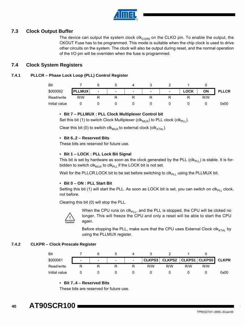
7.4.1 PLLCR – Phase Lock Loop (PLL) Control Register
• Bit 7 – PLLMUX : PLL Clock Multiplexer Control bitSet this bit (1) to switch Clock Multiplexer (clkMUX) to PLL clock (clkPLL).
Clear this bit (0) to switch clkMUX to external clock (clkXTAL).
• Bit 6..2 – Reserved BitsThese bits are reserved for future use.
• Bit 1 – LOCK : PLL Lock Bit SignalThis bit is set by hardware as soon as the clock generated by the PLL (clkPLL) is stable. It is for-bidden to switch clkMUX to clkPLL if the LOCK bit is not set.
Wait for the PLLCR.LOCK bit to be set before switching to clkPLL using the PLLMUX bit.
• Bit 0 – ON : PLL Start BitSetting this bit (1) will start the PLL. As soon as LOCK bit is set, you can switch on clkPLL clock,not before.
Clearing this bit (0) will stop the PLL.
7.4.2 CLKPR – Clock Prescale Register
• Bit 7..4 – Reserved BitsThese bits are reserved for future use.
Bit 7 6 5 4 3 2 1 0
$000062 PLLMUX - - - - - LOCK ON PLLCRRead/write R/W R R R R R R R/W
Initial value 0 0 0 0 0 0 0 0 0x00
When the CPU runs on clkPLL, and the PLL is stopped, the CPU will be clcked nolonger. This will freeze the CPU and only a reset will be able to start the CPUagain.
Before stopping the PLL, make sure that the CPU uses External Clock clkXTAL byusing the PLLMUX register.
Caution!
Bit 7 6 5 4 3 2 1 0
$000061 - - - - CLKPS3 CLKPS2 CLKPS1 CLKPS0 CLKPRRead/write R R R R R/W R/W R/W R/W
Initial value 0 0 0 0 0 0 0 0 0x00
40TPR0327AY–SMS–30Jan09
AT90SCR100

AT90SCR100
• Bits 3..0 – CLKPS3..0 : Clock Prescaler Select Bits 3..0These bits define the division factor between the selected clock source and the internal systemclock. These bits can be written at run-time to vary the clock frequency to suit the applicationrequirements. As the divider divides the master clock input to the MCU, the speed of all synchro-nous peripherals is reduced when a division factor is used. The division factors are given inTable 7-5.
You can change the CLKPR on the fly. The divider will automatically be active.
Default value of CLKPR is 0x00.
Notes: 1. clkMUX=96Mhz, clock generated by the PLL2. clkMUX=8Mhz, clock provided by external clock source XTAL.3. It is impossible for the CPU core to support 96Mhz, thus, by default, the divide by one clock
option generates a 16Mhz clock.
Table 7-5. Clock Prescaler Select (clkCPU)
CLKPS3 CLKPS2 CLKPS1 CLKPS0 CLKPRClock Division
FactorclkCPU
(clkMUX = clkPLL)(1)clkCPU
(clkMUX = clkXTAL)(2)
0 0 0 0 0x00 1(3) 16Mhz(3) 8Mhz
0 0 0 1 0x01 4 24Mhz 2Mhz
0 0 1 0 0x02 5 19.2Mhz 1.60Mhz
0 0 1 1 0x03 6 16Mhz 1.33Mhz
0 1 0 0 0x04 8 12Mhz 1Mhz
0 1 0 1 0x05 12 8Mhz 0.67Mhz
0 1 1 0 0x06 24 4Mhz 0.33Mhz
0 1 1 1 0x07 48 2Mhz 0.17Mhz
1 0 0 0 0x08 96 1Mhz 0.08Mhz
1 0 0 1 0x09
Reserved
1 0 1 0 0x0A
1 0 1 1 0x0B
1 1 0 0 0x0C
1 1 0 1 0x0D
1 1 1 0 0x0E
1 1 1 1 0X0F
41TPR0327AY–SMS–30Jan09

42TPR0327AY–SMS–30Jan09
AT90SCR100

AT90SCR100
8. Power Management and Sleep ModesSleep modes enable the application to shut down unused modules in the MCU, thereby savingpower. The AVR provides various sleep modes allowing the user to tailor the power consump-tion to the application’s requirements.
To enter any of the five sleep modes, the SE bit in the SMCR must be written to logic one and aSLEEP instruction must be executed. The SM2, SM1, and SM0 bits in the SMCR Register selectwhich sleep mode (Idle, Power-down, Power-save, or Standby) will be activated by the SLEEPinstruction. See Table 8-2 for a summary. If an enabled interrupt occurs while the MCU is in asleep mode, the MCU wakes up. The MCU is then halted for four cycles in addition to the start-up time, executes the interrupt routine, and resumes execution from the instruction followingSLEEP. The contents of the Register File and SRAM are unaltered when the device wakes upfrom sleep. If a reset occurs during sleep mode, the MCU wakes up and executes from theReset Vector.
Figure 7-1 on page 31 presents the different clock systems in the AT90SCR100, and their distri-bution. The figure is helpful in selecting an appropriate sleep mode.
8.1 Power Modes Descriptions
8.1.1 Idle ModeWhen the SM2:0 bits are written to 000, the SLEEP instruction makes the MCU enter Idle mode,stopping the CPU but allowing the peripherals and the interrupt system to continue operating.This sleep mode basically halts clkCPU and clkFLASH, while allowing the other clocks to run.
Idle mode enables the MCU to wake up from external triggered interrupts as well as internalones like the Timer Overflow and USART Transmit Complete interrupts, as shown in Table 8-1.
8.1.2 Power-down ModeWhen the SM2:0 bits are written to 010, the SLEEP instruction makes the MCU enter Power-down mode. In this mode, the external Oscillator is stopped, while the external interrupts, the 2-wire Serial Interface, and the Watchdog continue operating (if enabled). Only an External Reset,a coherent communication request on the different communication interface (TWI, USB, HSSPI,SPI, USART), a card insertion/removal, an external interrupt, a pin change interrupt or a key-board pin pressed interrupt can wake up the MCU. This sleep mode basically halts all generatedclocks, allowing operation of asynchronous modules only.
Please refer to the section entitled “Important note about: Entering and Leavinglow consumption modes” on page 47, to read important remarks on achieving min-imum consumption.
When waking up from Power-down or Power-Save mode, there is a delay fromwhen the wake-up condition occurs to when the wake-up becomes effective. Thisallows the clock to restart and become stable after having been stopped. Thewake-up period is defined by the same CKSEL Fuses that define the Reset Time-out period, as described in Table 7-3 on page 35.
Caution!
Note
To obtain a minimum consumption level, don’t forget to stop the DCDC and PLL,as remarked in section “Important note about: Entering and Leaving low consump-tion modes” on page 47.Caution
!
43TPR0327AY–SMS–30Jan09

Note that if a level triggered interrupt is used to wake-up from Power-down mode, the changedlevel must be held for some time to wake up the MCU. Refer to “External Interrupts” on page 69for details.
When waking up from Power-down mode, there is a delay from when the wake-up conditionoccurs until when the wake-up becomes effective. This allows the clock to restart and becomestable after having been stopped. The wake-up period is defined in Table 7-3.
8.1.3 Power-save ModeWhen the SM2:0 bits are written to 011, the SLEEP instruction makes the MCU enter Power-save mode. This mode is identical to Power-down, with one exception:
If Timer/Counter2 is enabled, it will keep running during sleep. The device can wake up fromeither Timer Overflow or Output Compare event from Timer/Counter2 if the correspondingTimer/Counter2 interrupt enable bits are set in TIMSK2, and the Global Interrupt Enable bit inSREG is set.
If Timer/Counter2 is not running, Power-down mode is recommended instead of Power-savemode.
The Timer/Counter2 can be clocked both synchronously and asynchronously in Power-savemode. If the Timer/Counter2 is not using the asynchronous clock, the Timer/Counter Oscillator isstopped during sleep. If the Timer/Counter2 is not using the synchronous clock, the clock sourceis stopped during sleep. Note that even if the synchronous clock is running in Power-save, thisclock is only available for the Timer/Counter2.
8.1.4 Standby ModeWhen the SM2:0 bits are 110, the SLEEP instruction makes the MCU enter Standby mode. Thismode is identical to Power-down with the exception that the Oscillator is kept running. FromStandby mode, the device wakes up in six clock cycles.
8.1.5 Extended Standby ModeWhen the SM2:0 bits are 111, the SLEEP instruction makes the MCU enter Extended Standbymode. This mode is identical to Power-save mode with the exception that the Oscillator is keptrunning. From Extended Standby mode, the device wakes up in six clock cycles.
Notes: 1. If Timer/Counter2 is running in asynchronous mode.2. For INT3:0, only level interrupt.
Table 8-1. Active Clock Domains and Wake-up Sources in the Different Sleep Modes.Active Clock Domains Oscillators Wake-up Sources
Sleep Mode clk C
PU
clk F
lash
, clk
SCI
clk I
/O
clk H
SSP
I, cl
k USB
clk A
SY
Mai
n C
lock
Sour
ce
Enab
led
Tim
er O
sc
Enab
led
INT3
:0Pi
n C
hang
eC
oher
ent
Com
mun
icat
ion
requ
est
Tim
er2
SPM
/EE
PRO
M R
eady
Key
boar
d Pi
npr
esse
d
WD
T In
terr
upt
Oth
er I/
O
Idle X X X X X(1) X X X X X X XPower-down X(2) X X XPower-save X X(1) X(2) X X X XStandby X X(2) X X XExtended Standby X(1) X X(1) X(2) X X X X
44TPR0327AY–SMS–30Jan09
AT90SCR100

AT90SCR100
8.2 Power Reduction RegisterThe Power Reduction Register, PRR, provides a method to stop the clock to individual peripher-als to reduce power consumption. The current state of the peripheral is frozen and the I/Oregisters can not be read or written. Resources used by the peripheral when stopping the clockwill remain occupied, hence the peripheral should in most cases be disabled before stopping theclock. Waking up a module, which is done by clearing the bit in PRR, puts the module in thesame state as before shutdown.
8.2.1 SMCR – Sleep Mode Control RegisterThe Sleep Mode Control Register contains control bits for power management.
• Bits 3..1 – SM2..0 : Sleep Mode Select Bits 2..0These bits select between the five available sleep modes as shown in Table 8-2.
Note: 1. Standby modes are only recommended for use with external crystals or resonators.
• Bit 0 – SE: Sleep EnableThe SE bit must be written to logic one to make the MCU enter the sleep mode when the SLEEPinstruction is executed. To avoid the MCU entering the sleep mode unless it is the programmer’spurpose, it is recommended to write the Sleep Enable (SE) bit to one just before the execution ofthe SLEEP instruction and to clear it immediately after waking up.
8.2.2 PRR0 – Power Reduction Register 0The Power Reduction Register allows the shut down of peripherals directly connected to CPUresources. These peripherals are activated by default and can be shut down for power con-sumption reasons if they are not used by an application.
Bit 7 6 5 4 3 2 1 0
0x33 (0x53) - - - - SM2 SM1 SM0 SE SMCRRead/write R R R R R/W R/W R/W R/W
Initial value 0 0 0 0 0 0 0 0 0x00
Table 8-2. Sleep Mode Select
SM2 SM1 SM0 Sleep Mode
0 0 0 Idle
0 0 1 Reserved
0 1 0 Power-down
0 1 1 Power-save
1 0 0 Reserved
1 0 1 Reserved
1 1 0 Standby(1)
1 1 1 Extended Standby(1)
Bit 7 6 5 4 3 2 1 0
$000064 PRTWI PRTIM2 PRTIM0 - PRTIM1 PRSPI PRUSART0 - PRR0Read/write R/W R/W R/W R R/W R/W R/W R
Initial value 0 0 0 0 0 0 0 0 0x00
45TPR0327AY–SMS–30Jan09

• Bit 7 - PRTWI: Power Reduction TWIWriting a logic one to this bit shuts down the TWI by stopping the clock to the module. Whenwaking up the TWI again, the TWI should be re initialized to ensure proper operation.
• Bit 6 - PRTIM2: Power Reduction Timer/Counter2Writing a logic one to this bit shuts down the Timer/Counter2 module in synchronous mode (AS2is 0). When the Timer/Counter2 is enabled, operation will continue like before the shutdown.
• Bit 5 - PRTIM0: Power Reduction Timer/Counter0Writing a logic one to this bit shuts down the Timer/Counter0 module. When the Timer/Counter0is enabled, operation will continue as before the shutdown.
• Bit 4 - Res: Reserved bitReserved for future use and will always read as zero.
• Bit 3 - PRTIM1: Power Reduction Timer/Counter1Writing a logic one to this bit shuts down the Timer/Counter1 module. When the Timer/Counter1is enabled, operation will continue like before the shutdown.
• Bit 2 - PRSPI: Power Reduction Serial Peripheral InterfaceWriting a logic one to this bit shuts down the Serial Peripheral Interface by stopping the clock tothe module. When waking up the SPI again, the SPI should be re initialized to ensure properoperation.
• Bit 1 - PRUSART0: Power Reduction USART0Writing a logic one to this bit shuts down the USART0 by stopping the clock to the module.When waking up the USART0 again, the USART0 should be reinitialized to ensure properoperation.
• Bit 0 - Res: Reserved bitReserved for future use and will always read as zero.
8.2.3 PRR1 – Power Reduction Register 1The Power Reduction Register allows the shut down of peripherals directly connected to CPUresources. These peripherals are activated by default and can be shut down for power con-sumption reasons if they are not used by an application.
• Bit 7 - Res: Reserved bitReserved for future use and will always read as zero.
• Bit 6 - Res: Reserved bitReserved for future use and will always read as zero.
• Bit 5 - PRKB: Power Reduction Keyboard
Bit 7 6 5 4 3 2 1 0
$000065 - - PRKB PRAES PRSCI PRHSSPI PRUSB PRUSBH PRR1Read/write R/W R/W R/W R R/W R/W R/W R
Initial value 0 0 0 0 0 0 0 0 0x00
46TPR0327AY–SMS–30Jan09
AT90SCR100

AT90SCR100
Writing a logic one to this bit shuts down the Keyboard module by stopping the clock to the mod-ule. When waking up the Keyboard again, the Keyboard should be re initialized to ensure properoperation.
• Bit 4 - PRAES: Power Reduction AESWriting a logic one to this bit shuts down the AES module by stopping the clock to the module.When waking up the AES again, the AES should be re initialized to ensure proper operation.
• Bit 3 - PRSCI: Power Reduction Smart Card InterfaceWriting a logic one to this bit shuts down the Smart Card Interface module by stopping the clockto the module. When waking up the SCIB again, the SCIB should be re initialized to ensureproper operation.
• Bit 2 - PRHSSPI: Power Reduction High Speed SPIWriting a logic one to this bit shuts down the High Speed Serial Peripheral Interface by stoppingthe clock to the module. When waking up the HSSPI again, the HSSPI should be re initialized toensure proper operation.
• Bit 1 - PRUSB: Power Reduction USBWriting a logic one to this bit shuts down the USB by stopping the clock to the module. Whenwaking up the USB again, the USB should be reinitialized to ensure proper operation.
• Bit 0 - PRUSBH: Power Reduction USB Host ControllerWriting a logic one to this bit shuts down the USB Host Controller by stopping the clock to themodule. When waking up the USB Host Controller again, the USB Host module should be reini-tialized to ensure proper operation.
8.3 Important note about: Entering and Leaving low consumption modes
8.3.1 Entering Power DownIt is very important to note that there is no automatic switch to a low consumption mode for thePLL Clock Multiplexer and for the DC/DC converter.
• To lower the powerdown consumption, the PLL Clock Multiplexer must be switched to External Clock and the PLL must be stopped. To do so:
– Switch from PLL to External Clock by clearing PLLCR.PLLMUX.– Turn the PLL off by clearing PLLCR.ON.– Wait until PLLCR.LOCK bit is cleared.
• To lower the powerdown consumption, the DC/DC converter must also be switched off. To do so:
– Clear DCCR.DCON bit. This will generate a deactivation sequence.
Enabling the ‘Power Reduction USB Host Controller’ prevents the device fromcommunicating with USB smart cards.
However, if the Smart Card Interface is ON, communication with standard smartcards (ISO7816 1-3) is still possible.
To optimize the power consumption, if the application does not target USB SmartCard, the USB Host Controller should be disabled this way.
Note
47TPR0327AY–SMS–30Jan09

– Wait until DCCR.DCRDY is cleared.
8.3.2 Waking up from Power DownDo not forget to restore the PLL configuration and DC/DC converter when waking the chip up.Please refer to Figure 7-4 on page 37 and Figure 16-1 on page 202 to re-enable theseperipherals.
8.4 Minimizing Power ConsumptionThere are several issues to consider when trying to minimize the power consumption in an AVRcontrolled system. In general, sleep modes should be used as much as possible, and the sleepmode should be selected so that as few as possible of the device’s functions are operating. Allfunctions not needed should be disabled. In particular, the following modules may need specialconsideration when trying to achieve the lowest possible power consumption.
8.4.1 Brown-out DetectorIf the Brown-out Detector is not needed by the application, this module should be turned off. Ifthe Brown-out Detector is enabled by the BODENABLE Fuses, it will be enabled in all sleepmodes, and hence, always consume power. In the deeper sleep modes, this will contribute sig-nificantly to the total current consumption. Refer to “Brown-out Detection” on page 54 for detailson how to configure the Brown-out Detector.
8.4.2 Internal Voltage ReferenceThe Internal Voltage Reference will be enabled when needed by the Brown-out Detection. If thismodule is disabled as described in the sections above, the internal voltage reference will be dis-abled and it will not be consuming power. When turned on again, the user must allow thereference to start up before the output is used. If the reference is kept on in sleep mode, the out-put can be used immediately. Refer to “Internal Voltage Reference” on page 55 for details on thestart-up time.
8.4.3 Watchdog TimerIf the Watchdog Timer is not needed in the application, the module should be turned off. If theWatchdog Timer is enabled, it will be enabled in all sleep modes, and hence, always consumepower. In the deeper sleep modes, this will contribute significantly to the total current consump-tion. Refer to “Interrupts” on page 63 for details on how to configure the Watchdog Timer.
8.4.4 Port PinsWhen entering a sleep mode, all port pins should be configured to use minimum power. It ismost important to ensure that no pins drive resistive loads. This ensures that no power is con-sumed by the input logic when not needed. In some cases, the input logic is needed to detectwake-up conditions, and it will then be enabled. Refer to the section “Digital Input Enable andSleep Modes” on page 81 for details on which pins are enabled. If the input buffer is enabled andthe input signal is left floating or has an analog signal level close to VCC/2, the input buffer willuse excessive power.
8.4.5 On-chip Debug SystemIf the On-chip debug system is enabled by the OCDEN Fuse and the chip enters sleep mode,the main clock source is enabled, and hence, always consumes power. In the deeper sleepmodes, this will contribute significantly to the total current consumption.
There are three alternative ways to disable the OCD system:
48TPR0327AY–SMS–30Jan09
AT90SCR100

AT90SCR100
• Disable the OCDEN Fuse.• Disable the JTAGEN Fuse.• Write one to the JTD bit in MCUCR. See “MCUCR – MCU Control Register” on page 356.
49TPR0327AY–SMS–30Jan09

50TPR0327AY–SMS–30Jan09
AT90SCR100

AT90SCR100
9. System Control and Reset
9.1 Resetting the AVRDuring reset, all I/O Registers are set to their initial values, and the program starts executionfrom the Reset Vector. The instruction placed at the Reset Vector must be a JMP – AbsoluteJump – instruction to the reset handling routine. If the program never enables an interruptsource, the Interrupt Vectors are not used, and regular program code can be placed at theselocations. This is also the case if the Reset Vector is in the Application section while the InterruptVectors are in the Boot section or vice versa. The circuit diagram in Figure 9-1 shows the resetlogic. Table 9-1 defines the electrical parameters of the reset circuitry.
The I/O ports of the AVR are immediately reset to their initial state when a reset source goesactive. This does not require any clock source to be running.
After all reset sources have gone inactive, a delay counter is invoked, stretching the internalreset. This allows the power to reach a stable level before normal operation starts. The time-outperiod of the delay counter is defined by the user through the SUT Fuses. The different selec-tions for the delay period are presented in Table 7-3.
9.2 Reset SourcesThe AT90SCR100 has five sources of reset:
• Power-on Reset. The MCU is reset when the supply voltage is below the Power-on Reset threshold (VPOT).
• External Reset. The MCU is reset when a low level is present on the RESET pin for longer than the minimum pulse length.
• Watchdog Reset. The MCU is reset when the Watchdog Timer period expires and the Watchdog is enabled.
• Brown-out Reset. The MCU is reset when the supply voltage VCC is below the Brown-out Reset threshold (VBOT) and the Brown-out Detector is enabled.
• JTAG AVR Reset. The MCU is reset as long as there is a logic one in the Reset Register, one of the scan chains of the JTAG system. Refer to the section “IEEE 1149.1 (JTAG) Boundary-scan” on page 353 for details.
51TPR0327AY–SMS–30Jan09

Figure 9-1. Reset Logic
Notes: 1. Values are guidelines only. Actual values are TBC.2. The Power-on Reset will not work unless the supply voltage has been below VPOT (falling)
9.2.1 Power-on ResetA Power-on Reset (POR) pulse is generated by an On-chip detection circuit. The detection levelis defined in Table 9-1. The POR is activated whenever VCC is below the detection level. ThePOR circuit can be used to trigger the start-up Reset, as well as to detect a failure in supplyvoltage.
Table 9-1. Reset Characteristics(1)
Symbol Parameter Condition Min Typ Max Units
VPOT
Power-on Reset Threshold Voltage (rising) 1.4 1.8 V
Power-on Reset Threshold Voltage (falling)(2) 1.3 1.8 V
VRST RESET Pin ViL 0.2VCC V
RESET Pin ViH 0.85VCC
tRSTMinimum pulse width onRESET Pin
1.5 μs
MCU StatusRegister (MCUSR)
Brown-outReset CircuitBODLEVEL
Delay CountersCKTIMEOUT
WD
RF
BORF
EXTR
F
PORF
DATA BUS
ClockController
SPIKEFILTER
Pull-up Resistor
JTRF
JTAG ResetRegister
WatchdogOscillator
SUT[1:0]
Power-on ResetCircuit
52TPR0327AY–SMS–30Jan09
AT90SCR100

AT90SCR100
A Power-on Reset (POR) circuit ensures that the device is reset from Power-on. Reaching thePower-on Reset threshold voltage invokes the delay counter, which determines how long thedevice is kept in RESET after VCC rise. The RESET signal is activated again, without any delay,when VCC decreases below the detection level.
Figure 9-2. MCU Start-up, RESET Tied to VCC
Figure 9-3. MCU Start-up, RESET Extended Externally
9.2.2 External ResetAn External Reset is generated by a low level on the RESET pin. Reset pulses longer than theminimum pulse width (see Table 9-1) will generate a reset, even if the clock is not running.Shorter pulses are not guaranteed to generate a reset. When the applied signal reaches theReset Threshold Voltage – VRST – on its positive edge, the delay counter starts the MCU afterthe Time-out period – tTOUT – has expired.
V
RESET
TIME-OUT
INTERNALRESET
tTOUT
V POT
V RST
CC
RESET
TIME-OUT
INTERNALRESET
tTOUT
V POT
V RST
V CC
53TPR0327AY–SMS–30Jan09

Figure 9-4. External Reset During Operation
9.2.3 Brown-out DetectionAT90SCR100 has an On-chip Brown-out Detection (BOD) circuit for monitoring the VCC levelduring operation by comparing it to a fixed trigger level. The BOD can be activated or disabledby the BODENABLE Fuses. The trigger level has a hysteresis to ensure spike free Brown-outDetection. The hysteresis on the detection level should be interpreted as VBOT+ = VBOT + VHYST/2and VBOT- = VBOT - VHYST/2.
When the BOD is enabled, and VCC decreases to a value below the trigger level (VBOT- in Figure9-5), the Brown-out Reset is immediately activated. When VCC increases above the trigger level(VBOT+ in Figure 9-5), the delay counter starts the MCU after the Time-out period tTOUT hasexpired.
The BOD circuit will only detect a drop in VCC if the voltage stays below the trigger level for lon-ger than tBOD given in Table 9-1.
CC
Table 9-2. BODENABLE Fuse Coding
BODENABLE Fuse Min VBOT Typ VBOT Max VBOT
1 BOD Disabled
0 2.3 V
Table 9-3. Brown-out Characteristics
Symbol Parameter Min Typ Max Units
VHYST Brown-out Detector Hysteresis 50 mV
tBOD Min Pulse Width on Brown-out Reset ns
54TPR0327AY–SMS–30Jan09
AT90SCR100

AT90SCR100
Figure 9-5. Brown-out Reset During Operation
9.2.4 Watchdog ResetWhen the Watchdog times out, it will generate a short reset pulse of one CK cycle duration. Onthe falling edge of this pulse, the delay timer starts counting the Time-out period tTOUT. Refer topage 63 for details on operation of the Watchdog Timer.
Figure 9-6. Watchdog Reset During Operation
9.3 Internal Voltage ReferenceAT90SCR100 features an internal bandgap reference. This reference is used for Brown-outDetection and supply monitor.
9.3.1 Voltage Reference Enable Signals and Start-up TimeThe voltage reference has a start-up time that may influence the way it should be used. Thestart-up time is given in Table 9-4. To save power, the reference is not always turned on. Thereference is on during the following situations:
1. When the BOD is enabled (by programming the BODENABLE Fuse).2. Supply Monitor is enabled (by programming the SMONCR.SMONEN bit).
VCC
RESET
TIME-OUT
INTERNALRESET
VBOT-VBOT+
tTOUT
CK
CC
55TPR0327AY–SMS–30Jan09

To reduce power consumption in Power-down mode, the user can avoid the two conditionsabove to ensure that the reference is turned off before entering Power-down mode.
Notes: 1. Values are guidelines only. Actual values are TBD.
9.4 Supply monitorThis feature is designed to prevent the AT90SCR100 operating under conditions that don’t guar-antee a correct operation of its peripherals.
Useful to detect battery low voltage, the supply monitor peripheral generate an interruption whenVcc drops below a level defined in Table 9-5.
Vcc shall be below Supply Monitor level for a minimum time before the interruption to be gener-ated. In the same behavior than BOD, the Supply Monitor has an hysteresis to reach the level,interpreted as VSMON+ = VSMON + VSMHYST/2 and VSMON- = VSMON - VSMHYST/2
Figure 9-7. Supply Monitor description
Please refer to section “SMONCR – Supply Monitor Control Register” on page 60 and section“Interrupts” on page 63 for Supply Monitor interruption management.
Table 9-4. Internal Voltage Reference Characteristics(1)
Symbol Parameter Condition Min Typ Max Units
tBG Reference start-up timeVCC = 2.7TA = 25°C
40 70 μs
Table 9-5. Supply Monitor References
Symbol Parameter Min Typ Max Units
VSMON Supply Monitor Level 2.5 V
VSMHYST Supply Monitor Hysteresis 50 mV
tSMON Min Pulse Width on Brown-out Reset ns
VCC
RESET
INTERRUPTTRIGGER
VSMON-VSMON+
56TPR0327AY–SMS–30Jan09
AT90SCR100

AT90SCR100
9.5 Watchdog TimerAT90SCR100 has an Enhanced Watchdog Timer (WDT). The main features are:
• Clocked from separate On-chip Oscillator• 3 Operating modes
– Interrupt– System Reset– Interrupt and System Reset
• Selectable Time-out period from 16ms to 8s• Possible Hardware fuse Watchdog always on (WDTON) for fail-safe mode
Figure 9-8. Watchdog Timer
The Watchdog Timer (WDT) is a timer counting cycles of a separate on-chip 125 kHz oscillator.The WDT gives an interrupt or a system reset when the counter reaches a given time-out value.In normal operation mode, it is required that the system uses the WDR - Watchdog Timer Reset- instruction to restart the counter before the time-out value is reached. If the system doesn'trestart the counter, an interrupt or system reset will be issued.
In Interrupt mode, the WDT gives an interrupt when the timer expires. This interrupt can be usedto wake the device from sleep-modes, and also as a general system timer. One example is tolimit the maximum time allowed for certain operations, giving an interrupt when the operationhas run longer than expected. In System Reset mode, the WDT gives a reset when the timerexpires. This is typically used to prevent system hang-up in case of runaway code. The thirdmode, Interrupt and System Reset mode, combines the other two modes by first giving an inter-rupt and then switch to System Reset mode. This mode will for instance allow a safe shutdownby saving critical parameters before a system reset.
The Watchdog always on (WDTON) fuse, if programmed, will force the Watchdog Timer to Sys-tem Reset mode. With the fuse programmed the System Reset mode bit (WDE) and Interruptmode bit (WDIE) are locked to 1 and 0 respectively. To further ensure program security, altera-tions to the Watchdog set-up must follow timed sequences. The sequence for clearing the WDEand changing the time-out configuration is as follows:
125kHzOSCILLATOR
OSC/
2KOS
C/4K
OSC/
8KOS
C/16
KOS
C/32
KOS
C/64
KOS
C/12
8KOS
C/25
6KOS
C/51
2KOS
C/10
24K
WDP0WDP1WDP2WDP3
WATCHDOGRESET
WDE
WDIF
WDIE
MCU RESET
INTERRUPT
57TPR0327AY–SMS–30Jan09

1. In the same operation, write a logic one to the Watchdog change enable bit (WDCE) and WDE. A logic one must be written to WDE regardless of the previous value of the WDE bit.
2. Within the next four clock cycles, write the WDE and Watchdog prescaler bits (WDP) as desired, but with the WDCE bit cleared. This must be done in one operation.
The following code example shows one assembly and one C function for turning off the Watch-dog Timer. The example assumes that interrupts are controlled (e.g. by disabling interruptsglobally) so that no interrupts will occur during the execution of these functions.
Assembly Code Example
WDT_off:
; Turn off global interrupt
cli
; Reset Watchdog Timer
wdr
; Clear WDRF in MCUSR
in r16, MCUSR
andi r16, (0xff & (0<<WDRF))
out MCUSR, r16
; Write logical one to WDCE and WDE
; Keep old prescaler setting to prevent unintentional time-out
in r16, WDTCSR
ori r16, (1<<WDCE) | (1<<WDE)
out WDTCSR, r16
; Turn off WDT
ldi r16, (0<<WDE)
out WDTCSR, r16
; Turn on global interrupt
sei
ret
C Code Example
void WDT_off(void)
{
__disable_interrupt();
__watchdog_reset();
/* Clear WDRF in MCUSR */
MCUSR &= ~(1<<WDRF);
/* Write logical one to WDCE and WDE */
/* Keep old prescaler setting to prevent unintentional time-out */
WDTCSR |= (1<<WDCE) | (1<<WDE);
/* Turn off WDT */
WDTCSR = 0x00;
__enable_interrupt();
}
58TPR0327AY–SMS–30Jan09
AT90SCR100

AT90SCR100
The following code example shows one assembly and one C function for changing the time-outvalue of the Watchdog Timer.
If the Watchdog is accidentally enabled, for example by a runaway pointer orbrown-out condition, the device will be reset and the Watchdog Timer will stayenabled. If the code is not set up to handle the Watchdog, this might lead to aneternal loop of time-out resets. To avoid this situation, the application softwareshould always clear the Watchdog System Reset Flag (WDRF) and the WDE con-trol bit in the initialisation routine, even if the Watchdog is not in use.
Assembly Code Example
WDT_Prescaler_Change:
; Turn off global interrupt
cli
; Reset Watchdog Timer
wdr
; Start timed sequence
in r16, WDTCSR
ori r16, (1<<WDCE) | (1<<WDE)
out WDTCSR, r16
; -- Got four cycles to set the new values from here -
; Set new prescaler(time-out) value = 64K cycles (~0.5 s)
ldi r16, (1<<WDE) | (1<<WDP2) | (1<<WDP0)
out WDTCSR, r16
; -- Finished setting new values, used 2 cycles -
; Turn on global interrupt
sei
ret
C Code Example
void WDT_Prescaler_Change(void)
{
__disable_interrupt();
__watchdog_reset();
/* Start timed Sequence */
WDTCSR |= (1<<WDCE) | (1<<WDE);
/* Set new prescaler(time-out) value = 64K cycles (~0.5 s) */
WDTCSR = (1<<WDE) | (1<<WDP2) | (1<<WDP0);
__enable_interrupt();
}
The Watchdog Timer should be reset before any change of the WDP bits, since achange in the WDP bits can result in a time-out when switching to a shorter time-out period.
Note
Note
59TPR0327AY–SMS–30Jan09

9.6 Register Description
9.6.1 MCUSR – MCU Status RegisterThe MCU Status Register provides information on which reset source caused an MCU reset.
• Bit 4 – JTRF: JTAG Reset FlagThis bit is set if a reset is being caused by a logic one in the JTAG Reset Register selected bythe JTAG instruction AVR_RESET. This bit is reset by a Power-on Reset, or by writing a logiczero to the flag.
• Bit 3 – WDRF: Watchdog Reset FlagThis bit is set if a Watchdog Reset occurs. The bit is reset by a Power-on Reset, or by writing alogic zero to the flag.
• Bit 2 – BORF: Brown-out Reset FlagThis bit is set if a Brown-out Reset occurs. The bit is reset by a Power-on Reset, or by writing alogic zero to the flag.
• Bit 1 – EXTRF: External Reset FlagThis bit is set if an External Reset occurs. The bit is reset by a Power-on Reset, or by writing alogic zero to the flag.
• Bit 0 – PORF: Power-on Reset FlagThis bit is set if a Power-on Reset occurs. The bit is reset only by writing a logic zero to the flag.
To make use of the Reset Flags to identify a reset condition, the user should read and thenReset the MCUSR as early as possible in the program. If the register is cleared before anotherreset occurs, the source of the reset can be found by examining the Reset Flags.
9.6.2 SMONCR – Supply Monitor Control Register
• Bit 7 – SMONIF: Supply Monitor Interrupt FlagThis bit is set by hardware when the external voltage Vcc drops below a Supply Monitor level.
If SMONIE and SREG.I bits are set, then an interrupt is triggered. This interrupt should allowtime to save important information, or cancel critical exchanges.
This bit must be cleared by software.
• Bit 6 – SMONIE: Supply Monitor Interrupt Enable
Bit 7 6 5 4 3 2 1 0
0x34 (0x54) - - - JTRF WDRF BORF EXTRF PORF MCUSRRead/write R R R R/W R/W R/W R/W R/W
Initial value See Bit Description
Bit 7 6 5 4 3 2 1 0
0x0063 SMONIF SMONIE - - - - - SMONEN SMONCRRead/write R/W R/W R R R R R R/W
Initial value 0 0 0 0 0 0 0 0 0x00
60TPR0327AY–SMS–30Jan09
AT90SCR100

AT90SCR100
This bit is set and cleared by software. Set this bit to enable interrupt generation as soon as Vccdrops below the Supply Monitor level. The global interrupt bit (SREG.I) should be set.
Clear this bit to mask Supply Monitor Interruption generation.
• Bit 5..1 – Reserved BitsThese bits are reserved for future use.
• Bit 0 – SMONEN: Supply Monitor EnableThis bit is set and cleared by software. Setting this bit will activate the Supply Monitor system.Clearing this bit will disable the Supply Monitor system and reduce power consumption.
9.6.3 WDTCSR – Watchdog Timer Control Register
• Bit 7 - WDIF: Watchdog Interrupt FlagThis bit is set when a time-out occurs in the Watchdog Timer and the Watchdog Timer is config-ured for interrupt. WDIF is cleared by hardware when executing the corresponding interrupthandling vector. Alternatively, WDIF is cleared by writing a logic one to the flag. When the I-bit inSREG and WDIE are set, the Watchdog Time-out Interrupt is executed.
• Bit 6 - WDIE: Watchdog Interrupt EnableWhen this bit is written to one and the I-bit in the Status Register is set, the Watchdog Interrupt isenabled. If WDE is cleared in combination with this setting, the Watchdog Timer is in InterruptMode, and the corresponding interrupt is executed if a time-out in the Watchdog Timer occurs.
If WDE is set, the Watchdog Timer is in Interrupt and System Reset Mode. The first time-out inthe Watchdog Timer will set WDIF. Executing the corresponding interrupt vector will clear WDIEand WDIF automatically by hardware (the Watchdog goes to System Reset Mode). This is use-ful for keeping the Watchdog Timer security while using the interrupt. To stay in Interrupt andSystem Reset Mode, WDIE must be set after each interrupt. This should however not be donewithin the interrupt service routine itself, as this might compromise the safety-function of theWatchdog System Reset mode. If the interrupt is not executed before the next time-out, a Sys-tem Reset will be applied.
Notes: 1. WDTON is a fuse bit (see “Fuse High Byte” on page 379).
Bit 7 6 5 4 3 2 1 0
$000060 WDIF WDIE WDP3 WDCE WDE WDP2 WDP1 WDP0 WDTCSRRead/write R/W R/W R/W R/W R/W R/W R/W R/W
Initial value 0 0 0 0 0 0 0 0 0x00
Table 9-6. Watchdog Timer Configuration
WDTON(1) WDE WDIE Mode Action on Time-out
0 0 0 Stopped None
0 0 1 Interrupt Mode Interrupt
0 1 0 System Reset Mode Reset
0 1 1 Interrupt and System Reset Mode
Interrupt, then go to System Reset Mode
1 x x System Reset Mode Reset
61TPR0327AY–SMS–30Jan09

• Bit 4 - WDCE: Watchdog Change EnableThis bit is used in timed sequences for changing WDE and prescaler bits. To clear the WDE bit,and/or change the prescaler bits, WDCE must be set.
Once written to one, hardware will clear WDCE after four clock cycles.
• Bit 3 - WDE: Watchdog System Reset EnableWDE is overridden by WDRF in MCUSR. This means that WDE is always set when WDRF isset. To clear WDE, WDRF must be cleared first. This feature ensures multiple resets during con-ditions causing failure, and a safe start-up after the failure.
• Bit 5, 2..0 - WDP3..0: Watchdog Timer Prescaler 3..0The WDP3:0 bits determine the Watchdog Timer prescaling when the Watchdog Timer is run-ning. The different prescaling values and their corresponding time-out periods are shown inTable 9-7 on page 62.
Table 9-7. Watchdog Timer Prescale Select
WDP3 WDP2 WDP1 WDP0Number of WDT Oscillator
CyclesTypical Time-out at
VCC = 5.0V
0 0 0 0 2K (2048) cycles 15.625 ms
0 0 0 1 4K (4096) cycles 31.25 ms
0 0 1 0 8K (8192) cycles 62.5 ms
0 0 1 1 16K (16384) cycles 0.122 s
0 1 0 0 32K (32768) cycles 0.24 s
0 1 0 1 64K (65536) cycles 0.48 s
0 1 1 0 128K (131072) cycles 0.97 s
0 1 1 1 256K (262144) cycles 1.95 s
1 0 0 0 512K (524288) cycles 3.9 s
1 0 0 1 1024K (1048576) cycles 7.81 s
1 0 1 0
Reserved
1 0 1 1
1 1 0 0
1 1 0 1
1 1 1 0
1 1 1 1
62TPR0327AY–SMS–30Jan09
AT90SCR100

AT90SCR100
10. InterruptsThis section describes the specifics of the interrupt handling as performed in AT90SCR100. Fora general explanation of the AVR interrupt handling, refer to “Reset and Interrupt Handling” onpage 18.
10.1 Interrupt Vectors in AT90SCR100
Table 10-1. Reset and Interrupt Vectors
VectorNo.
ProgramAddress(1) Source Interrupt Definition
1 $0000(2) RESET External Pin, Power-on Reset, Brown-out Reset, Watchdog Reset, and JTAG AVR Reset
2 $0002 INT0 External Interrupt Request 0
3 $0004 INT1 External Interrupt Request 1
4 $0006 INT2 External Interrupt Request 2
5 $0008 INT3 External Interrupt Request 3
6 $000A PCINT0 Pin Change Interrupt Request 0
7 $000C PCINT1 Pin Change Interrupt Request 1
8 $000E PCINT2 Pin Change Interrupt Request 2
9 $0010 WDT Watchdog Time-out Interrupt
10 $0012 TIMER2_COMPA Timer/Counter2 Compare Match A
11 $0014 TIMER2_COMPB Timer/Counter2 Compare Match B
12 $0016 TIMER2_OVF Timer/Counter2 Overflow
13 $0018 TIMER1_CAPT Timer/Counter1 Capture Event
14 $001A TIMER1_COMPA Timer/Counter1 Compare Match A
15 $001C TIMER1_COMPB Timer/Counter1 Compare Match B
16 $001E TIMER1_OVF Timer/Counter1 Overflow
17 $0020 TIMER0_COMPA Timer/Counter0 Compare Match A
18 $0022 TIMER0_COMPB Timer/Counter0 Compare Match B
19 $0024 TIMER0_OVF Timer/Counter0 Overflow
20 $0026 SPI_STC SPI Serial Transfer Complete
21 $0028 USART_RX USART Rx Complete
22 $002A USART_UDRE USART Data Register Empty
23 $002C USART_TX USART Tx Complete
24 $002E SUPPLY_MON Supply Monitor Interruption
25 -- RFU Reserved For Future Use
26 $0032 EE_READY EEPROM Ready
27 $0034 TWI 2-wire Serial Interface
28 $0036 SPM_READY Store Program Memory Ready
63TPR0327AY–SMS–30Jan09

Notes: 1. When the IVSEL bit in MCUCR is set, Interrupt Vectors will be moved to the start of the Boot Flash Section. The address of each Interrupt Vector will then be the address in this table added to the start address of the Boot Flash Section.
2. When the BOOTRST Fuse is programmed, the device will jump to the Boot Loader address at reset, see “Memory Programming” on page 377.
Table 10-2 shows reset and Interrupt Vectors placement for the various combinations ofBOOTRST and IVSEL settings. If the program never enables an interrupt source, the InterruptVectors are not used, and regular program code can be placed at these locations. This is alsothe case if the Reset Vector is in the Application section while the Interrupt Vectors are in theBoot section or vice versa.
Note: 1. The Boot Reset Address is shown in Table 28-7 on page 376. For the BOOTRST Fuse “1” means unprogrammed while “0” means programmed.
The most typical and general program setup for the Reset and Interrupt Vector Addresses inAT90SCR100 is:
29 $0038 KEYBOARD Keyboard Input Changed
30 $003A AES AES Block Operation Ended
31 $003C HSSPI High-Speed SPI Interface
32 $003E USB Endpoint USB Endpoint linked Interrupt
33 $0040 USB Protocol USB Protocol Interrupt
34 $0042 SCIB Smart Card Reader Interface
35 $0044 USB Host Control USB Host Controller Interrupt
36 $0046 USB Host Pipe USB Host Pipe Interrupt
37 $0048 CPRES Card Presence Detection
38 $004A PCINT3 Pin Change Interrupt Request 3
Table 10-2. Reset and Interrupt Vectors Placement(1)
BOOTRST IVSEL Reset Address Interrupt Vectors Start Address
1 0 0x0000 0x0002
1 1 0x0000 Boot Reset Address + 0x0002
0 0 Boot Reset Address 0x0002
0 1 Boot Reset Address Boot Reset Address + 0x0002
Table 10-1. Reset and Interrupt Vectors (Continued)
VectorNo.
ProgramAddress(1) Source Interrupt Definition
Address
Labels Code Comments
0x jmp RESET ; Reset Handler
0x02 jmp INT0 ; IRQ0 Handler
0x04 jmp INT1 ; IRQ1 Handler
0x06 jmp INT2 ; IRQ2 Handler
0x08 jmp INT3 ; IRQ3 Handler
0x0A jmp PCINT0 ; PCINT0 Handler
0x0C jmp PCINT1 ; PCINT1 Handler
64TPR0327AY–SMS–30Jan09
AT90SCR100

AT90SCR100
When the BOOTRST Fuse is unprogrammed, the Boot section size set to 8K bytes and theIVSEL bit in the MCUCR Register is set before any interrupts are enabled, the most typical andgeneral program setup for the Reset and Interrupt Vector Addresses is:
Address Labels Code Comments
0x00000 RESET: ldi r16,high(RAMEND); Main program start
0x00001 out SPH,r16 ; Set Stack Pointer to top of RAM
0x0E jmp PCINT2 ; PCINT2 Handler
0x10 jmp WDT ; Watchdog Timeout Handler
0x12 jmp TIM2_COMPA ; Timer2 CompareA Handler
0x14 jmp TIM2_COMPB ; Timer2 CompareB Handler
0x16 jmp TIM2_OVF ; Timer2 Overflow Handler
0x18 jmp TIM1_CAPT ; Timer1 Capture Handler
0x1A jmp TIM1_COMPA ; Timer1 CompareA Handler
0x1C jmp TIM1_COMPB ; Timer1 CompareB Handler
0x1E jmp TIM1_OVF ; Timer1 Overflow Handler
0x20 jmp TIM0_COMPA ; Timer0 CompareA Handler
0x22 jmp TIM0_COMPB ; Timer0 CompareB Handler
0x24 jmp TIM0_OVF ; Timer0 Overflow Handler
0x26 jmp SPI_STC ; SPI Transfer Complete
0x28 jmp USART0_RXC ; USART0 RX Complete Handler
0x2A jmp USART0_UDRE ; USART0,UDR Empty Handler
0x2C jmp USART0_TXC ; USART0 TX Complete Handler
0x2E jmp SUPPLY_MON ; Vcc dropped too low
0x30 jmp NO_VECT ; Vector Forbidden
0x32 jmp EE_RDY ; EEPROM Ready Handler
0x34 jmp TWI ; 2-wire Serial Handler
0x36 jmp SPM_RDY ; SPM Ready Handler
0x38 jmp KEYBOARD ; Keyboard Handler
0x3A jmp AES ; Crypto AES Handler
0x3C jmp HSSPI ; HighSPI IT Handler
0x3E jmp USB_Endpoint ; USB Endpoint IT Handler
0x40 jmp USB_Protocol ; USB Protocol IT Handler
0x42 jmp SCIB ; Smart Card Interface IT
0x44 jmp USB_Host_Ctl ; USB Host Controller IT
0x46 jmp USB_Host_Pipe ; USB Host Pipe IT
0x48 jmp CPRES ; Card inserted/removed
0x4A jmp PCINT3 ; PCINT3 Handler
;
0x3E RESET: ldi r16, high(RAMEND) ; Main program start
0x3F out SPH,r16 ; Set Stack Pointer to top of RAM
0x40 ldi r16, low(RAMEND)
0x41 out SPL,r16
0x42 sei ; Enable interrupts
0x43 <instr> xxx
... ... ... ...
65TPR0327AY–SMS–30Jan09

0x00002 ldi r16,low(RAMEND)
0x00003 out SPL,r160x00004 sei ; Enable interrupts
0x00005 <instr> xxx
;
.org 0x1F002
0x1F002 jmp EXT_INT0 ; IRQ0 Handler
0x1F004 jmp EXT_INT1 ; IRQ1 Handler
... ... ... ;
0x1FO36 jmp SPM_RDY ; SPM Ready Handler
When the BOOTRST Fuse is programmed and the Boot section size set to 8K bytes, the mosttypical and general program setup for the Reset and Interrupt Vector Addresses is:
Address Labels Code Comments
.org 0x0002
0x00002 jmp EXT_INT0 ; IRQ0 Handler
0x00004 jmp EXT_INT1 ; IRQ1 Handler
... ... ... ;
0x00036 jmp SPM_RDY ; SPM Ready Handler
;
.org 0x1F0000x1F000 RESET: ldi r16,high(RAMEND); Main program start
0x1F001 out SPH,r16 ; Set Stack Pointer to top of RAM
0x1F002 ldi r16,low(RAMEND)
0x1F003 out SPL,r160x1F004 sei ; Enable interrupts
0x1F005 <instr> xxx
When the BOOTRST Fuse is programmed, the Boot section size set to 8K bytes and the IVSELbit in the MCUCR Register is set before any interrupts are enabled, the most typical and generalprogram setup for the Reset and Interrupt Vector Addresses is:
Address Labels Code Comments
;
.org 0x1F0000x1F000 jmp RESET ; Reset handler0x1F002 jmp EXT_INT0 ; IRQ0 Handler
0x1F004 jmp EXT_INT1 ; IRQ1 Handler
... ... ... ;
0x1F036 jmp SPM_RDY ; SPM Ready Handler
;
0x1F03E RESET: ldi r16,high(RAMEND); Main program start
0x1F03F out SPH,r16 ; Set Stack Pointer to top of RAM
0x1F040 ldi r16,low(RAMEND)
0x1F041 out SPL,r160x1F042 sei ; Enable interrupts
0x1FO43 <instr> xxx
66TPR0327AY–SMS–30Jan09
AT90SCR100

AT90SCR100
10.1.1 Moving Interrupts Between Application and Boot SpaceThe General Interrupt Control Register controls the placement of the Interrupt Vector table.
10.1.2 MCUCR – MCU Control Register
• Bit 7..2 – Different bitsThese bits are used by other functions of the AVR core, or are reserved bits.
• Bit 1 – IVSEL: Interrupt Vector SelectWhen the IVSEL bit is cleared (zero), the Interrupt Vectors are placed at the start of the Flashmemory. When this bit is set (one), the Interrupt Vectors are moved to the beginning of the BootLoader section of the Flash. The actual address of the start of the Boot Flash Section is deter-mined by the BOOTSZ Fuses. Refer to the section “Memory Programming” on page 377 fordetails. To avoid unintentional changes of Interrupt Vector tables, a special write procedure mustbe followed to change the IVSEL bit:
1. Write the Interrupt Vector Change Enable (IVCE) bit to one.2. Within four cycles, write the desired value to IVSEL while writing a zero to IVCE.
Interrupts will automatically be disabled while this sequence is executed. Interrupts are disabledin the cycle IVCE is set, and they remain disabled until after the instruction following the write toIVSEL. If IVSEL is not written, interrupts remain disabled for four cycles. The I-bit in the StatusRegister is unaffected by the automatic disabling.
• Bit 0 – IVCE: Interrupt Vector Change EnableThe IVCE bit must be written to logic one to enable change of the IVSEL bit. IVCE is cleared byhardware four cycles after it is written or when IVSEL is written. Setting the IVCE bit will disableinterrupts, as explained in the IVSEL description above. See Code Example below.
Bit 7 6 5 4 3 2 1 0
0x35 (0x55) JTD - - PUD - - IVSEL IVCE MCUCRRead/write R/W R R R/W R R R/W R/W
Initial value 0 0 0 0 0 0 0 0 0x00
If Interrupt Vectors are placed in the Boot Loader section and Boot Lock bit BLB02is programmed, interrupts are disabled while executing from the Application sec-tion. If Interrupt Vectors are placed in the Application section and Boot Lock bitBLB12 is programed, interrupts are disabled while executing from the Boot Loadersection. Refer to the section “Memory Programming” on page 377 for details onBoot Lock bits.
Note
67TPR0327AY–SMS–30Jan09

Assembly Code Example
Move_interrupts:
; Get MCUCR
in r16, MCUCR
mov r17, r16
; Enable change of Interrupt Vector
ori r16, (1<<IVCE)
out MCUCR, r16
; Move interrupts to Boot Flash section
ldi r17, (1<<IVSEL)
out MCUCR, r17
ret
C Code Example
void Move_interrupts(void)
{
uchar temp;
/* Get MCUCR */
temp = MCUCR;
/* Enable change of Interrupt Vectors */
MCUCR = temp|(1<<IVCE);
/* Move interrupts to Boot Flash section */
MCUCR = temp|(1<<IVSEL);
}
68TPR0327AY–SMS–30Jan09
AT90SCR100

AT90SCR100
11. External InterruptsThe External Interrupts are triggered by the INT3:0 pin or any of the PCINT31:0 pins. Observethat, if enabled, the interrupts will trigger even if the INT3:0 or PCINT31:0 pins are configured asoutputs. This feature provides a way of generating a software interrupt.
The Pin change interrupt PCI3 will trigger if any enabled PCINT31:24 pin toggles, Pin changeinterrupt PCI2 will trigger if any enabled PCINT23:16 pin toggles, Pin change interrupt PCI1 willtrigger if any enabled PCINT15:8 pin toggles and Pin change interrupt PCI0 will trigger if anyenabled PCINT7:0 toggles. PCMSK3, PCMSK2, PCMSK1 and PCMSK0 Registers controlwhich pins contribute to the pin change interrupts. Pin change interrupts on PCINT31:0 aredetected asynchronously. This implies that these interrupts can also be used for waking the partfrom sleep modes other than Idle mode.
The External Interrupts can be triggered by a falling or rising edge or a low level. This is set upas indicated in the specification for the External Interrupt Control Registers – EICRA (INT3:0).When the external interrupt is enabled and is configured as level triggered, the interrupt will trig-ger as long as the pin is held low. Low level interrupts and the edge interrupt on INT3:0 aredetected asynchronously. This implies that these interrupts can be used for waking the part alsofrom sleep modes other than Idle mode. The I/O clock is halted in all sleep modes except Idlemode.
Finally, as the INT2 and INT3 pins, are configured to PB0 and PB1 respectively and these portbits are multiplexed with other outputs, there is a way to use other pins to trigger INT2 and INT3.
These pins are identified INT2b and INT3b (pins PC0 and PC1). Refer to “EIRR – External Inter-rupt Redirection Register” on page 71 for more information.
11.1 External Interrupt Registers
11.1.1 EICRA – External Interrupt Control Register AThe External Interrupt Control Register A contains control bits for interrupt sense control.
• Bits 7..0 – ISC31, ISC30 – ISC00, ISC00 : External Interrupt 3 - 0 Sense Control BitsThe External Interrupts 3 - 0 are activated by the external pins INT3:0 if the SREG I-flag and thecorresponding interrupt mask in the EIMSK is set. The level and edges on the external pins thatactivate the interrupts are defined in Table 11-1. Edges on INT3:0 are registered asynchro-nously. Pulses on INT3:0 pins wider than the minimum pulse width given in Table 11-2 willgenerate an interrupt. Shorter pulses are not guaranteed to generate an interrupt. If a low levelinterrupt is selected, the low level must be held until the completion of the currently executinginstruction to generate an interrupt. If enabled, a level triggered interrupt will generate an inter-rupt request as long as the pin is held low. When changing the ISCn bit, an interrupt can occur.
If a level triggered interrupt is used for wake-up from Power-down, the requiredlevel must be held long enough for the MCU to complete the wake-up to trigger thelevel interrupt. If the level disappears before the end of the Start-up Time, the MCUwill still wake up, but no interrupt will be generated. The start-up time is TBD.
Note
Bit 7 6 5 4 3 2 1 0
$000069 ISC31 ISC30 ISC21 ISC20 ISC11 ISC10 ISC01 ISC00 EICRARead/write R/W R/W R/W R/W R/W R/W R/W R/W
Initial value 0 0 0 0 0 0 0 0 0x00
69TPR0327AY–SMS–30Jan09

Therefore, it is recommended to first disable INTn by clearing its Interrupt Enable bit in theEIMSK Register. Then, the ISCn bit can be changed. Finally, the INTn interrupt flag should becleared by writing a logical one to its Interrupt Flag bit (INTFn) in the EIFR Register before theinterrupt is re-enabled.
Note: 1. n = 3, 2, 1or 0.When changing the ISCn1/ISCn0 bits, the interrupt must be disabled by clearing its Interrupt Enable bit in the EIMSK Register. Otherwise an interrupt can occur when the bits are changed
11.1.2 EIMSK – External Interrupt Mask Register
• Bits 3..0 – INT3..0 : External Interrupt Request 3 - 0 EnableWhen an INT3:0 bit is written to one and the I-bit in the Status Register (SREG) is set (one), thecorresponding external pin interrupt is enabled. The Interrupt Sense Control bits in the ExternalInterrupt Control Register, EICRA, defines whether the external interrupt is activated on rising orfalling edge or level sensed. Activity on any of these pins will trigger an interrupt request even ifthe pin is enabled as an output. This provides a way of generating a software interrupt.
11.1.3 EIFR – External Interrupt Flag Register
• Bits 3..0 – INTF3..0 : External Interrupt Flags 3 - 0When an edge or logic change on the INT3:0 pin triggers an interrupt request, INTF3:0 becomesset (one). If the I-bit in SREG and the corresponding interrupt enable bit, INT3:0 in EIMSK, areset (one), the MCU will jump to the interrupt vector. The flag is cleared when the interrupt routine
Table 11-1. Interrupt Sense Control(1)
ISCn1 ISCn0 Description
0 0 The low level of INTn generates an interrupt request.
0 1 Any edge of INTn generates asynchronously an interrupt request.
1 0 The falling edge of INTn generates asynchronously an interrupt request.
1 1 The rising edge of INTn generates asynchronously an interrupt request.
Table 11-2. Asynchronous External Interrupt Characteristics
Symbol Parameter Condition Min Typ Max Units
tINTMinimum pulse width for asynchronous external interrupt 50 ns
Bit 7 6 5 4 3 2 1 0
0x1D (0x3D) - - - - INT3 INT2 INT1 INT0 EIMSKRead/write R R R R R/W R/W R/W R/W
Initial value 0 0 0 0 0 0 0 0 0x00
Bit 7 6 5 4 3 2 1 0
0x1C (0x3C) - - - - INTF3 INTF2 INTF1 INTF0 EIFRRead/write R R R R R/W R/W R/W R/W
Initial value 0 0 0 0 0 0 0 0 0x00
70TPR0327AY–SMS–30Jan09
AT90SCR100

AT90SCR100
is executed. Alternatively, the flag can be cleared by writing a logical one to it. These flags arealways cleared when INT3:0 are configured as level interrupt.
11.1.4 EIRR – External Interrupt Redirection Register
• Bit 3 – INTD3 : External Interruption 3 DirectionThis bit is set and cleared by software. Please see the table below for bit description:
• Bit 2 – INTD2 : External Interruption 2 DirectionThis bit is set and cleared by software.
11.1.5 PCICR – Pin Change Interrupt Control Register
• Bit 3 – PCIE3 : Pin Change Interrupt Enable 3When the PCIE3 bit is set (one) and the I-bit in the Status Register (SREG) is set (one), pinchange interrupt 3 is enabled. Any change on any enabled PCINT31:24 pin will cause an inter-rupt. The corresponding interrupt of the Pin Change Interrupt Request is executed from the PCI3Interrupt Vector. PCINT31:24 pins are enabled individually by the PCMSK3 Register.
• Bit 2 – PCIE2 : Pin Change Interrupt Enable 2When the PCIE2 bit is set (one) and the I-bit in the Status Register (SREG) is set (one), pinchange interrupt 2 is enabled. Any change on any enabled PCINT23:16 pin will cause an inter-
When entering sleep mode with the INT3:0 interrupts disabled, the input buffers onthese pins will be disabled. This may cause a logic change in internal signalswhich will set the INTF3:0 flags. See “Digital Input Enable and Sleep Modes” onpage 81 for more information.
Note
Bit 7 6 5 4 3 2 1 0
0x1A (0x3A) - - - - INTD3 INTD2 - - EIRRRead/write R R R R R/W R/W R R
Initial value 0 0 0 0 0 0 0 0 0x00
Table 11-3. External Interruption 3 Pad location
INTD3 Interruption 3 Pad Description
0 PB1 INT3 active, INT3b inactive
1 PC1 INT3 inactive, INT3b active
Table 11-4. External Interruption 2 Pad location
INTD3 Interruption 3 Pad Description
0 PB0 INT2 active, INT2b inactive
1 PC0 INT2 inactive, INT2b active
Bit 7 6 5 4 3 2 1 0
0x68 - - - - PCIE3 PCIE2 PCIE1 PCIE0 PCICRRead/write R R R R R/W R/W R/W R/W
Initial value 0 0 0 0 0 0 0 0 0x00
71TPR0327AY–SMS–30Jan09

rupt. The corresponding interrupt of the Pin Change Interrupt Request is executed from the PCI2Interrupt Vector. PCINT23:16 pins are enabled individually by the PCMSK2 Register.
• Bit 1 – PCIE1 : Pin Change Interrupt Enable 1When the PCIE1 bit is set (one) and the I-bit in the Status Register (SREG) is set (one), pinchange interrupt 1 is enabled. Any change on any enabled PCINT15:8 pin will cause an inter-rupt. The corresponding interrupt of the Pin Change Interrupt Request is executed from the PCI1Interrupt Vector. PCINT15:8 pins are enabled individually by the PCMSK1 Register.
• Bit 0 – PCIE0 : Pin Change Interrupt Enable 0When the PCIE0 bit is set (one) and the I-bit in the Status Register (SREG) is set (one), pinchange interrupt 0 is enabled. Any change on any enabled PCINT7:0 pin will cause an interrupt.The corresponding interrupt of the Pin Change Interrupt Request is executed from the PCI0Interrupt Vector. PCINT7:0 pins are enabled individually by the PCMSK0 Register.
11.1.6 PCIFR – Pin Change Interrupt Flag Register
• Bit 3– PCIF3 : Pin Change Interrupt Flag 3When a logic change on any PCINT31:24 pin triggers an interrupt request, PCIF3 becomes set(one). If the I-bit in SREG and the PCIE3 bit in PCICR are set (one), the MCU will jump to thecorresponding Interrupt Vector. The flag is cleared when the interrupt routine is executed. Alter-natively, the flag can be cleared by writing a logical one to it.
• Bit 2 – PCIF2 : Pin Change Interrupt Flag 2When a logic change on any PCINT23:16 pin triggers an interrupt request, PCIF2 becomes set(one). If the I-bit in SREG and the PCIE2 bit in PCICR are set (one), the MCU will jump to thecorresponding Interrupt Vector. The flag is cleared when the interrupt routine is executed. Alter-natively, the flag can be cleared by writing a logical one to it.
• Bit 1 – PCIF1 : Pin Change Interrupt Flag 1When a logic change on any PCINT15:8 pin triggers an interrupt request, PCIF1 becomes set(one). If the I-bit in SREG and the PCIE1 bit in PCICR are set (one), the MCU will jump to thecorresponding Interrupt Vector. The flag is cleared when the interrupt routine is executed. Alter-natively, the flag can be cleared by writing a logical one to it.
• Bit 0 – PCIF0 : Pin Change Interrupt Flag 0When a logic change on any PCINT7:0 pin triggers an interrupt request, PCIF0 becomes set(one). If the I-bit in SREG and the PCIE0 bit in PCICR are set (one), the MCU will jump to thecorresponding Interrupt Vector. The flag is cleared when the interrupt routine is executed. Alter-natively, the flag can be cleared by writing a logical one to it.
Bit 7 6 5 4 3 2 1 0
0x1B (0x3B) - - - - PCIF3 PCIF2 PCIF1 PCIF0 PCIFRRead/write R R R R R R/W R/W R/W
Initial value 0 0 0 0 0 0 0 0 0x00
72TPR0327AY–SMS–30Jan09
AT90SCR100

AT90SCR100
11.1.7 PCMSK3 – Pin Change Mask Register 3
• Bit 7..0 – PCINT31..24 : Pin Change Enable Mask 31..24Each PCINT31:24 bit selects whether the pin change interrupt is enabled on the correspondingI/O pin. If PCINT31:24 is set and the PCIE3 bit in PCICR is set, the pin change interrupt isenabled on the corresponding I/O pin. If PCINT31:24 is cleared, the pin change interrupt on thecorresponding I/O pin is disabled.
11.1.8 PCMSK2 – Pin Change Mask Register 2
• Bit 7..0 – PCINT23..16 : Pin Change Enable Mask 23..16Each PCINT23:16-bit selects whether the pin change interrupt is enabled on the correspondingI/O pin. If PCINT23:16 is set and the PCIE2 bit in PCICR is set, the pin change interrupt isenabled on the corresponding I/O pin. If PCINT23:16 is cleared, the pin change interrupt on thecorresponding I/O pin is disabled.
11.1.9 PCMSK1 – Pin Change Mask Register 1
• Bit 7..0 – PCINT15..8 : Pin Change Enable Mask 15..8Each PCINT15:8-bit selects whether the pin change interrupt is enabled on the correspondingI/O pin. If PCINT15:8 is set and the PCIE1 bit in PCICR is set, the pin change interrupt isenabled on the corresponding I/O pin. If PCINT15:8 is cleared, the pin change interrupt on thecorresponding I/O pin is disabled.
11.1.10 PCMSK0 – Pin Change Mask Register 0
• Bit 7..0 – PCINT7..0: Pin Change Enable Mask 7..0Each PCINT7:0 bit selects whether the pin change interrupt is enabled on the corresponding I/Opin. If PCINT7:0 is set and the PCIE0 bit in PCICR is set, the pin change interrupt is enabled on
Bit 7 6 5 4 3 2 1 0
0x000073 PCINT31 PCINT30 PCINT29 PCINT28 PCINT27 PCINT26 PCINT25 PCINT24 PCMSK3Read/write R/W R/W R/W R/W R/W R/W R/W R/W
Initial value 0 0 0 0 0 0 0 0 0x00
Bit 7 6 5 4 3 2 1 0
0x00006D PCINT23 PCINT22 PCINT21 PCINT20 PCINT19 PCINT18 PCINT17 PCINT16 PCMSK2Read/write R/W R/W R/W R/W R/W R/W R/W R/W
Initial value 0 0 0 0 0 0 0 0 0x00
Bit 7 6 5 4 3 2 1 0
0x00006C PCINT15 PCINT14 PCINT13 PCINT12 PCINT11 PCINT10 PCINT9 PCINT8 PCMSK1Read/write R/W R/W R/W R/W R/W R/W R/W R/W
Initial value 0 0 0 0 0 0 0 0 0x00
Bit 7 6 5 4 3 2 1 0
0x00006B PCINT7 PCINT6 PCINT5 PCINT4 PCINT3 PCINT2 PCINT1 PCINT0 PCMSK0Read/write R/W R/W R/W R/W R/W R/W R/W R/W
Initial value 0 0 0 0 0 0 0 0 0x00
73TPR0327AY–SMS–30Jan09

the corresponding I/O pin. If PCINT7:0 is cleared, the pin change interrupt on the correspondingI/O pin is disabled.
74TPR0327AY–SMS–30Jan09
AT90SCR100

AT90SCR100
12. I/O Ports
12.1 Standard IO PortsAll AVR ports have true Read-Modify-Write functionality when used as general digital I/O ports.This means that the direction of one port pin can be changed without unintentionally changingthe direction of any other pin with the SBI and CBI instructions. The same applies when chang-ing drive value (if configured as output) or enabling/disabling of pull-up resistors (if configured asinput). Each output buffer has symmetrical drive characteristics with both high sink and sourcecapability. The pin driver is strong enough to drive LED displays directly. All port pins have indi-vidually selectable pull-up resistors with a supply-voltage invariant resistance. All I/O pins haveprotection diodes to both VCC and Ground as indicated in Figure 12-1. Refer to “Electrical Char-acteristics” on page 409 for a complete list of parameters.
Figure 12-1. I/O Pin Equivalent Schematic
All registers and bit references in this section are written in general form. A lower case “x” repre-sents the reference letter for the port, and a lower case “n” represents the bit number. However,when using the register or bit defines in a program, the precise form must be used. For example,PORTB3 for bit no. 3 in Port B, here documented generally as PORTxn. The physical I/O Regis-ters and bit locations are listed in “Register Description for I/O-Ports” on page 83.
Three I/O memory address locations are allocated for each port, one each for the Data Register– PORTx, Data Direction Register – DDRx, and the Port Input Pins – PINx. The Port Input PinsI/O location is read only, while the Data Register and the Data Direction Register are read/write.However, writing a logic one to a bit in the PINx Register, will result in a toggle in the correspond-ing bit in the Data Register. In addition, the Pull-up Disable – PUD bit in MCUCR disables thepull-up function for all pins in all ports when set.
Using the I/O port as General Digital I/O is described in “Ports as General Digital I/O” on page77. Most port pins are multiplexed with alternate functions for the peripheral features on thedevice. To get a full description of the different pin configuration, refer to “Pin List Configuration”on page 5.
Note that enabling the alternate function of some of the port pins does not affect the use of theother pins in the port as general digital I/O.
C pin
Logic
R pu
See Figure"General Digital I/O" for
Details
Pxn
75TPR0327AY–SMS–30Jan09

12.2 Specific Low Speed Keyboard OutputTo avoid abusive EMC generation, AT90SCR100 embeds specific Low Speed Output Pads.
Figure 12-2. Low-speed Output Schematic
The current limitation of the CTRL block requires a polarisation current of about 250μA. Thisblock is automatically disabled in power-down, power-save, standby and extended standbymodes.
These pads only concern KBOn pins located on port PE [0..7]. See “Pin List Configuration” onpage 5.
12.3 LEDAT90SCR100 supports specific ports driving current to allow easy control of LED displays.
Figure 12-3. LED Source Current
NPower Management ControlSMCR + CPU status
Port Latch Data
KBOn
CTRL
NNMOS
Weak
1. When switching a low level, LEDCR device has a permanent current of about N mA/15 (N is 2 or 4)
2. The port must be configured and driven as standard IO port.
NPort Latch Data
LEDn.0LEDn.1
Pin
LEDCR
NNMOS
Note
76TPR0327AY–SMS–30Jan09
AT90SCR100

AT90SCR100
Notes: 1. When LED control disabled, a current of ~8mA is provided on the port.
12.3.1 LEDCR - LED Control Register
• Bit 7..6, 5..4, 3..2, 1..0 - LEDn [1..0]: LED Port configuration bits
12.4 Ports as General Digital I/OThe ports are bi-directional I/O ports with optional internal pull-ups. Figure 12-4 shows a func-tional description of one I/O-port pin, here generically called Pxn.
Table 12-1. LED ConfigurationLEDx.1 LEDx.0 Port Latch Data NMOS PIN Comments
0 0 0 1 0LED control disabled(1)
0 0 1 0 1
0 1 0 0 0LED mode 2 mA
0 1 1 0 1
1 0 0 0 0LED mode 4 mA
1 0 1 0 1
Bit 7 6 5 4 3 2 1 0
$000075 LED3 [1..0] LED2 [1..0] LED1 [1..0] LED0 [1..0] LEDCRRead/write R R R R R R R R
Initial value 0 0 0 0 0 0 0 0 0x00
Table 13-1 .LED Port Selection
LEDn1 LEDn0 Description
0 0 LED control disabled
0 1 2 mA Current Source
1 0 4 mA Current Source
1 1 Reserved Configuration
For implementation example, please see section “Typical Application” on page400.
Note
77TPR0327AY–SMS–30Jan09

Figure 12-4. General Digital I/O
12.4.1 Configuring the PinEach port pin consists of three register bits: DDxn, PORTxn, and PINxn. As shown in “RegisterDescription for I/O-Ports” on page 83, the DDxn bits are accessed at the DDRx I/O address, thePORTxn bits at the PORTx I/O address, and the PINxn bits at the PINx I/O address.
The DDxn bit in the DDRx Register selects the direction of this pin. If DDxn is written logic one,Pxn is configured as an output pin. If DDxn is written logic zero, Pxn is configured as an inputpin.
If PORTxn is written logic one when the pin is configured as an input pin, the pull-up resistor isactivated. To switch the pull-up resistor off, PORTxn has to be written logic zero or the pin has to
WRx, WPx, WDx, RRx, RPx, and RDx are common to all pins within the sameport. clkI/O, SLEEP, and PUD are common to all ports.
clk
RPx
RRx
RDx
WDx
PUD
SYNCHRONIZER
WDx: WRITE DDRx
WRx: WRITE PORTxRRx: READ PORTx REGISTERRPx: READ PORTx PIN
PUD: PULLUP DISABLE
clk I/O: I/O CLOCK
RDx: READ DDRx
D
L
Q
Q
RESET
RESET
Q
QD
Q
Q D
CLR
PORTxn
Q
Q D
CLR
DDxn
PINxn
DAT
A B
US
SLEEP
SLEEP: SLEEP CONTROL
Pxn
I/O
WPx
0
1
WRx
WPx: WRITE PINx REGISTER
Note
78TPR0327AY–SMS–30Jan09
AT90SCR100

AT90SCR100
be configured as an output pin. The port pins are tri-stated when reset condition becomes active,even if no clocks are running.
If PORTxn is written logic one when the pin is configured as an output pin, the port pin is drivenhigh (one). If PORTxn is written logic zero when the pin is configured as an output pin, the portpin is driven low (zero).
12.4.2 Toggling the PinWriting a logic one to PINxn toggles the value of PORTxn, independent on the value of DDRxn.Note that the SBI instruction can be used to toggle one single bit in a port.
12.4.3 Switching Between Input and OutputWhen switching between tri-state ({DDxn, PORTxn} = 0b00) and output high ({DDxn, PORTxn}= 0b11), an intermediate state with either pull-up enabled {DDxn, PORTxn} = 0b01) or outputlow ({DDxn, PORTxn} = 0b10) must occur. Normally, the pull-up enabled state is fully accept-able, as a high-impedant environment will not notice the difference between a strong high driverand a pull-up. If this is not the case, the PUD bit in the MCUCR Register can be set to disable allpull-ups in all ports.
Switching between input with pull-up and output low generates the same problem. The usermust use either the tri-state ({DDxn, PORTxn} = 0b00) or the output high state ({DDxn, PORTxn}= 0b11) as an intermediate step.
Table 12-2 summarizes the control signals for the pin value.
12.4.4 Reading the Pin ValueIndependent of the setting of Data Direction bit DDxn, the port pin can be read through thePINxn Register bit. As shown in Figure 12-4, the PINxn Register bit and the preceding latch con-stitute a synchronizer. This is needed to avoid metastability if the physical pin changes valuenear the edge of the internal clock, but it also introduces a delay. Figure 12-5 shows a timing dia-gram of the synchronization when reading an externally applied pin value. The maximum andminimum propagation delays are denoted tpd,max and tpd,min respectively.
Table 12-2. Port Pin Configurations
DDxn PORTxnPUD
(in MCUCR) I/O Pull-up Comment
0 0 X Input No Tri-state (Hi-Z)
0 1 0 Input Yes Pxn will source current if ext. pulled low.
0 1 1 Input No Tri-state (Hi-Z)
1 0 X Output No Output Low (Sink)
1 1 X Output No Output High (Source)
79TPR0327AY–SMS–30Jan09
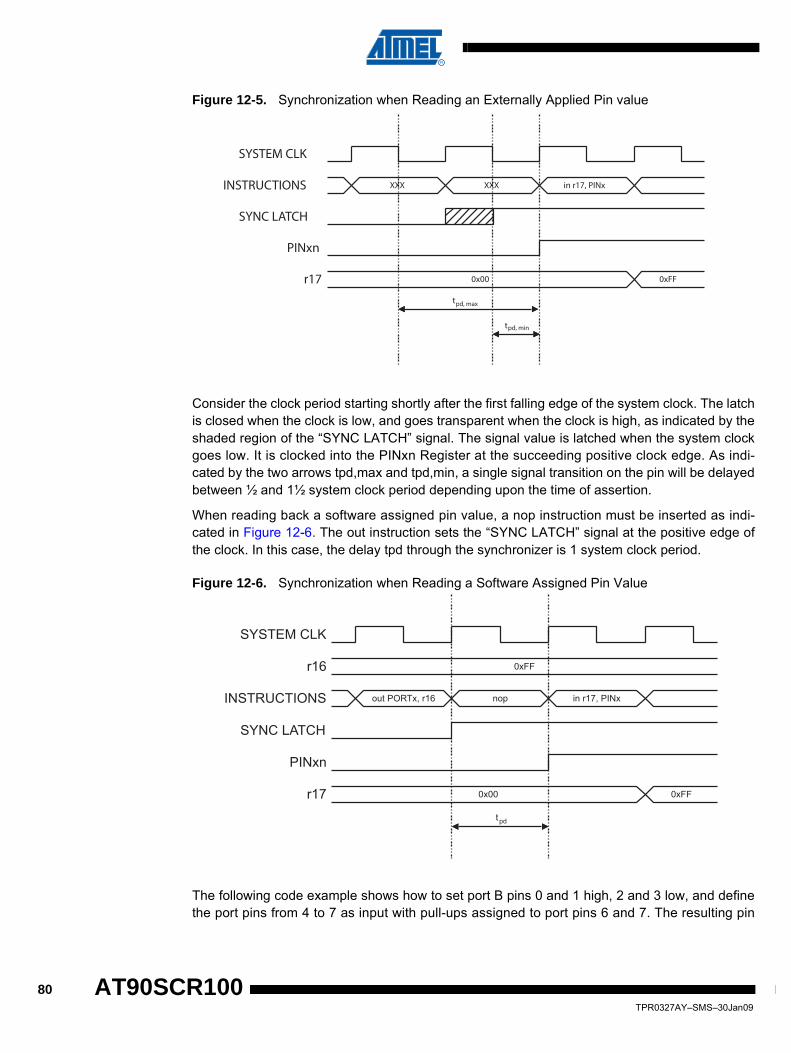
Figure 12-5. Synchronization when Reading an Externally Applied Pin value
Consider the clock period starting shortly after the first falling edge of the system clock. The latchis closed when the clock is low, and goes transparent when the clock is high, as indicated by theshaded region of the “SYNC LATCH” signal. The signal value is latched when the system clockgoes low. It is clocked into the PINxn Register at the succeeding positive clock edge. As indi-cated by the two arrows tpd,max and tpd,min, a single signal transition on the pin will be delayedbetween ½ and 1½ system clock period depending upon the time of assertion.
When reading back a software assigned pin value, a nop instruction must be inserted as indi-cated in Figure 12-6. The out instruction sets the “SYNC LATCH” signal at the positive edge ofthe clock. In this case, the delay tpd through the synchronizer is 1 system clock period.
Figure 12-6. Synchronization when Reading a Software Assigned Pin Value
The following code example shows how to set port B pins 0 and 1 high, 2 and 3 low, and definethe port pins from 4 to 7 as input with pull-ups assigned to port pins 6 and 7. The resulting pin
XXX in r17, PINx
0x00 0xFF
INSTRUCTIONS
SYNC LATCH
PINxn
r17
XXX
SYSTEM CLK
tpd, max
tpd, min
out PORTx, r16 nop in r17, PINx
0xFF
0x00 0xFF
SYSTEM CLK
r16
INSTRUCTIONS
SYNC LATCH
PINxn
r17tpd
80TPR0327AY–SMS–30Jan09
AT90SCR100

AT90SCR100
values are read back again, but as previously discussed, a nop instruction is included to be ableto read back the value recently assigned to some of the pins.
Note: 1. For the assembly program, two temporary registers are used to minimize the time from pull-ups are set on pins 0, 1, 6, and 7, until the direction bits are correctly set, defining bit 2 and 3 as low and redefining bits 0 and 1 as strong high drivers.
12.4.5 Digital Input Enable and Sleep ModesAs shown in Figure 12-4, the digital input signal can be clamped to ground at the input of theschmitt-trigger. The signal denoted SLEEP in the figure, is set by the MCU Sleep Controller inPower-down mode, Power-save mode, Standby and Extended Stand-By mode to avoid highpower consumption if some input signals are left floating, or have an analog signal level close toVCC/2.
SLEEP is overridden for port pins enabled as external interrupt pins. If the external interruptrequest is not enabled, SLEEP is active also for these pins.
If a logic high level (“one”) is present on an asynchronous external interrupt pin configured as“Interrupt on Rising Edge, Falling Edge, or Any Logic Change on Pin” while the external interruptis not enabled, the corresponding External Interrupt Flag will be set when resuming from theabove mentioned Sleep mode, as the clamping in these sleep mode produces the requestedlogic change.
Assembly Code Example(1)
...
; Define pull-ups and set outputs high
; Define directions for port pins
ldi r16,(1<<PB7)|(1<<PB6)|(1<<PB1)|(1<<PB0)
ldi r17,(1<<DDB3)|(1<<DDB2)|(1<<DDB1)|(1<<DDB0)
out PORTB,r16
out DDRB,r17
; Insert nop for synchronization
nop
; Read port pins
in r16,PINB
...
C Code Example(1)
unsigned char i;
...
/* Define pull-ups and set outputs high */
/* Define directions for port pins */
PORTB = (1<<PB7)|(1<<PB6)|(1<<PB1)|(1<<PB0);
DDRB = (1<<DDB3)|(1<<DDB2)|(1<<DDB1)|(1<<DDB0);
/* Insert nop for synchronization*/
__no_operation();
/* Read port pins */
i = PINB;
...
81TPR0327AY–SMS–30Jan09

12.4.6 Unconnected PinsIf some pins are unused, it is recommended to ensure that these pins have a defined level. Eventhough most of the digital inputs are disabled in the deep sleep modes as described above, float-ing inputs should be avoided to reduce current consumption in all other modes where the digitalinputs are enabled (Reset, Active mode and Idle mode).
The simplest method to ensure a defined level of an unused pin, is to enable the internal pull-up.In this case, the pull-up will be disabled during reset. If low power consumption during reset isimportant, it is recommended to use an external pull-up or pull-down. Connecting unused pinsdirectly to VCC or GND is not recommended, since this may cause excessive currents if the pin isaccidentally configured as an output.
12.4.7 MCUCR – MCU Control Register
• Bit 4 – PUD: Pull-up DisableWhen this bit is written to one, the pull-ups in the I/O ports are disabled even if the DDxn andPORTxn Registers are configured to enable the pull-ups ({DDxn, PORTxn} = 0b01). See “Con-figuring the Pin” on page 78 for more details about this feature.
Bit 7 6 5 4 3 2 1 0
0x35 (0x55) JTD - - PUD - - IVSEL IVCE MCUCRRead/write R/W R R R/W R R R/W R/W
Initial value 0 0 0 0 0 0 0 0 0x00
82TPR0327AY–SMS–30Jan09
AT90SCR100

AT90SCR100
12.5 Register Description for I/O-Ports
12.5.1 PORTA – Port A Data Register
12.5.2 DDRA – Port A Data Direction Register
12.5.3 PINA – Port A Input Pins Address
12.5.4 PORTB – Port B Data Register
12.5.5 DDRB – Port B Data Direction Register
12.5.6 PINB – Port B Input Pins Address
Bit 7 6 5 4 3 2 1 0
0x02 (0x22) PORTA [7..0] PORTARead/write R/W R/W R/W R/W R/W R/W R/W R/W
Initial value 0 0 0 0 0 0 0 0 0x00
Bit 7 6 5 4 3 2 1 0
0x01 (0x21) DDA [7..0] DDRARead/write R/W R/W R/W R/W R/W R/W R/W R/W
Initial value 0 0 0 0 0 0 0 0 0x00
Bit 7 6 5 4 3 2 1 0
0x00 (0x20) PINA [7..0] PINARead/write R/W R/W R/W R/W R/W R/W R/W R/W
Initial value N/A N/A N/A N/A N/A N/A N/A N/A
Bit 7 6 5 4 3 2 1 0
0x05 (0x25) PORTB [7..0] PORTBRead/write R/W R/W R/W R/W R/W R/W R/W R/W
Initial value 0 0 0 0 0 0 0 0 0x00
Bit 7 6 5 4 3 2 1 0
0x04 (0x24) DDB [7..0] DDRBRead/write R/W R/W R/W R/W R/W R/W R/W R/W
Initial value 0 0 0 0 0 0 0 0 0x00
Bit 7 6 5 4 3 2 1 0
0x03 (0x23) PINB [7..0] PINBRead/write R/W R/W R/W R/W R/W R/W R/W R/W
Initial value N/A N/A N/A N/A N/A N/A N/A N/A
83TPR0327AY–SMS–30Jan09

12.5.7 PORTC – Port C Data Register
12.5.8 DDRC – Port C Data Direction Register
12.5.9 PINC – Port C Input Pins Address
12.5.10 PORTD – Port D Data Register
12.5.11 DDRD – Port D Data Direction Register
12.5.12 PIND – Port D Input Pins Address
12.5.13 PORTE – Port E Data Register
Bit 7 6 5 4 3 2 1 0
0x08 (0x28) - - PORTC [5..0] PORTCRead/write R/W R/W R/W R/W R/W R/W R/W R/W
Initial value 0 0 0 0 0 0 0 0 0x00
Bit 7 6 5 4 3 2 1 0
0x07 (0x27) - - DDC [5..0] DDRCRead/write R/W R/W R/W R/W R/W R/W R/W R/W
Initial value 0 0 0 0 0 0 0 0 0x00
Bit 7 6 5 4 3 2 1 0
0x06 (0x26) - - PINC [5..0] PINCRead/write R/W R/W R/W R/W R/W R/W R/W R/W
Initial value N/A N/A N/A N/A N/A N/A N/A N/A
Bit 7 6 5 4 3 2 1 0
0x0B (0x2B) PORTD [7..0] PORTDRead/write R/W R/W R/W R/W R/W R/W R/W R/W
Initial value 0 0 0 0 0 0 0 0 0x00
Bit 7 6 5 4 3 2 1 0
0x0A (0x2A) DDD [7..0] DDRDRead/write R/W R/W R/W R/W R/W R/W R/W R/W
Initial value 0 0 0 0 0 0 0 0 0x00
Bit 7 6 5 4 3 2 1 0
0x09 (0x29) PIND [7..0] PINDRead/write R/W R/W R/W R/W R/W R/W R/W R/W
Initial value N/A N/A N/A N/A N/A N/A N/A N/A
Bit 7 6 5 4 3 2 1 0
0x0E (0x2E) PORTE [7..0] PORTERead/write R/W R/W R/W R/W R/W R/W R/W R/W
Initial value 0 0 0 0 0 0 0 0 0x00
84TPR0327AY–SMS–30Jan09
AT90SCR100

AT90SCR100
12.5.14 DDRE – Port E Data Direction Register
12.5.15 PINE – Port E Input Pins Address
Bit 7 6 5 4 3 2 1 0
0x0D (0x2D) DDE [7..0] DDRERead/write R/W R/W R/W R/W R/W R/W R/W R/W
Initial value 0 0 0 0 0 0 0 0 0x00
Bit 7 6 5 4 3 2 1 0
0x0C (0x2C) PINE [7..0] PINERead/write R/W R/W R/W R/W R/W R/W R/W R/W
Initial value N/A N/A N/A N/A N/A N/A N/A N/A
85TPR0327AY–SMS–30Jan09

86TPR0327AY–SMS–30Jan09
AT90SCR100

AT90SCR100
13. TimersThis section contains the detailed description of all 3 timers embedded in the AT90SCR100.Finally, a global chapter describes the mechanism for prescaler reset used on all 3 registers.
13.1 8-bit Timer/Counter0 with PWMTimer/Counter0 is a general purpose 8-bit Timer/Counter module, with two independent OutputCompare Units, and with PWM support. It allows accurate program execution timing (event man-agement) and wave generation. The main features are:
• Two Independent Output Compare Units• Double Buffered Output Compare Registers• Clear Timer on Compare Match (Auto Reload)• Glitch Free, Phase Correct Pulse Width Modulator (PWM)• Variable PWM Period• Frequency Generator• Three Independent Interrupt Sources (TOV0, OCF0A, and OCF0B)
13.1.1 OverviewA simplified block diagram of the 8-bit Timer/Counter0 is shown in Figure 13-1. For the actualplacement of I/O pins, refer to “Pin List Configuration” on page 5. The device-specific I/O Regis-ter and bit locations are listed in the ““8-bit Timer/Counter0 Register Description” on page 98”.
87TPR0327AY–SMS–30Jan09

Figure 13-1. 8-bit Timer/Counter0 Block Diagram
13.1.1.1 RegistersThe Timer/Counter (TCNT0) and Output Compare Registers (OCR0A and OCR0B) are 8-bitregisters. Interrupt request (abbreviated to Int.Req. in the figure) signals are all visible in theTimer Interrupt Flag Register (TIFR0). All interrupts are individually masked with the Timer Inter-rupt Mask Register (TIMSK0). TIFR0 and TIMSK0 are not shown in the figure.
The Timer/Counter can be clocked internally, via the prescaler, or by an external clock source onthe T0 pin. The Clock Select logic block controls which clock source and edge the Timer/Counteruses to increment (or decrement) its value. The Timer/Counter is inactive when no clock sourceis selected. The output from the Clock Select logic is referred to as the timer clock (clkT0).
The double buffered Output Compare Registers (OCR0A and OCR0B) are compared with theTimer/Counter value at all times. The result of the compare can be used by the Waveform Gen-erator to generate a PWM or variable frequency output on the Output Compare pins (OC0A andOC0B). See “Output Compare Unit” on page 90. for details. The Compare Match event will alsoset the Compare Flag (OCF0A or OCF0B) which can be used to generate an Output Compareinterrupt request.
13.1.1.2 DefinitionsMany register and bit references in this section are written in general form. A A lower case “x”replaces the Output Compare Unit, in this case Compare Unit A or Compare Unit B. However,
Clock Select
Timer/Counter
DAT
A B
US
OCR0A
OCR0B
=
=
TCNT0
WaveformGeneration
WaveformGeneration
OC0A
OC0B
=
FixedTOP
Value
Control Logic
= 0
TOP BOTTOM
Count
Clear
Direction
TOVn(Int.Req.)
OC0A(Int.Req.)
OC0B(Int.Req.)
TCCR0A TCCR0B
T0Edge
Detector
( From Prescaler )
clk T0
88TPR0327AY–SMS–30Jan09
AT90SCR100

AT90SCR100
when using the register or bit defines in a program, the precise form must be used, i.e., TCNT0for accessing Timer/Counter0 counter value and so on.
The definitions in Table 13-1 are also used extensively throughout the document.
13.1.2 Timer/Counter Clock SourcesThe Timer/Counter can be clocked by an internal or an external clock source. The clock sourceis selected by the Clock Select logic which is controlled by the Clock Select (CS02:0) bitslocated in the Timer/Counter Control Register (TCCR0B). For details on clock sources and pres-caler, see “Timer/Counter Prescaler” on page 154.
13.1.3 Counter UnitThe main part of the 8-bit Timer/Counter is the programmable bi-directional counter unit. Figure13-2 shows a block diagram of the counter and its surroundings.
Figure 13-2. Counter Unit Block Diagram
Signal description (internal signals):
count Increment or decrement TCNT0 by 1.
direction Select between increment and decrement.
clear Clear TCNT0 (set all bits to zero).
clkTn Timer/Counter clock, referred to as clkT0 in the following.
top Signifies that TCNT0 has reached maximum value.
bottom Signifies that TCNT0 has reached minimum value (zero).
Depending on the mode of operation used, the counter is cleared, incremented, or decrementedat each timer clock (clkT0). clkT0 can be generated from an external or internal clock source,selected by the Clock Select bits (CS02:0). When no clock source is selected (CS02:0 = 0) thetimer is stopped. However, the TCNT0 value can be accessed by the CPU, regardless of
Table 13-1. DefinitionsBOTTOM The counter reaches the BOTTOM when it becomes 0x00.
MAX The counter reaches its MAXimum when it becomes 0xFF (decimal 255).
TOP
The counter reaches the TOP when it becomes equal to the highest value in thecount sequence. The TOP value can be assigned to be the fixed value 0xFF(MAX) or the value stored in the OCR0A Register. The assignment is depen-dent on the mode of operation.
DATA BUS
TCNT0 Control Logic
count
TOV0(Int.Req.)
Clock Select
top
T0Edge
Detector
( From Prescaler )
clk Tn
bottom
direction
clear
89TPR0327AY–SMS–30Jan09

whether clkT0 is present or not. A CPU write overrides (has priority over) all counter clear orcount operations.
The counting sequence is determined by the setting of the WGM01 and WGM00 bits located inthe Timer/Counter Control Register (TCCR0A) and the WGM02 bit located in the Timer/CounterControl Register B (TCCR0B). There are close connections between how the counter behaves(counts) and how waveforms are generated on the Output Compare outputs OC0A and OC0B.For more details about advanced counting sequences and waveform generation, see “Modes ofOperation” on page 92.
The Timer/Counter Overflow Flag (TOV0) is set according to the mode of operation selected bythe WGM02:0 bits. TOV0 can be used for generating a CPU interrupt.
13.1.4 Output Compare UnitThe 8-bit comparator continuously compares TCNT0 with the Output Compare Registers(OCR0A and OCR0B). Whenever TCNT0 equals OCR0A or OCR0B, the comparator signals amatch. A match will set the Output Compare Flag (OCF0A or OCF0B) at the next timer clockcycle. If the corresponding interrupt is enabled, the Output Compare Flag generates an OutputCompare interrupt. The Output Compare Flag is automatically cleared when the interrupt is exe-cuted. Alternatively, the flag can be cleared by software by writing a logical one to its I/O bitlocation. The Waveform Generator uses the match signal to generate an output according tooperating mode set by the WGM02:0 bits and Compare Output mode (COM0x1:0) bits. TheTOP and BOTTOM signals are used by the Waveform Generator for handling the special casesthat occur in some modes of operation when maximum and minimum values are reached(“Modes of Operation” on page 92).
Figure 13-3 shows a block diagram of the Output Compare unit.
Figure 13-3. Output Compare Unit, Block Diagram
The OCR0x Registers are double buffered when using any of the Pulse Width Modulation(PWM) modes. For the normal and Clear Timer on Compare (CTC) modes of operation, the dou-
OCF0x (Int.Req.)
= (8-bit Comparator )
OCR0x
OC0x
DATA BUS
TCNT0
WGM02:0
Waveform Generator
top
FOC0x
COM0x1:0
bottom
90TPR0327AY–SMS–30Jan09
AT90SCR100

AT90SCR100
ble buffering is disabled. The double buffering synchronizes the update of the OCR0x CompareRegisters to either the top or bottom of the counting sequence. The synchronization prevents theoccurrence of odd-length, non-symmetrical PWM pulses, thereby making the output glitch-free.
The OCR0x Register access may seem complex, but this is not case. When the double bufferingis enabled, the CPU has access to the OCR0x Buffer Register, and if double buffering is dis-abled the CPU will access the OCR0x directly.
13.1.4.1 Force Output CompareIn non-PWM waveform generation modes, the match output of the comparator can be forced bywriting a one to the Force Output Compare (FOC0x) bit. Forcing Compare Match will not set theOCF0x Flag or reload/clear the timer, but the OC0x pin will be updated as if a real CompareMatch had occurred (the COM0x1:0 bits settings define whether the OC0x pin is set, cleared ortoggled).
13.1.4.2 Compare Match Blocking by TCNT0 WriteAll CPU write operations to the TCNT0 Register will block any Compare Match that occur in thenext timer clock cycle, even when the timer is stopped. This feature allows OCR0x to be initial-ized to the same value as TCNT0 without triggering an interrupt when the Timer/Counter clock isenabled.
13.1.4.3 Using the Output Compare UnitSince writing TCNT0 in any mode of operation will block all Compare Matches for one timerclock cycle, there are risks involved when changing TCNT0 when using the Output CompareUnit, independently of whether the Timer/Counter is running or not. If the value written to TCNT0equals the OCR0x value, the Compare Match will be missed, resulting in incorrect waveformgeneration. Similarly, do not write the TCNT0 value equal to BOTTOM when the counter isdown-counting.
The setup of the OC0x should be performed before setting the Data Direction Register for theport pin to output. The easiest way of setting the OC0x value is to use the Force Output Com-pare (FOC0x) strobe bits in Normal mode. The OC0x Registers keep their values even whenchanging between Waveform Generation modes.
Changing the COM0x1:0 bits will take effect immediately.
13.1.5 Compare Match Output UnitThe Compare Output mode (COM0x1:0) bits have two functions. The Waveform Generator usesthe COM0x1:0 bits for defining the Output Compare (OC0x) state at the next Compare Match.Also, the COM0x1:0 bits control the OC0x pin output source. Figure 13-4 shows a simplifiedschematic of the logic affected by the COM0x1:0 bit setting. The I/O Registers, I/O bits, and I/Opins in the figure are shown in bold. Only the parts of the general I/O Port Control Registers(DDR and PORT) that are affected by the COM0x1:0 bits are shown. When referring to theOC0x state, the reference is for the internal OC0x Register, not the OC0x pin. If a system resetoccurs, the OC0x Register is reset to “0”.
91TPR0327AY–SMS–30Jan09

Figure 13-4. Compare Match Output Unit, Schematic
The general I/O port function is overridden by the Output Compare (OC0x) from the WaveformGenerator if either of the COM0x1:0 bits are set. However, the OC0x pin direction (input or out-put) is still controlled by the Data Direction Register (DDR) for the port pin. The Data DirectionRegister bit for the OC0x pin (DDR_OC0x) must be set as an output before the OC0x value isvisible on the pin. The port override function is independent of the Waveform Generation mode.
The design of the Output Compare pin logic allows the initialization of the OC0x state before theoutput is enabled. Note that some COM0x1:0 bit settings are reserved for certain modes of oper-ation. See “8-bit Timer/Counter0 Register Description” on page 98.
13.1.6 Compare Output Mode and Waveform GenerationThe Waveform Generator uses the COM0x1:0 bits differently in Normal, CTC, and PWM modes.For all modes, setting the COM0x1:0 = 0 instructs the Waveform Generator that no action on theOC0x Register is to be performed on the next Compare Match. For compare output actions inthe non-PWM modes refer to Table 13-2 on page 99. For fast PWM mode, refer to Table 13-3 onpage 99, and for phase correct PWM refer to Table 13-4 on page 99.
A change of the COM0x1:0 bits state will have an effect at the first Compare Match after the bitsare written. For non-PWM modes, the action can be forced to have an immediate effect by usingthe FOC0x strobe bits.
13.1.7 Modes of OperationThe mode of operation, i.e., the behavior of the Timer/Counter and the Output Compare pins, isdefined by the combination of the Waveform Generation mode (WGM02:0) and the CompareOutput mode (COM0x1:0) bits. The Compare Output mode bits do not affect the countingsequence, while the Waveform Generation mode bits do. The COM0x1:0 bits control whetherthe PWM output generated should be inverted or not (inverted or non-inverted PWM). For non-PWM modes the COM0x1:0 bits control whether the output should be set, cleared, or toggled ata Compare Match (See “Compare Match Output Unit” on page 91.).
For detailed timing information see “Timer/Counter Timing Diagrams” on page 97.
PORT
DDR
D Q
D Q
OC0xPinOC0x
D QWaveformGenerator
COM0x1
COM0x0
0
1
DAT
A B
US
FOC0n
clk I/O
92TPR0327AY–SMS–30Jan09
AT90SCR100

AT90SCR100
13.1.7.1 Normal ModeThe simplest mode of operation is the Normal mode (WGM02:0 = 0). In this mode the countingdirection is always up (incrementing), and no counter clear is performed. The counter simplyoverruns when it passes its maximum 8-bit value (TOP = 0xFF) and then restarts from the bot-tom (0x00). In normal operation the Timer/Counter Overflow Flag (TOV0) will be set in the sametimer clock cycle as the TCNT0 becomes zero. The TOV0 Flag in this case behaves like a ninthbit, except that it is only set, not cleared. However, combined with the timer overflow interruptthat automatically clears the TOV0 Flag, the timer resolution can be increased by software.There are no special cases to consider in the Normal mode, a new counter value can be writtenanytime.
The Output Compare Unit can be used to generate interrupts at some given time. Using the Out-put Compare to generate waveforms in Normal mode is not recommended, since this willoccupy too much of the CPU time.
13.1.7.2 Clear Timer on Compare Match (CTC) ModeIn Clear Timer on Compare or CTC mode (WGM02:0 = 2), the OCR0A Register is used tomanipulate the counter resolution. In CTC mode the counter is cleared to zero when the countervalue (TCNT0) matches the OCR0A. The OCR0A defines the top value for the counter, hencealso its resolution. This mode allows greater control of the Compare Match output frequency. Italso simplifies the operation of counting external events.
The timing diagram for the CTC mode is shown in Figure 13-5. The counter value (TCNT0)increases until a Compare Match occurs between TCNT0 and OCR0A, and then counter(TCNT0) is cleared.
Figure 13-5. CTC Mode, Timing Diagram
An interrupt can be generated each time the counter value reaches the TOP value by using theOCF0A Flag. If the interrupt is enabled, the interrupt handler routine can be used for updatingthe TOP value. However, changing TOP to a value close to BOTTOM when the counter is run-ning with none or a low prescaler value must be done with care since the CTC mode does nothave the double buffering feature. If the new value written to OCR0A is lower than the currentvalue of TCNT0, the counter will miss the Compare Match. The counter will then have to count toits maximum value (0xFF) and wrap around starting at 0x00 before the Compare Match canoccur.
For generating a waveform output in CTC mode, the OC0A output can be set to toggle its logicallevel on each Compare Match by setting the Compare Output mode bits to toggle mode(COM0A1:0 = 1). The OC0A value will not be visible on the port pin unless the data direction for
TCNT0
OC0x(Toggle)
OC0x Interrupt Flag Set
1 4Period 2 3
(COM0x1:0 = 1)
93TPR0327AY–SMS–30Jan09

the pin is set to output. The waveform generated will have a maximum frequency of fOC0 =fclk_I/O/2 when OCR0A is set to zero (0x00). The waveform frequency is defined by the followingequation:
The N variable represents the prescale factor (1, 8, 64, 256, or 1024).
As for the Normal mode of operation, the TOV0 Flag is set in the same timer clock cycle that thecounter counts from MAX to 0x00.
13.1.7.3 Fast PWM ModeThe fast Pulse Width Modulation or fast PWM mode (WGM02:0 = 3 or 7) provides a high fre-quency PWM waveform generation option. The fast PWM differs from the other PWM option byits single-slope operation. The counter counts from BOTTOM to TOP then restarts from BOT-TOM. TOP is defined as 0xFF when WGM2:0 = 3, and OCR0A when WGM2:0 = 7. In non-inverting Compare Output mode, the Output Compare (OC0x) is cleared on the Compare Matchbetween TCNT0 and OCR0x, and set at BOTTOM. In inverting Compare Output mode, the out-put is set on Compare Match and cleared at BOTTOM. Due to the single-slope operation, theoperating frequency of the fast PWM mode can be twice as high as the phase correct PWMmode that use dual-slope operation. This high frequency makes the fast PWM mode well suitedfor power regulation, rectification, and DAC applications. High frequency allows physically smallsized external components (coils, capacitors), and therefore reduces total system cost.
In fast PWM mode, the counter is incremented until the counter value matches the TOP value.The counter is then cleared at the following timer clock cycle. The timing diagram for the fastPWM mode is shown in Figure 13-6. The TCNT0 value is in the timing diagram shown as a his-togram for illustrating the single-slope operation. The diagram includes non-inverted andinverted PWM outputs. The small horizontal line marks on the TCNT0 slopes represent Com-pare Matches between OCR0x and TCNT0.
Figure 13-6. Fast PWM Mode, Timing Diagram
The Timer/Counter Overflow Flag (TOV0) is set each time the counter reaches TOP. If the inter-rupt is enabled, the interrupt handler routine can be used for updating the compare value.
fOCnxfclk_I/O
2 N 1 OCRnx+( )⋅ ⋅--------------------------------------------------=
TCNT0
OCR0x Update andTOV0 Interrupt Flag Set
1Period 2 3
OC0x
OC0x
(COM0x1:0 = 2)
(COM0x1:0 = 3)
OCR0x Interrupt Flag Set
4 5 6 7
94TPR0327AY–SMS–30Jan09
AT90SCR100

AT90SCR100
In fast PWM mode, the compare unit allows generation of PWM waveforms on the OC0x pins.Setting the COM0x1:0 bits to two will produce a non-inverted PWM and an inverted PWM outputcan be generated by setting the COM0x1:0 to three: Setting the COM0A1:0 bits to one allowsthe OC0A pin to toggle on Compare Matches if the WGM02 bit is set. This option is not availablefor the OC0B pin (See Table 13-3 on page 99). The actual OC0x value will only be visible on theport pin if the data direction for the port pin is set as output. The PWM waveform is generated bysetting (or clearing) the OC0x Register at the Compare Match between OCR0x and TCNT0, andclearing (or setting) the OC0x Register at the timer clock cycle the counter is cleared (changesfrom TOP to BOTTOM).
The PWM frequency for the output can be calculated by the following equation:
The N variable represents the prescale factor (1, 8, 64, 256, or 1024).
The extreme values for the OCR0A Register represents special cases when generating a PWMwaveform output in the fast PWM mode. If the OCR0A is set equal to BOTTOM, the output willbe a narrow spike for each MAX+1 timer clock cycle. Setting the OCR0A equal to MAX will resultin a constantly high or low output (depending on the polarity of the output set by the COM0A1:0bits.)
A frequency (with 50% duty cycle) waveform output in fast PWM mode can be achieved by set-ting OC0x to toggle its logical level on each Compare Match (COM0x1:0 = 1). The waveformgenerated will have a maximum frequency of fOC0 = fclk_I/O/2 when OCR0A is set to zero. Thisfeature is similar to the OC0A toggle in CTC mode, except the double buffer feature of the Out-put Compare unit is enabled in the fast PWM mode.
13.1.7.4 Phase Correct PWM ModeThe phase correct PWM mode (WGM02:0 = 1 or 5) provides a high resolution phase correctPWM waveform generation option. The phase correct PWM mode is based on a dual-slopeoperation. The counter counts repeatedly from BOTTOM to TOP and then from TOP to BOT-TOM. TOP is defined as 0xFF when WGM2:0 = 1, and OCR0A when WGM2:0 = 5. In non-inverting Compare Output mode, the Output Compare (OC0x) is cleared on the Compare Matchbetween TCNT0 and OCR0x while upcounting, and set on the Compare Match while down-counting. In inverting Output Compare mode, the operation is inverted. The dual-slope operationhas lower maximum operation frequency than single slope operation. However, due to the sym-metric feature of the dual-slope PWM modes, these modes are preferred for motor controlapplications.
In phase correct PWM mode the counter is incremented until the counter value matches TOP.When the counter reaches TOP, it changes the count direction. The TCNT0 value will be equalto TOP for one timer clock cycle. The timing diagram for the phase correct PWM mode is shownon Figure 13-7. The TCNT0 value is in the timing diagram shown as a histogram for illustratingthe dual-slope operation. The diagram includes non-inverted and inverted PWM outputs. Thesmall horizontal line marks on the TCNT0 slopes represent Compare Matches between OCR0xand TCNT0.
fOCnxPWMfclk_I/ON 256⋅------------------=
95TPR0327AY–SMS–30Jan09

Figure 13-7. Phase Correct PWM Mode, Timing Diagram
The Timer/Counter Overflow Flag (TOV0) is set each time the counter reaches BOTTOM. TheInterrupt Flag can be used to generate an interrupt each time the counter reaches the BOTTOMvalue.
In phase correct PWM mode, the compare unit allows generation of PWM waveforms on theOC0x pins. Setting the COM0x1:0 bits to two will produce a non-inverted PWM. An invertedPWM output can be generated by setting the COM0x1:0 to three: Setting the COM0A0 bits toone allows the OC0A pin to toggle on Compare Matches if the WGM02 bit is set. This option isnot available for the OC0B pin (See Table 13-4 on page 99). The actual OC0x value will only bevisible on the port pin if the data direction for the port pin is set as output. The PWM waveform isgenerated by clearing (or setting) the OC0x Register at the Compare Match between OCR0xand TCNT0 when the counter increments, and setting (or clearing) the OC0x Register at Com-pare Match between OCR0x and TCNT0 when the counter decrements. The PWM frequency forthe output when using phase correct PWM can be calculated by the following equation:
The N variable represents the prescale factor (1, 8, 64, 256, or 1024).
The extreme values for the OCR0A Register represent special cases when generating a PWMwaveform output in the phase correct PWM mode. If the OCR0A is set equal to BOTTOM, theoutput will be continuously low and if set equal to MAX the output will be continuously high fornon-inverted PWM mode. For inverted PWM the output will have the opposite logic values.
At the very start of period 2 in Figure 13-7 OC0x has a transition from high to low even thoughthere is no Compare Match. The point of this transition is to guarantee symmetry around BOT-TOM. There are two cases that give a transition without Compare Match.
• OCR0A changes its value from MAX, like in Figure 13-7. When the OCR0A value is MAX the OC0 pin value is the same as the result of a down-counting Compare Match. To ensure
TOV0 Interrupt Flag Set
OC0x Interrupt Flag Set
1 2 3
TCNT0
Period
OC0x
OC0x
(COM0x1:0 = 2)
(COM0x1:0 = 3)
OCR0x Update
fOCnxPCPWMfclk_I/ON 510⋅------------------=
96TPR0327AY–SMS–30Jan09
AT90SCR100

AT90SCR100
symmetry around BOTTOM the OC0 value at MAX must correspond to the result of an up-counting Compare Match.
• The timer starts counting from a value higher than the one in OCR0A, and for that reason misses the Compare Match and hence the OC0 change that would have happened on the way up.
13.1.8 Timer/Counter Timing DiagramsThe Timer/Counter is a synchronous design and the timer clock (clkT0) is therefore shown as aclock enable signal in the following figures. The figures include information on when InterruptFlags are set. Figure 13-8 contains timing data for basic Timer/Counter operation. The figureshows the count sequence close to the MAX value in all modes other than phase correct PWMmode.
Figure 13-8. Timer/Counter Timing Diagram, no Prescaling
Figure 13-9 shows the same timing data, but with the prescaler enabled.
Figure 13-9. Timer/Counter Timing Diagram, with Prescaler (fclk_I/O/8)
Figure 13-10 shows the setting of OCF0B in all modes and OCF0A in all modes except CTCmode and PWM mode, where OCR0A is TOP.
clkTn(clk I/O/1)
TOV0
clkI/O
TCNT0 MAX - 1 MAX BOTTOM BOTTOM + 1
TOV0
TCNT0 MAX - 1 MAX BOTTOM BOTTOM + 1
clkI/O
clkTn(clk I/O/8)
97TPR0327AY–SMS–30Jan09

Figure 13-10. Timer/Counter Timing Diagram, Setting of OCF0x, with Prescaler (fclk_I/O/8)
Figure 13-11 shows the setting of OCF0A and the clearing of TCNT0 in CTC mode and fastPWM mode where OCR0A is TOP.
Figure 13-11. Timer/Counter Timing Diagram, Clear Timer on Compare Match mode, with Pres-caler (fclk_I/O/8)
13.1.9 8-bit Timer/Counter0 Register Description
13.1.9.1 TCCR0A – Timer/Counter Control Register A
• Bits 7..6 – COM0A1..0: Compare Match Output A ModeThese bits control the Output Compare pin (OC0A) behavior. If one or both of the COM0A1:0bits are set, the OC0A output overrides the normal port functionality of the I/O pin it is con-nected. However, note that the Data Direction Register (DDR) bit corresponding to which theOC0A pin must be set in order to enable the output driver.
OCF0x
OCR0x
TCNT0
OCR0x Value
OCR0x - 1 OCR0x OCR0x + 1 OCR0x + 2
clkI/O
clkTn(clk I/O/8)
OCF0x
OCR0x
TCNT0(CTC)
TOP
TOP - 1 TOP BOTTOM BOTTOM + 1
clkI/O
clkTn(clk I/O/8)
Bit 7 6 5 4 3 2 1 0
0x24 (0x44) COM0A1 COM0A0 COM0B1 COM0B0 - - WGM01 WGM00 TCCR0ARead/write R/W R/W R/W R/W R R R/W R/W
Initial value 0 0 0 0 0 0 0 0 0x00
98TPR0327AY–SMS–30Jan09
AT90SCR100

AT90SCR100
When OC0A is connected to the pin, the function of the COM0A1:0 bits depends on theWGM02:0 bit setting. Table 13-2 shows the COM0A1:0 bit functionality when the WGM02:0 bitsare set to a normal or CTC mode (non-PWM).
Table 13-3 shows the COM0A1:0 bit functionality when the WGM01:0 bits are set to fast PWMmode.
Note: 1. A special case occurs when OCR0A equals TOP and COM0A1 is set. In this case, the Com-pare Match is ignored, but the set or clear is done at BOTTOM. See “Fast PWM Mode” on page 94 for more details.
Table 13-4 shows the COM0A1:0 bit functionality when the WGM02:0 bits are set to phase cor-rect PWM mode.
Note: 1. A special case occurs when OCR0A equals TOP and COM0A1 is set. In this case, the Com-pare Match is ignored, but the set or clear is done at TOP. See “Phase Correct PWM Mode” on page 95 for more details.
• Bits 5..4 – COM0B1..0: Compare Match Output B ModeThese bits control the Output Compare pin (OC0B) behavior. If one or both of the COM0B1:0bits are set, the OC0B output overrides the normal port functionality of the I/O pin to which it is
Table 13-2. Compare Output Mode, non-PWM Mode
COM0A1 COM0A0 Description
0 0 Normal port operation, OC0A disconnected.
0 1 Toggle OC0A on Compare Match
1 0 Clear OC0A on Compare Match
1 1 Set OC0A on Compare Match
Table 13-3. Compare Output Mode, Fast PWM Mode(1)
COM0A1 COM0A0 Description
0 0 Normal port operation, OC0A disconnected.
0 1 WGM02 = 0: Normal Port Operation, OC0A Disconnected.WGM02 = 1: Toggle OC0A on Compare Match.
1 0 Clear OC0A on Compare Match, set OC0A at BOTTOM(non-inverting mode)
1 1 Set OC0A on Compare Match, clear OC0A at BOTTOM(inverting mode)
Table 13-4. Compare Output Mode, Phase Correct PWM Mode(1)
COM0A1 COM0A0 Description
0 0 Normal port operation, OC0A disconnected.
0 1 WGM02 = 0: Normal Port Operation, OC0A Disconnected.WGM02 = 1: Toggle OC0A on Compare Match.
1 0 Clear OC0A on Compare Match when up-counting. Set OC0A on Compare Match when down-counting.
1 1 Set OC0A on Compare Match when up-counting. Clear OC0A on Compare Match when down-counting.
99TPR0327AY–SMS–30Jan09

connected. However, note that the Data Direction Register (DDR) bit corresponding to the OC0Bpin must be set in order to enable the output driver.
When OC0B is connected to the pin, the function of the COM0B1:0 bits depends on theWGM02:0 bit setting. Table 13-5 shows the COM0B1:0 bit functionality when the WGM02:0 bitsare set to a normal or CTC mode (non-PWM).
Table 13-6 shows the COM0B1:0 bit functionality when the WGM02:0 bits are set to fast PWMmode.
Note: 1. A special case occurs when OCR0B equals TOP and COM0B1 is set. In this case, the Com-pare Match is ignored, but the set or clear is done at BOTTOM. See “Fast PWM Mode” on page 94 for more details.
Table 13-7 shows the COM0B1:0 bit functionality when the WGM02:0 bits are set to phase cor-rect PWM mode.
Note: 1. A special case occurs when OCR0B equals TOP and COM0B1 is set. In this case, the Com-pare Match is ignored, but the set or clear is done at TOP. See “Phase Correct PWM Mode” on page 95 for more details.
• Bits 3..2 – Res: Reserved BitsThese bits are reserved bits in the AT90SCR100 and will always read as zero.
Table 13-5. Compare Output Mode, non-PWM Mode
COM0B1 COM0B0 Description
0 0 Normal port operation, OC0B disconnected.
0 1 Toggle OC0B on Compare Match
1 0 Clear OC0B on Compare Match
1 1 Set OC0B on Compare Match
Table 13-6. Compare Output Mode, Fast PWM Mode(1)
COM0B1 COM0B0 Description
0 0 Normal port operation, OC0B disconnected.
0 1 Reserved
1 0 Clear OC0B on Compare Match, set OC0B at BOTTOM(non-inverting mode)
1 1 Set OC0B on Compare Match, clear OC0B at BOTTOM(inverting mode)
Table 13-7. Compare Output Mode, Phase Correct PWM Mode(1)
COM0B1 COM0B0 Description
0 0 Normal port operation, OC0B disconnected.
0 1 Reserved
1 0 Clear OC0B on Compare Match when up-counting. Set OC0B on Compare Match when down-counting.
1 1 Set OC0B on Compare Match when up-counting. Clear OC0B on Compare Match when down-counting.
100TPR0327AY–SMS–30Jan09
AT90SCR100

AT90SCR100
• Bits 1..0 – WGM01..0: Waveform Generation ModeWhen combined with the WGM02 bit found in the TCCR0B Register, these bits control thecounting sequence of the counter, the source for maximum (TOP) counter value, and what typeof waveform generation to be used, see Table 13-8. Modes of operation supported by theTimer/Counter unit are: Normal mode (counter), Clear Timer on Compare Match (CTC) mode,and two types of Pulse Width Modulation (PWM) modes (see “Modes of Operation” on page 92).
Note: 1. MAX = 0xFF, BOTTOM = 0x00
13.1.9.2 TCCR0B – Timer/Counter Control Register B
• Bit 7 – FOC0A: Force Output Compare AThe FOC0A bit is only active when the WGM bits specify a non-PWM mode.
However, for ensuring compatibility with future devices, this bit must be set to zero whenTCCR0B is written when operating in PWM mode. When writing a logical one to the FOC0A bit,an immediate Compare Match is forced on the Waveform Generation unit. The OC0A output ischanged according to its COM0A1:0 bits setting. Note that the FOC0A bit is implemented as astrobe. Therefore it is the value present in the COM0A1:0 bits that determines the effect of theforced compare.
A FOC0A strobe will not generate any interrupt, nor will it clear the timer in CTC mode usingOCR0A as TOP.
The FOC0A bit is always read as zero.
• Bit 6 – FOC0B: Force Output Compare BThe FOC0B bit is only active when the WGM bits specify a non-PWM mode.
Table 13-8. Waveform Generation Mode Bit Description
Mode WGM2 WGM1 WGM0
Timer/Counter Mode of
Operation TOPUpdate ofOCRx at
TOV FlagSet on(1)
0 0 0 0 Normal 0xFF Immediate MAX
1 0 0 1 PWM, Phase Correct 0xFF TOP BOTTOM
2 0 1 0 CTC OCRA Immediate MAX
3 0 1 1 Fast PWM 0xFF TOP MAX
4 1 0 0 Reserved – – –
5 1 0 1 PWM, Phase Correct OCRA TOP BOTTOM
6 1 1 0 Reserved – – –
7 1 1 1 Fast PWM OCRA TOP TOP
Bit 7 6 5 4 3 2 1 0
0x25 (0x45) FOC0A FOC0B - - WGM02 CS02 CS01 CSO0 TCCR0BRead/write W W R R R/W R/W R/W R/W
Initial value 0 0 0 0 0 0 0 0 0x00
101TPR0327AY–SMS–30Jan09

However, for ensuring compatibility with future devices, this bit must be set to zero whenTCCR0B is written when operating in PWM mode. When writing a logical one to the FOC0B bit,an immediate Compare Match is forced on the Waveform Generation unit. The OC0B output ischanged according to its COM0B1:0 bits setting. Note that the FOC0B bit is implemented as astrobe. Therefore it is the value present in the COM0B1:0 bits that determines the effect of theforced compare.
A FOC0B strobe will not generate any interrupt, nor will it clear the timer in CTC mode usingOCR0B as TOP.
The FOC0B bit is always read as zero.
• Bits 5..4 – Res: Reserved BitsThese bits are reserved bits and will always read as zero.
• Bit 3 – WGM02: Waveform Generation ModeSee the description in the “TCCR0A – Timer/Counter Control Register A” on page 98.
• Bits 2..0 – CS02..0: Clock SelectThe three Clock Select bits select the clock source to be used by the Timer/Counter.
If external pin modes are used for the Timer/Counter0, transitions on the T0 pin will clock thecounter even if the pin is configured as an output. This feature allows software control of thecounting.
13.1.9.3 TCNT0 – Timer/Counter Register
The Timer/Counter Register gives direct access, both for read and write operations, to theTimer/Counter unit 8-bit counter. Writing to the TCNT0 Register blocks (removes) the CompareMatch on the following timer clock. Modifying the counter (TCNT0) while the counter is running,introduces a risk of missing a Compare Match between TCNT0 and the OCR0x Registers.
Table 13-9. Clock Select Bit Description
CS02 CS01 CS00 Description
0 0 0 No clock source (Timer/Counter stopped)
0 0 1 clkI/O/(No prescaling)
0 1 0 clkI/O/8 (From prescaler)
0 1 1 clkI/O/64 (From prescaler)
1 0 0 clkI/O/256 (From prescaler)
1 0 1 clkI/O/1024 (From prescaler)
1 1 0 External clock source on T0 pin. Clock on falling edge.
1 1 1 External clock source on T0 pin. Clock on rising edge.
Bit 7 6 5 4 3 2 1 0
0x26 (0x46) TCNT0 [7..0] TCNT0Read/write R/W R/W R/W R/W R/W R/W R/W R/W
Initial value 0 0 0 0 0 0 0 0 0x00
102TPR0327AY–SMS–30Jan09
AT90SCR100

AT90SCR100
13.1.9.4 OCR0A – Output Compare Register A
The Output Compare Register A contains an 8-bit value that is continuously compared with thecounter value (TCNT0). A match can be used to generate an Output Compare interrupt, or togenerate a waveform output on the OC0A pin.
13.1.9.5 OCR0B – Output Compare Register B
The Output Compare Register B contains an 8-bit value that is continuously compared with thecounter value (TCNT0). A match can be used to generate an Output Compare interrupt, or togenerate a waveform output on the OC0B pin.
13.1.9.6 TIMSK0 – Timer/Counter Interrupt Mask Register
• Bits 7..3 – Res: Reserved BitsThese bits are reserved bits and will always read as zero.
• Bit 2 – OCIE0B: Timer/Counter Output Compare Match B Interrupt EnableWhen the OCIE0B bit is written to one, and the I-bit in the Status Register is set, theTimer/Counter Compare Match B interrupt is enabled. The corresponding interrupt is executed ifa Compare Match in Timer/Counter occurs, i.e., when the OCF0B bit is set in the Timer/CounterInterrupt Flag Register – TIFR0.
• Bit 1 – OCIE0A: Timer/Counter0 Output Compare Match A Interrupt EnableWhen the OCIE0A bit is written to one, and the I-bit in the Status Register is set, theTimer/Counter0 Compare Match A interrupt is enabled. The corresponding interrupt is executedif a Compare Match in Timer/Counter0 occurs, i.e., when the OCF0A bit is set in theTimer/Counter 0 Interrupt Flag Register – TIFR0.
• Bit 0 – TOIE0: Timer/Counter0 Overflow Interrupt EnableWhen the TOIE0 bit is written to one, and the I-bit in the Status Register is set, theTimer/Counter0 Overflow interrupt is enabled. The corresponding interrupt is executed if anoverflow in Timer/Counter0 occurs, i.e., when the TOV0 bit is set in the Timer/Counter 0 Inter-rupt Flag Register – TIFR0.
Bit 7 6 5 4 3 2 1 0
0x27 (0x47) OCR0A [7..0] OCR0ARead/write R/W R/W R/W R/W R/W R/W R/W R/W
Initial value 0 0 0 0 0 0 0 0 0x00
Bit 7 6 5 4 3 2 1 0
0x26 (0x46) OCR0B [7..0] OCR0BRead/write R/W R/W R/W R/W R/W R/W R/W R/W
Initial value 0 0 0 0 0 0 0 0 0x00
Bit 7 6 5 4 3 2 1 0
0x6E - - - - - OCIE0B OCIE0A TOIE0 TIMSK0Read/write R R R R R R/W R/W R/W
Initial value 0 0 0 0 0 0 0 0 0x00
103TPR0327AY–SMS–30Jan09

13.1.9.7 TIFR0 – Timer/Counter 0 Interrupt Flag Register
• Bits 7..3 – Res : Reserved BitsThese bits are reserved bits in the AT90SCR100 and will always read as zero.
• Bit 2 – OCF0B: Timer/Counter 0 Output Compare B Match FlagThe OCF0B bit is set when a Compare Match occurs between the Timer/Counter and the data inOCR0B – Output Compare Register0 B. OCF0B is cleared by hardware when executing the cor-responding interrupt handling vector. Alternatively, OCF0B is cleared by writing a logic one tothe flag. When the I-bit in SREG, OCIE0B (Timer/Counter Compare B Match Interrupt Enable),and OCF0B are set, the Timer/Counter Compare Match Interrupt is executed.
• Bit 1 – OCF0A: Timer/Counter 0 Output Compare A Match FlagThe OCF0A bit is set when a Compare Match occurs between the Timer/Counter0 and the datain OCR0A – Output Compare Register0. OCF0A is cleared by hardware when executing the cor-responding interrupt handling vector. Alternatively, OCF0A is cleared by writing a logic one tothe flag. When the I-bit in SREG, OCIE0A (Timer/Counter0 Compare Match Interrupt Enable),and OCF0A are set, the Timer/Counter0 Compare Match Interrupt is executed.
• Bit 0 – TOV0: Timer/Counter0 Overflow FlagThe bit TOV0 is set when an overflow occurs in Timer/Counter0. TOV0 is cleared by hardwarewhen executing the corresponding interrupt handling vector. Alternatively, TOV0 is cleared bywriting a logic one to the flag. When the SREG I-bit, TOIE0 (Timer/Counter0 Overflow InterruptEnable), and TOV0 are set, the Timer/Counter0 Overflow interrupt is executed.
The setting of this flag is dependent of the WGM02:0 bit setting. Refer to Table 13-8, “WaveformGeneration Mode Bit Description” on page 101.
Bit 7 6 5 4 3 2 1 0
0x15 (0x35) - - - - - OCF0B OCF0A TOV0 TIFR0Read/write R R R R R R/W R/W R/W
Initial value 0 0 0 0 0 0 0 0 0x00
104TPR0327AY–SMS–30Jan09
AT90SCR100

AT90SCR100
13.2 16-bit Timer/Counter1 with PWMThe 16-bit Timer/Counter unit allows accurate program execution timing (event management),wave generation, and signal timing measurement. The main features are:
• True 16-bit Design (i.e., Allows 16-bit PWM)• Two independent Output Compare Units• Double Buffered Output Compare Registers• One Input Capture Unit• Input Capture Noise Canceler• Clear Timer on Compare Match (Auto Reload)• Glitch-free, Phase Correct Pulse Width Modulator (PWM)• Variable PWM Period• Frequency Generator• External Event Counter• Four independent interrupt Sources (TOV1, OCF1A, OCF1B, and ICF1)
13.2.1 OverviewA simplified block diagram of the 16-bit Timer/Counter is shown in Figure 13-12. For the actualplacement of I/O pins, refer to “Pin List Configuration” on page 5. CPU accessible I/O Registers,including I/O bits and I/O pins, are shown in bold. The device-specific I/O Register and bit loca-tions are listed in the “16-bit Timer/Counter Register Description” on page 126.
The PRTIM1 bit in “PRR0 – Power Reduction Register 0” on page 45 must be written to zero toenable Timer/Counter1 module.
Refer to “Pin List Configuration” on page 5 for Timer/Counter1 pin placement and description.
105TPR0327AY–SMS–30Jan09

Figure 13-12. 16-bit Timer/Counter Block Diagram
13.2.1.1 RegistersThe Timer/Counter1 (TCNT1), Output Compare Registers (OCR1A/B), and Input Capture Reg-ister (ICR1) are all 16-bit registers. Special procedures must be followed when accessing the 16-bit registers. These procedures are described in the section “Accessing 16-bit Registers” onpage 107. The Timer/Counter Control Registers (TCCR1A/B/C) are 8-bit registers and have noCPU access restrictions. Interrupt requests (abbreviated to Int.Req. in the figure) signals are allvisible in the Timer Interrupt Flag Register (TIFR1). All interrupts are individually masked withthe Timer Interrupt Mask Register (TIMSK1). TIFR1 and TIMSK1 are not shown in the figure.
The Timer/Counter1 can be clocked internally, via the prescaler, or by an external clock sourceon the T1 pin. The Clock Select logic block controls which clock source and edge theTimer/Counter uses to increment (or decrement) its value. The Timer/Counter1 is inactive whenno clock source is selected. The output from the Clock Select logic is referred to as the timerclock (clkTn).
The double buffered Output Compare Registers (OCR1A/B) are compared with the Timer/Coun-ter value at all time. The result of the compare can be used by the Waveform Generator to
Clock Select
Timer/Counter
DAT
A B
US
OCR1A
OCR1B
ICR1
=
=
TCNT1
WaveformGeneration
WaveformGeneration
OC1A
OC1B
NoiseCanceler
ICP1
=
FixedTOP
Values
EdgeDetector
Control Logic
= 0
TOP BOTTOM
Count
Clear
Direction
TOV1(Int.Req.)
OC1A(Int.Req.)
OC1B(Int.Req.)
ICF1 (Int.Req.)
TCCR1A TCCR1B
T1Edge
Detector
( From Prescaler )
clk Tn
106TPR0327AY–SMS–30Jan09
AT90SCR100

AT90SCR100
generate a PWM or variable frequency output on the Output Compare pin (OCR1A/B). See“Output Compare Units” on page 114. The compare match event will also set the CompareMatch Flag (OCF1A/B) which can be used to generate an Output Compare interrupt request.
The Input Capture Register can capture the Timer/Counter value at a given external (edge trig-gered) event on either the Input Capture pin (ICP1). The Input Capture unit includes a digitalfiltering unit (Noise Canceler) for reducing the chance of capturing noise spikes.
The TOP value, or maximum Timer/Counter value, can in some modes of operation be definedby either the OCR1A Register, the ICR1 Register, or by a set of fixed values. When usingOCR1A as TOP value in a PWM mode, the OCR1A Register can not be used for generating aPWM output. However, the TOP value will in this case be double buffered allowing the TOPvalue to be changed in run time. If a fixed TOP value is required, the ICR1 Register can be usedas an alternative, freeing the OCR1A to be used as PWM output.
13.2.1.2 DefinitionsMost register and bit references in this section are written in general form. A lower case “x”replaces the Output Compare unit channel.
The following definitions are used extensively throughout the section:
13.2.2 Accessing 16-bit RegistersThe TCNT1, OCR1A/B, and ICR1 are 16-bit registers that can be accessed by the AVR CPU viathe 8-bit data bus. The 16-bit register must be byte accessed using two read or write operations.Each 16-bit timer has a single 8-bit register for temporary storage of the high byte of the 16-bitaccess. The same temporary register is shared between all 16-bit registers within each 16-bittimer. Accessing the low byte triggers the 16-bit read or write operation. When the low byte of a16-bit register is written by the CPU, the high byte stored in the temporary register, and the lowbyte written are both copied into the 16-bit register in the same clock cycle. When the low byte ofa 16-bit register is read by the CPU, the high byte of the 16-bit register is copied into the tempo-rary register in the same clock cycle as the low byte is read.
Not all 16-bit accesses uses the temporary register for the high byte. Reading the OCR1A/B 16-bit registers does not involve using the temporary register.
To do a 16-bit write, the high byte must be written before the low byte. For a 16-bit read, the lowbyte must be read before the high byte.
The following code examples show how to access the 16-bit Timer Registers assuming that nointerrupts updates the temporary register. The same principle can be used directly for accessingthe OCR1A/B and ICR1 Registers. Note that when using “C”, the compiler handles the 16-bitaccess.
Table 13-10. Definitions
BOTTOM The counter reaches the BOTTOM when it becomes 0x0000.
MAX The counter reaches its MAXimum when it becomes 0xFFFF (decimal 65535).
TOP
The counter reaches the TOP when it becomes equal to the highest value in the count sequence. The TOP value can be assigned to be one of the fixed values: 0x00FF, 0x01FF, or 0x03FF, or to the value stored in the OCR1A or ICR1 Register. The assignment is dependent of the mode of operation.
107TPR0327AY–SMS–30Jan09

Note: 1. The example code assumes that the part specific header file is included.For I/O Registers located in extended I/O map, “IN”, “OUT”, “SBIS”, “SBIC”, “CBI”, and “SBI” instructions must be replaced with instructions that allow access to extended I/O. Typically “LDS” and “STS” combined with “SBRS”, “SBRC”, “SBR”, and “CBR”.
The assembly code example returns the TCNT1 value in the r17:r16 register pair.
It is important to notice that accessing 16-bit registers are atomic operations. If an interruptoccurs between the two instructions accessing the 16-bit register, and the interrupt codeupdates the temporary register by accessing the same or any other of the 16-bit Timer Regis-ters, then the result of the access outside the interrupt will be corrupted. Therefore, when boththe main code and the interrupt code update the temporary register, the main code must disablethe interrupts during the 16-bit access.
The following code examples show how to do an atomic read of the TCNT1 Register contents.Reading any of the OCR1A/B or ICR1 Registers can be done by using the same principle
Assembly Code Examples(1)
...
; Set TCNT1 to 0x01FF
ldi r17,0x01
ldi r16,0xFF
out TCNT1H,r17
out TCNT1L,r16
; Read TCNT1 into r17:r16
in r16,TCNT1L
in r17,TCNT1H
...
C Code Examples(1)
unsigned int i;
...
/* Set TCNT1 to 0x01FF */
TCNT1 = 0x1FF;
/* Read TCNT1 into i */
i = TCNT1;
...
108TPR0327AY–SMS–30Jan09
AT90SCR100

AT90SCR100
.
Note: 1. The example code assumes that the part specific header file is included.For I/O Registers located in extended I/O map, “IN”, “OUT”, “SBIS”, “SBIC”, “CBI”, and “SBI” instructions must be replaced with instructions that allow access to extended I/O. Typically “LDS” and “STS” combined with “SBRS”, “SBRC”, “SBR”, and “CBR”.
The assembly code example returns the TCNT1 value in the r17:r16 register pair.
Assembly Code Example(1)
TIM16_ReadTCNT1:
; Save global interrupt flag
in r18,SREG
; Disable interrupts
cli
; Read TCNT1 into r17:r16
in r16,TCNT1L
in r17,TCNT1H
; Restore global interrupt flag
out SREG,r18
ret
C Code Example(1)
unsigned int TIM16_ReadTCNT1( void )
{
unsigned char sreg;
unsigned int i;
/* Save global interrupt flag */
sreg = SREG;
/* Disable interrupts */
_CLI();
/* Read TCNT1 into i */
i = TCNT1;
/* Restore global interrupt flag */
SREG = sreg;
return i;
}
109TPR0327AY–SMS–30Jan09

The following code examples show how to do an atomic write of the TCNT1 Register contents.Writing any of the OCR1A/B or ICR1 Registers can be done by using the same principle.
Note: 1. The example code assumes that the part specific header file is included.For I/O Registers located in extended I/O map, “IN”, “OUT”, “SBIS”, “SBIC”, “CBI”, and “SBI” instructions must be replaced with instructions that allow access to extended I/O. Typically “LDS” and “STS” combined with “SBRS”, “SBRC”, “SBR”, and “CBR”.
The assembly code example requires that the r17:r16 register pair contains the value to be writ-ten to TCNT1.
13.2.2.1 Reusing the Temporary High Byte RegisterIf writing to more than one 16-bit register where the high byte is the same for all registers written,then the high byte only needs to be written once. However, note that the same rule of atomicoperation described previously also applies in this case.
13.2.3 Timer/Counter Clock SourcesThe Timer/Counter can be clocked by an internal or an external clock source. The clock sourceis selected by the Clock Select logic which is controlled by the Clock Select (CS12:0) bitslocated in the Timer/Counter control Register B (TCCR1B). For details on clock sources andprescaler, see “Timer/Counter Prescaler” on page 154.
Assembly Code Example(1)
TIM16_WriteTCNT1:
; Save global interrupt flag
in r18,SREG
; Disable interrupts
cli
; Set TCNT1 to r17:r16
out TCNT1H,r17
out TCNT1L,r16
; Restore global interrupt flag
out SREG,r18
ret
C Code Example(1)
void TIM16_WriteTCNT1( unsigned int i )
{
unsigned char sreg;
unsigned int i;
/* Save global interrupt flag */
sreg = SREG;
/* Disable interrupts */
_CLI();
/* Set TCNT1 to i */
TCNT1 = i;
/* Restore global interrupt flag */
SREG = sreg;
}
110TPR0327AY–SMS–30Jan09
AT90SCR100

AT90SCR100
13.2.4 Counter UnitThe main part of the 16-bit Timer/Counter is the programmable 16-bit bi-directional counter unit.Figure 13-13 shows a block diagram of the counter and its surroundings.
Figure 13-13. Counter Unit Block Diagram
Signal description (internal signals):
Count Increment or decrement TCNT1 by 1.
Direction Select between increment and decrement.
Clear Clear TCNT1 (set all bits to zero).
clkTn Timer/Counter clock.
TOP Signifies that TCNT1 has reached maximum value.
BOTTOM Signifies that TCNT1 has reached minimum value (zero).
The 16-bit counter is mapped into two 8-bit I/O memory locations: Counter High (TCNT1H) con-taining the upper eight bits of the counter, and Counter Low (TCNT1L) containing the lower eightbits. The TCNT1H Register can only be indirectly accessed by the CPU. When the CPU does anaccess to the TCNT1H I/O location, the CPU accesses the high byte temporary register (TEMP).The temporary register is updated with the TCNT1H value when the TCNT1L is read, andTCNT1H is updated with the temporary register value when TCNT1L is written. This allows theCPU to read or write the entire 16-bit counter value within one clock cycle via the 8-bit data bus.It is important to notice that there are special cases of writing to the TCNT1 Register when thecounter is counting that will give unpredictable results. The special cases are described in thesections where they are of importance.
Depending on the mode of operation used, the counter is cleared, incremented, or decrementedat each timer clock (clkTn). The clkTn can be generated from an external or internal clock source,selected by the Clock Select bits (CS12:0). When no clock source is selected (CS12:0 = 0) thetimer is stopped. However, the TCNT1 value can be accessed by the CPU, independent ofwhether clkTn is present or not. A CPU write overrides (has priority over) all counter clear orcount operations.
The counting sequence is determined by the setting of the Waveform Generation mode bits(WGM13:0) located in the Timer/Counter Control Registers A and B (TCCR1A and TCCR1B).There are close connections between how the counter behaves (counts) and how waveformsare generated on the Output Compare outputs OC1x. For more details about advanced countingsequences and waveform generation, see “Modes of Operation” on page 117.
TEMP (8-bit)
DATA BUS (8-bit)
TCNT1 (16-bit Counter)
TCNT1H (8-bit) TCNT1L (8-bit)Control Logic
Count
Clear
Direction
TOV1(Int.Req.)
Clock Select
TOP BOTTOM
T1Edge
Detector
( From Prescaler )
clk Tn
111TPR0327AY–SMS–30Jan09

The Timer/Counter Overflow Flag (TOV1) is set according to the mode of operation selected bythe WGM13:0 bits. TOV1 can be used for generating a CPU interrupt.
13.2.5 Input Capture UnitThe Timer/Counter incorporates an Input Capture unit that can capture external events and givethem a time-stamp indicating the time of occurrence. The external signal indicating an event, ormultiple events, can be applied via the ICP1 pin. The time-stamps can then be used to calculatefrequency, duty-cycle, and other features of the signal applied. Alternatively the time-stamps canbe used for creating a log of the events.
The Input Capture unit is illustrated by the block diagram shown in Figure 13-14. The elementsof the block diagram that are not directly a part of the Input Capture unit are gray shaded.
Figure 13-14. Input Capture Unit Block Diagram
When a change of the logic level (an event) occurs on the Input Capture pin (ICP1) and thischange conforms to the setting of the edge detector, a capture will be triggered. When a captureis triggered, the 16-bit value of the counter (TCNT1) is written to the Input Capture Register(ICR1). The Input Capture Flag (ICF1) is set at the same system clock as the TCNT1 value iscopied into ICR1 Register. If enabled (ICIE1 = 1), the Input Capture Flag generates an InputCapture interrupt. The ICF1 Flag is automatically cleared when the interrupt is executed. Alter-natively the ICF1 Flag can be cleared by software by writing a logical one to its I/O bit location.
Reading the 16-bit value in the Input Capture Register (ICR1) is done by first reading the lowbyte (ICR1L) and then the high byte (ICR1H). When the low byte is read the high byte is copiedinto the high byte temporary register (TEMP). When the CPU reads the ICR1H I/O location it willaccess the TEMP Register.
The ICR1 Register can only be written when using a Waveform Generation mode that utilizesthe ICR1 Register for defining the counter’s TOP value. In these cases the Waveform Genera-tion mode (WGM13:0) bits must be set before the TOP value can be written to the ICR1
ICF1 (Int.Req.)
WRITE ICR1 (16-bit Register)
ICR1H (8-bit)
NoiseCanceler
ICP1Edge
Detector
TEMP (8-bit)
DATA BUS (8-bit)
ICR1L (8-bit)
TCNT1 (16-bit Counter)
TCNT1H (8-bit) TCNT1L (8-bit)
ICNC ICES
112TPR0327AY–SMS–30Jan09
AT90SCR100
AT90SCR100
Register. When writing the ICR1 Register the high byte must be written to the ICR1H I/O locationbefore the low byte is written to ICR1L.
For more information on how to access the 16-bit registers refer to “Accessing 16-bit Registers”on page 107.
13.2.5.1 Input Capture Trigger SourceThe main trigger source for the Input Capture unit is the Input Capture pin (ICP1).
The Input Capture pin (ICP1) is sampled using the same technique as for the Tn pin (Figure 13-12 on page 106). The edge detector is also identical. However, when the noise canceler isenabled, additional logic is inserted before the edge detector, which increases the delay by foursystem clock cycles.
An Input Capture can be triggered by software by controlling the port of the ICP1 pin.
13.2.5.2 Noise CancelerThe noise canceler improves noise immunity by using a simple digital filtering scheme. Thenoise canceler input is monitored over four samples, and all four must be equal to change theoutput that in turn is used by the edge detector.
The noise canceler is enabled by setting the Input Capture Noise Canceler (ICNCn) bit inTimer/Counter Control Register B (TCCR1B). When enabled the noise canceler introduces addi-tional four system clock cycles of delay from a change applied to the input, to the update of theICR1 Register. The noise canceler uses the system clock and is therefore not affected by theprescaler.
13.2.5.3 Using the Input Capture UnitThe main challenge when using the Input Capture unit is to assign enough processor capacityfor handling the incoming events. The time between two events is critical. If the processor hasnot read the captured value in the ICR1 Register before the next event occurs, the ICR1 will beoverwritten with a new value. In this case the result of the capture will be incorrect.
When using the Input Capture interrupt, the ICR1 Register should be read as early in the inter-rupt handler routine as possible. Even though the Input Capture interrupt has relatively highpriority, the maximum interrupt response time is dependent on the maximum number of clockcycles it takes to handle any of the other interrupt requests.
Using the Input Capture unit in any mode of operation when the TOP value (resolution) isactively changed during operation, is not recommended.
Measurement of an external signal’s duty cycle requires that the trigger edge is changed aftereach capture. Changing the edge sensing must be done as early as possible after the ICR1Register has been read. After a change of the edge, the Input Capture Flag (ICF1) must becleared by software (writing a logical one to the I/O bit location). For measuring frequency only,the clearing of the ICF1 Flag is not required (if an interrupt handler is used).
The input of the noise canceler and edge detector is always enabled unless theTimer/Counter is set in a Waveform Generation mode that uses ICR1 to defineTOP.Note
113TPR0327AY–SMS–30Jan09

13.2.6 Output Compare UnitsThe 16-bit comparator continuously compares TCNT1 with the Output Compare Register(OCR1x). If TCNT equals OCR1x the comparator signals a match. A match will set the OutputCompare Flag (OCF1x) at the next timer clock cycle. If enabled (OCIE1x = 1), the Output Com-pare Flag generates an Output Compare interrupt. The OCF1x Flag is automatically clearedwhen the interrupt is executed. Alternatively the OCF1x Flag can be cleared by software by writ-ing a logical one to its I/O bit location. The Waveform Generator uses the match signal togenerate an output according to operating mode set by the Waveform Generation mode(WGM13:0) bits and Compare Output mode (COM1x1:0) bits. The TOP and BOTTOM signalsare used by the Waveform Generator for handling the special cases that occur in some modesof operation when maximum and minimum values are reached (See “Modes of Operation” onpage 117.)
A special feature of Output Compare unit A allows it to define the Timer/Counter TOP value (i.e.,counter resolution). In addition to the counter resolution, the TOP value defines the period timefor waveforms generated by the Waveform Generator.
Figure 13-15 shows a block diagram of the Output Compare unit. The “x” indicates Output Com-pare unit (A/B/C). The elements of the block diagram that are not directly a part of the OutputCompare unit are gray shaded.
Figure 13-15. Output Compare Unit, Block Diagram
The OCR1x Register is double buffered when using any of the twelve Pulse Width Modulation(PWM) modes. For the Normal and Clear Timer on Compare (CTC) modes of operation, thedouble buffering is disabled. The double buffering synchronizes the update of the OCR1x Com-pare Register to either TOP or BOTTOM of the counting sequence. The synchronizationprevents the occurrence of odd-length, non-symmetrical PWM pulses, thereby making the out-put glitch-free.
OCF1x (Int.Req.)
= (16-bit Comparator )
OCR1x Buffer (16-bit Register)
OCR1xH Buf. (8-bit)
OC1x
TEMP (8-bit)
DATA BUS (8-bit)
OCR1xL Buf. (8-bit)
TCNT1 (16-bit Counter)
TCNT1H (8-bit) TCNT1L (8-bit)
COM1x1:0WGM13:0
OCR1x (16-bit Register)
OCR1xH (8-bit) OCR1xL (8-bit)
Waveform GeneratorTOP
BOTTOM
114TPR0327AY–SMS–30Jan09
AT90SCR100

AT90SCR100
The OCR1x Register access may seem complex, but this is not case. When the double bufferingis enabled, the CPU has access to the OCR1x Buffer Register, and if double buffering is dis-abled the CPU will access the OCR1x directly. The content of the OCR1x (Buffer or Compare)Register is only changed by a write operation (the Timer/Counter does not update this registerautomatically as the TCNT1 and ICR1 Register). Therefore OCR1x is not read via the high bytetemporary register (TEMP). However, it is a good practice to read the low byte first as whenaccessing other 16-bit registers. Writing the OCR1x Registers must be done via the TEMP Reg-ister since the compare of all 16 bits is done continuously. The high byte (OCR1xH) has to bewritten first. When the high byte I/O location is written by the CPU, the TEMP Register will beupdated by the value written. Then when the low byte (OCR1xL) is written to the lower eight bits,the high byte will be copied into the upper 8-bits of either the OCR1x buffer or OCR1x CompareRegister in the same system clock cycle.
For more information of how to access the 16-bit registers refer to “Accessing 16-bit Registers”on page 107.
13.2.6.1 Force Output CompareIn non-PWM Waveform Generation modes, the match output of the comparator can be forced bywriting a one to the Force Output Compare (FOC1x) bit. Forcing compare match will not set theOCF1x Flag or reload/clear the timer, but the OC1x pin will be updated as if a real comparematch had occurred (the COM11:0 bits settings define whether the OC1x pin is set, cleared ortoggled).
13.2.6.2 Compare Match Blocking by TCNT1 WriteAll CPU writes to the TCNT1 Register will block any compare match that occurs in the next timerclock cycle, even when the timer is stopped. This feature allows OCR1x to be initialized to thesame value as TCNT1 without triggering an interrupt when the Timer/Counter clock is enabled.
13.2.6.3 Using the Output Compare UnitSince writing TCNT1 in any mode of operation will block all compare matches for one timer clockcycle, there are risks involved when changing TCNT1 when using any of the Output Comparechannels, independent of whether the Timer/Counter is running or not. If the value written toTCNT1 equals the OCR1x value, the compare match will be missed, resulting in incorrect wave-form generation. Do not write the TCNT1 equal to TOP in PWM modes with variable TOPvalues. The compare match for the TOP will be ignored and the counter will continue to 0xFFFF.Similarly, do not write the TCNT1 value equal to BOTTOM when the counter is downcounting.
The setup of the OC1x should be performed before setting the Data Direction Register for theport pin to output. The easiest way of setting the OC1x value is to use the Force Output Com-pare (FOC1x) strobe bits in Normal mode. The OC1x Register keeps its value even whenchanging between Waveform Generation modes.
Changing the COM1x1:0 bits will take effect immediately.
115TPR0327AY–SMS–30Jan09

13.2.7 Compare Match Output UnitThe Compare Output mode (COM1x1:0) bits have two functions. The Waveform Generator usesthe COM1x1:0 bits for defining the Output Compare (OC1x) state at the next compare match.Secondly the COM1x1:0 bits control the OC1x pin output source. Figure 13-16 shows a simpli-fied schematic of the logic affected by the COM1x1:0 bit setting. The I/O Registers, I/O bits, andI/O pins in the figure are shown in bold. Only the parts of the general I/O Port Control Registers(DDR and PORT) that are affected by the COM1x1:0 bits are shown. When referring to theOC1x state, the reference is for the internal OC1x Register, not the OC1x pin. If a system resetoccur, the OC1x Register is reset to “0”.
Figure 13-16. Compare Match Output Unit, Schematic
The general I/O port function is overridden by the Output Compare (OC1x) from the WaveformGenerator if either of the COM1x1:0 bits are set. However, the OC1x pin direction (input or out-put) is still controlled by the Data Direction Register (DDR) for the port pin. The Data DirectionRegister bit for the OC1x pin (DDR_OC1x) must be set as output before the OC1x value is visi-ble on the pin. The port override function is generally independent of the Waveform Generationmode, but there are some exceptions. Refer to Table 13-11, Table 13-12 and Table 13-13 fordetails.
The design of the Output Compare pin logic allows initialization of the OC1x state before the out-put is enabled. Note that some COM1x1:0 bit settings are reserved for certain modes ofoperation. See “16-bit Timer/Counter Register Description” on page 126.
The COM1x1:0 bits have no effect on the Input Capture unit.
PORT
DDR
D Q
D Q
OC1xPinOC1x
D QWaveformGenerator
COM1x1
COM1x0
0
1
DAT
A B
US
FOC1x
clk I/O
116TPR0327AY–SMS–30Jan09
AT90SCR100

AT90SCR100
13.2.7.1 Compare Output Mode and Waveform GenerationThe Waveform Generator uses the COM1x1:0 bits differently in normal, CTC, and PWM modes.For all modes, setting the COM1x1:0 = 0 tells the Waveform Generator that no action on theOC1x Register is to be performed on the next compare match. For compare output actions in thenon-PWM modes refer to Table 13-11 on page 126. For fast PWM mode refer to Table 13-12 onpage 127, and for phase correct and phase and frequency correct PWM refer to Table 13-13 onpage 127.
A change of the COM1x1:0 bits state will have effect at the first compare match after the bits arewritten. For non-PWM modes, the action can be forced to have immediate effect by using theFOC1x strobe bits.
13.2.8 Modes of OperationThe mode of operation, i.e., the behavior of the Timer/Counter and the Output Compare pins, isdefined by the combination of the Waveform Generation mode (WGM13:0) and Compare Outputmode (COM1x1:0) bits. The Compare Output mode bits do not affect the counting sequence,while the Waveform Generation mode bits do. The COM1x1:0 bits control whether the PWM out-put generated should be inverted or not (inverted or non-inverted PWM). For non-PWM modesthe COM1x1:0 bits control whether the output should be set, cleared or toggle at a comparematch (See “Compare Match Output Unit” on page 116.)
For detailed timing information refer to “Timer/Counter Timing Diagrams” on page 124.
13.2.8.1 Normal ModeThe simplest mode of operation is the Normal mode (WGM13:0 = 0). In this mode the countingdirection is always up (incrementing), and no counter clear is performed. The counter simplyoverruns when it passes its maximum 16-bit value (MAX = 0xFFFF) and then restarts from theBOTTOM (0x0000). In normal operation the Timer/Counter Overflow Flag (TOV1) will be set inthe same timer clock cycle as the TCNT1 becomes zero. The TOV1 Flag in this case behaveslike a 17th bit, except that it is only set, not cleared. However, combined with the timer overflowinterrupt that automatically clears the TOV1 Flag, the timer resolution can be increased by soft-ware. There are no special cases to consider in the Normal mode, a new counter value can bewritten anytime.
The Input Capture unit is easy to use in Normal mode. However, observe that the maximuminterval between the external events must not exceed the resolution of the counter. If the intervalbetween events are too long, the timer overflow interrupt or the prescaler must be used toextend the resolution for the capture unit.
The Output Compare units can be used to generate interrupts at some given time. Using theOutput Compare to generate waveforms in Normal mode is not recommended, since this willoccupy too much of the CPU time.
13.2.8.2 Clear Timer on Compare Match (CTC) ModeIn Clear Timer on Compare or CTC mode (WGM13:0 = 4 or 12), the OCR1A or ICR1 Registerare used to manipulate the counter resolution. In CTC mode the counter is cleared to zero whenthe counter value (TCNT1) matches either the OCR1A (WGM13:0 = 4) or the ICR1 (WGM13:0 =12). The OCR1A or ICR1 define the top value for the counter, hence also its resolution. Thismode allows greater control of the compare match output frequency. It also simplifies the opera-tion of counting external events.
117TPR0327AY–SMS–30Jan09

The timing diagram for the CTC mode is shown in Figure 13-17. The counter value (TCNT1)increases until a compare match occurs with either OCR1A or ICR1, and then counter (TCNT1)is cleared.
Figure 13-17. CTC Mode, Timing Diagram
An interrupt can be generated at each time the counter value reaches the TOP value by eitherusing the OCF1A or ICF1 Flag according to the register used to define the TOP value. If theinterrupt is enabled, the interrupt handler routine can be used for updating the TOP value. How-ever, changing the TOP to a value close to BOTTOM when the counter is running with none or alow prescaler value must be done with care since the CTC mode does not have the double buff-ering feature. If the new value written to OCR1A or ICR1 is lower than the current value ofTCNT1, the counter will miss the compare match. The counter will then have to count to its max-imum value (0xFFFF) and wrap around starting at 0x0000 before the compare match can occur.In many cases this feature is not desirable. An alternative will then be to use the fast PWM modeusing OCR1A for defining TOP (WGM13:0 = 15) since the OCR1A then will be double buffered.
For generating a waveform output in CTC mode, the OC1A output can be set to toggle its logicallevel on each compare match by setting the Compare Output mode bits to toggle mode(COM1A1:0 = 1). The OC1A value will not be visible on the port pin unless the data direction forthe pin is set to output (DDR_OC1A = 1). The waveform generated will have a maximum fre-quency of fOC1A = fclk_I/O/2 when OCR1A is set to zero (0x0000). The waveform frequency isdefined by the following equation:
The N variable represents the prescaler factor (1, 8, 64, 256, or 1024).
As for the Normal mode of operation, the TOV1 Flag is set in the same timer clock cycle that thecounter counts from MAX to 0x0000.
13.2.8.3 Fast PWM ModeThe fast Pulse Width Modulation or fast PWM mode (WGM13:0 = 5, 6, 7, 14, or 15) provides ahigh frequency PWM waveform generation option. The fast PWM differs from the other PWMoptions by its single-slope operation. The counter counts from BOTTOM to TOP then restartsfrom BOTTOM. In non-inverting Compare Output mode, the Output Compare (OC1x) is clearedon the compare match between TCNT1 and OCR1x, and set at BOTTOM. In inverting CompareOutput mode output is set on compare match and cleared at BOTTOM. Due to the single-slopeoperation, the operating frequency of the fast PWM mode can be twice as high as the phase cor-
TCNT1
OC1A(Toggle)
OC1A Interrupt Flag Setor ICF1 Interrupt Flag Set(Interrupt on TOP)
1 4Period 2 3
(COM1A1:0 = 1)
fOCnAfclk_I/O
2 N 1 OCRnA+( )⋅ ⋅---------------------------------------------------=
118TPR0327AY–SMS–30Jan09
AT90SCR100

AT90SCR100
rect and phase and frequency correct PWM modes that use dual-slope operation. This highfrequency makes the fast PWM mode well suited for power regulation, rectification, and DACapplications. High frequency allows physically small sized external components (coils, capaci-tors), hence reduces total system cost.
The PWM resolution for fast PWM can be fixed to 8-, 9-, or 10-bit, or defined by either ICR1 orOCR1A. The minimum resolution allowed is 2-bit (ICR1 or OCR1A set to 0x0003), and the max-imum resolution is 16-bit (ICR1 or OCR1A set to MAX). The PWM resolution in bits can becalculated by using the following equation:
In fast PWM mode the counter is incremented until the counter value matches either one of thefixed values 0x00FF, 0x01FF, or 0x03FF (WGM13:0 = 5, 6, or 7), the value in ICR1 (WGM13:0 =14), or the value in OCR1A (WGM13:0 = 15). The counter is then cleared at the following timerclock cycle. The timing diagram for the fast PWM mode is shown in Figure 13-18. The figureshows fast PWM mode when OCR1A or ICR1 is used to define TOP. The TCNT1 value is in thetiming diagram shown as a histogram for illustrating the single-slope operation. The diagramincludes non-inverted and inverted PWM outputs. The small horizontal line marks on the TCNT1slopes represent compare matches between OCR1x and TCNT1. The OC1x Interrupt Flag willbe set when a compare match occurs.
Figure 13-18. Fast PWM Mode, Timing Diagram
The Timer/Counter Overflow Flag (TOV1) is set each time the counter reaches TOP. In additionthe OC1A or ICF1 Flag is set at the same timer clock cycle as TOV1 is set when either OCR1Aor ICR1 is used for defining the TOP value. If one of the interrupts are enabled, the interrupt han-dler routine can be used for updating the TOP and compare values.
When changing the TOP value the program must ensure that the new TOP value is higher orequal to the value of all of the Compare Registers. If the TOP value is lower than any of theCompare Registers, a compare match will never occur between the TCNT1 and the OCR1x.Note that when using fixed TOP values the unused bits are masked to zero when any of theOCR1x Registers are written.
The procedure for updating ICR1 differs from updating OCR1A when used for defining the TOPvalue. The ICR1 Register is not double buffered. This means that if ICR1 is changed to a low
RFPWMTOP 1+( )log
2( )log-----------------------------------=
TCNT1
OCR1x/TOP Update andTOV1 Interrupt Flag Set andOC1A Interrupt Flag Setor ICF1 Interrupt Flag Set(Interrupt on TOP)
1 7Period 2 3 4 5 6 8
OC1x
OC1x
(COM1x1:0 = 2)
(COM1x1:0 = 3)
119TPR0327AY–SMS–30Jan09

value when the counter is running with none or a low prescaler value, there is a risk that the newICR1 value written is lower than the current value of TCNT1. The result will then be that thecounter will miss the compare match at the TOP value. The counter will then have to count to theMAX value (0xFFFF) and wrap around starting at 0x0000 before the compare match can occur.The OCR1A Register however, is double buffered. This feature allows the OCR1A I/O locationto be written anytime. When the OCR1A I/O location is written the value written will be put intothe OCR1A Buffer Register. The OCR1A Compare Register will then be updated with the valuein the Buffer Register at the next timer clock cycle the TCNT1 matches TOP. The update is doneat the same timer clock cycle as the TCNT1 is cleared and the TOV1 Flag is set.
Using the ICR1 Register for defining TOP works well when using fixed TOP values. By usingICR1, the OCR1A Register is free to be used for generating a PWM output on OC1A. However,if the base PWM frequency is actively changed (by changing the TOP value), using the OCR1Aas TOP is clearly a better choice due to its double buffer feature.
In fast PWM mode, the compare units allow generation of PWM waveforms on the OC1x pins.Setting the COM1x1:0 bits to two will produce a non-inverted PWM and an inverted PWM outputcan be generated by setting the COM1x1:0 to three (see Table on page 127). The actual OC1xvalue will only be visible on the port pin if the data direction for the port pin is set as output(DDR_OC1x). The PWM waveform is generated by setting (or clearing) the OC1x Register atthe compare match between OCR1x and TCNT1, and clearing (or setting) the OC1x Register atthe timer clock cycle the counter is cleared (changes from TOP to BOTTOM).
The PWM frequency for the output can be calculated by the following equation:
The N variable represents the prescaler divider (1, 8, 64, 256, or 1024).
The extreme values for the OCR1x Register represents special cases when generating a PWMwaveform output in the fast PWM mode. If the OCR1x is set equal to BOTTOM (0x0000) the out-put will be a narrow spike for each TOP+1 timer clock cycle. Setting the OCR1x equal to TOPwill result in a constant high or low output (depending on the polarity of the output set by theCOM1x1:0 bits.)
A frequency (with 50% duty cycle) waveform output in fast PWM mode can be achieved by set-ting OC1A to toggle its logical level on each compare match (COM1A1:0 = 1). This applies onlyif OCR1A is used to define the TOP value (WGM13:0 = 15). The waveform generated will havea maximum frequency of fOC1A = fclk_I/O/2 when OCR1A is set to zero (0x0000). This feature issimilar to the OC1A toggle in CTC mode, except the double buffer feature of the Output Com-pare unit is enabled in the fast PWM mode.
13.2.8.4 Phase Correct PWM ModeThe phase correct Pulse Width Modulation or phase correct PWM mode (WGM13:0 = 1, 2, 3,10, or 11) provides a high resolution phase correct PWM waveform generation option. Thephase correct PWM mode is, like the phase and frequency correct PWM mode, based on a dual-slope operation. The counter counts repeatedly from BOTTOM (0x0000) to TOP and then fromTOP to BOTTOM. In non-inverting Compare Output mode, the Output Compare (OC1x) iscleared on the compare match between TCNT1 and OCR1x while upcounting, and set on thecompare match while downcounting. In inverting Output Compare mode, the operation isinverted. The dual-slope operation has lower maximum operation frequency than single slope
fOCnxPWMfclk_I/O
N 1 TOP+( )⋅-----------------------------------=
120TPR0327AY–SMS–30Jan09
AT90SCR100

AT90SCR100
operation. However, due to the symmetric feature of the dual-slope PWM modes, these modesare preferred for motor control applications.
The PWM resolution for the phase correct PWM mode can be fixed to 8-, 9-, or 10-bit, or definedby either ICR1 or OCR1A. The minimum resolution allowed is 2-bit (ICR1 or OCR1A set to0x0003), and the maximum resolution is 16-bit (ICR1 or OCR1A set to MAX). The PWM resolu-tion in bits can be calculated by using the following equation:
In phase correct PWM mode the counter is incremented until the counter value matches eitherone of the fixed values 0x00FF, 0x01FF, or 0x03FF (WGM13:0 = 1, 2, or 3), the value in ICR1(WGM13:0 = 10), or the value in OCR1A (WGM13:0 = 11). The counter has then reached theTOP and changes the count direction. The TCNT1 value will be equal to TOP for one timer clockcycle. The timing diagram for the phase correct PWM mode is shown on Figure 13-19. The fig-ure shows phase correct PWM mode when OCR1A or ICR1 is used to define TOP. The TCNT1value is in the timing diagram shown as a histogram for illustrating the dual-slope operation. Thediagram includes non-inverted and inverted PWM outputs. The small horizontal line marks onthe TCNT1 slopes represent compare matches between OCR1x and TCNT1. The OC1x Inter-rupt Flag will be set when a compare match occurs.
Figure 13-19. Phase Correct PWM Mode, Timing Diagram
The Timer/Counter Overflow Flag (TOV1) is set each time the counter reaches BOTTOM. Wheneither OCR1A or ICR1 is used for defining the TOP value, the OC1A or ICF1 Flag is set accord-ingly at the same timer clock cycle as the OCR1x Registers are updated with the double buffervalue (at TOP). The Interrupt Flags can be used to generate an interrupt each time the counterreaches the TOP or BOTTOM value.
When changing the TOP value the program must ensure that the new TOP value is higher orequal to the value of all of the Compare Registers. If the TOP value is lower than any of theCompare Registers, a compare match will never occur between the TCNT1 and the OCR1x.Note that when using fixed TOP values, the unused bits are masked to zero when any of the
RPCPWMTOP 1+( )log
2( )log-----------------------------------=
OCR1x/TOP Update andOC1A Interrupt Flag Setor ICF1 Interrupt Flag Set(Interrupt on TOP)
1 2 3 4
TOV1 Interrupt Flag Set(Interrupt on Bottom)
TCNT1
Period
OC1x
OC1x
(COM1x1:0 = 2)
(COM1x1:0 = 3)
121TPR0327AY–SMS–30Jan09

OCR1x Registers are written. As the third period shown in Figure 13-19 illustrates, changing theTOP actively while the Timer/Counter is running in the phase correct mode can result in anunsymmetrical output. The reason for this can be found in the time of update of the OCR1x Reg-ister. Since the OCR1x update occurs at TOP, the PWM period starts and ends at TOP. Thisimplies that the length of the falling slope is determined by the previous TOP value, while thelength of the rising slope is determined by the new TOP value. When these two values differ thetwo slopes of the period will differ in length. The difference in length gives the unsymmetricalresult on the output.
It is recommended to use the phase and frequency correct mode instead of the phase correctmode when changing the TOP value while the Timer/Counter is running. When using a staticTOP value there are practically no differences between the two modes of operation.
In phase correct PWM mode, the compare units allow generation of PWM waveforms on theOC1x pins. Setting the COM1x1:0 bits to two will produce a non-inverted PWM and an invertedPWM output can be generated by setting the COM1x1:0 to three (See Table on page 127). Theactual OC1x value will only be visible on the port pin if the data direction for the port pin is set asoutput (DDR_OC1x). The PWM waveform is generated by setting (or clearing) the OC1x Regis-ter at the compare match between OCR1x and TCNT1 when the counter increments, andclearing (or setting) the OC1x Register at compare match between OCR1x and TCNT1 whenthe counter decrements. The PWM frequency for the output when using phase correct PWM canbe calculated by the following equation:
The N variable represents the prescaler divider (1, 8, 64, 256, or 1024).
The extreme values for the OCR1x Register represent special cases when generating a PWMwaveform output in the phase correct PWM mode. If the OCR1x is set equal to BOTTOM theoutput will be continuously low and if set equal to TOP the output will be continuously high fornon-inverted PWM mode. For inverted PWM the output will have the opposite logic values. IfOCR1A is used to define the TOP value (WGM13:0 = 11) and COM1A1:0 = 1, the OC1A outputwill toggle with a 50% duty cycle.
13.2.8.5 Phase and Frequency Correct PWM ModeThe phase and frequency correct Pulse Width Modulation, or phase and frequency correct PWMmode (WGM13:0 = 8 or 9) provides a high resolution phase and frequency correct PWM wave-form generation option. The phase and frequency correct PWM mode is, like the phase correctPWM mode, based on a dual-slope operation. The counter counts repeatedly from BOTTOM(0x0000) to TOP and then from TOP to BOTTOM. In non-inverting Compare Output mode, theOutput Compare (OC1x) is cleared on the compare match between TCNT1 and OCR1x whileupcounting, and set on the compare match while downcounting. In inverting Compare Outputmode, the operation is inverted. The dual-slope operation gives a lower maximum operation fre-quency compared to the single-slope operation. However, due to the symmetric feature of thedual-slope PWM modes, these modes are preferred for motor control applications.
The main difference between the phase correct, and the phase and frequency correct PWMmode is the time the OCR1x Register is updated by the OCR1x Buffer Register, (see Figure 13-19 and Figure 13-20).
The PWM resolution for the phase and frequency correct PWM mode can be defined by eitherICR1 or OCR1A. The minimum resolution allowed is 2-bit (ICR1 or OCR1A set to 0x0003), and
fOCnxPCPWMfclk_I/O
2 N TOP⋅ ⋅----------------------------=
122TPR0327AY–SMS–30Jan09
AT90SCR100

AT90SCR100
the maximum resolution is 16-bit (ICR1 or OCR1A set to MAX). The PWM resolution in bits canbe calculated using the following equation:
In phase and frequency correct PWM mode the counter is incremented until the counter valuematches either the value in ICR1 (WGM13:0 = 8), or the value in OCR1A (WGM13:0 = 9). Thecounter has then reached the TOP and changes the count direction. The TCNT1 value will beequal to TOP for one timer clock cycle. The timing diagram for the phase correct and frequencycorrect PWM mode is shown on Figure 13-20. The figure shows phase and frequency correctPWM mode when OCR1A or ICR1 is used to define TOP. The TCNT1 value is in the timing dia-gram shown as a histogram for illustrating the dual-slope operation. The diagram includes non-inverted and inverted PWM outputs. The small horizontal line marks on the TCNT1 slopes repre-sent compare matches between OCR1x and TCNT1. The OC1x Interrupt Flag will be set when acompare match occurs.
Figure 13-20. Phase and Frequency Correct PWM Mode, Timing Diagram
The Timer/Counter Overflow Flag (TOV1) is set at the same timer clock cycle as the OCR1xRegisters are updated with the double buffer value (at BOTTOM). When either OCR1A or ICR1is used for defining the TOP value, the OC1A or ICF1 Flag set when TCNT1 has reached TOP.The Interrupt Flags can then be used to generate an interrupt each time the counter reaches theTOP or BOTTOM value.
When changing the TOP value the program must ensure that the new TOP value is higher orequal to the value of all of the Compare Registers. If the TOP value is lower than any of theCompare Registers, a compare match will never occur between the TCNT1 and the OCR1x.
As Figure 13-20 shows the output generated is, in contrast to the phase correct mode, symmet-rical in all periods. Since the OCR1x Registers are updated at BOTTOM, the length of the risingand the falling slopes will always be equal. This gives symmetrical output pulses and is thereforefrequency correct.
RPFCPWMTOP 1+( )log
2( )log-----------------------------------=
OCR1x/TOP UpdateandTOV1 Interrupt Flag Set(Interrupt on Bottom)
OC1A Interrupt Flag Setor ICF1 Interrupt Flag Set(Interrupt on TOP)
1 2 3 4
TCNT1
Period
OC1x
OC1x
(COM1x1:0 = 2)
(COM1x1:0 = 3)
123TPR0327AY–SMS–30Jan09

Using the ICR1 Register for defining TOP works well when using fixed TOP values. By usingICR1, the OCR1A Register is free to be used for generating a PWM output on OC1A. However,if the base PWM frequency is actively changed by changing the TOP value, using the OCR1A asTOP is clearly a better choice due to its double buffer feature.
In phase and frequency correct PWM mode, the compare units allow generation of PWM wave-forms on the OC1x pins. Setting the COM1x1:0 bits to two will produce a non-inverted PWM andan inverted PWM output can be generated by setting the COM1x1:0 to three (See Table onpage 127). The actual OC1x value will only be visible on the port pin if the data direction for theport pin is set as output (DDR_OC1x). The PWM waveform is generated by setting (or clearing)the OC1x Register at the compare match between OCR1x and TCNT1 when the counter incre-ments, and clearing (or setting) the OC1x Register at compare match between OCR1x andTCNT1 when the counter decrements. The PWM frequency for the output when using phaseand frequency correct PWM can be calculated by the following equation:
The N variable represents the prescaler divider (1, 8, 64, 256, or 1024).
The extreme values for the OCR1x Register represents special cases when generating a PWMwaveform output in the phase correct PWM mode. If the OCR1x is set equal to BOTTOM theoutput will be continuously low and if set equal to TOP the output will be set to high for non-inverted PWM mode. For inverted PWM the output will have the opposite logic values. If OCR1Ais used to define the TOP value (WGM13:0 = 9) and COM1A1:0 = 1, the OC1A output will togglewith a 50% duty cycle.
13.2.9 Timer/Counter Timing DiagramsThe Timer/Counter is a synchronous design and the timer clock (clkTn) is therefore shown as aclock enable signal in the following figures. The figures include information on when InterruptFlags are set, and when the OCR1x Register is updated with the OCR1x buffer value (only formodes utilizing double buffering). Figure 13-21 shows a timing diagram for the setting of OCF1x.
Figure 13-21. Timer/Counter Timing Diagram, Setting of OCF1x, no Prescaling
Figure 13-22 shows the same timing data, but with the prescaler enabled.
fOCnxPFCPWMfclk_I/O
2 N TOP⋅ ⋅----------------------------=
clkTn(clk I/O/1)
OCF1x
clkI/O
OCR1x
TCNT1
OCR1x Value
OCR1x - 1 OCR1x OCR1x + 1 OCR1x + 2
124TPR0327AY–SMS–30Jan09
AT90SCR100

AT90SCR100
Figure 13-22. Timer/Counter Timing Diagram, Setting of OCF1x, with Prescaler (fclk_I/O/8)
Figure 13-23 shows the count sequence close to TOP in various modes. When using phase andfrequency correct PWM mode the OCR1x Register is updated at BOTTOM. The timing diagramswill be the same, but TOP should be replaced by BOTTOM, TOP-1 by BOTTOM+1 and so on.The same renaming applies for modes that set the TOV1 Flag at BOTTOM.
Figure 13-23. Timer/Counter Timing Diagram, no Prescaling
Figure 13-24 shows the same timing data, but with the prescaler enabled.
OCF1x
OCR1x
TCNT1
OCR1x Value
OCR1x - 1 OCR1x OCR1x + 1 OCR1x + 2
clkI/O
clkTn(clk I/O/8)
TOV1 (FPWM)and ICF1 (if used
as TOP)
OCR1x(Update at TOP)
TCNT1(CTC and FPWM)
TCNT1(PC and PFC PWM)
TOP - 1 TOP TOP - 1 TOP - 2
Old OCR1x Value New OCR1x Value
TOP - 1 TOP BOTTOM BOTTOM + 1
clkTn(clk I/O/1)
clkI/O
125TPR0327AY–SMS–30Jan09

Figure 13-24. Timer/Counter Timing Diagram, with Prescaler (fclk_I/O/8)
13.2.10 16-bit Timer/Counter Register Description
13.2.10.1 TCCR1A – Timer/Counter1 Control Register A
• Bit 7..6 – COM1A1..0: Compare Output Mode for Channel A
• Bit 5..4 – COM1B1..0: Compare Output Mode for Channel BThe COM1A1:0 and COM1B1:0 control the Output Compare pins (OC1A and OC1B respec-tively) behavior. If one or both of the COM1A1:0 bits are written to one, the OC1A outputoverrides the normal port functionality of the I/O pin it is connected to. If one or both of theCOM1B1:0 bit are written to one, the OC1B output overrides the normal port functionality of theI/O pin it is connected to. However, note that the Data Direction Register (DDR) bit correspond-ing to the OC1A or OC1B pin must be set in order to enable the output driver.
When the OC1A or OC1B is connected to the pin, the function of the COM1x1:0 bits is depen-dent of the WGM13:0 bits setting. Table 13-11 shows the COM1x1:0 bit functionality when theWGM13:0 bits are set to a Normal or a CTC mode (non-PWM).
TOV1 (FPWM)and ICF1 (if used
as TOP)
OCR1x(Update at TOP)
TCNT1(CTC and FPWM)
TCNT1(PC and PFC PWM)
TOP - 1 TOP TOP - 1 TOP - 2
Old OCR1x Value New OCR1x Value
TOP - 1 TOP BOTTOM BOTTOM + 1
clkI/O
clkTn(clkI/O/8)
Bit 7 6 5 4 3 2 1 0
$000080 COM1A1 COM1A0 COM1B1 COM1B0 - - WGM11 WGM10 TCCR1ARead/write R/W R/W R/W R/W R R R/W R/W
Initial value 0 0 0 0 0 0 0 0 0x00
Table 13-11. Compare Output Mode, non-PWM
COM1A1/COM1B1 COM1A0/COM1B0 Description
0 0 Normal port operation, OC1A/OC1B disconnected.
0 1 Toggle OC1A/OC1B on Compare Match.
1 0 Clear OC1A/OC1B on Compare Match (Set output to low level).
1 1 Set OC1A/OC1B on Compare Match (Set output to high level).
126TPR0327AY–SMS–30Jan09
AT90SCR100

AT90SCR100
Table 13-12 shows the COM1x1:0 bit functionality when the WGM13:0 bits are set to the fastPWM mode.
Note: 1. A special case occurs when OCR1A/OCR1B equals TOP and COM1A1/COM1B1 is set. In this case the compare match is ignored, but the set or clear is done at TOP. See “Fast PWM Mode” on page 118. for more details.
Table 13-13 shows the COM1x1:0 bit functionality when the WGM13:0 bits are set to the phasecorrect or the phase and frequency correct, PWM mode.
Note: 1. A special case occurs when OCR1A/OCR1B equals TOP and COM1A1/COM1B1 is set. See “Phase Correct PWM Mode” on page 120. for more details.
• Bit 1..0 – WGM11..0: Waveform Generation ModeCombined with the WGM13:2 bits found in the TCCR1B Register, these bits control the countingsequence of the counter, the source for maximum (TOP) counter value, and what type of wave-form generation to be used, see Table 13-14. Modes of operation supported by theTimer/Counter unit are: Normal mode (counter), Clear Timer on Compare match (CTC) mode,and three types of Pulse Width Modulation (PWM) modes. (See “Modes of Operation” on page117.).
Table 13-12. Compare Output Mode, Fast PWM(1)
COM1A1/COM1B1 COM1A0/COM1B0 Description
0 0 Normal port operation, OC1A/OC1B disconnected.
0 1
WGM13:0 = 14 or 15: Toggle OC1A on Compare Match, OC1B disconnected (normal port operation). For all other WGM1 settings, normal port operation, OC1A/OC1B disconnected.
1 0 Clear OC1A/OC1B on Compare Match, set OC1A/OC1B at BOTTOM (non-inverting mode)
1 1 Set OC1A/OC1B on Compare Match, clear OC1A/OC1B at BOTTOM (inverting mode)
Table 13-13. Compare Output Mode, Phase Correct and Phase and Frequency Correct PWM(1)
COM1A1/COM1B1 COM1A0/COM1B0 Description
0 0 Normal port operation, OC1A/OC1B disconnected.
0 1
WGM13:0 = 9 or 11: Toggle OC1A on Compare Match, OC1B disconnected (normal port operation). For all other WGM1 settings, normal port operation, OC1A/OC1B disconnected.
1 0Clear OC1A/OC1B on Compare Match when up-counting. Set OC1A/OC1B on Compare Match when downcounting.
1 1Set OC1A/OC1B on Compare Match when up-counting. Clear OC1A/OC1B on Compare Match when downcounting.
127TPR0327AY–SMS–30Jan09

Note: 1. The CTCn and PWMn1:0 bit definition names are obsolete. Use the WGM12:0 definitions. However, the functionality and location of these bits are compatible with previous versions of the timer.
13.2.10.2 TCCR1B – Timer/Counter1 Control Register B
• Bit 7 – ICNCn: Input Capture Noise CancelerSetting this bit (to one) activates the Input Capture Noise Canceler. When the noise canceler isactivated, the input from the Input Capture pin (ICP1) is filtered. The filter function requires foursuccessive equal valued samples of the ICP1 pin for changing its output. The Input Capture istherefore delayed by four Oscillator cycles when the noise canceler is enabled.
• Bit 6 – ICESn: Input Capture Edge SelectThis bit selects which edge on the Input Capture pin (ICP1) that is used to trigger a captureevent. When the ICESn bit is written to zero, a falling (negative) edge is used as trigger, andwhen the ICESn bit is written to one, a rising (positive) edge will trigger the capture.
Table 13-14. Waveform Generation Mode Bit Description(1)
Mode WGM13WGM12(CTCn)
WGM11(PWMn1)
WGM10(PWMn0)
Timer/Counter Mode of Operation TOP
Update of OCR1x at
TOV1 Flag Set on
0 0 0 0 0 Normal 0xFFFF Immediate MAX
1 0 0 0 1 PWM, Phase Correct, 8-bit 0x00FF TOP BOTTOM
2 0 0 1 0 PWM, Phase Correct, 9-bit 0x01FF TOP BOTTOM
3 0 0 1 1 PWM, Phase Correct, 10-bit 0x03FF TOP BOTTOM
4 0 1 0 0 CTC OCR1A Immediate MAX
5 0 1 0 1 Fast PWM, 8-bit 0x00FF BOTTOM TOP
6 0 1 1 0 Fast PWM, 9-bit 0x01FF BOTTOM TOP
7 0 1 1 1 Fast PWM, 10-bit 0x03FF BOTTOM TOP
8 1 0 0 0 PWM, Phase and Frequency Correct ICR1 BOTTOM BOTTOM
9 1 0 0 1 PWM, Phase and Frequency Correct OCR1A BOTTOM BOTTOM
10 1 0 1 0 PWM, Phase Correct ICR1 TOP BOTTOM
11 1 0 1 1 PWM, Phase Correct OCR1A TOP BOTTOM
12 1 1 0 0 CTC ICR1 Immediate MAX
13 1 1 0 1 (Reserved) – – –
14 1 1 1 0 Fast PWM ICR1 BOTTOM TOP
15 1 1 1 1 Fast PWM OCR1A BOTTOM TOP
Bit 7 6 5 4 3 2 1 0
$000081 ICNC1 ICES1 - WGM13 WGM12 CS12 CS11 CS10 TCCR1BRead/write R/W R/W R R/W R/W R/W R/W R/W
Initial value 0 0 0 0 0 0 0 0 0x00
128TPR0327AY–SMS–30Jan09
AT90SCR100

AT90SCR100
When a capture is triggered according to the ICESn setting, the counter value is copied into theInput Capture Register (ICR1). The event will also set the Input Capture Flag (ICF1), and thiscan be used to cause an Input Capture Interrupt, if this interrupt is enabled.
When the ICR1 is used as TOP value (see description of the WGM13:0 bits located in theTCCR1A and the TCCR1B Register), the ICP1 is disconnected and consequently the Input Cap-ture function is disabled.
• Bit 5 – Reserved BitThis bit is reserved for future use. For ensuring compatibility with future devices, this bit must bewritten to zero when TCCR1B is written.
• Bit 4..3 – WGM13..2: Waveform Generation ModeSee TCCR1A Register description.
• Bit 2..0 – CS12..0: Clock SelectThe three Clock Select bits select the clock source to be used by the Timer/Counter, see Figure13-21 and Figure 13-22.
If external pin modes are used for the Timer/Countern, transitions on the Tn pin will clock thecounter even if the pin is configured as an output. This feature allows software control of thecounting.
13.2.10.3 TCCR1C – Timer/Counter1 Control Register C
• Bit 7 – FOC1A: Force Output Compare for Channel A
• Bit 6 – FOC1B: Force Output Compare for Channel BThe FOC1A/FOC1B bits are only active when the WGM13:0 bits specifies a non-PWM mode.However, for ensuring compatibility with future devices, these bits must be set to zero whenTCCR1A is written when operating in a PWM mode. When writing a logical one to theFOC1A/FOC1B bit, an immediate compare match is forced on the Waveform Generation unit.
Table 13-15. Clock Select Bit Description
CS12 CS11 CS10 Description
0 0 0 No clock source (Timer/Counter stopped).
0 0 1 clkI/O/1 (No prescaling)
0 1 0 clkI/O/8 (From prescaler)
0 1 1 clkI/O/64 (From prescaler)
1 0 0 clkI/O/256 (From prescaler)
1 0 1 clkI/O/1024 (From prescaler)
1 1 0 External clock source on Tn pin. Clock on falling edge.
1 1 1 External clock source on Tn pin. Clock on rising edge.
Bit 7 6 5 4 3 2 1 0
$000082 FOC1A FOC1B - - - - - - TCCR1CRead/write R/W R/W R R R R R R
Initial value 0 0 0 0 0 0 0 0 0x00
129TPR0327AY–SMS–30Jan09
The OC1A/OC1B output is changed according to its COM1x1:0 bits setting. Note that theFOC1A/FOC1B bits are implemented as strobes. Therefore it is the value present in theCOM1x1:0 bits that determine the effect of the forced compare.
A FOC1A/FOC1B strobe will not generate any interrupt nor will it clear the timer in Clear Timeron Compare match (CTC) mode using OCR1A as TOP.
The FOC1A/FOC1B bits are always read as zero.
13.2.10.4 TCNT1H and TCNT1L –Timer/Counter1
The two Timer/Counter I/O locations (TCNT1H and TCNT1L, combined TCNT1) give directaccess, both for read and for write operations, to the Timer/Counter unit 16-bit counter. Toensure that both the high and low bytes are read and written simultaneously when the CPUaccesses these registers, the access is performed using an 8-bit temporary High Byte Register(TEMP). This temporary register is shared by all the other 16-bit registers. See “Accessing 16-bitRegisters” on page 107.
Modifying the counter (TCNT1) while the counter is running introduces a risk of missing a com-pare match between TCNT1 and one of the OCR1x Registers.
Writing to the TCNT1 Register blocks (removes) the compare match on the following timer clockfor all compare units.
Bit 15 14 13 12 11 10 9 8
$000085 TCNT[15..8] TCNT1H$000084 TCNT [7..0] TCNT1LBit 7 6 5 4 3 2 1 0
Read/write R/W R/W R/W R/W R/W R/W R/W R/W
R/W R/W R/W R/W R/W R/W R/W R/W
Initial value 0 0 0 0 0 0 0 0 0x00
0 0 0 0 0 0 0 0 0x00
130TPR0327AY–SMS–30Jan09
AT90SCR100

AT90SCR100
13.2.10.5 OCR1AH and OCR1AL – Output Compare Register 1 A
13.2.10.6 OCR1BH and OCR1BL – Output Compare Register 1 B
The Output Compare Registers contain a 16-bit value that is continuously compared with thecounter value (TCNT1). A match can be used to generate an Output Compare interrupt, or togenerate a waveform output on the OC1x pin.
The Output Compare Registers are 16-bit in size. To ensure that both the high and low bytes arewritten simultaneously when the CPU writes to these registers, the access is performed using an8-bit temporary High Byte Register (TEMP). This temporary register is shared by all the other16-bit registers. See “Accessing 16-bit Registers” on page 107.
13.2.10.7 ICR1H and ICR1L – Input Capture Register 1
The Input Capture is updated with the counter (TCNT1) value each time an event occurs on theICP1 pin. The Input Capture can be used for defining the counter TOP value.
The Input Capture Register is 16-bit in size. To ensure that both the high and low bytes are readsimultaneously when the CPU accesses these registers, the access is performed using an 8-bittemporary High Byte Register (TEMP). This temporary register is shared by all the other 16-bitregisters. See “Accessing 16-bit Registers” on page 107.
Bit 15 14 13 12 11 10 9 8
$000089 OCR1A[15..8] OCR1AH$000088 OCR1A [7..0] OCR1ALBit 7 6 5 4 3 2 1 0
Read/write R/W R/W R/W R/W R/W R/W R/W R/W
R/W R/W R/W R/W R/W R/W R/W R/W
Initial value 0 0 0 0 0 0 0 0 0x00
0 0 0 0 0 0 0 0 0x00
Bit 15 14 13 12 11 10 9 8
$00008B OCR1B[15..8] OCR1BH$00008A OCR1B [7..0] OCR1BLBit 7 6 5 4 3 2 1 0
Read/write R/W R/W R/W R/W R/W R/W R/W R/W
R/W R/W R/W R/W R/W R/W R/W R/W
Initial value 0 0 0 0 0 0 0 0 0x00
0 0 0 0 0 0 0 0 0x00
Bit 15 14 13 12 11 10 9 8
$000087 ICR1[15..8] ICR1H$000086 ICR1 [7..0] ICR1LBit 7 6 5 4 3 2 1 0
Read/write R/W R/W R/W R/W R/W R/W R/W R/W
R/W R/W R/W R/W R/W R/W R/W R/W
Initial value 0 0 0 0 0 0 0 0 0x00
0 0 0 0 0 0 0 0 0x00
131TPR0327AY–SMS–30Jan09
13.2.10.8 TIMSK1 – Timer/Counter1 Interrupt Mask Register
• Bit 7..6 – Res: Reserved BitsThese bits are unused bits in the AT90SCR100, and will always read as zero.
• Bit 5 – ICIE1: Timer/Counter1, Input Capture Interrupt EnableWhen this bit is written to one, and the I-flag in the Status Register is set (interrupts globallyenabled), the Timer/Counter1 Input Capture interrupt is enabled. The corresponding InterruptVector (See “Interrupts” on page 63.) is executed when the ICF1 Flag, located in TIFR1, is set.
• Bit 4..3 – Res: Reserved BitsThese bits are unused bits in the AT90SCR100, and will always read as zero.
• Bit 2 – OCIE1B: Timer/Counter1, Output Compare B Match Interrupt EnableWhen this bit is written to one, and the I-flag in the Status Register is set (interrupts globallyenabled), the Timer/Counter1 Output Compare B Match interrupt is enabled. The correspondingInterrupt Vector (See “Interrupts” on page 63.) is executed when the OCF1B Flag, located inTIFR1, is set.
• Bit 1 – OCIE1A: Timer/Counter1, Output Compare A Match Interrupt EnableWhen this bit is written to one, and the I-flag in the Status Register is set (interrupts globallyenabled), the Timer/Counter1 Output Compare A Match interrupt is enabled. The correspondingInterrupt Vector (See “Interrupts” on page 63.) is executed when the OCF1A Flag, located inTIFR1, is set.
• Bit 0 – TOIE1: Timer/Counter1, Overflow Interrupt EnableWhen this bit is written to one, and the I-flag in the Status Register is set (interrupts globallyenabled), the Timer/Counter1 Overflow interrupt is enabled. The corresponding Interrupt Vector(See “Watchdog Timer” on page 57.) is executed when the TOV1 Flag, located in TIFR1, is set.
13.2.10.9 TIFR1 – Timer/Counter1 Interrupt Flag Register
• Bit 7..6 – Res: Reserved BitsThese bits are unused bits in the AT90SCR100, and will always read as zero.
• Bit 5 – ICF1: Timer/Counter1, Input Capture FlagThis flag is set when a capture event occurs on the ICP1 pin. When the Input Capture Register(ICR1) is set by the WGM13:0 to be used as the TOP value, the ICF1 Flag is set when the coun-ter reaches the TOP value.
Bit 7 6 5 4 3 2 1 0
$00006F - - ICIE1 - - OCIE1B OCIE1A TOIE1 TIMSK1Read/write R R R/W R R R/W R/W R/W
Initial value 0 0 0 0 0 0 0 0 0x00
Bit 7 6 5 4 3 2 1 0
$000016 - - ICF1 - - OCF1B OCF1A TOV1 TIFR1Read/write R R R/W R R R/W R/W R/W
Initial value 0 0 0 0 0 0 0 0 0x00
132TPR0327AY–SMS–30Jan09
AT90SCR100

AT90SCR100
ICF1 is automatically cleared when the Input Capture Interrupt Vector is executed. Alternatively,ICF1 can be cleared by writing a logic one to its bit location.
• Bit 4..3 – Res: Reserved BitsThese bits are unused bits in the AT90SCR100, and will always read as zero.
• Bit 2 – OCF1B: Timer/Counter1, Output Compare B Match FlagThis flag is set in the timer clock cycle after the counter (TCNT1) value matches the OutputCompare Register B (OCR1B).
Note that a Forced Output Compare (FOC1B) strobe will not set the OCF1B Flag.
OCF1B is automatically cleared when the Output Compare Match B Interrupt Vector is exe-cuted. Alternatively, OCF1B can be cleared by writing a logic one to its bit location.
• Bit 1 – OCF1A: Timer/Counter1, Output Compare A Match FlagThis flag is set in the timer clock cycle after the counter (TCNT1) value matches the OutputCompare Register A (OCR1A).
Note that a Forced Output Compare (FOC1A) strobe will not set the OCF1A Flag.
OCF1A is automatically cleared when the Output Compare Match A Interrupt Vector is exe-cuted. Alternatively, OCF1A can be cleared by writing a logic one to its bit location.
• Bit 0 – TOV1: Timer/Counter1, Overflow FlagThe setting of this flag is dependent of the WGM13:0 bits setting. In Normal and CTC modes,the TOV1 Flag is set when the timer overflows. Refer to Table 13-14 on page 128 for the TOV1Flag behavior when using another WGM13:0 bit setting.
TOV1 is automatically cleared when the Timer/Counter1 Overflow Interrupt Vector is executed.Alternatively, TOV1 can be cleared by writing a logic one to its bit location.
133TPR0327AY–SMS–30Jan09

13.3 8-bit Timer/Counter2 with PWM and Asynchronous Operation (RTC)Timer/Counter2 is a general purpose, single channel, 8-bit Timer/Counter module. The mainfeatures are:
• Single Channel Counter• Clear Timer on Compare Match (Auto Reload)• Glitch-free, Phase Correct Pulse Width Modulator (PWM)• Frequency Generator• 10-bit Clock Prescaler• Overflow and Compare Match Interrupt Sources (TOV2, OCF2A and OCF2B)• Allows Clocking from External 32 kHz Watch Crystal Independent of the I/O Clock
13.3.1 OverviewA simplified block diagram of the 8-bit Timer/Counter is shown in Figure 13-23. For the actualplacement of I/O pins, see “Pin List Configuration” on page 5. CPU accessible I/O Registers,including I/O bits and I/O pins, are shown in bold. The device-specific I/O Register and bit loca-tions are listed in the “8-bit Timer/Counter Register Description” on page 145.
The Power Reduction Timer/Counter2 bit, PRTIM2, in “PRR0 – Power Reduction Register 0” onpage 45 must be written to zero to enable Timer/Counter2 module.
Figure 13-25. 8-bit Timer/Counter Block Diagram
Timer/Counter
DAT
A B
US
OCR2A
OCR2B
=
=
TCNT2
WaveformGeneration
WaveformGeneration
OC2A
OC2B
=
FixedTOP
Value
Control Logic
= 0
TOP BOTTOM
Count
Clear
Direction
TOV2(Int.Req.)
OC2A(Int.Req.)
OC2B(Int.Req.)
TCCR2A TCCR2B
clk Tn
ASSR
Synchronization Unit
Prescaler
T/COscillator
clk I/O
clk ASY
asynchronous mode select (AS2)
Synchronized Status flags
TOSC1
TOSC2
Status flags
clk I/O
134TPR0327AY–SMS–30Jan09
AT90SCR100

AT90SCR100
13.3.1.1 RegistersThe Timer/Counter (TCNT2) and Output Compare Register (OCR2A and OCR2B) are 8-bit reg-isters. Interrupt request (abbreviated to Int.Req.) signals are all visible in the Timer Interrupt FlagRegister (TIFR2). All interrupts are individually masked with the Timer Interrupt Mask Register(TIMSK2). TIFR2 and TIMSK2 are not shown in the figure.
The Timer/Counter can be clocked internally, via the prescaler, or asynchronously clocked fromthe TOSC1/2 pins, as detailed later in this section. The asynchronous operation is controlled bythe Asynchronous Status Register (ASSR). The Clock Select logic block controls which clocksource the Timer/Counter uses to increment (or decrement) its value. The Timer/Counter is inac-tive when no clock source is selected. The output from the Clock Select logic is referred to as thetimer clock (clkT2).
The double buffered Output Compare Register (OCR2A and OCR2B) are compared with theTimer/Counter value at all times. The result of the compare can be used by the Waveform Gen-erator to generate a PWM or variable frequency output on the Output Compare pins (OC2A andOC2B). See “Output Compare Unit” on page 136. for details. The compare match event will alsoset the Compare Flag (OCF2A or OCF2B) which can be used to generate an Output Compareinterrupt request.
13.3.1.2 DefinitionsMost register and bit references in this section are written in general form. A lower case “x”replaces the Output Compare unit channel.
The definitions in Table 13-16 are also used extensively throughout the section.
13.3.2 Timer/Counter Clock SourcesThe Timer/Counter can be clocked by an internal synchronous or an external asynchronousclock source. The clock source clkT2 is by default equal to the MCU clock, clkI/O. When the AS2bit in the ASSR Register is written to logic one, the clock source is taken from the Timer/CounterOscillator connected to TOSC1 and TOSC2. For details on asynchronous operation, see “ASSR– Asynchronous Status Register” on page 150. For details on clock sources and prescaler, see“Timer/Counter Prescaler” on page 154.
13.3.3 Counter UnitThe main part of the 8-bit Timer/Counter is the programmable bi-directional counter unit. Figure13-26 shows a block diagram of the counter and its surrounding environment.
Table 13-16. DefinitionsBOTTOM The counter reaches the BOTTOM when it becomes zero (0x00).
MAX The counter reaches its MAXimum when it becomes 0xFF (decimal 255).
TOP
The counter reaches the TOP when it becomes equal to the highest value in thecount sequence. The TOP value can be assigned to be the fixed value 0xFF(MAX) or the value stored in the OCR2A Register. The assignment is depen-dent on the mode of operation.
135TPR0327AY–SMS–30Jan09

Figure 13-26. Counter Unit Block Diagram
Signal description (internal signals):
count Increment or decrement TCNT2 by 1.
direction Selects between increment and decrement.
clear Clear TCNT2 (set all bits to zero).
clkTn Timer/Counter clock, referred to as clkT2 in the following.
top Signalizes that TCNT2 has reached maximum value.
bottom Signalizes that TCNT2 has reached minimum value (zero).
Depending on the mode of operation used, the counter is cleared, incremented, or decrementedat each timer clock (clkT2). clkT2 can be generated from an external or internal clock source,selected by the Clock Select bits (CS22:0). When no clock source is selected (CS22:0 = 0) thetimer is stopped. However, the TCNT2 value can be accessed by the CPU, regardless ofwhether clkT2 is present or not. A CPU write overrides (has priority over) all counter clear orcount operations.
The counting sequence is determined by the setting of the WGM21 and WGM20 bits located inthe Timer/Counter Control Register (TCCR2A) and the WGM22 located in the Timer/CounterControl Register B (TCCR2B). There are close connections between how the counter behaves(counts) and how waveforms are generated on the Output Compare outputs OC2A and OC2B.For more details about advanced counting sequences and waveform generation, see “Modes ofOperation” on page 139.
The Timer/Counter Overflow Flag (TOV2) is set according to the mode of operation selected bythe WGM22:0 bits. TOV2 can be used for generating a CPU interrupt.
13.3.4 Output Compare UnitThe 8-bit comparator continuously compares TCNT2 with the Output Compare Register(OCR2A and OCR2B). Whenever TCNT2 equals OCR2A or OCR2B, the comparator signals amatch. A match will set the Output Compare Flag (OCF2A or OCF2B) at the next timer clockcycle. If the corresponding interrupt is enabled, the Output Compare Flag generates an OutputCompare interrupt. The Output Compare Flag is automatically cleared when the interrupt is exe-cuted. Alternatively, the Output Compare Flag can be cleared by software by writing a logicalone to its I/O bit location. The Waveform Generator uses the match signal to generate an outputaccording to operating mode set by the WGM22:0 bits and Compare Output mode (COM2x1:0)bits. The max and bottom signals are used by the Waveform Generator for handling the specialcases of the extreme values in some modes of operation (“Modes of Operation” on page 139).
Figure 13-21 on page 124 shows a block diagram of the Output Compare unit.
DATA BUS
TCNT2 Control Logic
count
TOV2(Int.Req.)
topbottom
direction
clear
TOSC1
T/COscillator
TOSC2
Prescaler
clkI/O
clkTn
136TPR0327AY–SMS–30Jan09
AT90SCR100

AT90SCR100
Figure 13-27. Output Compare Unit, Block Diagram
The OCR2x Register is double buffered when using any of the Pulse Width Modulation (PWM)modes. For the Normal and Clear Timer on Compare (CTC) modes of operation, the doublebuffering is disabled. The double buffering synchronizes the update of the OCR2x CompareRegister to either top or bottom of the counting sequence. The synchronization prevents theoccurrence of odd-length, non-symmetrical PWM pulses, thereby making the output glitch-free.
The OCR2x Register access may seem complex, but this is not case. When the double bufferingis enabled, the CPU has access to the OCR2x Buffer Register, and if double buffering is dis-abled the CPU will access the OCR2x directly.
13.3.4.1 Force Output CompareIn non-PWM waveform generation modes, the match output of the comparator can be forced bywriting a one to the Force Output Compare (FOC2x) bit. Forcing compare match will not set theOCF2x Flag or reload/clear the timer, but the OC2x pin will be updated as if a real comparematch had occurred (the COM2x1:0 bits settings define whether the OC2x pin is set, cleared ortoggled).
13.3.4.2 Compare Match Blocking by TCNT2 WriteAll CPU write operations to the TCNT2 Register will block any compare match that occurs in thenext timer clock cycle, even when the timer is stopped. This feature allows OCR2x to be initial-ized to the same value as TCNT2 without triggering an interrupt when the Timer/Counter clock isenabled.
13.3.4.3 Using the Output Compare UnitSince writing TCNT2 in any mode of operation will block all compare matches for one timer clockcycle, there are risks involved when changing TCNT2 when using the Output Compare channel,independently of whether the Timer/Counter is running or not. If the value written to TCNT2equals the OCR2x value, the compare match will be missed, resulting in incorrect waveformgeneration. Similarly, do not write the TCNT2 value equal to BOTTOM when the counter isdowncounting.
OC2x (Int.Req.)
= (8-bit Comparator )
OCR2x
OC2x
DATA BUS
TCNT2
WGM21:0
Waveform Generator
top
FOC2
COM2X1:0
bottom
137TPR0327AY–SMS–30Jan09
The setup of the OC2x should be performed before setting the Data Direction Register for theport pin to output. The easiest way of setting the OC2x value is to use the Force Output Com-pare (FOC2x) strobe bit in Normal mode. The OC2x Register keeps its value even whenchanging between Waveform Generation modes.
Changing the COM2x1:0 bits will take effect immediately.
13.3.5 Compare Match Output UnitThe Compare Output mode (COM2x1:0) bits have two functions. The Waveform Generator usesthe COM2x1:0 bits for defining the Output Compare (OC2x) state at the next compare match.Also, the COM2x1:0 bits control the OC2x pin output source. Figure 13-28 shows a simplifiedschematic of the logic affected by the COM2x1:0 bit setting. The I/O Registers, I/O bits, and I/Opins in the figure are shown in bold. Only the parts of the general I/O Port Control Registers(DDR and PORT) that are affected by the COM2x1:0 bits are shown. When referring to theOC2x state, the reference is for the internal OC2x Register, not the OC2x pin.
Figure 13-28. Compare Match Output Unit, Schematic
The general I/O port function is overridden by the Output Compare (OC2x) from the WaveformGenerator if either of the COM2x1:0 bits are set. However, the OC2x pin direction (input or out-put) is still controlled by the Data Direction Register (DDR) for the port pin. The Data DirectionRegister bit for the OC2x pin must be set as output before the OC2x value is visible on the pin.The port override function is independent of the Waveform Generation mode.
The design of the Output Compare pin logic allows initialization of the OC2x state before the out-put is enabled. Note that some COM2x1:0 bit settings are reserved for certain modes ofoperation. See “8-bit Timer/Counter Register Description” on page 145.
13.3.5.1 Compare Output Mode and Waveform GenerationThe Waveform Generator uses the COM2x1:0 bits differently in normal, CTC, and PWM modes.For all modes, setting the COM2x1:0 = 0 tells the Waveform Generator that no action on the
PORT
DDR
D Q
D Q
OC2xPinOC2x
D QWaveformGenerator
COM2x1
COM2x0
0
1
DAT
A B
US
FOC2x
clk I/O
138TPR0327AY–SMS–30Jan09
AT90SCR100

AT90SCR100
OC2x Register is to be performed on the next compare match. For compare output actions in thenon-PWM modes refer to Table 13-20 on page 147. For fast PWM mode, refer to Table 13-21on page 147, and for phase correct PWM refer to Table 13-22 on page 147.
A change of the COM2x1:0 bits state will have effect at the first compare match after the bits arewritten. For non-PWM modes, the action can be forced to have immediate effect by using theFOC2x strobe bits.
13.3.6 Modes of OperationThe mode of operation, i.e., the behavior of the Timer/Counter and the Output Compare pins, isdefined by the combination of the Waveform Generation mode (WGM22:0) and Compare Outputmode (COM2x1:0) bits. The Compare Output mode bits do not affect the counting sequence,while the Waveform Generation mode bits do. The COM2x1:0 bits control whether the PWM out-put generated should be inverted or not (inverted or non-inverted PWM). For non-PWM modesthe COM2x1:0 bits control whether the output should be set, cleared, or toggled at a comparematch (See “Compare Match Output Unit” on page 138.).
For detailed timing information refer to “Timer/Counter Timing Diagrams” on page 143.
13.3.6.1 Normal ModeThe simplest mode of operation is the Normal mode (WGM22:0 = 0). In this mode the countingdirection is always up (incrementing), and no counter clear is performed. The counter simplyoverruns when it passes its maximum 8-bit value (TOP = 0xFF) and then restarts from the bot-tom (0x00). In normal operation the Timer/Counter Overflow Flag (TOV2) will be set in the sametimer clock cycle as the TCNT2 becomes zero. The TOV2 Flag in this case behaves like a ninthbit, except that it is only set, not cleared. However, combined with the timer overflow interruptthat automatically clears the TOV2 Flag, the timer resolution can be increased by software.There are no special cases to consider in the Normal mode, a new counter value can be writtenanytime.
The Output Compare unit can be used to generate interrupts at some given time. Using the Out-put Compare to generate waveforms in Normal mode is not recommended, since this willoccupy too much of the CPU time.
13.3.6.2 Clear Timer on Compare Match (CTC) ModeIn Clear Timer on Compare or CTC mode (WGM22:0 = 2), the OCR2A Register is used tomanipulate the counter resolution. In CTC mode the counter is cleared to zero when the countervalue (TCNT2) matches the OCR2A. The OCR2A defines the top value for the counter, hencealso its resolution. This mode allows greater control of the compare match output frequency. Italso simplifies the operation of counting external events.
The timing diagram for the CTC mode is shown in Table 13-29. The counter value (TCNT2)increases until a compare match occurs between TCNT2 and OCR2A, and then counter(TCNT2) is cleared.
139TPR0327AY–SMS–30Jan09

Figure 13-29. CTC Mode, Timing Diagram
An interrupt can be generated each time the counter value reaches the TOP value by using theOCF2A Flag. If the interrupt is enabled, the interrupt handler routine can be used for updatingthe TOP value. However, changing TOP to a value close to BOTTOM when the counter is run-ning with none or a low prescaler value must be done with care since the CTC mode does nothave the double buffering feature. If the new value written to OCR2A is lower than the currentvalue of TCNT2, the counter will miss the compare match. The counter will then have to count toits maximum value (0xFF) and wrap around starting at 0x00 before the compare match canoccur.
For generating a waveform output in CTC mode, the OC2A output can be set to toggle its logicallevel on each compare match by setting the Compare Output mode bits to toggle mode(COM2A1:0 = 1). The OC2A value will not be visible on the port pin unless the data direction forthe pin is set to output. The waveform generated will have a maximum frequency of fOC2A =fclk_I/O/2 when OCR2A is set to zero (0x00). The waveform frequency is defined by the followingequation:
The N variable represents the prescale factor (1, 8, 32, 64, 128, 256, or 1024).
As for the Normal mode of operation, the TOV2 Flag is set in the same timer clock cycle that thecounter counts from MAX to 0x00.
13.3.6.3 Fast PWM ModeThe fast Pulse Width Modulation or fast PWM mode (WGM22:0 = 3 or 7) provides a high fre-quency PWM waveform generation option. The fast PWM differs from the other PWM option byits single-slope operation. The counter counts from BOTTOM to TOP then restarts from BOT-TOM. TOP is defined as 0xFF when WGM22:0 = 3, and OCR2A when MGM22:0 = 7. In non-inverting Compare Output mode, the Output Compare (OC2x) is cleared on the compare matchbetween TCNT2 and OCR2x, and set at BOTTOM. In inverting Compare Output mode, the out-put is set on compare match and cleared at BOTTOM. Due to the single-slope operation, theoperating frequency of the fast PWM mode can be twice as high as the phase correct PWMmode that uses dual-slope operation. This high frequency makes the fast PWM mode well suitedfor power regulation, rectification, and DAC applications. High frequency allows physically smallsized external components (coils, capacitors), and therefore reduces total system cost.
TCNT2
OC2x(Toggle)
OC2x Interrupt Flag Set
1 4Period 2 3
(COM2x1:0 = 1)
fOCnxfclk_I/O
2 N 1 OCRnx+( )⋅ ⋅--------------------------------------------------=
140TPR0327AY–SMS–30Jan09
AT90SCR100

AT90SCR100
In fast PWM mode, the counter is incremented until the counter value matches the TOP value.The counter is then cleared at the following timer clock cycle. The timing diagram for the fastPWM mode is shown in Figure 13-30 on page 141. The TCNT2 value is in the timing diagramshown as a histogram for illustrating the single-slope operation. The diagram includes non-inverted and inverted PWM outputs. The small horizontal line marks on the TCNT2 slopes repre-sent compare matches between OCR2x and TCNT2.
Figure 13-30. Fast PWM Mode, Timing Diagram
The Timer/Counter Overflow Flag (TOV2) is set each time the counter reaches TOP. If the inter-rupt is enabled, the interrupt handler routine can be used for updating the compare value.
In fast PWM mode, the compare unit allows generation of PWM waveforms on the OC2x pin.Setting the COM2x1:0 bits to two will produce a non-inverted PWM and an inverted PWM outputcan be generated by setting the COM2x1:0 to three. TOP is defined as 0xFF when WGM2:0 = 3,and OCR2A when WGM2:0 = 7 (See Table 13-18 on page 146). The actual OC2x value will onlybe visible on the port pin if the data direction for the port pin is set as output. The PWM wave-form is generated by setting (or clearing) the OC2x Register at the compare match betweenOCR2x and TCNT2, and clearing (or setting) the OC2x Register at the timer clock cycle thecounter is cleared (changes from TOP to BOTTOM).
The PWM frequency for the output can be calculated by the following equation:
The N variable represents the prescale factor (1, 8, 32, 64, 128, 256, or 1024).
The extreme values for the OCR2A Register represent special cases when generating a PWMwaveform output in the fast PWM mode. If the OCR2A is set equal to BOTTOM, the output willbe a narrow spike for each MAX+1 timer clock cycle. Setting the OCR2A equal to MAX will resultin a constantly high or low output (depending on the polarity of the output set by the COM2A1:0bits.)
A frequency (with 50% duty cycle) waveform output in fast PWM mode can be achieved by set-ting OC2x to toggle its logical level on each compare match (COM2x1:0 = 1). The waveform
TCNT2
OCR2x Update andTOV2 Interrupt Flag Set
1Period 2 3
OC2x
OC2x
(COM2x1:0 = 2)
(COM2x1:0 = 3)
OCR2x Interrupt Flag Set
4 5 6 7
fOCnxPWMfclk_I/ON 256⋅------------------=
141TPR0327AY–SMS–30Jan09
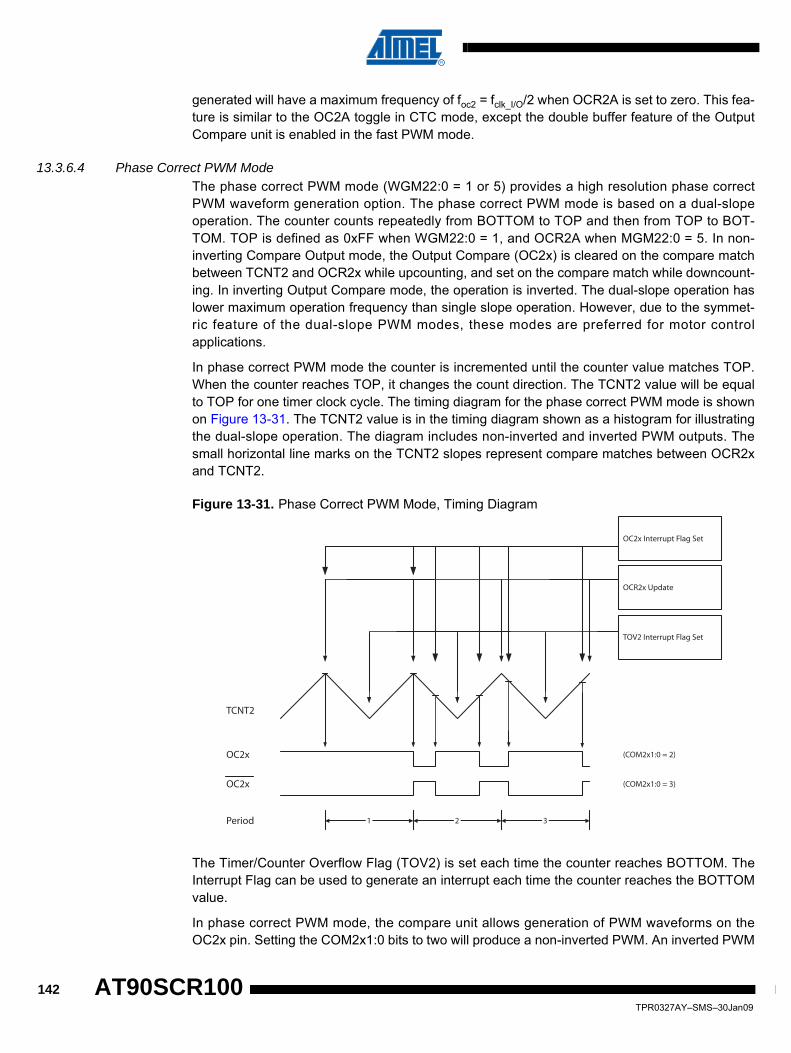
generated will have a maximum frequency of foc2 = fclk_I/O/2 when OCR2A is set to zero. This fea-ture is similar to the OC2A toggle in CTC mode, except the double buffer feature of the OutputCompare unit is enabled in the fast PWM mode.
13.3.6.4 Phase Correct PWM ModeThe phase correct PWM mode (WGM22:0 = 1 or 5) provides a high resolution phase correctPWM waveform generation option. The phase correct PWM mode is based on a dual-slopeoperation. The counter counts repeatedly from BOTTOM to TOP and then from TOP to BOT-TOM. TOP is defined as 0xFF when WGM22:0 = 1, and OCR2A when MGM22:0 = 5. In non-inverting Compare Output mode, the Output Compare (OC2x) is cleared on the compare matchbetween TCNT2 and OCR2x while upcounting, and set on the compare match while downcount-ing. In inverting Output Compare mode, the operation is inverted. The dual-slope operation haslower maximum operation frequency than single slope operation. However, due to the symmet-ric feature of the dual-slope PWM modes, these modes are preferred for motor controlapplications.
In phase correct PWM mode the counter is incremented until the counter value matches TOP.When the counter reaches TOP, it changes the count direction. The TCNT2 value will be equalto TOP for one timer clock cycle. The timing diagram for the phase correct PWM mode is shownon Figure 13-31. The TCNT2 value is in the timing diagram shown as a histogram for illustratingthe dual-slope operation. The diagram includes non-inverted and inverted PWM outputs. Thesmall horizontal line marks on the TCNT2 slopes represent compare matches between OCR2xand TCNT2.
Figure 13-31. Phase Correct PWM Mode, Timing Diagram
The Timer/Counter Overflow Flag (TOV2) is set each time the counter reaches BOTTOM. TheInterrupt Flag can be used to generate an interrupt each time the counter reaches the BOTTOMvalue.
In phase correct PWM mode, the compare unit allows generation of PWM waveforms on theOC2x pin. Setting the COM2x1:0 bits to two will produce a non-inverted PWM. An inverted PWM
TOV2 Interrupt Flag Set
OC2x Interrupt Flag Set
1 2 3
TCNT2
Period
OC2x
OC2x
(COM2x1:0 = 2)
(COM2x1:0 = 3)
OCR2x Update
142TPR0327AY–SMS–30Jan09
AT90SCR100

AT90SCR100
output can be generated by setting the COM2x1:0 to three. TOP is defined as 0xFF whenWGM2:0 = 3, and OCR2A when MGM2:0 = 7 (See Table 13-19 on page 146). The actual OC2xvalue will only be visible on the port pin if the data direction for the port pin is set as output. ThePWM waveform is generated by clearing (or setting) the OC2x Register at the compare matchbetween OCR2x and TCNT2 when the counter increments, and setting (or clearing) the OC2xRegister at compare match between OCR2x and TCNT2 when the counter decrements. ThePWM frequency for the output when using phase correct PWM can be calculated by the follow-ing equation:
The N variable represents the prescale factor (1, 8, 32, 64, 128, 256, or 1024).
The extreme values for the OCR2A Register represent special cases when generating a PWMwaveform output in the phase correct PWM mode. If the OCR2A is set equal to BOTTOM, theoutput will be continuously low and if set equal to MAX the output will be continuously high fornon-inverted PWM mode. For inverted PWM the output will have the opposite logic values.
At the very start of period 2 in Figure 13-31 OC2x has a transition from high to low even thoughthere is no Compare Match. The point of this transition is to guarantee symmetry around BOT-TOM. There are two cases that give a transition without Compare Match.
• OCR2A changes its value from MAX, like in Figure 13-31. When the OCR2A value is MAX the OC2 pin value is the same as the result of a down-counting compare match. To ensure symmetry around BOTTOM the OC2 value at MAX must correspond to the result of an up-counting Compare Match.
• The timer starts counting from a value higher than the one in OCR2A, and for that reason misses the Compare Match and hence the OC2 change that would have happened on the way up.
13.3.7 Timer/Counter Timing DiagramsThe following figures show the Timer/Counter in synchronous mode, and the timer clock (clkT2)is therefore shown as a clock enable signal. In asynchronous mode, clkI/O should be replaced bythe Timer/Counter Oscillator clock. The figures include information on when Interrupt Flags areset. Figure 13-32 contains timing data for basic Timer/Counter operation. The figure shows thecount sequence close to the MAX value in all modes other than phase correct PWM mode.
Figure 13-32. Timer/Counter Timing Diagram, no Prescaling
fOCnxPCPWMfclk_I/ON 510⋅------------------=
clkTn(clk I/O/1)
TOV2
clkI/O
TCNT2 MAX - 1 MAX BOTTOM BOTTOM + 1
143TPR0327AY–SMS–30Jan09

Figure 13-33 shows the same timing data, but with the prescaler enabled.
Figure 13-33. Timer/Counter Timing Diagram, with Prescaler (fclk_I/O/8)
Figure 13-34 shows the setting of OCF2A in all modes except CTC mode.
Figure 13-34. Timer/Counter Timing Diagram, Setting of OCF2A, with Prescaler (fclk_I/O/8)
Figure 13-35 shows the setting of OCF2A and the clearing of TCNT2 in CTC mode.
TOV2
TCNT2 MAX - 1 MAX BOTTOM BOTTOM + 1
clkI/O
clkTn(clk I/O/8)
OCF2x
OCR2x
TCNT2
OCR2x Value
OCR2x - 1 OCR2x OCR2x + 1 OCR2x + 2
clkI/O
clkTn(clk I/O/8)
144TPR0327AY–SMS–30Jan09
AT90SCR100

AT90SCR100
Figure 13-35. Timer/Counter Timing Diagram, Clear Timer on Compare Match mode, with Pres-caler (fclk_I/O/8)
13.3.8 8-bit Timer/Counter Register Description
13.3.8.1 TCCR2A – Timer/Counter Control Register A
• Bits 7..6 – COM2A1..0: Compare Match Output A ModeThese bits control the Output Compare pin (OC2A) behavior. If one or both of the COM2A1:0bits are set, the OC2A output overrides the normal port functionality of the I/O pin it is connectedto. However, note that the Data Direction Register (DDR) bit corresponding to the OC2A pinmust be set in order to enable the output driver.
When OC2A is connected to the pin, the function of the COM2A1:0 bits depends on theWGM22:0 bit setting. Table 13-17 shows the COM2A1:0 bit functionality when the WGM22:0bits are set to a normal or CTC mode (non-PWM).
OCF2x
OCR2x
TCNT2(CTC)
TOP
TOP - 1 TOP BOTTOM BOTTOM + 1
clkI/O
clkTn(clk I/O/8)
Bit 7 6 5 4 3 2 1 0
$0000B0 COM2A1 COM2A0 COM2B1 COM2B0 - - WGM21 WGM20 TCCR2ARead/write R/W R/W R/W R/W R R R/W R/W
Initial value 0 0 0 0 0 0 0 0 0x00
Table 13-17. Compare Output Mode, non-PWM Mode
COM2A1 COM2A0 Description
0 0 Normal port operation, OC0A disconnected.
0 1 Toggle OC2A on Compare Match
1 0 Clear OC2A on Compare Match
1 1 Set OC2A on Compare Match
145TPR0327AY–SMS–30Jan09

Table 13-18 shows the COM2A1:0 bit functionality when the WGM21:0 bits are set to fast PWMmode.
Note: 1. A special case occurs when OCR2A equals TOP and COM2A1 is set. In this case, the Com-pare Match is ignored, but the set or clear is done at BOTTOM. See “Fast PWM Mode” on page 140 for more details.
Table 13-19 shows the COM2A1:0 bit functionality when the WGM22:0 bits are set to phase cor-rect PWM mode.
Note: 1. A special case occurs when OCR2A equals TOP and COM2A1 is set. In this case, the Com-pare Match is ignored, but the set or clear is done at TOP. See “Phase Correct PWM Mode” on page 142 for more details.
• Bits 5..4 – COM2B1..0: Compare Match Output B ModeThese bits control the Output Compare pin (OC2B) behavior. If one or both of the COM2B1:0bits are set, the OC2B output overrides the normal port functionality of the I/O pin it is connectedto. However, note that the Data Direction Register (DDR) bit corresponding to the OC2B pinmust be set in order to enable the output driver.
When OC2B is connected to the pin, the function of the COM2B1:0 bits depends on theWGM22:0 bit setting. Table 13-20 shows the COM2B1:0 bit functionality when the WGM22:0bits are set to a normal or CTC mode (non-PWM).
Table 13-18. Compare Output Mode, Fast PWM Mode(1)
COM2A1 COM2A0 Description
0 0 Normal port operation, OC2A disconnected.
0 1 WGM22 = 0: Normal Port Operation, OC0A Disconnected.WGM22 = 1: Toggle OC2A on Compare Match.
1 0 Clear OC2A on Compare Match, set OC2A at BOTTOM(non-inverting mode)
1 1 Set OC2A on Compare Match, clear OC2A at BOTTOM(inverting mode)
Table 13-19. Compare Output Mode, Phase Correct PWM Mode(1)
COM2A1 COM2A0 Description
0 0 Normal port operation, OC2A disconnected.
0 1 WGM22 = 0: Normal Port Operation, OC2A Disconnected.WGM22 = 1: Toggle OC2A on Compare Match.
1 0 Clear OC2A on Compare Match when up-counting. Set OC2A on Compare Match when down-counting.
1 1 Set OC2A on Compare Match when up-counting. Clear OC2A on Compare Match when down-counting.
146TPR0327AY–SMS–30Jan09
AT90SCR100

AT90SCR100
Table 13-21 shows the COM2B1:0 bit functionality when the WGM22:0 bits are set to fast PWMmode.
Note: 1. A special case occurs when OCR2B equals TOP and COM2B1 is set. In this case, the Com-pare Match is ignored, but the set or clear is done at BOTTOM. See “Fast PWM Mode” on page 140 for more details.
Table 13-22 shows the COM2B1:0 bit functionality when the WGM22:0 bits are set to phase cor-rect PWM mode.
Note: 1. A special case occurs when OCR2B equals TOP and COM2B1 is set. In this case, the Com-pare Match is ignored, but the set or clear is done at TOP. See “Phase Correct PWM Mode” on page 142 for more details.
• Bits 3..2 – Res: Reserved BitsThese bits are reserved bits in the AT90SCR100 and will always read as zero.
• Bits 1..0 – WGM21..0: Waveform Generation Mode
Table 13-20. Compare Output Mode, non-PWM Mode
COM2B1 COM2B0 Description
0 0 Normal port operation, OC2B disconnected.
0 1 Toggle OC2B on Compare Match
1 0 Clear OC2B on Compare Match
1 1 Set OC2B on Compare Match
Table 13-21. Compare Output Mode, Fast PWM Mode(1)
COM2B1 COM2B0 Description
0 0 Normal port operation, OC2B disconnected.
0 1 Reserved
1 0 Clear OC2B on Compare Match, set OC2B at BOTTOM(non-inverting mode)
1 1 Set OC2B on Compare Match, clear OC2B at BOTTOM(inverting mode)
Table 13-22. Compare Output Mode, Phase Correct PWM Mode(1)
COM2B1 COM2B0 Description
0 0 Normal port operation, OC2B disconnected.
0 1 Reserved
1 0 Clear OC2B on Compare Match when up-counting. Set OC2B on Compare Match when down-counting.
1 1 Set OC2B on Compare Match when up-counting. Clear OC2B on Compare Match when down-counting.
147TPR0327AY–SMS–30Jan09

Combined with the WGM22 bit found in the TCCR2B Register, these bits control the countingsequence of the counter, the source for maximum (TOP) counter value, and what type of wave-form generation to be used, see Table 13-23. Modes of operation supported by theTimer/Counter unit are: Normal mode (counter), Clear Timer on Compare Match (CTC) mode,and two types of Pulse Width Modulation (PWM) modes (see “Modes of Operation” on page139).
Note: 1. MAX= 0xFF, BOTTOM= 0x00
13.3.8.2 TCCR2B – Timer/Counter Control Register B
• Bit 7 – FOC2A: Force Output Compare AThe FOC2A bit is only active when the WGM bits specify a non-PWM mode.
However, for ensuring compatibility with future devices, this bit must be set to zero whenTCCR2B is written when operating in PWM mode. When writing a logical one to the FOC2A bit,an immediate Compare Match is forced on the Waveform Generation unit. The OC2A output ischanged according to its COM2A1:0 bits setting. Note that the FOC2A bit is implemented as astrobe. Therefore it is the value present in the COM2A1:0 bits that determines the effect of theforced compare.
A FOC2A strobe will not generate any interrupt, nor will it clear the timer in CTC mode usingOCR2A as TOP.
The FOC2A bit is always read as zero.
• Bit 6 – FOC2B: Force Output Compare BThe FOC2B bit is only active when the WGM bits specify a non-PWM mode.
Table 13-23. Waveform Generation Mode Bit Description
Mode WGM22 WGM21 WGM20
Timer/Counter Mode of Operation TOP
Update ofOCRx at
TOV FlagSet on(1)
0 0 0 0 Normal 0xFF Immediate MAX
1 0 0 1 PWM, Phase Correct 0xFF TOP BOTTOM
2 0 1 0 CTC OCR2A Immediate MAX
3 0 1 1 Fast PWM 0xFF BOTTOM MAX
4 1 0 0 Reserved – – –
5 1 0 1 PWM, Phase Correct OCR2A TOP BOTTOM
6 1 1 0 Reserved – – –
7 1 1 1 Fast PWM OCR2A BOTTOM TOP
Bit 7 6 5 4 3 2 1 0
$0000B1 FOC2A FOC2B - - WGM22 CS22 CS21 CS20 TCCR2BRead/write W W R R R/W R/W R/W R/W
Initial value 0 0 0 0 0 0 0 0 0x00
148TPR0327AY–SMS–30Jan09
AT90SCR100

AT90SCR100
However, for ensuring compatibility with future devices, this bit must be set to zero whenTCCR2B is written when operating in PWM mode. When writing a logical one to the FOC2B bit,an immediate Compare Match is forced on the Waveform Generation unit. The OC2B output ischanged according to its COM2B1:0 bits setting. Note that the FOC2B bit is implemented as astrobe. Therefore it is the value present in the COM2B1:0 bits that determines the effect of theforced compare.
A FOC2B strobe will not generate any interrupt, nor will it clear the timer in CTC mode usingOCR2B as TOP.
The FOC2B bit is always read as zero.
• Bits 5..4 – Res: Reserved BitsThese bits are reserved bits and will always read as zero.
• Bit 3 – WGM22: Waveform Generation ModeSee the description in the “TCCR2A – Timer/Counter Control Register A” on page 145.
• Bit 2..0 – CS22..0: Clock SelectThe three Clock Select bits select the clock source to be used by the Timer/Counter, see Table13-24.
If external pin modes are used for the Timer/Counter0, transitions on the T0 pin will clock thecounter even if the pin is configured as an output. This feature allows software control of thecounting.
13.3.8.3 TCNT2 – Timer/Counter Register
The Timer/Counter Register gives direct access, both for read and write operations, to theTimer/Counter unit 8-bit counter. Writing to the TCNT2 Register blocks (removes) the CompareMatch on the following timer clock. Modifying the counter (TCNT2) while the counter is running,introduces a risk of missing a Compare Match between TCNT2 and the OCR2x Registers.
Table 13-24. Clock Select Bit Description
CS22 CS21 CS20 Description
0 0 0 No clock source (Timer/Counter stopped).
0 0 1 clkT2S/(No prescaling)
0 1 0 clkT2S/8 (From prescaler)
0 1 1 clkT2S/32 (From prescaler)
1 0 0 clkT2S/64 (From prescaler)
1 0 1 clkT2S/128 (From prescaler)
1 1 0 clkT2S/256 (From prescaler)
1 1 1 clkT2S/1024 (From prescaler)
Bit 7 6 5 4 3 2 1 0
$0000B2 TCNT2 [7..0] TCNT2Read/write R/W R/W R/W R/W R/W R/W R/W R/W
Initial value 0 0 0 0 0 0 0 0 0x00
149TPR0327AY–SMS–30Jan09
13.3.8.4 OCR2A – Output Compare Register A
The Output Compare Register A contains an 8-bit value that is continuously compared with thecounter value (TCNT2). A match can be used to generate an Output Compare interrupt, or togenerate a waveform output on the OC2A pin.
13.3.8.5 OCR2B – Output Compare Register B
The Output Compare Register B contains an 8-bit value that is continuously compared with thecounter value (TCNT2). A match can be used to generate an Output Compare interrupt, or togenerate a waveform output on the OC2B pin.
13.3.9 Asynchronous operation of the Timer/Counter
13.3.9.1 ASSR – Asynchronous Status Register
• Bit 6 – EXCLK: Enable External Clock InputWhen EXCLK is written to one, and asynchronous clock is selected, the external clock input buf-fer is enabled and an external clock can be input on Timer Oscillator 1 (TOSC1) pin instead of a32 kHz crystal. Writing to EXCLK should be done before asynchronous operation is selected.Note that the crystal Oscillator will only run when this bit is zero.
• Bit 5 – AS2: Asynchronous Timer/Counter2When AS2 is written to zero, Timer/Counter2 is clocked from the I/O clock, clkI/O. When AS2 iswritten to one, Timer/Counter2 is clocked from a crystal Oscillator connected to the Timer Oscil-lator 1 (TOSC1) pin. When the value of AS2 is changed, the contents of TCNT2, OCR2A,OCR2B, TCCR2A and TCCR2B might be corrupted.
• Bit 4 – TCN2UB: Timer/Counter2 Update BusyWhen Timer/Counter2 operates asynchronously and TCNT2 is written, this bit becomes set.When TCNT2 has been updated from the temporary storage register, this bit is cleared by hard-ware. A logical zero in this bit indicates that TCNT2 is ready to be updated with a new value.
• Bit 3 – OCR2AUB: Output Compare Register2 Update Busy
Bit 7 6 5 4 3 2 1 0
$0000B3 OCR2A [7..0] OCR2ARead/write R/W R/W R/W R/W R/W R/W R/W R/W
Initial value 0 0 0 0 0 0 0 0 0x00
Bit 7 6 5 4 3 2 1 0
$0000B4 OCR2B [7..0] OCR2BRead/write R/W R/W R/W R/W R/W R/W R/W R/W
Initial value 0 0 0 0 0 0 0 0 0x00
Bit 7 6 5 4 3 2 1 0
$0000B6 - EXCLK AS2 TCN2UB OCR2AUB OCR2BUB TCR2AUB TCR2BUB ASSRRead/write R R/W R/W R R R R R
Initial value 0 0 0 0 0 0 0 0 0x00
150TPR0327AY–SMS–30Jan09
AT90SCR100

AT90SCR100
When Timer/Counter2 operates asynchronously and OCR2A is written, this bit becomes set.When OCR2A has been updated from the temporary storage register, this bit is cleared by hard-ware. A logical zero in this bit indicates that OCR2A is ready to be updated with a new value.
• Bit 2 – OCR2BUB: Output Compare Register2 Update BusyWhen Timer/Counter2 operates asynchronously and OCR2B is written, this bit becomes set.When OCR2B has been updated from the temporary storage register, this bit is cleared by hard-ware. A logical zero in this bit indicates that OCR2B is ready to be updated with a new value.
• Bit 1 – TCR2AUB: Timer/Counter Control Register2 Update BusyWhen Timer/Counter2 operates asynchronously and TCCR2A is written, this bit becomes set.When TCCR2A has been updated from the temporary storage register, this bit is cleared byhardware. A logical zero in this bit indicates that TCCR2A is ready to be updated with a newvalue.
• Bit 0 – TCR2BUB: Timer/Counter Control Register2 Update BusyWhen Timer/Counter2 operates asynchronously and TCCR2B is written, this bit becomes set.When TCCR2B has been updated from the temporary storage register, this bit is cleared byhardware. A logical zero in this bit indicates that TCCR2B is ready to be updated with a newvalue.
If a write is performed to any of the five Timer/Counter2 Registers while its update busy flag isset, the updated value might get corrupted and cause an unintentional interrupt to occur.
The mechanisms for reading TCNT2, OCR2A, OCR2B, TCCR2A and TCCR2B are different.When reading TCNT2, the actual timer value is read. When reading OCR2A, OCR2B, TCCR2Aand TCCR2B the value in the temporary storage register is read.
13.3.9.2 Asynchronous Operation of Timer/Counter2When Timer/Counter2 operates asynchronously, some considerations must be taken.
• Warning: When switching between asynchronous and synchronous clocking of Timer/Counter2, the Timer Registers TCNT2, OCR2x, and TCCR2x might be corrupted. A safe procedure for switching clock source is:
1. Disable the Timer/Counter2 interrupts by clearing OCIE2x and TOIE2.2. Select clock source by setting AS2 as appropriate.3. Write new values to TCNT2, OCR2x, and TCCR2x.4. To switch to asynchronous operation: Wait for TCN2UB, OCR2xUB, and TCR2xUB.5. Clear the Timer/Counter2 Interrupt Flags.6. Enable interrupts, if needed.
• The CPU main clock frequency must be more than four times the Oscillator frequency.• When writing to one of the registers TCNT2, OCR2x, or TCCR2x, the value is transferred to a
temporary register, and latched after two positive edges on TOSC1. The user should not write a new value before the contents of the temporary register have been transferred to its destination. Each of the five mentioned registers have their individual temporary register, which means that e.g. writing to TCNT2 does not disturb an OCR2x write in progress. To detect that a transfer to the destination register has taken place, the Asynchronous Status Register – ASSR has been implemented.
151TPR0327AY–SMS–30Jan09

• When entering Power-save or ADC Noise Reduction mode after having written to TCNT2, OCR2x, or TCCR2x, the user must wait until the written register has been updated if Timer/Counter2 is used to wake up the device. Otherwise, the MCU will enter sleep mode before the changes are effective. This is particularly important if any of the Output Compare2 interrupt is used to wake up the device, since the Output Compare function is disabled during writing to OCR2x or TCNT2. If the write cycle is not finished, and the MCU enters sleep mode before the corresponding OCR2xUB bit returns to zero, the device will never receive a compare match interrupt, and the MCU will not wake up.
• If Timer/Counter2 is used to wake the device up from Power-save or ADC Noise Reduction mode, precautions must be taken if the user wants to re-enter one of these modes: The interrupt logic needs one TOSC1 cycle to be reset. If the time between wake-up and re-entering sleep mode is less than one TOSC1 cycle, the interrupt will not occur, and the device will fail to wake up. If the user is in doubt whether the time before re-entering Power-save or ADC Noise Reduction mode is sufficient, the following algorithm can be used to ensure that one TOSC1 cycle has elapsed:
1. Write a value to TCCR2x, TCNT2, or OCR2x.2. Wait until the corresponding Update Busy Flag in ASSR returns to zero.3. Enter Power-save or ADC Noise Reduction mode.
• When the asynchronous operation is selected, the 32.768 kHz Oscillator for Timer/Counter2 is always running, except in Power-down and Standby modes. After a Power-up Reset or wake-up from Power-down or Standby mode, the user should be aware of the fact that this Oscillator might take as long as one second to stabilize. The user is advised to wait for at least one second before using Timer/Counter2 after power-up or wake-up from Power-down or Standby mode. The contents of all Timer/Counter2 Registers must be considered lost after a wake-up from Power-down or Standby mode due to unstable clock signal upon start-up, no matter whether the Oscillator is in use or a clock signal is applied to the TOSC1 pin.
• Description of wake up from Power-save or ADC Noise Reduction mode when the timer is clocked asynchronously: When the interrupt condition is met, the wake up process is started on the following cycle of the timer clock, that is, the timer is always advanced by at least one before the processor can read the counter value. After wake-up, the MCU is halted for four cycles, it executes the interrupt routine, and resumes execution from the instruction following SLEEP.
• Reading of the TCNT2 Register shortly after wake-up from Power-save may give an incorrect result. Since TCNT2 is clocked on the asynchronous TOSC clock, reading TCNT2 must be done through a register synchronized to the internal I/O clock domain. Synchronization takes place for every rising TOSC1 edge. When waking up from Power-save mode, and the I/O clock (clkI/O) again becomes active, TCNT2 will read as the previous value (before entering sleep) until the next rising TOSC1 edge. The phase of the TOSC clock after waking up from Power-save mode is essentially unpredictable, as it depends on the wake-up time. The recommended procedure for reading TCNT2 is thus as follows:
1. Write any value to either of the registers OCR2x or TCCR2x. 2. Wait for the corresponding Update Busy Flag to be cleared. 3. Read TCNT2.
• During asynchronous operation, the synchronization of the Interrupt Flags for the asynchronous timer takes 3 processor cycles plus one timer cycle. The timer is therefore
152TPR0327AY–SMS–30Jan09
AT90SCR100

AT90SCR100
advanced by at least one before the processor can read the timer value causing the setting of the Interrupt Flag. The Output Compare pin is changed on the timer clock and is not synchronized to the processor clock.
13.3.9.3 TIMSK2 – Timer/Counter2 Interrupt Mask Register
• Bit 2 – OCIE2B : Timer/Counter2 Output Compare Match B Interrupt EnableWhen the OCIE2B bit is written to one and the I-bit in the Status Register is set (one), theTimer/Counter2 Compare Match B interrupt is enabled. The corresponding interrupt is executedif a compare match in Timer/Counter2 occurs, i.e., when the OCF2B bit is set in the Timer/Coun-ter 2 Interrupt Flag Register – TIFR2.
• Bit 1 – OCIE2A : Timer/Counter2 Output Compare Match A Interrupt EnableWhen the OCIE2A bit is written to one and the I-bit in the Status Register is set (one), theTimer/Counter2 Compare Match A interrupt is enabled. The corresponding interrupt is executedif a compare match in Timer/Counter2 occurs, i.e., when the OCF2A bit is set in the Timer/Coun-ter 2 Interrupt Flag Register – TIFR2.
• Bit 0 – TOIE2 : Timer/Counter2 Overflow Interrupt EnableWhen the TOIE2 bit is written to one and the I-bit in the Status Register is set (one), theTimer/Counter2 Overflow interrupt is enabled. The corresponding interrupt is executed if anoverflow in Timer/Counter2 occurs, i.e., when the TOV2 bit is set in the Timer/Counter2 InterruptFlag Register – TIFR2.
13.3.9.4 TIFR2 – Timer/Counter2 Interrupt Flag Register
• Bit 2 – OCF2B : Output Compare Flag 2 BThe OCF2B bit is set (one) when a compare match occurs between the Timer/Counter2 and thedata in OCR2B – Output Compare Register2. OCF2B is cleared by hardware when executingthe corresponding interrupt handling vector. Alternatively, OCF2B is cleared by writing a logicone to the flag. When the I-bit in SREG, OCIE2B (Timer/Counter2 Compare match InterruptEnable), and OCF2B are set (one), the Timer/Counter2 Compare match Interrupt is executed.
• Bit 1 – OCF2A : Output Compare Flag 2 AThe OCF2A bit is set (one) when a compare match occurs between the Timer/Counter2 and thedata in OCR2A – Output Compare Register2. OCF2A is cleared by hardware when executingthe corresponding interrupt handling vector. Alternatively, OCF2A is cleared by writing a logicone to the flag. When the I-bit in SREG, OCIE2A (Timer/Counter2 Compare match InterruptEnable), and OCF2A are set (one), the Timer/Counter2 Compare match Interrupt is executed.
Bit 7 6 5 4 3 2 1 0
$000070 - - - - - OCIE2B OCIE2A TOIE2 TIMSK2Read/write R R R R R R/W R/W R/W
Initial value 0 0 0 0 0 0 0 0 0x00
Bit 7 6 5 4 3 2 1 0
0x17 (0x37) - - - - - OCF2B OCF2A TOV2 TIFR2Read/write R R R R R R/W R/W R/W
Initial value 0 0 0 0 0 0 0 0 0x00
153TPR0327AY–SMS–30Jan09

• Bit 0 – TOV2 : Timer/Counter2 Overflow FlagThe TOV2 bit is set (one) when an overflow occurs in Timer/Counter2. TOV2 is cleared by hard-ware when executing the corresponding interrupt handling vector. Alternatively, TOV2 is clearedby writing a logic one to the flag. When the SREG I-bit, TOIE2A (Timer/Counter2 Overflow Inter-rupt Enable), and TOV2 are set (one), the Timer/Counter2 Overflow interrupt is executed. InPWM mode, this bit is set when Timer/Counter2 changes counting direction at 0x00.
13.4 Timer/Counter Prescaler
Figure 13-36. Prescaler for Timer/Counter2
The clock source for Timer/Counter2 is named clkT2S. clkT2S is by default connected to the mainsystem I/O clock clkIO. By setting the AS2 bit in ASSR, Timer/Counter2 is asynchronouslyclocked from the TOSC1 pin. This enables use of Timer/Counter2 as a Real Time Counter(RTC). When AS2 is set, pins TOSC1 and TOSC2 are disconnected from Port C. A crystal canthen be connected between the TOSC1 and TOSC2 pins to serve as an independent clocksource for Timer/Counter2. The Oscillator is optimized for use with a 32.768 kHz crystal. By set-ting the EXCLK bit in the ASSR, a 32 kHz external clock can be applied. See “ASSR –Asynchronous Status Register” on page 150 for details.
For Timer/Counter2, the possible prescaled selections are: clkT2S/8, clkT2S/32, clkT2S/64,clkT2S/128, clkT2S/256, and clkT2S/1024. Additionally, clkT2S as well as 0 (stop) may be selected.Setting the PSRASY bit in GTCCR resets the prescaler. This allows the user to operate with apredictable prescaler.
10-BIT T/C PRESCALER
TIMER/COUNTER2 CLOCK SOURCE
clkI/O clkT2S
TOSC1
AS2
CS20CS21CS22
clk T2
S/8
clk T2
S/64
clk T2
S/128
clk T2
S/102
4
clk T2
S/256
clk T2
S/32
0PSRASY
Clear
clkT2
154TPR0327AY–SMS–30Jan09
AT90SCR100

AT90SCR100
13.4.1 GTCCR – General Timer/Counter Control Register
• Bit 7 – TSM : Timer/Counter Synchronization ModeWriting the TSM bit to one activates the Timer/Counter Synchronization mode. In this mode, thevalue that is written to the PSRASY and PSRSYNC bits is kept, hence keeping the correspond-ing prescaler reset signals asserted. This ensures that the corresponding Timer/Counters arehalted and can be configured to the same value without the risk of one of them advancing duringconfiguration. When the TSM bit is written to zero, the PSRASY and PSRSYNC bits are clearedby hardware, and the Timer/Counters start counting simultaneously.
• Bit 1 – PSRASY : Prescaler Reset Timer/Counter2When this bit is one, the Timer/Counter2 prescaler will be reset. This bit is normally clearedimmediately by hardware. If the bit is written when Timer/Counter2 is operating in asynchronousmode, the bit will remain one until the prescaler has been reset. The bit will not be cleared byhardware if the TSM bit is set. Refer to the description of the “Bit 7 – TSM: Timer/Counter Syn-chronization Mode” on page 136 for a description of the Timer/Counter Synchronization mode.
• Bit 0 – PSRSYNC : Prescaler Reset Timer/Counter0, Timer/Counter1When this bit is one, Timer/Counter1 and Timer/Counter0 prescaler will be Reset. This bit is nor-mally cleared immediately by hardware, except if the TSM bit is set. Note that Timer/Counter1and Timer/Counter0 share the same prescaler and a reset of this prescaler will affect bothtimers.
Bit 7 6 5 4 3 2 1 0
0x23 (0x43) TSM - - - - - PSRASY PSRSYNC GTCCRRead/write R/W R R R R R R/W R/W
Initial value 0 0 0 0 0 0 0 0 0x00
155TPR0327AY–SMS–30Jan09

156TPR0327AY–SMS–30Jan09
AT90SCR100
AT90SCR100
14. USB Device InterfaceThis section contains an overview of the USB module and the description of the registers designto interface this USB module. It also details the USB interrupt, the Suspend and Resume modes,the double buffering, the mode detection and the attachment procedure. This section assumesthe reader of this document is comfortable with the USB Specifications V2.0, available on thewww.usb.org website. He may also refer to the USB register summary, located at the end of thisdocument to have a complete overview of the registers available. See “Register Summary” onpage 417.
14.1 Features• USB 2.0 FullSpeed compliant• Data transfer rates up to 12Mbit/s• 8 Programmable Endpoints bi-directionnals
– Endpoint 0 for control: 64bytes– Endpoints 1 to 3 support double buffers of 64bytes each– Endpoints 4 to 7: 8 bytes each
• Suspend/Resume Interrupts• Resume Wake Up Capabilities• Automatic NACK if USB not ready to transmit/receive• Specific USBDMA connected for fast and easy copy from Endpoint to RAM
14.2 OverviewThe following diagram represents the USB module that contains the necessary logic to commu-nicate via a Full-Speed USB port.
In Register configuration, you may see ‘X’ suffix at the end of some register. Thisvalue is to be changed into 0, 1, 2, 3, 4, 5, 6 and 7 according to the endpointtargeted.
The USBENUM is designed to target choose the endpoint to target.Note
157TPR0327AY–SMS–30Jan09

Figure 14-1. USB Module Diagram
The USB module of the AT90SCR100 is made up of the following elements:
• The USB Transceiver: it is the electrical and physical interface between the USB Bus and the internal logic of the AT90SCR100.
• The USB Serial Interface Engine: this logical part manages the NRZI coding/decoding, the bit stuffing/unstuffing, the CRC generation/checking and the serial-parallel data conversion as requested by the USB specifications.
• The Universal Function Interface: this block is the interface between the data flow and the internal Dual Port RAM of the USB module that contains the endpoints.
• The DPRAM block: the Dual Port RAM is an internal block of the USB module. It contains the seven available endpoints and can be accessed either by the SIE or the UFI. It is intended to be used as a buffer between the USB bus and the internal data bus of the AT90SCR100.
• The USBDMA Controller: the Direct Memory Access logical module allows fast data transfers from the DPRAM to the RAM of the AT90SCR100. See “USBDMA Controller” on page 172.
USB MODULE
USB Transceiver
USBDM(D-)
USBDP(D+)
USB SIE(Serial Interface
Engine)
Clock and
Suspend/
Resume Manager
XIN
XOUT
USB UFI(Universal Function Interface)
USBDMAController
Data Exchanges
USB Controland Status,
USB Interrupt,...
DPRAMEndpoint 0
Endpoint 3Endpoint 2Endpoint 1
64 Bytes2x64 Bytes
2x64 Bytes2x64 Bytes
Endpoint 4 8 BytesEndpoint 5 8 BytesEndpoint 6Endpoint 7
8 Bytes8 Bytes
158TPR0327AY–SMS–30Jan09
AT90SCR100

AT90SCR100
The USB interface of the AT90SCR100 is a module supporting one USB device address witheight configurable endpoints, managed by an embedded firmware running on the AVR. Thisfirmware is responsible for handling the enumeration (particularly the SETUP packets manage-ment), executing the Suspend and Resume mode entries, filling and emptying the endpointsthrough the USBDMA Controller, sending STALL packets.
The device is characterized by a full-speed (12Mb/s) bus-powered interface supporting Suspendand Resume modes and fully compliant with the USB V2.0 specifications.
The endpoints 1, 2 and 3 have a double-buffering capability (double DPRAM size). This featureis particularly suitable for Bulk data transfers and is totally managed by the hardware. See “Dou-ble Buffering” on page 163.
In order to communicate via the USB interface, the chip operates with at 48MHz clock.
The chip internally de-activates and activates its oscillator when necessary in order to be compli-ant with the power consumption of the Suspend mode.
14.3 Endpoints DescriptionThe USB module contains eight endpoints. They are fully configurable through their correspond-ing register USBFCEX (for further details, please refer to “USBFCEX - USB Function ControlRegisters for Endpoint X” on page 169).
The table below indicates the size (in Bytes) of each endpoint and also shows possible configu-rations for the USB device.
Notes: 1. Can also be INTERRUPT or ISOCHRONOUS, not CONTROL2. Can also be ISOCHRONOUS
An endpoint featuring the double-buffering capability is allocated on two banks of DPRAM, eachbank equal to the endpoint size. Endpoints 1, 2 and 3 support these double buffer of 64 Bytes.See “Double Buffering” on page 163.
The hardware is responsible for handling the internal data toggle bit for each endpoint. Thismechanism guarantees data sequence synchronisation between data transmitter and receiveracross multiple transactions. Synchronisation is achieved via use of the DATA0 and DATA1
Table 14-1. Endpoints Description
Endpoint Number
Size in Bytes
Double- Buffering Capability
Recommended Data Transfer Type
EP0 64 NO CONTROL
EP1 2x64 YES BULK(1)
EP2 2x64 YES BULK (1)
EP3 2x64 YES BULK (1)
EP4 8 NO CONTROL, BULK, INTERRUPT(2)
EP5 8 NO CONTROL, BULK, INTERRUPT(2)
EP6 8 NO CONTROL, BULK, INTERRUPT(2)
EP7 8 NO CONTROL, BULK, INTERRUPT(2)
159TPR0327AY–SMS–30Jan09

PIDs and separate data toggle sequence bits for the data transmitter and receiver. Receiversequence bits toggle only when the receiver is able to accept data and receives an error-freedata packet with the correct data PID. Transmitter sequence bits toggle only when the datatransmitter receives a valid ACK handshake. Data toggle synchronization is not supported forisochronous transfers.
14.4 Attachment ProcedureThis procedure must be applied in order to connect the pull-up between the USB signal D+ andUSBReg, thus identifying a Full-Speed USB device.
Even after reset, the pull-up is not connected. This operation must be controlled by the softwarein order to attach the device.
We can imagine two integration scenarios for AT90SCR100:
• If the AT90SCR100 is standalone USB device Smart Card reader, then, connecting the USB cable into a computer, for instance, will power up the AT90SCR100. After chip initialization, PLL running, the USB module can be enabled using USBCR.USBE bit, set attachement pull-up can also be set to make the host detect a full-speed peripheral. The host will then reset the communication, and the FEURI interruption will trigger. A enumeration procedure can finally go ahead naturally.
• If the AT90SCR100 can be controlled by different hosts, for example by USART and USB, and if the host detection must be done dynamically, then a specific detection must be initiated. After chip power up, communication modules initialisation and PLL activation, the interruption on USART and USB (in the example) must be activated. The attachement pull-up must be enabled. Then, the first interruption (USBPI.FEURI or USART reception) will indicate the host communication mode. Please note that in this case, the D- line may be in High-Z state, making the USB module consumpts until the USB module is disabled or communication is runnning. To prevent consumption issue, a resistor or 1MegaOhm should be place as pull-up on USB D- line.
14.5 USB InterruptsThe USB interrupt sources are split into two main families:
• The USB Protocol Interrupts (Falling Edge on USB Reset, Start Of Frame, Resume, Suspend). They are included into the USBPI register (see “USBPI - USB Protocol Interrupt register” on page 165 for further details).
• The USB Endpoint Interrupt (Endpoint0, 1, 2, 3, 4, 5, 6 and 7). They are included into the USBEI register (see “USBEI - USB Endpoint Interrupt Register” on page 166 for further details). This register only indicates which endpoint of the eight holds the source of the interruption. The source of the interruption can then be retrieved by checking the register USBCSEX corresponding to the endpoint (see “USBCSEX - USB Control And Status
The USB hardware module integrates the attachment pull-up resistors connectedbetween the USB D+ differential data line and the internal 3.3 V USB regulator(USBReg).
The serial resistors required by USB certification are not embedded in the USBhardware module. They must be added externally.
Note
Note
160TPR0327AY–SMS–30Jan09
AT90SCR100

AT90SCR100
Register for Endpoint X” on page 167 for further details). These sources are Stall sent, Setup packet received, Data received, Data sent events.
The AT90SCR100 has two interrupt vectors for both families. These vectors, called USB End-point and USB Protocol are only valid if the chip operates with the USB interface and arerespectively located at addresses $003E and $0040.
Every source can be enabled/disabled through bits of USBEIM or USBPIM registers.
The figure below shows the implications between the registers, the USB interrupt sources andthe AVR interrupt logic. For further details about the AVR Interrupt Logic please refer to Section10. “Interrupts” on page 63.
Figure 14-2. USB Interrupt Hierarchy
14.6 Suspend and Resume ModesIn order to be compliant with the USB specifications V2.0, a device has to support the low-powerconsumption state called Suspend and its associated resumption activity called Resume.
The AT90SCR100 enters the Suspend mode only when requested by the host through bus inac-tivity for at least 3ms.
A USB interrupt is triggered assuming bits SREG.I is set (one) in order to enablethe interrupt.
Note
EP3I
EP2I
EP1I
EP0I
USBPI
USBEI
USBPIM
USBEIM
LOGICAL OR
AVR INTERRUPT LOGIC
USB PROTOCOL
USB ENDPOINT
FEURI FEURIMSOFI SOFIM
RMWUI RMWUIM
RESI RESIM
SUSI SUSIM
EP3IM
EP2IM
EP1IM
EP0IM
UCSE3
UCSE3UCSE1
UCSE3UCSE0
UCSE2
ENDPOINT INTERRUPT
PROTOCOL INTERRUPT
UCSE4
UCSE5
UCSE6
UCSE7
EP4I
EP5I
EP6I
EP7I
EP4IM
EP5IM
EP6IM
EP7IM
161TPR0327AY–SMS–30Jan09

The USB module is able to detect this request and automatically sets the bit USBPI.SUSI. See“USBPI - USB Protocol Interrupt register” on page 165. This event generates a USB interruptionif the Suspend Interrupt source is not masked and if the USB interrupt is enabled.
Once Suspend mode has been entered, the USB module is able to detect a Resume request.This event immediately and automatically makes the chip come out the POWER-DOWN modeand sets (one) bit USBPI.RESI. The fact that bit USBPI.RESI is set (one) triggers a new USBinterrupt if the Resume Interrupt source is not masked and if the USB interrupt is enabled. Theapplication software shall then clear the interrupt source in its interrupt service routine.
14.6.1 Remote Wake-upThe USB Module is also able to generate a remote wake-up signal (K signal) to raise the com-munication with the host. To enable this feature, the USBGS.RMWUE bit must be set.
The wake-up signal start to be generated by setting the bit USBCR.URMWU bit.
As soon as this bit is set, a protocol interrupt is generated, if USBPIM.RMWUIM bit is set.through the raise of USBPI.RMWUI flag.
The remote wake-up signal will be automatically stopped after ~13ms generation. As soon asthe signal stops, the USBGS.RSMON bit is cleared.
Below is a scheme showing all the signal for Remote Wake Up management.
Figure 14-3. Remote Wake Up State Sequence Description
In order to support the power consumption threshold fixed by the USB specifica-tions, the oscillator is switched off by hardware. The POWER-DOWN mode mustbe entered by setting appropriate configuration in SMCR and followed by a SLEEPinstruction.
When a Resume signal has been detected the USB module does not automati-cally restarts the internal oscillator. See “Important note about: Entering andLeaving low consumption modes” on page 47.
Note
Note
When the USBGS.RSMON bit is cleared, do not forget to clear USBCR.URMWUbit, for next Remote Wake Up sequence.
Note
USBGS.RMWUE
USBCR.URMWU
USBGS.RMSON
USBPI.RMWUI
Enable the feature...
...Start the WakeUp Signal generation...
...and wait the end of the generation.
Flag to be cleared by software
Control to be cleared by software
~13ms
162TPR0327AY–SMS–30Jan09
AT90SCR100

AT90SCR100
14.7 Double BufferingThis special feature available on the endpoints 1, 2 and 3 allows the user to save time duringUSB transfers.
It is specially recommended for BULK data transfers but is also suitable for ISOCHRONOUS orINTERRUPT. CONTROL is not possible on these double buffered endpoints.
The double buffering uses two different data banks of the endpoint size. Its managementremains transparent for the user. The advantages of the double buffering are the followings:
• When receiving data from the host, the software can process the data received in one of the two banks while the second is being filled. The endpoints that do not have the double buffering capability must wait for their DPRAM to be emptied by the software before being ready to receive new data.
• When sending data to the host, the software can fill the free bank while the USB module is sending data from the other one. The endpoints that do not have this feature must wait for the previous data to be sent before being allowed to fill again the single bank.
The two following figures provide code algorithm for sending data to the host and receiving datafrom the host (respectively IN and OUT tokens). They are also valid for endpoints operating nor-mally (without the double buffering capability).
Figure 14-4. Sending Data Packets (Single Buffering)
The figure is correct if several data packets have to be sent. If only one packet is tobe sent the testing of the bit USBCSE.TXPB must be ignored.
FILL DPRAM
SET bit USBCSEX.TXPB
USBCSEX.TXPB = 0 ?YES
USBCSEX.TXC = 1 ?(POLLING or INTERRUPT)
NO
NO
YES
CLEAR bit USBCSEX.TXC
LAST DATA PACKET REACHED ? NO
YES
END
USBCSEX.TXPB = 0 ?
YES
NO
Note
163TPR0327AY–SMS–30Jan09

Figure 14-5. Receiving Data Packets
14.8 USB Device Registers Description
14.8.1 USBCR - USB Control Register
• Bit 7 - URMWU : USB Remote Wake up bitWhen in suspend mode, setting this bit to one generates a wake-up command to the host,according to USB2.0 specifications.
This bit must be cleared by software when USBGS.RSMON is cleared. See “Remote Wake-up”on page 162.
• Bit 6 - Res : Reserved BitThis bit is reserved bits in the AT90SCR100 and is always read as zero.
• Bit 5 - UPUC : USB Pull-Up Connection BitThis bit is set (one) and cleared (zero) by software.
It directly acts on the connection of the USB pull-up attachment resistors between USB bus sig-nal D+ and VREG.
If set (one) the pull-up is connected. If cleared (zero) the pull-up is not connected.
• Bit 4..2 - Res : Reserved BitsThese bits are reserved bits in the AT90SCR100 and are always read as zero.
USBCSEX.RCVD = 1 ?(POLLING or INTERRUPT)
NO
READ register USBDBCEX -> NbBytes
READ DPRAM to getNbBytes Bytes of data
CLEAR UCSEX.RCVD
END
Bit 7 6 5 4 3 2 1 0
$0000E0 URMWU - UPUC - - - USBE - USBCRRead/write R/W R R/W R R R R/W R
Initial value 0 0 0 0 0 0 0 0 0x00
164TPR0327AY–SMS–30Jan09
AT90SCR100

AT90SCR100
• Bit 1 - USBE : USB Enable BitYou must clear this bit before using it, even if the USB module has not been used previously.
Set this bit to enable the USB controller.
Clear this bit to disable and reset the USB controller, to disable the USB transceiver and to dis-able the USB controller clock inputs.
• Bit 0 - Res : Reserved BitThis bit is reserved and will always be read as zero.
14.8.2 USBPI - USB Protocol Interrupt registerThe following interrupt sources are all sources for the USB Protocol interruption
• Bits 7..5 - Res : Reserved BitsThese bits are reserved bits in the AT90SCR100 and are always read as zero.
• Bit 4 - FEURI : Falling Edge on USB Reset Interrupt BitSet (one) by hardware when a falling edge on the USB Reset has occurred. This bit indicatesthe end of the USB bus Reset signaling.
This interruption is not maskable at the USBPIM register level (see “USBPIM - USB ProtocolInterrupt Mask Register” on page 166).
Cleared (zero) by software.
• Bit 3 - SOFI : Start Of Frame Interrupt BitSet (one) by hardware when a Start Of Frame PID has been detected on the USB bus.
Cleared (zero) by software.
• Bit 2 - RMWUI :Remote WakeUp Interrupt BitSet (one) byt hardware when the USBCR.URMWU bit is set.
Cleared (zero) by software.
• Bit 1 - RESI : Resume Interrupt BitSet (one) by hardware when a USB Resume signal has been detected on the USB bus.
Cleared (zero) by software.
• Bit 0 - SUSI : Suspend Interrupt BitSet (one) by hardware when a USB Suspend signal has been detected on the USB bus.
Clearing the USBE bit will freeze the USB macro the same way as PRR1.PRUSB.Anyway, these two bits are independant, and for the USB macro to run, USBEmust be set and PRUSB must be cleared. See “PRR1 – Power Reduction Register1” on page 46.
Note
Bit 7 6 5 4 3 2 1 0
$0000E1 - - - FEURI SOFI RMWUI RESI SUSI USBPIRead/write R R R R/W R/W R/W R/W R/W
Initial value 0 0 0 0 0 0 0 0 0x00
165TPR0327AY–SMS–30Jan09

Cleared (zero) by software.
14.8.3 USBPIM - USB Protocol Interrupt Mask Register
See “USBPI - USB Protocol Interrupt register” on page 165.
• Bits 7..4 - Res : Reserved BitsThese bits are reserved bits in the AT90SCR100 and are always read as zero.
• Bit 3 - SOFIM : Start Of Frame Interrupt Mask BitWhen SOFIM is set (one) the Start Of Frame interrupt is enabled.
When SOFIM is cleared (zero) the Start Of Frame interrupt is masked.
• Bit 2 - RMWUIM : Remote Wake-Up Interrupt Mask BitWhen RMWUIM is set (one), the Remote WakeUp interrupt is enabled.
When RMWUIM is cleared (zero), the Remote WakeUp interrupt is disabled.
• Bit 1 - RESIM : Resume Interrupt Mask BitWhen RESIM is set (one) the Resume interrupt is enabled.
When RESIM is cleared (zero) the Resume interrupt is masked.
• Bit 0 - SUSIM : Suspend Interrupt Mask BitWhen SUSIM is set (one) the Suspend interrupt is enabled. When SUSIM is cleared (zero) theSuspend interrupt is masked.
14.8.4 USBEI - USB Endpoint Interrupt RegisterThe following interrupt sources are all sources for the USB Endpoint interruption.
• Bit n - EPnI : Endpoint n Interrupt Bit (n=0..7)This bit is set (one) by hardware when an endpoint interrupt condition has occurred on the end-point n.
These bits can also be set (one) by software.Note
Bit 7 6 5 4 3 2 1 0
$0000E2 - - - - SOFIM RMWUIM RESIM SUSIM USBPIMRead/write R R R R R/W R/W R/W R/W
Initial value 0 0 0 0 0 0 1 0 0x02
Bit 7 6 5 4 3 2 1 0
$0000E3 EP7I EP6I EP5I EP4I EP3I EP2I EP1I EP0I USBEIRead/write R R R R R R R R
Initial value 0 0 0 0 0 0 0 0 0x00
166TPR0327AY–SMS–30Jan09
AT90SCR100

AT90SCR100
This bit is cleared (zero) by hardware when the endpoint interrupt source has been cleared(zero) by the software (see “USBCSEX - USB Control And Status Register for Endpoint X” onpage 167).
14.8.5 USBEIM - USB Endpoint Interrupt Mask Register
See “USBEI - USB Endpoint Interrupt Register” on page 166.
• Bit n - EPnIM : Endpoint n Interrupt Mask Bit (n=0..7)When EPnIM is set (one) the Endpoint n interrupt is enabled.
When EPnIM is cleared (zero) the Endpoint n interrupt is masked.
14.8.6 USBENUM - USB Endpoint Number Register
• Bit 7..3 - Res : Reserved BitsThese bits are reserved and are always read as zero.
• Bit 2..0 - ENUM2..0 : Endpoint NumberUse this register to select an endpoint. The USB Device registers ended by a X correspond thento this number.
14.8.7 USBCSEX - USB Control And Status Register for Endpoint XSet USBENUM register to point to the relevant Endpoint before using the USBCEX register.
The endpoint interrupt conditions are listed below and further detailed in “USBC-SEX - USB Control And Status Register for Endpoint X” on page 167. They are thesame for the seven endpoints ( 0 ≤ n ≤ 7):
• USBCSEn.TXC bit is set in Bulk In, Interrupt In or Control mode.• USBCSEn.RCVD bit is set in Bulk Out, Interrupt Out, Isochronous Out or
Control mode.• USBCSEn.RXSETUP is set in Control mode.• USBCSEn.STSENT bit is set in Bulk, Interrupt or Control mode.
Note
Bit 7 6 5 4 3 2 1 0
$0000E5 EP7IM EP6IM EP5IM EP4IM EP3IM EP2IM EP1IM EP0IM USBEIMRead/write R/W R/W R/W R/W R/W R/W R/W R/W
Initial value 0 0 0 0 0 0 0 0 0x00
Bit 7 6 5 4 3 2 1 0
$0000CA - - - - - ENUM [2..0] USBENUMRead/write R R R R R R/W R/W R/W
Initial value 0 0 0 0 0 0 0 0 0x00
Bit 7 6 5 4 3 2 1 0
$0000CB - IERR FSTALL TXPB STSENT RXSETUP RCVD TXC USBCSEXRead/write R R R/W R/W R/W R/W R/W R/W
Initial value 0 0 0 0 0 0 0 0 0x00
167TPR0327AY–SMS–30Jan09

• Bit 7 - Res : Reserved BitThis bit is a reserved bit in the AT90SCR100 and is always read as zero.
• Bit 6 - IERR : Isochronous Error BitThis bit is a status bit.
It is set (one) by hardware when the CRC of a packet received in an Isochronous transfer isincorrect or corrupted.
If the CRC is correct the bit is cleared (zero) by hardware.
This bit is not a source for the Endpoint interrupt.
• Bit 5 - FSTALL : Force Stall BitThis bit is a control bit.
It is set (one) and cleared (zero) by software.
If it is set (one) the corresponding endpoint is stalled and the host immediately receives a STALLas response to the IN or OUT tokens sent to this endpoint (see procedure on next page).
If it is cleared (zero) the corresponding endpoint is not stalled.
This bit is not a source for the Endpoint interrupt.
• Bit 4 - TXPB : Tx Packet Busy BitThis bit is a control bit.
It is set (one) by software and cleared (zero) by hardware.
If it is cleared (zero), the DPRAM bank corresponding to the endpoint is empty. It can then befilled with data to be sent.
If it is set (one), the data present in the DPRAM bank is sent.
This bit is not a source for the Endpoint interrupt.
• Bit 3 - STSENT : Stall Sent BitThis bit is a status bit.
It is set (one) by hardware and cleared (zero) by software.
If it is set (one), a STALL has been sent from the corresponding endpoint to the host through theUSB bus.
This bit is a source for the Endpoint interrupt and must be cleared to acknowledge theinterruption.
• Bit 2 - RXSETUP : Rx Setup BitThis bit is a status bit.
It is set (one) by hardware and cleared (zero) by software.
If it is set (one) and if the corresponding endpoint operates with Control mode transfers, a validSetup packet has been received from the host through the USB bus.
This bit is a source for the Endpoint interrupt and must be cleared to acknowledge theinterruption.
168TPR0327AY–SMS–30Jan09
AT90SCR100

AT90SCR100
• Bit 1 - RCVD : Received Data BitThis bit is a status bit.
It is set (one) by hardware and cleared (zero) by software.
If it is set (one), the DPRAM of the corresponding endpoint is filled with data coming from thehost through the USB bus.
This bit is a source for the Endpoint interrupt and must be cleared to acknowledge theinterruption.
• Bit 0 - TXC : Tx Complete BitThis bit is a status bit.
It is set (one) by hardware and cleared (zero) by software.
If it is set (one), an ACK handshake from the host has been received on the corresponding end-point through the USB bus.
This bit is a source for the Endpoint interrupt and must be cleared to acknowledge theinterruption.
14.8.8 USBDBCEX - USB Data Byte Count Registers for Endpoint XSet USBENUM register to point to the relevant Endpoint before using the USBDBCEX register.
If a packet of data has been received from the host in the corresponding endpoint through theUSB bus, these registers indicate the amount of data bytes available in the DPRAM.
The value is considered valid if the bit USBCSEX.RCVD has been previously set by hardware.
• Bits 7..0 - BCT7..0 : Bytes Count BitsThese bits are set (one) and cleared (zero) by hardware.
14.8.9 USBFCEX - USB Function Control Registers for Endpoint XSet USBENUM register to point to the relevant Endpoint before using the USBFCEX register.
• Bits 7 - EPE : Endpoint Enable BitThis bit is set (one) and cleared (zero) by software.
When it is set (one) the corresponding endpoint is enabled.
When it is cleared (zero) the corresponding endpoint is disabled.
A disabled endpoint does not respond when addressed (read or written) by the host.
Bit 7 6 5 4 3 2 1 0
$0000CC BCT7 BCT6 BCT5 BCT4 BCT3 BCT2 BCT1 BCT0 USBDBCEXRead/write R/W R/W R/W R/W R/W R/W R/W R/W
Initial value 0 0 0 0 0 0 0 0 0x00
Bit 7 6 5 4 3 2 1 0
$0000CD EPE - - - - EPDIR EPTYP1 EPTYP0 USBFCEXRead/write R/W R R R R R/W R/W R/W
Initial value 0 0 0 0 0 0 0 0 0x00
169TPR0327AY–SMS–30Jan09

At USB reset, EPE for endpoint 0 (USBFCEX.EPE for USBENUM=0) is automatically set byhardware.
• Bits 6..3 - Res : Reserved BitsThese bits are reserved bits in the AT90SCR100 and are always read as zero.
• Bit 2- EPDIR : Endpoint Direction BitThis bit is set (one) and cleared (zero) by software.
This bit indicates the direction of the endpoint and is not valid for endpoints operating in Controltransfer mode as this type of transfer occurs in both direction.
If it is set (one), the endpoint direction is IN.
If it is cleared (zero), the endpoint direction is OUT.
• Bits 1..0 - EPTYP0 EPTYP1 : Endpoint Type BitsThese bits are set (one) and cleared (zero) by software.
These bit indicate the type of USB data transfer of the corresponding endpoint. See table belowfor the values available:
14.8.10 USBRSTE - USB Reset Endpoint Register
• Bits 7..0 - RSTE7..0 : Reset Endpoint 7..0 BitsThese bits are set (one) by software and cleared (zero) by hardware.
Each endpoint has its corresponding bit (e.g RSTE3 corresponds to the endpoint 3) which isused to reset the endpoint.
When resetting an endpoint, the following actions are performed:
• Reset the DPRAM address pointers.• Set the internal data toggle bit to zero.
To reset endpoint n (n=0..7), which is necessary when changing the device configuration andrecommended when receiving a USB bus Reset signaling (before starting the enumeration oper-ations), the following procedure shall be applied:
1. Clear (zero) USBRSTE.RSTEn.2. Set (one) bit USBRSTE.RSTEn.
Table 15-1 .Endpoint Types Selection
EPTYP1 EPTYP0 Transfer
0 0 Control
0 1 Isochronous
1 0 Bulk
1 1 Interrupt
Bit 7 6 5 4 3 2 1 0
$0000E5 RSTE7 RSTE6 RSTE5 RSTE4 RSTE3 RSTE2 RSTE1 RSTE0 USBRSTERead/write R/W R/W R/W R/W R/W R/W R/W R/W
Initial value 0 0 0 0 0 0 0 0 0x00
170TPR0327AY–SMS–30Jan09
AT90SCR100

AT90SCR100
3. Wait for USBRSE.RSTEn to be cleared (zero) by hardware (polling).
14.8.11 USBGS - USB Global State Register
• Bits 7..4 - Res : Reserved BitsThese bits are reserved bits in the AT90SCR100 and are always read as zero.
• Bits 3 - RSMON : Resume Signal ONThis bit is set and cleared by hardware.
Set by hardware when a resume is sent to the USB host during remote wake-up sequence.
Automatically cleared when the resume signal emission is halted (last ~13ms).
• Bits 2 - RMWUE : Remote Wake-Up EnableThis bit is set and cleared by software.
Set this bit to enable the remote wake-up feature.
• Bit 1 - FCF : Function Configured Flag BitThis bit is cleared (zero) by the hardware when a USB Reset signaling is received.
The software must set (one) this bit after receiving a valid SET_CONFIGURATION request fromthe host unless it is equal to zero.
The software must clear (zero) this bit after receiving a valid SET_CONFIGURATION requestfrom the host with a zero value.
• Bit 0 - FAF : Function Addressed Flag BitThis bit is cleared (zero) by the hardware when a USB Reset signaling is received.
The software must set (one) this bit after receiving a valid SET_ADDRESS request from thehost.
14.8.12 USBFA - USB Function Address Register
• Bit 7 - Res : Reserved Bit :This bit is reserved bit in the AT90SCR100 and is always read as zero.
• Bits 6..0 - FADD6..0 : Function Address Register 6..0 BitsThese bits are cleared (zero) by the hardware when a USB Reset is received.
Bit 7 6 5 4 3 2 1 0
$0000E6 - - - - RSMON RMWUE FCF FAF USBGSRead/write R R R R R R/W R/W R/W
Initial value 0 0 0 0 0 0 0 0 0x00
Bit 7 6 5 4 3 2 1 0
$0000E7 - FADD6 FADD5 FADD4 FADD3 FADD2 FADD1 FADD0 USBFARead/write R R/W R/W R/W R/W R/W R/W R/W
Initial value 0 0 0 0 0 0 0 0 0x00
171TPR0327AY–SMS–30Jan09

The software must update these bits with the address value received during a validSET_ADDRESS request.
It must then set (one) the bit USBGS.FAF (see “USBGS - USB Global State Register” on page171).
14.8.13 USBFN - USB Frame Number Registers
• Bits 15..13 - Res: Reserved BitsThese bits are reserved bits in the AT90SCR100 and are always read as zero.
• Bit 12 - FNEND : Frame Number End BitThis bit is set (one) and cleared (zero) by hardware.
This bit is set (one) when an End Of Packet Start Of Frame (SOF) transaction has occurred.
This bit is cleared (zero) by the next detected SOF.
• Bit 11 - FNERR : Frame Number Error BitThis bit is set (one) and cleared (zero) by hardware.
This bit is set (one) if the last Frame Number Field received is corrupted. Otherwise it is cleared(zero).
• Bits 10..0 - FN10..0 : Frame Number BitsThese bits are set (one) and cleared (zero) by hardware.
These bits represent the Frame Number value.
14.9 USBDMA ControllerThe USBDMA controller, implemented on the AT90SCR100, is intended to be used for execut-ing fast transfers between the RAM memory and the DPRAM (Dual Port RAM) which isdedicated to the USB endpoints. This feature allows the application software of theAT90SCR100 to manage the exchanges imposed by the USB protocol.
Bit 15 14 13 12 11 10 9 8
$0000E9 - - - FNEND FNERR FN10 FN9 FN8 USBFNH$0000E8 FN7 FN6 FN5 FN4 FN3 FN2 FN1 FN0 USBFNLBit 7 6 5 4 3 2 1 0
Read/write R R R R R R R R
R R R R R R R R
Initial value 0 0 0 0 0 0 0 0 0x00
0 0 0 0 0 0 0 0 0x00
The Frame Number value represented by the eleven bits USBFNH.FN2..0 andUSBFNL.FN7..0 should only be read when bit USBFNH.FNEND is set (one).
Note
All the USB registers described in this section cannot be accessed if the USBmodule is not enabled.
Caution!
172TPR0327AY–SMS–30Jan09
AT90SCR100

AT90SCR100
The USBDMA controller basically requires four I/O registers to run and can be configured eitherto send or to receive data through the USB bus. Actually, its main purpose is to transfer databetween the RAM of the AT90SCR100 and the DPRAM of the USB module. Very easy to use, itjust requires the application software to select an endpoint (which can be the source or the des-tination), to set a valid base address in RAM (which can be the source or the destination), to fixthe amount of data to be exchanged and the direction of the transfer.
One USBDMA operation can transfer up to N bytes in (N+1) AVR cycles.
Figure 14-6. USBDMA Controller Diagram
14.9.1 USBDMACS - USBDMA Control and Status RegisterThis is the control and status register of the USBDMA controller.
• Bit 7 - Res : Reserved BitThis bit is reserved in the AT90SCR100 and is always read as zero.
• Bit 6..4 - EPS2..0 : Endpoint Selection Bits
Even if not represented above, the exchanges between the RAM and the DPRAMare controlled by the USB USBFI (see “USB Module Diagram” on page 34).
When a USBDMA operation is started, the AVR is automatically stopped. At theend of the USBDMA operation, the application software automatically restartswhere it left (actually with the instruction following the launching of the USBDMAoperation). Thus the application software does not need to wait for an interruptionor to poll the end of the USBDMA operation.
RAM DPRAM
$100
$10FF Endpoint 0 (64 Bytes)
Endpoint 1(2x64 Bytes)Endpoint 2
(2x64 Bytes)Endpoint 3
(2x64 Bytes)
USBDMACS.EPS2:0
000
001
010
011
USBDMACS.DMAR01
USBDMACS.DMADIR
0
1DM
AB
USBDMACS.DMAERR
DMAD
Endpoint 4(8 Bytes)
Endpoint 5(8 Bytes)
Endpoint 6(8 Bytes)
100
101
110
Endpoint 7(8 Bytes)
111DMA Controller Diagram
Note
Bit 7 6 5 4 3 2 1 0
$0000EA - EPS2 EPS1 EPS0 - USBDMAERR USBDMAIR USBDMAR USBDMACSRead/write R R/W R/W R/W R R/W R/W R/W
Initial value 0 0 0 0 0 0 0 0 0x00
173TPR0327AY–SMS–30Jan09

These bits are set (one) and cleared (zero) by software.
They are used to select the source or destination endpoint for the next USBDMA operation.
• Bit 3 - Res : Reserved BitThis bit is reserved in the AT90SCR100 and is always read as zero.
• Bit 2 - USBDMAERR : USB DMA Error BitWhen launching the USBDMA controller, this bit is cleared (zero) by the hardware if the valuesinto USBDMADH, USBDMADL and USBDMAB registers are suitable for the USBDMA operationrequested.
This bit can also be cleared(zero) by software.
This bit is set (one) by hardware when starting a USBDMA operation and whenever one of thesefollowing cases occurs:
• The base address contained in the registers USBDMADH and USBDMADL is incorrect (out of the allowed range).
• According to the values of the registers USBDMADH, USBDMADL and USBDMAB and even if the base address is correct, an address out of the allowed range is going to be reached.
• The value in the register USBDMAB is greater than the size of the selected endpoint for the USBDMA operation (see bits USBDMACS.EPS2:0 below).
When this bit is set, and if the USB unterruptions are enabled, a USB interruption is generated.
• Bit 1 - USBDMADIR : USB DMA Direction BitThis bit is set (one) and cleared (zero) by software.
It indicates the direction of the next USBDMA operation transfer between the RAM memory andthe selected endpoint (represented by the bits USBDMACS.EPS2:0):
A violation is triggered if a USBDMA operation is launched with 0 byte to transferor when USBMACS.EPS2:0 value is more than 4.
Table 14-2. Endpoint Selection Bits
EPS2 EPS1 EPS0 Endpoint Selected Endpoint Size (Bytes)
0 0 0 Endpoint 0 64
0 0 1 Endpoint 1 2x64
0 1 0 Endpoint 2 2x64
0 1 1 Endpoint 3 64
1 0 0 Endpoint 4 8
1 0 1 Endpoint 5 8
1 1 0 Endpoint 6 8
1 1 1 Endpoint 7 8
Don’t forget to clear the USBDMACS.DMAERR bit before leaving the interruptionroutine to avoid repetitive and endless interruptions.
Note
Caution!
174TPR0327AY–SMS–30Jan09
AT90SCR100

AT90SCR100
• If the bit is set (one), the transfer will be from the RAM memory to the selected endpoint (emission mode).
• If the bit is cleared (zero), the transfer will be from the selected endpoint to the RAM memory (receiving mode).
• Bit 0 - USBDMAR : USB DMA Run BitThis bit is set (one) by software and cleared (zero) by hardware.
This bit controls the USBDMA operation launching.
It is set (one) by software when a USBDMA operation is to be performed.
It is cleared (zero) by hardware at the end of the operation.
14.9.2 USBDMAD - USBDMA ADdress Registers
• Bits 15..14 - Res : Reserved BitsThese bits are reserved bits in the AT90SCR100 and are always read as zero.
• Bits 13..0 - USBDMAD13..0 : DMA AddressThese bits represents the 14-bit USBDMA Address.
These two registers set the base address in RAM. This address represents the source of thedata to be sent if the USBDMA controller is configured in the emission mode. It represents thedestination to store the data if the USBDMA controller is configured in the receiving mode.The initial value corresponds to RAM address $000100.You can address the whole RAM with this parameter. Values in RAM that must not be dumped,shall be stored out of the USBDMA RAM accessible range.
When starting a USBDMA operation, the hardware will check if the values of USBDMADH, USB-DMADL and USBDMAB registers does not exceed the specific RAM area ($000100 to$0010FF). If an error is detected, USBDMACS.DMAERR bit is automatically set (one). A Super-
The software does not need to poll this bit in order to detect the end of the USB-DMA operation. Indeed, when the USBDMACS.DMAR bit is set by the software,the AVR is automatically stopped. When the end of the USBDMA operation isreached, the AVR then automatically executes the instructions following the set-ting of the bit USBDMACS.DMAR.
A USBDMA operation can not be interrupted because the CPU is not availableduring this time.
Note
Note
Bit 15 14 13 12 11 10 9 8
$0000EC - - USBDMAD [13..8] USBDMADH$0000EB USBDMAD [7..0] USBDMADLBit 7 6 5 4 3 2 1 0
Read/write R R R/W R/W R/W R/W R/W R/W
R/W R/W R/W R/W R/W R/W R/W R/W
Initial value 0 0 0 0 0 0 0 1 0x01
0 0 0 0 0 0 0 0 0x00
175TPR0327AY–SMS–30Jan09

visor RAM Illegal Access Attempt Violation security interrupt (if not masked) is so triggered.USBDMADH, USBDMADL and USBDMAB registers keep their previous value.
14.9.3 USBDMAB - USBDMA Amount of Bytes RegisterThis register is dedicated to the amount of bytes to be transferred during the next USBDMAoperation setting.
• Bit 7 - Res : Reserved BitThis bit is reserved bit in the AT90SCR100 and is always read as zero.
• Bits 6..0 - USBDMAB6..0 : DMA Amount of Bytes BitsThese bits are the (6..0) bits of the 7-bit USBDMA Amount of Bytes value.
When starting a USBDMA operation, the hardware will check if the values of USBDMADH, USB-DMADL and USBDMAB registers does not exceed the specific RAM area ($000100 to$0010FF). If an error is detected, USBDMACS.DMAERR bit is automatically set (one). A Super-visor RAM Illegal Access Attempt Violation security interrupt (if not masked) is so triggered.USBDMADH, USBDMADL and USBDMAB registers keep their previous value.
After a USBDMA operation, USBDMADH and USBDMADL are set to the lastvalue reached in RAM and incremented by one. For instance, after a 64-bytetransfer started from base address $000100, USBDMAD equals to $000140 (USB-DMADH = $01 and USBDMADL = $40). This feature allows to simplify registersand bits handlings when several USBDMA operations are to be successively per-formed, which can be the case when getting or sending several packets.
Note
Bit 7 6 5 4 3 2 1 0
$0000ED - USBDMAB [6..0] USBDMABRead/write R R/W R/W R/W R/W R/W R/W R/W
Initial value 0 0 0 0 0 0 0 0 0x00
After a USBDMA operation completion, the value of this register is not reset.
The maximum value allowed for USBDMAB depends on the endpoint selected. Note
176TPR0327AY–SMS–30Jan09
AT90SCR100
AT90SCR100
15. Smart Card Interface Block (SCIB)The SCIB provides all signals to interface directly with a smart card. The compliance with theISO7816, EMV’2000 and GSM standards has been certified. Also, the WHQL standard can beachieved with an appropriate software.
15.1 Features• Support of ISO/IEC 7816• Performances: Up to 3 cycles per etu, and ISO clock up to 4.8Mhz• Frequency up to 12Mhz• Character mode• One transmit/receive buffer• 11 bits ETU counter• 9 bits guard time counter• 32 bits waiting time counter• Auto character repetition on error signal detection in transmit mode• Auto error signal generation on parity error detection in receive mode• Power off sequence generation• Manual mode to drive directly the card I/O
15.2 OverviewAll synchronous (e.g. memory card), asynchronous and USB smart cards (e.g. microprocessorcard) are supported. The component supplies the different voltages requested by the smartcard. The power_on and power_off sequence is directly managed by the SCIB.
To enable the communication on CC4/CC8 with USB smart cards, the USB Host Controller mustbe enabled.
The card presence switch of the smart card connector is used to detect card insertion or cardremoval. In the case of card removal, the SCIB deactivates the smart card using the deactivationsequence. An interrupt can be generated when a card is inserted or removed.
Any malfunction is reported to the microcontroller (interrupt + control register).
The different operating modes are configured by internal registers.
15.3 Block DiagramThe Smart Card Interface Block diagram is shown Figure 15-1:
177TPR0327AY–SMS–30Jan09

Figure 15-1. SCIB Block Diagram
15.4 DefinitionsThis paragraph introduces some of the terms used in ISO 7816-3 and EMV standards. Pleaserefer to the full standards for a complete list of terms.
Terminal and ICC
Terminal is the reader, ICC is the Integrated Circuit Card
ETU
Elementary Timing Unit (Bit time)
T=0
Character oriented half duplex protocol T=0
T=1
Block oriented half duplex protocol T=1
Activation: Cold Reset
Reset initiated by the Terminal with Vcc power-up. The card will answer with ATR (see below)
Activation: Warm Reset
Reset initiated by the Terminal with Vcc already powered-up, and after a prior ATR or WarmReset
Barrel Shifter
Scartfsm
Power_onPower_off
fsm
INT
I/OMux
Etu Counter
Guard Time Counter
Waiting Time Counter
SCI Registers
Interrupt Generator
CIO (out)
CIO (in)
CCLK
CRST
CC4 (out)
CC8 (out)
CC4 (in)
CC8 (in)
VCARD
clk SCI
178TPR0327AY–SMS–30Jan09
AT90SCR100

AT90SCR100
De-Activation
Deactivation by the Terminal as a result of : unresponsive ICC, or ICC removal.
ATR
Answer To Reset. Response from the ICC to a Reset initiated by the Terminal
F and D
F = Clock Rate Conversion Factor, D = Bit rate adjustment factor. ETU is defined as : ETU =F/(D*f) with f = Card Clock frequency. If f is in Hertz, ETU is in second. F and D are available inthe ATR (byte TA1). The default values are F=372, D=1.
Guard Time
The time between 2 leading edges of the start bit of 2 consecutive characters is comprised of thecharacter duration (10) plus the guard time. Be aware that the Guard Time counter and theGuard Time registers in the AT90SCR100 consider the time between 2 consecutive characters.So the equation is Guard Time Counter = Guard Time + 10. In other words, the Guard Time isthe number of Stop Bits between 2 characters sent in the same direction.
Extra Guard Time
ISO IEC 7816-3 and EMV introduce the Extra Guard time to be added to the minimum GuardTime. Extra Guard Time only apply to consecutive characters sent by the terminal to the ICC.The TC1 byte in the ATR define the number N. For N=0 the character to character duration is 12ETUs. For N=254 the character to character duration is 266. For N=255 (special case) The min-imum character to character duration is to be used : 12 for T=0 protocol and 11 for T=1 protocol.
Block Guard Time
The time between the leading edges of 2 consecutive characters sent in opposit direction. ISOIEC 7816-3 and EMV recommend a fixed Block Guard Time of 22 ETUs.
Work Waiting Time (WWT)
In T=0 protocol WWT is the interval between the leading edge of any character sent by the ICC,and the leading edge of the previous character sent either by the ICC or the Terminal. If no char-acter is received by the terminal after WWTmax time, the Terminal initiates a deactivationsequence.
Character Waiting Time (CWT)
In T=1 protocol CWT is the interval between the leading edge of 2 consecutive characters sentby the ICC. If the next character is not received by the Terminal after CWTmax time, the Termi-nal initiates a deactivation sequence.
Block Waiting Time (BWT)
In T=1 protocol BWT is the interval between the leading edge of the start bit of the last charactersent by the Terminal that gives the right to sent to the ICC, and the leading edge of the start bitof the first character sent by the ICC. If the first character from the ICC is not received by theTerminal after BWTmax time, the Terminal initiates a deactivation sequence.
Waiting Time Extention (WTX)
In T=1 protocol the ICC can request a Waiting Time Extension with a S(WTX request) request.The Terminal should acknowlege it. The Waiting time between the leading edge of the start bit of
179TPR0327AY–SMS–30Jan09

the last character sent by the Terminal that gives the right to sent to the ICC, and the leadingedge of the start bit of the first character sent by the ICC will be BWT*WTX ETUs.
Parity error in T=0 protocol
In T=0 protocol, a Terminal (respectively an ICC) detecting a parity error while receiving a char-acter shall force the Card IO line at 0 starting at 10.5 ETUs, thus reducing the first Guard bit byhalf the time. The Terminal (respectively an ICC) shall maintain a 0 for 1 ETU min and 2 ETUsmax (according to ISO IEC) or to 2 ETUs (according to EMV). The ICC (respectively a Terminal)shall monitor the Card IO to detect this error signal then attempt to repeat the character. Accord-ing to EMV, following a parity error the character can be repeated one time, if parity error isdetected again this procedure can be repeated 3 more times. The same character can be trans-mitted 5 times in total. ISO IEC7816-3 says this procedure is mandatory in ATR for cardsupporting T=0 while EMV says this procedure is mandatory for T=0 but does not apply for ATR.
15.5 Functional DescriptionThe architecture of the Smart Card Interface Block can be detailed as follows:
15.5.1 Barrel ShifterThe Barrel Shifter performs the translation between 1 bit serial data and 8-bit parallel data.
The barrel function is useful for character repetition as the character is still present in the shifterat the end of the character transmission.
This shifter is able to shift the data in both directions and to invert the input or output value inorder to manage both direct and inverse ISO7816-3 convention.
Coupled with the barrel shifter is a parity checker and generator.
There are 2 registers connected to this barrel shifter, one for the transmission and one for thereception. They act as buffers to relieve the CPU of timing constraints.
15.5.2 SCART FSM(Smart Card Asynchronous Receiver Transmitter Finite State Machine)
This is the core of the block. Its purpose is to control the barrel shifter. To sequence correctly thebarrel shifter for a reception or a transmission, it uses the signals issued by the different coun-ters. One of the most important counters is the guard time counter that gives time slotscorresponding to the character frame.
The SCART FSM is enabled only in UART mode. See “SCICR - Smart Card Interface ControlRegister” on page 190.
The transition from reception mode to the transmission mode is done automatically. Priority isgiven to the transmission. Transmission refers to Terminal transmission to the ICC. Receptionrefers to reception by the Terminal from the ICC.
15.5.3 ETU CounterThe ETU (Elementary Timing Unit) counter controls the operating frequency of the barrel shifter,in fact it generates the enable signal of the barrel shifter. It receives the Card Clock, and gener-ates the ETU clock. The Card Clock frequency is called “f” below. The ETU counter is 11 bitwide.
A special compensation mode can be activated. It accomodates situations where the ETU is notan integer number of Card Clock (clkSCI). The compensation mode is controlled by the COMP bit
180TPR0327AY–SMS–30Jan09
AT90SCR100

AT90SCR100
in SCETUH register bit position 7. With COMP=1 the ETU of every character even bits isreduced by 1 Card Clock period. As a result, the average ETU is : ETU_average = (ETU - 0.5).One should bear in mind that the ETU counter should be programmed to deliver a faster ETUwhich will be reduced by the COMP mechanism, not the other way around. This allows to reachthe required precision of the character duration specified by the ISO7816-3 standard.
Example1 : F=372, D=32 => ETU= F/D = 11.625 clock cycles.
We select ETU[10-0] = 12 , COMP=1. ETUaverage= 12 - (0.5*COMP) = 11.5
The result will be a full character duration (10 bit) = (10 - 0.107)*ETU. The EMV specification is(10 +/- 0.2)*ETU
15.5.4 Guard Time Counter The minimum time between the leading edge of the start bits of 2 consecutive characters trans-mitted by the Terminal is controlled by the Guard Time counter, as described in Figure 15-4.
The Guard Time counter is an 9 bit counter. It is initialized to 001h at the start of a transmissionby the Terminal. It then increments itself at each ETU until it reaches the 9 bit value loaded intothe SCGT register. At this time a new Terminal transmission is enabled and the Guard TimeCounter stops incrementing. As soon as a new transmission starts, the Guard Time Counter isre-initialized to 1.
Care must be taken with the Guard Time Counter which counts the duration between the leadingedges of 2 consecutive characters. This corresponds to the character duration (10 ETU) plus theGuard Time as defined by the ISO and EMV recommendations. To program Guard Time = 2 : 2stop bits between 2 characters which is equivalent to the minimum delay of 12 ETUs betweenthe leading edges of 2 consecutive characters, SCGT should be loaded with the value 12 deci-mal. See Figure 15-2.
Figure 15-2. Guard Time
15.5.5 Block Guard Time CounterThe Block Guard Time counter provides a way to program a minimum time between the leadingedge of the start bit of a character received from the ICC and the leading edge of the start bit ofa character sent by the terminal. ISO IEC 7816-3 and EMV recommend a fixed Block GuardTime of 22 ETUs. The AT90SCR100 offers the possibility to extend this delay up to 512 ETUs.
The Block Guard Time is a 9 bit counter. When the Block Guard Time mode is enabled(BGTEN=1 in SCSR register) the Block Guard Time counter is initialized to 000h at the start of a
The value of the Guard Time Counter cannot be read. Reading SCGT only givesthe minimum time between 2 characters that the Guard Time Counter allows.
Note
CHAR n+1
>= SCGT
CHAR n+2
Transmission to ICC
181TPR0327AY–SMS–30Jan09

character receptions from the ICC. It then increments at each ETU until it reaches the 9 bit valueloaded into shadow SCGT registers, or until it is re-initialized by the start of an new transmissionfrom the ICC. If the Block Guard Time counter reaches the 9 bit value loaded into shadow SCGTregisters, a transmission by the TERMINAL is enabled, and the Block Guard Time counter stopsincrementing. The Block Guard Time counter is re-initialized at the start of each terminaltransmission.
The SCGT shadow registers are loaded with the content of GT[8-0] contained in the registersSCGT with the rising edge of the bit BGTEN in the SCSR register. See Figure 15-4.
Figure 15-3. Block Guard Time
Figure 15-4. Guard Time and Block Guard Time counters
To illustrate the use of Guard Time and Block Guard Time, consider the ISO/IEC7816-3 recom-mendation : Guard Time = 2 (minimum delay between 2 consecutive characters sent by theTerminal = 12 ETUs), and Block Guard Time = 22 ETUs.
After a smart Card Reset
• Write ‘00’ decimal in SCGTH, Write ‘22’ decimal in SCGTL• Set BGTEN in SCSR (BGTEN was 0 before as a result of the smart card reset)• Write ‘12’ decimal in SCGTL
Now the Guard Time and Block Guard Time are properly initialized. The TERMINAL will insure aminimun 12 ETUs between 2 leading edges of 2 consecutive characters transmitted. The TER-MINAL will also insure a minimum of 22 ETUs between the leading edge of a character sent by
CHAR 1
>= SCGT
CHAR 2 CHAR n CHAR 1 CHAR 2
Reception from ICC Transmission to ICC
>= Block Guard Time
Write “Block Guard Time” in SCGTregister and set the BGTEN to transfer the value to the shadow SCGT register
Write SCGT with a value for Guard Time
Guard Time Counter Block Guard Time Counter
ComparatorComparator
Shadow SCGTH Shadow SCGTL
SCGTH SCGTL
ETU Counter
9 bits
Transmit Enable Transmit Enable9 bits 9 bits
GT[8..0]
9 bits
182TPR0327AY–SMS–30Jan09
AT90SCR100

AT90SCR100
the ICC, and the leading edge of a character sent by the TERMINAL. There is no need to writeSCGT again and again.
15.5.6 Waiting Time (WT) CounterThe WT counter is a 32 bits down counter which can be loaded with the value contained in theSCWT3, SCWT2, SCWT1, SCWT0 registers. Its main purpose is timeout signal generation. It is32 bits wide and is decremented at the ETU rate. see Figure 15-5.
When the WT counter times out, an interrupt is generated and the SCIB function is locked:reception and emission are disabled. It can be enabled by resetting the macro or reloading thecounter.
The Waiting Time Counter can be used in T=0 protocol for the Work Waiting Time. It can beused in T=1 protocol for the Character Waiting Time and for the Block Waiting Time. See thedetailed explanation below.
Figure 15-5. Waiting Time Counter
In the so called manual mode, the counter is loaded, if WTEN = 0, during the write of SCWT2register. The counter is loaded with a 32 bit word built with SCWT3 SCWT2 SCWT1 SCWT0registers (SCWT0 contains WT[7-0] bytes. WTEN is located in the SCICR register.
When WTEN=1 and in UART mode, the counter is re-loaded at each start bit. This mode will bedetailed below in T=0 protocol and T=1 protocol.
In manual mode, the WTEN signal controls the start of the counter (rising edge) and the stop ofthe counter (falling edge). After a timeout of the counter, a falling edge on WTEN, a reload ofSCWT2 and a rising edge of WTEN are necessary to start again the counter and to release theSCIB macro. The reload of SCWT2 transfers all SCWT0, SCWT1, SCWT2 and SCWT3 regis-ters to the WT counter.
In UART mode there is an automatic load on the start bit detection. This automatic load is veryuseful for changing on-the-fly the timeout value since there is a register to hold the load value.This is the case for T=1 protocol.
In T=0 protocol the maximun interval between the start leading edge of any character sent bythe ICC and the start of the previous character sent by either the ICC or the Terminal is the max-imum Work Waiting Time. The Work Waiting Time shall not exceed 960*D*WI ETUs with D andWI parameters are returned by the field TA1 and TC2 respectively in the Answer To Reset(ATR). This is the value the user shall write in the SCWT0,1,2,3 register. This value will bereloaded in the Waiting Time counter every start bit.
Guard Time CounterTimeout
Load
WT [31..0]
ETU CounterWTEN
Write SCWT2
UartStart Bit SCWT3 SCWT2 SCWT1 SCWT0
183TPR0327AY–SMS–30Jan09

Figure 15-6. T=0 mode
In T=1 protocol : The maximum interval between the leading edge of the start bit of 2 consecu-tive characters sent by the ICC is called maximum Character Waiting Time. The CharacterWaiting Time shall not exceed (2*CWI + 11) ETUs with 0 =< BWI =< 5. Consequently 12 ETUs=< CWT =< 43 ETUs.
T=1 protocol also specify the maximum Block Waiting Time. This is the time between the leadingedge of the last character sent by the Terminal giving the right to send to the ICC, and the lead-ing edge of the start bit of the first character sent by the ICC. The Block Waiting Time shall notexceed (2*BWI*960 + 11) ETUs with 0 =< BWI =< 4. Consequently 971 ETUs =< BWT =< 15371ETUs.
In T=1 protocol it is possible to extend the Block Waiting Time with the Waiting Time Extension(WTX). When selected the waiting time becomes BWT*WTX ETUs. The Waiting Time counter is32 bit wide to accomodate this feature.
It is possible to take advantage of the automatic reload of the Waiting Time counter with a startbit in UART mode (T=1 protocol use UART mode) . If the Terminal sends a block of N charac-ters, and the ICC is supposed to answer immediately after, then the following sequence can beused.
While sending the (N-1)th character of the block, the Terminal can write the SCWT0,1,2,3 withBWImax.
At the start bit of the Nth character, the BWImax is loaded in the Waiting Time counter
During the transmission of the Nth character, the Terminal can write SCWT0,1,2,3 with theCWImax.
At the start bit of the first character sent by the ICC, the CWImax will be loaded in the WaitingTime counter.
Figure 15-7. T=1 Mode
CHAR 1 CHAR 2
> GT
< WT
CHAR 1 CHAR 2 CHAR n
Bloc 1
TRANSMISSION
CHAR 1 CHAR 2 CHAR n
< BWT
Bloc n
RECEPTION
< CWT
184TPR0327AY–SMS–30Jan09
AT90SCR100

AT90SCR100
15.5.7 Power-on and Power-off FSMThe Power-on Power-off Finite State Machine (FSM) applies the signals on the smart card inaccordance with ISO7816-3 standard. It drives the Activation (Cold Reset and Warm Reset aswell as De-Activation) it also manages the exception conditions such as overcurrent (see DC/DCConverter)
To be able to power on the SCIB, the card must be present. After the detection of a card pres-ence, the Terminal initiate a Cold Reset Activation.
The Cold Reset Activation Terminal procedure is as follow and the Figure 15-8. Timing indica-tions are given according to ISO IEC 7816:
• RESET= Low , I/O in the receive state• Power Vcc (see DC/DC Converter)• Once Vcc is established, apply Clock at time Ta• Maintain Reset Low until time Ta+tb (tb< 400 clocks)• Monitor The I/O line for the Answer To Reset (ATR) between 400 and 40000 clock cycles
after Tb. ( 400 clocks < tc < 40000clocks)
Figure 15-8. SCIB Activation Cold Reset Sequence after a Card Insertion
The Warm Reset Activation Terminal procedure is as follow and the Figure 15-9
• Vcc active, Reset = High, CLK active• Terminal drives Reset low at time T to initiate the warm Reset. Reset=0 maintained for at
least 400 clocks until time Td = T+te (400 clocks < te)• Terminal keeps the IO line in receive state• Terminal drives Reset high after at least 400 clocks at time Td• ICC shall respond with an ATR within 40000 clocks (tf<40000 clocks)
DataUndefined
Tb + tcTa + tbTa
CIO
CCLK
CRST
CVcc
185TPR0327AY–SMS–30Jan09

Figure 15-9. SCIB Activation Warm Reset Sequence
The removal of the smart card will automatically start the power off sequence as described inFigure 15-10.
The SCIB deactivation sequence after a reset of the CPU or after a lost of power supply isISO7816-3 compliant. The switch order of the signals is the same as in Figure 15-10 but thedelay between signals is analog and not clock dependant.
Figure 15-10. SCIB Deactivation Sequence after a Card Extraction
15.5.8 Interrupt GeneratorThere are several sources of interruption issued by the SCIB. All these interrupts generate thesignal: SCIB interruption. See “Interrupts” on page 63.
DataUndefined
Td + TfTd=T + te
CIO
CCLK
CRST
CVcc
Undefined
8 Clock Cycles
CIO
CCLK
CRST
CVcc
186TPR0327AY–SMS–30Jan09
AT90SCR100

AT90SCR100
Figure 15-11. SCIB Interrupt Sources
This signal is high level active. Each of the sources is able to activate the SCIB interruptionwhich is cleared by software by clearing the corresponding bits in the Smart Card Interruptregister.
If another interrupt occurs during the read of the Smart Card Interrupt register, the activation ofthe corresponding bit in the Smart Card Interrupt register and the new SCIB interruption isdelayed until the interrupt register is read by the microcontroller.
15.6 Additional Features
15.6.1 ClockThe clkSCI input must be in the range 1 - 5 MHz according to ISO 7816.
The clkSCI can be programmed up to 12 MHz. In this case, the timing specification of the outputbuffer will not be ISO 7816 compliant.
Please refer to section “Clock System” on page 31 for the description of the input clock.
The dividers values are designed to access most common frequencies of ISO7816 norm. Seesection “SCICLK - Smart Card Clock Register” on page 199, for the clock frequency available inoutput of the Smart Card interface.
15.6.2 Card Presence InputThe CPRES input can generate an interrupt. To do so, global interrupt must be enabled andSCIER.CARDINE must be set. The CPRES interrupt is generated by an event on CPRES (i.e. ahigh or low edge depending on the setting of SCICR.CARDDET).
Each bit of the SCIIR register is irrelevant while the corresponding interruption isdisabled in SCIER register. When the interruption mode is not used, the bits of theSCISR register must be used instead of the bits of the SCIIR register.
ESCTI
SCTITransmissioncomplete
ESCRI
SCRI
SCIB Interrupt
Receptioncomplete
ESCPI
SCPIParity errordetected
ESCWTI
SCWTITimer on WT counter
EVCARDER
VCARDERROutput voltageout of range
ESCTBI
SCTBITransmit buffercopied to shift register
Caution!
187TPR0327AY–SMS–30Jan09

As soon as the program executes the CPRES interrupt routine, the CPRES interrupt is automat-ically cleared. See “Interrupts” on page 63 for CPRES interrupt vector address."
An internal pull-up on Card Presence input can be disconnected in order to reduce the con-sumption (SCSR.CPRESRES). In this case, an external resistor (typically 1 MΩ) must beexternally tied to Vcc.
15.6.3 Transmit / Receive BufferThe contents of the SCIBUF Transmit / Receive Buffer is transferred or received into / from theShift Register. The Shift Register is not accessible by the microcontroller. Its role is to preparethe byte to be copied on the I/O pin for a transmission or in the SCIBUF buffer after a reception.
During a character transmission process, as soon as the contents of the SCIBUF buffer is trans-ferred to the shift register, the SCTBE bit is set in SCISR register to indicate that the SCIBUFbuffer is empty and ready to accept a new byte. This mechanism avoids to wait for the completetransmission of the previous byte before writing a new byte in the buffer and enables to speedup the transmission.
• If the Character repetition mode is not selected (bit CREP=0 in SCICR), as soon as the contents of the Shift Register is transferred to I/O pin, the SCTC bit is set in SCISR register to indicate that the byte has been transmitted.
• If the Character repetition mode is selected (bit CREP=1 in SCICR) The terminal will be able to repeat characters as requested by the ICC (See the Parity Error in T=0 protocol description in the definition paragraph above). The SCTC bit in SCISR register will be set after a successful transmission (no retry or no further retry requested by the ICC). If the number of retries is exhausted (up to 4 retries depending on CREPSEL bit in SCSR) and the last attempt is still unsuccessful, the SCTC bit in SCISR will not be set and the SCPE bit in SCISR register will be set instead.
During a character reception process, the contents of the Shift Register is transferred in the SCI-BUF buffer.
• If the Character repetition mode is not selected (bit CREP=0 in SCICR), as soon as the contents of the Shift Register is transferred to the SCIBUF the SCRC bit is set in SCISR register to indicate that the byte has been received, and the SCIBUF contains a valid character ready to be read by the microcontroller.
• If the Character repetition mode is selected (bit CREP=1 in SCICR) The terminal will be able to request repetition if the received character exhibit a parity error. Up to 4 retries can be requested depending on CREPSEL bit in SCSR. The SCRC bit will be set in SCISR register after a successful reception, first reception or after retry(ies). If the number of retries is exhausted (up to 4 retries depending on CREPSEL bit in SCSR) and the last retry is still
If Card Presence interruption is enabled, the AT90SCR100 wakes up from lowpower mode as soon as an event on CPRES is detected.
Note
188TPR0327AY–SMS–30Jan09
AT90SCR100

AT90SCR100
unsuccessful, the SCRC bit and the SCPE bit in SCISR register will be set. It will be possible to read the erroneous character.
Figure 15-12. Character Transmission Diagram
The SCTBI, SCTI, SCRI and SCPI bits have the same functions as SCTBE,SCTC, SCRC and SCPE bits. The first ones are able to generate interruptions ifthe interruptions are enabled in SCIER register while the second ones are onlystatus bits to be used in polling mode. If the interruption mode is not used, the sta-tus bits must be used. The SCTBI, SCTI and SCRI bits do not contain validinformation while their respective interrupt enable bits ESCTBI, EXCTI, ESCRI arecleared.
Caution!
SCTBE SCTC SCPE
SCTBI SCTI
SCIBUF
SCISR Register
SCIIR Register
Shift Register
SCPI
Parity Error
I/O PinTransmittedCharacter
Parity Error
SCIER.ESCTISCIER.ESCTBI
189TPR0327AY–SMS–30Jan09

Figure 15-13. Character Reception Diagram
15.6.4 SCIB ResetThe SCICR register contains a reset bit. If set, this bit generates a reset of the SCIB and its reg-isters. All default values will be set into the SCIB registers.
15.7 Smart Card Interface Block Registers
15.7.1 SCICR - Smart Card Interface Control Register
• Bit 7 – SCIRESET: Smart Card Interface Reset BitSet this bit to reset and deactivate the Smart Card interface. This bit acts as an active high soft-ware reset.
Clear this bit to activate the Smart Card interface. The read back value becomes 0 only whenthe card interface is completely activated and ready.
• Bit 6 – CARDDET: Card Presence Detector SenseClear this bit to indicate the card presence detector is open when no card is inserted (CPRES ishigh and will go low when a card is inserted).
SCTBE SCRC SCPE
SCTBI SCRI
Shift Register
SCISR Register
SCIIR Register
SCIBUF
SCPI
ReceivedCharacter
I/O Pin
SCIER.ESCRI
Bit 7 6 5 4 3 2 1 0
$0000FF SCIRESET CARDDET VCARD [1..0] UART WTEN CREP CONV SCICRRead/write R/W R/W R/W R/W R/W R/W R/W R/W
Initial value 0 0 0 0 0 0 0 0 0x00
When clearing this bit by software, it is required to wait till this bit is cleared beforeusing the interface.
Note
190TPR0327AY–SMS–30Jan09
AT90SCR100

AT90SCR100
Set this bit to indicate the card presence detector is closed when no card is inserted (CPRES islow and will go high when a card is inserted).
• Bit 5..4 – VCARD[1..0]: Card Voltage Selection
• Bit 3 – UART: Card UART SelectionClear this bit to use the CARDIO bit to drive the Card I/O (CIO) pin.
Set this bit to use the Smart Card UART to drive the Card I/O (CIO) pin.
Controls also the Waiting Time Counter as described in “Waiting Time (WT) Counter” on page183
• Bit 2 – WTEN: Waiting Time Counter EnableClear this bit to stop the counter and enable the load of the Waiting Time counter hold registers.
The hold registers are loaded with SCWT0, SCWT1, SCWT2, SCWT3 values when SCWT2 iswritten.
Set this bit to start the Waiting Time Counter. The counters stop when it reaches the timeoutvalue.
If the UART bit is set, the Waiting Time Counter automatically reloads with the hold registerswhenever a start bit is sent or received.
• Bit 1 – CREP: Character RepetitionClear this bit to disable parity error detection and indication on the Card I/O pin in receive modeand to disable character repetition in transmit mode.
Set this bit to enable parity error indication on the Card I/O pin in receive mode and to set auto-matic character repetition when a parity error is indicated in transmit mode.
Switching the value of CARDDET parameter can generate interruption ifSCIER.CARDINIE is set.
SCIER.CARDINIE must be set only when CARDDET bit is correctly configured.
Table 15-1. Card Voltage Selection
VCARD1 VCARD0 CVcc
0 01.8V
0 1
1 0 3.0V
1 1 5.0V
The DCDC peripheral must be ON and the SCCON.CARDVCC bit must be high togenerate the programmed card voltage.
Changing VCARD while DC/DC is workding and CVcc is already ON could gener-ate unexpected behavior. Please power_off the CVcc, and take care DC/DC is notbusy before changing these bits and reapplying new voltage.
See Figure 16-2 on page 203.
Caution!
Note
Caution!
191TPR0327AY–SMS–30Jan09

Depending upon CREPSET bit is SCSR register, the receiver can indicate parity error up to4times (3 repetitions) or up to 5times (4 repetitions) after which it will raise the parity error bitSCPE bit in the SCISR register. If parity interrupt is enabled, the SCPI bit in SCIIR register willbe set too.
Alternately, the transmitter will detect ICC character repetition request. After 3 or 4 unsuccessfulrepetitions (depending on CREPSEL bit in SCSR register), the transmitter will raise the parityerror bit SCPE bit in the SCISR register. If parity interrupt is enabled, the SCPI bit in SCIIR reg-ister will be set too.
• Bit 0 – CONV: ISO ConventionClear this bit to use the direct convention: b0 bit (LSB) is sent first, the parity bit is added after b7bit and a low level on the Card I/O pin represents a’0’.
Set this bit to use the inverse convention: b7 bit (LSB) is sent first, the parity bit is added after b0bit and a low level on the Card I/O pin represents a’1’.
15.7.2 SCCON - Smart Card Contacts Register
• Bit 7 – CLK: Card Clock SelectionClear this bit to use the SCCON.CARDCLK bit to drive Card CLK pin.
Set this bit to use clkSCI signal to drive the Card CLK pin
• Bit 6 – Reserved BitThis bit is reserved for future use.
• Bit 5 – CARDC8: Card C8Clear this bit to drive a low level on the Card C8 pin (CC8 pin).
Set this bit to set a high level on the Card C8 pin (CC8 pin).
The CC8 pin can be used as a pseudo bi-directional I/O when this bit is set.
VCARDOK=1 (SCISR.4 bit) condition must be true to change the state of CC8 pin.
• Bit 4 – CARDC4: Card C4Clear this bit to drive a low level on the Card C4 pin (CC4 pin).
Set this bit to set a high level on the Card C4 pin (CC4 pin).
Character repetition mode is specified for T=0 protocol only and should not beused in T=1 protocol (block oriented protocol)
Note
Bit 7 6 5 4 3 2 1 0
$0000FE CLK - CARDC8 CARDC4 CARDIO CARDCLK CARDRST CARDVCC SCCONRead/write R/W R R/W R/W R/W R/W R/W R/W
Initial value 0 0 0 0 0 0 0 0 0x00
Internal synchronization avoids glitches on the CLK pin when switching this bit.Note
192TPR0327AY–SMS–30Jan09
AT90SCR100

AT90SCR100
The CC4 pin can be used as a pseudo bi-directional I/O when this bit is set.
VCARDOK=1 (SCISR.4 bit) condition must be true to change the state of CC4 pin.
• Bit 3 – CARDIO: Card I/OIf UART bit is cleared in SCICR register, this bit enables the use of the Card IO pin (CIO pin) asa standard bi-directional port :
• To read from CIO port pin : set CARDIO bit then read CARDIO bit to have the CIO port value• To write in CIO port pin : set CARDIO bit to write a 1 in CIO port pin , clear CARDIO bit to
write a 0 in CIO port pin.VCARDOK=1 (SCISR.4 bit) condition must be true to change the state of CIO pin
• Bit 2 – CARDCLK: Card CLKWhen the CLK bit is cleared in SCCON Register, the value of this bit is driven to the Card CLKpin.
VCARDOK=1 (SCISR.4 bit) condition must be true to change the state of Card CLK pin.
• Bit 1 – CARDRST: Card RSTClear this bit to drive a low level on the Card RST pin.
Set this bit to set a high level on the Card RST pin.
VCARDOK=1 (SCISR.4 bit) condition must be true to change the state of Card RST pin.
• Bit 0 – CARDVCC: Card Vcc ControlClear this bit to deactivate the Card interface and set its power-off. The other bits of SCCON reg-ister have no effect while this bit is cleared.
Set this bit to power-on the Card interface. The activation sequence should be handled bysoftware.
15.7.3 SCISR - Smart Card UART Interface Status Register
• Bit 7 – SCTBE: UART Transmit Buffer Empty StatusThis bit is set by hardware when the Transmit Buffer is copied to the transmit shift register of theSmart Card UART.
It is cleared by hardware when SCIBUF register is written.
• Bit 6 – CARDIN: Card Presence StatusThis bit is set by hardware if there is a card presence (debouncing filter has to be done bysoftware).
Bit 7 6 5 4 3 2 1 0
$0000FD SCTBE CARDIN - VCARDOK SCWTO SCTC SCRC SCPE SCISRRead/write R R R R R R/W R/W R/W
Initial value 1 0 0 0 0 0 0 0 0x80
This bit can only be used if the Guardtime parameter is lesser or equal to 11etu.The meaning of this bit if guardtime is higher than 11etu is not reliable; In thiscase, using SCTC is mandatory.Caution
!
193TPR0327AY–SMS–30Jan09

This bit is cleared by hardware if there is no card presence.
If global interrupts are activated and SCIER.CARDINE is set (one), and Card Presence goeshigh, an interrupt is generated. See “Card Presence Input” on page 187.
• Bit 5 – Res: Reserved BitThis bit is reserved and will always be read as ‘0’.
• Bit 4 – VCARDOK: Card Voltage Correct StatusThis bit is set when the output voltage is within the voltage range specified by VCARD[1:0] inSCICR register.
It is cleared otherwise.
• Bit 3 – SCWTO: Waiting Time Counter Timeout StatusThis bit is set by hardware when the Waiting Time Counter has expired.
It is cleared by reloading the counter or by reseting the SCIB.
• Bit 2 – SCTC: UART Transmitted Character StatusThis bit is set by hardware when the Smart Card UART has transmitted a character.
If character repetition mode is selected, this bit will be set only after a successful transmission. Ifthe last allowed repetition is not successful, this bit will not be set.
This bit must be cleared by software.
• Bit 1 – SCRC: UART Received Character StatusThis bit is set by hardware when the Smart Card UART has received a character.
This bit must be cleared by software.
If character repetition mode is selected, this bit will be set only after a successful reception. If thelast allowed repetition is still unsuccessful, this bit will be set to let the user read the erroneousvalue if necessary.
• Bit 0 – SCPE: Character Reception Parity Error StatusThis bit is set when a parity error is detected on the received character.
This bit must be cleared by software.
If character repetition mode is selected, this bit will be set only if the ICC report an error on thelast allowed repetition of a TERMINAL transmission, or if a reception parity error is found on thelast allowed ICC character repetition.
To modify the bits CARDC8, CARDC4, CARDIO, CARDCLK and CARDRST inregister SCCON, the bit VCAROK must be equal to 1.
Note
194TPR0327AY–SMS–30Jan09
AT90SCR100

AT90SCR100
15.7.4 SCIIR - Smart Card UART Interrupt Identification Register
• Bit 7 – SCTBI: UART Transmit Buffer Empty InterruptThis bit is set by hardware when the Transmit Buffer is copied into the transmit shift register ofthe Smart Card UART. It generates an interrupt if ESCTBI bit is set in SCIER register otherwisethis bit is irrelevant.
This bit must be cleared by software.
• Bit 5..6 – Res: Reserved BitsThose bits arereserved and will always be read as ‘0’.
• Bit 4 – VCARDERR: Card Voltage Error InterruptThis bit is set when the output voltage goes out of the voltage range specified by VCARD field. Itgenerates an interrupt if EVCARDER bit is set in SCIER register otherwise this bit is irrelevant.
This bit must be cleared by software.
• Bit 3 – SCWTI: Waiting Time Counter Timeout InterruptThis bit is set by hardware when the Waiting Time Counter has expired. It generates an interruptif ESCWTI bit is set in SCIER register otherwise this bit is irrelevant.
This bit must be cleared by software.
• Bit 2 – SCTI: UART Transmitted Character InterruptThis bit is set by hardware when the Smart Card UART has completed the character transmis-sion. It generates an interrupt if ESCTI bit is set in SCIER register otherwise this bit is irrelevant.
This bit must be cleared by software.
• Bit 1 – SCRI: UART Received Character InterruptThis bit is set by hardware when the Smart Card UART has completed the character reception. Itgenerates an interrupt if ESCRI bit is set in SCIER register otherwise this bit is irrelevant.
This bit must be cleared by software.
• Bit 0 – SCPI: Character Reception Parity Error InterruptThis bit is set at the same time as SCTI or SCRI if a parity error is detected on the received char-acter. It generates an interrupt if ESCPI bit is set in SCIER register otherwise this bit is irrelevant.
This bit must be cleared by software.
Bit 7 6 5 4 3 2 1 0
$0000FC SCTBI - - VCARDERR SCWTI SCTI SCRI SCPI SCIIRRead/write R R R R R R R R
Initial value 0 0 0 0 0 0 0 0 0x00
It is recommended that the application saves the SCIIR register after reading it inorder to avoid the loss of pending interruptions as the SCIIR register is clearedwhen it is read by the MCU.Note
195TPR0327AY–SMS–30Jan09

15.7.5 SCIER - Smart Card UART Interrupt Enable Register
• Bit 7 – ESCTBI: UART Transmit Buffer Empty Interrupt EnableClear this bit to disable the Smart Card UART Transmit Buffer Empty interrupt.
Set this bit to enable the Smart Card UART Transmit Buffer Empty interrupt.
• Bit 6 – CARDINE: Card In Interrupt EnableClear this bit to disable te Smart Card Card Presence Detection interrupt generation.
Set this bit to enable te Smart Card Card Presence Detection interrupt generation.
• Bit 5 – Res: Reserved BitsThose bits arereserved and will always be read as ‘0’.
• Bit 4 – EVCARDER: Card Voltage Error Interrupt EnableClear this bit to disable the Card Voltage Error interrupt.
Set this bit to enable the Card Voltage Error interrupt.
• Bit 3 – ESCWTI: Waiting Time Counter Timeout Interrupt EnableClear this bit to disable the Waiting Time Counter timeout interrupt.
Set this bit to enable the Waiting Time Counter timeout interrupt.
• Bit 2 – ESCTI: UART Transmitted Character Interrupt EnableClear this bit to disable the Smart Card UART Transmitted Character interrupt.
Set this bit to enable the Smart Card UART Transmitted Character interrupt.
• Bit 1 – ESCRI: UART Received Character Interrupt EnableClear this bit to disable the Smart Card UART Received Character interrupt.
Set this bit to enable the Smart Card UART Received Character interrupt.
• Bit 0 – ESCPI: Character Reception Parity Error Interrupt EnableClear this bit to disable the Smart Card Character Reception Parity Error interrupt.
Set this bit to enable the Smart Card Character Reception Parity Error interrupt.
15.7.6 SCSR - Smart Card Selection Register
• Bit 7 – Reserved Bit
Bit 7 6 5 4 3 2 1 0
$0000FD ESCTBI CARDINE - EVCARDER ESCWTI ESCTI ESCRI ESCPI SCIERRead/write R/W R R R/W R/W R/W R/W R/W
Initial value 0 0 0 0 0 0 0 0 0x00
Bit 7 6 5 4 3 2 1 0
$0000FA - BGTEN - CREPSEL CPRESRES - - - SCSRRead/write R R/W R R/W R/W R R R
Initial value 0 0 0 0 0 0 0 0 0x00
196TPR0327AY–SMS–30Jan09
AT90SCR100

AT90SCR100
This bit is reserved for future use.
• Bit 6 – BGTEN: Block Guard Time EnableSet this bit to select the minimum interval between the leading edge of the start bits of the lastcharacter received from the ICC and the first character sent by the Terminal. The transfer ofGT[8-0] value to the BGT counter is done on the rising edge of the BGTEN.
Clear this bit to suppress the minimum time between reception and transmission.
• Bit 5 – Reserved BitThis bit is reserved for future use.
• Bit 4 – CREPSEL: Character Repetition SelectionClear this bit to select 5 times transmission (1 original + 4 repetitions) before parity error indica-tion (conform to EMV).
Set this bit to select 4 times transmission (1 original + 3 repetitions) before parity error indication.
• Bit 3 – CPRESRES: Card Presence Pull-up ResistorClear this bit to connect the internal 100K Pull-up on CPRES pin.
Set this bit to disconnect the internal pull-up from this pin.
• Bit 2..0 – Reserved BitsThese bits are reserved for future use. Writing these reserved bits can have side effects. Takecare of not writing them.
15.7.7 SCIBUF - Smart Card Transmit/Receive Buffer
• Bit 7..0 – SCIBUFD7..0: Smart Card Transmit/Receive BufferA new byte can be written in the buffer to be transmitted on the I/O pin when SCTBE bit is set.The bits are sorted and copied on the I/O pin according to the active convention.
A new byte received from I/O pin is ready to be read when SCRI bit is set. The bits are sortedaccording to the active convention.
Bit 7 6 5 4 3 2 1 0
$0000F9 SCIBUFD [7..0] SCIBUFRead/write R/W R/W R/W R/W R/W R/W R/W R/W
Initial value 0 0 0 0 0 0 0 0 0x00
197TPR0327AY–SMS–30Jan09

15.7.8 SCETU - Smart Card ETU Register
• Bit 15 – COMP: CompensationClear this bit when no time compensation is needed (i.e. when the ETU to Card CLK period ratiois close to an integer with an error less than 1/4 of Card CLK period).
Set this bit otherwise and reduce the ETU period by 1 Card CLK cycle for even bits.
• Bit 14..11 – Reserved BitsThese bits are reserved for future use.
• Bit 10..0 – ETU: ETU ValueThe Elementary Time Unit is (ETU[10:0] - 0.5*COMP)/f, where f is the Card CLK frequency.
According to ISO 7816, ETU[10:0] can be set between 11 and 2048.
The default reset value of ETU[10:0] is 372 (F=372, D=1).
15.7.9 SCGT - Smart Card Guard Time Register
• Bit 15..9 – Reserved BitsThese bits are reserved for future use.
Bit 15 14 13 12 11 10 9 8
$0000F8 COMP - - - - ETU [10..8] SCETUH$0000F7 ETU [7..0] SCETULBit 7 6 5 4 3 2 1 0
Read/write R/W R R R R R/W R/W R/W
R/W R/W R/W R/W R/W R/W R/W R/W
Initial value 0 0 0 0 0 0 0 1 0x01
0 1 1 1 0 1 0 0 0x74
The ETU counter is reloaded at each register’s write operation.
Do not change this register during character reception or transmission or whileGuard Time or Waiting Time Counters are running.
Note
Caution!
Bit 15 14 13 12 11 10 9 8
$0000F6 - - - - - - - GT8 SCGTH$0000F5 GT [7..0] SCGTLBit 7 6 5 4 3 2 1 0
Read/write R R R R R R R R/W
R/W R/W R/W R/W R/W R/W R/W R/W
Initial value 0 0 0 0 0 0 0 0 0x00
0 0 0 0 1 1 0 0 0x0C
198TPR0327AY–SMS–30Jan09
AT90SCR100

AT90SCR100
• Bit 8..0 – GT8..0: Transmit Guard TimeThe minimum time between two consecutive start bits in transmit mode is GT[8:0] x ETU. This isequal to ISO IEC Guard Time +10. See “Block Guard Time Counter” on page 181.
According to ISO IEC 7816, the time between 2 consecutive leading edge start bits can be setbetween 11 and 266 (11 to 254+12 ETUs).
15.7.10 SCWT - Smart Card Character/Block Waiting Time Register
• Bit 31..0 – WT: Waiting Time ByteWT[31:0] is the reload value of the Waiting Time Counter (WTC).
The WTC is a general-purpose timer. It uses the ETU clock and is controlled by the WTEN bit(See “SCICR - Smart Card Interface Control Register” on page 190. and See “Waiting Time(WT) Counter” on page 183.).
When UART bit of “Smart Card Interface Block Registers” is set, the WTC is automaticallyreloaded at each start bit of the UART. It is used to check the maximum time between to consec-utive start bits.
15.7.11 SCICLK - Smart Card Clock Register
• Bit 7..6 – Reserved BitsThese bits are reserved for future use.
• Bit 5..0 – SCICLK5..0: Clock BitsCombination of SCICLK bits provide clock divider for Smart Card Interface output as follow:
Bit 7 6 5 4 3 2 1 0
$0000F4 WT [31..24] SCWT3$0000F3 WT (23..16] SCWT2$0000F2 WT [15..8] SCWT1$0000F1 WT [7..0] SCWT0
R/W R/W R/W R/W R/W R/W R/W R/W
Initial value 0 0 0 0 0 0 0 0 0x00
0 0 0 0 0 0 0 0 0x00
0 0 1 0 0 1 0 1 0x25
1 0 0 0 0 0 0 0 0x80
If SCICR.WTEN=0, the Waiting Time Counter is loaded by writting SCWT2 andresetting SCICR.WTEN.
Caution!
Bit 7 6 5 4 3 2 1 0
$0000F0 - - SCICLK [5..0] SCICLKRead/write R R R/W R/W R/W R/W R/W R/W
Initial value 0 0 1 0 1 1 1 1 0x2F
199TPR0327AY–SMS–30Jan09

Table 15-2. Clock Dividers For Smart Card Interface
ClkPLL SCICLK [5-0]SCIB Frequency
(Mhz) Divider
96 0x00 48 2
96 0x01 32 3
96 0x02 24 4
96 0x03 19.2 5
96 0x04 16 6
96 0x05 8 12
96 0x06 6 16
96 0x07 4.8 20
96 0x08 4 24
96 0x09 3 32
96 0x0A 2.4 40
96 0x0B 2 48
96 0x0C Reserved Reserved
96 0x0D Reserved Reserved
96 0x0E Reserved Reserved
200TPR0327AY–SMS–30Jan09
AT90SCR100

AT90SCR100
16. DC/DC Converter
16.1 OverviewThe AT90SCR100 embeds a DC/DC converter to generate voltage to supply any kind ofISO7816 Smart Card, and to generate the VBUS voltage for USB Smart Cards.
This peripheral is also controlled by “Smart Card Interface Block (SCIB)” .
16.2 Features• Operating Voltages : 2.7 - 5.5 V• Programmable Ouput Voltages : 1.8V, 3V or 5V• Automatic deactivation sequence when switched off
16.3 DescriptionThe Smart Card voltage (CVcc) is supplied by the integrated DC/DC converter which is con-trolled by several registers:
• The DCCR register controls the start-up, shutdown of DC/DC peripheral. See “DCCR - DC/DC Converter Register” on page 203.
• The SCICR register controls the CVcc level by means of VCARD[1..0] bits. See “SCICR - Smart Card Interface Control Register” on page 190.
• The SCCON register controls the generation of by means of CARDVCC bit. See “SCCON - Smart Card Contacts Register” on page 192.
The CVcc cannot be generated while the CPRES pin remains inactive. If CPRES pin becomesinactive while the DC/DC converter is operating, an automatic power_off sequence of theDC/DC converter is initiated by the internal logic.
16.3.1 Initialization ProcedureTo generate a specific voltage on CVcc, please follow at the following diagram:
It is mandatory to switch off the DC/DC Converter before entering in Power-downmode, by clearing DCCR.DCON.
Note
To generate a VBUS voltage to supply a USB Smart Card, the below process ismandatory, with SCICR.VCARD = b11, to generate 5V.
The 3.3V of CC4/CC8 will be generate using a specific regulator.Caution!
201TPR0327AY–SMS–30Jan09

Figure 16-1. DC/DC initialization procedure:
16.3.2 Changing VCard Level ParameterIt is forbidden to modify the voltage delivered by CVcc while DC/DC is loaded.
The DCCR.DCBUSY bit permits to check the state of DC/DC load. While it is set, it is advised tonot:
• Shut the DC/DC Off (using DCCR.DCON bit)• Change SCICR.VCARD[0..1] parameter
16.4 Summary: State MachineThe graph below permits to see how work the different signals of the DC/DC, and understandwhat is accepted, or not, regarding the moment of DC/DC use:
This procedure does not take into account any error signal. This should be addedfor full Smart Card Interface management.
DC/DC Activation
CVcc generatedNeed activation
sequence
Wait for Card Insertion
DCCR.DCON=1
Set SCICR.VCARD
SCCON.CARDVCC=1
Start the DC/DC ConverterNo Card Presence required
Configure the Voltage to generateNo Card Presence required
Ask for CVcc generation
As the DCDC voltage is now generated,the activation sequence can be processed
This can be done either by polling or interruption. See Card Presence Input section
Poll DC/DC Converter is readyDCCR.DCRDY=1?No
Yes
Poll to know when CVcc hasreached the desired voltage
SCISR.VCARDOK=1?
No
Yes
Caution!
202TPR0327AY–SMS–30Jan09
AT90SCR100

AT90SCR100
Figure 16-2. DC/DC State Machine
16.5 DC/DC Registers
16.5.1 DCCR - DC/DC Converter Register
• Bit 7 – DCON : DC/DC ON bitSet (one) this bit to start the DC/DC up. The DC/DC must be started before trying to generate aCard Vcc using Smart Card Interface.
DCCR.DCRDY bit will inform you when the DCDC is ready to use.
Clear (zero) this bit to shut the DC/DC down.
• Bit 6 – DCRDY : DC/DC Ready bitThis bit is cleared and set by hardware.
After having started the DC/DC using DCCR.DCON, this bit indicates when the DC/DC is readyto be used.
This bit is cleared when the DC/DC is off.
• Bit 5 – DCBUSY : DC/DC Busy bitThis bit is cleared and set by hardware.
This bit is set when the DC/DC is loaded and running. This means that it is advised to wait for itsreset before changing parameters of DC/DC, shutting DC/DC down etc... See Figure 16-2 onpage 203.
Bit 7 6 5 4 3 2 1 0
$0000EF DCON DCRDY DCBUSY - - - - - DCCRRead/write R/W R R R R R R R
Initial value 0 0 0 0 0 0 0 0 0x00
Internal_Supply
DCCR.RDY
DCCR.BUSY
CVcc Signal
DCCR.DCON= 1
DCCR.DRDY
Modification of SCICR.VCARD
OK
Shutdownprocedure
SCCON.CARDVCC= 1
(*): This timing depends on SCICR.VCARD configuration but is, at least, 20μs
SCCON.CARDVCC= 0
DCCR.DCON= 0
DCCR.BUSY
~200μs
>20μs(*)
SCCON.CARDVCC= 1
>20μs(*)
SCCON.CARDVCC= 0
DCCR.BUSY
Modification of SCICR.VCARD
OK
203TPR0327AY–SMS–30Jan09

204TPR0327AY–SMS–30Jan09
AT90SCR100

AT90SCR100
17. USB Host ControllerThe USB Smart Card Interface provides an efficient way to communicate to USB with smartcards. AT90SCR100 embeds a USB Host Controller designed to communicate with USB smartcard the same way as another USB Host system, in addition to a USB Host Smart Card Inter-face, with some limitations.
17.1 Features• USB 2.0 Full Speed Peripheral with Host functions (low-speed compatbible)• Single Device Connection
– Device load: up to 60mA• Supports USB2.0 Electrical Conditions• Possibility to adapt USB IC Electrical Conditions• Handle Suspend/Resume Requests• 168 bytes of DPRAM• 4 Pipes, configured in the DPRAM
17.2 USB Host Smart Card Interface DescriptionThe AT90SCR100 USB Host Interface is dedicated to USB Smart Card connection. As a conse-quence, only D+/D- are controlled by this block and must be connected to C4 and C8 pads of theSmart Card Interface pads (see Smart Card Port in section “Pin List Configuration” ).
The USB Host Controller needs a 48Mhz clock. To do so, it needs the PLL running and PLL Mul-tiplexer switched to clkPLL. See “Clock System” on page 31.
Finally, to be compliant with any type of USB Smart Card, the USB Host smart card interfacesupports 2 different pads set: Standard USB 2.0 pads (with 15KΩ pull-down) and USB-IC pads(Standard IO). For USB-IC requirements, please see section “USB-IC Design” on page 206.Please refer to USB norm and documentation to get information on these two standards.
Finally, the AT90SCR100 can generate a VBUS 5V using the internal DC/DC. See “DC/DC Con-verter” on page 201. But the card consumption will be limited, in this case, to the capabilities ofDC/DC converter. Anyway, the card may also be supplied by external supply voltage with morecapabilities.
The USB serial resistors are not included inside USB Smart Card Interfacehardware. To be fully USB compliant, 2 externals serial resistors of 22Ω must be placed onD+ and D-.
Caution!
205TPR0327AY–SMS–30Jan09

Figure 17-1. USB Smart Card Interface Block Diagram
17.3 USB-IC DesignRegarding the USB-IC specifications, the AT90SCR100 pads are not exactly compliant, as theydo not include pull-down resistors of 30-150 KΩ.
Designing a specific USB-IC system will thus require to connect 2 pull-down resistors on CC4and CC8 pins.
Another external component will also be mandatory, to control the attachement of these pull-down resistors, as described in the USB-IC specifications. That is why this design will require theuse of another pin to control a commutator that will attach the pull-down resistors or not.
Please refer to the USB-IC specification for details about the need of control.
TBD: references of components to achieve such functionnalities.
Logical D+
Logical D-
USB Smart Card Interface
CPU
Internal Vcc
(SRAM)
USB HostController
UHCR.PAD
CC4
CC8
= '01' = '01'UHCR.UHEN=1
SCIB Controller
USB-IC Pad UHCR.PAD
UHCR.UHEN=1
D+
D-
D+
CC4
CC4
CC8
CC8
D-
15K15K
= '00' = '00'
USB 2.0
clk USB
On-Chip USB DPRAM
Pipe 0
168 BytesPipe 1
Pipe 2
Pipe 3USB Regulator
DC/DC
206TPR0327AY–SMS–30Jan09
AT90SCR100

AT90SCR100
Figure 17-2. USB-IC Design Recommendations
17.4 Memory ManagementThe controller does only support the following memory allocation management:
The reservation of a Pipe can only be made in the growing order (Pipe 0 to the last Pipe). Thefirmware shall thus configure them in the same order.
The reservation of a Pipe “ki” is done when its ALLOC bit is set. Then, the hardware allocatesthe memory and insert it between the Pipe “ki-1” and “ki+1”. The “ki+1” Pipe memory “slides” upand its data is lost. Note that the “ki+2” and upper Pipe memory does not slide.
Clearing a Pipe enable (PEN) does not clear neither its ALLOC bit, nor its configuration (PSIZE,PBK). To free its memory, the firmware should clear ALLOC. Then, the “ki+1” Pipe memory auto-matically “slides” down. Note that the “ki+2” and upper Pipe memory does not slide.
The following figure illustrates the allocation and reorganization of the USB memory in a typicalexample:
AT90SCR100CC4
CC8
D+
D-
30KΩ < RPDH < 150KΩ
RPDH RPDH
Bidirectional Commutator
GPIO
Can be any control pin
207TPR0327AY–SMS–30Jan09

Figure 17-3. USB Smart Card Interface Block Diagram
• First, Pipe 0 to Pipe 3 are configured, in the growing order. The memory of each is reserved in the DPRAM.
• Then, the Pipe 1 is disabled (EPEN=0), but its memory reservation is internally kept by the controller.
• Its ALLOC bit is cleared: the Pipe 2 “slides” down, but the Pipe 3 does not “slide”.• Finally, if the firmware chooses to reconfigure the Pipe 1 with a bigger size. The controller
reserved the memory after the Pipe 0 memory and automatically “slide” the Pipe 2. The Pipe 3 does not move and a memory conflict appears, in that both Pipe 2 and 3 use a common area. The data of those pipes are potentially lost.
17.5 USB Host Controller Description
17.5.1 Pipe descriptionFor the USB Host controller, the term of Pipe is used instead of Endpoint for the USB Devicecontroller. A Host Pipe corresponds to a Device Endpoint, as described in the USB specification:
0
1
2
3
Free
PipeActivation
PEN=1ALLOC=1
PipeActivation
PipeDisable
Free its memory(ALLOC=0)
0
PEN=0(ALLOC=1)
LOST MEMORY2
3
Free
0
2
3
Free
0
1 (bigger size)
2
3
Free
Conflict
• The data of Pipe/Endpoint 0 are never lost whatever the activation or deactivation of the higher Pipe. Its data is lost if it is deactivated.
• Deactivate and reactivate the same Pipe with the same parameters does not lead to a “slide” of the higher endpoints. For those endpoints, the data are preserved.
• CFGOK is set by hardware even in the case that there is a “conflict” in the memory allocation.
Note
208TPR0327AY–SMS–30Jan09
AT90SCR100
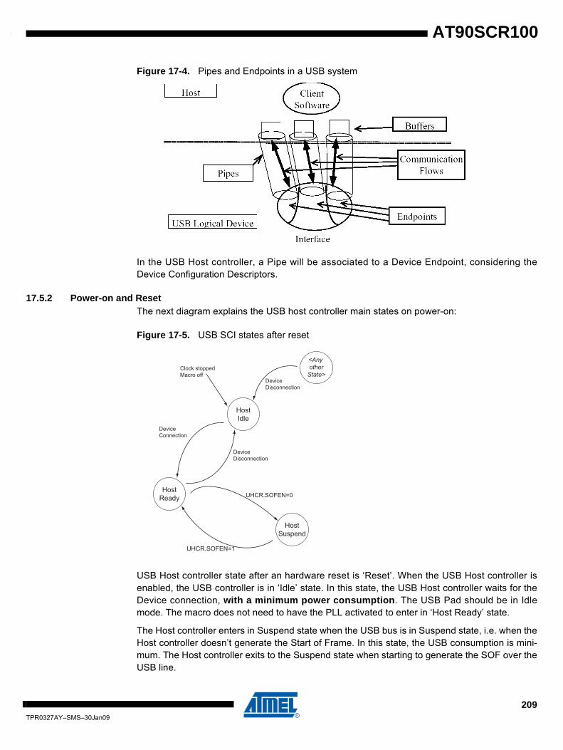
AT90SCR100
Figure 17-4. Pipes and Endpoints in a USB system
In the USB Host controller, a Pipe will be associated to a Device Endpoint, considering theDevice Configuration Descriptors.
17.5.2 Power-on and ResetThe next diagram explains the USB host controller main states on power-on:
Figure 17-5. USB SCI states after reset
USB Host controller state after an hardware reset is ‘Reset’. When the USB Host controller isenabled, the USB controller is in ‘Idle’ state. In this state, the USB Host controller waits for theDevice connection, with a minimum power consumption. The USB Pad should be in Idlemode. The macro does not need to have the PLL activated to enter in ‘Host Ready’ state.
The Host controller enters in Suspend state when the USB bus is in Suspend state, i.e. when theHost controller doesn’t generate the Start of Frame. In this state, the USB consumption is mini-mum. The Host controller exits to the Suspend state when starting to generate the SOF over theUSB line.
<Any other
State>
HostReady
HostIdle
UHCR.SOFEN=1
UHCR.SOFEN=0
DeviceConnection
Clock stoppedMacro off
DeviceDisconnection
DeviceDisconnection
HostSuspend
209TPR0327AY–SMS–30Jan09

17.5.3 Device DetectionA Device is detected by the USB controller when the USB bus if different from D+ and D- low. Inother words, when the USB Host Controller detects the Device pull-up on the D+ line. To enablethis detection, the Host Controller has to provide the Vbus power supply to the Device, thanks toCVcc pin.
The Device Disconnection is detected by the USB Host controller when the USB Idle correspondto D+ and D- low on the USB line.
17.5.4 Pipe SelectionPrior to any operation performed by the CPU, the Pipe must first be selected. This is done by:
• Clearing PNUMS.• Setting PNUM with the Pipe number which will be managed by the CPU.
The CPU can then access to the various Pipe registers and data.
17.5.5 Pipe ConfigurationThe following flow must be respected in order to activate a Pipe:
When a Device Disconnection event has been detected, you must reset the USBHost module, to reset the internal parameters and be able to support a newconnection.Caution
!
210TPR0327AY–SMS–30Jan09
AT90SCR100

AT90SCR100
Figure 17-6. Pipe activation flow:
Once the Pipe is activated (UPCRX.PEN set), the hardware is ready to send requests to theDevice.
When configured (UPSTAX.CFGOK=1), only the Pipe Token (UPCFG0X.PTOKEN) and thepolling interval for Interrupt pipe can be modified.
There are 4 pipes to configure. A Control type pipe supports only 1 bank (or data bank). Anyother value will lead to a configuration error (UPSTAX.CFGOK=0).
To guarantee a correct operation of the USB Host Controller:
• The pipe 0 size must not be greater than 32 bytes.• The pipe 1 size must not be greater than 64 bytes.• The pipe 2 size must not be greater than 64 bytes.• The pipe 3 size must not be greater than 8 bytes.
Pipe Activation
Pipe activatedand freezed
ERROR
UPCRX.PEN=1
Update UPCFG2X .INTFRQ(interrupt only)
Update: UPCFG0X .PTYPE .PTOKEN .PEPNUM
Configure the polling interval forinterrupt pipe
UPNUM.PNUM=X Select the pipe to configure
Select the pipe type:
Configure the Pipe memory:
- Type (Control, Isochronous, Bulk, I- Token (IN, OUT, SETUP)- Endpoint Number
Update: UPCFG1X .PSIZE .PBK .CFGMEM
- Pipesize- Number Of Banks
UPSTAX.CFGOK=1?
Caution!
211TPR0327AY–SMS–30Jan09

A clear of UPCRX.PEN will reset the configuration of the Pipe. All the corresponding Pipe regis-ters are reset to there reset values. Please refer to “Memory Management” section for moredetails.
17.5.6 USB ResetThe USB controller sends a USB Reset when the firmware set the UHCR.RESET bit. TheUHINT.RSTI bit is set by hardware when the USB Reset has been sent. This triggers an inter-rupt if the UHIEN.RSTE has been set.
When a USB Reset has been sent, all the Pipe configuration and the memory allocation arereset. The General Host interrupt enable register is left unchanged.
If the bus was previously in suspend mode (UHCR.SOFEN = 0), the USB controller automati-cally switches to the resume mode (UHINT.HWUPI is set) and the UHCR.SOFEN bit is set byhardware in order to generate SOF immediately after the USB Reset.
17.5.7 Address SetupOnce the Device has answer to the first Host requests with the default address (0), the Hostassigns a new address to the device. The Host controller has to send a USB reset to the deviceand perform a SET ADDRESS control request, with the new address to be used by the Device.This control request ended, the firmware writes the new address into the UHADDR register. Allfollowing requests, on every Pipes, will be performed using this new address.
When the Host controller sends a USB reset, the UHADDR register is reset by hardware and thefollowing Host requests will be performed using the default address (0).
17.5.8 Remote Wake-Up detectionThe Host Controller enters in Suspend mode when clearing the UHCR.SOFEN bit. No moreStart Of Frame is sent on the USB bus and the USB Device enters in Suspend mode 3ms later.
The Device awakes the Host Controller by sending an Upstream Resume (Remote Wake-Upfeature). The Host Controller detects a non-idle state on the USB bus and set the UHINT.HWUPIbit. If the non-Idle correspond to an Upstream Resume (K state), the UHINT.RXRSMI bit is setby hardware. The firmware has to generate a downstream resume within 1ms and for at least20ms by setting the UHCR.RESUME bit.
To initialize the communication with the USB device, the firmware has to configurethe Default Control Pipe with the following parameters:
• Type: Control• Token: SETUP• Data Bank:1• Size: 64 Bytes
The f irmware wi l l ask for 8 bytes of the Device Descriptor sending aGET_DESCRIPTOR request. These bytes contains the MaxPacketSize of theDevice default control endpoint and the firmware will then re-configure the size ofthe Default Control Pipe with this size parameter.
Note
212TPR0327AY–SMS–30Jan09
AT90SCR100

AT90SCR100
Once the downstream Resume has been generated, the UHCR.SOFE bit is automatically set byhardware in order to generate SOF immediately after the USB resume.
17.5.9 USB Pipe ResetThe firmware can reset a Pipe using the pipe reset register. The configuration of the pipe andthe data toggle remains unchanged. Only the bank management and the status bits are reset totheir initial values.
To completely reset a Pipe, the firmware has to disable and then enable the pipe.
17.5.10 Pipe Data AccessIn order to read or to write into the Pipe Fifo, the CPU selects the Pipe number with the UPNUMregister and performs read or write action on the UPDATX register.
17.5.11 Control Pipe managementA Control transaction is composed of 3 phases:
• SETUP• Data (IN or OUT)• Status (OUT or IN)
The firmware has to change the Token for each phase.
The initial data toggle is set for the corresponding token (ONLY for Control Pipe):
• SETUP: Data0• OUT: Data1• IN: Data1 (expected data toggle)
17.5.12 OUT Pipe managementThe Pipe must be configured and not frozen first.
17.5.12.1 “Manual” modeThe UPINTX.TXOUTI bit is set by hardware when the current bank becomes free. This triggersan interrupt if the UPIENX.TXOUTE bit is set. The UPINTX.FIFOCON bit is set at the same time.The CPU writes into the FIFO and clears the UPINTX.FIFOCON bit to allow the USB controllerto send the data.
If the OUT Pipe is composed of multiple banks, this also switches to the next data bank. TheUPINTX.TXOUTI and UPINTX.FIFOCON bits are automatically updated by hardware regardingthe status of the next bank.
HostReady
UHCR.SOFE=1or UHINT.HWUPI=1
UHCR.SOFEN=0
HostSuspend
If the firmware decides to switch to suspend mode (clear UHCR.SOFEN) even if abank is ready to be sent, the USB controller will automatically exit from Suspendmode and the bank will be sent.Note
213TPR0327AY–SMS–30Jan09

Figure 17-7. Example of OUT Data bank Management
17.5.12.2 “Autoswitch” modeIn this mode, the clear of the UPINTX.FIFOCON bit is performed automatically by hardwareeach time the Pipe bank is full. The firmware has to check if the next bank is empty or not beforewriting the next data. On UPINTX.TXOUTI interrupt, the firmware fills a complete bank. A newinterrupt will be generated each time the current bank becomes free.
OUT ACKDATA(Bank 0)
UPINTX.TXOUTI SW SW
UPINTX.FIFOCON SW SW
OUT
Write data from CPU Bank 0
Write data from CPU Bank 0
HW
OUT OUT ACKACKDATA(Bank 0)
DATA(Bank 1)
UPINTX.TXOUTI SW SW
UPINTX.FIFOCON SW
SW
Write data from CPU Bank 0
SW
Write data from CPU Bank 1
Write data from CPU Bank 0
HW
Example with 1 OUT data bank
Example with 2 OUT data banks
OUT OUT ACKACKDATA(Bank 0)
DATA(Bank 1)
UPINTX.TXOUTI SW SW
UPINTX.FIFOCON SW
SW
Write data from CPU Bank 0
SW
Write data from CPU Bank 1
Write data from CPU Bank 0
HW
Example with 2 OUT data banks
214TPR0327AY–SMS–30Jan09
AT90SCR100

AT90SCR100
17.5.13 IN Pipe management
17.5.13.1 “Manual” modeWhen the Host requires data from the device, the firmware has to determine first the IN mode touse using the INMODE bit:
• UPCRX.INMODE = 0. The UPINRQX register is taken in account. The Host controller will perform (UPINRQX+1) IN requests on the selected Pipe before freezing the Pipe. This mode avoids to have extra IN requests on a Pipe.
• UPCRX.INMODE = 1. The USB controller will perform infinite IN request until the firmware freezes the Pipe.
The IN request generation will start when the firmware clear the UPCRX.PFREEZE bit.
Each time the current bank is full, the UPINTX.RXINI and the UPINTX.FIFOCON bits are set.This triggers an interrupt if the UPIENX.RXINE bit is set. The firmware can acknowledge theUSB interrupt by clearing the UPINTX.RXINI bit. The Firmware reads the data and clears theUPINTX.FIFOCON bit in order to free the current bank. If the IN Pipeis composed of multiplebanks, clearing the UPINTX.FIFOCON bit will switch to the next bank. The RXINI and FIFOCONbits are then updated by hardware in accordance with the status of the new bank.
Figure 17-8. Example of IN Data bank Management
The Pipe must be configured first.Note
IN ACKDATA(to Bank 0)
UPINTX.RXINI SW SW
UPINTX.FIFOCON SW
Read data from CPUBank 0
Read data from CPUBank 0
HW
IN ACKDATA(to Bank 0)
HW
Example with 1 IN data bank
IN ACKDATA(to Bank 0)
UPINTX.RXINI SW SW
UPINTX.FIFOCON SW
Read data from CPUBank 0
Read data from CPUBank 1
HW
IN ACKDATA(to Bank 1)
HW
Example with 2 IN data banks
215TPR0327AY–SMS–30Jan09

17.5.13.2 “Autoswitch” modeIn this mode, the clear of the UPINTX.FIFOCON bit is performed automatically by hardwareeach time the Pipe bank is empty. The firmware has to check if the next bank is empty or notbefore reading the next data. On UPINTX.RXINI interrupt, the firmware reads a complete bank.A new interrupt will be generated each time the current bank contains data to read.
The acknowledge of the UPINTX.RXINI interrupt is always performed by software.
17.5.13.3 CRC Error (isochronous only)A CRC error can occur during IN stage if the USB controller detects a bad received packet. Inthis situation, the STALLEDI/CRCERRI interrupt is triggered. This does not prevent the RXINIinterrupt from being triggered.
17.6 Interrupt system
Figure 17-9. USB Host Controller Interrupt System
HWUPEUHIEN.6
HWUPIUHINT.6
HSOFIUHINT.5
HSOFEUHIEN.5
RXRSMIUHINT.4
RXRSMEUHIEN.4
RSMEDIUHINT.3
RSMEDEUHIEN.3
RSTIUHINT.2
RSTEUHIEN.2
DDISCIUHINT.1
DDISCEUHIEN.1
DCONNIUHINT.0
DCONNEUHIEN.0
USB Host Interrupt
216TPR0327AY–SMS–30Jan09
AT90SCR100

AT90SCR100
Figure 17-10. USB Host Controller Pipe Interrupt System
17.6.1 Idle and Power-DownThe CPU exits from Idle and Power-Down mode with any USB Interrupts.
17.7 USB Host Controller Registers
17.7.1 UHCR - USB Host Control Register
• Bit 7 - UHEN : USB Host EnableSet this bit to enable the USB Host Controller. This will connect CC4 and CC8 to USB Host blockoutput signals.
Clear this bit to disable USB Host controller and reconnect CC4 and CC8 pads to standardSmartCard Interface Block pads.
• Bit 6..5 - PAD1..0 : Pad TypeThese bits switch the D+/D- of the USB Host Controller outputs to specific pads as follow:
• 00 : Pad electrically compliant to USB 2.0 (USB Host pads)• 01 : Pad electrically compliant to USB-IC (SCIB pads)• Others : Reserved for future use
FLERREUPIEN.7
UNDERFIUPSTAX.5
OVERFIUPSTAX.6
NAKEDIUPINTX.6
NAKEDEUPIEN.6
PERRIUPINTX.4
PERREUPIEN.4
TXSTPIUPINTX.3
TXSTPEUPIEN.3
TXOUTIUPINTX.2
TXOUTEUPIEN.2
RXSTALLI
UPINTX.1RXSTALLE
UPIEN.1RXINI
UPINTX.0RXINE
UPIEN.0
FLERREUPIEN.7
PIPE 0
PIPE 1
PIPE 2
PIPE 3
USB HostPipe Interrupt
Bit 7 6 5 4 3 2 1 0
$009E UHEN PAD [1..0] FRZCLK - RESUME RESET SOFEN UHCRRead/write R/W R/W R/W R/W R R/W R/W R/W
Initial value 0 0 0 1 0 0 0 0 0x00
217TPR0327AY–SMS–30Jan09

• Bits 4 - FRZCLK : Freeze USB Clock BitSet to disable the PLL clock input (the ”Resume Detection” is still active). This reduces thepower consumption. Clear to enable the clock inputs.
• Bit 3 - Res : Reserved BitThis bit is a reserved bit. The value read from this bit is always 0. Do not set this bit.
• Bit 2 - RESUME : Send USB ResumeSet this bit to generate a USB Resume on the USB bus.
Cleared by hardware when the USB Resume has been sent. Clearing by software has no effect.
• Bit 1 - RESET : Send USB ResetSet this bit to generate a USB Reset on the USB bus.
Cleared by hardware when the USB Reset has been sent. Clearing by software has no effect.
Refer to the “USB Reset” section for more details.
• Bit 0 - SOFEN : Start Of Frame Generation ENableSet this bit to generate SOF on the USB bus.
Clear this bit to disable the SOF generation and to leave the USB bus in Idle state.
17.7.2 UHSR - USB Host Status Register
• Bits 7..4 - Res : Reserved BitsThese bits are reserved bits. The value read from these bits is always 0. Do not set these bits.
• Bit 3 - SPEED : Speed Status FlagSet by hardware when the controller is in FULL-SPEED mode. Cleared by hardware when thecontroller is in LOW-SPEED mode.
• Bit 2..0 - Res : Reserved BitsThese bits are reserved bits. The value read from these bits is always 0. Do not set these bits.
This bit is different from PRR1.PRUSBH which avoid providing clock to the statemachine of USB Host Controller, disabling the whole controller.
Note
Bit 7 6 5 4 3 2 1 0
$0099 - - - - SPEED - - - UHSRRead/write R R R R R R R R
Initial value 0 0 0 0 1 0 0 0 0x08
218TPR0327AY–SMS–30Jan09
AT90SCR100

AT90SCR100
17.7.3 UHINT - USB Host INTerrupt Register
• Bit 7 - Res : Reserved BitThis bit is reserved for future use. The value read from these bits is always 0. Do not set thesebits.
• Bit 6 - HWUPI : Host Wake-Up InterruptSet by hardware when a non-idle state is detected on the USB bus.
Shall be clear by software to acknowledge the interrupt. Setting by software has no effect.
• Bit 5 - HSOFI : Host Start Of Frame InterruptSet by hardware when a SOF is issued by the Host controller. This triggers a USB interruptwhen HSOFE is set.
Shall be cleared by software to acknowledge the interrupt. Setting by software has no effect.
• Bit 4 - RXRSMI : Upstream Resume Received Interrupt Set by hardware when an Upstream Resume has been received from the Device.
Shall be cleared by software. Setting by software has no effect.
• Bit 3 - RSMEDI : Downstream Resume Sent Interrupt Set by hardware when a Downstream Resume has been sent to the Device.
Shall be cleared by software. Setting by software has no effect.
• Bit 2 - RSTI : USB Reset Sent InterruptSet by hardware when a USB Reset has been sent to the Device.
Shall be cleared by software. Setting by software has no effect.
• Bit 1 - DDISCI :Device Disconnection InterruptSet by hardware when the device has been removed from the USB bus.
Shall be cleared by software. Setting by software has no effect.
After having detected a disconnection, please reset the USB Host. See “Device Detection” onpage 210.
• Bit 0 - DCONNI : Device Connection Interrupt Set by hardware when a new device has been connected to the USB bus.
Shall be cleared by software. Setting by software has no effect.
Bit 7 6 5 4 3 2 1 0
$009F - HWUPI HSOFI RXRSMI RSMEDI RSTI DDISCI DCONNI UHINTRead/write R R/W R/W R/W R/W R/W R/W R/W
Initial value 0 0 0 0 0 0 0 0 0x00
219TPR0327AY–SMS–30Jan09

17.7.4 UHIEN - USB Host Interrupt ENable Register
• Bit 7 - Res : Reserved BitThis bit is reserved for future use. The value read from these bits is always 0. Do not set thesebits.
• Bit 6 - HWUPE : Host Wake-Up Interrupt EnableSet this bit to enable HWUP interrupt.
Clear this bit to disable HWUP interrupt.
• Bit 5 - HSOFE : Host Start Of frame Interrupt EnableSet this bit to enable HSOF interrupt.
Clear this bit to disable HSOF interrupt.
• Bit 4 - RXRSME : Upstream Resume Received Interrupt Enable Set this bit to enable the RXRSMI interrupt.
Clear this bit to disable the RXRSMI interrupt.
• Bit 3 - RSMEDE : Downstream Resume Sent Interrupt EnableSet this bit to enable the RSMEDI interrupt.
Clear this bit to disable the RSMEDI interrupt.
• Bit 2 - RSTE : USB Reset Sent Interrupt Enable Set this bit to enable the RSTI interrupt.
Clear this bit to disable the RSTI interrupt.
• Bit 1 - DDISCE : Device Disconnection Interrupt EnableSet this bit to enable the DDISCI interrupt.
Clear this bit to disable the DDISCI interrupt.
After having detected a disconnection, please reset the USB Host. See “Device Detection” onpage 210.
• Bit 0 - DCONNE : Device Connection Interrupt EnableSet this bit to enable the DCONNI interrupt.
Clear this bit to disable the DCONNI interrupt.
Bit 7 6 5 4 3 2 1 0
$00A0 - HWUPE HSOFE RXRSME RSMEDE RSTE DDISCE DCONNE UHIENRead/write R R/W R/W R/W R/W R/W R/W R/W
Initial value 0 0 0 0 0 0 0 0 0x00
220TPR0327AY–SMS–30Jan09
AT90SCR100

AT90SCR100
17.7.5 UHADDR - USB Host ADDRess Register
• Bit 7 - Res : Reserved BitThis bit is reserved for future use. The value read from this bit is always 0. Do not set this bit.
• Bits 6..0 - HADDR6..0 : USB Host AddressThese bits contains the address of the USB Device.
17.7.6 UHFNUM - USB Host Frame Number Registers
• Bits 15..11 - Res : Reserved BitsThese bits are reserved for future use. The value read from these bits is always 0. Do not setthese bits.
• Bits 10..0 - FNUM10..0 - Frame Number The value contained in tis register is the current SOF number.
This value can be modified by software.
17.7.7 UHFLEN - USB Host Frame Length Register
• Bits 7..0 - FLEN7..0 : Frame LengthThe value contained the data frame length transmitted
Bit 7 6 5 4 3 2 1 0
$00A1 - HADDR [6..0] UHADDRRead/write R R/W R/W R/W R/W R/W R/W R/W
Initial value 0 0 0 0 0 0 0 0 0x00
Bit 15 14 13 12 11 10 9 8
$00A3 - - - - - FNUM [10..8] UHFNUMH$00A2 FNUM [7..0] UHFNUMLBit 7 6 5 4 3 2 1 0
Read/write R R R R R R R R
R R R R R R R R
Initial value 0 0 0 0 0 0 0 0 0x00
0 0 0 0 0 0 0 0 0x00
Bit 7 6 5 4 3 2 1 0
$00A4 FLEN [7..0] UHFLENRead/write R R R R R R R R
Initial value 0 0 0 0 0 0 0 0 0x00
221TPR0327AY–SMS–30Jan09

17.7.8 UPNUM - USB Pipe Number Register
• Bits 7..2 - Res : Reserved BitsThe value read from these bits is always 0. Do not set these bits.
• Bits 1..0 - PNUM1..0 : Pipe NumberSelect the pipe using this register. The USB Host registers ended by a X correspond then to thisnumber.
This number is used for the USB controller following the value of the PNUMD bit.
17.7.9 UPRST - USB Pipe Reset Register
• Bits 7..4 - Res : Reserved BitsThe value read from these bits is always 0. Do not set these bits.
• Bit 3 - P3RST : Pipe 3 Reset Set this bit to 1 and reset this bit to 0 to reset the Pipe 3.
• Bit 2 - P2RST : Pipe 2 ResetSet this bit to 1 and reset this bit to 0 to reset the Pipe 2.
• Bit 1 - P1RST : Pipe 1 ResetSet this bit to 1 and reset this bit to 0 to reset the Pipe 1.
• Bit 0 - P0RST : Pipe 0 Reset Set this bit to 1 and reset this bit to 0 to reset the Pipe 0.
17.7.10 UPCRX - USB Pipe Control Register for Pipe XSet UPNUM register to point to the relevant Pipe before updating the UPCRX register.
• Bit 7 - Res : ReservedThis bit is reserved. The value read from these bits is always 0. Do not set these bits.
Bit 7 6 5 4 3 2 1 0
$00A7 - PNUM1 PNUM0 UPNUMRead/write R R R R R R R/W R/W
Initial value 0 0 0 0 0 0 0 0 0x00
Bit 7 6 5 4 3 2 1 0
$00A8 - - - - P3RST P2RST P1RST P0RST UPRSTRead/write R R R R R/W R/W R/W R/W
Initial value 0 0 0 0 0 0 0 0 0x00
Bit 7 6 5 4 3 2 1 0
$00A9 - PFREEZE INMODE - RSTDT - - PEN UPCRXRead/write R R/W R/W R R/W R R R/W
Initial value 0 0 0 0 0 0 0 0 0x00
222TPR0327AY–SMS–30Jan09
AT90SCR100

AT90SCR100
• Bit 6 - PFREEZE : Pipe FreezeSet this bit to Freeze the Pipe requests generation.
Clear this bit to enable the Pipe request generation.
This bit is set by hardware when:
• The pipe is not configured• A STALL handshake has been received on this Pipe• An error occurs on the Pipe (PERR = 1)• (INRQ+1) In requests have been processed
This bit is set at 1 by hardware after a Pipe reset or a Pipe enable.
• Bit 5 - INMODE : IN Request mode Set this bit to allow the USB controller to perform infinite IN requests when the Pipe is not frozen.
Clear this bit to perform a pre-defined number of IN requests. This number is stored in the UIN-RQX register.
• Bit 4 - Res : Reserved BitThis bit is reserved. The value read from these bits is always 0. Do not set these bits.
• Bit 3 - RSTDT : Reset Data ToggleSet this bit to reset the Data Toggle to its initial value for the current Pipe.
Cleared by hardware when proceed. Clearing by software has no effect.
• Bits 2..1 -Res : Reserved BitsThe value read from these bits is always 0. Do not set these bits.
• Bit 0 - PEN : Pipe EnableSet to enable the Pipe.
Clear to disable and reset the Pipe.
17.7.11 UPCFG0X - USB Pipe Configuration Register 0 for Pipe XSet UPNUM register to point to the relevant Pipe before updating the UPCFG0X register.
• Bits 7..6 - PTYPE1..0 : Pipe TypeSelect the type of the Pipe:
• 00: Control• 01: Isochronous• 10: Bulk• 11: Interrupt
Bit 7 6 5 4 3 2 1 0
$00AA PTYPE [1..0] PTOKEN [1..0] PEPNUM [3..0] UPCFG0XRead/write R/W R/W R/W R/W R/W R/W R/W R/W
Initial value 0 0 0 0 0 0 0 0 0x00
223TPR0327AY–SMS–30Jan09

• Bits 5..4 - PTOKEN1..0 : Pipe Token Select the Token to associate to the Pipe
• 00: SETUP• 01: IN• 10: OUT• 11: reserved
• Bits 3..0 - PEPNUM3..0 : Pipe Endpoint Number Set this field according to the Pipe configuration. Set the number of the Endpoint targeted by thePipe. This value is from 0 and 15.
17.7.12 UPCFG1X - USB Pipe Configuration Register 1 for Pipe XSet UPNUM register to point to the relevant Pipe before updating the UPCFG1X register.
• Bit 7 - Res : ReservedThis bit is reserved. The value read from these bits is always 0. Do not set these bits.
• Bits 6..4 - PSIZE0..2 : Pipe SizeSelect the size of the Pipe:
• 000: 8• 001: 16• 010: 32• 011: 64• Other: Reserved
• Bits 3..2 - PBK0..1 : Pipe BankSelect the number of banks to declare for the current pipe!
• 00: 1bank• 01: 2banks• Others: reserved
• Bit 1 - ALLOC : Configure Pipe MemorySet to configure the pipe memory with the characteristics.
Clear to update the memory allocation. Refer to the “Memory Management” chapter for moredetails.
• Bit 0 - Res : ReservedThis bit is reserved. The value read from these bits is always 0. Do not set these bits.
Bit 7 6 5 4 3 2 1 0
$00AB - PSIZE [0..2] PBK [0..1] ALLOC UPCFG1XRead/write R R/W R/W R/W R/W R/W R/W R
Initial value 0 0 0 0 0 0 0 0 0x00
224TPR0327AY–SMS–30Jan09
AT90SCR100

AT90SCR100
17.7.13 UPCFG2X - USB Pipe Configuration Register 2 for Pipe XSet UPNUM register to point to the relevant Pipe before updating the UPCFG2X register.
• Bits 7..0 - INTFRQ7..0 : Interrupt Pipe Request FrequencyThese bits are the maximum value in millisecond of the pulling period for an Interrupt Pipe.
17.7.14 UPSTAX - USB Pipe Status Register for Pipe XSet UPNUM register to point to the relevant Pipe before using the UPSTAX register.
• Bit 7 - CFGOK : Configure Pipe Memory OKSet by hardware if the required memory configuration has been successfully performed.
Cleared by hardware when the pipe is disabled. The USB reset and the reset pipe have no effecton the configuration of the pipe.
• Bit 6 - OVERFI : OverflowSet by hardware when a the current Pipe has received more data than the maximum length ofthe current Pipe. An interrupt is triggered if the FLERRE bit is set.
Shall be cleared by software. Setting by software has no effect.
• Bit 5 - UNDERFI : UnderflowSet by hardware when a transaction underflow occurs in the current isochronous or interruptPipe. The Pipe can’t send the data flow required by the device. A ZLP will be sent instead. Aninterrupt is triggered if the FLERRE bit is set.
Shall be cleared by software. Setting by software has no effect.
• Bit 4 - Res : ReservedThe value read from these bits is always 0. Do not set these bits.
• Bits 3..2 - DTSEQ1..0 : Toggle Sequencing Flag
Bit 7 6 5 4 3 2 1 0
$00AD INTFRQ [7..0] UPCFG2XRead/write R/W R/W R/W R/W R/W R/W R/W R/W
Initial value 0 0 0 0 0 0 0 0 0x00
This value has no effect for a non-Interrupt Pipe.Note
Bit 7 6 5 4 3 2 1 0
$00AC CFGOK OVERFI UNDERFI - DTSEQ [1..0] NBUSYBK [1..0] UPSTAXRead/write R R/W R/W R R R R R
Initial value 0 0 0 0 0 0 0 0 0x00
The Host controller has to send a OUT packet, but the bank is empty. A ZLP willbe sent and the UNDERFI bit is set underflow for interrupt Pipe.
Note
225TPR0327AY–SMS–30Jan09
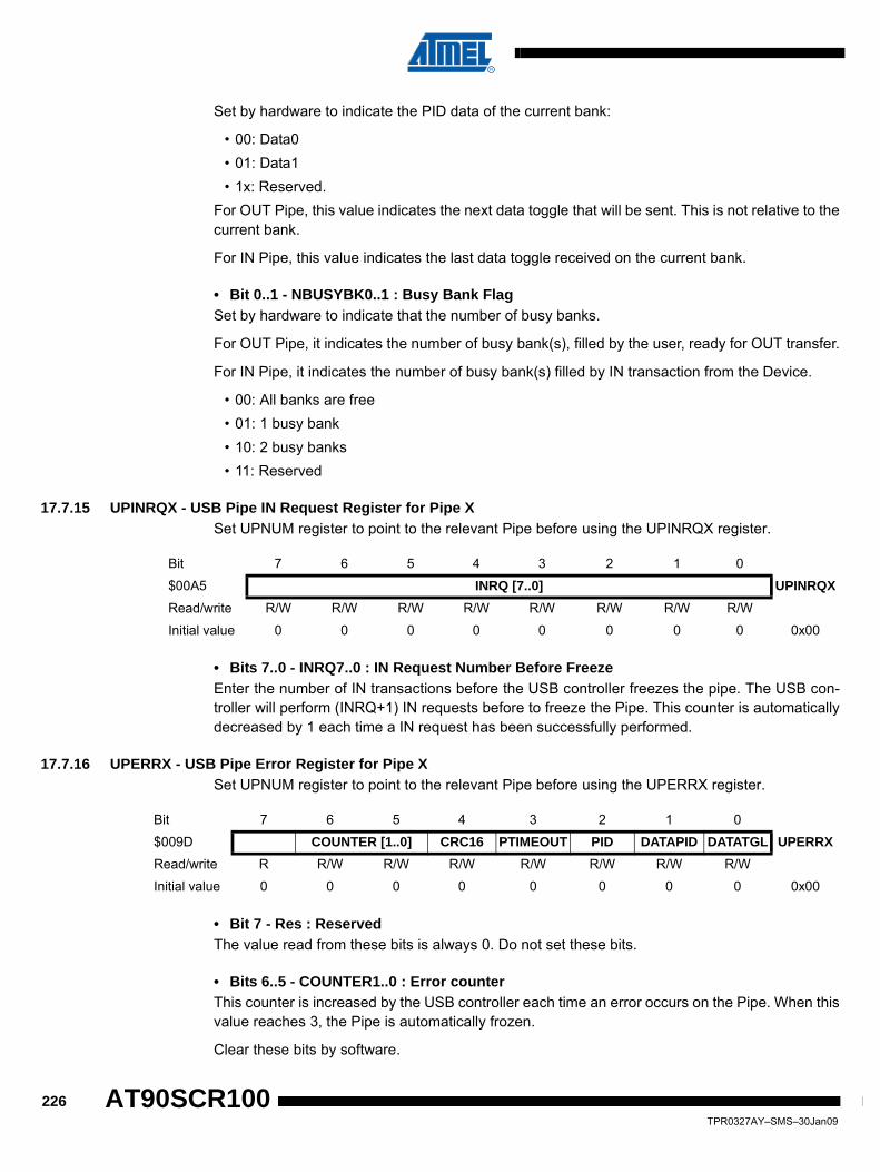
Set by hardware to indicate the PID data of the current bank:
• 00: Data0• 01: Data1• 1x: Reserved.
For OUT Pipe, this value indicates the next data toggle that will be sent. This is not relative to thecurrent bank.
For IN Pipe, this value indicates the last data toggle received on the current bank.
• Bit 0..1 - NBUSYBK0..1 : Busy Bank FlagSet by hardware to indicate that the number of busy banks.
For OUT Pipe, it indicates the number of busy bank(s), filled by the user, ready for OUT transfer.
For IN Pipe, it indicates the number of busy bank(s) filled by IN transaction from the Device.
• 00: All banks are free • 01: 1 busy bank • 10: 2 busy banks • 11: Reserved
17.7.15 UPINRQX - USB Pipe IN Request Register for Pipe XSet UPNUM register to point to the relevant Pipe before using the UPINRQX register.
• Bits 7..0 - INRQ7..0 : IN Request Number Before FreezeEnter the number of IN transactions before the USB controller freezes the pipe. The USB con-troller will perform (INRQ+1) IN requests before to freeze the Pipe. This counter is automaticallydecreased by 1 each time a IN request has been successfully performed.
17.7.16 UPERRX - USB Pipe Error Register for Pipe XSet UPNUM register to point to the relevant Pipe before using the UPERRX register.
• Bit 7 - Res : ReservedThe value read from these bits is always 0. Do not set these bits.
• Bits 6..5 - COUNTER1..0 : Error counterThis counter is increased by the USB controller each time an error occurs on the Pipe. When thisvalue reaches 3, the Pipe is automatically frozen.
Clear these bits by software.
Bit 7 6 5 4 3 2 1 0
$00A5 INRQ [7..0] UPINRQXRead/write R/W R/W R/W R/W R/W R/W R/W R/W
Initial value 0 0 0 0 0 0 0 0 0x00
Bit 7 6 5 4 3 2 1 0
$009D COUNTER [1..0] CRC16 PTIMEOUT PID DATAPID DATATGL UPERRXRead/write R R/W R/W R/W R/W R/W R/W R/W
Initial value 0 0 0 0 0 0 0 0 0x00
226TPR0327AY–SMS–30Jan09
AT90SCR100

AT90SCR100
• Bit 4 - CRC16 : CRC16 ErrorSet by hardware when a CRC16 error has been detected.
Shall be cleared by software. Setting by software has no effect.
• Bit 3 - PTIMEOUT - Pipe Time-out ErrorSet by hardware when a time-out error has been detected.
Shall be cleared by software. Setting by software has no effect.
• Bit 2 - PID - PID Error Set by hardware when a PID error has been detected.
Shall be cleared by software. Setting by software has no effect.
• Bit 1 - DATAPID - Data PID ErrorSet by hardware when a data PID error has been detected.
Shall be cleared by software. Setting by software has no effect.
• Bit 0 - DATATGL - Bad Data ToggleSet by hardware when a data toggle error has been detected.
Shall be cleared by software. Setting by software has no effect.
17.7.17 UPINTX - USB Pipe INTerrupt Register for Pipe XSet UPNUM register to point to the relevant Pipe before using the UPINTX register.
• Bit 7 - FIFOCON : FIFO ControlFor OUT and SETUP Pipe:
Set by hardware when the current bank is free, at the same time than TXOUT or TXSTP.
Clear to send the FIFO data. Setting by software has no effect.
For IN Pipe:
Set by hardware when a new IN message is stored in the current bank, at the same time thanRXIN.
Clear to free the current bank and to switch to the following bank. Setting by software has noeffect.
• Bit 6 - NAKEDI : NAK Handshake receivedSet by hardware when a NAK has been received on the current bank of the Pipe. This triggersan interrupt if the NAKEDE bit is set in the UPIENX register.
Shall be clear to handshake the interrupt. Setting by software has no effect.
• Bit 5 - RWAL : Read/Write Allowed
Bit 7 6 5 4 3 2 1 0
$00A6 FIFOCON NAKEDI RWAL PERRI TXSTPI TXOUTI RXSTALLI RXINI UPINTXRead/write R/W R/W R/W R/W R/W R/W R/W R/W
Initial value 0 0 0 0 0 0 0 0 0x00
227TPR0327AY–SMS–30Jan09

OUT Pipe:
Set by hardware when the firmware can write a new data into the Pipe FIFO.
Cleared by hardware when the current Pipe FIFO is full.
IN Pipe:
Set by hardware when the firmware can read a new data into the Pipe FIFO.
Cleared by hardware when the current Pipe FIFO is empty.
This bit is also cleared by hardware when the RXSTALL or the PERR bit is set
• Bit 4 - PERRI : PIPE ErrorSet by hardware when an error occurs on the current bank of the Pipe. This triggers an interruptif the PERRE bit is set in the UPIENX register. Refers to the UPERRX register to determine thesource of the error.
Automatically cleared by hardware when the error source bit is cleared.
• Bit 3 - TXSTPI : SETUP Bank readySet by hardware when the current SETUP bank is free and can be filled. This triggers an inter-rupt if the TXSTPE bit is set in the UPIENX register.
Shall be cleared to handshake the interrupt. Setting by software has no effect.
• Bit 2 - TXOUTI : OUT Bank ready Set by hardware when the current OUT bank is free and can be filled. This triggers an interrupt ifthe TXOUTE bit is set in the UPIENX register.
Shall be cleared to handshake the interrupt. Setting by software has no effect.
• Bit 1 - RXSTALLI / CRCERR : STALL Received / Isochronous CRC ErrorSet by hardware when a STALL handshake has been received on the current bank of the Pipe.The Pipe is automatically frozen. This triggers an interrupt if the RXSTALLE bit is set in the UPI-ENX register.
Shall be cleared to handshake the interrupt. Setting by software has no effect.
For Isochronous Pipe:
Set by hardware when a CRC error occurs on the current bank of the Pipe. This triggers an inter-rupt if the TXSTPE bit is set in the UPIENX register.
Shall be cleared to handshake the interrupt. Setting by software has no effect.
• Bit 0 - RXINI : IN Data received Set by hardware when a new USB message is stored in the current bank of the Pipe. This trig-gers an interrupt if the RXINE bit is set in the UPIENX register.
Shall be cleared to handshake the interrupt. Setting by software has no effect.
228TPR0327AY–SMS–30Jan09
AT90SCR100

AT90SCR100
17.7.18 UPIENX - USB Pipe Interrupt ENable Register for Pipe XSet UPNUM register to point to the relevant Pipe before using the UPIENX register.
• Bit 7 - FLERRE : Flow Error Interrupt enableSet to enable the OVERFI and UNDERFI interrupts.
Clear to disable the OVERFI and UNDERFI interrupts.
• Bit 6 - NAKEDE : NAK Handshake Received Interrupt EnableSet to enable the NAKEDI interrupt.
Clear to disable the NAKEDI interrupt.
• Bit 5 - Res : ReservedThe value read from these bits is always 0. Do not set these bits.
• Bit 4 - PERRE : PIPE Error Interrupt EnableSet to enable the PERRI interrupt.
Clear to disable the PERRI interrupt.
• Bit 3 - TXSTPE : SETUP Bank ready Interrupt EnableSet to enable the TXSTPI interrupt.
Clear to disable the TXSTPI interrupt.
• Bit 2 - TXOUTE : OUT Bank ready Interrupt EnableSet to enable the TXOUTI interrupt.
Clear to disable the TXOUTI interrupt.
• Bit 1 - RXSTALLE : STALL Received Interrupt EnableSet to enable the RXSTALLI interrupt.
Clear to disable the RXSTALLI interrupt.
• Bit 0 - RXINE : IN Data received Interrupt EnableSet to enable the RXINI interrupt.
Clear to disable the RXINI interrupt.
17.7.19 UPDATX - USB Pipe Data Register for Pipe XSet UPNUM register to point to the relevant Pipe before using the UPDATX register.
Bit 7 6 5 4 3 2 1 0
$00AE FLERRE NAKEDE - PERRE TXSTPE TXOUTE RXSTALLE RXINE UPIENXRead/write R/W R/W R R/W R/W R/W R/W R/W
Initial value 0 0 0 0 0 0 0 0 0x00
Bit 7 6 5 4 3 2 1 0
$00AF PDAT [7..0] UPDATXRead/write R/W R/W R R/W R/W R/W R/W R/W
Initial value 0 0 0 0 0 0 0 0 0x00
229TPR0327AY–SMS–30Jan09

• Bits 7..0 - PDAT7..0 : Pipe Data BitsSet by the software to read/write a byte from/to the Pipe FIFO selected by PNUM.
17.7.20 UPBCX - USB Pipe Byte Count Register for Pipe XSet UPNUM register to point to the relevant Pipe before using the UPBCXH and UPBCXLregisters.
• Bits 15..11 - Res : ReservedThe value read from these bits is always 0. Do not set these bits.
• Bits 10..0 - PBYCT10..0 : Byte count BitsSet by hardware.
PBYCT10:0 is:
• (for OUT Pipe) increased after each writing into the Pipe and decremented after each byte sent,
• (for IN Pipe) increased after each byte received by the host, and decremented after each byte read by the software.
17.7.21 UPINT - USB Pipe Interrupt Register
• Bits 7..4 - Res : ReservedThe value read from these bits is always 0. Do not set these bits.
• Bits 3..0 - PINT3..0 : Pipe Interrupts BitsSet by hardware when an interrupt is triggered by the UPINTX register and if the correspondingendpoint interrupt enable bit is set.
Cleared by hardware when the interrupt source is served.
Bit 15 14 13 12 11 10 9 8
$009C - - - - - PBYTCT [10..8] UPBCXH$009B PBYTCT [7..0] UPBCXLBit 7 6 5 4 3 2 1 0
Read/write R R R R R R/W R/W R/W
R/W R/W R/W R/W R/W R/W R/W R/W
Initial value 0 0 0 0 0 0 0 0 0x00
0 0 0 0 0 0 0 0 0x00
Bit 7 6 5 4 3 2 1 0
$009A - - - - PINT3 PINT2 PINT1 PINT0 UPINTRead/write R R R R R R R R
Initial value 0 0 0 0 0 0 0 0 0x00
230TPR0327AY–SMS–30Jan09
AT90SCR100

AT90SCR100
18. USARTThe Universal Synchronous and Asynchronous serial Receiver and Transmitter (USART) is ahighly flexible serial communication device.
18.1 Features• Full Duplex Operation (Independent Serial Receive and Transmit Registers)• Asynchronous or Synchronous Operation• Master or Slave Clocked Synchronous Operation• High Resolution Baud Rate Generator• Supports Serial Frames with 5, 6, 7, 8, or 9 Data Bits and 1 or 2 Stop Bits• Odd or Even Parity Generation and Parity Check Supported by Hardware• Data OverRun Detection• Framing Error Detection• Noise Filtering Includes False Start Bit Detection and Digital Low Pass Filter• Three Separate Interrupts on TX Complete, TX Data Register Empty and RX Complete• Multi-processor Communication Mode• Double Speed Asynchronous Communication Mode
18.2 USART0The AT90SCR100 has one USART, USART0.
18.3 OverviewA simplified block diagram of the USART Transmitter is shown in Figure 18-1 on page 232. CPUaccessible I/O Registers and I/O pins are shown in bold.
The Power Reducion USART0 bit, PRUSART0, in TBC must be disabled by writing a logicalzero to it.
231TPR0327AY–SMS–30Jan09

Figure 18-1. USART Block Diagram
The dashed boxes in the block diagram separate the three main parts of the USART (listed fromthe top): Clock Generator, Transmitter and Receiver. Control Registers are shared by all units.The Clock Generation logic consists of synchronization logic for external clock input used bysynchronous slave operation, and the baud rate generator. The XCK (Transfer Clock) pin is onlyused by synchronous transfer mode. The Transmitter consists of a single write buffer, a serialShift Register, Parity Generator and Control logic for handling different serial frame formats. Thewrite buffer allows a continuous transfer of data without any delay between frames. TheReceiver is the most complex part of the USART module due to its clock and data recoveryunits. The recovery units are used for asynchronous data reception. In addition to the recoveryunits, the Receiver includes a Parity Checker, Control logic, a Shift Register and a two levelreceive buffer (UDR0). The Receiver supports the same frame formats as the Transmitter, andcan detect Frame Error, Data OverRun and Parity Errors.
18.4 Clock GenerationThe Clock Generation logic generates the base clock for the Transmitter and Receiver. TheUSART0 supports four modes of clock operation: Normal asynchronous, Double Speed asyn-
PARITYGENERATOR
UBRR[H:L]
UDR (Transmit)
UCSRA UCSRB UCSRC
BAUD RATE GENERATOR
TRANSMIT SHIFT REGISTER
RECEIVE SHIFT REGISTER RxD
TxDPINCONTROL
UDR (Receive)
PINCONTROL
XCK
DATARECOVERY
CLOCKRECOVERY
PINCONTROL
TXCONTROL
RXCONTROL
PARITYCHECKER
DAT
A B
US
OSC
SYNC LOGIC
Clock Generator
Transmitter
Receiver
232TPR0327AY–SMS–30Jan09
AT90SCR100

AT90SCR100
chronous, Master synchronous and Slave synchronous mode. The UMSEL0 bit in USARTControl and Status Register C (UCSR0C) selects between asynchronous and synchronousoperation. Double Speed (asynchronous mode only) is controlled by the U2X0 found in theUCSR0A Register. When using synchronous mode (UMSEL0 = 1), the Data Direction Registerfor the XCK pin (DDR_XCK) controls whether the clock source is internal (Master mode) orexternal (Slave mode). The XCK pin is only active when using synchronous mode.
Figure 18-2. Clock Generation Logic, Block Diagram
Signal description:
txclk Transmitter clock (Internal Signal).
rxclk Receiver base clock (Internal Signal).
xcki Input from XCK pin (internal Signal). Used for synchronous slaveoperation.
xcko Clock output to XCK pin (Internal Signal). Used for synchronous masteroperation.
fOSC UART Block clock: clkIO
18.4.1 Internal Clock Generation – The Baud Rate GeneratorInternal clock generation is used for the asynchronous and the synchronous master modes ofoperation. The description in this section refers to Figure 18-2.
The USART Baud Rate Register (UBRR0) and the down-counter connected to it function as aprogrammable prescaler or baud rate generator. The down-counter, running at system clock(fosc), is loaded with the UBRR0 value each time the counter has counted down to zero or whenthe UBRRL0 Register is written. A clock is generated each time the counter reaches zero. Thisclock is the baud rate generator clock output (= fosc/(UBRR0+1)). The Transmitter divides thebaud rate generator clock output by 2, 8 or 16 depending on mode. The baud rate generator out-put is used directly by the Receiver’s clock and data recovery units. However, the recovery unitsuse a state machine that uses 2, 8 or 16 states depending on mode set by the state of theUMSEL0, U2X0 and DDR_XCK bits.
PrescalingDown-Counter /2
UBRR
/4 /2
fosc
UBRR+1
SyncRegister
Clkor XCK
XCKPin
txclk
U2X
UMSEL
DDR_XCK
0
1
0
1
xcki
io
xcko
DDR_XCKrxclk
0
1
1
0Edge
Detector
UCPOL
233TPR0327AY–SMS–30Jan09

Table 18-1 contains equations for calculating the baud rate (in bits per second) and for calculat-ing the UBRR0 value for each mode of operation using an internally generated clock source.
Some examples of UBRR0 values for some system clock frequencies are found in Table 18-9 onpage 254.
18.4.2 Double Speed Operation (U2X0)The transfer rate can be doubled by setting the U2X0 bit in UCSR0A. Setting this bit only haseffect for the asynchronous operation. Set this bit to zero when using synchronous operation.
Setting this bit will reduce the divisor of the baud rate divider from 16 to 8, effectively doublingthe transfer rate for asynchronous communication. Note however that the Receiver will in thiscase only use half the number of samples (reduced from 16 to 8) for data sampling and clockrecovery, and therefore a more accurate baud rate setting and system clock are required whenthis mode is used. For the Transmitter, there are no downsides.
Table 18-1. Equations for Calculating Baud Rate Register Setting
Operating ModeEquation for Calculating Baud
Rate (1)
1. The baud rate is defined to be the transfer rate in bit per second (bps)BAUDBaud rate (in bits per second, bps)fOSCSystem Oscillator clock frequency injected in UART block: clkIO
UBRRnContents of the UBRRH0 and UBRRL0 Registers, (0-4095)
Equation for Calculating UBRR Value
Asynchronous Normal mode (U2X0 = 0)
Asynchronous Double Speed mode (U2X0 = 1)
Synchronous Master mode
BAUDfOSC
16 UBRR0 1+( )------------------------------------------= UBRR0fOSC
16BAUD------------------------ 1–=
BAUDfOSC
8 UBRR0 1+( )---------------------------------------= UBRR0fOSC
8BAUD-------------------- 1–=
BAUDfOSC
2 UBRR0 1+( )---------------------------------------= UBRR0
fOSC2BAUD-------------------- 1–=
234TPR0327AY–SMS–30Jan09
AT90SCR100

AT90SCR100
18.4.3 External ClockExternal clocking is used by the synchronous slave modes of operation. The description in thissection refers to Figure 18-2 for details.
External clock input from the XCK pin is sampled by a synchronization register to minimize thechance of meta-stability. The output from the synchronization register must then pass throughan edge detector before it can be used by the Transmitter and Receiver. This process intro-duces a two CPU clock period delay and therefore the maximum external XCK clock frequencyis limited by the following equation:
18.4.4 Synchronous Clock OperationWhen synchronous mode is used (UMSEL0 = 1), the XCK pin will be used as either clock input(Slave) or clock output (Master). The dependency between the clock edges and data samplingor data change is the same. The basic principle is that data input (on RxD0) is sampled at theopposite XCK clock edge of the edge the data output (TxD0) is changed.
Figure 18-3. Synchronous Mode XCK Timing.
The UCPOL0 bit UCRSC selects which XCK clock edge is used for data sampling and which isused for data change. As Figure 18-3 shows, when UCPOL0 is zero the data will be changed atrising XCK edge and sampled at falling XCK edge. If UCPOL0 is set, the data will be changed atfalling XCK edge and sampled at rising XCK edge.
18.5 Frame FormatsA serial frame is defined to be one character of data bits with synchronization bits (start and stopbits), and optionally a parity bit for error checking. The USART accepts all 30 combinations ofthe following as valid frame formats:
• 1 start bit• 5, 6, 7, 8, or 9 data bits• no, even or odd parity bit• 1 or 2 stop bits
A frame starts with the start bit followed by the least significant data bit. Then the next data bits,up to a total of nine, are succeeding, ending with the most significant bit. If enabled, the parity bit
fXCKfOSC
4-----------<
RxD / TxD
XCK
RxD / TxD
XCKUCPOL = 0
UCPOL = 1
Sample
Sample
235TPR0327AY–SMS–30Jan09
is inserted after the data bits, before the stop bits. When a complete frame is transmitted, it canbe directly followed by a new frame, or the communication line can be set to an idle (high) state.Figure 18-4 illustrates the possible combinations of the frame formats. Bits inside brackets areoptional.
Figure 18-4. Frame Formats
St Start bit, always low.
(n) Data bits (0 to 8).
P Parity bit. Can be odd or even.
Sp Stop bit, always high.
IDLE No transfers on the communication line (RxD0 or TxD0). An IDLE linemust be
high.
The frame format used by the USART is set by the UCSZ02:0, UPM01:0 and USBS0 bits inUCSR0B and UCSR0C. The Receiver and Transmitter use the same setting. Note that changingthe setting of any of these bits will corrupt all ongoing communication for both the Receiver andTransmitter.
The USART Character SiZe (UCSZ02:0) bits select the number of data bits in the frame. TheUSART Parity mode (UPM01:0) bits enable and set the type of parity bit. The selection betweenone or two stop bits is done by the USART Stop Bit Select (USBS0) bit. The Receiver ignoresthe second stop bit. An FE (Frame Error) will therefore only be detected in the cases where thefirst stop bit is zero.
18.5.1 Parity Bit CalculationThe parity bit is calculated by doing an exclusive-or of all the data bits. If odd parity is used, theresult of the exclusive or is inverted. The relation between the parity bit and data bits is asfollows::
Peven Parity bit using even parity
Podd Parity bit using odd parity
dn Data bit n of the character
If used, the parity bit is located between the last data bit and first stop bit of a serial frame.
18.6 USART InitializationThe USART has to be initialized before any communication can take place. The initialization pro-cess normally consists of setting the baud rate, setting frame format and enabling theTransmitter or the Receiver depending on the usage. For interrupt driven by USART operation,
10 2 3 4 [5] [6] [7] [8] [P]St Sp1 [Sp2] (St / IDLE)(IDLE)
FRAME
Peven dn 1– … d3 d2 d1 d0 0Podd
⊕ ⊕ ⊕ ⊕ ⊕ ⊕dn 1– … d3 d2 d1 d0 1⊕ ⊕ ⊕ ⊕ ⊕ ⊕
==
236TPR0327AY–SMS–30Jan09
AT90SCR100

AT90SCR100
the Global Interrupt Flag should be cleared (and interrupts globally disabled) when doing theinitialization.
Before doing a re-initialization with changed baud rate or frame format, be sure that there are noongoing transmissions during the period the registers are changed. The TXC0 Flag can be usedto check that the Transmitter has completed all transfers, and the RXC Flag can be used tocheck that there are no unread data in the receive buffer.
The following simple USART initialization code examples show one assembly and one C func-tion that are equal in functionality. The examples assume asynchronous operation using polling(no interrupts enabled) and a fixed frame format. The baud rate is given as a function parameter.For the assembly code, the baud rate parameter is assumed to be stored in the r17:r16Registers.
Note: 1. See “About Code Examples” on page 11.
More advanced initialization routines can be made that include frame format as parameters, dis-able interrupts and so on. However, many applications use a fixed setting of the baud andcontrol registers, and for these types of applications the initialization code can be placed directlyin the main routine, or be combined with initialization code for other I/O modules.
The TXC0 Flag must be cleared before each transmission (before UDR0 is writ-ten) if it is used for this purpose.
Assembly Code Example(1)
USART_Init:
; Set baud rate
out UBRRH0, r17
out UBRRLn0 r16
; Enable receiver and transmitter
ldi r16, (1<<RXEN0)|(1<<TXEN0)
out UCSR0B,r16
; Set frame format: 8data, 2stop bit
ldi r16, (1<<USBS0)|(3<<UCSZ00)
out UCSR0C,r16
ret
C Code Example (1)
void USART_Init( unsigned int baud )
{
/* Set baud rate */
UBRRH0 = (unsigned char)(baud>>8);
UBRRL0 = (unsigned char)baud;
/* Enable receiver and transmitter */
UCSR0B = (1<<RXEN0)|(1<<TXEN0);
/* Set frame format: 8data, 2stop bit */
UCSR0C = (1<<USBS0)|(3<<UCSZ00);
}
Note
237TPR0327AY–SMS–30Jan09

18.7 Data Transmission – The USART TransmitterThe USART Transmitter is enabled by setting the Transmit Enable (TXEN) bit in the UCSR0BRegister. When the Transmitter is enabled, the normal port operation of the TxD0 pin is overrid-den by the USART and given the function as the Transmitter’s serial output. The baud rate,mode of operation and frame format must be set up once before doing any transmissions. If syn-chronous operation is used, the clock on the XCK pin will be overridden and used astransmission clock.
18.7.1 Sending Frames with 5 to 8 Data BitA data transmission is initiated by loading the transmit buffer with the data to be transmitted. TheCPU can load the transmit buffer by writing to the UDR0 I/O location. The buffered data in thetransmit buffer will be moved to the Shift Register when the Shift Register is ready to send a newframe. The Shift Register is loaded with new data if it is in idle state (no ongoing transmission) orimmediately after the last stop bit of the previous frame is transmitted. When the Shift Register isloaded with new data, it will transfer one complete frame at the rate given by the Baud Register,U2X0 bit or by XCK depending on mode of operation.
The following code examples show a simple USART transmit function based on polling of theData Register Empty (UDRE0) Flag. When using frames with less than eight bits, the most sig-nificant bits written to the UDR0 are ignored. The USART has to be initialized before the functioncan be used. For the assembly code, the data to be sent is assumed to be stored in RegisterR16
Note: 1. See “About Code Examples” on page 11.
The function simply waits for the transmit buffer to be empty by checking the UDRE0 Flag,before loading it with new data to be transmitted. If the Data Register Empty interrupt is utilized,the interrupt routine writes the data into the buffer.
Assembly Code Example(1)
USART_Transmit:
; Wait for empty transmit buffer
sbis UCSR0A,UDRE0
rjmp USART_Transmit
; Put data (r16) into buffer, sends the data
out UDR0,r16
ret
C Code Example (1)
void USART_Transmit( unsigned char data )
{
/* Wait for empty transmit buffer */
while ( !( UCSR0A & (1<<UDRE0)) )
;
/* Put data into buffer, sends the data */
UDR0 = data;
}
238TPR0327AY–SMS–30Jan09
AT90SCR100

AT90SCR100
18.7.2 Sending Frames with 9 Data BitIf 9-bit characters are used (UCSZ0 = 7), the ninth bit must be written to the TXB8 bit inUCSR0B before the low byte of the character is written to UDR0. The following code examplesshow a transmit function that handles 9-bit characters. For the assembly code, the data to besent is assumed to be stored in registers R17:R16.
Note: 1. These transmit functions are written to be general functions. They can be optimized if the con-tents of the UCSR0B is static. For example, only the TXB8 bit of the UCSR0B Register is used after initialization. See “About Code Examples” on page 11.
The ninth bit can be used for indicating an address frame when using multi processor communi-cation mode or for other protocol handling as for example synchronization.
18.7.3 Transmitter Flags and InterruptsThe USART Transmitter has two flags that indicate its state: USART Data Register Empty(UDRE0) and Transmit Complete (TXC0). Both flags can be used to generate interrupts.
The Data Register Empty (UDRE0) Flag indicates whether the transmit buffer is ready to receivenew data. This bit is set when the transmit buffer is empty, and cleared when the transmit buffercontains data to be transmitted that has not already been moved into the Shift Register. Forcompatibility with future devices, always write this bit to zero when writing the UCSR0A Register.
Assembly Code Example(1)
USART_Transmit:
; Wait for empty transmit buffer
sbis UCSR0A,UDRE0
rjmp USART_Transmit
; Copy 9th bit from r17 to TXB8
cbi UCSR0B,TXB8
sbrc r17,0
sbi UCSR0B,TXB8
; Put LSB data (r16) into buffer, sends the data
out UDR0,r16
ret
C Code Example (1)
void USART_Transmit( unsigned int data )
{
/* Wait for empty transmit buffer */
while ( !( UCSR0A & (1<<UDRE0))) )
;
/* Copy 9th bit to TXB8 */
UCSR0B &= ~(1<<TXB8);
if ( data & 0x0100 )
UCSR0B |= (1<<TXB8);
/* Put data into buffer, sends the data */
UDR0 = data;
}
239TPR0327AY–SMS–30Jan09

When the Data Register Empty Interrupt Enable (UDRIE0) bit in UCSR0B is written to one, theUSART Data Register Empty Interrupt will be executed as long as UDRE0 is set (assuming thatglobal interrupts are enabled). UDRE0 is cleared by writing UDR0. When interrupt-driven datatransmission is used, the Data Register Empty interrupt routine must either write new data toUDR0 in order to clear UDRE0 or disable the Data Register Empty interrupt, otherwise a newinterrupt will occur once the interrupt routine terminates.
The Transmit Complete (TXC0) Flag bit is set when the entire frame in the Transmit Shift Regis-ter has been shifted out and there are no new data currently present in the transmit buffer. TheTXC0 Flag bit is automatically cleared when a transmit complete interrupt is executed, or it canbe cleared by writing a one to its bit location. The TXC0 Flag is useful in half-duplex communica-tion interfaces (like the RS-485 standard), where a transmitting application must enter receivemode and free the communication bus immediately after completing the transmission.
When the Transmit Compete Interrupt Enable (TXCIE0) bit in UCSR0B is set, the USARTTransmit Complete Interrupt will be executed when the TXC0 Flag becomes set (provided thatglobal interrupts are enabled). When the transmit complete interrupt is used, the interrupt han-dling routine does not have to clear the TXC0 Flag, this is done automatically when the interruptis executed.
18.7.4 Parity GeneratorThe Parity Generator calculates the parity bit for the serial frame data. When parity bit is enabled(UPM01 = 1), the transmitter control logic inserts the parity bit between the last data bit and thefirst stop bit of the frame that is sent.
18.7.5 Disabling the TransmitterThe disabling of the Transmitter (setting the TXEN to zero) will not become effective until ongo-ing and pending transmissions are completed, i.e., when the Transmit Shift Register andTransmit Buffer Register do not contain data to be transmitted. When disabled, the Transmitterwill no longer override the TxD0 pin.
18.8 Data Reception – The USART ReceiverThe USART Receiver is enabled by writing the Receive Enable (RXEN0) bit in the UCSR0BRegister to one. When the Receiver is enabled, the normal pin operation of the RxD0 pin is over-ridden by the USART and given the function as the Receiver’s serial input. The baud rate, modeof operation and frame format must be set up once before any serial reception can be done. Ifsynchronous operation is used, the clock on the XCK pin will be used as transfer clock.
18.8.1 Receiving Frames with 5 to 8 Data BitsThe Receiver starts data reception when it detects a valid start bit. Each bit that follows the startbit will be sampled at the baud rate or XCK clock, and shifted into the Receive Shift Register untilthe first stop bit of a frame is received. A second stop bit will be ignored by the Receiver. Whenthe first stop bit is received, i.e., a complete serial frame is present in the Receive Shift Register,the contents of the Shift Register will be moved into the receive buffer. The receive buffer canthen be read by reading the UDR0 I/O location.
The following code example shows a simple USART receive function based on polling of theReceive Complete (RXC0) Flag. When using frames with less than eight bits the most significant
240TPR0327AY–SMS–30Jan09
AT90SCR100

AT90SCR100
bits of the data read from the UDR0 will be masked to zero. The USART has to be initializedbefore the function can be used.
Note: 1. See “About Code Examples” on page 11.The function simply waits for data to be present in the receive buffer by checking the RXC0 Flag,before reading the buffer and returning the value.
18.8.2 Receiving Frames with 9 Data BitsIf 9-bit characters are used (UCSZ0=7) the ninth bit must be read from the RXB80 bit inUCSR0B before reading the low bits from the UDRn. This rule applies to the FE0, DOR0 andUPE0 Status Flags as well. Read status from UCSR0A, then data from UDR0. Reading theUDR0 I/O location will change the state of the receive buffer FIFO and consequently the TXB80,FE0, DOR0 and UPE0 bits, which all are stored in the FIFO, will change.
The following code example shows a simple USART receive function that handles both nine bitcharacters and the status bits.
Assembly Code Example(1)
USART_Receive:
; Wait for data to be received
sbis UCSR0A, RXC0
rjmp USART_Receive
; Get and return received data from buffer
in r16, UDR0
ret
C Code Example(1)
unsigned char USART_Receive( void )
{
/* Wait for data to be received */
while ( !(UCSR0A & (1<<RXC0)) )
;
/* Get and return received data from buffer */
return UDR0;
}
241TPR0327AY–SMS–30Jan09
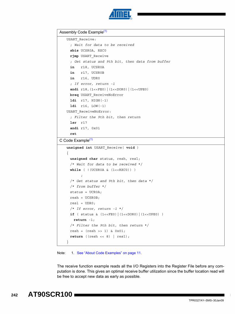
Note: 1. See “About Code Examples” on page 11.
The receive function example reads all the I/O Registers into the Register File before any com-putation is done. This gives an optimal receive buffer utilization since the buffer location read willbe free to accept new data as early as possible.
Assembly Code Example(1)
USART_Receive:
; Wait for data to be received
sbis UCSR0A, RXC0
rjmp USART_Receive
; Get status and 9th bit, then data from buffer
in r18, UCSR0A
in r17, UCSR0B
in r16, UDR0
; If error, return -1
andi r18,(1<<FE0)|(1<<DOR0)|(1<<UPE0)
breq USART_ReceiveNoError
ldi r17, HIGH(-1)
ldi r16, LOW(-1)
USART_ReceiveNoError:
; Filter the 9th bit, then return
lsr r17
andi r17, 0x01
ret
C Code Example(1)
unsigned int USART_Receive( void )
{
unsigned char status, resh, resl;
/* Wait for data to be received */
while ( !(UCSR0A & (1<<RXC0)) )
;
/* Get status and 9th bit, then data */
/* from buffer */
status = UCR0A;
resh = UCSR0B;
resl = UDR0;
/* If error, return -1 */
if ( status & (1<<FE0)|(1<<DOR0)|(1<<UPE0) )
return -1;
/* Filter the 9th bit, then return */
resh = (resh >> 1) & 0x01;
return ((resh << 8) | resl);
}
242TPR0327AY–SMS–30Jan09
AT90SCR100

AT90SCR100
18.8.3 Receive Compete Flag and InterruptThe USART Receiver has one flag that indicates the Receiver state.
The Receive Complete (RXC0) Flag indicates if there are unread data present in the receive buf-fer. This flag is one when unread data exist in the receive buffer, and zero when the receivebuffer is empty (i.e., does not contain any unread data). If the Receiver is disabled (RXEN0 = 0),the receive buffer will be flushed and consequently the RXC0 bit will become zero.
When the Receive Complete Interrupt Enable (RXCIE0) in UCSR0B is set, the USART ReceiveComplete interrupt will be executed as long as the RXC0 Flag is set (provided that global inter-rupts are enabled). When interrupt-driven data reception is used, the receive complete routinemust read the received data from UDR0 in order to clear the RXC0 Flag, otherwise a new inter-rupt will occur once the interrupt routine terminates.
18.8.4 Receiver Error FlagsThe USART Receiver has three Error Flags: Frame Error (FE0), Data OverRun (DOR0) andParity Error (UPE0). All can be accessed by reading UCSR0A. Common for the Error Flags isthat they are located in the receive buffer together with the frame for which they indicate theerror status. Due to the buffering of the Error Flags, the UCSR0A must be read before thereceive buffer (UDR0), since reading the UDR0 I/O location changes the buffer read location.Another equality for the Error Flags is that they can not be altered by software doing a write tothe flag location. However, all flags must be set to zero when the UCSR0A is written for upwardcompatibility of future USART implementations. None of the Error Flags can generate interrupts.
The Frame Error (FE0) Flag indicates the state of the first stop bit of the next readable framestored in the receive buffer. The FE0 Flag is zero when the stop bit was correctly read (as one),and the FE0 Flag will be one when the stop bit was incorrect (zero). This flag can be used fordetecting out-of-sync conditions, detecting break conditions and protocol handling. The FE0Flag is not affected by the setting of the USBS0 bit in UCSR0C since the Receiver ignores all,except for the first, stop bits. For compatibility with future devices, always set this bit to zerowhen writing to UCSR0A.
The Data OverRun (DOR0) Flag indicates data loss due to a receiver buffer full condition. AData OverRun occurs when the receive buffer is full (two characters), it is a new character wait-ing in the Receive Shift Register, and a new start bit is detected. If the DOR0 Flag is set therewas one or more serial frame lost between the frame last read from UDR0, and the next frameread from UDR0. For compatibility with future devices, always write this bit to zero when writingto UCSR0A. The DOR0 Flag is cleared when the frame received was successfully moved fromthe Shift Register to the receive buffer.
The Parity Error (UPE0) Flag indicates that the next frame in the receive buffer had a ParityError when received. If Parity Check is not enabled the UPE0 bit will always be read zero. Forcompatibility with future devices, always set this bit to zero when writing to UCSR0A. For moredetails see “Parity Bit Calculation” on page 236 and “Parity Checker” on page 243.
18.8.5 Parity CheckerThe Parity Checker is active when the high USART Parity mode (UPM01) bit is set. Type of Par-ity Check to be performed (odd or even) is selected by the UPM00 bit. When enabled, the ParityChecker calculates the parity of the data bits in incoming frames and compares the result withthe parity bit from the serial frame. The result of the check is stored in the receive buffer together
243TPR0327AY–SMS–30Jan09

with the received data and stop bits. The Parity Error (UPE0) Flag can then be read by softwareto check if the frame had a Parity Error.
The UPE0 bit is set if the next character that can be read from the receive buffer had a ParityError when received and the Parity Checking was enabled at that point (UPM01 = 1). This bit isvalid until the receive buffer (UDR0) is read.
18.8.6 Disabling the ReceiverIn contrast to the Transmitter, disabling of the Receiver will be immediate. Data from ongoingreceptions will therefore be lost. When disabled (i.e., the RXEN0 is set to zero) the Receiver willno longer override the normal function of the RxD0 port pin. The Receiver buffer FIFO will beflushed when the Receiver is disabled. Remaining data in the buffer will be lost
18.8.7 Flushing the Receive BufferThe receiver buffer FIFO will be flushed when the Receiver is disabled, i.e., the buffer will beemptied of its contents. Unread data will be lost. If the buffer has to be flushed during normaloperation, due to for instance an error condition, read the UDR0 I/O location until the RXC0 Flagis cleared. The following code example shows how to flush the receive buffer.
Note: 1. See “About Code Examples” on page 11.
18.9 Asynchronous Data ReceptionThe USART includes a clock recovery and a data recovery unit for handling asynchronous datareception. The clock recovery logic is used for synchronizing the internally generated baud rateclock to the incoming asynchronous serial frames at the RxD0 pin. The data recovery logic sam-ples and low pass filters each incoming bit, thereby improving the noise immunity of theReceiver. The asynchronous reception operational range depends on the accuracy of the inter-nal baud rate clock, the rate of the incoming frames, and the frame size in number of bits.
18.9.1 Asynchronous Clock RecoveryThe clock recovery logic synchronizes internal clock to the incoming serial frames. Figure 18-5illustrates the sampling process of the start bit of an incoming frame. The sample rate is 16 timesthe baud rate for Normal mode, and eight times the baud rate for Double Speed mode. The hor-izontal arrows illustrate the synchronization variation due to the sampling process. Note thelarger time variation is obtained when using the Double Speed mode (U2X0 = 1) of operation.
Assembly Code Example(1)
USART_Flush:
sbis UCSR0A, RXC0
ret
in r16, UDR0
rjmp USART_Flush
C Code Example(1)
void USART_Flush( void )
{
unsigned char dummy;
while ( UCSR0A & (1<<RXC0) ) dummy = UDR0;
}
244TPR0327AY–SMS–30Jan09
AT90SCR100

AT90SCR100
Samples denoted zero are samples done when the RxD0 line is idle (i.e., no communicationactivity).
Figure 18-5. Start Bit Sampling
When the clock recovery logic detects a high (idle) to low (start) transition on the RxD0 line, thestart bit detection sequence is initiated. Let sample 1 denote the first zero-sample as shown inthe figure. The clock recovery logic then uses samples 8, 9, and 10 for Normal mode, and sam-ples 4, 5, and 6 for Double Speed mode (indicated with sample numbers inside boxes on thefigure), to decide if a valid start bit is received. If two or more of these three samples have logicalhigh levels (the majority wins), the start bit is rejected as a noise spike and the Receiver startslooking for the next high to low-transition. If however, a valid start bit is detected, the clock recov-ery logic is synchronized and the data recovery can begin. The synchronization process isrepeated for each start bit.
18.9.2 Asynchronous Data RecoveryWhen the receiver clock is synchronized to the start bit, the data recovery can begin. The datarecovery unit uses a state machine that has 16 states for each bit in Normal mode and eightstates for each bit in Double Speed mode. Figure 18-6 shows the sampling of the data bits andthe parity bit. Each of the samples is given a number that is equal to the state of the recoveryunit.
Figure 18-6. Sampling of Data and Parity Bit
The decision of the logic level of the received bit is taken by doing a majority voting of the logicvalue to the three samples in the center of the received bit. The center samples are emphasizedon the figure by having the sample number inside boxes. The majority voting process is done asfollows: If two or all three samples have high levels, the received bit is registered to be a logic 1.If two or all three samples have low levels, the received bit is registered to be a logic 0. Thismajority voting process acts as a low pass filter for the incoming signal on the RxD0 pin. Therecovery process is then repeated until a complete frame is received. Including the first stop bit.Note that the Receiver only uses the first stop bit of a frame.
Figure 18-7 shows the sampling of the stop bit and the earliest possible beginning of the start bitof the next frame.
1 2 3 4 5 6 7 8 9 10 11 12 13 14 15 16 1 2
STARTIDLE
00
BIT 0
3
1 2 3 4 5 6 7 8 1 20
RxD
Sample(U2X = 0)
Sample(U2X = 1)
1 2 3 4 5 6 7 8 9 10 11 12 13 14 15 16 1
BIT n
1 2 3 4 5 6 7 8 1
RxD
Sample(U2X = 0)
Sample(U2X = 1)
245TPR0327AY–SMS–30Jan09

Figure 18-7. Stop Bit Sampling and Next Start Bit Sampling
The same majority voting is done to the stop bit as done for the other bits in the frame. If the stopbit is registered to have a logic 0 value, the Frame Error (FE0) Flag will be set.
A new high to low transition indicating the start bit of a new frame can come right after the last ofthe bits used for majority voting. For Normal Speed mode, the first low level sample can be atpoint marked (A) in Figure 18-7. For Double Speed mode the first low level must be delayed to(B). (C) marks a stop bit of full length. The early start bit detection influences the operationalrange of the Receiver.
18.9.3 Asynchronous Operational RangeThe operational range of the Receiver is dependent on the mismatch between the received bitrate and the internally generated baud rate. If the Transmitter is sending frames at too fast or tooslow bit rates, or the internally generated baud rate of the Receiver does not have a similar (seeTable 18-2) base frequency, the Receiver will not be able to synchronize the frames to the startbit.
The following equations can be used to calculate the ratio of the incoming data rate and internalreceiver baud rate.
D Sum of character size and parity size (D = 5 to 10 bit)
S Samples per bit. S = 16 for Normal Speed mode and S = 8 for Double Speedmode.
SF First sample number used for majority voting. SF = 8 for normal speed and SF = 4for Double Speed mode.
SM Middle sample number used for majority voting. SM = 9 for normal speed andSM = 5 for Double Speed mode.
Rslow is the ratio of the slowest incoming data rate that can be accepted in relation to thereceiver baud rate. Rfast is the ratio of the fastest incoming data rate that can beaccepted in relation to the receiver baud rate.
Table 18-2 and Table 18-3 list the maximum receiver baud rate error that can be tolerated. Notethat Normal Speed mode has higher toleration of baud rate variations.
1 2 3 4 5 6 7 8 9 10 0/1 0/1 0/1
STOP 1
1 2 3 4 5 6 0/1
RxD
Sample(U2X = 0)
Sample(U2X = 1)
(A) (B) (C)
Table 19-1 .
RslowD 1+( )S
S 1– D S⋅ SF+ +-------------------------------------------= RfastD 2+( )S
D 1+( )S SM+-----------------------------------=
246TPR0327AY–SMS–30Jan09
AT90SCR100

AT90SCR100
The recommendations of the maximum receiver baud rate error was made under the assump-tion that the Receiver and Transmitter equally divides the maximum total error.
There are two possible sources for the receivers baud rate error. The Receiver’s system clock(XTAL) will always have some minor instability over the supply voltage range and the tempera-ture range. When using a crystal to generate the system clock, this is rarely a problem, but for aresonator the system clock may differ more than 2% depending of the resonators tolerance. Thesecond source for the error is more controllable. The baud rate generator can not always do anexact division of the system frequency to get the baud rate wanted. In this case an UBRR valuethat gives an acceptable low error can be used if possible.
18.10 Multi-processor Communication ModeSetting the Multi-processor Communication mode (MPCM0) bit in UCSR0A enables a filteringfunction of incoming frames received by the USART Receiver. Frames that do not containaddress information will be ignored and not put into the receive buffer. This effectively reducesthe number of incoming frames that has to be handled by the CPU, in a system with multipleMCUs that communicate via the same serial bus. The Transmitter is unaffected by the MPCM0setting, but has to be used differently when it is a part of a system utilizing the Multi-processorCommunication mode.
If the Receiver is set up to receive frames that contain 5 to 8 data bits, then the first stop bit indi-cates if the frame contains data or address information. If the Receiver is set up for frames with
Table 18-2. Recommended Maximum Receiver Baud Rate Error for Normal Speed Mode (U2Xn = 0)
D# (Data+Parity Bit) Rslow (%) Rfast (%) Max Total Error (%)
Recommended Max Receiver Error (%)
5 93.20 106.67 +6.67/-6.8 ± 3.0
6 94.12 105.79 +5.79/-5.88 ± 2.5
7 94.81 105.11 +5.11/-5.19 ± 2.0
8 95.36 104.58 +4.58/-4.54 ± 2.0
9 95.81 104.14 +4.14/-4.19 ± 1.5
10 96.17 103.78 +3.78/-3.83 ± 1.5
Table 18-3. Recommended Maximum Receiver Baud Rate Error for Double Speed Mode (U2Xn = 1)
D# (Data+Parity Bit) Rslow (%) Rfast (%) Max Total Error (%)
Recommended Max Receiver Error (%)
5 94.12 105.66 +5.66/-5.88 ± 2.5
6 94.92 104.92 +4.92/-5.08 ± 2.0
7 95.52 104,35 +4.35/-4.48 ± 1.5
8 96.00 103.90 +3.90/-4.00 ± 1.5
9 96.39 103.53 +3.53/-3.61 ± 1.5
10 96.70 103.23 +3.23/-3.30 ± 1.0
247TPR0327AY–SMS–30Jan09

nine data bits, then the ninth bit (RXB8n) is used for identifying address and data frames. Whenthe frame type bit (the first stop or the ninth bit) is one, the frame contains an address. When theframe type bit is zero the frame is a data frame.
The Multi-processor Communication mode enables several slave MCUs to receive data from amaster MCU. This is done by first decoding an address frame to find out which MCU has beenaddressed. If a particular slave MCU has been addressed, it will receive the following dataframes as normal, while the other slave MCUs will ignore the received frames until anotheraddress frame is received.
18.10.1 Using MPCM0For an MCU to act as a master MCU, it can use a 9-bit character frame format (UCSZ0 = 7). Theninth bit (TXB80) must be set when an address frame (TXB80 = 1) or cleared when a data frame(TXB = 0) is being transmitted. The slave MCUs must in this case be set to use a 9-bit characterframe format.
The following procedure should be used to exchange data in Multi-processor Communicationmode:
1. All Slave MCUs are in Multi-processor Communication mode (MPCM0 in UCSR0A is set).
2. The Master MCU sends an address frame, and all slaves receive and read this frame. In the Slave MCUs, the RXC0 Flag in UCSR0A will be set as normal.
3. Each Slave MCU reads the UDR0 Register and determines if it has been selected. If so, it clears the MPCM0 bit in UCSR0A, otherwise it waits for the next address byte and keeps the MPCM0 setting.
4. The addressed MCU will receive all data frames until a new address frame is received. The other Slave MCUs, which still have the MPCM0 bit set, will ignore the data frames.
5. When the last data frame is received by the addressed MCU, the addressed MCU sets the MPCM0 bit and waits for a new address frame from master. The process then repeats from 2.
Using any of the 5- to 8-bit character frame formats is possible, but impractical since theReceiver must change between using n and n+1 character frame formats. This makes full-duplex operation difficult since the Transmitter and Receiver uses the same character size set-ting. If 5- to 8-bit character frames are used, the Transmitter must be set to use two stop bit(USBS0 = 1) since the first stop bit is used for indicating the frame type.
Do not use Read-Modify-Write instructions (SBI and CBI) to set or clear the MPCM0 bit. TheMPCM0 bit shares the same I/O location as the TXC0 Flag and this might accidentally becleared when using SBI or CBI instructions.
248TPR0327AY–SMS–30Jan09
AT90SCR100

AT90SCR100
18.11 USART Register Description
18.11.1 UDR0 – USART I/O Data Register n
The USART Transmit Data Buffer Register and USART Receive Data Buffer Registers share thesame I/O address referred to as USART Data Register or UDR0. The Transmit Data Buffer Reg-ister (TXB) will be the destination for data written to the UDR0 Register location. Reading theUDR0 Register location will return the contents of the Receive Data Buffer Register (RXB).
For 5-, 6-, or 7-bit characters the upper unused bits will be ignored by the Transmitter and set tozero by the Receiver.
The transmit buffer can only be written when the UDRE0 Flag in the UCSR0A Register is set.Data written to UDR0 when the UDRE0 Flag is not set, will be ignored by the USART Transmit-ter. When data is written to the transmit buffer, and the Transmitter is enabled, the Transmitterwill load the data into the Transmit Shift Register when the Shift Register is empty. Then thedata will be serially transmitted on the TxD0 pin.
The receive buffer consists of a two level FIFO. The FIFO will change its state whenever thereceive buffer is accessed. Due to this behavior of the receive buffer, do not use Read-Modify-Write instructions (SBI and CBI) on this location. Be careful when using bit test instructions(SBIC and SBIS), since these also will change the state of the FIFO.
18.11.2 UCSR0A – USART Control and Status Register A
• Bit 7 – RXC0: USART Receive CompleteThis flag bit is set when there are unread data in the receive buffer and cleared when the receivebuffer is empty (i.e., does not contain any unread data). If the Receiver is disabled, the receivebuffer will be flushed and consequently the RXC0 bit will become zero. The RXC0 Flag can beused to generate a Receive Complete interrupt (see description of the RXCIE0 bit).
• Bit 6 – TXC0: USART Transmit CompleteThis flag bit is set when the entire frame in the Transmit Shift Register has been shifted out andthere are no new data currently present in the transmit buffer (UDR0). The TXC0 Flag bit is auto-matically cleared when a transmit complete interrupt is executed, or it can be cleared by writinga one to its bit location. The TXC0 Flag can generate a Transmit Complete interrupt (seedescription of the TXCIE0 bit).
• Bit 5 – UDRE0: USART Data Register Empty
Bit 7 6 5 4 3 2 1 0 UDR0
$0000C6 RXB[7..0] (Read)
$0000C6 TXB[7..0] (Write)
Read/write R/W R/W R/W R/W R/W R/W R/W R/W
Initial value 0 0 0 0 0 0 0 0 0x00
Bit 7 6 5 4 3 2 1 0
$0000C0 RXC0 TXC0 UDRE0 FE0 DOR0 UPE0 U2X0 MPCM0 UCSR0ARead/write R R/W R R R R R/W R/W
Initial value 0 0 1 0 0 0 0 0 0x20
249TPR0327AY–SMS–30Jan09

The UDRE0 flag indicates if the transmit buffer (UDR0) is ready to receive new data. If UDRE0 isone, the buffer is empty, and therefore ready to be written. The UDRE0 Flag can generate aData Register Empty interrupt (see description of the UDRIE0 bit).
UDRE0 is set after a reset to indicate that the Transmitter is ready.
• Bit 4 – FE0: Frame ErrorThis bit is set if the next character in the receive buffer had a Frame Error when received. I.e.,when the first stop bit of the next character in the receive buffer is zero. This bit is valid until thereceive buffer (UDR0) is read. The FE0 bit is zero when the stop bit of received data is one.Always set this bit to zero when writing to UCSR0A.
• Bit 3 – DOR0: Data OverRunThis bit is set if a Data OverRun condition is detected. A Data OverRun occurs when the receivebuffer is full (two characters), it is a new character waiting in the Receive Shift Register, and anew start bit is detected. This bit is valid until the receive buffer (UDR0) is read. Always set thisbit to zero when writing to UCSR0A.
• Bit 2 – UPE0: USART Parity ErrorThis bit is set if the next character in the receive buffer had a Parity Error when received and theParity Checking was enabled at that point (UPM01 = 1). This bit is valid until the receive buffer(UDR0) is read. Always set this bit to zero when writing to UCSR0A.
• Bit 1 – U2X0: Double the USART Transmission SpeedThis bit only has effect for the asynchronous operation. Write this bit to zero when using syn-chronous operation.
Writing this bit to one will reduce the divisor of the baud rate divider from 16 to 8 effectively dou-bling the transfer rate for asynchronous communication.
• Bit 0 – MPCM0: Multi-processor Communication ModeThis bit enables the Multi-processor Communication mode. When the MPCM0 bit is written toone, all the incoming frames received by the USART Receiver that do not contain address infor-mation will be ignored. The Transmitter is unaffected by the MPCM0 setting. For more detailedinformation see “Multi-processor Communication Mode” on page 247.
18.11.3 UCSR0B – USART Control and Status Register B
• Bit 7 – RXCIE0: RX Complete Interrupt Enable 0Writing this bit to one enables interrupt on the RXC0 Flag. A USART Receive Complete interruptwill be generated only if the RXCIE0 bit is written to one, the Global Interrupt Flag in SREG iswritten to one and the RXC0 bit in UCSR0A is set.
• Bit 6 – TXCIE0: TX Complete Interrupt Enable 0
Bit 7 6 5 4 3 2 1 0
$0000C1 RXCIE0 TXCIE0 UDRIE0 RXEN0 TXEN0 UCSZ02 RXB80 TXB80 UCSR0BRead/write R/W R/W R/W R/W R/W R/W R R/W
Initial value 0 0 0 0 0 0 0 0 0x00
250TPR0327AY–SMS–30Jan09
AT90SCR100
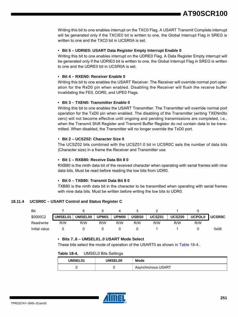
AT90SCR100
Writing this bit to one enables interrupt on the TXC0 Flag. A USART Transmit Complete interruptwill be generated only if the TXCIE0 bit is written to one, the Global Interrupt Flag in SREG iswritten to one and the TXC0 bit in UCSR0A is set.
• Bit 5 – UDRIE0: USART Data Register Empty Interrupt Enable 0Writing this bit to one enables interrupt on the UDRE0 Flag. A Data Register Empty interrupt willbe generated only if the UDRIE0 bit is written to one, the Global Interrupt Flag in SREG is writtento one and the UDRE0 bit in UCSR0A is set.
• Bit 4 – RXEN0: Receiver Enable 0Writing this bit to one enables the USART Receiver. The Receiver will override normal port oper-ation for the RxD0 pin when enabled. Disabling the Receiver will flush the receive bufferinvalidating the FE0, DOR0, and UPE0 Flags.
• Bit 3 – TXEN0: Transmitter Enable 0Writing this bit to one enables the USART Transmitter. The Transmitter will override normal portoperation for the TxD0 pin when enabled. The disabling of the Transmitter (writing TXENn0tozero) will not become effective until ongoing and pending transmissions are completed, i.e.,when the Transmit Shift Register and Transmit Buffer Register do not contain data to be trans-mitted. When disabled, the Transmitter will no longer override the TxD0 port.
• Bit 2 – UCSZ02: Character Size 0The UCSZ02 bits combined with the UCSZ01:0 bit in UCSR0C sets the number of data bits(Character size) in a frame the Receiver and Transmitter use.
• Bit 1 – RXB80: Receive Data Bit 8 0RXB80 is the ninth data bit of the received character when operating with serial frames with ninedata bits. Must be read before reading the low bits from UDR0.
• Bit 0 – TXB80: Transmit Data Bit 8 0TXB80 is the ninth data bit in the character to be transmitted when operating with serial frameswith nine data bits. Must be written before writing the low bits to UDR0.
18.11.4 UCSR0C – USART Control and Status Register C
• Bits 7..6 – UMSEL01..0 USART Mode SelectThese bits select the mode of operation of the USART0 as shown in Table 18-4..
Bit 7 6 5 4 3 2 1 0
$0000C2 UMSEL01 UMSEL00 UPM01 UPM00 USBS0 UCSZ01 UCSZ00 UCPOL0 UCSR0CRead/write R/W R/W R/W R/W R/W R/W R/W R/W
Initial value 0 0 0 0 0 1 1 0 0x06
Table 18-4. UMSEL0 Bits Settings
UMSEL01 UMSEL00 Mode
0 0 Asynchronous USART
251TPR0327AY–SMS–30Jan09

Note: 1. See “USART in SPI Mode” on page 257 for full description of the Master SPI Mode (MSPIM) operation
• Bits 5..4 – UPM01..0: Parity ModeThese bits enable and set type of parity generation and check. If enabled, the Transmitter willautomatically generate and send the parity of the transmitted data bits within each frame. TheReceiver will generate a parity value for the incoming data and compare it to the UPM0 setting.If a mismatch is detected, the UPE0 Flag in UCSR0A will be set.
• Bit 3 – USBS0: Stop Bit SelectThis bit selects the number of stop bits to be inserted by the Transmitter. The Receiver ignoresthis setting.
• Bit 2:1 – UCSZ01:0: Character SizeThe UCSZ01:0 bits combined with the UCSZ02 bit in UCSR0B sets the number of data bits(Character size) in a frame the Receiver and Transmitter use.
0 1 Synchronous USART
1 0 (Reserved)
1 1 Master SPI (MSPIM)(1)
Table 18-5. UPM0 Bits Settings
UPM01 UPM00 Parity Mode
0 0 Disabled
0 1 Reserved
1 0 Enabled, Even Parity
1 1 Enabled, Odd Parity
Table 18-6. USBS Bit Settings
USBS0 Stop Bit(s)
0 1-bit
1 2-bit
Table 18-7. UCSZ0 Bits Settings
UCSZ02 UCSZ01 UCSZ00 Character Size
0 0 0 5-bit
0 0 1 6-bit
0 1 0 7-bit
0 1 1 8-bit
1 0 0 Reserved
Table 18-4. UMSEL0 Bits Settings
UMSEL01 UMSEL00 Mode
252TPR0327AY–SMS–30Jan09
AT90SCR100

AT90SCR100
• Bit 0 – UCPOL0: Clock PolarityThis bit is used for synchronous mode only. Write this bit to zero when asynchronous mode isused. The UCPOL0 bit sets the relationship between data output change and data input sample,and the synchronous clock (XCK).
18.11.5 UBRR0L and UBRR0H – USART Baud Rate Registers
• Bit 15..12 – Reserved BitsThese bits are reserved for future use. For compatibility with future devices, these bit must bewritten to zero when UBRRH is written.
• Bit 11..0 – UBRR11..0: USART Baud Rate RegisterThis is a 12-bit register which contains the USART baud rate. The UBRRH contains the fourmost significant bits, and the UBRRL contains the eight least significant bits of the USART baudrate. Ongoing transmissions by the Transmitter and Receiver will be corrupted if the baud rate ischanged. Writing UBRRL will trigger an immediate update of the baud rate prescaler.
1 0 1 Reserved
1 1 0 Reserved
1 1 1 9-bit
Table 18-8. UCPOLn Bit Settings
UCPOL0Transmitted Data Changed (Output of TxD0 Pin)
Received Data Sampled (Input on RxD0 Pin)
0 Rising XCK Edge Falling XCK Edge
1 Falling XCK Edge Rising XCK Edge
Table 18-7. UCSZ0 Bits Settings
UCSZ02 UCSZ01 UCSZ00 Character Size
Bit 7 6 5 4 3 2 1 0
$0000C5 - - - - UBRR[11..8] UBRRH0$0000C4 UBRR[7..0] UBRRL0Read/write R R R R R/W R/W R/W R/W
R/W R/W R/W R/W R/W R/W R/W R/W
Initial value 0 0 0 0 0 0 0 0 0x00
0 0 0 0 0 0 0 0 0x00
253TPR0327AY–SMS–30Jan09

18.12 Examples of Baud Rate SettingFor AT90SCR100 frequencies, the most commonly used baud rates for asynchronous operationcan be generated by using the UBRR settings in Table 18-9 and Table 18-10. UBRR valueswhich yield an actual baud rate differing less than 0.5% from the target baud rate, are bold in thetable. Higher error ratings are acceptable, but the Receiver will have less noise resistance whenthe error ratings are high, especially for large serial frames (see “Asynchronous OperationalRange” on page 246). The error values are calculated using the following equation:
Note: 1. UBRR = 0, Error = 0.0%
Error[%]BaudRateClosest Match
BaudRate-------------------------------------------------------- 1–⎝ ⎠⎛ ⎞ 100%•=
Table 18-9. Examples of UBRR0 Settings accessible Oscillator Frequencies
Baud Rate (bps)
fosc = 8.0000 MHz fosc = 16 MHz fosc = 19.2 MHz
U2X0 = 0 U2X0 = 1 U2X0 = 0 U2X0 = 1 U2X0 = 0 U2X0 = 1
UBRR Error UBRR Error UBRR Error UBRR Error UBRR Error UBRR Error
2400 207 0.2% 416 -0.1% 416 -0.1% 832 0% 499 0% 999 0%
4800 103 0.2% 207 0.2% 207 0.2% 416 -0.1% 249 0% 499 0%
9600 51 0.2% 103 0.2% 103 0.2% 207 0.2% 124 0% 249 0%
14.4k 34 -0.8% 68 0.6% 68 0.6% 138 -0.1% 82 0.4% 166 -0.2%
19.2k 25 0.2% 51 0.2% 51 0.2% 103 0.2% 62 -0.8% 124 0%
28.8k 16 2.1% 34 -0.8% 34 -0.8% 68 0.6% 41 -0.8% 82 0.4%
38.4k 12 0.2% 25 0.2% 25 0.2% 51 0.2% 30 0.8% 62 -0.8%
57.6k 8 -3.5% 16 2.1% 16 2.1% 34 -0.8% 20 -0.8% 41 -0.8%
76.8k 6 -7% 12 0.2% 12 0.2% 25 0.2% 15 2.3% 30 0.8%
115.2k 3 8.5% 8 -3.5% 8 -3.5% 16 2.1% 9 4.2% 20 -0.8%
230.4k 1 8.5% 3 8.5% 3 8.5% 8 -3.5% 4 4.2% 9 4.2%
250k 1 0% 3 0% 3 0% 7 0% 4 -4% 9 -4%
500k 0 0% 1 0% 1 0% 3 0% 1 20% 4 -4%
1M - - 0 0% 0 0% 1 0% 0 20% 1 20%
1.5M - - - - - - 0 33.3% - -% 1 -20%
2M - - - - - - 0 0% - -% 0 20%
Max.(1) 500kbps 1Mbps 1Mbps 2Mbps 1.2Mbps 2.4Mbps
254TPR0327AY–SMS–30Jan09
AT90SCR100

AT90SCR100
Note: 1. UBRR = 0, Error = 0.0%
Table 18-10. Examples of UBRR0 Settings accessible Oscillator Frequencies (Continued)
Baud Rate (bps)
fosc = 20 MHz
U2X0 = 0 U2X0 = 1
UBRR Error UBRR Error
2400 520 0% 1041 0%
4800 259 0.2% 520 0%
9600 129 0.2% 259 0.2%
14.4k 86 -0.2% 173 -0.2%
19.2k 64 0.2% 129 0.2%
28.8k 42 0.9% 86 -0.2%
38.4k 32 -1.4% 64 0.2%
57.6k 21 -1.4% 42 0.9%
76.8k 15 1.7% 32 -1.4%
115.2k 10 -1.4% 21 -1.4%
230.4k 4 8.5% 10 -1.4%
250k 4 0% 9 0%
500k 2 -16.7% 4 0%
1M 0 25% 2 -16.7%
1.5M 1 -16.7%
2M 0 25%
Max.(1) 1.25Mbps 2.5Mbps
255TPR0327AY–SMS–30Jan09

256TPR0327AY–SMS–30Jan09
AT90SCR100

AT90SCR100
19. USART in SPI ModeThe Universal Synchronous and Asynchronous serial Receiver and Transmitter (USART) can beset to a master SPI compliant mode of operation. The Master SPI Mode (MSPIM) has the follow-ing features:
19.1 Features• Full Duplex, Three-wire Synchronous Data Transfer• Master Operation• Supports all four SPI Modes of Operation (Mode 0, 1, 2, and 3)• LSB First or MSB First Data Transfer (Configurable Data Order)• Queued Operation (Double Buffered)• High Resolution Baud Rate Generator• High Speed Operation (fXCKmax = fCK/2)• Flexible Interrupt Generation
19.2 OverviewSetting both UMSEL01:0 bits to one enables the USART in MSPIM logic. In this mode of opera-tion the SPI master control logic takes direct control over the USART resources. Theseresources include the transmitter and receiver shift register and buffers, and the baud rate gen-erator. The parity generator and checker, the data and clock recovery logic, and the RX and TXcontrol logic is disabled. The USART RX and TX control logic is replaced by a common SPItransfer control logic. However, the pin control logic and interrupt generation logic is identical inboth modes of operation.
The I/O register locations are the same in both modes. However, some of the functionality of thecontrol registers changes when using MSPIM.
19.3 Clock GenerationThe Clock Generation logic generates the base clock for the Transmitter and Receiver. ForUSART MSPIM mode of operation only internal clock generation (i.e. master operation) is sup-ported. The Data Direction Register for the XCK0 pin (DDR_XCK0) must therefore be set to one(i.e. as output) for the USART in MSPIM to operate correctly. Preferably the DDR_XCK0 shouldbe set up before the USART in MSPIM is enabled (i.e. TXEN0 and RXEN0 bit set to one).
The internal clock generation used in MSPIM mode is identical to the USART synchronous mas-ter mode. The baud rate or UBRR0 setting can therefore be calculated using the sameequations, see Table 19-1:
257TPR0327AY–SMS–30Jan09

BAUD Baud rate (in bits per second, bps)
fOSC System Oscillator clock frequency: clkIO
UBRR0 Contents of the UBRR0H and UBRR0L Registers, (0-4095)
19.4 SPI Data Modes and TimingThere are four combinations of XCK0 (SCK) phase and polarity with respect to serial data, whichare determined by control bits UCPHA0 and UCPOL0. The data transfer timing diagrams areshown in Figure 19-1. Data bits are shifted out and latched in on opposite edges of the XCK0signal, ensuring sufficient time for data signals to stabilize. The UCPOL0 and UCPHA0 function-ality is summarized in Table 19-2. Note that changing the setting of any of these bits will corruptall ongoing communication for both the Receiver and Transmitter.
Table 19-1. Equations for Calculating Baud Rate Register Setting
Operating ModeEquation for Calculating Baud
Rate (1)
1. The baud rate is defined to be the transfer rate in bit per second (bps)
Equation for Calculating UBRR0 Value
Synchronous Master mode BAUD
fOSC2 UBRRn 1+( )---------------------------------------= UBRRn
fOSC2BAUD-------------------- 1–=
Table 19-2. UCPOL0 and UCPHA0 Functionality-
UCPOL0 UCPHA0 SPI Mode Leading Edge Trailing Edge
0 0 0 Sample (Rising) Setup (Falling)
0 1 1 Setup (Rising) Sample (Falling)
1 0 2 Sample (Falling) Setup (Rising)
1 1 3 Setup (Falling) Sample (Rising)
258TPR0327AY–SMS–30Jan09
AT90SCR100

AT90SCR100
Figure 19-1. UCPHA0 and UCPOL0 data transfer timing diagrams.
19.5 Frame FormatsA serial frame for the MSPIM is defined to be one character of 8 data bits. The USART in MSPIMmode has two valid frame formats:
• 8-bit data with MSB first• 8-bit data with LSB first
A frame starts with the least or most significant data bit. Then the next data bits, up to a total ofeight, are succeeding, ending with the most or least significant bit accordingly. When a completeframe is transmitted, a new frame can directly follow it, or the communication line can be set toan idle (high) state.
The UDORD0 bit in UCSR0C sets the frame format used by the USART in MSPIM mode. TheReceiver and Transmitter use the same setting. Note that changing the setting of any of thesebits will corrupt all ongoing communication for both the Receiver and Transmitter.
16-bit data transfer can be achieved by writing two data bytes to UDR0. A UART transmit com-plete interrupt will then signal that the 16-bit value has been shifted out.
19.5.1 USART MSPIM InitializationThe USART in MSPIM mode has to be initialized before any communication can take place. Theinitialization process normally consists of setting the baud rate, setting master mode of operation(by setting DDR_XCK0 to one), setting frame format and enabling the Transmitter and theReceiver. Only the transmitter can operate independently. For interrupt driven USART opera-tion, the Global Interrupt Flag should be cleared (and thus interrupts globally disabled) whendoing the initialization.
Before doing a re-initialization with changed baud rate, data mode, or frame format, be sure thatthere is no ongoing transmissions during the period the registers are changed. The TXC0 Flag
XCK
Data setup (TXD)
Data sample (RXD)
XCK
Data setup (TXD)
Data sample (RXD)
XCK
Data setup (TXD)
Data sample (RXD)
XCK
Data setup (TXD)
Data sample (RXD)
UCPOL=0 UCPOL=1
UCP
HA
=0
UCP
HA
=1
To ensure immediate initialization of the XCK0 output the baud-rate register(UBRR0) must be zero at the time the transmitter is enabled. Contrary to the nor-mal mode USART operation the UBRR0 must then be written to the desired valueafter the transmitter is enabled, but before the first transmission is started. SettingUBRR0 to zero before enabling the transmitter is not necessary if the initializationis done immediately after a reset since UBRR0 is reset to zero.
Note
259TPR0327AY–SMS–30Jan09

can be used to check that the Transmitter has completed all transfers, and the RXC0 Flag canbe used to check that there are no unread data in the receive buffer. Note that the TXC0 Flagmust be cleared before each transmission (before UDR0 is written) if it is used for this purpose.
The following simple USART initialization code examples show one assembly and one C func-tion that are equal in functionality. The examples assume polling (no interrupts enabled). Thebaud rate is given as a function parameter. For the assembly code, the baud rate parameter isassumed to be stored in the r17:r16 registers.
19.6 Data TransferUsing the USART in MSPI mode requires the Transmitter to be enabled, i.e. the TXEN0 bit inthe UCSR0B register is set to one. When the Transmitter is enabled, the normal port operationof the TxD0 pin is overridden and given the function as the Transmitter's serial output. Enabling
Assembly Code Example
USART_Init:
clr r18
out UBRR0H,r18
out UBRR0L,r18
; Setting the XCK0 port pin as output, enables master mode.
sbi XCK0_DDR, XCK0
; Set MSPI mode of operation and SPI data mode 0.
ldi r18, (1<<UMSEL01)|(1<<UMSEL00)|(0<<UCPHA0)|(0<<UCPOL0)
out UCSR0C,r18
; Enable receiver and transmitter.
ldi r18, (1<<RXEN0)|(1<<TXEN0)
out UCSR0B,r18
; Set baud rate.
; IMPORTANT: The Baud Rate must be set after the transmitter is enabled!
out UBRR0H, r17
out UBRR0L, r18
ret
C Code Example
void USART_Init( unsigned int baud )
{
UBRR0 = 0;
/* Setting the XCK0 port pin as output, enables master mode. */
XCK0_DDR |= (1<<XCK0);
/* Set MSPI mode of operation and SPI data mode 0. */
UCSR0C = (1<<UMSEL01)|(1<<UMSEL00)|(0<<UCPHA0)|(0<<UCPOL0);
/* Enable receiver and transmitter. */
UCSR0B = (1<<RXEN0)|(1<<TXEN0);
/* Set baud rate. */
/* IMPORTANT: The Baud Rate must be set after the transmitter is enabled */
UBRR0 = baud;
}
260TPR0327AY–SMS–30Jan09
AT90SCR100

AT90SCR100
the receiver is optional and is done by setting the RXEN0 bit in the UCSR0B register to one.When the receiver is enabled, the normal pin operation of the RxD0 pin is overridden and giventhe function as the Receiver's serial input. The XCK0 will in both cases be used as the transferclock.
After initialization the USART is ready for doing data transfers. A data transfer is initiated by writ-ing to the UDR0 I/O location. This is the case for both sending and receiving data since thetransmitter controls the transfer clock. The data written to UDR0 is moved from the transmit buf-fer to the shift register when the shift register is ready to send a new frame.
The following code examples show a simple USART in MSPIM mode transfer function based onpolling of the Data Register Empty (UDRE0) Flag and the Receive Complete (RXC0) Flag. TheUSART has to be initialized before the function can be used. For the assembly code, the data tobe sent is assumed to be stored in Register R16 and the data received will be available in thesame register (R16) after the function returns.
The function simply waits for the transmit buffer to be empty by checking the UDRE0 Flag,before loading it with new data to be transmitted. The function then waits for data to be presentin the receive buffer by checking the RXC0 Flag, before reading the buffer and returning thevalue..
To keep the input buffer in sync with the number of data bytes transmitted, theUDR0 register must be read once for each byte transmitted. The input buffer oper-ation is identical to normal USART mode, i.e. if an overflow occurs the characterlast received will be lost, not the first data in the buffer. This means that if fourbytes are transferred, byte 1 first, then byte 2, 3, and 4, and the UDR0 is not readbefore all transfers are completed, then byte 3 to be received will be lost, and notbyte 1.
Note
261TPR0327AY–SMS–30Jan09

19.6.1 Transmitter and Receiver Flags and InterruptsThe RXC0, TXC0, and UDRE0 flags and corresponding interrupts in USART in MSPIM modeare identical in function to the normal USART operation. However, the receiver error status flags(FE, DOR, and PE) are not in use and is always read as zero.
19.6.2 Disabling the Transmitter or ReceiverThe disabling of the transmitter or receiver in USART in MSPIM mode is identical in function tothe normal USART operation.
19.7 USART MSPIM Register DescriptionThe following section describes the registers used for SPI operation using the USART.
19.7.1 UDR0 – USART MSPIM I/O Data RegisterThe function and bit description of the USART data register (UDR0) in MSPI mode is identical tonormal USART operation. See “UDR0 – USART I/O Data Register n” on page 249.
Assembly Code Example
USART_MSPIM_Transfer:
; Wait for empty transmit buffer
sbis UCSR0A, UDRE0
rjmp USART_MSPIM_Transfer
; Put data (r16) into buffer, sends the data
out UDR0,r16
; Wait for data to be received
USART_MSPIM_Wait_RXC0:
sbis UCSR0A, RXC0
rjmp USART_MSPIM_Wait_RXC0
; Get and return received data from buffer
in r16, UDR0
ret
C Code Example
unsigned char USART_Receive( void )
{
/* Wait for empty transmit buffer */
while ( !( UCSR0A & (1<<UDRE0)) );
/* Put data into buffer, sends the data */
UDR0 = data;
/* Wait for data to be received */
while ( !(UCSR0A & (1<<RXC0)) );
/* Get and return received data from buffer */
return UDR0;
}
262TPR0327AY–SMS–30Jan09
AT90SCR100

AT90SCR100
19.7.2 UCSR0A – USART MSPIM Control and Status Register 0 A
• Bit 7 – RXC0: USART Receive CompleteThis flag bit is set when there are unread data in the receive buffer and cleared when the receivebuffer is empty (i.e., does not contain any unread data). If the Receiver is disabled, the receivebuffer will be flushed and consequently the RXC0 bit will become zero. The RXC0 Flag can beused to generate a Receive Complete interrupt (see description of the RXCIE0 bit).
• Bit 6 – TXC0: USART Transmit CompleteThis flag bit is set when the entire frame in the Transmit Shift Register has been shifted out andthere are no new data currently present in the transmit buffer (UDR0). The TXC0 Flag bit is auto-matically cleared when a transmit complete interrupt is executed, or it can be cleared by writinga one to its bit location. The TXC0 Flag can generate a Transmit Complete interrupt (seedescription of the TXCIE0 bit).
• Bit 5 – UDRE0: USART Data Register EmptyThe UDRE0 flag indicates if the transmit buffer (UDR0) is ready to receive new data. If UDRE0 isone, the buffer is empty, and therefore ready to be written. The UDRE0 Flag can generate aData Register Empty interrupt (see description of the UDRIE0 bit).
UDRE0 is set after a reset to indicate that the Transmitter is ready.
• Bit 4..0 - Reserved Bits in MSPI modeWhen in MSPI mode, these bits are reserved for future use. For compatibility with future devices,these bits must be written to zero when UCSR0A is written.
19.7.3 UCSR0B – USART MSPIM Control and Status Register 0 B
• Bit 7 – RXCIE0: RX Complete Interrupt Enable 0Writing this bit to one enables interrupt on the RXC0 Flag. A USART Receive Complete interruptwill be generated only if the RXCIE0 bit is written to one, the Global Interrupt Flag in SREG iswritten to one and the RXC0 bit in UCSR0A is set.
• Bit 6 – TXCIE0: TX Complete Interrupt Enable 0Writing this bit to one enables interrupt on the TXC0 Flag. A USART Transmit Complete interruptwill be generated only if the TXCIE0 bit is written to one, the Global Interrupt Flag in SREG iswritten to one and the TXC0 bit in UCSR0A is set.
• Bit 5 – UDRIE0: USART Data Register Empty Interrupt Enable 0
Bit 7 6 5 4 3 2 1 0
$0000C0 RXC0 TXC0 UDRE0 - - - - - UCSR0ARead/write R R/W R R R R R/W R/W
Initial value 0 0 1 0 0 0 0 0 0x20
Bit 7 6 5 4 3 2 1 0
$0000C1 RXCIE0 TXCIE0 UDRIE0 RXE0 TXE0 - - - UCSR0BRead/write R/W R/W R/W R/W R/W R/W R R/W
Initial value 0 0 0 0 0 0 0 0 0x00
263TPR0327AY–SMS–30Jan09

Writing this bit to one enables interrupt on the UDRE0 Flag. A Data Register Empty interrupt willbe generated only if the UDRIE0 bit is written to one, the Global Interrupt Flag in SREG is writtento one and the UDRE0 bit in UCSR0A is set.
• Bit 4 – RXEN0: Receiver Enable 0Writing this bit to one enables the USART Receiver. The Receiver will override normal port oper-ation for the RxD0 pin when enabled. Disabling the Receiver will flush the receive bufferinvalidating the FE0, DOR0, and UPE0 Flags.
• Bit 3 – TXEN0: Transmitter Enable 0Writing this bit to one enables the USART Transmitter. The Transmitter will override normal portoperation for the TxD0 pin when enabled. The disabling of the Transmitter (writing TXENn0tozero) will not become effective until ongoing and pending transmissions are completed, i.e.,when the Transmit Shift Register and Transmit Buffer Register do not contain data to be trans-mitted. When disabled, the Transmitter will no longer override the TxD0 port
• Bit 2..0 - Reserved Bits in MSPI modeWhen in MSPI mode, these bits are reserved for future use. For compatibility with future devices,these bits must be written to zero when UCSR0B is written.
19.7.4 UCSR0C – USART MSPIM Control and Status Register 0 C
• Bit 7..6 - UMSEL01..0: USART Mode SelectThese bits select the mode of operation of the USART as shown in Table 19-3. See “UCSR0C –USART Control and Status Register C” on page 251 for full description of the normal USARToperation. The MSPIM is enabled when both UMSEL0 bits are set to one. The UDORD0,UCPHA0, and UCPOL0 can be set in the same write operation where the MSPIM is enabled.
• Bit 5..3 - Reserved Bits in MSPI modeWhen in MSPI mode, these bits are reserved for future use. For compatibility with future devices,these bits must be written to zero when UCSR0C is written.
• Bit 2 - UDORD0: Data OrderWhen set to one the LSB of the data word is transmitted first. When set to zero the MSB of thedata word is transmitted first. Refer to the Frame Formats section page 4 for details.
Bit 7 6 5 4 3 2 1 0
$0000C2 UMSEL01 UMSEL00 - - - UDORD0 UCPHA UCPOL0 UCSR0CRead/write R/W R/W R/W R/W R/W R/W R/W R/W
Initial value 0 0 0 0 0 1 1 0 0x06
Table 19-3. UMSEL0 Bits Settings
UMSEL01 UMSEL00 Mode
0 0 Asynchronous USART
0 1 Synchronous USART
1 0 (Reserved)
1 1 Master SPI (MSPIM)
264TPR0327AY–SMS–30Jan09
AT90SCR100

AT90SCR100
• Bit 1 - UCPHA0: Clock PhaseThe UCPHA0 bit setting determine if data is sampled on the leasing edge (first) or tailing (last)edge of XCK0. Refer to the SPI Data Modes and Timing section page 4 for details.
• Bit 0 - UCPOL0: Clock PolarityThe UCPOL0 bit sets the polarity of the XCK0 clock. The combination of the UCPOL0 andUCPHA0 bit settings determine the timing of the data transfer. Refer to the SPI Data Modes andTiming section page 4 for details.
19.7.5 UBRR0L and UBRR0H –USART MSPIM Baud Rate RegistersThe function and bit description of the baud rate registers in MSPI mode is identical to normalUSART operation. See “UBRR0L and UBRR0H – USART Baud Rate Registers” on page 253.
19.8 AVR USART MSPIM vs. AVR SPIThe USART in MSPIM mode is fully compatible with the AVR SPI regarding:
• Master mode timing diagram.• The UCPOL0 bit functionality is identical to the SPI CPOL bit.• The UCPHA0 bit functionality is identical to the SPI CPHA bit. • The UDORD0 bit functionality is identical to the SPI DORD bit.
However, since the USART in MSPIM mode reuses the USART resources, the use of theUSART in MSPIM mode is somewhat different compared to the SPI. In addition to differences ofthe control register bits, and that only master operation is supported by the USART in MSPIMmode, the following features differ between the two modules:
• The USART in MSPIM mode includes (double) buffering of the transmitter. The SPI has no buffer.
• The USART in MSPIM mode receiver includes an additional buffer level.• The SPI WCOL (Write Collision) bit is not included in USART in MSPIM mode.• The SPI double speed mode (SPI2X) bit is not included. However, the same effect is
achieved by setting UBRR0 accordingly.• Interrupt timing is not compatible.• Pin control differs due to the master only operation of the USART in MSPIM mode.
A comparison of the USART in MSPIM mode and the SPI pins is shown in Table 19-4 on page265.
Table 19-4. Comparison of USART in MSPIM mode and SPI pins.
USART_MSPIM SPI Comment
TxD0 MOSI Master Out only
RxD0 MISO Master In only
XCK0 SCK (Functionally identical)
(N/A) SS Not supported by USART in MSPIM
265TPR0327AY–SMS–30Jan09

266TPR0327AY–SMS–30Jan09
AT90SCR100

AT90SCR100
20. SPI - Serial Peripheral InterfaceThe Serial Peripheral Interface (SPI) allows synchronous data transfer between theAT90SCR100 and peripheral devices such as RF front-end chip. The AT90SCR100 SPIincludes the following features:
20.1 Features• Full-duplex, Three-wire Synchronous Data Transfer• Master or Slave Operation• LSB First or MSB First Data Transfer• Seven Programmable Bit Rates• End of Transmission Interrupt Flag• Write Collision Flag Protection• Wake-up from Idle Mode• Double Speed (CK/2) Master SPI Mode
20.2 DescriptionUSART can also be used in Master SPI mode. See “USART in SPI Mode” on page 257.
The Power Reduction SPI bit, PRSPI, in “PRR0 – Power Reduction Register 0” on page 45 onpage 50 must be written to zero to enable SPI module.
Please Refer to Section 2. “Pin List Configuration” on page 5 for SPI pin placement.
Figure 20-1. SPI Block Diagram
SPI2
X
SPI2
X
DIVIDER/2/4/8/16/32/64/128
ClkIO
267TPR0327AY–SMS–30Jan09

The interconnection between Master and Slave CPUs with SPI is shown in Figure 20-2. The sys-tem consists of two shift Registers, and a Master clock generator. The SPI Master initiates thecommunication cycle when pulling low the Slave Select SS pin of the desired Slave. Master andSlave prepare the data to be sent in their respective shift Registers, and the Master generatesthe required clock pulses on the SCK line to interchange data. Data is always shifted from Mas-ter to Slave on the Master Out – Slave In, MOSI, line, and from Slave to Master on the Master In– Slave Out, MISO, line. After each data packet, the Master will synchronize the Slave by pullinghigh the Slave Select, SS, line.
When configured as a Master, the SPI interface has no automatic control of the SS line. Thismust be handled by user software before communication can start. When this is done, writing abyte to the SPI Data Register starts the SPI clock generator, and the hardware shifts the eightbits into the Slave. After shifting one byte, the SPI clock generator stops, setting the end ofTransmission Flag (SPIF). If the SPI Interrupt Enable bit (SPIE) in the SPCR Register is set, aninterrupt is requested. The Master may continue to shift the next byte by writing it into SPDR, orsignal the end of packet by pulling high the Slave Select, SS line. The last incoming byte will bekept in the Buffer Register for later use.
When configured as a Slave, the SPI interface will remain sleeping with MISO tri-stated as longas the SS pin is driven high. In this state, software may update the contents of the SPI DataRegister, SPDR, but the data will not be shifted out by incoming clock pulses on the SCK pinuntil the SS pin is driven low. As one byte has been completely shifted, the end of TransmissionFlag, SPIF is set. If the SPI Interrupt Enable bit, SPIE, in the SPCR Register is set, an interruptis requested. The Slave may continue to place new data to be sent into SPDR before readingthe incoming data. The last incoming byte will be kept in the Buffer Register for later use.
Figure 20-2. SPI Master-slave Interconnection
The system is single buffered in the transmit direction and double buffered in the receive direc-tion. This means that bytes to be transmitted cannot be written to the SPI Data Register beforethe entire shift cycle is completed. When receiving data, however, a received character must beread from the SPI Data Register before the next character has been completely shifted in. Oth-erwise, the first byte is lost.
In SPI Slave mode, the control logic will sample the incoming signal of the SCK pin. To ensurecorrect sampling of the clock signal, the minimum low and high periods should be:
Low period: longer than 2 CPU clock cycles.
High period: longer than 2 CPU clock cycles.
SHIFTENABLE
268TPR0327AY–SMS–30Jan09
AT90SCR100

AT90SCR100
When the SPI is enabled, the data direction of the MOSI, MISO, SCK, and SS pins is overriddenaccording to Table 20-1.
Table 20-1. SPI Pin Overrides
Pin Direction, Master SPI Direction, Slave SPI
MOSI User Defined Input
MISO Input User Defined
SCK User Defined Input
SS User Defined Input
269TPR0327AY–SMS–30Jan09

The following code examples show how to initialize the SPI as a Master and how to perform asimple transmission. DDR_SPI in the examples must be replaced by the actual Data DirectionRegister controlling the SPI pins. DD_MOSI, DD_MISO and DD_SCK must be replaced by theactual data direction bits for these pins. E.g. if MOSI is placed on pin PB5, replace DD_MOSIwith DDB5 and DDR_SPI with DDRB.
Assembly Code Example
SPI_MasterInit:
; Set MOSI and SCK output, all others input
ldi r17,(1<<DD_MOSI)|(1<<DD_SCK)
out DDR_SPI,r17
; Enable SPI, Master, set clock rate fck/16
ldi r17,(1<<SPE)|(1<<MSTR)|(1<<SPR0)
out SPCR,r17
ret
SPI_MasterTransmit:
; Start transmission of data (r16)
out SPDR,r16
Wait_Transmit:
; Wait for transmission complete
sbis SPSR,SPIF
rjmp Wait_Transmit
ret
C Code Example
void SPI_MasterInit(void)
{
/* Set MOSI and SCK output, all others input */
DDR_SPI = (1<<DD_MOSI)|(1<<DD_SCK);
/* Enable SPI, Master, set clock rate fck/16 */
SPCR = (1<<SPE)|(1<<MSTR)|(1<<SPR0);
}
void SPI_MasterTransmit(char cData)
{
/* Start transmission */
SPDR = cData;
/* Wait for transmission complete */
while(!(SPSR & (1<<SPIF)))
;
}
270TPR0327AY–SMS–30Jan09
AT90SCR100

AT90SCR100
The following code examples show how to initialize the SPI as a Slave and how to perform asimple reception.
Assembly Code Example
SPI_SlaveInit:
; Set MISO output, all others input
ldi r17,(1<<DD_MISO)
out DDR_SPI,r17
; Enable SPI
ldi r17,(1<<SPE)
out SPCR,r17
ret
SPI_SlaveReceive:
; Wait for reception complete
sbis SPSR,SPIF
rjmp SPI_SlaveReceive
; Read received data and return
in r16,SPDR
ret
C Code Example
void SPI_SlaveInit(void)
{
/* Set MISO output, all others input */
DDR_SPI = (1<<DD_MISO);
/* Enable SPI */
SPCR = (1<<SPE);
}
char SPI_SlaveReceive(void)
{
/* Wait for reception complete */
while(!(SPSR & (1<<SPIF)))
;
/* Return Data Register */
return SPDR;
}
271TPR0327AY–SMS–30Jan09

20.3 SS Pin Functionality
20.3.1 Slave ModeWhen the SPI is configured as a Slave, the Slave Select (SS) pin is always input. When SS isheld low, the SPI is activated, and MISO becomes an output if configured so by the user. Allother pins are inputs. When SS is driven high, all pins are inputs, and the SPI is passive, whichmeans that it will not receive incoming data. Note that the SPI logic will be reset once the SS pinis driven high.
The SS pin is useful for packet/byte synchronization to keep the slave bit counter synchronouswith the master clock generator. When the SS pin is driven high, the SPI slave will immediatelyreset the send and receive logic, and drop any partially received data in the Shift Register.
20.3.2 Master ModeWhen the SPI is configured as a Master (MSTR in SPCR is set), the user can determine thedirection of the SS pin.
If SS is configured as an output, the pin is a general output pin which does not affect the SPIsystem. Typically, the pin will be driving the SS pin of the SPI Slave.
If SS is configured as an input, it must be held high to ensure Master SPI operation. If the SS pinis driven low by peripheral circuitry when the SPI is configured as a Master with the SS pindefined as an input, the SPI system interprets this as another master selecting the SPI as aslave and starting to send data to it. To avoid bus contention, the SPI system takes the followingactions:
1. The MSTR bit in SPCR is cleared and the SPI system becomes a Slave. As a result of the SPI becoming a Slave, the MOSI and SCK pins become inputs.
2. The SPIF Flag in SPSR is set, and if the SPI interrupt is enabled, and the I-bit in SREG is set, the interrupt routine will be executed.
Thus, when interrupt-driven SPI transmission is used in Master mode, and there exists a possi-bility that SS is driven low, the interrupt should always check that the MSTR bit is still set. If theMSTR bit has been cleared by a slave select, it must be set by the user to re-enable SPI Mastermode.
20.4 SPI Registers
20.4.1 SPCR – SPI Control Register
• Bit 7 – SPIE: SPI Interrupt EnableThis bit causes the SPI interrupt to be executed if SPIF bit in the SPSR Register is set and the ifthe Global Interrupt Enable bit in SREG is set.
• Bit 6 – SPE: SPI Enable
Bit 7 6 5 4 3 2 1 0
0x2C (0x4C) SPIE SPE DORD MSTR CPOL CPHA SPR1 SPR0 SPCRRead/write R/W R/W R/W R/W R/W R/W R/W R/W
Initial value 0 0 0 0 0 0 0 0 0x00
272TPR0327AY–SMS–30Jan09
AT90SCR100

AT90SCR100
When the SPE bit is written to one, the SPI is enabled. This bit must be set to enable any SPIoperations.
• Bit 5 – DORD: Data OrderWhen the DORD bit is written to one, the LSB of the data word is transmitted first.
When the DORD bit is written to zero, the MSB of the data word is transmitted first.
• Bit 4 – MSTR: Master/Slave SelectThis bit selects Master SPI mode when written to one, and Slave SPI mode when written logiczero. If SS is configured as an input and is driven low while MSTR is set, MSTR will be cleared,and SPIF in SPSR will become set. The user will then have to set MSTR to re-enable SPI Mas-ter mode.
• Bit 3 – CPOL: Clock PolarityWhen this bit is written to one, SCK is high when idle. When CPOL is written to zero, SCK is lowwhen idle. Refer to Figure 20-3 and Figure 20-4 for an example. The CPOL functionality is sum-marized below:
• Bit 2 – CPHA: Clock PhaseThe settings of the Clock Phase bit (CPHA) determine if data is sampled on the leading (first) ortrailing (last) edge of SCK. Refer to Figure 20-3 and Figure 20-4 for an example. The CPOLfunctionality is summarized below:
• Bits 1:0 – SPR1, SPR0: SPI Clock Rate Select 1 and 0These two bits control the SCK rate of the device configured as a Master. SPR1 and SPR0 haveno effect on the Slave. The relationship between SCK and the Oscillator Clock frequency clkIO isshown in the following table:
Table 20-2. CPOL Functionality
CPOL Leading Edge Trailing Edge
0 Rising Falling
1 Falling Rising
Table 20-3. CPHA Functionality
CPHA Leading Edge Trailing Edge
0 Sample Setup
1 Setup Sample
Table 20-4. Relationship Between SCK and the Oscillator Frequency
SPI2X SPR1 SPR0 SCK Frequency
0 0 0 clkIO/40 0 1 clkIO/16
0 1 0 clkIO/64
0 1 1 clkIO/128
1 0 0 clkIO/2
273TPR0327AY–SMS–30Jan09

20.4.2 SPSR – SPI Status Register
• Bit 7 – SPIF: SPI Interrupt FlagWhen a serial transfer is complete, the SPIF Flag is set. An interrupt is generated if SPIE inSPCR is set and global interrupts are enabled. If SS is an input and is driven low when the SPI isin Master mode, this will also set the SPIF Flag. SPIF is cleared by hardware when executing thecorresponding interrupt handling vector. Alternatively, the SPIF bit is cleared by first reading theSPI Status Register with SPIF set, then accessing the SPI Data Register (SPDR).
• Bit 6 – WCOL: Write COLlision FlagThe WCOL bit is set if the SPI Data Register (SPDR) is written during a data transfer. TheWCOL bit (and the SPIF bit) are cleared by first reading the SPI Status Register with WCOL set,and then accessing the SPI Data Register.
• Bit 5:1 – Res: Reserved BitsThese bits are reserved bits in the AT90SCR100 and will always read as zero.
• Bit 0 – SPI2X: Double SPI Speed BitWhen this bit is written logic one the SPI speed (SCK Frequency) will be doubled when the SPIis in Master mode (see Table 20-4). This means that the minimum SCK period will be two CPUclock periods. When the SPI is configured as Slave, the SPI is only guaranteed to work at clkIO/4or lower.
The SPI interface on the AT90SCR100 is also used for program memory and EEPROM down-loading or uploading. See page 381 for serial programming and verification.
20.4.3 SPDR – SPI Data Register
The SPI Data Register is a read/write register used for data transfer between the Register Fileand the SPI Shift Register. Writing to the register initiates data transmission. Reading the regis-ter causes the Shift Register Receive buffer to be read.
1 0 1 clkIO/81 1 0 clkIO/32
1 1 1 clkIO/64
Table 20-4. Relationship Between SCK and the Oscillator Frequency
SPI2X SPR1 SPR0 SCK Frequency
Bit 7 6 5 4 3 2 1 0
0x2D (0x4D) SPIF WCOL - - - - - SPI2X SPSRRead/write R R R R R R R R/W
Initial value 0 0 0 0 0 0 0 0 0x00
Bit 7 6 5 4 3 2 1 0
0x2E (0x4E) SPDR [7:0] SPDRRead/write R/W R/W R/W R/W R/W R/W R/W R/W
Initial value x x x x x x x x
274TPR0327AY–SMS–30Jan09
AT90SCR100

AT90SCR100
20.5 Data ModesThere are four combinations of SCK phase and polarity with respect to serial data, which aredetermined by control bits CPHA and CPOL. The SPI data transfer formats are shown in Figure20-3 and Figure 20-4. Data bits are shifted out and latched in on opposite edges of the SCK sig-nal, ensuring sufficient time for data signals to stabilize. This is clearly seen by summarizingTable 20-2 and Table 20-3, as done below:
Figure 20-3. SPI Transfer Format with CPHA = 0
Figure 20-4. SPI Transfer Format with CPHA = 1
Table 20-5. CPOL Functionality
Leading Edge Trailing eDge SPI Mode
CPOL=0, CPHA=0 Sample (Rising) Setup (Falling) 0
CPOL=0, CPHA=1 Setup (Rising) Sample (Falling) 1
CPOL=1, CPHA=0 Sample (Falling) Setup (Rising) 2
CPOL=1, CPHA=1 Setup (Falling) Sample (Rising) 3
Bit 1Bit 6
LSBMSB
SCK (CPOL = 0)mode 0
SAMPLE IMOSI/MISO
CHANGE 0MOSI PIN
CHANGE 0MISO PIN
SCK (CPOL = 1)mode 2
SS
MSBLSB
Bit 6Bit 1
Bit 5Bit 2
Bit 4Bit 3
Bit 3Bit 4
Bit 2Bit 5
MSB first (DORD = 0)LSB first (DORD = 1)
SCK (CPOL = 0)mode 1
SAMPLE IMOSI/MISO
CHANGE 0MOSI PIN
CHANGE 0MISO PIN
SCK (CPOL = 1)mode 3
SS
MSBLSB
Bit 6Bit 1
Bit 5Bit 2
Bit 4Bit 3
Bit 3Bit 4
Bit 2Bit 5
Bit 1Bit 6
LSBMSB
MSB first (DORD = 0)LSB first (DORD = 1)
275TPR0327AY–SMS–30Jan09

276TPR0327AY–SMS–30Jan09
AT90SCR100

AT90SCR100
21. High-Speed SPI ControllerThis High Speed SPI (HSSPI) Interface comes with 4 dedicated pads (HSMISO, HSMOSI,HSSCK, HSSS).
21.1 Features• Support clock up to 20Mhz in Master and Slave Mode• Full-duplex, 4-wire Synchronous Data Transfer• Master or Slave Operation• Transmission / Reception• Three sources of Interrupt: Byte Transmitted, Time-out and Reception Overflow• Specific DMA for fast copy from internal DPRAM to RAM• 4 DPRAM buffers of 16 bytes each: 2 for Reception and 2 for Transmission• Internal Double Buffering for high performance• Programmable clock and inter-bytes (guardtime) delays
Figure 21-1. HSSPI Block Diagram
21.2 DescriptionThe interconnection between Master and Slave CPUs with HSSPI is shown in Figure 21-2.
The HSSPI Controller is enabled by setting the HSSPICFG.SPIEN bit (by default, the HSSPIController is in Slave mode) and fully operational when the HSSPISR.SPICKRDY bit is set. Toselect the frequency of the HSSPI clock, the HSSPICFG.SPICKDIV bits (described in page 287)
HSSPI Clock (Master)
Msb Lsb
HSSPI Status Register HSSPI Control Register
HSSPI InterruptRequest
HSSPI Controller
DPRAM
Buffer
Clock
SPIE
N
MST
R
CPO
L
CPH
A
InternalData Bus
32 32
32
HSMISO
S
M
BTD
HSMOSI
HSSCK
M
S
S
M
Msb Lsb
Rx 8-Bit Shift RegisterTx 8-Bit Shift Register
SPIC
KRD
Y
S
M
HSSS
clk HSSPI
277TPR0327AY–SMS–30Jan09

must be configured before enabling the HSSPI Controller. Any attempt at modifying the HSSPIClock frequency once the HSSPI Controller is enabled will not affect it. The HSSPICFG.MSTRbit selects either Master or Slave operations. The HSSPI Master initiates the communicationcycle after pulling low the HSSS line of the desired Slave.
The Master and Slave prepare the data to be sent using their respective shift registers or usingthe internal DPRAM (according to the HSSPICFG.DPRAM bit), and the Master generates therequired clock pulses on the HSSCK line to exchange data. Data is always shifted from Masterto Slave on the Master Out - Slave In, HSMOSI line, and from Slave to Master on the Master In -Slave Out, HSMISO line, simultaneously.
Figure 21-2. HSSPI Master - Slave Interconnection
The DPRAM stores two 16 Bytes buffers for transmission and two 16 Bytes buffers for reception.
21.2.1 HSSPI Controller Configured as a MasterWhen configured as a Master, the HSSPI interface has no automatic control of the HSSS line.This must be handled by software before starting the communication.
21.2.1.1 One byte sending using shift register (without DPRAM)When the DPRAM is not activated (HSSPICFG.DPRAM bit cleared) and a byte is written to theHSSPI Transmit Data Register (HSSPITDR register), the hardware shifts the 8 bits (MSB first)into the Slave and receives a byte from the Slave simultaneously. After shifting one byte, theByte Transfer Done flag (HSSPIIR.BTD) is set. If global interrupt and the HSSPIIER.BTDIE bithave been previously set, an interrupt is generated.
At this stage, the Master can read the HSSPIRDR register to retrieve the byte sent by the otherdevice. The HSSPIIR.BTD flag must then be cleared by software.
The figure below illustrates the way the HSSPI works when configured as a Master withoutDPRAM mode.
Master HSSPIClock Generator
8 Bit Shift Register
Msb LsbMaster Slave
8 Bit Shift Register
Msb Lsb
HSSCK
HSMOSI
HSMISO
Chip as Master Chip as Slave
278TPR0327AY–SMS–30Jan09
AT90SCR100

AT90SCR100
Figure 21-3. HSSPI - Master without DPRAM operation
21.2.1.2 Buffer sending with DPRAM and HSSPIDMA (DPRAM mode)When the DPRAM is activated (HSSPICFG.DPRAM bit set), the data to be sent must be writtento one of the internal DPRAM buffers using the HSSPIDMA. To do so, use the HSSPIDMAmechanism to copy HSSPIDMAB bytes from RAM to DPRAM. It is not possible to copy morethan 16 bytes per copy. The DPRAM targeted by the copy is totally transparent to the user.Once this is done, the number of bytes to be transmitted is written to the HSSPICNT register.The HSSPI interface will start to shift this number of bytes from the master to the slave and fromthe slave to the master simultaneously. If the HSSPISR.TXBUFE = 1, new data can be copied inthe second buffer using HSSPIDMA again. After shifting all the bytes of one buffer, the ByteTransfer Done flag (HSSPIIR.BTD) is set. If the HSSPI interrupt enable bit and the HSSPI-IER.BTDIE bit have been previously set, an interrupt is generated.
Clear BTD (HSSPIIR)(mandatory if IRQ mode)
Data to receive?
Configure SPI Guard Time(HSSPIGTR)
Configure SPICK frequency(HSSPIFG)
Read data from HSSPIRDRYES
NO
Wait HSSPICKRDY
Write data to send into HSSPITDR
Configure CPOL, CPHA, MSTR=1,
SPIEN, DPRAM=0, BTDIE (if IRQ mode)
Wait BTD (HSSPIIR)
279TPR0327AY–SMS–30Jan09
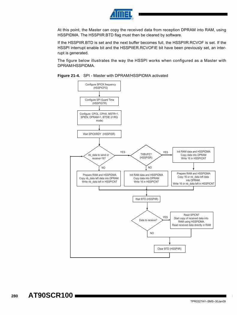
At this point, the Master can copy the received data from reception DPRAM into RAM, usingHSSPIDMA. The HSSPIIR.BTD flag must then be cleared by software.
If the HSSPIIR.BTD is set and the next buffer becomes full, the HSSPIIR.RCVOF is set. If theHSSPI interrupt enable bit and the HSSPIIER.RCVOFIE bit have been previously set, an inter-rupt is generated.
The figure below illustrates the way the HSSPI works when configured as a Master withDPRAM/HSSPIDMA.
Figure 21-4. SPI - Master with DPRAM/HSSPIDMA activated
Configure SPICK frequency(HSSPICFG)
Data to receive?
Configure SPI Guard Time(HSSPIGTR)
Configure CPOL, CPHA, MSTR=1, SPIEN, DPRAM=1, BTDIE (if IRQ
mode)
Wait SPICKRDY (HSSPISR)
Read SPICNTStart copy of received data into
RAM using HSSPIDMA.Read received data directly in RAM
Wait BTD (HSSPIIR)
Clear BTD (HSSPIIR)
YES
NO
nb_data to send or receive>16?
TXBUFE?(HSSPISR)
Init RAM data and HSSPIDMACopy data into DPRAMWrite 16 in HSSPICNT
Prepare RAM and HSSPIDMACopy 16 or nb_data left data
into DPRAM. Write 16 or nb_data left in HSSPICNT
YESYES
NONO
Init RAM data and HSSPIDMACopy data into DPRAMWrite 16 in HSSPICNT
Prepare RAM and HSSPIDMACopy nb_data left data into DPRAM.
Write nb_data left in HSSPICNT
280TPR0327AY–SMS–30Jan09
AT90SCR100

AT90SCR100
21.2.2 SPI Controller Configured as a Slave
21.2.2.1 One byte sending using shift register (without DPRAM)If the DPRAM is not activated (HSSPICFG.DPRAM bit cleared), the software may update thecontents of the HSSPI Transmit Data Register, SPITDR, that will be shifted out by incomingclock pulses on the clock pin. As soon as the byte has been completely shifted, the Byte transferDone flag (HSSPIIR.BTD) is set. If global interrupt and the HSSPIIER.BTDIE bit have been previ-ously set, an interrupt is generated.
At this stage, the Slave can read the HSSPIRDR register to retrieve the byte sent by the otherdevice. The HSSPICFG.BTD flag must then be cleared by software.
Figure 21-5. HSSPI - Slave without DPRAM activated
Clear BTD (HSSPIIR)(mandatory if IRQ mode)
Data to send?
YES
NO
Wait SPICKRDY (HSSPISR)
Write data to send into HSSPITDR
Configure CPOL, CPHA, MSTR=0,
SPIEN, DPRAM=0, BTDIE (if IRQ mode)
Wait BTD (HSSPIIR)
Data to receive?
Wait BTD (HSSPIIR)
Read data from HSSPIRDR
NO
YES
281TPR0327AY–SMS–30Jan09

21.2.2.2 Buffer sending with DPRAM and HSSPIDMA (DPRAM mode)When the DPRAM is activated (HSSPICFG.DPRAM bit set), the data to be sent must be writtento one of the internal DPRAM buffers using HSSPIDMA. Once this is done, the number of bytesto be transmitted is written to the HSSPICNT register. When the master applies the clock, thisnumber of bytes is shifted from the master to the slave and from the slave to the master simulta-neously. At this point, new data can be stored in the second buffer if the HSSPISR.TXBUFE = 1.Each time all the data in one of the buffers is sent, the Byte Transfer Done flag (HSSPIIR.BTD)is set. If global interrupt and the HSSPIIER.BTDIE bit have been previously set, an interrupt isgenerated.
At this stage, the incoming data can be copied from internal DPRAM to RAM using HSSPIDMA.The HSSPIIR.BTD flag must then be cleared by software.
If the HSSPIIR.BTD is set and the next buffer becomes full, the HSSPIIR.RCVOF is set. If globalinterrupt and the HSSPIIER.RCVOFIE bit have been previously set, an interrupt is generated.
The figures below (Figure 21-6, Figure 21-7 & Figure 21-8) illustrate the way the SPI workswhen configured as a Slave with DPRAM mode.
282TPR0327AY–SMS–30Jan09
AT90SCR100

AT90SCR100
Figure 21-6. SPI - Slave with DPRAM operation - First part
Configure SPICK frequency(HSSPICFG)
Use the timeout?
Configure HSSPITIMEOUT
Configure CPOL, CPHA, MSTR=0, SPIEN, DPRAM=1, BTDIE
Wait SPICKRDY (HSSPISR)
GOTO LABEL "RECEIVE DATA"
nb_data to send or receive>16?
TXBUFE?(HSSPISR)
Data to receive?
Wait BTD (HSSPIIR)
Clear BTD (HSSPIIR)
YES
YESYES
NONO
NO
Data to send?
YES
NO
YES
NO
Init RAM data and HSSPIDMACopy data into DPRAMWrite 16 in HSSPICNT
Prepare RAM and HSSPIDMACopy 16 or nb_data left data
into DPRAM. Write 16 or nb_data left in HSSPICNT
Init RAM data and HSSPIDMACopy data into DPRAMWrite 16 in HSSPICNT
Prepare RAM and HSSPIDMACopy nb_data left data into DPRAM.
Write nb_data left in HSSPICNT
Read SPICNTStart copy of received data into
RAM using HSSPIDMA.Read received data directly in RAM
283TPR0327AY–SMS–30Jan09

Figure 21-7. SPI - Slave with DPRAM operation - Second part
If the number of bytes to be received or sent is not known, a timeout can be used. It can be acti-vated by entering a time bit value in the HSSPITIMEOUT and setting the HSSPICR.STTTO bit.As the amount of data is unknown, the two registers (HSSPICNT) have to be set to the maxi-mum value, 16. When the timeout occurs, the HSSPIIR.TIMEOUT bit is set. If the HSSPIinterrupt enable bit and the HSSPIIER.TIMEOUTIE bit have been previously set, an interrupt isgenerated. The number of byte received is available in the HSSPICNT register. Clearing theHSSPIIR.TIMEOUT bit by soft or by setting the HSSPICR.STTTO bit will update the internalDPRAM
nb_data to receive known?
LABEL "RECEIVE DATA"
nb_data to receive >16?
rx_buf_full?
Write nb_data to receive in HSSPICNT
Write 16 in HSSPICNT
Wait BTD (HSSPIIR)
Write 16 in HSSPICNT
Clear BTD (HSSPIIR)
YES
YES
NO
NO
YES
NO GOTO LABEL "RECEIVE DATA UK"
Clear BTD (HSSPIIR)
nb_data to receive >16?YES
Write nb_data left in HSSPICNT
NO
Read HSSPICNTStart copy of received data into
RAM using HSSPIDMA.Read received data directly in RAM
Read HSSPICNTStart copy of received data into
RAM using HSSPIDMA.Read received data directly in RAM
284TPR0327AY–SMS–30Jan09
AT90SCR100

AT90SCR100
Figure 21-8. SPI - Slave with DPRAM operation - Third part
In SPI slave mode, the control logic will sample the incoming signal of the HSSCK pin. Toensure correct sampling of the clock signal, the frequency of the HSSPI clock should neverexceed fSCKmax (fSCKmax=24 Mbits/s). When the HSSPI is enabled, the data direction of theHSMOSI, HSMISO, HSSCK, and HSSS pins is overridden according to Table 21-1
.
Table 21-1. SPI Pin Overrides
Pin Direction, Master SPI Direction, Slave SPI
MOSI Output Input
MISO Input Output
SCK Output Input
NSS Output Input
BTD?
Write 16 in HSSPICNT
Read nb_data in HSSPICNTCopy nb_data into RAM using
HSSPIDMA.Read received data directly into RAM
Set bit HSSPICR.STTO
YES
NO
then TIMEOUT
LABEL "RECEIVE DATA UK"
Clear BTD (HSSPIIR)
Set bit HSSPICR.STTO
Wait BTD or TIMEOUT
Write 16 in HSSPICNT
End of reception.Next loop
Copy 16 into RAM using HSSPIDMA.Read received data directly into RAM
Clear TIMEOUT(HSSPIIR)
Disable DMA(Clear HSSPICFG.DPRAM)
Enable DMA(Set HSSPICFG.DPRAM)
Wait DMA ready(HSSPISR.DPRAMRDY)
285TPR0327AY–SMS–30Jan09

21.3 HSSS line Functionality
21.3.1 Slave ModeWhen the HSSPI is configured as a Slave (HSSPICFG.MSTR bit cleared), the Slave Select(HSSS) line is driven by the master device. The HSSS has no effect on the HSSPI logic. It is thesoftware’s responsibility to manage the HSSS level.
21.3.2 Master ModeWhen the HSSPI is configured as a Master (HSSPICFG.MSTR bit set), the HSSS line is used toselect the slave.
21.4 Data ModesThere are four combinations of SCK phase and polarity with respect to serial data, which aredetermined by control bits CPHA and CPOL. The SPI data transfer formats are shown in Figure21-9 and Figure 21-10.
Figure 21-9. SPI Transfer Format with CPHA = 0
Figure 21-10. SPI Transfer Format with CPHA = 1
286TPR0327AY–SMS–30Jan09
AT90SCR100

AT90SCR100
21.5 HSSPI Interface Registers
21.5.1 HSSPICFG - HSSPI Config Register
• Bits 7..5 - SPICKDIV2..0: SPI Clock Divider Ratio BitsDefines the HSSPI Clock divider ratio.
The following table gives, for each combination of SPICKDIV2, SPICKDIV1 and SPICKDIV0, thedivision applied to the clock. Figure 7-1 on page 31 gives information about the clock tree andbase frequency for HSSPI.
Note: 1. Base frequency is clkIO = 96Mhz
• Bit 4 - DPRAM: DPRAM BitWhen set (one), this bit enables the DPRAM/HSSPIDMA systems.
When cleared (zero), this bit disables the DPRAM/HSSPIDMA systems.
• Bit 3 - HSCPHA: High Speed Clock PHAse BitThe settings of the clock phase bit (CPHA) determine if data is sampled on the leading (first) ortrailing (last) edge of HSSCK. Refer to Figure 21-9 and Figure 21-10.
Bit 7 6 5 4 3 2 1 0
$0000D9 SPICKDIV [2..0] DPRAM HSCPHA HSCPOL HSMSTR HSSPIEN HSSPICFGRead/write R/W R/W R/W R/W R/W R/W R/W R/W
Initial value 1 0 0 0 0 0 0 0 0x80
Table 21-2. HSSPI dividers(1)
SPICKDIV2 SCKCKDIV1 SCKCKDIV0 Divider External clock divider ratio(1)
0 0 0 4 24 Mhz
0 0 1 5 19.2 Mhz
0 1 0 6 16 Mhz
0 1 1 8 12 Mhz
1 0 0 12 8 Mhz
1 0 1 24 4 Mhz
1 1 0 48 2 Mhz
1 1 1 96 1 Mhz
Any attempt at modifying the HSSPICFG.SPICKDIV value once the HSSPI Con-troller is enabled will not affect the HSSPI Clock frequency.
After a DPRAM is disabled, the DPRAM is reset. This reset is active for two clockcycles of the DPRAM clock. It is recommended to do nothing on the DPRAM dur-ing these two clock cycles.
Note
Note
287TPR0327AY–SMS–30Jan09

The CPHA functionality is summarized below:
• Bit 2 - HSCPOL: High Speed Clock POLarity BitWhen this bit is written to one, SCK is high when idle. When CPOL is written to zero, SCK is lowwhen idle. Refer to Figure 21-9 and Figure 21-10.
The CPOL functionality is summarized below:
• Bit 1 - HSMSTR: High Speed Master/Slave Select BitThis bit selects the Master HSSPI mode when set (one), and Slave HSSPI mode when cleared(zero).
This bit is cleared by software or by hardware when the HSSPICFG.SPIEN gets cleared (dis-abling the HSSPI).
• Bit 0 - HSSPIEN: High Speed SPI Enable BitWhen this bit is set (one), the HSSPI Controller is enabled with the predefined configuration.
When this bit is cleared (zero), the HSSPI Controller is disabled and HSSPICFG.HSMSTR isdriven low.
21.5.2 HSSPIIR - HSSPI Interrupt Register
• Bit 7 - TIMEOUT: Timeout Interrupt BitThis bit is set (one) when a Timeout occurs. An interrupt is generated if HSSPIIER.TIMEOUTIEis set and global interrupt is enabled.
This bit is cleared by software or by hardware when the HSSPICFG.SPIEN is toggled (enablingor disabling the HSSPI).
• Bit 6 - BTD: Byte Transfer Done Bit
Table 21-3. CPHA Configuration
CPHA Leading edge Trailing edge
0 Sample Setup
1 Setup Sample
Table 21-4. CPOL Configuration
CPOL Leading edge Trailing edge
0 Rising Falling
1 Falling Rising
Configuring and activating the HSSPI peripheral with the same instruction is a validaction.
Note
Bit 7 6 5 4 3 2 1 0
$0000DA TIMEOUT BTD RCVOF NSSRE NSSFE - - - HSSPIIRRead/write R/W R/W R/W R/W R/W R R R
Initial value 0 0 0 0 0 0 0 0 0x00
288TPR0327AY–SMS–30Jan09
AT90SCR100

AT90SCR100
This bit is set (one) when a serial transfer of the number of bytes specified in HSSPICNT is com-pleted. An interrupt is generated if HSSPIIER.BTDIE is set and global interrupt is enabled.
This bit is cleared by software or by hardware when the HSSPICFG.SPIEN is toggled (enablingor disabling the HSSPI).
• Bit 5 - RCVOF: Receive Overflow BitThis bit is set by hardware, when the DPRAM mode is set and the two 16 bytes receive buffersare full. An interrupt is generated if HSSPIIER.RCVOFIE is set and global interrupt is enabled.
• Bit 4 - NSSRE: NSS Rising EdgeSet (one) by hardware on a rising edge on HSSS
Cleared (zero) by software
• Bit 3 - NSSFE: NSS Falling edge BitSet (one) by hardware on a falling edge on HSSS
Cleared (zero) by software
21.5.3 HSSPIIER - HSSPI Interrupt Enable Register
• Bit 7 - TIMEOUTIE: Timeout Interrupt Enable BitWhen set (one), this bit enables the Timeout event as the source of the HSSPI interrupt.
When cleared (zero), this bit disables the Timeout source of the HSSPI interrupt.
• Bit 6 - BTDIE: Byte Transfer Done Interrupt Enable BitWhen set (one), this bit enables the Byte Transfer Done event as the source of the HSSPIinterrupt.
When cleared (zero), this bit disables the Byte Transfer Done source of the HSSPI interrupt.
• Bit 5 - RCVOFIE: Receive Overflow Interrupt Enable BitWhen set (one), this bit enables the Receive Overflow event as the source of the HSSPIinterrupt.
When cleared (zero), this bit disables the Receive Overflow source of the HSSPI interrupt.
• Bit 4 - NSSIE: NSS Interrupt EnableWhen set (one), the HSSS interrupt is enabled on falling and rising edges
When cleared (zero), the HSSS interrrupt is disabled
Bit 7 6 5 4 3 2 1 0
$0000D4 TIMEOUTIE BTDIE RCVOFIE NSSIE - - - - HSSPIIERRead/write R/W R/W R/W R/W R R R R
Initial value 0 0 0 0 0 0 0 0 0x00
289TPR0327AY–SMS–30Jan09

21.5.4 HSSPICR - HSSPI Control Register
• Bit 2 - STTTO: Start Time-OutWhen set (one), this will rearm the time-out timer and start it once the first byte is received
When cleared (zero), no action is performed.
• Bit 1 - RETTO: Rearm Timeout Interrupt Enable BitWhen set (one), this will rearm the time-out timer, giving more time to receive the next byte.
When cleared (zero), no action is performed.
• Bit 0 - CS: SPI CS BitWhen set (one), the HSSPI HSSS pin is set (one).
When cleared (zero), the SPI HSSS pin is cleared (zero).
21.5.5 HSSPISR - HSSPI Status Register
• Bit 4 - DPRAMRDY: DPRAM Ready BitWhen this bit is set (one), the DPRAM is running and operational.
When this bit is cleared (zero), the DPRAM is not available.
• Bit 3 - NSS: NSS BitStatus of the HSSS pin
• Bit 2 - RXBUFF: Reception Buffer Full BitWhen this bit is set (one), all reception buffers are full.
• Bit 1 - TXBUFE: Transmission Buffer Empty BitWhen this bit is set (one), all transmission buffers are empty.
• Bit 0 - SPICKRDY: SPI Clock Ready BitWhen this bit is set (one), the HSSPI Controller is running and operational.
When this bit is cleared (zero), the HSSPI Controller is not available.
Bit 7 6 5 4 3 2 1 0
$0000DB - - - - - STTTO RETTO CS HSSPICRRead/write R R R R R W W W
Initial value 0 0 0 0 0 0 0 0 0x00
Bit 7 6 5 4 3 2 1 0
$0000D8 - - - DPRAMRDY NSS RXBUFF TXBUFE SPICKRDY HSSPISRRead/write R R R R R R R R
Initial value 0 0 0 0 0 0 0 0 0x00
290TPR0327AY–SMS–30Jan09
AT90SCR100

AT90SCR100
21.5.6 HSSPITDR - HSSPI Transmit Data Register
• Bits 7..0 - HSSPITDD7..0: Transmit Data valueThis register is used only when the DPRAM mode is disabled.
The HSSPI Transmit Data register is a write register used for data transmission from the registerfile to the HSSPI Shift register. Writing to the register initiates data transmission.
21.5.7 HSSPIRDR - HSSPI Received Data Register
• Bits 7..0 - HSSPIRDD7..0: Receive Data valueThis register is used only when the DPRAM mode is disabled.
The HSSPI Receive Data register is a read register used for data reception to the register filefrom the HSSPI Shift register. Reading this register causes the Shift Register holding the firstreceived data to be read.
21.5.8 HSSPIGTR - HSSPI Guard Time Register
• Bits 7..0 - HSSPIGTD7..0: Guard Time valueThe HSSPI Guard Time register value is the number of HSSPI clock cycles to be insertedbetween characters, in master mode only.
21.5.9 HSSPICNT - HSSPI Byte Count Register
• Bits 4..0 - HSSPICNTD4..0 : Number of byte received or to sendThis register is used only when DPRAM mode is activated.
Writing this register specifies the number of bytes to be sent and received for the currentreceived and transmit buffers.
Bit 7 6 5 4 3 2 1 0
$0000D7 HSSPITDD [7..0] HSSPITDRRead/write W W W W W W W W
Initial value 0 0 0 0 0 0 0 0 0x00
Bit 7 6 5 4 3 2 1 0
$0000D6 HSSPIRDD [7..0] HSSPIRDRRead/write R R R R R R R R
Initial value 0 0 0 0 0 0 0 0 0x00
Bit 7 6 5 4 3 2 1 0
$0000D5 HSSPIGTD [7..0] HSSPIGTRRead/write R/W R/W R/W R/W R/W R/W R/W R/W
Initial value 0 0 0 0 0 0 0 0 0x00
Bit 7 6 5 4 3 2 1 0
$0000D3 - - - HSSPICNTD [4..0] HSSPICNTRead/write R R R R/W R/W R/W R/W R/W
Initial value 0 0 0 0 0 0 0 0 0x00
291TPR0327AY–SMS–30Jan09

Reading this register gives the amount of data received for the current received buffer (In thiscase, the current received buffer means that this buffer received the expected number of data orhad a timeout).
21.5.10 HSSPITIMEOUT - HSSPI Timeout Register
• Bits 15..0 - SPITIMEOUT15..0 : Communication TimeoutThis register is used only when DPRAM mode is activated. It specifies the number of clockcycles before a timeout occurs (bit HSSPIIR.TIMEOUT is set). See “HSSPIIR - HSSPI InterruptRegister” on page 288. The clock is defined by HSSPICFG.SPICKDIV bits. See “HSSPICFG -HSSPI Config Register” on page 287.
21.6 HSSPIDMA ControllerThe HSSPIDMA controller, implemented on the AT90SCR100, is intended to execute fast trans-fers between the RAM memory and the internal HSSPI DPRAM. This feature allows theapplication software of the AT90SCR100 to manage the exchanges imposed by the SPI com-munication at high frequency.
The HSSPIDMA is enabled as soon as DPRAM mode is act ivated (by sett ing bitHSSPICFG.DPRAM). One HSSPIDMA operation can transfer up to N bytes in (N+1) AVRcycles.
Writing HSSPICNT register will internally switch the DPRAM buffers.
Thus, the DMA controller will point to the other DPRAM buffer.Note
Bit 15 14 13 12 11 10 9 8
$0000D2 SPITIMEOUT[15..8] HSSPITOH$0000D1 SPITIMEOUT [7..0] HSSPITOLBit 7 6 5 4 3 2 1 0
Read/write R/W R/W R/W R/W R/W R/W R/W R/W
R/W R/W R/W R/W R/W R/W R/W R/W
Initial value 0 0 0 0 0 0 0 0 0x00
0 0 0 0 0 0 0 0 0x00
All the registers described in this section cannot be accessed if the HSSPI moduleis not enabled.
Caution!
292TPR0327AY–SMS–30Jan09
AT90SCR100

AT90SCR100
Figure 21-11. HSSPIDMA Controller Diagram
21.6.1 HSSPIDMACS - HSSPIDMA Control and Status registerThis is the control and status register of the HSSPIDMA controller.
• Bit 2 - HSSPIDMAERR : DMA Error BitWhen starting the HSSPIDMA controller, this bit is cleared (zero) by the hardware if the values inHSSPIDMADH, HSSPIDMADL and HSSPIDMAB registers are suitable for the HSSPIDMAoperation requested.
This bit can also be cleared(zero) by software.
This bit is set (one) by hardware when starting a HSSPIDMA operation and whenever one ofthese following cases occurs:
• The base address contained in the registers HSSPIDMADH and HSSPIDMADL is incorrect (out of the allowed range).
• According to the values of the registers HSSPIDMADH, HSSPIDMADL and HSSPIDMAB and even if the base address is correct, an address out of the allowed range is going to be reached.
When a HSSPIDMA operation is started, the AVR is automatically stopped. At theend of the HSSPIDMA operation, the application software automatically restartswhere it left (actually with the instruction following the launching of the HSSPIDMAoperation). Thus the application software does not need to wait for an interrupt orto need poll the end of the HSSPIDMA operation.
RAM Reception DPRAM
Automatic Switch
$100
$10FF 16 bytes
16 bytes
HSSPIDMACS.DMAR01
HSSPIDMACS.DMADIR
0
1DM
AB
HSSPIDMACS.DMAERR
DMAD
DMA Controller Diagram Transmission DPRAM
Automatic Switch
16 bytes
16 bytes
HSSPIDMACS.DMAR
01
Note
Bit 7 6 5 4 3 2 1 0
$0000DC - - - - - HSSPIDMAERR HSSPIDMADIR HSSPIDMAR HSSPIDMACSRead/write R R R R R R/W R/W R/W
Initial value 0 0 0 0 0 0 0 0 0x00
293TPR0327AY–SMS–30Jan09
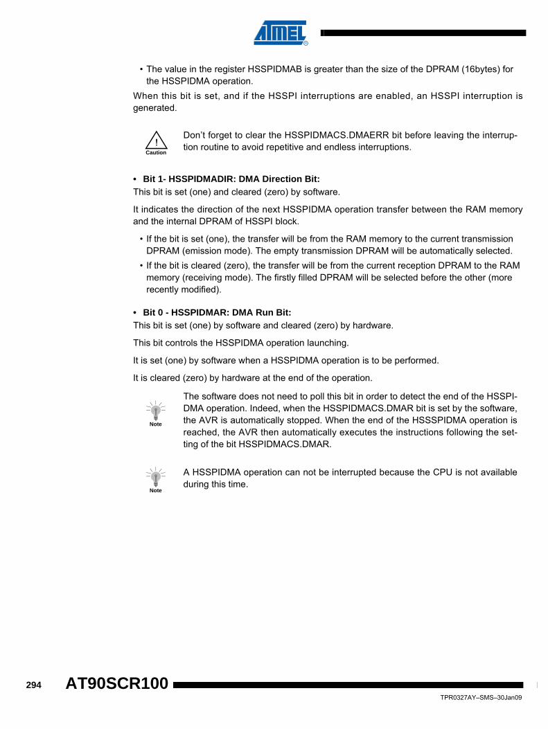
• The value in the register HSSPIDMAB is greater than the size of the DPRAM (16bytes) for the HSSPIDMA operation.
When this bit is set, and if the HSSPI interruptions are enabled, an HSSPI interruption isgenerated.
• Bit 1- HSSPIDMADIR: DMA Direction Bit:This bit is set (one) and cleared (zero) by software.
It indicates the direction of the next HSSPIDMA operation transfer between the RAM memoryand the internal DPRAM of HSSPI block.
• If the bit is set (one), the transfer will be from the RAM memory to the current transmission DPRAM (emission mode). The empty transmission DPRAM will be automatically selected.
• If the bit is cleared (zero), the transfer will be from the current reception DPRAM to the RAM memory (receiving mode). The firstly filled DPRAM will be selected before the other (more recently modified).
• Bit 0 - HSSPIDMAR: DMA Run Bit:This bit is set (one) by software and cleared (zero) by hardware.
This bit controls the HSSPIDMA operation launching.
It is set (one) by software when a HSSPIDMA operation is to be performed.
It is cleared (zero) by hardware at the end of the operation.
Don’t forget to clear the HSSPIDMACS.DMAERR bit before leaving the interrup-tion routine to avoid repetitive and endless interruptions.
The software does not need to poll this bit in order to detect the end of the HSSPI-DMA operation. Indeed, when the HSSPIDMACS.DMAR bit is set by the software,the AVR is automatically stopped. When the end of the HSSSPIDMA operation isreached, the AVR then automatically executes the instructions following the set-ting of the bit HSSPIDMACS.DMAR.
A HSSPIDMA operation can not be interrupted because the CPU is not availableduring this time.
Caution!
Note
Note
294TPR0327AY–SMS–30Jan09
AT90SCR100

AT90SCR100
21.6.2 HSSPIDMAD - HSSPIDMA ADdress registers
• Bits 7..6 - Res: Reserved BitsThese bits are reserved bits in the AT90SCR100 and are always read as zero.
• Bits 13..0 - HSSPIDMAD13..0 : HS SPI DMA AddressThese bits represents the 14-bit HSSPIDMA Address.
These two registers set the base address in RAM. This address represents the source of thedata to be sent if the HSSPIDMA controller is configured in the emission mode. It represents thedestination to store the data if the HSSPIDMA controller is configured in the receiving mode.
The initial value corresponds to RAM address $000100.
You can address the whole RAM with this parameter. Values in RAM that must not be dumped,shall be stored out of the HSSPIDMA RAM accessible range.
When starting a HSSPIDMA operation, the hardware will check if the values of HSSPIDMADH,HSSPIDMADL and HSSPIDMAB registers does not exceed the specific RAM area ($000100 to$0010FF). If an error is detected, HSSPIDMACS.DMAERR bit is automatically set (one). ASupervisor RAM Illegal Access Attempt Violation security interrupt (if not masked) is so trig-gered. HSSPIDMADH, HSSPIDMADL and HSSPIDMAB registers keep their previous value.
21.6.3 HSSPIDMAB - DMA Amount of Bytes RegisterThis register is dedicated to the amount of bytes to be transferred during the next HSSPIDMAoperation setting.
• Bit 7..5 - Res : Reserved BitsThis bit is reserved bit in the AT90SCR100 and is always read as zero.
Bit 15 14 13 12 11 10 9 8
$0000DE - - HSSPIDMAD [13..8] HSSPIDMADH$0000DD HSSPIDMAD [8..0] HSSPIDMADLBit 7 6 5 4 3 2 1 0
Read/write R R R/W R/W R/W R/W R/W R/W
R/W R/W R/W R/W R/W R/W R/W R/W
Initial value 0 0 0 0 0 0 0 1 0x01
0 0 0 0 0 0 0 0 0x00
After a HSSPIDMA operation, HSSPIDMADH and HSSPIDMADL are set to thelast value reached in RAM and incremented by one. For instance, after a 64-bytetransfer started from base address $000100, HSSPIDMAD equals to $000140(HSSPIDMADH = $01 and HSSPIDMADL = $40). This feature allows to simplifyregisters and bits handlings when several HSSPIDMA operations are to be suc-cessively performed, which can be the case when getting or sending severalpackets.
Note
Bit 7 6 5 4 3 2 1 0
$00DF - - - HSSPIDMAB [4..0] HSSPIDMABRead/write R R R R/W R/W R/W R/W R/W
Initial value 0 0 0 0 0 0 0 0 0x00
295TPR0327AY–SMS–30Jan09

• Bits 4..0 - HSSPIDMAB4..0 : HS SPI DMA Amount of Bytes BitsThese bits are the (4..0) bits of the 7-bit HSSPIDMA Amount of Bytes value.
When starting a HSSPIDMA operation, the hardware will check if the values of HSSPIDMADH,HSSPIDMADL and HSSPIDMAB registers does not exceed the specific RAM area ($000100 to$0010FF). If an error is detected, HSSPIDMACS.DMAERR bit is automatically set (one). ASupervisor RAM Illegal Access Attempt Violation security interrupt (if not masked) is so trig-gered. HSSPIDMADH, HSSPIDMADL and HSSPIDMAB registers keep their previous value.
After a HSSPIDMA operation completion, the value of this register is not reset.
The maximum value allowed for HSSPIDMAB is 16. Note
296TPR0327AY–SMS–30Jan09
AT90SCR100

AT90SCR100
22. 2-wire Serial Interface _ TWI
22.1 Features• Simple Yet Powerful and Flexible Communication Interface, only two Bus Lines Needed• Both Master and Slave Operation Supported• Device can Operate as Transmitter or Receiver• 7-bit Address Space Allows up to 128 Different Slave Addresses• Multi-master Arbitration Support• Up to 400 kHz Data Transfer Speed• Slew-rate Limited Output Drivers• Noise Suppression Circuitry Rejects Spikes on Bus Lines• Fully Programmable Slave Address with General Call Support• Address Recognition Causes Wake-up When AVR is in Sleep Mode
22.2 TWI Serial Interface Bus DefinitionThe 2-wire Serial Interface (TWI) is ideally suited for typical microcontroller applications. TheTWI protocol allows the systems designer to interconnect up to 128 different devices using onlytwo bi-directional bus lines, one for clock (SCL) and one for data (SDA). The only external hard-ware needed to implement the bus is a single pull-up resistor for each of the TWI bus lines. Alldevices connected to the bus have individual addresses, and mechanisms for resolving buscontention are inherent in the TWI protocol.
Figure 22-1. TWI Bus Interconnection
22.2.1 TWI TerminologyThe following definitions are frequently encountered in this section.
Device 1 Device 2 Device 3 Device n
SDA
SCL
........ R1 R2
V CC
Table 22-1. TWI Terminology
Term Description
Master The device that initiates and terminates a transmission. The Master also generates the SCL clock.
297TPR0327AY–SMS–30Jan09
The Power Reduction TWI bit, PRTWI bit in PRR0 must be written to zero to enable the TWISerial Interface.
22.2.2 Electrical InterconnectionThe number of devices that can be connected to the bus is only limited by the bus capacitance-limit of 400 pF and the 7-bit slave address space. A detailed specification of the electricalcharacteristics of the TWI is given in section “2-wire Serial Interface Characteristics TBC/TBD”on page 411. Two different sets of specifications are presented there, one relevant for busspeeds below 100 kHz, and one valid for bus speeds up to 400 kHz.
22.3 Data Transfer and Frame Format
22.3.1 Transferring BitsEach data bit transferred on the TWI bus is accompanied by a pulse on the clock line. The levelof the data line must be stable when the clock line is high. The only exception to this rule is forgenerating start and stop conditions.
Figure 22-2. Data Validity
22.3.2 START and STOP ConditionsThe Master initiates and terminates a data transmission. The transmission is initiated when theMaster issues a START condition on the bus, and it is terminated when the Master issues aSTOP condition. Between a START and a STOP condition, the bus is considered busy, and noother master should try to seize control of the bus. A special case occurs when a new STARTcondition is issued between a START and STOP condition. This is referred to as a REPEATEDSTART condition, and is used when the Master wishes to initiate a new transfer without relin-quishing control of the bus. After a REPEATED START, the bus is considered busy until the nextSTOP. This is identical to the START behavior, and therefore START is used to describe bothSTART and REPEATED START for the remainder of this datasheet, unless otherwise noted. As
Slave The device addressed by a Master.
Transmitter The device placing data on the bus.
Receiver The device reading data from the bus.
Table 22-1. TWI Terminology
Term Description
SDA
SCL
Data Stable Data Stable
Data Change
298TPR0327AY–SMS–30Jan09
AT90SCR100
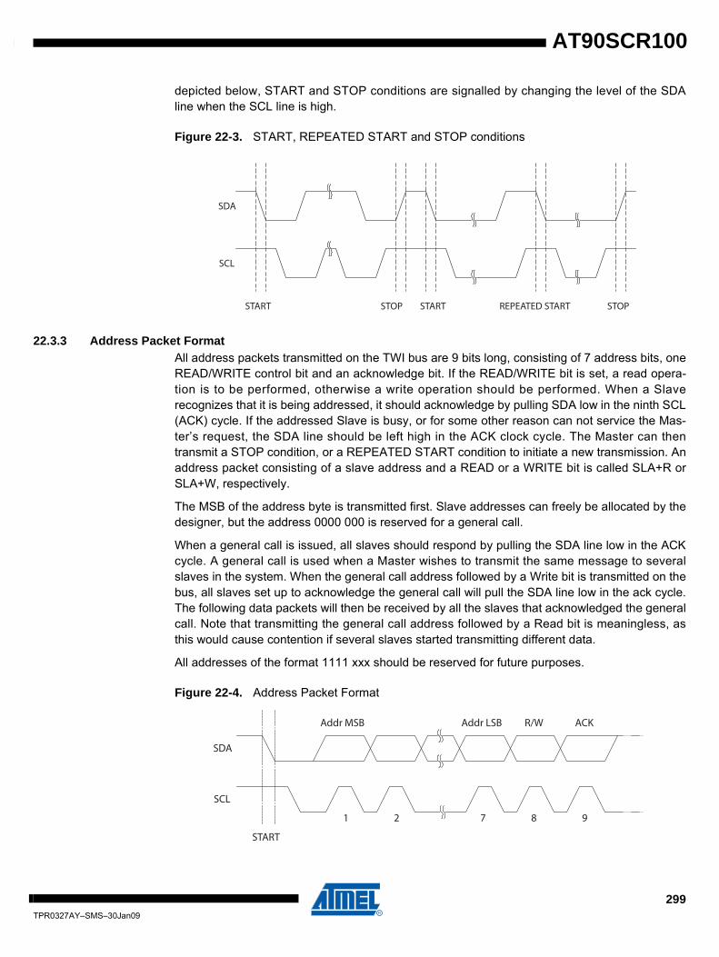
AT90SCR100
depicted below, START and STOP conditions are signalled by changing the level of the SDAline when the SCL line is high.
Figure 22-3. START, REPEATED START and STOP conditions
22.3.3 Address Packet FormatAll address packets transmitted on the TWI bus are 9 bits long, consisting of 7 address bits, oneREAD/WRITE control bit and an acknowledge bit. If the READ/WRITE bit is set, a read opera-tion is to be performed, otherwise a write operation should be performed. When a Slaverecognizes that it is being addressed, it should acknowledge by pulling SDA low in the ninth SCL(ACK) cycle. If the addressed Slave is busy, or for some other reason can not service the Mas-ter’s request, the SDA line should be left high in the ACK clock cycle. The Master can thentransmit a STOP condition, or a REPEATED START condition to initiate a new transmission. Anaddress packet consisting of a slave address and a READ or a WRITE bit is called SLA+R orSLA+W, respectively.
The MSB of the address byte is transmitted first. Slave addresses can freely be allocated by thedesigner, but the address 0000 000 is reserved for a general call.
When a general call is issued, all slaves should respond by pulling the SDA line low in the ACKcycle. A general call is used when a Master wishes to transmit the same message to severalslaves in the system. When the general call address followed by a Write bit is transmitted on thebus, all slaves set up to acknowledge the general call will pull the SDA line low in the ack cycle.The following data packets will then be received by all the slaves that acknowledged the generalcall. Note that transmitting the general call address followed by a Read bit is meaningless, asthis would cause contention if several slaves started transmitting different data.
All addresses of the format 1111 xxx should be reserved for future purposes.
Figure 22-4. Address Packet Format
SDA
SCL
START STOPREPEATED STARTSTOP START
SDA
SCL
START
1 2 7 8 9
Addr MSB Addr LSB R/W ACK
299TPR0327AY–SMS–30Jan09

22.3.4 Data Packet FormatAll data packets transmitted on the TWI bus are nine bits long, consisting of one data byte andan acknowledge bit. During a data transfer, the Master generates the clock and the START andSTOP conditions, while the Receiver is responsible for acknowledging the reception. AnAcknowledge (ACK) is signalled by the Receiver pulling the SDA line low during the ninth SCLcycle. If the Receiver leaves the SDA line high, a NACK is signalled. When the Receiver hasreceived the last byte, or for some reason cannot receive any more bytes, it should inform theTransmitter by sending a NACK after the final byte. The MSB of the data byte is transmitted first.
Figure 22-5. Data Packet Format
22.3.5 Combining Address and Data Packets into a TransmissionA transmission basically consists of a START condition, a SLA+R/W, one or more data packetsand a STOP condition. An empty message, consisting of a START followed by a STOP condi-tion, is illegal. Note that the Wired-ANDing of the SCL line can be used to implementhandshaking between the Master and the Slave. The Slave can extend the SCL low period bypulling the SCL line low. This is useful if the clock speed set up by the Master is too fast for theSlave, or the Slave needs extra time for processing between the data transmissions. The Slaveextending the SCL low period will not affect the SCL high period, which is determined by theMaster. As a consequence, the Slave can reduce the TWI data transfer speed by prolonging theSCL duty cycle.
Figure 22-6 shows a typical data transmission. Note that several data bytes can be transmittedbetween the SLA+R/W and the STOP condition, depending on the software protocol imple-mented by the application software.
Figure 22-6. Typical Data Transmission
1 2 7 8 9
Data MSB Data LSB ACK
AggregateSDA
SDA fromTransmitter
SDA fromReceiver
SCL fromMaster
SLA+R/W Data ByteSTOP, REPEATED
START or NextData Byte
1 2 7 8 9
Data Byte
Data MSB Data LSB ACK
START
1 2 7 8 9
Addr MSB Addr LSB R/W ACK
SLA+R/W ST
300TPR0327AY–SMS–30Jan09
AT90SCR100

AT90SCR100
22.4 Multi-master Bus Systems, Arbitration and SynchronizationThe TWI protocol allows bus systems with several masters. Special concerns have been takenin order to ensure that transmissions will proceed as normal, even if two or more masters initiatea transmission at the same time. Two problems arise in multi-master systems:
• An algorithm must be implemented allowing only one of the masters to complete the transmission. All other masters should cease transmission when they discover that they have lost the selection process. This selection process is called arbitration. When a contending master discovers that it has lost the arbitration process, it should immediately switch to Slave mode to check whether it is being addressed by the winning master. The fact that multiple masters have started transmission at the same time should not be detectable to the slaves, i.e. the data being transferred on the bus must not be corrupted.
• Different masters may use different SCL frequencies. A scheme must be devised to synchronize the serial clocks from all masters, in order to let the transmission proceed in a lockstep fashion. This will facilitate the arbitration process.
The wired-ANDing of the bus lines is used to solve both these problems. The serial clocks fromall masters will be wired-ANDed, yielding a combined clock with a high period equal to the onefrom the Master with the shortest high period. The low period of the combined clock is equal tothe low period of the Master with the longest low period. Note that all masters listen to the SCLline, effectively starting to count their SCL high and low time-out periods when the combinedSCL line goes high or low, respectively.
Figure 22-7. SCL Synchronization Between Multiple Masters
Arbitration is carried out by all masters continuously monitoring the SDA line after outputtingdata. If the value read from the SDA line does not match the value the Master had output, it haslost the arbitration. Note that a Master can only lose arbitration when it outputs a high SDA valuewhile another Master outputs a low value. The losing Master should immediately go to Slavemode, checking if it is being addressed by the winning Master. The SDA line should be left high,but losing masters are allowed to generate a clock signal until the end of the current data or
TA low TA high
SCL fromMaster A
SCL fromMaster B
SCL BusLine
TB low TB high
Masters StartCounting Low Period
Masters StartCounting High Period
301TPR0327AY–SMS–30Jan09
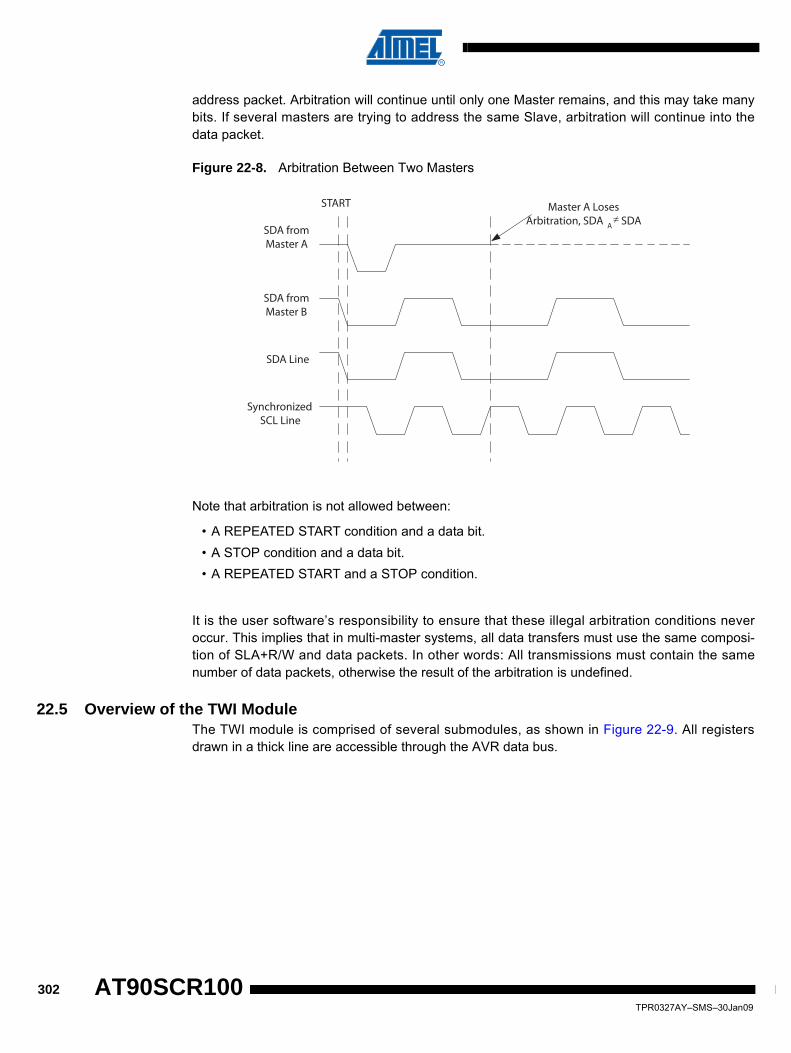
address packet. Arbitration will continue until only one Master remains, and this may take manybits. If several masters are trying to address the same Slave, arbitration will continue into thedata packet.
Figure 22-8. Arbitration Between Two Masters
Note that arbitration is not allowed between:
• A REPEATED START condition and a data bit.• A STOP condition and a data bit.• A REPEATED START and a STOP condition.
It is the user software’s responsibility to ensure that these illegal arbitration conditions neveroccur. This implies that in multi-master systems, all data transfers must use the same composi-tion of SLA+R/W and data packets. In other words: All transmissions must contain the samenumber of data packets, otherwise the result of the arbitration is undefined.
22.5 Overview of the TWI ModuleThe TWI module is comprised of several submodules, as shown in Figure 22-9. All registersdrawn in a thick line are accessible through the AVR data bus.
SDA fromMaster A
SDA fromMaster B
SDA Line
SynchronizedSCL Line
START Master A LosesArbitration, SDA A SDA
302TPR0327AY–SMS–30Jan09
AT90SCR100

AT90SCR100
Figure 22-9. Overview of the TWI Module
22.5.1 SCL and SDA PinsThese pins interface the AVR TWI with the rest of the MCU system. The output drivers contain aslew-rate limiter in order to conform to the TWI specification. The input stages contain a spikesuppression unit removing spikes shorter than 50 ns. Note that SDA and SCL pads supportsinternal pull-ups. The internal pull-ups can in some systems eliminate the need for externalones.
22.5.2 Bit Rate Generator UnitThis unit controls the period of SCL when operating in a Master mode. The SCL period is con-trolled by settings in the TWI Bit Rate Register (TWBR) and the Prescaler bits in the TWI StatusRegister (TWSR). Slave operation does not depend on Bit Rate or Prescaler settings, but theCPU clock frequency in the Slave must be at least 16 times higher than the SCL frequency. Notethat slaves may prolong the SCL low period, thereby reducing the average TWI bus clockperiod. The SCL frequency is generated according to the following equation:
• TWBR = Value of the TWI Bit Rate Register.
TWI U
nitAddress Register
(TWAR)
Address Match Unit
Address Comparator
Control Unit
Control Register(TWCR)
Status Register(TWSR)
State Machine andStatus control
SCL
Slew-rateControl
SpikeFilter
SDA
Slew-rateControl
SpikeFilter
Bit Rate Generator
Bit Rate Register(TWBR)
Prescaler
Bus Interface Unit
START / STOPControl
Arbitration detection Ack
Spike Suppression
Address/Data ShiftRegister (TWDR)
SCL frequency CPU Clock frequency16 2(TWBR) 4TWPS⋅+-----------------------------------------------------------=
303TPR0327AY–SMS–30Jan09

• TWPS = Value of the prescaler bits in the TWI Status Register
22.5.3 Bus Interface UnitThis unit contains the Data and Address Shift Register (TWDR), a START/STOP Controller andArbitration detection hardware. The TWDR contains the address or data bytes to be transmitted,or the address or data bytes received. In addition to the 8-bit TWDR, the Bus Interface Unit alsocontains a register containing the (N)ACK bit to be transmitted or received. This (N)ACK Regis-ter is not directly accessible by the application software. However, when receiving, it can be setor cleared by manipulating the TWI Control Register (TWCR). When in Transmitter mode, thevalue of the received (N)ACK bit can be determined by the value in the TWSR.
The START/STOP Controller is responsible for generation and detection of START, REPEATEDSTART, and STOP conditions. The START/STOP controller is able to detect START and STOPconditions even when the AVR MCU is in one of the sleep modes, enabling the MCU to wake upif addressed by a Master.
If the TWI has initiated a transmission as Master, the Arbitration Detection hardware continu-ously monitors the transmission trying to determine if arbitration is in process. If the TWI has lostan arbitration, the Control Unit is informed. Correct action can then be taken and appropriatestatus codes generated.
22.5.4 Address Match UnitThe Address Match unit checks if received address bytes match the seven-bit address in theTWI Address Register (TWAR). If the TWI General Call Recognition Enable (TWGCE) bit in theTWAR is written to one, all incoming address bits will also be compared against the General Calladdress. Upon an address match, the Control Unit is informed, allowing correct action to betaken. The TWI may or may not acknowledge its address, depending on settings in the TWCR.The Address Match unit is able to compare addresses even when the AVR MCU is in sleepmode, enabling the MCU to wake up if addressed by a Master. If another interrupt (e.g., INT0)occurs during TWI Power-down address match and wakes up the CPU, the TWI aborts opera-tion and return to its idle state. If this causes any problems, ensure that TWI Address Match isthe only enabled interrupt when entering Power-down.
22.5.5 Control UnitThe Control unit monitors the TWI bus and generates responses corresponding to settings in theTWI Control Register (TWCR). When an event requiring the attention of the application occurson the TWI bus, the TWI Interrupt Flag (TWINT) is asserted. In the next clock cycle, the TWI Sta-tus Register (TWSR) is updated with a status code identifying the event. The TWSR onlycontains relevant status information when the TWI Interrupt Flag is asserted. At all other times,the TWSR contains a special status code indicating that no relevant status information is avail-able. As long as the TWINT Flag is set, the SCL line is held low. This allows the applicationsoftware to complete its tasks before allowing the TWI transmission to continue.
The TWINT Flag is set in the following situations:
• After the TWI has transmitted a START/REPEATED START condition.• After the TWI has transmitted SLA+R/W.
Pull-up resistor values should be selected according to the SCL frequency and thecapacitive bus line load.
Note
304TPR0327AY–SMS–30Jan09
AT90SCR100

AT90SCR100
• After the TWI has transmitted an address byte.• After the TWI has lost arbitration.• After the TWI has been addressed by own slave address or general call.• After the TWI has received a data byte.• After a STOP or REPEATED START has been received while still addressed as a Slave.• When a bus error has occurred due to an illegal START or STOP condition.
22.6 Using the TWIThe AVR TWI is byte-oriented and interrupt based. Interrupts are issued after all bus events, likereception of a byte or transmission of a START condition. Because the TWI is interrupt-based,the application software is free to carry on other operations during a TWI byte transfer. Note thatthe TWI Interrupt Enable (TWIE) bit in TWCR together with the Global Interrupt Enable bit inSREG allow the application to decide whether or not assertion of the TWINT Flag should gener-ate an interrupt request. If the TWIE bit is cleared, the application must poll the TWINT Flag inorder to detect actions on the TWI bus.
When the TWINT Flag is asserted, the TWI has finished an operation and awaits applicationresponse. In this case, the TWI Status Register (TWSR) contains a value indicating the currentstate of the TWI bus. The application software can then decide how the TWI should behave inthe next TWI bus cycle by manipulating the TWCR and TWDR Registers.
Figure 22-10 is a simple example of how the application can interface to the TWI hardware. Inthis example, a Master wishes to transmit a single data byte to a Slave. This description is quiteabstract, a more detailed explanation follows later in this section. A simple code example imple-menting the desired behavior is also presented.
Figure 22-10. Interfacing the Application to the TWI in a Typical Transmission
1. The first step in a TWI transmission is to transmit a START condition. This is done by writing a specific value into TWCR, instructing the TWI hardware to transmit a START condition. The value to write is described later on. However, it is important that the TWINT bit is set in the value written. Writing a one to TWINT clears the flag. The TWI will not start any operation as long as the TWINT bit in TWCR is set. Immediately after
START SLA+W A Data A STOP
1. Applicationwrites to TWCR to
initiatetransmission of
START
2. TWINT set.Status code indicatesSTART condition sent
4. TWINT set.Status code indicates
SLA+W sent, ACKreceived
6. TWINT set.Status code indicates
data sent, ACK received
3. Check TWSR to see if START was sent. Application loads SLA+W into
TWDR, and loads appropriate control signals into TWCR, making sure that
TWINT is written to one, and TWSTA is written to zero.
5. Check TWSR to see if SLA+W wassent and ACK received.
Application loads data into TWDR, andloads appropriate control signals intoTWCR, making sure that TWINT is
written to one
7. Check TWSR to see if data was sentand ACK received.
Application loads appropriate controlsignals to send STOP into TWCR,
making sure that TWINT is written to one
TWI bus
IndicatesTWINT set
Appl
icat
ion
Actio
nTW
IHa
rdw
are
Actio
n
305TPR0327AY–SMS–30Jan09

the application has cleared TWINT, the TWI will initiate transmission of the START condition.
2. When the START condition has been transmitted, the TWINT Flag in TWCR is set, and TWSR is updated with a status code indicating that the START condition has success-fully been sent.
3. The application software should now examine the value of TWSR, to make sure that the START condition was successfully transmitted. If TWSR indicates otherwise, the application software might take some special action, like calling an error routine. Assuming that the status code is as expected, the application must load SLA+W into TWDR. Remember that TWDR is used both for address and data. After TWDR has been loaded with the desired SLA+W, a specific value must be written to TWCR, instructing the TWI hardware to transmit the SLA+W present in TWDR. Which value to write is described later on. However, it is important that the TWINT bit is set in the value written. Writing a one to TWINT clears the flag. The TWI will not start any operation as long as the TWINT bit in TWCR is set. Immediately after the application has cleared TWINT, the TWI will initiate transmission of the address packet.
4. When the address packet has been transmitted, the TWINT Flag in TWCR is set, and TWSR is updated with a status code indicating that the address packet has success-fully been sent. The status code will also reflect whether a Slave acknowledged the packet or not.
5. The application software should now examine the value of TWSR, to make sure that the address packet was successfully transmitted, and that the value of the ACK bit was as expected. If TWSR indicates otherwise, the application software might take some special action, like calling an error routine. Assuming that the status code is as expected, the application must load a data packet into TWDR. Subsequently, a specific value must be written to TWCR, instructing the TWI hardware to transmit the data packet present in TWDR. Which value to write is described later on. However, it is important that the TWINT bit is set in the value written. Writing a one to TWINT clears the flag. The TWI will not start any operation as long as the TWINT bit in TWCR is set. Immediately after the application has cleared TWINT, the TWI will initiate transmission of the data packet.
6. When the data packet has been transmitted, the TWINT Flag in TWCR is set, and TWSR is updated with a status code indicating that the data packet has successfully been sent. The status code will also reflect whether a Slave acknowledged the packet or not.
7. The application software should now examine the value of TWSR, to make sure that the data packet was successfully transmitted, and that the value of the ACK bit was as expected. If TWSR indicates otherwise, the application software might take some spe-cial action, like calling an error routine. Assuming that the status code is as expected, the application must write a specific value to TWCR, instructing the TWI hardware to transmit a STOP condition. Which value to write is described later on. However, it is important that the TWINT bit is set in the value written. Writing a one to TWINT clears the flag. The TWI will not start any operation as long as the TWINT bit in TWCR is set. Immediately after the application has cleared TWINT, the TWI will initiate transmission of the STOP condition. Note that TWINT is NOT set after a STOP condition has been sent.
Even though this example is simple, it shows the principles involved in all TWI transmissions.These can be summarized as follows:
• When the TWI has finished an operation and expects application response, the TWINT Flag is set. The SCL line is pulled low until TWINT is cleared.
306TPR0327AY–SMS–30Jan09
AT90SCR100

AT90SCR100
• When the TWINT Flag is set, the user must update all TWI Registers with the value relevant for the next TWI bus cycle. As an example, TWDR must be loaded with the value to be transmitted in the next bus cycle.
• After all TWI Register updates and other pending application software tasks have been completed, TWCR is written. When writing TWCR, the TWINT bit should be set. Writing a one to TWINT clears the flag. The TWI will then start executing whatever operation was specified by the TWCR setting.
In the following an assembly and C implementation of the example is given. Note that the codebelow assumes that several definitions have been made, for example by using include-files.
Assembly Code Example C Example Comments
1
ldi r16, (1<<TWINT)|(1<<TWSTA)|
(1<<TWEN)
out TWCR, r16
TWCR = (1<<TWINT)|(1<<TWSTA)|
(1<<TWEN) Send START condition
2
wait1:
in r16,TWCR
sbrs r16,TWINT
rjmp wait1
while (!(TWCR & (1<<TWINT)))
; Wait for TWINT Flag set. This indicates that the START condition has been transmitted
3
in r16,TWSR
andi r16, 0xF8
cpi r16, START
brne ERROR
if ((TWSR & 0xF8) != START)
ERROR();Check value of TWI Status Register. Mask prescaler bits. If status different from START go to ERROR
ldi r16, SLA_W
out TWDR, r16
ldi r16, (1<<TWINT) | (1<<TWEN)
out TWCR, r16
TWDR = SLA_W;
TWCR = (1<<TWINT) | (1<<TWEN);
Load SLA_W into TWDR Register. Clear TWINT bit in TWCR to start transmission of address
4
wait2:
in r16,TWCR
sbrs r16,TWINT
rjmp wait2
while (!(TWCR & (1<<TWINT)))
;Wait for TWINT Flag set. This indicates that the SLA+W has been transmitted, and ACK/NACK has been received.
5
in r16,TWSR
andi r16, 0xF8
cpi r16, MT_SLA_ACK
brne ERROR
if ((TWSR & 0xF8) != MT_SLA_ACK)
ERROR();
Check value of TWI Status Register. Mask prescaler bits. If status different from MT_SLA_ACK go to ERROR
ldi r16, DATA
out TWDR, r16
ldi r16, (1<<TWINT) | (1<<TWEN)
out TWCR, r16
TWDR = DATA;
TWCR = (1<<TWINT) | (1<<TWEN);
Load DATA into TWDR Register. Clear TWINT bit in TWCR to start transmission of data
307TPR0327AY–SMS–30Jan09

22.7 Transmission ModesThe TWI can operate in one of four major modes. These are named Master Transmitter (MT),Master Receiver (MR), Slave Transmitter (ST) and Slave Receiver (SR). Several of thesemodes can be used in the same application. As an example, the TWI can use MT mode to writedata into a TWI EEPROM, MR mode to read the data back from the EEPROM. If other mastersare present in the system, some of these might transmit data to the TWI, and then SR modewould be used. It is the application software that decides which modes are legal.
The following sections describe each of these modes. Possible status codes are describedalong with figures detailing data transmission in each of the modes. These figures contain thefollowing abbreviations:
S: START condition
Rs: REPEATED START condition
R: Read bit (high level at SDA)
W: Write bit (low level at SDA)
A: Acknowledge bit (low level at SDA)
A: Not acknowledge bit (high level at SDA)
Data: 8-bit data byte
P: STOP condition
SLA: Slave Address
In Figure 22-12 to Figure 22-18, circles are used to indicate that the TWINT Flag is set. Thenumbers in the circles show the status code held in TWSR, with the prescaler bits masked tozero. At these points, actions must be taken by the application to continue or complete the TWItransfer. The TWI transfer is suspended until the TWINT Flag is cleared by software.
When the TWINT Flag is set, the status code in TWSR is used to determine the appropriate soft-ware action. For each status code, the required software action and details of the following serialtransfer are given in Table 22-2 to Table 22-5. Note that the prescaler bits are masked to zero inthese tables.
6
wait3:
in r16,TWCR
sbrs r16,TWINT
rjmp wait3
while (!(TWCR & (1<<TWINT)))
;Wait for TWINT Flag set. This indicates that the DATA has been transmitted, and ACK/NACK has been received.
7
in r16,TWSR
andi r16, 0xF8
cpi r16, MT_DATA_ACK
brne ERROR
if ((TWSR & 0xF8) != MT_DATA_ACK)
ERROR();
Check value of TWI Status Register. Mask prescaler bits. If status different from MT_DATA_ACK go to ERROR
ldi r16, (1<<TWINT)|(1<<TWEN)|
(1<<TWSTO)
out TWCR, r16
TWCR = (1<<TWINT)|(1<<TWEN)|
(1<<TWSTO); Transmit STOP condition
Assembly Code Example C Example Comments
308TPR0327AY–SMS–30Jan09
AT90SCR100

AT90SCR100
22.7.1 Master Transmitter ModeIn the Master Transmitter mode, a number of data bytes are transmitted to a Slave Receiver(see Figure 22-11). In order to enter a Master mode, a START condition must be transmitted.The format of the following address packet determines whether Master Transmitter or MasterReceiver mode is to be entered. If SLA+W is transmitted, MT mode is entered, if SLA+R is trans-mitted, MR mode is entered. All the status codes mentioned in this section assume that theprescaler bits are zero or are masked to zero.
Figure 22-11. Data Transfer in Master Transmitter Mode
A START condition is sent by writing the following value to TWCR:
TWEN must be set to enable the 2-wire Serial Interface, TWSTA must be written to one to trans-mit a START condition and TWINT must be written to one to clear the TWINT Flag. The TWI willthen test the 2-wire Serial Bus and generate a START condition as soon as the bus becomesfree. After a START condition has been transmitted, the TWINT Flag is set by hardware, and thestatus code in TWSR will be 0x08 (see Table 22-2). In order to enter MT mode, SLA+W must betransmitted. This is done by writing SLA+W to TWDR. Thereafter the TWINT bit should becleared (by writing it to one) to continue the transfer. This is accomplished by writing the follow-ing value to TWCR:
When SLA+W have been transmitted and an acknowledgement bit has been received, TWINT isset again and a number of status codes in TWSR are possible. Possible status codes in Mastermode are 0x18, 0x20, or 0x38. The appropriate action to be taken for each of these status codesis detailed in Table 22-2.
When SLA+W has been successfully transmitted, a data packet should be transmitted. This isdone by writing the data byte to TWDR. TWDR must only be written when TWINT is high. If not,
Please note that R1 and R2 resistors may not be required. The internal pull-upresistors on SDA and SCL pads of AVR may be sufficient to setup a communica-tion. However, if the edges are not strong enough to get a clean signals, R1 andR2 can be added.
TWCR TWINT TWEA TWSTA TWSTO TWWC TWEN – TWIE
value 1 X 1 0 X 1 0 X
TWCR TWINT TWEA TWSTA TWSTO TWWC TWEN – TWIE
value 1 X 0 0 X 1 0 X
Device 1MASTER
TRANSMITTER
Device 2SLAVE
RECEIVERDevice 3 Device n
SDA
SCL
........ R1 R2
V CC
Note
309TPR0327AY–SMS–30Jan09

the access will be discarded, and the Write Collision bit (TWWC) will be set in the TWCR Regis-ter. After updating TWDR, the TWINT bit should be cleared (by writing it to one) to continue thetransfer. This is accomplished by writing the following value to TWCR:
This scheme is repeated until the last byte has been sent and the transfer is ended by generat-ing a STOP condition or a repeated START condition. A STOP condition is generated by writingthe following value to TWCR:
A REPEATED START condition is generated by writing the following value to TWCR:
After a repeated START condition (state 0x10) the 2-wire Serial Interface can access the sameSlave again, or a new Slave without transmitting a STOP condition. Repeated START enablesthe Master to switch between Slaves, Master Transmitter mode and Master Receiver mode with-out losing control of the bus.
TWCR TWINT TWEA TWSTA TWSTO TWWC TWEN – TWIE
value 1 X 0 0 X 1 0 X
TWCR TWINT TWEA TWSTA TWSTO TWWC TWEN – TWIE
value 1 X 0 1 X 1 0 X
TWCR TWINT TWEA TWSTA TWSTO TWWC TWEN – TWIE
value 1 X 1 0 X 1 0 X
Table 22-2. Status codes for Master Transmitter ModeStatus Code(TWSR)Prescaler Bitsare 0
Status of the 2-wire Serial Busand 2-wire Serial InterfaceHardware
Application Software Response
Next Action Taken by TWI Hardware
To/from TWDR To TWCRSTA STO TWIN
TTWE
A0x08 A START condition has been
transmittedLoad SLA+W 0 0 1 X SLA+W will be transmitted;
ACK or NOT ACK will be received0x10 A repeated START condition
has been transmittedLoad SLA+W or
Load SLA+R
0
0
0
0
1
1
X
X
SLA+W will be transmitted;ACK or NOT ACK will be receivedSLA+R will be transmitted;Logic will switch to Master Receiver mode
0x18 SLA+W has been transmitted;ACK has been received
Load data byte or
No TWDR action orNo TWDR action or
No TWDR action
0
10
1
0
01
1
1
11
1
X
XX
X
Data byte will be transmitted and ACK or NOT ACK will be receivedRepeated START will be transmittedSTOP condition will be transmitted andTWSTO Flag will be resetSTOP condition followed by a START condition will be transmitted and TWSTO Flag will be reset
0x20 SLA+W has been transmitted;NOT ACK has been received
Load data byte or
No TWDR action orNo TWDR action or
No TWDR action
0
10
1
0
01
1
1
11
1
X
XX
X
Data byte will be transmitted and ACK or NOT ACK will be receivedRepeated START will be transmittedSTOP condition will be transmitted andTWSTO Flag will be resetSTOP condition followed by a START condition will be transmitted and TWSTO Flag will be reset
310TPR0327AY–SMS–30Jan09
AT90SCR100

AT90SCR100
0x28 Data byte has been transmit-ted;ACK has been received
Load data byte or
No TWDR action orNo TWDR action or
No TWDR action
0
10
1
0
01
1
1
11
1
X
XX
X
Data byte will be transmitted and ACK or NOT ACK will be receivedRepeated START will be transmittedSTOP condition will be transmitted andTWSTO Flag will be resetSTOP condition followed by a START condition will be transmitted and TWSTO Flag will be reset
0x30 Data byte has been transmit-ted;NOT ACK has been received
Load data byte or
No TWDR action orNo TWDR action or
No TWDR action
0
10
1
0
01
1
1
11
1
X
XX
X
Data byte will be transmitted and ACK or NOT ACK will be receivedRepeated START will be transmittedSTOP condition will be transmitted andTWSTO Flag will be resetSTOP condition followed by a START condition will be transmitted and TWSTO Flag will be reset
0x38 Arbitration lost in SLA+W ordata bytes
No TWDR action or
No TWDR action
0
1
0
0
1
1
X
X
2-wire Serial Bus will be released and not addressed Slave mode enteredA START condition will be transmitted when the bus becomes free
Table 22-2. Status codes for Master Transmitter Mode
311TPR0327AY–SMS–30Jan09

Figure 22-12. Formats and States in the Master Transmitter Mode
22.7.2 Master Receiver ModeIn the Master Receiver mode, a number of data bytes are received from a Slave Transmitter(Slave see Figure 22-13). In order to enter a Master mode, a START condition must be transmit-ted. The format of the following address packet determines whether Master Transmitter orMaster Receiver mode is to be entered. If SLA+W is transmitted, MT mode is entered, if SLA+Ris transmitted, MR mode is entered. All the status codes mentioned in this section assume thatthe prescaler bits are zero or are masked to zero.
S SLA W A DATA A P
$08 $18 $28
R SLA W
$10
A P
$20
P
$30
A or A
$38
A
Other mastercontinues A or A
$38
Other mastercontinues
R
A
$68
Other mastercontinues
$78 $B0To correspondingstates in slave mode
MT
MR
Successfulltransmissionto a slavereceiver
Next transferstarted with arepeated startcondition
Not acknowledgereceived after theslave address
Not acknowledgereceived after a databyte
Arbitration lost in slaveaddress or data byte
Arbitration lost andaddressed as slave
DATA A
n
From master to slave
From slave to master
Any number of data bytesand their associated acknowledge bits
This number (contained in TWSR) correspondsto a defined state of the Two-Wire Serial Bus. Theprescaler bits are zero or masked to zero
S
312TPR0327AY–SMS–30Jan09
AT90SCR100

AT90SCR100
Figure 22-13. Data Transfer in Master Receiver Mode
A START condition is sent by writing the following value to TWCR:
TWEN must be written to one to enable the 2-wire Serial Interface, TWSTA must be written toone to transmit a START condition and TWINT must be set to clear the TWINT Flag. The TWIwill then test the 2-wire Serial Bus and generate a START condition as soon as the busbecomes free. After a START condition has been transmitted, the TWINT Flag is set by hard-ware, and the status code in TWSR will be 0x08 (See Table 22-2). In order to enter MR mode,SLA+R must be transmitted. This is done by writing SLA+R to TWDR. Thereafter the TWINT bitshould be cleared (by writing it to one) to continue the transfer. This is accomplished by writingthe following value to TWCR:
When SLA+R have been transmitted and an acknowledgement bit has been received, TWINT isset again and a number of status codes in TWSR are possible. Possible status codes in Mastermode are 0x38, 0x40, or 0x48. The appropriate action to be taken for each of these status codesis detailed in Table 22-3. Received data can be read from the TWDR Register when the TWINTFlag is set high by hardware. This scheme is repeated until the last byte has been received.After the last byte has been received, the MR should inform the ST by sending a NACK after thelast received data byte. The transfer is ended by generating a STOP condition or a repeatedSTART condition. A STOP condition is generated by writing the following value to TWCR:
A REPEATED START condition is generated by writing the following value to TWCR:
Please note that R1 and R2 resistors may be useless. Indeed, internal pull-upresistors on SDA and SCL pads of AVR may be sufficient to setup a communica-tion. Anyway, R1 and R2 are welcomed if the edges are not strong enough to get aclean signals.
TWCR TWINT TWEA TWSTA TWSTO TWWC TWEN – TWIE
value 1 X 1 0 X 1 0 X
TWCR TWINT TWEA TWSTA TWSTO TWWC TWEN – TWIE
value 1 X 0 0 X 1 0 X
TWCR TWINT TWEA TWSTA TWSTO TWWC TWEN – TWIE
value 1 X 0 1 X 1 0 X
TWCR TWINT TWEA TWSTA TWSTO TWWC TWEN – TWIE
Device 1MASTER
RECEIVER
Device 2SLAVE
TRANSMITTERDevice 3 Device n
SDA
SCL
........ R1 R2
V CC
Note
313TPR0327AY–SMS–30Jan09

After a repeated START condition (state 0x10) the 2-wire Serial Interface can access the sameSlave again, or a new Slave without transmitting a STOP condition. Repeated START enablesthe Master to switch between Slaves, Master Transmitter mode and Master Receiver mode with-out losing control over the bus.
value 1 X 1 0 X 1 0 X
Table 22-3. Status codes for Master Receiver ModeStatus Code(TWSR)Prescaler Bitsare 0
Status of the 2-wire Serial Busand 2-wire Serial InterfaceHardware
Application Software Response
Next Action Taken by TWI HardwareTo/from TWDR
To TWCRSTA STO TWIN
TTWE
A0x08 A START condition has been
transmittedLoad SLA+R 0 0 1 X SLA+R will be transmitted
ACK or NOT ACK will be received0x10 A repeated START condition
has been transmittedLoad SLA+R or
Load SLA+W
0
0
0
0
1
1
X
X
SLA+R will be transmittedACK or NOT ACK will be receivedSLA+W will be transmittedLogic will switch to Master Transmitter mode
0x38 Arbitration lost in SLA+R orNOT ACK bit
No TWDR action or
No TWDR action
0
1
0
0
1
1
X
X
2-wire Serial Bus will be released and not addressed Slave mode will be enteredA START condition will be transmitted when the busbecomes free
0x40 SLA+R has been transmitted;ACK has been received
No TWDR action or
No TWDR action
0
0
0
0
1
1
0
1
Data byte will be received and NOT ACK will be returnedData byte will be received and ACK will be returned
0x48 SLA+R has been transmitted;NOT ACK has been received
No TWDR action orNo TWDR action or
No TWDR action
10
1
01
1
11
1
XX
X
Repeated START will be transmittedSTOP condition will be transmitted and TWSTO Flag will be resetSTOP condition followed by a START condition will be transmitted and TWSTO Flag will be reset
0x50 Data byte has been received;ACK has been returned
Read data byte or
Read data byte
0
0
0
0
1
1
0
1
Data byte will be received and NOT ACK will be returnedData byte will be received and ACK will be returned
0x58 Data byte has been received;NOT ACK has been returned
Read data byte orRead data byte or
Read data byte
10
1
01
1
11
1
XX
X
Repeated START will be transmittedSTOP condition will be transmitted and TWSTO Flag will be resetSTOP condition followed by a START condition will be transmitted and TWSTO Flag will be reset
314TPR0327AY–SMS–30Jan09
AT90SCR100

AT90SCR100
Figure 22-14. Formats and States in the Master Receiver Mode
22.7.3 Slave Receiver ModeIn the Slave Receiver mode, a number of data bytes are received from a Master Transmitter(see Figure 22-15). All the status codes mentioned in this section assume that the prescaler bitsare zero or are masked to zero.
S SLA R A DATA A
$08 $40 $50
SLA R
$10
A P
$48
A or A
$38
Other mastercontinues
$38
Other mastercontinues
W
A
$68
Other mastercontinues
$78 $B0To correspondingstates in slave mode
MR
MT
Successfullreceptionfrom a slavereceiver
Next transferstarted with arepeated startcondition
Not acknowledgereceived after theslave address
Arbitration lost in slaveaddress or data byte
Arbitration lost andaddressed as slave
DATA A
n
From master to slave
From slave to master
Any number of data bytesand their associated acknowledge bits
This number (contained in TWSR) correspondsto a defined state of the Two-Wire Serial Bus. The prescaler bits are zero or masked to zero
PDATA A
$58
A
R S
315TPR0327AY–SMS–30Jan09

Figure 22-15. Data transfer in Slave Receiver mode
To initiate the Slave Receiver mode, TWAR and TWCR must be initialized as follows:
The upper 7 bits are the address to which the 2-wire Serial Interface will respond whenaddressed by a Master. If the LSB is set, the TWI will respond to the general call address (0x00),otherwise it will ignore the general call address.
TWEN must be written to one to enable the TWI. The TWEA bit must be written to one to enablethe acknowledgement of the device’s own slave address or the general call address. TWSTAand TWSTO must be written to zero.
When TWAR and TWCR have been initialized, the TWI waits until it is addressed by its ownslave address (or the general call address if enabled) followed by the data direction bit. If thedirection bit is “0” (write), the TWI will operate in SR mode, otherwise ST mode is entered. Afterits own slave address and the write bit have been received, the TWINT Flag is set and a validstatus code can be read from TWSR. The status code is used to determine the appropriate soft-ware action. The appropriate action to be taken for each status code is detailed in Table 22-4.The Slave Receiver mode may also be entered if arbitration is lost while the TWI is in the Mastermode (see states 0x68 and 0x78).
If the TWEA bit is reset during a transfer, the TWI will return a “Not Acknowledge” (“1”) to SDAafter the next received data byte. This can be used to indicate that the Slave is not able toreceive any more bytes. While TWEA is zero, the TWI does not acknowledge its own slaveaddress. However, the 2-wire Serial Bus is still monitored and address recognition may resumeat any time by setting TWEA. This implies that the TWEA bit may be used to temporarily isolatethe TWI from the 2-wire Serial Bus.
In all sleep modes other than Idle mode, the clock system to the TWI is turned off. If the TWEAbit is set, the interface can still acknowledge its own slave address or the general call address by
Please note that R1 and R2 resistors may be useless. Indeed, internal pull-upresistors on SDA and SCL pads of AVR may be sufficient to setup a communica-tion. Anyway, R1 and R2 are welcomed if the edges are not strong enough to get aclean signals.
TWAR TWA6 TWA5 TWA4 TWA3 TWA2 TWA1 TWA0 TWGCE
value Device’s Own Slave Address
TWCR TWINT TWEA TWSTA TWSTO TWWC TWEN – TWIE
value 0 1 0 0 0 1 0 X
Device 3 Device n
SDA
SCL
........ R1 R2
V CC
Device 2MASTER
TRANSMITTER
Device 1SLAVE
RECEIVER
Note
316TPR0327AY–SMS–30Jan09
AT90SCR100

AT90SCR100
using the 2-wire Serial Bus clock as a clock source. The part will then wake up from sleep andthe TWI will hold the SCL clock low during the wake up and until the TWINT Flag is cleared (bywriting it to one). Further data reception will be carried out as normal, with the AVR clocks run-ning as normal. Observe that if the AVR is set up with a long start-up time, the SCL line may beheld low for a long time, blocking other data transmissions.
theTWI Serial Interface Data Register – TWDR does not reflect the last byte pres-ent on the bus when waking up from these Sleep modes.
Caution!
Table 22-4. Status Codes for Slave Receiver ModeStatus Code(TWSR)Prescaler Bitsare 0
Status of the 2-wire Serial Busand 2-wire Serial Interface Hard-ware
Application Software Response
Next Action Taken by TWI HardwareTo/from TWDR
To TWCRSTA STO TWIN
TTWE
A0x60 Own SLA+W has been received;
ACK has been returnedNo TWDR action or
No TWDR action
X
X
0
0
1
1
0
1
Data byte will be received and NOT ACK will be returnedData byte will be received and ACK will be returned
0x68 Arbitration lost in SLA+R/W asMaster; own SLA+W has been received; ACK has been returned
No TWDR action or
No TWDR action
X
X
0
0
1
1
0
1
Data byte will be received and NOT ACK will be returnedData byte will be received and ACK will be returned
0x70 General call address has been received; ACK has been returned
No TWDR action or
No TWDR action
X
X
0
0
1
1
0
1
Data byte will be received and NOT ACK will be returnedData byte will be received and ACK will be returned
0x78 Arbitration lost in SLA+R/W asMaster; General call address hasbeen received; ACK has been returned
No TWDR action or
No TWDR action
X
X
0
0
1
1
0
1
Data byte will be received and NOT ACK will be returnedData byte will be received and ACK will be returned
0x80 Previously addressed with ownSLA+W; data has been received;ACK has been returned
Read data byte or
Read data byte
X
X
0
0
1
1
0
1
Data byte will be received and NOT ACK will be returnedData byte will be received and ACK will be returned
0x88 Previously addressed with ownSLA+W; data has been received;NOT ACK has been returned
Read data byte or
Read data byte or
Read data byte or
Read data byte
0
0
1
1
0
0
0
0
1
1
1
1
0
1
0
1
Switched to the not addressed Slave mode;no recognition of own SLA or GCASwitched to the not addressed Slave mode;own SLA will be recognized;GCA will be recognized if TWGCE = “1”Switched to the not addressed Slave mode;no recognition of own SLA or GCA;a START condition will be transmitted when the bus becomes freeSwitched to the not addressed Slave mode;own SLA will be recognized;GCA will be recognized if TWGCE = “1”;a START condition will be transmitted when the bus becomes free
317TPR0327AY–SMS–30Jan09

0x90 Previously addressed with general call; data has been re-ceived; ACK has been returned
Read data byte or
Read data byte
X
X
0
0
1
1
0
1
Data byte will be received and NOT ACK will be returnedData byte will be received and ACK will be returned
0x98 Previously addressed with general call; data has been received; NOT ACK has been returned
Read data byte or
Read data byte or
Read data byte or
Read data byte
0
0
1
1
0
0
0
0
1
1
1
1
0
1
0
1
Switched to the not addressed Slave mode;no recognition of own SLA or GCASwitched to the not addressed Slave mode;own SLA will be recognized;GCA will be recognized if TWGCE = “1”Switched to the not addressed Slave mode;no recognition of own SLA or GCA;a START condition will be transmitted when the bus becomes freeSwitched to the not addressed Slave mode;own SLA will be recognized;GCA will be recognized if TWGCE = “1”;a START condition will be transmitted when the bus becomes free
0xA0 A STOP condition or repeatedSTART condition has been received while still addressed asSlave
No action 0
0
1
1
0
0
0
0
1
1
1
1
0
1
0
1
Switched to the not addressed Slave mode;no recognition of own SLA or GCASwitched to the not addressed Slave mode;own SLA will be recognized;GCA will be recognized if TWGCE = “1”Switched to the not addressed Slave mode;no recognition of own SLA or GCA;a START condition will be transmitted when the bus becomes freeSwitched to the not addressed Slave mode;own SLA will be recognized;GCA will be recognized if TWGCE = “1”;a START condition will be transmitted when the bus becomes free
Table 22-4. Status Codes for Slave Receiver Mode
318TPR0327AY–SMS–30Jan09
AT90SCR100

AT90SCR100
Figure 22-16. Formats and States in the Slave Receiver Mode
22.7.4 Slave Transmitter ModeIn the Slave Transmitter mode, a number of data bytes are transmitted to a Master Receiver(see Figure 22-17). All the status codes mentioned in this section assume that the prescaler bitsare zero or are masked to zero.
S SLA W A DATA A
$60 $80
$88
A
$68
Reception of the ownslave address and one ormore data bytes. All areacknowledged
Last data byte receivedis not acknowledged
Arbitration lost as masterand addressed as slave
Reception of the general calladdress and one or more databytes
Last data byte received isnot acknowledged
n
From master to slave
From slave to master
Any number of data bytesand their associated acknowledge bits
This number (contained in TWSR) correspondsto a defined state of the Two-Wire Serial Bus. The prescaler bits are zero or masked to zero
P or SDATA A
$80 $A0
P or SA
A DATA A
$70 $90
$98
A
$78
P or SDATA A
$90 $A0
P or SA
General Call
Arbitration lost as master andaddressed as slave by general call
DATA A
319TPR0327AY–SMS–30Jan09

Figure 22-17. Data Transfer in Slave Transmitter Mode
To initiate the Slave Transmitter mode, TWAR and TWCR must be initialized as follows:
The upper seven bits are the address to which the 2-wire Serial Interface will respond whenaddressed by a Master. If the LSB is set, the TWI will respond to the general call address (0x00),otherwise it will ignore the general call address.
TWEN must be written to one to enable the TWI. The TWEA bit must be written to one to enablethe acknowledgement of the device’s own slave address or the general call address. TWSTAand TWSTO must be written to zero.
When TWAR and TWCR have been initialized, the TWI waits until it is addressed by its ownslave address (or the general call address if enabled) followed by the data direction bit. If thedirection bit is “1” (read), the TWI will operate in ST mode, otherwise SR mode is entered. Afterits own slave address and the write bit have been received, the TWINT Flag is set and a validstatus code can be read from TWSR. The status code is used to determine the appropriate soft-ware action. The appropriate action to be taken for each status code is detailed in Table 22-5.The Slave Transmitter mode may also be entered if arbitration is lost while the TWI is in theMaster mode (see state 0xB0).
If the TWEA bit is written to zero during a transfer, the TWI will transmit the last byte of the trans-fer. State 0xC0 or state 0xC8 will be entered, depending on whether the Master Receivertransmits a NACK or ACK after the final byte. The TWI is switched to the not addressed Slavemode, and will ignore the Master if it continues the transfer. Thus the Master Receiver receivesall “1” as serial data. State 0xC8 is entered if the Master demands additional data bytes (bytransmitting ACK), even though the Slave has transmitted the last byte (TWEA zero and expect-ing NACK from the Master).
While TWEA is zero, the TWI does not respond to its own slave address. However, the 2-wireSerial Bus is still monitored and address recognition may resume at any time by setting TWEA.This implies that the TWEA bit may be used to temporarily isolate the TWI from the 2-wire SerialBus.
TWAR TWA6 TWA5 TWA4 TWA3 TWA2 TWA1 TWA0 TWGCE
value Device’s Own Slave Address
TWCR TWINT TWEA TWSTA TWSTO TWWC TWEN – TWIE
value 0 1 0 0 0 1 0 X
Device 3 Device n
SDA
SCL
........ R1 R2
V CC
Device 2MASTER
RECEIVER
Device 1SLAVE
TRANSMITTER
320TPR0327AY–SMS–30Jan09
AT90SCR100

AT90SCR100
In all sleep modes other than Idle mode, the clock system to the TWI is turned off. If the TWEAbit is set, the interface can still acknowledge its own slave address or the general call address byusing the 2-wire Serial Bus clock as a clock source. The part will then wake up from sleep andthe TWI will hold the SCL clock will low during the wake up and until the TWINT Flag is cleared(by writing it to one). Further data transmission will be carried out as normal, with the AVR clocksrunning as normal. Observe that if the AVR is set up with a long start-up time, the SCL line maybe held low for a long time, blocking other data transmissions.
Note that the 2-wire Serial Interface Data Register – TWDR does not reflect the last byte presenton the bus when waking up from these sleep modes.
Table 22-5. Status Codes for Slave Transmitter ModeStatus Code(TWSR)PrescalerBitsare 0
Status of the 2-wire Serial Busand 2-wire Serial Interface Hard-ware
Application Software Response
Next Action Taken by TWI HardwareTo/from TWDR
To TWCRSTA STO TWIN
TTWE
A
0xA8 Own SLA+R has been received;ACK has been returned
Load data byte or
Load data byte
X
X
0
0
1
1
0
1
Last data byte will be transmitted and NOT ACK should be receivedData byte will be transmitted and ACK should be re-ceived
0xB0 Arbitration lost in SLA+R/W asMaster; own SLA+R has been received; ACK has been returned
Load data byte or
Load data byte
X
X
0
0
1
1
0
1
Last data byte will be transmitted and NOT ACK should be receivedData byte will be transmitted and ACK should be re-ceived
0xB8 Data byte in TWDR has been transmitted; ACK has been received
Load data byte or
Load data byte
X
X
0
0
1
1
0
1
Last data byte will be transmitted and NOT ACK should be receivedData byte will be transmitted and ACK should be re-ceived
0xC0 Data byte in TWDR has been transmitted; NOT ACK has been received
No TWDR action or
No TWDR action or
No TWDR action or
No TWDR action
0
0
1
1
0
0
0
0
1
1
1
1
0
1
0
1
Switched to the not addressed Slave mode;no recognition of own SLA or GCASwitched to the not addressed Slave mode;own SLA will be recognized;GCA will be recognized if TWGCE = “1”Switched to the not addressed Slave mode;no recognition of own SLA or GCA;a START condition will be transmitted when the bus becomes freeSwitched to the not addressed Slave mode;own SLA will be recognized;GCA will be recognized if TWGCE = “1”;a START condition will be transmitted when the bus becomes free
0xC8 Last data byte in TWDR has beentransmitted (TWEA = “0”); ACKhas been received
No TWDR action or
No TWDR action or
No TWDR action or
No TWDR action
0
0
1
1
0
0
0
0
1
1
1
1
0
1
0
1
Switched to the not addressed Slave mode;no recognition of own SLA or GCASwitched to the not addressed Slave mode;own SLA will be recognized;GCA will be recognized if TWGCE = “1”Switched to the not addressed Slave mode;no recognition of own SLA or GCA;a START condition will be transmitted when the bus becomes freeSwitched to the not addressed Slave mode;own SLA will be recognized;GCA will be recognized if TWGCE = “1”;a START condition will be transmitted when the bus becomes free
321TPR0327AY–SMS–30Jan09

Figure 22-18. Formats and States in the Slave Transmitter Mode
22.7.5 Miscellaneous StatesThere are two status codes that do not correspond to a defined TWI state, see Table 22-6.
Status 0xF8 indicates that no relevant information is available because the TWINT Flag is notset. This occurs between other states, and when the TWI is not involved in a serial transfer.
Status 0x00 indicates that a bus error has occurred during a 2-wire Serial Bus transfer. A buserror occurs when a START or STOP condition occurs at an illegal position in the format frame.Examples of such illegal positions are during the serial transfer of an address byte, a data byte,or an acknowledge bit. When a bus error occurs, TWINT is set. To recover from a bus error, theTWSTO Flag must set and TWINT must be cleared by writing a logic one to it. This causes theTWI to enter the not addressed Slave mode and to clear the TWSTO Flag (no other bits inTWCR are affected). The SDA and SCL lines are released, and no STOP condition istransmitted.
22.7.6 Combining Several TWI ModesIn some cases, several TWI modes must be combined in order to complete the desired action.Consider for example reading data from a serial EEPROM. Typically, such a transfer involvesthe following steps:
S SLA R A DATA A
$A8 $B8
A
$B0
Reception of the ownslave address and one ormore data bytes
Last data byte transmitted.Switched to not addressedslave (TWEA = '0')
Arbitration lost as masterand addressed as slave
n
From master to slave
From slave to master
Any number of data bytesand their associated acknowledge bits
This number (contained in TWSR) correspondsto a defined state of the Two-Wire Serial Bus. The prescaler bits are zero or masked to zero
P or SDATA
$C0
DATA A
A
$C8
P or SAll 1's
A
Table 22-6. Miscellaneous StatesStatus Code(TWSR)Prescaler Bitsare 0
Status of the 2-wire Serial Busand 2-wire Serial InterfaceHardware
Application Software Response
Next Action Taken by TWI HardwareTo/from TWDR
To TWCRSTA STO TWIN
TTWE
A0xF8 No relevant state information
available; TWINT = “0”No TWDR action No TWCR action Wait or proceed current transfer
0x00 Bus error due to an illegalSTART or STOP condition
No TWDR action 0 1 1 X Only the internal hardware is affected, no STOP condi-tion is sent on the bus. In all cases, the bus is released and TWSTO is cleared.
322TPR0327AY–SMS–30Jan09
AT90SCR100

AT90SCR100
1. The transfer must be initiated.2. The EEPROM must be instructed what location should be read.3. The reading must be performed.4. The transfer must be finished.
Note that data is transmitted both from Master to Slave and vice versa. The Master must instructthe Slave what location it wants to read, requiring the use of the MT mode. Subsequently, datamust be read from the Slave, implying the use of the MR mode. Thus, the transfer direction mustbe changed. The Master must keep control of the bus during all these steps, and the stepsshould be carried out as an atomical operation. If this principle is violated in a multimaster sys-tem, another Master can alter the data pointer in the EEPROM between steps 2 and 3, and theMaster will read the wrong data location. Such a change in transfer direction is accomplished bytransmitting a REPEATED START between the transmission of the address byte and receptionof the data. After a REPEATED START, the Master keeps ownership of the bus. The followingfigure shows the flow in this transfer.
Figure 22-19. Combining Several TWI Modes to Access a Serial EEPROM
22.8 Multi-master Systems and ArbitrationIf multiple masters are connected to the same bus, transmissions may be initiated simultane-ously by one or more of them. The TWI standard ensures that such situations are handled insuch a way that one of the masters will be allowed to proceed with the transfer, and that no datawill be lost in the process. An example of an arbitration situation is depicted below, where twomasters are trying to transmit data to a Slave Receiver.
Figure 22-20. An Arbitration Example
Several different scenarios may arise during arbitration, as described below:
Master Transmitter Master Receiver
S = START Rs = REPEATED START P = STOP
Transmitted from master to slave Transmitted from slave to master
S SLA+W A ADDRESS A Rs SLA+R A DATA A P
Device 1MASTER
TRANSMITTER
Device 2MASTER
TRANSMITTER
Device 3SLAVE
RECEIVERDevice n
SDA
SCL
........ R1 R2
V CC
323TPR0327AY–SMS–30Jan09

• Two or more masters are performing identical communication with the same Slave. In this case, neither the Slave nor any of the masters will know about the bus contention.
• Two or more masters are accessing the same Slave with different data or direction bit. In this case, arbitration will occur, either in the READ/WRITE bit or in the data bits. The masters trying to output a one on SDA while another Master outputs a zero will lose the arbitration. Losing masters will switch to not addressed Slave mode or wait until the bus is free and transmit a new START condition, depending on application software action.
• Two or more masters are accessing different slaves. In this case, arbitration will occur in the SLA bits. Masters trying to output a one on SDA while another Master outputs a zero will lose the arbitration. Masters losing arbitration in SLA will switch to Slave mode to check if they are being addressed by the winning Master. If addressed, they will switch to SR or ST mode, depending on the value of the READ/WRITE bit. If they are not being addressed, they will switch to not addressed Slave mode or wait until the bus is free and transmit a new START condition, depending on application software action.
This is summarized in Figure 22-21. Possible status values are given in circles.
Figure 22-21. Possible Status Codes Caused by Arbitration
22.9 TWI Register Description
22.9.1 TWBR – TWI Bit Rate Register
• Bits 7..0 – TWI Bit Rate RegisterTWBR selects the division factor for the bit rate generator. The bit rate generator is a frequencydivider which generates the SCL clock frequency in the Master modes. See “Bit Rate GeneratorUnit” on page 303 for calculating bit rates.
OwnAddress / General Call
received
Arbitration lost in SLA
TWI bus will be released and not addressed slave mode will be enteredA START condition will be transmitted when the bus becomes free
No
Arbitration lost in Data
Direction
Yes
Write Data byte will be received and NOT ACK will be returnedData byte will be received and ACK will be returned
Last data byte will be transmitted and NOT ACK should be receivedData byte will be transmitted and ACK should be received
ReadB0
68/78
38
SLASTART Data STOP
Bit 7 6 5 4 3 2 1 0
$0000B8 TWBR7 TWBR6 TWBR5 TWBR4 TWBR3 TWBR2 TWBR1 TWBR0 TWBRRead/write R/W R/W R/W R/W R/W R/W R/W R/W
Initial value 0 0 0 0 0 0 0 0 0x00
324TPR0327AY–SMS–30Jan09
AT90SCR100

AT90SCR100
22.9.2 TWCR – TWI Control Register
The TWCR is used to control the operation of the TWI. It is used to enable the TWI, to initiate aMaster access by applying a START condition to the bus, to generate a Receiver acknowledge,to generate a stop condition, and to control halting of the bus while the data to be written to thebus are written to the TWDR. It also indicates a write collision if data is attempted written toTWDR while the register is inaccessible.
• Bit 7 – TWINT: TWI Interrupt FlagThis bit is set by hardware when the TWI has finished its current job and expects applicationsoftware response. If the I-bit in SREG and TWIE in TWCR are set, the MCU will jump to theTWI Interrupt Vector. While the TWINT Flag is set, the SCL low period is stretched. The TWINTFlag must be cleared by software by writing a logic one to it. Note that this flag is not automati-cally cleared by hardware when executing the interrupt routine. Also note that clearing this flagstarts the operation of the TWI, so all accesses to the TWI Address Register (TWAR), TWI Sta-tus Register (TWSR), and TWI Data Register (TWDR) must be complete before clearing thisflag.
• Bit 6 – TWEA: TWI Enable Acknowledge BitThe TWEA bit controls the generation of the acknowledge pulse. If the TWEA bit is written toone, the ACK pulse is generated on the TWI bus if the following conditions are met:
1. The device’s own slave address has been received.2. A general call has been received, while the TWGCE bit in the TWAR is set.3. A data byte has been received in Master Receiver or Slave Receiver mode.
By writing the TWEA bit to zero, the device can be virtually disconnected from the 2-wire SerialBus temporarily. Address recognition can then be resumed by writing the TWEA bit to oneagain.
• Bit 5 – TWSTA: TWI START Condition BitThe application writes the TWSTA bit to one when it desires to become a Master on the 2-wireSerial Bus. The TWI hardware checks if the bus is available, and generates a START conditionon the bus if it is free. However, if the bus is not free, the TWI waits until a STOP condition isdetected, and then generates a new START condition to claim the bus Master status. TWSTAmust be cleared by software when the START condition has been transmitted.
• Bit 4 – TWSTO: TWI STOP Condition BitWriting the TWSTO bit to one in Master mode will generate a STOP condition on the 2-wireSerial Bus. When the STOP condition is executed on the bus, the TWSTO bit is cleared auto-matically. In Slave mode, setting the TWSTO bit can be used to recover from an error condition.This will not generate a STOP condition, but the TWI returns to a well-defined unaddressedSlave mode and releases the SCL and SDA lines to a high impedance state.
• Bit 3 – TWWC: TWI Write Collision Flag
Bit 7 6 5 4 3 2 1 0
$0000BC TWINT TWEA TWSTA TWSTO TWWC TWEN – TWIE TWCRRead/write R/W R/W R/W R/W R R/W R R/W
Initial value 0 0 0 0 0 0 0 0 0x00
325TPR0327AY–SMS–30Jan09

The TWWC bit is set when attempting to write to the TWI Data Register – TWDR when TWINT islow. This flag is cleared by writing the TWDR Register when TWINT is high.
• Bit 2 – TWEN: TWI Enable BitThe TWEN bit enables TWI operation and activates the TWI interface. When TWEN is written toone, the TWI takes control over the I/O pins connected to the SCL and SDA pins, enabling theslew-rate limiters and spike filters. If this bit is written to zero, the TWI is switched off and all TWItransmissions are terminated, regardless of any ongoing operation.
• Bit 1 – Res: Reserved BitThis bit is a reserved bit and will always read as zero.
• Bit 0 – TWIE: TWI Interrupt EnableWhen this bit is written to one, and the I-bit in SREG is set, the TWI interrupt request will be acti-vated for as long as the TWINT Flag is high.
22.9.3 TWSR – TWI Status Register
• Bits 7..3 – TWS: TWI StatusThese 5 bits reflect the status of the TWI logic and the 2-wire Serial Bus. The different statuscodes are described later in this section. Note that the value read from TWSR contains both the5-bit status value and the 2-bit prescaler value. The application designer should mask the pres-caler bits to zero when checking the Status bits. This makes status checking independent ofprescaler setting. This approach is used in this datasheet, unless otherwise noted.
• Bit 2 – Res: Reserved BitThis bit is reserved and will always read as zero.
• Bits 1..0 – TWPS: TWI Prescaler BitsThese bits can be read and written, and control the bit rate prescaler.
To calculate bit rates, see “Bit Rate Generator Unit” on page 303. The value of TWPS1..0 isused in the equation.
Bit 7 6 5 4 3 2 1 0
$0000B9 TWS7 TWS6 TWS5 TWS4 TWS3 – TWPS1 TWPS0 TWSRRead/write R R R R R R R/W R/W
Initial value 1 1 1 1 1 0 0 0 0x00
Table 22-7. TWI Bit Rate Prescaler
TWPS1 TWPS0 Prescaler Value
0 0 1
0 1 4
1 0 16
1 1 64
326TPR0327AY–SMS–30Jan09
AT90SCR100

AT90SCR100
22.9.4 TWDR – TWI Data Register
In Transmit mode, TWDR contains the next byte to be transmitted. In Receive mode, the TWDRcontains the last byte received. It is writable while the TWI is not in the process of shifting a byte.This occurs when the TWI Interrupt Flag (TWINT) is set by hardware. Note that the Data Regis-ter cannot be initialized by the user before the first interrupt occurs. The data in TWDR remainsstable as long as TWINT is set. While data is shifted out, data on the bus is simultaneouslyshifted in. TWDR always contains the last byte present on the bus, except after a wake up froma sleep mode by the TWI interrupt. In this case, the contents of TWDR is undefined. In the caseof a lost bus arbitration, no data is lost in the transition from Master to Slave. Handling of theACK bit is controlled automatically by the TWI logic, the CPU cannot access the ACK bit directly.
• Bits 7..0 – TWD: TWI Data Register These eight bits constitute the next data byte to be transmitted, or the latest data byte receivedon the 2-wire Serial Bus.
22.9.5 TWAR – TWI (Slave) Address Register
The TWAR should be loaded with the 7-bit Slave address (in the seven most significant bits ofTWAR) to which the TWI will respond when programmed as a Slave Transmitter or Receiver,and not needed in the Master modes. In multimaster systems, TWAR must be set in masterswhich can be addressed as Slaves by other Masters.
The LSB of TWAR is used to enable recognition of the general call address (0x00). There is anassociated address comparator that looks for the slave address (or general call address ifenabled) in the received serial address. If a match is found, an interrupt request is generated.
• Bits 7..1 – TWA: TWI (Slave) Address Register These seven bits constitute the slave address of the TWI unit.
• Bit 0 – TWGCE: TWI General Call Recognition Enable Bit If set, this bit enables the recognition of a General Call given over the 2-wire Serial Bus.
Bit 7 6 5 4 3 2 1 0
$0000BB TWD7 TWD6 TWD5 TWD4 TWD3 TWD2 TWD1 TWD0 TWDRRead/write R/W R/W R/W R/W R/W R/W R/W R/W
Initial value 1 1 1 1 1 1 1 1 0xFF
Bit 7 6 5 4 3 2 1 0
$0000BA TWA6 TWA5 TWA4 TWA3 TWA2 TWA1 TWA0 TWGCE TWARRead/write R/W R/W R/W R/W R/W R/W R/W R/W
Initial value 1 1 1 1 1 1 1 0 0xFE
327TPR0327AY–SMS–30Jan09

22.9.6 TWAMR – TWI (Slave) Address Mask Register
• Bits 7..1 – TWAM: TWI Address MaskThe TWAMR can be loaded with a 7-bit Slave Address mask. Each of the bits in TWAMR canmask (disable) the corresponding address bit in the TWI Address Register (TWAR). If the maskbit is set to one then the address match logic ignores the compare between the incomingaddress bit and the corresponding bit in TWAR. Figure 22-22 shows the address match logic indetail.
Figure 22-22. TWI Address Match Logic, Block Diagram
• Bit 0 – Res: Reserved Bit This bit is reserved and will always read as zero.
Bit 7 6 5 4 3 2 1 0
$0000BD TWAM [6:0] - TWAMRRead/write R/W R/W R/W R/W R/W R/W R/W R/W
Initial value 0 0 0 0 0 0 0 0 0x00
AddressMatch
Address Bit Comparator 0
Address Bit Comparator 6..1
TWAR0
TWAMR0
AddressBit 0
328TPR0327AY–SMS–30Jan09
AT90SCR100

AT90SCR100
23. Keyboard Interface
23.1 Features• Allows connection of a 8x8 matrix keyboard• Based on 8 inputs pins and 8 outputs specific pins• Supports slow edge pads to avoid abusive EMC generation (on outputs pads only)• Specific Keyboard pins only available in Full Pin Count package. See “Pin List Configuration” on
page 5.• Allows chip wake-up on key pressed event
23.2 General Description
23.2.1 OverviewThe keyboard interfaces with the AVR core through 3 registers: KBLS, the Keyboard LevelSelection register (page 332), KBE, The Keyboard interrupt Enable register (page 331), andKBF, the Keyboard Flag register (page 330).
23.2.2 Interrupt The keyboard inputs are considered as 8 independant interrupt sources sharing the same inter-rupt vector. An interrupt enable bit allows global enable or disable of the keyboard interrupt (seeFigure 23-1). As detailed in Figure 23-2 each keyboard input can detect a programmable levelaccording to KBLS.x bit value. Level detection is then reported in interrupt flags KBFR.x that canbe masked by software using KBER.x bits.
The KBFR.x flags are set by hardware when an active level is on input PAx.
The KBFR register is reset by writing any data inside the KBFR.
Figure 23-1. Keyboard Interface Block Diagram
You can choose to create a Keyboard interface only by using Pin Change Man-agement.This module’s purpose is to ease the creation of little Pinpads.
Note
Input Circuitry
Input Circuitry
Input Circuitry
Input Circuitry
Input CircuitryKbIN 0
KbIN 1
KbIN 2
KbIN 3
KbIN 4
PA0:
PA1:
PA2:
PA3:
PA4:
Input CircuitryKbIN 5PA5:
Input CircuitryKbIN 6PA6:
Input CircuitryKbIN 7PA7:
Global IT bit
Keyboard IT
Keyboard interfaceInterrupt request
329TPR0327AY–SMS–30Jan09

Figure 23-2. Keyboard Input Circuitry
23.2.3 Power Reduction ModeKeyboard inputs allow wake up from power-down, power-save, Standby, Extended Standbaymodes “Active Clock Domains and Wake-up Sources in the Different Sleep Modes.” on page 44.
23.3 Keyboard Register Description
23.3.1 KBFR - KeyBoard Flag Register
• Bit 7- KBF7: Keyboard Flag for KbIN7 pinSet by hardware when the pin function KbIN7 (PA7) detects a programmed level. It generates aKeyboard interrupt request if the KBER.KBE7 bit is set.
Writing a ‘0’ or a ‘1’ into this bit will erase all the bits (including this one) of the KBFR register
• Bit 6 - KBF6: Keyboard Flag for KbIN6 pinSet by hardware when the pin function KbIN6 (PA6) detects a programmed level. It generates aKeyboard interrupt request if the KBER.KBE6 bit is set.
Writing a ‘0’ or a ‘1’ into this bit will erase all the bits (including this one) of the KBFR register
• Bit 5 - KBF5: Keyboard Flag for KbIN5 pinSet by hardware when the pin function KbIN5 (PA5) detects a programmed level. It generates aKeyboard interrupt request if the KBER.KBE5 bit is set.
Writing a ‘0’ or a ‘1’ into this bit will erase all the bits (including this one) of the KBFR register
• Bit 4 - KBF4: Keyboard Flag for KbIN4 pinSet by hardware when the pin function KbIN4 (PA4) detects a programmed level. It generates aKeyboard interrupt request if the KBER.KBE4 bit is set.
Writing a ‘0’ or a ‘1’ into this bit will erase all the bits (including this one) of the KBFR register
• Bit 3 - KBF3 : Keyboard Flag for KbIN3 pinSet by hardware when the pin function KbIN3 (PA3) detects a programmed level. It generates aKeyboard interrupt request if the KBER.KBE3 bit is set.
KBLS.x
KbIN x KBF.x
KBE.x
0
1
Bit 7 6 5 4 3 2 1 0
$008F KBF7 KBF6 KBF5 KBF4 KBF3 KBF2 KBF1 KBF0 KBFRRead/write R/W R/W R/W R/W R/W R/W R/W R/W
Initial value 0 0 0 0 0 0 0 0 0x00
330TPR0327AY–SMS–30Jan09
AT90SCR100

AT90SCR100
Writing a ‘0’ or a ‘1’ into this bit will erase all the bits (including this one) of the KBFR register
• Bit 2 - KBF2 : Keyboard Flag for KbIN2 pinSet by hardware when the pin function KbIN2 (PA2) detects a programmed level. It generates aKeyboard interrupt request if the KBER.KBE2 bit is set.
Writing a ‘0’ or a ‘1’ into this bit will erase all the bits (including this one) of the KBFR register
• Bit 1 - KBF1: Keyboard Flag for KbIN1 pinSet by hardware when the pin function KbIN1 (PA1) detects a programmed level. It generates aKeyboard interrupt request if the KBER.KBE1 bit is set.
Writing a ‘0’ or a ‘1’ into this bit will erase all the bits (including this one) of the KBFR register
• Bit 0 - KBF0 : Keyboard Flag for KbIN0 pinSet by hardware when the pin function KbIN0 (PA0) detects a programmed level. It generates aKeyboard interrupt request if the KBER.KBE0 bit is set.
Writing a ‘0’ or a ‘1’ into this bit will erase all the bits (including this one) of the KBFR register
23.3.2 KBER - KeyBoard Enable Register
• Bit 7- KBE7 : Keyboard KbIN7 Enable bitCleared to enable standard I/O pin.
Set to enable KBFR.KBF7 to generate an interrupt request.
• Bit 6- KBE6 : Keyboard KbIN6 Enable bitCleared to enable standard I/O pin.
Set to enable KBFR.KBF6 to generate an interrupt request.
• Bit 5- KBE5 : Keyboard KbIN5 Enable bitCleared to enable standard I/O pin.
Set to enable KBFR.KBF5 to generate an interrupt request.
• Bit 4 - KBE4 : Keyboard KbIN4 Enable bitCleared to enable standard I/O pin.
Set to enable KBFR.KBF4 to generate an interrupt request.
• Bit 3 - KBE3 : Keyboard KbIN3 Enable bitCleared to enable standard I/O pin.
Set to enable KBFR.KBF3 to generate an interrupt request.
• Bit 2 - KBE2 : Keyboard KbIN2 Enable bitCleared to enable standard I/O pin.
Bit 7 6 5 4 3 2 1 0
$008E KBE7 KBE6 KBE5 KBE4 KBE3 KBE2 KBE1 KBE0 KBERRead/write R/W R/W R/W R/W R/W R/W R/W R/W
Initial value 0 0 0 0 0 0 0 0 0x00
331TPR0327AY–SMS–30Jan09

Set to enable KBFR.KBF2 to generate an interrupt request.
• Bit 1 - KBE1 : Keyboard KbIN1 Enable bitCleared to enable standard I/O pin.
Set to enable KBFR.KBF1 to generate an interrupt request.
• Bit 0 - KBE0 : Keyboard KbIN0 Enable bitCleared to enable standard I/O pin.
Set to enable KBFR.KBF0 to generate an interrupt request.
23.3.3 KBLSR - KeyBoard Level Selection Register
• Bit 7- KBLS7 : Keyboard KbIN7 Level Selection bitCleared to enable low level detection on KbIN7.
Set to enable a high level detection on KbIN7.
• Bit 6- KBLS6 : Keyboard KbIN6 Level Selection bitCleared to enable low level detection on KbIN6.
Set to enable a high level detection on KbIN6.
• Bit 5 - KBLS5 : Keyboard KbIN5 Level Selection bitCleared to enable low level detection on KbIN5.
Set to enable a high level detection on KbIN5.
• Bit 4 - KBLS4 : Keyboard KbIN4 Level Selection bitCleared to enable low level detection on KbIN4.
Set to enable a high level detection on KbIN4.
• Bit 3 - KBLS3 : Keyboard KbIN3 Level Selection bitCleared to enable low level detection on KbIN3.
Set to enable a high level detection on KbIN3.
• Bit 2 - KBLS2 : Keyboard KbIN2 Level Selection bitCleared to enable low level detection on KbIN2.
Set to enable a high level detection on KbIN2.
• Bit 1 - KBLS4 : Keyboard KbIN1 Level Selection bitCleared to enable low level detection on KbIN1.
Set to enable a high level detection on KbIN1.
Bit 7 6 5 4 3 2 1 0
$008D KBLS7 KBLS6 KBLS5 KBLS4 KBLS3 KBLS2 KBLS1 KBLS0 KBLSRRead/write R/W R/W R/W R/W R/W R/W R/W R/W
Initial value 0 0 0 0 0 0 0 0 0x00
332TPR0327AY–SMS–30Jan09
AT90SCR100

AT90SCR100
• Bit 0 - KBLS0 : Keyboard KbIN0 Level Selection bitCleared to enable low level detection on KbIN0.
Set to enable a high level detection on KbIN0.
333TPR0327AY–SMS–30Jan09

334TPR0327AY–SMS–30Jan09
AT90SCR100

AT90SCR100
24. Random Number Generator
24.1 Features• Automatic generation of 8-bits Random Number• Private Oscillator source used for unpredictable random generation
24.2 RNG DefinitionThe Random Number Generator of the AT90SCR100 uses a specific oscillator source controlledby the RNGCR.ROSCE bit.
This oscillator adapt is used to activate a hardware process.
This hardware process can be seeded through the LFSR3 to LFSR0 registers.
The result of the hardware post-processing can be read from the RDWDR register.
LFSR3 to LFSR0 registers must be changed while the oscil lator source is stopped(RNGCR.ROSCE bit is cleared).
When RNGCR.ROSCE bit is cleared, the oscillator source is stopped (as well as the shift regis-ter and the hardware post processing).
When RNGCR.ROSCE bit is set, the oscillator is activated and the configuration of the shift reg-ister and of the hardware post-processing depends on the LFSR registers and previoushardware iterations.
After chip start-up, some oscillator cycles will be performed in order to initialise to adifferent random value after each chip power-up.
OscillatorHardware
Postprocessing
LFSR0to
LFSR3
RDWDR
Note
335TPR0327AY–SMS–30Jan09

24.3 Random Number Generator Registers
24.3.1 RNGCR - Random Number Generator Control Register
• Bit 7..1 : Reserved for Future UseThese bits are reserved for future use.
• Bit 0 - ROSCE: Random Oscillator EnableSet this bit to enable the oscillator source and to start the Random Number Generation.
Clear this bit to stop the execution of the Random Number Generator. The value of the LFSRnand RDWDR registers will retain the value of the last oscillator step.
24.3.2 LFSR0 to LFSR3 - Initialization Registers
• Bit 31..0 - LFSDxx: Current LFSR Generator ValueThese registers can be loaded, with an initial seed value for the hardware process, if thePMCR.ROSCE bit is cleared. The values of LFSRx registers are changed between two AVRclock cycles.
Bit 7 6 5 4 3 2 1 0
$000095 - - - - - - - ROSCE RNGCRRead/write R R R R R R R R/W
Initial value 0 0 0 0 0 0 0 0 0x00
Bit 7 6 5 4 3 2 1 0
$000094 LFSD [31..24] LFSR3Read/write R/W R/W R/W R/W R/W R/W R/W R/W
Initial value x x x x x x x x
Bit 7 6 5 4 3 2 1 0
$000093 LFSD [23..16] LFSR2Read/write R/W R/W R/W R/W R/W R/W R/W R/W
Initial value x x x x x x x x
Bit 7 6 5 4 3 2 1 0
$000092 LFSD [15..8] LFSR1Read/write R/W R/W R/W R/W R/W R/W R/W R/W
Initial value x x x x x x x x
Bit 7 6 5 4 3 2 1 0
$000091 LFSD [7..0] LFSR0Read/write R/W R/W R/W R/W R/W R/W R/W R/W
Initial value x x x x x x x x
336TPR0327AY–SMS–30Jan09
AT90SCR100

AT90SCR100
24.3.3 RDWDR - Random Word Data Register
• Bit 7..0 - RDDx: Random Word Generator Result ValueReturns the post-processed random value.
At each AVR clock this register value is changed with a value derived from the hardware pro-cess, seeded by the LFSR0 to LFSR3 registers.
Bit 7 6 5 4 3 2 1 0
$000090 RDD [7..0] RDWDRRead/write R R R R R R R R
Initial value x x x x x x x x
337TPR0327AY–SMS–30Jan09

338TPR0327AY–SMS–30Jan09
AT90SCR100

AT90SCR100
25. AES 128/256 EngineTo support all the security needs and requirements of embedded systems, the AT90SCR100features a hardware AES engine. It provides an efficient and easy way to perform standard cryp-tographic calculus.
25.1 Features• 128 and 256 bits key length• Encryption and Decryption algorithm• Supports ECB, CBC, and MAC algorithms• Specific Encryption/Decryption key generation for optimized revet algorithm• Auto-incremented pointer register on data write for fast data loading• Interrupt generation on calculus completion
25.2 OverviewThe AES module of the AT90SCR100 includes an internal memory, dedicated to AES manage-ment. These registers are not directly accessible from the AVR core, and the user must use aspecific interface to write both key and data.
The AES module can only manage one data block of 128 bits at a time.
The figure below shows how to access the internal memory of the AES block:
Figure 25-1. AES Block Interface
AES Key Register
AES Engine
AES Control System
AES Block
AES Data Register
Internal Memory
0x00
0x00
0x31
0x15
AESDR
AESADDR
AESACR
Address DecoderAESACR.KD
AESACR.KD=0
AESACR.KD=1
AES Interrupt signal
339TPR0327AY–SMS–30Jan09

25.2.1 Memory OrganizationThere are 2 address areas: Key and Data. Internal registers can be observed or modified via theAESADDR and AESDR registers.
Below is a way to organize the memory according to an example:
Figure 25-2. Example of memory organization
Assembly code is available in section “Example. Code Sample” on page 343.
All bytes must be reverted in the AES Data and Key memory. This means that thedata must be oriented LSB first
As memory is reversed, the AES 128Key LSB will start at address #16 and MSB ofAES128 key will be at address #31
The result is also inverted in Data internal memory (LSB first).
Caution!
Caution!
Caution!
00010203050607080A0B0C0D0F101112AES128 Key:
506812A45F08C889B97F5980038B8359Data To cipher:
Ciphered Message: D8F532538289EF7D06B506A4FD5BE9C9
AES_Key
1211100F0D0C0B0A0807060503020100
#0
#15#16
#31
AES_Data
59838B0380597FB989C8085FA4126850
#00
#15
AES_Result
This is what can be read in the Data register after AES Run ofAES128 encryption
C9E95BFDA406B5067DEF89825332F5D8
#00
#15
340TPR0327AY–SMS–30Jan09
AT90SCR100

AT90SCR100
25.3 AES Registers description
25.3.1 AESCR - AES Control Register
• Bit 7 - AESIE : AES Interrupt EnableSet (one) this bit to enable interrupt generation when AES operation is ended.
Clear (zero) this bit to disable AES interrupt generation.
• Bit 6 - AESIF : AES Interrupt FlagThis bit is set by hardware on AES operation completion. If AESIE and SREG.I are set, an inter-rupt is automatically generated.
This bit must be cleared by software.
• Bit 5 - AUTOKEY : Encrypt/Decrypt Automatic Key Generation ModeThis bit is set and cleared by software.
If this bit is set, when AESGO is set, a decryption (encryption) key is automatically generatedfrom the encryption (decryption) key and will be used in the decryption (encryption) operation.This key is available in the key internal register and can be read.
If this bit is cleared, then AESGO performs a standard operation, using the key in its buffer.
• Bit 4 - KEYGN : Key Generation ModeThis bit is set and cleared by software.
This bit allows a decryption key to be generated from an encryption key without processing AESdata (which means that AES data registers won’t change).
When in this mode, a decryption key will be calculated from an encryption key if the ENCRYPTbit is set and an encryption key will be calculated from a decryption key if the ENCRYPT bit iscleared.
If this bit is set, AES key calculation will be perform when setting AESGO bit.
If this bit is cleared, AESGO bit will perform a standard operation, processing AES data.
• Bit 3 - KS : Key Selection bitThis bit is set and cleared by software.
Set this bit to activate AES256 mode, using 256 bits key.
Clear this bit to activate AES128 mode, using 128 LSB bits of the AES key (key[0..15]). TheMSB bits (key[16..31]) are unused.
• Bit 2 - Reserved bitThis bit is reserved for future use.
• Bit 1 - ENCRYPT : Encryption/Decryption bit
Bit 7 6 5 4 3 2 1 0
$0078 AESIE AESIF AUTOKEY KEYGN KS - ENCRYPT AESGO AESCRRead/write R/W R/W R/W R/W R/W R R/W R/W
Initial value 0 0 0 0 0 0 0 0 0x00
341TPR0327AY–SMS–30Jan09

This bit is set and cleared by software.
Set this bit to perform AES encryption when setting AESGO.
Clear this bit to perform AES decryption when setting AESGO.
• Bit 0 - AESGO : AES Run BitThis bit is set by software and cleared by hardware.
Set this bit to run AES operation specified by the other register settings.
This bit is cleared by hardware when the AES operation is complete. If this bit is equal to one,then the AES block is running and busy.
25.3.2 AESACR - AES Access Control Register
• Bit 7..4 - Reserved BitsThese bits are reserved for future use.
• Bit 3 - XOR : XOR ModeThis bit is set and cleared by software. This bit has no influence if the KD bit is set.
When this bit is cleared, writing new data in AESDR will copy the data in AES data memory, inaccordance with AESADDR register.
When this bit is set and new data is written into the AESDR, the data to the AES data memory,according to AESADDR register, will be ‘xored’ with the new data. This is useful when perform-ing a CBC algorithm, or MAC generation.
• Bit 2 - MANINC : Manual Increment bitThis bit is a write-only bit and always reads as ‘0’. This bit can only be set.
Setting this bit will increment the AESADDR register by one.
• Bit 1 - AUTOINC : Automatic Increment BitThis bit is set and cleared by software.
If this bit is set, writing new data in th AESDR register will automatically increment theAESADDR register by one, after the new data is loaded. The mechanism of automatic AESDRchanges are active, which means that the AESDR contents will be updated with the data pointedby the new AESADDR register value.
If this bit is cleared, the automatic increment is disabled.
• Bit 0 - KD : Key/Data bit
Bit 7 6 5 4 3 2 1 0
$0079 - - - - XOR MANINC AUTOINC KD AESACRRead/write R R R R R/W W R/W R/W
Initial value 0 0 0 0 0 0 1 0 0x02
When performing a write operation to the AESACR register, with this bit set, it isnot possible to change the state of the other register bits. This prevents the useraccidentally changing the functional operation of the AES during a manual incre-ment operation.
Note
342TPR0327AY–SMS–30Jan09
AT90SCR100

AT90SCR100
This bit is set and cleared by software.
When this bit is cleared, AESADDR register points to Key AES registers.
When this bit is set, AESADDR register points to Data AES registers.
25.3.3 AESADDR - AES Address Register
This register permits to target a specific byte inside AES internal memory. According toAESACR.KD value, the AESADDR targets Key of Data internal registers.
When writing this register, the AESDR data register will be updated to the newly data or key bytepointed.
This register can be automatically increment, if AESACR.AUTOINC bit is set, when writing newdata in AESDR. This will update AESDR after write operation, to the newly pointed byte.
25.3.4 AESDR - AES Data Register
This register permits to observe the internal key and data registers of the AES block.
When AESADDR register is modified, this register is updated to the newly pointed address.
When writing AESDR register, the data targeted by AESACR.KD and AESADDR will be auto-matically updated, according to AESACR.XOR bit.
25.4 Example. Code SampleBelow is code examples of how to initialize AES block to perform AES CBC.
;- This routine performs a AES128 bit encryption
;-registers used: ; storing and restoring of registers is not included in the routine; register usage can be optimized at the expense of code size
;-When jumping into these procedures, Z targets the key to use and
;Y the data to encrypt. X targets to the storage of the encrypted
;data;-It is assumed that interruptions are disabled
vAES128_Encrypt:
; Loading Key
ldi r16, (1<<AUTOINC)
sts AESACR, r16
Bit 7 6 5 4 3 2 1 0
$007A ADDR [7..0] AESADDRRead/write R/W R/W R/W R/W R/W R/W R/W R/W
Initial value x x x x x x x x
Bit 7 6 5 4 3 2 1 0
$007B DATA [7..0] AESDRRead/write R/W R/W R/W R/W R/W R/W R/W R/W
Initial value x x x x x x x x
343TPR0327AY–SMS–30Jan09

; Init address in AES memory (for 128bits, starting at #16)
ldi r16, 0x10
sts AESADDR, r16
call keydata_load
; Loading Data
ldi r16, (1<<AUTOINC) || (1<<KD)
sts AESACR, r16
; Init address in AES memory
clr r16
sts AESADDR, r16
movw ZL, YL
call keydata_load
; Start Encryption
ldi r16, (1<<ENCRYPT)
sts AESCR, r16
ori r16, (1<<AESGO)
sts AESCR, r16
poll_end_AES:
lds r16, AESCR
sbrs r16, AESIF
rjmp poll_end_AES
; read the result back
ldi r16, (1<<KD)
sts AESACR, r1
clr r16
sts AESADDR, r16
ldi r16, 16
ldi r17, (1<<KD)
ori r17, (1<<MANINC)
; update X register for reverted copy
adiw XL, 16
ReadResult:
; copy the result in the X targeted area
lds r18, AESDR
st -X, r18
; update internal address
sts AESACR, r17
344TPR0327AY–SMS–30Jan09
AT90SCR100

AT90SCR100
dec r16
brne ReadResult
ret
;----------------------------------------------------------
keydata_load:
ldi r16, 16
; update Z register for reverted copy
adiw ZL, 16
keydata_load_loop:
ld r17, -Z
sts AESDR, r17
dec r16
brne keydata_load_loop
ret
345TPR0327AY–SMS–30Jan09

346TPR0327AY–SMS–30Jan09
AT90SCR100

AT90SCR100
26. JTAG Interface and On-chip Debug System
26.1 Features• JTAG (IEEE std. 1149.1 Compliant) Interface• Boundary-scan Capabilities According to the IEEE std. 1149.1 (JTAG) Standard• Debugger Access to:
– All Internal Peripheral Units– Internal RAM– The Internal Register File– Program Counter– EEPROM and Flash Memories
• Extensive On-chip Debug Support for Break Conditions, Including– AVR Break Instruction– Break on Change of Program Memory Flow– Single Step Break– Program Memory Break Points on Single Address or Address Range– Data Memory Break Points on Single Address or Address Range
• Programming of Flash, EEPROM, Fuses, and Lock Bits through the JTAG Interface• On-chip Debugging Supported by AVR Studio®
26.2 OverviewThe AVR IEEE std. 1149.1 compliant JTAG interface can be used for
• Testing PCBs by using the JTAG Boundary-scan capability• Programming the non-volatile memories, Fuses and Lock bits• On-chip debugging
A brief description is given in the following sections. Detailed descriptions for Programming viathe JTAG interface, and using the Boundary-scan Chain can be found in the sections “Program-ming via the JTAG Interface” on page 385 and “IEEE 1149.1 (JTAG) Boundary-scan” on page353, respectively. The On-chip Debug support is considered being private JTAG instructions,and distributed within ATMEL and to selected third party vendors only.
Figure 26-1 shows a block diagram of the JTAG interface and the On-chip Debug system. TheTAP Controller is a state machine controlled by the TCK and TMS signals. The TAP Controllerselects either the JTAG Instruction Register or one of several Data Registers as the scan chain(Shift Register) between the TDI – input and TDO – output. The Instruction Register holds JTAGinstructions controlling the behavior of a Data Register.
The ID-Register, Bypass Register, and the Boundary-scan Chain are the Data Registers usedfor board-level testing. The JTAG Programming Interface (actually consisting of several physicaland virtual Data Registers) is used for serial programming via the JTAG interface. The InternalScan Chain and Break Point Scan Chain are used for On-chip debugging only.
26.3 TAP – Test Access PortThe JTAG interface is accessed through four of the AVR’s pins. In JTAG terminology, these pinsconstitute the Test Access Port – TAP. These pins are:
• TMS _ JTGTMS: Test mode select. This pin is used for navigating through the TAP-controller state machine.
• TCK _ JTGTCK: Test Clock. JTAG operation is synchronous to TCK.
347TPR0327AY–SMS–30Jan09

• TDI _ JTGTDI: Test Data In. Serial input data to be shifted in to the Instruction Register or Data Register (Scan Chains).
• TDO _ JTGTDO: Test Data Out. Serial output data from Instruction Register or Data Register.
The IEEE std. 1149.1 also specifies an optional TAP signal; TRST – Test ReSeT – which is notprovided.
When the JTAGEN Fuse is unprogrammed, these four TAP pins are normal port pins, and theTAP controller is in reset. When programmed, the input TAP signals are internally pulled highand the JTAG is enabled for Boundary-scan and programming. The device is shipped with thisfuse programmed.
For the On-chip Debug system, in addition to the JTAG interface pins, the RESET pin is moni-tored by the debugger to be able to detect external reset sources. The debugger can also pullthe RESET pin low to reset the whole system, assuming only open collectors on the reset lineare used in the application.
Figure 26-1. Block Diagram
TAPCONTROLLER
TDITDOTCKTMS
FLASHMEMORY
AVR CPU
DIGITALPERIPHERAL
UNITS
JTAG / AVR CORECOMMUNICATION
INTERFACE
BREAKPOINTUNIT
FLOW CONTROLUNIT
OCD STATUSAND CONTROL
INTERNAL SCANCHAIN
MUX
INSTRUCTIONREGISTER
IDREGISTER
BYPASSREGISTER
JTAG PROGRAMMINGINTERFACE
PCInstruction
AddressData
BREAKPOINTSCAN CHAIN
ADDRESSDECODER
ANALOGPERIPHERIAL
UNITS
I/O PORT 0
I/O PORT n
BOUNDARY SCAN CHAIN
Analog inputs
Control & Clock lines
DEVICE BOUNDARY
348TPR0327AY–SMS–30Jan09
AT90SCR100

AT90SCR100
Figure 26-2. TAP Controller State Diagram
26.4 TAP ControllerThe TAP controller is a 16-state finite state machine that controls the operation of the Boundary-scan circuitry, JTAG programming circuitry, or On-chip Debug system. The state transitionsdepicted in Figure 26-2 depend on the signal present on TMS (shown adjacent to each statetransition) at the time of the rising edge at TCK. The initial state after a Power-on Reset is Test-Logic-Reset.
As a definition in this document, the LSB is shifted in and out first for all Shift Registers.
Assuming Run-Test/Idle is the present state, a typical scenario for using the JTAG interface is:
• At the TMS input, apply the sequence 1, 1, 0, 0 at the rising edges of TCK to enter the Shift Instruction Register – Shift-IR state. While in this state, shift the four bits of the JTAG instructions into the JTAG Instruction Register from the TDI input at the rising edge of TCK. The TMS input must be held low during input of the 3 LSBs in order to remain in the Shift-IR state. The MSB of the instruction is shifted in when this state is left by setting TMS high. While the instruction is shifted in from the TDI pin, the captured IR-state 0x01 is shifted out on the TDO pin. The JTAG Instruction selects a particular Data Register as path between TDI and TDO and controls the circuitry surrounding the selected Data Register.
Test-Logic-Reset
Run-Test/Idle
Shift-DR
Exit1-DR
Pause-DR
Exit2-DR
Update-DR
Select-IR Scan
Capture-IR
Shift-IR
Exit1-IR
Pause-IR
Exit2-IR
Update-IR
Select-DR Scan
Capture-DR
0
1
0 1 1 1
0 0
0 0
1 1
1 0
1
1
0
1
0
0
1 0
1
1
0
1
0
0
00
11
349TPR0327AY–SMS–30Jan09

• Apply the TMS sequence 1, 1, 0 to re-enter the Run-Test/Idle state. The instruction is latched onto the parallel output from the Shift Register path in the Update-IR state. The Exit-IR, Pause-IR, and Exit2-IR states are only used for navigating the state machine.
• At the TMS input, apply the sequence 1, 0, 0 at the rising edges of TCK to enter the Shift Data Register – Shift-DR state. While in this state, upload the selected Data Register (selected by the present JTAG instruction in the JTAG Instruction Register) from the TDI input at the rising edge of TCK. In order to remain in the Shift-DR state, the TMS input must be held low during input of all bits except the MSB. The MSB of the data is shifted in when this state is left by setting TMS high. While the Data Register is shifted in from the TDI pin, the parallel inputs to the Data Register captured in the Capture-DR state is shifted out on the TDO pin.
• Apply the TMS sequence 1, 1, 0 to re-enter the Run-Test/Idle state. If the selected Data Register has a latched parallel-output, the latching takes place in the Update-DR state. The Exit-DR, Pause-DR, and Exit2-DR states are only used for navigating the state machine.
As shown in the state diagram, the Run-Test/Idle state need not be entered between selectingJTAG instruction and using Data Registers, and some JTAG instructions may select certainfunctions to be performed in the Run-Test/Idle, making it unsuitable as an Idle state.
For detailed information on the JTAG specification, refer to the literature listed in “Bibliography”on page 352.
26.5 Using the Boundary-scan ChainA complete description of the Boundary-scan capabilities are given in the section “IEEE 1149.1(JTAG) Boundary-scan” on page 353.
26.6 Using the On-chip Debug SystemAs shown in Figure 26-1, the hardware support for On-chip Debugging consists mainly of
• A scan chain on the interface between the internal AVR CPU and the internal peripheral units.
• Break Point unit.• Communication interface between the CPU and JTAG system.
All read or modify/write operations needed for implementing the Debugger are done by applyingAVR instructions via the internal AVR CPU Scan Chain. The CPU sends the result to an I/Omemory mapped location which is part of the communication interface between the CPU and theJTAG system.
The Break Point Unit implements Break on Change of Program Flow, Single Step Break, twoProgram Memory Break Points, and two combined Break Points. Together, the four BreakPoints can be configured as either:
• 4 single Program Memory Break Points.• 3 Single Program Memory Break Point + 1 single Data Memory Break Point.• 2 single Program Memory Break Points + 2 single Data Memory Break Points.
Independent of the initial state of the TAP Controller, the Test-Logic-Reset statecan always be entered by holding TMS high for five TCK clock periods.
Note
350TPR0327AY–SMS–30Jan09
AT90SCR100

AT90SCR100
• 2 single Program Memory Break Points + 1 Program Memory Break Point with mask (“range Break Point”).
• 2 single Program Memory Break Points + 1 Data Memory Break Point with mask (“range Break Point”).
A debugger, like the AVR Studio, may however use one or more of these resources for its inter-nal purpose, leaving less flexibility to the end-user.
A list of the On-chip Debug specific JTAG instructions is given in “On-chip Debug Specific JTAGInstructions” on page 351.
The JTAGEN Fuse must be programmed to enable the JTAG Test Access Port. In addition, theOCDEN Fuse must be programmed and no Lock bits must be set for the On-chip debug systemto work. As a security feature, the On-chip debug system is disabled when either of the LB1 orLB2 Lock bits are set. Otherwise, the On-chip debug system would have provided a back-doorinto a secured device.
The AVR Studio enables the user to fully control execution of programs on an AVR device withOn-chip Debug capability, AVR In-Circuit Emulator, or the built-in AVR Instruction Set Simulator.AVR Studio® supports source level execution of Assembly programs assembled with Atmel Cor-poration’s AVR Assembler and C programs compiled with third party vendors’ compilers.
For a full description of the AVR Studio, please refer to the AVR Studio User Guide. Only high-lights are presented in this document. You can also find information on the Atmel internetwebsite.
All necessary execution commands are available in AVR Studio, both on source level and ondisassembly level. The user can execute the program, single step through the code either bytracing into or stepping over functions, step out of functions, place the cursor on a statement andexecute until the statement is reached, stop the execution, and reset the execution target. Inaddition, the user can have an unlimited number of code Break Points (using the BREAKinstruction) and up to two data memory Break Points, alternatively combined as a mask (range)Break Point.
26.7 On-chip Debug Specific JTAG InstructionsThe On-chip debug support is considered being private JTAG instructions, and distributed withinATMEL and to selected third party vendors only. Instruction opcodes are listed for reference.
26.7.1 PRIVATE0; 0x8Private JTAG instruction for accessing On-chip debug system.
26.7.2 PRIVATE1; 0x9Private JTAG instruction for accessing On-chip debug system.
26.7.3 PRIVATE2; 0xAPrivate JTAG instruction for accessing On-chip debug system.
26.7.4 PRIVATE3; 0xBPrivate JTAG instruction for accessing On-chip debug system.
351TPR0327AY–SMS–30Jan09

26.8 On-chip Debug Related Register in I/O Memory
26.8.1 OCDR – On-chip Debug Register
The OCDR Register provides a communication channel from the running program in the micro-controller to the debugger. The CPU can transfer a byte to the debugger by writing to thislocation. At the same time, an internal flag; I/O Debug Register Dirty – IDRD – is set to indicateto the debugger that the register has been written. When the CPU reads the OCDR Register the7 LSB will be from the OCDR Register, while the MSB is the IDRD bit. The debugger clears theIDRD bit when it has read the information.
In some AVR devices, this register is shared with a standard I/O location. In this case, the OCDRRegister can only be accessed if the OCDEN Fuse is programmed, and the debugger enablesaccess to the OCDR Register. In all other cases, the standard I/O location is accessed.
Refer to the debugger documentation for further information on how to use this register.
26.9 Using the JTAG Programming CapabilitiesProgramming of AVR parts via JTAG is performed via the 4-pin JTAG port, TCK, TMS, TDI, andTDO. These are the only pins that need to be controlled/observed to perform JTAG program-ming (in addition to power pins). It is not required to apply 12V externally. The JTAGEN Fusemust be programmed and the JTD bit in the MCUCR Register must be cleared to enable theJTAG Test Access Port. See “MCUCR – MCU Control Register” on page 356.
The JTAG programming capability supports:
• Flash programming and verifying.• EEPROM programming and verifying.• Fuse programming and verifying.• Lock bit programming and verifying.
If the Lock bits LB1 or LB2 are programmed, the OCDEN Fuse cannot be programmed unlessfirst doing a chip erase. This is a security feature that ensures no back-door exists for readingout the content of a secured device.
The details on programming through the JTAG interface and programming specific JTAGinstructions are given in the section “Programming via the JTAG Interface” on page 385.
26.10 BibliographyFor more information about general Boundary-scan, the following literature can be consulted:
• IEEE: IEEE Std. 1149.1-1990. IEEE Standard Test Access Port and Boundary-scan Architecture, IEEE, 1993.
• Colin Maunder: The Board Designers Guide to Testable Logic Circuits, Addison-Wesley, 1992.
Bit 7 6 5 4 3 2 1 0
0x31 (0x51) D7/IDRD D6 D5 D4 D3 D2 D1 D0 OCDRRead/write R/W R/W R/W R/W R/W R/W R/W R/W
Initial value 0 0 0 0 0 0 0 0 0x00
352TPR0327AY–SMS–30Jan09
AT90SCR100

AT90SCR100
27. IEEE 1149.1 (JTAG) Boundary-scan
27.1 Features• JTAG (IEEE std. 1149.1 compliant) Interface• Boundary-scan Capabilities According to the JTAG Standard• Full Scan of all Port Functions as well as Analog Circuitry having Off-chip Connections• Supports the Optional IDCODE Instruction• Additional Public AVR_RESET Instruction to Reset the AVR
27.2 System OverviewThe Boundary-scan chain has the capability of driving and observing the logic levels on the digi-tal I/O pins, as well as the boundary between digital and analog logic for analog circuitry havingoff-chip connections. At system level, all ICs having JTAG capabilities are connected serially bythe TDI/TDO signals to form a long Shift Register. An external controller sets up the devices todrive values on their output pins, and observe the input values received from other devices. Thecontroller compares the received data with the expected result. In this way, Boundary-scan pro-vides a mechanism to test interconnections and integrity of components on Printed CircuitsBoards by using the four TAP signals only.
The four IEEE 1149.1 defined mandatory JTAG instructions IDCODE, BYPASS, SAMPLE/PRE-LOAD, and EXTEST, as well as the AVR specific public JTAG instruction AVR_RESET can beused to test the Printed Circuit Board. Initial scanning of the Data Register path will show the ID-Code of the device, as IDCODE is the default JTAG instruction. It is advised to have the AVRdevice in reset during test mode. If not reset, inputs to the device may be determined by thescan operations, and the internal software may remain in an undetermined state when exitingthe test mode. Entering reset, the outputs of any port pin will instantly enter in high impedancestate, making the HIGHZ instruction redundant. If needed, the BYPASS instruction can beissued to make the shortest possible scan chain through the device. The device can be set inthe reset state either by pulling the external RESET pin low, or issuing the AVR_RESET instruc-tion with appropriate setting of the Reset Data Register.
The EXTEST instruction is used to sample external pins and load output pins with data. Thedata from the output latch will be driven out on the pins as soon as the EXTEST instruction isloaded into the JTAG IR-Register. Therefore, the SAMPLE/PRELOAD should also be used toset initial values to the scan ring, to avoid damaging the board when issuing the EXTESTinstruction for the first time. SAMPLE/PRELOAD can also be used to take a snapshot of theexternal pins during normal operation of the part.
The JTAGEN Fuse must be programmed and the JTD bit in the I/O Register MCUCR must becleared to enable the JTAG Test Access Port.
When using the JTAG interface for Boundary-scan, using a JTAG TCK clock frequency higherthan the internal chip frequency is possible. The chip clock is not required to run.
27.3 Data Registers The Data Registers relevant for Boundary-scan operations are:
• Bypass Register• Device Identification Register• Reset Register• Boundary-scan Chain
353TPR0327AY–SMS–30Jan09

27.3.1 Bypass RegisterThe Bypass Register consists of a single Shift Register stage. When the Bypass Register isselected as path between TDI and TDO, the register is reset to 0 when leaving the Capture-DRcontroller state. The Bypass Register can be used to shorten the scan chain on a system whenthe other devices are to be tested.
27.3.2 Device Identification RegisterFigure 27-1 shows the structure of the Device Identification Register.
Figure 27-1. The Format of the Device Identification Register
Version
Version is a 4-bit number identifying the revision of the component. The JTAG version numberfollows the revision of the device. Revision A is 0x0, revision B is 0x1 and so on.
Part Number
The part number is a 16-bit code identifying the component. The JTAG Part Number forAT90SCR100 is listed in Table 29-6 on page 380.
Manufacturer ID
The Manufacturer ID is a 11-bit code identifying the manufacturer. The JTAG manufacturer IDfor ATMEL is listed in Table 29-6 on page 380.
27.3.3 Reset RegisterThe Reset Register is a test Data Register used to reset the part. Since the AVR tri-states PortPins when reset, the Reset Register can also replace the function of the unimplemented optionalJTAG instruction HIGHZ.
A high value in the Reset Register corresponds to pulling the external Reset low. The part isreset as long as there is a high value present in the Reset Register. Depending on the fuse set-tings for the clock options, the part will remain reset for a reset time-out period (refer to Table 7-3 on page 35) after having released the Reset Register. The output from this Data Register isnot latched, so the reset will take place immediately, as shown in Figure 27-2.
MSB LSB
Bit 31 28 27 12 11 1 0
Device ID Version Part Number Manufacturer ID 1
4 bits 16 bits 11 bits 1-bit
354TPR0327AY–SMS–30Jan09
AT90SCR100

AT90SCR100
Figure 27-2. Reset Register
27.3.4 Boundary-scan ChainThe Boundary-scan Chain has the capability of driving and observing the logic levels on the dig-ital I/O pins, as well as the boundary between digital and analog logic for analog circuitry havingoff-chip connections.
See “Boundary-scan Chain” on page 357 for a complete description.
27.4 Boundary-scan Specific JTAG InstructionsThe Instruction Register is 4-bit wide, supporting up to 16 instructions. Listed below are theJTAG instructions useful for Boundary-scan operation. Note that the optional HIGHZ instructionis not implemented, but all outputs with tri-state capability can be set in high-impedant state byusing the AVR_RESET instruction, since the initial state for all port pins is tri-state.
As a definition in this datasheet, the LSB is shifted in and out first for all Shift Registers.
The OPCODE for each instruction is shown behind the instruction name in hex format. The textdescribes which Data Register is selected as path between TDI and TDO for each instruction.
27.4.1 EXTEST; 0x0Mandatory JTAG instruction for selecting the Boundary-scan Chain as Data Register for testingcircuitry external to the AVR package. For port-pins, Pull-up Disable, Output Control, OutputData, and Input Data are all accessible in the scan chain. For Analog circuits having off-chipconnections, the interface between the analog and the digital logic is in the scan chain. The con-tents of the latched outputs of the Boundary-scan chain is driven out as soon as the JTAG IR-Register is loaded with the EXTEST instruction.
The active states are:
• Capture-DR: Data on the external pins are sampled into the Boundary-scan Chain.• Shift-DR: The Internal Scan Chain is shifted by the TCK input.• Update-DR: Data from the scan chain is applied to output pins.
27.4.2 IDCODE; 0x1Optional JTAG instruction selecting the 32 bit ID-Register as Data Register. The ID-Registerconsists of a version number, a device number and the manufacturer code chosen by JEDEC.This is the default instruction after power-up.
D QFromTDI
ClockDR · AVR_RESET
To TDO
From Other Internal andExternal Reset Sources
Internal reset
355TPR0327AY–SMS–30Jan09

The active states are:
• Capture-DR: Data in the IDCODE Register is sampled into the Boundary-scan Chain.• Shift-DR: The IDCODE scan chain is shifted by the TCK input.
27.4.3 SAMPLE_PRELOAD; 0x2Mandatory JTAG instruction for pre-loading the output latches and taking a snap-shot of theinput/output pins without affecting the system operation. However, the output latches are notconnected to the pins. The Boundary-scan Chain is selected as Data Register.
The active states are:
• Capture-DR: Data on the external pins are sampled into the Boundary-scan Chain. • Shift-DR: The Boundary-scan Chain is shifted by the TCK input. • Update-DR: Data from the Boundary-scan chain is applied to the output latches. However,
the output latches are not connected to the pins.
27.4.4 AVR_RESET; 0xCThe AVR specific public JTAG instruction for forcing the AVR device into the Reset mode orreleasing the JTAG reset source. The TAP controller is not reset by this instruction. The one bitReset Register is selected as Data Register. Note that the reset will be active as long as there isa logic “one” in the Reset Chain. The output from this chain is not latched.
The active states are:
• Shift-DR: The Reset Register is shifted by the TCK input.
27.4.5 BYPASS; 0xFMandatory JTAG instruction selecting the Bypass Register for Data Register.
The active states are:
• Capture-DR: Loads a logic “0” into the Bypass Register.• Shift-DR: The Bypass Register cell between TDI and TDO is shifted.
27.5 Boundary-scan Related Register in I/O Memory
27.5.1 MCUCR – MCU Control RegisterThe MCU Control Register contains control bits for general MCU functions.
• Bit 7 – JTD: JTAG Interface DisableWhen this bit is zero, the JTAG interface is enabled if the JTAGEN Fuse is programmed.
If this bit is one, the JTAG interface is disabled. In order to avoid unintentional disabling orenabling of the JTAG interface, a timed sequence must be followed when changing this bit: Theapplication software must write this bit to the desired value twice within four cycles to change itsvalue. Note that this bit must not be altered when using the On-chip Debug system.
Bit 7 6 5 4 3 2 1 0
0x35 (0x55) JTD - - PUD - - IVSEL IVCE MCUCRRead/write R/W R R R/W R R R/W R/W
Initial value 0 0 0 0 0 0 0 0 0x00
356TPR0327AY–SMS–30Jan09
AT90SCR100

AT90SCR100
• Others bits:Other bits are defined in other sections of the datasheet, but do not refer to the boundary scanmanagement.
27.5.2 MCUSR – MCU Status RegisterThe MCU Status Register provides information on which reset source caused an MCU reset.
• Bit 4 – JTRF: JTAG Reset FlagThis bit is set if a reset is being caused by a logic one in the JTAG Reset Register selected bythe JTAG instruction AVR_RESET. This bit is reset by a Power-on Reset, or by writing a logiczero to the flag.
• Others bits:Other bits are defined in other sections of the datasheet, but do not refer to the boundary scanmanagement.
27.6 Boundary-scan ChainThe Boundary-scan chain has the capability of driving and observing the logic levels on the digi-tal I/O pins, as well as the boundary between digital and analog logic for analog circuitry havingoff-chip connection.
27.6.1 Scanning the Digital Port PinsFigure 27-3 shows the Boundary-scan Cell for a bi-directional port pin. The pull-up function isdisabled during Boundary-scan when the JTAG IR contains EXTEST or SAMPLE_PRELOAD.The cell consists of a bi-directional pin cell that combines the three signals Output Control -OCxn, Output Data - ODxn, and Input Data - IDxn, into only a two-stage Shift Register. The portand pin indexes are not used in the following description
The Boundary-scan logic is not included in the figures in the datasheet. Figure 27-4 shows asimple digital port pin as described in the section “I/O Ports” on page 75. The Boundary-scandetails from Figure 27-3 replaces the dashed box in Figure 27-4.
When no alternate port function is present, the Input Data - ID - corresponds to the PINxn Regis-ter value (but ID has no synchronizer), Output Data corresponds to the PORT Register, OutputControl corresponds to the Data Direction - DD Register, and the Pull-up Enable - PUExn - cor-responds to logic expression PUD · DDxn · PORTxn.
Digital alternate port functions are connected outside the dotted box in Figure 27-4 to make thescan chain read the actual pin value. For analog function, there is a direct connection from theexternal pin to the analog circuit. There is no scan chain on the interface between the digital andthe analog circuitry, but some digital control signal to analog circuitry are turned off to avoid driv-ing contention on the pads.
When JTAG IR contains EXTEST or SAMPLE_PRELOAD the clock is not sent out on the portpins even if the CKOUT fuse is programmed. Even though the clock is output when the JTAG IRcontains SAMPLE_PRELOAD, the clock is not sampled by the boundary scan.
Bit 7 6 5 4 3 2 1 0
0x34 (0x54) - - - JTRF WDRF BORF EXTRF PORF MCUSRRead/write R R R R/W R/W R/W R/W R/W
Initial value 0 0 0 x x x x x
357TPR0327AY–SMS–30Jan09
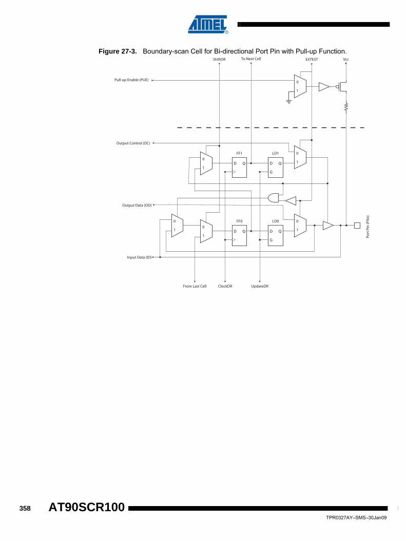
Figure 27-3. Boundary-scan Cell for Bi-directional Port Pin with Pull-up Function.
D Q D Q
G
0
10
1
D Q D Q
G
0
10
1
0
1
Port
Pin
(PXn
)
VccEXTESTTo Next CellShiftDR
Output Control (OC)
Output Data (OD)
Input Data (ID)
From Last Cell UpdateDRClockDR
FF1 LD1
LD0FF0
0
1
Pull-up Enable (PUE)
358TPR0327AY–SMS–30Jan09
AT90SCR100

AT90SCR100
Figure 27-4. General Port Pin Schematic Diagram
27.6.2 Scanning the RESET PinThe RESET pin accepts 5V active low logic for standard reset operation. An observe-only cell asshown in Figure 27-5 is inserted for the 5V reset signal.
Figure 27-5. Observe-only Cell
CLK
RPx
RRx
WRx
RDx
WDx
PUD
SYNCHRONIZER
WDx: WRITE DDRx
WRx: WRITE PORTxRRx: READ PORTx REGISTERRPx: READ PORTx PIN
PUD: PULLUP DISABLE
CLK : I/O CLOCK
RDx: READ DDRx
D
L
Q
Q
RESET
RESET
Q
QD
Q
Q D
CLR
PORTxn
Q
Q D
CLR
DDxn
PINxn
DAT
A B
US
SLEEP
SLEEP: SLEEP CONTROL
Pxn
I/O
I/O
See Boundary-scan Description for Details!
PUExn
OCxn
ODxn
IDxn
PUExn: PULLUP ENABLE for pin PxnOCxn: OUTPUT CONTROL for pin PxnODxn: OUTPUT DATA to pin PxnIDxn: INPUT DATA from pin Pxn
0
1D Q
FromPrevious
Cell
ClockDR
ShiftDR
ToNextCell
From System Pin To System Logic
FF1
359TPR0327AY–SMS–30Jan09

27.7 AT90SCR100 Boundary-scan OrderTable 27-1 shows the Scan order between TDI and TDO when the Boundary-scan chain isselected as data path. Bit 0 is the LSB; the first bit scanned in, and the first bit scanned out. Thescan order follows the pin-out order as far as possible. Therefore, the bits of Port A and Port K isscanned in the opposite bit order of the other ports. Exceptions from the rules are the Scanchains for the analog circuits, which constitute the most significant bits of the scan chain regard-less of which physical pin they are connected to. In Figure 27-3, PXn. Data corresponds to FF0,PXn. Control corresponds to FF1, PXn. Bit 4, 5, 6 and 7 of Port F is not in the scan chain, sincethese pins constitute the TAP pins when the JTAG is enabled.
Table 27-1. AT90SCR100 Boundary-scan Order
Bit Number Signal Name Module
68 PE0.Data
Port E
67 PE0.Control
66 PE1.Data
65 PE1.Control
64 PE2.Data
63 PE2.Control
62 PE3.Data
61 PE3.Control
60 PE4.Data
59 PE4.Control
58 PE5.Data
57 PE5.Control
56 PE6.Data
55 PE6.Control
54 PE7.Data
53 PE7.Control
360TPR0327AY–SMS–30Jan09
AT90SCR100

AT90SCR100
52 PB0.Data
Port B
51 PB0.Control
50 PB1.Data
49 PB1.Control
48 PB2.Data
47 PB2.Control
46 PB3.Data
45 PB3.Control
44 PB4.Data
43 PB4.Control
42 PB5.Data
41 PB5.Control
40 PB6.Data
39 PB6.Control
38 PB7.Data
37 PB7.Control
36 RSTT Reset Logic (Observe Only)
35 PD0.Data
Port D
34 PD0.Control
33 PD1.Data
32 PD1.Control
31 PD2.Data
30 PD2.Control
29 PD3.Data
28 PD3.Control
27 PD4.Data
26 PD4.Control
25 PD5.Data
24 PD5.Control
23 PD6.Data
22 PD6.Control
21 PD7.Data
20 PD7.Control
Table 27-1. AT90SCR100 Boundary-scan Order (Continued)
Bit Number Signal Name Module
361TPR0327AY–SMS–30Jan09

27.8 Boundary-scan Description Language FilesBoundary-scan Description Language (BSDL) files describe Boundary-scan capable devices ina standard format used by automated test-generation software. The order and function of bits inthe Boundary-scan Data Register are included in this description. BSDL files are available forAT90SCR100.
19 PC0.Data
Port C18 PC0.Control
17 PC1.Data
16 PC1.Control
15 PA7.Data
Port A
14 PA7.Control
13 PA6.Data
12 PA6.Control
11 PA5.Data
10 PA5.Control
9 PA4.Data
8 PA4.Control
7 PA3.Data
6 PA3.Control
5 PA2.Data
4 PA2.Control
3 PA1.Data
2 PA1.Control
1 PA0.Data
0 PA0.Control
Table 27-1. AT90SCR100 Boundary-scan Order (Continued)
Bit Number Signal Name Module
362TPR0327AY–SMS–30Jan09
AT90SCR100

AT90SCR100
28. Boot Loader Support - Read-While-Write Self-ProgrammingThe Boot Loader Support provides a real Read-While-Write Self-Programming mechanism todownload and upload program code by the MCU itself. This feature allows flexible applicationsoftware updates controlled by the MCU using a Flash-resident Boot Loader program. The BootLoader program can use any available data interface and associated protocol to read and/orwrite (program) code into the Flash memory. The program code within the Boot Loader sectionhas the capability to write into the entire Flash, including the Boot Loader memory. Thus, theBoot Loader can modify itself or erase itself from the code if the feature is not needed anymore.The size of the Boot Loader memory is configurable with fuses and the Boot Loader has twoseparate sets of Boot Lock bits which can be set independently. This gives the user a uniqueflexibility to select different levels of protection.
28.1 Boot Loader Features• Read-While-Write Self-Programming• Flexible Boot Memory Size• High Security (Separate Boot Lock Bits for a Flexible Protection)• Separate Fuse to Select Reset Vector• Optimized Page Size• Code Efficient Algorithm• Efficient Read-Modify-Write Support
28.2 Application and Boot Loader Flash SectionsThe Flash memory is organized in two main sections, the Application section and the BootLoader section (see Figure 28-2). The size of the different sections is configured by theBOOTSZ Fuses as shown in Table 28-7 on page 376 and Figure 28-2. These two sections canhave different level of protection because they have different sets of Lock bits.
28.2.1 Application SectionThe Application section is the section of the Flash that is used to store the application code. Theprotection level for the Application section can be selected by the application Boot Lock bits(Boot Lock bits 0), see Table 28-2 on page 366. The Application section can never store anyBoot Loader code because the SPM instruction is disabled when executed from the Applicationsection.
28.2.2 BLS – Boot Loader SectionWhile the Application section is used to store the application code, the The Boot Loader soft-ware must be located in the BLS because the SPM instruction can initiate a programmingsequence when executing from the BLS only. The SPM instruction can access the entire Flash,including the BLS itself. The protection level for the Boot Loader section can be selected by theBoot Loader Lock bits (Boot Lock bits 1), see Table 28-3 on page 366.
A page is a section in the Flash consisting of several bytes (see Table 29-7 onpage 381) used during programming sequence. The page organization does notaffect normal operation.Note
363TPR0327AY–SMS–30Jan09

28.3 Read-While-Write and No Read-While-Write Flash SectionsRegarding the address targeted by a programming sequence, the CPU supports Read-While-Write or is halted during a Boot Loader software update.
In addition to the two sections that are configurable by the BOOTSZ Fuses as described above,the Flash is also divided into two fixed sections, the Read-While-Write (RWW) section and theNo Read-While-Write (NRWW) section. The limit between the RWW- and NRWW sections isgiven in Table 28-1 and Figure 28-1 on page 365. The main differences between the two sec-tions are:
• The NRWW section can be read when erasing or writing a page located inside the RWW section.
• The CPU is stopped when erasing or writing a page located inside the NRWW section.
28.3.1 RWW – Read-While-Write SectionIf a Boot Loader software update is programming a page inside the RWW section you can onlyread code from the NRWW section.
During an on-going programming, the software must ensure that the RWW section won’t beread. If the user software is trying to read code located inside the RWW section (i.e., by load pro-gram memory, call, or jump instructions or an interrupt) during programming sequence, thesoftware may end up in an unknown state. To avoid this, the interrupts should either be disabledor moved to the Boot Loader section.
The Boot Loader section is always located in the NRWW section. The RWW Section Busy bit(RWWSB) in the Store Program Memory Control and Status Register (SPMCSR) will be read aslogical one as long as the RWW section is blocked for read operation. After the end of a pro-gramming sequence, the RWWSB must be cleared by software before reading code located inthe RWW section. See “SPMCSR – Store Program Memory Control and Status Register” onpage 367. for details on how to clear RWWSB.
28.3.2 NRWW – No Read-While-Write SectionThe code located in the NRWW section can be read when the Boot Loader software is updatinga page in the RWW section. When the Boot Loader code updates the NRWW section, the CPUis halted during the entire Page Erase or Page Write operation.
The user software can never read any code located inside the RWW section dur-ing a Boot Loader software operation. The syntax “Read-While-Write section”refers to the section that is being programmed (erased or written), not the sectionexecuted during a Boot Loader software update.
Note
Table 28-1. Read-While-Write Features
Which Section does the Z-pointer Address During the Programming?
Which Section Can be Read During Programming?
Is the CPU Halted?
Read-While-Write Supported?
RWW Section NRWW Section No Yes
NRWW Section None Yes No
364TPR0327AY–SMS–30Jan09
AT90SCR100

AT90SCR100
Figure 28-1. Read-While-Write vs. No Read-While-Write
Figure 28-2. Memory Sections
The parameters in the figure above are given in Table 28-7 on page 376.
Read-While-Write(RWW) Section
No Read-While-Write (NRWW) Section
Z-pointerAddresses RWWSection
Z-pointerAddresses NRWWSection
CPU is HaltedDuring the Operation
Code Located in NRWW SectionCan be Read Duringthe Operation
0x0000
0x6FFF
0x7000
0x7800
0x7C00
0x7E00
0x7FFF
Program Memory
BOOTSZ=’11’
Application Flash Section
Boot Loader Flash Section
Application Flash Section
Read
-Wh
ile-W
rite
Sec
tion
No
Read
-Wh
ile-W
rite
Sec
tion
BOOTSZ=’10’
BOOTSZ=’01’Start Boot Loader/End ApplicationLimitation
BOOTSZ=’00’
Note
365TPR0327AY–SMS–30Jan09

28.4 Boot Loader Lock BitsIf no Boot Loader capability is needed, the entire Flash is available for application code. TheBoot Loader has two separate sets of Boot Lock bits which can be set independently. This givesthe user a unique flexibility to select different levels of protection.
The user can select:
• To protect the entire Flash from a software update by the MCU.• To protect only the Boot Loader Flash section from a software update by the MCU.• To protect only the Application Flash section from a software update by the MCU.• Allow software update in the entire Flash.
See Table 28-2 and Table 28-3 for further details. The Boot Lock bits can be set in software andin Serial Pogramming mode, but they can be cleared by a Chip Erase command only. The gen-eral Write Lock (Lock Bit mode 2) does not control the programming of the Flash memory bySPM instruction. Similarly, the general Read/Write Lock (Lock Bit mode 1) does not control read-ing nor writing by (E)LPM/SPM, if it is attempted.
Note: 1. “1” means unprogrammed, “0” means programmed
Table 28-2. Boot Lock Bit0 Protection Modes (Application Section)(1)
BLB0 Mode BLB02 BLB01 Protection
1 1 1 No restrictions for SPM or (E)LPM accessing the Application section.
2 1 0 SPM is not allowed to write to the Application section.
3 0 0
SPM is not allowed to write to the Application section, and (E)LPM executing from the Boot Loader section is not allowed to read from the Application section. If Interrupt Vectors are placed in the Boot Loader section, interrupts are disabled while executing from the Application section.
4 0 1
(E)LPM executing from the Boot Loader section is not allowed to read from the Application section. If Interrupt Vectors are placed in the Boot Loader section, interrupts are disabled while executing from the Application section.
Table 28-3. Boot Lock Bit1 Protection Modes (Boot Loader Section)(1)
BLB1 Mode BLB12 BLB11 Protection
1 1 1 No restrictions for SPM or (E)LPM accessing the Boot Loader section.
2 1 0 SPM is not allowed to write to the Boot Loader section.
3 0 0
SPM is not allowed to write to the Boot Loader section, and (E)LPM executing from the Application section is not allowed to read from the Boot Loader section. If Interrupt Vectors are placed in the Application section, interrupts are disabled while executing from the Boot Loader section.
4 0 1
(E)LPM executing from the Application section is not allowed to read from the Boot Loader section. If Interrupt Vectors are placed in the Application section, interrupts are disabled while executing from the Boot Loader section.
366TPR0327AY–SMS–30Jan09
AT90SCR100

AT90SCR100
28.5 Entering the Boot Loader ProgramEntering the Boot Loader takes place by a jump or call from the application program. This maybe initiated by a trigger such as a command received via USART, or SPI interface. Alternatively,the Boot Reset Fuse can be programmed so that the Reset Vector is pointing to the Boot Flashstart address after a reset. In this case, the Boot Loader is started after a reset. After the applica-tion code is loaded, the program can start executing the application code. Note that the fusescannot be changed by the MCU itself. This means that once the Boot Reset Fuse is pro-grammed, the Reset Vector will always point to the Boot Loader Reset and the fuse can only bechanged through the serial programming interface.
Note: 1. “1” means unprogrammed, “0” means programmed
28.5.1 SPMCSR – Store Program Memory Control and Status RegisterThe Store Program Memory Control and Status Register contains the control bits needed to con-trol the Boot Loader operations.
• Bit 7 – SPMIE: SPM Interrupt EnableIf the SPMIE bit is set (one), and if the I-bit in the Status Register is set (one), the SPM readyinterrupt will be enabled.
The SPM ready Interrupt will remain activated as long as the SPMEN bit in the SPMCSR Regis-ter is cleared (zero).
• Bit 6 – RWWSB: Read-While-Write Section BusyWhen a Self-Programming (Page Erase or Page Write) operation to the RWW section is initi-ated, the RWWSB will be set (one) by hardware.
When the RWWSB bit is set, the RWW section cannot be accessed. The RWWSB bit will becleared if the RWWSRE bit is written to one after a Self-Programming operation is completed.Alternatively the RWWSB bit will automatically be cleared if a page load operation is initiated.
• Bit 5 – SIGRD: Signature Row ReadIf this bit is written to one at the same time as SPMEN, the next LPM instruction within threeclock cycles will read a byte from the signature row into the destination register. see “Readingthe Signature Row from Software” on page 373 for details. An SPM instruction within four cyclesafter SIGRD and SPMEN are set will have no effect. This operation is reserved for future useand should not be used.
• Bit 4 – RWWSRE: Read-While-Write Section Read Enable
Table 28-4. Boot Reset Fuse(1)
BOOTRST Reset Address
1 Reset Vector = Application Reset (address 0x0000)
0 Reset Vector = Boot Loader Reset (see Table 28-7 on page 376)
Bit 7 6 5 4 3 2 1 0
0x37 (0x57) SPMIE RWWSB SIGRD RWWSRE BLBSET PGWRT PGERS SPMEN SPMCSRRead/write R/W R R/W R/W R/W R/W R/W R/W
Initial value 0 0 0 1 0 0 0 0 0x00
367TPR0327AY–SMS–30Jan09

When programming (Page Erase or Page Write) to the RWW section, the RWW section isblocked for reading (the RWWSB will be set by hardware). To re-enable the RWW section, theuser software must wait until the programming is completed (SPMEN will be cleared). Then, ifthe RWWSRE bit is written to one at the same time as SPMEN, the next SPM instruction withinfour clock cycles re-enables the RWW section. The RWW section cannot be re-enabled whilethe Flash is busy with a Page Erase or a Page Write (SPMEN is set). If the RWWSRE bit is writ-ten while the Flash is being loaded, the Flash load operation will abort and the data loaded willbe lost.
• Bit 3 – BLBSET: Boot Lock Bit SetIf this bit is set (one) at the same time as SPMEN, the next SPM instruction within four clockcycles sets Boot Lock bits, according to the data in R0. The data in R1 and the address in the Z-pointer are ignored. The BLBSET bit will automatically be cleared upon completion of the Lockbit set operation, or if no SPM instruction is executed within four clock cycles.
An (E)LPM instruction within three cycles after BLBSET and SPMEN are set in the SPMCSRRegister, will read either the Lock bits or the Fuse bits (depending on Z0 in the Z-pointer) into thedestination register. See “Reading the Fuse and Lock Bits from Software” on page 372 fordetails.
• Bit 2 – PGWRT: Page WriteIf this bit is set (one)at the same time as SPMEN, the next SPM instruction within four clockcycles executes Page Write, with the data stored in the temporary buffer. The page address istaken from the high part of the Z-pointer. The data in R1 and R0 are ignored. The PGWRT bitwill be automatically cleared upon completion of a Page Write, or if no SPM instruction is exe-cuted within four clock cycles. The CPU is halted during the entire Page Write operation if theNRWW section is addressed.
• Bit 1 – PGERS: Page EraseIf this bit is set (one) at the same time as SPMEN, the next SPM instruction within four clockcycles executes Page Erase. The page address is taken from the high part of the Z-pointer. Thedata in R1 and R0 are ignored. The PGERS bit will be automatically cleared upon completion ofa Page Erase, or if no SPM instruction is executed within four clock cycles. The CPU is haltedduring the entire Page Write operation if the NRWW section is addressed.
• Bit 0 – SPMEN: Store Program Memory EnableThis bit enables the SPM instruction for the next four clock cycles. If written to one together witheither RWWSRE, BLBSET, PGWRT’ or PGERS, the following SPM instruction will have a spe-cial meaning, see description above. If only SPMEN is written, the following SPM instruction willstore the value of R1:R0 in the temporary page buffer addressed by the Z-pointer. The LSB ofthe Z-pointer is ignored. The SPMEN bit will be automatically cleared upon completion of anSPM instruction, or if no SPM instruction is executed within four clock cycles. During Page Eraseand Page Write, the SPMEN bit remains high until the operation is completed.
Writing any other combination than “10001”, “01001”, “00101”, “00011” or “00001” in the lowerfive bits will have no effect.
Only one SPM instruction should be active at any time.Note
368TPR0327AY–SMS–30Jan09
AT90SCR100

AT90SCR100
28.6 Addressing the Flash During Self-ProgrammingThe Z-pointer is used to address the SPM commands. The Z pointer consists of the Z-registersZL and ZH in the register file. The number of bits actually used is implementation dependent.
Since the Flash is organized in pages (see Table 29-7 on page 381), the Program Counter canbe treated as having two different sections. One section, consisting of the least significant bits, isaddressing the words within a page, while the most significant bits are addressing the pages.This is shown in Figure 28-3. Note that the Page Erase and Page Write operations areaddressed independently. Therefore it is of major importance that the Boot Loader softwareaddresses the same page in both the Page Erase and Page Write operation. Once a program-ming operation is initiated, the address is latched and the Z-pointer can be used for otheroperations.
The (E)LPM instruction use the Z-pointer to store the address. Since this instruction addressesthe Flash byte-by-byte, also bit Z0 of the Z-pointer is used.
Figure 28-3. Addressing the Flash During SPM
Bit 15 14 13 12 11 10 7 8
ZH (R31) Z15 Z14 Z13 Z12 Z11 Z10 Z9 Z8ZH (R30) Z7 Z6 Z5 Z4 Z3 Z2 Z1 Z0
7 6 5 4 3 2 1 0
Only one SPM instruction should be active at any time.
PROGRAM MEMORY
0115
Z - REGISTER
BIT
0
ZPAGEMSB
WORD ADDRESSWITHIN A PAGE
PAGE ADDRESSWITHIN THE FLASH
ZPCMSB
INSTRUCTION WORD
PAGE PCWORD[PAGEMSB:0]:
00
01
02
PAGEEND
PAGE
PCWORDPCPAGE
PCMSB PAGEMSBPROGRAMCOUNTER
Note
369TPR0327AY–SMS–30Jan09

28.7 Self-Programming the FlashThe program memory is updated page by page. Before programming a page with the datastored in the temporary page buffer, the page must be erased. The temporary page buffer isfilled one word per word using SPM instruction and the buffer can be filled either before thePage Erase command or between a Page Erase and a Page Write operation:
Alternative 1, fill the buffer before a Page Erase
• Fill temporary page buffer• Perform a Page Erase• Perform a Page Write
Alternative 2, fill the buffer after Page Erase
• Perform a Page Erase• Fill temporary page buffer• Perform a Page Write
If only a part of the page needs to be changed, the rest of the page must be stored (for examplein the temporary page buffer) before the erase, and then be rewritten. When using alternative 1,the Boot Loader provides an effective Read-Modify-Write feature which allows the user softwareto first read the page, do the necessary changes, and then write back the modified data. If alter-native 2 is used, it is not possible to read the old data while loading because the page is alreadyerased. The temporary page buffer can be accessed in a random sequence. It is essential thatthe page address used in both the Page Erase and Page Write operation is addressing thesame page. See “Simple Assembly Code Example for a Boot Loader” on page 374 for anassembly code example.
28.7.1 Performing Page Erase by SPMTo execute Page Erase, set up the address in the Z-pointer, write “X0000011” to SPMCSR andexecute SPM within four clock cycles after writing SPMCSR. The data in R1 and R0 are ignored.The page address must be written to PCPAGE in the Z-register. Other bits in the Z-pointer willbe ignored during this operation.
• Page Erase to the RWW section: The NRWW section can be read during the Page Erase.• Page Erase to the NRWW section: The CPU is halted during the operation.
28.7.2 Filling the Temporary Buffer (Page Loading)To write an instruction word, set up the address in the Z-pointer and data in R1:R0, write“00000001” to SPMCSR and execute SPM within four clock cycles after writing SPMCSR. Thecontent of PCWORD in the Z-register is used to address the data in the temporary buffer. Thetemporary buffer will be automatically erased after a Page Write operation or by writing theRWWSRE bit in SPMCSR. It is also erased after a system reset. Note that it is not possible towrite more than one time to each address without erasing the temporary buffer.
If the EEPROM is written in the middle of an SPM Page Load operation, all data loaded will belost.
370TPR0327AY–SMS–30Jan09
AT90SCR100

AT90SCR100
28.7.3 Performing a Page WriteTo execute Page Write, set up the address in the Z-pointer, write “X0000101” to SPMCSR andexecute SPM within four clock cycles after writing SPMCSR. The data in R1 and R0 is ignored.The page address must be written to PCPAGE. Other bits in the Z-pointer must be written tozero during this operation.
• Page Write to the RWW section: The NRWW section can be read during the Page Write.• Page Write to the NRWW section: The CPU is halted during the operation.
28.7.4 Using the SPM InterruptIf the SPM interrupt is enabled, the SPM interrupt will generate a constant interrupt when theSPMEN bit in SPMCSR is cleared. This means that the interrupt can be used instead of pollingthe SPMCSR Register in software. When using the SPM interrupt, the Interrupt Vectors shouldbe moved to the BLS section to avoid that an interrupt is accessing the RWW section when it isblocked for reading. How to move the interrupts is described in “Interrupts” on page 63.
28.7.5 Consideration While Updating BLSSpecial care must be taken if the user allows the Boot Loader section to be updated by leavingBoot Lock bit11 unprogrammed. An accidental write to the Boot Loader itself can corrupt theentire Boot Loader, and further software updates might be impossible. If it is not necessary tochange the Boot Loader software itself, it is recommended to program the Boot Lock bit11 toprotect the Boot Loader software from any internal software changes.
28.7.6 Prevent Reading the RWW Section During Self-ProgrammingDuring Self-Programming (either Page Erase or Page Write), the RWW section is alwaysblocked for reading. The user software itself must prevent that this section is addressed duringthe self programming operation. The RWWSB in the SPMCSR will be set as long as the RWWsection is busy. During Self-Programming the Interrupt Vector table should be moved to the BLSas described in “Interrupts” on page 63, or the interrupts must be disabled. Before addressingthe RWW section after the programming is completed, the user software must clear theRWWSB by writing the RWWSRE. See “Simple Assembly Code Example for a Boot Loader” onpage 374 for an example.
28.7.7 Setting the Boot Loader Lock Bits by SPMTo set the Boot Loader Lock bits and general Lock Bits, write the desired data to R0, write“X0001001” to SPMCSR and execute SPM within four clock cycles after writing SPMCSR.
See Table 28-2 and Table 28-3 for how the different settings of the Boot Loader bits affect theFlash access.
If bits 5..0 in R0 are cleared (zero), the corresponding Lock bit will be programmed if an SPMinstruction is executed within four cycles after BLBSET and SPMEN are set in SPMCSR. The Z-pointer is not used during this operation, but for future compatibility it is recommended to loadthe Z-pointer with 0x0001 value (same as used for reading the lOck bits). For future compatibilityit is also recommended to set bits 7 and 6 in R0 to “1” when writing the Lock bits. When pro-gramming the Lock bits the entire Flash can be read during the operation.
Bit 7 6 5 4 3 2 1 0
R0 1 1 BLB12 BLB11 BLB02 BLB01 LB2 LB1
371TPR0327AY–SMS–30Jan09

28.7.8 EEPROM Write Prevents Writing to SPMCSRNote that an EEPROM write operation will block all software programming to Flash. Reading theFuses and Lock bits from software will also be prevented during the EEPROM write operation. Itis recommended that the user checks the status bit (EEPE) in the EECR Register and verifiesthat the bit is cleared before writing to the SPMCSR Register.
28.7.9 Reading the Fuse and Lock Bits from SoftwareIt is possible to read both the Fuse and Lock bits from software. To read the Lock bits, load theZ-pointer with 0x0001 and set the BLBSET and SPMEN bits in SPMCSR. When an (E)LPMinstruction is executed within three CPU cycles after the BLBSET and SPMEN bits are set inSPMCSR, the value of the Lock bits will be loaded in the destination register. The BLBSET andSPMEN bits will auto-clear upon completion of reading the Lock bits or if no (E)LPM instructionis executed within three CPU cycles or no SPM instruction is executed within four CPU cycles.When BLBSET and SPMEN are cleared, (E)LPM will work as described in the Instruction setManual.
The algorithm for reading the Fuse Low byte is similar to the one described above for readingthe Lock bits. To read the Fuse Low byte, load the Z-pointer with 0x0000 and set the BLBSETand SPMEN bits in SPMCSR. When an (E)LPM instruction is executed within three cycles afterthe BLBSET and SPMEN bits are set in the SPMCSR, the value of the Fuse Low byte (FLB) willbe loaded in the destination register as shown below. Refer to Table 29-5 on page 380 for adetailed description and mapping of the Fuse Low byte.
Similarly, when reading the Fuse High byte, load 0x0003 in the Z-pointer. When an (E)LPMinstruction is executed within three cycles after the BLBSET and SPMEN bits are set in theSPMCSR, the value of the Fuse High byte (FHB) will be loaded in the destination register asshown below. Refer to Table 29-4 on page 379 for detailed description and mapping of the FuseHigh byte.
When reading the Extended Fuse byte, load 0x0002 in the Z-pointer. When an (E)LPM instruc-tion is executed within three cycles after the BLBSET and SPMEN bits are set in the SPMCSR,the value of the Extended Fuse byte (EFB) will be loaded in the destination register as shownbelow. Refer to Table 29-3 on page 379 for detailed description and mapping of the ExtendedFuse byte.
Fuse and Lock bits that are programmed, will be read as zero. Fuse and Lock bits that areunprogrammed, will be read as one.
Bit 7 6 5 4 3 2 1 0
Rd - - BLB12 BLB11 BLB02 BLB01 LB2 LB1
Bit 7 6 5 4 3 2 1 0
Rd FLB7 FLB6 FLB5 FLB4 FLB3 FLB2 FLB1 FLB0
Bit 7 6 5 4 3 2 1 0
Rd FHB7 FHB6 FHB5 FHB4 FHB3 FHB2 FHB1 FHB0
Bit 7 6 5 4 3 2 1 0
Rd - - - - - EFB2 EFB1 EFB0
372TPR0327AY–SMS–30Jan09
AT90SCR100

AT90SCR100
28.7.10 Reading the Signature Row from SoftwareTo read the Signature Row from software, load the Z-pointer with the signature byte addressgiven in Table 28-5 on page 373 and set the SIGRD and SPMEN bits in SPMCSR. When anLPM instruction is executed within three CPU cycles after the SIGRD and SPMEN bits are set inSPMCSR, the signature byte value will be loaded in the destination register. The SIGRD andSPMEN bits will auto-clear upon completion of reading the Signature Row Lock bits or if no LPMinstruction is executed within three CPU cycles. When SIGRD and SPMEN are cleared, LPM willwork as described in the Instruction set Manual.
Note: 1. All other addresses are reserved for future use.
28.7.11 Preventing Flash CorruptionDuring periods of low VCC, the Flash program can be corrupted because the supply voltage istoo low for the CPU and the Flash to operate properly. These issues are the same as for boardlevel systems using the Flash, and the same design solutions should be applied.
A Flash program corruption can be caused by two situations when the voltage is too low. First, aregular write sequence to the Flash requires a minimum voltage to operate correctly. Secondly,the CPU itself can execute instructions incorrectly, if the supply voltage for executing instructionsis too low.
Flash corruption can easily be avoided by following these design recommendations (one issufficient):
1. If there is no need for a Boot Loader update in the system, program the Boot Loader Lock bits to prevent any Boot Loader software updates.
2. Keep the AVR RESET active (low) during periods of insufficient power supply voltage. This can be done by enabling the internal Brown-out Detector (BOD) if the operating voltage matches the detection level. If not, an external low VCC reset protection circuit can be used. If a reset occurs while a write operation is in progress, the write operation will be completed provided that the power supply voltage is sufficient.
Table 28-5. Signature Row Addressing(1)
Signature Byte Z-Pointer Address
Device Signature Byte 1 0x0000
Device Signature Byte 2 0x0002
Device Signature Byte 3 0x0004
RC Oscillator Calibration Byte 0x0001
Serial Number byte 0 0x0006
Serial Number byte 1 0x0008
Serial Number byte 2 0x000A
Serial Number byte 3 0x000C
Serial Number byte 4 0x000E
Serial Number byte 5 0x0010
Serial Number byte 6 0x0012
Serial Number byte 7 0x0014
Serial Number byte 8 0x0016
373TPR0327AY–SMS–30Jan09

3. Keep the AVR core in Power-down sleep mode during periods of low VCC. This will pre-vent the CPU from attempting to decode and execute instructions, effectively protecting the SPMCSR Register and thus the Flash from unintentional writes.
28.7.12 Programming Time for Flash when Using SPMThe calibrated RC Oscillator is used to time Flash accesses. Table 28-6 shows the typical pro-gramming time for Flash accesses from the CPU.
28.7.13 Simple Assembly Code Example for a Boot Loader;-the routine writes one page of data from RAM to Flash; the first data location in RAM is pointed to by the Y pointer; the first data location in Flash is pointed to by the Z-pointer;-error handling is not included;-the routine must be placed inside the Boot space; (at least the Do_spm sub routine). Only code inside NRWW section can; be read during Self-Programming (Page Erase and Page Write).;-registers used: r0, r1, temp1 (r16), temp2 (r17), looplo (r24), ; loophi (r25), spmcrval (r20); storing and restoring of registers is not included in the routine; register usage can be optimized at the expense of code size;-It is assumed that either the interrupt table is moved to the Boot; loader section or that the interrupts are disabled.
.equ PAGESIZEB = PAGESIZE*2 ;PAGESIZEB is page size in BYTES, not words
.org SMALLBOOTSTARTWrite_page:; Page Eraseldi spmcrval, (1<<PGERS) | (1<<SPMEN)call Do_spm
; re-enable the RWW sectionldi spmcrval, (1<<RWWSRE) | (1<<SPMEN)call Do_spm
; transfer data from RAM to Flash page bufferldi looplo, low(PAGESIZEB) ;init loop variableldi loophi, high(PAGESIZEB) ;not required for PAGESIZEB<=256
Wrloop:ld r0, Y+ld r1, Y+ldi spmcrval, (1<<SPMEN)call Do_spmadiw ZH:ZL, 2sbiw loophi:looplo, 2 ;use subi for PAGESIZEB<=256brne Wrloop
; execute Page Write
Table 28-6. SPM Programming Time
Symbol Min Programming Time Max Programming Time
Flash write (Page Erase, Page Write, and write Lock bits by SPM) 3.7 ms 4.5 ms
These programming time are true after production calibration. If the oscillator trim-ming is modified, these values will be changed.
Note
374TPR0327AY–SMS–30Jan09
AT90SCR100

AT90SCR100
subi ZL, low(PAGESIZEB) ;restore pointersbci ZH, high(PAGESIZEB) ;not required for PAGESIZEB<=256ldi spmcrval, (1<<PGWRT) | (1<<SPMEN)call Do_spm
; re-enable the RWW sectionldi spmcrval, (1<<RWWSRE) | (1<<SPMEN)call Do_spm
; read back and check, optionalldi looplo, low(PAGESIZEB) ;init loop variableldi loophi, high(PAGESIZEB) ;not required for PAGESIZEB<=256subi YL, low(PAGESIZEB) ;restore pointersbci YH, high(PAGESIZEB)
Rdloop:elpm r0, Z+ld r1, Y+cpse r0, r1jmp Errorsbiw loophi:looplo, 1 ;use subi for PAGESIZEB<=256brne Rdloop
; return to RWW section; verify that RWW section is safe to read
Return:in temp1, SPMCSRsbrs temp1, RWWSB ; If RWWSB is set, the RWW section is not ready yetret; re-enable the RWW sectionldi spmcrval, (1<<RWWSRE) | (1<<SPMEN)call Do_spmrjmp Return
Do_spm:; check for previous SPM complete
Wait_spm:in temp1, SPMCSRsbrc temp1, SPMENrjmp Wait_spm; input: spmcrval determines SPM action; disable interrupts if enabled, store statusin temp2, SREGcli; check that no EEPROM write access is present
Wait_ee:sbic EECR, EEPErjmp Wait_ee; SPM timed sequenceout SPMCSR, spmcrvalspm; restore SREG (to enable interrupts if originally enabled)out SREG, temp2ret
For details about these two section, see “NRWW – No Read-While-Write Section”on page 364 and “RWW – Read-While-Write Section” on page 364.
Note
375TPR0327AY–SMS–30Jan09

28.7.14 AT90SCR100 Boot Loader ParametersIn Table 28-7 through Table 28-9, the parameters used in the description of the Self-Program-ming are given.
The different BOOTSZ Fuse configurations are shown in Figure 28-2.
Note: 1. For details about these two section, see “NRWW – No Read-While-Write Section” on page 364 and “RWW – Read-While-Write Section” on page 364.
Note: 1. Z0: should be zero for all SPM commands, byte select for the (E)LPM instruction.
See “Addressing the Flash During Self-Programming” on page 369 for details about the use ofZ-pointer during Self-Programming.
Table 28-7. Boot Size Configuration
BOOTSZ1 BOOTSZ0 Boot Size PagesApplicationFlash Section
Boot LoaderFlash Section
End ApplicationSection
Boot Reset Address (Start Boot Loader Section)
1 1 512 words 4 0x0000 - 0x7DFF 0x7E00 - 0x7FFF 0x7DFF 0x7E00
1 0 1024 words 8 0x0000 - 0x7BFF 0x7C00 - 0x7FFF 0x7BFF 0x7C00
0 1 2048 words 16 0x0000 - 0x77FF 0x7800 - 0x7FFF 0x77FF 0x7800
0 0 4096 words 32 0x0000 - 0x6FFF 0x7000 - 0x7FFF 0x6FFF 0x7000
Table 28-8. Read-While-Write Limit(1)
Section Pages Address
Read-While-Write section (RWW) 224 0x0000 - 0x6FFF
No Read-While-Write section (NRWW) 32 0x7000 - 0x7FFF
Table 28-9. Explanation of different variables used in Figure 28-3 and the mapping to the Z-pointer
VariableCorrespondig
Z-value Description(1)
PCMSB 14 Most significant bit in the Program Counter. (The Program Counter is 15 bits PC[14:0])
PAGEMSB 7 Most significant bit which is used to address the words within one page (128 words in a page requires seven bits PC [6:0]).
ZPCMSB Z15 Bit in Z-pointer that is mapped to PCMSB. Because Z0 is not used, the ZPCMSB equals PCMSB + 1.
ZPAGEMSB Z8 Bit in Z-pointer that is mapped to PCMSB. Because Z0 is not used, the ZPAGEMSB equals PAGEMSB + 1.
PCPAGE PC[14:7] Z15:Z7 Program Counter page address: Page select, for Page Erase and Page Write
PCWORD PC[6:0] Z7:Z1 Program Counter word address: Word select, for filling temporary buffer (must be zero during Page Write operation)
376TPR0327AY–SMS–30Jan09
AT90SCR100

AT90SCR100
29. Memory Programming
29.1 Program And Data Memory Lock BitsThe AT90SCR100 provides six Lock bits which can be left unprogrammed (“1”) or can be pro-grammed (“0”) to obtain the additional features listed in Table 29-2. The Lock bits can only beerased to “1” with the Chip Erase command.
Notes: 1. “1” means unprogrammed, “0” means programmed
Table 29-1. Lock Bit Byte(1)
Lock Bit Byte Bit No Description Default Value
– 7 – 1 (unprogrammed)
– 6 – 1 (unprogrammed)
BLB12 5 Boot Lock bit 1 (unprogrammed)
BLB11 4 Boot Lock bit 1 (unprogrammed)
BLB02 3 Boot Lock bit 1 (unprogrammed)
BLB01 2 Boot Lock bit 1 (unprogrammed)
LB2 1 Lock bit 1 (unprogrammed)
LB1 0 Lock bit 1 (unprogrammed)
377TPR0327AY–SMS–30Jan09

Notes: 1. Program the Fuse bits and Boot Lock bits before programming the LB1 and LB2.
Table 29-2. Lock Bit Protection Modes(1)
Memory Lock Bits Protection Type
LB Mode LB2 LB1
1 1 1 No memory lock features enabled.
2 1 0Further programming of the Flash and EEPROM is disabled in Serial Programming mode. The Fuse bits are locked in Serial Programming mode.
3 0 0Further programming and verification of the Flash and EEPROM is disabled in Serial Programming mode. The Boot Lock bits and Fuse bits are locked in both Serial Programming mode.
BLB0 Mode BLB02 BLB01
1 1 1 No restrictions for SPM or (E)LPM accessing the Application section.
2 1 0 SPM is not allowed to write to the Application section.
3 0 0
SPM is not allowed to write to the Application section, and (E)LPM executing from the Boot Loader section is not allowed to read from the Application section. If Interrupt Vectors are placed in the Boot Loader section, interrupts are disabled while executing from the Application section.
4 0 1
(E)LPM executing from the Boot Loader section is not allowed to read from the Application section. If Interrupt Vectors are placed in the Boot Loader section, interrupts are disabled while executing from the Application section.
BLB1 Mode BLB12 BLB11
1 1 1 No restrictions for SPM or (E)LPM accessing the Boot Loader section.
2 1 0 SPM is not allowed to write to the Boot Loader section.
3 0 0
SPM is not allowed to write to the Boot Loader section, and (E)LPM executing from the Application section is not allowed to read from the Boot Loader section. If Interrupt Vectors are placed in the Application section, interrupts are disabled while executing from the Boot Loader section.
4 0 1
(E)LPM executing from the Application section is not allowed to read from the Boot Loader section. If Interrupt Vectors are placed in the Application section, interrupts are disabled while executing from the Boot Loader section.
378TPR0327AY–SMS–30Jan09
AT90SCR100

AT90SCR100
29.2 Fuse BitsThe AT90SCR100 has four Fuse bytes. Table 29-3 - Table 29-5 describe briefly the functionalityof all the fuses and how they are mapped into the Fuse bytes. Note that the fuses are read aslogical zero, “0”, if they are programmed.
Notes: 1. Refer to Table 9-2 on page 54 to get decoding of BODENABLE bit.
Notes: 1. Never ship a product with the OCDEN Fuse programmed regardless of the setting of Lock bits and JTAGEN Fuse. A programmed OCDEN Fuse enables some parts of the clock system to be running in all sleep modes. This may increase the power consumption.
2. The SPIEN Fuse is not accessible in serial programming mode.3. See “WDTCSR – Watchdog Timer Control Register” on page 61 for details.4. The default value of BOOTSZ1..0 results in maximum Boot Size. See Table 28-7 on page 376
for details
Table 29-3. Extended Fuse Byte
Fuse Low Byte Bit No Description Default Value
– 7 – 1
– 6 – 1
– 5 – 1
– 4 – 1
– 3 – 1
– 2 – 1
– 1 – 1
BODENABLE(1) 0 Brown-out Detector Enable Control 1 (unprogrammed)
Table 29-4. Fuse High Byte
Fuse High Byte Bit No Description Default Value
OCDEN(1) 7 Enable OCD 1 (unprogrammed, OCD disabled)
JTAGEN 6 Enable JTAG 0 (programmed, JTAG enabled)
SPIEN(2) 5 Enable Serial Program and Data Downloading
0 (programmed, SPI prog. enabled)
WDTON(3) 4 Watchdog Timer always on 1 (unprogrammed)
EESAVE 3 EEPROM memory is preserved through the Chip Erase
1 (unprogrammed, EEPROM not preserved)
BOOTSZ1 2 Select Boot Size (see Table 28-7 for details) 0 (programmed)(4)
BOOTSZ0 1 Select Boot Size (see Table 28-7 for details) 0 (programmed)(4)
BOOTRST 0 Select Reset Vector 1 (unprogrammed)
379TPR0327AY–SMS–30Jan09

Notes: 1. The CKOUT Fuse allow the system clock to be output on PORTB1. See “Clock Output Buffer” on page 40 for details.
2. The default value of SUT1..0 results in maximum start-up time for the default clock source. See Table 7-3 on page 35 for details.
3. These values are fixed. They used to select clocks that are not available for AT90SCR100.
The status of the Fuse bits is not affected by Chip Erase. Note that the Fuse bits are locked ifLock bit1 (LB1) is programmed. Program the Fuse bits before programming the Lock bits.
29.2.1 Latching of FusesThe fuse values are latched when the device enters programming mode and changes of thefuse values will have no effect until the part leaves Programming mode. This does not apply tothe EESAVE Fuse which will take effect once it is programmed. The fuses are also latched onPower-up in Normal mode.
29.3 Signature Bytes
29.3.1 Device and JTAG IDsAll Atmel microcontrollers have a three-byte signature code which identifies the device. Thiscode can be read in both serial and parallel mode, also when the device is locked. The threebytes reside in a separate address space. The AT90SCR100 signature bytes are given in Table29-6.
29.3.2 Serial NumberThe Serial Number is composed of 9 bytes. You can only read these bytes. They are pro-grammed during probe sessions and are unique for each die. They are composed of:
• SN0: Chip ID: same for all AT90SCR100 ICs• SN1: Silicon Revision
Table 29-5. Fuse Low Byte
Fuse Low Byte Bit No Description Default Value
- 7 - 1
CKOUT(1) 6 Clock output 1 (unprogrammed)
SUT1 5 Select start-up time 1 (unprogrammed)(2)
SUT0 4 Select start-up time 0 (programmed)(2)
CKSEL3 3 Select Clock source 1 (unprogrammed)
- 2 - 0 (3)
- 1 - 0 (3)
CKSEL0 0 Select Clock source 1 (unprogrammed)
Table 29-6. Device and JTAG ID
Part
Signature Bytes Address JTAG
0x000 0x001 0x002 Part Number Manufacture ID
AT90SCR100 0x1E 0x96 0x09 96C1 0x1F
380TPR0327AY–SMS–30Jan09
AT90SCR100

AT90SCR100
• SN2: Production year• SN3: Fab & Quarter• SN4: Lot number high order byte• SN5: Lot number low order byte• SN6: Wafer number within the lot• SN7: Chip number (on the Wafer) low order byte (row number)• SN8: Chip number (on the Wafer) high order byte (column number)
29.4 Calibration ByteThe AT90SCR100 has a byte calibration value for the internal RC Oscillator. This byte resides inthe high byte of address 0x000 in the signature address space. During reset, this byte is auto-matically written into the internal calibration register to ensure correct frequency of the calibratedRC Oscillator.
29.5 Page Size
29.6 Serial DownloadingBoth the Flash and EEPROM memory arrays can be programmed using a serial programmingbus while RESET is pulled to GND. The serial programming interface consists of pins SCK,MOSI (input) and MISO (output). After RESET is set low, the Programming Enable instructionneeds to be executed first before program/erase operations can be executed.
29.6.1 Serial Programming Pin Mapping
Table 29-7. No. of Words in a Page and No. of Pages in the Flash
Device Flash Size Page Size PCWORD No. of Pages PCPAGE PCMSB
AT90SCR100 32K words (64 Kbytes) 128 words PC[6:0] 256 PC[14:7] 14
Table 29-8. No. of Words in a Page and No. of Pages in the EEPROM
Device EEPROM Size Page Size PCWORD No. of Pages PCPAGE EEAMSB
AT90SCR100 4 Kbytes 32 bytes EEA[2:0] 128 EEA[10:3] 10
Table 29-9. Pin Mapping Serial Programming
Symbol Pins I/O Description
MOSI PB5 I Serial Data in
MISO PB6 O Serial Data out
SCK PB7 I Serial Clock
381TPR0327AY–SMS–30Jan09

Figure 29-1. Serial Programming and Verify
When programming the EEPROM, an auto-erase cycle is built into the self-timed programmingoperation (in the Serial mode ONLY) and there is no need to first execute the Chip Eraseinstruction. The Chip Erase operation turns the content of every memory location in both theProgram and EEPROM arrays into 0xFF.
Depending on CKSEL Fuses, a valid clock must be present. The minimum low and high periodsfor the serial clock (SCK) input are defined as follows:
Low: > 2 CPU clock cycles for fck < 12 MHz, 3 CPU clock cycles for fck >= 12 MHz
High: > 2 CPU clock cycles for fck < 12 MHz, 3 CPU clock cycles for fck >= 12 MHz
29.6.2 Serial Programming AlgorithmWhen writing serial data to the AT90SCR100, data is clocked on the rising edge of SCK.
When reading data from the AT90SCR100, data is clocked on the falling edge of SCK. See Fig-ure 29-3 for timing details.
To program and verify the AT90SCR100 in the serial programming mode, the followingsequence is recommended (See four byte instruction formats in Table 29-11):
1. Power-up sequence:Apply power between VCC and GND while RESET and SCK are set to “0”. In some sys-tems, the programmer can not guarantee that SCK is held low during power-up. In this case, RESET must be given a positive pulse of at least two CPU clock cycles duration after SCK has been set to “0”.
2. Wait for at least 20 ms and enable serial programming by sending the Programming Enable serial instruction to pin MOSI.
3. The serial programming instructions will not work if the communication is out of syn-chronization. When in sync. the second byte (0x53), will echo back when issuing the third byte of the Programming Enable instruction. Whether the echo is correct or not, all four bytes of the instruction must be transmitted. If the 0x53 did not echo back, give RESET a positive pulse and issue a new Programming Enable command.
4. The Flash is programmed one page at a time. The memory page is loaded one byte at a time by supplying the 7 LSB of the address and data together with the Load Program Memory Page instruction. To ensure correct loading of the page, the data low byte must be loaded before data high byte is applied for a given address. The Program Memory Page is stored by loading the Write Program Memory Page instruction with the
VCC
GND
XT AL1
SCK
MISO
MOSI
RESET
+1.8 - 5.5V
AVCC
+1.8 - 5.5V(2)
382TPR0327AY–SMS–30Jan09
AT90SCR100

AT90SCR100
address lines 15..8. Before issuing this command, make sure the instruction Load Extended Address Byte has been used to define the MSB of the address. The extended address byte is stored until the command is re-issued, i.e., the command needs only be issued for the first page, and when crossing the 64KWord boundary. If polling (RDY/BSY) is not used, the user must wait at least tWD_FLASH before issuing the next page. (See Table 29-10.) Accessing the serial programming interface before the Flash write operation completes can result in incorrect programming.
5. The EEPROM array is programmed one byte at a time by supplying the address and data together with the appropriate Write instruction. An EEPROM memory location is first automatically erased before new data is written. If polling is not used, the user must wait at least tWD_EEPROM before issuing the next byte. (See Table 29-10.) In a chip erased device, no 0xFFs in the data file(s) need to be programmed.
6. Any memory location can be verified by using the Read instruction which returns the content at the selected address at serial output MISO. When reading the Flash mem-ory, use the instruction Load Extended Address Byte to define the upper address byte, which is not included in the Read Program Memory instruction. The extended address byte is stored until the command is re-issued, i.e., the command needs only be issued for the first page, and when crossing the 64KWord boundary.
7. At the end of the programming session, RESET can be set high to commence normal operation.
8. Power-off sequence (if needed):Set RESET to “1”.Turn VCC power off.
29.7 Serial Programming Instruction setTable 29-11 on page 383 and Figure 29-2 on page 385 describes the Instruction set.
Table 29-10. Minimum Wait Delay Before Writing the Next Flash or EEPROM Location
Symbol Minimum Wait Delay
tWD_FLASH 4.5 ms
tWD_EEPROM 9.0 ms
tWD_ERASE 9.0 ms
Table 29-11. Serial Programming Instruction Set (Hexadecimal values)
Instruction/Operation
Instruction Format
Byte 1 Byte 2 Byte 3 Byte4
Programming Enable $AC $53 $00 $00
Chip Erase (Program Memory/EEPROM) $AC $80 $00 $00
Poll RDY/BSY $F0 $00 $00 data byte out
Load Instructions
Load Extended Address byte(1) $4D $00 Extended adr $00
Load Program Memory Page, High byte $48 $00 adr LSB high data byte in
Load Program Memory Page, Low byte $40 $00 adr LSB low data byte in
Load EEPROM Memory Page (page access) $C1 $00 0000 000aa(2) data byte in
Read Instructions
Read Program Memory, High byte $28 adr MSB adr LSB high data byte out
383TPR0327AY–SMS–30Jan09

Notes: 1. Not all instructions are applicable for all parts.2. a = address
If the LSB in RDY/BSY data byte out is ‘1’, a programming operation is still pending. Wait untilthis bit returns ‘0’ before the next instruction is carried out.
Within the same page, the low data byte must be loaded prior to the high data byte.
After data is loaded to the page buffer, program the EEPROM page, see Figure 29-2 on page385.
Read Program Memory, Low byte $20 adr MSB adr LSB low data byte out
Read EEPROM Memory $A0 0000 00aa(2) aaaa aaaa(2) data byte out
Read Lock bits $58 $00 $00 data byte out
Read Signature Byte $30 $00 0000 aaaa(2) data byte out
Read Fuse bits $50 $00 $00 data byte out
Read Fuse High bits $58 $08 $00 data byte out
Read Extended Fuse Bits $50 $08 $00 data byte out
Read Calibration Byte $38 $00 $00 data byte out
Write Instructions
Write Program Memory Page $4C adr MSB adr LSB $00
Write EEPROM Memory $C0 0000 00aa(2) aaaa aaaa(2) data byte in
Write EEPROM Memory Page (page access) $C2 0000 00aa(2) aaaa aa00(2) $00
Write Lock bits $AC $E0 $00 data byte in
Write Fuse bits $AC $A0 $00 data byte in
Write Fuse High bits $AC $A8 $00 data byte in
Write Extended Fuse Bits $AC $A4 $00 data byte in
Table 29-11. Serial Programming Instruction Set (Hexadecimal values)
Instruction/Operation
Instruction Format
Byte 1 Byte 2 Byte 3 Byte4
1. Bits are programmed ‘0’, unprogrammed ‘1’.2. To ensure future compatibility, unused Fuses and Lock bits should be
unprogrammed (‘1’) .3. Refer to the correspondig section for Fuse and Lock bits, Calibration and
Signature bytes and Page size.4. See htt://www.atmel.com/avr for Application Notes regarding program-
ming and programmers.
Note
384TPR0327AY–SMS–30Jan09
AT90SCR100

AT90SCR100
Figure 29-2. Serial Programming Instruction example
29.7.1 Serial Programming CharacteristicsFor characteristics of the Serial Programming module. See “SPI Timing CharacteristicsTBC/TBD” on page 413.
Figure 29-3. Serial Programming Waveforms
29.8 Programming via the JTAG InterfaceProgramming through the JTAG interface requires control of the four JTAG specific pins: TCK,TMS, TDI, and TDO. Control of the reset and clock pins is not required.
To be able to use the JTAG interface, the JTAGEN Fuse must be programmed. The device isdefault shipped with the fuse programmed. In addition, the JTD bit in MCUCSR must be cleared.Alternatively, if the JTD bit is set, the external reset can be forced low. Then, the JTD bit will becleared after two chip clocks, and the JTAG pins are available for programming. This provides a
Byte 1 Byte 2 Byte 3 Byte 4
Adr MSB Adr LSB
Bit 15 B 0
Serial Programming Instruction
Program Memory/EEPROM Memory
Page 0
Page 1
Page 2
Page N-1
Page Buffer
Write Program Memory Page/Write EEPROM Memory Page
Load Program Memory Page (High/Low Byte)/Load EEPROM Memory Page (page access)
Byte 1 Byte 2 Byte 3 Byte 4
Bit 15 B 0
Adr MSB Adr LSB
Page Offset
Page Number
Adr MMSBA AAdrr LSSB
MSB
MSB
LSB
LSB
SERIAL CLOCK INPUT(SCK)
SERIAL DA TA INPUT (MOSI)
(MISO)
SAMPLE
SERIAL DA TA OUTPUT
385TPR0327AY–SMS–30Jan09

means of using the JTAG pins as normal port pins in Running mode while still allowing In-Sys-tem Programming via the JTAG interface. Note that this technique can not be used when usingthe JTAG pins for Boundary-scan or On-chip Debug. In these cases the JTAG pins must be ded-icated for this purpose.
During programming the clock frequency of the TCK Input must be less than the maximum fre-quency of the chip. The System Clock Prescaler can not be used to divide the TCK Clock Inputinto a sufficiently low frequency.
As a definition in this datasheet, the LSB is shifted in and out first of all Shift Registers.
29.8.1 Programming Specific JTAG InstructionsThe Instruction Register is 4-bit wide, supporting up to 16 instructions. The JTAG instructionsuseful for programming are listed below.
The OPCODE for each instruction is shown behind the instruction name in hex format. The textdescribes which Data Register is selected as path between TDI and TDO for each instruction.
The Run-Test/Idle state of the TAP controller is used to generate internal clocks. It can also beused as an idle state between JTAG sequences. The state machine sequence for changing theinstruction word is shown in Figure 29-4.
Figure 29-4. State Machine Sequence to Change the Instruction Word
Test-Logic-Reset
Run-Test/Idle
Shift-DR
Exit1-DR
Pause-DR
Exit2-DR
Update-DR
Select-IR Scan
Capture-IR
Shift-IR
Exit1-IR
Pause-IR
Exit2-IR
Update-IR
Select-DR Scan
Capture-DR
0
1
0 1 1 1
0 0
0 0
1 1
1 0
1
1
0
1
0
0
1 0
1
1
0
1
0
0
00
11
386TPR0327AY–SMS–30Jan09
AT90SCR100

AT90SCR100
29.8.2 AVR_RESET (0xC)The AVR specific public JTAG instruction to set the AVR device in the Reset mode or to take thedevice out from the Reset mode. The TAP controller is not reset by this instruction. The one bitReset Register is selected as Data Register. Note that the reset will be active as long as there isa logic “one” in the Reset Chain. The output from this chain is not latched.
The active states are:
• Shift-DR: The Reset Register is shifted by the TCK input.
29.8.3 PROG_ENABLE (0x4)The AVR specific public JTAG instruction to enable the programming via the JTAG port. The 16-bit Programming Enable Register is selected as Data Register. The active states are thefollowing:
• Shift-DR: The programming enable signature is shifted into the Data Register.• Update-DR: The programming enable signature is compared to the correct value, and
Programming mode is entered if the signature is valid.
29.8.4 PROG_COMMANDS (0x5)The AVR specific public JTAG instruction for entering programming commands via the JTAGport. The 15-bit Programming Command Register is selected as Data Register. The activestates are the following:
• Capture-DR: The result of the previous command is loaded into the Data Register.• Shift-DR: The Data Register is shifted by the TCK input, shifting out the result of the previous
command and shifting in the new command.• Update-DR: The programming command is applied to the Flash inputs• Run-Test/Idle: One clock cycle is generated, executing the applied command
29.8.5 PROG_PAGELOAD (0x6)The AVR specific public JTAG instruction to directly load the Flash data page via the JTAG port.An 8-bit Flash Data Byte Register is selected as the Data Register. This is physically the 8 LSBsof the Programming Command Register. The active states are the following:
• Shift-DR: The Flash Data Byte Register is shifted by the TCK input.• Update-DR: The content of the Flash Data Byte Register is copied into a temporary register.
A write sequence is initiated that within 11 TCK cycles loads the content of the temporary register into the Flash page buffer. The AVR automatically alternates between writing the low and the high byte for each new Update-DR state, starting with the low byte for the first Update-DR encountered after entering the PROG_PAGELOAD command. The Program Counter is pre-incremented before writing the low byte, except for the first written byte. This ensures that the first data is written to the address set up by PROG_COMMANDS, and loading the last location in the page buffer does not make the program counter increment into the next page.
29.8.6 PROG_PAGEREAD (0x7)The AVR specific public JTAG instruction to directly capture the Flash content via the JTAG port.An 8-bit Flash Data Byte Register is selected as the Data Register. This is physically the 8 LSBsof the Programming Command Register. The active states are the following:
387TPR0327AY–SMS–30Jan09

• Capture-DR: The content of the selected Flash byte is captured into the Flash Data Byte Register. The AVR automatically alternates between reading the low and the high byte for each new Capture-DR state, starting with the low byte for the first Capture-DR encountered after entering the PROG_PAGEREAD command. The Program Counter is post-incremented after reading each high byte, including the first read byte. This ensures that the first data is captured from the first address set up by PROG_COMMANDS, and reading the last location in the page makes the program counter increment into the next page.
• Shift-DR: The Flash Data Byte Register is shifted by the TCK input.
29.8.7 Data RegistersThe Data Registers are selected by the JTAG instruction registers described in section “Pro-gramming Specific JTAG Instructions” on page 386. The Data Registers relevant forprogramming operations are:
• Reset Register• Programming Enable Register• Programming Command Register• Flash Data Byte Register
29.8.8 Reset RegisterThe Reset Register is a Test Data Register used to reset the part during programming. It isrequired to reset the part before entering Programming mode.
A high value in the Reset Register corresponds to pulling the external reset low. The part is resetas long as there is a high value present in the Reset Register. The part will remain reset for aReset Time-out period (refer to Table 7-3, “Start-up Times for the Low Power Crystal OscillatorClock Selection,” on page 35) after releasing the Reset Register. The output from this Data Reg-ister is not latched, so the reset will take place immediately, as shown in Figure 27-2 on page355.
29.8.9 Programming Enable RegisterThe Programming Enable Register is a 16-bit register. The contents of this register is comparedto the programming enable signature, binary code 0b1010_0011_0111_0000. When the con-tents of the register is equal to the programming enable signature, programming via the JTAGport is enabled. The register is reset to 0 on Power-on Reset, and should always be reset whenleaving Programming mode.
Figure 29-5. Programming Enable RegisterTDI
TDO
DATA
= D Q
ClockDR & PROG_ENABLE
Programming Enable0xA370
388TPR0327AY–SMS–30Jan09
AT90SCR100

AT90SCR100
29.8.10 Programming Command RegisterThe Programming Command Register is a 15-bit register. This register is used to serially shift inprogramming commands, and to serially shift out the result of the previous command, if any. TheJTAG Programming Instruction Set is shown in Table 29-12. The state sequence when shiftingin the programming commands is illustrated in Figure 29-7.
Figure 29-6. Programming Command RegisterTDI
TDO
STROBES
ADDRESS/DATA
FlashEEPROM
FusesLock Bits
389TPR0327AY–SMS–30Jan09

Table 29-12. JTAG Programming Instruction Set a = address high bits, b = address low bits, c = address extended bits, H = 0 - Low byte, 1 - High Byte, o = data out, i = data in, x = don’t care
Instruction TDI Sequence TDO Sequence Notes
1a. Chip Erase
0100011_100000000110001_100000000110011_100000000110011_10000000
xxxxxxx_xxxxxxxxxxxxxxx_xxxxxxxxxxxxxxx_xxxxxxxxxxxxxxx_xxxxxxxx
1b. Poll for Chip Erase Complete 0110011_10000000 xxxxxox_xxxxxxxx (1)
2a. Enter Flash Write 0100011_00010000 xxxxxxx_xxxxxxxx
2b. Load Address Extended High Byte 0001011_cccccccc xxxxxxx_xxxxxxxx (2)
2c. Load Address High Byte 0000111_aaaaaaaa xxxxxxx_xxxxxxxx
2d. Load Address Low Byte 0000011_bbbbbbbb xxxxxxx_xxxxxxxx
2e. Load Data Low Byte 0010011_iiiiiiii xxxxxxx_xxxxxxxx
2f. Load Data High Byte 0010111_iiiiiiii xxxxxxx_xxxxxxxx
2g. Latch Data0110111_000000001110111_000000000110111_00000000
xxxxxxx_xxxxxxxxxxxxxxx_xxxxxxxxxxxxxxx_xxxxxxxx
(3)
2h. Write Flash Page
0110111_000000000110101_000000000110111_000000000110111_00000000
xxxxxxx_xxxxxxxxxxxxxxx_xxxxxxxxxxxxxxx_xxxxxxxxxxxxxxx_xxxxxxxx
(3)
2i. Poll for Page Write Complete 0110111_00000000 xxxxxox_xxxxxxxx (1)
3a. Enter Flash Read 0100011_00000010 xxxxxxx_xxxxxxxx
3b. Load Address Extended High Byte 0001011_cccccccc xxxxxxx_xxxxxxxx (2)
3c. Load Address High Byte 0000111_aaaaaaaa xxxxxxx_xxxxxxxx
3d. Load Address Low Byte 0000011_bbbbbbbb xxxxxxx_xxxxxxxx
3e. Read Data Low and High Byte0110010_000000000110110_000000000110111_00000000
xxxxxxx_xxxxxxxxxxxxxxx_ooooooooxxxxxxx_oooooooo
Low byteHigh byte
4a. Enter EEPROM Write 0100011_00010001 xxxxxxx_xxxxxxxx
4b. Load Address High Byte 0000111_aaaaaaaa xxxxxxx_xxxxxxxx (2)
4c. Load Address Low Byte 0000011_bbbbbbbb xxxxxxx_xxxxxxxx
4d. Load Data Byte 0010011_iiiiiiii xxxxxxx_xxxxxxxx
4e. Latch Data0110111_000000001110111_000000000110111_00000000
xxxxxxx_xxxxxxxxxxxxxxx_xxxxxxxxxxxxxxx_xxxxxxxx
(3)
4f. Write EEPROM Page
0110011_000000000110001_000000000110011_000000000110011_00000000
xxxxxxx_xxxxxxxxxxxxxxx_xxxxxxxxxxxxxxx_xxxxxxxxxxxxxxx_xxxxxxxx
(3)
390TPR0327AY–SMS–30Jan09
AT90SCR100

AT90SCR100
4g. Poll for Page Write Complete 0110011_00000000 xxxxxox_xxxxxxxx (1)
5a. Enter EEPROM Read 0100011_00000011 xxxxxxx_xxxxxxxx
5b. Load Address High Byte 0000111_aaaaaaaa xxxxxxx_xxxxxxxx (2)
5c. Load Address Low Byte 0000011_bbbbbbbb xxxxxxx_xxxxxxxx
5d. Read Data Byte0110011_bbbbbbbb0110010_000000000110011_00000000
xxxxxxx_xxxxxxxxxxxxxxx_xxxxxxxxxxxxxxx_oooooooo
6a. Enter Fuse Write 0100011_01000000 xxxxxxx_xxxxxxxx
6b. Load Data Low Byte(4) 0010011_iiiiiiii xxxxxxx_xxxxxxxx (5)
6c. Write Fuse Extended Byte
0111011_000000000111001_000000000111011_000000000111011_00000000
xxxxxxx_xxxxxxxxxxxxxxx_xxxxxxxxxxxxxxx_xxxxxxxxxxxxxxx_xxxxxxxx
(3)
6d. Poll for Fuse Write Complete 0110111_00000000 xxxxxox_xxxxxxxx (1)
6e. Load Data Low Byte(6) 0010011_iiiiiiii xxxxxxx_xxxxxxxx (5)
6f. Write Fuse High Byte
0110111_000000000110101_000000000110111_000000000110111_00000000
xxxxxxx_xxxxxxxxxxxxxxx_xxxxxxxxxxxxxxx_xxxxxxxxxxxxxxx_xxxxxxxx
(3)
6g. Poll for Fuse Write Complete 0110111_00000000 xxxxxox_xxxxxxxx (1)
6h. Load Data Low Byte(6) 0010011_iiiiiiii xxxxxxx_xxxxxxxx (5)
6i. Write Fuse Low Byte
0110011_000000000110001_000000000110011_000000000110011_00000000
xxxxxxx_xxxxxxxxxxxxxxx_xxxxxxxxxxxxxxx_xxxxxxxxxxxxxxx_xxxxxxxx
(3)
6j. Poll for Fuse Write Complete 0110011_00000000 xxxxxox_xxxxxxxx (1)
7a. Enter Lock Bit Write 0100011_00100000 xxxxxxx_xxxxxxxx
7b. Load Data Byte(7) 0010011_11iiiiii xxxxxxx_xxxxxxxx (8)
7c. Write Lock Bits
0110011_000000000110001_000000000110011_000000000110011_00000000
xxxxxxx_xxxxxxxxxxxxxxx_xxxxxxxxxxxxxxx_xxxxxxxxxxxxxxx_xxxxxxxx
(3)
7d. Poll for Lock Bit Write complete 0110011_00000000 xxxxxox_xxxxxxxx (1)
8a. Enter Fuse/Lock Bit Read 0100011_00000100 xxxxxxx_xxxxxxxx
8b. Read Extended Fuse Byte(4) 0111010_000000000111011_00000000
xxxxxxx_xxxxxxxxxxxxxxx_oooooooo
8c. Read Fuse High Byte(6) 0111110_000000000111111_00000000
xxxxxxx_xxxxxxxxxxxxxxx_oooooooo
Table 29-12. JTAG Programming Instruction (Continued)Set (Continued) a = address high bits, b = address low bits, c = address extended bits, H = 0 - Low byte, 1 - High Byte, o = data out, i = data in, x = don’t care
Instruction TDI Sequence TDO Sequence Notes
391TPR0327AY–SMS–30Jan09

Notes: 1. Repeat until o = “1”.2. Address bits exceeding PCMSB and EEAMSB (Table 29-7 and Table 29-8) are don’t care3. This command sequence is not required if the seven MSB are correctly set by the previous
command sequence (which is normally the case).4. The bit mapping for Fuses Extended byte is listed in Table 29-3 on page 3795. Set bits to “0” to program the corresponding Fuse, “1” to unprogram the Fuse.6. The bit mapping for Fuses High byte is listed in Table 29-4 on page 3797. The bit mapping for Lock bits byte is listed in Table 29-1 on page 3778. Set bits to “0” to program the corresponding Lock bit, “1” to leave the Lock bit unchanged.9. The bit mapping for Fuses Low byte is listed in Table 29-5 on page 38010. “0” = programmed, “1” = unprogrammed.
8d. Read Fuse Low Byte(9) 0110010_000000000110011_00000000
xxxxxxx_xxxxxxxxxxxxxxx_oooooooo
8e. Read Lock Bits(7) 0110110_000000000110111_00000000
xxxxxxx_xxxxxxxxxxxxxxx_xxoooooo
(10)
8f. Read Fuses and Lock Bits
0111010_000000000111110_000000000110010_000000000110110_000000000110111_00000000
xxxxxxx_xxxxxxxxxxxxxxx_ooooooooxxxxxxx_ooooooooxxxxxxx_ooooooooxxxxxxx_oooooooo
(10)
Fuse Ext. byteFuse High byteFuse Low byteLock bits
9a. Enter Signature Byte Read 0100011_00001000 xxxxxxx_xxxxxxxx
9b. Load Address Byte 0000011_bbbbbbbb xxxxxxx_xxxxxxxx
9c. Read Signature Byte0110010_000000000110011_00000000
xxxxxxx_xxxxxxxxxxxxxxx_oooooooo
10a. Enter Calibration Byte Read 0100011_00001000 xxxxxxx_xxxxxxxx
10b. Load Address Byte 0000011_bbbbbbbb xxxxxxx_xxxxxxxx
10c. Read Calibration Byte0110110_000000000110111_00000000
xxxxxxx_xxxxxxxxxxxxxxx_oooooooo
11a. Load No Operation Command0100011_000000000110011_00000000
xxxxxxx_xxxxxxxxxxxxxxx_xxxxxxxx
Table 29-12. JTAG Programming Instruction (Continued)Set (Continued) a = address high bits, b = address low bits, c = address extended bits, H = 0 - Low byte, 1 - High Byte, o = data out, i = data in, x = don’t care
Instruction TDI Sequence TDO Sequence Notes
All TDI and TDO sequences are represented by binary digits (0b...).Note
392TPR0327AY–SMS–30Jan09
AT90SCR100

AT90SCR100
Figure 29-7. State Machine Sequence to Change/Read the Data Word
29.8.11 Flash Data Byte RegisterThe Flash Data Byte Register provides an efficient way to load the entire Flash page bufferbefore executing Page Write, or to read out/verify the content of the Flash. A state machine setsup the control signals to the Flash and senses the strobe signals from the Flash, thus only thedata words need to be shifted in/out.
The Flash Data Byte Register actually consists of the 8-bit scan chain and a 8-bit temporary reg-ister. During page load, the Update-DR state copies the content of the scan chain over to thetemporary register and initiates a write sequence that within 11 TCK cycles loads the content ofthe temporary register into the Flash page buffer. The AVR automatically alternates betweenwriting the low and the high byte for each new Update-DR state, starting with the low byte for thefirst Update-DR encountered after entering the PROG_PAGELOAD command. The ProgramCounter is pre-incremented before writing the low byte, except for the first written byte. Thisensures that the first data is written to the address set up by PROG_COMMANDS, and loadingthe last location in the page buffer does not make the Program Counter increment into the nextpage.
During Page Read, the content of the selected Flash byte is captured into the Flash Data ByteRegister during the Capture-DR state. The AVR automatically alternates between reading thelow and the high byte for each new Capture-DR state, starting with the low byte for the first Cap-
Test-Logic-Reset
Run-Test/Idle
Shift-DR
Exit1-DR
Pause-DR
Exit2-DR
Update-DR
Select-IR Scan
Capture-IR
Shift-IR
Exit1-IR
Pause-IR
Exit2-IR
Update-IR
Select-DR Scan
Capture-DR
0
1
0 1 1 1
0 0
0 0
1 1
1 0
1
1
0
1
0
0
1 0
1
1
0
1
0
0
00
11
393TPR0327AY–SMS–30Jan09

ture-DR encountered after entering the PROG_PAGEREAD command. The Program Counter ispost-incremented after reading each high byte, including the first read byte. This ensures thatthe first data is captured from the first address set up by PROG_COMMANDS, and reading thelast location in the page makes the program counter increment into the next page.
Figure 29-8. Flash Data Byte Register
The state machine controlling the Flash Data Byte Register is clocked by TCK. During normaloperation in which eight bits are shifted for each Flash byte, the clock cycles needed to navigatethrough the TAP controller automatically feeds the state machine for the Flash Data Byte Regis-ter with sufficient number of clock pulses to complete its operation transparently for the user.However, if too few bits are shifted between each Update-DR state during page load, the TAPcontroller should stay in the Run-Test/Idle state for some TCK cycles to ensure that there are atleast 11 TCK cycles between each Update-DR state.
29.8.12 Programming AlgorithmAll references below of type “1a”, “1b”, and so on, refer to Table 29-12.
29.8.13 Entering Programming Mode1. Enter JTAG instruction AVR_RESET and shift 1 in the Reset Register.2. Enter instruction PROG_ENABLE and shift 0b1010_0011_0111_0000 in the Program-
ming Enable Register.
29.8.14 Leaving Programming Mode1. Enter JTAG instruction PROG_COMMANDS.2. Disable all programming instructions by using no operation instruction 11a.3. Enter instruction PROG_ENABLE and shift 0b0000_0000_0000_0000 in the program-
ming Enable Register.4. Enter JTAG instruction AVR_RESET and shift 0 in the Reset Register.
TDI
TDO
DATA
FlashEEPROM
FusesLock Bits
STROBES
ADDRESS
StateMachine
394TPR0327AY–SMS–30Jan09
AT90SCR100

AT90SCR100
29.8.15 Performing Chip Erase1. Enter JTAG instruction PROG_COMMANDS.2. Start Chip Erase using programming instruction 1a.3. Poll for Chip Erase complete using programming instruction 1b.
29.8.16 Programming the FlashBefore programming the Flash a Chip Erase must be performed. See “Performing Chip Erase”on page 395.
1. Enter JTAG instruction PROG_COMMANDS.2. Enable Flash write using programming instruction 2a.3. Load address Extended High byte using programming instruction 2b.4. Load address High byte using programming instruction 2c.5. Load address Low byte using programming instruction 2d.6. Load data using programming instructions 2e, 2f and 2g.7. Repeat steps 5 and 6 for all instruction words in the page.8. Write the page using programming instruction 2h.9. Poll for Flash write complete using programming instruction 2i.10. Repeat steps 3 to 9 until all data have been programmed.
A more efficient data transfer can be achieved using the PROG_PAGELOAD instruction:
1. Enter JTAG instruction PROG_COMMANDS.2. Enable Flash write using programming instruction 2a.3. Load the page address using programming instructions 2b, 2c and 2d. PCWORD (refer
to Table 29-7 on page 381) is used to address within one page and must be written as 0.
4. Enter JTAG instruction PROG_PAGELOAD.5. Load the entire page by shifting in all instruction words in the page byte-by-byte, start-
ing with the LSB of the first instruction in the page and ending with the MSB of the last instruction in the page. Use Update-DR to copy the contents of the Flash Data Byte Register into the Flash page location and to auto-increment the Program Counter before each new word.
6. Enter JTAG instruction PROG_COMMANDS.7. Write the page using programming instruction 2h.8. Poll for Flash write complete using programming instruction 2i.9. Repeat steps 3 to 8 until all data have been programmed.
29.8.17 Reading the Flash1. Enter JTAG instruction PROG_COMMANDS.2. Enable Flash read using programming instruction 3a.3. Load address using programming instructions 3b, 3c and 3d.4. Read data using programming instruction 3e.5. Repeat steps 3 and 4 until all data have been read.
A more efficient data transfer can be achieved using the PROG_PAGEREAD instruction:
1. Enter JTAG instruction PROG_COMMANDS.2. Enable Flash read using programming instruction 3a.
395TPR0327AY–SMS–30Jan09

3. Load the page address using programming instructions 3b, 3c and 3d. PCWORD (refer to Table 29-7 on page 381) is used to address within one page and must be written as 0.
4. Enter JTAG instruction PROG_PAGEREAD.5. Read the entire page (or Flash) by shifting out all instruction words in the page (or
Flash), starting with the LSB of the first instruction in the page (Flash) and ending with the MSB of the last instruction in the page (Flash). The Capture-DR state both captures the data from the Flash, and also auto-increments the program counter after each word is read. Note that Capture-DR comes before the shift-DR state. Hence, the first byte which is shifted out contains valid data.
6. Enter JTAG instruction PROG_COMMANDS.7. Repeat steps 3 to 6 until all data have been read.
29.8.18 Programming the EEPROMBefore programming the EEPROM a Chip Erase must be performed. See “Performing ChipErase” on page 395.
1. Enter JTAG instruction PROG_COMMANDS.2. Enable EEPROM write using programming instruction 4a.3. Load address High byte using programming instruction 4b.4. Load address Low byte using programming instruction 4c.5. Load data using programming instructions 4d and 4e.6. Repeat steps 4 and 5 for all data bytes in the page.7. Write the data using programming instruction 4f.8. Poll for EEPROM write complete using programming instruction 4g.9. Repeat steps 3 to 8 until all data have been programmed.
Note that the PROG_PAGELOAD instruction can not be used when programming the EEPROM.
29.8.19 Reading the EEPROM1. Enter JTAG instruction PROG_COMMANDS.2. Enable EEPROM read using programming instruction 5a.3. Load address using programming instructions 5b and 5c.4. Read data using programming instruction 5d.5. Repeat steps 3 and 4 until all data have been read.
Note that the PROG_PAGEREAD instruction can not be used when reading the EEPROM.
29.8.20 Programming the Fuses1. Enter JTAG instruction PROG_COMMANDS.2. Enable Fuse write using programming instruction 6a.3. Load data high byte using programming instructions 6b. A bit value of “0” will program
the corresponding fuse, a “1” will unprogram the fuse.4. Write Fuse High byte using programming instruction 6c.5. Poll for Fuse write complete using programming instruction 6d.6. Load data low byte using programming instructions 6e. A “0” will program the fuse, a “1”
will unprogram the fuse.7. Write Fuse low byte using programming instruction 6f.8. Poll for Fuse write complete using programming instruction 6g.
396TPR0327AY–SMS–30Jan09
AT90SCR100

AT90SCR100
29.8.21 Programming the Lock Bits1. Enter JTAG instruction PROG_COMMANDS.2. Enable Lock bit write using programming instruction 7a.3. Load data using programming instructions 7b. A bit value of “0” will program the corre-
sponding lock bit, a “1” will leave the lock bit unchanged.4. Write Lock bits using programming instruction 7c.5. Poll for Lock bit write complete using programming instruction 7d.
29.8.22 Reading the Fuses and Lock Bits1. Enter JTAG instruction PROG_COMMANDS.2. Enable Fuse/Lock bit read using programming instruction 8a.3. To read all Fuses and Lock bits, use programming instruction 8e.
To only read Fuse High byte, use programming instruction 8b.To only read Fuse Low byte, use programming instruction 8c.To only read Lock bits, use programming instruction 8d.
29.8.23 Reading the Signature Bytes1. Enter JTAG instruction PROG_COMMANDS.2. Enable Signature byte read using programming instruction 9a.3. Load address 0x00 using programming instruction 9b.4. Read first signature byte using programming instruction 9c.5. Repeat steps 3 and 4 with address 0x01 and address 0x02 to read the second and third
signature bytes, respectively.
29.8.24 Reading the Calibration Byte1. Enter JTAG instruction PROG_COMMANDS.2. Enable Calibration byte read using programming instruction 10a.3. Load address 0x00 using programming instruction 10b.4. Read the calibration byte using programming instruction 10c.
397TPR0327AY–SMS–30Jan09

398TPR0327AY–SMS–30Jan09
AT90SCR100

AT90SCR100
30. Application Information
30.1 Ordering Information
Note: 1. For differences between different configurations please see “Pin List Configuration” on page 5.2. Standard SPI present see “Pin List Configuration” on page 5 for complete configuration.3. High-Speed SPI present see “Pin List Configuration” on page 5 for complete configuration.
Table 30-1. Ordering Information (1)
Part Number Voltage Range (V) Temperature Range Package PackingAT90SCR100LSD-Z1T(2) 2.4-5.5 Industrial & Green QFN32 Tray
AT90SCR100LSD-Z1R(2) 2.4-5.5 Industrial & Green QFN32 Reel
AT90SCR100LHS-Z1T(3) 2.4-5.5 Industrial & Green QFN32 Tray
AT90SCR100LHS-Z1R(3) 2.4-5.5 Industrial & Green QFN32 Reel
AT90SCR100H-ALT 2.4-5.5 Industrial & Green LQFP64 Tray
AT90SCR100H-ALR 2.4-5.5 Industrial & Green LQFP64 Reel
AT90SCR100H-Z1T 2.4-5.5 Industrial & Green QFN64 Tray
AT90SCR100H-Z1R 2.4-5.5 Industrial & Green QFP64 Reel
On AT90SCR100LSD and AT90SCR100LHS, the JTAG is not accessible.
On AT90SCR100LHS, the ISP though SPI is neither accessible.
On all packages, the e-pad must be connected to ground.
Note
Caution!
399TPR0327AY–SMS–30Jan09

30.2 Typical Application
Table 30-2. External Components, Bill Of Materials
Reference Description Value Comment
R1, R2R3, R4
USB Pad Serial Resistor 22Ω +/-10% -
R5 CIO Pull-up Resistor 10KΩ +/-10% (Optional) Can be required for high speed communication
Rs DCDC Sense Resistor200mΩ +/-2%125mW
Current Sensing: Overcurrent detection
C1 Power Supply Decoupling capacitor 4.7μF +/-10% Maximum application capacitance allowed by USB
standard is 10μF
C2 Power Supply Filter capacitor 100nF -
C3 Internal Core Regulator Decoupling capacitor 2.2μF +/-10% Used for internal regulator stability
C4 Internal USB Regulator Decoupling capacitor 2.2μF +/-10% Used for internal regulator stability
C5, C6 PLL Filter capacitors 47pF +/-10% -
C7, C8 RTC Filter capacitors 22pF +/-10% Only if Real Time Counter is used.
C9 DCDC Decoupling Capacitor10μF +/-10%esr=100mΩ
Tantalum capacitor is neededRecommended: AVX: TPSE106-035-200
L1 DCDC inductance6.8μHesr=20.2mΩ
Recommended: Gowanda: SMP3316LP-681M
Q1 Crystal 8.0 Mhz
Q2 Real Time Crystal 3.768 Mhz Only if Real Time Counter is used
Rled/Dled LED mechanism -- Depends on the configuration of the Led Controller
VssC1
3.3V
C2
R1R2
C3 C4
Vss2Vss3AVss
CVcc
CVsense
CC4CC8
CIO
CVss
RST
D+
D-
D+
D-
RESET
: As DCDC generates noise, we encourage the use of another supply power than global Vcc, if possible.
Vcc4Vcc3Vcc2Vcc1
Vdcdc
DVcc
XTAL1 XTAL2
UCAP
Vcc
AT90SCR100
Host
C5 C6
Q1
3.3V
R3
R4
R5
Rs
Rled
Dled
RTC1 RTC2 Led0
Li
Lo
C7 C8
L1
Q2
C9
Card Vcc
Card C4/D+
Card C8/D-
Card IO
(1)
(1)
3.3V
400TPR0327AY–SMS–30Jan09
AT90SCR100

AT90SCR100
30.2.1 Recommendations1. In Order to reduce the board parasitics, the external components for DCDC converter
should be as close as possible to the chip pins (ideally solded directly on the pins).2. In order to have a correct current limitation, the board parasitic resistances must be
taken into account in the choice of the Rs value (e.g., if each metal line connecting Rs to the chip adds a 10 mΩ resistance, the correct Rs value should be 200-2x10=180mΩ)
3. CVcc and CVss lines must have very low resistance (short and wide metal line).4. R1, R2, R3 and R4 must be placed as close as possible to the chip pins.5. Connect e-pad to ground. If possible connect it to ground plane
401TPR0327AY–SMS–30Jan09
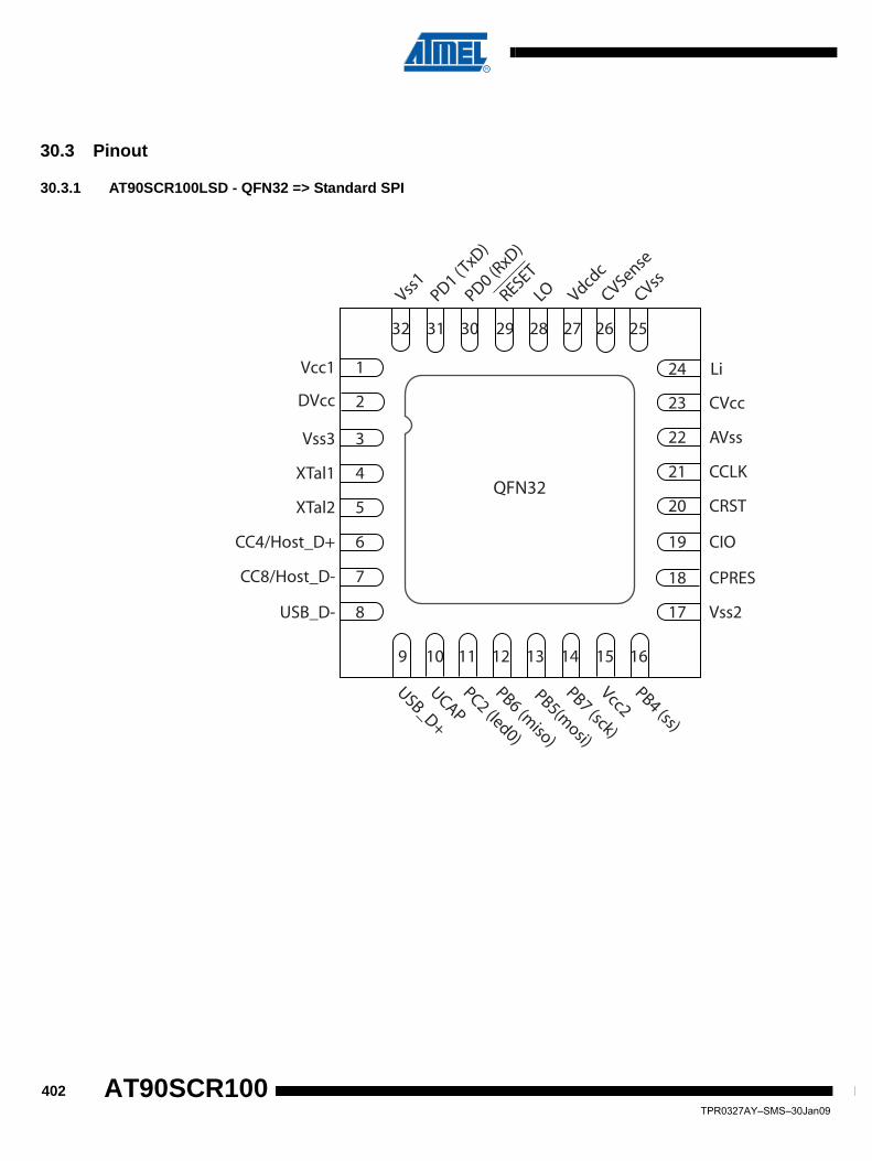
30.3 Pinout
30.3.1 AT90SCR100LSD - QFN32 => Standard SPI
QFN32
9
USB_D+
UCAPPC2 (led0)
PB6 (miso)
PB5(mosi)
PB7 (sck)
Vcc2PB4 (ss)
10 11 12 13 14 15 16
2
3
4
5XTal2
6CC4/Host_D+
7CC8/Host_D-
8USB_D-
24 Li
25
CVss
26
CVSense
27
Vdcdc
28
LO
2930
PD0 (RxD)
31
PD1 (TxD)
32
Vss1
1
23 CVcc
22 AVss
21 CCLK
20 CRST
19 CIO
18 CPRES
17 Vss2
Vcc1
DVcc
Vss3
XTal1
RESET
402TPR0327AY–SMS–30Jan09
AT90SCR100

AT90SCR100
30.3.2 AT90SCR100LHS - QFN32 => High-Speed SPI
QFN32
9
USB_D+
UCAPPC2 (led0)
PD7 (hs-miso)
PD6(hs-mosi)
PD5 (hs-sck)
Vcc2PD4 (hs-ss)
10 11 12 13 14 15 16
2
3
4
5XTal2
6CC4/Host_D+
7CC8/Host_D-
8USB_D-
24 Li
25
CVss
26
CVSense
27
Vdcdc
28
LO
2930
PD0 (RxD)
31
PD1 (TxD)
32
Vss1
1
23 CVcc
22 AVss
21 CCLK
20 CRST
19 CIO
18 CPRES
17 Vss2
Vcc1
DVcc
Vss3
XTal1
RESET
403TPR0327AY–SMS–30Jan09

30.3.3 AT90SCR100H - QFN64 & LQFP64
QFN64
1PA1 (KbIn1)
2PA2 (KbIn2)
3PA3 (KbIn3)
4
5
6
7
8
9
10
11
12
13
14
15
16
PE5 (KbO5)
Vcc1
Vcc2
DVcc
RTC1 (Tosc1)
RTC2 (Tosc2)
XTal1
XTal2
CC4/Host_D+
CC8/Host_D-
USB_D-
USB_D+
48
47
46
45
44
43
42
41
40
39
38
37
36
35
34
33
LI
CVcc
CCLK
CRST
CIO
CPRES
Vcc5
PA7 (KbIn7)
PA6 (KbIn6)
PD2 (int0)
PD3 (int1)
PB0 (int2)
PD4 (hs-ss)
PB3 (pwm)
PB4 (ss)
e-pad, underneath package must be connected to groundNC: Not Connected (pin16, 32)
3231302928272625242321 2220191817
NCVcc4PD5 (hs-sck)
PB7 (sck)
PD6 (hs-mosi)
PB5 (mosi)
PE7 (KbO7)
PE6 (KbO6)
PD7 (hs-miso)
PB6 (miso)
PC5 (led3)
Vcc3PC4 (led2)
PC3 (led1)
PC2 (led0)
UCAP
4950515253545556575860 5961626364
PE4 (KbO4)
PB1 (int3)
PE3 (KbO3)
PA0 (K
bIn0)
PE2 (KbO2)
PE1 (KbO1)
PE0 (KbO0)
PA5 (K
bIn5)
PA4 (K
bIn4)
PB2PD1 (T
xD)
PD0 (RxD)
PC1 (sda)
PC0 (scl)
LO Vdcdc
CVSense
RESET
404TPR0327AY–SMS–30Jan09
AT90SCR100

AT90SCR100
30.4 Mechanical Information
30.4.1 QFN32
D
E
eb
A30.10
A2
A1 AD2
E2
0.05 C
L
1
23
1
2
3 Pin 1 ID
Pitch #1 Notch(0.20 R)
COMMON DIMENSIONS(Unit of Measure = mm)
SYMBOL MIN NOM MAX
A 0.90
A1 0.05
A2 0.65 0.70
A3 0.20 REF
b 0.18 0.25 0.30
D
D2
3.40 3.50 3.80
5.00 BSC
5.00 BSC
E
E2
3.40 3.50 3.60
e
0.50 BSC
L 0.40
K 0.35 –
0.450.35
–
–
– –
–
–
K
0.45
K
TOP VIEW
BOTTOM VIEW
SIDE VIEW
Note: JEDEC Standard MO-220, Fig. 2 (Anvil Singulation), VHHD-21. All dimensions are in millimeters.2. Die thickness allowable is 0.305mm maximum.3. Dimensioning & Tolerances conform to ASME Y14.5M. 1994.4. The Pin #1 identifier must be placed on the top surface of the package by using identification mark or other feature of package body.5. Exact shape and size of this feature is optimal.6. Package warpage max 0.08mm.7. Applied for exposed pad and terminals. Exclude embedding part of exposed pard from measuring8. Applied only to terminals
405TPR0327AY–SMS–30Jan09

30.4.2 QFN 64
E
eb
D2
E2
L
123
A2
A1
A
0.05 C
Pin 1 ID
TOP VIEW
BOTTOM VIEW
SIDE VIEW
Pitch #1 Notch(0.20 R)
D
C
COMMON DIMENSIONS(Unit of Measure = mm)
Note: Compliant JEDEC Standard MO-220 variation VMMD-3
SYMBOL
A
A1
A2
D/E
e
L
b
D2/E2
1.00
0.05
0.95
9.10
0.55
0.3
7.50
0.80
0
–
8.90
0.30
0.18
3.25
0.50 BSC
–
–
–
9.00
0.40
0.25
–
MIN NOM MAX
406TPR0327AY–SMS–30Jan09
AT90SCR100

AT90SCR100
30.4.3 LQFP64 _ TBC
PIN 1 IDENTIFIER
0°~7°
PIN 1
LL1
c
A1 A2 A
D1D2
D
e E1E2 E
b
Notes:1. This drawing is for general information only. Refer to JEDEC drawing MS-026 for additional information.
COMMON DIMENSIONS (Unit of Measure = mm)
SYMBOL MIN NOM MAX
A – – 1.60
A1 0.05 – 0.15
A2 1.35 1.40 1.45
D 12.00 BSC
D1 10.00 BSC
D2 7.50
E 12.00 BSC
E1 10.00 BSC
E2 7.50
b 0.17 0.20 0.27
c 0.09 – 0.20
L 0.45 0.60 0.75
L1 1.00 REF
e 0.50 BSC
64-lead
407TPR0327AY–SMS–30Jan09

408TPR0327AY–SMS–30Jan09
AT90SCR100

AT90SCR100
31. Electrical Characteristics
31.1 ScopeThe AT90SCR100 application can make the use of the internal DC/DC converter or not.
Please pay attention to the configuration of the AT90SCR100 before reading the table, to matchyour particular needs.
AT90SCR100 without active DC/DC: Vcc range: 2.4V - 5.5V
AT90SCR100 with active DC/DC: Vcc range: 2.7V - 5.5V
Absolute Maximum Ratings*
Operating Temperature.................................... -40°C to +85°C *NOTICE: Stresses beyond those listed under “Absolute Maximum Ratings” may cause permanent dam-age to the device. This is a stress rating only and functional operation of the device at these or other conditions beyond those indicated in the operational sections of this specification is not implied. Exposure to absolute maximum rating conditions for extended periods may affect device reliability.
Storage Temperature ..................................... -65°C to +150°C
Voltage on any Pin except RESETwith respect to Ground ................................-0.5V to VCC+0.5V
Voltage on RESET with respect to Ground......-0.5V to +13.0V
Maximum Operating Voltage ............................................ 6.0V
DC Current VCC and GND Pins.........................................TBD
All DC Characteristics contained in this datasheet are based on characterization ofother AVR microcontrollers and peripherals.
These values are preliminary values representing design targets, and will beupdated after characterization of silicon
This datasheet is only a preliminary version. All values indicated here are indica-tive values, describing what the product should achieve.
ALL THESE VALUES ARE TO BE CONFIRMED OR TO BE DEFINED
Caution!
Caution!
409TPR0327AY–SMS–30Jan09

31.2 DC Characteristics TBC/TBD
Notes: 1. All DC Characteristics contained in this datasheet are based on characterization of other AVR microcontrollers and peripher-als. These values are preliminary values representing design targets, and will be updated after characterization of silicon.
2. These parameters are only for standard I/Os. These only include: Keyboard Inputs, External Interrupts, Standard Serial Peripheral Interface (SPI), High-speed Serial Peripheral Interface (HSSPI), JTAG/LED ports (driving only 2 or 4mA), 2-Wire Interface, Timers I/Os, USART.
3. "Max" means the highest value where the pin is guaranteed to be read as low4. "Min" means the lowest value where the pin is guaranteed to be read as high5. Values with “PRR0 – Power Reduction Register 0” and “PRR1 – Power Reduction Register 1” disabled (0x00).6. Power-down values includes Input Leakage Current.7. For USB Suspend power-down current measure, you should add 200μA generated by the different resistors on USB D+/D-
lines.
31.3 PORT
Note: (TA = -20°C to +50°C, VCC - VOL = 2 V )
TA = -40°C to 85°C, VCC = 2.4V to 5.5V (unless otherwise noted)
Symbol Parameter Condition Min.(1) Typ. Max.(1) Units
VIL(2) Input Low Voltage VCC = 2.4V - 5.5V -0.3 0.8(3) V
VIH(2) Input High Voltage VCC = 2.4V - 5.5V 2.0(4) VCC + 0.3 V
VIHys(2) Hysteresis on Input VCC = 2.4V - 5.5V 0.4 0.7 V
VOL(2) Output Low Voltage, VCC = 2.4V - 5.5V 0.4 V
VOH(2) Output High Voltage, VCC = 2.4V - 5.5V VCC - 0.4 V
IIL(2) Input Leakage
Current I/O PinVCC = 5.5V, pin low(absolute value) 1 μA
IIH(2) Input Leakage
Current I/O PinVCC = 5.5V, pin high(absolute value) 1 μA
RRST Reset Pull-up Resistor 30 60 kΩ
RPU I/O Pin Pull-up Resistor 20 50 kΩ
ICCPower Supply Current(5)
Active 8MHz, VCC = 5V(AT90SCR100)
TBD mA
Idle 8MHz, VCC = 5V(AT90SCR100)
TBD mA
Power-down mode(6) VCC = 5V 100(7) 150 μA
Symbol Parameter Min Typ Max Unit Test Conditions
IOLOutput Low Current, PC2, PC3, PC4, PC5 LED modes
12
36
58
mAmA
2 mA configuration4 mA configuration
IOL Output Low Current, PORT E 2 mA
IOL Output Low Current, all other PORTS 8 mA
410TPR0327AY–SMS–30Jan09
AT90SCR100

AT90SCR100
31.4 Clocks
31.4.1 XTAL1 : External Clock In TBC/TBDThis clock relates to Core and System clock. See “Clock Sources” on page 33.
31.4.2 Calibrated Internal RC Oscillator AccuracyThis clock concerns the Flash/Eeprom specific clock. See “Internal RC Oscillator” on page 37.
31.5 Communication Interfaces
31.5.1 2-wire Serial Interface Characteristics TBC/TBDTable 31-3 describes the requirements for devices connected to the 2-wire Serial Bus. TheAT90SCR100 2-wire Serial Interface meets or exceeds these requirements under the notedconditions.
Timing symbols refer to Figure 31-1.
Table 31-1. XTAL1 = XIN Clock Electrical Characteristics
Symbol Parameter Min. Max. Units
1/tCPXIN XIN Clock Frequency 8 MHz
tCHXIN XIN Clock High Half-Period 0.4 x tCPXIN
tCLCX XIN Clock Low HAlf-Period 0.4 x tCPXIN
CIN XIN Input Capacitance
RIN XIN Pulldown Resistor
Table 31-2. Calibration Accuracy of Internal RC Oscillator
Frequency VCC Temperature Calibration Accuracy
Factory Calibration 10.0 MHz 3V 25⋅C ±5%
User Calibration 9.5 - 10.5 MHz 2.4V - 5.5V -40⋅C - 85⋅C ±1%
Table 31-3. 2-wire Serial Bus Requirements
Symbol Parameter Condition Min Max Units
VIL Input Low-voltage -0.5 0.3 VCC V
VIH Input High-voltage 0.6 VCC VCC + 0.5 V
Vhys(1) Hysteresis of Schmitt Trigger Inputs 0.05 VCC
(2) – V
VOL(1) Output Low-voltage 3 mA sink current 0 0.4 V
tr(1)(8) Rise Time for both SDA and SCL 20 + 0.1Cb(2)(3) 300 ns
tof(1)(8) Output Fall Time from VIHmin to VILmax 10 pF < Cb < 400 pF(3) 20 + 0.1Cb
(2)(3) 250 ns
tSP(1)(8) Spikes Suppressed by Input Filter 0 50(2) ns
Ci(1)(8) Capacitance for each I/O Pin – 10 pF
fSCL SCL Clock Frequency fCK (4)> max(16fSCL, 250kHz)(5) 0 400 kHz
tHD;STA Hold Time (repeated) START ConditionfSCL ≤ 100 kHz 4.0 – μs
fSCL > 100 kHz 0.6 – μs
411TPR0327AY–SMS–30Jan09

Notes: 1. In AT90SCR100, this parameter is characterized and not 100% tested.2. Required only for fSCL > 100 kHz.3. Cb = capacitance of one bus line in pF.4. fCK = CPU clock frequency5. This requirement applies to all AT90SCR100 Two-wire Serial Interface operation. Other devices connected to the Two-wire
Serial Bus need only obey the general fSCL requirement.6. The actual low period generated by the AT90SCR100 Two-wire Serial Interface is (1/fSCL - 2/fCK), thus fCK must be greater
than 6 MHz for the low time requirement to be strictly met at fSCL = 100 kHz.7. The actual low period generated by the AT90SCR100 Two-wire Serial Interface is (1/fSCL - 2/fCK), thus the low time require-
ment will not be strictly met for fSCL > 308 kHz when fCK = 8 MHz. Still, AT90SCR100 devices connected to the bus may communicate at full speed (400 kHz) with other AT90SCR100 devices, as well as any other device with a proper tLOW accep-tance margin.
8. This parameter is theorical and is not part of the production test flow. It represents a some idea of the size of the parameter, but the exact value is not guaranteed.
Figure 31-1. 2-wire Serial Bus Timing
31.5.2 High-Speed SPI Interface CharacteristicsTBD
tLOW Low Period of the SCL ClockfSCL ≤ 100 kHz(6) 4.7 – μs
fSCL > 100 kHz(7) 1.3 – μs
tHIGH High period of the SCL clockfSCL ≤ 100 kHz 4.0 – μs
fSCL > 100 kHz 0.6 – μs
tSU;STA Set-up time for a repeated START conditionfSCL ≤ 100 kHz 4.7 – μs
fSCL > 100 kHz 0.6 – μs
tHD;DAT Data hold timefSCL ≤ 100 kHz 0 3.45 μs
fSCL > 100 kHz 0 0.9 μs
tSU;DAT Data setup timefSCL ≤ 100 kHz 250 – ns
fSCL > 100 kHz 100 – ns
tSU;STO Setup time for STOP conditionfSCL ≤ 100 kHz 4.0 – μs
fSCL > 100 kHz 0.6 – μs
tBUFBus free time between a STOP and START condition
fSCL ≤ 100 kHz 4.7 – μs
fSCL > 100 kHz 1.3 – μs
Table 31-3. 2-wire Serial Bus Requirements (Continued)
Symbol Parameter Condition Min Max Units
tSU;STA
tLOW
tHIGH
tLOW
tof
tHD;STA tHD;DAT tSU;DATtSU;STO
tBUF
SCL
SDA
tr
412TPR0327AY–SMS–30Jan09
AT90SCR100

AT90SCR100
31.5.3 SPI Timing Characteristics TBC/TBDSee Figure 31-2 and Figure 31-3 for details.
Notes: 1. In SPI Programming mode the minimum SCK high/low period is:- 2 tCLCL for fCK < 12 MHz- 3 tCLCL for fCK > 12 MHz
2. These values are for information only. They are not tested to production test flow. They are deduced from characterization session.
Figure 31-2. SPI Interface Timing Requirements (Master Mode)
Table 31-4. SPI Timing Parameters(2)
Description Mode Min Typ Max
1 SCK period Master See Table 20-4
ns
2 SCK high/low Master 50% duty cycle
3 Rise/Fall time Master 3.6
4 Setup Master 10
5 Hold Master 10
6 Out to SCK Master 0.5 • tsck
7 SCK to out Master 10
8 SCK to out high Master 10
9 SS low to out Slave 15
10 SCK period Slave 4 • tck
11 SCK high/low(1) Slave 2 • tck
12 Rise/Fall time Slave 1600
13 Setup Slave 10
14 Hold Slave tck
15 SCK to out Slave 15
16 SCK to SS high Slave 20
17 SS high to tri-state Slave 10
18 SS low to SCK Slave 20
MO SI(Data Output)
SCK(CPOL = 1)
MISO(Data Input)
SCK(CPOL = 0)
SS
MSB LSB
LSBMSB
...
...
6 1
2 2
34 5
87
413TPR0327AY–SMS–30Jan09

Figure 31-3. SPI Interface Timing Requirements (Slave Mode)
31.6 USB Interface Characteristics TBC/TBD
MISO(Data Output)
SCK(CPOL = 1)
MO SI(Data Input)
SCK(CPOL = 0)
SS
MSB LSB
LSBMSB
...
...
10
11 11
1213 14
1715
9
X
16
Table 31-5. USB Electrical Parameters
Symbol Parameter Condition Min. Typ. Max. Units
VIH Input Level High (driven) 2.0 V
VIHZ Input Level High (floating) 2.7 V
VIL Input Level Low 0.8 V
VDI Differential Input Sensitivity 0.2 V
VCMDifferential Common Mode Range 0.8 2.5 V
VOL1 Static Output Low 0.3 V
VOH1 Static Output High 2.8 3.6 V
CIN Input Capacitance 20 pF
tr Rise Time Cout = 50 pF 4 20 ns
tf Fall Time Cout = 50 pF 4 20 ns
trfm Rise / Fall Time matching (tr/tr ) 90 110 %
Zdrv Driver Output Resistance Steady State Drive 28 44 ohm
tdrate Full Speed Data Rate Average Bit Rate 11.97 12.03 Mb/s
tframe Frame Interval 0.9995 1.0005 ms
414TPR0327AY–SMS–30Jan09
AT90SCR100

AT90SCR100
31.7 Smart Card Interface Characteristics
All Characteristics contained in this section are based on characterization of otherproducts.
These values are preliminary values representing design targets, and will beupdated after characterization of silicon
This datasheet is only a preliminary version. All values indicated here are indica-tive values, describing what the product should achieve.
ALL THESE VALUES ARE TO BE CONFIRMED OR TO BE DEFINED
Caution!
Caution!
Table 31-6. Smart Card Class A, 5V (CVcc)
Symbol Parameter Min Typ Max Unit Test Conditions
CVCCSmart card voltage
with Vcc = 2.7V to 2.85Vwith Vcc > 2.85V
4.64.6
55
5.45.4
V Load = 50mALoad = 60mA
Spikes on CVCC TBD V
Vcardok up Vcardok high level threshold TBD V
Vcardok down Vcardok low level threshold TBD V
TVHL CVCC valid to 0.4V TBD TBD μs
TVLH CVCC 0 to valid TBD TBD μs
Table 31-7. Smart Card Class B, 3V (CVcc)
Symbol Parameter Min Typ Max Unit Test Conditions
CVCCSmart card voltage
with Vcc = 2.7V to 2.85Vwith Vcc > 2.85V
2.762.76
33
3.243.24
V Load = 50mALoad = 60mA
Spikes on CVCC TBD V
Vcardok up Vcardok high level threshold TBD V
Vcardok down Vcardok low level threshold TBD V
TVHL CVCC valid to 0.4V TBD TBD μs
TVLH CVCC 0 to valid TBD TBD μs
Table 31-8. Smart Card C, 1.8V (CVcc)
Symbol Parameter Min Typ Max Unit Test Conditions
CVCC Smart card voltage 1.66 1.8 1.944 V Load = 35mA
Spikes on CVCC TBD V
Vcardok up Vcardok high level threshold TBD V
415TPR0327AY–SMS–30Jan09

31.8 USB Host Controller CharacteristicsTBD
Vcardok down Vcardok low level threshold TBD V
TVHL CVCC valid to 0.4V TBD TBD TBD μs
TVLH CVCC 0 to valid TBD TBD μs
Table 31-8. Smart Card C, 1.8V (CVcc)
Symbol Parameter Min Typ Max Unit Test Conditions
Table 31-9. Smart Card Card Presence (CPRES)
Symbol Parameter Min Typ Max Unit Test Conditions
IOL1 CPRES weak pull-up output current 3 10 25 μA
Short to VSS
PULLUP = 1:
Internal pull-up active
416TPR0327AY–SMS–30Jan09
AT90SCR100

AT90SCR100
32. Register SummaryAddress Name Bit 7 Bit 6 Bit 5 Bit 4 Bit 3 Bit 2 Bit 1 Bit 0 Page
(0xFF) SCICR RESET CARDDET VCARD1 VCARD0 UART WTEN CREP CONV 190(0xFE) SCCON CLK - CARDC8 CARDC4 CARDIO CARDCLK CARDRST CARDVCC 192(0xFD) SCISR SCTBE CARDIN - VCARDOK SCWTO SCTC SCRC SCPE 193(0xFC) SCIIR SCTBI - - VCARDERR SCWTI SCTI SCRI SCPI 195(0xFB) SCIER ESCTBI CARDINE - IVCARDER ESCWTI ESCTI ESCRI ESCPI 196(0xFA) SCSR - BGTEN - CREPSEL CPRESRES - - - 196(0xF9) SCIBUF SCIBUFD [7..0] 197(0xF8) SCETUH COMP - - - - ETU [10:8] 198(0xF7) SCETUL ETU [7:0] 198(0xF6) SCGTH - - - - - - - GT8 198(0xF5) SCGTL GT [7:0] 198(0xF4) SCWT3 WT31 WT30 WT29 WT28 WT27 WT26 WT25 WT24 199(0xF3) SCWT2 WT23 WT22 WT21 WT20 WT19 WT18 WT17 WT16 199(0xF2) SCWT1 WT15 WT14 WT13 WT12 WT11 WT10 WT9 WT8 199(0xF1) SCWT0 WT7 WT6 WT5 WT4 WT3 WT2 WT1 WT0 199(0xF0) SCICLK XTSCS - SCICLK5 SCICLK4 SCICLK3 SCICLK2 SCICLK1 SCICLK0 199(0xEF) DCCR DCON DCRDY DCBUSY - - - - - 203(0xEE) Reserved - - - - - - - -(0xED) USBDMAB - USBDMAB [6..0] 176(0xEC) USBDMADH - - USBDMAD [13..8] 175(0xEB) USBDMADL USBDMAD [7..0] 175(0xEA) USBDMACS - EPS2 EPS1 EPS0 - DMAERR DMAIR DMAR 173(0xE9) USBFNH - - - FNEND FNERR FN10 FN9 FN8 172(0xE8) USBFNL FN7 FN6 FN5 FN4 FN3 FN2 FN1 FN0 172(0xE7) USBFA - FADD6 FADD5 FADD4 FADD3 FADD2 FADD1 FADD0 171(0xE6) USBGS - - - - RSMON RMWUE FCF FAF 171(0xE5) USBRSTE RSTE4 RSTE6 RSTE5 RSTE4 RSTE3 RSTE2 RSTE1 RSTE0 170(0xE4) USBEIM EP7IM EP7IM EP5IM EP4IM EP3IM EP2IM EP1IM EP0IM 167(0xE3) USBEI EP7I EP6I EP5I EP4I EP4I EP2I EP1I EP0I 166(0xE2) USBPIM - - - - SOFIM RMWUIM RESIM SUSIM 166(0xE1) USBPI - - - FEURI SOFI RMWUI RESI SUSI 165(0xE0) USBCR URMWU - UPUC - - - USBE - 164(0xDF) HSSPIDMAB - - - HSSPIDMAB [4..0] 295(0xDE) HSSPIDMADH - - HSSPIDMAD [13..8] 295(0xDD) HSSPIDMADL HSSPIDMAD [7..0] 295(0xDC) HSSPIDMACS - - - - - DMAERR DMADIR DMAR 293(0xDB) HSSPICR - - - - - STTTO RETTO CS 290(0xDA) HSSPIIR TIMEOUT BTD RCVOF NSSRE NSSFE - - - 288(0xD9) HSSPICFG SPICKDIV2 SPICKDIV1 SPICKDIV0 DPRAM CPHA CPOL MSTR SPIEN 287(0xD8) HSSPISR - - - DPRAMRDY NSS RXBUFF TXBUFE SPICKRDY 290(0xD7) HSSPITDR HSSPITDD [7..0] 291(0xD6) HSSPIRDR HSSPIRDD [7..0] 291(0xD5) HSSPIGTR HSSPIGTD [7..0] 291(0xD4) HSSPIIER TIMEOUTIE BTDIE RCVOFIE NSSIE - - - - 289(0xD3) HSSPICNT - - - HSSPICNT [4..0] 291(0xD2) HSSPITOH SPITIMEOUT[15:8] 292(0xD1) HSSPITOL SPITIMEOUT[7:0] 292(0xD0) Reserved - - - - - - - -(0xCF) Reserved - - - - - - - -(0xCE) Reserved - - - - - - - -(0xCD) USBFCEX EPE - - - - EPDIR EPTYP1 EPTYP0 169(0xCC) USBDBCEX BCT7 BCT6 BCT5 BCT4 BCT3 BCT2 BCT1 BCT0 169(0xCB) USBCSEX - IERR FSTALL TXPB STSENT RXSETUP RCVD TXC 167(0xCA) USBENUM - - - - ENUM3 ENUM2 ENUM1 ENUM0 167(0xC9) Reserved - - - - - - - -(0xC8) Reserved - - - - - - - -(0xC7) Reserved - - - - - - - -(0xC6) UDR0 USART0 I/O Data Register 249(0xC5) UBRR0H - - - - USART0 Baud Rate Register High Byte 253(0xC4) UBRR0L USART0 Baud Rate Register Low Byte 253(0xC3) Reserved - - - - - - - -(0xC2) UCSR0C UMSEL01 UMSEL00 UPM01 UPM00 USBS0 UCSZ01 UCSZ00 UCPOL0 251(0xC1) UCSR0B RXCIE0 TXCIE0 UDRIE0 RXEN0 TXEN0 UCSZ02 RXB80 TXB80 250(0xC0) UCSR0A RXC0 TXC0 UDRE0 FE0 DOR0 UPE0 U2X0 MPCM0 249
417TPR0327AY–SMS–30Jan09

(0xBF) Reserved - - - - - - - -(0xBE) Reserved - - - - - - - -(0xBD) TWAMR TWAM6 TWAM5 TWAM4 TWAM3 TWAM2 TWAM1 TWAM0 - 328(0xBC) TWCR TWINT TWEA TWSTA TWSTO TWWC TWEN - TWIE 325(0xBB) TWDR 2-wire Serial Interface Data Register 327(0xBA) TWAR TWA6 TWA5 TWA4 TWA3 TWA2 TWA1 TWA0 TWGCE 327(0xB9) TWSR TWS7 TWS6 TWS5 TWS4 TWS3 - TWPS1 TWPS0 326(0xB8) TWBR 2-wire Serial Interface Bit Rate Register 324(0xB7) Reserved - - - - - - - -(0xB6) ASSR - EXCLK AS2 TCN2UB OCR2AUB OCR2BUB TCR2AUB TCR2BUB 150(0xB5) Reserved - - - - - - - -(0xB4) OCR2B Timer/Counter2 Output Compare Register B 150(0xB3) OCR2A Timer/Counter2 Output Compare Register A 150(0xB2) TCNT2 Timer/Counter2 (8 Bit) 149(0xB1) TCCR2B FOC2A FOC2B - - WGM22 CS22 CS21 CS20 148(0xB0) TCCR2A COM2A1 COM2A0 COM2B1 COM2B0 - - WGM21 WGM20 145(0xAF) UPDATX PDAT [7..0] 229(0xAE) UPIENX FLERRE NAKEDE - PERRE TXSTPE TXOUTE RXSTALLE RXINE 229(0xAD) UPCFG2X INTFRQ [7..0] 225(0xAC) UPSTAX CFGOK OVERFI UNDERFI - DTSEQ [1..0] - NBUSYB 225(0xAB) UPCFG1X - PSIZE [0..2] PBK [0..1 ALLOC - 224(0xAA) UPCFG0X PTYPE [1..0] PTOKEN [0..1] PEPNUM [0..3] 223(0xA9) UPCRX - PFREEZE INMODE - RSTDT - - PEN 222(0xA8) UPRST - - - - P3RST P2RST P1RST P0RST 222(0xA7) UPNUM - - - - - - PNUM1 PNUM0 222(0xA6) UPINTX FIFOCON NAKEDI RWAL PERRI TXSPI TXOUTI RXSTALLI RXINI 227(0xA5) UPINRQX INRQ [7..0] 226(0xA4) UHFLEN FLEN [7..0] 221(0xA3) UHFNUMH - - - - - FNUM [10..8] 221(0xA2) UHFNUML FNUM [7..0] 221(0xA1) UHADDR - HADDR [6..0] 221(0xA0) UHIEN - HWUPE HSOFE RXRSME RSMEDE RSTE DDISCE DCONNE 220(0x9F) UHINT - HWUPI HSOFI RXRSMI RSMEDI RSTI DDISCI DCONNI 219(0x9E) UHCR UHEN PAD [1..0] FRZCLK - RESUME RESET SOFEN 217(0x9D) UPERRX - COUNTER [1..0] CRC16 TIMEOUT PID DATAPID DATATGL 226(0x9C) UPBCXH - - - - - PBYTCT [10..8] 230(0x9B) UPBCXL PBYTCT [7..0] 230(0x9A) UPINT - - - - PINT3 PINT2 PINT1 PINT0 230(0x99) UHSR - - - - SPEED - - - 218(0x98) Reserved - - - - - - - -(0x97) Reserved - - - - - - - -(0x96) Reserved - - - - - - - -(0x95) RNGCR - - - - - - - ROSCE 336(0x94) LFSR3 LFSD [31..24] 336(0x93) LFSR2 LFSD [23..16] 336(0x92) LFSR1 LFSD [15..8] 336(0x91) LFSR0 LFSD [7..0] 336(0x90) RDWDR RDD [7..0] 337(0x8F) KBFR KBF7 KBF6 KBF5 KBF4 KBF3 KBF2 KBF1 KBF0 330(0x8E) KBER KBE7 KBE6 KBE5 KBE4 KBE3 KBE2 KBE1 KBE0 331(0x8D) KBLSR KBLS7 KBLS6 KBLS5 KBLS4 KBLS3 KBLS2 KBLS1 KBLS0 332(0x8C) Reserved - - - - - - - -(0x8B) OCR1BH Timer/Counter1 - Output Compare Register B High Byte 131 (0x8A) OCR1BL Timer/Counter1 - Output Compare Register B Low Byte 131(0x89) OCR1AH Timer/Counter1 - Output Compare Register A High Byte 131(0x88) OCR1AL Timer/Counter1 - Output Compare Register A Low Byte 131(0x87) ICR1H Timer/Counter1 - Input Capture Register High Byte 131(0x86) ICR1L Timer/Counter1 - Input Capture Register Low Byte 131(0x85) TCNT1H Timer/Counter1 - Counter Register High Byte 130(0x84) TCNT1L Timer/Counter1 - Counter Register Low Byte 130(0x83) Reserved - - - - - - - -(0x82) TCCR1C FOC1A FOC1B - - - - - - 129(0x81) TCCR1B ICNC1 ICES1 - WGM13 WGM12 CS12 CS11 CS10 128(0x80) TCCR1A COM1A1 COM1A0 COM1B1 COM1B0 - - WGM11 WGM10 126(0x7F) Reserved - - - - - - - -(0x7E) Reserved - - - - - - - -
Address Name Bit 7 Bit 6 Bit 5 Bit 4 Bit 3 Bit 2 Bit 1 Bit 0 Page
418TPR0327AY–SMS–30Jan09
AT90SCR100

AT90SCR100
(0x7D) Reserved - - - - - - - -(0x7C) Reserved - - - - - - - -(0x7B) AESDR DATA [0..8] 343(0x7A) AESADDR ADDR [0..8] 343(0x79) AESACR - - - - XOR MANINC AUTOINC KD 342(0x78) AESCR AESIE AESIF AUTOKEY KEYGN KS - ENCRYPT AESGO 341(0x77) Reserved - - - - - - - -(0x76) Reserved - - - - - - - -(0x75) LEDCR LED3 LED2 LED1 LED0 77(0x74) Reserved - - - - - - - -(0x73) PCMSK3 PCINT31 PCINT30 PCINT29 PCINT28 PCINT27 PCINT26 PCINT25 PCINT24 73(0x72) Reserved - - - - - - - -(0x71) Reserved - - - - - - - -(0x70) TIMSK2 - - - - - OCIE2B OCIE2A TOIE2 153(0x6F) TIMSK1 - - ICIE1 - - OCIE1B OCIE1A TOIE1 132(0x6E) TIMSK0 - - - - - OCIE0B OCIE0A TOIE0 103(0x6D) PCMSK2 PCINT23 PCINT22 PCINT21 PCINT20 PCINT19 PCINT18 PCINT17 PCINT16 73(0x6C) PCMSK1 PCINT15 PCINT14 PCINT13 PCINT12 PCINT11 PCINT10 PCINT9 PCINT8 73(0x6B) PCMSK0 PCINT7 PCINT6 PCINT5 PCINT4 PCINT3 PCINT2 PCINT1 PCINT0 73(0x6A) Reserved - - - - - - - -(0x69) EICRA ISC31 ISC30 ISC21 ISC20 ISC11 ISC10 ISC01 ISC00 69(0x68) PCICR - - - - PCIE3 PCIE2 PCIE1 PCIE0 71(0x67) Reserved - - - - - - - -(0x66) OSCCAL CAL7 CAL6 CAL5 CAL4 CAL3 CAL2 CAL1 CAL0 39(0x65) PRR1 - - PRKB PRAES PRSCI PRHSSPI PRUSB PRSCUSB 46(0x64) PRR0 PRTWI PRTIM2 PRTIM0 - PRTIM1 PRSPI PRUSART0 - 45(0x63) SMONCR SMONIF SMONIE - - - - - SMONEN 60(0x62) PLLCR PLLMUX - - - - - LOCK ON/OFF 40(0x61) CLKPR - - - - CLKPS3 CLKPS2 CLKPS1 CLKPS0 40(0x60) WDTCSR WDIF WDIE WDP3 WDCE WDE WDP2 WDP1 WDP0 61
0x3F (0x5F) SREG I T H S V N Z C 150x3E (0x5E) SPH SP15 SP14 SP13 SP12 SP11 SP10 SP9 SP8 170x3D (0x5D) SPL SP7 SP6 SP5 SP4 SP3 SP2 SP1 SP0 170x3C (0x5C) Reserved - - - - - - - -0x3B (0x5B) Reserved - - - - - - - -0x3A (0x5A) Reserved - - - - - - - -0x39 (0x59) Reserved - - - - - - - -0x38 (0x58) Reserved - - - - - - - -0x37 (0x57) SPMCSR SPMIE RWWSB SIGRD RWWSRE BLBSET PGWRT PGERS SPMEN 3670x36 (0x56) Reserved - - - - - - - -0x35 (0x55) MCUCR JTD - - PUD - - IVSEL IVCE 67, 82, 3560x34 (0x54) MCUSR - - - JTRF WDRF BORF EXTRF PORF 600x33 (0x53) SMCR - - - - SM2 SM1 SM0 SE 450x32 (0x52) Reserved - - - - - - - -0x31 (0x51) OCDR D7/IDRD D6 D5 D4 D3 D2 D1 D0 3520x30 (0x50) Reserved - - - - - - - -0x2F (0x4F) Reserved - - - - - - - -0x2E (0x4E) SPDR SPI 0 Data Register 2740x2D (0x4D) SPSR SPIF WCOL - - - - - SPI2X 2740x2C (0x4C) SPCR SPIE SPE DORD MSTR CPOL CPHA SPR1 SPR0 2720x2B (0x4B) GPIOR2 General Purpose I/O Register 2 290x2A (0x4A) GPIOR1 General Purpose I/O Register 1 290x29 (0x49) Reserved - - - - - - - -0x28 (0x48) OCR0B Timer/Counter0 Output Compare Register B 1030x27 (0x47) OCR0A Timer/Counter0 Output Compare Register A 1030x26 (0x46) TCNT0 Timer/Counter0 (8 Bit) 1020x25 (0x45) TCCR0B FOC0A FOC0B - - WGM02 CS02 CS01 CS00 1010x24 (0x44) TCCR0A COM0A1 COM0A0 COM0B1 COM0B0 - - WGM01 WGM00 980x23 (0x43) GTCCR TSM - - - - - PSRASY PSRSYNC 1550x22 (0x42) EEARH - - - - EEARH [11:8] 240x21 (0x41) EEARL EEARL [7:0] 240x20 (0x40) EEDR EEPROM Data Register 240x1F (0x3F) EECR - - EEPM1 EEPM0 EERIE EEMPE EEPE EERE 240x1E (0x3E) GPIOR0 General Purpose I/O Register 0 300x1D (0x3D) EIMSK - - - - INT3 INT2 INT1 INT0 700x1C (0x3C) EIFR - - - - INTF3 INTF2 INTF1 INTF0 70
Address Name Bit 7 Bit 6 Bit 5 Bit 4 Bit 3 Bit 2 Bit 1 Bit 0 Page
419TPR0327AY–SMS–30Jan09

0x1B (0x3B) PCIFR - - - - PCIF3 PCIF2 PCIF1 PCIF0 720x1A (0x3A) EIRR - - - - INTD3 INTD2 - - 710x19 (0x39) Reserved - - - - - - - -0x18 (0x38) Reserved - - - - - - - -0x17 (0x37) TIFR2 - - - - - OCF2B OCF2A TOV2 1530x16 (0x36) TIFR1 - - ICF1 - - OCF1B OCF1A TOV1 1320x15 (0x35) TIFR0 - - - - - OCF0B OCF0A TOV0 1040x14 (0x34) Reserved - - - - - - - -0x13 (0x33) Reserved - - - - - - - -0x12 (0x32) Reserved - - - - - - - -0x11 (0x31) Reserved - - - - - - - -0x10 (0x30) Reserved - - - - - - - -0x0F (0x2F) Reserved - - - - - - - -0x0E (0x2E) PORTE PORTE7 PORTE6 PORTE5 PORTE4 PORTE3 PORTE2 PORTE1 PORTE0 840x0D (0x2D) DDRE DDE7 DDE6 DDE5 DDE4 DDE3 DDE2 DDE1 DDE0 850x0C (0x2C) PINE PINE7 PINE6 PINE5 PINE4 PINE3 PINE2 PINE1 PINE0 850x0B (0x2B) PORTD PORTD7 PORTD6 PORTD5 PORTD4 PORTD3 PORTD2 PORTD1 PORTD0 840x0A (0x2A) DDRD DDD7 DDD6 DDD5 DDD4 DDD3 DDD2 DDD1 DDD0 840x09 (0x29) PIND PIND7 PIND6 PIND5 PIND4 PIND3 PIND2 PIND1 PIND0 840x08 (0x28) PORTC - - PORTC5 PORTC4 PORTC3 PORTC2 PORTC1 PORTC0 840x07 (0x27) DDRC - - DDC5 DDC4 DDC3 DDC2 DDC1 DDC0 840x06 (0x26) PINC - - PINC5 PINC4 PINC3 PINC2 PINC1 PINC0 840x05 (0x25) PORTB PORTB7 PORTB6 PORTB5 PORTB4 PORTB3 PORTB2 PORTB1 PORTB0 830x04 (0x24) DDRB DDB7 DDB6 DDB5 DDB4 DDB3 DDB2 DDB1 DDB0 830x03 (0x23) PINB PINB7 PINB6 PINB5 PINB4 PINB3 PINB2 PINB1 PINB0 830x02 (0x22) PORTA PORTA7 PORTA6 PORTA5 PORTA4 PORTA3 PORTA2 PORTA1 PORTA0 830x01 (0x21) DDRA DDA7 DDA6 DDA5 DDA4 DDA3 DDA2 DDA1 DDA0 830x00 (0x20) PINA PINA7 PINA6 PINA5 PINA4 PINA3 PINA2 PINA1 PINA0 83
Address Name Bit 7 Bit 6 Bit 5 Bit 4 Bit 3 Bit 2 Bit 1 Bit 0 Page
1. For compatiliblity with future devices, reserved bits should be written to zero if accessed. Reserved I/O memory addresses should never be written.
2. I/O registers within the address range $00-$1F are directly bit-accessible using the SBI and CBI instructions. In these registers, the value of single bits can be checked by using SBIS and SBIC instructions.
3. Some of the status flags are cleared by writing a logical one to them. Note that the CBI and SBI instructions will operate on all bits in the I/O register, writing a one back into any flag read as set, this clearing the flag. The CBI and SBI instructions work with registers $00 to $1F only.
4. When using the I/O specific commands IN and OUT, the I/O addresses $00-$3F must be used. When addressing I/O registers as data space using LD and ST instructions, $20 must be added to these addresses. The AT90SCR100 is a complex microcontroller with more peripheral units than can be supported within the 64 locations reserved in Opcode for the IN and OUT instructions. For the Extended I/O space from $60-$FF, only the ST/STS/STD and LD/LDS/LDD instructions ca be used.
All ‘Reserved’ registers must not be read or written.Writing or Reading these registers may generate unhandled state.
Note
Caution!
420TPR0327AY–SMS–30Jan09
AT90SCR100

AT90SCR100
33. Instruction Set SummaryMnemonics Operands Description Operation Flags #Clocks
ARITHMETIC AND LOGIC INSTRUCTIONSADD Rd, Rr Add two Registers Rd ← Rd + Rr Z,C,N,V,H 1ADC Rd, Rr Add with Carry two Registers Rd ← Rd + Rr + C Z,C,N,V,H 1ADIW Rdl,K Add Immediate to Word Rdh:Rdl ← Rdh:Rdl + K Z,C,N,V,S 2SUB Rd, Rr Subtract two Registers Rd ← Rd - Rr Z,C,N,V,H 1SUBI Rd, K Subtract Constant from Register Rd ← Rd - K Z,C,N,V,H 1SBC Rd, Rr Subtract with Carry two Registers Rd ← Rd - Rr - C Z,C,N,V,H 1SBCI Rd, K Subtract with Carry Constant from Reg. Rd ← Rd - K - C Z,C,N,V,H 1SBIW Rdl,K Subtract Immediate from Word Rdh:Rdl ← Rdh:Rdl - K Z,C,N,V,S 2AND Rd, Rr Logical AND Registers Rd ← Rd • Rr Z,N,V 1ANDI Rd, K Logical AND Register and Constant Rd ← Rd • K Z,N,V 1OR Rd, Rr Logical OR Registers Rd ← Rd v Rr Z,N,V 1ORI Rd, K Logical OR Register and Constant Rd ← Rd v K Z,N,V 1EOR Rd, Rr Exclusive OR Registers Rd ← Rd ⊕ Rr Z,N,V 1COM Rd One’s Complement Rd ← 0xFF − Rd Z,C,N,V 1NEG Rd Two’s Complement Rd ← 0x00 − Rd Z,C,N,V,H 1SBR Rd,K Set Bit(s) in Register Rd ← Rd v K Z,N,V 1CBR Rd,K Clear Bit(s) in Register Rd ← Rd • (0xFF - K) Z,N,V 1INC Rd Increment Rd ← Rd + 1 Z,N,V 1DEC Rd Decrement Rd ← Rd − 1 Z,N,V 1TST Rd Test for Zero or Minus Rd ← Rd • Rd Z,N,V 1CLR Rd Clear Register Rd ← Rd ⊕ Rd Z,N,V 1SER Rd Set Register Rd ← 0xFF None 1MUL Rd, Rr Multiply Unsigned R1:R0 ← Rd x Rr Z,C 2
MULS Rd, Rr Multiply Signed R1:R0 ← Rd x Rr Z,C 2MULSU Rd, Rr Multiply Signed with Unsigned R1:R0 ← Rd x Rr Z,C 2FMUL Rd, Rr Fractional Multiply Unsigned R1:R0 ← (Rd x Rr) << 1 Z,C 2
FMULS Rd, Rr Fractional Multiply Signed R1:R0 ← (Rd x Rr) << 1 Z,C 2FMULSU Rd, Rr Fractional Multiply Signed with Unsigned R1:R0 ← (Rd x Rr) << 1 Z,C 2
BRANCH INSTRUCTIONSRJMP k Relative Jump PC ← PC + k + 1 None 2IJMP Indirect Jump to (Z) PC ← Z None 2JMP k Direct Jump PC ← k None 3
RCALL k Relative Subroutine Call PC ← PC + k + 1 None 4ICALL Indirect Call to (Z) PC ← Z None 4CALL k Direct Subroutine Call PC ← k None 5RET Subroutine Return PC ← STACK None 5RETI Interrupt Return PC ← STACK I 5CPSE Rd,Rr Compare, Skip if Equal if (Rd = Rr) PC ← PC + 2 or 3 None 1/2/3
CP Rd,Rr Compare Rd − Rr Z, N,V,C,H 1 CPC Rd,Rr Compare with Carry Rd − Rr − C Z, N,V,C,H 1CPI Rd,K Compare Register with Immediate Rd − K Z, N,V,C,H 1
SBRC Rr, b Skip if Bit in Register Cleared if (Rr(b)=0) PC ← PC + 2 or 3 None 1/2/3SBRS Rr, b Skip if Bit in Register is Set if (Rr(b)=1) PC ← PC + 2 or 3 None 1/2/3SBIC P, b Skip if Bit in I/O Register Cleared if (P(b)=0) PC ← PC + 2 or 3 None 1/2/3SBIS P, b Skip if Bit in I/O Register is Set if (P(b)=1) PC ← PC + 2 or 3 None 1/2/3BRBS s, k Branch if Status Flag Set if (SREG(s) = 1) then PC←PC+k + 1 None 1/2BRBC s, k Branch if Status Flag Cleared if (SREG(s) = 0) then PC←PC+k + 1 None 1/2BREQ k Branch if Equal if (Z = 1) then PC ← PC + k + 1 None 1/2BRNE k Branch if Not Equal if (Z = 0) then PC ← PC + k + 1 None 1/2BRCS k Branch if Carry Set if (C = 1) then PC ← PC + k + 1 None 1/2BRCC k Branch if Carry Cleared if (C = 0) then PC ← PC + k + 1 None 1/2BRSH k Branch if Same or Higher if (C = 0) then PC ← PC + k + 1 None 1/2BRLO k Branch if Lower if (C = 1) then PC ← PC + k + 1 None 1/2BRMI k Branch if Minus if (N = 1) then PC ← PC + k + 1 None 1/2BRPL k Branch if Plus if (N = 0) then PC ← PC + k + 1 None 1/2BRGE k Branch if Greater or Equal, Signed if (N ⊕ V= 0) then PC ← PC + k + 1 None 1/2BRLT k Branch if Less Than Zero, Signed if (N ⊕ V= 1) then PC ← PC + k + 1 None 1/2BRHS k Branch if Half Carry Flag Set if (H = 1) then PC ← PC + k + 1 None 1/2BRHC k Branch if Half Carry Flag Cleared if (H = 0) then PC ← PC + k + 1 None 1/2BRTS k Branch if T Flag Set if (T = 1) then PC ← PC + k + 1 None 1/2BRTC k Branch if T Flag Cleared if (T = 0) then PC ← PC + k + 1 None 1/2BRVS k Branch if Overflow Flag is Set if (V = 1) then PC ← PC + k + 1 None 1/2BRVC k Branch if Overflow Flag is Cleared if (V = 0) then PC ← PC + k + 1 None 1/2
421TPR0327AY–SMS–30Jan09

BRIE k Branch if Interrupt Enabled if ( I = 1) then PC ← PC + k + 1 None 1/2BRID k Branch if Interrupt Disabled if ( I = 0) then PC ← PC + k + 1 None 1/2
BIT AND BIT-TEST INSTRUCTIONSSBI P,b Set Bit in I/O Register I/O(P,b) ← 1 None 2CBI P,b Clear Bit in I/O Register I/O(P,b) ← 0 None 2LSL Rd Logical Shift Left Rd(n+1) ← Rd(n), Rd(0) ← 0 Z,C,N,V 1LSR Rd Logical Shift Right Rd(n) ← Rd(n+1), Rd(7) ← 0 Z,C,N,V 1ROL Rd Rotate Left Through Carry Rd(0)←C,Rd(n+1)← Rd(n),C←Rd(7) Z,C,N,V 1ROR Rd Rotate Right Through Carry Rd(7)←C,Rd(n)← Rd(n+1),C←Rd(0) Z,C,N,V 1ASR Rd Arithmetic Shift Right Rd(n) ← Rd(n+1), n=0..6 Z,C,N,V 1
SWAP Rd Swap Nibbles Rd(3..0)←Rd(7..4),Rd(7..4)←Rd(3..0) None 1BSET s Flag Set SREG(s) ← 1 SREG(s) 1BCLR s Flag Clear SREG(s) ← 0 SREG(s) 1BST Rr, b Bit Store from Register to T T ← Rr(b) T 1BLD Rd, b Bit load from T to Register Rd(b) ← T None 1SEC Set Carry C ← 1 C 1CLC Clear Carry C ← 0 C 1SEN Set Negative Flag N ← 1 N 1CLN Clear Negative Flag N ← 0 N 1SEZ Set Zero Flag Z ← 1 Z 1CLZ Clear Zero Flag Z ← 0 Z 1SEI Global Interrupt Enable I ← 1 I 1CLI Global Interrupt Disable I ← 0 I 1SES Set Signed Test Flag S ← 1 S 1CLS Clear Signed Test Flag S ← 0 S 1SEV Set Twos Complement Overflow. V ← 1 V 1CLV Clear Twos Complement Overflow V ← 0 V 1SET Set T in SREG T ← 1 T 1CLT Clear T in SREG T ← 0 T 1SEH Set Half Carry Flag in SREG H ← 1 H 1CLH Clear Half Carry Flag in SREG H ← 0 H 1
DATA TRANSFER INSTRUCTIONSMOV Rd, Rr Move Between Registers Rd ← Rr None 1
MOVW Rd, Rr Copy Register Word Rd+1:Rd ← Rr+1:Rr None 1LDI Rd, K Load Immediate Rd ← K None 1LD Rd, X Load Indirect Rd ← (X) None 2LD Rd, X+ Load Indirect and Post-Inc. Rd ← (X), X ← X + 1 None 2LD Rd, - X Load Indirect and Pre-Dec. X ← X - 1, Rd ← (X) None 2LD Rd, Y Load Indirect Rd ← (Y) None 2LD Rd, Y+ Load Indirect and Post-Inc. Rd ← (Y), Y ← Y + 1 None 2LD Rd, - Y Load Indirect and Pre-Dec. Y ← Y - 1, Rd ← (Y) None 2
LDD Rd,Y+q Load Indirect with Displacement Rd ← (Y + q) None 2LD Rd, Z Load Indirect Rd ← (Z) None 2LD Rd, Z+ Load Indirect and Post-Inc. Rd ← (Z), Z ← Z+1 None 2LD Rd, -Z Load Indirect and Pre-Dec. Z ← Z - 1, Rd ← (Z) None 2
LDD Rd, Z+q Load Indirect with Displacement Rd ← (Z + q) None 2LDS Rd, k Load Direct from SRAM Rd ← (k) None 2ST X, Rr Store Indirect (X) ← Rr None 2ST X+, Rr Store Indirect and Post-Inc. (X) ← Rr, X ← X + 1 None 2ST - X, Rr Store Indirect and Pre-Dec. X ← X - 1, (X) ← Rr None 2ST Y, Rr Store Indirect (Y) ← Rr None 2ST Y+, Rr Store Indirect and Post-Inc. (Y) ← Rr, Y ← Y + 1 None 2ST - Y, Rr Store Indirect and Pre-Dec. Y ← Y - 1, (Y) ← Rr None 2
STD Y+q,Rr Store Indirect with Displacement (Y + q) ← Rr None 2ST Z, Rr Store Indirect (Z) ← Rr None 2ST Z+, Rr Store Indirect and Post-Inc. (Z) ← Rr, Z ← Z + 1 None 2ST -Z, Rr Store Indirect and Pre-Dec. Z ← Z - 1, (Z) ← Rr None 2
STD Z+q,Rr Store Indirect with Displacement (Z + q) ← Rr None 2STS k, Rr Store Direct to SRAM (k) ← Rr None 2LPM Load Program Memory R0 ← (Z) None 3LPM Rd, Z Load Program Memory Rd ← (Z) None 3LPM Rd, Z+ Load Program Memory and Post-Inc Rd ← (Z), Z ← Z+1 None 3
ELPM Rd, Z Extended Load Program Memory Rd ← (Z) None 3SPM Store Program Memory (Z) ← R1:R0 None -
IN Rd, P In Port Rd ← P None 1OUT P, Rr Out Port P ← Rr None 1
Mnemonics Operands Description Operation Flags #Clocks
422TPR0327AY–SMS–30Jan09
AT90SCR100

AT90SCR100
PUSH Rr Push Register on Stack STACK ← Rr None 2POP Rd Pop Register from Stack Rd ← STACK None 2
MCU CONTROL INSTRUCTIONSNOP No Operation None 1
SLEEP Sleep (see specific descr. for Sleep function) None 1WDR Watchdog Reset (see specific descr. for WDR/timer) None 1
BREAK Break For On-chip Debug Only None N/A
Mnemonics Operands Description Operation Flags #Clocks
423TPR0327AY–SMS–30Jan09

424TPR0327AY–SMS–30Jan09
AT90SCR100

AT90SCR100
34. Datasheet Revision History
34.1 Rev. AY-30Jan091. All sections updated.2. USB Host Controller section: Caution on the pipe sizes.3. HSSPI section: Update of Figure 21-8 on page 285.4. I/O Ports section: “LEDCR - LED Control Register” in read only.
34.2 Rev. AX-13Nov081. Initial Revision
425TPR0327AY–SMS–30Jan09

426TPR0327AY–SMS–30Jan09
AT90SCR100

AT90SCR100
Table of Contents
General Features....................................................................................... 1
1 Block Diagram .......................................................................................... 3
2 Pin List Configuration ............................................................................. 5
3 Resources ................................................................................................. 9
4 About Code Examples ........................................................................... 11
5 AVR CPU Core ........................................................................................ 135.1 Introduction ......................................................................................................13
5.2 Architectural Overview .....................................................................................13
5.3 ALU – Arithmetic Logic Unit .............................................................................14
5.4 Status Register ................................................................................................15
5.5 General Purpose Register File ........................................................................16
5.6 Stack Pointer ...................................................................................................17
5.7 Instruction Execution Timing ...........................................................................17
5.8 Reset and Interrupt Handling ...........................................................................18
6 AT90SCR100 Memories ......................................................................... 216.1 In-System Reprogrammable Flash Program Memory .....................................21
6.2 SRAM Data Memory ........................................................................................22
6.3 EEPROM Data Memory ..................................................................................23
6.4 I/O Memory ......................................................................................................29
7 Clock System ......................................................................................... 317.1 Overview ..........................................................................................................31
7.2 Clock Sources .................................................................................................33
7.3 Clock Output Buffer .........................................................................................40
7.4 Clock System Registers ..................................................................................40
8 Power Management and Sleep Modes ................................................. 438.1 Power Modes Descriptions ..............................................................................43
8.2 Power Reduction Register ...............................................................................45
8.3 Important note about: Entering and Leaving low consumption modes ............47
8.4 Minimizing Power Consumption ......................................................................48
9 System Control and Reset .................................................................... 519.1 Resetting the AVR ...........................................................................................51
427TPR0327AY–SMS–30Jan09

9.2 Reset Sources .................................................................................................51
9.3 Internal Voltage Reference ..............................................................................55
9.4 Supply monitor .................................................................................................56
9.5 Watchdog Timer ..............................................................................................57
9.6 Register Description ........................................................................................60
10 Interrupts ................................................................................................ 6310.1 Interrupt Vectors in AT90SCR100 ...................................................................63
11 External Interrupts ................................................................................. 6911.1 External Interrupt Registers .............................................................................69
12 I/O Ports .................................................................................................. 7512.1 Standard IO Ports ............................................................................................75
12.2 Specific Low Speed Keyboard Output .............................................................76
12.3 LED ..................................................................................................................76
12.4 Ports as General Digital I/O .............................................................................77
12.5 Register Description for I/O-Ports ....................................................................83
13 Timers ..................................................................................................... 8713.1 8-bit Timer/Counter0 with PWM ......................................................................87
13.2 16-bit Timer/Counter1 with PWM ..................................................................105
13.3 8-bit Timer/Counter2 with PWM and Asynchronous Operation (RTC) ..........134
13.4 Timer/Counter Prescaler ...............................................................................154
14 USB Device Interface ........................................................................... 15714.1 Features ........................................................................................................157
14.2 Overview ........................................................................................................157
14.3 Endpoints Description ....................................................................................159
14.4 Attachment Procedure ...................................................................................160
14.5 USB Interrupts ...............................................................................................160
14.6 Suspend and Resume Modes .......................................................................161
14.7 Double Buffering ............................................................................................163
14.8 USB Device Registers Description ................................................................164
14.9 USBDMA Controller .......................................................................................172
15 Smart Card Interface Block (SCIB) ..................................................... 17715.1 Features ........................................................................................................177
15.2 Overview ........................................................................................................177
15.3 Block Diagram ...............................................................................................177
428TPR0327AY–SMS–30Jan09
AT90SCR100

AT90SCR100
15.4 Definitions ......................................................................................................178
15.5 Functional Description ...................................................................................180
15.6 Additional Features ........................................................................................187
15.7 Smart Card Interface Block Registers ...........................................................190
16 DC/DC Converter .................................................................................. 20116.1 Overview ........................................................................................................201
16.2 Features ........................................................................................................201
16.3 Description .....................................................................................................201
16.4 Summary: State Machine ..............................................................................202
16.5 DC/DC Registers ...........................................................................................203
17 USB Host Controller ............................................................................ 20517.1 Features ........................................................................................................205
17.2 USB Host Smart Card Interface Description .................................................205
17.3 USB-IC Design ..............................................................................................206
17.4 Memory Management ....................................................................................207
17.5 USB Host Controller Description ...................................................................208
17.6 Interrupt system .............................................................................................216
17.7 USB Host Controller Registers ......................................................................217
18 USART ................................................................................................... 23118.1 Features ........................................................................................................231
18.2 USART0 ........................................................................................................231
18.3 Overview ........................................................................................................231
18.4 Clock Generation ...........................................................................................232
18.5 Frame Formats ..............................................................................................235
18.6 USART Initialization .......................................................................................236
18.7 Data Transmission – The USART Transmitter ..............................................238
18.8 Data Reception – The USART Receiver .......................................................240
18.9 Asynchronous Data Reception ......................................................................244
18.10 Multi-processor Communication Mode ..........................................................247
18.11 USART Register Description .........................................................................249
18.12 Examples of Baud Rate Setting .....................................................................254
19 USART in SPI Mode ............................................................................. 25719.1 Features ........................................................................................................257
19.2 Overview ........................................................................................................257
19.3 Clock Generation ...........................................................................................257
429TPR0327AY–SMS–30Jan09

19.4 SPI Data Modes and Timing ..........................................................................258
19.5 Frame Formats ..............................................................................................259
19.6 Data Transfer .................................................................................................260
19.7 USART MSPIM Register Description ............................................................262
19.8 AVR USART MSPIM vs. AVR SPI ................................................................265
20 SPI - Serial Peripheral Interface .......................................................... 26720.1 Features ........................................................................................................267
20.2 Description .....................................................................................................267
20.3 SS Pin Functionality ......................................................................................272
20.4 SPI Registers .................................................................................................272
20.5 Data Modes ...................................................................................................275
21 High-Speed SPI Controller .................................................................. 27721.1 Features ........................................................................................................277
21.2 Description .....................................................................................................277
21.3 HSSS line Functionality .................................................................................286
21.4 Data Modes ...................................................................................................286
21.5 HSSPI Interface Registers .............................................................................287
21.6 HSSPIDMA Controller ...................................................................................292
22 2-wire Serial Interface _ TWI ............................................................... 29722.1 Features ........................................................................................................297
22.2 TWI Serial Interface Bus Definition ................................................................297
22.3 Data Transfer and Frame Format ..................................................................298
22.4 Multi-master Bus Systems, Arbitration and Synchronization .........................301
22.5 Overview of the TWI Module .........................................................................302
22.6 Using the TWI ................................................................................................305
22.7 Transmission Modes .....................................................................................308
22.8 Multi-master Systems and Arbitration ............................................................323
22.9 TWI Register Description ...............................................................................324
23 Keyboard Interface .............................................................................. 32923.1 Features ........................................................................................................329
23.2 General Description .......................................................................................329
23.3 Keyboard Register Description ......................................................................330
24 Random Number Generator ................................................................ 33524.1 Features ........................................................................................................335
430TPR0327AY–SMS–30Jan09
AT90SCR100

AT90SCR100
24.2 RNG Definition ...............................................................................................335
24.3 Random Number Generator Registers ..........................................................336
25 AES 128/256 Engine ............................................................................. 33925.1 Features ........................................................................................................339
25.2 Overview ........................................................................................................339
25.3 AES Registers description .............................................................................341
25.4 Example. Code Sample .................................................................................343
26 JTAG Interface and On-chip Debug System ..................................... 34726.1 Features ........................................................................................................347
26.2 Overview ........................................................................................................347
26.3 TAP – Test Access Port ................................................................................347
26.4 TAP Controller ...............................................................................................349
26.5 Using the Boundary-scan Chain ....................................................................350
26.6 Using the On-chip Debug System .................................................................350
26.7 On-chip Debug Specific JTAG Instructions ...................................................351
26.8 On-chip Debug Related Register in I/O Memory ...........................................352
26.9 Using the JTAG Programming Capabilities ...................................................352
26.10 Bibliography ...................................................................................................352
27 IEEE 1149.1 (JTAG) Boundary-scan ................................................... 35327.1 Features ........................................................................................................353
27.2 System Overview ...........................................................................................353
27.3 Data Registers ...............................................................................................353
27.4 Boundary-scan Specific JTAG Instructions ...................................................355
27.5 Boundary-scan Related Register in I/O Memory ...........................................356
27.6 Boundary-scan Chain ....................................................................................357
27.7 AT90SCR100 Boundary-scan Order .............................................................360
27.8 Boundary-scan Description Language Files ..................................................362
28 Boot Loader Support - Read-While-Write Self-Programming .......... 36328.1 Boot Loader Features ....................................................................................363
28.2 Application and Boot Loader Flash Sections .................................................363
28.3 Read-While-Write and No Read-While-Write Flash Sections ........................364
28.4 Boot Loader Lock Bits ...................................................................................366
28.5 Entering the Boot Loader Program ................................................................367
28.6 Addressing the Flash During Self-Programming ...........................................369
28.7 Self-Programming the Flash ..........................................................................370
431TPR0327AY–SMS–30Jan09

29 Memory Programming ......................................................................... 37729.1 Program And Data Memory Lock Bits ...........................................................377
29.2 Fuse Bits ........................................................................................................379
29.3 Signature Bytes .............................................................................................380
29.4 Calibration Byte .............................................................................................381
29.5 Page Size ......................................................................................................381
29.6 Serial Downloading ........................................................................................381
29.7 Serial Programming Instruction set ...............................................................383
29.8 Programming via the JTAG Interface ............................................................385
30 Application Information ....................................................................... 39930.1 Ordering Information ......................................................................................399
30.2 Typical Application .........................................................................................400
30.3 Pinout ............................................................................................................402
30.4 Mechanical Information .................................................................................405
31 Electrical Characteristics .................................................................... 40931.1 Scope ............................................................................................................409
31.2 DC Characteristics TBC/TBD ........................................................................410
31.3 PORT .............................................................................................................410
31.4 Clocks ............................................................................................................411
31.5 Communication Interfaces .............................................................................411
31.6 USB Interface Characteristics TBC/TBD ......................................................414
31.7 Smart Card Interface Characteristics ............................................................415
31.8 USB Host Controller Characteristics .............................................................416
32 Register Summary ............................................................................... 417
33 Instruction Set Summary .................................................................... 421
34 Datasheet Revision History ................................................................ 42534.1 Rev. AY-30Jan09 ..........................................................................................425
34.2 Rev. AX-13Nov08 ..........................................................................................425
Table of Contents.................................................................................. 427
432TPR0327AY–SMS–30Jan09
AT90SCR100

TPR0327AY–SMS–30Jan09
Headquarters International
Atmel Corporation2325 Orchard ParkwaySan Jose, CA 95131USATel: 1(408) 441-0311Fax: 1(408) 487-2600
Atmel AsiaUnit 01-05 & 16, 19/FBEA Tower, Millennium City 5418 Kwun Tong RoadKwun Tong, KowloonHong KongTel: (852) 2245-6100Fax: (852) 2722-1369
Atmel EuropeLe Krebs8, Rue Jean-Pierre TimbaudBP 30978054 Saint-Quentin-en-Yvelines CedexFranceTel: (33) 1-30-60-70-00 Fax: (33) 1-30-60-71-11
Atmel Japan9F, Tonetsu Shinkawa Bldg.1-24-8 ShinkawaChuo-ku, Tokyo 104-0033JapanTel: (81) 3-3523-3551Fax: (81) 3-3523-7581
Product Contact
Web Sitewww.atmel.com
Technical [email protected]
Sales Contactwww.atmel.com/contacts
Literature Requestswww.atmel.com/literature
Disclaimer: The information in this document is provided in connection with Atmel products. No license, express or implied, by estoppel or otherwise, to anyintellectual property right is granted by this document or in connection with the sale of Atmel products. EXCEPT AS SET FORTH IN ATMEL’S TERMS AND CONDI-TIONS OF SALE LOCATED ON ATMEL’S WEB SITE, ATMEL ASSUMES NO LIABILITY WHATSOEVER AND DISCLAIMS ANY EXPRESS, IMPLIED OR STATUTORYWARRANTY RELATING TO ITS PRODUCTS INCLUDING, BUT NOT LIMITED TO, THE IMPLIED WARRANTY OF MERCHANTABILITY, FITNESS FOR A PARTICULARPURPOSE, OR NON-INFRINGEMENT. IN NO EVENT SHALL ATMEL BE LIABLE FOR ANY DIRECT, INDIRECT, CONSEQUENTIAL, PUNITIVE, SPECIAL OR INCIDEN-TAL DAMAGES (INCLUDING, WITHOUT LIMITATION, DAMAGES FOR LOSS OF PROFITS, BUSINESS INTERRUPTION, OR LOSS OF INFORMATION) ARISING OUTOF THE USE OR INABILITY TO USE THIS DOCUMENT, EVEN IF ATMEL HAS BEEN ADVISED OF THE POSSIBILITY OF SUCH DAMAGES. Atmel makes norepresentations or warranties with respect to the accuracy or completeness of the contents of this document and reserves the right to make changes to specificationsand product descriptions at any time without notice. Atmel does not make any commitment to update the information contained herein. Unless specifically providedotherwise, Atmel products are not suitable for, and shall not be used in, automotive applications. Atmel’s products are not intended, authorized, or warranted for useas components in applications intended to support or sustain life.
© Atmel Corporation 2008. All Rights Reserved. Atmel®, Atmel logo and combinations thereof, AVR® and others are registered trademarks or trademarks of AtmelCorporation or its subsidiaries. Other terms and product names may be trademarks of others.
Copyright © 2022 FDOKUMEN