15 EXAMINATION Subject Code: 17320 Model Answer ...
32
MAHARASHTRA STATE BOARD OF TECHNICAL EDUCATION (Autonomous) (ISO/IEC - 27001 - 2005 Certified) WINTER– 15 EXAMINATION Subject Code: 17320 Model Answer Page 1 of 32 ________________________________________________________________________________________________________ Important Instructions to examiners: 1) The answers should be examined by key words and not as word-to-word as given in the Model answer scheme. 2) The model answer and the answer written by candidate may vary but the examiner may try To assess the understanding level of the candidate. 3) The language errors such as grammatical, spelling errors should not be given more Importance (Not applicable for subject English and Communication Skills. 4) While assessing figures, examiner may give credit for principal components indicated in the Figure. The figures drawn by candidate and model answer may vary. The examiner may give credit for any Equivalent figure drawn. 5) Credits may be given step wise for numerical problems. In some cases, the assumed constant Values may vary and there may be some difference in the candidate’s answers and model answer. 6) In case of some questions credit may be given by judgment on part of examiner of relevant answer based on candidate’s understanding. 7) For programming language papers, credit may be given to any other program based on equivalent concept. ___________________________________________________________________________________________ Q1. Attempt any TEN: 20M a. Convert following binary numbers to decimal: 1. 101011 2.110011 Ans: 01M each 1. (101011) 2 = 1*2 5 +0*2 4 +1*2 3 +0*2 2 +1*2 1 +1*2 0 = 32+0+8+0+2+1 = (43) 10 2. (110011) 2 = 1*2 5 +1*2 4 +0*2 3 +0*2 2 +1*2 1 +1*2 0 = 32+16+0+0+2+1 = (51) 10 b. Convert the following hexadecimal numbers to decimal : 1. 2CH 2.A9DH Ans: 01M each 1. (2C) 16 = 2*16 1 +12*16 0 =32 +12 = (44) 10
-
Upload
khangminh22 -
Category
Documents
-
view
2 -
download
0
Transcript of 15 EXAMINATION Subject Code: 17320 Model Answer ...

MAHARASHTRA STATE BOARD OF TECHNICAL EDUCATION (Autonomous)
(ISO/IEC - 27001 - 2005 Certified)
WINTER– 15 EXAMINATION
Subject Code: 17320 Model Answer Page 1 of 32 ________________________________________________________________________________________________________
Important Instructions to examiners:
1) The answers should be examined by key words and not as word-to-word as given in the
Model answer scheme.
2) The model answer and the answer written by candidate may vary but the examiner may try
To assess the understanding level of the candidate.
3) The language errors such as grammatical, spelling errors should not be given more
Importance (Not applicable for subject English and Communication Skills.
4) While assessing figures, examiner may give credit for principal components indicated in the
Figure. The figures drawn by candidate and model answer may vary. The examiner may give credit for any
Equivalent figure drawn.
5) Credits may be given step wise for numerical problems. In some cases, the assumed constant
Values may vary and there may be some difference in the candidate’s answers and model answer.
6) In case of some questions credit may be given by judgment on part of examiner of relevant answer based on
candidate’s understanding.
7) For programming language papers, credit may be given to any other program based on equivalent concept.
___________________________________________________________________________________________
Q1. Attempt any TEN: 20M
a. Convert following binary numbers to decimal:
1. 101011 2.110011
Ans: 01M each
1. (101011)2
= 1*25+0*2
4+1*2
3+0*2
2+1*2
1+1*2
0
= 32+0+8+0+2+1
= (43)10
2. (110011)2
= 1*25+1*2
4+0*2
3+0*2
2+1*2
1+1*2
0
= 32+16+0+0+2+1
= (51)10
b. Convert the following hexadecimal numbers to decimal :
1. 2CH 2.A9DH
Ans: 01M each
1. (2C)16
= 2*161+12*16
0
=32 +12
= (44)10
MAHARASHTRA STATE BOARD OF TECHNICAL EDUCATION (Autonomous)
(ISO/IEC - 27001 - 2005 Certified)
WINTER– 15 EXAMINATION
Subject Code: 17320 Model Answer Page 2 of 32 ________________________________________________________________________________________________________
2.(A9D)16
= 10*162
+9*161+13*16
0
=2560 +144+13
= (2717)10
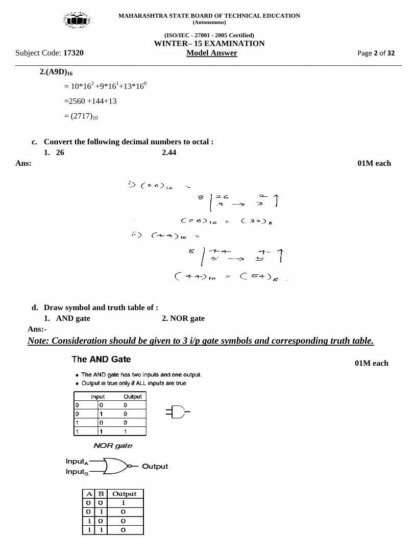
c. Convert the following decimal numbers to octal :
1. 26 2.44
Ans: 01M each
d. Draw symbol and truth table of :
1. AND gate 2. NOR gate
Ans:-
Note: Consideration should be given to 3 i/p gate symbols and corresponding truth table.
01M each
MAHARASHTRA STATE BOARD OF TECHNICAL EDUCATION (Autonomous)
(ISO/IEC - 27001 - 2005 Certified)
WINTER– 15 EXAMINATION
Subject Code: 17320 Model Answer Page 3 of 32 ________________________________________________________________________________________________________
e. State commutative and associative laws.
Ans: 01M each
COMMUTATIVE LAW:-
A+B=B+A
A*B=B*A
ASSOCIATIVE LAWS:-
(A+B)+C =A+(B+C)
(A*B)*C =A*(B*C)
f. Prove : A(1 + Ā) = A
Ans:- 02M
A (1+Ā)= A
= (A+AĀ)
= (A+0)
=A
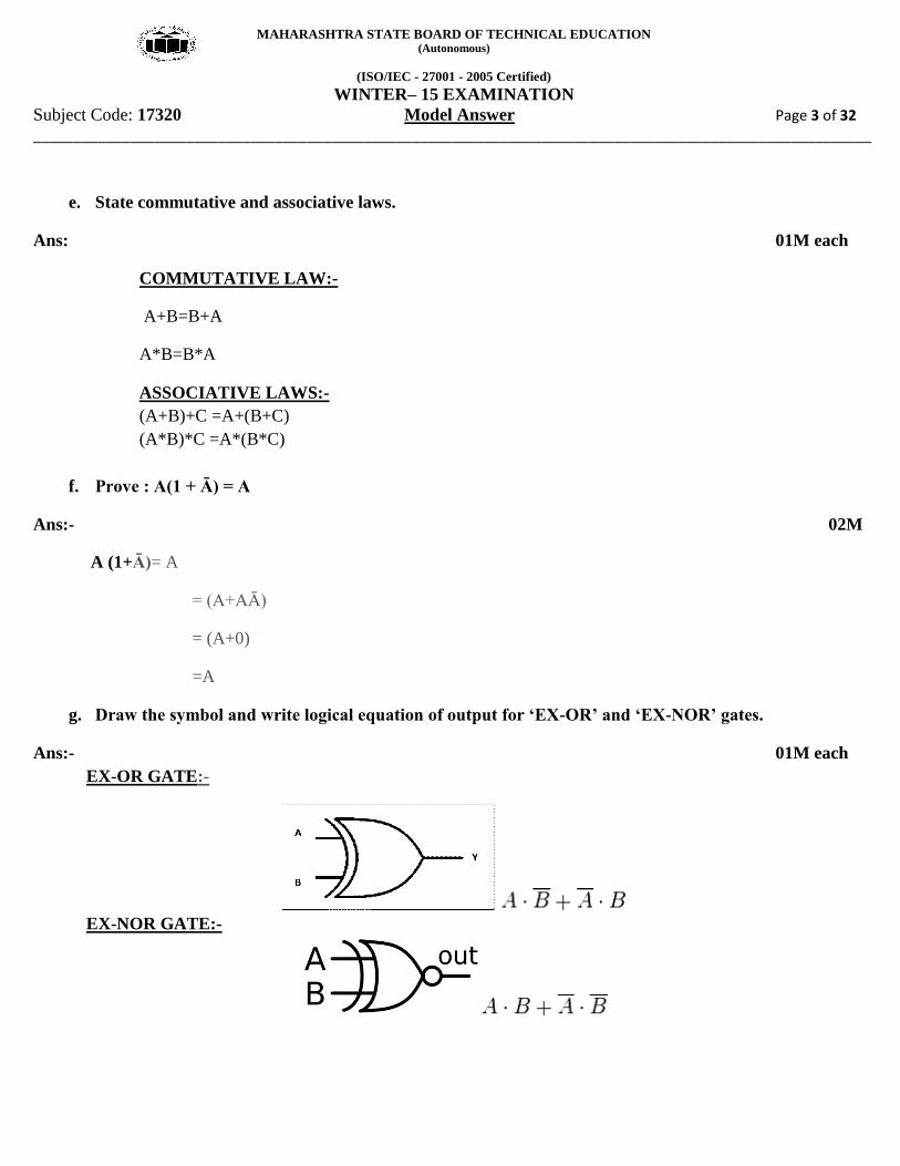
g. Draw the symbol and write logical equation of output for ‘EX-OR’ and ‘EX-NOR’ gates.
Ans:- 01M each
EX-OR GATE:-
EX-NOR GATE:-
MAHARASHTRA STATE BOARD OF TECHNICAL EDUCATION (Autonomous)
(ISO/IEC - 27001 - 2005 Certified)
WINTER– 15 EXAMINATION
Subject Code: 17320 Model Answer Page 4 of 32 ________________________________________________________________________________________________________
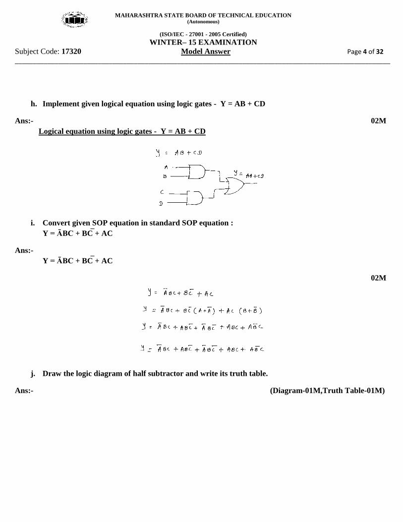
h. Implement given logical equation using logic gates - Y = AB + CD
Ans:- 02M
Logical equation using logic gates - Y = AB + CD
i. Convert given SOP equation in standard SOP equation :
Y = ĀBC + BC + AC
Ans:-
Y = ĀBC + BC + AC
02M
j. Draw the logic diagram of half subtractor and write its truth table.
Ans:- (Diagram-01M,Truth Table-01M)

MAHARASHTRA STATE BOARD OF TECHNICAL EDUCATION (Autonomous)
(ISO/IEC - 27001 - 2005 Certified)
WINTER– 15 EXAMINATION
Subject Code: 17320 Model Answer Page 5 of 32 ________________________________________________________________________________________________________
k. Define 1. Mux 2.De-Mux
Ans:-
1. MUX:- 01M
MUX-In electronics, a multiplexer (or mux) is a device that selects one of several analog or
digital input signals and forwards the selected input into a single line.
2. DE-MUX:- 01M
DEMUX-A de-multiplexer is a circuit with one input and many outputs. By applying control
signal, we can forward the input to any one of the selected outputs.
l. Draw the diagram of one bit memory cell using NAND gates only.
Ans:- One bit memory cell using NAND gates 02M
Note: Circuit diagram of any other flip – flop should also be considered
m. State drawback of S-R flip-flop. How is it overcome ?
Ans:-

MAHARASHTRA STATE BOARD OF TECHNICAL EDUCATION (Autonomous)
(ISO/IEC - 27001 - 2005 Certified)
WINTER– 15 EXAMINATION
Subject Code: 17320 Model Answer Page 6 of 32 ________________________________________________________________________________________________________
Drawback of S-R flip-flop: 01M
The output of an S-R (“set-reset”) flip-flop is undefined when both inputs are high at the clock
pulse. This is usually undesirable and is probably the “drawback”
It overcomes by using J-K flip-flop. 01M
n. Draw the symbol of D flip-flop and write its truth table.
Ans:- (Symbol-01M,Truth Table-01M)
Note: Similarly, weightage should be given to negative clock or edge triggered clock
signal(positive or negative) with suitable modification in the symbol and truth table.
Q.2) Attempt any FOUR: 16M
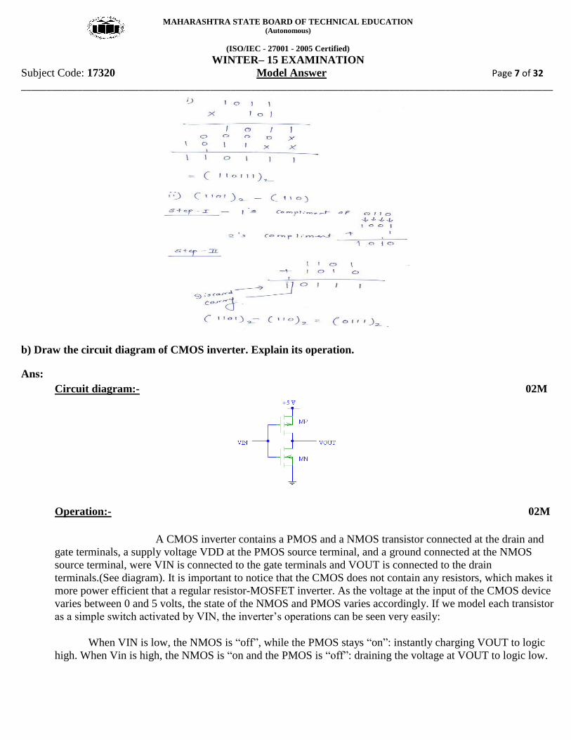
a) Perform following binary operations:
1. 1011 2. 1101
* 101 -110
(Using 2’s Complement method)
Ans: 02M each
MAHARASHTRA STATE BOARD OF TECHNICAL EDUCATION (Autonomous)
(ISO/IEC - 27001 - 2005 Certified)
WINTER– 15 EXAMINATION
Subject Code: 17320 Model Answer Page 7 of 32 ________________________________________________________________________________________________________
b) Draw the circuit diagram of CMOS inverter. Explain its operation.
Ans:
Circuit diagram:- 02M
Operation:- 02M
A CMOS inverter contains a PMOS and a NMOS transistor connected at the drain and
gate terminals, a supply voltage VDD at the PMOS source terminal, and a ground connected at the NMOS
source terminal, were VIN is connected to the gate terminals and VOUT is connected to the drain
terminals.(See diagram). It is important to notice that the CMOS does not contain any resistors, which makes it
more power efficient that a regular resistor-MOSFET inverter. As the voltage at the input of the CMOS device
varies between 0 and 5 volts, the state of the NMOS and PMOS varies accordingly. If we model each transistor
as a simple switch activated by VIN, the inverter’s operations can be seen very easily:
When VIN is low, the NMOS is “off”, while the PMOS stays “on”: instantly charging VOUT to logic
high. When Vin is high, the NMOS is “on and the PMOS is “off”: draining the voltage at VOUT to logic low.
MAHARASHTRA STATE BOARD OF TECHNICAL EDUCATION (Autonomous)
(ISO/IEC - 27001 - 2005 Certified)
WINTER– 15 EXAMINATION
Subject Code: 17320 Model Answer Page 8 of 32 ________________________________________________________________________________________________________
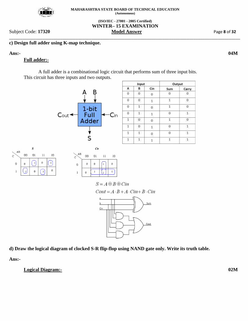
c) Design full adder using K-map technique.
Ans:- 04M
Full adder:-
A full adder is a combinational logic circuit that performs sum of three input bits.
This circuit has three inputs and two outputs.
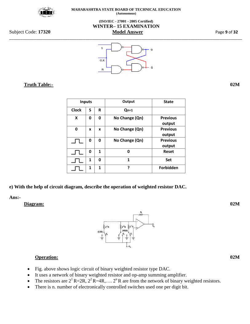
d) Draw the logical diagram of clocked S-R flip-flop using NAND gate only. Write its truth table.
Ans:-
Logical Diagram:- 02M
MAHARASHTRA STATE BOARD OF TECHNICAL EDUCATION (Autonomous)
(ISO/IEC - 27001 - 2005 Certified)
WINTER– 15 EXAMINATION
Subject Code: 17320 Model Answer Page 9 of 32 ________________________________________________________________________________________________________
Truth Table:- 02M
Inputs Output State
Clock S R Qn=1
X 0 0 No Change (Qn) Previous output
0 x x No Change (Qn) Previous output
0 0 No Change (Qn) Previous output
0 1 0 Reset
1 0 1 Set
1 1 ? Forbidden
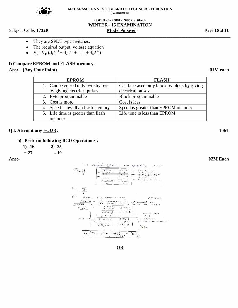
e) With the help of circuit diagram, describe the operation of weighted resistor DAC.
Ans:-
Diagram: 02M
Operation: 02M
Fig. above shows logic circuit of binary weighted resistor type DAC.
It uses a network of binary weighted resistor and op-amp summing amplifier.
The resistors are 21
R=2R, 22 R=4R,…. 2
n R are from the network of binary weighted resistors.
There is n. number of electronically controlled switches used one per digit bit.
MAHARASHTRA STATE BOARD OF TECHNICAL EDUCATION (Autonomous)
(ISO/IEC - 27001 - 2005 Certified)
WINTER– 15 EXAMINATION
Subject Code: 17320 Model Answer Page 10 of 32 ________________________________________________________________________________________________________
They are SPDT type switches.
The required output voltage equation
V0 =VR (d1 2-1
+ d2 2-2
+……+ dn2-n
)
f) Compare EPROM and FLASH memory.
Ans:- (Any Four Point) 01M each
EPROM FLASH
1. Can be erased only byte by byte
by giving electrical pulses.
Can be erased only block by block by giving
electrical pulses
2. Byte programmable Block programmable
3. Cost is more Cost is less
4. Speed is less than flash memory Speed is greater than EPROM memory
5. Life time is greater than flash
memory
Life time is less than EPROM
Q3. Attempt any FOUR: 16M
a) Perform following BCD Operations :
1) 16 2) 35
+ 27 - 19
Ans:- 02M Each
OR
MAHARASHTRA STATE BOARD OF TECHNICAL EDUCATION (Autonomous)
(ISO/IEC - 27001 - 2005 Certified)
WINTER– 15 EXAMINATION
Subject Code: 17320 Model Answer Page 11 of 32 ________________________________________________________________________________________________________
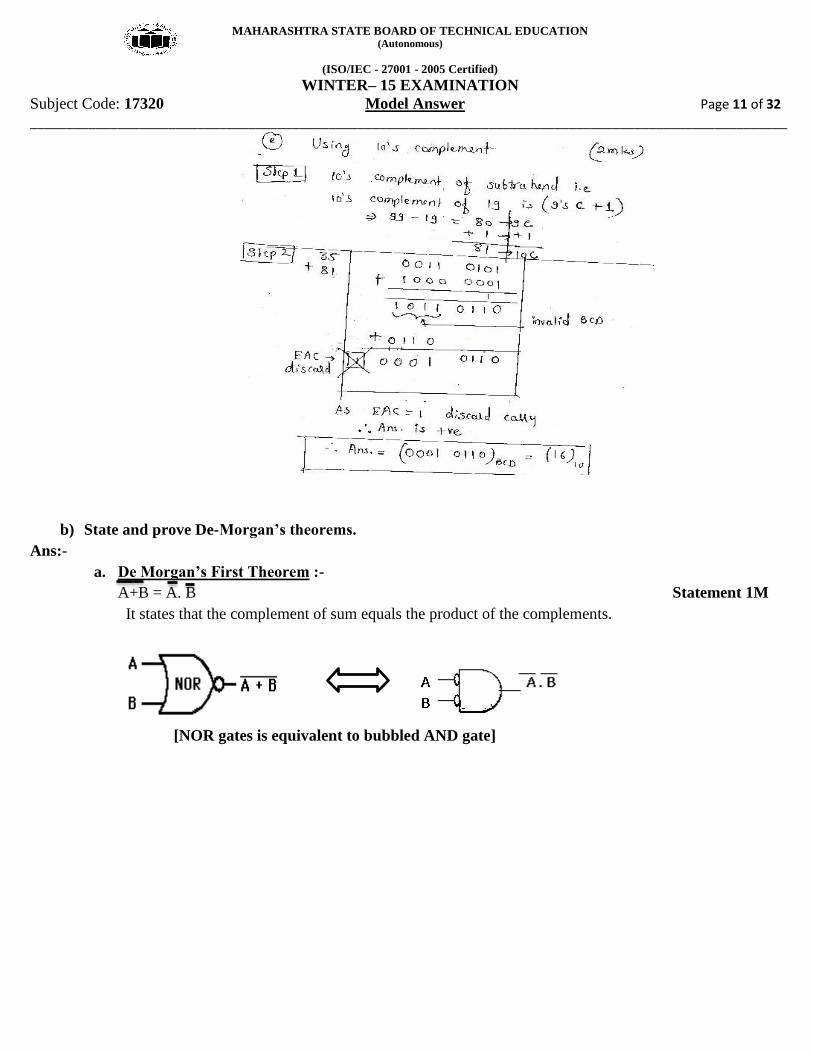
b) State and prove De-Morgan’s theorems.
Ans:-
a. De Morgan’s First Theorem :-
A+B = A. B Statement 1M
It states that the complement of sum equals the product of the complements.
[NOR gates is equivalent to bubbled AND gate]
MAHARASHTRA STATE BOARD OF TECHNICAL EDUCATION (Autonomous)
(ISO/IEC - 27001 - 2005 Certified)
WINTER– 15 EXAMINATION
Subject Code: 17320 Model Answer Page 12 of 32 ________________________________________________________________________________________________________
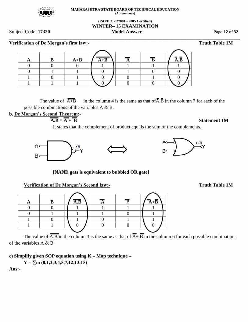
Verification of De Morgan’s first law:- Truth Table 1M
The value of A+B in the column 4 is the same as that ofA.B in the column 7 for each of the
possible combinations of the variables A & B.
b. De Morgan’s Second Theorem:-
A.B = A + B Statement 1M
It states that the complement of product equals the sum of the complements.
[NAND gats is equivalent to bubbled OR gate]
Verification of De Morgan’s Second law:- Truth Table 1M
The value of A.B in the column 3 is the same as that of A+ B in the column 6 for each possible combinations
of the variables A & B.
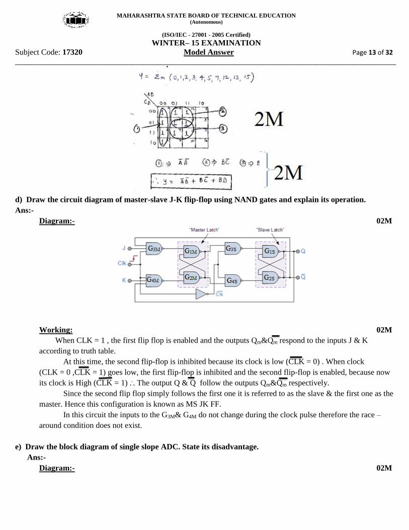
c) Simplify given SOP equation using K – Map technique –
Y = ∑m (0,1,2,3,4,5,7,12,13,15)
Ans:-
A B A+B A+B A B A.B
0 0 0 1 1 1 1
0 1 1 0 1 0 0
1 0 1 0 0 1 0
1 1 1 0 0 0 0
A B A.B A B A+B
0 0 1 1 1 1
0 1 1 1 0 1
1 0 1 0 1 1
1 1 0 0 0 0
MAHARASHTRA STATE BOARD OF TECHNICAL EDUCATION (Autonomous)
(ISO/IEC - 27001 - 2005 Certified)
WINTER– 15 EXAMINATION
Subject Code: 17320 Model Answer Page 13 of 32 ________________________________________________________________________________________________________
d) Draw the circuit diagram of master-slave J-K flip-flop using NAND gates and explain its operation.
Ans:-
Diagram:- 02M
Working: 02M
When CLK = 1 , the first flip flop is enabled and the outputs Qm&Qm respond to the inputs J & K
according to truth table.
At this time, the second flip-flop is inhibited because its clock is low (CLK = 0) . When clock
(CLK = 0 ,CLK = 1) goes low, the first flip-flop is inhibited and the second flip-flop is enabled, because now
its clock is High (CLK = 1) ... The output Q & Q follow the outputs Qm&Qm respectively.
Since the second flip flop simply follows the first one it is referred to as the slave & the first one as the
master. Hence this configuration is known as MS JK FF.
In this circuit the inputs to the G3M& G4M do not change during the clock pulse therefore the race –
around condition does not exist.
e) Draw the block diagram of single slope ADC. State its disadvantage.
Ans:-
Diagram:- 02M
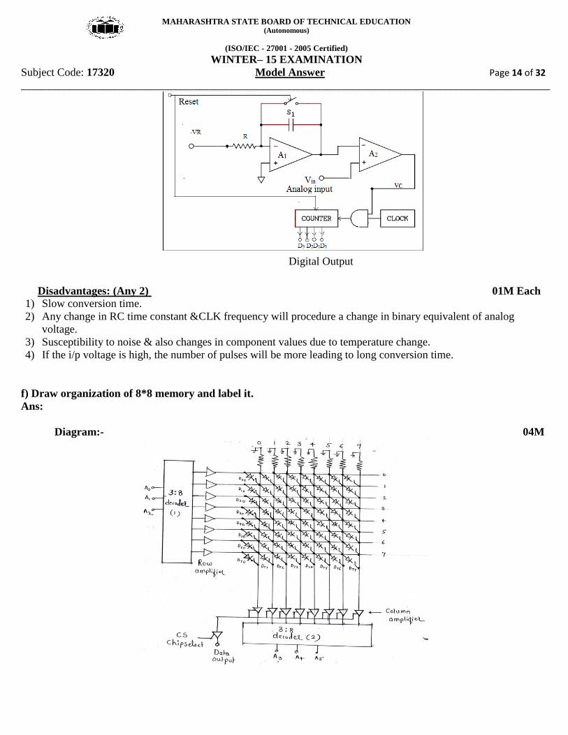
MAHARASHTRA STATE BOARD OF TECHNICAL EDUCATION (Autonomous)
(ISO/IEC - 27001 - 2005 Certified)
WINTER– 15 EXAMINATION
Subject Code: 17320 Model Answer Page 14 of 32 ________________________________________________________________________________________________________
Digital Output
Disadvantages: (Any 2) 01M Each
1) Slow conversion time.
2) Any change in RC time constant &CLK frequency will procedure a change in binary equivalent of analog
voltage.
3) Susceptibility to noise & also changes in component values due to temperature change.
4) If the i/p voltage is high, the number of pulses will be more leading to long conversion time.
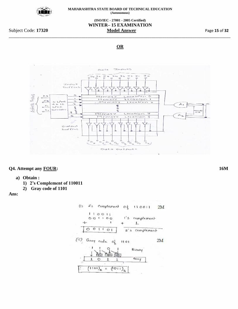
f) Draw organization of 8*8 memory and label it.
Ans:
Diagram:- 04M
MAHARASHTRA STATE BOARD OF TECHNICAL EDUCATION (Autonomous)
(ISO/IEC - 27001 - 2005 Certified)
WINTER– 15 EXAMINATION
Subject Code: 17320 Model Answer Page 15 of 32 ________________________________________________________________________________________________________
OR
Q4. Attempt any FOUR: 16M
a) Obtain :
1) 2’s Complement of 110011
2) Gray code of 1101
Ans:
MAHARASHTRA STATE BOARD OF TECHNICAL EDUCATION (Autonomous)
(ISO/IEC - 27001 - 2005 Certified)
WINTER– 15 EXAMINATION
Subject Code: 17320 Model Answer Page 16 of 32 ________________________________________________________________________________________________________
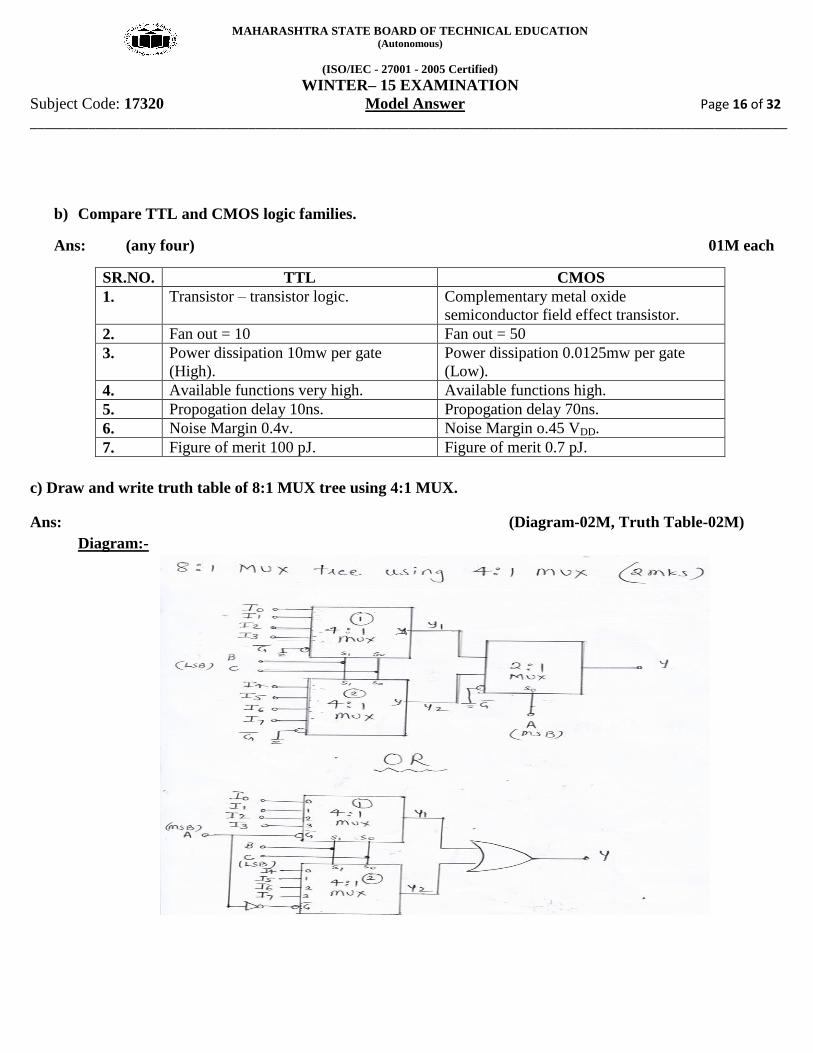
b) Compare TTL and CMOS logic families.
Ans: (any four) 01M each
SR.NO. TTL CMOS
1. Transistor – transistor logic. Complementary metal oxide
semiconductor field effect transistor.
2. Fan out = 10 Fan out = 50
3. Power dissipation 10mw per gate
(High).
Power dissipation 0.0125mw per gate
(Low).
4. Available functions very high. Available functions high.
5. Propogation delay 10ns. Propogation delay 70ns.
6. Noise Margin 0.4v. Noise Margin o.45 VDD.
7. Figure of merit 100 pJ. Figure of merit 0.7 pJ.
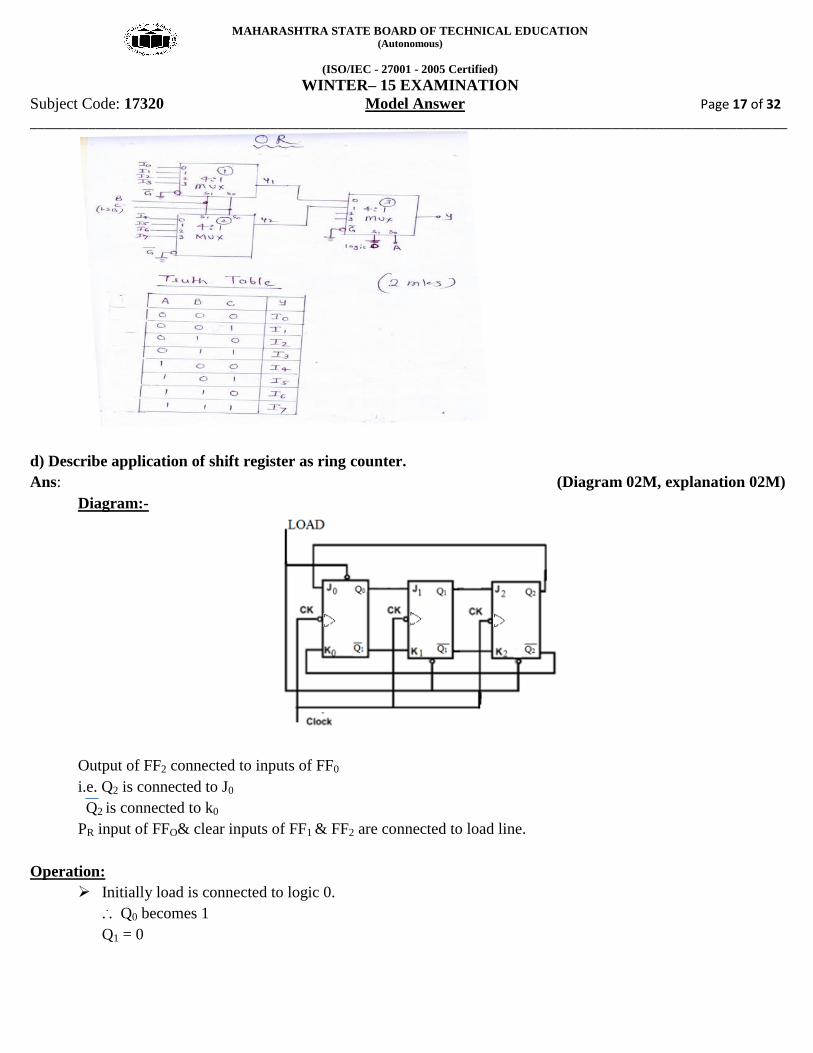
c) Draw and write truth table of 8:1 MUX tree using 4:1 MUX.
Ans: (Diagram-02M, Truth Table-02M)
Diagram:-
MAHARASHTRA STATE BOARD OF TECHNICAL EDUCATION (Autonomous)
(ISO/IEC - 27001 - 2005 Certified)
WINTER– 15 EXAMINATION
Subject Code: 17320 Model Answer Page 17 of 32 ________________________________________________________________________________________________________
d) Describe application of shift register as ring counter.
Ans: (Diagram 02M, explanation 02M)
Diagram:-
Output of FF2 connected to inputs of FF0
i.e. Q2 is connected to J0
Q2 is connected to k0
PR input of FFO& clear inputs of FF1 & FF2 are connected to load line.
Operation:
Initially load is connected to logic 0.
... Q0 becomes 1
Q1 = 0

MAHARASHTRA STATE BOARD OF TECHNICAL EDUCATION (Autonomous)
(ISO/IEC - 27001 - 2005 Certified)
WINTER– 15 EXAMINATION
Subject Code: 17320 Model Answer Page 18 of 32 ________________________________________________________________________________________________________
Q2 = 0
... Q2Q1Q0 = 001
Now connect load to logic 1,Now the clock signal is applied to all the flip flops simultaneously.
1st
Clock pulse
As soon as 1st
falling edge of the clock hits, only FF1 will be set because Q0 = J0 =1
FF0 will reset because Q2=J0=0
There is no change in Q2
... o/p after 1
st clock pulse
Q2Q1Q0 = 010
2nd
Clock pulse
Q2Q1Q0 = 100
3rd
Clock pulse
Q2Q1Q0 = 001
Number of Outputs
The number of outputs states for a ring counter will always be equal to the number of flip-flops
... For 3 bit ring counter no. of states = 3
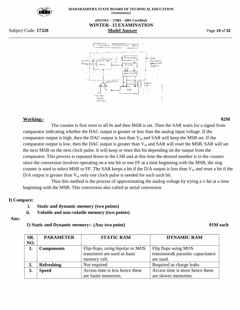
e) Draw the block diagram of SAR ADC and write its operation in brief.
Ans:
Diagram:- 02M
MAHARASHTRA STATE BOARD OF TECHNICAL EDUCATION (Autonomous)
(ISO/IEC - 27001 - 2005 Certified)
WINTER– 15 EXAMINATION
Subject Code: 17320 Model Answer Page 19 of 32 ________________________________________________________________________________________________________
Working:- 02M
The counter is first reset to all 0s and then MSB is set. Then the SAR waits for a signal from
comparator indicating whether the DAC output is greater or less than the analog input voltage. If the
comparator output is high, then the DAC output is less than Vin and SAR will keep the MSB set. If the
comparator output is low, then the DAC output is greater than Vin and SAR will reset the MSB. SAR will set
the next MSB on the next clock pulse. It will keep or reset this bit depending on the output from the
comparator. This process is repeated down to the LSB and at this time the desired number is in the counter
since the conversion involves operating on a one bit or one FF at a time beginning with the MSB, the ring
counter is used to select MSB or FF. The SAR keeps a bit if the D/A output is less than Vin and reset a bit if the
D/A output is greater than Vin only one clock pulse is needed for each such bit.
Thus this method is the process of approximating the analog voltage by trying a 1-bit at a time
beginning with the MSB. This conversion also called as serial conversion
f) Compare:
i. Static and dynamic memory (two points)
ii. Volatile and non-volatile memory (two points)
Ans:
1) Static and Dynamic memory:- (Any two point) 01M each
SR.
NO.
PARAMETER STATIC RAM DYNAMIC RAM
1. Components Flip-flops, using bipolar or MOS
transistors are used as basic
memory cell.
Flip flops using MOS
transistors& parasitic capacitance
are used.
2. Refreshing Not required Required as charge leaks
3. Speed Access time is less hence these
are faster memories.
Access time is more hence these
are slower memories.
MAHARASHTRA STATE BOARD OF TECHNICAL EDUCATION (Autonomous)
(ISO/IEC - 27001 - 2005 Certified)
WINTER– 15 EXAMINATION
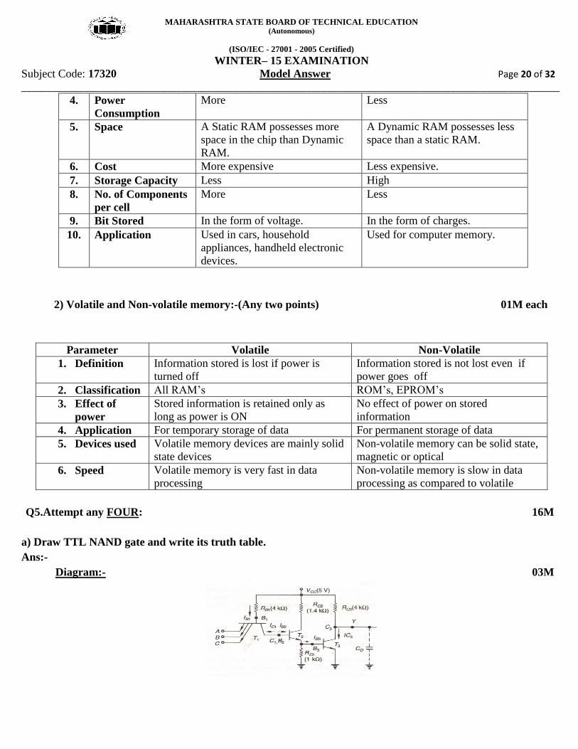
Subject Code: 17320 Model Answer Page 20 of 32 ________________________________________________________________________________________________________
4. Power
Consumption
More Less
5. Space A Static RAM possesses more
space in the chip than Dynamic
RAM.
A Dynamic RAM possesses less
space than a static RAM.
6. Cost More expensive Less expensive.
7. Storage Capacity Less High
8. No. of Components
per cell
More Less
9. Bit Stored In the form of voltage. In the form of charges.
10. Application Used in cars, household
appliances, handheld electronic
devices.
Used for computer memory.
2) Volatile and Non-volatile memory:-(Any two points) 01M each
Parameter Volatile Non-Volatile
1. Definition Information stored is lost if power is
turned off
Information stored is not lost even if
power goes off
2. Classification All RAM’s ROM’s, EPROM’s
3. Effect of
power
Stored information is retained only as
long as power is ON
No effect of power on stored
information
4. Application For temporary storage of data For permanent storage of data
5. Devices used Volatile memory devices are mainly solid
state devices
Non-volatile memory can be solid state,
magnetic or optical
6. Speed Volatile memory is very fast in data
processing
Non-volatile memory is slow in data
processing as compared to volatile
Q5.Attempt any FOUR: 16M
a) Draw TTL NAND gate and write its truth table.
Ans:-
Diagram:- 03M
MAHARASHTRA STATE BOARD OF TECHNICAL EDUCATION (Autonomous)
(ISO/IEC - 27001 - 2005 Certified)
WINTER– 15 EXAMINATION
Subject Code: 17320 Model Answer Page 21 of 32 ________________________________________________________________________________________________________
Truth Table:- 01M
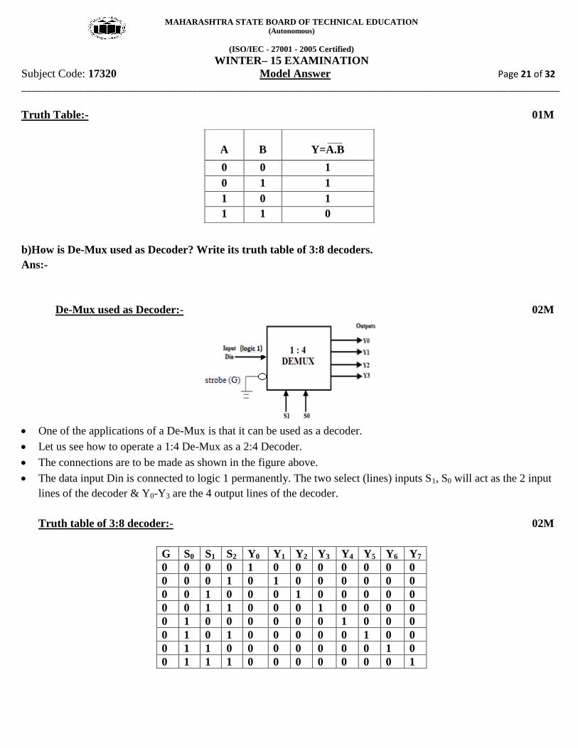
b)How is De-Mux used as Decoder? Write its truth table of 3:8 decoders.
Ans:-
De-Mux used as Decoder:- 02M
One of the applications of a De-Mux is that it can be used as a decoder.
Let us see how to operate a 1:4 De-Mux as a 2:4 Decoder.
The connections are to be made as shown in the figure above.
The data input Din is connected to logic 1 permanently. The two select (lines) inputs S1, S0 will act as the 2 input
lines of the decoder & Y0-Y3 are the 4 output lines of the decoder.
Truth table of 3:8 decoder:- 02M
G S0 S1 S2 Y0 Y1 Y2 Y3 Y4 Y5 Y6 Y7
0 0 0 0 1 0 0 0 0 0 0 0
0 0 0 1 0 1 0 0 0 0 0 0
0 0 1 0 0 0 1 0 0 0 0 0
0 0 1 1 0 0 0 1 0 0 0 0
0 1 0 0 0 0 0 0 1 0 0 0
0 1 0 1 0 0 0 0 0 1 0 0
0 1 1 0 0 0 0 0 0 0 1 0
0 1 1 1 0 0 0 0 0 0 0 1
A
B
Y=A.B
0 0 1
0 1 1
1 0 1
1 1 0
MAHARASHTRA STATE BOARD OF TECHNICAL EDUCATION (Autonomous)
(ISO/IEC - 27001 - 2005 Certified)
WINTER– 15 EXAMINATION
Subject Code: 17320 Model Answer Page 22 of 32 ________________________________________________________________________________________________________
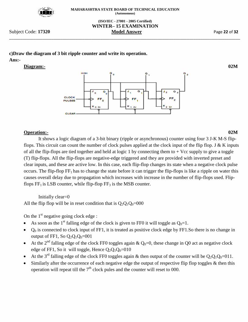
c)Draw the diagram of 3 bit ripple counter and write its operation.
Ans:-
Diagram:- 02M
Operation:- 02M
It shows a logic diagram of a 3-bit binary (ripple or asynchronous) counter using four 3 J-K M-S flip-
flops. This circuit can count the number of clock pulses applied at the clock input of the flip flop. J & K inputs
of all the flip-flops are tied together and held at logic 1 by connecting them to + Vcc supply to give a toggle
(T) flip-flops. All the flip-flops are negative-edge triggered and they are provided with inverted preset and
clear inputs, and these are active low. In this case, each flip-flop changes its state when a negative clock pulse
occurs. The flip-flop FF1 has to change the state before it can trigger the flip-flops is like a ripple on water this
causes overall delay due to propagation which increases with increase in the number of flip-flops used. Flip-
flops FF1 is LSB counter, while flip-flop FF3 is the MSB counter.
Initially clear=0
All the flip flop will be in reset condition that is Q2Q1Q0=000
On the 1st negative going clock edge :
As soon as the 1st falling edge of the clock is given to FF0 it will toggle as Q0=1.
Q0 is connected to clock input of FF1, it is treated as positive clock edge by FF1.So there is no change in
output of FF1, So Q2Q1Q0=001
At the 2nd
falling edge of the clock FF0 toggles again & Q0=0, these change in Q0 act as negative clock
edge of FF1, So it will toggle, Hence Q2Q1Q0=010
At the 3rd
falling edge of the clock FF0 toggles again & then output of the counter will be Q2Q1Q0=011.
Similarly after the occurrence of each negative edge the output of respective flip flop toggles & then this
operation will repeat till the 7th
clock pules and the counter will reset to 000.
MAHARASHTRA STATE BOARD OF TECHNICAL EDUCATION (Autonomous)
(ISO/IEC - 27001 - 2005 Certified)
WINTER– 15 EXAMINATION
Subject Code: 17320 Model Answer Page 23 of 32 ________________________________________________________________________________________________________
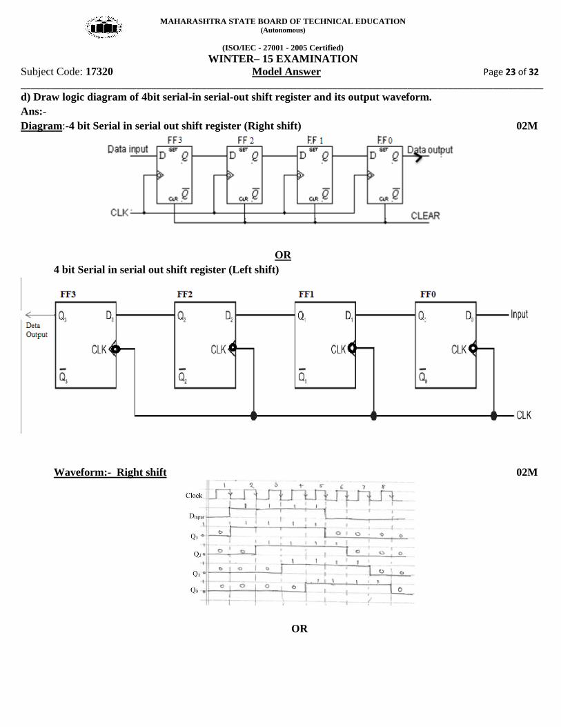
d) Draw logic diagram of 4bit serial-in serial-out shift register and its output waveform.
Ans:-
Diagram:-4 bit Serial in serial out shift register (Right shift) 02M
OR
4 bit Serial in serial out shift register (Left shift)
Waveform:- Right shift 02M
OR
MAHARASHTRA STATE BOARD OF TECHNICAL EDUCATION (Autonomous)
(ISO/IEC - 27001 - 2005 Certified)
WINTER– 15 EXAMINATION
Subject Code: 17320 Model Answer Page 24 of 32 ________________________________________________________________________________________________________
Waveform :- left shift
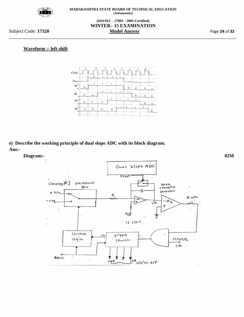
e) Describe the working principle of dual slope ADC with its block diagram.
Ans:-
Diagram:- 02M
MAHARASHTRA STATE BOARD OF TECHNICAL EDUCATION (Autonomous)
(ISO/IEC - 27001 - 2005 Certified)
WINTER– 15 EXAMINATION
Subject Code: 17320 Model Answer Page 25 of 32 ________________________________________________________________________________________________________
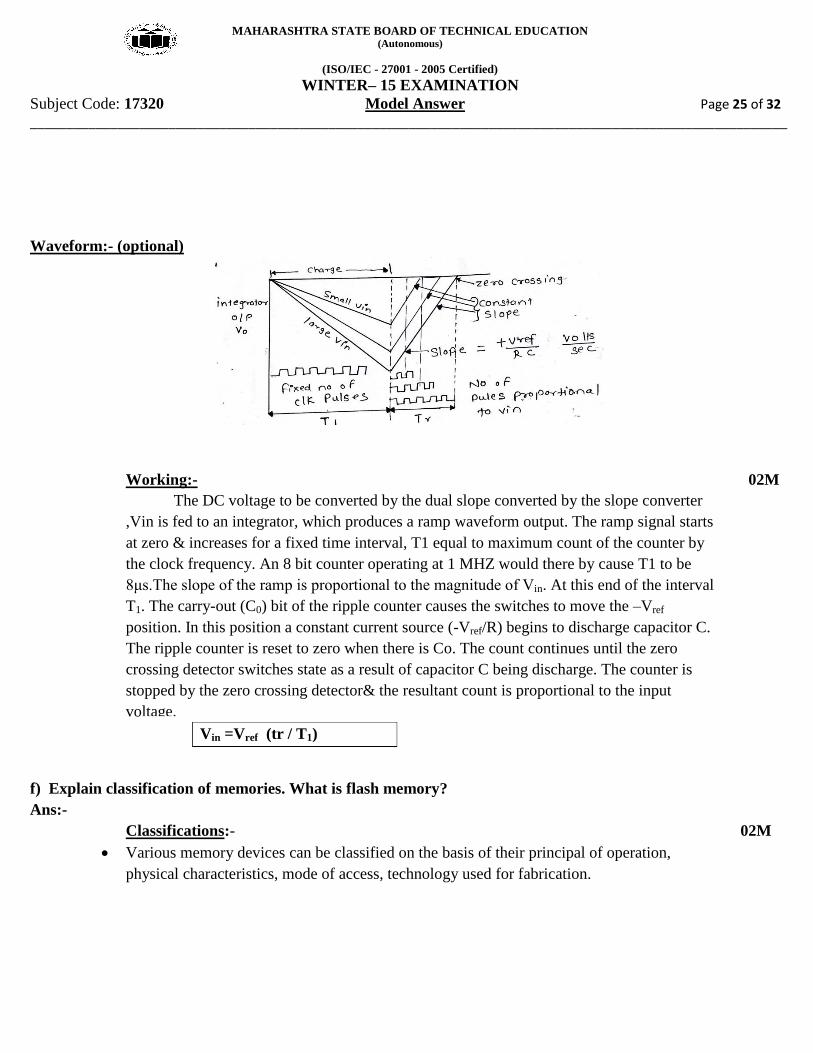
Waveform:- (optional)
Working:- 02M
The DC voltage to be converted by the dual slope converted by the slope converter
,Vin is fed to an integrator, which produces a ramp waveform output. The ramp signal starts
at zero & increases for a fixed time interval, T1 equal to maximum count of the counter by
the clock frequency. An 8 bit counter operating at 1 MHZ would there by cause T1 to be
8μs.The slope of the ramp is proportional to the magnitude of Vin. At this end of the interval
T1. The carry-out (C0) bit of the ripple counter causes the switches to move the –Vref
position. In this position a constant current source (-Vref/R) begins to discharge capacitor C.
The ripple counter is reset to zero when there is Co. The count continues until the zero
crossing detector switches state as a result of capacitor C being discharge. The counter is
stopped by the zero crossing detector& the resultant count is proportional to the input
voltage.
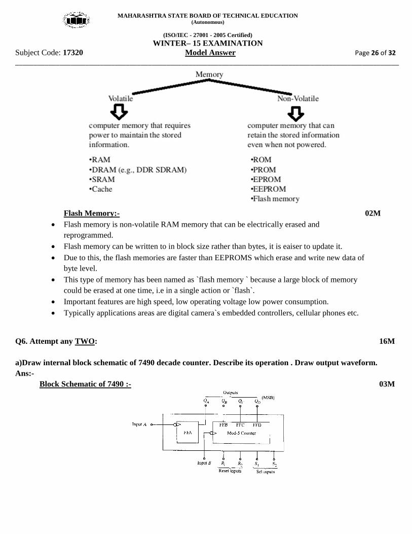
f) Explain classification of memories. What is flash memory?
Ans:-
Classifications:- 02M
Various memory devices can be classified on the basis of their principal of operation,
physical characteristics, mode of access, technology used for fabrication.
Vin =Vref (tr / T1)
MAHARASHTRA STATE BOARD OF TECHNICAL EDUCATION (Autonomous)
(ISO/IEC - 27001 - 2005 Certified)
WINTER– 15 EXAMINATION
Subject Code: 17320 Model Answer Page 26 of 32 ________________________________________________________________________________________________________
Flash Memory:- 02M
Flash memory is non-volatile RAM memory that can be electrically erased and
reprogrammed.
Flash memory can be written to in block size rather than bytes, it is eaiser to update it.
Due to this, the flash memories are faster than EEPROMS which erase and write new data of
byte level.
This type of memory has been named as `flash memory ` because a large block of memory
could be erased at one time, i.e in a single action or `flash`.
Important features are high speed, low operating voltage low power consumption.
Typically applications areas are digital camera`s embedded controllers, cellular phones etc.
Q6. Attempt any TWO: 16M
a)Draw internal block schematic of 7490 decade counter. Describe its operation . Draw output waveform.
Ans:-
Block Schematic of 7490 :- 03M
MAHARASHTRA STATE BOARD OF TECHNICAL EDUCATION (Autonomous)
(ISO/IEC - 27001 - 2005 Certified)
WINTER– 15 EXAMINATION
Subject Code: 17320 Model Answer Page 27 of 32 ________________________________________________________________________________________________________
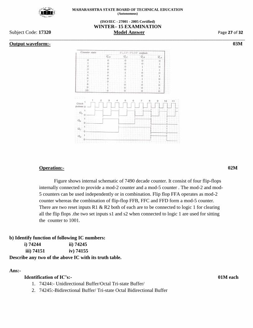
Output waveform:- 03M
Operation:- 02M
Figure shows internal schematic of 7490 decade counter. It consist of four flip-flops
internally connected to provide a mod-2 counter and a mod-5 counter . The mod-2 and mod-
5 counters can be used independently or in combination. Flip flop FFA operates as mod-2
counter whereas the combination of flip-flop FFB, FFC and FFD form a mod-5 counter.
There are two reset inputs R1 & R2 both of each are to be connected to logic 1 for clearing
all the flip flops .the two set inputs s1 and s2 when connected to logic 1 are used for sitting
the counter to 1001.
b) Identify function of following IC numbers:
i) 74244 ii) 74245
iii) 74151 iv) 74155
Describe any two of the above IC with its truth table.
Ans:-
Identification of IC’s:- 01M each
1. 74244:- Unidirectional Buffer/Octal Tri-state Buffer/
2. 74245:-Bidirectional Buffer/ Tri-state Octal Bidirectional Buffer
MAHARASHTRA STATE BOARD OF TECHNICAL EDUCATION (Autonomous)
(ISO/IEC - 27001 - 2005 Certified)
WINTER– 15 EXAMINATION
Subject Code: 17320 Model Answer Page 28 of 32 ________________________________________________________________________________________________________
3. 74151:-Multiplexer(8:1 MUX)
4. 74155:-De-Multiplexer(Dual 1:4 DEMUX)
Note:-Any two of IC can be explained
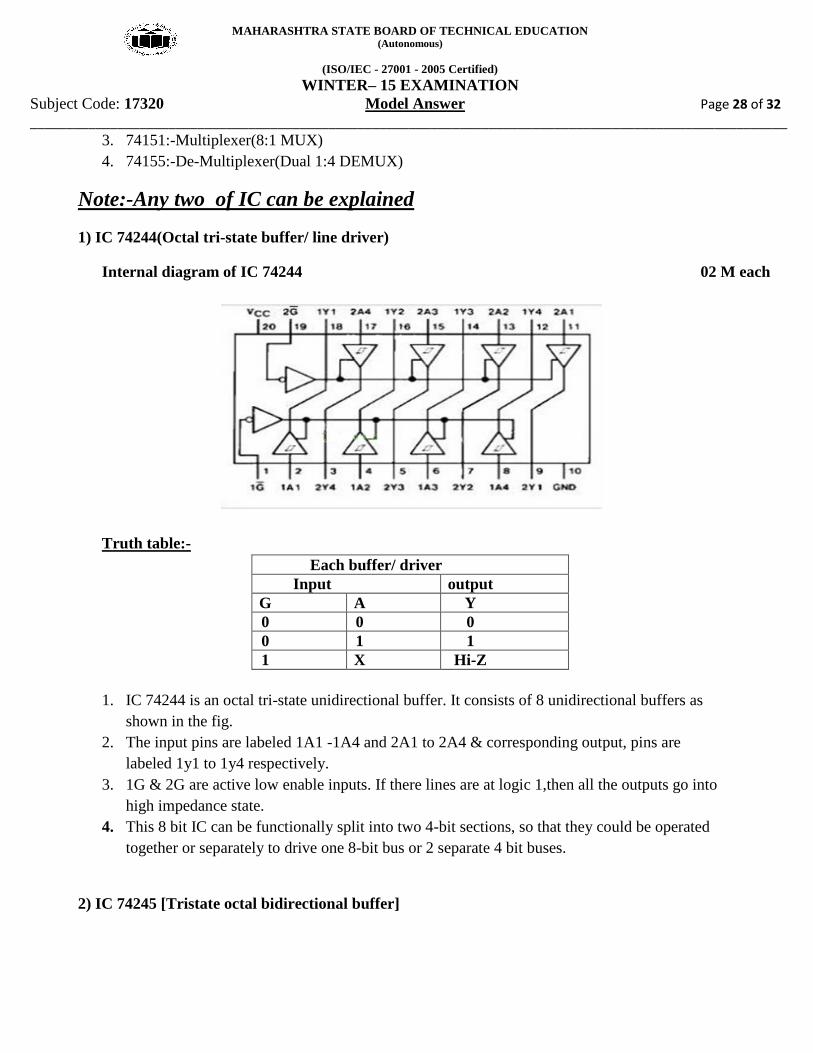
1) IC 74244(Octal tri-state buffer/ line driver)
Internal diagram of IC 74244 02 M each
Truth table:-
Each buffer/ driver
Input output
G A Y
0 0 0
0 1 1
1 X Hi-Z
1. IC 74244 is an octal tri-state unidirectional buffer. It consists of 8 unidirectional buffers as
shown in the fig.
2. The input pins are labeled 1A1 -1A4 and 2A1 to 2A4 & corresponding output, pins are
labeled 1y1 to 1y4 respectively.
3. 1G & 2G are active low enable inputs. If there lines are at logic 1,then all the outputs go into
high impedance state.
4. This 8 bit IC can be functionally split into two 4-bit sections, so that they could be operated
together or separately to drive one 8-bit bus or 2 separate 4 bit buses.
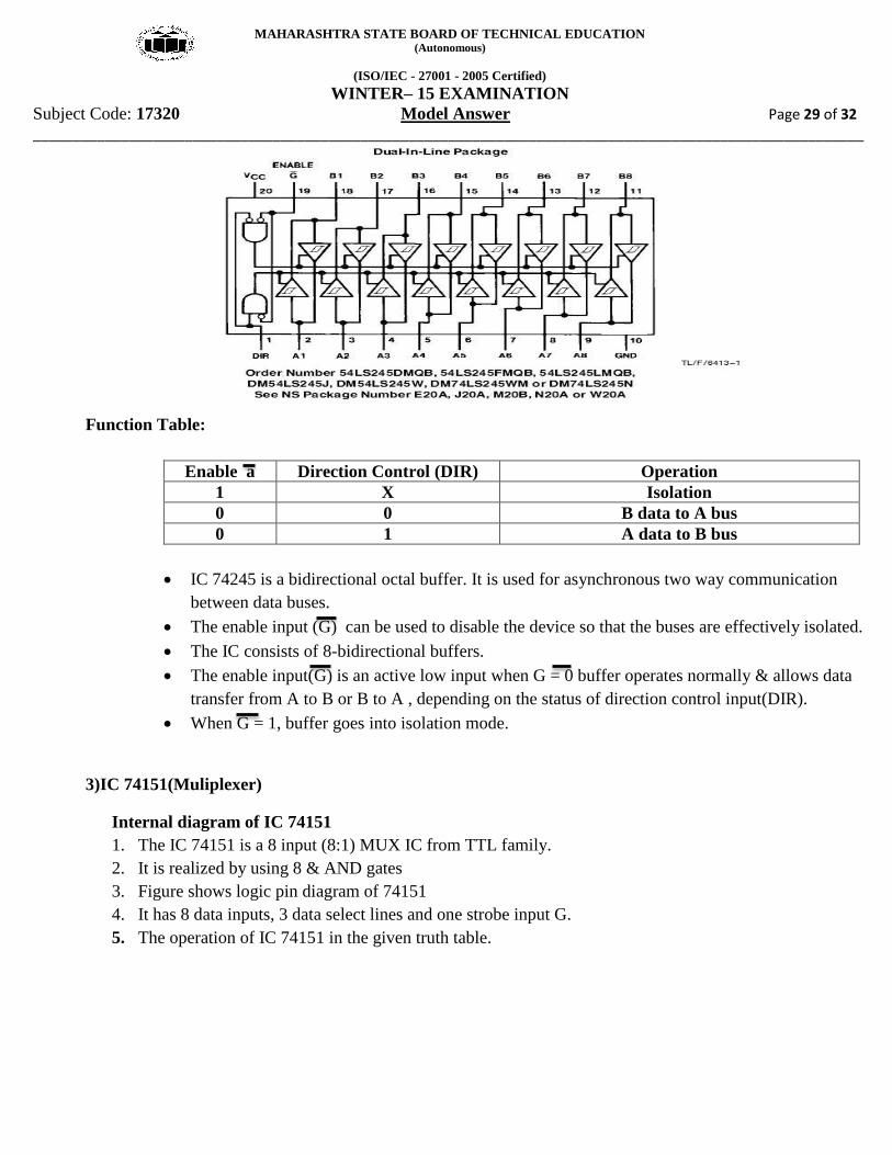
2) IC 74245 [Tristate octal bidirectional buffer]
MAHARASHTRA STATE BOARD OF TECHNICAL EDUCATION (Autonomous)
(ISO/IEC - 27001 - 2005 Certified)
WINTER– 15 EXAMINATION
Subject Code: 17320 Model Answer Page 29 of 32 ________________________________________________________________________________________________________
Function Table:
Enable a Direction Control (DIR) Operation
1 X Isolation
0 0 B data to A bus
0 1 A data to B bus
IC 74245 is a bidirectional octal buffer. It is used for asynchronous two way communication
between data buses.
The enable input (G) can be used to disable the device so that the buses are effectively isolated.
The IC consists of 8-bidirectional buffers.
The enable input(G) is an active low input when G = 0 buffer operates normally & allows data
transfer from A to B or B to A , depending on the status of direction control input(DIR).
When G = 1, buffer goes into isolation mode.
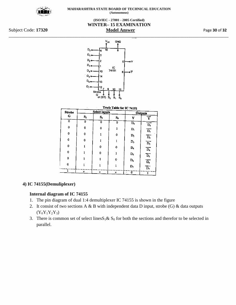
3)IC 74151(Muliplexer)
Internal diagram of IC 74151
1. The IC 74151 is a 8 input (8:1) MUX IC from TTL family.
2. It is realized by using 8 & AND gates
3. Figure shows logic pin diagram of 74151
4. It has 8 data inputs, 3 data select lines and one strobe input G.
5. The operation of IC 74151 in the given truth table.
MAHARASHTRA STATE BOARD OF TECHNICAL EDUCATION (Autonomous)
(ISO/IEC - 27001 - 2005 Certified)
WINTER– 15 EXAMINATION
Subject Code: 17320 Model Answer Page 30 of 32 ________________________________________________________________________________________________________
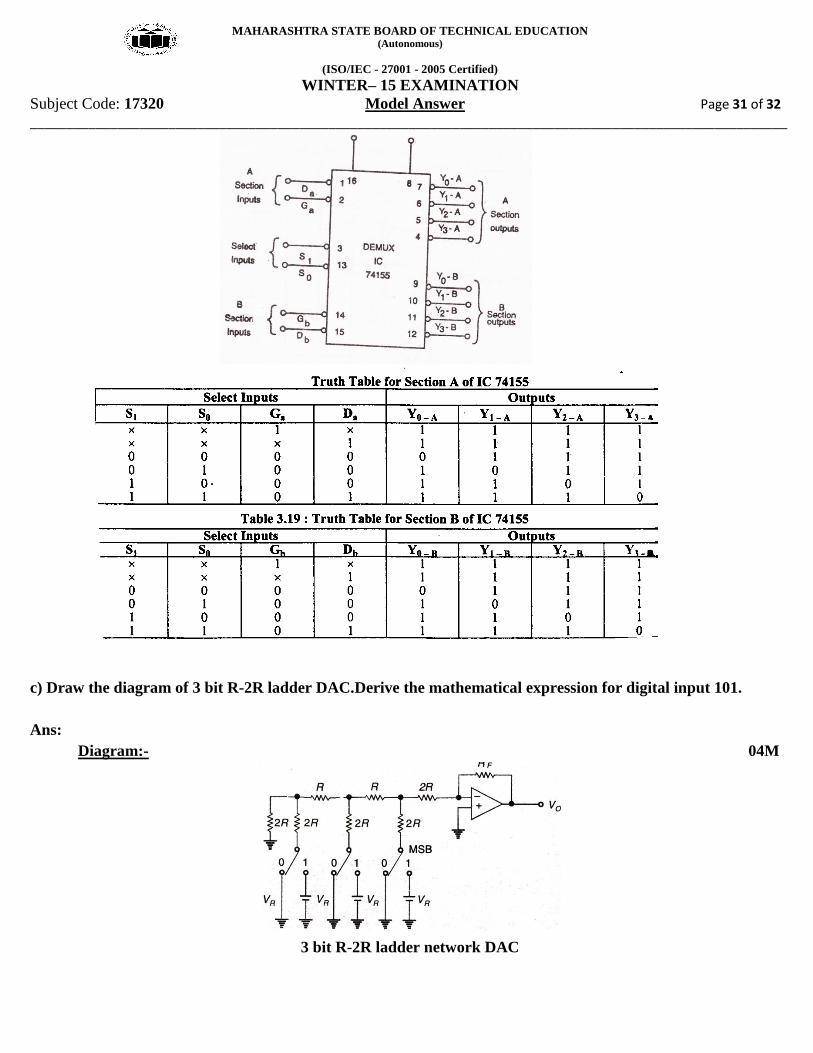
4) IC 74155(Demuliplexer)
Internal diagram of IC 74155
1. The pin diagram of dual 1:4 demultiplexer IC 74155 is shown in the figure
2. It consist of two sections A & B with independent data D input, strobe (G) & data outputs
(Y0Y1Y2Y3)
3. There is common set of select linesS1& S0 for both the sections and therefor to be selected in
parallel.
MAHARASHTRA STATE BOARD OF TECHNICAL EDUCATION (Autonomous)
(ISO/IEC - 27001 - 2005 Certified)
WINTER– 15 EXAMINATION
Subject Code: 17320 Model Answer Page 31 of 32 ________________________________________________________________________________________________________
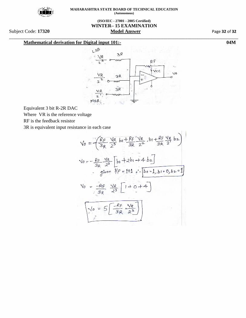
c) Draw the diagram of 3 bit R-2R ladder DAC.Derive the mathematical expression for digital input 101.
Ans:
Diagram:- 04M
3 bit R-2R ladder network DAC
MAHARASHTRA STATE BOARD OF TECHNICAL EDUCATION (Autonomous)
(ISO/IEC - 27001 - 2005 Certified)
WINTER– 15 EXAMINATION
Subject Code: 17320 Model Answer Page 32 of 32 ________________________________________________________________________________________________________
Mathematical derivation for Digital input 101:- 04M
Equivalent 3 bit R-2R DAC
Where VR is the reference voltage
RF is the feedback resistor
3R is equivalent input resistance in each case