(12) United States Patent (10) Patent No.: US 8,540,867 B2
139
USOO8540867B2 (12) United States Patent (10) Patent No.: US 8,540,867 B2 Rothberg et al. (45) Date of Patent: Sep. 24, 2013 (54) METHODS AND APPARATUS FOR 422/82.01-82.03: 435/6, 285.1, 287.1, 287.2: (75) (73) (*) (21) (22) (65) (63) (60) (51) (52) (58) DETECTING MOLECULAR INTERACTIONS USING FET ARRAYS Inventors: Jonathan Rothberg, Guilford, CT (US); Wolfgang Hinz, Killingworth, CT (US) Assignee: Life Technologies Corporation, Carlsbad, CA (US) Notice: Subject to any disclaimer, the term of this patent is extended or adjusted under 35 U.S.C. 154(b) by 17 days. Appl. No.: 13/229,439 Filed: Sep. 9, 2011 Prior Publication Data US 2012/OO61256A1 Mar. 15, 2012 Related U.S. Application Data Continuation of application No. 12/492.844, filed on Jun. 26, 2009, now Pat. No. 8,349,167, which is a continuation-in-part of application No. 12/002,781, filed on Dec. 17, 2007, now Pat. No. 8,262,900, which is a continuation-in-part of application No. 12/002291, filed on Dec. 17, 2007, now Pat. No. 7,948,015. Provisional application No. 60/870,073, filed on Dec. 14, 2006, provisional application No. 60/948,748, filed on Jul. 10, 2007, provisional application No. 60/956,324, filed on Aug. 16, 2007, provisional application No. 61/133,204, filed on Jun. 26, 2008. Int. C. GOIN33/50 (2006.01) GOIN 27/214 (2006.01) U.S. C. USPC ............. 205/793.5: 205/789; 257/253: 506/9 Field of Classification Search USPC ..................... 257/253; 205/789,792, 793.5; 436/103-105,150, 182: 506/1, 9; 204/403.01, 204/416, 433 See application file for complete search history. (56) References Cited U.S. PATENT DOCUMENTS 4.41 1,741 A 10, 1983 Janata 4490,678 A 12/1984 Kuislet al. (Continued) FOREIGN PATENT DOCUMENTS 1461350 12/2003 1022O3282 9, 2011 (Continued) OTHER PUBLICATIONS CN CN Schoning, Michael et al., “Recent advances in biologically sensitive field-effect transistors (BioFETs). Analyst, vol. 127, No. 9, 2002, 1137-1151. (Continued) Primary Examiner — J. Christopher Ball (74) Attorney, Agent, or Firm — Life Technologies Corporation (57) ABSTRACT Methods and apparatuses relating to large scale FET arrays for analyte detection and measurement are provided. Chem FET (e.g., ISFET) arrays may be fabricated using conven tional CMOS processing techniques based on improved FET pixel and array designs that increase measurement sensitivity and accuracy, and at the same time facilitate significantly Small pixel sizes and dense arrays. Improved array control techniques provide for rapid data acquisition from large and dense arrays. Such arrays may be employed to detect a pres ence and/or concentration changes of various analyte types in a wide variety of chemical and/or biological processes. 18 Claims, 77 Drawing Sheets Jo-N
-
Upload
khangminh22 -
Category
Documents
-
view
0 -
download
0
Transcript of (12) United States Patent (10) Patent No.: US 8,540,867 B2

USOO8540867B2
(12) United States Patent (10) Patent No.: US 8,540,867 B2 Rothberg et al. (45) Date of Patent: Sep. 24, 2013
(54) METHODS AND APPARATUS FOR 422/82.01-82.03: 435/6, 285.1, 287.1, 287.2:
(75)
(73)
(*)
(21)
(22)
(65)
(63)
(60)
(51)
(52)
(58)
DETECTING MOLECULAR INTERACTIONS USING FET ARRAYS
Inventors: Jonathan Rothberg, Guilford, CT (US); Wolfgang Hinz, Killingworth, CT (US)
Assignee: Life Technologies Corporation, Carlsbad, CA (US)
Notice: Subject to any disclaimer, the term of this patent is extended or adjusted under 35 U.S.C. 154(b) by 17 days.
Appl. No.: 13/229,439
Filed: Sep. 9, 2011
Prior Publication Data
US 2012/OO61256A1 Mar. 15, 2012
Related U.S. Application Data Continuation of application No. 12/492.844, filed on Jun. 26, 2009, now Pat. No. 8,349,167, which is a continuation-in-part of application No. 12/002,781, filed on Dec. 17, 2007, now Pat. No. 8,262,900, which is a continuation-in-part of application No. 12/002291, filed on Dec. 17, 2007, now Pat. No. 7,948,015.
Provisional application No. 60/870,073, filed on Dec. 14, 2006, provisional application No. 60/948,748, filed on Jul. 10, 2007, provisional application No. 60/956,324, filed on Aug. 16, 2007, provisional application No. 61/133,204, filed on Jun. 26, 2008.
Int. C. GOIN33/50 (2006.01) GOIN 27/214 (2006.01) U.S. C. USPC ............. 205/793.5: 205/789; 257/253: 506/9 Field of Classification Search USPC ..................... 257/253; 205/789,792, 793.5;
436/103-105,150, 182: 506/1, 9; 204/403.01, 204/416, 433
See application file for complete search history.
(56) References Cited
U.S. PATENT DOCUMENTS
4.41 1,741 A 10, 1983 Janata 4490,678 A 12/1984 Kuislet al.
(Continued) FOREIGN PATENT DOCUMENTS
1461350 12/2003 1022O3282 9, 2011
(Continued) OTHER PUBLICATIONS
CN CN
Schoning, Michael et al., “Recent advances in biologically sensitive field-effect transistors (BioFETs). Analyst, vol. 127, No. 9, 2002, 1137-1151.
(Continued)
Primary Examiner — J. Christopher Ball (74) Attorney, Agent, or Firm — Life Technologies Corporation
(57) ABSTRACT
Methods and apparatuses relating to large scale FET arrays for analyte detection and measurement are provided. Chem FET (e.g., ISFET) arrays may be fabricated using conven tional CMOS processing techniques based on improved FET pixel and array designs that increase measurement sensitivity and accuracy, and at the same time facilitate significantly Small pixel sizes and dense arrays. Improved array control techniques provide for rapid data acquisition from large and dense arrays. Such arrays may be employed to detect a pres ence and/or concentration changes of various analyte types in a wide variety of chemical and/or biological processes.
18 Claims, 77 Drawing Sheets
Jo-N

US 8,540,867 B2 Page 2
(56) References Cited 7,105,300 B2 9/2006 Parse ................................ 435/6 7,169,560 B2 1/2007 Lapidus et al. 7, 190,026 B2 3/2007 Lotfi et al. U.S. PATENT DOCUMENTS 7,192,745 B2 3/2007 Jaeger
4,722,830 A 2f1988 Urie et al. 7.211,390 B2 5/2007 Rothberg .......................... 435/6 4,743,954 A 5, 1988 Brown 7,223,540 B2 5/2007 Pourmand ......................... 435/6 4,777.019 A 10/1988 Dandekar 7,226,734 B2 6/2007 Chee et al. 4,822,566 A 4, 1989 Newman ......................... 422/68 7,238.323 B2 7/2007 Knapp et al. 4,863,849 A 9, 1989 Melamede ........................ 435/6 7,244.559 B2 7/2007 Rothberg . 435/6 4,864,229 A 9, 1989 Lauks et al. 7,244,567 B2 7/2007 Chen ........ 435/6 4,874,499 A 10/1989 Smith et al. 7,264,929 B2 9/2007 Rothberg 435/6 4.971,903 A 1 1/1990 Hyman ............................. 435/6 7.264,934 B2 9/2007 Fuller ............................... 435/6 5,038,192 A 8, 1991 Bonneau 7,265,929 B2 9/2007 Umeda et al. 5,110,441 A 5, 1992 Kinlen et al. 7,276,749 B2 10/2007 Martin et al. 5,151,759 A 9, 1992 Vinal 7.282,370 B2 10/2007 Bridgham et al. 5,164.319 A 11/1992 Hafeman et al. 7,291,496 B2 11/2007 Holm-Kennedy ......... 435/287.2 5,284,566 A 2f1994 Cuomo et al. 7,303,875 B1 12/2007 Bock ................................. 435/6 5,317,407 A 5, 1994 Michon 7,317,216 B2 1/2008 Holm-Kennedy ... 257/253 5,436,149 A 7, 1995 Barnes 7.323,305 B2 1/2008 Leamon .......... ... 435/6 5.439,839 A 8/1995 Jang 7.335,762 B2 2/2008 Rothberg ..................... 536, 24.3 5,466,348 A 11/1995 Holm-Kennedy ......... 204/153.1 7,394.263 B2 7/2008 Pechstein et al. 5,554,339 A 9, 1996 Cozzette ......................... 422,50 7,455,971 B2 11/2008 Chee et al. 5,593,838 A 1/1997 Zanzucchi et al. 7.462,512 B2 12/2008 Levon et al. 5,600,451 A 2, 1997 Maki 7.465,512 B2 12/2008 Wright et al. 5,637.469 A 6/1997 Wilding et al. 7,575,865 B2 8/2009 Leamon et al. 5,702.964. A 12/1997 Lee 7,595,883 B1 9/2009 El Gamal et al. 5,846,708 A 12/1998 Hollis et al. 7,608,810 B2 10/2009 Yamada 5,922,591 A 7, 1999 Anderson .................. 435/287.2 7,695,907 B2 4/2010 Miyahara et al. 5,923,421 A 7/1999 Rajic et al. 7,785,790 B1 8/2010 Church et al. 5,958,703 A 9, 1999 Dower et al. 7,859,029 B2 12/2010 Lee et al. 5,965,452. A 10/1999 Kovacs 7,888,013 B2 2/2011 Miyahara et al. 6,107,032 A 8/2000 Kilger et al. 7.923,240 B2 4/2011 Su 6,210,891 B1 4/2001 Nyrenet al. 7,932,034 B2 4/2011 Esfandyarpour et al. 6.255,678 B1 7/2001 Sawada ......................... 257/253 7,948,015 B2 5/2011 Rothberg et al. 6,274.320 B1 8/2001 Rothberg .......................... 435/6 8,231,831 B2 7/2012 Hartzell et al. 6,280,586 B1 8/2001 Wolfetal. 2001/0024790 Al 9, 2001 Kambara et al. 6,327,410 B1 12/2001 Walt .............................. 38.5/115 2002/0001801 A1 1/2002 Fan et al. 6,355.431 B1 3/2002 Chee et al. 2002/001293.0 A1 1/2002 Rothberg .......................... 435/6 6,361,671 B1 3/2002 Mathies et al. 2002/0012933 A1 1/2002 Rothberg et al. 6,403,957 B1 6/2002 Fodor et al. 2002/0042059 A1 4/2002 Makarov et al. 6,406,848 B1 6/2002 Bridgham ......................... 435/6 2002fOO42388 A1 4/2002 Cooper et al. 64 13,792 B1 7/2002 Sauer ....... ... 438/49 2002/0061529 A1 5/2002 Bridgham et al. 6,429,027 B1 8/2002 Chee ............................. 436,518 2002/0086318 A1 7/2002 Manalis et al. 6,432,360 B1 8/2002 Church 2002/0094.533 A1 7, 2002 Hess et al. 6,465,178 B2 10/2002 Chappa et al. 2002/01 17659 A1 8, 2002 Lieber et al. 6,475,728 B1 1 1/2002 Martin et al. 2002/01 17694 A1 8/2002 Migliorato et al. 6,482,639 B2 11/2002 Snow ......................... 435/287.2 2002/0131899 A1 9, 2002 Kovacs 6,485,944 B1 1 1/2002 Church et al. 2002/0132221 A1 9, 2002 Chee et al. 6,499.499 B2 12/2002 Dantsker et al. 2002.0137062 A1 9, 2002 Williams et al. 6,511,803 B1 1/2003 Church et al. 2002/0168678 A1 11/2002 Williams et al. 6,518,024 B2 2/2003 Choong et al. 2002/0172963 A1 1 1/2002 Kelley et al. 6,518,146 B1 2/2003 Singh et al. 2002fO187515 A1 12/2002 Chee et al. 6,537,881 B1 3/2003 Rangarajan et al. 2003, OO32052 A1 2/2003 Hadd et al. 6,602,702 B1 8/2003 McDevitt et al. 2003.0049624 A1 3, 2003 Shultz et al. 6,605,428 B2 8/2003 Kilger et al. 2003.0054396 A1 3, 2003 Weiner 6,613,513 B1 9/2003 Parce et al. ....................... 435/6 2003/0064366 A1 4/2003 Hardin et al. 6,624,637 B1 9/2003 Pechstein 2003/0068629 A1 4/2003 Rothberg .......................... 435/6 6,627,154 B1 9/2003 Goodman et al. 2003/0077615 A1 4/2003 Bridgham et al. 6,654,505 B2 11/2003 Bridgham et al. 2003/0100102 A1 5/2003 Rothberg et al. 6,682,899 B2 1/2004 Bryan et al. 2003/01088.67 A1 6/2003 Chee ................................. 435/6 6,700,814 B1 3/2004 Nahas et al. 2003/O124599 A1 7, 2003 Chen et al. 6,780,591 B2 8/2004 Williams .......................... 435/6 2003. O138809 A1 7, 2003 Williams et al. 6,806,052 B2 10/2004 Bridgham ... ... 435/6 2003/0.148301 A1 8/2003 Aono et al. 6,828, 100 B1 12/2004 Ronaghi ........................... 435/6 2003/0148344 A1 8/2003 Rothberg .......................... 435/6 6,831,994 B2 12/2004 Bridgham et al. 2003. O157504 A1 8, 2003 Chee et al. 6,859,570 B2 2/2005 Walt ................................ 385/12 2003/0186262 A1 10, 2003 Cailloux ........................... 435/6 6,919,211 B1 7/2005 Fodor et al. 2003. O194740 A1 10, 2003 Williams 6,939,451 B2 9/2005 Zhao et al. 2003/0215857 A1 1 1/2003 Kilger et al. 6,953,958 B2 10/2005 Baxter .......................... 257/253 2003/0224419 A1 12/2003 Corcoran et al. 6.969,488 B2 11/2005 Bridgham ....................... 422.61 2004/0002470 A1 1/2004 Keith et al. 6,998.274 B2 2/2006 Chee ............................. 436,518 2004/0012998 A1 1/2004 Chien et al. 7,033,754 B2 4/2006 Chee ................................. 435/6 2004/0023253 A1 2/2004 Kunwar et al. 7,037,687 B2 5/2006 Williams . 435,911 2004/0049237 A1 3/2004 Larson et al. 7,049,645 B2 5/2006 Sawada ... 257/292 2004/O121354 A1* 6/2004 Yazawa et al. .. ... 435/6 7,060,431 B2 6/2006 Chee ................................. 435/6 2004/0134798 A1 7/2004 Toumazou. ................. 205,7935 7,085,502 B2 8/2006 Shushakob et al. 2004/013.6866 A1 7/2004 Pontis et al. 7,087,387 B2 8/2006 Gerdes .............................. 435/6 2004/0146849 A1 7/2004 Huang et al. 7,090,975 B2 8/2006 Shultz ............................... 435/6 2004/0185484 Al 9, 2004 Costa ................................ 435/6 7,097.973 B1 8/2006 Zenhausern 2004/O1978O3 A1 10, 2004 Yaku et al.

US 8,540,867 B2 Page 3
2004/0235216 A1 11, 2004 Rhodes 2008/0204048 A1 8/2008 Stasiak et al. 2004/0248161 Al 12/2004 Rothberg et al. 2008, 0213770 A1 9, 2008 Williams et al. 2005.0006234 A1 1/2005 HaSSibi 2008/0230386 Al 9, 2008 Srinivasan et al. 2005, OOO9022 A1 1/2005 Weiner et al. 2008/0265985 A1 10, 2008 Toumazou. .................... 327,566 2005/0031490 A1 2/2005 Gumbrecht et al. 2008/0286762 A1 1 1/2008 Miyahara et al. 2005, OO32075 A1 2/2005 Yaku et al. 2008/0286767 A1 1 1/2008 Miyahara .......................... 435/6 2005/0032076 A1 2/2005 Williams .......................... 435/6 2009/0026082 A1 1/2009 Rothberg et al. 2005/0042627 A1 2/2005 Chakrabarti et al. 2009/00301 17 A1 1/2009 Lanphere et al. 2005.0062093 A1 3f2005 Sawada et al. 2009/0032401 A1 2/2009 Ronaghi et al. 2005, 007951.0 A1 4/2005 Berka ............................... 435/6 2009/004.8124 A1 2/2009 Leamon et al. 2005/0093072 A1 5/2005 Bonges et al. 2009 OO62132 A1 3, 2009 Borner 2005/0106587 A1 5/2005 Klapproth et al. 2009/00794.14 A1 3/2009 Levon et al. 2005/01 19497 A1 6/2005 Hong et al. 2009.01.08831 A1 4/2009 Levon et al. 2005/0130173 A1 6/2005 Leamon et al. 2009/0127589 A1 5/2009 Rothberg et al. 2005/0130188 A1 6/2005 Walt .................................. 435/6 2009, O140763 A1 6, 2009 Kim 2005. O156207 A1 7, 2005 Yazawa et al. 2009/0143244 A1 6/2009 Bridgham et al. 2005/0181440 A1 8/2005 Chee et al. 2009, O149607 A1 6, 2009 Karim et al. 2005,019 1698 A1 9, 2005 Chee et al. 2009, O156425 A1 6, 2009 Walt et al. 2005/0212016 A1 9, 2005 Brunner ........................ 257/253 2009,0170728 A1 7, 2009 Walt et al. 2005/0221473 A1 10, 2005 Dubin et al. 20090316477 A1 12/2009 Horiuchi 2005/0224346 A1 10/2005 Holm-Kennedy 2010.0007326 A1 1/2010 Nakazato 2005/0227264 A1 10, 2005 Nobile .............................. 435/6 2010/0137143 A1 6/2010 Rothberg et al. 2005/0230271 A1 10, 2005 Levon ........................... 205,789 2010.0156454 A1 6, 2010 Weir 2005/0233318 A1 10, 2005 Chee et al. 2010/0188073 A1 7/2010 Rothberg et al. 2005/0239132 A1 10/2005 Klapproth 2010/0197507 A1 8/2010 Rothberg et al. 2005/026645.6 A1 12, 2005 Williams et al. 2010/0255595 A1 10, 2010 Toumazou et al. 2006/0024711 A1 2/2006 Lapidus et al. 2010/02826 17 A1 1 1/2010 Rothberg et al. 2006/0040297 A1 2/2006 Leamon ............................ 435/6 2010/0300895 A1 12/2010 Nobile et al. 2006/0051807 A1 3, 2006 Fuller 2010/030 1398 Al 12/2010 Rothberg et al. 2006, OO57604 A1 3, 2006 Chen et al. 2011/O165557 A1 7, 2011. Ah et al. 2006, OO73513 A1 4, 2006 Chee et al. 2011/0217697 A1 9/2011 Rothberg et al. 2006/0093488 A1 5/2006 Wong et al. 2011/0263463 A1 10/2011 Rothberg et al. 2006/0105373 A1 5/2006 Pourmand......................... 435/6 2011/0275522 A1 1 1/2011 Rothberg et al. 2006/0115857 A1 6, 2006 Keen 2011/0287945 A1 1 1/2011 Rothberg et al. 2006, O121670 A1 6, 2006 Stasiak 2012/0000274 A1 1/2012 Fife 2006/0134633 A1 6/2006 Chen et al. 2012/000105.6 A1 1/2012 Fife et al. 2006/0141474 A1 6/2006 Miyahara et al. 2012 OOO1235 A1 1/2012 Fife 2006, O154399 A1 7, 2006 Sauer et al. 2012fOOO1236 A1 1/2012 Fife 2006,0166203 A1 7, 2006 Tooke 2012fOOO1237 A1 1/2012 Fife et al. 2006/0182664 A1 8/2006 Peck et al. 2012/0001615 A1 1/2012 Levine et al. 2006, O1831.45 A1 8, 2006 Turner 2012/0001646 A1 1/2012 Bolander et al. 2006/01971 18 A1 9/2006 Migliorato et al. 2012/0001685 A1 1/2012 Levine et al. 2006/0199.193 A1 9, 2006 Koo .................................. 435/6 2012/0022795 A1 1/2012 Johnson et al. 2006/0205061 A1 9, 2006 Roukes 2012/0040844 A1 2/2012 Rothberg et al. 2006/0219558 A1 10, 2006 Hafeman et al. 2012.0056248 A1 3, 2012 Fife 2006/0228721 A1 10/2006 Leamon ............................ 435/6 2012/0129728 A1 5/2012 Rothberg et al. 2006/0244147 A1 11/2006 Lee et al. 2012/0129732 A1 5/2012 Rothberg et al. 2006/0246497 Al 11/2006 Huang et al. 2012fO168307 A1 7, 2012 Fife 2006/0269927 A1 11/2006 Lieber 2012fO168784 A1 7, 2012 Fife et al. 2007/0059741 A1 3f2007 Kamalhori et al. 2007/0069291 A1 3, 2007 Stuber et al. FOREIGN PATENT DOCUMENTS 2007, 0087362 A1 4, 2007 Church et al. 2007, 00874O1 A1 4, 2007 Nelson et al. EP "ES: A 326 2007/0092872 A1 4/2007 Rothberg .......................... 435/6 EP 1371974 A1 12/2003
EP 1432818 A1 6, 2004 2007/0095663 A1 5, 2007 Chou et al. f 2007/0099208 A1 5/2007 Drmanac et al. EP 52999 Al $3.5 2007.0099351 A1 5, 2007 Peters et al. EP 2307577 4, 2011
GB 2457851 9, 2009 2007, 0109454 A1 5, 2007 Chou GB 2461127 B 7, 2010 2007/01 17099 A1 5/2007 Engelhardt et al. JP 2002272463 9, 2002 2007/01 17137 A1 5/2007 Jaeger JP 2005-518541 6, 2005 2007, 0138132 A1 6, 2007 Barth JP 2011-525810 9, 2011 2007/0172865 A1 7, 2007 Hardin et al.
KR 10-0442838 T 2004 2007/0212681 A1 9/2007 Shapiro et al. KR 10-0455.283 10, 2004 2007/0217963 A1 9, 2007 Elizarov et al. WO WO-89/O9283 A1 10, 1989 2007/0231824 A1 10, 2007 Chee et al. WO WO-98, 13523 A1 4f1998 2007,0252176 A1 11, 2007 Shim et al. WO WO-98/46797 A1 10, 1998
2007,0262363 A1 11, 2007 Tao et al. WO WO-01/20039 A2 3, 2001 2007/0278488 Al 12/2007 Hirabayashi et al. WO WO-01/42498 6, 2001 2008.0003142 A1 1/2008 Link et al.
WO WO-01/81896 11, 2001 2008/0012007 A1 1/2008 Li et al. WO WO-O2/O77287 A1 10, 2002
2008/0014589 A1 1/2008 Link et al. WO WO-02/086.162 10, 2002 2008/0032295 A1 2/2008 Toumazou. ................. 205/793.5 wo WO-02/086162 A1 10, 2002 2008.0035494 A1 2/2008 Gomez et al. WO WO-03/073O88 A2 9, 2003 2008/0096216 A1 4/2008 Quake WO WO-2004/040291 A1 5, 2004 2008. O115361 A1 5, 2008 Santini et al. WO WO 2005/047878 A1 5, 2005 2008/O121946 A1 5, 2008 Youn et al. WO WO-2005/084367 9, 2005 2008/O132693 A1 6/2008 Berka et al. WO WO-2006/022370 A1 3f2006 2008. O14591.0 A1 6, 2008 Ward et al. WO WO-2007/086935 A2 8, 2007 2008/O166727 A1 7/2008 Esfandyarpour ................. 435/6 WO WO-2008/OO7716 1, 2008

US 8,540,867 B2 Page 4
WO WO-2008/058282 A2 5, 2008 WO WO-2008/O76406 6, 2008 WO WO 2008.107014 A1 9, 2008 WO WO-2009/012112 A1 1, 2009 WO WO-2009/158006 12/2009 WO WO-2010/0084.80 A2 1, 2010 WO WO-2010/047804 4/2010 WO WO-2010/047804 A8 4/2010 WO WO-2010, 138182 12/2010 WO WO-2010, 1381.88 12/2010 WO WO-2012/003359 1, 2012 WO WO-2012/OO3363 1, 2012 WO WO-2012/003368 1, 2012 WO WO-2012/OO3380 1, 2012 WO WO-2012/OO6222 1, 2012
OTHER PUBLICATIONS
Akiyama et al., “Ion-sensitive field-effect transistors with inorganic gate oxide for pH sensing.” IEEE Transactions on Electron Devices, ED-29; 1936-41 (1982). Bausells et al., “Ion-sensitive field-effect transistors fabricated in a commercial CMOS technology.” Sensors and Actuators B, 57: 56-62 (1999). Bergveld, “Thirty years of Isfetology.” Sensors and Actuators B, 88: 1-20 (2003). Hammond et al., “Encapsulation of a liquid-sensing microchip.” Microelectronic Engineering, 73 74: 893-897 (2004). Han, "Label-free detection of biomolecules by a field-effect transis tor microarray biosensor with bio-functionalized gate Surfaces.” Masters Dissertation, RWTH Aachen University (2006). Hizawa et al., “Fabrication of a two-dimensional pH image sensor using a charge transfer technique.” Sensors and Actuators B, 1 17: 509-515 (2006). Koch et al., “Protein detection with a novel ISFET-based Zeta poten tial analyzer.” Biosensors & Bioelectronics, 14:413-421 (1999). Leamonetal, "A massively parallel Pico TiterPlate based platform for discrete picoliter-scale polymerase chain reactions.” Electrophoresis, 24; 3769-3777 (2003). Margulies et al., "Genome sequencing in microfabricated high-den sity picoliter reactors.” Nature, 437:376-380 (2005) (including Supplemental Materials). Martinoia et al., “Development of ISFET array-based Microsystems for bioelectrochemical measurements of cell populations. Biosen sors & Bioelectronics, 16: 1043-1050 (2001). Milgrew et al., “The fabrication of scalable multi-sensor arrays using standard CMOS technology.” Proceedings IEEE 2003 Custom Inte grated Circuits Conference, pp. 513-516. Milgrew et al., “The development of Scalable sensor arrays using standard CMOS technology.” Sensors and Actuators B, 103: 37-42 (2004). Milgrew et al., “A large transistor-based sensor array for direct extracellular imaging.” Sensors and Actuators B, 111-112: 347-353 (2005). Pourmand etal, “Direct electrical detection of DNA synthesis.” Proc. Natl. Acad. Sci., 103: 6466-6470 (2006). Purushothaman et al. “Towards fast solid state DNA sequencing.” IEEE ISCAS 2002 Proceedings, pp. IV-169 to IV-172. Purushothaman et al., “Protons and single nucleotide polymorphism detection: A simple use for the ion sensitive field effect transistor.” Sensors and Actuators B, 114: 964-986 (2006). Sakata et al., “Direct transduction of allele-specific primer extension into electrical signal using genetic field effect transistor. Biosensors and Bioelectronics, 22: 1311-1316 (2007). Sakurai et al., “Real-time monitoring of DNA polymerase reactions by a micro ISFET pH sensor.” Anal. Chem. 64(17): 1996-1997 (1992). Shepard etal, “Towards direct biochemical analysis with weak inver sion ISFETS. IEEE International Workshop on Biomedical Circuits & Systems, S1.5-5 to S. 1.5-8 (2004). van Haletal, “A general model to describe the electrostatic potential at electrolyte oxide interfaces.” Advances in Colloidal and Interface Science, 69: 31-62 (1996).
Woias et al., “Modeling the short-time response of ISFET sensors.” Sensors and Actuators B, 24-25: 211-217 (1995). Woias et al. "Slow pH response effects of silicon nitride ISFET sensors.” Sensors and Actuators B, 48: 501-504 (1998). Yeow et al., “A very large integrated pH-ISFET sensor array chip compatible with standard CMOS processes.” Sensors and Actuators B, 44; 434-440 (1997). Yuqing et al., “Ion sensitive field effect transducer-based biosensors.” Biotechnology Advances, 21:527-534 (2003). Zhang et al., “32-channel full customized CMOS biosensor chip for extracellular neural signal recording.” Proceedings 2" International IEEE EMBS Conference on Neural Engineering, Mar. 16-19 (2005). No Author Listed “ISFET'Wikipedia article. Last modified Nov. 7, 2006. Page printed and last accessed Nov. 21, 2006. No Author Listed Miniaturized bio-electronic hybrid for chemical sensing applications. TechConnect News. Apr. 22, 2008. Last accessed online on Apr. 30, 2008. Bandiera et al. A fully electronic sensor for the measurement of cDNA hybridization kinetics. Biosens Bioelectron. Apr. 15. 2007:22(9-10):2108-14. Epub Nov. 7, 2006. Bashford et al., Automated bead-trapping apparatus and control sys tem for single-molecule DNA sequencing. Optics Express. Mar. 3, 2008:16(5):3445-55. Baumann et al., Microelectronic sensor System for microphysiologi cal application on living cells. Sensors Actuators B. 1999:55:77-89. Besselink et al., ISFET affinity sensor. Chapter 12 in Methods in Biotechnology: Affinity Biosensors Techniques and Protocals, Rog ers et al., eds. Humana Press. 1998:173-85. Bobrov et al., Chemical sensitivity of an ISFET with Ta2O5 mem brane in strong acid and alkaline solutions. Sensors Actuators B; 1991:3:75-81. Bousse et al. A process for the combined fabrication of ion sensors and CMOS circuits. IEEE Electron Device Lett. Jan. 1988:9(1):44-6. Bousse et al., Zeta potential measurements of Ta2O5 and SiO2 thin films. J Colloid Interface Sci. Nov. 1991;147(1):22-32. Barbaro et al. A charge-modulated FET for detection of biomolecular processes: conception, modeling and simulation. IEEE Trans Electron Dev. 2006:53(1):158-66. Barbaro et al., A CMOS, fully integrated sensor for electronic detec tion of DNA hybridization. IEEE Electron Dev Lett. 2006:27(7):595 7. Barbaro et al., Fully electronic DNA hybridization detection by a standard CMOS biochip. Sens Act B. 2006:118(2006):41-6. Chung et al., ISFET interface circuit embedded with noise rejection capability. Electron Lett. Sep. 2, 2004:40(18): epub. 2 pgs. Eltoukhy et al., 12.3: A 0.18 um CMOS 10"lux bioluminescence detection system-on-chip. 2004 IEEE Intl Solid States Conference. Digest of Technical Papers. Session 12, Microsystems. 12.3. Feb. 17. 2004. pp. 1-3. Finn et al., Towards an optimization of FET-based bio-sensors. Eur Cells Mater. 2002:4(Suppl2):21-3. Hammond et al., A System-on-chip digital pH meter for use in a wireless diagnostic capsule. IEEE Trans Biomed Eng. 2005:52(4):687-94. Hammond et al., Design of a single-chip pH sensor using a conven tional 0.6-lum CMOS process. IEEE Sensors J. 2004:4(6): 706-12. Rodriguez-Villegas et al., Solution to trapped charge in FGMOS transistors. Electron Lett. Sep. 18, 2003;39(19):ePub. 2 pages. Salama et al., Modeling and simulation of luminescence detection platforms. Biosens Bioelectron. Jun. 15, 2004;19(11) 1377-86. Schöning et al., Bio FEDs (field-effect devices): state-of-the-art and new directions. Electroanalysis. 2006:18(19-20): 1893-1900. Chen et al., Nanoscale field effect transistor for biomolecular signal amplification. App Phys Lett. 2007:91:243511-1-3. Chen et al., Silicon-based nanoelectronic field-effect pH sensor with local gate control. App Phys Lett. 2006;89:223512-1-3. Chou et al., Letter to the editor on Simulation of TaO gate ISFET temperature characteristics by J.C. Chou, Y.S. Li, J.L. Chiang Sen sors and Actuators B 71 (2000) 73-6). Sensors Act B. 2001:80:290-1. Chou et al., Simulation of Ta2O5 gate ISFET temperature character istics. Sensors Act B. 2000:71:73-6. Chung et al., ISFET performance enhancement by using the improved circuit techniques. Sensors Actuators B. 2006; 113:555-62.

US 8,540,867 B2 Page 5
Eijkel et al., Measuring Donnan-related phenomena using a solid state ion sensor and a concentration-step method. J Membrane Sci. 1997; 127:203-21. Eijkel, Potentiometric detection and characterization of adsorbed protein using stimulus-response measurement techniques. Thesis dated Sep. 3, 1955. Amsterdam. pp. 1-147:160-192. Eltoukhy et al. A 0.18Lum CMOS bioluminescence detection lab-on chip. IEEE J Solid-state Circ. 2006:41(3):651-62. Esfandyarpour et al., Gate-controlled microfluidic chamber with magnetic bead for DNA sequencing-by-synthesis technology. Proc 5th Intl Conf Nanochannels, Microchannels, Minichannels. Jun. 18-20, 2007. Puebla, Mexico. 5 pages. Eversmann etal. A 128x128 CMOS biosensor array for extracellular recording of neural activity. IEEE J. Solid-State. Dec. 12, 2003:38(12):23.06-17. Faramarzpour et al., CMOS-based active pixel for low-light-level detection: analysis and measurements. IEEE Trans Electron Devices. Dec. 2007:54(12):3229-37. Fritz et al., Electronic detection of DNA by its intrinsic molecular charge. Proc Natl Acad Sci U S A. Oct. 29, 2002:99(22): 14142-6. Epub Oct. 17, 2002 Gracia et al., Test structures for ISFET chemical sensors. Proc IEEE 1992 Intl Conf Microelec Test Struct. 1992:5:156-9. Hara et al., Dynamic response of a Ta2O5-gate pH-sensitive field effect transistor. Sensors Actuators B. 1996:32: 115-9. Hizawa et al., 32X 32 pH image sensors for real time observation of biochemical phenomena. Solid-State Sensors, Actuators and Microsystems Conference, 2007. Transducers 2007. International Jun. 10-14, 2007: 1311-12. International Search Report and Written Opinion mailed Mar. 12, 2010 in connection with Application Serial No. PCT/US2009/ OO3797. Jakobson et al., Low frequency noise and drift in ion sensitive field effect transistors. Sensors Actuators B. 2000;68: 134-9. Ji et al., A CMOS contact imager for locating individual cells. ISCAS. 2006:3557-60. Ji et al., Contact imaging: simulation and experiment. IEEE Trans Circuits Systems-I: Regular Papers. Aug. 2007:54(8): 1698-1710. epublication ahead of print. Kim et al., An FET-type charge sensor for highly sensitive detection of DNA sequence. Biosens Bioelectron, Jul. 30, 2004.20(1):69-74. Abstract only. Klein, The effects of ion-sensitive field-effect transistors. Sens Act B. 1989; 17:203-8. Kruise et al., Detection of protein concentrations using a pH-step titration method. Sensors Actuators B. 1997:44:297-303. Leamon et al., Cramming more sequencing reactions onto microreac torchips. Chem Rev. Aug. 2007: 107(8):3367-76. Epub ahead of print Jul. 10, 2007. Lohrengeletal. A new microcell or microreactor for material Surface investigations at large current densities. Electrochimica Acta. 2004:49:2863-70. Lui et al. A test chip for ISFET/CMNOS technology development. Proc 1996 IEEE Intl Conf Microelect Test Struct. 1996:9:123-8. Martinoia et al., A behavioral macromodel of the ISFET in SPICE. Sensors Actuators B. 2000:62:18.2-9. Medoro et al. A lab-on-a-chip for cell detection and manipulation. IEEE Sensors J. Jun. 2003:3(3):317-25. Meyburg et al., N-Channel field-effect transistors with floating gates for extracellular recordings. Biosens Bioelectron. Jan. 15, 2006:21(7): 1037-44. Epub Jul. 18, 2005. Abstract only. Milgrew et al., 32.8 A 16x16 CMOS proton camera array for direct extracellular imaging of hydrogen-ion activity. IEEE Intl Solid-State Circuits Conf. 2008: Session 32:24. Milgrew et al., Matching the transconductance characteristics of CMOS ISFET arrays by removing trapped charge. IEEE Trans Elec tron Devices. Apr. 2008:55(4) 1074-9. Nyrén et al., Enzymatic method for continuous monitoring of inor ganic pyrophosphate synthesis. Analyt Biochem. Dec. 1985; 151(2):504-9. Oel?ner et al., Encapsulation of ISFET sensor chips. Sensors Actuat B. 2005; 105:104-117.
Oel?ner et al., Investigation of the dynamic response behaviour of ISFET pH sensors by means of laser Doppler velocimetry (LDV). Sensors Actuators B. 1995:26-27:345-8. Offenhäusser et al., Field-effect transistor array for monitoring elec trical activity from mammalian neurons in culture. Biosens Bioelectron. 1997; 12(8):819-26. Abstract only. Patolsky et al., Nanowire-based biosensors. Analyt Chem. Jul. 1, 2006:78(13):4261-9. Poghossian et al., Functional testing and characterization of ISFETs on wafer level by means of a micro-droplet cell. Sensors. 2006;6:397 404. Pouthas et al., Spatially resolved electronic detection of polymers. Phys Rev. 2004:70:03.1906-1-8. Premanode et al. A composite ISFET readout circuit employing current feedback. Sensors Actuators B. 2007; 127:486-90. Premanode et al. A novel, low power biosensor for real time moni toring of creatinine and urea in peritoneal dialysis. Sensors Actuators B. 2007; 120:732-5. Premanode et al., Ultra-low power precision ISFET readout using global current feedback. Electronic Lett. Oct. 26, 2006:42(22); 2 pageS. Sakata et al., Detection of DNA recognition events using multi-well field effect transistor. Biosens Biolelect. 2005:21:827-32. Sakata et al., Direct transduction of allele-specific primer extension into electrical signal using genetic field effect transistor. Biosen Bioelect. 2006. epub ahead of print. 6 pages. Sakata et al., DNA analysis chip based on field effect transistors. Japanese J Appl Phys. 2005:44(4B):2854-9. Sakata et al., DNA sequencing based on intrinsic molecular charges. Angew Chem Int Ed Engl. Mar. 27, 2006:45(14):2225-8. Sakata et al., DNA sequencing based on intrinsic molecular charges. Angew Chem. 2006; 118:2283-6. Sakata et al., Immobilization of oligonucleotide probes on Si3N4 Surface and its application to genetic field effect transistor. Mat Sci Eng C. 2004:24:827-32. Sakata et al., Potential behavior of biochemically modified gold electrode for extended-gate field effect transistor. Jap J Appl Phys. 2005:44(4B):2860-3. Sakata et al., Potentiometric detection of single nucleotide polymorphism using genetic field effect transistor. ChemBioChem. 2005;6:703-10. Salama, CMOS luminescence detection lab-on-chip: modeling, design, and characterization. Doctorate Thesis presented at Stanford Univesity. Sep. 2005. 78 pages. Sawada et al. A novel fused sensor for photo- and ion-sensing. Sensors Actuators B. 2005:106:614-8. Sawada et al., Highly sensitive ion sensors using charge transfer technique. Sens Act B 2004:98:69-72. Schasfoort et al. A new approach to immunoFET operation. Biosen sors & Bioelectronics. 1990;5: 103-24. Schasfoort et al., Field-effect flow control for microfabricated fluidic networks. Science. Oct. 29, 1999:286(5441):942-5. Abstract only. Shah et al., Microfabrication of a parallel-array DNA pyrosequenc ing chip. NNIN REU Research Accomplishments. 2005: 130-1. Shepherd et al. A biochemical translinear principle with weak inver sion ISFETs. IEEE Trans Circuits Syst-I. Regular Papers. Dec. 2005:52(12):2614-9. Shepherdetal. A novel voltage-clamped CMOSISFET sensor inter face. IEEE 2007:33.131-4. Shepherd et al., Weak inversion ISFETs for ultra-low power bio chemical sensing and real-time analysis. Sensors Actuators B. 2005; 107:468-73. Simonian et al., FET based biosensors for the direct detection of organophosphate neurotoxins. Electroanalysis. 2004; 16(22): 1896 1906. Souteyrand et al., Direct detection of the hybridization of synthetic homo-oligomer DNA sequences by field effect. J Phys Chem B. 1991; 101(15):2980-5. Tomaszewski et al., Electrical characterization of ISFETs. J Telecomm Info Technol. Mar. 2007:55-60. Toumazou et al. Using transistors to linearise biochemistry. Elec tronics Letters. Jan. 18, 2007:43(2):3 pages.

US 8,540,867 B2 Page 6
Truman et al., Monitoring liquid transport and chemical composition in lab on a chip systems using ion sensitive FET devices. Lab Chip. Sep. 2006;6(9): 1220-8. Epub Jul 25, 2006. Abstract only. Uslu et al., Labelfree fully electronic nucleic acid detection system based on a field-effect transistor device. Biosens Bioelectron. Jul. 15, 2004; 19(12): 1723-31. Van Der Wouden et al., Directional flow induced by synchronized longitudinal and Zeta-controlling AC-electrical fields. Lab Chip. Oct. 2006;6(10): 1300-5. Epub Aug. 17, 2006. Van Kerkhofetal., ISFET responses on a stepwise charge in electro lyte concentration at constant pH. Sensors Actuators B. 1994; 18 19:56-9. Van Kerkhof et al., The development of an ISFET-based heparin sensor. Thesis. Published Aug. 10, 1965. Van Kerkhofetal. The ISFET based heparin sensor with a monolayer of protamine as affinity ligand. Biosensors and Bioelectronics. 1995; 10(3):269-82. Wagner et al., “All-in-one” solid-state device based on a light-addres Sable potentiometric sensor platform. Sensors Actuators B. 2006; 117:472-9. Wu et al., DNA and protein microarray printing on silicon nitride waveguide surfaces. Biosens Bioelectron. Jan. 15, 2006:21(7): 1252 63. Epub Jul. 5, 2005. Sakata et al., Direct detection of single nucleotide polymorphism using genetic field effect transistor. 2004 International Microprocesses and Nanotechnology Conference. Oct. 26-29, 2004. Osaka, Japan. Digest of Papers Microprocesses and Nanotechnology 2004. pp. 226-227. Sakata et al., Potential response of genetic field effect transistor to charged nanoparticle—DNA conjugate. 2005 International Microprocesses and Nanotechnology Conference. Oct. 25-28, 2005. Tokyo, Japan. Digest of Papers Microprocesses and Nanotechnology 2005. pp. 42-43. Sakata et al., DNA Analysis Chip Based on Field-Effect Transistors. Jap J Appl Phys. Apr. 21, 2005:44:2854-9. Xu et al., Analytical aspects of fet-based biosensors. Front Biosci. Jan. 1, 2005; 10:420-30. Print Jan. 1, 2005. 200903992-6 Search and Examination Report (Favourable) Mailed Jan. 20, 2011. Bergveld, I, ISFET. Theory and Practice, IEEE Sensor Conference, Toronto, Canada, Oct. 2003, pp. 1-26. Fraden, J., Handbook of Modern Sensors—Physics, Designs, and Applications, 17.3.2 CHEMFET Sensors, 1996, pp. 499-501. Hammond, S. et al. Genomic sequencing and Analysis of a Chinese Hampster Ovary Cell Line Using Illumina Sequencing Technology, BMC Genomics, 12:67, 2011, 1-27. Milgrew, M. etal Microsensor Array Technology for Direct Extracel lular Imagining, Apr. 5, 2006. Miyahara, Y, et al. Direct Transduction of Primer Extension Into Electrical Signal Using Genetic Field Effect Transistor, Proceedings of uTAS 2004 8th International Conference on Miniatuurized Sys tems for Chemistry and Life Sciences, Malmo, Sweden, Sep. 26-30, 2004. PCT/US2007/025721 Declaration of Non-Establishment of Interna tional Search Report. PCT/US2007/025721 International Preliminary Report on Patent ability. PCT/US2007/025721 Written Opinion. Sakata, T., et al., Cell-based field effect devices for cell adhesion analysis, Proceedings of 2006 International Conference on Microtechnologies in Medicine and Biology, Okinowa, Japan, May 9-12, 2006, pp. 177-179. Sakata, T. etal, Detection sensitivity of genetic field effect transistor combined with charged nanoparticle—DNA conjugate, Proceedings of 2006 Interntional Conference on Microtechnologies in Medicine and Biology, Okinowa, Japan, May 9-12, 2006, pp. 97-100. Sakata, T., et al. Potentiometric Detection of Allele Specific Oligonucleotide Hybridization Using Genetic Field Effect Transis tor, Micro Total Analysis Systems 2004, vol. 1. Proceedings of uTAS 2004 85th International Conference on Miniaturized Systems for Chemistry and Life Sciences, Malmo, Sweden, Sep. 26-30, 2004, pp. 300-302.
Sakata, T. etal, Direct Detection of Single-Base Extension Reaction Using Genetic Field Effect Transistor, Proceedings of 34d Annual International IEEE EMBS Special Topic Conference on Microtechnologies in Medicine and Biology; Kahuku, Oahu, HI (May 12-15, 2005) pp. 219-222. Sakata, T., et al. DNA Sequencing Using Genetic Field Effect Tran sistor, 13th International Conference on Solid-State sensors, Actua tors and Microsystems, Jun. 5-9, 2005, Seoul, Korea, pp. 1676-1679. Ahmadian, A. et al., “Single-nucleotide polymorphism analysis by pyrosequencing”. Anal. Biochem. vol. 280, 2000, pp. 103-110. AU2011226767, Search Information Statement, Oct. 26, 2011, pp. 1-3. EP7867780.4. Examination Report Mailed Jul. 3, 2012. Eriksson, J et al., “Pyrosequencing technology at elevated tempera ture', Electrophoresis, vol. 25, 2004, pp. 20-27. GB081 1656.8, Search and Examination Report, Mar. 12, 2010. GB081 1656.8, Search Report, Sep. 21, 2009. GB081 1657.6, Examination Report, Jun. 30, 2010. GB081 1657.6, Search Report under Section 17, Oct. 26, 2009. Hermon, Z. et al., “Miniaturized bio-electronic hybrid for chemical sensing applications'. Tech Connect News, Apr. 22, 2008, pp. 1. Hideshima, S. et al., “Detection of tumor marker in blood serum using antibody-modified field effect transistor with optimized BSA blocking”. Sensors and Actuations B. Chemical, vol. 161, 2012, pp. 146-150. Hijikata, M. et al., “Identification of a Single Nucleotide Polymorphism in the MXA Gene Promoter (T/T at nt-88) Correlated with the Response of Hepatitis C Patients to Interferon'. Intervirol ogy, vol.43, 2000, pp. 124-127. Lee, C-Set al., “Ion-sensitive Field-Effect Transistor for Biological Sensing. Sensors, vol. 9, 2009, pp. 711 1-7131. Li, et al., “Sequence-Specific Label-Free DNA Sensors Based on Silico Nanowires', Nano Letters, vol. 4(2), 2004, pp. 245-247. Marshall, A. et al., “DNA chips: an array of possibilities”. Nature Biotechnology, vol. 16, Jan. 1998, pp. 27-31. Miyahara, Y. et al., “Biochip Using Micromatching Technology”. J. Institute of Electrostatics, Japan, vol. 27(6), 2003, pp. 268-272. Miyahara, Y. et al., “Potentiometric Detection of DNA Molecules Using Field Effect Transistor'. The Japan Society of Applied Physics, No. 3 (Translation included), 2003, pp. 1180, 30A-S2. Ohno.Y. et al., “Electrolyte-Gated Graphene Field-Effect Transistors for Detecting pH and Protein Adsorption', Nano Letters, vol. 9(9), Jul. 28, 2009, pp. 3318-3322. PCT/JP2005/00 1987, International Search Report, Apr. 5, 2005. PCT/JP2005/015522. International Search Report, (includes English translation), Sep. 27, 2005. PCT/US/2009/05745, International Preliminary Report on Patent ability, Issued Apr. 26, 2011. PCT/US/2009/05745, International Search Report, Mailed Dec. 11, 2009. PCT/US/2009/05745, Written Opinion, Mailed Dec. 11, 2009. PCT/US2009/003766, International Preliminary Report on Patent ability, Jan. 5, 2011. PCT/US2009/003766, International Search Report, Apr. 8, 2010. PCT/US2009/003766, Written Opinion, Apr. 8, 2010. PCT/US2010/00 1543, International Preliminary Report on Patent ability, Nov. 29, 2011, pp. 1-8. PCT/US2010/00 1543, International Search Report and Written Opinion, Oct. 13, 2010, pp. 1-12. PCT/US2010/001553, International Preliminary Report on Patent ability, Dec. 8, 2011, pp. 1-10. PCT/US2010/001553, International Search Report, Jul. 28, 2010, pp. 1-2. PCT/US2010/001553, Written Opinion, Jul. 14, 2010, pp. 1-6. PCT/US2010/48835, International Search Report and Written Opin ion, Mailed Dec. 16, 2010, pp. 1-12. PCT/US2011/042655. International Search Report, Mailed Oct. 21, 2011, pp. 1-2. PCT/US2011/042660, International Search Report, Nov. 2, 2011. PCT/US2011/042665, International Search Report, mailed Nov. 2, 2011. PCT/US2011/42669, International Search Report, Jan. 9, 2012, pp. 1-5.

US 8,540,867 B2 Page 7
PCT/US2011/42669, Written Opinion, Jan. 9, 2012, pp. 1-5. PCT/US2011/42683, International Search Report, Feb. 16, 2012. PCT/US2011/42683, Written Opinion, Feb. 16, 2012. Ronaghi, M. et al., “A Sequencing Method Based on Real-Time Pyrophosphate”, Science, vol. 281, Jul. 17, 1998, pp. 363-365. Sakata, T. et al., “Potentiometric Detection of DNA Molecules Hybridization Using Gene Field Effect Transistor and Intercalator'. Materials Research Society Symposium Proceedings, vol. 782, Micro- and NanoSystems, Dec. 1-3, 2003, Boston, Massachusetts, 2004, pp. 393-398. Sakata, T. et al., “Potentiometric Detection of DNA Using Genetic Transistor'. Denki Gakkai Kenkyukai Shiryo Chemical Sensor Kenkyukai, CHS-03-51-55, 2003, pp. 1-5. Shi, Y. et al., “Radical Capillary Array Electrophoresis Microplace and Scanner for High-Performance Nucleic Acid Analysis”. Anal. Chem., vol. 71(23), 1999, pp. 5354-5361. Starodub, N. et al., “Immunosensor for the determination of the herbicide simazine based on an ion-selective field-effect transistor', Analytica Chimica Acta, vol. 424, 2000, pp. 37-43. Takenaka, S. et al., “DNA Sensing on a DNA Probe-Modified Elec trode Using Ferrocenylnaphthalene Dimide as the Electrochemically Active Ligand”. Anal. Chem... vol. 72(6), 2000, pp. 1334-1341. Wang, W. et al., “Label-free detection of Small-molecule-protein interactions by using nanowire nanosensors'. Proceedings of the National Academy of Sciences (PNAS), vol. 102.(9), 2005, pp. 3208 3212. Zhou, G. et al., “Quantitative detection of single nucleotide polymorphisms for a pooled sample by a bioluminometric assay
coupled with modified primer extension reactions (BAMPER). Nuc. Acids Res., vol. 29(19), e93, 2001, pp. 1-11. Brzozka, Z. et al., “Enhanced performance of potassium CHEMFETs by optimization of a polysiloxane membrane'. Sensors and Actua tors B. Chemical, 18-19, 1994, 38-41. Cobben, Peter et al., “Transduction of Selective Recognition of Heavy Metal Ions by Chemically Modified Field Effect Transistors (CHEMFETs), J. Am. Chem. Soc., vol. 114, No. 26, 1992, 10573 10582. Han, Y. et al., “Detection of DNA hybridization by a field-effect transistor with covalently attached catcher molecules'. Surface and Interface Analysis, 38:2006, 176-181. Martel, R. et al., “Single-and multi-wall carbon nanotube field-effect transistors'. Applied Physics Letters, vol. 73, No. 17, 1998, 2447 2449. Sibbald, A. et al., “A miniature flowthrough cell with a four-function ChemFET integrated circuit for simultaneous measurements of potassium, hydrogen, calcium and sodium ions'. Analytica chimica acta. 159, 1984, 47-62. Chinese Patent Application 200980 133783.8 First Office Action dated Feb. 18, 2013. Chinese Patent Application 200780051353.2 Second Office Action dated Mar. 5, 2013. PCT/US2013/022140 International Search Report and Written Opin ion dated May 2, 2013.
* cited by examiner

U.S. Patent Sep. 24, 2013 Sheet 1 of 77 US 8,540,867 B2
Vos 74
-78 75 72 Sensitive. A reg
- 3. Possivation Layer re- 25
6. 7O 6. S 7 S-70
9 J77s it so/ n-type well Nez p-type silicon
58-1 63

US 8,540,867 B2 Sheet 2 of 77 Sep. 24, 2013 U.S. Patent
Wuu

U.S. Patent Sep. 24, 2013 Sheet 3 Of 77 US 8,540,867 B2
o RSE
. . . o RSEL s:
RSE 6
RSEL 6
Vss
u1 85 f F/G, J,
RSEL d --S11P
S1 N
r Ot
RSEL
F7G. 4

US 8,540,867 B2 Sheet 4 of 77 Sep. 24, 2013 U.S. Patent
uooaes edwu-d

U.S. Patent Sep. 24, 2013 Sheet 5 of 77 US 8.540,867 B2
92 95
Row 1 a RSEL Arro saasaaaaaa-------- is sex 85, y 65.6
Row 0-4-16 |RSEL Row -" Column 1 Columns
Decoder RSE. o &XS&
RSEl
vs. VS16 switching - 96 logic
( . . S16
vs
FIG. 7


US 8,540,867 B2 Sheet 7 Of 77 Sep. 24, 2013 U.S. Patent

U.S. Patent Sep. 24, 2013 Sheet 8 Of 77 US 8,540,867 B2
wo-oo-eror - - - - - --royo 20 Ao so so do to do so to 2do VB4 (Arnps)
F/G, 9B
US 8,540,867 B2 Sheet 9 Of 77 Sep. 24, 2013 U.S. Patent
S ,

VOI OL} ,
US 8,540,867 B2 U.S. Patent

US 8,540,867 B2 Sheet 11 Of 77 Sep. 24, 2013 U.S. Patent

US 8,540,867 B2 Sheet 12 Of 77 Sep. 24, 2013 U.S. Patent
! col

U.S. Patent Sep. 24, 2013 Sheet 13 Of 77 US 8,540,867 B2
Zn(NO3)2.6H2O -d- a hetessessee 2N2+ s
H2O, MeO- s Yi
Compound R
Compound 2Rs 2
(-)- re, N \-() /
Compound 4
Compound 5
F7G 11B(1)

U.S. Patent Sep. 24, 2013 Sheet 14 Of 77 US 8,540,867 B2
ZN'-dipicolylamine Compound 5
F7G. 11B(2)

US 8,540,867 B2 Sheet 15 Of 77 Sep. 24, 2013 U.S. Patent
Nar su N
C s! --
NCS s
--
Compound 8
2: zae C Ols 2 u C
NCS
F7G 11B(3)

A punoduuoo
US 8,540,867 B2 Sheet 16 Of 77 Sep. 24, 2013 U.S. Patent
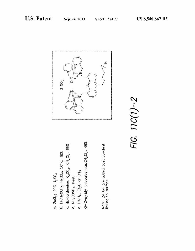
US 8,540,867 B2 Sheet 17 Of 77 Sep. 24, 2013 U.S. Patent

U.S. Patent Sep. 24, 2013 Sheet 18 Of 77 US 8,540,867 B2
Cornpound 8
i. TsCl, TEA, 4-DMAP, THF ii, Pd(PPh3)4, aq Na2CO, EtOH/benzene iii. dipicoyomine, K6. Kl, MeCN iv, H2, Pd/C, MeOH v. DPT, MeCN, r,t. vi. NaOH, MeOH, THF
F7G 11 CO2)

U.S. Patent Sep. 24, 2013 Sheet 19 Of 77 US 8,540,867 B2
HN HN H2N
) ) V ) --> ) --> s
Meo - Nu H e * *- NH, H2N--- NH2 HN-N-N-N- NH
2 s
Br-N
". --- OHC-( )-CHO + HN, ly -->
(. NH2
R - N
) W. N. * No. \
re O re Ary -Y-> ww.xxw
7 \ , , (, K. -N N NH / N
h
-( )- ey 7 8
Cornpound 9
4. s
i. ethylenedicarnine, 90'C ii. BH-THF iii. KOH, CuCOs, benzoyl chloride iv. 1: 4 ratio of 4: 6, MeCN, r.t. v. NaBH, Mech; HNNH if necessary
F7G 11 CO3)

US 8,540,867 B2 Sheet 20 Of 77 Sep. 24, 2013 U.S. Patent

US 8,540,867 B2 Sheet 21 Of 77 Sep. 24, 2013 U.S. Patent

US 8,540,867 B2 Sheet 22 Of 77 Sep. 24, 2013 U.S. Patent

US 8,540,867 B2 Sheet 23 Of 77 Sep. 24, 2013 U.S. Patent

US 8,540,867 B2 Sheet 24 Of 77 Sep. 24, 2013 U.S. Patent


U.S. Patent Sep. 24, 2013 Sheet 26 of 77 US 8,540,867 B2
RowSe RowSel2 RowSe51
LSW
as says &x axis - at
F/G, 14 CoSe2 CoSel4 ColSets
LST
WSSD or word- 38s six say w x: 808 wox
fgB 2- ts? - 199
Sink Col Se2
'coI2- 8%888%w VOut 2 (even) fgf
CoSel4 from W. 539 Co4 Bios/Recdout
Circuitry 19t f75
CoSei S12
Vcol512 1952
F/G, 16


US 8,540,867 B2
as -xy 88s a-- - -s are as we as
¿? ¿
512 s 2 Col 1,
Sheet 28 of 77
M. Col. 5t,
Sep. 24, 2013 U.S. Patent

U.S. Patent Sep. 24, 2013 Sheet 29 Of 77 US 8,540,867 B2
- Col1.2 Ref3,4
|cols11,51 Col509,510 s
S
s S w
is
CS N 5
8 r
s 2 :
s t r 3. re
i 5

U.S. Patent Sep. 24, 2013 Sheet 30 Of 77 US 8,540,867 B2
T-5O2 Acquire Array Data at Low Rote
w/Reference or No input
Calculate First Transition Volue Doto Set
Acquire Array Data at High - SOS (Overspeed) Data Rote w/Reference
or No input
508 Calculate Second Transition
Value Doto Set
calculate correction Factor Data set - 0 Based on First and Second Transition Value Doto Sets; Store CF Dato Set
- 572 Acquire Array Dato at Overspeed Data Rate in Presence of Analyte
514 Apply Correction Factor Data Set to Acquired Analyte Data
F/G, 18B

US 8,540,867 B2 Sheet 31 Of 77 Sep. 24, 2013 U.S. Patent
•••• • • • • ***
§-----
F/G, 18C
I +
F/G. 73D


US 8,540,867 B2 Sheet 33 of 77 Sep. 24, 2013 U.S. Patent
s?monoP! ’VOGA 'ÅGOBA "OOBA
ººrzoi-izou

US 8,540,867 B2 Sheet 34 of 77 Sep. 24, 2013 U.S. Patent
---------

US 8,540,867 B2 Sheet 35 of 77 Sep. 24, 2013 U.S. Patent
Åouw puno uns sºxaea kuung go


US 8,540,867 B2 Sheet 38 of 77 Sep. 24, 2013 U.S. Patent

US 8,540,867 B2 Sheet 39 of 77 Sep. 24, 2013 U.S. Patent

US 8,540,867 B2 Sheet 40 of 77 Sep. 24, 2013 U.S. Patent
<%I.

US 8,540,867 B2 Sheet 41 of 77 Sep. 24, 2013 U.S. Patent

US 8,540,867 B2 Sheet 42 of 77 Sep. 24, 2013 U.S. Patent
2540 20
F/G, 28A
2.5 2O

U.S. Patent Sep. 24, 2013 Sheet 43 of 77 US 8,540,867 B2
s
N
S
1.

U.S. Patent Sep. 24, 2013 Sheet 44 of 77 US 8,540,867 B2
OO


U.S. Patent Sep. 24, 2013 Sheet 46 of 77 US 8,540,867 B2
O

U.S. Patent Sep. 24, 2013 Sheet 47 of 77 US 8,540,867 B2
J320-N Uri cured V8O2.
3332- -3.329 -3.329
Uncured W8O21
3.338 sa 5,336 3,356
Wolfer 3.32
F/G, 33A
3,338 sa 3,336 5 ge 3350
Wolfer -3.31.2
F/G, 3B

U.S. Patent Sep. 24, 2013 Sheet 48 of 77 US 8,540,867 B2
33O4A 33OOA
3306A . MA
M3
a M2
* M.
Poly
in Nove
F.G. 33B-1

U.S. Patent Sep. 24, 2013 Sheet 49 of 77 US 8,540,867 B2

U.S. Patent Sep. 24, 2013 Sheet 50 of 77 US 8,540,867 B2
3324A
3326A
3328A

U.S. Patent Sep. 24, 2013 Sheet 51 of 77 US 8,540,867 B2

U.S. Patent Sep. 24, 2013 Sheet 52 of 77 US 8,540,867 B2

U.S. Patent Sep. 24, 2013 Sheet 53 of 77 US 8,540,867 B2
F7G. 37

U.S. Patent Sep. 24, 2013 Sheet 54 Of 77 US 8,540,867 B2
- 380
22
FIG. 38
-5910
5928 -
J22 2 | S24
32O - 2

U.S. Patent Sep. 24, 2013 Sheet 55 of 77 US 8,540,867 B2
4018 - 4022
4O4. *8&x -4C16
4Of O
- 4012
F/G, 40
F/G, 41

U.S. Patent Sep. 24, 2013 Sheet 56 of 77 US 8,540,867 B2

U.S. Patent Sep. 24, 2013 Sheet 57 Of 77 US 8,540,867 B2
Original Modified Diffuser Section Section
36 to -
F/G, 42A
- 42O2E
- 42O2E
F/G, 42E
-422Of
421.2B
F/G. 42F

U.S. Patent Sep. 24, 2013 Sheet 58 Of 77 US 8,540,867 B2
FIG. 42D

U.S. Patent Sep. 24, 2013 Sheet 59 of 77 US 8,540,867 B2
424.2F
2 (Ceiling height grading: Fluid 212 darker is higher) uid in
F7G 42F1

U.S. Patent Sep. 24, 2013 Sheet 60 of 77 US 8,540,867 B2
S. & s 42F500
F/G, 42F5 42F260s
H f
F7G 42F5

U.S. Patent Sep. 24, 2013 Sheet 61 of 77 US 8,540,867 B2
- 42F2oo
F/G. 42F8

U.S. Patent Sep. 24, 2013 Sheet 62 of 77 US 8,540,867 B2
inlet to Actuate Wolve
F/G, 42G
4252G
4262 N
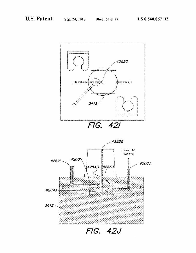
U.S. Patent Sep. 24, 2013 Sheet 63 Of 77 US 8,540,867 B2
4262 4263/
K
N NXZE).xx.

U.S. Patent Sep. 24, 2013 Sheet 64 of 77 US 8,540,867 B2

U.S. Patent Sep. 24, 2013 Sheet 65 Of 77 US 8,540,867 B2
42.7/k
4272K
4276K
F/G, 42M

U.S. Patent Sep. 24, 2013 Sheet 66 of 77 US 8,540,867 B2

US 8,540,867 B2 of 77 Sheet 67 Sep. 24, 2013 U.S. Patent
FIG. 46

US 8,540,867 B2 Sheet 68 of 77 Sep. 24, 2013 U.S. Patent
F/G, 47

US 8,540,867 B2 Sheet 69 Of 77 Sep. 24, 2013 U.S. Patent
F/G, 49

U.S. Patent Sep. 24, 2013 Sheet 70 of 77 US 8,540,867 B2
- 512O
52O

U.S. Patent Sep. 24, 2013 Sheet 71 Of 77 US 8,540,867 B2
- 532O

U.S. Patent Sep. 24, 2013 Sheet 72 Of 77 US 8,540,867 B2
55
550
A7G. 56

U.S. Patent Sep. 24, 2013 Sheet 73 of 77 US 8,540,867 B2
5720s

U.S. Patent Sep. 24, 2013 Sheet 74 of 77 US 8,540,867 B2
F7G. 59A

US 8,540,867 B2 Sheet 75 Of 77 Sep. 24, 2013 U.S. Patent

U.S. Patent Sep. 24, 2013 Sheet 76 of 77 US 8,540,867 B2
A
= E- z-z-z-zt fiz-z-za A Section A - A
w8xx zzz 22.77 a
B Section B-B
- 5922
- SSO
wxxxxxsooxxxx xxxx
X BOOM l
A/G 59C
U.S. Patent Sep. 24, 2013 Sheet 77 of 77 US 8,540,867 B2
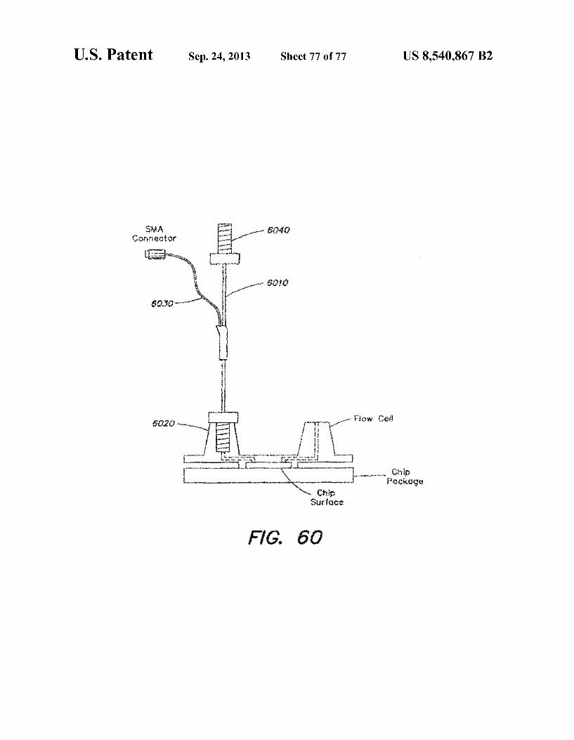
SMA Corrector
5040

US 8,540,867 B2 1.
METHODS AND APPARATUS FOR DETECTING MOLECULAR INTERACTIONS
USING FET ARRAYS
RELATED APPLICATIONS
This application is a continuation of U.S. application Ser. No. 12/492,844 filed Jun. 26, 2009, which claims priority to U.S. provisional application no. 61/133,204 filed Jun. 26, 2008; this application is a continuation-in-part of U.S. appli cation Ser. No. 12/002,781 filed Dec. 17, 2007, and claims priority to and is a continuation-in-part of U.S. application Ser. No. 12/002291 filed Dec. 14, 2007 (now Issued U.S. Pat. No. 7,948,015), both of which claim priority to U.S. provi sional application nos. 60/870,073 filed Dec. 14, 2006, 60/948,748 filed Jul. 10, 2007, and 60/956,324 filed Aug. 16, 2007, all of which disclosures are herein incorporated by reference in their entirety.
FIELD OF THE DISCLOSURE
The present disclosure is directed generally to inventive methods and apparatus relating to detection and measurement of one or more analytes.
BACKGROUND OF THE INVENTION
Electronic devices and components have found numerous applications in chemistry and biology (more generally, “life Sciences'), especially for detection and measurement of vari ous chemical and biological reactions and identification, detection and measurement of various compounds. One such electronic device is referred to as an ion-sensitive field effect transistor, often denoted in the relevant literature as ISFET (or pHFET). ISFETs conventionally have been explored, prima rily in the academic and research community, to facilitate measurement of the hydrogen ion concentration of a solution (commonly denoted as “pH). More specifically, an ISFET is an impedance transforma
tion device that operates in a manner similar to that of a MOSFET (Metal Oxide Semiconductor Field Effect Transis tor), and is particularly configured to selectively measure ion activity in a solution (e.g., hydrogen ions in the solution are the “analytes). A detailed theory of operation of an ISFET is given in “Thirty years of ISFETOLOGY: what happened in the past 30 years and what may happen in the next 30 years.” P. Bergveld, Sens. Actuators, 88 (2003), pp. 1-20, which publication is hereby incorporated herein by reference (here inafter referred to as “Bergveld').
FIG. 1 illustrates a cross-section of a p-type (p-channel) ISFET 50 fabricated using a conventional CMOS (Compli mentary Metal Oxide Semiconductor) process. However, biCMOS (i.e., bipolar and CMOS) processing may also be used, such as a process that would include a PMOSFET array with bipolar structures on the periphery. Taking the CMOS example, P-type ISFET fabrication is based on a p-type sili con substrate 52, in which an n-type well 54 forming a tran sistor “body' is formed. Highly doped p-type (p+) regions S and D, constituting a source 56 and a drain 58 of the ISFET, are formed within the n-type well 54. A highly doped n-type (n+) region B is also formed within the n-type well to provide a conductive body (or “bulk”) connection 62 to the n-type well. An oxide layer 65 is disposed above the source, drain and body connection regions, through which openings are made to provide electrical connections (via electrical conduc tors) to these regions; for example, metal contact 66 serves as a conductor to provide an electrical connection to the drain
10
15
25
30
35
40
45
50
55
60
65
2 58, and metal contact 68 serves as a conductor to provide a common connection to the source 56 and n-type well 54, via the highly conductive body connection 62. A polysilicon gate 64 is formed above the oxide layer at a location above a region 60 of the n-type well 54, between the source 56 and the drain 58. Because it is disposed between the polysilicon gate 64 and the transistor body (i.e., the n-type well), the oxide layer 65 often is referred to as the “gate oxide.”
Like a MOSFET, the operation of an ISFET is based on the modulation of charge concentration caused by a MOS (Metal-Oxide-Semiconductor) capacitance constituted by the polysilicon gate 64, the gate oxide 65 and the region 60 of the n-type well 54 between the source and the drain. When a negative Voltage is applied across the gate and source regions (V-OVolts), a “p-channel 63 is created at the interface of the region 60 and the gate oxide 65 by depleting this area of electrons. This p-channel 63 extends between the source and the drain, and electric current is conducted through the p-channel when the gate-source potential Vs is negative enough to attract holes from the source into the channel. The gate-source potential at which the channel 63 begins to con duct current is referred to as the transistors threshold voltage V (the transistor conducts when Vs has an absolute value greater than the threshold Voltage V). The Source is so named because it is the source of the charge carriers (holes for a p-channel) that flow through the channel 63; similarly, the drain is where the charge carriers leave the channel 63.
In the ISFET 50 of FIG. 1, the n-type well 54 (transistor body), via the body connection 62, is forced to be biased at a same potential as the source 56 (i.e., Vs OVolts), as seen by the metal contact 68 connected to both the source 56 and the body connection 62. This connection prevents forward bias ing of the p-- Source region and the n-type well, and thereby facilitates confinement of charge carriers to the area of the region 60 in which the channel 63 may be formed. Any potential difference between the source 56 and the body/n- type well 54 (a non-zero Source-to-body Voltage Vs) affects the threshold voltage V of the ISFET according to a non linear relationship, and is commonly referred to as the “body effect, which in many applications is undesirable. As also shown in FIG. 1, the polysilicon gate 64 of the
ISFET 50 is coupled to multiple metal layers disposed within one or more additional oxide layers 75 disposed above the gate oxide 65 to form a “floating gate' structure 70. The floating gate structure is so named because it is electrically isolated from other conductors associated with the ISFET namely, it is sandwiched between the gate oxide 65 and a passivation layer 72. In the ISFET 50, the passivation layer 72 constitutes an ion-sensitive membrane that gives rise to the ion-sensitivity of the device; i.e., the presence of analytes Such as ions in an “analyte solution' 74 (i.e., . . . . a solution containing analytes (including ions) of interest or being tested for the presence of analytes of interest) in contact with the passivation layer 72, particularly in a sensitive area 78 above the floating gate structure 70, alters the electrical character istics of the ISFET so as to modulate a current flowing through the p-channel 63 between the source 56 and the drain 58. The passivation layer 72 may comprise any one of a variety of different materials to facilitate sensitivity to par ticular ions; for example, passivation layers comprising sili con nitride or silicon oxynitride, as well as metal oxides Such as silicon, aluminum or tantalum oxides, generally provide sensitivity to hydrogen ion concentration (pH) in the analyte Solution 74, whereas passivation layers comprising polyvinyl chloride containing valinomycin provide sensitivity to potas sium ion concentration in the analyte solution 74. Materials

US 8,540,867 B2 3
Suitable for passivation layers and sensitive to other ions such as sodium, silver, iron, bromine, iodine, calcium, and nitrate, for example, are known.
With respect to ion sensitivity, an electric potential differ ence, commonly referred to as a 'surface potential arises at the solid/liquid interface of the passivation layer 72 and the analyte solution 74 as a function of the ion concentration in the sensitive area 78 due to a chemical reaction (e.g., usually involving the dissociation of oxide Surface groups by the ions in the analyte solution 74 in proximity to the sensitive area 78). This surface potential in turn affects the threshold voltage V of the ISFET; thus, it is the threshold voltage V of the ISFET that varies with changes in ion concentration in the analyte solution 74 in proximity to the sensitive area 78.
FIG. 2 illustrates an electric circuit representation of the p-channel ISFET 50 shown in FIG.1. With reference again to FIG. 1, a reference electrode 76 (a conventional Ag/AgCl electrode) in the analyte solution 74 determines the electric potential of the bulk of the analyte solution 74 itself and is analogous to the gate terminal of a conventional MOSFET, as shown in FIG. 2. In a linear or non-saturated operating region of the ISFET, the drain current I, is given as:
1 (1) ID = ?tvas - WTH - ivosvos,
where Vs is the Voltage between the drain and the source, and B is a transconductance parameter (in units of AmpS/ Volts) given by:
p3 = uC. () (2)
where LL represents the carrier mobility, C is the gate oxide capacitance per unit area, and the ratio W/L is the width to length ratio of the channel 63. If the reference electrode 76 provides an electrical reference or ground (V-0 Volts), and the drain current I, and the drain-to-source Voltage V, are kept constant, variations of the source Voltage Vs of the ISFET directly track variations of the threshold voltage V, according to Eq. (1); this may be observed by rearranging Eq. (1) as:
(3) ID Ye). W = - WTu - -- S TH (p, 2
Since the threshold voltage V of the ISFET is sensitive to ion concentration as discussed above, according to Eq. (3) the source Voltage Vs provides a signal that is directly related to the ion concentration in the analyte Solution 74 in proximity to the sensitive area 78 of the ISFET. More specifically, the threshold voltage V is given by:
(4)
where V is the flatband Voltage, Q, is the depletion charge in the silicon and p is the Fermi-potential. The flatband Voltage in turn is related to material properties such as work functions and charge accumulation. In the case of an ISFET, with reference to FIGS. 1 and 2, the flatband voltage contains
10
15
25
30
35
40
45
50
55
60
65
4 terms that reflect interfaces between 1) the reference elec trode 76 (acting as the transistor gate G) and the analyte solution 74; and 2) the analyte solution 74 and the passivation layer 72 in the sensitive area 78 (which in turn mimics the interface between the polysilicon gate 64 of the floating gate structure 70 and the gate oxide 65). The flatband voltage V, is thus given by:
ds (5) VFB = Ef -o + sot - -
Qss + Qor Cox
where E, is the reference electrode potential relative to vacuum, I is the surface potential that results from chemical reactions at the analyte Solution/passivation layer interface (e.g., dissociation of surface groups in the passivation layer), and X is the Surface dipole potential of the analyte Solution 74. The fourth term in Eq. (5) relates to the silicon workfunc tion (q is the electron charge), and the last term relates to charge densities at the silicon Surface and in the gate oxide. The only term in Eq. (5) sensitive to ion concentration in the analyte solution 74 is Io, as the ion concentration in the analyte solution 74 controls the chemical reactions (dissocia tion of Surface groups) at the analyte Solution/passivation layer interface. Thus, Substituting Eq. (5) into Eq. (4), it may be readily observed that it is the surface potential Po that renders the threshold Voltage V. sensitive to ion concentra tion in the analyte solution 74.
Regarding the chemical reactions at the analyte solution/ passivation layer interface, the Surface of a given material employed for the passivation layer 72 may include chemical groups that may donate protons to or accept protons from the analyte solution 74, leaving at any given time negatively charged, positively charged, and neutral sites on the Surface of the passivation layer 72 at the interface with the analyte Solution 74. A model for this proton donation/acceptance process at the analyte solution/passivation layer interface is referred to in the relevant literature as the “Site-Dissociation Model or the “Site-Binding Model.” and the concepts under lying Such a process may be applied generally to characterize Surface activity of passivation layers comprising various materials (e.g., metal oxides, metal nitrides, metal oxyni trides).
Using the example of a metal oxide for purposes of illus tration, the Surface of any metal oxide contains hydroxyl groups that may donate a proton to or accepta proton from the analyte to leave negatively or positively charged sites, respec tively, on the surface. The equilibrium reactions at these sites may be described by:
AOHe AO-H+ (6)
where Adenotes an exemplary metal, Hs' represents a proton in the analyte solution 74, Eq. (6) describes proton donation by a surface group, and Eq. (7) describes proton acceptance by a surface group. It should be appreciated that the reactions given in Eqs. (6) and (7) also are present and need to be considered in the analysis of a passivation layer comprising metal nitrides, together with the equilibrium reaction:
ANH' e ANH+H", (7b) wherein Eq. (7b) describes another proton acceptance equi librium reaction. For purposes of the present discussion how ever, again only the proton donation and acceptance reactions given in Eqs. (6) and (7) are initially considered to illustrate the relevant concepts.

US 8,540,867 B2 5
Based on the respective forward and backward reaction rate constants for each equilibrium reaction, intrinsic disso ciation constants K (for the reaction of Eq. (6)) and K. (for the reaction of Eq. (7)) may be calculated that describe the equilibrium reactions. These intrinsic dissociation constants in turn may be used to determine a Surface charge density Oo (in units of Coulombs/unit area) of the passivation layer 72 according to:
oo-qB, (8)
where the term B denotes the number of negatively charged Surface groups minus the number of positively charged Sur face groups per unit area, which in turn depends on the total number of proton donor/acceptor sites per unit area Ns on the passivation layer Surface, multiplied by a factor relating to the intrinsic dissociation constants K, and K, of the respective proton donation and acceptance equilibrium reactions and the Surface proton activity (or pHs). The effect of a small change in Surface proton activity (pHs) on the Surface charge density is given by:
6 pH S (9)
where B is referred to as the “intrinsic buffering capacity' of the surface. It should be appreciated that since the values of Ns, K, and K, are material dependent, the intrinsic buffering capacity B of the Surface similarly is material dependent. The fact that ionic species in the analyte solution 74 have a
finite size and cannot approach the passivation layer surface any closer than the ionic radius results in a phenomenon referred to as a “double layer capacitance' proximate to the analyte Solution/passivation layer interface. In the Gouy Chapman-Stern model for the double layer capacitance as described in Bergveld, the Surface charge density Oo is bal anced by an equal but opposite charge density in the analyte solution 74 at some position from the surface of the passiva tion layer 72. These two parallel opposite charges form a so-called “double layer capacitance C (per unit area), and the potential difference across the capacitance C is defined as the surface potential Po, according to:
where O is the charge density on the analyte Solution side of the double layer capacitance. This charge density O, in turnis a function of the concentration of all ion species or other analyte species (i.e., not just protons) in the bulk analyte Solution 74; in particular, the Surface charge density can be balanced not only by hydrogen ions but other ion species (e.g., Na', K) in the bulk analyte solution.
In the regime of relatively lower ionic strengths (e.g., <1 mole/liter), the Debye theory may be used to describe the double layer capacitance C according to:
keo Ci = - - d A.
(11)
where k is the dielectric constant e/e (for relatively lower ionic strengths, the dielectric constant of water may be used), and w is the Debye Screening length (i.e., the distance over which significant charge separation can occur). The Debye length w is in turn inversely proportional to the square root of the strength of the ionic species in the analyte solution, and in water at room temperature is given by:
10
15
25
30
35
40
45
50
55
60
65
0.3 nm.
VI (12)
The ionic strength I of the bulk analyte is a function of the concentration of all ionic species present, and is given by:
(13) = iXic.
where Z is the charge number of ionic species S and c is the molar concentration of ionic species S. Accordingly, from Eqs. (10) through (13), it may be observed that the surface potential is larger for larger Debye screening lengths (i.e., Smaller ionic strengths). The relation between pH values present at the analyte
Solution/passivation layer interface and in the bulk Solution is expressed in the relevant literature by Boltzman statistics with the surface potential Po as a parameter:
go (14) H - pH) = (pH - pH) kT
From Eqs. (9), (10) and (14), the sensitivity of the surface potential Po particularly to changes in the bulk pH of the analyte solution (i.e., “pH sensitivity') is given by:
Ao kT = -2.3-a. ApH i
(15)
where the parameter C. is a dimensionless sensitivity factor that varies between Zero and one and depends on the double layer capacitance C and the intrinsic buffering capacity of the surface?, as discussed above in connection with Eq. (9). In general, passivation layer materials with a high intrinsic buffering capacity f, render the surface potential Po less sensitive to concentration in the analyte solution 74 of ionic species other than protons (e.g., C. is maximized by a large B). From Eq. (15), at a temperature T of 298 degrees Kelvin, it may be appreciated that a theoretical maximum pH sensi tivity of 59.2 mV/pH may be achieved at C-1. From Eqs. (4) and (5), as noted above, changes in the ISFET threshold Voltage V directly track changes in the surface potential Po: accordingly, the pH sensitivity of an ISFET given by Eq. (15) also may be denoted and referred to herein as AV for convenience. In exemplary conventional ISFETs employing a silicon nitride or silicon oxynitride passivation layer 72 for pH-sensitivity, pH sensitivities AV (i.e., a change in thresh old voltage with change in pH of the analyte solution 74) over a range of approximately 30 mV/pH to 60 mV/pH have been observed experimentally.
Another noteworthy metric in connection with ISFET pH sensitivity relates to the bulk pH of the analyte solution 74 at which there is no net Surface charge density O'o and, accord ingly, a surface potential I of zero volts. This pH is referred to as the “point of zero charge” and denoted as pH. With reference again to Eqs. (8) and (9), like the intrinsic buffering capacity B, pH is a material dependent parameter. From the foregoing, it may be appreciated that the Surface potential at any given bulk pH of the analyte Solution 74 may be calculated according to:

US 8,540,867 B2
Ao (16) Yo (pH) = (pH - pH, ApH
Table 1 below lists various metal oxides and metal nitrides and their corresponding points of Zero charge (pH), pH sensitivities (AV), and theoretical maximum surface poten tial at a pH of 9:
TABLE 1.
Oxide? Theoretical Io Metal Nitride pHeze AV (mWipH) (mV) (a) pH = 9
Al Al2O3 9.2 54.5 (35° C.) -11 Zr ZrO2 S.1 50 150 T TiO2 5.5 57.4-62.3 2O1
(32° C., pH 3-11) Tal Ta2O5 2.9, 2.8 62.87 (35° C.) 384 Si SiN 4.6, 6-7 56.94 (25° C.) 251 Si SiO2 2.1 43 297 Mo MoO. 1.8-2.1 48-59 396 W WO, 0.3, 0.43, 0.5 50 435
Prior research efforts to fabricate ISFETs for pH measure ments based on conventional CMOS processing techniques typically have aimed to achieve high signal linearity over a pH range from 1-14. Using an exemplary threshold sensitivity of approximately 50 mV/pH, and considering Eq. (3) above, this requires a linear operating range of approximately 700 mV. for the source Voltage Vs. As discussed above in connection with FIG. 1, the threshold voltage V of ISFETs (as well as MOSFETs) is affected by any voltage Vs between the source and the body (n-type well 54). More specifically, the thresh old Voltage V is a nonlinear function of a nonzero Source to-body Voltage Vs. Accordingly, so as to avoid compromis ing linearity due to a difference between the source and body Voltage potentials (i.e., to mitigate the “body effect”), as shown in FIG. 1 the source 56 and body connection 62 of the ISFET 50 often are coupled to a common potential via the metal contact 68. This body-source coupling also is shown in the electric circuit representation of the ISFET 50 shown in FIG 2.
While the foregoing discussion relates primarily to a steady state analysis of ISFET response based on the equilib rium reactions given in Eqs. (6) and (7), the transient or dynamic response of a conventional ISFET to an essentially instantaneous change in ionic strength of the analyte Solution 74 (e.g., a stepwise change in proton or other ionic species concentration) has been explored in some research efforts. One exemplary treatment of ISFET transient or dynamic response is found in “ISFET responses on a stepwise change in electrolyte concentration at constant pH. J. C. van Kerkof, J. C. T. Eijkel and P. Bergveld, Sensors and Actuators B, 18-19 (1994), pp. 56-59, which is incorporated herein by reference.
For ISFET transient response, a stepwise change in the concentration of one or more ionic species in the analyte Solution in turn essentially instantaneously changes the charge density O, on the analyte Solution side of the double layer capacitance C. Because the instantaneous change in charge density O is faster than the reaction kinetics at the Surface of the passivation layer 72, the Surface charge density Oo initially remains constant, and the change in ion concen tration effectively results in a sudden change in the double layer capacitance C. From Eq. (10), it may be appreciated that such a Sudden change in the capacitance C at a constant Surface charge density Oo results in a corresponding Sudden
5
10
15
25
30
35
40
45
50
55
60
65
8 change in the surface potential Po. FIG. 2A illustrates this phenomenon, in which an essentially instantaneous or step wise increase in ion concentration in the analyte Solution, as shown in the top graph, results in a corresponding change in the surface potential as shown in the bottom graph of FIG. 2A. After Some time, as the passivation layer Surface groups react to the stimulus (i.e., as the Surface charge density adjusts), the system returns to Some equilibrium point, as illustrated by the decay of the ISFET response “pulse' 79 shown in the bottom graph of FIG. 2A. The foregoing phe nomenon is referred to in the relevant literature (and hereafter in this disclosure) as an “ion-step’ response. As indicated in the bottom graph of FIG. 2A, an amplitude
AI of the ion-step response 79 may be characterized by:
Oo Oo (17) An = 1 - ) = - - - - - = 1 - - - 0 Fr r2 Cd, CdI2 (
where I is an equilibrium surface potential at an initial ion concentration in the analyte solution, Cn is the double layer capacitance per unit area at the initial ion concentration, is the Surface potential corresponding to the ion-step stimulus, and Cn is the double layer capacitance per unit area based on the ion-step stimulus. The time decay profile 81 associated with the response 79 is determined at least in part by the kinetics of the equilibrium reactions at the analyte solution/ passivation layer interface (e.g., as given by Eqs. (6) and (7) for metal oxides, and also Eq. (7b) for metal nitrides). One instructive treatment in this regard is provided by “Modeling the short-time response of ISFET sensors. P. Woias et al., Sensors and Actuators B, 24-25 (1995) 211-217 (hereinafter referred to as “Woias'), which publication is incorporated herein by reference.
In the Woias publication, an exemplary ISFET having a silicon nitride passivation layer is considered. A system of coupled non-linear differential equations based on the equi librium reactions given by Eqs. (6), (7), and (7a) is formulated to describe the dynamic response of the ISFET to a step (essentially instantaneous) change in pH; more specifically, these equations describe the change in concentration over time of the various surface species involved in the equilibrium reactions, based on the forward and backward rate constants for the involved proton acceptance and proton donation reac tions and how changes in analyte pH affect one or more of the reaction rate constants. Exemplary solutions, some of which include multiple exponential functions and associated time constants, are provided for the concentration of each of the Surface ion species as a function of time. In one example provided by Woias, it is assumed that the proton donation reaction given by Eq. (6) dominates the transient response of the silicon nitride passivation layer surface for relatively Small step changes in pH, thereby facilitating a mono-expo nential approximation for the time decay profile 81 of the response 79 according to:
Jo(t)=Aloe", (18) where the exponential function essentially represents the change in Surface charge density as a function of time. In Eq. (16), the time constant t is both a function of the bulk pH and material parameters of the passivation layer, according to:
t-tox1OPH2, (19)
where to denotes a theoretical minimum response time that only depends on material parameters. For silicon nitride, Woias provides exemplary values for to on the order of 60

US 8,540,867 B2
microseconds to 200 microseconds. For purposes of provid ing an illustrative example, using to 60 microseconds and a bulk pH of 9, the time constant t given by Eq. (19) is 1.9 seconds. Exemplary values for other types of passivation materials may be found in the relevant literature and/or deter mined empirically.
Previous efforts to fabricate two-dimensional arrays of ISFETs based on the ISFET design of FIG. 1 have resulted in a maximum of 256 ISFET sensor elements (or “pixels’) in an array (i.e., a 16 pixel by 16 pixel array). Exemplary research in ISFET array fabrication is reported in the publications “A large transistor-based sensor array chip for direct extracellu lar imaging. M. J. Milgrew, M. O. Riehle, and D. R. S. Cumming, Sensors and Actuators, B. Chemical, 111-112, (2005), pp. 347-353, and “The development of scalable sen sor arrays using standard CMOS technology, M.J. Milgrew, P. A. Hammond, and D. R. S. Cumming, Sensors and Actua tors, B. Chemical, 103, (2004), pp. 37-42, which publications are incorporated herein by reference and collectively referred to hereafter as “Milgrew etal.” Other research efforts relating to the realization of ISFET arrays are reported in the publi cations “A very large integrated pH-ISFET sensor array chip compatible with standard CMOS processes.” T. C. W. Yeow, M. R. Haskard, D. E. Mulcahy, H. I. Seo and D. H. Kwon, Sensors and Actuators B: Chemical, 44, (1997), pp. 434–440 and “Fabrication of a two-dimensional pH image sensor using a charge transfer technique.” Ilizawa, T., Sawada, K., Takao, II., Ishida, M., Sensors and Actuators, B. Chemical 117 (2), 2006, pp. 509-515, which publications also are incorporated herein by reference.
FIG. 3 illustrates one column 85, of a two-dimensional ISFET array according to the design of Milgrew et al. The column 85, includes sixteen (16) pixels 80, through 80, and, as discussed further below in connection with FIG. 7, a com plete two-dimensional array includes sixteen (16) Such col umns 85, G=1,2,3,... 16) arranged side by side. As shown in FIG.3, a given column 85, includes a current source Isorce, that is shared by all pixels of the column, and ISFET bias/ readout circuitry 82, (including current sink Isre) that is also shared by all pixels of the column. Each ISFET pixel 80 through 80 includes a p-channel ISFET 50 having an elec trically coupled source and body (as shown in FIGS. 1 and 2), plus two switches S1 and S2 that are responsive to one of sixteen row select signals (RSEL through RSEL, and their complements). As discussed below in connection with FIG.7. a row select signal and its complement are generated simul taneously to “enable" or selecta given pixel of the column 85, and Such signal pairs are generated in some sequence to successively enable different pixels of the column one at a time. As shown in FIG. 3, the switch S2 of each pixel 80 in the
design of Milgrew et al. is implemented as a conventional n-channel MOSFET that couples the current source Isorce, to the source of the ISFET 50 upon receipt of the correspond ing row select signal. The switch S1 of each pixel 80 is implemented as a transmission gate, i.e., a CMOS pair includ ing an n-channel MOSFET and a p-channel MOSFET, that couples the source of the ISFET 50 to the bias/readout cir cuitry 82, upon receipt of the corresponding row select signal and its complement. An example of the switch S1 of the pixel 80 is shown in FIG. 4, in which the p-channel MOSFET of the transmission gate is indicated as S1 and the re-channel MOSFET is indicated as S1. In the design of Milgrew et al., a transmission gate is employed for the Switch S1 of each pixel so that, for an enabled pixel, any ISFET source voltage within the power Supply range V, to Vss may be applied to the bias/readout circuitry 82, and output by the column as the
5
10
15
25
30
35
40
45
50
55
60
65
10 signal Vs. From the foregoing, it should be appreciated that each pixel 80 in the ISFET sensor array design of Milgrew et al. includes four transistors, i.e., a p-channel ISFET, a CMOS pair transmission gate including an re-channel MOSFET and a p-channel MOSFET for switch S1, and an n-channel MOS FET for Switch S2.
As also shown in FIG. 3, the bias/readout circuitry 82, employs a source-drain follower configuration in the form of a Kelvin bridge to maintain a constant drain-source Voltage Vos, and isolate the measurement of the source voltage Vs. from the constant drain current Isoe, for the ISFET of an enabled pixel in the column 85. To this end, the bias/readout circuitry 82, includes two operational amplifiers A1 and A2, a current sink Is, and a resistor Rs. The Voltage developed across the resistor Rs, due to the current Isry, flowing through the resistor is forced by the operational amplifiers to appear across the drain and source of the ISFET of an enabled pixel as a constant drain-source Voltage V,s. Thus, with reference again to Eq. (3), due to the constant Vos, and the constant Isote, the source Voltage Vs, of the ISFET of the enabled pixel provides a signal corresponding to the ISFETs threshold Voltage V, and hence a measurement of pH in proximity to the ISFETs sensitive area (see FIG. 1). The wide dynamic range for the source Voltage Vs, provided by the transmission gate S1 ensures that a full range of pH values from 1-14 may be measured, and the source-body connection of each ISFET ensures sufficient linearity of the ISFETs threshold voltage over the full pH measurement range.
In the column design of Milgrew et al. shown in FIG. 3, it should be appreciated that for the Kelvin bridge configuration of the columnbias/readout circuitry 82, to function properly, a p-channel ISFET 50 as shown in FIG. 1 must be employed in each pixel; more specifically, an alternative implementa tion based on the Kelvin bridge configuration is not possible using an n-channel ISFET. With reference again to FIG. 1, for an n-channel ISFET based on a conventional CMOS process, the n-type well 54 would not be required, and highly doped n-type regions for the drain and source would be formed directly in the p-type silicon substrate 52 (which would con stitute the transistor body). For n-channel FET devices, the transistor body typically is coupled to electrical ground. Given the requirement that the source and body of an ISFET in the design of Milgrew et al. are electrically coupled together to mitigate nonlinear performance due to the body effect, this would result in the source of an n-channel ISFET also being connected to electrical ground (i.e., V V 0 Volts), thereby precluding any useful output signal from an enabled pixel. Accordingly, the column design of Milgrew et al. shown in FIG. 3 requires p-channel ISFETs for proper operation.
It should also be appreciated that in the column design of Milgrew etal. shown in FIG.3, the two n-channel MOSFETs required to implement the switches S1 and S2 in each pixel cannot be formed in the n-type well 54 shown in FIG. 1, in which the p-channel ISFET for the pixel is formed; rather, the n-channel MOSFETs are formed directly in the p-type silicon substrate 52, beyond the confines of the n-type well 54 for the ISFET FIG. 5 is a diagram similar to FIG. 1, illustrating a wider cross-section of a portion of the p-type silicon Substrate 52 corresponding to one pixel 80 of the column 85, shown in FIG. 3, in which the n-type well 54 containing the drain 58, source 56 and body connection 62 of the ISFET 50 is shown alongside a first n-channel MOSFET corresponding to the switch S2 and a second n-channel MOSFETS1 constitut ing one of the two transistors of the transmission gate S1 shown in FIG. 4.

US 8,540,867 B2 11
Furthermore, in the design of Milgrew et al., the p-channel MOSFET required to implement the transmission gate S1 in each pixel (e.g., see S1 in FIG. 4) cannot be formed in the same n-type well in which the p-channel ISFET 50 for the pixel is formed. In particular, because the body and Source of the p-channel ISFET are electrically coupled together, imple menting the p-channel MOSFETS1 in the same n-well as the p-channel ISFET 50 would lead to unpredictable opera tion of the transmission gate, or preclude operation entirely. Accordingly, two separate n-type wells are required to imple ment each pixel in the design of Milgrew et al. FIG. 6 is a diagram similar to FIG. 5, showing a cross-section of another portion of the p-type silicon Substrate 52 corresponding to one pixel 80, in which the n-type well 54 corresponding to the ISFET 50 is shown alongside a second n-type well 55 in which is formed the p-channel MOSFET S1 constituting one of the two transistors of the transmission gate S1 shown in FIG. 4. It should be appreciated that the drawings in FIGS. 5 and 6 are not to scale and may not exactly represent the actual layout of a particular pixel in the design of Milgrew et al.; rather these figures are conceptual in nature and are pro vided primarily to illustrate the requirements of multiple n-wells, and separate n-channel MOSFETs fabricated outside of the n-wells, in the design of Milgrew et al. The array design of Milgrew et al. was implemented using
a 0.35 micrometer (um) conventional CMOS fabrication pro cess. In this process, various design rules dictate minimum separation distances between features. For example, accord ing to the 0.35 um CMOS design rules, with reference to FIG. 6, a distance “a” between neighboring n-wells must be at least three (3) micrometers. A distance “a/2 also is indicated in FIG. 6 to the left of the n-well 54 and to the right of the n-well 55 to indicate the minimum distance required to separate the pixel 80 shown in FIG. 6 from neighboring pixels in other columns to the left and right, respectively. Additionally, according to typical 0.35um CMOS design rules, a distance “b' shown in FIG. 6 representing the width in cross-section of the n-type well 54 and a distance “c' representing the width in cross-section of the n-type well 55 are each on the order of approximately 3 um to 4 um (within the n-type well, an allowance of 1.2 um is made between the edge of the n-well and each of the Source and drain, and the Source and drain themselves have a width on the order of 0.7 um). Accordingly, a total distance “d’ shown in FIG. 6 representing the width of the pixel 80 in cross-section is on the order of approximately 12 um to 14 Lum. In one implementation, Milgrew etal. report an array based on the column/pixel design shown in FIG. 3 comprising geometrically square pixels each having a dimen sion of 12.8 um by 12.8 Lum.
In sum, the ISFET pixel design of Milgrew et al. is aimed at ensuring accurate hydrogen ion concentration measure ments over a pH range of 1-14. To ensure measurement lin earity, the source and body of each pixel’s ISFET are electri cally coupled together. To ensure a full range of pH measurements, a transmission gate S1 is employed in each pixel to transmit the Source Voltage of an enabled pixel. Thus, each pixel of Milgrew's array requires four transistors (p-channel ISFET, p-channel MOSFET, and two n-channel MOSFETs) and two separate n-wells (FIG. 6). Based on a 0.35 micrometer conventional CMOS fabrication process and corresponding design rules, the pixels of such an array have a minimum size appreciably greater than 10 um, i.e., on the order of approximately 12 um to 14 Lum.
FIG. 7 illustrates a complete two-dimensional pixel array 95 according to the design of Milgrew et al., together with accompanying row and column decoder circuitry and mea surement readout circuitry. The array 95 includes sixteen
5
10
15
25
30
35
40
45
50
55
60
65
12 columns 85 through 85 of pixels, each column having sixteen pixels as discussed above in connection with FIG. 3 (i.e., a 16 pixel by 16 pixel array). A row decoder 92 provides sixteen pairs of complementary row select signals, wherein each pair of row select signals simultaneously enables one pixel in each column 85 through 85 to provide a set of column output signals from the array 95 based on the respec tive source Voltages Vs through Vs of the enabled row of ISFETs. The row decoder 92 is implemented as a conven tional four-to-sixteen decoder (i.e., a four-bit binary input ROW-ROW, to select one of 2 outputs). The set of column output signals Vs through Vs for an enabled row of the array is applied to Switching logic 96, which includes sixteen transmission gates S1 through S16 (one transmission gate for each output signal). As above, each transmission gate of the switching logic 96 is implemented using a p-channel MOS FET and an n-channel MOSFET to ensure a sufficient dynamic range for each of the output signals Vs through Vs. The column decoder 94, like the row decoder 92, is implemented as a conventional four-to-sixteen decoder and is controlled via the four-bit binary input COL-COL to enable one of the transmission gates S1 through S16 of the switching logic 96 at any given time, so as to provide a single output signal Vs from the Switching logic 96. This output signal Vs is applied to a 10-bit analog to digital converter (ADC) 98 to provide a digital representation D-Do of the output signal Vs corresponding to a given pixel of the array. As noted earlier, individual ISFETs and arrays of ISFETs
similar to those discussed above have been employed as sens ing devices in a variety of chemical and biological applica tions. In particular, ISFETs have been employed as pH sen sors in the monitoring of various processes involving nucleic acids such as DNA. Some examples of employing ISFETs in various life-science related applications are given in the fol lowing publications, each of which is incorporated herein by reference: Massimo Barbaro, Annalisa Bonfiglio, Luigi Raffo, Andrea Alessandrini, Paolo Facci and Imrich Barak, “Fully electronic DNA hybridization detection by a standard CMOS biochip. Sensors and Actuators B. Chemical, Vol ume 118, Issues 1-2, 2006, pp. 41-46; Toshinari Sakurai and Yuzuru Husimi, “Real-time monitoring of DNA polymerase reactions by a micro ISFET pH sensor.” Anal. Chem., 64(17), 1992, pp 1996-1997; S. Purushothaman, C. Toumazou, J. Georgiou, “Towards fast solid state DNA sequencing.” Cir cuits and Systems, vol. 4, 2002, pp. IV-169 to IV-172; S. Purushothaman, C. Toumazou, C. P. Ou, “Protons and single nucleotide polymorphism detection: A simple use for the Ion Sensitive Field Effect Transistor. Sensors and Actuators B. Chemical, Vol. 114, no. 2, 2006, pp.964-968; A. L. Simonian, A. W. Flounders, J. R. Wild, “FET-Based Biosensors for The Direct Detection of Organophosphate Neurotoxins.” Elec troanalysis, Vol. 16, No. 22, 2004, pp. 1896-1906; C. Touma Zou, S. Purushothaman, “Sensing Apparatus and Method.” United States Patent Application 2004-0134798, published Jul. 15, 2004; and T. W. Koo, S. Chan, X. Su, Z. Jingwu, M. Yamakawa, V. M. Dubin, “Sensor Arrays and Nucleic Acid Sequencing Applications.” United States Patent Application 2006-0199.193, published Sep. 7, 2006.
SUMMARY OF THE INVENTION
The invention relates in part to the use of chemically sensitive FETs (i.e., chemFETs), more particularly chemFET arrays, and even more particularly large chemFET arrays (e.g., those comprising 256 FETs or sensors) for monitoring biological and/or chemical processes or reactions, including without limitation molecular interactions for the purpose of

US 8,540,867 B2 13
detecting analytes in a sample. These sensors may be used to detect and measure static and/or dynamic levels or concen trations of a variety of analytes (e.g., hydrogen or other ions, non-ionic molecules or compounds, nucleic acids, proteins, polysaccharides, Small chemical compounds such as chemi cal combinatorial library members, and the like). Analytes may be naturally occurring or non-naturally occurring, whether synthesized in vivo or in vitro. Analytes may be used as markers of a reaction or interaction, or progression thereof.
Reactions, processes or interactions that may be monitored according to the invention include without limitation those occurring in cell or tissue cultures, those occurring between molecular entities such as receptor-ligand interactions, anti body-antigen interactions, nucleic acid-nucleic acid interac tions, neural cell stimulation and/or triggering, interactions of cells or tissues with agents such as pharmaceutical candidate agents, and the like.
Samples may also be monitored according to the invention for the presence of analytes. Such samples may be naturally occurring or non-naturally occurring, including without limi tation bodily samples to be analyzed for diagnostic, prognos tic and/or therapeutic purposes, chemical or biological librar ies to be screened for the presence of agents with particular structural or functional attributes, etc. Samples are typically liquid (or are dissolved in a liquid) and of Small Volume, and therefore are amenable to high-speed, high-density analysis Such as analyte detection.
Accordingly, various embodiments of the present disclo Sure are directed generally to inventive methods and appara tuses that employ chemFETs and chemFET arrays, including large chemFET arrays (e.g., those that comprise 256 FETs or sensors, as the terms are used interchangeably herein) for measuring one or more analytes. FET arrays by definition include at least two FETs. An ISFET, as discussed above, is a particular type of chemFET that is configured for ion detec tion. It is to be understood that ISFETs may be employed in various embodiments disclosed herein. Other types of chem FETs contemplated by the present disclosure include enzyme FETs (EnFETs) which employ enzymes to detect analytes. It should be appreciated, however, that the present disclosure is not limited to ISFETs and EnFETs, but more generally relates to any FET that is configured to detect one or more analytes or one or more interactions. Typically, in these arrays, one or more chemFET-containing elements or 'pixels' constituting the sensors are configured to monitor one or more indepen dent biological or chemical reactions or events occurring in proximity to the pixels of the array.
In some exemplary implementations, individual chem FETs or chemFET arrays may be coupled to one or more microfluidics structures that form one or more reaction cham bers, or “wells' or “microwells, over individual sensors or groups of sensors (in the case of an array), and optionally to an apparatus that delivers samples to the reaction chambers and removes them from the reaction chambers between measure ments. Even when reaction chambers are not employed (and therefore the volume above the sensors is continuous), the sensor array may be coupled to one or more microfluidics structures for the delivery of samples or agents to the pixels and for removal of samples, agents and/or analytes between measurements. Accordingly, inventive aspects of this disclo sure, which are desired to be protected, include the various microfluidic structures which may be employed to flow samples and where appropriate other agents useful in for example the detection and measurement of analytes to and from the wells or pixels, methods and structures for coupling the arrayed wells with arrayed pixels, and the like.
10
15
25
30
35
40
45
50
55
60
65
14 Thus, in various aspects, the invention provides an appa
ratus comprising a chemFET array having disposed on its Surface a biological array or a chemical array. The biological array may be a nucleic acid array, a protein array including but not limited to an enzyme array, an antibody array and an antibody fragment array, a cell array, and the like. The chemi cal array may be an organic molecule array, or an inorganic molecule array, and the like. The biological array or chemical array may be arranged into a plurality of "cells' or spatially defined regions, and each of these regions is situated over a different sensor in the chemFETarray, in some embodiments.
In another aspect, the invention provides a method for detecting a nucleic acid comprising contacting a nucleic acid array disposed on a chemFET array with a sample, and detect ing binding of a nucleic acid from the sample to one or more regions on the nucleic acid array.
In another aspect, the invention provides a method for detecting a protein comprising contacting a protein array disposed on a chemFET array with a sample, and detecting binding of a protein from the sample to one or more regions on the protein array.
In another aspect, the invention provides a method for detecting a nucleic acid comprising contacting a protein array disposed on a chemFET array with a sample, and detecting binding of a nucleic acid from the sample to one or more regions on the protein array.
In another aspect, the invention provides a method for detecting an antigen comprising contacting an antibody array disposed on a chemFET array with a sample, and detecting binding of an antigen from the sample to one or more regions on the antibody array.
In another aspect, the invention provides a method for detecting an enzyme Substrate or inhibitor comprising con tacting an enzyme array disposed on a chemFET array with a sample, and detecting binding of an entity from the sample to one or more regions on the enzyme array.
In another aspect, the invention provides a method for detecting an analyte in a sample comprising contacting a sample to a plurality of biological or chemical agents attached to a chemFET array, and analyzing electrical output from a plurality of chemFET sensors in the chemFET array after contact with the sample, wherein electrical output from a chemFET sensor after contact with the sample indicates bind ing of an analyte to the biological or chemical agent attached to the array. As noted above, the sample may be from a naturally occur
ring source (e.g., a subject) and optionally it may be a bodily fluid. It may comprise cells, nucleic acids, proteins (including glycoproteins, antibodies, etc.), polysaccharides, and the like.
In various embodiments, the plurality of biological or chemical agents is a plurality of proteins, or a plurality of nucleic acids, or it may be a mixture of proteins and nucleic acids. The biological or chemical agents may be non-natu rally occurring or naturally-occurring, and if naturally-occur ring may be synthesized in vivo or in vitro. The plurality of biological or chemical agents may be a homogenous plurality of biological or chemical agents. In other embodiments, the plurality of biological or chemical agents is not homoge
OUS.
In one embodiment, the analyte is present in the sample. In another embodiment, the analyte is generated following con tact of the sample with the chemFET array or with other reagents in the solution in contact with the chemFET array.
In still other embodiments, each chemFET sensor in the chemFET array is coupled to a reaction chamber.
In another aspect, the invention provides a method for monitoring a biological or chemical process comprising

US 8,540,867 B2 15
exposing a first agent to a second agent in proximity to a chemFET sensor, and measuring an electrical output at the chemFET sensor after exposure of the first agent to the second agent, wherein an electrical output at the chemFET sensor after exposure of the first agent to the second agent indicates an interaction between the first agent and the second agent, and wherein the chemFET sensor is present in a chemFET array having at least 2 chemFET sensors.
In another aspect, the invention provides a method for monitoring a biological or chemical process comprising exposing a first agent to a second agent in proximity to a chemFET sensor, and measuring an electrical output at the chemFET sensor after exposure of the first agent to the second agent, wherein an electrical output at the chemFET sensor after exposure of the first agent to the second agent indicates an interaction between the first agent and the second agent, wherein the chemFET sensor is present in a chemFET array having at least 2 chemFET sensors, and wherein each chem FET sensor is coupled to a separate reaction chamber.
In another aspect, the invention provides an apparatus com prising nucleic acids or a plurality of nucleic acids attached to a chemFET array comprising 10 chemFETs.
In another aspect, the invention provides an apparatus com prising a protein or a plurality of proteins attached to a chem FET comprising 10 chemFETs.
In another aspect, the invention provides an apparatus com prising a peptide or a plurality of peptides attached to a chemFET array comprising 10 chemFET sensors.
In various embodiments, the chemFET is coupled to a reaction chamber array.
In still another aspect, the invention provides an apparatus comprising a cell culture disposed on a chemFET or a chem FET array.
In still another aspect, the invention provides an apparatus comprising a nucleic acid array disposed on a chemFET array, optionally comprising a coupled array of reaction chambers.
In still another aspect, the invention provides an apparatus comprising a nucleic acid array comprising a plurality of nucleic acids bound to physically defined regions of a Solid Support disposed on a chemFET array. In one embodiment, each of the physically defined regions is associated with at least one chemFET in the array. In one embodiment, the nucleic acid array comprises a plurality of reaction chambers. In one embodiment, each physically defined region is asso ciated with a single reaction chamber.
It is to be understood that any of the chemFET arrays described herein may comprise 3, 4, 5, 6, 7, 8, 9, 10, 11, 12, 13, 14, 15, 16, 17, 18, 19, 20, 50, 100, 200,300,400, 500, 10, 10, 10, 10, 107, or more chemFET sensors. In some embodiments, the chemFET array comprises 104 chemFET or more than 104 chemFET. When used, reaction chamber arrays that are in contact with or capacitively coupled to chemFET arrays similarly may comprise 3, 4, 5, 6,7,8,9, 10. 11, 12, 13, 14, 15, 16, 17, 18, 19, 20, 50, 100, 200, 300, 400, 500, 10, 10, 10, 10, 107, or more reaction chambers. It is also to be understood that, as used herein particularly with respect to arrays, an array that comprises, for example, 5 elements (such as sensors or reaction chambers) has at least 5 elements and may have more. An array that comprises more than, for example, 5 elements has at least 6 elements and may have more. It is further intended that aspects and embodi ments described herein that “comprise' elements and/or steps also fully Support and embrace aspects and embodiments that “consist of or “consist essentially of such elements and/or steps.
5
10
15
25
30
35
40
45
50
55
60
65
16 In some embodiments, the center-to-center distance
between adjacent sensors and/or adjacent reaction chambers is about 1-10 um, about 1-9 um, or about 2-9 um, about 1 um, about 2 Lim, about 3 um, about 4 Lim, about 5um, about 6 um, about 7 Lim, about 8 Lim, or about 9 um.
In one embodiment the plurality of nucleic acids is homo geneous, while in another embodiment the plurality of nucleic acids is not homogeneous. In one embodiment, the nucleic acid has a length of less than 1000 bases in length, or the plurality of nucleic acid has an average length of less than 1000 bases in length.
In one embodiment, the nucleic acid or the plurality of nucleic acids is single stranded. In another embodiment, the nucleic acid or the plurality of nucleic acids is double Stranded.
In one embodiment, the nucleic acid or the plurality of nucleic acids is DNA, RNA, miRNA, or cDNA. In another embodiment, the nucleic acid or the plurality of nucleic acids is an aptamer.
In various embodiments, the protein is an antibody or an antigen-binding antibody fragment, a tyrosine kinase recep tor, a transcription factor, a hormone, or an enzyme.
In one embodiment, the nucleic acid or the protein is attached covalently to the chemFET array. In another embodi ment, the nucleic acid or the protein is attached non-co valently to the chemFET array.
In other embodiments, the analyte of interest is hydrogen ion, and/or the ISFET arrays are specifically configured to measure changes in H concentration (i.e., changes in pH).
In other embodiments, biological or chemical reactions may be monitored, and the chemFET arrays may be specifi cally configured to measure hydrogen ions and/or one or more other analytes that provide relevant information relating to the occurrence and/or progress of a particular biological or chemical process of interest.
Various embodiments may be embraced in the various foregoing aspects of the invention and these are recited below once for convenience and brevity.
In various embodiments, the chemFET comprises a silicon nitride passivation layer. In some embodiments, the chem FET comprises a passivation layer attached to inorganic pyro phosphate (PPi) receptors. The chemFET may comprise a passivation layer that is or is not attached (whether covalently or non-covalently) to a nucleic acid or a protein or a polysac charide.
In some embodiments, each reaction chamber is in contact or is capacitively coupled with a single chemFET.
In some embodiments, the reaction chamber has a Volume of equal to or less than about 1 picoliter (pL), including less than 0.5 pI, less than 0.1 pL, less than 0.05 pl. less than 0.01 pI, less than 0.005 pl.
In some embodiments, the chemFET array comprises equal rows and columns of sensors such as 512 rows and 512 columns of sensors, although it not so limited. The reaction chambers may have a square cross section, for
example at their base or bottom. Examples include an 8 um by 8 um cross section, a 4 um by 4 um cross section, or a 1.5um by 1.5 um cross section. Alternatively, they may have a rect angular cross section, for example at their base or bottom. Examples include an 8 um by 12 um cross section, a 4 um by 6 um cross section, or a 1.5 um by 2.25 um cross section.
In various aspects, the chemFET arrays may be fabricated using conventional CMOS (or biCMOS or other suitable) processing technologies, and are particularly configured to facilitate the rapid acquisition of data from the entire array (scanning all of the pixels to obtain corresponding pixel out put signals).

US 8,540,867 B2 17
With respect to analyte detection and measurement, it should be appreciated that in various embodiments discussed herein, one or more analytes measured by a chemFET array according to the present disclosure may include any of a variety of biological or chemical substances that provide rel evant information regarding a biological or chemical process (e.g., binding events such as hybridization of nucleic acids to each other, antigen-antibody binding, receptor-ligand bind ing, enzyme-inhibitor binding, enzyme-substrate binding, and the like). In some aspects, the ability to measure absolute or relative as well as static and/or dynamic levels and/or concentrations of one or more analytes, in addition to merely determining the presence or absence of an analyte, provides valuable information in connection with biological and chemical processes. In other aspects, mere determination of the presence or absence of an analyte or analytes of interest may provide valuable information may be sufficient. A chemFET array according to various inventive embodi
ments of the present disclosure may be configured for sensi tivity to any one or more of a variety of analytes. In one embodiment, one or more chemFETs of an array may be particularly configured for sensitivity to one or more analytes, and in other embodiments different chemFETs of a given array may be configured for sensitivity to different analytes. For example, in one embodiment, one or more sensors (pix els) of the array may include a first type of chemFET config ured to be sensitive to a first analyte, and one or more other sensors of the array may include a second type of chemFET configured to be sensitive to a second analyte different from the first analyte. In one embodiment, the first and second analytes may be related to each other. As an example, the first and second analytes may be byproducts of the same biologi cal or chemical reaction/process and therefore they may be detected concurrently to confirm the occurrence of a reaction (or lack thereof). Such redundancy is preferred in Some ana lyte detection methods. Of course, it should be appreciated that more than two different types of chemFETs may be employed in any given array to detect and/or measure differ ent types of analytes, and optionally to monitor biological or chemical processes such as binding events. In general, it should be appreciated in any of the embodiments of sensor arrays discussed herein that a given sensor array may be “homogeneous” and thereby consist of chemFETs of sub stantially similar or identical type that detect and/or measure the same analyte (e.g., pH or other ion concentration), or a sensor array may be "heterogeneous” and include chemFETs of different types to detect and/or measure different analytes. In another embodiment, the sensors in an array may be con figured to detect and/or measure a single type (or class) of analyte even though the species of that type (or class) detected and/or measured may be different between sensors. As an example, all the sensors in an array may be configured to detect and/or measure nucleic acids, but each sensor detects and/or measures a different nucleic acid. The invention has specifically improved upon the ISFET
array design of Milgrew et al. discussed above in connection with FIGS. 1-7, as well as other conventional ISFET array designs, so as to significantly reduce pixel size, and thereby increase the number of pixels of a chemFET array for a given semiconductor die size (i.e., increase pixel density). In vari ous embodiments, this increase in pixel density is accom plished while at the same time increasing the signal-to-noise ratio (SNR) of output signals corresponding to monitored biological and chemical processes, and the speed with which Such output signals may be read from the array. In particular, it has been recognized and appreciated that by relaxing requirements for chemFET linearity and focusing on a more
10
15
25
30
35
40
45
50
55
60
65
18 limited measurement output signal range (e.g., output signals corresponding to a pH range of from approximately 7 to 9 or Smaller, rather than 1 to 14, as well as output signals that do not necessarily relate significantly to pH), individual pixel complexity and size may be significantly reduced, thereby facilitating the realization of very large scale dense chemFET arrays. It has also been recognized and appreciated that alter native less complex approaches to pixel selection in an chem FET array (e.g., alternatives to the row and column decoder approach employed in the design of Milgrew et al. as shown in FIG.7, whose complexity scales with array size), as well as various data processing techniques involving ISFET response modeling and data extrapolation based on Such modeling, facilitate rapid acquisition of data from significantly large and dense arrays.
With respect to chemFET array fabrication, it has been further recognized and appreciated that various techniques employed in a conventional CMOS fabrication process, as well as various post-fabrication processing steps (wafer han dling, cleaning, dicing, packaging, etc.), may in some instances adversely affect performance of the resulting chem FET array. For example, with reference again to FIG. 1, one potential issue relates to trapped charge that may be induced in the gate oxide 65 during etching of metals associated with the floating gate structure 70, and how Such trapped charge may affect chemFET threshold voltage V. Another poten tial issue relates to the density/porosity of the chemFET pas sivation layer (e.g., see ISFET passivation layer 72 in FIG. 1) resulting from low-temperature material deposition pro cesses commonly employed in aluminum metal-based CMOS fabrication. While such low-temperature processes generally provide an adequate passivation layer for conven tional CMOS devices, they may result in a somewhat low density and porous passivation layer which may be poten tially problematic for chemFETs in contact with an analyte Solution; in particular, a low-density porous passivation layer over time may absorb and become saturated with analytes or other Substances in the Solution, which may in turn cause an undesirable time-varying drift in the chemFETs threshold Voltage V. This phenomenon may in turn impede accurate measurements of one or more particular analytes of interest. In view of the foregoing, other inventive embodiments dis closed herein relate to methods and apparatuses which miti gate potentially adverse effects on chemFET performance that may arise from various aspects of fabrication and post fabrication processing/handling of chemFET arrays.
Accordingly, one embodiment of the present invention is directed to an apparatus, comprising an array of CMOS fabricated sensors, each sensor comprising one chemFET (and in some cases, consisting of one chemFET but optionally having other elements) and occupying an area on a Surface of the array of 10 um or less.
Another embodiment is directed to a sensor array compris ing a two-dimensional array of electronic sensors including at least 512 rows and at least 512 columns of the electronic sensors, each sensor comprising one chemFET (and in some cases, consisting of one chemFET but optionally having other elements) configured to provide at least one output signal representing a presence and/or concentration of an analyte proximate to a surface of the two-dimensional array.
Another embodiment is directed to an apparatus compris ing an array of CMOS-fabricated sensors, each sensor com prising one chemFET (and in Some cases, consisting of one chemFET but optionally having other elements). The array of CMOS-fabricated sensors includes more than 256 sensors, and a collection of chemFET output signals from all chem FETs of the array constitutes a frame of data. The apparatus

US 8,540,867 B2 19
further comprises control circuitry coupled to the array and configured to generate at least one array output signal to provide multiple frames of data from the array at a frame rate of at least 1 frame per second. In one aspect, the frame rate may be at least 10 frames per second. In another aspect, the 5 frame rate may be at least 20 frames per second. In yet other aspects, the frame rate may be at least 30, 40, 50, 70 or up to 100 frames per second. Another embodiment is directed to an apparatus compris
ing an array of CMOS-fabricated sensors, each sensor com prising a chemFET (and in some cases, consisting of one chemFET but optionally having other elements). The chem FET comprises a floating gate structure, and a source and a drain having a first semiconductor type and fabricated in a region having a second semiconductor type, wherein there is no electrical conductor that electrically connects the region having the second semiconductor type to either the source or the drain.
Another embodiment is directed to an apparatus compris ing an array of electronic sensors, each sensor consisting of three FETs including one chemFET.
Another embodiment is directed to an apparatus compris ing an array of electronic sensors, each sensor comprising three or fewer FETs, wherein the three or fewer FETs includes one chemFET.
Another embodiment is directed to an apparatus compris ing an array of electronic sensors, each sensor comprising a plurality of FETs including one chemFET, and a plurality of electrical conductors electrically connected to the plurality of FETs, wherein the plurality of FETs are arranged such that the plurality of electrical conductors includes no more than four conductors traversing an area occupied by each sensor and interconnecting multiple sensors of the array.
Another embodiment is directed to an apparatus compris ing an array of CMOS-fabricated sensors, each sensor com prising a plurality of FETs including one chemFET, wherein all of the FETs in each sensor are of a same channel type and are implemented in a single semiconductor region of an array substrate.
Another embodiment is directed to a sensor array compris ing a plurality of electronic sensors arranged in a plurality of rows and a plurality of columns. Each sensor comprises one chemFET configured to provide at least one and in some instances at least two output signals representing a presence and/or a concentration of an analyte proximate to a surface of 45 the array. For each column of the plurality of columns, the array further comprises column circuitry configured to pro vide a constant drain current and a constant drain-to-source voltage to respective chemFETs in the column, the column circuitry including two operational amplifiers and a diode- 50 connected FET arranged in a Kelvin bridge configuration with the respective chemFETs to provide the constant drain to-source Voltage.
Another embodiment is directed to a sensor array, compris ing a plurality of electronic sensors arranged in a plurality of 55 rows and a plurality of columns. Each sensor comprises one chemFET configured to provide at least one output signal and in some instances at least two output signals representing a concentration of ions in a solution proximate to a Surface of the array. The array further comprises at least one row select 60 shift register to enable respective rows of the plurality of rows, and at least one column select shift register to acquire chemFET output signals from respective columns of the plu rality of columns.
Another embodiment is directed to an apparatus, compris ing an array of CMOS-fabricated sensors, each sensor com prising a chemFET. The chemFET comprises a floating gate
10
15
25
30
35
40
65
20 structure, and a source and a drain having a first semiconduc tor type and fabricated in a region having a second semicon ductor type, wherein there is no electrical conductor that electrically connects the region having the second semicon ductor type to either the source or the drain. The array includes a two-dimensional array of at least 512 rows and at least 512 columns of the CMOS-fabricated sensors. Each sensor consists of three FETs including the chemFET, and each sensor includes a plurality of electrical conductors elec trically connected to the three FETs. The three FETs are arranged such that the plurality of electrical conductors includes no more than four conductors traversing an area occupied by each sensor and interconnecting multiple sensors of the array. All of the FETs in each sensor are of a same channel type and implemented in a single semiconductor region of an array substrate. A collection of chemFET output signals from all chemFETs of the array constitutes a frame of data. The apparatus further comprises control circuitry coupled to the array and configured to generate at least one array output signal to provide multiple frames of data from the array at a frame rate of at least 20 frames per second.
Another embodiment is directed to a method for process ing an array of CMOS-fabricated sensors, each sensor com prising a chemFET. The method comprises a) dicing a semi conductor wafer including the array to form at least one diced portion including the array, and b) performing a forming gas anneal on the at least one diced portion.
Another embodiment is directed to a method for manufac turing an array of chemFETs. The method comprises fabri cating an array of chemFETs, depositing on the array a dielec tric material, applying a forming gas anneal to the array before a dicing step, dicing the array, and applying a forming gas anneal after the dicing step. The method may further comprise testing the semiconductor wafer between one or more deposition steps.
Another embodiment is directed to a method for process ing an array of CMOS-fabricated sensors. Each sensor com prises a chemFET having a chemically-sensitive passivation layer of silicon nitride and/or silicon oxynitride deposited via plasma enhanced chemical vapor deposition (PECVD). The method comprises depositing at least one additional passiva tion material on the chemically-sensitive passivation layer So as to reduce a porosity and/or increase a density of the passi Vation layer.
It should be appreciated that all combinations of the fore going concepts and additional concepts discussed in greater detail below (provided such concepts are not mutually incon sistent) are contemplated as being part of the inventive subject matter disclosed herein. In particular, all combinations of claimed Subject matter appearing at the end of this disclosure are contemplated as being part of the inventive subject matter disclosed herein. It should also be appreciated that terminol ogy explicitly employed herein that also may appear in any disclosure incorporated by reference should be accorded a meaning most consistent with the particular concepts dis closed herein.
BRIEF DESCRIPTION OF THE DRAWINGS
In the drawings, like reference characters generally refer to the same parts throughout the different views. Also, the draw ings are not necessarily to scale, emphasis instead being placed upon generally illustrating the various concepts dis cussed herein.
FIG. 1 illustrates a cross-section of a p-type (p-channel) ion-sensitive field effect transistor (ISFET) fabricated using a conventional CMOS process.

US 8,540,867 B2 21
FIG. 2 illustrates an electric circuit representation of the p-channel ISFET shown in FIG. 1.
FIG. 2A illustrates an exemplary ISFET transient response to a step-change in ion concentration of an analyte.
FIG.3 illustrates one column of a two-dimensional ISFET array based on the ISFET shown in FIG. 1.
FIG. 4 illustrates a transmission gate including a p-channel MOSFET and an re-channel MOSFET that is employed in each pixel of the array column shown in FIG. 3.
FIG. 5 is a diagram similar to FIG. 1, illustrating a wider cross-section of a portion of a Substrate corresponding to one pixel of the array column shown in FIG.3, in which the ISFET is shown alongside two n-channel MOSFETs also included in the pixel.
FIG. 6 is a diagram similar to FIG. 5, illustrating a cross section of another portion of the Substrate corresponding to one pixel of the array column shown in FIG. 3, in which the ISFET is shown alongside the p-channel MOSFET of the transmission gate shown in FIG. 4.
FIG. 7 illustrates an example of a complete two-dimen sional ISFET pixel array based on the column design of FIG. 3, together with accompanying row and column decoder cir cuitry and measurement readout circuitry.
FIG. 8 generally illustrates a nucleic acid processing sys tem comprising a large scale chemFET array, according to one inventive embodiment of the present disclosure.
FIG. 9 illustrates one column of an chemFET array similar to that shown in FIG. 8, according to one inventive embodi ment of the present disclosure.
FIG. 9A illustrates a circuit diagram for an exemplary amplifier employed in the array column shown in FIG. 9. FIG.9B is a graph of amplifier bias vs. bandwidth, accord
ing to one inventive embodiment of the present disclosure. FIG. 10 illustrates a top view of a chip layout design for a
pixel of the column of an chemFET array shown in FIG. 9. according to one inventive embodiment of the present disclo SUC.
FIG. 10A illustrates a top view of a chip layout design for a cluster of four neighboring pixels of an chemFET array shown in FIG.9, according to another inventive embodiment of the present disclosure.
FIG. 11A shows a composite cross-sectional view along the line I-I of the pixel shown in FIG. 10, including additional elements on the right half of FIG. 10 between the lines II-II and III-III, illustrating a layer-by-layer view of the pixel fab rication according to one inventive embodiment of the present disclosure.
FIG. 11A-1 shows a composite cross-sectional view of multiple neighboring pixels, along the line I-I of one of the pixels shown in FIG. 10A, including additional elements of the pixel between the lines II-II, illustrating a layer-by-layer view of pixel fabrication according to another inventive embodiment of the present disclosure.
FIGS. 11B(1)–(3) provide the chemical structures of ten PPi receptors (compounds 1 through 10).
FIG. 11C(1) is a schematic of a synthesis protocol for compound 7 from FIG. 11B(3).
FIG. 11C(2) is a schematic of a synthesis protocol for compound 8 from FIG. 11B(3).
FIG. 11C(3) is a schematic of a synthesis protocol for compound 9 from FIG. 11B(3).
FIGS. 11D(1) and (2) are schematics illustrating a variety of chemistries that can be applied to the passivation layer in order to bind molecular recognition compounds (such as but not limited to PPi receptors).
FIG. 11E is a schematic of attachment of compound 7 from FIG. 11B(3) to a metal oxide surface.
5
10
15
25
30
35
40
45
50
55
60
65
22 FIGS. 12A1 through 12A12 provide top views of each of
the fabrication layers shown in FIG. 11A, according to one inventive embodiment of the present disclosure.
FIGS. 12B1 through 12B12 provide top views of each of the fabrication layers shown in FIG. 11 A-1, according to another inventive embodiment of the present disclosure.
FIG.13 illustrates a block diagram of an exemplary CMOS IC chip implementation of an chemFET sensor array similar to that shown in FIG. 8, based on the column and pixel designs shown in FIGS. 9-12A, according to one inventive embodi ment of the present disclosure.
FIG. 14 illustrates a row select shift register of the array shown in FIG. 13, according to one inventive embodiment of the present disclosure.
FIG. 15 illustrates one of two column select shift registers of the array shown in FIG. 13, according to one inventive embodiment of the present disclosure.
FIG. 16 illustrates one of two output drivers of the array shown in FIG. 13, according to one inventive embodiment of the present disclosure.
FIG. 17 illustrates a block diagram of the chemFET sensor array of FIG. 13 coupled to an array controller, according to one inventive embodiment of the present disclosure.
FIG. 18 illustrates an exemplary timing diagram for vari ous signals provided by the array controller of FIG. 17. according to one inventive embodiment of the present disclo SUC.
FIG. 18A illustrates another exemplary timing diagram for various signals provided by the array controller of FIG. 17. according to one inventive embodiment of the present disclo SUC.
FIG. 18B shows a flow chart illustrating an exemplary method for processing and correction of array data acquired at high acquisition rates, according to one inventive embodi ment of the present disclosure.
FIGS. 18C and 18D illustrate exemplary pixel voltages showing pixel-to-pixel transitions in a given array output signal, according to one embodiment of the present disclo SUC.
FIGS. 19-20 illustrate block diagrams of alternative CMOS IC chip implementations of chemFET sensor arrays, according to other inventive embodiments of the present dis closure.
FIG. 20A illustrates a top view of a chip layout design for a pixel of the chemFET array shown in FIG. 20, according to another inventive embodiment of the present disclosure.
FIGS. 21-23 illustrate block diagrams of additional alter native CMOS IC chip implementations of chemFET sensor arrays, according to other inventive embodiments of the present disclosure.
FIG. 24 illustrates the pixel design of FIG. 9 implemented with an n-channel chemFET and accompanying n-channel MOSFETs, according to another inventive embodiment of the present disclosure.
FIGS. 25-27 illustrate alternative pixel designs and asso ciated column circuitry for chemFET arrays according to other inventive embodiments of the present disclosure.
FIGS. 28A and 28B are isometric illustrations of portions of microwell arrays as employed herein, showing round wells and rectangular wells, to assist three-dimensional visualiza tion of the array structures.
FIG. 29 is a diagrammatic depiction of a top view of one corner (i.e., the lower left corner) of the layout of a chip showing an array of individual ISFET sensors on a CMOS die.
FIG. 30 is an illustration of an example of a layout for a portion of a (typically chromium) mask for a one-sensor-per

US 8,540,867 B2 23
well embodiment of the above-described sensor array, corre sponding to the portion of the die shown in FIG. 29.
FIG. 31 is a corresponding layout for a mask for a 4-sen sors-per-well embodiment.
FIG.32 is an illustration of a second mask used to maskan area which surrounds the array, to build a collar or wall (or basin, using that term in the geological sense) of resist which Surrounds the active array of sensors on a Substrate, as shown in FIG. 33A.
FIG.33 is an illustration of the resulting basin. FIG.33A is an illustration of a three-layer PCM process for
making the microwell array. FIG. 33B is a diagrammatic cross-section of a microwell
with a "bump' feature etched into the bottom. FIG. 33B-1 is an image from a scanning electron micro
Scope showing in cross-section a portion of an array architec ture as taught herein, with microwells formed in a layer of silicon dioxide over ISFETs.
FIG.33B-2 is a diagrammatic illustration of a microwell in cross-section, the microwell being produced as taught herein and having sloped sides, and showing how a bead of a corre spondingly appropriate diameter larger than that of the well bottom can be spaced from the well bottom by interference with the well sidewalls.
FIG. 33B-3 is another diagrammatic illustration of such a microwell with beads of different diameters shown, and indi cating optional use of packing beads below the nucleic acid carrying bead such as a DNA-carrying bead
FIGS. 34-37 diagrammatically illustrate a first example of a suitable experiment apparatus incorporating a fluidic inter face with the sensor array, with FIG. 35 providing a cross section through the FIG. 34 apparatus along section line 35-35 and FIG. 36 expanding part of FIG.35, in perspective, and FIG. 37 further expanding a portion of the structure to make the fluid flow more visible. FIG.38 is a diagrammatic illustration of a substrate with an
etched photoresist layer beginning the formation of an example flow cell of a certain configuration.
FIGS. 39-41 are diagrams of masks suitable for producing a first configuration of flow cell consistent with FIG. 38.
FIGS. 42-54 (but not including FIGS. 42A-42L) and 57-58 are pairs of partly isometric, sectional views of example appa ratus and enlargements, showing ways of introducing a ref erence electrode into, and forming, a flow cell and flow cham ber, using materials such as plastic and PDMS.
FIG. 42A is an illustration of a possible cross-sectional configuration of a non-rectangular flow chamber antecham ber (diffuser section) for use to promote laminar flow into a flow cell as used in the arrangements shown herein;
FIGS. 42B-42F are diagrammatic illustrations of examples of flow cell structures for unifying fluid flow.
FIG. 42F1 is a diagrammatic illustration of an example of a ceiling baffle arrangement for a flow cell in which fluid is introduced at one corner of the chip and exits at a diagonal corner, the baffle arrangement facilitating a desired fluid flow across the array.
FIGS. 42F2-42F8 comprise a set of illustrations of an exemplary flow cell member that may be manufactured by injection molding and may incorporate baffles to facilitate fluid flow, as well as a metalized surface for serving as a reference electrode, including an illustration of said member mounted to a sensor array package overa sensor array, to form a flow chamber thereover.
FIGS. 42G and 42II are diagrammatic illustrations of alter native embodiments of flow cells in which fluid flow is intro duced to the middle of the chip assembly.
10
15
25
30
35
40
45
50
55
60
65
24 FIGS. 42I and 42J are cross-sectional illustrations of the
type of flow cell embodiments shown in FIGS. 42G and 42H, mounted on a chip assembly:
FIGS. 42K and 42L are diagrammatic illustrations of flow cells in which the fluid is introduced at a corner of the chip assembly.
FIG. 42M is a diagrammatic illustration of fluid flow from one corner of an array on a chip assembly to an opposite corner, in apparatus such as that depicted in FIGS. 42K and 42L.
FIGS. 55 and 56 are schematic, cross-sectional views of two-layer glass (or plastic) arrangements for manufacturing fluidic apparatus for mounting onto a chip for use as taught herein.
FIGS. 57 and 58 are Schematic embodiments of a fluidic assembly.
FIGS. 59A-59C are illustrations of the pieces for two examples of two-piece injection molded parts for forming a flow cell.
FIG. 60 is a schematic illustration, in cross-section, for introducing a stainless steel capillary tube as an electrode, into a downstream port of a flow cell such as the flow cells of FIGS. 59A-59C, or other flow cells.
DETAILED DESCRIPTION OF THE INVENTION
Following below are more detailed descriptions of various concepts related to, and embodiments of inventive methods and apparatus relating to large scale chemFET arrays for detection and/or measurement or analytes. It should be appre ciated that various concepts introduced above and discussed in greater detail below may be implemented in any of numer ous ways, as the disclosed concepts are not limited to any particular manner of implementation. Examples of specific implementations and applications are provided primarily for illustrative purposes.
Various inventive embodiments according to the present disclosure are directed at least in part to a semiconductor based/microfluidic hybrid system that combines the power of microelectronics with the biocompatibility of a microfluidic system. In some examples below, the microelectronics por tion of the hybrid system is implemented in CMOS technol ogy for purposes of illustration. It should be appreciated, however, that the disclosure is not intended to be limiting in this respect, as other semiconductor-based technologies may be utilized to implement various aspects of the microelectron ics portion of the systems discussed herein. One embodiment disclosed herein is directed to a large
sensor array of chemFETs, wherein the individual chemFET sensor elements or “pixels' of the array are configured to detect analyte presence (or absence), analyte levels (or amounts), and/or analyte concentration in an unmanipulated sample, or as a result of chemical and/or biological processes (e.g., chemical reactions, cell cultures, neural activity, nucleic acid sequencing processes, etc.) occurring in proximity to the array. Examples of chemFETs contemplated by various embodiments discussed in greater detail below include, but are not limited to, ISFETs and EnFETs. In one exemplary implementation, one or more microfluidic structures is/are fabricated above the chemFET sensor array to provide for containment and/or confinement of a biological or chemical reaction in which an analyte of interest may be produced or consumed, as the case may be. For example, in one imple mentation, the microfluidic structure(s) may be configured as one or more “wells” (e.g., small reaction chambers or “reac tion wells') disposed above one or more sensors of the array, Such that the one or more sensors over which a given well is

US 8,540,867 B2 25
disposed detect and measure analyte presence, level, and/or concentration in the given well.
In important aspects and embodiments, the chemFET array comprises 104 chemFET and/or the center-to-center spacing between adjacent chemFETs is 1-10 um.
In another exemplary implementation, the invention encompasses a system for high-throughput sequencing com prising at least one two-dimensional array of reaction cham bers, wherein each reaction chamber is coupled to a chemFET and each reaction chamber is no greater than 10 Lum (i.e. 1 pI) in volume. Preferably, each reaction chamber is no greater than 0.34 p., and more preferably no greater than 0.096 pI, or even 0.012 pl. in volume. A reaction chamber can optionally be 2, 3, 4, 5, 6, 7, 8°, 9°, or 10° square microns in cross-sectional area at the top. Preferably, the array has at least 100, 1,000, 10,000, 100,000, or 1,000,000 reaction chambers. The reaction chambers may be capaci tively coupled to the chemFETs, and preferably are capaci tively coupled to the chemFETs.
The device may comprise an array of chemFETs with an array of microfluidic reaction chambers and/or a semiconduc tor material coupled to a dielectric material.
The above-described method may be automated via robot ics. In addition, the information obtained via the signal from the chemFET may be provided to a personal computer, a personal digital assistant, a cellular phone, a video game system, or a television so that a user can monitor the progress of reactions remotely.
In some embodiments, such a chemFET array/microfluid ics hybrid structure may be used to analyze solution(s)/ma terial(s) of interest potentially containing analytes such as nucleic acids. For example, such structures may be employed to monitor sequencing of nucleic acids. Detection and/or sequencing of analytes such as nucleic acids may be per formed to determine partial or complete nucleotide sequence of a nucleic acid, to detect the presence and in some instances nature of a single nucleotide polymorphism in a nucleic acid, to determine what therapeutic regimen will be most effective to treat a subject having a particular condition as can be determined by the Subject's genetic make-up, to determine and compare nucleic acid expression profiles of two or more states (e.g., comparing expression profiles of diseased and normal tissue, or comparing expression profiles of untreated tissue and tissue treated with drug, enzymes, radiation or chemical treatment), to haplotype a sample (e.g., comparing genes or variations in genes on each of the two alleles present in a human Subject), to karyotype a sample (e.g., analyzing chromosomal make-up of a cellora tissue such as an embryo, to detect gross chromosomal or other genomic abnormali ties), and to genotype (e.g., analyzing one or more genetic loci to determine for example carrier status and/or species-genus relationships). The systems described herein can also be used to aid in the
identification and treatment of disease. For example, the sys tem can be used for identifying a sequence associated with a particular disease or for identifying a sequence associated with a positive response to a particular active ingredient.
In one embodiment, the invention encompasses a method for identifying a sequence associated with a condition com prising delivering nucleic acids from a plurality of Subjects having the condition to a sequencing apparatus comprising a two-dimensional array of reaction chambers, wherein each of the reaction chambers is capacitively coupled to a chemFET, determining sequences of the nucleic acids from signal from said chemFETs, and identifying a common sequence between the DNA from the plurality of subjects. Preferably, the Subject is a mammal, and more preferably a human. Pref
10
15
25
30
35
40
45
50
55
60
65
26 erably, the condition is cancer, an immunosuppressant con dition, a neurological condition, or a viral infection.
In another embodiment, the invention encompasses a method for identifying a sequence associated with a positive response to a particular active agent, comprising sequencing DNA from a plurality of subjects that have exhibited a posi tive response and from a plurality of Subjects having a nega tive response to an active agent using one or more sequencing apparatuses, wherein each sequencing apparatus comprises an array of chemFETs; and identifying a common DNA sequence in the plurality of subjects that have exhibited a positive response or from the subjects that have exhibited a negative response that is not present in the other plurality of Subjects. Preferably, the Subject is a mammal, and more pref erably a human.
It should be appreciated, however, that while some illus trative examples of the concepts disclosed herein focus on nucleic acid processing, the invention contemplates abroader application of these concepts and is not intended to be limited to these examples.
FIG. 8 generally illustrates a nucleic acid processing sys tem 1000 comprising a large scale chemFET array, according to one inventive embodiment of the present disclosure. An example of a nucleic acid processing system is a nucleic acid sequencing system. In the discussion that follows, the chem FET sensors of the array are described for purposes of illus tration as ISFETs configured for sensitivity to static and/or dynamic ion concentration, including but not limited to hydrogen ion concentration and/or concentration of other ionic species involved in nucleic acid processing. However, it should be appreciated that the present disclosure is not lim ited in this respect, and that in any of the embodiments dis cussed herein in which ISFETs are employed as an illustrative example, other types of chemFETs may be similarly employed in alternative embodiments, as discussed in further detail below. Similarly it should be appreciated that various aspects and embodiments of the invention may employ ISFETs as sensors yet detect one or more ionic species that are not hydrogen ions. The system 1000 includes a semiconductor/microfluidics
hybrid structure 300 comprising an ISFET sensor array 100 and a microfluidics flow cell 200. In one aspect, the flow cell 200 may comprise a number of wells (not shown in FIG. 8) disposed above corresponding sensors of the ISFET array 100. In another aspect, the flow cell 200 is configured to facilitate the sequencing of one or more identical template nucleic acids disposed in the flow cell via the controlled and ordered admission (or introduction) to the flow cell of a number of sequencing reagents 272 (e.g., bases dATP, dCTP, dGTP, dTTP, generically referred to hereinas dNTP, divalent cations such as but not limited to Mg", wash solutions, and the like). As illustrated in FIG. 8, the admission of the sequencing
reagents to the flow cell 200 may be accomplished via one or more valves 270 and one or more pumps 274 that are con trolled by computer 260. A number oftechniques may be used to admit (i.e., introduce) the various processing materials (i.e., Solutions, Samples, reaction reagents, wash Solutions, and the like) to the wells of such a flow cell. As illustrated in FIG. 8, reagents including bases may be admitted to the flow cell (e.g., via the computer controlled valve 270 and pumps 274) from which they diffuse into the wells, or reagents may be added to the flow cell by other means such as an inkjet. In yet another example, the flow cell 200 may not contain any wells, and diffusion properties of the reagents may be exploited to limit cross-talk between respective sensors of the ISFET array 100.

US 8,540,867 B2 27
In still other embodiments, the wells can be coated with one or more nucleic acids, including for example a pair of primer nucleic acids, and a nucleic acid having adaptor nucle otide sequences complementary to the primer nucleotide sequence may be introduced into the wells. These and other agents useful in immobilizing nucleic acids may be provided to the sensor array, to individual dies as part of the chip packaging, or to wells immediately before the processing of a sample. Other methods involving Solgels may be used to immobilize agents such as nucleic acids near the Surface of the ISFET array. As will be discussed in greater detail herein, in some
aspects contemplated by the invention, nucleic acids may be amplified prior to or after placement in the well. Various methods exist to amplify nucleic acids. Thus, in one aspect, once a nucleic acid is loaded into a well, amplification may be performed in the well, and the resulting amplified product may be further analyzed. Amplification methods include but are not limited to bridge amplification, rolling circle amplifi cation, or other strategies using isothermal or non-isothermal amplification techniques.
In sum, the flow cell 200 in the system of FIG.8 may be configured in a variety of manners to provide one or more analytes (or one or more reaction Solutions) in proximity to the ISFET array 100. For example, a nucleic acid may be directly attached or applied in suitable proximity to one or more pixels of the sensor array 100, or on a support material (e.g., one or more “beads') located above the sensor array. Processing reagents (e.g., enzymes such as polymerases) can also be placed on the sensors directly, or on one or more solid Supports in proximity to the sensors. It is to be understood that the device may be used without wells or beads for a number of biosensor applications involving the detection and/or mea Surement of at least one sensor-detectable product (e.g., ion concentration change).
In the system 1000 of FIG. 8, according to one embodiment the ISFET sensor array 100 monitors ionic species, and in particular, changes in the levels/amounts and/or concentra tion of ionic species. In some embodiments, the species are those that result from a nucleic acid synthesis or sequencing reaction. One particularly important ionic species is the PPi that is released as a result of nucleotide incorporation. Another important species is excess nucleotides added to and remaining in the reaction chamber once a nucleic acid syn thesis or sequencing reaction is complete. Such nucleotides are referred to herein as “unincorporated nucleotides.” As will be discussed in greater detail herein, various
embodiments of the present invention may relate to monitor ing/measurement techniques that involve the static and/or dynamic responses of an ISFET. In one embodiment relating to detection of nucleotide incorporation during a nucleic acid synthesis or sequencing reaction, detection/measurement techniques particularly rely on the transient or dynamic response of an ISFET (ion-step response, or “ion pulse' out put), as discussed above in connection with FIG. 2A, to detect concentration changes of various ionic species relating to a nucleic acid synthesis or sequencing reaction. Although the particular example of a nucleic acid synthesis or sequencing reaction is provided to illustrate the transient or dynamic response of an ISFET, it should be appreciated that according to other embodiments, the transient or dynamic response of an ISFET as discussed below may be exploited for monitor ing/sensing other types of chemical and/or biological activity beyond the specific example of a nucleic acid synthesis or sequencing reaction.
In one exemplary implementation, beyond the step-wise or essentially instantaneous pH changes in the analyte Solution
5
10
15
25
30
35
40
45
50
55
60
65
28 contemplated by prior research efforts, detection/measure ment techniques relying on the dynamic response of an ISFET according to some embodiments of the present inven tion are based at least in part on the differential diffusion of various ionic species proximate to the analyte/passivation layer interface of the ISFET(s) (e.g., at the bottom of a reac tion well over an ISFET). In particular, it has been recognized and appreciated that if a given stimulus constituted by a change in ionic strength proximate to the analyte/passivation layer interface, due to the appropriate diffusion of respective species of interest, occurs at a rate that is significantly faster than the ability of the passivation layer to adjust its surface charge density in response to the stimulus of the concentra tion change (e.g., faster than a characteristic response time constant r associated with the passivation layer Surface), a step-wise or essentially instantaneous change in ionic strength is not necessarily required to observe an ion pulse output from the ISFET. This principle is applicable not only to the example of DNA sequencing, but also to other types of chemical and chemical reaction sensing, as well. As noted above, the ISFET may be employed to measure
steady state pH values, since in Some embodiments pH change is proportional to the number of nucleotides incorpo rated into the newly synthesized nucleic acid strand. In other embodiments discussed in greater detail below, the FETsen sor array may be particularly configured for sensitivity to other analytes that may provide relevant information about the chemical reactions of interest. An example of Such a modification or configuration is the use of analyte-specific receptors to bind the analytes of interest, as discussed in greater detail herein.
Via an array controller 250 (also under operation of the computer 260), the ISFET array may be controlled so as to acquire data (e.g., output signals of respective ISFETs of the array) relating to analyte detection and/or measurements, and collected data may be processed by the computer 260 to yield meaningful information associated with the processing (in cluding sequencing) of the template nucleic acid.
With respect to the ISFET array 100 of the system 1000 shown in FIG. 8, in one embodiment the array 100 is imple mented as an integrated circuit designed and fabricated using standard CMOS processes (e.g., 0.35 micrometer process, 0.18 micrometer process), comprising all the sensors and electronics needed to monitor/measure one or more analytes and/or reactions. With reference again to FIG. 1, one or more reference electrodes 76 to be employed in connection with the ISFET array 100 may be placed in the flow cell 200 (e.g., disposed in “unused wells of the flow cell) or otherwise exposed to a reference (e.g., one or more of the sequencing reagents 172) to establishabase line against which changes in analyte concentration proximate to respective ISFETs of the array 100 are compared. The reference electrode(s) 76 may be electrically coupled to the array 100, the array controller 250 or directly to the computer 260 to facilitate analyte measure ments based on voltage signals obtained from the array 100: in some implementations, the reference electrode(s) may be coupled to an electric ground or other predetermined poten tial, or the reference electrode voltage may be measured with respect to ground, to establish an electric reference for ISFET output signal measurements, as discussed further below. The ISFET array 100 is not limited to any particular size, as
one- or two-dimensional arrays, including but not limited to as few as two to 256 pixels (e.g., 16 by 16 pixels in a two dimensional implementation) or as many as 54 mega-pixels (e.g., 7400 by 7400 pixels in a two-dimensional implemen tation) or even greater may be fabricated and employed for various chemical/biological analysis purposes pursuant to the

US 8,540,867 B2 29
concepts disclosed herein. In one embodiment of the exem plary system shown in FIG.8, the individual ISFET sensors of the array may be configured for sensitivity to PPi, unincor porated nucleotides, hydrogen ions, and the like; however, it should also be appreciated that the present disclosure is not limited in this respect, as individual sensors of an ISFET sensor array may be particularly configured for sensitivity to other types of ion concentrations for a variety of applications (materials sensitive to other ions such as Sodium, silver, iron, bromine, iodine, calcium, and nitrate, for example, are known). More generally, a chemFET array according to various
embodiments of the present disclosure may be configured for sensitivity to any one or more of a variety of analytes. In one embodiment, one or more chemFETs of an array may be particularly configured for sensitivity to one or more analytes and/or one or more binding events, and in other embodiments different chemFETs of a given array may be configured for sensitivity to different analytes. For example, in one embodi ment, one or more sensors (pixels) of the array may include a first type of chemFET configured to be sensitive to a first analyte, and one or more other sensors of the array may include a second type of chemFET configured to be sensitive to a second analyte different from the first analyte. In one exemplary implementation, both a first and a second analyte may indicate a particular reaction Such as for example nucle otide incorporation in a sequencing-by-synthesis method. Of course, it should be appreciated that more than two different types of chemFETs may be employed in any given array to detect and/or measure different types of analytes and/or other reactions. In general, it should be appreciated in any of the embodiments of sensor arrays discussed herein that a given sensor array may be “homogeneous” and include chemFETs of substantially similar or identical types to detect and/or measure a same type of analyte (e.g., pH or other ion concen tration), or a sensor array may be "heterogeneous” and include chemFETs of different types to detect and/or measure different analytes. For simplicity of discussion, again the example of an ISFET is discussed below in various embodi ments of sensor arrays, but the present disclosure is not lim ited in this respect, and several other options for analyte sensitivity are discussed in further detail below (e.g., in con nection with FIG. 11A). The chemFET arrays configured for sensitivity to any one
or more of a variety of analytes may be disposed in electronic chips, and each chip may be configured to perform one or more different biological reactions. The electronic chips can be connected to the portions of the above-described system which read the array output by means of pins coded in a manner Such that the pins convey information to the system as to characteristics of the array and/or what kind of biological reaction(s) is(are) to be performed on the particular chip.
In one embodiment, the invention encompasses an elec tronic chip configured for conducting biological reactions thereon, comprising one or more pins for delivering informa tion to a circuitry identifying a characteristic of the chip and/or a type of reaction to be performed on the chip. Such t may include, but are not limited to, a short nucleotide poly morphism detection, short tandem repeat detection, or sequencing.
In another embodiment, the invention encompasses a sys tem adapted to performing more than one biological reaction on a chip comprising: a chip receiving module adapted for receiving the chip; and a receiver for detecting information from the electronic chip, wherein the information determines a biological reaction to be performed on the chip. Typically,
10
15
25
30
35
40
45
50
55
60
65
30 the system further comprises one or more reagents to perform the selected biological reaction.
In another embodiment, the invention encompasses an apparatus for sequencing a polymer template comprising: at least one integrated circuit that is configured to relay infor mation about spatial location of a reaction chamber, type of monomer added to the spatial location, time required to com plete reaction of a reagent comprising a plurality of the mono mers with an elongating polymer.
In exemplary implementations based on 0.35 micrometer CMOS processing techniques (or CMOS processing tech niques capable of Smaller feature sizes), each pixel of the ISFET array 100 may include an ISFET and accompanying enable/select components, and may occupy an area on a Sur face of the array of approximately ten micrometers by ten micrometers (i.e., 100 micrometers’) or less; stated differ ently, arrays having a pitch (center of pixel-to-center of pixel spacing) on the order of 10 micrometers or less may be realized. An array pitch on the order of 10 micrometers or less using a 0.35 micrometer CMOS processing technique consti tutes a significant improvement in terms of size reduction with respect to prior attempts to fabricate ISFET arrays, which resulted in pixel sizes on the order of at least 12 micrometers or greater. More specifically, in some embodiments discussed further
below based on the inventive concepts disclosed herein, an array pitch of approximately nine (9) micrometers allows an ISFET array including over 256,000 pixels (e.g., a 512 by 512 array), together with associated row and column select and bias/readout electronics, to be fabricated on a 7 millimeter by 7 millimeter semiconductor die, and a similar sensor array including over four million pixels (e.g., a 2048 by 2048 array yielding over 4 Mega-pixels) to be fabricated on a 21 milli meter by 21 millimeter die. In other examples, an array pitch of approximately 5 micrometers allows an ISFET array including approximately 1.55 Mega-pixels (e.g., a 1348 by 1152 array) and associated electronics to be fabricated on a 9 millimeter by 9 millimeter die, and an ISFET sensor array including over 14 Mega-pixels and associated electronics on a 22 millimeter by 20 millimeter die. In yet other implemen tations, using a CMOS fabrication process in which feature sizes of less than 0.35 micrometers are possible (e.g., 0.18 micrometer CMOS processing techniques), ISFET sensor arrays with a pitch significantly below 5 micrometers may be fabricated (e.g., array pitch of 2.6 micrometers or pixel area of less than 8 or 9 micrometers), providing for significantly dense ISFET arrays. Of course, it should be appreciated that pixel sizes greater than 10 micrometers (e.g., on the order of approximately 20, 50, 100 micrometers or greater) may be implemented in various embodiments of chemFET arrays according to the present disclosure also. As will be understood by those of skill in the art, the ability
to miniaturize sequencing reactions reduces the time, costand labor involved in sequencing of large genomes (such as the human genome).
In other aspects of the system shown in FIG. 8, one or more array controllers 250 may be employed to operate the ISFET array 100 (e.g., selecting/enabling respective pixels of the array to obtain output signals representing analyte measure ments). In various implementations, one or more components constituting one or more array controllers may be imple mented together with pixel elements of the arrays themselves, on the same integrated circuit (IC) chip as the array but in a different portion of the IC chip, or off-chip. In connection with array control, analog-to-digital conversion of ISFET output signals may be performed by circuitry implemented on the same integrated circuit chip as the ISFET array, but

US 8,540,867 B2 31
located outside of the sensor array region (locating the analog to digital conversion circuitry outside of the sensor array region allows for Smaller pitch and hence a larger number of sensors, as well as reduced noise). In various exemplary implementations discussed further below, analog-to-digital conversion can be 4-bit, 8-bit, 12-bit, 16-bit or other bit reso lutions depending on the signal dynamic range required. As used herein, an array is planar arrangement of elements
Such as sensors or wells. The array may be one or two dimen sional. A one dimensional array is an array having one column (or row) of elements in the first dimension and a plurality of columns (or rows) in the second dimension. An example of a one dimensional array is a 1x5 array. A two dimensional array is an array having a plurality of columns (or rows) in both the first and the second dimension. The number of columns (or rows) in the first and second dimensions may or may not be the same. An example of a two dimensional array is a 5x10 array.
Having provided a general overview of the role of a chem FET (e.g., ISFET) array 100 in an exemplary system 1000 for measuring one or more analytes, following below are more detailed descriptions of exemplary chemFET arrays accord ing to various inventive embodiments of the present disclo Sure that may be employed in a variety of applications. Again, for purposes of illustration, chemFET arrays according to the present disclosure are discussed below using the particular example of an ISFET array, but other types of chemFETs may be employed in alternative embodiments. Also, again, for purposes of illustration, chemFET arrays are discussed in the context of nucleic acid sequencing applications, however, the invention is not so limited and rather contemplates a variety of applications for the chemFET arrays described herein. As noted above, various inventive embodiments disclosed
herein specifically improve upon the ISFET array design of Milgrew et al. discussed above in connection with FIGS. 1-7. as well as other prior ISFET array designs, so as to signifi cantly reduce pixel size and array pitch, and thereby increase the number of pixels of an ISFET array for a given semicon ductor die size (i.e., increase pixel density). In some imple mentations, an increase in pixel density is accomplished while at the same time increasing the signal-to-noise ratio (SNR) of output signals corresponding to respective measure ments relating to one or more analytes and the speed with which Such output signals may be read from the array. In particular, Applicants have recognized and appreciated that by relaxing requirements for ISFET linearity and focusing on a more limited signal output/measurement range (e.g., signal outputs corresponding to a pH range of from approximately 7 to 9 or Smaller rather than 1 to 14, as well as output signals that may not necessarily relate significantly to pH changes in sample), individual pixel complexity and size may be signifi cantly reduced, thereby facilitating the realization of very large scale dense ISFET arrays.
To this end, FIG. 9 illustrates one column 102, of an ISFET array 100, according to one inventive embodiment of the present disclosure, in which ISFET pixel design is apprecia bly simplified to facilitate small pixel size. The column 102, includes n pixels, the first and last of which are shown in FIG. 9 as the pixels 105 and 105. As discussed further below in connection with FIG. 13, a complete two-dimensional ISFET array 100 based on the column design shown in FIG. 9 includes m Such columns 102, (=1,2,3,... m) with Succes sive columns of pixels generally arranged side by side. Of course, the ISFETs may be arrayed in other than a row column grid, Such as in a honeycomb pattern.
In one aspect of the embodiment shown in FIG. 9, each pixel 105 through 105, of the column 102, includes only
10
15
25
30
35
40
45
50
55
60
65
32 three components, namely, an ISFET 150 (also labeled as Q1) and two MOSFET switches Q2 and Q3. The MOSFET switches Q2 and Q3 are both responsive to one of n row select signals (RowSell through RowSel, logic low active) so as to enable or select a given pixel of the column 102, Using pixel 105 as an example that applies to all pixels of the column, the transistor switch Q3 couples a controllable current source 106, via the line 112 to the source of the ISFET 150 upon receipt of the corresponding row select signal via the line 118. The transistor switch Q2 couples the source of the ISFET 150 to column bias/readout circuitry 110, via the line 114 upon receipt of the corresponding row select signal. The drain of the ISFET 150 is directly coupled via the line 116 to the bias/readout circuitry 110. Thus, only four signal lines per pixel, namely the lines 112, 114, 116 and 118, are required to operate the three components of the pixel 105. In an array of m columns, a given row select signal is applied simultaneously to one pixel of each column (e.g., at same positions in respective columns). As illustrated in FIG. 9, the design for the column 102,
according to one embodiment is based on general principles similar to those discussed above in connection with the col umn design of Milgrew et al. shown FIG. 3. In particular, the ISFET of each pixel, when enabled, is configured with a constant drain current I, and a constant drain-to-source Volt age V, to obtain an output signal Vs, from an enabled pixel according to Eq. (3) above. To this end, the column 102, includes a controllable current source 106, coupled to an analog circuitry positive Supply Voltage VDDA and respon sive to a bias voltage VB1, that is shared by all pixels of the column to provide a constant drain current I, to the ISFET of an enabled pixel. In one aspect, the current source 106, is implemented as a current mirror including two long-channel length and high output impedance MOSFETs. The column also includes bias/readout circuitry 110, that is also shared by all pixels of the column to provide a constant drain-to-source voltage to the ISFET of an enabled pixel. The bias/readout circuitry 110, is based on a Kelvin Bridge configuration and includes two operational amplifiers 107A (A1) and 107B (A2) configured as buffer amplifiers and coupled to analog circuitry positive Supply Voltage VDDA and the analog Sup ply voltage ground VSSA. The bias/readout circuitry also includes a controllable current sink 108, (similar to the cur rent source 106j) coupled to the analog ground VSSA and responsive to a bias Voltage VB2, and a diode-connected MOSFET Q6. The bias voltages VB1 and VB2 are set/con trolled in tandem to provide a complimentary source and sink current. The Voltage developed across the diode-connected MOSFET Q6 as a result of the current drawn by the current sink 108; is forced by the operational amplifiers to appear across the drain and source of the ISFET of an enabled pixel as a constant drain-source Voltage Vos. By employing the diode-connected MOSFET Q6 in the
bias/readout circuitry 110, of FIG.9, rather than the resistor Rs, as shown in the design of Milgrew et al. illustrated in FIG. 3, a significant advantage is provided in a CMOS fabri cation process; specifically, matching resistors can be fabri cated with error tolerances generally on the order of +20%. whereas MOSFET matching in a CMOS fabrication process is on the order of +1% or better. The degree to which the component responsible for providing a constant ISFET drain to-source Voltage V, can be matched from column to col umn significantly affects measurement accuracy (e.g., offset) from column to column. Thus, employing the MOSFET Q6 rather than a resistor appreciably mitigates measurement off sets from column-to-column. Furthermore, whereas the ther mal drift characteristics of a resistor and an ISFET may be