


Bahasa
Halaman
Hukum


1996 Microchip Technology Inc. DS30390D-page 1
PIC16C7X
8-Bit CMOS Microcontrollers with A/D Converter
Devices included in this data sheet:
• PIC16C710• PIC16C71• PIC16C711• PIC16C72• PIC16C73• PIC16C73A• PIC16C74• PIC16C74A
PIC16C7X Microcontroller Core Features:
• High-performance RISC CPU• Only 35 single word instructions to learn• All single cycle instructions (200 ns) except for
program branches which are two cycle• Operating speed: DC - 20 MHz clock input
DC - 200 ns instruction cycle• Interrupt capability• Eight level deep hardware stack• Direct, indirect, and relative addressing modes• Power-on Reset (POR)• Power-up Timer (PWRT) and
Oscillator Start-up Timer (OST) • Watchdog Timer (WDT) with its own on-chip RC
oscillator for reliable operation• Programmable code-protection• Power saving SLEEP mode• Selectable oscillator options• 8-bit multichannel analog-to-digital converter
• Low-power, high-speed CMOS EPROM technology
• Fully static design• Wide operating voltage range: 2.5V to 6.0V• High Sink/Source Current 25/25 mA• Commercial, Industrial and Automotive tempera-
ture ranges• Low-power consumption:
- < 2 mA @ 5V, 4 MHz- 15
µ
A typical @ 3V, 32 kHz- < 1
µ
A typical standby current
PIC16C7X Peripheral Features:
• Timer0: 8-bit timer/counter with 8-bit prescaler• Timer1: 16-bit timer/counter. TMR1 can be incre-
mented during sleep via external crystal/clock• Timer2: 8-bit timer/counter with 8-bit period
register, prescaler and postscaler • Capture, Compare, PWM module(s)• Capture is 16-bit, max. resolution 12.5 ns,
Compare is 16-bit, max. resolution 200 ns,max. PWM resolution is 10-bit
• Synchronous Serial Port (SSP) withSPI
and I
2
C
• Universal Synchronous Asynchronous Receiver Transmitter (USART/SCI)
• Parallel Slave Port (PSP) 8-bits wide, withexternal RD, WR and CS controls
• Brown-out detection circuitry forBrown-out Reset (BOR)
PIC16C7X Features 710 71 711 72 73 73A 74 74A
Program Memory (EPROM) x 14 512 1K 1K 2K 4K 4K 4K 4K
Data Memory (Bytes) x 8 36 36 68 128 192 192 192 192
I/O Pins 13 13 13 22 22 22 33 33
Parallel Slave Port — — — — — — Yes Yes
Capture/Compare/PWM Modules — — — 1 2 2 2 2
Timer Modules 1 1 1 3 3 3 3 3
A/D Channels 4 4 4 5 5 5 8 8
Serial Communication — — — SPI/I
2
C SPI/I
2
C,USART
SPI/I
2
C,USART
SPI/I
2
C,USART
SPI/I
2
C,USART
In-Circuit Serial Programming Yes Yes Yes Yes Yes Yes Yes Yes
Brown-out Reset Yes — Yes Yes — Yes — Yes
Interrupt Sources 4 4 4 8 11 11 12 12
This document was created with FrameMaker 4 0 4

PIC16C7X
DS30390D-page 2
1996 Microchip Technology Inc.
Pin Diagrams
PIC
16C710
RA2/AN2
RA3/AN3/VREF
RA4/T0CKI
MCLR/VPP
VSS
VSS
RB0/INT
RB1
RB2
RB3
RA1/AN1
RA0/AN0
OSC1/CLKIN
OSC2/CLKOUT
VDD
RB7
RB6
RB5
RB4
• 1
2
3
4
5
6
7
8
9
10
20
19
18
17
16
15
14
13
12
11
VDD
SSOP
RA2/AN2
RA3/AN3/VREF
RA4/T0CKI
MCLR/VPP
VSS
RB0/INT
RB1
RB2
RB3
RA1/AN1
RA0/AN0
OSC1/CLKIN
OSC2/CLKOUT
VDD
RB7
RB6
RB5
RB4
• 1
2
3
4
5
6
7
8
9
18
17
16
15
14
13
12
11
10
PIC
16C710
PDIP, SOIC, Windowed CERDIP
PIC
16C711
RA2/AN2
RA3/AN3/VREF
RA4/T0CKI
MCLR/VPP
VSS
VSS
RB0/INT
RB1
RB2
RB3
RA1/AN1
RA0/AN0
OSC1/CLKIN
OSC2/CLKOUT
VDD
RB7
RB6
RB5
RB4
• 1
2
3
4
5
6
7
8
9
10
20
19
18
17
16
15
14
13
12
11
VDD
SSOP
RA2/AN2
RA3/AN3/VREF
RA4/T0CKI
MCLR/VPP
VSS
RB0/INT
RB1
RB2
RB3
RA1/AN1
RA0/AN0
OSC1/CLKIN
OSC2/CLKOUT
VDD
RB7
RB6
RB5
RB4
• 1
2
3
4
5
6
7
8
9
18
17
16
15
14
13
12
11
10
PIC
16C711
PDIP, SOIC, Windowed CERDIP
RA2/AN2
RA3/AN3/VREF
RA4/T0CKI
MCLR/VPP
VSS
RB0/INT
RB1
RB2
RB3
RA1/AN1
RA0/AN0
OSC1/CLKIN
OSC2/CLKOUT
VDD
RB7
RB6
RB5
RB4
• 1
2
3
4
5
6
7
8
9
18
17
16
15
14
13
12
11
10
PIC
16C71
PDIP, SOIC, Windowed CERDIP
PIC
16C72
MCLR/VPP
RA0/AN0
RA1/AN1
RA2/AN2
RA3/AN3/VREF
RA4/T0CKI
RA5/AN4/SS
VSS
OSC1/CLKIN
OSC2/CLKOUT
RC0/T1OSO/T1CKI
RC1/T1OSI
RC2/CCP1
RC3/SCK/SCL
RB7
RB6
RB5
RB4
RB3
RB2
RB1
RB0/INT
VDD
VSS
RC7
RC6
RC5/SDO
RC4/SDI/SDA
• 1
2
3
4
5
6
7
8
9
10
11
12
13
14
28
27
26
25
24
23
22
21
20
19
18
17
16
15
SDIP, SOIC, Windowed Side Brazed Ceramic
PIC
16C72
MCLR/VPP
RA0/AN0
RA1/AN1
RA2/AN2
RA3/AN3/VREF
RA4/T0CKI
RA5/AN4/SS
VSS
OSC1/CLKIN
OSC2/CLKOUT
RC0/T1OSO/T1CKI
RC1/T1OSI
RC2/CCP1
RC3/SCK/SCL
RB7
RB6
RB5
RB4
RB3
RB2
RB1
RB0/INT
VDD
VSS
RC7
RC6
RC5/SDO
RC4/SDI/SDA
• 1
2
3
4
5
6
7
8
9
10
11
12
13
14
28
27
26
25
24
23
22
21
20
19
18
17
16
15
SSOP

1996 Microchip Technology Inc. DS30390D-page 3
PIC16C7X
Pin Diagrams (Cont.’d)
PIC
16C73
MCLR/VPP
RA0/AN0
RA1/AN1
RA2/AN2
RA3/AN3/VREF
RA4/T0CKI
RA5/AN4/SS
VSS
OSC1/CLKIN
OSC2/CLKOUT
RC0/T1OSO/T1CKI
RC1/T1OSI/CCP2
RC2/CCP1
RC3/SCK/SCL
RB7
RB6
RB5
RB4
RB3
RB2
RB1
RB0/INT
VDD
VSS
RC7/RX/DT
RC6/TX/CK
RC5/SDO
RC4/SDI/SDA
• 1
2
3
4
5
6
7
8
9
10
11
12
13
14
28
27
26
25
24
23
22
21
20
19
18
17
16
15
PIC
16C73A
SDIP, SOIC, Windowed Side Brazed Ceramic
NCRC0/T1OSO/T1CKIOSC2/CLKOUTOSC1/CLKINVSSVDD
RE2/CS/AN7RE1/WR/AN6RE0/RD/AN5RA5/AN4/SSRA4/T0CKI
RC7/RX/DTRD4/PSP4RD5/PSP5RD6/PSP6RD7/PSP7
VSS
VDD
RB0/INTRB1RB2RB3
RC
6/T
X/C
KR
C5/
SD
OR
C4/
SD
I/SD
AR
D3/
PS
P3
RD
2/P
SP
2R
D1/
PS
P1
RD
0/P
SP
0R
C3/
SC
K/S
CL
RC
2/C
CP
1R
C1/
T1O
SI/C
CP
2N
C
1234567891011
3332313029282726252423
RA
3/AN
3/VR
EF
RA
2/AN
2R
A1/A
N1
RA
0/AN
0M
CLR
/VP
P
RB
7R
B6
RB
5R
B4
NC
NC
44 43 42 41 40 39 38 37 36 35 34
2221201918171615141312PIC16C74
MQFP
RB3RB2RB1RB0/INTVDD
VSS
RD7/PSP7RD6/PSP6RD5/PSP5RD4/PSP4RC7/RX/DT
RA4/T0CKIRA5/AN4/SSRE0/RD/AN5RE1/WR/AN6RE2/CS/AN7
VDD
VSS
OSC1/CLKINOSC2/CLKOUT
RC0/T1OSO/T1CKINC
RA
3/A
N3/
VR
EF
RA
2/A
N2
RA
1/A
N1
RA
0/A
N0
MC
LR/V
PP
NC
RB
7R
B6
RB
5R
B4
NC
7891011121314151617
3938373635343332313029
NC
RC
6/TX
/CK
RC
5/SD
OR
C4/S
DI/S
DA
RD
3/PS
P3
RD
2/PS
P2
RD
1/PS
P1
RD
0/PS
P0
RC
3/SC
K/S
CL
RC
2/CC
P1
RC
1/T1O
SI
6 5 4 3 2 1 44 43 42 41 40
2827262524232221201918PIC16C74
/CC
P2
NCRC0/T1OSO/T1CKIOSC2/CLKOUTOSC1/CLKINVSSVDD
RE2/CS/AN7RE1/WR/AN6RE0/RD/AN5RA5/AN4/SSRA4/T0CKI
RC7/RX/DTRD4/PSP4RD5/PSP5RD6/PSP6RD7/PSP7
VSS
VDD
RB0/INTRB1RB2RB3
RC
6/T
X/C
KR
C5/
SD
OR
C4/
SD
I/SD
AR
D3/
PS
P3
RD
2/P
SP
2R
D1/
PS
P1
RD
0/P
SP
0R
C3/
SC
K/S
CL
RC
2/C
CP
1R
C1/
T1O
SI/C
CP
2N
C
1234567891011
3332313029282726252423
RA
3/AN
3/VR
EF
RA
2/AN
2R
A1/A
N1
RA
0/AN
0M
CLR
/VP
P
RB
7R
B6
RB
5R
B4
NC
NC
44 43 42 41 40 39 38 37 36 35 34
2221201918171615141312
PDIP, Windowed CERDIP
MQFPPLCC
RB7RB6RB5RB4RB3RB2RB1RB0/INTVDD
VSS
RD7/PSP7RD6/PSP6RD5/PSP5RD4/PSP4RC7/RX/DTRC6/TX/CKRC5/SDORC4/SDI/SDARD3/PSP3RD2/PSP2
MCLR/VPP
RA0/AN0RA1/AN1RA2/AN2
RA3/AN3/VREF
RA4/T0CKIRA5/AN4/SSRE0/RD/AN5RE1/WR/AN6RE2/CS/AN7
VDD
VSS
OSC1/CLKINOSC2/CLKOUT
RC0/T1OSO/T1CKIRC1/T1OSI/CCP2
RC2/CCP1RC3/SCK/SCL
RD0/PSP0RD1/PSP1
1234567891011121314151617181920
4039383736353433323130292827262524232221
PIC
16C74
PIC
16C74A
PIC16C74APIC16C74A
TQFP
PIC16C7X
DS30390D-page 4
1996 Microchip Technology Inc.
Table of Contents
1.0 General Description ............................................................................................................................................52.0 PIC16C7X Device Varieties ................................................................................................................................73.0 Architectural Overview ........................................................................................................................................94.0 Memory Organization........................................................................................................................................215.0 I/O Ports ............................................................................................................................................................436.0 Overview of Timer Modules ..............................................................................................................................577.0 Timer0 Module ..................................................................................................................................................598.0 Timer1 Module ..................................................................................................................................................659.0 Timer2 Module ..................................................................................................................................................6910.0 Capture/Compare/PWM Module(s)...................................................................................................................7111.0 Synchronous Serial Port (SSP) Module ............................................................................................................7712.0 Universal Synchronous Asynchronous Receiver Transmitter (USART) ...........................................................9313.0 Analog-to-Digital Converter (A/D) Module.......................................................................................................10914.0 Special Features of the CPU...........................................................................................................................12115.0 Instruction Set Summary.................................................................................................................................14116.0 Development Support .....................................................................................................................................15517.0 Electrical Characteristics for PIC16C710 and PIC16C711 .............................................................................15918.0 DC and AC Characteristics Graphs and Tables for PIC16C710 and PIC16C711 ..........................................17319.0 Electrical Characteristics for PIC16C71 ..........................................................................................................17520.0 DC and AC Characteristics Graphs and Tables for PIC16C71.......................................................................18721.0 Electrical Characteristics for PIC16C72 ..........................................................................................................19522.0 Electrical Characteristics for PIC16C73/74 .....................................................................................................21323.0 Electrical Characteristics for PIC16C73A/74A ................................................................................................23524.0 DC and AC Characteristics Graphs and Tables for:
PIC16C72, PIC16C73, PIC16C73A, PIC16C74, PIC16C74A ........................................................................25725.0 Packaging Information ....................................................................................................................................267Appendix A:..................................................................................................................................................................283Appendix B: Compatibility ..........................................................................................................................................283Appendix C: What’s New ...........................................................................................................................................284Appendix D: What’s Changed....................................................................................................................................284Appendix E: PIC16/17 Microcontrollers ......................................................................................................................285Index ............................................................................................................................................................................295PIC16C7X Product Identification System.....................................................................................................................309
For register and module descriptions in this data sheet, device legends show which devices apply to those sections. Asan example, the legend below would mean that the following section applies only to the PIC16C711, PIC16C72,PIC16C73A and PIC16C74A devices.
Applicable Devices
710 71 711 72 73 73A 74 74A
To Our Valued Customers
We constantly strive to improve the quality of all our products and documentation. We have spent an exceptionalamount of time to ensure that these documents are correct. However, we realize that we may have missed a fewthings. If you find any information that is missing or appears in error, please use the reader response form in theback of this data sheet to inform us. We appreciate your assistance in making this a better document.
1996 Microchip Technology Inc. DS30390D-page 5
PIC16C7X
1.0 GENERAL DESCRIPTION
The PIC16C7X is a family of
low-cost, high-perfor-mance, CMOS, fully-static, 8-bit microcontrollers withintegrated analog-to-digital (A/D) converters, in thePIC16CXX mid-range family.
All PIC16/17 microcontrollers employ an advancedRISC architecture. The PIC16CXX microcontroller fam-ily has enhanced core features, eight-level deep stack,and multiple internal and external interrupt sources.The separate instruction and data buses of the Harvardarchitecture allow a 14-bit wide instruction word withthe separate 8-bit wide data. The two stage instructionpipeline allows all instructions to execute in a singlecycle, except for program branches which require twocycles. A total of 35 instructions (reduced instructionset) are available. Additionally, a large register set givessome of the architectural innovations used to achieve avery high performance.
PIC16CXX microcontrollers typically achieve a 2:1code compression and a 4:1 speed improvement overother 8-bit microcontrollers in their class.
The
PIC16C710/71
devices have 36 bytes of RAM,and the
PIC16C711
has 68 bytes of RAM. The
PIC16C710/71/711
devices have 13 I/O
pins. In addi-tion a timer/counter is available. Also a 4-channel high-speed 8-bit A/D is provided. The 8-bit resolution is ide-ally suited for applications requiring low-cost analoginterface, e.g. thermostat control, pressure sensing,etc.
The
PIC16C72
device has 128 bytes of RAM and 22I/O pins. In addition several peripheral features areavailable including: three timer/counters, one Cap-ture/Compare/PWM module and one serial port. TheSynchronous Serial Port can be configured as either a3-wire Serial Peripheral Interface (SPI) or the two-wireInter-Integrated Circuit (I
2
C) bus. Also a 5-channelhigh-speed 8-bit A/D is provided. The 8-bit resolutionis ideally suited for applications requiring low-cost ana-log interface, e.g. thermostat control, pressure sens-ing, etc.
The
PIC16C73/73A
devices have 192 bytes of RAMand 22 I/O pins. In addition, several peripheral featuresare available including: three timer/counters, two Cap-ture/Compare/PWM modules and two serial ports. TheSynchronous Serial Port can be configured as either a3-wire Serial Peripheral Interface (SPI) or the two-wireInter-Integrated Circuit (I
2
C) bus. The Universal Syn-chronous Asynchronous Receiver Transmitter(USART) is also known as the Serial CommunicationsInterface or SCI. Also a 5-channel high-speed 8-bit A/Dis provided.The 8-bit resolution is ideally suited forapplications requiring low-cost analog interface, e.g.thermostat control, pressure sensing, etc.
The
PIC16C74/74A
devices have 192 bytes of RAMand 33 I/O pins. In addition several peripheral featuresare available including: three timer/counters, two Cap-ture/Compare/PWM modules and two serial ports. The
Synchronous Serial Port can be configured as either a3-wire Serial Peripheral Interface (SPI) or the two-wireInter-Integrated Circuit (I
2
C) bus. The Universal Syn-chronous Asynchronous Receiver Transmitter(USART) is also known as the Serial CommunicationsInterface or SCI. An 8-bit Parallel Slave Port is pro-vided. Also an 8-channel high-speed 8-bit A/D is pro-vided. The 8-bit resolution is ideally suited forapplications requiring low-cost analog interface, e.g.thermostat control, pressure sensing, etc.
The PIC16C7X family has special features to reduceexternal components, thus reducing cost, enhancingsystem reliability and reducing power consumption.There are four oscillator options, of which the single pinRC oscillator provides a low-cost solution, the LP oscil-lator minimizes power consumption, XT is a standardcrystal, and the HS is for High Speed crystals. TheSLEEP (power-down) feature provides a power savingmode. The user can wake up the chip from SLEEPthrough several external and internal interrupts andresets.
A highly reliable Watchdog Timer with its own on-chipRC oscillator provides protection against software lock-up.
A UV erasable CERDIP packaged version is ideal forcode development while the cost-effective One-Time-Programmable (OTP) version is suitable for productionin any volume.
The PIC16C7X family fits perfectly in applications rang-ing from security and remote sensors to appliance con-trol and automotive. The EPROM technology makescustomization of application programs (transmittercodes, motor speeds, receiver frequencies, etc.)extremely fast and convenient. The small footprintpackages make this microcontroller series perfect forall applications with space limitations. Low cost, lowpower, high performance, ease of use and I/O flexibilitymake the PIC16C7X very versatile even in areaswhere no microcontroller use has been consideredbefore (e.g. timer functions, serial communication, cap-ture and compare, PWM functions and coprocessorapplications).
1.1 Family and Upward Compatibility
Users familiar with the PIC16C5X microcontroller fam-ily will realize that this is an enhanced version of thePIC16C5X architecture. Please refer to Appendix A fora detailed list of enhancements. Code written for thePIC16C5X can be easily ported to the PIC16CXX fam-ily of devices (Appendix B).
1.2 Development Support
The PIC16CXX family is supported by a full-featuredmacro assembler, a software simulator, an in-circuitemulator, a low-cost development programmer and afull-featured programmer. A “C” compiler and fuzzylogic support tools are also available. (Section 16.0)
This document was created with FrameMaker 4 0 4

PIC16C7X
DS30390D-page 6
1996 Microchip Technology Inc.
TABLE 1-1: PIC16C7X FAMILY OF DEVICES
PIC
16C
710
2051
236
TM
R0
——
—4
413
3.0-
6.0
Yes
Yes
18-p
in D
IP, S
OIC
; 20
-pin
SS
OP
PIC
16C
7120
1K36
TM
R0
——
—4
413
3.0-
6.0
Yes
—18
-pin
DIP
, SO
IC
PIC
16C
711
201K
68T
MR
0—
——
44
133.
0-6.
0Y
esY
es18
-pin
DIP
, SO
IC;
20-p
in S
SO
P
PIC
16C
7220
2K12
8T
MR
0,
TM
R1,
TM
R2
1S
PI/I
2 C—
58
222.
5-6.
0Y
esY
es28
-pin
SD
IP, S
OIC
, SS
OP
PIC
16C
7320
4K19
2T
MR
0,
TM
R1,
TM
R2
2S
PI/I
2 C,
US
AR
T—
511
223.
0-6.
0Y
es—
28-p
in S
DIP
, SO
IC
PIC
16C
73A
(1)
204K
192
TM
R0,
T
MR
1, T
MR
22
SP
I/I2 C
,U
SA
RT
—5
1122
2.5-
6.0
Yes
Yes
28-p
in S
DIP
, SO
IC
PIC
16C
7420
4K19
2T
MR
0,
TM
R1,
TM
R2
2S
PI/I
2 C,
US
AR
TY
es8
1233
3.0-
6.0
Yes
—40
-pin
DIP
; 44
-pin
PLC
C, M
QF
P
PIC
16C
74A
(1)
204K
192
TM
R0,
T
MR
1, T
MR
22
SP
I/I2 C
,U
SA
RT
Yes
812
332.
5-6.
0Y
esY
es40
-pin
DIP
; 44
-pin
PLC
C, M
QF
P, T
QF
P
All
PIC
16/1
7 Fa
mily
dev
ices
hav
e P
ower
-on
Res
et, s
elec
tabl
e W
atch
dog
Tim
er, s
elec
tabl
e co
de p
rote
ct a
nd h
igh
I/O c
urre
nt
capa
bilit
y.A
ll P
IC16
C7X
Fam
ily d
evic
es u
se s
eria
l pro
gram
min
g w
ith c
lock
pin
RB
6 an
d da
ta p
in R
B7.
Not
e1:
Ple
ase
cont
act y
our
loca
l sal
es o
ffice
for
avai
labi
lity
of th
ese
devi
ces.
Max
imum
Fre
quen
cy o
f Ope
ratio
n (M
Hz)
EPROM P
rogr
am M
emor
y (x1
4 wor
ds)
Data
Mem
ory (
byte
s)
Timer
Mod
ule(s
)
Captu
re/C
ompa
re/P
WM
Mod
ule(s
)
Serial
Por
t(s) (
SPI/I2C, U
SART)
Parall
el Slav
e Por
t
A/D C
onve
rter (
8-bit
) Cha
nnels
Inte
rrupt
Sou
rces
I/O P
ins
Voltag
e Ran
ge (V
olts) Bro
wn-ou
t Res
et Packa
ges
Clo
ckM
emor
yP
erip
hera
lsF
eatu
res
In-C
ircuit
Ser
ial P
rogr
amm
ing
1996 Microchip Technology Inc. DS30390D-page 7
PIC16C7X
2.0 PIC16C7X DEVICE VARIETIES
A variety of frequency ranges and packaging optionsare available. Depending on application and productionrequirements, the proper device option can be selectedusing the information in the PIC16C7X Product Identi-fication System section at the end of this data sheet.When placing orders, please use that page of the datasheet to specify the correct part number.
For the PIC16C7X family, there are two device “types”as indicated in the device number:
1.
C
, as in PIC16
C
74. These devices haveEPROM type memory and operate over thestandard voltage range.
2.
LC
, as in PIC16
LC
74. These devices haveEPROM type memory and operate over anextended voltage range.
2.1 UV Erasable Devices
The UV erasable version, offered in CERDIP package,is optimal for prototype development and pilot pro-grams.
The UV erasable version can be erased and repro-grammed to any of the configuration modes.Microchip's PICSTART
and PRO MATE
program-mers both support the PIC16C7X. Third party program-mers also are available; refer to the Microchip ThirdParty Guide for a list of sources.
2.2 One-Time-Programmable (OTP) Devices
The availability of OTP devices is especially useful forcustomers who need the flexibility for frequent codeupdates and small volume applications.
The OTP devices, packaged in plastic packages, per-mit the user to program them once. In addition to theprogram memory, the configuration bits must also beprogrammed.
2.3 Quick-Turnaround-Production (QTP)Devices
Microchip offers a QTP Programming Service for fac-tory production orders. This service is made availablefor users who choose not to program a medium to highquantity of units and whose code patterns have stabi-lized. The devices are identical to the OTP devices butwith all EPROM locations and configuration optionsalready programmed by the factory. Certain code andprototype verification procedures apply before produc-tion shipments are available. Please contact your localMicrochip Technology sales office for more details.
2.4 Serialized Quick-Turnaround Production (SQTP
SM
) Devices
Microchip offers a unique programming service wherea few user-defined locations in each device are pro-grammed with different serial numbers. The serial num-bers may be random, pseudo-random, or sequential.
Serial programming allows each device to have aunique number which can serve as an entry-code,password, or ID number.
This document was created with FrameMaker 4 0 4

PIC16C7X
DS30390D-page 8
1996 Microchip Technology Inc.
NOTES:

1996 Microchip Technology Inc. DS30390D-page 9
PIC16C7X
3.0 ARCHITECTURAL OVERVIEW
The high performance of the PIC16CXX family can beattributed to a number of architectural features com-monly found in RISC microprocessors. To begin with,the PIC16CXX uses a Harvard architecture, in which,program and data are accessed from separate memo-ries using separate buses. This improves bandwidthover traditional von Neumann architecture in whichprogram and data are fetched from the same memoryusing the same bus. Separating program and databuses further allows instructions to be sized differentlythan the 8-bit wide data word. Instruction opcodes are14-bits wide making it possible to have all single wordinstructions. A 14-bit wide program memory accessbus fetches a 14-bit instruction in a single cycle. A two-stage pipeline overlaps fetch and execution of instruc-tions (Example 3-1). Consequently, all instructions (35)execute in a single cycle (200 ns @ 20 MHz) except forprogram branches.
The table below lists program memory (EPROM) anddata memory (RAM) for each PIC16C7X device.
The PIC16CXX can directly or indirectly address itsregister files or data memory. All special function regis-ters, including the program counter, are mapped in thedata memory. The PIC16CXX has an orthogonal (sym-metrical) instruction set that makes it possible to carryout any operation on any register using any addressingmode. This symmetrical nature and lack of ‘specialoptimal situations’ make programming with thePIC16CXX simple yet efficient. In addition, the learningcurve is reduced significantly.
DeviceProgram Memory
Data Memory
PIC16C710 512 x 14 36 x 8PIC16C71 1K x 14 36 x 8PIC16C711 1K x 14 68 x 8PIC16C72 2K x 14 128 x 8PIC16C73 4K x 14 192 x 8PIC16C73A 4K x 14 192 x 8PIC16C74 4K x 14 192 x 8PIC16C74A 4K x 14 192 x 8
PIC16CXX devices contain an 8-bit ALU and workingregister. The ALU is a general purpose arithmetic unit.It performs arithmetic and Boolean functions betweenthe data in the working register and any register file.
The ALU is 8-bits wide and capable of addition, sub-traction, shift and logical operations. Unless otherwisementioned, arithmetic operations are two's comple-ment in nature. In two-operand instructions, typicallyone operand is the working register (W register). Theother operand is a file register or an immediate con-stant. In single operand instructions, the operand iseither the W register or a file register.
The W register is an 8-bit working register used for ALUoperations. It is not an addressable register.
Depending on the instruction executed, the ALU mayaffect the values of the Carry (C), Digit Carry (DC), andZero (Z) bits in the STATUS register. The C and DC bitsoperate as a borrow bit and a digit borrow out bit,respectively, in subtraction. See the
SUBLW
and
SUBWF
instructions for examples.
This document was created with FrameMaker 4 0 4

PIC16C7X
DS30390D-page 10
1996 Microchip Technology Inc.
FIGURE 3-1: PIC16C710/71/711 BLOCK DIAGRAM
EPROM
ProgramMemory
13 Data Bus 8
14ProgramBus
Instruction reg
Program Counter
8 Level Stack(13-bit)
RAMFile
Registers
Direct Addr 7
RAM Addr (1) 9
Addr MUX
IndirectAddr
FSR reg
STATUS reg
MUX
ALU
W reg
Power-upTimer
OscillatorStart-up Timer
Power-onReset
WatchdogTimer
InstructionDecode &
Control
TimingGeneration
OSC1/CLKINOSC2/CLKOUT
MCLR VDD, VSS
Timer0
A/D
PORTA
PORTB
RB0/INT
RB7:RB1
8
8
Brown-outReset(2)
Note 1: Higher order bits are from the STATUS register.2: Brown-out Reset is not available on the PIC16C71.
Device Program Memory Data Memory (RAM)
PIC16C710PIC16C71PIC16C711
512 x 141K x 141K x 14
36 x 836 x 868 x 8
RA4/T0CKIRA3/AN3/VREF
RA2/AN2RA1/AN1RA0/AN0
8
3
1996 Microchip Technology Inc. DS30390D-page 11
PIC16C7X
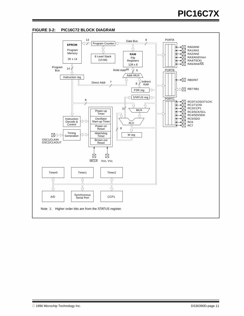
FIGURE 3-2: PIC16C72 BLOCK DIAGRAM
EPROM
ProgramMemory
2K x 14
13 Data Bus 8
14ProgramBus
Instruction reg
Program Counter
8 Level Stack(13-bit)
RAMFile
Registers128 x 8
Direct Addr 7
RAM Addr(1) 9
Addr MUX
IndirectAddr
FSR reg
STATUS reg
MUX
ALU
W reg
Power-upTimer
OscillatorStart-up Timer
Power-onReset
WatchdogTimer
InstructionDecode &
Control
TimingGeneration
OSC1/CLKINOSC2/CLKOUT
MCLR VDD, VSS
Timer0
A/DSynchronous
Serial Port
PORTA
PORTB
PORTC
RB0/INT
RB7:RB1
RC0/T1OSO/T1CKIRC1/T1OSIRC2/CCP1RC3/SCK/SCLRC4/SDI/SDARC5/SDORC6RC7
8
8
Brown-outReset
Note 1: Higher order bits are from the STATUS register.
CCP1
Timer1 Timer2
RA4/T0CKIRA5/AN4/SS
RA3/AN3/VREF
RA2/AN2RA1/AN1RA0/AN0
8
3

PIC16C7X
DS30390D-page 12
1996 Microchip Technology Inc.
FIGURE 3-3: PIC16C73/73A BLOCK DIAGRAM
EPROM
ProgramMemory
4K x 14
13 Data Bus 8
14ProgramBus
Instruction reg
Program Counter
8 Level Stack(13-bit)
RAMFile
Registers192 x 8
Direct Addr 7
RAM Addr(1) 9
Addr MUX
IndirectAddr
FSR reg
STATUS reg
MUX
ALU
W reg
Power-upTimer
OscillatorStart-up Timer
Power-onReset
WatchdogTimer
InstructionDecode &
Control
TimingGeneration
OSC1/CLKINOSC2/CLKOUT
MCLR VDD, VSS
USART
PORTA
PORTB
PORTC
RB0/INT
RB7:RB1
RC0/T1OSO/T1CKIRC1/T1OSI/CCP2RC2/CCP1RC3/SCK/SCLRC4/SDI/SDARC5/SDORC6/TX/CKRC7/RX/DT
8
8
Brown-outReset(2)
Note 1: Higher order bits are from the STATUS register.2: Brown-out Reset is not available on the PIC16C73.
CCP1 CCP2Synchronous
A/DTimer0 Timer1 Timer2
Serial Port
RA4/T0CKIRA5/AN4/SS
RA3/AN3/VREF
RA2/AN2RA1/AN1RA0/AN0
8
3
1996 Microchip Technology Inc. DS30390D-page 13
PIC16C7X
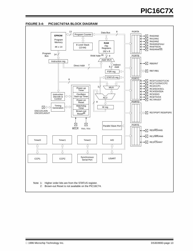
FIGURE 3-4: PIC16C74/74A BLOCK DIAGRAM
EPROM
ProgramMemory
4K x 14
13 Data Bus 8
14ProgramBus
Instruction reg
Program Counter
8 Level Stack(13-bit)
RAMFile
Registers192 x 8
Direct Addr 7
RAM Addr (1) 9
Addr MUX
IndirectAddr
FSR reg
STATUS reg
MUX
ALU
W reg
Power-upTimer
OscillatorStart-up Timer
Power-onReset
WatchdogTimer
InstructionDecode &
Control
TimingGeneration
OSC1/CLKINOSC2/CLKOUT
MCLR VDD, VSS
PORTA
PORTB
PORTC
PORTD
PORTE
RA4/T0CKIRA5/AN4/SS
RB0/INT
RB7:RB1
RC0/T1OSO/T1CKIRC1/T1OSI/CCP2RC2/CCP1RC3/SCK/SCLRC4/SDI/SDARC5/SDORC6/TX/CKRC7/RX/DT
RD7/PSP7:RD0/PSP0
RE0/RD/AN5
RE1/WR/AN6
RE2/CS/AN7
8
8
Brown-outReset(2)
Note 1: Higher order bits are from the STATUS register.2: Brown-out Reset is not available on the PIC16C74.
USARTCCP1 CCP2Synchronous
A/DTimer0 Timer1 Timer2
Serial Port
RA3/AN3/VREF
RA2/AN2RA1/AN1RA0/AN0
Parallel Slave Port
8
3

PIC16C7X
DS30390D-page 14
1996 Microchip Technology Inc.
TABLE 3-1: PIC16C710/711 PINOUT DESCRIPTION
Pin NameDIPPin#
SSOP Pin#
SOICPin#
I/O/PType
BufferType
Description
OSC1/CLKIN 16 18 16 I ST/CMOS
(3)
Oscillator crystal input/external clock source input.
OSC2/CLKOUT 15 17 15 O — Oscillator crystal output. Connects to crystal or resonator in crystal oscillator mode. In RC mode, OSC2 pin outputs CLKOUT which has 1/4 the frequency of OSC1, and denotes the instruction cycle rate.
MCLR/V
PP
4 4 4 I/P ST Master clear (reset) input/programming voltage input. This pin is an active low reset to the device.
PORTA is a bi-directional I/O port.
RA0/AN0 17 19 17 I/O TTL Analog input0
RA1/AN1 18 20 18 I/O TTL Analog input1
RA2/AN2 1 1 1 I/O TTL Analog input2
RA3/AN3/V
REF
2 2 2 I/O TTL Analog input3/V
REF
RA4/T0CKI 3 3 3 I/O ST Can also be selected to be the clock input to the Timer0 module.Output is open drain type.
PORTB is a bi-directional I/O port. PORTB can be software pro-grammed for internal weak pull-up on all inputs.
RB0/INT 6 7 6 I/O TTL/ST
(1)
RB0/INT can also be selected as an external interrupt pin.
RB1 7 8 7 I/O TTL
RB2 8 9 8 I/O TTL
RB3 9 10 9 I/O TTL
RB4 10 11 10 I/O TTL Interrupt on change pin.
RB5 11 12 11 I/O TTL Interrupt on change pin.
RB6 12 13 12 I/O TTL/ST
(2)
Interrupt on change pin. Serial programming clock.
RB7 13 14 13 I/O TTL/ST
(2)
Interrupt on change pin. Serial programming data.
V
SS
5 4, 6 5 P — Ground reference for logic and I/O pins.
V
DD
14 15, 16 14 P — Positive supply for logic and I/O pins.
Legend: I = input O = output I/O = input/output P = power— = Not used TTL = TTL input ST = Schmitt Trigger input
Note 1: This buffer is a Schmitt Trigger input when configured as the external interrupt.2: This buffer is a Schmitt Trigger input when used in serial programming mode.3: This buffer is a Schmitt Trigger input when configured in RC oscillator mode and a CMOS input otherwise.

1996 Microchip Technology Inc. DS30390D-page 15
PIC16C7X
TABLE 3-2: PIC16C71 PINOUT DESCRIPTION
Pin NameDIPPin#
SOICPin#
I/O/PType
BufferType
Description
OSC1/CLKIN 16 16 I ST/CMOS
(3)
Oscillator crystal input/external clock source input.
OSC2/CLKOUT 15 15 O — Oscillator crystal output. Connects to crystal or resonator in crystal oscillator mode. In RC mode, OSC2 pin outputs CLKOUT which has 1/4 the frequency of OSC1, and denotes the instruction cycle rate.
MCLR/V
PP
4 4 I/P ST Master clear (reset) input/programming voltage input. This pin is an active low reset to the device.
PORTA is a bi-directional I/O port.
RA0/AN0 17 17 I/O TTL Analog input0
RA1/AN1 18 18 I/O TTL Analog input1
RA2/AN2 1 1 I/O TTL Analog input2
RA3/AN3/V
REF
2 2 I/O TTL Analog input3/V
REF
RA4/T0CKI 3 3 I/O ST Can also be selected to be the clock input to the Timer0 module.Output is open drain type.
PORTB is a bi-directional I/O port. PORTB can be software pro-grammed for internal weak pull-up on all inputs.
RB0/INT 6 6 I/O TTL/ST
(1)
RB0/INT can also be selected as an external interrupt pin.
RB1 7 7 I/O TTL
RB2 8 8 I/O TTL
RB3 9 9 I/O TTL
RB4 10 10 I/O TTL Interrupt on change pin.
RB5 11 11 I/O TTL Interrupt on change pin.
RB6 12 12 I/O TTL/ST
(2)
Interrupt on change pin. Serial programming clock.
RB7 13 13 I/O TTL/ST
(2)
Interrupt on change pin. Serial programming data.
V
SS
5 5 P — Ground reference for logic and I/O pins.
V
DD
14 14 P — Positive supply for logic and I/O pins.
Legend: I = input O = output I/O = input/output P = power— = Not used TTL = TTL input ST = Schmitt Trigger input
Note 1: This buffer is a Schmitt Trigger input when configured as the external interrupt.2: This buffer is a Schmitt Trigger input when used in serial programming mode.3: This buffer is a Schmitt Trigger input when configured in RC oscillator mode and a CMOS input otherwise.
PIC16C7X
DS30390D-page 16
1996 Microchip Technology Inc.
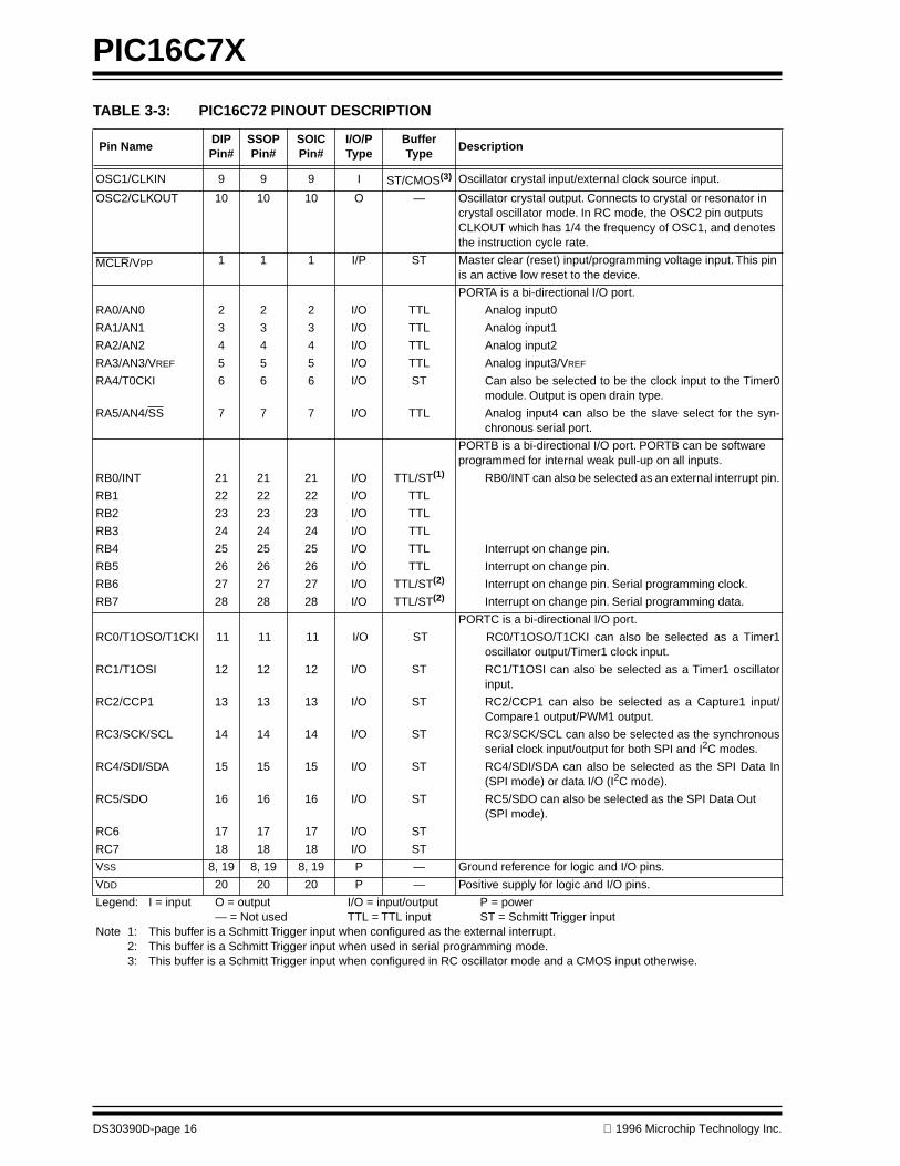
TABLE 3-3: PIC16C72 PINOUT DESCRIPTION
Pin NameDIPPin#
SSOP Pin#
SOICPin#
I/O/PType
BufferType
Description
OSC1/CLKIN 9 9 9 I ST/CMOS
(3)
Oscillator crystal input/external clock source input.
OSC2/CLKOUT 10 10 10 O — Oscillator crystal output. Connects to crystal or resonator in crystal oscillator mode. In RC mode, the OSC2 pin outputs CLKOUT which has 1/4 the frequency of OSC1, and denotes the instruction cycle rate.
MCLR/V
PP
1 1 1 I/P ST Master clear (reset) input/programming voltage input. This pin is an active low reset to the device.
PORTA is a bi-directional I/O port.
RA0/AN0 2 2 2 I/O TTL Analog input0
RA1/AN1 3 3 3 I/O TTL Analog input1
RA2/AN2 4 4 4 I/O TTL Analog input2
RA3/AN3/V
REF
5 5 5 I/O TTL Analog input3/V
REF
RA4/T0CKI 6 6 6 I/O ST Can also be selected to be the clock input to the Timer0module. Output is open drain type.
RA5/AN4/SS 7 7 7 I/O TTL Analog input4 can also be the slave select for the syn-chronous serial port.
PORTB is a bi-directional I/O port. PORTB can be software programmed for internal weak pull-up on all inputs.
RB0/INT 21 21 21 I/O TTL/ST
(1)
RB0/INT can also be selected as an external interrupt pin.
RB1 22 22 22 I/O TTL
RB2 23 23 23 I/O TTL
RB3 24 24 24 I/O TTL
RB4 25 25 25 I/O TTL Interrupt on change pin.
RB5 26 26 26 I/O TTL Interrupt on change pin.
RB6 27 27 27 I/O TTL/ST
(2)
Interrupt on change pin. Serial programming clock.
RB7 28 28 28 I/O TTL/ST
(2)
Interrupt on change pin. Serial programming data.
PORTC is a bi-directional I/O port.
RC0/T1OSO/T1CKI 11 11 11 I/O ST RC0/T1OSO/T1CKI can also be selected as a Timer1oscillator output/Timer1 clock input.
RC1/T1OSI 12 12 12 I/O ST RC1/T1OSI can also be selected as a Timer1 oscillatorinput.
RC2/CCP1 13 13 13 I/O ST RC2/CCP1 can also be selected as a Capture1 input/Compare1 output/PWM1 output.
RC3/SCK/SCL 14 14 14 I/O ST RC3/SCK/SCL can also be selected as the synchronousserial clock input/output for both SPI and I
2
C modes.
RC4/SDI/SDA 15 15 15 I/O ST RC4/SDI/SDA can also be selected as the SPI Data In(SPI mode) or data I/O (I
2
C mode).
RC5/SDO 16 16 16 I/O ST RC5/SDO can also be selected as the SPI Data Out(SPI mode).
RC6 17 17 17 I/O ST
RC7 18 18 18 I/O ST
V
SS
8, 19 8, 19 8, 19 P — Ground reference for logic and I/O pins.
V
DD
20 20 20 P — Positive supply for logic and I/O pins.
Legend: I = input O = output I/O = input/output P = power— = Not used TTL = TTL input ST = Schmitt Trigger input
Note 1: This buffer is a Schmitt Trigger input when configured as the external interrupt.2: This buffer is a Schmitt Trigger input when used in serial programming mode.3: This buffer is a Schmitt Trigger input when configured in RC oscillator mode and a CMOS input otherwise.

1996 Microchip Technology Inc. DS30390D-page 17
PIC16C7X
TABLE 3-4: PIC16C73/73A PINOUT DESCRIPTION
Pin NameDIPPin#
SOICPin#
I/O/PType
BufferType
Description
OSC1/CLKIN 9 9 I ST/CMOS
(3)
Oscillator crystal input/external clock source input.
OSC2/CLKOUT 10 10 O — Oscillator crystal output. Connects to crystal or resonator in crystal oscillator mode. In RC mode, the OSC2 pin outputs CLKOUT which has 1/4 the frequency of OSC1, and denotes the instruction cycle rate.
MCLR/V
PP
1 1 I/P ST Master clear (reset) input/programming voltage input. This pin is an active low reset to the device.
PORTA is a bi-directional I/O port.
RA0/AN0 2 2 I/O TTL Analog input0
RA1/AN1 3 3 I/O TTL Analog input1
RA2/AN2 4 4 I/O TTL Analog input2
RA3/AN3/V
REF
5 5 I/O TTL Analog input3/V
REF
RA4/T0CKI 6 6 I/O ST Can also be selected to be the clock input to the Timer0module. Output is open drain type.
RA5/AN4/SS 7 7 I/O TTL Analog input4 can also be the slave select for the syn-chronous serial port.
PORTB is a bi-directional I/O port. PORTB can be software programmed for internal weak pull-up on all inputs.
RB0/INT 21 21 I/O TTL/ST
(1)
RB0/INT can also be selected as an external interrupt pin.
RB1 22 22 I/O TTL
RB2 23 23 I/O TTL
RB3 24 24 I/O TTL
RB4 25 25 I/O TTL Interrupt on change pin.
RB5 26 26 I/O TTL Interrupt on change pin.
RB6 27 27 I/O TTL/ST
(2)
Interrupt on change pin. Serial programming clock.
RB7 28 28 I/O TTL/ST
(2)
Interrupt on change pin. Serial programming data.
PORTC is a bi-directional I/O port.
RC0/T1OSO/T1CKI 11 11 I/O ST RC0/T1OSO/T1CKI can also be selected as a Timer1oscillator output/Timer1 clock input.
RC1/T1OSI/CCP2 12 12 I/O ST RC1/T1OSI/CCP2 can also be selected as a Timer1oscillator input or Capture2 input/Compare2 output/PWM2 output.
RC2/CCP1 13 13 I/O ST RC2/CCP1 can also be selected as a Capture1 input/Compare1 output/PWM1 output.
RC3/SCK/SCL 14 14 I/O ST RC3/SCK/SCL can also be selected as the synchronousserial clock input/output for both SPI and I
2
C modes.
RC4/SDI/SDA 15 15 I/O ST RC4/SDI/SDA can also be selected as the SPI Data In(SPI mode) or data I/O (I
2
C mode).
RC5/SDO 16 16 I/O ST RC5/SDO can also be selected as the SPI Data Out(SPI mode).
RC6/TX/CK 17 17 I/O ST RC6/TX/CK can also be selected as AsynchronousTransmit or USART Synchronous Clock.
RC7/RX/DT 18 18 I/O ST RC7/RX/DT can also be selected as the AsynchronousReceive or USART Synchronous Data.
V
SS
8, 19 8, 19 P — Ground reference for logic and I/O pins.
V
DD
20 20 P — Positive supply for logic and I/O pins.
Legend: I = input O = output I/O = input/output P = power— = Not used TTL = TTL input ST = Schmitt Trigger input
Note 1: This buffer is a Schmitt Trigger input when configured as the external interrupt.2: This buffer is a Schmitt Trigger input when used in serial programming mode.3: This buffer is a Schmitt Trigger input when configured in RC oscillator mode and a CMOS input otherwise.

PIC16C7X
DS30390D-page 18
1996 Microchip Technology Inc.
TABLE 3-5: PIC16C74/74A PINOUT DESCRIPTION
Pin NameDIPPin#
PLCCPin#
QFPPin#
I/O/PType
BufferType
Description
OSC1/CLKIN 13 14 30 I ST/CMOS
(4)
Oscillator crystal input/external clock source input.
OSC2/CLKOUT 14 15 31 O — Oscillator crystal output. Connects to crystal or resonator in crystal oscillator mode. In RC mode, OSC2 pin outputs CLKOUT which has 1/4 the frequency of OSC1, and denotes the instruction cycle rate.
MCLR/V
PP
1 2 18 I/P ST Master clear (reset) input/programming voltage input. This pin is an active low reset to the device.
PORTA is a bi-directional I/O port.
RA0/AN0 2 3 19 I/O TTL Analog input0
RA1/AN1 3 4 20 I/O TTL Analog input1
RA2/AN2 4 5 21 I/O TTL Analog input2
RA3/AN3/V
REF
5 6 22 I/O TTL Analog input3/V
REF
RA4/T0CKI 6 7 23 I/O ST Can also be selected to be the clock input to theTimer0 timer/counter. Output is open drain type.
RA5/AN4/SS 7 8 24 I/O TTL Analog input4 can also be the slave select for the syn-chronous serial port.
PORTB is a bi-directional I/O port. PORTB can be software programmed for internal weak pull-up on all inputs.
RB0/INT 33 36 8 I/O TTL/ST
(1)
RB0/INT can also be selected as an external interruptpin.
RB1 34 37 9 I/O TTL
RB2 35 38 10 I/O TTL
RB3 36 39 11 I/O TTL
RB4 37 41 14 I/O TTL Interrupt on change pin.
RB5 38 42 15 I/O TTL Interrupt on change pin.
RB6 39 43 16 I/O TTL/ST
(2)
Interrupt on change pin. Serial programming clock.
RB7 40 44 17 I/O TTL/ST
(2)
Interrupt on change pin. Serial programming data.
Legend: I = input O = output I/O = input/output P = power— = Not used TTL = TTL input ST = Schmitt Trigger input
Note 1: This buffer is a Schmitt Trigger input when configured as an external interrupt.2: This buffer is a Schmitt Trigger input when used in serial programming mode.3: This buffer is a Schmitt Trigger input when configured as general purpose I/O and a TTL input when used in the Parallel
Slave Port mode (for interfacing to a microprocessor bus).4: This buffer is a Schmitt Trigger input when configured in RC oscillator mode and a CMOS input otherwise.

1996 Microchip Technology Inc. DS30390D-page 19
PIC16C7X
PORTC is a bi-directional I/O port.
RC0/T1OSO/T1CKI 15 16 32 I/O ST RC0/T1OSO/T1CKI can also be selected as a Timer1oscillator output or a Timer1 clock input.
RC1/T1OSI/CCP2 16 18 35 I/O ST RC1/T1OSI/CCP2 can also be selected as a Timer1oscillator input or Capture2 input/Compare2 output/PWM2 output.
RC2/CCP1 17 19 36 I/O ST RC2/CCP1 can also be selected as a Capture1 input/Compare1 output/PWM1 output.
RC3/SCK/SCL 18 20 37 I/O ST RC3/SCK/SCL can also be selected as the synchro-nous serial clock input/output for both SPI and I
2
Cmodes.
RC4/SDI/SDA 23 25 42 I/O ST RC4/SDI/SDA can also be selected as the SPI Data In(SPI mode) or data I/O (I
2
C mode).
RC5/SDO 24 26 43 I/O ST RC5/SDO can also be selected as the SPI Data Out(SPI mode).
RC6/TX/CK 25 27 44 I/O ST RC6/TX/CK can also be selected as AsynchronousTransmit or USART Synchronous Clock.
RC7/RX/DT 26 29 1 I/O ST RC7/RX/DT can also be selected as the Asynchro-nous Receive or USART Synchronous Data.
PORTD is a bi-directional I/O port or parallel slave port when interfacing to a microprocessor bus.
RD0/PSP0 19 21 38 I/O ST/TTL
(3)
RD1/PSP1 20 22 39 I/O ST/TTL
(3)
RD2/PSP2 21 23 40 I/O ST/TTL
(3)
RD3/PSP3 22 24 41 I/O ST/TTL
(3)
RD4/PSP4 27 30 2 I/O ST/TTL
(3)
RD5/PSP5 28 31 3 I/O ST/TTL
(3)
RD6/PSP6 29 32 4 I/O ST/TTL
(3)
RD7/PSP7 30 33 5 I/O ST/TTL
(3)
PORTE is a bi-directional I/O port.
RE0/RD/AN5 8 9 25 I/O ST/TTL
(3)
RE0/RD/AN5 read control for parallel slave port, oranalog input5.
RE1/WR/AN6 9 10 26 I/O ST/TTL
(3)
RE1/WR/AN6 write control for parallel slave port, oranalog input6.
RE2/CS/AN7 10 11 27 I/O ST/TTL
(3)
RE2/CS/AN7 select control for parallel slave port, oranalog input7.
V
SS
12,31 13,34 6,29 P — Ground reference for logic and I/O pins.
V
DD
11,32 12,35 7,28 P — Positive supply for logic and I/O pins.
NC — 1,17,28,40
12,13,33,34
— These pins are not internally connected. These pins should be left unconnected.
TABLE 3-5: PIC16C74/74A PINOUT DESCRIPTION (Cont.’d)
Pin NameDIPPin#
PLCCPin#
QFPPin#
I/O/PType
BufferType
Description
Legend: I = input O = output I/O = input/output P = power— = Not used TTL = TTL input ST = Schmitt Trigger input
Note 1: This buffer is a Schmitt Trigger input when configured as an external interrupt.2: This buffer is a Schmitt Trigger input when used in serial programming mode.3: This buffer is a Schmitt Trigger input when configured as general purpose I/O and a TTL input when used in the Parallel
Slave Port mode (for interfacing to a microprocessor bus).4: This buffer is a Schmitt Trigger input when configured in RC oscillator mode and a CMOS input otherwise.

PIC16C7X
DS30390D-page 20
1996 Microchip Technology Inc.
3.1 Clocking Scheme/Instruction Cycle
The clock input (from OSC1) is internally divided byfour to generate four non-overlapping quadratureclocks namely Q1, Q2, Q3 and Q4. Internally, the pro-gram counter (PC) is incremented every Q1, theinstruction is fetched from the program memory andlatched into the instruction register in Q4. The instruc-tion is decoded and executed during the following Q1through Q4. The clocks and instruction execution flowis shown in Figure 3-5.
3.2 Instruction Flow/Pipelining
An “Instruction Cycle” consists of four Q cycles (Q1,Q2, Q3 and Q4). The instruction fetch and execute arepipelined such that fetch takes one instruction cyclewhile decode and execute takes another instructioncycle. However, due to the pipelining, each instructioneffectively executes in one cycle. If an instructioncauses the program counter to change (e.g.
GOTO
)then two cycles are required to complete the instruction(Example 3-1).
A fetch cycle begins with the program counter (PC)incrementing in Q1.
In the execution cycle, the fetched instruction is latchedinto the “Instruction Register" (IR) in cycle Q1. Thisinstruction is then decoded and executed during theQ2, Q3, and Q4 cycles. Data memory is read during Q2(operand read) and written during Q4 (destinationwrite).
FIGURE 3-5: CLOCK/INSTRUCTION CYCLE
EXAMPLE 3-1: INSTRUCTION PIPELINE FLOW
Q1 Q2 Q3 Q4 Q1 Q2 Q3 Q4 Q1 Q2 Q3 Q4
OSC1
Q1
Q2
Q3
Q4
PC
OSC2/CLKOUT(RC mode)
PC PC+1 PC+2
Fetch INST (PC)Execute INST (PC-1) Fetch INST (PC+1)
Execute INST (PC) Fetch INST (PC+2)Execute INST (PC+1)
Internalphaseclock
All instructions are single cycle, except for any program branches. These take two cycles since the fetchinstruction is “flushed” from the pipeline while the new instruction is being fetched and then executed.
Tcy0 Tcy1 Tcy2 Tcy3 Tcy4 Tcy5
1. MOVLW 55h Fetch 1 Execute 1
2. MOVWF PORTB Fetch 2 Execute 2
3. CALL SUB_1 Fetch 3 Execute 3
4. BSF PORTA, BIT3 (Forced NOP) Fetch 4 Flush
5. Instruction @ address SUB_1 Fetch SUB_1 Execute SUB_1

1996 Microchip Technology Inc. DS30390D-page 21
PIC16C7X
4.0 MEMORY ORGANIZATION
4.1 Program Memory Organization
The PIC16C7X family has a 13-bit program countercapable of addressing an 8K x 14 program memoryspace.
For the PIC16C710, only the first 512 x 14 (0000h-01FFh) is physically implemented. For thePIC16C71/711 only the first 1K x 14 (0000h-03FFh) isimplemented. For the PIC16C72, only the first 2K x 14(0000h-07FFh) is implemented. For the PIC16C73,PIC16C73A, PIC16C74, and PIC16C74A, only the first4K x 14 (0000h-0FFFh) is physically implemented.Accessing a location above the physically implementedaddress will cause a wraparound. The reset vector is at0000h and the interrupt vector is at 0004h.
FIGURE 4-1: PIC16C710 PROGRAM MEMORY MAP AND STACK
Applicable Devices
710 71 711 72 73 73A 74 74A
PC<12:0>
13
0000h
0004h0005h
01FFh
0200h
1FFFh
Stack Level 1
Stack Level 8
Reset Vector
Interrupt Vector
On-chip ProgramMemory
CALL, RETURNRETFIE, RETLW
FIGURE 4-2: PIC16C71/711 PROGRAM MEMORY MAP AND STACK
PC<12:0>
13
0000h
0004h0005h
03FFh
0400h
1FFFh
Stack Level 1
Stack Level 8
Reset Vector
Interrupt Vector
On-chip ProgramMemory
CALL, RETURNRETFIE, RETLW
This document was created with FrameMaker 4 0 4
PIC16C7X
DS30390D-page 22
1996 Microchip Technology Inc.
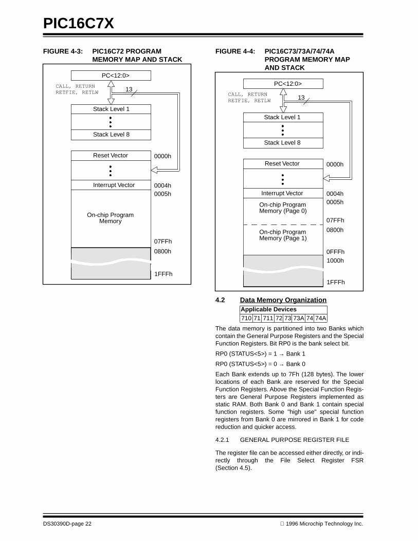
FIGURE 4-3: PIC16C72 PROGRAM MEMORY MAP AND STACK
PC<12:0>
13
0000h
0004h0005h
07FFh
1FFFh
Stack Level 1
Stack Level 8
Reset Vector
Interrupt Vector
On-chip ProgramMemory
CALL, RETURNRETFIE, RETLW
0800h
FIGURE 4-4: PIC16C73/73A/74/74A PROGRAM MEMORY MAP AND STACK
4.2 Data Memory Organization
The data memory is partitioned into two Banks whichcontain the General Purpose Registers and the SpecialFunction Registers. Bit RP0 is the bank select bit.
RP0 (STATUS<5>) = 1
→
Bank 1
RP0 (STATUS<5>) = 0
→
Bank 0
Each Bank extends up to 7Fh (128 bytes). The lowerlocations of each Bank are reserved for the SpecialFunction Registers. Above the Special Function Regis-ters are General Purpose Registers implemented asstatic RAM. Both Bank 0 and Bank 1 contain specialfunction registers. Some "high use" special functionregisters from Bank 0 are mirrored in Bank 1 for codereduction and quicker access.
4.2.1 GENERAL PURPOSE REGISTER FILE
The register file can be accessed either directly, or indi-rectly through the File Select Register FSR(Section 4.5).
Applicable Devices
710 71 711 72 73 73A 74 74A
PC<12:0>
13
0000h
0004h0005h
07FFh
0800h
0FFFh1000h
1FFFh
Stack Level 1
Stack Level 8
Reset Vector
Interrupt Vector
On-chip Program
On-chip ProgramMemory (Page 1)
Memory (Page 0)
CALL, RETURNRETFIE, RETLW
1996 Microchip Technology Inc. DS30390D-page 23
PIC16C7X
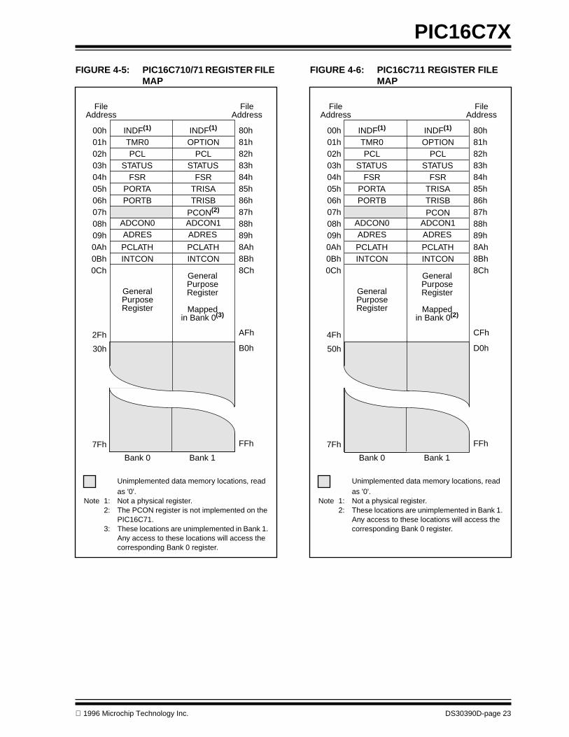
FIGURE 4-5: PIC16C710/71 REGISTER FILE MAP
INDF(1)
TMR0PCL
STATUSFSR
PORTAPORTB
PCLATHINTCON
ADRESADCON0
INDF(1)
OPTIONPCL
STATUSFSR
TRISATRISB
PCLATHINTCON
ADCON1
00h01h02h03h04h05h06h07h08h09h0Ah0Bh0Ch
80h81h82h83h84h85h86h87h88h89h8Ah8Bh8Ch
GeneralPurposeRegister
7Fh FFh
Bank 0 Bank 1
FileAddress
ADRES
2Fh
30h
AFh
B0h
Unimplemented data memory locations, read as '0'.
Note 1: Not a physical register.2: The PCON register is not implemented on the
PIC16C71.3: These locations are unimplemented in Bank 1.
Any access to these locations will access the corresponding Bank 0 register.
FileAddress
GeneralPurposeRegister
Mappedin Bank 0(3)
PCON(2)
FIGURE 4-6: PIC16C711 REGISTER FILE MAP
INDF(1)
TMR0PCL
STATUSFSR
PORTAPORTB
PCLATHINTCON
ADRESADCON0
INDF(1)
OPTIONPCL
STATUSFSR
TRISATRISB
PCLATHINTCON
ADCON1
00h01h02h03h04h05h06h07h08h09h0Ah0Bh0Ch
80h81h82h83h84h85h86h87h88h89h8Ah8Bh8Ch
GeneralPurposeRegister
7Fh FFh
Bank 0 Bank 1
FileAddress
ADRES
4Fh
50h
CFh
D0h
Unimplemented data memory locations, read as '0'.
Note 1: Not a physical register.2: These locations are unimplemented in Bank 1.
Any access to these locations will access the corresponding Bank 0 register.
FileAddress
GeneralPurposeRegister
Mappedin Bank 0(2)
PCON

PIC16C7X
DS30390D-page 24
1996 Microchip Technology Inc.
FIGURE 4-7: PIC16C72 REGISTER FILE MAP
INDF(1)
TMR0PCL
STATUSFSR
PORTAPORTBPORTC
PCLATHINTCON
PIR1
TMR1LTMR1HT1CONTMR2
T2CONSSPBUFSSPCONCCPR1LCCPR1H
CCP1CON
ADRESADCON0
INDF(1)
OPTIONPCL
STATUSFSR
TRISATRISBTRISC
PCLATHINTCON
PIE1
PCON
PR2SSPADDSSPSTAT
ADCON1
00h01h02h03h04h05h06h07h08h09h0Ah0Bh0Ch0Dh0Eh0Fh10h11h12h13h14h15h16h17h18h19h1Ah1Bh1Ch1Dh1Eh1Fh
80h81h82h83h84h85h86h87h88h89h8Ah8Bh8Ch8Dh8Eh8Fh90h91h92h93h94h95h96h97h98h99h9Ah9Bh9Ch9Dh9Eh9Fh
20h A0hGeneralPurposeRegister
GeneralPurposeRegister
7Fh FFhBank 0 Bank 1
FileAddress
BFh
C0h
Unimplemented data memory locations, read as '0'.
Note 1: Not a physical register.
FileAddress
FIGURE 4-8: PIC16C73/73A/74/74A REGISTER FILE MAP
INDF(1)
TMR0PCL
STATUSFSR
PORTAPORTBPORTC
PORTD(2)
PORTE(2)
PCLATHINTCON
PIR1PIR2
TMR1LTMR1HT1CONTMR2
T2CONSSPBUFSSPCONCCPR1LCCPR1H
CCP1CONRCSTATXREGRCREGCCPR2LCCPR2H
CCP2CONADRES
ADCON0
INDF(1)
OPTIONPCL
STATUSFSR
TRISATRISBTRISC
TRISD(2)
TRISE(2)
PCLATHINTCON
PIE1PIE2
PCON
PR2SSPADDSSPSTAT
TXSTASPBRG
ADCON1
00h01h02h03h04h05h06h07h08h09h0Ah0Bh0Ch0Dh0Eh0Fh10h11h12h13h14h15h16h17h18h19h1Ah1Bh1Ch1Dh1Eh1Fh
80h81h82h83h84h85h86h87h88h89h8Ah8Bh8Ch8Dh8Eh8Fh90h91h92h93h94h95h96h97h98h99h9Ah9Bh9Ch9Dh9Eh9Fh
20h A0h
GeneralPurposeRegister
GeneralPurposeRegister
7Fh FFh
Bank 0 Bank 1
FileAddress
FileAddress
Unimplemented data memory locations, read as '0'.
Note 1: Not a physical register.2: These registers are not physically imple-
mented on the PIC16C73/73A, read as '0'.

1996 Microchip Technology Inc. DS30390D-page 25
PIC16C7X
4.2.2 SPECIAL FUNCTION REGISTERS
The Special Function Registers are registers used bythe CPU and Peripheral Modules for controlling thedesired operation of the device. These registers areimplemented as static RAM.
The special function registers can be classified into twosets (core and peripheral). Those registers associatedwith the “core” functions are described in this section,and those related to the operation of the peripheral fea-tures are described in the section of that peripheral fea-ture.
TABLE 4-1: PIC16C710/71/711 SPECIAL FUNCTION REGISTER SUMMARY
Address Name Bit 7 Bit 6 Bit 5 Bit 4 Bit 3 Bit 2 Bit 1 Bit 0Value on:
POR,BOR
Value on allother resets
(1)
Bank 0
00h
(3)
INDF Addressing this location uses contents of FSR to address data memory (not a physical register)
0000 0000 0000 0000
01h TMR0 Timer0 module’s register
xxxx xxxx uuuu uuuu
02h
(3)
PCL Program Counter's (PC) Least Significant Byte
0000 0000 0000 0000
03h
(3)
STATUS IRP
(5)
RP1
(5)
RP0 TO PD Z DC C
0001 1xxx 000q quuu
04h
(3)
FSR Indirect data memory address pointer
xxxx xxxx uuuu uuuu
05h PORTA — — — PORTA Data Latch when written: PORTA pins when read
---x 0000 ---u 0000
06h PORTB PORTB Data Latch when written: PORTB pins when read
xxxx xxxx uuuu uuuu
07h — Unimplemented — —
08h ADCON0 ADCS1 ADCS0
(6)
CHS1 CHS0 GO/DONE ADIF ADON
00-0 0000 00-0 0000
09h
(3)
ADRES A/D Result Register
xxxx xxxx uuuu uuuu
0Ah
(2,3)
PCLATH — — — Write Buffer for the upper 5 bits of the Program Counter
---0 0000 ---0 0000
0Bh
(3)
INTCON GIE ADIE T0IE INTE RBIE T0IF INTF RBIF
0000 000x 0000 000u
Bank 1
80h
(3)
INDF Addressing this location uses contents of FSR to address data memory (not a physical register)
0000 0000 0000 0000
81h OPTION RBPU INTEDG T0CS T0SE PSA PS2 PS1 PS0
1111 1111 1111 1111
82h
(3)
PCL Program Counter's (PC) Least Significant Byte
0000 0000 0000 0000
83h
(3)
STATUS IRP
(5)
RP1
(5)
RP0 TO PD Z DC C
0001 1xxx 000q quuu
84h
(3)
FSR Indirect data memory address pointer
xxxx xxxx uuuu uuuu
85h TRISA — — — PORTA Data Direction Register
---1 1111 ---1 1111
86h TRISB PORTB Data Direction Control Register
1111 1111 1111 1111
87h
(4)
PCON — — — — — — POR BOR
---- --qq ---- --uu
88h ADCON1 — — — — — — PCFG1 PCFG0
---- --00 ---- --00
89h
(3)
ADRES A/D Result Register
xxxx xxxx uuuu uuuu
8Ah
(2,3)
PCLATH — — — Write Buffer for the upper 5 bits of the Program Counter
---0 0000 ---0 0000
8Bh
(3)
INTCON GIE ADIE T0IE INTE RBIE T0IF INTF RBIF
0000 000x 0000 000u
Legend:
x
= unknown,
u
= unchanged,
q
= value depends on condition,
-
= unimplemented read as '0'. Shaded locations are unimplemented, read as ‘0’.
Note 1: Other (non power-up) resets include external reset through MCLR and Watchdog Timer Reset.2: The upper byte of the program counter is not directly accessible. PCLATH is a holding register for the PC<12:8> whose
contents are transferred to the upper byte of the program counter.3: These registers can be addressed from either bank.4: The PCON register is not physically implemented in the PIC16C71, read as ’0’.5: The IRP and RP1 bits are reserved on the PIC16C7X, always maintain these bits clear.6: Bit5 of ADCON0 is a General Purpose R/W bit for the PIC16C71 only. For the PIC16C710/711, this bit is unimplemented,
read as '0'.

PIC16C7X
DS30390D-page 26
1996 Microchip Technology Inc.
TABLE 4-2: PIC16C72 SPECIAL FUNCTION REGISTER SUMMARY
Address Name Bit 7 Bit 6 Bit 5 Bit 4 Bit 3 Bit 2 Bit 1 Bit 0Value on:
POR,BOR
Value on allother resets
(3)
Bank 0
00h
(1)
INDF Addressing this location uses contents of FSR to address data memory (not a physical register)
0000 0000 0000 0000
01h TMR0 Timer0 module’s register
xxxx xxxx uuuu uuuu
02h
(1)
PCL Program Counter's (PC) Least Significant Byte
0000 0000 0000 0000
03h
(1)
STATUS IRP
(4)
RP1
(4)
RP0 TO PD Z DC C
0001 1xxx 000q quuu
04h
(1)
FSR Indirect data memory address pointer
xxxx xxxx uuuu uuuu
05h PORTA — — PORTA Data Latch when written: PORTA pins when read
--0x 0000 --0u 0000
06h PORTB PORTB Data Latch when written: PORTB pins when read
xxxx xxxx uuuu uuuu
07h PORTC PORTC Data Latch when written: PORTC pins when read
xxxx xxxx uuuu uuuu
08h — Unimplemented — —
09h — Unimplemented — —
0Ah
(1,2)
PCLATH — — — Write Buffer for the upper 5 bits of the Program Counter
---0 0000 ---0 0000
0Bh
(1)
INTCON GIE PEIE T0IE INTE RBIE T0IF INTF RBIF
0000 000x 0000 000u
0Ch PIR1 — ADIF — — SSPIF CCP1IF TMR2IF TMR1IF -0-- 0000 -0-- 0000
0Dh — Unimplemented — —
0Eh TMR1L Holding register for the Least Significant Byte of the 16-bit TMR1 register xxxx xxxx uuuu uuuu
0Fh TMR1H Holding register for the Most Significant Byte of the 16-bit TMR1 register xxxx xxxx uuuu uuuu
10h T1CON — — T1CKPS1 T1CKPS0 T1OSCEN T1SYNC TMR1CS TMR1ON --00 0000 --uu uuuu
11h TMR2 Timer2 module’s register 0000 0000 0000 0000
12h T2CON — TOUTPS3 TOUTPS2 TOUTPS1 TOUTPS0 TMR2ON T2CKPS1 T2CKPS0 -000 0000 -000 0000
13h SSPBUF Synchronous Serial Port Receive Buffer/Transmit Register xxxx xxxx uuuu uuuu
14h SSPCON WCOL SSPOV SSPEN CKP SSPM3 SSPM2 SSPM1 SSPM0 0000 0000 0000 0000
15h CCPR1L Capture/Compare/PWM Register (LSB) xxxx xxxx uuuu uuuu
16h CCPR1H Capture/Compare/PWM Register (MSB) xxxx xxxx uuuu uuuu
17h CCP1CON — — CCP1X CCP1Y CCP1M3 CCP1M2 CCP1M1 CCP1M0 --00 0000 --00 0000
18h — Unimplemented — —
19h — Unimplemented — —
1Ah — Unimplemented — —
1Bh — Unimplemented — —
1Ch — Unimplemented — —
1Dh — Unimplemented — —
1Eh ADRES A/D Result Register xxxx xxxx uuuu uuuu
1Fh ADCON0 ADCS1 ADCS0 CHS2 CHS1 CHS0 GO/DONE — ADON 0000 00-0 0000 00-0
Legend: x = unknown, u = unchanged, q = value depends on condition, - = unimplemented read as '0'. Shaded locations are unimplemented, read as ‘0’.
Note 1: These registers can be addressed from either bank.2: The upper byte of the program counter is not directly accessible. PCLATH is a holding register for the PC<12:8> whose
contents are transferred to the upper byte of the program counter.3: Other (non power-up) resets include external reset through MCLR and Watchdog Timer Reset.4: The IRP and RP1 bits are reserved on the PIC16C7X, always maintain these bits clear.
1996 Microchip Technology Inc. DS30390D-page 27
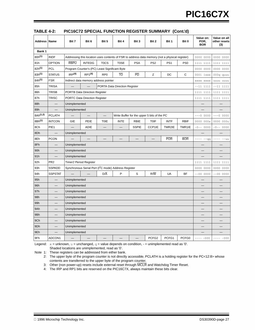
PIC16C7X
Bank 1
80h(1) INDF Addressing this location uses contents of FSR to address data memory (not a physical register) 0000 0000 0000 0000
81h OPTION RBPU INTEDG T0CS T0SE PSA PS2 PS1 PS0 1111 1111 1111 1111
82h(1) PCL Program Counter's (PC) Least Significant Byte 0000 0000 0000 0000
83h(1) STATUS IRP(4) RP1(4) RP0 TO PD Z DC C 0001 1xxx 000q quuu
84h(1) FSR Indirect data memory address pointer xxxx xxxx uuuu uuuu
85h TRISA — — PORTA Data Direction Register --11 1111 --11 1111
86h TRISB PORTB Data Direction Register 1111 1111 1111 1111
87h TRISC PORTC Data Direction Register 1111 1111 1111 1111
88h — Unimplemented — —
89h — Unimplemented — —
8Ah(1,2) PCLATH — — — Write Buffer for the upper 5 bits of the PC ---0 0000 ---0 0000
8Bh(1) INTCON GIE PEIE T0IE INTE RBIE T0IF INTF RBIF 0000 000x 0000 000u
8Ch PIE1 — ADIE — — SSPIE CCP1IE TMR2IE TMR1IE -0-- 0000 -0-- 0000
8Dh — Unimplemented — —
8Eh PCON — — — — — — POR BOR ---- --qq ---- --uu
8Fh — Unimplemented — —
90h — Unimplemented — —
91h — Unimplemented — —
92h PR2 Timer2 Period Register 1111 1111 1111 1111
93h SSPADD Synchronous Serial Port (I2C mode) Address Register 0000 0000 0000 0000
94h SSPSTAT — — D/A P S R/W UA BF --00 0000 --00 0000
95h — Unimplemented — —
96h — Unimplemented — —
97h — Unimplemented — —
98h — Unimplemented — —
99h — Unimplemented — —
9Ah — Unimplemented — —
9Bh — Unimplemented — —
9Ch — Unimplemented — —
9Dh — Unimplemented — —
9Eh — Unimplemented — —
9Fh ADCON1 — — — — — PCFG2 PCFG1 PCFG0 ---- -000 ---- -000
TABLE 4-2: PIC16C72 SPECIAL FUNCTION REGISTER SUMMARY (Cont.’d)
Address Name Bit 7 Bit 6 Bit 5 Bit 4 Bit 3 Bit 2 Bit 1 Bit 0Value on:
POR,BOR
Value on allother resets
(3)
Legend: x = unknown, u = unchanged, q = value depends on condition, - = unimplemented read as '0'. Shaded locations are unimplemented, read as ‘0’.
Note 1: These registers can be addressed from either bank.2: The upper byte of the program counter is not directly accessible. PCLATH is a holding register for the PC<12:8> whose
contents are transferred to the upper byte of the program counter.3: Other (non power-up) resets include external reset through MCLR and Watchdog Timer Reset.4: The IRP and RP1 bits are reserved on the PIC16C7X, always maintain these bits clear.

PIC16C7X
DS30390D-page 28 1996 Microchip Technology Inc.
TABLE 4-3: PIC16C73/73A/74/74A SPECIAL FUNCTION REGISTER SUMMARY
Address Name Bit 7 Bit 6 Bit 5 Bit 4 Bit 3 Bit 2 Bit 1 Bit 0Value on:
POR,BOR
Value on allother resets
(2)
Bank 0
00h(4) INDF Addressing this location uses contents of FSR to address data memory (not a physical register) 0000 0000 0000 0000
01h TMR0 Timer0 module’s register xxxx xxxx uuuu uuuu
02h(4) PCL Program Counter's (PC) Least Significant Byte 0000 0000 0000 0000
03h(4) STATUS IRP(7) RP1(7) RP0 TO PD Z DC C 0001 1xxx 000q quuu
04h(4) FSR Indirect data memory address pointer xxxx xxxx uuuu uuuu
05h PORTA — — PORTA Data Latch when written: PORTA pins when read --0x 0000 --0u 0000
06h PORTB PORTB Data Latch when written: PORTB pins when read xxxx xxxx uuuu uuuu
07h PORTC PORTC Data Latch when written: PORTC pins when read xxxx xxxx uuuu uuuu
08h(5) PORTD PORTD Data Latch when written: PORTD pins when read xxxx xxxx uuuu uuuu
09h(5) PORTE — — — — — RE2 RE1 RE0 ---- -xxx ---- -uuu
0Ah(1,4) PCLATH — — — Write Buffer for the upper 5 bits of the Program Counter ---0 0000 ---0 0000
0Bh(4) INTCON GIE PEIE T0IE INTE RBIE T0IF INTF RBIF 0000 000x 0000 000u
0Ch PIR1 PSPIF(3) ADIF RCIF TXIF SSPIF CCP1IF TMR2IF TMR1IF 0000 0000 0000 0000
0Dh PIR2 — — — – — — — CCP2IF ---- ---0 ---- ---0
0Eh TMR1L Holding register for the Least Significant Byte of the 16-bit TMR1 register xxxx xxxx uuuu uuuu
0Fh TMR1H Holding register for the Most Significant Byte of the 16-bit TMR1 register xxxx xxxx uuuu uuuu
10h T1CON — — T1CKPS1 T1CKPS0 T1OSCEN T1SYNC TMR1CS TMR1ON --00 0000 --uu uuuu
11h TMR2 Timer2 module’s register 0000 0000 0000 0000
12h T2CON — TOUTPS3 TOUTPS2 TOUTPS1 TOUTPS0 TMR2ON T2CKPS1 T2CKPS0 -000 0000 -000 0000
13h SSPBUF Synchronous Serial Port Receive Buffer/Transmit Register xxxx xxxx uuuu uuuu
14h SSPCON WCOL SSPOV SSPEN CKP SSPM3 SSPM2 SSPM1 SSPM0 0000 0000 0000 0000
15h CCPR1L Capture/Compare/PWM Register1 (LSB) xxxx xxxx uuuu uuuu
16h CCPR1H Capture/Compare/PWM Register1 (MSB) xxxx xxxx uuuu uuuu
17h CCP1CON — — CCP1X CCP1Y CCP1M3 CCP1M2 CCP1M1 CCP1M0 --00 0000 --00 0000
18h RCSTA SPEN RX9 SREN CREN — FERR OERR RX9D 0000 -00x 0000 -00x
19h TXREG USART Transmit Data Register 0000 0000 0000 0000
1Ah RCREG USART Receive Data Register 0000 0000 0000 0000
1Bh CCPR2L Capture/Compare/PWM Register2 (LSB) xxxx xxxx uuuu uuuu
1Ch CCPR2H Capture/Compare/PWM Register2 (MSB) xxxx xxxx uuuu uuuu
1Dh CCP2CON — — CCP2X CCP2Y CCP2M3 CCP2M2 CCP2M1 CCP2M0 --00 0000 --00 0000
1Eh ADRES A/D Result Register xxxx xxxx uuuu uuuu
1Fh ADCON0 ADCS1 ADCS0 CHS2 CHS1 CHS0 GO/DONE — ADON 0000 00-0 0000 00-0
Legend: x = unknown, u = unchanged, q = value depends on condition, - = unimplemented read as '0'. Shaded locations are unimplemented, read as ‘0’.
Note 1: The upper byte of the program counter is not directly accessible. PCLATH is a holding register for the PC<12:8> whose con-tents are transferred to the upper byte of the program counter.
2: Other (non power-up) resets include external reset through MCLR and Watchdog Timer Reset.3: Bits PSPIE and PSPIF are reserved on the PIC16C73/73A, always maintain these bits clear.4: These registers can be addressed from either bank.5: PORTD and PORTE are not physically implemented on the PIC16C73/73A, read as ‘0’.6: Brown-out Reset is not implemented on the PIC16C73 or the PIC16C74, read as '0'.7: The IRP and RP1 bits are reserved on the PIC16C7X, always maintain these bits clear.
1996 Microchip Technology Inc. DS30390D-page 29
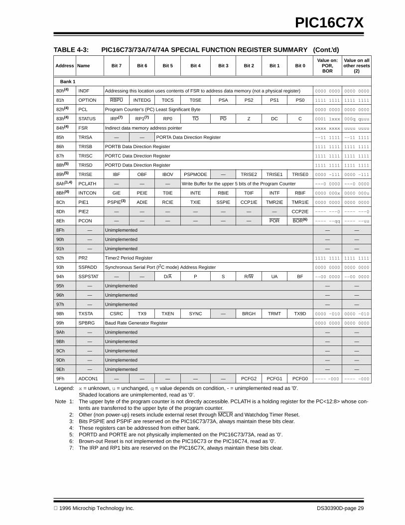
PIC16C7X
Bank 1
80h(4) INDF Addressing this location uses contents of FSR to address data memory (not a physical register) 0000 0000 0000 0000
81h OPTION RBPU INTEDG T0CS T0SE PSA PS2 PS1 PS0 1111 1111 1111 1111
82h(4) PCL Program Counter's (PC) Least Significant Byte 0000 0000 0000 0000
83h(4) STATUS IRP(7) RP1(7) RP0 TO PD Z DC C 0001 1xxx 000q quuu
84h(4) FSR Indirect data memory address pointer xxxx xxxx uuuu uuuu
85h TRISA — — PORTA Data Direction Register --11 1111 --11 1111
86h TRISB PORTB Data Direction Register 1111 1111 1111 1111
87h TRISC PORTC Data Direction Register 1111 1111 1111 1111
88h(5) TRISD PORTD Data Direction Register 1111 1111 1111 1111
89h(5) TRISE IBF OBF IBOV PSPMODE — TRISE2 TRISE1 TRISE0 0000 -111 0000 -111
8Ah(1,4) PCLATH — — — Write Buffer for the upper 5 bits of the Program Counter ---0 0000 ---0 0000
8Bh(4) INTCON GIE PEIE T0IE INTE RBIE T0IF INTF RBIF 0000 000x 0000 000u
8Ch PIE1 PSPIE(3) ADIE RCIE TXIE SSPIE CCP1IE TMR2IE TMR1IE 0000 0000 0000 0000
8Dh PIE2 — — — — — — — CCP2IE ---- ---0 ---- ---0
8Eh PCON — — — — — — POR BOR(6) ---- --qq ---- --uu
8Fh — Unimplemented — —
90h — Unimplemented — —
91h — Unimplemented — —
92h PR2 Timer2 Period Register 1111 1111 1111 1111
93h SSPADD Synchronous Serial Port (I2C mode) Address Register 0000 0000 0000 0000
94h SSPSTAT — — D/A P S R/W UA BF --00 0000 --00 0000
95h — Unimplemented — —
96h — Unimplemented — —
97h — Unimplemented — —
98h TXSTA CSRC TX9 TXEN SYNC — BRGH TRMT TX9D 0000 -010 0000 -010
99h SPBRG Baud Rate Generator Register 0000 0000 0000 0000
9Ah — Unimplemented — —
9Bh — Unimplemented — —
9Ch — Unimplemented — —
9Dh — Unimplemented — —
9Eh — Unimplemented — —
9Fh ADCON1 — — — — — PCFG2 PCFG1 PCFG0 ---- -000 ---- -000
TABLE 4-3: PIC16C73/73A/74/74A SPECIAL FUNCTION REGISTER SUMMARY (Cont.’d)
Address Name Bit 7 Bit 6 Bit 5 Bit 4 Bit 3 Bit 2 Bit 1 Bit 0Value on:
POR,BOR
Value on allother resets
(2)
Legend: x = unknown, u = unchanged, q = value depends on condition, - = unimplemented read as '0'. Shaded locations are unimplemented, read as ‘0’.
Note 1: The upper byte of the program counter is not directly accessible. PCLATH is a holding register for the PC<12:8> whose con-tents are transferred to the upper byte of the program counter.
2: Other (non power-up) resets include external reset through MCLR and Watchdog Timer Reset.3: Bits PSPIE and PSPIF are reserved on the PIC16C73/73A, always maintain these bits clear.4: These registers can be addressed from either bank.5: PORTD and PORTE are not physically implemented on the PIC16C73/73A, read as ‘0’.6: Brown-out Reset is not implemented on the PIC16C73 or the PIC16C74, read as '0'.7: The IRP and RP1 bits are reserved on the PIC16C7X, always maintain these bits clear.

PIC16C7X
DS30390D-page 30 1996 Microchip Technology Inc.
4.2.2.1 STATUS REGISTER
The STATUS register, shown in Figure 4-9, containsthe arithmetic status of the ALU, the RESET status andthe bank select bits for data memory.
The STATUS register can be the destination for anyinstruction, as with any other register. If the STATUSregister is the destination for an instruction that affectsthe Z, DC or C bits, then the write to these three bits isdisabled. These bits are set or cleared according to thedevice logic. Furthermore, the TO and PD bits are notwritable. Therefore, the result of an instruction with theSTATUS register as destination may be different thanintended.
For example, CLRF STATUS will clear the upper-threebits and set the Z bit. This leaves the STATUS registeras 000u u1uu (where u = unchanged).
Applicable Devices710 71 711 72 73 73A 74 74A
It is recommended, therefore, that only BCF, BSF,SWAPF and MOVWF instructions are used to alter theSTATUS register because these instructions do notaffect the Z, C or DC bits from the STATUS register. Forother instructions, not affecting any status bits, see the"Instruction Set Summary."
Note 1: Bits IRP and RP1 (STATUS<7:6>) are notused by the PIC16C7X and should bemaintained clear. Use of these bits asgeneral purpose R/W bits is NOT recom-mended, since this may affect upwardcompatibility with future products.
Note 2: The C and DC bits operate as a borrowand digit borrow bit, respectively, in sub-traction. See the SUBLW and SUBWFinstructions for examples.
FIGURE 4-9: STATUS REGISTER (ADDRESS 03h, 83h)
R/W-0 R/W-0 R/W-0 R-1 R-1 R/W-x R/W-x R/W-xIRP RP1 RP0 TO PD Z DC C R = Readable bit
W = Writable bitU = Unimplemented bit, read as ‘0’- n = Value at POR reset
bit7 bit0
bit 7: IRP: Register Bank Select bit (used for indirect addressing)1 = Bank 2, 3 (100h - 1FFh)0 = Bank 0, 1 (00h - FFh)The IRP bit is reserved on the PIC16C7X, always maintain this bit clear.
bit 6-5: RP1:RP0: Register Bank Select bits (used for direct addressing)11 = Bank 3 (180h - 1FFh)10 = Bank 2 (100h - 17Fh)01 = Bank 1 (80h - FFh)00 = Bank 0 (00h - 7Fh)Each bank is 128 bytes. The RP1 bit is reserved on the PIC16C7X, always maintain this bit clear.
bit 4: TO: Time-out bit1 = After power-up, CLRWDT instruction, or SLEEP instruction0 = A WDT time-out occurred
bit 3: PD: Power-down bit1 = After power-up or by the CLRWDT instruction0 = By execution of the SLEEP instruction
bit 2: Z: Zero bit1 = The result of an arithmetic or logic operation is zero0 = The result of an arithmetic or logic operation is not zero
bit 1: DC: Digit carry/borrow bit (ADDWF, ADDLW,SUBLW,SUBWF instructions)(for borrow the polarity is reversed)1 = A carry-out from the 4th low order bit of the result occurred0 = No carry-out from the 4th low order bit of the result
bit 0: C: Carry/borrow bit (ADDWF, ADDLW,SUBLW,SUBWF instructions)1 = A carry-out from the most significant bit of the result occurred0 = No carry-out from the most significant bit of the result occurredNote: For borrow the polarity is reversed. A subtraction is executed by adding the two’s complement of thesecond operand. For rotate (RRF, RLF) instructions, this bit is loaded with either the high or low order bit ofthe source register.

1996 Microchip Technology Inc. DS30390D-page 31
PIC16C7X
4.2.2.2 OPTION REGISTER
The OPTION register is a readable and writable regis-ter which contains various control bits to configure theTMR0/WDT prescaler, the External INT Interrupt,TMR0, and the weak pull-ups on PORTB.
Applicable Devices710 71 711 72 73 73A 74 74A
Note: To achieve a 1:1 prescaler assignment forthe TMR0 register, assign the prescaler tothe Watchdog Timer by setting bit PSA(OPTION<3>).
FIGURE 4-10: OPTION REGISTER (ADDRESS 81h)
R/W-1 R/W-1 R/W-1 R/W-1 R/W-1 R/W-1 R/W-1 R/W-1
RBPU INTEDG T0CS T0SE PSA PS2 PS1 PS0 R = Readable bitW = Writable bitU = Unimplemented bit,
read as ‘0’- n = Value at POR reset
bit7 bit0
bit 7: RBPU: PORTB Pull-up Enable bit1 = PORTB pull-ups are disabled0 = PORTB pull-ups are enabled by individual port latch values
bit 6: INTEDG: Interrupt Edge Select bit1 = Interrupt on rising edge of RB0/INT pin0 = Interrupt on falling edge of RB0/INT pin
bit 5: T0CS: TMR0 Clock Source Select bit1 = Transition on RA4/T0CKI pin0 = Internal instruction cycle clock (CLKOUT)
bit 4: T0SE: TMR0 Source Edge Select bit1 = Increment on high-to-low transition on RA4/T0CKI pin0 = Increment on low-to-high transition on RA4/T0CKI pin
bit 3: PSA: Prescaler Assignment bit1 = Prescaler is assigned to the WDT0 = Prescaler is assigned to the Timer0 module
bit 2-0: PS2:PS0: Prescaler Rate Select bits
000001010011100101110111
1 : 21 : 41 : 81 : 161 : 321 : 641 : 1281 : 256
1 : 11 : 21 : 41 : 81 : 161 : 321 : 641 : 128
Bit Value TMR0 Rate WDT Rate

PIC16C7X
DS30390D-page 32 1996 Microchip Technology Inc.
4.2.2.3 INTCON REGISTER
The INTCON Register is a readable and writable regis-ter which contains various enable and flag bits for theTMR0 register overflow, RB Port change and ExternalRB0/INT Pin interrupts.
Applicable Devices710 71 711 72 73 73A 74 74A
Note: Interrupt flag bits get set when an interruptcondition occurs regardless of the state ofits corresponding enable bit or the globalenable bit, GIE (INTCON<7>).
FIGURE 4-11: INTCON REGISTER FOR PIC16C710/71/711 (ADDRESS 0Bh, 8Bh)
R/W-0 R/W-0 R/W-0 R/W-0 R/W-0 R/W-0 R/W-0 R/W-x
GIE ADIE T0IE INTE RBIE T0IF INTF RBIF R = Readable bitW = Writable bitU = Unimplemented bit,
read as ‘0’- n = Value at POR reset
bit7 bit0
bit 7: GIE:(1) Global Interrupt Enable bit1 = Enables all un-masked interrupts0 = Disables all interrupts
bit 6: ADIE: A/D Converter Interrupt Enable bit1 = Enables A/D interrupt0 = Disables A/D interrupt
bit 5: T0IE: TMR0 Overflow Interrupt Enable bit1 = Enables the TMR0 interrupt0 = Disables the TMR0 interrupt
bit 4: INTE: RB0/INT External Interrupt Enable bit1 = Enables the RB0/INT external interrupt0 = Disables the RB0/INT external interrupt
bit 3: RBIE: RB Port Change Interrupt Enable bit1 = Enables the RB port change interrupt0 = Disables the RB port change interrupt
bit 2: T0IF: TMR0 Overflow Interrupt Flag bit1 = TMR0 register has overflowed (must be cleared in software)0 = TMR0 register did not overflow
bit 1: INTF: RB0/INT External Interrupt Flag bit1 = The RB0/INT external interrupt occurred (must be cleared in software)0 = The RB0/INT external interrupt did not occur
bit 0: RBIF: RB Port Change Interrupt Flag bit1 = At least one of the RB7:RB4 pins changed state (must be cleared in software)0 = None of the RB7:RB4 pins have changed state
Note 1: For the PIC16C71, if an interrupt occurs while the GIE bit is being cleared, the GIE bit may be uninten-tionally re-enabled by the RETFIE instruction in the user’s Interrupt Service Routine. Refer to Section 14.5 for a detailed description.

1996 Microchip Technology Inc. DS30390D-page 33
PIC16C7X
FIGURE 4-12: INTCON REGISTER FOR PIC16C72/73/73A/74/74A (ADDRESS 0Bh, 8Bh)
R/W-0 R/W-0 R/W-0 R/W-0 R/W-0 R/W-0 R/W-0 R/W-x
GIE PEIE T0IE INTE RBIE T0IF INTF RBIF R = Readable bitW = Writable bitU = Unimplemented bit,
read as ‘0’- n = Value at POR reset
bit7 bit0
bit 7: GIE:(1) Global Interrupt Enable bit1 = Enables all un-masked interrupts0 = Disables all interrupts
bit 6: PEIE: Peripheral Interrupt Enable bit1 = Enables all un-masked peripheral interrupts0 = Disables all peripheral interrupts
bit 5: T0IE: TMR0 Overflow Interrupt Enable bit1 = Enables the TMR0 interrupt0 = Disables the TMR0 interrupt
bit 4: INTE: RB0/INT External Interrupt Enable bit1 = Enables the RB0/INT external interrupt0 = Disables the RB0/INT external interrupt
bit 3: RBIE: RB Port Change Interrupt Enable bit1 = Enables the RB port change interrupt0 = Disables the RB port change interrupt
bit 2: T0IF: TMR0 Overflow Interrupt Flag bit1 = TMR0 register has overflowed (must be cleared in software)0 = TMR0 register did not overflow
bit 1: INTF: RB0/INT External Interrupt Flag bit1 = The RB0/INT external interrupt occurred (must be cleared in software)0 = The RB0/INT external interrupt did not occur
bit 0: RBIF: RB Port Change Interrupt Flag bit1 = At least one of the RB7:RB4 pins changed state (must be cleared in software)0 = None of the RB7:RB4 pins have changed state
Note 1: For the PIC16C73 and PIC16C74, if an interrupt occurs while the GIE bit is being cleared, the GIE bit may be unintentionally re-enabled by the RETFIE instruction in the user’s Interrupt Service Routine. Refer to Section 14.5 for a detailed description.
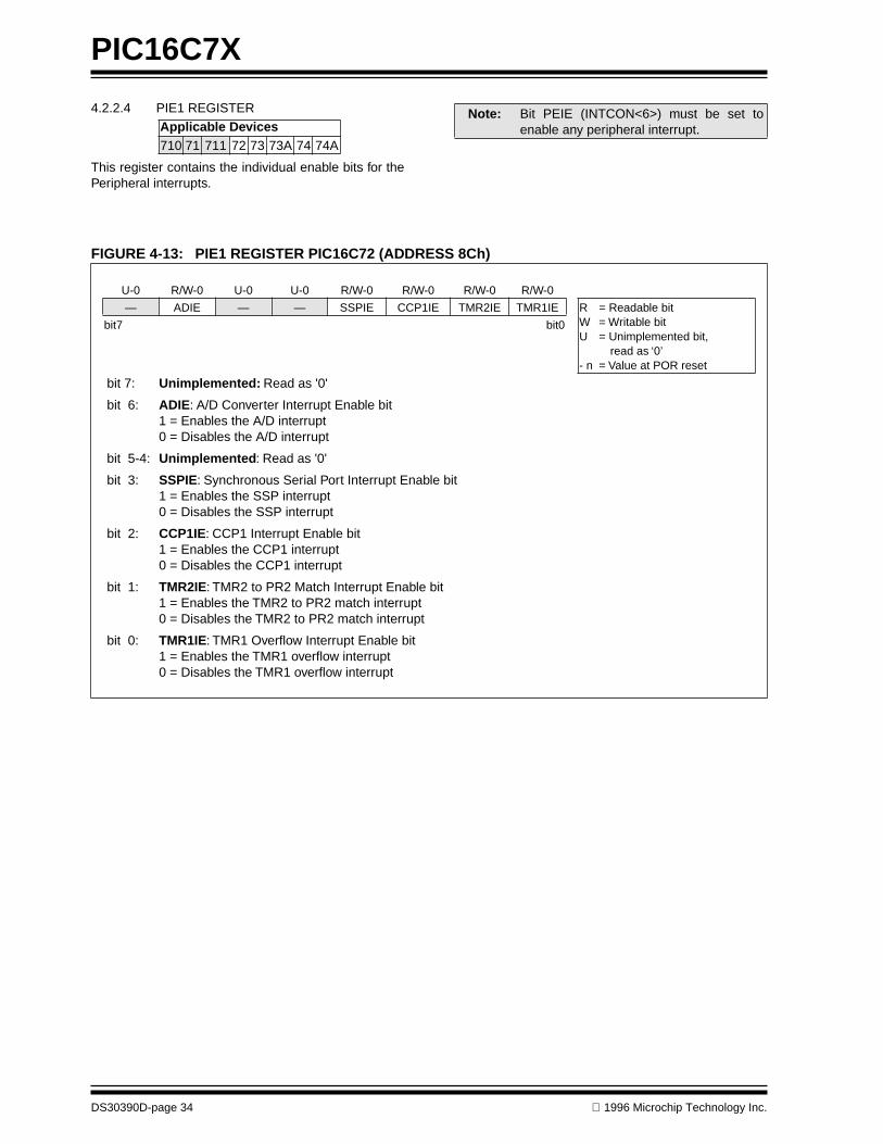
PIC16C7X
DS30390D-page 34 1996 Microchip Technology Inc.
4.2.2.4 PIE1 REGISTER
This register contains the individual enable bits for thePeripheral interrupts.
Applicable Devices710 71 711 72 73 73A 74 74A
Note: Bit PEIE (INTCON<6>) must be set toenable any peripheral interrupt.
FIGURE 4-13: PIE1 REGISTER PIC16C72 (ADDRESS 8Ch)
U-0 R/W-0 U-0 U-0 R/W-0 R/W-0 R/W-0 R/W-0
— ADIE — — SSPIE CCP1IE TMR2IE TMR1IE R = Readable bitW = Writable bitU = Unimplemented bit,
read as ‘0’- n = Value at POR reset
bit7 bit0
bit 7: Unimplemented: Read as '0'
bit 6: ADIE: A/D Converter Interrupt Enable bit1 = Enables the A/D interrupt0 = Disables the A/D interrupt
bit 5-4: Unimplemented: Read as '0'
bit 3: SSPIE: Synchronous Serial Port Interrupt Enable bit1 = Enables the SSP interrupt0 = Disables the SSP interrupt
bit 2: CCP1IE: CCP1 Interrupt Enable bit1 = Enables the CCP1 interrupt0 = Disables the CCP1 interrupt
bit 1: TMR2IE: TMR2 to PR2 Match Interrupt Enable bit1 = Enables the TMR2 to PR2 match interrupt0 = Disables the TMR2 to PR2 match interrupt
bit 0: TMR1IE: TMR1 Overflow Interrupt Enable bit1 = Enables the TMR1 overflow interrupt0 = Disables the TMR1 overflow interrupt

1996 Microchip Technology Inc. DS30390D-page 35
PIC16C7X
FIGURE 4-14: PIE1 REGISTER PIC16C73/73A/74/74A (ADDRESS 8Ch)
R/W-0 R/W-0 R/W-0 R/W-0 R/W-0 R/W-0 R/W-0 R/W-0
PSPIE(1) ADIE RCIE TXIE SSPIE CCP1IE TMR2IE TMR1IE R = Readable bitW = Writable bitU = Unimplemented bit,
read as ‘0’- n = Value at POR reset
bit7 bit0
bit 7: PSPIE(1): Parallel Slave Port Read/Write Interrupt Enable bit1 = Enables the PSP read/write interrupt0 = Disables the PSP read/write interrupt
bit 6: ADIE: A/D Converter Interrupt Enable bit1 = Enables the A/D interrupt0 = Disables the A/D interrupt
bit 5: RCIE: USART Receive Interrupt Enable bit1 = Enables the USART receive interrupt0 = Disables the USART receive interrupt
bit 4: TXIE: USART Transmit Interrupt Enable bit1 = Enables the USART transmit interrupt0 = Disables the USART transmit interrupt
bit 3: SSPIE: Synchronous Serial Port Interrupt Enable bit1 = Enables the SSP interrupt0 = Disables the SSP interrupt
bit 2: CCP1IE: CCP1 Interrupt Enable bit1 = Enables the CCP1 interrupt0 = Disables the CCP1 interrupt
bit 1: TMR2IE: TMR2 to PR2 Match Interrupt Enable bit1 = Enables the TMR2 to PR2 match interrupt0 = Disables the TMR2 to PR2 match interrupt
bit 0: TMR1IE: TMR1 Overflow Interrupt Enable bit1 = Enables the TMR1 overflow interrupt0 = Disables the TMR1 overflow interrupt
Note 1: PIC16C73 and PIC16C73A devices do not have a Parallel Slave Port implemented, this bit location is reserved on these two devices, always maintain this bit clear.

PIC16C7X
DS30390D-page 36 1996 Microchip Technology Inc.
4.2.2.5 PIR1 REGISTER
This register contains the individual flag bits for thePeripheral interrupts.
Applicable Devices710 71 711 72 73 73A 74 74A
Note: Interrupt flag bits get set when an interruptcondition occurs regardless of the state ofits corresponding enable bit or the globalenable bit, GIE (INTCON<7>). User soft-ware should ensure the appropriate inter-rupt flag bits are clear prior to enabling aninterrupt.
FIGURE 4-15: PIR1 REGISTER PIC16C72 (ADDRESS 0Ch)
U-0 R/W-0 U-0 U-0 R/W-0 R/W-0 R/W-0 R/W-0
— ADIF — — SSPIF CCP1IF TMR2IF TMR1IF R = Readable bitW = Writable bitU = Unimplemented bit,
read as ‘0’- n = Value at POR reset
bit7 bit0
bit 7: Unimplemented: Read as '0'
bit 6: ADIF: A/D Converter Interrupt Flag bit1 = An A/D conversion completed0 = The A/D conversion is not complete
bit 5-4: Unimplemented: Read as '0'
bit 3: SSPIF: Synchronous Serial Port Interrupt Flag bit1 = The transmission/reception is complete0 = Waiting to transmit/receive
bit 2: CCP1IF: CCP1 Interrupt Flag bitCapture Mode1 = A TMR1 register capture occurred (must be cleared in software)0 = No TMR1 register capture occurredCompare Mode1 = A TMR1 register compare match occurred (must be cleared in software)0 = No TMR1 register compare match occurredPWM ModeUnused in this mode
bit 1: TMR2IF: TMR2 to PR2 Match Interrupt Flag bit1 = TMR2 to PR2 match occurred (must be cleared in software)0 = No TMR2 to PR2 match occurred
bit 0: TMR1IF: TMR1 Overflow Interrupt Flag bit1 = TMR1 register overflowed (must be cleared in software)0 = TMR1 register did not overflow

1996 Microchip Technology Inc. DS30390D-page 37
PIC16C7X
FIGURE 4-16: PIR1 REGISTER PIC16C73/73A/74/74A (ADDRESS 0Ch)
R/W-0 R/W-0 R-0 R-0 R/W-0 R/W-0 R/W-0 R/W-0
PSPIF(1) ADIF RCIF TXIF SSPIF CCP1IF TMR2IF TMR1IF R = Readable bitW = Writable bitU = Unimplemented bit,
read as ‘0’- n = Value at POR reset
bit7 bit0
bit 7: PSPIF(1): Parallel Slave Port Read/Write Interrupt Flag bit1 = A read or a write operation has taken place (must be cleared in software)0 = No read or write has occurred
bit 6: ADIF: A/D Converter Interrupt Flag bit1 = An A/D conversion completed0 = The A/D conversion is not complete
bit 5: RCIF: USART Receive Interrupt Flag bit1 = The USART receive buffer is full0 = The USART receive buffer is empty
bit 4: TXIF: USART Transmit Interrupt Flag bit1 = The USART transmit buffer is empty0 = The USART transmit buffer is full
bit 3: SSPIF: Synchronous Serial Port Interrupt Flag bit1 = The transmission/reception is complete0 = Waiting to transmit/receive
bit 2: CCP1IF: CCP1 Interrupt Flag bitCapture Mode1 = A TMR1 register capture occurred (must be cleared in software)0 = No TMR1 register capture occurredCompare Mode1 = A TMR1 register compare match occurred (must be cleared in software)0 = No TMR1 register compare match occurredPWM ModeUnused in this mode
bit 1: TMR2IF: TMR2 to PR2 Match Interrupt Flag bit1 = TMR2 to PR2 match occurred (must be cleared in software)0 = No TMR2 to PR2 match occurred
bit 0: TMR1IF: TMR1 Overflow Interrupt Flag bit1 = TMR1 register overflowed (must be cleared in software)0 = TMR1 register did not overflow
Note 1: PIC16C73 and PIC16C73A devices do not have a Parallel Slave Port implemented, this bit location is reserved on these two devices, always maintain this bit clear.

PIC16C7X
DS30390D-page 38 1996 Microchip Technology Inc.
4.2.2.6 PIE2 REGISTER
This register contains the individual enable bit for theCCP2 peripheral interrupt.
FIGURE 4-17: PIE2 REGISTER (ADDRESS 8Dh)
Applicable Devices710 71 711 72 73 73A 74 74A
U-0 U-0 U-0 U-0 U-0 U-0 U-0 R/W-0
— — — — — — — CCP2IE R = Readable bitW = Writable bitU = Unimplemented bit,
read as ‘0’- n = Value at POR reset
bit7 bit0
bit 7-1: Unimplemented: Read as '0'
bit 0: CCP2IE: CCP2 Interrupt Enable bit1 = Enables the CCP2 interrupt0 = Disables the CCP2 interrupt

1996 Microchip Technology Inc. DS30390D-page 39
PIC16C7X
4.2.2.7 PIR2 REGISTER
This register contains the CCP2 interrupt flag bit.
Applicable Devices710 71 711 72 73 73A 74 74A
.
Note: Interrupt flag bits get set when an interruptcondition occurs regardless of the state ofits corresponding enable bit or the globalenable bit, GIE (INTCON<7>). User soft-ware should ensure the appropriate inter-rupt flag bits are clear prior to enabling aninterrupt.
FIGURE 4-18: PIR2 REGISTER (ADDRESS 0Dh)
U-0 U-0 U-0 U-0 U-0 U-0 U-0 R/W-0
— — — — — — — CCP2IF R = Readable bitW = Writable bitU = Unimplemented bit,
read as ‘0’- n = Value at POR reset
bit7 bit0
bit 7-1: Unimplemented: Read as '0'
bit 0: CCP2IF: CCP2 Interrupt Flag bit
Capture Mode1 = A TMR1 register capture occurred (must be cleared in software)0 = No TMR1 register capture occurred
Compare Mode1 = A TMR1 register compare match occurred (must be cleared in software)0 = No TMR1 register compare match occurred
PWM ModeUnused

PIC16C7X
DS30390D-page 40 1996 Microchip Technology Inc.
4.2.2.8 PCON REGISTER
The Power Control (PCON) register contains a flag bitto allow differentiation between a Power-on Reset(POR) to an external MCLR Reset or WDT Reset. Italso contains a status bit to determine if a Brown-outReset (BOR) occurred.
Applicable Devices710 71 711 72 73 73A 74 74A
Note: BOR is unknown on Power-on Reset. Itmust then be set by the user and checkedon subsequent resets to see if BOR isclear, indicating a brown-out has occurred.The BOR status bit is a don't care and isnot necessarily predictable if the brown-outcircuit is disabled (by clearing the BODENbit in the Configuration word).
FIGURE 4-19: PCON REGISTER (ADDRESS 8Eh)
U-0 U-0 U-0 U-0 U-0 U-0 R/W-0 R/W-q
— — — — — — POR BOR(1) R = Readable bitW = Writable bitU = Unimplemented bit,
read as ‘0’- n = Value at POR reset
bit7 bit0
bit 7-2: Unimplemented: Read as '0'
bit 1: POR: Power-on Reset Status bit1 = No Power-on Reset occurred0 = A Power-on Reset occurred (must be set in software after a Power-on Reset occurs)
bit 0: BOR(1): Brown-out Reset Status bit1 = No Brown-out Reset occurred0 = A Brown-out Reset occurred (must be set in software after a Brown-out Reset occurs)
Note 1: Brown-out Reset is not implemented on the PIC16C73/74.

1996 Microchip Technology Inc. DS30390D-page 41
PIC16C7X
4.3 PCL and PCLATH
The program counter (PC) is 13-bits wide. The low bytecomes from the PCL register, which is a readable andwritable register. The high byte (PC<12:8>) is notdirectly readable or writable and comes from PCLATH.On any reset, the PC is cleared. Figure 4-20 shows thetwo situations for the loading of the PC. The upperexample in the figure shows how the PC is loaded on awrite to PCL (PCLATH<4:0> → PCH). The lower exam-ple in the figure shows how the PC is loaded during aCALL or GOTO instruction (PCLATH<4:3> → PCH).
FIGURE 4-20: LOADING OF PC IN DIFFERENT SITUATIONS
4.3.1 COMPUTED GOTO
A computed GOTO is accomplished by adding an offsetto the program counter (ADDWF PCL). When doing atable read using a computed GOTO method, careshould be exercised if the table location crosses a PCLmemory boundary (each 256 byte block). Refer to theapplication note “Implementing a Table Read" (AN556).
4.3.2 STACK
The PIC16CXX family has an 8 level deep x 13-bit widehardware stack. The stack space is not part of eitherprogram or data space and the stack pointer is notreadable or writable. The PC is PUSHed onto the stackwhen a CALL instruction is executed or an interruptcauses a branch. The stack is POPed in the event of aRETURN, RETLW or a RETFIE instruction execution.PCLATH is not affected by a PUSH or POP operation.
The stack operates as a circular buffer. This means thatafter the stack has been PUSHed eight times, the ninthpush overwrites the value that was stored from the firstpush. The tenth push overwrites the second push (andso on).
Applicable Devices710 71 711 72 73 73A 74 74A
PC
12 8 7 0
5PCLATH<4:0>
PCLATH
Instruction with
ALU result
GOTO, CALL
Opcode <10:0>
8
PC
12 11 10 0
11PCLATH<4:3>
PCH PCL
8 7
2
PCLATH
PCH PCL
PCL as Destination
4.4 Program Memory Paging
The PIC16C73/73A and the PIC16C74/74A have 4K ofprogram memory, but the CALL and GOTO instructionsonly have a 11-bit address range. This 11-bit addressrange allows a branch within a 2K program memorypage size. To allow CALL and GOTO instructions toaddress the entire 4K program memory address range,there must be another bit to specify the program mem-ory page. This paging bit comes from the PCLATH<3>bit (Figure 4-20). When doing a CALL or GOTO instruc-tion, the user must ensure that this page bit(PCLATH<3>) is programmed so that the desired pro-gram memory page is addressed. If a return from aCALL instruction (or interrupt) is executed, the entire13-bit PC is PUSHed onto the stack. Therefore, manip-ulation of the PCLATH<3> is not required for the returninstructions (which POPs the address from the stack).
Note 1: There are no status bits to indicate stackoverflow or stack underflow conditions.
Note 2: There are no instructions/mnemonicscalled PUSH or POP. These are actionsthat occur from the execution of theCALL, RETURN, RETLW, and RETFIEinstructions, or the vectoring to an inter-rupt address.
Applicable Devices710 71 711 72 73 73A 74 74A
Note 1: The PIC16C710/71/711/72 ignore bothpaging bits (PCLATH<4:3>, which areused to access program memory whenmore than one page is available. The useof PCLATH<4:3> as general purposeread/write bits for the PIC16C7X is notrecommended since this may affectupward compatibility with future products.
The PIC16C73/73A/74/74A ignores pag-ing bit (PCLATH<4>), which is used toaccess program memory pages 2 and 3(1000h - 1FFFh). The use of PCLATH<4>as a general purpose read/write bit is notrecommended since this may affectupward compatibility with future products.
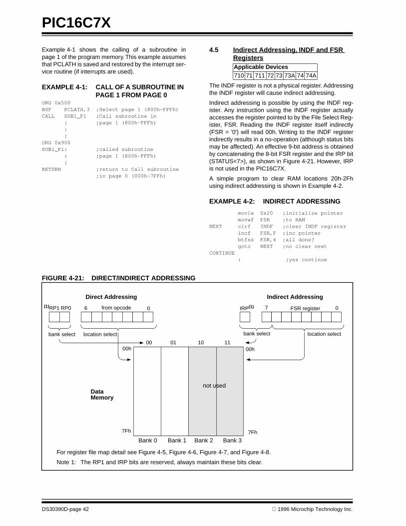
PIC16C7X
DS30390D-page 42 1996 Microchip Technology Inc.
Example 4-1 shows the calling of a subroutine inpage 1 of the program memory. This example assumesthat PCLATH is saved and restored by the interrupt ser-vice routine (if interrupts are used).
EXAMPLE 4-1: CALL OF A SUBROUTINE IN PAGE 1 FROM PAGE 0
ORG 0x500BSF PCLATH,3 ;Select page 1 (800h-FFFh)CALL SUB1_P1 ;Call subroutine in : ;page 1 (800h-FFFh) : :ORG 0x900SUB1_P1: ;called subroutine : ;page 1 (800h-FFFh) :RETURN ;return to Call subroutine ;in page 0 (000h-7FFh)
4.5 Indirect Addressing, INDF and FSR Registers
The INDF register is not a physical register. Addressingthe INDF register will cause indirect addressing.
Indirect addressing is possible by using the INDF reg-ister. Any instruction using the INDF register actuallyaccesses the register pointed to by the File Select Reg-ister, FSR. Reading the INDF register itself indirectly(FSR = '0') will read 00h. Writing to the INDF registerindirectly results in a no-operation (although status bitsmay be affected). An effective 9-bit address is obtainedby concatenating the 8-bit FSR register and the IRP bit(STATUS<7>), as shown in Figure 4-21. However, IRPis not used in the PIC16C7X.
A simple program to clear RAM locations 20h-2Fhusing indirect addressing is shown in Example 4-2.
EXAMPLE 4-2: INDIRECT ADDRESSING
movlw 0x20 ;initialize pointer movwf FSR ;to RAMNEXT clrf INDF ;clear INDF register incf FSR,F ;inc pointer btfss FSR,4 ;all done? goto NEXT ;no clear nextCONTINUE : ;yes continue
Applicable Devices710 71 711 72 73 73A 74 74A
FIGURE 4-21: DIRECT/INDIRECT ADDRESSING
For register file map detail see Figure 4-5, Figure 4-6, Figure 4-7, and Figure 4-8.
Note 1: The RP1 and IRP bits are reserved, always maintain these bits clear.
DataMemory
Indirect AddressingDirect Addressing
bank select location select
(1)RP1 RP0 6 0from opcode IRP(1) FSR register7 0
bank select location select
00 01 10 1100h
7Fh
00h
7Fh
Bank 0 Bank 1 Bank 2 Bank 3
not used
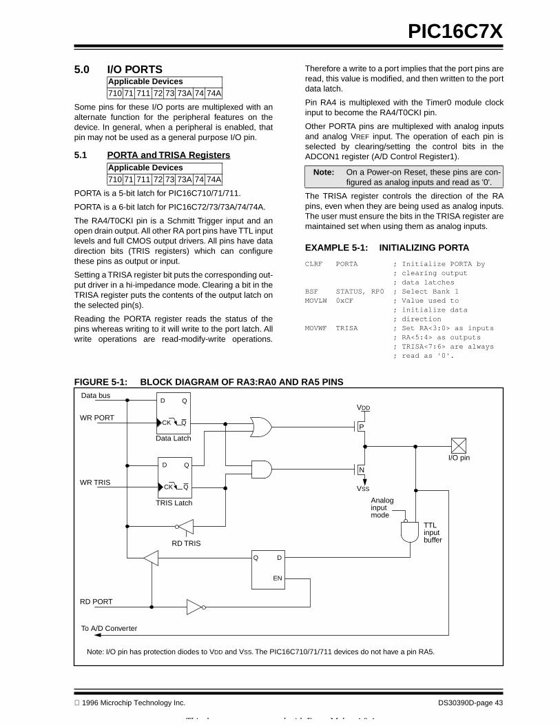
1996 Microchip Technology Inc. DS30390D-page 43
PIC16C7X
5.0 I/O PORTS
Some pins for these I/O ports are multiplexed with analternate function for the peripheral features on thedevice. In general, when a peripheral is enabled, thatpin may not be used as a general purpose I/O pin.
5.1 PORTA and TRISA Registers
PORTA is a 5-bit latch for PIC16C710/71/711.
PORTA is a 6-bit latch for PIC16C72/73/73A/74/74A.
The RA4/T0CKI pin is a Schmitt Trigger input and anopen drain output. All other RA port pins have TTL inputlevels and full CMOS output drivers. All pins have datadirection bits (TRIS registers) which can configurethese pins as output or input.
Setting a TRISA register bit puts the corresponding out-put driver in a hi-impedance mode. Clearing a bit in theTRISA register puts the contents of the output latch onthe selected pin(s).
Reading the PORTA register reads the status of thepins whereas writing to it will write to the port latch. Allwrite operations are read-modify-write operations.
Applicable Devices
710 71 711 72 73 73A 74 74A
Applicable Devices
710 71 711 72 73 73A 74 74A
Therefore a write to a port implies that the port pins areread, this value is modified, and then written to the portdata latch.
Pin RA4 is multiplexed with the Timer0 module clockinput to become the RA4/T0CKI pin.
Other PORTA pins are multiplexed with analog inputsand analog V
REF
input. The operation of each pin isselected by clearing/setting the control bits in theADCON1 register (A/D Control Register1).
The TRISA register controls the direction of the RApins, even when they are being used as analog inputs.The user must ensure the bits in the TRISA register aremaintained set when using them as analog inputs.
EXAMPLE 5-1: INITIALIZING PORTA
CLRF PORTA ; Initialize PORTA by ; clearing output ; data latchesBSF STATUS, RP0 ; Select Bank 1MOVLW 0xCF ; Value used to ; initialize data ; directionMOVWF TRISA ; Set RA<3:0> as inputs ; RA<5:4> as outputs ; TRISA<7:6> are always ; read as '0'.
Note:
On a Power-on Reset, these pins are con-figured as analog inputs and read as '0'.
FIGURE 5-1: BLOCK DIAGRAM OF RA3:RA0 AND RA5 PINSData bus
WR PORT
WR TRIS
RD PORT
Data Latch
TRIS Latch
P
VSS
I/O pin
To A/D Converter
Note: I/O pin has protection diodes to VDD and VSS. The PIC16C710/71/711 devices do not have a pin RA5.
QD
QCK
QD
QCK
EN
Q D
EN
N
Analoginputmode
TTLinputbuffer
VDD
RD TRIS
This document was created with FrameMaker 4 0 4

PIC16C7X
DS30390D-page 44
1996 Microchip Technology Inc.
FIGURE 5-2: BLOCK DIAGRAM OF RA4/T0CKI PIN
TABLE 5-1: PORTA FUNCTIONS
TABLE 5-2: SUMMARY OF REGISTERS ASSOCIATED WITH PORTA
Name Bit# Buffer Function
RA0/AN0 bit0 TTL Input/output or analog inputRA1/AN1 bit1 TTL Input/output or analog inputRA2/AN2 bit2 TTL Input/output or analog inputRA3/AN3/V
REF
bit3 TTL Input/output or analog input/V
REF
RA4/T0CKI bit4 ST Input/output or external clock input for Timer0Output is open drain type
RA5/AN4/SS
(1)
bit5 TTL Input/output or slave select input for synchronous serial port or analog inputLegend: TTL = TTL input, ST = Schmitt Trigger inputNote 1: The PIC16C710/71/711 does not have PORTA<5> or TRISA<5>, read as '0'.
Address Name Bit 7 Bit 6 Bit 5 Bit 4 Bit 3 Bit 2 Bit 1 Bit 0Value on:
POR,BOR
Value on all other resets
05h PORTA — — RA5
(1)
RA4 RA3 RA2 RA1 RA0
--0x 0000 --0u 0000
85h TRISA — — TRISA5
(1)
TRISA4 TRISA3 TRISA2 TRISA1 TRISA0
--11 1111 --11 1111
9Fh ADCON1 — — — — — PCFG2
(2)
PCFG1 PCFG0
---- -000 ---- -000
Legend:
x
= unknown,
u
= unchanged,
-
= unimplemented locations read as '0'. Shaded cells are not used by PORTA.Note 1: PORTA<5> and TRISA<5> are not implemented on the PIC16C710/71/711.
2: Bit PCFG2 is not implemented on the PIC16C710/71/711.
Data Bus
WR PORT
WR TRIS
RD PORT
Data Latch
TRIS Latch
SchmittTriggerinputbuffer
N
VSS
TMR0 clock input
Note: I/O pin has protection diodes to VSS only.
QD
QCK
QD
QCK
EN
Q D
EN
RD TRIS
RA4/T0CKI pin
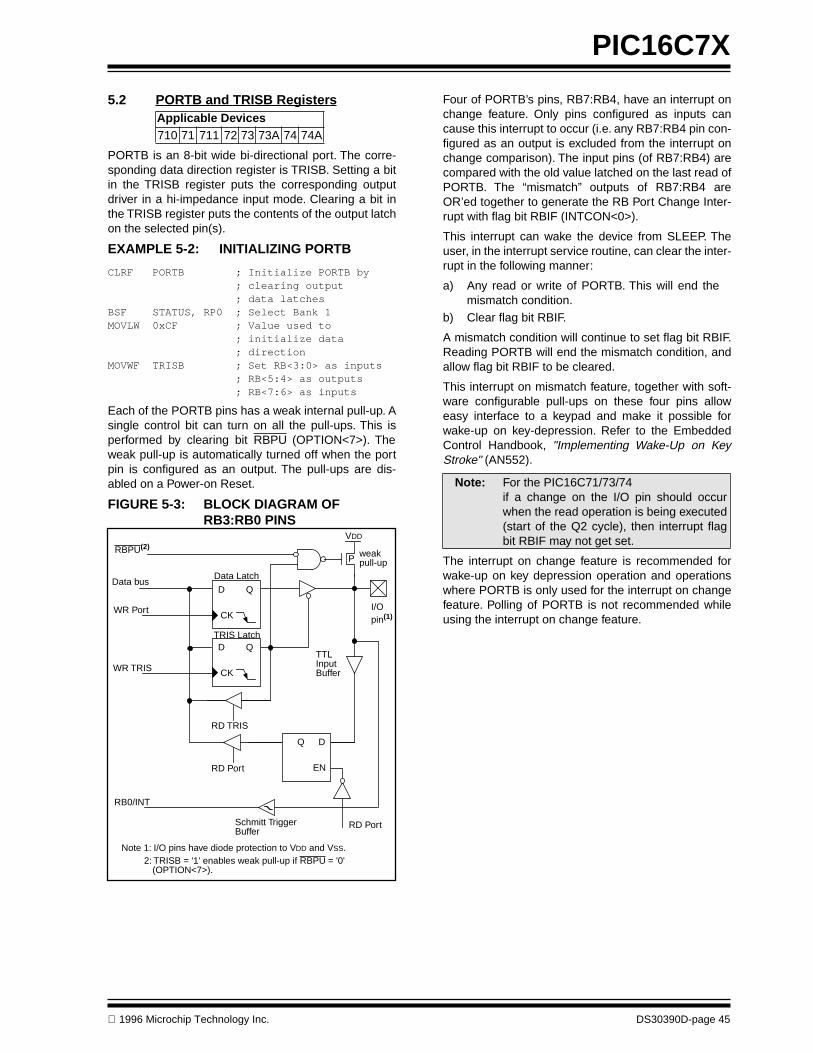
1996 Microchip Technology Inc. DS30390D-page 45
PIC16C7X
5.2 PORTB and TRISB Registers
PORTB is an 8-bit wide bi-directional port. The corre-sponding data direction register is TRISB. Setting a bitin the TRISB register puts the corresponding outputdriver in a hi-impedance input mode. Clearing a bit inthe TRISB register puts the contents of the output latchon the selected pin(s).
EXAMPLE 5-2: INITIALIZING PORTB
CLRF PORTB ; Initialize PORTB by ; clearing output ; data latchesBSF STATUS, RP0 ; Select Bank 1MOVLW 0xCF ; Value used to ; initialize data ; directionMOVWF TRISB ; Set RB<3:0> as inputs ; RB<5:4> as outputs ; RB<7:6> as inputs
Each of the PORTB pins has a weak internal pull-up. Asingle control bit can turn on all the pull-ups. This isperformed by clearing bit RBPU (OPTION<7>). Theweak pull-up is automatically turned off when the portpin is configured as an output. The pull-ups are dis-abled on a Power-on Reset.
FIGURE 5-3: BLOCK DIAGRAM OF RB3:RB0 PINS
Applicable Devices
710 71 711 72 73 73A 74 74A
Data Latch
RBPU(2)
P
VDD
QD
CK
QD
CK
Q D
EN
Data bus
WR Port
WR TRIS
RD TRIS
RD Port
weakpull-up
RD Port
RB0/INT
I/Opin(1)
TTLInputBuffer
Note 1: I/O pins have diode protection to VDD and VSS. 2: TRISB = '1' enables weak pull-up if RBPU = '0'
(OPTION<7>).
Schmitt TriggerBuffer
TRIS Latch
Four of PORTB’s pins, RB7:RB4, have an interrupt onchange feature. Only pins configured as inputs cancause this interrupt to occur (i.e. any RB7:RB4 pin con-figured as an output is excluded from the interrupt onchange comparison). The input pins (of RB7:RB4) arecompared with the old value latched on the last read ofPORTB. The “mismatch” outputs of RB7:RB4 areOR’ed together to generate the RB Port Change Inter-rupt with flag bit RBIF (INTCON<0>).
This interrupt can wake the device from SLEEP. Theuser, in the interrupt service routine, can clear the inter-rupt in the following manner:
a) Any read or write of PORTB. This will end themismatch condition.
b) Clear flag bit RBIF.
A mismatch condition will continue to set flag bit RBIF.Reading PORTB will end the mismatch condition, andallow flag bit RBIF to be cleared.
This interrupt on mismatch feature, together with soft-ware configurable pull-ups on these four pins alloweasy interface to a keypad and make it possible forwake-up on key-depression. Refer to the EmbeddedControl Handbook,
"Implementing Wake-Up on KeyStroke"
(AN552).
The interrupt on change feature is recommended forwake-up on key depression operation and operationswhere PORTB is only used for the interrupt on changefeature. Polling of PORTB is not recommended whileusing the interrupt on change feature.
Note:
For the PIC16C71/73/74if a change on the I/O pin should occurwhen the read operation is being executed(start of the Q2 cycle), then interrupt flagbit RBIF may not get set.

PIC16C7X
DS30390D-page 46
1996 Microchip Technology Inc.
FIGURE 5-4: BLOCK DIAGRAM OF RB7:RB4 PINS (PIC16C71/73/74)
Data Latch
From other
RBPU(2)
P
VDD
I/O
QD
CK
QD
CK
Q D
EN
Q D
EN
Data bus
WR Port
WR TRIS
Set RBIF
TRIS Latch
RD TRIS
RD Port
RB7:RB4 pins
weakpull-up
RD Port
Latch
TTLInputBuffer
pin(1)
Note 1: I/O pins have diode protection to VDD and VSS.2: TRISB = '1' enables weak pull-up if RBPU = '0'
(OPTION<7>).
STBuffer
RB7:RB6 in serial programming mode
FIGURE 5-5: BLOCK DIAGRAM OFRB7:RB4 PINS (PIC16C710/711/72/73A/74A)
Data Latch
From other
RBPU(2)
P
VDD
I/O
QD
CK
QD
CK
Q D
EN
Q D
EN
Data bus
WR Port
WR TRIS
Set RBIF
TRIS Latch
RD TRIS
RD Port
RB7:RB4 pins
weakpull-up
RD Port
Latch
TTLInputBuffer
pin(1)
Note 1: I/O pins have diode protection to VDD and VSS.2: TRISB = '1' enables weak pull-up if RBPU = '0'
(OPTION<7>).
STBuffer
RB7:RB6 in serial programming mode
Q3
Q1
TABLE 5-3: PORTB FUNCTIONS
Name Bit# Buffer Function
RB0/INT bit0 TTL/ST
(1)
Input/output pin or external interrupt input. Internal software programmable weak pull-up.
RB1 bit1 TTL Input/output pin. Internal software programmable weak pull-up.RB2 bit2 TTL Input/output pin. Internal software programmable weak pull-up.RB3 bit3 TTL Input/output pin. Internal software programmable weak pull-up.RB4 bit4 TTL Input/output pin (with interrupt on change). Internal software programmable
weak pull-up.RB5 bit5 TTL Input/output pin (with interrupt on change). Internal software programmable
weak pull-up.RB6 bit6 TTL/ST
(2)
Input/output pin (with interrupt on change). Internal software programmable weak pull-up. Serial programming clock.
RB7 bit7 TTL/ST
(2)
Input/output pin (with interrupt on change). Internal software programmable weak pull-up. Serial programming data.
Legend: TTL = TTL input, ST = Schmitt Trigger inputNote 1: This buffer is a Schmitt Trigger input when configured as the external interrupt.
2: This buffer is a Schmitt Trigger input when used in serial programming mode.

1996 Microchip Technology Inc. DS30390D-page 47
PIC16C7X
TABLE 5-4: SUMMARY OF REGISTERS ASSOCIATED WITH PORTB
Address Name Bit 7 Bit 6 Bit 5 Bit 4 Bit 3 Bit 2 Bit 1 Bit 0Value on:
POR,BOR
Value on all other resets
06h PORTB RB7 RB6 RB5 RB4 RB3 RB2 RB1 RB0
xxxx xxxx uuuu uuuu
86h TRISB TRISB7 TRISB6 TRISB5 TRISB4 TRISB3 TRISB2 TRISB1 TRISB0
1111 1111 1111 1111
81h OPTION RBPU INTEDG T0CS T0SE PSA PS2 PS1 PS0
1111 1111 1111 1111
Legend:
x
= unknown,
u
= unchanged. Shaded cells are not used by PORTB.
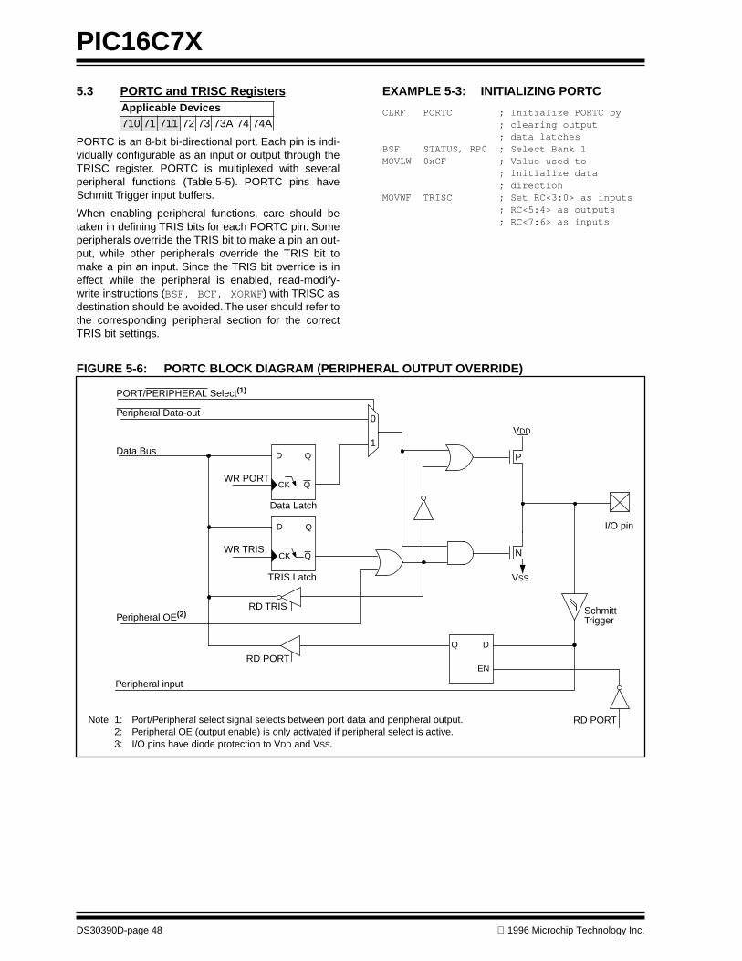
PIC16C7X
DS30390D-page 48
1996 Microchip Technology Inc.
5.3 PORTC and TRISC Registers
PORTC is an 8-bit bi-directional port. Each pin is indi-vidually configurable as an input or output through theTRISC register. PORTC is multiplexed with severalperipheral functions (Table 5-5). PORTC pins haveSchmitt Trigger input buffers.
When enabling peripheral functions, care should betaken in defining TRIS bits for each PORTC pin. Someperipherals override the TRIS bit to make a pin an out-put, while other peripherals override the TRIS bit tomake a pin an input. Since the TRIS bit override is ineffect while the peripheral is enabled, read-modify-write instructions (
BSF, BCF, XORWF
) with TRISC asdestination should be avoided. The user should refer tothe corresponding peripheral section for the correctTRIS bit settings.
Applicable Devices
710 71 711 72 73 73A 74 74A
EXAMPLE 5-3: INITIALIZING PORTC
CLRF PORTC ; Initialize PORTC by ; clearing output ; data latchesBSF STATUS, RP0 ; Select Bank 1MOVLW 0xCF ; Value used to ; initialize data ; directionMOVWF TRISC ; Set RC<3:0> as inputs ; RC<5:4> as outputs ; RC<7:6> as inputs
FIGURE 5-6: PORTC BLOCK DIAGRAM (PERIPHERAL OUTPUT OVERRIDE)
Data Latch
TRIS Latch
RD TRIS
P
VSS
QD
QCK
QD
QCK
EN
Q D
EN
N
VDD
0
1
RD PORT
WR PORT
WR TRIS
SchmittTrigger
Peripheral input
Peripheral OE(2)
Data Bus
PORT/PERIPHERAL Select(1)
Peripheral Data-out
RD PORTNote 1: Port/Peripheral select signal selects between port data and peripheral output.2: Peripheral OE (output enable) is only activated if peripheral select is active.3: I/O pins have diode protection to VDD and VSS.
I/O pin
1996 Microchip Technology Inc. DS30390D-page 49
PIC16C7X
TABLE 5-5: PORTC FUNCTIONS
TABLE 5-6: SUMMARY OF REGISTERS ASSOCIATED WITH PORTC
Name Bit# Buffer Type Function
RC0/T1OSO/T1CKI bit0 ST Input/output port pin or Timer1 oscillator output/Timer1 clock input
RC1/T1OSI/CCP2
(1)
bit1 ST Input/output port pin or Timer1 oscillator input or Capture2 input/Compare2 output/PWM2 output
RC2/CCP1 bit2 ST Input/output port pin or Capture1 input/Compare1 output/PWM1 output
RC3/SCK/SCL bit3 ST RC3/SCK/SCL can also be selected as the synchronous serial clock for both SPI and I
2
C modes.
RC4/SDI/SDA bit4 ST RC4/SDI/SDA can also be selected as the SPI Data In (SPI mode) or data I/O (I
2
C mode).
RC5/SDO bit5 ST Input/output port pin or Synchronous Serial Port data output
RC6/TX/CK
(2)
bit6 ST Input/output port pin or USART Asynchronous Transmit, or USART Synchronous Clock
RC7/RX/DT
(2)
bit7 ST Input/output port pin or USART Asynchronous Receive, or USART Synchronous Data
Legend: ST = Schmitt Trigger inputNote 1: The CCP2 multiplexed function is not enabled on the PIC16C72.
2: The TX/CK and RX/DT multiplexed functions are not enabled on the PIC16C72.
Address Name Bit 7 Bit 6 Bit 5 Bit 4 Bit 3 Bit 2 Bit 1 Bit 0Value on:
POR,BOR
Value on all other resets
07h PORTC RC7 RC6 RC5 RC4 RC3 RC2 RC1 RC0
xxxx xxxx uuuu uuuu
87h TRISC TRISC7 TRISC6 TRISC5 TRISC4 TRISC3 TRISC2 TRISC1 TRISC0
1111 1111 1111 1111
Legend:
x
= unknown,
u
= unchanged.

PIC16C7X
DS30390D-page 50
1996 Microchip Technology Inc.
5.4 PORTD and TRISD Registers
PORTD is an 8-bit port with Schmitt Trigger input buff-ers. Each pin is individually configurable as an input oroutput.
Applicable Devices
710 71 711 72 73 73A 74 74A
PORTD can be configured as an 8-bit wide micropro-cessor port (parallel slave port) by setting control bitPSPMODE (TRISE<4>). In this mode, the input buffersare TTL.
FIGURE 5-7: PORTD BLOCK DIAGRAM (IN I/O PORT MODE)
TABLE 5-7: PORTD FUNCTIONS
Name Bit# Buffer Type Function
RD0/PSP0 bit0 ST/TTL
(1)
Input/output port pin or parallel slave port bit0
RD1/PSP1 bit1 ST/TTL
(1)
Input/output port pin or parallel slave port bit1
RD2/PSP2 bit2 ST/TTL
(1)
Input/output port pin or parallel slave port bit2
RD3/PSP3 bit3 ST/TTL
(1)
Input/output port pin or parallel slave port bit3
RD4/PSP4 bit4 ST/TTL
(1)
Input/output port pin or parallel slave port bit4
RD5/PSP5 bit5 ST/TTL
(1)
Input/output port pin or parallel slave port bit5
RD6/PSP6 bit6 ST/TTL
(1)
Input/output port pin or parallel slave port bit6
RD7/PSP7 bit7 ST/TTL
(1)
Input/output port pin or parallel slave port bit7Legend: ST = Schmitt Trigger input TTL = TTL input Note 1: Input buffers are Schmitt Triggers when in I/O mode and TTL buffer when in Parallel Slave Port Mode.
Data Bus
WR PORT
WR TRIS
RD PORT
Data Latch
TRIS Latch
SchmittTriggerinputbuffer
Note: I/O pins have protection diodes to VDD and VSS.
QD
QCK
QD
QCK
EN
Q D
EN
I/O pin
RD TRIS

1996 Microchip Technology Inc. DS30390D-page 51
PIC16C7X
TABLE 5-8: SUMMARY OF REGISTERS ASSOCIATED WITH PORTD
Address Name Bit 7 Bit 6 Bit 5 Bit 4 Bit 3 Bit 2 Bit 1 Bit 0Value on:
POR,BOR
Value on all other resets
08h PORTD RD7 RD6 RD5 RD4 RD3 RD2 RD1 RD0 xxxx xxxx uuuu uuuu
88h TRISD TRISD7 TRISD6 TRISD5 TRISD4 TRISD3 TRISD2 TRISD1 TRISD0 1111 1111 1111 1111
89h TRISE IBF OBF IBOV PSPMODE — TRISE2 TRISE1 TRISE0 0000 -111 0000 -111
Legend: x = unknown, u = unchanged, - = unimplemented read as '0'. Shaded cells are not used by PORTD.

PIC16C7X
DS30390D-page 52 1996 Microchip Technology Inc.
5.5 PORTE and TRISE Register
PORTE has three pins RE0/RD/AN5, RE1/WR/AN6and RE2/CS/AN7, which are individually configurableas inputs or outputs. These pins have Schmitt Triggerinput buffers.
I/O PORTE becomes control inputs for the micropro-cessor port when bit PSPMODE (TRISE<4>) is set. Inthis mode, the user must make sure that theTRISE<2:0> bits are set (pins are configured as digitalinputs) and that register ADCON1 is configured for dig-ital I/O. In this mode the input buffers are TTL.
Applicable Devices710 71 711 72 73 73A 74 74A
Figure 5-8 shows the TRISE register, which also con-trols the parallel slave port operation.
PORTE pins are multiplexed with analog inputs. Theoperation of these pins is selected by control bits in theADCON1 register. When selected as an analog input,these pins will read as '0's.
TRISE controls the direction of the RE pins, even whenthey are being used as analog inputs. The user mustmake sure to keep the pins configured as inputs whenusing them as analog inputs.
Note: On a Power-on Reset these pins are con-figured as analog inputs.
FIGURE 5-8: TRISE REGISTER (ADDRESS 89h)
R-0 R-0 R/W-0 R/W-0 U-0 R/W-1 R/W-1 R/W-1
IBF OBF IBOV PSPMODE — TRISE2 TRISE1 TRISE0 R = Readable bitW = Writable bitU = Unimplemented bit,
read as ‘0’- n = Value at POR reset
bit7 bit0
bit 7: IBF: Input Buffer Full Status bit1 = A word has been received and waiting to be read by the CPU0 = No word has been received
bit 6: OBF: Output Buffer Full Status bit1 = The output buffer still holds a previously written word0 = The output buffer has been read
bit 5: IBOV: Input Buffer Overflow Detect bit (in microprocessor mode)1 = A write occurred when a previously input word has not been read (must be cleared in software)0 = No overflow occurred
bit 4: PSPMODE: Parallel Slave Port Mode Select bit1 = Parallel slave port mode0 = General purpose I/O mode
bit 3: Unimplemented: Read as '0'
bit 2: TRISE2: Direction control bit for pin RE2/CS/AN71 = Input0 = Output
bit 1: TRISE1: Direction control bit for pin RE1/WR/AN61 = Input0 = Output
bit 0: TRISE0: Direction control bit for pin RE0/RD/AN51 = Input0 = Output
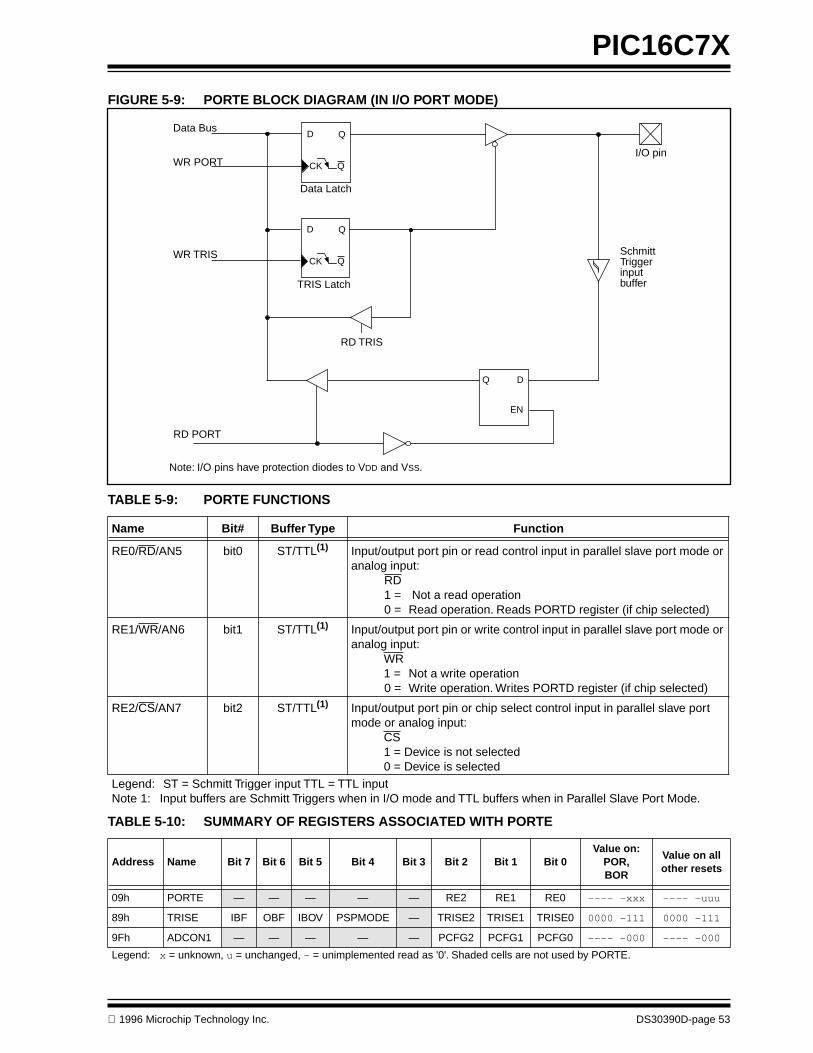
1996 Microchip Technology Inc. DS30390D-page 53
PIC16C7X
FIGURE 5-9: PORTE BLOCK DIAGRAM (IN I/O PORT MODE)
TABLE 5-9: PORTE FUNCTIONS
TABLE 5-10: SUMMARY OF REGISTERS ASSOCIATED WITH PORTE
Name Bit# Buffer Type Function
RE0/RD/AN5 bit0 ST/TTL(1) Input/output port pin or read control input in parallel slave port mode or analog input:
RD1 = Not a read operation0 = Read operation. Reads PORTD register (if chip selected)
RE1/WR/AN6 bit1 ST/TTL(1) Input/output port pin or write control input in parallel slave port mode or analog input:
WR1 = Not a write operation0 = Write operation. Writes PORTD register (if chip selected)
RE2/CS/AN7 bit2 ST/TTL(1) Input/output port pin or chip select control input in parallel slave port mode or analog input:
CS1 = Device is not selected0 = Device is selected
Legend: ST = Schmitt Trigger input TTL = TTL input Note 1: Input buffers are Schmitt Triggers when in I/O mode and TTL buffers when in Parallel Slave Port Mode.
Address Name Bit 7 Bit 6 Bit 5 Bit 4 Bit 3 Bit 2 Bit 1 Bit 0Value on:
POR,BOR
Value on all other resets
09h PORTE — — — — — RE2 RE1 RE0 ---- -xxx ---- -uuu
89h TRISE IBF OBF IBOV PSPMODE — TRISE2 TRISE1 TRISE0 0000 -111 0000 -111
9Fh ADCON1 — — — — — PCFG2 PCFG1 PCFG0 ---- -000 ---- -000
Legend: x = unknown, u = unchanged, - = unimplemented read as '0'. Shaded cells are not used by PORTE.
Data Bus
WR PORT
WR TRIS
RD PORT
Data Latch
TRIS Latch
SchmittTriggerinputbuffer
QD
QCK
QD
QCK
EN
Q D
EN
I/O pin
RD TRIS
Note: I/O pins have protection diodes to VDD and VSS.

PIC16C7X
DS30390D-page 54 1996 Microchip Technology Inc.
5.6 I/O Programming Considerations
5.6.1 BI-DIRECTIONAL I/O PORTS
Any instruction which writes, operates internally as aread followed by a write operation. The BCF and BSFinstructions, for example, read the register into theCPU, execute the bit operation and write the resultback to the register. Caution must be used when theseinstructions are applied to a port with both inputs andoutputs defined. For example, a BSF operation on bit5of PORTB will cause all eight bits of PORTB to be readinto the CPU. Then the BSF operation takes place onbit5 and PORTB is written to the output latches. Ifanother bit of PORTB is used as a bi-directional I/O pin(e.g., bit0) and it is defined as an input at this time, theinput signal present on the pin itself would be read intothe CPU and rewritten to the data latch of this particularpin, overwriting the previous content. As long as the pinstays in the input mode, no problem occurs. However,if bit0 is switched to an output, the content of the datalatch may now be unknown.
Reading the port register, reads the values of the portpins. Writing to the port register writes the value to theport latch. When using read-modify-write instructions(ex. BCF, BSF, etc.) on a port, the value of the port pinsis read, the desired operation is done to this value, andthis value is then written to the port latch.
Example 5-4 shows the effect of two sequential read-modify-write instructions on an I/O port.
Applicable Devices710 71 711 72 73 73A 74 74A
EXAMPLE 5-4: READ-MODIFY-WRITE INSTRUCTIONS ON AN I/O PORT
;Initial PORT settings: PORTB<7:4> Inputs; PORTB<3:0> Outputs;PORTB<7:6> have external pull-ups and are;not connected to other circuitry;; PORT latch PORT pins; ---------- --------- BCF PORTB, 7 ; 01pp pppp 11pp pppp BCF PORTB, 6 ; 10pp pppp 11pp pppp BSF STATUS, RP0 ; BCF TRISB, 7 ; 10pp pppp 11pp pppp BCF TRISB, 6 ; 10pp pppp 10pp pppp;;Note that the user may have expected the ;pin values to be 00pp ppp. The 2nd BCF;caused RB7 to be latched as the pin value;(high).
A pin actively outputting a Low or High should not bedriven from external devices at the same time in orderto change the level on this pin (“wired-or”, “wired-and”).The resulting high output currents may damage thechip.
5.6.2 SUCCESSIVE OPERATIONS ON I/O PORTS
The actual write to an I/O port happens at the end of aninstruction cycle, whereas for reading, the data must bevalid at the beginning of the instruction cycle(Figure 5-10). Therefore, care must be exercised if awrite followed by a read operation is carried out on thesame I/O port. The sequence of instructions should besuch to allow the pin voltage to stabilize (load depen-dent) before the next instruction which causes that fileto be read into the CPU is executed. Otherwise, theprevious state of that pin may be read into the CPUrather than the new state. When in doubt, it is better toseparate these instructions with a NOP or anotherinstruction not accessing this I/O port.
FIGURE 5-10: SUCCESSIVE I/O OPERATION
PC PC + 1 PC + 2 PC + 3
Q1 Q2 Q3 Q4 Q1 Q2 Q3 Q4 Q1 Q2 Q3 Q4 Q1 Q2 Q3 Q4
Instructionfetched
RB7:RB0
MOVWF PORTBwrite toPORTB
NOP
Port pinsampled here
NOPMOVF PORTB,W
Instructionexecuted
MOVWF PORTBwrite toPORTB
NOP
MOVF PORTB,W
PC
TPD
Note:
This example shows a write to PORTBfollowed by a read from PORTB.
Note that:
data setup time = (0.25TCY - TPD)
where TCY = instruction cycleTPD = propagation delay
Therefore, at higher clock frequencies,a write followed by a read may be prob-lematic.
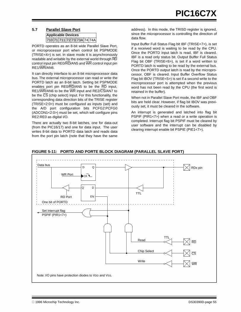
1996 Microchip Technology Inc. DS30390D-page 55
PIC16C7X
5.7 Parallel Slave Port
PORTD operates as an 8-bit wide Parallel Slave Port,or microprocessor port when control bit PSPMODE(TRISE<4>) is set. In slave mode it is asynchronouslyreadable and writable by the external world through RDcontrol input pin RE0/RD/AN5 and WR control input pinRE1/WR/AN6.
It can directly interface to an 8-bit microprocessor databus. The external microprocessor can read or write thePORTD latch as an 8-bit latch. Setting bit PSPMODEenables port pin RE0/RD/AN5 to be the RD input,RE1/WR/AN6 to be the WR input and RE2/CS/AN7 tobe the CS (chip select) input. For this functionality, thecorresponding data direction bits of the TRISE register(TRISE<2:0>) must be configured as inputs (set) andthe A/D port configuration bits PCFG2:PCFG0(ADCON1<2:0>) must be set, which will configure pinsRE2:RE0 as digital I/O.
There are actually two 8-bit latches, one for data-out(from the PIC16/17) and one for data input. The userwrites 8-bit data to PORTD data latch and reads datafrom the port pin latch (note that they have the same
Applicable Devices710 71 711 72 73 73A 74 74A
address). In this mode, the TRISD register is ignored,since the microprocessor is controlling the direction ofdata flow.
Input Buffer Full Status Flag bit IBF (TRISE<7>), is setif a received word is waiting to be read by the CPU.Once the PORTD input latch is read, IBF is cleared.IBF is a read only status bit. Output Buffer Full StatusFlag bit OBF (TRISE<6>), is set if a word written toPORTD latch is waiting to be read by the external bus.Once the PORTD output latch is read by the micropro-cessor, OBF is cleared. Input Buffer Overflow StatusFlag bit IBOV (TRISE<5>) is set if a second write to themicroprocessor port is attempted when the previousword has not been read by the CPU (the first word isretained in the buffer).
When not in Parallel Slave Port mode, the IBF and OBFbits are held clear. However, if flag bit IBOV was previ-ously set, it must be cleared in the software.
An interrupt is generated and latched into flag bitPSPIF (PIR1<7>) when a read or a write operation iscompleted. Interrupt flag bit PSPIF must be cleared byuser software and the interrupt can be disabled byclearing interrupt enable bit PSPIE (PIE1<7>).
FIGURE 5-11: PORTD AND PORTE BLOCK DIAGRAM (PARALLEL SLAVE PORT)
EN
QD
CK
Data bus
WR Port
RD Port
One bit of PORTD
Set interrupt flagPSPIF (PIR1<7>)
RDx pin
TTL
TTLRead
Chip Select
Write
RD
CS
WR
Note: I/O pins have protection diodes to VDD and VSS.
EN
Q D
EN

PIC16C7X
DS30390D-page 56 1996 Microchip Technology Inc.
TABLE 5-11: REGISTERS ASSOCIATED WITH PARALLEL SLAVE PORT
Address Name Bit 7 Bit 6 Bit 5 Bit 4 Bit 3 Bit 2 Bit 1 Bit 0Value on:
POR,BOR
Value on all other resets
08h PORTD PSP7 PSP6 PSP5 PSP4 PSP3 PSP2 PSP1 PSP0 xxxx xxxx uuuu uuuu
09h PORTE — — — — — RE2 RE1 RE0 ---- -xxx ---- -uuu
89h TRISE IBF OBF IBOV PSPMODE — TRISE2 TRISE1 TRISE0 0000 -111 0000 -111
0Ch PIR1 PSPIF ADIF RCIF TXIF SSPIF CCP1IF TMR2IF TMR1IF 0000 0000 0000 0000
8Ch PIE1 PSPIE ADIE RCIE TXIE SSPIE CCP1IE TMR2IE TMR1IE 0000 0000 0000 0000
9Fh ADCON1 — — — — — PCFG2 PCFG1 PCFG0 ---- -000 ---- -000
Legend: x = unknown, u = unchanged, - = unimplemented read as '0'. Shaded cells are not used by the Parallel Slave Port.

1996 Microchip Technology Inc. DS30390D-page 57
PIC16C7X
6.0 OVERVIEW OF TIMER MODULES
The PIC16C710 and PIC16C71/711 have one timermodule.
The PIC16C72, PIC16C73/73A and PIC16C74/74Aeach have three timer modules.
Each module can generate an interrupt to indicate thatan event has occurred (i.e. timer overflow). Each ofthese modules is explained in full detail in the followingsections. The timer modules are:
• Timer0 Module (Section 7.0)• Timer1 Module (Section 8.0)• Timer2 Module (Section 9.0)
6.1 Timer0 Overview
The Timer0 module (previously known as RTCC) is asimple 8-bit overflow counter. The clock source can beeither the internal system clock (Fosc/4) or an externalclock. When the clock source is an external clock, theTimer0 module can be selected to increment on eitherthe rising or falling edge.
The Timer0 module also has a programmable pres-caler option. This prescaler can be assigned to eitherthe Timer0 module or the Watchdog Timer. Bit PSA(OPTION<3>) assigns the prescaler, and bits PS2:PS0(OPTION<2:0>) determine the prescaler value. Timer0can increment at the following rates: 1:1 (when pres-caler assigned to Watchdog timer), 1:2, 1:4, 1:8, 1:16,1:32, 1:64, 1:128, and 1:256 (Timer0 only).
Synchronization of the external clock occurs after theprescaler. When the prescaler is used, the externalclock frequency may be higher then the device’s fre-quency. The maximum frequency is 50 MHz, given thehigh and low time requirements of the clock.
6.2 Timer1 Overview
Timer1 is a 16-bit timer/counter. The clock source canbe either the internal system clock (Fosc/4), an exter-nal clock, or an external crystal. Timer1 can operate aseither a timer or a counter. When operating as acounter (external clock source), the counter can eitheroperate synchronized to the device or asynchronouslyto the device. Asynchronous operation allows Timer1 tooperate during sleep, which is useful for applicationsthat require a real-time clock as well as the power sav-ings of SLEEP mode.
Timer1 also has a prescaler option which allows Timer1to increment at the following rates: 1:1, 1:2, 1:4, and1:8. Timer1 can be used in conjunction with the Cap-
Applicable Devices
710 71 711 72 73 73A 74 74A
Applicable Devices
710 71 711 72 73 73A 74 74A
Applicable Devices
710 71 711 72 73 73A 74 74A
ture/Compare/PWM module. When used with a CCPmodule, Timer1 is the time-base for 16-bit Capture orthe 16-bit Compare and must be synchronized to thedevice.
6.3 Timer2 Overview
Timer2 is an 8-bit timer with a programmable prescalerand postscaler, as well as an 8-bit period register(PR2). Timer2 can be used with the CCP1 module (inPWM mode) as well as the Baud Rate Generator forthe Synchronous Serial Port (SSP). The prescaleroption allows Timer2 to increment at the followingrates: 1:1, 1:4, 1:16.
The postscaler allows the TMR2 register to match theperiod register (PR2) a programmable number of timesbefore generating an interrupt. The postscaler can beprogrammed from 1:1 to 1:16 (inclusive).
6.4 CCP Overview
The CCP module(s) can operate in one of these threemodes: 16-bit capture, 16-bit compare, or up to 10-bitPulse Width Modulation (PWM).
Capture mode captures the 16-bit value of TMR1 intothe CCPRxH:CCPRxL register pair. The capture eventcan be programmed for either the falling edge, risingedge, fourth rising edge, or the sixteenth rising edge ofthe CCPx pin.
Compare mode compares the TMR1H:TMR1L registerpair to the CCPRxH:CCPRxL register pair. When amatch occurs an interrupt can be generated, and theoutput pin CCPx can be forced to given state (High orLow), TMR1 can be reset (CCP1), or TMR1 reset andstart A/D conversion (CCP2). This depends on the con-trol bits CCPxM3:CCPxM0.
PWM mode compares the TMR2 register to a 10-bitduty cycle register (CCPRxH:CCPRxL<5:4>) as wellas to an 8-bit period register (PR2). When the TMR2register = Duty Cycle register, the CCPx pin will beforced low. When TMR2 = PR2, TMR2 is cleared to00h, an interrupt can be generated, and the CCPx pin(if an output) will be forced high.
Applicable Devices
710 71 711 72 73 73A 74 74A
Applicable Devices
710 71 711 72 73 73A 74 74A
This document was created with FrameMaker 4 0 4

PIC16C7X
DS30390D-page 58
1996 Microchip Technology Inc.
NOTES:

1996 Microchip Technology Inc. DS30390D-page 59
PIC16C7X
7.0 TIMER0 MODULE
The Timer0 module timer/counter has the following fea-tures:
• 8-bit timer/counter• Readable and writable• 8-bit software programmable prescaler• Internal or external clock select• Interrupt on overflow from FFh to 00h• Edge select for external clock
Figure 7-1 is a simplified block diagram of the Timer0module.
Timer mode is selected by clearing bit T0CS(OPTION<5>). In timer mode, the Timer0 module willincrement every instruction cycle (without prescaler). Ifthe TMR0 register is written, the increment is inhibitedfor the following two instruction cycles (Figure 7-2 andFigure 7-3). The user can work around this by writingan adjusted value to the TMR0 register.
Counter mode is selected by setting bit T0CS(OPTION<5>). In counter mode, Timer0 will incrementeither on every rising or falling edge of pin RA4/T0CKI.The incrementing edge is determined by the Timer0
Applicable Devices
710 71 711 72 73 73A 74 74A
Source Edge Select bit T0SE (OPTION<4>). Clearingbit T0SE selects the rising edge. Restrictions on theexternal clock input are discussed in detail inSection 7.2.
The prescaler is mutually exclusively shared betweenthe Timer0 module and the Watchdog Timer. The pres-caler assignment is controlled in software by control bitPSA (OPTION<3>). Clearing bit PSA will assign theprescaler to the Timer0 module. The prescaler is notreadable or writable. When the prescaler is assigned tothe Timer0 module, prescale values of 1:2, 1:4, ...,1:256 are selectable. Section 7.3 details the operationof the prescaler.
7.1 Timer0 Interrupt
The TMR0 interrupt is generated when the TMR0 reg-ister overflows from FFh to 00h. This overflow sets bitT0IF (INTCON<2>). The interrupt can be masked byclearing bit T0IE (INTCON<5>). Bit T0IF must becleared in software by the Timer0 module interrupt ser-vice routine before re-enabling this interrupt. TheTMR0 interrupt cannot awaken the processor fromSLEEP since the timer is shut off during SLEEP. SeeFigure 7-4 for Timer0 interrupt timing.
Applicable Devices
710 71 711 72 73 73A 74 74A
FIGURE 7-1: TIMER0 BLOCK DIAGRAM
FIGURE 7-2: TIMER0 TIMING: INTERNAL CLOCK/NO PRESCALE
Note 1: T0CS, T0SE, PSA, PS2:PS0 (OPTION<5:0>).2: The prescaler is shared with Watchdog Timer (refer to Figure 7-6 for detailed block diagram).
RA4/T0CKI
T0SE
0
1
1
0pin
T0CS
FOSC/4
ProgrammablePrescaler
Sync withInternalclocks
TMR0
PSout
(2 cycle delay)
PSout
Data bus
8
PSAPS2, PS1, PS0Set interruptflag bit T0IFon overflow
3
PC-1
Q1 Q2 Q3 Q4 Q1 Q2 Q3 Q4 Q1 Q2 Q3 Q4 Q1 Q2 Q3 Q4 Q1 Q2 Q3 Q4 Q1 Q2 Q3 Q4 Q1 Q2 Q3 Q4 Q1 Q2 Q3 Q4PC(ProgramCounter)
InstructionFetch
TMR0
PC PC+1 PC+2 PC+3 PC+4 PC+5 PC+6
T0 T0+1 T0+2 NT0 NT0 NT0 NT0+1 NT0+2 T0
MOVWF TMR0 MOVF TMR0,W MOVF TMR0,W MOVF TMR0,W MOVF TMR0,W MOVF TMR0,W
Write TMR0executed
Read TMR0reads NT0
Read TMR0reads NT0
Read TMR0reads NT0
Read TMR0reads NT0 + 1
Read TMR0reads NT0 + 2
InstructionExecuted
This document was created with FrameMaker 4 0 4

PIC16C7X
DS30390D-page 60
1996 Microchip Technology Inc.
FIGURE 7-3: TIMER0 TIMING: INTERNAL CLOCK/PRESCALE 1:2
FIGURE 7-4: TIMER0 INTERRUPT TIMING
PC+6
PC-1
Q1 Q2 Q3 Q4 Q1 Q2 Q3 Q4 Q1 Q2 Q3 Q4 Q1 Q2 Q3 Q4 Q1 Q2 Q3 Q4 Q1 Q2 Q3 Q4 Q1 Q2 Q3 Q4 Q1 Q2 Q3 Q4PC(ProgramCounter)
InstructionFetch
TMR0
PC PC+1 PC+2 PC+3 PC+4 PC+5 PC+6
T0 NT0+1
MOVWF TMR0 MOVF TMR0,W MOVF TMR0,W MOVF TMR0,W MOVF TMR0,W MOVF TMR0,W
Write TMR0executed
Read TMR0reads NT0
Read TMR0reads NT0
Read TMR0reads NT0
Read TMR0reads NT0
Read TMR0reads NT0 + 1
T0+1 NT0
InstructionExecute
Q2Q1 Q3 Q4Q2Q1 Q3 Q4 Q2Q1 Q3 Q4 Q2Q1 Q3 Q4 Q2Q1 Q3 Q4
1 1
OSC1
CLKOUT(3)
Timer0
T0IF bit(INTCON<2>)
FEh
GIE bit(INTCON<7>)
INSTRUCTION
PC
Instructionfetched
PC PC +1 PC +1 0004h 0005h
Instructionexecuted
Inst (PC)
Inst (PC-1)
Inst (PC+1)
Inst (PC)
Inst (0004h) Inst (0005h)
Inst (0004h)Dummy cycle Dummy cycle
FFh 00h 01h 02h
Note 1: Interrupt flag bit T0IF is sampled here (every Q1).2: Interrupt latency = 4Tcy where Tcy = instruction cycle time.3: CLKOUT is available only in RC oscillator mode.
FLOW

1996 Microchip Technology Inc. DS30390D-page 61
PIC16C7X
7.2 Using Timer0 with an External Clock
When an external clock input is used for Timer0, it mustmeet certain requirements. The requirements ensurethe external clock can be synchronized with the internalphase clock (T
OSC
). Also, there is a delay in the actualincrementing of Timer0 after synchronization.
7.2.1 EXTERNAL CLOCK SYNCHRONIZATION
When no prescaler is used, the external clock input isthe same as the prescaler output. The synchronizationof T0CKI with the internal phase clocks is accom-plished by sampling the prescaler output on the Q2 andQ4 cycles of the internal phase clocks (Figure 7-5).Therefore, it is necessary for T0CKI to be high for atleast 2Tosc (and a small RC delay of 20 ns) and low forat least 2Tosc (and a small RC delay of 20 ns). Refer tothe electrical specification of the desired device.
Applicable Devices
710 71 711 72 73 73A 74 74A
When a prescaler is used, the external clock input isdivided by the asynchronous ripple-counter type pres-caler so that the prescaler output is symmetrical. Forthe external clock to meet the sampling requirement,the ripple-counter must be taken into account. There-fore, it is necessary for T0CKI to have a period of atleast 4Tosc (and a small RC delay of 40 ns) divided bythe prescaler value. The only requirement on T0CKIhigh and low time is that they do not violate the mini-mum pulse width requirement of 10 ns. Refer to param-eters 40, 41 and 42 in the electrical specification of thedesired device.
7.2.2 TMR0 INCREMENT DELAY
Since the prescaler output is synchronized with theinternal clocks, there is a small delay from the time theexternal clock edge occurs to the time the Timer0 mod-ule is actually incremented. Figure 7-5 shows the delayfrom the external clock edge to the timer incrementing.
FIGURE 7-5: TIMER0 TIMING WITH EXTERNAL CLOCK
Q1 Q2 Q3 Q4 Q1 Q2 Q3 Q4 Q1 Q2 Q3 Q4 Q1 Q2 Q3 Q4
External Clock Input orPrescaler output (2)
External Clock/PrescalerOutput after sampling
Increment Timer0 (Q4)
Timer0 T0 T0 + 1 T0 + 2
Small pulsemisses sampling
Note 1: Delay from clock input change to Timer0 increment is 3Tosc to 7Tosc. (Duration of Q = Tosc).Therefore, the error in measuring the interval between two edges on Timer0 input = ±4Tosc max.
2: External clock if no prescaler selected, Prescaler output otherwise.3: The arrows indicate the points in time where sampling occurs.
(3)
(1)

PIC16C7X
DS30390D-page 62
1996 Microchip Technology Inc.
7.3 Prescaler
An 8-bit counter is available as a prescaler for theTimer0 module, or as a postscaler for the WatchdogTimer, respectively (Figure 7-6). For simplicity, thiscounter is being referred to as “prescaler” throughoutthis data sheet. Note that there is only one prescaleravailable which is mutually exclusively shared betweenthe Timer0 module and the Watchdog Timer. Thus, a
Applicable Devices
710 71 711 72 73 73A 74 74A
prescaler assignment for the Timer0 module meansthat there is no prescaler for the Watchdog Timer, andvice-versa.
The PSA and PS2:PS0 bits (OPTION<3:0>) determinethe prescaler assignment and prescale ratio.
When assigned to the Timer0 module, all instructionswriting to the TMR0 register (e.g.
CLRF 1, MOVWF 1,BSF 1,x
....etc.) will clear the prescaler. Whenassigned to WDT, a
CLRWDT
instruction will clear theprescaler along with the Watchdog Timer. The pres-caler is not readable or writable.
FIGURE 7-6: BLOCK DIAGRAM OF THE TIMER0/WDT PRESCALER
RA4/T0CKI
T0SE
pin
MUX
CLKOUT (=Fosc/4)
SYNC2
CyclesTMR0 reg
8-bit Prescaler
8 - to - 1MUX
MUX
M U X
WatchdogTimer
PSA
0 1
0
1
WDTTime-out
PS2:PS0
8
Note: T0CS, T0SE, PSA, PS2:PS0 are (OPTION<5:0>).
PSA
WDT Enable bit
MUX
0
1 0
1
Data Bus
Set flag bit T0IFon Overflow
8
PSAT0CS

1996 Microchip Technology Inc. DS30390D-page 63
PIC16C7X
7.3.1 SWITCHING PRESCALER ASSIGNMENT
The prescaler assignment is fully under software con-trol, i.e., it can be changed “on the fly” during programexecution.
EXAMPLE 7-1: CHANGING PRESCALER (TIMER0
→
WDT)
BCF STATUS, RP0 ;Bank 0 CLRF TMR0 ;Clear TMR0 & Prescaler BSF STATUS, RP0 ;Bank 1 CLRWDT ;Clears WDT MOVLW b'xxxx1xxx' ;Select new prescale MOVWF OPTION_REG ;value & WDT BCF STATUS, RP0 ;Bank 0
Note:
To avoid an unintended device RESET, thefollowing instruction sequence (shown inExample 7-1) must be executed whenchanging the prescaler assignment fromTimer0 to the WDT. This sequence mustbe followed even if the WDT is disabled.
To change prescaler from the WDT to the Timer0 mod-ule use the sequence shown in Example 7-2.
EXAMPLE 7-2: CHANGING PRESCALER (WDT
→
TIMER0)
CLRWDT ;Clear WDT and ;prescaler BSF STATUS, RP0 ;Bank 1 MOVLW b'xxxx0xxx' ;Select TMR0, new ;prescale value and MOVWF OPTION_REG ;clock source BCF STATUS, RP0 ;Bank 0
TABLE 7-1: REGISTERS ASSOCIATED WITH TIMER0, PIC16C710/71/711
TABLE 7-2: REGISTERS ASSOCIATED WITH TIMER0, PIC16C72/73/73A/74/74A
Address Name Bit 7 Bit 6 Bit 5 Bit 4 Bit 3 Bit 2 Bit 1 Bit 0Value on:
POR,BOR
Value on all other resets
01h TMR0 Timer0 module’s register
xxxx xxxx uuuu uuuu
0Bh/8Bh INTCON GIE ADIE T0IE INTE RBIE T0IF INTF RBIF
0000 000x 0000 000u
81h OPTION RBPU INTEDG T0CS T0SE PSA PS2 PS1 PS0
1111 1111 1111 1111
85h TRISA — — — TRISA4 TRISA3 TRISA2 TRISA1 TRISA0
---1 1111 ---1 1111
Legend:
x
= unknown,
u
= unchanged,
-
= unimplemented locations read as '0'. Shaded cells are not used by Timer0.
Address Name Bit 7 Bit 6 Bit 5 Bit 4 Bit 3 Bit 2 Bit 1 Bit 0Value on:
POR,BOR
Value on all other resets
01h TMR0 Timer0 module’s register
xxxx xxxx uuuu uuuu
0Bh/8Bh INTCON GIE PEIE T0IE INTE RBIE T0IF INTF RBIF
0000 000x 0000 000u
81h OPTION RBPU INTEDG T0CS T0SE PSA PS2 PS1 PS0
1111 1111 1111 1111
85h TRISA — — TRISA5 TRISA4 TRISA3 TRISA2 TRISA1 TRISA0
--11 1111 --11 1111
Legend:
x
= unknown,
u
= unchanged,
-
= unimplemented locations read as '0'. Shaded cells are not used by Timer0.

PIC16C7X
DS30390D-page 64
1996 Microchip Technology Inc.
NOTES:
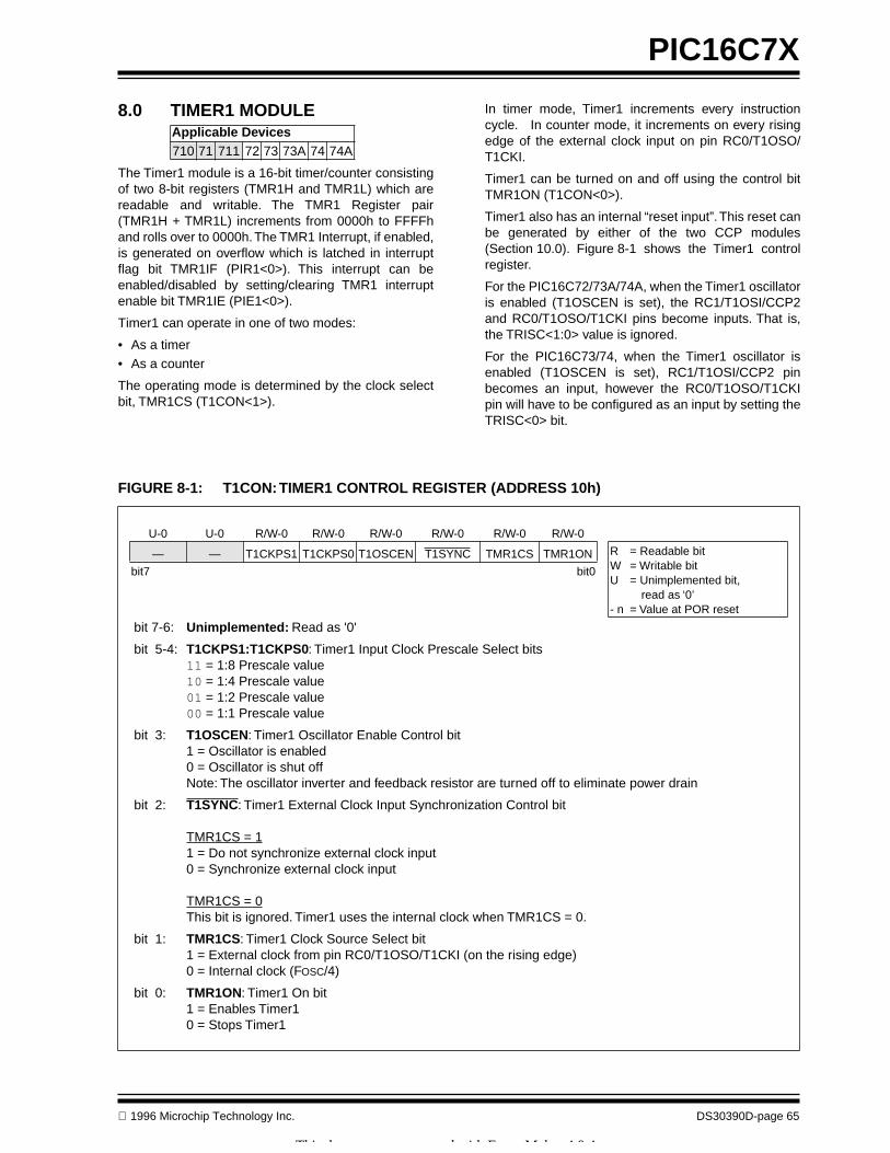
1996 Microchip Technology Inc. DS30390D-page 65
PIC16C7X
8.0 TIMER1 MODULE
The Timer1 module is a 16-bit timer/counter consistingof two 8-bit registers (TMR1H and TMR1L) which arereadable and writable. The TMR1 Register pair(TMR1H + TMR1L) increments from 0000h to FFFFhand rolls over to 0000h. The TMR1 Interrupt, if enabled,is generated on overflow which is latched in interruptflag bit TMR1IF (PIR1<0>). This interrupt can beenabled/disabled by setting/clearing TMR1 interruptenable bit TMR1IE (PIE1<0>).
Timer1 can operate in one of two modes:
• As a timer• As a counter
The operating mode is determined by the clock selectbit, TMR1CS (T1CON<1>).
Applicable Devices
710 71 711 72 73 73A 74 74A
In timer mode, Timer1 increments every instructioncycle. In counter mode, it increments on every risingedge of the external clock input on pin RC0/T1OSO/T1CKI.
Timer1 can be turned on and off using the control bitTMR1ON (T1CON<0>).
Timer1 also has an internal “reset input”. This reset canbe generated by either of the two CCP modules(Section 10.0). Figure 8-1 shows the Timer1 controlregister.
For the PIC16C72/73A/74A, when the Timer1 oscillatoris enabled (T1OSCEN is set), the RC1/T1OSI/CCP2and RC0/T1OSO/T1CKI pins become inputs. That is,the TRISC<1:0> value is ignored.
For the PIC16C73/74, when the Timer1 oscillator isenabled (T1OSCEN is set), RC1/T1OSI/CCP2 pinbecomes an input, however the RC0/T1OSO/T1CKIpin will have to be configured as an input by setting theTRISC<0> bit.
FIGURE 8-1: T1CON: TIMER1 CONTROL REGISTER
(ADDRESS 10h)
U-0 U-0 R/W-0 R/W-0 R/W-0 R/W-0 R/W-0 R/W-0
— — T1CKPS1 T1CKPS0 T1OSCEN T1SYNC TMR1CS TMR1ON R = Readable bitW = Writable bitU = Unimplemented bit,
read as ‘0’- n = Value at POR reset
bit7 bit0
bit 7-6:
Unimplemented:
Read as '0'
bit 5-4:
T1CKPS1:T1CKPS0
: Timer1 Input Clock Prescale Select bits
11
= 1:8 Prescale value
10
= 1:4 Prescale value
01
= 1:2 Prescale value
00
= 1:1 Prescale value
bit 3:
T1OSCEN
: Timer1 Oscillator Enable Control bit1 = Oscillator is enabled0 = Oscillator is shut offNote: The oscillator inverter and feedback resistor are turned off to eliminate power drain
bit 2:
T1SYNC
: Timer1 External Clock Input Synchronization Control bit
TMR1CS = 11 = Do not synchronize external clock input0 = Synchronize external clock input
TMR1CS = 0This bit is ignored. Timer1 uses the internal clock when TMR1CS = 0.
bit 1:
TMR1CS
: Timer1 Clock Source Select bit1 = External clock from pin RC0/T1OSO/T1CKI (on the rising edge)0 = Internal clock (F
OSC
/4)
bit 0:
TMR1ON
: Timer1 On bit1 = Enables Timer10 = Stops Timer1
This document was created with FrameMaker 4 0 4

PIC16C7X
DS30390D-page 66
1996 Microchip Technology Inc.
8.1 Timer1 Operation in Timer Mode
Timer mode is selected by clearing the TMR1CS(T1CON<1>) bit. In this mode, the input clock to thetimer is F
OSC
/4. The synchronize control bit T1SYNC(T1CON<2>) has no effect since the internal clock isalways in sync.
8.2 Timer1 Operation in Synchronized Counter Mode
Counter mode is selected by setting bit TMR1CS. Inthis mode the timer increments on every rising edge ofclock input on pin RC1/T1OSI/CCP2 when bitT1OSCEN is set or pin RC0/T1OSO/T1CKI when bitT1OSCEN is cleared.
If T1SYNC is cleared, then the external clock input issynchronized with internal phase clocks. The synchro-nization is done after the prescaler stage. The pres-caler stage is an asynchronous ripple-counter.
In this configuration, during SLEEP mode, Timer1 willnot increment even if the external clock is present,since the synchronization circuit is shut off. The pres-caler however will continue to increment.
Applicable Devices
710 71 711 72 73 73A 74 74A
Applicable Devices
710 71 711 72 73 73A 74 74A
8.2.1 EXTERNAL CLOCK INPUT TIMING FOR SYNCHRONIZED COUNTER MODE
When an external clock input is used for Timer1 in syn-chronized counter mode, it must meet certain require-ments. The external clock requirement is due tointernal phase clock (Tosc) synchronization. Also, thereis a delay in the actual incrementing of TMR1 after syn-chronization.
When the prescaler is 1:1, the external clock input isthe same as the prescaler output. The synchronizationof T1CKI with the internal phase clocks is accom-plished by sampling the prescaler output on the Q2 andQ4 cycles of the internal phase clocks. Therefore, it isnecessary for T1CKI to be high for at least 2Tosc (anda small RC delay of 20 ns) and low for at least 2Tosc(and a small RC delay of 20 ns). Refer to the appropri-ate electrical specifications, parameters 45, 46, and 47.
When a prescaler other than 1:1 is used, the externalclock input is divided by the asynchronous ripple-counter type prescaler so that the prescaler output issymmetrical. In order for the external clock to meet thesampling requirement, the ripple-counter must betaken into account. Therefore, it is necessary for T1CKIto have a period of at least 4Tosc (and a small RC delayof 40 ns) divided by the prescaler value. The onlyrequirement on T1CKI high and low time is that they donot violate the minimum pulse width requirements of10 ns). Refer to the appropriate electrical specifica-tions, parameters 40, 42, 45, 46, and 47.
FIGURE 8-2: TIMER1 BLOCK DIAGRAM
TMR1H TMR1L
T1OSCT1SYNC
TMR1CST1CKPS1:T1CKPS0
SLEEP input
T1OSCENEnableOscillator(1)
FOSC/4InternalClock
TMR1ONon/off
Prescaler1, 2, 4, 8
Synchronize
det
1
0
0
1
Synchronizedclock input
2
RC0/T1OSO/T1CKI
RC1/T1OSI/CCP2(2)
Note 1: When the T1OSCEN bit is cleared, the inverter and feedback resistor are turned off. This eliminates power drain.2: The CCP2 module is not implemented in the PIC16C72.3: For the PIC16C73 and PIC16C74, the Schmitt Trigger is not implemented in external clock mode.
Set flag bitTMR1IF onOverflow
TMR1
(3)

1996 Microchip Technology Inc. DS30390D-page 67
PIC16C7X
8.3 Timer1 Operation in Asynchronous Counter Mode
If control bit T1SYNC (T1CON<2>) is set, the externalclock input is not synchronized. The timer continues toincrement asynchronous to the internal phase clocks.The timer will continue to run during SLEEP and cangenerate an interrupt on overflow which will wake-upthe processor. However, special precautions in soft-ware are needed to read/write the timer(Section 8.3.2).
In asynchronous counter mode, Timer1 can not beused as a time-base for capture or compare opera-tions.
8.3.1 EXTERNAL CLOCK INPUT TIMING WITH UNSYNCHRONIZED CLOCK
If control bit T1SYNC is set, the timer will incrementcompletely asynchronously. The input clock must meetcertain minimum high time and low time requirements.Refer to the appropriate Electrical Specifications Sec-tion, timing parameters 45, 46, and 47.
8.3.2 READING AND WRITING TIMER1 IN ASYNCHRONOUS COUNTER MODE
Reading TMR1H or TMR1L while the timer is running,from an external asynchronous clock, will guarantee avalid read (taken care of in hardware). However, theuser should keep in mind that reading the 16-bit timerin two 8-bit values itself poses certain problems sincethe timer may overflow between the reads.
For writes, it is recommended that the user simply stopthe timer and write the desired values. A write conten-tion may occur by writing to the timer registers while theregister is incrementing. This may produce an unpre-dictable value in the timer register.
Reading the 16-bit value requires some care.Example 8-1 is an example routine to read the 16-bittimer value. This is useful if the timer cannot bestopped.
Applicable Devices
710 71 711 72 73 73A 74 74A
EXAMPLE 8-1: READING A 16-BIT FREE-RUNNING TIMER
; All interrupts are disabled MOVF TMR1H, W ;Read high byte MOVWF TMPH ; MOVF TMR1L, W ;Read low byte MOVWF TMPL ; MOVF TMR1H, W ;Read high byte SUBWF TMPH, W ;Sub 1st read ; with 2nd read BTFSC STATUS,Z ;Is result = 0 GOTO CONTINUE ;Good 16-bit read;; TMR1L may have rolled over between the read; of the high and low bytes. Reading the high; and low bytes now will read a good value.; MOVF TMR1H, W ;Read high byte MOVWF TMPH ; MOVF TMR1L, W ;Read low byte MOVWF TMPL ;; Re-enable the Interrupt (if required)CONTINUE ;Continue with your code
8.4 Timer1 Oscillator
A crystal oscillator circuit is built in between pins T1OSI(input) and T1OSO (amplifier output). It is enabled bysetting control bit T1OSCEN (T1CON<3>). The oscilla-tor is a low power oscillator rated up to 200 kHz. It willcontinue to run during SLEEP. It is primarily intendedfor a 32 kHz crystal. Table 8-1 shows the capacitorselection for the Timer1 oscillator.
The Timer1 oscillator is identical to the LP oscillator.The user must provide a software time delay to ensureproper oscillator start-up.
Applicable Devices
710 71 711 72 73 73A 74 74A
TABLE 8-1: CAPACITOR SELECTION FOR THE TIMER1 OSCILLATOR
Osc Type Freq C1 C2
LP 32 kHz
(1)
100 kHz200 kHz
15 pF15 pF
0 - 15 pF
15 pF15 pF
0 - 15 pFHigher capacitance increases the stability of oscilla-tor but also increases the start-up time. These values are for design guidance only. Note 1: For V
DD
> 4.5V, C1 = C2
≈
30 pF is recom-mended.
Crystals Tested:
32.768 kHz Epson C-001R32.768K-A
±
20 PPM100 kHz Epson C-2 100.00 KC-P
±
20 PPM200 kHz STD XTL 200.000 kHz
±
20 PPM
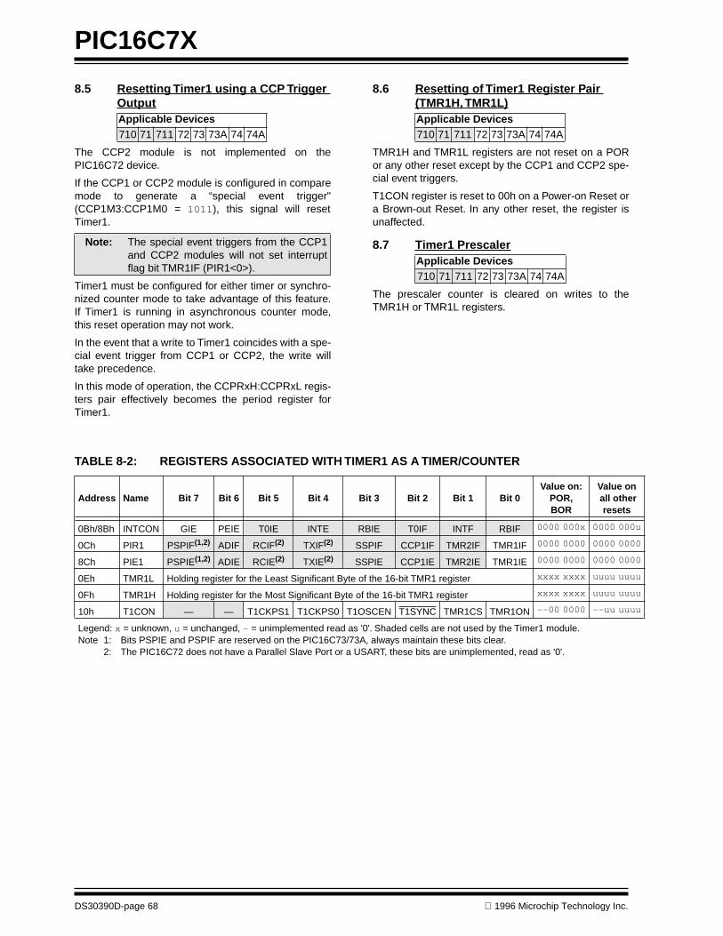
PIC16C7X
DS30390D-page 68
1996 Microchip Technology Inc.
8.5 Resetting Timer1 using a CCP Trigger Output
The CCP2 module is not implemented on thePIC16C72 device.
If the CCP1 or CCP2 module is configured in comparemode to generate a “special event trigger"(CCP1M3:CCP1M0 =
1011
), this signal will resetTimer1.
Timer1 must be configured for either timer or synchro-nized counter mode to take advantage of this feature.If Timer1 is running in asynchronous counter mode,this reset operation may not work.
In the event that a write to Timer1 coincides with a spe-cial event trigger from CCP1 or CCP2, the write willtake precedence.
In this mode of operation, the CCPRxH:CCPRxL regis-ters pair effectively becomes the period register forTimer1.
Applicable Devices
710 71 711 72 73 73A 74 74A
Note:
The special event triggers from the CCP1and CCP2 modules will not set interruptflag bit TMR1IF (PIR1<0>).
8.6 Resetting of Timer1 Register Pair (TMR1H, TMR1L)
TMR1H and TMR1L registers are not reset on a PORor any other reset except by the CCP1 and CCP2 spe-cial event triggers.
T1CON register is reset to 00h on a Power-on Reset ora Brown-out Reset. In any other reset, the register isunaffected.
8.7 Timer1 Prescaler
The prescaler counter is cleared on writes to theTMR1H or TMR1L registers.
Applicable Devices
710 71 711 72 73 73A 74 74A
Applicable Devices
710 71 711 72 73 73A 74 74A
TABLE 8-2: REGISTERS ASSOCIATED WITH TIMER1 AS A TIMER/COUNTER
Address Name Bit 7 Bit 6 Bit 5 Bit 4 Bit 3 Bit 2 Bit 1 Bit 0Value on:
POR,BOR
Value on all other
resets
0Bh/8Bh INTCON GIE PEIE T0IE INTE RBIE T0IF INTF RBIF
0000 000x 0000 000u
0Ch PIR1 PSPIF
(1,2)
ADIF RCIF
(2)
TXIF
(2)
SSPIF CCP1IF TMR2IF TMR1IF
0000 0000 0000 0000
8Ch PIE1 PSPIE
(1,2)
ADIE RCIE
(2)
TXIE
(2)
SSPIE CCP1IE TMR2IE TMR1IE
0000 0000 0000 0000
0Eh TMR1L Holding register for the Least Significant Byte of the 16-bit TMR1 register
xxxx xxxx uuuu uuuu
0Fh TMR1H Holding register for the Most Significant Byte of the 16-bit TMR1 register
xxxx xxxx uuuu uuuu
10h T1CON — — T1CKPS1 T1CKPS0 T1OSCEN T1SYNC TMR1CS TMR1ON
--00 0000 --uu uuuu
Legend:
x
= unknown,
u
= unchanged,
-
= unimplemented read as '0'. Shaded cells are not used by the Timer1 module.Note 1: Bits PSPIE and PSPIF are reserved on the PIC16C73/73A, always maintain these bits clear.
2: The PIC16C72 does not have a Parallel Slave Port or a USART, these bits are unimplemented, read as '0'.
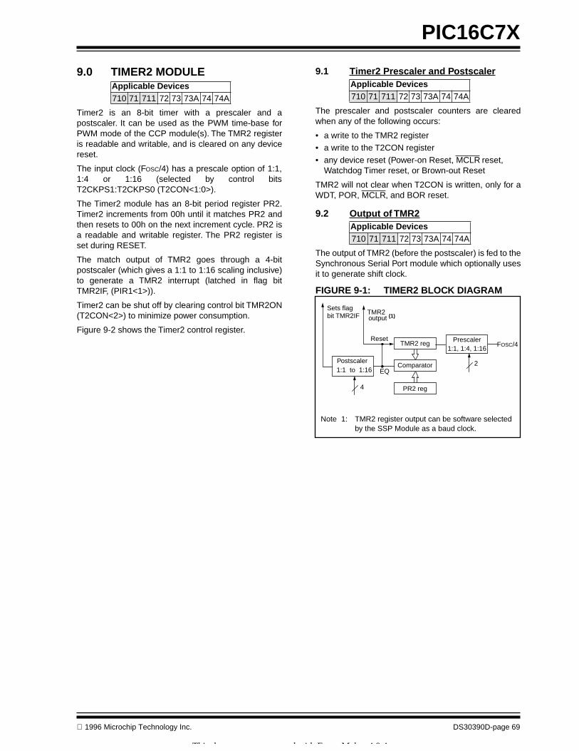
1996 Microchip Technology Inc. DS30390D-page 69
PIC16C7X
9.0 TIMER2 MODULE
Timer2 is an 8-bit timer with a prescaler and apostscaler. It can be used as the PWM time-base forPWM mode of the CCP module(s). The TMR2 registeris readable and writable, and is cleared on any devicereset.
The input clock (F
OSC
/4) has a prescale option of 1:1,1:4 or 1:16 (selected by control bitsT2CKPS1:T2CKPS0 (T2CON<1:0>).
The Timer2 module has an 8-bit period register PR2.Timer2 increments from 00h until it matches PR2 andthen resets to 00h on the next increment cycle. PR2 isa readable and writable register. The PR2 register isset during RESET.
The match output of TMR2 goes through a 4-bitpostscaler (which gives a 1:1 to 1:16 scaling inclusive)to generate a TMR2 interrupt (latched in flag bitTMR2IF, (PIR1<1>)).
Timer2 can be shut off by clearing control bit TMR2ON(T2CON<2>) to minimize power consumption.
Figure 9-2 shows the Timer2 control register.
Applicable Devices
710 71 711 72 73 73A 74 74A
9.1 Timer2 Prescaler and Postscaler
The prescaler and postscaler counters are clearedwhen any of the following occurs:
• a write to the TMR2 register• a write to the T2CON register• any device reset (Power-on Reset, MCLR reset,
Watchdog Timer reset, or Brown-out Reset
TMR2 will not clear when T2CON is written, only for aWDT, POR, MCLR, and BOR reset.
9.2 Output of TMR2
The output of TMR2 (before the postscaler) is fed to theSynchronous Serial Port module which optionally usesit to generate shift clock.
FIGURE 9-1: TIMER2 BLOCK DIAGRAM
Applicable Devices
710 71 711 72 73 73A 74 74A
Applicable Devices
710 71 711 72 73 73A 74 74A
Comparator
TMR2Sets flag
TMR2 reg
output (1)
Reset
Postscaler
Prescaler
PR2 reg
2
FOSC/4
1:1 1:16
1:1, 1:4, 1:16
EQ
4
bit TMR2IF
Note 1: TMR2 register output can be software selected by the SSP Module as a baud clock.
to
This document was created with FrameMaker 4 0 4

PIC16C7X
DS30390D-page 70
1996 Microchip Technology Inc.
FIGURE 9-2: T2CON: TIMER2 CONTROL REGISTER (ADDRESS 12h)
TABLE 9-1: REGISTERS ASSOCIATED WITH TIMER2 AS A TIMER/COUNTER
U-0 R/W-0 R/W-0 R/W-0 R/W-0 R/W-0 R/W-0 R/W-0
— TOUTPS3 TOUTPS2 TOUTPS1 TOUTPS0 TMR2ON T2CKPS1 T2CKPS0 R = Readable bitW = Writable bitU = Unimplemented bit,
read as ‘0’- n = Value at POR reset
bit7 bit0
bit 7:
Unimplemented:
Read as '0'
bit 6-3:
TOUTPS3:TOUTPS0
: Timer2 Output Postscale Select bits
0000
= 1:1 Postscale
0001
= 1:2 Postscale•••
1111
= 1:16 Postscale
bit 2:
TMR2ON
: Timer2 On bit1 = Timer2 is on0 = Timer2 is off
bit 1-0:
T2CKPS1:T2CKPS0
: Timer2 Clock Prescale Select bits
00
= Prescaler is 1
01
= Prescaler is 4
1x
= Prescaler is 16
Address Name Bit 7 Bit 6 Bit 5 Bit 4 Bit 3 Bit 2 Bit 1 Bit 0Value on:
POR,BOR
Value on all other
resets
0Bh/8Bh INTCON GIE PEIE T0IE INTE RBIE T0IF INTF RBIF
0000 000x 0000 000u
0Ch PIR1 PSPIF
(1,2)
ADIF RCIF
(2)
TXIF
(2)
SSPIF CCP1IF TMR2IF TMR1IF
0000 0000 0000 0000
8Ch PIE1 PSPIE
(1,2)
ADIE RCIE
(2)
TXIE
(2)
SSPIE CCP1IE TMR2IE TMR1IE
0000 0000 0000 0000
11h TMR2 Timer2 module’s register
0000 0000 0000 0000
12h T2CON — TOUTPS3 TOUTPS2 TOUTPS1 TOUTPS0 TMR2ON T2CKPS1 T2CKPS0
-000 0000 -000 0000
92h PR2 Timer2 Period Register
1111 1111 1111 1111
Legend:
x
= unknown,
u
= unchanged,
-
= unimplemented read as '0'. Shaded cells are not used by the Timer2 module.Note 1: Bits PSPIE and PSPIF are reserved on the PIC16C73/73A, always maintain these bits clear.
2: The PIC16C72 does not have a Parallel Slave Port or a USART, these bits are unimplemented, read as '0'.

1996 Microchip Technology Inc. DS30390D-page 71
PIC16C7X
10.0 CAPTURE/COMPARE/PWM MODULE(s)
Each CCP (Capture/Compare/PWM) module containsa 16-bit register which can operate as a 16-bit captureregister, as a 16-bit compare register or as a PWMmaster/slave Duty Cycle register. Both the CCP1 andCCP2 modules are identical in operation, with theexception of the operation of the special event trigger.Table 10-1 and Table 10-2 show the resources andinteractions of the CCP module(s). In the following sec-tions, the operation of a CCP module is described withrespect to CCP1. CCP2 operates the same as CCP1,except where noted.
Applicable Devices
710 71 711 72 73 73A 74 74A
CCP1
710 71 711 72 73 73A 74 74A
CCP2
CCP1 module:
Capture/Compare/PWM Register1 (CCPR1) is com-prised of two 8-bit registers: CCPR1L (low byte) andCCPR1H (high byte). The CCP1CON register controlsthe operation of CCP1. All are readable and writable.
CCP2 module:
Capture/Compare/PWM Register2 (CCPR2) is com-prised of two 8-bit registers: CCPR2L (low byte) andCCPR2H (high byte). The CCP2CON register controlsthe operation of CCP2. All are readable and writable.
For use of the CCP modules, refer to the EmbeddedControl Handbook,
"Using the CCP Modules"
(AN594).
TABLE 10-1: CCP MODE - TIMER RESOURCE
TABLE 10-2: INTERACTION OF TWO CCP MODULES
CCP Mode Timer Resource
CaptureCompare
PWM
Timer1Timer1Timer2
CCPx Mode CCPy Mode Interaction
Capture Capture Same TMR1 time-base.
Capture Compare The compare should be configured for the special event trigger, which clears TMR1.
Compare Compare The compare(s) should be configured for the special event trigger, which clears TMR1.
PWM PWM The PWMs will have the same frequency, and update rate (TMR2 interrupt).
PWM Capture None
PWM Compare None
This document was created with FrameMaker 4 0 4
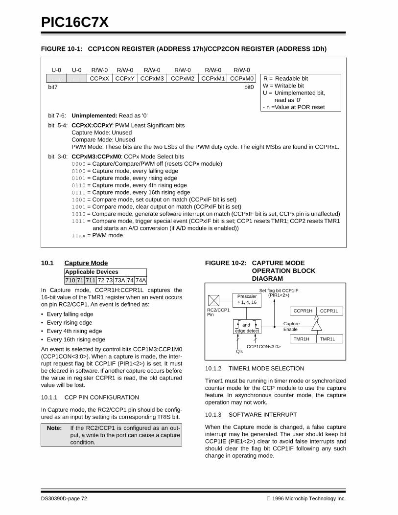
PIC16C7X
DS30390D-page 72
1996 Microchip Technology Inc.
FIGURE 10-1: CCP1CON REGISTER (ADDRESS 17h)/CCP2CON REGISTER
(ADDRESS 1Dh)
U-0 U-0 R/W-0 R/W-0 R/W-0 R/W-0 R/W-0 R/W-0— — CCPxX CCPxY CCPxM3 CCPxM2 CCPxM1 CCPxM0 R = Readable bit
W = Writable bitU = Unimplemented bit,
read as ‘0’- n =Value at POR reset
bit7 bit0
bit 7-6:
Unimplemented:
Read as '0'
bit 5-4:
CCPxX:CCPxY
: PWM Least Significant bitsCapture Mode: UnusedCompare Mode: UnusedPWM Mode: These bits are the two LSbs of the PWM duty cycle. The eight MSbs are found in CCPRxL.
bit 3-0:
CCPxM3:CCPxM0
: CCPx Mode Select bits
0000
= Capture/Compare/PWM off (resets CCPx module)
0100
= Capture mode, every falling edge
0101
= Capture mode, every rising edge
0110
= Capture mode, every 4th rising edge
0111
= Capture mode, every 16th rising edge
1000
= Compare mode, set output on match (CCPxIF bit is set)
1001
= Compare mode, clear output on match (CCPxIF bit is set)
1010
= Compare mode, generate software interrupt on match (CCPxIF bit is set, CCPx pin is unaffected)
1011
= Compare mode, trigger special event (CCPxIF bit is set; CCP1 resets TMR1; CCP2 resets TMR1and starts an A/D conversion (if A/D module is enabled))
11xx
= PWM mode
10.1 Capture Mode
In Capture mode, CCPR1H:CCPR1L captures the16-bit value of the TMR1 register when an event occurson pin RC2/CCP1. An event is defined as:
• Every falling edge• Every rising edge• Every 4th rising edge• Every 16th rising edge
An event is selected by control bits CCP1M3:CCP1M0(CCP1CON<3:0>). When a capture is made, the inter-rupt request flag bit CCP1IF (PIR1<2>) is set. It mustbe cleared in software. If another capture occurs beforethe value in register CCPR1 is read, the old capturedvalue will be lost.
10.1.1 CCP PIN CONFIGURATION
In Capture mode, the RC2/CCP1 pin should be config-ured as an input by setting its corresponding TRIS bit.
Applicable Devices
710 71 711 72 73 73A 74 74A
Note:
If the RC2/CCP1 is configured as an out-put, a write to the port can cause a capturecondition.
FIGURE 10-2: CAPTURE MODE OPERATION BLOCK DIAGRAM
10.1.2 TIMER1 MODE SELECTION
Timer1 must be running in timer mode or synchronizedcounter mode for the CCP module to use the capturefeature. In asynchronous counter mode, the captureoperation may not work.
10.1.3 SOFTWARE INTERRUPT
When the Capture mode is changed, a false captureinterrupt may be generated. The user should keep bitCCP1IE (PIE1<2>) clear to avoid false interrupts andshould clear the flag bit CCP1IF following any suchchange in operating mode.
CCPR1H CCPR1L
TMR1H TMR1L
Set flag bit CCP1IF(PIR1<2>)
CaptureEnable
Q’sCCP1CON<3:0>
RC2/CCP1
Prescaler÷ 1, 4, 16
andedge detect
Pin
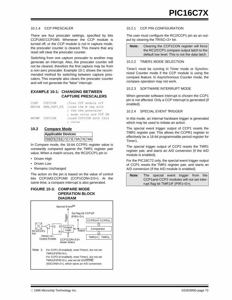
1996 Microchip Technology Inc. DS30390D-page 73
PIC16C7X
10.1.4 CCP PRESCALER
There are four prescaler settings, specified by bitsCCP1M3:CCP1M0. Whenever the CCP module isturned off, or the CCP module is not in capture mode,the prescaler counter is cleared. This means that anyreset will clear the prescaler counter.
Switching from one capture prescaler to another maygenerate an interrupt. Also, the prescaler counter willnot be cleared, therefore the first capture may be froma non-zero prescaler. Example 10-1 shows the recom-mended method for switching between capture pres-calers. This example also clears the prescaler counterand will not generate the “false” interrupt.
EXAMPLE 10-1: CHANGING BETWEEN CAPTURE PRESCALERS
CLRF CCP1CON ;Turn CCP module offMOVLW NEW_CAPT_PS ;Load the W reg with ; the new prescaler ; mode value and CCP ONMOVWF CCP1CON ;Load CCP1CON with this ; value
10.2 Compare Mode
In Compare mode, the 16-bit CCPR1 register value isconstantly compared against the TMR1 register pairvalue. When a match occurs, the RC2/CCP1 pin is:
• Driven High• Driven Low• Remains Unchanged
The action on the pin is based on the value of controlbits CCP1M3:CCP1M0 (CCP1CON<3:0>). At thesame time, a compare interrupt is also generated.
FIGURE 10-3: COMPARE MODE OPERATION BLOCK DIAGRAM
Applicable Devices
710 71 711 72 73 73A 74 74A
CCPR1H CCPR1L
TMR1H TMR1L
ComparatorQ S
R
OutputLogic
Special Event(1)
Trig
ger Set flag bit CCP1IF
(PIR1<2>)
matchRC2/CCP1
TRISC<2>CCP1CON<3:0>Mode Select
Output Enable
Pin
Note 1: For CCP1 (if enabled), reset Timer1, but not set TMR1IF(PIR<0>).For CCP2 (if enabled), reset Timer1, but not set TMR1IF(PIR<0>), and set bit GO/DONE (ADCON0<2>), which starts an A/D conversion.
10.2.1 CCP PIN CONFIGURATION
The user must configure the RC2/CCP1 pin as an out-put by clearing the TRISC<2> bit.
10.2.2 TIMER1 MODE SELECTION
Timer1 must be running in Timer mode or Synchro-nized Counter mode if the CCP module is using thecompare feature. In Asynchronous Counter mode, thecompare operation may not work.
10.2.3 SOFTWARE INTERRUPT MODE
When generate software interrupt is chosen the CCP1pin is not affected. Only a CCP interrupt is generated (ifenabled).
10.2.4 SPECIAL EVENT TRIGGER
In this mode, an internal hardware trigger is generatedwhich may be used to initiate an action.
The special event trigger output of CCP1 resets theTMR1 register pair. This allows the CCPR1 register toeffectively be a 16-bit programmable period register forTimer1.
The special trigger output of CCP2 resets the TMR1register pair, and starts an A/D conversion (if the A/Dmodule is enabled).
For the PIC16C72 only, the special event trigger outputof CCP1 resets the TMR1 register pair, and starts anA/D conversion (if the A/D module is enabled).
Note:
Clearing the CCP1CON register will forcethe RC2/CCP1 compare output latch to thedefault low level. This is not the data latch.
Note:
The special event trigger from theCCP1and CCP2 modules will not set inter-rupt flag bit TMR1IF (PIR1<0>).
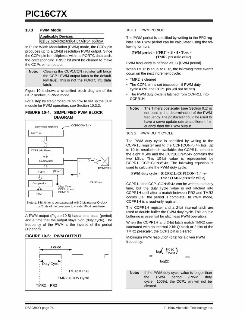
PIC16C7X
DS30390D-page 74
1996 Microchip Technology Inc.
10.3 PWM Mode
In Pulse Width Modulation (PWM) mode, the CCPx pinproduces up to a 10-bit resolution PWM output. Sincethe CCPx pin is multiplexed with the PORTC data latch,the corresponding TRISC bit must be cleared to makethe CCPx pin an output.
Figure 10-4 shows a simplified block diagram of theCCP module in PWM mode.
For a step by step procedure on how to set up the CCPmodule for PWM operation, see Section 10.3.3.
FIGURE 10-4: SIMPLIFIED PWM BLOCK DIAGRAM
A PWM output (Figure 10-5) has a time base (period)and a time that the output stays high (duty cycle). Thefrequency of the PWM is the inverse of the period(1/period).
FIGURE 10-5: PWM OUTPUT
Applicable Devices
61 62 62A R62 63 64 64A R64 65 65A
Note:
Clearing the CCP1CON register will forcethe CCP1 PWM output latch to the defaultlow level. This is not the PORTC I/O datalatch.
CCPR1L
CCPR1H (Slave)
Comparator
TMR2
Comparator
PR2
(Note 1)
R Q
S
Duty cycle registers CCP1CON<5:4>
Clear Timer,CCP1 pin and latch D.C.
TRISC<y>
RC1/CCP1
Note 1: 8-bit timer is concatenated with 2-bit internal Q clockor 2 bits of the prescaler to create 10-bit time-base.
Period
Duty Cycle
TMR2 = PR2
TMR2 = Duty Cycle
TMR2 = PR2
10.3.1 PWM PERIOD
The PWM period is specified by writing to the PR2 reg-ister. The PWM period can be calculated using the fol-lowing formula:
PWM period = [(PR2) + 1]
•
4
•
T
OSC
•
(TMR2 prescale value)
PWM frequency is defined as 1 / [PWM period].
When TMR2 is equal to PR2, the following three eventsoccur on the next increment cycle:
• TMR2 is cleared• The CCP1 pin is set (exception: if PWM duty
cycle = 0%, the CCP1 pin will not be set)• The PWM duty cycle is latched from CCPR1L into
CCPR1H
10.3.2 PWM DUTY CYCLE
The PWM duty cycle is specified by writing to theCCPR1L register and to the CCP1CON<5:4> bits. Upto 10-bit resolution is available: the CCPR1L containsthe eight MSbs and the CCP1CON<5:4> contains thetwo LSbs. This 10-bit value is represented byCCPR1L:CCP1CON<5:4>. The following equation isused to calculate the PWM duty cycle:
PWM duty cycle = (CCPR1L:CCP1CON<5:4>)
•
Tosc
•
(TMR2 prescale value)
CCPR1L and CCP1CON<5:4> can be written to at anytime, but the duty cycle value is not latched intoCCPR1H until after a match between PR2 and TMR2occurs (i.e., the period is complete). In PWM mode,CCPR1H is a read-only register.
The CCPR1H register and a 2-bit internal latch areused to double buffer the PWM duty cycle. This doublebuffering is essential for glitchless PWM operation.
When the CCPR1H and 2-bit latch match TMR2 con-catenated with an internal 2-bit Q clock or 2 bits of theTMR2 prescaler, the CCP1 pin is cleared.
Maximum PWM resolution (bits) for a given PWMfrequency:
Note:
The Timer2 postscaler (see Section 9.1) isnot used in the determination of the PWMfrequency. The postscaler could be used tohave a servo update rate at a different fre-quency than the PWM output.
Note:
If the PWM duty cycle value is longer thanthe PWM period (PWM dutycycle = 100%), the CCP1 pin will not becleared.
log( FPWM
log(2)
FOSC )bits=
1996 Microchip Technology Inc. DS30390D-page 75
PIC16C7X
EXAMPLE 10-2: PWM PERIOD AND DUTY CYCLE CALCULATION
Desired PWM frequency is 78.125 kHz,Fosc = 20 MHzTMR2 prescale = 1
1/78.125 kHz = [(PR2) + 1] • 4 • 1/20 MHz • 1
12.8
µ
s = [(PR2) + 1] • 4 • 50 ns • 1
PR2 = 63
Find the maximum resolution of the duty cycle that canbe used with a 78.125 kHz frequency and 20 MHzoscillator:
1/78.125 kHz = 2
PWM
RESOLUTION
• 1/20 MHz • 1
12.8
µ
s = 2
PWM
RESOLUTION
• 50 ns • 1
256 = 2
PWM
RESOLUTION
log(256) = (PWM Resolution) • log(2)
8.0 = PWM Resolution
At most, an 8-bit resolution duty cycle can be obtainedfrom a 78.125 kHz frequency and a 20 MHz oscillator,i.e., 0
≤
CCPR1L:CCP1CON<5:4>
≤
255. Any valuegreater than 255 will result in a 100% duty cycle.
In order to achieve higher resolution, the PWM fre-quency must be decreased. In order to achieve higherPWM frequency, the resolution must be decreased.
Table 10-3 lists example PWM frequencies and resolu-tions for Fosc = 20 MHz. TMR2 prescaler and PR2 val-ues are also shown.
10.3.3 SET-UP FOR PWM OPERATION
The following steps should be taken when configuringthe CCP module for PWM operation:
1. Set the PWM period by writing to the PR2 regis-ter.
2. Set the PWM duty cycle by writing to theCCPR1L register and CCP1CON<5:4> bits.
3. Make the CCP1 pin an output by clearing theappropriate TRISC bit.
4. Set the TMR2 prescale value and enable Timer2by writing to T2CON.
5. Configure the CCP module for PWM operation.
TABLE 10-3: EXAMPLE PWM FREQUENCIES AND RESOLUTIONS AT 20 MHz
TABLE 10-4: REGISTERS ASSOCIATED WITH CAPTURE, COMPARE, AND TIMER1
PWM Frequency 1.22 kHz 4.88 kHz 19.53 kHz 78.12 kHz 156.3 kHz 208.3 kHz
Timer Prescaler (1, 4, 16) 16 4 1 1 1 1PR2 Value 0xFF 0xFF 0xFF 0x3F 0x1F 0x17Maximum Resolution (bits) 10 10 10 8 7 5.5
Address Name Bit 7 Bit 6 Bit 5 Bit 4 Bit 3 Bit 2 Bit 1 Bit 0Value on:
POR,BOR
Value onall otherresets
0Bh/8Bh INTCON GIE PEIE T0IE INTE RBIE T0IF INTF RBIF
0000 000x 0000 000u
0Ch PIR1 PSPIF
(1,2)
ADIF RCIF
(2)
TXIF
(2)
SSPIF CCP1IF TMR2IF TMR1IF
0000 0000 0000 0000
0Dh
(2)
PIR2 — — — — — — — CCP2IF
---- ---0 ---- ---0
8Ch PIE1 PSPIE
(1,2)
ADIE RCIE
(2)
TXIE
(2)
SSPIE CCP1IE TMR2IE TMR1IE
0000 0000 0000 0000
8Dh
(2)
PIE2 — — — — — — — CCP2IE
---- ---0 ---- ---0
87h TRISC TRISC7 TRISC6 TRISC5 TRISC4 TRISC3 TRISC2 TRISC1 TRISC0
1111 1111 1111 1111
0Eh TMR1L Holding register for the Least Significant Byte of the 16-bit TMR1 register
xxxx xxxx uuuu uuuu
0Fh TMR1H Holding register for the Most Significant Byte of the 16-bit TMR1register
xxxx xxxx uuuu uuuu
10h T1CON — — T1CKPS1 T1CKPS0 T1OSCEN T1SYNC TMR1CS TMR1ON
--00 0000 --uu uuuu
15h CCPR1L Capture/Compare/PWM register1 (LSB)
xxxx xxxx uuuu uuuu
16h CCPR1H Capture/Compare/PWM register1 (MSB)
xxxx xxxx uuuu uuuu
17h CCP1CON — — CCP1X CCP1Y CCP1M3 CCP1M2 CCP1M1 CCP1M0
--00 0000 --00 0000
1Bh
(2)
CCPR2L Capture/Compare/PWM register2 (LSB)
xxxx xxxx uuuu uuuu
1Ch
(2)
CCPR2H Capture/Compare/PWM register2 (MSB)
xxxx xxxx uuuu uuuu
1Dh
(2)
CCP2CON — — CCP2X CCP2Y CCP2M3 CCP2M2 CCP2M1 CCP2M0
--00 0000 --00 0000
Legend: x = unknown, u = unchanged, - = unimplemented read as '0'. Shaded cells are not used by Capture and Timer1.Note 1: Bits PSPIE and PSPIF are reserved on the PIC16C73/73A, always maintain these bits clear.
2: The PIC16C72 does not have a Parallel Slave Port, USART or CCP2 module, these bits are unimplemented, read as '0'.

PIC16C7X
DS30390D-page 76 1996 Microchip Technology Inc.
TABLE 10-5: REGISTERS ASSOCIATED WITH PWM AND TIMER2
Address Name Bit 7 Bit 6 Bit 5 Bit 4 Bit 3 Bit 2 Bit 1 Bit 0Value on:
POR,BOR
Value on all otherresets
0Bh/8Bh INTCON GIE PEIE T0IE INTE RBIE T0IF INTF RBIF 0000 000x 0000 000u
0Ch PIR1 PSPIF(1,2) ADIF RCIF(2) TXIF(2) SSPIF CCP1IF TMR2IF TMR1IF 0000 0000 0000 0000
0Dh(2) PIR2 — — — — — — — CCP2IF ---- ---0 ---- ---0
8Ch PIE1 PSPIE(1,2) ADIE RCIE(2) TXIE(2) SSPIE CCP1IE TMR2IE TMR1IE 0000 0000 0000 0000
8Dh(2) PIE2 — — — — — — — CCP2IE ---- ---0 ---- ---0
87h TRISC TRISC7 TRISC6 TRISC5 TRISC4 TRISC3 TRISC2 TRISC1 TRISC0 1111 1111 1111 1111
11h TMR2 Timer2 module’s register 0000 0000 0000 0000
92h PR2 Timer2 module’s period register 1111 1111 1111 1111
12h T2CON — TOUTPS3 TOUTPS2 TOUTPS1 TOUTPS0 TMR2ON T2CKPS1 T2CKPS0 -000 0000 -000 0000
15h CCPR1L Capture/Compare/PWM register1 (LSB) xxxx xxxx uuuu uuuu
16h CCPR1H Capture/Compare/PWM register1 (MSB) xxxx xxxx uuuu uuuu
17h CCP1CON — — CCP1X CCP1Y CCP1M3 CCP1M2 CCP1M1 CCP1M0 --00 0000 --00 0000
1Bh(2) CCPR2L Capture/Compare/PWM register2 (LSB) xxxx xxxx uuuu uuuu
1Ch(2) CCPR2H Capture/Compare/PWM register2 (MSB) xxxx xxxx uuuu uuuu
1Dh(2) CCP2CON — — CCP2X CCP2Y CCP2M3 CCP2M2 CCP2M1 CCP2M0 --00 0000 --00 0000
Legend: x = unknown, u = unchanged, - = unimplemented read as '0'. Shaded cells are not used by PWM and Timer2.Note 1: Bits PSPIE and PSPIF are reserved on the PIC16C73/73A, always maintain these bits clear.
2: The PIC16C72 does not have a Parallel Slave Port, USART or CCP2 module, these bits are unimplemented, read as '0'.

1996 Microchip Technology Inc. DS30390D-page 77
PIC16C7X
11.0 SYNCHRONOUS SERIAL PORT (SSP) MODULE
The Synchronous Serial Port (SSP) module is a serialinterface useful for communicating with other periph-eral or microcontroller devices. These peripheraldevices may be Serial EEPROMs, shift registers, dis-play drivers, A/D converters, etc. The SSP module canoperate in one of two modes:
• Serial Peripheral Interface (SPI)• Inter-Integrated Circuit (I
2
C)
Applicable Devices
710 71 711 72 73 73A 74 74A
Refer to Application Note AN578,
"Use of the SSP Mod-ule in the I
2
C Multi-Master Environment."
FIGURE 11-1: SSPSTAT: SYNC SERIAL PORT STATUS REGISTER
(ADDRESS 94h)
U-0 U-0 R-0 R-0 R-0 R-0 R-0 R-0— — D/A P S R/W UA BF R = Readable bit
W = Writable bitU = Unimplemented bit,
read as ‘0’- n =Value at POR reset
bit7 bit0
bit 7-6:
Unimplemented:
Read as '0'
bit 5:
D/A
: Data/Address bit (I
2
C mode only)1 = Indicates that the last byte received or transmitted was data0 = Indicates that the last byte received or transmitted was address
bit 4:
P
: Stop bit (I
2
C mode only. This bit is cleared when the SSP module is disabled, SSPEN is cleared)1 = Indicates that a stop bit has been detected last (this bit is '0' on RESET)0 = Stop bit was not detected last
bit 3:
S
: Start bit (I
2
C mode only. This bit is cleared when the SSP module is disabled, SSPEN is cleared)1 = Indicates that a start bit has been detected last (this bit is '0' on RESET)0 = Start bit was not detected last
bit 2:
R/W
: Read/Write bit information (I
2
C mode only)This bit holds the R/W bit information following the last address match. This bit is only valid during thetransmission.1 = Read0 = Write
bit 1:
UA
: Update Address (10-bit I
2
C mode only)1 = Indicates that the user needs to update the address in the SSPADD register0 = Address does not need to be updated
bit 0:
BF
: Buffer Full Status bit
Receive (SPI and I
2
C modes)1 = Receive complete, SSPBUF is full0 = Receive not complete, SSPBUF is empty
Transmit (I
2
C mode only)1 = Transmit in progress, SSPBUF is full0 = Transmit complete, SSPBUF is empty
This document was created with FrameMaker 4 0 4

PIC16C7X
DS30390D-page 78
1996 Microchip Technology Inc.
FIGURE 11-2: SSPCON: SYNC SERIAL PORT CONTROL REGISTER (ADDRESS 14h)
R/W-0 R/W-0 R/W-0 R/W-0 R/W-0 R/W-0 R/W-0 R/W-0WCOL SSPOV SSPEN CKP SSPM3 SSPM2 SSPM1 SSPM0 R = Readable bit
W = Writable bitU = Unimplemented bit,
read as ‘0’- n =Value at POR reset
bit7 bit0
bit 7:
WCOL
: Write Collision Detect bit1 = The SSPBUF register is written while it is still transmitting the previous word (must be cleared in software)0 = No collision
bit 6:
SSPOV
: Receive Overflow Indicator bit
In SPI mode1 = A new byte is received while the SSPBUF register is still holding the previous data. In case of overflow,the data in SSPSR is lost. Overflow can only occur in slave mode. The user must read the SSPBUF, evenif only transmitting data, to avoid setting overflow. In master mode the overflow bit is not set since eachnew reception (and transmission) is initiated by writing to the SSPBUF register.0 = No overflow
In I
2
C mode1 = A byte is received while the SSPBUF register is still holding the previous byte. SSPOV is a "don’t care"in transmit mode. SSPOV must be cleared in software in either mode.0 = No overflow
bit 5:
SSPEN
: Synchronous Serial Port Enable bit
In SPI mode1 = Enables serial port and configures SCK, SDO, and SDI as serial port pins0 = Disables serial port and configures these pins as I/O port pins
In I
2
C mode1 = Enables the serial port and configures the SDA and SCL pins as serial port pins0 = Disables serial port and configures these pins as I/O port pinsIn both modes, when enabled, these pins must be properly configured as input or output.
bit 4:
CKP
: Clock Polarity Select bitIn SPI mode1 = Transmit happens on falling edge, receive on rising edge. Idle state for clock is a high level0 = Transmit happens on rising edge, receive on falling edge. Idle state for clock is a low levelIn I
2
C modeSCK release control1 = Enable clock0 = Holds clock low (clock stretch) (Used to ensure data setup time)
bit 3-0:
SSPM3:SSPM0
: Synchronous Serial Port Mode Select bits
0000
= SPI master mode, clock = F
OSC
/4
0001
= SPI master mode, clock = F
OSC
/16
0010
= SPI master mode, clock = F
OSC
/64
0011
= SPI master mode, clock = TMR2 output/2
0100
= SPI slave mode, clock = SCK pin. SS pin control enabled.
0101
= SPI slave mode, clock = SCK pin. SS pin control disabled. SS can be used as I/O pin
0110
= I
2
C slave mode, 7-bit address
0111
= I
2
C slave mode, 10-bit address
1011
= I
2
C start and stop bit interrupts enabled (slave idle)
1110
= I
2
C slave mode, 7-bit address with start and stop bit interrupts enabled
1111
= I
2
C slave mode, 10-bit address with start and stop bit interrupts enabled

1996 Microchip Technology Inc. DS30390D-page 79
PIC16C7X
11.1 SPI Mode
The SPI mode allows 8-bits of data to be synchro-nously transmitted and received simultaneously. Toaccomplish communication, typically three pins areused:
• Serial Data Out (SDO) RC5/SDO• Serial Data In (SDI) RC4/SDI• Serial Clock (SCK) RC3/SCK
Additionally a fourth pin may be used when in a slavemode of operation:
• Slave Select (SS) RA5/AN4/SS
When initializing the SPI, several options need to bespecified. This is done by programming the appropriatecontrol bits in the SSPCON register (SSPCON<5:0>).These control bits allow the following to be specified:
• Master Mode (SCK is the clock output)• Slave Mode (SCK is the clock input)• Clock Polarity (Output/Input data on the
Rising/Falling edge of SCK)• Clock Rate (Master mode only)• Slave Select Mode (Slave mode only)
The SSP consists of a transmit/receive Shift Register(SSPSR) and a Buffer register (SSPBUF). The SSPSRshifts the data in and out of the device, MSB first. TheSSPBUF holds the data that was previously written tothe SSPSR, until the received data is ready. Once the8-bits of data have been received, that information ismoved to the SSPBUF register. Then the buffer fulldetect bit BF (SSPSTAT <0>) and interrupt flag bitSSPIF (PIR1<3>) are set. This double buffering of thereceived data (SSPBUF) allows the next byte to startreception before reading the data that was received.Any write to the SSPBUF register during transmission/reception of data will be ignored, and the write collisiondetect bit WCOL (SSPCON<7>) will be set. User soft-ware must clear the WCOL bit so that it can be deter-mined if the following write(s) to the SSPBUF registercompleted successfully. When the application softwareis expecting to receive valid data, the SSPBUF shouldbe read before the next byte of data to transfer is writ-ten to the SSPBUF. Buffer full bit BF (SSPSTAT<0>)indicates when SSPBUF has been loaded with thereceived data (transmission is complete). When theSSPBUF is read, bit BF is cleared. This data may beirrelevant if the SPI is only a transmitter. Generally theSSP Interrupt is used to determine when the transmis-sion/reception has completed. The SSPBUF can thenbe read (if data is meaningful) and/or the SSPBUF(SSPSR) can be written. If the interrupt method is notgoing to be used, then software polling can be done toensure that a write collision does not occur.Example 11-1 shows the loading of the SSPBUF(SSPSR) for data transmission. The shaded instructionis only required if the received data is meaningful.
Applicable Devices
710 71 711 72 73 73A 74 74A
EXAMPLE 11-1: LOADING THE SSPBUF (SSPSR) REGISTER
BSF STATUS, RP0 ;Specify Bank 1LOOP BTFSS SSPSTAT, BF ;Has data been ;received ;(transmit ;complete)? GOTO LOOP ;No BCF STATUS, RP0 ;Specify Bank 0 MOVF SSPBUF, W ;W reg = contents ; of SSPBUF
MOVF TXDATA, W ;W reg = contents ; of TXDATA MOVWF SSPBUF ;New data to xmit
The block diagram of the SSP module, when in SPImode (Figure 11-3), shows that the SSPSR is notdirectly readable or writable, and can only be accessedfrom addressing the SSPBUF register. Additionally, theSSP status register (SSPSTAT) indicates the variousstatus conditions.
FIGURE 11-3: SSP BLOCK DIAGRAM (SPI MODE)
MOVWF RXDATA ;Save in user RAM
Read Write
Internaldata bus
RC4/SDI/SDA
RC5/SDO
RA5/AN4/SS
RC3/SCK/
SSPSR reg
SSPBUF reg
SSPM3:SSPM0
bit0 shiftclock
SS ControlEnable
EdgeSelect
Clock Select
TMR2 output
TCYPrescaler4, 16, 64
TRISC<3>
2
EdgeSelect
2
4
SCL

PIC16C7X
DS30390D-page 80
1996 Microchip Technology Inc.
To enable the serial port, SSP enable bit SSPEN (SSP-CON<5>) must be set. To reset or reconfigure SPImode, clear bit SSPEN, re-initialize the SSPCON reg-ister, and then set bit SSPEN. This configures the SDI,SDO, SCK, and SS pins as serial port pins. For the pinsto behave as the serial port function, they must havetheir data direction bits (in the TRISC register) appro-priately programmed. That is:
• SDI must have TRISC<4> set• SDO must have TRISC<5> cleared• SCK (Master mode) must have TRISC<3>
cleared• SCK (Slave mode) must have TRISC<3> set • SS must have TRISA<5> set
Any serial port function that is not desired may be over-ridden by programming the corresponding data direc-tion (TRIS) register to the opposite value. An examplewould be in master mode where you are only sendingdata (to a display driver), then both SDI and SS couldbe used as general purpose outputs by clearing theircorresponding TRIS register bits.
Figure 11-4 shows a typical connection between twomicrocontrollers. The master controller (Processor 1)initiates the data transfer by sending the SCK signal.Data is shifted out of both shift registers on their pro-grammed clock edge, and latched on the oppositeedge of the clock. Both processors should be pro-grammed to same Clock Polarity (CKP), then both con-trollers would send and receive data at the same time.Whether the data is meaningful (or dummy data)depends on the application software. This leads tothree scenarios for data transmission:
• Master sends data
—
Slave sends dummy data• Master sends data
—
Slave sends data• Master sends dummy data
—
Slave sends data
The master can initiate the data transfer at any timebecause it controls the SCK. The master determineswhen the slave (Processor 2) wishes to broadcast databy the software protocol.
In master mode the data is transmitted/received assoon as the SSPBUF register is written to. If the SPI isonly going to receive, the SCK output could be disabled(programmed as an input). The SSPSR register willcontinue to shift in the signal present on the SDI pin atthe programmed clock rate. As each byte is received, itwill be loaded into the SSPBUF register as if a normalreceived byte (interrupts and status bits appropriatelyset). This could be useful in receiver applications as a“line activity monitor” mode.
In slave mode, the data is transmitted and received asthe external clock pulses appear on SCK. When thelast bit is latched the interrupt flag bit SSPIF (PIR1<3>)is set.
The clock polarity is selected by appropriately pro-gramming bit CKP (SSPCON<4>). This then wouldgive waveforms for SPI communication as shown inFigure 11-5 and Figure 11-6 where the MSB is trans-mitted first. In master mode, the SPI clock rate (bit rate)is user programmable to be one of the following:
• F
OSC
/4 (or T
CY
)• F
OSC
/16 (or 4 • T
CY
)• F
OSC
/64 (or 16 • T
CY
)• Timer2 output/2
This allows a maximum bit clock frequency (at 20 MHz)of 5 MHz. When in slave mode the external clock mustmeet the minimum high and low times.
In sleep mode, the slave can transmit and receive dataand wake the device from sleep.
FIGURE 11-4: SPI MASTER/SLAVE CONNECTION
Serial Input Buffer(SSPBUF)
Shift Register(SSPSR)
MSb LSb
SDO
SDI
PROCESSOR 1
SCK
SPI Master (SSPM3:SSPM0 = 00xxb)
Serial Input Buffer(SSPBUF)
Shift Register(SSPSR)
LSbMSb
SDI
SDO
PROCESSOR 2
SCK
SPI Slave (SSPM3:SSPM0 = 010xb)
Serial Clock

1996 Microchip Technology Inc. DS30390D-page 81
PIC16C7X
The SS pin allows a synchronous slave mode. The SPImust be in slave mode (SSPCON<3:0> = 04h) and theTRISA<5> bit must be set the for the synchronousslave mode to be enabled. When the SS pin is low,transmission and reception are enabled and the SDOpin is driven. When the SS pin goes high, the SDO pinis no longer driven, even if in the middle of a transmit-ted byte, and becomes a floating output. If the SS pinis taken low without resetting SPI mode, the transmis-sion will continue from the point at which it was takenhigh. External pull-up/pull-down resistors may be desir-able, depending on the application.
To emulate two-wire communication, the SDO pin canbe connected to the SDI pin. When the SPI needs tooperate as a receiver the SDO pin can be configured asan input. This disables transmissions from the SDO.The SDI can always be left as an input (SDI function)since it cannot create a bus conflict.
FIGURE 11-5: SPI MODE TIMING (MASTER MODE OR SLAVE MODE W/O SS CONTROL)
FIGURE 11-6: SPI MODE TIMING (SLAVE MODE WITH SS CONTROL)
SCK(CKP = 0)SCK(CKP = 1)
SDO
SDI
SSPIFInterrupt flag
bit7
bit7 bit0
bit6 bit5 bit4 bit3 bit2 bit1 bit0
SCK(CKP = 0)SCK(CKP = 1)
SDO
SDI
SSPIF
bit7
bit7 bit0
bit6 bit5 bit4 bit3 bit2 bit1 bit0
SS

PIC16C7X
DS30390D-page 82
1996 Microchip Technology Inc.
TABLE 11-1: REGISTERS ASSOCIATED WITH SPI OPERATION
Address Name Bit 7 Bit 6 Bit 5 Bit 4 Bit 3 Bit 2 Bit 1 Bit 0Value on:
POR,BOR
Value onall otherresets
0Bh/8Bh INTCON GIE PEIE T0IE INTE RBIE T0IF INTF RBIF
0000 000x 0000 000u
0Ch PIR1 PSPIF
(1,2)
ADIF RCIF
(2)
TXIF
(2)
SSPIF CCP1IF TMR2IF TMR1IF
0000 0000 0000 0000
8Ch PIE1 PSPIE
(1,2)
ADIE RCIE
(2)
TXIE
(2)
SSPIE CCP1IE TMR2IE TMR1IE
0000 0000 0000 0000
87h TRISC TRISC7 TRISC6 TRISC5 TRISC4 TRISC3 TRISC2 TRISC1 TRISC0
1111 1111 1111 1111
13h SSPBUF Synchronous Serial Port Receive Buffer/Transmit Register
xxxx xxxx uuuu uuuu
14h SSPCON WCOL SSPOV SSPEN CKP SSPM3 SSPM2 SSPM1 SSPM0
0000 0000 0000 0000
85h TRISA — — TRISA5 TRISA4 TRISA3 TRISA2 TRISA1 TRISA0
--11 1111 --11 1111
94h SSPSTAT — — D/A P S R/W UA BF
--00 0000 --00 0000
Legend:
x
= unknown,
u
= unchanged,
-
= unimplemented read as '0'. Shaded cells are not used by the SSP in SPI mode.Note 1: Bits PSPIE and PSPIF are reserved on the PIC16C73/73A, always maintain these bits clear.
2: The PIC16C72 does not have a Parallel Slave Port or USART, these bits are unimplemented, read as '0'.

1996 Microchip Technology Inc. DS30390D-page 83
PIC16C7X
11.2 I
2
C
Overview
This section provides an overview of the Inter-Inte-grated Circuit (I
2
C) bus, with Section 11.3 discussingthe operation of the SSP module in I
2
C mode.
The I
2C bus is a two-wire serial interface developed bythe Philips Corporation. The original specification, orstandard mode, was for data transfers of up to 100Kbps. An enhanced specification, or fast mode, sup-ports data transmission up to 400 Kbps. Both standardmode and fast mode devices will inter-operate ifattached to the same bus.
The I2C interface employs a comprehensive protocol toensure reliable transmission and reception of data.When transmitting data, one device is the “master”(generates the clock), while the other device(s) acts asthe “slave.” All portions of the slave protocol are imple-mented in the SSP module’s hardware, while portionsof the master protocol need to be addressed in thePIC16CXX software. Table 11-2 defines some of theI2C bus terminology. For additional information on theI2C interface specification, refer to the Philips docu-ment “The I2C bus and how to use it.”, which can beobtained from the Philips Corporation.
In the I2C interface protocol each device has anaddress. When a master wishes to initiate a data trans-fer, it first transmits the address of the device that itwishes to “talk” to. All devices “listen” to see if this istheir address. Within this address, a bit specifies if themaster wishes to read-from/write-to the slave device.The master and slave are always in opposite modes(transmitter/receiver) of operation during a data trans-fer. That is they can be thought of operating in either ofthese two relations:
• Master-transmitter and Slave-receiver• Slave-transmitter and Master-receiver
In both cases the master generates the clock signal.
Applicable Devices710 71 711 72 73 73A 74 74A
The output stages of the clock (SCL) and data (SDA)lines must have an open-drain or open-collector inorder to perform the wired-AND function of the bus.External pull-up resistors are used to ensure a highlevel when no device is pulling the line down. The num-ber of devices that may be attached to the I2C bus islimited only by the maximum bus loading specificationof 400 pF.
11.2.1 INITIATING AND TERMINATING DATA TRANSFER
During times of no data transfer (idle time), both theclock line (SCL) and the data line (SDA) are pulled highthrough the external pull-up resistors. The START andSTOP conditions determine the start and stop of datatransmission. The START condition is defined as a highto low transition of the SDA when the SCL is high. TheSTOP condition is defined as a low to high transition ofthe SDA when the SCL is high. Figure 11-7 shows theSTART and STOP conditions. The master generatesthese conditions for starting and terminating data trans-fer. Due to the definition of the START and STOP con-ditions, when data is being transmitted, the SDA linecan only change state when the SCL line is low.
FIGURE 11-7: START AND STOP CONDITIONS
SDA
SCL S P
StartCondition
Changeof DataAllowed
Changeof DataAllowed
StopCondition
TABLE 11-2: I2C BUS TERMINOLOGY
Term Description
Transmitter The device that sends the data to the bus.
Receiver The device that receives the data from the bus.
Master The device which initiates the transfer, generates the clock and terminates the transfer.
Slave The device addressed by a master.
Multi-master More than one master device in a system. These masters can attempt to control the bus at the same time without corrupting the message.
Arbitration Procedure that ensures that only one of the master devices will control the bus. This ensure that the transfer data does not get corrupted.
Synchronization Procedure where the clock signals of two or more devices are synchronized.

PIC16C7X
DS30390D-page 84 1996 Microchip Technology Inc.
11.2.2 ADDRESSING I2C DEVICES
There are two address formats. The simplest is the7-bit address format with a R/W bit (Figure 11-8). Themore complex is the 10-bit address with a R/W bit(Figure 11-9). For 10-bit address format, two bytesmust be transmitted with the first five bits specifying thisto be a 10-bit address.
FIGURE 11-8: 7-BIT ADDRESS FORMAT
FIGURE 11-9: I2C 10-BIT ADDRESS FORMAT
11.2.3 TRANSFER ACKNOWLEDGE
All data must be transmitted per byte, with no limit tothe number of bytes transmitted per data transfer. Aftereach byte, the slave-receiver generates an acknowl-edge bit (ACK) (Figure 11-10). When a slave-receiverdoesn’t acknowledge the slave address or receiveddata, the master must abort the transfer. The slavemust leave SDA high so that the master can generatethe STOP condition (Figure 11-7).
S R/W ACK
Sent bySlave
slave address
SR/W Read/Write pulse
MSb LSb
Start Condition
ACK Acknowledge
S 1 1 1 1 0 A9 A8 R/W ACK A7 A6 A5 A4 A3 A2 A1 A0 ACK
sent by slave
= 0 for writeSR/WACK
- Start Condition- Read/Write Pulse- Acknowledge
FIGURE 11-10: SLAVE-RECEIVERACKNOWLEDGE
If the master is receiving the data (master-receiver), itgenerates an acknowledge signal for each receivedbyte of data, except for the last byte. To signal the endof data to the slave-transmitter, the master does notgenerate an acknowledge (not acknowledge). Theslave then releases the SDA line so the master cangenerate the STOP condition. The master can alsogenerate the STOP condition during the acknowledgepulse for valid termination of data transfer.
If the slave needs to delay the transmission of the nextbyte, holding the SCL line low will force the master intoa wait state. Data transfer continues when the slavereleases the SCL line. This allows the slave to movethe received data or fetch the data it needs to transferbefore allowing the clock to start. This wait state tech-nique can also be implemented at the bit level,Figure 11-11. The slave will inherently stretch the clockwhen it is a transmitter but will not when it is a receiver.The slave will have to clear the SSPCON<4> bit toenable clock stretching when it is a receiver.
S
DataOutput by
Transmitter
DataOutput byReceiver
SCL fromMaster
StartCondition
Clock Pulse forAcknowledgment
not acknowledge
acknowledge
1 2 8 9
FIGURE 11-11: DATA TRANSFER WAIT STATE
1 2 7 8 9 1 2 3 • 8 9 P
SDA
SCL S
StartCondition Address R/W ACK Wait
StateData ACK
MSB acknowledgmentsignal from receiver
acknowledgmentsignal from receiverbyte complete
interrupt with receiver
clock line held low whileinterrupts are serviced
StopCondition

1996 Microchip Technology Inc. DS30390D-page 85
PIC16C7X
Figure 11-12 and Figure 11-13 show Master-transmit-ter and Master-receiver data transfer sequences.
When a master does not wish to relinquish the bus (bygenerating a STOP condition), a repeated START con-dition (Sr) must be generated. This condition is identi-cal to the start condition (SDA goes high-to-low while
SCL is high), but occurs after a data transfer acknowl-edge pulse (not the bus-free state). This allows a mas-ter to send “commands” to the slave and then receivethe requested information or to address a differentslave device. This sequence is shown in Figure 11-14.
FIGURE 11-12: MASTER-TRANSMITTER SEQUENCE
FIGURE 11-13: MASTER-RECEIVER SEQUENCE
FIGURE 11-14: COMBINED FORMAT
For 7-bit address:
S Slave AddressFirst 7 bits
S R/W A1 Slave AddressSecond byte
A2
Data A Data P
A master transmitter addresses a slave receiverwith a 10-bit address.
A/A
Slave Address R/W A Data A Data A/A P
'0' (write) data transferred(n bytes - acknowledge)
A master transmitter addresses a slave receiver with a7-bit address. The transfer direction is not changed.
From master to slave
From slave to master
A = acknowledge (SDA low)A = not acknowledge (SDA high)S = Start ConditionP = Stop Condition
(write)
For 10-bit address:
For 7-bit address:
S Slave AddressFirst 7 bits
S R/W A1 Slave AddressSecond byte
A2
A master transmitter addresses a slave receiverwith a 10-bit address.
Slave Address R/W A Data A Data A P
'1' (read) data transferred(n bytes - acknowledge)
A master reads a slave immediately after the first byte.
From master to slave
From slave to master
A = acknowledge (SDA low)A = not acknowledge (SDA high)S = Start ConditionP = Stop Condition
(write)
For 10-bit address:
Slave AddressFirst 7 bits
Sr R/W A3 AData A PData
(read)
Combined format:
S
Combined format - A master addresses a slave with a 10-bit address, then transmits
Slave Address R/W A Data A/A Sr P
(read) Sr = repeated
Transfer direction of data and acknowledgment bits depends on R/W bits.
From master to slave
From slave to master
A = acknowledge (SDA low)A = not acknowledge (SDA high)S = Start ConditionP = Stop Condition
Slave AddressFirst 7 bits
Sr R/W A
(write)
data to this slave and reads data from this slave.
Slave AddressSecond byte
Data Sr Slave AddressFirst 7 bits
R/W A Data A A PA A Data A/A Data
(read)
Slave Address R/W A Data A/A
Start Condition(write) Direction of transfer
may change at this point
(read or write)(n bytes + acknowledge)

PIC16C7X
DS30390D-page 86 1996 Microchip Technology Inc.
11.2.4 MULTI-MASTER
The I2C protocol allows a system to have more thanone master. This is called multi-master. When two ormore masters try to transfer data at the same time, arbi-tration and synchronization occur.
11.2.4.1 ARBITRATION
Arbitration takes place on the SDA line, while the SCLline is high. The master which transmits a high whenthe other master transmits a low loses arbitration(Figure 11-15), and turns off its data output stage. Amaster which lost arbitration can generate clock pulsesuntil the end of the data byte where it lost arbitration.When the master devices are addressing the samedevice, arbitration continues into the data.
FIGURE 11-15: MULTI-MASTER ARBITRATION (TWO MASTERS)
Masters that also incorporate the slave function, andhave lost arbitration must immediately switch over toslave-receiver mode. This is because the winning mas-ter-transmitter may be addressing it.
Arbitration is not allowed between:
• A repeated START condition• A STOP condition and a data bit• A repeated START condition and a STOP condi-
tion
Care needs to be taken to ensure that these conditionsdo not occur.
transmitter 1 loses arbitrationDATA 1 SDA
DATA 1
DATA 2
SDA
SCL
11.2.4.2 CLOCK SYNCHRONIZATION
Clock synchronization occurs after the devices havestarted arbitration. This is performed using a wired-AND connection to the SCL line. A high to low transitionon the SCL line causes the concerned devices to startcounting off their low period. Once a device clock hasgone low, it will hold the SCL line low until its SCL highstate is reached. The low to high transition of this clockmay not change the state of the SCL line, if anotherdevice clock is still within its low period. The SCL line isheld low by the device with the longest low period.Devices with shorter low periods enter a high wait-state, until the SCL line comes high. When the SCL linecomes high, all devices start counting off their highperiods. The first device to complete its high period willpull the SCL line low. The SCL line high time is deter-mined by the device with the shortest high period,Figure 11-16.
FIGURE 11-16: CLOCK SYNCHRONIZATION
CLK1
CLK2
SCL
waitstate
start countingHIGH period
counterreset

1996 Microchip Technology Inc. DS30390D-page 87
PIC16C7X
11.3 SSP I2C Operation
The SSP module in I2C mode fully implements all slavefunctions, and provides interrupts on start and stop bitsin hardware to facilitate software implementations ofthe master functions. The SSP module implements thestandard and fast mode specifications as well as 7-bitand 10-bit addressing. Two pins are used for datatransfer. These are the RC3/SCK/SCL pin, which is theclock (SCL), and the RC4/SDI/SDA pin, which is thedata (SDA). The user must configure these pins asinputs or outputs through the TRISC<4:3> bits. TheSSP module functions are enabled by setting SSPEnable bit SSPEN (SSPCON<5>).
FIGURE 11-17: SSP BLOCK DIAGRAM (I2C MODE)
The SSP module has five registers for I2C operation.These are the:
• SSP Control Register (SSPCON)• SSP Status Register (SSPSTAT)• Serial Receive/Transmit Buffer (SSPBUF)• SSP Shift Register (SSPSR) - Not directly acces-
sible• SSP Address Register (SSPADD)
Applicable Devices710 71 711 72 73 73A 74 74A
Read Write
SSPSR reg
Match detect
SSPADD reg
Start and Stop bit detect
SSPBUF reg
Internaldata bus
Addr Match
Set, ResetS, P bits
(SSPSTAT reg)
RC3/SCK/SCL
RC4/
shiftclock
MSbSDI/
LSb
SDA
The SSPCON register allows control of the I2C opera-tion. Four mode selection bits (SSPCON<3:0>) allowone of the following I2C modes to be selected:
• I2C Slave mode (7-bit address)• I2C Slave mode (10-bit address)• I2C Slave mode (7-bit address), with start and
stop bit interrupts enabled• I2C Slave mode (10-bit address), with start and
stop bit interrupts enabled• I2C start and stop bit interrupts enabled, slave is
idle
Selection of any I2C mode, with the SSPEN bit set,forces the SCL and SDA pins to be open drain, pro-vided these pins are programmed to inputs by settingthe appropriate TRISC bits.
The SSPSTAT register gives the status of the datatransfer. This information includes detection of aSTART or STOP bit, specifies if the received byte wasdata or address if the next byte is the completion of10-bit address, and if this will be a read or write datatransfer. The SSPSTAT register is read only.
The SSPBUF is the register to which transfer data iswritten to or read from. The SSPSR register shifts thedata in or out of the device. In receive operations, theSSPBUF and SSPSR create a doubled bufferedreceiver. This allows reception of the next byte to beginbefore reading the last byte of received data. When thecomplete byte is received, it is transferred to the SSP-BUF register and flag bit SSPIF is set. If another com-plete byte is received before the SSPBUF register isread, a receiver overflow has occurred and bit SSPOV(SSPCON<6>) is set.
The SSPADD register holds the slave address. In 10-bitmode, the user needs to write the high byte of theaddress (1111 0 A9 A8 0). Following the high byteaddress match, the low byte of the address needs to beloaded (A7:A0).
PIC16C7X
DS30390D-page 88 1996 Microchip Technology Inc.
11.3.1 SLAVE MODE
In slave mode, the SCL and SDA pins must be config-ured as inputs (TRISC<4:3> set). The SSP module willoverride the input state with the output data whenrequired (slave-transmitter).
When an address is matched or the data transfer afteran address match is received, the hardware automati-cally will generate the acknowledge (ACK) pulse, andthen load the SSPBUF register with the received valuecurrently in the SSPSR register.
There are certain conditions that will cause the SSPmodule not to give this ACK pulse. These are if either(or both):
a) The buffer full bit BF (SSPSTAT<0>) was setbefore the transfer was received.
b) The overflow bit SSPOV (SSPCON<6>) was setbefore the transfer was received.
In this case, the SSPSR register value is not loadedinto the SSPBUF, but bit SSPIF (PIR1<3>) is set.Table 11-3 shows what happens when a data transferbyte is received, given the status of bits BF andSSPOV. The shaded cells show the condition whereuser software did not properly clear the overflow condi-tion. Flag bit BF is cleared by reading the SSPBUF reg-ister while bit SSPOV is cleared through software.
The SCL clock input must have a minimum high andlow time for proper operation. The high and low timesof the I2C specification as well as the requirement ofthe SSP module is shown in timing parameter #100and parameter #101 (see Electrical Specification sec-tion).
11.3.1.1 ADDRESSING
Once the SSP module has been enabled, it waits for aSTART condition to occur. Following the START condi-tion, the 8-bits are shifted into the SSPSR register. Allincoming bits are sampled with the rising edge of theclock (SCL) line. The value of register SSPSR<7:1> iscompared to the value of the SSPADD register. Theaddress is compared on the falling edge of the eighthclock (SCL) pulse. If the addresses match, and the BFand SSPOV bits are clear, the following events occur:
a) The SSPSR register value is loaded into theSSPBUF register.
b) The buffer full bit, BF is set.c) An ACK pulse is generated.d) SSP interrupt flag bit, SSPIF (PIR1<3>) is set
(interrupt is generated if enabled) - on the fallingedge of the ninth SCL pulse.
In 10-bit address mode, two address bytes need to bereceived by the slave (Figure 11-9). The five Most Sig-nificant bits (MSbs) of the first address byte specify ifthis is a 10-bit address. Bit R/W (SSPSTAT<2>) mustspecify a write, so the slave device will receive the sec-ond address byte. For a 10-bit address the first bytewould equal ‘1111 0 A9 A8 0’, where A9 and A8 arethe two MSbs of the address. The sequence of eventsfor a 10-bit address is as follows, with steps 7- 9 forslave-transmitter:
1. Receive first (high) byte of Address (bits SSPIF,BF, and bit UA (SSPSTAT<1>) are set).
2. Update the SSPADD register with second (low)byte of Address (clears bit UA and releases theSCL line).
3. Read the SSPBUF register (clears bit BF) andclear flag bit SSPIF.
4. Receive second (low) byte of Address (bitsSSPIF, BF, and UA are set).
5. Update the SSPADD register with the first (high)byte of Address (clears bit UA, if match releasesSCL line).
6. Read the SSPBUF register (clears bit BF) andclear flag bit SSPIF.
7. Receive repeated START condition.8. Receive first (high) byte of Address (bits SSPIF
and BF are set).9. Read the SSPBUF register (clears bit BF) and
clear flag bit SSPIF.
TABLE 11-3: DATA TRANSFER RECEIVED BYTE ACTIONS
Status Bits as DataTransfer is Received
SSPSR → SSPBUFGenerate ACK
Pulse
Set bit SSPIF(SSP Interrupt occurs
if Enabled)BF SSPOV
0 0 Yes Yes Yes1 0 No No Yes1 1 No No Yes
0 1 No No Yes

1996 Microchip Technology Inc. DS30390D-page 89
PIC16C7X
11.3.1.2 RECEPTION
When the R/W bit of the address byte is clear and anaddress match occurs, the R/W bit of the SSPSTATregister is cleared. The received address is loaded intothe SSPBUF register.
When the address byte overflow condition exists, thenno acknowledge (ACK) pulse is given. An overflow con-dition is defined as either bit BF (SSPSTAT<0>) is setor bit SSPOV (SSPCON<6>) is set.
An SSP interrupt is generated for each data transferbyte. Flag bit SSPIF (PIR1<3>) must be cleared in soft-ware, and the SSPSTAT register is used to determinethe status of the byte.
FIGURE 11-18: I2C WAVEFORMS FOR RECEPTION (7-BIT ADDRESS)
P98765
D0D1D2D3D4D5D6D7
S
A7 A6 A5 A4 A3 A2 A1SDA
SCL 1 2 3 4 5 6 7 8 9 1 2 3 4 5 6 7 8 9 1 2 3 4
Bus Masterterminatestransfer
Bit SSPOV is set because the SSPBUF register is still full.
Cleared in softwareSSPBUF register is read
ACK Receiving DataReceiving Data
D0D1D2D3D4D5D6D7ACKR/W=0Receiving Address
SSPIF (PIR1<3>)
BF (SSPSTAT<0>)
SSPOV (SSPCON<6>)
ACK
ACK is not sent.

PIC16C7X
DS30390D-page 90 1996 Microchip Technology Inc.
11.3.1.3 TRANSMISSION
When the R/W bit of the incoming address byte is setand an address match occurs, the R/W bit of theSSPSTAT register is set. The received address isloaded into the SSPBUF register. The ACK pulse willbe sent on the ninth bit, and pin RC3/SCK/SCL is heldlow. The transmit data must be loaded into the SSP-BUF register, which also loads the SSPSR register.Then pin RC3/SCK/SCL should be enabled by settingbit CKP (SSPCON<4>). The eight data bits are shiftedout on the falling edge of the SCL input. This ensuresthat the SDA signal is valid during the SCL high time(Figure 11-19).
An SSP interrupt is generated for each data transferbyte. Flag bit SSPIF must be cleared in software, andthe SSPSTAT register is used to determine the statusof the byte. Flag bit SSPIF is set on the falling edge ofthe ninth clock pulse.
As a slave-transmitter, the ACK pulse from the master-receiver is latched on the rising edge of the ninth SCLinput pulse. If the SDA line was high (not ACK), thenthe data transfer is complete. The slave then monitorsfor another occurrence of the START bit. If the SDA linewas low (ACK), the transmit data must be loaded intothe SSPBUF register, which also loads the SSPSR reg-ister. Then pin RC3/SCK/SCL should be enabled bysetting bit CKP.
FIGURE 11-19: I2C WAVEFORMS FOR TRANSMISSION (7-BIT ADDRESS)
SDA
SCL
SSPIF (PIR1<3>)
BF (SSPSTAT<0>)
CKP (SSPCON<4>)
A7 A6 A5 A4 A3 A2 A1 ACK D7 D6 D5 D4 D3 D2 D1 D0
ACKTransmitting DataR/W = 1Receiving Address
1 2 3 4 5 6 7 8 9 1 2 3 4 5 6 7 8 9 P
cleared in softwareSSPBUF is written in software
From SSP interruptservice routine
Set bit after writing to SSPBUF
SData in sampled
SCL held lowwhile CPU
responds to SSPIF
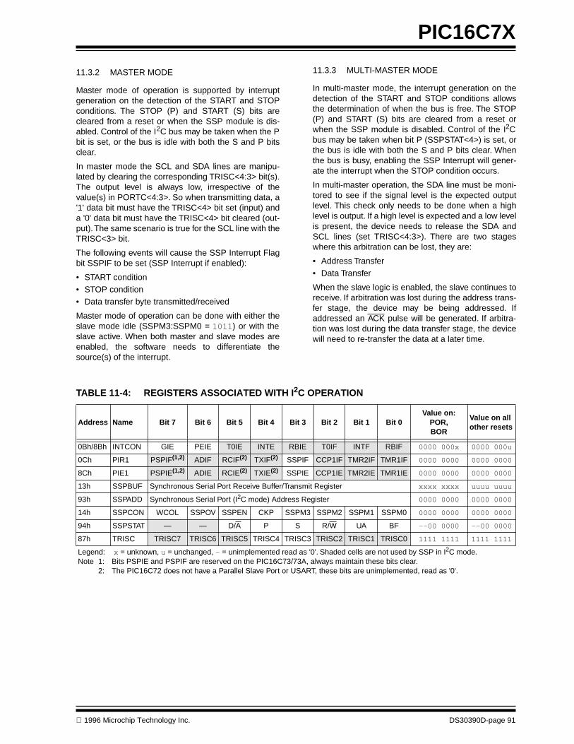
1996 Microchip Technology Inc. DS30390D-page 91
PIC16C7X
11.3.2 MASTER MODE
Master mode of operation is supported by interruptgeneration on the detection of the START and STOPconditions. The STOP (P) and START (S) bits arecleared from a reset or when the SSP module is dis-abled. Control of the I2C bus may be taken when the Pbit is set, or the bus is idle with both the S and P bitsclear.
In master mode the SCL and SDA lines are manipu-lated by clearing the corresponding TRISC<4:3> bit(s).The output level is always low, irrespective of thevalue(s) in PORTC<4:3>. So when transmitting data, a'1' data bit must have the TRISC<4> bit set (input) anda '0' data bit must have the TRISC<4> bit cleared (out-put). The same scenario is true for the SCL line with theTRISC<3> bit.
The following events will cause the SSP Interrupt Flagbit SSPIF to be set (SSP Interrupt if enabled):
• START condition• STOP condition• Data transfer byte transmitted/received
Master mode of operation can be done with either theslave mode idle (SSPM3:SSPM0 = 1011) or with theslave active. When both master and slave modes areenabled, the software needs to differentiate thesource(s) of the interrupt.
11.3.3 MULTI-MASTER MODE
In multi-master mode, the interrupt generation on thedetection of the START and STOP conditions allowsthe determination of when the bus is free. The STOP(P) and START (S) bits are cleared from a reset orwhen the SSP module is disabled. Control of the I2Cbus may be taken when bit P (SSPSTAT<4>) is set, orthe bus is idle with both the S and P bits clear. Whenthe bus is busy, enabling the SSP Interrupt will gener-ate the interrupt when the STOP condition occurs.
In multi-master operation, the SDA line must be moni-tored to see if the signal level is the expected outputlevel. This check only needs to be done when a highlevel is output. If a high level is expected and a low levelis present, the device needs to release the SDA andSCL lines (set TRISC<4:3>). There are two stageswhere this arbitration can be lost, they are:
• Address Transfer• Data Transfer
When the slave logic is enabled, the slave continues toreceive. If arbitration was lost during the address trans-fer stage, the device may be being addressed. Ifaddressed an ACK pulse will be generated. If arbitra-tion was lost during the data transfer stage, the devicewill need to re-transfer the data at a later time.
TABLE 11-4: REGISTERS ASSOCIATED WITH I2C OPERATION
Address Name Bit 7 Bit 6 Bit 5 Bit 4 Bit 3 Bit 2 Bit 1 Bit 0Value on:
POR,BOR
Value on allother resets
0Bh/8Bh INTCON GIE PEIE T0IE INTE RBIE T0IF INTF RBIF 0000 000x 0000 000u
0Ch PIR1 PSPIF(1,2) ADIF RCIF(2) TXIF(2) SSPIF CCP1IF TMR2IF TMR1IF 0000 0000 0000 0000
8Ch PIE1 PSPIE(1,2) ADIE RCIE(2) TXIE(2) SSPIE CCP1IE TMR2IE TMR1IE 0000 0000 0000 0000
13h SSPBUF Synchronous Serial Port Receive Buffer/Transmit Register xxxx xxxx uuuu uuuu
93h SSPADD Synchronous Serial Port (I2C mode) Address Register 0000 0000 0000 0000
14h SSPCON WCOL SSPOV SSPEN CKP SSPM3 SSPM2 SSPM1 SSPM0 0000 0000 0000 0000
94h SSPSTAT — — D/A P S R/W UA BF --00 0000 --00 0000
87h TRISC TRISC7 TRISC6 TRISC5 TRISC4 TRISC3 TRISC2 TRISC1 TRISC0 1111 1111 1111 1111
Legend: x = unknown, u = unchanged, - = unimplemented read as '0'. Shaded cells are not used by SSP in I2C mode.Note 1: Bits PSPIE and PSPIF are reserved on the PIC16C73/73A, always maintain these bits clear.
2: The PIC16C72 does not have a Parallel Slave Port or USART, these bits are unimplemented, read as '0'.

PIC16C7X
DS30390D-page 92 1996 Microchip Technology Inc.
FIGURE 11-20: OPERATION OF THE I2C MODULE IN IDLE_MODE, RCV_MODE OR XMIT_MODE
IDLE_MODE (7-bit):if (Addr_match) Set interrupt;
if (R/W = 1) Send ACK = 0; set XMIT_MODE;
else if (R/W = 0) set RCV_MODE;
RCV_MODE:if ((SSPBUF=Full) OR (SSPOV = 1))
Set SSPOV;Do not acknowledge;
else transfer SSPSR → SSPBUF;
send ACK = 0;
Receive 8-bits in SSPSR;Set interrupt;XMIT_MODE:While ((SSPBUF = Empty) AND (CKP=0)) Hold SCL Low;Send byte;Set interrupt;if ( ACK Received = 1) End of transmission;
Go back to IDLE_MODE;
else if ( ACK Received = 0) Go back to XMIT_MODE;IDLE_MODE (10-Bit):If (High_byte_addr_match AND (R/W = 0))
PRIOR_ADDR_MATCH = FALSE;Set interrupt;if ((SSPBUF = Full) OR ((SSPOV = 1))
Set SSPOV;Do not acknowledge;
else Set UA = 1;
Send ACK = 0;While (SSPADD not updated) Hold SCL low;Clear UA = 0;Receive Low_addr_byte;Set interrupt;Set UA = 1;If (Low_byte_addr_match)
PRIOR_ADDR_MATCH = TRUE;Send ACK = 0;while (SSPADD not updated) Hold SCL low;Clear UA = 0;
Set RCV_MODE;
else if (High_byte_addr_match AND (R/W = 1)
if (PRIOR_ADDR_MATCH)
send ACK = 0;
set XMIT_MODE;
else PRIOR_ADDR_MATCH = FALSE;

1996 Microchip Technology Inc. DS30390D-page 93
PIC16C7X
12.0 UNIVERSAL SYNCHRONOUS ASYNCHRONOUS RECEIVER TRANSMITTER (USART)
The Universal Synchronous Asynchronous ReceiverTransmitter (USART) module is one of the two serialI/O modules. (USART is also know as a Serial Commu-nications Interface or SCI). The USART can be config-ured as a full duplex asynchronous system that cancommunicate with peripheral devices such as CRT ter-minals and personal computers, or it can be configured
Applicable Devices
710 71 711 72 73 73A 74 74A
as a half duplex synchronous system that can commu-nicate with peripheral devices such as A/D or D/A inte-grated circuits, Serial EEPROMs etc.
The USART can be configured in the following modes:
• Asynchronous (full duplex)• Synchronous - Master (half duplex)• Synchronous - Slave (half duplex)
Bit SPEN (RCSTA<7>), and bits TRISC<7:6>, have tobe set in order to configure pins RC6/TX/CK andRC7/RX/DT for the Serial Communication Interface.
FIGURE 12-1: TXSTA: TRANSMIT STATUS AND CONTROL REGISTER (ADDRESS 98h)
R/W-0 R/W-0 R/W-0 R/W-0 U-0 R/W-0 R-1 R/W-0CSRC TX9 TXEN SYNC — BRGH TRMT TX9D R = Readable bit
W = Writable bitU = Unimplemented bit,
read as ‘0’- n =Value at POR reset
bit7 bit0
bit 7:
CSRC
:
Clock Source Select bit
Asynchronous modeDon’t care
Synchronous mode1 = Master mode (Clock generated internally from BRG)0 = Slave mode (Clock from external source)
bit 6:
TX9
: 9-bit Transmit Enable bit1 = Selects 9-bit transmission0 = Selects 8-bit transmission
bit 5:
TXEN
: Transmit Enable bit1 = Transmit enabled0 = Transmit disabledNote: SREN/CREN overrides TXEN in SYNC mode.
bit 4:
SYNC
: USART Mode Select bit1 = Synchronous mode0 = Asynchronous mode
bit 3:
Unimplemented:
Read as '0'
bit 2:
BRGH
: High Baud Rate Select bit
Asynchronous mode1 = High speed
Note:
At the time of this printing, the asynchronous high speed mode (BRGH is set) may experience a high rate of receive errors. It is recommended to have the BRGH bit cleared. If you desire a higher baud rate than BRGH=0 can support, refer to the device errata for additional information.
0 = Low speed
Synchronous modeUnused in this mode
bit 1:
TRMT
: Transmit Shift Register Status bit1 = TSR empty0 = TSR full
bit 0:
TX9D
:
9th bit of transmit data. Can be parity bit.
This document was created with FrameMaker 4 0 4

PIC16C7X
DS30390D-page 94
1996 Microchip Technology Inc.
FIGURE 12-2: RCSTA: RECEIVE STATUS AND CONTROL REGISTER
(ADDRESS 18h)
R/W-0 R/W-0 R/W-0 R/W-0 U-0 R-0 R-0 R-xSPEN RX9 SREN CREN — FERR OERR RX9D R = Readable bit
W = Writable bitU = Unimplemented bit,
read as ‘0’- n =Value at POR reset
bit7 bit0
bit 7:
SPEN
:
Serial Port Enable bit1 = Serial port enabled (Configures RC7/RX/DT and RC6/TX/CK pins as serial port pins)0 = Serial port disabled
bit 6:
RX9
: 9-bit Receive Enable bit1 = Selects 9-bit reception0 = Selects 8-bit reception
bit 5:
SREN
: Single Receive Enable bit
Asynchronous modeDon’t care
Synchronous mode - master1 = Enables single receive0 = Disables single receiveThis bit is cleared after reception is complete.
Synchronous mode - slaveUnused in this mode
bit 4:
CREN
: Continuous Receive Enable bit
Asynchronous mode1 = Enables continuous receive0 = Disables continuous receive
Synchronous mode1 = Enables continuous receive until enable bit CREN is cleared (CREN overrides SREN)0 = Disables continuous receive
bit 3:
Unimplemented:
Read as '0'
bit 2:
FERR
: Framing Error bit1 = Framing error (Can be updated by reading RCREG register and receive next valid byte)0 = No framing error
bit 1:
OERR
: Overrun Error bit1 = Overrun error (Can be cleared by clearing bit CREN)0 = No overrun error
bit 0:
RX9D
:
9th bit of received data (Can be parity bit)
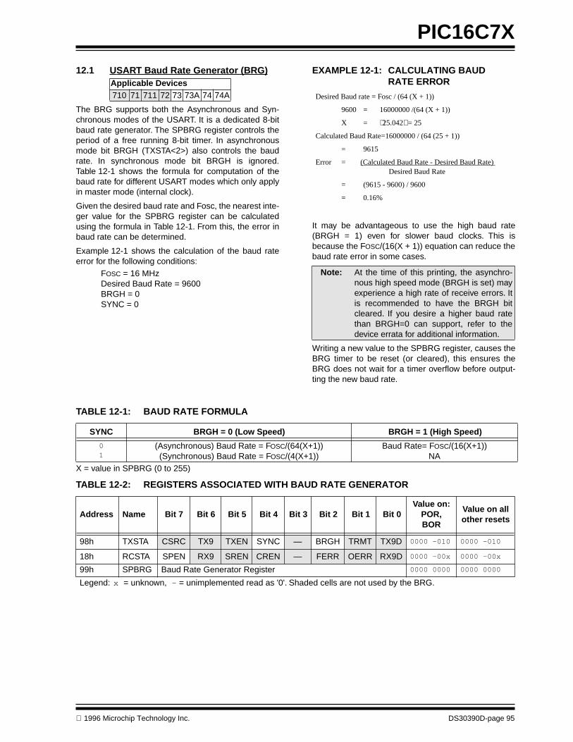
1996 Microchip Technology Inc. DS30390D-page 95
PIC16C7X
12.1 USART Baud Rate Generator (BRG)
The BRG supports both the Asynchronous and Syn-chronous modes of the USART. It is a dedicated 8-bitbaud rate generator. The SPBRG register controls theperiod of a free running 8-bit timer. In asynchronousmode bit BRGH (TXSTA<2>) also controls the baudrate. In synchronous mode bit BRGH is ignored.Table 12-1 shows the formula for computation of thebaud rate for different USART modes which only applyin master mode (internal clock).
Given the desired baud rate and Fosc, the nearest inte-ger value for the SPBRG register can be calculatedusing the formula in Table 12-1. From this, the error inbaud rate can be determined.
Example 12-1 shows the calculation of the baud rateerror for the following conditions:
F
OSC
= 16 MHzDesired Baud Rate = 9600BRGH = 0SYNC = 0
Applicable Devices
710 71 711 72 73 73A 74 74A
EXAMPLE 12-1: CALCULATING BAUD RATE ERROR
It may be advantageous to use the high baud rate(BRGH = 1) even for slower baud clocks. This isbecause the F
OSC
/(16(X + 1)) equation can reduce thebaud rate error in some cases.
Writing a new value to the SPBRG register, causes theBRG timer to be reset (or cleared), this ensures theBRG does not wait for a timer overflow before output-ting the new baud rate.
Note:
At the time of this printing, the asynchro-nous high speed mode (BRGH is set) mayexperience a high rate of receive errors. Itis recommended to have the BRGH bitcleared. If you desire a higher baud ratethan BRGH=0 can support, refer to thedevice errata for additional information.
Desired Baud rate = Fosc / (64 (X + 1))
9600 = 16000000 /(64 (X + 1))
X = 25.042 = 25
Calculated Baud Rate=16000000 / (64 (25 + 1))
= 9615
Error = (Calculated Baud Rate - Desired Baud Rate) Desired Baud Rate
= (9615 - 9600) / 9600
= 0.16%
TABLE 12-1: BAUD RATE FORMULA
TABLE 12-2: REGISTERS ASSOCIATED WITH BAUD RATE GENERATOR
SYNC BRGH = 0 (Low Speed) BRGH = 1 (High Speed)
01
(Asynchronous) Baud Rate = F
OSC
/(64(X+1))(Synchronous) Baud Rate = F
OSC
/(4(X+1))Baud Rate= F
OSC
/(16(X+1))NA
X = value in SPBRG (0 to 255)
Address Name Bit 7 Bit 6 Bit 5 Bit 4 Bit 3 Bit 2 Bit 1 Bit 0Value on:
POR,BOR
Value on allother resets
98h TXSTA CSRC TX9 TXEN SYNC — BRGH TRMT TX9D
0000 -010 0000 -010
18h RCSTA SPEN RX9 SREN CREN — FERR OERR RX9D
0000 -00x 0000 -00x
99h SPBRG Baud Rate Generator Register
0000 0000 0000 0000
Legend:
x
= unknown,
-
= unimplemented read as '0'. Shaded cells are not used by the BRG.

PIC16C7X
DS30390D-page 96
1996 Microchip Technology Inc.
TABLE 12-3: BAUD RATES FOR SYNCHRONOUS MODE
TABLE 12-4: BAUD RATES FOR ASYNCHRONOUS MODE (BRGH = 0)
BAUDRATE
(K)
F
OSC
= 20 MHzSPBRG
value (decimal)
16 MHzSPBRG
value (decimal)
10 MHzSPBRG
value (decimal)
7.15909 MHzSPBRG
value (decimal)KBAUD %
ERROR KBAUD %ERROR KBAUD %
ERROR KBAUD %ERROR
0.3 NA - - NA - - NA - - NA - -1.2 NA - - NA - - NA - - NA - -2.4 NA - - NA - - NA - - NA - -9.6 NA - - NA - - 9.766 +1.73 255 9.622 +0.23 18519.2 19.53 +1.73 255 19.23 +0.16 207 19.23 +0.16 129 19.24 +0.23 9276.8 76.92 +0.16 64 76.92 +0.16 51 75.76 -1.36 32 77.82 +1.32 2296 96.15 +0.16 51 95.24 -0.79 41 96.15 +0.16 25 94.20 -1.88 18300 294.1 -1.96 16 307.69 +2.56 12 312.5 +4.17 7 298.3 -0.57 5500 500 0 9 500 0 7 500 0 4 NA - -
HIGH 5000 - 0 4000 - 0 2500 - 0 1789.8 - 0LOW 19.53 - 255 15.625 - 255 9.766 - 255 6.991 - 255
BAUDRATE
(K)
F
OSC
= 5.0688 MHz 4 MHz
SPBRGvalue
(decimal)
3.579545 MHz
SPBRGvalue
(decimal)
1 MHz
SPBRGvalue
(decimal)
32.768 kHz
SPBRGvalue
(decimal)KBAUD %
ERROR
SPBRGvalue
(decimal)KBAUD %
ERRORKBAUD %
ERRORKBAUD %
ERRORKBAUD %
ERROR
0.3 NA - - NA - - NA - - NA - - 0.303 +1.14 261.2 NA - - NA - - NA - - 1.202 +0.16 207 1.170 -2.48 62.4 NA - - NA - - NA - - 2.404 +0.16 103 NA - -9.6 9.6 0 131 9.615 +0.16 103 9.622 +0.23 92 9.615 +0.16 25 NA - -19.2 19.2 0 65 19.231 +0.16 51 19.04 -0.83 46 19.24 +0.16 12 NA - -76.8 79.2 +3.13 15 76.923 +0.16 12 74.57 -2.90 11 83.34 +8.51 2 NA - -96 97.48 +1.54 12 1000 +4.17 9 99.43 +3.57 8 NA - - NA - -300 316.8 +5.60 3 NA - - 298.3 -0.57 2 NA - - NA - -500 NA - - NA - - NA - - NA - - NA - -
HIGH 1267 - 0 100 - 0 894.9 - 0 250 - 0 8.192 - 0LOW 4.950 - 255 3.906 - 255 3.496 - 255 0.9766 - 255 0.032 - 255
BAUDRATE
(K)
F
OSC
= 20 MHzSPBRG
value (decimal)
16 MHzSPBRG
value (decimal)
10 MHzSPBRG
value (decimal)
7.15909 MHzSPBRG
value (decimal)KBAUD
%ERROR KBAUD
%ERROR KBAUD
%ERROR KBAUD
%ERROR
0.3 NA - - NA - - NA - - NA - -1.2 1.221 +1.73 255 1.202 +0.16 207 1.202 +0.16 129 1.203 +0.23 922.4 2.404 +0.16 129 2.404 +0.16 103 2.404 +0.16 64 2.380 -0.83 469.6 9.469 -1.36 32 9.615 +0.16 25 9.766 +1.73 15 9.322 -2.90 1119.2 19.53 +1.73 15 19.23 +0.16 12 19.53 +1.73 7 18.64 -2.90 576.8 78.13 +1.73 3 83.33 +8.51 2 78.13 +1.73 1 NA - -96 104.2 +8.51 2 NA - - NA - - NA - -300 312.5 +4.17 0 NA - - NA - - NA - -500 NA - - NA - - NA - - NA - -
HIGH 312.5 - 0 250 - 0 156.3 - 0 111.9 - 0LOW 1.221 - 255 0.977 - 255 0.6104 - 255 0.437 - 255
BAUDRATE
(K)
F
OSC
= 5.0688 MHz 4 MHz
SPBRGvalue
(decimal)
3.579545 MHz
SPBRGvalue
(decimal)
1 MHz
SPBRGvalue
(decimal)
32.768 kHz
SPBRGvalue
(decimal)KBAUD%
ERROR
SPBRGvalue
(decimal) KBAUD%
ERROR KBAUD%
ERROR KBAUD%
ERROR KBAUD%
ERROR
0.3 0.31 +3.13 255 0.3005 -0.17 207 0.301 +0.23 185 0.300 +0.16 51 0.256 -14.67 11.2 1.2 0 65 1.202 +1.67 51 1.190 -0.83 46 1.202 +0.16 12 NA - -2.4 2.4 0 32 2.404 +1.67 25 2.432 +1.32 22 2.232 -6.99 6 NA - -9.6 9.9 +3.13 7 NA - - 9.322 -2.90 5 NA - - NA - -19.2 19.8 +3.13 3 NA - - 18.64 -2.90 2 NA - - NA - -76.8 79.2 +3.13 0 NA - - NA - - NA - - NA - -96 NA - - NA - - NA - - NA - - NA - -300 NA - - NA - - NA - - NA - - NA - -500 NA - - NA - - NA - - NA - - NA - -
HIGH 79.2 - 0 62.500 - 0 55.93 - 0 15.63 - 0 0.512 - 0LOW 0.3094 - 255 3.906 - 255 0.2185 - 255 0.0610 - 255 0.0020 - 255

1996 Microchip Technology Inc. DS30390D-page 97
PIC16C7X
TABLE 12-5: BAUD RATES FOR ASYNCHRONOUS MODE (BRGH = 1)
BAUDRATE
(K)
F
OSC
= 20 MHzSPBRG
value (decimal)
16 MHzSPBRG
value (decimal)
10 MHzSPBRG
value (decimal)
7.16 MHzSPBRG
value (decimal)KBAUD
%ERROR KBAUD
%ERROR KBAUD
%ERROR KBAUD
%ERROR
9.6 9.615 +0.16 129 9.615 +0.16 103 9.615 +0.16 64 9.520 -0.83 4619.2 19.230 +0.16 64 19.230 +0.16 51 18.939 -1.36 32 19.454 +1.32 2238.4 37.878 -1.36 32 38.461 +0.16 25 39.062 +1.7 15 37.286 -2.90 1157.6 56.818 -1.36 21 58.823 +2.12 16 56.818 -1.36 10 55.930 -2.90 7115.2 113.636 -1.36 10 111.111 -3.55 8 125 +8.51 4 111.860 -2.90 3250 250 0 4 250 0 3 NA - - NA - -625 625 0 1 NA - - 625 0 0 NA - -1250 1250 0 0 NA - - NA - - NA - -
BAUDRATE
(K)
F
OSC
= 5.068 MHzSPBRG
value (decimal)
4 MHzSPBRG
value (decimal)
3.579 MHzSPBRG
value (decimal)
1 MHzSPBRG
value (decimal)
32.768 kHzSPBRG
value (decimal)KBAUD
%ERROR KBAUD
%ERROR KBAUD
%ERROR KBAUD
%ERROR KBAUD
%ERROR
9.6 9.6 0 32 NA - - 9.727 +1.32 22 8.928 -6.99 6 NA - -19.2 18.645 -2.94 16 1.202 +0.17 207 18.643 -2.90 11 20.833 +8.51 2 NA - -
38.4 39.6 +3.12 7 2.403 +0.13 103 37.286 -2.90 5 31.25 -18.61 1 NA - -57.6 52.8 -8.33 5 9.615 +0.16 25 55.930 -2.90 3 62.5 +8.51 0 NA - -115.2 105.6 -8.33 2 19.231 +0.16 12 111.860 -2.90 1 NA - - NA - -250 NA - - NA - - 223.721 -10.51 0 NA - - NA - -625 NA - - NA - - NA - - NA - - NA - -1250 NA - - NA - - NA - - NA - - NA - -

PIC16C7X
DS30390D-page 98
1996 Microchip Technology Inc.
12.1.1 SAMPLING
The data on the RC7/RX/DT pin is sampled three timesby a majority detect circuit to determine if a high or alow level is present at the RX pin. If bit BRGH(TXSTA<2>) is clear (i.e., at the low baud rates), thesampling is done on the seventh, eighth and ninth fall-ing edges of a x16 clock (Figure 12-3). If bit BRGH is
set (i.e., at the high baud rates), the sampling is doneon the 3 clock edges preceding the second rising edgeafter the first falling edge of a x4 clock (Figure 12-4 andFigure 12-5).
FIGURE 12-3: RX PIN SAMPLING SCHEME (BRGH = 0)
FIGURE 12-4: RX PIN SAMPLING SCHEME (BRGH = 1)
FIGURE 12-5: RX PIN SAMPLING SCHEME (BRGH = 1)
RX
baud CLK
x16 CLK
Start bit Bit0
Samples
1 2 3 4 5 6 7 8 9 10 11 12 13 14 15 16 1 2 3
Baud CLK for all but start bit(RC7/RX/DT pin)
RX pin
baud clk
x4 clk
Q2, Q4 clk
Start Bit bit0 bit1
First falling edge after RX pin goes lowSecond rising edge
Samples Samples Samples
1 2 3 4 1 2 3 4 1 2
RX pin
baud clk
x4 clk
Q2, Q4 clk
Start Bit bit0
First falling edge after RX pin goes lowSecond rising edge
Samples
1 2 3 4
Baud clk for all but start bit

1996 Microchip Technology Inc. DS30390D-page 99
PIC16C7X
12.2 USART Asynchronous Mode
In this mode, the USART uses standard nonreturn-to-zero (NRZ) format (one start bit, eight or nine data bitsand one stop bit). The most common data format is8-bits. An on-chip dedicated 8-bit baud rate generatorcan be used to derive standard baud rate frequenciesfrom the oscillator. The USART transmits and receivesthe LSb first. The USART’s transmitter and receiver arefunctionally independent but use the same data formatand baud rate. The baud rate generator produces aclock either x16 or x64 of the bit shift rate, dependingon bit BRGH (TXSTA<2>). Parity is not supported bythe hardware, but can be implemented in software (andstored as the ninth data bit). Asynchronous mode isstopped during SLEEP.
Asynchronous mode is selected by clearing bit SYNC(TXSTA<4>).
The USART Asynchronous module consists of the fol-lowing important elements:
• Baud Rate Generator• Sampling Circuit• Asynchronous Transmitter• Asynchronous Receiver
12.2.1 USART ASYNCHRONOUS TRANSMITTER
The USART transmitter block diagram is shown inFigure 12-6. The heart of the transmitter is the transmit(serial) shift register (TSR). The shift register obtains itsdata from the read/write transmit buffer, TXREG. TheTXREG register is loaded with data in software. TheTSR register is not loaded until the STOP bit has beentransmitted from the previous load. As soon as theSTOP bit is transmitted, the TSR is loaded with newdata from the TXREG register (if available). Once theTXREG register transfers the data to the TSR register(occurs in one T
CY
), the TXREG register is empty and
Applicable Devices
710 71 711 72 73 73A 74 74A
flag bit TXIF (PIR1<4>) is set. This interrupt can beenabled/disabled by setting/clearing enable bit TXIE( PIE1<4>). Flag bit TXIF will be set regardless of thestate of enable bit TXIE and cannot be cleared in soft-ware. It will reset only when new data is loaded into theTXREG register. While flag bit TXIF indicated the sta-tus of the TXREG register, another bit TRMT(TXSTA<1>) shows the status of the TSR register. Sta-tus bit TRMT is a read only bit which is set when theTSR register is empty. No interrupt logic is tied to thisbit, so the user has to poll this bit in order to determineif the TSR register is empty.
Transmission is enabled by setting enable bit TXEN(TXSTA<5>). The actual transmission will not occuruntil the TXREG register has been loaded with dataand the baud rate generator (BRG) has produced ashift clock (Figure 12-6). The transmission can also bestarted by first loading the TXREG register and thensetting enable bit TXEN. Normally when transmissionis first started, the TSR register is empty, so a transferto the TXREG register will result in an immediate trans-fer to TSR resulting in an empty TXREG. A back-to-back transfer is thus possible (Figure 12-8). Clearingenable bit TXEN during a transmission will cause thetransmission to be aborted and will reset the transmit-ter. As a result the RC6/TX/CK pin will revert to hi-impedance.
In order to select 9-bit transmission, transmit bit TX9(TXSTA<6>) should be set and the ninth bit should bewritten to TX9D (TXSTA<0>). The ninth bit must bewritten before writing the 8-bit data to the TXREG reg-ister. This is because a data write to the TXREG regis-ter can result in an immediate transfer of the data to theTSR register (if the TSR is empty). In such a case, anincorrect ninth data bit maybe loaded in the TSR regis-ter.
Note 1:
The TSR register is not mapped in datamemory so it is not available to the user.
Note 2:
Flag bit TXIF is set when enable bit TXENis set.
FIGURE 12-6: USART TRANSMIT BLOCK DIAGRAM
TXIFTXIE
Interrupt
TXEN Baud Rate CLK
SPBRG
Baud Rate Generator
TX9D
MSb LSb
Data Bus
TXREG register
TSR register
(8) 0
TX9
TRMT SPEN
RC6/TX/CK pin
Pin Bufferand Control
8
• • •

PIC16C7X
DS30390D-page 100
1996 Microchip Technology Inc.
Steps to follow when setting up a Asynchronous Trans-mission:
1. Initialize the SPBRG register for the appropriatebaud rate. If a high speed baud rate is desired,set bit BRGH. (Section 12.1)
2. Enable the asynchronous serial port by clearingbit SYNC and setting bit SPEN.
3. If interrupts are desired, then set enable bitTXIE.
4. If 9-bit transmission is desired, then set transmitbit TX9.
5. Enable the transmission by setting bit TXEN,which will also set bit TXIF.
6. If 9-bit transmission is selected, the ninth bitshould be loaded in bit TX9D.
7. Load data to the TXREG register (starts trans-mission).
FIGURE 12-7: ASYNCHRONOUS MASTER TRANSMISSION
FIGURE 12-8: ASYNCHRONOUS MASTER TRANSMISSION (BACK TO BACK)
TABLE 12-6: REGISTERS ASSOCIATED WITH ASYNCHRONOUS TRANSMISSION
Address Name Bit 7 Bit 6 Bit 5 Bit 4 Bit 3 Bit 2 Bit 1 Bit 0Value on:
POR,BOR
Value onall otherResets
0Ch PIR1 PSPIF
(1)
ADIF RCIF TXIF SSPIF CCP1IF TMR2IF TMR1IF
0000 0000 0000 0000
18h RCSTA SPEN RX9 SREN CREN — FERR OERR RX9D
0000 -00x 0000 -00x
19h TXREG TX7 TX6 TX5 TX4 TX3 TX2 TX1 TX0
0000 0000 0000 0000
8Ch PIE1 PSPIE
(1)
ADIE RCIE TXIE SSPIE CCP1IE TMR2IE TMR1IE
0000 0000 0000 0000
98h TXSTA CSRC TX9 TXEN SYNC — BRGH TRMT TX9D
0000 -010 0000 -010
99h SPBRG Baud Rate Generator Register
0000 0000 0000 0000
Legend:
x
= unknown,
-
= unimplemented locations read as '0'. Shaded cells are not used for Asynchronous Transmission.Note 1: Bits PSPIE and PSPIF are reserved on the PIC16C73/73A, always maintain these bits clear.
WORD 1Stop Bit
WORD 1Transmit Shift Reg
Start Bit Bit 0 Bit 1 Bit 7/8
Write to TXREGWord 1
BRG output(shift clock)
RC6/TX/CK (pin)
TXIF bit(Transmit bufferreg. empty flag)
TRMT bit(Transmit shiftreg. empty flag)
Transmit Shift Reg.
Write to TXREG
BRG output(shift clock)
RC6/TX/CK (pin)
TXIF bit(interrupt reg. flag)
TRMT bit(Transmit shiftreg. empty flag)
Word 1 Word 2
WORD 1 WORD 2
Start Bit Stop Bit Start Bit
Transmit Shift Reg.
WORD 1 WORD 2Bit 0 Bit 1 Bit 7/8 Bit 0
Note: This timing diagram shows two consecutive transmissions.
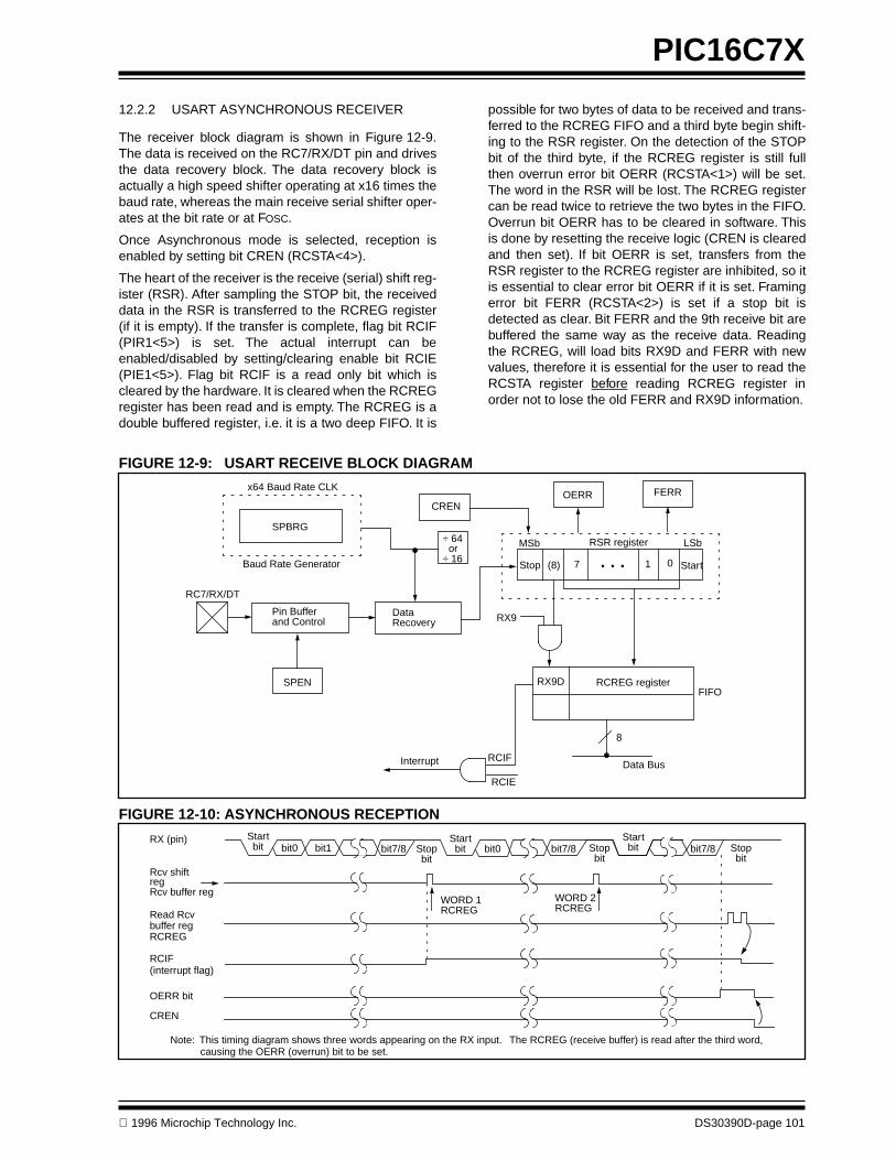
1996 Microchip Technology Inc. DS30390D-page 101
PIC16C7X
12.2.2 USART ASYNCHRONOUS RECEIVER
The receiver block diagram is shown in Figure 12-9.The data is received on the RC7/RX/DT pin and drivesthe data recovery block. The data recovery block isactually a high speed shifter operating at x16 times thebaud rate, whereas the main receive serial shifter oper-ates at the bit rate or at F
OSC
.
Once Asynchronous mode is selected, reception isenabled by setting bit CREN (RCSTA<4>).
The heart of the receiver is the receive (serial) shift reg-ister (RSR). After sampling the STOP bit, the receiveddata in the RSR is transferred to the RCREG register(if it is empty). If the transfer is complete, flag bit RCIF(PIR1<5>) is set. The actual interrupt can beenabled/disabled by setting/clearing enable bit RCIE(PIE1<5>). Flag bit RCIF is a read only bit which iscleared by the hardware. It is cleared when the RCREGregister has been read and is empty. The RCREG is adouble buffered register, i.e. it is a two deep FIFO. It is
possible for two bytes of data to be received and trans-ferred to the RCREG FIFO and a third byte begin shift-ing to the RSR register. On the detection of the STOPbit of the third byte, if the RCREG register is still fullthen overrun error bit OERR (RCSTA<1>) will be set.The word in the RSR will be lost. The RCREG registercan be read twice to retrieve the two bytes in the FIFO.Overrun bit OERR has to be cleared in software. Thisis done by resetting the receive logic (CREN is clearedand then set). If bit OERR is set, transfers from theRSR register to the RCREG register are inhibited, so itis essential to clear error bit OERR if it is set. Framingerror bit FERR (RCSTA<2>) is set if a stop bit isdetected as clear. Bit FERR and the 9th receive bit arebuffered the same way as the receive data. Readingthe RCREG, will load bits RX9D and FERR with newvalues, therefore it is essential for the user to read theRCSTA register before reading RCREG register inorder not to lose the old FERR and RX9D information.
FIGURE 12-9: USART RECEIVE BLOCK DIAGRAM
FIGURE 12-10: ASYNCHRONOUS RECEPTION
x64 Baud Rate CLK
SPBRG
Baud Rate Generator
RC7/RX/DT
Pin Bufferand Control
SPEN
DataRecovery
CRENOERR FERR
RSR registerMSb LSb
RX9D RCREG registerFIFO
Interrupt RCIF
RCIE
Data Bus
8
÷ 64
÷ 16or
Stop Start(8) 7 1 0
RX9
• • •
Startbit bit7/8bit1bit0 bit7/8 bit0Stop
bit
Startbit
Startbitbit7/8 Stop
bit
RX (pin)
regRcv buffer reg
Rcv shift
Read Rcvbuffer regRCREG
RCIF(interrupt flag)
OERR bit
CREN
WORD 1RCREG
WORD 2RCREG
Stopbit
Note: This timing diagram shows three words appearing on the RX input. The RCREG (receive buffer) is read after the third word,causing the OERR (overrun) bit to be set.
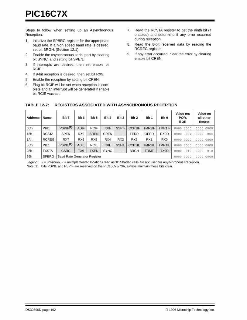
PIC16C7X
DS30390D-page 102
1996 Microchip Technology Inc.
Steps to follow when setting up an AsynchronousReception:
1. Initialize the SPBRG register for the appropriatebaud rate. If a high speed baud rate is desired,set bit BRGH. (Section 12.1).
2. Enable the asynchronous serial port by clearingbit SYNC, and setting bit SPEN.
3. If interrupts are desired, then set enable bitRCIE.
4. If 9-bit reception is desired, then set bit RX9.5. Enable the reception by setting bit CREN.6. Flag bit RCIF will be set when reception is com-
plete and an interrupt will be generated if enablebit RCIE was set.
7. Read the RCSTA register to get the ninth bit (ifenabled) and determine if any error occurredduring reception.
8. Read the 8-bit received data by reading theRCREG register.
9. If any error occurred, clear the error by clearingenable bit CREN.
TABLE 12-7: REGISTERS ASSOCIATED WITH ASYNCHRONOUS RECEPTION
Address Name Bit 7 Bit 6 Bit 5 Bit 4 Bit 3 Bit 2 Bit 1 Bit 0Value on:
POR,BOR
Value onall otherResets
0Ch PIR1 PSPIF
(1)
ADIF RCIF TXIF SSPIF CCP1IF TMR2IF TMR1IF
0000 0000 0000 0000
18h RCSTA SPEN RX9 SREN CREN — FERR OERR RX9D
0000 -00x 0000 -00x
1Ah RCREG RX7 RX6 RX5 RX4 RX3 RX2 RX1 RX0
0000 0000 0000 0000
8Ch PIE1 PSPIE
(1)
ADIE RCIE TXIE SSPIE CCP1IE TMR2IE TMR1IE
0000 0000 0000 0000
98h TXSTA CSRC TX9 TXEN SYNC — BRGH TRMT TX9D
0000 -010 0000 -010
99h SPBRG Baud Rate Generator Register
0000 0000 0000 0000
Legend: x = unknown, - = unimplemented locations read as '0'. Shaded cells are not used for Asynchronous Reception.Note 1: Bits PSPIE and PSPIF are reserved on the PIC16C73/73A, always maintain these bits clear.
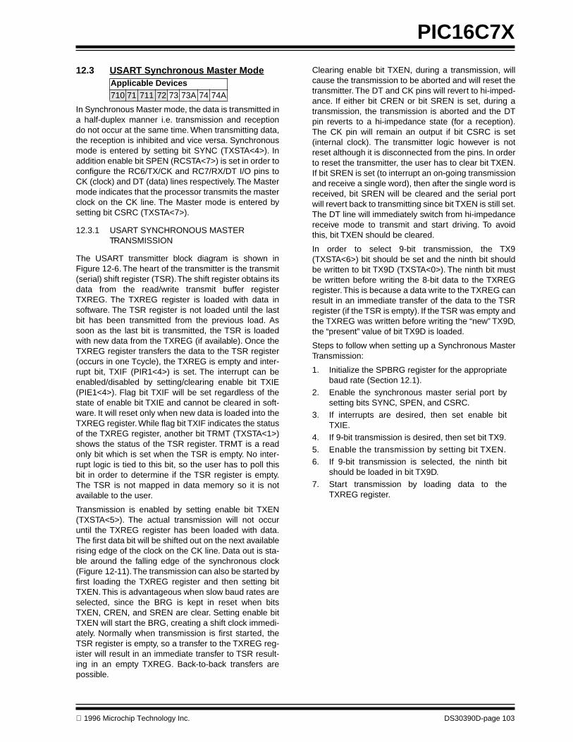
1996 Microchip Technology Inc. DS30390D-page 103
PIC16C7X
12.3 USART Synchronous Master Mode
In Synchronous Master mode, the data is transmitted ina half-duplex manner i.e. transmission and receptiondo not occur at the same time. When transmitting data,the reception is inhibited and vice versa. Synchronousmode is entered by setting bit SYNC (TXSTA<4>). Inaddition enable bit SPEN (RCSTA<7>) is set in order toconfigure the RC6/TX/CK and RC7/RX/DT I/O pins toCK (clock) and DT (data) lines respectively. The Mastermode indicates that the processor transmits the masterclock on the CK line. The Master mode is entered bysetting bit CSRC (TXSTA<7>).
12.3.1 USART SYNCHRONOUS MASTER TRANSMISSION
The USART transmitter block diagram is shown inFigure 12-6. The heart of the transmitter is the transmit(serial) shift register (TSR). The shift register obtains itsdata from the read/write transmit buffer registerTXREG. The TXREG register is loaded with data insoftware. The TSR register is not loaded until the lastbit has been transmitted from the previous load. Assoon as the last bit is transmitted, the TSR is loadedwith new data from the TXREG (if available). Once theTXREG register transfers the data to the TSR register(occurs in one Tcycle), the TXREG is empty and inter-rupt bit, TXIF (PIR1<4>) is set. The interrupt can beenabled/disabled by setting/clearing enable bit TXIE(PIE1<4>). Flag bit TXIF will be set regardless of thestate of enable bit TXIE and cannot be cleared in soft-ware. It will reset only when new data is loaded into theTXREG register. While flag bit TXIF indicates the statusof the TXREG register, another bit TRMT (TXSTA<1>)shows the status of the TSR register. TRMT is a readonly bit which is set when the TSR is empty. No inter-rupt logic is tied to this bit, so the user has to poll thisbit in order to determine if the TSR register is empty.The TSR is not mapped in data memory so it is notavailable to the user.
Transmission is enabled by setting enable bit TXEN(TXSTA<5>). The actual transmission will not occuruntil the TXREG register has been loaded with data.The first data bit will be shifted out on the next availablerising edge of the clock on the CK line. Data out is sta-ble around the falling edge of the synchronous clock(Figure 12-11). The transmission can also be started byfirst loading the TXREG register and then setting bitTXEN. This is advantageous when slow baud rates areselected, since the BRG is kept in reset when bitsTXEN, CREN, and SREN are clear. Setting enable bitTXEN will start the BRG, creating a shift clock immedi-ately. Normally when transmission is first started, theTSR register is empty, so a transfer to the TXREG reg-ister will result in an immediate transfer to TSR result-ing in an empty TXREG. Back-to-back transfers arepossible.
Applicable Devices710 71 711 72 73 73A 74 74A
Clearing enable bit TXEN, during a transmission, willcause the transmission to be aborted and will reset thetransmitter. The DT and CK pins will revert to hi-imped-ance. If either bit CREN or bit SREN is set, during atransmission, the transmission is aborted and the DTpin reverts to a hi-impedance state (for a reception).The CK pin will remain an output if bit CSRC is set(internal clock). The transmitter logic however is notreset although it is disconnected from the pins. In orderto reset the transmitter, the user has to clear bit TXEN.If bit SREN is set (to interrupt an on-going transmissionand receive a single word), then after the single word isreceived, bit SREN will be cleared and the serial portwill revert back to transmitting since bit TXEN is still set.The DT line will immediately switch from hi-impedancereceive mode to transmit and start driving. To avoidthis, bit TXEN should be cleared.
In order to select 9-bit transmission, the TX9(TXSTA<6>) bit should be set and the ninth bit shouldbe written to bit TX9D (TXSTA<0>). The ninth bit mustbe written before writing the 8-bit data to the TXREGregister. This is because a data write to the TXREG canresult in an immediate transfer of the data to the TSRregister (if the TSR is empty). If the TSR was empty andthe TXREG was written before writing the “new” TX9D,the “present” value of bit TX9D is loaded.
Steps to follow when setting up a Synchronous MasterTransmission:
1. Initialize the SPBRG register for the appropriatebaud rate (Section 12.1).
2. Enable the synchronous master serial port bysetting bits SYNC, SPEN, and CSRC.
3. If interrupts are desired, then set enable bitTXIE.
4. If 9-bit transmission is desired, then set bit TX9.5. Enable the transmission by setting bit TXEN.6. If 9-bit transmission is selected, the ninth bit
should be loaded in bit TX9D.7. Start transmission by loading data to the
TXREG register.
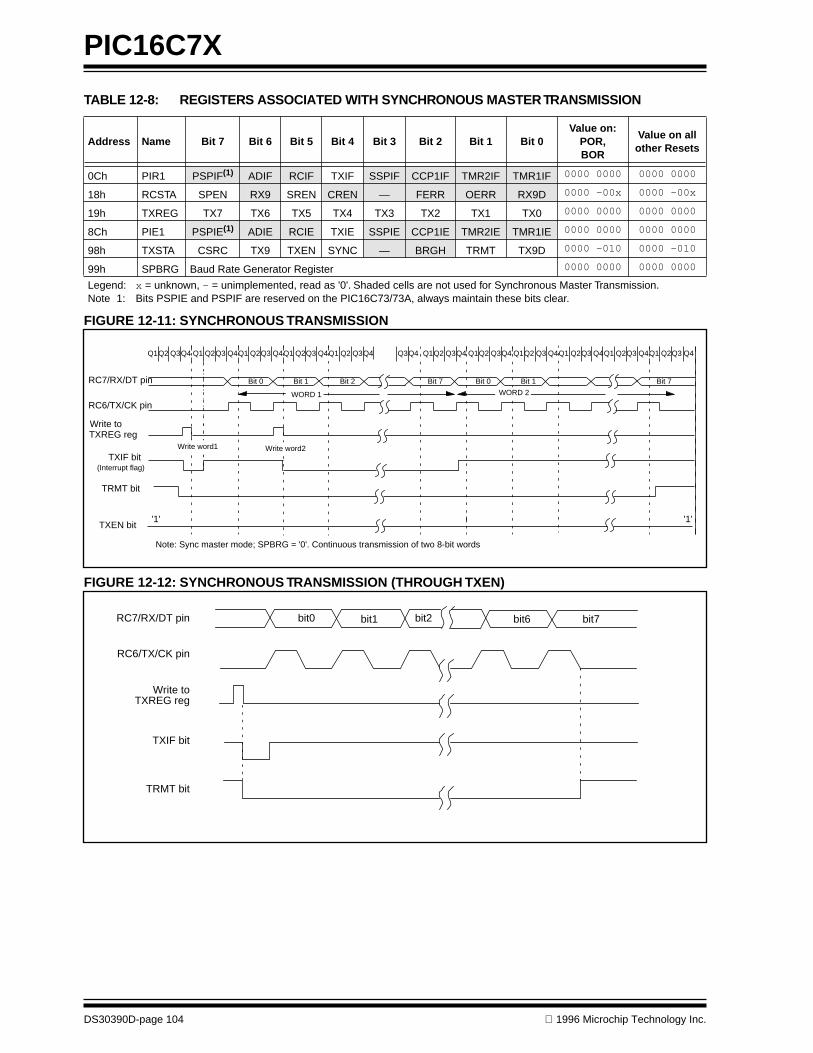
PIC16C7X
DS30390D-page 104 1996 Microchip Technology Inc.
TABLE 12-8: REGISTERS ASSOCIATED WITH SYNCHRONOUS MASTER TRANSMISSION
FIGURE 12-11: SYNCHRONOUS TRANSMISSION
FIGURE 12-12: SYNCHRONOUS TRANSMISSION (THROUGH TXEN)
Address Name Bit 7 Bit 6 Bit 5 Bit 4 Bit 3 Bit 2 Bit 1 Bit 0Value on:
POR,BOR
Value on all other Resets
0Ch PIR1 PSPIF(1) ADIF RCIF TXIF SSPIF CCP1IF TMR2IF TMR1IF 0000 0000 0000 0000
18h RCSTA SPEN RX9 SREN CREN — FERR OERR RX9D 0000 -00x 0000 -00x
19h TXREG TX7 TX6 TX5 TX4 TX3 TX2 TX1 TX0 0000 0000 0000 0000
8Ch PIE1 PSPIE(1) ADIE RCIE TXIE SSPIE CCP1IE TMR2IE TMR1IE 0000 0000 0000 0000
98h TXSTA CSRC TX9 TXEN SYNC — BRGH TRMT TX9D 0000 -010 0000 -010
99h SPBRG Baud Rate Generator Register 0000 0000 0000 0000
Legend: x = unknown, - = unimplemented, read as '0'. Shaded cells are not used for Synchronous Master Transmission.Note 1: Bits PSPIE and PSPIF are reserved on the PIC16C73/73A, always maintain these bits clear.
Bit 0 Bit 1 Bit 7
WORD 1
Q1Q2 Q3Q4 Q1 Q2Q3 Q4Q1 Q2Q3 Q4Q1 Q2Q3 Q4Q1 Q2 Q3Q4 Q3Q4 Q1Q2 Q3Q4 Q1Q2 Q3Q4 Q1Q2 Q3 Q4Q1 Q2Q3 Q4Q1 Q2Q3 Q4Q1 Q2Q3 Q4
Bit 2 Bit 0 Bit 1 Bit 7RC7/RX/DT pin
RC6/TX/CK pin
Write toTXREG reg
TXIF bit(Interrupt flag)
TRMT
TXEN bit'1' '1'
Note: Sync master mode; SPBRG = '0'. Continuous transmission of two 8-bit words
WORD 2
TRMT bit
Write word1 Write word2
RC7/RX/DT pin
RC6/TX/CK pin
Write toTXREG reg
TXIF bit
TRMT bit
bit0 bit1 bit2 bit6 bit7

1996 Microchip Technology Inc. DS30390D-page 105
PIC16C7X
12.3.2 USART SYNCHRONOUS MASTER RECEPTION
Once Synchronous mode is selected, reception isenabled by setting either enable bit SREN(RCSTA<5>) or enable bit CREN (RCSTA<4>). Data issampled on the RC7/RX/DT pin on the falling edge ofthe clock. If enable bit SREN is set, then only a singleword is received. If enable bit CREN is set, the recep-tion is continuous until CREN is cleared. If both bits areset then CREN takes precedence. After clocking thelast bit, the received data in the Receive Shift Register(RSR) is transferred to the RCREG register (if it isempty). When the transfer is complete, interrupt flag bitRCIF (PIR1<5>) is set. The actual interrupt can beenabled/disabled by setting/clearing enable bit RCIE(PIE1<5>). Flag bit RCIF is a read only bit which isreset by the hardware. In this case it is reset when theRCREG register has been read and is empty. TheRCREG is a double buffered register, i.e. it is a twodeep FIFO. It is possible for two bytes of data to bereceived and transferred to the RCREG FIFO and athird byte to begin shifting into the RSR register. On theclocking of the last bit of the third byte, if the RCREGregister is still full then overrun error bit OERR(RCSTA<1>) is set. The word in the RSR will be lost.The RCREG register can be read twice to retrieve thetwo bytes in the FIFO. Bit OERR has to be cleared insoftware (by clearing bit CREN). If bit OERR is set,transfers from the RSR to the RCREG are inhibited, so
it is essential to clear bit OERR if it is set. The 9threceive bit is buffered the same way as the receivedata. Reading the RCREG register, will load bit RX9Dwith a new value, therefore it is essential for the user toread the RCSTA register before reading RCREG inorder not to lose the old RX9D information.
Steps to follow when setting up a Synchronous MasterReception:
1. Initialize the SPBRG register for the appropriatebaud rate. (Section 12.1)
2. Enable the synchronous master serial port bysetting bits SYNC, SPEN, and CSRC.
3. Ensure bits CREN and SREN are clear.4. If interrupts are desired, then set enable bit
RCIE.5. If 9-bit reception is desired, then set bit RX9.6. If a single reception is required, set bit SREN.
For continuous reception set bit CREN.7. Interrupt flag bit RCIF will be set when reception
is complete and an interrupt will be generated ifenable bit RCIE was set.
8. Read the RCSTA register to get the ninth bit (ifenabled) and determine if any error occurredduring reception.
9. Read the 8-bit received data by reading theRCREG register.
10. If any error occurred, clear the error by clearingbit CREN.
TABLE 12-9: REGISTERS ASSOCIATED WITH SYNCHRONOUS MASTER RECEPTION
Address Name Bit 7 Bit 6 Bit 5 Bit 4 Bit 3 Bit 2 Bit 1 Bit 0Value on:
POR,BOR
Value on all other Resets
0Ch PIR1 PSPIF(1) ADIF RCIF TXIF SSPIF CCP1IF TMR2IF TMR1IF 0000 0000 0000 0000
18h RCSTA SPEN RX9 SREN CREN — FERR OERR RX9D 0000 -00x 0000 -00x
1Ah RCREG RX7 RX6 RX5 RX4 RX3 RX2 RX1 RX0 0000 0000 0000 0000
8Ch PIE1 PSPIE(1) ADIE RCIE TXIE SSPIE CCP1IE TMR2IE TMR1IE 0000 0000 0000 0000
98h TXSTA CSRC TX9 TXEN SYNC — BRGH TRMT TX9D 0000 -010 0000 -010
99h SPBRG Baud Rate Generator Register 0000 0000 0000 0000
Legend: x = unknown, - = unimplemented read as '0'. Shaded cells are not used for Synchronous Master Reception.Note 1: Bits PSPIE and PSPIF are reserved on the PIC16C73/73A, always maintain these bits clear.
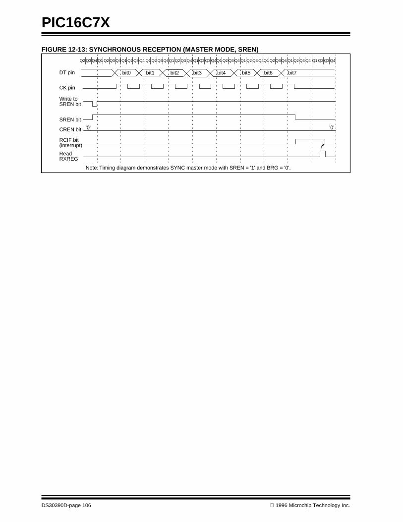
PIC16C7X
DS30390D-page 106 1996 Microchip Technology Inc.
FIGURE 12-13: SYNCHRONOUS RECEPTION (MASTER MODE, SREN)
CREN bit
DT pin
CK pin
Write toSREN bit
SREN bit
RCIF bit(interrupt)
Read RXREG
Note: Timing diagram demonstrates SYNC master mode with SREN = '1' and BRG = '0'.
Q3 Q4 Q1 Q2 Q3 Q4 Q1 Q2 Q3 Q4Q2 Q1 Q2 Q3 Q4Q1 Q2 Q3 Q4 Q1 Q2 Q3 Q4Q1 Q2 Q3 Q4 Q1 Q2 Q3 Q4Q1 Q2 Q3 Q4 Q1 Q2 Q3 Q4
'0'
bit0 bit1 bit2 bit3 bit4 bit5 bit6 bit7
'0'
Q1 Q2 Q3 Q4

1996 Microchip Technology Inc. DS30390D-page 107
PIC16C7X
12.4 USART Synchronous Slave Mode
Synchronous slave mode differs from the Master modein the fact that the shift clock is supplied externally atthe RC6/TX/CK pin (instead of being supplied internallyin master mode). This allows the device to transfer orreceive data while in SLEEP mode. Slave mode isentered by clearing bit CSRC (TXSTA<7>).
12.4.1 USART SYNCHRONOUS SLAVE TRANSMIT
The operation of the synchronous master and slavemodes are identical except in the case of the SLEEPmode.
If two words are written to the TXREG and then theSLEEP instruction is executed, the following will occur:
a) The first word will immediately transfer to theTSR register and transmit.
b) The second word will remain in TXREG register. c) Flag bit TXIF will not be set. d) When the first word has been shifted out of TSR,
the TXREG register will transfer the secondword to the TSR and flag bit TXIF will now beset.
e) If enable bit TXIE is set, the interrupt will wakethe chip from SLEEP and if the global interruptis enabled, the program will branch to the inter-rupt vector (0004h).
Steps to follow when setting up a Synchronous SlaveTransmission:
1. Enable the synchronous slave serial port by set-ting bits SYNC and SPEN and clearing bitCSRC.
2. Clear bits CREN and SREN.3. If interrupts are desired, then set enable bit
TXIE.4. If 9-bit transmission is desired, then set bit TX9.5. Enable the transmission by setting enable bit
TXEN.6. If 9-bit transmission is selected, the ninth bit
should be loaded in bit TX9D.7. Start transmission by loading data to the
TXREG register.
Applicable Devices710 71 711 72 73 73A 74 74A
12.4.2 USART SYNCHRONOUS SLAVE RECEPTION
The operation of the synchronous master and slavemodes is identical except in the case of the SLEEPmode. Also, bit SREN is a don't care in slave mode.
If receive is enabled, by setting bit CREN, prior to theSLEEP instruction, then a word may be received duringSLEEP. On completely receiving the word, the RSRregister will transfer the data to the RCREG registerand if enable bit RCIE bit is set, the interrupt generatedwill wake the chip from SLEEP. If the global interrupt isenabled, the program will branch to the interrupt vector(0004h).
Steps to follow when setting up a Synchronous SlaveReception:
1. Enable the synchronous master serial port bysetting bits SYNC and SPEN and clearing bitCSRC.
2. If interrupts are desired, then set enable bitRCIE.
3. If 9-bit reception is desired, then set bit RX9.4. To enable reception, set enable bit CREN.5. Flag bit RCIF will be set when reception is com-
plete and an interrupt will be generated, ifenable bit RCIE was set.
6. Read the RCSTA register to get the ninth bit (ifenabled) and determine if any error occurredduring reception.
7. Read the 8-bit received data by reading theRCREG register.
8. If any error occurred, clear the error by clearingbit CREN.
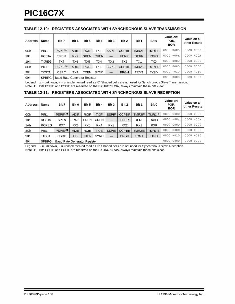
PIC16C7X
DS30390D-page 108 1996 Microchip Technology Inc.
TABLE 12-10: REGISTERS ASSOCIATED WITH SYNCHRONOUS SLAVE TRANSMISSION
TABLE 12-11: REGISTERS ASSOCIATED WITH SYNCHRONOUS SLAVE RECEPTION
Address Name Bit 7 Bit 6 Bit 5 Bit 4 Bit 3 Bit 2 Bit 1 Bit 0Value on:
POR,BOR
Value on all other Resets
0Ch PIR1 PSPIF(1) ADIF RCIF TXIF SSPIF CCP1IF TMR2IF TMR1IF 0000 0000 0000 0000
18h RCSTA SPEN RX9 SREN CREN — FERR OERR RX9D 0000 -00x 0000 -00x
19h TXREG TX7 TX6 TX5 TX4 TX3 TX2 TX1 TX0 0000 0000 0000 0000
8Ch PIE1 PSPIE(1) ADIE RCIE TXIE SSPIE CCP1IE TMR2IE TMR1IE 0000 0000 0000 0000
98h TXSTA CSRC TX9 TXEN SYNC — BRGH TRMT TX9D 0000 -010 0000 -010
99h SPBRG Baud Rate Generator Register 0000 0000 0000 0000
Legend: x = unknown, - = unimplemented read as '0'. Shaded cells are not used for Synchronous Slave Transmission.Note 1: Bits PSPIE and PSPIF are reserved on the PIC16C73/73A, always maintain these bits clear.
Address Name Bit 7 Bit 6 Bit 5 Bit 4 Bit 3 Bit 2 Bit 1 Bit 0Value on:
POR,BOR
Value on all other Resets
0Ch PIR1 PSPIF(1) ADIF RCIF TXIF SSPIF CCP1IF TMR2IF TMR1IF 0000 0000 0000 0000
18h RCSTA SPEN RX9 SREN CREN — FERR OERR RX9D 0000 -00x 0000 -00x
1Ah RCREG RX7 RX6 RX5 RX4 RX3 RX2 RX1 RX0 0000 0000 0000 0000
8Ch PIE1 PSPIE(1) ADIE RCIE TXIE SSPIE CCP1IE TMR2IE TMR1IE 0000 0000 0000 0000
98h TXSTA CSRC TX9 TXEN SYNC — BRGH TRMT TX9D 0000 -010 0000 -010
99h SPBRG Baud Rate Generator Register 0000 0000 0000 0000
Legend: x = unknown, - = unimplemented read as '0'. Shaded cells are not used for Synchronous Slave Reception.Note 1: Bits PSPIE and PSPIF are reserved on the PIC16C73/73A, always maintain these bits clear.

1996 Microchip Technology Inc. DS30390D-page 109
PIC16C7X
FIGURE 13-1: ADCON0 REGISTER, PIC16C710/71/711 (ADDRESS 08h)
R/W-0 R/W-0 U-0 R/W-0 R/W-0 R/W-0 R/W-0 R/W-0ADCS1 ADCS0 —
(1)
CHS1 CHS0 GO/DONE ADIF ADON R = Readable bitW = Writable bitU = Unimplemented
bit, read as ‘0’- n =Value at POR reset
bit7 bit0
bit 7-6:
ADCS1:ADCS0:
A/D Conversion Clock Select bits
00
= F
OSC
/2
01
= F
OSC
/8
10
= F
OSC
/32
11
= F
RC
(clock derived from an RC oscillation)
bit 5:
Unimplemented
: Read as '0'.
bit 4-3:
CHS2:CHS0
: Analog Channel Select bits
00
= channel 0, (RA0/AN0)
01
= channel 1, (RA1/AN1)
10
= channel 2, (RA2/AN2)
11
= channel 3, (RA3/AN3)
bit 2:
GO/DONE:
A/D Conversion Status bit
If ADON = 11 = A/D conversion in progress (setting this bit starts the A/D conversion)0 = A/D conversion not in progress (This bit is automatically cleared by hardware when the A/D conver-sion is complete)
bit 1:
ADIF:
A/D Conversion Complete Interrupt Flag bit1 = conversion is complete (must be cleared in software)0 = conversion is not complete
bit 0:
ADON:
A/D On bit1 = A/D converter module is operating0 = A/D converter module is shutoff and consumes no operating current
Note 1:
Bit5 of ADCON0 is a General Purpose R/W bit for the PIC16C71 only. For the PIC16C710/711, this bit isunimplemented, read as '0'.
13.0 ANALOG-TO-DIGITAL CONVERTER (A/D) MODULE
The analog-to-digital (A/D) converter module has fouranalog inputs for the PIC16C710/71/711, five inputs forthe PIC16C72/73/73A, and eight for thePIC16C74/74A.
The A/D allows conversion of an analog input signal toa corresponding 8-bit digital number (refer to Applica-tion Note AN546 for use of A/D Converter). The outputof the sample and hold is the input into the converter,which generates the result via successive approxima-tion. The analog reference voltage is software select-able to either the device’s positive supply voltage (V
DD
)
Applicable Devices
710 71 711 72 73 73A 74 74A
or the voltage level on the RA3/AN3/V
REF
pin. The A/Dconverter has a unique feature of being able to operatewhile the device is in SLEEP mode.
The A/D module has three registers. These registersare:
• A/D Result Register (ADRES)• A/D Control Register 0 (ADCON0)• A/D Control Register 1 (ADCON1)
The ADCON0 register, shown in Figure 13-1 andFigure 13-2, controls the operation of the A/D module.The ADCON1 register, shown in Figure 13-3 andFigure 13-4, configures the functions of the port pins.The port pins can be configured as analog inputs (RA3can also be a voltage reference) or as digital I/O.
This document was created with FrameMaker 4 0 4

PIC16C7X
DS30390D-page 110
1996 Microchip Technology Inc.
FIGURE 13-2: ADCON0 REGISTER, PIC16C72/73/73A/74/74A (ADDRESS 1Fh)
FIGURE 13-3: ADCON1 REGISTER FOR PIC16C710/71/711 (ADDRESS 88h)
R/W-0 R/W-0 R/W-0 R/W-0 R/W-0 R/W-0 U-0 R/W-0ADCS1 ADCS0 CHS2 CHS1 CHS0 GO/DONE — ADON R = Readable bit
W = Writable bitU = Unimplemented bit,
read as ‘0’- n = Value at POR reset
bit7 bit0
bit 7-6:
ADCS1:ADCS0:
A/D Conversion Clock Select bits
00
= F
OSC
/2
01
= F
OSC
/8
10
= F
OSC
/32
11
= F
RC
(clock derived from an RC oscillation)
bit 5-3:
CHS2:CHS0
: Analog Channel Select bits
000
= channel 0, (RA0/AN0)
001
= channel 1, (RA1/AN1)
010
= channel 2, (RA2/AN2)
011
= channel 3, (RA3/AN3)
100
= channel 4, (RA5/AN4)
101
= channel 5, (RE0/AN5)
(1)
110
= channel 6, (RE1/AN6)
(1)
111
= channel 7, (RE2/AN7)
(1)
bit 2:
GO/DONE:
A/D Conversion Status bit
If ADON = 11 = A/D conversion in progress (setting this bit starts the A/D conversion)0 = A/D conversion not in progress (This bit is automatically cleared by hardware when the A/D conver-sion is complete)
bit 1:
Unimplemented
: Read as '0'
bit 0:
ADON
: A/D On bit1 = A/D converter module is operating0 = A/D converter module is shutoff and consumes no operating current
Note 1:
A/D channels 5, 6, and 7 are implemented on the PIC16C74/74A only.
U-0 U-0 U-0 U-0 U-0 U-0 R/W-0 R/W-0— — — — — — PCFG1 PCFG0 R = Readable bit
W = Writable bitU = Unimplemented
bit, read as ‘0’- n =Value at POR reset
bit7 bit0
bit 7-2:
Unimplemented:
Read as '0'
bit 1-0:
PCFG1:PCFG0
: A/D Port Configuration Control bits
A = Analog input
D = Digital I/O
PCFG1:PCFG0 RA1 & RA0 RA2 RA3 VREF
00 A A A VDD
01 A A VREF RA310 A D D VDD
11 D D D VDD

1996 Microchip Technology Inc. DS30390D-page 111
PIC16C7X
FIGURE 13-4: ADCON1 REGISTER, PIC16C72/73/73A/74/74A (ADDRESS 9Fh)
U-0 U-0 U-0 U-0 U-0 R/W-0 R/W-0 R/W-0— — — — — PCFG2 PCFG1 PCFG0 R = Readable bit
W = Writable bitU = Unimplemented
bit, read as ‘0’- n = Value at POR reset
bit7 bit0
bit 7-3:
Unimplemented:
Read as '0'
bit 2-0:
PCFG2:PCFG0
: A/D Port Configuration Control bits
Note 1:
RE0, RE1, and RE2 are implemented on the PIC16C74/74A only.
A = Analog input
D = Digital I/O
PCFG2:PCFG0 RA0 RA1 RA2 RA5 RA3 RE0(1) RE1(1) RE2(1) VREF
000 A A A A A A A A VDD
001 A A A A VREF A A A RA3010 A A A A A D D D VDD
011 A A A A VREF D D D RA3100 A A D D A D D D VDD
101 A A D D VREF D D D RA311x D D D D D D D D —

PIC16C7X
DS30390D-page 112
1996 Microchip Technology Inc.
The ADRES register contains the result of the A/D con-version. When the A/D conversion is complete, theresult is loaded into the ADRES register, the GO/DONEbit (ADCON0<2>) is cleared, and A/D interrupt flag bitADIF is set. The block diagrams of the A/D module areshown in Figure 13-5 and Figure 13-6.
After the A/D module has been configured as desired,the selected channel must be acquired before the con-version is started. The analog input channels musthave their corresponding TRIS bits selected as aninput. To determine sample time, see Section 13.1.After this acquisition time has elapsed the A/D conver-sion can be started. The following steps should be fol-lowed for doing an A/D conversion:
1. Configure the A/D module:• Configure analog pins / voltage reference /
and digital I/O (ADCON1)• Select A/D input channel (ADCON0)• Select A/D conversion clock (ADCON0)• Turn on A/D module (ADCON0)
2. Configure A/D interrupt (if desired):• Clear ADIF bit • Set ADIE bit • Set GIE bit
3. Wait the required acquisition time.4. Start conversion:
• Set GO/DONE bit (ADCON0)5. Wait for A/D conversion to complete, by either:
• Polling for the GO/DONE bit to be cleared
OR
• Waiting for the A/D interrupt6. Read A/D Result register (ADRES), clear bit
ADIF if required.7. For next conversion, go to step 1 or step 2 as
required. The A/D conversion time per bit isdefined as T
AD
. A minimum wait of 2T
AD
isrequired before next acquisition starts.
FIGURE 13-5: A/D BLOCK DIAGRAM, PIC16C710/71/711
(Input voltage)
VIN
VREF
(Referencevoltage)
VDD
PCFG1:PCFG0
CHS1:CHS0
00 or 10 or 11
01
RA3/AN3/VREF
RA0/AN0
RA2/AN2
RA1/AN1
11
10
01
00
A/DConverter

1996 Microchip Technology Inc. DS30390D-page 113
PIC16C7X
FIGURE 13-6: A/D BLOCK DIAGRAM, PIC16C72/73/73A/74/74A
(Input voltage)
VIN
VREF
(Referencevoltage)
VDD
PCFG2:PCFG0
CHS2:CHS0
000 or010 or100
001 or011 or101
RE2/AN7(1)
RE1/AN6(1)
RE0/AN5(1)
RA5/AN4
RA3/AN3/VREF
RA2/AN2
RA1/AN1
RA0/AN0
111
110
101
100
011
010
001
000
A/DConverter
Note 1: Not available on PIC16C72/73/73A.

PIC16C7X
DS30390D-page 114 1996 Microchip Technology Inc.
13.1 A/D Sampling Requirements
For the A/D converter to meet its specified accuracy,the charge holding capacitor (CHOLD) must be allowedto fully charge to the input channel voltage level. Theanalog input model is shown in Figure 13-7. Thesource impedance (RS) and the internal samplingswitch (RSS) impedance directly affect the timerequired to charge the capacitor CHOLD. The samplingswitch (RSS) impedance varies over the device voltage(VDD), see Figure 13-7. The maximum recom-mended impedance for analog sources is 10 kΩ.After the analog input channel is selected (changed)this acquisition must be done before the conversioncan be started.
To calculate the minimum acquisition time,Equation 13-1 may be used. This equation assumesthat 1/2 LSb error is used (512 steps for the A/D). The1/2 LSb error is the maximum error allowed for the A/Dto meet its specified resolution.
EQUATION 13-1: A/D MINIMUM CHARGING TIME
VHOLD = (VREF - (VREF/512)) • (1 - e(-Tc/CHOLD(RIC + RSS + RS)))
or
Tc = -(51.2 pF)(1 kΩ + RSS + RS) ln(1/511)
Example 13-1 shows the calculation of the minimumrequired acquisition time TACQ. This calculation isbased on the following system assumptions.
Rs = 10 kΩ
1/2 LSb error
VDD = 5V → Rss = 7 kΩ
Temp (system max.) = 50°C
VHOLD = 0 @ t = 0
Applicable Devices710 71 711 72 73 73A 74 74A
EXAMPLE 13-1: CALCULATING THE MINIMUM REQUIRED SAMPLE TIME
TACQ = Amplifier Settling Time +
Holding Capacitor Charging Time +
Temperature Coefficient
TACQ = 5 µs + Tc + [(Temp - 25°C)(0.05 µs/°C)]
TC = -CHOLD (RIC + RSS + RS) ln(1/512)
-51.2 pF (1 kΩ + 7 kΩ + 10 kΩ) ln(0.0020)
-51.2 pF (18 kΩ) ln(0.0020)
-0.921 µs (-6.2146)
5.724 µs
TACQ = 5 µs + 5.724 µs + [(50°C - 25°C)(0.05 µs/°C)]
10.724 µs + 1.25 µs
11.974 µs
Note 1: The reference voltage (VREF) has noeffect on the equation, since it cancelsitself out.
Note 2: The charge holding capacitor (CHOLD) isnot discharged after each conversion.
Note 3: The maximum recommended impedancefor analog sources is 10 kΩ. This isrequired to meet the pin leakage specifi-cation.
Note 4: After a conversion has completed, a2.0 TAD delay must complete beforeacquisition can begin again. During thistime the holding capacitor is not con-nected to the selected A/D input channel.
FIGURE 13-7: ANALOG INPUT MODEL
CPINVA
Rs RAx
5 pF
VDD
VT = 0.6V
VT = 0.6V I leakage
RIC ≤ 1k
SamplingSwitch
SS RSS
CHOLD= DAC capacitance
VSS
6V
Sampling Switch
5V4V3V2V
5 6 7 8 9 10 11
( kΩ )
VDD
= 51.2 pF± 500 nA
Legend CPIN
VT
I leakage
RIC
SSCHOLD
= input capacitance= threshold voltage= leakage current at the pin due to
= interconnect resistance= sampling switch= sample/hold capacitance (from DAC)
various junctions

1996 Microchip Technology Inc. DS30390D-page 115
PIC16C7X
13.2 Selecting the A/D Conversion Clock
The A/D conversion time per bit is defined as TAD. TheA/D conversion requires 9.5 TAD per 8-bit conversion.The source of the A/D conversion clock is softwareselected. The four possible options for TAD are:
• 2TOSC
• 8TOSC
• 32TOSC • Internal RC oscillator
For correct A/D conversions, the A/D conversion clock(TAD) must be selected to ensure a minimum TAD timeof:
2.0 µs for the PIC16C71
1.6 µs for all other PIC16C7X devices
Table 13-2 and Table 13-1 show the resultant TAD
times derived from the device operating frequenciesand the A/D clock source selected.
Applicable Devices710 71 711 72 73 73A 74 74A
13.3 Configuring Analog Port Pins
The ADCON1, TRISA, and TRISE registers control theoperation of the A/D port pins. The port pins that aredesired as analog inputs must have their correspond-ing TRIS bits set (input). If the TRIS bit is cleared (out-put), the digital output level (VOH or VOL) will beconverted.
The A/D operation is independent of the state of theCHS2:CHS0 bits and the TRIS bits.
Applicable Devices710 71 711 72 73 73A 74 74A
Note 1: When reading the port register, all pinsconfigured as analog input channel willread as cleared (a low level). Pins config-ured as digital inputs, will convert an ana-log input. Analog levels on a digitallyconfigured input will not affect the conver-sion accuracy.
Note 2: Analog levels on any pin that is defined asa digital input (including the AN7:AN0pins), may cause the input buffer to con-sume current that is out of the devicesspecification.
TABLE 13-1: TAD vs. DEVICE OPERATING FREQUENCIES, PIC16C71
TABLE 13-2: TAD vs. DEVICE OPERATING FREQUENCIES, PIC16C710/711/72/73/73A/74/74A
AD Clock Source (TAD) Device Frequency
Operation ADCS1:ADCS0 20 MHz 16 MHz 4 MHz 1 MHz 333.33 kHz
2TOSC 00 100 ns(2) 125 ns(2) 500 ns(2) 2.0 µs 6 µs
8TOSC 01 400 ns(2) 500 ns(2) 2.0 µs 8.0 µs 24 µs(3)
32TOSC 10 1.6 µs(2) 2.0 µs 8.0 µs 32.0 µs(3) 96 µs(3)
RC(5) 11 2 - 6 µs(1,4) 2 - 6 µs(1,4) 2 - 6 µs(1,4) 2 - 6 µs(1) 2 - 6 µs(1)
Note 1: The RC source has a typical TAD time of 4 µs.2: These values violate the minimum required TAD time.3: For faster conversion times, the selection of another clock source is recommended.4: While in RC mode, with device frequency above 1 MHz, conversion accuracy is out of specification.5: For extended voltage devices (LC), please refer to Electrical Specifications section.
AD Clock Source (TAD) Device Frequency
Operation ADCS1:ADCS0 20 MHz 5 MHz 1.25 MHz 333.33 kHz
2TOSC 00 100 ns(2) 400 ns(2) 1.6 µs 6 µs
8TOSC 01 400 ns(2) 1.6 µs 6.4 µs 24 µs(3)
32TOSC 10 1.6 µs 6.4 µs 25.6 µs(3) 96 µs(3)
RC(5) 11 2 - 6 µs(1,4) 2 - 6 µs(1,4) 2 - 6 µs(1,4) 2 - 6 µs(1)
Note 1: The RC source has a typical TAD time of 4 µs.2: These values violate the minimum required TAD time.3: For faster conversion times, the selection of another clock source is recommended.4: While in RC mode, with device frequency above 1 MHz, conversion accuracy is out of specification.5: For extended voltage devices (LC), please refer to Electrical Specifications section.
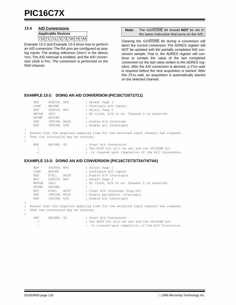
PIC16C7X
DS30390D-page 116 1996 Microchip Technology Inc.
13.4 A/D Conversions
Example 13-2 and Example 13-3 show how to performan A/D conversion. The RA pins are configured as ana-log inputs. The analog reference (VREF) is the deviceVDD. The A/D interrupt is enabled, and the A/D conver-sion clock is FRC. The conversion is performed on theRA0 channel.
Applicable Devices710 71 711 72 73 73A 74 74A
Clearing the GO/DONE bit during a conversion willabort the current conversion. The ADRES register willNOT be updated with the partially completed A/D con-version sample. That is, the ADRES register will con-tinue to contain the value of the last completedconversion (or the last value written to the ADRES reg-ister). After the A/D conversion is aborted, a 2TAD waitis required before the next acquisition is started. Afterthis 2TAD wait, an acquisition is automatically startedon the selected channel.
Note: The GO/DONE bit should NOT be set inthe same instruction that turns on the A/D.
EXAMPLE 13-2: DOING AN A/D CONVERSION (PIC16C710/71/711)
BSF STATUS, RP0 ; Select Page 1 CLRF ADCON1 ; Configure A/D inputs BCF STATUS, RP0 ; Select Page 0 MOVLW 0xC1 ; RC Clock, A/D is on, Channel 0 is selected MOVWF ADCON0 ; BSF INTCON, ADIE ; Enable A/D Interrupt BSF INTCON, GIE ; Enable all interrupts;; Ensure that the required sampling time for the selected input channel has elapsed.; Then the conversion may be started.; BSF ADCON0, GO ; Start A/D Conversion : ; The ADIF bit will be set and the GO/DONE bit : ; is cleared upon completion of the A/D Conversion.
EXAMPLE 13-3: DOING AN A/D CONVERSION (PIC16C72/73/73A/74/74A)
BSF STATUS, RP0 ; Select Page 1 CLRF ADCON1 ; Configure A/D inputs BSF PIE1, ADIE ; Enable A/D interrupts BCF STATUS, RP0 ; Select Page 0 MOVLW 0xC1 ; RC Clock, A/D is on, Channel 0 is selected MOVWF ADCON0 ; BCF PIR1, ADIF ; Clear A/D interrupt flag bit BSF INTCON, PEIE ; Enable peripheral interrupts BSF INTCON, GIE ; Enable all interrupts;; Ensure that the required sampling time for the selected input channel has elapsed.; Then the conversion may be started.; BSF ADCON0, GO ; Start A/D Conversion : ; The ADIF bit will be set and the GO/DONE bit : ; is cleared upon completion of the A/D Conversion.

1996 Microchip Technology Inc. DS30390D-page 117
PIC16C7X
13.4.1 FASTER CONVERSION - LOWER RESOLUTION TRADE-OFF
Not all applications require a result with 8-bits of reso-lution, but may instead require a faster conversiontime. The A/D module allows users to make the trade-off of conversion speed to resolution. Regardless of theresolution required, the acquisition time is the same. Tospeed up the conversion, the clock source of the A/Dmodule may be switched so that the TAD time violatesthe minimum specified time (see the applicable electri-cal specification). Once the TAD time violates the mini-mum specified time, all the following A/D result bits arenot valid (see A/D Conversion Timing in the ElectricalSpecifications section.) The clock sources may only beswitched between the three oscillator versions (cannotbe switched from/to RC). The equation to determinethe time before the oscillator can be switched is as fol-lows:
Conversion time = 2TAD + N • TAD + (8 - N)(2TOSC)Where: N = number of bits of resolution required.
Since the TAD is based from the device oscillator, theuser must use some method (a timer, software loop,etc.) to determine when the A/D oscillator may bechanged. Example 13-4 shows a comparison of timerequired for a conversion with 4-bits of resolution, ver-sus the 8-bit resolution conversion. The example is fordevices operating at 20 MHz and 16 MHz (The A/Dclock is programmed for 32TOSC), and assumes thatimmediately after 6TAD, the A/D clock is programmedfor 2TOSC.
The 2TOSC violates the minimum TAD time since thelast 4-bits will not be converted to correct values.
EXAMPLE 13-4: 4-BIT vs. 8-BIT CONVERSION TIMES
Freq. (MHz)(1)Resolution
4-bit 8-bit
TAD 20 1.6 µs 1.6 µs16 2.0 µs 2.0 µs
TOSC 20 50 ns 50 ns16 62.5 ns 62.5 ns
2TAD + N • TAD + (8 - N)(2TOSC) 20 10 µs 16 µs16 12.5 µs 20 µs
Note 1: The PIC16C71 has a minimum TAD time of 2.0 µs. All other PIC16C7X devices have a minimum TAD time of 1.6 µs.
PIC16C7X
DS30390D-page 118 1996 Microchip Technology Inc.
13.5 A/D Operation During Sleep
The A/D module can operate during SLEEP mode. Thisrequires that the A/D clock source be set to RC(ADCS1:ADCS0 = 11). When the RC clock source isselected, the A/D module waits one instruction cyclebefore starting the conversion. This allows the SLEEPinstruction to be executed, which eliminates all digitalswitching noise from the conversion. When the conver-sion is completed the GO/DONE bit will be cleared, andthe result loaded into the ADRES register. If the A/Dinterrupt is enabled, the device will wake-up fromSLEEP. If the A/D interrupt is not enabled, the A/D mod-ule will then be turned off, although the ADON bit willremain set.
When the A/D clock source is another clock option (notRC), a SLEEP instruction will cause the present conver-sion to be aborted and the A/D module to be turned off,though the ADON bit will remain set.
Turning off the A/D places the A/D module in its lowestcurrent consumption state.
13.6 A/D Accuracy/Error
The overall accuracy of the A/D is less than ± 1 LSb forVDD = 5V ± 10% and the analog VREF = VDD. This over-all accuracy includes offset error, full scale error, andintegral error. The A/D converter is guaranteed to bemonotonic. The resolution and accuracy may be lesswhen either the analog reference (VDD) is less than5.0V or when the analog reference (VREF) is less thanVDD.
The maximum pin leakage current is ± 5 µA.
In systems where the device frequency is low, use ofthe A/D RC clock is preferred. At moderate to high fre-quencies, TAD should be derived from the device oscil-lator. TAD must not violate the minimum and should be≤ 8 µs for preferred operation. This is because TAD,when derived from TOSC, is kept away from on-chipphase clock transitions. This reduces, to a large extent,the effects of digital switching noise. This is not possi-ble with the RC derived clock. The loss of accuracy dueto digital switching noise can be significant if many I/Opins are active.
In systems where the device will enter SLEEP modeafter the start of the A/D conversion, the RC clocksource selection is required. In this mode, the digitalnoise from the modules in SLEEP are stopped. Thismethod gives high accuracy.
Applicable Devices710 71 711 72 73 73A 74 74A
Note: For the A/D module to operate in SLEEP,the A/D clock source must be set to RC(ADCS1:ADCS0 = 11). To perform an A/Dconversion in SLEEP, the GO/DONE bitmust be set, followed by the SLEEP instruc-tion.
Applicable Devices710 71 711 72 73 73A 74 74A
13.7 Effects of a RESET
A device reset forces all registers to their reset state.This forces the A/D module to be turned off, and anyconversion is aborted. The value that is in the ADRESregister is not modified for a Power-on Reset. TheADRES register will contain unknown data after aPower-on Reset.
13.8 Use of the CCP Trigger
An A/D conversion can be started by the “special eventtrigger” of the CCP2 module (CCP1 on the PIC16C72only). This requires that the CCP2M3:CCP2M0 bits(CCP2CON<3:0>) be programmed as 1011 and thatthe A/D module is enabled (ADON bit is set). When thetrigger occurs, the GO/DONE bit will be set, starting theA/D conversion, and the Timer1 counter will be reset tozero. Timer1 is reset to automatically repeat the A/Dacquisition period with minimal software overhead(moving the ADRES to the desired location). Theappropriate analog input channel must be selected andthe minimum acquisition done before the “special eventtrigger” sets the GO/DONE bit (starts a conversion).
If the A/D module is not enabled (ADON is cleared),then the “special event trigger” will be ignored by theA/D module, but will still reset the Timer1 counter.
Applicable Devices710 71 711 72 73 73A 74 74A
Applicable Devices710 71 711 72 73 73A 74 74A
Note: In the PIC16C72 the "special event trigger"is implemented in the CCP1 module.
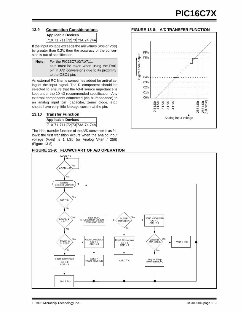
1996 Microchip Technology Inc. DS30390D-page 119
PIC16C7X
13.9 Connection Considerations
If the input voltage exceeds the rail values (VSS or VDD)by greater than 0.2V, then the accuracy of the conver-sion is out of specification.
An external RC filter is sometimes added for anti-alias-ing of the input signal. The R component should beselected to ensure that the total source impedance iskept under the 10 kΩ recommended specification. Anyexternal components connected (via hi-impedance) toan analog input pin (capacitor, zener diode, etc.)should have very little leakage current at the pin.
13.10 Transfer Function
The ideal transfer function of the A/D converter is as fol-lows: the first transition occurs when the analog inputvoltage (VAIN) is 1 LSb (or Analog VREF / 256)(Figure 13-8).
Applicable Devices710 71 711 72 73 73A 74 74A
Note: For the PIC16C710/71/711,care must be taken when using the RA0pin in A/D conversions due to its proximityto the OSC1 pin.
Applicable Devices710 71 711 72 73 73A 74 74A
FIGURE 13-8: A/D TRANSFER FUNCTION
Dig
ital c
ode
outp
ut
FFh
FEh
04h
03h
02h
01h
00h
0.5
LSb
1 LS
b
2 LS
b
3 LS
b
4 LS
b
255
LSb
256
LSb
(ful
l sca
le)
Analog input voltage
FIGURE 13-9: FLOWCHART OF A/D OPERATION
Acquire
ADON = 0
ADON = 0?
GO = 0?
A/D Clock
GO = 0ADIF = 0
Abort Conversion
SLEEPPower-down A/D Wait 2 TAD
Wake-up
Yes
No
Yes
No
No
Yes
Finish ConversionGO = 0
ADIF = 1
Device in
No
Yes
Finish ConversionGO = 0
ADIF = 1
Wait 2 TAD
Stay in Sleep
Selected Channel
= RC?SLEEP
No
Yes
Instruction?Start of A/D
Conversion Delayed1 Instruction Cycle
From Sleep?
Power-down A/D
Yes
No
Wait 2 TAD
Finish ConversionGO = 0
ADIF = 1
SLEEP?

PIC16C7X
DS30390D-page 120 1996 Microchip Technology Inc.
TABLE 13-3: SUMMARY OF A/D REGISTERS, PIC16C710/71/711
TABLE 13-4: SUMMARY OF A/D REGISTERS, PIC16C72
TABLE 13-5: SUMMARY OF A/D REGISTERS, PIC16C73/73A/74/74A
Address Name Bit 7 Bit 6 Bit 5 Bit 4 Bit 3 Bit 2 Bit 1 Bit 0Value on:
POR,BOR
Value on all other Resets
0Bh/8Bh INTCON GIE ADIE T0IE INTE RBIE T0IF INTF RBIF 0000 000x 0000 000u
89h ADRES A/D Result Register xxxx xxxx uuuu uuuu
08h ADCON0 ADCS1 ADCS0 — CHS1 CHS0 GO/DONE ADIF ADON 00-0 0000 00-0 0000
88h ADCON1 — — — — — — PCFG1 PCFG0 ---- --00 ---- --00
05h PORTA — — — RA4 RA3 RA2 RA1 RA0 ---x 0000 ---u 0000
85h TRISA — — — TRISA4 TRISA3 TRISA2 TRISA1 TRISA0 ---1 1111 ---1 1111
Legend: x = unknown, u = unchanged, - = unimplemented read as '0'. Shaded cells are not used for A/D conversion.
Address Name Bit 7 Bit 6 Bit 5 Bit 4 Bit 3 Bit 2 Bit 1 Bit 0Value on:
POR,BOR
Value on all other Resets
0Bh/8Bh INTCON GIE PEIE T0IE INTE RBIE T0IF INTF RBIF 0000 000x 0000 000u
0Ch PIR1 — ADIF — — SSPIF CCP1IF TMR2IF TMR1IF -0-- 0000 -0-- 0000
8Ch PIE1 — ADIE — — SSPIE CCP1IE TMR2IE TMR1IE -0-- 0000 -0-- 0000
1Eh ADRES A/D Result Register xxxx xxxx uuuu uuuu
1Fh ADCON0 ADCS1 ADCS0 CHS2 CHS1 CHS0 GO/DONE — ADON 0000 00-0 0000 00-0
9Fh ADCON1 — — — — — PCFG2 PCFG1 PCFG0 ---- -000 ---- -000
05h PORTA — — RA5 RA4 RA3 RA2 RA1 RA0 --0x 0000 --0u 0000
85h TRISA — — TRISA5 TRISA4 TRISA3 TRISA2 TRISA1 TRISA0 --11 1111 --11 1111
Legend: x = unknown, u = unchanged, - = unimplemented read as '0'. Shaded cells are not used for A/D conversion.
Address Name Bit 7 Bit 6 Bit 5 Bit 4 Bit 3 Bit 2 Bit 1 Bit 0Value on:
POR,BOR
Value on allother Resets
0Bh/8Bh INTCON GIE PEIE T0IE INTE RBIE T0IF INTF RBIF 0000 000x 0000 000u
0Ch PIR1 PSPIF(1) ADIF RCIF TXIF SSPIF CCP1IF TMR2IF TMR1IF 0000 0000 0000 0000
8Ch PIE1 PSPIE(1) ADIE RCIE TXIE SSPIE CCP1IE TMR2IE TMR1IE 0000 0000 0000 0000
0Dh PIR2 — — — — — — — CCP2IF ---- ---0 ---- ---0
8Dh PIE2 — — — — — — — CCP2IE ---- ---0 ---- ---0
1Eh ADRES A/D Result Register xxxx xxxx uuuu uuuu
1Fh ADCON0 ADCS1 ADCS0 CHS2 CHS1 CHS0 GO/DONE — ADON 0000 00-0 0000 00-0
9Fh ADCON1 — — — — — PCFG2 PCFG1 PCFG0 ---- -000 ---- -000
05h PORTA — — RA5 RA4 RA3 RA2 RA1 RA0 --0x 0000 --0u 0000
85h TRISA — — TRISA5 TRISA4 TRISA3 TRISA2 TRISA1 TRISA0 --11 1111 --11 1111
09h PORTE — — — — — RE2 RE1 RE0 ---- -xxx ---- -uuu
89h TRISE IBF OBF IBOV PSPMODE — TRISE2 TRISE1 TRISE0 0000 -111 0000 -111
Legend: x = unknown, u = unchanged, - = unimplemented read as '0'. Shaded cells are not used for A/D conversion.Note 1: Bits PSPIE and PSPIF are reserved on the PIC6C73/73A, always maintain these bits clear.
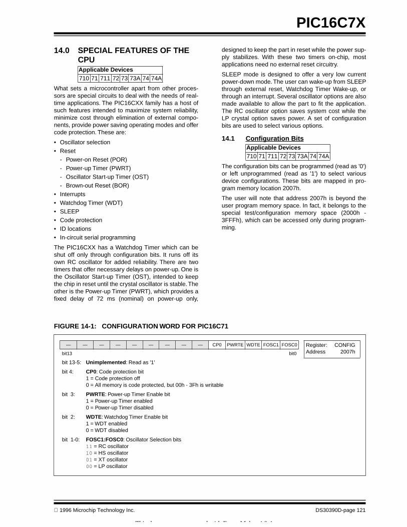
1996 Microchip Technology Inc. DS30390D-page 121
PIC16C7X
14.0 SPECIAL FEATURES OF THE CPU
What sets a microcontroller apart from other proces-sors are special circuits to deal with the needs of real-time applications. The PIC16CXX family has a host ofsuch features intended to maximize system reliability,minimize cost through elimination of external compo-nents, provide power saving operating modes and offercode protection. These are:
• Oscillator selection• Reset
- Power-on Reset (POR)- Power-up Timer (PWRT)- Oscillator Start-up Timer (OST)- Brown-out Reset (BOR)
• Interrupts• Watchdog Timer (WDT)• SLEEP• Code protection• ID locations• In-circuit serial programming
The PIC16CXX has a Watchdog Timer which can beshut off only through configuration bits. It runs off itsown RC oscillator for added reliability. There are twotimers that offer necessary delays on power-up. One isthe Oscillator Start-up Timer (OST), intended to keepthe chip in reset until the crystal oscillator is stable. Theother is the Power-up Timer (PWRT), which provides afixed delay of 72 ms (nominal) on power-up only,
Applicable Devices
710 71 711 72 73 73A 74 74A
designed to keep the part in reset while the power sup-ply stabilizes. With these two timers on-chip, mostapplications need no external reset circuitry.
SLEEP mode is designed to offer a very low currentpower-down mode. The user can wake-up from SLEEPthrough external reset, Watchdog Timer Wake-up, orthrough an interrupt. Several oscillator options are alsomade available to allow the part to fit the application.The RC oscillator option saves system cost while theLP crystal option saves power. A set of configurationbits are used to select various options.
14.1 Configuration Bits
The configuration bits can be programmed (read as '0')or left unprogrammed (read as '1') to select variousdevice configurations. These bits are mapped in pro-gram memory location 2007h.
The user will note that address 2007h is beyond theuser program memory space. In fact, it belongs to thespecial test/configuration memory space (2000h -3FFFh), which can be accessed only during program-ming.
Applicable Devices
710 71 711 72 73 73A 74 74A
FIGURE 14-1: CONFIGURATION WORD FOR PIC16C71
— — — — — — — — — CP0 PWRTE WDTE FOSC1 FOSC0
Register: CONFIGAddress 2007h
bit13 bit0
bit 13-5:
Unimplemented
: Read as '1'
bit 4:
CP0
: Code protection bit1 = Code protection off0 = All memory is code protected, but 00h - 3Fh is writable
bit 3:
PWRTE
: Power-up Timer Enable bit1 = Power-up Timer enabled0 = Power-up Timer disabled
bit 2:
WDTE
: Watchdog Timer Enable bit1 = WDT enabled0 = WDT disabled
bit 1-0:
FOSC1:FOSC0
: Oscillator Selection bits
11
= RC oscillator
10
= HS oscillator
01
= XT oscillator
00
= LP oscillator
This document was created with FrameMaker 4 0 4
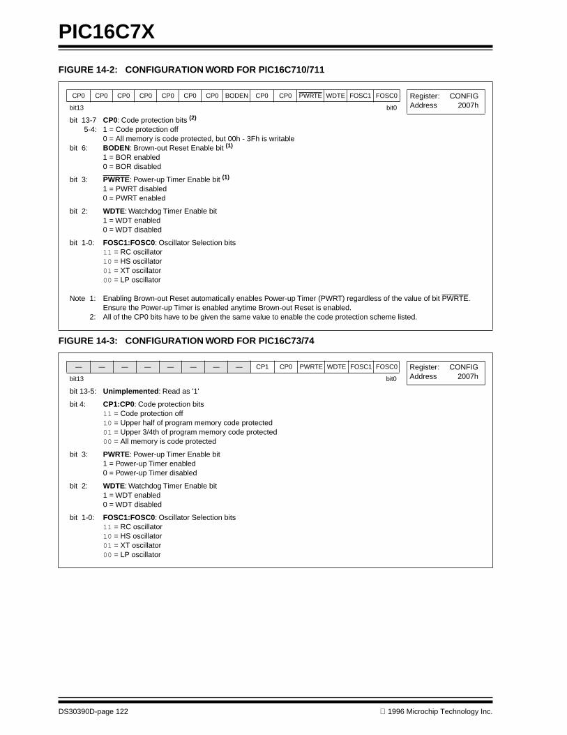
PIC16C7X
DS30390D-page 122
1996 Microchip Technology Inc.
FIGURE 14-2: CONFIGURATION WORD FOR PIC16C710/711
FIGURE 14-3: CONFIGURATION WORD FOR PIC16C73/74
CP0 CP0 CP0 CP0 CP0 CP0 CP0 BODEN CP0 CP0 PWRTE WDTE FOSC1 FOSC0
Register: CONFIGAddress 2007h
bit13 bit0
bit 13-7
CP0
: Code protection bits
(2)
5-4: 1 = Code protection off0 = All memory is code protected, but 00h - 3Fh is writable
bit 6:
BODEN
: Brown-out Reset Enable bit
(1)
1 = BOR enabled0 = BOR disabled
bit 3:
PWRTE
: Power-up Timer Enable bit
(1)
1 = PWRT disabled0 = PWRT enabled
bit 2:
WDTE
: Watchdog Timer Enable bit1 = WDT enabled0 = WDT disabled
bit 1-0:
FOSC1:FOSC0
: Oscillator Selection bits
11
= RC oscillator
10
= HS oscillator
01
= XT oscillator
00
= LP oscillator
Note 1: Enabling Brown-out Reset automatically enables Power-up Timer (PWRT) regardless of the value of bit PWRTE. Ensure the Power-up Timer is enabled anytime Brown-out Reset is enabled.
2: All of the CP0 bits have to be given the same value to enable the code protection scheme listed.
— — — — — — — — CP1 CP0 PWRTE WDTE FOSC1 FOSC0
Register: CONFIGAddress 2007h
bit13 bit0
bit 13-5:
Unimplemented
: Read as '1'
bit 4:
CP1:CP0
: Code protection bits
11
= Code protection off
10
= Upper half of program memory code protected
01
= Upper 3/4th of program memory code protected
00
= All memory is code protected
bit 3:
PWRTE
: Power-up Timer Enable bit1 = Power-up Timer enabled0 = Power-up Timer disabled
bit 2:
WDTE
: Watchdog Timer Enable bit1 = WDT enabled0 = WDT disabled
bit 1-0:
FOSC1:FOSC0
: Oscillator Selection bits
11
= RC oscillator
10
= HS oscillator
01
= XT oscillator
00
= LP oscillator
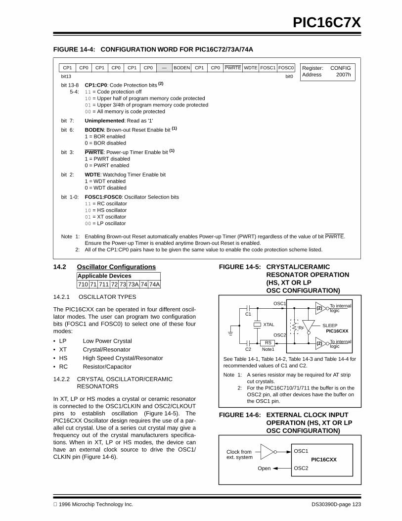
1996 Microchip Technology Inc. DS30390D-page 123
PIC16C7X
FIGURE 14-4: CONFIGURATION WORD FOR PIC16C72/73A/74A
CP1 CP0 CP1 CP0 CP1 CP0 — BODEN CP1 CP0 PWRTE WDTE FOSC1 FOSC0
Register: CONFIGAddress 2007h
bit13 bit0
bit 13-8
CP1:CP0
: Code Protection bits
(2)
5-4:
11
= Code protection off
10
= Upper half of program memory code protected
01
= Upper 3/4th of program memory code protected
00
= All memory is code protected
bit 7:
Unimplemented
: Read as '1'
bit 6:
BODEN
: Brown-out Reset Enable bit
(1)
1 = BOR enabled0 = BOR disabled
bit 3:
PWRTE
: Power-up Timer Enable bit
(1)
1 = PWRT disabled0 = PWRT enabled
bit 2:
WDTE
: Watchdog Timer Enable bit1 = WDT enabled0 = WDT disabled
bit 1-0:
FOSC1:FOSC0
: Oscillator Selection bits
11
= RC oscillator
10
= HS oscillator
01
= XT oscillator
00
= LP oscillator
Note 1: Enabling Brown-out Reset automatically enables Power-up Timer (PWRT) regardless of the value of bit PWRTE. Ensure the Power-up Timer is enabled anytime Brown-out Reset is enabled.
2: All of the CP1:CP0 pairs have to be given the same value to enable the code protection scheme listed.
14.2 Oscillator Configurations
14.2.1 OSCILLATOR TYPES
The PIC16CXX can be operated in four different oscil-lator modes. The user can program two configurationbits (FOSC1 and FOSC0) to select one of these fourmodes:
• LP Low Power Crystal• XT Crystal/Resonator• HS High Speed Crystal/Resonator• RC Resistor/Capacitor
14.2.2 CRYSTAL OSCILLATOR/CERAMIC RESONATORS
In XT, LP or HS modes a crystal or ceramic resonatoris connected to the OSC1/CLKIN and OSC2/CLKOUTpins to establish oscillation (Figure 14-5). ThePIC16CXX Oscillator design requires the use of a par-allel cut crystal. Use of a series cut crystal may give afrequency out of the crystal manufacturers specifica-tions. When in XT, LP or HS modes, the device canhave an external clock source to drive the OSC1/CLKIN pin (Figure 14-6).
Applicable Devices
710 71 711 72 73 73A 74 74A
FIGURE 14-5: CRYSTAL/CERAMIC RESONATOR OPERATION (HS, XT OR LP OSC CONFIGURATION)
FIGURE 14-6: EXTERNAL CLOCK INPUT OPERATION (HS, XT OR LP OSC CONFIGURATION)
C1
C2
XTAL
OSC2
Note1
OSC1
RFSLEEP
To internallogic
PIC16CXX
RS
See Table 14-1, Table 14-2, Table 14-3 and Table 14-4 forrecommended values of C1 and C2.
Note 1: A series resistor may be required for AT strip cut crystals.
2: For the PIC16C710/71/711 the buffer is on the OSC2 pin, all other devices have the buffer on the OSC1 pin.
(2)
(2)
To internallogic
OSC1
OSC2Open
Clock fromext. system PIC16CXX

PIC16C7X
DS30390D-page 124
1996 Microchip Technology Inc.
TABLE 14-1: CERAMIC RESONATORS PIC16C71
TABLE 14-2: CAPACITOR SELECTION FOR CRYSTAL OSCILLATOR FOR PIC16C71
Ranges Tested:
Mode Freq OSC1 OSC2
XT 455 kHz2.0 MHz4.0 MHz
47 - 100 pF15 - 68 pF15 - 68 pF
47 - 100 pF15 - 68 pF15 - 68 pF
HS 8.0 MHz16.0 MHz
15 - 68 pF10 - 47 pF
15 - 68 pF10 - 47 pF
Note : Recommended values of C1 and C2 are identical to the ranges tested table.
Higher capacitance increases the stability of oscilla-tor but also increases the start-up time. These val-ues are for design guidance only. Since each resonator has its own characteristics, the user should consult the resonator manufacturer for appropriate values of external components.
Resonators Used:
455 kHz Panasonic EFO-A455K04B
±
0.3%2.0 MHz Murata Erie CSA2.00MG
±
0.5%4.0 MHz Murata Erie CSA4.00MG
±
0.5%8.0 MHz Murata Erie CSA8.00MT
±
0.5%16.0 MHz Murata Erie CSA16.00MX
±
0.5%
All resonators used did not have built-in capacitors.
Mode Freq OSC1 OSC2
LP 32 kHz200 kHz
33 - 68 pF15 - 47 pF
33 - 68 pF15 - 47 pF
XT 100 kHz500 kHz1 MHz2 MHz4 MHz
47 - 100 pF20 - 68 pF15 - 68 pF15 - 47 pF15 - 33 pF
47 - 100 pF20 - 68 pF15 - 68 pF15 - 47 pF15 - 33 pF
HS 8 MHz20 MHz
15 - 47 pF15 - 47 pF
15 - 47 pF15 - 47 pF
Note : Higher capacitance increases the stability of oscil-lator but also increases the start-up time. These values are for design guidance only. Rs may be required in HS mode as well as XT mode to avoid overdriving crystals with low drive level specifica-tion. Since each crystal has its own characteristics, the user should consult the crystal manufacturer for appropriate values of external components.
TABLE 14-3: CERAMIC RESONATORS PIC16C710/711/72/73/73A/74/74A
TABLE 14-4: CAPACITOR SELECTION FOR CRYSTAL OSCILLATOR FOR PIC16C710/711/72/73/73A/74/74A
Ranges Tested:
Mode Freq OSC1 OSC2
XT 455 kHz2.0 MHz4.0 MHz
68 - 100 pF15 - 68 pF15 - 68 pF
68 - 100 pF15 - 68 pF15 - 68 pF
HS 8.0 MHz16.0 MHz
10 - 68 pF10 - 22 pF
10 - 68 pF10 - 22 pF
Note : Recommended values of C1 and C2 are identical to the ranges tested table.
Higher capacitance increases the stability of oscil-lator but also increases the start-up time. These values are for design guidance only. Since each resonator has its own characteristics, the user should consult the resonator manufacturer for appropriate values of external components.
Resonators Used:
455 kHz Panasonic EFO-A455K04B
±
0.3%2.0 MHz Murata Erie CSA2.00MG
±
0.5%4.0 MHz Murata Erie CSA4.00MG
±
0.5%8.0 MHz Murata Erie CSA8.00MT
±
0.5%16.0 MHz Murata Erie CSA16.00MX
±
0.5%
All resonators used did not have built-in capacitors.
Mode Freq OSC1 OSC2
LP 32 kHz
(1)
200 kHz15 - 47 pF15 - 33 pF
15 - 47 pF15 - 33 pF
XT 100 kHz500 kHz1 MHz2 MHz4 MHz
47 - 100 pF20 - 68 pF15 - 68 pF15 - 47 pF15 - 33 pF
47 - 100 pF20 - 68 pF15 - 68 pF15 - 47 pF15 - 33 pF
HS 8 MHz20 MHz
15 - 47 pF15 - 47 pF
15 - 47 pF15 - 47 pF
Note : Higher capacitance increases the stability of oscil-lator but also increases the start-up time. These values are for design guidance only. Rs may be required in HS mode as well as XT mode to avoid overdriving crystals with low drive level specifica-tion. Since each crystal has its own characteristics, the user should consult the crystal manufacturer for appropriate values of external components.
Note 1: For V
DD
> 4.5V, C1 = C2
≈
30 pF is recom-mended.

1996 Microchip Technology Inc. DS30390D-page 125
PIC16C7X
14.2.3 EXTERNAL CRYSTAL OSCILLATOR CIRCUIT
Either a prepackaged oscillator can be used or a simpleoscillator circuit with TTL gates can be built. Prepack-aged oscillators provide a wide operating range andbetter stability. A well-designed crystal oscillator willprovide good performance with TTL gates. Two types ofcrystal oscillator circuits can be used; one with seriesresonance, or one with parallel resonance.
Figure 14-7 shows implementation of a parallel reso-nant oscillator circuit. The circuit is designed to use thefundamental frequency of the crystal. The 74AS04inverter performs the 180-degree phase shift that a par-allel oscillator requires. The 4.7 k
Ω
resistor providesthe negative feedback for stability. The 10 k
Ω
potenti-ometer biases the 74AS04 in the linear region. Thiscould be used for external oscillator designs.
FIGURE 14-7: EXTERNAL PARALLEL RESONANT CRYSTAL OSCILLATOR CIRCUIT
Figure 14-8 shows a series resonant oscillator circuit.This circuit is also designed to use the fundamental fre-quency of the crystal. The inverter performs a 180-degree phase shift in a series resonant oscillator cir-cuit. The 330 k
Ω
resistors provide the negative feed-back to bias the inverters in their linear region.
FIGURE 14-8: EXTERNAL SERIES RESONANT CRYSTAL OSCILLATOR CIRCUIT
20 pF
+5V
20 pF
10k4.7k
10k
74AS04
XTAL
10k
74AS04
CLKIN
To OtherDevices
PIC16CXX
330 kΩ
74AS04 74AS04 PIC16CXX
CLKIN
To OtherDevices
XTAL
330 kΩ
74AS04
0.1 µF
14.2.4 RC OSCILLATOR
For timing insensitive applications the “RC” deviceoption offers additional cost savings. The RC oscillatorfrequency is a function of the supply voltage, the resis-tor (Rext) and capacitor (Cext) values, and the operat-ing temperature. In addition to this, the oscillatorfrequency will vary from unit to unit due to normal pro-cess parameter variation. Furthermore, the differencein lead frame capacitance between package types willalso affect the oscillation frequency, especially for lowCext values. The user also needs to take into accountvariation due to tolerance of external R and C compo-nents used. Figure 14-9 shows how the R/C combina-tion is connected to the PIC16CXX. For Rext valuesbelow 2.2 k
Ω
, the oscillator operation may becomeunstable, or stop completely. For very high Rext values(e.g. 1 MΩ), the oscillator becomes sensitive to noise,humidity and leakage. Thus, we recommend to keepRext between 3 kΩ and 100 kΩ.
Although the oscillator will operate with no externalcapacitor (Cext = 0 pF), we recommend using valuesabove 20 pF for noise and stability reasons. With no orsmall external capacitance, the oscillation frequencycan vary dramatically due to changes in externalcapacitances, such as PCB trace capacitance or pack-age lead frame capacitance.
See characterization data for desired device for RC fre-quency variation from part to part due to normal pro-cess variation. The variation is larger for larger R (sinceleakage current variation will affect RC frequency morefor large R) and for smaller C (since variation of inputcapacitance will affect RC frequency more).
See characterization data for desired device for varia-tion of oscillator frequency due to VDD for given Rext/Cext values as well as frequency variation due to oper-ating temperature for given R, C, and VDD values.
The oscillator frequency, divided by 4, is available onthe OSC2/CLKOUT pin, and can be used for test pur-poses or to synchronize other logic (see Figure 3-5 forwaveform).
FIGURE 14-9: RC OSCILLATOR MODE
OSC2/CLKOUT
Cext
VDD
Rext
VSS
PIC16CXX
OSC1
Fosc/4
Internalclock

PIC16C7X
DS30390D-page 126 1996 Microchip Technology Inc.
14.3 Reset
The PIC16CXX differentiates between various kinds ofreset:
• Power-on Reset (POR) • MCLR reset during normal operation• MCLR reset during SLEEP • WDT Reset (normal operation)• Brown-out Reset (BOR) (PIC16C710/711/72/73A/
74A)
Some registers are not affected in any reset condition;their status is unknown on POR and unchanged in anyother reset. Most other registers are reset to a “resetstate” on Power-on Reset (POR), on the MCLR andWDT Reset, on MCLR reset during SLEEP, and Brown-out Reset (BOR). They are not affected by a WDTWake-up, which is viewed as the resumption of normaloperation. The TO and PD bits are set or cleared differ-ently in different reset situations as indicated in
Applicable Devices710 71 711 72 73 73A 74 74A
Table 14-7 and Table 14-8. These bits are used in soft-ware to determine the nature of the reset. SeeTable 14-10 for a full description of reset states of allregisters.
A simplified block diagram of the on-chip reset circuit isshown in Figure 14-10.
The PIC16C710/711/72/73A/74A have a MCLR noisefilter in the MCLR reset path. The filter will detect andignore small pulses.
It should be noted that a WDT Reset does not driveMCLR pin low.
FIGURE 14-10: SIMPLIFIED BLOCK DIAGRAM OF ON-CHIP RESET CIRCUIT
S
R Q
ExternalReset
MCLR
VDD
OSC1
WDTModule
VDD risedetect
OST/PWRT
On-chip(1) RC OSC
WDTTime-out
Power-on Reset
OST
10-bit Ripple counter
PWRT
Chip_Reset
10-bit Ripple counter
Reset
Enable OST
Enable PWRT
SLEEP
See Table 14-5 and Table 14-6 for time-out situations.
Note 1: This is a separate oscillator from the RC oscillator of the CLKIN pin.
2: Brown-out Reset is implemented on the PIC16C710/711/72/73A/74A.
Brown-outReset(2)
BODEN
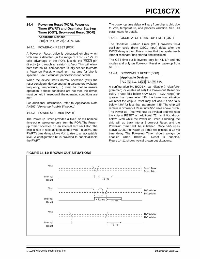
1996 Microchip Technology Inc. DS30390D-page 127
PIC16C7X
14.4 Power-on Reset (POR), Power-up Timer (PWRT) and Oscillator Start-up Timer (OST), Brown-out Reset (BOR)
14.4.1 POWER-ON RESET (POR)
A Power-on Reset pulse is generated on-chip whenVDD rise is detected (in the range of 1.5V - 2.1V). Totake advantage of the POR, just tie the MCLR pindirectly (or through a resistor) to VDD. This will elimi-nate external RC components usually needed to createa Power-on Reset. A maximum rise time for VDD isspecified. See Electrical Specifications for details.
When the device starts normal operation (exits thereset condition), device operating parameters (voltage,frequency, temperature, ...) must be met to ensureoperation. If these conditions are not met, the devicemust be held in reset until the operating conditions aremet.
For additional information, refer to Application NoteAN607, "Power-up Trouble Shooting."
14.4.2 POWER-UP TIMER (PWRT)
The Power-up Timer provides a fixed 72 ms nominaltime-out on power-up only, from the POR. The Power-up Timer operates on an internal RC oscillator. Thechip is kept in reset as long as the PWRT is active. ThePWRT’s time delay allows VDD to rise to an acceptablelevel. A configuration bit is provided to enable/disablethe PWRT.
Applicable Devices710 71 711 72 73 73A 74 74A
The power-up time delay will vary from chip to chip dueto VDD, temperature, and process variation. See DCparameters for details.
14.4.3 OSCILLATOR START-UP TIMER (OST)
The Oscillator Start-up Timer (OST) provides 1024oscillator cycle (from OSC1 input) delay after thePWRT delay is over. This ensures that the crystal oscil-lator or resonator has started and stabilized.
The OST time-out is invoked only for XT, LP and HSmodes and only on Power-on Reset or wake-up fromSLEEP.
14.4.4 BROWN-OUT RESET (BOR)
A configuration bit, BODEN, can disable (if clear/pro-grammed) or enable (if set) the Brown-out Reset cir-cuitry. If VDD falls below 4.0V (3.8V - 4.2V range) forgreater than parameter #35, the brown-out situationwill reset the chip. A reset may not occur if VDD fallsbelow 4.0V for less than parameter #35. The chip willremain in Brown-out Reset until VDD rises above BVDD.The Power-up Timer will now be invoked and will keepthe chip in RESET an additional 72 ms. If VDD dropsbelow BVDD while the Power-up Timer is running, thechip will go back into a Brown-out Reset and thePower-up Timer will be initialized. Once VDD risesabove BVDD, the Power-up Timer will execute a 72 mstime delay. The Power-up Timer should always beenabled when Brown-out Reset is enabled.Figure 14-11 shows typical brown-out situations.
Applicable Devices710 71 711 72 73 73A 74 74A
FIGURE 14-11: BROWN-OUT SITUATIONS
72 ms
BVDD Max.BVDD Min.
VDD
InternalReset
BVDD Max.BVDD Min.
VDD
InternalReset 72 ms<72 ms
72 ms
BVDD Max.BVDD Min.
VDD
InternalReset

PIC16C7X
DS30390D-page 128 1996 Microchip Technology Inc.
14.4.5 TIME-OUT SEQUENCE
On power-up the time-out sequence is as follows: FirstPWRT time-out is invoked after the POR time delayhas expired. Then OST is activated. The total time-outwill vary based on oscillator configuration and the sta-tus of the PWRT. For example, in RC mode with thePWRT disabled, there will be no time-out at all.Figure 14-12, Figure 14-13, and Figure 14-14 depicttime-out sequences on power-up.
Since the time-outs occur from the POR pulse, if MCLRis kept low long enough, the time-outs will expire. Thenbringing MCLR high will begin execution immediately(Figure 14-13). This is useful for testing purposes or tosynchronize more than one PIC16CXX device operat-ing in parallel.
Table 14-9 shows the reset conditions for some specialfunction registers, while Table 14-10 shows the resetconditions for all the registers.
14.4.6 POWER CONTROL/STATUS REGISTER (PCON)
The Power Control/Status Register, PCON has up to 2bits, depending upon the device. Bit0 is not imple-mented on the PIC16C73 or PIC16C74.
Bit0 is Brown-out Reset Status bit, BOR. Bit BOR isunknown on a Power-on Reset. It must then be set bythe user and checked on subsequent resets to see if bitBOR cleared, indicating a BOR occurred. The BOR bitis a "Don’t Care" bit and is not necessarily predictableif the Brown-out Reset circuitry is disabled (by clearingbit BODEN in the Configuration Word).
Bit1 is Power-on Reset Status bit POR. It is cleared ona Power-on Reset and unaffected otherwise. The usermust set this bit following a Power-on Reset.
Applicable Devices710 71 711 72 73 73A 74 74A
TABLE 14-5: TIME-OUT IN VARIOUS SITUATIONS, PIC16C71/73/74
TABLE 14-6: TIME-OUT IN VARIOUS SITUATIONS, PIC16C710/711/72/73A/74A
TABLE 14-7: STATUS BITS AND THEIR SIGNIFICANCE, PIC16C71/73/74
TABLE 14-8: STATUS BITS AND THEIR SIGNIFICANCE, PIC16C710/711/72/73A/74A
Oscillator Configuration Power-up Wake-up from SLEEPPWRTE = 1 PWRTE = 0
XT, HS, LP 72 ms + 1024TOSC 1024TOSC 1024 TOSC
RC 72 ms — —
Oscillator Configuration Power-upBrown-out
Wake-up from SLEEPPWRTE = 0 PWRTE = 1
XT, HS, LP 72 ms + 1024TOSC 1024TOSC 72 ms + 1024TOSC 1024TOSC
RC 72 ms — 72 ms —
POR(1) TO PD
0 1 1 Power-on Reset0 0 x Illegal, TO is set on POR0 x 0 Illegal, PD is set on POR1 0 1 WDT Reset 1 0 0 WDT Wake-up1 u u MCLR Reset during normal operation1 1 0 MCLR Reset during SLEEP or interrupt wake-up from SLEEP
Legend: u = unchanged, x = unknownNote 1: Bit POR is not implemented on the PIC16C71.
POR BOR TO PD
0 x 1 1 Power-on Reset0 x 0 x Illegal, TO is set on POR0 x x 0 Illegal, PD is set on POR1 0 x x Brown-out Reset1 1 0 1 WDT Reset 1 1 0 0 WDT Wake-up1 1 u u MCLR Reset during normal operation1 1 1 0 MCLR Reset during SLEEP or interrupt wake-up from SLEEP

1996 Microchip Technology Inc. DS30390D-page 129
PIC16C7X
TABLE 14-9: RESET CONDITION FOR SPECIAL REGISTERS
ConditionProgramCounter
STATUSRegister
PCONRegister
PIC16C710/711
PCONRegister
PIC16C73/74
PCONRegister
PIC16C72/73A/74A
Power-on Reset 000h 0001 1xxx ---- --0x ---- --0- ---- --0x
MCLR Reset during normal operation 000h 000u uuuu ---- --uu ---- --u- ---- --uu
MCLR Reset during SLEEP 000h 0001 0uuu ---- --uu ---- --u- ---- --uu
WDT Reset 000h 0000 1uuu ---- --uu ---- --u- ---- --uu
WDT Wake-up PC + 1 uuu0 0uuu ---- --uu ---- --u- ---- --uu
Brown-out Reset 000h 0001 1uuu ---- --u0 N/A ---- --u0
Interrupt wake-up from SLEEP PC + 1(1) uuu1 0uuu ---- --uu ---- --u- ---- --uu
Legend: u = unchanged, x = unknown, - = unimplemented bit read as '0'.Note 1: When the wake-up is due to an interrupt and the GIE bit is set, the PC is loaded
with the interrupt vector (0004h).
TABLE 14-10: INITIALIZATION CONDITIONS FOR ALL REGISTERS
Register Applicable Devices Power-on Reset,Brown-out Reset
MCLR ResetsWDT Reset
Wake-up viaWDT or Interrupt
W 710 71 711 72 73 73A 74 74A xxxx xxxx uuuu uuuu uuuu uuuu
INDF 710 71 711 72 73 73A 74 74A N/A N/A N/A
TMR0 710 71 711 72 73 73A 74 74A xxxx xxxx uuuu uuuu uuuu uuuu
PCL 710 71 711 72 73 73A 74 74A 0000h 0000h PC + 1(2)
STATUS 710 71 711 72 73 73A 74 74A 0001 1xxx 000q quuu(3) uuuq quuu(3)
FSR 710 71 711 72 73 73A 74 74A xxxx xxxx uuuu uuuu uuuu uuuu
PORTA710 71 711 72 73 73A 74 74A ---x 0000 ---u 0000 ---u uuuu
710 71 711 72 73 73A 74 74A --0x 0000 --0u 0000 --uu uuuu
PORTB 710 71 711 72 73 73A 74 74A xxxx xxxx uuuu uuuu uuuu uuuu
PORTC 710 71 711 72 73 73A 74 74A xxxx xxxx uuuu uuuu uuuu uuuu
PORTD 710 71 711 72 73 73A 74 74A xxxx xxxx uuuu uuuu uuuu uuuu
PORTE 710 71 711 72 73 73A 74 74A ---- -xxx ---- -uuu ---- -uuu
PCLATH 710 71 711 72 73 73A 74 74A ---0 0000 ---0 0000 ---u uuuu
INTCON 710 71 711 72 73 73A 74 74A 0000 000x 0000 000u uuuu uuuu(1)
PIR1
710 71 711 72 73 73A 74 74A -0-- 0000 -0-- 0000 -u-- uuuu(1)
710 71 711 72 73 73A 74 74A -000 0000 -000 0000 -uuu uuuu(1)
710 71 711 72 73 73A 74 74A 0000 0000 0000 0000 uuuu uuuu(1)
PIR2 710 71 711 72 73 73A 74 74A ---- ---0 ---- ---0 ---- ---u(1)
TMR1L 710 71 711 72 73 73A 74 74A xxxx xxxx uuuu uuuu uuuu uuuu
TMR1H 710 71 711 72 73 73A 74 74A xxxx xxxx uuuu uuuu uuuu uuuu
T1CON 710 71 711 72 73 73A 74 74A --00 0000 --uu uuuu --uu uuuu
Legend: u = unchanged, x = unknown, - = unimplemented bit, read as '0', q = value depends on conditionNote 1: One or more bits in INTCON, PIR1 and/or PIR2 will be affected (to cause wake-up).
2: When the wake-up is due to an interrupt and the GIE bit is set, the PC is loaded with the interrupt vector (0004h).
3: See Table 14-9 for reset value for specific condition.

PIC16C7X
DS30390D-page 130 1996 Microchip Technology Inc.
TMR2 710 71 711 72 73 73A 74 74A 0000 0000 0000 0000 uuuu uuuu
T2CON 710 71 711 72 73 73A 74 74A -000 0000 -000 0000 -uuu uuuu
SSPBUF 710 71 711 72 73 73A 74 74A xxxx xxxx uuuu uuuu uuuu uuuu
SSPCON 710 71 711 72 73 73A 74 74A 0000 0000 0000 0000 uuuu uuuu
CCPR1L 710 71 711 72 73 73A 74 74A xxxx xxxx uuuu uuuu uuuu uuuu
CCPR1H 710 71 711 72 73 73A 74 74A xxxx xxxx uuuu uuuu uuuu uuuu
CCP1CON 710 71 711 72 73 73A 74 74A --00 0000 --00 0000 --uu uuuu
RCSTA 710 71 711 72 73 73A 74 74A 0000 -00x 0000 -00x uuuu -uuu
TXREG 710 71 711 72 73 73A 74 74A 0000 0000 0000 0000 uuuu uuuu
RCREG 710 71 711 72 73 73A 74 74A 0000 0000 0000 0000 uuuu uuuu
CCPR2L 710 71 711 72 73 73A 74 74A xxxx xxxx uuuu uuuu uuuu uuuu
CCPR2H 710 71 711 72 73 73A 74 74A xxxx xxxx uuuu uuuu uuuu uuuu
CCP2CON 710 71 711 72 73 73A 74 74A 0000 0000 0000 0000 uuuu uuuu
ADRES 710 71 711 72 73 73A 74 74A xxxx xxxx uuuu uuuu uuuu uuuu
ADCON0710 71 711 72 73 73A 74 74A 00-0 0000 00-0 0000 uu-u uuuu
710 71 711 72 73 73A 74 74A 0000 00-0 0000 00-0 uuuu uu-u
OPTION 710 71 711 72 73 73A 74 74A 1111 1111 1111 1111 uuuu uuuu
TRISA710 71 711 72 73 73A 74 74A ---1 1111 ---1 1111 ---u uuuu
710 71 711 72 73 73A 74 74A --11 1111 --11 1111 --uu uuuu
TRISB 710 71 711 72 73 73A 74 74A 1111 1111 1111 1111 uuuu uuuu
TRISC 710 71 711 72 73 73A 74 74A 1111 1111 1111 1111 uuuu uuuu
TRISD 710 71 711 72 73 73A 74 74A 1111 1111 1111 1111 uuuu uuuu
TRISE 710 71 711 72 73 73A 74 74A 0000 -111 0000 -111 uuuu -uuu
PIE1
710 71 711 72 73 73A 74 74A -0-- 0000 -0-- 0000 -u-- uuuu
710 71 711 72 73 73A 74 74A -000 0000 -000 0000 -uuu uuuu
710 71 711 72 73 73A 74 74A 0000 0000 0000 0000 uuuu uuuu
PIE2 710 71 711 72 73 73A 74 74A ---- ---0 ---- ---0 ---- ---u
PCON710 71 711 72 73 73A 74 74A ---- --0- ---- --u- ---- --u-
710 71 711 72 73 73A 74 74A ---- --0u ---- --uu ---- --uu
PR2 710 71 711 72 73 73A 74 74A 1111 1111 1111 1111 1111 1111
SSPADD 710 71 711 72 73 73A 74 74A 0000 0000 0000 0000 uuuu uuuu
SSPSTAT 710 71 711 72 73 73A 74 74A --00 0000 --00 0000 --uu uuuu
TXSTA 710 71 711 72 73 73A 74 74A 0000 -010 0000 -010 uuuu -uuu
SPBRG 710 71 711 72 73 73A 74 74A 0000 0000 0000 0000 uuuu uuuu
ADCON1710 71 711 72 73 73A 74 74A ---- --00 ---- --00 ---- --uu
710 71 711 72 73 73A 74 74A ---- -000 ---- -000 ---- -uuu
TABLE 14-10: INITIALIZATION CONDITIONS FOR ALL REGISTERS (Cont.’d)
Register Applicable Devices Power-on Reset,Brown-out Reset
MCLR ResetsWDT Reset
Wake-up viaWDT or Interrupt
Legend: u = unchanged, x = unknown, - = unimplemented bit, read as '0', q = value depends on conditionNote 1: One or more bits in INTCON, PIR1 and/or PIR2 will be affected (to cause wake-up).
2: When the wake-up is due to an interrupt and the GIE bit is set, the PC is loaded with the interrupt vector (0004h).
3: See Table 14-9 for reset value for specific condition.

1996 Microchip Technology Inc. DS30390D-page 131
PIC16C7X
FIGURE 14-12: TIME-OUT SEQUENCE ON POWER-UP (MCLR NOT TIED TO VDD): CASE 1
FIGURE 14-13: TIME-OUT SEQUENCE ON POWER-UP (MCLR NOT TIED TO VDD): CASE 2
FIGURE 14-14: TIME-OUT SEQUENCE ON POWER-UP (MCLR TIED TO VDD)
TPWRT
TOST
VDD
MCLR
INTERNAL POR
PWRT TIME-OUT
OST TIME-OUT
INTERNAL RESET
VDD
MCLR
INTERNAL POR
PWRT TIME-OUT
OST TIME-OUT
INTERNAL RESET
TPWRT
TOST
TPWRT
TOST
VDD
MCLR
INTERNAL POR
PWRT TIME-OUT
OST TIME-OUT
INTERNAL RESET

PIC16C7X
DS30390D-page 132 1996 Microchip Technology Inc.
FIGURE 14-15: EXTERNAL POWER-ON RESET CIRCUIT (FOR SLOW VDD POWER-UP)
Note 1: External Power-on Reset circuit is required only if VDD power-up slope is too slow. The diode D helps discharge the capacitor quickly when VDD powers down.
2: R < 40 kΩ is recommended to make sure that voltage drop across R does not violate the device’s electrical specification.
3: R1 = 100Ω to 1 kΩ will limit any current flowing into MCLR from external capacitor C in the event of MCLR/VPP pin break-down due to Electrostatic Discharge (ESD) or Electrical Overstress (EOS).
C
R1RD
VDD
MCLR
PIC16CXX
FIGURE 14-16: EXTERNAL BROWN-OUT PROTECTION CIRCUIT 1
FIGURE 14-17: EXTERNAL BROWN-OUT PROTECTION CIRCUIT 2
Note 1: This circuit will activate reset when VDD goes below (Vz + 0.7V) where Vz = Zener voltage.
2: Internal brown-out detection on the PIC16C710/711/72/73A/74A should be disabled when using this circuit.
3: Resistors should be adjusted for the char-acteristics of the transistor.
VDD
33k
10k
40k
VDD
MCLR
PIC16CXX
Note 1: This brown-out circuit is less expensive, albeit less accurate. Transistor Q1 turns off when VDD is below a certain level such that:
2: Internal brown-out detection on the PIC16C710/711/72/73A/74A should be disabled when using this circuit.
3: Resistors should be adjusted for the characteristics of the transistor.
VDD •R1
R1 + R2= 0.7V
VDD
R2 40k
VDD
MCLR
PIC16CXX
R1
Q1
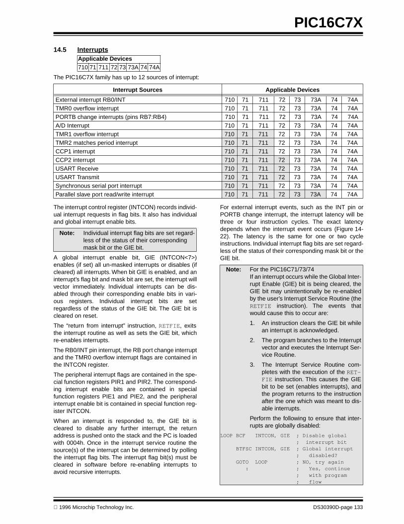
1996 Microchip Technology Inc. DS30390D-page 133
PIC16C7X
14.5 Interrupts
The PIC16C7X family has up to 12 sources of interrupt:
Applicable Devices710 71 711 72 73 73A 74 74A
Interrupt Sources Applicable Devices
External interrupt RB0/INT 710 71 711 72 73 73A 74 74ATMR0 overflow interrupt 710 71 711 72 73 73A 74 74APORTB change interrupts (pins RB7:RB4) 710 71 711 72 73 73A 74 74AA/D Interrupt 710 71 711 72 73 73A 74 74ATMR1 overflow interrupt 710 71 711 72 73 73A 74 74ATMR2 matches period interrupt 710 71 711 72 73 73A 74 74ACCP1 interrupt 710 71 711 72 73 73A 74 74ACCP2 interrupt 710 71 711 72 73 73A 74 74AUSART Receive 710 71 711 72 73 73A 74 74AUSART Transmit 710 71 711 72 73 73A 74 74ASynchronous serial port interrupt 710 71 711 72 73 73A 74 74AParallel slave port read/write interrupt 710 71 711 72 73 73A 74 74A
The interrupt control register (INTCON) records individ-ual interrupt requests in flag bits. It also has individualand global interrupt enable bits.
A global interrupt enable bit, GIE (INTCON<7>)enables (if set) all un-masked interrupts or disables (ifcleared) all interrupts. When bit GIE is enabled, and aninterrupt’s flag bit and mask bit are set, the interrupt willvector immediately. Individual interrupts can be dis-abled through their corresponding enable bits in vari-ous registers. Individual interrupt bits are setregardless of the status of the GIE bit. The GIE bit iscleared on reset.
The “return from interrupt” instruction, RETFIE, exitsthe interrupt routine as well as sets the GIE bit, whichre-enables interrupts.
The RB0/INT pin interrupt, the RB port change interruptand the TMR0 overflow interrupt flags are contained inthe INTCON register.
The peripheral interrupt flags are contained in the spe-cial function registers PIR1 and PIR2. The correspond-ing interrupt enable bits are contained in specialfunction registers PIE1 and PIE2, and the peripheralinterrupt enable bit is contained in special function reg-ister INTCON.
When an interrupt is responded to, the GIE bit iscleared to disable any further interrupt, the returnaddress is pushed onto the stack and the PC is loadedwith 0004h. Once in the interrupt service routine thesource(s) of the interrupt can be determined by pollingthe interrupt flag bits. The interrupt flag bit(s) must becleared in software before re-enabling interrupts toavoid recursive interrupts.
Note: Individual interrupt flag bits are set regard-less of the status of their corresponding mask bit or the GIE bit.
For external interrupt events, such as the INT pin orPORTB change interrupt, the interrupt latency will bethree or four instruction cycles. The exact latencydepends when the interrupt event occurs (Figure 14-22). The latency is the same for one or two cycleinstructions. Individual interrupt flag bits are set regard-less of the status of their corresponding mask bit or theGIE bit.
Note: For the PIC16C71/73/74If an interrupt occurs while the Global Inter-rupt Enable (GIE) bit is being cleared, theGIE bit may unintentionally be re-enabledby the user’s Interrupt Service Routine (theRETFIE instruction). The events thatwould cause this to occur are:
1. An instruction clears the GIE bit whilean interrupt is acknowledged.
2. The program branches to the Interruptvector and executes the Interrupt Ser-vice Routine.
3. The Interrupt Service Routine com-pletes with the execution of the RET-FIE instruction. This causes the GIEbit to be set (enables interrupts), andthe program returns to the instructionafter the one which was meant to dis-able interrupts.
Perform the following to ensure that inter-rupts are globally disabled:
LOOP BCF INTCON, GIE ; Disable global ; interrupt bit BTFSC INTCON, GIE ; Global interrupt ; disabled? GOTO LOOP ; NO, try again : ; Yes, continue ; with program ; flow

PIC16C7X
DS30390D-page 134 1996 Microchip Technology Inc.
FIGURE 14-18: INTERRUPT LOGIC FOR PIC16C710/71/711
FIGURE 14-19: INTERRUPT LOGIC FOR PIC16C72
FIGURE 14-20: INTERRUPT LOGIC FOR PIC16C73/73A
RBIFRBIE
T0IFT0IE
INTFINTE
GIE
ADIE
Wakeup(If in SLEEP mode)
Interrupt to CPU
ADIF
TMR1IFTMR1IE
TMR2IFTMR2IE
CCP1IFCCP1IE
ADIFADIE
SSPIFSSPIE
T0IFT0IE
INTFINTE
RBIFRBIE
GIE
PEIE
Wake-up (If in SLEEP mode)
Interrupt to CPU
TMR1IFTMR1IE
TMR2IFTMR2IE
CCP1IFCCP1IE
CCP2IFCCP2IE
ADIFADIE
RCIFRCIE
SSPIFSSPIE
T0IFT0IE
INTFINTE
RBIFRBIE
GIE
PEIE
Wake-up (If in SLEEP mode)
Interrupt to CPU
TXIFTXIE
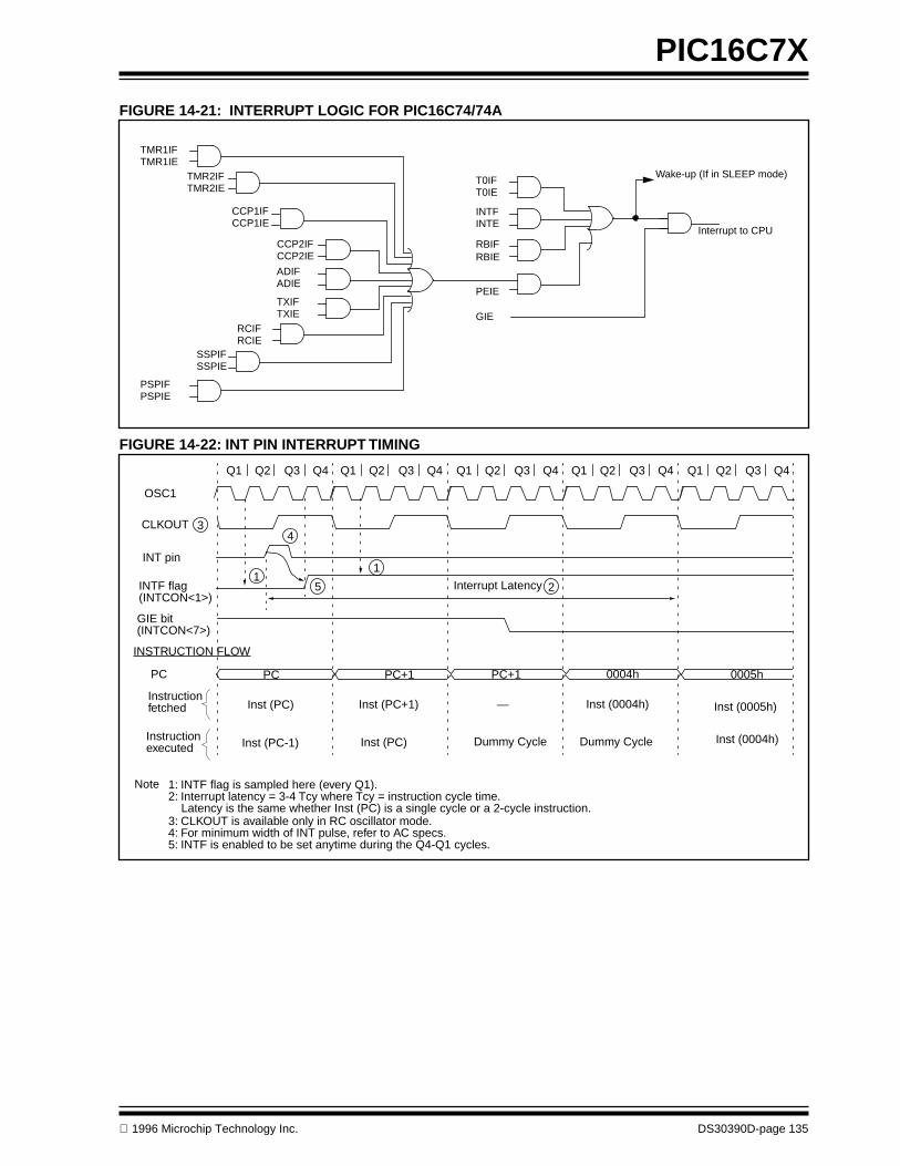
1996 Microchip Technology Inc. DS30390D-page 135
PIC16C7X
FIGURE 14-21: INTERRUPT LOGIC FOR PIC16C74/74A
FIGURE 14-22: INT PIN INTERRUPT TIMING
TMR1IFTMR1IE
TMR2IFTMR2IE
CCP1IFCCP1IE
CCP2IFCCP2IE
ADIFADIE
TXIFTXIE
RCIFRCIE
SSPIFSSPIE
T0IFT0IE
INTFINTE
RBIFRBIE
GIE
PEIE
Wake-up (If in SLEEP mode)
Interrupt to CPU
PSPIEPSPIF
Q2Q1 Q3 Q4 Q2Q1 Q3 Q4 Q2Q1 Q3 Q4 Q2Q1 Q3 Q4 Q2Q1 Q3 Q4
OSC1
CLKOUT
INT pin
INTF flag(INTCON<1>)
GIE bit(INTCON<7>)
INSTRUCTION FLOW
PC
Instructionfetched
Instructionexecuted
Interrupt Latency
PC PC+1 PC+1 0004h 0005h
Inst (0004h) Inst (0005h)
Dummy Cycle
Inst (PC) Inst (PC+1)
Inst (PC-1) Inst (0004h)Dummy CycleInst (PC)
—
1
4
5
1
Note 1: INTF flag is sampled here (every Q1).2: Interrupt latency = 3-4 Tcy where Tcy = instruction cycle time.
Latency is the same whether Inst (PC) is a single cycle or a 2-cycle instruction.3: CLKOUT is available only in RC oscillator mode.4: For minimum width of INT pulse, refer to AC specs.5: INTF is enabled to be set anytime during the Q4-Q1 cycles.
2
3

PIC16C7X
DS30390D-page 136 1996 Microchip Technology Inc.
14.5.1 INT INTERRUPT
External interrupt on RB0/INT pin is edge triggered:either rising if bit INTEDG (OPTION<6>) is set, or fall-ing, if the INTEDG bit is clear. When a valid edgeappears on the RB0/INT pin, flag bit INTF(INTCON<1>) is set. This interrupt can be disabled byclearing enable bit INTE (INTCON<4>). Flag bit INTFmust be cleared in software in the interrupt service rou-tine before re-enabling this interrupt. The INT interruptcan wake-up the processor from SLEEP, if bit INTEwas set prior to going into SLEEP. The status of globalinterrupt enable bit GIE decides whether or not the pro-cessor branches to the interrupt vector following wake-up. See Section 14.8 for details on SLEEP mode.
14.5.2 TMR0 INTERRUPT
An overflow (FFh → 00h) in the TMR0 register will setflag bit T0IF (INTCON<2>). The interrupt can beenabled/disabled by setting/clearing enable bit T0IE(INTCON<5>). (Section 7.0)
14.5.3 PORTB INTCON CHANGE
An input change on PORTB<7:4> sets flag bit RBIF(INTCON<0>). The interrupt can be enabled/disabledby setting/clearing enable bit RBIE (INTCON<4>).(Section 5.2)
14.6 Context Saving During Interrupts
During an interrupt, only the return PC value is savedon the stack. Typically, users may wish to save key reg-isters during an interrupt i.e., W register and STATUSregister. This will have to be implemented in software.
Example 14-1 and Example 14-2 store and restore theSTATUS and W registers. For PIC16C72/73/73A/74/74A, the register, W_TEMP, must be defined in bothbanks and must be defined at the same offset from thebank base address (i.e., if W_TEMP is defined at 0x20in bank 0, it must also be defined at 0xA0 in bank 1).For PIC16C710/71/711, the user register,STATUS_TEMP, must be defined in bank 0.
The example:
a) Stores the W register.b) Stores the STATUS register in bank 0.c) Executes the ISR code.d) Restores the STATUS register (and bank select
bit).e) Restores the W register.
Note: For the PIC16C71/73/74if a change on the I/O pin should occurwhen the read operation is being executed(start of the Q2 cycle), then the RBIF inter-rupt flag may not get set.
Applicable Devices710 71 711 72 73 73A 74 74A
EXAMPLE 14-1: SAVING STATUS AND W REGISTERS IN RAM (PIC16C710/71/711)
MOVWF W_TEMP ;Copy W to TEMP register, could be bank one or zero SWAPF STATUS,W ;Swap status to be saved into W MOVWF STATUS_TEMP ;Save status to bank zero STATUS_TEMP register : :(ISR) : SWAPF STATUS_TEMP,W ;Swap STATUS_TEMP register into W ;(sets bank to original state) MOVWF STATUS ;Move W into STATUS register SWAPF W_TEMP,F ;Swap W_TEMP SWAPF W_TEMP,W ;Swap W_TEMP into W
EXAMPLE 14-2: SAVING STATUS AND W REGISTERS IN RAM (PIC16C72/73/73A/74/74A)
MOVWF W_TEMP ;Copy W to TEMP register, could be bank one or zero SWAPF STATUS,W ;Swap status to be saved into W BCF STATUS,RP0 ;Change to bank zero, regardless of current bank MOVWF STATUS_TEMP ;Save status to bank zero STATUS_TEMP register : :(ISR) : SWAPF STATUS_TEMP,W ;Swap STATUS_TEMP register into W ;(sets bank to original state) MOVWF STATUS ;Move W into STATUS register SWAPF W_TEMP,F ;Swap W_TEMP SWAPF W_TEMP,W ;Swap W_TEMP into W

1996 Microchip Technology Inc. DS30390D-page 137
PIC16C7X
14.7 Watchdog Timer (WDT)
The Watchdog Timer is as a free running on-chip RCoscillator which does not require any external compo-nents. This RC oscillator is separate from the RC oscil-lator of the OSC1/CLKIN pin. That means that the WDTwill run, even if the clock on the OSC1/CLKIN andOSC2/CLKOUT pins of the device has been stopped,for example, by execution of a SLEEP instruction. Dur-ing normal operation, a WDT time-out generates adevice RESET (Watchdog Timer Reset). If the deviceis in SLEEP mode, a WDT time-out causes the deviceto wake-up and continue with normal operation (Watch-dog Timer Wake-up). The WDT can be permanentlydisabled by clearing configuration bit WDTE(Section 14.1).
14.7.1 WDT PERIOD
The WDT has a nominal time-out period of 18 ms, (withno prescaler). The time-out periods vary with tempera-ture, VDD and process variations from part to part (seeDC specs). If longer time-out periods are desired, a
Applicable Devices710 71 711 72 73 73A 74 74A
prescaler with a division ratio of up to 1:128 can beassigned to the WDT under software control by writingto the OPTION register. Thus, time-out periods up to2.3 seconds can be realized.
The CLRWDT and SLEEP instructions clear the WDT andthe postscaler, if assigned to the WDT, and prevent itfrom timing out and generating a device RESET condi-tion.
The TO bit in the STATUS register will be cleared upona Watchdog Timer time-out.
14.7.2 WDT PROGRAMMING CONSIDERATIONS
It should also be taken into account that under worstcase conditions (VDD = Min., Temperature = Max., andmax. WDT prescaler) it may take several secondsbefore a WDT time-out occurs.
Note: When the prescaler is assigned to theWDT, always execute a CLRWDT instructionbefore changing the prescale value, other-wise a WDT reset may occur.
FIGURE 14-23: WATCHDOG TIMER BLOCK DIAGRAM
FIGURE 14-24: SUMMARY OF WATCHDOG TIMER REGISTERS
Address Name Bit 7 Bit 6 Bit 5 Bit 4 Bit 3 Bit 2 Bit 1 Bit 0
2007h Config. bits (1) BODEN(1) CP1 CP0 PWRTE(1) WDTE FOSC1 FOSC0
81h OPTION RBPU INTEDG T0CS T0SE PSA PS2 PS1 PS0
Legend: Shaded cells are not used by the Watchdog Timer.
Note 1: See Figure 14-1, Figure 14-2, Figure 14-3, and Figure 14-4 for operation of these bits.
From TMR0 Clock Source(Figure 7-6)
To TMR0 (Figure 7-6)
Postscaler
WDT Timer
WDT Enable Bit
0
1 MUX
PSA
8 - to - 1 MUX PS2:PS0
0 1
MUX PSA
WDTTime-outNote: PSA and PS2:PS0 are bits in the OPTION register.
8
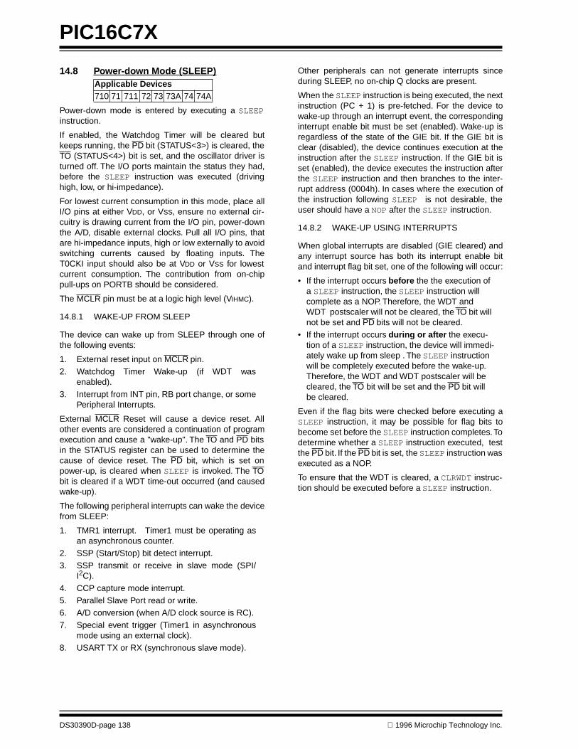
PIC16C7X
DS30390D-page 138 1996 Microchip Technology Inc.
14.8 Power-down Mode (SLEEP)
Power-down mode is entered by executing a SLEEPinstruction.
If enabled, the Watchdog Timer will be cleared butkeeps running, the PD bit (STATUS<3>) is cleared, theTO (STATUS<4>) bit is set, and the oscillator driver isturned off. The I/O ports maintain the status they had,before the SLEEP instruction was executed (drivinghigh, low, or hi-impedance).
For lowest current consumption in this mode, place allI/O pins at either VDD, or VSS, ensure no external cir-cuitry is drawing current from the I/O pin, power-downthe A/D, disable external clocks. Pull all I/O pins, thatare hi-impedance inputs, high or low externally to avoidswitching currents caused by floating inputs. TheT0CKI input should also be at VDD or VSS for lowestcurrent consumption. The contribution from on-chippull-ups on PORTB should be considered.
The MCLR pin must be at a logic high level (VIHMC).
14.8.1 WAKE-UP FROM SLEEP
The device can wake up from SLEEP through one ofthe following events:
1. External reset input on MCLR pin.2. Watchdog Timer Wake-up (if WDT was
enabled).3. Interrupt from INT pin, RB port change, or some
Peripheral Interrupts.
External MCLR Reset will cause a device reset. Allother events are considered a continuation of programexecution and cause a "wake-up". The TO and PD bitsin the STATUS register can be used to determine thecause of device reset. The PD bit, which is set onpower-up, is cleared when SLEEP is invoked. The TObit is cleared if a WDT time-out occurred (and causedwake-up).
The following peripheral interrupts can wake the devicefrom SLEEP:
1. TMR1 interrupt. Timer1 must be operating asan asynchronous counter.
2. SSP (Start/Stop) bit detect interrupt.3. SSP transmit or receive in slave mode (SPI/
I2C).4. CCP capture mode interrupt.5. Parallel Slave Port read or write.6. A/D conversion (when A/D clock source is RC).7. Special event trigger (Timer1 in asynchronous
mode using an external clock).8. USART TX or RX (synchronous slave mode).
Applicable Devices710 71 711 72 73 73A 74 74A
Other peripherals can not generate interrupts sinceduring SLEEP, no on-chip Q clocks are present.
When the SLEEP instruction is being executed, the nextinstruction (PC + 1) is pre-fetched. For the device towake-up through an interrupt event, the correspondinginterrupt enable bit must be set (enabled). Wake-up isregardless of the state of the GIE bit. If the GIE bit isclear (disabled), the device continues execution at theinstruction after the SLEEP instruction. If the GIE bit isset (enabled), the device executes the instruction afterthe SLEEP instruction and then branches to the inter-rupt address (0004h). In cases where the execution ofthe instruction following SLEEP is not desirable, theuser should have a NOP after the SLEEP instruction.
14.8.2 WAKE-UP USING INTERRUPTS
When global interrupts are disabled (GIE cleared) andany interrupt source has both its interrupt enable bitand interrupt flag bit set, one of the following will occur:
• If the interrupt occurs before the the execution of a SLEEP instruction, the SLEEP instruction will complete as a NOP. Therefore, the WDT and WDT postscaler will not be cleared, the TO bit will not be set and PD bits will not be cleared.
• If the interrupt occurs during or after the execu-tion of a SLEEP instruction, the device will immedi-ately wake up from sleep . The SLEEP instruction will be completely executed before the wake-up. Therefore, the WDT and WDT postscaler will be cleared, the TO bit will be set and the PD bit will be cleared.
Even if the flag bits were checked before executing aSLEEP instruction, it may be possible for flag bits tobecome set before the SLEEP instruction completes. Todetermine whether a SLEEP instruction executed, testthe PD bit. If the PD bit is set, the SLEEP instruction wasexecuted as a NOP.
To ensure that the WDT is cleared, a CLRWDT instruc-tion should be executed before a SLEEP instruction.

1996 Microchip Technology Inc. DS30390D-page 139
PIC16C7X
FIGURE 14-25: WAKE-UP FROM SLEEP THROUGH INTERRUPT
Q1 Q2 Q3 Q4 Q1 Q2 Q3 Q4 Q1 Q1 Q2 Q3 Q4 Q1 Q2 Q3 Q4 Q1 Q2 Q3 Q4 Q1 Q2 Q3 Q4
OSC1
CLKOUT(4)
INT pin
INTF flag(INTCON<1>)
GIE bit(INTCON<7>)
INSTRUCTION FLOW
PC
Instructionfetched
Instructionexecuted
PC PC+1 PC+2
Inst(PC) = SLEEP
Inst(PC - 1)
Inst(PC + 1)
SLEEP
Processor in
SLEEP
Interrupt Latency(Note 2)
Inst(PC + 2)
Inst(PC + 1)
Inst(0004h) Inst(0005h)
Inst(0004h)Dummy cycle
PC + 2 0004h 0005h
Dummy cycle
TOST(2)
PC+2
Note 1: XT, HS or LP oscillator mode assumed.2: TOST = 1024TOSC (drawing not to scale) This delay will not be there for RC osc mode.3: GIE = '1' assumed. In this case after wake- up, the processor jumps to the interrupt routine. If GIE = '0', execution will continue in-line.4: CLKOUT is not available in these osc modes, but shown here for timing reference.
14.9 Program Verification/Code Protection
If the code protection bit(s) have not been pro-grammed, the on-chip program memory can be readout for verification purposes.
14.10 ID Locations
Four memory locations (2000h - 2003h) are designatedas ID locations where the user can store checksum orother code-identification numbers. These locations arenot accessible during normal execution but are read-able and writable during program/verify. It is recom-mended that only the 4 least significant bits of the IDlocation are used.
14.11 In-Circuit Serial Programming
PIC16CXX microcontrollers can be serially pro-grammed while in the end application circuit. This issimply done with two lines for clock and data, and threeother lines for power, ground, and the programmingvoltage. This allows customers to manufacture boardswith unprogrammed devices, and then program themicrocontroller just before shipping the product. Thisalso allows the most recent firmware or a custom firm-ware to be programmed.
Applicable Devices710 71 711 72 73 73A 74 74A
Note: Microchip does not recommend code pro-tecting windowed devices.
Applicable Devices710 71 711 72 73 73A 74 74A
Applicable Devices710 71 711 72 73 73A 74 74A
The device is placed into a program/verify mode byholding the RB6 and RB7 pins low while raising theMCLR (VPP) pin from VIL to VIHH (see programmingspecification). RB6 becomes the programming clockand RB7 becomes the programming data. Both RB6and RB7 are Schmitt Trigger inputs in this mode.
After reset, to place the device into programming/verifymode, the program counter (PC) is at location 00h. A 6-bit command is then supplied to the device. Dependingon the command, 14-bits of program data are then sup-plied to or from the device, depending if the commandwas a load or a read. For complete details of serial pro-gramming, please refer to the PIC16C6X/7X Program-ming Specifications (Literature #DS30228).
FIGURE 14-26: TYPICAL IN-CIRCUIT SERIAL PROGRAMMING CONNECTION
ExternalConnectorSignals
To NormalConnections
To NormalConnections
PIC16CXX
VDD
VSS
MCLR/VPP
RB6
RB7
+5V
0V
VPP
CLK
Data I/O
VDD

PIC16C7X
DS30390D-page 140 1996 Microchip Technology Inc.
NOTES:

1996 Microchip Technology Inc. DS30390D-page 141
PIC16C7X
15.0 INSTRUCTION SET SUMMARY
Each PIC16CXX instruction is a 14-bit word dividedinto an OPCODE which specifies the instruction typeand one or more operands which further specify theoperation of the instruction. The PIC16CXX instructionset summary in Table 15-2 lists
byte-oriented
,
bit-ori-ented
, and
literal and control
operations. Table 15-1shows the opcode field descriptions.
For
byte-oriented
instructions, 'f' represents a file reg-ister designator and 'd' represents a destination desig-nator. The file register designator specifies which fileregister is to be used by the instruction.
The destination designator specifies where the result ofthe operation is to be placed. If 'd' is zero, the result isplaced in the W register. If 'd' is one, the result is placedin the file register specified in the instruction.
For
bit-oriented
instructions, 'b' represents a bit fielddesignator which selects the number of the bit affectedby the operation, while 'f' represents the number of thefile in which the bit is located.
For
literal and control
operations, 'k' represents aneight or eleven bit constant or literal value.
Applicable Devices
710 71 711 72 73 73A 74 74A
TABLE 15-1: OPCODE FIELD DESCRIPTIONS
Field Description
f
Register file address (0x00 to 0x7F)
W
Working register (accumulator)
b
Bit address within an 8-bit file register
k
Literal field, constant data or label
x
Don't care location (= 0 or 1) The assembler will generate code with x = 0. It is the recommended form of use for compatibility with all Microchip software tools.
d
Destination select; d = 0: store result in W,d = 1: store result in file register f. Default is d = 1
label
Label name
TOS
Top of Stack
PC
Program Counter
PCLATH
Program Counter High Latch
GIE
Global Interrupt Enable bit
WDT
Watchdog Timer/Counter
TO
Time-out bit
PD
Power-down bit
dest
Destination either the W register or the specified register file location
[ ] Options
( )
Contents
→
Assigned to
< >
Register bit field
∈
In the set of
i
talics
User defined term (font is courier)
This document was created with FrameMaker 4 0 4

PIC16C7X
DS30390D-page 142
1996 Microchip Technology Inc.
The instruction set is highly orthogonal and is groupedinto three basic categories:
•
Byte-oriented
operations•
Bit-oriented
operations•
Literal and control
operations
All instructions are executed within one single instruc-tion cycle, unless a conditional test is true or the pro-gram counter is changed as a result of an instruction.In this case, the execution takes two instruction cycleswith the second cycle executed as a NOP. One instruc-tion cycle consists of four oscillator periods. Thus, foran oscillator frequency of 4 MHz, the normal instructionexecution time is 1
µ
s. If a conditional test is true or theprogram counter is changed as a result of an instruc-tion, the instruction execution time is 2
µ
s.
Table 15-2 lists the instructions recognized by theMPASM assembler.
Figure 15-1 shows the three general formats that theinstructions can have.
All examples use the following format to represent ahexadecimal number:
0xhh
where h signifies a hexadecimal digit.
FIGURE 15-1: GENERAL FORMAT FOR INSTRUCTIONS
Note:
To maintain upward compatibility withfuture PIC16CXX products, do not use the
OPTION
and
TRIS
instructions.
Byte-oriented file register operations13 8 7 6 0
d = 0 for destination W
OPCODE d f (FILE #)
d = 1 for destination ff = 7-bit file register address
Bit-oriented file register operations13 10 9 7 6 0
OPCODE b (BIT #) f (FILE #)
b = 3-bit bit addressf = 7-bit file register address
Literal and control operations
13 8 7 0
OPCODE k (literal)
k = 8-bit immediate value
13 11 10 0
OPCODE k (literal)
k = 11-bit immediate value
General
CALL and GOTO instructions only
15.1 Special Function Registers as Source/Destination
The PIC16C7X’s orthogonal instruction set allows readand write of all file registers, including special functionregisters. There are some special situations the usershould be aware of:
15.1.1 STATUS AS DESTINATION
If an instruction writes to STATUS, the Z, C and DC bitsmay be set or cleared as a result of the instruction andoverwrite the original data bits written. For example,executing
CLRF STATUS
will clear register STA-TUS, and then set the Z bit leaving
0000 0100b
in theregister.
15.1.2 PCL AS SOURCE OR DESTINATION
Read, write or read-modify-write on PCL may have thefollowing results:
Read PC: PCL
→
dest
Write PCL: PCLATH
→
PCH;8-bit destination value
→
PCL
Read-Modify-Write: PCL
→
ALU operandPCLATH
→
PCH;8-bit result
→
PCL
Where PCH = program counter high byte (not anaddressable register), PCLATH = Program counterhigh holding latch, dest = destination, WREG or f.
15.1.3 BIT MANIPULATION
All bit manipulation instructions are done by first read-ing the entire register, operating on the selected bit andwriting the result back (read-modify-write). The usershould keep this in mind when operating on specialfunction registers, such as ports.

1996 Microchip Technology Inc. DS30390D-page 143
PIC16C7X
TABLE 15-2: PIC16CXX INSTRUCTION SET
Mnemonic,Operands
Description Cycles 14-Bit Opcode StatusAffected
Notes
MSb LSb
BYTE-ORIENTED FILE REGISTER OPERATIONS
ADDWFANDWFCLRFCLRWCOMFDECFDECFSZINCFINCFSZIORWFMOVFMOVWFNOPRLFRRFSUBWFSWAPFXORWF
f, df, df-f, df, df, df, df, df, df, df-f, df, df, df, df, d
Add W and fAND W with fClear fClear WComplement fDecrement fDecrement f, Skip if 0Increment fIncrement f, Skip if 0Inclusive OR W with fMove fMove W to fNo OperationRotate Left f through CarryRotate Right f through CarrySubtract W from fSwap nibbles in fExclusive OR W with f
111111
1(2)1
1(2)111111111
000000000000000000000000000000000000
011101010001000110010011101110101111010010000000000011011100001011100110
dfffdffflfff0xxxdfffdfffdfffdfffdfffdfffdffflfff0xx0dfffdfffdfffdfffdfff
ffffffffffffxxxxffffffffffffffffffffffffffffffff0000ffffffffffffffffffff
C,DC,ZZZZZZ
Z
ZZ
CCC,DC,Z
Z
1,21,22
1,21,21,2,31,21,2,31,21,2
1,21,21,21,21,2
BIT-ORIENTED FILE REGISTER OPERATIONS
BCFBSFBTFSCBTFSS
f, bf, bf, bf, b
Bit Clear fBit Set fBit Test f, Skip if ClearBit Test f, Skip if Set
11
1 (2)1 (2)
01010101
00bb01bb10bb11bb
bfffbfffbfffbfff
ffffffffffffffff
1,21,233
LITERAL AND CONTROL OPERATIONS
ADDLWANDLWCALLCLRWDTGOTOIORLWMOVLWRETFIERETLWRETURNSLEEPSUBLWXORLW
kkk-kkk-k--kk
Add literal and WAND literal with WCall subroutineClear Watchdog TimerGo to addressInclusive OR literal with WMove literal to WReturn from interruptReturn with literal in W Return from SubroutineGo into standby modeSubtract W from literalExclusive OR literal with W
1121211222111
11111000101111001100001111
111x10010kkk00001kkk100000xx000001xx00000000110x1010
kkkkkkkkkkkk0110kkkkkkkkkkkk0000kkkk00000110kkkkkkkk
kkkkkkkkkkkk0100kkkkkkkkkkkk1001kkkk10000011kkkkkkkk
C,DC,ZZ
TO
,
PD
Z
TO
,
PDC,DC,ZZ
Note 1: When an I/O register is modified as a function of itself ( e.g.,
MOVF PORTB, 1
), the value used will be that value present on the pins themselves. For example, if the data latch is '1' for a pin configured as input and is driven low by an external device, the data will be written back with a '0'.
2: If this instruction is executed on the TMR0 register (and, where applicable, d = 1), the prescaler will be cleared if assigned to the Timer0 Module.
3: If Program Counter (PC) is modified or a conditional test is true, the instruction requires two cycles. The second cycle is executed as a NOP.

PIC16C7X
DS30390D-page 144
1996 Microchip Technology Inc.
15.2 Instruction Descriptions
ADDLW Add Literal and W
Syntax: [
label
] ADDLW k
Operands: 0
≤
k
≤
255
Operation: (W) + k
→
(W)
Status Affected: C, DC, Z
Encoding:
11 111x kkkk kkkk
Description:
The contents of the W register are added to the eight bit literal 'k' and the result is placed in the W register
.
Words: 1
Cycles: 1
Example
ADDLW 0x15
Before Instruction
W = 0x10
After Instruction
W = 0x25
ADDWF Add W and f
Syntax: [
label
] ADDWF f,d
Operands: 0
≤
f
≤
127d
∈ [0,1]
Operation: (W) + (f)
→
(dest)
Status Affected: C, DC, Z
Encoding:
00 0111 dfff ffff
Description:
Add the contents of the W register with register 'f'. If 'd' is 0 the result is stored in the W register. If 'd' is 1 the result is stored back in register 'f'
.
Words: 1
Cycles: 1
Example
ADDWF FSR, 0
Before Instruction
W = 0x17FSR = 0xC2
After Instruction
W = 0xD9FSR = 0xC2
ANDLW And Literal with W
Syntax: [
label
] ANDLW k
Operands: 0
≤
k
≤
255
Operation: (W) .AND. (k)
→
(W)
Status Affected: Z
Encoding:
11 1001 kkkk kkkk
Description:
The contents of W register are AND’ed with the eight bit literal 'k'. The result is placed in the W register
.
Words: 1
Cycles: 1
Example
ANDLW 0x5F
Before Instruction
W = 0xA3
After Instruction
W = 0x03
ANDWF AND W with f
Syntax: [
label
] ANDWF f,d
Operands: 0
≤
f
≤
127d
∈ [0,1]
Operation: (W) .AND. (f)
→
(dest)
Status Affected: Z
Encoding:
00 0101 dfff ffff
Description: AND the W register with register 'f'. If 'd' is 0 the result is stored in the W register. If 'd' is 1 the result is stored back in register 'f'.
Words: 1
Cycles: 1
Example ANDWF FSR, 1
Before Instruction W = 0x17FSR = 0xC2
After InstructionW = 0x17FSR = 0x02
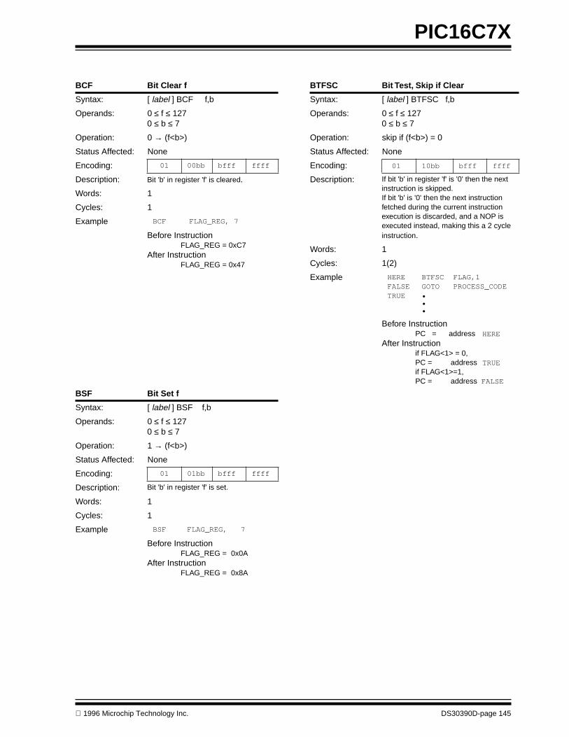
1996 Microchip Technology Inc. DS30390D-page 145
PIC16C7X
BCF Bit Clear f
Syntax: [ label ] BCF f,b
Operands: 0 ≤ f ≤ 1270 ≤ b ≤ 7
Operation: 0 → (f<b>)
Status Affected: None
Encoding: 01 00bb bfff ffff
Description: Bit 'b' in register 'f' is cleared.
Words: 1
Cycles: 1
Example BCF FLAG_REG, 7
Before InstructionFLAG_REG = 0xC7
After InstructionFLAG_REG = 0x47
BSF Bit Set f
Syntax: [ label ] BSF f,b
Operands: 0 ≤ f ≤ 1270 ≤ b ≤ 7
Operation: 1 → (f<b>)
Status Affected: None
Encoding: 01 01bb bfff ffff
Description: Bit 'b' in register 'f' is set.
Words: 1
Cycles: 1
Example BSF FLAG_REG, 7
Before InstructionFLAG_REG = 0x0A
After InstructionFLAG_REG = 0x8A
BTFSC Bit Test, Skip if Clear
Syntax: [ label ] BTFSC f,b
Operands: 0 ≤ f ≤ 1270 ≤ b ≤ 7
Operation: skip if (f<b>) = 0
Status Affected: None
Encoding: 01 10bb bfff ffff
Description: If bit 'b' in register 'f' is '0' then the next instruction is skipped.If bit 'b' is '0' then the next instruction fetched during the current instruction execution is discarded, and a NOP is executed instead, making this a 2 cycle instruction.
Words: 1
Cycles: 1(2)
Example HEREFALSETRUE
BTFSCGOTO•••
FLAG,1PROCESS_CODE
Before InstructionPC = address HERE
After Instructionif FLAG<1> = 0,PC = address TRUEif FLAG<1>=1,PC = address FALSE
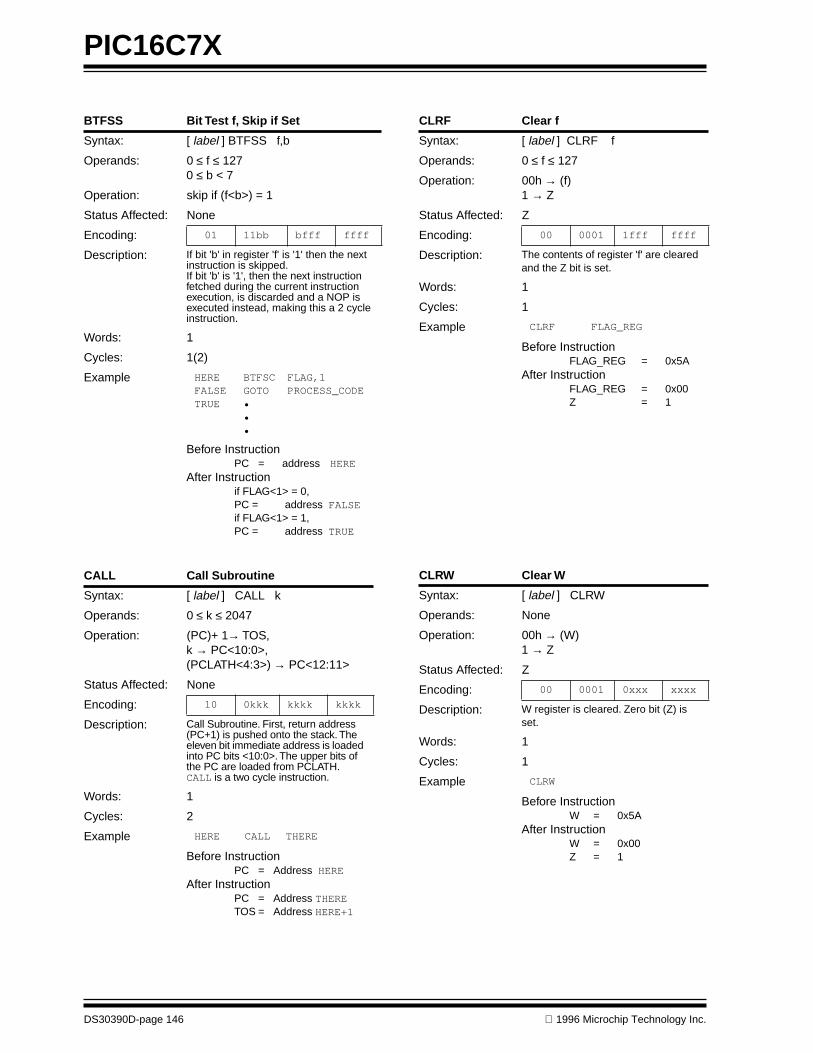
PIC16C7X
DS30390D-page 146 1996 Microchip Technology Inc.
BTFSS Bit Test f, Skip if Set
Syntax: [ label ] BTFSS f,b
Operands: 0 ≤ f ≤ 1270 ≤ b < 7
Operation: skip if (f<b>) = 1
Status Affected: None
Encoding: 01 11bb bfff ffff
Description: If bit 'b' in register 'f' is '1' then the next instruction is skipped.If bit 'b' is '1', then the next instruction fetched during the current instruction execution, is discarded and a NOP is executed instead, making this a 2 cycle instruction.
Words: 1
Cycles: 1(2)
Example HEREFALSETRUE
BTFSCGOTO•••
FLAG,1PROCESS_CODE
Before InstructionPC = address HERE
After Instructionif FLAG<1> = 0,PC = address FALSEif FLAG<1> = 1,PC = address TRUE
CALL Call Subroutine
Syntax: [ label ] CALL k
Operands: 0 ≤ k ≤ 2047
Operation: (PC)+ 1→ TOS,k → PC<10:0>,(PCLATH<4:3>) → PC<12:11>
Status Affected: None
Encoding: 10 0kkk kkkk kkkk
Description: Call Subroutine. First, return address (PC+1) is pushed onto the stack. The eleven bit immediate address is loaded into PC bits <10:0>. The upper bits of the PC are loaded from PCLATH. CALL is a two cycle instruction.
Words: 1
Cycles: 2
Example HERE CALL THERE
Before InstructionPC = Address HERE
After InstructionPC = Address THERETOS = Address HERE+1
CLRF Clear f
Syntax: [ label ] CLRF f
Operands: 0 ≤ f ≤ 127
Operation: 00h → (f)1 → Z
Status Affected: Z
Encoding: 00 0001 1fff ffff
Description: The contents of register 'f' are cleared and the Z bit is set.
Words: 1
Cycles: 1
Example CLRF FLAG_REG
Before InstructionFLAG_REG = 0x5A
After InstructionFLAG_REG = 0x00Z = 1
CLRW Clear W
Syntax: [ label ] CLRW
Operands: None
Operation: 00h → (W)1 → Z
Status Affected: Z
Encoding: 00 0001 0xxx xxxx
Description: W register is cleared. Zero bit (Z) is set.
Words: 1
Cycles: 1
Example CLRW
Before InstructionW = 0x5A
After InstructionW = 0x00Z = 1
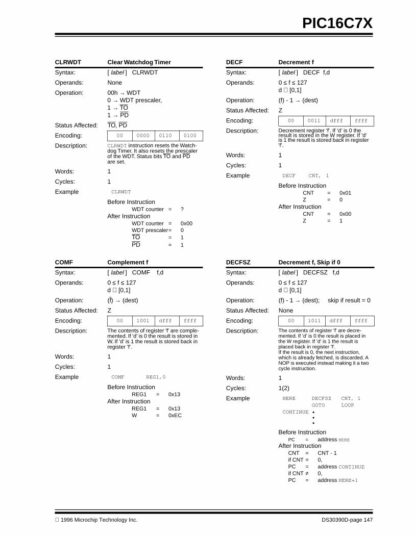
1996 Microchip Technology Inc. DS30390D-page 147
PIC16C7X
CLRWDT Clear Watchdog Timer
Syntax: [ label ] CLRWDT
Operands: None
Operation: 00h → WDT0 → WDT prescaler,1 → TO1 → PD
Status Affected: TO, PD
Encoding: 00 0000 0110 0100
Description: CLRWDT instruction resets the Watch-dog Timer. It also resets the prescaler of the WDT. Status bits TO and PD are set.
Words: 1
Cycles: 1
Example CLRWDT
Before InstructionWDT counter = ?
After InstructionWDT counter = 0x00WDT prescaler= 0TO = 1PD = 1
COMF Complement f
Syntax: [ label ] COMF f,d
Operands: 0 ≤ f ≤ 127d ∈ [0,1]
Operation: (f) → (dest)
Status Affected: Z
Encoding: 00 1001 dfff ffff
Description: The contents of register 'f' are comple-mented. If 'd' is 0 the result is stored in W. If 'd' is 1 the result is stored back in register 'f'.
Words: 1
Cycles: 1
Example COMF REG1,0
Before InstructionREG1 = 0x13
After InstructionREG1 = 0x13W = 0xEC
DECF Decrement f
Syntax: [ label ] DECF f,d
Operands: 0 ≤ f ≤ 127d ∈ [0,1]
Operation: (f) - 1 → (dest)
Status Affected: Z
Encoding: 00 0011 dfff ffff
Description: Decrement register 'f'. If 'd' is 0 the result is stored in the W register. If 'd' is 1 the result is stored back in register 'f'.
Words: 1
Cycles: 1
Example DECF CNT, 1
Before InstructionCNT = 0x01Z = 0
After InstructionCNT = 0x00Z = 1
DECFSZ Decrement f, Skip if 0
Syntax: [ label ] DECFSZ f,d
Operands: 0 ≤ f ≤ 127d ∈ [0,1]
Operation: (f) - 1 → (dest); skip if result = 0
Status Affected: None
Encoding: 00 1011 dfff ffff
Description: The contents of register 'f' are decre-mented. If 'd' is 0 the result is placed in the W register. If 'd' is 1 the result is placed back in register 'f'. If the result is 0, the next instruction, which is already fetched, is discarded. A NOP is executed instead making it a two cycle instruction.
Words: 1
Cycles: 1(2)
Example HERE DECFSZ CNT, 1 GOTO LOOPCONTINUE • • •
Before InstructionPC = address HERE
After InstructionCNT = CNT - 1if CNT = 0,PC = address CONTINUEif CNT ≠ 0,PC = address HERE+1

PIC16C7X
DS30390D-page 148 1996 Microchip Technology Inc.
GOTO Unconditional Branch
Syntax: [ label ] GOTO k
Operands: 0 ≤ k ≤ 2047
Operation: k → PC<10:0>PCLATH<4:3> → PC<12:11>
Status Affected: None
Encoding: 10 1kkk kkkk kkkk
Description: GOTO is an unconditional branch. The eleven bit immediate value is loaded into PC bits <10:0>. The upper bits of PC are loaded from PCLATH<4:3>. GOTO is a two cycle instruction.
Words: 1
Cycles: 2
Example GOTO THERE
After InstructionPC = Address THERE
INCF Increment f
Syntax: [ label ] INCF f,d
Operands: 0 ≤ f ≤ 127d ∈ [0,1]
Operation: (f) + 1 → (dest)
Status Affected: Z
Encoding: 00 1010 dfff ffff
Description: The contents of register 'f' are incre-mented. If 'd' is 0 the result is placed in the W register. If 'd' is 1 the result is placed back in register 'f'.
Words: 1
Cycles: 1
Example INCF CNT, 1
Before InstructionCNT = 0xFFZ = 0
After InstructionCNT = 0x00Z = 1
INCFSZ Increment f, Skip if 0
Syntax: [ label ] INCFSZ f,d
Operands: 0 ≤ f ≤ 127d ∈ [0,1]
Operation: (f) + 1 → (dest), skip if result = 0
Status Affected: None
Encoding: 00 1111 dfff ffff
Description: The contents of register 'f' are incre-mented. If 'd' is 0 the result is placed in the W register. If 'd' is 1 the result is placed back in register 'f'.If the result is 0, the next instruction, which is already fetched, is discarded. A NOP is executed instead making it a two cycle instruction.
Words: 1
Cycles: 1(2)
Example HERE INCFSZ CNT, 1 GOTO LOOPCONTINUE • • •
Before InstructionPC = address HERE
After InstructionCNT = CNT + 1if CNT= 0,PC = address CONTINUEif CNT≠ 0,PC = address HERE +1
IORLW Inclusive OR Literal with W
Syntax: [ label ] IORLW k
Operands: 0 ≤ k ≤ 255
Operation: (W) .OR. k → (W)
Status Affected: Z
Encoding: 11 1000 kkkk kkkk
Description: The contents of the W register is OR’ed with the eight bit literal 'k'. The result is placed in the W register.
Words: 1
Cycles: 1
Example IORLW 0x35
Before InstructionW = 0x9A
After InstructionW = 0xBFZ = 1

1996 Microchip Technology Inc. DS30390D-page 149
PIC16C7X
IORWF Inclusive OR W with f
Syntax: [ label ] IORWF f,d
Operands: 0 ≤ f ≤ 127d ∈ [0,1]
Operation: (W) .OR. (f) → (dest)
Status Affected: Z
Encoding: 00 0100 dfff ffff
Description: Inclusive OR the W register with regis-ter 'f'. If 'd' is 0 the result is placed in the W register. If 'd' is 1 the result is placed back in register 'f'.
Words: 1
Cycles: 1
Example IORWF RESULT, 0
Before InstructionRESULT = 0x13W = 0x91
After InstructionRESULT = 0x13W = 0x93Z = 1
MOVLW Move Literal to W
Syntax: [ label ] MOVLW k
Operands: 0 ≤ k ≤ 255
Operation: k → (W)
Status Affected: None
Encoding: 11 00xx kkkk kkkk
Description: The eight bit literal 'k' is loaded into W register. The don’t cares will assemble as 0’s.
Words: 1
Cycles: 1
Example MOVLW 0x5A
After InstructionW = 0x5A
MOVF Move f
Syntax: [ label ] MOVF f,d
Operands: 0 ≤ f ≤ 127d ∈ [0,1]
Operation: (f) → (dest)
Status Affected: Z
Encoding: 00 1000 dfff ffff
Description: The contents of register f is moved to a destination dependant upon the sta-tus of d. If d = 0, destination is W reg-ister. If d = 1, the destination is file register f itself. d = 1 is useful to test a file register since status flag Z is affected.
Words: 1
Cycles: 1
Example MOVF FSR, 0
After InstructionW = value in FSR registerZ = 1
MOVWF Move W to f
Syntax: [ label ] MOVWF f
Operands: 0 ≤ f ≤ 127
Operation: (W) → (f)
Status Affected: None
Encoding: 00 0000 1fff ffff
Description: Move data from W register to register 'f'.
Words: 1
Cycles: 1
Example MOVWF OPTION
Before InstructionOPTION = 0xFFW = 0x4F
After InstructionOPTION = 0x4FW = 0x4F
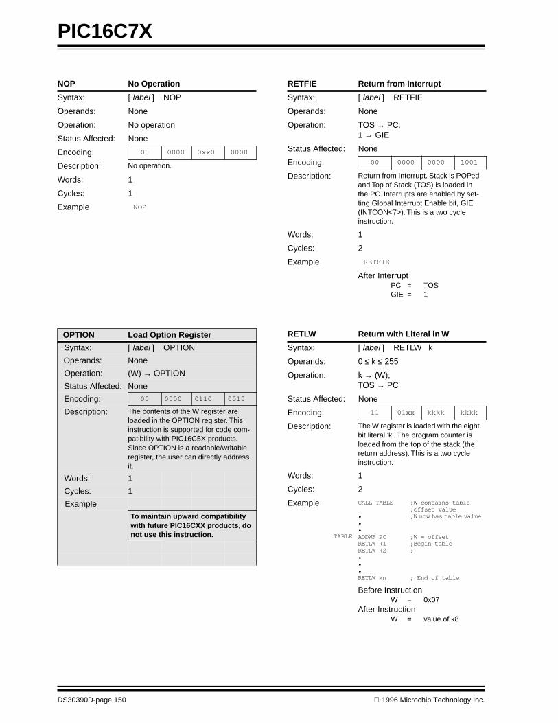
PIC16C7X
DS30390D-page 150 1996 Microchip Technology Inc.
NOP No Operation
Syntax: [ label ] NOP
Operands: None
Operation: No operation
Status Affected: None
Encoding: 00 0000 0xx0 0000
Description: No operation.
Words: 1
Cycles: 1
Example NOP
OPTION Load Option Register
Syntax: [ label ] OPTION
Operands: None
Operation: (W) → OPTION
Status Affected: None
Encoding: 00 0000 0110 0010
Description: The contents of the W register are loaded in the OPTION register. This instruction is supported for code com-patibility with PIC16C5X products. Since OPTION is a readable/writable register, the user can directly address it.
Words: 1
Cycles: 1
Example
To maintain upward compatibility with future PIC16CXX products, do not use this instruction.
RETFIE Return from Interrupt
Syntax: [ label ] RETFIE
Operands: None
Operation: TOS → PC,1 → GIE
Status Affected: None
Encoding: 00 0000 0000 1001
Description: Return from Interrupt. Stack is POPed and Top of Stack (TOS) is loaded in the PC. Interrupts are enabled by set-ting Global Interrupt Enable bit, GIE (INTCON<7>). This is a two cycle instruction.
Words: 1
Cycles: 2
Example RETFIE
After InterruptPC = TOSGIE = 1
RETLW Return with Literal in W
Syntax: [ label ] RETLW k
Operands: 0 ≤ k ≤ 255
Operation: k → (W); TOS → PC
Status Affected: None
Encoding: 11 01xx kkkk kkkk
Description: The W register is loaded with the eight bit literal 'k'. The program counter is loaded from the top of the stack (the return address). This is a two cycle instruction.
Words: 1
Cycles: 2
Example
TABLE
CALL TABLE ;W contains table ;offset value• ;W now has table value••ADDWF PC ;W = offsetRETLW k1 ;Begin tableRETLW k2 ;•••RETLW kn ; End of table
Before InstructionW = 0x07
After InstructionW = value of k8
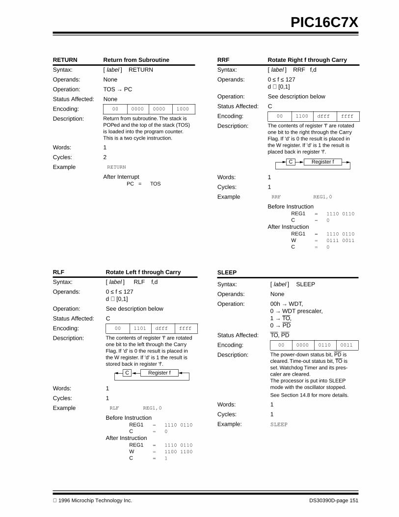
1996 Microchip Technology Inc. DS30390D-page 151
PIC16C7X
RETURN Return from Subroutine
Syntax: [ label ] RETURN
Operands: None
Operation: TOS → PC
Status Affected: None
Encoding: 00 0000 0000 1000
Description: Return from subroutine. The stack is POPed and the top of the stack (TOS) is loaded into the program counter. This is a two cycle instruction.
Words: 1
Cycles: 2
Example RETURN
After InterruptPC = TOS
RLF Rotate Left f through Carry
Syntax: [ label ] RLF f,d
Operands: 0 ≤ f ≤ 127d ∈ [0,1]
Operation: See description below
Status Affected: C
Encoding: 00 1101 dfff ffff
Description: The contents of register 'f' are rotated one bit to the left through the Carry Flag. If 'd' is 0 the result is placed in the W register. If 'd' is 1 the result is stored back in register 'f'.
Words: 1
Cycles: 1
Example RLF REG1,0
Before InstructionREG1 = 1110 0110C = 0
After InstructionREG1 = 1110 0110W = 1100 1100C = 1
Register fC
RRF Rotate Right f through Carry
Syntax: [ label ] RRF f,d
Operands: 0 ≤ f ≤ 127d ∈ [0,1]
Operation: See description below
Status Affected: C
Encoding: 00 1100 dfff ffff
Description: The contents of register 'f' are rotated one bit to the right through the Carry Flag. If 'd' is 0 the result is placed in the W register. If 'd' is 1 the result is placed back in register 'f'.
Words: 1
Cycles: 1
Example RRF REG1,0
Before InstructionREG1 = 1110 0110C = 0
After InstructionREG1 = 1110 0110W = 0111 0011C = 0
SLEEP
Syntax: [ label ] SLEEP
Operands: None
Operation: 00h → WDT,0 → WDT prescaler,1 → TO,0 → PD
Status Affected: TO, PD
Encoding: 00 0000 0110 0011
Description: The power-down status bit, PD is cleared. Time-out status bit, TO is set. Watchdog Timer and its pres-caler are cleared.The processor is put into SLEEP mode with the oscillator stopped.
See Section 14.8 for more details.
Words: 1
Cycles: 1
Example: SLEEP
Register fC
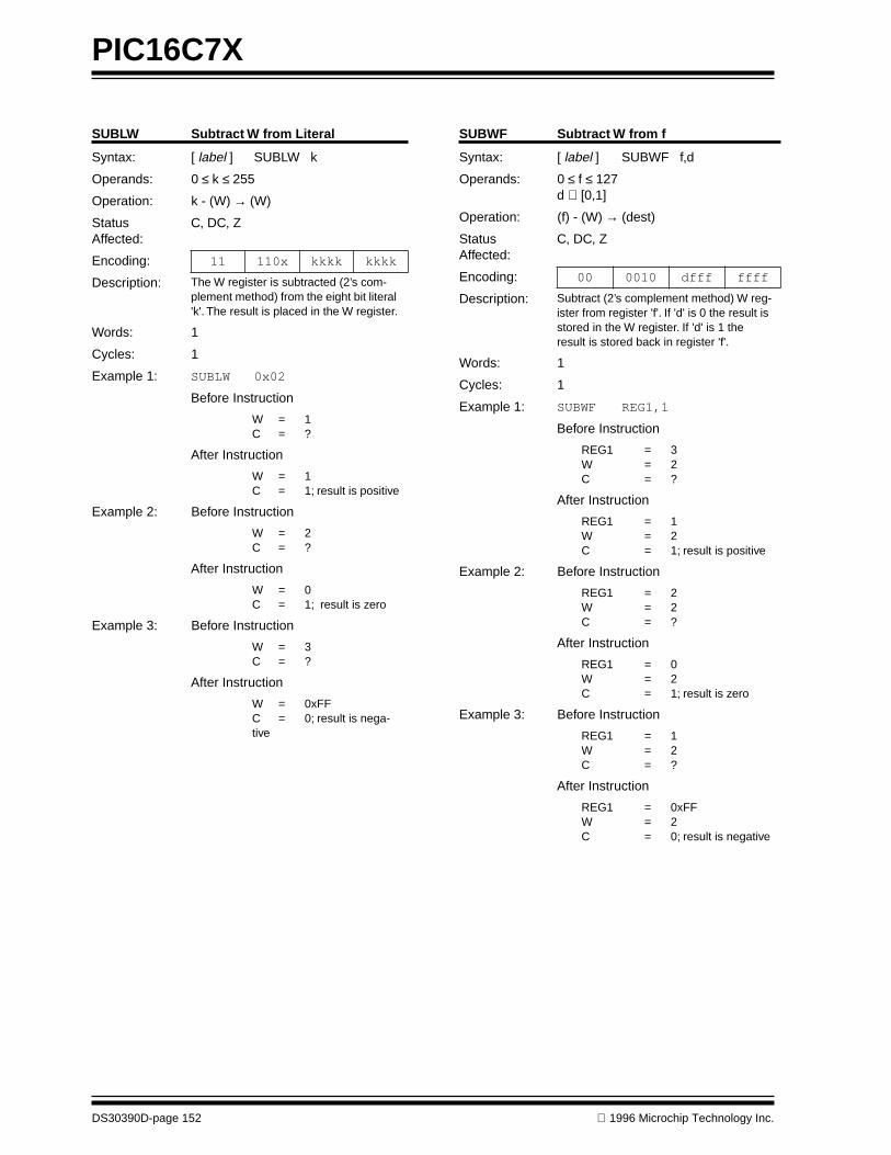
PIC16C7X
DS30390D-page 152 1996 Microchip Technology Inc.
SUBLW Subtract W from Literal
Syntax: [ label ] SUBLW k
Operands: 0 ≤ k ≤ 255
Operation: k - (W) → (W)
Status Affected:
C, DC, Z
Encoding: 11 110x kkkk kkkk
Description: The W register is subtracted (2’s com-plement method) from the eight bit literal 'k'. The result is placed in the W register.
Words: 1
Cycles: 1
Example 1: SUBLW 0x02
Before Instruction
W = 1C = ?
After Instruction
W = 1C = 1; result is positive
Example 2: Before Instruction
W = 2C = ?
After Instruction
W = 0C = 1; result is zero
Example 3: Before Instruction
W = 3C = ?
After Instruction
W = 0xFFC = 0; result is nega-tive
SUBWF Subtract W from f
Syntax: [ label ] SUBWF f,d
Operands: 0 ≤ f ≤ 127d ∈ [0,1]
Operation: (f) - (W) → (dest)
Status Affected:
C, DC, Z
Encoding: 00 0010 dfff ffff
Description: Subtract (2’s complement method) W reg-ister from register 'f'. If 'd' is 0 the result is stored in the W register. If 'd' is 1 the result is stored back in register 'f'.
Words: 1
Cycles: 1
Example 1: SUBWF REG1,1
Before Instruction
REG1 = 3W = 2C = ?
After Instruction
REG1 = 1W = 2C = 1; result is positive
Example 2: Before Instruction
REG1 = 2W = 2C = ?
After Instruction
REG1 = 0W = 2C = 1; result is zero
Example 3: Before Instruction
REG1 = 1W = 2C = ?
After Instruction
REG1 = 0xFFW = 2C = 0; result is negative
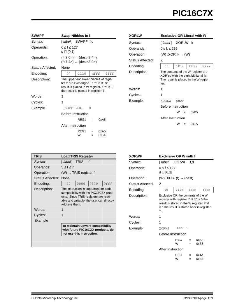
1996 Microchip Technology Inc. DS30390D-page 153
PIC16C7X
SWAPF Swap Nibbles in f
Syntax: [ label ] SWAPF f,d
Operands: 0 ≤ f ≤ 127d ∈ [0,1]
Operation: (f<3:0>) → (dest<7:4>),(f<7:4>) → (dest<3:0>)
Status Affected: None
Encoding: 00 1110 dfff ffff
Description: The upper and lower nibbles of regis-ter 'f' are exchanged. If 'd' is 0 the result is placed in W register. If 'd' is 1 the result is placed in register 'f'.
Words: 1
Cycles: 1
Example SWAPF REG, 0
Before Instruction
REG1 = 0xA5
After Instruction
REG1 = 0xA5W = 0x5A
TRIS Load TRIS Register
Syntax: [ label ] TRIS f
Operands: 5 ≤ f ≤ 7
Operation: (W) → TRIS register f;
Status Affected: None
Encoding: 00 0000 0110 0fff
Description: The instruction is supported for code compatibility with the PIC16C5X prod-ucts. Since TRIS registers are read-able and writable, the user can directly address them.
Words: 1
Cycles: 1
Example
To maintain upward compatibility with future PIC16CXX products, do not use this instruction.
XORLW Exclusive OR Literal with W
Syntax: [ label ] XORLW k
Operands: 0 ≤ k ≤ 255
Operation: (W) .XOR. k → (W)
Status Affected: Z
Encoding: 11 1010 kkkk kkkk
Description: The contents of the W register are XOR’ed with the eight bit literal 'k'. The result is placed in the W regis-ter.
Words: 1
Cycles: 1
Example: XORLW 0xAF
Before Instruction
W = 0xB5
After Instruction
W = 0x1A
XORWF Exclusive OR W with f
Syntax: [ label ] XORWF f,d
Operands: 0 ≤ f ≤ 127d ∈ [0,1]
Operation: (W) .XOR. (f) → (dest)
Status Affected: Z
Encoding: 00 0110 dfff ffff
Description: Exclusive OR the contents of the W register with register 'f'. If 'd' is 0 the result is stored in the W register. If 'd' is 1 the result is stored back in register 'f'.
Words: 1
Cycles: 1
Example XORWF REG 1
Before Instruction
REG = 0xAFW = 0xB5
After Instruction
REG = 0x1AW = 0xB5

PIC16C7X
DS30390D-page 154 1996 Microchip Technology Inc.
1996 Microchip Technology Inc. DS30390D-page 155
PIC16C7X
16.0 DEVELOPMENT SUPPORT
16.1 Development Tools
The PIC16/17 microcontrollers are supported with a fullrange of hardware and software development tools:
• PICMASTER/PICMASTER CE
Real-Time In-Circuit Emulator
• ICEPIC Low-Cost PIC16C5X and PIC16CXXX In-Circuit Emulator
• PRO MATE
II Universal Programmer• PICSTART
Plus Entry-Level Prototype Programmer
• PICDEM-1 Low-Cost Demonstration Board• PICDEM-2 Low-Cost Demonstration Board• PICDEM-3 Low-Cost Demonstration Board• MPASM Assembler• MPLAB-SIM Software Simulator• MPLAB-C (C Compiler)• Fuzzy logic development system (fuzzyTECH
−
MP)
16.2 PICMASTER: High Performance Universal In-Circuit Emulator with MPLAB IDE
The PICMASTER Universal In-Circuit Emulator isintended to provide the product development engineerwith a complete microcontroller design tool set for allmicrocontrollers in the PIC12C5XX, PIC14000,PIC16C5X, PIC16CXXX and PIC17CXX families.PICMASTER is supplied with the MPLAB
IntegratedDevelopment Environment (IDE), which allows editing,“make” and download, and source debugging from asingle environment.
Interchangeable target probes allow the system to beeasily reconfigured for emulation of different proces-sors. The universal architecture of the PICMASTERallows expansion to support all new Microchip micro-controllers.
The PICMASTER Emulator System has beendesigned as a real-time emulation system withadvanced features that are generally found on moreexpensive development tools. The PC compatible 386(and higher) machine platform and Microsoft Windows
3.x environment were chosen to best make these fea-tures available to you, the end user.
A CE compliant version of PICMASTER is available forEuropean Union (EU) countries.
16.3 ICEPIC: Low-cost PIC16CXXXIn-Circuit Emulator
ICEPIC is a low-cost in-circuit emulator solution for theMicrochip PIC16C5X and PIC16CXXX families of 8-bitOTP microcontrollers.
ICEPIC is designed to operate on PC-compatiblemachines ranging from 286-AT
through Pentium
based machines under Windows 3.x environment.ICEPIC features real time, non-intrusive emulation.
16.4 PRO MATE II: Universal Programmer
The PRO MATE II Universal Programmer is a full-fea-tured programmer capable of operating in stand-alonemode as well as PC-hosted mode.
The PRO MATE II has programmable V
DD
and V
PP
supplies which allows it to verify programmed memoryat V
DD
min and V
DD
max for maximum reliability. It hasan LCD display for displaying error messages, keys toenter commands and a modular detachable socketassembly to support various package types. In stand-alone mode the PRO MATE II can read, verify or pro-gram PIC16C5X, PIC16CXXX, PIC17CXX andPIC14000 devices. It can also set configuration andcode-protect bits in this mode.
16.5 PICSTART Plus Entry Level Development System
The PICSTART programmer is an easy-to-use, low-cost prototype programmer. It connects to the PC viaone of the COM (RS-232) ports. MPLAB IntegratedDevelopment Environment software makes using theprogrammer simple and efficient. PICSTART Plus isnot recommended for production programming.
PICSTART Plus supports all PIC12C5XX, PIC14000,PIC16C5X, PIC16CXXX and PIC17CXX devices withup to 40 pins. Larger pin count devices such as thePIC16C923 and PIC16C924 may be supported with anadapter socket.
This document was created with FrameMaker 4 0 4

PIC16C7X
DS30390D-page 156
1996 Microchip Technology Inc.
16.6 PICDEM-1 Low-Cost PIC16/17 Demonstration Board
The PICDEM-1 is a simple board which demonstratesthe capabilities of several of Microchip’s microcontrol-lers. The microcontrollers supported are: PIC16C5X(PIC16C54 to PIC16C58A), PIC16C61, PIC16C62X,PIC16C71, PIC16C8X, PIC17C42, PIC17C43 andPIC17C44. All necessary hardware and software isincluded to run basic demo programs. The users canprogram the sample microcontrollers provided withthe PICDEM-1 board, on a PRO MATE II orPICSTART-16B programmer, and easily test firm-ware. The user can also connect the PICDEM-1board to the PICMASTER emulator and downloadthe firmware to the emulator for testing. Additional pro-totype area is available for the user to build some addi-tional hardware and connect it to the microcontrollersocket(s). Some of the features include an RS-232interface, a potentiometer for simulated analog input,push-button switches and eight LEDs connected toPORTB.
16.7 PICDEM-2 Low-Cost PIC16CXX Demonstration Board
The PICDEM-2 is a simple demonstration board thatsupports the PIC16C62, PIC16C64, PIC16C65,PIC16C73 and PIC16C74 microcontrollers. All thenecessary hardware and software is included torun the basic demonstration programs. The usercan program the sample microcontrollers providedwith the PICDEM-2 board, on a PRO MATE II pro-grammer or PICSTART-16C, and easily test firmware.The PICMASTER emulator may also be used with thePICDEM-2 board to test firmware. Additional prototypearea has been provided to the user for adding addi-tional hardware and connecting it to the microcontrollersocket(s). Some of the features include a RS-232 inter-face, push-button switches, a potentiometer for simu-lated analog input, a Serial EEPROM to demonstrateusage of the I
2
C bus and separate headers for connec-tion to an LCD module and a keypad.
16.8 PICDEM-3 Low-Cost PIC16CXXX Demonstration Board
The PICDEM-3 is a simple demonstration board thatsupports the PIC16C923 and PIC16C924 in the PLCCpackage. It will also support future 44-pin PLCCmicrocontrollers with a LCD Module. All the neces-sary hardware and software is included to run thebasic demonstration programs. The user can pro-gram the sample microcontrollers provided withthe PICDEM-3 board, on a PRO MATE II program-mer or PICSTART Plus with an adapter socket, andeasily test firmware. The PICMASTER emulator mayalso be used with the PICDEM-3 board to test firm-ware. Additional prototype area has been provided tothe user for adding hardware and connecting it to themicrocontroller socket(s). Some of the features
include an RS-232 interface, push-button switches, apotentiometer for simulated analog input, a thermistorand separate headers for connection to an externalLCD module and a keypad. Also provided on thePICDEM-3 board is an LCD panel, with 4 commonsand 12 segments, that is capable of displaying time,temperature and day of the week. The PICDEM-3 pro-vides an additional RS-232 interface and Windows 3.1software for showing the demultiplexed LCD signals ona PC. A simple serial interface allows the user to con-struct a hardware demultiplexer for the LCD signals.PICDEM-3 will be available in the 3rd quarter of 1996.
16.9 MPLAB Integrated Development Environment Software
The MPLAB IDE Software brings an ease of softwaredevelopment previously unseen in the 8-bit microcon-troller market. MPLAB is a windows based applicationwhich contains:
• A full featured editor• Three operating modes
- editor- emulator- simulator
• A project manager• Customizable tool bar and key mapping• A status bar with project information• Extensive on-line help
MPLAB allows you to:
• Edit your source files (either assembly or ‘C’)• One touch assemble (or compile) and download
to PIC16/17 tools (automatically updates all project information)
• Debug using:- source files- absolute listing file
• Transfer data dynamically via DDE (soon to be replaced by OLE)
• Run up to four emulators on the same PC
The ability to use MPLAB with Microchip’s simulatorallows a consistent platform and the ability to easilyswitch from the low cost simulator to the full featuredemulator with minimal retraining due to developmenttools.
16.10 Assembler (MPASM)
The MPASM Universal Macro Assembler is a PC-hosted symbolic assembler. It supports all microcon-troller series including the PIC12C5XX, PIC14000,PIC16C5X, PIC16CXXX, and PIC17CXX families.
MPASM offers full featured Macro capabilities, condi-tional assembly, and several source and listing formats.It generates various object code formats to supportMicrochip's development tools as well as third partyprogrammers.

1996 Microchip Technology Inc. DS30390D-page 157
PIC16C7X
MPASM allow full symbolic debugging from theMicrochip Universal Emulator System(PICMASTER).
MPASM has the following features to assist in develop-ing software for specific use applications.
• Provides translation of Assembler source code to object code for all Microchip microcontrollers.
• Macro assembly capability.• Produces all the files (Object, Listing, Symbol,
and special) required for symbolic debug with Microchip’s emulator systems.
• Supports Hex (default), Decimal and Octal source and listing formats.
MPASM provides a rich directive language to supportprogramming of the PIC16/17. Directives are helpful inmaking the development of your assemble sourcecode shorter and more maintainable.
16.11 Software Simulator (MPLAB-SIM)
The MPLAB-SIM Software Simulator allows codedevelopment in a PC host environment. It allows theuser to simulate the PIC16/17 series microcontrollerson an instruction level. On any given instruction, theuser may examine or modify any of the data areas orprovide external stimulus to any of the pins. The input/output radix can be set by the user and the executioncan be performed in; single step, execute until break,or in a trace mode.
MPLAB-SIM fully supports symbolic debugging usingMPLAB-C and MPASM. The Software Simulator offersthe low cost flexibility to develop and debug code out-side of the laboratory environment making it an excel-lent multi-project software development tool.
16.12 C Compiler (MPLAB-C)
The MPLAB-C Code Development System is acomplete ‘C’ compiler and integrated developmentenvironment for Microchip’s PIC16/17 family of micro-controllers. The compiler provides powerful integrationcapabilities and ease of use not found with othercompilers.
For easier source level debugging, the compiler pro-vides symbol information that is compatible with theMPLAB IDE memory display (PICMASTER emulatorsoftware versions 1.13 and later).
16.13 Fuzzy Logic Development System (
fuzzy
TECH-MP)
fuzzy
TECH-MP fuzzy logic development tool is avail-able in two versions - a low cost introductory version,MP Explorer, for designers to gain a comprehensiveworking knowledge of fuzzy logic system design; and afull-featured version,
fuzzy
TECH-MP, edition for imple-menting more complex systems.
Both versions include Microchip’s
fuzzy
LAB
demon-stration board for hands-on experience with fuzzy logicsystems implementation.
16.14 MP-DriveWay
– Application Code Generator
MP-DriveWay is an easy-to-use Windows-based Appli-cation Code Generator. With MP-DriveWay you canvisually configure all the peripherals in a PIC16/17device and, with a click of the mouse, generate all theinitialization and many functional code modules in Clanguage. The output is fully compatible with Micro-chip’s MPLAB-C C compiler. The code produced ishighly modular and allows easy integration of your owncode. MP-DriveWay is intelligent enough to maintainyour code through subsequent code generation.
16.15 SEEVAL
Evaluation and Programming System
The SEEVAL SEEPROM Designer’s Kit supports allMicrochip 2-wire and 3-wire Serial EEPROMs. The kitincludes everything necessary to read, write, erase orprogram special features of any Microchip SEEPROMproduct including Smart Serials
and secure serials.The Total Endurance
Disk is included to aid in trade-off analysis and reliability calculations. The total kit cansignificantly reduce time-to-market and result in anoptimized system.
16.16 TrueGauge
Intelligent Battery Management
The TrueGauge development tool supports systemdevelopment with the MTA11200B TrueGauge Intelli-gent Battery Management IC. System design verifica-tion can be accomplished before hardware prototypesare built. User interface is graphically-oriented andmeasured data can be saved in a file for exporting toMicrosoft Excel.
16.17 K
EE
L
OQ
Evaluation and Programming Tools
K
EE
L
OQ
evaluation and programming tools supportMicrochips HCS Secure Data Products. The HCS eval-uation kit includes an LCD display to show changingcodes, a decoder to decode transmissions, and a pro-gramming interface to program test transmitters.

PIC16C7X
DS30390D-page 158
1996 Microchip Technology Inc.
TABLE 16-1: DEVELOPMENT TOOLS FROM MICROCHIP
Pro
du
ct**
MP
LA
B
Inte
gra
ted
Dev
elo
pm
ent
Env
iro
nm
ent
MP
LA
B
CC
om
pile
rM
P-D
rive
Way
Ap
plic
atio
ns
Co
de
Gen
erat
or
fuzz
yTE
CH
-MP
Exp
lore
r/E
dit
ion
Fu
zzy
Lo
gic
Dev
. To
ol
***
PIC
MA
ST
ER
/P
ICM
AS
TE
R-C
EIn
-Cir
cuit
E
mu
lato
r
ICE
PIC
Low
-Co
stIn
-Cir
cuit
Em
ula
tor
***
*PR
O M
AT
E
II U
niv
ersa
lM
icro
chip
Pro
gra
mm
er
PIC
STA
RT
Lit
eU
ltra
Low
-Co
stD
ev. K
it
PIC
STA
RT
Plu
sL
ow-C
ost
Un
iver
sal
Dev
. Kit
PIC
12C
508,
509
SW
0070
02S
W00
6005
—
—E
M16
7015
/E
M16
7101
—D
V00
7003
—
DV
0030
01
PIC
1400
0S
W00
7002
SW
0060
05
—
—E
M14
7001
/E
M14
7101
—
DV
0070
03 —
DV
0030
01
PIC
16C
52, 5
4, 5
4A,
55, 5
6, 5
7, 5
8AS
W00
7002
SW
0060
05S
W00
6006
DV
0050
01/
DV
0050
02E
M16
7015
/E
M16
7101
EM
1672
01D
V00
7003
DV
1620
03D
V00
3001
PIC
16C
554,
556
, 558
SW
0070
02S
W00
6005
—
DV
0050
01/
DV
0050
02E
M16
7033
/E
M16
7113
—
-D
V00
7003
—
DV
0030
01
PIC
16C
61S
W00
7002
SW
0060
05S
W00
6006
DV
0050
01/
DV
0050
02E
M16
7021
/N
/AE
M16
7205
DV
0070
03D
V16
2003
DV
0030
01
PIC
16C
62, 6
2A,
64, 6
4AS
W00
7002
SW
0060
05S
W00
6006
DV
0050
01/
DV
0050
02E
M16
7025
/E
M16
7103
EM
1672
03D
V00
7003
DV
1620
02D
V00
3001
PIC
16C
620,
621
, 622
SW
0070
02S
W00
6005
SW
0060
06D
V00
5001
/D
V00
5002
EM
1670
23/
EM
1671
09E
M16
7202
DV
0070
03D
V16
2003
DV
0030
01
PIC
16C
63, 6
5, 6
5A,
73, 7
3A, 7
4, 7
4AS
W00
7002
SW
0060
05S
W00
6006
DV
0050
01/
DV
0050
02E
M16
7025
/E
M16
7103
EM
1672
04D
V00
7003
DV
1620
02D
V00
3001
PIC
16C
642,
662
*S
W00
7002
SW
0060
05
—
—E
M16
7035
/E
M16
7105
—
-D
V00
7003
DV
1620
02D
V00
3001
PIC
16C
71S
W00
7002
SW
0060
05S
W00
6006
DV
0050
01/
DV
0050
02E
M16
7027
/E
M16
7105
EM
1672
05D
V00
7003
DV
1620
03D
V00
3001
PIC
16C
710,
711
SW
0070
02S
W00
6005
SW
0060
06D
V00
5001
/D
V00
5002
EM
1670
27/
EM
1671
05
—D
V00
7003
DV
1620
03D
V00
3001
PIC
16C
72S
W00
7002
SW
0060
05S
W00
6006
—
EM
1670
25/
EM
1671
03
—D
V00
7003
DV
1620
02D
V00
3001
PIC
16F
83S
W00
7002
SW
0060
05S
W00
6006
DV
0050
01/
DV
0050
02E
M16
7029
/E
M16
7107
—
DV
0070
03D
V16
2003
DV
0030
01
PIC
16C
84S
W00
7002
SW
0060
05S
W00
6006
DV
0050
01/
DV
0050
02E
M16
7029
/E
M16
7107
EM
1672
06D
V00
7003
DV
1620
03D
V00
3001
PIC
16F
84S
W00
7002
SW
0060
05S
W00
6006
DV
0050
01/
DV
0050
02E
M16
7029
/E
M16
7107
—
DV
0070
03D
V16
2003
DV
0030
01
PIC
16C
923,
924
*S
W00
7002
SW
0060
05S
W00
6006
DV
0050
01/
DV
0050
02E
M16
7031
/E
M16
7111
—D
V00
7003
—
DV
0030
01
PIC
17C
42,
42A
, 43,
44
SW
0070
02S
W00
6005
SW
0060
06D
V00
5001
/D
V00
5002
EM
1770
07/
EM
1771
07
—D
V00
7003
—D
V00
3001
*C
onta
ct M
icro
chip
Tec
hnol
ogy
for
avai
labi
lity
date
**M
PLA
B In
tegr
ated
Dev
elop
men
t Env
ironm
ent i
nclu
des
MP
LAB
-SIM
Sim
ulat
or a
nd
MPA
SM
Ass
embl
er
***
All
PIC
MA
ST
ER
and
PIC
MA
ST
ER
-CE
ord
erin
g pa
rt n
umbe
rs a
bove
incl
ude
PR
O M
ATE
II p
rogr
amm
er**
**P
RO
MAT
E s
ocke
t mod
ules
are
ord
ered
sep
arat
ely.
See
dev
elop
men
t sys
tem
s
o
rder
ing
guid
e fo
r sp
ecifi
c or
derin
g pa
rt n
umbe
rs
Pro
du
ctT
RU
EG
AU
GE
Dev
elo
pm
ent
Kit
SE
EVA
L
Des
ign
ers
Kit
Ho
pp
ing
Co
de
Sec
uri
ty P
rog
ram
mer
Kit
Ho
pp
ing
Co
de
Sec
uri
ty E
val/D
emo
Kit
All
2 w
ire a
nd 3
wire
S
eria
l EE
PR
OM
'sN
/AD
V24
3001
N/A
N/A
MTA
1120
0BD
V11
4001
N/A
N/A
N/A
HC
S20
0, 3
00, 3
01 *
N/A
N/A
PG
3060
01D
M30
3001
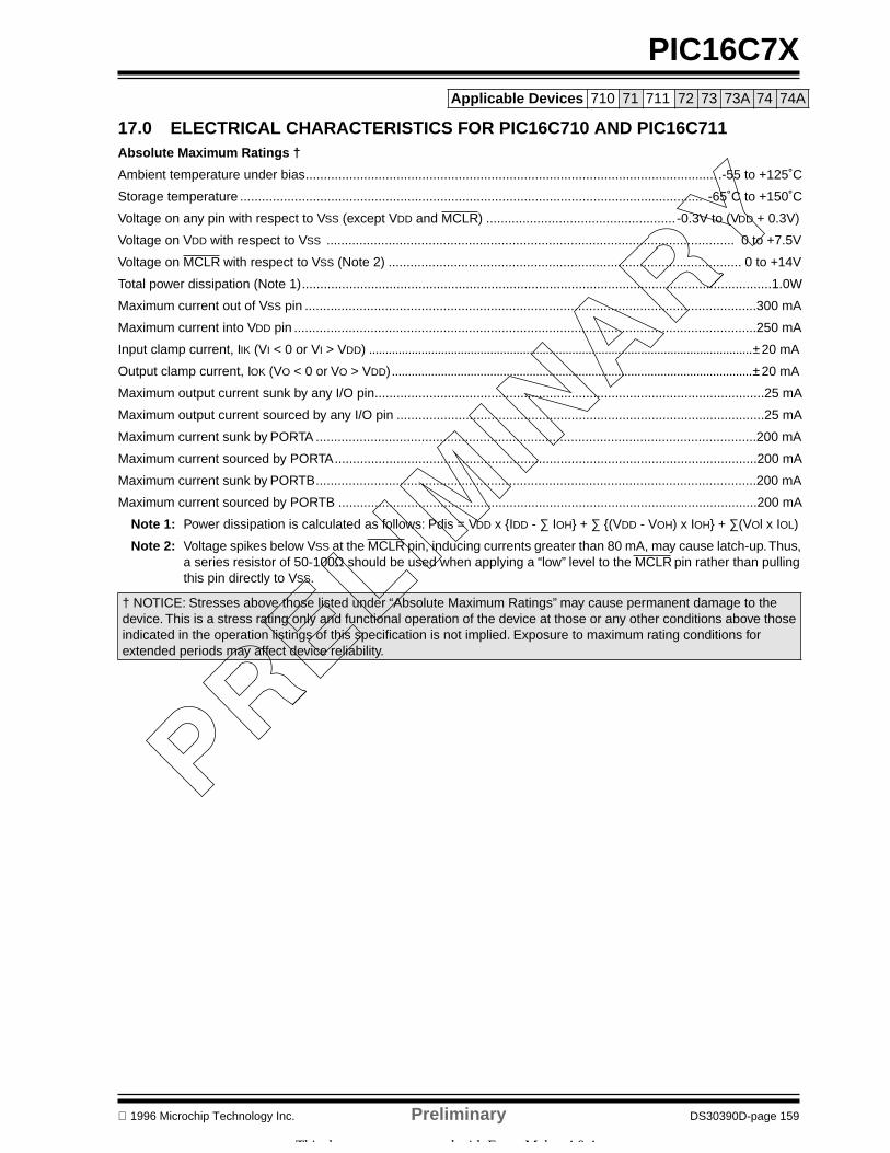
1996 Microchip Technology Inc.
Preliminary
DS30390D-page 159
PIC16C7X
Applicable Devices
710 71 711 72 73 73A 74 74A
17.0 ELECTRICAL CHARACTERISTICS FOR PIC16C710 AND PIC16C711
Absolute Maximum Ratings †
Ambient temperature under bias................................................................................................................. .-55 to +125˚C
Storage temperature ............................................................................................................................... -65˚C to +150˚C
Voltage on any pin with respect to V
SS
(except V
DD
and MCLR) .................................................... -0.3V to (V
DD
+ 0.3V)
Voltage on V
DD
with respect to V
SS
................................................................................................................ 0 to +7.5V
Voltage on MCLR with respect to V
SS
(Note 2) ................................................................................................. 0 to +14V
Total power dissipation (Note 1).................................................................................................................................1.0W
Maximum current out of V
SS
pin ............................................................................................................................300 mA
Maximum current into V
DD
pin ...............................................................................................................................250 mA
Input clamp current, I
IK
(V
I
< 0 or V
I
> V
DD
)
.....................................................................................................................±
20 mA
Output clamp current, I
OK
(V
O
< 0 or V
O
> V
DD
)
..............................................................................................................±
20 mA
Maximum output current sunk by any I/O pin...........................................................................................................25 mA
Maximum output current sourced by any I/O pin .....................................................................................................25 mA
Maximum current sunk by
PORTA .........................................................................................................................200 mA
Maximum current sourced by PORTA....................................................................................................................200 mA
Maximum current sunk by
PORTB.........................................................................................................................200 mA
Maximum current sourced by PORTB ...................................................................................................................200 mA
Note 1:
Power dissipation is calculated as follows: Pdis = V
DD
x I
DD
-
∑
I
OH
+
∑
(V
DD
- V
OH
) x I
OH
+
∑
(V
O
l x I
OL
)
Note 2:
Voltage spikes below V
SS
at the MCLR pin, inducing currents greater than 80 mA, may cause latch-up. Thus,a series resistor of 50-100
Ω
should be used when applying a “low” level to the MCLR pin rather than pullingthis pin directly to V
SS
.
† NOTICE: Stresses above those listed under “Absolute Maximum Ratings” may cause permanent damage to the device. This is a stress rating only and functional operation of the device at those or any other conditions above those indicated in the operation listings of this specification is not implied. Exposure to maximum rating conditions for extended periods may affect device reliability.
This document was created with FrameMaker 4 0 4

PIC16C7X
DS30390D-page 160
Preliminary
1996 Microchip Technology Inc.
Applicable Devices
710 71 711 72 73 73A 74 74A
TABLE 17-1: CROSS REFERENCE OF DEVICE SPECS FOR OSCILLATOR CONFIGURATIONS AND FREQUENCIES OF OPERATION (COMMERCIAL DEVICES)
OS
CP
IC16
C71
0-04
PIC
16C
711-
04P
IC16
C71
0-10
P
IC16
C71
1-10
PIC
16C
710-
20P
IC16
C71
1-20
PIC
16L
C71
0-04
PIC
16L
C71
1-04
PIC
16C
710/
JWP
IC16
C71
1/JW
RC
VD
D:
4.0V
to 6
.0V
IDD
: 5
mA
max
. at 5
.5V
IPD
: 21
µA
max
. at 4
VFr
eq:
4 M
Hz
max
.
VD
D:
4.5V
to 5
.5V
IDD
: 2.
7 m
A ty
p. a
t 5.5
VIP
D:
1.5
µA ty
p. a
t 4V
Freq
: 4
MH
z m
ax.
VD
D:
4.5V
to 5
.5V
IDD
: 2.
7 m
A ty
p. a
t 5.5
VIP
D:
1.5
µA ty
p. a
t 4V
Freq
: 4
MH
z m
ax.
VD
D:
3.0V
to 6
.0V
IDD
: 2.
0 m
A ty
p. a
t 3.0
VIP
D:
0.9
µA ty
p. a
t 3V
Freq
: 4
MH
z m
ax.
VD
D:
4.0V
to 6
.0V
IDD
: 5
mA
max
. at 5
.5V
IPD
: 21
µA
max
. at 4
VFr
eq:
4 M
Hz
max
.
XT
VD
D:
4.0V
to 6
.0V
IDD
: 5
mA
max
. at 5
.5V
IPD
: 21
µA
max
. at 4
VFr
eq:
4 M
Hz
max
.
VD
D:
4.5V
to 5
.5V
IDD
: 2.
7 m
A ty
p. a
t 5.5
VIP
D:
1.5
µA ty
p. a
t 4V
Freq
: 4
MH
z m
ax.
VD
D:
4.5V
to 5
.5V
IDD
: 2.
7 m
A ty
p. a
t 5.5
VIP
D:
1.5
µA ty
p. a
t 4V
Freq
: 4
MH
z m
ax.
VD
D:
3.0V
to 6
.0V
IDD
: 2.
0 m
A ty
p. a
t 3.0
VIP
D:
0.9
µA ty
p. a
t 3V
Freq
: 4
MH
z m
ax.
VD
D:
4.0V
to 6
.0V
IDD
: 5
mA
max
. at 5
.5V
IPD
: 21
µA
max
. at 4
VFr
eq:
4 M
Hz
max
.
HS
VD
D:
4.5V
to 5
.5V
VD
D:
4.5V
to 5
.5V
VD
D:
4.5V
to 5
.5V
Do
not u
se in
HS
mod
e
VD
D:
4.5V
to 5
.5V
IDD
: 13
.5 m
A ty
p. a
t 5.5
VID
D:
30 m
A m
ax. a
t 5.5
VID
D:
30 m
A m
ax. a
t 5.5
VID
D:
30 m
A m
ax. a
t 5.5
V
IPD
: 1.
5 µA
typ.
at 4
.5V
IPD
: 1.
5 µA
typ.
at 4
.5V
IPD
:1.
5 µA
typ.
at 4
.5V
IPD
: 1.
5 µA
typ.
at 4
.5V
Freq
: 4
MH
z m
ax.
Freq
: 10
MH
z m
ax.
Freq
:20
MH
z m
ax.
Freq
: 10
MH
z m
ax.
LP
VD
D:
4.0V
to 6
.0V
IDD
: 52
.5 µ
A ty
p. a
t 32
kHz,
4.0
VIP
D:
0.9
µA ty
p. a
t 4.0
VFr
eq:
200
kHz
max
.
Do
not u
se in
LP
mod
eD
o no
t use
in L
P m
ode
VD
D:
3.0V
to 6
.0V
IDD
: 48
µA
max
. at 3
2 kH
z, 3
.0V
IPD
: 5.
0 µA
max
. at 3
.0V
Freq
: 20
0 kH
z m
ax.
VD
D:
3.0V
to 6
.0V
IDD
: 48
µA
max
. at 3
2 kH
z, 3
.0V
IPD
: 5.
0 µA
max
. at 3
.0V
Freq
: 20
0 kH
z m
ax.
The
sha
ded
sect
ions
indi
cate
osc
illat
or s
elec
tions
whi
ch a
re te
sted
for
func
tiona
lity,
but
not
for
MIN
/MA
X s
peci
ficat
ions
. It i
s re
com
men
ded
that
the
user
sel
ect t
he d
evic
e ty
pe
that
ens
ures
the
spec
ifica
tions
req
uire
d.

1996 Microchip Technology Inc.
Preliminary
DS30390D-page 161
PIC16C7X
Applicable Devices
710 71 711 72 73 73A 74 74A
17.1 DC Characteristics: PIC16C710-04 (Commercial, Industrial, Automotive
(5)
)PIC16C711-04 (Commercial, Industrial, Automotive
(5)
)PIC16C710-10 (Commercial, Industrial, Automotive
(5)
)PIC16C711-10 (Commercial, Industrial, Automotive
(5)
)PIC16C710-20 (Commercial, Industrial, Automotive
(5)
)PIC16C711-20 (Commercial, Industrial, Automotive
(5)
)
DC CHARACTERISTICS
Standard Operating Conditions (unless otherwise stated)
Operating temperature -40˚C
≤
T
A
≤
+125˚C for automotive,-40˚C
≤
T
A
≤
+85˚C for industrial and 0˚C
≤
TA ≤ +710˚C for commercial
Param.No.
Characteristic Sym Min Typ† Max Units Conditions
D001D001A
Supply Voltage VDD 4.04.5
--
6.05.5
VV
XT, RC and LP osc configurationHS osc configuration
D002* RAM Data RetentionVoltage (Note 1)
VDR - 1.5 - V Device in SLEEP mode
D003 VDD start voltage toensure internal Power-on Reset signal
VPOR - VSS - V See section on Power-on Reset for details
D004* VDD rise rate to ensure internal Power-on Reset signal
SVDD 0.05 - - V/ms See section on Power-on Reset for details
D005 Brown-out Reset Voltage BVDD 3.7 4.0 4.3 V BODEN configuration bit is enabled
D010
D013
Supply Current (Note 2) IDD -
-
2.7
13.5
5
30
mA
mA
XT, RC osc configuration (PIC16C710/711-04)FOSC = 4 MHz, VDD = 5.5V (Note 4)
HS osc configuration (PIC16C710/711-20)FOSC = 20 MHz, VDD = 5.5V
D015 Brown-out Reset Current (Note 6)
∆IBOR - 300* 500 µA BOR enabled VDD = 5.0V
D020D021D021AD021B
Power-down Current (Note 3)
IPD ----
10.51.51.51.5
422124
TBD
µAµAµAµA
VDD = 4.0V, WDT enabled, -40°C to +85°CVDD = 4.0V, WDT disabled, -0°C to +70°CVDD = 4.0V, WDT disabled, -40°C to +85°CVDD = 4.0V, WDT disabled, -40°C to +125°C
D023 Brown-out Reset Current (Note 6)
∆IBOR - 300* 500 µA BOR enabled VDD = 5.0V
* These parameters are characterized but not tested.† Data in "Typ" column is at 5V, 25˚C unless otherwise stated. These parameters are for design guidance only
and are not tested.Note 1: This is the limit to which VDD can be lowered in SLEEP mode without losing RAM data.
2: The supply current is mainly a function of the operating voltage and frequency. Other factors such as I/O pin loading and switching rate, oscillator type, internal code execution pattern, and temperature also have an impact on the current consumption.The test conditions for all IDD measurements in active operation mode are: OSC1 = external square wave, from rail to rail; all I/O pins tristated, pulled to VDD MCLR = VDD; WDT enabled/disabled as specified.
3: The power-down current in SLEEP mode does not depend on the oscillator type. Power-down current is measured with the part in SLEEP mode, with all I/O pins in hi-impedance state and tied to VDD and VSS.
4: For RC osc configuration, current through Rext is not included. The current through the resistor can be esti-mated by the formula Ir = VDD/2Rext (mA) with Rext in kOhm.
5: Automotive operating range is Advance Information for this device.6: The ∆ current is the additional current consumed when this peripheral is enabled. This current should be
added to the base IDD or IPD measurement.

PIC16C7X
DS30390D-page 162 Preliminary 1996 Microchip Technology Inc.
Applicable Devices 710 71 711 72 73 73A 74 74A
17.2 DC Characteristics: PIC16LC710-04 (Commercial, Industrial)PIC16LC711-04 (Commercial, Industrial)
DC CHARACTERISTICSStandard Operating Conditions (unless otherwise stated)Operating temperature -40˚C ≤ TA ≤ +85˚C for industrial and
0˚C ≤ TA ≤ +70˚C for commercial
ParamNo.
Characteristic Sym Min Typ† Max Units Conditions
D001 Supply Voltage VDD 3.0 - 6.0 V LP, XT, RC osc configuration (DC - 4 MHz)
D002* RAM Data Retention Voltage (Note 1)
VDR - 1.5 - V Device in SLEEP mode
D003 VDD start voltage to ensure internal Power-on Resetsignal
VPOR - VSS - V See section on Power-on Reset for details
D004* VDD rise rate to ensure internal Power-on Resetsignal
SVDD 0.05 - - V/ms See section on Power-on Reset for details
D005 Brown-out Reset Voltage
BVDD 3.7 4.0 4.3 V BODEN configuration bit is enabled
D010
D010A
Supply Current (Note 2)
IDD -
-
2.0
22.5
3.8
48
mA
µA
XT, RC osc configurationFOSC = 4 MHz, VDD = 3.0V (Note 4)
LP osc configurationFOSC = 32 kHz, VDD = 3.0V, WDT disabled
D015 Brown-out ResetCurrent (Note 5)
∆IBOR - 300* 500 µA BOR enabled VDD = 3.0V
D020D021D021AD021B
Power-down Current (Note 3)
IPD ----
7.50.90.90.9
305510
µAµAµAµA
VDD = 3.0V, WDT enabled, -40°C to +85°CVDD = 3.0V, WDT disabled, 0°C to +70°CVDD = 3.0V, WDT disabled, -40°C to +85°CVDD = 3.0V, WDT disabled, -40°C to +125°C
D023 Brown-out Reset Cur-rent (Note 5)
∆IBOR - 300* 500 µA BOR enabled VDD = 3.0V
* These parameters are characterized but not tested.† Data in "Typ" column is at 5V, 25˚C unless otherwise stated. These parameters are for design guidance only
and are not tested.Note 1: This is the limit to which VDD can be lowered in SLEEP mode without losing RAM data.
2: The supply current is mainly a function of the operating voltage and frequency. Other factors such as I/O pin loading and switching rate, oscillator type, internal code execution pattern, and temperature also have an impact on the current consumption.The test conditions for all IDD measurements in active operation mode are: OSC1 = external square wave, from rail to rail; all I/O pins tristated, pulled to VDD MCLR = VDD; WDT enabled/disabled as specified.
3: The power-down current in SLEEP mode does not depend on the oscillator type. Power-down current is measured with the part in SLEEP mode, with all I/O pins in hi-impedance state and tied to VDD and VSS.
4: For RC osc configuration, current through Rext is not included. The current through the resistor can be esti-mated by the formula Ir = VDD/2Rext (mA) with Rext in kOhm.
5: The ∆ current is the additional current consumed when this peripheral is enabled. This current should be added to the base IDD or IPD measurement.

1996 Microchip Technology Inc. Preliminary DS30390D-page 163
PIC16C7XApplicable Devices 710 71 711 72 73 73A 74 74A
17.3 DC Characteristics: PIC16C710-04 (Commercial, Industrial, Automotive(4))PIC16C711-04 (Commercial, Industrial, Automotive(4))PIC16C710-10 (Commercial, Industrial, Automotive(4))PIC16C711-10 (Commercial, Industrial, Automotive(4))PIC16C710-20 (Commercial, Industrial, Automotive(4))PIC16C711-20 (Commercial, Industrial, Automotive(4))PIC16LC710-04 (Commercial, Industrial)PIC16LC711-04 (Commercial, Industrial)
DC CHARACTERISTICS
Standard Operating Conditions (unless otherwise stated)Operating temperature -40˚C ≤ TA ≤ +125˚C for automotive,
-40˚C ≤ TA ≤ +85˚C for industrial and 0˚C ≤ TA ≤ +70˚C for commercial
Operating voltage VDD range as described in DC spec Section 17.1 and Section 17.2.
ParamNo.
Characteristic Sym Min Typ†
Max Units Conditions
Input Low VoltageI/O ports VIL
D030 with TTL buffer VSS - 0.5V VD031 with Schmitt Trigger buffer VSS - 0.2VDD VD032 MCLR, RA4/T0CKI,OSC1
(in RC mode)VSS - 0.2VDD V
D033 OSC1 (in XT, HS and LP) VSS - 0.3VDD V Note1Input High VoltageI/O ports VIH -
D040 with TTL buffer 2.0 - VDD V 4.5 ≤ VDD ≤ 5.5VD040A 0.8VDD - VDD V For VDD > 5.5V or VDD < 4.5VD041 with Schmitt Trigger buffer 0.8VDD - VDD V For entire VDD rangeD042 MCLR, RA4/T0CKI RB0/INT 0.8VDD - VDD VD042A OSC1 (XT, HS and LP) 0.7VDD - VDD V Note1D043 OSC1 (in RC mode) 0.9VDD - VDD VD070 PORTB weak pull-up current IPURB 50 250 400 µA VDD = 5V, VPIN = VSS
Input Leakage Current (Notes 2, 3)D060 I/O ports IIL - - ±1 µA Vss ≤ VPIN ≤ VDD, Pin at hi-
impedanceD061 MCLR, RA4/T0CKI - - ±5 µA Vss ≤ VPIN ≤ VDD
D063 OSC1 - - ±5 µA Vss ≤ VPIN ≤ VDD, XT, HS and LP osc configuration
Output Low VoltageD080 I/O ports VOL - - 0.6 V IOL = 8.5 mA, VDD = 4.5V,
-40°C to +85°CD080A - - 0.6 V IOL = 7.0 mA, VDD = 4.5V,
-40°C to +125°CD083 OSC2/CLKOUT (RC osc config) - - 0.6 V IOL = 1.6 mA, VDD = 4.5V,
-40°C to +85°CD083A - - 0.6 V IOL = 1.2 mA, VDD = 4.5V,
-40°C to +125°C† Data in “Typ” column is at 5V, 25°C unless otherwise stated. These parameters are for design guidance only
and are not tested.Note 1: In RC oscillator configuration, the OSC1/CLKIN pin is a Schmitt Trigger input. It is not recommended that the
PIC16C7X be driven with external clock in RC mode.2: The leakage current on the MCLR pin is strongly dependent on the applied voltage level. The specified levels
represent normal operating conditions. Higher leakage current may be measured at different input voltages.3: Negative current is defined as coming out of the pin.4: Automotive operating range is Advance Information for this device.
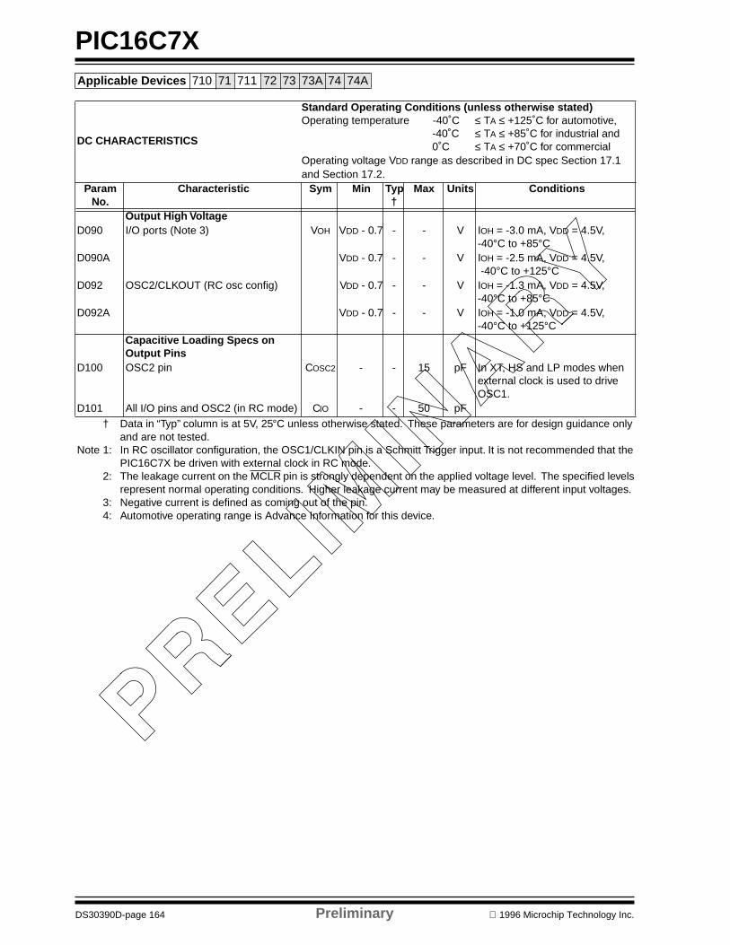
PIC16C7X
DS30390D-page 164 Preliminary 1996 Microchip Technology Inc.
Applicable Devices 710 71 711 72 73 73A 74 74A
Output High VoltageD090 I/O ports (Note 3) VOH VDD - 0.7 - - V IOH = -3.0 mA, VDD = 4.5V,
-40°C to +85°CD090A VDD - 0.7 - - V IOH = -2.5 mA, VDD = 4.5V,
-40°C to +125°CD092 OSC2/CLKOUT (RC osc config) VDD - 0.7 - - V IOH = -1.3 mA, VDD = 4.5V,
-40°C to +85°CD092A VDD - 0.7 - - V IOH = -1.0 mA, VDD = 4.5V,
-40°C to +125°CCapacitive Loading Specs onOutput Pins
D100 OSC2 pin COSC2 - - 15 pF In XT, HS and LP modes when external clock is used to drive OSC1.
D101 All I/O pins and OSC2 (in RC mode) CIO - - 50 pF
DC CHARACTERISTICS
Standard Operating Conditions (unless otherwise stated)Operating temperature -40˚C ≤ TA ≤ +125˚C for automotive,
-40˚C ≤ TA ≤ +85˚C for industrial and 0˚C ≤ TA ≤ +70˚C for commercial
Operating voltage VDD range as described in DC spec Section 17.1 and Section 17.2.
ParamNo.
Characteristic Sym Min Typ†
Max Units Conditions
† Data in “Typ” column is at 5V, 25°C unless otherwise stated. These parameters are for design guidance only and are not tested.
Note 1: In RC oscillator configuration, the OSC1/CLKIN pin is a Schmitt Trigger input. It is not recommended that the PIC16C7X be driven with external clock in RC mode.
2: The leakage current on the MCLR pin is strongly dependent on the applied voltage level. The specified levels represent normal operating conditions. Higher leakage current may be measured at different input voltages.
3: Negative current is defined as coming out of the pin.4: Automotive operating range is Advance Information for this device.

1996 Microchip Technology Inc. Preliminary DS30390D-page 165
PIC16C7XApplicable Devices 710 71 711 72 73 73A 74 74A
17.4 Timing Parameter Symbology
The timing parameter symbols have been created following one of the following formats:
FIGURE 17-1: LOAD CONDITIONS
1. TppS2ppS 3. TCC:ST (I2C specifications only)2. TppS 4. Ts (I2C specifications only)T
F Frequency T TimeLowercase letters (pp) and their meanings:
ppcc CCP1 osc OSC1ck CLKOUT rd RD
cs CS rw RD or WRdi SDI sc SCKdo SDO ss SSdt Data in t0 T0CKIio I/O port t1 T1CKImc MCLR wr WRUppercase letters and their meanings:
SF Fall P PeriodH High R RiseI Invalid (Hi-impedance) V ValidL Low Z Hi-impedance
I2C onlyAA output access High HighBUF Bus free Low Low
TCC:ST (I2C specifications only)CC
HD Hold SU SetupST
DAT DATA input hold STO STOP conditionSTA START condition
VDD/2
CL
RL
Pin Pin
VSS VSS
CL
RL = 464Ω
CL = 50 pF for all pins except OSC2
15 pF for OSC2 output
Load condition 1 Load condition 2
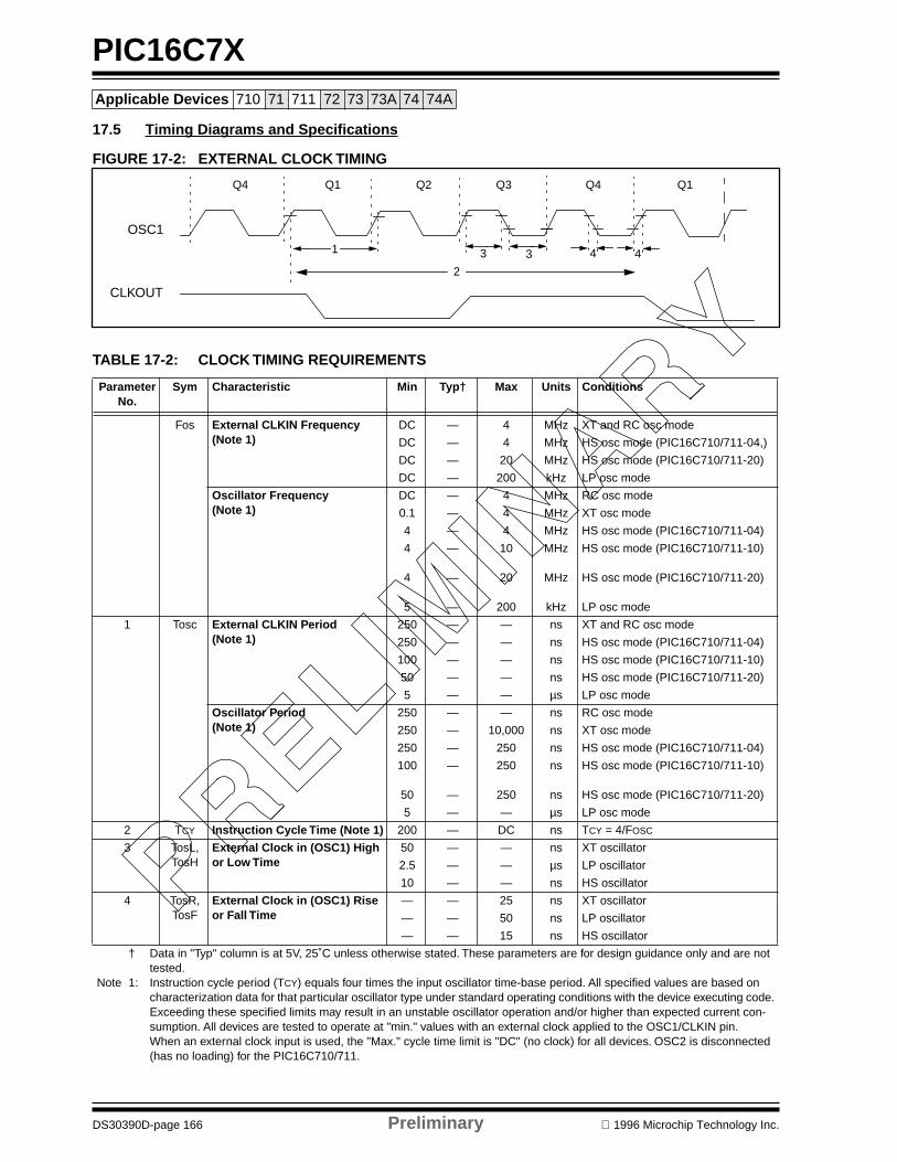
PIC16C7X
DS30390D-page 166 Preliminary 1996 Microchip Technology Inc.
Applicable Devices 710 71 711 72 73 73A 74 74A
17.5 Timing Diagrams and Specifications
FIGURE 17-2: EXTERNAL CLOCK TIMING
TABLE 17-2: CLOCK TIMING REQUIREMENTS
Parameter No.
Sym Characteristic Min Typ† Max Units Conditions
Fos External CLKIN Frequency (Note 1)
DC — 4 MHz XT and RC osc mode
DC — 4 MHz HS osc mode (PIC16C710/711-04,)
DC — 20 MHz HS osc mode (PIC16C710/711-20)
DC — 200 kHz LP osc mode
Oscillator Frequency (Note 1)
DC — 4 MHz RC osc mode
0.1 — 4 MHz XT osc mode
4 — 4 MHz HS osc mode (PIC16C710/711-04)
4
4
5
—
—
—
10
20
200
MHz
MHz
kHz
HS osc mode (PIC16C710/711-10)
HS osc mode (PIC16C710/711-20)
LP osc mode
1 Tosc External CLKIN Period(Note 1)
250 — — ns XT and RC osc mode
250 — — ns HS osc mode (PIC16C710/711-04)
100 — — ns HS osc mode (PIC16C710/711-10)
50 — — ns HS osc mode (PIC16C710/711-20)
5 — — µs LP osc mode
Oscillator Period(Note 1)
250 — — ns RC osc mode
250 — 10,000 ns XT osc mode
250 — 250 ns HS osc mode (PIC16C710/711-04)
100
50
—
—
250
250
ns
ns
HS osc mode (PIC16C710/711-10)
HS osc mode (PIC16C710/711-20)
5 — — µs LP osc mode
2 TCY Instruction Cycle Time (Note 1) 200 — DC ns TCY = 4/FOSC
3 TosL,TosH
External Clock in (OSC1) High or Low Time
50 — — ns XT oscillator
2.5 — — µs LP oscillator
10 — — ns HS oscillator
4 TosR,TosF
External Clock in (OSC1) Rise or Fall Time
— — 25 ns XT oscillator
— — 50 ns LP oscillator
— — 15 ns HS oscillator
† Data in "Typ" column is at 5V, 25˚C unless otherwise stated. These parameters are for design guidance only and are not tested.
Note 1: Instruction cycle period (TCY) equals four times the input oscillator time-base period. All specified values are based on characterization data for that particular oscillator type under standard operating conditions with the device executing code. Exceeding these specified limits may result in an unstable oscillator operation and/or higher than expected current con-sumption. All devices are tested to operate at "min." values with an external clock applied to the OSC1/CLKIN pin.When an external clock input is used, the "Max." cycle time limit is "DC" (no clock) for all devices. OSC2 is disconnected (has no loading) for the PIC16C710/711.
OSC1
CLKOUT
Q4 Q1 Q2 Q3 Q4 Q1
1
2
3 3 4 4

1996 Microchip Technology Inc. Preliminary DS30390D-page 167
PIC16C7XApplicable Devices 710 71 711 72 73 73A 74 74A
FIGURE 17-3: CLKOUT AND I/O TIMING
TABLE 17-3: CLKOUT AND I/O TIMING REQUIREMENTS
ParameterNo.
Sym Characteristic Min Typ† Max Units Conditions
10* TosH2ckL OSC1↑ to CLKOUT↓ — 15 30 ns Note 1
11* TosH2ckH OSC1↑ to CLKOUT↑ — 15 30 ns Note 1
12* TckR CLKOUT rise time — 5 15 ns Note 1
13* TckF CLKOUT fall time — 5 15 ns Note 1
14* TckL2ioV CLKOUT ↓ to Port out valid — — 0.5TCY + 20 ns Note 1
15* TioV2ckH Port in valid before CLKOUT ↑ 0.25TCY + 25 — — ns Note 1
16* TckH2ioI Port in hold after CLKOUT ↑ 0 — — ns Note 1
17* TosH2ioV OSC1↑ (Q1 cycle) to Port out valid
— — 80 - 100 ns
18* TosH2ioI OSC1↑ (Q2 cycle) to Port input invalid (I/O in hold time)
TBD — — ns
19* TioV2osH Port input valid to OSC1↑ (I/O in setup time) TBD — — ns
20* TioR Port output rise time PIC16C710/711 — 10 25 ns
PIC16LC710/711 — — 60 ns
21* TioF Port output fall time PIC16C710/711 — 10 25 ns
PIC16LC710/711 — — 60 ns
22††* Tinp INT pin high or low time 20 — — ns
23††* Trbp RB7:RB4 change INT high or low time 20 — — ns
* These parameters are characterized but not tested.† Data in "Typ" column is at 5V, 25˚C unless otherwise stated. These parameters are for design guidance only and are not
tested.†† These parameters are asynchronous events not related to any internal clock edges.
Note 1: Measurements are taken in RC Mode where CLKOUT output is 4 x TOSC.
Note: Refer to Figure 17-1 for load conditions.
OSC1
CLKOUT
I/O Pin(input)
I/O Pin(output)
Q4 Q1 Q2 Q3
10
1314
17
20, 21
19 18
15
11
1216
old value new value
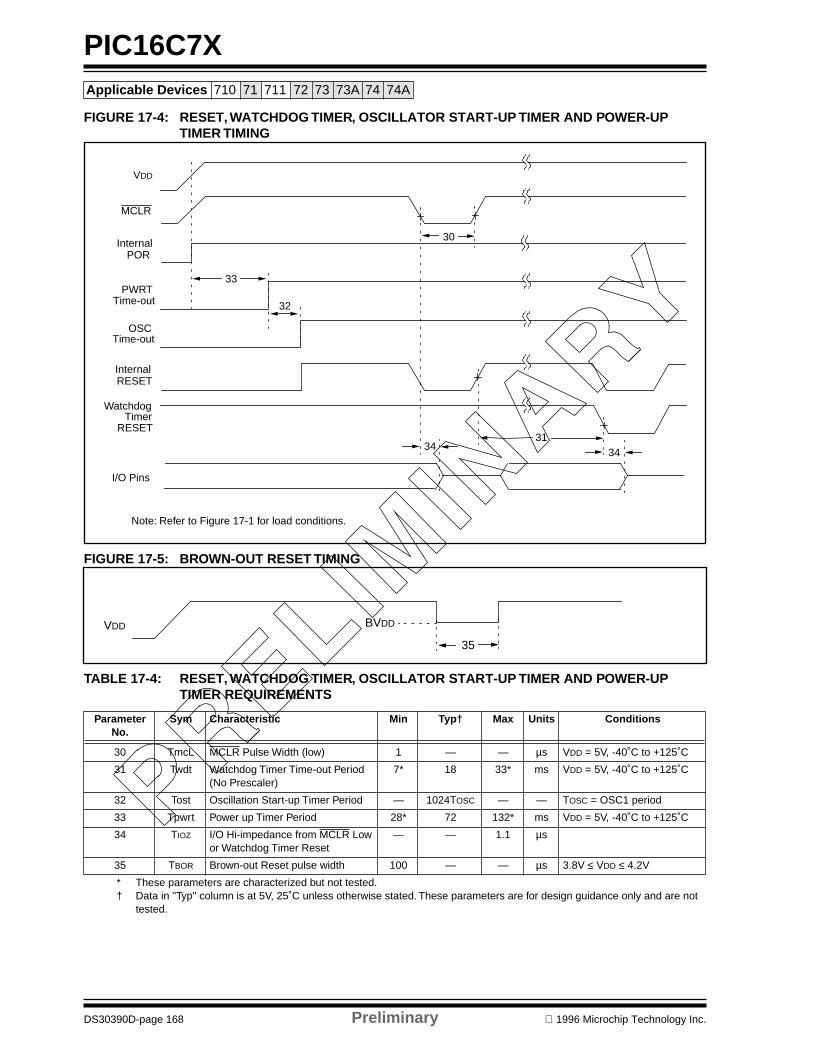
PIC16C7X
DS30390D-page 168 Preliminary 1996 Microchip Technology Inc.
Applicable Devices 710 71 711 72 73 73A 74 74A
FIGURE 17-4: RESET, WATCHDOG TIMER, OSCILLATOR START-UP TIMER AND POWER-UP TIMER TIMING
FIGURE 17-5: BROWN-OUT RESET TIMING
TABLE 17-4: RESET, WATCHDOG TIMER, OSCILLATOR START-UP TIMER AND POWER-UP TIMER REQUIREMENTS
Parameter No.
Sym Characteristic Min Typ† Max Units Conditions
30 TmcL MCLR Pulse Width (low) 1 — — µs VDD = 5V, -40˚C to +125˚C
31 Twdt Watchdog Timer Time-out Period (No Prescaler)
7* 18 33* ms VDD = 5V, -40˚C to +125˚C
32 Tost Oscillation Start-up Timer Period — 1024TOSC — — TOSC = OSC1 period
33 Tpwrt Power up Timer Period 28* 72 132* ms VDD = 5V, -40˚C to +125˚C
34 TIOZ I/O Hi-impedance from MCLR Low or Watchdog Timer Reset
— — 1.1 µs
35 TBOR Brown-out Reset pulse width 100 — — µs 3.8V ≤ VDD ≤ 4.2V
* These parameters are characterized but not tested.† Data in "Typ" column is at 5V, 25˚C unless otherwise stated. These parameters are for design guidance only and are not
tested.
VDD
MCLR
InternalPOR
PWRTTime-out
OSCTime-out
InternalRESET
WatchdogTimer
RESET
33
32
30
3134
I/O Pins
34
Note: Refer to Figure 17-1 for load conditions.
VDD BVDD
35
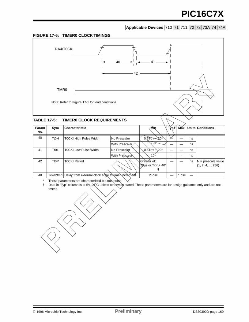
1996 Microchip Technology Inc. Preliminary DS30390D-page 169
PIC16C7XApplicable Devices 710 71 711 72 73 73A 74 74A
FIGURE 17-6: TIMER0 CLOCK TIMINGS
TABLE 17-5: TIMER0 CLOCK REQUIREMENTS
Param No.
Sym Characteristic Min Typ† Max Units Conditions
40 Tt0H T0CKI High Pulse Width No Prescaler 0.5TCY + 20* — — ns
With Prescaler 10* — — ns
41 Tt0L T0CKI Low Pulse Width No Prescaler 0.5TCY + 20* — — ns
With Prescaler 10* — — ns
42 Tt0P T0CKI Period Greater of:20µs or TCY + 40* N
— — ns N = prescale value (1, 2, 4,..., 256)
48 Tcke2tmrI Delay from external clock edge to timer increment 2Tosc — 7Tosc —
* These parameters are characterized but not tested.† Data in "Typ" column is at 5V, 25˚C unless otherwise stated. These parameters are for design guidance only and are not
tested.
Note: Refer to Figure 17-1 for load conditions.
41
42
40
RA4/T0CKI
TMR0
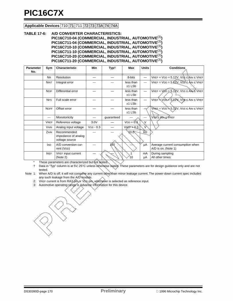
PIC16C7X
DS30390D-page 170 Preliminary 1996 Microchip Technology Inc.
Applicable Devices 710 71 711 72 73 73A 74 74A
TABLE 17-6: A/D CONVERTER CHARACTERISTICS:PIC16C710-04 (COMMERCIAL, INDUSTRIAL, AUTOMOTIVE(3))PIC16C711-04 (COMMERCIAL, INDUSTRIAL, AUTOMOTIVE(3))PIC16C710-10 (COMMERCIAL, INDUSTRIAL, AUTOMOTIVE(3))PIC16C711-10 (COMMERCIAL, INDUSTRIAL, AUTOMOTIVE(3))PIC16C710-20 (COMMERCIAL, INDUSTRIAL, AUTOMOTIVE(3))PIC16C711-20 (COMMERCIAL, INDUSTRIAL, AUTOMOTIVE(3))
Parameter No.
Sym Characteristic Min Typ† Max Units Conditions
NR Resolution — — 8-bits — VREF = VDD = 5.12V, VSS ≤ AIN ≤ VREF
NINT Integral error — — less than ±1 LSb
— VREF = VDD = 5.12V, VSS ≤ AIN ≤ VREF
NDIF Differential error — — less than ±1 LSb
— VREF = VDD = 5.12V, VSS ≤ AIN ≤ VREF
NFS Full scale error — — less than ±1 LSb
— VREF = VDD = 5.12V, VSS ≤ AIN ≤ VREF
NOFF Offset error — — less than ±1 LSb
— VREF = VDD = 5.12V, VSS ≤ AIN ≤ VREF
— Monotonicity — guaranteed — — VSS ≤ AIN ≤ VREF
VREF Reference voltage 3.0V — VDD + 0.3 V
VAIN Analog input voltage VSS - 0.3 — VREF + 0.3 V
ZAIN Recommended impedance of analog voltage source
— — 10.0 kΩ
IAD A/D conversion cur-rent (VDD)
— 180 — µA Average current consumption when A/D is on. (Note 1)
IREF VREF input current (Note 2)
— — 110
mAµA
During samplingAll other times
* These parameters are characterized but not tested.† Data in “Typ” column is at 5V, 25°C unless otherwise stated. These parameters are for design guidance only and are not
tested.Note 1: When A/D is off, it will not consume any current other than minor leakage current. The power-down current spec includes
any such leakage from the A/D module.2: VREF current is from RA3 pin or VDD pin, whichever is selected as reference input.3: Automotive operating range is Advance Information for this device.

1996 Microchip Technology Inc. Preliminary DS30390D-page 171
PIC16C7XApplicable Devices 710 71 711 72 73 73A 74 74A
TABLE 17-7: A/D CONVERTER CHARACTERISTICS:PIC16LC710-04 (COMMERCIAL, INDUSTRIAL, AUTOMOTIVE(4))PIC16LC711-04 (COMMERCIAL, INDUSTRIAL, AUTOMOTIVE(4))
Parameter No.
Sym Characteristic Min Typ† Max Units Conditions
NR Resolution — — 8-bits — VREF = VDD = 3.0V (Note 1)
NINT Integral error — — less than ±1 LSb
— VREF = VDD = 3.0V (Note 1)
NDIF Differential error — — less than ±1 LSb
— VREF = VDD = 3.0V (Note 1)
NFS Full scale error — — less than ±1 LSb
— VREF = VDD = 3.0V (Note 1)
NOFF Offset error — — less than ±1 LSb
— VREF = VDD = 3.0V (Note 1)
— Monotonicity — guaranteed — — VSS ≤ AIN ≤ VREF
VREF Reference voltage 3.0V — VDD + 0.3 V
VAIN Analog input voltage VSS - 0.3 — VREF + 0.3 V
ZAIN Recommended impedance of ana-log voltage source
— — 10.0 kΩ
IAD A/D conversion cur-rent (VDD)
— 180 — µA Average current consumption when A/D is on. (Note 2)
IREF VREF input current (Note 3)
— — 110
mAµA
During samplingAll other times
* These parameters are characterized but not tested.† Data in “Typ” column is at 5V, 25°C unless otherwise stated. These parameters are for design guidance only and are not
tested.Note 1: These specifications apply if VREF = 3.0V and if VDD ≥ 3.0V. VIN must be between VSS and VREF
2: When A/D is off, it will not consume any current other than minor leakage current. The power-down current spec includes any such leakage from the A/D module.
3: VREF current is from RA3 pin or VDD pin, whichever is selected as reference input.4: Automotive operating range is Advance Information for this device.

PIC16C7X
DS30390D-page 172 Preliminary 1996 Microchip Technology Inc.
Applicable Devices 710 71 711 72 73 73A 74 74A
FIGURE 17-7: A/D CONVERSION TIMING
TABLE 17-8: A/D CONVERSION REQUIREMENTS
Parameter No.
Sym Characteristic Min Typ† Max Units Conditions
130 TAD A/D clock period 1.62.0
——
µsµs
VREF ≥ 3.0VVREF full range
130 TAD A/D Internal RC Oscillator source
ADCS1:ADCS0 = 11 (RC oscillator source)
3.0 6.0 9.0 µs PIC16LC710, VDD = 3.0V
2.0 4.0 6.0 µs PIC16C710
131 TCNV Conversion time (not including S/H time). Note 1
— 9.5TAD — —
132 TACQ Acquisition time Note 2 20 — µs
* These parameters are characterized but not tested.† Data in “Typ” column is at 5V, 25°C unless otherwise stated. These parameters are for design guidance only and are not
tested.Note 1: ADRES register may be read on the following TCY cycle.
2: See Section 13.1 for min conditions.
131
130
132
BSF ADCON0, GO
Q4
A/D CLK
A/D DATA
ADRES
ADIF
GO
SAMPLE
OLD_DATA
SAMPLING STOPPED
DONE
NEW_DATA
(TOSC/2) (1)
7 6 5 4 3 2 1 0
Note 1: If the A/D clock source is selected as RC, a time of TCY is added before the A/D clock starts. This allows the SLEEP instruction to be executed.
1 Tcy

1996 Microchip Technology Inc.
Preliminary
DS30390D-page 173
PIC16C7X
Applicable Devices
710 71 711 72 73 73A 74 74A
18.0 DC AND AC CHARACTERISTICS GRAPHS AND TABLES FOR PIC16C710 AND PIC16C711
NOT AVAILABLE AT THIS TIME
This document was created with FrameMaker 4 0 4

PIC16C7X
DS30390D-page 174
Preliminary
1996 Microchip Technology Inc.
Applicable Devices
710 71 711 72 73 73A 74 74A
NOTES:

1996 Microchip Technology Inc. DS30390D-page 175
PIC16C7X
Applicable Devices
710 71 711 72 73 73A 74 74A
19.0 ELECTRICAL CHARACTERISTICS FOR PIC16C71
Absolute Maximum Ratings †
Ambient temperature under bias................................................................................................................. .-55 to +125˚C
Storage temperature ............................................................................................................................... -65˚C to +150˚C
Voltage on any pin with respect to V
SS
(except V
DD
and MCLR) .................................................... -0.3V to (V
DD
+ 0.3V)
Voltage on V
DD
with respect to V
SS
................................................................................................................ 0 to +7.5V
Voltage on MCLR with respect to V
SS
(Note 2) ................................................................................................. 0 to +14V
Total power dissipation (Note 1)............................................................................................................................800 mW
Maximum current out of V
SS
pin ............................................................................................................................150 mA
Maximum current into V
DD
pin ...............................................................................................................................100 mA
Input clamp current, I
IK
(V
I
< 0 or V
I
> V
DD
)
.....................................................................................................................±
20 mA
Output clamp current, I
OK
(V
O
< 0 or V
O
> V
DD
)
..............................................................................................................±
20 mA
Maximum output current sunk by any I/O pin...........................................................................................................25 mA
Maximum output current sourced by any I/O pin .....................................................................................................20 mA
Maximum current sunk by
PORTA ...........................................................................................................................80 mA
Maximum current sourced by PORTA......................................................................................................................50 mA
Maximum current sunk by PORTB.........................................................................................................................150 mA
Maximum current sourced by PORTB ...................................................................................................................100 mA
Note 1:
Power dissipation is calculated as follows: Pdis = V
DD
x I
DD
-
∑
I
OH
+
∑
(V
DD
-V
OH
) x I
OH
+
∑
(V
O
l x I
OL
)
Note 2:
Voltage spikes below V
SS
at the MCLR pin, inducing currents greater than 80 mA, may cause latch-up. Thus,a series resistor of 50-100
Ω
should be used when applying a “low” level to the MCLR pin rather than pullingthis pin directly to V
SS
.
TABLE 19-1: CROSS REFERENCE OF DEVICE SPECS FOR OSCILLATOR CONFIGURATIONS AND FREQUENCIES OF OPERATION (COMMERCIAL DEVICES)
† NOTICE: Stresses above those listed under “Absolute Maximum Ratings” may cause permanent damage to the device. This is a stress rating only and functional operation of the device at those or any other conditions above those indicated in the operation listings of this specification is not implied. Exposure to maximum rating conditions for extended periods may affect device reliability.
OSC PIC16C71-04 PIC16C71-20 PIC16LC71-04 JW Devices
RC
V
DD
: 4.0V to 6.0VI
DD
: 3.3 mA max. at 5.5VI
PD
: 14
µ
A max. at 4VFreq: 4 MHz max.
V
DD
: 4.5V to 5.5VI
DD
: 1.8 mA typ. at 5.5VI
PD
: 1.0
µ
A typ. at 4VFreq: 4 MHz max.
V
DD
: 3.0V to 6.0VI
DD
: 1.4 mA typ. at 3.0VI
PD
: 0.6
µ
A typ. at 3VFreq: 4 MHz max.
V
DD
: 4.0V to 6.0VI
DD
: 3.3 mA max. at 5.5VI
PD
: 14
µ
A max. at 4VFreq: 4 MHz max.
XT
V
DD
: 4.0V to 6.0VI
DD
: 3.3 mA max. at 5.5VI
PD
: 14
µ
A max. at 4VFreq: 4 MHz max.
V
DD
: 4.5V to 5.5VI
DD
: 1.8 mA typ. at 5.5VI
PD
: 1.0
µ
A typ. at 4VFreq: 4 MHz max.
V
DD
: 3.0V to 6.0VI
DD
: 1.4 mA typ. at 3.0VI
PD
: 0.6
µ
A typ. at 3VFreq: 4 MHz max.
V
DD
: 4.0V to 6.0VI
DD
: 3.3 mA max. at 5.5VI
PD
: 14
µ
A max. at 4VFreq: 4 MHz max.
HS
V
DD
: 4.5V to 5.5V V
DD
: 4.5V to 5.5V
Do not use in HS mode
V
DD
: 4.5V to 5.5V
I
DD
: 13.5 mA typ. at 5.5V I
DD
: 30 mA max. at 5.5V I
DD
: 30 mA max. at 5.5V
I
PD
: 1.0
µ
A typ. at 4.5V I
PD
: 1.0
µ
A typ. at 4.5V I
PD
: 1.0
µ
A typ. at 4.5V
Freq: 4 MHz max. Freq: 20 MHz max. Freq: 20 MHz max.
LP
V
DD
: 4.0V to 6.0VI
DD
: 15
µ
A typ. at 32 kHz, 4.0V
I
PD
: 0.6
µ
A typ. at 4.0VFreq: 200 kHz max.
Do not use in LP mode
V
DD
: 3.0V to 6.0VI
DD
: 32
µ
A max. at 32 kHz, 3.0V
I
PD
: 9
µ
A max. at 3.0VFreq: 200 kHz max.
V
DD
: 3.0V to 6.0VI
DD
: 32
µ
A max. at 32 kHz, 3.0V
I
PD
: 9
µ
A max. at 3.0VFreq: 200 kHz max.
The shaded sections indicate oscillator selections which are tested for functionality, but not for MIN/MAX specifications. It is recom-mended that the user select the device type that ensures the specifications required.
This document was created with FrameMaker 4 0 4
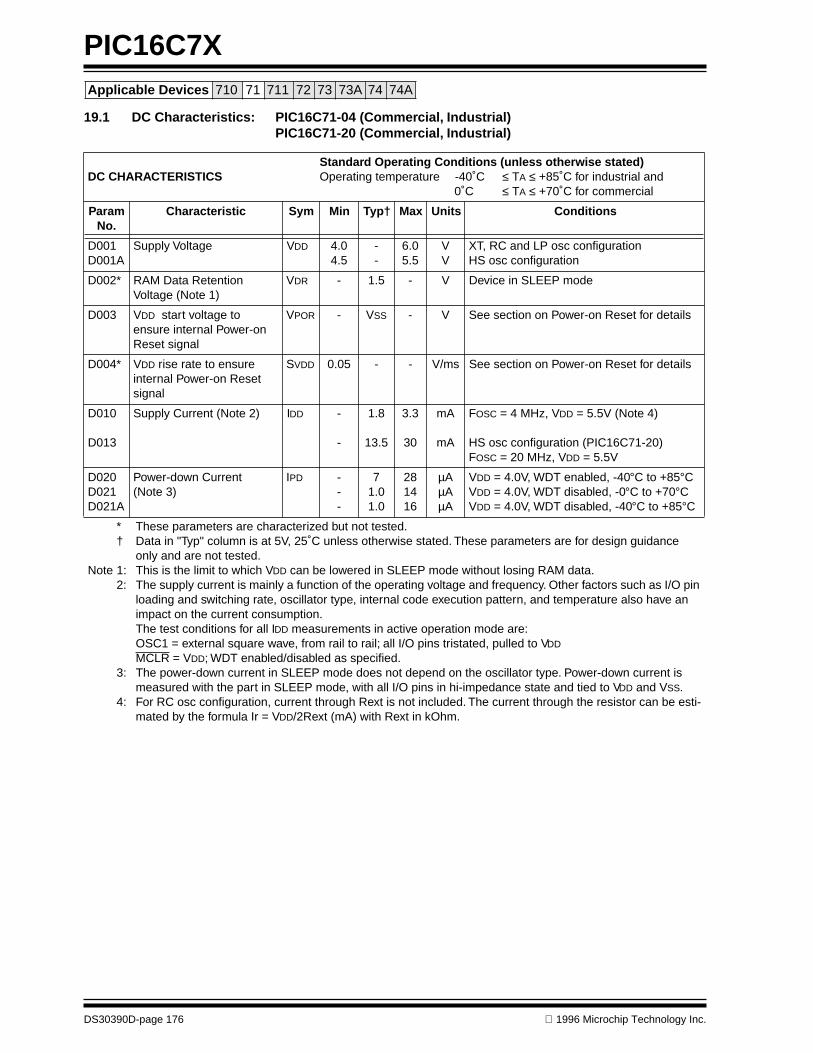
PIC16C7X
DS30390D-page 176
1996 Microchip Technology Inc.
Applicable Devices
710 71 711 72 73 73A 74 74A
19.1 DC Characteristics: PIC16C71-04 (Commercial, Industrial)PIC16C71-20 (Commercial, Industrial)
DC CHARACTERISTICSStandard Operating Conditions (unless otherwise stated)
Operating temperature -40˚C
≤
T
A
≤
+85˚C for industrial and 0˚C
≤
T
A
≤
+70˚C for commercial
ParamNo.
Characteristic Sym Min Typ† Max Units Conditions
D001D001A
Supply Voltage V
DD
4.04.5
--
6.05.5
VV
XT, RC and LP osc configurationHS osc configuration
D002* RAM Data RetentionVoltage (Note 1)
V
DR
- 1.5 - V Device in SLEEP mode
D003 V
DD
start voltage toensure internal Power-on Reset signal
V
POR
- V
SS
- V See section on Power-on Reset for details
D004* V
DD
rise rate to ensure internal Power-on Reset signal
S
VDD
0.05 - - V/ms See section on Power-on Reset for details
D010
D013
Supply Current (Note 2) I
DD
-
-
1.8
13.5
3.3
30
mA
mA
F
OSC
= 4 MHz, V
DD
= 5.5V (Note 4)
HS osc configuration (PIC16C71-20)F
OSC
= 20 MHz, V
DD
= 5.5V
D020D021D021A
Power-down Current (Note 3)
I
PD
---
71.01.0
281416
µ
A
µ
A
µ
A
V
DD
= 4.0V, WDT enabled, -40
°
C to +85
°
CV
DD
= 4.0V, WDT disabled, -0
°
C to +70
°
CV
DD
= 4.0V, WDT disabled, -40
°
C to +85
°C
* These parameters are characterized but not tested.† Data in "Typ" column is at 5V, 25˚C unless otherwise stated. These parameters are for design guidance
only and are not tested.Note 1: This is the limit to which VDD can be lowered in SLEEP mode without losing RAM data.
2: The supply current is mainly a function of the operating voltage and frequency. Other factors such as I/O pin loading and switching rate, oscillator type, internal code execution pattern, and temperature also have an impact on the current consumption.The test conditions for all IDD measurements in active operation mode are: OSC1 = external square wave, from rail to rail; all I/O pins tristated, pulled to VDD MCLR = VDD; WDT enabled/disabled as specified.
3: The power-down current in SLEEP mode does not depend on the oscillator type. Power-down current is measured with the part in SLEEP mode, with all I/O pins in hi-impedance state and tied to VDD and VSS.
4: For RC osc configuration, current through Rext is not included. The current through the resistor can be esti-mated by the formula Ir = VDD/2Rext (mA) with Rext in kOhm.
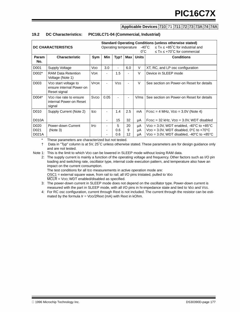
1996 Microchip Technology Inc. DS30390D-page 177
PIC16C7XApplicable Devices 710 71 711 72 73 73A 74 74A
19.2 DC Characteristics: PIC16LC71-04 (Commercial, Industrial)
DC CHARACTERISTICSStandard Operating Conditions (unless otherwise stated)Operating temperature -40˚C ≤ TA ≤ +85˚C for industrial and
0˚C ≤ TA ≤ +70˚C for commercial
ParamNo.
Characteristic Sym Min Typ† Max Units Conditions
D001 Supply Voltage VDD 3.0 - 6.0 V XT, RC, and LP osc configuration
D002* RAM Data Retention Voltage (Note 1)
VDR - 1.5 - V Device in SLEEP mode
D003 VDD start voltage to ensure internal Power-on Reset signal
VPOR - VSS - V See section on Power-on Reset for details
D004* VDD rise rate to ensure internal Power-on Reset signal
SVDD 0.05 - - V/ms See section on Power-on Reset for details
D010
D010A
Supply Current (Note 2) IDD -
-
1.4
15
2.5
32
mA
µA
FOSC = 4 MHz, VDD = 3.0V (Note 4)
FOSC = 32 kHz, VDD = 3.0V, WDT disabled
D020D021D021A
Power-down Current (Note 3)
IPD ---
50.60.6
20912
µAµAµA
VDD = 3.0V, WDT enabled, -40°C to +85°CVDD = 3.0V, WDT disabled, 0°C to +70°CVDD = 3.0V, WDT disabled, -40°C to +85°C
* These parameters are characterized but not tested.† Data in "Typ" column is at 5V, 25˚C unless otherwise stated. These parameters are for design guidance only
and are not tested.Note 1: This is the limit to which VDD can be lowered in SLEEP mode without losing RAM data.
2: The supply current is mainly a function of the operating voltage and frequency. Other factors such as I/O pin loading and switching rate, oscillator type, internal code execution pattern, and temperature also have an impact on the current consumption.The test conditions for all IDD measurements in active operation mode are: OSC1 = external square wave, from rail to rail; all I/O pins tristated, pulled to VDD MCLR = VDD; WDT enabled/disabled as specified.
3: The power-down current in SLEEP mode does not depend on the oscillator type. Power-down current is measured with the part in SLEEP mode, with all I/O pins in hi-impedance state and tied to VDD and VSS.
4: For RC osc configuration, current through Rext is not included. The current through the resistor can be esti-mated by the formula Ir = VDD/2Rext (mA) with Rext in kOhm.

PIC16C7X
DS30390D-page 178 1996 Microchip Technology Inc.
Applicable Devices 710 71 711 72 73 73A 74 74A
19.3 DC Characteristics: PIC16C71-04 (Commercial, Industrial)PIC16C71-20 (Commercial, Industrial)PIC16LC71-04 (Commercial, Industrial)
DC CHARACTERISTICS
Standard Operating Conditions (unless otherwise stated)Operating temperature -40˚C ≤ TA ≤ +85˚C for industrial and
0˚C ≤ TA ≤ +70˚C for commercialOperating voltage VDD range as described in DC spec Section 19.1 and Section 19.2.
ParamNo.
Characteristic Sym Min Typ†
Max Units Conditions
Input Low VoltageI/O ports VIL
D030 with TTL buffer VSS - 0.5V VD031 with Schmitt Trigger buffer VSS - 0.2VDD VD032 MCLR, RA4/T0CKI,OSC1
(in RC mode)VSS - 0.2VDD V
D033 OSC1 (in XT, HS and LP) VSS - 0.3VDD V Note1Input High VoltageI/O ports (Note 4) VIH -
D040 with TTL buffer 0.36VDD - VDD V 4.5 ≤ VDD ≤ 5.5VD040A 0.45VDD - VDD For VDD > 5.5V or VDD < 4.5VD041 with Schmitt Trigger buffer 0.85VDD - VDD For entire VDD rangeD042 MCLR RA4/T0CKI 0.85VDD - VDD VD042A OSC1 (XT, HS and LP) 0.7VDD - VDD V Note1D043 OSC1 (in RC mode) 0.9VDD - VDD VD070 PORTB weak pull-up current IPURB 50 250 †400 µA VDD = 5V, VPIN = VSS
Input Leakage Current (Notes 2, 3)D060 I/O ports IIL - - ±1 µA Vss ≤ VPIN ≤ VDD, Pin at hi-
impedanceD061 MCLR, RA4/T0CKI - - ±5 µA Vss ≤ VPIN ≤ VDD
D063 OSC1 - - ±5 µA Vss ≤ VPIN ≤ VDD, XT, HS and LP osc configuration
Output Low VoltageD080 I/O ports VOL - - 0.6 V IOL = 8.5mA, VDD = 4.5V,
-40°C to +85°CD083 OSC2/CLKOUT (RC osc config) - - 0.6 V IOL = 1.6mA, VDD = 4.5V,
-40°C to +85°COutput High Voltage
D090 I/O ports (Note 3) VOH VDD - 0.7 - - V IOH = -3.0mA, VDD = 4.5V, -40°C to +85°C
D092 OSC2/CLKOUT (RC osc config) VDD - 0.7 - - V IOH = -1.3mA, VDD = 4.5V, -40°C to +85°C
Capacitive Loading Specs onOutput Pins
D100 OSC2 pin COSC2 15 pF In XT, HS and LP modes when external clock is used to drive OSC1.
D101 All I/O pins and OSC2 (in RC mode) CIO 50 pF† Data in “Typ” column is at 5V, 25°C unless otherwise stated. These parameters are for design guidance only
and are not tested.Note 1: In RC oscillator configuration, the OSC1 pin is a Schmitt trigger input. It is not recommended that the
PIC16C71 be driven with external clock in RC mode.2: The leakage current on the MCLR pin is strongly dependent on the applied voltage level. The specified levels
represent normal operating conditions. Higher leakage current may be measured at different input voltages.3: Negative current is defined as coming out of the pin.4: PIC16C71 Rev. "Ax" INT pin has a TTL input buffer. PIC16C71 Rev. "Bx" INT pin has a Schmitt Trigger input
buffer.

1996 Microchip Technology Inc. DS30390D-page 179
PIC16C7XApplicable Devices 710 71 711 72 73 73A 74 74A
19.4 Timing Parameter Symbology
The timing parameter symbols have been created following one of the following formats:
FIGURE 19-1: LOAD CONDITIONS
1. TppS2ppS 3. TCC:ST (I2C specifications only)2. TppS 4. Ts (I2C specifications only)T
F Frequency T TimeLowercase letters (pp) and their meanings:
ppcc CCP1 osc OSC1ck CLKOUT rd RD
cs CS rw RD or WRdi SDI sc SCKdo SDO ss SSdt Data in t0 T0CKIio I/O port t1 T1CKImc MCLR wr WRUppercase letters and their meanings:
SF Fall P PeriodH High R RiseI Invalid (Hi-impedance) V ValidL Low Z Hi-impedance
I2C onlyAA output access High HighBUF Bus free Low Low
TCC:ST (I2C specifications only)CC
HD Hold SU SetupST
DAT DATA input hold STO STOP conditionSTA START condition
VDD/2
CL
RL
Pin Pin
VSS VSS
CL
RL = 464Ω
CL = 50 pF for all pins except OSC2/CLKOUT15 pF for OSC2 output
Load condition 1 Load condition 2
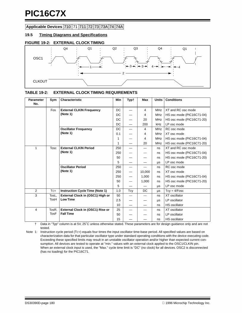
PIC16C7X
DS30390D-page 180 1996 Microchip Technology Inc.
Applicable Devices 710 71 711 72 73 73A 74 74A
19.5 Timing Diagrams and Specifications
FIGURE 19-2: EXTERNAL CLOCK TIMING
TABLE 19-2: EXTERNAL CLOCK TIMING REQUIREMENTS
Parameter No.
Sym Characteristic Min Typ† Max Units Conditions
Fos External CLKIN Frequency (Note 1)
DC — 4 MHz XT and RC osc mode
DC — 4 MHz HS osc mode (PIC16C71-04)
DC — 20 MHz HS osc mode (PIC16C71-20)
DC — 200 kHz LP osc mode
Oscillator Frequency (Note 1)
DC — 4 MHz RC osc mode
0.1 — 4 MHz XT osc mode
1 — 4 MHz HS osc mode (PIC16C71-04)
1 — 20 MHz HS osc mode (PIC16C71-20)
1 Tosc External CLKIN Period(Note 1)
250 — — ns XT and RC osc mode
250 — — ns HS osc mode (PIC16C71-04)
50 — — ns HS osc mode (PIC16C71-20)
5 — — µs LP osc mode
Oscillator Period(Note 1)
250 — — ns RC osc mode
250 — 10,000 ns XT osc mode
250 — 1,000 ns HS osc mode (PIC16C71-04)
50 — 1,000 ns HS osc mode (PIC16C71-20)
5 — — µs LP osc mode
2 TCY Instruction Cycle Time (Note 1) 1.0 Tcy DC µs Tcy = 4/Fosc
3 TosL,TosH
External Clock in (OSC1) High or Low Time
50 — — ns XT oscillator
2.5 — — µs LP oscillator
10 — — ns HS oscillator
4 TosR,TosF
External Clock in (OSC1) Rise or Fall Time
25 — — ns XT oscillator
50 — — ns LP oscillator
15 — — ns HS oscillator
† Data in "Typ" column is at 5V, 25˚C unless otherwise stated. These parameters are for design guidance only and are not tested.
Note 1: Instruction cycle period (TCY) equals four times the input oscillator time-base period. All specified values are based on characterization data for that particular oscillator type under standard operating conditions with the device executing code. Exceeding these specified limits may result in an unstable oscillator operation and/or higher than expected current con-sumption. All devices are tested to operate at "min." values with an external clock applied to the OSC1/CLKIN pin.When an external clock input is used, the "Max." cycle time limit is "DC" (no clock) for all devices. OSC2 is disconnected (has no loading) for the PIC16C71.
33 4 41
2
Q4 Q1 Q2 Q3 Q4 Q1
OSC1
CLKOUT
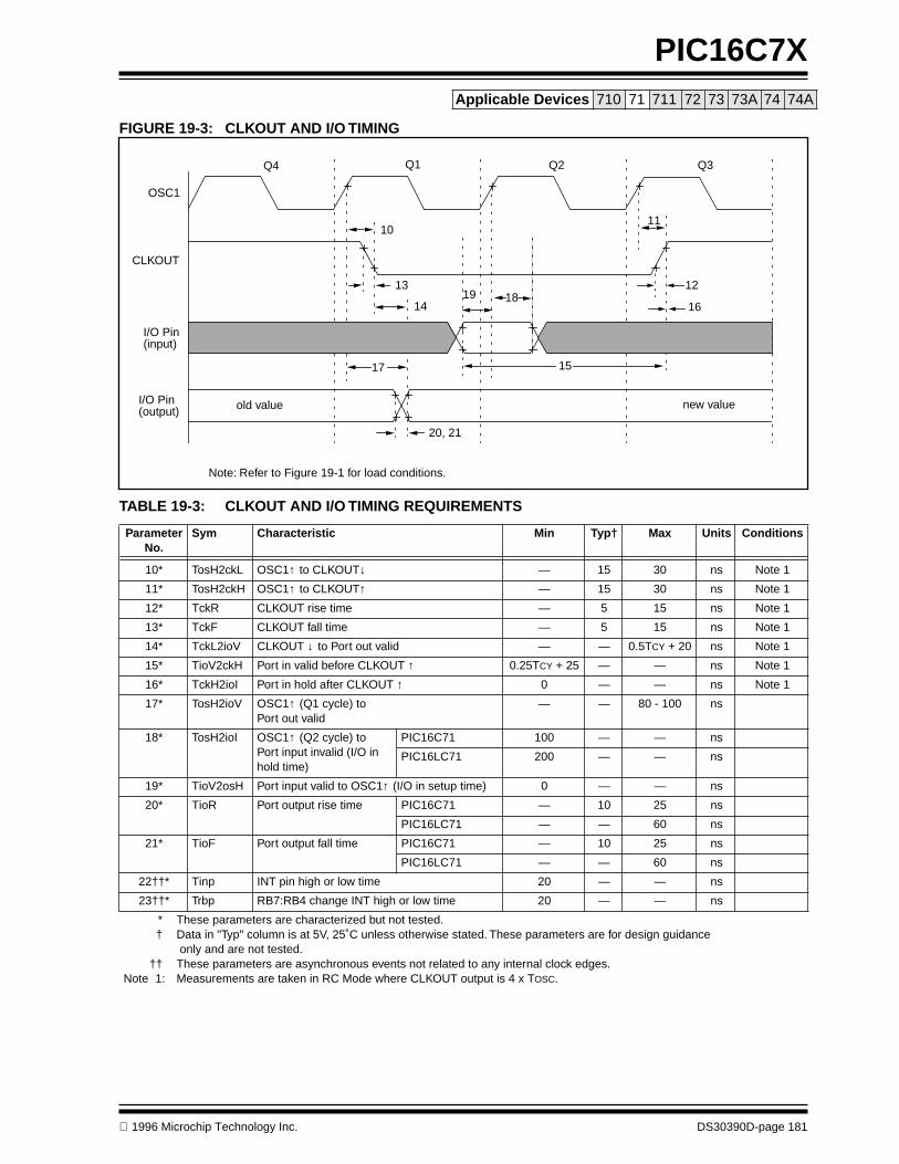
1996 Microchip Technology Inc. DS30390D-page 181
PIC16C7XApplicable Devices 710 71 711 72 73 73A 74 74A
FIGURE 19-3: CLKOUT AND I/O TIMING
TABLE 19-3: CLKOUT AND I/O TIMING REQUIREMENTS
ParameterNo.
Sym Characteristic Min Typ† Max Units Conditions
10* TosH2ckL OSC1↑ to CLKOUT↓ — 15 30 ns Note 1
11* TosH2ckH OSC1↑ to CLKOUT↑ — 15 30 ns Note 1
12* TckR CLKOUT rise time — 5 15 ns Note 1
13* TckF CLKOUT fall time — 5 15 ns Note 1
14* TckL2ioV CLKOUT ↓ to Port out valid — — 0.5TCY + 20 ns Note 1
15* TioV2ckH Port in valid before CLKOUT ↑ 0.25TCY + 25 — — ns Note 1
16* TckH2ioI Port in hold after CLKOUT ↑ 0 — — ns Note 1
17* TosH2ioV OSC1↑ (Q1 cycle) to Port out valid
— — 80 - 100 ns
18* TosH2ioI OSC1↑ (Q2 cycle) to Port input invalid (I/O in hold time)
PIC16C71 100 — — ns
PIC16LC71 200 — — ns
19* TioV2osH Port input valid to OSC1↑ (I/O in setup time) 0 — — ns
20* TioR Port output rise time PIC16C71 — 10 25 ns
PIC16LC71 — — 60 ns
21* TioF Port output fall time PIC16C71 — 10 25 ns
PIC16LC71 — — 60 ns
22††* Tinp INT pin high or low time 20 — — ns
23††* Trbp RB7:RB4 change INT high or low time 20 — — ns
* These parameters are characterized but not tested.† Data in "Typ" column is at 5V, 25˚C unless otherwise stated. These parameters are for design guidance
only and are not tested.†† These parameters are asynchronous events not related to any internal clock edges.
Note 1: Measurements are taken in RC Mode where CLKOUT output is 4 x TOSC.
Note: Refer to Figure 19-1 for load conditions.
OSC1
CLKOUT
I/O Pin(input)
I/O Pin(output)
Q4 Q1 Q2 Q3
10
13
14
17
20, 21
19 18
15
11
12
16
old value new value

PIC16C7X
DS30390D-page 182 1996 Microchip Technology Inc.
Applicable Devices 710 71 711 72 73 73A 74 74A
FIGURE 19-4: RESET, WATCHDOG TIMER, OSCILLATOR START-UP TIMER AND POWER-UP TIMER TIMING
TABLE 19-4: RESET, WATCHDOG TIMER, OSCILLATOR START-UP TIMER AND POWER-UP TIMER REQUIREMENTS
Parameter No.
Sym Characteristic Min Typ† Max Units Conditions
30 TmcL MCLR Pulse Width (low) 200 — — ns VDD = 5V, -40˚C to +85˚C
31 Twdt Watchdog Timer Time-out Period 7* 18 33* ms VDD = 5V, -40˚C to +85˚C
(No Prescaler)
32 Tost Oscillation Start-up Timer Period — 1024 TOSC — — TOSC = OSC1 period
33 Tpwrt Power-up Timer Period 28* 72 132* ms VDD = 5V, -40˚C to +85˚C
34 TIOZ I/O High Impedance from MCLR Low
— — 100 ns
* These parameters are characterized but not tested.† Data in "Typ" column is at 5V, 25˚C unless otherwise stated. These parameters are for design guidance only
and are not tested.
VDD
MCLR
InternalPOR
PWRTTime-out
OSCTime-out
InternalRESET
WatchdogTimer
RESET
33
32
30
3134
I/O Pins
34
Note: Refer to Figure 19-1 for load conditions.

1996 Microchip Technology Inc. DS30390D-page 183
PIC16C7XApplicable Devices 710 71 711 72 73 73A 74 74A
FIGURE 19-5: TIMER0 CLOCK TIMINGS
TABLE 19-5: TIMER0 CLOCK REQUIREMENTS
Param No.
Sym Characteristic Min Typ† Max Units Conditions
40 Tt0H T0CKI High Pulse Width No Prescaler 0.5TCY + 20* — — ns
With Prescaler 10* — — ns
41 Tt0L T0CKI Low Pulse Width No Prescaler 0.5TCY + 20* — — ns
With Prescaler 10* — — ns
42 Tt0P T0CKI Period Greater of:20µs or TCY + 40* N
— — ns N = prescale value (2, 4,..., 256)
* These parameters are characterized but not tested.† Data in "Typ" column is at 5V, 25˚C unless otherwise stated. These parameters are for design guidance only and are not
tested.
Note: Refer to Figure 19-1 for load conditions.
41
42
40
RA4/T0CKI
TMR0
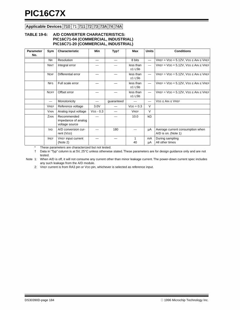
PIC16C7X
DS30390D-page 184 1996 Microchip Technology Inc.
Applicable Devices 710 71 711 72 73 73A 74 74A
TABLE 19-6: A/D CONVERTER CHARACTERISTICS:PIC16C71-04 (COMMERCIAL, INDUSTRIAL)PIC16C71-20 (COMMERCIAL, INDUSTRIAL)
Parameter No.
Sym Characteristic Min Typ† Max Units Conditions
NR Resolution — — 8 bits — VREF = VDD = 5.12V, VSS ≤ AIN ≤ VREF
NINT Integral error — — less than ±1 LSb
— VREF = VDD = 5.12V, VSS ≤ AIN ≤ VREF
NDIF Differential error — — less than ±1 LSb
— VREF = VDD = 5.12V, VSS ≤ AIN ≤ VREF
NFS Full scale error — — less than ±1 LSb
— VREF = VDD = 5.12V, VSS ≤ AIN ≤ VREF
NOFF Offset error — — less than ±1 LSb
— VREF = VDD = 5.12V, VSS ≤ AIN ≤ VREF
— Monotonicity — guaranteed — — VSS ≤ AIN ≤ VREF
VREF Reference voltage 3.0V — VDD + 0.3 V
VAIN Analog input voltage VSS - 0.3 — VREF V
ZAIN Recommended impedance of analog voltage source
— — 10.0 kΩ
IAD A/D conversion cur-rent (VDD)
— 180 — µA Average current consumption when A/D is on. (Note 1)
IREF VREF input current (Note 2)
— — 140
mAµA
During samplingAll other times
* These parameters are characterized but not tested.† Data in “Typ” column is at 5V, 25°C unless otherwise stated. These parameters are for design guidance only and are not
tested.Note 1: When A/D is off, it will not consume any current other than minor leakage current. The power-down current spec includes
any such leakage from the A/D module.2: VREF current is from RA3 pin or VDD pin, whichever is selected as reference input.
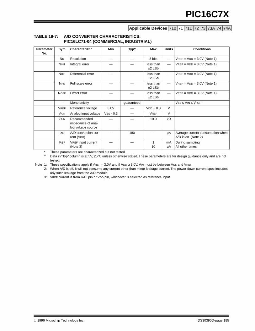
1996 Microchip Technology Inc. DS30390D-page 185
PIC16C7XApplicable Devices 710 71 711 72 73 73A 74 74A
TABLE 19-7: A/D CONVERTER CHARACTERISTICS:PIC16LC71-04 (COMMERCIAL, INDUSTRIAL)
Parameter No.
Sym Characteristic Min Typ† Max Units Conditions
NR Resolution — — 8 bits — VREF = VDD = 3.0V (Note 1)
NINT Integral error — — less than ±2 LSb
— VREF = VDD = 3.0V (Note 1)
NDIF Differential error — — less than ±2 LSb
— VREF = VDD = 3.0V (Note 1)
NFS Full scale error — — less than ±2 LSb
— VREF = VDD = 3.0V (Note 1)
NOFF Offset error — — less than ±2 LSb
— VREF = VDD = 3.0V (Note 1)
— Monotonicity — guaranteed — — VSS ≤ AIN ≤ VREF
VREF Reference voltage 3.0V — VDD + 0.3 V
VAIN Analog input voltage VSS - 0.3 — VREF V
ZAIN Recommended impedance of ana-log voltage source
— — 10.0 kΩ
IAD A/D conversion cur-rent (VDD)
— 180 — µA Average current consumption when A/D is on. (Note 2)
IREF VREF input current (Note 3)
— — 110
mAµA
During samplingAll other times
* These parameters are characterized but not tested.† Data in “Typ” column is at 5V, 25°C unless otherwise stated. These parameters are for design guidance only and are not
tested.Note 1: These specifications apply if VREF = 3.0V and if VDD ≥ 3.0V. VIN must be between VSS and VREF
2: When A/D is off, it will not consume any current other than minor leakage current. The power-down current spec includes any such leakage from the A/D module.
3: VREF current is from RA3 pin or VDD pin, whichever is selected as reference input.

PIC16C7X
DS30390D-page 186 1996 Microchip Technology Inc.
Applicable Devices 710 71 711 72 73 73A 74 74A
FIGURE 19-6: A/D CONVERSION TIMING
TABLE 19-8: A/D CONVERSION REQUIREMENTS
Parameter No.
Sym Characteristic Min Typ† Max Units Conditions
130 TAD A/D clock period 2.0 — — µs TOSC based, VREF ≥ 3.0V
PIC16C71 2.0 4.0 6.0 µs A/D RC Mode
PIC16LC71 3.0 6.0 9.0 µs A/D RC Mode
131 TCNV Conversion time(not including S/H time) (Note 1)
— 10TAD — —
132 TACQ Acquisition time Note 2 20 — µs
* These parameters are characterized but not tested.† Data in “Typ” column is at 5V, 25°C unless otherwise stated. These parameters are for design guidance only and are not
tested.Note 1: ADRES register may be read on the following TCY cycle.
2: See Section 13.1 for min conditions.
131
130
132
BSF ADCON0, GO
Q4
A/D CLK
A/D DATA
ADRES
ADIF
GO
SAMPLE
OLD_DATA
SAMPLING STOPPED
DONE
NEW_DATA
(TOSC/2) (1)
7 6 5 4 3 2 1 0
Note 1: If the A/D clock source is selected as RC, a time of TCY is added before the A/D clock starts. This allows the SLEEP instruction to be executed.
1 Tcy
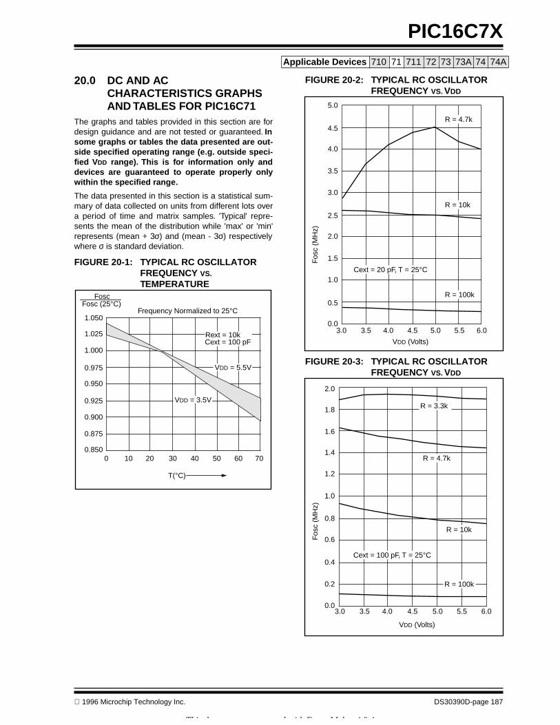
1996 Microchip Technology Inc. DS30390D-page 187
PIC16C7X
Applicable Devices
710 71 711 72 73 73A 74 74A
20.0 DC AND AC CHARACTERISTICS GRAPHS AND TABLES FOR PIC16C71
The graphs and tables provided in this section are fordesign guidance and are not tested or guaranteed.
Insome graphs or tables the data presented are out-side specified operating range (e.g. outside speci-fied V
DD
range). This is for information only anddevices are guaranteed to operate properly onlywithin the specified range.
The data presented in this section is a statistical sum-mary of data collected on units from different lots overa period of time and matrix samples. 'Typical' repre-sents the mean of the distribution while 'max' or 'min'represents (mean + 3
σ
) and (mean - 3
σ
) respectivelywhere
σ
is standard deviation.
FIGURE 20-1: TYPICAL RC OSCILLATOR FREQUENCY
VS.
TEMPERATURE
Frequency Normalized to 25°C1.050
1.025
1.000
0.975
0.950
0.925
0.900
0.875
0.850
FoscFosc (25°C)
T(°C)
Rext = 10kCext = 100 pF
VDD = 5.5V
VDD = 3.5V
0 10 20 30 40 50 60 70
FIGURE 20-2: TYPICAL RC OSCILLATOR FREQUENCY
VS.
V
DD
FIGURE 20-3: TYPICAL RC OSCILLATOR FREQUENCY
VS.
V
DD
5.0
4.5
4.0
3.5
3.0
2.5
2.0
1.5
1.0
0.5
0.03.0 3.5 4.0 4.5 5.0 5.5 6.0
VDD (Volts)
Fos
c (M
Hz)
R = 4.7k
R = 10k
R = 100k
Cext = 20 pF, T = 25°C
2.0
1.8
1.0
0.8
0.6
0.4
0.2
0.03.0 4.03.5 4.5 5.0 5.5 6.0
VDD (Volts)
Fos
c (M
Hz)
R = 3.3k
R = 4.7k
R = 10k
Cext = 100 pF, T = 25°C
R = 100k
1.6
1.4
1.2
This document was created with FrameMaker 4 0 4

PIC16C7X
DS30390D-page 188
1996 Microchip Technology Inc.
Applicable Devices
710 71 711 72 73 73A 74 74A
FIGURE 20-4: TYPICAL RC OSCILLATOR FREQUENCY
VS.
V
DD
FIGURE 20-5: TYPICAL I
PD
VS.
V
DD
WATCHDOG TIMER DISABLED 25
°
C
03.0
VDD (Volts)
Fos
c (M
Hz)
Cext = 300 pF, T = 25°C
R = 100k
3.5 4.0 4.5 5.0 5.5 6.0
.1
.2
.3
.4
.5
.6
.7
.8
R = 10k
R = 4.7k
R = 3.3k
0.03.0
VDD (Volts)
IPD
(µA
)
0.1
0.2
0.3
0.4
0.5
0.6
3.5 4.0 4.5 5.0 5.5 6.0
TABLE 20-1: RC OSCILLATOR FREQUENCIES
The percentage variation indicated here is part to partvariation due to normal process distribution. The varia-tion indicated is
±
3 standard deviation from averagevalue for V
DD
= 5V.
FIGURE 20-6: TYPICAL I
PD
VS.
V
DD
WATCHDOG TIMER ENABLED 25
°
C
Cext RextAverage
F
OSC
@ 5V, 25
°
C
20 pf 4.7k10k100k
4.52 MHz2.47 MHz290.86 kHz
±
17.35%
±
10.10%
±
11.90%100 pf 3.3k
4.7k10k100k
1.92 MHz1.49 MHz788.77 kHz88.11 kHz
±
9.43%
±
9.83%
±
10.92%
±
16.03%300 pf 3.3k
4.7k10k100k
726.89 kHz573.95 kHz307.31 kHz33.82 kHz
±
10.97%
±
10.14%
±
10.43%
±
11.24%
VDD (Volts)
IPD
(µA
)
03.0 3.5 4.0 4.5 5.0 5.5 6.0
2
4
6
8
10
12
14
Dat
a ba
sed
on m
atrix
sam
ples
. See
firs
t pag
e of
this
sec
tion
for
deta
ils.
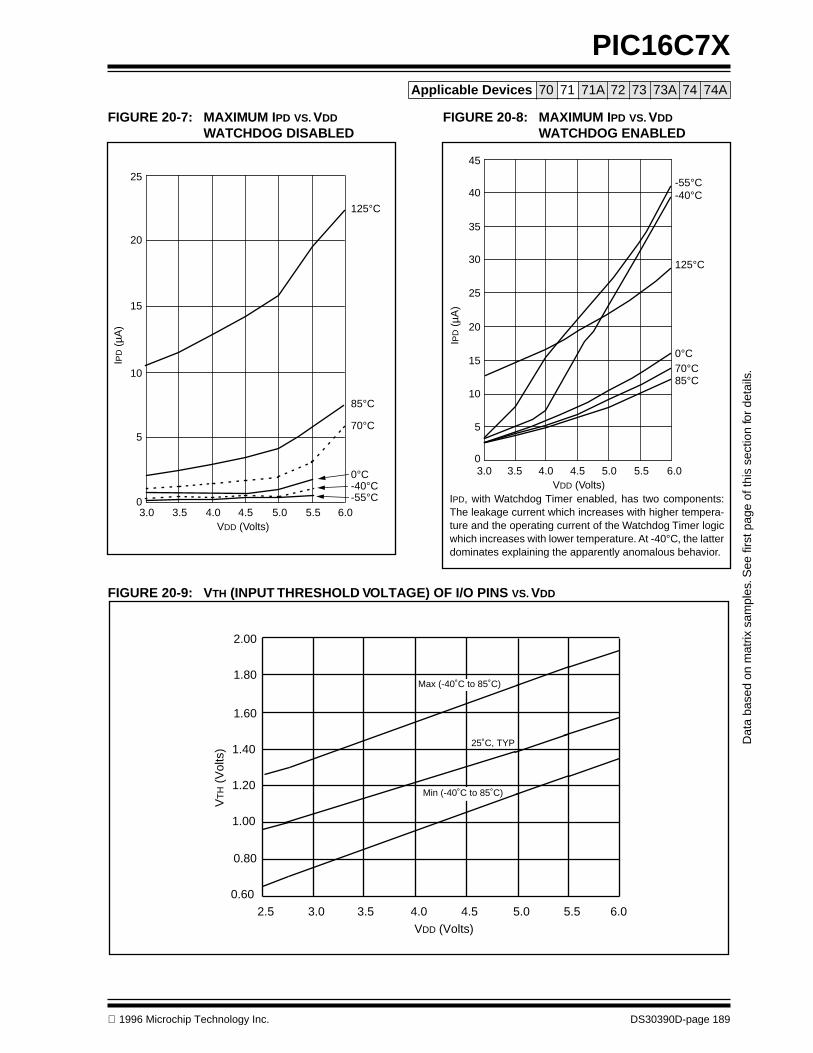
1996 Microchip Technology Inc. DS30390D-page 189
PIC16C7X
Applicable Devices
70 71 71A 72 73 73A 74 74A
FIGURE 20-7: MAXIMUM I
PD
VS.
V
DD
WATCHDOG DISABLED
3.0 3.5 4.0 4.5 5.0 5.5 6.0VDD (Volts)
0°C
-55°C-40°C
70°C
85°C
125°C
IPD
(µA
)
25
20
15
10
5
0
FIGURE 20-8: MAXIMUM I
PD
VS.
V
DD
WATCHDOG ENABLED
IPD, with Watchdog Timer enabled, has two components:The leakage current which increases with higher tempera-ture and the operating current of the Watchdog Timer logicwhich increases with lower temperature. At -40°C, the latterdominates explaining the apparently anomalous behavior.
0°C
-55°C-40°C
70°C85°C
125°C
3.0 3.5 4.0 4.5 5.0 5.5 6.0VDD (Volts)
IPD
(µA
)
45
40
35
30
25
20
15
10
5
0
FIGURE 20-9: V
TH
(INPUT THRESHOLD VOLTAGE) OF I/O PINS
VS.
V
DD
VDD (Volts)
0.80
1.00
1.20
1.40
1.60
1.80
2.00
2.5 3.0 3.5 4.0 4.5 5.0 5.5 6.0
25˚C, TYP
Min (-40˚C to 85˚C)
0.60
Max (-40˚C to 85˚C)
VT
H (
Vol
ts)
Dat
a ba
sed
on m
atrix
sam
ples
. See
firs
t pag
e of
this
sec
tion
for
deta
ils.

PIC16C7X
DS30390D-page 190
1996 Microchip Technology Inc.
Applicable Devices
70 71 71A 72 73 73A 74 74A
FIGURE 20-10: V
IH
, V
IL
OF MCLR, T0CKI AND OSC1 (IN RC MODE)
VS.
V
DD
FIGURE 20-11: V
TH
(INPUT THRESHOLD VOLTAGE) OF OSC1 INPUT (IN XT, HS, AND LP MODES)
VS.
V
DD
4.50
4.00
3.50
3.00
2.50
2.00
1.50
1.00
0.50
0.002.5 3.0 3.5 4.0 4.5 5.0 5.5 6.0
VDD (Volts)
Note: These input pins have a Schmitt Trigger input buffer.
VIH
, VIL
(V
olts
)
VIH, Max (-40°C to 85°C)VIH, Typ (25°C)
VIH, Min (-40°C to 85°C)
VIL, Max (-40°C to 85°C)
VIL, Typ (25°C)VIL, Min (-40°C to 85°C)
3.60
3.40
3.20
3.00
2.80
2.60
2.40
2.20
2.00
1.80
1.60
1.40
1.20
1.003.0 3.5 4.0 4.5 5.0 5.5 6.0 6.5
VDD (Volts)
VT
H (
Vol
ts)
Min (-40°C to 85°C)
Max (-40°C to 85°C)
Min (-40°C to 85°C)
TYP (25°C)
Dat
a ba
sed
on m
atrix
sam
ples
. See
firs
t pag
e of
this
sec
tion
for
deta
ils.
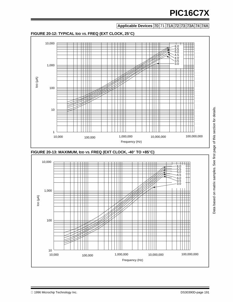
1996 Microchip Technology Inc. DS30390D-page 191
PIC16C7XApplicable Devices 70 71 71A 72 73 73A 74 74A
FIGURE 20-12: TYPICAL IDD VS. FREQ (EXT CLOCK, 25°C)
FIGURE 20-13: MAXIMUM, IDD VS. FREQ (EXT CLOCK, -40° TO +85°C)
1
10
100
1,000
10,000
10,000 100,000 1,000,000 10,000,000 100,000,000
IDD
(µA
)
Frequency (Hz)
6.05.55.04.54.03.53.0
10
100
1,000
10,000
10,000 100,000 1,000,000 10,000,000 100,000,000
IDD
(µA
)
Frequency (Hz)
6.05.55.04.54.03.53.0
Dat
a ba
sed
on m
atrix
sam
ples
. See
firs
t pag
e of
this
sec
tion
for
deta
ils.
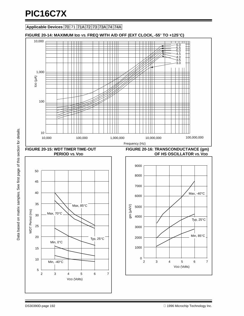
PIC16C7X
DS30390D-page 192 1996 Microchip Technology Inc.
Applicable Devices 70 71 71A 72 73 73A 74 74A
FIGURE 20-14: MAXIMUM IDD VS. FREQ WITH A/D OFF (EXT CLOCK, -55° TO +125°C)
10
100
1,000
10,000
10,000 100,000 1,000,000 10,000,000 100,000,000
IDD
(µA
)
Frequency (Hz)
6.05.55.04.54.03.53.0
FIGURE 20-15: WDT TIMER TIME-OUT PERIOD VS. VDD
50
45
40
35
30
25
20
15
10
52 3 4 5 6 7
VDD (Volts)
WD
T P
erio
d (m
s)
Max, 85°C
Max, 70°C
Typ, 25°CMin, 0°C
Min, -40°C
FIGURE 20-16: TRANSCONDUCTANCE (gm) OF HS OSCILLATOR VS. VDD
Min, 85°C
Typ, 25°C
Max, -40°C
2 3 4 5 6 7
VDD (Volts)
gm (
µA/V
)
0
9000
8000
7000
6000
5000
4000
3000
2000
1000
Dat
a ba
sed
on m
atrix
sam
ples
. See
firs
t pag
e of
this
sec
tion
for
deta
ils.

1996 Microchip Technology Inc. DS30390D-page 193
PIC16C7XApplicable Devices 710 71 711 72 73 73A 74 74A
FIGURE 20-17: TRANSCONDUCTANCE (gm) OF LP OSCILLATOR VS. VDD
FIGURE 20-18: TRANSCONDUCTANCE (gm) OF XT OSCILLATOR VS. VDD
Min, 85°C
Typ, 25°C
Max, -40°C
225
200
175
150
125
100
75
50
25
03.0 3.5 4.0 4.5 5.0 5.5 6.0
VDD (Volts)
gm (
µA/V
)
Min, 85°C
Typ, 25°C
Max, -40°C
2 3 4 5 6 7VDD (Volts)
2500
2000
1500
1000
500
0
gm (
µA/V
)FIGURE 20-19: IOH VS. VOH, VDD = 3V
FIGURE 20-20: IOH VS. VOH, VDD = 5V
Min, 85°C
Typ, 25°C
Max, -40°C
0.0 0.5 1.0 1.5 2.0 2.5 3.0VOH (Volts)
IOH
(m
A)
0
-5
-10
-15
-20
-25
0
-5
-10
-15
-20
-25
-30
-35
-40
-45
-500.0 0.5 1.0 1.5 2.0 2.5 3.0 3.5 4.0 4.5 5.0
VOH (Volts)
IOH
(m
A)
Min @ 85°C
Typ @ 25°C
Max @ -40°C
Dat
a ba
sed
on m
atrix
sam
ples
. See
firs
t pag
e of
this
sec
tion
for
deta
ils.

PIC16C7X
DS30390D-page 194 1996 Microchip Technology Inc.
Applicable Devices 710 71 711 72 73 73A 74 74A
FIGURE 20-21: IOL VS. VOL, VDD = 3V35
30
25
20
15
10
5
00.0 0.5 1.0 1.5 2.0 2.5 3.0
VOL (Volts)
IOL
(mA
)
Max @ -40°C
Typ @ 25°C
Min @ +85°C
FIGURE 20-22: IOL VS. VOL, VDD = 5V
Max @ -40°C80
90
70
60
50
40
30
20
10
0
VOL (Volts)
IOL
(mA
)
Min @ +85°C
Typ @ 25°C
0.0 0.5 1.0 1.5 2.0 2.5 3.0 3.5 4.0 4.5 5.0
Dat
a ba
sed
on m
atrix
sam
ples
. See
firs
t pag
e of
this
sec
tion
for
deta
ils.

1996 Microchip Technology Inc. DS30390D-page 195
PIC16C7X
Applicable Devices
710 71 711 72 73 73A 74 74A
21.0 ELECTRICAL CHARACTERISTICS FOR PIC16C72
Absolute Maximum Ratings †
Ambient temperature under bias................................................................................................................. .-55 to +125˚C
Storage temperature ............................................................................................................................... -65˚C to +150˚C
Voltage on any pin with respect to V
SS
(except V
DD
and MCLR) .................................................... -0.3V to (V
DD
+ 0.3V)
Voltage on V
DD
with respect to V
SS
................................................................................................................ 0 to +7.5V
Voltage on MCLR with respect to V
SS
(Note 2) ................................................................................................. 0 to +14V
Total power dissipation (Note 1).................................................................................................................................1.0W
Maximum current out of V
SS
pin ............................................................................................................................300 mA
Maximum current into V
DD
pin ...............................................................................................................................250 mA
Input clamp current, I
IK
(V
I
< 0 or V
I
> V
DD
)
.....................................................................................................................±
20 mA
Output clamp current, I
OK
(V
O
< 0 or V
O
> V
DD
)
..............................................................................................................±
20 mA
Maximum output current sunk by any I/O pin...........................................................................................................25 mA
Maximum output current sourced by any I/O pin .....................................................................................................25 mA
Maximum current sunk by
PORTA and PORTB (combined)..................................................................................200 mA
Maximum current sourced by PORTA and PORTB (combined).............................................................................200 mA
Maximum current sunk by PORTC ........................................................................................................................200 mA
Maximum current sourced by PORTC ...................................................................................................................200 mA
Note 1:
Power dissipation is calculated as follows: Pdis = V
DD
x I
DD
-
∑
I
OH
+
∑
(V
DD
- V
OH
) x I
OH
+
∑
(V
O
l x I
OL
)
Note 2:
Voltage spikes below V
SS
at the MCLR pin, inducing currents greater than 80 mA, may cause latch-up. Thus,a series resistor of 50-100
Ω
should be used when applying a “low” level to the MCLR pin rather than pullingthis pin directly to V
SS
.
† NOTICE: Stresses above those listed under “Absolute Maximum Ratings” may cause permanent damage to the device. This is a stress rating only and functional operation of the device at those or any other conditions above those indicated in the operation listings of this specification is not implied. Exposure to maximum rating conditions for extended periods may affect device reliability.
This document was created with FrameMaker 4 0 4

PIC16C7X
DS30390D-page 196
1996 Microchip Technology Inc.
Applicable Devices
710 71 711 72 73 73A 74 74A
TABLE 21-1: CROSS REFERENCE OF DEVICE SPECS FOR OSCILLATOR CONFIGURATIONS AND FREQUENCIES OF OPERATION (COMMERCIAL DEVICES)
OS
CP
IC16
C72
-04
PIC
16C
72-1
0P
IC16
C72
-20
PIC
16L
C72
-04
JW D
evic
es
RC
VD
D:
4.0V
to 6
.0V
IDD
: 5
mA
max
. at 5
.5V
IPD
: 16
µA
max
. at 4
VFr
eq:
4 M
Hz
max
.
VD
D:
4.5V
to 5
.5V
IDD
: 2.
7 m
A ty
p. a
t 5.5
VIP
D:
1.5
µA ty
p. a
t 4V
Freq
: 4
MH
z m
ax.
VD
D:
4.5V
to 5
.5V
IDD
: 2.
7 m
A ty
p. a
t 5.5
VIP
D:
1.5
µA ty
p. a
t 4V
Freq
: 4
MH
z m
ax.
VD
D:
2.5V
to 6
.0V
IDD
: 2.
0 m
A ty
p. a
t 3.0
VIP
D:
0.9
µA ty
p. a
t 3V
Freq
: 4
MH
z m
ax.
VD
D:
4.0V
to 6
.0V
IDD
: 5
mA
max
. at 5
.5V
IPD
: 16
µA
max
. at 4
VFr
eq:
4 M
Hz
max
.
XT
VD
D:
4.0V
to 6
.0V
IDD
: 5
mA
max
. at 5
.5V
IPD
: 16
µA
max
. at 4
VFr
eq:
4 M
Hz
max
.
VD
D:
4.5V
to 5
.5V
IDD
: 2.
7 m
A ty
p. a
t 5.5
VIP
D:
1.5
µA ty
p. a
t 4V
Freq
: 4
MH
z m
ax.
VD
D:
4.5V
to 5
.5V
IDD
: 2.
7 m
A ty
p. a
t 5.5
VIP
D:
1.5
µA ty
p. a
t 4V
Freq
: 4
MH
z m
ax.
VD
D:
2.5V
to 6
.0V
IDD
: 2.
0 m
A ty
p. a
t 3.0
VIP
D:
0.9
µA ty
p. a
t 3V
Freq
: 4
MH
z m
ax.
VD
D:
4.0V
to 6
.0V
IDD
: 5
mA
max
. at 5
.5V
IPD
: 16
µA
max
. at 4
VFr
eq:
4 M
Hz
max
.
HS
VD
D:
4.5V
to 5
.5V
VD
D:
4.5V
to 5
.5V
VD
D:
4.5V
to 5
.5V
Do
not u
se in
HS
mod
e
VD
D:
4.5V
to 5
.5V
IDD
: 13
.5 m
A ty
p. a
t 5.5
VID
D:
10 m
A m
ax. a
t 5.5
VID
D:
20 m
A m
ax. a
t 5.5
VID
D:
20 m
A m
ax. a
t 5.5
V
IPD
: 1.
5 µA
typ.
at 4
.5V
IPD
: 1.
5 µA
typ.
at 4
.5V
IPD
:1.
5 µA
typ.
at 4
.5V
IPD
: 1.
5 µA
typ.
at 4
.5V
Freq
: 4
MH
z m
ax.
Freq
: 10
MH
z m
ax.
Freq
:20
MH
z m
ax.
Freq
: 20
MH
z m
ax.
LP
VD
D:
4.0V
to 6
.0V
IDD
: 52
.5 µ
A ty
p. a
t 32
kHz,
4.0
VIP
D:
0.9
µA ty
p. a
t 4.0
VFr
eq:
200
kHz
max
.
Do
not u
se in
LP
mod
eD
o no
t use
in L
P m
ode
VD
D:
2.5V
to 6
.0V
IDD
: 48
µA
max
. at 3
2 kH
z, 3
.0V
IPD
: 5.
0 µA
max
. at 3
.0V
Freq
: 20
0 kH
z m
ax.
VD
D:
2.5V
to 6
.0V
IDD
: 48
µA
max
. at 3
2 kH
z, 3
.0V
IPD
: 5.
0 µA
max
. at 3
.0V
Freq
: 20
0 kH
z m
ax.
The
sha
ded
sect
ions
indi
cate
osc
illat
or s
elec
tions
whi
ch a
re te
sted
for f
unct
iona
lity,
but
not
for M
IN/M
AX
spe
cific
atio
ns. I
t is
reco
mm
ende
d th
at th
e us
er s
elec
t the
dev
ice
type
th
at e
nsur
es th
e sp
ecifi
catio
ns r
equi
red.

1996 Microchip Technology Inc. DS30390D-page 197
PIC16C7X
Applicable Devices
710 71 711 72 73 73A 74 74A
21.1 DC Characteristics: PIC16C72-04 (Commercial, Industrial, Automotive)PIC16C72-10 (Commercial, Industrial, Automotive)PIC16C72-20 (Commercial, Industrial, Automotive)
DC CHARACTERISTICS
Standard Operating Conditions (unless otherwise stated)
Operating temperature -40˚C
≤
T
A
≤
+125˚C for automotive,-40˚C
≤
T
A
≤
+85˚C for industrial and 0˚C
≤
T
A
≤
+70˚C for commercial
ParamNo.
Characteristic Sym Min Typ† Max Units Conditions
D001D001A
Supply Voltage V
DD
4.04.5
--
6.05.5
VV
XT, RC and LP osc configurationHS osc configuration
D002* RAM Data RetentionVoltage (Note 1)
V
DR
- 1.5 - V Device in SLEEP mode
D003 V
DD
start voltage toensure internal Power-on Reset Signal
V
POR
- V
SS
- V See section on Power-on Reset for details
D004* V
DD
rise rate to ensure internal Power-on Reset Signal
S
VDD
0.05 - - V/ms See section on Power-on Reset for details
D005 Brown-out Reset Voltage B
VDD
3.7 4.0 4.3 V BODEN bit in configuration word enabled
D010
D013
Supply Current (Note 2,5)
I
DD -
-
2.7
10
5
20
mA
mA
XT, RC osc configuration (PIC16C72-04)FOSC = 4 MHz, VDD = 5.5V (Note 4)
HS osc configuration (PIC16C72-20)FOSC = 20 MHz, VDD = 5.5V
D015 Brown-out Reset Current (Note 6)
∆IBOR - 350 425 µA BOR enabled VDD = 5.0V
D020D021D021AD021B
Power-down Current (Note 3,5)
IPD ----
10.51.51.52.5
42161919
µAµAµAµA
VDD = 4.0V, WDT enabled, -40°C to +85°CVDD = 4.0V, WDT disabled, -0°C to +70°CVDD = 4.0V, WDT disabled, -40°C to +85°CVDD = 4.0V, WDT disabled, -40°C to +125°C
D023 Brown-out Reset Current (Note 6)
∆IBOR - 350 425 µA BOR enabled VDD = 5.0V
* These parameters are characterized but not tested.† Data in "Typ" column is at 5V, 25˚C unless otherwise stated. These parameters are for design guidance only
and are not tested.Note 1: This is the limit to which VDD can be lowered in SLEEP mode without losing RAM data.
2: The supply current is mainly a function of the operating voltage and frequency. Other factors such as I/O pin loading and switching rate, oscillator type, internal code execution pattern, and temperature also have an impact on the current consumption.The test conditions for all IDD measurements in active operation mode are: OSC1 = external square wave, from rail to rail; all I/O pins tristated, pulled to VDD MCLR = VDD; WDT enabled/disabled as specified.
3: The power-down current in SLEEP mode does not depend on the oscillator type. Power-down current is measured with the part in SLEEP mode, with all I/O pins in hi-impedance state and tied to VDD and VSS.
4: For RC osc configuration, current through Rext is not included. The current through the resistor can be esti-mated by the formula Ir = VDD/2Rext (mA) with Rext in kOhm.
5: Timer1 oscillator (when enabled) adds approximately 20 µA to the specification. This value is from charac-terization and is for design guidance only. This is not tested.
6: The ∆ current is the additional current consumed when this peripheral is enabled. This current should be added to the base IDD or IPD measurement.

PIC16C7X
DS30390D-page 198 1996 Microchip Technology Inc.
Applicable Devices 710 71 711 72 73 73A 74 74A
21.2 DC Characteristics: PIC16LC72-04 (Commercial, Industrial)
DC CHARACTERISTICS
Standard Operating Conditions (unless otherwise stated)Operating temperature -40˚C ≤ TA ≤ +85˚C for industrial and
0˚C ≤ TA ≤ +70˚C for commercial
ParamNo.
Characteristic Sym Min Typ† Max Units Conditions
D001 Supply Voltage VDD 2.5 - 6.0 V LP, XT, RC osc configuration (DC - 4 MHz)
D002* RAM Data Retention Voltage (Note 1)
VDR - 1.5 - V Device in SLEEP mode
D003 VDD start voltage to ensure internal Power-on Reset signal
VPOR - VSS - V See section on Power-on Reset for details
D004* VDD rise rate to ensure internal Power-on Reset signal
SVDD 0.05 - - V/ms See section on Power-on Reset for details
D005 Brown-out Reset Voltage BVDD 3.7 4.0 4.3 V BODEN bit in configuration word enabled
D010
D010A
Supply Current (Note 2,5)
IDD -
-
2.0
22.5
3.8
48
mA
µA
XT, RC osc configurationFOSC = 4 MHz, VDD = 3.0V (Note 4)
LP osc configurationFOSC = 32 kHz, VDD = 3.0V, WDT disabled
D015* Brown-out Reset Current (Note 6)
∆IBOR - 350 425 µA BOR enabled VDD = 3.0V
D020D021D021A
Power-down Current (Note 3,5)
IPD ---
7.50.90.9
3055
µAµAµA
VDD = 3.0V, WDT enabled, -40°C to +85°CVDD = 3.0V, WDT disabled, 0°C to +70°CVDD = 3.0V, WDT disabled, -40°C to +85°C
D023* Brown-out Reset Current (Note 6)
∆IBOR - 300 500 µA BOR enabled VDD = 3.0V
* These parameters are characterized but not tested.† Data in "Typ" column is at 5V, 25˚C unless otherwise stated. These parameters are for design guidance
only and are not tested.Note 1: This is the limit to which VDD can be lowered in SLEEP mode without losing RAM data.
2: The supply current is mainly a function of the operating voltage and frequency. Other factors such as I/O pin loading and switching rate, oscillator type, internal code execution pattern, and temperature also have an impact on the current consumption.The test conditions for all IDD measurements in active operation mode are: OSC1 = external square wave, from rail to rail; all I/O pins tristated, pulled to VDD MCLR = VDD; WDT enabled/disabled as specified.
3: The power-down current in SLEEP mode does not depend on the oscillator type. Power-down current is measured with the part in SLEEP mode, with all I/O pins in hi-impedance state and tied to VDD and VSS.
4: For RC osc configuration, current through Rext is not included. The current through the resistor can be esti-mated by the formula Ir = VDD/2Rext (mA) with Rext in kOhm.
5: Timer1 oscillator (when enabled) adds approximately 20 µA to the specification. This value is from charac-terization and is for design guidance only. This is not tested.
6: The ∆ current is the additional current consumed when this peripheral is enabled. This current should be added to the base IDD or IPD measurement.
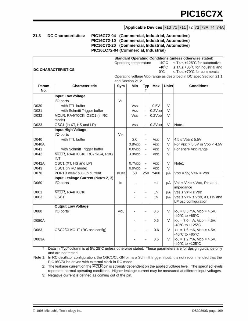
1996 Microchip Technology Inc. DS30390D-page 199
PIC16C7XApplicable Devices 710 71 711 72 73 73A 74 74A
21.3 DC Characteristics: PIC16C72-04 (Commercial, Industrial, Automotive)PIC16C72-10 (Commercial, Industrial, Automotive)PIC16C72-20 (Commercial, Industrial, Automotive)PIC16LC72-04 (Commercial, Industrial)
DC CHARACTERISTICS
Standard Operating Conditions (unless otherwise stated)Operating temperature -40˚C ≤ TA ≤ +125˚C for automotive,
-40˚C ≤ TA ≤ +85˚C for industrial and 0˚C ≤ TA ≤ +70˚C for commercial
Operating voltage VDD range as described in DC spec Section 21.1 and Section 21.2.
ParamNo.
Characteristic Sym Min Typ†
Max Units Conditions
Input Low VoltageI/O ports VIL
D030 with TTL buffer VSS - 0.5V VD031 with Schmitt Trigger buffer VSS - 0.2VDD VD032 MCLR, RA4/T0CKI,OSC1 (in RC
mode)VSS - 0.2VDD V
D033 OSC1 (in XT, HS and LP) VSS - 0.3VDD V Note1Input High VoltageI/O ports VIH -
D040 with TTL buffer 2.0 - VDD V 4.5 ≤ VDD ≤ 5.5VD040A 0.8VDD - VDD V For VDD > 5.5V or VDD < 4.5VD041 with Schmitt Trigger buffer 0.8VDD - VDD V For entire VDD rangeD042 MCLR, RA4/T0CKI, RC7:RC4, RB0/
INT0.8VDD - VDD V
D042A OSC1 (XT, HS and LP) 0.7VDD - VDD V Note1D043 OSC1 (in RC mode) 0.9VDD - VDD VD070 PORTB weak pull-up current IPURB 50 250 †400 µA VDD = 5V, VPIN = VSS
Input Leakage Current (Notes 2, 3)D060 I/O ports IIL - - ±1 µA Vss ≤ VPIN ≤ VDD, Pin at hi-
impedanceD061 MCLR, RA4/T0CKI - - ±5 µA Vss ≤ VPIN ≤ VDD
D063 OSC1 - - ±5 µA Vss ≤ VPIN ≤ VDD, XT, HS and LP osc configuration
Output Low VoltageD080 I/O ports VOL - - 0.6 V IOL = 8.5 mA, VDD = 4.5V,
-40°C to +85°CD080A - - 0.6 V IOL = 7.0 mA, VDD = 4.5V,
-40°C to +125°CD083 OSC2/CLKOUT (RC osc config) - - 0.6 V IOL = 1.6 mA, VDD = 4.5V,
-40°C to +85°CD083A - - 0.6 V IOL = 1.2 mA, VDD = 4.5V,
-40°C to +125°C† Data in “Typ” column is at 5V, 25°C unless otherwise stated. These parameters are for design guidance only
and are not tested.Note 1: In RC oscillator configuration, the OSC1/CLKIN pin is a Schmitt trigger input. It is not recommended that the
PIC16C7X be driven with external clock in RC mode.2: The leakage current on the MCLR pin is strongly dependent on the applied voltage level. The specified levels
represent normal operating conditions. Higher leakage current may be measured at different input voltages.3: Negative current is defined as coming out of the pin.

PIC16C7X
DS30390D-page 200 1996 Microchip Technology Inc.
Applicable Devices 710 71 711 72 73 73A 74 74A
Output High VoltageD090 I/O ports (Note 3) VOH VDD - 0.7 - - V IOH = -3.0 mA, VDD = 4.5V,
-40°C to +85°CD090A VDD - 0.7 - - V IOH = -2.5 mA, VDD = 4.5V,
-40°C to +125°CD092 OSC2/CLKOUT (RC osc config) VDD - 0.7 - - V IOH = -1.3 mA, VDD = 4.5V,
-40°C to +85°CD092A VDD - 0.7 - - V IOH = -1.0 mA, VDD = 4.5V,
-40°C to +125°CCapacitive Loading Specs on Out-put Pins
D100 OSC2 pin COSC2 - - 15 pF In XT, HS and LP modes when external clock is used to drive OSC1.
D101D102
All I/O pins and OSC2 (in RC mode)
SCL, SDA in I2C mode
CIO
CB
--
--
50400
pFpF
DC CHARACTERISTICS
Standard Operating Conditions (unless otherwise stated)Operating temperature -40˚C ≤ TA ≤ +125˚C for automotive,
-40˚C ≤ TA ≤ +85˚C for industrial and 0˚C ≤ TA ≤ +70˚C for commercial
Operating voltage VDD range as described in DC spec Section 21.1 and Section 21.2.
ParamNo.
Characteristic Sym Min Typ†
Max Units Conditions
† Data in “Typ” column is at 5V, 25°C unless otherwise stated. These parameters are for design guidance only and are not tested.
Note 1: In RC oscillator configuration, the OSC1/CLKIN pin is a Schmitt trigger input. It is not recommended that the PIC16C7X be driven with external clock in RC mode.
2: The leakage current on the MCLR pin is strongly dependent on the applied voltage level. The specified levels represent normal operating conditions. Higher leakage current may be measured at different input voltages.
3: Negative current is defined as coming out of the pin.

1996 Microchip Technology Inc. DS30390D-page 201
PIC16C7XApplicable Devices 710 71 711 72 73 73A 74 74A
21.4 Timing Parameter Symbology
The timing parameter symbols have been created following one of the following formats:
FIGURE 21-1: LOAD CONDITIONS
1. TppS2ppS 3. TCC:ST (I2C specifications only)2. TppS 4. Ts (I2C specifications only)T
F Frequency T TimeLowercase letters (pp) and their meanings:
ppcc CCP1 osc OSC1ck CLKOUT rd RD
cs CS rw RD or WRdi SDI sc SCKdo SDO ss SSdt Data in t0 T0CKIio I/O port t1 T1CKImc MCLR wr WRUppercase letters and their meanings:
SF Fall P PeriodH High R RiseI Invalid (Hi-impedance) V ValidL Low Z Hi-impedance
I2C onlyAA output access High HighBUF Bus free Low Low
TCC:ST (I2C specifications only)CC
HD Hold SU SetupST
DAT DATA input hold STO STOP conditionSTA START condition
VDD/2
CL
RL
Pin Pin
VSS VSS
CL
RL = 464Ω
CL = 50 pF for all pins except OSC2
15 pF for OSC2 output
Load condition 1 Load condition 2
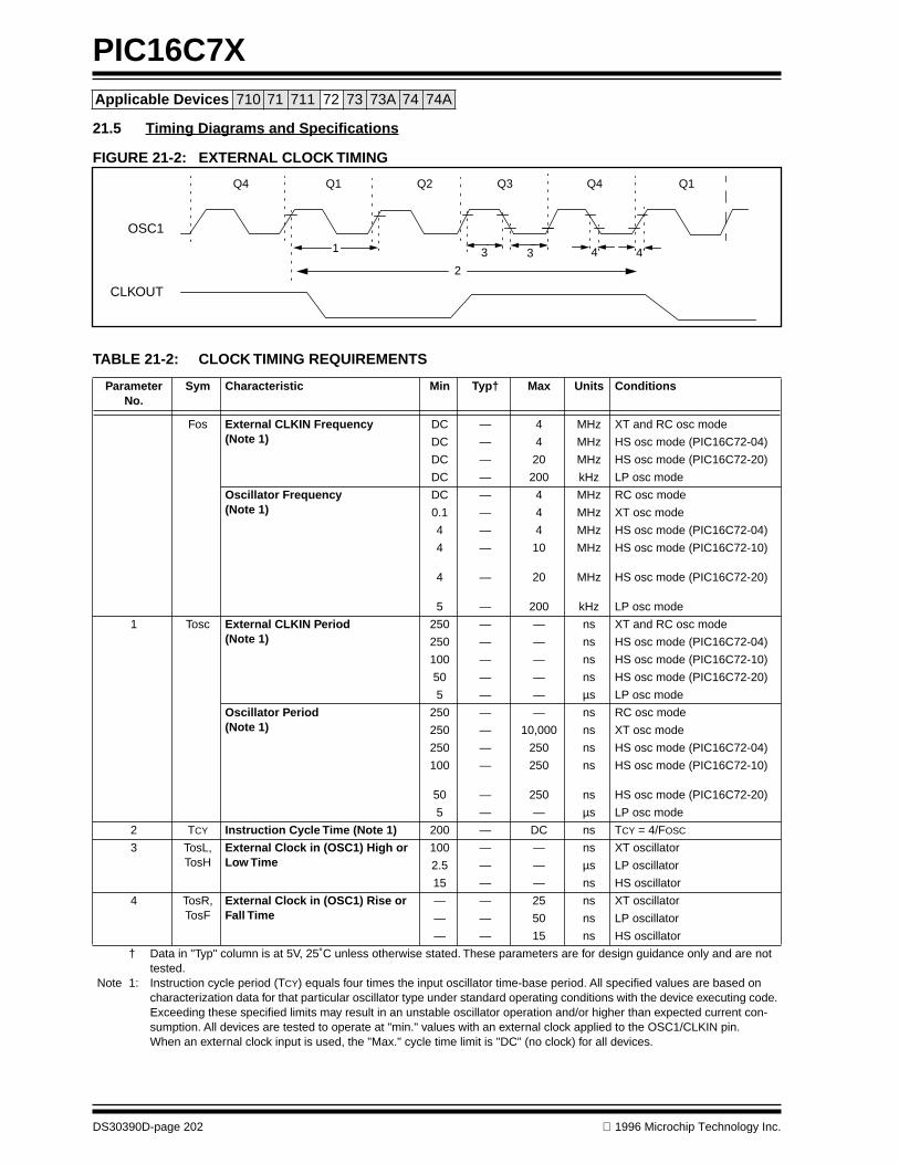
PIC16C7X
DS30390D-page 202 1996 Microchip Technology Inc.
Applicable Devices 710 71 711 72 73 73A 74 74A
21.5 Timing Diagrams and Specifications
FIGURE 21-2: EXTERNAL CLOCK TIMING
TABLE 21-2: CLOCK TIMING REQUIREMENTS
Parameter No.
Sym Characteristic Min Typ† Max Units Conditions
Fos External CLKIN Frequency (Note 1)
DC — 4 MHz XT and RC osc mode
DC — 4 MHz HS osc mode (PIC16C72-04)
DC — 20 MHz HS osc mode (PIC16C72-20)
DC — 200 kHz LP osc mode
Oscillator Frequency (Note 1)
DC — 4 MHz RC osc mode
0.1 — 4 MHz XT osc mode
4 — 4 MHz HS osc mode (PIC16C72-04)
4
4
5
—
—
—
10
20
200
MHz
MHz
kHz
HS osc mode (PIC16C72-10)
HS osc mode (PIC16C72-20)
LP osc mode
1 Tosc External CLKIN Period(Note 1)
250 — — ns XT and RC osc mode
250 — — ns HS osc mode (PIC16C72-04)
100 — — ns HS osc mode (PIC16C72-10)
50 — — ns HS osc mode (PIC16C72-20)
5 — — µs LP osc mode
Oscillator Period(Note 1)
250 — — ns RC osc mode
250 — 10,000 ns XT osc mode
250 — 250 ns HS osc mode (PIC16C72-04)
100
50
—
—
250
250
ns
ns
HS osc mode (PIC16C72-10)
HS osc mode (PIC16C72-20)
5 — — µs LP osc mode
2 TCY Instruction Cycle Time (Note 1) 200 — DC ns TCY = 4/FOSC
3 TosL,TosH
External Clock in (OSC1) High or Low Time
100 — — ns XT oscillator
2.5 — — µs LP oscillator
15 — — ns HS oscillator
4 TosR,TosF
External Clock in (OSC1) Rise or Fall Time
— — 25 ns XT oscillator
— — 50 ns LP oscillator
— — 15 ns HS oscillator
† Data in "Typ" column is at 5V, 25˚C unless otherwise stated. These parameters are for design guidance only and are not tested.
Note 1: Instruction cycle period (TCY) equals four times the input oscillator time-base period. All specified values are based on characterization data for that particular oscillator type under standard operating conditions with the device executing code. Exceeding these specified limits may result in an unstable oscillator operation and/or higher than expected current con-sumption. All devices are tested to operate at "min." values with an external clock applied to the OSC1/CLKIN pin.When an external clock input is used, the "Max." cycle time limit is "DC" (no clock) for all devices.
OSC1
CLKOUT
Q4 Q1 Q2 Q3 Q4 Q1
1
2
3 3 4 4

1996 Microchip Technology Inc. DS30390D-page 203
PIC16C7XApplicable Devices 710 71 711 72 73 73A 74 74A
FIGURE 21-3: CLKOUT AND I/O TIMING
TABLE 21-3: CLKOUT AND I/O TIMING REQUIREMENTS
ParameterNo.
Sym Characteristic Min Typ† Max Units Conditions
10* TosH2ckL OSC1↑ to CLKOUT↓ — 75 200 ns Note 1
11* TosH2ckH OSC1↑ to CLKOUT↑ — 75 200 ns Note 1
12* TckR CLKOUT rise time — 35 100 ns Note 1
13* TckF CLKOUT fall time — 35 100 ns Note 1
14* TckL2ioV CLKOUT ↓ to Port out valid — — 0.5TCY + 20 ns Note 1
15* TioV2ckH Port in valid before CLKOUT ↑ TOSC + 200 — — ns Note 1
16* TckH2ioI Port in hold after CLKOUT ↑ 0 — — ns Note 1
17* TosH2ioV OSC1↑ (Q1 cycle) to Port out valid
— 50 150 ns
18* TosH2ioI OSC1↑ (Q2 cycle) to Port input invalid (I/O in hold time)
PIC16C72 100 — — ns
PIC16LC72 200 — — ns
19* TioV2osH Port input valid to OSC1↑ (I/O in setup time) 0 — — ns
20* TioR Port output rise time PIC16C72 — 10 40 ns
PIC16LC72 — — 80 ns
21* TioF Port output fall time PIC16C72 — 10 40 ns
PIC16LC72 — — 80 ns
22††* Tinp INT pin high or low time TCY — — ns
23††* Trbp RB7:RB4 change INT high or low time TCY — — ns
* These parameters are characterized but not tested.† Data in "Typ" column is at 5V, 25˚C unless otherwise stated. These parameters are for design guidance
only and are not tested.†† These parameters are asynchronous events not related to any internal clock edges.
Note 1: Measurements are taken in RC Mode where CLKOUT output is 4 x TOSC.
Note: Refer to Figure 21-1 for load conditions.
OSC1
CLKOUT
I/O Pin(input)
I/O Pin(output)
Q4 Q1 Q2 Q3
10
1314
17
20, 21
19 18
15
11
1216
old value new value
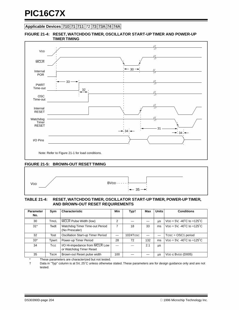
PIC16C7X
DS30390D-page 204 1996 Microchip Technology Inc.
Applicable Devices 710 71 711 72 73 73A 74 74A
FIGURE 21-4: RESET, WATCHDOG TIMER, OSCILLATOR START-UP TIMER AND POWER-UP TIMER TIMING
FIGURE 21-5: BROWN-OUT RESET TIMING
TABLE 21-4: RESET, WATCHDOG TIMER, OSCILLATOR START-UP TIMER, POWER-UP TIMER, AND BROWN-OUT RESET REQUIREMENTS
Parameter No.
Sym Characteristic Min Typ† Max Units Conditions
30 TmcL MCLR Pulse Width (low) 2 — — µs VDD = 5V, -40˚C to +125˚C
31* Twdt Watchdog Timer Time-out Period (No Prescaler)
7 18 33 ms VDD = 5V, -40˚C to +125˚C
32 Tost Oscillation Start-up Timer Period — 1024TOSC — — TOSC = OSC1 period
33* Tpwrt Power-up Timer Period 28 72 132 ms VDD = 5V, -40˚C to +125˚C
34 TIOZ I/O Hi-impedance from MCLR Low or Watchdog Timer Reset
— — 2.1 µs
35 TBOR Brown-out Reset pulse width 100 — — µs VDD ≤ BVDD (D005)
* These parameters are characterized but not tested.† Data in "Typ" column is at 5V, 25˚C unless otherwise stated. These parameters are for design guidance only and are not
tested.
VDD
MCLR
InternalPOR
PWRTTime-out
OSCTime-out
InternalRESET
WatchdogTimer
RESET
33
32
30
3134
I/O Pins
34
Note: Refer to Figure 21-1 for load conditions.
VDD BVDD
35
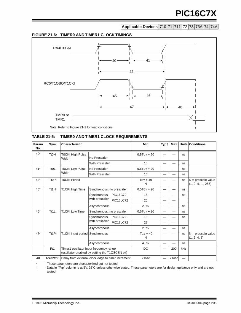
1996 Microchip Technology Inc. DS30390D-page 205
PIC16C7XApplicable Devices 710 71 711 72 73 73A 74 74A
FIGURE 21-6: TIMER0 AND TIMER1 CLOCK TIMINGS
TABLE 21-5: TIMER0 AND TIMER1 CLOCK REQUIREMENTS
Param No.
Sym Characteristic Min Typ† Max Units Conditions
40* Tt0H T0CKI High Pulse Width No Prescaler
0.5TCY + 20 — — ns
With Prescaler 10 — — ns
41* Tt0L T0CKI Low Pulse Width
No Prescaler 0.5TCY + 20 — — ns
With Prescaler 10 — — ns
42* Tt0P T0CKI Period TCY + 40N
— — ns N = prescale value (1, 2, 4, ..., 256)
45* Tt1H T1CKI High Time Synchronous, no prescaler 0.5TCY + 20 — — ns
Synchronous, with prescaler
PIC16C72 15 — — ns
PIC16LC72 25 — —
Asynchronous 2TCY — — ns
46* Tt1L T1CKI Low Time Synchronous, no prescaler 0.5TCY + 20 — — ns
Synchronous, with prescaler
PIC16C72 15 — — ns
PIC16LC72 25 — —
Asynchronous 2TCY — — ns
47* Tt1P T1CKI input period Synchronous TCY + 40N
— — ns N = prescale value (1, 2, 4, 8)
Asynchronous 4TCY — — ns
Ft1 Timer1 oscillator input frequency range (oscillator enabled by setting the T1OSCEN bit)
DC — 200 kHz
48 Tcke2tmrI Delay from external clock edge to timer increment 2Tosc — 7Tosc —
* These parameters are characterized but not tested.† Data in "Typ" column is at 5V, 25˚C unless otherwise stated. These parameters are for design guidance only and are not
tested.
Note: Refer to Figure 21-1 for load conditions.
46
47
45
48
41
42
40
RA4/T0CKI
RC0/T1OSO/T1CKI
TMR0 orTMR1
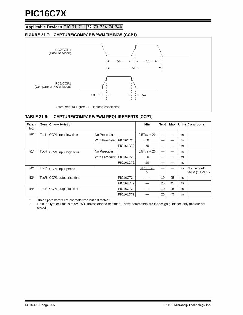
PIC16C7X
DS30390D-page 206 1996 Microchip Technology Inc.
Applicable Devices 710 71 711 72 73 73A 74 74A
FIGURE 21-7: CAPTURE/COMPARE/PWM TIMINGS (CCP1)
TABLE 21-6: CAPTURE/COMPARE/PWM REQUIREMENTS (CCP1)
Param No.
Sym Characteristic Min Typ† Max Units Conditions
50* TccL CCP1 input low time No Prescaler 0.5TCY + 20 — — ns
With Prescaler PIC16C72 10 — — ns
PIC16LC72 20 — — ns
51* TccH CCP1 input high time No Prescaler 0.5TCY + 20 — — ns
With Prescaler PIC16C72 10 — — ns
PIC16LC72 20 — — ns
52* TccP CCP1 input period 3TCY + 40N
— — ns N = prescale value (1,4 or 16)
53* TccR CCP1 output rise time PIC16C72 — 10 25 ns
PIC16LC72 — 25 45 ns
54* TccF CCP1 output fall time PIC16C72 — 10 25 ns
PIC16LC72 — 25 45 ns
* These parameters are characterized but not tested.† Data in "Typ" column is at 5V, 25˚C unless otherwise stated. These parameters are for design guidance only and are not
tested.
Note: Refer to Figure 21-1 for load conditions.
RC2/CCP1(Capture Mode)
50 51
52
53 54
RC2/CCP1(Compare or PWM Mode)

1996 Microchip Technology Inc. DS30390D-page 207
PIC16C7XApplicable Devices 710 71 711 72 73 73A 74 74A
FIGURE 21-8: SPI MODE TIMING
TABLE 21-7: SPI MODE REQUIREMENTS
Parameter No.
Sym Characteristic Min Typ† Max Units Conditions
70 TssL2scH, TssL2scL
SS↓ to SCK↓ or SCK↑ input TCY — — ns
71 TscH SCK input high time (slave mode) TCY + 20 — — ns
72 TscL SCK input low time (slave mode) TCY + 20 — — ns
73 TdiV2scH, TdiV2scL
Setup time of SDI data input to SCK edge
50 — — ns
74 TscH2diL, TscL2diL
Hold time of SDI data input to SCK edge
50 — — ns
75 TdoR SDO data output rise time — 10 25 ns
76 TdoF SDO data output fall time — 10 25 ns
77 TssH2doZ SS↓ to SDO output hi-impedance 10 — 50 ns
78 TscR SCK output rise time (master mode) — 10 25 ns
79 TscF SCK output fall time (master mode) — 10 25 ns
80 TscH2doV,TscL2doV
SDO data output valid after SCK edge
— — 50 ns
† Data in "Typ" column is at 5V, 25˚C unless otherwise stated. These parameters are for design guidance only and are not tested.
Note: Refer to Figure 21-1 for load conditions
SS
SCK(CKP = 0)
SCK(CKP = 1)
SDO
SDI
70
71 72
7374
75, 76 77
787980
7978
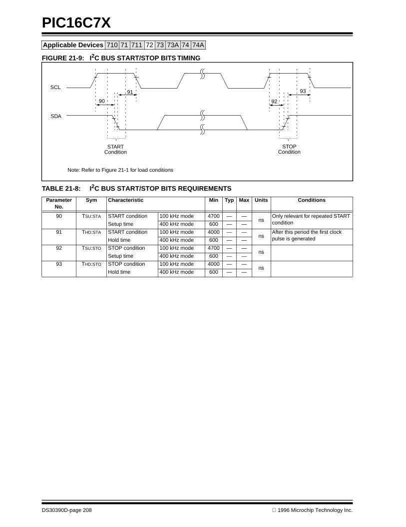
PIC16C7X
DS30390D-page 208 1996 Microchip Technology Inc.
Applicable Devices 710 71 711 72 73 73A 74 74A
FIGURE 21-9: I2C BUS START/STOP BITS TIMING
TABLE 21-8: I2C BUS START/STOP BITS REQUIREMENTS
ParameterNo.
Sym Characteristic Min Typ Max Units Conditions
90 TSU:STA START condition 100 kHz mode 4700 — —ns
Only relevant for repeated START conditionSetup time 400 kHz mode 600 — —
91 THD:STA START condition 100 kHz mode 4000 — —ns
After this period the first clock pulse is generatedHold time 400 kHz mode 600 — —
92 TSU:STO STOP condition 100 kHz mode 4700 — —ns
Setup time 400 kHz mode 600 — —
93 THD:STO STOP condition 100 kHz mode 4000 — —ns
Hold time 400 kHz mode 600 — —
Note: Refer to Figure 21-1 for load conditions
91 93SCL
SDA
STARTCondition
STOPCondition
90 92
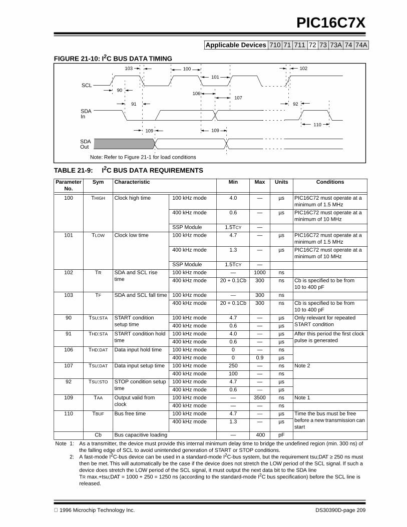
1996 Microchip Technology Inc. DS30390D-page 209
PIC16C7XApplicable Devices 710 71 711 72 73 73A 74 74A
FIGURE 21-10: I2C BUS DATA TIMING
TABLE 21-9: I2C BUS DATA REQUIREMENTS
ParameterNo.
Sym Characteristic Min Max Units Conditions
100 THIGH Clock high time 100 kHz mode 4.0 — µs PIC16C72 must operate at a minimum of 1.5 MHz
400 kHz mode 0.6 — µs PIC16C72 must operate at a minimum of 10 MHz
SSP Module 1.5TCY —
101 TLOW Clock low time 100 kHz mode 4.7 — µs PIC16C72 must operate at a minimum of 1.5 MHz
400 kHz mode 1.3 — µs PIC16C72 must operate at a minimum of 10 MHz
SSP Module 1.5TCY —
102 TR SDA and SCL rise time
100 kHz mode — 1000 ns
400 kHz mode 20 + 0.1Cb 300 ns Cb is specified to be from 10 to 400 pF
103 TF SDA and SCL fall time 100 kHz mode — 300 ns
400 kHz mode 20 + 0.1Cb 300 ns Cb is specified to be from 10 to 400 pF
90 TSU:STA START condition setup time
100 kHz mode 4.7 — µs Only relevant for repeated START condition400 kHz mode 0.6 — µs
91 THD:STA START condition hold time
100 kHz mode 4.0 — µs After this period the first clock pulse is generated400 kHz mode 0.6 — µs
106 THD:DAT Data input hold time 100 kHz mode 0 — ns
400 kHz mode 0 0.9 µs
107 TSU:DAT Data input setup time 100 kHz mode 250 — ns Note 2
400 kHz mode 100 — ns
92 TSU:STO STOP condition setup time
100 kHz mode 4.7 — µs
400 kHz mode 0.6 — µs
109 TAA Output valid from clock
100 kHz mode — 3500 ns Note 1
400 kHz mode — — ns
110 TBUF Bus free time 100 kHz mode 4.7 — µs Time the bus must be free before a new transmission can start
400 kHz mode 1.3 — µs
Cb Bus capacitive loading — 400 pF
Note 1: As a transmitter, the device must provide this internal minimum delay time to bridge the undefined region (min. 300 ns) of the falling edge of SCL to avoid unintended generation of START or STOP conditions.
2: A fast-mode I2C-bus device can be used in a standard-mode I2C-bus system, but the requirement tsu;DAT ≥ 250 ns must then be met. This will automatically be the case if the device does not stretch the LOW period of the SCL signal. If such a device does stretch the LOW period of the SCL signal, it must output the next data bit to the SDA line TR max.+tsu;DAT = 1000 + 250 = 1250 ns (according to the standard-mode I2C bus specification) before the SCL line is released.
Note: Refer to Figure 21-1 for load conditions
90
91 92
100
101
103
106107
109 109110
102
SCL
SDAIn
SDAOut

PIC16C7X
DS30390D-page 210 1996 Microchip Technology Inc.
Applicable Devices 710 71 711 72 73 73A 74 74A
TABLE 21-10: A/D CONVERTER CHARACTERISTICS:PIC16C72-04 (COMMERCIAL, INDUSTRIAL, AUTOMOTIVE)PIC16C72-10 (COMMERCIAL, INDUSTRIAL, AUTOMOTIVE)PIC16C72-20 (COMMERCIAL, INDUSTRIAL, AUTOMOTIVE)
Parameter No.
Sym Characteristic Min Typ† Max Units Conditions
NR Resolution — — 8-bits — VREF = VDD = 5.12V, VSS ≤ AIN ≤ VREF
NINT Integral error — — less than ±1 LSb
— VREF = VDD = 5.12V, VSS ≤ AIN ≤ VREF
NDIF Differential error — — less than ±1 LSb
— VREF = VDD = 5.12V, VSS ≤ AIN ≤ VREF
NFS Full scale error — — less than ±1 LSb
— VREF = VDD = 5.12V, VSS ≤ AIN ≤ VREF
NOFF Offset error — — less than ±1 LSb
— VREF = VDD = 5.12V, VSS ≤ AIN ≤ VREF
— Monotonicity — guaranteed — — VSS ≤ AIN ≤ VREF
VREF Reference voltage 3.0V — VDD + 0.3 V
VAIN Analog input voltage VSS - 0.3 — VREF + 0.3 V
ZAIN Recommended impedance of analog voltage source
— — 10.0 kΩ
IAD A/D conversion cur-rent (VDD)
— 180 — µA Average current consumption when A/D is on. (Note 1)
IREF VREF input current (Note 2)
— — 110
mAµA
During samplingAll other times
* These parameters are characterized but not tested.† Data in “Typ” column is at 5V, 25°C unless otherwise stated. These parameters are for design guidance only and are not
tested.Note 1: When A/D is off, it will not consume any current other than minor leakage current. The power-down current spec includes
any such leakage from the A/D module.2: VREF current is from RA3 pin or VDD pin, whichever is selected as reference input.

1996 Microchip Technology Inc. DS30390D-page 211
PIC16C7XApplicable Devices 710 71 711 72 73 73A 74 74A
TABLE 21-11: A/D CONVERTER CHARACTERISTICS:PIC16LC72-04 (COMMERCIAL, INDUSTRIAL)
Parameter No.
Sym Characteristic Min Typ† Max Units Conditions
NR Resolution — — 8-bits — VREF = VDD = 3.0V (Note 1)
NINT Integral error — — less than ±1 LSb
— VREF = VDD = 3.0V (Note 1)
NDIF Differential error — — less than ±1 LSb
— VREF = VDD = 3.0V (Note 1)
NFS Full scale error — — less than ±1 LSb
— VREF = VDD = 3.0V (Note 1)
NOFF Offset error — — less than ±1 LSb
— VREF = VDD = 3.0V (Note 1)
— Monotonicity — guaranteed — — VSS ≤ AIN ≤ VREF
VREF Reference voltage 3.0V — VDD + 0.3 V
VAIN Analog input voltage VSS - 0.3 — VREF + 0.3 V
ZAIN Recommended impedance of ana-log voltage source
— — 10.0 kΩ
IAD A/D conversion cur-rent (VDD)
— 180 — µA Average current consumption when A/D is on. (Note 2)
IREF VREF input current (Note 3)
— — 110
mAµA
During samplingAll other times
* These parameters are characterized but not tested.† Data in “Typ” column is at 5V, 25°C unless otherwise stated. These parameters are for design guidance only and are not
tested.Note 1: These specifications apply if VREF = 3.0V and if VDD ≥ 3.0V. Vin must be between VSS and VREF
2: When A/D is off, it will not consume any current other than minor leakage current. The power-down current spec includes any such leakage from the A/D module.
3: VREF current is from RA3 pin or VDD pin, whichever is selected as reference input.4: Automotive operating range is Advance Information for this device.

PIC16C7X
DS30390D-page 212 1996 Microchip Technology Inc.
Applicable Devices 710 71 711 72 73 73A 74 74A
FIGURE 21-11: A/D CONVERSION TIMING
TABLE 21-12: A/D CONVERSION REQUIREMENTS
Parameter No.
Sym Characteristic Min Typ† Max Units Conditions
130 TAD A/D clock period PIC16C72 1.6 — — µs TOSC based, VREF ≥ 3.0V
PIC16LC72 2.0 — — µs TOSC based, VREF full range
PIC16C72 2.0 4.0 6.0 µs A/D RC Mode
PIC16LC72 3.0 6.0 9.0 µs A/D RC Mode
131 TCNV Conversion time (not including S/H time) (Note 1)
— 9.5TAD — —
132 TACQ Acquisition time Note 2 20 — µs
* These parameters are characterized but not tested.† Data in “Typ” column is at 5V, 25°C unless otherwise stated. These parameters are for design guidance only and are not
tested.Note 1: ADRES register may be read on the following TCY cycle.
2: See Section 13.1 for min conditions.
131
130
132
BSF ADCON0, GO
Q4
A/D CLK
A/D DATA
ADRES
ADIF
GO
SAMPLE
OLD_DATA
SAMPLING STOPPED
DONE
NEW_DATA
(TOSC/2) (1)
7 6 5 4 3 2 1 0
Note 1: If the A/D clock source is selected as RC, a time of TCY is added before the A/D clock starts. This allows the SLEEP instruction to be executed.
1 TCY

1996 Microchip Technology Inc. DS30390D-page 213
PIC16C7X
Applicable Devices
710 71 711 72 73 73A 74 74A
22.0 ELECTRICAL CHARACTERISTICS FOR PIC16C73/74
Absolute Maximum Ratings †
Ambient temperature under bias................................................................................................................. .-55 to +125˚C
Storage temperature ............................................................................................................................... -65˚C to +150˚C
Voltage on any pin with respect to V
SS
(except V
DD
and MCLR) .................................................... -0.3V to (V
DD
+ 0.3V)
Voltage on V
DD
with respect to V
SS
................................................................................................................ 0 to +7.5V
Voltage on MCLR with respect to V
SS
(Note 2) ................................................................................................. 0 to +14V
Total power dissipation (Note 1).................................................................................................................................1.0W
Maximum current out of V
SS
pin ............................................................................................................................300 mA
Maximum current into V
DD
pin ...............................................................................................................................250 mA
Input clamp current, I
IK
(V
I
< 0 or V
I
> V
DD
)
.....................................................................................................................±
20 mA
Output clamp current, I
OK
(V
O
< 0 or V
O
> V
DD
)
..............................................................................................................±
20 mA
Maximum output current sunk by any I/O pin...........................................................................................................25 mA
Maximum output current sourced by any I/O pin .....................................................................................................25 mA
Maximum current sunk by
PORTA, PORTB, and PORTE (combined) (Note 3).....................................................200 mA
Maximum current sourced by PORTA, PORTB, and PORTE (combined) (Note 3) ...............................................200 mA
Maximum current sunk by PORTC and PORTD (combined) (Note 3) ...................................................................200 mA
Maximum current sourced by PORTC and PORTD (combined) (Note 3)..............................................................200 mA
Note 1:
Power dissipation is calculated as follows: Pdis = V
DD
x I
DD
-
∑
I
OH
+
∑
(V
DD
- V
OH
) x I
OH
+
∑
(V
O
l x I
OL
)
Note 2:
Voltage spikes below V
SS
at the MCLR pin, inducing currents greater than 80 mA, may cause latch-up. Thus,a series resistor of 50-100
Ω
should be used when applying a “low” level to the MCLR pin rather than pullingthis pin directly to V
SS
.
Note 3:
PORTD and PORTE are not implemented on the PIC16C73.
† NOTICE: Stresses above those listed under “Absolute Maximum Ratings” may cause permanent damage to the device. This is a stress rating only and functional operation of the device at those or any other conditions above those indicated in the operation listings of this specification is not implied. Exposure to maximum rating conditions for extended periods may affect device reliability.
This document was created with FrameMaker 4 0 4

PIC16C7X
DS30390D-page 214
1996 Microchip Technology Inc.
Applicable Devices
710 71 711 72 73 73A 74 74A
TABLE 22-1: CROSS REFERENCE OF DEVICE SPECS FOR OSCILLATOR CONFIGURATIONS AND FREQUENCIES OF OPERATION (COMMERCIAL DEVICES)
OS
CP
IC16
C73
-04
PIC
16C
74-0
4P
IC16
C73
-10
PIC
16C
74-1
0P
IC16
C73
-20
PIC
16C
74-2
0P
IC16
LC
73-0
4P
IC16
LC
74-0
4JW
Dev
ices
RC
VD
D:
4.0V
to 6
.0V
IDD
: 5
mA
max
. at 5
.5V
IPD
: 21
µA
max
. at 4
VFr
eq:
4 M
Hz
max
.
VD
D:
4.5V
to 5
.5V
IDD
: 2.
7 m
A ty
p. a
t 5.5
VIP
D:
1.5
µA ty
p. a
t 4V
Freq
: 4
MH
z m
ax.
VD
D:
4.5V
to 5
.5V
IDD
: 2.
7 m
A ty
p. a
t 5.5
VIP
D:
1.5
µA ty
p. a
t 4V
Freq
: 4
MH
z m
ax.
VD
D:
3.0V
to 6
.0V
IDD
: 3.
8 m
A m
ax. a
t 3.0
VIP
D:
13.5
µA
max
. at 3
VFr
eq:
4 M
Hz
max
.
VD
D:
4.0V
to 6
.0V
IDD
: 5
mA
max
. at 5
.5V
IPD
: 21
µA
max
. at 4
VFr
eq:
4 M
Hz
max
.
XT
VD
D:
4.0V
to 6
.0V
IDD
: 5
mA
max
. at 5
.5V
IPD
: 21
µA
max
. at 4
VFr
eq:
4 M
Hz
max
.
VD
D:
4.5V
to 5
.5V
IDD
: 2.
7 m
A ty
p. a
t 5.5
VIP
D:
1.5
µA ty
p. a
t 4V
Freq
: 4
MH
z m
ax.
VD
D:
4.5V
to 5
.5V
IDD
: 2.
7 m
A ty
p. a
t 5.5
VIP
D:
1.5
µA ty
p. a
t 4V
Freq
: 4
MH
z m
ax.
VD
D:
3.0V
to 6
.0V
IDD
: 3.
8 m
A m
ax. a
t 3.0
VIP
D:
13.5
µA
max
. at 3
VFr
eq:
4 M
Hz
max
.
VD
D:
4.0V
to 6
.0V
IDD
: 5
mA
max
. at 5
.5V
IPD
: 21
µA
max
. at 4
VFr
eq:
4 M
Hz
max
.
HS
VD
D:
4.5V
to 5
.5V
VD
D:
4.5V
to 5
.5V
VD
D:
4.5V
to 5
.5V
Do
not u
se in
HS
mod
e
VD
D:
4.5V
to 5
.5V
IDD
: 13
.5 m
A ty
p. a
t 5.5
VID
D:
15 m
A m
ax. a
t 5.5
VID
D:
30 m
A m
ax. a
t 5.5
VID
D:
30 m
A m
ax. a
t 5.5
V
IPD
: 1.
5 µA
typ.
at 4
.5V
IPD
: 1.
5 µA
typ.
at 4
.5V
IPD
:1.
5 µA
typ.
at 4
.5V
IPD
: 1.
5 µA
typ.
at 4
.5V
Freq
: 4
MH
z m
ax.
Freq
: 10
MH
z m
ax.
Freq
:20
MH
z m
ax.
Freq
: 20
MH
z m
ax.
LP
VD
D:
4.0V
to 6
.0V
IDD
: 52
.5 µ
A ty
p. a
t 32
kHz,
4.0
VIP
D:
0.9
µA ty
p. a
t 4.0
VFr
eq:
200
kHz
max
.
Do
not u
se in
LP
mod
eD
o no
t use
in L
P m
ode
VD
D:
3.0V
to 6
.0V
IDD
: 48
µA
max
. at 3
2 kH
z, 3
.0V
IPD
: 13
.5 µ
A m
ax. a
t 3.0
VFr
eq:
200
kHz
max
.
VD
D:
3.0V
to 6
.0V
IDD
: 48
µA
max
. at 3
2 kH
z, 3
.0V
IPD
: 13
.5 µ
A m
ax. a
t 3.0
VFr
eq:
200
kHz
max
.
The
sha
ded
sect
ions
indi
cate
osc
illat
or s
elec
tions
whi
ch a
re te
sted
for
func
tiona
lity,
but
not
for
MIN
/MA
X s
peci
ficat
ions
. It i
s re
com
men
ded
that
the
user
sel
ect t
he d
evic
e ty
pe
that
ens
ures
the
spec
ifica
tions
req
uire
d.

1996 Microchip Technology Inc. DS30390D-page 215
PIC16C7X
Applicable Devices
710 71 711 72 73 73A 74 74A
22.1 DC Characteristics: PIC16C73-04 (Commercial, Industrial)PIC16C74-04 (Commercial, Industrial)PIC16C73-10 (Commercial, Industrial)PIC16C74-10 (Commercial, Industrial)PIC16C73-20 (Commercial, Industrial)PIC16C74-20 (Commercial, Industrial)
DC CHARACTERISTICSStandard Operating Conditions (unless otherwise stated)
Operating temperature -40˚C
≤
T
A
≤
+85˚C for industrial and 0˚C
≤
T
A
≤
+70˚C for commercial
Param No.
Characteristic Sym Min Typ† Max Units Conditions
D001D001A
Supply Voltage V
DD
4.04.5
--
6.05.5
VV
XT, RC and LP osc configurationHS osc configuration
D002* RAM Data RetentionVoltage (Note 1)
V
DR
- 1.5 - V Device in SLEEP mode
D003 V
DD
start voltage toensure internal Power-on Reset signal
V
POR
- V
SS
- V See section on Power-on Reset for details
D004* V
DD
rise rate to ensure internal Power-on Reset signal
S
VDD
0.05 - - V/ms See section on Power-on Reset for details
D010
D013
Supply Current (Note 2,5) I
DD
-
-
2.7
13.5
5
30
mA
mA
XT, RC osc configuration (PIC16C74-04)F
OSC
= 4 MHz, V
DD
= 5.5V (Note 4)
HS osc configuration (PIC16C74-20)F
OSC = 20 MHz, VDD = 5.5V
D020D021D021A
Power-down Current (Note 3,5)
IPD ---
10.51.51.5
422124
µAµAµA
VDD = 4.0V, WDT enabled, -40°C to +85°CVDD = 4.0V, WDT disabled, -0°C to +70°CVDD = 4.0V, WDT disabled, -40°C to +85°C
* These parameters are characterized but not tested.† Data in "Typ" column is at 5V, 25˚C unless otherwise stated. These parameters are for design guidance only
and are not tested.Note 1: This is the limit to which VDD can be lowered in SLEEP mode without losing RAM data.
2: The supply current is mainly a function of the operating voltage and frequency. Other factors such as I/O pin loading and switching rate, oscillator type, internal code execution pattern, and temperature also have an impact on the current consumption.The test conditions for all IDD measurements in active operation mode are: OSC1 = external square wave, from rail to rail; all I/O pins tristated, pulled to VDD MCLR = VDD; WDT enabled/disabled as specified.
3: The power-down current in SLEEP mode does not depend on the oscillator type. Power-down current is measured with the part in SLEEP mode, with all I/O pins in hi-impedance state and tied to VDD and VSS.
4: For RC osc configuration, current through Rext is not included. The current through the resistor can be esti-mated by the formula Ir = VDD/2Rext (mA) with Rext in kOhm.
5: Timer1 oscillator (when enabled) adds approximately 20 µA to the specification. This value is from charac-terization and is for design guidance only. This is not tested.

PIC16C7X
DS30390D-page 216 1996 Microchip Technology Inc.
Applicable Devices 710 71 711 72 73 73A 74 74A
22.2 DC Characteristics: PIC16LC73-04 (Commercial, Industrial)PIC16LC74-04 (Commercial, Industrial)
DC CHARACTERISTICSStandard Operating Conditions (unless otherwise stated)Operating temperature -40˚C ≤ TA ≤ +85˚C for industrial and
0˚C ≤ TA ≤ +70˚C for commercial
Param No.
Characteristic Sym Min Typ† Max Units Conditions
D001 Supply Voltage VDD 3.0 - 6.0 V LP, XT, RC osc configuration (DC - 4 MHz)
D002* RAM Data Retention Voltage (Note 1)
VDR - 1.5 - V Device in SLEEP mode
D003 VDD start voltage to ensure internal Power-on Reset signal
VPOR - VSS - V See section on Power-on Reset for details
D004* VDD rise rate to ensure internal Power-on Reset signal
SVDD 0.05 - - V/ms See section on Power-on Reset for details
D010
D010A
Supply Current (Note 2,5) IDD -
-
2.0
22.5
3.8
48
mA
µA
XT, RC osc configurationFOSC = 4 MHz, VDD = 3.0V (Note 4)
LP osc configurationFOSC = 32 kHz, VDD = 3.0V, WDT disabled
D020D021D021A
Power-down Current (Note 3,5)
IPD ---
7.50.90.9
3013.518
µAµAµA
VDD = 3.0V, WDT enabled, -40°C to +85°CVDD = 3.0V, WDT disabled, 0°C to +70°CVDD = 3.0V, WDT disabled, -40°C to +85°C
* These parameters are characterized but not tested.† Data in "Typ" column is at 5V, 25˚C unless otherwise stated. These parameters are for design guidance
only and are not tested.Note 1: This is the limit to which VDD can be lowered in SLEEP mode without losing RAM data.
2: The supply current is mainly a function of the operating voltage and frequency. Other factors such as I/O pin loading and switching rate, oscillator type, internal code execution pattern, and temperature also have an impact on the current consumption.The test conditions for all IDD measurements in active operation mode are: OSC1 = external square wave, from rail to rail; all I/O pins tristated, pulled to VDD MCLR = VDD; WDT enabled/disabled as specified.
3: The power-down current in SLEEP mode does not depend on the oscillator type. Power-down current is measured with the part in SLEEP mode, with all I/O pins in hi-impedance state and tied to VDD and VSS.
4: For RC osc configuration, current through Rext is not included. The current through the resistor can be esti-mated by the formula Ir = VDD/2Rext (mA) with Rext in kOhm.
5: Timer1 oscillator (when enabled) adds approximately 20 µA to the specification. This value is from charac-terization and is for design guidance only. This is not tested.

1996 Microchip Technology Inc. DS30390D-page 217
PIC16C7XApplicable Devices 710 71 711 72 73 73A 74 74A
22.3 DC Characteristics: PIC16C73-04 (Commercial, Industrial)PIC16C74-04 (Commercial, Industrial)PIC16C73-10 (Commercial, Industrial)PIC16C74-10 (Commercial, Industrial)PIC16C73-20 (Commercial, Industrial)PIC16C74-20 (Commercial, Industrial)PIC16LC73-04 (Commercial, Industrial)PIC16LC74-04 (Commercial, Industrial)
DC CHARACTERISTICS
Standard Operating Conditions (unless otherwise stated)Operating temperature -40˚C ≤ TA ≤ +85˚C for industrial and
0˚C ≤ TA ≤ +70˚C for commercialOperating voltage VDD range as described in DC spec Section 22.1 and Section 22.2.
ParamNo.
Characteristic Sym Min Typ†
Max Units Conditions
Input Low VoltageI/O ports VIL
D030 with TTL buffer VSS - 0.5V VD031 with Schmitt Trigger buffer VSS - 0.2VDD VD032 MCLR, RA4/T0CKI,OSC1
(in RC mode)VSS - 0.2VDD V
D033 OSC1 (in XT, HS and LP) VSS - 0.3VDD V Note1Input High VoltageI/O ports VIH -
D040 with TTL buffer 2.0 - VDD V 4.5V ≤ VDD ≤ 5.5VD040A 0.8VDD - VDD V For VDD > 5.5V or VDD < 4.5VD041 with Schmitt Trigger buffer 0.8VDD - VDD V For entire VDD rangeD042 MCLR, RA4/T0CKI, RC7:RC4,
RD7:RD4, RB0/INT, RE2:RE00.8VDD - VDD V
D042A OSC1 (XT, HS and LP) 0.7VDD - VDD V Note1D043 OSC1 (in RC mode) 0.9VDD - VDD VD070 PORTB weak pull-up current IPURB 50 250 400 µA VDD = 5V, VPIN = VSS
Input Leakage Current (Notes 2, 3)
D060 I/O ports IIL - - ±1 µA Vss ≤ VPIN ≤ VDD, Pin at hi-imped-ance
D061 MCLR, RA4/T0CKI - - ±5 µA Vss ≤ VPIN ≤ VDD
D063 OSC1 - - ±5 µA Vss ≤ VPIN ≤ VDD, XT, HS and LP osc configuration
Output Low VoltageD080 I/O ports VOL - - 0.6 V IOL = 8.5 mA, VDD = 4.5V,
-40°C to +85°CD083 OSC2/CLKOUT (RC osc config) - - 0.6 V IOL = 1.6 mA, VDD = 4.5V,
-40°C to +85°C† Data in “Typ” column is at 5V, 25°C unless otherwise stated. These parameters are for design guidance only
and are not tested.Note 1: In RC oscillator configuration, the OSC1/CLKIN pin is a Schmitt Trigger input. It is not recommended that the
PIC16C7X be driven with external clock in RC mode.2: The leakage current on the MCLR pin is strongly dependent on the applied voltage level. The specified levels
represent normal operating conditions. Higher leakage current may be measured at different input voltages.3: Negative current is defined as coming out of the pin.
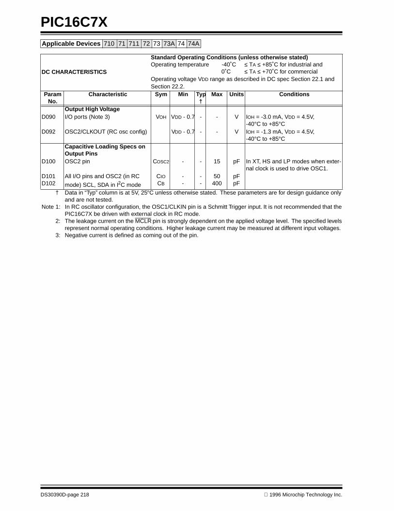
PIC16C7X
DS30390D-page 218 1996 Microchip Technology Inc.
Applicable Devices 710 71 711 72 73 73A 74 74A
Output High VoltageD090 I/O ports (Note 3) VOH VDD - 0.7 - - V IOH = -3.0 mA, VDD = 4.5V,
-40°C to +85°CD092 OSC2/CLKOUT (RC osc config) VDD - 0.7 - - V IOH = -1.3 mA, VDD = 4.5V,
-40°C to +85°CCapacitive Loading Specs on Output Pins
D100 OSC2 pin COSC2 - - 15 pF In XT, HS and LP modes when exter-nal clock is used to drive OSC1.
D101D102
All I/O pins and OSC2 (in RC
mode) SCL, SDA in I2C mode
CIO
CB
--
--
50400
pFpF
DC CHARACTERISTICS
Standard Operating Conditions (unless otherwise stated)Operating temperature -40˚C ≤ TA ≤ +85˚C for industrial and
0˚C ≤ TA ≤ +70˚C for commercialOperating voltage VDD range as described in DC spec Section 22.1 and Section 22.2.
ParamNo.
Characteristic Sym Min Typ†
Max Units Conditions
† Data in “Typ” column is at 5V, 25°C unless otherwise stated. These parameters are for design guidance only and are not tested.
Note 1: In RC oscillator configuration, the OSC1/CLKIN pin is a Schmitt Trigger input. It is not recommended that the PIC16C7X be driven with external clock in RC mode.
2: The leakage current on the MCLR pin is strongly dependent on the applied voltage level. The specified levels represent normal operating conditions. Higher leakage current may be measured at different input voltages.
3: Negative current is defined as coming out of the pin.
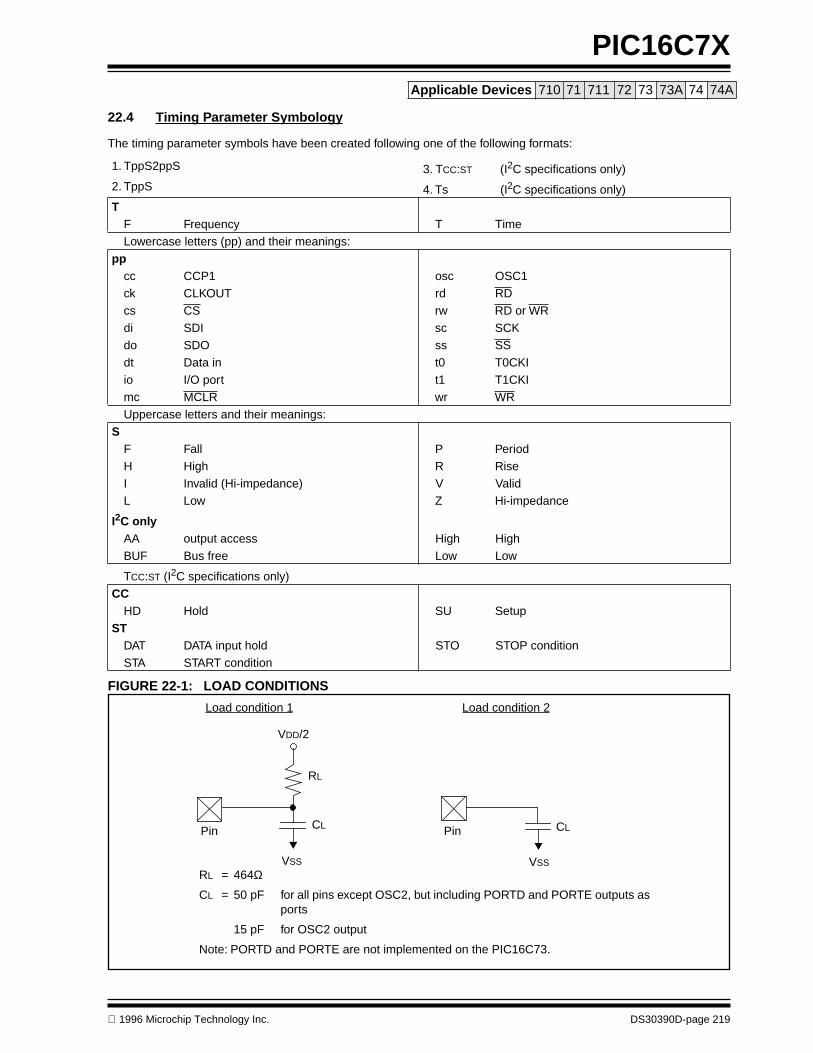
1996 Microchip Technology Inc. DS30390D-page 219
PIC16C7XApplicable Devices 710 71 711 72 73 73A 74 74A
22.4 Timing Parameter Symbology
The timing parameter symbols have been created following one of the following formats:
FIGURE 22-1: LOAD CONDITIONS
1. TppS2ppS 3. TCC:ST (I2C specifications only)2. TppS 4. Ts (I2C specifications only)T
F Frequency T TimeLowercase letters (pp) and their meanings:
ppcc CCP1 osc OSC1ck CLKOUT rd RD
cs CS rw RD or WRdi SDI sc SCKdo SDO ss SSdt Data in t0 T0CKIio I/O port t1 T1CKImc MCLR wr WRUppercase letters and their meanings:
SF Fall P PeriodH High R RiseI Invalid (Hi-impedance) V ValidL Low Z Hi-impedance
I2C onlyAA output access High HighBUF Bus free Low Low
TCC:ST (I2C specifications only)CC
HD Hold SU SetupST
DAT DATA input hold STO STOP conditionSTA START condition
VDD/2
CL
RL
Pin Pin
VSS VSS
CL
RL = 464Ω
CL = 50 pF for all pins except OSC2, but including PORTD and PORTE outputs asports
15 pF for OSC2 output
Note: PORTD and PORTE are not implemented on the PIC16C73.
Load condition 1 Load condition 2

PIC16C7X
DS30390D-page 220 1996 Microchip Technology Inc.
Applicable Devices 710 71 711 72 73 73A 74 74A
22.5 Timing Diagrams and Specifications
FIGURE 22-2: EXTERNAL CLOCK TIMING
TABLE 22-2: EXTERNAL CLOCK TIMING REQUIREMENTS
Parameter No.
Sym Characteristic Min Typ† Max Units Conditions
Fos External CLKIN Frequency (Note 1)
DC — 4 MHz XT and RC osc mode
DC — 4 MHz HS osc mode (PIC16C73-04, PIC16C74-04)
DC — 20 MHz HS osc mode (PIC16C73-20, PIC16C74-20)
DC — 200 kHz LP osc mode
Oscillator Frequency (Note 1)
DC — 4 MHz RC osc mode
0.1 — 4 MHz XT osc mode
4 — 4 MHz HS osc mode (PIC16C73-04, PIC16C74-04)
4
4
5
—
—
—
10
20
200
MHz
MHz
kHz
HS osc mode (PIC16C73-10, PIC16C74-10)HS osc mode (PIC16C73-20, PIC16C74-20)LP osc mode
1 Tosc External CLKIN Period(Note 1)
250 — — ns XT and RC osc mode
250 — — ns HS osc mode (PIC16C73-04, PIC16C74-04)
100 — — ns HS osc mode (PIC16C73-10, PIC16C74-10)
50 — — ns HS osc mode (PIC16C73-20, PIC16C74-20)
5 — — µs LP osc mode
Oscillator Period(Note 1)
250 — — ns RC osc mode
250 — 10,000 ns XT osc mode
250 — 250 ns HS osc mode (PIC16C73-04, PIC16C74-04)
100
50
—
—
250
250
ns
ns
HS osc mode (PIC16C73-10, PIC16C74-10)HS osc mode (PIC16C73-20, PIC16C74-20)
5 — — µs LP osc mode
2 TCY Instruction Cycle Time (Note 1) 200 — DC ns TCY = 4/FOSC
† Data in "Typ" column is at 5V, 25˚C unless otherwise stated. These parameters are for design guidance only and are not tested.
Note 1: Instruction cycle period (TCY) equals four times the input oscillator time-base period. All specified values are based on characterization data for that particular oscillator type under standard operating conditions with the device executing code. Exceeding these specified limits may result in an unstable oscillator operation and/or higher than expected current con-sumption. All devices are tested to operate at "min." values with an external clock applied to the OSC1/CLKIN pin.When an external clock input is used, the "Max." cycle time limit is "DC" (no clock) for all devices.
OSC1
CLKOUT
Q4 Q1 Q2 Q3 Q4 Q1
1
2
3 3 4 4

1996 Microchip Technology Inc. DS30390D-page 221
PIC16C7XApplicable Devices 710 71 711 72 73 73A 74 74A
3 TosL,TosH
External Clock in (OSC1) High or Low Time
50 — — ns XT oscillator
2.5 — — µs LP oscillator
15 — — ns HS oscillator
4 TosR,TosF
External Clock in (OSC1) Rise or Fall Time
— — 25 ns XT oscillator
— — 50 ns LP oscillator
— — 15 ns HS oscillator
TABLE 22-2: EXTERNAL CLOCK TIMING REQUIREMENTS (Cont.’d)
Parameter No.
Sym Characteristic Min Typ† Max Units Conditions
† Data in "Typ" column is at 5V, 25˚C unless otherwise stated. These parameters are for design guidance only and are not tested.
Note 1: Instruction cycle period (TCY) equals four times the input oscillator time-base period. All specified values are based on characterization data for that particular oscillator type under standard operating conditions with the device executing code. Exceeding these specified limits may result in an unstable oscillator operation and/or higher than expected current con-sumption. All devices are tested to operate at "min." values with an external clock applied to the OSC1/CLKIN pin.When an external clock input is used, the "Max." cycle time limit is "DC" (no clock) for all devices.

PIC16C7X
DS30390D-page 222 1996 Microchip Technology Inc.
Applicable Devices 710 71 711 72 73 73A 74 74A
FIGURE 22-3: CLKOUT AND I/O TIMING
TABLE 22-3: CLKOUT AND I/O TIMING REQUIREMENTS
ParameterNo.
Sym Characteristic Min Typ† Max Units Conditions
10* TosH2ckL OSC1↑ to CLKOUT↓ — 75 200 ns Note 1
11* TosH2ckH OSC1↑ to CLKOUT↑ — 75 200 ns Note 1
12* TckR CLKOUT rise time — 35 100 ns Note 1
13* TckF CLKOUT fall time — 35 100 ns Note 1
14* TckL2ioV CLKOUT ↓ to Port out valid — — 0.5TCY + 20 ns Note 1
15* TioV2ckH Port in valid before CLKOUT ↑ 0.25TCY + 25 — — ns Note 1
16* TckH2ioI Port in hold after CLKOUT ↑ 0 — — ns Note 1
17* TosH2ioV OSC1↑ (Q1 cycle) to Port out valid
— 50 150 ns
18* TosH2ioI OSC1↑ (Q2 cycle) to Port input invalid (I/O in hold time)
PIC16C73/74 100 — — ns
PIC16LC73/74 200 — — ns
19* TioV2osH Port input valid to OSC1↑ (I/O in setup time) 0 — — ns
20* TioR Port output rise time PIC16C73/74 — 10 25 ns
PIC16LC73/74 — — 60 ns
21* TioF Port output fall time PIC16C73/74 — 10 25 ns
PIC16LC73/74 — — 60 ns
22††* Tinp INT pin high or low time TCY — — ns
23††* Trbp RB7:RB4 change INT high or low time TCY — — ns
* These parameters are characterized but not tested.† Data in "Typ" column is at 5V, 25˚C unless otherwise stated. These parameters are for design guidance
only and are not tested.†† These parameters are asynchronous events not related to any internal clock edges.
Note 1: Measurements are taken in RC Mode where CLKOUT output is 4 x TOSC.
Note: Refer to Figure 22-1 for load conditions.
OSC1
CLKOUT
I/O Pin(input)
I/O Pin(output)
Q4 Q1 Q2 Q3
10
1314
17
20, 21
19 18
15
11
1216
old value new value

1996 Microchip Technology Inc. DS30390D-page 223
PIC16C7XApplicable Devices 710 71 711 72 73 73A 74 74A
FIGURE 22-4: RESET, WATCHDOG TIMER, OSCILLATOR START-UP TIMER AND POWER-UP TIMER TIMING
TABLE 22-4: RESET, WATCHDOG TIMER, OSCILLATOR START-UP TIMER AND POWER-UP TIMER REQUIREMENTS
Parameter No.
Sym Characteristic Min Typ† Max Units Conditions
30 TmcL MCLR Pulse Width (low) 100 — — ns VDD = 5V, -40˚C to +85˚C
31 Twdt Watchdog Timer Time-out Period (No Prescaler)
7* 18 33* ms VDD = 5V, -40˚C to +85˚C
32 Tost Oscillation Start-up Timer Period — 1024TOSC — — TOSC = OSC1 period
33 Tpwrt Power up Timer Period 28* 72 132* ms VDD = 5V, -40˚C to +85˚C
34 TIOZ I/O Hi-impedance from MCLR Low or Watchdog Timer Reset
— — 100 ns
* These parameters are characterized but not tested.† Data in "Typ" column is at 5V, 25˚C unless otherwise stated. These parameters are for design guidance only and are not
tested.
VDD
MCLR
InternalPOR
PWRTTime-out
OSCTime-out
InternalRESET
WatchdogTimer
RESET
33
32
30
3134
I/O Pins
34
Note: Refer to Figure 22-1 for load conditions.
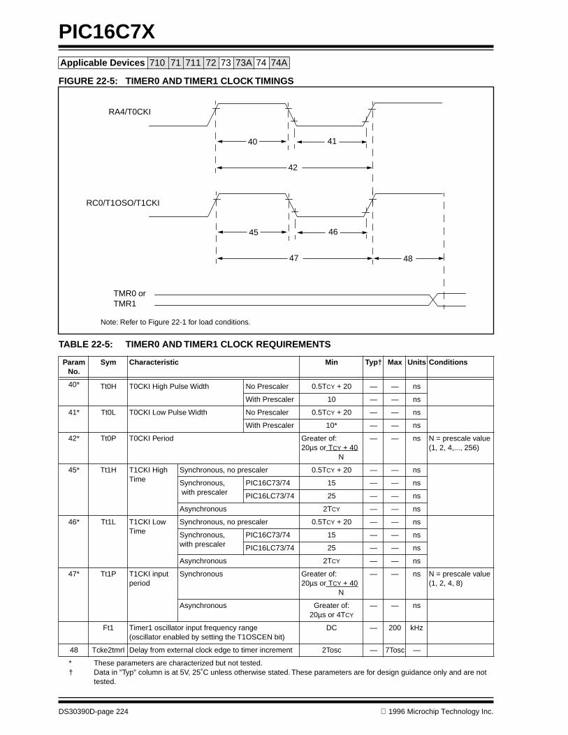
PIC16C7X
DS30390D-page 224 1996 Microchip Technology Inc.
Applicable Devices 710 71 711 72 73 73A 74 74A
FIGURE 22-5: TIMER0 AND TIMER1 CLOCK TIMINGS
TABLE 22-5: TIMER0 AND TIMER1 CLOCK REQUIREMENTS
Param No.
Sym Characteristic Min Typ† Max Units Conditions
40* Tt0H T0CKI High Pulse Width No Prescaler 0.5TCY + 20 — — ns
With Prescaler 10 — — ns
41* Tt0L T0CKI Low Pulse Width No Prescaler 0.5TCY + 20 — — ns
With Prescaler 10* — — ns
42* Tt0P T0CKI Period Greater of:20µs or TCY + 40 N
— — ns N = prescale value (1, 2, 4,..., 256)
45* Tt1H T1CKI High Time
Synchronous, no prescaler 0.5TCY + 20 — — ns
Synchronous, with prescaler
PIC16C73/74 15 — — ns
PIC16LC73/74 25 — — ns
Asynchronous 2TCY — — ns
46* Tt1L T1CKI Low Time
Synchronous, no prescaler 0.5TCY + 20 — — ns
Synchronous, with prescaler
PIC16C73/74 15 — — ns
PIC16LC73/74 25 — — ns
Asynchronous 2TCY — — ns
47* Tt1P T1CKI input period
Synchronous Greater of:20µs or TCY + 40 N
— — ns N = prescale value (1, 2, 4, 8)
Asynchronous Greater of:20µs or 4TCY
— — ns
Ft1 Timer1 oscillator input frequency range (oscillator enabled by setting the T1OSCEN bit)
DC — 200 kHz
48 Tcke2tmrI Delay from external clock edge to timer increment 2Tosc — 7Tosc —
* These parameters are characterized but not tested.† Data in "Typ" column is at 5V, 25˚C unless otherwise stated. These parameters are for design guidance only and are not
tested.
Note: Refer to Figure 22-1 for load conditions.
46
47
45
48
41
42
40
RA4/T0CKI
RC0/T1OSO/T1CKI
TMR0 orTMR1

1996 Microchip Technology Inc. DS30390D-page 225
PIC16C7XApplicable Devices 710 71 711 72 73 73A 74 74A
FIGURE 22-6: CAPTURE/COMPARE/PWM TIMINGS (CCP1 AND CCP2)
TABLE 22-6: CAPTURE/COMPARE/PWM REQUIREMENTS (CCP1 AND CCP2)
Parameter No.
Sym Characteristic Min Typ† Max Units Conditions
50* TccL CCP1 and CCP2input low time
No Prescaler 0.5TCY + 20 — — ns
With PrescalerPIC16C73/74 10 — — ns
PIC16LC73/74 20 — — ns
51* TccH CCP1 and CCP2input high time
No Prescaler 0.5TCY + 20 — — ns
With PrescalerPIC16C73/74 10 — — ns
PIC16LC73/74 20 — — ns
52* TccP CCP1 and CCP2 input period 3TCY + 40N
— — ns N = prescale value (1,4 or 16)
53* TccR CCP1 and CCP2 output fall time PIC16C73/74 — 10 25 ns
PIC16LC73/74 — 25 45 ns
54* TccF CCP1 and CCP2 output fall time PIC16C73/74 — 10 25 ns
PIC16LC73/74 — 25 45 ns
* These parameters are characterized but not tested.† Data in "Typ" column is at 5V, 25˚C unless otherwise stated. These parameters are for design guidance only and are not
tested.
Note: Refer to Figure 22-1 for load conditions.
and RC2/CCP1(Capture Mode)
50 51
52
53 54
RC1/T1OSI/CCP2
and RC2/CCP1(Compare or PWM Mode)
RC1/T1OSI/CCP2
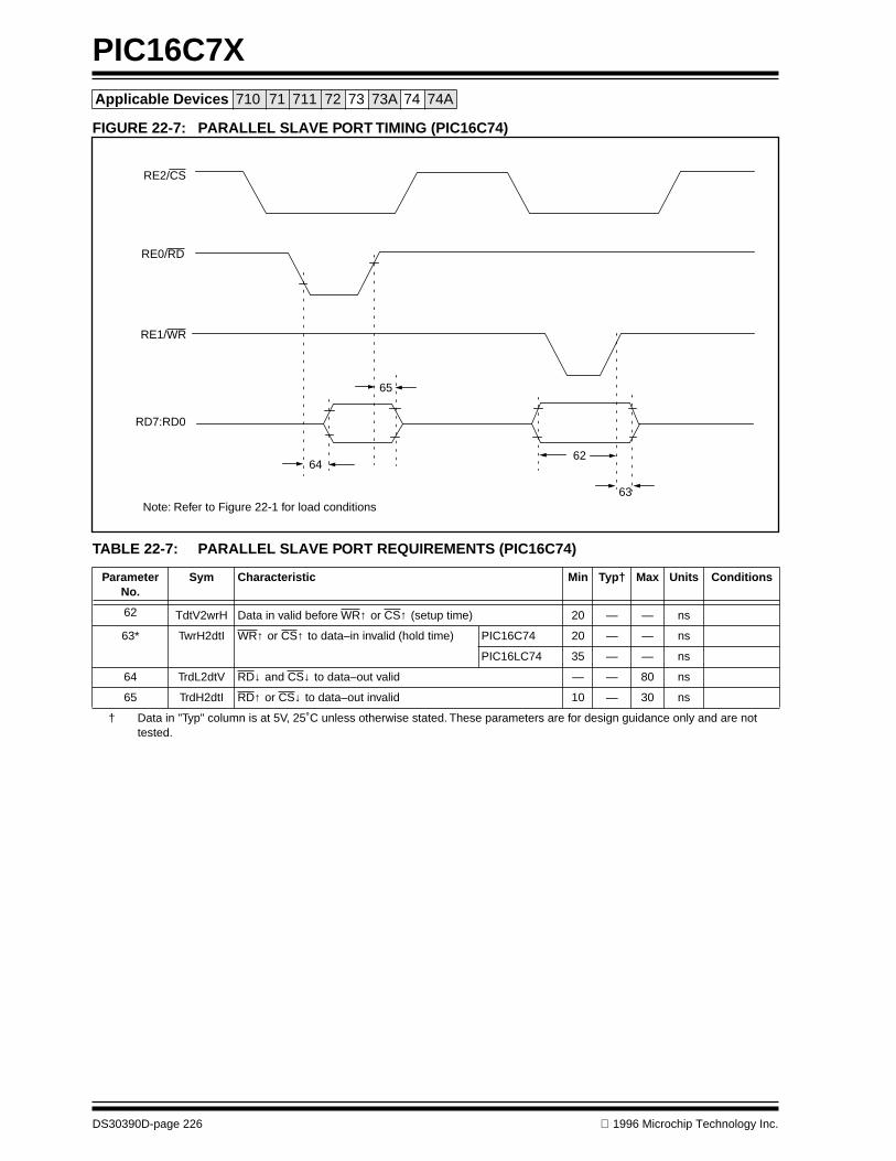
PIC16C7X
DS30390D-page 226 1996 Microchip Technology Inc.
Applicable Devices 710 71 711 72 73 73A 74 74A
FIGURE 22-7: PARALLEL SLAVE PORT TIMING (PIC16C74)
TABLE 22-7: PARALLEL SLAVE PORT REQUIREMENTS (PIC16C74)
Parameter No.
Sym Characteristic Min Typ† Max Units Conditions
62 TdtV2wrH Data in valid before WR↑ or CS↑ (setup time) 20 — — ns
63* TwrH2dtI WR↑ or CS↑ to data–in invalid (hold time) PIC16C74 20 — — ns
PIC16LC74 35 — — ns
64 TrdL2dtV RD↓ and CS↓ to data–out valid — — 80 ns
65 TrdH2dtI RD↑ or CS↓ to data–out invalid 10 — 30 ns
† Data in "Typ" column is at 5V, 25˚C unless otherwise stated. These parameters are for design guidance only and are not tested.
Note: Refer to Figure 22-1 for load conditions
RE2/CS
RE0/RD
RE1/WR
RD7:RD0
62
63
64
65

1996 Microchip Technology Inc. DS30390D-page 227
PIC16C7XApplicable Devices 710 71 711 72 73 73A 74 74A
FIGURE 22-8: SPI MODE TIMING
TABLE 22-8: SPI MODE REQUIREMENTS
Parameter No.
Sym Characteristic Min Typ† Max Units Conditions
70 TssL2scH, TssL2scL
SS↓ to SCK↓ or SCK↑ input TCY — — ns
71 TscH SCK input high time (slave mode) TCY + 20 — — ns
72 TscL SCK input low time (slave mode) TCY + 20 — — ns
73 TdiV2scH, TdiV2scL
Setup time of SDI data input to SCK edge
50 — — ns
74 TscH2diL, TscL2diL
Hold time of SDI data input to SCK edge
50 — — ns
75 TdoR SDO data output rise time — 10 25 ns
76 TdoF SDO data output fall time — 10 25 ns
77 TssH2doZ SS↓ to SDO output hi-impedance 10 — 50 ns
78 TscR SCK output rise time (master mode) — 10 25 ns
79 TscF SCK output fall time (master mode) — 10 25 ns
80 TscH2doV,TscL2doV
SDO data output valid after SCK edge
— — 50 ns
† Data in "Typ" column is at 5V, 25˚C unless otherwise stated. These parameters are for design guidance only and are not tested.
Note: Refer to Figure 22-1 for load conditions
SS
SCK(CKP = 0)
SCK(CKP = 1)
SDO
SDI
70
71 72
7374
75, 76 77
787980
7978

PIC16C7X
DS30390D-page 228 1996 Microchip Technology Inc.
Applicable Devices 710 71 711 72 73 73A 74 74A
FIGURE 22-9: I2C BUS START/STOP BITS TIMING
TABLE 22-9: I2C BUS START/STOP BITS REQUIREMENTS
ParameterNo.
Sym Characteristic Min Typ Max Units Conditions
90 TSU:STA START condition 100 kHz mode 4700 — —ns
Only relevant for repeated START conditionSetup time 400 kHz mode 600 — —
91 THD:STA START condition 100 kHz mode 4000 — —ns
After this period the first clock pulse is generatedHold time 400 kHz mode 600 — —
92 TSU:STO STOP condition 100 kHz mode 4700 — —ns
Setup time 400 kHz mode 600 — —
93 THD:STO STOP condition 100 kHz mode 4000 — —ns
Hold time 400 kHz mode 600 — —
Note: Refer to Figure 22-1 for load conditions
91 93SCL
SDA
STARTCondition
STOPCondition
90 92

1996 Microchip Technology Inc. DS30390D-page 229
PIC16C7XApplicable Devices 710 71 711 72 73 73A 74 74A
FIGURE 22-10: I2C BUS DATA TIMING
TABLE 22-10: I2C BUS DATA REQUIREMENTS
ParameterNo.
Sym Characteristic Min Max Units Conditions
100 THIGH Clock high time 100 kHz mode 4.0 — µs PIC16C73/74 must operate at a minimum of 1.5 MHz
400 kHz mode 0.6 — µs PIC16C73/74 must operate at a minimum of 10 MHz
SSP Module 1.5TCY —
101 TLOW Clock low time 100 kHz mode 4.7 — µs PIC16C73/74 must operate at a minimum of 1.5 MHz
400 kHz mode 1.3 — µs PIC16C73/74 must operate at a minimum of 10 MHz
SSP Module 1.5TCY —
102 TR SDA and SCL rise time
100 kHz mode — 1000 ns
400 kHz mode 20 + 0.1Cb 300 ns Cb is specified to be from 10 to 400 pF
103 TF SDA and SCL fall time 100 kHz mode — 300 ns
400 kHz mode 20 + 0.1Cb 300 ns Cb is specified to be from 10 to 400 pF
90 TSU:STA START condition setup time
100 kHz mode 4.7 — µs Only relevant for repeated START condition400 kHz mode 0.6 — µs
91 THD:STA START condition hold time
100 kHz mode 4.0 — µs After this period the first clock pulse is generated400 kHz mode 0.6 — µs
106 THD:DAT Data input hold time 100 kHz mode 0 — ns
400 kHz mode 0 0.9 µs
107 TSU:DAT Data input setup time 100 kHz mode 250 — ns Note 2
400 kHz mode 100 — ns
92 TSU:STO STOP condition setup time
100 kHz mode 4.7 — µs
400 kHz mode 0.6 — µs
109 TAA Output valid from clock
100 kHz mode — 3500 ns Note 1
400 kHz mode — — ns
110 TBUF Bus free time 100 kHz mode 4.7 — µs Time the bus must be free before a new transmission can start
400 kHz mode 1.3 — µs
Cb Bus capacitive loading — 400 pF
Note 1: As a transmitter, the device must provide this internal minimum delay time to bridge the undefined region (min. 300 ns) of the falling edge of SCL to avoid unintended generation of START or STOP conditions.
2: A fast-mode I2C-bus device can be used in a standard-mode I2C-bus system, but the requirement tsu;DAT ≥ 250 ns must then be met. This will automatically be the case if the device does not stretch the LOW period of the SCL signal. If such a device does stretch the LOW period of the SCL signal, it must output the next data bit to the SDA line TR max.+tsu;DAT = 1000 + 250 = 1250 ns (according to the standard-mode I2C bus specification) before the SCL line is released.
Note: Refer to Figure 22-1 for load conditions
90
91 92
100
101
103
106107
109 109110
102
SCL
SDAIn
SDAOut

PIC16C7X
DS30390D-page 230 1996 Microchip Technology Inc.
Applicable Devices 710 71 711 72 73 73A 74 74A
FIGURE 22-11: USART SYNCHRONOUS TRANSMISSION (MASTER/SLAVE) TIMING
TABLE 22-11: USART SYNCHRONOUS TRANSMISSION REQUIREMENTS
FIGURE 22-12: USART SYNCHRONOUS RECEIVE (MASTER/SLAVE) TIMING
TABLE 22-12: USART SYNCHRONOUS RECEIVE REQUIREMENTS
Parameter No.
Sym Characteristic Min Typ† Max Units Conditions
120 TckH2dtV SYNC XMIT (MASTER & SLAVE)Clock high to data out valid
PIC16C73/74 — — 80 ns
PIC16LC73/74 — — 100 ns
121 Tckrf Clock out rise time and fall time (Master Mode)
PIC16C73/74 — — 45 ns
PIC16LC73/74 — — 50 ns
122 Tdtrf Data out rise time and fall time PIC16C73/74 — — 45 ns
PIC16LC73/74 — — 50 ns
†: Data in “Typ” column is at 5V, 25°C unless otherwise stated. These parameters are for design guidance only and are not tested.
Parameter No.
Sym Characteristic Min Typ† Max Units Conditions
125 TdtV2ckl SYNC RCV (MASTER & SLAVE)Data hold before CK ↓ (DT hold time) 15 — — ns
126 TckL2dtl Data hold after CK ↓ (DT hold time) 15 — — ns
†: Data in “Typ” column is at 5V, 25°C unless otherwise stated. These parameters are for design guidance only and are not tested.
Note: Refer to Figure 22-1 for load conditions
121121
122
RC6/TX/CK
RC7/RX/DTpin
pin
120
Note: Refer to Figure 22-1 for load conditions
125
126
RC6/TX/CK
RC7/RX/DTpin
pin

1996 Microchip Technology Inc. DS30390D-page 231
PIC16C7XApplicable Devices 710 71 711 72 73 73A 74 74A
TABLE 22-13: A/D CONVERTER CHARACTERISTICS:PIC16C73-04 (COMMERCIAL, INDUSTRIAL)PIC16C74-04 (COMMERCIAL, INDUSTRIAL)PIC16C73-10 (COMMERCIAL, INDUSTRIAL)PIC16C74-10 (COMMERCIAL, INDUSTRIAL)PIC16C73-20 (COMMERCIAL, INDUSTRIAL)PIC16C74-20 (COMMERCIAL, INDUSTRIAL)
Parameter No.
Sym Characteristic Min Typ† Max Units Conditions
NR Resolution — — 8-bits — VREF = VDD = 5.12V, VSS ≤ AIN ≤ VREF
NINT Integral error — — less than ±1 LSb
— VREF = VDD = 5.12V, VSS ≤ AIN ≤ VREF
NDIF Differential error — — less than ±1 LSb
— VREF = VDD = 5.12V, VSS ≤ AIN ≤ VREF
NFS Full scale error — — less than ±1 LSb
— VREF = VDD = 5.12V, VSS ≤ AIN ≤ VREF
NOFF Offset error — — less than ±1 LSb
— VREF = VDD = 5.12V, VSS ≤ AIN ≤ VREF
— Monotonicity — guaranteed — — VSS ≤ AIN ≤ VREF
VREF Reference voltage 3.0V — VDD + 0.3 V
VAIN Analog input voltage VSS - 0.3 — VREF + 0.3 V
ZAIN Recommended impedance of analog voltage source
— — 10.0 kΩ
IAD A/D conversion cur-rent (VDD)
— 180 — µA Average current consumption when A/D is on. (Note 1)
IREF VREF input current (Note 2)
— — 110
mAµA
During samplingAll other times
* These parameters are characterized but not tested.† Data in “Typ” column is at 5V, 25°C unless otherwise stated. These parameters are for design guidance only and are not
tested.Note 1: When A/D is off, it will not consume any current other than minor leakage current. The power-down current spec includes
any such leakage from the A/D module.2: VREF current is from RA3 pin or VDD pin, whichever is selected as reference input.

PIC16C7X
DS30390D-page 232 1996 Microchip Technology Inc.
Applicable Devices 710 71 711 72 73 73A 74 74A
TABLE 22-14: A/D CONVERTER CHARACTERISTICS:PIC16LC73-04 (COMMERCIAL, INDUSTRIAL)PIC16LC74-04 (COMMERCIAL, INDUSTRIAL)
Parameter No.
Sym Characteristic Min Typ† Max Units Conditions
NR Resolution — — 8-bits — VREF = VDD = 3.0V (Note 1)
NINT Integral error — — less than ±1 LSb
— VREF = VDD = 3.0V (Note 1)
NDIF Differential error — — less than ±1 LSb
— VREF = VDD = 3.0V (Note 1)
NFS Full scale error — — less than ±1 LSb
— VREF = VDD = 3.0V (Note 1)
NOFF Offset error — — less than ±1 LSb
— VREF = VDD = 3.0V (Note 1)
— Monotonicity — guaranteed — — VSS ≤ AIN ≤ VREF
VREF Reference voltage 3.0V — VDD + 0.3 V
VAIN Analog input voltage VSS - 0.3 — VREF + 0.3 V
ZAIN Recommended impedance of ana-log voltage source
— — 10.0 kΩ
IAD A/D conversion cur-rent (VDD)
— 90 — µA Average current consumption when A/D is on. (Note 2)
IREF VREF input current (Note 3)
— — 110
mAµA
During samplingAll other times
* These parameters are characterized but not tested.† Data in “Typ” column is at 5V, 25°C unless otherwise stated. These parameters are for design guidance only and are not
tested.Note 1: These specifications apply if VREF = 3.0V and if VDD ≥ 3.0V. VIN must be between VSS and VREF
2: When A/D is off, it will not consume any current other than minor leakage current. The power-down current spec includes any such leakage from the A/D module.
3: VREF current is from RA3 pin or VDD pin, whichever is selected as reference input.
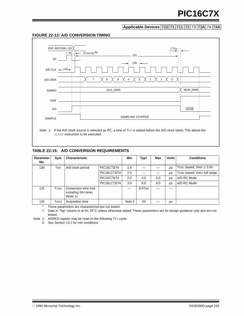
1996 Microchip Technology Inc. DS30390D-page 233
PIC16C7XApplicable Devices 710 71 711 72 73 73A 74 74A
FIGURE 22-13: A/D CONVERSION TIMING
TABLE 22-15: A/D CONVERSION REQUIREMENTS
Parameter No.
Sym Characteristic Min Typ† Max Units Conditions
130 TAD A/D clock period PIC16C73/74 1.6 — — µs TOSC based, VREF ≥ 3.0V
PIC16LC73/74 2.0 — — µs TOSC based, VREF full range
PIC16C73/74 2.0 4.0 6.0 µs A/D RC Mode
PIC16LC73/74 3.0 6.0 9.0 µs A/D RC Mode
131 TCNV Conversion time (not including S/H time)(Note 1)
— 9.5TAD — —
132 TACQ Acquisition time Note 2 20 — µs
* These parameters are characterized but not tested.† Data in “Typ” column is at 5V, 25°C unless otherwise stated. These parameters are for design guidance only and are not
tested.Note 1: ADRES register may be read on the following TCY cycle.
2: See Section 13.1 for min conditions.
131
130
132
BSF ADCON0, GO
Q4
A/D CLK
A/D DATA
ADRES
ADIF
GO
SAMPLE
OLD_DATA
SAMPLING STOPPED
DONE
NEW_DATA
(TOSC/2) (1)
7 6 5 4 3 2 1 0
Note 1: If the A/D clock source is selected as RC, a time of TCY is added before the A/D clock starts. This allows the SLEEP instruction to be executed.
1 Tcy

PIC16C7X
DS30390D-page 234 1996 Microchip Technology Inc.
Applicable Devices 710 71 711 72 73 73A 74 74A
NOTES:

1996 Microchip Technology Inc. DS30390D-page 235
PIC16C7X
Applicable Devices
710 71 711 72 73 73A 74 74A
23.0 ELECTRICAL CHARACTERISTICS FOR PIC16C73A/74A
Absolute Maximum Ratings †
Ambient temperature under bias................................................................................................................ .-55 to +125˚C
Storage temperature .............................................................................................................................. -65˚C to +150˚C
Voltage on any pin with respect to V
SS
(except V
DD
and MCLR) ................................................... -0.3V to (V
DD
+ 0.3V)
Voltage on V
DD
with respect to V
SS
................................................................................................................ 0 to +7.5V
Voltage on MCLR with respect to V
SS
(Note 2) .................................................................................................0 to +14V
Total power dissipation (Note 1)................................................................................................................................1.0W
Maximum current out of V
SS
pin ...........................................................................................................................300 mA
Maximum current into V
DD
pin ..............................................................................................................................250 mA
Input clamp current, I
IK
(V
I
< 0 or V
I
> V
DD
)
.....................................................................................................................±
20 mA
Output clamp current, I
OK
(V
O
< 0 or V
O
> V
DD
)
.............................................................................................................±
20 mA
Maximum output current sunk by any I/O pin..........................................................................................................25 mA
Maximum output current sourced by any I/O pin ....................................................................................................25 mA
Maximum current sunk by
PORTA, PORTB, and PORTE (combined) (Note 3) ...................................................200 mA
Maximum current sourced by PORTA, PORTB, and PORTE (combined) (Note 3) ..............................................200 mA
Maximum current sunk by PORTC and PORTD (combined) (Note 3)..................................................................200 mA
Maximum current sourced by PORTC and PORTD (combined) (Note 3).............................................................200 mA
Note 1:
Power dissipation is calculated as follows: Pdis = V
DD
x I
DD
-
∑
I
OH
+
∑
(V
DD
- V
OH
) x I
OH
+
∑
(V
O
l x I
OL
)
Note 2:
Voltage spikes below V
SS
at the MCLR pin, inducing currents greater than 80 mA, may cause latch-up. Thus,a series resistor of 50-100
Ω
should be used when applying a “low” level to the MCLR pin rather than pullingthis pin directly to V
SS
.
Note 3:
PORTD and PORTE are not implemented on the PIC16C73A.
† NOTICE: Stresses above those listed under “Absolute Maximum Ratings” may cause permanent damage to the device. This is a stress rating only and functional operation of the device at those or any other conditions above those indicated in the operation listings of this specification is not implied. Exposure to maximum rating conditions for extended periods may affect device reliability.
This document was created with FrameMaker 4 0 4
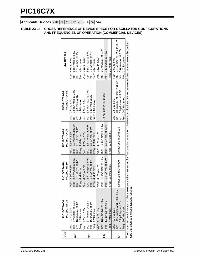
PIC16C7X
DS30390D-page 236
1996 Microchip Technology Inc.
Applicable Devices
710 71 711 72 73 73A 74 74A
TABLE 23-1: CROSS REFERENCE OF DEVICE SPECS FOR OSCILLATOR CONFIGURATIONS AND FREQUENCIES OF OPERATION (COMMERCIAL DEVICES)
OS
CP
IC16
C73
A-0
4P
IC16
C74
A-0
4P
IC16
C73
A-1
0P
IC16
C74
A-1
0P
IC16
C73
A-2
0P
IC16
C74
A-2
0P
IC16
LC
73A
-04
PIC
16L
C74
A-0
4JW
Dev
ices
RC
VD
D:
4.0V
to 6
.0V
IDD
: 5
mA
max
. at 5
.5V
IPD
: 16
µA
max
. at 4
VF
req:
4 M
Hz
max
.
VD
D:
4.5V
to 5
.5V
IDD
: 2.
7 m
A ty
p. a
t 5.5
VIP
D:
1.5
µA ty
p. a
t 4V
Fre
q: 4
MH
z m
ax.
VD
D:
4.5V
to 5
.5V
IDD
: 2.
7 m
A ty
p. a
t 5.5
VIP
D:
1.5
µA ty
p. a
t 4V
Fre
q: 4
MH
z m
ax.
VD
D:
2.5V
to 6
.0V
IDD
: 3.
8 m
A m
ax. a
t 3.0
VIP
D:
5 µA
max
. at 3
VF
req:
4 M
Hz
max
.
VD
D:
4.0V
to 6
.0V
IDD
: 5
mA
max
. at 5
.5V
IPD
: 16
µA
max
. at 4
VF
req:
4 M
Hz
max
.
XT
VD
D:
4.0V
to 6
.0V
IDD
: 5
mA
max
. at 5
.5V
IPD
: 16
µA
max
. at 4
VF
req:
4 M
Hz
max
.
VD
D:
4.5V
to 5
.5V
IDD
: 2.
7 m
A ty
p. a
t 5.5
VIP
D:
1.5
µA ty
p. a
t 4V
Fre
q: 4
MH
z m
ax.
VD
D:
4.5V
to 5
.5V
IDD
: 2.
7 m
A ty
p. a
t 5.5
VIP
D:
1.5
µA ty
p. a
t 4V
Fre
q: 4
MH
z m
ax.
VD
D:
2.5V
to 6
.0V
IDD
: 3.
8 m
A m
ax. a
t 3.0
VIP
D:
5 µA
max
. at 3
VF
req:
4 M
Hz
max
.
VD
D:
4.0V
to 6
.0V
IDD
: 5
mA
max
. at 5
.5V
IPD
: 16
µA
max
. at 4
VF
req:
4 M
Hz
max
.
HS
VD
D:
4.5V
to 5
.5V
VD
D:
4.5V
to 5
.5V
VD
D:
4.5V
to 5
.5V
Do
not u
se in
HS
mod
e
VD
D:
4.5V
to 5
.5V
IDD
: 13
.5 m
A ty
p. a
t 5.5
VID
D:
10 m
A m
ax. a
t 5.5
VID
D:
20 m
A m
ax. a
t 5.5
VID
D:
20 m
A m
ax. a
t 5.5
V
IPD
: 1.
5 µA
typ.
at 4
.5V
IPD
: 1.
5 µA
typ.
at 4
.5V
IPD
:1.
5 µA
typ.
at 4
.5V
IPD
: 1.
5 µA
typ.
at 4
.5V
Fre
q: 4
MH
z m
ax.
Fre
q: 1
0 M
Hz
max
.F
req:
20 M
Hz
max
.F
req:
20
MH
z m
ax.
LP
VD
D:
4.0V
to 6
.0V
IDD
: 52
.5 µ
A ty
p. a
t 32
kHz,
4.0
VIP
D:
0.9
µA ty
p. a
t 4.0
VF
req:
200
kH
z m
ax.
Do
not u
se in
LP
mod
eD
o no
t use
in L
P m
ode
VD
D:
2.5V
to 6
.0V
IDD
: 48
µA
max
. at 3
2 kH
z, 3
.0V
IPD
: 5.
0 µA
max
. at 3
.0V
Fre
q: 2
00 k
Hz
max
.
VD
D:
2.5V
to 6
.0V
IDD
: 48
µA
max
. at 3
2 kH
z, 3
.0V
IPD
: 5.
0 µA
max
. at 3
.0V
Fre
q: 2
00 k
Hz
max
.
The
sha
ded
sect
ions
indi
cate
osc
illat
or s
elec
tions
whi
ch a
re te
sted
for
func
tiona
lity,
but
not
for
MIN
/MA
X s
peci
ficat
ions
. It i
s re
com
men
ded
that
the
user
sel
ect t
he d
evic
e ty
pe th
at e
nsur
es th
e sp
ecifi
catio
ns r
equi
red.
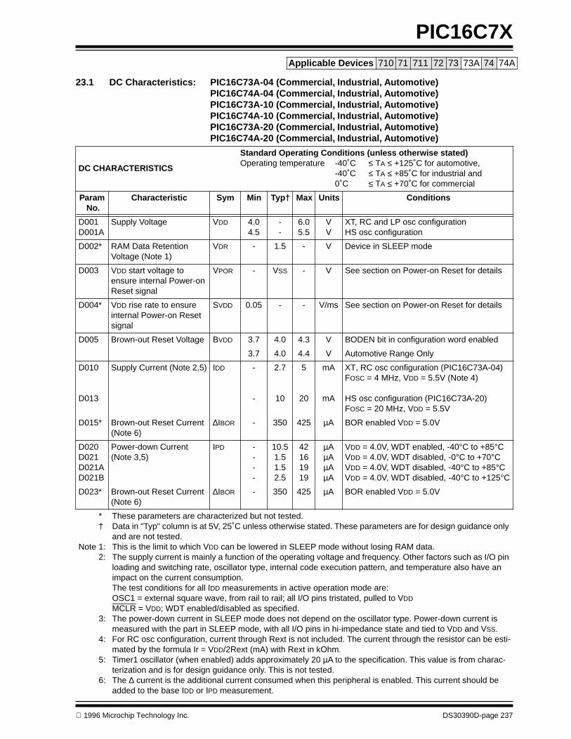
1996 Microchip Technology Inc. DS30390D-page 237
PIC16C7X
Applicable Devices
710 71 711 72 73 73A 74 74A
23.1 DC Characteristics: PIC16C73A-04 (Commercial, Industrial, Automotive)PIC16C74A-04 (Commercial, Industrial, Automotive)PIC16C73A-10 (Commercial, Industrial, Automotive)PIC16C74A-10 (Commercial, Industrial, Automotive)PIC16C73A-20 (Commercial, Industrial, Automotive)PIC16C74A-20 (Commercial, Industrial, Automotive)
DC CHARACTERISTICS
Standard Operating Conditions (unless otherwise stated)
Operating temperature -40˚C
≤
T
A
≤
+125˚C for automotive,-40˚C
≤
T
A
≤
+85˚C for industrial and 0˚C
≤
T
A
≤
+70˚C for commercial
Param No.
Characteristic Sym Min Typ† Max Units Conditions
D001D001A
Supply Voltage V
DD
4.04.5
--
6.05.5
VV
XT, RC and LP osc configurationHS osc configuration
D002* RAM Data RetentionVoltage (Note 1)
V
DR
- 1.5 - V Device in SLEEP mode
D003 V
DD
start voltage toensure internal Power-on Reset signal
V
POR
- V
SS
- V See section on Power-on Reset for details
D004* V
DD
rise rate to ensure internal Power-on Reset signal
S
VDD
0.05 - - V/ms See section on Power-on Reset for details
D005 Brown-out Reset Voltage BVDD 3.7 4.0 4.3 V BODEN bit in configuration word enabled
3.7 4.0 4.4 V Automotive Range Only
D010
D013
Supply Current (Note 2,5) IDD -
-
2.7
10
5
20
mA
mA
XT, RC osc configuration (PIC16C73A-04)FOSC = 4 MHz, VDD = 5.5V (Note 4)
HS osc configuration (PIC16C73A-20)FOSC = 20 MHz, VDD = 5.5V
D015* Brown-out Reset Current (Note 6)
∆IBOR - 350 425 µA BOR enabled VDD = 5.0V
D020D021D021AD021B
Power-down Current (Note 3,5)
IPD ----
10.51.51.52.5
42161919
µAµAµAµA
VDD = 4.0V, WDT enabled, -40°C to +85°CVDD = 4.0V, WDT disabled, -0°C to +70°CVDD = 4.0V, WDT disabled, -40°C to +85°CVDD = 4.0V, WDT disabled, -40°C to +125°C
D023* Brown-out Reset Current (Note 6)
∆IBOR - 350 425 µA BOR enabled VDD = 5.0V
* These parameters are characterized but not tested.† Data in "Typ" column is at 5V, 25˚C unless otherwise stated. These parameters are for design guidance only
and are not tested.Note 1: This is the limit to which VDD can be lowered in SLEEP mode without losing RAM data.
2: The supply current is mainly a function of the operating voltage and frequency. Other factors such as I/O pin loading and switching rate, oscillator type, internal code execution pattern, and temperature also have an impact on the current consumption.The test conditions for all IDD measurements in active operation mode are: OSC1 = external square wave, from rail to rail; all I/O pins tristated, pulled to VDD MCLR = VDD; WDT enabled/disabled as specified.
3: The power-down current in SLEEP mode does not depend on the oscillator type. Power-down current is measured with the part in SLEEP mode, with all I/O pins in hi-impedance state and tied to VDD and VSS.
4: For RC osc configuration, current through Rext is not included. The current through the resistor can be esti-mated by the formula Ir = VDD/2Rext (mA) with Rext in kOhm.
5: Timer1 oscillator (when enabled) adds approximately 20 µA to the specification. This value is from charac-terization and is for design guidance only. This is not tested.
6: The ∆ current is the additional current consumed when this peripheral is enabled. This current should be added to the base IDD or IPD measurement.

PIC16C7X
DS30390D-page 238 1996 Microchip Technology Inc.
Applicable Devices 710 71 711 72 73 73A 74 74A
23.2 DC Characteristics: PIC16LC73A-04 (Commercial, Industrial)PIC16LC74A-04 (Commercial, Industrial)
DC CHARACTERISTICSStandard Operating Conditions (unless otherwise stated)Operating temperature -40˚C ≤ TA ≤ +85˚C for industrial and
0˚C ≤ TA ≤ +70˚C for commercial
Param No.
Characteristic Sym Min Typ† Max Units Conditions
D001 Supply Voltage VDD 2.5 - 6.0 V LP, XT, RC osc configuration (DC - 4 MHz)
D002* RAM Data Retention Voltage (Note 1)
VDR - 1.5 - V Device in SLEEP mode
D003 VDD start voltage to ensure internal Power-on Reset signal
VPOR - VSS - V See section on Power-on Reset for details
D004* VDD rise rate to ensure internal Power-on Reset signal
SVDD 0.05 - - V/ms See section on Power-on Reset for details
D005 Brown-out Reset Voltage BVDD 3.7 4.0 4.3 V BODEN bit in configuration word enabled
D010
D010A
Supply Current (Note 2,5) IDD -
-
2.0
22.5
3.8
48
mA
µA
XT, RC osc configurationFOSC = 4 MHz, VDD = 3.0V (Note 4)
LP osc configurationFOSC = 32 kHz, VDD = 3.0V, WDT disabled
D015* Brown-out Reset Current (Note 6)
∆IBOR - 350 425 µA BOR enabled VDD = 3.0V
D020D021D021A
Power-down Current (Note 3,5)
IPD ---
7.50.90.9
3055
µAµAµA
VDD = 3.0V, WDT enabled, -40°C to +85°CVDD = 3.0V, WDT disabled, 0°C to +70°CVDD = 3.0V, WDT disabled, -40°C to +85°C
D023* Brown-out Reset Current (Note 6)
∆IBOR - 350 425 µA BOR enabled VDD = 3.0V
* These parameters are characterized but not tested.† Data in "Typ" column is at 5V, 25˚C unless otherwise stated. These parameters are for design guidance
only and are not tested.Note 1: This is the limit to which VDD can be lowered in SLEEP mode without losing RAM data.
2: The supply current is mainly a function of the operating voltage and frequency. Other factors such as I/O pin loading and switching rate, oscillator type, internal code execution pattern, and temperature also have an impact on the current consumption.The test conditions for all IDD measurements in active operation mode are: OSC1 = external square wave, from rail to rail; all I/O pins tristated, pulled to VDD MCLR = VDD; WDT enabled/disabled as specified.
3: The power-down current in SLEEP mode does not depend on the oscillator type. Power-down current is measured with the part in SLEEP mode, with all I/O pins in hi-impedance state and tied to VDD and VSS.
4: For RC osc configuration, current through Rext is not included. The current through the resistor can be esti-mated by the formula Ir = VDD/2Rext (mA) with Rext in kOhm.
5: Timer1 oscillator (when enabled) adds approximately 20 µA to the specification. This value is from charac-terization and is for design guidance only. This is not tested.
6: The ∆ current is the additional current consumed when this peripheral is enabled. This current should be added to the base IDD or IPD measurement.

1996 Microchip Technology Inc. DS30390D-page 239
PIC16C7XApplicable Devices 710 71 711 72 73 73A 74 74A
23.3 DC Characteristics: PIC16C73A-04 (Commercial, Industrial, Automotive)PIC16C74A-04 (Commercial, Industrial, Automotive)PIC16C73A-10 (Commercial, Industrial, Automotive)PIC16C74A-10 (Commercial, Industrial, Automotive)PIC16C73A-20 (Commercial, Industrial, Automotive)PIC16C74A-20 (Commercial, Industrial, Automotive)PIC16LC73A-04 (Commercial, Industrial)PIC16LC74A-04 (Commercial, Industrial)
DC CHARACTERISTICS
Standard Operating Conditions (unless otherwise stated)Operating temperature -40˚C ≤ TA ≤ +125˚C for automotive,
-40˚C ≤ TA ≤ +85˚C for industrial and 0˚C ≤ TA ≤ +70˚C for commercial
Operating voltage VDD range as described in DC spec Section 23.1 and Section 23.2.
ParamNo.
Characteristic Sym Min Typ†
Max Units Conditions
Input Low VoltageI/O ports VIL
D030 with TTL buffer VSS - 0.5V VD031 with Schmitt Trigger buffer VSS - 0.2VDD VD032 MCLR, RA4/T0CKI,OSC1
(in RC mode)VSS - 0.2VDD V
D033 OSC1 (in XT, HS and LP) VSS - 0.3VDD V Note1Input High VoltageI/O ports VIH -
D040 with TTL buffer 2.0 - VDD V 4.5V ≤ VDD ≤ 5.5VD040A 0.8VDD - VDD V For VDD > 5.5V or VDD < 4.5VD041 with Schmitt Trigger buffer 0.8VDD - VDD V For entire VDD rangeD042 MCLR, RA4/T0CKI, RC7:RC4,
RD7:RD4, RB0/INT0.8VDD - VDD V
D042A RE2:RE0, OSC1 (XT, HS and LP) 0.7VDD - VDD V Note1D043 OSC1 (in RC mode) 0.9VDD - VDD VD070 PORTB weak pull-up current IPURB 50 250 400 µA VDD = 5V, VPIN = VSS
Input Leakage Current (Notes 2, 3)
D060 I/O ports IIL - - ±1 µA Vss ≤ VPIN ≤ VDD, Pin at hi-imped-ance
D061 MCLR, RA4/T0CKI - - ±5 µA Vss ≤ VPIN ≤ VDD
D063 OSC1 - - ±5 µA Vss ≤ VPIN ≤ VDD, XT, HS and LP osc configuration
† Data in “Typ” column is at 5V, 25°C unless otherwise stated. These parameters are for design guidance only and are not tested.
Note 1: In RC oscillator configuration, the OSC1/CLKIN pin is a Schmitt Trigger input. It is not recommended that the PIC16C7X be driven with external clock in RC mode.
2: The leakage current on the MCLR pin is strongly dependent on the applied voltage level. The specified lev-els represent normal operating conditions. Higher leakage current may be measured at different input volt-ages.
3: Negative current is defined as coming out of the pin.

PIC16C7X
DS30390D-page 240 1996 Microchip Technology Inc.
Applicable Devices 710 71 711 72 73 73A 74 74A
Output Low VoltageD080 I/O ports VOL - - 0.6 V IOL = 8.5 mA, VDD = 4.5V,
-40°C to +85°CD080A - - 0.6 V IOL = 7.0 mA, VDD = 4.5V,
-40°C to +125°CD083 OSC2/CLKOUT (RC osc config) - - 0.6 V IOL = 1.6 mA, VDD = 4.5V,
-40°C to +85°CD083A - - 0.6 V IOL = 1.2 mA, VDD = 4.5V,
-40°C to +125°COutput High Voltage
D090 I/O ports (Note 3) VOH VDD - 0.7 - - V IOH = -3.0 mA, VDD = 4.5V, -40°C to +85°C
D090A VDD - 0.7 - - V IOH = -2.5 mA, VDD = 4.5V, -40°C to +125°C
D092 OSC2/CLKOUT (RC osc config) VDD - 0.7 - - V IOH = -1.3 mA, VDD = 4.5V, -40°C to +85°C
D092A VDD - 0.7 - - V IOH = -1.0 mA, VDD = 4.5V, -40°C to +125°C
Capacitive Loading Specs on Output Pins
D100 OSC2 pin COSC2 - - 15 pF In XT, HS and LP modes when exter-nal clock is used to drive OSC1.
D101D102
All I/O pins and OSC2 (in RC
mode) SCL, SDA in I2C mode
CIO
CB
--
--
50400
pFpF
DC CHARACTERISTICS
Standard Operating Conditions (unless otherwise stated)Operating temperature -40˚C ≤ TA ≤ +125˚C for automotive,
-40˚C ≤ TA ≤ +85˚C for industrial and 0˚C ≤ TA ≤ +70˚C for commercial
Operating voltage VDD range as described in DC spec Section 23.1 and Section 23.2.
ParamNo.
Characteristic Sym Min Typ†
Max Units Conditions
† Data in “Typ” column is at 5V, 25°C unless otherwise stated. These parameters are for design guidance only and are not tested.
Note 1: In RC oscillator configuration, the OSC1/CLKIN pin is a Schmitt Trigger input. It is not recommended that the PIC16C7X be driven with external clock in RC mode.
2: The leakage current on the MCLR pin is strongly dependent on the applied voltage level. The specified lev-els represent normal operating conditions. Higher leakage current may be measured at different input volt-ages.
3: Negative current is defined as coming out of the pin.
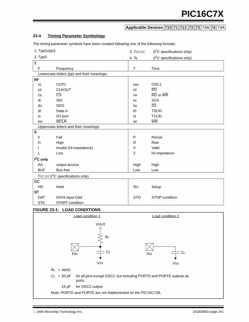
1996 Microchip Technology Inc. DS30390D-page 241
PIC16C7XApplicable Devices 710 71 711 72 73 73A 74 74A
23.4 Timing Parameter Symbology
The timing parameter symbols have been created following one of the following formats:
FIGURE 23-1: LOAD CONDITIONS
1. TppS2ppS 3. TCC:ST (I2C specifications only)2. TppS 4. Ts (I2C specifications only)T
F Frequency T TimeLowercase letters (pp) and their meanings:
ppcc CCP1 osc OSC1ck CLKOUT rd RD
cs CS rw RD or WRdi SDI sc SCKdo SDO ss SSdt Data in t0 T0CKIio I/O port t1 T1CKImc MCLR wr WRUppercase letters and their meanings:
SF Fall P PeriodH High R RiseI Invalid (Hi-impedance) V ValidL Low Z Hi-impedance
I2C onlyAA output access High HighBUF Bus free Low Low
TCC:ST (I2C specifications only)CC
HD Hold SU SetupST
DAT DATA input hold STO STOP conditionSTA START condition
VDD/2
CL
RL
Pin Pin
VSS VSS
CL
RL = 464Ω
CL = 50 pF for all pins except OSC2, but including PORTD and PORTE outputs asports
15 pF for OSC2 output
Note: PORTD and PORTE are not implemented on the PIC16C73A.
Load condition 1 Load condition 2
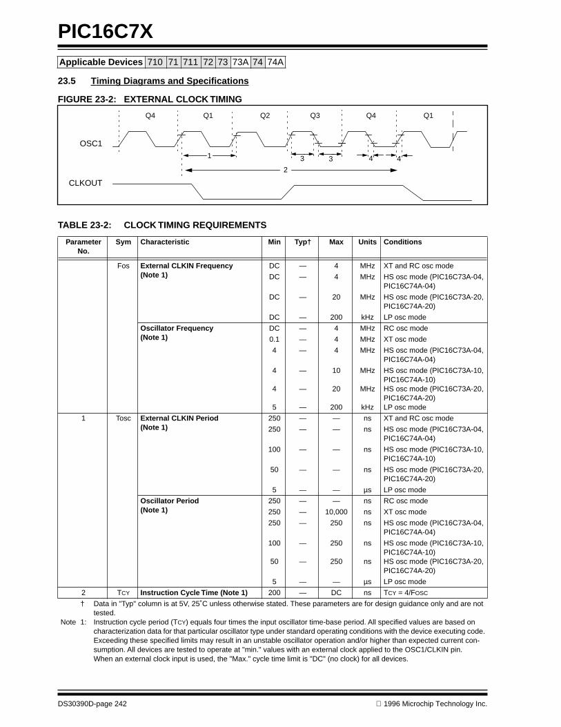
PIC16C7X
DS30390D-page 242 1996 Microchip Technology Inc.
Applicable Devices 710 71 711 72 73 73A 74 74A
23.5 Timing Diagrams and Specifications
FIGURE 23-2: EXTERNAL CLOCK TIMING
TABLE 23-2: CLOCK TIMING REQUIREMENTS
Parameter No.
Sym Characteristic Min Typ† Max Units Conditions
Fos External CLKIN Frequency (Note 1)
DC — 4 MHz XT and RC osc mode
DC — 4 MHz HS osc mode (PIC16C73A-04, PIC16C74A-04)
DC — 20 MHz HS osc mode (PIC16C73A-20, PIC16C74A-20)
DC — 200 kHz LP osc mode
Oscillator Frequency (Note 1)
DC — 4 MHz RC osc mode
0.1 — 4 MHz XT osc mode
4 — 4 MHz HS osc mode (PIC16C73A-04, PIC16C74A-04)
4
4
5
—
—
—
10
20
200
MHz
MHz
kHz
HS osc mode (PIC16C73A-10, PIC16C74A-10)HS osc mode (PIC16C73A-20, PIC16C74A-20)LP osc mode
1 Tosc External CLKIN Period(Note 1)
250 — — ns XT and RC osc mode
250 — — ns HS osc mode (PIC16C73A-04, PIC16C74A-04)
100 — — ns HS osc mode (PIC16C73A-10, PIC16C74A-10)
50 — — ns HS osc mode (PIC16C73A-20, PIC16C74A-20)
5 — — µs LP osc mode
Oscillator Period(Note 1)
250 — — ns RC osc mode
250 — 10,000 ns XT osc mode
250 — 250 ns HS osc mode (PIC16C73A-04, PIC16C74A-04)
100
50
—
—
250
250
ns
ns
HS osc mode (PIC16C73A-10, PIC16C74A-10)HS osc mode (PIC16C73A-20, PIC16C74A-20)
5 — — µs LP osc mode
2 TCY Instruction Cycle Time (Note 1) 200 — DC ns TCY = 4/FOSC
† Data in "Typ" column is at 5V, 25˚C unless otherwise stated. These parameters are for design guidance only and are not tested.
Note 1: Instruction cycle period (TCY) equals four times the input oscillator time-base period. All specified values are based on characterization data for that particular oscillator type under standard operating conditions with the device executing code. Exceeding these specified limits may result in an unstable oscillator operation and/or higher than expected current con-sumption. All devices are tested to operate at "min." values with an external clock applied to the OSC1/CLKIN pin.When an external clock input is used, the "Max." cycle time limit is "DC" (no clock) for all devices.
OSC1
CLKOUT
Q4 Q1 Q2 Q3 Q4 Q1
1
2
3 3 4 4
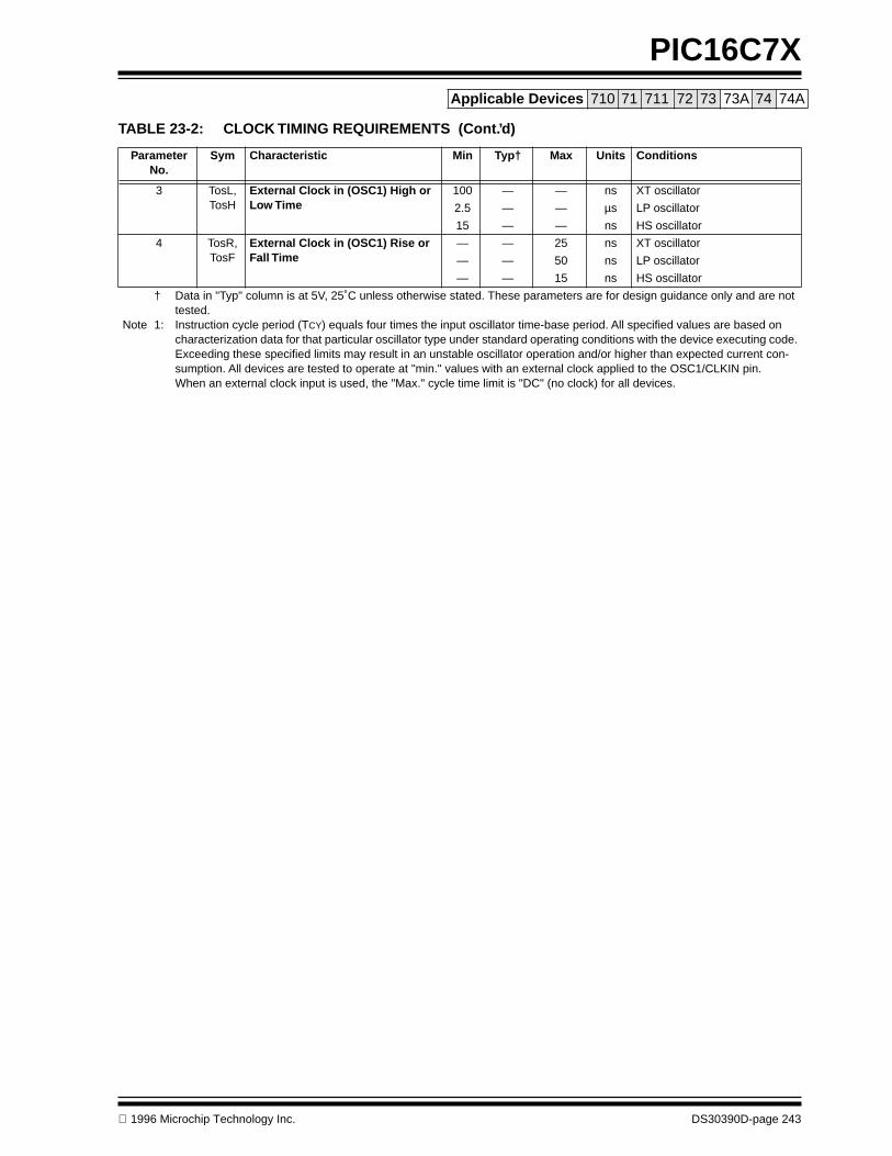
1996 Microchip Technology Inc. DS30390D-page 243
PIC16C7XApplicable Devices 710 71 711 72 73 73A 74 74A
3 TosL,TosH
External Clock in (OSC1) High or Low Time
100 — — ns XT oscillator
2.5 — — µs LP oscillator
15 — — ns HS oscillator
4 TosR,TosF
External Clock in (OSC1) Rise or Fall Time
— — 25 ns XT oscillator
— — 50 ns LP oscillator
— — 15 ns HS oscillator
TABLE 23-2: CLOCK TIMING REQUIREMENTS (Cont.’d)
Parameter No.
Sym Characteristic Min Typ† Max Units Conditions
† Data in "Typ" column is at 5V, 25˚C unless otherwise stated. These parameters are for design guidance only and are not tested.
Note 1: Instruction cycle period (TCY) equals four times the input oscillator time-base period. All specified values are based on characterization data for that particular oscillator type under standard operating conditions with the device executing code. Exceeding these specified limits may result in an unstable oscillator operation and/or higher than expected current con-sumption. All devices are tested to operate at "min." values with an external clock applied to the OSC1/CLKIN pin.When an external clock input is used, the "Max." cycle time limit is "DC" (no clock) for all devices.
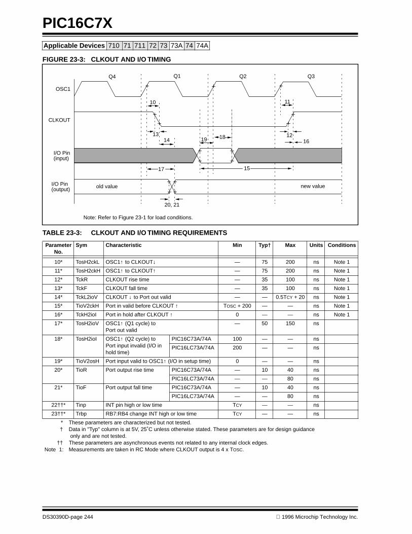
PIC16C7X
DS30390D-page 244 1996 Microchip Technology Inc.
Applicable Devices 710 71 711 72 73 73A 74 74A
FIGURE 23-3: CLKOUT AND I/O TIMING
TABLE 23-3: CLKOUT AND I/O TIMING REQUIREMENTS
ParameterNo.
Sym Characteristic Min Typ† Max Units Conditions
10* TosH2ckL OSC1↑ to CLKOUT↓ — 75 200 ns Note 1
11* TosH2ckH OSC1↑ to CLKOUT↑ — 75 200 ns Note 1
12* TckR CLKOUT rise time — 35 100 ns Note 1
13* TckF CLKOUT fall time — 35 100 ns Note 1
14* TckL2ioV CLKOUT ↓ to Port out valid — — 0.5TCY + 20 ns Note 1
15* TioV2ckH Port in valid before CLKOUT ↑ TOSC + 200 — — ns Note 1
16* TckH2ioI Port in hold after CLKOUT ↑ 0 — — ns Note 1
17* TosH2ioV OSC1↑ (Q1 cycle) to Port out valid
— 50 150 ns
18* TosH2ioI OSC1↑ (Q2 cycle) to Port input invalid (I/O in hold time)
PIC16C73A/74A 100 — — ns
PIC16LC73A/74A 200 — — ns
19* TioV2osH Port input valid to OSC1↑ (I/O in setup time) 0 — — ns
20* TioR Port output rise time PIC16C73A/74A — 10 40 ns
PIC16LC73A/74A — — 80 ns
21* TioF Port output fall time PIC16C73A/74A — 10 40 ns
PIC16LC73A/74A — — 80 ns
22††* Tinp INT pin high or low time TCY — — ns
23††* Trbp RB7:RB4 change INT high or low time TCY — — ns
* These parameters are characterized but not tested.† Data in "Typ" column is at 5V, 25˚C unless otherwise stated. These parameters are for design guidance
only and are not tested.†† These parameters are asynchronous events not related to any internal clock edges.
Note 1: Measurements are taken in RC Mode where CLKOUT output is 4 x TOSC.
Note: Refer to Figure 23-1 for load conditions.
OSC1
CLKOUT
I/O Pin(input)
I/O Pin(output)
Q4 Q1 Q2 Q3
10
1314
17
20, 21
19 18
15
11
1216
old value new value

1996 Microchip Technology Inc. DS30390D-page 245
PIC16C7XApplicable Devices 710 71 711 72 73 73A 74 74A
FIGURE 23-4: RESET, WATCHDOG TIMER, OSCILLATOR START-UP TIMER AND POWER-UP TIMER TIMING
FIGURE 23-5: BROWN-OUT RESET TIMING
TABLE 23-4: RESET, WATCHDOG TIMER, OSCILLATOR START-UP TIMER, POWER-UP TIMER, AND BROWN-OUT RESET REQUIREMENTS
Parameter No.
Sym Characteristic Min Typ† Max Units Conditions
30 TmcL MCLR Pulse Width (low) 2 — — µs VDD = 5V, -40˚C to +125˚C
31* Twdt Watchdog Timer Time-out Period (No Prescaler)
7 18 33 ms VDD = 5V, -40˚C to +125˚C
32 Tost Oscillation Start-up Timer Period — 1024TOSC — — TOSC = OSC1 period
33* Tpwrt Power up Timer Period 28 72 132 ms VDD = 5V, -40˚C to +125˚C
34 TIOZ I/O Hi-impedance from MCLR Low or Watchdog Timer Reset
— — 2.1 µs
35 TBOR Brown-out Reset pulse width 100 — — µs VDD ≤ BVDD (D005)
* These parameters are characterized but not tested.† Data in "Typ" column is at 5V, 25˚C unless otherwise stated. These parameters are for design guidance only and are not
tested.
VDD
MCLR
InternalPOR
PWRTTime-out
OSCTime-out
InternalRESET
WatchdogTimer
RESET
33
32
30
3134
I/O Pins
34
Note: Refer to Figure 23-1 for load conditions.
VDD BVDD
35

PIC16C7X
DS30390D-page 246 1996 Microchip Technology Inc.
Applicable Devices 710 71 711 72 73 73A 74 74A
FIGURE 23-6: TIMER0 AND TIMER1 CLOCK TIMINGS
TABLE 23-5: TIMER0 AND TIMER1 CLOCK REQUIREMENTS
Parameter No. Sym Characteristic Min Typ† Max Units Conditions
40* Tt0H T0CKI High Pulse Width No Prescaler 0.5TCY + 20 — — ns
With Prescaler 10 — — ns
41* Tt0L T0CKI Low Pulse Width No Prescaler 0.5TCY + 20 — — ns
With Prescaler 10 — — ns
42* Tt0P T0CKI Period TCY + 40N
— — ns N = prescale value (1, 2, 4,..., 256)
45* Tt1H T1CKI High Time
Synchronous, no prescaler 0.5TCY + 20 — — ns
Synchronous, with prescaler
PIC16C73A/74A 15 — — ns
PIC16LC73A/74A 25 — — ns
Asynchronous 2TCY — — ns
46* Tt1L T1CKI Low Time
Synchronous, no prescaler 0.5TCY + 20 — — ns
Synchronous, with prescaler
PIC16C73A/74A 15 — — ns
PIC16LC73A/74A 25 — — ns
Asynchronous 2TCY — — ns
47* Tt1P T1CKI input period
Synchronous TCY + 40N
— — ns N = prescale value (1, 2, 4, 8)
Asynchronous 4TCY — — ns
Ft1 Timer1 oscillator input frequency range (oscillator enabled by setting the T1OSCEN bit)
DC — 200 kHz
48 Tcke2tmrI Delay from external clock edge to timer increment 2Tosc — 7Tosc —
* These parameters are characterized but not tested.† Data in "Typ" column is at 5V, 25˚C unless otherwise stated. These parameters are for design guidance only and are not
tested.
Note: Refer to Figure 23-1 for load conditions.
46
47
45
48
41
42
40
RA4/T0CKI
RC0/T1OSO/T1CKI
TMR0 orTMR1

1996 Microchip Technology Inc. DS30390D-page 247
PIC16C7XApplicable Devices 710 71 711 72 73 73A 74 74A
FIGURE 23-7: CAPTURE/COMPARE/PWM TIMINGS (CCP1 AND CCP2)
TABLE 23-6: CAPTURE/COMPARE/PWM REQUIREMENTS (CCP1 AND CCP2)
Param No.
Sym Characteristic Min Typ† Max Units Conditions
50* TccL CCP1 and CCP2input low time
No Prescaler 0.5TCY + 20 — — ns
With PrescalerPIC16C73A/74A 10 — — ns
PIC16LC73A/74A 20 — — ns
51* TccH CCP1 and CCP2input high time
No Prescaler 0.5TCY + 20 — — ns
With PrescalerPIC16C73A/74A 10 — — ns
PIC16LC73A/74A 20 — — ns
52* TccP CCP1 and CCP2 input period 3TCY + 40N
— — ns N = prescale value (1,4 or 16)
53* TccR CCP1 and CCP2 output rise time PIC16C73A/74A 10 25 ns
PIC16LC73A/74A 25 45 ns
54* TccF CCP1 and CCP2 output fall time PIC16C73A/74A 10 25 ns
PIC16LC73A/74A 25 45 ns
* These parameters are characterized but not tested.† Data in "Typ" column is at 5V, 25˚C unless otherwise stated. These parameters are for design guidance only and are not
tested.
Note: Refer to Figure 23-1 for load conditions.
and RC2/CCP1(Capture Mode)
50 51
52
53 54
RC1/T1OSI/CCP2
and RC2/CCP1(Compare or PWM Mode)
RC1/T1OSI/CCP2

PIC16C7X
DS30390D-page 248 1996 Microchip Technology Inc.
Applicable Devices 710 71 711 72 73 73A 74 74A
FIGURE 23-8: PARALLEL SLAVE PORT TIMING (PIC16C74A)
TABLE 23-7: PARALLEL SLAVE PORT REQUIREMENTS (PIC16C74A)
Parameter No.
Sym Characteristic Min Typ† Max Units Conditions
62 TdtV2wrH Data in valid before WR↑ or CS↑ (setup time) 20 — — ns
63* TwrH2dtI WR↑ or CS↑ to data–in invalid (hold time) PIC16C74A 20 — — ns
PIC16LC74A 35 — — ns
64 TrdL2dtV RD↓ and CS↓ to data–out valid — — 80 ns
65 TrdH2dtI RD↑ or CS↓ to data–out invalid 10 — 30 ns
† Data in "Typ" column is at 5V, 25˚C unless otherwise stated. These parameters are for design guidance only and are not tested.
Note: Refer to Figure 23-1 for load conditions
RE2/CS
RE0/RD
RE1/WR
RD7:RD0
62
63
64
65

1996 Microchip Technology Inc. DS30390D-page 249
PIC16C7XApplicable Devices 710 71 711 72 73 73A 74 74A
FIGURE 23-9: SPI MODE TIMING
TABLE 23-8: SPI MODE REQUIREMENTS
Parameter No.
Sym Characteristic Min Typ† Max Units Conditions
70 TssL2scH, TssL2scL
SS↓ to SCK↓ or SCK↑ input TCY — — ns
71 TscH SCK input high time (slave mode) TCY + 20 — — ns
72 TscL SCK input low time (slave mode) TCY + 20 — — ns
73 TdiV2scH, TdiV2scL
Setup time of SDI data input to SCK edge
50 — — ns
74 TscH2diL, TscL2diL
Hold time of SDI data input to SCK edge
50 — — ns
75 TdoR SDO data output rise time — 10 25 ns
76 TdoF SDO data output fall time — 10 25 ns
77 TssH2doZ SS↓ to SDO output hi-impedance 10 — 50 ns
78 TscR SCK output rise time (master mode) — 10 25 ns
79 TscF SCK output fall time (master mode) — 10 25 ns
80 TscH2doV,TscL2doV
SDO data output valid after SCK edge
— — 50 ns
† Data in "Typ" column is at 5V, 25˚C unless otherwise stated. These parameters are for design guidance only and are not tested.
Note: Refer to Figure 23-1 for load conditions
SS
SCK(CKP = 0)
SCK(CKP = 1)
SDO
SDI
70
71 72
7374
75, 76 77
787980
7978

PIC16C7X
DS30390D-page 250 1996 Microchip Technology Inc.
Applicable Devices 710 71 711 72 73 73A 74 74A
FIGURE 23-10: I2C BUS START/STOP BITS TIMING
TABLE 23-9: I2C BUS START/STOP BITS REQUIREMENTS
ParameterNo.
Sym Characteristic Min Typ Max Units Conditions
90 TSU:STA START condition 100 kHz mode 4700 — —ns
Only relevant for repeated START conditionSetup time 400 kHz mode 600 — —
91 THD:STA START condition 100 kHz mode 4000 — —ns
After this period the first clock pulse is generatedHold time 400 kHz mode 600 — —
92 TSU:STO STOP condition 100 kHz mode 4700 — —ns
Setup time 400 kHz mode 600 — —
93 THD:STO STOP condition 100 kHz mode 4000 — —ns
Hold time 400 kHz mode 600 — —
Note: Refer to Figure 23-1 for load conditions
91 93SCL
SDA
STARTCondition
STOPCondition
90 92
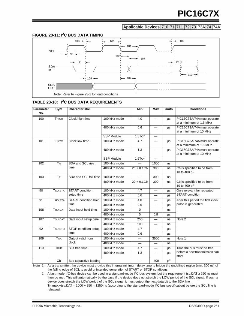
1996 Microchip Technology Inc. DS30390D-page 251
PIC16C7XApplicable Devices 710 71 711 72 73 73A 74 74A
FIGURE 23-11: I2C BUS DATA TIMING
TABLE 23-10: I2C BUS DATA REQUIREMENTS
ParameterNo.
Sym Characteristic Min Max Units Conditions
100 THIGH Clock high time 100 kHz mode 4.0 — µs PIC16C73A/74A must operate at a minimum of 1.5 MHz
400 kHz mode 0.6 — µs PIC16C73A/74A must operate at a minimum of 10 MHz
SSP Module 1.5TCY —
101 TLOW Clock low time 100 kHz mode 4.7 — µs PIC16C73A/74A must operate at a minimum of 1.5 MHz
400 kHz mode 1.3 — µs PIC16C73A/74A must operate at a minimum of 10 MHz
SSP Module 1.5TCY —
102 TR SDA and SCL rise time
100 kHz mode — 1000 ns
400 kHz mode 20 + 0.1Cb 300 ns Cb is specified to be from 10 to 400 pF
103 TF SDA and SCL fall time 100 kHz mode — 300 ns
400 kHz mode 20 + 0.1Cb 300 ns Cb is specified to be from 10 to 400 pF
90 TSU:STA START condition setup time
100 kHz mode 4.7 — µs Only relevant for repeated START condition400 kHz mode 0.6 — µs
91 THD:STA START condition hold time
100 kHz mode 4.0 — µs After this period the first clock pulse is generated400 kHz mode 0.6 — µs
106 THD:DAT Data input hold time 100 kHz mode 0 — ns
400 kHz mode 0 0.9 µs
107 TSU:DAT Data input setup time 100 kHz mode 250 — ns Note 2
400 kHz mode 100 — ns
92 TSU:STO STOP condition setup time
100 kHz mode 4.7 — µs
400 kHz mode 0.6 — µs
109 TAA Output valid from clock
100 kHz mode — 3500 ns Note 1
400 kHz mode — — ns
110 TBUF Bus free time 100 kHz mode 4.7 — µs Time the bus must be free before a new transmission can start
400 kHz mode 1.3 — µs
Cb Bus capacitive loading — 400 pF
Note 1: As a transmitter, the device must provide this internal minimum delay time to bridge the undefined region (min. 300 ns) of the falling edge of SCL to avoid unintended generation of START or STOP conditions.
2: A fast-mode I2C-bus device can be used in a standard-mode I2C-bus system, but the requirement tsu;DAT ≥ 250 ns must then be met. This will automatically be the case if the device does not stretch the LOW period of the SCL signal. If such a device does stretch the LOW period of the SCL signal, it must output the next data bit to the SDA line TR max.+tsu;DAT = 1000 + 250 = 1250 ns (according to the standard-mode I2C bus specification) before the SCL line is released.
Note: Refer to Figure 23-1 for load conditions
90
91 92
100
101
103
106107
109 109110
102
SCL
SDAIn
SDAOut
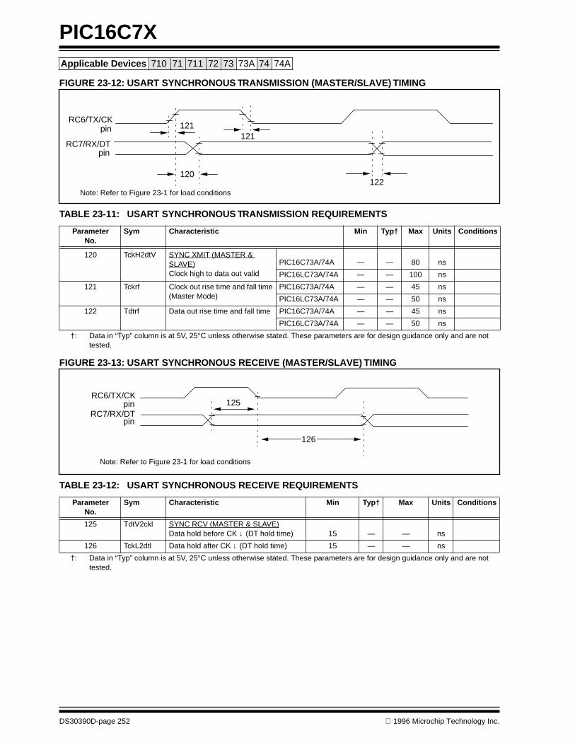
PIC16C7X
DS30390D-page 252 1996 Microchip Technology Inc.
Applicable Devices 710 71 711 72 73 73A 74 74A
FIGURE 23-12: USART SYNCHRONOUS TRANSMISSION (MASTER/SLAVE) TIMING
TABLE 23-11: USART SYNCHRONOUS TRANSMISSION REQUIREMENTS
FIGURE 23-13: USART SYNCHRONOUS RECEIVE (MASTER/SLAVE) TIMING
TABLE 23-12: USART SYNCHRONOUS RECEIVE REQUIREMENTS
Parameter No.
Sym Characteristic Min Typ† Max Units Conditions
120 TckH2dtV SYNC XMIT (MASTER & SLAVE)Clock high to data out valid
PIC16C73A/74A — — 80 ns
PIC16LC73A/74A — — 100 ns
121 Tckrf Clock out rise time and fall time (Master Mode)
PIC16C73A/74A — — 45 ns
PIC16LC73A/74A — — 50 ns
122 Tdtrf Data out rise time and fall time PIC16C73A/74A — — 45 ns
PIC16LC73A/74A — — 50 ns
†: Data in “Typ” column is at 5V, 25°C unless otherwise stated. These parameters are for design guidance only and are not tested.
Parameter No.
Sym Characteristic Min Typ† Max Units Conditions
125 TdtV2ckl SYNC RCV (MASTER & SLAVE)Data hold before CK ↓ (DT hold time) 15 — — ns
126 TckL2dtl Data hold after CK ↓ (DT hold time) 15 — — ns
†: Data in “Typ” column is at 5V, 25°C unless otherwise stated. These parameters are for design guidance only and are not tested.
Note: Refer to Figure 23-1 for load conditions
121121
122
RC6/TX/CK
RC7/RX/DTpin
pin
120
Note: Refer to Figure 23-1 for load conditions
125
126
RC6/TX/CK
RC7/RX/DTpin
pin
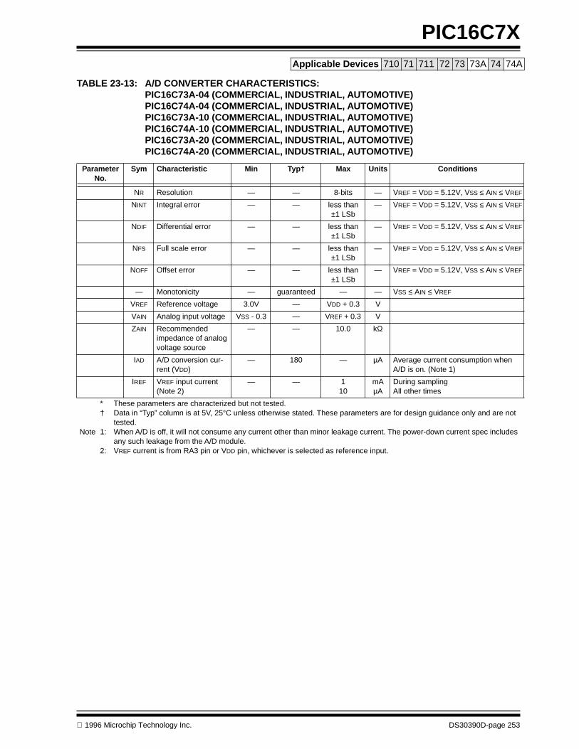
1996 Microchip Technology Inc. DS30390D-page 253
PIC16C7XApplicable Devices 710 71 711 72 73 73A 74 74A
TABLE 23-13: A/D CONVERTER CHARACTERISTICS:PIC16C73A-04 (COMMERCIAL, INDUSTRIAL, AUTOMOTIVE)PIC16C74A-04 (COMMERCIAL, INDUSTRIAL, AUTOMOTIVE)PIC16C73A-10 (COMMERCIAL, INDUSTRIAL, AUTOMOTIVE)PIC16C74A-10 (COMMERCIAL, INDUSTRIAL, AUTOMOTIVE)PIC16C73A-20 (COMMERCIAL, INDUSTRIAL, AUTOMOTIVE)PIC16C74A-20 (COMMERCIAL, INDUSTRIAL, AUTOMOTIVE)
Parameter No.
Sym Characteristic Min Typ† Max Units Conditions
NR Resolution — — 8-bits — VREF = VDD = 5.12V, VSS ≤ AIN ≤ VREF
NINT Integral error — — less than ±1 LSb
— VREF = VDD = 5.12V, VSS ≤ AIN ≤ VREF
NDIF Differential error — — less than ±1 LSb
— VREF = VDD = 5.12V, VSS ≤ AIN ≤ VREF
NFS Full scale error — — less than ±1 LSb
— VREF = VDD = 5.12V, VSS ≤ AIN ≤ VREF
NOFF Offset error — — less than ±1 LSb
— VREF = VDD = 5.12V, VSS ≤ AIN ≤ VREF
— Monotonicity — guaranteed — — VSS ≤ AIN ≤ VREF
VREF Reference voltage 3.0V — VDD + 0.3 V
VAIN Analog input voltage VSS - 0.3 — VREF + 0.3 V
ZAIN Recommended impedance of analog voltage source
— — 10.0 kΩ
IAD A/D conversion cur-rent (VDD)
— 180 — µA Average current consumption when A/D is on. (Note 1)
IREF VREF input current (Note 2)
— — 110
mAµA
During samplingAll other times
* These parameters are characterized but not tested.† Data in “Typ” column is at 5V, 25°C unless otherwise stated. These parameters are for design guidance only and are not
tested.Note 1: When A/D is off, it will not consume any current other than minor leakage current. The power-down current spec includes
any such leakage from the A/D module.2: VREF current is from RA3 pin or VDD pin, whichever is selected as reference input.

PIC16C7X
DS30390D-page 254 1996 Microchip Technology Inc.
Applicable Devices 710 71 711 72 73 73A 74 74A
TABLE 23-14: A/D CONVERTER CHARACTERISTICS:PIC16LC73A-04 (COMMERCIAL, INDUSTRIAL)PIC16LC74A-04 (COMMERCIAL, INDUSTRIAL)
Parameter No.
Sym Characteristic Min Typ† Max Units Conditions
NR Resolution — — 8-bits — VREF = VDD = 3.0V (Note 1)
NINT Integral error — — less than ±1 LSb
— VREF = VDD = 3.0V (Note 1)
NDIF Differential error — — less than ±1 LSb
— VREF = VDD = 3.0V (Note 1)
NFS Full scale error — — less than ±1 LSb
— VREF = VDD = 3.0V (Note 1)
NOFF Offset error — — less than ±1 LSb
— VREF = VDD = 3.0V (Note 1)
— Monotonicity — guaranteed — — VSS ≤ AIN ≤ VREF
VREF Reference voltage 3.0V — VDD + 0.3 V
VAIN Analog input voltage VSS - 0.3 — VREF + 0.3 V
ZAIN Recommended impedance of ana-log voltage source
— — 10.0 kΩ
IAD A/D conversion cur-rent (VDD)
— 180 — µA Average current consumption when A/D is on. (Note 2)
IREF VREF input current (Note 3)
— — 110
mAµA
During samplingAll other times
* These parameters are characterized but not tested.† Data in “Typ” column is at 5V, 25°C unless otherwise stated. These parameters are for design guidance only and are not
tested.Note 1: These specifications apply if VREF = 3.0V and if VDD ≥ 3.0V. VIN must be between VSS and VREF
2: When A/D is off, it will not consume any current other than minor leakage current. The power-down current spec includes any such leakage from the A/D module.
3: VREF current is from RA3 pin or VDD pin, whichever is selected as reference input.

1996 Microchip Technology Inc. DS30390D-page 255
PIC16C7XApplicable Devices 710 71 711 72 73 73A 74 74A
FIGURE 23-14: A/D CONVERSION TIMING
TABLE 23-15: A/D CONVERSION REQUIREMENTS
Parameter No.
Sym Characteristic Min Typ† Max Units Conditions
130 TAD A/D clock period PIC16C73/74 1.6 — — µs TOSC based, VREF ≥ 3.0V
PIC16LC73/74 2.0 — — µs TOSC based, VREF full range
PIC16C73/74 2.0 4.0 6.0 µs A/D RC Mode
PIC16LC73/74 3.0 6.0 9.0 µs A/D RC Mode
131 TCNV Conversion time (not including S/H time) (Note 1)
— 9.5TAD — —
132 TACQ Acquisition time Note 2 20 — µs
* These parameters are characterized but not tested.† Data in “Typ” column is at 5V, 25°C unless otherwise stated. These parameters are for design guidance only and are not
tested.Note 1: ADRES register may be read on the following TCY cycle.
2: See Section 13.1 for min conditions.
131
130
132
BSF ADCON0, GO
Q4
A/D CLK
A/D DATA
ADRES
ADIF
GO
SAMPLE
OLD_DATA
SAMPLING STOPPED
DONE
NEW_DATA
(TOSC/2) (1)
7 6 5 4 3 2 1 0
Note 1: If the A/D clock source is selected as RC, a time of TCY is added before the A/D clock starts. This allows the SLEEP instruction to be executed.
1 Tcy
PIC16C7X
DS30390D-page 256 1996 Microchip Technology Inc.
Applicable Devices 710 71 711 72 73 73A 74 74A
NOTES:

1996 Microchip Technology Inc. DS30390D-page 257
PIC16C7X
Applicable Devices
710 71 711 72 73 73A 74 74A
24.0 DC AND AC CHARACTERISTICS GRAPHS AND TABLES FOR:PIC16C72, PIC16C73, PIC16C73A, PIC16C74, PIC16C74A
The graphs and tables provided in this section are for design guidance and are not tested or guaranteed.
In some graphs or tables the data presented are outside specified operating range (i.e., outside specified V
DD
range). This is for information only and devices are guaranteed to operate properly only within the specifiedrange.
FIGURE 24-1: TYPICAL I
PD
vs. V
DD
(WDT DISABLED, RC MODE)
FIGURE 24-2: MAXIMUM I
PD
vs. V
DD
(WDT DISABLED, RC MODE)
Note:
The data presented in this section is a statistical summary of data collected on units from different lots overa period of time and matrix samples. 'Typical' represents the mean of the distribution at, 25
°
C, while 'max'or 'min' represents (mean +3
σ
) and (mean -3
σ
) respectively where
σ
is standard deviation.
35
30
25
20
15
10
5
02.5 3.0 3.5 4.0 4.5 5.0 5.5 6.0
IPD
(nA
)
VDD(Volts)
IPD
(µA
)
VDD(Volts)
10.000
1.000
0.100
0.010
0.0012.5 3.0 3.5 4.0 4.5 5.0 5.5 6.0
85°C70°C
25°C
0°C-40°C
This document was created with FrameMaker 4 0 4

PIC16C7X
DS30390D-page 258
1996 Microchip Technology Inc.
Applicable Devices
710 71 711 72 73 73A 74 74A
FIGURE 24-3: TYPICAL I
PD
vs. V
DD
@ 25
°
C (WDT ENABLED, RC MODE)
FIGURE 24-4: MAXIMUM I
PD
vs. V
DD
(WDT ENABLED, RC MODE)
25
20
15
10
5
02.5 3.0 3.5 4.0 4.5 5.0 5.5 6.0
IPD
(µA
)
VDD(Volts)
35
30
25
20
15
10
5
02.5 3.0 3.5 4.0 4.5 5.0 5.5 6.0
IPD
(µA
)
VDD(Volts)
-40°C
0°C
70°C
85°C
FIGURE 24-5: TYPICAL RC OSCILLATOR FREQUENCY vs. V
DD
FIGURE 24-6: TYPICAL RC OSCILLATOR FREQUENCY vs. V
DD
FIGURE 24-7: TYPICAL RC OSCILLATOR FREQUENCY vs. V
DD
2.5 3.0 3.5 4.0 4.5 5.0 5.5 6.0VDD(Volts)
6.0
5.5
5.0
4.5
4.0
3.5
3.0
2.5
2.0
1.5
1.0
0.5
0.0
Fo
sc(M
Hz)
Cext = 22 pF, T = 25°C
R = 100k
R = 10k
R = 5k
Shaded area is beyond recommended range.
2.5 3.0 3.5 4.0 4.5 5.0 5.5 6.0
VDD(Volts)
2.4
2.2
2.0
1.8
1.6
1.4
1.2
1.0
0.8
0.6
0.4
0.2
0.0
Fo
sc(M
Hz)
Cext = 100 pF, T = 25°C
R = 100k
R = 10k
R = 5k
R = 3.3k
2.5 3.0 3.5 4.0 4.5 5.0 5.5 6.0
VDD(Volts)
1000
900
800
700
600
500
400
300
200
100
0
Fo
sc(k
Hz)
Cext = 300 pF, T = 25°C
R = 3.3k
R = 5k
R = 10k
R = 100k
Dat
a ba
sed
on m
atrix
sam
ples
. See
firs
t pag
e of
this
sec
tion
for
deta
ils.

1996 Microchip Technology Inc. DS30390D-page 259
PIC16C7X
Applicable Devices
710 71 711 72 73 73A 74 74A
FIGURE 24-8: TYPICAL I
PD
vs. V
DD
BROWN-OUT DETECT ENABLED (RC MODE)
FIGURE 24-9: MAXIMUM I
PD
vs. V
DD
BROWN-OUT DETECT ENABLED (85
°
C TO -40
°
C, RC MODE)
The shaded region represents the built-in hysteresis of thebrown-out reset circuitry.
2.5 3.0 3.5 4.0 4.5 5.0 5.5 6.0
1400
1200
1000
800
600
400
200
0
VDD(Volts)
IPD
(µA
)
Device inBrown-out
Device NOT inBrown-out Reset
Reset
The shaded region represents the built-in hysteresis of thebrown-out reset circuitry.
2.5 3.0 3.5 4.0 4.5 5.0 5.5 6.0
1400
1200
1000
800
600
400
200
0
VDD(Volts)
IPD
(µA
)
4.3
1600
Device NOT inBrown-out Reset
Device inBrown-out
Reset
FIGURE 24-10: TYPICAL I
PD
vs. TIMER1 ENABLED (32 kHz, RC0/RC1 = 33 pF/33 pF, RC MODE)
FIGURE 24-11: MAXIMUM I
PD
vs. TIMER1 ENABLED (32 kHz, RC0/RC1 = 33 pF/33 pF, 85
°
C TO -40
°
C, RC MODE)
30
25
20
15
10
5
02.5 3.0 3.5 4.0 4.5 5.0 5.5 6.0
VDD(Volts)
IPD
(µA
)
30
25
20
15
10
5
02.5 3.0 3.5 4.0 4.5 5.0 5.5 6.0
VDD(Volts)
IPD
(µA
)
35
40
45
Dat
a ba
sed
on m
atrix
sam
ples
. See
firs
t pag
e of
this
sec
tion
for
deta
ils.
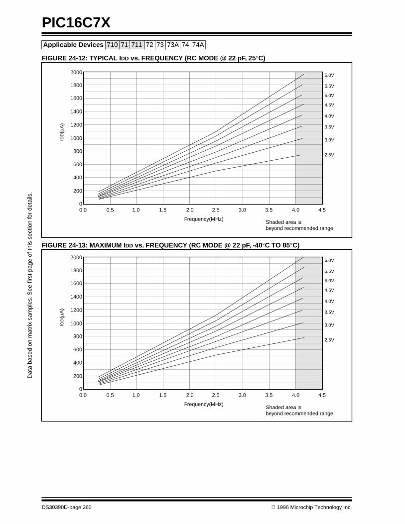
PIC16C7X
DS30390D-page 260
1996 Microchip Technology Inc.
Applicable Devices
710 71 711 72 73 73A 74 74A
FIGURE 24-12: TYPICAL I
DD
vs. FREQUENCY (RC MODE @ 22 pF, 25
°
C)
FIGURE 24-13: MAXIMUM I
DD
vs. FREQUENCY (RC MODE @ 22 pF, -40
°
C TO 85
°
C)
2000
1800
1600
1400
1200
800
1000
600
400
200
00.0 0.5 1.0 1.5 2.0 2.5 3.0 3.5 4.0 4.5
Frequency(MHz)
IDD
(µA
)
Shaded area is
6.0V
5.5V
5.0V
4.5V
4.0V
3.5V
3.0V
2.5V
beyond recommended range
2000
1800
1600
1400
1200
800
1000
600
400
200
00.0 0.5 1.0 1.5 2.0 2.5 3.0 3.5 4.0 4.5
Frequency(MHz)
IDD
(µA
)
Shaded area is
6.0V
5.5V
5.0V
4.5V
4.0V
3.5V
3.0V
2.5V
beyond recommended range
Dat
a ba
sed
on m
atrix
sam
ples
. See
firs
t pag
e of
this
sec
tion
for
deta
ils.

1996 Microchip Technology Inc. DS30390D-page 261
PIC16C7X
Applicable Devices
710 71 711 72 73 73A 74 74A
FIGURE 24-14: TYPICAL I
DD
vs. FREQUENCY (RC MODE @ 100 pF, 25
°
C)
FIGURE 24-15: MAXIMUM I
DD
vs. FREQUENCY (RC MODE @ 100 pF, -40
°
C TO 85
°
C)
1600
1400
1200
1000
800
600
400
200
00 200 400 600 800 1000 1200 1400 1600 1800
Frequency(kHz)
IDD
(µA
)6.0V
5.5V
5.0V
4.5V
4.0V
3.5V
3.0V
2.5V
1600
1400
1200
1000
800
600
400
200
00 200 400 600 800 1000 1200 1400 1600 1800
Frequency(kHz)
IDD
(µA
)
6.0V
5.5V
5.0V
4.5V
4.0V
3.5V
3.0V
2.5V
Dat
a ba
sed
on m
atrix
sam
ples
. See
firs
t pag
e of
this
sec
tion
for
deta
ils.

PIC16C7X
DS30390D-page 262
1996 Microchip Technology Inc.
Applicable Devices
710 71 711 72 73 73A 74 74A
FIGURE 24-16: TYPICAL IDD vs. FREQUENCY (RC MODE @ 300 pF, 25°C)
FIGURE 24-17: MAXIMUM IDD vs. FREQUENCY (RC MODE @ 300 pF, -40°C TO 85°C)
1200
1000
800
600
400
200
00 100 200 300 400 500 600 700
Frequency(kHz)
IDD
(µA
)6.0V
5.5V
5.0V
4.5V
4.0V
3.5V
3.0V
2.5V
1200
1000
800
600
400
200
00 100 200 300 400 500 600 700
Frequency(kHz)
IDD
(µA
)
6.0V
5.5V
5.0V
4.5V
4.0V
3.5V
3.0V
2.5V
Dat
a ba
sed
on m
atrix
sam
ples
. See
firs
t pag
e of
this
sec
tion
for
deta
ils.

1996 Microchip Technology Inc. DS30390D-page 263
PIC16C7XApplicable Devices 710 71 711 72 73 73A 74 74A
FIGURE 24-18: TYPICAL IDD vs. CAPACITANCE @ 500 kHz (RC MODE)
TABLE 24-1: RC OSCILLATOR FREQUENCIES
Cext RextAverage
Fosc @ 5V, 25°C
22 pF 5k 4.12 MHz ± 1.4%
10k 2.35 MHz ± 1.4%
100k 268 kHz ± 1.1%
100 pF 3.3k 1.80 MHz ± 1.0%
5k 1.27 MHz ± 1.0%
10k 688 kHz ± 1.2%
100k 77.2 kHz ± 1.0%
300 pF 3.3k 707 kHz ± 1.4%
5k 501 kHz ± 1.2%
10k 269 kHz ± 1.6%
100k 28.3 kHz ± 1.1%
The percentage variation indicated here is part to part variation due to normal process distribution. The variation indicated is ±3 standard deviation from average value for VDD = 5V.
Capacitance(pF)
600
IDD
(µA
)
500
400
300
200
100
020 pF 100 pF 300 pF
5.0V
4.0V
3.0V
FIGURE 24-19: TRANSCONDUCTANCE(gm) OF HS OSCILLATOR vs. VDD
FIGURE 24-20: TRANSCONDUCTANCE(gm) OF LP OSCILLATOR vs. VDD
FIGURE 24-21: TRANSCONDUCTANCE(gm) OF XT OSCILLATOR vs. VDD
4.0
3.0 3.5 4.0 4.5 5.0 5.5 6.0 6.5 7.0
gm
(mA
/V)
VDD(Volts)
3.5
3.0
2.5
2.0
1.5
1.0
0.5
0.0
Max -40°C
Typ 25°C
Min 85°C
110
100
90
80
70
60
50
40
30
20
10
02.0 2.5 3.0 3.5 4.0 4.5 5.0 5.5 6.0 6.5 7.0
gm(µ
A/V
)
VDD(Volts)
Max -40°C
Typ 25°C
Min 85°C
1000
900
800
700
600
500
400
300
200
100
02.0 2.5 3.0 3.5 4.0 4.5 5.0 5.5 6.0 6.5 7.0
gm(µ
A/V
)
VDD(Volts)
Max -40°C
Typ 25°C
Min 85°C
Dat
a ba
sed
on m
atrix
sam
ples
. See
firs
t pag
e of
this
sec
tion
for
deta
ils.
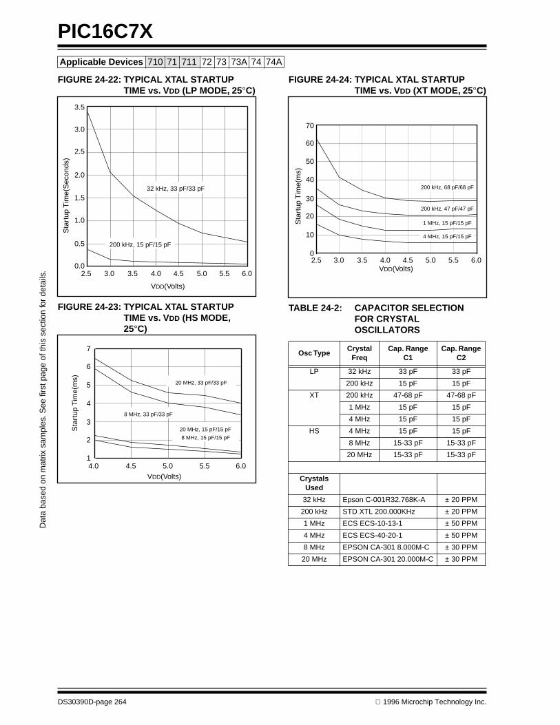
PIC16C7X
DS30390D-page 264 1996 Microchip Technology Inc.
Applicable Devices 710 71 711 72 73 73A 74 74A
FIGURE 24-22: TYPICAL XTAL STARTUP TIME vs. VDD (LP MODE, 25°C)
FIGURE 24-23: TYPICAL XTAL STARTUP TIME vs. VDD (HS MODE, 25°C)
3.5
3.0
2.5
2.0
1.5
1.0
0.5
0.02.5 3.0 3.5 4.0 4.5 5.0 5.5 6.0
VDD(Volts)
Sta
rtup
Tim
e(S
econ
ds)
32 kHz, 33 pF/33 pF
200 kHz, 15 pF/15 pF
7
6
5
4
3
2
14.0 4.5 5.0 5.5 6.0
VDD(Volts)
Sta
rtup
Tim
e(m
s)
20 MHz, 33 pF/33 pF
8 MHz, 33 pF/33 pF
8 MHz, 15 pF/15 pF
20 MHz, 15 pF/15 pF
FIGURE 24-24: TYPICAL XTAL STARTUP TIME vs. VDD (XT MODE, 25°C)
TABLE 24-2: CAPACITOR SELECTION FOR CRYSTAL OSCILLATORS
Osc TypeCrystal
FreqCap. Range
C1Cap. Range
C2
LP 32 kHz 33 pF 33 pF
200 kHz 15 pF 15 pF
XT 200 kHz 47-68 pF 47-68 pF
1 MHz 15 pF 15 pF
4 MHz 15 pF 15 pF
HS 4 MHz 15 pF 15 pF
8 MHz 15-33 pF 15-33 pF
20 MHz 15-33 pF 15-33 pF
Crystals Used
32 kHz Epson C-001R32.768K-A ± 20 PPM
200 kHz STD XTL 200.000KHz ± 20 PPM
1 MHz ECS ECS-10-13-1 ± 50 PPM
4 MHz ECS ECS-40-20-1 ± 50 PPM
8 MHz EPSON CA-301 8.000M-C ± 30 PPM
20 MHz EPSON CA-301 20.000M-C ± 30 PPM
70
60
50
40
30
20
10
03.0 3.52.5 4.0 5.0 5.5 6.04.5
VDD(Volts)
Sta
rtup
Tim
e(m
s)
200 kHz, 68 pF/68 pF
200 kHz, 47 pF/47 pF
1 MHz, 15 pF/15 pF
4 MHz, 15 pF/15 pF
Dat
a ba
sed
on m
atrix
sam
ples
. See
firs
t pag
e of
this
sec
tion
for
deta
ils.

1996 Microchip Technology Inc. DS30390D-page 265
PIC16C7XApplicable Devices 710 71 711 72 73 73A 74 74A
FIGURE 24-25: TYPICAL IDD vs. FREQUENCY (LP MODE, 25°C)
FIGURE 24-26: MAXIMUM IDD vs. FREQUENCY(LP MODE, 85°C TO -40°C)
120
100
80
60
40
20
00 50 100 150 200
Frequency(kHz)
IDD
(µA
)
6.0V5.5V5.0V4.5V4.0V3.5V3.0V2.5V
120
100
80
60
40
20
00 50 100 150 200
Frequency(kHz)
IDD
(µA
)
140
6.0V5.5V5.0V4.5V4.0V3.5V3.0V2.5V
FIGURE 24-27: TYPICAL IDD vs. FREQUENCY(XT MODE, 25°C)
FIGURE 24-28: MAXIMUM IDD vs. FREQUENCY(XT MODE, -40°C TO 85°C)
1200
1000
800
600
400
200
00.0 0.4
Frequency(MHz)
IDD
(µA
)
1400
1600
1800
0.8 1.2 1.6 2.0 2.4 2.8 3.2 3.6 4.0
6.0V
5.5V
5.0V
4.5V
4.0V
3.5V
3.0V
2.5V
1200
1000
800
600
400
200
00.0 0.4
Frequency(MHz)
IDD
(µA
)
1400
1600
1800
0.8 1.2 1.6 2.0 2.4 2.8 3.2 3.6 4.0
6.0V
5.5V
5.0V
4.5V
4.0V
3.5V
3.0V
2.5V
Dat
a ba
sed
on m
atrix
sam
ples
. See
firs
t pag
e of
this
sec
tion
for
deta
ils.

PIC16C7X
DS30390D-page 266 1996 Microchip Technology Inc.
Applicable Devices 710 71 711 72 73 73A 74 74A
FIGURE 24-29: TYPICAL IDD vs. FREQUENCY (HS MODE, 25°C)
7.0
6.0
5.0
4.0
3.0
2.0
1.0
0.01 2 4 6 8 10 12 14 16 18 20
Frequency(MHz)
IDD
(mA
)
6.0V5.5V5.0V4.5V4.0V
FIGURE 24-30: MAXIMUM IDD vs. FREQUENCY(HS MODE, -40°C TO 85°C)
7.0
6.0
5.0
4.0
3.0
2.0
1.0
0.01 2 4 6 8 10 12 14 16 18 20
Frequency(MHz)
IDD
(mA
)
6.0V5.5V5.0V4.5V4.0V
Dat
a ba
sed
on m
atrix
sam
ples
. See
firs
t pag
e of
this
sec
tion
for
deta
ils.

1996 Microchip Technology Inc. DS30390C-page 267
PIC16C7X
25.0 PACKAGING INFORMATION
25.1 18-Lead Ceramic CERDIP Dual In-line with Window (300 mil)
Package Group: Ceramic CERDIP Dual In-Line (CDP)
Symbol
Millimeters Inches
Min Max Notes Min Max Notes
α
0
°
10
°
0
°
10
°
A — 5.080 — 0.200A1 0.381 1.7780 0.015 0.070A2 3.810 4.699 0.150 0.185A3 3.810 4.445 0.150 0.175B 0.355 0.585 0.014 0.023B1 1.270 1.651
Typical
0.050 0.065
Typical
C 0.203 0.381
Typical
0.008 0.015
Typical
D 22.352 23.622 0.880 0.930D1 20.320 20.320
Reference
0.800 0.800
Reference
E 7.620 8.382 0.300 0.330E1 5.588 7.874 0.220 0.310e1 2.540 2.540
Reference
0.100 0.100
Reference
eA 7.366 8.128
Typical
0.290 0.320
Typical
eB 7.620 10.160 0.300 0.400L 3.175 3.810 0.125 0.150N 18 18 18 18S 0.508 1.397 0.020 0.055S1 0.381 1.270 0.015 0.050
N
Pin No. 1IndicatorArea
E1 E
SD
B1
BD1
BasePlane
SeatingPlane
S1
A1 A3 A
L
α C
eA
eB
e1 A2
This document was created with FrameMaker 4 0 4
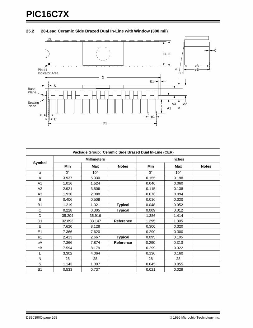
PIC16C7X
DS30390C-page 268
1996 Microchip Technology Inc.
25.2 28-Lead Ceramic Side Brazed Dual In-Line with Window (300 mil)
Package Group: Ceramic Side Brazed Dual In-Line (CER)
SymbolMillimeters Inches
Min Max Notes Min Max Notes
α
0
°
10
°
0
°
10
°
A 3.937 5.030 0.155 0.198A1 1.016 1.524 0.040 0.060A2 2.921 3.506 0.115 0.138A3 1.930 2.388 0.076 0.094B 0.406 0.508 0.016 0.020B1 1.219 1.321
Typical
0.048 0.052C 0.228 0.305
Typical
0.009 0.012D 35.204 35.916 1.386 1.414D1 32.893 33.147
Reference
1.295 1.305E 7.620 8.128 0.300 0.320E1 7.366 7.620 0.290 0.300e1 2.413 2.667
Typical
0.095 0.105eA 7.366 7.874
Reference
0.290 0.310eB 7.594 8.179 0.299 0.322L 3.302 4.064 0.130 0.160N 28 28 28 28S 1.143 1.397 0.045 0.055S1 0.533 0.737 0.021 0.029
E1 E
SBasePlane
SeatingPlane
B1B
S1D
LA1
A2A3A
e1
Pin #1Indicator Area
D1
C
eAeBα
N

1996 Microchip Technology Inc. DS30390C-page 269
PIC16C7X
25.3 40-Lead Ceramic CERDIP Dual In-line with Window (600 mil)
Package Group: Ceramic CERDIP Dual In-Line (CDP)
Symbol
Millimeters Inches
Min Max Notes Min Max Notes
α
0
°
10
°
0
°
10
°
A 4.318 5.715 0.170 0.225A1 0.381 1.778 0.015 0.070A2 3.810 4.699
0.150 0.185
A3 3.810 4.445 0.150 0.175B 0.355 0.585 0.014 0.023B1 1.270 1.651
Typical
0.050 0.065
Typical
C 0.203 0.381
Typical
0.008 0.015
Typical
D 51.435 52.705 2.025 2.075D1 48.260 48.260
Reference
1.900 1.900
Reference
E 15.240 15.875 0.600 0.625E1 12.954 15.240 0.510 0.600e1 2.540 2.540
Reference
0.100 0.100
Reference
eA 14.986 16.002
Typical
0.590 0.630
Typical
eB 15.240 18.034 0.600 0.710L 3.175 3.810 0.125 0.150N 40 40 40 40S 1.016 2.286 0.040 0.090S1 0.381 1.778 0.015 0.070
N
Pin No. 1IndicatorArea
E1 E
SD
B1
BD1
BasePlane
SeatingPlane
S1
A1 A3 A A2
L
e1
α C
eA
eB

PIC16C7X
DS30390C-page 270
1996 Microchip Technology Inc.
25.4 18-Lead Plastic Dual In-line (300 mil)
Package Group: Plastic Dual In-Line (PLA)
Symbol
Millimeters Inches
Min Max Notes Min Max Notes
α
0
°
10
°
0
°
10
°
A – 4.064 – 0.160A1 0.381 – 0.015 –A2 3.048 3.810 0.120 0.150B 0.355 0.559 0.014 0.022B1 1.524 1.524
Reference
0.060 0.060
Reference
C 0.203 0.381
Typical
0.008 0.015
Typical
D 22.479 23.495 0.885 0.925D1 20.320 20.320
Reference
0.800 0.800
Reference
E 7.620 8.255 0.300 0.325E1 6.096 7.112 0.240 0.280e1 2.489 2.591
Typical
0.098 0.102
Typical
eA 7.620 7.620
Reference
0.300 0.300
Reference
eB 7.874 9.906 0.310 0.390L 3.048 3.556 0.120 0.140N 18 18 18 18S 0.889 – 0.035 –S1 0.127 – 0.005 –
N
Pin No. 1IndicatorArea
E1 E
SD
B1
BD1
BasePlane
SeatingPlane
S1
A1 A2 A
L
e1
αC
eA
eB
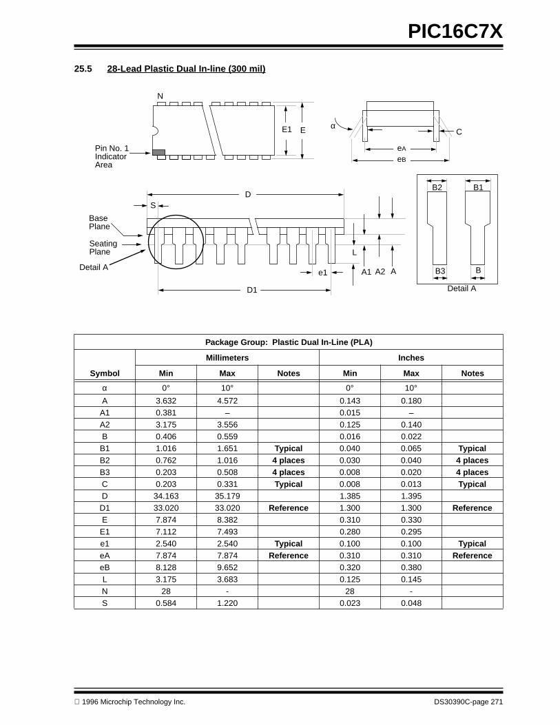
1996 Microchip Technology Inc. DS30390C-page 271
PIC16C7X
25.5 28-Lead Plastic Dual In-line (300 mil)
Package Group: Plastic Dual In-Line (PLA)
Symbol
Millimeters Inches
Min Max Notes Min Max Notes
α
0
°
10
°
0
°
10
°
A 3.632 4.572 0.143 0.180A1 0.381 – 0.015 –A2 3.175 3.556 0.125 0.140B 0.406 0.559 0.016 0.022B1 1.016 1.651
Typical
0.040 0.065
Typical
B2 0.762 1.016
4 places
0.030 0.040
4 places
B3 0.203 0.508
4 places
0.008 0.020
4 places
C 0.203 0.331
Typical
0.008 0.013
Typical
D 34.163 35.179 1.385 1.395D1 33.020 33.020
Reference
1.300 1.300
Reference
E 7.874 8.382 0.310 0.330E1 7.112 7.493 0.280 0.295e1 2.540 2.540
Typical
0.100 0.100
Typical
eA 7.874 7.874
Reference
0.310 0.310
Reference
eB 8.128 9.652 0.320 0.380L 3.175 3.683 0.125 0.145N 28 - 28 -S 0.584 1.220 0.023 0.048
N
Pin No. 1IndicatorArea
E1 E
SD
D1
BasePlane
SeatingPlane
A1 A2 A
L
e1
αC
eA
eB
Detail A
Detail A
B2 B1
BB3

PIC16C7X
DS30390C-page 272
1996 Microchip Technology Inc.
25.6 40-Lead Plastic Dual In-line (600 mil)
Package Group: Plastic Dual In-Line (PLA)
Symbol
Millimeters Inches
Min Max Notes Min Max Notes
α
0
°
10
°
0
°
10
°
A – 5.080 – 0.200A1 0.381 – 0.015 –A2 3.175 4.064 0.125 0.160B 0.355 0.559 0.014 0.022B1 1.270 1.778
Typical
0.050 0.070
Typical
C 0.203 0.381
Typical
0.008 0.015
Typical
D 51.181 52.197 2.015 2.055D1 48.260 48.260
Reference
1.900 1.900
Reference
E 15.240 15.875 0.600 0.625E1 13.462 13.970 0.530 0.550e1 2.489 2.591
Typical 0.098 0.102 TypicaleA 15.240 15.240 Reference 0.600 0.600 ReferenceeB 15.240 17.272 0.600 0.680L 2.921 3.683 0.115 0.145N 40 40 40 40S 1.270 – 0.050 –S1 0.508 – 0.020 –
N
Pin No. 1IndicatorArea
E1 E
SD
B1
BD1
BasePlane
SeatingPlane
S1
A1 A2 A
L
e1
αC
eA
eB

1996 Microchip Technology Inc. DS30390C-page 273
PIC16C7X
25.7 18-Lead Plastic Surface Mount (SOIC - Wide, 300 mil Body)
Package Group: Plastic SOIC (SO)
Symbol
Millimeters Inches
Min Max Notes Min Max Notes
α 0° 8° 0° 8°A 2.362 2.642 0.093 0.104A1 0.101 0.300 0.004 0.012B 0.355 0.483 0.014 0.019C 0.241 0.318 0.009 0.013D 11.353 11.735 0.447 0.462E 7.416 7.595 0.292 0.299e 1.270 1.270 Reference 0.050 0.050 ReferenceH 10.007 10.643 0.394 0.419h 0.381 0.762 0.015 0.030L 0.406 1.143 0.016 0.045N 18 18 18 18
CP – 0.102 – 0.004
B
e
N
IndexArea
Chamferh x 45°
αE H
1 2 3
CP
h x 45°
C
L
SeatingPlane
BasePlane
D
A1 A
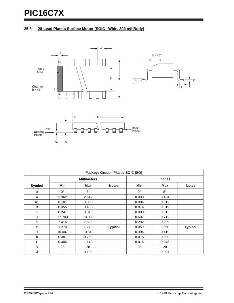
PIC16C7X
DS30390C-page 274 1996 Microchip Technology Inc.
25.8 28-Lead Plastic Surface Mount (SOIC - Wide, 300 mil Body)
Package Group: Plastic SOIC (SO)
Symbol
Millimeters Inches
Min Max Notes Min Max Notes
α 0° 8° 0° 8°A 2.362 2.642 0.093 0.104A1 0.101 0.300 0.004 0.012B 0.355 0.483 0.014 0.019C 0.241 0.318 0.009 0.013D 17.703 18.085 0.697 0.712E 7.416 7.595 0.292 0.299e 1.270 1.270 Typical 0.050 0.050 TypicalH 10.007 10.643 0.394 0.419h 0.381 0.762 0.015 0.030L 0.406 1.143 0.016 0.045N 28 28 28 28
CP – 0.102 – 0.004
B
e
N
IndexArea
Chamferh x 45°
αE H
1 2 3
CP
h x 45°
C
L
SeatingPlane
BasePlane
D
A1 A

1996 Microchip Technology Inc. DS30390C-page 275
PIC16C7X
25.9 20-Lead Plastic Surface Mount (SSOP - 209 mil Body 5.30 mm)
Package Group: Plastic SSOP
Symbol
Millimeters Inches
Min Max Notes Min Max Notes
α 0° 8° 0° 8°A 1.730 1.990 0.068 0.078A1 0.050 0.210 0.002 0.008B 0.250 0.380 0.010 0.015C 0.130 0.220 0.005 0.009D 7.070 7.330 0.278 0.289E 5.200 5.380 0.205 0.212e 0.650 0.650 Reference 0.026 0.026 ReferenceH 7.650 7.900 0.301 0.311L 0.550 0.950 0.022 0.037N 20 20 20 20
CP - 0.102 - 0.004
Indexarea
N
H
1 2 3
E
e B
CP
D
A
A1
Base plane
Seating plane
L
Cα

PIC16C7X
DS30390C-page 276 1996 Microchip Technology Inc.
25.10 28-Lead Plastic Surface Mount (SSOP - 209 mil Body 5.30 mm)
Package Group: Plastic SSOP
Symbol
Millimeters Inches
Min Max Notes Min Max Notes
α 0° 8° 0° 8°A 1.730 1.990 0.068 0.078A1 0.050 0.210 0.002 0.008B 0.250 0.380 0.010 0.015C 0.130 0.220 0.005 0.009D 10.070 10.330 0.396 0.407E 5.200 5.380 0.205 0.212e 0.650 0.650 Reference 0.026 0.026 ReferenceH 7.650 7.900 0.301 0.311L 0.550 0.950 0.022 0.037N 28 28 28 28
CP - 0.102 - 0.004
Indexarea
N
H
1 2 3
E
e B
CP
D
A
A1
Base plane
Seating plane
L
Cα
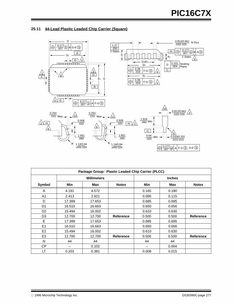
1996 Microchip Technology Inc. DS30390C-page 277
PIC16C7X
25.11 44-Lead Plastic Leaded Chip Carrier (Square)
Package Group: Plastic Leaded Chip Carrier (PLCC)
Symbol
Millimeters Inches
Min Max Notes Min Max Notes
A 4.191 4.572 0.165 0.180
A1 2.413 2.921 0.095 0.115D 17.399 17.653 0.685 0.695D1 16.510 16.663 0.650 0.656D2 15.494 16.002 0.610 0.630D3 12.700 12.700 Reference 0.500 0.500 ReferenceE 17.399 17.653 0.685 0.695E1 16.510 16.663 0.650 0.656E2 15.494 16.002 0.610 0.630E3 12.700 12.700 Reference 0.500 0.500 ReferenceN 44 44 44 44
CP – 0.102 – 0.004LT 0.203 0.381 0.008 0.015
S0.177.007 B D-E
-A-
0.254
D1
D
3
3
3
-C-
-F-
-D-
4
9
8
-B-
-E-S
0.177.007 A F-G
S
S
EE1
-H-
-G-
6
2
3
.010 Max1.524.060
10
2
11
0.508.020
1.651.065
R 1.14/0.64.045/.025
R 1.14/0.64.045/.025
1.651.065
0.508.020 -H-
110.254.010 Max
6
Min
0.812/0.661.032/.026 3
-C-
0.64.025
Min5
0.533/0.331.021/.013
0.177.007 M A F-G S , D-E S
1.27.050
2 SidesA
S0.177.007 B AS
D3/E3
D20.101.004
0.812/0.661.032/.026
S0.38.015 F-G
4S0.38.015 F-G
E2
D
-H-
A1
SeatingPlane
2 Sides
N Pics

PIC16C7X
DS30390C-page 278 1996 Microchip Technology Inc.
25.12 44-Lead Plastic Surface Mount (MQFP 10x10 mm Body 1.6/0.15 mm Lead Form))
Package Group: Plastic MQFP
Symbol
Millimeters Inches
Min Max Notes Min Max Notes
α 0° 7° 0° 7°A 2.000 2.350 0.078 0.093A1 0.050 0.250 0.002 0.010A2 1.950 2.100 0.768 0.083b 0.300 0.450 Typical 0.011 0.018 TypicalC 0.150 0.180 0.006 0.007D 12.950 13.450 0.510 0.530D1 9.900 10.100 0.390 0.398D3 8.000 8.000 Reference 0.315 0.315 ReferenceE 12.950 13.450 0.510 0.530E1 9.900 10.100 0.390 0.398E3 8.000 8.000 Reference 0.315 0.315 Referencee 0.800 0.800 0.031 0.032L 0.730 1.030 0.028 0.041N 44 44 44 44
CP 0.102 – 0.004 –
Indexarea
9b
TYP 4x
BasePlane
A2
e B
A
A1
SeatingPlane
6
D
D1
D3
4
5 7
E3 E1 E
100.20 M A-B
0.05 mm/mm D
H S SD
0.20 M A-BC S SD
75
4
0.20 M A-BC S SD
0.20 M A-BH S SD
0.05 mm/mm A-B
CL
1.60 Ref.
0.13/0.30 R
0.13 R min.
0.20 min.
PARTINGLINE
α

1996 Microchip Technology Inc. DS30390C-page 279
PIC16C7X
25.13 44-Lead Plastic Surface Mount (TQFP 10x10 mm Body 1.0/0.10 mm Lead Form)
Note 1: Dimensions D1 and E1 do not include mold protrusion. Allowable mold protrusion is 0.25m/m (0.010”) per side. D1 and E1 dimensions including mold mismatch.
2: Dimension “b” does not include Dambar protrusion, allowable Dambar protrusion shall be 0.08m/m (0.003”)max.
3: This outline conforms to JEDEC MS-026.
Package Group: Plastic TQFP
Symbol
Millimeters Inches
Min Max Notes Min Max Notes
A 1.00 1.20 0.039 0.047A1 0.05 0.15 0.002 0.006A2 0.95 1.05 0.037 0.041D 11.75 12.25 0.463 0.482D1 9.90 10.10 0.390 0.398E 11.75 12.25 0.463 0.482E1 9.90 10.10 0.390 0.398L 0.45 0.75 0.018 0.030e 0.80 BSC 0.031 BSCb 0.30 0.45 0.012 0.018b1 0.30 0.40 0.012 0.016c 0.09 0.20 0.004 0.008c1 0.09 0.16 0.004 0.006N 44 44 44 44
Θ 0° 7° 0° 7°
D
E
D1
E1
Pin#12
e
1.0ø (0.039ø) Ref.
Option 1 (TOP side)
Pin#12
Option 2 (TOP side)
3.0ø (0.118ø) Ref.
Detail ADetail BL
1.00 Ref.
A2A1
A b
b1
c c1
Base Metal
Detail A
Lead Finish
Detail B
11°/13°(4x)
0° Min
11°/13°(4x)Θ
R1 0.08 Min
R 0.08/0.20
Gage Plane0.250
L
L1
S0.20Min
1.00 Ref
Detail B
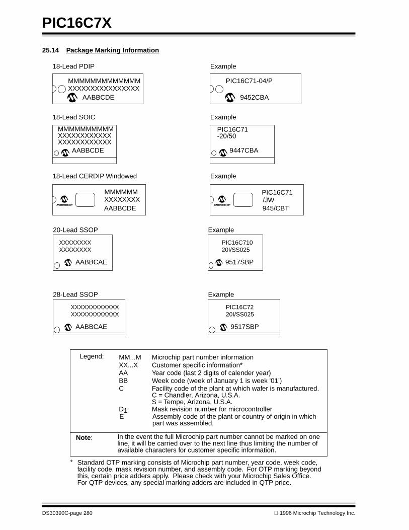
PIC16C7X
DS30390C-page 280 1996 Microchip Technology Inc.
25.14 Package Marking Information
Legend: MM...MXX...XAABBC
D1E
Microchip part number informationCustomer specific information*Year code (last 2 digits of calender year)Week code (week of January 1 is week '01’)Facility code of the plant at which wafer is manufactured.C = Chandler, Arizona, U.S.A.
Mask revision number for microcontrollerAssembly code of the plant or country of origin in whichpart was assembled.
In the event the full Microchip part number cannot be marked on one line, it will be carried over to the next line thus limiting the number of available characters for customer specific information.
Note:
Standard OTP marking consists of Microchip part number, year code, week code,facility code, mask revision number, and assembly code. For OTP marking beyondthis, certain price adders apply. Please check with your Microchip Sales Office.For QTP devices, any special marking adders are included in QTP price.
*
MMMMMMMMMMMMMXXXXXXXXXXXXXXXX
AABBCDE
18-Lead PDIP
18-Lead SOIC
XXXXXXXXXXXX
AABBCDEXXXXXXXXXXXX
MMMMMMMMMM
MMMMMMXXXXXXXXAABBCDE
18-Lead CERDIP Windowed
PIC16C71-04/P
9452CBA
Example
Example
-20/50
9447CBA
PIC16C71
PIC16C71/JW945/CBT
Example
S = Tempe, Arizona, U.S.A.
AABBCAE
XXXXXXXXXXXXXXXXXXXXXXXX
28-Lead SSOP
9517SBP
20I/SS025PIC16C72
Example
AABBCAE
XXXXXXXXXXXXXXXX
20-Lead SSOP
9517SBP
20I/SS025PIC16C710
Example
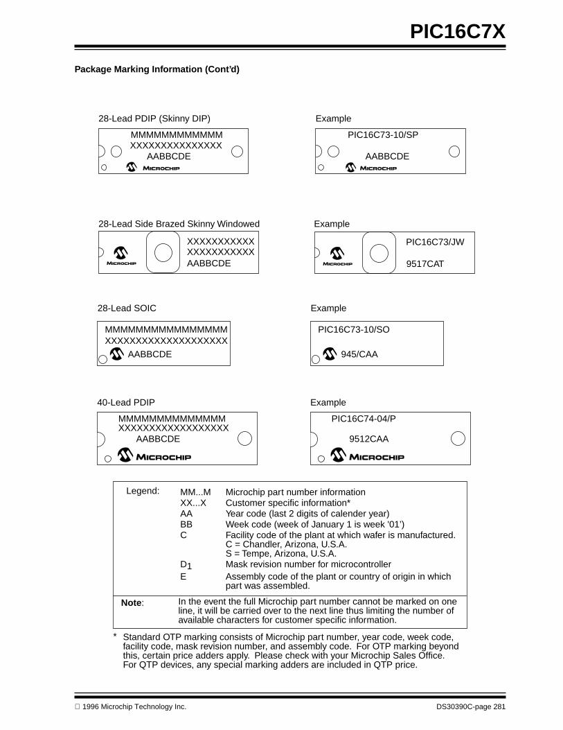
1996 Microchip Technology Inc. DS30390C-page 281
PIC16C7X
Package Marking Information (Cont’d)
Legend: MM...MXX...XAABBC
D1E
Microchip part number informationCustomer specific information*Year code (last 2 digits of calender year)Week code (week of January 1 is week '01’)Facility code of the plant at which wafer is manufactured.C = Chandler, Arizona, U.S.A.
Mask revision number for microcontrollerAssembly code of the plant or country of origin in whichpart was assembled.
In the event the full Microchip part number cannot be marked on one line, it will be carried over to the next line thus limiting the number of available characters for customer specific information.
Note:
Standard OTP marking consists of Microchip part number, year code, week code,facility code, mask revision number, and assembly code. For OTP marking beyondthis, certain price adders apply. Please check with your Microchip Sales Office.For QTP devices, any special marking adders are included in QTP price.
*
28-Lead SOIC
XXXXXXXXXXXXXXXXXXXX
AABBCDE
MMMMMMMMMMMMMMMM
Example
945/CAA
PIC16C73-10/SO
S = Tempe, Arizona, U.S.A.
XXXXXXXXXXXXXXXAABBCDE
28-Lead PDIP (Skinny DIP)
MMMMMMMMMMMM
AABBCDE
Example
PIC16C73-10/SP
Example28-Lead Side Brazed Skinny Windowed
XXXXXXXXXXXXXXXXXXXXXXAABBCDE
PIC16C73/JW
9517CAT
XXXXXXXXXXXXXXXXXXAABBCDE
40-Lead PDIP
MMMMMMMMMMMMMM
9512CAA
Example
PIC16C74-04/P

PIC16C7X
DS30390C-page 282 1996 Microchip Technology Inc.
Package Marking Information (Cont’d)
Legend: MM...MXX...XAABBC
D1E
Microchip part number informationCustomer specific information*Year code (last 2 digits of calender year)Week code (week of January 1 is week '01’)Facility code of the plant at which wafer is manufactured.C = Chandler, Arizona, U.S.A.
Mask revision number for microcontrollerAssembly code of the plant or country of origin in whichpart was assembled.
In the event the full Microchip part number cannot be marked on one line, it will be carried over to the next line thus limiting the number of available characters for customer specific information.
Note:
Standard OTP marking consists of Microchip part number, year code, week code,facility code, mask revision number, and assembly code. For OTP marking beyondthis, certain price adders apply. Please check with your Microchip Sales Office.For QTP devices, any special marking adders are included in QTP price.
*
44-Lead PLCC
MMMMMMMM
AABBCDE
XXXXXXXXXXXXXXXXXXXX
44-Lead MQFP
XXXXXXXXXX
AABBCDE
MMMMMMMM
XXXXXXXXXX
Example
PIC16C74
AABBCDE
-10/L
Example
-10/PQ
AABBCDE
PIC16C74
S = Tempe, Arizona, U.S.A.
44-Lead TQFP
XXXXXXXXXX
AABBCDE
MMMMMMMM
XXXXXXXXXX
Example
-10/TQ
AABBCDE
PIC16C74A
MMMMMMMMMXXXXXXXXXXX
AABBCDE
40-Lead CERDIP Windowed
XXXXXXXXXXX
PIC16C74/JW
AABBCDE
Example

1996 Microchip Technology Inc. DS30390D-page 283
PIC16C7X
APPENDIX A:
The following are the list of modifications over thePIC16C5X microcontroller family:
1. Instruction word length is increased to 14-bits.This allows larger page sizes both in programmemory (4K now as opposed to 512 before) andregister file (192 bytes now versus 32 bytesbefore).
2. A PC high latch register (PCLATH) is added tohandle program memory paging. Bits PA2, PA1,PA0 are removed from STATUS register.
3. Data memory paging is redefined slightly. STA-TUS register is modified.
4. Four new instructions have been added:
RETURN, RETFIE, ADDLW
, and
SUBLW
.Two instructions
TRIS
and
OPTION
are beingphased out although they are kept for compati-bility with PIC16C5X.
5. OPTION and TRIS registers are made address-able.
6. Interrupt capability is added. Interrupt vector isat 0004h.
7. Stack size is increased to 8 deep.8. Reset vector is changed to 0000h.9. Reset of all registers is revisited. Five different
reset (and wake-up) types are recognized. Reg-isters are reset differently.
10. Wake up from SLEEP through interrupt isadded.
11. Two separate timers, Oscillator Start-up Timer(OST) and Power-up Timer (PWRT) areincluded for more reliable power-up. These tim-ers are invoked selectively to avoid unnecessarydelays on power-up and wake-up.
12. PORTB has weak pull-ups and interrupt onchange feature.
13. T0CKI pin is also a port pin (RA4) now.14. FSR is made a full eight bit register.15. “In-circuit serial programming” is made possible.
The user can program PIC16CXX devices usingonly five pins: V
DD
, V
SS
, MCLR/V
PP
, RB6 (clock)and RB7 (data in/out).
16. PCON status register is added with a Power-onReset status bit (POR).
17. Code protection scheme is enhanced such thatportions of the program memory can be pro-tected, while the remainder is unprotected.
18. Brown-out protection circuitry has been added.Controlled by configuration word bit BODEN.Brown-out reset ensures the device is placed ina reset condition if V
DD
dips below a fixed set-point.
APPENDIX B: COMPATIBILITY
To convert code written for PIC16C5X to PIC16CXX,the user should take the following steps:
1. Remove any program memory page selectoperations (PA2, PA1, PA0 bits) for
CALL
,
GOTO
.2. Revisit any computed jump operations (write to
PC or add to PC, etc.) to make sure page bitsare set properly under the new scheme.
3. Eliminate any data memory page switching.Redefine data variables to reallocate them.
4. Verify all writes to STATUS, OPTION, and FSRregisters since these have changed.
5. Change reset vector to 0000h.
This document was created with FrameMaker 4 0 4

PIC16C7X
DS30390D-page 284
1996 Microchip Technology Inc.
APPENDIX C: WHAT’S NEW
Characterization data charts and graphs have beenadded for the following devices:
• PIC16C72• PIC16C73• PIC16C73A• PIC16C74• PIC16C74A
APPENDIX D: WHAT’S CHANGED
Minor changes, spelling and grammatical changes.

PIC16C7X
1996 Microchip Technology Inc. DS30390D-page 285
APPENDIX E: PIC16/17 MICROCONTROLLERS
E.1 PIC14000 Devices
PIC
1400
020
4K19
2T
MR
0A
DT
MR
I2 C/
SM
Bus
1411
222.
7-6.
0Y
es
Inte
rnal
Osc
illat
or,
Ban
dgap
Ref
eren
ce,
Tem
pera
ture
Sen
sor,
Cal
ibra
tion
Fac
tors
,Lo
w V
olta
ge D
etec
tor,
SLE
EP
, HIB
ER
NA
TE
,C
ompa
rato
rs w
ithP
rogr
amm
able
Ref
eren
ces
(2)
28-p
in D
IP, S
OIC
, SS
OP
(.30
0 m
il)
Max
imum
Fre
quen
cy o
f Ope
ratio
n (M
Hz)
Data
Mem
ory (
byte
s)
Timer
Mod
ule(s
)
Serial
Por
t(s) (
SPI/I2C, U
SART)
Slope
A/D C
onve
rter
Inte
rrupt
Sou
rces
I/O P
ins
Voltag
e Ran
ge (V
olts)
EPROM P
rogr
am M
emor
y (x1
4 wor
ds)
Clo
ckM
emor
yP
erip
hera
lsF
eatu
res
In-C
ircuit
Ser
ial P
rogr
amm
ing
Additio
nal O
n-ch
ip
Featu
res
Packa
ges
(high
-res)
Cha
nnels
This document was created with FrameMaker 4 0 4

PIC16C7X
DS30390D-page 286
1996 Microchip Technology Inc.
E.2 PIC16C5X Family of Devices
PIC
16C
524
384
—25
TM
R0
122.
5-6.
2533
18-p
in D
IP, S
OIC
PIC
16C
5420
512
—25
TM
R0
122.
5-6.
2533
18-p
in D
IP, S
OIC
; 20-
pin
SS
OP
PIC
16C
54A
2051
2—
25T
MR
012
2.0-
6.25
3318
-pin
DIP
, SO
IC; 2
0-pi
n S
SO
P
PIC
16C
R54
A20
—51
225
TM
R0
122.
0-6.
2533
18-p
in D
IP, S
OIC
; 20-
pin
SS
OP
PIC
16C
5520
512
—24
TM
R0
202.
5-6.
2533
28-p
in D
IP, S
OIC
, SS
OP
PIC
16C
5620
1K—
25T
MR
012
2.5-
6.25
3318
-pin
DIP
, SO
IC; 2
0-pi
n S
SO
P
PIC
16C
5720
2K—
72T
MR
020
2.5-
6.25
3328
-pin
DIP
, SO
IC, S
SO
P
PIC
16C
R57
B20
—2K
72T
MR
020
2.5-
6.25
3328
-pin
DIP
, SO
IC, S
SO
P
PIC
16C
58A
202K
—73
TM
R0
122.
0-6.
2533
18-p
in D
IP, S
OIC
; 20-
pin
SS
OP
PIC
16C
R58
A20
—2K
73T
MR
012
2.5-
6.25
3318
-pin
DIP
, SO
IC; 2
0-pi
n S
SO
P
All
PIC
16/1
7 Fa
mily
dev
ices
hav
e P
ower
-On
Res
et, s
elec
tabl
e W
atch
dog
Tim
er, s
elec
tabl
e co
de p
rote
ct a
nd h
igh
I/O c
urre
nt c
apab
ility
.
Packages
Number of In
structi
ons
Voltage R
ange (Volts
)
I/O Pins
Timer M
odule(s)
RAM Data M
emory (byte
s)
(x12 w
ords)
Program Memory
ROM
EPROM
Maximum Frequency
of Operatio
n (MHz)
Fea
ture
sP
erip
hera
lsM
emor
yC
lock

PIC16C7X
1996 Microchip Technology Inc. DS30390D-page 287
E.3 PIC16CXXX Family of Devices
PIC
16C
554
2051
280
TM
R0
——
313
2.5-
6.0
—18
-pin
DIP
, SO
IC; 2
0-pi
n S
SO
P
PIC
16C
556
201K
80T
MR
0—
—3
132.
5-6.
0—
18-p
in D
IP, S
OIC
; 20-
pin
SS
OP
PIC
16C
558
202K
128
TM
R0
——
313
2.5-
6.0
—18
-pin
DIP
, SO
IC; 2
0-pi
n S
SO
P
PIC
16C
620
2051
280
TM
R0
2Ye
s4
132.
5-6.
0Ye
s18
-pin
DIP
, SO
IC; 2
0-pi
n S
SO
P
PIC
16C
621
201K
80T
MR
02
Yes
413
2.5-
6.0
Yes
18-p
in D
IP, S
OIC
; 20-
pin
SS
OP
PIC
16C
622
202K
128
TM
R0
2Ye
s4
132.
5-6.
0Ye
s18
-pin
DIP
, SO
IC; 2
0-pi
n S
SO
P
All
PIC
16/1
7 Fa
mily
dev
ices
hav
e P
ower
-on
Res
et, s
elec
tabl
e W
atch
dog
Tim
er, s
elec
tabl
e co
de p
rote
ct a
nd h
igh
I/Ocu
rren
t cap
abili
ty.
All
PIC
16C
6XX
X F
amily
dev
ices
use
ser
ial p
rogr
amm
ing
with
clo
ck p
in R
B6
and
data
pin
RB
7.
Max
imum
Fre
quen
cy o
f Ope
ratio
n (M
Hz)
EPROM
Data
Mem
ory (
byte
s)
Timer
Mod
ule(s
)
Compa
rato
r(s)
Inte
rnal
Refer
ence
Volt
age
Inte
rrupt
Sou
rces
I/O P
ins
Voltag
e Ran
ge (V
olts)
Brown-
out R
eset Pac
kage
s
Progr
am M
emor
y
Clo
ckM
emor
yP
erip
hera
lsF
eatu
res
(x14
wor
ds)

PIC16C7X
DS30390D-page 288
1996 Microchip Technology Inc.
E.4 PIC16C6X Family of Devices
PIC
16C
6220
2K—
128
TM
R0,
T
MR
1, T
MR
21
SP
I/I2 C
—7
223.
0-6.
0Y
es—
28-p
in S
DIP
, SO
IC, S
SO
P
PIC
16C
62A
(1)
202K
—12
8T
MR
0,
TM
R1,
TM
R2
1S
PI/I
2 C—
722
2.5-
6.0
Yes
Yes
28-p
in S
DIP
, SO
IC, S
SO
P
PIC
16C
R62
(1)
20—
2K12
8T
MR
0,
TM
R1,
TM
R2
1S
PI/I
2 C—
722
2.5-
6.0
Yes
Yes
28-p
in S
DIP
, SO
IC, S
SO
P
PIC
16C
6320
4K—
192
TM
R0,
T
MR
1, T
MR
22
SP
I/I2 C
,U
SA
RT
—10
222.
5-6.
0Y
esY
es28
-pin
SD
IP, S
OIC
PIC
16C
R63
(1)
20—
4K19
2T
MR
0,
TM
R1,
TM
R2
2S
PI/I
2 C,
US
AR
T—
1022
2.5-
6.0
Yes
Yes
28-p
in S
DIP
, SO
IC
PIC
16C
6420
2K—
128
TM
R0,
T
MR
1, T
MR
21
SP
I/I2 C
Yes
833
3.0-
6.0
Yes
—40
-pin
DIP
; 44
-pin
PLC
C, M
QF
P
PIC
16C
64A
(1)
202K
—12
8T
MR
0,
TM
R1,
TM
R2
1S
PI/I
2 CY
es8
332.
5-6.
0Y
esY
es40
-pin
DIP
; 44
-pin
PLC
C, M
QF
P, T
QF
P
PIC
16C
R64
(1)
20—
2K12
8T
MR
0,
TM
R1,
TM
R2
1S
PI/I
2 CY
es8
332.
5-6.
0Y
esY
es40
-pin
DIP
; 44
-pin
PLC
C, M
QF
P, T
QF
P
PIC
16C
6520
4K—
192
TM
R0,
T
MR
1, T
MR
22
SP
I/I2 C
,U
SA
RT
Yes
1133
3.0-
6.0
Yes
—40
-pin
DIP
; 44
-pin
PLC
C, M
QF
P
PIC
16C
65A
(1)
204K
—19
2T
MR
0,
TM
R1,
TM
R2
2S
PI/I
2 C,
US
AR
TY
es11
332.
5-6.
0Y
esY
es40
-pin
DIP
; 44
-pin
PLC
C, M
QF
P, T
QF
P
PIC
16C
R65
(1)
20—
4K19
2T
MR
0,
TM
R1,
TM
R2
2S
PI/I
2 C,
US
AR
TY
es11
332.
5-6.
0Y
esY
es40
-pin
DIP
; 44
-pin
PLC
C, M
QF
P, T
QF
P
All
PIC
16/1
7 fa
mily
dev
ices
hav
e P
ower
-on
Res
et, s
elec
tabl
e W
atch
dog
Tim
er, s
elec
tabl
e co
de p
rote
ct, a
nd h
igh
I/O c
urre
nt c
apab
ility
.A
ll P
IC16
C6X
fam
ily d
evic
es u
se s
eria
l pro
gram
min
g w
ith c
lock
pin
RB
6 an
d da
ta p
in R
B7.
Not
e1:
Ple
ase
cont
act y
our
loca
l sal
es o
ffice
for
avai
labi
lity
of th
ese
devi
ces.
Max
imum
Fre
quen
cy o
f Ope
ratio
n (M
Hz)
EPROM
Data
Mem
ory (
byte
s)
Timer
Mod
ule(s
)
Captu
re/C
ompa
re/P
WM
Mod
ule(s
)
Serial
Por
t(s) (
SPI/I2C, U
SART)
Parall
el Slav
e Por
t
Inte
rrupt
Sou
rces
I/O P
ins
Voltag
e Ran
ge (V
olts) Bro
wn-ou
t Res
et Packa
ges
Progr
am M
emor
y
Clo
ckM
emor
yP
erip
hera
lsF
eatu
res
ROMIn
-Circ
uit S
erial
Pro
gram
ming
(x14
wor
ds)
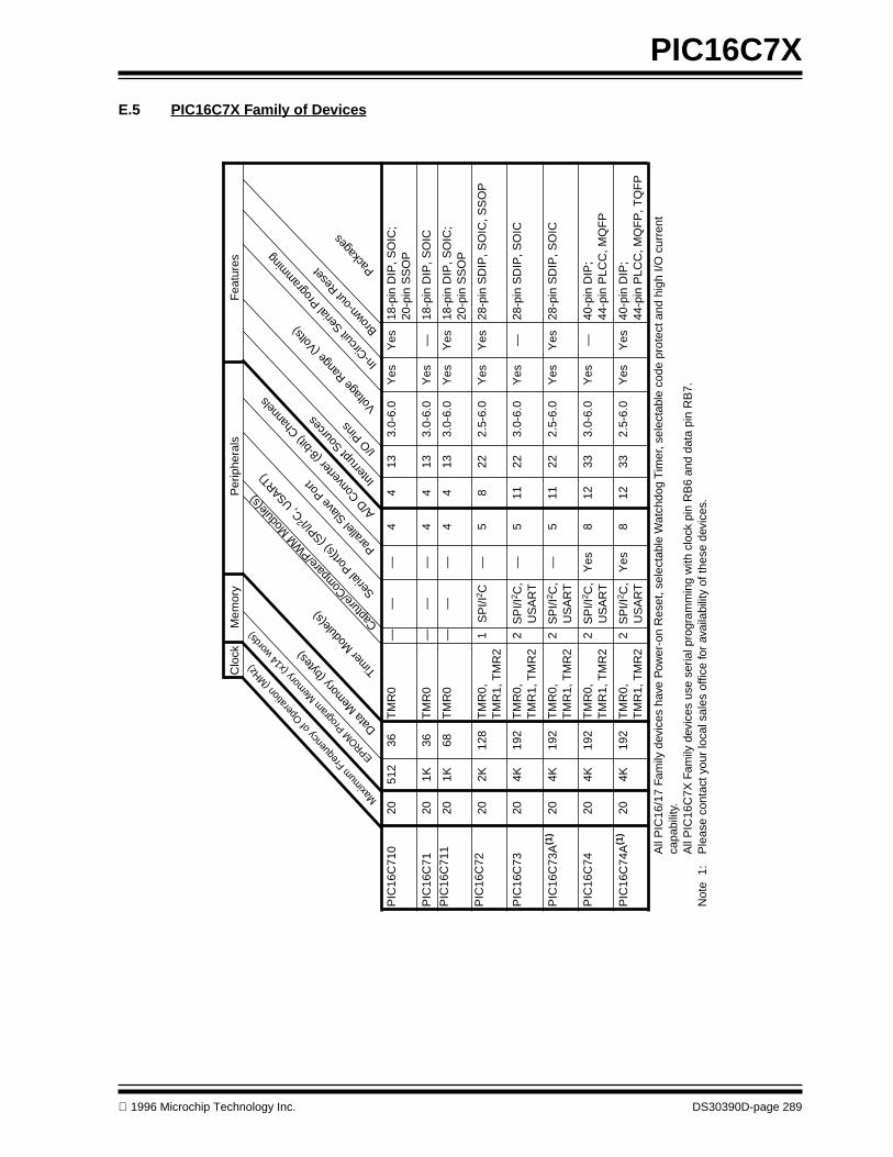
PIC16C7X
1996 Microchip Technology Inc. DS30390D-page 289
E.5 PIC16C7X Family of Devices
PIC
16C
710
2051
236
TM
R0
——
—4
413
3.0-
6.0
Yes
Yes
18-p
in D
IP, S
OIC
; 20
-pin
SS
OP
PIC
16C
7120
1K36
TM
R0
——
—4
413
3.0-
6.0
Yes
—18
-pin
DIP
, SO
IC
PIC
16C
711
201K
68T
MR
0—
——
44
133.
0-6.
0Y
esY
es18
-pin
DIP
, SO
IC;
20-p
in S
SO
P
PIC
16C
7220
2K12
8T
MR
0,
TM
R1,
TM
R2
1S
PI/I
2 C—
58
222.
5-6.
0Y
esY
es28
-pin
SD
IP, S
OIC
, SS
OP
PIC
16C
7320
4K19
2T
MR
0,
TM
R1,
TM
R2
2S
PI/I
2 C,
US
AR
T—
511
223.
0-6.
0Y
es—
28-p
in S
DIP
, SO
IC
PIC
16C
73A
(1)
204K
192
TM
R0,
T
MR
1, T
MR
22
SP
I/I2 C
,U
SA
RT
—5
1122
2.5-
6.0
Yes
Yes
28-p
in S
DIP
, SO
IC
PIC
16C
7420
4K19
2T
MR
0,
TM
R1,
TM
R2
2S
PI/I
2 C,
US
AR
TY
es8
1233
3.0-
6.0
Yes
—40
-pin
DIP
; 44
-pin
PLC
C, M
QF
P
PIC
16C
74A
(1)
204K
192
TM
R0,
T
MR
1, T
MR
22
SP
I/I2 C
,U
SA
RT
Yes
812
332.
5-6.
0Y
esY
es40
-pin
DIP
; 44
-pin
PLC
C, M
QF
P, T
QF
P
All
PIC
16/1
7 Fa
mily
dev
ices
hav
e P
ower
-on
Res
et, s
elec
tabl
e W
atch
dog
Tim
er, s
elec
tabl
e co
de p
rote
ct a
nd h
igh
I/O c
urre
nt
capa
bilit
y.A
ll P
IC16
C7X
Fam
ily d
evic
es u
se s
eria
l pro
gram
min
g w
ith c
lock
pin
RB
6 an
d da
ta p
in R
B7.
Not
e1:
Ple
ase
cont
act y
our
loca
l sal
es o
ffice
for
avai
labi
lity
of th
ese
devi
ces.
Max
imum
Fre
quen
cy o
f Ope
ratio
n (M
Hz)
EPROM P
rogr
am M
emor
y (x1
4 wor
ds)
Data
Mem
ory (
byte
s)
Timer
Mod
ule(s
)
Captu
re/C
ompa
re/P
WM
Mod
ule(s
)
Serial
Por
t(s) (
SPI/I2C, U
SART)
Parall
el Slav
e Por
t
A/D C
onve
rter (
8-bit
) Cha
nnels
Inte
rrupt
Sou
rces
I/O P
ins
Voltag
e Ran
ge (V
olts) Bro
wn-ou
t Res
et Packa
ges
Clo
ckM
emor
yP
erip
hera
lsF
eatu
res
In-C
ircuit
Ser
ial P
rogr
amm
ing

PIC16C7X
DS30390D-page 290
1996 Microchip Technology Inc.
E.6 PIC16C8X Family of Devices
PIC
16C
8410
—1K
—36
64T
MR
04
132.
0-6.
018
-pin
DIP
, SO
IC
PIC
16F
84(1
)10
1K—
—68
64T
MR
04
132.
0-6.
018
-pin
DIP
, SO
IC
PIC
16C
R84
(1)
10—
—1K
6864
TM
R0
413
2.0-
6.0
18-p
in D
IP, S
OIC
PIC
16F
83(1
)10
512
——
3664
TM
R0
413
2.0-
6.0
18-p
in D
IP, S
OIC
PIC
16C
R83
(1)
10—
—51
236
64T
MR
04
132.
0-6.
018
-pin
DIP
, SO
IC
All
PIC
16/1
7 fa
mily
dev
ices
hav
e P
ower
-on
Res
et, s
elec
tabl
e W
atch
dog
Tim
er, s
elec
tabl
e co
de p
rote
ct, a
nd
high
I/O
cur
rent
cap
abili
ty.
All
PIC
16C
8X fa
mily
dev
ices
use
ser
ial p
rogr
amm
ing
with
clo
ck p
in R
B6
and
data
pin
RB
7.N
ote
1:P
leas
e co
ntac
t you
r lo
cal s
ales
offi
ce fo
r av
aila
bilit
y of
thes
e de
vice
s.
Max
imum
Fre
quen
cy o
f Ope
ratio
n (M
Hz)
EEPROM
Data
EEPROM (b
ytes)
Data
Mem
ory (
byte
s)
Timer
Mod
ule(s
) Inte
rrupt
Sou
rces
I/O P
ins
Voltag
e Ran
ge (V
olts)
Packa
ges
Progr
am M
emor
y
Clo
ckM
emor
yP
erip
hera
lsF
eatu
res
ROM
Flash

PIC16C7X
1996 Microchip Technology Inc. DS30390D-page 291
E.7 PIC16C9XX Family Of Devices
PIC
16C
923
84K
176
TM
R0,
T
MR
1, T
MR
21
SP
I/I2 C
——
4 C
om32
Seg
825
273.
0-6.
0Y
es—
64-p
in S
DIP
(1) ,
TQ
FP
, 68
-pin
PLC
C, D
IE
PIC
16C
924
84K
176
TM
R0,
T
MR
1, T
MR
21
SP
I/I2 C
—5
4 C
om32
Seg
925
273.
0-6.
0Y
es—
64-p
in S
DIP
(1) ,
TQ
FP
, 68
-pin
PLC
C, D
IE
All
PIC
16/1
7 Fa
mily
dev
ices
hav
e P
ower
-on
Res
et, s
elec
tabl
e W
atch
dog
Tim
er, s
elec
tabl
e co
de p
rote
ct a
nd h
igh
I/O c
urre
nt c
apab
ility
.A
ll P
IC16
CX
X F
amily
dev
ices
use
ser
ial p
rogr
amm
ing
with
clo
ck p
in R
B6
and
data
pin
RB
7.N
ote
1:P
leas
e co
ntac
t you
r lo
cal M
icro
chip
rep
rese
ntat
ive
for
avai
labi
lity
of th
is p
acka
ge.
Max
imum
Fre
quen
cy o
f Ope
ratio
n (M
Hz)
EPROM
Data
Mem
ory (
byte
s)
Timer
Mod
ule(s
)
Captu
re/C
ompa
re/P
WM
Mod
ule(s
)
Serial
Por
t(s) (
SPI/I2C, U
SART)
Parall
el Slav
e Por
t
A/D C
onve
rter (
8-bit
) Cha
nnels
Inte
rrupt
Sou
rces
I/O P
ins
Voltag
e Ran
ge (V
olts) Bro
wn-ou
t Res
et Packa
ges
Progr
am M
emor
y
Clo
ckM
emor
yP
erip
hera
lsF
eatu
res
In-C
ircuit
Ser
ial P
rogr
amm
ing
Inpu
t Pins
LCD M
odule

PIC16C7X
DS30390D-page 292
1996 Microchip Technology Inc.
E.8 PIC17CXX Family of Devices
PIC
17C
4225
2K—
232
TM
R0,
TM
R1,
TM
R2,
TM
R3
22
Yes
—Y
es11
334.
5-5.
555
40-p
in D
IP;
44-p
in P
LCC
, MQ
FP
PIC
17C
42A
252K
—23
2T
MR
0,T
MR
1,T
MR
2,T
MR
32
2Y
esY
esY
es11
332.
5-6.
058
40-p
in D
IP;
44-p
in P
LCC
, TQ
FP
, MQ
FP
PIC
17C
R42
25—
2K23
2T
MR
0,T
MR
1,T
MR
2,T
MR
32
2Y
esY
esY
es11
332.
5-6.
058
40-p
in D
IP;
44-p
in P
LCC
, TQ
FP
, MQ
FP
PIC
17C
4325
4K—
454
TM
R0,
TM
R1,
TM
R2,
TM
R3
22
Yes
Yes
Yes
1133
2.5-
6.0
5840
-pin
DIP
; 44
-pin
PLC
C, T
QF
P, M
QF
P
PIC
17C
R43
25—
4K45
4T
MR
0,T
MR
1,T
MR
2,T
MR
32
2Y
esY
esY
es11
332.
5-6.
058
40-p
in D
IP;
44-p
in P
LCC
, TQ
FP
, MQ
FP
PIC
17C
4425
8K45
4T
MR
0,T
MR
1,T
MR
2,T
MR
32
2Y
esY
esY
es11
332.
5-6.
058
40-p
in D
IP;
44-p
in P
LCC
, TQ
FP
, MQ
FP
All
PIC
16/1
7 Fa
mily
dev
ices
hav
e P
ower
-on
Res
et, s
elec
tabl
e W
atch
dog
Tim
er, s
elec
tabl
e co
de p
rote
ct a
nd h
igh
I/O c
urre
nt c
apab
ility
.
Maxim
um F
requ
ency
of O
pera
tion (
MHz)
EPROM
RAM Data
Mem
ory (
bytes
)
Timer
Mod
ule(s) Cap
tures
Serial
Por
t(s) (
USART) Extern
al Int
erru
pts
Inter
rupt
Source
s
I/O P
insVolt
age R
ange
(Volt
s)
Numbe
r of In
struc
tions
Packa
ges
Clo
ckM
emor
yP
erip
hera
lsF
eatu
res
PWMs
Hardw
are M
ultipl
y
Progr
am M
emor
y (W
ords
)
ROM
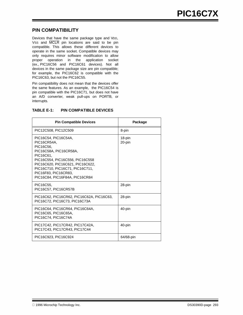
1996 Microchip Technology Inc. DS30390D-page 293
PIC16C7X
PIN COMPATIBILITY
Devices that have the same package type and V
DD
,V
SS
and MCLR pin locations are said to be pincompatible. This allows these different devices tooperate in the same socket. Compatible devices mayonly requires minor software modification to allowproper operation in the application socket(ex., PIC16C56 and PIC16C61 devices). Not alldevices in the same package size are pin compatible;for example, the PIC16C62 is compatible with thePIC16C63, but not the PIC16C55.
Pin compatibility does not mean that the devices offerthe same features. As an example, the PIC16C54 ispin compatible with the PIC16C71, but does not havean A/D converter, weak pull-ups on PORTB, orinterrupts.
TABLE E-1: PIN COMPATIBLE DEVICES
Pin Compatible Devices Package
PIC12C508, PIC12C509 8-pin
PIC16C54, PIC16C54A,PIC16CR54A,PIC16C56,PIC16C58A, PIC16CR58A,PIC16C61,PIC16C554, PIC16C556, PIC16C558PIC16C620, PIC16C621, PIC16C622,PIC16C710, PIC16C71, PIC16C711,PIC16F83, PIC16CR83,PIC16C84, PIC16F84A, PIC16CR84
18-pin 20-pin
PIC16C55,PIC16C57, PIC16CR57B
28-pin
PIC16C62, PIC16CR62, PIC16C62A, PIC16C63,PIC16C72, PIC16C73, PIC16C73A
28-pin
PIC16C64, PIC16CR64, PIC16C64A, PIC16C65, PIC16C65A,PIC16C74, PIC16C74A
40-pin
PIC17C42, PIC17CR42, PIC17C42A,PIC17C43, PIC17CR43, PIC17C44
40-pin
PIC16C923, PIC16C924 64/68-pin

PIC16C7X
DS30390D-page 294
1996 Microchip Technology Inc.
NOTES:
1996 Microchip Technology Inc. DS30390D-page 295
PIC16C7X
INDEX
A
A/DAccuracy/Error ......................................................... 118ADCON0 Register .................................................... 109ADCON1 Register .................................................... 111ADIF bit .................................................................... 112Analog Input Model Block Diagram .......................... 114Analog-to-Digital Converter ...................................... 109Block Diagram .......................................................... 113Configuring Analog Port Pins ................................... 115Configuring the Interrupt .......................................... 112Configuring the Module ............................................ 112Connection Considerations ...................................... 119Conversion Clock ..................................................... 115Conversion Time ...................................................... 117Conversions ............................................................. 116Converter Characteristics ........ 170, 184, 210, 231, 253Delays ...................................................................... 114Effects of a Reset ..................................................... 118Equations ................................................................. 114Faster Conversion - Lower Resolution Tradeoff ...... 117Flowchart of A/D Operation ...................................... 119GO/DONE bit ........................................................... 112Internal Sampling Switch (Rss) Impedence ............. 114Operation During Sleep ........................................... 118Sampling Requirements ........................................... 114Sampling Time ......................................................... 114Source Impedence ................................................... 114Time Delays ............................................................. 114Transfer Function ..................................................... 119Using the CCP Trigger ............................................. 118
Absolute Maximum Ratings ............. 159, 175, 195, 213, 235ACK ........................................................................ 84, 88, 89ADCS0 bit ........................................................................ 109ADCS1 bit ........................................................................ 109ADDLW Instruction .......................................................... 144ADDWF Instruction .......................................................... 144ADIE bit ........................................................................ 32, 34ADIF bit ...................................................................... 36, 109ADON bit .......................................................................... 109ADRES Register .......................................... 26, 28, 109, 112ALU ...................................................................................... 9ALUSTA ........................................................................... 142ANDLW Instruction .......................................................... 144ANDWF Instruction .......................................................... 144Application Notes
AN546 ...................................................................... 109AN552 ........................................................................ 45AN556 ........................................................................ 41AN578 ........................................................................ 77AN594 ........................................................................ 71
ArchitectureHarvard ........................................................................ 9Overview ...................................................................... 9von Neumann ............................................................... 9
Assembler ........................................................................ 156
B
Baud Rate Error ................................................................. 95Baud Rate Formula ............................................................ 95Baud Rates
Asynchronous Mode .................................................. 96Synchronous Mode .................................................... 96
BCF Instruction ................................................................ 145
BF bit ......................................................................77, 88, 89Bit Manipulation ................................................................142Block Diagrams
A/D ............................................................................113Analog Input Model ...................................................114Capture .......................................................................72Compare .....................................................................73Interrupt Logic ...........................................................134On-Chip Reset Circuit ...............................................126PIC16C70 ...................................................................10PIC16C71 ...................................................................10PIC16C71A .................................................................10PIC16C72 ...................................................................11PIC16C73 ...................................................................12PIC16C73A .................................................................12PIC16C74 ...................................................................13PIC16C74A .................................................................13PORTC .......................................................................48PORTD (In I/O Port Mode) .........................................50PORTD and PORTE as a Parallel Slave Port ............55PORTE (In I/O Port Mode) .........................................53PWM ...........................................................................74RA3:RA0 and RA5 Port Pins ......................................43RA4/T0CKI Pin ...........................................................44RB3:RB0 Port Pins .....................................................45RB7:RB4 Pins .............................................................46RB7:RB4 Port Pins .....................................................46SPI Master/Slave Connection .....................................80SSP (I
2
C Mode) ..........................................................87SSP, SPI Mode ...........................................................79Timer0 ........................................................................59Timer0/WDT Prescaler ...............................................62Timer1 ........................................................................66Timer2 ........................................................................69USART Receive .......................................................101USART Transmit ........................................................99Watchdog Timer .......................................................137
BODEN bit ........................................................................122BOR bit .......................................................................40, 128BRGH bit ............................................................................95BSF Instruction .................................................................145BTFSC Instruction ............................................................145BTFSS Instruction ............................................................146
C
C bit ....................................................................................30C Compiler (MP-C) ...........................................................157CALL Instruction ...............................................................146Capture/Compare/PWM
CaptureBlock Diagram ....................................................72CCP1CON Register ...........................................72CCP1IF ...............................................................72CCPR1 ...............................................................72CCPR1H:CCPR1L .............................................72Mode ..................................................................72Prescaler ............................................................73
CCP Timer Resources ................................................71Compare
Block Diagram ....................................................73Mode ..................................................................73Software Interrupt Mode .....................................73Special Event Trigger .........................................73Special Trigger Output of CCP1 .........................73Special Trigger Output of CCP2 .........................73
Interaction of Two CCP Modules ................................71
This document was created with FrameMaker 4 0 4

PIC16C7X
DS30390D-page 296
1996 Microchip Technology Inc.
Section ....................................................................... 71Special Event Trigger and A/D Conversions .............. 73
Capture/Compare/PWM (CCP)PWM Block Diagram .................................................. 74PWM Mode ................................................................ 74PWM, Example Frequencies/Resolutions .................. 75
Carry bit ................................................................................ 9CCP1IE bit ......................................................................... 34CCP1IF bit .................................................................... 36, 37CCP2IE bit ......................................................................... 38CCP2IF bit .......................................................................... 39CCPR1H Register ........................................................ 28, 71CCPR1L Register ............................................................... 71CCPR2H Register ........................................................ 28, 71CCPR2L Register ......................................................... 28, 71CCPxM0 bit ........................................................................ 72CCPxM1 bit ........................................................................ 72CCPxM2 bit ........................................................................ 72CCPxM3 bit ........................................................................ 72CCPxX bit ........................................................................... 72CCPxY bit ........................................................................... 72CHS0 bit ........................................................................... 109CHS1 bit ........................................................................... 109CKP bit ............................................................................... 78Clocking Scheme ............................................................... 20CLRF Instruction .............................................................. 146CLRW Instruction ............................................................. 146CLRWDT Instruction ........................................................ 147Code Examples
Call of a Subroutine in Page 1 from Page 0 ............... 42Changing Between Capture Prescalers ..................... 73Changing Prescaler (Timer0 to WDT) ........................ 63Changing Prescaler (WDT to Timer0) ........................ 63Doing an A/D Conversion ........................................ 116I/O Programming ........................................................ 54Indirect Addressing .................................................... 42Initializing PORTA ...................................................... 43Initializing PORTB ...................................................... 45Initializing PORTC ...................................................... 48Loading the SSPBUF Register .................................. 79Saving W register and STATUS in RAM .................. 136
Code Protection ....................................................... 121, 139COMF Instruction ............................................................. 147Computed GOTO ............................................................... 41Configuration Bits ............................................................. 121Configuration Word .......................................................... 122CP0 bit ............................................................................. 122CP1 bit ............................................................................. 122CREN bit ............................................................................ 94CS pin ................................................................................ 55
D
D/A bit ................................................................................ 77DC bit ................................................................................. 30DC Characteristics
PIC16C70 ................................................................ 161PIC16C71 ................................................................ 176PIC16C71A .............................................................. 161PIC16C72 ................................................................ 197PIC16C73 ................................................................ 215PIC16C73A .............................................................. 237PIC16C74 ................................................................ 215PIC16C74A .............................................................. 237
DECF Instruction .............................................................. 147DECFSZ Instruction ......................................................... 147Development Support .................................................. 5, 155
Development Tools .......................................................... 155Diagrams - See Block DiagramsDigit Carry bit ....................................................................... 9Direct Addressing .............................................................. 42
E
Electrical CharacteristicsPIC16C70 ................................................................ 159PIC16C71 ................................................................ 175PIC16C71A .............................................................. 159PIC16C72 ................................................................ 195PIC16C73 ................................................................ 213PIC16C73A .............................................................. 235PIC16C74 ................................................................ 213PIC16C74A .............................................................. 235
External Brown-out Protection Circuit .............................. 132External Power-on Reset Circuit ...................................... 132
F
Family of DevicesPIC14000 ................................................................. 285PIC16C5X ................................................................ 286PIC16CXXX ............................................................. 287PIC16C6X ................................................................ 288PIC16C7X ............................................................ 6, 289PIC16C8X ................................................................ 290PIC16C9XX .............................................................. 291PIC17CXX ............................................................... 292
FERR bit ............................................................................ 94FOSC0 bit ........................................................................ 122FOSC1 bit ........................................................................ 122FSR Register ............................................. 26, 27, 28, 29, 42Fuzzy Logic Dev. System (
fuzzy
TECH
-MP) .......... 155, 157
G
General Description ............................................................. 5GIE bit ........................................................................ 32, 133GO/DONE bit ................................................................... 109GOTO Instruction ............................................................. 148Graphs and Charts, PIC16C71 ........................................ 187
I
I/O PortsPORTA ...................................................................... 43PORTB ...................................................................... 45PORTC ...................................................................... 48PORTD ................................................................ 50, 55PORTE ...................................................................... 52Section ....................................................................... 43
I/O Programming Considerations ...................................... 54I
2
C, See Synchronous Serial PortIBF bit ................................................................................ 55IDLE_MODE ...................................................................... 92INCF Instruction ............................................................... 148INCFSZ Instruction .......................................................... 148In-Circuit Serial Programming .................................. 121, 139INDF Register ........................................... 25, 27, 28, 29, 42Indirect Addressing ............................................................ 42Initialization Condition for all Register .............................. 129Instruction Cycle ................................................................ 20Instruction Flow/Pipelining ................................................. 20Instruction Format ............................................................ 142Instruction Set
ADDLW .................................................................... 144ADDWF ................................................................... 144ANDLW .................................................................... 144ANDWF ................................................................... 144

1996 Microchip Technology Inc. DS30390D-page 297
PIC16C7X
BCF .......................................................................... 145BSF .......................................................................... 145BTFSC ..................................................................... 145BTFSS ..................................................................... 146CALL ........................................................................ 146CLRF ........................................................................ 146CLRW ...................................................................... 146CLRWDT .................................................................. 147COMF ...................................................................... 147DECF ....................................................................... 147DECFSZ ................................................................... 147GOTO ...................................................................... 148INCF ......................................................................... 148INCFSZ .................................................................... 148IORLW ..................................................................... 148IORWF ..................................................................... 149MOVF ....................................................................... 149MOVLW ................................................................... 149MOVWF ................................................................... 149NOP ......................................................................... 150OPTION ................................................................... 150RETFIE .................................................................... 150RETLW .................................................................... 150RETURN .................................................................. 151RLF .......................................................................... 151RRF .......................................................................... 151SLEEP ..................................................................... 151SUBLW .................................................................... 152SUBWF .................................................................... 152SWAPF .................................................................... 153TRIS ......................................................................... 153XORLW .................................................................... 153XORWF .................................................................... 153Section ..................................................................... 141Summary Table ........................................................ 143
INT Interrupt ..................................................................... 136INTCON Register ............................................................... 32INTE bit .............................................................................. 32INTEDG bit ................................................................. 31, 136Inter-Integrated Circuit (I
2
C) ............................................... 77Internal Sampling Switch (Rss) Impedence ..................... 114Interrupts .......................................................................... 121
A/D ........................................................................... 133CCP1 ....................................................................... 133CCP2 ....................................................................... 133PortB Change .......................................................... 136PSP .......................................................................... 133RB7:RB4 Port Change ............................................... 45Section ..................................................................... 133SSP .......................................................................... 133TMR0 ....................................................................... 136TMR1 Overflow ........................................................ 133TMR2 Matches PR2 ................................................. 133USART RX ............................................................... 133USART TX ............................................................... 133
INTF bit .............................................................................. 32IORLW Instruction ............................................................ 148IORWF Instruction ........................................................... 149IRP bit ................................................................................ 30
L
Loading of PC .................................................................... 41
M
MCLR ....................................................................... 126, 129Memory
Data Memory ............................................................. 22
Program Memory ........................................................21Program Memory Maps
PIC16C70 ...........................................................21PIC16C71 ...........................................................21PIC16C71A ........................................................21PIC16C72 ...........................................................22PIC16C73 ...........................................................22PIC16C73A ........................................................22PIC16C74 ...........................................................22PIC16C74A ........................................................22
Register File MapsPIC16C70 ...........................................................23PIC16C71 ...........................................................23PIC16C71A ........................................................23PIC16C72 ...........................................................24PIC16C73 ...........................................................24PIC16C73A ........................................................24PIC16C74 ...........................................................24PIC16C74A ........................................................24
MOVF Instruction ..............................................................149MOVLW Instruction ..........................................................149MOVWF Instruction ..........................................................149MPASM Assembler ..................................................155, 156MP-C C Compiler .............................................................157MPSIM Software Simulator ......................................155, 157
N
NOP Instruction ................................................................150
O
OBF bit ...............................................................................55OERR bit ............................................................................94Opcode .............................................................................141OPTION Instruction ..........................................................150OPTION Register ...............................................................31Orthogonal ............................................................................9OSC Selection ..................................................................121Oscillator
HS .....................................................................123, 128LP .....................................................................123, 128RC ............................................................................123XT .....................................................................123, 128
Oscillator Configurations ..................................................123Output of TMR2 ..................................................................69
P
P bit ....................................................................................77Packaging
18-Lead CERDIP w/Window ....................................26718-Lead PDIP ...........................................................27018-Lead SOIC ...........................................................27320-Lead SSOP .........................................................27528-Lead Ceramic w/Window .....................................26828-Lead PDIP ...........................................................27128-Lead SOIC ...........................................................27428-Lead SSOP .........................................................27640-Lead CERDIP w/Window ....................................26940-Lead PDIP ...........................................................27244-Lead MQFP .........................................................27844-Lead PLCC ..........................................................27744-Lead TQFP ..........................................................279
Paging, Program Memory ...................................................41Parallel Slave Port ........................................................50, 55PCFG0 bit .........................................................................111PCFG1 bit .........................................................................111PCFG2 bit .........................................................................111PCL ...................................................................................142

PIC16C7X
DS30390D-page 298
1996 Microchip Technology Inc.
PCL Register ........................................ 25, 26, 27, 28, 29, 41PCLATH ........................................................................... 129PCLATH Register ................................. 25, 26, 27, 28, 29, 41PCON Register .......................................................... 40, 128PD bit ................................................................. 30, 126, 128PICDEM-1 Low-Cost PIC16/17 Demo Board ........... 155, 156PICDEM-2 Low-Cost PIC16CXX Demo Board ........ 155, 156PICDEM-3 Low-Cost PIC16C9XXX Demo Board ............ 156PICMASTER
RT In-Circuit Emulator ............................. 155PICSTART
Low-Cost Development System .................. 155PIE1 Register ..................................................................... 34PIE2 Register ..................................................................... 38Pin Compatible Devices ................................................... 293Pin Functions
MCLR/V
PP
.......................................... 14, 15, 16, 17, 18OSC1/CLKIN ...................................... 14, 15, 16, 17, 18OSC2/CLKOUT .................................. 14, 15, 16, 17, 18RA0/AN0 ............................................ 14, 15, 16, 17, 18RA1/AN1 ............................................ 14, 15, 16, 17, 18RA2/AN2 ............................................ 14, 15, 16, 17, 18RA3/AN3/V
REF
................................... 14, 15, 16, 17, 18RA4/T0CKI ......................................... 14, 15, 16, 17, 18RA5/AN4/SS .................................................. 16, 17, 18RB0/INT ............................................. 14, 15, 16, 17, 18RB1 .................................................... 14, 15, 16, 17, 18RB2 .................................................... 14, 15, 16, 17, 18RB3 .................................................... 14, 15, 16, 17, 18RB4 .................................................... 14, 15, 16, 17, 18RB5 .................................................... 14, 15, 16, 17, 18RB6 .................................................... 14, 15, 16, 17, 18RB7 .................................................... 14, 15, 16, 17, 18RC0/T1OSO/T1CKI ....................................... 16, 17, 19RC1/T1OSI ................................................................ 16RC1/T1OSI/CCP2 ................................................ 17, 19RC2/CCP1 ..................................................... 16, 17, 19RC3/SCK/SCL ............................................... 16, 17, 19RC4/SDI/SDA ................................................ 16, 17, 19RC5/SDO ....................................................... 16, 17, 19RC6 ............................................................................ 16RC6/TX/CK ............................................ 17, 19, 93–107RC7 ............................................................................ 16RC7/RX/DT ............................................ 17, 19, 93–107RD0/PSP0 .................................................................. 19RD1/PSP1 .................................................................. 19RD2/PSP2 .................................................................. 19RD3/PSP3 .................................................................. 19RD4/PSP4 .................................................................. 19RD5/PSP5 .................................................................. 19RD6/PSP6 .................................................................. 19RD7/PSP7 .................................................................. 19RE0/RD/AN5 .............................................................. 19RE1/WR/AN6 ............................................................. 19RE2/CS/AN7 .............................................................. 19V
DD
.................................................... 14, 15, 16, 17, 19V
SS
..................................................... 14, 15, 16, 17, 19Pinout Descriptions
PIC16C70 ............................................................ 14, 15PIC16C71 ............................................................ 14, 15PIC16C71A .......................................................... 14, 15PIC16C72 .................................................................. 16PIC16C73 .................................................................. 17PIC16C73A ................................................................ 17PIC16C74 .................................................................. 18PIC16C74A ................................................................ 18
PIR1 Register ..................................................................... 36PIR2 Register ..................................................................... 39
POP ................................................................................... 41POR ......................................................................... 127, 128
Oscillator Start-up Timer (OST) ....................... 121, 127Power Control Register (PCON) .............................. 128Power-on Reset (POR) ............................ 121, 127, 129Power-up Timer (PWRT) ................................. 121, 127Power-Up-Timer (PWRT) ........................................ 127Time-out Sequence ................................................. 128Time-out Sequence on Power-up ............................ 131TO .................................................................... 126, 128
POR bit ...................................................................... 40, 128Port RB Interrupt .............................................................. 136PORTA ............................................................................ 129PORTA Register .............................................. 25, 26, 28, 43PORTB ............................................................................ 129PORTB Register .............................................. 25, 26, 28, 45PORTC ............................................................................ 129PORTC Register .................................................... 26, 28, 48PORTD ............................................................................ 129PORTD Register .......................................................... 28, 50PORTE ............................................................................ 129PORTE Register .......................................................... 28, 52Power-down Mode (SLEEP) ............................................ 138PR2 Register ............................................................... 29, 69Prescaler, Switching Between Timer0 and WDT ............... 63PRO MATE
Universal Programmer ............................... 155Program Branches ............................................................... 9Program Memory
Paging ....................................................................... 41Program Memory Maps
PIC16C70 .................................................................. 21PIC16C71 .................................................................. 21PIC16C71A ................................................................ 21PIC16C72 .................................................................. 22PIC16C73 .................................................................. 22PIC16C73A ................................................................ 22PIC16C74 .................................................................. 22PIC16C74A ................................................................ 22
Program Verification ........................................................ 139PS0 bit ............................................................................... 31PS1 bit ............................................................................... 31PS2 bit ............................................................................... 31PSA bit ............................................................................... 31PSPIE bit ..................................................................... 35, 55PSPIF bit ...................................................................... 37, 55PSPMODE bit ........................................................ 50, 52, 55PUSH ................................................................................. 41PWRTE bit ....................................................................... 122
R
R/W bit ............................................................. 84, 88, 89, 90R/W bit ............................................................................... 77RBIE bit .............................................................................. 32RBIF bit ................................................................ 32, 45, 136RBPU bit ............................................................................ 31RC Oscillator ............................................................ 125, 128RCIE bit ............................................................................. 35RCIF bit .............................................................................. 37RCSTA Register ................................................................ 94RCV_MODE ...................................................................... 92RD pin ................................................................................ 55Read-Modify-Write ............................................................. 54Register File ....................................................................... 22Registers
Initialization Conditions ............................................ 129Maps

1996 Microchip Technology Inc. DS30390D-page 299
PIC16C7X
PIC16C70 .......................................................... 23PIC16C71 .......................................................... 23PIC16C71A ........................................................ 23PIC16C72 .......................................................... 24PIC16C73 .......................................................... 24PIC16C73A ........................................................ 24PIC16C74 .......................................................... 24PIC16C74A ........................................................ 24
Reset Conditions ...................................................... 129Summary .............................................................. 25–28
Reset ........................................................................ 121, 126Reset Conditions for Special Registers ........................... 129RETFIE Instruction ........................................................... 150RETLW Instruction ........................................................... 150RETURN Instruction ........................................................ 151RLF Instruction ................................................................. 151RP0 bit ......................................................................... 22, 30RP1 bit ............................................................................... 30RRF Instruction ................................................................ 151RX9 bit ............................................................................... 94RX9D bit ............................................................................. 94
S
S bit .................................................................................... 77SCL .............................................................................. 88, 91SDA .............................................................................. 90, 91Serial Communication Interface (SCI) Module, See USARTSerial Peripheral Interface (SPI) ........................................ 77Services
One-Time-Programmable (OTP) ................................. 7Quick-Turnaround-Production (QTP) ........................... 7Serialized Quick-Turnaround Production (SQTP) ........ 7
SFR .................................................................................. 142SFR As Source/Destination ............................................. 142SLEEP ..................................................................... 121, 126SLEEP Instruction ............................................................ 151Software Simulator (MPSIM) ........................................... 157SPBRG Register ................................................................ 29Special Event Trigger ....................................................... 118Special Features of the CPU ........................................... 121Special Function Registers .............................................. 142
PIC16C70 .................................................................. 25PIC16C71 .................................................................. 25PIC16C71A ................................................................ 25PIC16C72 .................................................................. 26PIC16C73 .................................................................. 28PIC16C73A ................................................................ 28PIC16C74 .................................................................. 28PIC16C74A ................................................................ 28
Special Function Registers, Section .................................. 25SPEN bit ............................................................................ 94SPI, See Synchronous Serial PortSREN bit ............................................................................ 94SS bit ................................................................................. 81SSPADD Register .................................................. 27, 29, 88SSPBUF Register ........................................................ 28, 88SSPCON Register ................................................. 28, 78, 89SSPEN bit .......................................................................... 78SSPIE bit ............................................................................ 34SSPIF bit .......................................................... 36, 37, 88, 89SSPM0 bit .......................................................................... 78SSPM1 bit .......................................................................... 78SSPM2 bit .......................................................................... 78SSPM3 bit .......................................................................... 78SSPOV bit .................................................................... 78, 88SSPSR Register ................................................................ 88
SSPSTAT Register ...........................................27, 29, 77, 89Stack ...................................................................................41
Overflows ....................................................................41Underflow ...................................................................41
STATUS Register ...............................................................30SUBLW Instruction ...........................................................152SUBWF Instruction ...........................................................152SWAPF Instruction ...........................................................153Synchronous Serial Port
I
2
CAddressing .........................................................88Addressing I
2
C Devices .....................................84Arbitration ...........................................................86Block Diagram ....................................................87Clock Synchronization ........................................86Combined Format ...............................................85I
2
C Operation .....................................................87I
2
C Overview ......................................................83Initiating and Terminating Data Transfer ............83Master-Receiver Sequence ................................85Master-Transmitter Sequence ............................85Multi-master ........................................................86Multi-master Mode ..............................................91Reception ...........................................................89Slave Mode ........................................................88START ..........................................................83, 90START (S) ..........................................................91STOP ............................................................83, 84STOP (P) ............................................................91Transfer Acknowledge ........................................84Transmission ......................................................90
SPIBlock Diagram of Master/Slave Connection .......80Master Mode ......................................................80Serial Clock ........................................................79Serial Data In ......................................................79Serial Data Out ...................................................79Slave Select .......................................................79SPI Clock ............................................................80SPI Mode ............................................................79SSPBUF Register ...............................................80SSPSR Register .................................................80
Synchronous Serial Port (SSP)Block Diagram, SPI Mode ..........................................79
Synchronous Serial Port Module ........................................77
T
T0CS bit ..............................................................................31T0IE bit ...............................................................................32T0IF bit ...............................................................................32T1CKPS0 bit .......................................................................65T1CKPS1 bit .......................................................................65T1CON Register .................................................................65T1OSCEN bit ......................................................................65T1SYNC bit .........................................................................65T2CKPS0 bit .......................................................................70T2CKPS1 bit .......................................................................70T2CON Register .................................................................70T
AD
...................................................................................115Timer Modules, Overview ...................................................57Timer0
RTCC ........................................................................129Timers
Timer0Block Diagram ....................................................59External Clock ....................................................61

PIC16C7X
DS30390D-page 300
1996 Microchip Technology Inc.
External Clock Timing ........................................ 61Increment Delay ................................................. 61Interrupt .............................................................. 59Interrupt Timing .................................................. 60Overview ............................................................ 57Prescaler ............................................................ 62Prescaler Block Diagram ................................... 62Section ............................................................... 59Switching Prescaler Assignment ........................ 63Synchronization ................................................. 61T0CKI ................................................................. 61T0IF .................................................................. 136Timing ................................................................ 59TMR0 Interrupt ................................................. 136
Timer1Asynchronous Counter Mode ............................ 67Block Diagram .................................................... 66Capacitor Selection ............................................ 67External Clock Input ........................................... 66External Clock Input Timing ............................... 67Operation in Timer Mode ................................... 66Oscillator ............................................................ 67Overview ............................................................ 57Prescaler ...................................................... 66, 68Resetting of Timer1 Registers ........................... 68Resetting Timer1 using a CCP Trigger Output .. 68Synchronized Counter Mode ............................. 66T1CON ............................................................... 65TMR1H ............................................................... 67TMR1L ............................................................... 67
Timer2Block Diagram .................................................... 69Module ............................................................... 69Overview ............................................................ 57Postscaler .......................................................... 69Prescaler ............................................................ 69T2CON ............................................................... 70
Timing DiagramsA/D Conversion ........................ 172, 186, 212, 233, 255Brown-out Reset .............................. 127, 168, 204, 245Capture/Compare/PWM ........................... 206, 225, 247CLKOUT and I/O ...................... 167, 181, 203, 222, 244External Clock Timing .............. 166, 180, 202, 220, 242I
2
C Bus Data ............................................ 209, 229, 251I
2
C Bus Start/Stop bits ............................. 208, 228, 250I
2
C Clock Synchronization ......................................... 86I
2
C Data Transfer Wait State ..................................... 84I
2
C Multi-Master Arbitration ........................................ 86I
2
C Reception ............................................................. 89I
2
C Transmission ....................................................... 90Parallel Slave Port ................................................... 226Power-up Timer ....................... 168, 182, 204, 223, 245Reset ........................................ 168, 182, 204, 223, 245SPI Mode ................................................. 207, 227, 249SPI Mode Timing (No SS Control) ............................. 81SPI Mode Timing (SS Control) ................................... 81Start-up Timer .......................... 168, 182, 204, 223, 245Time-out Sequence .................................................. 131Timer0 ................................ 59, 169, 183, 205, 224, 246Timer0 Interrupt Timing .............................................. 60Timer0 with External Clock ........................................ 61Timer1 ...................................................... 205, 224, 246USART Asynchronous Master Transmission ........... 100USART Asynchronous Reception ............................ 101USART RX Pin Sampling ........................................... 98USART Synchronous Receive ......................... 230, 252
USART Synchronous Reception ............................. 106USART Synchronous Transmission ........ 104, 230, 252Wake-up from Sleep via Interrupt ............................ 139Watchdog Timer ...................... 168, 182, 204, 223, 245
TMR0 Register ................................................................... 28TMR1CS bit ....................................................................... 65TMR1H Register .......................................................... 26, 28TMR1IE bit ......................................................................... 34TMR1IF bit ................................................................... 36, 37TMR1L Register ........................................................... 26, 28TMR1ON bit ....................................................................... 65TMR2 Register ............................................................. 26, 28TMR2IE bit ......................................................................... 34TMR2IF bit ................................................................... 36, 37TMR2ON bit ....................................................................... 70TO bit ................................................................................. 30TOUTPS0 bit ..................................................................... 70TOUTPS1 bit ..................................................................... 70TOUTPS2 bit ..................................................................... 70TOUTPS3 bit ..................................................................... 70TRIS Instruction ............................................................... 153TRISA Register ................................................ 25, 27, 29, 43TRISB Register ................................................ 25, 27, 29, 45TRISC Register ...................................................... 27, 29, 48TRISD Register ...................................................... 25, 29, 50TRISE Register ............................................................ 29, 52Two’s Complement .............................................................. 9TXIE bit .............................................................................. 35TXIF bit .............................................................................. 37TXSTA Register ................................................................. 93
U
UA bit ................................................................................. 77Universal Synchronous Asynchronous Receiver Transmitter(USART) ............................................................................ 93USART
Asynchronous Mode .................................................. 99Asynchronous Receiver ........................................... 101Asynchronous Reception ......................................... 102Asynchronous Transmission ................................... 100Asynchronous Transmitter ......................................... 99Baud Rate Generator (BRG) ..................................... 95Receive Block Diagram ........................................... 101Sampling .................................................................... 98Synchronous Master Mode ...................................... 103Synchronous Master Reception .............................. 105Synchronous Master Transmission ......................... 103Synchronous Slave Mode ........................................ 107Synchronous Slave Reception ................................ 107Synchronous Slave Transmit ................................... 107Transmit Block Diagram ............................................ 99
UV Erasable Devices ........................................................... 7
W
W RegisterALU .............................................................................. 9
Wake-up from SLEEP ...................................................... 138Watchdog Timer (WDT) ........................... 121, 126, 129, 137WCOL bit ........................................................................... 78WDT ................................................................................. 129
Block Diagram ......................................................... 137Period ...................................................................... 137Programming Considerations .................................. 137Timeout .................................................................... 129
WDTE bit ......................................................................... 122Word ................................................................................ 122WR pin ............................................................................... 55
1996 Microchip Technology Inc. DS30390D-page 301
PIC16C7X
X
XMIT_MODE ...................................................................... 92XORLW Instruction .......................................................... 153XORWF Instruction .......................................................... 153
Z
Z bit .................................................................................... 30Zero bit ................................................................................. 9
LIST OF EXAMPLES
Example 3-1: Instruction Pipeline Flow............................20Example 4-1: Call of a Subroutine in Page 1
from Page 0 ...............................................42Example 4-2: Indirect Addressing....................................42Example 5-1: Initializing PORTA......................................43Example 5-2: Initializing PORTB......................................45Example 5-3: Initializing PORTC .....................................48Example 5-4: Read-Modify-Write Instructions on
an I/O Port .................................................54Example 7-1: Changing Prescaler (Timer0
→
WDT)........63Example 7-2: Changing Prescaler (WDT
→
Timer0).........63Example 8-1: Reading a 16-bit
Free-Running Timer...................................67Example 10-1: Changing Between Capture
Prescalers..................................................73Example 10-2: PWM Period and Duty Cycle
Calculation .................................................75Example 11-1: Loading the SSPBUF (SSPSR)
Register .....................................................79Example 12-1: Calculating Baud Rate Error ......................95Equation 13-1: A/D Minimum Charging Time...................114Example 13-1: Calculating the Minimum Required
Sample Time............................................114Example 13-2: Doing an A/D Conversion
(PIC16C710/71/711)................................116Example 13-3: Doing an A/D Conversion
(PIC16C72/73/73A/74/74A) .....................116Example 13-4: 4-bit vs. 8-bit Conversion Times ..............117Example 14-1: Saving STATUS and W Registers
in RAM (PIC16C710/71/711) ...................136Example 14-2: Saving STATUS and W Registers
in RAM (PIC16C72/73/73A/74/74A) ........136
LIST OF FIGURES
Figure 3-1: PIC16C710/71/711 Block Diagram............10Figure 3-2: PIC16C72 Block Diagram..........................11Figure 3-3: PIC16C73/73A Block Diagram ..................12Figure 3-4: PIC16C74/74A Block Diagram ..................13Figure 3-5: Clock/Instruction Cycle ..............................20Figure 4-1: PIC16C710 Program Memory Map
and Stack...................................................21Figure 4-2: PIC16C71/711 Program Memory Map
and Stack...................................................21Figure 4-3: PIC16C72 Program Memory Map
and Stack...................................................22Figure 4-4: PIC16C73/73A/74/74A Program
Memory Map and Stack.............................22Figure 4-5: PIC16C710/71 Register File Map..............23Figure 4-6: PIC16C711 Register File Map...................23Figure 4-7: PIC16C72 Register File Map.....................24Figure 4-8: PIC16C73/73A/74/74A Register
File Map.....................................................24Figure 4-9: Status Register (Address 03h, 83h)...........30Figure 4-10: OPTION Register (Address 81h) ...............31Figure 4-11: INTCON Register for
PIC16C710/71/711 (Address 0Bh, 8Bh)....32Figure 4-12: INTCON Register for PIC16C72/
73/73A/74/74A (Address 0Bh, 8Bh)...........33Figure 4-13: PIE1 Register PIC16C72
(Address 8Ch)............................................34Figure 4-14: PIE1 Register PIC16C73/73A/74/74A
(Address 8Ch)............................................35Figure 4-15: PIR1 Register PIC16C72
(Address 0Ch)............................................36
PIC16C7X
DS30390D-page 302
1996 Microchip Technology Inc.
Figure 4-16: PIR1 Register PIC16C73/73A/74/74A (Address 0Ch) ........................................... 37
Figure 4-17: PIE2 Register (Address 8Dh).................... 38Figure 4-18: PIR2 Register (Address 0Dh).................... 39Figure 4-19: PCON Register (Address 8Eh) ................. 40Figure 4-20: Loading of PC In Different Situations ........ 41Figure 4-21: Direct/Indirect Addressing ......................... 42Figure 5-1: Block Diagram of RA3:RA0 and
RA5 Pins ................................................... 43Figure 5-2: Block Diagram of RA4/T0CKI Pin ............. 44Figure 5-3: Block Diagram of RB3:RB0 Pins............... 45Figure 5-4: Block Diagram of RB7:RB4 Pins
(PIC16C71/73/74) ..................................... 46Figure 5-5: Block Diagram of RB7:RB4 Pins
(PIC16C710/711/72/73A/74A) .................. 46Figure 5-6: PORTC Block Diagram
(Peripheral Output Override)..................... 48Figure 5-7: PORTD Block Diagram
(in I/O Port Mode)...................................... 50Figure 5-8: TRISE Register (Address 89h).................. 52Figure 5-9: PORTE Block Diagram
(in I/O Port Mode)...................................... 53Figure 5-10: Successive I/O Operation ......................... 54Figure 5-11: PORTD and PORTE Block Diagram
(Parallel Slave Port) .................................. 55Figure 7-1: Timer0 Block Diagram............................... 59Figure 7-2: Timer0 Timing: Internal Clock/
No Prescale............................................... 59Figure 7-3: Timer0 Timing: Internal Clock/
Prescale 1:2 .............................................. 60Figure 7-4: Timer0 Interrupt Timing............................. 60Figure 7-5: Timer0 Timing with External Clock............ 61Figure 7-6: Block Diagram of the Timer0/WDT
Prescaler ................................................... 62Figure 8-1: T1CON: Timer1 Control Register
(Address 10h)............................................ 65Figure 8-2: Timer1 Block Diagram............................... 66Figure 9-1: Timer2 Block Diagram............................... 69Figure 9-2: T2CON: Timer2 Control Register
(Address 12h)............................................ 70Figure 10-1: CCP1CON Register (Address 17h)/
CCP2CON Register (Address 1Dh) .......... 72Figure 10-2: Capture Mode Operation Block Diagram .. 72Figure 10-3: Compare Mode Operation
Block Diagram........................................... 73Figure 10-4: Simplified PWM Block Diagram ................ 74Figure 10-5: PWM Output.............................................. 74Figure 11-1: SSPSTAT: Sync Serial Port Status
Register (Address 94h) ............................. 77Figure 11-2: SSPCON: Sync Serial Port Control
Register (Address 14h) ............................. 78Figure 11-3: SSP Block Diagram (SPI Mode) ............... 79Figure 11-4: SPI Master/Slave Connection ................... 80Figure 11-5: SPI Mode Timing (Master Mode
or Slave Mode w/o ss Control) .................. 81Figure 11-6: SPI Mode Timing (Slave Mode
with ss Control) ......................................... 81Figure 11-7: Start and Stop Conditions ......................... 83Figure 11-8: 7-bit Address Format................................. 84Figure 11-9: I
2
C 10-bit Address Format ........................ 84Figure 11-10: Slave-receiver Acknowledge..................... 84Figure 11-11: Data Transfer Wait State........................... 84Figure 11-12: Master-transmitter Sequence.................... 85Figure 11-13: Master-receiver Sequence ........................ 85Figure 11-14: Combined Format ..................................... 85Figure 11-15: Multi-master Arbitration (Two Masters) ..... 86
Figure 11-16: Clock Synchronization .............................. 86Figure 11-17: SSP Block Diagram (I
2
C Mode)................ 87Figure 11-18: I
2
C Waveforms for Reception (7-bit Address) .......................................... 89
Figure 11-19: I
2
C Waveforms for Transmission (7-bit Address) .......................................... 90
Figure 11-20: Operation of the I
2
C Module in IDLE_MODE, RCV_MODE or XMIT_MODE ............................................ 92
Figure 12-1: TXSTA: Transmit Status and Control Register (Address 98h) ................ 93
Figure 12-2: RCSTA: Receive Status and Control Register (Address 18h) ................ 94
Figure 12-3: RX Pin Sampling Scheme (BRGH = 0)..... 98Figure 12-4: RX Pin Sampling Scheme (BRGH = 1)..... 98Figure 12-5: RX Pin Sampling Scheme (BRGH = 1)..... 98Figure 12-6: USART Transmit Block Diagram .............. 99Figure 12-7: Asynchronous Master Transmission....... 100Figure 12-8: Asynchronous Master Transmission
(Back to Back) ........................................ 100Figure 12-9: USART Receive Block Diagram ............. 101Figure 12-10: Asynchronous Reception........................ 101Figure 12-11: Synchronous Transmission .................... 104Figure 12-12: Synchronous Transmission
(Through TXEN) ..................................... 104Figure 12-13: Synchronous Reception
(Master Mode, SREN) ............................ 106Figure 13-1: ADCON0 Register, PIC16C710/71/711
(Address 08h) ......................................... 109Figure 13-2: ADCON0 Register, PIC16C72/73/73A/
74/74A (Address 1Fh)............................. 110Figure 13-3: ADCON1 Register for
PIC16C710/71/711 (Address 88h).......... 110Figure 13-4: ADCON1 Register, PIC16C72/73/73A/
74/74A (Address 9Fh)............................. 111Figure 13-5: A/D Block Diagram,
PIC16C710/71/711 ................................. 112Figure 13-6: A/D Block Diagram,
PIC16C72/73/73A/74/74A ...................... 113Figure 13-7: Analog Input Model................................. 114Figure 13-8: A/D Transfer Function............................. 119Figure 13-9: Flowchart of A/D Operation .................... 119Figure 14-1: Configuration Word for PIC16C71 .......... 121Figure 14-2: Configuration Word for PIC16C710/711 . 122Figure 14-3: Configuration Word for PIC16C73/74 ..... 122Figure 14-4: Configuration Word for
PIC16C72/73A/74A ................................ 123Figure 14-5: Crystal/Ceramic Resonator Operation
(HS, XT or LP OSC Configuration) ................................ 123
Figure 14-6: External Clock Input Operation (HS, XT or LP OSC Configuration) ......... 123
Figure 14-7: External Parallel Resonant Crystal Oscillator Circuit...................................... 125
Figure 14-8: External Series Resonant Crystal Oscillator Circuit...................................... 125
Figure 14-9: RC Oscillator Mode................................. 125Figure 14-10: Simplified Block Diagram of
On-chip Reset Circuit.............................. 126Figure 14-11: Brown-out Situations............................... 127Figure 14-12: Time-out Sequence on Power-up
(MCLR not Tied to V
DD
): Case 1 ............ 131Figure 14-13: Time-out Sequence on Power-up
(MCLR Not Tied To V
DD
): Case 2 .......... 131Figure 14-14: Time-out Sequence on Power-up
(MCLR Tied to V
DD
)................................ 131
1996 Microchip Technology Inc. DS30390D-page 303
PIC16C7X
Figure 14-15: External Power-on Reset Circuit (for Slow V
DD
Power-up)......................... 132Figure 14-16: External Brown-out Protection Circuit 1 .. 132Figure 14-17: External Brown-out Protection Circuit 2 .. 132Figure 14-18: Interrupt Logic for PIC16C710/71/711 .... 134Figure 14-19: Interrupt Logic for PIC16C72 .................. 134Figure 14-20: Interrupt Logic for PIC16C73/73A........... 134Figure 14-21: Interrupt Logic for PIC16C74/74A........... 135Figure 14-22: INT Pin Interrupt Timing .......................... 135Figure 14-23: Watchdog Timer Block Diagram ............. 137Figure 14-24: Summary of Watchdog Timer
Registers ................................................. 137Figure 14-25: Wake-up from Sleep Through
Interrupt................................................... 139Figure 14-26: Typical In-Circuit Serial Programming
Connection .............................................. 139Figure 15-1: General Format for Instructions .............. 142Figure 17-1: Load Conditions ...................................... 165Figure 17-2: External Clock Timing ............................. 166Figure 17-3: CLKOUT and I/O Timing ......................... 167Figure 17-4: Reset, Watchdog Timer,
Oscillator Start-up Timer and Power-up Timer Timing........................... 168
Figure 17-5: Brown-out Reset Timing.......................... 168Figure 17-6: Timer0 Clock Timings ............................. 169Figure 17-7: A/D Conversion Timing ........................... 172Figure 19-1: Load Conditions ...................................... 179Figure 19-2: External Clock Timing ............................. 180Figure 19-3: CLKOUT and I/O Timing ......................... 181Figure 19-4: Reset, Watchdog Timer,
Oscillator Start-up Timer and Power-up Timer Timing........................... 182
Figure 19-5: Timer0 Clock Timings ............................. 183Figure 19-6: A/D Conversion Timing ........................... 186Figure 20-1: Typical RC Oscillator Frequency
vs. Temperature ...................................... 187Figure 20-2: Typical RC Oscillator Frequency
vs. VDD................................................... 187Figure 20-3: Typical RC Oscillator Frequency
vs. VDD................................................... 187Figure 20-4: Typical RC Oscillator Frequency
vs. VDD................................................... 188Figure 20-5: Typical Ipd vs. VDD Watchdog Timer
Disabled 25
°
C ......................................... 188Figure 20-6: Typical Ipd vs. VDD Watchdog Timer
Enabled 25
°
C.......................................... 188Figure 20-7: Maximum Ipd vs. VDD Watchdog
Disabled .................................................. 189Figure 20-8: Maximum Ipd vs. VDD Watchdog
Enabled................................................... 189Figure 20-9: Vth (Input Threshold Voltage) of
I/O Pins vs. VDD ..................................... 189Figure 20-10: VIH, VIL of MCLR, T0CKI and OSC1
(in RC Mode) vs. VDD............................. 190Figure 20-11: V
TH
(Input Threshold Voltage) of OSC1 Input (in XT, HS, and LP Modes) vs. VDD................................. 190
Figure 20-12: Typical IDD vs. Freq (Ext Clock, 25
°
C) ... 191Figure 20-13: Maximum, IDD vs. Freq
(Ext Clock, -40
°
to +85
°
C)....................... 191Figure 20-14: Maximum Idd vs. Freq with A/D Off
(Ext Clock, -55
°
to +125
°
C)..................... 192Figure 20-15: WDT Timer Time-out Period vs. Vdd ...... 192Figure 20-16: Transconductance (gm) of HS
Oscillator vs. VDD................................... 192
Figure 20-17: Transconductance (gm) of LP Oscillator vs. VDD....................................193
Figure 20-18: Transconductance (gm) of XT Oscillator vs. VDD....................................193
Figure 20-19: IOH vs. VOH, VDD = 3V..........................193Figure 20-20: IOH vs. VOH, VDD = 5V..........................193Figure 20-21: IOL vs. VOL, VDD = 3V ...........................194Figure 20-22: IOL vs. VOL, VDD = 5V ...........................194Figure 21-1: Load Conditions.......................................201Figure 21-2: External Clock Timing..............................202Figure 21-3: CLKOUT and I/O Timing..........................203Figure 21-4: Reset, Watchdog Timer,
Oscillator Start-up Timer and Power-up Timer Timing ...........................204
Figure 21-5: Brown-out Reset Timing ..........................204Figure 21-6: Timer0 and Timer1 Clock Timings...........205Figure 21-7: Capture/Compare/PWM Timings
(CCP1).....................................................206Figure 21-8: SPI Mode Timing .....................................207Figure 21-9: I
2
C Bus Start/Stop Bits Timing.................208Figure 21-10: I
2
C Bus Data Timing................................209Figure 21-11: A/D Conversion Timing............................212Figure 22-1: Load Conditions.......................................219Figure 22-2: External Clock Timing..............................220Figure 22-3: CLKOUT and I/O Timing..........................222Figure 22-4: Reset, Watchdog Timer,
Oscillator Start-up Timer and Power-up Timer Timing ...........................223
Figure 22-5: Timer0 and Timer1 Clock Timings...........224Figure 22-6: Capture/Compare/PWM Timings
(CCP1 and CCP2) ...................................225Figure 22-7: Parallel Slave Port Timing (PIC16C74) ...226Figure 22-8: SPI Mode Timing .....................................227Figure 22-9: I
2
C Bus Start/Stop Bits Timing.................228Figure 22-10: I
2
C Bus Data Timing................................229Figure 22-11: USART Synchronous Transmission
(Master/Slave) Timing..............................230Figure 22-12: USART Synchronous Receive
(Master/Slave) Timing..............................230Figure 22-13: A/D Conversion Timing............................233Figure 23-1: Load Conditions.......................................241Figure 23-2: External Clock Timing..............................242Figure 23-3: CLKOUT and I/O Timing..........................244Figure 23-4: Reset, Watchdog Timer,
Oscillator Start-up Timer and Power-up Timer Timing ...........................245
Figure 23-5: Brown-out Reset Timing ..........................245Figure 23-6: Timer0 and Timer1 Clock Timings...........246Figure 23-7: Capture/Compare/PWM Timings
(CCP1 and CCP2) ...................................247Figure 23-8: Parallel Slave Port Timing
(PIC16C74A) ...........................................248Figure 23-9: SPI Mode Timing .....................................249Figure 23-10: I
2
C Bus Start/Stop Bits Timing.................250Figure 23-11: I
2
C Bus Data Timing................................251Figure 23-12: USART Synchronous Transmission
(Master/Slave) Timing..............................252Figure 23-13: USART Synchronous Receive
(Master/Slave) Timing..............................252Figure 23-14: A/D Conversion Timing............................255Figure 24-1: Typical I
PD
vs. V
DD
(WDT Disabled, RC Mode) ................................................257
Figure 24-2: Maximum I
PD
vs. V
DD
(WDT Disabled, RC Mode) ................................................257
Figure 24-3: Typical I
PD
vs. V
DD
@ 25
°
C (WDT Enabled, RC Mode).......................258
PIC16C7X
DS30390D-page 304
1996 Microchip Technology Inc.
Figure 24-4: Maximum I
PD
vs. V
DD
(WDT Enabled, RC MOde) ............................................... 258
Figure 24-5: Typical RC Oscillator Frequency vs. V
DD
.................................................... 258Figure 24-6: Typical RC Oscillator Frequency
vs. V
DD
.................................................... 258Figure 24-7: Typical RC Oscillator Frequency
vs. V
DD
.................................................... 258Figure 24-8: Typical I
PD
vs. V
DD
Brown-out Detect Enabled (RC Mode) ................................ 259
Figure 24-9: Maximum I
PD
vs. V
DD
Brown-out Detect Enabled (85
°
C to -40
°
C, RC Mode) ........ 259Figure 24-10: Typical I
PD
vs. Timer1 Enabled (32 kHz, RC0/RC1 = 33 pF/33 pF, RC Mode)................................................ 259
Figure 24-11: Maximum I
PD
vs. Timer1 Enabled (32 kHz, RC0/RC1 = 33 pF/33 pF, 85
°
C to -40
°
C, RC Mode)........................ 259Figure 24-12: Typical I
DD
vs. Frequency (RC Mode @ 22 pF, 25
°
C)...................... 260Figure 24-13: Maximum I
DD
vs. Frequency (RC Mode @ 22 pF, -40
°
C to 85
°
C)........ 260Figure 24-14: Typical I
DD
vs. Frequency (RC Mode @ 100 pF, 25
°
C).................... 261Figure 24-15: Maximum I
DD
vs. Frequency (RC Mode @ 100 pF, -40
°
C to 85
°
C)...... 261Figure 24-16: Typical I
DD
vs. Frequency (RC Mode @ 300 pF, 25
°
C).................... 262Figure 24-17: Maximum I
DD
vs. Frequency (RC Mode @ 300 pF, -40
°
C to 85
°
C)...... 262Figure 24-18: Typical I
DD
vs. Capacitance @ 500 kHz (RC Mode)............................................... 263
Figure 24-19: Transconductance(gm) of HS Oscillator vs. V
DD
.............................. 263Figure 24-20: Transconductance(gm) of
LP Oscillator vs. V
DD
............................... 263Figure 24-21: Transconductance(gm) of
XT Oscillator vs. V
DD
.............................. 263Figure 24-22: Typical XTAL Startup Time vs. V
DD
(LP Mode, 25
°
C) ..................................... 264Figure 24-23: Typical XTAL Startup Time vs. VDD
(HS Mode, 25°C)..................................... 264Figure 24-24: Typical XTAL Startup Time vs. VDD
(XT Mode, 25°C) ..................................... 264Figure 24-25: Typical Idd vs. Frequency
(LP Mode, 25°C) ..................................... 265Figure 24-26: Maximum IDD vs. Frequency
(LP Mode, 85°C to -40°C) ....................... 265Figure 24-27: Typical IDD vs. Frequency
(XT Mode, 25°C) ..................................... 265Figure 24-28: Maximum IDD vs. Frequency
(XT Mode, -40°C to 85°C) ....................... 265Figure 24-29: Typical IDD vs. Frequency
(HS Mode, 25°C)..................................... 266Figure 24-30: Maximum IDD vs. Frequency
(HS Mode, -40°C to 85°C)....................... 266
LIST OF TABLESTable 1-1: PIC16C7X Family of Devices...................... 6Table 3-1: PIC16C710/711 Pinout Description .......... 14Table 3-2: PIC16C71 Pinout Description ................... 15Table 3-3: PIC16C72 Pinout Description ................... 16Table 3-4: PIC16C73/73A Pinout Description ............ 17Table 3-5: PIC16C74/74A Pinout Description ............ 18Table 4-1: PIC16C710/71/711 Special Function
Register Summary .................................... 25
Table 4-2: PIC16C72 Special Function Register Summary .................................................. 26
Table 4-3: PIC16C73/73A/74/74A Special Function Register Summary .................................... 28
Table 5-1: PORTA Functions..................................... 44Table 5-2: Summary of Registers Associated
with PORTA .............................................. 44Table 5-3: PORTB Functions..................................... 46Table 5-4: Summary of Registers Associated
with PORTB .............................................. 47Table 5-5: PORTC Functions..................................... 49Table 5-6: Summary of Registers Associated
with PORTC.............................................. 49Table 5-7: PORTD Functions..................................... 50Table 5-8: Summary of Registers Associated
with PORTD.............................................. 51Table 5-9: PORTE Functions..................................... 53Table 5-10: Summary of Registers Associated
with PORTE .............................................. 53Table 5-11: Registers Associated with Parallel
Slave Port ................................................. 56Table 7-1: Registers Associated with Timer0,
PIC16C710/71/711 ................................... 63Table 7-2: Registers Associated with Timer0,
PIC16C72/73/73A/74/74A ........................ 63Table 8-1: Capacitor Selection for the Timer1
Oscillator................................................... 67Table 8-2: Registers Associated with Timer1
as a Timer/Counter ................................... 68Table 9-1: Registers Associated with Timer2
as a Timer/Counter ................................... 70Table 10-1: CCP Mode - Timer Resource ................... 71Table 10-2: Interaction of Two CCP Modules .............. 71Table 10-3: Example PWM Frequencies and
Resolutions at 20 MHz.............................. 75Table 10-4: Registers Associated with Capture,
Compare, and Timer1............................... 75Table 10-5: Registers Associated with PWM and
Timer2....................................................... 76Table 11-1: Registers Associated with SPI
Operation .................................................. 82Table 11-2: I2C Bus Terminology................................. 83Table 11-3: Data Transfer Received Byte Actions....... 88Table 11-4: Registers Associated with I2C
Operation .................................................. 91Table 12-1: Baud Rate Formula................................... 95Table 12-2: Registers Associated with
Baud Rate Generator................................ 95Table 12-3: Baud Rates for Synchronous Mode.......... 96Table 12-4: Baud Rates for Asynchronous Mode
(BRGH = 0) ............................................... 96Table 12-5: Baud Rates for Asynchronous Mode
(BRGH = 1) ............................................... 97Table 12-6: Registers Associated with
Asynchronous Transmission................... 100Table 12-7: Registers Associated with
Asynchronous Reception........................ 102Table 12-8: Registers Associated with
Synchronous Master Transmission ........ 104Table 12-9: Registers Associated with
Synchronous Master Reception.............. 105Table 12-10: Registers Associated with
Synchronous Slave Transmission .......... 108Table 12-11: Registers Associated with
Synchronous Slave Reception................ 108
1996 Microchip Technology Inc. DS30390D-page 305
PIC16C7X
Table 13-1: TAD vs. Device Operating Frequencies, PIC16C71................................................ 115
Table 13-2: TAD vs. Device Operating Frequencies, PIC16C710/711/72/73/73A/74/74A......... 115
Table 13-3: Summary of A/D Registers, PIC16C710/71/711.................................. 120
Table 13-4: Summary of A/D Registers, PIC16C72... 120Table 13-5: Summary of A/D Registers,
PIC16C73/73A/74/74A............................ 120Table 14-1: Ceramic Resonators PIC16C71.............. 124Table 14-2: Capacitor Selection for
Crystal Oscillator for PIC16C71 .............. 124Table 14-3: Ceramic Resonators
PIC16C710/711/72/73/73A/74/74A......... 124Table 14-4: Capacitor Selection for
Crystal Oscillator for PIC16C710/711/72/73/73A/74/74A ................................... 124
Table 14-5: Time-out in Various Situations, PIC16C71/73/74...................................... 128
Table 14-6: Time-out in Various Situations, PIC16C710/711/72/73A/74A................... 128
Table 14-7: Status Bits and Their Significance, PIC16C71/73/74...................................... 128
Table 14-8: Status Bits and Their Significance, PIC16C710/711/72/73A/74A................... 128
Table 14-9: Reset Condition for Special Registers .... 129Table 14-10: Initialization Conditions for all
Registers ................................................. 129Table 15-1: Opcode Field Descriptions ...................... 141Table 15-2: PIC16CXX Instruction Set....................... 143Table 16-1: Development Tools From Microchip ....... 158Table 17-1: Cross Reference of Device Specs for
Oscillator Configurations and Frequencies of Operation (Commercial Devices)............................. 160
Table 17-2: Clock Timing Requirements .................... 166Table 17-3: CLKOUT and I/O Timing Requirements.. 167Table 17-4: Reset, Watchdog Timer,
Oscillator Start-up Timer and Power-up Timer Requirements ............... 168
Table 17-5: Timer0 Clock Requirements.................... 169Table 17-6: A/D Converter Characteristics:
PIC16C710-04 (Commercial, Industrial, Automotive(3))PIC16C711-04 (Commercial, Industrial, Automotive(3))PIC16C710-10 (Commercial, Industrial, Automotive(3))PIC16C711-10 (Commercial, Industrial, Automotive(3))PIC16C710-20 (Commercial, Industrial, Automotive(3))PIC16C711-20 (Commercial, Industrial, Automotive(3)) ......................................... 170
Table 17-7: A/D Converter Characteristics:PIC16LC710-04 (Commercial, Industrial, Automotive(4))PIC16LC711-04 (Commercial, Industrial, Automotive(4)) ......................................... 171
Table 17-8: A/D Conversion Requirements................ 172Table 19-1: Cross Reference of Device Specs for
Oscillator Configurations and Frequencies of Operation (Commercial Devices)............................. 175
Table 19-2: External Clock Timing Requirements...... 180Table 19-3: CLKOUT and I/O Timing Requirements.. 181
Table 19-4: Reset, Watchdog Timer, Oscillator Start-up Timer and Power-up Timer Requirements................182
Table 19-5: Timer0 Clock Requirements ....................183Table 19-6: A/D Converter Characteristics:
PIC16C71-04 (Commercial, Industrial)PIC16C71-20 (Commercial, Industrial)....184
Table 19-7: A/D Converter Characteristics:PIC16LC71-04 (Commercial, Industrial)..185
Table 19-8: A/D Conversion Requirements ................186Table 20-1: RC Oscillator Frequencies.......................188Table 21-1: Cross Reference of Device Specs
for Oscillator Configurations and Frequencies of Operation (Commercial Devices) .............................196
Table 21-2: Clock Timing Requirements.....................202Table 21-3: CLKOUT and I/O Timing Requirements ..203Table 21-4: Reset, Watchdog Timer, Oscillator
Start-up Timer, Power-up Timer, and Brown-out Reset Requirements...............204
Table 21-5: Timer0 and Timer1 Clock Requirements ..........................................205
Table 21-6: Capture/Compare/PWM Requirements (CCP1).....................................................206
Table 21-7: SPI Mode Requirements..........................207Table 21-8: I2C Bus Start/Stop Bits Requirements .....208Table 21-9: I2C Bus Data Requirements ....................209Table 21-10: A/D Converter Characteristics:
PIC16C72-04 (Commercial, Industrial, Automotive)PIC16C72-10 (Commercial, Industrial, Automotive)PIC16C72-20 (Commercial, Industrial, Automotive)..............................................210
Table 21-11: A/D Converter Characteristics:PIC16LC72-04 (Commercial, Industrial)..211
Table 21-12: A/D Conversion Requirements ................212Table 22-1: Cross Reference of Device Specs for
Oscillator Configurations and Frequencies of Operation (Commercial Devices) .............................214
Table 22-2: external Clock Timing Requirements.......220Table 22-3: CLKOUT and I/O Timing Requirements ..222Table 22-4: Reset, Watchdog Timer, Oscillator
Start-up Timer and Power-up Timer Requirements ..........................................223
Table 22-5: Timer0 and Timer1 Clock Requirements ..........................................224
Table 22-6: Capture/Compare/PWM Requirements (CCP1 and CCP2) ...................................225
Table 22-7: Parallel Slave Port Requirements (PIC16C74)..............................................226
Table 22-8: SPI Mode Requirements..........................227Table 22-9: I2C Bus Start/Stop Bits Requirements .....228Table 22-10: I2C Bus Data Requirements ....................229Table 22-11: USART Synchronous Transmission
Requirements ..........................................230Table 22-12: USART Synchronous Receive
Requirements ..........................................230Table 22-13: A/D Converter Characteristics:
PIC16C73-04 (Commercial, Industrial)PIC16C74-04 (Commercial, Industrial)PIC16C73-10 (Commercial, Industrial)PIC16C74-10 (Commercial, Industrial)PIC16C73-20 (Commercial, Industrial)PIC16C74-20 (Commercial, Industrial)....231

PIC16C7X
DS30390D-page 306 1996 Microchip Technology Inc.
Table 22-14: A/D Converter Characteristics:PIC16LC73-04 (Commercial, Industrial)PIC16LC74-04 (Commercial, Industrial) . 232
Table 22-15: A/D Conversion Requirements................ 233Table 23-1: Cross Reference of Device Specs for
Oscillator Configurations and Frequencies of Operation (Commercial Devices)............................. 236
Table 23-2: Clock Timing Requirements .................... 242Table 23-3: CLKOUT and I/O Timing Requirements.. 244Table 23-4: Reset, Watchdog Timer, Oscillator
Start-up Timer, Power-up Timer, and Brown-out Reset Requirements .............. 245
Table 23-5: Timer0 and Timer1 Clock Requirements.......................................... 246
Table 23-6: Capture/Compare/PWM Requirements (CCP1 and CCP2)................................... 247
Table 23-7: Parallel Slave Port Requirements (PIC16C74A)........................................... 248
Table 23-8: SPI Mode Requirements ......................... 249Table 23-9: I2C Bus Start/Stop Bits Requirements .... 250Table 23-10: I2C Bus Data Requirements.................... 251Table 23-11: USART Synchronous Transmission
Requirements.......................................... 252Table 23-12: USART Synchronous Receive
Requirements.......................................... 252Table 23-13: A/D Converter Characteristics:
PIC16C73A-04 (Commercial, Industrial, Automotive)PIC16C74A-04 (Commercial, Industrial, Automotive)PIC16C73A-10 (Commercial, Industrial, Automotive)PIC16C74A-10 (Commercial, Industrial, Automotive)PIC16C73A-20 (Commercial, Industrial, Automotive)PIC16C74A-20 (Commercial, Industrial, Automotive) ............................................. 253
Table 23-14: A/D Converter Characteristics:PIC16LC73A-04 (Commercial, Industrial)PIC16LC74A-04 (Commercial, Industrial) .....254
Table 23-15: A/D Conversion Requirements................ 255Table 24-1: RC Oscillator Frequencies ...................... 263Table 24-2: Capacitor Selection for Crystal
Oscillators ............................................... 264

1996 Microchip Technology Inc. DS30390D-page 307
PIC16C7X
ON-LINE SUPPORT
Microchip provides two methods of on-line support.These are the Microchip BBS and the Microchip WorldWide Web (WWW) site.
Use Microchip's Bulletin Board Service (BBS) to getcurrent information and help about Microchip products.Microchip provides the BBS communication channel foryou to use in extending your technical staff with micro-controller and memory experts.
To provide you with the most responsive service possible,the Microchip systems team monitors the BBS, poststhe latest component data and software tool updates,provides technical help and embedded systemsinsights, and discusses how Microchip products pro-vide project solutions.
The web site, like the BBS, is used by Microchip as ameans to make files and information easily available tocustomers. To view the site, the user must have accessto the Internet and a web browser, such as Netscape orMicrosoft Explorer. Files are also available for FTPdownload from our FTP site.
Connecting to the Microchip Internet Web Site
The Microchip web site is available by using yourfavorite Internet browser to attach to:
www.microchip.com
The file transfer site is available by using an FTP ser-vice to connect to:
ftp.mchip.com/biz/mchip
The web site and file transfer site provide a variety ofservices. Users may download files for the latestDevelopment Tools, Data Sheets, Application Notes,User's Guides, Articles and Sample Programs. A vari-ety of Microchip specific business information is alsoavailable, including listings of Microchip sales offices,distributors and factory representatives. Other dataavailable for consideration is:
• Latest Microchip Press Releases• Technical Support Section with Frequently Asked
Questions • Design Tips• Device Errata• Job Postings• Microchip Consultant Program Member Listing• Links to other useful web sites related to
Microchip Products
Connecting to the Microchip BBS
Connect worldwide to the Microchip BBS using eitherthe Internet or the CompuServe
communications net-work.
Internet:
You can telnet or ftp to the Microchip BBS at theaddress:
mchipbbs.microchip.com
CompuServe Communications Network:
When using the BBS via the Compuserve Network,in most cases, a local call is your only expense.The Microchip BBS connection does not use CompuServemembership services, therefore you do not needCompuServe membership to join Microchip's BBS.There is no charge for connecting to the Microchip BBS.
The procedure to connect will vary slightly from countryto country. Please check with your local CompuServeagent for details if you have a problem. CompuServeservice allow multiple users various baud ratesdepending on the local point of access.
The following connect procedure applies in most loca-tions.
1. Set your modem to 8-bit, No parity, and One stop(8N1). This is not the normal CompuServe settingwhich is 7E1.
2. Dial your local CompuServe access number.3. Depress the <Enter> key and a garbage string will
appear because CompuServe is expecting a 7E1setting.
4. Type +, depress the <Enter> key and “Host Name:”will appear.
5. Type MCHIPBBS, depress the <Enter> key and youwill be connected to the Microchip BBS.
In the United States, to find the CompuServe phonenumber closest to you, set your modem to 7E1 and dial(800) 848-4480 for 300-2400 baud or (800) 331-7166for 9600-14400 baud connection. After the systemresponds with “Host Name:”, type NETWORK, depressthe <Enter> key and follow CompuServe's directions.
For voice information (or calling from overseas), youmay call (614) 723-1550 for your local CompuServenumber.
Microchip regularly uses the Microchip BBS to distributetechnical information, application notes, source code,errata sheets, bug reports, and interim patches forMicrochip systems software products. For each SIG, amoderator monitors, scans, and approves or disap-proves files submitted to the SIG. No executable filesare accepted from the user community in general tolimit the spread of computer viruses.
Systems Information and Upgrade Hot Line
The Systems Information and Upgrade Line providessystem users a listing of the latest versions of all ofMicrochip's development systems software products.Plus, this line provides information on how customerscan receive any currently available upgrade kits.TheHot Line Numbers are:
1-800-755-2345 for U.S. and most of Canada, and
1-602-786-7302 for the rest of the world.
Trademarks: The Microchip name, logo, PIC, PICSTART, PICMASTER and PRO MATE are registered trademarks of Microchip Technology Incorporated in the U.S.A. and other countries. FlexROM, MPLAB and fuzzyLAB, are trade-marks and SQTP is a service mark of Microchip in the U.S.A.
fuzzyTECH is a registered trademark of Inform Software Corporation. IBM, IBM PC-AT are registered trademarks of International Business Machines Corp. Pentium is a trade-mark of Intel Corporation. Windows is a trademark and MS-DOS, Microsoft Windows are registered trademarks of Microsoft Corporation. CompuServe is a registered trademark of CompuServe Incorporated.
All other trademarks mentioned herein are the property of their respective companies.
960513
This document was created with FrameMaker 4 0 4

PIC16C7X
DS30390D-page 308
1996 Microchip Technology Inc.
READER RESPONSE
It is our intention to provide you with the best documentation possible to ensure successful use of your Microchip prod-uct. If you wish to provide your comments on organization, clarity, subject matter, and ways in which our documentationcan better serve you, please FAX your comments to the Technical Publications Manager at (602) 786-7578.
Please list the following information, and use this outline to provide us with your comments about this Data Sheet.
1. What are the best features of this document?
2. How does this document meet your hardware and software development needs?
3. Do you find the organization of this data sheet easy to follow? If not, why?
4. What additions to the data sheet do you think would enhance the structure and subject?
5. What deletions from the data sheet could be made without affecting the overall usefulness?
6. Is there any incorrect or misleading information (what and where)?
7. How would you improve this document?
8. How would you improve our software, systems, and silicon products?
To: Technical Publications Manager
RE: Reader Response
Total Pages Sent
From: Name
Company
Address
City / State / ZIP / Country
Telephone: (_______) _________ - _________
Application (optional):
Would you like a reply? Y N
Device: Literature Number:
Questions:
FAX: (______) _________ - _________
DS30390DPIC16C7X
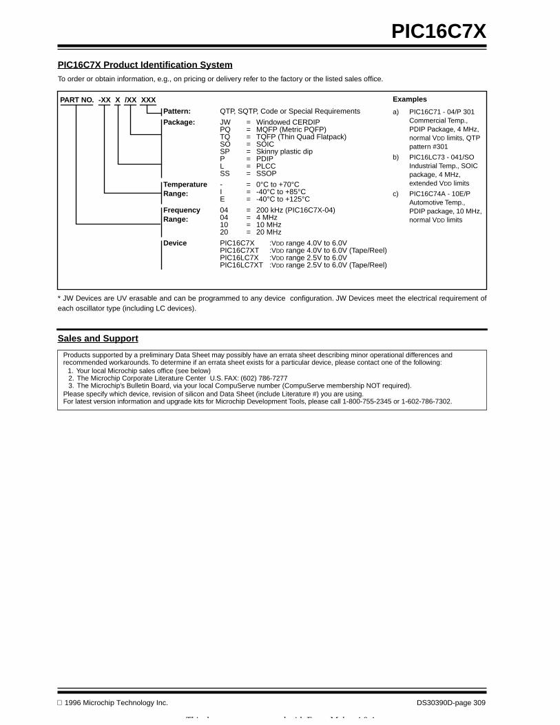
PIC16C7X
PIC16C7X Product Identification System
To order or obtain information, e.g., on pricing or delivery refer to the factory or the listed sales office.
1996 Microchip Technology Inc. DS30390D-page 309
* JW Devices are UV erasable and can be programmed to any device configuration. JW Devices meet the electrical requirement ofeach oscillator type (including LC devices).
PART NO. -XX X /XX XXX
Pattern: QTP, SQTP, Code or Special Requirements
Package: JW = Windowed CERDIPPQ = MQFP (Metric PQFP)TQ = TQFP (Thin Quad Flatpack)SO = SOICSP = Skinny plastic dipP = PDIP L = PLCCSS = SSOP
Temperature Range:
- = 0°C to +70°C I = -40°C to +85°C E = -40°C to +125°C
Frequency Range:
04 = 200 kHz (PIC16C7X-04)04 = 4 MHz10 = 10 MHz20 = 20 MHz
Device PIC16C7X :VDD range 4.0V to 6.0VPIC16C7XT :VDD range 4.0V to 6.0V (Tape/Reel)PIC16LC7X :VDD range 2.5V to 6.0VPIC16LC7XT :VDD range 2.5V to 6.0V (Tape/Reel)
Examples
a) PIC16C71 - 04/P 301 Commercial Temp., PDIP Package, 4 MHz, normal VDD limits, QTP pattern #301
b) PIC16LC73 - 041/SO Industrial Temp., SOIC package, 4 MHz, extended VDD limits
c) PIC16C74A - 10E/P Automotive Temp., PDIP package, 10 MHz, normal VDD limits
Sales and Support
Products supported by a preliminary Data Sheet may possibly have an errata sheet describing minor operational differences and recommended workarounds. To determine if an errata sheet exists for a particular device, please contact one of the following:
Your local Microchip sales office (see below)The Microchip Corporate Literature Center U.S. FAX: (602) 786-7277The Microchip’s Bulletin Board, via your local CompuServe number (CompuServe membership NOT required).
Please specify which device, revision of silicon and Data Sheet (include Literature #) you are using.For latest version information and upgrade kits for Microchip Development Tools, please call 1-800-755-2345 or 1-602-786-7302.
1.2.3.
This document was created with FrameMaker 4 0 4
PIC16C7X
DS30390D-page 310
1996 Microchip Technology Inc.
NOTES:

1996 Microchip Technology Inc. DS30390D-page 311
PIC16C7X
NOTES:

W
ORLDWIDE
S
ALES
& S
ERVICE
ASIA/PACIFIC
Hong Kong
Microchip TechnologyRM 3801B, Tower TwoMetroplaza223 Hing Fong RoadKwai Fong, N.T. Hong KongTel: 852 2 401 1200 Fax: 852 2 401 3431
India
Microchip TechnologyNo. 6, Legacy, Convent RoadBangalore 560 025 IndiaTel: 91 80 526 3148 Fax: 91 80 559 9840
Korea
Microchip Technology168-1, Youngbo Bldg. 3 FloorSamsung-Dong, Kangnam-Ku,Seoul, KoreaTel: 82 2 554 7200 Fax: 82 2 558 5934
Shanghai
Microchip Technology Unit 406 of Shanghai Golden Bridge Bldg.2077 Yan’an Road West, Hongiao DistrictShanghai, Peoples Republic of ChinaTel: 86 21 6275 5700 Fax: 86 21 6275 5060
Singapore
Microchip Technology200 Middle Road#10-03 Prime CentreSingapore 188980Tel: 65 334 8870 Fax: 65 334 8850
Taiwan, R.O.C
Microchip Technology 10F-1C 207Tung Hua North RoadTaipei, Taiwan, ROCTel: 886 2 717 7175 Fax: 886 2 545 0139
EUROPE
United Kingdom
Arizona Microchip Technology Ltd.Unit 6, The CourtyardMeadow Bank, Furlong RoadBourne End, Buckinghamshire SL8 5AJTel: 44 1628 850303 Fax: 44 1628 850178
France
Arizona Microchip Technology SARLZone Industrielle de la Bonde2 Rue du Buisson aux Fraises91300 Massy - FranceTel: 33 1 69 53 63 20 Fax: 33 1 69 30 90 79
Germany
Arizona Microchip Technology GmbHGustav-Heinemann-Ring 125D-81739 Muenchen, GermanyTel: 49 89 627 144 0 Fax: 49 89 627 144 44
Italy
Arizona Microchip Technology SRLCentro Direzionale Colleone Pas Taurus 1Viale Colleoni 120041 Agrate BrianzaMilan Italy Tel: 39 39 6899939 Fax: 39 39 689 9883
JAPAN
Microchip Technology Intl. Inc.Benex S-1 6F3-18-20, Shin YokohamaKohoku-Ku, YokohamaKanagawa 222 JapanTel: 81 45 471 6166 Fax: 81 45 471 6122
9/3/96
AMERICAS
Corporate Office
Microchip Technology Inc.2355 West Chandler Blvd.Chandler, AZ 85224-6199Tel: 602 786-7200 Fax: 602 786-7277
Technical Support:
602 786-7627
Web:
http://www.microchip.com
Atlanta
Microchip Technology Inc.500 Sugar Mill Road, Suite 200BAtlanta, GA 30350Tel: 770 640-0034 Fax: 770 640-0307
Boston
Microchip Technology Inc.5 Mount Royal AvenueMarlborough, MA 01752Tel: 508 480-9990 Fax: 508 480-8575
Chicago
Microchip Technology Inc.333 Pierce Road, Suite 180Itasca, IL 60143Tel: 708 285-0071 Fax: 708 285-0075
Dallas
Microchip Technology Inc.14651 Dallas Parkway, Suite 816Dallas, TX 75240-8809Tel: 972 991-7177 Fax: 972 991-8588
Dayton
Microchip Technology Inc.Suite 150Two Prestige PlaceMiamisburg, OH 45342Tel: 513 291-1654 Fax: 513 291-9175
Los Angeles
Microchip Technology Inc.18201 Von Karman, Suite 1090Irvine, CA 92612Tel: 714 263-1888 Fax: 714 263-1338
New York
Microchip Technmgy Inc.150 Motor Parkway, Suite 416Hauppauge, NY 11788Tel: 516 273-5305 Fax: 516 273-5335
San Jose
Microchip Technology Inc.2107 North First Street, Suite 590San Jose, CA 95131Tel: 408 436-7950 Fax: 408 436-7955
Toronto
Microchip Technology Inc.5925 Airport Road, Suite 200Mississauga, Ontario L4V 1W1, Canada Tel: 905 405-6279 Fax: 905 405-6253
Information contained in this publication regarding device applications and the like is intended through suggestion only and may be superseded by updates. No repre-sentation or warranty is given and no liability is assumed by Microchip Technology Incorporated with respect to the accuracy or use of such information, or infringementof patents or other intellectual property rights arising from such use or otherwise. Use of Microchip’s products as critical components in life support systems is not autho-rized except with express written approval by Microchip. No licenses are conveyed, implicitly or otherwise, under any intellectual property rights. The Microchip logo andname are registered trademarks of Microchip Technology Inc. All rights reserved. All other trademarks mentioned herein are the property of their respective companies.
All rights reserved.
1996, Microchip Technology Incorporated, USA.
DS30390D - page 312
1996 Microchip Technology Inc.
Top Related
Copyright © 2022 FDOKUMEN

