


Bahasa
Halaman
Hukum

Freescale SemiconductorUser’s Guide
PTKIT8122HVUGRev. 0, 6/2005
CONTENTS
1 Packet Telephony Development Kit .......................32 Getting Started with the MSC8122PFC-HV ...........42.1 Board Configuration Options ..................................52.2 JTAG Chain Configuration ...................................112.3 Optional Flash Memory ........................................122.4 Probing Board Voltages ........................................ 123 MSC81x2PFC-HV Hardware Components ..........133.1 MSC8103 Aggregator ...........................................133.2 MSC8122 DSP Farm ............................................164 FPGA Firmware ....................................................184.1 PT3MC-Compliant FPGA Firmware.................... 184.2 PDK-Compliant FPGA Firmware .........................204.3 FPGA Registers .....................................................254.4 PCI Bus Interface ..................................................32
MSC8122PFC-HV Packet Telephony Farm Card User’s Guide
The high-volume MSC8122 packet telephony farm card (MSC8122PFC-HV) is a PCI telephony mezzanine card (PTMC) for evaluating and developing media gateway products. This card, which uses the StarCore™ MSC8122 16-bit fixed-point DSP devices, demonstrates a cost versus performance optimized implementation. The design can become a subsystem component of a larger telecommunications product.
The MSC8122PFC-HV DSP farm consists of five MSC8122 devices running at up to 500 MHz and one MSC8103 device to aggregate the data to/from the DSP farm. Each MSC8122 device has two associated 2M × 32 (8 MB) SDRAM, giving 16 MB of 64-bit wide memory. The MSC8103 aggregator has an optional 4M × 8 (4 MB) flash device to store boot code.
The MSC8122PFC-HV (see Figure 1) interfaces with a baseboard platform via its PTMC site. The PTMC is a PCI mezzanine card (PMC) module that conforms to the PMC standard for PN1 and PN2 but uses PN3 and PN4 to support a variety of telecommunications interfaces. The PTMC site on the PFC is configured to meet the PT3MC standard, a subset of the PTMC specification that supports UTOPIA, Ethernet reduced media-independent interface (RMII), and computer telephony bus interfaces on PN3/4. An optional fifth connector (PN5) supports an MII interface to the MSC8103 device. PN5 is a proprietary connector, effectively supporting an enhanced PTMC that is backward-compatible with existing PTMCs.
© Freescale Semiconductor, Inc., 2005. All rights reserved.

Data is transferred primarily through 10/100 Mbps Ethernet (MII or RMII interfaces) or UTOPIA and a computer telephony TDM bus through the PTMC connectors. An I2C management interface is available through the PTMC PN1 connector. Additional I/O interfaces include HDI16/PCI, serial port, and EOnCE JTAG TAP for debug. The MSC8122PFC-HV interfaces with Freescale packet telephony enhanced PTMC baseboards such as the PDK demonstration system, as well as with standard customer PTMC type III baseboards.
Figure 1. MSC1822 Packet Telephony Farm Card (MSC8122PFC-HV)
Features of the MSC8102PFC-HV are as follows:
• MSC8122PFC-HV platform:
— Digital support for up to 672 channels.
— PTMC Type 3 (PT3MC)-compliant card for interfacing to standard subsystems.
— Optional PN5 connector to allow integration with the Freescale PDK.
• MSC8103 aggregator DSP:
— 1 RMII fast Ethernet via a PN3 PTMC interface.
— 1 MII/RMII fast Ethernet or UTOPIA via PN4 PTMC interface.
— 1 MII fast Ethernet via PN5 (channel shared with PN3 RMII).
— Host control (over HDI16) via PTMC PCI standard interface.
— 32-bit asynchronous 60x bus interface to the MSC8122 DSI ports for on-board data distribution to the DSP farm.
— 4 MB of Flash memory for system bootstrap.
— Control over the programming sequence of the FPGA.
MSC8122PFC-HV Packet Telephony Farm Card User’s Guide, Rev. 0
2 Freescale Semiconductor
Packet Telephony Development Kit
• MSC8122 farm consisting of five MSC8122 DSPs:
— Standard CT-Bus TDM via the PN3 PTMC interface.
— 32-bit DSI asynchronous slave port interfacing the MSC8103 60x bus.
— 16 MB of 64-bit wide SDRAM.
• FPGA:
— Direct connection or PCI interface from the host to the MSC8103 host port (HDI16) interface.
— MII-to-RMII conversion for PN3 PTMC (and non-standard RMII on PN4).
— CT-bus back-up clock and frame signal selection.
— DSP HRESET control.
• Debug:
— Chained DSP EOnCE port with optional jumpers so that individual MSC8122 farm DSPs can be depopulated.
— DSP EOnCE chain on the J1 debug connector.
— Jumper to connect DSP EOnCE chain to the PN1/PN2 PTMC interface.
— FPGA configuration EEPROM ISP through the J1 debug connector.
— Boot mode option signals on the J1 debug connector.
— J1 debug connector in envelope provided by the PTMC specification.
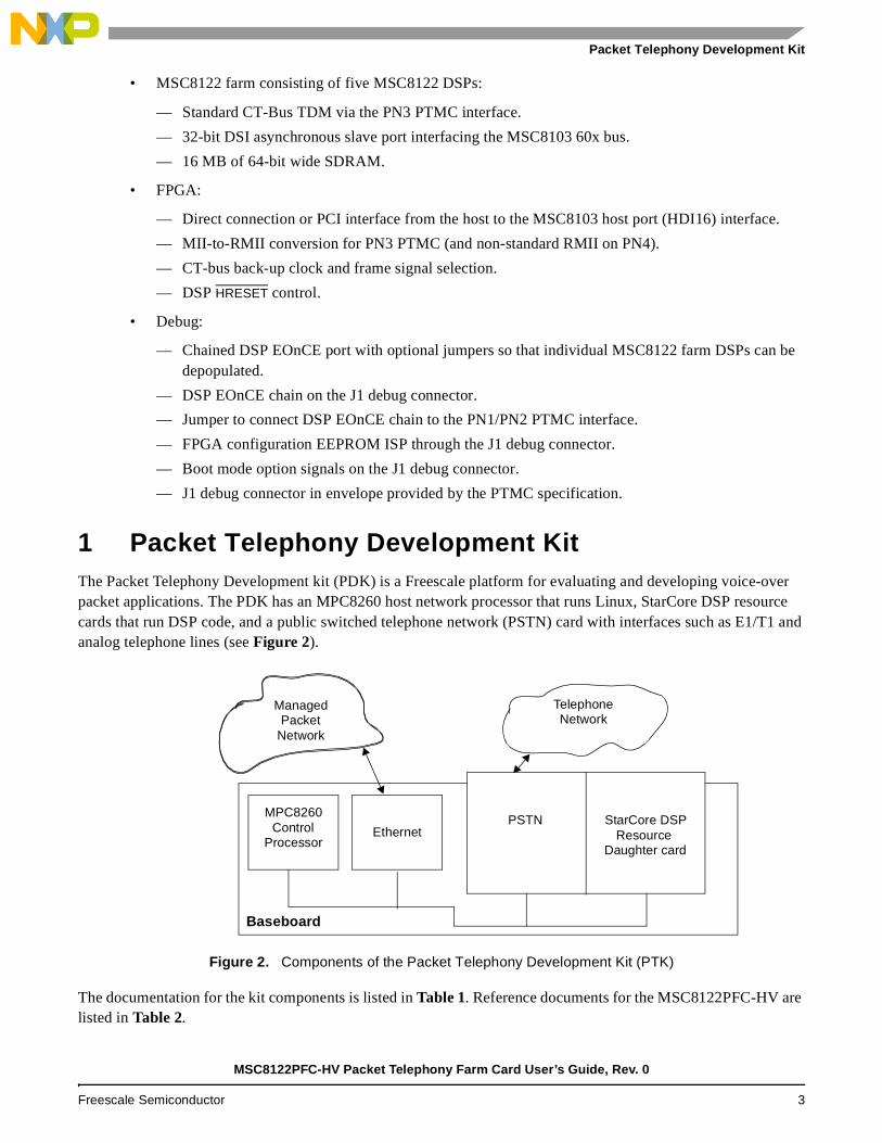
1 Packet Telephony Development KitThe Packet Telephony Development kit (PDK) is a Freescale platform for evaluating and developing voice-over packet applications. The PDK has an MPC8260 host network processor that runs Linux, StarCore DSP resource cards that run DSP code, and a public switched telephone network (PSTN) card with interfaces such as E1/T1 and analog telephone lines (see Figure 2).
Figure 2. Components of the Packet Telephony Development Kit (PTK)
The documentation for the kit components is listed in Table 1. Reference documents for the MSC8122PFC-HV are listed in Table 2.
PSTN StarCore DSPResource
Daughter card
MPC8260Control
ProcessorEthernet
ManagedPacket
Network
TelephoneNetwork
Baseboard
MSC8122PFC-HV Packet Telephony Farm Card User’s Guide, Rev. 0
Freescale Semiconductor 3

Getting Started with the MSC8122PFC-HV
Caution: The packet telephony development kit includes open-construction printed circuit boards that contain static-sensitive components. These boards are subject to damage from electrostatic discharge (ESD). To prevent such damage, you must use static-safe work surfaces and grounding straps, as defined in ANSI/EOS/ESD S6.1 and ANSI/EOS/ESD S4.1. All handling of these boards must be in accordance with ANSI/EAI 625.
2 Getting Started with the MSC8122PFC-HVFigure 2 shows the position of major components on the MSC8122PFC-HV. In compliance with the PMC specification, all heat generating components are placed on the side facing the base card. A goal of the specification is to contain heat within one card slot in a card rack. It seeks to limit heat transfer from one base card in a rack to the next. However, with the heat generating components placed as they are, heat dissipation through ambient air convection is hindered because of the limited air volume and non-optimal air movement path. Therefore, forced air movement is required to cool the MSC8122PFC-HV, especially when the PFC is mounted horizontally. The amount of air flow required depends on ambient air temperature, DSP work load, and PFC mounting orientation. Read the data sheets of all components on the board and design a system with adequate forced air flow over the PFC to comply with maximum junction temperature limits of all components. The major components of interest are the MSC8122 DSP devices when they perform heavy loads. An on-board temperature sensor aids with thermal management software.
Table 1. PTK Components and Their Associated Documents
Component Document Document ID
Baseboard Packet Development Kit Baseboard Hardware User’s Guide PTKITBASEUG
MPC8260 control processor
MPC8260 PowerQUICC II™ Family Reference Manual(Available at the website listed on the back page of this user’s guide.)
MPC8260UM
PSTN card Packet Development Kit PSTN Mezzanine User’s Guide PTKITPSTNUG
StarCore DSP resource daughter card
• MSC8102 Packet Telephony Farm Card (MSC8102PFC) User’s Guide• MSC8101 Packet Telephony Farm Card (MSC8101PFC) User’s Guide• MSC8122 Packet Telephony Farm Card (MSC8122PFC-HV) User’s
Guide
PTKIT8102UGPTKIT8101UGPTKIT8122UG
MSC8122 processor MSC8122 Reference Manual and other MSC8122 documentation are located at the web site listed on the back cover of this user’s guide.
MSC8122RM
MSC8103 processor MSC8103 Reference Manual and other MSC8103 documentation are located at the web site listed on the back cover of this user’s guide.
MSC8103RM
Software Packet Telephony Development Kit Software User’s Guide PTKITSOFTUG
Table 2. Reference Documents
Document Revision Date Document ID
Standard Physical and Environmental layers for PCI Mezzanine Cards: PMC
Draft 2.4 January 12, 2001
IEEE: P1386.1
Standard for a Common Mezzanine Card Family: CMC Draft 2.4a March 21, 2001 IEEE: P1386
CompactPCI PCI Telecom Mezzanine Card Specification R1.0 April 11, 2001 PICMG 2.15
H.100 Hardware Compatibility Specification: CT Bus 1.0 H.100
MSC8122PFC-HV Packet Telephony Farm Card User’s Guide, Rev. 0
4 Freescale Semiconductor
Getting Started with the MSC8122PFC-HV
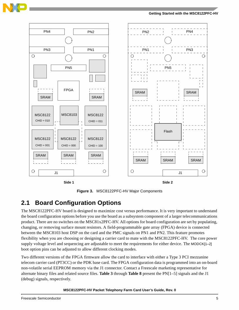
Figure 3. MSC8122PFC-HV Major Components
2.1 Board Configuration OptionsThe MSC8122PFC-HV board is designed to maximize cost versus performance. It is very important to understand the board configuration options before you use the board as a subsystem component of a larger telecommunications product. There are no switches on the MSC81x2PFC-HV. All options for board configuration are set by populating, changing, or removing surface mount resistors. A field-programmable gate array (FPGA) device is connected between the MSC8103 host DSP on the card and the PMC signals on PN1 and PN2. This feature promotes flexibility when you are choosing or designing a carrier card to mate with the MSC8122PFC-HV. The core power supply voltage level and sequencing are adjustable to meet the requirements for either device. The MODCK[1–2] boot option pins can be adjusted to allow different clocking modes.
Two different versions of the FPGA firmware allow the card to interface with either a Type 3 PCI mezzanine telecom carrier card (PT3CC) or the PDK base card. The FPGA configuration data is programmed into an on-board non-volatile serial EEPROM memory via the J1 connector. Contact a Freescale marketing representative for alternate binary files and related source files. Table 3 through Table 8 present the PN[1–5] signals and the J1 (debug) signals, respectively.
Side 1
PN4 PN2
PN3 PN1
PN5
MSC8122 MSC8122 MSC8122
MSC8122
J1
SRAMSRAM
SRAM SRAM SRAM
MSC8122MSC8103
FPGA
Side 2
PN4PN2
PN3PN1
PN5
J1
SRAM SRAM
SRAMSRAMSRAM
Flash
CHID = 010 CHID = 011
CHID = 001 CHID = 000 CHID = 100
MSC8122PFC-HV Packet Telephony Farm Card User’s Guide, Rev. 0
Freescale Semiconductor 5
Getting Started with the MSC8122PFC-HV
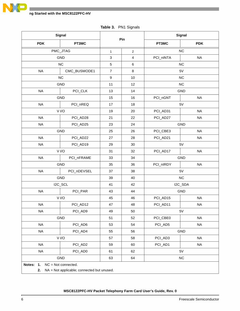
Table 3. PN1 Signals
SignalPin
Signal
PDK PT3MC PT3MC PDK
PMC_JTAG 1 2 NC
GND 3 4 PCI_nINTA NA
NC 5 6 NC
NA CMC_BUSMODE1 7 8 5V
NC 9 10 NC
GND 11 12 NC
NA PCI_CLK 13 14 GND
GND 15 16 PCI_nGNT NA
NA PCI_nREQ 17 18 5V
V I/O 19 20 PCI_AD31 NA
NA PCI_AD28 21 22 PCI_AD27 NA
NA PCI_AD25 23 24 GND
GND 25 26 PCI_CBE3 NA
NA PCI_AD22 27 28 PCI_AD21 NA
NA PCI_AD19 29 30 5V
V I/O 31 32 PCI_AD17 NA
NA PCI_nFRAME 33 34 GND
GND 35 36 PCI_nIRDY NA
NA PCI_nDEVSEL 37 38 5V
GND 39 40 NC
I2C_SCL 41 42 I2C_SDA
NA PCI_PAR 43 44 GND
V I/O 45 46 PCI_AD15 NA
NA PCI_AD12 47 48 PCI_AD11 NA
NA PCI_AD9 49 50 5V
GND 51 52 PCI_CBE0 NA
NA PCI_AD6 53 54 PCI_AD5 NA
NA PCI_AD4 55 56 GND
V I/O 57 58 PCI_AD3 NA
NA PCI_AD2 59 60 PCI_AD1 NA
NA PCI_AD0 61 62 5V
GND 63 64 NC
Notes: 1. NC = Not connected.
2. NA = Not applicable; connected but unused.
MSC8122PFC-HV Packet Telephony Farm Card User’s Guide, Rev. 0
6 Freescale Semiconductor
Getting Started with the MSC8122PFC-HV
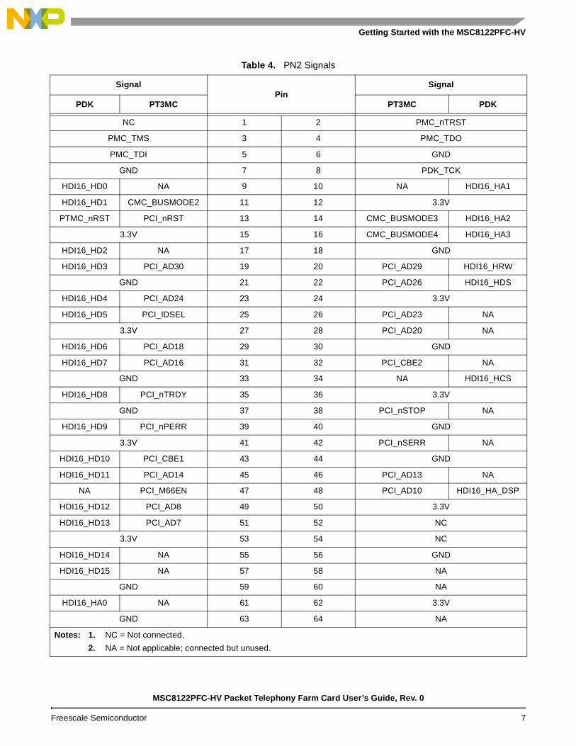
Table 4. PN2 Signals
SignalPin
Signal
PDK PT3MC PT3MC PDK
NC 1 2 PMC_nTRST
PMC_TMS 3 4 PMC_TDO
PMC_TDI 5 6 GND
GND 7 8 PDK_TCK
HDI16_HD0 NA 9 10 NA HDI16_HA1
HDI16_HD1 CMC_BUSMODE2 11 12 3.3V
PTMC_nRST PCI_nRST 13 14 CMC_BUSMODE3 HDI16_HA2
3.3V 15 16 CMC_BUSMODE4 HDI16_HA3
HDI16_HD2 NA 17 18 GND
HDI16_HD3 PCI_AD30 19 20 PCI_AD29 HDI16_HRW
GND 21 22 PCI_AD26 HDI16_HDS
HDI16_HD4 PCI_AD24 23 24 3.3V
HDI16_HD5 PCI_IDSEL 25 26 PCI_AD23 NA
3.3V 27 28 PCI_AD20 NA
HDI16_HD6 PCI_AD18 29 30 GND
HDI16_HD7 PCI_AD16 31 32 PCI_CBE2 NA
GND 33 34 NA HDI16_HCS
HDI16_HD8 PCI_nTRDY 35 36 3.3V
GND 37 38 PCI_nSTOP NA
HDI16_HD9 PCI_nPERR 39 40 GND
3.3V 41 42 PCI_nSERR NA
HDI16_HD10 PCI_CBE1 43 44 GND
HDI16_HD11 PCI_AD14 45 46 PCI_AD13 NA
NA PCI_M66EN 47 48 PCI_AD10 HDI16_HA_DSP
HDI16_HD12 PCI_AD8 49 50 3.3V
HDI16_HD13 PCI_AD7 51 52 NC
3.3V 53 54 NC
HDI16_HD14 NA 55 56 GND
HDI16_HD15 NA 57 58 NA
GND 59 60 NA
HDI16_HA0 NA 61 62 3.3V
GND 63 64 NA
Notes: 1. NC = Not connected.
2. NA = Not applicable; connected but unused.
MSC8122PFC-HV Packet Telephony Farm Card User’s Guide, Rev. 0
Freescale Semiconductor 7

Getting Started with the MSC8122PFC-HV
Table 5. PN3 Signals
Signal Pin Signal
MII_MDIO 1 2 GND
GND 3 4 SRX
MII_MDC 5 6 STX
RMII2_RXER 7 8 GND
PTMC_PTID2 9 10 RMII2_RXD0
NC 11 12 RMII2_RXD1
RMII_REFCLK 13 14 GND
GND 15 16 RMII2_TXD0
CT_FA 17 18 RMII2_TXD1
CT_FB 19 20 GND
PTMC_PTID0 21 22 RMII2_TXEN
NC 23 24 RMII2_CRS_DV
CT_C8A 25 26 GND
GND 27 28 CT_D19
CT_D18 29 30 CT_D17
CT_D16 31 32 GND
GND 33 34 NC
CT_D14 35 36 NC
CT_D12 37 38 GND
PTMC_PTENB 39 40 NC
NC 41 42 NC
CT_C8B 43 44 GND
GND 45 46 CT_D15
CT_D10 47 48 CT_D13
CT_D8 49 50 CT_D11
GND 51 52 CT_D9
CT_D6 53 54 CT_D7
CT_D4 55 56 GND
PTMC_PTID1 57 58 CT+D5
CT_D2 59 60 CT_D3
CT_D0 61 62 GND
GND 63 64 CT_D1
MSC8122PFC-HV Packet Telephony Farm Card User’s Guide, Rev. 0
8 Freescale Semiconductor
Getting Started with the MSC8122PFC-HV
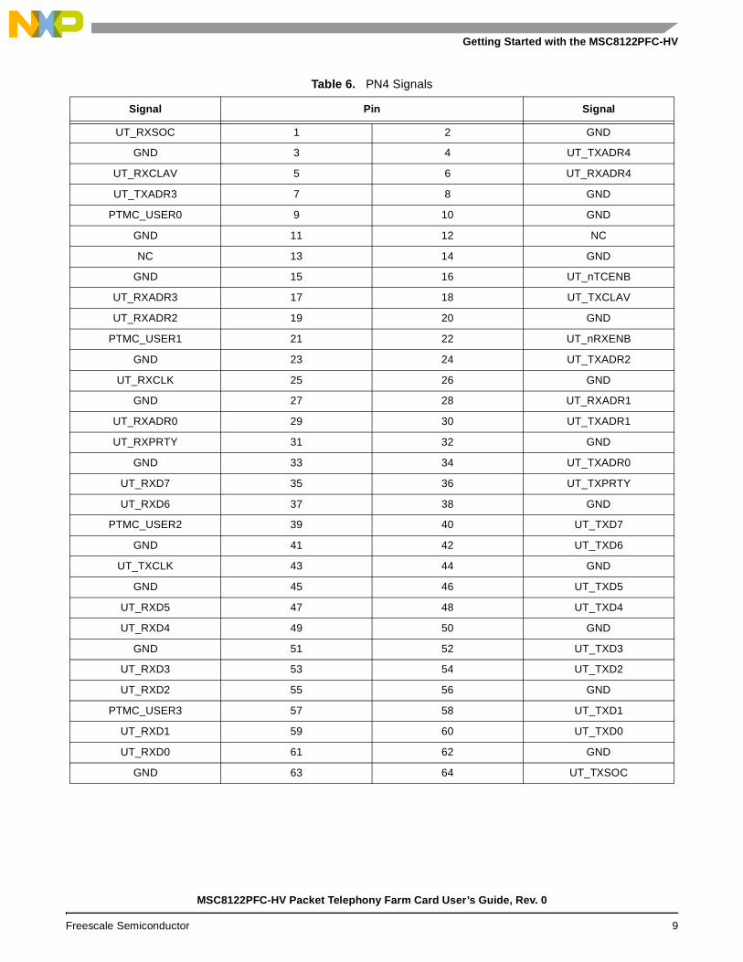
Table 6. PN4 Signals
Signal Pin Signal
UT_RXSOC 1 2 GND
GND 3 4 UT_TXADR4
UT_RXCLAV 5 6 UT_RXADR4
UT_TXADR3 7 8 GND
PTMC_USER0 9 10 GND
GND 11 12 NC
NC 13 14 GND
GND 15 16 UT_nTCENB
UT_RXADR3 17 18 UT_TXCLAV
UT_RXADR2 19 20 GND
PTMC_USER1 21 22 UT_nRXENB
GND 23 24 UT_TXADR2
UT_RXCLK 25 26 GND
GND 27 28 UT_RXADR1
UT_RXADR0 29 30 UT_TXADR1
UT_RXPRTY 31 32 GND
GND 33 34 UT_TXADR0
UT_RXD7 35 36 UT_TXPRTY
UT_RXD6 37 38 GND
PTMC_USER2 39 40 UT_TXD7
GND 41 42 UT_TXD6
UT_TXCLK 43 44 GND
GND 45 46 UT_TXD5
UT_RXD5 47 48 UT_TXD4
UT_RXD4 49 50 GND
GND 51 52 UT_TXD3
UT_RXD3 53 54 UT_TXD2
UT_RXD2 55 56 GND
PTMC_USER3 57 58 UT_TXD1
UT_RXD1 59 60 UT_TXD0
UT_RXD0 61 62 GND
GND 63 64 UT_TXSOC
MSC8122PFC-HV Packet Telephony Farm Card User’s Guide, Rev. 0
Freescale Semiconductor 9

Getting Started with the MSC8122PFC-HV
Table 7. PN5 Signals
Signal Pin Signal
NC 1 2 NC
NC 3 4 NC
NC 5 6 NC
NC 7 8 NC
NC 9 10 NC
NC 11 12 GND
NC 13 14 NC
NC 15 16 NC
NC 17 18 NC
GND 19 20 MII2_TCLK
MII2_TXD0 21 22 NC
MII2_TXD1 23 24 MII2_RXDV
MII2_TXD2 25 26 MII2_RXD0
MII2_TXD3 27 28 MII2_RXD1
NC 29 30 MII2_RXD2
NC 31 32 GND
MII2_TXEN 33 34 MII2_RXD3
MII2_TXER 35 36 MII2_RXER
MII2_COL 37 38 MII2_CRS
NC 39 40 MII2_RCLK
NC 41 42 NC
NC 43 44 NC
NC 45 46 NC
NC 47 48 NC
NC 49 50 NC
NC 51 52 GND
NC 53 54 NC
NC 55 56 NC
NC 57 58 NC
GND 59 60 NC
NC 61 62 GND
NC 63 64 NC
Table 8. J1 (Debug) Signals
Signal Pin Signal
TDI 1 2 GND
TDO 3 4 GND
TCK 5 6 GND
MSC8122PFC-HV Packet Telephony Farm Card User’s Guide, Rev. 0
10 Freescale Semiconductor

Getting Started with the MSC8122PFC-HV
2.2 JTAG Chain ConfigurationThe JTAG chain on the card links all six DSPs. The chain is always connected to the J1 debug and programming connector. The board JTAG chain can also be connected to the PMC JTAG chain by populating resistors R209, R224, R287, R288, R269, and R244 (see schematic). The chain is organized as shown in Table 9.
FPGA_nSER_EN 7 8 KEY
HRESET 9 10 TMS
3.3V 11 12 FPGA_DIN
FPGA_CCLK 13 14 nTRST
SRX 15 16 STX
3.3V 17 18 A_RSTCONF
3.3V 19 20 A_BOOT
NC 21 22 NC
NC 23 24 NC
Table 9. JTAG Chain Index
JTAG Chain Index Device
0 MSC8122 CHIP ID 4 SYNC
1 Core 3
2 Core 2
3 Core 1
4 Core 0
5 MSC8122 CHIP ID 3 SYNC
6 Core 3
7 Core 2
8 Core 1
9 Core 0
10 MSC8122 CHIP ID 2 SYNC
11 Core 3
12 Core 2
13 Core 1
14 Core 0
15 MSC8122 CHIP ID 1 SYNC
16 Core 3
17 Core 2
18 Core 1
19 Core 0
Table 8. J1 (Debug) Signals (Continued)
Signal Pin Signal
MSC8122PFC-HV Packet Telephony Farm Card User’s Guide, Rev. 0
Freescale Semiconductor 11
Getting Started with the MSC8122PFC-HV
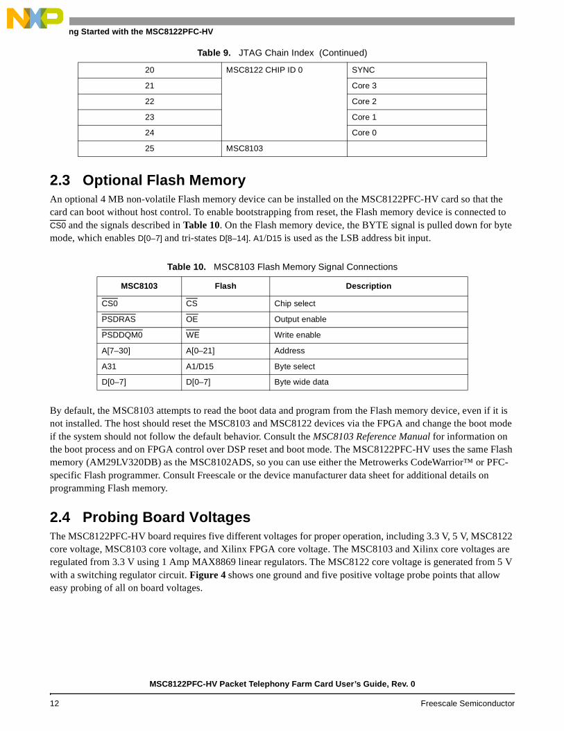
2.3 Optional Flash MemoryAn optional 4 MB non-volatile Flash memory device can be installed on the MSC8122PFC-HV card so that the card can boot without host control. To enable bootstrapping from reset, the Flash memory device is connected to CS0 and the signals described in Table 10. On the Flash memory device, the BYTE signal is pulled down for byte mode, which enables D[0–7] and tri-states D[8–14]. A1/D15 is used as the LSB address bit input.
By default, the MSC8103 attempts to read the boot data and program from the Flash memory device, even if it is not installed. The host should reset the MSC8103 and MSC8122 devices via the FPGA and change the boot mode if the system should not follow the default behavior. Consult the MSC8103 Reference Manual for information on the boot process and on FPGA control over DSP reset and boot mode. The MSC8122PFC-HV uses the same Flash memory (AM29LV320DB) as the MSC8102ADS, so you can use either the Metrowerks CodeWarrior™ or PFC-specific Flash programmer. Consult Freescale or the device manufacturer data sheet for additional details on programming Flash memory.
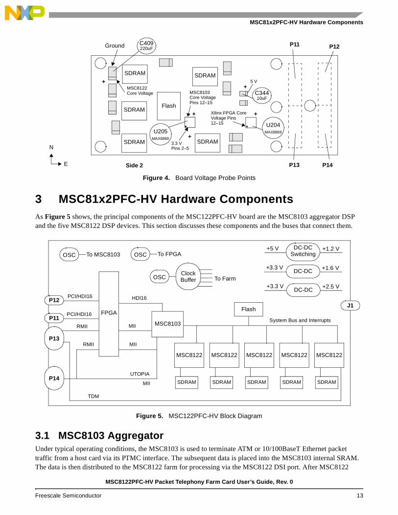
2.4 Probing Board VoltagesThe MSC8122PFC-HV board requires five different voltages for proper operation, including 3.3 V, 5 V, MSC8122 core voltage, MSC8103 core voltage, and Xilinx FPGA core voltage. The MSC8103 and Xilinx core voltages are regulated from 3.3 V using 1 Amp MAX8869 linear regulators. The MSC8122 core voltage is generated from 5 V with a switching regulator circuit. Figure 4 shows one ground and five positive voltage probe points that allow easy probing of all on board voltages.
20 MSC8122 CHIP ID 0 SYNC
21 Core 3
22 Core 2
23 Core 1
24 Core 0
25 MSC8103
Table 10. MSC8103 Flash Memory Signal Connections
MSC8103 Flash Description
CS0 CS Chip select
PSDRAS OE Output enable
PSDDQM0 WE Write enable
A[7–30] A[0–21] Address
A31 A1/D15 Byte select
D[0–7] D[0–7] Byte wide data
Table 9. JTAG Chain Index (Continued)
MSC8122PFC-HV Packet Telephony Farm Card User’s Guide, Rev. 0
12 Freescale Semiconductor
MSC81x2PFC-HV Hardware Components
Figure 4. Board Voltage Probe Points
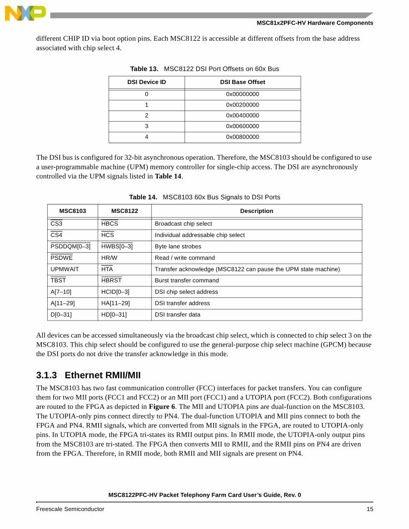
3 MSC81x2PFC-HV Hardware ComponentsAs Figure 5 shows, the principal components of the MSC122PFC-HV board are the MSC8103 aggregator DSP and the five MSC8122 DSP devices. This section discusses these components and the buses that connect them.
Figure 5. MSC122PFC-HV Block Diagram
3.1 MSC8103 AggregatorUnder typical operating conditions, the MSC8103 is used to terminate ATM or 10/100BaseT Ethernet packet traffic from a host card via its PTMC interface. The subsequent data is placed into the MSC8103 internal SRAM. The data is then distributed to the MSC8122 farm for processing via the MSC8122 DSI port. After MSC8122
Flash
SDRAMSDRAM
SDRAM
SDRAM SDRAM
P11 P12
P14P13
Ground C409220uF
C34410uF
U204MAX8869
++
+
+
+
Side 2
N
E
5 V
3.3 VPins 2–5
Xilinx FPGA CoreVoltage Pins12–15
U205MAX8869
MSC8122Core Voltage MSC8103
Core VoltagePins 12–15
MSC8122
SDRAM
MSC8122
SDRAM
MSC8122
SDRAM
MSC8122
SDRAM
MSC8122
SDRAM
MSC8103System Bus and Interrupts
FlashJ1
P12
P11
P13
P14UTOPIA
FPGA
RMII MII
RMII MII
PCI/HDI16
PCI/HDI16 HDI16
MII
TDM
OSC To MSC8103 OSC To FPGA
OSC To FarmClockBuffer
DC-DC+3.3 V +1.6 V
DC-DC+3.3 V +2.5 V
+5 V +1.2 VDC-DCSwitching
MSC8122PFC-HV Packet Telephony Farm Card User’s Guide, Rev. 0
Freescale Semiconductor 13

MSC81x2PFC-HV Hardware Components
processing, the data is dispatched through the MSC8122 TDM interfaces to the CT bus. Data also flows in the opposite path. An FPGA connects the PTMC I/O pins on PN1 and PN2 to the HDI16 port on the MSC8103. This connection provides a slave interface to the MSC8103 on the PTMC or PDK data buses. The MSC8103 then connects to the optional Flash memory device and the MSC8122 DSP farm through a 60x system bus. MSC8103 system bus chip selects are connected as shown in Table 11.
The MSC8103 interrupts are connected to the FPGA and to the DSP farm. Each DSP in the farm has an interrupt line from and another interrupt line to the MSC8103 host. All interrupt lines are pulled high with weak resistors. The interrupts are connected as shown in Table 12.
3.1.1 HDI16 to FPGAThe MSC8103 HDI16 port connects directly to the FPGA. The FPGA is then connected to the PMC PN1/2 connectors. These connections allow creative implementation of slave interfaces to a base card.
3.1.2 System Bus to MSC8122 DSIThe direct slave interface (DSI) on each MSC8122 device gives the aggregator direct access to the MSC8122 internal memory space, including on-chip memory and registers. The DSI write buffer stores the address and the data of the accesses until they are performed. The external host can therefore perform multiple writes without waiting for those accesses to complete. Latencies that are typical during accesses to on-chip memories are greatly reduced by a DSI read prefetch mechanism. The DSI on each MSC8122 device connects to the external 60x system bus on the MSC8103 device. The same chip select is connected to all the DSI ports, but each device is given a
Table 11. MSC8103 Chip Select Assignment
Signal Peripheral
CS0 Flash
CS3 MSC8122 DSI Broadcast
CS4 MSC8122 DSI Single
Table 12. MSC8103 Interrupt Signals
Signal Description
IRQ1 Interrupt from farm DSP 1
IRQ2 Interrupt from FPGA (defined in FPGA)
IRQ4 Interrupt from farm DSP 2
IRQ5 Interrupt from farm DSP 3
IRQ6 Interrupt from farm DSP 4
IRQ7 Interrupt from farm DSP 5
PC4 Interrupt to farm DSP 1
PC5 Interrupt to farm DSP 2
PC22 Interrupt to farm DSP 3
PC23 Interrupt to farm DSP 4
PC24 Interrupt to farm DSP 5
MSC8122PFC-HV Packet Telephony Farm Card User’s Guide, Rev. 0
14 Freescale Semiconductor
MSC81x2PFC-HV Hardware Components
different CHIP ID via boot option pins. Each MSC8122 is accessible at different offsets from the base address associated with chip select 4.
The DSI bus is configured for 32-bit asynchronous operation. Therefore, the MSC8103 should be configured to use a user-programmable machine (UPM) memory controller for single-chip access. The DSI are asynchronously controlled via the UPM signals listed in Table 14.
All devices can be accessed simultaneously via the broadcast chip select, which is connected to chip select 3 on the MSC8103. This chip select should be configured to use the general-purpose chip select machine (GPCM) because the DSI ports do not drive the transfer acknowledge in this mode.
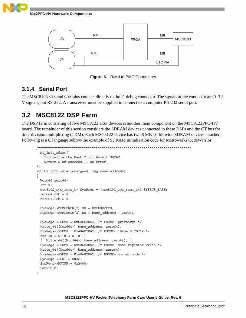
3.1.3 Ethernet RMII/MII The MSC8103 has two fast communication controller (FCC) interfaces for packet transfers. You can configure them for two MII ports (FCC1 and FCC2) or an MII port (FCC1) and a UTOPIA port (FCC2). Both configurations are routed to the FPGA as depicted in Figure 6. The MII and UTOPIA pins are dual-function on the MSC8103. The UTOPIA-only pins connect directly to PN4. The dual-function UTOPIA and MII pins connect to both the FPGA and PN4. RMII signals, which are converted from MII signals in the FPGA, are routed to UTOPIA-only pins. In UTOPIA mode, the FPGA tri-states its RMII output pins. In RMII mode, the UTOPIA-only output pins from the MSC8103 are tri-stated. The FPGA then converts MII to RMII, and the RMII pins on PN4 are driven from the FPGA. Therefore, in RMII mode, both RMII and MII signals are present on PN4.
Table 13. MSC8122 DSI Port Offsets on 60x Bus
DSI Device ID DSI Base Offset
0 0x00000000
1 0x00200000
2 0x00400000
3 0x00600000
4 0x00800000
Table 14. MSC8103 60x Bus Signals to DSI Ports
MSC8103 MSC8122 Description
CS3 HBCS Broadcast chip select
CS4 HCS Individual addressable chip select
PSDDQM[0–3] HWBS[0–3] Byte lane strobes
PSDWE HR/W Read / write command
UPMWAIT HTA Transfer acknowledge (MSC8122 can pause the UPM state machine)
TBST HBRST Burst transfer command
A[7–10] HCID[0–3] DSI chip select address
A[11–29] HA[11–29] DSI transfer address
D[0–31] HD[0–31] DSI transfer data
MSC8122PFC-HV Packet Telephony Farm Card User’s Guide, Rev. 0
Freescale Semiconductor 15
MSC81x2PFC-HV Hardware Components
Figure 6. R/MII to PMC Connectors
3.1.4 Serial PortThe MSC8103 STX and SRX pins connect directly to the J1 debug connector. The signals at the connector are 0–3.3 V signals, not RS-232. A transceiver must be supplied to connect to a computer RS-232 serial port.
3.2 MSC8122 DSP FarmThe DSP farm consisting of five MSC8122 DSP devices is another main component on the MSC8122PFC-HV board. The remainder of this section considers the SDRAM devices connected to these DSPs and the CT bus for time-division multiplexing (TDM). Each MSC8122 device has two 8 MB 16-bit wide SDRAM devices attached. Following is a C language subroutine example of SDRAM initialization code for Metrowerks CodeWarrior:
/***************************************************************************** HV_init_sdram() : Initialize the Bank 2 for 64-bit SDRAM. Return 0 on success, 1 on error.*/int HV_init_sdram(unsigned long base_address){ Word64 zero64; Int x; msc8102_sys_regs_t* SysRegs = (msc8102_sys_regs_t*) SYSBUS_BASE; zero64.msb = 0; zero64.lsb = 0; SysRegs->MEMCBROR[2].OR = 0xFE002CC0; SysRegs->MEMCBROR[2].BR = base_address + 0x0041; SysRegs->PSDMR = 0x606B20A2; /* PSDMR- precharge */ Write_64((Word64*) base_address, zero64); SysRegs->PSDMR = 0x486B2062; /* PSDMR- issue 8 CBR’s */ for (x = 0; x < 8; x++) { Write_64((Word64*) base_address, zero64); } SysRegs->PSDMR = 0x586B2062; /* PSDMR- mode register write */ Write_64((Word64*) base_address, zero64); SysRegs->PSDMR = 0x406B2062; /* PSDMR- normal mode */ SysRegs->PSRT = 0x2C; SysRegs->MPTPR = 0x2000; return 0;}
J3
J4
MSC8103FPGARMII
RMII
UTOPIA
MII
MII
MSC8122PFC-HV Packet Telephony Farm Card User’s Guide, Rev. 0
16 Freescale Semiconductor
MSC81x2PFC-HV Hardware Components
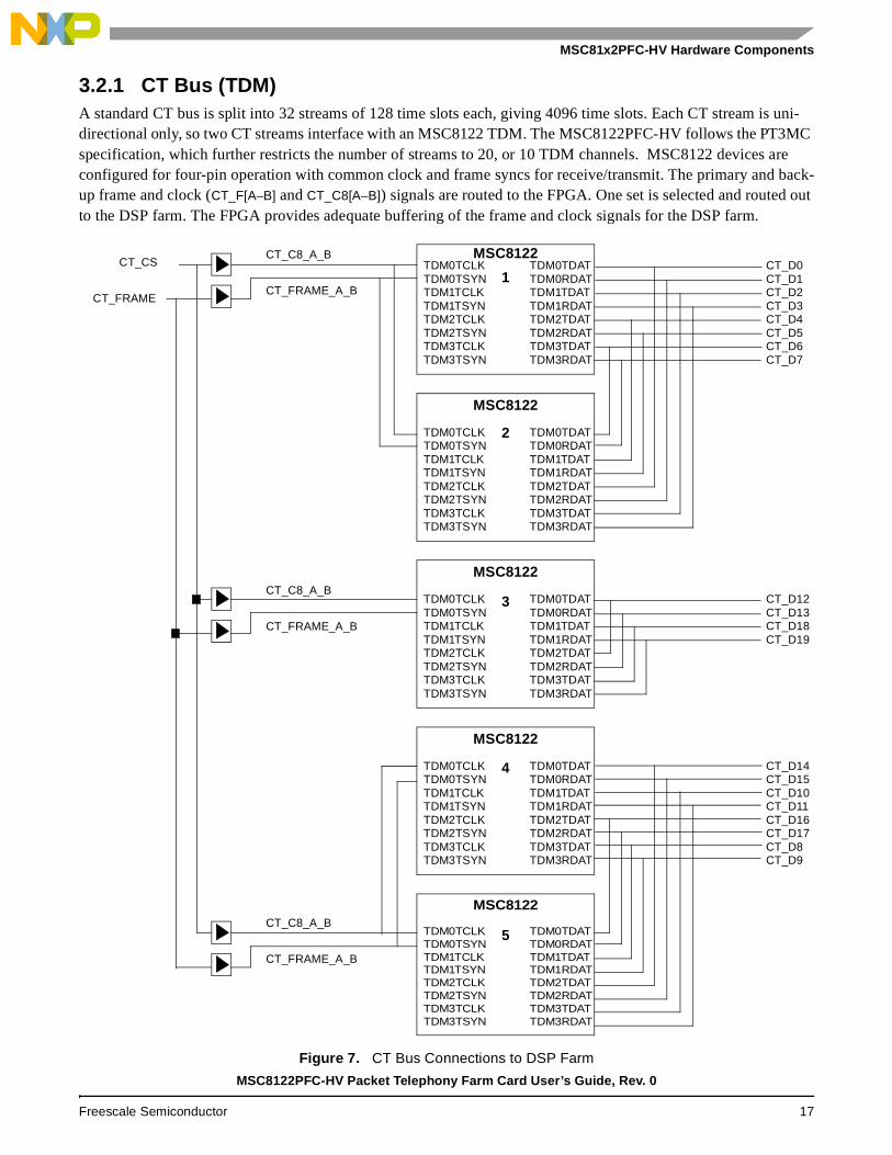
3.2.1 CT Bus (TDM)A standard CT bus is split into 32 streams of 128 time slots each, giving 4096 time slots. Each CT stream is uni-directional only, so two CT streams interface with an MSC8122 TDM. The MSC8122PFC-HV follows the PT3MC specification, which further restricts the number of streams to 20, or 10 TDM channels. MSC8122 devices are configured for four-pin operation with common clock and frame syncs for receive/transmit. The primary and back-up frame and clock (CT_F[A–B] and CT_C8[A–B]) signals are routed to the FPGA. One set is selected and routed out to the DSP farm. The FPGA provides adequate buffering of the frame and clock signals for the DSP farm.
Figure 7. CT Bus Connections to DSP Farm
MSC8122TDM0TDATTDM0RDATTDM1TDATTDM1RDATTDM2TDATTDM2RDATTDM3TDATTDM3RDAT
TDM0TCLKTDM0TSYNTDM1TCLKTDM1TSYNTDM2TCLKTDM2TSYNTDM3TCLKTDM3TSYN
MSC8122
TDM0TDATTDM0RDATTDM1TDATTDM1RDATTDM2TDATTDM2RDATTDM3TDATTDM3RDAT
TDM0TCLKTDM0TSYNTDM1TCLKTDM1TSYNTDM2TCLKTDM2TSYNTDM3TCLKTDM3TSYN
MSC8122
TDM0TDATTDM0RDATTDM1TDATTDM1RDATTDM2TDATTDM2RDATTDM3TDATTDM3RDAT
TDM0TCLKTDM0TSYNTDM1TCLKTDM1TSYNTDM2TCLKTDM2TSYNTDM3TCLKTDM3TSYN
MSC8122
TDM0TDATTDM0RDATTDM1TDATTDM1RDATTDM2TDATTDM2RDATTDM3TDATTDM3RDAT
TDM0TCLKTDM0TSYNTDM1TCLKTDM1TSYNTDM2TCLKTDM2TSYNTDM3TCLKTDM3TSYN
MSC8122
TDM0TDATTDM0RDATTDM1TDATTDM1RDATTDM2TDATTDM2RDATTDM3TDATTDM3RDAT
TDM0TCLKTDM0TSYNTDM1TCLKTDM1TSYNTDM2TCLKTDM2TSYNTDM3TCLKTDM3TSYN
CT_D0CT_D1CT_D2CT_D3CT_D4CT_D5CT_D6CT_D7
CT_D12CT_D13CT_D18CT_D19
CT_D14CT_D15CT_D10CT_D11CT_D16CT_D17CT_D8CT_D9
CT_C8_A_B
CT_FRAME_A_B
CT_C8_A_B
CT_FRAME_A_B
CT_C8_A_B
CT_FRAME_A_B
CT_CS
CT_FRAME
1
2
3
4
5
MSC8122PFC-HV Packet Telephony Farm Card User’s Guide, Rev. 0
Freescale Semiconductor 17

FPGA Firmware
4 FPGA FirmwareThere are two versions of the FPGA architecture:
• Standard PT3MC FPGA for interfacing with a 32-bit PCI, which includes modules for the PCI-to-HDI16 bus bridge and the collection of subsystem capabilities.
• Non-standard PDK FPGA for interfacing with the HDI16 (pass-through) on the packet telephony development kit (PDK) local bus. The PDK FPGA architecture is much less complex and reuses many PT3MC modules. The PDK FPGA replaces the bus bridge with an HDI16 pass-through module but maintains all the subsystem capabilities of the PT3MC FPGA.
4.1 PT3MC-Compliant FPGA FirmwareThe PT3MC FPGA connects the MSC8122PFC-HV with a standard PT3CC through a 33 MHz, 32-bit, 3.3 V PCI, and through RMII, UTOPIA, and the CT bus (TDM). To support the PT3CC interface, the FPGA contains a PCI target, RMII-to-MII converters, and a CT bus back-up frame and clock selector. The hardware description language (HDL) for the FPGA is written in Verilog and has a hierarchical design. The top-level design is divided into the PCI-to-HDI16 bus bridge and the subsystem as shown in Figure 8.
Figure 8. PT3MC FPGA Block Diagram
The main components of the PCI-to-HDI16 bus bridge are the PCI target module, memory decoder module, and HDI16 module. The PCI target connects directly to the PCI bus of the PT3CC, handles PCI target configuration, and converts PCI transfers into internal bus transfers. The memory decoder splits the internal address space into HDI16 access and subsystem control register access. The HDI16 module controls the HDI16 interface and converts internal bus transactions to HDI16 bus transactions. The subsystem combines all modules that handle subsystem
PCI-to-HDI16 Bus Bridge
PC
ITa
rget
Con
figur
atio
nS
pace
Mem
ory
Dec
oder
HDI16
S31
(Serial fromAggregator)
TemperatureSensor
CT Bus F/C8Select
RMII-to-MII Subsystem
MSC8122PFC-HV Packet Telephony Farm Card User’s Guide, Rev. 0
18 Freescale Semiconductor
FPGA Firmware
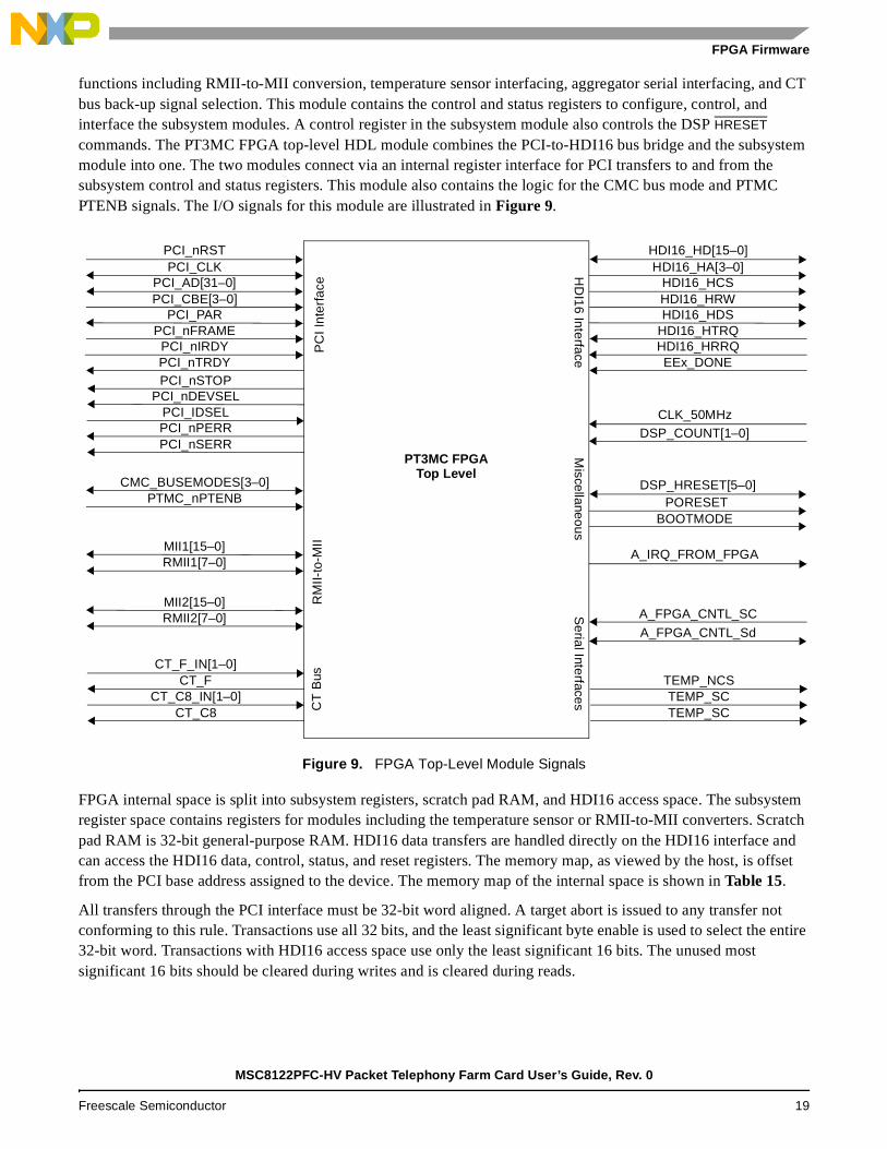
functions including RMII-to-MII conversion, temperature sensor interfacing, aggregator serial interfacing, and CT bus back-up signal selection. This module contains the control and status registers to configure, control, and interface the subsystem modules. A control register in the subsystem module also controls the DSP HRESET commands. The PT3MC FPGA top-level HDL module combines the PCI-to-HDI16 bus bridge and the subsystem module into one. The two modules connect via an internal register interface for PCI transfers to and from the subsystem control and status registers. This module also contains the logic for the CMC bus mode and PTMC PTENB signals. The I/O signals for this module are illustrated in Figure 9.
Figure 9. FPGA Top-Level Module Signals
FPGA internal space is split into subsystem registers, scratch pad RAM, and HDI16 access space. The subsystem register space contains registers for modules including the temperature sensor or RMII-to-MII converters. Scratch pad RAM is 32-bit general-purpose RAM. HDI16 data transfers are handled directly on the HDI16 interface and can access the HDI16 data, control, status, and reset registers. The memory map, as viewed by the host, is offset from the PCI base address assigned to the device. The memory map of the internal space is shown in Table 15.
All transfers through the PCI interface must be 32-bit word aligned. A target abort is issued to any transfer not conforming to this rule. Transactions use all 32 bits, and the least significant byte enable is used to select the entire 32-bit word. Transactions with HDI16 access space use only the least significant 16 bits. The unused most significant 16 bits should be cleared during writes and is cleared during reads.
PT3MC FPGATop Level
HDI16_HD[15–0]HDI16_HA[3–0]
HDI16_HCSHDI16_HRWHDI16_HDS
HDI16_HTRQHDI16_HRRQEEx_DONE
HD
I16 InterfaceM
iscellaneousS
erial InterfacesP
CI I
nter
face
RM
II-to
-MII
CT
Bus
CLK_50MHzDSP_COUNT[1–0]
DSP_HRESET[5–0]PORESET
BOOTMODE
A_IRQ_FROM_FPGA
A_FPGA_CNTL_SC
A_FPGA_CNTL_Sd
TEMP_NCSTEMP_SCTEMP_SC
PCI_nRSTPCI_CLK
PCI_AD[31–0]PCI_CBE[3–0]
PCI_PARPCI_nFRAME
PCI_nIRDYPCI_nTRDYPCI_nSTOP
PCI_nDEVSELPCI_IDSELPCI_nPERRPCI_nSERR
CMC_BUSEMODES[3–0]PTMC_nPTENB
MII1[15–0]RMII1[7–0]
MII2[15–0]RMII2[7–0]
CT_F_IN[1–0]CT_F
CT_C8_IN[1–0]CT_C8
MSC8122PFC-HV Packet Telephony Farm Card User’s Guide, Rev. 0
Freescale Semiconductor 19

FPGA Firmware
4.2 PDK-Compliant FPGA FirmwareThe PDK FPGA connects the MSC8122PFC-HV with the packet telephony development kit (PDK) through the HDI16 over the MPC8XXX local bus, MII, and CT Bus (TDM). For future expansion, the PDK FPGA also contains two RMII-to-MII converter modules. The HDI16 pass-through module uses the PDK_HDI16_HA_DSP0 input to select either aggregator HDI16 transfers or internal subsystem register transfers. If the signal is low during a transfer cycle, the module performs an aggregator DSP HDI16 transfer. If the signal is high during a transfer cycle, the module performs an internal subsystem register transfer.
The main difference between the subsystem module in the PT3MC FPGA version and that in the PDK FPGA version is the register transfer interface. The PT3MC FPGA version has a 32-bit data, 8-bit address interface, where the PDK FPGA version has a 16-bit data, 4-bit address interface. Therefore, the subsystem registers in the PDK FPGA version are partitioned into low and high 16-bit words, accessed individually through the register transfer interface. Also, the internal scratch pad RAM is not included in the PDK FPGA version due to a lack of addressing space.
Table 15. PT3MC FPGA Memory Map
Size Byte Address Offset Interface/Register
0x0000–0x03FF Register interface to subsystem module
32 Bits 0x0000 Host Control/Status Register (HCSR)
16 Bits 0x0004 Temperature Sensor Output Register (TSOR)
N/A 0x0008 Reserved
16 Bits 0x000C RMII Control Register (RCR)
16 Bits 0x0010 Aggregator Command Register (ACR)
16 Bits 0x0014 HRESET Status Register (HSR)
16 Bits 0x001C FPGA Version Register (FVR)
32 Bits 0x0020–0x03FF Scratch pad RAM
0x0400–0x043F Direct to MSC8103 HDI16 registers
16 Bits 0x0400 HDI16 ICR
16 Bits 0x0404 HDI16 CVR
16 Bits 0x0408 HDI16 ISR
16 Bits 0x0410 HDI16 RX3/TX3
16 Bits 0x0414 HDI16 RX2/TX2
16 Bits 0x0418 HDI16 RX1/TX1
16 Bits 0x041C HDI16 RX0/TX0
16 Bits 0x0420 HDI16 RST3
16 Bits 0x0424 HDI16 RST2
16 Bits 0x0428 HDI16 RST1
16 Bits 0x042C HDI16 RST0
Note: Address ranges are given in byte alignment, but accesses must be performed in 32-bit widths and alignment.
MSC8122PFC-HV Packet Telephony Farm Card User’s Guide, Rev. 0
20 Freescale Semiconductor
FPGA Firmware
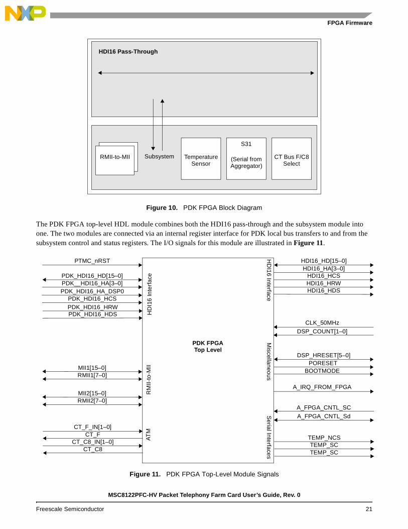
Figure 10. PDK FPGA Block Diagram
The PDK FPGA top-level HDL module combines both the HDI16 pass-through and the subsystem module into one. The two modules are connected via an internal register interface for PDK local bus transfers to and from the subsystem control and status registers. The I/O signals for this module are illustrated in Figure 11.
Figure 11. PDK FPGA Top-Level Module Signals
HDI16 Pass-Through
S31
(Serial fromAggregator)
TemperatureSensor
CT Bus F/C8Select
RMII-to-MII Subsystem
PDK FPGATop Level
HDI16_HD[15–0]HDI16_HA[3–0]
HDI16_HCSHDI16_HRWHDI16_HDS
HD
I16 InterfaceM
iscellaneousS
erial Interfaces
HD
I16
Inte
rfac
eR
MII-
to-M
IIA
TM
CLK_50MHz
DSP_COUNT[1–0]
DSP_HRESET[5–0]PORESET
BOOTMODE
A_IRQ_FROM_FPGA
A_FPGA_CNTL_SC
A_FPGA_CNTL_Sd
TEMP_NCSTEMP_SCTEMP_SC
PTMC_nRST
PDK_HDI16_HD[15–0]PDK__HDI16_HA[3–0]PDK_HDI16_HA_DSP0
PDK_HDI16_HCSPDK_HDI16_HRWPDK_HDI16_HDS
MII1[15–0]RMII1[7–0]
MII2[15–0]RMII2[7–0]
CT_F_IN[1–0]CT_F
CT_C8_IN[1–0]CT_C8
MSC8122PFC-HV Packet Telephony Farm Card User’s Guide, Rev. 0
Freescale Semiconductor 21
FPGA Firmware
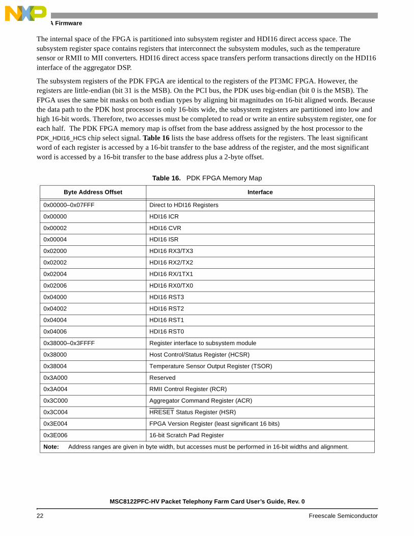
The internal space of the FPGA is partitioned into subsystem register and HDI16 direct access space. The subsystem register space contains registers that interconnect the subsystem modules, such as the temperature sensor or RMII to MII converters. HDI16 direct access space transfers perform transactions directly on the HDI16 interface of the aggregator DSP.
The subsystem registers of the PDK FPGA are identical to the registers of the PT3MC FPGA. However, the registers are little-endian (bit 31 is the MSB). On the PCI bus, the PDK uses big-endian (bit 0 is the MSB). The FPGA uses the same bit masks on both endian types by aligning bit magnitudes on 16-bit aligned words. Because the data path to the PDK host processor is only 16-bits wide, the subsystem registers are partitioned into low and high 16-bit words. Therefore, two accesses must be completed to read or write an entire subsystem register, one for each half. The PDK FPGA memory map is offset from the base address assigned by the host processor to the PDK_HDI16_HCS chip select signal. Table 16 lists the base address offsets for the registers. The least significant word of each register is accessed by a 16-bit transfer to the base address of the register, and the most significant word is accessed by a 16-bit transfer to the base address plus a 2-byte offset.
Table 16. PDK FPGA Memory Map
Byte Address Offset Interface
0x00000–0x07FFF Direct to HDI16 Registers
0x00000 HDI16 ICR
0x00002 HDI16 CVR
0x00004 HDI16 ISR
0x02000 HDI16 RX3/TX3
0x02002 HDI16 RX2/TX2
0x02004 HDI16 RX/1TX1
0x02006 HDI16 RX0/TX0
0x04000 HDI16 RST3
0x04002 HDI16 RST2
0x04004 HDI16 RST1
0x04006 HDI16 RST0
0x38000–0x3FFFF Register interface to subsystem module
0x38000 Host Control/Status Register (HCSR)
0x38004 Temperature Sensor Output Register (TSOR)
0x3A000 Reserved
0x3A004 RMII Control Register (RCR)
0x3C000 Aggregator Command Register (ACR)
0x3C004 HRESET Status Register (HSR)
0x3E004 FPGA Version Register (least significant 16 bits)
0x3E006 16-bit Scratch Pad Register
Note: Address ranges are given in byte width, but accesses must be performed in 16-bit widths and alignment.
MSC8122PFC-HV Packet Telephony Farm Card User’s Guide, Rev. 0
22 Freescale Semiconductor
FPGA Firmware
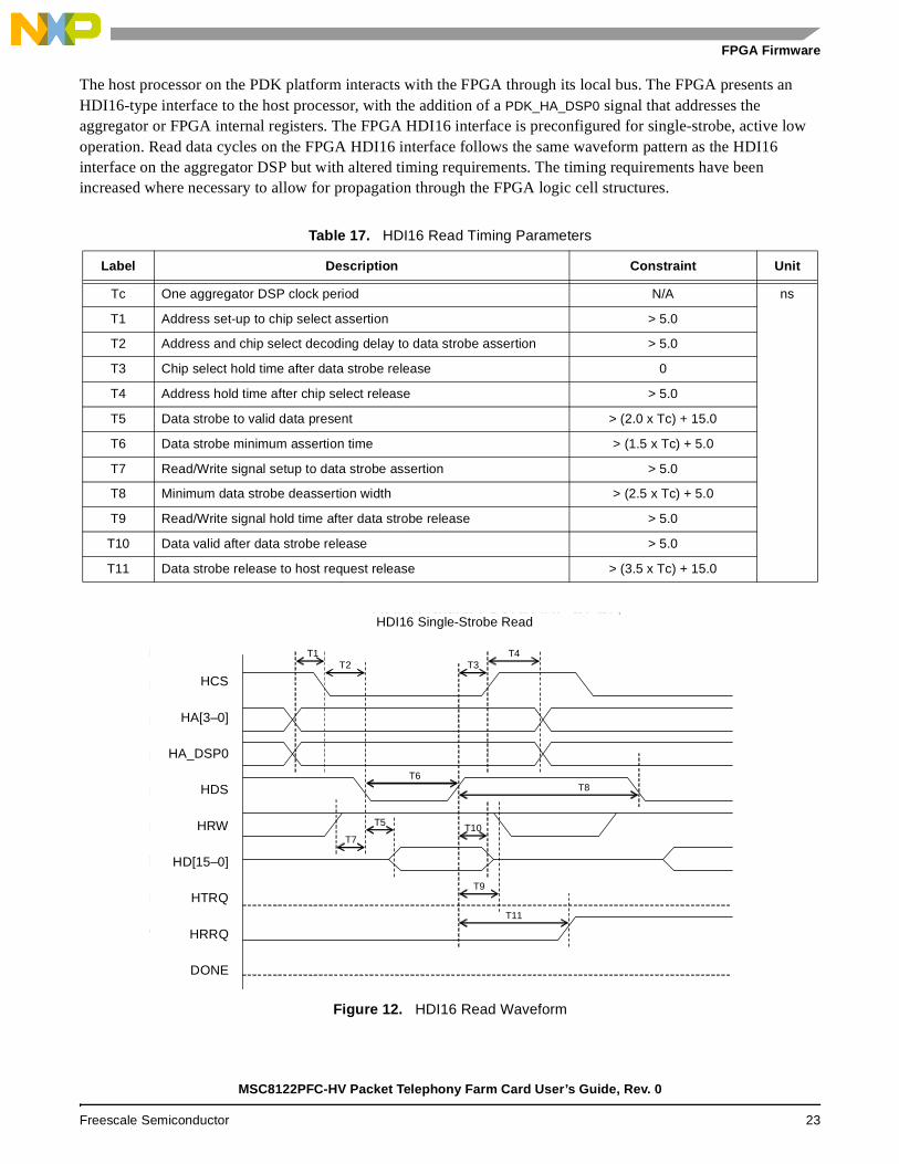
The host processor on the PDK platform interacts with the FPGA through its local bus. The FPGA presents an HDI16-type interface to the host processor, with the addition of a PDK_HA_DSP0 signal that addresses the aggregator or FPGA internal registers. The FPGA HDI16 interface is preconfigured for single-strobe, active low operation. Read data cycles on the FPGA HDI16 interface follows the same waveform pattern as the HDI16 interface on the aggregator DSP but with altered timing requirements. The timing requirements have been increased where necessary to allow for propagation through the FPGA logic cell structures.
Figure 12. HDI16 Read Waveform
Table 17. HDI16 Read Timing Parameters
Label Description Constraint Unit
Tc One aggregator DSP clock period N/A ns
T1 Address set-up to chip select assertion > 5.0
T2 Address and chip select decoding delay to data strobe assertion > 5.0
T3 Chip select hold time after data strobe release 0
T4 Address hold time after chip select release > 5.0
T5 Data strobe to valid data present > (2.0 x Tc) + 15.0
T6 Data strobe minimum assertion time > (1.5 x Tc) + 5.0
T7 Read/Write signal setup to data strobe assertion > 5.0
T8 Minimum data strobe deassertion width > (2.5 x Tc) + 5.0
T9 Read/Write signal hold time after data strobe release > 5.0
T10 Data valid after data strobe release > 5.0
T11 Data strobe release to host request release > (3.5 x Tc) + 15.0
HCS
HA[3:0]
HA_DSP0
HDS
HRW
HD[15:0]
HTRQ
HRRQ
DONE
T1
T5
T7
T2 T3T4
T9
T10
T6
T11
T8
HCS
HA[3:0]
HA_DSP0
HDS
HRW
HD[15:0]
HTRQ
HRRQ
DONE
HDI16 SINGLE-STROBE READ
T1
T5
T7
T2 T3T4
T9
T10
T6
T11
T8
HDI16 Single-Strobe Read
HCS
HA[3–0]
HA_DSP0
HDS
HRW
HD[15–0]
HTRQ
HRRQ
DONE
MSC8122PFC-HV Packet Telephony Farm Card User’s Guide, Rev. 0
Freescale Semiconductor 23

FPGA Firmware
Write data cycles on the FPGA HDI16 interface have the same waveform pattern as the HDI16 interface on the aggregator DSP, but the timing requirements are increased to allow propagation through the FPGA logic cell structures. Also, there are differing latch requirements for FPGA internal registers (see Table 18 and Figure 13). The DSP HDI16 interface latches data on the rising edge (release) of data strobe (HDS), whereas the FPGA latches data on the falling edge (assertion) of HDS. Therefore, data must be valid before the assertion of HDS and remain valid until after the release of HDS.
Figure 13. HDI16 Write Waveform
Table 18. HDI16 Write Timing Parameters
Label Description Constraint Unit
Tc One aggregator DSP clock period N/A ns
T1 Address set-up to chip select assertion > 5.0
T2 Address and chip select decoding delay to data strobe assertion > 5.0
T3 Chip select hold time after data strobe release 0
T4 Address hold time after chip select release > 5.0
T5 Valid data present to data strobe assertion > 10.0
T6 Data strobe minimum assertion time > (1.5 x Tc) + 5.0
T7 Read/Write signal setup to data strobe assertion > 5.0
T8 Minimum data strobe deassertion width > (2.5 x Tc) + 5.0
T9 Read/Write signal hold time after data strobe release > 5.0
T10 Data valid after data strobe release > 5.0
T11 Data strobe release to host request release > (3.0 x Tc) + 15.0
HCS
HA[3:0]
HA_DSP0
HDS
HRW
HD[15:0]
HTRQ
HRRQ
DONE
T1
T5
T7
T2 T3T4
T9
T10
T6
T11
T8
HCS
HA[3–0]
HA_DSP0
HDS
HRW
HD[15–0]
HTRQ
HRRQ
DONE
HDI16 Single-Strobe Write
MSC8122PFC-HV Packet Telephony Farm Card User’s Guide, Rev. 0
24 Freescale Semiconductor

FPGA Firmware
4.2.1 Aggregator Serial InterfaceA simple synchronous serial interface provides a control and status data path between the aggregator DSP and the FPGA. This interface transfers 16 data bits to the FPGA from the DSP and allows the DSP to read back 16 data bits. The 16-bit data from the DSP is latched into the Aggregator Command Register (ACR) (see page 30) on the rising edge of SC during the second framing zero from the DSP. The returned 16-bit data from the FPGA is the mirror of the ACR, with the exception that the HR[4–0] bits indicate the true status of the HRESET lines to the DSP farm, taken from the HRESET Status Register (HSR). The transfer of data between the DSP and the FPGA must follow the simple frame format shown in Figure 14. There are two signals, Serial Data (SD) and Serial Clock (SC). SD is wire-and with a pull-up, and SC is actively driven by the DSP only. Data is clocked into the FPGA on the rising edge of SC, starting with the first framing zero until the second framing zero. A frame starts with a zero, then the 16-bit data (MSB first), then another zero, all clocked at the rising edge of SC. The FPGA does not start latching data until it receives the first zero, and it triggers a framing error condition, resetting the interface if it does not receive the second framing zero after the 16-bit data.
Figure 14. Aggregator Serial Interface Waveform
After the second framing zero is clocked, the FPGA begins to drive SD low if no framing error is triggered. The DSP should release SD and then sample SD to check for the ACK zero from the FPGA. If ACK zero is sent, the FPGA shifts the return data out onto SD with each rising edge of SC. The DSP should sample the return data after each rising edge of SC until all 16 bits are received. The FPGA then releases SD and begins to search for the next beginning frame zero from the DSP on each rising edge of SC. To reset the interface from the DSP, release SD and clock SC at least 18 times. Nothing happens if the interface is already reset. If the FPGA is driving SD, any remaining return data clocks out. If there is a partially unfinished transfer from the DSP to the FPGA, a reset triggers a framing error and resets the interface. The ACR is untouched under all these conditions. To clear the ACR, perform a complete transfer with all zero data to the FPGA.
4.3 FPGA RegistersThe FPGA registers discussed in this section are as follows:
• Host Control/Status Register (HCSR), page 26.
• Temperature Sensor Output Register (TSOR), page 28.
• RMII Control Register (RCR), page 29.
• Aggregator Command Register (ACR), page 30.
• HRESET Status Register (HSR), page 31.
• FPGA Version Register (FVR), page 32.
• Scratch Pad RAM (SPR), page 32.
16-Bit Data From FPGAM
SB
LSB
16-Bit Data From DSP
MS
B
LSB
SC
SD
Frame Zero from DSP Ack Zero from FPGA
Latch IN on Rising Edge Latch OUT on Rising Edge
MSC8122PFC-HV Packet Telephony Farm Card User’s Guide, Rev. 0
Freescale Semiconductor 25

FPGA Firmware
HCSR Host Control/Status Register Byte Offset 0x0
Bit 31 30 29 28 27 26 25 24 23 22 21 20 19 18 17 16
— BM POR
TYPE R R/W
RESET 0 0 0 0 0 0 0 0 0 0 0 0 0 0 0 0
Bit 15 14 13 12 11 10 9 8 7 6 5 4 3 2 1 0
RAH CFS CFC1 CFC2 CAC IFH ITHE ITH DC1 DC0 HRA HR4 HR3 HR2 HR1 HR0
TYPE R/W R R/W R R/W
RESET 0 — 0 0 0 0 0 — — — 0 0 0 0 0 0
Table 19. HCSR Bit Descriptions
Name Reset Description Settings
—31–18
0 Reserved. Write to zero for future compatibility.
BM17
0 Boot ModeSets the boot mode of the aggregator DSP after the next PORESET. When power is first applied to the board, the FPGA asserts the PORESET signal for a few micro-seconds while it drives the BOOTMODE external signal low. The FPGA then release the PORESET signal, booting the DSP via Flash. To boot the aggregator via HDI16, set the BM bit and the POR bit of the HCSR for some time, then clear the POR bit but keep the BM bit set. Finally, send the Hardware Reset Configuration Word (HRCW) settings to the DSP via the HDI16 direct access space.
0 Boot via Flash device (default).
1 Boot via the HDI16.
POR16
0 Power-On Reset (PORESET)Controls the state of the PORESET pin on the FPGA.
0 PORESET pin on the FPGA is set to High-Z.
1 PORESET pin on the FPGA is driven low.
RAH15
0 HDI16 Request Active HighSets the polarity of the request lines from the aggregator to the FPGA for buffered accesses. These signals, HRRQ and HTRQ, are driven by the aggregator. The polarity programmed in the aggregator should match the polarity programmed with this bit if buffered (FIFO) accesses to the HDI16 data registers are performed.
0 Polarity is active low.
1 Polarity is active high.
CFS14
— CT Bus Frame/C8 Failover StatusIndicates whether a failover on the CT bus frame and C8 signals was performed. This bit is cleared when a manual selection CT bus failover command (CFC) is issued. This bit is set when an active failover CT bus failover command (CFC) is issued and a failover is triggered.
MSC8122PFC-HV Packet Telephony Farm Card User’s Guide, Rev. 0
26 Freescale Semiconductor
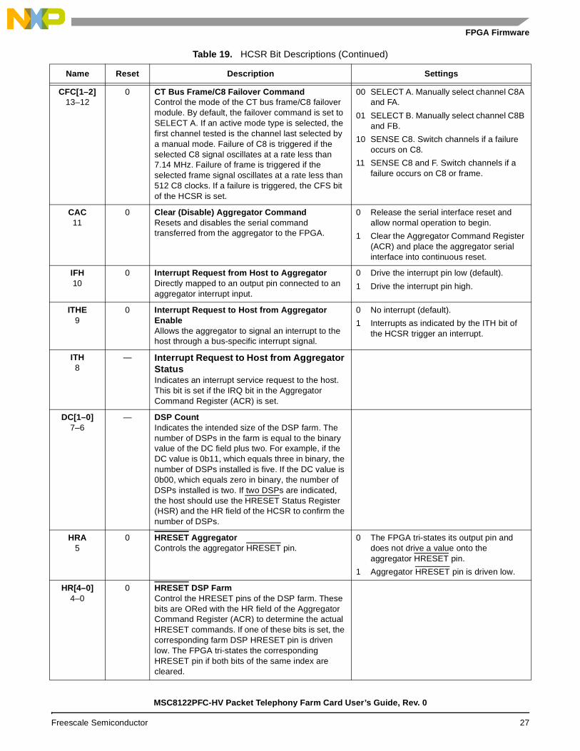
FPGA Firmware
CFC[1–2]13–12
0 CT Bus Frame/C8 Failover CommandControl the mode of the CT bus frame/C8 failover module. By default, the failover command is set to SELECT A. If an active mode type is selected, the first channel tested is the channel last selected by a manual mode. Failure of C8 is triggered if the selected C8 signal oscillates at a rate less than 7.14 MHz. Failure of frame is triggered if the selected frame signal oscillates at a rate less than 512 C8 clocks. If a failure is triggered, the CFS bit of the HCSR is set.
00 SELECT A. Manually select channel C8A and FA.
01 SELECT B. Manually select channel C8B and FB.
10 SENSE C8. Switch channels if a failure occurs on C8.
11 SENSE C8 and F. Switch channels if a failure occurs on C8 or frame.
CAC11
0 Clear (Disable) Aggregator CommandResets and disables the serial command transferred from the aggregator to the FPGA.
0 Release the serial interface reset and allow normal operation to begin.
1 Clear the Aggregator Command Register (ACR) and place the aggregator serial interface into continuous reset.
IFH10
0 Interrupt Request from Host to AggregatorDirectly mapped to an output pin connected to an aggregator interrupt input.
0 Drive the interrupt pin low (default).
1 Drive the interrupt pin high.
ITHE9
0 Interrupt Request to Host from Aggregator EnableAllows the aggregator to signal an interrupt to the host through a bus-specific interrupt signal.
0 No interrupt (default).
1 Interrupts as indicated by the ITH bit of the HCSR trigger an interrupt.
ITH8
— Interrupt Request to Host from Aggregator StatusIndicates an interrupt service request to the host. This bit is set if the IRQ bit in the Aggregator Command Register (ACR) is set.
DC[1–0]7–6
— DSP Count Indicates the intended size of the DSP farm. The number of DSPs in the farm is equal to the binary value of the DC field plus two. For example, if the DC value is 0b11, which equals three in binary, the number of DSPs installed is five. If the DC value is 0b00, which equals zero in binary, the number of DSPs installed is two. If two DSPs are indicated, the host should use the HRESET Status Register (HSR) and the HR field of the HCSR to confirm the number of DSPs.
HRA5
0 HRESET AggregatorControls the aggregator HRESET pin.
0 The FPGA tri-states its output pin and does not drive a value onto the aggregator HRESET pin.
1 Aggregator HRESET pin is driven low.
HR[4–0]4–0
0 HRESET DSP FarmControl the HRESET pins of the DSP farm. These bits are ORed with the HR field of the Aggregator Command Register (ACR) to determine the actual HRESET commands. If one of these bits is set, the corresponding farm DSP HRESET pin is driven low. The FPGA tri-states the corresponding HRESET pin if both bits of the same index are cleared.
Table 19. HCSR Bit Descriptions (Continued)
Name Reset Description Settings
MSC8122PFC-HV Packet Telephony Farm Card User’s Guide, Rev. 0
Freescale Semiconductor 27
FPGA Firmware
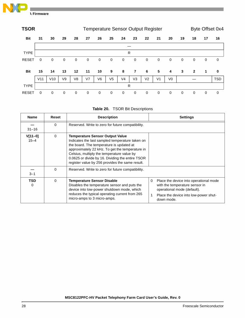
TSOR Temperature Sensor Output Register Byte Offset 0x4
Bit 31 30 29 28 27 26 25 24 23 22 21 20 19 18 17 16
—
TYPE R
RESET 0 0 0 0 0 0 0 0 0 0 0 0 0 0 0 0
Bit 15 14 13 12 11 10 9 8 7 6 5 4 3 2 1 0
V11 V10 V9 V8 V7 V6 V5 V4 V3 V2 V1 V0 — TSD
TYPE R
RESET 0 0 0 0 0 0 0 0 0 0 0 0 0 0 0 0
Table 20. TSOR Bit Descriptions
Name Reset Description Settings
—31–16
0 Reserved. Write to zero for future compatibility.
V[11–0]15–4
0 Temperature Sensor Output ValueIndicates the last sampled temperature taken on the board. The temperature is updated at approximately 22 kHz. To get the temperature in Celsius, multiply the temperature value by 0.0625 or divide by 16. Dividing the entire TSOR register value by 256 provides the same result.
—3–1
0 Reserved. Write to zero for future compatibility.
TSD0
0 Temperature Sensor DisableDisables the temperature sensor and puts the device into low-power shutdown mode, which reduces the typical operating current from 265 micro-amps to 3 micro-amps.
0 Place the device into operational mode with the temperature sensor in operational mode (default).
1 Place the device into low-power shut-down mode.
MSC8122PFC-HV Packet Telephony Farm Card User’s Guide, Rev. 0
28 Freescale Semiconductor
FPGA Firmware
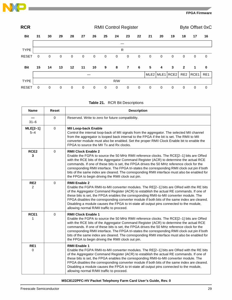
RCR RMII Control Register Byte Offset 0xC
Bit 31 30 29 28 27 26 25 24 23 22 21 20 19 18 17 16
—
TYPE R
RESET 0 0 0 0 0 0 0 0 0 0 0 0 0 0 0 0
Bit 15 14 13 12 11 10 9 8 7 6 5 4 3 2 1 0
— MLE2 MLE1 RCE2 RE2 RCE1 RE1
TYPE R/W
RESET 0 0 0 0 0 0 0 0 0 0 0 0 0 0 0 0
Table 21. RCR Bit Descriptions
Name Reset Description
—31–6
0 Reserved. Write to zero for future compatibility.
MLE[2–1]5–4
0 MII Loop-back EnableControl the internal loop-back of MII signals from the aggregator. The selected MII channel from the aggregator is looped back internal to the FPGA if the bit is set. The RMII to MII converter module must also be enabled. Set the proper RMII Clock Enable bit to enable the FPGA to source the MII Tx and Rx clocks.
RCE23
0 RMII Clock Enable 2Enable the FGPA to source the 50 MHz RMII reference clocks. The RCE[2–1] bits are ORed with the RCE bits of the Aggregator Command Register (ACR) to determine the actual RCE commands. If one of these bits is set, the FPGA drives the 50 MHz reference clock for the corresponding RMII interface. The FPGA tri-states the corresponding RMII clock out pin if both bits of the same index are cleared. The corresponding RMII interface must also be enabled for the FPGA to begin driving the RMII clock out pin.
RE22
0 RMII Enable 2Enable the FGPA RMII-to-MII converter modules. The RE[2–1] bits are ORed with the RE bits of the Aggregator Command Register (ACR) to establish the actual RE commands. If one of these bits is set, the FPGA enables the corresponding RMII-to-MII converter module. The FPGA disables the corresponding converter module if both bits of the same index are cleared. Disabling a module causes the FPGA to tri-state all output pins connected to the module, allowing normal R/MII traffic to proceed.
RCE11
0 RMII Clock Enable 1Enable the FGPA to source the 50 MHz RMII reference clocks. The RCE[2–1] bits are ORed with the RCE bits of the Aggregator Command Register (ACR) to determine the actual RCE commands. If one of these bits is set, the FPGA drives the 50 MHz reference clock for the corresponding RMII interface. The FPGA tri-states the corresponding RMII clock out pin if both bits of the same index are cleared. The corresponding RMII interface must also be enabled for the FPGA to begin driving the RMII clock out pin.
RE10
RMII Enable 1Enable the FGPA RMII-to-MII converter modules. The RE[2–1] bits are ORed with the RE bits of the Aggregator Command Register (ACR) to establish the actual RE commands. If one of these bits is set, the FPGA enables the corresponding RMII-to-MII converter module. The FPGA disables the corresponding converter module if both bits of the same index are cleared. Disabling a module causes the FPGA to tri-state all output pins connected to the module, allowing normal R/MII traffic to proceed.
MSC8122PFC-HV Packet Telephony Farm Card User’s Guide, Rev. 0
Freescale Semiconductor 29

FPGA Firmware
ACR Aggregator Command Register Byte Offset 0x10
Bit 31 30 29 28 27 26 25 24 23 22 21 20 19 18 17 16
— AFE
TYPE R
RESET 0 0 0 0 0 0 0 0 0 0 0 0 0 0 0 0
Bit 15 14 13 12 11 10 9 8 7 6 5 4 3 2 1 0
AF5 AF4 AF3 AF2 AF1 AF0 RCE2 RE2 RCE1 RE1 IRQ HR4 HR3 HR2 HR1 HR0
TYPE R
RESET 0 0 0 0 0 0 0 0 0 0 0 0 0 0 0 0
Table 22. ACR Bit Descriptions
Name Reset Description
—31–17
0 Reserved. Write to zero for future compatibility.
AFE16
0 Aggregator Command Frame ErrorIndicates an error condition generated on the transfer of command data from the aggregator to the FPGA. The transfer must follow a specific format; otherwise, a frame error is generated. The frame error is cleared if the CAC bit in the Host Control/Status Register (HCRS) is set or when the next successful transfer completes.
AF[5–0]15–10
0 Aggregator FlagsGeneral-purpose flags by which the aggregator communicates information to the host, such as system states or service requests. This field can be used with the IRQ field of this register to indicate the types of service requested by the aggregator.
RCE29
0 RMII Clock Enable 2Enables the FGPA to source the 50 MHz RMII reference clocks. The RCE bits are ORed with the RCE bits of the RMII Control Register (RCR) to determine the actual RCE commands. If one of these bits is set, the FPGA drives the 50 MHz reference clock for the corresponding RMII interface. The FPGA tri-states the corresponding RMII clock out pin if both bits of the same index are cleared. The corresponding RMII interface must also be enabled for the FPGA to begin driving the RMII clock out pin.
RE28
0 RMII Enable 2Enables the FGPA RMII-to-MII converter modules. These bits are ORed with the RE bits of the RMII Control Register (RCR) to determine the actual RE commands. If one of these bits is set, the FPGA enables the corresponding RMII-to-MII converter module. The FPGA disables the corresponding RMII-to-MII converter module if both bits of the same index are cleared. Disabling a module causes the FPGA to tri-state all output pins connected to the module, allowing normal R/MII traffic to proceed.
RCE17
0 RMII Clock Enable 1Enables the FGPA to source the 50 MHz RMII reference clocks. The RCE bits are OREed with the RCE bits of the RMII Control Register (RCR) to determine the actual RCE commands. If one of these bits is set, the FPGA drives the 50 MHz reference clock for the corresponding RMII interface. The FPGA tri-states the corresponding RMII clock out pin if both bits of the same index are cleared. The corresponding RMII interface must also be enabled for the FPGA to begin driving the RMII clock out pin.
MSC8122PFC-HV Packet Telephony Farm Card User’s Guide, Rev. 0
30 Freescale Semiconductor

FPGA Firmware
RE16
0 RMII Enable 1Enables the FGPA RMII-to-MII converter modules. These bits are ORed with the RE bits of the RMII Control Register (RCR) to determine the actual RE commands. If one of these bits is set, the FPGA enables the corresponding RMII-to-MII converter module. The FPGA disables the corresponding RMII-to-MII converter module if both bits of the same index are cleared. Disabling a module causes the FPGA to tri-state all output pins connected to the module, allowing normal R/MII traffic to proceed.
IRQ5
0 Interrupt Request to HostIndicates that the aggregator is requesting service from the host. When this bit is set, an interrupt request is generated.
HR[4–0]4–0
0 HRESET DSP FarmControls the HRESET pins of the DSP farm. These bits are ORed with the HR field of the Host Control/Status Register (HCSR) to determine the actual HRESET commands. If one of these bits is set, the corresponding farm DSP HRESET pin is driven low. The FPGA tri-states the corresponding HRESET pin if both bits of the same index are cleared.
HSR HRESET Status Register Byte Offset 0x14
Bit 31 30 29 28 27 26 25 24 23 22 21 20 19 18 17 16
—
TYPE R
RESET 0 0 0 0 0 0 0 0 0 0 0 0 0 0 0 0
Bit 15 14 13 12 11 10 9 8 7 6 5 4 3 2 1 0
— HRA HR4 HR3 HR2 HR1 HR0
TYPE R
RESET 0 0 0 0 0 0 0 0 0 0 — — — — — —
Table 23. HSR Bit Descriptions
Name Reset Description Settings
—31–6
0 Reserved. Write to zero for future compatibility.
HRA5
— HRESET Aggregator StatusIndicates the current state of the aggregator HRESET pin. Since multiple sources can drive the HRESET pin of the aggregator, this bit allows a true indication of the state of the pin.
0 The aggregator HRESET pin is low and is in reset mode.
1 The aggregator HRESET pin is high and is no longer in reset.
HR[4–0]4–0
— HRESET DSP Farm Status BitsIndicates the current state of the farm HRESET pins. Since multiple sources can drive the HRESET pins of the farm, these bits allow to a true indication of the state of these pins.
0 The farm HRESET pin is low and is in reset mode.
1 The farm HRESET pin is high and is no longer in reset.
Table 22. ACR Bit Descriptions (Continued)
Name Reset Description
MSC8122PFC-HV Packet Telephony Farm Card User’s Guide, Rev. 0
Freescale Semiconductor 31
FPGA Firmware
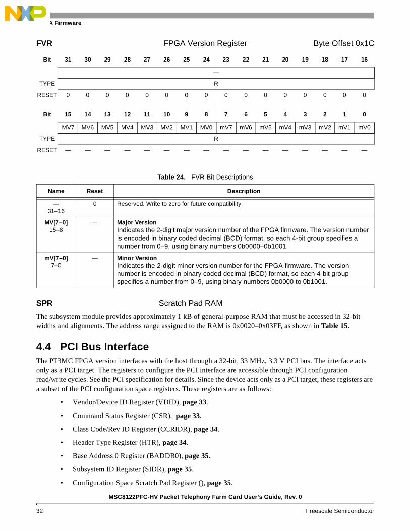
SPR Scratch Pad RAM
The subsystem module provides approximately 1 kB of general-purpose RAM that must be accessed in 32-bit widths and alignments. The address range assigned to the RAM is 0x0020–0x03FF, as shown in Table 15.
4.4 PCI Bus InterfaceThe PT3MC FPGA version interfaces with the host through a 32-bit, 33 MHz, 3.3 V PCI bus. The interface acts only as a PCI target. The registers to configure the PCI interface are accessible through PCI configuration read/write cycles. See the PCI specification for details. Since the device acts only as a PCI target, these registers are a subset of the PCI configuration space registers. These registers are as follows:
• Vendor/Device ID Register (VDID), page 33.
• Command Status Register (CSR), page 33.
• Class Code/Rev ID Register (CCRIDR), page 34.
• Header Type Register (HTR), page 34.
• Base Address 0 Register (BADDR0), page 35.
• Subsystem ID Register (SIDR), page 35.
• Configuration Space Scratch Pad Register (), page 35.
FVR FPGA Version Register Byte Offset 0x1C
Bit 31 30 29 28 27 26 25 24 23 22 21 20 19 18 17 16
—
TYPE R
RESET 0 0 0 0 0 0 0 0 0 0 0 0 0 0 0 0
Bit 15 14 13 12 11 10 9 8 7 6 5 4 3 2 1 0
MV7 MV6 MV5 MV4 MV3 MV2 MV1 MV0 mV7 mV6 mV5 mV4 mV3 mV2 mV1 mV0
TYPE R
RESET — — — — — — — — — — — — — — — —
Table 24. FVR Bit Descriptions
Name Reset Description
—31–16
0 Reserved. Write to zero for future compatibility.
MV[7–0]15–8
— Major VersionIndicates the 2-digit major version number of the FPGA firmware. The version number is encoded in binary coded decimal (BCD) format, so each 4-bit group specifies a number from 0–9, using binary numbers 0b0000–0b1001.
mV[7–0]7–0
— Minor VersionIndicates the 2-digit minor version number for the FPGA firmware. The version number is encoded in binary coded decimal (BCD) format, so each 4-bit group specifies a number from 0–9, using binary numbers 0b0000 to 0b1001.
MSC8122PFC-HV Packet Telephony Farm Card User’s Guide, Rev. 0
32 Freescale Semiconductor
FPGA Firmware
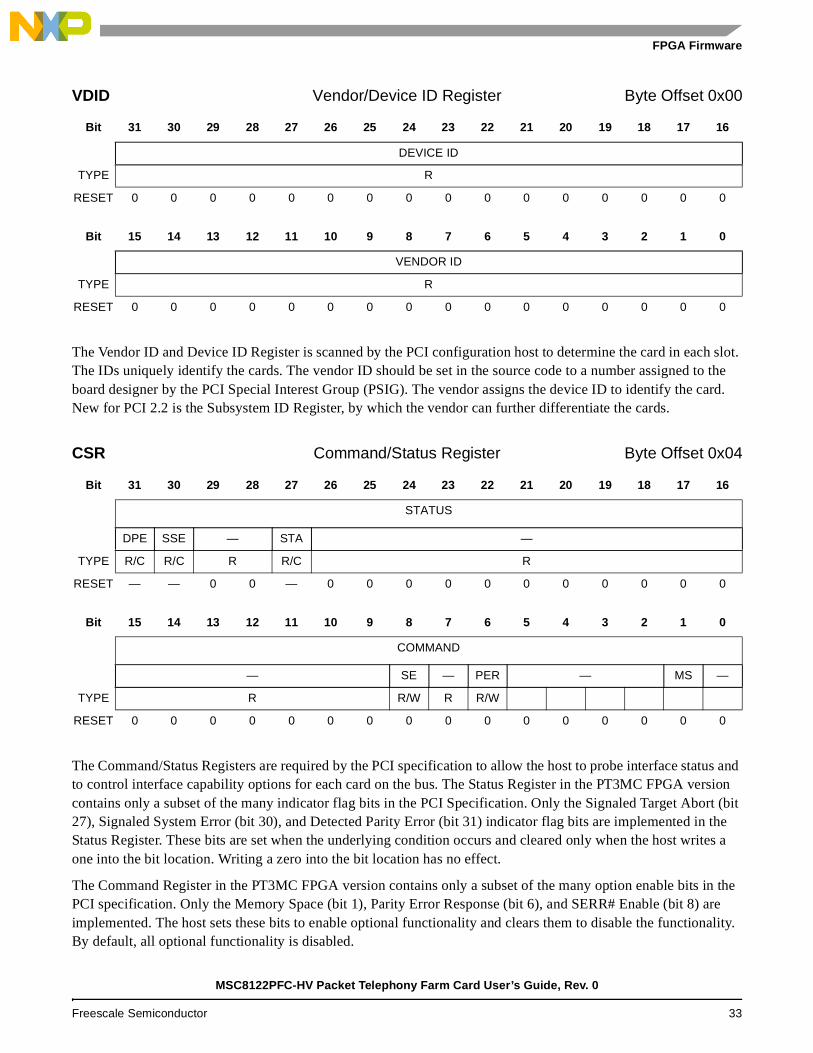
The Vendor ID and Device ID Register is scanned by the PCI configuration host to determine the card in each slot. The IDs uniquely identify the cards. The vendor ID should be set in the source code to a number assigned to the board designer by the PCI Special Interest Group (PSIG). The vendor assigns the device ID to identify the card. New for PCI 2.2 is the Subsystem ID Register, by which the vendor can further differentiate the cards.
The Command/Status Registers are required by the PCI specification to allow the host to probe interface status and to control interface capability options for each card on the bus. The Status Register in the PT3MC FPGA version contains only a subset of the many indicator flag bits in the PCI Specification. Only the Signaled Target Abort (bit 27), Signaled System Error (bit 30), and Detected Parity Error (bit 31) indicator flag bits are implemented in the Status Register. These bits are set when the underlying condition occurs and cleared only when the host writes a one into the bit location. Writing a zero into the bit location has no effect.
The Command Register in the PT3MC FPGA version contains only a subset of the many option enable bits in the PCI specification. Only the Memory Space (bit 1), Parity Error Response (bit 6), and SERR# Enable (bit 8) are implemented. The host sets these bits to enable optional functionality and clears them to disable the functionality. By default, all optional functionality is disabled.
VDID Vendor/Device ID Register Byte Offset 0x00
Bit 31 30 29 28 27 26 25 24 23 22 21 20 19 18 17 16
DEVICE ID
TYPE R
RESET 0 0 0 0 0 0 0 0 0 0 0 0 0 0 0 0
Bit 15 14 13 12 11 10 9 8 7 6 5 4 3 2 1 0
VENDOR ID
TYPE R
RESET 0 0 0 0 0 0 0 0 0 0 0 0 0 0 0 0
CSR Command/Status Register Byte Offset 0x04
Bit 31 30 29 28 27 26 25 24 23 22 21 20 19 18 17 16
STATUS
DPE SSE — STA —
TYPE R/C R/C R R/C R
RESET — — 0 0 — 0 0 0 0 0 0 0 0 0 0 0
Bit 15 14 13 12 11 10 9 8 7 6 5 4 3 2 1 0
COMMAND
— SE — PER — MS —
TYPE R R/W R R/W
RESET 0 0 0 0 0 0 0 0 0 0 0 0 0 0 0 0
MSC8122PFC-HV Packet Telephony Farm Card User’s Guide, Rev. 0
Freescale Semiconductor 33
FPGA Firmware
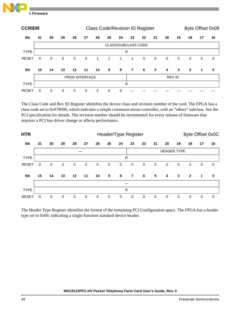
The Class Code and Rev ID Register identifies the device class and revision number of the card. The FPGA has a class code set to 0x078000, which indicates a simple communications controller, with an “others” subclass. See the PCI specification for details. The revision number should be incremented for every release of firmware that requires a PCI bus driver change or affects performance.
The Header Type Register identifies the format of the remaining PCI Configuration space. The FPGA has a header type set to 0x00, indicating a single-function standard device header.
CCRIDR Class Code/Revision ID Register Byte Offset 0x08
Bit 31 30 29 28 27 26 25 24 23 22 21 20 19 18 17 16
CLASS/SUBCLASS CODE
TYPE R
RESET 0 0 0 0 0 1 1 1 1 0 0 0 0 0 0 0
Bit 15 14 13 12 11 10 9 8 7 6 5 4 3 2 1 0
PROG INTERFACE REV ID
TYPE R
RESET 0 0 0 0 0 0 0 0 — — — — — — — —
HTR Header/Type Register Byte Offset 0x0C
Bit 31 30 29 28 27 26 25 24 23 22 21 20 19 18 17 16
— HEADER TYPE
TYPE R
RESET 0 0 0 0 0 0 0 0 0 0 0 0 0 0 0 0
Bit 15 14 13 12 11 10 9 8 7 6 5 4 3 2 1 0
—
TYPE R
RESET 0 0 0 0 0 0 0 0 0 0 0 0 0 0 0 0
MSC8122PFC-HV Packet Telephony Farm Card User’s Guide, Rev. 0
34 Freescale Semiconductor
FPGA Firmware
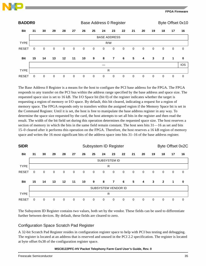
The Base Address 0 Register is a means for the host to configure the PCI base address for the FPGA. The FPGA responds to any transfer on the PCI bus within the address range specified by the base address and space size. The requested space size is set to 16 kB. The I/O Space bit (bit 0) of the register indicates whether the target is requesting a region of memory or I/O space. By default, this bit cleared, indicating a request for a region of memory space. The FPGA responds only to transfers within the assigned region if the Memory Space bit is set in the Command Register. Until it is set, the host is free to manipulate the base address register in any way. To determine the space size requested by the card, the host attempts to set all bits in the register and then read the result. The width of the bit field set during this operation determines the requested space size. The host reserves a section of memory in which the bits in the same field remain constant. The host sees bits 31—16 as set and bits 15–0 cleared after it performs this operation on the FPGA. Therefore, the host reserves a 16 kB region of memory space and writes the 16 most significant bits of the address space into bits 31–16 of the base address register.
The Subsystem ID Register contains two values, both set by the vendor. These fields can be used to differentiate further between devices. By default, these fields are cleared to zero.
Configuration Space Scratch Pad Register
A 32-bit Scratch Pad Register resides in configuration register space to help with PCI bus testing and debugging. The register is located at an address that is reserved and unused in the PCI 2.2 specification. The register is located at byte offset 0x38 of the configuration register space.
BADDR0 Base Address 0 Register Byte Offset 0x10
Bit 31 30 29 28 27 26 25 24 23 22 21 20 19 18 17 16
BASE ADDRESS
TYPE R/W
RESET 0 0 0 0 0 0 0 0 0 0 0 0 0 0 0 0
Bit 15 14 13 12 11 10 9 8 7 6 5 4 3 2 1 0
— IOS
TYPE R
RESET 0 0 0 0 0 0 0 0 0 0 0 0 0 0 0 0
SIDR Subsystem ID Register Byte Offset 0x2C
Bit 31 30 29 28 27 26 25 24 23 22 21 20 19 18 17 16
SUBSYSTEM ID
TYPE R
RESET 0 0 0 0 0 0 0 0 0 0 0 0 0 0 0 0
Bit 15 14 13 12 11 10 9 8 7 6 5 4 3 2 1 0
SUBSYSTEM VENDOR ID
TYPE R
RESET 0 0 0 0 0 0 0 0 0 0 0 0 0 0 0 0
MSC8122PFC-HV Packet Telephony Farm Card User’s Guide, Rev. 0
Freescale Semiconductor 35
FPGA Firmware
Appendix A Schematics
MSC8122PFC-HV Packet Telephony Farm Card User’s Guide, Rev. 0
36 Freescale Semiconductor
5
5
4
4
3
3
2
2
1
1
D D
C C
B B
A A
Nam e Rev
Date: Sheet of
T i tle Block
2.1
Packet TelelphonyFreescale NCSDCopyright 2005
18Friday, Apri l 08, 2005
Front Page
David Kol tak
Freescale General Business Inform ation
8122PFC HV
1
Nam e Rev
Date: Sheet of
T i tle Block
2.1
Packet TelelphonyFreescale NCSDCopyright 2005
18Friday, Apri l 08, 2005
Front Page
David Kol tak
Freescale General Business Inform ation
8122PFC HV
1
Nam e Rev
Date: Sheet of
T i tle Block
2.1
Packet TelelphonyFreescale NCSDCopyright 2005
18Friday, Apri l 08, 2005
Front Page
David Kol tak
Freescale General Business Inform ation
8122PFC HV
1
5
6
4
2
DescriptionPage
3
MSC8103 Memory
1 This Page
Table of Contents
MSC8103 Core
PTMC Connectors
Revision History
FPGA
PFC Overview
First Release1.0
MSC8122 - PACKET TELEPHONY FARMCARD (8122PFC)HIGH VOLUME
7 POWER / RESET
8 DSP FARM
1.1 DRC clean-up and incorporated comments
1.2 STX/SRX, Temp IC, PORESET-J1, P5
1.3 64-bit SRAM and clean up to get ready for layout
9
10
11
12
13
14
15
16
17
18
DSP1 FARM CORE
DSP1 FARM MEMORY
DSP2 FARM CORE
DSP2 FARM MEMORY
DSP3 FARM CORE
DSP3 FARM MEMORY
DSP4 FARM CORE
DSP4 FARM MEMORY
DSP5 FARM CORE
DSP5 FARM MEMORY
1.4 Post Design Review
1.5 Modified FPGA Pinout to Optimize Layout
1.6 Added Third Oscillator to FPGA for optional RMII clock source
1.7 Back Annotated from Layout Design
1.8 Added Serial EEPROM for FPGA Boot
TDM to 8101, J1, TDM Mismatch, Boot Mode, Farm Caps2.0
2.1 Heat Sink on Linear Regulators, Caps, Inductor
5
5
4
4
3
3
2
2
1
1
D D
C C
B B
A A
Name RevDate: Sheet of
Title Block
2.1
Packet TelelphonyFreescale NCSDCopyright 2005
18Tuesday, April 12, 2005
PFC Overview
David KoltakFreescale General Business Information
8122PFC HV
2
Name RevDate: Sheet of
Title Block
2.1
Packet TelelphonyFreescale NCSDCopyright 2005
18Tuesday, April 12, 2005
PFC Overview
David KoltakFreescale General Business Information
8122PFC HV
2
Name RevDate: Sheet of
Title Block
2.1
Packet TelelphonyFreescale NCSDCopyright 2005
18Tuesday, April 12, 2005
PFC Overview
David KoltakFreescale General Business Information
8122PFC HV
2
60x
FCC1
FCC2
Dh[0:31]
MSC8103
Ah[0:31]
FLASH(4MB)
Ah[9:26]
Dh[0:7]
Pn3
Pn4
Pn2
Pn1
MSC8122 - 1
MSC8122 - 5
DSI
60x
60x
SDRAM(16MB)
TDM
60x
DSI
TDM
Ah[11:29]
Dh[0:31]
TDM
DSI
TDM
MSC8122 - 3
MSC8122 - 4
DSI
DSI
60x
TDM
60x
MSC8122 - 2
FPGA
Clock Method
PLL ClockDriver
MSC8102 FarmClocks(CLKIN)
44.3 MHZ
MSC8101AggregatorClock
PCIHDI16HDI16
MII
RMII
UTOPIA/MII
RM
II
Ah[11:29]
Ah[11:29]
Ah[11:29]
Ah[11:29]
Dh[0:31]
Dh[0:31]
Dh[0:31]
Dh[0:31]
D[0:31]
A[18:29]
CT
UTOPIA/(R)MII
SDRAM(16MB)
D[32:63]
A[18:29]
D[0:63]
SDRAM(16MB)
SDRAM(16MB)
D[32:63]
A[18:29]
D[0:63] D[0:31]
A[18:29]
SDRAM(16MB)
SDRAM(16MB)
D[32:63]
A[18:29]
D[0:63] D[0:31]
A[18:29]
SDRAM(16MB)
SDRAM(16MB)
D[32:63]
A[18:29]
D[0:63] D[0:31]
A[18:29]
SDRAM(16MB)
SDRAM(16MB)
D[32:63]
A[18:29]
D[0:63] D[0:31]
A[18:29]
50.00 MHz (for 300 MHz Part)45.83 MHz (for 275 MHz Part)
Pn5
MII (From MSC8103 SCC1)
OPTIONAL
SMC2
SERIAL
BADDR[27:31]
BADDR[27:31]
RMII Source Clockto FPGA
50 MHz
SerialEEPROM
CF
G D
AT
A
Notes for Alternate BOM with MSC8102 devices:1.) Do Not Populate R2772.) Populate R273 with RES TF 2.1k 1/16W 1% 06033.) Change MSC8122VT6400 to MSC8102M44004.) Change MSC8103VT1200F to MSC8103M1200F5.) Change 44.3 MHz (U207) to 41.67 MHz part6.) Do Not Populate R2847.) Populate R2838.) Change MT48LC4M32B2B5-6 to MT48LC4M32B2F5-69.) Change XC2S50-5FGG256C to XC2S50-5FG256C

5
5
4
4
3
3
2
2
1
1
D D
C C
B B
A A
PCI_AD2
PCI_AD9PCI_AD9PCI_AD9PCI_AD12
PCI_AD19PCI_AD22
PCI_AD28PCI_AD31PCI_AD27
PCI_CBE3PCI_CBE3PCI_CBE3PCI_CBE3
PCI_AD17PCI_AD17PCI_AD17PCI_AD17PCI_AD17PCI_AD17PCI_AD17PCI_AD17PCI_AD17PCI_AD17PCI_AD17PCI_AD17
PCI_AD11
PCI_CBE0PCI_CBE0PCI_AD5
PCI_AD3PCI_AD1PCI_AD1
PCI_AD30
PCI_AD24
PCI_AD18
PCI_CBE1
PCI_M 66ENPCI_M 66ENPCI_AD8PCI_AD7
PCI_AD29PCI_AD26
PCI_AD23PCI_AD20
PCI_CBE2
PCI_AD13PCI_AD10
PT M C_PT ID0PT M C_PT ID0PT M C_PT ID0PT M C_PT ID0
PT M C_PT ID1PT M C_PT ID1
UT _RXD7UT _RXD6
UT _RXD5UT _RXD4
UT _RXD3UT _RXD2
UT _RXD1UT _RXD0
UT _RXADR1UT _T XADR1
UT _T XADR0
UT _T XD7UT _T XD6
UT _T XD5UT _T XD4
UT _T XD3UT _T XD2
UT _T XD1UT _T XD0
UT _T XD1
UT _T XD2
UT _RXD1
UT _RXD2
UT _RXD0
UT _T XADR1
UT _RXADR1
UT _T XADR0
PT M C_PT ID2PT M C_PT ID2PT M C_PT ID2PT M C_PT ID2PT M C_PT ID2PT M C_PT ID2PT M C_PT ID2PT M C_PT ID2PT M C_PT ID2PT M C_PT ID2PT M C_PT ID2PT M C_PT ID2PT M C_PT ID2PT M C_PT ID2PT M C_PT ID2PT M C_PT ID2PT M C_PT ID2PT M C_PT ID2PT M C_PT ID2PT M C_PT ID2PT M C_PT ID2PT M C_PT ID2PT M C_PT ID2PT M C_PT ID2PT M C_PT ID2PT M C_PT ID2PT M C_PT ID2PT M C_PT ID2PT M C_PT ID2PT M C_PT ID2PT M C_PT ID2PT M C_PT ID2PT M C_PT ID2PT M C_PT ID2PT M C_PT ID2PT M C_PT ID2PT M C_PT ID2PT M C_PT ID2PT M C_PT ID2PT M C_PT ID2PT M C_PT ID2PT M C_PT ID2PT M C_PT ID2PT M C_PT ID2PT M C_PT ID2PT M C_PT ID2PT M C_PT ID2PT M C_PT ID2PT M C_PT ID2PT M C_PT ID2PT M C_PT ID2PT M C_PT ID2PT M C_PT ID2PT M C_PT ID2PT M C_PT ID2PT M C_PT ID2PT M C_PT ID2PT M C_PT ID2PT M C_PT ID2PT M C_PT ID2PT M C_PT ID2PT M C_PT ID2PT M C_PT ID2PT M C_PT ID2PT M C_PT ID2PT M C_PT ID2PT M C_PT ID2PT M C_PT ID2PT M C_PT ID2PT M C_PT ID2PT M C_PT ID2PT M C_PT ID2PT M C_PT ID2PT M C_PT ID2PT M C_PT ID2PT M C_PT ID2PT M C_PT ID2PT M C_PT ID2PT M C_PT ID2PT M C_PT ID2
PCI_AD16
PCI_AD14
PCI_AD6
PM C_T CK
PM C_T M SPM C_T DI
PM C_nT RSTPM C_T DO
PCI_AD0
PCI_AD4PCI_AD4
PCI_AD25
PM C_nT RST
PCI_AD15
PCI_AD21
M II2_RXD0M II2_RXD1M II2_RXD2
M II2_RXD3
M II2_T XD0M II2_T XD1M II2_T XD2M II2_T XD3
UT _T XD3UT _T XD2UT _T XD1UT _T XD0
UT _RXD3UT _RXD2UT _RXD1UT _RXD0
UT _RXD4UT _RXD5UT _RXD6UT _RXD7
UT _T XD4UT _T XD5UT _T XD6UT _T XD7
T CKT M S
PM
C_T
MS
PM
C_T
CK
PM
C_T
DO
PM
C_T
DI
T DIT DO
T DIT DOT CK
T M S
PDK_T CK
PD
K_T
CK
PN4_57
PN4_39
PN4_21
PN4_9
PN4_9
PN4_21
PN4_39
PN4_57
5V
V I/O
V I/O
V I/O
V I/O
3V3
V I/O
3V3
CM C_BUSM ODE1
PCI_CLK
PCI_nFRAM E
PCI_nDEVSEL
PCI_PAR
PCI_nINT A
PCI_nIRDY
M II_M DIO
RM II2_RXER
RM II2_REFCLK
CT _FA
M II_M DC
CT _FB
CT _C8A
CT _D18CT _D16
CT _D14
PT M C_nPT ENBCT _D12
CT _C8B
CT _D10CT _D8
CT _D6CT _D4
CT _D2CT _D0
UT _RXSOC
UT _T XADR3
UT _RXADR3
UT _RXCLAV
UT _RXADR2
UT _RXCLK
UT _RXADR0UT _RXPRT Y
UT _T XCLK
PCI_nRSTCM C_BUSM ODE2
PCI_IDSEL
PCI_nT RDY
PCI_nPERR
CM C_BUSM ODE3CM C_BUSM ODE4
PCI_nST OP
PCI_nSERR
UT _T XADR4UT _RXADR4
UT _nT XENBUT _T XCLAV
UT _nRXENBUT _T XADR2
UT _RXADR1UT _T XADR1
UT _T XADR0UT _T XPRT Y
UT _T XSOC
RM II2_RXD0RM II2_RXD1
RM II2_T XD0RM II2_T XD1
RM II2_T XENRM II2_CRS_DV
CT _D19CT _D17
CT _D15CT _D13CT _D11CT _D9CT _D7
CT _D5CT _D3
CT _D1
I2C_SDAI2C_SCL
RM II1_RXD0
RM II1_RXD1
RM II1_T XD0
RM II1_T XD1
RM II1_REFCLK
RM II1_RXDV
RM II1_T XEN
RM II1_RXER
PCI_AD[0:31]
PCI_CBE[0:3]
T DIT DOT CK
T M S
nT RST
HRESET
PT M C_USER0
PT M C_USER1
PT M C_USER2
PT M C_USER3
PCI_RSVD9
PCI_RSVD17
PCI_RSVD55PCI_RSVD57
PCI_RSVD61
PCI_RSVD10
PCI_RSVD34
SRXST X
M II2_RXD[0:3]
M II2_T XD[0:3]
M II2_RXDV
M II2_RXERM II2_CRSM II2_RCLK
M II2_T CLK
M II2_T XENM II2_T XERM II2_COL
UT _T XD[0:7] UT _RXD[0:7]
PCI_nREQPCI_nGNT
PCI_RSVD58PCI_RSVD60
PCI_RSVD64
FPGA_nSER_EN
FPGA_CCLKFPGA_DIN
A_RST CONFA_BOOT
SRX ST X
PM C_3V3
Nam e Rev
Date: Sheet of
T i tle Block
2.1
Packet TelelphonyFreescale NCSDCopyright 2005
18T uesday, Apri l 12, 2005
PT M C Connectors
David Kol tak
Freescale General Business Inform ation
8122PFC HV
3
Nam e Rev
Date: Sheet of
T i tle Block
2.1
Packet TelelphonyFreescale NCSDCopyright 2005
18T uesday, Apri l 12, 2005
PT M C Connectors
David Kol tak
Freescale General Business Inform ation
8122PFC HV
3
Nam e Rev
Date: Sheet of
T i tle Block
2.1
Packet TelelphonyFreescale NCSDCopyright 2005
18T uesday, Apri l 12, 2005
PT M C Connectors
David Kol tak
Freescale General Business Inform ation
8122PFC HV
3
Note 1
Note 1
Note 1
TABLE 1 : PTMC Board Types
0 1 2 3 4 5 6 7--------------------------------------------------- ----------------------RS232 N Y Y Y Y N N NRMII N N Y Y N N N NUTOPIA I/II (8-bit) N Y N Y Y N N NUTOPIA II (16-bit) N N N N Y N N NPOS-PHY N N N N Y N N NLocal CT N N Y Y N N N NUSER I/O N 64 66 6 0 N N 6432-bit PCI Y Y Y Y Y Y Y Y64-bit PCI N N N N N N N YJTAG Y Y Y Y Y Y Y YSMB Y Y Y Y Y Y Y Y
Notes :1.) Populate resistors dependant on intended PTMC board type. By default, the board should be type 3. Therefore, populate resistors R201 and R226 only. The carrier should have pull-down resistors. See Table 1 for a definition of PTMC board types.
2.) Signal to PCI that card is 66MHz capable. By default, populate the resistor to disable 66MHz Bus Mode.
3.) By default, do not populate. If PMC JTAG is not connected, populate to not brake chain.
PTMC P11PTMC P12
PTMC P14PTMC P13
DEBUG
(OPTIONAL) PMC P5
Note 2
Note 3
Do Not Fit
1 2R504
0R504
0
1 2R506
0R506
0
12
R2090R2090
12
R50210kR50210k
1 2R245
0
R245
0
12
R2260R2260
24681012141618202224
13579
11131517192123
J1
(M olex) 87333-2420
J1
(M olex) 87333-2420
12
R31410kR31410k
12
R31610kR31610k
12
R2250R2250
13579
111315171921232527293133353739414345474951535557596163
246810121416182022242628303234363840424446485052545658606264
PN5
120525-1
PN5
120525-1
13579
111315171921232527293133353739414345474951535557596163
246810121416182022242628303234363840424446485052545658606264
PN2
120525-1
PN2
120525-1
12
R2690R2690
12
R2880R2880
1 2R505
0R505
0
1 2R507
0R507
0
12
R21047kR21047k
12
R2270R2270
12
R2000R2000
12
R2010R2010
13579
111315171921232527293133353739414345474951535557596163
246810121416182022242628303234363840424446485052545658606264
PN4
120525-1
PN4
120525-1
12
R31310kR31310k
12
R31510kR31510k
12
R2870R2870
1 2R272 0R272 0
13579
111315171921232527293133353739414345474951535557596163
246810121416182022242628303234363840424446485052545658606264
PN1
120525-1
PN1
120525-1
12
R2240R2240
12
R2081kR2081k
13579
111315171921232527293133353739414345474951535557596163
246810121416182022242628303234363840424446485052545658606264
PN3
120525-1
PN3
120525-1
12
R2440R2440
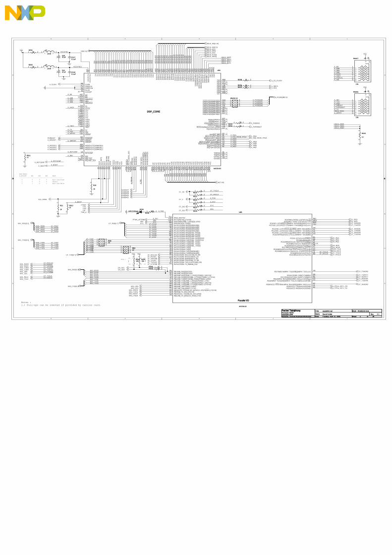
5
5
4
4
3
3
2
2
1
1
D D
C C
B B
A A
A_PSDDQM 2A_PSDDQM 3
A_PSDDQM 0A_PSDDQM 1
UT _RXD0
UT _T XD1UT _T XD1UT _T XD0
A_RST CONF
VCCSYNC1
UT _RXD1UT _RXD2UT _RXD3
UT _T XCLK
M II2_RXD0M II2_RXD1
UT _T XD2UT _T XD2UT _T XD3UT _T XD3
UT _RXCLK
VCCSYNC
A_DBBA_DBGA_ABBA_BR
A_AACK
A_PSDVALA_T BST
A_SRESET
Dh0
Dh1
Dh2
Dh3
Dh4
Dh5
Dh6
Dh7
Dh8
Dh9
Dh1
0D
h11
Dh1
2D
h13
Dh1
4D
h15
Dh1
6D
h17
Dh1
8D
h19
Dh2
0D
h21
Dh2
2D
h23
Dh2
4D
h25
Dh2
6D
h27
Dh2
8D
h29
Dh3
0D
h31
Ah7
Ah8
Ah9
Ah1
0A
h11
Ah1
2A
h13
Ah1
4A
h15
Ah1
6A
h17
Ah1
8A
h19
Ah2
0A
h21
Ah2
2A
h23
Ah2
4A
h25
Ah2
6A
h27
Ah2
8A
h29
A_BOOT
HD
I16_
HD
0H
DI1
6_H
D1
HD
I16_
HD
2H
DI1
6_H
D3
HD
I16_
HD
4H
DI1
6_H
D5
HD
I16_
HD
6H
DI1
6_H
D7
HD
I16_
HD
8H
DI1
6_H
D9
HD
I16_
HD
10H
DI1
6_H
D11
HD
I16_
HD
12H
DI1
6_H
D13
HD
I16_
HD
14H
DI1
6_H
D15
HD
I16_
HA
0H
DI1
6_H
A1
HD
I16_
HA
2H
DI1
6_H
A3
UT _T XD4UT _T XD5UT _T XD6UT _T XD7
UT _RXD4UT _RXD5UT _RXD6UT _RXD7
ST XSRX
A_IRQ3
A_SRESET
A_IRQ1A_IRQ_FROM _FPGAA_IRQ3A_IRQ4A_IRQ5A_IRQ6A_IRQ7
A_PUPM WAIT
HDI16_HDSPHDI16_HDDSHDI16_H8BITHDI16_HCS2
HDI16_HCS2
HDI16_HDSPHDI16_HDDSHDI16_H8BIT
A_T A
A_PA7
A_NM I
A_T EAA_NM I
A_GBL
M II2_T XD0M II2_T XD1M II2_T XD2
A_PA6
M II1_T XD0 UT _T XD7M II1_T XD1 UT _T XD6M II1_T XD2 UT _T XD5M II1_T XD3 UT _T XD4
M II1_RXD0 UT _RXD7M II1_RXD1 UT _RXD6M II1_RXD2 UT _RXD5M II1_RXD3 UT _RXD4
UT _RXCLAVUT _RXSOCUT _nRXENBUT _T XSOCUT _T XCLAVUT _nT XENB
UT _T XCLKUT _RXCLK
A_BR
A_T EAA_ART RY
A_ART RY
A_T A
A_G
BL
A_P
SD
VA
L
A_T BST
A_AACK
A_DBBA_DBGA_ABB
M II2_T XD3
M II2_RXD2M II2_RXD3
A_RST CONF
A_BOOT
UT _T XCLK
UT _RXCLK
A_PA6
A_PA7
ST X
SRX
1V6
3V3 3V3
3V3
3V3
Dh[0:31]
PORESETA_HRESET
nT RSTT CKT M ST DI
T DO_A
UT _RXD[0:7]
UT _T XD[0:7] UT _RXCLAVUT _RXSOCUT _nRXENBUT _T XSOCUT _T XCLAVUT _nT XENB
M II2_RXD[0:3]
M II2_T XD[0:3] M II2_CRSM II2_COL
M II2_RXERM II2_T XENM II2_RXDVM II2_T XER
I2C_SCLI2C_SDA
D1_IRQ1D2_IRQ1
D3_IRQ1D4_IRQ1D5_IRQ1
M II2_T CLKM II2_RCLKUT _T XCLKUT _RXCLK
UT _T XPRT YUT _RXPRT Y
A_PUPM WAIT
A_PSDRAS
A_PSDDQM [0:3]
A_HCSA_HBCS
A_CS_FLASH
A_CLKIN
UT _RXADR2UT _T XADR2
UT _RXADR1UT _T XADR1UT _RXADR0UT _T XADR0
UT _T XADR3
UT _RXADR4UT _T XADR4
UT _RXADR3
Ah[7:29]
HDI16_HD[0:15]
HDI16_HA[0:3]HDI16_HCSHDI16_HRWHDI16_HDSHDI16_HT RQHDI16_HRRQ
A_FPGA_CNT L_SD
M II_M DC
A_M ODCK1A_M ODCK2A_M ODCK3
A_IRQ1A_IRQ_FROM _FPGA
A_IRQ4A_IRQ5A_IRQ6
M II_M DIO
EEx_DONE
PT M C_nPT ENBSRXST XM II1_RXD[0:3]
M II1_T XD[0:3]
M II1_RXERM II1_RXDVM II1_T XENM II1_T XERM II1_CRSM II1_COL
M II1_RCLKM II1_T CLK
BADDR27BADDR28BADDR29BADDR30BADDR31
A_IRQ7
A_FPGA_CNT L_SC
A_RST CONF
A_BOOT
CT _C8
CT _F
CT _D12
CT _D13
Nam e Rev
Date: Sheet of
T i tle Block
2.1
Packet TelelphonyFreescale NCSDCopyright 2005
18T uesday, Apri l 12, 2005
M SC8103 Core
David Kol tak
Freescale General Business Inform ation
8122PFC HV
4
Nam e Rev
Date: Sheet of
T i tle Block
2.1
Packet TelelphonyFreescale NCSDCopyright 2005
18T uesday, Apri l 12, 2005
M SC8103 Core
David Kol tak
Freescale General Business Inform ation
8122PFC HV
4
Nam e Rev
Date: Sheet of
T i tle Block
2.1
Packet TelelphonyFreescale NCSDCopyright 2005
18T uesday, Apri l 12, 2005
M SC8103 Core
David Kol tak
Freescale General Business Inform ation
8122PFC HV
4
Note 1
Notes :1.) Pull-ups can be removed if provided by carrier card.
BOOT MODE:A_RSTCONF EE1 EE4 EE5 MODE--------------------------------------------------- ---- 0 0 0 0 Boot from Flash 1 0 0 0 Default 1 1 0 1 Boot from HDI16
1 2R258 22R258 22
1 2R510
0R510
0
1 2R238
150R238
150
12
R3121kR3121k
1 2R233
22R233
22
1234 5
678
RN522RN522
1 2R512
0R512
0
1 2R262 0R262 0
1 2R234 22R234 22
+ C4047uF
+ C4047uF
1 2R260 0R260 0
12
R3111kR3111k
12
R21
1k
R21
1k
1 2R256 22R256 22
PA6/L1RSYNCT11
PA7/SMSYN/L1TSYNCV10
PA8/SMRXD/NBL L1RXD[0]/L1RXDU10
PA9/SMTXD/L1TXD[0]W9
PA10/UTOPIA8 RXD[0]/MSNUM[5]U9
PA11/UTOPIA8 RXD[1]/MSNUM[4]V8
PA12/UTOPIA8 RXD[2]/MSNUM[3]T9
PA13/UTOPIA8 RXD[3]/MSNUM[2]U8
PA14/UTOPIA8 RXD[4]/NBL RXD[3]W8
PA15/UTOPIA8 RXD[5]/NBL RXD[2]W3
PA16/UTOPIA8 RXD[6]/NBL RXD[1]M7
PA17/UTOPIA8 RXD[7]/NBL RXD[0]/RXDT4
PA18/UTOPIA8 TXD[7]/NBL TXD[0]/TXDW2
PA19/UTOPIA8 TXD[6]/NBL TXD[1]R5
PA20/UTOPIA8 TXD[5]/NBL TXD[2]T3
PA21/UTOPIA8 TXD[4]/NBL_TXD[3]U1
PA23/UTOPIA8 TXD[2]P4
PA24/UTOPIA8 TXD[1]/MSNUM[1]P2
PA25/UTOPIA8 TXD[0]/MSNUM[0]N2
PA26/UTOPIA RXCLAV/MII_RX_ERM6
PA27/UTOPIA RXSOC/MII RX_DVL1
PA28/UTOPIA RXENB/MII TX_ENK1
PA29/UTOPIA TXSOC/MII_TX_ERJ1
PA30/UTOPIA TXCLAV/RTS/MII_CRSJ7
PA31/UTOPIA TX_ENB/MII_COLG1
PB18/MII_RXD[3]/I2CSCLR4
PB19/MII_RXD[2]/I2CSDAU2
PB20/MII_RXD[1]/NBL L1TXD[1]/TDMD2 L1RSYNCP5
PB21/MII_RXD[0]/RXD/NBL L1TXD[2]/TDMD2 L1TSYNCT1
PB22/MII_TXD[0]/TXD/NBL RXD[1]/TDMD2 L1RXDT2
PB23/MII_TXD[1]/NBL L1RXD[2]/TDMD2 L1TXDV1
PB24/MII_TXD[2]/NBL L1RXD[3]/TDMC2 L1RSYNCP3
PB25/MII_TXD[3]/NBL L1TXD[3]/TDMC2 L1TSYNCN3
PB26/MII_CRS/TDMC2 L1RXDM3
PB27/MII_COL/TDMC2 L1TXDM1
PB28/FCC2_RTS/MII_RX_ER/SCC2_RTS/TENA/L1TSYNCL2
PB29/MII_TX_EN/L1RSYNCK4
PB30/SCC2_TXD/MII_RX_DV/L1RXDH1
PB31/MII_TX_ER/SCC2_RXD/L1TXDH4
PC23/CLK9/DACK1N5
PC24/BRG8O/CLK8,TIN3/TOUT4/DREQ2P1
PC25/BRG7O/CLK7,TIN4/DACK2N1
PC26/BRG6O/CLK6/TOUT3/TMCLKM2
PC27/BRG5O/CLK5/TIMER3,4 TGATE2L7
PC28/BRG4O/CLK4/TIN1/TOUT2/SCC2 CTS,CLSNL3
PC29/BRG3O/CLK3,TIN2/SCC1 CTS/SCC1CLSNK3
PC30/BRG2O/CLK2/TOUT1J3
PC31/BRG1O/CLK1/TGATE1H3
PC12/SI1 L1ST3/SCC2 CD,RENA,MPHY RXADDR[1]V4
PC13/SI1 L1ST4/SCC2 CTS,CLSN/MPHY TXADDR[1]T5
PC14/SI1 L1ST2/SCC1 CD,RENA/MPHY RXADDR[0]T6
PC15/SMTXD2/SCC1 CTS,CLSN/MPHY TXADDR[0]V3
PC4/SMC1 RX/SI2 L1ST4/FCC2 CDP10
PC5/SMC1 TX/SI2 L1ST3/FCC2 CTSW10
PC6/SI2 L1ST2/FCC1 CD/MPHY RXADDR[2]/RXCLAV1N10
PC7/SI2 L1ST1/FCC1 CTS/MPHY TXADDR[2]/TXCLAV1T10
PD7/SMSYN/MPHY TXADDR[3]/MPHY TXCLAV2V9
PD16/UTOPIA TXPRTY/SPIMISOU4
PD17/BRG2O/UTOPIA RXPRTY/SPIMOSIN7
PD18/MPHY RXADDR[4]/MPHY RXCLAV3/SPICLKU3
PD19/MPHY TXADDR[4]/MPHY TXCLAV3/BRG1O/SPI SELV2
PD29/SCC1 RTS/TENA/MPHY RXADDR[3]/MPHY RXCLAV2K2
PD30/SCC1 TXD/DACK2/DONE2J2
PD31/SCC1 RXD/DACK1/DONE1H2
PC22/L1ST1/CLK10/DREQ1R1
PA22/UTOPIA8 TXD[3]R3
Parallel I/O
U8B
M SC8103
Parallel I/O
U8B
M SC8103
C3160.1uFC3160.1uF
+ C4147uF
+ C4147uF
C3170.1uFC3170.1uF
12
R26110kR26110k
1 2R257 22R257 22
12
R25910kR25910k
1 2R514
0R514
0
1234 5
678
RN209 22RN209 22
1 2R511
0R511
0
1 2R264
10R264
10
11
22
L6
10nH
L6
10nH 11
22
33
44
55
66
77
88
99
1010RN207
10k
RN207
10k
1234 5
678
RN322RN322
11
22
33
44
55
66
77
88
99
1010RN206
10k
RN206
10k
VC
CS
YN
1T
7V
CC
SY
NW
7GNDSYN
V7
DLLINP8
CLKINN8
BRH17
BGV12
ABB/IRQ2V11
DBGB18
DBB/IRQ3C18
TST13
AACKT12
TT0N13
TT1N12
TT2U14
TT3V14
TT4W14
TSIZ0V13
TSIZ1W13
TSIZ2W12
TSIZ3N11
TBSTU13
BA
DD
R29
/IRQ
2C
19
BA
DD
R30
/IRQ
3H
14
BA
DD
R31
/IRQ
5H
13
GB
L/IR
Q1
D18
TAJ13
TEAG17
ARTRYU12
PORESETW5
HRESETV6
SRESETW4
MODCK1/TC0/BNKSEL0E18
MODCK2/TC1/BNKSEL1F18
MODCK3/TC2/BNKSEL2G18
RSTCONFU6
D0
B3
D1
A3
D2
C4
D3
B4
D4
A4
D5
C5
D6
B5
D7
A5
D8
D6
D9
C6
D10
B6
D11
A6
D12
G7
D13
E7
D14
D7
D15
C7
D16
B7
D17
A7
D18
F8
D19
D8
D20
C8
D21
B8
D22
A8
D23
G9
D24
D9
D25
C9
D26
B9
D27
A9
D28
F10
D29
D10
D30
C10
D31
B10
D32
/H0
A10
D33
/H1
G11
D34
/H2
D11
D35
/H3
C11
D36
/H4
B11
D37
/H5
A11
D38
/H6
F12
D39
/H7
D12
D40
/H8
C12
D41
/H9
B12
D42
/H10
A12
D43
/H11
D13
D44
/H12
C13
D45
/H13
B13
D46
/H14
A13
D47
/H15
E14
D48
/HA
0D
14
D49
/HA
1C
14
D50
/HA
2B
14
D51
/HA
3A
14
D52
/HC
SD
15
D53
/HR
D/H
RW
C15
D54
/HW
R/H
DS
B15
D55
/HT
RQ
/HR
EQ
A15
D56
/HR
RQ
/HA
CK
E16
D57
/HD
SP
D16
D58
/HD
DS
C16
D59
/H8B
ITB
16
D60
/HC
S2
A16
D61
C17
D62
A17
D63
A18
CS0M16
CS1L17
CS2K19
CS3L18
CS4M19
CS5M17
CS6L13
CS7M18
BC
TL1
/DB
G_D
ISL1
9
PWE0/PSDDQM0/PBS0K18
PWE1/PSDDQM1/PBS1K17
PWE2/PSDDQM2/PBS2K14
PWE3/PSDDQM3/PBS3J19
PWE4/PSDDQM4/PBS4H19
PWE5/PSDDQM5/PBS5D17
PWE6/PSDDQM6/PBS6B17
PWE7/PSDDQM7/PBS7F17
PSDA10/PGPL0E17
PSDWE/PGPL1F14
POE/PSDRAS/PGPL2G19
PSDCAS/PGPL3E19
PGTA/PUPMWAIT/PGPL4/PPBSJ18
PSDAMUX/PGPL5J17
BC
TL0
F19
THERM0C1
THERM1D3
SPARE1R2
SPARE5U11
DP0/EXT_BR2C2
IRQ1/DP1/EXT_BG2B1
IRQ2/DP2/EXT_DBG2D4
IRQ3/DP3/EXT_BR3B2
IRQ4/DP4/EXT_BG3/DREQ3C3
IRQ5/DP5/EXT_DBG3/DREQ4A2
IRQ6/DP6/DACK3D5
IRQ7/DP7/DACK4F6
NMI_OUTV5
TR
ST
G3
TC
KG
4
TM
SG
2
TD
IH
6
TD
0F
1
ALE
H18
PS
DV
AL
G13
BA
DD
R27
D19
BA
DD
R28
B19
A0
W15
A1
N14
A2
V15
A3
T14
A4
U15
A5
W16
A6
V16
A7
W17
A8
U16
A9
V17
A10
W18
A11
U17
A12
T16
A13
V18
A14
V19
A15
R16
A16
T17
A17
U18
A18
U19
A19
R17
A20
T18
A21
M13
A22
T19
A23
P17
A24
R18
A25
R19
A26
M14
A27
P18
A28
N17
A29
P19
A30
N18
A31
N19
NMIU5
IRQ7/INT_OUTW11
EE
1/H
PE
D1
EE
2E
3
EE
3E
2
EE
4/B
TM
0E
1
EE
5/B
TM
1F
3
EE
0D
2
CLKOUTT8
EE
DF
2
GNDSYN1U7
DSP_CORE
U8C
M SC8103
DSP_CORE
U8C
M SC8103
1 2R263
10R263
10
1 2R515
0R515
0
12
R229
1k
R229
1k
1 2R513
0R513
0
D200LED (Yel low)
D200LED (Yel low)
11
22
L5
10nH
L5
10nH
12
R19
1k
R19
1k

5
5
4
4
3
3
2
2
1
1
D D
C C
B B
A A
A_TEST
Dh1
Dh3Dh2
Dh7
Dh5Dh4
Dh6
FLASH_BYTE
FLASH_WP
Ah26
Ah24Ah25
Ah17
Ah19
Ah23
Ah20
Ah18
Ah21
Ah16
Ah22
Ah14Ah15
Ah12Ah13
Ah11Ah10Ah9
Dh0
1V6 3V3
3V3
1V6 3V3
3V3
1V6
1V6
3V3
PORESET
A_CS_FLASHA_PSDRAS
A_PSDDQM0
Ah[7:29]
Dh[0:31]
BADDR31
BADDR27BADDR28BADDR29BADDR30
Name RevDate: Sheet of
Title Block
2.1
Packet TelelphonyFreescale NCSDCopyright 2005
18Tuesday, April 12, 2005
MSC8103 Power
David KoltakFreescale General Business Information
8122PFC HV
5
Name RevDate: Sheet of
Title Block
2.1
Packet TelelphonyFreescale NCSDCopyright 2005
18Tuesday, April 12, 2005
MSC8103 Power
David KoltakFreescale General Business Information
8122PFC HV
5
Name RevDate: Sheet of
Title Block
2.1
Packet TelelphonyFreescale NCSDCopyright 2005
18Tuesday, April 12, 2005
MSC8103 Power
David KoltakFreescale General Business Information
8122PFC HV
5
Place caps as closeto MSC8103 aspossible.
GND - 26,46VCC - 37
C2800.01uF
C2800.01uF
A025 A124 A223 A322 A421 A520 A619 A718 A88 A97 A106 A115 A124 A133 A142 A151 A1648 A1717 A1816 A199
D0 29D1 31D2 33D3 35D4 38D5 40D6 42D7 44D8 30D9 32D10 34D11 36D12 39D13 41D14 43A-1/D15 45
A2010
WE11
RESET12
NC1(A21)13
WP/ACC14
RY/BY15
CE26
OE28
BYTE47
U209
AM29LV320DB120
U209
AM29LV320DB120
C3100.01uFC3100.01uF
C2760.1uFC2760.1uF
C2770.01uF
C2770.01uF
C3190.1uFC3190.1uF
C2820.01uFC2820.01uF
12
R201k
R201k
C3080.1uFC308
0.1uF
C3140.1uFC314
0.1uF
12
R4310k
R4310k
C3180.01uFC3180.01uF
C2830.1uF
C2830.1uF
C3150.01uFC315
0.01uF
+ C278
33uF
+ C278
33uF
+ C312
33uF
+ C312
33uF
C3070.1uF
C3070.1uF
+ C311
10uF
+ C311
10uF
C2750.1uFC2750.1uF
12
R53
1k
R53
1k
+ C285
10uF
+ C285
10uFC320
0.1uFC320
0.1uFC3090.1uFC3090.1uF
C3130.01uF
C3130.01uF
VDDH E10
VDDH E11
VDDH E13
VDDH E15
VDDH E4
VDDH E6
VDDH E8
VDDH G15
VDDH G16
VDDH G5
VDDH J15
VDDH J16
VDDH K16
VDDH K5
VDDH M4
VDDH N15
VDDH N16
VDDH R10
VDDH R12
VDDH R14
VDDH R15
VDDH R6
VDDH R7
VDDH R9
VDDH T15
VDDE12
VDDE5
VDDE9
VDDF16
VDDF4
VDDH16
VDDJ4
VDDL16
VDDL4
VDDN4
VDDP16
VDDR11
VDDR13
VDDR8
GNDF11
GNDF13
GNDF15
GNDF5
GNDF7
GNDF9
GNDG10
GNDG12
GNDG14
GNDG6
GNDG8
GNDH15
GNDH5
GNDH7
GNDJ14
GNDJ5
GNDJ6
GNDK13
GNDK15
GNDK6
GNDK7
GNDL14
GNDL15
GNDL5
GNDL6
GNDM15
GNDM5
GNDN6
GNDN9
GNDP11
GNDP12
GNDP13
GNDP14
GNDP15
GNDP6
GNDP7
GNDP9
TEST W6
Power
U8A
MSC8103
Power
U8A
MSC8103
C2810.01uFC2810.01uF

5
5
4
4
3
3
2
2
1
1
D D
C C
B B
A AFPGA_nPROGRAMFPGA_CCLKFPGA_DIN
FPGA_nINIT
D5_HRESETD4_HRESETD3_HRESETD2_HRESETD1_HRESET
T EM P_SC
T EM P_nCS
T EM P_SD
DSP_COUNT 0DSP_COUNT 1
A_HRESETHRESET
PC
I_A
D31
PC
I_A
D30
PC
I_A
D29
PCI_AD28
PCI_AD27PCI_AD26
PCI_AD25
PCI_AD24
PCI_AD23
PCI_AD22
PCI_AD21
PCI_AD20
PCI_AD19
PCI_AD18
PCI_AD17
PCI_AD16
PCI_AD15
PCI_AD14PCI_AD13
PCI_AD12
PCI_AD11
PCI_AD10
PCI_AD9
PCI_AD8
PCI_AD7
PCI_AD6
PCI_AD5
PCI_AD4
PCI_AD3
PCI_AD2
PCI_AD1
PCI_AD0
PCI_CBE3PCI_CBE2PCI_CBE1PCI_CBE0
PCI_CBE3
PCI_CBE2
PCI_CBE1PCI_CBE0
HRESET
A_HRESETD1_HRESETD2_HRESETD3_HRESETD4_HRESETD5_HRESET
FPGA_T P1
FPGA_T P2
FPGA_T P3
FPGA_T P4
A_FPGA_CNT L_SCA_FPGA_CNT L_SD
A_IRQ_FROM _FPGA
FP
GA
_TP
3F
PG
A_T
P2
FP
GA
_TP
1
CT
_C8
CT
_FA
CT
_F
CT
_C8A
DS
P_C
OU
NT
1
DS
P_C
OU
NT
0
HD
I16_
HA
3
HD
I16_
HA
2
HD
I16_
HA
1
HD
I16_
HA
0
HDI16_HA3HDI16_HA2HDI16_HA1HDI16_HA0
HD
I16_
HD
14H
DI1
6_H
D10
HD
I16_
HD
4H
DI1
6_H
D5
HD
I16_
HD
0
HD
I16_
HD
13H
DI1
6_H
D9
HD
I16_
HD
3
HD
I16_
HD
12H
DI1
6_H
D8
HD
I16_
HD
2
HD
I16_
HD
11H
DI1
6_H
D7
HD
I16_
HD
6H
DI1
6_H
D15
HD
I16_
HD
1
A_IRQ_FROM _FPGAD3_HRESETD2_HRESETA_HRESET
D1_HRESET
D5_HRESET
D4_HRESET
M II1_RXD1
M II1_T XD3M II1_T XD2M II1_RXD0M II1_T XD1M II1_T XD0M II1_RXD2M II1_RXD3
MII
2_T
XD
3
MII
2_T
XD
1M
II2_
RX
D2
MII
2_T
XD
0M
II2_
RX
D0
MII
2_R
XD
3M
II2_
TX
D2
MII
2_R
XD
1
TE
MP
_nC
S
TE
MP
_SD
TE
MP
_SC
M II1_T XD3M II1_T XD2
M II1_T XD0
M II1_RXD3M II1_RXD2M II1_RXD1M II1_RXD0
M II1_T XD1
M II2_T XD3M II2_T XD2M II2_T XD1M II2_T XD0
M II2_RXD3M II2_RXD2M II2_RXD1M II2_RXD0
FPGA_DIN
FPGA_CCLK
FPGA_nPROGRAMFPGA_nSER_EN
FPGA_nINIT
FPGA_nSER_EN
FPGA_DONE
FPGA_DONE
T EM P_nCST EM P_SDFPGA_nPROGRAMFPGA_DINFPGA_DONEFPGA_nINIT
CT _C8A
CT _C8
CT _FA
CT _F
D1_
HR
ES
ET
D2_
HR
ES
ET
2V5
3V3
3V3
3V3
3V3
3V3
3V3
3V3
PCI_AD[0:31]
PCI_CBE[0:3]
PC
I_C
LK
PT
MC
_nP
TE
NB
RM
II2_
RE
FC
LK
CM
C_B
US
MO
DE
1C
MC
_BU
SM
OD
E2
CM
C_B
US
MO
DE
3C
MC
_BU
SM
OD
E4
PCI_AD[0:31]P
CI_
nRS
T
PCI_IDSEL
PCI_nDEVSEL
PCI_nST OP
PCI_nIRDY
PCI_nT RDY
PCI_nFRAM E
PCI_nINT A
PCI_nSERR
PCI_nPERR
PCI_PAR
PCI_nREQ
PCI_nGNT
PC
I_R
SV
D61
PC
I_R
SV
D57
PC
I_R
SV
D55
PC
I_R
SV
D34
PC
I_R
SV
D17
PC
I_R
SV
D10
PC
I_R
SV
D9
A_IRQ_FROM _FPGA
A_HRESETD1_HRESETD2_HRESETD3_HRESETD4_HRESETD5_HRESET
HRESET
PC
I_R
SV
D64
A_FPGA_CNT L_SDA_FPGA_CNT L_SC
PC
I_R
SV
D58
PC
I_R
SV
D60
EE
x_D
ON
ECT
_C8
CT
_F
CT
_FB
CT
_FA
CT
_C8B
CT
_C8A
HD
I16_
HR
RQ
HD
I16_
HC
S
HD
I16_
HR
W
HD
I16_
HD
S
HD
I16_
HT
RQ
A_F
PG
A_C
NT
L_S
D
A_F
PG
A_C
NT
L_S
C
HDI16_HA[0:3]
HDI16_HD[0:15]
RM II2_T XD1
RM II2_CRS_DVRM II2_T XD0RM II2_RXD1
RM II2_T XENRM II2_RXERRM II2_RXD0
RM II2_REFCLK
RM II1_RXERRM II1_T XD0RM II1_RXD0
RM II1_REFCLKRM II1_RXDVRM II1_T XENRM II1_T XD1
RM II1_RXD1
M II1_T CLKM II1_COLM II1_CRSM II1_T XER
M II1_RCLKM II1_RXDVM II1_T XENM II1_RXER
PT M C_USER3
PT
MC
_US
ER
2
PT
MC
_US
ER
0P
TM
C_U
SE
R1
MII
2_R
XD
VM
II2_
TX
EN
MII
2_T
XE
R
MII
2_C
OL
MII
2_R
XE
RM
II2_
CR
S
FP
GA
_CLK
IN
M II1_T XD[0:3]
M II1_RXD[0:3]
M II2_T XD[0:3]
M II2_RXD[0:3]
M II2_RCLKM II2_T CLK
RM
II1_
RE
FC
LK
FPGA_DIN
FPGA_CCLK
FPGA_nSER_EN
FPGA_PORESET
A_R
ST
CO
NF
A_B
OO
T
Nam e Rev
Date: Sheet of
T i tle Block
2.1
Packet TelelphonyFreescale NCSDCopyright 2005
18T uesday, Apri l 12, 2005
FPGA
David Kol tak
Freescale General Business Inform ation
8122PFC HV
6
Nam e Rev
Date: Sheet of
T i tle Block
2.1
Packet TelelphonyFreescale NCSDCopyright 2005
18T uesday, Apri l 12, 2005
FPGA
David Kol tak
Freescale General Business Inform ation
8122PFC HV
6
Nam e Rev
Date: Sheet of
T i tle Block
2.1
Packet TelelphonyFreescale NCSDCopyright 2005
18T uesday, Apri l 12, 2005
FPGA
David Kol tak
Freescale General Business Inform ation
8122PFC HV
6
Note 1
Notes :1.) These resistors advertise the number of MSC8122 DSPs populated in the farm. By default, do not populate either of these resistors. The number of DSPS in the farm is equal to the the 2-bit binary number + 1.
2.) The FPGA is configured to be programmed via its slave serial interface and to float its I/O pins until programmed.
3.) PTMC_USER[0:3] must be 5V tolerant FPGA I/O for PDK compatability.
4.) Mount on side 2 to allow probing.
5.) These resistors select the optional functions of A_FGPA_CNTL_x. By default, populate R251 and R250 only.
6.) Manually select CT Bus signals. By default, DNP.
Note 4
Note 4
Note 5
Note 3
Note 3
Note 4
Note 4
Note 2
Note 6
1 2R301
1k
R301
1k
12
R5090R5090
1 T P205T EST POINTT P205T EST POINT
12
R5080R5080
12
R2530R2530
12
C2710.01uFC2710.01uF
1 T P200T EST POINTT P200T EST POINT
12
C3030.01uFC3030.01uF
12
R25110kR25110k
12
C3021uFC3021uF
12
C2730.1uFC2730.1uF
12
R5030R5030
12
C3010.01uFC3010.01uF
TCKC4TDIA15TDOB14TMSD3
M2R3
M1P2
M0N3
DONER14
nPROGRAMP15
CCLKD15
I/O, DIN, D0 (2)D14
I/O, DOUT, BUSY (2)C15
I/O, nCS (1)B13
I/O, nWRITE (1)C13
Vcc
int
C3
Vcc
int
C14
Vcc
int
D4
Vcc
int
D13
Vcc
int
E5
Vcc
int
E12
Vcc
int
M5
Vcc
int
M12
Vcc
int
N4
Vcc
int
N13
Vcc
int
P3
Vcc
int
P14
Vcc
o (0
)E
8
Vcc
o (0
)F
8
Vcc
o (1
)E
9
Vcc
o (1
)F
9
Vcc
o (2
)H
11
Vcc
o (2
)H
12
Vcc
o (3
)J1
1
Vcc
o (3
)J1
2
Vcc
o (4
)L9
Vcc
o (4
)M
9
Vcc
o (5
)L8
Vcc
o (5
)M
8
Vcc
o (6
)J5
Vcc
o (6
)J6
Vcc
o (7
)H
5
Vcc
o (7
)H
6
GN
DA
1
GN
DA
16
GN
DB
2
GN
DB
15
GN
DF
6
GN
DF
7
GN
DF
10
GN
DF
11
GN
DG
6
GN
DG
7
GN
DG
9G
ND
G8
GN
DG
10
GN
DG
11
GN
DH
7
GN
DH
8
GN
DH
9
GN
DH
10
GN
DJ7
GN
DJ8
GN
DJ9
GN
DJ1
0
GN
DK
6
GN
DK
7
GN
DK
8
GN
DK
9
GN
DK
10
GN
DK
11
GN
DL6
GN
DL7
GN
DL1
0
GN
DL1
1
GN
DR
2
GN
DR
15
GN
DT
1
GN
DT
16
(NC
_R4)
R4
(NC
_P4)
P4
I/O, nINIT (3)N15
FPGA POWER and CONFIG
U9B
XC2S50_FG256
FPGA POWER and CONFIG
U9B
XC2S50_FG256
NC11NC33NC99NC1111NC1212NC1313NC1616NC1818NC1919
DATA2
CLK4
WP15
RESET/nOE6
WP27
nCE8
GN
D10
nCEO (A2)14
READY15
nSER_EN17
VC
C20
U300
AT 17LV010-10J
U300
AT 17LV010-10J
12
C2670.01uFC2670.01uF
12
R3091kR3091k
A12
A23
A34
A45
A56
A67
A78
A89
G11
G219
Y118
Y217
Y316
Y415
Y514
Y613
Y712
Y811
VC
C20
GN
D10
U5
74HC541
U5
74HC541
12
C3001uFC3001uF
12
C3040.1uFC3040.1uF
I/O (6_L2)L2
I/O (6_L1)L1
I/O (6_K5)K5
I/O (6_K4)K4
I/O (6_K3)K3
I/O (6_K2)K2
I/O (6_K1)K1
I/O (6_J4)J4
I/O, Vref (6_J3)J3
I/O, TRDY (6)J2
I/O (6_J1)J1
I/O (6_H1)H1
I/O (7_H4)H4
I/O, Vref (7_H3)H3
I/O (7_H2)H2
I/O (7_G5)G5
I/O (7_G4)G4
I/O (7_G3)G3
I/O (7_G2)G2
I/O, IRDY (7)G1
I/O (7_F5)F5
I/O (7_F4)F4
I/O (7_F3)F3
I/O (7_F2)F2
I/O (7_F1)F1
I/O (7_E4)E4
I/O (7_E3)E3
I/O (7_E2)E2
I/O (7_E1)E1
I/O (7_D2)D2
I/O (7_D1)D1
I/O (7_C2)C2
I/O, Vref (7_C1)C1
I/O (7_B1)B1
I/O (7_A2)A2
I/O (6_L3)L3I/O (6_L4)L4I/O (6_L5)L5I/O (6_M1)M1I/O (6_M2)M2I/O (6_M3)M3I/O (6_M4)M4I/O, Vref (6_N1)N1I/O (6_N2)N2I/O (6_P1P1I/O (6_R1)R1
I/O (
0_E
7)E
7
I/O (
0_E
6)E
6
I/O (
0_D
8)D
8
I/O (
0_D
7)D
7
I/O (
0_D
6)D
6
I/O (
0_D
5)D
5
I/O (
0_C
8)C
8
I/O (
0_C
7)C
7
I/O (
0_C
6)C
6
I/O (
0_C
5)C
5
I/O, V
ref (
0_B
7)B
7
I/O (
0_B
6)B
6
I/O (
0_B
5)B
5
I/O, V
ref (
0_B
4)B
4
I/O (
0_B
3)B
3
I/O (
0_A
7)A
7
I/O (
0_A
6)A
6
I/O (
0_A
5)A
5
I/O (
0_A
4)A
4
I/O (
0_A
3)A
3
I, G
CK
3 (0
)B
8I,
GC
K2
(1)
C9
I/O (
1_E
11)
E11
I/O (
1_E
10)
E10
I/O (
1_D
12)
D12
I/O (
1_D
11)
D11
I/O (
1_D
10)
D10
I/O (
1_D
9)D
9
I/O (
1_C
12)
C12
I/O, V
ref (
1_C
11)
C11
I/O (
1_C
10)
C10
I/O (
1_B
12)
B12
I/O (
1_B
11)
B11
I/O (
1_B
10)
B10
I/O, V
ref (
1_B
9)B
9
I/O (
1_A
14)
A14
I/O (
1_A
13)
A13
I/O (
1_A
12)
A12
I/O (
1_A
11)
A11
I/O (
1_A
10)
A10
I/O (
1_A
9)A
9
I/O (
1_A
8)A
8
I/O (3_L15)L15 I/O (3_L16)L16 I/O (3_M13)M13 I/O (3_M14)M14 I/O (3_M15)M15 I/O, D5 (3)M16 I/O, D7 (3)N14 I/O, D6 (3)N16 I/O (3_P16)P16 I/O (3_R16)R16 I/O (3_T15)T15
I/O (2_B16)B16 I/O (2_C16)C16 I/O (2_D16)D16 I/O (2_E13)E13 I/O (2_E14)E14 I/O (2_E15)E15 I/O, D1 (2)E16 I/O (2_F12)F12 I/O, Vref (2_F13)F13 I/O (2_F14)F14 I/O, D2 (2)F15 I/O (2_F16)F16 I/O (2_G12)G12 I/O (2_G13)G13 I/O (2_G14)G14 I/O (2_G15)G15 I/O, D3 (2)G16 I/O, Vref (2_h13)H13 I/O (2H14)H14 I/O (2_H15)H15 I/O, IRDY (2)H16 I/O (2_J13)J13
I/O (3_J14)J14 I/O, TRDY (3)J15 I/O, D4 (3)J16 I/O (3_K12)K12 I/O (3_K13)K13 I/O (3_K14)K14 I/O (3_K15)K15 I/O, Vref (3_K16)K16 I/O (3_L12)L12 I/O (3_L13)L13 I/O, Vref (3_L14)L14
I/O (
5_M
6)M
6I/O
(5_
M7)
M7
I/O (
5_N
5)N
5I/O
(5_
N6)
N6
I/O (
5_N
7)N
7I/O
(5_
P5)
P5
I/O (
5_P
6)P
6I/O
(5_
P7)
P7
I/O, V
ref (
5_P
8)P
8I/O
(5_
R5)
R5
I/O (
5_R
6)R
6I/O
(5_
R7)
R7
I/O (
5_T
2)T
2I/O
(5_
T3)
T3
I/O, V
ref (
5_T
4)T
4I/O
(5_
T5)
T5
I/O (
5_T
6)T
6I/O
(5_
T7)
T7
I/O (
5_T
8)T
8
I, G
CK
1 (5
)R
8I,
GC
K0
(4)
N8
I/O (
4_M
10)
M10
I/O (
4_M
11)
M11
I/O (
4_N
9)N
9I/O
(4_
N10
)N
10I/O
(4_
N11
)N
11I/O
(4_
N12
)N
12
I/O, V
ref (
4_P
9)P
9I/O
(4_
P10
)P
10I/O
(4_
P11
)P
11I/O
(4_
P12
)P
12I/O
(4_
P13
)P
13
I/O (
4_R
9)R
9I/O
(4_
R10
)R
10I/O
(4_
R11
)R
11I/O
(4_
R12
)R
12I/O
(4_
R13
)R
13
I/O (
4_T
9)T
9I/O
(4_
T10
)T
10I/O
(4_
T11
)T
11I/O
, Vre
f (4_
T12
)T
12I/O
(4_
T13
)T
13I/O
(4_
T14
)T
14
FPGA I/O
U9A
XC2S50_FG256
FPGA I/O
U9A
XC2S50_FG256
12
R2520R2520
12
C3051uFC3051uF
12
R2540R2540
1 T P203T EST POINTT P203T EST POINT
12
C5011uFC5011uF
12
R25010kR25010k
12
C2690.1uFC2690.1uF
12
C2680.01uFC2680.01uF
12
C2721uFC2721uF
GN
D4
V8
CS7
SC2
SD1
NC13
NC25
NC36
U213
LM 74
U213
LM 74
12
R2550R2550
12
C2660.1uFC2660.1uF
1 T P204T EST POINTT P204T EST POINT
12
R3021kR3021k
11
22
33
44
55
66
77
88
99
1010RN205
10k
RN205
10k
11
22
33
44
55
66
77
88
99
1010RN208
10k
RN208
10k
12
C2740.01uFC2740.01uF
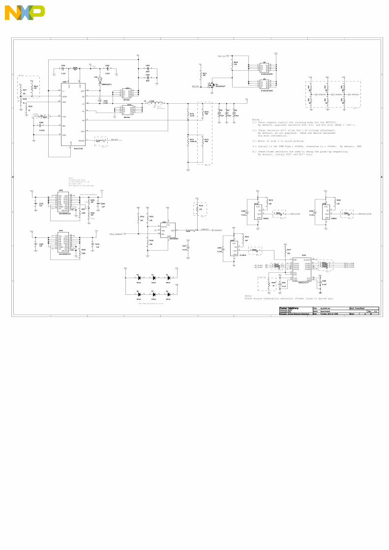
5
5
4
4
3
3
2
2
1
1
D D
C C
B B
A A
PORESET
SW_3V3
SW_3V3
5V
1V2
3V31V6
5V
3V3 2V5
1V6
3V3
3V3 1V6
1V23V3
5V
3V3
3V3
3V3
3V33V3
3V3
3V3 3V3 3V3
3V3 3V3
5V
3V3
3V3
D3_CLKIND4_CLKIND5_CLKIN
D1_CLKIND2_CLKIN
PORESET
A_M ODCK1 A_M ODCK2 A_M ODCK3
A_CLKIN FPGA_CLKIN
FPGA_PORESET
PM C_3V3
Nam e Rev
Date: Sheet of
T i tle Block
2.1
Packet TelelphonyFreescale NCSDCopyright 2005
18T uesday, Apri l 12, 2005
Power/Reset
David Kol tak
Freescale General Business Inform ation
8122PFC HV
7
Nam e Rev
Date: Sheet of
T i tle Block
2.1
Packet TelelphonyFreescale NCSDCopyright 2005
18T uesday, Apri l 12, 2005
Power/Reset
David Kol tak
Freescale General Business Inform ation
8122PFC HV
7
Nam e Rev
Date: Sheet of
T i tle Block
2.1
Packet TelelphonyFreescale NCSDCopyright 2005
18T uesday, Apri l 12, 2005
Power/Reset
David Kol tak
Freescale General Business Inform ation
8122PFC HV
7
BiasSupply
Host Power-Up protection circuit
pin3:mechanical
DNP
Notes:1A guartanteed output-2% Vout deviation at 1.5A4A current limitBulk caps are on 8103 power page
VOUT=0.8V(1+Rup/Rdown)
Rup
Rdown
Do Not Fit
Note:Place Source termination resistors (33ohm) close to driver pin.
Note 1
Notes :1.) These signals control the clocking mode for the MSC8103. By default, populate resistors R30, R31, and R33 only (MODE = '001').
2.) These resistors will allow the 1.2V voltage adjustment. By default, do not populate. Read the device datasheet for more information.
3.) Mount on side 2 to allow probing.
4.) Install to set PWM Freq = 600kHz, otherwise is = 300kHz. By default, DNP.
5.) These three resistors are used to setup the power-up sequencing. By default, install R247 and R277 only.
Note 2
Note 3
Note 3Note 3
Note 3
Note 3Note 3
Note 4
Note 5
Note 5
REF1
CLKA12
CLKA23
GND5
CLKB310
VCC4
CLKB27
CLKOUT16
CLKA314
CLKA415
CLKB16
CLKB411
GND12VCC13
FS19
FS28
U206
ICS9112-17-F
U206
ICS9112-17-F
12 R21133
R21133
12
C270
1uF
C270
1uF
12
R33
1kR
331k
OUT3
GND
2
VCC
4
OE1
U200
50M Hz
U200
50M Hz
12
+C56
470uF
+C56
470uF
S11
S22
S33
G4
D45D36D27D18
Q3
NT M S10P02R2
Q3
NT M S10P02R2
12
C291
0.1uF
C291
0.1uF
1 2R215 0R215 0
1 2
D3
GF1A
D3
GF1A
12 R21933
R21933
12
C296
0.1uF
C296
0.1uF
12
R217
10k
R217
10k
12
C200
0.1uF
C200
0.1uF
12
R2751k 1%R2751k 1%
12
R247
10k
R247
10k
NC11
IN12
IN23
IN34
IN45
RST6
SHDN7
SS8
NC39GND10SET11OUT412OUT313OUT214OUT115NC216
DIE PADTAB
U205
M AX8869EU18
U205
M AX8869EU18
12
R223
10k
R223
10k
OUT3
GND
2
VCC
4
OE1
U214
50M Hz
U214
50M Hz
12
R202
10k
R202
10k
1 2
D7
GF1A
D7
GF1A
12
C2791uFC2791uF
1 2
D2
GF1A
D2
GF1A
12
R237
100k
R237
100k
12
C306
0.1uF
C306
0.1uF
12
R34
10k
R34
10k
12
R51910kR51910k
1 2
C298
0.22uF
C298
0.22uF
1 2
D6
GF1A
D6
GF1A
12
R32
10k
R32
10k
12
R23510kR23510k
12
C227
0.1uF
C227
0.1uF
12
R29
1kR
291k
12
R230
10k
R230
10k
12
R231
10k
R231
10k
1 2
D4
GF1A
D4
GF1A
12
R51610kR51610k
S11
S22
S33
G4
D45D36D27D18
Q2
NT M S10P02R2
Q2
NT M S10P02R2
12 R23933
R23933
12
R278
10k
R278
10k
12
C2251uFC2251uF
Q12N7002/SOTQ12N7002/SOT
12
R27310MR27310M
12
C286
0.1uF
C286
0.1uF
12
R216
10k
R216
10k
12
R228
100k
R228
100k
12 R27933
R27933
12 R22133
R22133
1 2R277 0R277 0
12
+C57
470uF
+C57
470uF
11
223
3
L8 1.0uHL8 1.0uH
NC11
IN12
IN23
IN34
IN45
RST6
SHDN7
SS8
NC39GND10SET11OUT412OUT313OUT214OUT115NC216
DIE PADTAB
U204
M AX8869EU25
U204
M AX8869EU25
S11
S22
S33
G4
D45D36D27D18
U212
IRF7831
U212
IRF7831
1 2+
C343
10uF
+
C343
10uF
12
R23610kR23610k
12
R214
10k
R214
10k
12
R248
1k
R248
1k
12
R2744.99k 1%R2744.99k 1%
12 R24233
R24233
12
R27610MR27610M
1 2+
C342
3.3uF
+
C342
3.3uF
VD
D10
VC
C11
V+13
SHDN2
SKIP14
TON12
REF6
GND8
ILIM
5
PGOOD7
OUT4
FB3
DL9
LX16
DH1
BST15
U208
M AX1714B
U208
M AX1714B
1 2R518
0R518
0
1 2R24922
R24922
12 R24333
R24333
12
R31
1kR
311k
RST1
GND
2
MR3
WDI4
RST IN5 VCC
6U201
M AX6828S
U201
M AX6828S
12 +
C341
4.7uF
+
C341
4.7uF
12
R246
1k
R246
1k
12
R30
10k
R30
10k
S11
S22
S33
G4
D45D36D27D18
U211
IRF7831
U211
IRF7831
12
R51710kR51710k
12
+C58
470uF
+C58
470uF
12
C2990.1uFC2990.1uF
12
C284
1uF
C284
1uF
1 2+
C344
10uF
+
C344
10uF
12 R22033
R22033
1 2
D1
GF1A
D1
GF1A
12
R218
1k
R218
1k
A1
C2
U10
M BRS340T 3
U10
M BRS340T 3
OUT3
GND
2
VCC
4
OE1
U207
44.3M Hz
U207
44.3M Hz
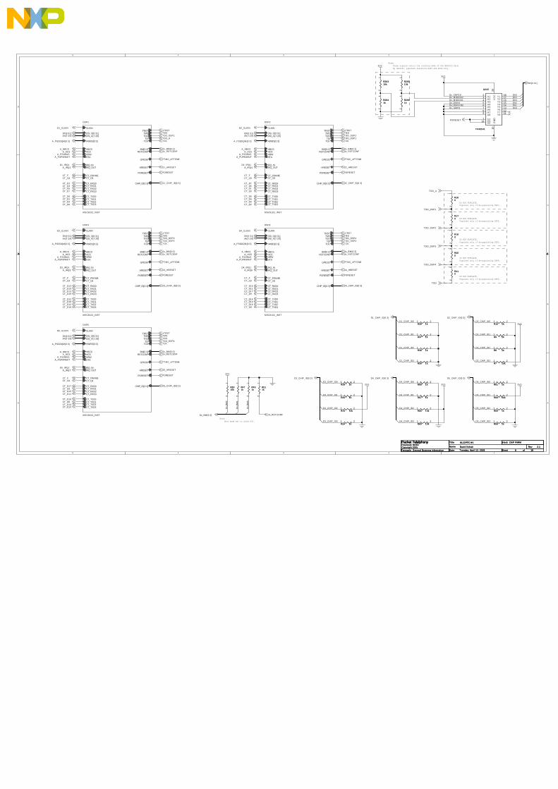
5
5
4
4
3
3
2
2
1
1
D D
C C
B B
A A
D1_CHIP_ID2
D1_CHIP_ID0
D1_CHIP_ID1
D2_CHIP_ID2
D2_CHIP_ID0
D2_CHIP_ID1
D4_CHIP_ID2
D4_CHIP_ID0
D4_CHIP_ID1
D5_CHIP_ID2
D5_CHIP_ID0
D5_CHIP_ID1
D3_CHIP_ID2
D3_CHIP_ID0
D3_CHIP_ID1
D3_CHIP_ID3 D4_CHIP_ID3 D5_CHIP_ID3
D2_CHIP_ID3D1_CHIP_ID3
Dx_
BM
0
Dx_
BM
1
Dx_
BM
2
Dh5Dh4Dh3Dh2Dh1Dh0
Dx_M ODCK2Dx_M ODCK1
Dx_CNFGS
Dx_DSI64Dx_DSISYNCDx_SWT E
3V3
3V33V33V3
3V3
3V3
3V3
D1_CLKIN D2_CLKIN
D4_CLKIND3_CLKIN
D5_CLKIN
Dh[0:31] Dh[0:31]
Dh[0:31]Dh[0:31]
Dh[0:31]
CT _FCT _C8
CT _FCT _C8
CT _FCT _C8
CT _FCT _C8
CT _FCT _C8
T CK T CK
T CKT CK
T CK
nT RSTT M S
nT RSTT M S
nT RSTT M S
nT RSTT M S
nT RSTT M S
T DO_DSP1T DO_A
T DO_DSP2T DO_DSP1
T DO_DSP3T DO_DSP2
T DO_DSP4T DO_DSP3
T DOT DO_DSP4
D1_CHIP_ID[0:3] D2_CHIP_ID[0:3]
D3_CHIP_ID[0:3] D4_CHIP_ID[0:3]
D5_CHIP_ID[0:3]
D1_CHIP_ID[0:3] D2_CHIP_ID[0:3]
D5_CHIP_ID[0:3]D4_CHIP_ID[0:3]D3_CHIP_ID[0:3]
A_HBCSA_HCS
A_PSDRAS
A_PSDDQM [0:3]
A_PUPM WAIT
A_PUPM WAIT
A_HBCSA_HCS
A_PSDRAS
A_PSDDQM [0:3]
A_PUPM WAIT
A_HBCSA_HCS
A_PSDRAS
A_PSDDQM [0:3]
A_PUPM WAIT
A_HBCSA_HCS
A_PSDRAS
A_PSDDQM [0:3]
A_PUPM WAIT
A_HBCSA_HCS
A_PSDRAS
A_PSDDQM [0:3]
A_IRQ5 A_IRQ6
A_IRQ7
A_IRQ1 A_IRQ4
D5_HRESET
PORESET
PORESET
D4_HRESET
PORESET
D3_HRESET
PORESET
D1_HRESET
PORESET
D2_HRESET
Dx_RST CONFDx_BM [0:2]
Dx_RST CONFDx_BM [0:2]
Dx_RST CONFDx_BM [0:2]
Dx_RST CONFDx_BM [0:2]
D1_IRQ1 D2_IRQ1
D4_IRQ1D3_IRQ1
D5_IRQ1
Dx_RST CONFDx_BM [0:2]
PT M C_nPT ENB PT M C_nPT ENB
PT M C_nPT ENBPT M C_nPT ENB
PT M C_nPT ENB
Dx_BM [0:2] Dx_RST CONF
PORESET
CT _D1CT _D3CT _D5
CT _D0CT _D2CT _D4
CT _D7CT _D5CT _D1
CT _D6CT _D4CT _D0
CT _D13CT _D19
CT _D12CT _D18
CT _D15
CT _D14
CT _D17
CT _D16
T DO_DSP3
T DO_DSP4
T DO
T DO_A
T DO_DSP1
T DO_DSP2
CT _D9
CT _D8
CT _D11
CT _D10
Dh[0:31]
Ah[7:29] Ah[7:29]
Ah[7:29]Ah[7:29]
Ah[7:29]
CT _D13CT _D19
CT _D12CT _D18
CT _D17CT _D9
CT _D16CT _D8
CT _D15CT _D11
CT _D14CT _D10
CT _D2
CT _D3CT _D7
CT _D6
Nam e Rev
Date: Sheet of
T i tle Block
2.1
Packet TelelphonyFreescale NCSDCopyright 2005
18T uesday, Apri l 12, 2005
DSP FARM
David Kol tak
Freescale General Business Inform ation
8122PFC HV
8
Nam e Rev
Date: Sheet of
T i tle Block
2.1
Packet TelelphonyFreescale NCSDCopyright 2005
18T uesday, Apri l 12, 2005
DSP FARM
David Kol tak
Freescale General Business Inform ation
8122PFC HV
8
Nam e Rev
Date: Sheet of
T i tle Block
2.1
Packet TelelphonyFreescale NCSDCopyright 2005
18T uesday, Apri l 12, 2005
DSP FARM
David Kol tak
Freescale General Business Inform ation
8122PFC HV
8
Note: These signals conrol the clocking mode of the M SC8122 Farm. By default, populate resistors R283 and R266 on ly.
Note: Boot mode set to slave DSI.
DO NOT POPULATE.Populate only if de-populating DSP2.
DO NOT POPULATE.Populate only if de-populating DSP3.
DO NOT POPULATE.Populate only if de-populating DSP4.
DO NOT POPULATE.Populate only if de-populating DSP5.
DO NOT POPULATE.Populate only if de-populating DSP1.
1 2R36 1kR36 1k
12
R160R160
1 2R24 1kR24 1k
1 2R25 10kR25 10k
1 2R59 1kR59 1k
DSP4
M SC8102_INST
DSI_D[0:31]
CLKIN
HBCSHCSHRWHTA
BM[0:2]
TCK
TDOTDI
TRSTTMS
RSTCONF
HRESET
PORESETCT_FRAMECT_C8
GPIO30
CHIP_ID[0:3]
IRQ_INIRQ_OUT
HWBS[0:3]
CT_TXD0CT_TXD1CT_TXD2
CT_RXD0
CT_TXD3
CT_RXD1CT_RXD2CT_RXD3
DSI_A[7:29]
12
R511kR511k
12
R170R170
1 2R65 10kR65 10k
1 2R39 1kR39 1k
12
R2661kR2661k
12
R5010kR5010k
12
R471kR471k
12
R491kR491k
12
R180R180
1 2R37 1kR37 1k
1 2R58 1kR58 1k
A12
A23
A34
A45
A56
A67
A78
A89
G11
G219
Y118
Y217
Y316
Y415
Y514
Y613
Y712
Y811
VC
C20
GN
D10
U215
74HC541
U215
74HC541
DSP1
M SC8102_INST
DSI_D[0:31]
CLKIN
HBCSHCSHRWHTA
BM[0:2]
TCK
TDOTDI
TRSTTMS
RSTCONF
HRESET
PORESETCT_FRAMECT_C8
GPIO30
CHIP_ID[0:3]
IRQ_INIRQ_OUT
HWBS[0:3]
CT_TXD0CT_TXD1CT_TXD2
CT_RXD0
CT_TXD3
CT_RXD1CT_RXD2CT_RXD3
DSI_A[7:29]
1 2R38 1kR38 1k
12
R2841kR2841k
12
R400R400
1 2R10 1kR10 1k
DSP3
M SC8102_INST
DSI_D[0:31]
CLKIN
HBCSHCSHRWHTA
BM[0:2]
TCK
TDOTDI
TRSTTMS
RSTCONF
HRESET
PORESETCT_FRAMECT_C8
GPIO30
CHIP_ID[0:3]
IRQ_INIRQ_OUT
HWBS[0:3]
CT_TXD0CT_TXD1CT_TXD2
CT_RXD0
CT_TXD3
CT_RXD1CT_RXD2CT_RXD3
DSI_A[7:29]
1 2R67 1kR67 1k
1 2R7 10kR7 10k
12
R410R410
1 2R9 1kR9 1k
1 2R68 1kR68 1k
12
R26510kR26510k
1 2R60 10kR60 10k
DSP5
M SC8102_INST
DSI_D[0:31]
CLKIN
HBCSHCSHRWHTA
BM[0:2]
TCK
TDOTDI
TRSTTMS
RSTCONF
HRESET
PORESETCT_FRAMECT_C8
GPIO30
CHIP_ID[0:3]
IRQ_INIRQ_OUT
HWBS[0:3]
CT_TXD0CT_TXD1CT_TXD2
CT_RXD0
CT_TXD3
CT_RXD1CT_RXD2CT_RXD3
DSI_A[7:29]
1 2R66 10kR66 10k
1 2R61 1kR61 1k
12
R28310kR28310k
1 2R26 1kR26 1k
1 2R8 1kR8 1k
DSP2
M SC8102_INST
DSI_D[0:31]
CLKIN
HBCSHCSHRWHTA
BM[0:2]
TCK
TDOTDI
TRSTTMS
RSTCONF
HRESET
PORESETCT_FRAMECT_C8
GPIO30
CHIP_ID[0:3]
IRQ_INIRQ_OUT
HWBS[0:3]
CT_TXD0CT_TXD1CT_TXD2
CT_RXD0
CT_TXD3
CT_RXD1CT_RXD2CT_RXD3
DSI_A[7:29]
1 2R28 1kR28 1k

5
5
4
4
3
3
2
2
1
1
D D
C C
B B
A A
HT A
HWBS1
HWBS3HWBS2
HWBS0
HWBS[0:3]
IRQ6
IRQ3
T DI
IRQ7
T M S
RST CONF
T CK
IRQ4
T RST
T DO
IRQ_OUT
DLLIN
IRQ5
IRQ2
CLKOUT
CLKIN
EE0
HRESET
PORESET
T EST
D30
D21
D26
D23
D24
D19
D31
D25
D27
D20
D22
D28
D18
D29
D0
D10
D17
D11
D12
D4
D5
D1
D2
D8
D6
D16
D9
D7
D3
D14
D15
D13
BM 0
BM [0:2]
BM 1BM 2
A20
A23
A27
A22
A25
A21
A26
A28
A24
DSI_D29
DSI_A29
DSI_D14
DSI_D2
DSI_D27
DSI_A26
DSI_A23
DSI_A11
DSI_D10
DSI_D23
DSI_A17
DSI_D22
DSI_A12
DSI_A16
DSI_D0
DS
I_A
10
DSI_D16
DSI_D28
DS
I_A
8
DSI_D11
DSI_A19
DSI_D1
DSI_D15
DSI_D17 DSI_A22
DSI_D[0:31]
DSI_D9DSI_D8
DSI_A25
DS
I_A
7
DSI_D31
DSI_D7
DSI_D26
DSI_D4
DSI_A13
DSI_A20
DSI_A14
DSI_D13
DSI_D20
DSI_D5
DSI_A15
DSI_D19
DSI_A28DSI_D24
DSI_D12
DSI_A27
DSI_D6
DSI_D25
DS
I_A
9
DSI_A21
DSI_A24DSI_D18
DSI_D3
DSI_D21
A17
A16
CT _RXD3
CT _T XD3
CT _RXD0
CT _RXD2
CT _FRAM E
CT _C8
CT _T XD2
CT _T XD1
CT _RXD1
CT _T XD0
GPIO30
DSI_A[7:29]
DSI_A[7:29]
DSI_D[0:31]
DSI_A[7:29]
CLKIN
HCSHBCS
HRW
HBCS
HCS
HT A
HRW
HWBS[0:3]
IRQ_OUT
T CK
T DI
T DO
T RST
T M S
RST CONF
HRESET
PORESET
CT _FRAM E
CT _C8
GPIO30
CHIP_ID[0:3]
CHIP_ID3CHIP_ID2CHIP_ID1CHIP_ID0
CHIP_ID[0:3]
DSI_D30
DSI_A18
CT _RXD[0:3]
CT _T XD[0:3]
BM [0:2]
IRQ_IN
IRQ_IN
CT _RXD[0:3]
CT _T XD[0:3]
CT _RXD0CT _RXD1CT _RXD2CT _RXD3
CT _T XD0CT _T XD1CT _T XD2CT _T XD3
D32
D33
D34
D35
D36
D37
D38
D39
D40
D41
D42
D43
D44
D45
D46
D47
D48
D49
D50
D51
D52
D53
D54
D55
D56
D57
D58
D59
D60
D61
D62
D63
DQM _S5
DQM _S7DQM _S6
DQM _S3DQM _S2DQM _S1DQM _S0
DQM _S5DQM _S5DQM _S5DQM _S4
A19
A15
IRQ1
DSI_D[0:31]
DSI_A[7:29]
CLKIN
IRQ_IN
HBCS
HCS
HRW
HT A
HWBS[0:3]
IRQ_OUT
T DO
T DI
T RST
T M S
RST CONF
HRESET
PORESET
CT _FRAM E
CT _C8
GPIO30
CHIP_ID[0:3]
CT _RXD0
CT _T XD0
T CK
BM [0:2]
CT _RXD1CT _RXD2CT _RXD3
CT _T XD1CT _T XD2CT _T XD3
D[0:63]
IRQ[1:7]
NM I
DQM _S[0:7]
GPL_RASGPL_SDA10
GPL_CAS
GPL_PSDWE
SDRM CS
SRAM _CLKIN
HBRSTHBCSHCSHT AHRW
SRESET
A[15:17]
A[19:28]
BR
T AT EA
AR
TR
Y
DBGDBB
IRQ_OUTGBL
T BST
PSDVAL
AB
BA
AC
K
EE1
Nam e Rev
Date: Sheet of
T i tle Block
2.1
Packet TelelphonyFreescale NCSDCopyright 2005
18T uesday, Apri l 12, 2005
DSP1 FARM CORE
David Kol tak
Freescale General Business Inform ation
M SC8122PFC HV
9
Nam e Rev
Date: Sheet of
T i tle Block
2.1
Packet TelelphonyFreescale NCSDCopyright 2005
18T uesday, Apri l 12, 2005
DSP1 FARM CORE
David Kol tak
Freescale General Business Inform ation
M SC8122PFC HV
9
Nam e Rev
Date: Sheet of
T i tle Block
2.1
Packet TelelphonyFreescale NCSDCopyright 2005
18T uesday, Apri l 12, 2005
DSP1 FARM CORE
David Kol tak
Freescale General Business Inform ation
M SC8122PFC HV
9
B
N
8
Bottom View
P
1972
L
165
M
4
J
18
K
173 14
G
1511
W
H
13
E
12
U
F
9
V
C
10
R
D
6
T
20 21 22
Y
A A
A B
FCPBGA20x20 431pins
Note 1
Note 1
Notes:1.) Mount on side 2 to allow probing.
BGN16
BRP16
A0
AA
20
A1
AB
21
A2
AA
21
A3
AA
22
A4
Y21
A5
Y22
A6
W22
A7
W21
A8
V19
A9
V20
A10
V21
A11
V22
A12
U21
A13
U22
A14
T22
A15
T21
A16
R22
A17
R20
A18
R21
A19
P22
A20
N22
A21
M22
A22
L22
A23
N21
A24
M21
A25
L21
A26
K20
A27
L20
A28
K22
A29
K21
A30
J22
A31
H22
CLKINJ10
BA
DD
R31
/IRQ
3G
10B
AD
DR
30/IR
Q2
K8
BA
DD
R29
/IRQ
5L8
BA
DD
R28
L7B
AD
DR
27J8
AR
TR
YH
11
ALE
K17
DBB/IRQ5H13
DP1/DACK1/EXT_BG2/IRQ1T18 DP0/DREQ1/EXT_BR2P19
DBGJ12
GBL/IRQ1R10
EE1D4 EE0D3
DP7/DREQ4/IRQ7R15 DP6/DREQ3/IRQ6R16 DP5/DACK4/EXT_DBG3/IRQ5T16 DP4/DACK3/EXT_BG3/IRQ4T17
AB
B/IR
Q4
G12
DP3/DREQ2/EXT_BR3/IRQ3R17 DP2/DACK2/EXT_DBG2/IRQ2R19
AA
CK
H12
TDOC4
TEAP17
TMSE4
TRSTE3
D0
V5
D1
V6
D2
U5
D3
U6
D4
V7
D5
V8
D6
U7
D7
V9
D8
U8
D9
U9
D10
V10
D11
U10
D12
V11
D13
V12
D14
U11
D15
U12
D16
T12
D17
U13
D18
V13
D19
U14
D20
V14
D21
T14
D22
U15
D23
T15
D24
V16
D25
U16
D26
U17
D27
V17
D28
U18
D29
V18
D30
T19
D31
U19
HD
_D32
W18
HD
_D33
W16
HD
_D34
Y19
HD
_D35
AA
19
HD
_D36
AB
20
HD
_D37
Y18
HD
_D38
AA
18
HD
_D39
AB
19
HD
_D40
W14
HD
_D41
AB
18
HD
_D42
AA
17
HD
_D43
Y14
HD
_D44
AB
17
HD
_D45
AB
16
HD
_D46
AA
15
HD
_D47
AB
15
HD
_D48
AB
14
HD
_D49
AB
13
HD
_D50
AB
12
HD
_D51
Y11
HD
_D52
AA
11
HD
_D53
AB
11
HD
_D54
AA
10
HD
_D55
AB
10
HD
_D56
AB
9
HD
_D57
AB
8
HD
_D58
Y8
HD
_D59
AA
7
HD
_D60
Y7
HD
_D61
AB
7
HD
_D62
AB
6
HD
_D63
AA
6
INT_OUT/IRQ7G14
PGTA/PPBS/PUPMWAIT/PGPL4H8
POE/PSDRAS/PGPL2K7
PSDA10/PGPL0J17
PSDAMUX/PGPL5J7
PSDCAS/PGPL3H7
PSDVALP18
PSDWE/PGPL1N19
TCKE2
TDID2
TAP15
TBSTT10
TSR18
TSIZ0T8
TSIZ1R8
TSIZ2T9
TSIZ3R9
CS
0N
18C
S1
G17
CS
2K
18C
S3
L18
CS
4H
17
CLKOUTK14
RSTCONFF3
SRESETC5
HRESETE5
CS
5/T
T2
K16
CS
6/T
T3
J16
CS
7/T
T4
H16
TT
0R
14T
T1
T13
PORESETF2
TESTH6
PWE0/PSDDQM0/PBS0G7
PWE1/PSDDQM1/PBS1K6
PWE2/PSDDQM2/PBS2N6
PWE3/PSDDQM3/PBS3K5
PWE4/PSDDQM4/PBS4/HWBS4/HDBS4R7
PWE5/PSDDQM5/PBS5/HWBS5/HDBS5T7
PWE6/PSDDQM6/PBS6/HWBS6/HDBS6R6
PWE7/PSDDQM7/PBS7/HWBS7/HDBS7T6
BCTL0G18
BCTL1/CS5J18
BNKSEL0/BM0/TC0G11
BNKSEL1/BM1/TC1H10
BNKSEL2/BM2/TC2J11
NMIF4
DLLINK9
NMI_OUTB6
ETHRX_CLK/ETHSYNC_INF15
ETHCRS/ETHRXDG15
ETHTX_CLK/ETHSYNC_INF16
GPIO25/IRQ15/TDM0RCLKJ21
GPIO26/TDM0RDATN20
GPIO24/IRQ14/TDM0RSYNH18
GPIO22/DRACK2/DONE2/TDM0TCLKG22
GPIO23/IRQ13/TDM0TDATJ19
GPIO21/TDM0TSYNH19
GPIO19/DACK2/TDM1RCLKF22
GPIO20/TDM1RDATF17
GPIO18/DREQ2/TDM1RSYNF18
GPIO16/DRACK1/DONE1/TDM1TCLKF19
GPIO17/DACK1/TDM1TDATG21
GPIO15/DREQ1/TDM1TSYNG19
GPIO13/IRQ11/TDM2RCLK/ETHMDCE20
GPIO14/IRQ12/TDM2RDATETHRXD0F21
GPIO12/IRQ10/TDM2RSYN/ETHRXD1/ETHSYNCE22
GPIO10/IRQ8/TDM2TCLK/ETHRX_DV/ETH_CRS_DVE21
GPIO11/IRQ9/TDM2TDAT/ETHRX_ER/ETHTXDF20
GPIO9/IRQ7/TDM2TSYN/ETHMDIOE19
GPIO7/IRQ5/TDM3RCLK/ETHTXD3C19
GPIO8/IRQ6/TDM3RDAT/ETHCOLD22
GPIO6/IRQ4/TDM3RSYN/ETHRXD2C22
GPIO4/IRQ2/TDM3TCLK/ETHTX_ERD19
GPIO5/IRQ3/TDM3TDAT/ETHRXD3C21
GPIO3/IRQ1/TDM3TSYN/ETHTXD2C20
GPIO30/TIMER2/TMCLK/SDAC16
GPIO31/TIMER3/SCLD16
GPIO27/URXDE6
GPIO28/UTXDC6
U7A
MSC8122SYSTEM
U7A
MSC8122SYSTEM
12R240 0R240 0
12R13 1kR13 1k
12R42 0R42 0
12R268 33R268 33
1 2R46
22R46
22
12 R151kR151k
12
R2670R267012R241 0R241 0
HR
/WN
15
HT
AH
14
HW
BS
0/H
DB
S0
N8
HW
BS
1/H
DB
S1
P8
HW
BS
2/H
DB
S2
P7
HW
BS
3/H
DB
S3
P6
HA17G6HA18J2HA19H5HA20H2HA21K3HA22F6HA23G5HA24G2HA25G4HA26J3HA27G3HA28H3HA29F5
HB
CS
N9
HA11L4HA12L2HA13J5HA14L3HA15K2HA16K4
HD0/SWTET5 HD1/DSISYNCT4 HD2/DSI64U4 HD3/MODCK1V2 HD4/MODCK2W4 HD5/CNFGSW3 HD6W2 HD7Y2 HD8
AB5 HD9Y5 HD10
AA5 HD11AB4 HD12AA4 HD13AB3 HD14AA3 HD15
Y3 HD16U2 HD17T2 HD18R2 HD19U3 HD20P2 HD21T3 HD22R5 HD23P5 HD24N5 HD25P4 HD26N2 HD27P3 HD28M2 HD29N4 HD30N3 HD31M3
HC
SN
17
HC
LKIN
P9
HB
RS
TM
16
HD
ST
0W
11
HD
ST
1W
10
HC
ID0
E7
HC
ID1
C7
HC
ID2
D7
HC
ID3
D8
GP
IO0/
CH
IP_I
D0/
IRQ
4/E
TH
TX
D0
B19
GP
IO29
/CH
IP_I
D3/
ET
HT
X_E
ND
17
GP
IO1/
TIM
ER
0/C
HIP
_ID
1/IR
Q5/
ET
HT
XD
1C
18
GP
IO2/
TIM
ER
1/C
HIP
_ID
2/IR
Q6
C17 U7B
MSC8122
DSI
U7B
MSC8122
DSI
12R44 0R44 0
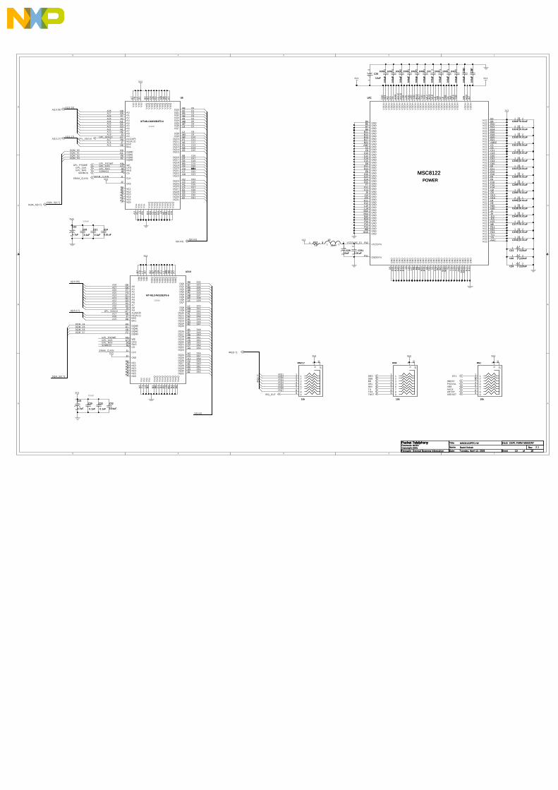
5
5
4
4
3
3
2
2
1
1
D D
C C
B B
A A
GPL_RAS
DQM _S3
GPL_PSDWEGPL_CAS
SDRM CS
DQM _S0DQM _S1
SRAM _CLKIN
DQM _S2
DQM _S[0:7]
D[0:63]
A[19:28]
D12D11
D15
D10D9D8
D14D13
D30
D24
D28D29
D31
D25
D27D26
D16
D20
D17
D22D23
D19D18
D21D21D21D21
D5
D3
D1
D6
D4
D7
D2
D0
VCCSYNC_D1
A17A16A15
A20A21
A27
A23
A28
GPL_SDA10
A24
A22
A19
A26A25
IRQ
[1:7
] IRQ1IRQ2IRQ3IRQ4IRQ5IRQ6IRQ7
A[15:17]
GPL_RAS
DQM _S7
A22
GPL_PSDWEGPL_CAS
SDRM CS
DQM _S4
A21
A28
A26
DQM _S5
SRAM _CLKIN
A27
A23
GPL_SDA10A19
A25
DQM _S6
A20
A24
DQM _S[0:7]
D[0:63]
A[19:28]
A17D44D43
D47
D42D41D40
D46D45
D62
D56
D60D61
D63
D57
D59D58
D48
D52
D49
D54D55
D51D50
D53
D37
D35
D33
D38
D36
D39
D34
D32
A16A15
A[15:17]
3V3
3V3
1V2
3V3
1V2
3V3 3V3
3V3
3V3
3V3
3V3
3V3
3V3
IRQ[1:7]
DBB
T A
D[0:63]
DQM _S[0:7]
GPL_PSDWEGPL_CASGPL_RAS
SDRM CS
SRAM _CLKIN
GPL_SDA10
A[19:28]
A[15:17]
T BST
GBL
IRQ_OUT SRESETART RYAACKABBPSDVALHBRST
DBG
BR
NM I
T EA
EE1
Nam e Rev
Date: Sheet of
T i tle Block
2.1
Packet TelelphonyFreescale NCSDCopyright 2005
18T uesday, Apri l 12, 2005
DSP1 FARM M EM ORY
David Kol tak
Freescale General Business Inform ation
M SC8122PFC HV
10
Nam e Rev
Date: Sheet of
T i tle Block
2.1
Packet TelelphonyFreescale NCSDCopyright 2005
18T uesday, Apri l 12, 2005
DSP1 FARM M EM ORY
David Kol tak
Freescale General Business Inform ation
M SC8122PFC HV
10
Nam e Rev
Date: Sheet of
T i tle Block
2.1
Packet TelelphonyFreescale NCSDCopyright 2005
18T uesday, Apri l 12, 2005
DSP1 FARM M EM ORY
David Kol tak
Freescale General Business Inform ation
M SC8122PFC HV
10
SDRAM
SDRAM
SDRAM
SDRAM
1 2C340 0.01uFC340 0.01uF
1 2R1210
R1210
1 2C322 0.01uFC322 0.01uF
1 2C332 0.01uFC332 0.01uF
C32
0.01uF
C32
0.01uF
12
C339
0.01
uF
C339
0.01
uF
12
C335
0.01
uF
C335
0.01
uF
C33
0.1uF
C33
0.1uF
12
C325
0.01
uF
C325
0.01
uF
1 2+
C36 220uF
+
C36 220uF
12
+C26
10uF
+C26
10uF
Vdd
A7
DQ0R8V
ddQ
B2
DQ1N7
Vss
QN
1
DQ3N8DQ2R9
DQ4P9
Vdd
QB
7
DQ6M7DQ5M8
Vss
QB
3
DQ7L8
NC6K3
Vdd
F9
DQM0K9
WEK8
CASK7
RASJ9
CSJ8
NC(A11)H9
BA0J7
BA1H8
A10(AP)G7
A0G8
A1G9
A2F7
DQM2F8
Vdd
R7
NC5K2
DQ16E8
Vss
QB
8
DQ17D7
DQ18D8
Vdd
QN
9
DQ19B9
DQ20C8
DQ21A9
DQ22C7
Vss
QC
1
Vdd
L7
DQ23A8
Vdd
QL1
Vss
A3
Vss
QD
1
Vdd
QM
9
DQ27C2DQ26A1DQ25C3
DQ28B1
DQ29D2
DQ31E2
Vdd
QE
1
Vss
QM
1
Vss
F1
DQM3F2
NC4H7
A3F3
A4G1
A5G2
A6G3
A7H1
A8H2
A9J3
CKEJ2
CLKJ1
NC3H3 NC2E7
DQM1K1
Vss
QE
9
Vdd
QC
9
DQ8L2
DQ11P1
DQ13R1
Vss
R3
DQ9M3
NC1E3
Vss
L3
Vdd
QD
9
Vss
QL9
DQ12N2
DQ10M2
DQ14N3
DQ24A2
DQ30D3
DQ15R2
Vdd
QP
2
Vdd
QP
7V
ssQ
P3
Vss
QP
8
U210
M T 48LC4M 32B2F5-6
U210
M T 48LC4M 32B2F5-6
1 2+
C29 220uF
+
C29 220uF
12
+C31
4.7uF
+C31
4.7uF
1 2C288 0.01uFC288 0.01uF
12
+ C28
10uF
+ C28
10uF
1 2+
C22 220uF
+
C22 220uF
C30
0.1uF
C30
0.1uF
C24
0.01uF
C24
0.01uF
VCCSYNP12
GNDSYNP11
VD
DH
D20
VD
DH
H21
VD
DH
R3
VD
DH
V3
VD
DH
Y4
VD
DH
AA
9
VD
DH
AA
12
VD
DH
AA
14
VD
DH
L19
VD
DH
L15
VD
DH
P20
VD
DH
U20
VD
DH
Y20
VD
DH
W12
VD
DH
W17
VD
DH
Y10
VD
DH
Y13
VD
DH
M17
VD
DH
W15
VD
DH
M18
VD
DH
L5
VD
DH
M9
VD
DH
N7
VD
DH
L6
VD
DH
D18
VD
DH
D6
VD
DH
W8
VD
DH
M15
VD
DH
Y16
GN
DD
5
GN
DD
21
GN
DE
18
GN
DG
20
GN
DK
13
GN
DK
19
GN
DL9
GN
DL1
6
GN
DL1
7
GN
DM
5
GN
DM
6
GN
DM
7
GN
DM
19
GN
DP
21
GN
DR
4
GN
DT
20
GN
DV
4
GN
DV
15
GN
DW
5
GN
DW
9
GN
DW
13
GN
DW
20
GN
DY
9
GN
DY
12
GN
DY
15
GN
DY
17
GN
DA
A8
GN
DA
A13
GN
DA
A16
GN
DE
17
GNDB4
GNDB5
GNDB7
GNDB9
GNDB11
GNDB13
GNDB15
GNDB17
GNDB22
GNDAB2
GNDC2
GNDC8
GNDC10
GNDC12
GNDC14
GNDC15
GNDD9
GNDD11
GNDD13
GNDE8
GNDE10
GNDE12
GNDE14
GNDE15
GNDF7
GNDF11
GNDF13
VCCB3
VCCB8
VCCB10
VCCB12
VCCB14
VCCB16
VCCB18
VCCB20
VCCB21
VCCAB22
VCCC3
VCCC9
VCCC11
VCCC13
VCCD10
VCCD12
VCCD14
VCCD15
VCCE9
VCCE11
VCCE13
VCCE16
VCCF8
VCCF9
VCCF10
VCCF12
VCCF14
VCCG8
VCCG9
VCCG13
VCCG16
VCCH4
VCCH9
VCCH15
VCCH20
VCCJ4
VCCJ9
VCCJ13
VCCJ15
VCCK15
VCCM8
VCCR11
VCCR12
VCCR13
VCCT11
VCCY6
VCCAA2
VD
DH
M4
VD
DH
M20
VD
DH
W7
GN
DK
10
GNDJ6
GNDJ14
GNDJ20
GNDK11
GNDK12
GNDL10
GNDL14
GNDM10
GNDM14
GNDN10
GNDN14
GNDP10
GNDP13
GNDP14
GNDW6
GNDW19
U7C
MSC8122POWER
U7C
MSC8122POWER
12
C326
0.01
uF
C326
0.01
uF
1 2C289 0.01uFC289 0.01uF
1 2C290 0.01uFC290 0.01uF
12C324 0.01uFC324 0.01uF
Vdd
A7
DQ0R8V
ddQ
B2
DQ1N7
Vss
QN
1
DQ3N8DQ2R9
DQ4P9
Vdd
QB
7
DQ6M7DQ5M8
Vss
QB
3
DQ7L8
NC6K3
Vdd
F9
DQM0K9
WEK8
CASK7
RASJ9
CSJ8
NC(A11)H9
BA0J7
BA1H8
A10(AP)G7
A0G8
A1G9
A2F7
DQM2F8
Vdd
R7
NC5K2
DQ16E8
Vss
QB
8
DQ17D7
DQ18D8
Vdd
QN
9DQ19
B9
DQ20C8
DQ21A9
DQ22C7
Vss
QC
1
Vdd
L7
DQ23A8
Vdd
QL1
Vss
A3
Vss
QD
1
Vdd
QM
9
DQ27C2DQ26A1DQ25C3
DQ28B1
DQ29D2
DQ31E2
Vdd
QE
1
Vss
QM
1
Vss
F1
DQM3F2
NC4H7
A3F3
A4G1
A5G2
A6G3
A7H1
A8H2
A9J3
CKEJ2
CLKJ1
NC3H3 NC2E7
DQM1K1
Vss
QE
9
Vdd
QC
9
DQ8L2
DQ11P1
DQ13R1
Vss
R3
DQ9M3
NC1E3
Vss
L3
Vdd
QD
9
Vss
QL9
DQ12N2
DQ10M2
DQ14N3
DQ24A2
DQ30D3
DQ15R2
Vdd
QP
2
Vdd
QP
7V
ssQ
P3
Vss
QP
8
U6
M T 48LC4M 32B2F5-6
U6
M T 48LC4M 32B2F5-6
12
C32
30.
01uF
C32
30.
01uF
11
22
33
44
55
66
77
88
99
1010RN1
10k
RN1
10k
12
C292
0.01
uF
C292
0.01
uF
C25
0.1uF
C25
0.1uF
1 2C328 0.01uFC328 0.01uF
12
C338
0.01
uF
C338
0.01
uF
11
22
33
44
55
66
77
88
99
1010RN4
10k
RN4
10k
12C295 0.01uFC295 0.01uF
12
C294
0.01
uF
C294
0.01
uF
1 2C334 0.01uFC334 0.01uF
11
22
33
44
55
66
77
88
99
1010RN212
10k
RN212
10k
1 2C321 0.01uFC321 0.01uF
C21
0.1uF
C21
0.1uF
1 2C336 0.01uFC336 0.01uF
1 2C330 0.01uFC330 0.01uF
12
+C23
4.7uF
+C23
4.7uF
12
C329
0.01
uF
C329
0.01
uF
12
C3310.01uF
C3310.01uF
1 2C327 0.01uFC327 0.01uF
11
22
L2
10nH
L2
10nH
1 2C293 0.01uFC293 0.01uF
1 2C337 0.01uFC337 0.01uF
12
C333
0.01
uF
C333
0.01
uF12
C27
0.01
uF
C27
0.01
uF
12
C28
70.
01uF
C28
70.
01uF

5
5
4
4
3
3
2
2
1
1
D D
C C
B B
A A
HT A
HWBS1
HWBS3HWBS2
HWBS0
HWBS[0:3]
IRQ6
IRQ3
T DI
IRQ7
T M S
RST CONF
T CK
IRQ4
T RST
T DO
IRQ_OUT
DLLIN
IRQ5
IRQ2
CLKOUT
CLKIN
EE0
HRESET
PORESET
T EST
D30
D21
D26
D23
D24
D19
D31
D25
D27
D20
D22
D28
D18
D29
D0
D10
D17
D11
D12
D4
D5
D1
D2
D8
D6
D16
D9
D7
D3
D14
D15
D13
BM 0
BM [0:2]
BM 1BM 2
A20
A23
A27
A22
A25
A21
A26
A28
A24
DSI_D29
DSI_A29
DSI_D14
DSI_D2
DSI_D27
DSI_A26
DSI_A23
DSI_A11
DSI_D10
DSI_D23
DSI_A17
DSI_D22
DSI_A12
DSI_A16
DSI_D0
DS
I_A
10
DSI_D16
DSI_D28
DS
I_A
8
DSI_D11
DSI_A19
DSI_D1
DSI_D15
DSI_D17 DSI_A22
DSI_D[0:31]
DSI_D9DSI_D8
DSI_A25
DS
I_A
7
DSI_D31
DSI_D7
DSI_D26
DSI_D4
DSI_A13
DSI_A20
DSI_A14
DSI_D13
DSI_D20
DSI_D5
DSI_A15
DSI_D19
DSI_A28DSI_D24
DSI_D12
DSI_A27
DSI_D6
DSI_D25
DS
I_A
9
DSI_A21
DSI_A24DSI_D18
DSI_D3
DSI_D21
A17
A16
CT _RXD3
CT _T XD3
CT _RXD0
CT _RXD2
CT _FRAM E
CT _C8
CT _T XD2
CT _T XD1
CT _RXD1
CT _T XD0
GPIO30
DSI_A[7:29]
DSI_A[7:29]
DSI_D[0:31]
DSI_A[7:29]
CLKIN
HCSHBCS
HRW
HBCS
HCS
HT A
HRW
HWBS[0:3]
IRQ_OUT
T CK
T DI
T DO
T RST
T M S
RST CONF
HRESET
PORESET
CT _FRAM E
CT _C8
GPIO30
CHIP_ID[0:3]
CHIP_ID3CHIP_ID2CHIP_ID1CHIP_ID0
CHIP_ID[0:3]
DSI_D30
DSI_A18
CT _RXD[0:3]
CT _T XD[0:3]
BM [0:2]
IRQ_IN
IRQ_IN
CT _RXD[0:3]
CT _T XD[0:3]
CT _RXD0CT _RXD1CT _RXD2CT _RXD3
CT _T XD0CT _T XD1CT _T XD2CT _T XD3
D32
D33
D34
D35
D36
D37
D38
D39
D40
D41
D42
D43
D44
D45
D46
D47
D48
D49
D50
D51
D52
D53
D54
D55
D56
D57
D58
D59
D60
D61
D62
D63
DQM _S5
DQM _S7DQM _S6
DQM _S3DQM _S2DQM _S1DQM _S0
DQM _S5DQM _S5DQM _S5DQM _S4
A19
A15
IRQ1
DSI_D[0:31]
DSI_A[7:29]
CLKIN
IRQ_IN
HBCS
HCS
HRW
HT A
HWBS[0:3]
IRQ_OUT
T DO
T DI
T RST
T M S
RST CONF
HRESET
PORESET
CT _FRAM E
CT _C8
GPIO30
CHIP_ID[0:3]
CT _RXD0
CT _T XD0
T CK
BM [0:2]
CT _RXD1CT _RXD2CT _RXD3
CT _T XD1CT _T XD2CT _T XD3
D[0:63]
IRQ[1:7]
NM I
DQM _S[0:7]
GPL_RASGPL_SDA10
GPL_CAS
GPL_PSDWE
SDRM CS
SRAM _CLKIN
HBRSTHBCSHCSHT AHRW
SRESET
A[15:17]
A[19:28]
BR
T AT EA
AR
TR
Y
DBGDBB
IRQ_OUTGBL
T BST
PSDVAL
AB
BA
AC
K
EE1
Nam e Rev
Date: Sheet of
T i tle Block
2.1
Packet TelelphonyFreescale NCSDCopyright 2005
18T uesday, Apri l 12, 2005
DSP2 FARM CORE
David Kol tak
Freescale General Business Inform ation
M SC8122PFC HV
11
Nam e Rev
Date: Sheet of
T i tle Block
2.1
Packet TelelphonyFreescale NCSDCopyright 2005
18T uesday, Apri l 12, 2005
DSP2 FARM CORE
David Kol tak
Freescale General Business Inform ation
M SC8122PFC HV
11
Nam e Rev
Date: Sheet of
T i tle Block
2.1
Packet TelelphonyFreescale NCSDCopyright 2005
18T uesday, Apri l 12, 2005
DSP2 FARM CORE
David Kol tak
Freescale General Business Inform ation
M SC8122PFC HV
11
B
N
8
Bottom View
P
1972
L
165
M
4
J
18
K
173 14
G
1511
W
H
13
E
12
U
F
9
V
C
10
R
D
6
T
20 21 22
Y
A A
A B
FCPBGA20x20 431pins
Note 1
Note 1
Notes:1.) Mount on side 2 to allow probing.
BGN16
BRP16
A0
AA
20
A1
AB
21
A2
AA
21
A3
AA
22
A4
Y21
A5
Y22
A6
W22
A7
W21
A8
V19
A9
V20
A10
V21
A11
V22
A12
U21
A13
U22
A14
T22
A15
T21
A16
R22
A17
R20
A18
R21
A19
P22
A20
N22
A21
M22
A22
L22
A23
N21
A24
M21
A25
L21
A26
K20
A27
L20
A28
K22
A29
K21
A30
J22
A31
H22
CLKINJ10
BA
DD
R31
/IRQ
3G
10B
AD
DR
30/IR
Q2
K8
BA
DD
R29
/IRQ
5L8
BA
DD
R28
L7B
AD
DR
27J8
AR
TR
YH
11
ALE
K17
DBB/IRQ5H13
DP1/DACK1/EXT_BG2/IRQ1T18 DP0/DREQ1/EXT_BR2P19
DBGJ12
GBL/IRQ1R10
EE1D4 EE0D3
DP7/DREQ4/IRQ7R15 DP6/DREQ3/IRQ6R16 DP5/DACK4/EXT_DBG3/IRQ5T16 DP4/DACK3/EXT_BG3/IRQ4T17
AB
B/IR
Q4
G12
DP3/DREQ2/EXT_BR3/IRQ3R17 DP2/DACK2/EXT_DBG2/IRQ2R19
AA
CK
H12
TDOC4
TEAP17
TMSE4
TRSTE3
D0
V5
D1
V6
D2
U5
D3
U6
D4
V7
D5
V8
D6
U7
D7
V9
D8
U8
D9
U9
D10
V10
D11
U10
D12
V11
D13
V12
D14
U11
D15
U12
D16
T12
D17
U13
D18
V13
D19
U14
D20
V14
D21
T14
D22
U15
D23
T15
D24
V16
D25
U16
D26
U17
D27
V17
D28
U18
D29
V18
D30
T19
D31
U19
HD
_D32
W18
HD
_D33
W16
HD
_D34
Y19
HD
_D35
AA
19
HD
_D36
AB
20
HD
_D37
Y18
HD
_D38
AA
18
HD
_D39
AB
19
HD
_D40
W14
HD
_D41
AB
18
HD
_D42
AA
17
HD
_D43
Y14
HD
_D44
AB
17
HD
_D45
AB
16
HD
_D46
AA
15
HD
_D47
AB
15
HD
_D48
AB
14
HD
_D49
AB
13
HD
_D50
AB
12
HD
_D51
Y11
HD
_D52
AA
11
HD
_D53
AB
11
HD
_D54
AA
10
HD
_D55
AB
10
HD
_D56
AB
9
HD
_D57
AB
8
HD
_D58
Y8
HD
_D59
AA
7
HD
_D60
Y7
HD
_D61
AB
7
HD
_D62
AB
6
HD
_D63
AA
6
INT_OUT/IRQ7G14
PGTA/PPBS/PUPMWAIT/PGPL4H8
POE/PSDRAS/PGPL2K7
PSDA10/PGPL0J17
PSDAMUX/PGPL5J7
PSDCAS/PGPL3H7
PSDVALP18
PSDWE/PGPL1N19
TCKE2
TDID2
TAP15
TBSTT10
TSR18
TSIZ0T8
TSIZ1R8
TSIZ2T9
TSIZ3R9
CS
0N
18C
S1
G17
CS
2K
18C
S3
L18
CS
4H
17
CLKOUTK14
RSTCONFF3
SRESETC5
HRESETE5
CS
5/T
T2
K16
CS
6/T
T3
J16
CS
7/T
T4
H16
TT
0R
14T
T1
T13
PORESETF2
TESTH6
PWE0/PSDDQM0/PBS0G7
PWE1/PSDDQM1/PBS1K6
PWE2/PSDDQM2/PBS2N6
PWE3/PSDDQM3/PBS3K5
PWE4/PSDDQM4/PBS4/HWBS4/HDBS4R7
PWE5/PSDDQM5/PBS5/HWBS5/HDBS5T7
PWE6/PSDDQM6/PBS6/HWBS6/HDBS6R6
PWE7/PSDDQM7/PBS7/HWBS7/HDBS7T6
BCTL0G18
BCTL1/CS5J18
BNKSEL0/BM0/TC0G11
BNKSEL1/BM1/TC1H10
BNKSEL2/BM2/TC2J11
NMIF4
DLLINK9
NMI_OUTB6
ETHRX_CLK/ETHSYNC_INF15
ETHCRS/ETHRXDG15
ETHTX_CLK/ETHSYNC_INF16
GPIO25/IRQ15/TDM0RCLKJ21
GPIO26/TDM0RDATN20
GPIO24/IRQ14/TDM0RSYNH18
GPIO22/DRACK2/DONE2/TDM0TCLKG22
GPIO23/IRQ13/TDM0TDATJ19
GPIO21/TDM0TSYNH19
GPIO19/DACK2/TDM1RCLKF22
GPIO20/TDM1RDATF17
GPIO18/DREQ2/TDM1RSYNF18
GPIO16/DRACK1/DONE1/TDM1TCLKF19
GPIO17/DACK1/TDM1TDATG21
GPIO15/DREQ1/TDM1TSYNG19
GPIO13/IRQ11/TDM2RCLK/ETHMDCE20
GPIO14/IRQ12/TDM2RDATETHRXD0F21
GPIO12/IRQ10/TDM2RSYN/ETHRXD1/ETHSYNCE22
GPIO10/IRQ8/TDM2TCLK/ETHRX_DV/ETH_CRS_DVE21
GPIO11/IRQ9/TDM2TDAT/ETHRX_ER/ETHTXDF20
GPIO9/IRQ7/TDM2TSYN/ETHMDIOE19
GPIO7/IRQ5/TDM3RCLK/ETHTXD3C19
GPIO8/IRQ6/TDM3RDAT/ETHCOLD22
GPIO6/IRQ4/TDM3RSYN/ETHRXD2C22
GPIO4/IRQ2/TDM3TCLK/ETHTX_ERD19
GPIO5/IRQ3/TDM3TDAT/ETHRXD3C21
GPIO3/IRQ1/TDM3TSYN/ETHTXD2C20
GPIO30/TIMER2/TMCLK/SDAC16
GPIO31/TIMER3/SCLD16
GPIO27/URXDE6
GPIO28/UTXDC6
U2A
MSC8122SYSTEM
U2A
MSC8122SYSTEM
12R205 0R205 0
12R3 1kR3 1k
12R6 0R6 0
12R222 33R222 33
1 2R11
22R11
22
12 R21kR21k
12
R2070R207012R206 0R206 0
HR
/WN
15
HT
AH
14
HW
BS
0/H
DB
S0
N8
HW
BS
1/H
DB
S1
P8
HW
BS
2/H
DB
S2
P7
HW
BS
3/H
DB
S3
P6
HA17G6HA18J2HA19H5HA20H2HA21K3HA22F6HA23G5HA24G2HA25G4HA26J3HA27G3HA28H3HA29F5
HB
CS
N9
HA11L4HA12L2HA13J5HA14L3HA15K2HA16K4
HD0/SWTET5 HD1/DSISYNCT4 HD2/DSI64U4 HD3/MODCK1V2 HD4/MODCK2W4 HD5/CNFGSW3 HD6W2 HD7Y2 HD8
AB5 HD9Y5 HD10
AA5 HD11AB4 HD12AA4 HD13AB3 HD14AA3 HD15
Y3 HD16U2 HD17T2 HD18R2 HD19U3 HD20P2 HD21T3 HD22R5 HD23P5 HD24N5 HD25P4 HD26N2 HD27P3 HD28M2 HD29N4 HD30N3 HD31M3
HC
SN
17
HC
LKIN
P9
HB
RS
TM
16
HD
ST
0W
11
HD
ST
1W
10
HC
ID0
E7
HC
ID1
C7
HC
ID2
D7
HC
ID3
D8
GP
IO0/
CH
IP_I
D0/
IRQ
4/E
TH
TX
D0
B19
GP
IO29
/CH
IP_I
D3/
ET
HT
X_E
ND
17
GP
IO1/
TIM
ER
0/C
HIP
_ID
1/IR
Q5/
ET
HT
XD
1C
18
GP
IO2/
TIM
ER
1/C
HIP
_ID
2/IR
Q6
C17 U2B
MSC8122
DSI
U2B
MSC8122
DSI
12R14 0R14 0

5
5
4
4
3
3
2
2
1
1
D D
C C
B B
A A
GPL_RAS
DQM _S3
GPL_PSDWEGPL_CAS
SDRM CS
DQM _S0DQM _S1
SRAM _CLKIN
DQM _S2
DQM _S[0:7]
D[0:63]
A[19:28]
D12D11
D15
D10D9D8
D14D13
D30
D24
D28D29
D31
D25
D27D26
D16
D20
D17
D22D23
D19D18
D21D21D21D21
D5
D3
D1
D6
D4
D7
D2
D0
VCCSYNC_D1
A17A16A15
A20A21
A27
A23
A28
GPL_SDA10
A24
A22
A19
A26A25
IRQ
[1:7
] IRQ1IRQ2IRQ3IRQ4IRQ5IRQ6IRQ7
A[15:17]
GPL_RAS
DQM _S7
A22
GPL_PSDWEGPL_CAS
SDRM CS
DQM _S4
A21
A28
A26
DQM _S5
SRAM _CLKIN
A27
A23
GPL_SDA10A19
A25
DQM _S6
A20
A24
DQM _S[0:7]
D[0:63]
A[19:28]
A17D44D43
D47
D42D41D40
D46D45
D62
D56
D60D61
D63
D57
D59D58
D48
D52
D49
D54D55
D51D50
D53
D37
D35
D33
D38
D36
D39
D34
D32
A16A15
A[15:17]
3V3
3V3
1V2
3V3
1V2
3V3 3V3
3V3
3V3
3V3
3V3
3V3
3V3
IRQ[1:7]
DBB
T A
D[0:63]
DQM _S[0:7]
GPL_PSDWEGPL_CASGPL_RAS
SDRM CS
SRAM _CLKIN
GPL_SDA10
A[19:28]
A[15:17]
T BST
GBL
IRQ_OUT SRESETART RYAACKABBPSDVALHBRST
DBG
BR
NM I
T EA
EE1
Nam e Rev
Date: Sheet of
T i tle Block
2.1
Packet TelelphonyFreescale NCSDCopyright 2005
18T uesday, Apri l 12, 2005
DSP2 FARM M EM ORY
David Kol tak
Freescale General Business Inform ation
M SC8122PFC HV
12
Nam e Rev
Date: Sheet of
T i tle Block
2.1
Packet TelelphonyFreescale NCSDCopyright 2005
18T uesday, Apri l 12, 2005
DSP2 FARM M EM ORY
David Kol tak
Freescale General Business Inform ation
M SC8122PFC HV
12
Nam e Rev
Date: Sheet of
T i tle Block
2.1
Packet TelelphonyFreescale NCSDCopyright 2005
18T uesday, Apri l 12, 2005
DSP2 FARM M EM ORY
David Kol tak
Freescale General Business Inform ation
M SC8122PFC HV
12
SDRAM
SDRAM
SDRAM
SDRAM
1 2C247 0.01uFC247 0.01uF
1 2R110
R110
1 2C253 0.01uFC253 0.01uF
1 2C219 0.01uFC219 0.01uF
C14
0.01uF
C14
0.01uF
12
C254
0.01
uF
C254
0.01
uF
12
C220
0.01
uF
C220
0.01
uF
C15
0.1uF
C15
0.1uF
12
C265
0.01
uF
C265
0.01
uF
1 2+
C224 220uF
+
C224 220uF
12
+C6
10uF
+C6
10uF
Vdd
A7
DQ0R8V
ddQ
B2
DQ1N7
Vss
QN
1
DQ3N8DQ2R9
DQ4P9
Vdd
QB
7
DQ6M7DQ5M8
Vss
QB
3
DQ7L8
NC6K3
Vdd
F9
DQM0K9
WEK8
CASK7
RASJ9
CSJ8
NC(A11)H9
BA0J7
BA1H8
A10(AP)G7
A0G8
A1G9
A2F7
DQM2F8
Vdd
R7
NC5K2
DQ16E8
Vss
QB
8
DQ17D7
DQ18D8
Vdd
QN
9
DQ19B9
DQ20C8
DQ21A9
DQ22C7
Vss
QC
1
Vdd
L7
DQ23A8
Vdd
QL1
Vss
A3
Vss
QD
1
Vdd
QM
9
DQ27C2DQ26A1DQ25C3
DQ28B1
DQ29D2
DQ31E2
Vdd
QE
1
Vss
QM
1
Vss
F1
DQM3F2
NC4H7
A3F3
A4G1
A5G2
A6G3
A7H1
A8H2
A9J3
CKEJ2
CLKJ1
NC3H3 NC2E7
DQM1K1
Vss
QE
9
Vdd
QC
9
DQ8L2
DQ11P1
DQ13R1
Vss
R3
DQ9M3
NC1E3
Vss
L3
Vdd
QD
9
Vss
QL9
DQ12N2
DQ10M2
DQ14N3
DQ24A2
DQ30D3
DQ15R2
Vdd
QP
2
Vdd
QP
7V
ssQ
P3
Vss
QP
8
U203
M T 48LC4M 32B2F5-6
U203
M T 48LC4M 32B2F5-6
1 2+
C297 220uF
+
C297 220uF
12
+C13
4.7uF
+C13
4.7uF
1 2C264 0.01uFC264 0.01uF
12
+ C223
10uF
+ C223
10uF
1 2+
C16 220uF
+
C16 220uF
C12
0.1uF
C12
0.1uF
C2
0.01uF
C2
0.01uF
VCCSYNP12
GNDSYNP11
VD
DH
D20
VD
DH
H21
VD
DH
R3
VD
DH
V3
VD
DH
Y4
VD
DH
AA
9
VD
DH
AA
12
VD
DH
AA
14
VD
DH
L19
VD
DH
L15
VD
DH
P20
VD
DH
U20
VD
DH
Y20
VD
DH
W12
VD
DH
W17
VD
DH
Y10
VD
DH
Y13
VD
DH
M17
VD
DH
W15
VD
DH
M18
VD
DH
L5
VD
DH
M9
VD
DH
N7
VD
DH
L6
VD
DH
D18
VD
DH
D6
VD
DH
W8
VD
DH
M15
VD
DH
Y16
GN
DD
5
GN
DD
21
GN
DE
18
GN
DG
20
GN
DK
13
GN
DK
19
GN
DL9
GN
DL1
6
GN
DL1
7
GN
DM
5
GN
DM
6
GN
DM
7
GN
DM
19
GN
DP
21
GN
DR
4
GN
DT
20
GN
DV
4
GN
DV
15
GN
DW
5
GN
DW
9
GN
DW
13
GN
DW
20
GN
DY
9
GN
DY
12
GN
DY
15
GN
DY
17
GN
DA
A8
GN
DA
A13
GN
DA
A16
GN
DE
17
GNDB4
GNDB5
GNDB7
GNDB9
GNDB11
GNDB13
GNDB15
GNDB17
GNDB22
GNDAB2
GNDC2
GNDC8
GNDC10
GNDC12
GNDC14
GNDC15
GNDD9
GNDD11
GNDD13
GNDE8
GNDE10
GNDE12
GNDE14
GNDE15
GNDF7
GNDF11
GNDF13
VCCB3
VCCB8
VCCB10
VCCB12
VCCB14
VCCB16
VCCB18
VCCB20
VCCB21
VCCAB22
VCCC3
VCCC9
VCCC11
VCCC13
VCCD10
VCCD12
VCCD14
VCCD15
VCCE9
VCCE11
VCCE13
VCCE16
VCCF8
VCCF9
VCCF10
VCCF12
VCCF14
VCCG8
VCCG9
VCCG13
VCCG16
VCCH4
VCCH9
VCCH15
VCCH20
VCCJ4
VCCJ9
VCCJ13
VCCJ15
VCCK15
VCCM8
VCCR11
VCCR12
VCCR13
VCCT11
VCCY6
VCCAA2
VD
DH
M4
VD
DH
M20
VD
DH
W7
GN
DK
10
GNDJ6
GNDJ14
GNDJ20
GNDK11
GNDK12
GNDL10
GNDL14
GNDM10
GNDM14
GNDN10
GNDN14
GNDP10
GNDP13
GNDP14
GNDW6
GNDW19
U2C
MSC8122POWER
U2C
MSC8122POWER
12
C251
0.01
uF
C251
0.01
uF
1 2C263 0.01uFC263 0.01uF
1 2C248 0.01uFC248 0.01uF
12C216 0.01uFC216 0.01uF
Vdd
A7
DQ0R8V
ddQ
B2
DQ1N7
Vss
QN
1
DQ3N8DQ2R9
DQ4P9
Vdd
QB
7
DQ6M7DQ5M8
Vss
QB
3
DQ7L8
NC6K3
Vdd
F9
DQM0K9
WEK8
CASK7
RASJ9
CSJ8
NC(A11)H9
BA0J7
BA1H8
A10(AP)G7
A0G8
A1G9
A2F7
DQM2F8
Vdd
R7
NC5K2
DQ16E8
Vss
QB
8
DQ17D7
DQ18D8
Vdd
QN
9DQ19
B9
DQ20C8
DQ21A9
DQ22C7
Vss
QC
1
Vdd
L7
DQ23A8
Vdd
QL1
Vss
A3
Vss
QD
1
Vdd
QM
9
DQ27C2DQ26A1DQ25C3
DQ28B1
DQ29D2
DQ31E2
Vdd
QE
1
Vss
QM
1
Vss
F1
DQM3F2
NC4H7
A3F3
A4G1
A5G2
A6G3
A7H1
A8H2
A9J3
CKEJ2
CLKJ1
NC3H3 NC2E7
DQM1K1
Vss
QE
9
Vdd
QC
9
DQ8L2
DQ11P1
DQ13R1
Vss
R3
DQ9M3
NC1E3
Vss
L3
Vdd
QD
9
Vss
QL9
DQ12N2
DQ10M2
DQ14N3
DQ24A2
DQ30D3
DQ15R2
Vdd
QP
2
Vdd
QP
7V
ssQ
P3
Vss
QP
8
U1
M T 48LC4M 32B2F5-6
U1
M T 48LC4M 32B2F5-6
12
C21
70.
01uF
C21
70.
01uF
11
22
33
44
55
66
77
88
99
1010RN2
10k
RN2
10k
12
C258
0.01
uF
C258
0.01
uF
C1
0.1uF
C1
0.1uF
1 2C222 0.01uFC222 0.01uF
12
C259
0.01
uF
C259
0.01
uF
11
22
33
44
55
66
77
88
99
1010RN203
10k
RN203
10k
12C255 0.01uFC255 0.01uF
12
C4
0.01
uF
C4
0.01
uF
1 2C260 0.01uFC260 0.01uF
11
22
33
44
55
66
77
88
99
1010RN204
10k
RN204
10k
1 2C252 0.01uFC252 0.01uF
C5
0.1uF
C5
0.1uF
1 2C249 0.01uFC249 0.01uF
1 2C214 0.01uFC214 0.01uF
12
+C3
4.7uF
+C3
4.7uF
12
C215
0.01
uF
C215
0.01
uF
12
C2560.01uF
C2560.01uF
1 2C218 0.01uFC218 0.01uF
11
22
L1
10nH
L1
10nH
1 2C257 0.01uFC257 0.01uF
1 2C261 0.01uFC261 0.01uF
12
C221
0.01
uF
C221
0.01
uF12
C250
0.01
uF
C250
0.01
uF
12
C26
20.
01uF
C26
20.
01uF
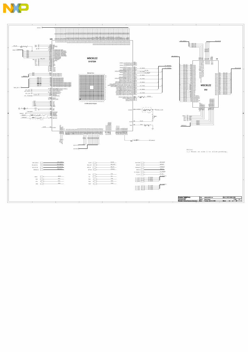
5
5
4
4
3
3
2
2
1
1
D D
C C
B B
A A
HT A
HWBS1
HWBS3HWBS2
HWBS0
HWBS[0:3]
IRQ6
IRQ3
T DI
IRQ7
T M S
RST CONF
T CK
IRQ4
T RST
T DO
IRQ_OUT
DLLIN
IRQ5
IRQ2
CLKOUT
CLKIN
EE0
HRESET
PORESET
T EST
D30
D21
D26
D23
D24
D19
D31
D25
D27
D20
D22
D28
D18
D29
D0
D10
D17
D11
D12
D4
D5
D1
D2
D8
D6
D16
D9
D7
D3
D14
D15
D13
BM 0
BM [0:2]
BM 1BM 2
A20
A23
A27
A22
A25
A21
A26
A28
A24
DSI_D29
DSI_A29
DSI_D14
DSI_D2
DSI_D27
DSI_A26
DSI_A23
DSI_A11
DSI_D10
DSI_D23
DSI_A17
DSI_D22
DSI_A12
DSI_A16
DSI_D0
DS
I_A
10
DSI_D16
DSI_D28
DS
I_A
8
DSI_D11
DSI_A19
DSI_D1
DSI_D15
DSI_D17 DSI_A22
DSI_D[0:31]
DSI_D9DSI_D8
DSI_A25
DS
I_A
7
DSI_D31
DSI_D7
DSI_D26
DSI_D4
DSI_A13
DSI_A20
DSI_A14
DSI_D13
DSI_D20
DSI_D5
DSI_A15
DSI_D19
DSI_A28DSI_D24
DSI_D12
DSI_A27
DSI_D6
DSI_D25
DS
I_A
9
DSI_A21
DSI_A24DSI_D18
DSI_D3
DSI_D21
A17
A16
CT _RXD3
CT _T XD3
CT _RXD0
CT _RXD2
CT _FRAM E
CT _C8
CT _T XD2
CT _T XD1
CT _RXD1
CT _T XD0
GPIO30
DSI_A[7:29]
DSI_A[7:29]
DSI_D[0:31]
DSI_A[7:29]
CLKIN
HCSHBCS
HRW
HBCS
HCS
HT A
HRW
HWBS[0:3]
IRQ_OUT
T CK
T DI
T DO
T RST
T M S
RST CONF
HRESET
PORESET
CT _FRAM E
CT _C8
GPIO30
CHIP_ID[0:3]
CHIP_ID3CHIP_ID2CHIP_ID1CHIP_ID0
CHIP_ID[0:3]
DSI_D30
DSI_A18
CT _RXD[0:3]
CT _T XD[0:3]
BM [0:2]
IRQ_IN
IRQ_IN
CT _RXD[0:3]
CT _T XD[0:3]
CT _RXD0CT _RXD1CT _RXD2CT _RXD3
CT _T XD0CT _T XD1CT _T XD2CT _T XD3
D32
D33
D34
D35
D36
D37
D38
D39
D40
D41
D42
D43
D44
D45
D46
D47
D48
D49
D50
D51
D52
D53
D54
D55
D56
D57
D58
D59
D60
D61
D62
D63
DQM _S5
DQM _S7DQM _S6
DQM _S3DQM _S2DQM _S1DQM _S0
DQM _S5DQM _S5DQM _S5DQM _S4
A19
A15
IRQ1
DSI_D[0:31]
DSI_A[7:29]
CLKIN
IRQ_IN
HBCS
HCS
HRW
HT A
HWBS[0:3]
IRQ_OUT
T DO
T DI
T RST
T M S
RST CONF
HRESET
PORESET
CT _FRAM E
CT _C8
GPIO30
CHIP_ID[0:3]
CT _RXD0
CT _T XD0
T CK
BM [0:2]
CT _RXD1CT _RXD2CT _RXD3
CT _T XD1CT _T XD2CT _T XD3
D[0:63]
IRQ[1:7]
NM I
DQM _S[0:7]
GPL_RASGPL_SDA10
GPL_CAS
GPL_PSDWE
SDRM CS
SRAM _CLKIN
HBRSTHBCSHCSHT AHRW
SRESET
A[15:17]
A[19:28]
BR
T AT EA
AR
TR
Y
DBGDBB
IRQ_OUTGBL
T BST
PSDVAL
AB
BA
AC
K
EE1
Nam e Rev
Date: Sheet of
T i tle Block
2.1
Packet TelelphonyFreescale NCSDCopyright 2005
18T uesday, Apri l 12, 2005
DSP3 FARM CORE
David Kol tak
Freescale General Business Inform ation
M SC8122PFC HV
13
Nam e Rev
Date: Sheet of
T i tle Block
2.1
Packet TelelphonyFreescale NCSDCopyright 2005
18T uesday, Apri l 12, 2005
DSP3 FARM CORE
David Kol tak
Freescale General Business Inform ation
M SC8122PFC HV
13
Nam e Rev
Date: Sheet of
T i tle Block
2.1
Packet TelelphonyFreescale NCSDCopyright 2005
18T uesday, Apri l 12, 2005
DSP3 FARM CORE
David Kol tak
Freescale General Business Inform ation
M SC8122PFC HV
13
B
N
8
Bottom View
P
1972
L
165
M
4
J
18
K
173 14
G
1511
W
H
13
E
12
U
F
9
V
C
10
R
D
6
T
20 21 22
Y
A A
A B
FCPBGA20x20 431pins
Note 1
Note 1
Notes:1.) Mount on side 2 to allow probing.
BGN16
BRP16
A0
AA
20
A1
AB
21
A2
AA
21
A3
AA
22
A4
Y21
A5
Y22
A6
W22
A7
W21
A8
V19
A9
V20
A10
V21
A11
V22
A12
U21
A13
U22
A14
T22
A15
T21
A16
R22
A17
R20
A18
R21
A19
P22
A20
N22
A21
M22
A22
L22
A23
N21
A24
M21
A25
L21
A26
K20
A27
L20
A28
K22
A29
K21
A30
J22
A31
H22
CLKINJ10
BA
DD
R31
/IRQ
3G
10B
AD
DR
30/IR
Q2
K8
BA
DD
R29
/IRQ
5L8
BA
DD
R28
L7B
AD
DR
27J8
AR
TR
YH
11
ALE
K17
DBB/IRQ5H13
DP1/DACK1/EXT_BG2/IRQ1T18 DP0/DREQ1/EXT_BR2P19
DBGJ12
GBL/IRQ1R10
EE1D4 EE0D3
DP7/DREQ4/IRQ7R15 DP6/DREQ3/IRQ6R16 DP5/DACK4/EXT_DBG3/IRQ5T16 DP4/DACK3/EXT_BG3/IRQ4T17
AB
B/IR
Q4
G12
DP3/DREQ2/EXT_BR3/IRQ3R17 DP2/DACK2/EXT_DBG2/IRQ2R19
AA
CK
H12
TDOC4
TEAP17
TMSE4
TRSTE3
D0
V5
D1
V6
D2
U5
D3
U6
D4
V7
D5
V8
D6
U7
D7
V9
D8
U8
D9
U9
D10
V10
D11
U10
D12
V11
D13
V12
D14
U11
D15
U12
D16
T12
D17
U13
D18
V13
D19
U14
D20
V14
D21
T14
D22
U15
D23
T15
D24
V16
D25
U16
D26
U17
D27
V17
D28
U18
D29
V18
D30
T19
D31
U19
HD
_D32
W18
HD
_D33
W16
HD
_D34
Y19
HD
_D35
AA
19
HD
_D36
AB
20
HD
_D37
Y18
HD
_D38
AA
18
HD
_D39
AB
19
HD
_D40
W14
HD
_D41
AB
18
HD
_D42
AA
17
HD
_D43
Y14
HD
_D44
AB
17
HD
_D45
AB
16
HD
_D46
AA
15
HD
_D47
AB
15
HD
_D48
AB
14
HD
_D49
AB
13
HD
_D50
AB
12
HD
_D51
Y11
HD
_D52
AA
11
HD
_D53
AB
11
HD
_D54
AA
10
HD
_D55
AB
10
HD
_D56
AB
9
HD
_D57
AB
8
HD
_D58
Y8
HD
_D59
AA
7
HD
_D60
Y7
HD
_D61
AB
7
HD
_D62
AB
6
HD
_D63
AA
6
INT_OUT/IRQ7G14
PGTA/PPBS/PUPMWAIT/PGPL4H8
POE/PSDRAS/PGPL2K7
PSDA10/PGPL0J17
PSDAMUX/PGPL5J7
PSDCAS/PGPL3H7
PSDVALP18
PSDWE/PGPL1N19
TCKE2
TDID2
TAP15
TBSTT10
TSR18
TSIZ0T8
TSIZ1R8
TSIZ2T9
TSIZ3R9
CS
0N
18C
S1
G17
CS
2K
18C
S3
L18
CS
4H
17
CLKOUTK14
RSTCONFF3
SRESETC5
HRESETE5
CS
5/T
T2
K16
CS
6/T
T3
J16
CS
7/T
T4
H16
TT
0R
14T
T1
T13
PORESETF2
TESTH6
PWE0/PSDDQM0/PBS0G7
PWE1/PSDDQM1/PBS1K6
PWE2/PSDDQM2/PBS2N6
PWE3/PSDDQM3/PBS3K5
PWE4/PSDDQM4/PBS4/HWBS4/HDBS4R7
PWE5/PSDDQM5/PBS5/HWBS5/HDBS5T7
PWE6/PSDDQM6/PBS6/HWBS6/HDBS6R6
PWE7/PSDDQM7/PBS7/HWBS7/HDBS7T6
BCTL0G18
BCTL1/CS5J18
BNKSEL0/BM0/TC0G11
BNKSEL1/BM1/TC1H10
BNKSEL2/BM2/TC2J11
NMIF4
DLLINK9
NMI_OUTB6
ETHRX_CLK/ETHSYNC_INF15
ETHCRS/ETHRXDG15
ETHTX_CLK/ETHSYNC_INF16
GPIO25/IRQ15/TDM0RCLKJ21
GPIO26/TDM0RDATN20
GPIO24/IRQ14/TDM0RSYNH18
GPIO22/DRACK2/DONE2/TDM0TCLKG22
GPIO23/IRQ13/TDM0TDATJ19
GPIO21/TDM0TSYNH19
GPIO19/DACK2/TDM1RCLKF22
GPIO20/TDM1RDATF17
GPIO18/DREQ2/TDM1RSYNF18
GPIO16/DRACK1/DONE1/TDM1TCLKF19
GPIO17/DACK1/TDM1TDATG21
GPIO15/DREQ1/TDM1TSYNG19
GPIO13/IRQ11/TDM2RCLK/ETHMDCE20
GPIO14/IRQ12/TDM2RDATETHRXD0F21
GPIO12/IRQ10/TDM2RSYN/ETHRXD1/ETHSYNCE22
GPIO10/IRQ8/TDM2TCLK/ETHRX_DV/ETH_CRS_DVE21
GPIO11/IRQ9/TDM2TDAT/ETHRX_ER/ETHTXDF20
GPIO9/IRQ7/TDM2TSYN/ETHMDIOE19
GPIO7/IRQ5/TDM3RCLK/ETHTXD3C19
GPIO8/IRQ6/TDM3RDAT/ETHCOLD22
GPIO6/IRQ4/TDM3RSYN/ETHRXD2C22
GPIO4/IRQ2/TDM3TCLK/ETHTX_ERD19
GPIO5/IRQ3/TDM3TDAT/ETHRXD3C21
GPIO3/IRQ1/TDM3TSYN/ETHTXD2C20
GPIO30/TIMER2/TMCLK/SDAC16
GPIO31/TIMER3/SCLD16
GPIO27/URXDE6
GPIO28/UTXDC6
U3A
MSC8122SYSTEM
U3A
MSC8122SYSTEM
12R203 0R203 0
12R4 1kR4 1k
12R27 0R27 0
12R212 33R212 33
1 2R35
22R35
22
12 R51kR51k
12
R2130R213012R204 0R204 0
HR
/WN
15
HT
AH
14
HW
BS
0/H
DB
S0
N8
HW
BS
1/H
DB
S1
P8
HW
BS
2/H
DB
S2
P7
HW
BS
3/H
DB
S3
P6
HA17G6HA18J2HA19H5HA20H2HA21K3HA22F6HA23G5HA24G2HA25G4HA26J3HA27G3HA28H3HA29F5
HB
CS
N9
HA11L4HA12L2HA13J5HA14L3HA15K2HA16K4
HD0/SWTET5 HD1/DSISYNCT4 HD2/DSI64U4 HD3/MODCK1V2 HD4/MODCK2W4 HD5/CNFGSW3 HD6W2 HD7Y2 HD8
AB5 HD9Y5 HD10
AA5 HD11AB4 HD12AA4 HD13AB3 HD14AA3 HD15
Y3 HD16U2 HD17T2 HD18R2 HD19U3 HD20P2 HD21T3 HD22R5 HD23P5 HD24N5 HD25P4 HD26N2 HD27P3 HD28M2 HD29N4 HD30N3 HD31M3
HC
SN
17
HC
LKIN
P9
HB
RS
TM
16
HD
ST
0W
11
HD
ST
1W
10
HC
ID0
E7
HC
ID1
C7
HC
ID2
D7
HC
ID3
D8
GP
IO0/
CH
IP_I
D0/
IRQ
4/E
TH
TX
D0
B19
GP
IO29
/CH
IP_I
D3/
ET
HT
X_E
ND
17
GP
IO1/
TIM
ER
0/C
HIP
_ID
1/IR
Q5/
ET
HT
XD
1C
18
GP
IO2/
TIM
ER
1/C
HIP
_ID
2/IR
Q6
C17 U3B
MSC8122
DSI
U3B
MSC8122
DSI
12R23 0R23 0

5
5
4
4
3
3
2
2
1
1
D D
C C
B B
A A
GPL_RAS
DQM _S3
GPL_PSDWEGPL_CAS
SDRM CS
DQM _S0DQM _S1
SRAM _CLKIN
DQM _S2
DQM _S[0:7]
D[0:63]
A[19:28]
D12D11
D15
D10D9D8
D14D13
D30
D24
D28D29
D31
D25
D27D26
D16
D20
D17
D22D23
D19D18
D21D21D21D21
D5
D3
D1
D6
D4
D7
D2
D0
VCCSYNC_D1
A17A16A15
A20A21
A27
A23
A28
GPL_SDA10
A24
A22
A19
A26A25
IRQ
[1:7
] IRQ1IRQ2IRQ3IRQ4IRQ5IRQ6IRQ7
A[15:17]
GPL_RAS
DQM _S7
A22
GPL_PSDWEGPL_CAS
SDRM CS
DQM _S4
A21
A28
A26
DQM _S5
SRAM _CLKIN
A27
A23
GPL_SDA10A19
A25
DQM _S6
A20
A24
DQM _S[0:7]
D[0:63]
A[19:28]
A17D44D43
D47
D42D41D40
D46D45
D62
D56
D60D61
D63
D57
D59D58
D48
D52
D49
D54D55
D51D50
D53
D37
D35
D33
D38
D36
D39
D34
D32
A16A15
A[15:17]
3V3
3V3
1V2
3V3
1V2
3V3 3V3
3V3
3V3
3V3
3V3
3V3
3V3
IRQ[1:7]
DBB
T A
D[0:63]
DQM _S[0:7]
GPL_PSDWEGPL_CASGPL_RAS
SDRM CS
SRAM _CLKIN
GPL_SDA10
A[19:28]
A[15:17]
T BST
GBL
IRQ_OUT SRESETART RYAACKABBPSDVALHBRST
DBG
BR
NM I
T EA
EE1
Nam e Rev
Date: Sheet of
T i tle Block
2.1
Packet TelelphonyFreescale NCSDCopyright 2005
18T uesday, Apri l 12, 2005
DSP3 FARM M EM ORY
David Kol tak
Freescale General Business Inform ation
M SC8122PFC HV
14
Nam e Rev
Date: Sheet of
T i tle Block
2.1
Packet TelelphonyFreescale NCSDCopyright 2005
18T uesday, Apri l 12, 2005
DSP3 FARM M EM ORY
David Kol tak
Freescale General Business Inform ation
M SC8122PFC HV
14
Nam e Rev
Date: Sheet of
T i tle Block
2.1
Packet TelelphonyFreescale NCSDCopyright 2005
18T uesday, Apri l 12, 2005
DSP3 FARM M EM ORY
David Kol tak
Freescale General Business Inform ation
M SC8122PFC HV
14
SDRAM
SDRAM
SDRAM
SDRAM
1 2C207 0.01uFC207 0.01uF
1 2R2210
R2210
1 2C212 0.01uFC212 0.01uF
1 2C229 0.01uFC229 0.01uF
C18
0.01uF
C18
0.01uF
12
C232
0.01
uF
C232
0.01
uF
12
C213
0.01
uF
C213
0.01
uF
C20
0.1uF
C20
0.1uF
12
C209
0.01
uF
C209
0.01
uF
1 2+
C201 220uF
+
C201 220uF
12
+C246
10uF
+C246
10uF
Vdd
A7
DQ0R8V
ddQ
B2
DQ1N7
Vss
QN
1
DQ3N8DQ2R9
DQ4P9
Vdd
QB
7
DQ6M7DQ5M8
Vss
QB
3
DQ7L8
NC6K3
Vdd
F9
DQM0K9
WEK8
CASK7
RASJ9
CSJ8
NC(A11)H9
BA0J7
BA1H8
A10(AP)G7
A0G8
A1G9
A2F7
DQM2F8
Vdd
R7
NC5K2
DQ16E8
Vss
QB
8
DQ17D7
DQ18D8
Vdd
QN
9
DQ19B9
DQ20C8
DQ21A9
DQ22C7
Vss
QC
1
Vdd
L7
DQ23A8
Vdd
QL1
Vss
A3
Vss
QD
1
Vdd
QM
9
DQ27C2DQ26A1DQ25C3
DQ28B1
DQ29D2
DQ31E2
Vdd
QE
1
Vss
QM
1
Vss
F1
DQM3F2
NC4H7
A3F3
A4G1
A5G2
A6G3
A7H1
A8H2
A9J3
CKEJ2
CLKJ1
NC3H3 NC2E7
DQM1K1
Vss
QE
9
Vdd
QC
9
DQ8L2
DQ11P1
DQ13R1
Vss
R3
DQ9M3
NC1E3
Vss
L3
Vdd
QD
9
Vss
QL9
DQ12N2
DQ10M2
DQ14N3
DQ24A2
DQ30D3
DQ15R2
Vdd
QP
2
Vdd
QP
7V
ssQ
P3
Vss
QP
8
U202
M T 48LC4M 32B2F5-6
U202
M T 48LC4M 32B2F5-6
1 2+
C226 220uF
+
C226 220uF
12
+C19
4.7uF
+C19
4.7uF
1 2C228 0.01uFC228 0.01uF
12
+ C202
10uF
+ C202
10uF
1 2+
C11 220uF
+
C11 220uF
C17
0.1uF
C17
0.1uF
C8
0.01uF
C8
0.01uF
VCCSYNP12
GNDSYNP11
VD
DH
D20
VD
DH
H21
VD
DH
R3
VD
DH
V3
VD
DH
Y4
VD
DH
AA
9
VD
DH
AA
12
VD
DH
AA
14
VD
DH
L19
VD
DH
L15
VD
DH
P20
VD
DH
U20
VD
DH
Y20
VD
DH
W12
VD
DH
W17
VD
DH
Y10
VD
DH
Y13
VD
DH
M17
VD
DH
W15
VD
DH
M18
VD
DH
L5
VD
DH
M9
VD
DH
N7
VD
DH
L6
VD
DH
D18
VD
DH
D6
VD
DH
W8
VD
DH
M15
VD
DH
Y16
GN
DD
5
GN
DD
21
GN
DE
18
GN
DG
20
GN
DK
13
GN
DK
19
GN
DL9
GN
DL1
6
GN
DL1
7
GN
DM
5
GN
DM
6
GN
DM
7
GN
DM
19
GN
DP
21
GN
DR
4
GN
DT
20
GN
DV
4
GN
DV
15
GN
DW
5
GN
DW
9
GN
DW
13
GN
DW
20
GN
DY
9
GN
DY
12
GN
DY
15
GN
DY
17
GN
DA
A8
GN
DA
A13
GN
DA
A16
GN
DE
17
GNDB4
GNDB5
GNDB7
GNDB9
GNDB11
GNDB13
GNDB15
GNDB17
GNDB22
GNDAB2
GNDC2
GNDC8
GNDC10
GNDC12
GNDC14
GNDC15
GNDD9
GNDD11
GNDD13
GNDE8
GNDE10
GNDE12
GNDE14
GNDE15
GNDF7
GNDF11
GNDF13
VCCB3
VCCB8
VCCB10
VCCB12
VCCB14
VCCB16
VCCB18
VCCB20
VCCB21
VCCAB22
VCCC3
VCCC9
VCCC11
VCCC13
VCCD10
VCCD12
VCCD14
VCCD15
VCCE9
VCCE11
VCCE13
VCCE16
VCCF8
VCCF9
VCCF10
VCCF12
VCCF14
VCCG8
VCCG9
VCCG13
VCCG16
VCCH4
VCCH9
VCCH15
VCCH20
VCCJ4
VCCJ9
VCCJ13
VCCJ15
VCCK15
VCCM8
VCCR11
VCCR12
VCCR13
VCCT11
VCCY6
VCCAA2
VD
DH
M4
VD
DH
M20
VD
DH
W7
GN
DK
10
GNDJ6
GNDJ14
GNDJ20
GNDK11
GNDK12
GNDL10
GNDL14
GNDM10
GNDM14
GNDN10
GNDN14
GNDP10
GNDP13
GNDP14
GNDW6
GNDW19
U3C
MSC8122POWER
U3C
MSC8122POWER
12
C206
0.01
uF
C206
0.01
uF
1 2C204 0.01uFC204 0.01uF
1 2C210 0.01uFC210 0.01uF
12C238 0.01uFC238 0.01uF
Vdd
A7
DQ0R8V
ddQ
B2
DQ1N7
Vss
QN
1
DQ3N8DQ2R9
DQ4P9
Vdd
QB
7
DQ6M7DQ5M8
Vss
QB
3
DQ7L8
NC6K3
Vdd
F9
DQM0K9
WEK8
CASK7
RASJ9
CSJ8
NC(A11)H9
BA0J7
BA1H8
A10(AP)G7
A0G8
A1G9
A2F7
DQM2F8
Vdd
R7
NC5K2
DQ16E8
Vss
QB
8
DQ17D7
DQ18D8
Vdd
QN
9DQ19
B9
DQ20C8
DQ21A9
DQ22C7
Vss
QC
1
Vdd
L7
DQ23A8
Vdd
QL1
Vss
A3
Vss
QD
1
Vdd
QM
9
DQ27C2DQ26A1DQ25C3
DQ28B1
DQ29D2
DQ31E2
Vdd
QE
1
Vss
QM
1
Vss
F1
DQM3F2
NC4H7
A3F3
A4G1
A5G2
A6G3
A7H1
A8H2
A9J3
CKEJ2
CLKJ1
NC3H3 NC2E7
DQM1K1
Vss
QE
9
Vdd
QC
9
DQ8L2
DQ11P1
DQ13R1
Vss
R3
DQ9M3
NC1E3
Vss
L3
Vdd
QD
9
Vss
QL9
DQ12N2
DQ10M2
DQ14N3
DQ24A2
DQ30D3
DQ15R2
Vdd
QP
2
Vdd
QP
7V
ssQ
P3
Vss
QP
8
U4
M T 48LC4M 32B2F5-6
U4
M T 48LC4M 32B2F5-6
12
C24
20.
01uF
C24
20.
01uF
11
22
33
44
55
66
77
88
99
1010RN200
10k
RN200
10k
12
C239
0.01
uF
C239
0.01
uF
C10
0.1uF
C10
0.1uF
1 2C211 0.01uFC211 0.01uF
12
C243
0.01
uF
C243
0.01
uF
11
22
33
44
55
66
77
88
99
1010RN201
10k
RN201
10k
12C231 0.01uFC231 0.01uF
12
C233
0.01
uF
C233
0.01
uF
1 2C230 0.01uFC230 0.01uF
11
22
33
44
55
66
77
88
99
1010RN202
10k
RN202
10k
1 2C245 0.01uFC245 0.01uF
C7
0.1uF
C7
0.1uF
1 2C244 0.01uFC244 0.01uF
1 2C234 0.01uFC234 0.01uF
12
+C9
4.7uF
+C9
4.7uF
12
C237
0.01
uF
C237
0.01
uF
12
C2400.01uF
C2400.01uF
1 2C236 0.01uFC236 0.01uF
11
22
L3
10nH
L3
10nH
1 2C203 0.01uFC203 0.01uF
1 2C241 0.01uFC241 0.01uF
12
C208
0.01
uF
C208
0.01
uF12
C235
0.01
uF
C235
0.01
uF
12
C20
50.
01uF
C20
50.
01uF

5
5
4
4
3
3
2
2
1
1
D D
C C
B B
A A
HT A
HWBS1
HWBS3HWBS2
HWBS0
HWBS[0:3]
IRQ6
IRQ3
T DI
IRQ7
T M S
RST CONF
T CK
IRQ4
T RST
T DO
IRQ_OUT
DLLIN
IRQ5
IRQ2
CLKOUT
CLKIN
EE0
HRESET
PORESET
T EST
D30
D21
D26
D23
D24
D19
D31
D25
D27
D20
D22
D28
D18
D29
D0
D10
D17
D11
D12
D4
D5
D1
D2
D8
D6
D16
D9
D7
D3
D14
D15
D13
BM 0
BM [0:2]
BM 1BM 2
A20
A23
A27
A22
A25
A21
A26
A28
A24
DSI_D29
DSI_A29
DSI_D14
DSI_D2
DSI_D27
DSI_A26
DSI_A23
DSI_A11
DSI_D10
DSI_D23
DSI_A17
DSI_D22
DSI_A12
DSI_A16
DSI_D0
DS
I_A
10
DSI_D16
DSI_D28
DS
I_A
8
DSI_D11
DSI_A19
DSI_D1
DSI_D15
DSI_D17 DSI_A22
DSI_D[0:31]
DSI_D9DSI_D8
DSI_A25
DS
I_A
7
DSI_D31
DSI_D7
DSI_D26
DSI_D4
DSI_A13
DSI_A20
DSI_A14
DSI_D13
DSI_D20
DSI_D5
DSI_A15
DSI_D19
DSI_A28DSI_D24
DSI_D12
DSI_A27
DSI_D6
DSI_D25
DS
I_A
9
DSI_A21
DSI_A24DSI_D18
DSI_D3
DSI_D21
A17
A16
CT _RXD3
CT _T XD3
CT _RXD0
CT _RXD2
CT _FRAM E
CT _C8
CT _T XD2
CT _T XD1
CT _RXD1
CT _T XD0
GPIO30
DSI_A[7:29]
DSI_A[7:29]
DSI_D[0:31]
DSI_A[7:29]
CLKIN
HCSHBCS
HRW
HBCS
HCS
HT A
HRW
HWBS[0:3]
IRQ_OUT
T CK
T DI
T DO
T RST
T M S
RST CONF
HRESET
PORESET
CT _FRAM E
CT _C8
GPIO30
CHIP_ID[0:3]
CHIP_ID3CHIP_ID2CHIP_ID1CHIP_ID0
CHIP_ID[0:3]
DSI_D30
DSI_A18
CT _RXD[0:3]
CT _T XD[0:3]
BM [0:2]
IRQ_IN
IRQ_IN
CT _RXD[0:3]
CT _T XD[0:3]
CT _RXD0CT _RXD1CT _RXD2CT _RXD3
CT _T XD0CT _T XD1CT _T XD2CT _T XD3
D32
D33
D34
D35
D36
D37
D38
D39
D40
D41
D42
D43
D44
D45
D46
D47
D48
D49
D50
D51
D52
D53
D54
D55
D56
D57
D58
D59
D60
D61
D62
D63
DQM _S5
DQM _S7DQM _S6
DQM _S3DQM _S2DQM _S1DQM _S0
DQM _S5DQM _S5DQM _S5DQM _S4
A19
A15
IRQ1
DSI_D[0:31]
DSI_A[7:29]
CLKIN
IRQ_IN
HBCS
HCS
HRW
HT A
HWBS[0:3]
IRQ_OUT
T DO
T DI
T RST
T M S
RST CONF
HRESET
PORESET
CT _FRAM E
CT _C8
GPIO30
CHIP_ID[0:3]
CT _RXD0
CT _T XD0
T CK
BM [0:2]
CT _RXD1CT _RXD2CT _RXD3
CT _T XD1CT _T XD2CT _T XD3
D[0:63]
IRQ[1:7]
NM I
DQM _S[0:7]
GPL_RASGPL_SDA10
GPL_CAS
GPL_PSDWE
SDRM CS
SRAM _CLKIN
HBRSTHBCSHCSHT AHRW
SRESET
A[15:17]
A[19:28]
BR
T AT EA
AR
TR
Y
DBGDBB
IRQ_OUTGBL
T BST
PSDVAL
AB
BA
AC
K
EE1
Nam e Rev
Date: Sheet of
T i tle Block
2.1
Packet TelelphonyFreescale NCSDCopyright 2005
18T uesday, Apri l 12, 2005
DSP4 FARM CORE
David Kol tak
Freescale General Business Inform ation
M SC8122PFC HV
15
Nam e Rev
Date: Sheet of
T i tle Block
2.1
Packet TelelphonyFreescale NCSDCopyright 2005
18T uesday, Apri l 12, 2005
DSP4 FARM CORE
David Kol tak
Freescale General Business Inform ation
M SC8122PFC HV
15
Nam e Rev
Date: Sheet of
T i tle Block
2.1
Packet TelelphonyFreescale NCSDCopyright 2005
18T uesday, Apri l 12, 2005
DSP4 FARM CORE
David Kol tak
Freescale General Business Inform ation
M SC8122PFC HV
15
B
N
8
Bottom View
P
1972
L
165
M
4
J
18
K
173 14
G
1511
W
H
13
E
12
U
F
9
V
C
10
R
D
6
T
20 21 22
Y
A A
A B
FCPBGA20x20 431pins
Note 1
Note 1
Notes:1.) Mount on side 2 to allow probing.
BGN16
BRP16
A0
AA
20
A1
AB
21
A2
AA
21
A3
AA
22
A4
Y21
A5
Y22
A6
W22
A7
W21
A8
V19
A9
V20
A10
V21
A11
V22
A12
U21
A13
U22
A14
T22
A15
T21
A16
R22
A17
R20
A18
R21
A19
P22
A20
N22
A21
M22
A22
L22
A23
N21
A24
M21
A25
L21
A26
K20
A27
L20
A28
K22
A29
K21
A30
J22
A31
H22
CLKINJ10
BA
DD
R31
/IRQ
3G
10B
AD
DR
30/IR
Q2
K8
BA
DD
R29
/IRQ
5L8
BA
DD
R28
L7B
AD
DR
27J8
AR
TR
YH
11
ALE
K17
DBB/IRQ5H13
DP1/DACK1/EXT_BG2/IRQ1T18 DP0/DREQ1/EXT_BR2P19
DBGJ12
GBL/IRQ1R10
EE1D4 EE0D3
DP7/DREQ4/IRQ7R15 DP6/DREQ3/IRQ6R16 DP5/DACK4/EXT_DBG3/IRQ5T16 DP4/DACK3/EXT_BG3/IRQ4T17
AB
B/IR
Q4
G12
DP3/DREQ2/EXT_BR3/IRQ3R17 DP2/DACK2/EXT_DBG2/IRQ2R19
AA
CK
H12
TDOC4
TEAP17
TMSE4
TRSTE3
D0
V5
D1
V6
D2
U5
D3
U6
D4
V7
D5
V8
D6
U7
D7
V9
D8
U8
D9
U9
D10
V10
D11
U10
D12
V11
D13
V12
D14
U11
D15
U12
D16
T12
D17
U13
D18
V13
D19
U14
D20
V14
D21
T14
D22
U15
D23
T15
D24
V16
D25
U16
D26
U17
D27
V17
D28
U18
D29
V18
D30
T19
D31
U19
HD
_D32
W18
HD
_D33
W16
HD
_D34
Y19
HD
_D35
AA
19
HD
_D36
AB
20
HD
_D37
Y18
HD
_D38
AA
18
HD
_D39
AB
19
HD
_D40
W14
HD
_D41
AB
18
HD
_D42
AA
17
HD
_D43
Y14
HD
_D44
AB
17
HD
_D45
AB
16
HD
_D46
AA
15
HD
_D47
AB
15
HD
_D48
AB
14
HD
_D49
AB
13
HD
_D50
AB
12
HD
_D51
Y11
HD
_D52
AA
11
HD
_D53
AB
11
HD
_D54
AA
10
HD
_D55
AB
10
HD
_D56
AB
9
HD
_D57
AB
8
HD
_D58
Y8
HD
_D59
AA
7
HD
_D60
Y7
HD
_D61
AB
7
HD
_D62
AB
6
HD
_D63
AA
6
INT_OUT/IRQ7G14
PGTA/PPBS/PUPMWAIT/PGPL4H8
POE/PSDRAS/PGPL2K7
PSDA10/PGPL0J17
PSDAMUX/PGPL5J7
PSDCAS/PGPL3H7
PSDVALP18
PSDWE/PGPL1N19
TCKE2
TDID2
TAP15
TBSTT10
TSR18
TSIZ0T8
TSIZ1R8
TSIZ2T9
TSIZ3R9
CS
0N
18C
S1
G17
CS
2K
18C
S3
L18
CS
4H
17
CLKOUTK14
RSTCONFF3
SRESETC5
HRESETE5
CS
5/T
T2
K16
CS
6/T
T3
J16
CS
7/T
T4
H16
TT
0R
14T
T1
T13
PORESETF2
TESTH6
PWE0/PSDDQM0/PBS0G7
PWE1/PSDDQM1/PBS1K6
PWE2/PSDDQM2/PBS2N6
PWE3/PSDDQM3/PBS3K5
PWE4/PSDDQM4/PBS4/HWBS4/HDBS4R7
PWE5/PSDDQM5/PBS5/HWBS5/HDBS5T7
PWE6/PSDDQM6/PBS6/HWBS6/HDBS6R6
PWE7/PSDDQM7/PBS7/HWBS7/HDBS7T6
BCTL0G18
BCTL1/CS5J18
BNKSEL0/BM0/TC0G11
BNKSEL1/BM1/TC1H10
BNKSEL2/BM2/TC2J11
NMIF4
DLLINK9
NMI_OUTB6
ETHRX_CLK/ETHSYNC_INF15
ETHCRS/ETHRXDG15
ETHTX_CLK/ETHSYNC_INF16
GPIO25/IRQ15/TDM0RCLKJ21
GPIO26/TDM0RDATN20
GPIO24/IRQ14/TDM0RSYNH18
GPIO22/DRACK2/DONE2/TDM0TCLKG22
GPIO23/IRQ13/TDM0TDATJ19
GPIO21/TDM0TSYNH19
GPIO19/DACK2/TDM1RCLKF22
GPIO20/TDM1RDATF17
GPIO18/DREQ2/TDM1RSYNF18
GPIO16/DRACK1/DONE1/TDM1TCLKF19
GPIO17/DACK1/TDM1TDATG21
GPIO15/DREQ1/TDM1TSYNG19
GPIO13/IRQ11/TDM2RCLK/ETHMDCE20
GPIO14/IRQ12/TDM2RDATETHRXD0F21
GPIO12/IRQ10/TDM2RSYN/ETHRXD1/ETHSYNCE22
GPIO10/IRQ8/TDM2TCLK/ETHRX_DV/ETH_CRS_DVE21
GPIO11/IRQ9/TDM2TDAT/ETHRX_ER/ETHTXDF20
GPIO9/IRQ7/TDM2TSYN/ETHMDIOE19
GPIO7/IRQ5/TDM3RCLK/ETHTXD3C19
GPIO8/IRQ6/TDM3RDAT/ETHCOLD22
GPIO6/IRQ4/TDM3RSYN/ETHRXD2C22
GPIO4/IRQ2/TDM3TCLK/ETHTX_ERD19
GPIO5/IRQ3/TDM3TDAT/ETHRXD3C21
GPIO3/IRQ1/TDM3TSYN/ETHTXD2C20
GPIO30/TIMER2/TMCLK/SDAC16
GPIO31/TIMER3/SCLD16
GPIO27/URXDE6
GPIO28/UTXDC6
U13A
MSC8122SYSTEM
U13A
MSC8122SYSTEM
12R280 0R280 0
12R54 1kR54 1k
12R69 0R69 0
12R290 33R290 33
1 2R70
22R70
22
12 R551kR551k
12
R2890R289012R281 0R281 0
HR
/WN
15
HT
AH
14
HW
BS
0/H
DB
S0
N8
HW
BS
1/H
DB
S1
P8
HW
BS
2/H
DB
S2
P7
HW
BS
3/H
DB
S3
P6
HA17G6HA18J2HA19H5HA20H2HA21K3HA22F6HA23G5HA24G2HA25G4HA26J3HA27G3HA28H3HA29F5
HB
CS
N9
HA11L4HA12L2HA13J5HA14L3HA15K2HA16K4
HD0/SWTET5 HD1/DSISYNCT4 HD2/DSI64U4 HD3/MODCK1V2 HD4/MODCK2W4 HD5/CNFGSW3 HD6W2 HD7Y2 HD8
AB5 HD9Y5 HD10
AA5 HD11AB4 HD12AA4 HD13AB3 HD14AA3 HD15
Y3 HD16U2 HD17T2 HD18R2 HD19U3 HD20P2 HD21T3 HD22R5 HD23P5 HD24N5 HD25P4 HD26N2 HD27P3 HD28M2 HD29N4 HD30N3 HD31M3
HC
SN
17
HC
LKIN
P9
HB
RS
TM
16
HD
ST
0W
11
HD
ST
1W
10
HC
ID0
E7
HC
ID1
C7
HC
ID2
D7
HC
ID3
D8
GP
IO0/
CH
IP_I
D0/
IRQ
4/E
TH
TX
D0
B19
GP
IO29
/CH
IP_I
D3/
ET
HT
X_E
ND
17
GP
IO1/
TIM
ER
0/C
HIP
_ID
1/IR
Q5/
ET
HT
XD
1C
18
GP
IO2/
TIM
ER
1/C
HIP
_ID
2/IR
Q6
C17 U13B
MSC8122
DSI
U13B
MSC8122
DSI
12R64 0R64 0

5
5
4
4
3
3
2
2
1
1
D D
C C
B B
A A
GPL_RAS
DQM _S3
GPL_PSDWEGPL_CAS
SDRM CS
DQM _S0DQM _S1
SRAM _CLKIN
DQM _S2
DQM _S[0:7]
D[0:63]
A[19:28]
D12D11
D15
D10D9D8
D14D13
D30
D24
D28D29
D31
D25
D27D26
D16
D20
D17
D22D23
D19D18
D21D21D21D21
D5
D3
D1
D6
D4
D7
D2
D0
VCCSYNC_D1
A17A16A15
A20A21
A27
A23
A28
GPL_SDA10
A24
A22
A19
A26A25
IRQ
[1:7
] IRQ1IRQ2IRQ3IRQ4IRQ5IRQ6IRQ7
A[15:17]
GPL_RAS
DQM _S7
A22
GPL_PSDWEGPL_CAS
SDRM CS
DQM _S4
A21
A28
A26
DQM _S5
SRAM _CLKIN
A27
A23
GPL_SDA10A19
A25
DQM _S6
A20
A24
DQM _S[0:7]
D[0:63]
A[19:28]
A17D44D43
D47
D42D41D40
D46D45
D62
D56
D60D61
D63
D57
D59D58
D48
D52
D49
D54D55
D51D50
D53
D37
D35
D33
D38
D36
D39
D34
D32
A16A15
A[15:17]
3V3
3V3
1V2
3V3
1V2
3V3 3V3
3V3
3V3
3V3
3V3
3V3
3V3
IRQ[1:7]
DBB
T A
D[0:63]
DQM _S[0:7]
GPL_PSDWEGPL_CASGPL_RAS
SDRM CS
SRAM _CLKIN
GPL_SDA10
A[19:28]
A[15:17]
T BST
GBL
IRQ_OUT SRESETART RYAACKABBPSDVALHBRST
DBG
BR
NM I
T EA
EE1
Nam e Rev
Date: Sheet of
T i tle Block
2.1
Packet TelelphonyFreescale NCSDCopyright 2005
18T uesday, Apri l 12, 2005
DSP4 FARM M EM ORY
David Kol tak
Freescale General Business Inform ation
M SC8122PFC HV
16
Nam e Rev
Date: Sheet of
T i tle Block
2.1
Packet TelelphonyFreescale NCSDCopyright 2005
18T uesday, Apri l 12, 2005
DSP4 FARM M EM ORY
David Kol tak
Freescale General Business Inform ation
M SC8122PFC HV
16
Nam e Rev
Date: Sheet of
T i tle Block
2.1
Packet TelelphonyFreescale NCSDCopyright 2005
18T uesday, Apri l 12, 2005
DSP4 FARM M EM ORY
David Kol tak
Freescale General Business Inform ation
M SC8122PFC HV
16
SDRAM
SDRAM
SDRAM
SDRAM
1 2C346 0.01uFC346 0.01uF
1 2R6310
R6310
1 2C380 0.01uFC380 0.01uF
1 2C370 0.01uFC370 0.01uF
C52
0.01uF
C52
0.01uF
12
C382
0.01
uF
C382
0.01
uF
12
C386
0.01
uF
C386
0.01
uF
C50
0.1uF
C50
0.1uF
12
C357
0.01
uF
C357
0.01
uF
1 2+
C345 220uF
+
C345 220uF
12
+C49
10uF
+C49
10uF
Vdd
A7
DQ0R8V
ddQ
B2
DQ1N7
Vss
QN
1
DQ3N8DQ2R9
DQ4P9
Vdd
QB
7
DQ6M7DQ5M8
Vss
QB
3
DQ7L8
NC6K3
Vdd
F9
DQM0K9
WEK8
CASK7
RASJ9
CSJ8
NC(A11)H9
BA0J7
BA1H8
A10(AP)G7
A0G8
A1G9
A2F7
DQM2F8
Vdd
R7
NC5K2
DQ16E8
Vss
QB
8
DQ17D7
DQ18D8
Vdd
QN
9
DQ19B9
DQ20C8
DQ21A9
DQ22C7
Vss
QC
1
Vdd
L7
DQ23A8
Vdd
QL1
Vss
A3
Vss
QD
1
Vdd
QM
9
DQ27C2DQ26A1DQ25C3
DQ28B1
DQ29D2
DQ31E2
Vdd
QE
1
Vss
QM
1
Vss
F1
DQM3F2
NC4H7
A3F3
A4G1
A5G2
A6G3
A7H1
A8H2
A9J3
CKEJ2
CLKJ1
NC3H3 NC2E7
DQM1K1
Vss
QE
9
Vdd
QC
9
DQ8L2
DQ11P1
DQ13R1
Vss
R3
DQ9M3
NC1E3
Vss
L3
Vdd
QD
9
Vss
QL9
DQ12N2
DQ10M2
DQ14N3
DQ24A2
DQ30D3
DQ15R2
Vdd
QP
2
Vdd
QP
7V
ssQ
P3
Vss
QP
8
U216
M T 48LC4M 32B2F5-6
U216
M T 48LC4M 32B2F5-6
1 2+
C368 220uF
+
C368 220uF
12
+C51
4.7uF
+C51
4.7uF
1 2C384 0.01uFC384 0.01uF
12
+ C356
10uF
+ C356
10uF
1 2+
C55 220uF
+
C55 220uF
C53
0.1uF
C53
0.1uF
C44
0.01uF
C44
0.01uF
VCCSYNP12
GNDSYNP11
VD
DH
D20
VD
DH
H21
VD
DH
R3
VD
DH
V3
VD
DH
Y4
VD
DH
AA
9
VD
DH
AA
12
VD
DH
AA
14
VD
DH
L19
VD
DH
L15
VD
DH
P20
VD
DH
U20
VD
DH
Y20
VD
DH
W12
VD
DH
W17
VD
DH
Y10
VD
DH
Y13
VD
DH
M17
VD
DH
W15
VD
DH
M18
VD
DH
L5
VD
DH
M9
VD
DH
N7
VD
DH
L6
VD
DH
D18
VD
DH
D6
VD
DH
W8
VD
DH
M15
VD
DH
Y16
GN
DD
5
GN
DD
21
GN
DE
18
GN
DG
20
GN
DK
13
GN
DK
19
GN
DL9
GN
DL1
6
GN
DL1
7
GN
DM
5
GN
DM
6
GN
DM
7
GN
DM
19
GN
DP
21
GN
DR
4
GN
DT
20
GN
DV
4
GN
DV
15
GN
DW
5
GN
DW
9
GN
DW
13
GN
DW
20
GN
DY
9
GN
DY
12
GN
DY
15
GN
DY
17
GN
DA
A8
GN
DA
A13
GN
DA
A16
GN
DE
17
GNDB4
GNDB5
GNDB7
GNDB9
GNDB11
GNDB13
GNDB15
GNDB17
GNDB22
GNDAB2
GNDC2
GNDC8
GNDC10
GNDC12
GNDC14
GNDC15
GNDD9
GNDD11
GNDD13
GNDE8
GNDE10
GNDE12
GNDE14
GNDE15
GNDF7
GNDF11
GNDF13
VCCB3
VCCB8
VCCB10
VCCB12
VCCB14
VCCB16
VCCB18
VCCB20
VCCB21
VCCAB22
VCCC3
VCCC9
VCCC11
VCCC13
VCCD10
VCCD12
VCCD14
VCCD15
VCCE9
VCCE11
VCCE13
VCCE16
VCCF8
VCCF9
VCCF10
VCCF12
VCCF14
VCCG8
VCCG9
VCCG13
VCCG16
VCCH4
VCCH9
VCCH15
VCCH20
VCCJ4
VCCJ9
VCCJ13
VCCJ15
VCCK15
VCCM8
VCCR11
VCCR12
VCCR13
VCCT11
VCCY6
VCCAA2
VD
DH
M4
VD
DH
M20
VD
DH
W7
GN
DK
10
GNDJ6
GNDJ14
GNDJ20
GNDK11
GNDK12
GNDL10
GNDL14
GNDM10
GNDM14
GNDN10
GNDN14
GNDP10
GNDP13
GNDP14
GNDW6
GNDW19
U13C
MSC8122POWER
U13C
MSC8122POWER
12
C348
0.01
uF
C348
0.01
uF
1 2C369 0.01uFC369 0.01uF
1 2C355 0.01uFC355 0.01uF
12C371 0.01uFC371 0.01uF
Vdd
A7
DQ0R8V
ddQ
B2
DQ1N7
Vss
QN
1
DQ3N8DQ2R9
DQ4P9
Vdd
QB
7
DQ6M7DQ5M8
Vss
QB
3
DQ7L8
NC6K3
Vdd
F9
DQM0K9
WEK8
CASK7
RASJ9
CSJ8
NC(A11)H9
BA0J7
BA1H8
A10(AP)G7
A0G8
A1G9
A2F7
DQM2F8
Vdd
R7
NC5K2
DQ16E8
Vss
QB
8
DQ17D7
DQ18D8
Vdd
QN
9DQ19
B9
DQ20C8
DQ21A9
DQ22C7
Vss
QC
1
Vdd
L7
DQ23A8
Vdd
QL1
Vss
A3
Vss
QD
1
Vdd
QM
9
DQ27C2DQ26A1DQ25C3
DQ28B1
DQ29D2
DQ31E2
Vdd
QE
1
Vss
QM
1
Vss
F1
DQM3F2
NC4H7
A3F3
A4G1
A5G2
A6G3
A7H1
A8H2
A9J3
CKEJ2
CLKJ1
NC3H3 NC2E7
DQM1K1
Vss
QE
9
Vdd
QC
9
DQ8L2
DQ11P1
DQ13R1
Vss
R3
DQ9M3
NC1E3
Vss
L3
Vdd
QD
9
Vss
QL9
DQ12N2
DQ10M2
DQ14N3
DQ24A2
DQ30D3
DQ15R2
Vdd
QP
2
Vdd
QP
7V
ssQ
P3
Vss
QP
8
U14
M T 48LC4M 32B2F5-6
U14
M T 48LC4M 32B2F5-6
12
C38
10.
01uF
C38
10.
01uF
11
22
33
44
55
66
77
88
99
1010RN211
10k
RN211
10k
12
C372
0.01
uF
C372
0.01
uF
C43
0.1uF
C43
0.1uF
1 2C353 0.01uFC353 0.01uF
12
C374
0.01
uF
C374
0.01
uF
11
22
33
44
55
66
77
88
99
1010RN213
10k
RN213
10k
12C385 0.01uFC385 0.01uF
12
C378
0.01
uF
C378
0.01
uF
1 2C347 0.01uFC347 0.01uF
11
22
33
44
55
66
77
88
99
1010RN6
10k
RN6
10k
1 2C349 0.01uFC349 0.01uF
C54
0.1uF
C54
0.1uF
1 2C376 0.01uFC376 0.01uF
1 2C350 0.01uFC350 0.01uF
12
+C42
4.7uF
+C42
4.7uF
12
C377
0.01
uF
C377
0.01
uF
12
C3790.01uF
C3790.01uF
1 2C373 0.01uFC373 0.01uF
11
22
L7
10nH
L7
10nH
1 2C375 0.01uFC375 0.01uF
1 2C351 0.01uFC351 0.01uF
12
C352
0.01
uF
C352
0.01
uF12
C383
0.01
uF
C383
0.01
uF
12
C35
40.
01uF
C35
40.
01uF

5
5
4
4
3
3
2
2
1
1
D D
C C
B B
A A
HT A
HWBS1
HWBS3HWBS2
HWBS0
HWBS[0:3]
IRQ6
IRQ3
T DI
IRQ7
T M S
RST CONF
T CK
IRQ4
T RST
T DO
IRQ_OUT
DLLIN
IRQ5
IRQ2
CLKOUT
CLKIN
EE0
HRESET
PORESET
T EST
D30
D21
D26
D23
D24
D19
D31
D25
D27
D20
D22
D28
D18
D29
D0
D10
D17
D11
D12
D4
D5
D1
D2
D8
D6
D16
D9
D7
D3
D14
D15
D13
BM 0
BM [0:2]
BM 1BM 2
A20
A23
A27
A22
A25
A21
A26
A28
A24
DSI_D29
DSI_A29
DSI_D14
DSI_D2
DSI_D27
DSI_A26
DSI_A23
DSI_A11
DSI_D10
DSI_D23
DSI_A17
DSI_D22
DSI_A12
DSI_A16
DSI_D0
DS
I_A
10
DSI_D16
DSI_D28
DS
I_A
8
DSI_D11
DSI_A19
DSI_D1
DSI_D15
DSI_D17 DSI_A22
DSI_D[0:31]
DSI_D9DSI_D8
DSI_A25
DS
I_A
7
DSI_D31
DSI_D7
DSI_D26
DSI_D4
DSI_A13
DSI_A20
DSI_A14
DSI_D13
DSI_D20
DSI_D5
DSI_A15
DSI_D19
DSI_A28DSI_D24
DSI_D12
DSI_A27
DSI_D6
DSI_D25
DS
I_A
9
DSI_A21
DSI_A24DSI_D18
DSI_D3
DSI_D21
A17
A16
CT _RXD3
CT _T XD3
CT _RXD0
CT _RXD2
CT _FRAM E
CT _C8
CT _T XD2
CT _T XD1
CT _RXD1
CT _T XD0
GPIO30
DSI_A[7:29]
DSI_A[7:29]
DSI_D[0:31]
DSI_A[7:29]
CLKIN
HCSHBCS
HRW
HBCS
HCS
HT A
HRW
HWBS[0:3]
IRQ_OUT
T CK
T DI
T DO
T RST
T M S
RST CONF
HRESET
PORESET
CT _FRAM E
CT _C8
GPIO30
CHIP_ID[0:3]
CHIP_ID3CHIP_ID2CHIP_ID1CHIP_ID0
CHIP_ID[0:3]
DSI_D30
DSI_A18
CT _RXD[0:3]
CT _T XD[0:3]
BM [0:2]
IRQ_IN
IRQ_IN
CT _RXD[0:3]
CT _T XD[0:3]
CT _RXD0CT _RXD1CT _RXD2CT _RXD3
CT _T XD0CT _T XD1CT _T XD2CT _T XD3
D32
D33
D34
D35
D36
D37
D38
D39
D40
D41
D42
D43
D44
D45
D46
D47
D48
D49
D50
D51
D52
D53
D54
D55
D56
D57
D58
D59
D60
D61
D62
D63
DQM _S5
DQM _S7DQM _S6
DQM _S3DQM _S2DQM _S1DQM _S0
DQM _S5DQM _S5DQM _S5DQM _S4
A19
A15
IRQ1
DSI_D[0:31]
DSI_A[7:29]
CLKIN
IRQ_IN
HBCS
HCS
HRW
HT A
HWBS[0:3]
IRQ_OUT
T DO
T DI
T RST
T M S
RST CONF
HRESET
PORESET
CT _FRAM E
CT _C8
GPIO30
CHIP_ID[0:3]
CT _RXD0
CT _T XD0
T CK
BM [0:2]
CT _RXD1CT _RXD2CT _RXD3
CT _T XD1CT _T XD2CT _T XD3
D[0:63]
IRQ[1:7]
NM I
DQM _S[0:7]
GPL_RASGPL_SDA10
GPL_CAS
GPL_PSDWE
SDRM CS
SRAM _CLKIN
HBRSTHBCSHCSHT AHRW
SRESET
A[15:17]
A[19:28]
BR
T AT EA
AR
TR
Y
DBGDBB
IRQ_OUTGBL
T BST
PSDVAL
AB
BA
AC
K
EE1
Nam e Rev
Date: Sheet of
T i tle Block
2.1
Packet telelphonyFreescale NCSDCopyright 2005
18T uesday, Apri l 12, 2005
DSP5 FARM CORE
David Kol tak
Freescale General Business Inform ation
M SC8122PFC HV
17
Nam e Rev
Date: Sheet of
T i tle Block
2.1
Packet telelphonyFreescale NCSDCopyright 2005
18T uesday, Apri l 12, 2005
DSP5 FARM CORE
David Kol tak
Freescale General Business Inform ation
M SC8122PFC HV
17
Nam e Rev
Date: Sheet of
T i tle Block
2.1
Packet telelphonyFreescale NCSDCopyright 2005
18T uesday, Apri l 12, 2005
DSP5 FARM CORE
David Kol tak
Freescale General Business Inform ation
M SC8122PFC HV
17
B
N
8
Bottom View
P
1972
L
165
M
4
J
18
K
173 14
G
1511
W
H
13
E
12
U
F
9
V
C
10
R
D
6
T
20 21 22
Y
A A
A B
FCPBGA20x20 431pins
Note 1
Note 1
Notes:1.) Mount on side 2 to allow probing.
BGN16
BRP16
A0
AA
20
A1
AB
21
A2
AA
21
A3
AA
22
A4
Y21
A5
Y22
A6
W22
A7
W21
A8
V19
A9
V20
A10
V21
A11
V22
A12
U21
A13
U22
A14
T22
A15
T21
A16
R22
A17
R20
A18
R21
A19
P22
A20
N22
A21
M22
A22
L22
A23
N21
A24
M21
A25
L21
A26
K20
A27
L20
A28
K22
A29
K21
A30
J22
A31
H22
CLKINJ10
BA
DD
R31
/IRQ
3G
10B
AD
DR
30/IR
Q2
K8
BA
DD
R29
/IRQ
5L8
BA
DD
R28
L7B
AD
DR
27J8
AR
TR
YH
11
ALE
K17
DBB/IRQ5H13
DP1/DACK1/EXT_BG2/IRQ1T18 DP0/DREQ1/EXT_BR2P19
DBGJ12
GBL/IRQ1R10
EE1D4 EE0D3
DP7/DREQ4/IRQ7R15 DP6/DREQ3/IRQ6R16 DP5/DACK4/EXT_DBG3/IRQ5T16 DP4/DACK3/EXT_BG3/IRQ4T17
AB
B/IR
Q4
G12
DP3/DREQ2/EXT_BR3/IRQ3R17 DP2/DACK2/EXT_DBG2/IRQ2R19
AA
CK
H12
TDOC4
TEAP17
TMSE4
TRSTE3
D0
V5
D1
V6
D2
U5
D3
U6
D4
V7
D5
V8
D6
U7
D7
V9
D8
U8
D9
U9
D10
V10
D11
U10
D12
V11
D13
V12
D14
U11
D15
U12
D16
T12
D17
U13
D18
V13
D19
U14
D20
V14
D21
T14
D22
U15
D23
T15
D24
V16
D25
U16
D26
U17
D27
V17
D28
U18
D29
V18
D30
T19
D31
U19
HD
_D32
W18
HD
_D33
W16
HD
_D34
Y19
HD
_D35
AA
19
HD
_D36
AB
20
HD
_D37
Y18
HD
_D38
AA
18
HD
_D39
AB
19
HD
_D40
W14
HD
_D41
AB
18
HD
_D42
AA
17
HD
_D43
Y14
HD
_D44
AB
17
HD
_D45
AB
16
HD
_D46
AA
15
HD
_D47
AB
15
HD
_D48
AB
14
HD
_D49
AB
13
HD
_D50
AB
12
HD
_D51
Y11
HD
_D52
AA
11
HD
_D53
AB
11
HD
_D54
AA
10
HD
_D55
AB
10
HD
_D56
AB
9
HD
_D57
AB
8
HD
_D58
Y8
HD
_D59
AA
7
HD
_D60
Y7
HD
_D61
AB
7
HD
_D62
AB
6
HD
_D63
AA
6
INT_OUT/IRQ7G14
PGTA/PPBS/PUPMWAIT/PGPL4H8
POE/PSDRAS/PGPL2K7
PSDA10/PGPL0J17
PSDAMUX/PGPL5J7
PSDCAS/PGPL3H7
PSDVALP18
PSDWE/PGPL1N19
TCKE2
TDID2
TAP15
TBSTT10
TSR18
TSIZ0T8
TSIZ1R8
TSIZ2T9
TSIZ3R9
CS
0N
18C
S1
G17
CS
2K
18C
S3
L18
CS
4H
17
CLKOUTK14
RSTCONFF3
SRESETC5
HRESETE5
CS
5/T
T2
K16
CS
6/T
T3
J16
CS
7/T
T4
H16
TT
0R
14T
T1
T13
PORESETF2
TESTH6
PWE0/PSDDQM0/PBS0G7
PWE1/PSDDQM1/PBS1K6
PWE2/PSDDQM2/PBS2N6
PWE3/PSDDQM3/PBS3K5
PWE4/PSDDQM4/PBS4/HWBS4/HDBS4R7
PWE5/PSDDQM5/PBS5/HWBS5/HDBS5T7
PWE6/PSDDQM6/PBS6/HWBS6/HDBS6R6
PWE7/PSDDQM7/PBS7/HWBS7/HDBS7T6
BCTL0G18
BCTL1/CS5J18
BNKSEL0/BM0/TC0G11
BNKSEL1/BM1/TC1H10
BNKSEL2/BM2/TC2J11
NMIF4
DLLINK9
NMI_OUTB6
ETHRX_CLK/ETHSYNC_INF15
ETHCRS/ETHRXDG15
ETHTX_CLK/ETHSYNC_INF16
GPIO25/IRQ15/TDM0RCLKJ21
GPIO26/TDM0RDATN20
GPIO24/IRQ14/TDM0RSYNH18
GPIO22/DRACK2/DONE2/TDM0TCLKG22
GPIO23/IRQ13/TDM0TDATJ19
GPIO21/TDM0TSYNH19
GPIO19/DACK2/TDM1RCLKF22
GPIO20/TDM1RDATF17
GPIO18/DREQ2/TDM1RSYNF18
GPIO16/DRACK1/DONE1/TDM1TCLKF19
GPIO17/DACK1/TDM1TDATG21
GPIO15/DREQ1/TDM1TSYNG19
GPIO13/IRQ11/TDM2RCLK/ETHMDCE20
GPIO14/IRQ12/TDM2RDATETHRXD0F21
GPIO12/IRQ10/TDM2RSYN/ETHRXD1/ETHSYNCE22
GPIO10/IRQ8/TDM2TCLK/ETHRX_DV/ETH_CRS_DVE21
GPIO11/IRQ9/TDM2TDAT/ETHRX_ER/ETHTXDF20
GPIO9/IRQ7/TDM2TSYN/ETHMDIOE19
GPIO7/IRQ5/TDM3RCLK/ETHTXD3C19
GPIO8/IRQ6/TDM3RDAT/ETHCOLD22
GPIO6/IRQ4/TDM3RSYN/ETHRXD2C22
GPIO4/IRQ2/TDM3TCLK/ETHTX_ERD19
GPIO5/IRQ3/TDM3TDAT/ETHRXD3C21
GPIO3/IRQ1/TDM3TSYN/ETHTXD2C20
GPIO30/TIMER2/TMCLK/SDAC16
GPIO31/TIMER3/SCLD16
GPIO27/URXDE6
GPIO28/UTXDC6
U12A
MSC8122SYSTEM
U12A
MSC8122SYSTEM
12R282 0R282 0
12R48 1kR48 1k
12R57 0R57 0
12R291 33R291 33
1 2R62
22R62
22
12 R521kR521k
12
R2860R286012R285 0R285 0
HR
/WN
15
HT
AH
14
HW
BS
0/H
DB
S0
N8
HW
BS
1/H
DB
S1
P8
HW
BS
2/H
DB
S2
P7
HW
BS
3/H
DB
S3
P6
HA17G6HA18J2HA19H5HA20H2HA21K3HA22F6HA23G5HA24G2HA25G4HA26J3HA27G3HA28H3HA29F5
HB
CS
N9
HA11L4HA12L2HA13J5HA14L3HA15K2HA16K4
HD0/SWTET5 HD1/DSISYNCT4 HD2/DSI64U4 HD3/MODCK1V2 HD4/MODCK2W4 HD5/CNFGSW3 HD6W2 HD7Y2 HD8
AB5 HD9Y5 HD10
AA5 HD11AB4 HD12AA4 HD13AB3 HD14AA3 HD15
Y3 HD16U2 HD17T2 HD18R2 HD19U3 HD20P2 HD21T3 HD22R5 HD23P5 HD24N5 HD25P4 HD26N2 HD27P3 HD28M2 HD29N4 HD30N3 HD31M3
HC
SN
17
HC
LKIN
P9
HB
RS
TM
16
HD
ST
0W
11
HD
ST
1W
10
HC
ID0
E7
HC
ID1
C7
HC
ID2
D7
HC
ID3
D8
GP
IO0/
CH
IP_I
D0/
IRQ
4/E
TH
TX
D0
B19
GP
IO29
/CH
IP_I
D3/
ET
HT
X_E
ND
17
GP
IO1/
TIM
ER
0/C
HIP
_ID
1/IR
Q5/
ET
HT
XD
1C
18
GP
IO2/
TIM
ER
1/C
HIP
_ID
2/IR
Q6
C17 U12B
MSC8122
DSI
U12B
MSC8122
DSI
12R56 0R56 0

5
5
4
4
3
3
2
2
1
1
D D
C C
B B
A A
GPL_RAS
DQM _S3
GPL_PSDWEGPL_CAS
SDRM CS
DQM _S0DQM _S1
SRAM _CLKIN
DQM _S2
DQM _S[0:7]
D[0:63]
A[19:28]
D12D11
D15
D10D9D8
D14D13
D30
D24
D28D29
D31
D25
D27D26
D16
D20
D17
D22D23
D19D18
D21D21D21D21
D5
D3
D1
D6
D4
D7
D2
D0
VCCSYNC_D1
A17A16A15
A20A21
A27
A23
A28
GPL_SDA10
A24
A22
A19
A26A25
IRQ
[1:7
] IRQ1IRQ2IRQ3IRQ4IRQ5IRQ6IRQ7
A[15:17]
GPL_RAS
DQM _S7
A22
GPL_PSDWEGPL_CAS
SDRM CS
DQM _S4
A21
A28
A26
DQM _S5
SRAM _CLKIN
A27
A23
GPL_SDA10A19
A25
DQM _S6
A20
A24
DQM _S[0:7]
D[0:63]
A[19:28]
A17D44D43
D47
D42D41D40
D46D45
D62
D56
D60D61
D63
D57
D59D58
D48
D52
D49
D54D55
D51D50
D53
D37
D35
D33
D38
D36
D39
D34
D32
A16A15
A[15:17]
3V3
3V3
1V2
3V3
1V2
3V3 3V3
3V3
3V3
3V3
3V3
3V3
3V3
IRQ[1:7]
DBB
T A
D[0:63]
DQM _S[0:7]
GPL_PSDWEGPL_CASGPL_RAS
SDRM CS
SRAM _CLKIN
GPL_SDA10
A[19:28]
A[15:17]
T BST
GBL
IRQ_OUT SRESETART RYAACKABBPSDVALHBRST
DBG
BR
NM I
T EA
EE1
Nam e Rev
Date: Sheet of
T i tle Block
2.1
Packet telelphonyFreescale NCSDCopyright 2005
18T uesday, Apri l 12, 2005
DSP5 FARM M EM ORY
David Kol tak
Freescale General Business Inform ation
M SC8122PFC HV
18
Nam e Rev
Date: Sheet of
T i tle Block
2.1
Packet telelphonyFreescale NCSDCopyright 2005
18T uesday, Apri l 12, 2005
DSP5 FARM M EM ORY
David Kol tak
Freescale General Business Inform ation
M SC8122PFC HV
18
Nam e Rev
Date: Sheet of
T i tle Block
2.1
Packet telelphonyFreescale NCSDCopyright 2005
18T uesday, Apri l 12, 2005
DSP5 FARM M EM ORY
David Kol tak
Freescale General Business Inform ation
M SC8122PFC HV
18
SDRAM
SDRAM
SDRAM
SDRAM
1 2C361 0.01uFC361 0.01uF
1 2R4510
R4510
1 2C366 0.01uFC366 0.01uF
1 2C405 0.01uFC405 0.01uF
C46
0.01uF
C46
0.01uF
12
C402
0.01
uF
C402
0.01
uF
12
C403
0.01
uF
C403
0.01
uF
C48
0.1uF
C48
0.1uF
12
C395
0.01
uF
C395
0.01
uF
1 2+
C409 220uF
+
C409 220uF
12
+C39
10uF
+C39
10uF
Vdd
A7
DQ0R8V
ddQ
B2
DQ1N7
Vss
QN
1
DQ3N8DQ2R9
DQ4P9
Vdd
QB
7
DQ6M7DQ5M8
Vss
QB
3
DQ7L8
NC6K3
Vdd
F9
DQM0K9
WEK8
CASK7
RASJ9
CSJ8
NC(A11)H9
BA0J7
BA1H8
A10(AP)G7
A0G8
A1G9
A2F7
DQM2F8
Vdd
R7
NC5K2
DQ16E8
Vss
QB
8
DQ17D7
DQ18D8
Vdd
QN
9
DQ19B9
DQ20C8
DQ21A9
DQ22C7
Vss
QC
1
Vdd
L7
DQ23A8
Vdd
QL1
Vss
A3
Vss
QD
1
Vdd
QM
9
DQ27C2DQ26A1DQ25C3
DQ28B1
DQ29D2
DQ31E2
Vdd
QE
1
Vss
QM
1
Vss
F1
DQM3F2
NC4H7
A3F3
A4G1
A5G2
A6G3
A7H1
A8H2
A9J3
CKEJ2
CLKJ1
NC3H3 NC2E7
DQM1K1
Vss
QE
9
Vdd
QC
9
DQ8L2
DQ11P1
DQ13R1
Vss
R3
DQ9M3
NC1E3
Vss
L3
Vdd
QD
9
Vss
QL9
DQ12N2
DQ10M2
DQ14N3
DQ24A2
DQ30D3
DQ15R2
Vdd
QP
2
Vdd
QP
7V
ssQ
P3
Vss
QP
8
U217
M T 48LC4M 32B2F5-6
U217
M T 48LC4M 32B2F5-6
1 2+
C387 220uF
+
C387 220uF
12
+C47
4.7uF
+C47
4.7uF
1 2C397 0.01uFC397 0.01uF
12
+ C365
10uF
+ C365
10uF
1 2+
C367 220uF
+
C367 220uF
C45
0.1uF
C45
0.1uF
C35
0.01uF
C35
0.01uF
VCCSYNP12
GNDSYNP11
VD
DH
D20
VD
DH
H21
VD
DH
R3
VD
DH
V3
VD
DH
Y4
VD
DH
AA
9
VD
DH
AA
12
VD
DH
AA
14
VD
DH
L19
VD
DH
L15
VD
DH
P20
VD
DH
U20
VD
DH
Y20
VD
DH
W12
VD
DH
W17
VD
DH
Y10
VD
DH
Y13
VD
DH
M17
VD
DH
W15
VD
DH
M18
VD
DH
L5
VD
DH
M9
VD
DH
N7
VD
DH
L6
VD
DH
D18
VD
DH
D6
VD
DH
W8
VD
DH
M15
VD
DH
Y16
GN
DD
5
GN
DD
21
GN
DE
18
GN
DG
20
GN
DK
13
GN
DK
19
GN
DL9
GN
DL1
6
GN
DL1
7
GN
DM
5
GN
DM
6
GN
DM
7
GN
DM
19
GN
DP
21
GN
DR
4
GN
DT
20
GN
DV
4
GN
DV
15
GN
DW
5
GN
DW
9
GN
DW
13
GN
DW
20
GN
DY
9
GN
DY
12
GN
DY
15
GN
DY
17
GN
DA
A8
GN
DA
A13
GN
DA
A16
GN
DE
17
GNDB4
GNDB5
GNDB7
GNDB9
GNDB11
GNDB13
GNDB15
GNDB17
GNDB22
GNDAB2
GNDC2
GNDC8
GNDC10
GNDC12
GNDC14
GNDC15
GNDD9
GNDD11
GNDD13
GNDE8
GNDE10
GNDE12
GNDE14
GNDE15
GNDF7
GNDF11
GNDF13
VCCB3
VCCB8
VCCB10
VCCB12
VCCB14
VCCB16
VCCB18
VCCB20
VCCB21
VCCAB22
VCCC3
VCCC9
VCCC11
VCCC13
VCCD10
VCCD12
VCCD14
VCCD15
VCCE9
VCCE11
VCCE13
VCCE16
VCCF8
VCCF9
VCCF10
VCCF12
VCCF14
VCCG8
VCCG9
VCCG13
VCCG16
VCCH4
VCCH9
VCCH15
VCCH20
VCCJ4
VCCJ9
VCCJ13
VCCJ15
VCCK15
VCCM8
VCCR11
VCCR12
VCCR13
VCCT11
VCCY6
VCCAA2
VD
DH
M4
VD
DH
M20
VD
DH
W7
GN
DK
10
GNDJ6
GNDJ14
GNDJ20
GNDK11
GNDK12
GNDL10
GNDL14
GNDM10
GNDM14
GNDN10
GNDN14
GNDP10
GNDP13
GNDP14
GNDW6
GNDW19
U12C
MSC8122POWER
U12C
MSC8122POWER
12
C392
0.01
uF
C392
0.01
uF
1 2C358 0.01uFC358 0.01uF
1 2C364 0.01uFC364 0.01uF
12C363 0.01uFC363 0.01uF
Vdd
A7
DQ0R8V
ddQ
B2
DQ1N7
Vss
QN
1
DQ3N8DQ2R9
DQ4P9
Vdd
QB
7
DQ6M7DQ5M8
Vss
QB
3
DQ7L8
NC6K3
Vdd
F9
DQM0K9
WEK8
CASK7
RASJ9
CSJ8
NC(A11)H9
BA0J7
BA1H8
A10(AP)G7
A0G8
A1G9
A2F7
DQM2F8
Vdd
R7
NC5K2
DQ16E8
Vss
QB
8
DQ17D7
DQ18D8
Vdd
QN
9DQ19
B9
DQ20C8
DQ21A9
DQ22C7
Vss
QC
1
Vdd
L7
DQ23A8
Vdd
QL1
Vss
A3
Vss
QD
1
Vdd
QM
9
DQ27C2DQ26A1DQ25C3
DQ28B1
DQ29D2
DQ31E2
Vdd
QE
1
Vss
QM
1
Vss
F1
DQM3F2
NC4H7
A3F3
A4G1
A5G2
A6G3
A7H1
A8H2
A9J3
CKEJ2
CLKJ1
NC3H3 NC2E7
DQM1K1
Vss
QE
9
Vdd
QC
9
DQ8L2
DQ11P1
DQ13R1
Vss
R3
DQ9M3
NC1E3
Vss
L3
Vdd
QD
9
Vss
QL9
DQ12N2
DQ10M2
DQ14N3
DQ24A2
DQ30D3
DQ15R2
Vdd
QP
2
Vdd
QP
7V
ssQ
P3
Vss
QP
8
U11
M T 48LC4M 32B2F5-6
U11
M T 48LC4M 32B2F5-6
12
C36
00.
01uF
C36
00.
01uF
11
22
33
44
55
66
77
88
99
1010RN215
10k
RN215
10k
12
C394
0.01
uF
C394
0.01
uF
C38
0.1uF
C38
0.1uF
1 2C401 0.01uFC401 0.01uF
12
C393
0.01
uF
C393
0.01
uF
11
22
33
44
55
66
77
88
99
1010RN214
10k
RN214
10k
12C362 0.01uFC362 0.01uF
12
C408
0.01
uF
C408
0.01
uF
1 2C398 0.01uFC398 0.01uF
11
22
33
44
55
66
77
88
99
1010RN216
10k
RN216
10k
1 2C407 0.01uFC407 0.01uF
C34
0.1uF
C34
0.1uF
1 2C388 0.01uFC388 0.01uF
1 2C390 0.01uFC390 0.01uF
12
+C37
4.7uF
+C37
4.7uF
12
C406
0.01
uF
C406
0.01
uF
12
C4000.01uF
C4000.01uF
1 2C389 0.01uFC389 0.01uF
11
22
L4
10nH
L4
10nH
1 2C391 0.01uFC391 0.01uF
1 2C359 0.01uFC359 0.01uF
12
C404
0.01
uF
C404
0.01
uF12
C396
0.01
uF
C396
0.01
uF
12
C39
90.
01uF
C39
90.
01uF

FPGA Firmware
MSC8122PFC-HV Packet Telephony Farm Card User’s Guide, Rev. 0
Freescale Semiconductor 37

Document Order No.: PTKIT8122UG
Information in this document is provided solely to enable system and software implementers to use Freescale Semiconductor products. There are no express or implied copyright licenses granted hereunder to design or fabricate any integrated circuits or integrated circuits based on the information in this document.
Freescale Semiconductor reserves the right to make changes without further notice to any products herein. Freescale Semiconductor makes no warranty, representation or guarantee regarding the suitability of its products for any particular purpose, nor does Freescale Semiconductor assume any liability arising out of the application or use of any product or circuit, and specifically disclaims any and all liability, including without limitation consequential or incidental damages. “Typical” parameters which may be provided in Freescale Semiconductor data sheets and/or specifications can and do vary in different applications and actual performance may vary over time. All operating parameters, including “Typicals” must be validated for each customer application by customer’s technical experts. Freescale Semiconductor does not convey any license under its patent rights nor the rights of others. Freescale Semiconductor products are not designed, intended, or authorized for use as components in systems intended for surgical implant into the body, or other applications intended to support or sustain life, or for any other application in which the failure of the Freescale Semiconductor product could create a situation where personal injury or death may occur. Should Buyer purchase or use Freescale Semiconductor products for any such unintended or unauthorized application, Buyer shall indemnify and hold Freescale Semiconductor and its officers, employees, subsidiaries, affiliates, and distributors harmless against all claims, costs, damages, and expenses, and reasonable attorney fees arising out of, directly or indirectly, any claim of personal injury or death associated with such unintended or unauthorized use, even if such claim alleges that Freescale Semiconductor was negligent regarding the design or manufacture of the part.
Freescale and the Freescale logo are trademarks of Freescale Semiconductor, Inc. CodeWarrior is a trademark or registered trademark of Metrowerk Corp. in the US and/or other countries. StarCore is a licensed trademark of StarCore LLC. All other product or service names are the property of their respective owners.
© Freescale Semiconductor, Inc. 2005.
How to Reach Us:Home Page:www.freescale.com
E-mail:[email protected]
USA/Europe or Locations not listed:Freescale Semiconductor Technical Information Center, CH3701300 N. Alma School RoadChandler, Arizona 85224+1-800-521-6274 or [email protected]
Europe, Middle East, and Africa:Freescale Halbleiter Deutschland GMBHTechnical Information CenterSchatzbogen 781829 München, Germany+44 1296 380 456 (English)+46 8 52200080 (English)+49 89 92103 559 (German)+33 1 69 35 48 48 (French)[email protected]
Japan:Freescale Semiconductor Japan Ltd. HeadquartersARCO Tower 15F1-8-1, Shimo-Meguro, Meguro-ku,Tokyo 153-0064, Japan0120 191014 or +81 3 5437 [email protected]
Asia/Pacific:Freescale Semiconductor Hong Kong Ltd.Technical Information Center2 Dai King StreetTai Po Industrial EstateTai Po, N.T. Hong Kong+800 2666 8080
For Literature Requests Only:Freescale Semiconductor Literature Distribution CenterP.O. Box 5405Denver, Colorado 802171-800-441-2447 or 303-675-2140Fax: [email protected]
Rev. 06/2005
Top Related
Copyright © 2022 FDOKUMEN

