


Bahasa
Halaman
Hukum


2 YEAR LIMITED WARRANTY
This product is warranted by CERONIX to be free of defects in materialand workmanship for a period of two years from the date of purchase.
In case of a fault, developed during this time, it is the customer'sresponsibility to transport the defective unit to CERONIX orone of the authorized service centers for repair.Please attach a note describing the problem.All parts and labor are free of charge during the warranty period.
CERONIX12265 Locksley LaneAuburn, CA. 95602-2055(530) 888-1044
This warranty does not cover mechanical breakage due to physical abuse.
CERONIX shall not be liable for any consequential damages, includingwithout limitation damages resulting from loss of use.Some states do not allow limitation of incidental or consequentialdamages, so the limitation or exclusion may not apply to you.
This warranty gives you specific rights and you may also haveother rights which vary from state to state.
The information contained in this manualis subject to change without prior notice.
COPYRIGHT 1988, 1990, 1998
CERONIX
All rights reserved.
Recognized under the Component Programof Underwriters Laboratories Inc. andthe Canadian Standards Association.
©
®
®
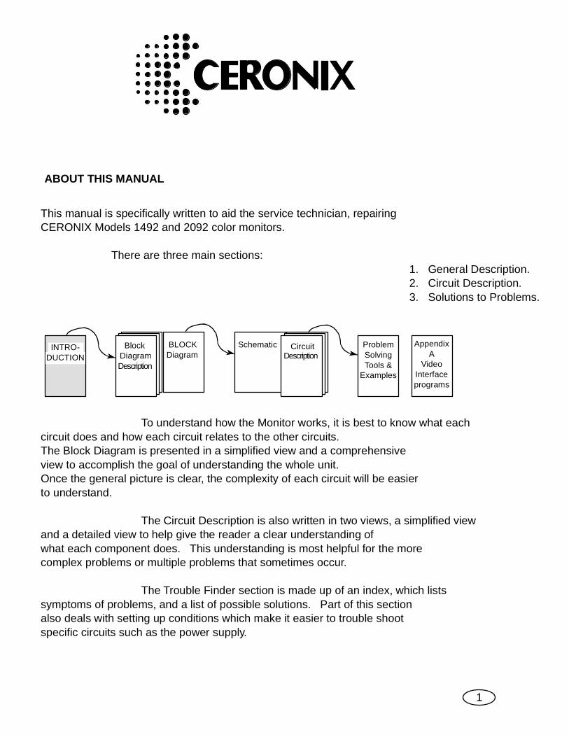
This manual is specifically written to aid the service technician, repairingCERONIX Models 1492 and 2092 color monitors.
There are three main sections:1. General Description.2. Circuit Description.3. Solutions to Problems.
To understand how the Monitor works, it is best to know what eachcircuit does and how each circuit relates to the other circuits.The Block Diagram is presented in a simplified view and a comprehensiveview to accomplish the goal of understanding the whole unit.Once the general picture is clear, the complexity of each circuit will be easierto understand.
The Circuit Description is also written in two views, a simplified viewand a detailed view to help give the reader a clear understanding ofwhat each component does. This understanding is most helpful for the morecomplex problems or multiple problems that sometimes occur.
The Trouble Finder section is made up of an index, which listssymptoms of problems, and a list of possible solutions. Part of this sectionalso deals with setting up conditions which make it easier to trouble shootspecific circuits such as the power supply.
ABOUT THIS MANUAL
INTRO-DUCTION
BlockDiagram
BLOCKDiagram
Schematic CircuitDescription
ProblemSolvingTools &
Examples
AppendixA
VideoInterfaceprograms
1
Description
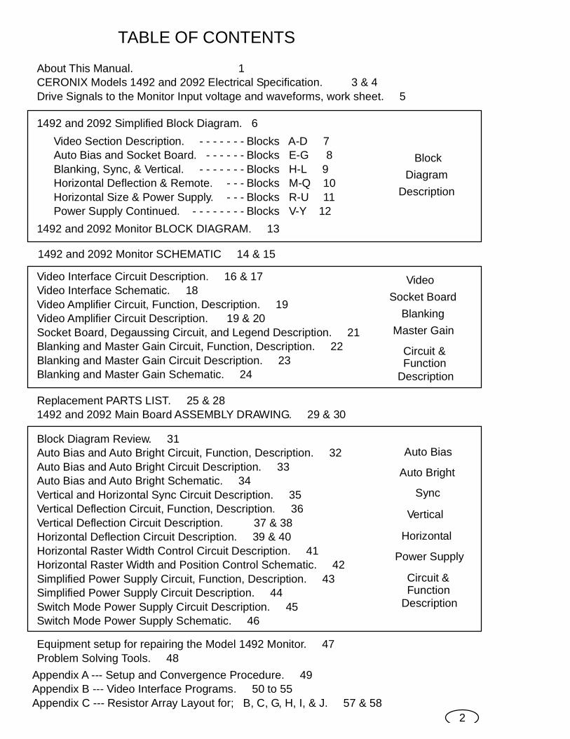
TABLE OF CONTENTS
About This Manual. 1CERONIX Models 1492 and 2092 Electrical Specification. 3 & 4Drive Signals to the Monitor Input voltage and waveforms, work sheet. 5
2
Equipment setup for repairing the Model 1492 Monitor. 47Problem Solving Tools. 48
Block Diagram Review. 31Auto Bias and Auto Bright Circuit, Function, Description. 32Auto Bias and Auto Bright Circuit Description. 33Auto Bias and Auto Bright Schematic. 34Vertical and Horizontal Sync Circuit Description. 35Vertical Deflection Circuit, Function, Description. 36Vertical Deflection Circuit Description. 37 & 38Horizontal Deflection Circuit Description. 39 & 40Horizontal Raster Width Control Circuit Description. 41Horizontal Raster Width and Position Control Schematic. 42Simplified Power Supply Circuit, Function, Description. 43Simplified Power Supply Circuit Description. 44Switch Mode Power Supply Circuit Description. 45Switch Mode Power Supply Schematic. 46
Replacement PARTS LIST. 25 & 281492 and 2092 Main Board ASSEMBLY DRAWING. 29 & 30
Video Interface Circuit Description. 16 & 17Video Interface Schematic. 18Video Amplifier Circuit, Function, Description. 19Video Amplifier Circuit Description. 19 & 20Socket Board, Degaussing Circuit, and Legend Description. 21Blanking and Master Gain Circuit, Function, Description. 22Blanking and Master Gain Circuit Description. 23Blanking and Master Gain Schematic. 24
1492 and 2092 Monitor SCHEMATIC 14 & 15
1492 and 2092 Simplified Block Diagram. 6
Description
Block Diagram
Blocks A-D 7Blocks E-G 8Blocks H-L 9Blocks M-Q 10Blocks R-U 11Blocks V-Y 12
Video Section Description.Auto Bias and Socket Board.Blanking, Sync, & Vertical.Horizontal Deflection & Remote.Horizontal Size & Power Supply.Power Supply Continued.
- - - - - - - - - - - - -
- - - - - - -- - -- - -
- - - - - - - -1492 and 2092 Monitor BLOCK DIAGRAM. 13
VideoSocket Board
Blanking
Circuit &Function
Description
Master Gain
Circuit &Function
Description
Auto Bias
Auto Bright
Sync
Vertical
Horizontal
Power Supply
Appendix A --- Setup and Convergence Procedure. 49Appendix B --- Video Interface Programs. 50 to 55Appendix C --- Resistor Array Layout for; B, C, G, H, I, & J. 57 & 58
1.8K
C. 4 Line TTL
CERONIX MODELS 1492 and 2092 Electrical Specification
INPUTSStandard Video Configurations, available, are:A. Positive Analog
Black levelSaturated color{Source
only
{SourceandMonitor
Black levelSaturated color
To Amp.Video
Gnd
.6mA
Monitor
1492 & 2092Min. Typ. Max
3.1V 3.2V 3.3V.06V .09V
0V 0V .05V
.15V1.61V 1.69V 1.75V
B. Negative Analog
D-A
VideoSource
Video
Gnd
VideoSourceD-A
Black levelRed & GreenBlue Black levelSaturated color
5.4V 5.6V 5.8V4.85V 5.05V 5.25V.7V .9V 1.1V
+12VTo Amp.
BIAS
VB
R,G,BVideo
Intensity
Black levelColor on
Low intensityFull intensity
0V .2V .5V2.7V 3.5V 6.0V
0V .2V .4V4.5V 4.6V 4.8V
VideoSource
No pullup resistor on intensity line.*
*
Note: RS170 and other voltage combinations optional for analog video.
1.
The Sync signals may be of either polarity and separate or composite.2.
SyncSource .15V
1.8K
220 2 PL
High input voltageLow input voltage
Horizontal sync pulseVertical sync pulse
Horizontal frequency
Vertical frequency
2.2V 3.5V 20V-2.7V .30V .80V1.5uS 4.5uS 31uS
15.3KHz 15.6KHz 15.9KHz
120uS .5mS 1.5mS
60Hz 65Hz45Hz 50Hz
For composite sync, vertical and horizontalsync lines are connected together.
Hs
Vs
3.Model 1492 Model 2092
Min. Typ. Max. Min. Typ. Max.85VAC
170VAC 230VAC290VAC230VAC 290VAC180VAC
90VAC 115VAC 145VAC115VAC 145VAC
32W 44W 60W 30W 50W 67W
115VAC 50Hz or 60Hz230VAC 50HZ or 60Hz
Power
The Power to the monitor is to besupplied by a secondary windingof an isolation transformer.
To Amp.
905
INRVBlk.+.7 V
Gnd
Gnd
3
301ý
ý
ý,
301ý
Monitor
Monitor
Monitor

4. The remote Controls are located ona separate PCB for easy access.
H SIZE--------------Horizontal raster sizeV SIZE---------------Vertical raster sizeV RAS. POS.-----Vertical raster positionH POS-------Horizontal picture position*M GAIN---------------------Master gain
Model 1492 Model 2092
9.9" 11.4" 14.8" 16.3"6.3" 10.3" 10.0" 14.0"0" .44" 0" .60"
.9" Right 2" Left 1.2 right 2.8" left
Min. Max. Min. Max.
LightScreen
DarkScreen
DarkScreen
LightScreen
* For start of horizontal sync 1.7uS after end of picture.Focus on the flyback transformer and an optional Horizontal hold control.The board Controls are located on the main PCB, and are:
5. Picture
Min. Typ.
Max.Min. Typ.
Max.Model 1492 Model 2092
Rise timeFall time
OvershootBand width
Horizontal blank timeVertical blank timeHorizontal linearity
Vertical linearityPincushion
Video response is measured at thetube socket, using low capacitancecoupling. The input signal shouldbe fully damped and faster thanthe expected response.
35nS 44nS 49nS 37nS 46nS 52nS32nS 42nS 47nS 35nS 44nS 50nS0% 0%0% 0%2% 2%
DCDC to to 8MHz8MHz12.9uS 13.4uS12.4uS
20H20H20H20H 1.28mS1.28mS
1%1%
1%
1%1%1%
2%2%
2%2%
2%
2%
6. Picture tube Model 1492 Model 2092InchInch mmmm
13 328 20 50810.83 275 16 406.68.13 206.5 12 304.8
.015 .39 .029 .74Useful area
Useful horizontalUseful vertical
Useful diagonal
Spacing between dot/line trios
PixelsPixelsPixels
PixelsPixelsPixels680 550
240240480480
90°90°46% 46%
Horizontal resolutionVertical resolution
InterlacedDeflection angle
Light transmission at center of glass Approximately Approximately
CRT also features: Enhanced contrast, Internal magnetic shield, andX-Ray output Less than .3mR/hour.
7. Environmental Operating temperatureStorage temperature
Operating humidityStorage humidity
0° C 0° C 70° C70° C85° C85° C -20° C-20° C
20%20% 80%80%10%10% 95%95%
4
12.9uS 13.4uS12.4uS
86 558 192 1,239
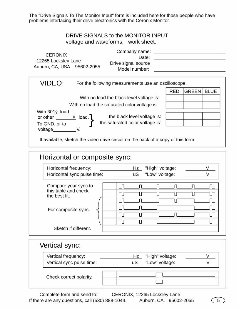
DRIVE SIGNALS to the MONITOR INPUTvoltage and waveforms, work sheet.
CERONIX 12265 Locksley Lane Auburn, CA, USA 95602-2055
Company name: Date:Drive signal source Model number:
VIDEO: For the following measurements use an oscilloscope.
the black level voltage is:the saturated color voltage is:
RED GREEN BLUE
}If available, sketch the video drive circuit on the back of a copy of this form.
Horizontal or composite sync:Horizontal frequency: Hz "High" voltage: VHorizontal sync pulse time: uS "Low" voltage: V
Compare your sync tothis table and checkthe best fit.
For composite sync.
Sketch if different.
Vertical sync:Vertical frequency: Hz "High" voltage: VVertical sync pulse time: uS "Low" voltage: V
Check correct polarity.
Complete form and send to: CERONIX, 12265 Locksley LaneIf there are any questions, call (530) 888-1044.
The "Drive Signals To The Monitor Input" form is included here for those people who haveproblems interfacing their drive electronics with the Ceronix Monitor.
With no load the black level voltage is:With no load the saturated color voltage is:
With 301ý loador otherTo GND, or tovoltage V.
load.ý
5Auburn, CA. 95602-2055
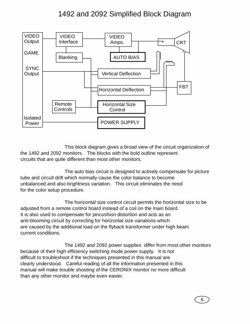
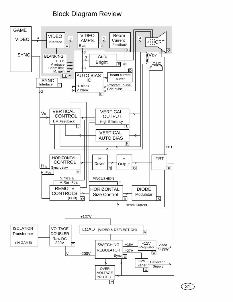
1492 and 2092 Simplified Block Diagram
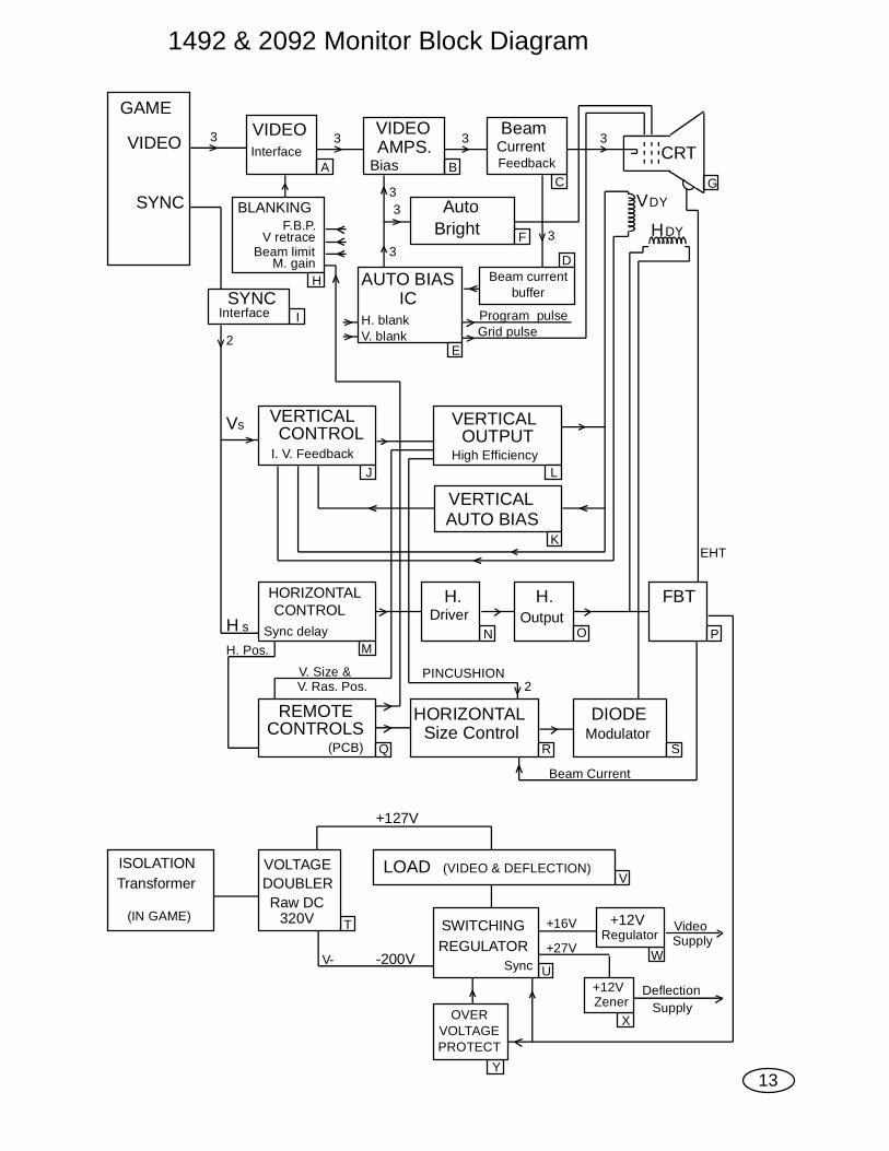
This block diagram gives a broad view of the circuit organization ofthe 1492 and 2092 monitors. The blocks with the bold outline representcircuits that are quite different than most other monitors.
The auto bias circuit is designed to actively compensate for picturetube and circuit drift which normally cause the color balance to becomeunbalanced and also brightness variation. This circuit eliminates the needfor the color setup procedure.
The horizontal size control circuit permits the horizontal size to beadjusted from a remote control board instead of a coil on the main board.It is also used to compensate for pincushion distortion and acts as ananti-blooming circuit by correcting for horizontal size variations whichare caused by the additional load on the flyback transformer under high beamcurrent conditions.
The 1492 and 2092 power supplies differ from most other monitorsbecause of their high efficiency switching mode power supply. It is notdifficult to troubleshoot if the techniques presented in this manual areclearly understood. Careful reading of all the information presented in thismanual will make trouble shooting of the CERONIX monitor no more difficultthan any other monitor and maybe even easier.
6
VIDEOOutput
GAME
SYNCOutput
InterfaceVIDEO
Blanking
VIDEO Amps.
AUTO BIAS
Vertical Deflection
Horizontal Deflection
CRT
FBT
Horizontal Size Control
POWER SUPPLY
RemoteControls
IsolatedPower

The Beam Current Buffer converts the, high impedance low current, beamcurrent signal into a low impedance voltage. This voltage is applied to theauto bias IC through a 200 ohm resistor. After the three lines of beamcurrent are measured, the program pulse from the auto bias IC, produces avoltage drop across this 200 ohm resistor that equals the amplitude of thebeam current voltage.
A
B
C
D
Refer to the block diagram on page 13 (foldout) when reading this description.
7
The Video Interface is designed around a custom IC and will accept positiveor negative analog video signals and also 4 line TTL. This IC also has abuilt in multiplier circuit for the master gain control and blanking.Resistors are used to protect the IC and to set the gain. The programmed gainis dependent on the input signal amplitude except on TTL. Solder jumpers areused to program the Video Interface for the type of input signal to be received.The output of the IC drives the video amplifiers. This drive is a current where0 mA is black and 4.5 mA is a saturated color.
The Video Amplifiers are of the push pull type. They are built partly onthick films and partly on the PCB. Spreading out the amplifier reduces thecomponent heat and improves the life of the unit. The bandwidth is 8 MHzwith 60Vp-p output. The rise and fall times are .04uS.
The Beam Current Feedback circuit directs most of the beam current of eachamplifier to the beam current buffer. The only time this current is measured bythe auto bias circuit is during the time of the three faint lines at the top of thescreen and three lines thereafter. The auto bias circuit is designed to adjust thevideo amplifier bias voltage such that the beam current of each of the three guns isset (programmed), at this time.
The aging of the picture tube (CRT) not only affects the balance of thecathode cutoff voltage, which is corrected by the auto bias circuit, butit also affects the gain of the CRT. The Auto Bright circuit activelycorrects for CRT gain changes by sensing any common bias change fromthe auto bias circuit and adjusts the screen voltage to hold the averagebias voltage constant. The lower adjustment on the flybacktransformer is used to set the auto bright voltage to the center ofits range. This sets up a second control feedback loop to eliminatepicture variation due to the aging of the picture tube.
8
E
F
G
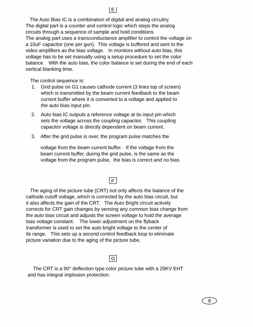
The Auto Bias IC is a combination of digital and analog circuitry.The digital part is a counter and control logic which steps the analogcircuits through a sequence of sample and hold conditions.The analog part uses a transconductance amplifier to control the voltage ona 10uF capacitor (one per gun). This voltage is buffered and sent to thevideo amplifiers as the bias voltage. In monitors without auto bias, thisvoltage has to be set manually using a setup procedure to set the colorbalance. With the auto bias, the color balance is set during the end of eachvertical blanking time.
The control sequence is:
The CRT is a 90° deflection type color picture tube with a 25KV EHTand has integral implosion protection.
After the grid pulse is over, the program pulse matches the
voltage from the beam current buffer. If the voltage from the beam current buffer, during the grid pulse, is the same as thevoltage from the program pulse, the bias is correct and no bias
Auto bias IC outputs a reference voltage at its input pin whichsets the voltage across the coupling capacitor. This couplingcapacitor voltage is directly dependent on beam current.
Grid pulse on G1 causes cathode current (3 lines top of screen)which is transmitted by the beam current feedback to the beamcurrent buffer where it is converted to a voltage and applied tothe auto bias input pin.
1.
2.
3.
The Vertical Output circuit (LA7830) is a power driver which drives the verticaldeflection yoke. It also has a special pump up circuit which doubles the outputvoltage during vertical retrace. This voltage doubler also doubles the efficiency ofthe circuit since the high retrace voltage is not present across the power driverduring the trace time.
H
I
J
K
9
The Vertical Auto Bias circuit greatly increases the range of the bias circuit builtinto the LA7851. It is made up of a negative peak detector and an amplifier whichoutputs current to the normal bias circuit, but with a much lower frequency response.This then eliminates the need for adjustments during production and permits the useof 50Hz and 60Hz vertical sync with only a size adjustment on the remote control board.
Blanking is accomplished by setting the gain of the interface IC to zero duringblank time. The Horizontal Blanking pulse is generated by amplifying the flybackpulse. The Vertical Blanking pulse is started by the vertical oscillator and endedby the counter in the auto bias IC via the "bias out" pulse. The Master Gain control,located on the remote PCB, sets the gain of the video signal when blanking is notactive. The Beam Current Limiter circuit, which is designed to keep the FBT fromoverloading, will reduce the video gain if the average beam current exceeds .75mA.
The Sync Interface can be made to accept separate or composite sync. Twocomparators are used to receive sync, one for vertical sync and the other forhorizontal sync. Resistor dividers are used to protect the comparator IC fromover voltage damage.
1. Vertical sync circuit.2. Vertical oscillator.3. Linear ramp generator.4. Output control and bias circuits for controlling the power driver.
The Vertical Control circuit consists of:
The active components that make up these circuits, except for part of the bias circuit,are located in the deflection control IC (LA7851). The vertical sync circuit is capableof accepting either positive or negative going sync pulses without adjustment.The vertical oscillator in the LA7851 is set at 45 Hz and will sync up to 65 Hzwithout adjustment. The deflection yoke is driven with a linear current ramp whichproduces evenly spaced horizontal lines on the raster. This linear ramp is generatedby supplying a 1uF capacitor with a constant current. The vertical output voltage isheld within range (biased) by a timer which partly discharges the 1uF ramp capacitorat the start of vertical retrace. The duration of the timer is controlled by the verticaloutput voltage and the vertical auto bias circuit.
L
The Horizontal Control incorporates a variable sync delay and a phaselocked loop to generate the horizontal timing. The H POS. adjustment on theremote control board sets the sync delay time which controls the picture position.The phase locked loop uses the flyback pulse to generate a sawtooth wavewhich is gated with the delayed sync pulse to control the horizontal oscillator.
M
N
O
10
P
Q
1. H SIZE ----------- Horizontal raster size --------- Diode modulator2. V SIZE ----------- Vertical raster size ------------- Vertical drive3. V RAS. POS. --- Vertical raster position ------- DC current to V. yoke4. H POS ------------ Horizontal picture position -- H. sync delay5. M GAIN ---------- Master gain ---------------------- Video interface
The Remote Control PCB houses the:
CONTROL DESCRIPTION CIRCUIT
The main function of the Flyback Transformer (FBT) is to generate a25,000 volt (EHT) potential for the anode of the picture tube. This voltagetimes the beam current is the power that lights up the phosphor on the faceof the picture tube. At .75mA beam current the FBT is producing almost 19watts of high voltage power. The FBT also sources the focus voltage and thefilament power. The FBT has a built in high voltage load resistor whichstabilizes the EHT, for the low beam current condition. This resistor alsodischarges the EHT, when the monitor is turned off, which improves thesafety of handling the monitor.
The Horizontal Output transistor is mounted to the rear frame which acts asa heat sink. The collector conducts 1,000 volt flyback pulses which shouldnot be measured unless the equipment is specifically designed to withstandthis type of stress. A linear ramp current is produced in the horizontalyoke by the conduction of the horizontal output transistor (trace time).A fast current reversal (retrace time) is achieved by the high voltage pulsethat follows the turn off of the horizontal output transistor. This pulse is dueto the inductive action of the yoke and flyback transformer.
The Horizontal Driver supplies the high base current necessary to drive thehorizontal output transistor which has a beta as low as three.It also protects the horizontal output transistor since it is a transformer andcannot keep the base turned on for longer than its inductive time constant.

The Horizontal Size Control circuit has four inputs:
11
R
S
T
U
The Switching Regulator is synchronized to the horizontal pulse and drivesa power MOSFET. Unlike most regulators that have a common GND, thispower supply has a common V+ and current is supplied from V- to GND.The MOSFET is connected to V- and signal ground (GND) through atransformer which is used as an inductor for series switchmode regulation.An operational amplifier, voltage reference, comparator, and oscillatorin the power supply controller IC are used to accomplished regulation bymeans of pulse width modulation.
1. To improve the efficiency of the power supply.2. To permit 120 volt and 220 volt operation. For the 220 volt
operation the voltage doubler is replaced with a bridge rectifier.
A Voltage Doubler is used in the power supply for two reasons:
The Diode Modulator is a series element of the horizontal tuned circuit.It forms a node between GND and the normal yoke return circuit.If this node is shorted to GND, maximum horizontal size is present.A diode is used to control the starting time of the retrace pulse at this node.The reverse conduction time is dependent on the forward current because thecurrent waveform at this node has to exceed the forward current in the diode.A diode, placed in series with the yoke, is then used to control the retracepulse amplitude across the yoke. The horizontal size, therefore, is controlled bycontrolling the current to this diode via the horizontal size control circuit.
The horizontal size control circuit sums the four signals at one node toproduce the diode modulator control voltage.
# SIGNAL FUNCTION1. Horizontal size ---------------------- Horizontal size control2. Beam current ----------------------- Blooming control3. Vertical linear ramp ---------------- (#4)-(#3)=Vertical parabolic4. Vertical parabolic + V. linear ramp (Pincushion)

The transformer has two taps on the main winding which are used togenerate the +16 volt and +24 volt supplies. It also has a secondary which isreferenced to V- and supplies the power supply. Since the power supply isgenerating its own power, a special start up circuit is built into the powersupply controller IC that delays start up until its supply capacitor ischarged up enough to furnish the current to start the power supply.This capacitor is charged with current through a high value resistorfrom the raw dc supply. This is why the power supply chirps whenan overload or underload occurs.
The Load consists of the video amplifiers and the horizontal flyback circuit.The power supply will not operate without the load since the voltage thatsustains the power supply comes from a secondary in the power transformerand depends on some primary current to generate secondary current.
12
V
W X&
Y
The Over Voltage Protect circuit is built into the power supply and monitors theflyback transformer peak pulse voltage. This circuit will turn off the powersupply and hold it off if the EHT exceeds its rated value. This circuit not onlyprovides assurance that the X-ray specifications are met but also protects themonitor from catastrophic failure due to a minor component failure.
A separate +12V regulator for the video and the deflection circuits are used in thismonitor to minimize raster and video interactions. This also simplifies PCB layout,since the video GND loops are separate from the deflection GND loops.
13
1492 & 2092 Monitor Block Diagram
SYNC
VIDEO
GAME
CRT
H
V
VERTICAL
CONTROL
CONTROLVERTICAL
OUTPUT
HORIZONTAL H.H.
REMOTECONTROLS
HORIZONTALSize Control
DIODEModulator
FBT
LOADISOLATIONTransformer DOUBLER
VOLTAGE
SWITCHINGREGULATOR
Raw DC320V
+127V
-200V
Driver Output
3
Interface
DY
DY
G
sV
I. V. Feedback High Efficiency
EHT
J
H s
H. Pos.
V. Size &V. Ras. Pos.
PINCUSHION
Sync delayM
N O
(PCB)
P
Q R
(IN GAME)
S
Beam Current
(VIDEO & DEFLECTION)
U
+16V
+27VRegulator
+12V VideoSupply
T
Sync
OVERVOLTAGEPROTECT
DeflectionSupply
V
W
X
+12VZener
2
V-
VIDEOVIDEOAMPS.
BrightAuto
AUTO BIASSYNC IC
Bias
BLANKING
Interface
F.B.P.V retrace
Beam limitM. gain
H. blankV. blank
Program pulseGrid pulse
Beam currentbuffer
3 3
33
3
2
3
A BC
E
F
H
I
D
3
VERTICALAUTO BIAS
L
Y
BeamCurrentFeedback
K

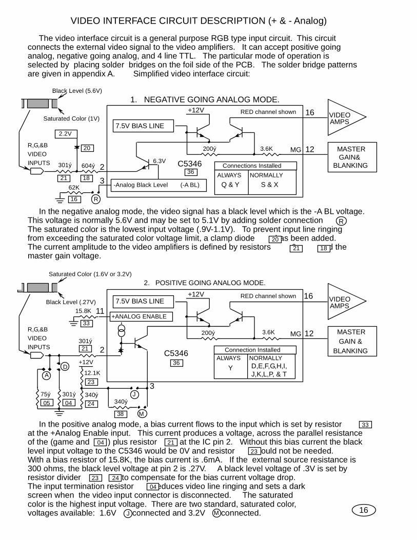
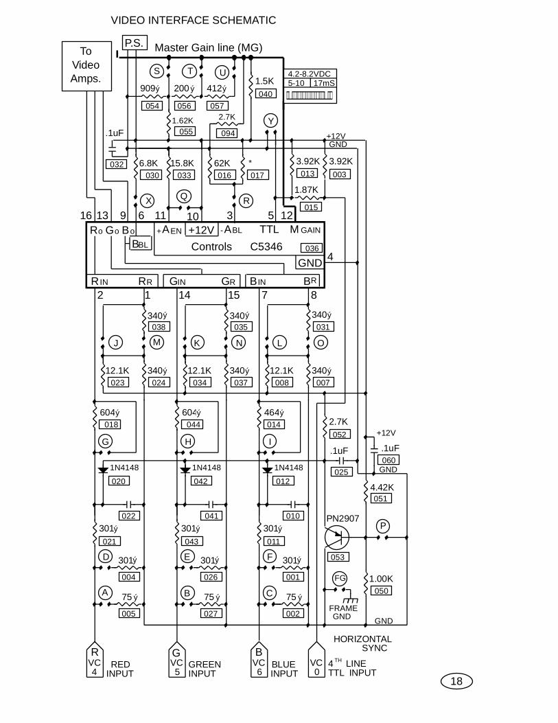
In the positive analog mode, a bias current flows to the input which is set by resistorat the +Analog Enable input. This current produces a voltage, across the parallel resistanceof the (game and ) plus resistor , at the IC pin 2. Without this bias current the blacklevel input voltage to the C5346 would be 0V and resistor would not be needed.With a bias resistor of 15.8K, the bias current is .6mA. If the external source resistance is300 ohms, the black level voltage at pin 2 is .27V. A black level voltage of .3V is set byresistor divider , to compensate for the bias current voltage drop.The input termination resistor reduces video line ringing and sets a darkscreen when the video input connector is disconnected. The saturatedcolor is the highest input voltage. There are two standard, saturated color,voltages available: 1.6V connected and 3.2V connected.
VIDEO INTERFACE CIRCUIT DESCRIPTION (+ & - Analog)
The video interface circuit is a general purpose RGB type input circuit. This circuitconnects the external video signal to the video amplifiers. It can accept positive goinganalog, negative going analog, and 4 line TTL. The particular mode of operation isselected by placing solder bridges on the foil side of the PCB. The solder bridge patternsare given in appendix A. Simplified video interface circuit:
In the negative analog mode, the video signal has a black level which is the -A BL voltage.This voltage is normally 5.6V and may be set to 5.1V by adding solder connection .The saturated color is the lowest input voltage (.9V-1.1V). To prevent input line ringingfrom exceeding the saturated color voltage limit, a clamp diode has been added.The current amplitude to the video amplifiers is defined by resistors & and themaster gain voltage.
21 18
7.5V BIAS LINE
MASTER GAIN&BLANKING
+12V
200 3.6K
2
3
16
12R,G,&BVIDEOINPUTS
1. NEGATIVE GOING ANALOG MODE.
MG
1821
2.2V
20
C534636
RED channel shown
-Analog Black Level (-A BL)
J
232104
21
7.5V BIAS LINE
MASTER GAIN &BLANKING
+12V
200ý 3.6K
2
16
12
+ANALOG ENABLE
R,G,&BVIDEOINPUTS
2. POSITIVE GOING ANALOG MODE.
MG
11
+12V
3
33
15.8K
23
24
12.1K
340ý04
301ý
C534636
RED channel shown
301ý
J
38
23 2404
Connections InstalledALWAYS NORMALLY
Q & Y S & X
20
Connection InstalledALWAYS NORMALLY
Y D,E,F,G,H,I,J,K,L,P, & T
M
340ý
33
16M
301ý 604ý
ý
R
Saturated Color (1V)
Black Level (5.6V)
16 R
62K
6.3V
Saturated Color (1.6V or 3.2V)
Black Level (.27V)
VIDEOAMPS
VIDEOAMPS
0575ý
AD
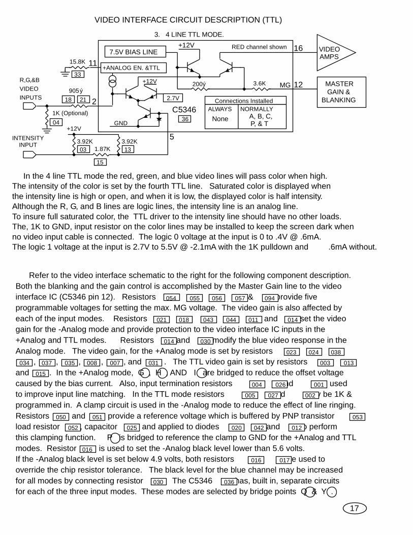
Refer to the video interface schematic to the right for the following component description.Both the blanking and the gain control is accomplished by the Master Gain line to the videointerface IC (C5346 pin 12). Resistors , , , , & provide fiveprogrammable voltages for setting the max. MG voltage. The video gain is also affected byeach of the input modes. Resistors , , , , , and set the videogain for the -Analog mode and provide protection to the video interface IC inputs in the+Analog and TTL modes. Resistors and modify the blue video response in theAnalog mode. The video gain, for the +Analog mode is set by resistors , , , , , , , , and . The TTL video gain is set by resistors , ,and . In the +Analog mode, G , H , AND I are bridged to reduce the offset voltagecaused by the bias current. Also, input termination resistors , , and are usedto improve input line matching. In the TTL mode resistors , , and may be 1K &programmed in. A clamp circuit is used in the -Analog mode to reduce the effect of line ringing.Resistors and provide a reference voltage which is buffered by PNP transistor ,load resistor , capacitor , and applied to diodes , , and to performthis clamping function. P is bridged to reference the clamp to GND for the +Analog and TTLmodes. Resistor is used to set the -Analog black level lower than 5.6 volts.If the -Analog black level is set below 4.9 volts, both resistors & are used tooverride the chip resistor tolerance. The black level for the blue channel may be increasedfor all modes by connecting resistor . The C5346 has, built in, separate circuitsfor each of the three input modes. These modes are selected by bridge points Q & Y .
In the 4 line TTL mode the red, green, and blue video lines will pass color when high.The intensity of the color is set by the fourth TTL line. Saturated color is displayed whenthe intensity line is high or open, and when it is low, the displayed color is half intensity.Although the R, G, and B lines are logic lines, the intensity line is an analog line.To insure full saturated color, the TTL driver to the intensity line should have no other loads.The, 1K to GND, input resistor on the color lines may be installed to keep the screen dark whenno video input cable is connected. The logic 0 voltage at the input is 0 to .4V @ .6mA.The logic 1 voltage at the input is 2.7V to 5.5V @ -2.1mA with the 1K pulldown and .6mA without.
Connections Installed
+12V
7.5V BIAS LINE VIDEO
MASTER GAIN &BLANKING
+12V
200 3.6K
2
16
12
+ANALOG EN. &TTL
R,G,&BVIDEOINPUTS
3. 4 LINE TTL MODE.
MG
11
5
33
15.8K
18 21
04
905
C534636
03
15
133.92K 3.92K
1.87K
GND
+12V
2.7V
RED channel shown
1K (Optional)ALWAYS NORMALLY
None
INTENSITYINPUT
VIDEO INTERFACE CIRCUIT DESCRIPTION (TTL)
ýý
P, & TA, B, C,
AMPS
17
021 018 043 044 011 014
023 024
034 037
038
035 007 031 003
015
055054 056 057
030014
004 026 001
005 027 002
050 051 053
052 025 020 042 012
016
016
017
030 036
094
008 013
Master Gain line (MG)ToVideoAmps.
P.S.
18
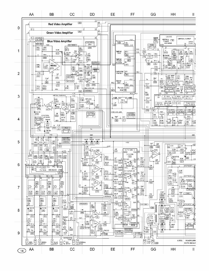
VIDEO INTERFACE SCHEMATIC
10
TTL
909
301 301301
RVC4 5
VCG
4
1.87K
1N4148
604
75
301
12.1K 340
6
BVC
1N4148
464
75
301
12.1K 340
1N4148
604
75
301
12.1K 340
2 1 14 15 7 8
BoRo Go GAINMTTL+ ENABLB
GNDControls C5346
INBGINR IN RR RG RB
Y
3.92K 3.92K6.8K 15.8K 62K
GND+12V
REDINPUT
GREENINPUT
BLUEINPUT
HORIZONTALSYNC
VC0
4 LINETH
GND
1.00K
4.42K
050
051
005 027 002
004 026 001
021 043 011
010041022
020 042 012025
052
023 024 034 037 008
038 035 031
030 033 017016 013 003
015
055
054 056 057040
200 4121.5K
S T U
J K N L OM
G H I.1uF
A B
P
D E F
INPUT
053
PN2907
1.62K
2.7K
.1uF060
GND
+12V
036
A- BL
16 13 5 123X Q R
9 6 11
*
2.7K
094.1uF
032
340 340340
C
044018 014
007
+12V
ý ý ý
ý ý ý
ý ý ý
ý ý ý
ý ý
ýý
ý
ý
FRAMEGND
FG
ý ý ý
4.2-8.2VDC5-10 17mS

The control circuit for the video amplifier is located on the B PRA (B precision resistor array).The B PRA includes all the resistors and the NE592. All of the parts labeled Rxx , xxG , and xxB , are components located on the circuit board, which are part of the red,green, and blue video amplifiers.
The video amplifier's stability and precise response to the input signal comes from acombination of the geometric layout of the B PRA and the high frequency response of the NE592.The NE592 stabilization capacitor B00 is an integral part of the B PRA conductor layout.Resistor B 4 is used to boost the NE592 drive current to the PNP transistor 87B .The NE592 bias circuit, at the input side, consists of B 5 , B6 , and B 9 .The negative feedback bias resistors are, B11 , B10 , and B 12 with B 17 as theoutput feedback resistor. Resistors B19 and B20 are connected to solder pads which,when bridged, permit the 1492 B PRA to be used on the models 1490 and 1491 monitors.
The NE592 gain is set by resistor . The drive signal from the NE592, pin 7,is coupled to the base of the NPN transistor through an impedance matching resistor B2 .This drive is also coupled to the base of the PNP transistor 87B via a coupling capacitor 82B .The NE592 output voltage range is 6V to 10V, which is the reason for the 7.9 volt NPN bias line.The 7.9 volt bias line is generated by buffering a voltage divider, formed by resistors 97and 100 , with a PNP darlington transistor 98 . A capacitor 9 5 is connected toshunt the high current spikes to GND. This line is common to all three video amplifiers.
The AC current gain is set by resistor B3 for the NPN output transistor and by B13for the PNP output transistor which is AC coupled via a capacitor 84B . On a positiveoutput transition of the video amplifier, the current of the PNP transistor can goas high as 32mA and on a negative transition the current drops to 0mA
VIDEO AMPLIFIER CIRCUIT, FUNCTION, DESCRIPTION The video amplifier, is a high speed push pull amplifier, which can swing as much as 92 volts.The maximum dynamic output swing is limited to 60 volts. The rest of the output voltage rangeis reserved for bias adjustment.
SIMPLIFIED VIDEO AMPLIFIER CIRCUIT:
+
+7.9V lineFrom Auto Biascontrol output
C5346
+12V
B5
B6
B9
B11
B10
NE592
B17
B12
B14
B182B
B15
87B
83B
B3
+127V
270ý 66ý
27ý
68K.015uF
40.2K1.65K
836ý
392ý
606ý
790ý 5.62K
VIDEOINTERFACE
2SA1370
2SC3467
The voltage swing at the output is 60 volts for a 4.3 mA current signal from the C5346.For this same 4.3 mA current signal the voltage swing at the video amp. input is 1.32 volts and the-input voltage swing at the NE592 is .75 volts. The reason for using the voltage matching resistor B6 is that the C5346 minimum output voltage is 7.7 volts, and the bias voltage at the NE592input is 5.3 volts.
VIDEO AMPLIFIER CIRCUIT DESCRIPTION
19
1
14
7
The video amplifier's output voltage, With no input signal, is the black levelwhich is the picture tube cut off voltage. This voltage is set for each of the three videoamplifiers by the auto bias circuit. This black level voltage has a range of 80V to 112V.
xxG xxBxxRBxx
B0087B
B5 B6 B9B11 B10 B12 B17
B19 B20
B4
B8 B2283B
87B 82B
097095098
B1384B
B3
100
B6
B2

R G BGND
16
1.65K
B16
B15B14
B13
B11
B10B9
B8B6
B5
93B
92B
91B
90B
88B
87B86B
392
539
1.27K
40.2K
606 NE592
3.78K
790 836
.1uF
1.2K
270
1N41482SA
1370
66
510
510B22
81B
82B
83B
84B
85B
.015uF
1000pF
FDH400
2SA137027
32
180
68K
2SC3467
2.2K
2.2K
B1
B2
B3
B4 B7
B17
B19
B20
096
13
1214
10
7
8
5
SOT
3.32K
.1uF
19
18
15
3
2
5 14
20
Blue Video Amplifier
.1uF095
1.21K
1.62K097
100MPS A64
098D
B00
3.3pF
B12
5.62K
13376
B18
270+12V
20
8.0-9.2VDC
WITH GRID
4uS1-2V
1.8-2.3VDC
124-126VDC
Dark screen80-112VDC
85Bacross
1.5-2.4V
8
8
8.9-9.8VDC
WITH GRID
4uS 1V
7.4-8.4VDCGND
+12V
BIAS CONTROL LINE
11
+127V
17
1
4
ý
ý
ý
ýý
ý
ý
ý ý
ý
ý
ý
ý
VIDEO INTERFACE VERTICAL andHORIZONTALBLANKING,
Master Gain, &Beam limiter
MG
VIDEO SOURCE (external)
For low output distortion, the PNP transistor is biased with a 6 mA current. The NPNtransistor and resistor B 17 conduct the PNP bias current to GND. Diode 86B balances thePNP base to emitter voltage. Resistors and set the voltage across B 15 whichdefine the video amplifier output stage bias current. A quick way to check this current, is tomeasure the voltage drop across the 510 ohm . The permissible voltage range islisted on the schematic as 1.5-2.4V. The PNP and NPN collector resistors and help stabilize the amplifier and provide some arc protection. Resistor B 18 is used to decouplethe video amplifiers from the +127V line. Capacitor is used to decouple the +12 volt lineclose to the video amplifiers. If this capacitor or the 7.9V line capacitor is open, thevideo may be unstable and distorted. Resistor B7 is the auto bias output load resistor.
If there is a problem with the video, first check the output waveform of the video amplifier,with the oscilloscope, if ok the problem is not in the video section. If not ok, check the inputwaveform at B PRA pin 8, if not ok there, check the video interface, If ok at the video amplifierinput, refer to this section to help with analyzing the video amplifier problems.
20
VIDEO AMPLIFIER SCHEMATIC
+12V
PART OFAUTO BIAS
GND
+12V
86BB1 B14 B15
85BB16 85B
B18
B7095
096
B17

The primary function of the socket board is to connect the main board to the CRT and toprotect the main board against arc related voltage spikes which originate in the CRT. The tube socket has built in spark gaps which direct part of the arc energy to thetube ground (aquadag) through a dissipation resistor 403 . The remaining high voltagefrom an arc is dropped across current limit resistors: Resistors 404 , 406 , and anddiodes , 408 , & 410 protect the video amplifiers by directing the arc energy tocapacitor . Since arcing does not normally occur in rapid succession, capacitor 414is left to discharge by the leakage current of diodes , 408 , & 410 and zenerdiode is not normally used. The grid pulse transistor is protected by a low pass filtermade up of resistors 422 & 42 and capacitor 423 . The auto bright transistor 417is protected by resistors 416 & 420 and by a low pass filter comprised ofresistors 413 , 418 ,& 415 and capacitor . Resistors & 424reduce the arc energy from the tube ground to signal GND. The current gain of the auto bright control loop is set by resistor 420 . The filament current is fine tuned by resistor 405 . The degaussing coil 432 is energized when power is turned on.It then rapidly turns off due to the heating of posistor 244 .
432SOCKET BOARD , DEGAUSSING CIRCUIT, AND LEGEND DESCRIPTION
241
245
3A FUSE
2 1PCPC 115VAC
INPUT 238
244
CC1
CC2
No. Represents the 1492 board part number. The parts list gives theCERONIX PART NUMBER which is indexed to the board part number.{
LTR.No. Part numbers of the resistors on the PRA indicated by LTR.X X PRA pin number. To determine which PRA the pin number
belongs to, look for the nearest PRA part number on that line.{
X-Y VDC
X-Y V
DC voltages are measured to GND except in the power supplywhere V- is the reference. Use a DVM for DC measurements.
CAUTION: When making measurements on the powersupply be sure that the other scope probe is not connected to GND.
TIME is the cycle time of the waveform.The waveform is normally checked with a oscilloscope.
Vp-pIt has a P-P voltage amplitude of{X-Y VDC
TIMEVp-p
WAVEFORM .
Legend Description
21
12
GND
1K 1/2W
425
431
414412403
422
405413
418
416
420402
415
424
100K2SC3675
200K47ý 47ý
.1uF 250V
407
408
410
406
404
411
FDH400 1K 1/2W
1K 1/2W
100K 1/2W
10K 1/2W
.68ý1/2W470ý
1K 1/2W
330pF 2,200pF
EHT
FIL.
*
GRID PULSE
RED
GREEN
BLUE
8
6
11
10
9 5 7 1
Socket BoardPCB 428
423 421417
TC1
TC2
TC4
TC3
TC10
TC6
8
FDH400
FDH400
20920ý405
1K 1/2W
1K1/2W
EHTFOCUSSCREEN
FIL.FIL.
FBT
BF5ROM125
No.
LTR.No.
X-Y VDCX-Y V
X-Y VDCTIMEVp-p
WAVEFORM
X X
LEGENDBOARD PART No.PART No. ON PRA.PRA PIN No.
DC VOLTAGERANGE, USING
A DMM.AC VOLTS
Peak to PeakCYCLETIME
Measured with scope
414
406 411 404403
407 408 410
407 408 410414
412422 425 423
413 418 415416 420
402421 424
420405
244432
417
The video P-P voltage amplitude at the cathodes, is the video input signal amplitude timesthe master gain control setting times the video amplifier gain. The gain select resistors setthe maximum video gain via the master gain line. For a greater range of brightness,(highlighting) the video system is allowed to supply high peak video currents which coulddamage the FBT if sustained. The beam current limiter circuit insures that the long termmaximum beam current is not exceeded.
Horizontal blanking is achieved by amplifying the flyback pulse (FBP) with transistor 104 .Vertical blanking starts as soon as the LA7851 starts the vertical retrace sequence and isterminated by the auto bias, bias active signal. A comparator is used to sense the vertical biasO/S, at pin 16 of the LA7851, which goes low when vertical retrace starts. Capacitor 132
holds the vertical blanking active, between the vertical bias O/S pulse, and the bias active pulse.When the bias active line goes high, the capacitor 132 is reset and vertical blanking ends,after the bias active line returns to it's high impedance state.
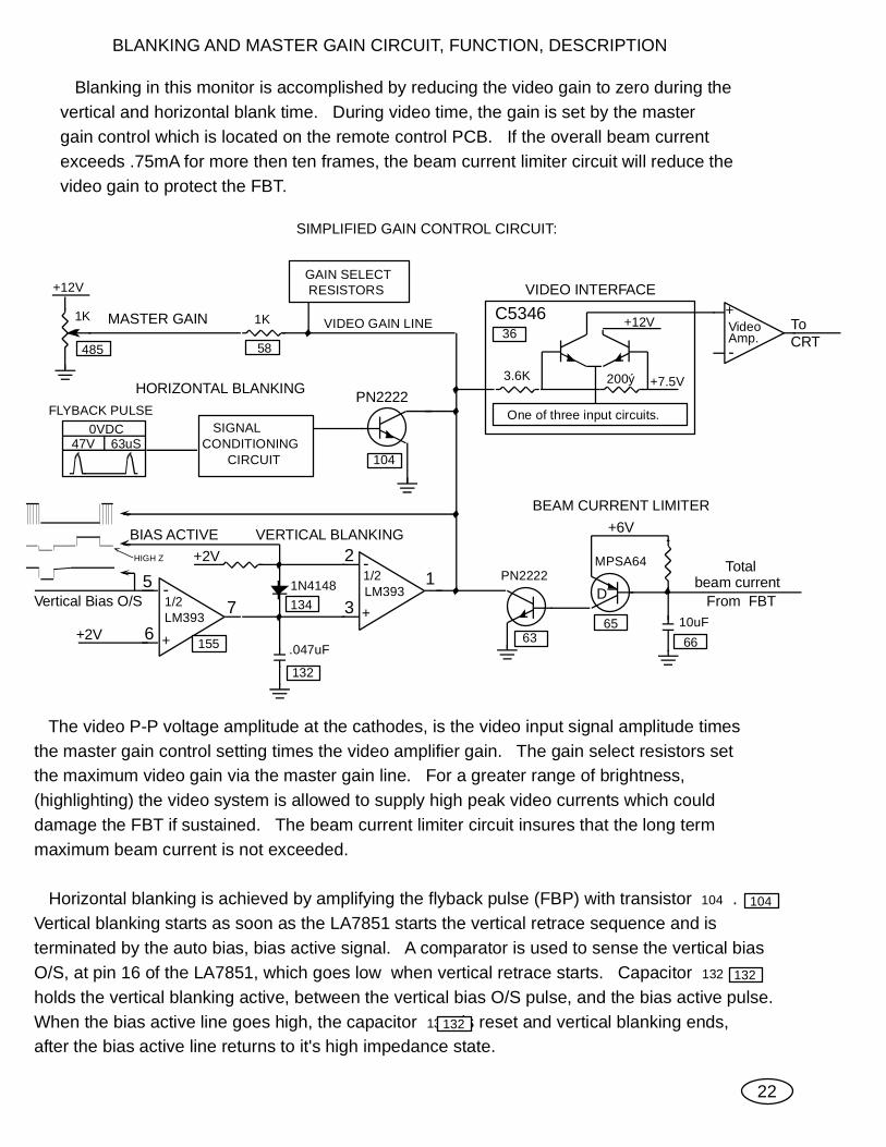
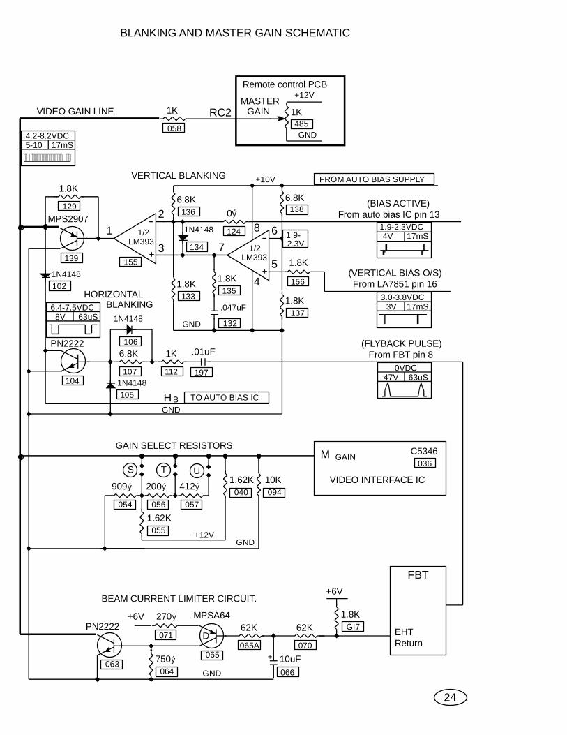
BLANKING AND MASTER GAIN CIRCUIT, FUNCTION, DESCRIPTION
Blanking in this monitor is accomplished by reducing the video gain to zero during thevertical and horizontal blank time. During video time, the gain is set by the mastergain control which is located on the remote control PCB. If the overall beam currentexceeds .75mA for more then ten frames, the beam current limiter circuit will reduce thevideo gain to protect the FBT.
SIMPLIFIED GAIN CONTROL CIRCUIT:
+2V
+VideoAmp.
+7.5V
+12V
One of three input circuits.
C5346+12V
0VDC47V 63uS
FLYBACK PULSE SIGNALCONDITIONING CIRCUIT 104
PN2222
MASTER GAIN
HORIZONTAL BLANKING
132
.047uF
1341N4148
+3LM3931/2 1
2
+
LM3931/2 7
VERTICAL BLANKING
6+2V
D
+6VBEAM CURRENT LIMITER
beam currentFrom FBT
Total
ToCRT
VIDEO INTERFACE
200ý3.6K
1K
485 58
1K
10uF66
MPSA64
6365
PN2222
155
36
GAIN SELECT RESISTORS
VIDEO GAIN LINE
132
132
104
BIAS ACTIVE
Vertical Bias O/S5
22
HIGH Z

The master gain control 485 is connected to the video gain line through a 1Kresistor 58 . The voltage range of the video gain line is programmable via resistor 094
and solder bridges at S , T , & U which may connect resistors 54 , 55 , 56 , and 57 to the video gain line. This arrangement permits a variety of input signals andpicture tubes to be used with the same monitor PCB.
Horizontal blanking ( ) is added to the gain line by transistors 104 . This transistorpulls down on the gain line through diode 102 when the flyback pulse is high.Capacitor 197 is charged by diodes 105 , 106 and resistor 112 such that, as soon asthe flyback pulse starts going positive the NPN transistor 104 turns on and horizontalblanking starts. The time constant of capacitor 197 and resistors 112 and 107 ischosen such that the capacitor will lead the FBP on the downward slope and turn thehorizontal blanking transistor off just at the end of the FBP.
Vertical blank time is started when a low going pulse from the LA7851 pin 16 causesthe output, pin 7, of the dual comparator 155 to go low. Capacitor 132 is dischargedthrough resistor 135 at this time. After the end of the LA7851 pulse, the capacitor 132
holds the output, pin 1 of the comparator, low until the bias active pulse recharges thecapacitor 132 through diode 134 . During the high time of the bias active pulse, thesecond comparator output is still low, because of the voltage drop across the diode 134 .The end of vertical blank time occurs when the bias active line returns to it's highimpedance state. The capacitor 132 holds the charge from the bias active pulse until thenext vertical blank time.
The video gain line will source up to 32mA during blank time, which is the reason forbuffering the vertical blank comparator with a PNP transistor 139 and E-B resistor 129 .Resistors 137 and 138 supply a voltage that is midrange relative to the LA7851 pulsefor maximum noise immunity. Resistors 133 and 136 also supply another midrangevoltage for the bias active pulse and the, vertical blanking, hold capacitor to work against.Resistors 124 and 156 are used as jumpers.
The beam current limiter circuit uses the base to emitter voltage of a darlingtontransistor 65 to set the maximum beam current. The beam current is converted to avoltage across resistor G17 . This voltage is applied to a long time constant RC circuit,resistor 70 and capacitor 66 , before it is sensed by the darlington transistor.Resistor 65 A has been added to protect the darlington transistor from arc energy.The sharpness of the limiting response is set by resistors 64 and 71 .Transistor 63 then, reduces the video gain by pulling down on the master gain lineupon excessive beam current.
BLANKING AND MASTER GAIN CIRCUIT DESCRIPTION
23
H B
66
485
54 55 56
57
58
104
102
105 106 112
104
197
197 112 107
155 132
132
132 134
135
134
132
129139
133 136
70
63
7164
137 138
124 156
65
G17
094
S UT
65A
BLANKING AND MASTER GAIN SCHEMATIC
0VDC47V 63uS
5
VERTICAL BLANKING
GND
1/2
156
1.8K
1N4148
HORIZONTALBLANKING
1N4148
107
105
112 197
1066.8K 1K .01uF
104
PN2222
LM393+
+10V
+
133
137
134
136
124
138
LM3931/2
155
6.8K 6.8K
1.8K
132
1351.8K
.047uF1.8K
GND
1N414813
2
4
8
76
6.4-7.5VDC8V 63uS
1N4148102
129
1.8K
MPS2907
139
1.9-2.3V
From FBT pin 8
VIDEO GAIN LINE
TO AUTO BIAS IC
FROM AUTO BIAS SUPPLY
3.0-3.8VDC 3V 17mS
909
055
054 056 057040
200 4121.62K
S T U
1.62K
094
1.9-2.3VDC4V 17mS
D
+6V
071
064 066
070
063065
PN2222MPSA64270
750 10uF
62K
BEAM CURRENT LIMITER CIRCUIT.
GND
+
Remote control PCB+12V
GND
MASTERGAIN 1K1K
058 485RC2
+12V
GAIN SELECT RESISTORS
+6V
1.8KGI7
GND
FBT
EHTReturn
VIDEO INTERFACE IC
C5346M GAIN
From auto bias IC pin 130ý
From LA7851 pin 16
(BIAS ACTIVE)
HB
036
(VERTICAL BIAS O/S)
(FLYBACK PULSE)
24
10K
ý
ý
ý ý ý
4.2-8.2VDC5-10 17mS
065A
62K
CERONIXPART No. DESCRIPTION
CERONIXPART No. DESCRIPTION
.01001002003004005006007008009010011012013014015016017018019020021022023024025026027028029030031032033034035036037038039040041042043044045046047048049050
.01
.01
.01
.01
.01
.01
.01
.01
.01
.01
.01
.01
.01
.01
.01
.01
.01
.05
.01
.22
CPR0128CPR0124CPR0140CPR0128CPR0124
CPR0129CPR0144
CPD1251CPR0140CPR0131CPR0011CPR0018
CPR0132
CPD1251CPR0128
CPR0144CPR0129CPC1039CPR0128CPR0124CPR0050
CPR0013CPR0129CPC1039CPR0145CPR0144CPR0129CPI1409CPR0129CPR0129
CPR0136
CPD1251CPR0128CPR0132CPR0004CPR0011CPR0011CPR0004
CPR0009
CPS1754
CPR0128
.01
.01
.05
.01
.01
.01
.01
.01
.01
.01
.01
.01
.01
.01
.01
.01
25
051052053054055056057058059060061062063064065
06606706806907007107207307407507607707807908081B82B83B84B85B86B87B88B89B90B91B92B93B094095096097098099100
065A
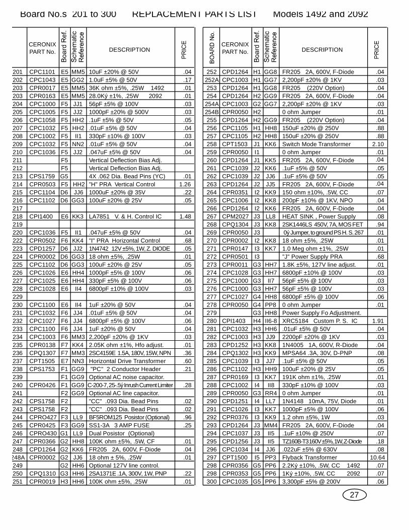
Board No.s 001 to 100 REPLACEMENT PARTS LIST Models 1492 and 2092
CC8CC8CC8AA5AA5AA5BB5EE3
CC8DD9DD8PP5PP5PP5
RR5DD8GG2PP5RR5PP5
EE9EE8
DD8CC1CC1CC2DD1
CC2
CC1CC1DD2
DD2DD2DD2DD2
DD3BB2CC3DD3
CC3
RR5
BB5
301 ohm ±1%, .25W75 ohm ±1%, .25W3.92K ohm ±1%, .25W301 ohm ±1%, .25W75 ohm ±1%, .25W6 Conductor Header.340 ohm ±1%, .25W12.1K ohm ±1%, .25W
301 ohm ±1%, .25W1N4148 10mA, 75V Diode3.92K ohm ±1%, .25W464 ohm ±1%, .25W1.8K ohm ±5%, .25W62K ohm ±5%, .25W
604 ohm ±1%, .25W
1N4148 10mA, 75V Diode301 ohm ±1%, .25W
12.1K ohm ±1%, .25W340 ohm ±1%, .25W.1uF ±5% @ 50V301 ohm ±1%, .25W75 ohm ±1%, .25W0 ohm Jumper
6.8K ohm ±5%, .25W340 ohm ±1%, .25W.1uF ±5% @ 50V15.8K ohm ±1%, .25W12.1K ohm ±1%, .25W340 ohm ±1%, .25WXRC5346A Custom Video IC340 ohm ±1%, .25W340 ohm ± 1%, .25W
1.62K ohm ±1%, .25W
1N4148 10mA, 75V Diode301 ohm ± 1%, .25W604 ohm ±1%, .25W270 ohm ±5%, .25W1.8K ohm ±5%, .25W1.8K ohm ±5%, .25W270 ohm ±5%, .25W
1K ohm ±5%, .25W
Optional input filter capacitor.
Optional input filter capacitor.
Optional input filter capacitor.
Optional -BL adjust resistor.
BB9BB9CC6AA9AA9
BB7BB7
BB8BB8BB6BB7BB6BB6
AA7
AA8AA8
AA7AA7CC8BB9BB9
AA6BB7AA5AA6AA7BB7AA6BB7AA7
BB5
AA8AA8AA7DD8CC8CC9DD8
CC9
BB8
BB8
AA8
BB6
.01
.01
CPR0141CPR0012CPQ1301CPR0126CPR0136CPR0127CPR0130CPR0009
CPC1039CPR0004
CPQ1303CPR0007CPQ1302
CPC1101CPI1410CPC1101CPC1039CPR0018CPR0004
CPR0011CPR0009
CPR0013CPR0500CPC1040CPQ1308CPC1037CPR0050CPD1251CPQ1309CPC1005
CPQ1309CPR0011
CPR0012CPC1039CPC1039CPR0136CPQ1302
CPR0134
CPR0015
CPD1250
CPR0011
CPR0018
CPR0006
750 ohm ±5%, .25W
4.42K ohm ±1%, .25W2.7K ohm ±5%, .25WPN2907 .6A, 40V, .6W, PNP909 ohm ±1%, .25W1.62K ohm ±1%, .25W205 ohm ±1%, .25W412 ohm ±1%, .25W1K ohm ±5%, .25W
.1uF ±5% @ 50V270 ohm ±5%, .25W22K ohm ±5%, .25WPN2222A .6A, 30V, .5W, NPN
MPSA64 .3A, 30V, D-PNP
10uF ±20% @ 50VLM393 Dual Comparator10uF ±20% @ 50V.1uF ±5%, @ 50V62K ohm ±5%, .25W270 ohm ±5%, .25W
1.8K ohm ±5%, .25W1K ohm ±5%, .25W
6.8K ohm ±5%, .25WBlue Video Amplifier.015uF ±10% @ 250V2SC3467AE .1A, 200V, 1W, NPN..1uF ±10% @ 250V
510 ohm ±5%, .25W
1N4148 10mA, 75V Diode2SA1370E .1A, 200V, 1W, PNP1000pF ±20% @ 500V
FDH400 .1A, 200V, Diode2SA1370E .1A, 200V, 1W, PNP1.8K ohm ±5%, .25W CF1.8K ohm ±5%, .25W CF2.7K ohm ±5%, .25W.1uF ±5% @ 50V.1uF ±5% @ 50V1.62K ohm ±1%, .25WMPSA64 .3A, 30V, D-PNP
1.21K ohm ±1%, .25W
62K ohm ±5%, .25W
0ý Jumper
.01
.05
.01
.01
.06
.01
.01
.01
.01
.05
.01
.01
.05
.01
.08
.04
.31
.04
.01
.01
.01
.01
.011.12
.07
.16
.07
.01
.01
.19
.03
.03
.19
.01 .01 .01
.05.05.01.08
.01
.01
.01
.01
1.51
A1A1B1B1B1C1A2A2
A2A2A2B1B2B1B1B1B2
B1B2B2B2C2C2C2C2A2
A2A2A2A2B3B2B2B2B2
B2C2C2C2C2D1D1D1D1
D1B4
A4A4B3A3B3C4C3C3C3C3C3C3C3B3C3A3A3C3E1
E2E1E1E1E1E1E1E2E2D1E2E1D2D2D2D2D1D1D1D1
C2D2D2D2D2C2C1D1

CERONIXPART No. DESCRIPTION
CERONIXPART No. DESCRIPTION
101102103104105106107108109110111112113114115116117118119120121122123124125126127128129130131132133134135136137138139140141142143144145146147148149150151152
CPQ1303CPR0012CPI1410CPR0011
CPS1755
CPR0050CPC1039CPC1036CPC1032
CPI1405CPR0144
CPC1032CPC1102CPR0504CPR0013CPR0142CPR0050CPR0050CPR0050CPR0144CPR0050CPR0009
CPQ1308CPR0050CPR0351CPC1041
CPR0143CPQ1307CPM2037CPC1036CPM2036
CPD1252CPC1109CPI1401CPR0377CPR0050CPC1104CPR0391CPC1032CPC1000
6800pF ±10% @ 100V
6800pF ±10% @ 100V
1N4005 1A, 600V, R-Diode1N4148 10mA, 75V, Diode .01
.02
1N4005 1A, 600V, R-Diode .02PN2222A .8A, 40V, .5W, NPN .051N4148 10mA, 75V, Diode .011N4148 10mA, 75V, Diode .016.8K ohm ±5%, .25W .01
.03
.036800pF ±10% @ 100V .031K ohm ±5%, .25W .01
"TC" 10 Conductor Header .29"C" PRA (Auto Bias) .68.047 uF ±5% @ 50V .04.1 uF ±5% @ 50V .05.047uF ±5% @ 50V .04
.1uF ±5% @ 50V .05
CPD1252
CPR0050
CPD1251
CPR0016
CPD1252
CPD1251CPD1251CPR0013CPC1028
CPC1028CPR0009
CPS1756CPR0506CPC1036CPC1039CPC1036
CPC1039
CPC1039CPI1402CPR0050CPC1101CPC1101CPC1101CPC1039CPR0011CPI1407CPC1104CPC1036CPR0011CPD1251CPR0011CPR0013CPR0011CPR0013CPQ1301CPR0050CPR0016CPR0016CPR0016CPC1039CPD1252CPI1405CPR0015CPR0015
CPC1039
CPQ1303
CPC1028
CPC1036 .047uF ±5% @ 50V .04.1uF ±5% @ 50V .05
1.950 ohm Jumper. .0110uF ±20% @ 50V .0410uF ±20% @ 50V .0410uF ±20% @ 50V .04.1uF ±5% @ 50V .051.8K ohm ±5%, .25W .01NJM7812FA 12V, 1A, Regulator. .301000uF ±20% @ 35V .22.047uF ±5% @ 50V .041.8K ohm ±5%, .25W .011N4148 10mA, 75V, Diode .011.8K ohm ±5%, .25W .016.8K ohm ±5%, .25W .011.8K ohm ±5%, .25W .01 6.8K ohm ±5%, .25W .01MPS2907 .6A, 40V, .6W, PNP .060 ohm Jumper .0133K ohm ±5%, .25W .0133K ohm ±5%, .25W .0133K ohm ±5%, .25W .01.1uF ±5% @ 50V .051N4005 1A, 600V, R-Diode .02LM324 Quad Op. Amp. .3122K ohm ±5%, .25W .0122K ohm ±5%, .25W .01
.1uF ±5% @ 50V .050 ohm Jumper .01
DD5AA4DD5AA4BB4BB4BB4DD6
DD7DD7BB4
EE7EE7EE7
EE6EE6EE6FF7CC3FF7FF6FF6EE3AA3EE3JJ6BB4BB4BB3BB4BB3CC4CC3AA3
GG6GG7GG7EE5DD5GG6GG6GG6
GG5
EE8 33K ohm ±5%, .25W .01
PN2222A .6A, 30V, .5W, NPN .052.7K ohm ±5%, .25W .01LM393 Dual Comparators .311.8K ohm ±5%, .25W .01
CPR0393 390 ohm ±5%, 2W .04"RC" 8 Conductor Header .26
0 ohm Jumper .01.1uF ±5% @ 50V .05.047uF ±5% @ 50V.01uF ±5% @ 50V .04
.04
LM324 Quad Op. Amp. .31.0112.1Ký ±1%.25W (Pin. Adj) 1492
CPR0168 8.06Ký ±1%.25W (Pin. Adj) 1492 .01
.01uF ±5% @ 50V .04100uF ±20% @ 25V .05"G" PRA (H. Width Control) .926.8K ohm ±5%, .25W .017.15K ohm ±1%, .25W .010 ohm Jumper .010 ohm Jumper .010 ohm Jumper .0112.1K ohm ±1%, .25W .010 ohm Jumper .011K ohm ±5%, .25W .01
2SC3467F .1A, 200V, 1W, NPN .160 ohm Jumper .01150 ohm ±10%, .5W, CC .05.33uF ±5% @ 50V .08
10.0K ohm ±1%, .25W .012SC4159E 1.5A, 180V, 15W, NPN .36Heat Sink, H. Width output .11.047uF ±5% @ 50V .04Heat Sink, V. Deflection out .13
1N4005 1A, 600V, R-Diode .02470uF ±20% @ 50V .19LA7830 Vert. Def. Output .673.3 ohm ±5%, 1W .030 ohm Jumper .011000uF ±20% @ 35V .22200 ohm ±5%, 2W .04.01uF ±5% @ 50V .0456pF ±5% @ 100V .03
CA3224E Auto Bias IC
26
Board No.s 101 to 200 REPLACEMENT PARTS LIST Models 1492 and 2092
CPR0157 127K ohm ±1%, .25W
CPR0018 .0162Ký ±5%, .25W (H. Ras. Adj.)
CPR0011 .011.8K ohm ±5% (Blooming adjust)
CPR0024 .013.3Ký ±5% .25W (Max. iBeam adj.)
CPR0050 0 ohm Jumper .01
62K ±5%, .25W (2092 Option)
CPR0017 .0136Ký ±5%, .25W (Pin. Adj) 2092
CPR0015 22Ký ±5%, .25W (Pin. Adj) 2092 .01
CPR0018 .01
.01
153154155156157158159160161162163164165166
167
168169170171172173174175176177178
180181182183
184185186187188
189190191192193194195196197198200
166A
179
183A
166
167
188A CPM2037
EE9DD9BB3CC4MM4
LL0NN8MM7NN7
NN7NN7
NN7
PP8MM7
MM8NN5GG4GG1GG2EE8
NN5
MM2GG1NN3MM5
NN6PP8PP8GG3GG1
KK1KK1
GG2
MM2JJ2BB4
HH1
EE4HH2
NN7
MM7
MM7
NN8
NN7
NN7
GG1 Heat Sink (2092 Option) .11
.01
A5A5B5B5B5B5B4C5
C5C5D5
D4C5A5B5B5
B5B5B5A6A6B6B6B6A7A6A7B7B7C7C7C7C7C7C6A6C6C6C6C6B6C5C5C6C6
C6D6C6 E5
D5D5D5G4F4F4E4E4E4F4
E4D4G3F3E3E3E4E3E3E4F3E3E3D3D3D3D3E3F3F3E2E3E3E3E3E3E3E2E2E2E2E2D2F3C2D7D7C7C6C6
CERONIXPART No. DESCRIPTION
CERONIXPART No. DESCRIPTION
.04.17
.01
.03
.03
.05
.04 .03 .04 .04
.011.26
.22
.05
1.48
.04
.68
.05 .01 .05
.06
.06
.03
.04
.04
.06 .04
.03
.01
.36
.60
.21
.28
.02
.02
.96
.25
.01
.04
.22
.01
.04
.04.04
.04
.88
.88 2.10
.04.05.05
.07.04.04.08.94
.01 .01
.68
.01
.03
.03
.03
.06
.01
1.91.04.03.04.08.05.05.01.03
.01
.06
.03
.04 .07
.18
.08
.07
.06
27
Board No.s 201 to 300 REPLACEMENT PARTS LIST Models 1492 and 2092
.01
.03
.01
.01
201202
203204205206207208209210211212213214215216217218219220222223224225226227228229230231232233234235236237238239240241242243244245246247248
248A
250251
249
203 .01
.03
.01
.04
10.64
252
253254
255256257258259260261262263264265266267268269270271272273274275276277278279280281282283284285286287288289290291292293294295296297298
300
252A
254A254B
298
CPD1264
CPD1264CPD1264
CPD1264CPC1105
CPT1503
CPD1264CPC1039CPC1039
CPR0351CPC1006CPD1264CPM2027CPQ1304
CPR0002CPR0147CPR0501CPR0011CPC1028CPC1000CPC1000CPC1027CPR0050
CPI1403CPC1032CPC1003CPD1252CPQ1302CPC1039CPC1102CPR0169CPC1002
CPD1251CPC1026CPR0376CPD1264CPC1037CPD1256CPC1034CPT1500CPR0356
CPC1035
CPC1105
CPC1003
CPR0050
CPR0050
CPC1003CPR0050
CPD1264
CPR0353 .07
MM5GG2
MM5JJ1JJ2HH2HH2II1
NN2JJ2
JJ6GG3
KK3
II1KK4JJ2
GG3GG3HH4HH4II4
II4JJ4JJ4JJ4
MM3KK4MM3NN3GG9
GG9
LL9GG9
HH8KK6
HH6HH6
HH6JJ6
GG9
GG9
MM5
LL9
GG8
GG8GG9
KK9KK8KK6LL8KK8
KK8KK7
HH7HH7II7
HH7HH8PP8
II6-8HH6JJ9KK8KK9JJ7HH9KK7II8
LL7KK7KK9MM4
II5II5
JJ6PP3PP6
PP6
GG7
HH8
GG9HH8HH8KK6
KK5KK6JJ6JJ5
GG7
PP6
RR4
FR205 2A, 600V, F-Diode
FR205 (220V Option)FR205 2A, 600V, F-Diode
FR205 (220V Option)150uF ±20% @ 250V150uF ±20% @ 250VSwitch Mode Transformer
FR205 2A, 600V, F-Diode.1uF ±5% @ 50V.1uF ±5% @ 50V
150 ohm ±10%, .5W, CC200pF ±10% @ 1KV, NPOFR205 2A, 600V, F-DiodeHEAT SINK , Power Supply2SK1446LS 450V, 7A, MOS FET
18 ohm ±5%, .25W1.0 Meg ohm ±1%, .25W"J" Power Supply PRA1.8K ±5%, 127V line adjust.6800pF ±10% @ 100V56pF ±5% @ 100V56pF ±5% @ 100V6800pF ±5% @ 100V0 ohm Jumper
XRC5184 Custom P. S. IC.01uF ±5% @ 50V2200pF ±20% @ 1KV1N4005 1A, 600V, R-DiodeMPSA64 .3A, 30V, D-PNP.1uF ±5% @ 50V100uF ±20% @ 25V191K ohm ±1%, .25W330pF ±10% @ 100V
1N4148 10mA, 75V, Diode1000pF ±5% @ 100V1.2 ohm ±5%, 1WFR205 2A, 600V, F-Diode.1uF ±10% @ 250VTZ160B-T3 160V ±5%, 1W, Z-Diode.022uF ±5% @ 630VFlyback Transformer2.2Ký ±10%, .5W, CC 1492
3,300pF ±5% @ 200V
2,200pF ±20% @ 1KV
0 ohm Jumper
Power Supply Fo Adjustment.
0 ohm Jumper
2,200pF ±20% @ 1KV0 ohm Jumper
FR205 2A, 600V, F-Diode
1Ký ±10%, .5W, CC 2092
10uF ±20% @ 50V1.0uF ±5% @ 50V
28.0Ký ±1%, .25W 209256pF ±5% @ 100V1000pF ±20% @ 500V.1uF ±5% @ 50V.01uF ±5% @ 50V330pF ±10% @ 100V.01uF ±5% @ 50V.047uF ±5% @ 50V
4X .062 Dia. Bead Pins (YC)"H" PRA Vertical Control1000uF ±20% @ 35V100uF ±20% @ 25V
LA7851 V. & H. Control IC
.047uF ±5% @ 50V"I" PRA Horizontal Control1N4742 12V ±5%, 1W, Z. DIODE18 ohm ±5%, .25W100uF ±20% @ 25V1000pF ±5% @ 100V330pF ±5% @ 100V6800pF ±10% @ 100V
1uF ±20% @ 50V.01uF ±5% @ 50V6800pF ±5% @ 100V1uF ±20% @ 50V2,200pF ±20% @ 1KV2.05K ohm ±1%, Hfo adjust.2SC4159E 1.5A, 180V, 15W, NPNHorizontal Drive Transformer "PC" 2 Conductor Header
C-200-7, 25-.5ý Inrush Current Limiter
"CC" .093 Dia. Bead Pins"CC" .093 Dia. Bead PinsBF5ROM125 Posistor (Optional)SS1-3A 3 AMP FUSE
100K ohm ±5%, .5W, CFFR205 2A, 600V, F-Diode18 ohm ± 5%, .25W
2SA1371E .1A, 300V, 1W, PNP100K ohm ±5%, .25W
Optional 127V line control.
Optional AC noise capacitor.
Optional AC line capacitor.
36K ohm ±5%, .25W 1492
Dual Posistor (Optional)
CPC1101CPC1043
CPR0163CPC1000CPC1005CPC1058CPC1032CPC1002CPC1032CPC1036
CPS1759CPR0503CPC1104CPC1102
CPI1400
CPC1036CPR0502CPD1257CPR0002CPC1102CPC1026CPC1025CPC1028
CPC1100CPC1032CPC1027CPC1100CPC1003CPR0138CPQ1307CPT1505CPS1753
CPR0426
CPS1758CPS1758CPRO427CPR0425
CPR0366CPD1264CPR0002
CPQ1310CPR0019
CPR0017
CPRO430
E5E5E5E5F5F5F5F5F5F5F5F5F5G5F5D6D6
E6
F5F6D6D6D6E6E6E6
E6F6F6F6F6F7F7E7F1F1F1F2F2F2F3F3G1G2G2G2G2G3H3 G5
G5G5I5I4J3J3J3I3I3I4G3I4I3H3I3H3H3H3H3H4G3G4G4G3G3G3G3I3I3I2
J3J3I2I2I2J2J2J2J1I1J1H2H1H2H2G2H2H1H1H1
Vertical Deflection Bias Adj.Vertical Deflection Bias Adj.
HH2
.01CPR0050 0ý Jumper, to ground PS H. S. 267J3

CERONIXPART No. DESCRIPTION
CERONIXPART No. DESCRIPTION
301
302303304305
306
307308309310
CPT1523
311312313314315316317
401402403404405
406407408409410411
CPT1506CPR0392CPQ1305CPC1050
CPC1030
CPC1034CPD1252CPR0365CPD1252CPD1253CPD1264CPR0050
CPC1044CPT1504CPC1105
CPS1750CPR0350CPR0352CPR0353CPR0375
CPR0353CPD1250CPD1250
CPD1250CPR0353
CPR0353CPC1040CPR0355CPR0019CPQ1306CPR0353
CPR0029CPC1003CPR0353CPC1002CPR0350CPR0354
CPS1758
CPS1769CPS1768
CPR0402481
482 CPR0405
CPR0401
CPR0403
CPR0400
CPR0007CPS1767
CPA4102REMOTE CONTROL BOARD
PCB ASSEMBLIES
TUBE SOCKET BOARD
PP7 220uH Horz. Width Coil. 1492
PP6 Horz. Linearity Coil .60NN4 270 ohm ±5%, 2W .04NN3 2SD1651 5A, 1.5KV, NPN 1.48RR7 .47uF ±5% @ 250V 1492 .36
RR6 .01uF ±3% @ 1.6KV 1492 .26
RR8 .022uF ±5% @ 630V .08RR6 1N4005 1A, 600V, R-Diode .02NN4 470 ohm ±5%, .5W, CF .01RR7 1N4005 1A, 600V, R-Diode .02RR8 1N4937 1A, 600V, F-Diode .03NN4 FR205 2A, 600V, F-Diode .04
0 ohm Jumper .01
PP8 2.7uF ±10% @ 100V .32PP7 Horizontal Width Coil .63II5 150uF ±20% @ 250V .88
CRT SOCKETNN1 47 ohm ±10%, .5W, CC
1.54
NN1 470 ohm ±10%, .5W, CC.07.07
NN0 1K ohm ±10%, .5W, CC .07PP1 .68 ohm ±5%, 1W 1492 .03
NN1 1K ohm ±10%, .5W, CC .07MM0 FDH400 .1A, 200V, Diode .03MM0 FDH400 .1A, 200V, Diode .03
MM0 FDH400 .1A, 200V, Diode .03NN0 1K ohm ±10%, .5W, CC .07
413 PP1 1K ohm ±10%, .5W, CC .07414 MM1 .015uF ±10% @ 250V415 NN1 100K ohm ±10%, .5W, CC .07416 MM1 100K ohm ±5%, .25W, CF .01417 MM1 2SC3675 .1A, 1.5KV, NPN .67418 PP1 1K ohm ±10%, .5W, CC .07
420 MM1 200K ohm ±10%, .25W, CF .01421 PP1 2200pF ±20% @ 1KV .03422 PP1 1K ohm ±10%, .5W, CC .07423424425
PP1 330pF ±10% @ 100V .03NN1 47 ohm ±10%, .5W, CC .07NN1 10K ohm ±10%, .5W, CC .07
426
427 .093 Dia. Bead Pin .02
10 Conductor Cable .8310 Conductor Cable, Double length. .99
FF1 10K ohm Yellow Pot
FF1 500 ohm Black Pot
483
484
485
486487
FF2 1K ohm Blue Pot
FF2 20K ohm Orange Pot
FF2 1K ohm White Pot .17
FF1 750 ohm ±5%, .25W .01"RC" 8 Conductor Cable .87
Remote PCB Assembly. 4.75
CPA4100 1492 Main PCB Assembly 105.00
CPA4101 CRT P.C. Board Assembly 7.50
28
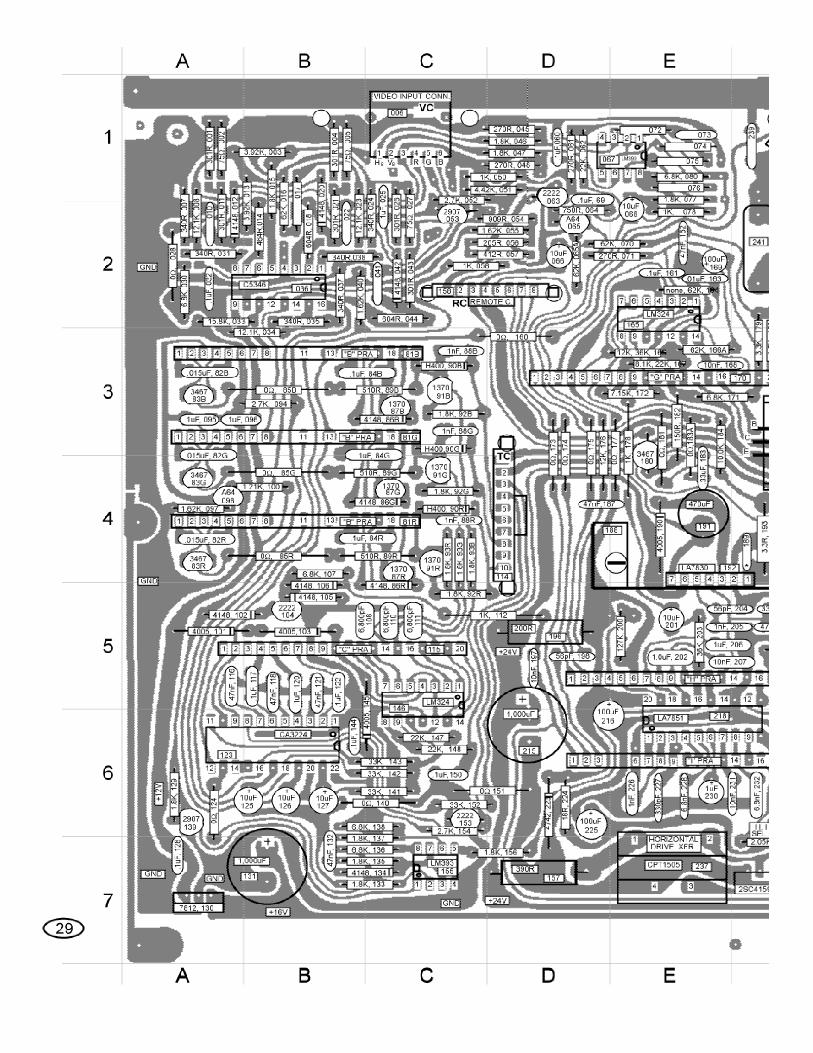
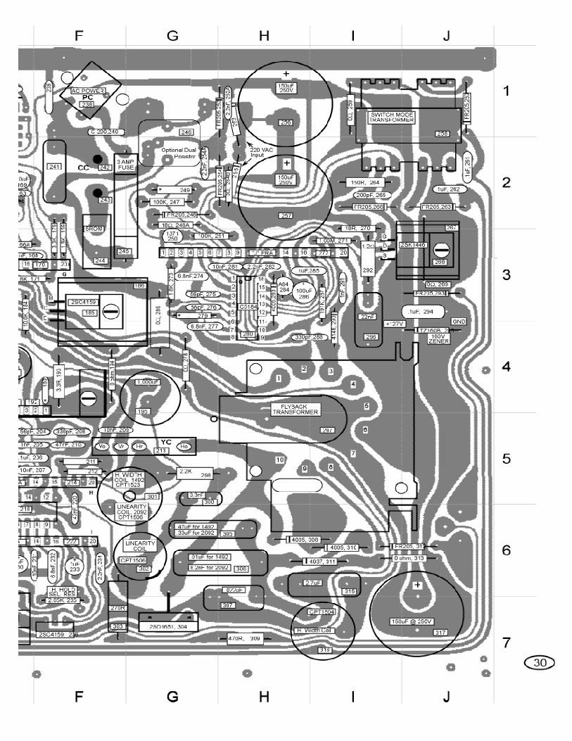
Board No.s 301 to 490 REPLACEMENT PARTS LIST Models 1492 and 2092
419
412
.60
306 CPC1055 RR6 8,200pF ±3% @ 1.6KV 2092 .37
301 CPT1506 PP7 .60
305 CPC1059 RR7 .33uF ±5% @ 250V 2092 .38
405 PP1CPR0050 0ý Jumper 2092 .01
.07
.17
.17
.17
.17
CPA4103 2092 Main PCB Assembly 115.00
Horz. Linearity Coil 2092G5G5G6F7G7H6H6H6H6H7I6H7I6I6J6J6
I6I7J7
31
Block Diagram Review
SYNC
VIDEO
GAME
CRT
H
V
VERTICAL
CONTROL
CONTROLVERTICAL
OUTPUT
HORIZONTAL H.H.
REMOTECONTROLS
HORIZONTALSize Control
DIODEModulator
FBT
LOADISOLATIONTransformer DOUBLER
VOLTAGE
SWITCHINGREGULATOR
Raw DC320V
+127V
-200V
Driver Output
3
Interface
DY
DY
G
sV
I. V. Feedback High Efficiency
EHT
J
H s
H. Pos.
V. Size &V. Ras. Pos.
PINCUSHION
Sync delayM
N O
(PCB)
P
Q R
(IN GAME)
S
Beam Current
(VIDEO & DEFLECTION)
U
+16V
+27VRegulator
+12V VideoSupply
T
Sync
OVERVOLTAGEPROTECT
DeflectionSupply
V
W
X
+12VZener
2
V-
BrightAuto
AUTO BIASSYNC IC
BLANKINGF.B.P.
V retraceBeam limit
M. gain
H. blankV. blank
Program pulseGrid pulse
Beam currentbuffer
3 3
33
3
2
3
A BC
E
F
H
I
D
3
VERTICALAUTO BIAS
L
Y
BeamCurrentFeedback
VIDEOInterface
VIDEOAMPS.
Bias
K
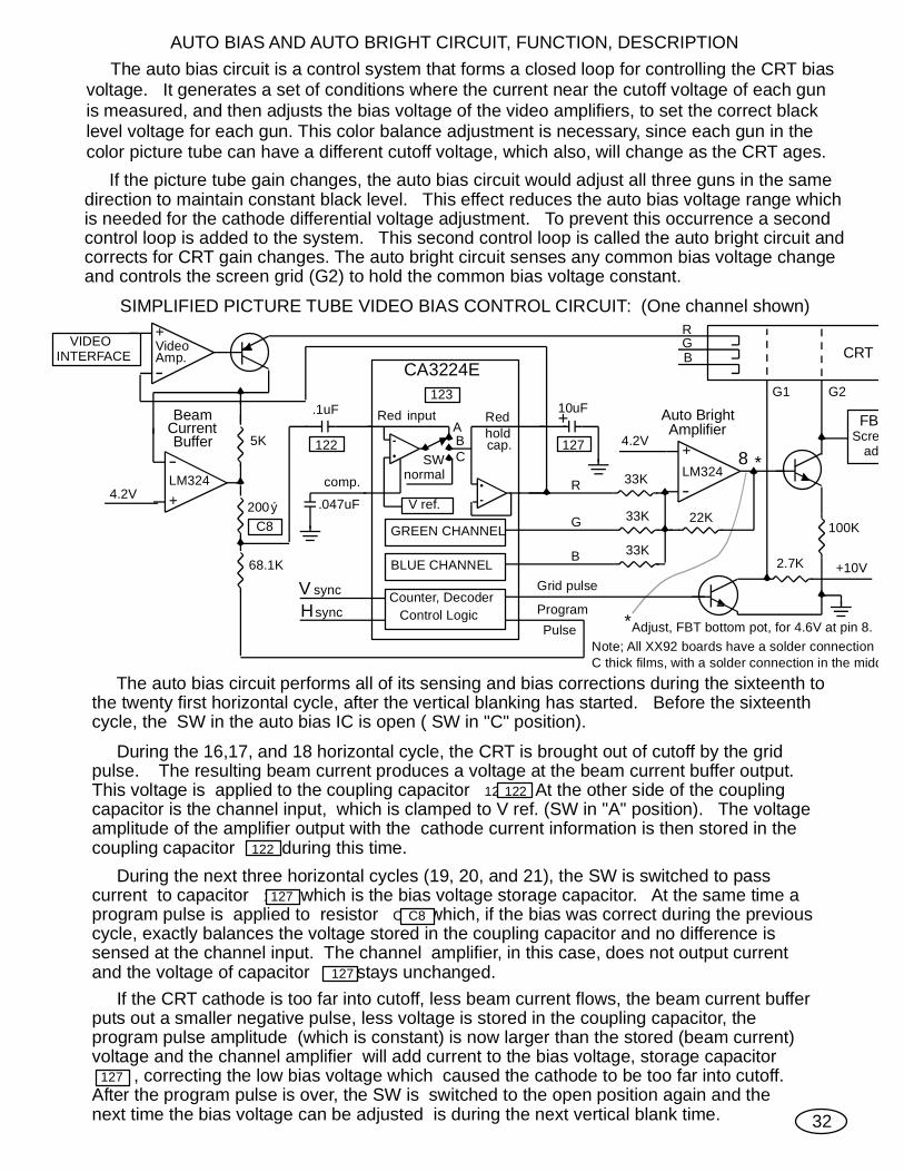
The auto bias circuit performs all of its sensing and bias corrections during the sixteenth tothe twenty first horizontal cycle, after the vertical blanking has started. Before the sixteenthcycle, the SW in the auto bias IC is open ( SW in "C" position).
If the CRT cathode is too far into cutoff, less beam current flows, the beam current bufferputs out a smaller negative pulse, less voltage is stored in the coupling capacitor, theprogram pulse amplitude (which is constant) is now larger than the stored (beam current)voltage and the channel amplifier will add current to the bias voltage, storage capacitor 127 , correcting the low bias voltage which caused the cathode to be too far into cutoff.After the program pulse is over, the SW is switched to the open position again and thenext time the bias voltage can be adjusted is during the next vertical blank time.
During the next three horizontal cycles (19, 20, and 21), the SW is switched to passcurrent to capacitor 127 which is the bias voltage storage capacitor. At the same time aprogram pulse is applied to resistor C8 which, if the bias was correct during the previouscycle, exactly balances the voltage stored in the coupling capacitor and no difference issensed at the channel input. The channel amplifier, in this case, does not output currentand the voltage of capacitor 127 stays unchanged.
During the 16,17, and 18 horizontal cycle, the CRT is brought out of cutoff by the gridpulse. The resulting beam current produces a voltage at the beam current buffer output.This voltage is applied to the coupling capacitor 122 . At the other side of the couplingcapacitor is the channel input, which is clamped to V ref. (SW in "A" position). The voltageamplitude of the amplifier output with the cathode current information is then stored in thecoupling capacitor 122 during this time.
The auto bias circuit is a control system that forms a closed loop for controlling the CRT biasvoltage. It generates a set of conditions where the current near the cutoff voltage of each gunis measured, and then adjusts the bias voltage of the video amplifiers, to set the correct blacklevel voltage for each gun. This color balance adjustment is necessary, since each gun in thecolor picture tube can have a different cutoff voltage, which also, will change as the CRT ages.
AUTO BIAS AND AUTO BRIGHT CIRCUIT, FUNCTION, DESCRIPTION
SIMPLIFIED PICTURE TUBE VIDEO BIAS CONTROL CIRCUIT: (One channel shown)
32
Red Red
CA3224E
127
123
+10uFinput
holdcap.
SWnormal
GREEN CHANNEL
BLUE CHANNEL
Counter, DecoderControl Logic
V sync
Hsync
Grid pulse
Program
V ref.
4.2V
G1 G2
CRTVIDEO
INTERFACEVideoAmp.
comp.4.2V
LM324LM32433K
33K
33K
22K
ABC
Auto BrightAmplifier
BeamCurrentBuffer 5K
200
68.1K
.047uF
.1uF
122
C8 100K
2.7K +10V
8
GB
R
G
B
R
*
*Adjust, FBT bottom pot, for 4.6V at pin 8.
FBScre
ad
+
+
+
ý
If the picture tube gain changes, the auto bias circuit would adjust all three guns in the samedirection to maintain constant black level. This effect reduces the auto bias voltage range whichis needed for the cathode differential voltage adjustment. To prevent this occurrence a secondcontrol loop is added to the system. This second control loop is called the auto bright circuit andcorrects for CRT gain changes. The auto bright circuit senses any common bias voltage changeand controls the screen grid (G2) to hold the common bias voltage constant.
Note; All XX92 boards have a solder connection oC thick films, with a solder connection in the midd
Pulse
122
122
127C8
127
127

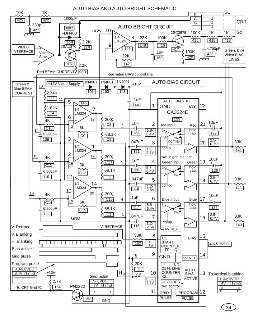
Resistor 141 , 142 , and 143 are part of the auto bright circuit. They are used tosum the bias voltage of each of the three channels via a voltage node at the autobright amplifier, 146 pin 9. The resulting output voltage then controls the screengrid via transistor 417 . Resistors 413 and 418 protect the CRT from excessivecurrent during arcing. Capacitor 423 supplies a low AC impedance to GND toinsure that the CRT gain is constant during each horizontal line.Resistor 420 defines the current gain of, and stabilizes, the auto bright control loop.Resistor 148 and capacitor 150 act as a low pass filter to reduce the chance ofdamaging the amplifier 146 due to CRT arcing. Resistors 415 , and 416 protectthe auto bright control transistor 417 . The grid pulse is generated by a discretetransistor 153 to protect the auto bias IC from possible arc energy.Pullup resistor 154 supplies the grid pulse voltage during the grid pulse time.The auto bias IC (CA3224E) is designed for a supply voltage of +10V and since thevideo amplifier requires +12V, three diodes 101 , 103 , and 145 are used to supplythis IC. Resistors C4 and C7 form a voltage divider which supplies the biasvoltage to the LM324 146 . The green and blue channel circuits are identical to thered channel and are controlled by the timing logic in the same way. Refer to thewaveforms at the bottom left of page 34 for the timing relationship. The verticalretrace pulse, from the LA7851, starts the 21 count auto bias state counter. Thegrid pulse becomes active between the 15 and 18 horizontal cycle and the programpulse is active between the 18 and 21 horizontal cycle. These two pulses inconjunction with the internal control of the transconductance amplifier output switchare what measure and set the video bias.
The beam current feedback circuit uses a PNP video transistor 91R to direct most ofthe beam current to the auto bias circuit while passing the voltage waveform, from thevideo amplifiers to the CRT cathodes. Diode 90R and capacitor 88R insure that novideo waveform distortion occurs. An additional benefit of this circuit is that it protectsthe video amplifiers from the destructive arc energy. Resistors 92R and 93R divideenergy due to CRT arcing, between the video amplifier transistors and the beam currentfeedback transistor 91R . The beam current is filtered by capacitor 108 and resistor C10 and is buffered by an operational amplifier, which translates the beam current intoa low impedance voltage. This voltage is applied to a coupling capacitor 122 through a200 ohm resistor C8 . The 200 ohm and the 68.1K resistor C3 forms the programvalue which sets the black level voltage via the action of the program pulse.Capacitor 121 is used to stabilize the transconductance amplifier which is used at thechannel input of the auto bias IC 123 . The auto bias IC stores the bias voltage of thischannel in capacitor 127 at pin 21. This voltage is buffered by an internal amplifier,with output at pin 20, which is connected to the Red video amplifier bias input.
AUTO BIAS AND AUTO BRIGHT CIRCUIT DESCRIPTION
91R
90R 88R
92R 93R
91R 108
C10
122
C8 C3
121
123
127
143
417
141 142
146
413
423
146
148
101 103
C7C4
146
417
416415
145
154
150
420
418
33
153
8
+
AUTO BIAS CIRCUIT1N400110
11
13
9
10
12
14
15
7
6
5
4
16
17
18
19
1
2
3 20
21
22GND Vcc
Red Red
GND
CA3224E
AUTO BIAS IC
+10V
68.1K
68.1K
68.1K
.047uF
.047uF
.047uF
.1uF
.1uF
.1uF
C1
C16
152
33K
116
117
118
120
121
122
C2
C13
C3
C8
144.1uF
126
141
127
123
142
125
143
33K
+
+10uF
10uF
10uF
33K
33K
153
PN2222
2.5-6.7V
2.5-6.7V
2.5-6.7V
4.6-5.2VDC
1.9-2.3VDC4V 17mS
8.0-9.0VDC8.4V 17mS
6.3-7.7V
.1-
.3V
1.2-2.5V
5.8-6.4V
.5-.8VDC .7V 17mS
1.2-2.5V
1.2-2.5V
5.8-6.4V
5.8-6.4V
7
5
4
20KC5
comp.
inputholdcap.
comp.
holdcap.
comp.
holdcap.
sw.
sw. in grid pls. pos.
sw.
sw.
normal
V. RETRACE
STARTCOUNTER
FF
CL
Q
EN21 H. LINECOUNTERCLDECODER
5V REF
BIAS
AUTOBIAS
ACTIVE
PROGRAMPULSE
GRIDPULSE
sw. control
HB 2,9
8
1
Green input
Blue input
Green
Blue
To vertical blanking
7
4K
6,800pF
4K
6,800pF
4K
6,800pF
LM3241/4
111C15
C12
C14
C11
110
LM3241/4
LM3241/4
C9108
C10
C4
C7
1.82K
2.74K
1N4001 1N4001
103 145101
15
18
14
5
6
3
21
12
1314
13
12
17
16
19
20
5K
5K
5K
11
+12V Video Supply
90R
88R
1000pF
FDH400
93R
91R
2SA1370
2.2K
92R2.2K
VIDEOINTERFACE Video
Amp.
GND
To CRT Grid #1
2.7K154
+10V
Green &Blue BEAM CURRENT
Red BEAM CURRENTRed video BIAS control line.
.1uF
+4.2V
147
22K
1/4LM324
146
10
98
148
22K
Green, BlueVideo BIAS
LINES
AUTO BRIGHT CIRCUIT
G1
1K1K100K
100K
RGB
100K
416415 413418
423420150
4,700pF
G2
CRT
GND
V. Retrace
V. Blanking
H. Blanking
Bias active
Grid pulse
Program pulse
Grid pulse
2SC3675
417
1 18
AUTO BIAS AND AUTO BRIGHT SCHEMATIC
34
10K 1K
330pF425 422
421
200ý
200ý
200ý
+
+
+
+
+
146
6V REF.

This sync interface incorporates a dual voltage comparator 67 and a resistive inputcircuit for high reliability. For TTL level sync signals, the resistive inputs are seven to oneattenuators comprised of resistors 45 , 46 , 47 , and 48 . The comparators arebiased to .15 volts by resistors 61 , 62 which permit direct connection to an RS170sync source by removing resistors 45 and 48 .
The vertical sync signal from the second comparator is coupled to the LA7851, vertical syncinput, via a coupling capacitor 68 . Resistor 77 and capacitor 187 form a low passfilter to eliminate false triggering by horizontal sync pulses in the case of composite sync.Resistor 78 and capacitor 77 compliments the comparator open collector output byacting as a pullup. These resistors also form a voltage divider which insures that thecapacitor 68 is not reverse biased and provide the proper vertical sync drive amplitude.The LA7851 vertical sync input circuit is designed to accept either positive or negative syncpulses, but will not work with a sync signal that is close to a square wave.
The horizontal sync signal from the comparator output is pulled up by resistor 80 andattenuated by resistor 176 and I1 , for correct drive amplitude. It is differentiated bycapacitor 198 and applied to the horizontal sync input, pin 1, of the LA7851.Bias resistors I2 and I3 set up the correct voltage for positive edge triggering.By adding resistor I12 , the LA7851 is programmed for negative edge triggering.This is used when the horizontal sync pulses are negative going. Resistor I12 is connectedby adding a solder bridge to the I PRA solder pads above pin 6.
VERTICAL AND HORIZONTAL SYNC CIRCUIT DESCRIPTION
The 1492 Monitor has a separate input for horizontal and vertical sync. The horizontalsync pulse is normally positive going. The horizontal deflection control circuit will syncon the rising edge of this pulse. If horizontal sync is negative going, the picture is shiftedto the left, and may be out of range of the horizontal picture position adjustment circuit.To sync on the falling edge of horizontal sync, a solder bridge is installed on the I PRA.
HORIZONTALSYNC
GND
VC2
VC1
Hs V sVERTICALSYNC
GND
270
270
1.8K
1.8K
270
47
46
45
48
67
1/2LM393
1/2LM393
61
22K62
13
2
7
6
5
8
4
6.8K
.14-.16V
VERTICAL AND HORIZONTAL SYNC CIRCUIT
1.8K
12K
1KVIDEO +12V
80
176
78
77
LA7851DeflectionControl IC
HorizontalSync input
VerticalSync input
1.8K12K
8.8K 22K
.047uF
10uF
56pF
+
1
19
198 I1
I2
I3I12
187
68
DEFLECTION +12V
ý
ý
+
+
ý
The vertical deflection circuit will sync on either a negative or positive sync pulse,provided that the pulse width is between two and twenty horizontal cycles long. Both thevertical and horizontal sync lines are joined for composite sync operation.
35
78 77
68 77 187
68
198176
45 4861
45 46 47 4862
67
I2I12
I3
I180
I12

VERTICAL DEFLECTION CIRCUIT, FUNCTION, DESCRIPTION
The LA7851 IC and the H PRA have all the active components to control the vertical deflection.LA7830 is a high efficiency vertical yolk driver IC. Together they form a compact and efficientvertical deflection system. SIMPLIFIED VERTICAL DEFLECTION CIRCUIT
The vertical oscillator supplies the start time for the vertical cycle and when vertical syncis present, sync supplies the start time to the vertical oscillator. The linear vertical rampcurrent which is necessary for linear vertical deflection is generated by supplying acapacitor 202 with a constant current from resistor H6 , at a voltage node (pin 16).The voltage at this node is held constant by a system of amplifiers which drive the deflectionyoke. The yoke current sensing resistor 193 is connected to the other side of this capacitor 202 and supplies the ramp voltage which balances the current from H6 during trace time.
2
CONTROL
OUTPUT
RETRACEBOOSTER
LA7830
+24V LINE
+220uF
192
73
4
6
SYNCV
+12V
.1uFOSC
+ or -VERT.SYNC
V. S QFF
R Q 5V
3.4V
COMP.
AMP.
17 16
15
18
19LA7851
218
+12V
H6
202 193
SIZEV118K
500
330
330301 1uF
.047uF
.01uF
3.3
VERT. YOLK
+ 1000uF76.8K
34K
ý ý
ý
ý ý
V. Auto Bias on H PRA22K 22K
22K
200K
10uF+
To better understand the LA7851 bias control loop, imagine the vertical output voltagegoes up, the time out shortens which causes the capacitor 202 to be less discharged. Thisraises the voltage on capacitor 202 and lowers the vertical output voltage. This type ofvertical bias control system has the advantage of only correcting the bias during retracewhich means that it will not cause current ramp distortion during vertical trace time.
The vertical yoke driver LA7830 is the power output stage for the vertical amplifier.It has a built-in voltage booster circuit to reduce vertical retrace time withoutthe power losses associated with a high vertical supply voltage.
To generate the other half of the deflection yoke sawtooth current (vertical retrace),a flip flop is set by the vertical oscillator which partly discharges the capacitor 202
and causes the drive voltage across the yoke to reverse. The amount of discharge ofcapacitor 202 determines the vertical output voltage for the next cycle and is controlled by atimer at pin 17. The time out of the timer is controlled by the vertical output voltage from twodifferent paths. One path is through the 34K and 118K resistors which supplies the higherfrequency component for the timer and stabilize the vertical amplifier. The other path isthrough the vertical auto bias circuit which detects the minimum vertical output voltage overmany vertical cycles and supplies a second current source to the timer. This second currentsource has a wide dynamic range and will hold the vertical output voltage well within operatinglimits for both 50Hz and 60Hz with no need for manual adjustment.
H6
H6
193
202
202
202
202
36
202
202
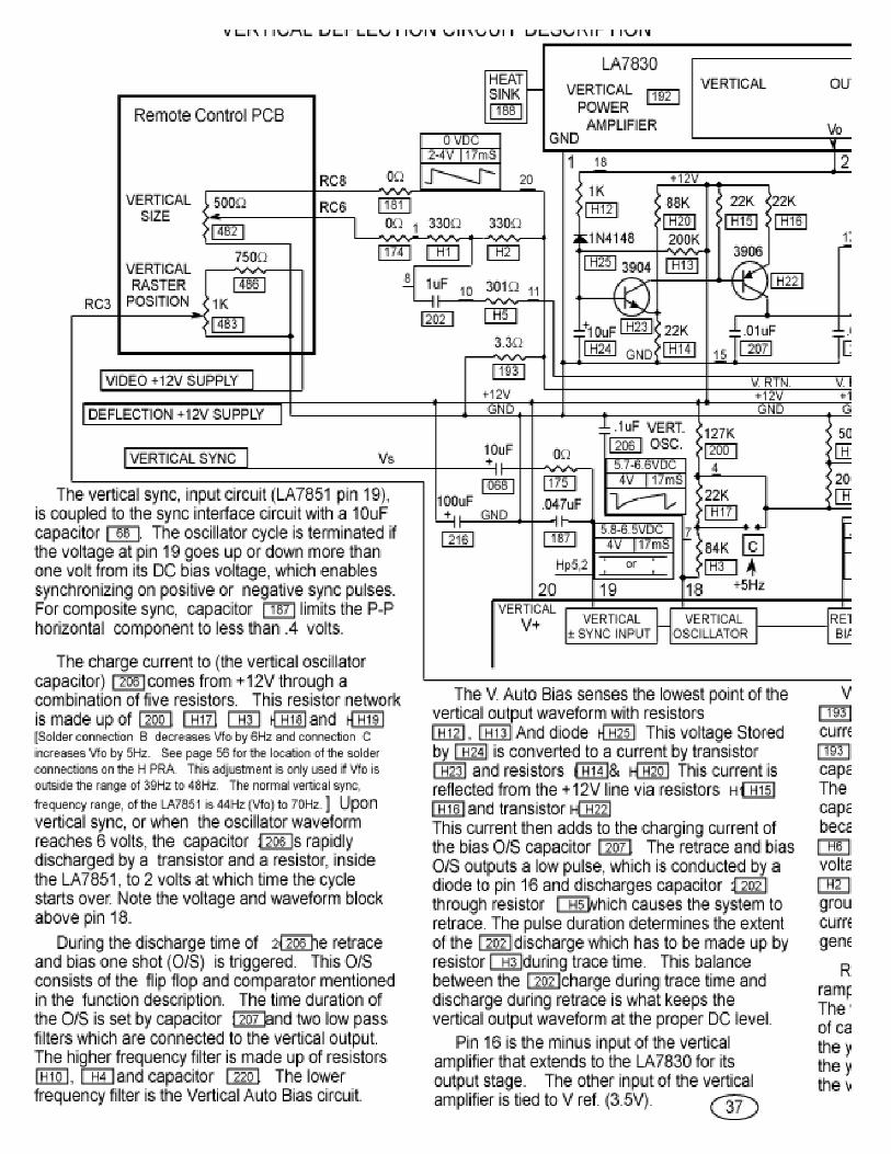
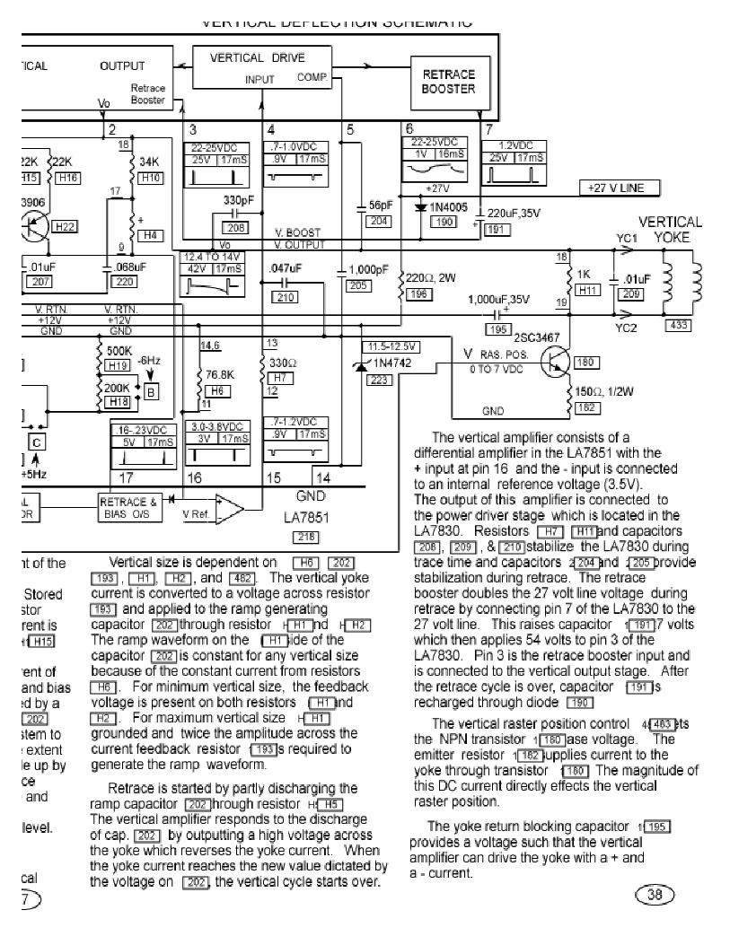

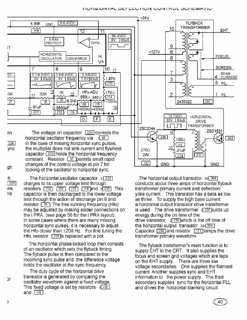
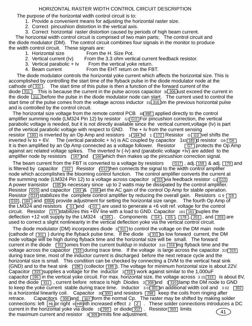
The purpose of the horizontal width control circuit is to: 1. Provide a convenient means for adjusting the horizontal raster size. 2. Correct pincushion distortion in the vertical axis. 3. Correct horizontal raster distortion caused by periods of high beam current. The horizontal width control circuit is comprised of two main parts; The control circuit andthe diode modulator (DM). The control circuit combines four signals in the monitor to producethe width control circuit. These signals are: 1. Horizontal size From the H. Size Pot. 2. Vertical current (Iv) From the 3.3 ohm vertical current feedback resistor. 3. Vertical parabolic + Iv From the vertical yoke return. 4. Beam current From the EHT return on the FBT.
HORIZONTAL RASTER WIDTH CONTROL CIRCUIT DESCRIPTION
The diode modulator (DM) incorporates diode 311 to control the voltage on the DM main node(cathode of 311 ) during the flyback pulse time. If the diode 311 has low forward current, the DMnode voltage will be high during flyback time and the horizontal size will be small. The forwardcurrent in the diode 311 comes from the current buildup in inductor 316 during flyback time and thevoltage across the capacitor 315 during trace time. If the voltage is large across the capacitor 315during trace time, most of the inductor current is discharged before the next retrace cycle and thehorizontal size is small. This condition can be checked by connecting a DVM to the vertical heat sink(GND) and to the heat sink 186 (collector 185 ). The voltage for minimum horizontal size is about 22V.Capacitor 315 supplies a voltage for the inductor 316 to work against similar to the 1,000uFcapacitor 195 in the vertical yoke circuit. For max. horizontal size, the voltage across 3 15 is about 8V,and the diode 311 , current before retrace is high Diodes 3 08 and 3 10 clamp the DM node to GNDto keep the yoke current stable during trace time. Inductor 3 01 is an additional width coil and 3 02is a horizontal linearity coil. Capacitor 300 and resistors 298 keep the coils from ringing afterretrace. Capacitors 306 and 307 form the normal Cp. The raster may be shifted by making solderconnections: left HL or right HR with increased effect Z . These solder connections introduces a DCcurrent in the horizontal yoke via diode 193 or diode 31 . Resistor 303 limitsthe maximum current and resistor 309 permits fine adjustment.
The beam current from the FBT is converted to a voltage by resistors G17 , adj. 159 & adj. 179 andis filtered by capacitor 162 . Resistor G12 then connects the signal to the width control amplifiernode which accomplishes the blooming control function. The control amplifier converts the current atthe summing node (LM324 Pin 12) to a voltage across capacitor 315 , via feedback resistor G13 .A power transistor 185 is necessary since up to 2 watts may be dissipated by the control amplifier.Resistor G15 and capacitor 163 & 16 set the AC gain of the control Op Amp for stable operation.Resistor G14 stabilizes the complete control amplifier by reducing the overall gain. Resistors G 9 , G 10 , 1 64 and 166A provide adjustment for setting the horizontal size range. The fourth Op Amp ofthe LM324 and resistors G 1 and G 2 are used to generate a +6 volt ref. voltage for the controlcircuit. Resistor 1 71 stabilizes this +6V line with a load to GND. Capacitor 161 decouples thedeflection +12 volt supply by the LM324 165 . Components G4 , G5 , 178 , 201 , and 203 areused to correct a slight nonlinearity in the vertical deflection yoke via the vertical control circuit.
The horizontal size voltage from the remote control PCB 490 is applied directly to the controlamplifier summing node (LM324 Pin 12) by resistor G11 . For pincushion correction, the verticalparabolic voltage is needed, but it is not directly available since the vertical current,voltage (Iv) is partof the vertical parabolic voltage with respect to GND. The + Iv from the current sensingresistor 193 , is inverted by an Op Amp and resistors 148 and 1 72 . Resistor G 3 level shifts theinverted Iv to + 6V. The (vertical parabolic + Iv) is AC coupled by capacitor 183 and resistor G6 .It is then amplified by an Op Amp connected as a voltage follower. Resistor G7 protects the Op Ampagainst arc related voltage spikes. The inverted Iv (-Iv) and (parabolic voltage +Iv) are added to theamplifier node by resistors 1 6 and 166 which then makes up the pincushion correction signal.
41
The diode modulator controls the horizontal yoke current which affects the horizontal size. This isaccomplished by controlling the start time of the flyback pulse in the diode modulator node at thecathode of 311 . The start time of this pulse is then a function of the forward current of thediode 311 . This is because the current in the pulse across capacitor 306 must exceed the current inthe diode 311 before the pulse in the diode modulator node can start. The current used to control thestart time of the pulse comes from the voltage across inductor 316 from the previous horizontal pulseand is controlled by the control circuit.
315
311311
311
311 316315
183G7
193
167 166
G12
490G11
184 172 G3
162
315
G13185
G15G14
G10G1 G2
163
164G9
165 201178 203G4 G5171
311
186 185
195
315
310301
293
308302
306 307
309312
315
300
303
161
168
316
G6
G17
ZHL HR
298
166A
159 179
311311
311306
316
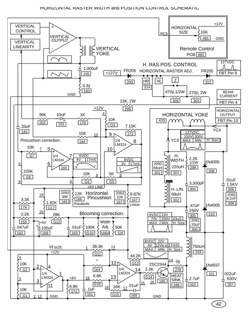
7
10
+12V
13
810
311
+
203 178
172
184
G4 G5
167
G1
G2
171161
164
G16
G15 168
G14
G11
278
315 307
305 310
308
306
2.7uF
1N4937
630V.022uF
0ýG13
44.2K
2.2K
.01uF16K
LM3241/4
LM3241/4
750uH316
38.3K
*
6.8K
LM3241/4
10K
10K6.8K
.1uF
2
31
12144
11
LM3241/4
16612K 8.87K
.33uF
10K 5K
10K
3003,300pF
1N4005
1N4005
.01uF1.5KV
G310K
1K36K
201
10uF+
5
6
HORIZONTAL YOKE
250V.47uF
6VDC17mS4V 6VDC
3V 17mS
Blooming correction.
Pincushion correction.
7.15K
YC3
YC4
89
5G6
G7
10K
220K
6
4
3
1 13
18 1715 16
8VDC 22V
MAX. MIN. H. Size4V 12Vp-p
2SC2344
165
302
68uH
298
2.2K1/2W
HEATSINK185
186
H SIZE
GND
+6V
183
7
8
4
19
2, 12
14+
17mS
H. LIN.
220uHWIDTH
301
H.
209268uH301
20928.2nF306
2092.33uF305
209222K167
209236K166
PincushionParabolic Linear
9
8VDC 23V
MAX. MIN. H. Size70V 250V 63uS
127VDC50V 170V
MAX. MIN. H. Size
127VDC150V 300V
MAX. MIN.
FBT Pin 10
FBT Pin 4
BEAMCURRENT
HORIZONTALOUTPUT
433
293314
309
312
470ý,1/2W
FR205
270ý, 2W
303
HORIZONTAL RASTER ADJ.+127V
481
10KHORIZONTAL
SIZERC5
+12V
GND
Remote ControlPCB 490
VERTICALLINEARITY
3.3ý
1,000uF
VERTICALOUTPUT
+
-
CONTROLVERTICAL
195
193GND
HORIZONTAL RASTER WIDTH and POSITION CONTROL SCHEMATIC
H. RAS POS. CONTROL
VERTICAL
Horizontal+6V LINE
+12V
FBT Pin 9
127VDC
42
GND
YOKE
HL ZHR
28K
162
G17
50KG10
100K163.01uF.047uF
1.82K
G12
20
19
+6V
G9
+ 100uF166A
Width Adj.
159
2.2K
169
179
3.3K
12K, 2W
289
FR205
ACline
User suppliedIsolationTransformer
V-
GND
+127V
+
+
LOADH Dy & EHT
VIDEO266
SECONDARIES
268
258
292
VREF.
Error Amp.Comp.
OSC. ENABLE
DRIVER
280
C5184
(-200V)
FET
V-
FLYBACKDIODE
GND
Res.+
SIMPLIFIED POWER SUPPLY CIRCUIT FUNCTION DESCRIPTION
The switching regulator includes the power FET 268 which passes current fromV- to GND through the inductor 258 . During the time the FET is on, the current in
the inductor is increasing and the inductor is storing energy. When the FETis turned off, the stored energy in the inductor continues supplying current to GND.But in this case, the current path is from V+ to GND, instead of V-to GND.During this part of the cycle, the current in the inductor is decreasing.
As can be seen from the waveforms, the largest number of changes occur whenthe FET is turned off. Also, the FET drain voltage switches fast due to the highinductor current. To minimize video interference from the power supply, thepower supply is synchronized to the horizontal oscillator such that horizontalblanking is coincident with the FET turn off time. The C5184 280 is the series regulator IC. All of the control circuits that are builtinto this IC work together to produce one output signal, which is the FET drivesignal. This signal can take on many shapes depending on the load conditionsof the power supply. The waveforms for normal operation are shown above. For the shorted +127V to GND condition, which also occur right on power up,
FET Gate Drive
FET Drain Voltage
Inductor Current
The first FET pulse is a full on pulse which causes current to flow in the inductor.After the FET is turned off the current in the inductor drops much more slowly thannormal since the inductor is discharging into a much lower than normal voltage.If the FET were turned on for full power in the next cycle with current still flowingin the flyback diode, a current spike of 6A would occur, which is a power spike of2,000W. The reason for this is that the diode stores charge when current flowswhich turns into reverse current for a short time when the voltage is reversedacross the diode. 43
The waveforms are:
FET drain voltage
Flyback pulse
Current in diode
Voltage across 292
Current in inductor Current supplying GND
Current from V-
Current added to the +127V line266
268258
280
The regulator IC has a built in reference voltage which is used by theerror amplifier set and hold the +127V line constant. Solder connections on the J PRAare used to adjust the +127V line in steps of ±1.5V. The over voltage protect circuit, when activated, turns off the regulator IC untilpower is disconnected. This circuit is connected to the rectified flyback pulse, whichoutputs a voltage that is proportional to the EHT. The circuit's main purposeis to protect the user against excessive x-ray which is caused by excessive EHT.
The FET drive waveform avoids this problem by sensing flyback diode conduction.If the flyback diode conduction is sensed, the low current start mode is selected.this mode turns the FET on, to a current of .1A, for not more than 4uS. If before orduring the low current FET on time, the flyback diode breaks free, and the FETdrain voltage goes down, the flyback diode voltage comparator will signal theregulator to permit the FET to be turned on for a full power cycle.The cycle after the last low power cycle in the waveform above is an example of thiscondition. The flyback diode voltage comparator inputs are located at pins 12 & 13of the C5184. The two resistor dividers J10 J11 and J12 271 connect thecomparator across the flyback diode. The comparator enables the FET drive onlyafter a 10% voltage drop is measured across this diode.
Most of the power supply fault conditions cause the power supply to chirpbecause the source of +17V for the regulator IC is generated by the power supply.A special circuit is built into the regulator IC, which permits charging the +17V linefilter capacitor with only a very low load from the IC. This circuit turns the restof the IC on only after the voltage at pin 15 reaches 17V. If the transformer does notsupply at least 12V to this line before the filter capacitor discharges to 12V, theregulator IC turns off. The reason for the audible chirp, is that, the power supplyis not full on for each cycle which produces a frequency low enough to hear. A 19V to 20V @ 1A, DC, isolated power supply is a tool necessary for trouble shootingCERONIX monitors. When trouble shooting the power supply, it can be connected toV- and the +17V line to keep the power supply running while checking the voltagesand waveforms to find the fault. It can also be used to supply the GND to +24V linefor checking the horizontal circuit. If the horizontal circuit does not work, thepower supply will chirp. Without the horizontal circuit working, there is notenough load on the power supply for transformer action to keep the regulator IC+17V line up to the minimum of +12V. A quick check for this condition is to clipa 2-4K@10W power resistor from GND to +127V line. If the chirping stops, thehorizontal is probably not working.
44
SIMPLIFIED POWER SUPPLY CIRCUIT DESCRIPTION
Another fault condition exists when the FET exceeds 1.6A drain current.This condition can occur if the oscillator frequency is too low, the FET drain is shortedto GND or V+, the transformer has a shorted secondary, or the core is broken.In these cases the voltage across the FET source resistor 292 exceeds 1.6V whichis sensed by the over current comparator at pin 11. If pin 11 exceeds 1.6V, the FETdrive is set to 0V for the rest of the cycle. In some cases, this condition canproduce an output waveform which looks normal, but the voltage across the load(+127V to GND) would be low or unstable. A quick check for this condition is tocheck the peak voltage across the FET source resistor. CAUTION; Wheneverconnecting a scope ground to V-, be sure that the other scope probe or commongrounded devices are not connected to the monitor GND.
The heart of the power supply is the oscillator which supplies the basic timing.The FET drive is always low during the negative slope of the oscillator or, whensynchronized, after the start of the sync pulse. The low to high transition of theFET drive, pin 10, is determined by the voltage at the output of the error amplifier.If the 127V line goes up in voltage, the error amplifier voltage goes up, which thenintersects the oscillator waveform at a higher voltage and causes the FET on time tostart later and be shorter. This negative feedback accomplishes the control loop ofthe power supply.
J12 271,J10 J11,
292
The FET drive is always off during the negative slope of the oscillator, or just after the sync pulse.Since the FET drive pulse is started by the error amplifier voltage and terminated by the end of theoscillator cycle, a control system via pulse width modulation has been established. The oscillatorwaveform is produced by charging capacitor 277 with a constant current set by resistor J7to a voltage of 5V and then discharging the capacitor with double the charging current to 2.5V.Adding the flyback pulse, via capacitor 288 to this waveform synchronizes the oscillator, since theoscillator frequency is set below the horizontal frequency.Resistors J2 , J4 and capacitor 274 limit the error amplifier's AC gain, to hold the control loopstable. Capacitor 275 holds the error amplifier stable. Capacitor 281 reduces power supplynoise, but, if too large, will cause the power supply to be unstable. The 127V line is adjusted by making solder connections on the J PRA(refer to page 56 for the layout). Solder connections A and B are used toraise the 127V line up to 4.5 volts in steps of 1.5 volts. Connections C and D lower the 127V line as much as 4.5V. The 127V lineshould be adjusted if below 125.8V or higher than 128.2V.Resistors 273 and 249 are used for monitors with special127V line voltages.
The series regulator IC 280 , controls current to the monitor GND by pulse width modulation.A PNP transistor 250 , has an emitter current, that is directly proportional to the 127V line voltagedue to resistor J1 and adjustment resistors J13 & J14 . This current is transmitted to the powersupply V- line, and is applied to a resistor J5 , J15 , & J16 . The voltage across these resistorsis compared to a reference voltage by the error amplifier. If the +127V line goes up the output ofthe error amplifier voltage goes up. The pulse width modulation, which controls the + 127V linevoltage, is accomplished by turning the FET drive on at some particular voltage along the risingslope of the oscillator waveform. This particular voltage is the error amplifier output voltage.
Oscillator waveform with sync:
FET drive, C5184 pin 10:
Error Amp. V.
Fet DriveWith Sync
SWITCH MODE POWER SUPPLY CIRCUIT DESCRIPTION
Oscillator waveform without sync:
The FET 268 works together with the transformer 258to provide a low resistance current path from V- to GND.This low resistance coupled with no large voltage timescurrent products is what makes the power supply efficient.Resistor 292 provides a means for sensing the FET current.In the low current mode, it is used to set the 100mA currentand in the full on mode it is used to sense the max. current.Resistors 264 , 270 and capacitor 265 reduce power supplyelectrical noise. Transistor 284 and diode 283 short theFET drive to V- when the monitor is turned off to protect theFET from conducting current with a still large drain voltage.Resistors J10 , J11 , J12 and 271 provide a means forchecking flyback diode 266 conduction via a comparator.If the comparator measures low flyback diode voltage theFET is turned on to the .1A low current mode. This modeis necessary during power up, since initially the +127V lineis 0V and no reverse diode voltage exists. The over voltage protect circuit has a trip voltage of 8Vand when it is activated, it shuts down the power supply. The EHT is measured by rectifying theflyback pulse, with diode 290 , from a secondary winding of the FBT. Capacitors 291 , 285 andresistors 287 , J9 are connected as a low pass filter to smooth out the simulated EHT voltage whichis then applied to the C5184 at pin 14. Resistor J8 protects the IC current sense input from voltagespikes and resistor 251 protects the PNP transistor from momentary overvoltage damage due toline spikes. Zener diode 295 protects the horizontal and video circuitsfrom overvoltage due to power supply failure. If the +127V line exceeds 160V,the zener diode 295 shorts to GND the +127V line. 45
250280
J1
277 J7
288
J2 J4 274
J5
275 281
273
268 258
292
264 270 265284 283
J10 J11 J12 271266
290 291 285287
295251
J8J9
295
J13 J14J15 J16
249
A B
C D
256 247
257J6
286
150uF
250V
250V
90K
100K
100uF
1/2W
+
8,147
252
253
255
254
240
241
245
FR205
3A FUSE
CURRENTLIMIT
INRUSH
25-.5ý
2 1PCPC
220Vo
220Vo
CUTFOR220Vo
+
+246
GL200
115VACINPUT 238
To deguassing coiland posistor.
V-
127V
FR205
2,200pF
252A
150uF
2,200pF
254A

At the input to the power supply is a voltage doubler which outputs between 240 to 425VDCdepending on the AC line voltage. It has a three amp fuse 245 to protect the PCB traces, an inrushcurrent limiter 240 to protect the rectifier diodes 252 , 254 , and optional capacitor 241 andinductor 246 which can be used to reduce conducted noise from the monitor AC input. For 220VACoperation the voltage doubler is replaced by a full wave rectifier by adding diodes 253 , 255 andcutting the 220Vo trace. 256 & 257 are the raw DC filter capacitors. Resistor J6 supplies thepower supply start current and resistor 247 balances the series connected filtercapacitors for 220VAC operation. 46
248260263
1,000uF1,000uF
NONE.1uF.1uF
286131215
261262
POWER SUPPLY CONTROLVOLTAGE CURRENT CIRCUIT SUPPLIED DIODE FILTER CAP. NOISE CAP.
17VDC16VDC27VDC
7mA250mA250mA
VIDEO AND INPUTV. &H. DEFLECTION
100uF
255253J6
247257256
254240245
252 241246
POWERSUPPLY
LOW VOLTAGESECONDARIES
4.67K
13
3.4-4.2VDC
5.7-6.3VDC
16.3-17.8VDC
OUTPUT
1
2
4
3
1516
14
5
6
7
8
12
11
10
9V-+7.5V REF.
XRC5184
Osc.
Rx
Cx
CurrentSENSE
DRIVE
CONTROL &FAULT SENSE
+15V+17V
INPUT
INPUT
INPUT
ERRORAMP.
COMP.
Output
OverVoltageProtectINPUT
+COMP.
4uSDELAY
280
282
SMXFR
D
251
215 262 131 261
263
260
258248 266
285
287
291J9
290
271J10
J11 J12
275
273
J3
274
J4
275
276
J7
277288
292
J8
270
283
284
265
2642,200pF
MPSA641N4005
18ý
510ý
14.7K 15.8K
1.2ý 150ý
200pF
2SK1446
1.00M
38.3K1,000
pF
191K
.1uF
FR205FR205
11K
56K
6,800pF 56pF
10.6K
23.2K
1.87K56pF
100K2SA1371E
++ 1,000uF1,000uF
FR205
FR205
.1uF
330pF
6,800pF
33.2K
1.00M
268
.1uF295
317 294TZ160B-T3
160V
+27V+16V
+127V
150uF250V
.1uF250V
14.8-16.3VDC
3
1
594
2
6-7VDC
3.6-4.4VDC6V 63uS
5.3-5.7VDC
63uS.10-.17VDC
1V
63uS2.4-3.6VDC14V
3.5-4.1VDC3-4V 63uS
.1-.5VDC
.5-.8VDC
6.5-7.5VDC
6.5-7.5VDC
V- V-
1312
17 18
16
J PRA PINS:
6
GND
+127V
V-296.022uF
HeatSink267
20
9
2
4
5
3,10,15, & 19
275281.01uF
J1193K
250
1
20
DC
2.33K
J13 J14
-1.5V -3V
J2
J5
J16
J15
260ý
130ý
+3V
+1.5V
B
A
18ý
248A
}
249*
SWITCH MODE POWER SUPPLY SCHEMATIC+24V
FROMFBT
+16V +127V
17V
0VDC48V 63uSFROM
FBT
GND
127V
1N4148
20 Volt
IN OUTADJ.
LM337MT
115 VAC 60 Hz
1,000uF20V @ 1A
TransformerTriad #F-254 X
1N4005
35V
301R,1%
1N4005
1N4005
1N4005 -7V
+20V
HEAT SINK
4.75K,1%
47K 10K 1uF
1A Std. Fuse
24V Zener1N4749A
1A Std. Fuse
@.5 APower SW
ISOLATED +20V POWER SUPPLY CIRCUIT.
0V
Equipment setup for repairing the Model 1492 Monitor
47
+127.0
DVM
OSCILLOSCOPE
TRANSFORMER
VARIABLE
ISOLATION
TRANSFORMER
ISOLATED +20V @.5A DC
POWERSUPPLY
115VAC
CERONIX Model 1492
SAFETY FIRST; Use only one hand when working on a powered up monitor to avoid electricalshock.
Problem Solving Tools
48 There is a line voltage range of about 60% to 70% AC line voltage where a correctly operating monitor will chirp.
The power supply may chirp if:
If the +127V crowbar zener 295 is shorted, a fault exists in the power supply whichpermitted the +127V line to exceed +160V. First replace the zener. Never operate the monitorwithout the crowbar zener installed. Then with the external supply, the DVM, and the scopeconnected to the power supply (as in 2) slowly increase the AC line and observe the power supply response. Do not exceed +145V on the +127 V line. If the monitor runs normally, a fault maystill exist in the power supply power down circuit. Check parts 283 and 284 . If the crowbarzener is shorted and the FET is internally shorted, the C5184 IC 280 should also be replaced. If there is no FET drive waveform, check the voltages and waveforms on the C5184 pinsand compare them to the voltages and waveforms on the schematic. Shorts on the +127V, 24V, and 16V lines other than the crowbar zener are not likely to beconnected to the power supply even though the power supply chirps. By operating the powersupply with the +20V external power supply many of these problems can be found using the sameprocedure as are used in trouble shooting monitors with linear power supplies.
For the overloaded supply line problems, which often occur only when the +127V line is fullypowered up, the +20 volt external power supply is used to keep the monitor power supply running.To use the external supply, connect the 0V line to V- (anode of diode 254 ) and the +20V line tothe monitor power supply +17V line (cathode of diode 248 ). Connect the oscilloscope GND to V- and the probe to the FET drive (anode of diode 283 ).TAKE CARE NOT TO TOUCH THE OSCILLOSCOPE AND MONITOR CHASSIS DURING THISTEST, SINCETHE VOLTAGE DIFFERENCE CAN BE AS HIGH AS 400 VOLTS.Increase the AC supply, slowly, to the normal operating voltage while monitoring the +127V lineto GND voltage with the DVM. The power supply overload condition can be seen on the scopeas an almost square wave which can break up into short and long pulses as the AC line voltageis increased. The short pulses are the flyback diode current sense pulses. Sometimes the monitorwill operate normally in this mode, in which case, watch for smoke and after a few minutes ofoperation disconnect the power connections and carefully feel around the conductor side of theboard for hot spots. Overload conditions will not harm the power supply unless there is a problemin the power supply.
A quick check for the insufficient +127V load is to connect a 2K to 4K ohm 10 watt powerresistor to GND and the +127V line. If the chirping stops, proceed to check the horizontaldeflection circuit. First disconnect the board from the AC supply. Then connect the +20V supply,0V line to GND, and the +20V line to +127V and +24V lines on the monitor. Now the completehorizontal and vertical circuits can be checked with the oscilloscope and DVM.The flyback waveform will be about 140Vp–p instead of 1,000Vp–p which permits checking eventhe horizontal output transistor, collector, waveform.
Many of the failures that cause burnt components and boards are eliminated by the load sensitiveswitching mode power supply in the CERONIX monitor. This feature can cause problems withservicing the monitor if the proper trouble shooting approach is not used. The equipment setup,shown here, is necessary for efficient trouble shooting of the CERONIX monitors. Problems that cause the power supply to chirp are: 1. Insufficient +127V line load. 2. Overloaded +127V, +24V, or +16V lines. 3. Shorted +127V, +24V, or +16V lines. 4. Power supply component failure. 5. Raw DC (+127V to V-) voltage too low.
Always wear safety glasses.
The +17V line is open. (goes away when ext. PS is used)The 1.2 ohm current sensing resistor value is too high.The transformer core is broken or a winding is shorted.
1.
2.
3.
4.
5.
283 284280
295
248283
254

1. Use a knife to brake free the magnetic rings on the yoke which are locked with red varnish. Bring the adjustment tabs on each pair of magnetic rings in line for the starting point.
2. Loosen the yoke clamp. Remove the yoke wedges and the tape from the CRT.
3. Connect a test generator to the video input and clip the red lead to the +12V line (anode of diode 101 ).
4. Turn the monitor on. Switch the test generator to red field. Adjust the horizontal and vertical raster size, on the remote control board, for under scan. Let the monitor run for at least half an hour.
5. Check the auto bright control voltage with a DVM connected to GND and pin 8 of the LM324 146 . The voltage range is 4.3V to 4.9V. If out of range, adjust this voltage to 4.6V by using pliers to rotate the bottom knob on the FBT.
6. Degauss the picture tube and front part of the frame.
CAUTION: To avoid electrical shock , take care not to touch the yoke conductors or push against the anode cap. Always keep one hand away from unit.
7. Adjust the yoke position, on the CRT neck, to the center of purity. One way to locate this yoke position is to make a felt pen mark on the CRT neck at the rear extreme of purity and another mark at the front extreme of purity. Make a third mark between the two marks and set the yoke to this position. Rotate the yoke to line up, the raster top line, with the top of the picture tube. Tighten the yoke clamp. Tilt the yoke side to side and up and down while watching the red field to verify that purity is good.
8. On the 13 inch CRT, use the purity magnets (closest to the yoke coils) to center the raster horizontally. To accomplish this, find the rotational position where spreading the tabs has the most effect on the horizontal position and spread the tabs a minimum to center the raster horizontally. On the 20 inch CRT, the purity magnets are often needed to optimize purity. The horizontal raster position solder connections are used to adjust the raster position. These solder connections are located on the foil side of the PCB next to the FBT. Connection HR shifts the raster right, HL shifts the raster left and the range of this shift can be increased by making solder connection Z under resistor 309 .
9. Check the purity with red field and with blue field while tilting the yoke side to side and up and down.
10. Switch the generator to red/blue grid. Adjust the 4 pole magnets (center pair) for convergence of the red and blue guns in the center of the screen.
11. Tilt the yoke up and down for the best convergence around the edge of the grid. Insert the top yoke wedge. Tilt the yoke side to side for the best convergence around the edge of the grid and insert the rest of the yoke wedges. Secure the wedges with tape.
12. Switch the generator to white grid. Adjust the 6 pole magnets (Pair closest to the socket board) for convergence of the green gun. Step #10 and this step may have to be repeated for optimum convergence.
SETUP AND CONVERGENCE PROCEDURE
49
146
309
101
Z
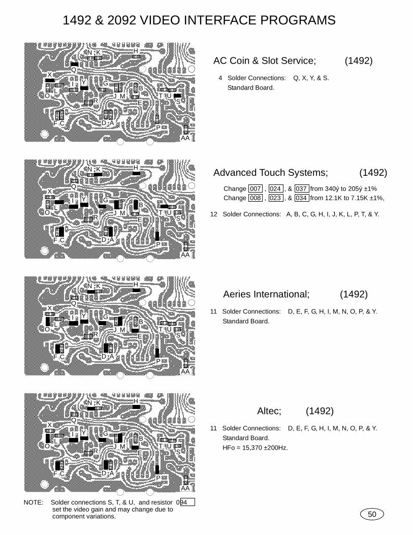
X
A
B
C D
E
F
G
H
I
J
K
L
N
P
Q
R ST U
Y
MO
AA
X
A
B
C D
E
F
G
H
I
J
K
L
N
P
Q
R ST U
Y
MO
AA
1492 & 2092 VIDEO INTERFACE PROGRAMS
50
NOTE: Solder connections S, T, & U, and resistor 094 set the video gain and may change due to component variations.
X
A
B
C D
E
F
G
H
I
J
K
L
N
P
Q
R ST U
Y
MO
AA
X
A
B
C D
E
F
G
H
I
J
K
L
N
P
Q
R ST U
Y
MO
AA
Altec; (1492)
11 Solder Connections: D, E, F, G, H, I, M, N, O, P, & Y.
Advanced Touch Systems;Change 007 , 024 , & 037 from 340ý to 205ý ±1%Change 008 , 023 , & 034 from 12.1K to 7.15K ±1%,
12 Solder Connections: A, B, C, G, H, I, J, K, L, P, T, & Y.
(1492)
AC Coin & Slot Service; (1492)
4 Solder Connections: Q, X, Y, & S.Standard Board.
Aeries International; (1492)
11 Solder Connections: D, E, F, G, H, I, M, N, O, P, & Y.Standard Board.
Standard Board.HFo = 15,370 ±200Hz.

X
A
B
C D
E
F
G
H
I
J
K
L
N
P
Q
R ST U
Y
MO
AA
X
A
B
C D
E
F
G
H
I
J
K
L
N
P
Q
R ST U
Y
MO
AA
X
A
B
C D
E
F
G
H
I
J
K
L
N
P
Q
R ST U
Y
MO
AA
X
A
B
C D
E
F
G
H
I
J
K
L
N
P
Q
R ST U
Y
MO
AA
1492 & 2092 VIDEO INTERFACE PROGRAMS
51
NOTE: Solder connections S, T, & U, and resistor 094 set the video gain and may change due to component variations.
Bally;
12 Solder Connections: D, E, F, G, H, I, J, K, L, P, T, & Y.
Add a solder connection on the "I" PRA above pin 5.
(1492)
Brunswick;
11 Solder Connections: A, B, C, G, H, I, J, K, L, P, & Y.
(1492)Change 007 , 024 , & 037 from 340ý to 301ý ±1%Change 235 , from Hfo set resistor to 3K pot.Remove the 2.7K resistor at 094 .Add a solder connection on the I PRA above pin 5.
Before final test, add the AA solder connection andcut out the 270ý resistor at 045 .
X
A
B
C D
E
F
G
H
I
J
K
L
N
P
Q
R ST U
Y
MO
AA
Automation; (1492)
Change 002 From 75ý to 130ý..Change 027 From 75ý to 47ý.Change 094 from 2.7K to 10K.
Install posistor 244 .
11 Solder Connections: D, E, F, G, H, I, M, N, O, P, & Y
Before final test add solder connections B & C.
X
A
B
C D
E
F
G
H
I
J
K
L
N
P
Q
R ST U
Y
MO
AA
Aristocrat;
11 Solder Connections: D, E, F, G, H, I, M, N, O, P, & Y.
(1492)Install three 100pF disc capacitors at 010 , 022 , & 041 .Invert horizontal sync by adding a solder connectionon the "I" PRA above pin 5.
Before final test, clip out 045 , 270 ohm resistor, and addone solder connection AA by component no. 060 .
Install posistor at 244 .
High resolution board.
High resolution board.
Install posistor at 244 .
High resolution board.
Standard board.
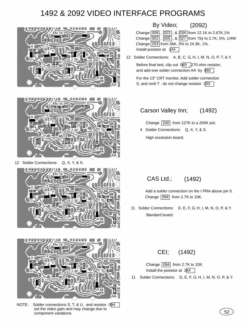
X
A
B
C D
E
F
G
H
I
J
K
L
N
P
Q
R ST U
Y
MO
AA
X
A
B
C D
E
F
G
H
I
J
K
L
N
P
Q
R ST U
Y
MO
AA
X
A
B
C D
E
F
G
H
I
J
K
L
N
P
Q
R ST U
Y
MO
AA
X
A
B
C D
E
F
G
H
I
J
K
L
N
P
Q
R ST U
Y
MO
AA
1492 & 2092 VIDEO INTERFACE PROGRAMS
52
NOTE: Solder connections S, T, & U, and resistor 094 set the video gain and may change due to component variations.
11 Solder Connections: D, E, F, G, H, I, M, N, O, P, & Y.
CEI; (1492)
For the 13" CRT monitor, Add solder connectionS, and omit T . do not change resistor 203
By Video;
12 Solder Connections: A, B, C, G, H, I, M, N, O, P, T, & Y.
(2092)Change 008 , 023 , & 034 from 12.1K to 2.67K,1%Change 002 , 005 , & 027 from 75ý to 2.7K, 5%, 1/4WChange 203 from 36K, 5% to 24.3K, 1%.
Before final test, clip out 045 , 270 ohm resistor,and add one solder connection AA by 060 .
Add a solder connection on the I PRA above pin 5.Change 094 from 2.7K to 10K.
CAS Ltd.; (1492)
11 Solder Connections: D, E, F, G, H, I, M, N, O, P, & Y.
Install posistor at 244 .
Carson Valley Inn; (1492)
4 Solder Connections: Q, X, Y, & S.
Change 200 from 127K to a 200K pot.
High resolution board.
Standard board.
Change 094 from 2.7K to 10K.Install the posistor at 244 .
12 Solder Connections: Q, X, Y, & S.

X
A
B
C D
E
F
G
H
I
J
K
L
N
P
Q
R ST U
Y
MO
AA
X
A
B
C D
E
F
G
H
I
J
K
L
N
P
Q
R ST U
Y
MO
AA
X
A
B
C D
E
F
G
H
I
J
K
L
N
P
Q
R ST U
Y
MO
AA
X
A
B
C D
E
F
G
H
I
J
K
L
N
P
Q
R ST U
Y
MO
AA
1492 & 2092 VIDEO INTERFACE PROGRAMS
53
NOTE: Solder connections S, T, & U, and resistor 094 set the video gain and may change due to component variations.
Games of Nevada; (1492)
12 Solder connections: D, E, F, G, H, I, J, K, L, P, T, & Y.
High resolution board.
IGT;
4 Solder Connections: Q, S, X, & Y.
(1492)
Delete degaussing circuit.
High resolution board.
Keevex;
4 Solder Connections: Q, S, X, & Y.
(1492)
High resolution board.
Install posistor at 244 .
Horizontal frequency is 17,182Hz
Mast Keystone;
5 Solder Connections: A, B, C, P, & S.
(1492)
Change 002 , 005 , & 027 from 75ý to 1K ±5%.
Standard Board.
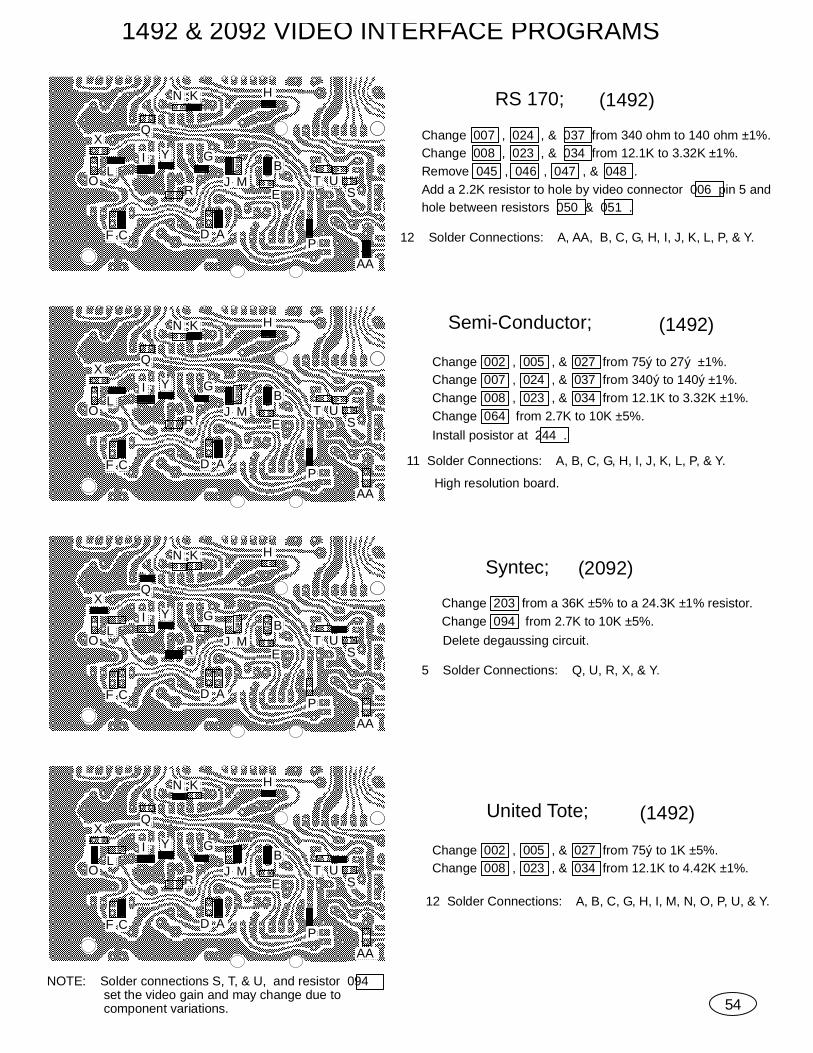
X
A
B
C D
E
F
G
H
I
J
K
L
N
P
Q
R ST U
Y
MO
AA
X
A
B
C D
E
F
G
H
I
J
K
L
N
P
Q
R ST U
Y
MO
AA
X
A
B
C D
E
F
G
H
I
J
K
L
N
P
Q
R ST U
Y
MO
AA
X
A
B
C D
E
F
G
H
I
J
K
L
N
P
Q
R ST U
Y
MO
AA
1492 & 2092 VIDEO INTERFACE PROGRAMS
54
NOTE: Solder connections S, T, & U, and resistor 094 set the video gain and may change due to component variations.
Change 002 , 005 , & 027 from 75ý to 1K ±5%.Change 008 , 023 , & 034 from 12.1K to 4.42K ±1%.
United Tote;
12 Solder Connections: A, B, C, G, H, I, M, N, O, P, U, & Y.
(1492)
Syntec;
5 Solder Connections: Q, U, R, X, & Y.
(2092)
Change 203 from a 36K ±5% to a 24.3K ±1% resistor.Change 094 from 2.7K to 10K ±5%.Delete degaussing circuit.
Change 002 , 005 , & 027 from 75ý to 27ý ±1%.Change 007 , 024 , & 037 from 340ý to 140ý ±1%.Change 008 , 023 , & 034 from 12.1K to 3.32K ±1%.Change 064 from 2.7K to 10K ±5%.
Semi-Conductor;
11 Solder Connections: A, B, C, G, H, I, J, K, L, P, & Y.
(1492)
Install posistor at 244 .
High resolution board.
Change 007 , 024 , & 037 from 340 ohm to 140 ohm ±1%.Change 008 , 023 , & 034 from 12.1K to 3.32K ±1%.Remove 045 , 046 , 047 , & 048 .Add a 2.2K resistor to hole by video connector 006 pin 5 andhole between resistors 050 & 051 .
RS 170; (1492)
12 Solder Connections: A, AA, B, C, G, H, I, J, K, L, P, & Y.

X
A
B
C D
E
F
G
H
I
J
K
L
N
P
Q
R ST U
Y
MO
AA
X
A
B
C D
E
F
G
H
I
J
K
L
N
P
Q
R ST U
Y
MO
AA
X
A
B
C D
E
F
G
H
I
J
K
L
N
P
Q
R ST U
Y
MO
AA
X
A
B
C D
E
F
G
H
I
J
K
L
N
P
Q
R ST U
Y
MO
AA
1492 & 2092 VIDEO INTERFACE PROGRAMS
55
NOTE: Solder connections S, T, & U, and resistor 094 set the video gain and may change due to component variations.
Change 002 , 005 , & 027 from 75ý to 1K ±5%.Change, the video input connector, 006 from a 6 conductor to a 7 conductor header.
5 Solder Connections: A, B, C, P, & S
4 Line TTL; (1492)
Solder Connections:
Solder Connections:
Change 094 from 2.7K to 10K, ±5%.
11 Solder Connections: D, E, F, G, H, I, M, N, O, P, & Y.
Western Amusement (1492)
Install posistor 244 .
Standard board.

NOTES:
56

2 3 5 6 7 8 9 10 13 14 15 16 17 18 19 201 14 12
P/N CPR0504
HORIZONTAL WIDTH CONTROL RESISTOR ARRAY "G"
G1 G2G7
G6
G5
G4
G3
G8 G10
G9
G11
G12
G13 G14 G15 G16 G1710K
10K
10K
10K
10K10K 5K
220K
50K
100K
44.2K
28K
38.3K
2.2K
16K 6.8K
1.82KA
Solder connection A reduces the horizontal raster size.
G
H. SIZEPOT GND
+6VSource
+12VLINE
Pincush.CoupleCap.
to Pin.Buffer
V. LIN.Correct.
LIN.buffernode
NC GND DMBuffer
DMcontrolV FB
DM ampOutput
NPNB
StabilityCap. Neg FB
+6VLINE
i BeamFB
DM amp
3 7 5 8 9 12 14 13 1LM324 Pin No.
AUTO BIAS RESISTOR ARRAY "C"
2 3 5 6 7 8 9 10 13 14 15 16 17 18 19 201 14 12
C15C14
C12
C11C10
C9C4C7C6C5
C8
C3C2C1
C16 C13
P/N CPR0503
68.1K
200ý 200ý
200ý
68.1K68.1K 20K 1.82K
2.74K 1.82K
5.00K
4K
5.00K
4K
5.00K
4K
C
ProgramPULSE
H.Blank
BLUEi Beam
GREEN REDGND NC
10.7VLINE
4.2VLINE
REDAmp out
REDAmp FB
ProgramPULSE
ProgramPULSEi Beam i Beam
REDi sense
GREENAmp FBGREEN
i sense Amp outGREEN BLUE
Amp FBi sense Amp outBLUE BLUE
4 5 7 6 LM324 Pin No. 2 1 13 14
2 3 5 6 7 8 9 10 13 14 15 16 17 18 19 201 14 12
P/N CPR0500
VIDEO AMPLIFIER RESISTOR ARRAY "B"
1234567
10 1 12 13 148 9
B4
B1
B3B2
B5
B20
B7
B18
B13
B6
B14B15
B16
B17
B9 B19
B11 B10
B12
B8
1.2K
68K
180ý
27ý
392ý
606ý3.32
K
1.27K
790ý 3.78K
1.65K836ý
5.62K
40.2K
510ý66ý270ý
32ý
270ý539ý
1490-91
1490-91
B
NE592
PNPdrivecap.
NPNE
NE592OutputB
NPN7.9VLINE GND +12V
LINEVIDEOINPUT
AUTOBIAS
127VLINE
7.9V PNP ECAP.
PNP BDIODE
PNPB
PNPE
PNPC
AMPOutputGND GND
57


Top Related
Copyright © 2022 FDOKUMEN

