


Bahasa
Halaman
Hukum


Product
Folder
Order
Now
Technical
Documents
Tools &
Software
Support &Community
本文档旨在为方便起见,提供有关 TI 产品中文版本的信息,以确认产品的概要。 有关适用的官方英文版本的最新信息,请访问 www.ti.com,其内容始终优先。 TI 不保证翻译的准确性和有效性。 在实际设计之前,请务必参考最新版本的英文版本。
English Data Sheet: SPRS968
DRA790, DRA791DRA793, DRA797
ZHCSII2E –AUGUST 2016–REVISED MAY 2019
DRA79x 信信息息娱娱乐乐 应应用用 处处理理器器
1 器器件件概概述述
1
1.1 特特性性1
• 专为信息娱乐协处理器 应用、混合无线电和放大器应用设计的架构
• Arm® Cortex®-A15 微处理器子系统
• C66x 浮点 VLIW DSP– 目标代码与 C67x 和 C64x+ 完全兼容
– 每周期最多 32 次 16 x 16 位定点乘法
• 片上 L3 RAM 高达 512KB• 3 级 (L3) 和 4 级 (L4) 互连
• DDR3/DDR3L 存储器接口 (EMIF) 模块
– 最高支持 DDR-1333 (667MHz)– 高达 2GB 的单芯片选择
• 双核 Arm® Cortex®-M4 图像处理单元 (IPU)• 显示子系统
– 带有 DMA 引擎和多达三条管线的显示控制器
– HDMI™编码器:兼容 HDMI 1.4a 和 DVI 1.0• 视频处理引擎 (VPE)• 一个视频输入端口 (VIP) 模块
– 支持多达四个复用输入端口
• 通用存储器控制器 (GPMC)• 增强型直接存储器存取 (EDMA) 控制器
• 2 端口千兆以太网 (GMAC)– 多达两个外部端口
• 16 个 32 位通用计时器
• 32 位 MPU 看门狗计时器
• 六个高速内部集成电路 (I2C) 端口
• HDQ™/ 单线®接口
• 10 个可配置 UART/IrDA/CIR 模块
• 4 个多通道串行外设接口 (McSPI)
• 四路 SPI 接口 (QSPI)• 媒体本地总线子系统 (MLBSS)• 8 个多通道音频串行端口 (McASP) 模块
• 超高速 USB 3.0 双角色器件
• 高速 USB 2.0 双重角色器件
• 高速 USB 2.0 On-The-Go• 四个多媒体卡/安全数字/安全数字输入输出接口
( MMC™/ SD®/SDIO)• PCI Express®3.0 子系统,带两个 5Gbps 通道
– 一个与第 2 代兼容的双通道端口
– 或两个与第 2 代兼容的单通道端口
• 双控制器局域网 (DCAN) 模块
– CAN 2.0B 协议
• MIPI®CSI-2 摄像头串行接口
• 多达 186 个通用 I/O (GPIO) 引脚
• 器件安全 特性
– 硬件加密加速器和 DMA– 防火墙
– JTAG 锁定
– 安全密钥
– 安全 ROM 和引导
– 客户可编程的秘钥
• 电源、复位和时钟管理
• 支持 CTool 技术的片上调试
• 28nm CMOS 技术
• 17mm × 17mm、0.65mm 间距、538 引脚 BGA(CBD)

2
DRA790, DRA791DRA793, DRA797ZHCSII2E –AUGUST 2016–REVISED MAY 2019 www.ti.com.cn
器件概述 版权 © 2016–2019, Texas Instruments Incorporated
1.2 应应用用
• 数字和模拟无线电
• 混合无线电
• DSP 音频放大器
• 车载互联协处理器
(1) 有关更多信息,请参阅节 9:机械、封装和可订购信息。
1.3 说说明明
DRA79x 处理器采用 538 焊球、17mm x 17mm、0.65mm 焊球间距(0.8mm 间距规则可用于信号)(通过Channel™ 阵列 (VCA) 技术实现)、球栅阵列 (S-BGA) 封装。
此架构旨在昨用经济高效的解决方案,为汽车协处理、混合无线电和放大器应用提供高性能并发性 , 实现DRA75x(“Jacinto 6 EP”和“Jacinto 6 Ex”)、DRA74x“Jacinto 6”、DRA72x“Jacinto 6 Eco”和DRA71x“Jacinto 6 Entry”信息娱乐处理器系列的全面可扩展性。
采用配有 Neon™ 扩展组件的单核 Arm Cortex-A15 RISC CPU 和 TI C66x VLIW 浮点 DSP 内核,可提供编程功能。借助 Arm 处理器,开发人员能够将控制函数与在 DSP 和协处理器上编程的其他算法分离开来,从而降低系统软件的复杂性。
此外,TI 提供了一整套针对 Arm 和 DSP 的开发工具,其中包括 C 语言编译器和一个可查看源代码执行情况的调试界面。
每个器件都具有加密加速特性。HS(高安全性)器件上还提供支持的所有其他安全 特性,包括安全引导支持、调试安全性和可信执行环境支持。有关 HS 器件的更多信息,请联系您的 TI 代表。
DRA79x Jacinto 6 RSP(无线电音频处理器)系列器件符合 AEC-Q100 标准。
该器件 采用 简化的电源轨映射,这使得低成本电源管理集成电路 (PMIC) 解决方案得以实现。
器器件件信信息息 (1)
器器件件型型号号 封封装装 封封装装尺尺寸寸
DRA790CBD FCBGA (538) 17.0mm × 17.0mmDRA791CBD FCBGA (538) 17.0mm × 17.0mmDRA793CBD FCBGA (538) 17.0mm × 17.0mmDRA797CBD FCBGA (538) 17.0mm × 17.0mm
Mailbox x13
EDMA
High-Speed Interconnect
Program/Data Storage
ConnectivitySystem
(1x ArmCortex–A15)
PCIe SS x2
MediaLB
(NAND/NOR/Async)
VIP x1
intro-001
GPMC / ELM
256-KB ROM
OCMC
DRA79x
MPU
Serial Interfaces
I2C x6
UART x10
McSPI x4
DCAN x2
Spinlock
GPIO x8
Timers x16
WDT
QSPI EMIF x11x 32-bit
DDR3/DDR3L
sDMA VPE
McASP x8
MMU x2
PWM SS x3
HDQKBD GMAC AVB
MOST150
1x USB 3.0Dual Mode FS/HS/SS
w/ PHY
2x USB 2.0Dual Mode FS/HS1x PHY, 1x ULPI
512-KBRAM with ECC
DMM
MMC / SD x4
PRU-ICSS x2
(1x C66xCo-Processor)
DSP
IPU1
(Dual Cortex–M4) (Dual Cortex–M4)
IPU2
Display Subsystem
1xGFX / 3xVID
Blend / Scale
HDMI 1.4a
LCD3
Secure Boot
Debug
Security
TEE
(HS devices)
CAL CSI2 x1
Radio Accelerators
VCP x2 HD ATL
LCD2
3
DRA790, DRA791DRA793, DRA797
www.ti.com.cn ZHCSII2E –AUGUST 2016–REVISED MAY 2019
器件概述版权 © 2016–2019, Texas Instruments Incorporated
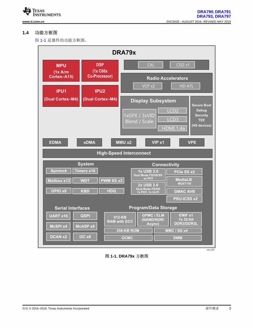
1.4 功功能能方方框框图图
图 1-1 是器件的功能方框图。
图图 1-1. DRA79x 方方框框图图

4
DRA790, DRA791DRA793, DRA797ZHCSII2E –AUGUST 2016–REVISED MAY 2019 www.ti.com.cn
内容 版权 © 2016–2019, Texas Instruments Incorporated
内内容容
1 器器件件概概述述 .................................................... 11.1 特性 ................................................... 11.2 应用 ................................................... 21.3 说明 ................................................... 21.4 功能方框图 ........................................... 3
2 修修订订历历史史记记录录............................................... 53 Device Comparison ..................................... 6
3.1 Related Products ..................................... 84 Terminal Configuration and Functions.............. 9
4.1 Pin Diagram .......................................... 94.2 Pin Attributes ......................................... 94.3 Signal Descriptions.................................. 684.4 Pin Multiplexing .................................... 1064.5 Connections for Unused Pins...................... 120
5 Specifications ......................................... 1215.1 Absolute Maximum Ratings........................ 1225.2 ESD Ratings ....................................... 1235.3 Power on Hour (POH) Limits ...................... 1235.4 Recommended Operating Conditions ............. 1235.5 Operating Performance Points..................... 1265.6 Power Consumption Summary .................... 1455.7 Electrical Characteristics........................... 1455.8 VPP Specifications for One-Time Programmable
(OTP) eFuses ...................................... 1525.9 Thermal Resistance Characteristics for CBD
Package............................................ 1535.10 Timing Requirements and Switching
Characteristics ..................................... 1556 Detailed Description.................................. 329
6.1 Description ......................................... 3296.2 Functional Block Diagram ......................... 329
6.3 MPU................................................ 3316.4 DSP Subsystem ................................... 3346.5 IPU ................................................. 3386.6 PRU-ICSS.......................................... 3396.7 Memory Subsystem................................ 3406.8 Interprocessor Communication .................... 3436.9 Interrupt Controller................................. 3436.10 EDMA .............................................. 3446.11 Peripherals ......................................... 3466.12 On-chip Debug..................................... 363
7 Applications, Implementation, and Layout ...... 3667.1 Introduction ........................................ 3667.2 Power Optimizations ............................... 3677.3 Core Power Domains .............................. 3787.4 Single-Ended Interfaces ........................... 3897.5 Differential Interfaces .............................. 3917.6 Clock Routing Guidelines .......................... 4107.7 DDR3 Board Design and Layout Guidelines....... 410
8 Device and Documentation Support .............. 4348.1 Device Nomenclature .............................. 4348.2 Tools and Software ................................ 4368.3 Documentation Support............................ 4378.4 Related Links ...................................... 4378.5 Community Resources............................. 4378.6 商标 ................................................ 4388.7 静电放电警告....................................... 4388.8 Glossary............................................ 438
9 Mechanical, Packaging, and OrderableInformation ............................................. 4399.1 Packaging Information ............................. 439

5
DRA790, DRA791DRA793, DRA797
www.ti.com.cn ZHCSII2E –AUGUST 2016–REVISED MAY 2019
修订历史记录版权 © 2016–2019, Texas Instruments Incorporated
2 修修订订历历史史记记录录
Changes from July 16, 2018 to May 15, 2019 (from D Revision (July 2018) to E Revision) Page
• Added clarification note regarding X777 part number in 表 3-1, Device Comparison ....................................... 6• Added clarification notes for EMU[1:0] connections to 表 4-21, GPIOs Signal Descriptions and 表 4-26, Debug
Signal Descriptions.................................................................................................................. 94• Added clarification note regarding TSHUT feature in Section 5.4, Recommended Operating Conditions ............ 126• Updated 表 5-2, AVS and ABB Requirements per vdd_* Supply ........................................................... 126• Updated OPP_HIGH voltage range in note (6) under 表 5-3, Voltage Domains Operating Performance Points..... 127• Added Ivpp specification in 表 5-14, Recommended Operating Conditions for OTP eFuse Programming............ 152• Updated EMIF_DLL_FCLK max rate in Table 5-28, DLL Characteristics ................................................. 175• Added MII_TXER timing to 节 5.10.6.19.1, GMAC MII Timings ............................................................. 264• Updated 图 5-72, GMAC MDIO diagrams and MDIO7 parameter values in 表 5-99, Switching Characteristics
Over Recommended Operating Conditions for MDIO Output ............................................................... 265• Added note regarding DDR ECC solutions to 表 7-25, Supported DDR3 Device Combinations ....................... 411• Added clarifications about validated DDR topology in 节 7.7.2.15, CK and ADDR_CTRL Topologies and Routing
Definition ............................................................................................................................ 420• Added the TI E2E™ Online Community link to the Community Resources section under 节 8, Device and
Documentation Support ........................................................................................................... 434• Added clarification note regarding X777 part number in 表 8-1, Nomenclature Description ............................ 436

6
DRA790, DRA791DRA793, DRA797ZHCSII2E –AUGUST 2016–REVISED MAY 2019 www.ti.com.cn
Device Comparison 版权 © 2016–2019, Texas Instruments Incorporated
3 Device Comparison
表 3-1 shows a comparison between devices, highlighting the differences.
表表 3-1. Device Comparison(2)
FEATURESDEVICE
DRA790 DRA791 DRA793 DRA797FeaturesCTRL_WKUP_STD_FUSE_DIE_ID_2 [31:24] Base PN register bitfieldvalue(1)(2) 128 (0x80) 129 (0x81) 131 (0x83) 135 (0x87)
Processors/AcceleratorsSpeed Grades A B D HArm Single Cortex-A15 Microprocessor (MPU)Subsystem MPU core 0 Yes
C66x VLIW DSP DSP1 YesBitBLT 2D Hardware Acceleration Engine (BB2D) BB2D No
Display Subsystem
VOUT1 NoVOUT2 YesVOUT3 YesHDMI Yes
Dual Arm Cortex-M4 Image Processing Unit (IPU)IPU1 YesIPU2 Yes
Image Video Accelarator (IVA) IVA NoSGX544 Single-Core 3D Graphics Processing Unit(GPU) GPU No
Video Input Port (VIP) VIP1
vin1a Yesvin1b Yesvin2a Yesvin2b Yes
Video Processing Engine (VPE) VPE YesProgram/Data StorageOn-Chip Shared Memory (RAM) OCMC_RAM1 512KBGeneral-Purpose Memory Controller (GPMC) GPMC YesDDR3/DDR3L Memory Controller EMIF1 up to 2GBDynamic Memory Manager (DMM) DMM YesRadio SupportAudio Tracking Logic (ATL) ATL Yes
Viterbi Coprocessor (VCP)VCP1 YesVCP2 Yes
Peripherals
Controller Area Network (DCAN) InterfaceDCAN1 YesDCAN2 Yes
Enhanced DMA (EDMA) EDMA YesSystem DMA (DMA_SYSTEM) DMA_SYSTEM Yes
Ethernet Subsystem (Ethernet SS)GMAC_SW[0] MII, RMII, or RGMIIGMAC_SW[1] MII, RMII, or RGMII
General-Purpose I/O (GPIO) GPIO Up to 186Inter-Integrated Circuit Interface (I2C) I2C 6System Mailbox Module MAILBOX 13Media Local Bus Subsystem (MLBSS) MLB Yes

7
DRA790, DRA791DRA793, DRA797
www.ti.com.cn ZHCSII2E –AUGUST 2016–REVISED MAY 2019
Device Comparison版权 © 2016–2019, Texas Instruments Incorporated
表表 3-1. Device Comparison(2) (continued)
FEATURESDEVICE
DRA790 DRA791 DRA793 DRA797
Camera Adaptation Layer (CAL) Camera SerialInterface 2 (CSI2)
CSI2_0 1 CLK + 2 DataCSI2_1 No
Multichannel Audio Serial Port (McASP)
McASP1 16 serializersMcASP2 16 serializersMcASP3 4 serializersMcASP4 4 serializersMcASP5 4 serializersMcASP6 4 serializersMcASP7 4 serializersMcASP8 2 serializers
MultiMedia Card/Secure Digital/Secure Digital InputOutput Interface (MMC/SD/SDIO)
MMC1 1x UHSI 4bMMC2 1x eMMC 8bMMC3 1x SDIO 8bMMC4 1x SDIO 4b
PCI Express 3.0 Port with Integrated PHYPCIe_SS1 Up to two lanes (second lane shared with PCIe_SS2 and
USB1)PCIe_SS2 Single lane (shared with PCIe_SS1 and USB1)
Serial Advanced Technology Attachment (SATA) SATA NoReal-Time Clock Subsystem (RTCSS) RTCSS No
Programmable Real-Time Unit Subsystem andIndustrial Communication Subsystem (PRU-ICSS)
PRU-ICSS1 No No No YesPRU-ICSS2 No No No Yes
Multichannel Serial Peripheral Interface (McSPI) McSPI 4HDQ1W HDQ1W YesQuad SPI (QSPI) QSPI YesSpinlock Module SPINLOCK YesKeyboard Controller (KBD) KBD YesTimers, General-Purpose TIMERS GP 16Timer, Watchdog WD TIMER Yes
Pulse-Width Modulation Subsystem (PWMSS)PWMSS1 YesPWMSS2 YesPWMSS3 Yes
Universal Asynchronous Receiver/Transmitter(UART) UART 10
Universal Serial Bus (USB3.0)USB1 (Super-Speed,Dual-Role-Device[DRD])
Yes
Universal Serial Bus (USB2.0)
USB2 (High-Speed,Dual-Role-Device[DRD], withembedded HS PHY)
Yes
USB3 (High-Speed,OTG2.0, with ULPI) Yes
USB4 (High-Speed,OTG2.0, with ULPI) No
(1) For more details about the CTRL_WKUP_STD_FUSE_DIE_ID_2 register and Base PN bitfield, see the device TRM.(2) X777 base part number with X speed grade indicator is the part number for the superset device. Software should constrain the features
and speed used to match the intended production device. The Base PN register bitfield value is 0x4F.
3.1 Related Products

8
DRA790, DRA791DRA793, DRA797ZHCSII2E –AUGUST 2016–REVISED MAY 2019 www.ti.com.cn
Device Comparison 版权 © 2016–2019, Texas Instruments Incorporated
Automotive ProcessorsDRAx Infotainment SoCs The "Jacinto™ 6" family of infotainment processors (DRA7xx), paired with
robust software and ecosystem offering bring unprecedented feature-rich, in-vehicleinfotainment, instrument cluster and telematics features to the next generation automobiles.

9
DRA790, DRA791DRA793, DRA797
www.ti.com.cn ZHCSII2E –AUGUST 2016–REVISED MAY 2019
Terminal Configuration and Functions版权 © 2016–2019, Texas Instruments Incorporated
4 Terminal Configuration and Functions
4.1 Pin Diagram图 4-1 shows the ball locations for the 538 plastic ball grid array (PBGA) package and isused inconjunction with 表 4-1 through 表 4-31 to locate signal names and ball grid numbers.
图图 4-1. CBD S-PBGA-N538 Package (Bottom View)
注注The following bottom balls are not pinned out: AE4 / AE7 / AE10 / AE13 / AD5 / AD8 / AD11/ AD14 / AC7 / AC9 / AC12 / AC14 / AC17 / AB3 / AB4 / AB5 / AB13 / AB14 / AB17 / AB20 /AB21 / AB22 / AA14 / AA17 / AA22 / Y22 / W3 / W4 / W5 / W6 / V6 / V21 / V22 / V23 / R3 /R4 / R5 / R6 / R21 / R22 / R23 / P6 / M3 / M4 / M5 / M6 / M21 / M22 / M23 / J3 / J4 / J5 / J6/ J21 / J22 / J23 / F4 / F5 / F9 / F12 / F15 / F18 / F21 / F22 / E3 / E4 / E5 / E6 / E9 / E12 /E15 / E18 / E21 / E22 / E23 / D4 / D5 / D9 / D12 / D15 / D18 / D21 / D22 / C9 / C12 / C15 /C18.
These balls do not exist on the package.
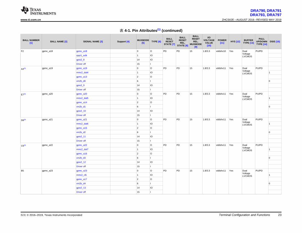
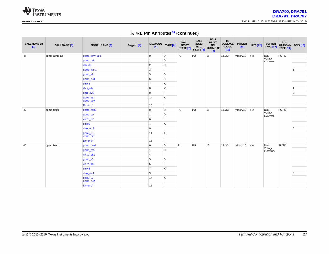
4.2 Pin Attributes表 4-1 describes the terminal characteristics and the signals multiplexed on each ball. The following listdescribes the table column headers:1. BALL NUMBER:This column lists ball numbers on the bottom side associated with each signal on the
bottom.2. BALL NAME: This column lists mechanical name from package device (name is taken from muxmode
0).3. SIGNAL NAME:This column lists names of signals multiplexed on each ball (also notice that the name
of the ball is the signal name in muxmode 0).
注注表 4-1 does not take into account the subsystem multiplexing signals. Subsystemmultiplexing signals are described in 节 4.3, Signal Descriptions.
注注In driver off mode, the buffer is configured in high-impedance.
10
DRA790, DRA791DRA793, DRA797ZHCSII2E –AUGUST 2016–REVISED MAY 2019 www.ti.com.cn
Terminal Configuration and Functions 版权 © 2016–2019, Texas Instruments Incorporated
注注In some cases 表 4-1 may present more than one signal name per muxmode for the sameball. First signal in the list is the dominant function as selected via CTRL_CORE_PAD_*register.
All other signals are virtual functions that present alternate multiplexing options. This virtualfunctions are controlled via CTRL_CORE_ALT_SELECT_MUX orCTRL_CORE_VIP_MUX_SELECT register. For more information on how to use this options,please refer to Device TRM, Chapter Control Module, Section Pad Configuration Registers.
4. Support: This column shows if the functionality is applicable for DRA790 / DRA791 / DRA793 devices.Note that the Pin Attributes table presents the functionality of DRA797 device. An empty box means"Yes".
5. MUXMODE: Multiplexing mode number:a. MUXMODE 0 is the primary mode; this means that when MUXMODE=0 is set, the function
mapped on the pin corresponds to the name of the pin. The primary muxmode is not necessarilythe default muxmode.
注注The default mode is the mode at the release of the reset; also see the RESET REL.MUXMODE column.
b. MUXMODE 1 through 15 are possible muxmodes for alternate functions. On each pin, somemuxmodes are effectively used for alternate functions, while some muxmodes are not used. OnlyMUXMODE values which correspond to defined functions should be used.
c. An empty box means Not Applicable.6. TYPE: Signal type and direction:
– I = Input– O = Output– IO = Input or Output– D = Open drain– DS = Differential Signaling– A = Analog– PWR = Power– GND = Ground– CAP = LDO Capacitor
7. BALL RESET STATE: The state of the terminal at power-on reset:– drive 0 (OFF): The buffer drives VOL (pulldown or pullup resistor not activated)– drive 1 (OFF): The buffer drives VOH (pulldown or pullup resistor not activated)– OFF: High-impedance– PD: High-impedance with an active pulldown resistor– PU: High-impedance with an active pullup resistor– An empty box means Not Applicable
8. BALL RESET REL. STATE: The state of the terminal at the deactivation of the rstoutn signal (alsomapped to the PRCM SYS_WARM_OUT_RST signal)– drive 0 (OFF): The buffer drives VOL (pulldown or pullup resistor not activated)– drive clk (OFF): The buffer drives a toggling clock (pulldown or pullup resistor not activated)– drive 1 (OFF): The buffer drives VOH (pulldown or pullup resistor not activated)– OFF: High-impedance– PD: High-impedance with an active pulldown resistor– PU: High-impedance with an active pullup resistor– An empty box means Not Applicable

11
DRA790, DRA791DRA793, DRA797
www.ti.com.cn ZHCSII2E –AUGUST 2016–REVISED MAY 2019
Terminal Configuration and Functions版权 © 2016–2019, Texas Instruments Incorporated
注注For more information on the CORE_PWRON_RET_RST reset signal and its reset sources,see the Power, Reset, and Clock Management / PRCM Reset Management FunctionalDescription section of the Device TRM.
9. BALL RESET REL. MUXMODE: This muxmode is automatically configured at the release of therstoutn signal (also mapped to the PRCM SYS_WARM_OUT_RST signal).An empty box means Not Applicable.
10. IO VOLTAGE VALUE: This column describes the IO voltage value (the corresponding power supply).An empty box means Not Applicable.
11. POWER: The voltage supply that powers the terminal IO buffers.An empty box means Not Applicable.
12. HYS: Indicates if the input buffer is with hysteresis:– Yes: With hysteresis– No: Without hysteresis– An empty box: Not Applicable
注注For more information, see the hysteresis values in 节 5.7, Electrical Characteristics.
13. BUFFER TYPE: Drive strength of the associated output buffer.An empty box means Not Applicable.
注注For programmable buffer strength:– The default value is given in 表 4-1.– A note describes all possible values according to the selected muxmode.
14. PULLUP / PULLDOWN TYPE: Denotes the presence of an internal pullup or pulldown resistor.Pullup and pulldown resistors can be enabled or disabled via software.– PU: Internal pullup– PD: Internal pulldown– PU/PD: Internal pullup and pulldown– PUx/PDy: Programmable internal pullup and pulldown– PDy: Programmable internal pulldown– An empty box means No pull
15. DSIS: The deselected input state (DSIS) indicates the state driven on the peripheral input (logic "0" orlogic "1") when the peripheral pin function is not selected by any of the PINCNTLx registers.– 0: Logic 0 driven on the peripheral's input signal port.– 1: Logic 1 driven on the peripheral's input signal port.– blank: Pin state driven on the peripheral's input signal port.
注注Configuring two pins to the same input signal is not supported as it can yield unexpectedresults. This can be easily prevented with the proper software configuration (Hi-Z mode is notan input signal).
注注When a pad is set into a multiplexing mode which is not defined by pin multiplexing, thatpad’s behavior is undefined. This should be avoided.
12
DRA790, DRA791DRA793, DRA797ZHCSII2E –AUGUST 2016–REVISED MAY 2019 www.ti.com.cn
Terminal Configuration and Functions 版权 © 2016–2019, Texas Instruments Incorporated
注注Some of the EMIF1 signals have an additional state change at the release of porz. The statethat the signals change to at the release of porz is as follows:
drive 0 (OFF) for: ddr1_ck, ddr1_odt[0], ddr1_rst.
drive 1 (OFF) for: ddr1_casn, ddr1_rasn, ddr1_wen, ddr1_nck, ddr1_ba[2:0], ddr1_a[15:0],ddr1_csn[0], ddr1_cke, ddr1_dqm[3:0].
注注Dual rank support is not available on this device, but signal names are retained forconsistency with the DRA7xx family of devices.

版权 © 2016–2019, Texas Instruments Incorporated Terminal Configuration and Functions 13
DRA790, DRA791DRA793, DRA797
www.ti.com.cn ZHCSII2E –AUGUST 2016–REVISED MAY 2019
表表 4-1. Pin Attributes(1)
BALL NUMBER[1] BALL NAME [2] SIGNAL NAME [3] Support [4] MUXMODE
[5] TYPE [6]BALL
RESETSTATE [7]
BALLRESETREL.
STATE [8]
BALLRESETREL.
MUXMODE[9]
I/OVOLTAGE
VALUE[10]
POWER[11] HYS [12] BUFFER
TYPE [13]
PULLUP/DOWNTYPE [14]
DSIS [15]
F8 cap_vbbldo_dsp cap_vbbldo_dsp CAP
T7 cap_vbbldo_gpu cap_vbbldo_gpu CAP
G14 cap_vbbldo_iva cap_vbbldo_iva CAP
F17 cap_vbbldo_mpu cap_vbbldo_mpu CAP
U20 cap_vddram_core1 cap_vddram_core1 CAP
K7 cap_vddram_core3 cap_vddram_core3 CAP
G19 cap_vddram_core4 cap_vddram_core4 CAP
L7 cap_vddram_dsp cap_vddram_dsp CAP
V7 cap_vddram_gpu cap_vddram_gpu CAP
G12 cap_vddram_iva cap_vddram_iva CAP
G18 cap_vddram_mpu cap_vddram_mpu CAP
AC1 csi2_0_dx0 csi2_0_dx0 0 I 1.8 Yes LVCMOSCSI2
PU/PD
AD1 csi2_0_dx1 csi2_0_dx1 0 I 1.8 Yes LVCMOSCSI2
PU/PD
AE2 csi2_0_dx2 csi2_0_dx2 0 I 1.8 Yes LVCMOSCSI2
PU/PD
AB2 csi2_0_dy0 csi2_0_dy0 0 I 1.8 Yes LVCMOSCSI2
PU/PD
AC2 csi2_0_dy1 csi2_0_dy1 0 I 1.8 Yes LVCMOSCSI2
PU/PD
AD2 csi2_0_dy2 csi2_0_dy2 0 I 1.8 Yes LVCMOSCSI2
PU/PD
H23 dcan1_rx dcan1_rx 0 IO PU PU 15 1.8/3.3 vddshv3 Yes DualVoltageLVCMOS
PU/PD 1
uart8_txd 2 O
mmc2_sdwp 3 I 0
hdmi1_cec 6 IO
gpio1_15 14 IO
Driver off 15 I
H22 dcan1_tx dcan1_tx 0 IO PU PU 15 1.8/3.3 vddshv3 Yes DualVoltageLVCMOS
PU/PD 1
uart8_rxd 2 I 1
mmc2_sdcd 3 I 1
hdmi1_hpd 6 IO
gpio1_14 14 IO
Driver off 15 I
AC18 ddr1_a0 ddr1_a0 0 O PD drive 1(OFF)
1.35/1.5 vdds_ddr1 No LVCMOSDDR
PUx/PDy
AE19 ddr1_a1 ddr1_a1 0 O PD drive 1(OFF)
1.35/1.5 vdds_ddr1 No LVCMOSDDR
PUx/PDy

版权 © 2016–2019, Texas Instruments IncorporatedTerminal Configuration and Functions14
DRA790, DRA791DRA793, DRA797ZHCSII2E –AUGUST 2016–REVISED MAY 2019 www.ti.com.cn
表表 4-1. Pin Attributes(1) (continued)
BALL NUMBER[1] BALL NAME [2] SIGNAL NAME [3] Support [4] MUXMODE
[5] TYPE [6]BALL
RESETSTATE [7]
BALLRESETREL.
STATE [8]
BALLRESETREL.
MUXMODE[9]
I/OVOLTAGE
VALUE[10]
POWER[11] HYS [12] BUFFER
TYPE [13]
PULLUP/DOWNTYPE [14]
DSIS [15]
AD19 ddr1_a2 ddr1_a2 0 O PD drive 1(OFF)
1.35/1.5 vdds_ddr1 No LVCMOSDDR
PUx/PDy
AB19 ddr1_a3 ddr1_a3 0 O PD drive 1(OFF)
1.35/1.5 vdds_ddr1 No LVCMOSDDR
PUx/PDy
AD20 ddr1_a4 ddr1_a4 0 O PD drive 1(OFF)
1.35/1.5 vdds_ddr1 No LVCMOSDDR
PUx/PDy
AE20 ddr1_a5 ddr1_a5 0 O PD drive 1(OFF)
1.35/1.5 vdds_ddr1 No LVCMOSDDR
PUx/PDy
AA18 ddr1_a6 ddr1_a6 0 O PD drive 1(OFF)
1.35/1.5 vdds_ddr1 No LVCMOSDDR
PUx/PDy
AA20 ddr1_a7 ddr1_a7 0 O PD drive 1(OFF)
1.35/1.5 vdds_ddr1 No LVCMOSDDR
PUx/PDy
Y21 ddr1_a8 ddr1_a8 0 O PD drive 1(OFF)
1.35/1.5 vdds_ddr1 No LVCMOSDDR
PUx/PDy
AC20 ddr1_a9 ddr1_a9 0 O PD drive 1(OFF)
1.35/1.5 vdds_ddr1 No LVCMOSDDR
PUx/PDy
AA21 ddr1_a10 ddr1_a10 0 O PD drive 1(OFF)
1.35/1.5 vdds_ddr1 No LVCMOSDDR
PUx/PDy
AC21 ddr1_a11 ddr1_a11 0 O PD drive 1(OFF)
1.35/1.5 vdds_ddr1 No LVCMOSDDR
PUx/PDy
AC22 ddr1_a12 ddr1_a12 0 O PD drive 1(OFF)
1.35/1.5 vdds_ddr1 No LVCMOSDDR
PUx/PDy
AC15 ddr1_a13 ddr1_a13 0 O PD drive 1(OFF)
1.35/1.5 vdds_ddr1 No LVCMOSDDR
PUx/PDy
AB15 ddr1_a14 ddr1_a14 0 O PD drive 1(OFF)
1.35/1.5 vdds_ddr1 No LVCMOSDDR
PUx/PDy
AC16 ddr1_a15 ddr1_a15 0 O PD drive 1(OFF)
1.35/1.5 vdds_ddr1 No LVCMOSDDR
PUx/PDy
AE16 ddr1_ba0 ddr1_ba0 0 O PU drive 1(OFF)
1.35/1.5 vdds_ddr1 No LVCMOSDDR
PUx/PDy
AA16 ddr1_ba1 ddr1_ba1 0 O PU drive 1(OFF)
1.35/1.5 vdds_ddr1 No LVCMOSDDR
PUx/PDy
AB16 ddr1_ba2 ddr1_ba2 0 O PU drive 1(OFF)
1.35/1.5 vdds_ddr1 No LVCMOSDDR
PUx/PDy
AD16 ddr1_casn ddr1_casn 0 O PU drive 1(OFF)
1.35/1.5 vdds_ddr1 No LVCMOSDDR
PUx/PDy
AD21 ddr1_ck ddr1_ck 0 O PD drive 0(OFF)
1.35/1.5 vdds_ddr1 No LVCMOSDDR
PUx/PDy
AB18 ddr1_cke ddr1_cke 0 O PU drive 1(OFF)
1.35/1.5 vdds_ddr1 No LVCMOSDDR
PUx/PDy
AC19 ddr1_csn0 ddr1_csn0 0 O PU drive 1(OFF)
1.35/1.5 vdds_ddr1 No LVCMOSDDR
PUx/PDy
AA23 ddr1_d0 ddr1_d0 0 IO PD PD 1.35/1.5 vdds_ddr1 No LVCMOSDDR
PUx/PDy
AC24 ddr1_d1 ddr1_d1 0 IO PD PD 1.35/1.5 vdds_ddr1 No LVCMOSDDR
PUx/PDy

版权 © 2016–2019, Texas Instruments Incorporated Terminal Configuration and Functions 15
DRA790, DRA791DRA793, DRA797
www.ti.com.cn ZHCSII2E –AUGUST 2016–REVISED MAY 2019
表表 4-1. Pin Attributes(1) (continued)
BALL NUMBER[1] BALL NAME [2] SIGNAL NAME [3] Support [4] MUXMODE
[5] TYPE [6]BALL
RESETSTATE [7]
BALLRESETREL.
STATE [8]
BALLRESETREL.
MUXMODE[9]
I/OVOLTAGE
VALUE[10]
POWER[11] HYS [12] BUFFER
TYPE [13]
PULLUP/DOWNTYPE [14]
DSIS [15]
AB24 ddr1_d2 ddr1_d2 0 IO PD PD 1.35/1.5 vdds_ddr1 No LVCMOSDDR
PUx/PDy
AD24 ddr1_d3 ddr1_d3 0 IO PD PD 1.35/1.5 vdds_ddr1 No LVCMOSDDR
PUx/PDy
AB23 ddr1_d4 ddr1_d4 0 IO PD PD 1.35/1.5 vdds_ddr1 No LVCMOSDDR
PUx/PDy
AC23 ddr1_d5 ddr1_d5 0 IO PD PD 1.35/1.5 vdds_ddr1 No LVCMOSDDR
PUx/PDy
AD23 ddr1_d6 ddr1_d6 0 IO PD PD 1.35/1.5 vdds_ddr1 No LVCMOSDDR
PUx/PDy
AE24 ddr1_d7 ddr1_d7 0 IO PD PD 1.35/1.5 vdds_ddr1 No LVCMOSDDR
PUx/PDy
AA24 ddr1_d8 ddr1_d8 0 IO PD PD 1.35/1.5 vdds_ddr1 No LVCMOSDDR
PUx/PDy
W25 ddr1_d9 ddr1_d9 0 IO PD PD 1.35/1.5 vdds_ddr1 No LVCMOSDDR
PUx/PDy
Y23 ddr1_d10 ddr1_d10 0 IO PD PD 1.35/1.5 vdds_ddr1 No LVCMOSDDR
PUx/PDy
AD25 ddr1_d11 ddr1_d11 0 IO PD PD 1.35/1.5 vdds_ddr1 No LVCMOSDDR
PUx/PDy
AC25 ddr1_d12 ddr1_d12 0 IO PD PD 1.35/1.5 vdds_ddr1 No LVCMOSDDR
PUx/PDy
AB25 ddr1_d13 ddr1_d13 0 IO PD PD 1.35/1.5 vdds_ddr1 No LVCMOSDDR
PUx/PDy
AA25 ddr1_d14 ddr1_d14 0 IO PD PD 1.35/1.5 vdds_ddr1 No LVCMOSDDR
PUx/PDy
W24 ddr1_d15 ddr1_d15 0 IO PD PD 1.35/1.5 vdds_ddr1 No LVCMOSDDR
PUx/PDy
W23 ddr1_d16 ddr1_d16 0 IO PD PD 1.35/1.5 vdds_ddr1 No LVCMOSDDR
PUx/PDy
U25 ddr1_d17 ddr1_d17 0 IO PD PD 1.35/1.5 vdds_ddr1 No LVCMOSDDR
PUx/PDy
U24 ddr1_d18 ddr1_d18 0 IO PD PD 1.35/1.5 vdds_ddr1 No LVCMOSDDR
PUx/PDy
W21 ddr1_d19 ddr1_d19 0 IO PD PD 1.35/1.5 vdds_ddr1 No LVCMOSDDR
PUx/PDy
T22 ddr1_d20 ddr1_d20 0 IO PD PD 1.35/1.5 vdds_ddr1 No LVCMOSDDR
PUx/PDy
U22 ddr1_d21 ddr1_d21 0 IO PD PD 1.35/1.5 vdds_ddr1 No LVCMOSDDR
PUx/PDy
U23 ddr1_d22 ddr1_d22 0 IO PD PD 1.35/1.5 vdds_ddr1 No LVCMOSDDR
PUx/PDy
T21 ddr1_d23 ddr1_d23 0 IO PD PD 1.35/1.5 vdds_ddr1 No LVCMOSDDR
PUx/PDy
T23 ddr1_d24 ddr1_d24 0 IO PD PD 1.35/1.5 vdds_ddr1 No LVCMOSDDR
PUx/PDy

版权 © 2016–2019, Texas Instruments IncorporatedTerminal Configuration and Functions16
DRA790, DRA791DRA793, DRA797ZHCSII2E –AUGUST 2016–REVISED MAY 2019 www.ti.com.cn
表表 4-1. Pin Attributes(1) (continued)
BALL NUMBER[1] BALL NAME [2] SIGNAL NAME [3] Support [4] MUXMODE
[5] TYPE [6]BALL
RESETSTATE [7]
BALLRESETREL.
STATE [8]
BALLRESETREL.
MUXMODE[9]
I/OVOLTAGE
VALUE[10]
POWER[11] HYS [12] BUFFER
TYPE [13]
PULLUP/DOWNTYPE [14]
DSIS [15]
T25 ddr1_d25 ddr1_d25 0 IO PD PD 1.35/1.5 vdds_ddr1 No LVCMOSDDR
PUx/PDy
T24 ddr1_d26 ddr1_d26 0 IO PD PD 1.35/1.5 vdds_ddr1 No LVCMOSDDR
PUx/PDy
P21 ddr1_d27 ddr1_d27 0 IO PD PD 1.35/1.5 vdds_ddr1 No LVCMOSDDR
PUx/PDy
N21 ddr1_d28 ddr1_d28 0 IO PD PD 1.35/1.5 vdds_ddr1 No LVCMOSDDR
PUx/PDy
P22 ddr1_d29 ddr1_d29 0 IO PD PD 1.35/1.5 vdds_ddr1 No LVCMOSDDR
PUx/PDy
P23 ddr1_d30 ddr1_d30 0 IO PD PD 1.35/1.5 vdds_ddr1 No LVCMOSDDR
PUx/PDy
P24 ddr1_d31 ddr1_d31 0 IO PD PD 1.35/1.5 vdds_ddr1 No LVCMOSDDR
PUx/PDy
AE23 ddr1_dqm0 ddr1_dqm0 0 O PU drive 1(OFF)
1.35/1.5 vdds_ddr1 No LVCMOSDDR
PUx/PDy
W22 ddr1_dqm1 ddr1_dqm1 0 O PU drive 1(OFF)
1.35/1.5 vdds_ddr1 No LVCMOSDDR
PUx/PDy
U21 ddr1_dqm2 ddr1_dqm2 0 O PU drive 1(OFF)
1.35/1.5 vdds_ddr1 No LVCMOSDDR
PUx/PDy
P25 ddr1_dqm3 ddr1_dqm3 0 O PU drive 1(OFF)
1.35/1.5 vdds_ddr1 No LVCMOSDDR
PUx/PDy
AD22 ddr1_dqs0 ddr1_dqs0 0 IO PD PD 1.35/1.5 vdds_ddr1 LVCMOSDDR
PUx/PDy
Y24 ddr1_dqs1 ddr1_dqs1 0 IO PD PD 1.35/1.5 vdds_ddr1 LVCMOSDDR
PUx/PDy
V24 ddr1_dqs2 ddr1_dqs2 0 IO PD PD 1.35/1.5 vdds_ddr1 LVCMOSDDR
PUx/PDy
R24 ddr1_dqs3 ddr1_dqs3 0 IO PD PD 1.35/1.5 vdds_ddr1 LVCMOSDDR
PUx/PDy
AE22 ddr1_dqsn0 ddr1_dqsn0 0 IO PU PU 1.35/1.5 vdds_ddr1 LVCMOSDDR
PUx/PDy
Y25 ddr1_dqsn1 ddr1_dqsn1 0 IO PU PU 1.35/1.5 vdds_ddr1 LVCMOSDDR
PUx/PDy
V25 ddr1_dqsn2 ddr1_dqsn2 0 IO PU PU 1.35/1.5 vdds_ddr1 LVCMOSDDR
PUx/PDy
R25 ddr1_dqsn3 ddr1_dqsn3 0 IO PU PU 1.35/1.5 vdds_ddr1 LVCMOSDDR
PUx/PDy
AE21 ddr1_nck ddr1_nck 0 O PU drive 1(OFF)
1.35/1.5 vdds_ddr1 No LVCMOSDDR
PUx/PDy
AD18 ddr1_odt0 ddr1_odt0 0 O PD drive 0(OFF)
1.35/1.5 vdds_ddr1 No LVCMOSDDR
PUx/PDy
AD17 ddr1_rasn ddr1_rasn 0 O PU drive 1(OFF)
1.35/1.5 vdds_ddr1 No LVCMOSDDR
PUx/PDy
AE17 ddr1_rst ddr1_rst 0 O PD drive 0(OFF)
1.35/1.5 vdds_ddr1 No LVCMOSDDR
PUx/PDy

版权 © 2016–2019, Texas Instruments Incorporated Terminal Configuration and Functions 17
DRA790, DRA791DRA793, DRA797
www.ti.com.cn ZHCSII2E –AUGUST 2016–REVISED MAY 2019
表表 4-1. Pin Attributes(1) (continued)
BALL NUMBER[1] BALL NAME [2] SIGNAL NAME [3] Support [4] MUXMODE
[5] TYPE [6]BALL
RESETSTATE [7]
BALLRESETREL.
STATE [8]
BALLRESETREL.
MUXMODE[9]
I/OVOLTAGE
VALUE[10]
POWER[11] HYS [12] BUFFER
TYPE [13]
PULLUP/DOWNTYPE [14]
DSIS [15]
Y20 ddr1_vref0 ddr1_vref0 0 PWR OFF drive 1(OFF)
1.35/1.5 vdds_ddr1 No LVCMOSDDR
AE18 ddr1_wen ddr1_wen 0 O PU drive 1(OFF)
1.35/1.5 vdds_ddr1 No LVCMOSDDR
PUx/PDy
C21 emu0 emu0 0 IO PU PU 0 1.8/3.3 vddshv3 Yes DualVoltageLVCMOS
PU/PD
gpio8_30 14 IO
C22 emu1 emu1 0 IO PU PU 0 1.8/3.3 vddshv3 Yes DualVoltageLVCMOS
PU/PD
gpio8_31 14 IO
E14 emu2 emu2 2 O PD PD 15 1.8/3.3 vddshv3 Yes DualVoltageLVCMOS
PU/PD
F14 emu3 emu3 2 O PD PD 15 1.8/3.3 vddshv3 Yes DualVoltageLVCMOS
PU/PD
F13 emu4 emu4 2 O PD PD 15 1.8/3.3 vddshv3 Yes DualVoltageLVCMOS
PU/PD
Y5 gpio6_10 gpio6_10 0 IO PU PU 15 1.8/3.3 vddshv7 Yes DualVoltageLVCMOS
PU/PD
mdio_mclk 1 O 1
i2c3_sda 2 IO 1
usb3_ulpi_d7 3 IO 0
vin2b_hsync1 4 I
vin1a_clk0 9 I 0
ehrpwm2A 10 O
pr2_mii_mt1_clk No 11 I 0
pr2_pru0_gpi0 No 12 I
pr2_pru0_gpo0 No 13 O
gpio6_10 14 IO
Driver off 15 I

版权 © 2016–2019, Texas Instruments IncorporatedTerminal Configuration and Functions18
DRA790, DRA791DRA793, DRA797ZHCSII2E –AUGUST 2016–REVISED MAY 2019 www.ti.com.cn
表表 4-1. Pin Attributes(1) (continued)
BALL NUMBER[1] BALL NAME [2] SIGNAL NAME [3] Support [4] MUXMODE
[5] TYPE [6]BALL
RESETSTATE [7]
BALLRESETREL.
STATE [8]
BALLRESETREL.
MUXMODE[9]
I/OVOLTAGE
VALUE[10]
POWER[11] HYS [12] BUFFER
TYPE [13]
PULLUP/DOWNTYPE [14]
DSIS [15]
Y6 gpio6_11 gpio6_11 0 IO PU PU 15 1.8/3.3 vddshv7 Yes DualVoltageLVCMOS
PU/PD
mdio_d 1 IO 1
i2c3_scl 2 IO 1
usb3_ulpi_d6 3 IO 0
vin2b_vsync1 4 I
vin1a_de0 9 I 0
ehrpwm2B 10 O
pr2_mii1_txen No 11 O
pr2_pru0_gpi1 No 12 I
pr2_pru0_gpo1 No 13 O
gpio6_11 14 IO
Driver off 15 I
H21 gpio6_14 gpio6_14 0 IO PU PU 15 1.8/3.3 vddshv3 Yes DualVoltageLVCMOS
PU/PD
mcasp1_axr8 1 IO 0
dcan2_tx 2 IO 1
uart10_rxd 3 I 1
i2c3_sda 9 IO 1
timer1 10 IO
gpio6_14 14 IO
Driver off 15 I
K22 gpio6_15 gpio6_15 0 IO PU PU 15 1.8/3.3 vddshv3 Yes DualVoltageLVCMOS
PU/PD
mcasp1_axr9 1 IO 0
dcan2_rx 2 IO 1
uart10_txd 3 O
i2c3_scl 9 IO 1
timer2 10 IO
gpio6_15 14 IO
Driver off 15 I
K23 gpio6_16 gpio6_16 0 IO PU PU 15 1.8/3.3 vddshv3 Yes DualVoltageLVCMOS
PU/PD
mcasp1_axr10 1 IO 0
clkout1 9 O
timer3 10 IO
gpio6_16 14 IO
Driver off 15 I

版权 © 2016–2019, Texas Instruments Incorporated Terminal Configuration and Functions 19
DRA790, DRA791DRA793, DRA797
www.ti.com.cn ZHCSII2E –AUGUST 2016–REVISED MAY 2019
表表 4-1. Pin Attributes(1) (continued)
BALL NUMBER[1] BALL NAME [2] SIGNAL NAME [3] Support [4] MUXMODE
[5] TYPE [6]BALL
RESETSTATE [7]
BALLRESETREL.
STATE [8]
BALLRESETREL.
MUXMODE[9]
I/OVOLTAGE
VALUE[10]
POWER[11] HYS [12] BUFFER
TYPE [13]
PULLUP/DOWNTYPE [14]
DSIS [15]
M1 gpmc_a0 gpmc_a0 0 O PD PD 15 1.8/3.3 vddshv10 Yes DualVoltageLVCMOS
PU/PD
vin1a_d16 2 I 0
vout3_d16 3 O
vin1b_d0 6 I 0
i2c4_scl 7 IO 1
uart5_rxd 8 I 1
gpio7_3gpmc_a26gpmc_a16
14 IO
Driver off 15 I
M2 gpmc_a1 gpmc_a1 0 O PD PD 15 1.8/3.3 vddshv10 Yes DualVoltageLVCMOS
PU/PD
vin1a_d17 2 I 0
vout3_d17 3 O
vin1b_d1 6 I 0
i2c4_sda 7 IO 1
uart5_txd 8 O
gpio7_4 14 IO
Driver off 15 I
L2 gpmc_a2 gpmc_a2 0 O PD PD 15 1.8/3.3 vddshv10 Yes DualVoltageLVCMOS
PU/PD
vin1a_d18 2 I 0
vout3_d18 3 O
vin1b_d2 6 I 0
uart7_rxd 7 I 1
uart5_ctsn 8 I 1
gpio7_5 14 IO
Driver off 15 I
L1 gpmc_a3 gpmc_a3 0 O PD PD 15 1.8/3.3 vddshv10 Yes DualVoltageLVCMOS
PU/PD
qspi1_cs2 1 O 1
vin1a_d19 2 I 0
vout3_d19 3 O
vin1b_d3 6 I 0
uart7_txd 7 O
uart5_rtsn 8 O
gpio7_6 14 IO
Driver off 15 I

版权 © 2016–2019, Texas Instruments IncorporatedTerminal Configuration and Functions20
DRA790, DRA791DRA793, DRA797ZHCSII2E –AUGUST 2016–REVISED MAY 2019 www.ti.com.cn
表表 4-1. Pin Attributes(1) (continued)
BALL NUMBER[1] BALL NAME [2] SIGNAL NAME [3] Support [4] MUXMODE
[5] TYPE [6]BALL
RESETSTATE [7]
BALLRESETREL.
STATE [8]
BALLRESETREL.
MUXMODE[9]
I/OVOLTAGE
VALUE[10]
POWER[11] HYS [12] BUFFER
TYPE [13]
PULLUP/DOWNTYPE [14]
DSIS [15]
K3 gpmc_a4 gpmc_a4 0 O PD PD 15 1.8/3.3 vddshv10 Yes DualVoltageLVCMOS
PU/PD
qspi1_cs3 1 O 1
vin1a_d20 2 I 0
vout3_d20 3 O
vin1b_d4 6 I 0
i2c5_scl 7 IO 1
uart6_rxd 8 I 1
gpio1_26 14 IO
Driver off 15 I
K2 gpmc_a5 gpmc_a5 0 O PD PD 15 1.8/3.3 vddshv10 Yes DualVoltageLVCMOS
PU/PD
vin1a_d21 2 I 0
vout3_d21 3 O
vin1b_d5 6 I 0
i2c5_sda 7 IO 1
uart6_txd 8 O
gpio1_27 14 IO
Driver off 15 I
J1 gpmc_a6 gpmc_a6 0 O PD PD 15 1.8/3.3 vddshv10 Yes DualVoltageLVCMOS
PU/PD
vin1a_d22 2 I 0
vout3_d22 3 O
vin1b_d6 6 I 0
uart8_rxd 7 I 1
uart6_ctsn 8 I 1
gpio1_28 14 IO
Driver off 15 I
K1 gpmc_a7 gpmc_a7 0 O PD PD 15 1.8/3.3 vddshv10 Yes DualVoltageLVCMOS
PU/PD
vin1a_d23 2 I 0
vout3_d23 3 O
vin1b_d7 6 I 0
uart8_txd 7 O
uart6_rtsn 8 O
gpio1_29 14 IO
Driver off 15 I

版权 © 2016–2019, Texas Instruments Incorporated Terminal Configuration and Functions 21
DRA790, DRA791DRA793, DRA797
www.ti.com.cn ZHCSII2E –AUGUST 2016–REVISED MAY 2019
表表 4-1. Pin Attributes(1) (continued)
BALL NUMBER[1] BALL NAME [2] SIGNAL NAME [3] Support [4] MUXMODE
[5] TYPE [6]BALL
RESETSTATE [7]
BALLRESETREL.
STATE [8]
BALLRESETREL.
MUXMODE[9]
I/OVOLTAGE
VALUE[10]
POWER[11] HYS [12] BUFFER
TYPE [13]
PULLUP/DOWNTYPE [14]
DSIS [15]
K4 gpmc_a8 gpmc_a8 0 O PD PD 15 1.8/3.3 vddshv10 Yes DualVoltageLVCMOS
PU/PD
vin1a_hsync0 2 I 0
vout3_hsync 3 O
vin1b_hsync1 6 I 0
timer12 7 IO
spi4_sclk 8 IO 0
gpio1_30 14 IO
Driver off 15 I
H1 gpmc_a9 gpmc_a9 0 O PD PD 15 1.8/3.3 vddshv10 Yes DualVoltageLVCMOS
PU/PD
vin1a_vsync0 2 I 0
vout3_vsync 3 O
vin1b_vsync1 6 I 0
timer11 7 IO
spi4_d1 8 IO 0
gpio1_31 14 IO
Driver off 15 I
J2 gpmc_a10 gpmc_a10 0 O PD PD 15 1.8/3.3 vddshv10 Yes DualVoltageLVCMOS
PU/PD
vin1a_de0 2 I 0
vout3_de 3 O
vin1b_clk1 6 I 0
timer10 7 IO
spi4_d0 8 IO 0
gpio2_0 14 IO
Driver off 15 I
L3 gpmc_a11 gpmc_a11 0 O PD PD 15 1.8/3.3 vddshv10 Yes DualVoltageLVCMOS
PU/PD
vin1a_fld0 2 I 0
vout3_fld 3 O
vin1b_de1 6 I 0
timer9 7 IO
spi4_cs0 8 IO 1
gpio2_1 14 IO
Driver off 15 I

版权 © 2016–2019, Texas Instruments IncorporatedTerminal Configuration and Functions22
DRA790, DRA791DRA793, DRA797ZHCSII2E –AUGUST 2016–REVISED MAY 2019 www.ti.com.cn
表表 4-1. Pin Attributes(1) (continued)
BALL NUMBER[1] BALL NAME [2] SIGNAL NAME [3] Support [4] MUXMODE
[5] TYPE [6]BALL
RESETSTATE [7]
BALLRESETREL.
STATE [8]
BALLRESETREL.
MUXMODE[9]
I/OVOLTAGE
VALUE[10]
POWER[11] HYS [12] BUFFER
TYPE [13]
PULLUP/DOWNTYPE [14]
DSIS [15]
G1 gpmc_a12 gpmc_a12 0 O PD PD 15 1.8/3.3 vddshv10 Yes DualVoltageLVCMOS
PU/PD
gpmc_a0 5 O
vin1b_fld1 6 I 0
timer8 7 IO
spi4_cs1 8 IO 1
dma_evt1 9 I 0
gpio2_2 14 IO
Driver off 15 I
H3 gpmc_a13 gpmc_a13 0 O PD PD 15 1.8/3.3 vddshv10 Yes DualVoltageLVCMOS
PU/PD
qspi1_rtclk 1 I 0
timer7 7 IO
spi4_cs2 8 IO 1
dma_evt2 9 I 0
gpio2_3 14 IO
Driver off 15 I
H4 gpmc_a14 gpmc_a14 0 O PD PD 15 1.8/3.3 vddshv10 Yes DualVoltageLVCMOS
PU/PD
qspi1_d3 1 IO 0
timer6 7 IO
spi4_cs3 8 IO 1
gpio2_4 14 IO
Driver off 15 I
K6 gpmc_a15 gpmc_a15 0 O PD PD 15 1.8/3.3 vddshv10 Yes DualVoltageLVCMOS
PU/PD
qspi1_d2 1 IO 0
timer5 7 IO
gpio2_5 14 IO
Driver off 15 I
K5 gpmc_a16 gpmc_a16 0 O PD PD 15 1.8/3.3 vddshv10 Yes DualVoltageLVCMOS
PU/PD
qspi1_d0 1 IO 0
gpio2_6 14 IO
Driver off 15 I
G2 gpmc_a17 gpmc_a17 0 O PD PD 15 1.8/3.3 vddshv10 Yes DualVoltageLVCMOS
PU/PD
qspi1_d1 1 IO 0
gpio2_7 14 IO
Driver off 15 I
版权 © 2016–2019, Texas Instruments Incorporated Terminal Configuration and Functions 23
DRA790, DRA791DRA793, DRA797
www.ti.com.cn ZHCSII2E –AUGUST 2016–REVISED MAY 2019
表表 4-1. Pin Attributes(1) (continued)
BALL NUMBER[1] BALL NAME [2] SIGNAL NAME [3] Support [4] MUXMODE
[5] TYPE [6]BALL
RESETSTATE [7]
BALLRESETREL.
STATE [8]
BALLRESETREL.
MUXMODE[9]
I/OVOLTAGE
VALUE[10]
POWER[11] HYS [12] BUFFER
TYPE [13]
PULLUP/DOWNTYPE [14]
DSIS [15]
F2 gpmc_a18 gpmc_a18 0 O PD PD 15 1.8/3.3 vddshv10 Yes DualVoltageLVCMOS
PU/PD
qspi1_sclk 1 IO
gpio2_8 14 IO
Driver off 15 I
A4(9) gpmc_a19 gpmc_a19 0 O PD PD 15 1.8/3.3 vddshv11 Yes DualVoltageLVCMOS
PU/PD
mmc2_dat4 1 IO 1
gpmc_a13 2 O
vin2b_d0 6 I 0
gpio2_9 14 IO
Driver off 15 I
E7(9) gpmc_a20 gpmc_a20 0 O PD PD 15 1.8/3.3 vddshv11 Yes DualVoltageLVCMOS
PU/PD
mmc2_dat5 1 IO 1
gpmc_a14 2 O
vin2b_d1 6 I 0
gpio2_10 14 IO
Driver off 15 I
D6(9) gpmc_a21 gpmc_a21 0 O PD PD 15 1.8/3.3 vddshv11 Yes DualVoltageLVCMOS
PU/PD
mmc2_dat6 1 IO 1
gpmc_a15 2 O
vin2b_d2 6 I 0
gpio2_11 14 IO
Driver off 15 I
C5(9) gpmc_a22 gpmc_a22 0 O PD PD 15 1.8/3.3 vddshv11 Yes DualVoltageLVCMOS
PU/PD
mmc2_dat7 1 IO 1
gpmc_a16 2 O
vin2b_d3 6 I 0
gpio2_12 14 IO
Driver off 15 I
B5 gpmc_a23 gpmc_a23 0 O PD PD 15 1.8/3.3 vddshv11 Yes DualVoltageLVCMOS
PU/PD
mmc2_clk 1 IO 1
gpmc_a17 2 O
vin2b_d4 6 I 0
gpio2_13 14 IO
Driver off 15 I

版权 © 2016–2019, Texas Instruments IncorporatedTerminal Configuration and Functions24
DRA790, DRA791DRA793, DRA797ZHCSII2E –AUGUST 2016–REVISED MAY 2019 www.ti.com.cn
表表 4-1. Pin Attributes(1) (continued)
BALL NUMBER[1] BALL NAME [2] SIGNAL NAME [3] Support [4] MUXMODE
[5] TYPE [6]BALL
RESETSTATE [7]
BALLRESETREL.
STATE [8]
BALLRESETREL.
MUXMODE[9]
I/OVOLTAGE
VALUE[10]
POWER[11] HYS [12] BUFFER
TYPE [13]
PULLUP/DOWNTYPE [14]
DSIS [15]
D7(9) gpmc_a24 gpmc_a24 0 O PD PD 15 1.8/3.3 vddshv11 Yes DualVoltageLVCMOS
PU/PD
mmc2_dat0 1 IO 1
gpmc_a18 2 O
vin2b_d5 6 I 0
gpio2_14 14 IO
Driver off 15 I
C6(9) gpmc_a25 gpmc_a25 0 O PD PD 15 1.8/3.3 vddshv11 Yes DualVoltageLVCMOS
PU/PD
mmc2_dat1 1 IO 1
gpmc_a19 2 O
vin2b_d6 6 I 0
gpio2_15 14 IO
Driver off 15 I
A5(9) gpmc_a26 gpmc_a26 0 O PD PD 15 1.8/3.3 vddshv11 Yes DualVoltageLVCMOS
PU/PD
mmc2_dat2 1 IO 1
gpmc_a20 2 O
vin2b_d7 6 I 0
gpio2_16 14 IO
Driver off 15 I
B6(9) gpmc_a27 gpmc_a27 0 O PD PD 15 1.8/3.3 vddshv11 Yes DualVoltageLVCMOS
PU/PD
mmc2_dat3 1 IO 1
gpmc_a21 2 O
vin2b_hsync1 6 I
gpio2_17 14 IO
Driver off 15 I
F1 gpmc_ad0 gpmc_ad0 0 IO OFF OFF 15 1.8/3.3 vddshv10 Yes DualVoltageLVCMOS
PU/PD 0
vin1a_d0 2 I 0
vout3_d0 3 O
gpio1_6 14 IO
sysboot0 15 I
E2 gpmc_ad1 gpmc_ad1 0 IO OFF OFF 15 1.8/3.3 vddshv10 Yes DualVoltageLVCMOS
PU/PD 0
vin1a_d1 2 I 0
vout3_d1 3 O
gpio1_7 14 IO
sysboot1 15 I

版权 © 2016–2019, Texas Instruments Incorporated Terminal Configuration and Functions 25
DRA790, DRA791DRA793, DRA797
www.ti.com.cn ZHCSII2E –AUGUST 2016–REVISED MAY 2019
表表 4-1. Pin Attributes(1) (continued)
BALL NUMBER[1] BALL NAME [2] SIGNAL NAME [3] Support [4] MUXMODE
[5] TYPE [6]BALL
RESETSTATE [7]
BALLRESETREL.
STATE [8]
BALLRESETREL.
MUXMODE[9]
I/OVOLTAGE
VALUE[10]
POWER[11] HYS [12] BUFFER
TYPE [13]
PULLUP/DOWNTYPE [14]
DSIS [15]
E1 gpmc_ad2 gpmc_ad2 0 IO OFF OFF 15 1.8/3.3 vddshv10 Yes DualVoltageLVCMOS
PU/PD 0
vin1a_d2 2 I 0
vout3_d2 3 O
gpio1_8 14 IO
sysboot2 15 I
C1 gpmc_ad3 gpmc_ad3 0 IO OFF OFF 15 1.8/3.3 vddshv10 Yes DualVoltageLVCMOS
PU/PD 0
vin1a_d3 2 I 0
vout3_d3 3 O
gpio1_9 14 IO
sysboot3 15 I
D1 gpmc_ad4 gpmc_ad4 0 IO OFF OFF 15 1.8/3.3 vddshv10 Yes DualVoltageLVCMOS
PU/PD 0
vin1a_d4 2 I 0
vout3_d4 3 O
gpio1_10 14 IO
sysboot4 15 I
D2 gpmc_ad5 gpmc_ad5 0 IO OFF OFF 15 1.8/3.3 vddshv10 Yes DualVoltageLVCMOS
PU/PD 0
vin1a_d5 2 I 0
vout3_d5 3 O
gpio1_11 14 IO
sysboot5 15 I
B1 gpmc_ad6 gpmc_ad6 0 IO OFF OFF 15 1.8/3.3 vddshv10 Yes DualVoltageLVCMOS
PU/PD 0
vin1a_d6 2 I 0
vout3_d6 3 O
gpio1_12 14 IO
sysboot6 15 I
B2 gpmc_ad7 gpmc_ad7 0 IO OFF OFF 15 1.8/3.3 vddshv10 Yes DualVoltageLVCMOS
PU/PD 0
vin1a_d7 2 I 0
vout3_d7 3 O
gpio1_13 14 IO
sysboot7 15 I
C2 gpmc_ad8 gpmc_ad8 0 IO OFF OFF 15 1.8/3.3 vddshv10 Yes DualVoltageLVCMOS
PU/PD 0
vin1a_d8 2 I 0
vout3_d8 3 O
gpio7_18 14 IO
sysboot8 15 I

版权 © 2016–2019, Texas Instruments IncorporatedTerminal Configuration and Functions26
DRA790, DRA791DRA793, DRA797ZHCSII2E –AUGUST 2016–REVISED MAY 2019 www.ti.com.cn
表表 4-1. Pin Attributes(1) (continued)
BALL NUMBER[1] BALL NAME [2] SIGNAL NAME [3] Support [4] MUXMODE
[5] TYPE [6]BALL
RESETSTATE [7]
BALLRESETREL.
STATE [8]
BALLRESETREL.
MUXMODE[9]
I/OVOLTAGE
VALUE[10]
POWER[11] HYS [12] BUFFER
TYPE [13]
PULLUP/DOWNTYPE [14]
DSIS [15]
D3 gpmc_ad9 gpmc_ad9 0 IO OFF OFF 15 1.8/3.3 vddshv10 Yes DualVoltageLVCMOS
PU/PD 0
vin1a_d9 2 I 0
vout3_d9 3 O
gpio7_19 14 IO
sysboot9 15 I
A2 gpmc_ad10 gpmc_ad10 0 IO OFF OFF 15 1.8/3.3 vddshv10 Yes DualVoltageLVCMOS
PU/PD 0
vin1a_d10 2 I 0
vout3_d10 3 O
gpio7_28 14 IO
sysboot10 15 I
B3 gpmc_ad11 gpmc_ad11 0 IO OFF OFF 15 1.8/3.3 vddshv10 Yes DualVoltageLVCMOS
PU/PD 0
vin1a_d11 2 I 0
vout3_d11 3 O
gpio7_29 14 IO
sysboot11 15 I
C3 gpmc_ad12 gpmc_ad12 0 IO OFF OFF 15 1.8/3.3 vddshv10 Yes DualVoltageLVCMOS
PU/PD 0
vin1a_d12 2 I 0
vout3_d12 3 O
gpio1_18 14 IO
sysboot12 15 I
C4 gpmc_ad13 gpmc_ad13 0 IO OFF OFF 15 1.8/3.3 vddshv10 Yes DualVoltageLVCMOS
PU/PD 0
vin1a_d13 2 I 0
vout3_d13 3 O
gpio1_19 14 IO
sysboot13 15 I
A3 gpmc_ad14 gpmc_ad14 0 IO OFF OFF 15 1.8/3.3 vddshv10 Yes DualVoltageLVCMOS
PU/PD 0
vin1a_d14 2 I 0
vout3_d14 3 O
gpio1_20 14 IO
sysboot14 15 I
B4 gpmc_ad15 gpmc_ad15 0 IO OFF OFF 15 1.8/3.3 vddshv10 Yes DualVoltageLVCMOS
PU/PD 0
vin1a_d15 2 I 0
vout3_d15 3 O
gpio1_21 14 IO
sysboot15 15 I
版权 © 2016–2019, Texas Instruments Incorporated Terminal Configuration and Functions 27
DRA790, DRA791DRA793, DRA797
www.ti.com.cn ZHCSII2E –AUGUST 2016–REVISED MAY 2019
表表 4-1. Pin Attributes(1) (continued)
BALL NUMBER[1] BALL NAME [2] SIGNAL NAME [3] Support [4] MUXMODE
[5] TYPE [6]BALL
RESETSTATE [7]
BALLRESETREL.
STATE [8]
BALLRESETREL.
MUXMODE[9]
I/OVOLTAGE
VALUE[10]
POWER[11] HYS [12] BUFFER
TYPE [13]
PULLUP/DOWNTYPE [14]
DSIS [15]
H5 gpmc_advn_ale gpmc_advn_ale 0 O PU PU 15 1.8/3.3 vddshv10 Yes DualVoltageLVCMOS
PU/PD
gpmc_cs6 1 O
clkout2 2 O
gpmc_wait1 3 I 1
gpmc_a2 5 O
gpmc_a23 6 O
timer3 7 IO
i2c3_sda 8 IO 1
dma_evt2 9 I 0
gpio2_23gpmc_a19
14 IO
Driver off 15 I
H2 gpmc_ben0 gpmc_ben0 0 O PU PU 15 1.8/3.3 vddshv10 Yes DualVoltageLVCMOS
PU/PD
gpmc_cs4 1 O
vin2b_de1 6 I
timer2 7 IO
dma_evt3 9 I 0
gpio2_26gpmc_a21
14 IO
Driver off 15 I
H6 gpmc_ben1 gpmc_ben1 0 O PU PU 15 1.8/3.3 vddshv10 Yes DualVoltageLVCMOS
PU/PD
gpmc_cs5 1 O
vin2b_clk1 4 I
gpmc_a3 5 O
vin2b_fld1 6 I
timer1 7 IO
dma_evt4 9 I 0
gpio2_27gpmc_a22
14 IO
Driver off 15 I

版权 © 2016–2019, Texas Instruments IncorporatedTerminal Configuration and Functions28
DRA790, DRA791DRA793, DRA797ZHCSII2E –AUGUST 2016–REVISED MAY 2019 www.ti.com.cn
表表 4-1. Pin Attributes(1) (continued)
BALL NUMBER[1] BALL NAME [2] SIGNAL NAME [3] Support [4] MUXMODE
[5] TYPE [6]BALL
RESETSTATE [7]
BALLRESETREL.
STATE [8]
BALLRESETREL.
MUXMODE[9]
I/OVOLTAGE
VALUE[10]
POWER[11] HYS [12] BUFFER
TYPE [13]
PULLUP/DOWNTYPE [14]
DSIS [15]
L4 gpmc_clk gpmc_clk 0 IO PU PU 15 1.8/3.3 vddshv10 Yes DualVoltageLVCMOS
PU/PD 0
gpmc_cs7 1 O
clkout1 2 O
gpmc_wait1 3 I 1
vin2b_clk1 6 I
timer4 7 IO
i2c3_scl 8 IO 1
dma_evt1 9 I 0
gpio2_22gpmc_a20
14 IO
Driver off 15 I
F3 gpmc_cs0 gpmc_cs0 0 O PU PU 15 1.8/3.3 vddshv10 Yes DualVoltageLVCMOS
PU/PD
gpio2_19 14 IO
Driver off 15 I
A6 gpmc_cs1 gpmc_cs1 0 O PU PU 15 1.8/3.3 vddshv11 Yes DualVoltageLVCMOS
PU/PD
mmc2_cmd 1 IO 1
gpmc_a22 2 O
vin2b_vsync1 6 I
gpio2_18 14 IO
Driver off 15 I
G4 gpmc_cs2 gpmc_cs2 0 O PU PU 15 1.8/3.3 vddshv10 Yes DualVoltageLVCMOS
PU/PD
qspi1_cs0 1 IO 1
gpio2_20gpmc_a23gpmc_a13
14 IO
Driver off 15 I
G3 gpmc_cs3 gpmc_cs3 0 O PU PU 15 1.8/3.3 vddshv10 Yes DualVoltageLVCMOS
PU/PD
qspi1_cs1 1 O 1
vin1a_clk0 2 I 0
vout3_clk 3 O
gpmc_a1 5 O
gpio2_21gpmc_a24gpmc_a14
14 IO
Driver off 15 I
G5 gpmc_oen_ren gpmc_oen_ren 0 O PU PU 15 1.8/3.3 vddshv10 Yes DualVoltageLVCMOS
PU/PD
gpio2_24 14 IO
Driver off 15 I

版权 © 2016–2019, Texas Instruments Incorporated Terminal Configuration and Functions 29
DRA790, DRA791DRA793, DRA797
www.ti.com.cn ZHCSII2E –AUGUST 2016–REVISED MAY 2019
表表 4-1. Pin Attributes(1) (continued)
BALL NUMBER[1] BALL NAME [2] SIGNAL NAME [3] Support [4] MUXMODE
[5] TYPE [6]BALL
RESETSTATE [7]
BALLRESETREL.
STATE [8]
BALLRESETREL.
MUXMODE[9]
I/OVOLTAGE
VALUE[10]
POWER[11] HYS [12] BUFFER
TYPE [13]
PULLUP/DOWNTYPE [14]
DSIS [15]
F6 gpmc_wait0 gpmc_wait0 0 I PU PU 15 1.8/3.3 vddshv10 Yes DualVoltageLVCMOS
PU/PD 1
gpio2_28gpmc_a25gpmc_a15
14 IO
Driver off 15 I
G6 gpmc_wen gpmc_wen 0 O PU PU 15 1.8/3.3 vddshv10 Yes DualVoltageLVCMOS
PU/PD
gpio2_25 14 IO
Driver off 15 I
AE9 hdmi1_clockx hdmi1_clockx 0 O 1.8 vdda_hdmi HDMIPHY Pdy
AD10 hdmi1_clocky hdmi1_clocky 0 O 1.8 vdda_hdmi HDMIPHY Pdy
AE11 hdmi1_data0x hdmi1_data0x 0 O 1.8 vdda_hdmi HDMIPHY Pdy
AD12 hdmi1_data0y hdmi1_data0y 0 O 1.8 vdda_hdmi HDMIPHY Pdy
AE12 hdmi1_data1x hdmi1_data1x 0 O 1.8 vdda_hdmi HDMIPHY Pdy
AD13 hdmi1_data1y hdmi1_data1y 0 O 1.8 vdda_hdmi HDMIPHY Pdy
AE14 hdmi1_data2x hdmi1_data2x 0 O 1.8 vdda_hdmi HDMIPHY Pdy
AD15 hdmi1_data2y hdmi1_data2y 0 O 1.8 vdda_hdmi HDMIPHY Pdy
G22 i2c1_scl i2c1_scl 0 IO 1.8/3.3 vddshv3 Yes DualVoltageLVCMOSI2C
PU/PD
Driver off 15 I
G23 i2c1_sda i2c1_sda 0 IO 1.8/3.3 vddshv3 Yes DualVoltageLVCMOSI2C
PU/PD
Driver off 15 I
G21 i2c2_scl i2c2_scl 0 IO 15 1.8/3.3 vddshv3 Yes DualVoltageLVCMOSI2C
PU/PD 1
hdmi1_ddc_sda 1 IO
Driver off 15 I
F23 i2c2_sda i2c2_sda 0 IO 15 1.8/3.3 vddshv3 Yes DualVoltageLVCMOSI2C
PU/PD 1
hdmi1_ddc_scl 1 IO
Driver off 15 I
AB9 ljcb_clkn ljcb_clkn 0 IO 1.8 vdda_pcie LJCB
AC8 ljcb_clkp ljcb_clkp 0 IO 1.8 vdda_pcie LJCB
D16 mcasp1_aclkr mcasp1_aclkr 0 IO PD PD 15 1.8/3.3 vddshv3 Yes DualVoltageLVCMOS
PU/PD 0
mcasp7_axr2 1 IO 0
i2c4_sda 10 IO 1
gpio5_0 14 IO
Driver off 15 I

版权 © 2016–2019, Texas Instruments IncorporatedTerminal Configuration and Functions30
DRA790, DRA791DRA793, DRA797ZHCSII2E –AUGUST 2016–REVISED MAY 2019 www.ti.com.cn
表表 4-1. Pin Attributes(1) (continued)
BALL NUMBER[1] BALL NAME [2] SIGNAL NAME [3] Support [4] MUXMODE
[5] TYPE [6]BALL
RESETSTATE [7]
BALLRESETREL.
STATE [8]
BALLRESETREL.
MUXMODE[9]
I/OVOLTAGE
VALUE[10]
POWER[11] HYS [12] BUFFER
TYPE [13]
PULLUP/DOWNTYPE [14]
DSIS [15]
C16 mcasp1_aclkx mcasp1_aclkx 0 IO PD PD 15 1.8/3.3 vddshv3 Yes DualVoltageLVCMOS
PU/PD 0
vin1a_fld0 7 I 0
i2c3_sda 10 IO 1
pr2_mdio_mdclk No 11 O
pr2_pru1_gpi7 No 12 I
pr2_pru1_gpo7 No 13 O
gpio7_31 14 IO
Driver off 15 I
D14 mcasp1_axr0 mcasp1_axr0 0 IO PD PD 15 1.8/3.3 vddshv3 Yes DualVoltageLVCMOS
PU/PD 0
uart6_rxd 3 I 1
vin1a_vsync0 7 I 0
i2c5_sda 10 IO 1
pr2_mii0_rxer No 11 I 0
pr2_pru1_gpi8 No 12 I
pr2_pru1_gpo8 No 13 O
gpio5_2 14 IO
Driver off 15 I
B14 mcasp1_axr1 mcasp1_axr1 0 IO PD PD 15 1.8/3.3 vddshv3 Yes DualVoltageLVCMOS
PU/PD 0
uart6_txd 3 O
vin1a_hsync0 7 I 0
i2c5_scl 10 IO 1
pr2_mii_mt0_clk No 11 I 0
pr2_pru1_gpi9 No 12 I
pr2_pru1_gpo9 No 13 O
gpio5_3 14 IO
Driver off 15 I
C14 mcasp1_axr2 mcasp1_axr2 0 IO PD PD 15 1.8/3.3 vddshv3 Yes DualVoltageLVCMOS
PU/PD 0
mcasp6_axr2 1 IO 0
uart6_ctsn 3 I 1
gpio5_4 14 IO
Driver off 15 I
B15 mcasp1_axr3 mcasp1_axr3 0 IO PD PD 15 1.8/3.3 vddshv3 Yes DualVoltageLVCMOS
PU/PD 0
mcasp6_axr3 1 IO 0
uart6_rtsn 3 O
gpio5_5 14 IO
Driver off 15 I

版权 © 2016–2019, Texas Instruments Incorporated Terminal Configuration and Functions 31
DRA790, DRA791DRA793, DRA797
www.ti.com.cn ZHCSII2E –AUGUST 2016–REVISED MAY 2019
表表 4-1. Pin Attributes(1) (continued)
BALL NUMBER[1] BALL NAME [2] SIGNAL NAME [3] Support [4] MUXMODE
[5] TYPE [6]BALL
RESETSTATE [7]
BALLRESETREL.
STATE [8]
BALLRESETREL.
MUXMODE[9]
I/OVOLTAGE
VALUE[10]
POWER[11] HYS [12] BUFFER
TYPE [13]
PULLUP/DOWNTYPE [14]
DSIS [15]
A15 mcasp1_axr4 mcasp1_axr4 0 IO PD PD 15 1.8/3.3 vddshv3 Yes DualVoltageLVCMOS
PU/PD 0
mcasp4_axr2 1 IO 0
gpio5_6 14 IO
Driver off 15 I
A14 mcasp1_axr5 mcasp1_axr5 0 IO PD PD 15 1.8/3.3 vddshv3 Yes DualVoltageLVCMOS
PU/PD 0
mcasp4_axr3 1 IO 0
gpio5_7 14 IO
Driver off 15 I
A17 mcasp1_axr6 mcasp1_axr6 0 IO PD PD 15 1.8/3.3 vddshv3 Yes DualVoltageLVCMOS
PU/PD 0
mcasp5_axr2 1 IO 0
gpio5_8 14 IO
Driver off 15 I
A16 mcasp1_axr7 mcasp1_axr7 0 IO PD PD 15 1.8/3.3 vddshv3 Yes DualVoltageLVCMOS
PU/PD 0
mcasp5_axr3 1 IO 0
timer4 10 IO
gpio5_9 14 IO
Driver off 15 I
A18 mcasp1_axr8 mcasp1_axr8 0 IO PD PD 15 1.8/3.3 vddshv3 Yes DualVoltageLVCMOS
PU/PD 0
mcasp6_axr0 1 IO 0
spi3_sclk 3 IO 0
vin1a_d15 7 I 0
timer5 10 IO
pr2_mii0_txen No 11 O
pr2_pru1_gpi10 No 12 I
pr2_pru1_gpo10 No 13 O
gpio5_10 14 IO
Driver off 15 I
B17 mcasp1_axr9 mcasp1_axr9 0 IO PD PD 15 1.8/3.3 vddshv3 Yes DualVoltageLVCMOS
PU/PD 0
mcasp6_axr1 1 IO 0
spi3_d1 3 IO 0
vin1a_d14 7 I 0
timer6 10 IO
pr2_mii0_txd3 No 11 O
pr2_pru1_gpi11 No 12 I
pr2_pru1_gpo11 No 13 O
gpio5_11 14 IO
Driver off 15 I

版权 © 2016–2019, Texas Instruments IncorporatedTerminal Configuration and Functions32
DRA790, DRA791DRA793, DRA797ZHCSII2E –AUGUST 2016–REVISED MAY 2019 www.ti.com.cn
表表 4-1. Pin Attributes(1) (continued)
BALL NUMBER[1] BALL NAME [2] SIGNAL NAME [3] Support [4] MUXMODE
[5] TYPE [6]BALL
RESETSTATE [7]
BALLRESETREL.
STATE [8]
BALLRESETREL.
MUXMODE[9]
I/OVOLTAGE
VALUE[10]
POWER[11] HYS [12] BUFFER
TYPE [13]
PULLUP/DOWNTYPE [14]
DSIS [15]
B16 mcasp1_axr10 mcasp1_axr10 0 IO PD PD 15 1.8/3.3 vddshv3 Yes DualVoltageLVCMOS
PU/PD 0
mcasp6_aclkx 1 IO 0
mcasp6_aclkr 2 IO
spi3_d0 3 IO 0
vin1a_d13 7 I 0
timer7 10 IO
pr2_mii0_txd2 No 11 O
pr2_pru1_gpi12 No 12 I
pr2_pru1_gpo12 No 13 O
gpio5_12 14 IO
Driver off 15 I
B18 mcasp1_axr11 mcasp1_axr11 0 IO PD PD 15 1.8/3.3 vddshv3 Yes DualVoltageLVCMOS
PU/PD 0
mcasp6_fsx 1 IO 0
mcasp6_fsr 2 IO
spi3_cs0 3 IO 1
vin1a_d12 7 I 0
timer8 10 IO
pr2_mii0_txd1 No 11 O
pr2_pru1_gpi13 No 12 I
pr2_pru1_gpo13 No 13 O
gpio4_17 14 IO
Driver off 15 I
A19 mcasp1_axr12 mcasp1_axr12 0 IO PD PD 15 1.8/3.3 vddshv3 Yes DualVoltageLVCMOS
PU/PD 0
mcasp7_axr0 1 IO 0
spi3_cs1 3 IO 1
vin1a_d11 7 I 0
timer9 10 IO
pr2_mii0_txd0 No 11 O
pr2_pru1_gpi14 No 12 I
pr2_pru1_gpo14 No 13 O
gpio4_18 14 IO
Driver off 15 I

版权 © 2016–2019, Texas Instruments Incorporated Terminal Configuration and Functions 33
DRA790, DRA791DRA793, DRA797
www.ti.com.cn ZHCSII2E –AUGUST 2016–REVISED MAY 2019
表表 4-1. Pin Attributes(1) (continued)
BALL NUMBER[1] BALL NAME [2] SIGNAL NAME [3] Support [4] MUXMODE
[5] TYPE [6]BALL
RESETSTATE [7]
BALLRESETREL.
STATE [8]
BALLRESETREL.
MUXMODE[9]
I/OVOLTAGE
VALUE[10]
POWER[11] HYS [12] BUFFER
TYPE [13]
PULLUP/DOWNTYPE [14]
DSIS [15]
E17 mcasp1_axr13 mcasp1_axr13 0 IO PD PD 15 1.8/3.3 vddshv3 Yes DualVoltageLVCMOS
PU/PD 0
mcasp7_axr1 1 IO 0
vin1a_d10 7 I 0
timer10 10 IO
pr2_mii_mr0_clk No 11 I 0
pr2_pru1_gpi15 No 12 I
pr2_pru1_gpo15 No 13 O
gpio6_4 14 IO
Driver off 15 I
E16 mcasp1_axr14 mcasp1_axr14 0 IO PD PD 15 1.8/3.3 vddshv3 Yes DualVoltageLVCMOS
PU/PD 0
mcasp7_aclkx 1 IO 0
mcasp7_aclkr 2 IO
vin1a_d9 7 I 0
timer11 10 IO
pr2_mii0_rxdv No 11 I 0
pr2_pru1_gpi16 No 12 I
pr2_pru1_gpo16 No 13 O
gpio6_5 14 IO
Driver off 15 I
F16 mcasp1_axr15 mcasp1_axr15 0 IO PD PD 15 1.8/3.3 vddshv3 Yes DualVoltageLVCMOS
PU/PD 0
mcasp7_fsx 1 IO 0
mcasp7_fsr 2 IO
vin1a_d8 7 I 0
timer12 10 IO
pr2_mii0_rxd3 No 11 I 0
pr2_pru0_gpi20 No 12 I
pr2_pru0_gpo20 No 13 O
gpio6_6 14 IO
Driver off 15 I
D17 mcasp1_fsr mcasp1_fsr 0 IO PD PD 15 1.8/3.3 vddshv3 Yes DualVoltageLVCMOS
PU/PD 0
mcasp7_axr3 1 IO 0
i2c4_scl 10 IO 1
gpio5_1 14 IO
Driver off 15 I

版权 © 2016–2019, Texas Instruments IncorporatedTerminal Configuration and Functions34
DRA790, DRA791DRA793, DRA797ZHCSII2E –AUGUST 2016–REVISED MAY 2019 www.ti.com.cn
表表 4-1. Pin Attributes(1) (continued)
BALL NUMBER[1] BALL NAME [2] SIGNAL NAME [3] Support [4] MUXMODE
[5] TYPE [6]BALL
RESETSTATE [7]
BALLRESETREL.
STATE [8]
BALLRESETREL.
MUXMODE[9]
I/OVOLTAGE
VALUE[10]
POWER[11] HYS [12] BUFFER
TYPE [13]
PULLUP/DOWNTYPE [14]
DSIS [15]
C17 mcasp1_fsx mcasp1_fsx 0 IO PD PD 15 1.8/3.3 vddshv3 Yes DualVoltageLVCMOS
PU/PD 0
vin1a_de0 7 I 0
i2c3_scl 10 IO 1
pr2_mdio_data No 11 IO 1
gpio7_30 14 IO
Driver off 15 I
E19 mcasp2_aclkx mcasp2_aclkx 0 IO PD PD 15 1.8/3.3 vddshv3 Yes DualVoltageLVCMOS
PU/PD 0
vin1a_d7 7 I 0
pr2_mii0_rxd2 No 11 I 0
pr2_pru0_gpi18 No 12 I
pr2_pru0_gpo18 No 13 O
Driver off 15 I
A20 mcasp2_axr0 mcasp2_axr0 0 IO PD PD 15 1.8/3.3 vddshv3 Yes DualVoltageLVCMOS
PU/PD 0
Driver off 15 I
B19 mcasp2_axr1 mcasp2_axr1 0 IO PD PD 15 1.8/3.3 vddshv3 Yes DualVoltageLVCMOS
PU/PD 0
Driver off 15 I
A21 mcasp2_axr2 mcasp2_axr2 0 IO PD PD 15 1.8/3.3 vddshv3 Yes DualVoltageLVCMOS
PU/PD 0
mcasp3_axr2 1 IO 0
vin1a_d5 7 I 0
pr2_mii0_rxd0 No 11 I 0
pr2_pru0_gpi16 No 12 I
pr2_pru0_gpo16 No 13 O
gpio6_8 14 IO
Driver off 15 I
B21 mcasp2_axr3 mcasp2_axr3 0 IO PD PD 15 1.8/3.3 vddshv3 Yes DualVoltageLVCMOS
PU/PD 0
mcasp3_axr3 1 IO 0
vin1a_d4 7 I 0
pr2_mii0_rxlink No 11 I 0
pr2_pru0_gpi17 No 12 I
pr2_pru0_gpo17 No 13 O
gpio6_9 14 IO
Driver off 15 I
B20 mcasp2_axr4 mcasp2_axr4 0 IO PD PD 15 1.8/3.3 vddshv3 Yes DualVoltageLVCMOS
PU/PD 0
mcasp8_axr0 1 IO 0
gpio1_4 14 IO
Driver off 15 I

版权 © 2016–2019, Texas Instruments Incorporated Terminal Configuration and Functions 35
DRA790, DRA791DRA793, DRA797
www.ti.com.cn ZHCSII2E –AUGUST 2016–REVISED MAY 2019
表表 4-1. Pin Attributes(1) (continued)
BALL NUMBER[1] BALL NAME [2] SIGNAL NAME [3] Support [4] MUXMODE
[5] TYPE [6]BALL
RESETSTATE [7]
BALLRESETREL.
STATE [8]
BALLRESETREL.
MUXMODE[9]
I/OVOLTAGE
VALUE[10]
POWER[11] HYS [12] BUFFER
TYPE [13]
PULLUP/DOWNTYPE [14]
DSIS [15]
C19 mcasp2_axr5 mcasp2_axr5 0 IO PD PD 15 1.8/3.3 vddshv3 Yes DualVoltageLVCMOS
PU/PD 0
mcasp8_axr1 1 IO 0
gpio6_7 14 IO
Driver off 15 I
D20 mcasp2_axr6 mcasp2_axr6 0 IO PD PD 15 1.8/3.3 vddshv3 Yes DualVoltageLVCMOS
PU/PD 0
mcasp8_aclkx 1 IO 0
mcasp8_aclkr 2 IO
gpio2_29 14 IO
Driver off 15 I
C20 mcasp2_axr7 mcasp2_axr7 0 IO PD PD 15 1.8/3.3 vddshv3 Yes DualVoltageLVCMOS
PU/PD 0
mcasp8_fsx 1 IO 0
mcasp8_fsr 2 IO
gpio1_5 14 IO
Driver off 15 I
D19 mcasp2_fsx mcasp2_fsx 0 IO PD PD 15 1.8/3.3 vddshv3 Yes DualVoltageLVCMOS
PU/PD 0
vin1a_d6 7 I 0
pr2_mii0_rxd1 No 11 I 0
pr2_pru0_gpi19 No 12 I
pr2_pru0_gpo19 No 13 O
Driver off 15 I
A22 mcasp3_aclkx mcasp3_aclkx 0 IO PD PD 15 1.8/3.3 vddshv3 Yes DualVoltageLVCMOS
PU/PD 0
mcasp3_aclkr 1 IO
mcasp2_axr12 2 IO 0
uart7_rxd 3 I 1
vin1a_d3 7 I 0
pr2_mii0_crs No 11 I 0
pr2_pru0_gpi12 No 12 I
pr2_pru0_gpo12 No 13 O
gpio5_13 14 IO
Driver off 15 I

版权 © 2016–2019, Texas Instruments IncorporatedTerminal Configuration and Functions36
DRA790, DRA791DRA793, DRA797ZHCSII2E –AUGUST 2016–REVISED MAY 2019 www.ti.com.cn
表表 4-1. Pin Attributes(1) (continued)
BALL NUMBER[1] BALL NAME [2] SIGNAL NAME [3] Support [4] MUXMODE
[5] TYPE [6]BALL
RESETSTATE [7]
BALLRESETREL.
STATE [8]
BALLRESETREL.
MUXMODE[9]
I/OVOLTAGE
VALUE[10]
POWER[11] HYS [12] BUFFER
TYPE [13]
PULLUP/DOWNTYPE [14]
DSIS [15]
B22 mcasp3_axr0 mcasp3_axr0 0 IO PD PD 15 1.8/3.3 vddshv3 Yes DualVoltageLVCMOS
PU/PD 0
mcasp2_axr14 2 IO 0
uart7_ctsn 3 I 1
uart5_rxd 4 I 1
vin1a_d1 7 I 0
pr2_mii1_rxer No 11 I 0
pr2_pru0_gpi14 No 12 I
pr2_pru0_gpo14 No 13 O
Driver off 15 I
B23 mcasp3_axr1 mcasp3_axr1 0 IO PD PD 15 1.8/3.3 vddshv3 Yes DualVoltageLVCMOS
PU/PD 0
mcasp2_axr15 2 IO 0
uart7_rtsn 3 O
uart5_txd 4 O
vin1a_d0 7 I 0
pr2_mii1_rxlink No 11 I 0
pr2_pru0_gpi15 No 12 I
pr2_pru0_gpo15 No 13 O
Driver off 15 I
A23 mcasp3_fsx mcasp3_fsx 0 IO PD PD 15 1.8/3.3 vddshv3 Yes DualVoltageLVCMOS
PU/PD 0
mcasp3_fsr 1 IO
mcasp2_axr13 2 IO 0
uart7_txd 3 O
vin1a_d2 7 I 0
pr2_mii0_col No 11 I 0
pr2_pru0_gpi13 No 12 I
pr2_pru0_gpo13 No 13 O
gpio5_14 14 IO
Driver off 15 I
C23 mcasp4_aclkx mcasp4_aclkx 0 IO PD PD 15 1.8/3.3 vddshv3 Yes DualVoltageLVCMOS
PU/PD 0
mcasp4_aclkr 1 IO
spi3_sclk 2 IO 0
uart8_rxd 3 I 1
i2c4_sda 4 IO 1
Driver off 15 I

版权 © 2016–2019, Texas Instruments Incorporated Terminal Configuration and Functions 37
DRA790, DRA791DRA793, DRA797
www.ti.com.cn ZHCSII2E –AUGUST 2016–REVISED MAY 2019
表表 4-1. Pin Attributes(1) (continued)
BALL NUMBER[1] BALL NAME [2] SIGNAL NAME [3] Support [4] MUXMODE
[5] TYPE [6]BALL
RESETSTATE [7]
BALLRESETREL.
STATE [8]
BALLRESETREL.
MUXMODE[9]
I/OVOLTAGE
VALUE[10]
POWER[11] HYS [12] BUFFER
TYPE [13]
PULLUP/DOWNTYPE [14]
DSIS [15]
A24 mcasp4_axr0 mcasp4_axr0 0 IO PD PD 15 1.8/3.3 vddshv3 Yes DualVoltageLVCMOS
PU/PD 0
spi3_d0 2 IO 0
uart8_ctsn 3 I 1
uart4_rxd 4 I 1
i2c6_scl(10) 14 IO
Driver off 15 I
D23 mcasp4_axr1 mcasp4_axr1 0 IO PD PD 15 1.8/3.3 vddshv3 Yes DualVoltageLVCMOS
PU/PD 0
spi3_cs0 2 IO 1
uart8_rtsn 3 O
uart4_txd 4 O
pr2_pru1_gpi0 No 12 I
pr2_pru1_gpo0 No 13 O
i2c6_sda(10) 14 IO
Driver off 15 I
B25 mcasp4_fsx mcasp4_fsx 0 IO PD PD 15 1.8/3.3 vddshv3 Yes DualVoltageLVCMOS
PU/PD 0
mcasp4_fsr 1 IO
spi3_d1 2 IO 0
uart8_txd 3 O
i2c4_scl 4 IO 1
Driver off 15 I
AC3 mcasp5_aclkx mcasp5_aclkx 0 IO PD PD 15 1.8/3.3 vddshv7 Yes DualVoltageLVCMOS
PU/PD 0
mcasp5_aclkr 1 IO
spi4_sclk 2 IO 0
uart9_rxd 3 I 1
i2c5_sda 4 IO 1
mlb_clk 5 I 1
pr2_pru1_gpi1 No 12 I
pr2_pru1_gpo1 No 13 O
Driver off 15 I

版权 © 2016–2019, Texas Instruments IncorporatedTerminal Configuration and Functions38
DRA790, DRA791DRA793, DRA797ZHCSII2E –AUGUST 2016–REVISED MAY 2019 www.ti.com.cn
表表 4-1. Pin Attributes(1) (continued)
BALL NUMBER[1] BALL NAME [2] SIGNAL NAME [3] Support [4] MUXMODE
[5] TYPE [6]BALL
RESETSTATE [7]
BALLRESETREL.
STATE [8]
BALLRESETREL.
MUXMODE[9]
I/OVOLTAGE
VALUE[10]
POWER[11] HYS [12] BUFFER
TYPE [13]
PULLUP/DOWNTYPE [14]
DSIS [15]
AA5 mcasp5_axr0 mcasp5_axr0 0 IO PD PD 15 1.8/3.3 vddshv7 Yes DualVoltageLVCMOS
PU/PD 0
spi4_d0 2 IO 0
uart9_ctsn 3 I 1
uart3_rxd 4 I 1
mlb_sig 5 IO 1
pr2_mdio_mdclk No 11 O
pr2_pru1_gpi3 No 12 I
pr2_pru1_gpo3 No 13 O
Driver off 15 I
AC4 mcasp5_axr1 mcasp5_axr1 0 IO PD PD 15 1.8/3.3 vddshv7 Yes DualVoltageLVCMOS
PU/PD 0
spi4_cs0 2 IO 1
uart9_rtsn 3 O
uart3_txd 4 O
mlb_dat 5 IO 1
pr2_mdio_data No 11 IO 1
pr2_pru1_gpi4 No 12 I
pr2_pru1_gpo4 No 13 O
Driver off 15 I
U6 mcasp5_fsx mcasp5_fsx 0 IO PD PD 15 1.8/3.3 vddshv7 Yes DualVoltageLVCMOS
PU/PD 0
mcasp5_fsr 1 IO
spi4_d1 2 IO 0
uart9_txd 3 O
i2c5_scl 4 IO 1
pr2_pru1_gpi2 No 12 I
pr2_pru1_gpo2 No 13 O
Driver off 15 I
L6 mdio_d mdio_d 0 IO PU PU 15 1.8/3.3 vddshv9 Yes DualVoltageLVCMOS
PU/PD 1
uart3_ctsn 1 I 1
mii0_txer 3 O 0
vin2a_d0 4 I 0
vin1b_d0 5 I 0
pr1_mii0_rxlink No 11 I 0
pr2_pru1_gpi1 No 12 I
pr2_pru1_gpo1 No 13 O
gpio5_16 14 IO
Driver off 15 I

版权 © 2016–2019, Texas Instruments Incorporated Terminal Configuration and Functions 39
DRA790, DRA791DRA793, DRA797
www.ti.com.cn ZHCSII2E –AUGUST 2016–REVISED MAY 2019
表表 4-1. Pin Attributes(1) (continued)
BALL NUMBER[1] BALL NAME [2] SIGNAL NAME [3] Support [4] MUXMODE
[5] TYPE [6]BALL
RESETSTATE [7]
BALLRESETREL.
STATE [8]
BALLRESETREL.
MUXMODE[9]
I/OVOLTAGE
VALUE[10]
POWER[11] HYS [12] BUFFER
TYPE [13]
PULLUP/DOWNTYPE [14]
DSIS [15]
L5 mdio_mclk mdio_mclk 0 O PU PU 15 1.8/3.3 vddshv9 Yes DualVoltageLVCMOS
PU/PD 1
uart3_rtsn 1 O
mii0_col 3 I 0
vin2a_clk0 4 I
vin1b_clk1 5 I 0
pr1_mii0_col No 11 I 0
pr2_pru1_gpi0 No 12 I
pr2_pru1_gpo0 No 13 O
gpio5_15 14 IO
Driver off 15 I
U1 mlbp_clk_n mlbp_clk_n 0 I vdds_mlbp No BMLB18
U2 mlbp_clk_p mlbp_clk_p 0 I vdds_mlbp No BMLB18
T1 mlbp_dat_n mlbp_dat_n 0 IO OFF OFF vdds_mlbp No BMLB18
T2 mlbp_dat_p mlbp_dat_p 0 IO OFF OFF vdds_mlbp No BMLB18
U4 mlbp_sig_n mlbp_sig_n 0 IO OFF OFF vdds_mlbp No BMLB18
T3 mlbp_sig_p mlbp_sig_p 0 IO OFF OFF vdds_mlbp No BMLB18
U3 mmc1_clk mmc1_clk 0 IO PU PU 15 1.8/3.3 vddshv8 Yes SDIO2KV1833
Pux/PDy 1
gpio6_21 14 IO
Driver off 15 I
V4 mmc1_cmd mmc1_cmd 0 IO PU PU 15 1.8/3.3 vddshv8 Yes SDIO2KV1833
Pux/PDy 1
gpio6_22 14 IO
Driver off 15 I
V3 mmc1_dat0 mmc1_dat0 0 IO PU PU 15 1.8/3.3 vddshv8 Yes SDIO2KV1833
Pux/PDy 1
gpio6_23 14 IO
Driver off 15 I
V2 mmc1_dat1 mmc1_dat1 0 IO PU PU 15 1.8/3.3 vddshv8 Yes SDIO2KV1833
Pux/PDy 1
gpio6_24 14 IO
Driver off 15 I
W1 mmc1_dat2 mmc1_dat2 0 IO PU PU 15 1.8/3.3 vddshv8 Yes SDIO2KV1833
Pux/PDy 1
gpio6_25 14 IO
Driver off 15 I
V1 mmc1_dat3 mmc1_dat3 0 IO PU PU 15 1.8/3.3 vddshv8 Yes SDIO2KV1833
Pux/PDy 1
gpio6_26 14 IO
Driver off 15 I

版权 © 2016–2019, Texas Instruments IncorporatedTerminal Configuration and Functions40
DRA790, DRA791DRA793, DRA797ZHCSII2E –AUGUST 2016–REVISED MAY 2019 www.ti.com.cn
表表 4-1. Pin Attributes(1) (continued)
BALL NUMBER[1] BALL NAME [2] SIGNAL NAME [3] Support [4] MUXMODE
[5] TYPE [6]BALL
RESETSTATE [7]
BALLRESETREL.
STATE [8]
BALLRESETREL.
MUXMODE[9]
I/OVOLTAGE
VALUE[10]
POWER[11] HYS [12] BUFFER
TYPE [13]
PULLUP/DOWNTYPE [14]
DSIS [15]
U5 mmc1_sdcd mmc1_sdcd 0 I PU PU 15 1.8/3.3 vddshv8 Yes DualVoltageLVCMOS
PU/PD 1
uart6_rxd 3 I 1
i2c4_sda 4 IO 1
gpio6_27 14 IO
Driver off 15 I
V5 mmc1_sdwp mmc1_sdwp 0 I PD PD 15 1.8/3.3 vddshv8 Yes DualVoltageLVCMOS
PU/PD 0
uart6_txd 3 O
i2c4_scl 4 IO 1
gpio6_28 14 IO
Driver off 15 I
Y2 mmc3_clk mmc3_clk 0 IO PU PU 15 1.8/3.3 vddshv7 Yes DualVoltageLVCMOS
PU/PD 1
usb3_ulpi_d5 3 IO 0
vin2b_d7 4 I 0
vin1a_d7 9 I 0
ehrpwm2_tripzone_input 10 IO 0
pr2_mii1_txd3 No 11 O
pr2_pru0_gpi2 No 12 I
pr2_pru0_gpo2 No 13 O
gpio6_29 14 IO
Driver off 15 I
Y1 mmc3_cmd mmc3_cmd 0 IO PU PU 15 1.8/3.3 vddshv7 Yes DualVoltageLVCMOS
PU/PD 1
spi3_sclk 1 IO 0
usb3_ulpi_d4 3 IO 0
vin2b_d6 4 I 0
vin1a_d6 9 I 0
eCAP2_in_PWM2_out 10 IO 0
pr2_mii1_txd2 No 11 O
pr2_pru0_gpi3 No 12 I
pr2_pru0_gpo3 No 13 O
gpio6_30 14 IO
Driver off 15 I

版权 © 2016–2019, Texas Instruments Incorporated Terminal Configuration and Functions 41
DRA790, DRA791DRA793, DRA797
www.ti.com.cn ZHCSII2E –AUGUST 2016–REVISED MAY 2019
表表 4-1. Pin Attributes(1) (continued)
BALL NUMBER[1] BALL NAME [2] SIGNAL NAME [3] Support [4] MUXMODE
[5] TYPE [6]BALL
RESETSTATE [7]
BALLRESETREL.
STATE [8]
BALLRESETREL.
MUXMODE[9]
I/OVOLTAGE
VALUE[10]
POWER[11] HYS [12] BUFFER
TYPE [13]
PULLUP/DOWNTYPE [14]
DSIS [15]
Y4 mmc3_dat0 mmc3_dat0 0 IO PU PU 15 1.8/3.3 vddshv7 Yes DualVoltageLVCMOS
PU/PD 1
spi3_d1 1 IO 0
uart5_rxd 2 I 1
usb3_ulpi_d3 3 IO 0
vin2b_d5 4 I 0
vin1a_d5 9 I 0
eQEP3A_in 10 I 0
pr2_mii1_txd1 No 11 O
pr2_pru0_gpi4 No 12 I
pr2_pru0_gpo4 No 13 O
gpio6_31 14 IO
Driver off 15 I
AA2 mmc3_dat1 mmc3_dat1 0 IO PU PU 15 1.8/3.3 vddshv7 Yes DualVoltageLVCMOS
PU/PD 1
spi3_d0 1 IO 0
uart5_txd 2 O
usb3_ulpi_d2 3 IO 0
vin2b_d4 4 I 0
vin1a_d4 9 I 0
eQEP3B_in 10 I 0
pr2_mii1_txd0 No 11 O
pr2_pru0_gpi5 No 12 I
pr2_pru0_gpo5 No 13 O
gpio7_0 14 IO
Driver off 15 I
AA3 mmc3_dat2 mmc3_dat2 0 IO PU PU 15 1.8/3.3 vddshv7 Yes DualVoltageLVCMOS
PU/PD 1
spi3_cs0 1 IO 1
uart5_ctsn 2 I 1
usb3_ulpi_d1 3 IO 0
vin2b_d3 4 I 0
vin1a_d3 9 I 0
eQEP3_index 10 IO 0
pr2_mii_mr1_clk No 11 I 0
pr2_pru0_gpi6 No 12 I
pr2_pru0_gpo6 No 13 O
gpio7_1 14 IO
Driver off 15 I

版权 © 2016–2019, Texas Instruments IncorporatedTerminal Configuration and Functions42
DRA790, DRA791DRA793, DRA797ZHCSII2E –AUGUST 2016–REVISED MAY 2019 www.ti.com.cn
表表 4-1. Pin Attributes(1) (continued)
BALL NUMBER[1] BALL NAME [2] SIGNAL NAME [3] Support [4] MUXMODE
[5] TYPE [6]BALL
RESETSTATE [7]
BALLRESETREL.
STATE [8]
BALLRESETREL.
MUXMODE[9]
I/OVOLTAGE
VALUE[10]
POWER[11] HYS [12] BUFFER
TYPE [13]
PULLUP/DOWNTYPE [14]
DSIS [15]
W2 mmc3_dat3 mmc3_dat3 0 IO PU PU 15 1.8/3.3 vddshv7 Yes DualVoltageLVCMOS
PU/PD 1
spi3_cs1 1 IO 1
uart5_rtsn 2 O
usb3_ulpi_d0 3 IO 0
vin2b_d2 4 I 0
vin1a_d2 9 I 0
eQEP3_strobe 10 IO 0
pr2_mii1_rxdv No 11 I 0
pr2_pru0_gpi7 No 12 I
pr2_pru0_gpo7 No 13 O
gpio7_2 14 IO
Driver off 15 I
Y3 mmc3_dat4 mmc3_dat4 0 IO PU PU 15 1.8/3.3 vddshv7 Yes DualVoltageLVCMOS
PU/PD 1
spi4_sclk 1 IO 0
uart10_rxd 2 I 1
usb3_ulpi_nxt 3 I 0
vin2b_d1 4 I 0
vin1a_d1 9 I 0
ehrpwm3A 10 O
pr2_mii1_rxd3 No 11 I 0
pr2_pru0_gpi8 No 12 I
pr2_pru0_gpo8 No 13 O
gpio1_22 14 IO
Driver off 15 I
AA1 mmc3_dat5 mmc3_dat5 0 IO PU PU 15 1.8/3.3 vddshv7 Yes DualVoltageLVCMOS
PU/PD 1
spi4_d1 1 IO 0
uart10_txd 2 O
usb3_ulpi_dir 3 I 0
vin2b_d0 4 I 0
vin1a_d0 9 I 0
ehrpwm3B 10 O
pr2_mii1_rxd2 No 11 I 0
pr2_pru0_gpi9 No 12 I
pr2_pru0_gpo9 No 13 O
gpio1_23 14 IO
Driver off 15 I

版权 © 2016–2019, Texas Instruments Incorporated Terminal Configuration and Functions 43
DRA790, DRA791DRA793, DRA797
www.ti.com.cn ZHCSII2E –AUGUST 2016–REVISED MAY 2019
表表 4-1. Pin Attributes(1) (continued)
BALL NUMBER[1] BALL NAME [2] SIGNAL NAME [3] Support [4] MUXMODE
[5] TYPE [6]BALL
RESETSTATE [7]
BALLRESETREL.
STATE [8]
BALLRESETREL.
MUXMODE[9]
I/OVOLTAGE
VALUE[10]
POWER[11] HYS [12] BUFFER
TYPE [13]
PULLUP/DOWNTYPE [14]
DSIS [15]
AA4 mmc3_dat6 mmc3_dat6 0 IO PU PU 15 1.8/3.3 vddshv7 Yes DualVoltageLVCMOS
PU/PD 1
spi4_d0 1 IO 0
uart10_ctsn 2 I 1
usb3_ulpi_stp 3 O
vin2b_de1 4 I
vin1a_hsync0 9 I 0
ehrpwm3_tripzone_input 10 IO 0
pr2_mii1_rxd1 No 11 I 0
pr2_pru0_gpi10 No 12 I
pr2_pru0_gpo10 No 13 O
gpio1_24 14 IO
Driver off 15 I
AB1 mmc3_dat7 mmc3_dat7 0 IO PU PU 15 1.8/3.3 vddshv7 Yes DualVoltageLVCMOS
PU/PD 1
spi4_cs0 1 IO 1
uart10_rtsn 2 O
usb3_ulpi_clk 3 I 0
vin2b_clk1 4 I
vin1a_vsync0 9 I 0
eCAP3_in_PWM3_out 10 IO 0
pr2_mii1_rxd0 No 11 I 0
pr2_pru0_gpi11 No 12 I
pr2_pru0_gpo11 No 13 O
gpio1_25 14 IO
Driver off 15 I
L24 nmin_dsp nmin_dsp 0 I PD PD 1.8/3.3 vddshv3 Yes DualVoltageLVCMOS
PU/PD
AE6 pcie_rxn0 pcie_rxn0 0 I OFF OFF 1.8 vdda_pcie SERDES
AD7 pcie_rxp0 pcie_rxp0 0 I OFF OFF 1.8 vdda_pcie SERDES
AE8 pcie_txn0 pcie_txn0 0 O 1.8 vdda_pcie SERDES
AD9 pcie_txp0 pcie_txp0 0 O 1.8 vdda_pcie SERDES
F19 porz porz 0 I 1.8/3.3 vddshv3 Yes IHHV1833 PU/PD
K24 resetn resetn 0 I PU PU 1.8/3.3 vddshv3 Yes DualVoltageLVCMOS
PU/PD

版权 © 2016–2019, Texas Instruments IncorporatedTerminal Configuration and Functions44
DRA790, DRA791DRA793, DRA797ZHCSII2E –AUGUST 2016–REVISED MAY 2019 www.ti.com.cn
表表 4-1. Pin Attributes(1) (continued)
BALL NUMBER[1] BALL NAME [2] SIGNAL NAME [3] Support [4] MUXMODE
[5] TYPE [6]BALL
RESETSTATE [7]
BALLRESETREL.
STATE [8]
BALLRESETREL.
MUXMODE[9]
I/OVOLTAGE
VALUE[10]
POWER[11] HYS [12] BUFFER
TYPE [13]
PULLUP/DOWNTYPE [14]
DSIS [15]
N2 rgmii0_rxc rgmii0_rxc 0 I PD PD 15 1.8/3.3 vddshv9 Yes DualVoltageLVCMOS
PU/PD 0
rmii1_txen 2 O
mii0_txclk 3 I 0
vin2a_d5 4 I 0
vin1b_d5 5 I 0
usb3_ulpi_d2 6 IO 0
pr1_mii_mt0_clk No 11 I 0
pr2_pru1_gpi11 No 12 I
pr2_pru1_gpo11 No 13 O
gpio5_26 14 IO
Driver off 15 I
P2 rgmii0_rxctl rgmii0_rxctl 0 I PD PD 15 1.8/3.3 vddshv9 Yes DualVoltageLVCMOS
PU/PD 0
rmii1_txd1 2 O
mii0_txd3 3 O
vin2a_d6 4 I 0
vin1b_d6 5 I 0
usb3_ulpi_d3 6 IO 0
pr1_mii0_txd3 No 11 O
pr2_pru1_gpi12 No 12 I
pr2_pru1_gpo12 No 13 O
gpio5_27 14 IO
Driver off 15 I
N4 rgmii0_rxd0 rgmii0_rxd0 0 I PD PD 15 1.8/3.3 vddshv9 Yes DualVoltageLVCMOS
PU/PD 0
rmii0_txd0 1 O
mii0_txd0 3 O
vin2a_fld0 4 I
vin1b_fld1 5 I 0
usb3_ulpi_d7 6 IO 0
pr1_mii0_txd0 No 11 O
pr2_pru1_gpi16 No 12 I
pr2_pru1_gpo16 No 13 O
gpio5_31 14 IO
Driver off 15 I

版权 © 2016–2019, Texas Instruments Incorporated Terminal Configuration and Functions 45
DRA790, DRA791DRA793, DRA797
www.ti.com.cn ZHCSII2E –AUGUST 2016–REVISED MAY 2019
表表 4-1. Pin Attributes(1) (continued)
BALL NUMBER[1] BALL NAME [2] SIGNAL NAME [3] Support [4] MUXMODE
[5] TYPE [6]BALL
RESETSTATE [7]
BALLRESETREL.
STATE [8]
BALLRESETREL.
MUXMODE[9]
I/OVOLTAGE
VALUE[10]
POWER[11] HYS [12] BUFFER
TYPE [13]
PULLUP/DOWNTYPE [14]
DSIS [15]
N3 rgmii0_rxd1 rgmii0_rxd1 0 I PD PD 15 1.8/3.3 vddshv9 Yes DualVoltageLVCMOS
PU/PD 0
rmii0_txd1 1 O
mii0_txd1 3 O
vin2a_d9 4 I 0
usb3_ulpi_d6 6 IO 0
pr1_mii0_txd1 No 11 O
pr2_pru1_gpi15 No 12 I
pr2_pru1_gpo15 No 13 O
gpio5_30 14 IO
Driver off 15 I
P1 rgmii0_rxd2 rgmii0_rxd2 0 I PD PD 15 1.8/3.3 vddshv9 Yes DualVoltageLVCMOS
PU/PD 0
rmii0_txen 1 O
mii0_txen 3 O
vin2a_d8 4 I 0
usb3_ulpi_d5 6 IO 0
pr1_mii0_txen No 11 O
pr2_pru1_gpi14 No 12 I
pr2_pru1_gpo14 No 13 O
gpio5_29 14 IO
Driver off 15 I
N1 rgmii0_rxd3 rgmii0_rxd3 0 I PD PD 15 1.8/3.3 vddshv9 Yes DualVoltageLVCMOS
PU/PD 0
rmii1_txd0 2 O
mii0_txd2 3 O
vin2a_d7 4 I 0
vin1b_d7 5 I 0
usb3_ulpi_d4 6 IO 0
pr1_mii0_txd2 No 11 O
pr2_pru1_gpi13 No 12 I
pr2_pru1_gpo13 No 13 O
gpio5_28 14 IO
Driver off 15 I

版权 © 2016–2019, Texas Instruments IncorporatedTerminal Configuration and Functions46
DRA790, DRA791DRA793, DRA797ZHCSII2E –AUGUST 2016–REVISED MAY 2019 www.ti.com.cn
表表 4-1. Pin Attributes(1) (continued)
BALL NUMBER[1] BALL NAME [2] SIGNAL NAME [3] Support [4] MUXMODE
[5] TYPE [6]BALL
RESETSTATE [7]
BALLRESETREL.
STATE [8]
BALLRESETREL.
MUXMODE[9]
I/OVOLTAGE
VALUE[10]
POWER[11] HYS [12] BUFFER
TYPE [13]
PULLUP/DOWNTYPE [14]
DSIS [15]
T4 rgmii0_txc rgmii0_txc 0 O PD PD 15 1.8/3.3 vddshv9 Yes DualVoltageLVCMOS
PU/PD
uart3_ctsn 1 I 1
rmii1_rxd1 2 I 0
mii0_rxd3 3 I 0
vin2a_d3 4 I 0
vin1b_d3 5 I 0
usb3_ulpi_clk 6 I 0
spi3_d0 7 IO 0
spi4_cs2 8 IO 1
pr1_mii0_rxd3 No 11 I 0
pr2_pru1_gpi5 No 12 I
pr2_pru1_gpo5 No 13 O
gpio5_20 14 IO
Driver off 15 I
T5 rgmii0_txctl rgmii0_txctl 0 O PD PD 15 1.8/3.3 vddshv9 Yes DualVoltageLVCMOS
PU/PD
uart3_rtsn 1 O
rmii1_rxd0 2 I 0
mii0_rxd2 3 I 0
vin2a_d4 4 I 0
vin1b_d4 5 I 0
usb3_ulpi_stp 6 O
spi3_cs0 7 IO 1
spi4_cs3 8 IO 1
pr1_mii0_rxd2 No 11 I 0
pr2_pru1_gpi6 No 12 I
pr2_pru1_gpo6 No 13 O
gpio5_21 14 IO
Driver off 15 I

版权 © 2016–2019, Texas Instruments Incorporated Terminal Configuration and Functions 47
DRA790, DRA791DRA793, DRA797
www.ti.com.cn ZHCSII2E –AUGUST 2016–REVISED MAY 2019
表表 4-1. Pin Attributes(1) (continued)
BALL NUMBER[1] BALL NAME [2] SIGNAL NAME [3] Support [4] MUXMODE
[5] TYPE [6]BALL
RESETSTATE [7]
BALLRESETREL.
STATE [8]
BALLRESETREL.
MUXMODE[9]
I/OVOLTAGE
VALUE[10]
POWER[11] HYS [12] BUFFER
TYPE [13]
PULLUP/DOWNTYPE [14]
DSIS [15]
R1 rgmii0_txd0 rgmii0_txd0 0 O PD PD 15 1.8/3.3 vddshv9 Yes DualVoltageLVCMOS
PU/PD
rmii0_rxd0 1 I 0
mii0_rxd0 3 I 0
vin2a_d10 4 I 0
usb3_ulpi_d1 6 IO 0
spi4_cs0 7 IO 1
uart4_rtsn 8 O
pr1_mii0_rxd0 No 11 I 0
pr2_pru1_gpi10 No 12 I
pr2_pru1_gpo10 No 13 O
gpio5_25 14 IO
Driver off 15 I
R2 rgmii0_txd1 rgmii0_txd1 0 O PD PD 15 1.8/3.3 vddshv9 Yes DualVoltageLVCMOS
PU/PD
rmii0_rxd1 1 I 0
mii0_rxd1 3 I 0
vin2a_vsync0 4 I
vin1b_vsync1 5 I 0
usb3_ulpi_d0 6 IO 0
spi4_d0 7 IO 0
uart4_ctsn 8 IO 1
pr1_mii0_rxd1 No 11 I 0
pr2_pru1_gpi9 No 12 I
pr2_pru1_gpo9 No 13 O
gpio5_24 14 IO
Driver off 15 I
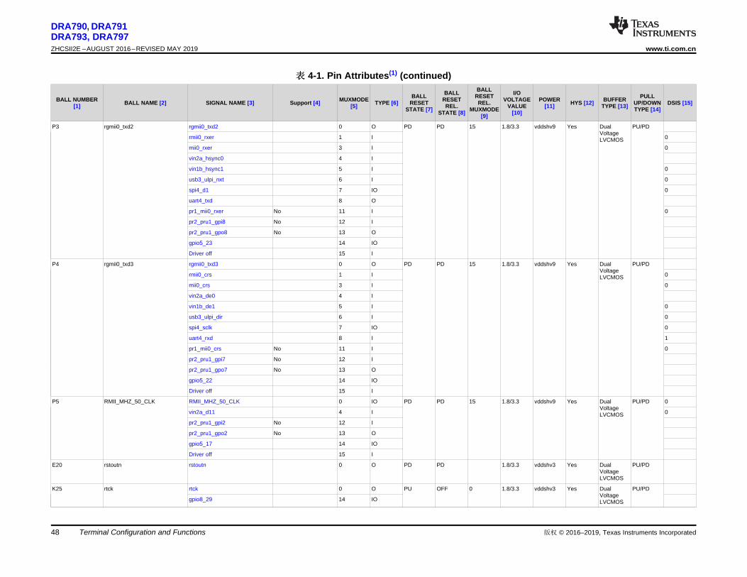
版权 © 2016–2019, Texas Instruments IncorporatedTerminal Configuration and Functions48
DRA790, DRA791DRA793, DRA797ZHCSII2E –AUGUST 2016–REVISED MAY 2019 www.ti.com.cn
表表 4-1. Pin Attributes(1) (continued)
BALL NUMBER[1] BALL NAME [2] SIGNAL NAME [3] Support [4] MUXMODE
[5] TYPE [6]BALL
RESETSTATE [7]
BALLRESETREL.
STATE [8]
BALLRESETREL.
MUXMODE[9]
I/OVOLTAGE
VALUE[10]
POWER[11] HYS [12] BUFFER
TYPE [13]
PULLUP/DOWNTYPE [14]
DSIS [15]
P3 rgmii0_txd2 rgmii0_txd2 0 O PD PD 15 1.8/3.3 vddshv9 Yes DualVoltageLVCMOS
PU/PD
rmii0_rxer 1 I 0
mii0_rxer 3 I 0
vin2a_hsync0 4 I
vin1b_hsync1 5 I 0
usb3_ulpi_nxt 6 I 0
spi4_d1 7 IO 0
uart4_txd 8 O
pr1_mii0_rxer No 11 I 0
pr2_pru1_gpi8 No 12 I
pr2_pru1_gpo8 No 13 O
gpio5_23 14 IO
Driver off 15 I
P4 rgmii0_txd3 rgmii0_txd3 0 O PD PD 15 1.8/3.3 vddshv9 Yes DualVoltageLVCMOS
PU/PD
rmii0_crs 1 I 0
mii0_crs 3 I 0
vin2a_de0 4 I
vin1b_de1 5 I 0
usb3_ulpi_dir 6 I 0
spi4_sclk 7 IO 0
uart4_rxd 8 I 1
pr1_mii0_crs No 11 I 0
pr2_pru1_gpi7 No 12 I
pr2_pru1_gpo7 No 13 O
gpio5_22 14 IO
Driver off 15 I
P5 RMII_MHZ_50_CLK RMII_MHZ_50_CLK 0 IO PD PD 15 1.8/3.3 vddshv9 Yes DualVoltageLVCMOS
PU/PD 0
vin2a_d11 4 I 0
pr2_pru1_gpi2 No 12 I
pr2_pru1_gpo2 No 13 O
gpio5_17 14 IO
Driver off 15 I
E20 rstoutn rstoutn 0 O PD PD 1.8/3.3 vddshv3 Yes DualVoltageLVCMOS
PU/PD
K25 rtck rtck 0 O PU OFF 0 1.8/3.3 vddshv3 Yes DualVoltageLVCMOS
PU/PD
gpio8_29 14 IO

版权 © 2016–2019, Texas Instruments Incorporated Terminal Configuration and Functions 49
DRA790, DRA791DRA793, DRA797
www.ti.com.cn ZHCSII2E –AUGUST 2016–REVISED MAY 2019
表表 4-1. Pin Attributes(1) (continued)
BALL NUMBER[1] BALL NAME [2] SIGNAL NAME [3] Support [4] MUXMODE
[5] TYPE [6]BALL
RESETSTATE [7]
BALLRESETREL.
STATE [8]
BALLRESETREL.
MUXMODE[9]
I/OVOLTAGE
VALUE[10]
POWER[11] HYS [12] BUFFER
TYPE [13]
PULLUP/DOWNTYPE [14]
DSIS [15]
B24 spi1_cs0 spi1_cs0 0 IO PU PU 15 1.8/3.3 vddshv3 Yes DualVoltageLVCMOS
PU/PD 1
gpio7_10 14 IO
Driver off 15 I
C25 spi1_cs1 spi1_cs1 0 IO PU PU 15 1.8/3.3 vddshv3 Yes DualVoltageLVCMOS
PU/PD 1
spi2_cs1 3 IO 1
gpio7_11 14 IO
Driver off 15 I
E24 spi1_cs2 spi1_cs2 0 IO PU PU 15 1.8/3.3 vddshv3 Yes DualVoltageLVCMOS
PU/PD 1
uart4_rxd 1 I 1
mmc3_sdcd 2 I 1
spi2_cs2 3 IO 1
dcan2_tx 4 IO 1
mdio_mclk 5 O 1
hdmi1_hpd 6 IO
gpio7_12 14 IO
Driver off 15 I
E25 spi1_cs3 spi1_cs3 0 IO PU PU 15 1.8/3.3 vddshv3 Yes DualVoltageLVCMOS
PU/PD 1
uart4_txd 1 O
mmc3_sdwp 2 I 0
spi2_cs3 3 IO 1
dcan2_rx 4 IO 1
mdio_d 5 IO 1
hdmi1_cec 6 IO
gpio7_13 14 IO
Driver off 15 I
D25 spi1_d0 spi1_d0 0 IO PD PD 15 1.8/3.3 vddshv3 Yes DualVoltageLVCMOS
PU/PD 0
gpio7_9 14 IO
Driver off 15 I
D24 spi1_d1 spi1_d1 0 IO PD PD 15 1.8/3.3 vddshv3 Yes DualVoltageLVCMOS
PU/PD 0
gpio7_8 14 IO
Driver off 15 I
C24 spi1_sclk spi1_sclk 0 IO PD PD 15 1.8/3.3 vddshv3 Yes DualVoltageLVCMOS
PU/PD 0
gpio7_7 14 IO
Driver off 15 I

版权 © 2016–2019, Texas Instruments IncorporatedTerminal Configuration and Functions50
DRA790, DRA791DRA793, DRA797ZHCSII2E –AUGUST 2016–REVISED MAY 2019 www.ti.com.cn
表表 4-1. Pin Attributes(1) (continued)
BALL NUMBER[1] BALL NAME [2] SIGNAL NAME [3] Support [4] MUXMODE
[5] TYPE [6]BALL
RESETSTATE [7]
BALLRESETREL.
STATE [8]
BALLRESETREL.
MUXMODE[9]
I/OVOLTAGE
VALUE[10]
POWER[11] HYS [12] BUFFER
TYPE [13]
PULLUP/DOWNTYPE [14]
DSIS [15]
F24 spi2_cs0 spi2_cs0 0 IO PU PU 15 1.8/3.3 vddshv3 Yes DualVoltageLVCMOS
PU/PD 1
uart3_rtsn 1 O
uart5_txd 2 O
gpio7_17 14 IO
Driver off 15 I
G24 spi2_d0 spi2_d0 0 IO PD PD 15 1.8/3.3 vddshv3 Yes DualVoltageLVCMOS
PU/PD 0
uart3_ctsn 1 I 1
uart5_rxd 2 I 1
gpio7_16 14 IO
Driver off 15 I
F25 spi2_d1 spi2_d1 0 IO PD PD 15 1.8/3.3 vddshv3 Yes DualVoltageLVCMOS
PU/PD 0
uart3_txd 1 O
gpio7_15 14 IO
Driver off 15 I
G25 spi2_sclk spi2_sclk 0 IO PD PD 15 1.8/3.3 vddshv3 Yes DualVoltageLVCMOS
PU/PD 0
uart3_rxd 1 I 1
gpio7_14 14 IO
Driver off 15 I
K21 tclk tclk 0 I PU PU 0 1.8/3.3 vddshv3 Yes IQ1833 PU/PD
L23 tdi tdi 0 I PU PU 0 1.8/3.3 vddshv3 Yes DualVoltageLVCMOS
PU/PD
gpio8_27 14 I
J20 tdo tdo 0 O PU PU 0 1.8/3.3 vddshv3 Yes DualVoltageLVCMOS
PU/PD
gpio8_28 14 IO
L21 tms tms 0 I PU PU 0 1.8/3.3 vddshv3 Yes DualVoltageLVCMOS
PU/PD
L22 trstn trstn 0 I PD PD 1.8/3.3 vddshv3 Yes DualVoltageLVCMOS
PU/PD
L20 uart1_ctsn uart1_ctsn 0 I PU PU 15 1.8/3.3 vddshv4 Yes DualVoltageLVCMOS
PU/PD 1
uart9_rxd 2 I 1
mmc4_clk 3 IO 1
gpio7_24 14 IO
Driver off 15 I
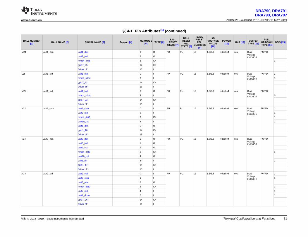
版权 © 2016–2019, Texas Instruments Incorporated Terminal Configuration and Functions 51
DRA790, DRA791DRA793, DRA797
www.ti.com.cn ZHCSII2E –AUGUST 2016–REVISED MAY 2019
表表 4-1. Pin Attributes(1) (continued)
BALL NUMBER[1] BALL NAME [2] SIGNAL NAME [3] Support [4] MUXMODE
[5] TYPE [6]BALL
RESETSTATE [7]
BALLRESETREL.
STATE [8]
BALLRESETREL.
MUXMODE[9]
I/OVOLTAGE
VALUE[10]
POWER[11] HYS [12] BUFFER
TYPE [13]
PULLUP/DOWNTYPE [14]
DSIS [15]
M24 uart1_rtsn uart1_rtsn 0 O PU PU 15 1.8/3.3 vddshv4 Yes DualVoltageLVCMOS
PU/PD
uart9_txd 2 O
mmc4_cmd 3 IO 1
gpio7_25 14 IO
Driver off 15 I
L25 uart1_rxd uart1_rxd 0 I PU PU 15 1.8/3.3 vddshv4 Yes DualVoltageLVCMOS
PU/PD 1
mmc4_sdcd 3 I 1
gpio7_22 14 IO
Driver off 15 I
M25 uart1_txd uart1_txd 0 O PU PU 15 1.8/3.3 vddshv4 Yes DualVoltageLVCMOS
PU/PD
mmc4_sdwp 3 I 0
gpio7_23 14 IO
Driver off 15 I
N22 uart2_ctsn uart2_ctsn 0 I PU PU 15 1.8/3.3 vddshv4 Yes DualVoltageLVCMOS
PU/PD 1
uart3_rxd 2 I 1
mmc4_dat2 3 IO 1
uart10_rxd 4 I 1
uart1_dtrn 5 O
gpio1_16 14 IO
Driver off 15 I
N24 uart2_rtsn uart2_rtsn 0 O PU PU 15 1.8/3.3 vddshv4 Yes DualVoltageLVCMOS
PU/PD
uart3_txd 1 O
uart3_irtx 2 O
mmc4_dat3 3 IO 1
uart10_txd 4 O
uart1_rin 5 I 1
gpio1_17 14 IO
Driver off 15 I
N23 uart2_rxd uart2_rxd 0 I PU PU 15 1.8/3.3 vddshv4 Yes DualVoltageLVCMOS
PU/PD 1
uart3_ctsn 1 I 1
uart3_rctx 2 O
mmc4_dat0 3 IO 1
uart2_rxd 4 I 1
uart1_dcdn 5 I 1
gpio7_26 14 IO
Driver off 15 I

版权 © 2016–2019, Texas Instruments IncorporatedTerminal Configuration and Functions52
DRA790, DRA791DRA793, DRA797ZHCSII2E –AUGUST 2016–REVISED MAY 2019 www.ti.com.cn
表表 4-1. Pin Attributes(1) (continued)
BALL NUMBER[1] BALL NAME [2] SIGNAL NAME [3] Support [4] MUXMODE
[5] TYPE [6]BALL
RESETSTATE [7]
BALLRESETREL.
STATE [8]
BALLRESETREL.
MUXMODE[9]
I/OVOLTAGE
VALUE[10]
POWER[11] HYS [12] BUFFER
TYPE [13]
PULLUP/DOWNTYPE [14]
DSIS [15]
N25 uart2_txd uart2_txd 0 O PU PU 15 1.8/3.3 vddshv4 Yes DualVoltageLVCMOS
PU/PD
uart3_rtsn 1 O
uart3_sd 2 O
mmc4_dat1 3 IO 1
uart2_txd 4 O
uart1_dsrn 5 I 0
gpio7_27 14 IO
Driver off 15 I
N5 uart3_rxd uart3_rxd 0 I PD PD 15 1.8/3.3 vddshv9 Yes DualVoltageLVCMOS
PU/PD 1
rmii1_crs 2 I 0
mii0_rxdv 3 I 0
vin2a_d1 4 I 0
vin1b_d1 5 I 0
spi3_sclk 7 IO 0
pr1_mii0_rxdv No 11 I 0
pr2_pru1_gpi3 No 12 I
pr2_pru1_gpo3 No 13 O
gpio5_18 14 IO
Driver off 15 I
N6 uart3_txd uart3_txd 0 O PD PD 15 1.8/3.3 vddshv9 Yes DualVoltageLVCMOS
PU/PD
rmii1_rxer 2 I 0
mii0_rxclk 3 I 0
vin2a_d2 4 I 0
vin1b_d2 5 I 0
spi3_d1 7 IO 0
spi4_cs1 8 IO 1
pr1_mii_mr0_clk No 11 I 0
pr2_pru1_gpi4 No 12 I
pr2_pru1_gpo4 No 13 O
gpio5_19 14 IO
Driver off 15 I
AB7 usb1_dm usb1_dm 0 IO OFF OFF 3.3 vdda33v_usb1
USBPHY
AC6 usb1_dp usb1_dp 0 IO OFF OFF 3.3 vdda33v_usb1
USBPHY

版权 © 2016–2019, Texas Instruments Incorporated Terminal Configuration and Functions 53
DRA790, DRA791DRA793, DRA797
www.ti.com.cn ZHCSII2E –AUGUST 2016–REVISED MAY 2019
表表 4-1. Pin Attributes(1) (continued)
BALL NUMBER[1] BALL NAME [2] SIGNAL NAME [3] Support [4] MUXMODE
[5] TYPE [6]BALL
RESETSTATE [7]
BALLRESETREL.
STATE [8]
BALLRESETREL.
MUXMODE[9]
I/OVOLTAGE
VALUE[10]
POWER[11] HYS [12] BUFFER
TYPE [13]
PULLUP/DOWNTYPE [14]
DSIS [15]
AD3 usb1_drvvbus usb1_drvvbus 0 O PD PD 15 1.8/3.3 vdda33v_usb2
Yes DualVoltageLVCMOS
PU/PD
timer16 7 IO
gpio6_12 14 IO
Driver off 15 I
AC5 usb2_dm usb2_dm 0 IO 3.3 vdda33v_usb2
No USBPHY
AB6 usb2_dp usb2_dp 0 IO 3.3 vdda33v_usb2
No USBPHY
AA6 usb2_drvvbus usb2_drvvbus 0 O PD PD 15 1.8/3.3 vdda33v_usb2
Yes DualVoltageLVCMOS
PU/PD
timer15 7 IO
gpio6_13 14 IO
Driver off 15 I
AE5 usb_rxn0 usb_rxn0 0 I OFF OFF 1.8 vdda_usb1 SERDES
pcie_rxn1 1 I
AD6 usb_rxp0 usb_rxp0 0 I OFF OFF 1.8 vdda_usb1 SERDES
pcie_rxp1 1 I
AE3 usb_txn0 usb_txn0 0 O 1.8 vdda_usb1 SERDES
pcie_txn1 1 O
AD4 usb_txp0 usb_txp0 0 O 1.8 vdda_usb1 SERDES
pcie_txp1 1 O
J15, J16, J18, K12,K18, L12, L17,M11, M13, M15,M17, N11, N13,N15, N18, P10,P12, P14, P16,P18, R10, R12,R14, R16, R17,T11, T13, T15,T17, T9, U11, U13,U15, U18, U9, V10,V12, V14, V16,V18, W10, W12,W14, W16
vdd vdd PWR
F20 vpp vpp(11) PWR
AA10 vdda33v_usb1 vdda33v_usb1 PWR
Y10 vdda33v_usb2 vdda33v_usb2 PWR
L9 vdda_core_gmac vdda_core_gmac PWR
T6 vdda_csi vdda_csi PWR
R20 vdda_ddr vdda_ddr PWR
N10 vdda_debug vdda_debug PWR
K10, L10 vdda_dsp_iva vdda_dsp_iva PWR
N9 vdda_gpu vdda_gpu PWR

版权 © 2016–2019, Texas Instruments IncorporatedTerminal Configuration and Functions54
DRA790, DRA791DRA793, DRA797ZHCSII2E –AUGUST 2016–REVISED MAY 2019 www.ti.com.cn
表表 4-1. Pin Attributes(1) (continued)
BALL NUMBER[1] BALL NAME [2] SIGNAL NAME [3] Support [4] MUXMODE
[5] TYPE [6]BALL
RESETSTATE [7]
BALLRESETREL.
STATE [8]
BALLRESETREL.
MUXMODE[9]
I/OVOLTAGE
VALUE[10]
POWER[11] HYS [12] BUFFER
TYPE [13]
PULLUP/DOWNTYPE [14]
DSIS [15]
W15, Y15 vdda_hdmi vdda_hdmi PWR
K16, L16 vdda_mpu_abe vdda_mpu_abe PWR
W13, Y13 vdda_osc vdda_osc PWR
W11, Y11 vdda_pcie vdda_pcie PWR
M10 vdda_per vdda_per PWR
W8 vdda_usb1 vdda_usb1 PWR
Y8 vdda_usb2 vdda_usb2 PWR
Y9 vdda_usb3 vdda_usb3 PWR
K14, L14 vdda_video vdda_video PWR
G11, H20, W7, Y18 vdds18v vdds18v PWR
AA19, P20, Y19 vdds18v_ddr1 vdds18v_ddr1 PWR
G10, G9 vddshv1 vddshv1 PWR
G15, G17, H15,H17, J19, K19
vddshv3 vddshv3 PWR
M19, N19 vddshv4 vddshv4 PWR
U7, U8 vddshv7 vddshv7 PWR
N8, P8 vddshv8 vddshv8 PWR
M7, N7 vddshv9 vddshv9 PWR
J7, J8, K8 vddshv10 vddshv10 PWR
F7, G7, H7 vddshv11 vddshv11 PWR
T19, T20, V20,W17, W18, W20
vdds_ddr1 vdds_ddr1 PWR
P7, R7 vdds_mlbp vdds_mlbp PWR
H11, H13, H9, J11,J13, J9
vdd_dsp vdd_dsp PWR
D8 vin2a_clk0 vin2a_clk0 0 I PD PD 15 1.8/3.3 vddshv1 Yes DualVoltageLVCMOS
PU/PD
vout2_fld 4 O
emu5 5 O
kbd_row0 9 I 0
eQEP1A_in 10 I 0
pr1_edio_data_in0 No 12 I 0
pr1_edio_data_out0 No 13 O
gpio3_28gpmc_a27gpmc_a17
14 IO
Driver off 15 I

版权 © 2016–2019, Texas Instruments Incorporated Terminal Configuration and Functions 55
DRA790, DRA791DRA793, DRA797
www.ti.com.cn ZHCSII2E –AUGUST 2016–REVISED MAY 2019
表表 4-1. Pin Attributes(1) (continued)
BALL NUMBER[1] BALL NAME [2] SIGNAL NAME [3] Support [4] MUXMODE
[5] TYPE [6]BALL
RESETSTATE [7]
BALLRESETREL.
STATE [8]
BALLRESETREL.
MUXMODE[9]
I/OVOLTAGE
VALUE[10]
POWER[11] HYS [12] BUFFER
TYPE [13]
PULLUP/DOWNTYPE [14]
DSIS [15]
C8 vin2a_d0 vin2a_d0 0 I PD PD 15 1.8/3.3 vddshv1 Yes DualVoltageLVCMOS
PU/PD 0
vout2_d23 4 O
emu10 5 O
uart9_ctsn 7 I 1
spi4_d0 8 IO 0
kbd_row4 9 I 0
ehrpwm1B 10 O
pr1_uart0_rxd No 11 I 1
pr1_edio_data_in5 No 12 I 0
pr1_edio_data_out5 No 13 O
gpio4_1 14 IO
Driver off 15 I
B9 vin2a_d1 vin2a_d1 0 I PD PD 15 1.8/3.3 vddshv1 Yes DualVoltageLVCMOS
PU/PD 0
vout2_d22 4 O
emu11 5 O
uart9_rtsn 7 O
spi4_cs0 8 IO 1
kbd_row5 9 I 0
ehrpwm1_tripzone_input 10 IO 0
pr1_uart0_txd No 11 O
pr1_edio_data_in6 No 12 I 0
pr1_edio_data_out6 No 13 O
gpio4_2 14 IO
Driver off 15 I
A7 vin2a_d2 vin2a_d2 0 I PD PD 15 1.8/3.3 vddshv1 Yes DualVoltageLVCMOS
PU/PD 0
vout2_d21 4 O
emu12 5 O
uart10_rxd 8 I 1
kbd_row6 9 I 0
eCAP1_in_PWM1_out 10 IO 0
pr1_ecap0_ecap_capin_apwm_o
No 11 IO 0
pr1_edio_data_in7 No 12 I 0
pr1_edio_data_out7 No 13 O
gpio4_3 14 IO
Driver off 15 I

版权 © 2016–2019, Texas Instruments IncorporatedTerminal Configuration and Functions56
DRA790, DRA791DRA793, DRA797ZHCSII2E –AUGUST 2016–REVISED MAY 2019 www.ti.com.cn
表表 4-1. Pin Attributes(1) (continued)
BALL NUMBER[1] BALL NAME [2] SIGNAL NAME [3] Support [4] MUXMODE
[5] TYPE [6]BALL
RESETSTATE [7]
BALLRESETREL.
STATE [8]
BALLRESETREL.
MUXMODE[9]
I/OVOLTAGE
VALUE[10]
POWER[11] HYS [12] BUFFER
TYPE [13]
PULLUP/DOWNTYPE [14]
DSIS [15]
A9 vin2a_d3 vin2a_d3 0 I PD PD 15 1.8/3.3 vddshv1 Yes DualVoltageLVCMOS
PU/PD 0
vout2_d20 4 O
emu13 5 O
uart10_txd 8 O
kbd_col0 9 O
ehrpwm1_synci 10 I 0
pr1_edc_latch0_in No 11 I 0
pr1_pru1_gpi0 No 12 I
pr1_pru1_gpo0 No 13 O
gpio4_4 14 IO
Driver off 15 I
A8 vin2a_d4 vin2a_d4 0 I PD PD 15 1.8/3.3 vddshv1 Yes DualVoltageLVCMOS
PU/PD 0
vout2_d19 4 O
emu14 5 O
uart10_ctsn 8 I 1
kbd_col1 9 O
ehrpwm1_synco 10 O
pr1_edc_sync0_out No 11 O
pr1_pru1_gpi1 No 12 I
pr1_pru1_gpo1 No 13 O
gpio4_5 14 IO
Driver off 15 I
A11 vin2a_d5 vin2a_d5 0 I PD PD 15 1.8/3.3 vddshv1 Yes DualVoltageLVCMOS
PU/PD 0
vout2_d18 4 O
emu15 5 O
uart10_rtsn 8 O
kbd_col2 9 O
eQEP2A_in 10 I 0
pr1_edio_sof No 11 O
pr1_pru1_gpi2 No 12 I
pr1_pru1_gpo2 No 13 O
gpio4_6 14 IO
Driver off 15 I

版权 © 2016–2019, Texas Instruments Incorporated Terminal Configuration and Functions 57
DRA790, DRA791DRA793, DRA797
www.ti.com.cn ZHCSII2E –AUGUST 2016–REVISED MAY 2019
表表 4-1. Pin Attributes(1) (continued)
BALL NUMBER[1] BALL NAME [2] SIGNAL NAME [3] Support [4] MUXMODE
[5] TYPE [6]BALL
RESETSTATE [7]
BALLRESETREL.
STATE [8]
BALLRESETREL.
MUXMODE[9]
I/OVOLTAGE
VALUE[10]
POWER[11] HYS [12] BUFFER
TYPE [13]
PULLUP/DOWNTYPE [14]
DSIS [15]
F10 vin2a_d6 vin2a_d6 0 I PD PD 15 1.8/3.3 vddshv1 Yes DualVoltageLVCMOS
PU/PD 0
vout2_d17 4 O
emu16 5 O
mii1_rxd1 8 I 0
kbd_col3 9 O
eQEP2B_in 10 I 0
pr1_mii_mt1_clk No 11 I 0
pr1_pru1_gpi3 No 12 I
pr1_pru1_gpo3 No 13 O
gpio4_7 14 IO
Driver off 15 I
A10 vin2a_d7 vin2a_d7 0 I PD PD 15 1.8/3.3 vddshv1 Yes DualVoltageLVCMOS
PU/PD 0
vout2_d16 4 O
emu17 5 O
mii1_rxd2 8 I 0
kbd_col4 9 O
eQEP2_index 10 IO 0
pr1_mii1_txen No 11 O
pr1_pru1_gpi4 No 12 I
pr1_pru1_gpo4 No 13 O
gpio4_8 14 IO
Driver off 15 I
B10 vin2a_d8 vin2a_d8 0 I PD PD 15 1.8/3.3 vddshv1 Yes DualVoltageLVCMOS
PU/PD 0
vout2_d15 4 O
emu18 5 O
mii1_rxd3 8 I 0
kbd_col5 9 O
eQEP2_strobe 10 IO 0
pr1_mii1_txd3 No 11 O
pr1_pru1_gpi5 No 12 I
pr1_pru1_gpo5 No 13 O
gpio4_9gpmc_a26
14 IO
Driver off 15 I

版权 © 2016–2019, Texas Instruments IncorporatedTerminal Configuration and Functions58
DRA790, DRA791DRA793, DRA797ZHCSII2E –AUGUST 2016–REVISED MAY 2019 www.ti.com.cn
表表 4-1. Pin Attributes(1) (continued)
BALL NUMBER[1] BALL NAME [2] SIGNAL NAME [3] Support [4] MUXMODE
[5] TYPE [6]BALL
RESETSTATE [7]
BALLRESETREL.
STATE [8]
BALLRESETREL.
MUXMODE[9]
I/OVOLTAGE
VALUE[10]
POWER[11] HYS [12] BUFFER
TYPE [13]
PULLUP/DOWNTYPE [14]
DSIS [15]
E10 vin2a_d9 vin2a_d9 0 I PD PD 15 1.8/3.3 vddshv1 Yes DualVoltageLVCMOS
PU/PD 0
vout2_d14 4 O
emu19 5 O
mii1_rxd0 8 I 0
kbd_col6 9 O
ehrpwm2A 10 O
pr1_mii1_txd2 No 11 O
pr1_pru1_gpi6 No 12 I
pr1_pru1_gpo6 No 13 O
gpio4_10gpmc_a25
14 IO
Driver off 15 I
D10 vin2a_d10 vin2a_d10 0 I PD PD 15 1.8/3.3 vddshv1 Yes DualVoltageLVCMOS
PU/PD 0
mdio_mclk 3 O 1
vout2_d13 4 O
kbd_col7 9 O
ehrpwm2B 10 O
pr1_mdio_mdclk No 11 O
pr1_pru1_gpi7 No 12 I
pr1_pru1_gpo7 No 13 O
gpio4_11gpmc_a24
14 IO
Driver off 15 I
C10 vin2a_d11 vin2a_d11 0 I PD PD 15 1.8/3.3 vddshv1 Yes DualVoltageLVCMOS
PU/PD 0
mdio_d 3 IO 1
vout2_d12 4 O
kbd_row7 9 I 0
ehrpwm2_tripzone_input 10 IO 0
pr1_mdio_data No 11 IO 1
pr1_pru1_gpi8 No 12 I
pr1_pru1_gpo8 No 13 O
gpio4_12gpmc_a23
14 IO
Driver off 15 I

版权 © 2016–2019, Texas Instruments Incorporated Terminal Configuration and Functions 59
DRA790, DRA791DRA793, DRA797
www.ti.com.cn ZHCSII2E –AUGUST 2016–REVISED MAY 2019
表表 4-1. Pin Attributes(1) (continued)
BALL NUMBER[1] BALL NAME [2] SIGNAL NAME [3] Support [4] MUXMODE
[5] TYPE [6]BALL
RESETSTATE [7]
BALLRESETREL.
STATE [8]
BALLRESETREL.
MUXMODE[9]
I/OVOLTAGE
VALUE[10]
POWER[11] HYS [12] BUFFER
TYPE [13]
PULLUP/DOWNTYPE [14]
DSIS [15]
B11 vin2a_d12 vin2a_d12 0 I PD PD 15 1.8/3.3 vddshv1 Yes DualVoltageLVCMOS
PU/PD 0
rgmii1_txc 3 O
vout2_d11 4 O
mii1_rxclk 8 I 0
kbd_col8 9 O
eCAP2_in_PWM2_out 10 IO 0
pr1_mii1_txd1 No 11 O
pr1_pru1_gpi9 No 12 I
pr1_pru1_gpo9 No 13 O
gpio4_13 14 IO
Driver off 15 I
D11 vin2a_d13 vin2a_d13 0 I PD PD 15 1.8/3.3 vddshv1 Yes DualVoltageLVCMOS
PU/PD 0
rgmii1_txctl 3 O
vout2_d10 4 O
mii1_rxdv 8 I 0
kbd_row8 9 I 0
eQEP3A_in 10 I 0
pr1_mii1_txd0 No 11 O
pr1_pru1_gpi10 No 12 I
pr1_pru1_gpo10 No 13 O
gpio4_14 14 IO
Driver off 15 I
C11 vin2a_d14 vin2a_d14 0 I PD PD 15 1.8/3.3 vddshv1 Yes DualVoltageLVCMOS
PU/PD 0
rgmii1_txd3 3 O
vout2_d9 4 O
mii1_txclk 8 I 0
eQEP3B_in 10 I 0
pr1_mii_mr1_clk No 11 I 0
pr1_pru1_gpi11 No 12 I
pr1_pru1_gpo11 No 13 O
gpio4_15 14 IO
Driver off 15 I

版权 © 2016–2019, Texas Instruments IncorporatedTerminal Configuration and Functions60
DRA790, DRA791DRA793, DRA797ZHCSII2E –AUGUST 2016–REVISED MAY 2019 www.ti.com.cn
表表 4-1. Pin Attributes(1) (continued)
BALL NUMBER[1] BALL NAME [2] SIGNAL NAME [3] Support [4] MUXMODE
[5] TYPE [6]BALL
RESETSTATE [7]
BALLRESETREL.
STATE [8]
BALLRESETREL.
MUXMODE[9]
I/OVOLTAGE
VALUE[10]
POWER[11] HYS [12] BUFFER
TYPE [13]
PULLUP/DOWNTYPE [14]
DSIS [15]
B12 vin2a_d15 vin2a_d15 0 I PD PD 15 1.8/3.3 vddshv1 Yes DualVoltageLVCMOS
PU/PD 0
rgmii1_txd2 3 O
vout2_d8 4 O
mii1_txd0 8 O
eQEP3_index 10 IO 0
pr1_mii1_rxdv No 11 I 0
pr1_pru1_gpi12 No 12 I
pr1_pru1_gpo12 No 13 O
gpio4_16 14 IO
Driver off 15 I
A12 vin2a_d16 vin2a_d16 0 I PD PD 15 1.8/3.3 vddshv1 Yes DualVoltageLVCMOS
PU/PD 0
vin2b_d7 2 I 0
rgmii1_txd1 3 O
vout2_d7 4 O
mii1_txd1 8 O
eQEP3_strobe 10 IO 0
pr1_mii1_rxd3 No 11 I 0
pr1_pru1_gpi13 No 12 I
pr1_pru1_gpo13 No 13 O
gpio4_24 14 IO
Driver off 15 I
A13 vin2a_d17 vin2a_d17 0 I PD PD 15 1.8/3.3 vddshv1 Yes DualVoltageLVCMOS
PU/PD 0
vin2b_d6 2 I 0
rgmii1_txd0 3 O
vout2_d6 4 O
mii1_txd2 8 O
ehrpwm3A 10 O
pr1_mii1_rxd2 No 11 I 0
pr1_pru1_gpi14 No 12 I
pr1_pru1_gpo14 No 13 O
gpio4_25 14 IO
Driver off 15 I

版权 © 2016–2019, Texas Instruments Incorporated Terminal Configuration and Functions 61
DRA790, DRA791DRA793, DRA797
www.ti.com.cn ZHCSII2E –AUGUST 2016–REVISED MAY 2019
表表 4-1. Pin Attributes(1) (continued)
BALL NUMBER[1] BALL NAME [2] SIGNAL NAME [3] Support [4] MUXMODE
[5] TYPE [6]BALL
RESETSTATE [7]
BALLRESETREL.
STATE [8]
BALLRESETREL.
MUXMODE[9]
I/OVOLTAGE
VALUE[10]
POWER[11] HYS [12] BUFFER
TYPE [13]
PULLUP/DOWNTYPE [14]
DSIS [15]
E11 vin2a_d18 vin2a_d18 0 I PD PD 15 1.8/3.3 vddshv1 Yes DualVoltageLVCMOS
PU/PD 0
vin2b_d5 2 I 0
rgmii1_rxc 3 I 0
vout2_d5 4 O
mii1_txd3 8 O
ehrpwm3B 10 O
pr1_mii1_rxd1 No 11 I 0
pr1_pru1_gpi15 No 12 I
pr1_pru1_gpo15 No 13 O
gpio4_26 14 IO
Driver off 15 I
F11 vin2a_d19 vin2a_d19 0 I PD PD 15 1.8/3.3 vddshv1 Yes DualVoltageLVCMOS
PU/PD 0
vin2b_d4 2 I 0
rgmii1_rxctl 3 I 0
vout2_d4 4 O
mii1_txer 8 O 0
ehrpwm3_tripzone_input 10 IO 0
pr1_mii1_rxd0 No 11 I 0
pr1_pru1_gpi16 No 12 I
pr1_pru1_gpo16 No 13 O
gpio4_27 14 IO
Driver off 15 I
B13 vin2a_d20 vin2a_d20 0 I PD PD 15 1.8/3.3 vddshv1 Yes DualVoltageLVCMOS
PU/PD 0
vin2b_d3 2 I 0
rgmii1_rxd3 3 I 0
vout2_d3 4 O
mii1_rxer 8 I 0
eCAP3_in_PWM3_out 10 IO 0
pr1_mii1_rxer No 11 I 0
pr1_pru1_gpi17 No 12 I
pr1_pru1_gpo17 No 13 O
gpio4_28 14 IO
Driver off 15 I

版权 © 2016–2019, Texas Instruments IncorporatedTerminal Configuration and Functions62
DRA790, DRA791DRA793, DRA797ZHCSII2E –AUGUST 2016–REVISED MAY 2019 www.ti.com.cn
表表 4-1. Pin Attributes(1) (continued)
BALL NUMBER[1] BALL NAME [2] SIGNAL NAME [3] Support [4] MUXMODE
[5] TYPE [6]BALL
RESETSTATE [7]
BALLRESETREL.
STATE [8]
BALLRESETREL.
MUXMODE[9]
I/OVOLTAGE
VALUE[10]
POWER[11] HYS [12] BUFFER
TYPE [13]
PULLUP/DOWNTYPE [14]
DSIS [15]
E13 vin2a_d21 vin2a_d21 0 I PD PD 15 1.8/3.3 vddshv1 Yes DualVoltageLVCMOS
PU/PD 0
vin2b_d2 2 I 0
rgmii1_rxd2 3 I 0
vout2_d2 4 O
mii1_col 8 I 0
pr1_mii1_rxlink No 11 I 0
pr1_pru1_gpi18 No 12 I
pr1_pru1_gpo18 No 13 O
gpio4_29 14 IO
Driver off 15 I
C13 vin2a_d22 vin2a_d22 0 I PD PD 15 1.8/3.3 vddshv1 Yes DualVoltageLVCMOS
PU/PD 0
vin2b_d1 2 I 0
rgmii1_rxd1 3 I 0
vout2_d1 4 O
mii1_crs 8 I 0
pr1_mii1_col No 11 I 0
pr1_pru1_gpi19 No 12 I
pr1_pru1_gpo19 No 13 O
gpio4_30 14 IO
Driver off 15 I
D13 vin2a_d23 vin2a_d23 0 I PD PD 15 1.8/3.3 vddshv1 Yes DualVoltageLVCMOS
PU/PD 0
vin2b_d0 2 I 0
rgmii1_rxd0 3 I 0
vout2_d0 4 O
mii1_txen 8 O
pr1_mii1_crs No 11 I 0
pr1_pru1_gpi20 No 12 I
pr1_pru1_gpo20 No 13 O
gpio4_31 14 IO
Driver off 15 I

版权 © 2016–2019, Texas Instruments Incorporated Terminal Configuration and Functions 63
DRA790, DRA791DRA793, DRA797
www.ti.com.cn ZHCSII2E –AUGUST 2016–REVISED MAY 2019
表表 4-1. Pin Attributes(1) (continued)
BALL NUMBER[1] BALL NAME [2] SIGNAL NAME [3] Support [4] MUXMODE
[5] TYPE [6]BALL
RESETSTATE [7]
BALLRESETREL.
STATE [8]
BALLRESETREL.
MUXMODE[9]
I/OVOLTAGE
VALUE[10]
POWER[11] HYS [12] BUFFER
TYPE [13]
PULLUP/DOWNTYPE [14]
DSIS [15]
B7 vin2a_de0 vin2a_de0 0 I PD PD 15 1.8/3.3 vddshv1 Yes DualVoltageLVCMOS
PU/PD
vin2a_fld0 1 I
vin2b_fld1 2 I
vin2b_de1 3 I
vout2_de 4 O
emu6 5 O
kbd_row1 9 I 0
eQEP1B_in 10 I 0
pr1_edio_data_in1 No 12 I 0
pr1_edio_data_out1 No 13 O
gpio3_29 14 IO
Driver off 15 I
C7 vin2a_fld0 vin2a_fld0 0 I PD PD 15 1.8/3.3 vddshv1 Yes DualVoltageLVCMOS
PU/PD
vin2b_clk1 2 I
vout2_clk 4 O
emu7 5 O
eQEP1_index 10 IO 0
pr1_edio_data_in2 No 12 I 0
pr1_edio_data_out2 No 13 O
gpio3_30gpmc_a27gpmc_a18
14 IO
Driver off 15 I
E8 vin2a_hsync0 vin2a_hsync0 0 I PD PD 15 1.8/3.3 vddshv1 Yes DualVoltageLVCMOS
PU/PD
vin2b_hsync1 3 I
vout2_hsync 4 O
emu8 5 O
uart9_rxd 7 I 1
spi4_sclk 8 IO 0
kbd_row2 9 I 0
eQEP1_strobe 10 IO 0
pr1_uart0_cts_n No 11 I 1
pr1_edio_data_in3 No 12 I 0
pr1_edio_data_out3 No 13 O
gpio3_31gpmc_a27
14 IO
Driver off 15 I

版权 © 2016–2019, Texas Instruments IncorporatedTerminal Configuration and Functions64
DRA790, DRA791DRA793, DRA797ZHCSII2E –AUGUST 2016–REVISED MAY 2019 www.ti.com.cn
表表 4-1. Pin Attributes(1) (continued)
BALL NUMBER[1] BALL NAME [2] SIGNAL NAME [3] Support [4] MUXMODE
[5] TYPE [6]BALL
RESETSTATE [7]
BALLRESETREL.
STATE [8]
BALLRESETREL.
MUXMODE[9]
I/OVOLTAGE
VALUE[10]
POWER[11] HYS [12] BUFFER
TYPE [13]
PULLUP/DOWNTYPE [14]
DSIS [15]
B8 vin2a_vsync0 vin2a_vsync0 0 I PD PD 15 1.8/3.3 vddshv1 Yes DualVoltageLVCMOS
PU/PD
vin2b_vsync1 3 I
vout2_vsync 4 O
emu9 5 O
uart9_txd 7 O
spi4_d1 8 IO 0
kbd_row3 9 I 0
ehrpwm1A 10 O
pr1_uart0_rts_n No 11 O
pr1_edio_data_in4 No 12 I 0
pr1_edio_data_out4 No 13 O
gpio4_0 14 IO
Driver off 15 I
A1, A25, AA13,AA15, AA7, AA8,AA9, AB8, AC13,AE1, AE15, AE25,G13, G16, G8,H10, H12, H14,H16, H18, H19, H8,J10, J12, J14, J17,K11, K13, K15,K17, K9, L11, L13,L15, L18, L8, M12,M14, M16, M18,M20, M8, M9, N12,N14, N16, N17,N20, P11, P13,P15, P17, P19, P9,R11, R13, R15,R18, R19, R8, R9,T10, T12, T14,T16, T18, T8, U10,U12, U14, U16,U17, U19, V11,V13, V15, V17,V19, V8, V9, W19,W9, Y14, Y16,Y17, Y7
vss vss GND
AA12 vssa_osc0 vssa_osc0 GND
AB11 vssa_osc1 vssa_osc1 GND
AC10 Wakeup0 dcan1_rx 1 I 15 1.8/3.3 vdda33v_usb1
Yes IHHV1833 PU/PD 1
gpio1_0sys_nirq2
14 I
Driver off 15 I

版权 © 2016–2019, Texas Instruments Incorporated Terminal Configuration and Functions 65
DRA790, DRA791DRA793, DRA797
www.ti.com.cn ZHCSII2E –AUGUST 2016–REVISED MAY 2019
表表 4-1. Pin Attributes(1) (continued)
BALL NUMBER[1] BALL NAME [2] SIGNAL NAME [3] Support [4] MUXMODE
[5] TYPE [6]BALL
RESETSTATE [7]
BALLRESETREL.
STATE [8]
BALLRESETREL.
MUXMODE[9]
I/OVOLTAGE
VALUE[10]
POWER[11] HYS [12] BUFFER
TYPE [13]
PULLUP/DOWNTYPE [14]
DSIS [15]
AB10 Wakeup3 sys_nirq1 1 I 15 1.8/3.3 vdda33v_usb1
Yes IHHV1833 PU/PD
gpio1_3dcan2_rx
14 I
Driver off 15 I
Y12 xi_osc0 xi_osc0 0 I 1.8 vdda_osc No LVCMOSAnalog
AC11 xi_osc1 xi_osc1 0 I 1.8 vdda_osc No LVCMOSAnalog
AB12 xo_osc0 xo_osc0 0 O 1.8 vdda_osc No LVCMOSAnalog
AA11 xo_osc1 xo_osc1 0 A 1.8 vdda_osc No LVCMOSAnalog
J25 xref_clk0 xref_clk0 0 I PD PD 15 1.8/3.3 vddshv3 Yes DualVoltageLVCMOS
PU/PD
mcasp2_axr8 1 IO 0
mcasp1_axr4 2 IO 0
mcasp1_ahclkx 3 O
mcasp5_ahclkx 4 O
atl_clk0 5 O
vin1a_d0 7 I 0
hdq0 8 IO 1
clkout2 9 O
timer13 10 IO
pr2_mii1_col No 11 I 0
pr2_pru1_gpi5 No 12 I
pr2_pru1_gpo5 No 13 O
gpio6_17 14 IO
Driver off 15 I

版权 © 2016–2019, Texas Instruments IncorporatedTerminal Configuration and Functions66
DRA790, DRA791DRA793, DRA797ZHCSII2E –AUGUST 2016–REVISED MAY 2019 www.ti.com.cn
表表 4-1. Pin Attributes(1) (continued)
BALL NUMBER[1] BALL NAME [2] SIGNAL NAME [3] Support [4] MUXMODE
[5] TYPE [6]BALL
RESETSTATE [7]
BALLRESETREL.
STATE [8]
BALLRESETREL.
MUXMODE[9]
I/OVOLTAGE
VALUE[10]
POWER[11] HYS [12] BUFFER
TYPE [13]
PULLUP/DOWNTYPE [14]
DSIS [15]
J24 xref_clk1 xref_clk1 0 I PD PD 15 1.8/3.3 vddshv3 Yes DualVoltageLVCMOS
PU/PD
mcasp2_axr9 1 IO 0
mcasp1_axr5 2 IO 0
mcasp2_ahclkx 3 O
mcasp6_ahclkx 4 O
atl_clk1 5 O
vin1a_clk0 7 I 0
timer14 10 IO
pr2_mii1_crs No 11 I 0
pr2_pru1_gpi6 No 12 I
pr2_pru1_gpo6 No 13 O
gpio6_18 14 IO
Driver off 15 I
H24 xref_clk2 xref_clk2 0 I PD PD 15 1.8/3.3 vddshv3 Yes DualVoltageLVCMOS
PU/PD
mcasp2_axr10 1 IO 0
mcasp1_axr6 2 IO 0
mcasp3_ahclkx 3 O
mcasp7_ahclkx 4 O
atl_clk2 5 O
timer15 10 IO
gpio6_19 14 IO
Driver off 15 I
H25 xref_clk3 xref_clk3 0 I PD PD 15 1.8/3.3 vddshv3 Yes DualVoltageLVCMOS
PU/PD
mcasp2_axr11 1 IO 0
mcasp1_axr7 2 IO 0
mcasp4_ahclkx 3 O
mcasp8_ahclkx 4 O
atl_clk3 5 O
hdq0 7 IO 1
clkout3 9 O
timer16 10 IO
gpio6_20 14 IO
Driver off 15 I

版权 © 2016–2019, Texas Instruments Incorporated Terminal Configuration and Functions 67
DRA790, DRA791DRA793, DRA797
www.ti.com.cn ZHCSII2E –AUGUST 2016–REVISED MAY 2019
(1) NA in this table stands for Not Applicable.(2) For more information on recommended operating conditions, see Section 5.4, Recommended Operating Conditions.(3) The pullup or pulldown block strength is equal to: minimum = 50 μA, typical = 100 μA, maximum = 250 μA.(4) The output impedance settings of this IO cell are programmable; by default, the value is DS[1:0] = 10, this means 40 Ω. For more information on DS[1:0] register configuration, see the
Device TRM.(5) IO drive strength for usb1_dp, usb1_dm, usb2_dp and usb2_dm: minimum 18.3 mA, maximum 89 mA (for a power supply vdda33v_usb1 and vdda33v_usb2 = 3.46 V).(6) Minimum PU = 900 Ω, maximum PU = 3.090 kΩ and minimum PD = 14.25 kΩ, maximum PD = 24.8 kΩ.
For more information, see chapter 7 of the USB2.0 specification, in particular section Signaling / Device Speed Identification.(7) This function will not be supported on some pin-compatible roadmap devices. Pin compatibility can be maintained in the future by not using these GPIO signals.(8) In PUx / PDy, x and y = 60 to 200 μA.
The output impedance settings (or drive strengths) of this IO are programmable (34 Ω, 40 Ω, 48 Ω, 60 Ω, 80 Ω) depending on the values of the I[2:0] registers.(9) The internal pull resistors for balls A4, E7, D6, C5, D7, C6, A5, B6 are permanently disabled when sysboot15 is set to 0 as described in the section Sysboot Configuration of the Device
TRM. If internal pull-up/down resistors are desired on these balls then sysboot15 should be set to 1. If gpmc boot mode is used with SYSBOOT15=0 (not recommended) then externalpull-downs should be implemented to keep the address bus at logic-1 value during boot since the gpmc ms-address bits are high-z during boot.
(10) I2C6 is not supported in TI standard software. I2C6 is not recommended for use to due to internal clock/reset dependencies on i2c1-5 and uart7.(11) This signal is valid only for High-Security devices. For more details, see 节 5.8 VPP Specification for One-Time Programmable (OTP) eFUSEs. For General Purpose devices do not
connect any signal, test point, or board trace to this signal.

版权 © 2016–2019, Texas Instruments IncorporatedTerminal Configuration and Functions68
DRA790, DRA791DRA793, DRA797ZHCSII2E –AUGUST 2016–REVISED MAY 2019 www.ti.com.cn
4.3 Signal DescriptionsMany signals are available on multiple pins, according to the software configuration of the pin multiplexing options.1. SIGNAL NAME: The name of the signal passing through the pin.
注注The subsystem multiplexing signals are not described in 表 4-1 and 表 4-32.
2. DESCRIPTION: Description of the signal3. TYPE: Signal direction and type:
– I = Input– O = Output– IO = Input or output– D = Open Drain– DS = Differential– A = Analog– PWR = Power– GND = Ground
4. BALL: Associated ball(s) bottom
注注For more information, see the Control Module / Control Module Register Manual section of the device TRM.
4.3.1 VIP
注注For more information, see the Video Input Port (VIP) section of the device TRM.
表表 4-2. VIP Signal Descriptions
SIGNAL NAME DESCRIPTION TYPE BALLVideo Input 1
vin1a_clk0 Video Input 1 Port A Clock input. Input clock for 8-bit 16-bit or 24-bit Port A video capture. Input data is sampled onthe CLK0 edge.
I G3, J24, Y5
vin1a_d0 Video Input 1 Port A Data input I AA1, B23, F1, J25vin1a_d1 Video Input 1 Port A Data input I B22, E2, Y3vin1a_d2 Video Input 1 Port A Data input I A23, E1, W2

版权 © 2016–2019, Texas Instruments Incorporated Terminal Configuration and Functions 69
DRA790, DRA791DRA793, DRA797
www.ti.com.cn ZHCSII2E –AUGUST 2016–REVISED MAY 2019
表表 4-2. VIP Signal Descriptions (continued)SIGNAL NAME DESCRIPTION TYPE BALL
vin1a_d3 Video Input 1 Port A Data input I A22, AA3, C1vin1a_d4 Video Input 1 Port A Data input I AA2, B21, D1vin1a_d5 Video Input 1 Port A Data input I A21, D2, Y4vin1a_d6 Video Input 1 Port A Data input I B1, D19, Y1vin1a_d7 Video Input 1 Port A Data input I B2, E19, Y2vin1a_d8 Video Input 1 Port A Data input I C2, F16vin1a_d9 Video Input 1 Port A Data input I D3, E16vin1a_d10 Video Input 1 Port A Data input I A2, E17vin1a_d11 Video Input 1 Port A Data input I A19, B3vin1a_d12 Video Input 1 Port A Data input I B18, C3vin1a_d13 Video Input 1 Port A Data input I B16, C4vin1a_d14 Video Input 1 Port A Data input I A3, B17vin1a_d15 Video Input 1 Port A Data input I A18, B4vin1a_d16 Video Input 1 Port A Data input I M1vin1a_d17 Video Input 1 Port A Data input I M2vin1a_d18 Video Input 1 Port A Data input I L2vin1a_d19 Video Input 1 Port A Data input I L1vin1a_d20 Video Input 1 Port A Data input I K3vin1a_d21 Video Input 1 Port A Data input I K2vin1a_d22 Video Input 1 Port A Data input I J1vin1a_d23 Video Input 1 Port A Data input I K1vin1a_de0 Video Input 1 Port A Field ID input I C17, J2, Y6vin1a_fld0 Video Input 1 Port A Field ID input I C16, L3
vin1a_hsync0 Video Input 1 Port A Horizontal Sync input I AA4, B14, K4vin1a_vsync0 Video Input 1 Port A Vertical Sync input I AB1, D14, H1
vin1b_clk1 Video Input 1 Port B Clock input I J2, L5vin1b_d0 Video Input 1 Port B Data input I L6, M1vin1b_d1 Video Input 1 Port B Data input I M2, N5vin1b_d2 Video Input 1 Port B Data input I L2, N6vin1b_d3 Video Input 1 Port B Data input I L1, T4vin1b_d4 Video Input 1 Port B Data input I K3, T5vin1b_d5 Video Input 1 Port B Data input I K2, N2vin1b_d6 Video Input 1 Port B Data input I J1, P2

版权 © 2016–2019, Texas Instruments IncorporatedTerminal Configuration and Functions70
DRA790, DRA791DRA793, DRA797ZHCSII2E –AUGUST 2016–REVISED MAY 2019 www.ti.com.cn
表表 4-2. VIP Signal Descriptions (continued)SIGNAL NAME DESCRIPTION TYPE BALL
vin1b_d7 Video Input 1 Port B Data input I K1, N1vin1b_de1 Video Input 1 Port B Field ID input I L3, P4vin1b_fld1 Video Input 1 Port B Field ID input I G1, N4
vin1b_hsync1 Video Input 1 Port B Horizontal Sync input I K4, P3vin1b_vsync1 Video Input 1 Port B Vertical Sync input I H1, R2
Video Input 2vin2a_clk0 Video Input 2 Port A Clock input. I D8, L5vin2a_d0 Video Input 2 Port A Data input I C8, L6vin2a_d1 Video Input 2 Port A Data input I B9, N5vin2a_d2 Video Input 2 Port A Data input I A7, N6vin2a_d3 Video Input 2 Port A Data input I A9, T4vin2a_d4 Video Input 2 Port A Data input I A8, T5vin2a_d5 Video Input 2 Port A Data input I A11, N2vin2a_d6 Video Input 2 Port A Data input I F10, P2vin2a_d7 Video Input 2 Port A Data input I A10, N1vin2a_d8 Video Input 2 Port A Data input I B10, P1vin2a_d9 Video Input 2 Port A Data input I E10, N3vin2a_d10 Video Input 2 Port A Data input I D10, R1vin2a_d11 Video Input 2 Port A Data input I C10, P5vin2a_d12 Video Input 2 Port A Data input I B11vin2a_d13 Video Input 2 Port A Data input I D11vin2a_d14 Video Input 2 Port A Data input I C11vin2a_d15 Video Input 2 Port A Data input I B12vin2a_d16 Video Input 2 Port A Data input I A12vin2a_d17 Video Input 2 Port A Data input I A13vin2a_d18 Video Input 2 Port A Data input I E11vin2a_d19 Video Input 2 Port A Data input I F11vin2a_d20 Video Input 2 Port A Data input I B13vin2a_d21 Video Input 2 Port A Data input I E13vin2a_d22 Video Input 2 Port A Data input I C13vin2a_d23 Video Input 2 Port A Data input I D13vin2a_de0 Video Input 2 Port A Field ID input I B7, P4vin2a_fld0 Video Input 2 Port A Field ID input I B7, C7, N4

版权 © 2016–2019, Texas Instruments Incorporated Terminal Configuration and Functions 71
DRA790, DRA791DRA793, DRA797
www.ti.com.cn ZHCSII2E –AUGUST 2016–REVISED MAY 2019
表表 4-2. VIP Signal Descriptions (continued)SIGNAL NAME DESCRIPTION TYPE BALLvin2a_hsync0 Video Input 2 Port A Horizontal Sync input I E8, P3vin2a_vsync0 Video Input 2 Port A Vertical Sync input I B8, R2
vin2b_clk1 Video Input 2 Port B Clock input I AB1, C7, L4, H6vin2b_d0 Video Input 2 Port B Data input I AA1, D13, A4vin2b_d1 Video Input 2 Port B Data input I C13, Y3, E7vin2b_d2 Video Input 2 Port B Data input I E13, W2, D6vin2b_d3 Video Input 2 Port B Data input I AA3, B13, C5vin2b_d4 Video Input 2 Port B Data input I AA2, F11, B5vin2b_d5 Video Input 2 Port B Data input I E11, Y4, D7vin2b_d6 Video Input 2 Port B Data input I A13, Y1, C6vin2b_d7 Video Input 2 Port B Data input I A12, Y2, A5vin2b_de1 Video Input 2 Port B Field ID input I AA4, B7, H2vin2b_fld1 Video Input 2 Port B Field ID input I B7, H6
vin2b_hsync1 Video Input 2 Port B Horizontal Sync input I E8, Y5, B6vin2b_vsync1 Video Input 2 Port B Vertical Sync input I B8, Y6, A6

72
DRA790, DRA791DRA793, DRA797ZHCSII2E –AUGUST 2016–REVISED MAY 2019 www.ti.com.cn
Terminal Configuration and Functions 版权 © 2016–2019, Texas Instruments Incorporated
4.3.2 DSS
表表 4-3. DSS Signal Descriptions
SIGNAL NAME DESCRIPTION TYPE BALLDPI Video Output 2
vout2_clk Video Output 2 Clock output O C7vout2_d0 Video Output 2 Data output O D13vout2_d1 Video Output 2 Data output O C13vout2_d2 Video Output 2 Data output O E13vout2_d3 Video Output 2 Data output O B13vout2_d4 Video Output 2 Data output O F11vout2_d5 Video Output 2 Data output O E11vout2_d6 Video Output 2 Data output O A13vout2_d7 Video Output 2 Data output O A12vout2_d8 Video Output 2 Data output O B12vout2_d9 Video Output 2 Data output O C11vout2_d10 Video Output 2 Data output O D11vout2_d11 Video Output 2 Data output O B11vout2_d12 Video Output 2 Data output O C10vout2_d13 Video Output 2 Data output O D10vout2_d14 Video Output 2 Data output O E10vout2_d15 Video Output 2 Data output O B10vout2_d16 Video Output 2 Data output O A10vout2_d17 Video Output 2 Data output O F10vout2_d18 Video Output 2 Data output O A11vout2_d19 Video Output 2 Data output O A8vout2_d20 Video Output 2 Data output O A9vout2_d21 Video Output 2 Data output O A7vout2_d22 Video Output 2 Data output O B9vout2_d23 Video Output 2 Data output O C8vout2_de Video Output 2 Data Enable output O B7vout2_fld Video Output 2 Field ID output. This signal is not used for embedded sync modes. O D8
vout2_hsync Video Output 2 Horizontal Sync output. This signal is not used for embedded syncmodes.
O E8
vout2_vsync Video Output 2 Vertical Sync output. This signal is not used for embedded sync modes. O B8DPI Video Output 3
vout3_clk Video Output 3 Clock output O G3vout3_d0 Video Output 3 Data output O F1vout3_d1 Video Output 3 Data output O E2vout3_d2 Video Output 3 Data output O E1vout3_d3 Video Output 3 Data output O C1vout3_d4 Video Output 3 Data output O D1vout3_d5 Video Output 3 Data output O D2vout3_d6 Video Output 3 Data output O B1vout3_d7 Video Output 3 Data output O B2vout3_d8 Video Output 3 Data output O C2vout3_d9 Video Output 3 Data output O D3vout3_d10 Video Output 3 Data output O A2vout3_d11 Video Output 3 Data output O B3

73
DRA790, DRA791DRA793, DRA797
www.ti.com.cn ZHCSII2E –AUGUST 2016–REVISED MAY 2019
Terminal Configuration and Functions版权 © 2016–2019, Texas Instruments Incorporated
表表 4-3. DSS Signal Descriptions (continued)SIGNAL NAME DESCRIPTION TYPE BALL
vout3_d12 Video Output 3 Data output O C3vout3_d13 Video Output 3 Data output O C4vout3_d14 Video Output 3 Data output O A3vout3_d15 Video Output 3 Data output O B4vout3_d16 Video Output 3 Data output O M1vout3_d17 Video Output 3 Data output O M2vout3_d18 Video Output 3 Data output O L2vout3_d19 Video Output 3 Data output O L1vout3_d20 Video Output 3 Data output O K3vout3_d21 Video Output 3 Data output O K2vout3_d22 Video Output 3 Data output O J1vout3_d23 Video Output 3 Data output O K1vout3_de Video Output 3 Data Enable output O J2vout3_fld Video Output 3 Field ID output. This signal is not used for embedded sync modes. O L3
vout3_hsync Video Output 3 Horizontal Sync output. This signal is not used for embedded syncmodes.
O K4
vout3_vsync Video Output 3 Vertical Sync output. This signal is not used for embedded sync modes. O H1
4.3.3 HDMI
注注For more information, see the Display Subsystem / Display Subsystem Overview of thedevice TRM.
表表 4-4. HDMI Signal Descriptions
SIGNAL NAME DESCRIPTION TYPE BALLhdmi1_cec HDMI consumer electronic control IOD E25, H23hdmi1_hpd HDMI display hot plug detect IO E24, H22
hdmi1_ddc_scl HDMI display data channel clock IOD F23hdmi1_ddc_sda HDMI display data channel data IOD G21hdmi1_clockx HDMI clock differential positive or negative ODS AE9hdmi1_clocky HDMI clock differential positive or negative ODS AD10hdmi1_data2x HDMI data 2 differential positive or negative ODS AE14hdmi1_data2y HDMI data 2 differential positive or negative ODS AD15hdmi1_data1x HDMI data 1 differential positive or negative ODS AE12hdmi1_data1y HDMI data 1 differential positive or negative ODS AD13hdmi1_data0x HDMI data 0 differential positive or negative ODS AE11hdmi1_data0y HDMI data 0 differential positive or negative ODS AD12
4.3.4 CSI2
注注For more information, see the CAL Subsystem / CAL Subsystem Overview of the deviceTRM.

74
DRA790, DRA791DRA793, DRA797ZHCSII2E –AUGUST 2016–REVISED MAY 2019 www.ti.com.cn
Terminal Configuration and Functions 版权 © 2016–2019, Texas Instruments Incorporated
表表 4-5. CSI 2 Signal Descriptions
SIGNAL NAME DESCRIPTION TYPE BALLcsi2_0_dx0 Serial data/clock input - line 0 (position 1) I AC1csi2_0_dy0 Serial data/clock input - line 0 (position 1) I AB2csi2_0_dx1 Serial data/clock input - line 1 (position 2) I AD1csi2_0_dy1 Serial data/clock input - line 1 (position 2) I AC2csi2_0_dx2 Serial data/clock input - line 2 (position 3) I AE2csi2_0_dy2 Serial data/clock input - line 2 (position 3) I AD2
4.3.5 EMIF
注注For more information, see the Memory Subsystem / EMIF Controller section of the deviceTRM.
注注The index number 1 which is part of the EMIF1 signal prefixes (ddr1_*) listed in 表 4-6, EMIFSignal Descriptions, column "SIGNAL NAME" not to be confused with DDR1 type of SDRAMmemories.
表表 4-6. EMIF Signal Descriptions
SIGNAL NAME DESCRIPTION TYPE BALLddr1_csn0 EMIF1 Chip Select 0 O AC19ddr1_cke EMIF1 Clock Enable O AB18ddr1_ck EMIF1 Clock O AD21
ddr1_nck EMIF1 Negative Clock O AE21ddr1_odt0 EMIF1 On-Die Termination for Chip Select 0 O AD18ddr1_casn EMIF1 Column Address Strobe O AD16ddr1_rasn EMIF1 Row Address Strobe O AD17ddr1_wen EMIF1 Write Enable O AE18ddr1_rst EMIF1 Reset output (DDR3-SDRAM only) O AE17ddr1_ba0 EMIF1 Bank Address O AE16ddr1_ba1 EMIF1 Bank Address O AA16ddr1_ba2 EMIF1 Bank Address O AB16ddr1_a0 EMIF1 Address Bus O AC18ddr1_a1 EMIF1 Address Bus O AE19ddr1_a2 EMIF1 Address Bus O AD19ddr1_a3 EMIF1 Address Bus O AB19ddr1_a4 EMIF1 Address Bus O AD20ddr1_a5 EMIF1 Address Bus O AE20ddr1_a6 EMIF1 Address Bus O AA18ddr1_a7 EMIF1 Address Bus O AA20ddr1_a8 EMIF1 Address Bus O Y21ddr1_a9 EMIF1 Address Bus O AC20ddr1_a10 EMIF1 Address Bus O AA21ddr1_a11 EMIF1 Address Bus O AC21ddr1_a12 EMIF1 Address Bus O AC22ddr1_a13 EMIF1 Address Bus O AC15

75
DRA790, DRA791DRA793, DRA797
www.ti.com.cn ZHCSII2E –AUGUST 2016–REVISED MAY 2019
Terminal Configuration and Functions版权 © 2016–2019, Texas Instruments Incorporated
表表 4-6. EMIF Signal Descriptions (continued)SIGNAL NAME DESCRIPTION TYPE BALL
ddr1_a14 EMIF1 Address Bus O AB15ddr1_a15 EMIF1 Address Bus O AC16ddr1_d0 EMIF1 Data Bus IO AA23ddr1_d1 EMIF1 Data Bus IO AC24ddr1_d2 EMIF1 Data Bus IO AB24ddr1_d3 EMIF1 Data Bus IO AD24ddr1_d4 EMIF1 Data Bus IO AB23ddr1_d5 EMIF1 Data Bus IO AC23ddr1_d6 EMIF1 Data Bus IO AD23ddr1_d7 EMIF1 Data Bus IO AE24ddr1_d8 EMIF1 Data Bus IO AA24ddr1_d9 EMIF1 Data Bus IO W25ddr1_d10 EMIF1 Data Bus IO Y23ddr1_d11 EMIF1 Data Bus IO AD25ddr1_d12 EMIF1 Data Bus IO AC25ddr1_d13 EMIF1 Data Bus IO AB25ddr1_d14 EMIF1 Data Bus IO AA25ddr1_d15 EMIF1 Data Bus IO W24ddr1_d16 EMIF1 Data Bus IO W23ddr1_d17 EMIF1 Data Bus IO U25ddr1_d18 EMIF1 Data Bus IO U24ddr1_d19 EMIF1 Data Bus IO W21ddr1_d20 EMIF1 Data Bus IO T22ddr1_d21 EMIF1 Data Bus IO U22ddr1_d22 EMIF1 Data Bus IO U23ddr1_d23 EMIF1 Data Bus IO T21ddr1_d24 EMIF1 Data Bus IO T23ddr1_d25 EMIF1 Data Bus IO T25ddr1_d26 EMIF1 Data Bus IO T24ddr1_d27 EMIF1 Data Bus IO P21ddr1_d28 EMIF1 Data Bus IO N21ddr1_d29 EMIF1 Data Bus IO P22ddr1_d30 EMIF1 Data Bus IO P23ddr1_d31 EMIF1 Data Bus IO P24
ddr1_dqm0 EMIF1 Data Mask O AE23ddr1_dqm1 EMIF1 Data Mask O W22ddr1_dqm2 EMIF1 Data Mask O U21ddr1_dqm3 EMIF1 Data Mask O P25ddr1_dqs0 Data strobe 0 input/output for byte 0 of the 32-bit data bus. This signal is output to the
EMIF1 memory when writing and input when reading.IO AD22
ddr1_dqsn0 Data strobe 0 invert IO AE22ddr1_dqs1 Data strobe 1 input/output for byte 1 of the 32-bit data bus. This signal is output to the
EMIF1 memory when writing and input when reading.IO Y24
ddr1_dqsn1 Data strobe 1 invert IO Y25ddr1_dqs2 Data strobe 2 input/output for byte 2 of the 32-bit data bus. This signal is output to the
EMIF1 memory when writing and input when reading.IO V24
ddr1_dqsn2 Data strobe 2 invert IO V25

76
DRA790, DRA791DRA793, DRA797ZHCSII2E –AUGUST 2016–REVISED MAY 2019 www.ti.com.cn
Terminal Configuration and Functions 版权 © 2016–2019, Texas Instruments Incorporated
表表 4-6. EMIF Signal Descriptions (continued)SIGNAL NAME DESCRIPTION TYPE BALL
ddr1_dqs3 Data strobe 3 input/output for byte 3 of the 32-bit data bus. This signal is output to theEMIF1 memory when writing and input when reading.
IO R24
ddr1_dqsn3 Data strobe 3 invert IO R25ddr1_vref0 Reference Power Supply EMIF1 A Y20
4.3.6 GPMC
注注For more information, see the Memory Subsystem / General-Purpose Memory Controllersection of the device TRM.
表表 4-7. GPMC Signal Descriptions
SIGNAL NAME DESCRIPTION TYPE BALLgpmc_ad0 GPMC Data 0 in A/D nonmultiplexed mode and additionally Address 1
in A/D multiplexed modeIO F1
gpmc_ad1 GPMC Data 1 in A/D nonmultiplexed mode and additionally Address 2in A/D multiplexed mode
IO E2
gpmc_ad2 GPMC Data 2 in A/D nonmultiplexed mode and additionally Address 3in A/D multiplexed mode
IO E1
gpmc_ad3 GPMC Data 3 in A/D nonmultiplexed mode and additionally Address 4in A/D multiplexed mode
IO C1
gpmc_ad4 GPMC Data 4 in A/D nonmultiplexed mode and additionally Address 5in A/D multiplexed mode
IO D1
gpmc_ad5 GPMC Data 5 in A/D nonmultiplexed mode and additionally Address 6in A/D multiplexed mode
IO D2
gpmc_ad6 GPMC Data 6 in A/D nonmultiplexed mode and additionally Address 7in A/D multiplexed mode
IO B1
gpmc_ad7 GPMC Data 7 in A/D nonmultiplexed mode and additionally Address 8in A/D multiplexed mode
IO B2
gpmc_ad8 GPMC Data 8 in A/D nonmultiplexed mode and additionally Address 9in A/D multiplexed mode
IO C2
gpmc_ad9 GPMC Data 9 in A/D nonmultiplexed mode and additionally Address 10in A/D multiplexed mode
IO D3
gpmc_ad10 GPMC Data 10 in A/D nonmultiplexed mode and additionally Address11 in A/D multiplexed mode
IO A2
gpmc_ad11 GPMC Data 11 in A/D nonmultiplexed mode and additionally Address12 in A/D multiplexed mode
IO B3
gpmc_ad12 GPMC Data 12 in A/D nonmultiplexed mode and additionally Address13 in A/D multiplexed mode
IO C3
gpmc_ad13 GPMC Data 13 in A/D nonmultiplexed mode and additionally Address14 in A/D multiplexed mode
IO C4
gpmc_ad14 GPMC Data 14 in A/D nonmultiplexed mode and additionally Address15 in A/D multiplexed mode
IO A3
gpmc_ad15 GPMC Data 15 in A/D nonmultiplexed mode and additionally Address16 in A/D multiplexed mode
IO B4
gpmc_a0 GPMC Address 0. Only used to effectively address 8-bit datanonmultiplexed memories
O G1, M1
gpmc_a1 GPMC address 1 in A/D nonmultiplexed mode and Address 17 in A/Dmultiplexed mode
O G3, M2
gpmc_a2 GPMC address 2 in A/D nonmultiplexed mode and Address 18 in A/Dmultiplexed mode
O H5, L2
gpmc_a3 GPMC address 3 in A/D nonmultiplexed mode and Address 19 in A/Dmultiplexed mode
O H6, L1

77
DRA790, DRA791DRA793, DRA797
www.ti.com.cn ZHCSII2E –AUGUST 2016–REVISED MAY 2019
Terminal Configuration and Functions版权 © 2016–2019, Texas Instruments Incorporated
表表 4-7. GPMC Signal Descriptions (continued)SIGNAL NAME DESCRIPTION TYPE BALL
gpmc_a4 GPMC address 4 in A/D nonmultiplexed mode and Address 20 in A/Dmultiplexed mode
O K3
gpmc_a5 GPMC address 5 in A/D nonmultiplexed mode and Address 21 in A/Dmultiplexed mode
O K2
gpmc_a6 GPMC address 6 in A/D nonmultiplexed mode and Address 22 in A/Dmultiplexed mode
O J1
gpmc_a7 GPMC address 7 in A/D nonmultiplexed mode and Address 23 in A/Dmultiplexed mode
O K1
gpmc_a8 GPMC address 8 in A/D nonmultiplexed mode and Address 24 in A/Dmultiplexed mode
O K4
gpmc_a9 GPMC address 9 in A/D nonmultiplexed mode and Address 25 in A/Dmultiplexed mode
O H1
gpmc_a10 GPMC address 10 in A/D nonmultiplexed mode and Address 26 in A/Dmultiplexed mode
O J2
gpmc_a11 GPMC address 11 in A/D nonmultiplexed mode and unused in A/Dmultiplexed mode
O L3
gpmc_a12 GPMC address 12 in A/D nonmultiplexed mode and unused in A/Dmultiplexed mode
O G1
gpmc_a13 GPMC address 13 in A/D nonmultiplexed mode and unused in A/Dmultiplexed mode
O A4, H3, G4
gpmc_a14 GPMC address 14 in A/D nonmultiplexed mode and unused in A/Dmultiplexed mode
O E7, H4, G3
gpmc_a15 GPMC address 15 in A/D nonmultiplexed mode and unused in A/Dmultiplexed mode
O D6, K6, F6
gpmc_a16 GPMC address 16 in A/D nonmultiplexed mode and unused in A/Dmultiplexed mode
O C5, K5, M1
gpmc_a17 GPMC address 17 in A/D nonmultiplexed mode and unused in A/Dmultiplexed mode
O B5, G2, D8
gpmc_a18 GPMC address 18 in A/D nonmultiplexed mode and unused in A/Dmultiplexed mode
O D7, F2, C7
gpmc_a19 GPMC address 19 in A/D nonmultiplexed mode and unused in A/Dmultiplexed mode
O A4(3), C6, H5
gpmc_a20 GPMC address 20 in A/D nonmultiplexed mode and unused in A/Dmultiplexed mode
O A5, E7(3), L4
gpmc_a21 GPMC address 21 in A/D nonmultiplexed mode and unused in A/Dmultiplexed mode
O B6, D6(3), H2
gpmc_a22 GPMC address 22 in A/D nonmultiplexed mode and unused in A/Dmultiplexed mode
O A6, C5(3), H6
gpmc_a23 GPMC address 23 in A/D nonmultiplexed mode and unused in A/Dmultiplexed mode
O B5, H5, C10, G4
gpmc_a24 GPMC address 24 in A/D nonmultiplexed mode and unused in A/Dmultiplexed mode
O D7(3), D10, G3
gpmc_a25 GPMC address 25 in A/D nonmultiplexed mode and unused in A/Dmultiplexed mode
O C6(3), F6, E10
gpmc_a26 GPMC address 26 in A/D nonmultiplexed mode and unused in A/Dmultiplexed mode
O A5(3), M1, B10
gpmc_a27 GPMC address 27 in A/D nonmultiplexed mode and Address 27 in A/Dmultiplexed mode
O B6(3), D8, C7, E8
gpmc_cs0 GPMC Chip Select 0 (active low) O F3gpmc_cs1 GPMC Chip Select 1 (active low) O A6gpmc_cs2 GPMC Chip Select 2 (active low) O G4gpmc_cs3 GPMC Chip Select 3 (active low) O G3gpmc_cs4 GPMC Chip Select 4 (active low) O H2gpmc_cs5 GPMC Chip Select 5 (active low) O H6gpmc_cs6 GPMC Chip Select 6 (active low) O H5

78
DRA790, DRA791DRA793, DRA797ZHCSII2E –AUGUST 2016–REVISED MAY 2019 www.ti.com.cn
Terminal Configuration and Functions 版权 © 2016–2019, Texas Instruments Incorporated
表表 4-7. GPMC Signal Descriptions (continued)SIGNAL NAME DESCRIPTION TYPE BALL
gpmc_cs7 GPMC Chip Select 7 (active low) O L4gpmc_clk(1)(2) GPMC Clock output IO L4
gpmc_advn_ale GPMC address valid active low or address latch enable O H5gpmc_oen_ren GPMC output enable active low or read enable O G5
gpmc_wen GPMC write enable active low O G6gpmc_ben0 GPMC lower-byte enable active low O H2gpmc_ben1 GPMC upper-byte enable active low O H6gpmc_wait0 GPMC external indication of wait 0 I F6gpmc_wait1 GPMC external indication of wait 1 I H5, L4
(1) This clock signal is implemented as 'pad loopback' inside the device - the output signal is looped back through the input buffer to serveas the internal reference signal. Series termination is recommended (as close to device pin as possible) to improve signal integrity of theclock input. Any nonmonotonicity in voltage that occurs at the pad loopback clock pin between VIH and VIL must be less than VHYS.
(2) The gpio6_16.clkout1 signal can be used as an “always-on” alternative to gpmc_clk provided that the external device can support theassociated timing. See 表 5-48 GPMC/NOR Flash Interface Switching Characteristics - Synchronous Mode - Default and 表 5-50GPMC/NOR Flash Interface Switching Characteristics - Synchronous Mode - Alternate for timing information.
(3) The internal pull resistors for balls A4, E7, D6, C5, D7, C6, A5, B6 are permanently disabled when sysboot15 is set to 0 as described inthe section Sysboot Configuration of the Device TRM. If internal pull-up/down resistors are desired on these balls then sysboot15 shouldbe set to 1. If gpmc boot mode is used with SYSBOOT15=0 (not recommended) then external pull-downs should be implemented tokeep the address bus at logic-1 value during boot since the gpmc ms-address bits are high-z during boot.
4.3.7 Timers
注注For more information, see the Timers section of the device TRM.
表表 4-8. Timers Signal Descriptions
SIGNAL NAME DESCRIPTION TYPE BALLtimer1 PWM output/event trigger input IO H21, H6timer2 PWM output/event trigger input IO H2, K22timer3 PWM output/event trigger input IO H5, K23timer4 PWM output/event trigger input IO A16, L4timer5 PWM output/event trigger input IO A18, K6timer6 PWM output/event trigger input IO B17, H4timer7 PWM output/event trigger input IO B16, H3timer8 PWM output/event trigger input IO B18, G1timer9 PWM output/event trigger input IO A19, L3
timer10 PWM output/event trigger input IO E17, J2timer11 PWM output/event trigger input IO E16, H1timer12 PWM output/event trigger input IO F16, K4timer13 PWM output/event trigger input IO J25timer14 PWM output/event trigger input IO J24timer15 PWM output/event trigger input IO AA6, H24timer16 PWM output/event trigger input IO AD3, H25

79
DRA790, DRA791DRA793, DRA797
www.ti.com.cn ZHCSII2E –AUGUST 2016–REVISED MAY 2019
Terminal Configuration and Functions版权 © 2016–2019, Texas Instruments Incorporated
4.3.8 I2C
注注For more information, see the Serial Communication Interface / Multimaster High-Speed I2CController / HS I2C Environment / HS I2C in I2C Mode section of the device TRM.
注注I2C1 and I2C2 do NOT support HS-mode.
表表 4-9. I2C Signal Descriptions
SIGNAL NAME DESCRIPTION TYPE BALLInter-Integrated Circuit Interface 1 (I2C1)
i2c1_scl I2C1 Clock IOD G22i2c1_sda I2C1 Data IOD G23
Inter-Integrated Circuit Interface 2 (I2C2)i2c2_scl I2C2 Clock IOD G21i2c2_sda I2C2 Data IOD F23
Inter-Integrated Circuit Interface 3 (I2C3)i2c3_scl I2C3 Clock IOD C17, K22, L4, Y6i2c3_sda I2C3 Data IOD C16, H21, H5, Y5
Inter-Integrated Circuit Interface 4 (I2C4)i2c4_scl I2C4 Clock IOD B25, D17, M1, V5i2c4_sda I2C4 Data IOD C23, D16, M2, U5
Inter-Integrated Circuit Interface 5 (I2C5)i2c5_scl I2C5 Clock IOD B14, K3, U6i2c5_sda I2C5 Data IOD AC3, D14, K2
Inter-Integrated Circuit Interface 6 (I2C6)i2c6_scl(1) I2C6 Clock IOD A24i2c6_sda(1) I2C6 Data IOD D23
(1) I2C6 is not supported in TI standard software. I2C6 is not recommended for use to due to internal clock/reset dependencies on i2c1-5and uart7.
4.3.9 HDQ1W
注注For more information, see the Serial Communication Interface / HDQ/1-Wire section of thedevice TRM.
表表 4-10. HDQ / 1-Wire Signal Descriptions
SIGNAL NAME DESCRIPTION TYPE BALLhdq0 HDQ or 1-wire protocol single interface pin IOD H25, J25
4.3.10 UART
注注For more information about UART booting, see the Initialization / Device Initialization byROM Code / Perypheral Booting / Initialization Phase for UART Boot section of the deviceTRM.

80
DRA790, DRA791DRA793, DRA797ZHCSII2E –AUGUST 2016–REVISED MAY 2019 www.ti.com.cn
Terminal Configuration and Functions 版权 © 2016–2019, Texas Instruments Incorporated
表表 4-11. UART Signal Descriptions
SIGNAL NAME DESCRIPTION TYPE BALLUniversal Asynchronous Receiver/Transmitter 1 (UART1)
uart1_dcdn UART1 Data Carrier Detect active low I N23uart1_dsrn UART1 Data Set Ready Active Low I N25uart1_dtrn UART1 Data Terminal Ready Active Low O N22uart1_rin UART1 Ring Indicator I N24uart1_rxd UART1 Receive Data I L25uart1_txd UART1 Transmit Data O M25uart1_ctsn UART1 clear to send active low I L20uart1_rtsn UART1 request to send active low O M24
Universal Asynchronous Receiver/Transmitter 2 (UART2)uart2_rxd UART2 Receive Data I N23uart2_txd UART2 Transmit Data O N25uart2_ctsn UART2 clear to send active low I N22uart2_rtsn UART2 request to send active low O N24
Universal Asynchronous Receiver/Transmitter 3 (UART3)/IrDAuart3_rxd UART3 Receive Data I AA5, G25, N22, N5uart3_txd UART3 Transmit Data O AC4, F25, N24, N6uart3_ctsn UART3 clear to send active low I G24, L6, N23, T4uart3_rtsn UART3 request to send active low O F24, L5, N25, T5uart3_rctx Remote control data O N23uart3_sd Infrared transceiver configure/shutdown O N25uart3_irtx Infrared data output O N24
Universal Asynchronous Receiver/Transmitter 4 (UART4)uart4_rxd UART4 Receive Data I A24, E24, P4uart4_txd UART4 Transmit Data O D23, E25, P3uart4_ctsn UART4 clear to send active low I R2uart4_rtsn UART4 request to send active low O R1
Universal Asynchronous Receiver/Transmitter 5 (UART5)uart5_rxd UART5 Receive Data I B22, G24, M1, Y4uart5_txd UART5 Transmit Data O AA2, B23, F24, M2uart5_ctsn UART5 clear to send active low I AA3, L2uart5_rtsn UART5 request to send active low O L1, W2
Universal Asynchronous Receiver/Transmitter 6 (UART6)uart6_rxd UART6 Receive Data I D14, K3, U5uart6_txd UART6 Transmit Data O B14, K2, V5uart6_ctsn UART6 clear to send active low I C14, J1uart6_rtsn UART6 request to send active low O B15, K1
Universal Asynchronous Receiver/Transmitter 7 (UART7)uart7_rxd UART7 Receive Data I A22, L2uart7_txd UART7 Transmit Data O A23, L1uart7_ctsn UART7 clear to send active low I B22uart7_rtsn UART7 request to send active low O B23
Universal Asynchronous Receiver/Transmitter 8 (UART8)uart8_rxd UART8 Receive Data I C23, H22, J1uart8_txd UART8 Transmit Data O B25, H23, K1uart8_ctsn UART8 clear to send active low I A24uart8_rtsn UART8 request to send active low O D23

81
DRA790, DRA791DRA793, DRA797
www.ti.com.cn ZHCSII2E –AUGUST 2016–REVISED MAY 2019
Terminal Configuration and Functions版权 © 2016–2019, Texas Instruments Incorporated
表表 4-11. UART Signal Descriptions (continued)SIGNAL NAME DESCRIPTION TYPE BALL
Universal Asynchronous Receiver/Transmitter 9 (UART9)uart9_rxd UART9 Receive Data I AC3, E8, L20uart9_txd UART9 Transmit Data O B8, M24, U6uart9_ctsn UART9 clear to send active low I AA5, C8uart9_rtsn UART9 request to send active low O AC4, B9
Universal Asynchronous Receiver/Transmitter 10 (UART10)uart10_rxd UART10 Receive Data I A7, H21, N22, Y3uart10_txd UART10 Transmit Data O A9, AA1, K22, N24uart10_ctsn UART10 clear to send active low I A8, AA4uart10_rtsn UART10 request to send active low O A11, AB1
4.3.11 McSPI
注注For more information, see the Serial Communication Interface / Multichannel SerialPeripheral Interface (McSPI) section of the device TRM.
表表 4-12. SPI Signal Descriptions
SIGNAL NAME DESCRIPTION TYPE BALLSerial Peripheral Interface 1
spi1_sclk(1) SPI1 Clock IO C24spi1_d1 SPI1 Data. Can be configured as either MISO or MOSI. IO D24spi1_d0 SPI1 Data. Can be configured as either MISO or MOSI. IO D25spi1_cs0 SPI1 Chip Select IO B24spi1_cs1 SPI1 Chip Select IO C25spi1_cs2 SPI1 Chip Select IO E24spi1_cs3 SPI1 Chip Select IO E25
Serial Peripheral Interface 2spi2_sclk(1) SPI2 Clock IO G25
spi2_d1 SPI2 Data. Can be configured as either MISO or MOSI. IO F25spi2_d0 SPI2 Data. Can be configured as either MISO or MOSI. IO G24spi2_cs0 SPI2 Chip Select IO F24spi2_cs1 SPI2 Chip Select IO C25spi2_cs2 SPI2 Chip Select IO E24spi2_cs3 SPI2 Chip Select IO E25
Serial Peripheral Interface 3spi3_sclk(1) SPI3 Clock IO A18, C23, N5, Y1
spi3_d1 SPI3 Data. Can be configured as either MISO or MOSI. IO B17, B25, N6, Y4spi3_d0 SPI3 Data. Can be configured as either MISO or MOSI. IO A24, AA2, B16, T4spi3_cs0 SPI3 Chip Select IO AA3, B18, D23, T5spi3_cs1 SPI3 Chip Select IO A19, W2
Serial Peripheral Interface 4spi4_sclk(1) SPI4 Clock IO AC3, E8, K4, P4, Y3
spi4_d1 SPI4 Data. Can be configured as either MISO or MOSI. IO AA1, B8, H1, P3, U6spi4_d0 SPI4 Data. Can be configured as either MISO or MOSI. IO AA4, AA5, C8, J2,
R2

82
DRA790, DRA791DRA793, DRA797ZHCSII2E –AUGUST 2016–REVISED MAY 2019 www.ti.com.cn
Terminal Configuration and Functions 版权 © 2016–2019, Texas Instruments Incorporated
表表 4-12. SPI Signal Descriptions (continued)SIGNAL NAME DESCRIPTION TYPE BALL
spi4_cs0 SPI4 Chip Select IO AB1, AC4, B9, L3,R1
spi4_cs1 SPI4 Chip Select IO G1, N6spi4_cs2 SPI4 Chip Select IO H3, T4spi4_cs3 SPI4 Chip Select IO H4, T5
(1) This clock signal is implemented as 'pad loopback' inside the device - the output signal is looped back through the input buffer to serveas the internal reference signal. Series termination is recommended (as close to device pin as possible) to improve signal integrity of theclock input. Any nonmonotonicity in voltage that occurs at the pad loopback clock pin between VIH and VIL must be less than VHYS.
4.3.12 QSPI
注注For more information about UART booting, see the Initialization / Device Initialization byROM Code / Memory Booting / SPI/QSPI Flash Devices section of the device TRM.
表表 4-13. QSPI Signal Descriptions
SIGNAL NAME DESCRIPTION TYPE BALLqspi1_sclk QSPI1 Serial Clock IO F2qspi1_rtclk QSPI1 Return Clock Input. Must be connected from QSPI1_SCLK on PCB. Refer
to PCB Guidelines for QSPI1I H3
qspi1_d0 QSPI1 Data[0]. This pin is output data for all commands/writes and for dual readand quad read modes it becomes input data pin during read phase.
IO K5
qspi1_d1 QSPI1 Data[1]. Input read data in all modes. IO G2qspi1_d2 QSPI1 Data[2]. This pin is used only in quad read mode as input data pin during
read phaseIO K6
qspi1_d3 QSPI1 Data[3]. This pin is used only in quad read mode as input data pin duringread phase
IO H4
qspi1_cs0 QSPI1 Chip Select[0]. This pin is Used for QSPI1 boot modes. IO G4qspi1_cs1 QSPI1 Chip Select[1] O G3qspi1_cs2 QSPI1 Chip Select[2] O L1qspi1_cs3 QSPI1 Chip Select[3] O K3
4.3.13 McASP
注注For more information, see the Serial Communication Interface / Multichannel Audio SerialPort (McASP) section of the device TRM.
表表 4-14. McASP Signal Descriptions
SIGNAL NAME DESCRIPTION TYPE BALLMultichannel Audio Serial Port 1
mcasp1_axr0 McASP1 Transmit/Receive Data IO D14mcasp1_axr1 McASP1 Transmit/Receive Data IO B14mcasp1_axr2 McASP1 Transmit/Receive Data IO C14mcasp1_axr3 McASP1 Transmit/Receive Data IO B15mcasp1_axr4 McASP1 Transmit/Receive Data IO A15, J25mcasp1_axr5 McASP1 Transmit/Receive Data IO A14, J24mcasp1_axr6 McASP1 Transmit/Receive Data IO A17, H24mcasp1_axr7 McASP1 Transmit/Receive Data IO A16, H25

83
DRA790, DRA791DRA793, DRA797
www.ti.com.cn ZHCSII2E –AUGUST 2016–REVISED MAY 2019
Terminal Configuration and Functions版权 © 2016–2019, Texas Instruments Incorporated
表表 4-14. McASP Signal Descriptions (continued)SIGNAL NAME DESCRIPTION TYPE BALLmcasp1_axr8 McASP1 Transmit/Receive Data IO A18, H21mcasp1_axr9 McASP1 Transmit/Receive Data IO B17, K22mcasp1_axr10 McASP1 Transmit/Receive Data IO B16, K23mcasp1_axr11 McASP1 Transmit/Receive Data IO B18mcasp1_axr12 McASP1 Transmit/Receive Data IO A19mcasp1_axr13 McASP1 Transmit/Receive Data IO E17mcasp1_axr14 McASP1 Transmit/Receive Data IO E16mcasp1_axr15 McASP1 Transmit/Receive Data IO F16
mcasp1_fsx McASP1 Transmit Frame Sync IO C17mcasp1_aclkr(1) McASP1 Receive Bit Clock IO D16
mcasp1_fsr McASP1 Receive Frame Sync IO D17mcasp1_ahclkx McASP1 Transmit High-Frequency Master Clock O J25mcasp1_aclkx(1) McASP1 Transmit Bit Clock IO C16
Multichannel Audio Serial Port 2mcasp2_axr0 McASP2 Transmit/Receive Data IO A20mcasp2_axr1 McASP2 Transmit/Receive Data IO B19mcasp2_axr2 McASP2 Transmit/Receive Data IO A21mcasp2_axr3 McASP2 Transmit/Receive Data IO B21mcasp2_axr4 McASP2 Transmit/Receive Data IO B20mcasp2_axr5 McASP2 Transmit/Receive Data IO C19mcasp2_axr6 McASP2 Transmit/Receive Data IO D20mcasp2_axr7 McASP2 Transmit/Receive Data IO C20mcasp2_axr8 McASP2 Transmit/Receive Data IO J25mcasp2_axr9 McASP2 Transmit/Receive Data IO J24mcasp2_axr10 McASP2 Transmit/Receive Data IO H24mcasp2_axr11 McASP2 Transmit/Receive Data IO H25mcasp2_axr12 McASP2 Transmit/Receive Data IO A22mcasp2_axr13 McASP2 Transmit/Receive Data IO A23mcasp2_axr14 McASP2 Transmit/Receive Data IO B22mcasp2_axr15 McASP2 Transmit/Receive Data IO B23
mcasp2_fsx McASP2 Transmit Frame Sync IO D19mcasp2_ahclkx McASP2 Transmit High-Frequency Master Clock O J24mcasp2_aclkx(1) McASP2 Transmit Bit Clock IO E19
Multichannel Audio Serial Port 3mcasp3_axr0 McASP3 Transmit/Receive Data IO B22mcasp3_axr1 McASP3 Transmit/Receive Data IO B23mcasp3_axr2 McASP3 Transmit/Receive Data IO A21mcasp3_axr3 McASP3 Transmit/Receive Data IO B21mcasp3_fsx McASP3 Transmit Frame Sync IO A23
mcasp3_ahclkx McASP3 Transmit High-Frequency Master Clock O H24mcasp3_aclkx(1) McASP3 Transmit Bit Clock IO A22mcasp3_aclkr(1) McASP3 Receive Bit Clock IO A22
mcasp3_fsr McASP3 Receive Frame Sync IO A23Multichannel Audio Serial Port 4
mcasp4_axr0 McASP4 Transmit/Receive Data IO A24mcasp4_axr1 McASP4 Transmit/Receive Data IO D23mcasp4_axr2 McASP4 Transmit/Receive Data IO A15

84
DRA790, DRA791DRA793, DRA797ZHCSII2E –AUGUST 2016–REVISED MAY 2019 www.ti.com.cn
Terminal Configuration and Functions 版权 © 2016–2019, Texas Instruments Incorporated
表表 4-14. McASP Signal Descriptions (continued)SIGNAL NAME DESCRIPTION TYPE BALLmcasp4_axr3 McASP4 Transmit/Receive Data IO A14mcasp4_fsx McASP4 Transmit Frame Sync IO B25
mcasp4_ahclkx McASP4 Transmit High-Frequency Master Clock O H25mcasp4_aclkx(1) McASP4 Transmit Bit Clock IO C23mcasp4_aclkr(1) McASP4 Receive Bit Clock IO C23
mcasp4_fsr McASP4 Receive Frame Sync IO B25Multichannel Audio Serial Port 5
mcasp5_axr0 McASP5 Transmit/Receive Data IO AA5mcasp5_axr1 McASP5 Transmit/Receive Data IO AC4mcasp5_axr2 McASP5 Transmit/Receive Data IO A17mcasp5_axr3 McASP5 Transmit/Receive Data IO A16mcasp5_fsx McASP5 Transmit Frame Sync IO U6
mcasp5_ahclkx McASP5 Transmit High-Frequency Master Clock O J25mcasp5_aclkx(1) McASP5 Transmit Bit Clock IO AC3mcasp5_aclkr(1) McASP5 Receive Bit Clock IO AC3
mcasp5_fsr McASP5 Receive Frame Sync IO U6Multichannel Audio Serial Port 6
mcasp6_axr0 McASP6 Transmit/Receive Data IO A18mcasp6_axr1 McASP6 Transmit/Receive Data IO B17mcasp6_axr2 McASP6 Transmit/Receive Data IO C14mcasp6_axr3 McASP6 Transmit/Receive Data IO B15
mcasp6_ahclkx McASP6 Transmit High-Frequency Master Clock O J24mcasp6_aclkx(1) McASP6 Transmit Bit Clock IO B16
mcasp6_fsx McASP6 Transmit Frame Sync IO B18mcasp6_aclkr(1) McASP6 Receive Bit Clock IO B16
mcasp6_fsr McASP6 Receive Frame Sync IO B18Multichannel Audio Serial Port 7
mcasp7_aclkr(1) McASP7 Receive Bit Clock I/O IO E16mcasp7_aclkx(1) McASP7 Transmit Bit Clock I/O IO E16mcasp7_ahclkx McASP7 Transmit High-Frequency Master Clock O H24mcasp7_axr0 McASP7 Transmit/Receive Data I/O IO A19mcasp7_axr1 McASP7 Transmit/Receive Data I/O IO E17mcasp7_axr2 McASP7 Transmit/Receive Data I/O IO D16mcasp7_axr3 McASP7 Transmit/Receive Data I/O IO D17mcasp7_fsr McASP7 Receive Frame Sync I/O IO F16mcasp7_fsx McASP7 Transmit Frame Sync I/O IO F16
Multichannel Audio Serial Port 8mcasp8_aclkr(1) McASP8 Receive Bit Clock I/O IO D20mcasp8_aclkx(1) McASP8 Transmit Bit Clock I/O IO D20mcasp8_ahclkx McASP8 Transmit High-Frequency Master Clock I/O O H25mcasp8_axr0 McASP8 Transmit/Receive Data I/O IO B20mcasp8_axr1 McASP8 Transmit/Receive Data I/O IO C19mcasp8_fsr McASP8 Receive Frame Sync I/O IO C20mcasp8_fsx McASP8 Transmit Frame Sync I/O IO C20

85
DRA790, DRA791DRA793, DRA797
www.ti.com.cn ZHCSII2E –AUGUST 2016–REVISED MAY 2019
Terminal Configuration and Functions版权 © 2016–2019, Texas Instruments Incorporated
(1) This clock signal is implemented as 'pad loopback' inside the device - the output signal is looped back through the input buffer to serveas the internal reference signal. Series termination is recommended (as close to device pin as possible) to improve signal integrity of theclock input. Any nonmonotonicity in voltage that occurs at the pad loopback clock pin between VIH and VIL must be less than VHYS.
4.3.14 USB
注注For more information, see: Serial Communication Interface / SuperSpeed USB DRDSubsystem section of the device TRM.
表表 4-15. Universal Serial Bus Signal Descriptions
SIGNAL NAME DESCRIPTION TYPE BALLUniversal Serial Bus 1
usb1_dm USB1 USB2.0 differential signal pair (negative) IODS AB7usb1_dp USB1 USB2.0 differential signal pair (positive) IODS AC6
usb1_drvvbus USB1 Drive VBUS signal O AD3usb_rxn0(1) USB1 USB3.0 receiver negative lane IDS AE5usb_rxp0(1) USB1 USB3.0 receiver positive lane IDS AD6usb_txn0(1) USB1 USB3.0 transmitter negative lane ODS AE3usb_txp0(1) USB1 USB3.0 transmitter positive lane ODS AD4
Universal Serial Bus 2usb2_dm USB2 USB2.0 differential signal pair (negative) IO AC5usb2_dp USB2 USB2.0 differential signal pair (positive) IO AB6
usb2_drvvbus USB2 Drive VBUS signal O AA6Universal Serial Bus 3
usb3_ulpi_d0 USB3 - ULPI 8-bit data bus IODS R2, W2usb3_ulpi_d1 USB3 - ULPI 8-bit data bus IODS AA3, R1usb3_ulpi_d2 USB3 - ULPI 8-bit data bus IO AA2, N2usb3_ulpi_d3 USB3 - ULPI 8-bit data bus IO P2, Y4usb3_ulpi_d4 USB3 - ULPI 8-bit data bus IO N1, Y1usb3_ulpi_d5 USB3 - ULPI 8-bit data bus IO P1, Y2usb3_ulpi_d6 USB3 - ULPI 8-bit data bus IO N3, Y6usb3_ulpi_d7 USB3 - ULPI 8-bit data bus IO N4, Y5usb3_ulpi_nxt USB3 - ULPI next I P3, Y3usb3_ulpi_dir USB3 - ULPI bus direction I AA1, P4usb3_ulpi_stp USB3 - ULPI stop O AA4, T5usb3_ulpi_clk USB3 - ULPI functional clock I AB1, T4
(1) Signals are enabled by selecting the correct field in the PCIE_B1C0_MODE_SEL register. There are no CTRL_CORE_PAD* registerinvolved.
4.3.15 PCIe
注注For more information, see the Serial Communication Interfaces / PCIe Controllers and theShared PHY Component Subsystems / PCIe Shared PHY Susbsytem sections of the deviceTRM.
表表 4-16. PCIe Signal Descriptions
SIGNAL NAME DESCRIPTION TYPE BALLpcie_rxn0 PCIe1_PHY_RX Receive Data Lane 0 (negative) - mapped to PCIe_SS1 only. IDS AE6

86
DRA790, DRA791DRA793, DRA797ZHCSII2E –AUGUST 2016–REVISED MAY 2019 www.ti.com.cn
Terminal Configuration and Functions 版权 © 2016–2019, Texas Instruments Incorporated
表表 4-16. PCIe Signal Descriptions (continued)SIGNAL NAME DESCRIPTION TYPE BALL
pcie_rxp0 PCIe1_PHY_RX Receive Data Lane 0 (positive) - mapped to PCIe_SS1 only. IDS AD7pcie_txn0 PCIe1_PHY_TX Transmit Data Lane 0 (negative) - mapped to PCIe_SS1 only. ODS AE8pcie_txp0 PCIe1_PHY_TX Transmit Data Lane 0 (positive) - mapped to PCIe_SS1 only. ODS AD9pcie_rxn1 PCIe2_PHY_RX Receive Data Lane 1 (negative) - mapped to either PCIe_SS1
(dual lane- mode) or PCIe_SS2 (single lane- mode)IDS AE5
pcie_rxp1 PCIe2_PHY_RX Receive Data Lane 1 (positive) - mapped to either PCIe_SS1(dual lane- mode) or PCIe_SS2 (single lane- mode)
IDS AD6
pcie_txn1 PCIe2_PHY_TX Transmit Data Lane 1 (negative) - mapped to either PCIe_SS1(dual lane- mode) or PCIe_SS2 (single lane- mode)
ODS AE3
pcie_txp1 PCIe2_PHY_TX Transmit Data Lane 1 (positive) - mapped to either PCIe_SS1(dual lane- mode) or PCIe_SS2 (single lane- mode)
ODS AD4
ljcb_clkn PCIe1_PHY / PCIe2_PHY shared Reference Clock Input / Output Differential Pair(negative)
IODS AB9
ljcb_clkp PCIe1_PHY / PCIe2_PHY shared Reference Clock Input / Output Differential Pair(positive)
IODS AC8
4.3.16 DCAN
注注For more information, see the Serial Communication Interface / DCAN section of the deviceTRM.
表表 4-17. DCAN Signal Descriptions
SIGNAL NAME DESCRIPTION TYPE BALLDCAN 1
dcan1_rx DCAN1 receive data pin IO H23, AC10dcan1_tx DCAN1 transmit data pin IO H22
DCAN 2dcan2_rx DCAN2 receive data pin IO E25, K22, AB10dcan2_tx DCAN2 transmit data pin IO E24, H21
4.3.17 GMAC_SW
注注For more information, see the Serial Communication Interfaces / Ethernet Controller sectionof the device TRM.
表表 4-18. GMAC Signal Descriptions
SIGNAL NAME DESCRIPTION TYPE BALLrgmii0_rxc RGMII0 Receive Clock I N2rgmii0_rxctl RGMII0 Receive Control I P2rgmii0_rxd0 RGMII0 Receive Data I N4rgmii0_rxd1 RGMII0 Receive Data I N3rgmii0_rxd2 RGMII0 Receive Data I P1rgmii0_rxd3 RGMII0 Receive Data I N1rgmii0_txc RGMII0 Transmit Clock O T4rgmii0_txctl RGMII0 Transmit Enable O T5rgmii0_txd0 RGMII0 Transmit Data O R1

87
DRA790, DRA791DRA793, DRA797
www.ti.com.cn ZHCSII2E –AUGUST 2016–REVISED MAY 2019
Terminal Configuration and Functions版权 © 2016–2019, Texas Instruments Incorporated
表表 4-18. GMAC Signal Descriptions (continued)SIGNAL NAME DESCRIPTION TYPE BALL
rgmii0_txd1 RGMII0 Transmit Data O R2rgmii0_txd2 RGMII0 Transmit Data O P3rgmii0_txd3 RGMII0 Transmit Data O P4rgmii1_rxc RGMII1 Receive Clock I E11rgmii1_rxctl RGMII1 Receive Control I F11rgmii1_rxd0 RGMII1 Receive Data I D13rgmii1_rxd1 RGMII1 Receive Data I C13rgmii1_rxd2 RGMII1 Receive Data I E13rgmii1_rxd3 RGMII1 Receive Data I B13rgmii1_txc RGMII1 Transmit Clock O B11rgmii1_txctl RGMII1 Transmit Enable O D11rgmii1_txd0 RGMII1 Transmit Data O A13rgmii1_txd1 RGMII1 Transmit Data O A12rgmii1_txd2 RGMII1 Transmit Data O B12rgmii1_txd3 RGMII1 Transmit Data O C11
mii1_col MII1 Collision Detect (Sense) input I E13mii1_crs MII1 Carrier Sense input I C13
mii1_rxclk MII1 Receive Clock I B11mii1_rxd0 MII1 Receive Data I E10mii1_rxd1 MII1 Receive Data I F10mii1_rxd2 MII1 Receive Data I A10mii1_rxd3 MII1 Receive Data I B10mii1_rxdv MII1 Receive Data Valid input I D11mii1_rxer MII1 Receive Data Error input I B13mii1_txclk MII1 Transmit Clock I C11mii1_txd0 MII1 Transmit Data O B12mii1_txd1 MII1 Transmit Data O A12mii1_txd2 MII1 Transmit Data O A13mii1_txd3 MII1 Transmit Data O E11mii1_txen MII1 Transmit Data Enable Output O D13mii1_txer MII1 Transmit Error O F11mii0_col MII0 Collision Detect (Sense) input I L5mii0_crs MII0 Carrier Sense input I P4
mii0_rxclk MII0 Receive Clock I N6mii0_rxd0 MII0 Receive Data I R1mii0_rxd1 MII0 Receive Data I R2mii0_rxd2 MII0 Receive Data I T5mii0_rxd3 MII0 Receive Data I T4mii0_rxdv MII0 Receive Data Valid input I N5mii0_rxer MII0 Receive Data Error input I P3mii0_txclk MII0 Transmit Clock I N2mii0_txd0 MII0 Transmit Data O N4mii0_txd1 MII0 Transmit Data O N3mii0_txd2 MII0 Transmit Data O N1mii0_txd3 MII0 Transmit Data O P2mii0_txen MII0 Transmit Data Enable Output O P1mii0_txer MII0 Transmit Error O L6

88
DRA790, DRA791DRA793, DRA797ZHCSII2E –AUGUST 2016–REVISED MAY 2019 www.ti.com.cn
Terminal Configuration and Functions 版权 © 2016–2019, Texas Instruments Incorporated
表表 4-18. GMAC Signal Descriptions (continued)SIGNAL NAME DESCRIPTION TYPE BALL
rmii1_crs RMII1 Carrier Sense input I N5rmii1_rxd0 RMII1 Receive Data I T5rmii1_rxd1 RMII1 Receive Data I T4rmii1_rxer RMII1 Receive Data Error input I N6rmii1_txd0 RMII1 Transmit Data O N1rmii1_txd1 RMII1 Transmit Data O P2rmii1_txen RMII1 Transmit Data Enable output O N2rmii0_crs RMII0 Carrier Sense input I P4
rmii0_rxd0 RMII0 Receive Data I R1rmii0_rxd1 RMII0 Receive Data I R2rmii0_rxer RMII0 Receive Data Error input I P3rmii0_txd0 RMII0 Transmit Data O N4rmii0_txd1 RMII0 Transmit Data O N3rmii0_txen RMII0 Transmit Data Enable output O P1mdio_mclk Management Data Serial Clock O D10, E24, L5, Y5
mdio_d Management Data IO C10, E25, L6, Y6
4.3.18 MLB
注注MLB in 6-pin mode may require pull ups/ downs on SIG and DAT bus signals.
For additional details, please consult the MLB bus interface specification.
注注For more information, see the Serial Communication Interface / Media Local Bus (MLB)section of the device TRM.
表表 4-19. MLB Signal Descriptions
SIGNAL NAME DESCRIPTION TYPE BALLmlb_dat Media Local Bus (MLB) Subsystem data input and output IO AC4mlb_sig Media Local Bus (MLB) Subsystem signal input and output IO AA5mlb_clk Media Local Bus (MLB) Subsystem clock I AC3
mlbp_clk_n Media Local Bus (MLB) Subsystem clock differential pair (negative) IDS U1mlbp_clk_p Media Local Bus (MLB) Subsystem clock differential pair (positive) IDS U2mlbp_dat_n Media Local Bus (MLB) Subsystem data differential pair (negative) IODS T1mlbp_dat_p Media Local Bus (MLB) Subsystem data differential pair (positive) IODS T2mlbp_sig_n Media Local Bus (MLB) Subsystem signal differential pair (negative) IODS U4mlbp_sig_p Media Local Bus (MLB) Subsystem signal differential pair (positive) IODS T3
4.3.19 eMMC/SD/SDIO
注注For more information, see the HS MMC/SDIO section of the device TRM.

89
DRA790, DRA791DRA793, DRA797
www.ti.com.cn ZHCSII2E –AUGUST 2016–REVISED MAY 2019
Terminal Configuration and Functions版权 © 2016–2019, Texas Instruments Incorporated
表表 4-20. eMMC/SD/SDIO Signal Descriptions
SIGNAL NAME DESCRIPTION TYPE BALLMulti Media Card 1
mmc1_clk(1) MMC1 clock IO U3mmc1_cmd MMC1 command IO V4mmc1_dat0 MMC1 data bit 0 IO V3mmc1_dat1 MMC1 data bit 1 IO V2mmc1_dat2 MMC1 data bit 2 IO W1mmc1_dat3 MMC1 data bit 3 IO V1mmc1_sdcd MMC1 Card Detect I U5mmc1_sdwp MMC1 Write Protect I V5
Multi Media Card 2mmc2_clk(1) MMC2 clock IO B5mmc2_cmd MMC2 command IO A6mmc2_dat0 MMC2 data bit 0 IO D7mmc2_dat1 MMC2 data bit 1 IO C6mmc2_dat2 MMC2 data bit 2 IO A5mmc2_dat3 MMC2 data bit 3 IO B6mmc2_dat4 MMC2 data bit 4 IO A4mmc2_dat5 MMC2 data bit 5 IO E7mmc2_dat6 MMC2 data bit 6 IO D6mmc2_dat7 MMC2 data bit 7 IO C5mmc2_sdcd MMC2 Card Detect I H22mmc2_sdwp MMC2 Write Protect I H23
Multi Media Card 3mmc3_clk(1) MMC3 clock IO Y2mmc3_cmd MMC3 command IO Y1mmc3_dat0 MMC3 data bit 0 IO Y4mmc3_dat1 MMC3 data bit 1 IO AA2mmc3_dat2 MMC3 data bit 2 IO AA3mmc3_dat3 MMC3 data bit 3 IO W2mmc3_dat4 MMC3 data bit 4 IO Y3mmc3_dat5 MMC3 data bit 5 IO AA1mmc3_dat6 MMC3 data bit 6 IO AA4mmc3_dat7 MMC3 data bit 7 IO AB1mmc3_sdcd MMC3 Card Detect I E24mmc3_sdwp MMC3 Write Protect I E25
Multi Media Card 4mmc4_clk(1) MMC4 clock IO L20mmc4_cmd MMC4 command IO M24mmc4_sdcd MMC4 Card Detect I L25mmc4_sdwp MMC4 Write Protect I M25mmc4_dat0 MMC4 data bit 0 IO N23mmc4_dat1 MMC4 data bit 1 IO N25mmc4_dat2 MMC4 data bit 2 IO N22mmc4_dat3 MMC4 data bit 3 IO N24

90
DRA790, DRA791DRA793, DRA797ZHCSII2E –AUGUST 2016–REVISED MAY 2019 www.ti.com.cn
Terminal Configuration and Functions 版权 © 2016–2019, Texas Instruments Incorporated
(1) By default, this clock signal is implemented as 'pad loopback' inside the device - the output signal is looped back through the input bufferto serve as the internal reference signal. mmc1_clk and mmc2_clk have an optional software programmable setting to use an 'internalloopback clock' instead of the default 'pad loopback clock'. If the 'pad loopback clock' is used, series termination is recommended (asclose to device pin as possible) to improve signal integrity of the clock input. Any nonmonotonicity in voltage that occurs at the padloopback clock pin between VIH and VIL must be less than VHYS.
4.3.20 GPIO
注注For more information, see the General-Purpose Interface section of the device TRM.
表表 4-21. GPIOs Signal Descriptions
SIGNAL NAME DESCRIPTION TYPE BALLGPIO 1
gpio1_0 General-Purpose Input I AC10gpio1_3 General-Purpose Input I AB10gpio1_4 General-Purpose Input/Output IO B20gpio1_5 General-Purpose Input/Output IO C20gpio1_6 General-Purpose Input/Output IO F1gpio1_7 General-Purpose Input/Output IO E2gpio1_8 General-Purpose Input/Output IO E1gpio1_9 General-Purpose Input/Output IO C1gpio1_10 General-Purpose Input/Output IO D1gpio1_11 General-Purpose Input/Output IO D2gpio1_12 General-Purpose Input/Output IO B1gpio1_13 General-Purpose Input/Output IO B2gpio1_14 General-Purpose Input/Output IO H22gpio1_15 General-Purpose Input/Output IO H23gpio1_16 General-Purpose Input/Output IO N22gpio1_17 General-Purpose Input/Output IO N24gpio1_18 General-Purpose Input/Output IO C3gpio1_19 General-Purpose Input/Output IO C4gpio1_20 General-Purpose Input/Output IO A3gpio1_21 General-Purpose Input/Output IO B4gpio1_22 General-Purpose Input/Output IO Y3gpio1_23 General-Purpose Input/Output IO AA1gpio1_24 General-Purpose Input/Output IO AA4gpio1_25 General-Purpose Input/Output IO AB1gpio1_26 General-Purpose Input/Output IO K3gpio1_27 General-Purpose Input/Output IO K2gpio1_28 General-Purpose Input/Output IO J1gpio1_29 General-Purpose Input/Output IO K1gpio1_30 General-Purpose Input/Output IO K4gpio1_31 General-Purpose Input/Output IO H1
GPIO2gpio2_0 General-Purpose Input/Output IO J2gpio2_1 General-Purpose Input/Output IO L3gpio2_2 General-Purpose Input/Output IO G1gpio2_3 General-Purpose Input/Output IO H3gpio2_4 General-Purpose Input/Output IO H4

91
DRA790, DRA791DRA793, DRA797
www.ti.com.cn ZHCSII2E –AUGUST 2016–REVISED MAY 2019
Terminal Configuration and Functions版权 © 2016–2019, Texas Instruments Incorporated
表表 4-21. GPIOs Signal Descriptions (continued)SIGNAL NAME DESCRIPTION TYPE BALL
gpio2_5 General-Purpose Input/Output IO K6gpio2_6 General-Purpose Input/Output IO K5gpio2_7 General-Purpose Input/Output IO G2gpio2_8 General-Purpose Input/Output IO F2gpio2_9 General-Purpose Input/Output IO A4gpio2_10 General-Purpose Input/Output IO E7gpio2_11 General-Purpose Input/Output IO D6gpio2_12 General-Purpose Input/Output IO C5gpio2_13 General-Purpose Input/Output IO B5gpio2_14 General-Purpose Input/Output IO D7gpio2_15 General-Purpose Input/Output IO C6gpio2_16 General-Purpose Input/Output IO A5gpio2_17 General-Purpose Input/Output IO B6gpio2_18 General-Purpose Input/Output IO A6gpio2_19 General-Purpose Input/Output IO F3gpio2_20 General-Purpose Input/Output IO G4gpio2_21 General-Purpose Input/Output IO G3gpio2_22 General-Purpose Input/Output IO L4gpio2_23 General-Purpose Input/Output IO H5gpio2_24 General-Purpose Input/Output IO G5gpio2_25 General-Purpose Input/Output IO G6gpio2_26 General-Purpose Input/Output IO H2gpio2_27 General-Purpose Input/Output IO H6gpio2_28 General-Purpose Input/Output IO F6gpio2_29 General-Purpose Input/Output IO D20
GPIO 3gpio3_28 General-Purpose Input/Output IO D8gpio3_29 General-Purpose Input/Output IO B7gpio3_30 General-Purpose Input/Output IO C7gpio3_31 General-Purpose Input/Output IO E8
GPIO 4gpio4_0 General-Purpose Input/Output IO B8gpio4_1 General-Purpose Input/Output IO C8gpio4_2 General-Purpose Input/Output IO B9gpio4_3 General-Purpose Input/Output IO A7gpio4_4 General-Purpose Input/Output IO A9gpio4_5 General-Purpose Input/Output IO A8gpio4_6 General-Purpose Input/Output IO A11gpio4_7 General-Purpose Input/Output IO F10gpio4_8 General-Purpose Input/Output IO A10gpio4_9 General-Purpose Input/Output IO B10gpio4_10 General-Purpose Input/Output IO E10gpio4_11 General-Purpose Input/Output IO D10gpio4_12 General-Purpose Input/Output IO C10gpio4_13 General-Purpose Input/Output IO B11gpio4_14 General-Purpose Input/Output IO D11gpio4_15 General-Purpose Input/Output IO C11

92
DRA790, DRA791DRA793, DRA797ZHCSII2E –AUGUST 2016–REVISED MAY 2019 www.ti.com.cn
Terminal Configuration and Functions 版权 © 2016–2019, Texas Instruments Incorporated
表表 4-21. GPIOs Signal Descriptions (continued)SIGNAL NAME DESCRIPTION TYPE BALL
gpio4_16 General-Purpose Input/Output IO B12gpio4_17 General-Purpose Input/Output IO B18gpio4_18 General-Purpose Input/Output IO A19gpio4_24 General-Purpose Input/Output IO A12gpio4_25 General-Purpose Input/Output IO A13gpio4_26 General-Purpose Input/Output IO E11gpio4_27 General-Purpose Input/Output IO F11gpio4_28 General-Purpose Input/Output IO B13gpio4_29 General-Purpose Input/Output IO E13gpio4_30 General-Purpose Input/Output IO C13gpio4_31 General-Purpose Input/Output IO D13
GPIO 5gpio5_0 General-Purpose Input/Output IO D16gpio5_1 General-Purpose Input/Output IO D17gpio5_2 General-Purpose Input/Output IO D14gpio5_3 General-Purpose Input/Output IO B14gpio5_4 General-Purpose Input/Output IO C14gpio5_5 General-Purpose Input/Output IO B15gpio5_6 General-Purpose Input/Output IO A15gpio5_7 General-Purpose Input/Output IO A14gpio5_8 General-Purpose Input/Output IO A17gpio5_9 General-Purpose Input/Output IO A16gpio5_10 General-Purpose Input/Output IO A18gpio5_11 General-Purpose Input/Output IO B17gpio5_12 General-Purpose Input/Output IO B16gpio5_13 General-Purpose Input/Output IO A22gpio5_14 General-Purpose Input/Output IO A23gpio5_15 General-Purpose Input/Output IO L5gpio5_16 General-Purpose Input/Output IO L6gpio5_17 General-Purpose Input/Output IO P5gpio5_18 General-Purpose Input/Output IO N5gpio5_19 General-Purpose Input/Output IO N6gpio5_20 General-Purpose Input/Output IO T4gpio5_21 General-Purpose Input/Output IO T5gpio5_22 General-Purpose Input/Output IO P4gpio5_23 General-Purpose Input/Output IO P3gpio5_24 General-Purpose Input/Output IO R2gpio5_25 General-Purpose Input/Output IO R1gpio5_26 General-Purpose Input/Output IO N2gpio5_27 General-Purpose Input/Output IO P2gpio5_28 General-Purpose Input/Output IO N1gpio5_29 General-Purpose Input/Output IO P1gpio5_30 General-Purpose Input/Output IO N3gpio5_31 General-Purpose Input/Output IO N4
GPIO 6gpio6_4 General-Purpose Input/Output IO E17gpio6_5 General-Purpose Input/Output IO E16

93
DRA790, DRA791DRA793, DRA797
www.ti.com.cn ZHCSII2E –AUGUST 2016–REVISED MAY 2019
Terminal Configuration and Functions版权 © 2016–2019, Texas Instruments Incorporated
表表 4-21. GPIOs Signal Descriptions (continued)SIGNAL NAME DESCRIPTION TYPE BALL
gpio6_6 General-Purpose Input/Output IO F16gpio6_7 General-Purpose Input/Output IO C19gpio6_8 General-Purpose Input/Output IO A21gpio6_9 General-Purpose Input/Output IO B21gpio6_10 General-Purpose Input/Output IO Y5gpio6_11 General-Purpose Input/Output IO Y6gpio6_12 General-Purpose Input/Output IO AD3gpio6_13 General-Purpose Input/Output IO AA6gpio6_14 General-Purpose Input/Output IO H21gpio6_15 General-Purpose Input/Output IO K22gpio6_16 General-Purpose Input/Output IO K23gpio6_17 General-Purpose Input/Output IO J25gpio6_18 General-Purpose Input/Output IO J24gpio6_19 General-Purpose Input/Output IO H24gpio6_20 General-Purpose Input/Output IO H25gpio6_21 General-Purpose Input/Output IO U3gpio6_22 General-Purpose Input/Output IO V4gpio6_23 General-Purpose Input/Output IO V3gpio6_24 General-Purpose Input/Output IO V2gpio6_25 General-Purpose Input/Output IO W1gpio6_26 General-Purpose Input/Output IO V1gpio6_27 General-Purpose Input/Output IO U5gpio6_28 General-Purpose Input/Output IO V5gpio6_29 General-Purpose Input/Output IO Y2gpio6_30 General-Purpose Input/Output IO Y1gpio6_31 General-Purpose Input/Output IO Y4
GPIO 7gpio7_0 General-Purpose Input/Output IO AA2gpio7_1 General-Purpose Input/Output IO AA3gpio7_2 General-Purpose Input/Output IO W2gpio7_3 General-Purpose Input/Output IO M1gpio7_4 General-Purpose Input/Output IO M2gpio7_5 General-Purpose Input/Output IO L2gpio7_6 General-Purpose Input/Output IO L1gpio7_7 General-Purpose Input/Output IO C24gpio7_8 General-Purpose Input/Output IO D24gpio7_9 General-Purpose Input/Output IO D25gpio7_10 General-Purpose Input/Output IO B24gpio7_11 General-Purpose Input/Output IO C25gpio7_12 General-Purpose Input/Output IO E24gpio7_13 General-Purpose Input/Output IO E25gpio7_14 General-Purpose Input/Output IO G25gpio7_15 General-Purpose Input/Output IO F25gpio7_16 General-Purpose Input/Output IO G24gpio7_17 General-Purpose Input/Output IO F24gpio7_18 General-Purpose Input/Output IO C2gpio7_19 General-Purpose Input/Output IO D3

94
DRA790, DRA791DRA793, DRA797ZHCSII2E –AUGUST 2016–REVISED MAY 2019 www.ti.com.cn
Terminal Configuration and Functions 版权 © 2016–2019, Texas Instruments Incorporated
表表 4-21. GPIOs Signal Descriptions (continued)SIGNAL NAME DESCRIPTION TYPE BALL
gpio7_22 General-Purpose Input/Output IO L25gpio7_23 General-Purpose Input/Output IO M25gpio7_24 General-Purpose Input/Output IO L20gpio7_25 General-Purpose Input/Output IO M24gpio7_26 General-Purpose Input/Output IO N23gpio7_27 General-Purpose Input/Output IO N25gpio7_28 General-Purpose Input/Output IO A2gpio7_29 General-Purpose Input/Output IO B3gpio7_30 General-Purpose Input/Output IO C17gpio7_31 General-Purpose Input/Output IO C16
GPIO 8gpio8_27 General-Purpose Input I L23gpio8_28 General-Purpose Input/Output IO J20gpio8_29 General-Purpose Input/Output IO K25
gpio8_30(1) General-Purpose Input/Output IO C21gpio8_31(1) General-Purpose Input/Output IO C22
(1) gpio8_30 is multiplexed with EMU0 and gpio8_31 is multiplexed with EMU1. These pins will be sampled at reset release by the test andemulation logic. Therefore, if they are used as GPIO pins, they must return to the high state whenever the device enters reset. This canbe controlled by logic driven from rstoutn. After the device exits reset (indicated by rstoutn rising), these can return to GPIO mode.
4.3.21 KBD
注注For more information, see Keyboard Controller section of the device TRM.
表表 4-22. Keyboard Signal Descriptions
SIGNAL NAME DESCRIPTION TYPE BALLkbd_row0 Keypad row 0 I D8kbd_row1 Keypad row 1 I B7kbd_row2 Keypad row 2 I E8kbd_row3 Keypad row 3 I B8kbd_row4 Keypad row 4 I C8kbd_row5 Keypad row 5 I B9kbd_row6 Keypad row 6 I A7kbd_row7 Keypad row 7 I C10kbd_row8 Keypad row 8 I D11kbd_col0 Keypad column 0 O A9kbd_col1 Keypad column 1 O A8kbd_col2 Keypad column 2 O A11kbd_col3 Keypad column 3 O F10kbd_col4 Keypad column 4 O A10kbd_col5 Keypad column 5 O B10kbd_col6 Keypad column 6 O E10kbd_col7 Keypad column 7 O D10kbd_col8 Keypad column 8 O B11

95
DRA790, DRA791DRA793, DRA797
www.ti.com.cn ZHCSII2E –AUGUST 2016–REVISED MAY 2019
Terminal Configuration and Functions版权 © 2016–2019, Texas Instruments Incorporated
4.3.22 PWM
注注For more information, see the Pulse-Width Modulation (PWM) SS section of the device TRM.
表表 4-23. PWM Signal Descriptions
SIGNAL NAME DESCRIPTION TYPE BALLPWMSS1eCAP1_in_PWM1_out ECAP1 Capture Input / PWM Output IO A7
ehrpwm1_synci EHRPWM1 Sync Input I A9ehrpwm1_synco EHRPWM1 Sync Output O A8
ehrpwm1_tripzone_input
EHRPWM1 Trip Zone Input IO B9
ehrpwm1A EHRPWM1 Output A O B8ehrpwm1B EHRPWM1 Output B O C8
eQEP1_index EQEP1 Index Input IO C7eQEP1_strobe EQEP1 Strobe Input IO E8
eQEP1A_in EQEP1 Quadrature Input A I D8eQEP1B_in EQEP1 Quadrature Input B I B7
PWMSS2eCAP2_in_PWM2_out ECAP2 Capture Input / PWM Output IO B11, Y1ehrpwm2_tripzone_in
putEHRPWM2 Trip Zone Input IO C10, Y2
ehrpwm2A EHRPWM2 Output A O E10, Y5ehrpwm2B EHRPWM2 Output B O D10, Y6
eQEP2_index EQEP2 Index Input IO A10eQEP2_strobe EQEP2 Strobe Input IO B10
eQEP2A_in EQEP2 Quadrature Input A I A11eQEP2B_in EQEP2 Quadrature Input B I F10
PWMSS3eCAP3_in_PWM3_out ECAP3 Capture Input / PWM Output IO AB1, B13ehrpwm3_tripzone_in
putEHRPWM3 Trip Zone Input IO AA4, F11
ehrpwm3A EHRPWM3 Output A O A13, Y3ehrpwm3B EHRPWM3 Output B O AA1, E11
eQEP3_index EQEP3 Index Input IO AA3, B12eQEP3_strobe EQEP3 Strobe Input IO A12, W2
eQEP3A_in EQEP3 Quadrature Input A I D11, Y4eQEP3B_in EQEP3 Quadrature Input B I AA2, C11
4.3.23 PRU-ICSS
注注For more information, see the Serial Communication Interfaces / PCIe Controllers and theShared PHY Component Subsystems / PCIe Shared PHY Susbsytem sections of the deviceTRM.

96
DRA790, DRA791DRA793, DRA797ZHCSII2E –AUGUST 2016–REVISED MAY 2019 www.ti.com.cn
Terminal Configuration and Functions 版权 © 2016–2019, Texas Instruments Incorporated
表表 4-24. PRU-ICSS Signal Descriptions
SIGNAL NAME DESCRIPTION TYPE BALLPRU-ICSS1pr1_ecap0_ecap_capin_apwm_o
Capture Input / PWM output IO A7
pr1_edc_sync0_out SYNC 0 Output O A8pr1_edio_data_in0 Ethernet Digital Input I D8pr1_edio_data_in1 Ethernet Digital Input I B7pr1_edio_data_in2 Ethernet Digital Input I C7pr1_edio_data_in3 Ethernet Digital Input I E8pr1_edio_data_in4 Ethernet Digital Input I B8pr1_edio_data_in5 Ethernet Digital Input I C8pr1_edio_data_in6 Ethernet Digital Input I B9pr1_edio_data_in7 Ethernet Digital Input I A7pr1_edio_data_out0 Ethernet Digital Output O D8pr1_edio_data_out1 Ethernet Digital Output O B7pr1_edio_data_out2 Ethernet Digital Output O C7pr1_edio_data_out3 Ethernet Digital Output O E8pr1_edio_data_out4 Ethernet Digital Output O B8pr1_edio_data_out5 Ethernet Digital Output O C8pr1_edio_data_out6 Ethernet Digital Output O B9pr1_edio_data_out7 Ethernet Digital Output O A7pr1_edio_sof Start Of Frame O A11pr1_mdio_data MDIO Data IO C10pr1_mdio_mdclk MDIO Clock O D10pr1_edc_latch0_in Latch Input 0 I A9pr1_mii0_col MII0 Collision Detect I L5pr1_mii0_crs MII0 Carrier Sense I P4pr1_mii0_rxd0 MII0 Receive Data I R1pr1_mii0_rxd1 MII0 Receive Data I R2pr1_mii0_rxd2 MII0 Receive Data I T5pr1_mii0_rxd3 MII0 Receive Data I T4pr1_mii0_rxdv MII0 Data Valid I N5pr1_mii0_rxer MII0 Receive Error I P3pr1_mii0_rxlink MII0 Receive Link I L6pr1_mii0_txd0 MII0 Transmit Data O N4pr1_mii0_txd1 MII0 Transmit Data O N3pr1_mii0_txd2 MII0 Transmit Data O N1pr1_mii0_txd3 MII0 Transmit Data O P2pr1_mii0_txen MII0 Transmit Enable O P1pr1_mii1_col MII1 Collision Detect I C13pr1_mii1_crs MII1 Carrier Sense I D13pr1_mii1_rxd0 MII1 Receive Data I F11pr1_mii1_rxd1 MII1 Receive Data I E11pr1_mii1_rxd2 MII1 Receive Data I A13pr1_mii1_rxd3 MII1 Receive Data I A12pr1_mii1_rxdv MII1 Data Valid I B12pr1_mii1_rxer MII1 Receive Error I B13pr1_mii1_rxlink MII1 Receive Link I E13

97
DRA790, DRA791DRA793, DRA797
www.ti.com.cn ZHCSII2E –AUGUST 2016–REVISED MAY 2019
Terminal Configuration and Functions版权 © 2016–2019, Texas Instruments Incorporated
表表 4-24. PRU-ICSS Signal Descriptions (continued)SIGNAL NAME DESCRIPTION TYPE BALL
pr1_mii1_txd0 MII1 Transmit Data O D11pr1_mii1_txd1 MII1 Transmit Data O B11pr1_mii1_txd2 MII1 Transmit Data O E10pr1_mii1_txd3 MII1 Transmit Data O B10pr1_mii1_txen MII1 Transmit Enable O A10pr1_mii_mr0_clk MII0 Master Receive Clock I N6pr1_mii_mr1_clk MII1 Master Receive Clock I C11pr1_mii_mt0_clk MII0 Master Transmit Clock I N2pr1_mii_mt1_clk MII1 Master Transmit Clock I F10pr1_pru1_gpi0 PRU1 General-Purpose Input I A9pr1_pru1_gpi1 PRU1 General-Purpose Input I A8pr1_pru1_gpi2 PRU1 General-Purpose Input I A11pr1_pru1_gpi3 PRU1 General-Purpose Input I F10pr1_pru1_gpi4 PRU1 General-Purpose Input I A10pr1_pru1_gpi5 PRU1 General-Purpose Input I B10pr1_pru1_gpi6 PRU1 General-Purpose Input I E10pr1_pru1_gpi7 PRU1 General-Purpose Input I D10pr1_pru1_gpi8 PRU1 General-Purpose Input I C10pr1_pru1_gpi9 PRU1 General-Purpose Input I B11pr1_pru1_gpi10 PRU1 General-Purpose Input I D11pr1_pru1_gpi11 PRU1 General-Purpose Input I C11pr1_pru1_gpi12 PRU1 General-Purpose Input I B12pr1_pru1_gpi13 PRU1 General-Purpose Input I A12pr1_pru1_gpi14 PRU1 General-Purpose Input I A13pr1_pru1_gpi15 PRU1 General-Purpose Input I E11pr1_pru1_gpi16 PRU1 General-Purpose Input I F11pr1_pru1_gpi17 PRU1 General-Purpose Input I B13pr1_pru1_gpi18 PRU1 General-Purpose Input I E13pr1_pru1_gpi19 PRU1 General-Purpose Input I C13pr1_pru1_gpi20 PRU1 General-Purpose Input I D13pr1_pru1_gpo0 PRU1 General-Purpose Output O A9pr1_pru1_gpo1 PRU1 General-Purpose Output O A8pr1_pru1_gpo2 PRU1 General-Purpose Output O A11pr1_pru1_gpo3 PRU1 General-Purpose Output O F10pr1_pru1_gpo4 PRU1 General-Purpose Output O A10pr1_pru1_gpo5 PRU1 General-Purpose Output O B10pr1_pru1_gpo6 PRU1 General-Purpose Output O E10pr1_pru1_gpo7 PRU1 General-Purpose Output O D10pr1_pru1_gpo8 PRU1 General-Purpose Output O C10pr1_pru1_gpo9 PRU1 General-Purpose Output O B11pr1_pru1_gpo10 PRU1 General-Purpose Output O D11pr1_pru1_gpo11 PRU1 General-Purpose Output O C11pr1_pru1_gpo12 PRU1 General-Purpose Output O B12pr1_pru1_gpo13 PRU1 General-Purpose Output O A12pr1_pru1_gpo14 PRU1 General-Purpose Output O A13pr1_pru1_gpo15 PRU1 General-Purpose Output O E11pr1_pru1_gpo16 PRU1 General-Purpose Output O F11

98
DRA790, DRA791DRA793, DRA797ZHCSII2E –AUGUST 2016–REVISED MAY 2019 www.ti.com.cn
Terminal Configuration and Functions 版权 © 2016–2019, Texas Instruments Incorporated
表表 4-24. PRU-ICSS Signal Descriptions (continued)SIGNAL NAME DESCRIPTION TYPE BALL
pr1_pru1_gpo17 PRU1 General-Purpose Output O B13pr1_pru1_gpo18 PRU1 General-Purpose Output O E13pr1_pru1_gpo19 PRU1 General-Purpose Output O C13pr1_pru1_gpo20 PRU1 General-Purpose Output O D13pr1_uart0_cts_n UART Clear-To-Send I E8pr1_uart0_rts_n UART Ready-To-Send O B8pr1_uart0_rxd UART Receive Data I C8pr1_uart0_txd UART Transmit Data O B9PRU-ICSS 2pr2_mdio_data MDIO Data IO AC4, C17pr2_mdio_mdclk MDIO Clock O AA5, C16pr2_mii0_col MII0 Collision Detect I A23pr2_mii0_crs MII0 Carrier Sense I A22pr2_mii0_rxd0 MII0 Receive Data I A21pr2_mii0_rxd1 MII0 Receive Data I D19pr2_mii0_rxd2 MII0 Receive Data I E19pr2_mii0_rxd3 MII0 Receive Data I F16pr2_mii0_rxdv MII0 Data Valid I E16pr2_mii0_rxer MII0 Receive Error I D14pr2_mii0_rxlink MII0 Receive Link I B21pr2_mii0_txd0 MII0 Transmit Data O A19pr2_mii0_txd1 MII0 Transmit Data O B18pr2_mii0_txd2 MII0 Transmit Data O B16pr2_mii0_txd3 MII0 Transmit Data O B17pr2_mii0_txen MII0 Transmit Enable O A18pr2_mii1_col MII1 Collision Detect I J25pr2_mii1_crs MII1 Carrier Sense I J24pr2_mii1_rxd0 MII1 Receive Data I AB1pr2_mii1_rxd1 MII1 Receive Data I AA4pr2_mii1_rxd2 MII1 Receive Data I AA1pr2_mii1_rxd3 MII1 Receive Data I Y3pr2_mii1_rxdv MII1 Data Valid I W2pr2_mii1_rxer MII1 Receive Error I B22pr2_mii1_rxlink MII1 Receive Link I B23pr2_mii1_txd0 MII1 Transmit Data O AA2pr2_mii1_txd1 MII1 Transmit Data O Y4pr2_mii1_txd2 MII1 Transmit Data O Y1pr2_mii1_txd3 MII1 Transmit Data O Y2pr2_mii1_txen MII1 Transmit Enable O Y6pr2_mii_mr0_clk MII0 Master Receive Clock I E17pr2_mii_mr1_clk MII1 Master Receive Clock I AA3pr2_mii_mt0_clk MII0 Master Transmit Clock I B14pr2_mii_mt1_clk MII1 Master Transmit Clock I Y5pr2_pru0_gpi0 PRU0 General-Purpose Input I Y5pr2_pru0_gpi1 PRU0 General-Purpose Input I Y6pr2_pru0_gpi2 PRU0 General-Purpose Input I Y2pr2_pru0_gpi3 PRU0 General-Purpose Input I Y1

99
DRA790, DRA791DRA793, DRA797
www.ti.com.cn ZHCSII2E –AUGUST 2016–REVISED MAY 2019
Terminal Configuration and Functions版权 © 2016–2019, Texas Instruments Incorporated
表表 4-24. PRU-ICSS Signal Descriptions (continued)SIGNAL NAME DESCRIPTION TYPE BALL
pr2_pru0_gpi4 PRU0 General-Purpose Input I Y4pr2_pru0_gpi5 PRU0 General-Purpose Input I AA2pr2_pru0_gpi6 PRU0 General-Purpose Input I AA3pr2_pru0_gpi7 PRU0 General-Purpose Input I W2pr2_pru0_gpi8 PRU0 General-Purpose Input I Y3pr2_pru0_gpi9 PRU0 General-Purpose Input I AA1pr2_pru0_gpi10 PRU0 General-Purpose Input I AA4pr2_pru0_gpi11 PRU0 General-Purpose Input I AB1pr2_pru0_gpi12 PRU0 General-Purpose Input I A22pr2_pru0_gpi13 PRU0 General-Purpose Input I A23pr2_pru0_gpi14 PRU0 General-Purpose Input I B22pr2_pru0_gpi15 PRU0 General-Purpose Input I B23pr2_pru0_gpi16 PRU0 General-Purpose Input I A21pr2_pru0_gpi17 PRU0 General-Purpose Input I B21pr2_pru0_gpi18 PRU0 General-Purpose Input I E19pr2_pru0_gpi19 PRU0 General-Purpose Input I D19pr2_pru0_gpi20 PRU0 General-Purpose Input I F16pr2_pru0_gpo0 PRU0 General-Purpose Output O Y5pr2_pru0_gpo1 PRU0 General-Purpose Output O Y6pr2_pru0_gpo2 PRU0 General-Purpose Output O Y2pr2_pru0_gpo3 PRU0 General-Purpose Output O Y1pr2_pru0_gpo4 PRU0 General-Purpose Output O Y4pr2_pru0_gpo5 PRU0 General-Purpose Output O AA2pr2_pru0_gpo6 PRU0 General-Purpose Output O AA3pr2_pru0_gpo7 PRU0 General-Purpose Output O W2pr2_pru0_gpo8 PRU0 General-Purpose Output O Y3pr2_pru0_gpo9 PRU0 General-Purpose Output O AA1pr2_pru0_gpo10 PRU0 General-Purpose Output O AA4pr2_pru0_gpo11 PRU0 General-Purpose Output O AB1pr2_pru0_gpo12 PRU0 General-Purpose Output O A22pr2_pru0_gpo13 PRU0 General-Purpose Output O A23pr2_pru0_gpo14 PRU0 General-Purpose Output O B22pr2_pru0_gpo15 PRU0 General-Purpose Output O B23pr2_pru0_gpo16 PRU0 General-Purpose Output O A21pr2_pru0_gpo17 PRU0 General-Purpose Output O B21pr2_pru0_gpo18 PRU0 General-Purpose Output O E19pr2_pru0_gpo19 PRU0 General-Purpose Output O D19pr2_pru0_gpo20 PRU0 General-Purpose Output O F16pr2_pru1_gpi0 PRU1 General-Purpose Input I D23, L5pr2_pru1_gpi1 PRU1 General-Purpose Input I AC3, L6pr2_pru1_gpi2 PRU1 General-Purpose Input I U6, P5pr2_pru1_gpi3 PRU1 General-Purpose Input I AA5, N5pr2_pru1_gpi4 PRU1 General-Purpose Input I AC4, N6pr2_pru1_gpi5 PRU1 General-Purpose Input I J25, T4pr2_pru1_gpi6 PRU1 General-Purpose Input I J24, T5pr2_pru1_gpi7 PRU1 General-Purpose Input I C16, P4pr2_pru1_gpi8 PRU1 General-Purpose Input I D14, P3

100
DRA790, DRA791DRA793, DRA797ZHCSII2E –AUGUST 2016–REVISED MAY 2019 www.ti.com.cn
Terminal Configuration and Functions 版权 © 2016–2019, Texas Instruments Incorporated
表表 4-24. PRU-ICSS Signal Descriptions (continued)SIGNAL NAME DESCRIPTION TYPE BALL
pr2_pru1_gpi9 PRU1 General-Purpose Input I B14, R2pr2_pru1_gpi10 PRU1 General-Purpose Input I A18, R1pr2_pru1_gpi11 PRU1 General-Purpose Input I B17, N2pr2_pru1_gpi12 PRU1 General-Purpose Input I B16, P2pr2_pru1_gpi13 PRU1 General-Purpose Input I B18, N1pr2_pru1_gpi14 PRU1 General-Purpose Input I A19, P1pr2_pru1_gpi15 PRU1 General-Purpose Input I E17, N3pr2_pru1_gpi16 PRU1 General-Purpose Input I E16, N4pr2_pru1_gpo0 PRU1 General-Purpose Output O D23, L5pr2_pru1_gpo1 PRU1 General-Purpose Output O AC3, L6pr2_pru1_gpo2 PRU1 General-Purpose Output O U6, P5pr2_pru1_gpo3 PRU1 General-Purpose Output O AA5, N5pr2_pru1_gpo4 PRU1 General-Purpose Output O AC4, N6pr2_pru1_gpo5 PRU1 General-Purpose Output O J25, T4pr2_pru1_gpo6 PRU1 General-Purpose Output O J24, T5pr2_pru1_gpo7 PRU1 General-Purpose Output O C16, P4pr2_pru1_gpo8 PRU1 General-Purpose Output O D14, P3pr2_pru1_gpo9 PRU1 General-Purpose Output O B14, R2pr2_pru1_gpo10 PRU1 General-Purpose Output O A18, R1pr2_pru1_gpo11 PRU1 General-Purpose Output O B17, N2pr2_pru1_gpo12 PRU1 General-Purpose Output O B16, P2pr2_pru1_gpo13 PRU1 General-Purpose Output O B18, N1pr2_pru1_gpo14 PRU1 General-Purpose Output O A19, P1pr2_pru1_gpo15 PRU1 General-Purpose Output O E17, N3pr2_pru1_gpo16 PRU1 General-Purpose Output O E16, N4
4.3.24 ATL
注注For more information, see the Audio Tracking Logic (ATL) section of the device TRM.
表表 4-25. ATL Signal Descriptions
SIGNAL NAME DESCRIPTION TYPE BALLatl_clk0 Audio Tracking Logic Clock 0 O J25atl_clk1 Audio Tracking Logic Clock 1 O J24atl_clk2 Audio Tracking Logic Clock 2 O H24atl_clk3 Audio Tracking Logic Clock 3 O H25
4.3.25 Emulation and Debug Subsystem
注注For more information, see the On-Chip Debug Support / Debug Ports section of the deviceTRM.

101
DRA790, DRA791DRA793, DRA797
www.ti.com.cn ZHCSII2E –AUGUST 2016–REVISED MAY 2019
Terminal Configuration and Functions版权 © 2016–2019, Texas Instruments Incorporated
表表 4-26. Debug Signal Descriptions
SIGNAL NAME DESCRIPTION TYPE BALLtms JTAG test port mode select. An external pullup resistor should be used on this
ball.IO L21
tdi JTAG test data I L23tdo JTAG test port data O J20tclk JTAG test clock I K21trstn JTAG test reset I L22rtck JTAG return clock O K25
emu0(1) Emulator pin 0 IO C21emu1(1) Emulator pin 1 IO C22emu2 Emulator pin 2 IO E14emu3 Emulator pin 3 IO F14emu4 Emulator pin 4 IO F13emu5 Emulator pin 5 O D8emu6 Emulator pin 6 O B7emu7 Emulator pin 7 O C7emu8 Emulator pin 8 O E8emu9 Emulator pin 9 O B8
emu10 Emulator pin 10 O C8emu11 Emulator pin 11 O B9emu12 Emulator pin 12 O A7emu13 Emulator pin 13 O A9emu14 Emulator pin 14 O A8emu15 Emulator pin 15 O A11emu16 Emulator pin 16 O F10emu17 Emulator pin 17 O A10emu18 Emulator pin 18 O B10emu19 Emulator pin 19 O E10
(1) EMU0 and EMU1 are multiplexed with GPIO. These pins will be sampled at reset release by the test and emulation logic. Therefore, ifthey are used as GPIO pins, they must return to the high state whenever the device enters reset. This can be controlled by logic drivenfrom rstoutn. After the device exits reset (indicated by rstoutn rising), these can return to GPIO mode.
4.3.26 System and Miscellaneous
4.3.26.1 Sysboot
注注For more information, see the Initialization (ROM Code) section of the device TRM.
表表 4-27. Sysboot Signal Descriptions
SIGNAL NAME DESCRIPTION TYPE BALLsysboot0 Boot Mode Configuration 0. The value latched on this pin upon porz reset release
will determine the boot mode configuration of the device.I F1
sysboot1 Boot Mode Configuration 1. The value latched on this pin upon porz reset releasewill determine the boot mode configuration of the device.
I E2
sysboot2 Boot Mode Configuration 2. The value latched on this pin upon porz reset releasewill determine the boot mode configuration of the device.
I E1
sysboot3 Boot Mode Configuration 3. The value latched on this pin upon porz reset releasewill determine the boot mode configuration of the device.
I C1

102
DRA790, DRA791DRA793, DRA797ZHCSII2E –AUGUST 2016–REVISED MAY 2019 www.ti.com.cn
Terminal Configuration and Functions 版权 © 2016–2019, Texas Instruments Incorporated
表表 4-27. Sysboot Signal Descriptions (continued)SIGNAL NAME DESCRIPTION TYPE BALL
sysboot4 Boot Mode Configuration 4. The value latched on this pin upon porz reset releasewill determine the boot mode configuration of the device.
I D1
sysboot5 Boot Mode Configuration 5. The value latched on this pin upon porz reset releasewill determine the boot mode configuration of the device.
I D2
sysboot6 Boot Mode Configuration 6. The value latched on this pin upon porz reset releasewill determine the boot mode configuration of the device.
I B1
sysboot7 Boot Mode Configuration 7. The value latched on this pin upon porz reset releasewill determine the boot mode configuration of the device.
I B2
sysboot8 Boot Mode Configuration 8. The value latched on this pin upon porz reset releasewill determine the boot mode configuration of the device.
I C2
sysboot9 Boot Mode Configuration 9. The value latched on this pin upon porz reset releasewill determine the boot mode configuration of the device.
I D3
sysboot10 Boot Mode Configuration 10. The value latched on this pin upon porz reset releasewill determine the boot mode configuration of the device.
I A2
sysboot11 Boot Mode Configuration 11. The value latched on this pin upon porz reset releasewill determine the boot mode configuration of the device.
I B3
sysboot12 Boot Mode Configuration 12. The value latched on this pin upon porz reset releasewill determine the boot mode configuration of the device.
I C3
sysboot13 Boot Mode Configuration 13. The value latched on this pin upon porz reset releasewill determine the boot mode configuration of the device.
I C4
sysboot14 Boot Mode Configuration 14. The value latched on this pin upon porz reset releasewill determine the boot mode configuration of the device.
I A3
sysboot15 Boot Mode Configuration 15. The value latched on this pin upon porz reset releasewill determine the boot mode configuration of the device.
I B4
4.3.26.2 Power, Reset, and Clock Management (PRCM)
注注For more information, see PRCM section of the device TRM.
表表 4-28. PRCM Signal Descriptions
SIGNAL NAME DESCRIPTION TYPE BALLclkout1 Device Clock output 1. Can be used externally for devices with non-
critical timing requirements, or for debug, or as a reference clock onGPMC as described in 表 5-48 GPMC/NOR Flash Interface SwitchingCharacteristics - Synchronous Mode - Default and 表 5-50GPMC/NOR Flash Interface Switching Characteristics - SynchronousMode - Alternate.
O K23, L4
clkout2 Device Clock output 2. Can be used externally for devices with non-critical timing requirements, or for debug.
O H5, J25
clkout3 Device Clock output 3. Can be used xternally for devices with non-critical timing requirements, or for debug.
O H25
porz Power on Reset (active low) input must be asserted low during adevice power up sequence or cold reset state when all supplies aredisabled. Typically, an external PMIC is the source and sets porzhigh after all supplies reach valid operating levels. Asserting porz lowputs the entire device in a safe reset state.
I F19
resetn Reset (active low) input’s falling edge can trigger a device warm resetstate from an external component. This signal should be high prior toor simultaneous with, porz rising. If the signal is not used in thesystem, resetn should be pulled high with an external pull-up resistorto vddshv3.
I K24

103
DRA790, DRA791DRA793, DRA797
www.ti.com.cn ZHCSII2E –AUGUST 2016–REVISED MAY 2019
Terminal Configuration and Functions版权 © 2016–2019, Texas Instruments Incorporated
表表 4-28. PRCM Signal Descriptions (continued)SIGNAL NAME DESCRIPTION TYPE BALL
rstoutn Reset out (Active low) output is asserted low whenever any globalreset condition exists. After a brief delay, it will be set high uponremoval of the internal global reset condition (i.e. porz, warm reset). Itis only functional after its output buffer’s reference voltage (vddshv3)is valid. If it is used as a reset for device peripheral components, thenit should be AND gated with porz to avoid the possibility of resetsignal glitches during a power up sequence.(2)
O E20
xi_osc0 System Oscillator OSC0 Crystal input / LVCMOS clock input.Functions as the input connection to a crystal when the internaloscillator OSC0 is used. Functions as an LVCMOS-compatible inputclock when an external oscillator is used.
I Y12
xi_osc1 Auxiliary Oscillator OSC1 Crystal input / LVCMOS clock input.Functions as the input connection to a crystal when the internaloscillator OSC1 is used. Functions as an LVCMOS-compatible inputclock when an external oscillator is used
I AC11
xo_osc0 System Oscillator OSC0 Crystal output O AB12xo_osc1 Auxiliary Oscillator OSC1 Crystal output O AA11xref_clk0 External Reference Clock 0. For Audio and other Peripherals. I J25xref_clk1 External Reference Clock 1. For Audio and other Peripherals. I J24xref_clk2 External Reference Clock 2. For Audio and other Peripherals. I H24xref_clk3 External Reference Clock 3. For Audio and other Peripherals. I H25
RMII_MHZ_50_CLK(1) RMII Reference Clock (50MHz). This pin is an input when externalreference is used or output when internal reference is used.
IO P5
(1) This clock signal is implemented as 'pad loopback' inside the device - the output signal is looped back through the input buffer to serveas the internal reference signal. Series termination is recommended (as close to device pin as possible) to improve signal integrity of theclock input. Any nonmonotonicity in voltage that occurs at the pad loopback clock pin between VIH and VIL must be less than VHYS.
(2) Note that rstoutn is only valid after vddshv3 is valid. If the rstoutn signal will be used as a reset into other devices attached to the SOC, itmust be AND'ed with porz. This will prevent glitches occurring during supply ramping being propagated.
4.3.26.3 System Direct Memory Access (SDMA)
注注For more information, see the DMA Controllers / System DMA section of the device TRM.
表表 4-29. SDMA Signal Descriptions
SIGNAL NAME DESCRIPTION TYPE BALLdma_evt1 System DMA Event Input 1 I G1, L4dma_evt2 System DMA Event Input 2 I H3, H5dma_evt3 System DMA Event Input 3 I H2dma_evt4 System DMA Event Input 4 I H6
4.3.26.4 Interrupt Controllers (INTC)
注注For more information, see the Interrupt Controllers section of the device TRM.

104
DRA790, DRA791DRA793, DRA797ZHCSII2E –AUGUST 2016–REVISED MAY 2019 www.ti.com.cn
Terminal Configuration and Functions 版权 © 2016–2019, Texas Instruments Incorporated
表表 4-30. INTC Signal Descriptions
SIGNAL NAME DESCRIPTION TYPE BALLnmin_dsp Non maskable interrupt input, active-low. This pin can be optionally routed to the
DSP NMI input or as generic input to the Arm cores. Note that by default this pinhas an internal pulldown resistor enabled. This internal pulldown should be disabledor countered by a stronger external pullup resistor before routing to the DSP or Armprocessors.
I L24
sys_nirq2 External interrupt event to any device INTC I AC10sys_nirq1 External interrupt event to any device INTC I AB10
4.3.27 Power Supplies
注注For more information, see Power, Reset, and Clock Management / PRCM SubsystemEnvironment / External Voltage Inputs section of the device TRM.
表表 4-31. Power Supply Signal Descriptions
SIGNAL NAME DESCRIPTION TYPE BALL
vdd Core voltage domain supply
PWR J15, J16, J18, K12,K18, L12, L17, M11,
M13, M15, M17, N11,N13, N15, N18, P10,P12, P14, P16, P18,R10, R12, R14, R16,R17, T11, T13, T15,T17, T9, U11, U13,U15, U18, U9, V10,V12, V14, V16, V18,
W10, W12, W14, W16vpp(2) eFuse power supply PWR F20
vss Ground
GND A1, A25, AA13, AA15,AA7, AA8, AA9, AB8,
AC13, AE1, AE15,AE25, G13, G16, G8,H10, H12, H14, H16,H18, H19, H8, J10,J12, J14, J17, K11,K13, K15, K17, K9,L11, L13, L15, L18,L8, M12, M14, M16,M18, M20, M8, M9,
N12, N14, N16, N17,N20, P11, P13, P15,P17, P19, P9, R11,
R13, R15, R18, R19,R8, R9, T10, T12,T14, T16, T18, T8,
U10, U12, U14, U16,U17, U19, V11, V13,V15, V17, V19, V8,V9, W19, W9, Y14,
Y16, Y17, Y7cap_vbbldo_gpu (1) MM (SGX) Back bias supply CAP T7cap_vbbldo_iva (1) IVA Back bias supply CAP G14
cap_vbbldo_mpu (1) MPU back bias supply CAP F17cap_vbbldo_dsp (1) External capacitor connection for the DSP vbb ldo output CAP F8
cap_vddram_core1(1) SRAM array supply for core memories CAP U20cap_vddram_core3 (1) SRAM array supply for core memories CAP K7cap_vddram_core4 (1) SRAM array supply for core memories CAP G19cap_vddram_gpu (1) SRAM array supply for SGX (MM) memories CAP V7

105
DRA790, DRA791DRA793, DRA797
www.ti.com.cn ZHCSII2E –AUGUST 2016–REVISED MAY 2019
Terminal Configuration and Functions版权 © 2016–2019, Texas Instruments Incorporated
表表 4-31. Power Supply Signal Descriptions (continued)SIGNAL NAME DESCRIPTION TYPE BALL
cap_vddram_iva (1) SRAM array supply for IVA memories CAP G12cap_vddram_dsp (1) External capacitor connection for the DSP CAP L7cap_vddram_mpu (1) External capacitor connection for the MPU SRAM array ldo output CAP G18
vdda33v_usb1 HS USB1 3p3 supply PWR AA10vdda33v_usb2 HS USB1 3p3 supply PWR Y10
vdda_core_gmac DPLL_CORE and CORE HSDIVIDER analog power supply PWR L9vdda_csi CSI Interface 1.8v Supply PWR T6
vdda_dsp_iva DSP PLL and IVA PLL analog power supply PWR K10, L10vdda_mpu_abe MPU_ABE PLL analog power supply PWR K16, L16
vdda_per DPLL_ABE, DPLL_PER, and PER HSDIVIDER analog power supply PWR M10vdda_usb2 HS USB2 1.8V analog power supply PWR Y8vdds_mlbp MLBP IO power supply PWR P7, R7vdd_dsp DSP voltage domain supply PWR H11, H13, H9, J11,
J13, J9vdda_ddr DDR PLL and DDR HSDIVIDER analog power supply PWR R20
vdda_debug Debug PLL inside IOSC PLL supply PWR N10vdda_gpu GPU (SGX) PLL analog power supply PWR N9vdda_hdmi HDMI PLL and HDMI analog power supply PWR W15, Y15vdda_osc HFOSC - 1.8v vdds supply PWR W13, Y13vdda_pcie PCIe PLL analog power supply PWR W11, Y11vdda_usb1 USB2 PLL analog power supply PWR W8vdda_usb3 USB3 PLL analog power supply PWR Y9vdda_video VIDEO1 and VIDEO2 PLL analog power supply PWR K14, L14
vdds18v 1.8V bump added for atestv esd supply PWR G11, H20, W7, Y18vdds18v_ddr1 DDR2 - 1.8v bias supply PWR AA19, P20, Y19
vddshv1 VIN2 domain - 1.8/3.3 mode voltage Power cell - secondary powersupply
PWR G10, G9
vddshv3 GENERAL Domain - 1.8/3.3 mode voltage Power cell - secondarypower supply
PWR G15, G17, H15, H17,J19, K19
vddshv4 MMC4 Domain (UART4) - 1.8/3.3 mode voltage Power cell - secondarypower supply
PWR M19, N19
vddshv7 WIFI Power Group (MMC3/McASP5) - 1.8/3.3 mode voltage Power cell- secondary power supply
PWR U7, U8
vddshv8 Dual Voltage (1.8V or 3.3V) power supply for the MMC1 Power Grouppins
PWR N8, P8
vddshv9 RGMII - 1.8/3.3 mode voltage Power cell - secondary power supply PWR M7, N7vddshv10 GPMC - 1.8/3.3 mode voltage Power cell - secondary power supply PWR J7, J8, K8vddshv11 MMC2 - 1.8/3.3 mode voltage Power cell - secondary power supply PWR F7, G7, H7vdds_ddr1 DDR2 - vdds2 can be 1.8 (ddr2)/1.5(ddr3) - secondary power supply PWR T19, T20, V20, W17,
W18, W20vssa_osc0 OSC0 Analog ground GND AA12vssa_osc1 OSC1 Analog ground GND AB11
(1) This pin must always be connected via a 1-µF capacitor to vss.(2) This signal is valid only for High-Security devices. For more details, see 节 5.8 VPP Specification for One-Time Programmable (OTP)
eFUSEs. For General Purpose devices do not connect any signal, test point, or board trace to this signal.

版权 © 2016–2019, Texas Instruments IncorporatedTerminal Configuration and Functions106
DRA790, DRA791DRA793, DRA797ZHCSII2E –AUGUST 2016–REVISED MAY 2019 www.ti.com.cn
4.4 Pin Multiplexing表 4-32 describes the device pin multiplexing (no characteristics are provided in this table).
注注表 4-32, Pin Multiplexing doesn't take into account subsystem multiplexing signals. Subsystem multiplexing signals are described in 节4.3, Signal Descriptions.
注注For more information, see the Control Module / Control Module Functional Description / PAD Functional Multiplexing and Configurationsection of the Device TRM.
注注Configuring two pins to the same input signal is not supported as it can yield unexpected results. This can be easily prevented with theproper software configuration (Hi-Z mode is not an input signal).
注注When a pad is set into a pin multiplexing mode which is not defined, that pad’s behavior is undefined. This should be avoided.
注注In some cases 表 4-32 may present more than one signal per muxmode for the same ball. First signal in the list is the dominant functionas selected via CTRL_CORE_PAD_* register.
All other signals are virtual functions that present alternate multiplexing options. This virtual functions are controlled viaCTRL_CORE_ALT_SELECT_MUX or CTRL_CORE_VIP_MUX_SELECT register. For more information on how to use this options,please refer to Device TRM, Chapter Control Module, Section Pad Configuration Registers.
表表 4-32. Pin Multiplexing
ADDRESS REGISTER NAME BALLNUMBER
MUXMODE FIELD SETTINGS (CTRL_CORE_PAD_*[3:0])
0 1 2 3* 4* 5* 6* 7 8* 9 10 11 12 13 14* 15
P25 ddr1_dqm3
Y23 ddr1_d10
P21 ddr1_d27
T3 mlbp_sig_p
U25 ddr1_d17

版权 © 2016–2019, Texas Instruments Incorporated Terminal Configuration and Functions 107
DRA790, DRA791DRA793, DRA797
www.ti.com.cn ZHCSII2E –AUGUST 2016–REVISED MAY 2019
表表 4-32. Pin Multiplexing (continued)
ADDRESS REGISTER NAME BALLNUMBER
MUXMODE FIELD SETTINGS (CTRL_CORE_PAD_*[3:0])
0 1 2 3* 4* 5* 6* 7 8* 9 10 11 12 13 14* 15
AA20 ddr1_a7
V25 ddr1_dqsn2
AB16 ddr1_ba2
T25 ddr1_d25
N21 ddr1_d28
AB25 ddr1_d13
AE9 hdmi1_clockx
W23 ddr1_d16
AC24 ddr1_d1
AD16 ddr1_casn
AA23 ddr1_d0
AD18 ddr1_odt0
AE19 ddr1_a1
AC20 ddr1_a9
U21 ddr1_dqm2
AA24 ddr1_d8
U4 mlbp_sig_n
AC11 xi_osc1
AD1 csi2_0_dx1
AE3 usb_txn0 pcie_txn1
AC6 usb1_dp
AD6 usb_rxp0 pcie_rxp1
AA16 ddr1_ba1
Y12 xi_osc0
AB15 ddr1_a14
AC18 ddr1_a0
AE11 hdmi1_data0x
R25 ddr1_dqsn3
Y24 ddr1_dqs1
Y21 ddr1_a8
W21 ddr1_d19
AD20 ddr1_a4
AA25 ddr1_d14
AD13 hdmi1_data1y
AB9 ljcb_clkn
AC25 ddr1_d12
U22 ddr1_d21

版权 © 2016–2019, Texas Instruments IncorporatedTerminal Configuration and Functions108
DRA790, DRA791DRA793, DRA797ZHCSII2E –AUGUST 2016–REVISED MAY 2019 www.ti.com.cn
表表 4-32. Pin Multiplexing (continued)
ADDRESS REGISTER NAME BALLNUMBER
MUXMODE FIELD SETTINGS (CTRL_CORE_PAD_*[3:0])
0 1 2 3* 4* 5* 6* 7 8* 9 10 11 12 13 14* 15
AB23 ddr1_d4
AB24 ddr1_d2
AE16 ddr1_ba0
T22 ddr1_d20
T21 ddr1_d23
AB19 ddr1_a3
AE24 ddr1_d7
AC15 ddr1_a13
AC21 ddr1_a11
AD17 ddr1_rasn
AB12 xo_osc0
AD23 ddr1_d6
AD9 pcie_txp0
V24 ddr1_dqs2
U1 mlbp_clk_n
U23 ddr1_d22
T1 mlbp_dat_n
AC22 ddr1_a12
AD24 ddr1_d3
AC8 ljcb_clkp
AE21 ddr1_nck
Y20 ddr1_vref0
AD7 pcie_rxp0
T2 mlbp_dat_p
AE23 ddr1_dqm0
AD21 ddr1_ck
Y25 ddr1_dqsn1
AA11 xo_osc1
AE17 ddr1_rst
W22 ddr1_dqm1
AE12 hdmi1_data1x
AE14 hdmi1_data2x
AB2 csi2_0_dy0
AB18 ddr1_cke
AB6 usb2_dp
AC1 csi2_0_dx0
AE8 pcie_txn0

版权 © 2016–2019, Texas Instruments Incorporated Terminal Configuration and Functions 109
DRA790, DRA791DRA793, DRA797
www.ti.com.cn ZHCSII2E –AUGUST 2016–REVISED MAY 2019
表表 4-32. Pin Multiplexing (continued)
ADDRESS REGISTER NAME BALLNUMBER
MUXMODE FIELD SETTINGS (CTRL_CORE_PAD_*[3:0])
0 1 2 3* 4* 5* 6* 7 8* 9 10 11 12 13 14* 15
AC19 ddr1_csn0
AA21 ddr1_a10
AE6 pcie_rxn0
AB7 usb1_dm
F19 porz
W25 ddr1_d9
P24 ddr1_d31
AD22 ddr1_dqs0
P22 ddr1_d29
U24 ddr1_d18
AD2 csi2_0_dy2
AE18 ddr1_wen
AE20 ddr1_a5
W24 ddr1_d15
T24 ddr1_d26
R24 ddr1_dqs3
AD15 hdmi1_data2y
AE22 ddr1_dqsn0
AA18 ddr1_a6
U2 mlbp_clk_p
AC2 csi2_0_dy1
AD12 hdmi1_data0y
T23 ddr1_d24
AD10 hdmi1_clocky
AE5 usb_rxn0 pcie_rxn1
AE2 csi2_0_dx2
P23 ddr1_d30
AC5 usb2_dm
AC23 ddr1_d5
AD19 ddr1_a2
AC16 ddr1_a15
AD25 ddr1_d11
AD4 usb_txp0 pcie_txp1
0x1400 CTRL_CORE_PAD_GPMC_AD0
F1 gpmc_ad0 vin1a_d0 vout3_d0 gpio1_6 sysboot0
0x1404 CTRL_CORE_PAD_GPMC_AD1
E2 gpmc_ad1 vin1a_d1 vout3_d1 gpio1_7 sysboot1

版权 © 2016–2019, Texas Instruments IncorporatedTerminal Configuration and Functions110
DRA790, DRA791DRA793, DRA797ZHCSII2E –AUGUST 2016–REVISED MAY 2019 www.ti.com.cn
表表 4-32. Pin Multiplexing (continued)
ADDRESS REGISTER NAME BALLNUMBER
MUXMODE FIELD SETTINGS (CTRL_CORE_PAD_*[3:0])
0 1 2 3* 4* 5* 6* 7 8* 9 10 11 12 13 14* 15
0x1408 CTRL_CORE_PAD_GPMC_AD2
E1 gpmc_ad2 vin1a_d2 vout3_d2 gpio1_8 sysboot2
0x140C CTRL_CORE_PAD_GPMC_AD3
C1 gpmc_ad3 vin1a_d3 vout3_d3 gpio1_9 sysboot3
0x1410 CTRL_CORE_PAD_GPMC_AD4
D1 gpmc_ad4 vin1a_d4 vout3_d4 gpio1_10 sysboot4
0x1414 CTRL_CORE_PAD_GPMC_AD5
D2 gpmc_ad5 vin1a_d5 vout3_d5 gpio1_11 sysboot5
0x1418 CTRL_CORE_PAD_GPMC_AD6
B1 gpmc_ad6 vin1a_d6 vout3_d6 gpio1_12 sysboot6
0x141C CTRL_CORE_PAD_GPMC_AD7
B2 gpmc_ad7 vin1a_d7 vout3_d7 gpio1_13 sysboot7
0x1420 CTRL_CORE_PAD_GPMC_AD8
C2 gpmc_ad8 vin1a_d8 vout3_d8 gpio7_18 sysboot8
0x1424 CTRL_CORE_PAD_GPMC_AD9
D3 gpmc_ad9 vin1a_d9 vout3_d9 gpio7_19 sysboot9
0x1428 CTRL_CORE_PAD_GPMC_AD10
A2 gpmc_ad10 vin1a_d10 vout3_d10 gpio7_28 sysboot10
0x142C CTRL_CORE_PAD_GPMC_AD11
B3 gpmc_ad11 vin1a_d11 vout3_d11 gpio7_29 sysboot11
0x1430 CTRL_CORE_PAD_GPMC_AD12
C3 gpmc_ad12 vin1a_d12 vout3_d12 gpio1_18 sysboot12
0x1434 CTRL_CORE_PAD_GPMC_AD13
C4 gpmc_ad13 vin1a_d13 vout3_d13 gpio1_19 sysboot13
0x1438 CTRL_CORE_PAD_GPMC_AD14
A3 gpmc_ad14 vin1a_d14 vout3_d14 gpio1_20 sysboot14
0x143C CTRL_CORE_PAD_GPMC_AD15
B4 gpmc_ad15 vin1a_d15 vout3_d15 gpio1_21 sysboot15
0x1440 CTRL_CORE_PAD_GPMC_A0
M1 gpmc_a0 vin1a_d16 vout3_d16 vin1b_d0 i2c4_scl uart5_rxd gpio7_3gpmc_a26gpmc_a16
Driver off
0x1444 CTRL_CORE_PAD_GPMC_A1
M2 gpmc_a1 vin1a_d17 vout3_d17 vin1b_d1 i2c4_sda uart5_txd gpio7_4 Driver off
0x1448 CTRL_CORE_PAD_GPMC_A2
L2 gpmc_a2 vin1a_d18 vout3_d18 vin1b_d2 uart7_rxd uart5_ctsn gpio7_5 Driver off
0x144C CTRL_CORE_PAD_GPMC_A3
L1 gpmc_a3 qspi1_cs2 vin1a_d19 vout3_d19 vin1b_d3 uart7_txd uart5_rtsn gpio7_6 Driver off
0x1450 CTRL_CORE_PAD_GPMC_A4
K3 gpmc_a4 qspi1_cs3 vin1a_d20 vout3_d20 vin1b_d4 i2c5_scl uart6_rxd gpio1_26 Driver off
0x1454 CTRL_CORE_PAD_GPMC_A5
K2 gpmc_a5 vin1a_d21 vout3_d21 vin1b_d5 i2c5_sda uart6_txd gpio1_27 Driver off
0x1458 CTRL_CORE_PAD_GPMC_A6
J1 gpmc_a6 vin1a_d22 vout3_d22 vin1b_d6 uart8_rxd uart6_ctsn gpio1_28 Driver off
0x145C CTRL_CORE_PAD_GPMC_A7
K1 gpmc_a7 vin1a_d23 vout3_d23 vin1b_d7 uart8_txd uart6_rtsn gpio1_29 Driver off
0x1460 CTRL_CORE_PAD_GPMC_A8
K4 gpmc_a8 vin1a_hsync0
vout3_hsync
vin1b_hsync1
timer12 spi4_sclk gpio1_30 Driver off

版权 © 2016–2019, Texas Instruments Incorporated Terminal Configuration and Functions 111
DRA790, DRA791DRA793, DRA797
www.ti.com.cn ZHCSII2E –AUGUST 2016–REVISED MAY 2019
表表 4-32. Pin Multiplexing (continued)
ADDRESS REGISTER NAME BALLNUMBER
MUXMODE FIELD SETTINGS (CTRL_CORE_PAD_*[3:0])
0 1 2 3* 4* 5* 6* 7 8* 9 10 11 12 13 14* 15
0x1464 CTRL_CORE_PAD_GPMC_A9
H1 gpmc_a9 vin1a_vsync0
vout3_vsync
vin1b_vsync1
timer11 spi4_d1 gpio1_31 Driver off
0x1468 CTRL_CORE_PAD_GPMC_A10
J2 gpmc_a10 vin1a_de0 vout3_de vin1b_clk1 timer10 spi4_d0 gpio2_0 Driver off
0x146C CTRL_CORE_PAD_GPMC_A11
L3 gpmc_a11 vin1a_fld0 vout3_fld vin1b_de1 timer9 spi4_cs0 gpio2_1 Driver off
0x1470 CTRL_CORE_PAD_GPMC_A12
G1 gpmc_a12 gpmc_a0 vin1b_fld1 timer8 spi4_cs1 dma_evt1 gpio2_2 Driver off
0x1474 CTRL_CORE_PAD_GPMC_A13
H3 gpmc_a13 qspi1_rtclk timer7 spi4_cs2 dma_evt2 gpio2_3 Driver off
0x1478 CTRL_CORE_PAD_GPMC_A14
H4 gpmc_a14 qspi1_d3 timer6 spi4_cs3 gpio2_4 Driver off
0x147C CTRL_CORE_PAD_GPMC_A15
K6 gpmc_a15 qspi1_d2 timer5 gpio2_5 Driver off
0x1480 CTRL_CORE_PAD_GPMC_A16
K5 gpmc_a16 qspi1_d0 gpio2_6 Driver off
0x1484 CTRL_CORE_PAD_GPMC_A17
G2 gpmc_a17 qspi1_d1 gpio2_7 Driver off
0x1488 CTRL_CORE_PAD_GPMC_A18
F2 gpmc_a18 qspi1_sclk gpio2_8 Driver off
0x148C CTRL_CORE_PAD_GPMC_A19
A4 gpmc_a19 mmc2_dat4 gpmc_a13 vin2b_d0 gpio2_9 Driver off
0x1490 CTRL_CORE_PAD_GPMC_A20
E7 gpmc_a20 mmc2_dat5 gpmc_a14 vin2b_d1 gpio2_10 Driver off
0x1494 CTRL_CORE_PAD_GPMC_A21
D6 gpmc_a21 mmc2_dat6 gpmc_a15 vin2b_d2 gpio2_11 Driver off
0x1498 CTRL_CORE_PAD_GPMC_A22
C5 gpmc_a22 mmc2_dat7 gpmc_a16 vin2b_d3 gpio2_12 Driver off
0x149C CTRL_CORE_PAD_GPMC_A23
B5 gpmc_a23 mmc2_clk gpmc_a17 vin2b_d4 gpio2_13 Driver off
0x14A0 CTRL_CORE_PAD_GPMC_A24
D7 gpmc_a24 mmc2_dat0 gpmc_a18 vin2b_d5 gpio2_14 Driver off
0x14A4 CTRL_CORE_PAD_GPMC_A25
C6 gpmc_a25 mmc2_dat1 gpmc_a19 vin2b_d6 gpio2_15 Driver off
0x14A8 CTRL_CORE_PAD_GPMC_A26
A5 gpmc_a26 mmc2_dat2 gpmc_a20 vin2b_d7 gpio2_16 Driver off
0x14AC CTRL_CORE_PAD_GPMC_A27
B6 gpmc_a27 mmc2_dat3 gpmc_a21 vin2b_hsync1
gpio2_17 Driver off
0x14B0 CTRL_CORE_PAD_GPMC_CS1
A6 gpmc_cs1 mmc2_cmd gpmc_a22 vin2b_vsync1
gpio2_18 Driver off
0x14B4 CTRL_CORE_PAD_GPMC_CS0
F3 gpmc_cs0 gpio2_19 Driver off
0x14B8 CTRL_CORE_PAD_GPMC_CS2
G4 gpmc_cs2 qspi1_cs0 gpio2_20gpmc_a23gpmc_a13
Driver off
0x14BC CTRL_CORE_PAD_GPMC_CS3
G3 gpmc_cs3 qspi1_cs1 vin1a_clk0 vout3_clk gpmc_a1 gpio2_21gpmc_a24gpmc_a14
Driver off
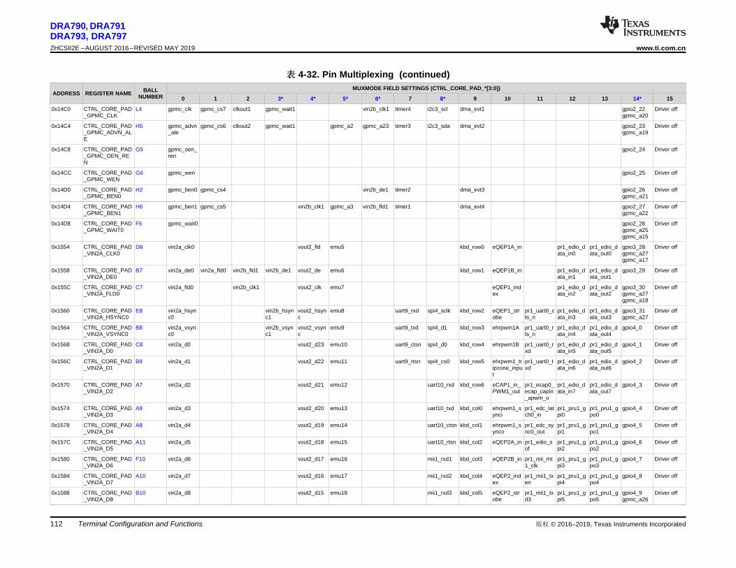
版权 © 2016–2019, Texas Instruments IncorporatedTerminal Configuration and Functions112
DRA790, DRA791DRA793, DRA797ZHCSII2E –AUGUST 2016–REVISED MAY 2019 www.ti.com.cn
表表 4-32. Pin Multiplexing (continued)
ADDRESS REGISTER NAME BALLNUMBER
MUXMODE FIELD SETTINGS (CTRL_CORE_PAD_*[3:0])
0 1 2 3* 4* 5* 6* 7 8* 9 10 11 12 13 14* 15
0x14C0 CTRL_CORE_PAD_GPMC_CLK
L4 gpmc_clk gpmc_cs7 clkout1 gpmc_wait1 vin2b_clk1 timer4 i2c3_scl dma_evt1 gpio2_22gpmc_a20
Driver off
0x14C4 CTRL_CORE_PAD_GPMC_ADVN_ALE
H5 gpmc_advn_ale
gpmc_cs6 clkout2 gpmc_wait1 gpmc_a2 gpmc_a23 timer3 i2c3_sda dma_evt2 gpio2_23gpmc_a19
Driver off
0x14C8 CTRL_CORE_PAD_GPMC_OEN_REN
G5 gpmc_oen_ren
gpio2_24 Driver off
0x14CC CTRL_CORE_PAD_GPMC_WEN
G6 gpmc_wen gpio2_25 Driver off
0x14D0 CTRL_CORE_PAD_GPMC_BEN0
H2 gpmc_ben0 gpmc_cs4 vin2b_de1 timer2 dma_evt3 gpio2_26gpmc_a21
Driver off
0x14D4 CTRL_CORE_PAD_GPMC_BEN1
H6 gpmc_ben1 gpmc_cs5 vin2b_clk1 gpmc_a3 vin2b_fld1 timer1 dma_evt4 gpio2_27gpmc_a22
Driver off
0x14D8 CTRL_CORE_PAD_GPMC_WAIT0
F6 gpmc_wait0 gpio2_28gpmc_a25gpmc_a15
Driver off
0x1554 CTRL_CORE_PAD_VIN2A_CLK0
D8 vin2a_clk0 vout2_fld emu5 kbd_row0 eQEP1A_in pr1_edio_data_in0
pr1_edio_data_out0
gpio3_28gpmc_a27gpmc_a17
Driver off
0x1558 CTRL_CORE_PAD_VIN2A_DE0
B7 vin2a_de0 vin2a_fld0 vin2b_fld1 vin2b_de1 vout2_de emu6 kbd_row1 eQEP1B_in pr1_edio_data_in1
pr1_edio_data_out1
gpio3_29 Driver off
0x155C CTRL_CORE_PAD_VIN2A_FLD0
C7 vin2a_fld0 vin2b_clk1 vout2_clk emu7 eQEP1_index
pr1_edio_data_in2
pr1_edio_data_out2
gpio3_30gpmc_a27gpmc_a18
Driver off
0x1560 CTRL_CORE_PAD_VIN2A_HSYNC0
E8 vin2a_hsync0
vin2b_hsync1
vout2_hsync
emu8 uart9_rxd spi4_sclk kbd_row2 eQEP1_strobe
pr1_uart0_cts_n
pr1_edio_data_in3
pr1_edio_data_out3
gpio3_31gpmc_a27
Driver off
0x1564 CTRL_CORE_PAD_VIN2A_VSYNC0
B8 vin2a_vsync0
vin2b_vsync1
vout2_vsync
emu9 uart9_txd spi4_d1 kbd_row3 ehrpwm1A pr1_uart0_rts_n
pr1_edio_data_in4
pr1_edio_data_out4
gpio4_0 Driver off
0x1568 CTRL_CORE_PAD_VIN2A_D0
C8 vin2a_d0 vout2_d23 emu10 uart9_ctsn spi4_d0 kbd_row4 ehrpwm1B pr1_uart0_rxd
pr1_edio_data_in5
pr1_edio_data_out5
gpio4_1 Driver off
0x156C CTRL_CORE_PAD_VIN2A_D1
B9 vin2a_d1 vout2_d22 emu11 uart9_rtsn spi4_cs0 kbd_row5 ehrpwm1_tripzone_input
pr1_uart0_txd
pr1_edio_data_in6
pr1_edio_data_out6
gpio4_2 Driver off
0x1570 CTRL_CORE_PAD_VIN2A_D2
A7 vin2a_d2 vout2_d21 emu12 uart10_rxd kbd_row6 eCAP1_in_PWM1_out
pr1_ecap0_ecap_capin_apwm_o
pr1_edio_data_in7
pr1_edio_data_out7
gpio4_3 Driver off
0x1574 CTRL_CORE_PAD_VIN2A_D3
A9 vin2a_d3 vout2_d20 emu13 uart10_txd kbd_col0 ehrpwm1_synci
pr1_edc_latch0_in
pr1_pru1_gpi0
pr1_pru1_gpo0
gpio4_4 Driver off
0x1578 CTRL_CORE_PAD_VIN2A_D4
A8 vin2a_d4 vout2_d19 emu14 uart10_ctsn kbd_col1 ehrpwm1_synco
pr1_edc_sync0_out
pr1_pru1_gpi1
pr1_pru1_gpo1
gpio4_5 Driver off
0x157C CTRL_CORE_PAD_VIN2A_D5
A11 vin2a_d5 vout2_d18 emu15 uart10_rtsn kbd_col2 eQEP2A_in pr1_edio_sof
pr1_pru1_gpi2
pr1_pru1_gpo2
gpio4_6 Driver off
0x1580 CTRL_CORE_PAD_VIN2A_D6
F10 vin2a_d6 vout2_d17 emu16 mii1_rxd1 kbd_col3 eQEP2B_in pr1_mii_mt1_clk
pr1_pru1_gpi3
pr1_pru1_gpo3
gpio4_7 Driver off
0x1584 CTRL_CORE_PAD_VIN2A_D7
A10 vin2a_d7 vout2_d16 emu17 mii1_rxd2 kbd_col4 eQEP2_index
pr1_mii1_txen
pr1_pru1_gpi4
pr1_pru1_gpo4
gpio4_8 Driver off
0x1588 CTRL_CORE_PAD_VIN2A_D8
B10 vin2a_d8 vout2_d15 emu18 mii1_rxd3 kbd_col5 eQEP2_strobe
pr1_mii1_txd3
pr1_pru1_gpi5
pr1_pru1_gpo5
gpio4_9gpmc_a26
Driver off

版权 © 2016–2019, Texas Instruments Incorporated Terminal Configuration and Functions 113
DRA790, DRA791DRA793, DRA797
www.ti.com.cn ZHCSII2E –AUGUST 2016–REVISED MAY 2019
表表 4-32. Pin Multiplexing (continued)
ADDRESS REGISTER NAME BALLNUMBER
MUXMODE FIELD SETTINGS (CTRL_CORE_PAD_*[3:0])
0 1 2 3* 4* 5* 6* 7 8* 9 10 11 12 13 14* 15
0x158C CTRL_CORE_PAD_VIN2A_D9
E10 vin2a_d9 vout2_d14 emu19 mii1_rxd0 kbd_col6 ehrpwm2A pr1_mii1_txd2
pr1_pru1_gpi6
pr1_pru1_gpo6
gpio4_10gpmc_a25
Driver off
0x1590 CTRL_CORE_PAD_VIN2A_D10
D10 vin2a_d10 mdio_mclk vout2_d13 kbd_col7 ehrpwm2B pr1_mdio_mdclk
pr1_pru1_gpi7
pr1_pru1_gpo7
gpio4_11gpmc_a24
Driver off
0x1594 CTRL_CORE_PAD_VIN2A_D11
C10 vin2a_d11 mdio_d vout2_d12 kbd_row7 ehrpwm2_tripzone_input
pr1_mdio_data
pr1_pru1_gpi8
pr1_pru1_gpo8
gpio4_12gpmc_a23
Driver off
0x1598 CTRL_CORE_PAD_VIN2A_D12
B11 vin2a_d12 rgmii1_txc vout2_d11 mii1_rxclk kbd_col8 eCAP2_in_PWM2_out
pr1_mii1_txd1
pr1_pru1_gpi9
pr1_pru1_gpo9
gpio4_13 Driver off
0x159C CTRL_CORE_PAD_VIN2A_D13
D11 vin2a_d13 rgmii1_txctl vout2_d10 mii1_rxdv kbd_row8 eQEP3A_in pr1_mii1_txd0
pr1_pru1_gpi10
pr1_pru1_gpo10
gpio4_14 Driver off
0x15A0 CTRL_CORE_PAD_VIN2A_D14
C11 vin2a_d14 rgmii1_txd3 vout2_d9 mii1_txclk eQEP3B_in pr1_mii_mr1_clk
pr1_pru1_gpi11
pr1_pru1_gpo11
gpio4_15 Driver off
0x15A4 CTRL_CORE_PAD_VIN2A_D15
B12 vin2a_d15 rgmii1_txd2 vout2_d8 mii1_txd0 eQEP3_index
pr1_mii1_rxdv
pr1_pru1_gpi12
pr1_pru1_gpo12
gpio4_16 Driver off
0x15A8 CTRL_CORE_PAD_VIN2A_D16
A12 vin2a_d16 vin2b_d7 rgmii1_txd1 vout2_d7 mii1_txd1 eQEP3_strobe
pr1_mii1_rxd3
pr1_pru1_gpi13
pr1_pru1_gpo13
gpio4_24 Driver off
0x15AC CTRL_CORE_PAD_VIN2A_D17
A13 vin2a_d17 vin2b_d6 rgmii1_txd0 vout2_d6 mii1_txd2 ehrpwm3A pr1_mii1_rxd2
pr1_pru1_gpi14
pr1_pru1_gpo14
gpio4_25 Driver off
0x15B0 CTRL_CORE_PAD_VIN2A_D18
E11 vin2a_d18 vin2b_d5 rgmii1_rxc vout2_d5 mii1_txd3 ehrpwm3B pr1_mii1_rxd1
pr1_pru1_gpi15
pr1_pru1_gpo15
gpio4_26 Driver off
0x15B4 CTRL_CORE_PAD_VIN2A_D19
F11 vin2a_d19 vin2b_d4 rgmii1_rxctl vout2_d4 mii1_txer ehrpwm3_tripzone_input
pr1_mii1_rxd0
pr1_pru1_gpi16
pr1_pru1_gpo16
gpio4_27 Driver off
0x15B8 CTRL_CORE_PAD_VIN2A_D20
B13 vin2a_d20 vin2b_d3 rgmii1_rxd3 vout2_d3 mii1_rxer eCAP3_in_PWM3_out
pr1_mii1_rxer
pr1_pru1_gpi17
pr1_pru1_gpo17
gpio4_28 Driver off
0x15BC CTRL_CORE_PAD_VIN2A_D21
E13 vin2a_d21 vin2b_d2 rgmii1_rxd2 vout2_d2 mii1_col pr1_mii1_rxlink
pr1_pru1_gpi18
pr1_pru1_gpo18
gpio4_29 Driver off
0x15C0 CTRL_CORE_PAD_VIN2A_D22
C13 vin2a_d22 vin2b_d1 rgmii1_rxd1 vout2_d1 mii1_crs pr1_mii1_col
pr1_pru1_gpi19
pr1_pru1_gpo19
gpio4_30 Driver off
0x15C4 CTRL_CORE_PAD_VIN2A_D23
D13 vin2a_d23 vin2b_d0 rgmii1_rxd0 vout2_d0 mii1_txen pr1_mii1_crs
pr1_pru1_gpi20
pr1_pru1_gpo20
gpio4_31 Driver off
0x15E4 CTRL_CORE_PAD_VOUT1_D2
E14 emu2
0x1604 CTRL_CORE_PAD_VOUT1_D10
F14 emu3
0x1624 CTRL_CORE_PAD_VOUT1_D18
F13 emu4
0x163C CTRL_CORE_PAD_MDIO_MCLK
L5 mdio_mclk uart3_rtsn mii0_col vin2a_clk0 vin1b_clk1 pr1_mii0_col
pr2_pru1_gpi0
pr2_pru1_gpo0
gpio5_15 Driver off
0x1640 CTRL_CORE_PAD_MDIO_D
L6 mdio_d uart3_ctsn mii0_txer vin2a_d0 vin1b_d0 pr1_mii0_rxlink
pr2_pru1_gpi1
pr2_pru1_gpo1
gpio5_16 Driver off
0x1644 CTRL_CORE_PAD_RMII_MHZ_50_CLK
P5 RMII_MHZ_50_CLK
vin2a_d11 pr2_pru1_gpi2
pr2_pru1_gpo2
gpio5_17 Driver off
0x1648 CTRL_CORE_PAD_UART3_RXD
N5 uart3_rxd rmii1_crs mii0_rxdv vin2a_d1 vin1b_d1 spi3_sclk pr1_mii0_rxdv
pr2_pru1_gpi3
pr2_pru1_gpo3
gpio5_18 Driver off

版权 © 2016–2019, Texas Instruments IncorporatedTerminal Configuration and Functions114
DRA790, DRA791DRA793, DRA797ZHCSII2E –AUGUST 2016–REVISED MAY 2019 www.ti.com.cn
表表 4-32. Pin Multiplexing (continued)
ADDRESS REGISTER NAME BALLNUMBER
MUXMODE FIELD SETTINGS (CTRL_CORE_PAD_*[3:0])
0 1 2 3* 4* 5* 6* 7 8* 9 10 11 12 13 14* 15
0x164C CTRL_CORE_PAD_UART3_TXD
N6 uart3_txd rmii1_rxer mii0_rxclk vin2a_d2 vin1b_d2 spi3_d1 spi4_cs1 pr1_mii_mr0_clk
pr2_pru1_gpi4
pr2_pru1_gpo4
gpio5_19 Driver off
0x1650 CTRL_CORE_PAD_RGMII0_TXC
T4 rgmii0_txc uart3_ctsn rmii1_rxd1 mii0_rxd3 vin2a_d3 vin1b_d3 usb3_ulpi_clk
spi3_d0 spi4_cs2 pr1_mii0_rxd3
pr2_pru1_gpi5
pr2_pru1_gpo5
gpio5_20 Driver off
0x1654 CTRL_CORE_PAD_RGMII0_TXCTL
T5 rgmii0_txctl uart3_rtsn rmii1_rxd0 mii0_rxd2 vin2a_d4 vin1b_d4 usb3_ulpi_stp
spi3_cs0 spi4_cs3 pr1_mii0_rxd2
pr2_pru1_gpi6
pr2_pru1_gpo6
gpio5_21 Driver off
0x1658 CTRL_CORE_PAD_RGMII0_TXD3
P4 rgmii0_txd3 rmii0_crs mii0_crs vin2a_de0 vin1b_de1 usb3_ulpi_dir
spi4_sclk uart4_rxd pr1_mii0_crs
pr2_pru1_gpi7
pr2_pru1_gpo7
gpio5_22 Driver off
0x165C CTRL_CORE_PAD_RGMII0_TXD2
P3 rgmii0_txd2 rmii0_rxer mii0_rxer vin2a_hsync0
vin1b_hsync1
usb3_ulpi_nxt
spi4_d1 uart4_txd pr1_mii0_rxer
pr2_pru1_gpi8
pr2_pru1_gpo8
gpio5_23 Driver off
0x1660 CTRL_CORE_PAD_RGMII0_TXD1
R2 rgmii0_txd1 rmii0_rxd1 mii0_rxd1 vin2a_vsync0
vin1b_vsync1
usb3_ulpi_d0
spi4_d0 uart4_ctsn pr1_mii0_rxd1
pr2_pru1_gpi9
pr2_pru1_gpo9
gpio5_24 Driver off
0x1664 CTRL_CORE_PAD_RGMII0_TXD0
R1 rgmii0_txd0 rmii0_rxd0 mii0_rxd0 vin2a_d10 usb3_ulpi_d1
spi4_cs0 uart4_rtsn pr1_mii0_rxd0
pr2_pru1_gpi10
pr2_pru1_gpo10
gpio5_25 Driver off
0x1668 CTRL_CORE_PAD_RGMII0_RXC
N2 rgmii0_rxc rmii1_txen mii0_txclk vin2a_d5 vin1b_d5 usb3_ulpi_d2
pr1_mii_mt0_clk
pr2_pru1_gpi11
pr2_pru1_gpo11
gpio5_26 Driver off
0x166C CTRL_CORE_PAD_RGMII0_RXCTL
P2 rgmii0_rxctl rmii1_txd1 mii0_txd3 vin2a_d6 vin1b_d6 usb3_ulpi_d3
pr1_mii0_txd3
pr2_pru1_gpi12
pr2_pru1_gpo12
gpio5_27 Driver off
0x1670 CTRL_CORE_PAD_RGMII0_RXD3
N1 rgmii0_rxd3 rmii1_txd0 mii0_txd2 vin2a_d7 vin1b_d7 usb3_ulpi_d4
pr1_mii0_txd2
pr2_pru1_gpi13
pr2_pru1_gpo13
gpio5_28 Driver off
0x1674 CTRL_CORE_PAD_RGMII0_RXD2
P1 rgmii0_rxd2 rmii0_txen mii0_txen vin2a_d8 usb3_ulpi_d5
pr1_mii0_txen
pr2_pru1_gpi14
pr2_pru1_gpo14
gpio5_29 Driver off
0x1678 CTRL_CORE_PAD_RGMII0_RXD1
N3 rgmii0_rxd1 rmii0_txd1 mii0_txd1 vin2a_d9 usb3_ulpi_d6
pr1_mii0_txd1
pr2_pru1_gpi15
pr2_pru1_gpo15
gpio5_30 Driver off
0x167C CTRL_CORE_PAD_RGMII0_RXD0
N4 rgmii0_rxd0 rmii0_txd0 mii0_txd0 vin2a_fld0 vin1b_fld1 usb3_ulpi_d7
pr1_mii0_txd0
pr2_pru1_gpi16
pr2_pru1_gpo16
gpio5_31 Driver off
0x1680 CTRL_CORE_PAD_USB1_DRVVBUS
AD3 usb1_drvvbus
timer16 gpio6_12 Driver off
0x1684 CTRL_CORE_PAD_USB2_DRVVBUS
AA6 usb2_drvvbus
timer15 gpio6_13 Driver off
0x1688 CTRL_CORE_PAD_GPIO6_14
H21 gpio6_14 mcasp1_axr8
dcan2_tx uart10_rxd i2c3_sda timer1 gpio6_14 Driver off
0x168C CTRL_CORE_PAD_GPIO6_15
K22 gpio6_15 mcasp1_axr9
dcan2_rx uart10_txd i2c3_scl timer2 gpio6_15 Driver off
0x1690 CTRL_CORE_PAD_GPIO6_16
K23 gpio6_16 mcasp1_axr10
clkout1 timer3 gpio6_16 Driver off
0x1694 CTRL_CORE_PAD_XREF_CLK0
J25 xref_clk0 mcasp2_axr8
mcasp1_axr4
mcasp1_ahclkx
mcasp5_ahclkx
atl_clk0 vin1a_d0 hdq0 clkout2 timer13 pr2_mii1_col
pr2_pru1_gpi5
pr2_pru1_gpo5
gpio6_17 Driver off
0x1698 CTRL_CORE_PAD_XREF_CLK1
J24 xref_clk1 mcasp2_axr9
mcasp1_axr5
mcasp2_ahclkx
mcasp6_ahclkx
atl_clk1 vin1a_clk0 timer14 pr2_mii1_crs
pr2_pru1_gpi6
pr2_pru1_gpo6
gpio6_18 Driver off
0x169C CTRL_CORE_PAD_XREF_CLK2
H24 xref_clk2 mcasp2_axr10
mcasp1_axr6
mcasp3_ahclkx
mcasp7_ahclkx
atl_clk2 timer15 gpio6_19 Driver off
0x16A0 CTRL_CORE_PAD_XREF_CLK3
H25 xref_clk3 mcasp2_axr11
mcasp1_axr7
mcasp4_ahclkx
mcasp8_ahclkx
atl_clk3 hdq0 clkout3 timer16 gpio6_20 Driver off
0x16A4 CTRL_CORE_PAD_MCASP1_ACLKX
C16 mcasp1_aclkx
vin1a_fld0 i2c3_sda pr2_mdio_mdclk
pr2_pru1_gpi7
pr2_pru1_gpo7
gpio7_31 Driver off
0x16A8 CTRL_CORE_PAD_MCASP1_FSX
C17 mcasp1_fsx vin1a_de0 i2c3_scl pr2_mdio_data
gpio7_30 Driver off

版权 © 2016–2019, Texas Instruments Incorporated Terminal Configuration and Functions 115
DRA790, DRA791DRA793, DRA797
www.ti.com.cn ZHCSII2E –AUGUST 2016–REVISED MAY 2019
表表 4-32. Pin Multiplexing (continued)
ADDRESS REGISTER NAME BALLNUMBER
MUXMODE FIELD SETTINGS (CTRL_CORE_PAD_*[3:0])
0 1 2 3* 4* 5* 6* 7 8* 9 10 11 12 13 14* 15
0x16AC CTRL_CORE_PAD_MCASP1_ACLKR
D16 mcasp1_aclkr
mcasp7_axr2
i2c4_sda gpio5_0 Driver off
0x16B0 CTRL_CORE_PAD_MCASP1_FSR
D17 mcasp1_fsr mcasp7_axr3
i2c4_scl gpio5_1 Driver off
0x16B4 CTRL_CORE_PAD_MCASP1_AXR0
D14 mcasp1_axr0
uart6_rxd vin1a_vsync0
i2c5_sda pr2_mii0_rxer
pr2_pru1_gpi8
pr2_pru1_gpo8
gpio5_2 Driver off
0x16B8 CTRL_CORE_PAD_MCASP1_AXR1
B14 mcasp1_axr1
uart6_txd vin1a_hsync0
i2c5_scl pr2_mii_mt0_clk
pr2_pru1_gpi9
pr2_pru1_gpo9
gpio5_3 Driver off
0x16BC CTRL_CORE_PAD_MCASP1_AXR2
C14 mcasp1_axr2
mcasp6_axr2
uart6_ctsn gpio5_4 Driver off
0x16C0 CTRL_CORE_PAD_MCASP1_AXR3
B15 mcasp1_axr3
mcasp6_axr3
uart6_rtsn gpio5_5 Driver off
0x16C4 CTRL_CORE_PAD_MCASP1_AXR4
A15 mcasp1_axr4
mcasp4_axr2
gpio5_6 Driver off
0x16C8 CTRL_CORE_PAD_MCASP1_AXR5
A14 mcasp1_axr5
mcasp4_axr3
gpio5_7 Driver off
0x16CC CTRL_CORE_PAD_MCASP1_AXR6
A17 mcasp1_axr6
mcasp5_axr2
gpio5_8 Driver off
0x16D0 CTRL_CORE_PAD_MCASP1_AXR7
A16 mcasp1_axr7
mcasp5_axr3
timer4 gpio5_9 Driver off
0x16D4 CTRL_CORE_PAD_MCASP1_AXR8
A18 mcasp1_axr8
mcasp6_axr0
spi3_sclk vin1a_d15 timer5 pr2_mii0_txen
pr2_pru1_gpi10
pr2_pru1_gpo10
gpio5_10 Driver off
0x16D8 CTRL_CORE_PAD_MCASP1_AXR9
B17 mcasp1_axr9
mcasp6_axr1
spi3_d1 vin1a_d14 timer6 pr2_mii0_txd3
pr2_pru1_gpi11
pr2_pru1_gpo11
gpio5_11 Driver off
0x16DC CTRL_CORE_PAD_MCASP1_AXR10
B16 mcasp1_axr10
mcasp6_aclkx
mcasp6_aclkr
spi3_d0 vin1a_d13 timer7 pr2_mii0_txd2
pr2_pru1_gpi12
pr2_pru1_gpo12
gpio5_12 Driver off
0x16E0 CTRL_CORE_PAD_MCASP1_AXR11
B18 mcasp1_axr11
mcasp6_fsx mcasp6_fsr spi3_cs0 vin1a_d12 timer8 pr2_mii0_txd1
pr2_pru1_gpi13
pr2_pru1_gpo13
gpio4_17 Driver off
0x16E4 CTRL_CORE_PAD_MCASP1_AXR12
A19 mcasp1_axr12
mcasp7_axr0
spi3_cs1 vin1a_d11 timer9 pr2_mii0_txd0
pr2_pru1_gpi14
pr2_pru1_gpo14
gpio4_18 Driver off
0x16E8 CTRL_CORE_PAD_MCASP1_AXR13
E17 mcasp1_axr13
mcasp7_axr1
vin1a_d10 timer10 pr2_mii_mr0_clk
pr2_pru1_gpi15
pr2_pru1_gpo15
gpio6_4 Driver off
0x16EC CTRL_CORE_PAD_MCASP1_AXR14
E16 mcasp1_axr14
mcasp7_aclkx
mcasp7_aclkr
vin1a_d9 timer11 pr2_mii0_rxdv
pr2_pru1_gpi16
pr2_pru1_gpo16
gpio6_5 Driver off
0x16F0 CTRL_CORE_PAD_MCASP1_AXR15
F16 mcasp1_axr15
mcasp7_fsx mcasp7_fsr vin1a_d8 timer12 pr2_mii0_rxd3
pr2_pru0_gpi20
pr2_pru0_gpo20
gpio6_6 Driver off
0x16F4 CTRL_CORE_PAD_MCASP2_ACLKX
E19 mcasp2_aclkx
vin1a_d7 pr2_mii0_rxd2
pr2_pru0_gpi18
pr2_pru0_gpo18
Driver off
0x16F8 CTRL_CORE_PAD_MCASP2_FSX
D19 mcasp2_fsx vin1a_d6 pr2_mii0_rxd1
pr2_pru0_gpi19
pr2_pru0_gpo19
Driver off
0x1704 CTRL_CORE_PAD_MCASP2_AXR0
A20 mcasp2_axr0
Driver off
0x1708 CTRL_CORE_PAD_MCASP2_AXR1
B19 mcasp2_axr1
Driver off
0x170C CTRL_CORE_PAD_MCASP2_AXR2
A21 mcasp2_axr2
mcasp3_axr2
vin1a_d5 pr2_mii0_rxd0
pr2_pru0_gpi16
pr2_pru0_gpo16
gpio6_8 Driver off
0x1710 CTRL_CORE_PAD_MCASP2_AXR3
B21 mcasp2_axr3
mcasp3_axr3
vin1a_d4 pr2_mii0_rxlink
pr2_pru0_gpi17
pr2_pru0_gpo17
gpio6_9 Driver off
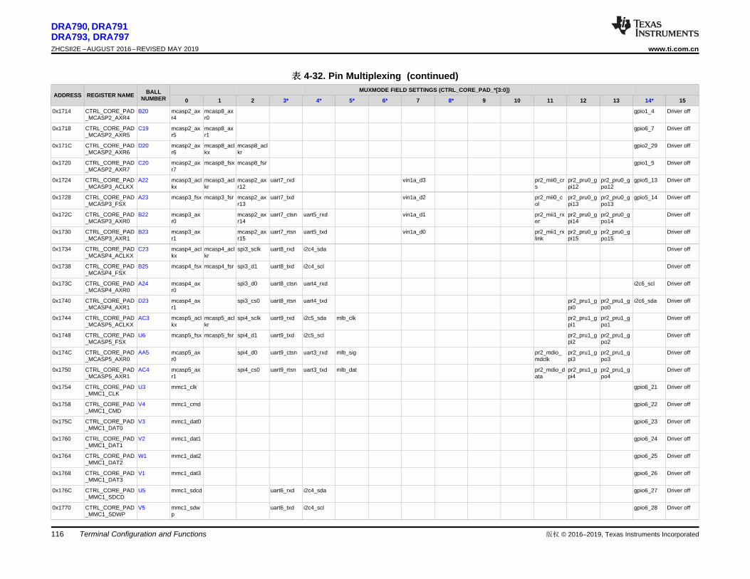
版权 © 2016–2019, Texas Instruments IncorporatedTerminal Configuration and Functions116
DRA790, DRA791DRA793, DRA797ZHCSII2E –AUGUST 2016–REVISED MAY 2019 www.ti.com.cn
表表 4-32. Pin Multiplexing (continued)
ADDRESS REGISTER NAME BALLNUMBER
MUXMODE FIELD SETTINGS (CTRL_CORE_PAD_*[3:0])
0 1 2 3* 4* 5* 6* 7 8* 9 10 11 12 13 14* 15
0x1714 CTRL_CORE_PAD_MCASP2_AXR4
B20 mcasp2_axr4
mcasp8_axr0
gpio1_4 Driver off
0x1718 CTRL_CORE_PAD_MCASP2_AXR5
C19 mcasp2_axr5
mcasp8_axr1
gpio6_7 Driver off
0x171C CTRL_CORE_PAD_MCASP2_AXR6
D20 mcasp2_axr6
mcasp8_aclkx
mcasp8_aclkr
gpio2_29 Driver off
0x1720 CTRL_CORE_PAD_MCASP2_AXR7
C20 mcasp2_axr7
mcasp8_fsx mcasp8_fsr gpio1_5 Driver off
0x1724 CTRL_CORE_PAD_MCASP3_ACLKX
A22 mcasp3_aclkx
mcasp3_aclkr
mcasp2_axr12
uart7_rxd vin1a_d3 pr2_mii0_crs
pr2_pru0_gpi12
pr2_pru0_gpo12
gpio5_13 Driver off
0x1728 CTRL_CORE_PAD_MCASP3_FSX
A23 mcasp3_fsx mcasp3_fsr mcasp2_axr13
uart7_txd vin1a_d2 pr2_mii0_col
pr2_pru0_gpi13
pr2_pru0_gpo13
gpio5_14 Driver off
0x172C CTRL_CORE_PAD_MCASP3_AXR0
B22 mcasp3_axr0
mcasp2_axr14
uart7_ctsn uart5_rxd vin1a_d1 pr2_mii1_rxer
pr2_pru0_gpi14
pr2_pru0_gpo14
Driver off
0x1730 CTRL_CORE_PAD_MCASP3_AXR1
B23 mcasp3_axr1
mcasp2_axr15
uart7_rtsn uart5_txd vin1a_d0 pr2_mii1_rxlink
pr2_pru0_gpi15
pr2_pru0_gpo15
Driver off
0x1734 CTRL_CORE_PAD_MCASP4_ACLKX
C23 mcasp4_aclkx
mcasp4_aclkr
spi3_sclk uart8_rxd i2c4_sda Driver off
0x1738 CTRL_CORE_PAD_MCASP4_FSX
B25 mcasp4_fsx mcasp4_fsr spi3_d1 uart8_txd i2c4_scl Driver off
0x173C CTRL_CORE_PAD_MCASP4_AXR0
A24 mcasp4_axr0
spi3_d0 uart8_ctsn uart4_rxd i2c6_scl Driver off
0x1740 CTRL_CORE_PAD_MCASP4_AXR1
D23 mcasp4_axr1
spi3_cs0 uart8_rtsn uart4_txd pr2_pru1_gpi0
pr2_pru1_gpo0
i2c6_sda Driver off
0x1744 CTRL_CORE_PAD_MCASP5_ACLKX
AC3 mcasp5_aclkx
mcasp5_aclkr
spi4_sclk uart9_rxd i2c5_sda mlb_clk pr2_pru1_gpi1
pr2_pru1_gpo1
Driver off
0x1748 CTRL_CORE_PAD_MCASP5_FSX
U6 mcasp5_fsx mcasp5_fsr spi4_d1 uart9_txd i2c5_scl pr2_pru1_gpi2
pr2_pru1_gpo2
Driver off
0x174C CTRL_CORE_PAD_MCASP5_AXR0
AA5 mcasp5_axr0
spi4_d0 uart9_ctsn uart3_rxd mlb_sig pr2_mdio_mdclk
pr2_pru1_gpi3
pr2_pru1_gpo3
Driver off
0x1750 CTRL_CORE_PAD_MCASP5_AXR1
AC4 mcasp5_axr1
spi4_cs0 uart9_rtsn uart3_txd mlb_dat pr2_mdio_data
pr2_pru1_gpi4
pr2_pru1_gpo4
Driver off
0x1754 CTRL_CORE_PAD_MMC1_CLK
U3 mmc1_clk gpio6_21 Driver off
0x1758 CTRL_CORE_PAD_MMC1_CMD
V4 mmc1_cmd gpio6_22 Driver off
0x175C CTRL_CORE_PAD_MMC1_DAT0
V3 mmc1_dat0 gpio6_23 Driver off
0x1760 CTRL_CORE_PAD_MMC1_DAT1
V2 mmc1_dat1 gpio6_24 Driver off
0x1764 CTRL_CORE_PAD_MMC1_DAT2
W1 mmc1_dat2 gpio6_25 Driver off
0x1768 CTRL_CORE_PAD_MMC1_DAT3
V1 mmc1_dat3 gpio6_26 Driver off
0x176C CTRL_CORE_PAD_MMC1_SDCD
U5 mmc1_sdcd uart6_rxd i2c4_sda gpio6_27 Driver off
0x1770 CTRL_CORE_PAD_MMC1_SDWP
V5 mmc1_sdwp
uart6_txd i2c4_scl gpio6_28 Driver off
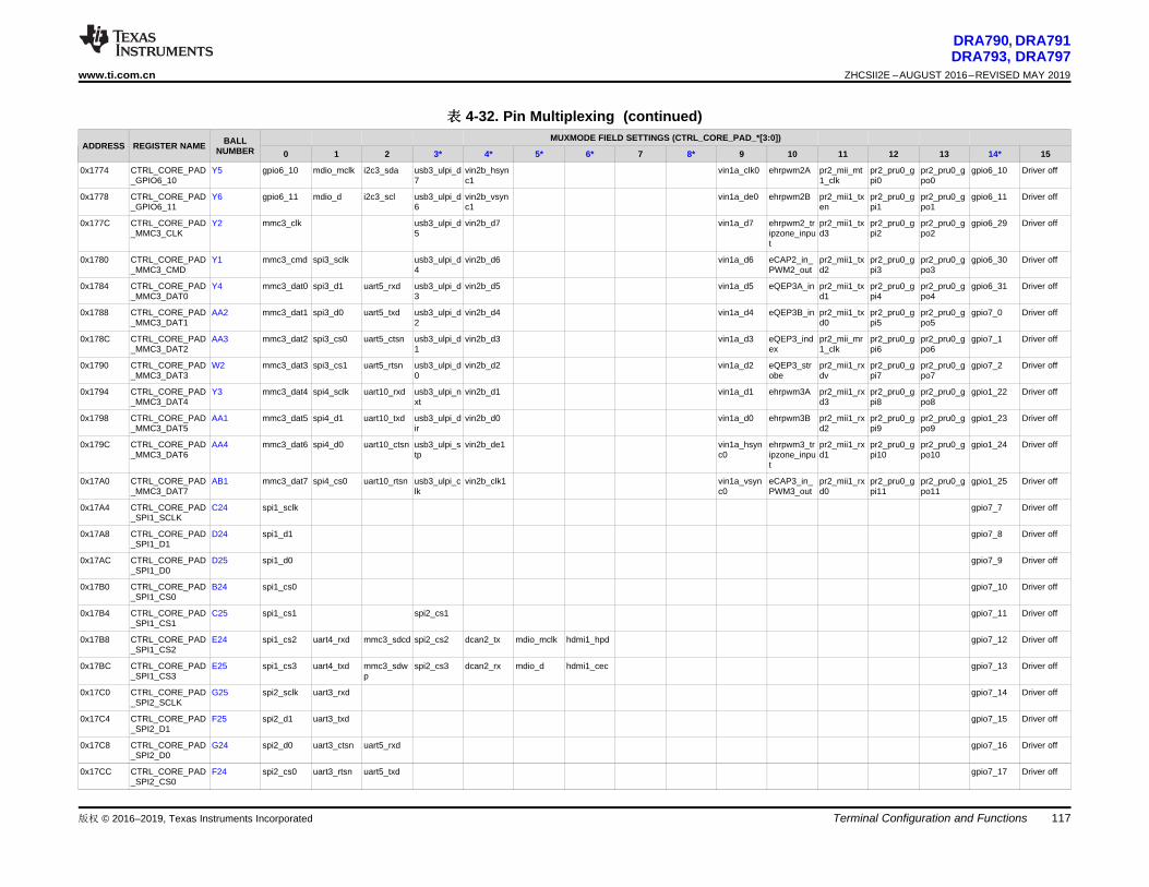
版权 © 2016–2019, Texas Instruments Incorporated Terminal Configuration and Functions 117
DRA790, DRA791DRA793, DRA797
www.ti.com.cn ZHCSII2E –AUGUST 2016–REVISED MAY 2019
表表 4-32. Pin Multiplexing (continued)
ADDRESS REGISTER NAME BALLNUMBER
MUXMODE FIELD SETTINGS (CTRL_CORE_PAD_*[3:0])
0 1 2 3* 4* 5* 6* 7 8* 9 10 11 12 13 14* 15
0x1774 CTRL_CORE_PAD_GPIO6_10
Y5 gpio6_10 mdio_mclk i2c3_sda usb3_ulpi_d7
vin2b_hsync1
vin1a_clk0 ehrpwm2A pr2_mii_mt1_clk
pr2_pru0_gpi0
pr2_pru0_gpo0
gpio6_10 Driver off
0x1778 CTRL_CORE_PAD_GPIO6_11
Y6 gpio6_11 mdio_d i2c3_scl usb3_ulpi_d6
vin2b_vsync1
vin1a_de0 ehrpwm2B pr2_mii1_txen
pr2_pru0_gpi1
pr2_pru0_gpo1
gpio6_11 Driver off
0x177C CTRL_CORE_PAD_MMC3_CLK
Y2 mmc3_clk usb3_ulpi_d5
vin2b_d7 vin1a_d7 ehrpwm2_tripzone_input
pr2_mii1_txd3
pr2_pru0_gpi2
pr2_pru0_gpo2
gpio6_29 Driver off
0x1780 CTRL_CORE_PAD_MMC3_CMD
Y1 mmc3_cmd spi3_sclk usb3_ulpi_d4
vin2b_d6 vin1a_d6 eCAP2_in_PWM2_out
pr2_mii1_txd2
pr2_pru0_gpi3
pr2_pru0_gpo3
gpio6_30 Driver off
0x1784 CTRL_CORE_PAD_MMC3_DAT0
Y4 mmc3_dat0 spi3_d1 uart5_rxd usb3_ulpi_d3
vin2b_d5 vin1a_d5 eQEP3A_in pr2_mii1_txd1
pr2_pru0_gpi4
pr2_pru0_gpo4
gpio6_31 Driver off
0x1788 CTRL_CORE_PAD_MMC3_DAT1
AA2 mmc3_dat1 spi3_d0 uart5_txd usb3_ulpi_d2
vin2b_d4 vin1a_d4 eQEP3B_in pr2_mii1_txd0
pr2_pru0_gpi5
pr2_pru0_gpo5
gpio7_0 Driver off
0x178C CTRL_CORE_PAD_MMC3_DAT2
AA3 mmc3_dat2 spi3_cs0 uart5_ctsn usb3_ulpi_d1
vin2b_d3 vin1a_d3 eQEP3_index
pr2_mii_mr1_clk
pr2_pru0_gpi6
pr2_pru0_gpo6
gpio7_1 Driver off
0x1790 CTRL_CORE_PAD_MMC3_DAT3
W2 mmc3_dat3 spi3_cs1 uart5_rtsn usb3_ulpi_d0
vin2b_d2 vin1a_d2 eQEP3_strobe
pr2_mii1_rxdv
pr2_pru0_gpi7
pr2_pru0_gpo7
gpio7_2 Driver off
0x1794 CTRL_CORE_PAD_MMC3_DAT4
Y3 mmc3_dat4 spi4_sclk uart10_rxd usb3_ulpi_nxt
vin2b_d1 vin1a_d1 ehrpwm3A pr2_mii1_rxd3
pr2_pru0_gpi8
pr2_pru0_gpo8
gpio1_22 Driver off
0x1798 CTRL_CORE_PAD_MMC3_DAT5
AA1 mmc3_dat5 spi4_d1 uart10_txd usb3_ulpi_dir
vin2b_d0 vin1a_d0 ehrpwm3B pr2_mii1_rxd2
pr2_pru0_gpi9
pr2_pru0_gpo9
gpio1_23 Driver off
0x179C CTRL_CORE_PAD_MMC3_DAT6
AA4 mmc3_dat6 spi4_d0 uart10_ctsn usb3_ulpi_stp
vin2b_de1 vin1a_hsync0
ehrpwm3_tripzone_input
pr2_mii1_rxd1
pr2_pru0_gpi10
pr2_pru0_gpo10
gpio1_24 Driver off
0x17A0 CTRL_CORE_PAD_MMC3_DAT7
AB1 mmc3_dat7 spi4_cs0 uart10_rtsn usb3_ulpi_clk
vin2b_clk1 vin1a_vsync0
eCAP3_in_PWM3_out
pr2_mii1_rxd0
pr2_pru0_gpi11
pr2_pru0_gpo11
gpio1_25 Driver off
0x17A4 CTRL_CORE_PAD_SPI1_SCLK
C24 spi1_sclk gpio7_7 Driver off
0x17A8 CTRL_CORE_PAD_SPI1_D1
D24 spi1_d1 gpio7_8 Driver off
0x17AC CTRL_CORE_PAD_SPI1_D0
D25 spi1_d0 gpio7_9 Driver off
0x17B0 CTRL_CORE_PAD_SPI1_CS0
B24 spi1_cs0 gpio7_10 Driver off
0x17B4 CTRL_CORE_PAD_SPI1_CS1
C25 spi1_cs1 spi2_cs1 gpio7_11 Driver off
0x17B8 CTRL_CORE_PAD_SPI1_CS2
E24 spi1_cs2 uart4_rxd mmc3_sdcd spi2_cs2 dcan2_tx mdio_mclk hdmi1_hpd gpio7_12 Driver off
0x17BC CTRL_CORE_PAD_SPI1_CS3
E25 spi1_cs3 uart4_txd mmc3_sdwp
spi2_cs3 dcan2_rx mdio_d hdmi1_cec gpio7_13 Driver off
0x17C0 CTRL_CORE_PAD_SPI2_SCLK
G25 spi2_sclk uart3_rxd gpio7_14 Driver off
0x17C4 CTRL_CORE_PAD_SPI2_D1
F25 spi2_d1 uart3_txd gpio7_15 Driver off
0x17C8 CTRL_CORE_PAD_SPI2_D0
G24 spi2_d0 uart3_ctsn uart5_rxd gpio7_16 Driver off
0x17CC CTRL_CORE_PAD_SPI2_CS0
F24 spi2_cs0 uart3_rtsn uart5_txd gpio7_17 Driver off

版权 © 2016–2019, Texas Instruments IncorporatedTerminal Configuration and Functions118
DRA790, DRA791DRA793, DRA797ZHCSII2E –AUGUST 2016–REVISED MAY 2019 www.ti.com.cn
表表 4-32. Pin Multiplexing (continued)
ADDRESS REGISTER NAME BALLNUMBER
MUXMODE FIELD SETTINGS (CTRL_CORE_PAD_*[3:0])
0 1 2 3* 4* 5* 6* 7 8* 9 10 11 12 13 14* 15
0x17D0 CTRL_CORE_PAD_DCAN1_TX
H22 dcan1_tx uart8_rxd mmc2_sdcd hdmi1_hpd gpio1_14 Driver off
0x17D4 CTRL_CORE_PAD_DCAN1_RX
H23 dcan1_rx uart8_txd mmc2_sdwp
hdmi1_cec gpio1_15 Driver off
0x17E0 CTRL_CORE_PAD_UART1_RXD
L25 uart1_rxd mmc4_sdcd gpio7_22 Driver off
0x17E4 CTRL_CORE_PAD_UART1_TXD
M25 uart1_txd mmc4_sdwp
gpio7_23 Driver off
0x17E8 CTRL_CORE_PAD_UART1_CTSN
L20 uart1_ctsn uart9_rxd mmc4_clk gpio7_24 Driver off
0x17EC CTRL_CORE_PAD_UART1_RTSN
M24 uart1_rtsn uart9_txd mmc4_cmd gpio7_25 Driver off
0x17F0 CTRL_CORE_PAD_UART2_RXD
N23 uart2_rxd uart3_ctsn uart3_rctx mmc4_dat0 uart2_rxd uart1_dcdn gpio7_26 Driver off
0x17F4 CTRL_CORE_PAD_UART2_TXD
N25 uart2_txd uart3_rtsn uart3_sd mmc4_dat1 uart2_txd uart1_dsrn gpio7_27 Driver off
0x17F8 CTRL_CORE_PAD_UART2_CTSN
N22 uart2_ctsn uart3_rxd mmc4_dat2 uart10_rxd uart1_dtrn gpio1_16 Driver off
0x17FC CTRL_CORE_PAD_UART2_RTSN
N24 uart2_rtsn uart3_txd uart3_irtx mmc4_dat3 uart10_txd uart1_rin gpio1_17 Driver off
0x1800 CTRL_CORE_PAD_I2C1_SDA
G23 i2c1_sda Driver off
0x1804 CTRL_CORE_PAD_I2C1_SCL
G22 i2c1_scl Driver off
0x1808 CTRL_CORE_PAD_I2C2_SDA
F23 i2c2_sda hdmi1_ddc_scl
Driver off
0x180C CTRL_CORE_PAD_I2C2_SCL
G21 i2c2_scl hdmi1_ddc_sda
Driver off
0x1818 CTRL_CORE_PAD_WAKEUP0
AC10 dcan1_rx gpio1_0sys_nirq2
Driver off
0x1824 CTRL_CORE_PAD_WAKEUP3
AB10 sys_nirq1 gpio1_3dcan2_rx
Driver off
0x1830 CTRL_CORE_PAD_TMS
L21 tms
0x1834 CTRL_CORE_PAD_TDI
L23 tdi gpio8_27
0x1838 CTRL_CORE_PAD_TDO
J20 tdo gpio8_28
0x183C CTRL_CORE_PAD_TCLK
K21 tclk
0x1840 CTRL_CORE_PAD_TRSTN
L22 trstn
0x1844 CTRL_CORE_PAD_RTCK
K25 rtck gpio8_29
0x1848 CTRL_CORE_PAD_EMU0
C21 emu0 gpio8_30
0x184C CTRL_CORE_PAD_EMU1
C22 emu1 gpio8_31

版权 © 2016–2019, Texas Instruments Incorporated Terminal Configuration and Functions 119
DRA790, DRA791DRA793, DRA797
www.ti.com.cn ZHCSII2E –AUGUST 2016–REVISED MAY 2019
表表 4-32. Pin Multiplexing (continued)
ADDRESS REGISTER NAME BALLNUMBER
MUXMODE FIELD SETTINGS (CTRL_CORE_PAD_*[3:0])
0 1 2 3* 4* 5* 6* 7 8* 9 10 11 12 13 14* 15
0x185C CTRL_CORE_PAD_RESETN
K24 resetn
0x1860 CTRL_CORE_PAD_NMIN_DSP
L24 nmin_dsp
0x1864 CTRL_CORE_PAD_RSTOUTN
E20 rstoutn
1. NA in table stands for Not Applicable.

120
DRA790, DRA791DRA793, DRA797ZHCSII2E –AUGUST 2016–REVISED MAY 2019 www.ti.com.cn
Terminal Configuration and Functions 版权 © 2016–2019, Texas Instruments Incorporated
4.5 Connections for Unused PinsThis section describes the connection requirements of the unused and reserved balls.
注注The following balls are reserved: K20, L19, G20
These balls must be left unconnected.
注注All unused power supply balls must be supplied with the voltages specified in theSection 5.4, Recommended Operating Conditions, unless alternative tie-off options areincluded in 节 4.3, Signal Descriptions.
表表 4-33. Unused Balls Specific Connection Requirements
BALLS CONNECTION REQUIREMENTS
Y12 / AC11 / L22 / AC10 / AB10 / AD22 / Y24 / V24 / R24 These balls must be connected to GND through an external pullresistor if unused.
K21 / L24 / K24 / G22 / G23 / L21 / G21 / F23 / AE22 / Y25 / V25 /R25
These balls must be connect to the corresponding power supplythrough an external pull resistor if unused.
F20 (vpp) This ball must be left unconnected if unused
注注All other unused signal balls with a Pad Configuration register can be left unconnected withtheir internal pullup or pulldown resistor enabled.
注注All other unused signal balls without a Pad Configuration register can be left unconnected.

121
DRA790, DRA791DRA793, DRA797
www.ti.com.cn ZHCSII2E –AUGUST 2016–REVISED MAY 2019
Specifications版权 © 2016–2019, Texas Instruments Incorporated
5 Specifications
注注For more information, see Power, Reset, and Clock Management / PRCM SubsystemEnvironment / External Voltage Inputs or Initialization / Preinitialization / Power Requirementssection of the Device TRM.
注注The index number 1which is part of the EMIF1 signal prefixes (ddr1_*) listed in 表 4-6, EMIFSignal Descriptions, column "SIGNAL NAME" not to be confused with DDR1 type of SDRAMmemories.
注注Audio Back End (ABE) module is not supported for this family of devices, but “ABE” name isstill present in some clock or DPLL names.
CAUTION
All IO Cells are NOT Fail-safe compliant and should not be externally driven inabsence of their IO supply.

122
DRA790, DRA791DRA793, DRA797ZHCSII2E –AUGUST 2016–REVISED MAY 2019 www.ti.com.cn
Specifications 版权 © 2016–2019, Texas Instruments Incorporated
5.1 Absolute Maximum Ratingsover operating free-air temperature range (unless otherwise noted) (1)
PARAMETER(1) MIN MAX UNITVSUPPLY (Steady-State) Supply Voltage Ranges (Steady-
State)Core (vdd, vdd_dsp) -0.3 1.5 VAnalog (vdda_usb1, vdda_usb2,vdda_per, vdda_ddr, vdda_debug,vdda_mpu_abe, vdda_usb3,vdda_csi, vdda_core_gmac,vdda_gpu, dda_hdmi, vdda_pcie,vdda_video, vdda_osc)
-0.3 2.0 V
Analog 3.3V (vdda33v_usb1,vdda33v_usb2)
-0.3 3.8 V
vdds18v, vdds18v_ddr1,vdds_mlbp, vdds_ddr1
-0.3 2.1 V
vddshv1, vddshv3, vddshv4,vddshv7-11 (1.8V mode)
-0.3 2.1 V
vddshv1, vddshv3, vddshv4,vddshv7, vddshv9-11 (3.3V mode)
-0.3 3.8 V
vddshv8 (3.3V mode) -0.3 3.6 VVIO (Steady-State) Input and Output Voltage Ranges
(Steady-State)Core I/Os -0.3 1.5 VAnalog I/Os (except HDMI) -0.3 2.0 VHDMI I/Os -0.3 3.5 VI/O 1.35V -0.3 1.65 VI/O 1.5V -0.3 1.8 V1.8V I/Os -0.3 2.1 V3.3V I/Os (except those powered byvddshv8)
-0.3 3.8 V
3.3V I/Os (powered by vddshv8) -0.3 3.6 VSR Maximum slew rate, all supplies 105 V/s
VIO (Transient Overshoot /Undershoot)
Input and Output Voltage Ranges (Transient Overshoot/Undershoot)Note: valid for up to 20% of the signal period. See 图 5-1, IO transientvoltage ranges.
0.2 ×VDD (4)
V
TJ Operating junction temperaturerange
Automotive -40 +125 °C
TSTG Storage temperature range after soldered onto PC Board -55 +150 °CLatch-up I-Test I-test(5), All I/Os (if different levels then one line per level) -100 100 mA
Latch-up OV-Test Over-voltage Test(6), All supplies (if different levels then one line per level) N/A 1.5 ×Vsupply
max
V
(1) Stresses beyond those listed as absolute maximum ratings may cause permanent damage to the device. These are stress ratings only,and functional operation of the device at these or any other conditions beyond those listed under Section 5.4, Recommended OperatingConditions, is not implied. Exposure to absolute maximum rated conditions for extended periods may affect device reliability.
(2) All voltage values are with respect to VSS, unless otherwise noted.(3) See I/Os supplied by this power pin in 表 4-1 Pin Attributes(4) VDD is the voltage on the corresponding power-supply pin(s) for the IO.(5) Per JEDEC JESD78 at 125°C with specified I/O pin injection current and clamp voltage of 1.5 times maximum recommended I/O
voltage and negative 0.5 times maximum recommended I/O voltage.(6) Per JEDEC JESD78 at 125°C.(7) The maximum valid input voltage on an IO pin cannot exceed 0.3 volts when the supply powering the IO is turned off. This requirement
applies to all the IO pins which are not fail-safe and for all values of IO supply voltage. Special attention should be applied anytimeperipheral devices are not powered from the same power sources used to power the respective IO supply. It is important the attachedperipheral never sources a voltage outside the valid input voltage range, including power supply ramp-up and ramp-down sequences.
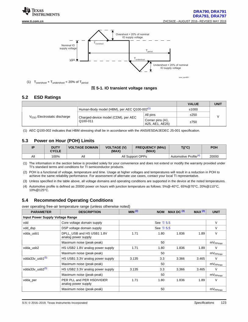
Tovershoot
Tundershoot
Tperiod
Overshoot = 20% of nominalIO supply voltage
Undershoot = 20% of nominalIO supply voltage
Nominal IOsupply voltage
VSS
osus_sprs851
123
DRA790, DRA791DRA793, DRA797
www.ti.com.cn ZHCSII2E –AUGUST 2016–REVISED MAY 2019
Specifications版权 © 2016–2019, Texas Instruments Incorporated
(1) Tovershoot + Tundershoot < 20% of Tperiod
图图 5-1. IO transient voltage ranges
5.2 ESD RatingsVALUE UNIT
VESD Electrostatic discharge
Human-Body model (HBM), per AEC Q100-002(1) ±1000
VCharged-device model (CDM), per AECQ100-011
All pins ±250Corner pins (A1,A25, AE1, AE25) ±750
(1) AEC Q100-002 indicates that HBM stressing shall be in accordance with the ANSI/ESDA/JEDEC JS-001 specification.
5.3 Power on Hour (POH) LimitsIP DUTY
CYCLEVOLTAGE DOMAIN VOLTAGE (V)
(MAX)FREQUENCY (MHz)
(MAX)Tj(°C) POH
All 100% All All Support OPPs Automotive Profile(4) 20000
(1) The information in the section below is provided solely for your convenience and does not extend or modify the warranty provided underTI’s standard terms and conditions for TI semiconductor products.
(2) POH is a functional of voltage, temperature and time. Usage at higher voltages and temperatures will result in a reduction in POH toachieve the same reliability performance. For assessment of alternate use cases, contact your local TI representative.
(3) Unless specified in the table above, all voltage domains and operating conditions are supported in the device at the noted temperatures.(4) Automotive profile is defined as 20000 power on hours with junction temperature as follows: 5%@-40°C, 65%@70°C, 20%@110°C,
10%@125°C.
5.4 Recommended Operating Conditionsover operating free-air temperature range (unless otherwise noted)
PARAMETER DESCRIPTION MIN (2) NOM MAX DC (3) MAX (2) UNITInput Power Supply Voltage Rangevdd Core voltage domain supply See 节 5.5 Vvdd_dsp DSP voltage domain supply See 节 5.5 Vvdda_usb1 DPLL_USB and HS USB1 1.8V
analog power supply1.71 1.80 1.836 1.89 V
Maximum noise (peak-peak) 50 mVPPmax
vdda_usb2 HS USB2 1.8V analog power supply 1.71 1.80 1.836 1.89 VMaximum noise (peak-peak) 50 mVPPmax
vdda33v_usb1(5) HS USB1 3.3V analog power supply 3.135 3.3 3.366 3.465 VMaximum noise (peak-peak) 50 mVPPmax
vdda33v_usb2(5) HS USB2 3.3V analog power supply 3.135 3.3 3.366 3.465 VMaximum noise (peak-peak) 50 mVPPmax
vdda_per PER PLL and PER HSDIVIDERanalog power supply
1.71 1.80 1.836 1.89 V
Maximum noise (peak-peak) 50 mVPPmax

124
DRA790, DRA791DRA793, DRA797ZHCSII2E –AUGUST 2016–REVISED MAY 2019 www.ti.com.cn
Specifications 版权 © 2016–2019, Texas Instruments Incorporated
Recommended Operating Conditions (continued)over operating free-air temperature range (unless otherwise noted)
PARAMETER DESCRIPTION MIN (2) NOM MAX DC (3) MAX (2) UNITvdda_ddr DPLL_DDR and DDR HSDIVIDER
analog power supply1.71 1.80 1.836 1.89 V
Maximum noise (peak-peak) 50 mVPPmax
vdda_debug DPLL_DEBUG analog power supply 1.71 1.80 1.836 1.89 VMaximum noise (peak-peak) 50 mVPPmax
vdda_core_gmac DPLL_CORE and CORE HSDIVIDERanalog power supply
1.71 1.80 1.836 1.89 V
Maximum noise (peak-peak) 50 mVPPmax
vdda_gpu DPLL_GPU analog power supply 1.71 1.80 1.836 1.89 VMaximum noise (peak-peak) 50 mVPPmax
vdda_hdmi PLL_HDMI and HDMI analog powersupply
1.71 1.80 1.836 1.89 V
Maximum noise (peak-peak) 50 mVPPmax
vdda_pcie DPLL_PCIe_REF and PCIe analogpower supply
1.71 1.80 1.836 1.89 V
Maximum noise (peak-peak) 50 mVPPmax
vdda_usb3 DPLL_USB_OTG_SS and USB3.0RX/TX analog power supply
1.71 1.80 1.836 1.89 V
Maximum noise (peak-peak) 50 mVPPmax
vdda_video DPLL_VIDEO1 analog power supply 1.71 1.80 1.836 1.89 VMaximum noise (peak-peak) 50 mVPPmax
vdds_mlbp MLBP IO power supply 1.71 1.80 1.89 VMaximum noise (peak-peak) 50 mVPPmax
vdda_mpu_abe DPLL_MPU analog power supply 1.71 1.80 1.836 1.89 VMaximum noise (peak-peak) 50 mVPPmax
vdda_osc HFOSC analog power supply 1.71 1.80 1.89 VMaximum noise (peak-peak) 50 mVPPmax
vdda_csi CSI Interface 1.8v Supply 1.71 1.80 1.836 1.89 VMaximum noise (peak-peak) 50 mVPPmax
vdds18v 1.8V power supply 1.71 1.80 1.836 1.89 VMaximum noise (peak-peak) 50 mVPPmax
vdds18v_ddr1 EMIF1 bias power supply 1.71 1.80 1.836 1.89 VMaximum noise (peak-peak) 50 mVPPmax
vdds_ddr1 EMIF1 power supply(1.5V for DDR3 mode /1.35V DDR3L mode)
1.35-VMode
1.28 1.35 1.377 1.42 V
1.5-V Mode 1.43 1.50 1.53 1.57Maximum noise(peakpeak)
1.35-VMode
50 mVPPmax
1.5-V Modevddshv1 Dual Voltage (1.8V or
3.3V) power supply forthe VIN2 Power Grouppins
1.8-V Mode 1.71 1.80 1.836 1.89 V3.3-V Mode 3.135 3.30 3.366 3.465
Maximum noise (peak-peak)
1.8-V Mode 50 mVPPmax
3.3-V Mode

125
DRA790, DRA791DRA793, DRA797
www.ti.com.cn ZHCSII2E –AUGUST 2016–REVISED MAY 2019
Specifications版权 © 2016–2019, Texas Instruments Incorporated
Recommended Operating Conditions (continued)over operating free-air temperature range (unless otherwise noted)
PARAMETER DESCRIPTION MIN (2) NOM MAX DC (3) MAX (2) UNITvddshv10 Dual Voltage (1.8V or
3.3V) power supply forthe GPMC Power Grouppins
1.8-V Mode 1.71 1.80 1.836 1.89 V3.3-V Mode 3.135 3.30 3.366 3.465
Maximum noise (peak-peak)
1.8-V Mode 50 mVPPmax
3.3-V Modevddshv11 Dual Voltage (1.8V or
3.3V) power supply forthe MMC2 Power Grouppins
1.8-V Mode 1.71 1.80 1.836 1.89 V3.3-V Mode 3.135 3.30 3.366 3.465
Maximum noise (peak-peak)
1.8-V Mode 50 mVPPmax
3.3-V Modevddshv3 Dual Voltage (1.8V or
3.3V) power supply forthe GENERAL PowerGroup pins
1.8-V Mode 1.71 1.80 1.836 1.89 V3.3-V Mode 3.135 3.30 3.366 3.465
Maximum noise (peak-peak)
1.8-V Mode 50 mVPPmax
3.3-V Modevddshv4 Dual Voltage (1.8V or
3.3V) power supply forthe MMC4 Power Grouppins
1.8-V Mode 1.71 1.80 1.836 1.89 V3.3-V Mode 3.135 3.30 3.366 3.465
Maximum noise (peak-peak)
1.8-V Mode 50 mVPPmax
3.3-V Modevddshv7 Dual Voltage (1.8V or
3.3V) power supply forthe WIFI Power Grouppins
1.8-V Mode 1.71 1.80 1.836 1.89 V3.3-V Mode 3.135 3.30 3.366 3.465
Maximum noise (peak-peak)
1.8-V Mode 50 mVPPmax
3.3-V Modevddshv8 Dual Voltage (1.8V or
3.3V) power supply forthe MMC1 Power Grouppins
1.8-V Mode 1.71 1.80 1.836 1.89 V3.3-V Mode 3.135 3.30 3.366 3.465
Maximum noise (peak-peak)
1.8-V Mode 50 mVPPmax
3.3-V Modevddshv9 Dual Voltage (1.8V or
3.3V) power supply forthe RGMII Power Grouppins
1.8-V Mode 1.71 1.80 1.836 1.89 V3.3-V Mode 3.135 3.30 3.366 3.465
Maximum noise (peak-peak)
1.8-V Mode 50 mVPPmax
3.3-V Modevss Ground supply 0 Vvssa_osc0 OSC0 analog ground 0 Vvssa_osc1 OSC1 analog ground 0 VTJ
(1) Operating junctiontemperature range
Automotive -40 +125(6) °C
ddr1_vref0 Reference Power Supply EMIF1 0.5 × vdds_ddr1 V
(1) Refer to Power on Hours table for limitations.(2) The voltage at the device ball should never be below the MIN voltage or above the MAX voltage for any amount of time. This
requirement includes dynamic voltage events such as AC ripple, voltage transients, voltage dips, etc.(3) The DC voltage at the device ball should never be above the MAX DC voltage to avoid impact on device reliability and lifetime POH
(Power-On-Hours). The MAX DC voltage is defined as the highest allowed DC regulated voltage, without transients, seen at the ball.(4) Logic functions and parameter values are not assured out of the range specified in the recommended operating conditions.

126
DRA790, DRA791DRA793, DRA797ZHCSII2E –AUGUST 2016–REVISED MAY 2019 www.ti.com.cn
Specifications 版权 © 2016–2019, Texas Instruments Incorporated
Recommended Operating Conditions (continued)over operating free-air temperature range (unless otherwise noted)(5) USB Analog supply also powers digital IO buffers. This supply cannot be tied to VSS if USB is unused since digital IO buffers must be
powered during device operation.(6) The TSHUT feature of the SoC resets the device by default when one of the on-die temp sensors reports 123 °C. This is intended to
protect the device from exceeding 125 °C. Though not recommended, the TSHUT temperature threshold can be modified in software ifother mechanisms are in place to avoid exceeding 125 °C. Refer to the device TRM for details on the TSHUT feature.
5.5 Operating Performance PointsThis section describes the operating conditions of the device. This section also contains the description ofeach OPP (operating performance point) for processor clocks and device core clocks.
表 5-1 describes the maximum supported frequency per speed grade for DRA79x devices.
表表 5-1. Speed Grade Maximum Frequency(1)
DEVICE SPEEDMAXIMUM FREQUENCY (MHz)
MPU DSP IPU L3 DDR3 / DDR3LDRA79xxA 300 500 106.4 266 532 (DDR-1066)DRA79xxB 300 750 106.4 266 532 (DDR 1066)DRA79xxD 500 750 212.8 266 532 (DDR 1066)DRA79xxH 800 750 212.8 266 667 (DDR-1333)
(1) N/A stands for Not Applicable.
5.5.1 AVS and ABB RequirementsAdaptive Voltage Scaling (AVS) and Adaptive Body Biasing (ABB) are required on most of the vdd_*supplies as defined in 表 5-2.
表表 5-2. AVS and ABB Requirements per vdd_* Supply
SUPPLY VOLTAGE DOMAIN AVS REQUIRED? ABB REQUIRED?vdd VD_CORE Yes, for all OPPs No
VD_SGX Yes, for all OPPs Yes, for all OPPsVD_MPU Yes, for all OPPs Yes, for all OPPs
vdd_dsp VD_DSP Yes, for all OPPs Yes, for all OPPsVD_IVA Yes, for all OPPs Yes, for all OPPs
5.5.2 Voltage And Core Clock Specifications表 5-3 shows the recommended OPP per voltage domain.
表表 5-3. Voltage Domains Operating Performance Points (1)
DOMAIN CONDITION OPP_NOM OPP_HIGHMIN (3) NOM (2) MAX (3) MIN (3) NOM (2) MAX DC (4) MAX (3)
VD_CORE (V) (8) BOOT (Before AVS isenabled) (5)
1.11 1.15 1.2 Not Applicable
After AVS is enabled (5) AVSVoltage
(6) – 3.5%
AVSVoltage
(6)
1.2 Not Applicable
VD_DSP (V) (9) BOOT (Before AVS isenabled) (5)
1.02 1.06 1.16 Not Applicable
After AVS is enabled (5) AVSVoltage(6)
– 3.5%
AVSVoltage
(6)
1.2 AVSVoltage(6)
– 3.5%
AVSVoltage (6)
AVSVoltage (6)
+2%
AVSVoltage(6)
+ 5%

127
DRA790, DRA791DRA793, DRA797
www.ti.com.cn ZHCSII2E –AUGUST 2016–REVISED MAY 2019
Specifications版权 © 2016–2019, Texas Instruments Incorporated
(1) The voltage ranges in this table are preliminary, and final voltage ranges may be different than shown. Systems should be designed withthe ability to modify the voltage to comply with future recommendations.
(2) In a typical implementation, the power supply should target the NOM voltage.(3) The voltage at the device ball should never be below the MIN voltage or above the MAX voltage for any amount of time. This
requirement includes dynamic voltage events such as AC ripple, voltage transients, voltage dips, etc.(4) The DC voltage at the device ball should never be above the MAX DC voltage to avoid impact on device reliability and lifetime POH
(Power-On-Hours). The MAX DC voltage is defined as the highest allowed DC regulated voltage, without transients, seen at the ball.(5) For all OPPs, AVS must be enabled to avoid impact on device reliability, lifetime POH (Power-On-Hours), and device power.(6) The AVS voltages are device-dependent, voltage domain-dependent, and OPP-dependent. They must be read from the
STD_FUSE_OPP Registers. For information about STD_FUSE_OPP Registers address, please refer to Control Module Section of theTRM. The power supply should be adjustable over the following ranges for each required OPP:– OPP_NOM for DSP: 0.85 V – 1.15 V– OPP_NOM for CORE: 0.85 V - 1.15 V– OPP_HIGH: 1.01 V - 1.25 VThe AVS voltages will be within the above specified ranges.
(7) The power supply must be programmed with the AVS voltages for the CORE voltage domain, either just after the ROM boot or at theearliest possible time in the secondary boot loader before there is significant activity seen on these domains.
(8) The package routes VD_CORE (vdd) to the VD_MPU, VD_SGX, VD_CORE and VD_RTC domains on the die.(9) The package routes VD_DSP (vdd_dsp) to the VD_DSPEVE and VD_IVA domains on the die.
表 5-4 describes the standard processor clocks speed characteristics vs OPP of the device.
表表 5-4. Supported OPP vs Max Frequency (2)
DESCRIPTION OPP_NOM OPP_HIGHMAXIMUM FREQUENCY (MHz) MAXIMUM FREQUENCY (MHz)
VD_COREMPU_CLK 800 N/A
CORE_IPUx_CLK 212.8 N/AL3_CLK 266 N/A
DDR3 / DDR3L 667 (DDR-1333) N/AVD_DSP
DSP_CLK 600 750
(1) N/A stands for Not Applicable.(2) Maximum supported frequency is limited according to the Device Speed Grade (see 表 5-1).
5.5.3 Maximum Supported FrequencyDevice modules either receive their clock directly from an external clock input, directly from a PLL, or froma PRCM. 表 5-5 lists the clock source options for each module on this device, along with the maximumfrequency that module can accept. To ensure proper module functionality, the device PLLs and dividersmust be programmed not to exceed the maximum frequencies listed in this table.
表表 5-5. Maximum Supported Frequency
MODULE CLOCK SOURCES
INSTANCE NAME INPUT CLOCKNAME
CLOCKTYPE
MAX. CLOCKALLOWED
(MHz)PRCM CLOCK NAME
PLL / OSC /SOURCE CLOCK
NAMEPLL / OSC /
SOURCE NAME
AES1 AES1_L3_CLK Int 266 L4SEC_L3_GICLK CORE_X2_CLK DPLL_COREAES2 AES2_L3_CLK Int 266 L4SEC_L3_GICLK CORE_X2_CLK DPLL_CORE

128
DRA790, DRA791DRA793, DRA797ZHCSII2E –AUGUST 2016–REVISED MAY 2019 www.ti.com.cn
Specifications 版权 © 2016–2019, Texas Instruments Incorporated
表表 5-5. Maximum Supported Frequency (continued)MODULE CLOCK SOURCES
INSTANCE NAME INPUT CLOCKNAME
CLOCKTYPE
MAX. CLOCKALLOWED
(MHz)PRCM CLOCK NAME
PLL / OSC /SOURCE CLOCK
NAMEPLL / OSC /
SOURCE NAME
ATL ATL_ICLK_L3 Int 266 ATL_L3_GICLK CORE_X2_CLK DPLL_COREATLPCLK Func 266 ATL_GFCLK CORE_X2_CLK DPLL_CORE
PER_ABE_X1_GFCLK
DPLL_ABE
FUNC_32K_CLK OSC0HDMI_CLK DPLL_HDMI
VIDEO1_CLK DPLL_VIDEO1COUNTER_32K COUNTER_32K_F
CLKFunc 0.032 FUNC_32K_CLK SYS_CLK1/610 OSC0
COUNTER_32K_ICLK
Int 38.4 WKUPAON_GICLK SYS_CLK1 OSC0DPLL_ABE_X2_CL
KDPLL_ABE
CTRL_MODULE_BANDGAP
L3INSTR_TS_GCLK
Int 4.8 L3INSTR_TS_GCLK SYS_CLK1 OSC0DPLL_ABE_X2_CL
KDPLL_ABE
CTRL_MODULE_CORE
L4CFG_L4_GICLK Int 133 L4CFG_L4_GICLK CORE_X2_CLK DPLL_CORE
CTRL_MODULE_WKUP
WKUPAON_GICLK Int 38.4 WKUPAON_GICLK SYS_CLK1 OSC0DPLL_ABE_X2_CL
KDPLL_ABE
DCAN1 DCAN1_FCLK Func 38.4 DCAN1_SYS_CLK SYS_CLK1 OSC0SYS_CLK2 OSC1
DCAN1_ICLK Int 266 WKUPAON_GICLK SYS_CLK1 OSC0DPLL_ABE_X2_CL
KDPLL_ABE
DCAN2 DCAN2_FCLK Func 38.4 DCAN2_SYS_CLK SYS_CLK1 OSC0DCAN2_ICLK Int 266 L4PER2_L3_GICLK CORE_X2_CLK DPLL_CORE
DES3DES DES_CLK_L3 Int 266 L4SEC_L3_GICLK CORE_X2_CLK DPLL_COREDLL EMIF_DLL_FCLK Func EMIF_DLL_FC
LKEMIF_DLL_GCLK EMIF_DLL_GCLK DPLL_DDR
DLL_AGING FCLK Int 38.4 L3INSTR_DLL_AGING_GCLK
SYS_CLK1 OSC0DPLL_ABE_X2_CL
KDPLL_ABE
DMM DMM_CLK Int 266 EMIF_L3_GICLK CORE_X2_CLK DPLL_COREDPLL_DEBUG SYSCLK Int 38.4 EMU_SYS_CLK SYS_CLK1 OSC0
DSP1 DSP1_FICLK Int &Func
DSP_CLK DSP1_GFCLK DSP_GFCLK DPLL_DSP

129
DRA790, DRA791DRA793, DRA797
www.ti.com.cn ZHCSII2E –AUGUST 2016–REVISED MAY 2019
Specifications版权 © 2016–2019, Texas Instruments Incorporated
表表 5-5. Maximum Supported Frequency (continued)MODULE CLOCK SOURCES
INSTANCE NAME INPUT CLOCKNAME
CLOCKTYPE
MAX. CLOCKALLOWED
(MHz)PRCM CLOCK NAME
PLL / OSC /SOURCE CLOCK
NAMEPLL / OSC /
SOURCE NAME
DSS DSS_HDMI_CEC_CLK
Func 0.032 HDMI_CEC_GFCLK SYS_CLK1/610 OSC0
DSS_HDMI_PHY_CLK
Func 48 HDMI_PHY_GFCLK FUNC_192M_CLK DPLL_PER
DSS_CLK Func 192 DSS_GFCLK DSS_CLK DPLL_PERHDMI_CLKINP Func 38.4 HDMI_DPLL_CLK SYS_CLK1 OSC0
SYS_CLK2 OSC1DSS_L3_ICLK Int 266 DSS_L3_GICLK CORE_X2_CLK DPLL_CORE
VIDEO1_CLKINP Func 38.4 VIDEO1_DPLL_CLK SYS_CLK1 OSC0SYS_CLK2 OSC1
VIDEO2_CLKINP Func 38.4 VIDEO2_DPLL_CLK SYS_CLK1 OSC0SYS_CLK2 OSC1
DPLL_DSI1_A_CLK1
Func 209.3 N/A HDMI_CLK DPLL_HDMIVIDEO1_CLKOUT1 DPLL_VIDEO1
DPLL_DSI1_B_CLK1
Func 209.3 N/A VIDEO1_CLKOUT3 DPLL_VIDEO1HDMI_CLK DPLL_HDMI
DPLL_ABE_X2_CLK
DPLL_ABE
DPLL_DSI1_C_CLK1
Func 209.3 N/A HDMI_CLK DPLL_HDMIVIDEO1_CLKOUT3 DPLL_VIDEO1
DPLL_HDMI_CLK1 Func 185.6 N/A HDMI_CLK DPLL_HDMIDSS DISPC LCD1_CLK Func 209.3 N/A DPLL_DSI1_A_CL
K1See DSS data inthe rows above
DSS_CLKLCD2_CLK Func 209.3 N/A DPLL_DSI1_B_CL
K1DSS_CLK
LCD3_CLK Func 209.3 N/A DPLL_DSI1_C_CLK1
DSS_CLKF_CLK Func 209.3 N/A DPLL_DSI1_A_CL
K1DPLL_DSI1_B_CL
K1DPLL_DSI1_C_CL
K1DSS_CLK
DPLL_HDMI_CLK1EFUSE_CTRL_CU
STocp_clk Int 133 CUSTEFUSE_L4_GICL
KCORE_X2_CLK DPLL_CORE
sys_clk Func 38.4 CUSTEFUSE_SYS_GFCLK
SYS_CLK1 OSC0
ELM ELM_ICLK Int 266 L4PER_L3_GICLK CORE_X2_CLK DPLL_COREEMIF_OCP_FW L3_CLK Int 266 EMIF_L3_GICLK CORE_X2_CLK DPLL_CORE
EMIF_PHY1 EMIF_PHY1_FCLK Func DDR EMIF_PHY_GCLK EMIF_PHY_GCLK DPLL_DDREMIF1 EMIF1_ICLK Int 266 EMIF_L3_GICLK CORE_X2_CLK DPLL_CORE

130
DRA790, DRA791DRA793, DRA797ZHCSII2E –AUGUST 2016–REVISED MAY 2019 www.ti.com.cn
Specifications 版权 © 2016–2019, Texas Instruments Incorporated
表表 5-5. Maximum Supported Frequency (continued)MODULE CLOCK SOURCES
INSTANCE NAME INPUT CLOCKNAME
CLOCKTYPE
MAX. CLOCKALLOWED
(MHz)PRCM CLOCK NAME
PLL / OSC /SOURCE CLOCK
NAMEPLL / OSC /
SOURCE NAME
GMAC_SW CPTS_RFT_CLK Func 266 GMAC_RFT_CLK PER_ABE_X1_GFCLK
DPLL_ABE
VIDEO1_CLK DPLL_VIDEO1HDMI_CLK DPLL_HDMI
CORE_X2_CLK DPLL_COREMAIN_CLK Int 125 GMAC_MAIN_CLK GMAC_250M_CLK DPLL_GMAC
MHZ_250_CLK Func 250 GMII_250MHZ_CLK GMII_250MHZ_CLK
DPLL_GMAC
MHZ_5_CLK Func 5 RGMII_5MHZ_CLK GMAC_RMII_HS_CLK
DPLL_GMAC
MHZ_50_CLK Func 50 RMII_50MHZ_CLK GMAC_RMII_HS_CLK
DPLL_GMAC
RMII1_MHZ_50_CLK
Func 50 RMII_50MHZ_CLK GMAC_RMII_HS_CLK
DPLL_GMAC
RMII2_MHZ_50_CLK
Func 50 RMII_50MHZ_CLK GMAC_RMII_HS_CLK
DPLL_GMAC
GPIO1 GPIO1_ICLK Int 38.4 WKUPAON_GICLK SYS_CLK1 OSC0DPLL_ABE_X2_CL
KDPLL_ABE
GPIO1_DBCLK Func 0.032 WKUPAON_SYS_GFCLK
WKUPAON_32K_GFCLK
OSC0
GPIO2 GPIO2_ICLK Int 266 L4PER_L3_GICLK CORE_X2_CLK DPLL_COREGPIO2_DBCLK Func 0.032 GPIO_GFCLK FUNC_32K_CLK OSC0
GPIO3 GPIO3_ICLK Int 266 L4PER_L3_GICLK CORE_X2_CLK DPLL_COREGPIO3_DBCLK Func 0.032 GPIO_GFCLK FUNC_32K_CLK OSC0
GPIO4 GPIO4_ICLK Int 266 L4PER_L3_GICLK CORE_X2_CLK DPLL_COREGPIO4_DBCLK Func 0.032 GPIO_GFCLK FUNC_32K_CLK OSC0
PIDBCLK Func 0.032 GPIO_GFCLKGPIO5 GPIO5_ICLK Int 266 L4PER_L3_GICLK CORE_X2_CLK DPLL_CORE
GPIO5_DBCLK Func 0.032 GPIO_GFCLK FUNC_32K_CLK OSC0PIDBCLK Func 0.032 GPIO_GFCLK
GPIO6 GPIO6_ICLK Int 266 L4PER_L3_GICLK CORE_X2_CLK DPLL_COREGPIO6_DBCLK Func 0.032 GPIO_GFCLK FUNC_32K_CLK OSC0
PIDBCLK Func 0.032 GPIO_GFCLKGPIO7 GPIO7_ICLK Int 266 L4PER_L3_GICLK CORE_X2_CLK DPLL_CORE
GPIO7_DBCLK Func 0.032 GPIO_GFCLK FUNC_32K_CLK OSC0PIDBCLK Func 0.032 GPIO_GFCLK
GPIO8 GPIO8_ICLK Int 266 L4PER_L3_GICLK CORE_X2_CLK DPLL_COREGPIO8_DBCLK Func 0.032 GPIO_GFCLK FUNC_32K_CLK OSC0
PIDBCLK Func 0.032 GPIO_GFCLKGPMC GPMC_FCLK Int 266 L3MAIN1_L3_GICLK CORE_X2_CLK DPLL_CORE
HDMI PHY DSS_HDMI_PHY_CLK
Func 38.4 HDMI_PHY_GFCLK FUNC_192M_CLK DPLL_PER
HDQ1W HDQ1W_ICLK Int &Func
266 L4PER_L3_GICLK CORE_X2_CLK DPLL_CORE
HDQ1W_FCLK Func 12 PER_12M_GFCLK FUNC_192M_CLK DPLL_PERI2C1 I2C1_ICLK Int 266 L4PER_L3_GICLK CORE_X2_CLK DPLL_CORE
I2C1_FCLK Func 96 PER_96M_GFCLK FUNC_192M_CLK DPLL_PER
131
DRA790, DRA791DRA793, DRA797
www.ti.com.cn ZHCSII2E –AUGUST 2016–REVISED MAY 2019
Specifications版权 © 2016–2019, Texas Instruments Incorporated
表表 5-5. Maximum Supported Frequency (continued)MODULE CLOCK SOURCES
INSTANCE NAME INPUT CLOCKNAME
CLOCKTYPE
MAX. CLOCKALLOWED
(MHz)PRCM CLOCK NAME
PLL / OSC /SOURCE CLOCK
NAMEPLL / OSC /
SOURCE NAME
I2C2 I2C2_ICLK Int 266 L4PER_L3_GICLK CORE_X2_CLK DPLL_COREI2C2_FCLK Func 96 PER_96M_GFCLK FUNC_192M_CLK DPLL_PER
I2C3 I2C3_ICLK Int 266 L4PER_L3_GICLK CORE_X2_CLK DPLL_COREI2C3_FCLK Func 96 PER_96M_GFCLK FUNC_192M_CLK DPLL_PER
I2C4 I2C4_ICLK Int 266 L4PER_L3_GICLK CORE_X2_CLK DPLL_COREI2C4_FCLK Func 96 PER_96M_GFCLK FUNC_192M_CLK DPLL_PER
I2C5 I2C5_ICLK Int 266 IPU_L3_GICLK CORE_X2_CLK DPLL_COREI2C5_FCLK Func 96 IPU_96M_GFCLK FUNC_192M_CLK DPLL_PER
I2C6 I2C6_ICLK Int 266 L4PER2_L3_GICLK CORE_X2_CLK DPLL_COREI2C6_FCLK Func 96 IPU_96M_GFCLK FUNC_192M_CLK DPLL_PER
IEEE1500_2_OCP PI_L3CLK Int &Func
266 L3INIT_L3_GICLK CORE_X2_CLK DPLL_CORE
IPU1 IPU1_GFCLK Int &Func
425.6 IPU1_GFCLK DPLL_ABE_X2_CLK
DPLL_ABE
CORE_IPU_ISS_BOOST_CLK
DPLL_CORE
IPU2 IPU2_GFCLK Int &Func
425.6 IPU2_GFCLK CORE_IPU_ISS_BOOST_CLK
DPLL_CORE
KBD KBD_FCLK Func 0.032 WKUPAON_SYS_GFCLK
WKUPAON_32K_GFCLK
OSC0
PICLKKBD Func 0.032 WKUPAON_SYS_GFCLK
KBD_ICLK Int 38.4 WKUPAON_GICLK SYS_CLK1 OSC0PICLKOCP Int 38.4 WKUPAON_GICLK DPLL_ABE_X2_CL
KDPLL_ABE
L3_INSTR L3_CLK Int L3_CLK L3INSTR_L3_GICLK CORE_X2_CLK DPLL_COREL3_MAIN L3_CLK1 Int L3_CLK L3MAIN1_L3_GICLK CORE_X2_CLK DPLL_CORE
L3_CLK2 Int L3_CLK L3INSTR_L3_GICLK CORE_X2_CLK DPLL_COREL4_CFG L4_CFG_CLK Int 133 L4CFG_L3_GICLK CORE_X2_CLK DPLL_COREL4_PER1 L4_PER1_CLK Int 133 L4PER_L3_GICLK CORE_X2_CLK DPLL_COREL4_PER2 L4_PER2_CLK Int 133 L4PER2_L3_GICLK CORE_X2_CLK DPLL_COREL4_PER3 L4_PER3_CLK Int 133 L4PER3_L3_GICLK CORE_X2_CLK DPLL_COREL4_WKUP L4_WKUP_CLK Int 38.4 WKUPAON_GICLK SYS_CLK1 OSC0
DPLL_ABE_X2_CLK
DPLL_ABE
MAILBOX1 MAILBOX1_FLCK Int 266 L4CFG_L3_GICLK CORE_X2_CLK DPLL_COREMAILBOX2 MAILBOX2_FLCK Int 266 L4CFG_L3_GICLK CORE_X2_CLK DPLL_COREMAILBOX3 MAILBOX3_FLCK Int 266 L4CFG_L3_GICLK CORE_X2_CLK DPLL_COREMAILBOX4 MAILBOX4_FLCK Int 266 L4CFG_L3_GICLK CORE_X2_CLK DPLL_COREMAILBOX5 MAILBOX5_FLCK Int 266 L4CFG_L3_GICLK CORE_X2_CLK DPLL_COREMAILBOX6 MAILBOX6_FLCK Int 266 L4CFG_L3_GICLK CORE_X2_CLK DPLL_COREMAILBOX7 MAILBOX7_FLCK Int 266 L4CFG_L3_GICLK CORE_X2_CLK DPLL_COREMAILBOX8 MAILBOX8_FLCK Int 266 L4CFG_L3_GICLK CORE_X2_CLK DPLL_COREMAILBOX9 MAILBOX9_FLCK Int 266 L4CFG_L3_GICLK CORE_X2_CLK DPLL_COREMAILBOX10 MAILBOX10_FLCK Int 266 L4CFG_L3_GICLK CORE_X2_CLK DPLL_COREMAILBOX11 MAILBOX11_FLCK Int 266 L4CFG_L3_GICLK CORE_X2_CLK DPLL_COREMAILBOX12 MAILBOX12_FLCK Int 266 L4CFG_L3_GICLK CORE_X2_CLK DPLL_CORE

132
DRA790, DRA791DRA793, DRA797ZHCSII2E –AUGUST 2016–REVISED MAY 2019 www.ti.com.cn
Specifications 版权 © 2016–2019, Texas Instruments Incorporated
表表 5-5. Maximum Supported Frequency (continued)MODULE CLOCK SOURCES
INSTANCE NAME INPUT CLOCKNAME
CLOCKTYPE
MAX. CLOCKALLOWED
(MHz)PRCM CLOCK NAME
PLL / OSC /SOURCE CLOCK
NAMEPLL / OSC /
SOURCE NAME
MAILBOX13 MAILBOX13_FLCK Int 266 L4CFG_L3_GICLK CORE_X2_CLK DPLL_COREMcASP1 MCASP1_AHCLKR Func 100 MCASP1_AHCLKR ABE_24M_GFCLK DPLL_ABE
ABE_SYS_CLK OSC0FUNC_24M_GFCL
KDPLL_PER
ATL_CLK0 Module ATLATL_CLK1 Module ATLATL_CLK2 Module ATLATL_CLK3 Module ATLSYS_CLK2 OSC1
XREF_CLK0 XREF_CLK0XREF_CLK1 XREF_CLK1XREF_CLK2 XREF_CLK2XREF_CLK3 XREF_CLK3
MLB_CLK Module MLBMLBP_CLK Module MLB
MCASP1_AHCLKX Func 100 MCASP1_AHCLKX ABE_24M_GFCLK DPLL_ABEABE_SYS_CLK OSC0
FUNC_24M_GFCLK
DPLL_PER
ATL_CLK0 Module ATLATL_CLK1 Module ATLATL_CLK2 Module ATLATL_CLK3 Module ATLSYS_CLK2 OSC1
XREF_CLK0 XREF_CLK0XREF_CLK1 XREF_CLK1XREF_CLK2 XREF_CLK2XREF_CLK3 XREF_CLK3
MLB_CLK Module MLBMLBP_CLK Module MLB
MCASP1_FCLK Func 192 MCASP1_AUX_GFCLK PER_ABE_X1_GFCLK
DPLL_ABE
VIDEO1_CLK DPLL_VIDEO1HDMI_CLK DPLL_HDMI
MCASP1_ICLK Int 266 IPU_L3_GICLK CORE_X2_CLK DPLL_CORE

133
DRA790, DRA791DRA793, DRA797
www.ti.com.cn ZHCSII2E –AUGUST 2016–REVISED MAY 2019
Specifications版权 © 2016–2019, Texas Instruments Incorporated
表表 5-5. Maximum Supported Frequency (continued)MODULE CLOCK SOURCES
INSTANCE NAME INPUT CLOCKNAME
CLOCKTYPE
MAX. CLOCKALLOWED
(MHz)PRCM CLOCK NAME
PLL / OSC /SOURCE CLOCK
NAMEPLL / OSC /
SOURCE NAME
McASP2 MCASP2_AHCLKR Func 100 MCASP2_AHCLKR ABE_24M_GFCLK DPLL_ABEABE_SYS_CLK OSC0
FUNC_24M_GFCLK
DPLL_PER
ATL_CLK0 Module ATLATL_CLK1 Module ATLATL_CLK2 Module ATLATL_CLK3 Module ATLSYS_CLK2 OSC1
XREF_CLK0 XREF_CLK0XREF_CLK1 XREF_CLK1XREF_CLK2 XREF_CLK2XREF_CLK3 XREF_CLK3
MLB_CLK Module MLBMLBP_CLK Module MLB
MCASP2_AHCLKX Func 100 MCASP2_AHCLKX ABE_24M_GFCLK DPLL_ABEABE_SYS_CLK OSC0
FUNC_24M_GFCLK
DPLL_PER
ATL_CLK0 Module ATLATL_CLK1 Module ATLATL_CLK2 Module ATLATL_CLK3 Module ATLSYS_CLK2 OSC1
XREF_CLK0 XREF_CLK0XREF_CLK1 XREF_CLK1XREF_CLK2 XREF_CLK2XREF_CLK3 XREF_CLK3
MLB_CLK Module MLBMLBP_CLK Module MLB
MCASP2_FCLK Func 192 MCASP2_AUX_GFCLK PER_ABE_X1_GFCLK
DPLL_ABE
VIDEO1_CLK DPLL_VIDEO1HDMI_CLK DPLL_HDMI
MCASP2_ICLK Int 266 L4PER2_L3_GICLK CORE_X2_CLK DPLL_CORE

134
DRA790, DRA791DRA793, DRA797ZHCSII2E –AUGUST 2016–REVISED MAY 2019 www.ti.com.cn
Specifications 版权 © 2016–2019, Texas Instruments Incorporated
表表 5-5. Maximum Supported Frequency (continued)MODULE CLOCK SOURCES
INSTANCE NAME INPUT CLOCKNAME
CLOCKTYPE
MAX. CLOCKALLOWED
(MHz)PRCM CLOCK NAME
PLL / OSC /SOURCE CLOCK
NAMEPLL / OSC /
SOURCE NAME
McASP3 MCASP3_AHCLKX Func 100 MCASP3_AHCLKX ABE_24M_GFCLK DPLL_ABEABE_SYS_CLK OSC0
FUNC_24M_GFCLK
DPLL_PER
ATL_CLK0 Module ATLATL_CLK1 Module ATLATL_CLK2 Module ATLATL_CLK3 Module ATLSYS_CLK2 OSC1
XREF_CLK0 XREF_CLK0XREF_CLK1 XREF_CLK1XREF_CLK2 XREF_CLK2XREF_CLK3 XREF_CLK3
MLB_CLK Module MLBMLBP_CLK Module MLB
MCASP3_FCLK Func 192 MCASP3_AUX_GFCLK PER_ABE_X1_GFCLK
DPLL_ABE
VIDEO1_CLK DPLL_ABEHDMI_CLK DPLL_HDMI
MCASP3_ICLK Int 266 L4PER2_L3_GICLK CORE_X2_CLK DPLL_COREMcASP4 MCASP4_AHCLKX Func 100 MCASP4_AHCLKX ABE_24M_GFCLK DPLL_ABE
ABE_SYS_CLK OSC0FUNC_24M_GFCL
KDPLL_PER
ATL_CLK0 Module ATLATL_CLK1 Module ATLATL_CLK2 Module ATLATL_CLK3 Module ATLSYS_CLK2 OSC1
XREF_CLK0 XREF_CLK0XREF_CLK1 XREF_CLK1XREF_CLK2 XREF_CLK2XREF_CLK3 XREF_CLK3
MLB_CLK Module MLBMLBP_CLK Module MLB
MCASP4_FCLK Func 192 MCASP4_AUX_GFCLK PER_ABE_X1_GFCLK
DPLL_ABE
VIDEO1_CLK DPLL_ABEHDMI_CLK DPLL_HDMI
MCASP4_ICLK Int 266 L4PER2_L3_GICLK CORE_X2_CLK DPLL_CORE

135
DRA790, DRA791DRA793, DRA797
www.ti.com.cn ZHCSII2E –AUGUST 2016–REVISED MAY 2019
Specifications版权 © 2016–2019, Texas Instruments Incorporated
表表 5-5. Maximum Supported Frequency (continued)MODULE CLOCK SOURCES
INSTANCE NAME INPUT CLOCKNAME
CLOCKTYPE
MAX. CLOCKALLOWED
(MHz)PRCM CLOCK NAME
PLL / OSC /SOURCE CLOCK
NAMEPLL / OSC /
SOURCE NAME
McASP5 MCASP5_AHCLKX Func 100 MCASP5_AHCLKX ABE_24M_GFCLK DPLL_ABEABE_SYS_CLK OSC0
FUNC_24M_GFCLK
DPLL_PER
ATL_CLK0 Module ATLATL_CLK1 Module ATLATL_CLK2 Module ATLATL_CLK3 Module ATLSYS_CLK2 OSC1
XREF_CLK0 XREF_CLK0XREF_CLK1 XREF_CLK1XREF_CLK2 XREF_CLK2XREF_CLK3 XREF_CLK3
MLB_CLK Module MLBMLBP_CLK Module MLB
MCASP5_FCLK Func 192 MCASP5_AUX_GFCLK PER_ABE_X1_GFCLK
DPLL_ABE
VIDEO1_CLK DPLL_ABEHDMI_CLK DPLL_HDMI
MCASP5_ICLK Int 266 L4PER2_L3_GICLK CORE_X2_CLK DPLL_COREMcASP6 MCASP6_AHCLKX Func 100 MCASP6_AHCLKX ABE_24M_GFCLK DPLL_ABE
FUNC_24M_GFCLK
DPLL_PER
ATL_CLK0 Module ATLATL_CLK1 Module ATLATL_CLK2 Module ATLATL_CLK3 Module ATLMLB_CLK Module MLB
MLBP_CLK Module MLBABE_SYS_CLK OSC0
SYS_CLK2 OSC1XREF_CLK0 XREF_CLK0XREF_CLK1 XREF_CLK1XREF_CLK2 XREF_CLK2XREF_CLK3 XREF_CLK3
MCASP6_FCLK Func 192 MCASP6_AUX_GFCLK PER_ABE_X1_GFCLK
DPLL_ABE
VIDEO1_CLK DPLL_ABEHDMI_CLK DPLL_HDMI
MCASP6_ICLK Int 266 L4PER2_L3_GICLK CORE_X2_CLK DPLL_CORE

136
DRA790, DRA791DRA793, DRA797ZHCSII2E –AUGUST 2016–REVISED MAY 2019 www.ti.com.cn
Specifications 版权 © 2016–2019, Texas Instruments Incorporated
表表 5-5. Maximum Supported Frequency (continued)MODULE CLOCK SOURCES
INSTANCE NAME INPUT CLOCKNAME
CLOCKTYPE
MAX. CLOCKALLOWED
(MHz)PRCM CLOCK NAME
PLL / OSC /SOURCE CLOCK
NAMEPLL / OSC /
SOURCE NAME
McASP7 MCASP7_AHCLKX Func 100 MCASP7_AHCLKX ABE_24M_GFCLK DPLL_ABEABE_SYS_CLK OSC0
FUNC_24M_GFCLK
DPLL_PER
ATL_CLK0 Module ATLATL_CLK1 Module ATLATL_CLK2 Module ATLATL_CLK3 Module ATLSYS_CLK2 OSC1
XREF_CLK0 XREF_CLK0XREF_CLK1 XREF_CLK1XREF_CLK2 XREF_CLK2XREF_CLK3 XREF_CLK3
MLB_CLK Module MLBMLBP_CLK Module MLB
MCASP7_FCLK Func 192 MCASP7_AUX_GFCLK PER_ABE_X1_GFCLK
DPLL_ABE
VIDEO1_CLK DPLL_ABEHDMI_CLK DPLL_HDMI
MCASP7_ICLK Int 266 L4PER2_L3_GICLK CORE_X2_CLK DPLL_COREMcASP8 MCASP8_AHCLKX Func 100 MCASP8_AHCLKX ABE_24M_GFCLK DPLL_ABE
ABE_SYS_CLK OSC0FUNC_24M_GFCL
KDPLL_PER
ATL_CLK0 Module ATLATL_CLK1 Module ATLATL_CLK2 Module ATLATL_CLK3 Module ATLSYS_CLK2 OSC1
XREF_CLK0 XREF_CLK0XREF_CLK1 XREF_CLK1XREF_CLK2 XREF_CLK2XREF_CLK3 XREF_CLK3
MLB_CLK Module MLBMLBP_CLK Module MLB
MCASP8_FCLK Func 192 MCASP8_AUX_GFCLK PER_ABE_X1_GFCLK
DPLL_ABE
VIDEO1_CLK DPLL_ABEHDMI_CLK DPLL_HDMI
MCASP8_ICLK Int 266 L4PER2_L3_GICLK CORE_X2_CLK DPLL_COREMcSPI1 SPI1_ICLK Int 266 L4PER_L3_GICLK CORE_X2_CLK DPLL_CORE
SPI1_FCLK Func 48 PER_48M_GFCLK PER_48M_GFCLK DPLL_PERMcSPI2 SPI2_ICLK Int 266 L4PER_L3_GICLK CORE_X2_CLK DPLL_CORE
SPI2_FCLK Func 48 PER_48M_GFCLK PER_48M_GFCLK DPLL_PERMcSPI3 SPI3_ICLK Int 266 L4PER_L3_GICLK CORE_X2_CLK DPLL_CORE
SPI3_FCLK Func 48 PER_48M_GFCLK PER_48M_GFCLK DPLL_PER
137
DRA790, DRA791DRA793, DRA797
www.ti.com.cn ZHCSII2E –AUGUST 2016–REVISED MAY 2019
Specifications版权 © 2016–2019, Texas Instruments Incorporated
表表 5-5. Maximum Supported Frequency (continued)MODULE CLOCK SOURCES
INSTANCE NAME INPUT CLOCKNAME
CLOCKTYPE
MAX. CLOCKALLOWED
(MHz)PRCM CLOCK NAME
PLL / OSC /SOURCE CLOCK
NAMEPLL / OSC /
SOURCE NAME
McSPI4 SPI4_ICLK Int 266 L4PER_L3_GICLK CORE_X2_CLK DPLL_CORESPI4_FCLK Func 48 PER_48M_GFCLK PER_48M_GFCLK DPLL_PER
MLB_SS MLB_L3_ICLK Int 266 MLB_SHB_L3_GICLK CORE_X2_CLK DPLL_COREMLB_L4_ICLK Int 133 MLB_SPB_L4_GICLK CORE_X2_CLK DPLL_CORE
MLB_FCLK Func 266 MLB_SYS_L3_GFCLK CORE_X2_CLK DPLL_CORECSI2_0 CTRLCLK Int &
Func96 LVDSRX_96M_GFCLK FUNC_192M_CLK DPLL_PER
CAL_FCLK Int &Func
266 CAL_GICLK CORE_ISS_MAIN_CLK
DPLL_CORE
L3_ICLK CM_CORE_AONMMC1 MMC1_CLK_32K Func 0.032 L3INIT_32K_GFCLK FUNC_32K_CLK OSC0
MMC1_FCLK Func 192 MMC1_GFCLK FUNC_192M_CLK DPLL_PER128 FUNC_256M_CLK DPLL_PER
MMC1_ICLK1 Int 266 L3INIT_L3_GICLK CORE_X2_CLK DPLL_COREMMC1_ICLK2 Int 133 L3INIT_L4_GICLK CORE_X2_CLK DPLL_CORE
MMC2 MMC2_CLK_32K Func 0.032 L3INIT_32K_GFCLK FUNC_32K_CLK OSC0MMC2_FCLK Func 192 MMC2_GFCLK FUNC_192M_CLK DPLL_PER
128 FUNC_256M_CLK DPLL_PERMMC2_ICLK1 Int 266 L3INIT_L3_GICLK CORE_X2_CLK DPLL_COREMMC2_ICLK2 Int 133 L3INIT_L4_GICLK CORE_X2_CLK DPLL_CORE
MMC3 MMC3_ICLK Int 266 L4PER_L3_GICLK CORE_X2_CLK DPLL_COREMMC3_CLK_32K Func 0.032 L4PER_32K_GFCLK FUNC_32K_CLK OSC0
MMC3_FCLK Func 48 MMC3_GFCLK FUNC_192M_CLK DPLL_PER192
MMC4 MMC4_ICLK Int 266 L4PER_L3_GICLK CORE_X2_CLK DPLL_COREMMC4_CLK_32K Func 0.032 L4PER_32K_GFCLK FUNC_32K_CLK OSC0
MMC4_FCLK Func 48 MMC4_GFCLK FUNC_192M_CLK DPLL_PER192
MMU_EDMA MMU1_CLK Int 266 L3MAIN1_L3_GICLK CORE_X2_CLK DPLL_COREMMU_PCIESS MMU2_CLK Int 266 L3MAIN1_L3_GICLK CORE_X2_CLK DPLL_CORE
MPU MPU_CLK Int &Func
MPU_CLK MPU_GCLK MPU_GCLK DPLL_MPU
MPU_EMU_DBG FCLK Int 38.4 EMU_SYS_CLK SYS_CLK1 OSC0MPU_GCLK DPLL_MPU
OCMC_RAM1 OCMC1_L3_CLK Int 266 L3MAIN1_L3_GICLK CORE_X2_CLK DPLL_COREOCMC_ROM OCMC_L3_CLK Int 266 L3MAIN1_L3_GICLK CORE_X2_CLK DPLL_CORE
OCP_WP_NOC PICLKOCPL3 Int 266 L3INSTR_L3_GICLK CORE_X2_CLK DPLL_COREOCP2SCP1 L4CFG1_ADAPTE
R_CLKINInt 133 L3INIT_L4_GICLK CORE_X2_CLK DPLL_CORE
OCP2SCP2 L4CFG2_ADAPTER_CLKIN
Int 133 L4CFG_L4_GICLK CORE_X2_CLK DPLL_CORE
OCP2SCP3 L4CFG3_ADAPTER_CLKIN
Int 133 L3INIT_L4_GICLK CORE_X2_CLK DPLL_CORE

138
DRA790, DRA791DRA793, DRA797ZHCSII2E –AUGUST 2016–REVISED MAY 2019 www.ti.com.cn
Specifications 版权 © 2016–2019, Texas Instruments Incorporated
表表 5-5. Maximum Supported Frequency (continued)MODULE CLOCK SOURCES
INSTANCE NAME INPUT CLOCKNAME
CLOCKTYPE
MAX. CLOCKALLOWED
(MHz)PRCM CLOCK NAME
PLL / OSC /SOURCE CLOCK
NAMEPLL / OSC /
SOURCE NAME
PCIESS1 PCIE1_PHY_WKUP_CLK
Func 0.032 PCIE_32K_GFCLK FUNC_32K_CLK DPLL_CORE
PCIe_SS1_FICLK Int 266 PCIE_L3_GICLK CORE_X2_CLKPCIEPHY_CLK Func 2500 PCIE_PHY_GCLK PCIE_PHY_GCLK APLL_PCIE
PCIEPHY_CLK_DIV
Func 1250 PCIE_PHY_DIV_GCLK PCIE_PHY_DIV_GCLK
APLL_PCIE
PCIE1_REF_CLKIN
Func 34.3 PCIE_REF_GFCLK CORE_USB_OTG_SS_LFPS_TX_CLK
DPLL_CORE
PCIE1_PWR_CLK Func 38.4 PCIE_SYS_GFCLK SYS_CLK1 OSC0PCIESS2 PCIE2_PHY_WKU
P_CLKFunc 0.032 PCIE_32K_GFCLK FUNC_32K_CLK
PCIe_SS2_FICLK Func 266 PCIE_L3_GICLK CORE_X2_CLK DPLL_COREPCIEPHY_CLK Func 2500 PCIE_PHY_GCLK PCIE_PHY_GCLK APLL_PCIE
PCIEPHY_CLK_DIV
Func 1250 PCIE_PHY_DIV_GCLK PCIE_PHY_DIV_GCLK
APLL_PCIE
PCIE2_REF_CLKIN
Func 34.3 PCIE_REF_GFCLK CORE_USB_OTG_SS_LFPS_TX_CLK
DPLL_CORE
PCIE2_PWR_CLK Func 38.4 PCIE_SYS_GFCLK SYS_CLK1 OSC0PRCM_MPU 32K_CLK Func 0.032 FUNC_32K_CLK SYS_CLK1/610 OSC0
SYS_CLK Func 38.4 WKUPAON_ICLK SYS_CLK1 OSC0DPLL_ABE_X2_CL
KDPLL_ABE
PWMSS1 PWMSS1_GICLK Int &Func
266 L4PER2_L3_GICLK CORE_X2_CLK DPLL_CORE
PWMSS2 PWMSS2_GICLK Int &Func
266 L4PER2_L3_GICLK CORE_X2_CLK DPLL_CORE
PWMSS3 PWMSS3_GICLK Int &Func
266 L4PER2_L3_GICLK CORE_X2_CLK DPLL_CORE
QSPI QSPI_ICLK Int 266 L4PER2_L3_GICLK CORE_X2_CLK DPLL_COREQSPI_FCLK Func 128 QSPI_GFCLK FUNC_256M_CLK DPLL_PER
PER_QSPI_CLK DPLL_PERRNG RNG_ICLK Int 266 L4SEC_L3_GICLK CORE_X2_CLK DPLL_CORE
SAR_ROM PRCM_ROM_CLOCK
Int 266 L4CFG_L3_GICLK CORE_X2_CLK DPLL_CORE
SDMA SDMA_FCLK Int &Func
266 DMA_L3_GICLK CORE_X2_CLK DPLL_CORE
SHA2MD51 SHAM_1_CLK Int 266 L4SEC_L3_GICLK CORE_X2_CLK DPLL_CORESHA2MD52 SHAM_2_CLK Int 266 L4SEC_L3_GICLK CORE_X2_CLK DPLL_CORE
SL2 IVA_GCLK Int IVA_GCLK IVA_GCLK IVA_GFCLK DPLL_IVASMARTREFLEX_C
OREMCLK Int 133 COREAON_L4_GICLK CORE_X2_CLK DPLL_CORE
SYSCLK Func 38.4 WKUPAON_ICLK SYS_CLK1 OSC0DPLL_ABE_X2_CL
KDPLL_ABE
SMARTREFLEX_DSP
MCLK Int 133 COREAON_L4_GICLK CORE_X2_CLK DPLL_CORESYSCLK Func 38.4 WKUPAON_ICLK SYS_CLK1 OSC0
DPLL_ABE_X2_CLK
DPLL_ABE

139
DRA790, DRA791DRA793, DRA797
www.ti.com.cn ZHCSII2E –AUGUST 2016–REVISED MAY 2019
Specifications版权 © 2016–2019, Texas Instruments Incorporated
表表 5-5. Maximum Supported Frequency (continued)MODULE CLOCK SOURCES
INSTANCE NAME INPUT CLOCKNAME
CLOCKTYPE
MAX. CLOCKALLOWED
(MHz)PRCM CLOCK NAME
PLL / OSC /SOURCE CLOCK
NAMEPLL / OSC /
SOURCE NAME
SMARTREFLEX_IVAHD
MCLK Int 133 COREAON_L4_GICLK CORE_X2_CLK DPLL_CORESYSCLK Func 38.4 WKUPAON_ICLK SYS_CLK1 OSC0
DPLL_ABE_X2_CLK
DPLL_ABE
SMARTREFLEX_MPU
MCLK Int 133 COREAON_L4_GICLK CORE_X2_CLK DPLL_CORESYSCLK Func 38.4 WKUPAON_ICLK SYS_CLK1 OSC0
DPLL_ABE_X2_CLK
DPLL_ABE
SPINLOCK SPINLOCK_ICLK Int 266 L4CFG_L3_GICLK CORE_X2_CLK DPLL_CORETIMER1 TIMER1_ICLK Int 38.4 WKUPAON_GICLK SYS_CLK1 OSC0
DPLL_ABE_X2_CLK
DPLL_ABE
TIMER1_FCLK Func 100 TIMER1_GFCLK SYS_CLK1 OSC0FUNC_32K_CLK OSC0
SYS_CLK2 OSC1XREF_CLK0 XREF_CLK0XREF_CLK1 XREF_CLK1XREF_CLK2 XREF_CLK2XREF_CLK3 XREF_CLK3
DPLL_ABE_X2_CLK
DPLL_ABE
VIDEO1_CLK DPLL_VIDEO1HDMI_CLK DPLL_HDMI
TIMER2 TIMER2_ICLK Int 266 L4PER_L3_GICLK CORE_X2_CLK DPLL_CORETIMER2_FCLK Func 100 TIMER2_GFCLK SYS_CLK1 OSC0
FUNC_32K_CLK OSC0SYS_CLK2 OSC1
XREF_CLK0 XREF_CLK0XREF_CLK1 XREF_CLK1XREF_CLK2 XREF_CLK2XREF_CLK3 XREF_CLK3
DPLL_ABE_X2_CLK
DPLL_ABE
VIDEO1_CLK DPLL_VIDEO1HDMI_CLK DPLL_HDMI
TIMER3 TIMER3_ICLK Int 266 L4PER_L3_GICLK CORE_X2_CLK DPLL_CORETIMER3_FCLK Func 100 TIMER3_GFCLK SYS_CLK1 OSC0
FUNC_32K_CLK OSC0SYS_CLK2 OSC1
XREF_CLK0 XREF_CLK0XREF_CLK1 XREF_CLK1XREF_CLK2 XREF_CLK2XREF_CLK3 XREF_CLK3
DPLL_ABE_X2_CLK
DPLL_ABE
VIDEO1_CLK DPLL_VIDEO1HDMI_CLK DPLL_HDMI

140
DRA790, DRA791DRA793, DRA797ZHCSII2E –AUGUST 2016–REVISED MAY 2019 www.ti.com.cn
Specifications 版权 © 2016–2019, Texas Instruments Incorporated
表表 5-5. Maximum Supported Frequency (continued)MODULE CLOCK SOURCES
INSTANCE NAME INPUT CLOCKNAME
CLOCKTYPE
MAX. CLOCKALLOWED
(MHz)PRCM CLOCK NAME
PLL / OSC /SOURCE CLOCK
NAMEPLL / OSC /
SOURCE NAME
TIMER4 TIMER4_ICLK Int 266 L4PER_L3_GICLK CORE_X2_CLK DPLL_CORETIMER4_FCLK Func 100 TIMER4_GFCLK SYS_CLK1 OSC0
FUNC_32K_CLK OSC0SYS_CLK2 OSC1
XREF_CLK0 XREF_CLK0XREF_CLK1 XREF_CLK1XREF_CLK2 XREF_CLK2XREF_CLK3 XREF_CLK3
DPLL_ABE_X2_CLK
DPLL_ABE
VIDEO1_CLK DPLL_VIDEO1HDMI_CLK DPLL_HDMI
TIMER5 TIMER5_ICLK Int 266 IPU_L3_GICLK CORE_X2_CLK DPLL_CORETIMER5_FCLK Func 100 TIMER5_GFCLK SYS_CLK1 OSC0
FUNC_32K_CLK OSC0SYS_CLK2 OSC1
XREF_CLK0 XREF_CLK0XREF_CLK1 XREF_CLK1XREF_CLK2 XREF_CLK2XREF_CLK3 XREF_CLK3
DPLL_ABE_X2_CLK
DPLL_ABE
VIDEO1_CLK DPLL_VIDEO1HDMI_CLK DPLL_HDMI
CLKOUTMUX[0] CLKOUTMUX[0]TIMER6 TIMER6_ICLK Int 266 IPU_L3_GICLK CORE_X2_CLK DPLL_CORE
TIMER6_FCLK Func 100 TIMER6_GFCLK SYS_CLK1 OSC0FUNC_32K_CLK OSC0
SYS_CLK2 OSC1XREF_CLK0 XREF_CLK0XREF_CLK1 XREF_CLK1XREF_CLK2 XREF_CLK2XREF_CLK3 XREF_CLK3
DPLL_ABE_X2_CLK
DPLL_ABE
VIDEO1_CLK DPLL_VIDEO1HDMI_CLK DPLL_HDMI
CLKOUTMUX[0] CLKOUTMUX[0]

141
DRA790, DRA791DRA793, DRA797
www.ti.com.cn ZHCSII2E –AUGUST 2016–REVISED MAY 2019
Specifications版权 © 2016–2019, Texas Instruments Incorporated
表表 5-5. Maximum Supported Frequency (continued)MODULE CLOCK SOURCES
INSTANCE NAME INPUT CLOCKNAME
CLOCKTYPE
MAX. CLOCKALLOWED
(MHz)PRCM CLOCK NAME
PLL / OSC /SOURCE CLOCK
NAMEPLL / OSC /
SOURCE NAME
TIMER7 TIMER7_ICLK Int 266 IPU_L3_GICLK CORE_X2_CLK DPLL_CORETIMER7_FCLK Func 100 TIMER7_GFCLK SYS_CLK1 OSC0
FUNC_32K_CLK OSC0SYS_CLK2 OSC1
XREF_CLK0 XREF_CLK0XREF_CLK1 XREF_CLK1XREF_CLK2 XREF_CLK2XREF_CLK3 XREF_CLK3
DPLL_ABE_X2_CLK
DPLL_ABE
VIDEO1_CLK DPLL_VIDEO1HDMI_CLK DPLL_HDMI
CLKOUTMUX[0] CLKOUTMUX[0]TIMER8 TIMER8_ICLK Int 266 IPU_L3_GICLK CORE_X2_CLK DPLL_CORE
TIMER8_FCLK Func 100 TIMER8_GFCLK SYS_CLK1 OSC0FUNC_32K_CLK OSC0
SYS_CLK2 OSC1XREF_CLK0 XREF_CLK0XREF_CLK1 XREF_CLK1XREF_CLK2 XREF_CLK2XREF_CLK3 XREF_CLK3
DPLL_ABE_X2_CLK
DPLL_ABE
VIDEO1_CLK DPLL_VIDEO1HDMI_CLK DPLL_HDMI
CLKOUTMUX[0] CLKOUTMUX[0]TIMER9 TIMER9_ICLK Int 266 L4PER_L3_GICLK CORE_X2_CLK DPLL_CORE
TIMER9_FCLK Func 100 TIMER9_GFCLK SYS_CLK1 OSC0FUNC_32K_CLK OSC0
SYS_CLK2 OSC1XREF_CLK0 XREF_CLK0XREF_CLK1 XREF_CLK1XREF_CLK2 XREF_CLK2XREF_CLK3 XREF_CLK3
DPLL_ABE_X2_CLK
DPLL_ABE
VIDEO1_CLK DPLL_VIDEO1HDMI_CLK DPLL_HDMI

142
DRA790, DRA791DRA793, DRA797ZHCSII2E –AUGUST 2016–REVISED MAY 2019 www.ti.com.cn
Specifications 版权 © 2016–2019, Texas Instruments Incorporated
表表 5-5. Maximum Supported Frequency (continued)MODULE CLOCK SOURCES
INSTANCE NAME INPUT CLOCKNAME
CLOCKTYPE
MAX. CLOCKALLOWED
(MHz)PRCM CLOCK NAME
PLL / OSC /SOURCE CLOCK
NAMEPLL / OSC /
SOURCE NAME
TIMER10 TIMER10_ICLK Int 266 L4PER_L3_GICLK CORE_X2_CLK DPLL_CORETIMER10_FCLK Func 100 TIMER10_GFCLK SYS_CLK1 OSC0
FUNC_32K_CLK OSC0SYS_CLK2 OSC1
XREF_CLK0 XREF_CLK0XREF_CLK1 XREF_CLK1XREF_CLK2 XREF_CLK2XREF_CLK3 XREF_CLK3
DPLL_ABE_X2_CLK
DPLL_ABE
VIDEO1_CLK DPLL_VIDEO1HDMI_CLK DPLL_HDMI
TIMER11 TIMER11_ICLK Int 266 L4PER_L3_GICLK CORE_X2_CLK DPLL_CORETIMER11_FCLK Func 100 TIMER11_GFCLK SYS_CLK1 OSC0
FUNC_32K_CLK OSC0SYS_CLK2 OSC1
XREF_CLK0 XREF_CLK0XREF_CLK1 XREF_CLK1XREF_CLK2 XREF_CLK2XREF_CLK3 XREF_CLK3
DPLL_ABE_X2_CLK
DPLL_ABE
VIDEO1_CLK DPLL_VIDEO1HDMI_CLK DPLL_HDMI
TIMER12 TIMER12_ICLK Int 38.4 WKUPAON_GICLK SYS_CLK1 OSC0DPLL_ABE_X2_CL
KDPLL_ABE
TIMER12_FCLK Func 0.032 OSC_32K_CLK RC_CLK RC oscillatorTIMER13 TIMER13_ICLK Int 266 L4PER3_L3_GICLK CORE_X2_CLK DPLL_CORE
TIMER13_FCLK Func 100 TIMER13_GFCLK SYS_CLK1 OSC0FUNC_32K_CLK OSC0
SYS_CLK2 OSC1XREF_CLK0 XREF_CLK0XREF_CLK1 XREF_CLK1XREF_CLK2 XREF_CLK2XREF_CLK3 XREF_CLK3
DPLL_ABE_X2_CLK
DPLL_ABE
VIDEO1_CLK DPLL_VIDEO1HDMI_CLK DPLL_HDMI

143
DRA790, DRA791DRA793, DRA797
www.ti.com.cn ZHCSII2E –AUGUST 2016–REVISED MAY 2019
Specifications版权 © 2016–2019, Texas Instruments Incorporated
表表 5-5. Maximum Supported Frequency (continued)MODULE CLOCK SOURCES
INSTANCE NAME INPUT CLOCKNAME
CLOCKTYPE
MAX. CLOCKALLOWED
(MHz)PRCM CLOCK NAME
PLL / OSC /SOURCE CLOCK
NAMEPLL / OSC /
SOURCE NAME
TIMER14 TIMER14_ICLK Int 266 L4PER3_L3_GICLK CORE_X2_CLK DPLL_CORETIMER14_FCLK Func 100 TIMER14_GFCLK SYS_CLK1 OSC0
FUNC_32K_CLK OSC0SYS_CLK2 OSC1
XREF_CLK0 XREF_CLK0XREF_CLK1 XREF_CLK1XREF_CLK2 XREF_CLK2XREF_CLK3 XREF_CLK3
DPLL_ABE_X2_CLK
DPLL_ABE
VIDEO1_CLK DPLL_VIDEO1HDMI_CLK DPLL_HDMI
TIMER15 TIMER15_ICLK Int 266 L4PER3_L3_GICLK CORE_X2_CLK DPLL_CORETIMER15_FCLK Func 100 TIMER15_GFCLK SYS_CLK1 OSC0
FUNC_32K_CLK OSC0SYS_CLK2 OSC1
XREF_CLK0 XREF_CLK0XREF_CLK1 XREF_CLK1XREF_CLK2 XREF_CLK2XREF_CLK3 XREF_CLK3
DPLL_ABE_X2_CLK
DPLL_ABE
VIDEO1_CLK DPLL_VIDEO1HDMI_CLK DPLL_HDMI
TIMER16 TIMER16_ICLK Int 266 L4PER3_L3_GICLK CORE_X2_CLK DPLL_CORETIMER16_FCLK Func 100 TIMER16_GFCLK SYS_CLK1 OSC0
FUNC_32K_CLK OSC0SYS_CLK2 OSC1
XREF_CLK0 XREF_CLK0XREF_CLK1 XREF_CLK1XREF_CLK2 XREF_CLK2XREF_CLK3 XREF_CLK3
DPLL_ABE_X2_CLK
DPLL_ABE
VIDEO1_CLK DPLL_VIDEO1HDMI_CLK DPLL_HDMI
TPCC TPCC_GCLK Int 266 L3MAIN1_L3_GICLK CORE_X2_CLK DPLL_CORETPTC1 TPTC0_GCLK Int 266 L3MAIN1_L3_GICLK CORE_X2_CLK DPLL_CORETPTC2 TPTC1_GCLK Int 266 L3MAIN1_L3_GICLK CORE_X2_CLK DPLL_COREUART1 UART1_FCLK Func 48 UART1_GFCLK FUNC_192M_CLK DPLL_PER
UART1_ICLK Int 266 L4PER_L3_GICLK CORE_X2_CLK DPLL_COREUART2 UART2_FCLK Func 48 UART2_GFCLK FUNC_192M_CLK DPLL_PER
UART2_ICLK Int 266 L4PER_L3_GICLK CORE_X2_CLK DPLL_COREUART3 UART3_FCLK Func 48 UART3_GFCLK FUNC_192M_CLK DPLL_PER
UART3_ICLK Int 266 L4PER_L3_GICLK CORE_X2_CLK DPLL_CORE

144
DRA790, DRA791DRA793, DRA797ZHCSII2E –AUGUST 2016–REVISED MAY 2019 www.ti.com.cn
Specifications 版权 © 2016–2019, Texas Instruments Incorporated
表表 5-5. Maximum Supported Frequency (continued)MODULE CLOCK SOURCES
INSTANCE NAME INPUT CLOCKNAME
CLOCKTYPE
MAX. CLOCKALLOWED
(MHz)PRCM CLOCK NAME
PLL / OSC /SOURCE CLOCK
NAMEPLL / OSC /
SOURCE NAME
UART4 UART4_FCLK Func 48 UART4_GFCLK FUNC_192M_CLK DPLL_PERUART4_ICLK Int 266 L4PER_L3_GICLK CORE_X2_CLK DPLL_CORE
UART5 UART5_FCLK Func 48 UART5_GFCLK FUNC_192M_CLK DPLL_PERUART5_ICLK Int 266 L4PER_L3_GICLK CORE_X2_CLK DPLL_CORE
UART6 UART6_FCLK Func 48 UART6_GFCLK FUNC_192M_CLK DPLL_PERUART6_ICLK Int 266 IPU_L3_GICLK CORE_X2_CLK DPLL_CORE
UART7 UART7_FCLK Func 48 UART7_GFCLK FUNC_192M_CLK DPLL_PERUART7_ICLK Int 266 L4PER2_L3_GICLK CORE_X2_CLK DPLL_CORE
UART8 UART8_FCLK Func 48 UART8_GFCLK FUNC_192M_CLK DPLL_PERUART8_ICLK Int 266 L4PER2_L3_GICLK CORE_X2_CLK DPLL_CORE
UART9 UART9_FCLK Func 48 UART9_GFCLK FUNC_192M_CLK DPLL_PERUART9_ICLK Int 266 L4PER2_L3_GICLK CORE_X2_CLK DPLL_CORE
UART10 UART10_FCLK Func 48 UART10_GFCLK FUNC_192M_CLK DPLL_PERUART10_ICLK Int 38.4 WKUPAON_GICLK SYS_CLK1 OSC0
DPLL_ABE_X2_CLK
DPLL_ABE
USB1 USB1_MICLK Int 266 L3INIT_L3_GICLK CORE_X2_CLK DPLL_COREUSB3PHY_REF_C
LKFunc 34.3 USB_LFPS_TX_GFCL
KCORE_USB_OTG_SS_LFPS_TX_CLK
DPLL_CORE
USB2PHY1_TREF_CLK
Func 38.4 USB_OTG_SS_REF_CLK
SYS_CLK1 OSC0
USB2PHY1_REF_CLK
Func 960 L3INIT_960M_GFCLK L3INIT_960_GFCLK
DPLL_USB
USB2 USB2_MICLK Int 266 L3INIT_L3_GICLK CORE_X2_CLK DPLL_COREUSB2PHY2_TREF
_CLKFunc 38.4 USB_OTG_SS_REF_C
LKSYS_CLK1 OSC0
USB2PHY2_REF_CLK
Func 960 L3INIT_960M_GFCLK L3INIT_960_GFCLK
DPLL_USB
USB3 USB3_MICLK Int 266 L3INIT_L3_GICLK CORE_X2_CLK DPLL_COREUSB3PHY_PWRS_
CLKFunc 38.4 USB_OTG_SS_REF_C
LKSYS_CLK1 OSC0
USB_PHY1_CORE USB2PHY1_WKUP_CLK
Func 0.032 COREAON_32K_GFCLK
SYS_CLK1/610 OSC0
USB_PHY2_CORE USB2PHY2_WKUP_CLK
Func 0.032 COREAON_32K_GFCLK
SYS_CLK1/610 OSC0
USB_PHY3_CORE USB3PHY_WKUP_CLK
Func 0.032 COREAON_32K_GFCLK
SYS_CLK1/610 OSC0
VCP1 VCP1_CLK Int 266 L3MAIN1_L3_GICLK CORE_X2_CLK DPLL_COREVCP2 VCP2_CLK Int 266 L3MAIN1_L3_GICLK CORE_X2_CLK DPLL_COREVIP1 L3_CLK_PROC_CL
KInt &Func
266 VIP1_GCLK CORE_X2_CLK DPLL_CORECORE_ISS_MAIN_
CLKDPLL_CORE
VPE L3_CLK_PROC_CLK
Int &Func
300 VPE_GCLK CORE_ISS_MAIN_CLK
DPLL_CORE
VIDEO1_CLKOUT4 DPLL_VIDEO1WD_TIMER1 PIOCPCLK Int 38.4 WKUPAON_GICLK SYS_CLK1 OSC0
DPLL_ABE_X2_CLK
DPLL_ABE
PITIMERCLK Func 0.032 OSC_32K_CLK RC_CLK RC oscillator
145
DRA790, DRA791DRA793, DRA797
www.ti.com.cn ZHCSII2E –AUGUST 2016–REVISED MAY 2019
Specifications版权 © 2016–2019, Texas Instruments Incorporated
表表 5-5. Maximum Supported Frequency (continued)MODULE CLOCK SOURCES
INSTANCE NAME INPUT CLOCKNAME
CLOCKTYPE
MAX. CLOCKALLOWED
(MHz)PRCM CLOCK NAME
PLL / OSC /SOURCE CLOCK
NAMEPLL / OSC /
SOURCE NAME
WD_TIMER2 WD_TIMER2_ICLK Int 38.4 WKUPAON_GICLK SYS_CLK1 OSC0DPLL_ABE_X2_CL
KDPLL_ABE
WD_TIMER2_FCLK
Func 0.032 WKUPAON_SYS_GFCLK
WKUPAON_32K_GFCLK
5.6 Power Consumption Summary
注注Maximum power consumption for this SoC depends on the specific use conditions for theend system. Contact your TI representative for assistance in estimating maximum powerconsumption for the end system use case.
5.7 Electrical Characteristics
注注The data specified in 节 5.7 through 节 5.7.3 are subject to change.
注注The interfaces or signals described in 节 5.7 through 节 5.7.3 correspond to the interfaces orsignals available in multiplexing mode 0 (Function 1).
All interfaces or signals multiplexed on the balls described in these tables have the same DCelectrical characteristics, unless multiplexing involves a PHY/GPIO combination in whichcase different DC electrical characteristics are specified for the different multiplexing modes(Functions).
表表 5-6. LVCMOS DDR DC Electrical Characteristicsover operating free-air temperature range (unless otherwise noted)
PARAMETER MIN NOM MAX UNITSignal Names in MUXMODE 0 (Single-Ended Signals): ddr1_d[31:0], ddr1_a[15:0], ddr1_dqm[3:0], ddr1_ba[2:0], ddr1_csn0, ddr1_cke,ddr1_odt0, ddr1_casn, ddr1_rasn, ddr1_wen, ddr1_rstBalls: AA23 / AC24 / AB24 / AD24 / AB23 / AC23 / AD23 / AE24 / AA24 / W25 / Y23 / AD25 / AC25 / AB25 / AA25 / W24 / W23 / U25 /U24 / W21 / T22 / U22 / U23 / T21 / T23 / T25 / T24 / P21 / N21 / P22 / P23 / P24 / AC18 / AE19 / AD19 / AB19 / AD20 / AE20 / AA18 /AA20 / Y21 / AC20 / AA21 / AC21 / AC22 / AC15 / AB15 / AC16 / AE23 / W22 / U21 / P25 / AE16 / AA16 / AB16 / AC19 / AB18 / AD18 /AD16 / AD17 / AE18 / AE17Driver Mode
VOH High-level output threshold (IOH = 0.1 mA) 0.9 × VDDS VVOL Low-level output threshold (IOL = 0.1 mA) 0.1 × VDDS V
CPAD Pad capacitance (including package capacitance) 3 pF

146
DRA790, DRA791DRA793, DRA797ZHCSII2E –AUGUST 2016–REVISED MAY 2019 www.ti.com.cn
Specifications 版权 © 2016–2019, Texas Instruments Incorporated
表表 5-6. LVCMOS DDR DC Electrical Characteristics (continued)over operating free-air temperature range (unless otherwise noted)
PARAMETER MIN NOM MAX UNITZO Output impedance (drive
strength)l[2:0] = 000
(Imp80)80 Ω
l[2:0] = 001(Imp60)
60
l[2:0] = 010(Imp48)
48
l[2:0] = 011(Imp40)
40
l[2:0] = 100(Imp34)
34
Single-Ended Receiver ModeVIH High-level input threshold DDR3/DDR3L VREF+0.1 VDDS+0.2 VVIL Low-level input threshold DDR3/DDR3L -0.2 VREF-0.1 VVCM Input common-mode voltage VREF
-10%vddsVREF+
10%vddsV
CPAD Pad capacitance (including package capacitance) 3 pFSignal Names in MUXMODE 0 (Differential Signals): ddr1_ck, ddr1_nck, ddr1_dqs[3:0], ddr1_dqsn[3:0]Bottom Balls: AD21 / AE21 / AD22 / AE22 / Y24 / Y25 / V24 / V25 / R24 / R25Driver Mode
VOH High-level output threshold (IOH = 0.1 mA) 0.9 × VDDS VVOL Low-level output threshold (IOL = 0.1 mA) 0.1 × VDDS V
CPAD Pad capacitance (including package capacitance) 3 pFZO Output impedance (drive
strength)l[2:0] = 000
(Imp80)80 Ω
l[2:0] = 001(Imp60)
60
l[2:0] = 010(Imp48)
48
l[2:0] = 011(Imp40)
40
l[2:0] = 100(Imp34)
34
Single-Ended Receiver ModeVIH High-level input threshold DDR3/DDR3L VREF+0.1 VDDS+0.2 VVIL Low-level input threshold DDR3/DDR3L -0.2 VREF-0.1 VVCM Input common-mode voltage VREF
-10%vddsVREF+
10%vddsV
CPAD Pad capacitance (including package capacitance) 3 pFDifferential Receiver Mode
VSWING Input voltage swing DDR3/DDR3L 0.2 vdds+0.4 VVCM Input common-mode voltage VREF
-10%vddsVREF+
10%vddsV
CPAD Pad capacitance (including package capacitance) 3 pF
(1) VDDS stands for corresponding power supply (that is, vdds_ddr1). For more information on the power supply name and thecorresponding ball, see 表 4-1, POWER [11] column.
(2) VREF in this table stands for corresponding Reference Power Supply (that is, ddr1_vref0). For more information on the power supplyname and the corresponding ball, see 表 4-1, POWER [11] column.
(3) For more information on the I/O cell configurations (i[2:0], sr[1:0]), see the Chapter Control Module of the Device TRM.

147
DRA790, DRA791DRA793, DRA797
www.ti.com.cn ZHCSII2E –AUGUST 2016–REVISED MAY 2019
Specifications版权 © 2016–2019, Texas Instruments Incorporated
表表 5-7. Dual Voltage LVCMOS I2C DC Electrical Characteristicsover operating free-air temperature range (unless otherwise noted)
PARAMETER MIN NOM MAX UNITSignal Names in MUXMODE 0: i2c1_scl; i2c1_sda; i2c2_scl; i2c_sdaBalls: G22 / G23 / G21 / F23I2C Standard Mode – 1.8 V
VIH Input high-level threshold 0.7 × VDDS VVIL Input low-level threshold 0.3 × VDDS VVhys Hysteresis 0.1 × VDDS VIIN Input current at each I/O pin with an input voltage
between 0.1 × VDDS to 0.9 × VDDS12 µA
IOZ IOZ(IPAD Current) for BIDI cell. This current iscontributed by the tristated driver leakage + inputcurrent of the Rx + weak pullup/pulldown leakage.PAD is swept from 0 to VDDS and the Max(I(PAD))is measured and is reported as IOZ
12 µA
CIN Input capacitance 10 pFVOL3 Output low-level threshold open-drain at 3-mA
sink current0.2 × VDDS V
IOLmin Low-level output current @VOL=0.2 × VDDS 3 mAtOF Output fall time from VIHmin to VILmax with a bus
capacitance CB from 5 pF to 400 pF250 ns
I2C Fast Mode – 1.8 VVIH Input high-level threshold 0.7 × VDDS VVIL Input low-level threshold 0.3 × VDDS VVhys Hysteresis 0.1 × VDDS VIIN Input current at each I/O pin with an input voltage
between 0.1 × VDDS to 0.9 × VDDS12 µA
IOZ IOZ(IPAD Current) for BIDI cell. This current iscontributed by the tristated driver leakage + inputcurrent of the Rx + weak pullup/pulldown leakage.PAD is swept from 0 to VDDS and the Max(I(PAD))is measured and is reported as IOZ
12 µA
CIN Input capacitance 10 pFVOL3 Output low-level threshold open-drain at 3-mA
sink current0.2 × VDDS V
IOLmin Low-level output current @VOL=0.2 × VDDS 3 mAtOF Output fall time from VIHmin to VILmax with a bus
capacitance CB from 10 pF to 400 pF20+0.1 × Cb 250 ns
I2C Standard Mode – 3.3 VVIH Input high-level threshold 0.7 × VDDS VVIL Input low-level threshold 0.3 × VDDS VVhys Hysteresis 0.05 × VDDS VIIN Input current at each I/O pin with an input voltage
between 0.1 × VDDS to 0.9 × VDDS31 80 µA
IOZ IOZ(IPAD Current) for BIDI cell. This current iscontributed by the tristated driver leakage + inputcurrent of the Rx + weak pullup/pulldown leakage.PAD is swept from 0 to VDDS and the Max(I(PAD))is measured and is reported as IOZ
31 80 µA
CIN Input capacitance 10 pFVOL3 Output low-level threshold open-drain at 3-mA
sink current0.4 V
IOLmin Low-level output current @VOL=0.4V 3 mAIOLmin Low-level output current @VOL=0.6V for full drive
load (400pF/400KHz)6 mA
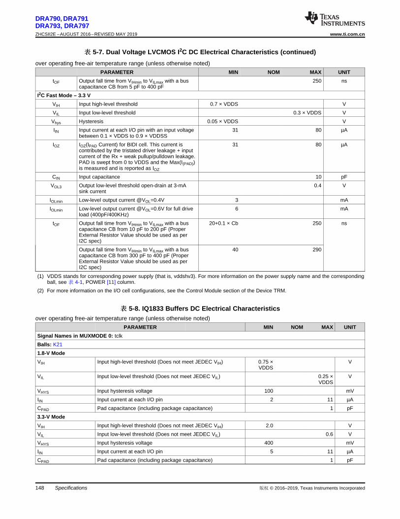
148
DRA790, DRA791DRA793, DRA797ZHCSII2E –AUGUST 2016–REVISED MAY 2019 www.ti.com.cn
Specifications 版权 © 2016–2019, Texas Instruments Incorporated
表表 5-7. Dual Voltage LVCMOS I2C DC Electrical Characteristics (continued)over operating free-air temperature range (unless otherwise noted)
PARAMETER MIN NOM MAX UNITtOF Output fall time from VIHmin to VILmax with a bus
capacitance CB from 5 pF to 400 pF250 ns
I2C Fast Mode – 3.3 VVIH Input high-level threshold 0.7 × VDDS VVIL Input low-level threshold 0.3 × VDDS VVhys Hysteresis 0.05 × VDDS VIIN Input current at each I/O pin with an input voltage
between 0.1 × VDDS to 0.9 × VDDSS31 80 µA
IOZ IOZ(IPAD Current) for BIDI cell. This current iscontributed by the tristated driver leakage + inputcurrent of the Rx + weak pullup/pulldown leakage.PAD is swept from 0 to VDDS and the Max(I(PAD))is measured and is reported as IOZ
31 80 µA
CIN Input capacitance 10 pFVOL3 Output low-level threshold open-drain at 3-mA
sink current0.4 V
IOLmin Low-level output current @VOL=0.4V 3 mAIOLmin Low-level output current @VOL=0.6V for full drive
load (400pF/400KHz)6 mA
tOF Output fall time from VIHmin to VILmax with a buscapacitance CB from 10 pF to 200 pF (ProperExternal Resistor Value should be used as perI2C spec)
20+0.1 × Cb 250 ns
Output fall time from VIHmin to VILmax with a buscapacitance CB from 300 pF to 400 pF (ProperExternal Resistor Value should be used as perI2C spec)
40 290
(1) VDDS stands for corresponding power supply (that is, vddshv3). For more information on the power supply name and the correspondingball, see 表 4-1, POWER [11] column.
(2) For more information on the I/O cell configurations, see the Control Module section of the Device TRM.
表表 5-8. IQ1833 Buffers DC Electrical Characteristicsover operating free-air temperature range (unless otherwise noted)
PARAMETER MIN NOM MAX UNITSignal Names in MUXMODE 0: tclkBalls: K211.8-V ModeVIH Input high-level threshold (Does not meet JEDEC VIH) 0.75 ×
VDDSV
VIL Input low-level threshold (Does not meet JEDEC VIL) 0.25 ×VDDS
V
VHYS Input hysteresis voltage 100 mVIIN Input current at each I/O pin 2 11 µACPAD Pad capacitance (including package capacitance) 1 pF3.3-V ModeVIH Input high-level threshold (Does not meet JEDEC VIH) 2.0 VVIL Input low-level threshold (Does not meet JEDEC VIL) 0.6 VVHYS Input hysteresis voltage 400 mVIIN Input current at each I/O pin 5 11 µACPAD Pad capacitance (including package capacitance) 1 pF

149
DRA790, DRA791DRA793, DRA797
www.ti.com.cn ZHCSII2E –AUGUST 2016–REVISED MAY 2019
Specifications版权 © 2016–2019, Texas Instruments Incorporated
(1) VDDS stands for corresponding power supply (that is, vddshv3). For more information on the power supply name and the correspondingball, see 表 4-1, POWER [11] column.
表表 5-9. IHHV1833 Buffers DC Electrical Characteristicsover operating free-air temperature range (unless otherwise noted)
PARAMETER MIN NOM MAX UNITSignal Names in MUXMODE 0: porz / wakeup3 / wakeup0Balls: AB10/ AC10/ F191.8-V ModeVIH Input high-level threshold 1.2 VVIL Input low-level threshold 0.4 VVHYS Input hysteresis voltage 40 mVIIN Input current at each I/O pin 0.02 1 µACPAD Pad capacitance (including package capacitance) 1 pF3.3-V ModeVIH Input high-level threshold 1.2 VVIL Input low-level threshold 0.4 VVHYS Input hysteresis voltage 40 mVIIN Input current at each I/O pin 5 8 µACPAD Pad capacitance (including package capacitance) 1 pF
表表 5-10. LVCMOS CSI2 DC Electrical Characteristicsover operating free-air temperature range (unless otherwise noted)
PARAMETER MIN NOM MAX UNITSignals MUXMODE 0 : csi2_0_dx[2:0]; csi2_0_dy[2:0]Bottom Balls: AC1 / AB2 / AD1 / AC2 / AE2 / AD2MIPI D-PHY Mode Low-Power Receiver (LP-RX)
VIH Input high-level voltage 880 1350 mVVIL Input low-level voltage 550 mV
VITH Input high-level threshold(1) 880 mVVITL Input low-level threshold(2) 550 mVVHYS Input hysteresis(3) 25 mV
MIPI D-PHY Mode Ultralow Power Receiver (ULP-RX)VIL Input low-level voltage 300 mVVITL Input low-level threshold(4) 300 mVVHYS Input hysteresis(3) 25 mV
MIPI D-PHY Mode High-Speed Receiver (HS-RX)VIDTH Differential input high-level threshold 70 mVVIDTL Differential input low-level threshold –70 mV
VIDMAX Maximum differential input voltage(7) 270 mVVIHHS Single-ended input high voltage(5) 460 mVVILHS Single-ended input low voltage(5) –40 mV
VCMRXDC Differential input common-mode voltage(5)(6) 70 330 mVZID Differential input impedance 80 100 125 Ω
(1) VITH is the voltage at which the receiver is required to detect a high state in the input signal.(2) VITL is the voltage at which the receiver is required to detect a low state in the input signal. VITL is larger than the maximum single-ended
line high voltage during HS transmission. Therefore, both low-power (LP) receivers will detect low during HS signaling.(3) To reduce noise sensitivity on the received signal, the LP receiver is required to incorporate a hysteresis, VHYST. VHYST is the difference
between the VITH threshold and the VITL threshold.(4) VITL is the voltage at which the receiver is required to detect a low state in the input signal. Specification is relaxed for detecting 0 during

150
DRA790, DRA791DRA793, DRA797ZHCSII2E –AUGUST 2016–REVISED MAY 2019 www.ti.com.cn
Specifications 版权 © 2016–2019, Texas Instruments Incorporated
ultralow power (ULP) state. The LP receiver is not required to detect HS single-ended voltage as 0 in this state.(5) Excluding possible additional RF interference of 200 mVPP beyond 450 MHz.(6) This value includes a ground difference of 50 mV between the transmitter and the receiver, the static common-mode level tolerance and
variations below 450 MHz.(7) This number corresponds to the VODMAX transmitter.(8) Common mode is defined as the average voltage level of X and Y: VCMRX = (VX + VY) / 2.(9) Common mode ripple may be due to tR or tF and transmission line impairments in the PCB.(10) For more information regarding the pin name (or ball name) and corresponding signal name, see 表 4-5 CSI 2 Signal Descriptions.
表表 5-11. BMLB18 Buffers DC Electrical Characteristicsover operating free-air temperature range (unless otherwise noted)
PARAMETER MIN NOM MAX UNITSignal Names in MUXMODE 0: mlbp_dat_n / mlbp_dat_p / mlbp_sig_n / mlbp_sig_p / mlbp_clk_n / mlbp_clk_pBalls: T1 / T2 / U4 / T3 / U1 / U21.8-V ModeVIH/VIL Input high-level threshold VCM ±
50mVV
VHYS Input hysteresis voltage NONE mVVOD Differential output voltage (measured with 50ohm resistor
between PAD and PADN)300 500 mV
VCM Common mode output voltage 1 1.5 VCPAD Pad capacitance (including package capacitance) 4 pF
表表 5-12. Dual Voltage SDIO1833 DC Electrical Characteristicsover operating free-air temperature range (unless otherwise noted)
PARAMETER MIN NOM MAX UNITSignal Names in Mode 0: mmc1_clk, mmc1_cmd, mmc1_data[3:0]Bottom Balls: U3 / V4 / V3 / V2 / W1 / V11.8-V ModeVIH Input high-level threshold 1.27 VVIL Input low-level threshold 0.58 VVHYS Input hysteresis voltage 50 (2) mVIIN Input current at each I/O pin 30 µAIOZ IOZ(IPAD Current) for BIDI cell. This current is contributed by the
tristated driver leakage + input current of the Rx + weakpullup/pulldown leakage. PAD is swept from 0 to VDDS and theMax(I(PAD)) is measured and is reported as IOZ
30 µA
IIN withpulldownenabled
Input current at each I/O pin with weak pulldown enabledmeasured when PAD = VDDS
50 120 210 µA
IIN withpullupenabled
Input current at each I/O pin with weak pullup enabled measuredwhen PAD = 0
60 120 200 µA
CPAD Pad capacitance (including package capacitance) 5 pFVOH Output high-level threshold (IOH = 2 mA) 1.4 VVOL Output low-level threshold (IOL = 2 mA) 0.45 V3.3-V ModeVIH Input high-level threshold 0.625 ×
VDDSV
VIL Input low-level threshold 0.25 × VDDS VVHYS Input hysteresis voltage 40 (2) mVIIN Input current at each I/O pin 110 µA

151
DRA790, DRA791DRA793, DRA797
www.ti.com.cn ZHCSII2E –AUGUST 2016–REVISED MAY 2019
Specifications版权 © 2016–2019, Texas Instruments Incorporated
表表 5-12. Dual Voltage SDIO1833 DC Electrical Characteristics (continued)over operating free-air temperature range (unless otherwise noted)
PARAMETER MIN NOM MAX UNITIOZ IOZ(IPAD Current) for BIDI cell. This current is contributed by the
tristated driver leakage + input current of the Rx + weakpullup/pulldown leakage. PAD is swept from 0 to VDDS and theMax(I(PAD)) is measured and is reported as IOZ
110 µA
IIN withpulldownenabled
Input current at each I/O pin with weak pulldown enabledmeasured when PAD = VDDS
40 100 290 µA
IIN withpullupenabled
Input current at each I/O pin with weak pullup enabled measuredwhen PAD = 0
10 100 290 µA
CPAD Pad capacitance (including package capacitance) 5 pFVOH Output high-level threshold (IOH = 2 mA) 0.75 × VDDS VVOL Output low-level threshold (IOL = 2 mA) 0.125 ×
VDDSV
(1) VDDS stands for corresponding power supply (that is, vddshv8). For more information on the power supply name and the correspondingball, see 表 4-1, POWER [11] column.
(2) Hysteresis is enabled/disabled with CTRL_CORE_CONTROL_HYST_1.SDCARD_HYST register.
表表 5-13. Dual Voltage LVCMOS DC Electrical Characteristicsover operating free-air temperature range (unless otherwise noted)PARAMETER MIN NOM MAX UNIT1.8-V ModeVIH Input high-level threshold 0.65 × VDDS VVIL Input low-level threshold 0.35 × VDDS VVHYS Input hysteresis voltage 100 mVVOH Output high-level threshold (IOH = 2 mA) VDDS-0.45 VVOL Output low-level threshold (IOL = 2 mA) 0.45 VIDRIVE Pin Drive strength at PAD Voltage = 0.45V or
VDDS-0.45V6 mA
IIN Input current at each I/O pin 16 µAIOZ IOZ(IPAD Current) for BIDI cell. This current is
contributed by the tristated driver leakage + inputcurrent of the Rx + weak pullup/pulldown leakage.PAD is swept from 0 to VDDS and the Max(I(PAD))is measured and is reported as IOZ
16 µA
IIN with pulldownenabled
Input current at each I/O pin with weak pulldownenabled measured when PAD = VDDS
50 120 210 µA
IIN with pullupenabled
Input current at each I/O pin with weak pullupenabled measured when PAD = 0
60 120 200 µA
CPAD Pad capacitance (including package capacitance) 4 pFZO Output impedance (drive strength) 40 Ω
3.3-V ModeVIH Input high-level threshold 2 VVIL Input low-level threshold 0.8 VVHYS Input hysteresis voltage 200 mVVOH Output high-level threshold (IOH = 100 µA) VDDS-0.2 VVOL Output low-level threshold (IOL = 100 µA) 0.2 VIDRIVE Pin Drive strength at PAD Voltage = 0.45V or
VDDS-0.45V6 mA
IIN Input current at each I/O pin 65 µA

152
DRA790, DRA791DRA793, DRA797ZHCSII2E –AUGUST 2016–REVISED MAY 2019 www.ti.com.cn
Specifications 版权 © 2016–2019, Texas Instruments Incorporated
表表 5-13. Dual Voltage LVCMOS DC Electrical Characteristics (continued)over operating free-air temperature range (unless otherwise noted)PARAMETER MIN NOM MAX UNITIOZ IOZ(IPAD Current) for BIDI cell. This current is
contributed by the tristated driver leakage + inputcurrent of the Rx + weak pullup/pulldown leakage.PAD is swept from 0 to VDDS and the Max(I(PAD))is measured and is reported as IOZ
65 µA
IIN with pulldownenabled
Input current at each I/O pin with weak pulldownenabled measured when PAD = VDDS
40 100 200 µA
IIN with pullupenabled
Input current at each I/O pin with weak pullupenabled measured when PAD = 0
10 100 290 µA
CPAD Pad capacitance (including package capacitance) 4 pFZO Output impedance (drive strength) 40 Ω
(1) VDDS stands for corresponding power supply. For more information on the power supply name and the corresponding ball, see 表 4-1,POWER [11] column.
5.7.1 USBPHY DC Electrical Characteristics
注注USB1 instance is compliant with the USB3.0 SuperSpeed Transmitter and ReceiverNormative Electrical Parameters as defined in the USB3.0 Specification Rev 1.0 dated Jun 6,2011.
注注USB1 and USB2 Electrical Characteristics are compliant with USB2.0 Specification Rev 2.0dated April 27, 2000 including ECNs and Errata as applicable.
5.7.2 HDMIPHY DC Electrical Characteristics
注注The HDMIPHY DC Electrical Characteristics are compliant with the HDMI 1.4a specificationand are not reproduced here.
5.7.3 PCIEPHY DC Electrical Characteristics
注注The PCIe interfaces are compliant with the electrical parameters specified in PCI Express®Base Specification Revision 3.0.
5.8 VPP Specifications for One-Time Programmable (OTP) eFusesThis section specifies the operating conditions required for programming the OTP eFuses and isapplicable only for High-Security Devices.

153
DRA790, DRA791DRA793, DRA797
www.ti.com.cn ZHCSII2E –AUGUST 2016–REVISED MAY 2019
Specifications版权 © 2016–2019, Texas Instruments Incorporated
表表 5-14. Recommended Operating Conditions for OTP eFuse Programmingover operating free-air temperature range (unless otherwise noted)
PARAMETER DESCRIPTION MIN NOM MAX UNITvdd Supply voltage range for the core domain
during OTP operation1.11 1.15 1.2 V
vpp Supply voltage range for the eFuse ROMdomain during normal operation
NC V
Supply voltage range for the eFuse ROMdomain during OTP programming(1)(2)
1.8 V
I(vpp) 100 mATj Temperature (junction) 0 25 85 ºC
(1) Supply voltage range includes DC errors and peak-to-peak noise. TI power management solutions TLV70018-Q1 from the TLV700xxfamily meet the supply voltage range needed for vpp.
(2) During normal operation, no voltage should be applied to vpp. This can be typically achieved by disabling the regulator attached to thevpp terminal. For more details, see TLV700xx-Q1 300-mA, Low-IQ, Low-Dropout Regulator.
5.8.1 Hardware RequirementsThe following hardware requirements must be met when programming keys in the OTP eFuses:• The vpp power supply must be disabled when not programming OTP registers.• The vpp power supply must be ramped up after the proper device power-up sequence (for more
details, see Section 5.10.3).
5.8.2 Programming SequenceProgramming sequence for OTP eFuses:1. Power on the board per the power-up sequencing. No voltage should be applied on the vpp terminal
during power up and normal operation.2. Load the OTP write software required to program the eFuse (contact your local TI representative for
the OTP software package).3. Apply the voltage on the vpp terminal according to the specification in 表 5-14.4. Run the software that programs the OTP registers.5. After validating the content of the OTP registers, remove the voltage from the vpp terminal.
5.8.3 Impact to Your Hardware WarrantyYou accept that e-Fusing the TI Devices with security keys permanently alters them. You acknowledgethat the e-Fuse can fail, for example, due to incorrect or aborted program sequence or if you omit asequence step. Further the TI Device may fail to secure boot if the error code correction check fails for theProduction Keys or if the image is not signed and optionally encrypted with the current active ProductionKeys. These types of situations will render the TI Device inoperable and TI will be unable to confirmwhether the TI Devices conformed to their specifications prior to the attempted e-Fuse.CONSEQUENTLY, TI WILL HAVE NO LIABILITY (WARRANTY OR OTHERWISE) FOR ANY TIDEVICES THAT HAVE BEEN e-FUSED WITH SECURITY KEYS.
5.9 Thermal Resistance Characteristics for CBD PackageFor reliability and operability concerns, the maximum junction temperature of the Device has to be at orbelow the TJ value identified in Section 5.4, Recommended Operating Conditions.
A BCI compact thermal model for this Device is available and recommended for use when modelingthermal performance in a system.
Therefore, it is recommended to perform thermal simulations at the system level with the worst casedevice power consumption.

154
DRA790, DRA791DRA793, DRA797ZHCSII2E –AUGUST 2016–REVISED MAY 2019 www.ti.com.cn
Specifications 版权 © 2016–2019, Texas Instruments Incorporated
5.9.1 Package Thermal Characteristics表 5-15 provides the thermal resistance characteristics for the package used on this device.
注注Power dissipation of 3.0 W and an ambient temperature of 85ºC is assumed for CBDpackage.
表表 5-15. Thermal Resistance Characteristics
NO. PARAMETER DESCRIPTION °C/W(1) AIR FLOW (m/s)(2)
T1 RΘJC Junction-to-case 0.23 N/AT2 RΘJB Junction-to-board 3.65 N/AT3
RΘJA
Junction-to-free air 12.8 0T4
Junction-to-moving air
10.4 0.5T5 9.6 1T6 8.8 2T7 8.3 3T8
ΨJT Junction-to-package top
0.1 0T9 0.1 0.5T10 0.1 1T11 0.1 2T12 0.1 3T13
ΨJB Junction-to-board
3.7 0T14 3.7 0.5T15 3.6 1T16 3.6 2T17 3.5 3
(1) These measurements were conducted in a JEDEC defined 2S2P system (with the exception of the Theta JC [RΘJC] measurement,which was conducted in a JEDEC defined 1S0P system) and will change based on environment as well as application. For moreinformation, see these EIA/JEDEC standards:– JESD51-2, Integrated Circuits Thermal Test Method Environment Conditions - Natural Convection (Still Air)– JESD51-3, Low Effective Thermal Conductivity Test Board for Leaded Surface Mount Packages– JESD51-7, High Effective Thermal Conductivity Test Board for Leaded Surface Mount Packages– JESD51-9, Test Boards for Area Array Surface Mount Packages
(2) m/s = meters per second

155
DRA790, DRA791DRA793, DRA797
www.ti.com.cn ZHCSII2E –AUGUST 2016–REVISED MAY 2019
Submit Documentation FeedbackProduct Folder Links: DRA790 DRA791 DRA793 DRA797
SpecificationsCopyright © 2016–2019, Texas Instruments Incorporated
5.10 Timing Requirements and Switching Characteristics
5.10.1 Timing Parameters and InformationThe timing parameter symbols used in the timing requirement and switching characteristic tables arecreated in accordance with JEDEC Standard 100. To shorten the symbols, some of pin names and otherrelated terminologies have been abbreviated as follows:
Table 5-16. Timing Parameters
SUBSCRIPTSSYMBOL PARAMETER
c Cycle time (period)d Delay time
dis Disable timeen Enable timeh Hold timesu Setup time
START Start bitt Transition timev Valid timew Pulse duration (width)X Unknown, changing, or don't care levelF Fall timeH HighL LowR Rise timeV ValidIV InvalidAE Active EdgeFE First EdgeLE Last EdgeZ High impedance

V = V MAX (or V MAX)ref IL OL
V = V MIN (or V MIN)ref IH OH
pm_transvolt_prs403
Vref
pm_io_volt_prs403
Transmission Line
4.0 pF 1.85 pF
Z0 = 50(see Note)
Ω
Tester Pin Electronics Data Sheet Timing Reference Point
OutputUnderTest
NOTE: The data sheet provides timing at the device pin. For output timing analysis, the tester pin electronics and its transmission line effects must betaken into account.A transmission line with a delay of 2 ns can be used to produce the desired transmission line effect. The transmission line isintended as a load only. It is not necessary to add or subtract the transmission line delay (2 ns) from the data sheet timings.
Input requirements in this data sheet are tested with an input slew rate of < 4 Volts per nanosecond (4 V/ns) at the device pin.
42 Ω 3.5 nH
Device Pin(see Note)
pm_tstcirc_prs403
156
DRA790, DRA791DRA793, DRA797ZHCSII2E –AUGUST 2016–REVISED MAY 2019 www.ti.com.cn
Submit Documentation FeedbackProduct Folder Links: DRA790 DRA791 DRA793 DRA797
Specifications Copyright © 2016–2019, Texas Instruments Incorporated
5.10.1.1 Parameter Information
Figure 5-2. Test Load Circuit for AC Timing Measurements
The load capacitance value stated is only for characterization and measurement of AC timing signals.
This load capacitance value does not indicate the maximum load the device is capable of driving.
5.10.1.1.1 1.8 V and 3.3 V Signal Transition Levels
All input and output timing parameters are referenced to Vref for both "0" and "1" logic levels. Vref = (VDDI/O)/2.
Figure 5-3. Input and Output Voltage Reference Levels for AC Timing Measurements
All rise and fall transition timing parameters are referenced to VIL MAX and VIH MIN for input clocks, VOLMAX and VOH MIN for output clocks.
Figure 5-4. Rise and Fall Transition Time Voltage Reference Levels
5.10.1.1.2 1.8 V and 3.3 V Signal Transition Rates
The default SLEWCONTROL settings in each pad configuration register must be used to ensure timings,unless specific instructions otherwise are given in the individual timing subsections of the datasheet.
All timings are tested with an input edge rate of 4 volts per nanosecond (4 V/ns).

157
DRA790, DRA791DRA793, DRA797
www.ti.com.cn ZHCSII2E –AUGUST 2016–REVISED MAY 2019
Submit Documentation FeedbackProduct Folder Links: DRA790 DRA791 DRA793 DRA797
SpecificationsCopyright © 2016–2019, Texas Instruments Incorporated
5.10.1.1.3 Timing Parameters and Board Routing Analysis
The timing parameter values specified in this data manual do not include delays by board routes. As agood board design practice, such delays must always be taken into account. Timing values may beadjusted by increasing/decreasing such delays. TI recommends using the available I/O buffer informationspecification (IBIS) models to analyze the timing characteristics correctly. To properly use IBIS models toattain accurate timing analysis for a given system, see the Using IBIS Models for timing Analysisapplication report. If needed, external logic hardware such as buffers may be used to compensate anytiming differences.
5.10.2 Interface Clock Specifications
5.10.2.1 Interface Clock Terminology
The interface clock is used at the system level to sequence the data and/or to control transfers accordinglywith the interface protocol.
5.10.2.2 Interface Clock Frequency
The two interface clock characteristics are:• The maximum clock frequency• The maximum operating frequency
The interface clock frequency documented in this document is the maximum clock frequency, whichcorresponds to the maximum frequency programmable on this output clock. This frequency defines themaximum limit supported by the Device IC and does not take into account any system consideration(PCB, peripherals).
The system designer will have to consider these system considerations and the Device IC timingcharacteristics as well to define properly the maximum operating frequency that corresponds to themaximum frequency supported to transfer the data on this interface.
5.10.3 Power Supply SequencesThis section describes the power-up and power-down sequence required to ensure proper deviceoperation. The power supply names described in this section comprise a superset of a family ofcompatible devices. Some members of this family will not include a subset of these power supplies andtheir associated device modules. Refer to the 节 4.2, Pin Attributes of the 节 4, Terminal Configuration andFunctions to determine which power supplies are applicable.

Note 13 Note 14
Note 15
Note 9
Note 11
vdds18v, vdds_mlbp, vdds18v_ddr1
vdda_per, vdda_ddr, vdda_debug,vdda_core_gmac, vdda_gpu,
vdda_video, vdda_osc, vdda_mpu_abe(VDDA_PLL group)
vdds_ddr1, ddr1_vref0
vdd
vdd_dsp
vdda_usb1, vdda_usb2, vdda_hdmi,vdda_csi, vdda_pcie, vdda_usb3
(VDDA_PHY group)
vddshv1, vddshv3, vddshv4,
vddshv7, vddshv9,
vddshv10, vddshv11
vdda33v_usb1, vdda33v_usb2
vddshv8
xi_osc0
resetn/porz
sysboot[15:0]
rstoutn
SPRS960_ELCH_04
Valid Config
Note 12
T0 T1 T2 T3 T4 T5 T6 T7 T8
Note 4
Note 5
Note 6
Note 7
Note 8
Note 10
158
DRA790, DRA791DRA793, DRA797ZHCSII2E –AUGUST 2016–REVISED MAY 2019 www.ti.com.cn
Submit Documentation FeedbackProduct Folder Links: DRA790 DRA791 DRA793 DRA797
Specifications Copyright © 2016–2019, Texas Instruments Incorporated
Figure 5-5 through Figure 5-9 and associated notes described the device Recommended PowerSequencing.
Figure 5-5. Recommended Power-Up Sequencing(1) T0 = 0ms, T1 = 0.55ms, T2 = 1.1ms, T3 = 1.65ms, T4 = 2.2ms, T5 = 2.75ms, T6 = 3.3ms, T7 = 6.9ms, T8 ≈ 9ms. All “Tn” markers show
total elapsed time from T0.(2) Terminology:
– VOPR MIN = Minimum Operational Voltage level that ensures device functionality and specified performance per Section 5.4,Recommended Operating Conditions.
– Ramp Up = transition time from VOFF to V OPR MIN
(3) General timing diagram items:– Grey shaded areas show valid transition times for supplies between V OPR MIN and VOFF.– Dashed horizontal lines are not valid ramp times but show alternate transition times based upon common sources and clarified in
associated note.– Dashed vertical lines show approximate elapse times based upon TI recommended PMIC power sequencer circuit performance.
(4) vdda_* rails should not be combined with vdds18v_* for best performance to avoid transient switching noise impacts on analog domains.vdda_* should not ramp-up before vdds18v_* but could ramp concurrently if design ensures final operational voltage will not be reached

159
DRA790, DRA791DRA793, DRA797
www.ti.com.cn ZHCSII2E –AUGUST 2016–REVISED MAY 2019
Submit Documentation FeedbackProduct Folder Links: DRA790 DRA791 DRA793 DRA797
SpecificationsCopyright © 2016–2019, Texas Instruments Incorporated
until after vdds18v. The preferred sequence has vdda_* following vdds18v_* to ensure circuit components and PCB design do not causean inadvertent violation.
(5) vdds_ddr1 should not ramp-up before vdds18v_*. The preferred sequence has vdds_ddr1 following vdds18v_* to ensure circuitcomponents and PCB design do not cause an inadvertent violation. vdds_ddr1 can ramp-up before, concurrently or after vdda_*, thereare no dependencies between vdds_ddr1 and vdda_* domains.– For DDR2 mode of operation (1.8V), vdds_ddr1 supplies can be combined with all vdds18v_* supplies and ramped up together for
simplified PDN and power sequencing.– If vdds_ddr1 is combined with vdds18v_ddr1 but kept separate from vdds18v on board, then this combined 1.8V DDR supply can
come up together or after the vdds18v supply. The 1.8V DDR supply should never ramp up before the vdds18v.(6) vdd should not ramp-up before vdds18v_* or vdds_ddr1 domains have reached VOPR MIN.(7) vdd_dsp could ramp concurrently with vdd if design ensures:
– Final vdd_dsp operational voltage will not be reached until after vdd.– vdd_dsp maintains a voltage level at least 150mV less than vdd during entire ramp time. The preferred sequence has vdd_dsp
following vdd to ensure circuit components and PCB design do not cause an inadvertent violation.(8) VDDA_PHY group:
– should ramp up concurrently or after vdda33v_usb[1-2] to avoid unintended current path between vdda_pcie to vdda33v_usb1during power sequencing.
– could ramp up concurrently with VDDA_PLL group only if the vdda33v_usb1 power resource has an “off impedance” greater than100Ω.
(9) vddshv[1, 3-4, 7, 9-11] domains:– If 1.8V I/O signaling is needed, then 1.8V must be sourced from common vdds18v supply and ramp up concurrently with vdds18v.– If any 3.3V I/O signaling is needed, then the desired 3.3V vddshv[1, 3-4, 7, 9-11] rails must ramp up after vdd_dsp.
(10) vdda33v_usb[1-2] domain should:– ramp up before or concurrently with VDDA_PHY group if USB signaling is needed and to avoid unintended current path between
vdda_pcie to vdda33v_usb[1-2] during power sequencing.– connect to 3.3V vddshv[1, 3-4, 7, 9-11] common supply if USB signaling is not needed since USB analog power ball also supplies
digital IO buffers that must be powered during operation.(11) vddshv8 shows two ramp up options for 1.8V I/O or 3.3V I/O or SD Card operation:
– If 1.8V I/O signaling is needed, then vddshv8 must ramp up after vdd and before or concurrently with 3.3V vddshv* rails.– If 3.3V I/O signaling is needed, then vddshv8 must be combined with other 3.3V vddshv* rails.– If SD Card operation is needed, then vddshv8 must be sourced from a dual voltage (3.3/1.8V) power source per SDIO specifications
and ramp up concurrently with 3.3V vddshv* rails.(12) porz must remain asserted low until both of the following conditions are met:
– Minimum of 12 *P, where P = 1 / (SYS_CLK1/610), units in ns.– All device supply rails reach stable operational levels.
(13) Setup time: sysboot[15:0] pins must be valid 2P(12) before porz is de-asserted high.(14) Hold time: sysboot[15:0] pins must be valid 15P(12) after porz is de-asserted high.(15) rstoutn will be set high after global reset, due to porz, is de-asserted following an internal 2ms delay. rstoutn is only valid after vddshv3
reaches an operational level. If used as a peripheral component reset, it should be AND gated with porz to avoid possible reset glitchesduring power up.

vdda33v_usb1, vdda33v_usb2
vdda_usb1, vdda_usb2, vdda_hdmi,vdda_csi, vdda_pcie, vdda_usb3
(VDDA_PHY group)
vdd_dsp
vdd
vdds18v, vdds_mlbp, vdds18v_ddr1
vdda_per, vdda_ddr, vdda_debug,vdda_core_gmac, vdda_gpu,
vdda_video, vdda_osc, vdda_mpu_abe(VDDA_PLL group)
vdds_ddr1, ddr1_vref0
xi_osc0
SPRS960_ELCH_05
Note 6
vddshv8
vddshv1, vddshv3, vddshv4,
vddshv7, vddshv9,vddshv10,
vddshv11
T0 T1 T2 T3 T4
V1
porz
Note 5
Note 8
Note 9
Note 12
Note 13
Note 14
Note 10
Note 11
Note 7
Note 4
Note 13
160
DRA790, DRA791DRA793, DRA797ZHCSII2E –AUGUST 2016–REVISED MAY 2019 www.ti.com.cn
Submit Documentation FeedbackProduct Folder Links: DRA790 DRA791 DRA793 DRA797
Specifications Copyright © 2016–2019, Texas Instruments Incorporated
Figure 5-6. Recommended Power-Down Sequencing
(1) T1 ≥ 100 µs; T2 = 500 µs; T3 = 1.0 ms; T4 = 1.5ms; V1 = 2.7 V. All "Tn" markers are intended to show total elapsed time, not intervaltimes.
(2) Terminology:– VOPR MIN = Minimum Operational Voltage level that ensures device functionality and specified performance in Section 5.4,
Recommended Operating Conditions.– VOFF = OFF Voltage level is defined to be less than 0.6 V where any current draw has no impact to POH.– Ramp Down = transition time from VOPR MIN to VOFF and is slew rate independent.
(3) General timing diagram items:– Grey shaded areas show valid transition times for supplies between VOPR MIN and VOFF.– Blue dashed lines are not valid windows but show alternate ramp possibilities based on the associated note.– Dashed vertical lines show approximate elapse times based upon TI recommended PMIC power-down sequencer circuit
performance.(4) PORz must be asserted low for 100 µs min to ensure SoC is set to a safe functional state before any voltage begins to ramp down.(5) vddshv[1, 3-4, 7, 9-11] domains supplied by 3.3 V:
– must remain greater than 2.7 V to enable Dual Voltage GPIO selector circuit operation for 100 µs min after PORz is asserted low.– must be in first group of supplies ramping down after PORz has been asserted low for 100 µs min.– must not exceed vdds18v by more than 2 V during ramp down, see Figure 5-7, "vdds18v versus vddshv[1, 3-4, 7, 9-11] Discharge
Relationship".(6) vddshv[1, 3-4, 7, 9-11] domains supplied by 1.8 V must ramp down concurrently with vdds18v and be sourced from common vdds18v
supply.(7) vddshv8 supporting SD Card:

vddshv1, vddshv3,
vddshv4, vddshv7,
vddshv9, vddshv10,
vddshv11, vddshv8(2)
vdds18v
Vdelta(Note1)
SPRS85v_ELCH_06
161
DRA790, DRA791DRA793, DRA797
www.ti.com.cn ZHCSII2E –AUGUST 2016–REVISED MAY 2019
Submit Documentation FeedbackProduct Folder Links: DRA790 DRA791 DRA793 DRA797
SpecificationsCopyright © 2016–2019, Texas Instruments Incorporated
– must be sourced from independent power resource that can provide dual voltage (3.3 / 1.8 V) operation as required to be compliantto SDIO specification
– must be in first group of supplies to ramp down after PORz has been asserted low for 100 µs min.– if SDIO operation is not needed, must be grouped and ramped down with other vddshv[1, 3-4, 7, 9-11] domains as noted above.
(8) vdda33v_usb[1-2] domains:– can start ramping down 100 µs after low assertion of PORz– can ramp down concurrently or before VDDA_PHY group
(9) VDDA_PHY domain group must ramp down concurrently or after vdda33v_usb[1-2].(10) vdd_dsp domain can ramp down before or concurrently with vdd.(11) vdd must ramp down after or concurrently with vdd_dsp.(12) vdds_ddr1 domain:
– should ramp down after vdd begins ramping down.– If DDR2 memory is used (requiring 1.8V supply),
– then vdds_ddr1 can be combined with vdds18v and vdds18v_ddr1 domains and sourced from a common supply. Accordingly,all domains can ramp down concurrently with vdds18v.
– if vdds_ddr1 and vdds18v_ddr1 are combined but kept separate from vdds18v, then the combined 1.8V DDR supply can rampdown before or concurrently with vdds18v.
(13) vdda_* domains:– can ramp down before, concurrently or after vdds_ddr1, there is no dependency between these supplies.– can ramp down before or concurrently with vdds18v.– must satisfy the vdds18v versus vdda_* discharge relationship (see Figure 5-9) if any of the vdda_* disable point is later or
discharge rate is slower than vdds18v.(14) vdds18v domain:
– should maintain VOPR MIN (VNOM -5% = 1.71 V) until all other supplies start to ramp down.– must satisfy the vdds18v versus vddshv[1, 3-4, 7, 9-11] discharge relationship (see Figure 5-7) if any of the vddshv[1, 3-4, 7, 9-11]
is operating at 3.3 V.– must satisfy the vdds18v versus vdds_ddr1 discharge relationship ( see Figure 5-8) if vdds_ddr1 discharge rate is slower than
vdds18v.
Figure 5-7 describes vddshv[1, 3-4, 7, 9-11] Supplies Falling Before vdds18v Supplies Delta.
Figure 5-7. vdds18v versus vddshv[1, 3-4, 7, 9-11] Discharge Relationship(1) Vdelta MAX = 2V.(2) If vddshv8 is powered by the same supply source as the other vddshv[1, 3-4, 7, 9-11] rails.

SPRS85v_ELCH_08
vdds18v
V2
V1
Note 1
Note 2
vdda_*
vdds18v
vdds_ddr1
SPRS85v_ELCH_07
V1
V2
T1
162
DRA790, DRA791DRA793, DRA797ZHCSII2E –AUGUST 2016–REVISED MAY 2019 www.ti.com.cn
Submit Documentation FeedbackProduct Folder Links: DRA790 DRA791 DRA793 DRA797
Specifications Copyright © 2016–2019, Texas Instruments Incorporated
If vdds18v and vdds_ddr1 are disabled at the same time due to a loss of input power event or ifvdds_ddr1 discharges more slowly than vdds18v, analysis has shown no reliability impacts when theelapsed time period beginning with vdds18v dropping below 1.0 V and ending with vdds_ddr1 droppingbelow 0.6 V is less than 10 ms (Figure 5-8).
Figure 5-8. vdds18v and vdds_ddr1 Discharge Relationship(1)
(1) V1 > 1.0 V; V2 < 0.6 V; T1 < 10ms.
Figure 5-9. vdds18v and vdda_* Discharge Relationship(3)
(1) vdda_* can be ≥ vdds18v, until vdds18v drops below 1.62 V.(2) vdds18v must be ≥ vdda_*, until vdds18v reaches 0.6 V.(3) V1 = 1.62 V; V2 < 0.6 V.
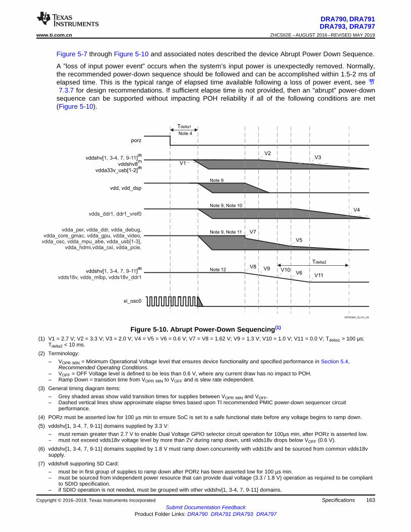
SPRS960_ELCH_09
vdd, vdd_dsp
vdda_per, vdda_ddr, vdda_debug,vdda_core_gmac, vdda_gpu, vdda_video,
vdda_osc, vdda_mpu_abe, vdda_usb[1-3],vdda_hdmi,vdda_csi, vdda_pcie,
xi_osc0
porz
V1V3
V2
V7
V5
V10
V4
V11V6V9V8
Tdelta2
vdds_ddr1, ddr1_vref0
Tdelta1
vddshv[ ]
vddshv8
1, 3-4, 7, 9-11(5)
(7)
(8)vdda33v_usb[1-2]
vddshv[ ]1, 3-4, 7, 9-11(6)
vdds18v, vdds_mlbp, vdds18v_ddr1
Note 9, Note 11
Note 4
Note 9
Note 9, Note 10
Note 12
163
DRA790, DRA791DRA793, DRA797
www.ti.com.cn ZHCSII2E –AUGUST 2016–REVISED MAY 2019
Submit Documentation FeedbackProduct Folder Links: DRA790 DRA791 DRA793 DRA797
SpecificationsCopyright © 2016–2019, Texas Instruments Incorporated
Figure 5-7 through Figure 5-10 and associated notes described the device Abrupt Power Down Sequence.
A ”loss of input power event” occurs when the system’s input power is unexpectedly removed. Normally,the recommended power-down sequence should be followed and can be accomplished within 1.5-2 ms ofelapsed time. This is the typical range of elapsed time available following a loss of power event, see 节7.3.7 for design recommendations. If sufficient elapse time is not provided, then an “abrupt” power-down
sequence can be supported without impacting POH reliability if all of the following conditions are met(Figure 5-10).
Figure 5-10. Abrupt Power-Down Sequencing(1)
(1) V1 = 2.7 V; V2 = 3.3 V; V3 = 2.0 V; V4 = V5 = V6 = 0.6 V; V7 = V8 = 1.62 V; V9 = 1.3 V; V10 = 1.0 V; V11 = 0.0 V; Tdelta1 > 100 µs;Tdelta2 < 10 ms.
(2) Terminology:– VOPR MIN = Minimum Operational Voltage level that ensures device functionality and specified performance in Section 5.4,
Recommended Operating Conditions.– VOFF = OFF Voltage level is defined to be less than 0.6 V, where any current draw has no impact to POH.– Ramp Down = transition time from VOPR MIN to VOFF and is slew rate independent.
(3) General timing diagram items:– Grey shaded areas show valid transition times for supplies between VOPR MIN and VOFF.– Dashed vertical lines show approximate elapse times based upon TI recommended PMIC power-down sequencer circuit
performance.(4) PORz must be asserted low for 100 µs min to ensure SoC is set to a safe functional state before any voltage begins to ramp down.(5) vddshv[1, 3-4, 7, 9-11] domains supplied by 3.3 V:
– must remain greater than 2.7 V to enable Dual Voltage GPIO selector circuit operation for 100µs min, after PORz is asserted low.– must not exceed vdds18v voltage level by more than 2V during ramp down, until vdds18v drops below VOFF (0.6 V).
(6) vddshv[1, 3-4, 7, 9-11] domains supplied by 1.8 V must ramp down concurrently with vdds18v and be sourced from common vdds18vsupply.
(7) vddshv8 supporting SD Card:– must be in first group of supplies to ramp down after PORz has been asserted low for 100 µs min.– must be sourced from independent power resource that can provide dual voltage (3.3 / 1.8 V) operation as required to be compliant
to SDIO specification.– if SDIO operation is not needed, must be grouped with other vddshv[1, 3-4, 7, 9-11] domains.

164
DRA790, DRA791DRA793, DRA797ZHCSII2E –AUGUST 2016–REVISED MAY 2019 www.ti.com.cn
Submit Documentation FeedbackProduct Folder Links: DRA790 DRA791 DRA793 DRA797
Specifications Copyright © 2016–2019, Texas Instruments Incorporated
(8) vdda33v_usb[1-2] domains must be in first group of supplies to ramp down after PORz has been asserted low for 100 µs min.(9) vdd_dsp, vdd, vdds_ddr1, vdda_* domains can all start to ramp down in any order after 100 µs low assertion of PORz.(10) vdds_ddr1 domain:
– can remain at VOPR MIN or a level greater than vdds18v during ramp down.– elapsed time from vdds18v dropping below 1.0 V to vdds_ddr1 dropping below 0.6 V must not exceed 10 ms.
(11) vdda_* domains:– can start to ramp down before or concurrently with vdds18v.– must not exceed vdds18v voltage level after vdds18v drops below 1.62 V until vdds18v drops below VOFF (0.6 V).
(12) vdds18v domain should maintain a minimum level of 1.62 V (VNOM – 10%) until vdd_dsp and vdd start to ramp down.
5.10.4 Clock Specifications
NOTEFor more information, see Power Reset and Clock Management / PRCM Environment /External Clock Signal and Power Reset / PRCM Functional Description / PRCM ClockManager Functional Description section of the Device TRM.
NOTEAudio Back End (ABE) module is not supported for this family of devices, but “ABE” name isstill present in some clock or DPLL names.
The device operation requires the following clocks:• The system clocks, SYS_CLK1 (Mandatory) and SYS_CLK2 (Optional) are the main clock sources of
the device. They supply the reference clock to the DPLLs as well as functional clock to severalmodules.
The Device also embeds an internal free-running 32-kHz oscillator that is always active as long as the thewake-up (WKUP) domain is supplied.
Figure 5-11 shows the external input clock sources and the output clocks to peripherals.

DEVICE
clkout1
To quartz (from oscillator output).
resetn
rstoutn
External Reference Clock [3:0].For Audio and other Peripherals
xref_clk1
sysboot[15:0]
From quartz (19.2, 20 or 27 MHz)or from CMOS square clock source (19.2, 20 or 27MHz).
Boot Mode Configuration
xi_osc1
Warm reset output.
Device reset input.
porz Power ON Reset.
xi_osc0
xo_osc0
xo_osc1
From quartz (range from MHz)or from CMOS square clock source(range from MHz).
19.2 to 3212 to 38.4
To quartz (from oscillator output).
clkout2
clkout3
xref_clk0
xref_clk2
xref_clk3
Output clkout[3:1] clocks come from:• Either the input system clock and alternate clock (xi_osc0 or xi_osc1)• Or a CORE clock (from CORE output)• Or a 192-MHz clock (from PER DPLL output).
165
DRA790, DRA791DRA793, DRA797
www.ti.com.cn ZHCSII2E –AUGUST 2016–REVISED MAY 2019
Submit Documentation FeedbackProduct Folder Links: DRA790 DRA791 DRA793 DRA797
SpecificationsCopyright © 2016–2019, Texas Instruments Incorporated
Figure 5-11. Clock Interface
5.10.4.1 Input Clocks / Oscillators• The source of the internal system clock (SYS_CLK1) could be either:
– A CMOS clock that enters on the xi_osc0 ball (with xo_osc0 left unconnected on the CMOS clockcase).
– A crystal oscillator clock managed by xi_osc0 and xo_osc0.• The source of the internal system clock (SYS_CLK2) could be either:
– A CMOS clock that enters on the xi_osc1 ball (with xo_osc1 left unconnected on the CMOS clockcase).
– A crystal oscillator clock managed by xi_osc1 and xo_osc1.
SYS_CLK1 is received directly from oscillator OSC0. For more information about SYS_CLK1 see DeviceTRM, Chapter: Power, Reset, and Clock Management.
5.10.4.1.1 OSC0 External Crystal
An external crystal is connected to the device pins. Figure 5-12 describes the crystal implementation.

CL=C Cf1 2f
(C +C )2f1 f
vssa_osc0
Device
xo_osc0xi_osc0
Cf1
CrystalRd
Cf2
(Optional)
SPRS906_CLK_03
166
DRA790, DRA791DRA793, DRA797ZHCSII2E –AUGUST 2016–REVISED MAY 2019 www.ti.com.cn
Submit Documentation FeedbackProduct Folder Links: DRA790 DRA791 DRA793 DRA797
Specifications Copyright © 2016–2019, Texas Instruments Incorporated
Figure 5-12. OSC0 Crystal Implementation
NOTEThe load capacitors, Cf1 and Cf2 in Figure 5-12, should be chosen such that the belowequation is satisfied. CL in the equation is the load specified by the crystal manufacturer. Alldiscrete components used to implement the oscillator circuit should be placed as close aspossible to the associated oscillator xi_osc0, xo_osc0, and vssa_osc0 pins.
Figure 5-13. Load Capacitance Equation
The crystal must be in the fundamental mode of operation and parallel resonant. Table 5-17 summarizesthe required electrical constraints and Table 5-21
Table 5-17. OSC0 Crystal Electrical Characteristics
NAME DESCRIPTION MIN TYP MAX UNITfp Parallel resonance crystal frequency 19.2, 20, 27 MHz
Cf1 Cf1 load capacitance for crystal parallel resonance with Cf1 = Cf2 12 24 pFCf2 Cf2 load capacitance for crystal parallel resonance with Cf1 = Cf2 12 24 pF
ESR(Cf1,Cf2)(1) Crystal ESR 100 Ω
CO Crystal shunt capacitance
ESR = 30 ΩESR = 40 Ω 19.2 MHz, 20 MHz, 27 MHz 7 pF
ESR = 50 Ω19.2 MHz, 20 MHz 7 pF27 MHz 5 pF
ESR = 60 Ω19.2 MHz, 20 MHz 7 pF27 MHz Not Supported -
ESR = 80 Ω19.2 MHz, 20 MHz 5 pF27 MHz Not Supported -
ESR = 100 Ω19.2 MHz, 20 MHz 3 pF27 MHz Not Supported -
LM Crystal motional inductance for fp = 20 MHz 10.16 mHCM Crystal motional capacitance 3.42 fF

vssa_osc0
Device
xo_osc0xi_osc0
NC
SPRS906_CLK_04
167
DRA790, DRA791DRA793, DRA797
www.ti.com.cn ZHCSII2E –AUGUST 2016–REVISED MAY 2019
Submit Documentation FeedbackProduct Folder Links: DRA790 DRA791 DRA793 DRA797
SpecificationsCopyright © 2016–2019, Texas Instruments Incorporated
Table 5-17. OSC0 Crystal Electrical Characteristics (continued)NAME DESCRIPTION MIN TYP MAX UNIT
tj(xiosc0) Frequency accuracy(1), xi_osc0
Ethernet and MLB not used ±200
ppm
Ethernet RGMII and RMIIusing derived clock ±50
Ethernet MII using derivedclock ±100
MLB using derived clock ±50
(1) Crystal characteristics should account for tolerance+stability+aging.
When selecting a crystal, the system design must consider the temperature and aging characteristics of abased on the worst case environment and expected life expectancy of the system.
Table 5-18 details the switching characteristics of the oscillator and the requirements of the input clock.
Table 5-18. Oscillator Switching Characteristics—Crystal Mode
NAME DESCRIPTION MIN TYP MAX UNITfp Oscillation frequency 19.2, 20, 27 MHz MHztsX Start-up time 4 ms
5.10.4.1.2 OSC0 Input Clock
A 1.8-V LVCMOS-Compatible Clock Input can be used instead of the internal oscillator to provide theSYS_CLK1 clock input to the system. The external connections to support this are shown in Figure 5-14.The xi_osc0 pin is connected to the 1.8-V LVCMOS-Compatible clock source. The xi_osc0 pin is leftunconnected. The vssa_osc0 pin is connected to board ground (VSS).
Figure 5-14. 1.8-V LVCMOS-Compatible Clock Input
Table 5-19 summarizes the OSC0 input clock electrical characteristics.
Table 5-19. OSC0 Input Clock Electrical Characteristics—Bypass Mode
NAME DESCRIPTION MIN TYP MAX UNITf Frequency 19.2, 20, 27 MHz
CIN Input capacitance 2.184 2.384 2.584 pFIIN Input current (3.3V mode) 4 6 10 µA

xi_osc1 vssa_osc1
Device
xo_osc1
Cf1
CrystalRd
Cf2
(Optional)
SPRS906_CLK_06
xi_osc0
CK0 CK1 CK1
SPRS906_CLK_05
168
DRA790, DRA791DRA793, DRA797ZHCSII2E –AUGUST 2016–REVISED MAY 2019 www.ti.com.cn
Submit Documentation FeedbackProduct Folder Links: DRA790 DRA791 DRA793 DRA797
Specifications Copyright © 2016–2019, Texas Instruments Incorporated
Table 5-20 details the OSC0 input clock timing requirements.
Table 5-20. OSC0 Input Clock Timing Requirements
NAME DESCRIPTION MIN TYP MAX UNIT
CK0 1 /tc(xiosc0)
Frequency, xi_osc0 19.2, 20, 27 MHz
CK1 tw(xiosc0) Pulse duration, xi_osc0 low or high 0.45 ×tc(xiosc0)
0.55 ×tc(xiosc0)
ns
tj(xiosc0) Period jitter(1), xi_osc0 0.01 ×tc(xiosc0)
ns
tR(xiosc0) Rise time, xi_osc0 5 nstF(xiosc0) Fall time, xi_osc0 5 ns
tj(xiosc0) Frequency accuracy(2), xi_osc0
Ethernet and MLB not used ±200
ppm
Ethernet RGMII and RMIIusing derived clock ±50
Ethernet MII using derivedclock ±100
MLB using derived clock ±50
(1) Period jitter is meant here as follows:
– The maximum value is the difference between the longest measured clock period and the expected clock period
– The minimum value is the difference between the shortest measured clock period and the expected clock period(2) Crystal characteristics should account for tolerance+stability+aging.
Figure 5-15. xi_osc0 Input Clock
5.10.4.1.3 Auxiliary Oscillator OSC1 Input Clock
SYS_CLK2 is received directly from oscillator OSC1. For more information about SYS_CLK2 see DeviceTRM, Chapter: Power, Reset, and Clock Management.
5.10.4.1.3.1 OSC1 External Crystal
An external crystal is connected to the device pins. Figure 5-16 describes the crystal implementation.
Figure 5-16. Crystal Implementation

CL=C Cf1 2f
(C +C )2f1 f
169
DRA790, DRA791DRA793, DRA797
www.ti.com.cn ZHCSII2E –AUGUST 2016–REVISED MAY 2019
Submit Documentation FeedbackProduct Folder Links: DRA790 DRA791 DRA793 DRA797
SpecificationsCopyright © 2016–2019, Texas Instruments Incorporated
NOTEThe load capacitors, Cf1 and Cf2 in Figure 5-16, should be chosen such that the belowequation is satisfied. CL in the equation is the load specified by the crystal manufacturer. Alldiscrete components used to implement the oscillator circuit should be placed as close aspossible to the associated oscillator xi_osc1, xo_osc1, and vssa_osc1 pins.
Figure 5-17. Load Capacitance Equation
The crystal must be in the fundamental mode of operation and parallel resonant. Table 5-21 summarizesthe required electrical constraints.
Table 5-21. OSC1 Crystal Electrical Characteristics
NAME DESCRIPTION MIN TYP MAX UNITfp Parallel resonance crystal frequency Range from 19.2 to 32 MHz
Cf1 Cf1 load capacitance for crystal parallel resonance with Cf1 = Cf2 12 24 pFCf2 Cf2 load capacitance for crystal parallel resonance with Cf1 = Cf2 12 24 pF
ESR(Cf1,Cf2) Crystal ESR 100 Ω
CO Crystal shunt capacitance
ESR = 30 Ω 19.2 MHz ≤ fp ≤ 32 MHz 7 pFESR = 40 Ω 19.2 MHz ≤ fp ≤ 32 MHz 5 pF
ESR = 50 Ω
19.2 MHz ≤ fp ≤ 25 MHz 7 pF25 MHz < fp ≤ 27 MHz 5 pF27 MHz < fp ≤ 32 MHz Not Supported -
ESR = 60 Ω
19.2 MHz ≤ fp ≤ 23 MHz 7 pF23 MHz < fp ≤ 25 MHz 5 pF25 MHz < fp ≤ 32 MHz Not Supported -
ESR = 80 Ω
19.2 MHz ≤ fp ≤ 23 MHz 5 pF23 MHz ≤ fp ≤ 25 MHz 3 pF25 MHz < fp ≤ 32 MHz Not Supported -
ESR = 100 Ω19.2 MHz ≤ fp ≤ 20 MHz 3 pF20 MHz < fp ≤ 32 MHz Not Supported -
LM Crystal motional inductance for fp = 20 MHz 10.16 mHCM Crystal motional capacitance 3.42 fF
tj(xiosc1) Frequency accuracy(1), xi_osc1
Ethernet and MLB not used ±200
ppm
Ethernet RGMII and RMIIusing derived clock ±50
Ethernet MII using derivedclock ±100
MLB using derived clock ±50
(1) Crystal characteristics should account for tolerance+stability+aging.
When selecting a crystal, the system design must consider the temperature and aging characteristics of abased on the worst case environment and expected life expectancy of the system.
Table 5-22 details the switching characteristics of the oscillator and the requirements of the input clock.
Table 5-22. Oscillator Switching Characteristics—Crystal Mode
NAME DESCRIPTION MIN TYP MAX UNITfp Oscillation frequency Range from 19.2 to 32 MHz

vssa_osc1
Device
xo_osc1xi_osc1
NC
SPRS906_CLK_07
170
DRA790, DRA791DRA793, DRA797ZHCSII2E –AUGUST 2016–REVISED MAY 2019 www.ti.com.cn
Submit Documentation FeedbackProduct Folder Links: DRA790 DRA791 DRA793 DRA797
Specifications Copyright © 2016–2019, Texas Instruments Incorporated
Table 5-22. Oscillator Switching Characteristics—Crystal Mode (continued)NAME DESCRIPTION MIN TYP MAX UNIT
tsX Start-up time 4 ms
5.10.4.1.3.2 OSC1 Input Clock
A 1.8-V LVCMOS-Compatible Clock Input can be used instead of the internal oscillator to provide theSYS_CLK2 clock input to the system. The external connections to support this are shown in, Figure 5-18.The xi_osc1 pin is connected to the 1.8-V LVCMOS-Compatible clock sources. The xo_osc1 pin is leftunconnected. The vssa_osc1 pin is connected to board ground (vss).
Figure 5-18. 1.8-V LVCMOS-Compatible Clock Input
Table 5-23 summarizes the OSC1 input clock electrical characteristics.
Table 5-23. OSC1 Input Clock Electrical Characteristics—Bypass Mode
NAME DESCRIPTION MIN TYP MAX UNITf Frequency Range from 12 to 38.4 MHz
CIN Input capacitance 2.819 3.019 3.219 pFIIN Input current (3.3V mode) 4 6 10 µAtsX Start-up time(1) See(2) ms
(1) To switch from bypass mode to crystal or from crystal mode to bypass mode, there is a waiting time about 100 μs; however, if the chipcomes from bypass mode to crystal mode the crystal will start-up after time mentioned in Table 5-22, tsX parameter.
(2) Before the processor boots up and the oscillator is set to bypass mode, there is a waiting time when the internal oscillator is inapplication mode and receives a wave. The switching time in this case is about 100 μs.
Table 5-24 details the OSC1 input clock timing requirements.
Table 5-24. OSC1 Input Clock Timing Requirements
NAME DESCRIPTION MIN TYP MAX UNIT
CK0 1 /tc(xiosc1)
Frequency, xi_osc1 Range from 12 to 38.4 MHz
CK1 tw(xiosc1) Pulse duration, xi_osc1 low or high 0.45 ×tc(xiosc1)
0.55 ×tc(xiosc1)
ns
tj(xiosc1) Period jitter(1), xi_osc10.01 ×
tc(xiosc1)(3)
ns
tR(xiosc1) Rise time, xi_osc1 5 nstF(xiosc1) Fall time, xi_osc1 5 ns

xi_osc1
CK0 CK1 CK1
SPRS906_CLK_08
171
DRA790, DRA791DRA793, DRA797
www.ti.com.cn ZHCSII2E –AUGUST 2016–REVISED MAY 2019
Submit Documentation FeedbackProduct Folder Links: DRA790 DRA791 DRA793 DRA797
SpecificationsCopyright © 2016–2019, Texas Instruments Incorporated
Table 5-24. OSC1 Input Clock Timing Requirements (continued)NAME DESCRIPTION MIN TYP MAX UNIT
tj(xiosc1) Frequency accuracy(2), xi_osc1
Ethernet and MLB not used ±200
ppm
Ethernet RGMII and RMIIusing derived clock ±50
Ethernet MII using derivedclock ±100
MLB using derived clock ±50
(1) Period jitter is meant here as follows:– The maximum value is the difference between the longest measured clock period and the expected clock period– The minimum value is the difference between the shortest measured clock period and the expected clock period
(2) Crystal characteristics should account for tolerance+stability+aging.(3) The Period jitter requirement for osc1 can be relaxed to 0.02 × tc(xiosc1) under the following constraints:
a.The osc1/SYS_CLK2 clock bypasses all device PLLsb.The osc1/SYS_CLK2 clock is only used to source the DSS pixel clock outputs
Figure 5-19. xi_osc1 Input Clock
5.10.4.1.4 RC On-die Oscillator Clock
NOTEThe OSC_32K_CLK clock, provided by the On-die 32K RC oscillator, inside of the SoC, isnot accurate 32kHz clock.
The frequency may significantly vary with temperature and silicon characteristics.
For more information about OSC_32K_CLK see the Device TRM, Chapter: Power, Reset, and ClockManagement.
5.10.4.2 Output Clocks
The device provides three output clocks. Summary of these output clocks are as follows:• clkout1 - Device Clock output 1. Can be used as a system clock for other devices. The source of the
clkout1 could be either:– The input system clock and alternate clock (xi_osc0 or xi_osc1)– CORE clock (from CORE output)– 192-MHz clock (from PER DPLL output)
• clkout2 - Device Clock output 2. Can be used as a system clock for other devices. The source of theclkout2 could be either:– The input system clock and alternate clock (xi_osc0 or xi_osc1)– CORE clock (from CORE output)– 192-MHz clock (from PER DPLL output)
• clkout3 - Device Clock output 3. Can be used as a system clock for other devices. The source of theclkout3 could be either:– The input system clock and alternate clock (xi_osc0 or xi_osc1)– CORE clock (from CORE output)– 192-MHz clock (from PER DPLL output)
For more information about Output Clocks see Device TRM, Chapter: Power, Reset, and ClockManagement.

172
DRA790, DRA791DRA793, DRA797ZHCSII2E –AUGUST 2016–REVISED MAY 2019 www.ti.com.cn
Submit Documentation FeedbackProduct Folder Links: DRA790 DRA791 DRA793 DRA797
Specifications Copyright © 2016–2019, Texas Instruments Incorporated
5.10.4.3 DPLLs, DLLs
NOTEFor more information, see:• Power, Reset, and Clock Management / Clock Management Functional / Internal Clock
Sources / Generators / Generic DPLL Overview Sectionand
• Display Subsystem / Display Subsystem Overview section of the Device TRM.
To generate high-frequency clocks, the device supports multiple on-chip DPLLs controlled directly by thePRCM module. They are of two types: type A and type B DPLLs.
• They have their own independent power domain (each one embeds its own switch and can becontrolled as an independent functional power domain)
• They are fed with ALWAYS ON system clock, with independent control per DPLL.The different DPLLs managed by the PRCM are listed below:• DPLL_MPU: It supplies the MPU subsystem clocking internally.• DPLL_IVA: It feeds the IVA subsystem clocking.• DPLL_CORE: It supplies all interface clocks and also few module functional clocks.• DPLL_PER: It supplies several clock sources: a 192-MHz clock for the display functional clock, a
96-MHz functional clock to subsystems and peripherals.• DPLL_ABE: It provides clocks to various modules within the device.• DPLL_USB: It provides 960M clock for USB modules (USB1/2/3/4).• DPLL_GMAC: It supplies several clocks for the Gigabit Ethernet Switch (GMAC_SW).• DPLL_DSP: It feeds the DSP Subsystem clocking.• DPLL_GPU: It supplies clock for the GPU Subsystem.• DPLL_DDR: It generates clocks for the two External Memory Interface (EMIF) controllers and their
associated EMIF PHYs.• DPLL_PCIE_REF: It provides reference clock for the APLL_PCIE in PCIE Subsystem.• APLL_PCIE: It feeds clocks for the device Peripheral Component Interconnect Express (PCIe)
controllers.
NOTEThe following DPLLs are controlled by the clock manager located in the always-on Corepower domain (CM_CORE_AON):• DPLL_MPU, DPLL_IVA, DPLL_CORE, DPLL_ABE, DPLL_DDR, DPLL_GMAC,
DPLL_PCIE_REF, DPLL_PER, DPLL_USB, DPLL_DSP, DPLL_GPU, APLL_PCIE_REF.
For more information on CM_CORE_AON and CM_CORE or PRCM DPLLs, see the Power, Reset, andClock Management (PRCM) chapter of the Device TRM.
The following DPLLs are not managed by the PRCM:
• DPLL_VIDEO1; (It is controlled from DSS)• DPLL_HDMI; (It is controlled from DSS)• DPLL_DEBUG; (It is controlled from DEBUGSS)• DPLL_USB_OTG_SS; (It is controlled from OCP2SCP1)
NOTEFor more information for not controlled from PRCM DPLL’s see the related chapters in TRM.

173
DRA790, DRA791DRA793, DRA797
www.ti.com.cn ZHCSII2E –AUGUST 2016–REVISED MAY 2019
Submit Documentation FeedbackProduct Folder Links: DRA790 DRA791 DRA793 DRA797
SpecificationsCopyright © 2016–2019, Texas Instruments Incorporated
5.10.4.3.1 DPLL Characteristics
The DPLL has three relevant input clocks. One of them is the reference clock (CLKINP) used to generatedthe synthesized clock but can also be used as the bypass clock whenever the DPLL enters a bypassmode. It is therefore mandatory. The second one is a fast bypass clock (CLKINPULOW) used whenselected as the bypass clock and is optional. The third clock (CLKINPHIF) is explained in the nextparagraph.
The DPLL has three output clocks (namely CLKOUT, CLKOUTX2, and CLKOUTHIF). CLKOUT andCLKOUTX2 run at the bypass frequency whenever the DPLL enters a bypass mode. Both of them aregenerated from the lock frequency divided by a post-divider (namely M2 post-divider). The third clock,CLKOUTHIF, has no automatic bypass capability. It is an output of a post-divider (M3 post-divider) withthe input clock selectable between the internal lock clock (Fdpll) and CLKINPHIF input of the PLL throughan asynchronous multplexing.
For more information, see the Power Reset Controller Management chapter of the Device TRM.
Table 5-25 summarizes DPLL type described in Section 5.10.4.3, DPLLs, DLLs Specificationsintroduction.
Table 5-25. DPLL Control Type
DPLL NAME TYPE CONTROLLED BY PRCMDPLL_ABE Table 5-26 (Type A) Yes(1)
DPLL_CORE Table 5-26 (Type A) Yes(1)
DPLL_DEBUGSS Table 5-26 (Type A) No(2)
DPLL_DSP Table 5-26 (Type A) Yes(1)
DPLL_GMAC Table 5-26 (Type A) Yes(1)
DPLL_HDMI Table 5-27 (Type B) No(2)
DPLL_IVA Table 5-26 (Type A) Yes(1)
DPLL_MPU Table 5-26 (Type A) Yes(1)
DPLL_PER Table 5-26 (Type A) Yes(1)
APLL_PCIE Table 5-26 (Type A) Yes(1)
DPLL_PCIE_REF Table 5-27 (Type B) Yes(1)
DPLL_USB Table 5-27 (Type B) Yes(1)
DPLL_USB_OTG_SS Table 5-27 (Type B) No(2)
DPLL_VIDEO1 Table 5-26 (Type A) No(2)
DPLL_DDR Table 5-26 (Type A) Yes(1)
DPLL_GPU Table 5-26 (Type A) Yes(1)
(1) DPLL is in the always-on domain.(2) DPLL is not controlled by the PRCM.
Table 5-26 and Table 5-27 summarize the DPLL characteristics and assume testing over recommendedoperating conditions.
Table 5-26. DPLL Type A Characteristics
NAME DESCRIPTION MIN TYP MAX UNIT COMMENTSfinput CLKINP input frequency 0.032 52 MHz FINP
finternal Internal reference frequency 0.15 52 MHz REFCLKfCLKINPHIF CLKINPHIF input frequency 10 1400 MHz FINPHIF
fCLKINPULOW CLKINPULOW input frequency 0.001 600 MHzBypass mode: fCLKOUT =fCLKINPULOW / (M1 + 1) ifulowclken = 1(6)
fCLKOUT CLKOUT output frequency 20(1) 1800(2) MHz [M / (N + 1)] × FINP × [1 / M2](in locked condition)
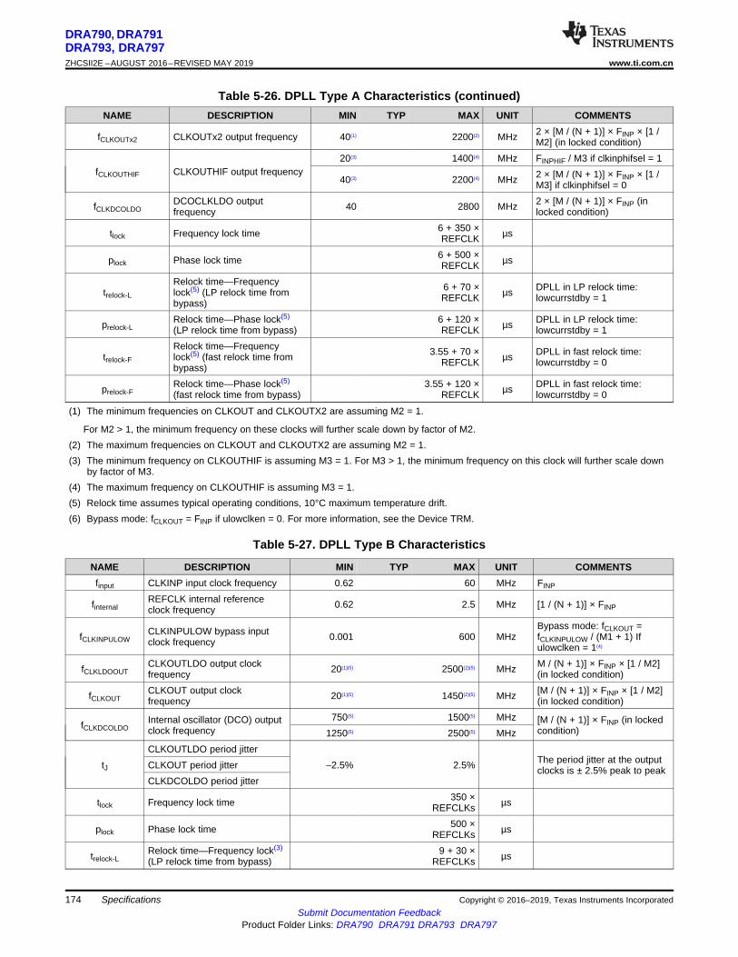
174
DRA790, DRA791DRA793, DRA797ZHCSII2E –AUGUST 2016–REVISED MAY 2019 www.ti.com.cn
Submit Documentation FeedbackProduct Folder Links: DRA790 DRA791 DRA793 DRA797
Specifications Copyright © 2016–2019, Texas Instruments Incorporated
Table 5-26. DPLL Type A Characteristics (continued)NAME DESCRIPTION MIN TYP MAX UNIT COMMENTS
fCLKOUTx2 CLKOUTx2 output frequency 40(1) 2200(2) MHz 2 × [M / (N + 1)] × FINP × [1 /M2] (in locked condition)
fCLKOUTHIF CLKOUTHIF output frequency20(3) 1400(4) MHz FINPHIF / M3 if clkinphifsel = 1
40(3) 2200(4) MHz 2 × [M / (N + 1)] × FINP × [1 /M3] if clkinphifsel = 0
fCLKDCOLDODCOCLKLDO outputfrequency 40 2800 MHz 2 × [M / (N + 1)] × FINP (in
locked condition)
tlock Frequency lock time 6 + 350 ×REFCLK µs
plock Phase lock time 6 + 500 ×REFCLK µs
trelock-L
Relock time—Frequencylock(5) (LP relock time frombypass)
6 + 70 ×REFCLK µs DPLL in LP relock time:
lowcurrstdby = 1
prelock-LRelock time—Phase lock(5)
(LP relock time from bypass)6 + 120 ×REFCLK µs DPLL in LP relock time:
lowcurrstdby = 1
trelock-F
Relock time—Frequencylock(5) (fast relock time frombypass)
3.55 + 70 ×REFCLK µs DPLL in fast relock time:
lowcurrstdby = 0
prelock-FRelock time—Phase lock(5)
(fast relock time from bypass)3.55 + 120 ×
REFCLK µs DPLL in fast relock time:lowcurrstdby = 0
(1) The minimum frequencies on CLKOUT and CLKOUTX2 are assuming M2 = 1.
For M2 > 1, the minimum frequency on these clocks will further scale down by factor of M2.(2) The maximum frequencies on CLKOUT and CLKOUTX2 are assuming M2 = 1.(3) The minimum frequency on CLKOUTHIF is assuming M3 = 1. For M3 > 1, the minimum frequency on this clock will further scale down
by factor of M3.(4) The maximum frequency on CLKOUTHIF is assuming M3 = 1.(5) Relock time assumes typical operating conditions, 10°C maximum temperature drift.(6) Bypass mode: fCLKOUT = FINP if ulowclken = 0. For more information, see the Device TRM.
Table 5-27. DPLL Type B Characteristics
NAME DESCRIPTION MIN TYP MAX UNIT COMMENTSfinput CLKINP input clock frequency 0.62 60 MHz FINP
finternalREFCLK internal referenceclock frequency 0.62 2.5 MHz [1 / (N + 1)] × FINP
fCLKINPULOWCLKINPULOW bypass inputclock frequency 0.001 600 MHz
Bypass mode: fCLKOUT =fCLKINPULOW / (M1 + 1) Ifulowclken = 1(4)
fCLKLDOOUTCLKOUTLDO output clockfrequency 20(1)(5) 2500(2)(5) MHz M / (N + 1)] × FINP × [1 / M2]
(in locked condition)
fCLKOUTCLKOUT output clockfrequency 20(1)(5) 1450(2)(5) MHz [M / (N + 1)] × FINP × [1 / M2]
(in locked condition)
fCLKDCOLDOInternal oscillator (DCO) outputclock frequency
750(5) 1500(5) MHz [M / (N + 1)] × FINP (in lockedcondition)1250(5) 2500(5) MHz
tJ
CLKOUTLDO period jitter–2.5% 2.5% The period jitter at the output
clocks is ± 2.5% peak to peakCLKOUT period jitterCLKDCOLDO period jitter
tlock Frequency lock time 350 ×REFCLKs µs
plock Phase lock time 500 ×REFCLKs µs
trelock-LRelock time—Frequency lock(3)
(LP relock time from bypass)9 + 30 ×
REFCLKs µs

175
DRA790, DRA791DRA793, DRA797
www.ti.com.cn ZHCSII2E –AUGUST 2016–REVISED MAY 2019
提交文档反馈意见产品主页链接: DRA790 DRA791 DRA793 DRA797
Specifications版权 © 2016–2019, Texas Instruments Incorporated
Table 5-27. DPLL Type B Characteristics (continued)NAME DESCRIPTION MIN TYP MAX UNIT COMMENTS
prelock-LRelock time—Phase lock(3) (LPrelock time from bypass)
9 + 125 ×REFCLKs µs
(1) The minimum frequency on CLKOUT is assuming M2 = 1.
For M2 > 1, the minimum frequency on this clock will further scale down by factor of M2.(2) The maximum frequency on CLKOUT is assuming M2 = 1.(3) Relock time assumes typical operating conditions, 10°C maximum temperature drift.(4) Bypass mode: fCLKOUT = FINP if ULOWCLKEN = 0. For more information, see the Device TRM.(5) For output clocks, there are two frequency ranges according to the SELFREQDCO setting. For more information, see the Device TRM.
5.10.4.3.2 DLL Characteristics
Table 5-28 summarizes the DLL characteristics and assumes testing over recommended operatingconditions.
Table 5-28. DLL Characteristics
NAME DESCRIPTION MIN TYP MAX UNITfinput Input clock frequency (EMIF_DLL_FCLK) 333 MHztlock Lock time 50k cycles
trelock Relock time (a change of the DLL frequency implies that DLL must relock) 50k cycles
5.10.4.3.3 DPLL and DLL Noise Isolation
NOTEFor more information on DPLL and DLL decoupling capacitor requirements, see the ExternalCapacitors / Voltage Decoupling Capacitors / I/O and Analog Voltage Decoupling / VDDAPower Domain section.
5.10.5 Recommended Clock and Control Signal Transition BehaviorAll clocks and control signals must transition between VIH and VIL (or between VIL and VIH) in a monotonicmanner. Monotonic transitions are more easily ensured with faster switching signals. Slower inputtransitions are more susceptible to glitches due to noise and special care should be taken for slow inputclocks.
5.10.6 Peripherals
5.10.6.1 Timing Test Conditions
All timing requirements and switching characteristics are valid over the recommended operating conditionsunless otherwise specified.
5.10.6.2 Virtual and Manual I/O Timing Modes
Some of the timings described in the following sections require the use of Virtual or Manual I/O TimingModes. 表 5-29 provides a summary of the Virtual and Manual I/O Timing Modes across all deviceinterfaces. The individual interface timing sections found later in this document provide the full descriptionof each applicable Virtual and Manual I/O Timing Mode. Refer to the "Pad Configuration" section of theTRM for the procedure on implementing the Virtual and Manual Timing Modes in a system.
表表 5-29. Modes Summary
Virtual or Manual IO Mode Name Data Manual Timing ModeDPI Video Output
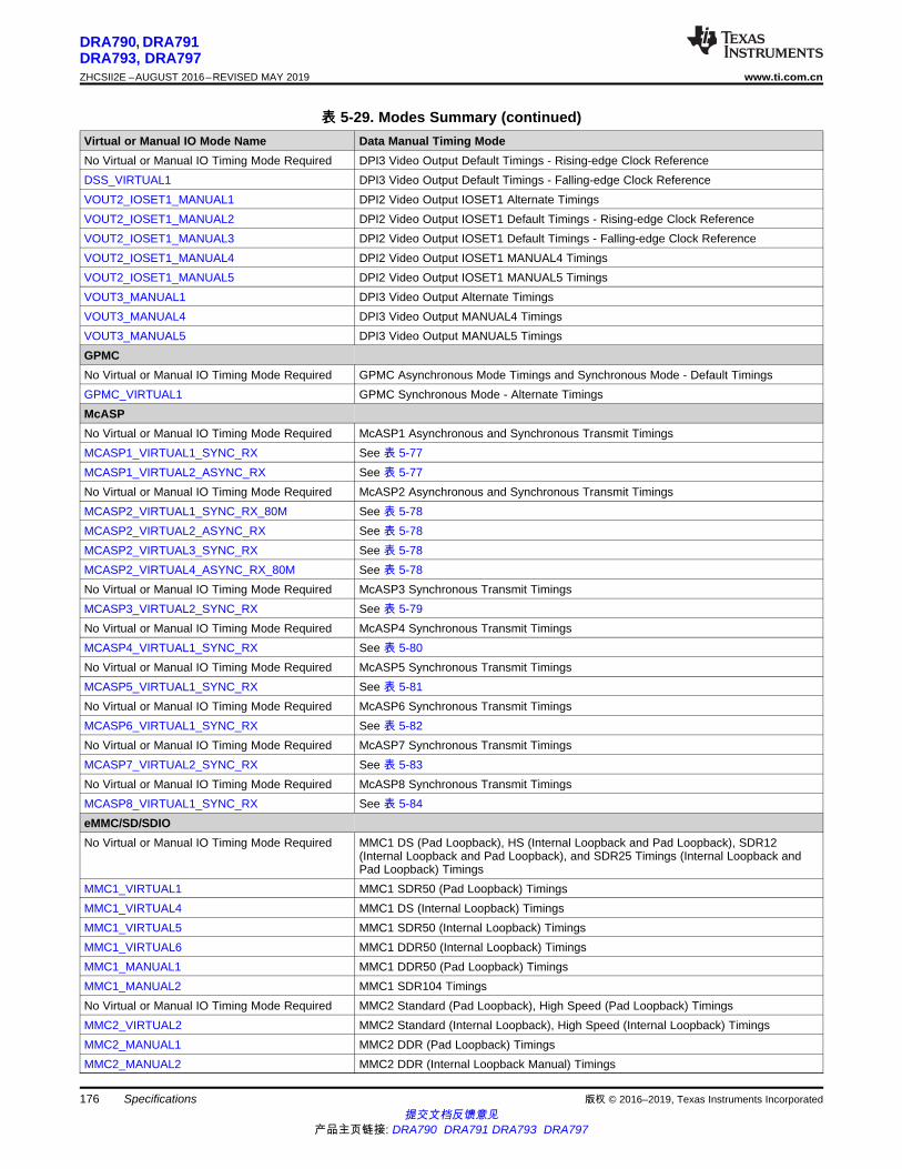
176
DRA790, DRA791DRA793, DRA797ZHCSII2E –AUGUST 2016–REVISED MAY 2019 www.ti.com.cn
提交文档反馈意见产品主页链接: DRA790 DRA791 DRA793 DRA797
Specifications 版权 © 2016–2019, Texas Instruments Incorporated
表表 5-29. Modes Summary (continued)Virtual or Manual IO Mode Name Data Manual Timing ModeNo Virtual or Manual IO Timing Mode Required DPI3 Video Output Default Timings - Rising-edge Clock ReferenceDSS_VIRTUAL1 DPI3 Video Output Default Timings - Falling-edge Clock ReferenceVOUT2_IOSET1_MANUAL1 DPI2 Video Output IOSET1 Alternate TimingsVOUT2_IOSET1_MANUAL2 DPI2 Video Output IOSET1 Default Timings - Rising-edge Clock ReferenceVOUT2_IOSET1_MANUAL3 DPI2 Video Output IOSET1 Default Timings - Falling-edge Clock ReferenceVOUT2_IOSET1_MANUAL4 DPI2 Video Output IOSET1 MANUAL4 TimingsVOUT2_IOSET1_MANUAL5 DPI2 Video Output IOSET1 MANUAL5 TimingsVOUT3_MANUAL1 DPI3 Video Output Alternate TimingsVOUT3_MANUAL4 DPI3 Video Output MANUAL4 TimingsVOUT3_MANUAL5 DPI3 Video Output MANUAL5 TimingsGPMCNo Virtual or Manual IO Timing Mode Required GPMC Asynchronous Mode Timings and Synchronous Mode - Default TimingsGPMC_VIRTUAL1 GPMC Synchronous Mode - Alternate TimingsMcASPNo Virtual or Manual IO Timing Mode Required McASP1 Asynchronous and Synchronous Transmit TimingsMCASP1_VIRTUAL1_SYNC_RX See 表 5-77MCASP1_VIRTUAL2_ASYNC_RX See 表 5-77No Virtual or Manual IO Timing Mode Required McASP2 Asynchronous and Synchronous Transmit TimingsMCASP2_VIRTUAL1_SYNC_RX_80M See 表 5-78MCASP2_VIRTUAL2_ASYNC_RX See 表 5-78MCASP2_VIRTUAL3_SYNC_RX See 表 5-78MCASP2_VIRTUAL4_ASYNC_RX_80M See 表 5-78No Virtual or Manual IO Timing Mode Required McASP3 Synchronous Transmit TimingsMCASP3_VIRTUAL2_SYNC_RX See 表 5-79No Virtual or Manual IO Timing Mode Required McASP4 Synchronous Transmit TimingsMCASP4_VIRTUAL1_SYNC_RX See 表 5-80No Virtual or Manual IO Timing Mode Required McASP5 Synchronous Transmit TimingsMCASP5_VIRTUAL1_SYNC_RX See 表 5-81No Virtual or Manual IO Timing Mode Required McASP6 Synchronous Transmit TimingsMCASP6_VIRTUAL1_SYNC_RX See 表 5-82No Virtual or Manual IO Timing Mode Required McASP7 Synchronous Transmit TimingsMCASP7_VIRTUAL2_SYNC_RX See 表 5-83No Virtual or Manual IO Timing Mode Required McASP8 Synchronous Transmit TimingsMCASP8_VIRTUAL1_SYNC_RX See 表 5-84eMMC/SD/SDIONo Virtual or Manual IO Timing Mode Required MMC1 DS (Pad Loopback), HS (Internal Loopback and Pad Loopback), SDR12
(Internal Loopback and Pad Loopback), and SDR25 Timings (Internal Loopback andPad Loopback) Timings
MMC1_VIRTUAL1 MMC1 SDR50 (Pad Loopback) TimingsMMC1_VIRTUAL4 MMC1 DS (Internal Loopback) TimingsMMC1_VIRTUAL5 MMC1 SDR50 (Internal Loopback) TimingsMMC1_VIRTUAL6 MMC1 DDR50 (Internal Loopback) TimingsMMC1_MANUAL1 MMC1 DDR50 (Pad Loopback) TimingsMMC1_MANUAL2 MMC1 SDR104 TimingsNo Virtual or Manual IO Timing Mode Required MMC2 Standard (Pad Loopback), High Speed (Pad Loopback) TimingsMMC2_VIRTUAL2 MMC2 Standard (Internal Loopback), High Speed (Internal Loopback) TimingsMMC2_MANUAL1 MMC2 DDR (Pad Loopback) TimingsMMC2_MANUAL2 MMC2 DDR (Internal Loopback Manual) Timings

177
DRA790, DRA791DRA793, DRA797
www.ti.com.cn ZHCSII2E –AUGUST 2016–REVISED MAY 2019
提交文档反馈意见产品主页链接: DRA790 DRA791 DRA793 DRA797
Specifications版权 © 2016–2019, Texas Instruments Incorporated
表表 5-29. Modes Summary (continued)Virtual or Manual IO Mode Name Data Manual Timing ModeMMC2_MANUAL3 MMC2 HS200 TimingsNo Virtual or Manual IO Timing Mode Required MMC3 DS, SDR12, HS, SDR25 TimingsMMC3_MANUAL1 MMC3 SDR50 TimingsNo Virtual or Manual IO Timing Mode Required MMC4 DS, SDR12, HS, SDR25 TimingsQSPINo Virtual or Manual IO Timing Mode Required QSPI Mode 3 TimingsQSPI1_MANUAL1 QSPI Mode 0 TimingsGMACNo Virtual or Manual IO Timing Mode Required GMAC MII0/1 TimingsGMAC_RGMII0_MANUAL1 GMAC RGMII0 with Transmit Clock Internal Delay EnabledGMAC_RGMII1_MANUAL1 GMAC RGMII1 with Transmit Clock Internal Delay EnabledGMAC_RMII0_MANUAL1 GMAC RMII0 TimingsGMAC_RMII1_MANUAL1 GMAC RMII1 TimingsVIPVIP_MANUAL3 VIN2A (IOSET4/5/6) Rise-Edge Capture Mode TimingsVIP_MANUAL4 VIN2B (IOSET7/8/9) Rise-Edge Capture Mode TimingsVIP_MANUAL5 VIN2A (IOSET4/5/6) Fall-Edge Capture Mode TimingsVIP_MANUAL6 VIN2B (IOSET7/8/9) Fall-Edge Capture Mode TimingsVIP_MANUAL7 VIN1A (IOSET2) and VIN2B (IOSET1/10) Rise-Edge Capture Mode TimingsVIP_MANUAL9 VIN1B (IOSET6/7) Rise-Edge Capture Mode TimingsVIP_MANUAL10 VIN2B (IOSET2/11) Rise-Edge Capture Mode TimingsVIP_MANUAL11 VIN2B (IOSET2/11) Fall-Edge Capture Mode TimingsVIP_MANUAL12 VIN1A (IOSET2) and VIN2B (IOSET1/10) Fall-Edge Capture Mode TimingsVIP_MANUAL14 VIN1B (IOSET6/7) Fall-Edge Capture Mode TimingsVIP_MANUAL15 VIN1A (IOSET8/9/10) Rise-Edge Capture Mode TimingsVIP_MANUAL16 VIN1A (IOSET8/9/10) Fall-Edge Capture Mode TimingsPRU-ICSSNo Virtual or Manual IO Timing Mode Required All PRU_ICSS Modes not covered belowPR1_PRU1_DIR_IN_MANUAL PRU-ICSS1 PRU1 Direct Input Mode TimingsPR1_PRU1_DIR_OUT_MANUAL PRU-ICSS1 PRU1 Direct Output Mode TimingsPR1_PRU1_PAR_CAP_MANUAL PRU-ICSS1 PRU1 Parallel Capture Mode TimingsPR2_PRU0_DIR_IN_MANUAL2 PRU-ICSS2 PRU0 IOSET2 Direct Input Mode TimingsPR2_PRU0_DIR_OUT_MANUAL2 PRU-ICSS2 PRU0 IOSET2 Direct Output Mode TimingsPR2_PRU1_DIR_IN_MANUAL1 PRU-ICSS2 PRU1 IOSET1 Direct Input Mode TimingsPR2_PRU1_DIR_IN_MANUAL2 PRU-ICSS2 PRU1 IOSET2 Direct Input Mode TimingsPR2_PRU1_DIR_OUT_MANUAL1 PRU-ICSS2 PRU1 IOSET1 Direct Output Mode TimingsPR2_PRU1_DIR_OUT_MANUAL2 PRU-ICSS2 PRU1 IOSET2 Direct Output Mode TimingsPR2_PRU0_PAR_CAP_MANUAL2 PRU-ICSS2 PRU0 IOSET2 Parallel Capture Mode TimingsPR2_PRU1_PAR_CAP_MANUAL1 PRU-ICSS2 PRU1 IOSET1 Parallel Capture Mode TimingsPR2_PRU1_PAR_CAP_MANUAL2 PRU-ICSS2 PRU1 IOSET2 Parallel Capture Mode TimingsHDMI, EMIF, Timers, I2C, HDQ/1-Wire, UART, McSPI, USB, PCIe, DCAN, GPIO, KBD, PWM, JTAG, TPIU, SDMA, INTC, MLBNo Virtual or Manual IO Timing Mode Required All Modes
5.10.6.3 VIP
The Device includes 1 Video Input Port (VIP).
表 5-30, 图 5-20 and 图 5-21 present timings and switching characteristics of the VIP.

vinx_clki(positive-edge clocking)
V4
vinx_d[23:0]/sig
V5
vinx_clki(negative-edge clocking)
SPRS8xx_VIP_02
vinx_clki
V2
V1
V3
SPRS906_TIMING_VIP_01
178
DRA790, DRA791DRA793, DRA797ZHCSII2E –AUGUST 2016–REVISED MAY 2019 www.ti.com.cn
提交文档反馈意见产品主页链接: DRA790 DRA791 DRA793 DRA797
Specifications 版权 © 2016–2019, Texas Instruments Incorporated
CAUTION
The I/O timings provided in this section are valid only for VIN1 and VIN2 ifsignals within a single IOSET are used. The IOSETs are defined in 表 5-31.
表表 5-30. Timing Requirements for VIP (3)(4)(5)
NO. PARAMETER DESCRIPTION MIN MAX UNITV1 tc(CLK) Cycle time, vinx_clki (3) (5) 6.06 (2) nsV2 tw(CLKH) Pulse duration, vinx_clki high (3) (5) 0.45 × P
(2)ns
V3 tw(CLKL) Pulse duration, vinx_clki low (3) (5) 0.45 × P(2)
ns
V4 tsu(CTL/DATA-CLK) Input setup time, Control (vinx_dei, vinx_vsynci, vinx_fldi,vinx_hsynci) and Data (vinx_dn) valid to vinx_clki transition (3) (4) (5)
3.11 (2) ns
V6 th(CLK-CTL/DATA) Input hold time, Control (vinx_dei, vinx_vsynci, vinx_fldi, vinx_hsynci)and Data (vinx_dn) valid from vinx_clki transition (3) (4) (5)
-0.05 (2) ns
(1) For maximum frequency of 165 MHz.(2) P = vinx_clki period.(3) x in vinx = 1a, 1b, 2a, 2b.(4) n in dn = 0 to 7 when x = 1b, 2b.
n = 0 to 23 when x = 1a, 2a.(5) i in clki, dei, vsynci, hsynci and fldi = 0 or 1.
图图 5-20. Video Input Ports Clock Signal
图图 5-21. Video Input Ports Timings

版权 © 2016–2019, Texas Instruments Incorporated Specifications提交文档反馈意见
产品主页链接: DRA790 DRA791 DRA793 DRA797
179
DRA790, DRA791DRA793, DRA797
www.ti.com.cn ZHCSII2E –AUGUST 2016–REVISED MAY 2019
In 表 5-31 and 表 5-32 are presented the specific groupings of signals (IOSET) for use with vin1 and vin2.
表表 5-31. VIN1 IOSETs
SIGNALS IOSET2 IOSET6 (1) IOSET7 (1) IOSET8 IOSET9 IOSET10BALL MUX BALL MUX BALL MUX BALL MUX BALL MUX BALL MUX
vin1avin1a_clk0 G3 2 Y5 9 J24 7 J24 7
vin1a_hsync0 K4 2 AA4 9 B14 7 B14 7vin1a_vsync0 H1 2 AB1 9 D14 7 D14 7
vin1a_fld0 L3 2 C16 7 C16 7vin1a_de0 J2 2 Y6 9 C17 7 C17 7vin1a_d0 F1 2 AA1 9 J25 7 B23 7vin1a_d1 E2 2 Y3 9 B22 7 B22 7vin1a_d2 E1 2 W2 9 A23 7 A23 7vin1a_d3 C1 2 AA3 9 A22 7 A22 7vin1a_d4 D1 2 AA2 9 B21 7 B21 7vin1a_d5 D2 2 Y4 9 A21 7 A21 7vin1a_d6 B1 2 Y1 9 D19 7 D19 7vin1a_d7 B2 2 Y2 9 E19 7 E19 7vin1a_d8 C2 2 F16 7 F16 7vin1a_d9 D3 2 E16 7 E16 7vin1a_d10 A2 2 E17 7 E17 7vin1a_d11 B3 2 A19 7 A19 7vin1a_d12 C3 2 B18 7 B18 7vin1a_d13 C4 2 B16 7 B16 7vin1a_d14 A3 2 B17 7 B17 7vin1a_d15 B4 2 A18 7 A18 7vin1a_d16 M1 2vin1a_d17 M2 2vin1a_d18 L2 2vin1a_d19 L1 2vin1a_d20 K3 2vin1a_d21 K2 2vin1a_d22 J1 2vin1a_d23 K1 2
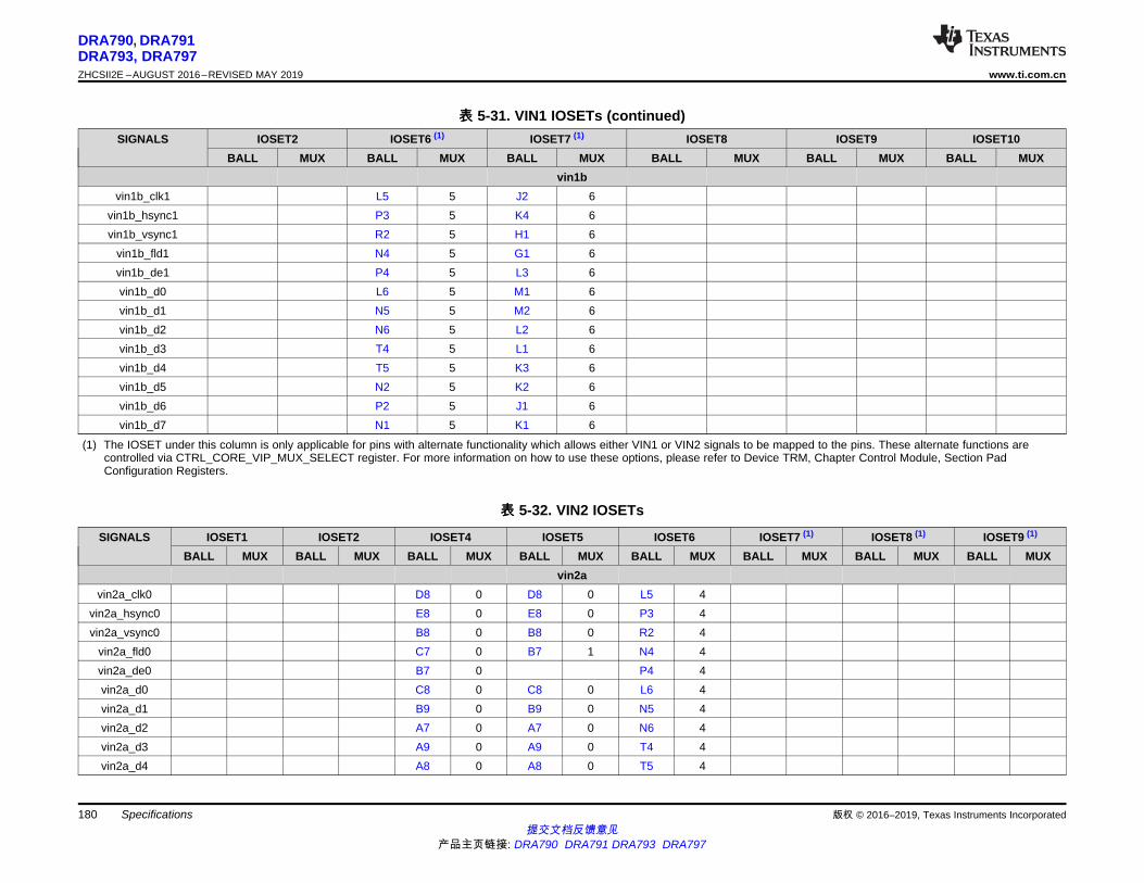
版权 © 2016–2019, Texas Instruments IncorporatedSpecifications提交文档反馈意见
产品主页链接: DRA790 DRA791 DRA793 DRA797
180
DRA790, DRA791DRA793, DRA797ZHCSII2E –AUGUST 2016–REVISED MAY 2019 www.ti.com.cn
表表 5-31. VIN1 IOSETs (continued)SIGNALS IOSET2 IOSET6 (1) IOSET7 (1) IOSET8 IOSET9 IOSET10
BALL MUX BALL MUX BALL MUX BALL MUX BALL MUX BALL MUXvin1b
vin1b_clk1 L5 5 J2 6vin1b_hsync1 P3 5 K4 6vin1b_vsync1 R2 5 H1 6
vin1b_fld1 N4 5 G1 6vin1b_de1 P4 5 L3 6vin1b_d0 L6 5 M1 6vin1b_d1 N5 5 M2 6vin1b_d2 N6 5 L2 6vin1b_d3 T4 5 L1 6vin1b_d4 T5 5 K3 6vin1b_d5 N2 5 K2 6vin1b_d6 P2 5 J1 6vin1b_d7 N1 5 K1 6
(1) The IOSET under this column is only applicable for pins with alternate functionality which allows either VIN1 or VIN2 signals to be mapped to the pins. These alternate functions arecontrolled via CTRL_CORE_VIP_MUX_SELECT register. For more information on how to use these options, please refer to Device TRM, Chapter Control Module, Section PadConfiguration Registers.
表表 5-32. VIN2 IOSETs
SIGNALS IOSET1 IOSET2 IOSET4 IOSET5 IOSET6 IOSET7 (1) IOSET8 (1) IOSET9 (1)
BALL MUX BALL MUX BALL MUX BALL MUX BALL MUX BALL MUX BALL MUX BALL MUXvin2a
vin2a_clk0 D8 0 D8 0 L5 4vin2a_hsync0 E8 0 E8 0 P3 4vin2a_vsync0 B8 0 B8 0 R2 4
vin2a_fld0 C7 0 B7 1 N4 4vin2a_de0 B7 0 P4 4vin2a_d0 C8 0 C8 0 L6 4vin2a_d1 B9 0 B9 0 N5 4vin2a_d2 A7 0 A7 0 N6 4vin2a_d3 A9 0 A9 0 T4 4vin2a_d4 A8 0 A8 0 T5 4

版权 © 2016–2019, Texas Instruments Incorporated Specifications提交文档反馈意见
产品主页链接: DRA790 DRA791 DRA793 DRA797
181
DRA790, DRA791DRA793, DRA797
www.ti.com.cn ZHCSII2E –AUGUST 2016–REVISED MAY 2019
表表 5-32. VIN2 IOSETs (continued)SIGNALS IOSET1 IOSET2 IOSET4 IOSET5 IOSET6 IOSET7 (1) IOSET8 (1) IOSET9 (1)
BALL MUX BALL MUX BALL MUX BALL MUX BALL MUX BALL MUX BALL MUX BALL MUXvin2a_d5 A11 0 A11 0 N2 4vin2a_d6 F10 0 F10 0 P2 4vin2a_d7 A10 0 A10 0 N1 4vin2a_d8 B10 0 B10 0 P1 4vin2a_d9 E10 0 E10 0 N3 4vin2a_d10 D10 0 D10 0 R1 4vin2a_d11 C10 0 C10 0 P5 4vin2a_d12 B11 0 B11 0vin2a_d13 D11 0 D11 0vin2a_d14 C11 0 C11 0vin2a_d15 B12 0 B12 0vin2a_d16 A12 0 A12 0vin2a_d17 A13 0 A13 0vin2a_d18 E11 0 E11 0vin2a_d19 F11 0 F11 0vin2a_d20 B13 0 B13 0vin2a_d21 E13 0 E13 0vin2a_d22 C13 0 C13 0vin2a_d23 D13 0 D13 0
vin2bvin2b_clk1 L4 6 H6 4 C7 2 C7 2 AB1 4
vin2b_hsync1 B6 6 B6 6 E8 3 E8 3 Y5 4vin2b_vsync1 A6 6 A6 6 B8 3 B8 3 Y6 4
vin2b_fld1 H6 6 B7 2vin2b_de1 H2 6 H2 6 B7 3 AA4 4vin2b_d0 A4 6 A4 6 D13 2 D13 2 AA1 4vin2b_d1 E7 6 E7 6 C13 2 C13 2 Y3 4vin2b_d2 D6 6 D6 6 E13 2 E13 2 W2 4vin2b_d3 C5 6 C5 6 B13 2 B13 2 AA3 4vin2b_d4 B5 6 B5 6 F11 2 F11 2 AA2 4vin2b_d5 D7 6 D7 6 E11 2 E11 2 Y4 4vin2b_d6 C6 6 C6 6 A13 2 A13 2 Y1 4

版权 © 2016–2019, Texas Instruments IncorporatedSpecifications提交文档反馈意见
产品主页链接: DRA790 DRA791 DRA793 DRA797
182
DRA790, DRA791DRA793, DRA797ZHCSII2E –AUGUST 2016–REVISED MAY 2019 www.ti.com.cn
表表 5-32. VIN2 IOSETs (continued)SIGNALS IOSET1 IOSET2 IOSET4 IOSET5 IOSET6 IOSET7 (1) IOSET8 (1) IOSET9 (1)
BALL MUX BALL MUX BALL MUX BALL MUX BALL MUX BALL MUX BALL MUX BALL MUXvin2b_d7 A5 6 A5 6 A12 2 A12 2 Y2 4
(1) The IOSET under this column is only applicable for pins with alternate functionality which allows either VIN1 or VIN2 signals to be mapped to the pins. These alternate functions arecontrolled via CTRL_CORE_VIP_MUX_SELECT register. For more information on how to use these options, please refer to Device TRM, Chapter Control Module, Section PadConfiguration Registers.
注注To configure the desired Manual IO Timing Mode the user must follow the steps described in section "Manual IO Timing Modes" of theDevice TRM.
The associated registers to configure are listed in the CFG REGISTER column. For more information please see the Control ModuleChapter in the Device TRM.
Manual IO Timings Modes must be used to ensure some IO timings for VIP1. See 表 5-29 Modes Summary for a list of IO timings requiring theuse of Manual IO Timings Modes. See 表 5-33 Manual Functions Mapping for VIN2A (IOSET4/5/6) for a definition of the Manual modes.
表 5-33 lists the A_DELAY and G_DELAY values needed to calculate the correct values to be set in the CFG_x registers.
表表 5-33. Manual Functions Mapping for VIN2A (IOSET4/5/6)
BALL BALL NAME VIP_MANUAL3 VIP_MANUAL5 CFG REGISTER MUXMODEA_DELAY (ps) G_DELAY (ps) A_DELAY (ps) G_DELAY (ps) 0 1 4
P5 RMII_MHZ_50_CLK
2616 1379 2798 1294 CFG_RMII_MHZ_50_CLK_IN - - vin2a_d11
L6 mdio_d 2558 1105 2790 954 CFG_MDIO_D_IN - - vin2a_d0L5 mdio_mclk 998 463 1029 431 CFG_MDIO_MCLK_IN - - vin2a_clk0N2 rgmii0_rxc 2658 862 2896 651 CFG_RGMII0_RXC_IN - - vin2a_d5P2 rgmii0_rxctl 2658 1628 2844 1518 CFG_RGMII0_RXCTL_IN - - vin2a_d6N4 rgmii0_rxd0 2638 1123 2856 888 CFG_RGMII0_RXD0_IN - - vin2a_fld0N3 rgmii0_rxd1 2641 1737 2804 1702 CFG_RGMII0_RXD1_IN - - vin2a_d9P1 rgmii0_rxd2 2641 1676 2801 1652 CFG_RGMII0_RXD2_IN - - vin2a_d8N1 rgmii0_rxd3 2644 1828 2807 1790 CFG_RGMII0_RXD3_IN - - vin2a_d7T4 rgmii0_txc 2638 1454 2835 1396 CFG_RGMII0_TXC_IN - - vin2a_d3T5 rgmii0_txctl 2672 1663 2831 1640 CFG_RGMII0_TXCTL_IN - - vin2a_d4R1 rgmii0_txd0 2604 1442 2764 1417 CFG_RGMII0_TXD0_IN - - vin2a_d10R2 rgmii0_txd1 2683 1598 2843 1600 CFG_RGMII0_TXD1_IN - - vin2a_vsync0P3 rgmii0_txd2 2563 1483 2816 1344 CFG_RGMII0_TXD2_IN - - vin2a_hsync0
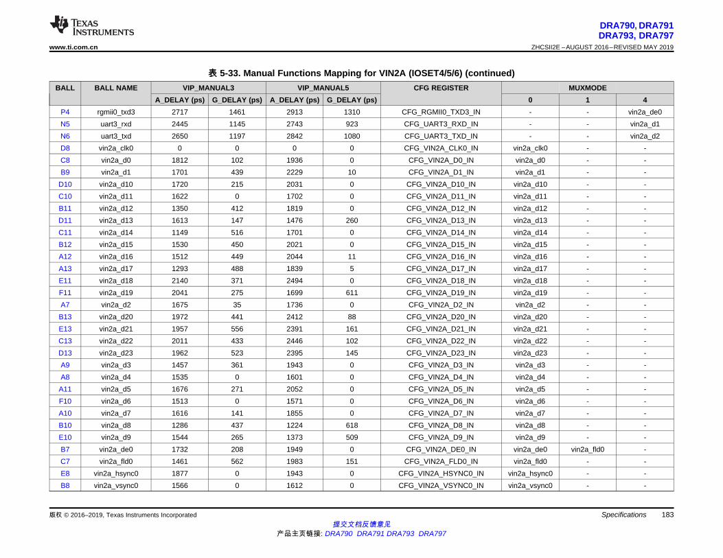
版权 © 2016–2019, Texas Instruments Incorporated Specifications提交文档反馈意见
产品主页链接: DRA790 DRA791 DRA793 DRA797
183
DRA790, DRA791DRA793, DRA797
www.ti.com.cn ZHCSII2E –AUGUST 2016–REVISED MAY 2019
表表 5-33. Manual Functions Mapping for VIN2A (IOSET4/5/6) (continued)BALL BALL NAME VIP_MANUAL3 VIP_MANUAL5 CFG REGISTER MUXMODE
A_DELAY (ps) G_DELAY (ps) A_DELAY (ps) G_DELAY (ps) 0 1 4P4 rgmii0_txd3 2717 1461 2913 1310 CFG_RGMII0_TXD3_IN - - vin2a_de0N5 uart3_rxd 2445 1145 2743 923 CFG_UART3_RXD_IN - - vin2a_d1N6 uart3_txd 2650 1197 2842 1080 CFG_UART3_TXD_IN - - vin2a_d2D8 vin2a_clk0 0 0 0 0 CFG_VIN2A_CLK0_IN vin2a_clk0 - -C8 vin2a_d0 1812 102 1936 0 CFG_VIN2A_D0_IN vin2a_d0 - -B9 vin2a_d1 1701 439 2229 10 CFG_VIN2A_D1_IN vin2a_d1 - -
D10 vin2a_d10 1720 215 2031 0 CFG_VIN2A_D10_IN vin2a_d10 - -C10 vin2a_d11 1622 0 1702 0 CFG_VIN2A_D11_IN vin2a_d11 - -B11 vin2a_d12 1350 412 1819 0 CFG_VIN2A_D12_IN vin2a_d12 - -D11 vin2a_d13 1613 147 1476 260 CFG_VIN2A_D13_IN vin2a_d13 - -C11 vin2a_d14 1149 516 1701 0 CFG_VIN2A_D14_IN vin2a_d14 - -B12 vin2a_d15 1530 450 2021 0 CFG_VIN2A_D15_IN vin2a_d15 - -A12 vin2a_d16 1512 449 2044 11 CFG_VIN2A_D16_IN vin2a_d16 - -A13 vin2a_d17 1293 488 1839 5 CFG_VIN2A_D17_IN vin2a_d17 - -E11 vin2a_d18 2140 371 2494 0 CFG_VIN2A_D18_IN vin2a_d18 - -F11 vin2a_d19 2041 275 1699 611 CFG_VIN2A_D19_IN vin2a_d19 - -A7 vin2a_d2 1675 35 1736 0 CFG_VIN2A_D2_IN vin2a_d2 - -B13 vin2a_d20 1972 441 2412 88 CFG_VIN2A_D20_IN vin2a_d20 - -E13 vin2a_d21 1957 556 2391 161 CFG_VIN2A_D21_IN vin2a_d21 - -C13 vin2a_d22 2011 433 2446 102 CFG_VIN2A_D22_IN vin2a_d22 - -D13 vin2a_d23 1962 523 2395 145 CFG_VIN2A_D23_IN vin2a_d23 - -A9 vin2a_d3 1457 361 1943 0 CFG_VIN2A_D3_IN vin2a_d3 - -A8 vin2a_d4 1535 0 1601 0 CFG_VIN2A_D4_IN vin2a_d4 - -A11 vin2a_d5 1676 271 2052 0 CFG_VIN2A_D5_IN vin2a_d5 - -F10 vin2a_d6 1513 0 1571 0 CFG_VIN2A_D6_IN vin2a_d6 - -A10 vin2a_d7 1616 141 1855 0 CFG_VIN2A_D7_IN vin2a_d7 - -B10 vin2a_d8 1286 437 1224 618 CFG_VIN2A_D8_IN vin2a_d8 - -E10 vin2a_d9 1544 265 1373 509 CFG_VIN2A_D9_IN vin2a_d9 - -B7 vin2a_de0 1732 208 1949 0 CFG_VIN2A_DE0_IN vin2a_de0 vin2a_fld0 -C7 vin2a_fld0 1461 562 1983 151 CFG_VIN2A_FLD0_IN vin2a_fld0 - -E8 vin2a_hsync0 1877 0 1943 0 CFG_VIN2A_HSYNC0_IN vin2a_hsync0 - -B8 vin2a_vsync0 1566 0 1612 0 CFG_VIN2A_VSYNC0_IN vin2a_vsync0 - -

版权 © 2016–2019, Texas Instruments IncorporatedSpecifications提交文档反馈意见
产品主页链接: DRA790 DRA791 DRA793 DRA797
184
DRA790, DRA791DRA793, DRA797ZHCSII2E –AUGUST 2016–REVISED MAY 2019 www.ti.com.cn
Manual IO Timings Modes must be used to ensure some IO timings for VIP1. See 表 5-29 Modes Summary for a list of IO timings requiring theuse of Manual IO Timings Modes. See 表 5-34 Manual Functions Mapping for VIN2B (IOSET7/8/9) for a definition of the Manual modes.
表 5-34 lists the A_DELAY and G_DELAY values needed to calculate the correct values to be set in the CFG_x registers.
表表 5-34. Manual Functions Mapping for VIN2B (IOSET7/8/9)
BALL BALL NAME VIP_MANUAL4 VIP_MANUAL6 CFG REGISTER MUXMODEA_DELAY (ps) G_DELAY (ps) A_DELAY (ps) G_DELAY (ps) 2 3 4
Y5 gpio6_10 2829 884 3009 892 CFG_GPIO6_10_IN - - vin2b_hsync1Y6 gpio6_11 2648 1033 2890 1096 CFG_GPIO6_11_IN - - vin2b_vsync1Y2 mmc3_clk 2794 1074 2997 1089 CFG_MMC3_CLK_IN - - vin2b_d7Y1 mmc3_cmd 2789 1162 2959 1210 CFG_MMC3_CMD_IN - - vin2b_d6Y4 mmc3_dat0 2689 1180 2897 1269 CFG_MMC3_DAT0_IN - - vin2b_d5
AA2 mmc3_dat1 2605 1219 2891 1219 CFG_MMC3_DAT1_IN - - vin2b_d4AA3 mmc3_dat2 2616 703 2947 590 CFG_MMC3_DAT2_IN - - vin2b_d3W2 mmc3_dat3 2760 1235 2931 1342 CFG_MMC3_DAT3_IN - - vin2b_d2Y3 mmc3_dat4 2757 880 2979 891 CFG_MMC3_DAT4_IN - - vin2b_d1
AA1 mmc3_dat5 2688 1177 2894 1262 CFG_MMC3_DAT5_IN - - vin2b_d0AA4 mmc3_dat6 2638 1165 2894 1187 CFG_MMC3_DAT6_IN - - vin2b_de1AB1 mmc3_dat7 995 182 1202 107 CFG_MMC3_DAT7_IN - - vin2b_clk1A12 vin2a_d16 1423 0 1739 0 CFG_VIN2A_D16_IN vin2b_d7 - -A13 vin2a_d17 1253 0 1568 0 CFG_VIN2A_D17_IN vin2b_d6 - -E11 vin2a_d18 2080 0 2217 0 CFG_VIN2A_D18_IN vin2b_d5 - -F11 vin2a_d19 1849 0 2029 0 CFG_VIN2A_D19_IN vin2b_d4 - -B13 vin2a_d20 1881 50 2202 0 CFG_VIN2A_D20_IN vin2b_d3 - -E13 vin2a_d21 1917 167 2313 0 CFG_VIN2A_D21_IN vin2b_d2 - -C13 vin2a_d22 1955 79 2334 0 CFG_VIN2A_D22_IN vin2b_d1 - -D13 vin2a_d23 1899 145 2288 0 CFG_VIN2A_D23_IN vin2b_d0 - -B7 vin2a_de0 1568 261 2048 0 CFG_VIN2A_DE0_IN vin2b_fld1 vin2b_de1 -C7 vin2a_fld0 0 0 0 0 CFG_VIN2A_FLD0_IN vin2b_clk1 - -E8 vin2a_hsync0 1793 0 2011 0 CFG_VIN2A_HSYNC0_IN - vin2b_hsync1 -B8 vin2a_vsync0 1382 0 1632 0 CFG_VIN2A_VSYNC0_IN - vin2b_vsync1 -

版权 © 2016–2019, Texas Instruments Incorporated Specifications提交文档反馈意见
产品主页链接: DRA790 DRA791 DRA793 DRA797
185
DRA790, DRA791DRA793, DRA797
www.ti.com.cn ZHCSII2E –AUGUST 2016–REVISED MAY 2019
Manual IO Timings Modes must be used to ensure some IO timings for VIP1. See 表 5-29 Modes Summary for a list of IO timings requiring theuse of Manual IO Timings Modes. See 表 5-35 Manual Functions Mapping for VIN1A (IOSET2) and VIN2B (IOSET1/10) for a definition of theManual modes.
表 5-35 lists the A_DELAY and G_DELAY values needed to calculate the correct values to be set in the CFG_x registers.
表表 5-35. Manual Functions Mapping for VIN1A (IOSET2) and VIN2B (IOSET1/10)
BALL BALL NAME VIP_MANUAL7 VIP_MANUAL12 CFG REGISTER MUXMODEA_DELAY (ps) G_DELAY (ps) A_DELAY (ps) G_DELAY (ps) 2 6
M1 gpmc_a0 3080 1792 3376 1632 CFG_GPMC_A0_IN vin1a_d16 -M2 gpmc_a1 2958 1890 3249 1749 CFG_GPMC_A1_IN vin1a_d17 -J2 gpmc_a10 3073 1653 3388 1433 CFG_GPMC_A10_IN vin1a_de0 -L3 gpmc_a11 3014 1784 3290 1693 CFG_GPMC_A11_IN vin1a_fld0 -A4 gpmc_a19 1385 0 1246 0 CFG_GPMC_A19_IN - vin2b_d0L2 gpmc_a2 3041 1960 3322 1850 CFG_GPMC_A2_IN vin1a_d18 -E7 gpmc_a20 859 0 720 0 CFG_GPMC_A20_IN - vin2b_d1D6 gpmc_a21 1465 0 1334 0 CFG_GPMC_A21_IN - vin2b_d2C5 gpmc_a22 1210 0 1064 0 CFG_GPMC_A22_IN - vin2b_d3B5 gpmc_a23 1111 0 954 0 CFG_GPMC_A23_IN - vin2b_d4D7 gpmc_a24 1137 0 1051 0 CFG_GPMC_A24_IN - vin2b_d5C6 gpmc_a25 1402 0 1283 0 CFG_GPMC_A25_IN - vin2b_d6A5 gpmc_a26 1298 0 1153 0 CFG_GPMC_A26_IN - vin2b_d7B6 gpmc_a27 934 0 870 0 CFG_GPMC_A27_IN - vin2b_hsync1L1 gpmc_a3 3019 2145 3296 2050 CFG_GPMC_A3_IN vin1a_d19 -K3 gpmc_a4 3063 1981 3357 1829 CFG_GPMC_A4_IN vin1a_d20 -K2 gpmc_a5 3021 1954 3304 1840 CFG_GPMC_A5_IN vin1a_d21 -J1 gpmc_a6 3062 1716 3348 1592 CFG_GPMC_A6_IN vin1a_d22 -K1 gpmc_a7 3260 1889 3583 1631 CFG_GPMC_A7_IN vin1a_d23 -K4 gpmc_a8 3033 1702 3328 1547 CFG_GPMC_A8_IN vin1a_hsync0 -H1 gpmc_a9 2991 1905 3281 1766 CFG_GPMC_A9_IN vin1a_vsync0 -F1 gpmc_ad0 2907 1342 3181 1255 CFG_GPMC_AD0_IN vin1a_d0 -E2 gpmc_ad1 2858 1321 3132 1234 CFG_GPMC_AD1_IN vin1a_d1 -A2 gpmc_ad10 2920 1384 3223 1204 CFG_GPMC_AD10_IN vin1a_d10 -B3 gpmc_ad11 2719 1310 3019 1198 CFG_GPMC_AD11_IN vin1a_d11 -C3 gpmc_ad12 2845 1135 3160 917 CFG_GPMC_AD12_IN vin1a_d12 -C4 gpmc_ad13 2765 1225 3045 1119 CFG_GPMC_AD13_IN vin1a_d13 -

版权 © 2016–2019, Texas Instruments IncorporatedSpecifications提交文档反馈意见
产品主页链接: DRA790 DRA791 DRA793 DRA797
186
DRA790, DRA791DRA793, DRA797ZHCSII2E –AUGUST 2016–REVISED MAY 2019 www.ti.com.cn
表表 5-35. Manual Functions Mapping for VIN1A (IOSET2) and VIN2B (IOSET1/10) (continued)BALL BALL NAME VIP_MANUAL7 VIP_MANUAL12 CFG REGISTER MUXMODE
A_DELAY (ps) G_DELAY (ps) A_DELAY (ps) G_DELAY (ps) 2 6A3 gpmc_ad14 2845 1150 3153 952 CFG_GPMC_AD14_IN vin1a_d14 -B4 gpmc_ad15 2766 1453 3044 1355 CFG_GPMC_AD15_IN vin1a_d15 -E1 gpmc_ad2 2951 1296 3226 1209 CFG_GPMC_AD2_IN vin1a_d2 -C1 gpmc_ad3 2825 1154 3121 997 CFG_GPMC_AD3_IN vin1a_d3 -D1 gpmc_ad4 2927 1245 3246 1014 CFG_GPMC_AD4_IN vin1a_d4 -D2 gpmc_ad5 2923 1251 3217 1098 CFG_GPMC_AD5_IN vin1a_d5 -B1 gpmc_ad6 2958 1342 3238 1239 CFG_GPMC_AD6_IN vin1a_d6 -B2 gpmc_ad7 2900 1244 3174 1157 CFG_GPMC_AD7_IN vin1a_d7 -C2 gpmc_ad8 2845 1585 3125 1482 CFG_GPMC_AD8_IN vin1a_d8 -D3 gpmc_ad9 2779 1343 3086 1223 CFG_GPMC_AD9_IN vin1a_d9 -H2 gpmc_ben0 1555 0 1425 0 CFG_GPMC_BEN0_IN - vin2b_de1H6 gpmc_ben1 1501 0 1397 0 CFG_GPMC_BEN1_IN - vin2b_fld1L4 gpmc_clk 0 0 0 0 CFG_GPMC_CLK_IN - vin2b_clk1A6 gpmc_cs1 1192 0 1102 0 CFG_GPMC_CS1_IN - vin2b_vsync1G3 gpmc_cs3 1324 374 1466 353 CFG_GPMC_CS3_IN vin1a_clk0 -
Manual IO Timings Modes must be used to ensure some IO timings for VIP1. See 表 5-29 Modes Summary for a list of IO timings requiring theuse of Manual IO Timings Modes. See 表 5-36 Manual Functions Mapping for VIN1B (IOSET6/7) for a definition of the Manual modes.
表 5-36 lists the A_DELAY and G_DELAY values needed to calculate the correct values to be set in the CFG_x registers.
表表 5-36. Manual Functions Mapping for VIN1B (IOSET6/7)
BALL BALL NAME VIP_MANUAL9 VIP_MANUAL14 CFG REGISTER MUXMODEA_DELAY (ps) G_DELAY (ps) A_DELAY (ps) G_DELAY (ps) 5 6
M1 gpmc_a0 1873 702 2202 441 CFG_GPMC_A0_IN - vin1b_d0M2 gpmc_a1 1629 772 2057 413 CFG_GPMC_A1_IN - vin1b_d1J2 gpmc_a10 0 0 0 0 CFG_GPMC_A10_IN - vin1b_clk1L3 gpmc_a11 1851 1011 2126 856 CFG_GPMC_A11_IN - vin1b_de1G1 gpmc_a12 2009 601 2289 327 CFG_GPMC_A12_IN - vin1b_fld1L2 gpmc_a2 1734 898 2131 573 CFG_GPMC_A2_IN - vin1b_d2L1 gpmc_a3 1757 1076 2106 812 CFG_GPMC_A3_IN - vin1b_d3K3 gpmc_a4 1794 893 2164 559 CFG_GPMC_A4_IN - vin1b_d4K2 gpmc_a5 1726 853 2120 523 CFG_GPMC_A5_IN - vin1b_d5

版权 © 2016–2019, Texas Instruments Incorporated Specifications提交文档反馈意见
产品主页链接: DRA790 DRA791 DRA793 DRA797
187
DRA790, DRA791DRA793, DRA797
www.ti.com.cn ZHCSII2E –AUGUST 2016–REVISED MAY 2019
表表 5-36. Manual Functions Mapping for VIN1B (IOSET6/7) (continued)BALL BALL NAME VIP_MANUAL9 VIP_MANUAL14 CFG REGISTER MUXMODE
A_DELAY (ps) G_DELAY (ps) A_DELAY (ps) G_DELAY (ps) 5 6J1 gpmc_a6 1792 612 2153 338 CFG_GPMC_A6_IN - vin1b_d6K1 gpmc_a7 2117 610 2389 304 CFG_GPMC_A7_IN - vin1b_d7K4 gpmc_a8 1758 653 2140 308 CFG_GPMC_A8_IN - vin1b_hsync1H1 gpmc_a9 1705 899 2067 646 CFG_GPMC_A9_IN - vin1b_vsync1L6 mdio_d 1945 671 2265 414 CFG_MDIO_D_IN vin1b_d0 -L5 mdio_mclk 255 119 337 0 CFG_MDIO_MCLK_IN vin1b_clk1 -N2 rgmii0_rxc 2057 909 2341 646 CFG_RGMII0_RXC_IN vin1b_d5 -P2 rgmii0_rxctl 2121 1139 2323 988 CFG_RGMII0_RXCTL_IN vin1b_d6 -N4 rgmii0_rxd0 2070 655 2336 340 CFG_RGMII0_RXD0_IN vin1b_fld1 -N1 rgmii0_rxd3 2092 1357 2306 1216 CFG_RGMII0_RXD3_IN vin1b_d7 -T4 rgmii0_txc 2088 1205 2328 1079 CFG_RGMII0_TXC_IN vin1b_d3 -T5 rgmii0_txctl 2143 1383 2312 1311 CFG_RGMII0_TXCTL_IN vin1b_d4 -R2 rgmii0_txd1 2078 1189 2324 1065 CFG_RGMII0_TXD1_IN vin1b_vsync1 -P3 rgmii0_txd2 1928 1125 2306 763 CFG_RGMII0_TXD2_IN vin1b_hsync1 -P4 rgmii0_txd3 2255 971 2401 846 CFG_RGMII0_TXD3_IN vin1b_de1 -N5 uart3_rxd 1829 747 2220 400 CFG_UART3_RXD_IN vin1b_d1 -N6 uart3_txd 2030 837 2324 568 CFG_UART3_TXD_IN vin1b_d2 -
Manual IO Timings Modes must be used to ensure some IO timings for VIP1. See 表 5-29 Modes Summary for a list of IO timings requiring theuse of Manual IO Timings Modes. See 表 5-37 Manual Functions Mapping for VIN2B (IOSET2/11) for a definition of the Manual modes.
表 5-37 lists the A_DELAY and G_DELAY values needed to calculate the correct values to be set in the CFG_x registers.
表表 5-37. Manual Functions Mapping for VIN2B (IOSET2/11)
BALL BALL NAME VIP_MANUAL10 VIP_MANUAL11 CFG REGISTER MUXMODEA_DELAY (ps) G_DELAY (ps) A_DELAY (ps) G_DELAY (ps) 4 6
A4 gpmc_a19 1600 943 2023 477 CFG_GPMC_A19_IN - vin2b_d0E7 gpmc_a20 1440 621 1875 136 CFG_GPMC_A20_IN - vin2b_d1D6 gpmc_a21 1602 1066 2021 604 CFG_GPMC_A21_IN - vin2b_d2C5 gpmc_a22 1395 983 1822 519 CFG_GPMC_A22_IN - vin2b_d3B5 gpmc_a23 1571 716 2045 200 CFG_GPMC_A23_IN - vin2b_d4D7 gpmc_a24 1463 832 1893 396 CFG_GPMC_A24_IN - vin2b_d5C6 gpmc_a25 1426 1166 1842 732 CFG_GPMC_A25_IN - vin2b_d6

版权 © 2016–2019, Texas Instruments IncorporatedSpecifications提交文档反馈意见
产品主页链接: DRA790 DRA791 DRA793 DRA797
188
DRA790, DRA791DRA793, DRA797ZHCSII2E –AUGUST 2016–REVISED MAY 2019 www.ti.com.cn
表表 5-37. Manual Functions Mapping for VIN2B (IOSET2/11) (continued)BALL BALL NAME VIP_MANUAL10 VIP_MANUAL11 CFG REGISTER MUXMODE
A_DELAY (ps) G_DELAY (ps) A_DELAY (ps) G_DELAY (ps) 4 6A5 gpmc_a26 1362 1094 1797 584 CFG_GPMC_A26_IN - vin2b_d7B6 gpmc_a27 1283 809 1760 338 CFG_GPMC_A27_IN - vin2b_hsync1H2 gpmc_ben0 1978 780 2327 389 CFG_GPMC_BEN0_IN - vin2b_de1H6 gpmc_ben1 0 0 0 0 CFG_GPMC_BEN1_IN vin2b_clk1 -A6 gpmc_cs1 1411 982 1857 536 CFG_GPMC_CS1_IN - vin2b_vsync1
Manual IO Timings Modes must be used to ensure some IO timings for VIP1. See 表 5-29 Modes Summary for a list of IO timings requiring theuse of Manual IO Timings Modes. See 表 5-38 Manual Functions Mapping for VIN1A (IOSET8/9/10) for a definition of the Manual modes.
表 5-38 lists the A_DELAY and G_DELAY values needed to calculate the correct values to be set in the CFG_x registers.
表表 5-38. Manual Functions Mapping for VIN1A (IOSET8/9/10)
BALL BALL NAME VIP_MANUAL15 VIP_MANUAL16 CFG REGISTER MUXMODEA_DELAY (ps) G_DELAY (ps) A_DELAY (ps) G_DELAY (ps) 7 9
Y5 gpio6_10 2131 2198 2170 2180 CFG_GPIO6_10_IN - vin1a_clk0Y6 gpio6_11 3720 2732 4106 2448 CFG_GPIO6_11_IN - vin1a_de0
C16 mcasp1_aclkx 2447 0 3042 0 CFG_MCASP1_ACLKX_IN vin1a_fld0 -D14 mcasp1_axr0 3061 0 3380 292 CFG_MCASP1_AXR0_IN vin1a_vsync0 -B14 mcasp1_axr1 3113 0 3396 304 CFG_MCASP1_AXR1_IN vin1a_hsync0 -B16 mcasp1_axr10 2803 0 3362 0 CFG_MCASP1_AXR10_IN vin1a_d13 -B18 mcasp1_axr11 3292 0 3357 546 CFG_MCASP1_AXR11_IN vin1a_d12 -A19 mcasp1_axr12 2854 0 3145 320 CFG_MCASP1_AXR12_IN vin1a_d11 -E17 mcasp1_axr13 2813 0 3229 196 CFG_MCASP1_AXR13_IN vin1a_d10 -E16 mcasp1_axr14 2471 0 3053 0 CFG_MCASP1_AXR14_IN vin1a_d9 -F16 mcasp1_axr15 2815 0 3225 201 CFG_MCASP1_AXR15_IN vin1a_d8 -A18 mcasp1_axr8 2965 0 3427 83 CFG_MCASP1_AXR8_IN vin1a_d15 -B17 mcasp1_axr9 3082 0 3253 440 CFG_MCASP1_AXR9_IN vin1a_d14 -C17 mcasp1_fsx 2898 0 3368 139 CFG_MCASP1_FSX_IN vin1a_de0 -E19 mcasp2_aclkx 2413 0 2972 0 CFG_MCASP2_ACLKX_IN vin1a_d7 -A21 mcasp2_axr2 2478 0 3062 0 CFG_MCASP2_AXR2_IN vin1a_d5 -B21 mcasp2_axr3 2806 0 3175 242 CFG_MCASP2_AXR3_IN vin1a_d4 -D19 mcasp2_fsx 2861 78 2936 599 CFG_MCASP2_FSX_IN vin1a_d6 -A22 mcasp3_aclkx 1583 0 1878 0 CFG_MCASP3_ACLKX_IN vin1a_d3 -

版权 © 2016–2019, Texas Instruments Incorporated Specifications提交文档反馈意见
产品主页链接: DRA790 DRA791 DRA793 DRA797
189
DRA790, DRA791DRA793, DRA797
www.ti.com.cn ZHCSII2E –AUGUST 2016–REVISED MAY 2019
表表 5-38. Manual Functions Mapping for VIN1A (IOSET8/9/10) (continued)BALL BALL NAME VIP_MANUAL15 VIP_MANUAL16 CFG REGISTER MUXMODE
A_DELAY (ps) G_DELAY (ps) A_DELAY (ps) G_DELAY (ps) 7 9B22 mcasp3_axr0 2873 0 3109 375 CFG_MCASP3_AXR0_IN vin1a_d1 -B23 mcasp3_axr1 1625 1400 2072 1023 CFG_MCASP3_AXR1_IN vin1a_d0 -A23 mcasp3_fsx 2792 0 3146 257 CFG_MCASP3_FSX_IN vin1a_d2 -Y2 mmc3_clk 3907 2744 4260 2450 CFG_MMC3_CLK_IN - vin1a_d7Y1 mmc3_cmd 3892 2768 4242 2470 CFG_MMC3_CMD_IN - vin1a_d6Y4 mmc3_dat0 3786 2765 4156 2522 CFG_MMC3_DAT0_IN - vin1a_d5
AA2 mmc3_dat1 3673 2961 4053 2667 CFG_MMC3_DAT1_IN - vin1a_d4AA3 mmc3_dat2 3818 2447 4209 2096 CFG_MMC3_DAT2_IN - vin1a_d3W2 mmc3_dat3 3902 2903 4259 2672 CFG_MMC3_DAT3_IN - vin1a_d2Y3 mmc3_dat4 3905 2622 4259 2342 CFG_MMC3_DAT4_IN - vin1a_d1
AA1 mmc3_dat5 3807 2824 4167 2595 CFG_MMC3_DAT5_IN - vin1a_d0AA4 mmc3_dat6 3724 2818 4123 2491 CFG_MMC3_DAT6_IN - vin1a_hsync0AB1 mmc3_dat7 3775 2481 4159 2161 CFG_MMC3_DAT7_IN - vin1a_vsync0J25 xref_clk0 1971 0 2472 0 CFG_XREF_CLK0_IN vin1a_d0 -J24 xref_clk1 0 192 0 603 CFG_XREF_CLK1_IN vin1a_clk0 -

190
DRA790, DRA791DRA793, DRA797ZHCSII2E –AUGUST 2016–REVISED MAY 2019 www.ti.com.cn
提交文档反馈意见产品主页链接: DRA790 DRA791 DRA793 DRA797
Specifications 版权 © 2016–2019, Texas Instruments Incorporated
5.10.6.4 DSS
Two Display Parallel Interfaces (DPI) channels are available in DSS named DPI Video Output 2 and DPIVideo Output 3.
注注The DPI Video Output i (i = 2, 3) interface is also referred to as VOUTi.
Every VOUT interface consists of:• 24-bit data bus (data[23:0])• Horizontal synchronization signal (HSYNC)• Vertical synchronization signal (VSYNC)• Data enable (DE)• Field ID (FID)• Pixel clock (CLK)
注注For more information, see the Display Subsystem chapter of the Device TRM.
CAUTION
The I/O Timings provided in this section are valid only if signals within a singleIOSET are used. The IOSETs are defined in 表 5-43.
CAUTION
The I/O Timings provided in this section are valid only for some DSS usagemodes when the corresponding Virtual I/O Timings or Manual I/O Timings areconfigured as described in the tables found in this section.
CAUTION
All pads/balls configured as vouti_* signals must be programmed to use slowslew rate by setting the corresponding CTRL_CORE_PAD_*[SLEWCONTROL]register field to SLOW (0b1).
表 5-39, 表 5-40 through 表 5-42 assume testing over the recommended operating conditions andelectrical characteristic conditions.
表表 5-39. DPI Video Output i (i = 2, 3) Default Switching Characteristics(1)(2)
NO. PARAMETER DESCRIPTION MODE MIN MAX UNIT
D1 tc(clk) Cycle time, output pixel clock vouti_clk DPI2/3 11.76 nsD2 tw(clkL) Pulse duration, output pixel clock vouti_clk low P × 0.5-
1 (1)ns
D3 tw(clkH) Pulse duration, output pixel clock vouti_clk high P × 0.5-1 (1)
ns
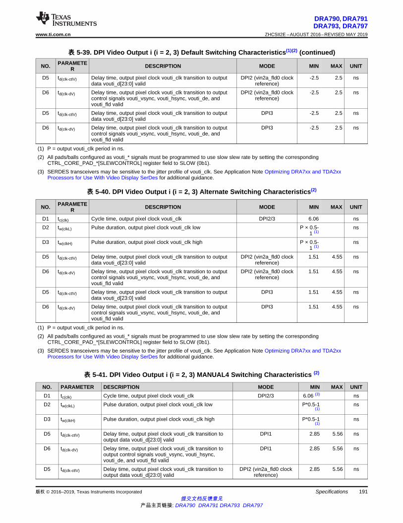
191
DRA790, DRA791DRA793, DRA797
www.ti.com.cn ZHCSII2E –AUGUST 2016–REVISED MAY 2019
提交文档反馈意见产品主页链接: DRA790 DRA791 DRA793 DRA797
Specifications版权 © 2016–2019, Texas Instruments Incorporated
表表 5-39. DPI Video Output i (i = 2, 3) Default Switching Characteristics(1)(2) (continued)
NO. PARAMETER DESCRIPTION MODE MIN MAX UNIT
D5 td(clk-ctlV) Delay time, output pixel clock vouti_clk transition to outputdata vouti_d[23:0] valid
DPI2 (vin2a_fld0 clockreference)
-2.5 2.5 ns
D6 td(clk-dV) Delay time, output pixel clock vouti_clk transition to outputcontrol signals vouti_vsync, vouti_hsync, vouti_de, andvouti_fld valid
DPI2 (vin2a_fld0 clockreference)
-2.5 2.5 ns
D5 td(clk-ctlV) Delay time, output pixel clock vouti_clk transition to outputdata vouti_d[23:0] valid
DPI3 -2.5 2.5 ns
D6 td(clk-dV) Delay time, output pixel clock vouti_clk transition to outputcontrol signals vouti_vsync, vouti_hsync, vouti_de, andvouti_fld valid
DPI3 -2.5 2.5 ns
(1) P = output vouti_clk period in ns.(2) All pads/balls configured as vouti_* signals must be programmed to use slow slew rate by setting the corresponding
CTRL_CORE_PAD_*[SLEWCONTROL] register field to SLOW (0b1).(3) SERDES transceivers may be sensitive to the jitter profile of vouti_clk. See Application Note Optimizing DRA7xx and TDA2xx
Processors for Use With Video Display SerDes for additional guidance.
表表 5-40. DPI Video Output i (i = 2, 3) Alternate Switching Characteristics(2)
NO. PARAMETER DESCRIPTION MODE MIN MAX UNIT
D1 tc(clk) Cycle time, output pixel clock vouti_clk DPI2/3 6.06 nsD2 tw(clkL) Pulse duration, output pixel clock vouti_clk low P × 0.5-
1 (1)ns
D3 tw(clkH) Pulse duration, output pixel clock vouti_clk high P × 0.5-1 (1)
ns
D5 td(clk-ctlV) Delay time, output pixel clock vouti_clk transition to outputdata vouti_d[23:0] valid
DPI2 (vin2a_fld0 clockreference)
1.51 4.55 ns
D6 td(clk-dV) Delay time, output pixel clock vouti_clk transition to outputcontrol signals vouti_vsync, vouti_hsync, vouti_de, andvouti_fld valid
DPI2 (vin2a_fld0 clockreference)
1.51 4.55 ns
D5 td(clk-ctlV) Delay time, output pixel clock vouti_clk transition to outputdata vouti_d[23:0] valid
DPI3 1.51 4.55 ns
D6 td(clk-dV) Delay time, output pixel clock vouti_clk transition to outputcontrol signals vouti_vsync, vouti_hsync, vouti_de, andvouti_fld valid
DPI3 1.51 4.55 ns
(1) P = output vouti_clk period in ns.(2) All pads/balls configured as vouti_* signals must be programmed to use slow slew rate by setting the corresponding
CTRL_CORE_PAD_*[SLEWCONTROL] register field to SLOW (0b1).(3) SERDES transceivers may be sensitive to the jitter profile of vouti_clk. See Application Note Optimizing DRA7xx and TDA2xx
Processors for Use With Video Display SerDes for additional guidance.
表表 5-41. DPI Video Output i (i = 2, 3) MANUAL4 Switching Characteristics (2)
NO. PARAMETER DESCRIPTION MODE MIN MAX UNITD1 tc(clk) Cycle time, output pixel clock vouti_clk DPI2/3 6.06 (3) nsD2 tw(clkL) Pulse duration, output pixel clock vouti_clk low P*0.5-1
(1)ns
D3 tw(clkH) Pulse duration, output pixel clock vouti_clk high P*0.5-1(1)
ns
D5 td(clk-ctlV) Delay time, output pixel clock vouti_clk transition tooutput data vouti_d[23:0] valid
DPI1 2.85 5.56 ns
D6 td(clk-dV) Delay time, output pixel clock vouti_clk transition tooutput control signals vouti_vsync, vouti_hsync,vouti_de, and vouti_fld valid
DPI1 2.85 5.56 ns
D5 td(clk-ctlV) Delay time, output pixel clock vouti_clk transition tooutput data vouti_d[23:0] valid
DPI2 (vin2a_fld0 clockreference)
2.85 5.56 ns

192
DRA790, DRA791DRA793, DRA797ZHCSII2E –AUGUST 2016–REVISED MAY 2019 www.ti.com.cn
提交文档反馈意见产品主页链接: DRA790 DRA791 DRA793 DRA797
Specifications 版权 © 2016–2019, Texas Instruments Incorporated
表表 5-41. DPI Video Output i (i = 2, 3) MANUAL4 Switching Characteristics (2) (continued)NO. PARAMETER DESCRIPTION MODE MIN MAX UNITD6 td(clk-dV) Delay time, output pixel clock vouti_clk transition to
output control signals vouti_vsync, vouti_hsync,vouti_de, and vouti_fld valid
DPI2 (vin2a_fld0 clockreference)
2.85 5.56 ns
D5 td(clk-ctlV) Delay time, output pixel clock vouti_clk transition tooutput data vouti_d[23:0] valid
DPI2 (xref_clk2 clockreference)
2.85 5.56 ns
D6 td(clk-dV) Delay time, output pixel clock vouti_clk transition tooutput control signals vouti_vsync, vouti_hsync,vouti_de, and vouti_fld valid
DPI2 (xref_clk2 clockreference)
2.85 5.56 ns
D5 td(clk-ctlV) Delay time, output pixel clock vouti_clk transition tooutput data vouti_d[23:0] valid
DPI3 2.85 5.56 ns
D6 td(clk-dV) Delay time, output pixel clock vouti_clk transition tooutput control signals vouti_vsync, vouti_hsync,vouti_de, and vouti_fld valid
DPI3 2.85 5.56 ns
(1) P = output vouti_clk period in ns.(2) All pads/balls configured as vouti_* signals must be programmed to use slow slew rate by setting the corresponding
CTRL_CORE_PAD_*[SLEWCONTROL] register field to SLOW (0b1).(3) SERDES transceivers may be sensitive to the jitter profile of vouti_clk. See Application Note Optimizing DRA7xx and TDA2xx
Processors for Use With Video Display SerDes for additional guidance.
表表 5-42. DPI Video Output i (i = 2, 3) MANUAL5 Switching Characteristics (2)
NO. PARAMETER DESCRIPTION MODE MIN MAX UNITD1 tc(clk) Cycle time, output pixel clock vouti_clk DPI2/3 6.06 (3) nsD2 tw(clkL) Pulse duration, output pixel clock vouti_clk low P*0.5-1
(1)ns
D3 tw(clkH) Pulse duration, output pixel clock vouti_clk high P*0.5-1(1)
ns
D5 td(clk-ctlV) Delay time, output pixel clock vouti_clk transition tooutput data vouti_d[23:0] valid
DPI1 3.55 6.61 ns
D6 td(clk-dV) Delay time, output pixel clock vouti_clk transition tooutput control signals vouti_vsync, vouti_hsync,vouti_de, and vouti_fld valid
DPI1 3.55 6.61 ns
D5 td(clk-ctlV) Delay time, output pixel clock vouti_clk transition tooutput data vouti_d[23:0] valid
DPI2 (vin2a_fld0 clockreference)
3.55 6.61 ns
D6 td(clk-dV) Delay time, output pixel clock vouti_clk transition tooutput control signals vouti_vsync, vouti_hsync,vouti_de, and vouti_fld valid
DPI2 (vin2a_fld0 clockreference)
3.55 6.61 ns
D5 td(clk-ctlV) Delay time, output pixel clock vouti_clk transition tooutput data vouti_d[23:0] valid
DPI2 (xref_clk2 clockreference)
3.55 6.61 ns
D6 td(clk-dV) Delay time, output pixel clock vouti_clk transition tooutput control signals vouti_vsync, vouti_hsync,vouti_de, and vouti_fld valid
DPI2 (xref_clk2 clockreference)
3.55 6.61 ns
D5 td(clk-ctlV) Delay time, output pixel clock vouti_clk transition tooutput data vouti_d[23:0] valid
DPI3 3.55 6.61 ns
D6 td(clk-dV) Delay time, output pixel clock vouti_clk transition tooutput control signals vouti_vsync, vouti_hsync,vouti_de, and vouti_fld valid
DPI3 3.55 6.61 ns

vouti_clk
vouti_vsync
vouti_hsync
vouti_d[23:0]
vouti_de
vouti_fld
data_1 data_2 data_n
odd even
D1
D2
D3
D6
D6
D5
D6
D6
SWPS049-018
D4
vouti_clk
Falling-edge Clock Reference
Rising-edge Clock Reference
193
DRA790, DRA791DRA793, DRA797
www.ti.com.cn ZHCSII2E –AUGUST 2016–REVISED MAY 2019
提交文档反馈意见产品主页链接: DRA790 DRA791 DRA793 DRA797
Specifications版权 © 2016–2019, Texas Instruments Incorporated
(1) P = output vouti_clk period in ns.(2) All pads/balls configured as vouti_* signals must be programmed to use slow slew rate by setting the corresponding
CTRL_CORE_PAD_*[SLEWCONTROL] register field to SLOW (0b1).(3) SERDES transceivers may be sensitive to the jitter profile of vouti_clk. See Application Note Optimizing DRA7xx and TDA2xx
Processors for Use With Video Display SerDes for additional guidance.
图图 5-22. DPI Video Output(1)(2)(3)
(1) The configuration of assertion of the data can be programmed on the falling or rising edge of the pixel clock.(2) The polarity and the pulse width of vouti_hsync and vouti_vsync are programmable, refer to the DSS section of the device TRM.(3) The vouti_clk frequency can be configured, refer to the DSS section of the device TRM.
In 表 5-43 are presented the specific groupings of signals (IOSET) for use with VOUT2.
表表 5-43. VOUT2 IOSETs
SIGNALS IOSET1BALL MUX
vout2_d23 C8 4vout2_d22 B9 4vout2_d21 A7 4vout2_d20 A9 4vout2_d19 A8 4vout2_d18 A11 4vout2_d17 F10 4vout2_d16 A10 4vout2_d15 B10 4vout2_d14 E10 4vout2_d13 D10 4vout2_d12 C10 4vout2_d11 B11 4

194
DRA790, DRA791DRA793, DRA797ZHCSII2E –AUGUST 2016–REVISED MAY 2019 www.ti.com.cn
提交文档反馈意见产品主页链接: DRA790 DRA791 DRA793 DRA797
Specifications 版权 © 2016–2019, Texas Instruments Incorporated
表表 5-43. VOUT2 IOSETs (continued)SIGNALS IOSET1
BALL MUXvout2_d10 D11 4vout2_d9 C11 4vout2_d8 B12 4vout2_d7 A12 4vout2_d6 A13 4vout2_d5 E11 4vout2_d4 F11 4vout2_d3 B13 4vout2_d2 E13 4vout2_d1 C13 4vout2_d0 D13 4
vout2_vsync B8 4vout2_hsync E8 4
vout2_clk C7 4vout2_fld D8 4vout2_de B7 4
注注To configure the desired virtual mode the user must set MODESELECT bit andDELAYMODE bitfield for each corresponding pad control register.
The pad control registers are presented in 表 4-32 and described in Device TRM, ControlModule Chapter.
Virtual IO Timings Modes must be used to ensure some IO timings for VOUT3. See 表 5-29 ModesSummary for a list of IO timings requiring the use of Virtual IO Timings Modes. See 表 5-44 VirtualFunctions Mapping for VOUT3 for a definition of the Virtual modes.
表 5-44 presents the values for DELAYMODE bitfield.
表表 5-44. Virtual Functions Mapping for DSS VOUT3
BALL BALL NAME Delay Mode Value MUXMODEDSS_VIRTUAL1 3
B4 gpmc_ad15 14 vout3_d15K4 gpmc_a8 15 vout3_hsyncD1 gpmc_ad4 14 vout3_d4F1 gpmc_ad0 14 vout3_d0C4 gpmc_ad13 14 vout3_d13L2 gpmc_a2 15 vout3_d18E2 gpmc_ad1 14 vout3_d1K3 gpmc_a4 15 vout3_d20J1 gpmc_a6 15 vout3_d22A3 gpmc_ad14 14 vout3_d14M2 gpmc_a1 15 vout3_d17G3 gpmc_cs3 15 vout3_clkH1 gpmc_a9 15 vout3_vsyncB3 gpmc_ad11 14 vout3_d11B1 gpmc_ad6 14 vout3_d6

195
DRA790, DRA791DRA793, DRA797
www.ti.com.cn ZHCSII2E –AUGUST 2016–REVISED MAY 2019
提交文档反馈意见产品主页链接: DRA790 DRA791 DRA793 DRA797
Specifications版权 © 2016–2019, Texas Instruments Incorporated
表表 5-44. Virtual Functions Mapping for DSS VOUT3 (continued)BALL BALL NAME Delay Mode Value MUXMODE
DSS_VIRTUAL1 3E1 gpmc_ad2 14 vout3_d2C1 gpmc_ad3 14 vout3_d3K1 gpmc_a7 15 vout3_d23L1 gpmc_a3 15 vout3_d19A2 gpmc_ad10 14 vout3_d10B2 gpmc_ad7 14 vout3_d7J2 gpmc_a10 15 vout3_deK2 gpmc_a5 15 vout3_d21C2 gpmc_ad8 14 vout3_d8D2 gpmc_ad5 14 vout3_d5M1 gpmc_a0 15 vout3_d16C3 gpmc_ad12 14 vout3_d12L3 gpmc_a11 15 vout3_fldD3 gpmc_ad9 14 vout3_d9
注注To configure the desired Manual IO Timing Mode the user must follow the steps described insection "Manual IO Timing Modes" of the Device TRM.
The associated registers to configure are listed in the CFG REGISTER column. For moreinformation please see the Control Module Chapter in the Device TRM.
Manual IO Timings Modes must be used to ensure some IO timings for VOUT2. See 表 5-29, ModesSummary for a list of IO timings requiring the use of Manual IO Timings Modes. See 表 5-45, ManualFunctions Mapping for DSS VOUT2 IOSET1 for a definition of the Manual modes.
表 5-45 lists the A_DELAY and G_DELAY values needed to calculate the correct values to be set in theCFG_x registers.

版权 © 2016–2019, Texas Instruments IncorporatedSpecifications提交文档反馈意见
产品主页链接: DRA790 DRA791 DRA793 DRA797
196
DRA790, DRA791DRA793, DRA797ZHCSII2E –AUGUST 2016–REVISED MAY 2019 www.ti.com.cn
表表 5-45. Manual Functions Mapping for DSS VOUT2 IOSET1
BALL BALLNAME
VOUT2_IOSET1_MANUAL1
VOUT2_IOSET1_MANUAL2
VOUT2_IOSET1_MANUAL3
VOUT2_IOSET1_MANUAL4
VOUT2_IOSET1_MANUAL5
CFG REGISTER MUXMODE
A_DELAY(ps)
G_DELAY(ps)
A_DELAY(ps)
G_DELAY(ps)
A_DELAY(ps)
G_DELAY(ps)
A_DELAY(ps)
G_DELAY(ps)
A_DELAY(ps)
G_DELAY(ps)
4
D8 vin2a_clk0 2571 0 1059 0 1025 0 4110 0 4980 0 CFG_VIN2A_CLK0_OUT vout2_fldC8 vin2a_d0 2124 0 589 0 577 0 3613 0 4483 0 CFG_VIN2A_D0_OUT vout2_d23B9 vin2a_d1 2103 0 568 0 557 0 3442 0 4312 0 CFG_VIN2A_D1_OUT vout2_d22
D10 vin2a_d10 2091 0 557 0 545 0 3430 0 4200 0 CFG_VIN2A_D10_OUT vout2_d13C10 vin2a_d11 2142 0 608 0 596 0 3481 0 4251 0 CFG_VIN2A_D11_OUT vout2_d12B11 vin2a_d12 2920 385 1816 255 1783 276 3943 601 4713 601 CFG_VIN2A_D12_OUT vout2_d11D11 vin2a_d13 2776 322 1872 192 1838 213 3799 538 4669 538 CFG_VIN2A_D13_OUT vout2_d10C11 vin2a_d14 2904 0 1769 0 1757 0 3869 174 4739 174 CFG_VIN2A_D14_OUT vout2_d9B12 vin2a_d15 2670 257 1665 127 1632 148 3792 473 4662 473 CFG_VIN2A_D15_OUT vout2_d8A12 vin2a_d16 2814 155 1908 31 1878 43 3837 371 4707 371 CFG_VIN2A_D16_OUT vout2_d7A13 vin2a_d17 3002 199 1897 69 1865 89 4024 415 4894 415 CFG_VIN2A_D17_OUT vout2_d6E11 vin2a_d18 1893 0 358 0 347 0 3432 0 4302 0 CFG_VIN2A_D18_OUT vout2_d5F11 vin2a_d19 1698 0 163 0 151 0 3237 0 4007 0 CFG_VIN2A_D19_OUT vout2_d4A7 vin2a_d2 2193 0 658 0 646 0 3531 0 4401 0 CFG_VIN2A_D2_OUT vout2_d21B13 vin2a_d20 1736 0 202 0 190 0 3075 0 3945 0 CFG_VIN2A_D20_OUT vout2_d3E13 vin2a_d21 1636 0 101 0 89 0 3074 0 3944 0 CFG_VIN2A_D21_OUT vout2_d2C13 vin2a_d22 1628 0 93 0 81 0 3266 0 4036 0 CFG_VIN2A_D22_OUT vout2_d1D13 vin2a_d23 1538 0 0 0 0 0 2968 0 3838 0 CFG_VIN2A_D23_OUT vout2_d0A9 vin2a_d3 1997 0 462 0 450 0 3335 0 4205 0 CFG_VIN2A_D3_OUT vout2_d20A8 vin2a_d4 2528 0 993 0 982 0 3867 0 4537 0 CFG_VIN2A_D4_OUT vout2_d19A11 vin2a_d5 2038 0 503 0 492 0 3577 0 4347 0 CFG_VIN2A_D5_OUT vout2_d18F10 vin2a_d6 1746 0 211 0 200 0 3285 0 4055 0 CFG_VIN2A_D6_OUT vout2_d17A10 vin2a_d7 2213 0 678 0 666 0 3552 0 4272 0 CFG_VIN2A_D7_OUT vout2_d16B10 vin2a_d8 2268 0 733 0 721 0 3607 0 4277 0 CFG_VIN2A_D8_OUT vout2_d15E10 vin2a_d9 2170 0 635 0 623 0 3509 0 4379 0 CFG_VIN2A_D9_OUT vout2_d14B7 vin2a_de0 2102 0 568 0 556 0 3841 0 4611 0 CFG_VIN2A_DE0_OUT vout2_deC7 vin2a_fld0 0 983 1398 1185 1385 1202 0 994 0 994 CFG_VIN2A_FLD0_OUT vout2_clkE8 vin2a_hsy
nc02482 0 974 0 936 0 4021 0 4891 0 CFG_VIN2A_HSYNC0_
OUTvout2_hsync
B8 vin2a_vsync0
2296 0 784 0 750 0 3935 0 4805 0 CFG_VIN2A_VSYNC0_OUT
vout2_vsync

版权 © 2016–2019, Texas Instruments Incorporated Specifications提交文档反馈意见
产品主页链接: DRA790 DRA791 DRA793 DRA797
197
DRA790, DRA791DRA793, DRA797
www.ti.com.cn ZHCSII2E –AUGUST 2016–REVISED MAY 2019

198
DRA790, DRA791DRA793, DRA797ZHCSII2E –AUGUST 2016–REVISED MAY 2019 www.ti.com.cn
提交文档反馈意见产品主页链接: DRA790 DRA791 DRA793 DRA797
Specifications 版权 © 2016–2019, Texas Instruments Incorporated
Manual IO Timings Modes must be used to ensure some IO timings for VOUT3. See 表 5-29, ModesSummary for a list of IO timings requiring the use of Manual IO Timings Modes. See 表 5-46, ManualFunctions Mapping for DSS VOUT3 for a definition of the Manual modes.
表 5-46 lists the A_DELAY and G_DELAY values needed to calculate the correct values to be set in theCFG_x registers.
表表 5-46. Manual Functions Mapping for DSS VOUT3
BALL BALLNAME
VOUT3_MANUAL1 VOUT3_MANUAL4 VOUT3_MANUAL5 CFG REGISTER MUXMODEA_DELAY
(ps)G_DELAY
(ps)A_DELAY
(ps)G_DELAY
(ps)A_DELAY
(ps)G_DELAY
(ps)3
M1 gpmc_a0 2395 0 3909 0 4779 0 CFG_GPMC_A0_OUT vout3_d16M2 gpmc_a1 2412 0 3957 0 4827 0 CFG_GPMC_A1_OUT vout3_d17J2 gpmc_a10 2473 0 3980 0 4850 0 CFG_GPMC_A10_OUT vout3_deL3 gpmc_a11 2906 0 4253 0 5123 0 CFG_GPMC_A11_OUT vout3_fldL2 gpmc_a2 2360 0 3873 0 4743 0 CFG_GPMC_A2_OUT vout3_d18L1 gpmc_a3 2391 0 4112 0 4982 0 CFG_GPMC_A3_OUT vout3_d19K3 gpmc_a4 2626 0 4336 0 5206 0 CFG_GPMC_A4_OUT vout3_d20K2 gpmc_a5 2338 0 3840 0 4710 0 CFG_GPMC_A5_OUT vout3_d21J1 gpmc_a6 2374 0 3913 0 4783 0 CFG_GPMC_A6_OUT vout3_d22K1 gpmc_a7 2432 0 3947 0 4817 0 CFG_GPMC_A7_OUT vout3_d23K4 gpmc_a8 3155 0 4309 105 5179 105 CFG_GPMC_A8_OUT vout3_hsyncH1 gpmc_a9 2309 0 3842 0 4712 0 CFG_GPMC_A9_OUT vout3_vsyncF1 gpmc_ad0 2360 0 3652 0 4522 0 CFG_GPMC_AD0_OUT vout3_d0E2 gpmc_ad1 2420 0 3762 0 4632 0 CFG_GPMC_AD1_OUT vout3_d1A2 gpmc_ad10 2235 0 3456 0 4326 0 CFG_GPMC_AD10_OUT vout3_d10B3 gpmc_ad11 2253 0 3584 0 4454 0 CFG_GPMC_AD11_OUT vout3_d11C3 gpmc_ad12 1949 427 3589 0 4459 0 CFG_GPMC_AD12_OUT vout3_d12C4 gpmc_ad13 2318 0 3547 0 4417 0 CFG_GPMC_AD13_OUT vout3_d13A3 gpmc_ad14 2123 0 3302 0 4172 0 CFG_GPMC_AD14_OUT vout3_d14B4 gpmc_ad15 2195 29 3532 0 4402 0 CFG_GPMC_AD15_OUT vout3_d15E1 gpmc_ad2 2617 0 3859 0 4729 0 CFG_GPMC_AD2_OUT vout3_d2C1 gpmc_ad3 2350 0 3590 0 4460 0 CFG_GPMC_AD3_OUT vout3_d3D1 gpmc_ad4 2324 0 3534 0 4404 0 CFG_GPMC_AD4_OUT vout3_d4D2 gpmc_ad5 2371 0 3609 0 4479 0 CFG_GPMC_AD5_OUT vout3_d5B1 gpmc_ad6 2231 0 3416 0 4286 0 CFG_GPMC_AD6_OUT vout3_d6B2 gpmc_ad7 2440 0 3661 0 4531 0 CFG_GPMC_AD7_OUT vout3_d7C2 gpmc_ad8 2479 0 3714 0 4584 0 CFG_GPMC_AD8_OUT vout3_d8D3 gpmc_ad9 2355 0 3593 0 4463 0 CFG_GPMC_AD9_OUT vout3_d9G3 gpmc_cs3 0 641 0 905 0 905 CFG_GPMC_CS3_OUT vout3_clk
5.10.6.5 HDMI
The High-Definition Multimedia Interface is provided for transmitting digital television audiovisual signalsfrom DVD players, set-top boxes and other audiovisual sources to television sets, projectors and othervideo displays. The HDMI interface is aligned with the HDMI TMDS single stream standard v1.4a (720p@60Hz to 1080p @24Hz) and the HDMI v1.3 (1080p @60Hz): 3 data channels, plus 1 clock channel issupported (differential).
In are presented the specific groupings of signals (IOSET) for use with HDMI.

199
DRA790, DRA791DRA793, DRA797
www.ti.com.cn ZHCSII2E –AUGUST 2016–REVISED MAY 2019
提交文档反馈意见产品主页链接: DRA790 DRA791 DRA793 DRA797
Specifications版权 © 2016–2019, Texas Instruments Incorporated
注注For more information, see the High-Definition Multimedia Interface chapter of the deviceTRM
5.10.6.6 CSI2
注注For more information, see the Camera Serial Interface 2 CAL Bridge chapter of the deviceTRM
The camera adaptation layer (CAL) deals with the processing of the pixel data coming from an externalimage sensor, data from memory. The CAL is a key component for the following multimedia applications:camera viewfinder, video record, and still image capture. The CAL has two serial camera interfaces(primary and secondary):• The primary serial interface (CSI2 Port A) is compliant with MIPI CSI-2 protocol with four data lanes.
5.10.6.6.1 CSI-2 MIPI D-PHY
The CSI-2 port A is compliant with the MIPI D-PHY RX specification v1.00.00 and the MIPI CSI-2specification v1.00, with 2 data differential lanes plus 1 clock differential lane in synchronous mode,double data rate:• 1.5 Gbps (750 MHz) @OPP_NOM for each lane.
5.10.6.7 EMIF
The device has a dedicated interface to DDR3 and DDR3L SDRAM. It supports JEDEC standardcompliant DDR3 and DDR3L SDRAM devices with the following features:• 16-bit or 32-bit data path to external SDRAM memory• Memory device capacity: 128Mb, 256Mb, 512Mb, 1Gb, 2Gb, 4Gb and 8Gb devices• One interface with associated DDR3/DDR3L PHYs
注注For more information, see the EMIF Controller section of the Device TRM.
5.10.6.8 GPMC
The GPMC is the unified memory controller that interfaces external memory devices such as:• Asynchronous SRAM-like memories and ASIC devices• Asynchronous page mode and synchronous burst NOR flash• NAND flash
注注For more information, see the General-Purpose Memory Controller section of the DeviceTRM.

200
DRA790, DRA791DRA793, DRA797ZHCSII2E –AUGUST 2016–REVISED MAY 2019 www.ti.com.cn
提交文档反馈意见产品主页链接: DRA790 DRA791 DRA793 DRA797
Specifications 版权 © 2016–2019, Texas Instruments Incorporated
5.10.6.8.1 GPMC/NOR Flash Interface Synchronous Timing
CAUTION
The I/O Timings provided in this section are valid only for some GPMC usagemodes when the corresponding Virtual I/O Timings or Manual I/O Timings areconfigured as described in the tables found in this section.
表 5-47 and 表 5-48 assume testing over the recommended operating conditions and electricalcharacteristic conditions below (see 图 5-23, 图 5-24, 图 5-25, 图 5-26, 图 5-27 and 图 5-28).
表表 5-47. GPMC/NOR Flash Interface Timing Requirements - Synchronous Mode - Default
NO. PARAMETER DESCRIPTION MIN MAX UNITF12 tsu(dV-clkH) Setup time, read gpmc_ad[15:0] valid before gpmc_clk high 3 nsF13 th(clkH-dV) Hold time, read gpmc_ad[15:0] valid after gpmc_clk high 1.1 nsF21 tsu(waitV-clkH) Setup time, gpmc_wait[1:0] valid before gpmc_clk high 2.5 nsF22 th(clkH-waitV) Hold Time, gpmc_wait[1:0] valid after gpmc_clk high 1.3 ns
注注Wait monitoring support is limited to a WaitMonitoringTime value > 0. For a full description ofwait monitoring feature, see the Device TRM.
表表 5-48. GPMC/NOR Flash Interface Switching Characteristics - Synchronous Mode - Default
NO. PARAMETER DESCRIPTION MIN MAX UNITF0 tc(clk) Cycle time, output clock gpmc_clk period 11.3 nsF2 td(clkH-nCSV) Delay time, gpmc_clk rising edge to gpmc_cs[7:0] transition F-1.7 (7) F+4.3 (7) nsF3 td(clkH-nCSIV) Delay time, gpmc_clk rising edge to gpmc_cs[7:0] invalid E-1.7 (6) E+4.2 (6) nsF4 td(ADDV-clk) Delay time, gpmc_a[27:0] address bus valid to gpmc_clk first edge B-1.8 (3) B+4.3 (3) nsF5 td(clkH-ADDIV) Delay time, gpmc_clk rising edge to gpmc_a[27:0] gpmc address bus invalid -1.8 nsF6 td(nBEV-clk) Delay time, gpmc_ben[1:0] valid to gpmc_clk rising edge B-4.3(3) B+1.5(3) nsF7 td(clkH-nBEIV) Delay time, gpmc_clk rising edge to gpmc_ben[1:0] invalid D-1.5(5) D+4.3(5) nsF8 td(clkH-nADV) Delay time, gpmc_clk rising edge to gpmc_advn_ale transition G-1.3 (8) G+4.2 (8) nsF9 td(clkH-nADVIV) Delay time, gpmc_clk rising edge to gpmc_advn_ale invalid D-1.3 (5) G+4.2 (5) nsF10 td(clkH-nOE) Delay time, gpmc_clk rising edge to gpmc_oen_ren transition H-1.0 (9) H+3.2 (9) nsF11 td(clkH-nOEIV) Delay time, gpmc_clk rising edge to gpmc_oen_ren invalid E-1.0 (6) E+3.2 (6) nsF14 td(clkH-nWE) Delay time, gpmc_clk rising edge to gpmc_wen transition I-0.9 (10) I+4.2 (10) nsF15 td(clkH-Data) Delay time, gpmc_clk rising edge to gpmc_ad[15:0] data bus transition J-2.1 (11) J+4.6 (11) nsF17 td(clkH-nBE) Delay time, gpmc_clk rising edge to gpmc_ben[1:0] transition J-1.5 (11) J+4.3 (11) nsF18 tw(nCSV) Pulse duration, gpmc_cs[7:0] low A (2) nsF19 tw(nBEV) Pulse duration, gpmc_ben[1:0] low C (4) nsF20 tw(nADVV) Pulse duration, gpmc_advn_ale low K (12) nsF23 td(CLK-GPIO) Delay time, gpmc_clk transition to gpio6_16 transition 0.5 7.5 ns
表表 5-49. GPMC/NOR Flash Interface Timing Requirements - Synchronous Mode - Alternate
NO. PARAMETER DESCRIPTION MIN MAX UNITF12 tsu(dV-clkH) Setup time, read gpmc_ad[15:0] valid before gpmc_clk high 2.5 nsF13 th(clkH-dV) Hold time, read gpmc_ad[15:0] valid after gpmc_clk high 1.9 ns

201
DRA790, DRA791DRA793, DRA797
www.ti.com.cn ZHCSII2E –AUGUST 2016–REVISED MAY 2019
提交文档反馈意见产品主页链接: DRA790 DRA791 DRA793 DRA797
Specifications版权 © 2016–2019, Texas Instruments Incorporated
表表 5-49. GPMC/NOR Flash Interface Timing Requirements - Synchronous Mode - Alternate (continued)NO. PARAMETER DESCRIPTION MIN MAX UNITF21 tsu(waitV-clkH) Setup time, gpmc_wait[1:0] valid before gpmc_clk high 2.5 nsF22 th(clkH-waitV) Hold Time, gpmc_wait[1:0] valid after gpmc_clk high 1.9 ns
表表 5-50. GPMC/NOR Flash Interface Switching Characteristics - Synchronous Mode - Alternate
NO. PARAMETER DESCRIPTION MIN MAX UNITF0 tc(clk) Cycle time, output clock gpmc_clk period (13) 15.04 nsF2 td(clkH-nCSV) Delay time, gpmc_clk rising edge to gpmc_cs[7:0] transition F+0.6 (7) F+7.0 (7) nsF3 td(clkH-nCSIV) Delay time, gpmc_clk rising edge to gpmc_cs[7:0] invalid E+0.6 (6) E+7.0 (6) nsF4 td(ADDV-clk) Delay time, gpmc_a[27:0] address bus valid to gpmc_clk first edge B-0.7 (3) B+7.0 (3) nsF5 td(clkH-ADDIV) Delay time, gpmc_clk rising edge to gpmc_a[27:0] gpmc address bus invalid -0.7 nsF6 td(nBEV-clk) Delay time, gpmc_ben[1:0] valid to gpmc_clk rising edge B-7.0 B+0.4 nsF7 td(clkH-nBEIV) Delay time, gpmc_clk rising edge to gpmc_ben[1:0] invalid D-0.4 D+7.0 nsF8 td(clkH-nADV) Delay time, gpmc_clk rising edge to gpmc_advn_ale transition G+0.7 (8) G+6.1 (8) nsF9 td(clkH-nADVIV) Delay time, gpmc_clk rising edge to gpmc_advn_ale invalid D+0.7 (5) D+6.1 (5) ns
F10 td(clkH-nOE) Delay time, gpmc_clk rising edge to gpmc_oen_ren transition H+0.7 (9) H+5.1 (9) nsF11 td(clkH-nOEIV) Delay time, gpmc_clk rising edge to gpmc_oen_ren invalid E+0.7 (6) E+5.1 (6) nsF14 td(clkH-nWE) Delay time, gpmc_clk rising edge to gpmc_wen transition I+0.7 (10) I+6.1 (10) nsF15 td(clkH-Data) Delay time, gpmc_clk rising edge to gpmc_ad[15:0] data bus transition J-0.4 (11) J+4.9 (11) nsF17 td(clkH-nBE) Delay time, gpmc_clk rising edge to gpmc_ben[1:0] transition J-0.4 (11) J+4.9 (11) nsF18 tw(nCSV) Pulse duration, gpmc_cs[7:0] low A (2) nsF19 tw(nBEV) Pulse duration, gpmc_ben[1:0] low C (4) nsF20 tw(nADVV) Pulse duration, gpmc_advn_ale low K (12) nsF23 td(CLK-GPIO) Delay time, gpmc_clk transition to gpio6_16.clkout1 transition (14) 0.5 7.5 ns
(1) Total GPMC load on any signal at 3.3V must not exceed 10pF.(2) For single read: A = (CSRdOffTime - CSOnTime) × (TimeParaGranularity + 1) × GPMC_FCLK period
For burst read: A = (CSRdOffTime - CSOnTime + (n - 1) × PageBurstAccessTime) × (TimeParaGranularity + 1) × GPMC_FCLK periodFor burst write: A = (CSWrOffTime - CSOnTime + (n - 1) × PageBurstAccessTime) × (TimeParaGranularity + 1) × GPMC_FCLK periodwith n the page burst access number.
(3) B = ClkActivationTime × GPMC_FCLK(4) For single read: C = RdCycleTime × (TimeParaGranularity + 1) × GPMC_FCLK
For burst read: C = (RdCycleTime + (n - 1) × PageBurstAccessTime) × (TimeParaGranularity + 1) × GPMC_FCLKFor Burst write: C = (WrCycleTime + (n - 1) × PageBurstAccessTime) × (TimeParaGranularity + 1) × GPMC_FCLK with n the page burstaccess number.
(5) For single read: D = (RdCycleTime - AccessTime) × (TimeParaGranularity + 1) × GPMC_FCLKFor burst read: D = (RdCycleTime - AccessTime) × (TimeParaGranularity + 1) × GPMC_FCLKFor burst write: D = (WrCycleTime - AccessTime) × (TimeParaGranularity + 1) × GPMC_FCLK
(6) For single read: E = (CSRdOffTime - AccessTime) × (TimeParaGranularity + 1) × GPMC_FCLKFor burst read: E = (CSRdOffTime - AccessTime) × (TimeParaGranularity + 1) × GPMC_FCLKFor burst write: E = (CSWrOffTime - AccessTime) × (TimeParaGranularity + 1) × GPMC_FCLK
(7) For nCS falling edge (CS activated):Case GpmcFCLKDivider = 0 :F = 0.5 × CSExtraDelay × GPMC_FCLK Case GpmcFCLKDivider = 1:F = 0.5 × CSExtraDelay × GPMC_FCLK if (ClkActivationTime and CSOnTime are odd) or (ClkActivationTime and CSOnTime are even)F = (1 + 0.5 × CSExtraDelay) × GPMC_FCLK otherwiseCase GpmcFCLKDivider = 2:F = 0.5 × CSExtraDelay × GPMC_FCLK if ((CSOnTime - ClkActivationTime) is a multiple of 3)F = (1 + 0.5 × CSExtraDelay) × GPMC_FCLK if ((CSOnTime - ClkActivationTime - 1) is a multiple of 3)F = (2 + 0.5 × CSExtraDelay) × GPMC_FCLK if ((CSOnTime - ClkActivationTime - 2) is a multiple of 3)Case GpmcFCLKDivider = 3:F = 0.5 × CSExtraDelay × GPMC_FCLK if ((CSOnTime - ClkActivationTime) is a multiple of 4)F = (1 + 0.5 × CSExtraDelay) × GPMC_FCLK if ((CSOnTime - ClkActivationTime - 1) is a multiple of 4)F = (2 + 0.5 × CSExtraDelay) × GPMC_FCLK if ((CSOnTime - ClkActivationTime - 2) is a multiple of 4)F = (3 + 0.5 × CSExtraDelay) × GPMC_FCLK if ((CSOnTime - ClkActivationTime - 3) is a multiple of 4)

202
DRA790, DRA791DRA793, DRA797ZHCSII2E –AUGUST 2016–REVISED MAY 2019 www.ti.com.cn
提交文档反馈意见产品主页链接: DRA790 DRA791 DRA793 DRA797
Specifications 版权 © 2016–2019, Texas Instruments Incorporated
(8) For ADV falling edge (ADV activated):Case GpmcFCLKDivider = 0 :G = 0.5 × ADVExtraDelay × GPMC_FCLKCase GpmcFCLKDivider = 1:G = 0.5 × ADVExtraDelay × GPMC_FCLK if (ClkActivationTime and ADVOnTime are odd) or (ClkActivationTime and ADVOnTime areeven)G = (1 + 0.5 × ADVExtraDelay) × GPMC_FCLK otherwiseCase GpmcFCLKDivider = 2:G = 0.5 × ADVExtraDelay × GPMC_FCLK if ((ADVOnTime - ClkActivationTime) is a multiple of 3)G = (1 + 0.5 × ADVExtraDelay) × GPMC_FCLK if ((ADVOnTime - ClkActivationTime - 1) is a multiple of 3)G = (2 + 0.5 × ADVExtraDelay) × GPMC_FCLK if ((ADVOnTime - ClkActivationTime - 2) is a multiple of 3)For ADV rising edge (ADV desactivated) in Reading mode:Case GpmcFCLKDivider = 0:G = 0.5 × ADVExtraDelay × GPMC_FCLKCase GpmcFCLKDivider = 1:G = 0.5 × ADVExtraDelay × GPMC_FCLK if (ClkActivationTime and ADVRdOffTime are odd) or (ClkActivationTime and ADVRdOffTimeare even)G = (1 + 0.5 × ADVExtraDelay) × GPMC_FCLK otherwiseCase GpmcFCLKDivider = 2:G = 0.5 × ADVExtraDelay × GPMC_FCLK if ((ADVRdOffTime - ClkActivationTime) is a multiple of 3)G = (1 + 0.5 × ADVExtraDelay) × GPMC_FCLK if ((ADVRdOffTime - ClkActivationTime - 1) is a multiple of 3)G = (2 + 0.5 × ADVExtraDelay) × GPMC_FCLK if ((ADVRdOffTime - ClkActivationTime - 2) is a multiple of 3)Case GpmcFCLKDivider = 3:G = 0.5 × ADVExtraDelay × GPMC_FCLK if ((ADVRdOffTime - ClkActivationTime) is a multiple of 4)G = (1 + 0.5 × ADVExtraDelay) × GPMC_FCLK if ((ADVRdOffTime - ClkActivationTime - 1) is a multiple of 4)G = (2 + 0.5 × ADVExtraDelay) × GPMC_FCLK if ((ADVRdOffTime - ClkActivationTime - 2) is a multiple of 4)G = (3 + 0.5 × ADVExtraDelay) × GPMC_FCLK if ((ADVRdOffTime - ClkActivationTime - 3) is a multiple of 4)For ADV rising edge (ADV desactivated) in Writing mode:Case GpmcFCLKDivider = 0:G = 0.5 × ADVExtraDelay × GPMC_FCLKCase GpmcFCLKDivider = 1:G = 0.5 × ADVExtraDelay × GPMC_FCLK if (ClkActivationTime and ADVWrOffTime are odd) or (ClkActivationTime and ADVWrOffTimeare even)G = (1 + 0.5 × ADVExtraDelay) × GPMC_FCLK otherwiseCase GpmcFCLKDivider = 2:G = 0.5 × ADVExtraDelay × GPMC_FCLK if ((ADVWrOffTime - ClkActivationTime) is a multiple of 3)G = (1 + 0.5 × ADVExtraDelay) × GPMC_FCLK if ((ADVWrOffTime - ClkActivationTime - 1) is a multiple of 3)G = (2 + 0.5 × ADVExtraDelay) × GPMC_FCLK if ((ADVWrOffTime - ClkActivationTime - 2) is a multiple of 3)Case GpmcFCLKDivider = 3:G = 0.5 × ADVExtraDelay × GPMC_FCLK if ((ADVWrOffTime - ClkActivationTime) is a multiple of 4)G = (1 + 0.5 × ADVExtraDelay) × GPMC_FCLK if ((ADVWrOffTime - ClkActivationTime - 1) is a multiple of 4)G = (2 + 0.5 × ADVExtraDelay) × GPMC_FCLK if ((ADVWrOffTime - ClkActivationTime - 2) is a multiple of 4)G = (3 + 0.5 × ADVExtraDelay) × GPMC_FCLK if ((ADVWrOffTime - ClkActivationTime - 3) is a multiple of 4)
(9) For OE falling edge (OE activated):Case GpmcFCLKDivider = 0:- H = 0.5 × OEExtraDelay × GPMC_FCLKCase GpmcFCLKDivider = 1:- H = 0.5 × OEExtraDelay × GPMC_FCLK if (ClkActivationTime and OEOnTime are odd) or (ClkActivationTime and OEOnTime areeven)- H = (1 + 0.5 × OEExtraDelay) × GPMC_FCLK otherwiseCase GpmcFCLKDivider = 2:- H = 0.5 × OEExtraDelay × GPMC_FCLK if ((OEOnTime - ClkActivationTime) is a multiple of 3)- H = (1 + 0.5 × OEExtraDelay) × GPMC_FCLK if ((OEOnTime - ClkActivationTime - 1) is a multiple of 3)- H = (2 + 0.5 × OEExtraDelay) × GPMC_FCLK if ((OEOnTime - ClkActivationTime - 2) is a multiple of 3)Case GpmcFCLKDivider = 3:- H = 0.5 × OEExtraDelay × GPMC_FCLK if ((OEOnTime - ClkActivationTime) is a multiple of 4)- H = (1 + 0.5 × OEExtraDelay) × GPMC_FCLK if ((OEOnTime - ClkActivationTime - 1) is a multiple of 4)- H = (2 + 0.5 × OEExtraDelay) × GPMC_FCLK if ((OEOnTime - ClkActivationTime - 2) is a multiple of 4)- H = (3 + 0.5 × OEExtraDelay)) × GPMC_FCLK if ((OEOnTime - ClkActivationTime - 3) is a multiple of 4)For OE rising edge (OE desactivated):Case GpmcFCLKDivider = 0:- H = 0.5 × OEExtraDelay × GPMC_FCLKCase GpmcFCLKDivider = 1:- H = 0.5 × OEExtraDelay × GPMC_FCLK if (ClkActivationTime and OEOffTime are odd) or (ClkActivationTime and OEOffTime areeven)- H = (1 + 0.5 × OEExtraDelay) × GPMC_FCLK otherwiseCase GpmcFCLKDivider = 2:- H = 0.5 × OEExtraDelay × GPMC_FCLK if ((OEOffTime - ClkActivationTime) is a multiple of 3)- H = (1 + 0.5 × OEExtraDelay) × GPMC_FCLK if ((OEOffTime - ClkActivationTime - 1) is a multiple of 3)- H = (2 + 0.5 × OEExtraDelay) × GPMC_FCLK if ((OEOffTime - ClkActivationTime - 2) is a multiple of 3)Case GpmcFCLKDivider = 3:- H = 0.5 × OEExtraDelay × GPMC_FCLK if ((OEOffTime - ClkActivationTime) is a multiple of 4)

203
DRA790, DRA791DRA793, DRA797
www.ti.com.cn ZHCSII2E –AUGUST 2016–REVISED MAY 2019
提交文档反馈意见产品主页链接: DRA790 DRA791 DRA793 DRA797
Specifications版权 © 2016–2019, Texas Instruments Incorporated
- H = (1 + 0.5 × OEExtraDelay) × GPMC_FCLK if ((OEOffTime - ClkActivationTime - 1) is a multiple of 4)- H = (2 + 0.5 × OEExtraDelay) × GPMC_FCLK if ((OEOffTime - ClkActivationTime - 2) is a multiple of 4)- H = (3 + 0.5 × OEExtraDelay) × GPMC_FCLK if ((OEOffTime - ClkActivationTime - 3) is a multiple of 4)
(10) For WE falling edge (WE activated):Case GpmcFCLKDivider = 0:- I = 0.5 × WEExtraDelay × GPMC_FCLKCase GpmcFCLKDivider = 1:- I = 0.5 × WEExtraDelay × GPMC_FCLK if (ClkActivationTime and WEOnTime are odd) or (ClkActivationTime and WEOnTime areeven)- I = (1 + 0.5 × WEExtraDelay) × GPMC_FCLK otherwiseCase GpmcFCLKDivider = 2:- I = 0.5 × WEExtraDelay × GPMC_FCLK if ((WEOnTime - ClkActivationTime) is a multiple of 3)- I = (1 + 0.5 × WEExtraDelay) × GPMC_FCLK if ((WEOnTime - ClkActivationTime - 1) is a multiple of 3)- I = (2 + 0.5 × WEExtraDelay) × GPMC_FCLK if ((WEOnTime - ClkActivationTime - 2) is a multiple of 3)Case GpmcFCLKDivider = 3:- I = 0.5 × WEExtraDelay × GPMC_FCLK if ((WEOnTime - ClkActivationTime) is a multiple of 4)- I = (1 + 0.5 × WEExtraDelay) × GPMC_FCLK if ((WEOnTime - ClkActivationTime - 1) is a multiple of 4)- I = (2 + 0.5 × WEExtraDelay) × GPMC_FCLK if ((WEOnTime - ClkActivationTime - 2) is a multiple of 4)- I = (3 + 0.5 × WEExtraDelay) × GPMC_FCLK if ((WEOnTime - ClkActivationTime - 3) is a multiple of 4)For WE rising edge (WE desactivated):Case GpmcFCLKDivider = 0:- I = 0.5 × WEExtraDelay × GPMC_FCLKCase GpmcFCLKDivider = 1:- I = 0.5 × WEExtraDelay × GPMC_FCLK if (ClkActivationTime and WEOffTime are odd) or (ClkActivationTime and WEOffTime areeven)- I = (1 + 0.5 × WEExtraDelay) × GPMC_FCLK otherwiseCase GpmcFCLKDivider = 2:- I = 0.5 × WEExtraDelay × GPMC_FCLK if ((WEOffTime - ClkActivationTime) is a multiple of 3)- I = (1 + 0.5 × WEExtraDelay) × GPMC_FCLK if ((WEOffTime - ClkActivationTime - 1) is a multiple of 3)- I = (2 + 0.5 × WEExtraDelay) × GPMC_FCLK if ((WEOffTime - ClkActivationTime - 2) is a multiple of 3)Case GpmcFCLKDivider = 3:- I = 0.5 × WEExtraDelay × GPMC_FCLK if ((WEOffTime - ClkActivationTime) is a multiple of 4)- I = (1 + 0.5 × WEExtraDelay) × GPMC_FCLK if ((WEOffTime - ClkActivationTime - 1) is a multiple of 4)- I = (2 + 0.5 × WEExtraDelay) × GPMC_FCLK if ((WEOffTime - ClkActivationTime - 2) is a multiple of 4)- I = (3 + 0.5 × WEExtraDelay) × GPMC_FCLK if ((WEOffTime - ClkActivationTime - 3) is a multiple of 4)
(11) J = GPMC_FCLK period, where GPMC_FCLK is the General Purpose Memory Controller internal functional clock(12) For read:
K = (ADVRdOffTime - ADVOnTime) × (TimeParaGranularity + 1) × GPMC_FCLKFor write: K = (ADVWrOffTime - ADVOnTime) × (TimeParaGranularity + 1) × GPMC_FCLK
(13) The gpmc_clk output clock maximum and minimum frequency is programmable in the I/F module by setting the GPMC_CONFIG1_CSxconfiguration register bit fields GpmcFCLKDivider
(14) gpio6_16 programmed to MUXMODE=9 (clkout1), CM_CLKSEL_CLKOUTMUX1 programmed to 7 (CORE_DPLL_OUT_DCLK),CM_CLKSEL_CORE_DPLL_OUT_CLK_CLKOUTMUX programmed to 1.
(15) CSEXTRADELAY = 0, ADVEXTRADELAY = 0, WEEXTRADELAY = 0, OEEXTRADELAY = 0. Extra half-GPMC_FCLK cycle delaymode is not timed.

gpmc_clk
gpmc_csi
gpmc_a[ :1]1027gpmc_a[ ]
gpmc_be 1n
gpmc_ben0
gpmc_adv _alen
gpmc_oen_ren
gpmc_ad[15:0]
gpmc_waitj
Address (MSB)
Address (LSB) D 0
F0
F12
F13
F6
F2
F8
F3
F7
F9
F11
F1
F1
F8
F19
F18
F20
F10
F4 F5
F6 F7
F19
F4
F22 F21
F23
GPMC_01
gpio6_16.clkout1
F23
204
DRA790, DRA791DRA793, DRA797ZHCSII2E –AUGUST 2016–REVISED MAY 2019 www.ti.com.cn
提交文档反馈意见产品主页链接: DRA790 DRA791 DRA793 DRA797
Specifications 版权 © 2016–2019, Texas Instruments Incorporated
图图 5-23. GPMC / Multiplexed 16bits NOR Flash - Synchronous Single Read -(GpmcFCLKDivider = 0)(1)(2)
(1) In gpmc_csi, i = 0 to 7.(2) In gpmc_waitj, j = 0 to 1.

gpmc_clk
gpmc_csi
gpmc_a[2 :1]7
gpmc_be 1n
gpmc_ben0
gpmc_ _aleadvn
gpmc_oen_ren
gpmc_ad[15:0]
gpmc_waitj
Address
D 0
F0
F12
F13
F6
F2
F8
F3
F7
F9
F11
F1
F1
F8
F19
F18
F20
F10
F6 F7
F19
F4
F22 F21
F23
GPMC_02
gpio6_16.clkout1
F23
205
DRA790, DRA791DRA793, DRA797
www.ti.com.cn ZHCSII2E –AUGUST 2016–REVISED MAY 2019
提交文档反馈意见产品主页链接: DRA790 DRA791 DRA793 DRA797
Specifications版权 © 2016–2019, Texas Instruments Incorporated
图图 5-24. GPMC / Nonmultiplexed 16bits NOR Flash - Synchronous Single Read -(GpmcFCLKDivider = 0)(1)(2)
(1) In gpmc_csi, i = 0 to 7.(2) In gpmc_waitj, j = 0 to 1.

gpmc_clk
gpmc_csi
gpmc_a[ :1]1027gpmc_a[ ]
gpmc_ 1ben
gpmc_ben0
gpmc_ _aleadvn
gpmc_oen_ren
gpmc_ad[15:0]
gpmc_waitj
Address (MSB)
Valid
Valid
Address (LSB) D0 D1 D2 D3
F6
F4
F2
F8 F8
F10
F13
F12
F12
F11
F9
F7
F3
F0 F1
F1
F5
F6F7
F22 F21
F4
F18
F20
F19
F19
F23
GPMC_03
gpio6_16.clkout1
F23
206
DRA790, DRA791DRA793, DRA797ZHCSII2E –AUGUST 2016–REVISED MAY 2019 www.ti.com.cn
提交文档反馈意见产品主页链接: DRA790 DRA791 DRA793 DRA797
Specifications 版权 © 2016–2019, Texas Instruments Incorporated
图图 5-25. GPMC / Multiplexed 16bits NOR Flash - Synchronous Burst Read 4x16 bits -(GpmcFCLKDivider = 0)(1)(2)
(1) In gpmc_csi, i= 0 to 7.(2) In gpmc_waitj, j = 0 to 1.

gpmc_clk
gpmc_csi
gpmc_a[2 :1]7
gpmc_be 1n
gpmc_ben0
gpmc_ _aleadvn
gpmc_oen_ren
gpmc_ad[15:0]
gpmc_waitj
Address
Valid
Valid
D0 D1 D2 D3
F6
F2
F8 F8
F10
F13
F12
F12
F11
F9
F7
F3
F0 F1
F1
F6F7
F22 F21
F4
F18
F20
F19
F19
F23
GPMC_04
gpio6_16.clkout1
F23
207
DRA790, DRA791DRA793, DRA797
www.ti.com.cn ZHCSII2E –AUGUST 2016–REVISED MAY 2019
提交文档反馈意见产品主页链接: DRA790 DRA791 DRA793 DRA797
Specifications版权 © 2016–2019, Texas Instruments Incorporated
图图 5-26. GPMC / Nonmultiplexed 16bits NOR Flash - Synchronous Burst Read 4x16 bits -(GpmcFCLKDivider = 0)(1)(2)
(1) In gpmc_csi, i = 0 to 7.(2) In gpmc_waitj, j = 0 to 1.

gpmc_clk
gpmc_csi
gpmc_a[ :1]1027gpmc_a[ ]
gpmc_ 1ben
gpmc_ben0
gpmc_ _aleadvn
gpmc_wen
gpmc_ad[15:0]
gpmc_waitj
Address (MSB)
Address (LSB) D 0 D 1 D 2 D 3
F4
F15 F15 F15
F1
F1
F2
F6
F8F8
F0
F3
F17
F17
F17
F9
F6 F17
F17
F17
F18
F20
F14
F14
F22 F21
GPMC_05
gpio6_16.clkout1
F23F23
208
DRA790, DRA791DRA793, DRA797ZHCSII2E –AUGUST 2016–REVISED MAY 2019 www.ti.com.cn
提交文档反馈意见产品主页链接: DRA790 DRA791 DRA793 DRA797
Specifications 版权 © 2016–2019, Texas Instruments Incorporated
图图 5-27. GPMC / Multiplexed 16bits NOR Flash - Synchronous Burst Write 4x16bits -(GpmcFCLKDivider = 0)(1)(2)
(1) In “gpmc_csi”, i = 0 to 7.(2) In “gpmc_waitj”, j = 0 to 1.

gpmc_clk
gpmc_csi
gpmc_a[2 :1]7
gpmc_ 1ben
gpmc_ben0
gpmc_ _aleadvn
gpmc_wen
gpmc_ad[15:0]
gpmc_waitj
Address
D 0 D 1 D 2 D 3
F4
F15 F15 F15
F1
F1
F2
F6
F8F8
F0
F3
F17
F17
F17
F9
F6 F17
F17
F17
F18
F20
F14
F14
F22 F21
GPMC_06
gpio6_16.clkout1
F23 F23
209
DRA790, DRA791DRA793, DRA797
www.ti.com.cn ZHCSII2E –AUGUST 2016–REVISED MAY 2019
提交文档反馈意见产品主页链接: DRA790 DRA791 DRA793 DRA797
Specifications版权 © 2016–2019, Texas Instruments Incorporated
图图 5-28. GPMC / Nonmultiplexed 16bits NOR Flash - Synchronous Burst Write 4x16bits -(GpmcFCLKDivider = 0)(1)(2)
(1) In “gpmc_csi”, i = 1 to 7.(2) In “gpmc_waitj”, j = 0 to 1.
5.10.6.8.2 GPMC/NOR Flash Interface Asynchronous Timing
CAUTION
The I/O Timings provided in this section are valid only for some GPMC usagemodes when the corresponding Virtual I/O Timings or Manual I/O Timings areconfigured as described in the tables found in this section.
表 5-51 and 表 5-52 assume testing over the recommended operating conditions and electricalcharacteristic conditions below (see 图 5-29, 图 5-30, 图 5-31, 图 5-32, 图 5-33 and 图 5-34).
表表 5-51. GPMC/NOR Flash Interface Timing Requirements - Asynchronous Mode
NO. PARAMETER DESCRIPTION MIN MAX UNITFA5 tacc(DAT) Data Maximum Access Time (GPMC_FCLK cycles) H (1) cycles
FA20 tacc1-pgmode(DAT) Page Mode Successive Data Maximum Access Time (GPMC_FCLKcycles)
P (2) cycles

210
DRA790, DRA791DRA793, DRA797ZHCSII2E –AUGUST 2016–REVISED MAY 2019 www.ti.com.cn
提交文档反馈意见产品主页链接: DRA790 DRA791 DRA793 DRA797
Specifications 版权 © 2016–2019, Texas Instruments Incorporated
表表 5-51. GPMC/NOR Flash Interface Timing Requirements - Asynchronous Mode (continued)NO. PARAMETER DESCRIPTION MIN MAX UNIT
FA21 tacc2-pgmode(DAT) Page Mode First Data Maximum Access Time (GPMC_FCLK cycles) H (1) cycles- tsu(DV-OEH) Setup time, read gpmc_ad[15:0] valid before gpmc_oen_ren high 1.9 ns- th(OEH-DV) Hold time, read gpmc_ad[15:0] valid after gpmc_oen_ren high 1 ns
(1) H = Access Time × (TimeParaGranularity + 1)(2) P = PageBurstAccessTime × (TimeParaGranularity + 1)
表表 5-52. GPMC/NOR Flash Interface Switching Characteristics - Asynchronous Mode
NO. PARAMETER DESCRIPTION MIN MAX UNIT- tr(DO) Rising time, gpmc_ad[15:0] output data 0.447 4.067 ns- tf(DO) Fallling time, gpmc_ad[15:0] output data 0.43 4.463 ns
FA0 tw(nBEV) Pulse duration, gpmc_ben[1:0] valid time N (1) nsFA1 tw(nCSV) Pulse duration, gpmc_cs[7:0] low A (2) nsFA3 td(nCSV-nADVIV) Delay time, gpmc_cs[7:0] valid to gpmc_advn_ale invalid B - 2 (3) B + 4 (3) nsFA4 td(nCSV-nOEIV) Delay time, gpmc_cs[7:0] valid to gpmc_oen_ren invalid (Single read) C - 2 (4) C + 4 (4) nsFA9 td(AV-nCSV) Delay time, address bus valid to gpmc_cs[7:0] valid J - 2 (5) J + 4 (5) nsFA10 td(nBEV-nCSV) Delay time, gpmc_ben[1:0] valid to gpmc_cs[7:0] valid J - 2 (5) J + 4 (5) nsFA12 td(nCSV-nADVV) Delay time, gpmc_cs[7:0] valid to gpmc_advn_ale valid K - 2 (6) K + 4 (6) nsFA13 td(nCSV-nOEV) Delay time, gpmc_cs[7:0] valid to gpmc_oen_ren valid L - 2 (7) L + 4 (7) nsFA16 tw(AIV) Pulse duration, address invalid between 2 successive R/W accesses G (8) nsFA18 td(nCSV-nOEIV) Delay time, gpmc_cs[7:0] valid to gpmc_oen_ren invalid (Burst read) I - 2 (9) I + 4 (9) nsFA20 tw(AV) Pulse duration, address valid : 2nd, 3rd and 4th accesses D (10) nsFA25 td(nCSV-nWEV) Delay time, gpmc_cs[7:0] valid to gpmc_wen valid E - 2 (11) E + 4 (11) nsFA27 td(nCSV-nWEIV) Delay time, gpmc_cs[7:0] valid to gpmc_wen invalid F - 2 (12) F + 4 (12) nsFA28 td(nWEV-DV) Delay time, gpmc_ wen valid to data bus valid 2 nsFA29 td(DV-nCSV) Delay time, data bus valid to gpmc_cs[7:0] valid J - 2 (5) J + 4 (5) nsFA37 td(nOEV-AIV) Delay time, gpmc_oen_ren valid to gpmc_ad[15:0] multiplexed address bus
phase end2 ns
(1) For single read: N = RdCycleTime × (TimeParaGranularity + 1) × GPMC_FCLKFor single write: N = WrCycleTime × (TimeParaGranularity + 1) × GPMC_FCLKFor burst read: N = (RdCycleTime + (n - 1) × PageBurstAccessTime) × (TimeParaGranularity + 1) × GPMC_FCLKFor burst write: N = (WrCycleTime + (n - 1) × PageBurstAccessTime) × (TimeParaGranularity + 1) × GPMC_FCLK
(2) For single read: A = (CSRdOffTime - CSOnTime) × (TimeParaGranularity + 1) × GPMC_FCLKFor single write: A = (CSWrOffTime - CSOnTime) × (TimeParaGranularity + 1) × GPMC_FCLKFor burst read: A = (CSRdOffTime - CSOnTime + (n - 1) × PageBurstAccessTime) × (TimeParaGranularity + 1) × GPMC_FCLKFor burst write: A = (CSWrOffTime - CSOnTime + (n - 1) × PageBurstAccessTime) × (TimeParaGranularity + 1) × GPMC_FCLK
(3) For reading: B = ((ADVRdOffTime - CSOnTime) × (TimeParaGranularity + 1) + 0.5 × (ADVExtraDelay - CSExtraDelay)) × GPMC_FCLKFor writing: B = ((ADVWrOffTime - CSOnTime) × (TimeParaGranularity + 1) + 0.5 × (ADVExtraDelay - CSExtraDelay)) × GPMC_FCLK
(4) C = ((OEOffTime - CSOnTime) × (TimeParaGranularity + 1) + 0.5 × (OEExtraDelay - CSExtraDelay)) × GPMC_FCLK(5) J = (CSOnTime × (TimeParaGranularity + 1) + 0.5 × CSExtraDelay) × GPMC_FCLK(6) K = ((ADVOnTime - CSOnTime) × (TimeParaGranularity + 1) + 0.5 × (ADVExtraDelay - CSExtraDelay)) × GPMC_FCLK(7) L = ((OEOnTime - CSOnTime) × (TimeParaGranularity + 1) + 0.5 × (OEExtraDelay - CSExtraDelay)) × GPMC_FCLK(8) G = Cycle2CycleDelay × GPMC_FCLK × (TimeParaGranularity +1)(9) I = ((OEOffTime + (n - 1) × PageBurstAccessTime - CSOnTime) × (TimeParaGranularity + 1) + 0.5 × (OEExtraDelay - CSExtraDelay)) ×
GPMC_FCLK(10) D = PageBurstAccessTime × (TimeParaGranularity + 1) × GPMC_FCLK(11) E = ((WEOnTime - CSOnTime) × (TimeParaGranularity + 1) + 0.5 × (WEExtraDelay - CSExtraDelay)) × GPMC_FCLK(12) F = ((WEOffTime - CSOnTime) × (TimeParaGranularity + 1) + 0.5 × (WEExtraDelay - CSExtraDelay)) × GPMC_FCLK

GPMC_FCLK
gpmc_clk
gpmc_csi
gpmc_a[ :1]27
gpmc_ben0
gpmc_be 1n
gpmc_ _aleadvn
gpmc_oen_ren
gpmc_ d[15:0]a
gpmc_waitj
DIR
Valid Address
Valid
Valid
Data IN 0 Data IN 0
OUTOUT IN OUT
FA0
FA9
FA10
FA3
FA1
FA4
FA12
FA13
FA0
FA10
FA5
FA14
FA15
GPMC_07
211
DRA790, DRA791DRA793, DRA797
www.ti.com.cn ZHCSII2E –AUGUST 2016–REVISED MAY 2019
提交文档反馈意见产品主页链接: DRA790 DRA791 DRA793 DRA797
Specifications版权 © 2016–2019, Texas Instruments Incorporated
图图 5-29. GPMC / NOR Flash - Asynchronous Read - Single Word Timing(1)(2)(3)
(1) In gpmc_csi, i = 0 to 7. In gpmc_waitj, j = 0 to 1.(2) FA5 parameter illustrates amount of time required to internally sample input data. It is expressed in number of GPMC functional clock
cycles. From start of read cycle and after FA5 functional clock cycles, input Data will be internally sampled by active functional clockedge. FA5 value must be stored inside AccessTime register bits field.
(3) GPMC_FCLK is an internal clock (GPMC functional clock) not provided externally.(4) The "DIR" (direction control) output signal is NOT pinned out on any of the device pads. It is an internal signal only representing a signal
direction on the GPMC data bus.

GPMC_FCLK
gpmc_clk
gpmc_csi
gpmc_a[ :1]27
gpmc_ben0
gpmc_be 1n
gpmc_ _aleadvn
gpmc_oen_ren
gpmc_ d[15:0]a
gpmc_waitj
DIR
Address 0 Address 1
Valid Valid
Valid Valid
Data Upper
OUTOUT IN OUT IN
FA9
FA10
FA3
FA9
FA3
FA13 FA13
FA1 FA1
FA4 FA4
FA12 FA12
FA10
FA0 FA0
FA16
FA0 FA0
FA10 FA10
FA5 FA5
FA14
FA15
FA14
FA15
GPMC_08
212
DRA790, DRA791DRA793, DRA797ZHCSII2E –AUGUST 2016–REVISED MAY 2019 www.ti.com.cn
提交文档反馈意见产品主页链接: DRA790 DRA791 DRA793 DRA797
Specifications 版权 © 2016–2019, Texas Instruments Incorporated
图图 5-30. GPMC / NOR Flash - Asynchronous Read - 32-bit Timing(1)(2)(3)
(1) In “gpmc_csi”, i = 0 to 7. In “gpmc_waitj”, j = 0 to 1.(2) FA5 parameter illustrates amount of time required to internally sample input Data. It is expressed in number of GPMC functional clock
cycles. From start of read cycle and after FA5 functional clock cycles, input Data will be internally sampled by active functional clockedge. FA5 value should be stored inside AccessTime register bits field
(3) GPMC_FCLK is an internal clock (GPMC functional clock) not provided externally(4) The "DIR" (direction control) output signal is NOT pinned out on any of the device pads. It is an internal signal only representing a signal
direction on the GPMC data bus.

GPMC_FCLK
gpmc_clk
gpmc_csi
gpmc_a[ :1]27
gpmc_ben0
gpmc_be 1n
gpmc_ _aleadvn
gpmc_oen_ren
gpmc_ d[15:0]a
gpmc_waitj
DIR
Add0 Add1 Add2 Add3 Add4
D0 D1 D2 D3 D3
OUTOUT IN OUT
FA1
FA0
FA18
FA13
FA12
FA0
FA9
FA10
FA10
FA21 FA20 FA20 FA20
FA14
FA15
SPRS91v_GPMC_09
213
DRA790, DRA791DRA793, DRA797
www.ti.com.cn ZHCSII2E –AUGUST 2016–REVISED MAY 2019
提交文档反馈意见产品主页链接: DRA790 DRA791 DRA793 DRA797
Specifications版权 © 2016–2019, Texas Instruments Incorporated
图图 5-31. GPMC / NOR Flash - Asynchronous Read - Page Mode 4x16-bit Timing(1)(2)(3)(4)
(1) In “gpmc_csi”, i = 0 to 7. In “gpmc_waitj”, j = 0 to 1(2) FA21 parameter illustrates amount of time required to internally sample first input Page Data. It is expressed in number of GPMC
functional clock cycles. From start of read cycle and after FA21 functional clock cycles, First input Page Data will be internally sampledby active functional clock edge. FA21 calculation is detailled in a separated application note and should be stored inside AccessTimeregister bits field.
(3) FA20 parameter illustrates amount of time required to internally sample successive input Page Data. It is expressed in number of GPMCfunctional clock cycles. After each access to input Page Data, next input Page Data will be internally sampled by active functional clockedge after FA20 functional clock cycles. FA20 is also the duration of address phases for successive input Page Data (excluding firstinput Page Data). FA20 value should be stored in PageBurstAccessTime register bits field.
(4) GPMC_FCLK is an internal clock (GPMC functional clock) not provided externally(5) The "DIR" (direction control) output signal is NOT pinned out on any of the device pads. It is an internal signal only representing a signal
direction on the GPMC data bus.

gpmc_fclk
gpmc_clk
gpmc_csi
gpmc_a[ :1]27
gpmc_ben0
gpmc_be 1n
gpmc_ _aleadvn
gpmc_wen
gpmc_ d[15:0]a
gpmc_waitj
DIR
Valid Address
Data OUT
OUT
FA0
FA1
FA10
FA3
FA25
FA29
FA9
FA12
FA27
FA0
FA10
GPMC_10
214
DRA790, DRA791DRA793, DRA797ZHCSII2E –AUGUST 2016–REVISED MAY 2019 www.ti.com.cn
提交文档反馈意见产品主页链接: DRA790 DRA791 DRA793 DRA797
Specifications 版权 © 2016–2019, Texas Instruments Incorporated
图图 5-32. GPMC / NOR Flash - Asynchronous Write - Single Word Timing(1)
(1) In “gpmc_csi”, i = 0 to 7. In “gpmc_waitj”, j = 0 to 1.(2) The "DIR" (direction control) output signal is NOT pinned out on any of the device pads. It is an internal signal only representing a signal
direction on the GPMC data bus.
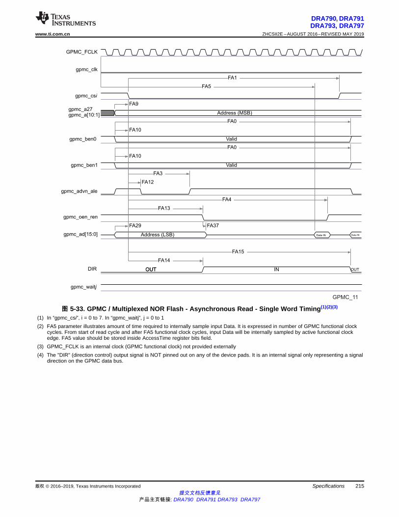
GPMC_FCLK
gpmc_clk
gpmc_csi
gpmc_a27
gpmc_ben0
gpmc_ 1ben
gpmc_ _aleadvn
gpmc_oen_ren
gpmc_a [15:0]d
DIR
gpmc_waitj
Address (MSB)
Valid
Valid
Address (LSB) Data IN Data IN
OUTOUT IN OUT
FA0
FA9
FA10
FA3
FA13
FA29
FA1
FA37
FA12
FA4
FA10
FA0
FA5
FA14
FA15
GPMC_11
gpmc_a[10:1]
215
DRA790, DRA791DRA793, DRA797
www.ti.com.cn ZHCSII2E –AUGUST 2016–REVISED MAY 2019
提交文档反馈意见产品主页链接: DRA790 DRA791 DRA793 DRA797
Specifications版权 © 2016–2019, Texas Instruments Incorporated
图图 5-33. GPMC / Multiplexed NOR Flash - Asynchronous Read - Single Word Timing(1)(2)(3)
(1) In “gpmc_csi”, i = 0 to 7. In “gpmc_waitj”, j = 0 to 1(2) FA5 parameter illustrates amount of time required to internally sample input Data. It is expressed in number of GPMC functional clock
cycles. From start of read cycle and after FA5 functional clock cycles, input Data will be internally sampled by active functional clockedge. FA5 value should be stored inside AccessTime register bits field.
(3) GPMC_FCLK is an internal clock (GPMC functional clock) not provided externally(4) The "DIR" (direction control) output signal is NOT pinned out on any of the device pads. It is an internal signal only representing a signal
direction on the GPMC data bus.

gpmc_fclk
gpmc_clk
gpmc_csi
gpmc_ben0
gpmc_ 1ben
gpmc_ _aleadvn
gpmc_wen
gpmc_ad[15:0]
gpmc_waitj
DIR
Address (MSB)
Valid Address (LSB) Data OUT
OUT
FA0
FA1
FA9
FA10
FA3
FA25
FA29
FA12
FA27
FA28
FA0
FA10
GPMC_12
gpmc_a27gpmc_a[10:1]
216
DRA790, DRA791DRA793, DRA797ZHCSII2E –AUGUST 2016–REVISED MAY 2019 www.ti.com.cn
提交文档反馈意见产品主页链接: DRA790 DRA791 DRA793 DRA797
Specifications 版权 © 2016–2019, Texas Instruments Incorporated
图图 5-34. GPMC / Multiplexed NOR Flash - Asynchronous Write - Single Word Timing(1)
(1) In “gpmc_csi”, i = 0 to 7. In “gpmc_waitj”, j = 0 to 1.(2) The "DIR" (direction control) output signal is NOT pinned out on any of the device pads. It is an internal signal only representing a signal
direction on the GPMC data bus.
5.10.6.8.3 GPMC/NAND Flash Interface Asynchronous Timing
CAUTION
The I/O Timings provided in this section are valid only for some GPMC usagemodes when the corresponding Virtual I/O Timings or Manual I/O Timings areconfigured as described in the tables found in this section.
表 5-53 and 表 5-54 assume testing over the recommended operating conditions and electricalcharacteristic conditions below (see 图 5-35, 图 5-36, 图 5-37 and 图 5-38).
表表 5-53. GPMC/NAND Flash Interface Timing Requirements
NO. PARAMETER DESCRIPTION MIN MAX UNITGNF12 tacc(DAT) Data maximum access time (GPMC_FCLK Cycles) J (1) cycles
- tsu(DV-OEH) Setup time, read gpmc_ad[15:0] valid beforegpmc_oen_ren high
1.9 ns
- th(OEH-DV) Hold time, read gpmc_ad[15:0] valid aftergpmc_oen_ren high
1 ns

217
DRA790, DRA791DRA793, DRA797
www.ti.com.cn ZHCSII2E –AUGUST 2016–REVISED MAY 2019
提交文档反馈意见产品主页链接: DRA790 DRA791 DRA793 DRA797
Specifications版权 © 2016–2019, Texas Instruments Incorporated
(1) J = AccessTime × (TimeParaGranularity + 1)
表表 5-54. GPMC/NAND Flash Interface Switching Characteristics
NO. PARAMETER DESCRIPTION MIN MAX UNIT- tr(DO) Rising time, gpmc_ad[15:0] output data 0.447 4.067 ns- tf(DO) Fallling time, gpmc_ad[15:0] output data 0.43 4.463 ns
GNF0 tw(nWEV) Pulse duration, gpmc_wen valid time A (1) nsGNF1 td(nCSV-nWEV) Delay time, gpmc_cs[7:0] valid to gpmc_wen valid B - 2 (2) B + 4 (2) nsGNF2 td(CLEH-nWEV) Delay time, gpmc_ben[1:0] high to gpmc_wen valid C - 2 (3) C + 4 (3) nsGNF3 td(nWEV-DV) Delay time, gpmc_ad[15:0] valid to gpmc_wen valid D - 2 (4) D + 4 (4) nsGNF4 td(nWEIV-DIV) Delay time, gpmc_wen invalid to gpmc_ad[15:0] invalid E - 2 (5) E + 4 (5) nsGNF5 td(nWEIV-CLEIV) Delay time, gpmc_wen invalid to gpmc_ben[1:0] invalid F - 2 (6) F + 4 (6) nsGNF6 td(nWEIV-nCSIV) Delay time, gpmc_wen invalid to gpmc_cs[7:0] invalid G - 2 (7) G + 4 (7) nsGNF7 td(ALEH-nWEV) Delay time, gpmc_advn_ale high to gpmc_wen valid C - 2 (3) C + 4 (3) nsGNF8 td(nWEIV-ALEIV) Delay time, gpmc_wen invalid to gpmc_advn_ale invalid F - 2 (6) F + 4 (6) nsGNF9 tc(nWE) Cycle time, write cycle time H (8) nsGNF10 td(nCSV-nOEV) Delay time, gpmc_cs[7:0] valid to gpmc_oen_ren valid I - 2 (9) I + 4 (9) nsGNF13 tw(nOEV) Pulse duration, gpmc_oen_ren valid time K (10) nsGNF14 tc(nOE) Cycle time, read cycle time L (11) nsGNF15 td(nOEIV-nCSIV) Delay time, gpmc_oen_ren invalid to gpmc_cs[7:0] invalid M - 2 (12) M + 4 (12) ns
(1) A = (WEOffTime – WEOnTime) × (TimeParaGranularity + 1) × GPMC_FCLK(2) B = ((WEOnTime – CSOnTime) × (TimeParaGranularity + 1) + 0.5 × (WEExtraDelay – CSExtraDelay)) × GPMC_FCLK(3) C = ((WEOnTime – ADVOnTime) × (TimeParaGranularity + 1) + 0.5 × (WEExtraDelay – ADVExtraDelay)) × GPMC_FCLK(4) D = (WEOnTime × (TimeParaGranularity + 1) + 0.5 × WEExtraDelay ) × GPMC_FCLK(5) E = (WrCycleTime – WEOffTime × (TimeParaGranularity + 1) – 0.5 × WEExtraDelay ) × GPMC_FCLK(6) F = (ADVWrOffTime – WEOffTime × (TimeParaGranularity + 1) + 0.5 × (ADVExtraDelay – WEExtraDelay ) × GPMC_FCLK(7) G = (CSWrOffTime – WEOffTime × (TimeParaGranularity + 1) + 0.5 × (CSExtraDelay – WEExtraDelay ) × GPMC_FCLK(8) H = WrCycleTime × (1 + TimeParaGranularity) × GPMC_FCLK(9) I = ((OEOffTime + (n – 1) × PageBurstAccessTime – CSOnTime) × (TimeParaGranularity + 1) + 0.5 × (OEExtraDelay – CSExtraDelay))
× GPMC_FCLK(10) K = (OEOffTime – OEOnTime) × (1 + TimeParaGranularity) × GPMC_FCLK(11) L = RdCycleTime × (1 + TimeParaGranularity) × GPMC_FCLK(12) M = (CSRdOffTime – OEOffTime × (TimeParaGranularity + 1) + 0.5 × (CSExtraDelay – OEExtraDelay ) × GPMC_FCLK

GPMC_FCLK
gpmc_csi
gpmc_ben0
gpmc_ _aleadvn
gpmc_oen_ren
gpmc_wen
gpmc_ad[15:0] Address
GNF0
GNF1
GNF7
GNF3 GNF4
GNF6
GNF8
GNF9
GPMC_14
GPMC_FCLK
gpmc_csi
gpmc_ben0
gpmc_ _aleadvn
gpmc_oen_ren
gpmc_wen
gpmc_ad[15:0] Command
GNF0
GNF1
GNF2
GNF3 GNF4
GNF5
GNF6
GPMC_13
218
DRA790, DRA791DRA793, DRA797ZHCSII2E –AUGUST 2016–REVISED MAY 2019 www.ti.com.cn
提交文档反馈意见产品主页链接: DRA790 DRA791 DRA793 DRA797
Specifications 版权 © 2016–2019, Texas Instruments Incorporated
图图 5-35. GPMC / NAND Flash - Command Latch Cycle Timing(1)
(1) In gpmc_csi, i = 0 to 7.
图图 5-36. GPMC / NAND Flash - Address Latch Cycle Timing(1)
(1) In gpmc_csi, i = 0 to 7.

GPMC_FCLK
gpmc_csi
gpmc_ben0
gpmc_ _aleadvn
gpmc_oen_ren
gpmc_wen
gpmc_ad[15:0] DATA
GNF0
GNF1
GNF4
GNF6
GNF9
GNF3
GPMC_16
GPMC_FCLK
gpmc_csi
gpmc_ben0
gpmc_ _aleadvn
gpmc_oen_ren
gpmc_ad[15:0]
gpmc_waitj
DATA
GNF10
GNF13
GNF14
GNF15
GNF12
GPMC_15
219
DRA790, DRA791DRA793, DRA797
www.ti.com.cn ZHCSII2E –AUGUST 2016–REVISED MAY 2019
提交文档反馈意见产品主页链接: DRA790 DRA791 DRA793 DRA797
Specifications版权 © 2016–2019, Texas Instruments Incorporated
图图 5-37. GPMC / NAND Flash - Data Read Cycle Timing(1)(2)(3)
(1) GNF12 parameter illustrates amount of time required to internally sample input Data. It is expressed in number of GPMC functionalclock cycles. From start of read cycle and after GNF12 functional clock cycles, input data will be internally sampled by active functionalclock edge. GNF12 value must be stored inside AccessTime register bits field.
(2) GPMC_FCLK is an internal clock (GPMC functional clock) not provided externally.(3) In gpmc_csi, i = 0 to 7. In gpmc_waitj, j = 0 to 1.
图图 5-38. GPMC / NAND Flash - Data Write Cycle Timing(1)
(1) In gpmc_csi, i = 0 to 7.
注注To configure the desired virtual mode the user must set MODESELECT bit andDELAYMODE bitfield for each corresponding pad control register.
The pad control registers are presented in 表 4-32 and described in Device TRM, ControlModule Chapter.

版权 © 2016–2019, Texas Instruments IncorporatedSpecifications提交文档反馈意见
产品主页链接: DRA790 DRA791 DRA793 DRA797
220
DRA790, DRA791DRA793, DRA797ZHCSII2E –AUGUST 2016–REVISED MAY 2019 www.ti.com.cn
Virtual IO Timings Modes must be used to ensure some IO timings for GPMC. See 表 5-29 Modes Summary for a list of IO timings requiring theuse of Virtual IO Timings Modes. See 表 5-55 Virtual Functions Mapping for GPMC for a definition of the Virtual modes.
表 5-55 presents the values for DELAYMODE bitfield.
表表 5-55. Virtual Functions Mapping for GPMC
BALL BALL NAME Delay Mode Value MUXMODEGPMC_VIRTUAL1 0 1 2 3 5 6 14(1) 14(1)
H5 gpmc_advn_ale
15 gpmc_advn_ale
gpmc_cs6 gpmc_wait1 gpmc_a2 gpmc_a23
B4 gpmc_ad15 13 gpmc_ad15B1 gpmc_ad6 13 gpmc_ad6E1 gpmc_ad2 13 gpmc_ad2E10 vin2a_d9 9 gpmc_a25G6 gpmc_wen 15 gpmc_wenA3 gpmc_ad14 13 gpmc_ad14H3 gpmc_a13 15 gpmc_a13K4 gpmc_a8 14 gpmc_a8H4 gpmc_a14 15 gpmc_a14D1 gpmc_ad4 13 gpmc_ad4A5 gpmc_a26 15 gpmc_a26 gpmc_a20F1 gpmc_ad0 13 gpmc_ad0F6 gpmc_wait0 15 gpmc_wait0
C10 vin2a_d11 9 gpmc_a23E2 gpmc_ad1 13 gpmc_ad1C4 gpmc_ad13 13 gpmc_ad13L2 gpmc_a2 14 gpmc_a2D2 gpmc_ad5 13 gpmc_ad5B10 vin2a_d8 9 gpmc_a26F3 gpmc_cs0 15 gpmc_cs0E8 vin2a_hsync0 9 gpmc_a27K3 gpmc_a4 14 gpmc_a4H2 gpmc_ben0 15 gpmc_ben0 gpmc_cs4J1 gpmc_a6 14 gpmc_a6K6 gpmc_a15 15 gpmc_a15B3 gpmc_ad11 13 gpmc_ad11
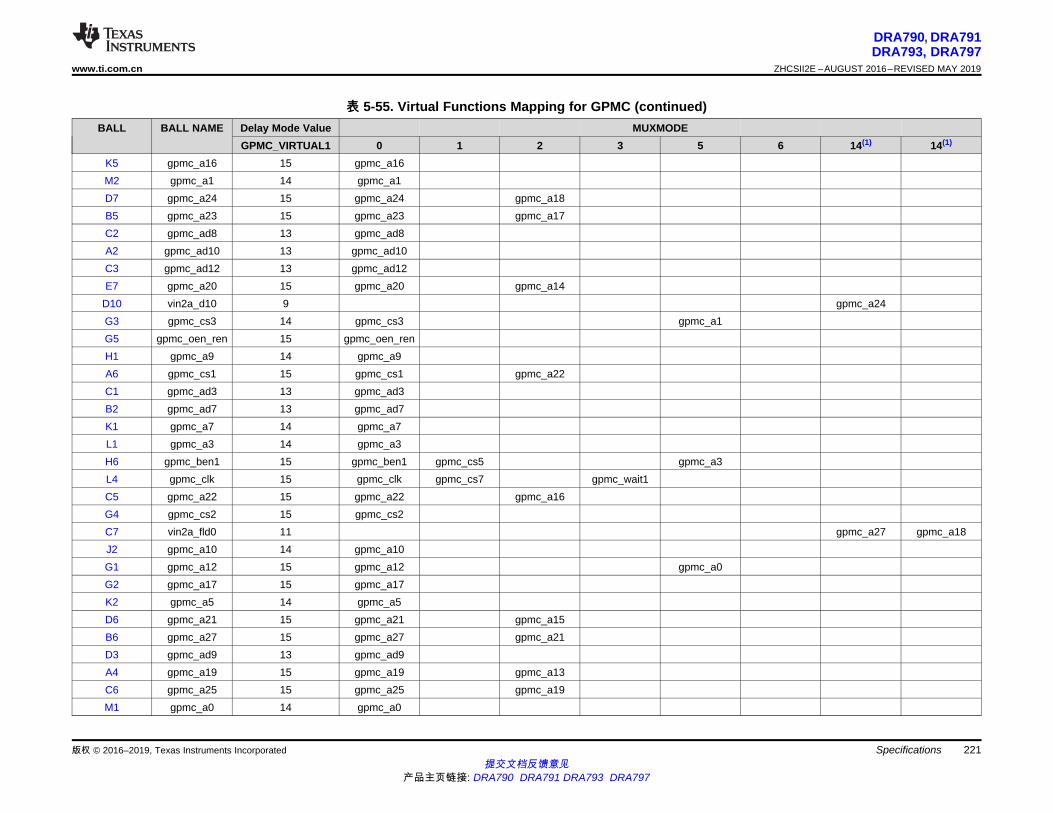
版权 © 2016–2019, Texas Instruments Incorporated Specifications提交文档反馈意见
产品主页链接: DRA790 DRA791 DRA793 DRA797
221
DRA790, DRA791DRA793, DRA797
www.ti.com.cn ZHCSII2E –AUGUST 2016–REVISED MAY 2019
表表 5-55. Virtual Functions Mapping for GPMC (continued)BALL BALL NAME Delay Mode Value MUXMODE
GPMC_VIRTUAL1 0 1 2 3 5 6 14(1) 14(1)
K5 gpmc_a16 15 gpmc_a16M2 gpmc_a1 14 gpmc_a1D7 gpmc_a24 15 gpmc_a24 gpmc_a18B5 gpmc_a23 15 gpmc_a23 gpmc_a17C2 gpmc_ad8 13 gpmc_ad8A2 gpmc_ad10 13 gpmc_ad10C3 gpmc_ad12 13 gpmc_ad12E7 gpmc_a20 15 gpmc_a20 gpmc_a14
D10 vin2a_d10 9 gpmc_a24G3 gpmc_cs3 14 gpmc_cs3 gpmc_a1G5 gpmc_oen_ren 15 gpmc_oen_renH1 gpmc_a9 14 gpmc_a9A6 gpmc_cs1 15 gpmc_cs1 gpmc_a22C1 gpmc_ad3 13 gpmc_ad3B2 gpmc_ad7 13 gpmc_ad7K1 gpmc_a7 14 gpmc_a7L1 gpmc_a3 14 gpmc_a3H6 gpmc_ben1 15 gpmc_ben1 gpmc_cs5 gpmc_a3L4 gpmc_clk 15 gpmc_clk gpmc_cs7 gpmc_wait1C5 gpmc_a22 15 gpmc_a22 gpmc_a16G4 gpmc_cs2 15 gpmc_cs2C7 vin2a_fld0 11 gpmc_a27 gpmc_a18J2 gpmc_a10 14 gpmc_a10G1 gpmc_a12 15 gpmc_a12 gpmc_a0G2 gpmc_a17 15 gpmc_a17K2 gpmc_a5 14 gpmc_a5D6 gpmc_a21 15 gpmc_a21 gpmc_a15B6 gpmc_a27 15 gpmc_a27 gpmc_a21D3 gpmc_ad9 13 gpmc_ad9A4 gpmc_a19 15 gpmc_a19 gpmc_a13C6 gpmc_a25 15 gpmc_a25 gpmc_a19M1 gpmc_a0 14 gpmc_a0
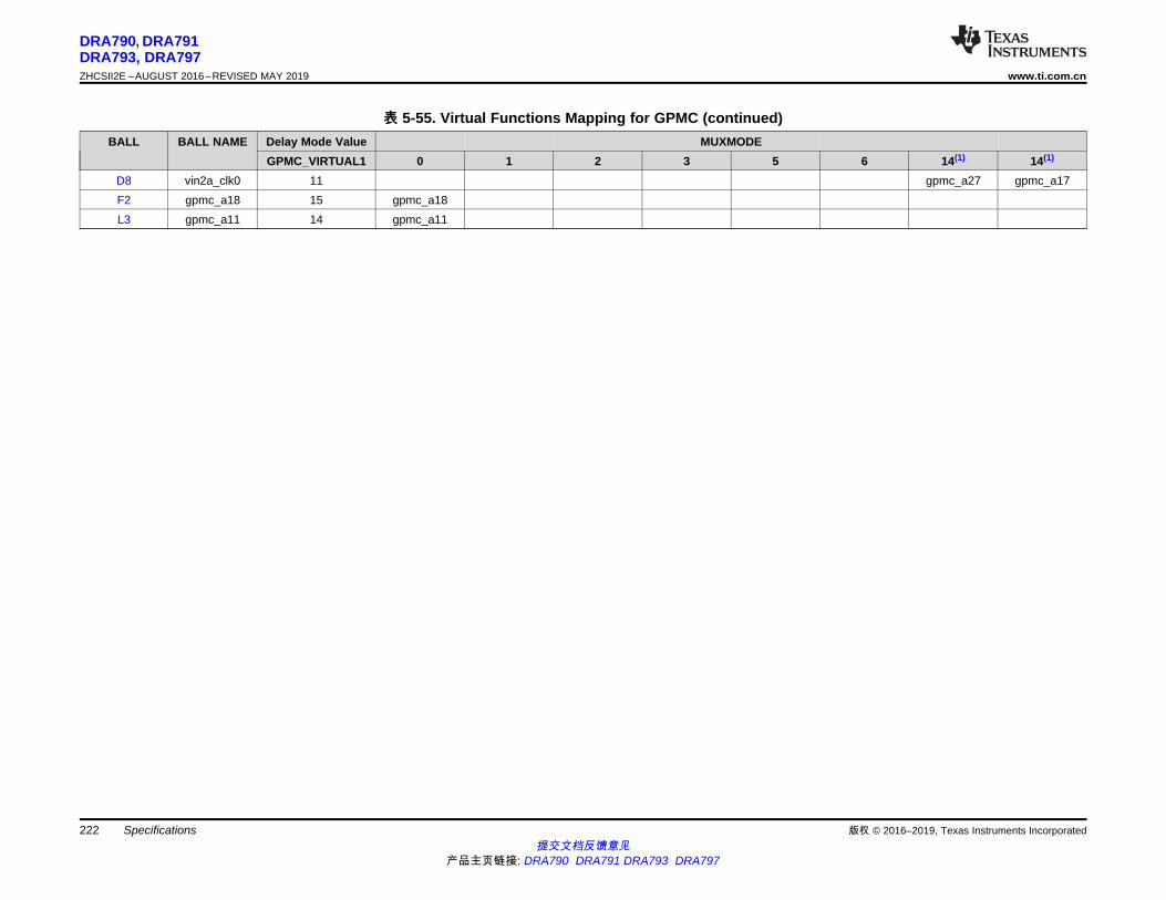
版权 © 2016–2019, Texas Instruments IncorporatedSpecifications提交文档反馈意见
产品主页链接: DRA790 DRA791 DRA793 DRA797
222
DRA790, DRA791DRA793, DRA797ZHCSII2E –AUGUST 2016–REVISED MAY 2019 www.ti.com.cn
表表 5-55. Virtual Functions Mapping for GPMC (continued)BALL BALL NAME Delay Mode Value MUXMODE
GPMC_VIRTUAL1 0 1 2 3 5 6 14(1) 14(1)
D8 vin2a_clk0 11 gpmc_a27 gpmc_a17F2 gpmc_a18 15 gpmc_a18L3 gpmc_a11 14 gpmc_a11

223
DRA790, DRA791DRA793, DRA797
www.ti.com.cn ZHCSII2E –AUGUST 2016–REVISED MAY 2019
提交文档反馈意见产品主页链接: DRA790 DRA791 DRA793 DRA797
Specifications版权 © 2016–2019, Texas Instruments Incorporated
(1) Some signals listed are virtual functions that present alternate multiplexing options. These virtual functions are controlled viaCTRL_CORE_ALT_SELECT_MUX or CTRL_CORE_VIP_MUX_SELECT registers. For more information on how to use these options,please refer to Device TRM, Chapter Control Module, Section Pad Configuration Registers.
5.10.6.9 Timers
The device has 16 general-purpose (GP) timers (TIMER1 - TIMER16), two watchdog timers, and a 32-kHzsynchronized timer (COUNTER_32K) that have the following features:• Dedicated input trigger for capture mode and dedicated output trigger/pulse width modulation (PWM)
signal• Interrupts generated on overflow, compare, and capture• Free-running 32-bit upward counter• Supported modes:
– Compare and capture modes– Auto-reload mode– Start-stop mode
• On-the-fly read/write register (while counting)
The device has two system watchdog timer (WD_TIMER1 and WD_TIMER2) that have the followingfeatures:• Free-running 32-bit upward counter• On-the-fly read/write register (while counting)• Reset upon occurrence of a timer overflow condition
The device includes one instance of the 32-bit watchdog timer: WD_TIMER2, also called the MPUwatchdog timer.
The watchdog timer is used to provide a recovery mechanism for the device in the event of a faultcondition, such as a non-exiting code loop.
In are presented the specific groupings of signals (IOSET) for use with TIMERS.
注注For additional information on the Timer Module, see the Device TRM.
5.10.6.10 I2C
The device includes 6 inter-integrated circuit (I2C) modules which provide an interface to other devicescompliant with Philips Semiconductors Inter-IC bus (I2C-bus™) specification version 2.1. Externalcomponents attached to this 2-wire serial bus can transmit/receive 8-bit data to/from the device throughthe I2C module.
注注Note that, on I2C1 and I2C2, due to characteristics of the open drain IO cells, HS mode isnot supported.
注注Inter-integrated circuit i (i=1 to 6) module is also referred to as I2Ci.

224
DRA790, DRA791DRA793, DRA797ZHCSII2E –AUGUST 2016–REVISED MAY 2019 www.ti.com.cn
提交文档反馈意见产品主页链接: DRA790 DRA791 DRA793 DRA797
Specifications 版权 © 2016–2019, Texas Instruments Incorporated
注注For more information, see the Multimaster High-Speed I2C Controller section of the DeviceTRM.
表 5-56, 表 5-57 and 图 5-39 assume testing over the recommended operating conditions and electricalcharacteristic conditions below.
表表 5-56. Timing Requirements for I2C Input Timings(1)
NO. PARAMETER DESCRIPTIONSTANDARD MODE FAST MODE
UNITMIN MAX MIN MAX
1 tc(SCL) Cycle time, SCL 10 2.5 µs
2 tsu(SCLH-SDAL)Setup time, SCL high before SDA low (for arepeated START condition) 4.7 0.6 µs
3 th(SDAL-SCLL)Hold time, SCL low after SDA low (for a STARTand a repeated START condition) 4 0.6 µs
4 tw(SCLL) Pulse duration, SCL low 4.7 1.3 µs5 tw(SCLH) Pulse duration, SCL high 4 0.6 µs6 tsu(SDAV-SCLH) Setup time, SDA valid before SCL high 250 100(2) ns7 th(SCLL-SDAV) Hold time, SDA valid after SCL low 0(3) 3.45(4) 0(3) 0.9(4) µs
8 tw(SDAH)Pulse duration, SDA high between STOP andSTART conditions 4.7 1.3 µs
9 tr(SDA) Rise time, SDA 1000 20 + 0.1Cb(5) 300(3) ns
10 tr(SCL) Rise time, SCL 1000 20 + 0.1Cb(5) 300(3) ns
11 tf(SDA) Fall time, SDA 300 20 + 0.1Cb(5) 300(3) ns
12 tf(SCL) Fall time, SCL 300 20 + 0.1Cb(5) 300(3) ns
13 tsu(SCLH-SDAH)Setup time, SCL high before SDA high (forSTOP condition) 4 0.6 µs
14 tw(SP) Pulse duration, spike (must be suppressed) 0 50 ns15 Cb
(5) Capacitive load for each bus line 400 400 pF
(1) The I2C pins SDA and SCL do not feature fail-safe I/O buffers. These pins could potentially draw current when the device is powereddown.
(2) A Fast-mode I2C-bus™ device can be used in a Standard-mode I2C-bus system, but the requirement tsu(SDA-SCLH)≥ 250 ns must then bemet. This will automatically be the case if the device does not stretch the LOW period of the SCL signal. If such a device does stretchthe LOW period of the SCL signal, it must output the next data bit to the SDA line tr max + tsu(SDA-SCLH)= 1000 + 250 = 1250 ns(according to the Standard-mode I2C-Bus Specification) before the SCL line is released.
(3) A device must internally provide a hold time of at least 300 ns for the SDA signal (referred to the VIHmin of the SCL signal) to bridge theundefined region of the falling edge of SCL.
(4) The maximum th(SDA-SCLL) has only to be met if the device does not stretch the low period [tw(SCLL)] of the SCL signal.(5) Cb = total capacitance of one bus line in pF. If mixed with HS-mode devices, faster fall-times are allowed.
表表 5-57. Timing Requirements for I2C HS-Mode (I2C3/4/5/6 Only)(1)
NO. PARAMETER DESCRIPTION Cb = 100 pF MAX Cb = 400 pF (2) UNITMIN MAX MIN MAX
1 tc(SCL) Cycle time, SCL 0.294 0.588 µs2 tsu(SCLH-SDAL) Set-up time, SCL high before
SDA low (for a repeated STARTcondition)
160 160 ns
3 th(SDAL-SCLL) Hold time, SCL low after SDAlow (for a repeated STARTcondition)
160 160 ns

10
8
4
3
7
12
5
6 14
2
3
13
Stop Start RepeatedStart
Stop
I2Ci_SDA
I2Ci_SCL
1
11 9
SPRS906_TIMING_I2C_01
225
DRA790, DRA791DRA793, DRA797
www.ti.com.cn ZHCSII2E –AUGUST 2016–REVISED MAY 2019
提交文档反馈意见产品主页链接: DRA790 DRA791 DRA793 DRA797
Specifications版权 © 2016–2019, Texas Instruments Incorporated
表表 5-57. Timing Requirements for I2C HS-Mode (I2C3/4/5/6 Only)(1) (continued)NO. PARAMETER DESCRIPTION Cb = 100 pF MAX Cb = 400 pF (2) UNIT
MIN MAX MIN MAX4 tw(SCLL) LOW period of the SCLH clock 160 320 ns5 tw(SCLH) HIGH period of the SCLH clock 60 120 ns6 tsu(SDAV-SCLH) Setup time, SDA valid vefore
SCL high10 10 ns
7 th(SCLL-SDAV) Hold time, SDA valid after SCLlow
0 (3) 70 0 (3) 150 ns
13 tsu(SCLH-SDAH) Setup time, SCL high beforeSDA high (for a STOP condition)
160 160 ns
14 tw(SP) Pulse duration, spike (must besuppressed)
0 10 0 10 ns
15 Cb(2) Capacitive load for SDAH and
SCLH lines100 400 pF
16 Cb Capacitive load for SDAH + SDAline and SCLH + SCL line
400 400 pF
(1) I2C HS-Mode is only supported on I2C3/4/5/6. I2C HS-Mode is not supported on I2C1/2.(2) For bus line loads Cb between 100 and 400 pF the timing parameters must be linearly interpolated.(3) A device must internally provide a Data hold time to bridge the undefined part between VIH and VIL of the falling edge of the SCLH
signal. An input circuit with a threshold as low as possible for the falling edge of the SCLH signal minimizes this hold time.
图图 5-39. I2C Receive Timing
表 5-58 and 图 5-40 assume testing over the recommended operating conditions and electricalcharacteristic conditions below.
表表 5-58. Switching Characteristics Over Recommended Operating Conditions for I2C Output Timings(2)
NO. PARAMETER DESCRIPTIONSTANDARD MODE FAST MODE
UNITMIN MAX MIN MAX
16 tc(SCL) Cycle time, SCL 10 2.5 µs
17 tsu(SCLH-SDAL)Setup time, SCL high before SDA low (for arepeated START condition) 4.7 0.6 µs
18 th(SDAL-SCLL)Hold time, SCL low after SDA low (for aSTART and a repeated START condition) 4 0.6 µs
19 tw(SCLL) Pulse duration, SCL low 4.7 1.3 µs20 tw(SCLH) Pulse duration, SCL high 4 0.6 µs21 tsu(SDAV-SCLH) Setup time, SDA valid before SCL high 250 100 ns

25
23
19
18
22
27
20
21
17
18
28
Stop Start RepeatedStart
Stop
I2Ci_SDA
I2Ci_SCL
16
26 24
SPRS906_TIMING_I2C_02
226
DRA790, DRA791DRA793, DRA797ZHCSII2E –AUGUST 2016–REVISED MAY 2019 www.ti.com.cn
提交文档反馈意见产品主页链接: DRA790 DRA791 DRA793 DRA797
Specifications 版权 © 2016–2019, Texas Instruments Incorporated
表表 5-58. Switching Characteristics Over Recommended Operating Conditions for I2C OutputTimings(2) (continued)
NO. PARAMETER DESCRIPTIONSTANDARD MODE FAST MODE
UNITMIN MAX MIN MAX
22 th(SCLL-SDAV)Hold time, SDA valid after SCL low (for I2Cbus devices) 0 3.45 0 0.9 µs
23 tw(SDAH)Pulse duration, SDA high between STOP andSTART conditions 4.7 1.3 µs
24 tr(SDA) Rise time, SDA 1000 20 + 0.1Cb(1) (3) 300(3) ns
25 tr(SCL) Rise time, SCL 1000 20 + 0.1Cb(1) (3) 300(3) ns
26 tf(SDA) Fall time, SDA 300 20 + 0.1Cb(1) (3) 300(3) ns
27 tf(SCL) Fall time, SCL 300 20 + 0.1Cb(1) (3) 300(3) ns
28 tsu(SCLH-SDAH)Setup time, SCL high before SDA high (forSTOP condition) 4 0.6 µs
29 Cp Capacitance for each I2C pin 10 10 pF
(1) Cb = total capacitance of one bus line in pF. If mixed with HS-mode devices, faster fall-times are allowed.(2) Software must properly configure the I2C module registers to achieve the timings shown in this table. See the Device TRM for details.(3) These timings apply only to I2C1 and I2C2. I2C3, I2C4, I2C5 and I2C6 use standard LVCMOS buffers to emulate open-drain buffers
and their rise/fall times should be referenced in the device IBIS model.
注注I2C emulation is achieved by configuring the LVCMOS buffers to output Hi-Z instead ofdriving high when transmitting logic-1.
图图 5-40. I2C Transmit Timing
In are presented the specific groupings of signals (IOSET) for use with I2C1/2/3/4/5.
5.10.6.11 HDQ1W
The module is intended to work with both HDQ and 1-Wire protocols. The protocols use a single wire tocommunicate between the master and the slave. The protocols employ an asynchronous return to onemechanism where, after any command, the line is pulled high.

HDQ
tDW1
tDW0
tCYCD
SPRS906_TIMING_HDQ1W_03
HDQ
tHW1
tHW0
tCYCH
SPRS906_TIMING_HDQ1W_02
HDQ
tB tBR
SPRS906_TIMING_HDQ1W_01
227
DRA790, DRA791DRA793, DRA797
www.ti.com.cn ZHCSII2E –AUGUST 2016–REVISED MAY 2019
提交文档反馈意见产品主页链接: DRA790 DRA791 DRA793 DRA797
Specifications版权 © 2016–2019, Texas Instruments Incorporated
注注For more information, see the HDQ / 1-Wire section of the Device TRM.
5.10.6.11.1 HDQ / 1-Wire — HDQ Mode
表 5-59 and 表 5-60 assume testing over the recommended operating conditions and electricalcharacteristic conditions below (see 图 5-41, 图 5-42, 图 5-43 and 图 5-44).
表表 5-59. HDQ/1-Wire Timing Requirements—HDQ Mode
NO. PARAMETER DESCRIPTION MIN MAX UNIT1 tCYCH Read bit window timing 190 250 µs2 tHW1 Read one data valid after HDQ low 32(2) 66(2) µs3 tHW0 Read zero data hold after HDQ low 70(2) 145(2) µs4 tRSPS Response time from HDQ slave device(1) 190 320 µs
(1) Defined by software.(2) If the HDQ slave device drives a logic-low state after tHW0 maximum, it can be interpreted as a break pulse. For more information see
"HDQ / 1-Wire Switching Characteristics - HDQ Mode" and the HDQ/1-Wire chapter of the TRM.
表表 5-60. HDQ / 1-Wire Switching Characteristics - HDQ Mode
NO. PARAMETER DESCRIPTION MIN MAX UNIT5 tB Break timing 190 µs6 tBR Break recovery time 40 µs7 tCYCD Write bit windows timing 190 µs8 tDW1 Write one data valid after HDQ low 0.5 50 µs9 tDW0 Write zero data hold after HDQ low 86 145 µs
图图 5-41. HDQ Break and Break Recovery Timing — HDQ Interface Writing to Slave
图图 5-42. Device HDQ Interface Bit Read Timing (Data)
图图 5-43. Device HDQ Interface Bit Write Timing (Command / Address or Data)

1-WIRE
tLOWR
tRDV and__ tREL
tSLOT_ _and tREC
SPRS906_TIMING_HDQ1W_06
1-WIRE
tRSTH
tPDLtPDHtRTSL
SPRS906_TIMING_HDQ1W_05
HDQ
Break
0_(LSB)
1 6 7_(MSB)
tRSPS 1
6
Command_byte_written Data_byte_received
0_(LSB)
SPRS906_TIMING_HDQ1W_04
228
DRA790, DRA791DRA793, DRA797ZHCSII2E –AUGUST 2016–REVISED MAY 2019 www.ti.com.cn
提交文档反馈意见产品主页链接: DRA790 DRA791 DRA793 DRA797
Specifications 版权 © 2016–2019, Texas Instruments Incorporated
图图 5-44. HDQ Communication Timing
5.10.6.11.2 HDQ/1-Wire—1-Wire Mode
表 5-61 and 表 5-62 assume testing over the recommended operating conditions and electricalcharacteristic conditions below (see 图 5-45, 图 5-46 and 图 5-47).
表表 5-61. HDQ / 1-Wire Timing Requirements - 1-Wire Mode
NO. PARAMETER DESCRIPTION MIN MAX UNIT10 tPDH Presence pulse delay high 15 60 µs11 tPDL Presence pulse delay low 60 240 µs12 tRDV Read data valid time tLOWR 15 µs13 tREL Read data release time 0 45 µs
表表 5-62. HDQ / 1-Wire Switching Characteristics - 1-Wire Mode
NO. PARAMETER DESCRIPTION MIN MAX UNIT14 tRSTL Reset time low 480 960 µs15 tRSTH Reset time high 480 µs16 tSLOT Bit cycle time 60 120 µs17 tLOW1 Write bit-one time 1 15 µs18 tLOW0 Write bit-zero time(2) 60 120 µs19 tREC Recovery time 1 µs20 tLOWR Read bit strobe time(1) 1 15 µs
(1) tLOWR (low pulse sent by the master) must be short as possible to maximize the master sampling window.(2) tLOWR must be less than tSLOT.
图图 5-45. 1-Wire—Break (Reset)
图图 5-46. 1-Wire—Read Bit (Data)
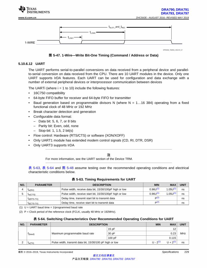
1-WIRE
tLOW1
tLOW0
tSLOT_ _and tREC
SPRS906_TIMING_HDQ1W_07
229
DRA790, DRA791DRA793, DRA797
www.ti.com.cn ZHCSII2E –AUGUST 2016–REVISED MAY 2019
提交文档反馈意见产品主页链接: DRA790 DRA791 DRA793 DRA797
Specifications版权 © 2016–2019, Texas Instruments Incorporated
图图 5-47. 1-Wire—Write Bit-One Timing (Command / Address or Data)
5.10.6.12 UART
The UART performs serial-to-parallel conversions on data received from a peripheral device and parallel-to-serial conversion on data received from the CPU. There are 10 UART modules in the device. Only oneUART supports IrDA features. Each UART can be used for configuration and data exchange with anumber of external peripheral devices or interprocessor communication between devices
The UARTi (where i = 1 to 10) include the following features:• 16C750 compatibility• 64-byte FIFO buffer for receiver and 64-byte FIFO for transmitter• Baud generation based on programmable divisors N (where N = 1…16 384) operating from a fixed
functional clock of 48 MHz or 192 MHz• Break character detection and generation• Configurable data format:
– Data bit: 5, 6, 7, or 8 bits– Parity bit: Even, odd, none– Stop-bit: 1, 1.5, 2 bit(s)
• Flow control: Hardware (RTS/CTS) or software (XON/XOFF)• Only UART1 module has extended modem control signals (CD, RI, DTR, DSR)• Only UART3 supports IrDA
注注For more information, see the UART section of the Device TRM.
表 5-63, 表 5-64 and 图 5-48 assume testing over the recommended operating conditions and electricalcharacteristic conditions below.
表表 5-63. Timing Requirements for UARTNO. PARAMETER DESCRIPTION MIN MAX UNIT
4 tw(RX) Pulse width, receive data bit, 15/30/100pF high or low 0.96U(1) 1.05U(1) ns5 tw(CTS) Pulse width, receive start bit, 15/30/100pF high or low 0.96U(1) 1.05U(1) ns
td(RTS-TX) Delay time, transmit start bit to transmit data P(2) nstd(CTS-TX) Delay time, receive start bit to transmit data P(2) ns
(1) U = UART baud time = 1/programmed baud rate(2) P = Clock period of the reference clock (FCLK, usually 48 MHz or 192MHz).
表表 5-64. Switching Characteristics Over Recommended Operating Conditions for UARTNO. PARAMETER DESCRIPTION MIN MAX UNIT
f(baud) Maximum programmable baud rate15 pF 12
MHz30 pF 0.23100 pF 0.115
2 tw(TX) Pulse width, transmit data bit, 15/30/100 pF high or low U - 2(1) U + 2(1) ns

3
2
Start
Bit
Data Bits
UARTi_TXD
5
Data Bits
Bit
Start
4
UARTi_RXD
SPRS906_TIMING_UART_01
230
DRA790, DRA791DRA793, DRA797ZHCSII2E –AUGUST 2016–REVISED MAY 2019 www.ti.com.cn
提交文档反馈意见产品主页链接: DRA790 DRA791 DRA793 DRA797
Specifications 版权 © 2016–2019, Texas Instruments Incorporated
表表 5-64. Switching Characteristics Over Recommended Operating Conditions for UART (continued)NO. PARAMETER DESCRIPTION MIN MAX UNIT
3 tw(RTS) Pulse width, transmit start bit, 15/30/100 pF high or low U - 2(1) U + 2(1) ns
(1) U = UART baud time = 1/programmed baud rate
图图 5-48. UART Timing
In are presented the specific groupings of signals (IOSET) for use with UART.
5.10.6.13 McSPI
The McSPI is a master/slave synchronous serial bus. There are four separate McSPI modules (SPI1,SPI2, SPI3, and SPI4) in the device. All these four modules support up to four external devices (four chipselects) and are able to work as both master and slave.
The McSPI modules include the following main features:• Serial clock with programmable frequency, polarity, and phase for each channel• Wide selection of SPI word lengths, ranging from 4 to 32 bits• Up to four master channels, or single channel in slave mode• Master multichannel mode:
– Full duplex/half duplex– Transmit-only/receive-only/transmit-and-receive modes– Flexible input/output (I/O) port controls per channel– Programmable clock granularity– SPI configuration per channel. This means, clock definition, polarity enabling and word width
• Power management through wake-up capabilities• Programmable timing control between chip select and external clock generation• Built-in FIFO available for a single channel.• Each SPI module supports multiple chip select pins spim_cs[i], whete i = 1 to 4.
注注For more information, see the Serial Communication Interface section of the device TRM.
注注The McSPIm module (m = 1 to 4) is also referred to as SPIm.

231
DRA790, DRA791DRA793, DRA797
www.ti.com.cn ZHCSII2E –AUGUST 2016–REVISED MAY 2019
提交文档反馈意见产品主页链接: DRA790 DRA791 DRA793 DRA797
Specifications版权 © 2016–2019, Texas Instruments Incorporated
CAUTION
The I/O timings provided in this section are applicable for all combinations ofsignals for SPI1 and SPI2. However, the timings are valid only for SPI3 andSPI4 if signals within a single IOSET are used. The IOSETS are defined in 表5-67.
表 5-65, 图 5-49 and 图 5-50 present Timing Requirements for McSPI - Master Mode.
表表 5-65. Timing Requirements for SPI - Master Mode (1)
NO. PARAMETER DESCRIPTION MODE MIN MAX UNITSM1 tc(SPICLK) Cycle time, spi_sclk (1) (2) SPI1/2/3/
420.8 (3) ns
SM2 tw(SPICLKL) Typical Pulse duration, spi_sclk low (1) 0.5 × P-1(4)
ns
SM3 tw(SPICLKH) Typical Pulse duration, spi_sclk high (1) 0.5 × P-1(4)
ns
SM4 tsu(MISO-SPICLK) Setup time, spi_d[x] valid before spi_sclk active edge (1) 3.5 nsSM5 th(SPICLK-MISO) Hold time, spi_d[x] valid after spi_sclk active edge (1) 3.7 nsSM6 td(SPICLK-SIMO) Delay time, spi_sclk active edge to spi_d[x] transition (1) SPI1 -3.57 4.1 ns
SPI2 -3.9 3.6 nsSPI3 -4.9 4.7 nsSPI4 -4.3 4.5 ns
SM7 td(CS-SIMO) Delay time, spi_cs[x] active edge to spi_d[x] transition 5 nsSM8 td(CS-SPICLK) Delay time, spi_cs[x] active to spi_sclk first edge (1) MASTER
_PHA0(5)
B-4.2 (6) ns
MASTER_PHA1
(5)
A-4.2 (7) ns
SM9 td(SPICLK-CS) Delay time, spi_sclk last edge to spi_cs[x] inactive (1) MASTER_PHA0
(5)
A-4.2 (7) ns
MASTER_PHA1
(5)
B-4.2 (6) ns
(1) This timing applies to all configurations regardless of SPI_CLK polarity and which clock edges are used to drive output data and captureinput data.
(2) Related to the SPI_CLK maximum frequency.(3) 20.8ns cycle time = 48MHz(4) P = SPICLK period.(5) SPI_CLK phase is programmable with the PHA bit of the SPI_CH(i)CONF register.(6) B = (TCS + 0.5) × TSPICLKREF × Fratio, where TCS is a bit field of the SPI_CH(i)CONF register and Fratio = Even ≥2.(7) When P = 20.8 ns, A = (TCS + 1) × TSPICLKREF, where TCS is a bit field of the SPI_CH(i)CONF register. When P > 20.8 ns, A = (TCS
+ 0.5) × Fratio × TSPICLKREF, where TCS is a bit field of the SPI_CH(i)CONF register.

spim_cs(OUT)
spi _sclk(OUT)m
spi _sclkm (OUT)
spi _m d(OUT)
spim_cs(OUT)
spi _sclkm (OUT)
spi _sclkm (OUT)
spi _m d(OUT)
Bit n-1 Bit n-2 Bit n-3 Bit n-4 Bit 0
Bit n-1 Bit n-2 Bit n-3 Bit 1 Bit0
PHA=0
EPOL=1
POL=0
POL=1
PHA=1
EPOL=1
POL=0
POL=1
SM8 SM9
SM6
SM3
SM1
SM2
SM1
SM8 SM9SM3
SM1
SM2
SM1
SM6
SM7 SM6
SM2
SM3
SM2
SM3
SM6 SM6 SM6
SPRS906_TIMING_McSPI_01
232
DRA790, DRA791DRA793, DRA797ZHCSII2E –AUGUST 2016–REVISED MAY 2019 www.ti.com.cn
提交文档反馈意见产品主页链接: DRA790 DRA791 DRA793 DRA797
Specifications 版权 © 2016–2019, Texas Instruments Incorporated
图图 5-49. McSPI - Master Mode Transmit

spim_cs(OUT)
spi _sclkm (OUT)
spi _sclkm (OUT)
spi _m d(IN)
spim_cs(OUT)
spi _sclkm (OUT)
spi _sclkm (OUT)
spi _m d(IN)
Bit n-1 Bit n-2 Bit n-3 Bit n-4 Bit 0
Bit n-1 Bit n-2 Bit n-3 Bit 1 Bit 0
PHA=0
EPOL=1
PHA=1
EPOL=1
POL=0
POL=1
POL=0
POL=1
SM8 SM9
SM3
SM1
SM2
SM1
SM8 SM9SM3
SM1
SM2
SM1
SM2
SM3
SM2
SM3
SM4
SM5
SM4
SM5
SM4
SM4
SM5
SM5
SPRS906_TIMING_McSPI_02
233
DRA790, DRA791DRA793, DRA797
www.ti.com.cn ZHCSII2E –AUGUST 2016–REVISED MAY 2019
提交文档反馈意见产品主页链接: DRA790 DRA791 DRA793 DRA797
Specifications版权 © 2016–2019, Texas Instruments Incorporated
图图 5-50. McSPI - Master Mode Receive
表 5-66, 图 5-51 and 图 5-52 present Timing Requirements for McSPI - Slave Mode.
表表 5-66. Timing Requirements for SPI - Slave Mode
NO. PARAMETER DESCRIPTION MODE MIN MAX UNITSS1 (1) tc(SPICLK) Cycle time, spi_sclk 62.5 (2)
(3)ns
SS2 (1) tw(SPICLKL) Typical Pulse duration, spi_sclk low 0.45 × P(4)
ns
SS3 (1) tw(SPICLKH) Typical Pulse duration, spi_sclk high 0.45 × P(4)
ns
SS4 (1) tsu(SIMO-SPICLK) Setup time, spi_d[x] valid before spi_sclk active edge 5 nsSS5 (1) th(SPICLK-SIMO) Hold time, spi_d[x] valid after spi_sclk active edge 5 nsSS6 (1) td(SPICLK-SOMI) Delay time, spi_sclk active edge to mcspi_somi transition SPI1/2/3 2 26.6 ns
SPI4 2 20.1 ns

spim_cs(IN)
spi _sclkm (IN)
spi _sclkm (IN)
spi _m d(OUT)
spim_cs(IN)
spi _sclkm (IN)
spi _sclkm (IN)
spi _m d(OUT)
Bit n-1 Bit n-2 Bit n-3 Bit n-4 Bit 0
Bit n-1 Bit n-2 Bit n-3 Bit 1 Bit 0
PHA=0
EPOL=1
POL=0
POL=1
POL=0
POL=1
PHA=1
EPOL=1
SS6
SS3
SS1
SS3
SS1
SS3
SS1
SS2
SS1
SS6
SS6
SS8 SS9
SS7
SS8SS2
SS3
SS2
SS2
SS6 SS6SS6
SS9
SPRS906_TIMING_McSPI_03
234
DRA790, DRA791DRA793, DRA797ZHCSII2E –AUGUST 2016–REVISED MAY 2019 www.ti.com.cn
提交文档反馈意见产品主页链接: DRA790 DRA791 DRA793 DRA797
Specifications 版权 © 2016–2019, Texas Instruments Incorporated
表表 5-66. Timing Requirements for SPI - Slave Mode (continued)NO. PARAMETER DESCRIPTION MODE MIN MAX UNIT
SS7 (5) td(CS-SOMI) Delay time, spi_cs[x] active edge to mcspi_somi transition 20.95 nsSS8 (1) tsu(CS-SPICLK) Setup time, spi_cs[x] valid before spi_sclk first edge 5 nsSS9 (1) th(SPICLK-CS) Hold time, spi_cs[x] valid after spi_sclk last edge SPI1/2 5 ns
SPI3 7.5 nsSPI4 6 ns
(1) This timing applies to all configurations regardless of SPI_CLK polarity and which clock edges are used to drive output data and captureinput data.
(2) When operating the SPI interface in RX-only mode, the minimum Cycle time is 26ns (38.4MHz)(3) 62.5ns Cycle time = 16 MHz(4) P = SPICLK period.(5) PHA = 0; SPI_CLK phase is programmable with the PHA bit of the SPI_CH(i)CONF register.
图图 5-51. McSPI - Slave Mode Transmit

spim_cs(IN)
spi _sclkm (IN)
spi _sclkm (IN)
spi _m d(IN)
spim_cs(IN)
spi _sclkm (IN)
spi _sclkm (IN)
spi _m d(IN)
Bit n-1 Bit n-2 Bit n-3 Bit n-4 Bit 0
Bit n-1 Bit n-2 Bit n-3 Bit 1 Bit 0
PHA=0
EPOL=1
POL=0
POL=1
POL=0
POL=1
PHA=1
EPOL=1
SS3
SS1
SS3
SS1
SS3
SS1
SS2
SS1
SS8 SS9
SS8 SS9SS2
SS3
SS2
SS2
SS4
SS5
SS5
SS4
SS4
SS5
SS4
SS5
SPRS906_TIMING_McSPI_04
235
DRA790, DRA791DRA793, DRA797
www.ti.com.cn ZHCSII2E –AUGUST 2016–REVISED MAY 2019
提交文档反馈意见产品主页链接: DRA790 DRA791 DRA793 DRA797
Specifications版权 © 2016–2019, Texas Instruments Incorporated
图图 5-52. McSPI - Slave Mode Receive
In 表 5-67 are presented the specific groupings of signals (IOSET) for use with SPI3 and SPI4.
表表 5-67. McSPI3/4 IOSETs
SIGNALS IOSET1 IOSET2 IOSET3 IOSET4 IOSET5BALL MUX BALL MUX BALL MUX BALL MUX BALL MUX
McSPI3spi3_cs0 T5 7 B18 3 D23 2 AA3 1spi3_cs1 W2 1 A19 3 W2 1spi3_d0 T4 7 B16 3 A24 2 AA2 1spi3_d1 N6 7 B17 3 B25 2 Y4 1
spi3_sclk N5 7 A18 3 C23 2 Y1 1McSPI4
spi4_cs0 L3 8 B9 8 R1 7 AC4 2 AB1 1spi4_cs1 G1 8 G1 8 N6 8 N6 8 N6 8spi4_cs2 H3 8 H3 8 T4 8 T4 8 T4 8

236
DRA790, DRA791DRA793, DRA797ZHCSII2E –AUGUST 2016–REVISED MAY 2019 www.ti.com.cn
提交文档反馈意见产品主页链接: DRA790 DRA791 DRA793 DRA797
Specifications 版权 © 2016–2019, Texas Instruments Incorporated
表表 5-67. McSPI3/4 IOSETs (continued)SIGNALS IOSET1 IOSET2 IOSET3 IOSET4 IOSET5
BALL MUX BALL MUX BALL MUX BALL MUX BALL MUXspi4_cs3 H4 8 H4 8 T5 8 T5 8 T5 8spi4_d0 J2 8 C8 8 R2 7 AA5 2 AA4 1spi4_d1 H1 8 B8 8 P3 7 U6 2 AA1 1
spi4_sclk K4 8 E8 8 P4 7 AC3 2 Y3 1
5.10.6.14 QSPI
The Quad SPI (QSPI) module is a type of SPI module that allows single, dual or quad read access toexternal SPI devices. This module has a memory mapped register interface, which provides a directinterface for accessing data from external SPI devices and thus simplifying software requirements. Itworks as a master only. There is one QSPI module in the device and it is primary intended for fastbooting from quad-SPI flash memories.General SPI features:• Programmable clock divider• Six pin interface (DCLK, CS_N, DOUT, DIN, QDIN1, QDIN2)• 4 external chip select signals• Support for 3-, 4- or 6-pin SPI interface• Programmable CS_N to DOUT delay from 0 to 3 DCLKs• Programmable signal polarities• Programmable active clock edge• Software controllable interface allowing for any type of SPI transfer
注注For more information, see the Quad Serial Peripheral Interface section of the Device TRM.
CAUTION
The I/O Timings provided in this section are only valid when all QSPI ChipSelects used in a system are configured to use the same Clock Mode (eitherClock Mode 0 or Clock Mode 3).
CAUTION
The I/O Timings provided in this section are valid only for some QSPI usagemodes when the corresponding Virtual I/O Timings or Manual I/O Timings areconfigured as described in the tables found in this section.
表 5-68 and 表 5-69 Present Timing and Switching Characteristics for Quad SPI Interface.
表表 5-68. Switching Characteristics for QSPI
NO. PARAMETER DESCRIPTION MODE MIN MAX UNITQ1 tc(SCLK) Cycle time, sclk Default Timing Mode,
Clock Mode 011.71 ns
Default Timing Mode,Clock Mode 3
20.8 ns

cs
sclk
d[0]
d[3:1]
Bit n-1 Bit n-2 Bit 1 Bit 0
PHA=1
POL=1
Command Command Read Data Read Data
Bit 1 Bit 0Read Data Read Data
Q4
Q7 Q6
Q3 Q2Q1
Q6
Q5
SPRS91v_QSPI_01
Q12 Q13
Q14
Q15
Q12 Q13
Q15Q14
237
DRA790, DRA791DRA793, DRA797
www.ti.com.cn ZHCSII2E –AUGUST 2016–REVISED MAY 2019
提交文档反馈意见产品主页链接: DRA790 DRA791 DRA793 DRA797
Specifications版权 © 2016–2019, Texas Instruments Incorporated
表表 5-68. Switching Characteristics for QSPI (continued)NO. PARAMETER DESCRIPTION MODE MIN MAX UNITQ2 tw(SCLKL) Pulse duration, sclk low Y × P-1
(1)ns
Q3 tw(SCLKH) Pulse duration, sclk high Y × P-1(1)
ns
Q4 td(CS-SCLK) Delay time, sclk falling edge to cs active edge, CS3:0 Default Timing Mode -M × P-1.6 (2)
(3)
-M ×P+2.6
(2) (3)
ns
Q5 td(SCLK-CS) Delay time, sclk falling edge to cs inactive edge,CS3:0
Default Timing Mode N × P-1.6 (2)
(3)
N ×P+2.6
(2) (3)
ns
Q6 td(SCLK-D0) Delay time, sclk falling edge to d[0] transition Default Timing Mode -1.6 2.6 nsQ7 tena(CS-D0LZ) Enable time, cs active edge to d[0] driven (lo-z) -P-3.5 -P+2.5 nsQ8 tdis(CS-D0Z) Disable time, cs active edge to d[0] tri-stated (hi-z) -P-2.5 -P+2.0 nsQ9 td(SCLK-D0) Delay time, sclk first falling edge to first d[0] transition PHA=0 Only, Default
Timing Mode-1.6-P(2)
2.6-P(2) ns
(1) The Y parameter is defined as follows:If DCLK_DIV is 0 or ODD then, Y equals 0.5.If DCLK_DIV is EVEN then, Y equals (DCLK_DIV/2) / (DCLK_DIV+1).For best performance, it is recommended to use a DCLK_DIV of 0 or ODD to minimize the duty cycle distortion. The HSDIVIDER onCLKOUTX2_H13 output of DPLL_PER can be used to achieve the desired clock divider ratio. All required details about clock divisionfactor DCLK_DIV can be found in the device-specific Technical Reference Manual.
(2) P = SCLK period.(3) M=QSPI_SPI_DC_REG.DDx + 1 when Clock Mode 0.
M=QSPI_SPI_DC_REG.DDx when Clock Mode 3.N = 2 when Clock Mode 0.N = 3 when Clock Mode 3.
图图 5-53. QSPI Read (Clock Mode 3)

cs
sclk
rtclk
d[0]
d[3:1]
Bit n-1 Bit n-2 Bit 1 Bit 0
PHA=0
POL=0
POL=0
Command Command Read Data Read Data
Bit 1 Bit 0Read Data Read Data
Q4
Q7 Q9
Q2 Q3Q1
Q6
Q5
SPRS91v_QSPI_02
Q12 Q13 Q12 Q13
Q12 Q13 Q12 Q13
238
DRA790, DRA791DRA793, DRA797ZHCSII2E –AUGUST 2016–REVISED MAY 2019 www.ti.com.cn
提交文档反馈意见产品主页链接: DRA790 DRA791 DRA793 DRA797
Specifications 版权 © 2016–2019, Texas Instruments Incorporated
图图 5-54. QSPI Read (Clock Mode 0)
CAUTION
The I/O Timings provided in this section are valid only for some QSPI usagemodes when the corresponding Virtual I/O Timings or Manual I/O Timings areconfigured as described in the tables found in this section.
表表 5-69. Timing Requirements for QSPI(3)(2)
NO. PARAMETER DESCRIPTION MODE MIN MAX UNITQ2 tsu(D-RTCLK) Setup time, d[3:0] valid before falling rtclk edge Default Timing Mode,
Clock Mode 04.6 ns
tsu(D-SCLK) Setup time, d[3:0] valid before falling sclk edge Default Timing Mode,Clock Mode 3
12.3 ns
Q13 th(RTCLK-D) Hold time, d[3:0] valid after falling rtclk edge Default Timing Mode,Clock Mode 0
-0.1 ns
th(SCLK-D) Hold time, d[3:0] valid after falling sclk edge Default Timing Mode,Clock Mode 3
0.1 ns
Q14 tsu(D-SCLK) Setup time, final d[3:0] bit valid before final falling sclkedge
Default Timing Mode,Clock Mode 3
12.3-P(1)
ns
Q15 th(SCLK-D) Hold time, final d[3:0] bit valid after final falling sclkedge
Default Timing Mode,Clock Mode 3
0.1+P(1)
ns

cs
sclk
d[0]
d[3:1]
Bit n-1 Bit n-2 Bit 1 Bit 0
PHA=0
POL=0
Command Command Write Data Write Data
Q4
Q7
Q2 Q3Q1
Q6 Q6
Q5
SPRS91v_QSPI_04
Q8Q9 Q6
cs
sclk
d[0]
d[3:1]
Bit n-1 Bit n-2 Bit 1 Bit 0
PHA=1
POL=1
Command Command Write Data Write Data
Q4
Q7Q6
Q3 Q2Q1
Q6 Q6
Q5
SPRS91v_QSPI_03
Q8Q6
239
DRA790, DRA791DRA793, DRA797
www.ti.com.cn ZHCSII2E –AUGUST 2016–REVISED MAY 2019
提交文档反馈意见产品主页链接: DRA790 DRA791 DRA793 DRA797
Specifications版权 © 2016–2019, Texas Instruments Incorporated
(1) P = SCLK period.(2) Clock Modes 1 and 2 are not supported.(3) The Device captures data on the falling clock edge in Clock Mode 0 and 3, as opposed to the traditional rising clock edge. Although
non-standard, the falling-edge-based setup and hold time timings have been designed to be compatible with standard SPI devices thatlaunch data on the falling edge in Clock Modes 0 and 3.
图图 5-55. QSPI Write (Clock Mode 3)
图图 5-56. QSPI Write (Clock Mode 0)
CAUTION
The I/O Timings provided in this section are valid only for some QSPI usagemodes when the corresponding Virtual I/O Timings or Manual I/O Timings areconfigured as described in the tables found in this section.

240
DRA790, DRA791DRA793, DRA797ZHCSII2E –AUGUST 2016–REVISED MAY 2019 www.ti.com.cn
提交文档反馈意见产品主页链接: DRA790 DRA791 DRA793 DRA797
Specifications 版权 © 2016–2019, Texas Instruments Incorporated
注注To configure the desired Manual IO Timing Mode the user must follow the steps described insection Manual IO Timing Modes of the Device TRM.
The associated registers to configure are listed in the CFG REGISTER column. For moreinformation see the Control Module chapter in the Device TRM.
Manual IO Timings Modes must be used to ensure some IO timings for QSPI. See 表 5-29 ModesSummary for a list of IO timings requiring the use of Manual IO Timings Modes. See 表 5-70 ManualFunctions Mapping for QSPI for a definition of the Manual modes.
表 5-70 lists the A_DELAY and G_DELAY values needed to calculate the correct values to be set in theCFG_x registers.
表表 5-70. Manual Functions Mapping for QSPI
BALL BALL NAME QSPI1_MANUAL1 CFG REGISTER MUXMODEA_DELAY (ps) G_DELAY (ps) 1
L1 gpmc_a3 0 0 CFG_GPMC_A3_OUT qspi1_cs2K3 gpmc_a4 0 0 CFG_GPMC_A4_OUT qspi1_cs3H3 gpmc_a13 0 0 CFG_GPMC_A13_IN qspi1_rtclkH4 gpmc_a14 2247 1186 CFG_GPMC_A14_IN qspi1_d3K6 gpmc_a15 2176 1197 CFG_GPMC_A15_IN qspi1_d2K5 gpmc_a16 2229 1268 CFG_GPMC_A16_IN qspi1_d0K5 gpmc_a16 0 0 CFG_GPMC_A16_OUT qspi1_d0G2 gpmc_a17 2251 1217 CFG_GPMC_A17_IN qspi1_d1F2 gpmc_a18 0 0 CFG_GPMC_A18_OUT qspi1_sclkG4 gpmc_cs2 0 0 CFG_GPMC_CS2_OUT qspi1_cs0G3 gpmc_cs3 0 0 CFG_GPMC_CS3_OUT qspi1_cs1
5.10.6.15 McASP
The multichannel audio serial port (McASP) functions as a general-purpose audio serial port optimized forthe needs of multichannel audio applications. The McASP is useful for time-division multiplexed (TDM)stream, Inter-Integrated Sound (I2S) protocols, and intercomponent digital audio interface transmission(DIT).
The device have integrated 8 McASP modules (McASP1-McASP8) with:• McASP1 and McASP2 modules supporting 16 channels with independent TX/RX clock/sync domain• McASP3 through McASP7 modules supporting 4 channels with independent TX/RX clock/sync domain• McASP8 module supporting 2 channels with independent TX/RX clock/sync domain
注注For more information, see the Serial Communication Interface section of the Device TRM.
CAUTION
The I/O Timings provided in this section are valid only for some McASP usagemodes when the corresponding Virtual I/O Timings or Manual I/O Timings areconfigured as described in the tables found in this section.
表 5-71, 表 5-72, 表 5-73 and 图 5-57 present Timing Requirements for McASP1 to McASP8.

241
DRA790, DRA791DRA793, DRA797
www.ti.com.cn ZHCSII2E –AUGUST 2016–REVISED MAY 2019
提交文档反馈意见产品主页链接: DRA790 DRA791 DRA793 DRA797
Specifications版权 © 2016–2019, Texas Instruments Incorporated
表表 5-71. Timing Requirements for McASP1(1)
NO. PARAMETER DESCRIPTION MODE MIN MAX UNIT1 tc(AHCLKX) Cycle time, AHCLKX 20 ns2 tw(AHCLKX) Pulse duration, AHCLKX high or low 0.35P (2) ns3 tc(ACLKRX) Cycle time, ACLKR/X 20 ns4 tw(ACLKRX) Pulse duration, ACLKR/X high or low 0.5R - 3
(3)ns
5 tsu(AFSRX-ACLK) Setup time, AFSR/X input valid before ACLKR/X ACLKR/X int 20.5 nsACLKR/X ext
inACLKR/X ext
out
4 ns
6 th(ACLK-AFSRX) Hold time, AFSR/X input valid after ACLKR/X ACLKR/X int -1 nsACLKR/X ext
inACLKR/X ext
out
1.7 ns
7 tsu(AXR-ACLK) Setup time, AXR input valid before ACLKR/X ACLKR/X int 21.6 nsACLKR/X ext
inACLKR/X ext
out
11.5 ns
8 th(ACLK-AXR) Hold time, AXR input valid after ACLKR/X ACLKR/X int -1 nsACLKR/X ext
inACLKR/X ext
out
1.8 ns
(1) ACLKR internal: ACLKRCTL.CLKRM=1, PDIR.ACLKR = 1ACLKR external input: ACLKRCTL.CLKRM=0, PDIR.ACLKR=0ACLKR external output: ACLKRCTL.CLKRM=0, PDIR.ACLKR=1ACLKX internal: ACLKXCTL.CLKXM=1, PDIR.ACLKX = 1ACLKX external input: ACLKXCTL.CLKXM=0, PDIR.ACLKX=0ACLKX external output: ACLKXCTL.CLKXM=0, PDIR.ACLKX=1
(2) P = AHCLKX period in ns.(3) R = ACLKR/X period in ns.
表表 5-72. Timing Requirements for McASP2(1)
NO. PARAMETER DESCRIPTION MODE MIN MAX UNIT1 tc(AHCLKX) Cycle time, AHCLKX 20 ns2 tw(AHCLKX) Pulse duration, AHCLKX high or low 0.35P
(2)ns
3 tc(ACLKX) Cycle time, ACLKX Any Other Conditions 20 nsACLKX/AFSX (In Sync Mode)and AXR are all inputs "80M"
Virtual IO Timing Modes
12.5 ns
4 tw(ACLKX) Pulse duration, ACLKX high or low Any Other Conditions 0.5R - 3(3)
ns
ACLKX/AFSX (In Sync Mode)and AXR are all inputs "80M"
Virtual IO Timing Modes
0.38R(3)
ns
5 tsu(AFSX-ACLK) Setup time, AFSX input valid before ACLKX ACLKX int 20.3 nsACLKX ext in
ACLKX ext out4.5 ns
ACLKX ext inACLKX ext out "80M" Virtual IO
Timing Modes
3 ns

242
DRA790, DRA791DRA793, DRA797ZHCSII2E –AUGUST 2016–REVISED MAY 2019 www.ti.com.cn
提交文档反馈意见产品主页链接: DRA790 DRA791 DRA793 DRA797
Specifications 版权 © 2016–2019, Texas Instruments Incorporated
表表 5-72. Timing Requirements for McASP2(1) (continued)NO. PARAMETER DESCRIPTION MODE MIN MAX UNIT
6 th(ACLK-AFSX) Hold time, AFSX input valid after ACLKX ACLKX int -1 nsACLKX ext in
ACLKX ext out1.8 ns
ACLKX ext inACLKX ext out "80M" Virtual IO
Timing Modes
3 ns
7 tsu(AXR-ACLK) Setup time, AXR input valid before ACLKX ACLKX int 21.1 nsACLKX ext in
ACLKX ext out4.5 ns
ACLKX ext inACLKX ext out "80M" Virtual IO
Timing Modes
3 ns
8 th(ACLK-AXR) Hold time, AXR input valid after ACLKX ACLKX int -1 nsACLKX ext in
ACLKX ext out1.8 ns
ACLKX ext inACLKX ext out "80M" Virtual IO
Timing Modes
3 ns
(1) ACLKX internal: ACLKXCTL.CLKXM=1, PDIR.ACLKX = 1ACLKX external input: ACLKXCTL.CLKXM=0, PDIR.ACLKX=0ACLKX external output: ACLKXCTL.CLKXM=0, PDIR.ACLKX=1
(2) P = AHCLKX period in ns.(3) R = ACLKX period in ns.
表表 5-73. Timing Requirements for McASP3/4/5/6/7/8(1)
NO. PARAMETER DESCRIPTION MODE MIN MAX UNIT1 tc(AHCLKX) Cycle time, AHCLKX 20 ns2 tw(AHCLKX) Pulse duration, AHCLKX high or low 0.35P
(2)ns
3 tc(ACLKRX) Cycle time, ACLKR/X 20 ns4 tw(ACLKRX) Pulse duration, ACLKR/X high or low 0.5R - 3
(3)ns
5 tsu(AFSRX-ACLK) Setup time, AFSR/X input valid before ACLKR/X ACLKR/X int 19.7 nsACLKR/X ext in
ACLKR/X ext out5.6 ns
6 th(ACLK-AFSRX) Hold time, AFSR/X input valid after ACLKR/X ACLKR/X int -1.1 nsACLKR/X ext in
ACLKR/X ext out2.5 ns
tsu(AXR-ACLK) Setup time, AXR input valid before ACLKX ACLKX int(ASYNC=0)
20.3 ns
ACLKR/X ext inACLKR/X ext out
5.1 ns
8 th(ACLK-AXR) Hold time, AXR input valid after ACLKX ACLKX int(ASYNC=0)
-0.8 ns
ACLKR/X ext inACLKR/X ext out
2.5 ns
(1) ACLKR internal: ACLKRCTL.CLKRM=1, PDIR.ACLKR = 1 (NOT SUPPORTED)ACLKR external input: ACLKRCTL.CLKRM=0, PDIR.ACLKR=0ACLKR external output: ACLKRCTL.CLKRM=0, PDIR.ACLKR=1ACLKX internal: ACLKXCTL.CLKXM=1, PDIR.ACLKX = 1ACLKX external input: ACLKXCTL.CLKXM=0, PDIR.ACLKX=0ACLKX external output: ACLKXCTL.CLKXM=0, PDIR.ACLKX=1
(2) P = AHCLKX period in ns.(3) R = ACLKR/X period in ns.

8
7
4
43
2
21
A0 A1 B0 B1A30 A31 B30 B31 C0 C1 C2 C3 C31
AHCLKX (Falling Edge Polarity)
AHCLKX (Rising Edge Polarity)
AFSR/X (Bit Width, 0 Bit Delay)
AFSR/X (Bit Width, 1 Bit Delay)
AFSR/X (Bit Width, 2 Bit Delay)
AFSR/X (Slot Width, 0 Bit Delay)
AFSR/X (Slot Width, 1 Bit Delay)
AFSR/X (Slot Width, 2 Bit Delay)
AXR[n] (Data In/Receive)
6
5
ACLKR/X (CLKRP = CLKXP = 0) (A)
ACLKR/X (CLKRP = CLKXP = 1) (B)
SPRS906_TIMING_McASP_01
243
DRA790, DRA791DRA793, DRA797
www.ti.com.cn ZHCSII2E –AUGUST 2016–REVISED MAY 2019
提交文档反馈意见产品主页链接: DRA790 DRA791 DRA793 DRA797
Specifications版权 © 2016–2019, Texas Instruments Incorporated
A. For CLKRP = CLKXP = 0, the McASP transmitter is configured for rising edge (to shift data out) and the McASPreceiver is configured for falling edge (to shift data in).
B. For CLKRP = CLKXP = 1, the McASP transmitter is configured for falling edge (to shift data out) and the McASPreceiver is configured for rising edge (to shift data in).
图图 5-57. McASP Input Timing
CAUTION
The I/O Timings provided in this section are valid only for some McASP usagemodes when the corresponding Virtual I/O Timings or Manual I/O Timings areconfigured as described in the tables found in this section.
表 5-74, 表 5-75, 表 5-76 and 图 5-58 present Switching Characteristics Over Recommended OperatingConditions for McASP1 to McASP8.

244
DRA790, DRA791DRA793, DRA797ZHCSII2E –AUGUST 2016–REVISED MAY 2019 www.ti.com.cn
提交文档反馈意见产品主页链接: DRA790 DRA791 DRA793 DRA797
Specifications 版权 © 2016–2019, Texas Instruments Incorporated
表表 5-74. Switching Characteristics Over Recommended Operating Conditions for McASP1(1)
NO. PARAMETER DESCRIPTION MODE MIN MAX UNIT9 tc(AHCLKX) Cycle time, AHCLKX 20 ns10 tw(AHCLKX) Pulse duration, AHCLKX high or low 0.5P -
2.5 (2)ns
11 tc(ACLKRX) Cycle time, ACLKR/X 20 ns12 tw(ACLKRX) Pulse duration, ACLKR/X high or low 0.5P -
2.5 (3)ns
13 td(ACLK-AFSXR) Delay time, ACLKR/X transmit edge to AFSX/R output valid ACLKR/X int -0.9 6 nsACLKR/X ext in
ACLKR/X ext out2 23.1 ns
14 td(ACLK-AXR) Delay time, ACLKR/X transmit edge to AXR output valid ACLKR/X int -1.4 6 nsACLKR/X ext in
ACLKR/X ext out2 24.2 ns
(1) ACLKR internal: ACLKRCTL.CLKRM=1, PDIR.ACLKR = 1ACLKR external input: ACLKRCTL.CLKRM=0, PDIR.ACLKR=0ACLKR external output: ACLKRCTL.CLKRM=0, PDIR.ACLKR=1ACLKX internal: ACLKXCTL.CLKXM=1, PDIR.ACLKX = 1ACLKX external input: ACLKXCTL.CLKXM=0, PDIR.ACLKX=0ACLKX external output: ACLKXCTL.CLKXM=0, PDIR.ACLKX=1
(2) P = AHCLKX period in ns.(3) R = ACLKR/X period in ns.
表表 5-75. Switching Characteristics Over Recommended Operating Conditions for McASP2 (1)
NO. PARAMETER DESCRIPTION MODE MIN MAX UNIT9 tc(AHCLKX) Cycle time, AHCLKX 20 ns10 tw(AHCLKX) Pulse duration, AHCLKX high or low 0.5P -
2.5 (2)ns
11 tc(ACLKX) Cycle time, ACLKX 20 ns12 tw(ACLKX) Pulse duration, ACLKX high or low 0.5P -
2.5 (3)ns
13 td(ACLK-AFSX) Delay time, ACLKX transmit edge to AFSX output valid ACLKX int -1 6 nsACLKX ext in
ACLKX ext out2 23.2 ns
14 td(ACLK-AXR) Delay time, ACLKX transmit edge to AXR output valid ACLKX int -1.3 6 nsACLKX ext in
ACLKX ext out2 23.7 ns
(1) ACLKX internal: ACLKXCTL.CLKXM=1, PDIR.ACLKX = 1ACLKX external input: ACLKXCTL.CLKXM=0, PDIR.ACLKX=0ACLKX external output: ACLKXCTL.CLKXM=0, PDIR.ACLKX=1
(2) P = AHCLKX period in ns.(3) R = ACLKX period in ns.
表表 5-76. Switching Characteristics Over Recommended Operating Conditions forMcASP3/4/5/6/7/8(1)
NO. PARAMETER DESCRIPTION MODE MIN MAX UNIT9 tc(AHCLKX) Cycle time, AHCLKX 20 ns10 tw(AHCLKX) Pulse duration, AHCLKX high or low 0.5P -
2.5 (2)ns
11 tc(ACLKRX) Cycle time, ACLKR/X 20 ns12 tw(ACLKRX) Pulse duration, ACLKR/X high or low 0.5P -
2.5 (3)ns

245
DRA790, DRA791DRA793, DRA797
www.ti.com.cn ZHCSII2E –AUGUST 2016–REVISED MAY 2019
提交文档反馈意见产品主页链接: DRA790 DRA791 DRA793 DRA797
Specifications版权 © 2016–2019, Texas Instruments Incorporated
表表 5-76. Switching Characteristics Over Recommended Operating Conditions forMcASP3/4/5/6/7/8(1) (continued)
NO. PARAMETER DESCRIPTION MODE MIN MAX UNIT13 td(ACLK-AFSXR) Delay time, ACLKR/X transmit edge to AFSX/R output valid ACLKR/X int -0.5 6 ns
ACLKR/X ext inACLKR/X ext out
1.9 24.5 ns
14 td(ACLK-AXR) Delay time, ACLKR/X transmit edge to AXR output valid ACLKR/X int -1.4 7.1 nsACLKR/X ext in
ACLKR/X ext out1.1 24.2 ns
(1) ACLKR internal: ACLKRCTL.CLKRM=1, PDIR.ACLKR = 1ACLKR external input: ACLKRCTL.CLKRM=0, PDIR.ACLKR=0ACLKR external output: ACLKRCTL.CLKRM=0, PDIR.ACLKR=1ACLKX internal: ACLKXCTL.CLKXM=1, PDIR.ACLKX = 1ACLKX external input: ACLKXCTL.CLKXM=0, PDIR.ACLKX=0ACLKX external output: ACLKXCTL.CLKXM=0, PDIR.ACLKX=1
(2) P = AHCLKX period in ns.(3) R = ACLKR/X period in ns.

15
14
131313
1313
1313
12
1211
1010
9
A0 A1 B0 B1A30 A31 B30 B31 C0 C1 C2 C3 C31
AHCLKX (Falling Edge Polarity)
AHCLKX (Rising Edge Polarity)
AFSR/X (Bit Width, 0 Bit Delay)
AFSR/X (Bit Width, 1 Bit Delay)
AFSR/X (Bit Width, 2 Bit Delay)
AFSR/X (Slot Width, 0 Bit Delay)
AFSR/X (Slot Width, 1 Bit Delay)
AFSR/X (Slot Width, 2 Bit Delay)
AXR[n] (Data Out/T ransmit)
ACLKR/X (CLKRP = CLKXP = 0) (B)
ACLKR/X (CLKRP = CLKXP = 1) (A)
SPRS906_TIMING_McASP_02
246
DRA790, DRA791DRA793, DRA797ZHCSII2E –AUGUST 2016–REVISED MAY 2019 www.ti.com.cn
提交文档反馈意见产品主页链接: DRA790 DRA791 DRA793 DRA797
Specifications 版权 © 2016–2019, Texas Instruments Incorporated
A. For CLKRP = CLKXP = 1, the McASP transmitter is configured for falling edge (to shift data out) and the McASPreceiver is configured for rising edge (to shift data in).
B. For CLKRP = CLKXP = 0, the McASP transmitter is configured for rising edge (to shift data out) and the McASPreceiver is configured for falling edge (to shift data in).
图图 5-58. McASP Output Timing
注注To configure the desired virtual mode the user must set MODESELECT bit andDELAYMODE bitfield for each corresponding pad control register.
The pad control registers are presented in 表 4-32 and described in Device TRM, ControlModule Chapter.
表 5-77 through 表 5-84 explain all cases with Virtual Mode Details for McASP1/2/3/4/5/6/7/8 (see 图 5-59through 图 5-66).

247
DRA790, DRA791DRA793, DRA797
www.ti.com.cn ZHCSII2E –AUGUST 2016–REVISED MAY 2019
提交文档反馈意见产品主页链接: DRA790 DRA791 DRA793 DRA797
Specifications版权 © 2016–2019, Texas Instruments Incorporated
表表 5-77. Virtual Mode Case Details for McASP1
No. CASE CASE Description Virtual Mode Settings NotesSignals Virtual Mode Value
IP Mode : ASYNC1 COIFOI CLKX / FSX: Output
CLKR / FSR: InputAXR(Outputs)/CLKX/FSX Default (No Virtual Mode) See 图 5-59AXR(Inputs)/CLKR/FSR MCASP1_VIRTUAL2_ASYNC_RX
2 COIFIO CLKX / FSR: OutputCLKR / FSX: Input
AXR(Outputs)/CLKX/FSX Default (No Virtual Mode) See 图 5-60AXR(Inputs)/CLKR/FSR MCASP1_VIRTUAL2_ASYNC_RX
3 CIOFIO CLKR / FSR: OutputCLKX / FSX: Input
AXR(Outputs)/CLKX/FSX MCASP1_VIRTUAL2_ASYNC_RX See 图 5-61AXR(Inputs)/CLKR/FSR Default (No Virtual Mode)
4 CIOFOI CLKR / FSX: OutputCLKX / FSR: Input
AXR(Outputs)/CLKX/FSX MCASP1_VIRTUAL2_ASYNC_RX See 图 5-62AXR(Inputs)/CLKR/FSR Default (No Virtual Mode)
IP Mode : SYNC (CLKR / FSR internally generated from CLKX / FSX)5 CO-FO- CLKX / FSX: Output AXR(Outputs)/CLKX/FSX Default (No Virtual Mode) See 图 5-63
AXR(Inputs)/CLKX/FSX Default (No Virtual Mode)6 CI-FO- FSX: Output CLKX:
InputAXR(Outputs)/CLKX/FSX MCASP1_VIRTUAL1_SYNC_RX See 图 5-64AXR(Inputs)/CLKX/FSX MCASP1_VIRTUAL1_SYNC_RX
7 CI-FI- CLKX / FSX: Input AXR(Outputs)/CLKX/FSX MCASP1_VIRTUAL1_SYNC_RX See 图 5-65AXR(Inputs)/CLKX/FSX MCASP1_VIRTUAL1_SYNC_RX
8 CO-FI- CLKX: Output FSX:Input
AXR(Outputs)/CLKX/FSX Default (No Virtual Mode) See 图 5-66AXR(Inputs)/CLKX/FSX Default (No Virtual Mode)
表表 5-78. Virtual Mode Case Details for McASP2
No. CASE CASEDescription
Virtual Mode Settings NotesSignals Virtual Mode Value
IP Mode : SYNC (CLKR / FSR internally generated from CLKX / FSX)5 CO-FO- CLKX / FSX:
OutputAXR(Outputs)/CLKX/FSX Default (No Virtual Mode) See 图 5-63AXR(Inputs)/CLKX/FSX Default (No Virtual Mode)
6 CI-FO- FSX: OutputCLKX: Input
AXR(Outputs)/CLKX/FSX MCASP2_VIRTUAL3_SYNC_RX See 图 5-64AXR(Inputs)/CLKX/FSX MCASP2_VIRTUAL3_SYNC_RX
7 CI-FI- CLKX / FSX:Input
AXR(Outputs)/CLKX/FSX MCASP2_VIRTUAL3_SYNC_RX(1) See 图 5-65AXR(Inputs)/CLKX/FSX MCASP2_VIRTUAL3_SYNC_RX(1)
AXR(Inputs)/CLKX/FSX MCASP2_VIRTUAL1_SYNC_RX_80M(2)
8 CO-FI- CLKX: OutputFSX: Input
AXR(Outputs)/CLKX/FSX Default (No Virtual Mode) See 图 5-66AXR(Inputs)/CLKX/FSX Default (No Virtual Mode)
(1) Used up to 50MHz. Should also be used in a CI-FI- mixed case where AXR operate as both inputs and outputs (that is, AXR arebidirectional).
(2) Used in 80MHz input only mode when AXR, CLKX and FSX are all inputs.
表表 5-79. Virtual Mode Case Details for McASP3
No. CASE CASEDescription
Virtual Mode Settings NotesSignals Virtual Mode Value
IP Mode : ASYNC1 COIFOI CLKX /
FSX: OutputCLKR /
FSR: Input
AXR(Outputs)/CLKX/FSX Default (No Virtual Mode) See 图 5-59AXR(Inputs)/CLKR/FSR MCASP3_VIRTUAL2_SYNC_RX

248
DRA790, DRA791DRA793, DRA797ZHCSII2E –AUGUST 2016–REVISED MAY 2019 www.ti.com.cn
提交文档反馈意见产品主页链接: DRA790 DRA791 DRA793 DRA797
Specifications 版权 © 2016–2019, Texas Instruments Incorporated
表表 5-79. Virtual Mode Case Details for McASP3 (continued)No. CASE CASE
DescriptionVirtual Mode Settings Notes
Signals Virtual Mode Value2 COIFIO CLKX /
FSR: OutputCLKR /
FSX: Input
AXR(Outputs)/CLKX/FSX Default (No Virtual Mode) See 图 5-60AXR(Inputs)/CLKR/FSR MCASP3_VIRTUAL2_SYNC_RX
3 CIOFIO CLKR /FSR: Output
CLKX /FSX: Input
AXR(Outputs)/CLKX/FSX MCASP3_VIRTUAL2_SYNC_RX See 图 5-61AXR(Inputs)/CLKR/FSR MCASP3_VIRTUAL2_SYNC_RX
4 CIOFOI CLKR /FSX: Output
CLKX /FSR: Input
AXR(Outputs)/CLKX/FSX MCASP3_VIRTUAL2_SYNC_RX See 图 5-62AXR(Inputs)/CLKR/FSR MCASP3_VIRTUAL2_SYNC_RX
IP Mode : SYNC (CLKR / FSR internally generated from CLKX / FSX)5 CO-FO- CLKX /
FSX: OutputAXR(Outputs)/CLKX/FSX Default (No Virtual Mode) See 图 5-63AXR(Inputs)/CLKX/FSX Default (No Virtual Mode)
6 CI-FO- FSX: OutputCLKX: Input
AXR(Outputs)/CLKX/FSX MCASP3_VIRTUAL2_SYNC_RX See 图 5-64AXR(Inputs)/CLKX/FSX MCASP3_VIRTUAL2_SYNC_RX
7 CI-FI- CLKX /FSX: Input
AXR(Outputs)/CLKX/FSX MCASP3_VIRTUAL2_SYNC_RX See 图 5-65AXR(Inputs)/CLKX/FSX MCASP3_VIRTUAL2_SYNC_RX
8 CO-FI- CLKX:Output FSX:
Input
AXR(Outputs)/CLKX/FSX Default (No Virtual Mode) See 图 5-66AXR(Inputs)/CLKX/FSX Default (No Virtual Mode)
表表 5-80. Virtual Mode Case Details for McASP4
No. CASE CASEDescription
Virtual Mode Settings NotesSignals Virtual Mode Value
IP Mode : ASYNC1 COIFOI CLKX / FSX:
Output CLKR /FSR: Input
AXR(Outputs)/CLKX/FSX Default (No Virtual Mode) See 图 5-59AXR(Inputs)/CLKR/FSR MCASP4_VIRTUAL1_SYNC_RX
2 COIFIO CLKX / FSR:Output CLKR /
FSX: Input
AXR(Outputs)/CLKX/FSX Default (No Virtual Mode) See 图 5-60AXR(Inputs)/CLKR/FSR MCASP4_VIRTUAL1_SYNC_RX
3 CIOFIO CLKR / FSR:Output CLKX /
FSX: Input
AXR(Outputs)/CLKX/FSX MCASP4_VIRTUAL1_SYNC_RX See 图 5-61AXR(Inputs)/CLKR/FSR MCASP4_VIRTUAL1_SYNC_RX
4 CIOFOI CLKR / FSX:Output CLKX /
FSR: Input
AXR(Outputs)/CLKX/FSX MCASP4_VIRTUAL1_SYNC_RX See 图 5-62AXR(Inputs)/CLKR/FSR MCASP4_VIRTUAL1_SYNC_RX
IP Mode : SYNC (CLKR / FSR internally generated from CLKX / FSX)5 CO-FO- CLKX / FSX:
OutputAXR(Outputs)/CLKX/FSX Default (No Virtual Mode) See 图 5-63AXR(Inputs)/CLKX/FSX Default (No Virtual Mode)
6 CI-FO- FSX: OutputCLKX: Input
AXR(Outputs)/CLKX/FSX MCASP4_VIRTUAL1_SYNC_RX See 图 5-64AXR(Inputs)/CLKX/FSX MCASP4_VIRTUAL1_SYNC_RX
7 CI-FI- CLKX / FSX:Input
AXR(Outputs)/CLKX/FSX MCASP4_VIRTUAL1_SYNC_RX See 图 5-65AXR(Inputs)/CLKX/FSX MCASP4_VIRTUAL1_SYNC_RX
8 CO-FI- CLKX: OutputFSX: Input
AXR(Outputs)/CLKX/FSX Default (No Virtual Mode) See 图 5-66AXR(Inputs)/CLKX/FSX Default (No Virtual Mode)

249
DRA790, DRA791DRA793, DRA797
www.ti.com.cn ZHCSII2E –AUGUST 2016–REVISED MAY 2019
提交文档反馈意见产品主页链接: DRA790 DRA791 DRA793 DRA797
Specifications版权 © 2016–2019, Texas Instruments Incorporated
表表 5-81. Virtual Mode Case Details for McASP5
No. CASE CASEDescription
Virtual Mode Settings NotesSignals Virtual Mode Value
IP Mode : ASYNC1 COIFOI CLKX / FSX:
Output CLKR /FSR: Input
AXR(Outputs)/CLKX/FSX Default (No Virtual Mode) See 图 5-59AXR(Inputs)/CLKR/FSR MCASP5_VIRTUAL1_SYNC_RX
2 COIFIO CLKX / FSR:Output CLKR /
FSX: Input
AXR(Outputs)/CLKX/FSX Default (No Virtual Mode) See 图 5-60AXR(Inputs)/CLKR/FSR MCASP5_VIRTUAL1_SYNC_RX
3 CIOFIO CLKR / FSR:Output CLKX /
FSX: Input
AXR(Outputs)/CLKX/FSX MCASP5_VIRTUAL1_SYNC_RX See 图 5-61AXR(Inputs)/CLKR/FSR MCASP5_VIRTUAL1_SYNC_RX
4 CIOFOI CLKR / FSX:Output CLKX /
FSR: Input
AXR(Outputs)/CLKX/FSX MCASP5_VIRTUAL1_SYNC_RX See 图 5-62AXR(Inputs)/CLKR/FSR MCASP5_VIRTUAL1_SYNC_RX
IP Mode : SYNC (CLKR / FSR internally generated from CLKX / FSX)5 CO-FO- CLKX / FSX:
OutputAXR(Outputs)/CLKX/FSX Default (No Virtual Mode) See 图 5-63AXR(Inputs)/CLKX/FSX Default (No Virtual Mode)
6 CI-FO- FSX: OutputCLKX: Input
AXR(Outputs)/CLKX/FSX MCASP5_VIRTUAL1_SYNC_RX See 图 5-64AXR(Inputs)/CLKX/FSX MCASP5_VIRTUAL1_SYNC_RX
7 CI-FI- CLKX / FSX:Input
AXR(Outputs)/CLKX/FSX MCASP5_VIRTUAL1_SYNC_RX See 图 5-65AXR(Inputs)/CLKX/FSX MCASP5_VIRTUAL1_SYNC_RX
8 CO-FI- CLKX: OutputFSX: Input
AXR(Outputs)/CLKX/FSX Default (No Virtual Mode) See 图 5-66AXR(Inputs)/CLKX/FSX Default (No Virtual Mode)
表表 5-82. Virtual Mode Case Details for McASP6
No. CASE CASEDescription
Virtual Mode Settings NotesSignals Virtual Mode Value
IP Mode : ASYNC1 COIFOI CLKX / FSX:
Output CLKR/ FSR: Input
AXR(Outputs)/CLKX/FSX Default (No Virtual Mode) See 图 5-59AXR(Inputs)/CLKR/FSR MCASP6_VIRTUAL1_SYNC_RX
2 COIFIO CLKX / FSR:Output CLKR/ FSX: Input
AXR(Outputs)/CLKX/FSX Default (No Virtual Mode) See 图 5-60AXR(Inputs)/CLKR/FSR MCASP6_VIRTUAL1_SYNC_RX
3 CIOFIO CLKR / FSR:Output CLKX/ FSX: Input
AXR(Outputs)/CLKX/FSX MCASP6_VIRTUAL1_SYNC_RX See 图 5-61AXR(Inputs)/CLKR/FSR MCASP6_VIRTUAL1_SYNC_RX
4 CIOFOI CLKR / FSX:Output CLKX/ FSR: Input
AXR(Outputs)/CLKX/FSX MCASP6_VIRTUAL1_SYNC_RX See 图 5-62AXR(Inputs)/CLKR/FSR MCASP6_VIRTUAL1_SYNC_RX
IP Mode : SYNC (CLKR / FSR internally generated from CLKX / FSX)5 CO-FO- CLKX / FSX:
OutputAXR(Outputs)/CLKX/FSX Default (No Virtual Mode) See 图 5-63AXR(Inputs)/CLKX/FSX Default (No Virtual Mode)
6 CI-FO- FSX: OutputCLKX: Input
AXR(Outputs)/CLKX/FSX MCASP6_VIRTUAL1_SYNC_RX See 图 5-64AXR(Inputs)/CLKX/FSX MCASP6_VIRTUAL1_SYNC_RX
7 CI-FI- CLKX / FSX:Input
AXR(Outputs)/CLKX/FSX MCASP6_VIRTUAL1_SYNC_RX See 图 5-65AXR(Inputs)/CLKX/FSX MCASP6_VIRTUAL1_SYNC_RX
8 CO-FI- CLKX:Output FSX:
Input
AXR(Outputs)/CLKX/FSX Default (No Virtual Mode) See 图 5-66AXR(Inputs)/CLKX/FSX Default (No Virtual Mode)

250
DRA790, DRA791DRA793, DRA797ZHCSII2E –AUGUST 2016–REVISED MAY 2019 www.ti.com.cn
提交文档反馈意见产品主页链接: DRA790 DRA791 DRA793 DRA797
Specifications 版权 © 2016–2019, Texas Instruments Incorporated
表表 5-83. Virtual Mode Case Details for McASP7
No. CASE CASEDescription
Virtual Mode Settings NotesSignals Virtual Mode Value
IP Mode : ASYNC1 COIFOI CLKX / FSX:
Output CLKR/ FSR: Input
AXR(Outputs)/CLKX/FSX Default (No Virtual Mode) See 图 5-59AXR(Inputs)/CLKR/FSR MCASP7_VIRTUAL2_SYNC_RX
2 COIFIO CLKX / FSR:Output CLKR/ FSX: Input
AXR(Outputs)/CLKX/FSX Default (No Virtual Mode) See 图 5-60AXR(Inputs)/CLKR/FSR MCASP7_VIRTUAL2_SYNC_RX
3 CIOFIO CLKR / FSR:Output CLKX/ FSX: Input
AXR(Outputs)/CLKX/FSX MCASP7_VIRTUAL2_SYNC_RX See 图 5-61AXR(Inputs)/CLKR/FSR MCASP7_VIRTUAL2_SYNC_RX
4 CIOFOI CLKR / FSX:Output CLKX/ FSR: Input
AXR(Outputs)/CLKX/FSX MCASP7_VIRTUAL2_SYNC_RX See 图 5-62AXR(Inputs)/CLKR/FSR MCASP7_VIRTUAL2_SYNC_RX
IP Mode : SYNC (CLKR / FSR internally generated from CLKX / FSX)5 CO-FO- CLKX / FSX:
OutputAXR(Outputs)/CLKX/FSX Default (No Virtual Mode) See 图 5-63AXR(Inputs)/CLKX/FSX Default (No Virtual Mode)
6 CI-FO- FSX: OutputCLKX: Input
AXR(Outputs)/CLKX/FSX MCASP7_VIRTUAL2_SYNC_RX See 图 5-64AXR(Inputs)/CLKX/FSX MCASP7_VIRTUAL2_SYNC_RX
7 CI-FI- CLKX / FSX:Input
AXR(Outputs)/CLKX/FSX MCASP7_VIRTUAL2_SYNC_RX See 图 5-65AXR(Inputs)/CLKX/FSX MCASP7_VIRTUAL2_SYNC_RX
8 CO-FI- CLKX:Output FSX:
Input
AXR(Outputs)/CLKX/FSX Default (No Virtual Mode) See 图 5-66AXR(Inputs)/CLKX/FSX Default (No Virtual Mode)
表表 5-84. Virtual Mode Case Details for McASP8
No. CASE CASEDescription
Virtual Mode Settings NotesSignals Virtual Mode Value
IP Mode : ASYNC1 COIFOI CLKX / FSX:
Output CLKR/ FSR: Input
AXR(Outputs)/CLKX/FSX Default (No Virtual Mode) See 图 5-59AXR(Inputs)/CLKR/FSR MCASP8_VIRTUAL1_SYNC_RX
2 COIFIO CLKX / FSR:Output CLKR/ FSX: Input
AXR(Outputs)/CLKX/FSX Default (No Virtual Mode) See 图 5-60AXR(Inputs)/CLKR/FSR MCASP8_VIRTUAL1_SYNC_RX
3 CIOFIO CLKR / FSR:Output CLKX/ FSX: Input
AXR(Outputs)/CLKX/FSX MCASP8_VIRTUAL1_SYNC_RX See 图 5-61AXR(Inputs)/CLKR/FSR MCASP8_VIRTUAL1_SYNC_RX
4 CIOFOI CLKR / FSX:Output CLKX/ FSR: Input
AXR(Outputs)/CLKX/FSX MCASP8_VIRTUAL1_SYNC_RX See 图 5-62AXR(Inputs)/CLKR/FSR MCASP8_VIRTUAL1_SYNC_RX
IP Mode : SYNC (CLKR / FSR internally generated from CLKX / FSX)5 CO-FO- CLKX / FSX:
OutputAXR(Outputs)/CLKX/FSX Default (No Virtual Mode) See 图 5-63AXR(Inputs)/CLKX/FSX Default (No Virtual Mode)
6 CI-FO- FSX: OutputCLKX: Input
AXR(Outputs)/CLKX/FSX MCASP8_VIRTUAL1_SYNC_RX See 图 5-64AXR(Inputs)/CLKX/FSX MCASP8_VIRTUAL1_SYNC_RX
7 CI-FI- CLKX / FSX:Input
AXR(Outputs)/CLKX/FSX MCASP8_VIRTUAL1_SYNC_RX See 图 5-65AXR(Inputs)/CLKX/FSX MCASP8_VIRTUAL1_SYNC_RX
8 CO-FI- CLKX:Output FSX:
Input
AXR(Outputs)/CLKX/FSX Default (No Virtual Mode) See 图 5-66AXR(Inputs)/CLKX/FSX Default (No Virtual Mode)

McASP
CLKX
FSX
TXDATA
CLKR
FSR
RXDATA
SoC IOs
SPRS906_MCASP_uc_02
McASP
CLKX
FSX
TXDATA
CLKR
FSR
RXDATA
SoC IOs
SPRS906_MCASP_uc_01
251
DRA790, DRA791DRA793, DRA797
www.ti.com.cn ZHCSII2E –AUGUST 2016–REVISED MAY 2019
提交文档反馈意见产品主页链接: DRA790 DRA791 DRA793 DRA797
Specifications版权 © 2016–2019, Texas Instruments Incorporated
图图 5-59. McASP1-8 COIFOI – ASYNC Mode
图图 5-60. McASP1-8 COIFIO – ASYNC Mode

McASP
CLKX
FSX
TXDATA
CLKR
FSR
RXDATA
SoC IOs
SPRS906_MCASP_uc_04
McASP
CLKX
FSX
TXDATA
CLKR
FSR
RXDATA
SoC IOs
SPRS906_MCASP_uc_03
252
DRA790, DRA791DRA793, DRA797ZHCSII2E –AUGUST 2016–REVISED MAY 2019 www.ti.com.cn
提交文档反馈意见产品主页链接: DRA790 DRA791 DRA793 DRA797
Specifications 版权 © 2016–2019, Texas Instruments Incorporated
图图 5-61. McASP1-8 CIOFIO – ASYNC Mode
图图 5-62. McASP1-8 CIOFOI – ASYNC Mode

McASP
CLKX
FSX
TXDATA
CLKR
FSR
RXDATA
SoC IOs
SPRS906_MCASP_uc_06
McASP
CLKX
FSX
TXDATA
CLKR
FSR
RXDATA
SoC IOs
SPRS906_MCASP_uc_05
253
DRA790, DRA791DRA793, DRA797
www.ti.com.cn ZHCSII2E –AUGUST 2016–REVISED MAY 2019
提交文档反馈意见产品主页链接: DRA790 DRA791 DRA793 DRA797
Specifications版权 © 2016–2019, Texas Instruments Incorporated
图图 5-63. McASP1-8 CO-FO- – SYNC Mode
图图 5-64. McASP1-8 CI-FO- – SYNC Mode

McASP
CLKX
FSX
TXDATA
CLKR
FSR
RXDATA
SoC IOs
SPRS906_MCASP_uc_08
McASP
CLKX
FSX
TXDATA
CLKR
FSR
RXDATA
SoC IOs
SPRS906_MCASP_uc_07
254
DRA790, DRA791DRA793, DRA797ZHCSII2E –AUGUST 2016–REVISED MAY 2019 www.ti.com.cn
提交文档反馈意见产品主页链接: DRA790 DRA791 DRA793 DRA797
Specifications 版权 © 2016–2019, Texas Instruments Incorporated
图图 5-65. McASP1-8 CI-FI- – SYNC Mode
图图 5-66. McASP1-8 CO-FI- – SYNC Mode

版权 © 2016–2019, Texas Instruments Incorporated Specifications提交文档反馈意见
产品主页链接: DRA790 DRA791 DRA793 DRA797
255
DRA790, DRA791DRA793, DRA797
www.ti.com.cn ZHCSII2E –AUGUST 2016–REVISED MAY 2019
Virtual IO Timings Modes must be used to ensure some IO timings for McASP1. See 表 5-29 Modes Summary for a list of IO timings requiring theuse of Virtual IO Timings Modes. See 表 5-85 Virtual Functions Mapping for McASP1 for a definition of the Virtual modes.
表 5-85 presents the values for DELAYMODE bitfield.
表表 5-85. Virtual Functions Mapping for McASP1
BALL BALL NAME Delay Mode Value MUXMODEMCASP1_VIRTUAL1_SYNC_RX MCASP1_VIRTUAL2_ASYNC_RX 0 1 2
C16 mcasp1_aclkx 15 14 mcasp1_aclkxH21 gpio6_14 14 13 mcasp1_axr8E17 mcasp1_axr13 15 14 mcasp1_axr13A15 mcasp1_axr4 14 13 mcasp1_axr4H24 xref_clk2 14 13 mcasp1_axr6B17 mcasp1_axr9 15 14 mcasp1_axr9A16 mcasp1_axr7 14 13 mcasp1_axr7A19 mcasp1_axr12 15 14 mcasp1_axr12K23 gpio6_16 14 13 mcasp1_axr10K22 gpio6_15 14 13 mcasp1_axr9H25 xref_clk3 14 13 mcasp1_axr7A17 mcasp1_axr6 14 13 mcasp1_axr6B16 mcasp1_axr10 15 14 mcasp1_axr10D17 mcasp1_fsr N/A 14 mcasp1_fsrA18 mcasp1_axr8 15 14 mcasp1_axr8B18 mcasp1_axr11 15 14 mcasp1_axr11C14 mcasp1_axr2 14 13 mcasp1_axr2C17 mcasp1_fsx 15 14 mcasp1_fsxE16 mcasp1_axr14 15 14 mcasp1_axr14F16 mcasp1_axr15 15 14 mcasp1_axr15B14 mcasp1_axr1 15 14 mcasp1_axr1D16 mcasp1_aclkr N/A 14 mcasp1_aclkrA14 mcasp1_axr5 14 13 mcasp1_axr5J24 xref_clk1 15 14 mcasp1_axr5D14 mcasp1_axr0 15 14 mcasp1_axr0B15 mcasp1_axr3 14 13 mcasp1_axr3J25 xref_clk0 15 14 mcasp1_axr4
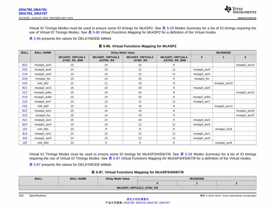
版权 © 2016–2019, Texas Instruments IncorporatedSpecifications提交文档反馈意见
产品主页链接: DRA790 DRA791 DRA793 DRA797
256
DRA790, DRA791DRA793, DRA797ZHCSII2E –AUGUST 2016–REVISED MAY 2019 www.ti.com.cn
Virtual IO Timings Modes must be used to ensure some IO timings for McASP2. See 表 5-29 Modes Summary for a list of IO timings requiring theuse of Virtual IO Timings Modes. See 表 5-86 Virtual Functions Mapping for McASP2 for a definition of the Virtual modes.
表 5-86 presents the values for DELAYMODE bitfield.
表表 5-86. Virtual Functions Mapping for McASP2
BALL BALL NAME Delay Mode Value MUXMODEMCASP2_VIRTUAL1
_SYNC_RX_80MMCASP2_VIRTUAL2
_ASYNC_RXMCASP2_VIRTUAL3
_SYNC_RXMCASP2_VIRTUAL4_ASYNC_RX_80M
0 1 2
B22 mcasp3_axr0 15 14 10 9 mcasp2_axr14D20 mcasp2_axr6 14 13 12 11 mcasp2_axr6C19 mcasp2_axr5 14 13 12 11 mcasp2_axr5D19 mcasp2_fsx 15 14 10 9 mcasp2_fsxH24 xref_clk2 12 11 10 9 mcasp2_axr10B21 mcasp2_axr3 15 14 10 9 mcasp2_axr3A22 mcasp3_aclkx 15 14 10 9 mcasp2_axr12E19 mcasp2_aclkx 15 14 10 9 mcasp2_aclkxC20 mcasp2_axr7 14 13 12 11 mcasp2_axr7H25 xref_clk3 12 11 10 9 mcasp2_axr11B23 mcasp3_axr1 15 14 10 8 mcasp2_axr15A23 mcasp3_fsx 15 14 10 9 mcasp2_axr13A21 mcasp2_axr2 15 14 10 9 mcasp2_axr2B20 mcasp2_axr4 14 13 12 11 mcasp2_axr4J24 xref_clk1 10 9 8 6 mcasp2_axr9B19 mcasp2_axr1 14 13 12 11 mcasp2_axr1A20 mcasp2_axr0 14 13 12 11 mcasp2_axr0J25 xref_clk0 10 9 8 6 mcasp2_axr8
Virtual IO Timings Modes must be used to ensure some IO timings for McASP3/4/5/6/7/8. See 表 5-29 Modes Summary for a list of IO timingsrequiring the use of Virtual IO Timings Modes. See 表 5-87 Virtual Functions Mapping for McASP3/4/5/6/7/8 for a definition of the Virtual modes.
表 5-87 presents the values for DELAYMODE bitfield.
表表 5-87. Virtual Functions Mapping for McASP3/4/5/6/7/8
BALL BALL NAME Delay Mode Value MUXMODE0 1 2
MCASP3_VIRTUAL2_SYNC_RX

版权 © 2016–2019, Texas Instruments Incorporated Specifications提交文档反馈意见
产品主页链接: DRA790 DRA791 DRA793 DRA797
257
DRA790, DRA791DRA793, DRA797
www.ti.com.cn ZHCSII2E –AUGUST 2016–REVISED MAY 2019
表表 5-87. Virtual Functions Mapping for McASP3/4/5/6/7/8 (continued)BALL BALL NAME Delay Mode Value MUXMODE
0 1 2B21 mcasp2_axr3 8 mcasp3_axr3A22 mcasp3_aclkx 8 mcasp3_aclkx mcasp3_aclkrB22 mcasp3_axr0 8 mcasp3_axr0B23 mcasp3_axr1 6 mcasp3_axr1A23 mcasp3_fsx 8 mcasp3_fsx mcasp3_fsrA21 mcasp2_axr2 8 mcasp3_axr2
MCASP4_VIRTUAL1_SYNC_RXB25 mcasp4_fsx 14 mcasp4_fsx mcasp4_fsrC23 mcasp4_aclkx 14 mcasp4_aclkx mcasp4_aclkrA24 mcasp4_axr0 14 mcasp4_axr0D23 mcasp4_axr1 14 mcasp4_axr1A14 mcasp1_axr5 12 mcasp4_axr3A15 mcasp1_axr4 12 mcasp4_axr2
MCASP5_VIRTUAL1_SYNC_RXAC3 mcasp5_aclkx 14 mcasp5_aclkx mcasp5_aclkrU6 mcasp5_fsx 14 mcasp5_fsx mcasp5_fsr
AC4 mcasp5_axr1 14 mcasp5_axr1A17 mcasp1_axr6 12 mcasp5_axr2AA5 mcasp5_axr0 14 mcasp5_axr0A16 mcasp1_axr7 12 mcasp5_axr3
MCASP6_VIRTUAL1_SYNC_RXC14 mcasp1_axr2 12 mcasp6_axr2B15 mcasp1_axr3 12 mcasp6_axr3B16 mcasp1_axr10 10 mcasp6_aclkx mcasp6_aclkrB17 mcasp1_axr9 10 mcasp6_axr1A18 mcasp1_axr8 10 mcasp6_axr0B18 mcasp1_axr11 10 mcasp6_fsx mcasp6_fsr
MCASP7_VIRTUAL2_SYNC_RXA19 mcasp1_axr12 10 mcasp7_axr0F16 mcasp1_axr15 10 mcasp7_fsx mcasp7_fsrE16 mcasp1_axr14 10 mcasp7_aclkx mcasp7_aclkrE17 mcasp1_axr13 10 mcasp7_axr1

版权 © 2016–2019, Texas Instruments IncorporatedSpecifications提交文档反馈意见
产品主页链接: DRA790 DRA791 DRA793 DRA797
258
DRA790, DRA791DRA793, DRA797ZHCSII2E –AUGUST 2016–REVISED MAY 2019 www.ti.com.cn
表表 5-87. Virtual Functions Mapping for McASP3/4/5/6/7/8 (continued)BALL BALL NAME Delay Mode Value MUXMODE
0 1 2D16 mcasp1_aclkr 13 mcasp7_axr2D17 mcasp1_fsr 13 mcasp7_axr3
MCASP8_VIRTUAL1_SYNC_RXB20 mcasp2_axr4 10 mcasp8_axr0C20 mcasp2_axr7 10 mcasp8_fsx mcasp8_fsrD20 mcasp2_axr6 10 mcasp8_aclkx mcasp8_aclkrC19 mcasp2_axr5 10 mcasp8_axr1

259
DRA790, DRA791DRA793, DRA797
www.ti.com.cn ZHCSII2E –AUGUST 2016–REVISED MAY 2019
提交文档反馈意见产品主页链接: DRA790 DRA791 DRA793 DRA797
Specifications版权 © 2016–2019, Texas Instruments Incorporated
5.10.6.16 USB
SuperSpeed USB DRD Subsystem has four instances in the device providing the following functions:• USB1: SuperSpeed (SS) USB 3.0 Dual-Role-Device (DRD) subsystem with integrated SS (USB3.0)
PHY and HS/FS (USB2.0) PHY.• USB2: High-Speed (HS) USB 2.0 Dual-Role-Device (DRD) subsystem with integrated HS/FS PHY.• USB3: HS USB 2.0 Dual-Role-Device (DRD) subsystem with ULPI (SDR) interface to external HS/FS
PHYs.
注注For more information, see the SuperSpeed USB DRD section of the Device TRM.
5.10.6.16.1 USB1 DRD PHY
The USB1 DRD interface supports the following applications:• USB2.0 High-Speed PHY port (1.8 V and 3.3 V): this asynchronous high-speed interface is compliant
with the USB2.0 PHY standard with an internal transceiver (USB2.0 standard v2.0), for a maximumdata rate of 480 Mbps.
• USB3.0 Super-Speed PHY port (1.8 V): this asynchronous differential super-speed interface iscompliant with the USB3.0 RX/TX PHY standard (USB3.0 standard v1.0) for a maximum data bit rateof 5Gbps.
5.10.6.16.2 USB2 PHY
The USB2 interface supports the following applications:• USB2.0 High-Speed PHY port (1.8 V and 3.3 V): this asynchronous high-speed interface is compliant
with the USB2.0 PHY standard with an internal transceiver (USB2.0 standard v2.0), for a maximumdata rate of 480 Mbps.
5.10.6.16.3 USB3 DRD ULPI—SDR—Slave Mode—12-pin Mode
TheUSB3 DRD interfaces support the following application:• USB ULPI port: this synchronous interface is compliant with the USB2.0 ULPI SDR standard (UTMI+
v1.22), for alternative off-chip USB2.0 PHY interface; that is, with external transceiver with a maximumfrequency of 60 MHz (synchronous slave mode, SDR, 12-pin, 8-data-bit).
注注The Universal Serial Bus k ULPI modules are also refered as USBk where k = 3, 4.
表 5-88, 表 5-89 and 图 5-67 assume testing over the recommended operating conditions and electricalcharacteristic conditions.
表表 5-88. Timing Requirements for ULPI SDR Slave Mode
NO. PARAMETER DESCRIPTION MIN MAX UNITUS1 tc(clk) Cycle time, usb_ulpi_clk period 16.66 nsUS5 tsu(ctrlV-clkH) Setup time, usb_ulpi_dir/usb_ulpi_nxt valid before usb_ulpi_clk
rising edge6.73 ns
US6 th(clkH-ctrlV) Hold time, usb_ulpi_dir/usb_ulpi_nxt valid after usb_ulpi_clkrising edge
-0.41 ns
US7 tsu(dV-clkH) Setup time, usb_ulpi_d[7:0] valid before usb_ulpi_clk rising edge 6.73 nsUS8 th(clkH-dV) Hold time, usb_ulpi_d[7:0] valid after usb_ulpi_clk rising edge -0.41 ns

usbk_ulpi_clk
usbk_ulpi_stp
usbk_ulpi_dir_&_nxt
usbk_ulpi_d[7:0] Data_IN Data_OUT
US1
US8
US7 US9
US9
US2 US3
US4 US4
US5
US6
SPRS906_TIMING_USB_01
260
DRA790, DRA791DRA793, DRA797ZHCSII2E –AUGUST 2016–REVISED MAY 2019 www.ti.com.cn
提交文档反馈意见产品主页链接: DRA790 DRA791 DRA793 DRA797
Specifications 版权 © 2016–2019, Texas Instruments Incorporated
表表 5-89. Switching Characteristics for ULPI SDR Slave Mode
NO. PARAMETER DESCRIPTION MIN MAX UNITUS4 td(clkH-stpV) Delay time, usb_ulpi_clk rising edge high to output
usb_ulpi_stp valid0.44 8.35 ns
US9 td(clkL-doV) Delay time, usb_ulpi_clk rising edge high to outputusb_ulpi_d[7:0] valid
0.44 8.35 ns
图图 5-67. HS USB3 ULPI —SDR—Slave Mode—12-pin Mode
In 表 5-90 are presented the specific groupings of signals (IOSET) for use with USB3 signals.
表表 5-90. USB3 IOSETs
SIGNALS IOSET2 IOSET3BALL MUX BALL MUX
usb3_ulpi_d7 Y5 3 N4 6usb3_ulpi_d6 Y6 3 N3 6usb3_ulpi_d5 Y2 3 P1 6usb3_ulpi_d4 Y1 3 N1 6usb3_ulpi_d3 Y4 3 P2 6usb3_ulpi_d2 AA2 3 N2 6usb3_ulpi_d1 AA3 3 R1 6usb3_ulpi_d0 W2 3 R2 6usb3_ulpi_nxt Y3 3 P3 6usb3_ulpi_dir AA1 3 P4 6usb3_ulpi_stp AA4 3 T5 6usb3_ulpi_clk AB1 3 T4 6
5.10.6.17 PCIe
The device supports connections to PCIe-compliant devices via the integrated PCIe master/slave businterface. The PCIe module is comprised of a dual-mode PCIe core and a SerDes PHY. Each PCIesubsystem controller has support for PCIe Gen-II mode (5.0 Gbps /lane) and Gen-I mode (2.5 Gbps/lane)(Single Lane and Flexible dual lane configuration).
The device PCIe supports the following features:• 16-bit operation @250 MHz on PIPE interface (per 16-bit lane)• Supports 2 ports x 1 lane or 1 port x 2 lanes configuration• Single virtual channel (VC0), single traffic class (TC0)• Single function in end-point mode
261
DRA790, DRA791DRA793, DRA797
www.ti.com.cn ZHCSII2E –AUGUST 2016–REVISED MAY 2019
提交文档反馈意见产品主页链接: DRA790 DRA791 DRA793 DRA797
Specifications版权 © 2016–2019, Texas Instruments Incorporated
• Automatic width and speed negotiation• Max payload: 128 byte outbound, 256 byte inbound• Automatic credit management• ECRC generation and checking• Configurable BAR filtering• Legacy interrupt reception (RC) and generation (EP)• MSI generation and reception• PCI Express Active State Power Management (ASPM) state L0s and L1 (with exceptions)• All PCI Device Power Management D-states with the exception of D3cold / L2 state
The PCIe controller on this device conforms to the PCI Express Base 3.0 Specification, revision 1.0 andthe PCI Local Bus Specification, revision 3.0.
注注For more information, see the PCIe Controller section of the Device TRM.
5.10.6.18 DCAN
The device provides two DCAN interfaces for supporting distributed realtime control with a high level ofsecurity. The DCAN interfaces implement the following features:• Supports CAN protocol version 2.0 part A, B• Bit rates up to 1 MBit/s• 64 message objects• Individual identifier mask for each message object• Programmable FIFO mode for message objects• Programmable loop-back modes for self-test operation• Suspend mode for debug support• Software module reset• Automatic bus on after Bus-Off state by a programmable 32-bit timer• Direct access to Message RAM during test mode• CAN Rx/Tx pins are configurable as general-purpose IO pins• Two interrupt lines (plus additional parity-error interrupts line)• RAM initialization• DMA support
注注For more information, see the DCAN section of the Device TRM.
注注The Controller Area Network Interface x (x = 1 to 2) is also referred to as DCANx.
注注Refer to the CAN Specification for calculations necessary to validate timing compliance. Jittertolerance calculations must be performed to validate the implementation.
表 5-91 and 表 5-92 present timing and switching characteristics for DCANx Interface.

262
DRA790, DRA791DRA793, DRA797ZHCSII2E –AUGUST 2016–REVISED MAY 2019 www.ti.com.cn
提交文档反馈意见产品主页链接: DRA790 DRA791 DRA793 DRA797
Specifications 版权 © 2016–2019, Texas Instruments Incorporated
表表 5-91. Timing Requirements for DCANx ReceiveNO. PARAMETER DESCRIPTION MIN NOM MAX UNIT
- f(baud) Maximum programmable baud rate 1 Mbps- td(DCANRX) Delay time, DCANx_RX pin to receive shift register 15 ns
表表 5-92. Switching Characteristics Over Recommended Operating Conditions for DCANx TransmitNO. PARAMETER DESCRIPTION MIN MAX UNIT
- f(baud) Maximum programmable baud rate 1 Mbps- td(DCANTX) Delay time, Transmit shift register to DCANx_TX pin(1) 23 ns
(1) These values do not include rise/fall times of the output buffer.
5.10.6.19 GMAC_SW
The three-port gigabit ethernet switch subsystem (GMAC_SW) provides ethernet packet communicationand can be configured as an ethernet switch. It provides the Gigabit Media Independent Interface (G/MII)in MII mode, Reduced Gigabit Media Independent Interface (RGMII), Reduced Media IndependentInterface (RMII), and the Management Data Input/Output (MDIO) for physical layer device (PHY)management.
注注For more information, see the Ethernet Subsystem section of the Device TRM.
注注The Gigabit, Reduced and Media Independent Interface n (n = 0 to 1) are also referred to asMIIn, RMIIn and RGMIIn.
CAUTION
The I/O Timings provided in this section are valid only if signals within a singleIOSET are used. The IOSETs are defined in 表 5-97, 表 5-100, 表 5-105 and 表5-112.
CAUTION
The I/O Timings provided in this section are valid only for some GMAC usagemodes when the corresponding Virtual I/O Timings or Manual I/O Timings areconfigured as described in the tables found in this section.
5.10.6.19.1 GMAC MII Timings
表 5-93 and 图 5-68 present timing requirements for MIIn in receive operation.
表表 5-93. Timing Requirements for miin_rxclk - MII OperationNO. PARAMETER DESCRIPTION SPEED MIN MAX UNIT1 tc(RX_CLK) Cycle time, miin_rxclk 10 Mbps 400 ns
100 Mbps 40 ns2 tw(RX_CLKH) Pulse duration, miin_rxclk high 10 Mbps 140 260 ns
100 Mbps 14 26 ns3 tw(RX_CLKL) Pulse duration, miin_rxclk low 10 Mbps 140 260 ns
100 Mbps 14 26 ns

mii _txclkn
2 3
1 4
4
SPRS906_TIMING_GMAC_MIITXCLK_02
mii _rxclkn
2 3
1 4
4
SPRS906_TIMING_GMAC_MIIRXCLK_01
263
DRA790, DRA791DRA793, DRA797
www.ti.com.cn ZHCSII2E –AUGUST 2016–REVISED MAY 2019
提交文档反馈意见产品主页链接: DRA790 DRA791 DRA793 DRA797
Specifications版权 © 2016–2019, Texas Instruments Incorporated
表表 5-93. Timing Requirements for miin_rxclk - MII Operation (continued)NO. PARAMETER DESCRIPTION SPEED MIN MAX UNIT4 tt(RX_CLK) Transition time, miin_rxclk 10 Mbps 3 ns
100 Mbps 3 ns
图图 5-68. Clock Timing (GMAC Receive) - MIIn operation
表 5-94 and 图 5-69 present timing requirements for MIIn in transmit operation.
表表 5-94. Timing Requirements for miin_txclk - MII OperationNO. PARAMETER DESCRIPTION SPEED MIN MAX UNIT1 tc(TX_CLK) Cycle time, miin_txclk 10 Mbps 400 ns
100 Mbps 40 ns2 tw(TX_CLKH) Pulse duration, miin_txclk high 10 Mbps 140 260 ns
100 Mbps 14 26 ns3 tw(TX_CLKL) Pulse duration, miin_txclk low 10 Mbps 140 260 ns
100 Mbps 14 26 ns4 tt(TX_CLK) Transition time, miin_txclk 10 Mbps 3 ns
100 Mbps 3 ns
图图 5-69. Clock Timing (GMAC Transmit) - MIIn operation
表 5-95 and 图 5-70 present timing requirements for GMAC MIIn Receive 10/100Mbit/s.
表表 5-95. Timing Requirements for GMAC MIIn Receive 10/100 Mbit/sNO. PARAMETER DESCRIPTION MIN MAX UNIT
1tsu(RXD-RX_CLK)
Setup time, receive selected signals valid before miin_rxclk 8 nstsu(RX_DV-RX_CLK)
tsu(RX_ER-RX_CLK)
2th(RX_CLK-RXD)
Hold time, receive selected signals valid after miin_rxclk 8 nsth(RX_CLK-RX_DV)
th(RX_CLK-RX_ER)

1
mii _txclkn (input)
miin_txd3miin_txen, miin_txer
− ,(outputs)
miin_txd0
SPRS906_TIMING_GMAC_MIITX_04
mii _rxclkn (Input)
1
2
mii _rxd3nmii _rxdv miin_rxer
−, (Inputs)
mii _rxd0,nn
SPRS906_TIMING_GMAC_MIIRCV_03
264
DRA790, DRA791DRA793, DRA797ZHCSII2E –AUGUST 2016–REVISED MAY 2019 www.ti.com.cn
提交文档反馈意见产品主页链接: DRA790 DRA791 DRA793 DRA797
Specifications 版权 © 2016–2019, Texas Instruments Incorporated
图图 5-70. GMAC Receive Interface Timing MIIn operation
表 5-96 and 图 5-71 present timing requirements for GMAC MIIn Transmit 10/100Mbit/s.
表表 5-96. Switching Characteristics Over Recommended Operating Conditions for GMAC MIIn Transmit10/100 Mbits/s
NO. PARAMETER DESCRIPTION MIN MAX UNIT
1td(TX_CLK-TXD)
Delay time, miin_txclk to transmit selected signals valid 0 25 nstd(TX_CLK-TX_EN)
td(TX_CLK-TX_ER)
图图 5-71. GMAC Transmit Interface Timing MIIn operation
In 表 5-97 are presented the specific groupings of signals (IOSET) for use with GMAC MII signals.
表表 5-97. GMAC MII IOSETs
SIGNALS IOSET5 IOSET6BALL MUX BALL MUX
GMAC MII1mii1_txd3 E11 8mii1_txd2 A13 8mii1_txd1 A12 8mii1_txd0 B12 8mii1_rxd3 B10 8mii1_rxd2 A10 8mii1_rxd1 F10 8mii1_rxd0 E10 8mii1_col E13 8mii1_rxer B13 8mii1_txer F11 8mii1_txen D13 8mii1_crs C13 8
mii1_rxclk B11 8mii1_txclk C11 8mii1_rxdv D11 8

265
DRA790, DRA791DRA793, DRA797
www.ti.com.cn ZHCSII2E –AUGUST 2016–REVISED MAY 2019
提交文档反馈意见产品主页链接: DRA790 DRA791 DRA793 DRA797
Specifications版权 © 2016–2019, Texas Instruments Incorporated
表表 5-97. GMAC MII IOSETs (continued)SIGNALS IOSET5 IOSET6
BALL MUX BALL MUXGMAC MII0
mii0_txd3 P2 3mii0_txd2 N1 3mii0_txd1 N3 3mii0_txd0 N4 3mii0_rxd3 T4 3mii0_rxd2 T5 3mii0_rxd1 R2 3mii0_rxd0 R1 3mii0_txclk N2 3mii0_txer L6 3mii0_rxer P3 3mii0_rxdv N5 3mii0_crs P4 3mii0_col L5 3
mii0_rxclk N6 3mii0_txen P1 3
5.10.6.19.2 GMAC MDIO Interface Timings
CAUTION
The I/O Timings provided in this section are valid only for some GMAC usagemodes when the corresponding Virtual I/O Timings or Manual I/O Timings areconfigured as described in the tables found in this section.
表 5-98, 表 5-98 and 图 5-72 present timing requirements for MDIO.
表表 5-98. Timing Requirements for MDIO Input
No PARAMETER DESCRIPTION MIN MAX UNITMDIO1 tc(MDC) Cycle time, MDC 400 nsMDIO2 tw(MDCH) Pulse Duration, MDC High 160 nsMDIO3 tw(MDCL) Pulse Duration, MDC Low 160 nsMDIO4 tsu(MDIO-MDC) Setup time, MDIO valid before MDC High 90 nsMDIO5 th(MDIO_MDC) Hold time, MDIO valid from MDC High 0 ns
表表 5-99. Switching Characteristics Over Recommended Operating Conditions for MDIO Output
NO PARAMETER DESCRIPTION MIN MAX UNITMDIO6 tt(MDC) Transition time, MDC 5 nsMDIO7 td(MDC-MDIO) Delay time, MDC low to MDIO valid -150 150 ns

1
MDIO4
MDIO5
MDIO7
MDIO2
MDIO3
MDIO6 MDIO6
MDCLK
MDIO(input)
MDIO(output)
266
DRA790, DRA791DRA793, DRA797ZHCSII2E –AUGUST 2016–REVISED MAY 2019 www.ti.com.cn
提交文档反馈意见产品主页链接: DRA790 DRA791 DRA793 DRA797
Specifications 版权 © 2016–2019, Texas Instruments Incorporated
图图 5-72. GMAC MDIO diagrams
In 表 5-100 are presented the specific groupings of signals (IOSET) for use with GMAC MDIO signals.
表表 5-100. GMAC MDIO IOSETs
SIGNALS IOSET7 IOSET8 IOSET9 IOSET10BALL MUX BALL MUX BALL MUX BALL MUX
mdio_d C10 3 L6 0 Y6 1 E25 5mdio_mclk D10 3 L5 0 Y5 1 E24 5
5.10.6.19.3 GMAC RMII Timings
The main reference clock REF_CLK (RMII_50MHZ_CLK) of RMII interface is internally supplied fromPRCM. The source of this clock could be either externally sourced from the RMII_MHZ_50_CLK pin of thedevice or internally generated from DPLL_GMAC output clock GMAC_RMII_HS_CLK. Please see thePRCM chapter of the device TRM for full details about RMII reference clock.
CAUTION
The I/O Timings provided in this section are valid only for some GMAC usagemodes when the corresponding Virtual I/O Timings or Manual I/O Timings areconfigured as described in the tables found in this section.
表 5-101, 表 5-102 and 图 5-73 present timing requirements for GMAC RMIIn Receive.
表表 5-101. Timing Requirements for GMAC REF_CLK - RMII OperationNO. PARAMETER DESCRIPTION MIN MAX UNIT
RMII1 tc(REF_CLK) Cycle time, REF_CLK 20 nsRMII2 tw(REF_CLKH) Pulse duration, REF_CLK high 7 13 nsRMII3 tw(REF_CLKL) Pulse duration, REF_CLK low 7 13 nsRMII4 ttt(REF_CLK) Transistion time, REF_CLK 3 ns

REF_CLK (PRCM)
rmiin_txd1−rmiin_txd0,rmiin_txen (Outputs)
SPRS906_TIMING_GMAC_RMIITX_07
RMII7
RMII8 RMII9
RMII11RMII10
REF_CLK (PRCM)
RMII5 RMII6
rmiin_rxd1−rmin_rxer
rmiin_rxd0,rmiin_crs, (inputs)
SPRS906_TIMING_GMAC_RGMIITX_09
RMII1
RMII3 RMII2
RMII4
267
DRA790, DRA791DRA793, DRA797
www.ti.com.cn ZHCSII2E –AUGUST 2016–REVISED MAY 2019
提交文档反馈意见产品主页链接: DRA790 DRA791 DRA793 DRA797
Specifications版权 © 2016–2019, Texas Instruments Incorporated
表表 5-102. Timing Requirements for GMAC RMIIn ReceiveNO. PARAMETER DESCRIPTION MIN MAX UNIT
RMII5 tsu(RXD-REF_CLK) Setup time, receive selected signals valid before REF_CLK 4 nstsu(CRS_DV-REF_CLK)
tsu(RX_ER-REF_CLK)
RMII6 th(REF_CLK-RXD) Hold time, receive selected signals valid after REF_CLK 2 nsth(REF_CLK-CRS_DV)
th(REF_CLK-RX_ER)
图图 5-73. GMAC Receive Interface Timing RMIIn operation
表 5-103, 表 5-103 and 图 5-74 present switching characteristics for GMAC RMIIn Transmit 10/100Mbit/s.
表表 5-103. Switching Characteristics Over Recommended Operating Conditions for GMAC REF_CLK - RMIIOperation
NO. PARAMETER DESCRIPTION MIN MAX UNITRMII7 tc(REF_CLK) Cycle time, REF_CLK 20 nsRMII8 tw(REF_CLKH) Pulse duration, REF_CLK high 7 13 nsRMII9 tw(REF_CLKL) Pulse duration, REF_CLK low 7 13 nsRMII10 tt(REF_CLK) Transistion time, REF_CLK 3 ns
表表 5-104. Switching Characteristics Over Recommended Operating Conditions for GMAC RMIIn Transmit10/100 Mbits/s
NO. PARAMETER DESCRIPTION RMIIn MIN MAX UNIT
RMII11
td(REF_CLK-TXD)
Delay time, REF_CLK high to selected transmit signalsvalid
RMII0 2 13.5 nstdd(REF_CLK-TXEN)
td(REF_CLK-TXD) RMII1 2 13.8 nstdd(REF_CLK-TXEN)
图图 5-74. GMAC Transmit Interface Timing RMIIn Operation
In 表 5-105 are presented the specific groupings of signals (IOSET) for use with GMAC RMII signals.

268
DRA790, DRA791DRA793, DRA797ZHCSII2E –AUGUST 2016–REVISED MAY 2019 www.ti.com.cn
提交文档反馈意见产品主页链接: DRA790 DRA791 DRA793 DRA797
Specifications 版权 © 2016–2019, Texas Instruments Incorporated
表表 5-105. GMAC RMII IOSETs
SIGNALS IOSET1 IOSET2BALL MUX BALL MUX
GMAC RMII1RMII_MHZ_50_CLK P5 0
rmii1_txd1 P2 2rmii1_txd0 N1 2rmii1_rxd1 T4 2rmii1_rxd0 T5 2rmii1_rxer N6 2rmii1_txen N2 2rmii1_crs N5 2
GMAC RMII0RMII_MHZ_50_CLK P5 0
rmii0_txd1 N3 1rmii0_txd0 N4 1rmii0_rxd1 R2 1rmii0_rxd0 R1 1rmii0_txen P1 1rmii0_rxer P3 1rmii0_crs P4 1
Manual IO Timings Modes must be used to ensure some IO timings for GMAC. See 表 5-29 ModesSummary for a list of IO timings requiring the use of Manual IO Timings Modes. See 表 5-106 ManualFunctions Mapping for GMAC RMII0 for a definition of the Manual modes.
表 5-106 lists the A_DELAY and G_DELAY values needed to calculate the correct values to be set in theCFG_x registers.
表表 5-106. Manual Functions Mapping for GMAC RMII0
BALL BALL NAME GMAC_RMII0_MANUAL1 CFG REGISTER MUXMODEA_DELAY
(ps)G_DELAY
(ps)0 1
P5 RMII_MHZ_50_CLK 0 0 CFG_RMII_MHZ_50_CLK_IN RMII_MHZ_50_CLKR1 rgmii0_txd0 2444 804 CFG_RGMII0_TXD0_IN rmii0_rxd0R2 rgmii0_txd1 2453 981 CFG_RGMII0_TXD1_IN rmii0_rxd1P3 rgmii0_txd2 2356 847 CFG_RGMII0_TXD2_IN rmii0_rxerP4 rgmii0_txd3 2415 993 CFG_RGMII0_TXD3_IN rmii0_crs
Manual IO Timings Modes must be used to ensure some IO timings for GMAC. See 表 5-29 ModesSummary for a list of IO timings requiring the use of Manual IO Timings Modes. See 表 5-107 ManualFunctions Mapping for GMAC RMII1 for a definition of the Manual modes.
表 5-107 list the A_DELAY and G_DELAY values needed to calculate the correct values to be set in theCFG_x registers.
表表 5-107. Manual Functions Mapping for GMAC RMII1
BALL BALL NAME GMAC_RMII1_MANUAL1 CFG REGISTER MUXMODEA_DELAY
(ps)G_DELAY
(ps)0 2
P5 RMII_MHZ_50_CLK 0 0 CFG_RMII_MHZ_50_CLK_IN RMII_MHZ_50_CLKT5 rgmii0_txctl 2450 909 CFG_RGMII0_TXCTL_IN rmii1_rxd0

269
DRA790, DRA791DRA793, DRA797
www.ti.com.cn ZHCSII2E –AUGUST 2016–REVISED MAY 2019
提交文档反馈意见产品主页链接: DRA790 DRA791 DRA793 DRA797
Specifications版权 © 2016–2019, Texas Instruments Incorporated
表表 5-107. Manual Functions Mapping for GMAC RMII1 (continued)BALL BALL NAME GMAC_RMII1_MANUAL1 CFG REGISTER MUXMODE
A_DELAY(ps)
G_DELAY(ps)
0 2
T4 rgmii0_txc 2327 926 CFG_RGMII0_TXC_IN rmii1_rxd1N6 uart3_txd 2553 443 CFG_UART3_TXD_IN rmii1_rxerN5 uart3_rxd 1943 1110 CFG_UART3_RXD_IN rmii1_crs
5.10.6.19.4 GMAC RGMII Timings
CAUTION
The I/O Timings provided in this section are valid only for some GMAC usagemodes when the corresponding Virtual I/O Timings or Manual I/O Timings areconfigured as described in the tables found in this section.
表 5-108, 表 5-109 and 图 5-75 present timing requirements for receive RGMIIn operation.
表表 5-108. Timing Requirements for rgmiin_rxc - RGMIIn OperationNO. PARAMETER DESCRIPTION SPEED MIN MAX UNIT
1 tc(RXC) Cycle time, rgmiin_rxc 10 Mbps 360 440 ns100 Mbps 36 44 ns1000 Mbps 7.2 8.8 ns
2 tw(RXCH) Pulse duration, rgmiin_rxc high 10 Mbps 160 240 ns100 Mbps 16 24 ns1000 Mbps 3.6 4.4 ns
3 tw(RXCL) Pulse duration, rgmiin_rxc low 10 Mbps 160 240 ns100 Mbps 16 24 ns1000 Mbps 3.6 4.4 ns
4 tt(RXC) Transition time, rgmiin_rxc 10 Mbps 0.75 ns100 Mbps 0.75 ns1000 Mbps 0.75 ns
表表 5-109. Timing Requirements for GMAC RGMIIn Input Receive for 10/100/1000 Mbps (1)
NO. PARAMETER DESCRIPTION MODE MIN MAX UNIT5 tsu(RXD-RXCH) Setup time, receive selected signals valid before
rgmiin_rxc high/lowRGMII0/1 1 ns
6 th(RXCH-RXD) Hold time, receive selected signals valid afterrgmiin_rxc high/low
RGMII0/1 1 ns

rgmii _rxd[3:0]n(B)
rgmii _rxctln(B)
rgmii _rxcn(A)
5
RXERRRXDV
1st Half-byte
2nd Half-byte
RGRXD[7:4]RGRXD[3:0]
23
1
4
4
6
SPRS906_TIMING_GMAC_RGMIIRX_08
270
DRA790, DRA791DRA793, DRA797ZHCSII2E –AUGUST 2016–REVISED MAY 2019 www.ti.com.cn
提交文档反馈意见产品主页链接: DRA790 DRA791 DRA793 DRA797
Specifications 版权 © 2016–2019, Texas Instruments Incorporated
(1) For RGMII, receive selected signals include: rgmiin_rxd[3:0] and rgmiin_rxctl.
A. rgmiin_rxc must be externally delayed relative to the data and control pins.B. Data and control information is received using both edges of the clocks. rgmiin_rxd[3:0] carries data bits 3-0 on the
rising edge of rgmiin_rxc and data bits 7-4 on the falling edge ofrgmiin_rxc. Similarly, rgmiin_rxctl carries RXDV onrising edge of rgmiin_rxc and RXERR on falling edge of rgmiin_rxc.
图图 5-75. GMAC Receive Interface Timing, RGMIIn operation
表 5-110, 表 5-111 and 图 5-76 present switching characteristics for transmit - RGMIIn for10/100/1000Mbit/s.
表表 5-110. Switching Characteristics Over Recommended Operating Conditions for rgmiin_txctl - RGMIInOperation for 10/100/1000 Mbit/s
NO. PARAMETER DESCRIPTION SPEED MIN MAX UNIT1 tc(TXC) Cycle time, rgmiin_txc 10 Mbps 360 440 ns
100 Mbps 36 44 ns1000 Mbps 7.2 8.8 ns
2 tw(TXCH) Pulse duration, rgmiin_txc high 10 Mbps 160 240 ns100 Mbps 16 24 ns1000 Mbps 3.6 4.4 ns
3 tw(TXCL) Pulse duration, rgmiin_txc low 10 Mbps 160 240 ns100 Mbps 16 24 ns1000 Mbps 3.6 4.4 ns
4 tt(TXC) Transition time, rgmiin_txc 10 Mbps 0.75 ns100 Mbps 0.75 ns1000 Mbps 0.75 ns
表表 5-111. Switching Characteristics for GMAC RGMIIn Output Transmit for 10/100/1000 Mbps (1)
NO. PARAMETER DESCRIPTION MODE MIN MAX UNIT5 tosu(TXD-TXC) Output Setup time, transmit selected signals valid to
rgmiin_txc high/lowRGMII0, Internal DelayEnabled, 1000 Mbps
1.05(2)
ns
RGMII0, Internal DelayEnabled, 10/100 Mbps
1.2 ns
RGMII1, Internal DelayEnabled, 1000 Mbps
1.05(3)
ns
RGMII1, Internal DelayEnabled, 10/100 Mbps
1.2 ns

rgmii _txcn(A)
rgmii _txdn [3:0](B)
rgmii _txctln(B)
5
1st Half-byte
TXERRTXEN
2nd Half-byte
4
4
23
1
6
[internal delay enabled]
SPRS906_TIMING_GMAC_RGMIITX_09
271
DRA790, DRA791DRA793, DRA797
www.ti.com.cn ZHCSII2E –AUGUST 2016–REVISED MAY 2019
提交文档反馈意见产品主页链接: DRA790 DRA791 DRA793 DRA797
Specifications版权 © 2016–2019, Texas Instruments Incorporated
表表 5-111. Switching Characteristics for GMAC RGMIIn Output Transmit for 10/100/1000 Mbps(1) (continued)
NO. PARAMETER DESCRIPTION MODE MIN MAX UNIT6 toh(TXC-TXD) Output Hold time, transmit selected signals valid after
rgmiin_txc high/lowRGMII0, Internal DelayEnabled, 1000 Mbps
1.05(2)
ns
RGMII0, Internal DelayEnabled, 10/100 Mbps
1.2 ns
RGMII1, Internal DelayEnabled, 1000 Mbps
1.05(3)
ns
RGMII1, Internal DelayEnabled, 10/100 Mbps
1.2 ns
(1) For RGMII, transmit selected signals include: rgmiin_txd[3:0] and rgmiin_txctl.(2) RGMII0 requires that the 4 data pins rgmii0_txd[3:0] and rgmii0_txctl have their board propagation delays matched within 50pS of
rgmii0_txc.(3) RGMII1 requires that the 4 data pins rgmii1_txd[3:0] and rgmii1_txctl have their board propagation delays matched within 50pS of
rgmii1_txc.
A. TXC is delayed internally before being driven to the rgmiin_txc pin. This internal delay is always enabled.B. Data and control information is transmitted using both edges of the clocks. rgmiin_txd[3:0] carries data bits 3-0 on the
rising edge of rgmiin_txc and data bits 7-4 on the falling edge of rgmiin_txc. Similarly, rgmiin_txctl carries TXEN onrising edge of rgmiin_txc and TXERR of falling edge of rgmiin_txc.
图图 5-76. GMAC Transmit Interface Timing RGMIIn operation
In 表 5-112 are presented the specific groupings of signals (IOSET) for use with GMAC RGMII signals.
表表 5-112. GMAC RGMII IOSETs
SIGNALS IOSET3 IOSET4BALL MUX BALL MUX
GMAC RGMII1rgmii1_txd3 C11 3rgmii1_txd2 B12 3rgmii1_txd1 A12 3rgmii1_txd0 A13 3rgmii1_rxd3 B13 3rgmii1_rxd2 E13 3rgmii1_rxd1 C13 3rgmii1_rxd0 D13 3rgmii1_rxctl F11 3rgmii1_txc B11 3rgmii1_txctl D11 3
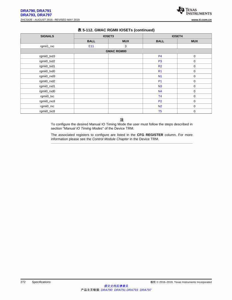
272
DRA790, DRA791DRA793, DRA797ZHCSII2E –AUGUST 2016–REVISED MAY 2019 www.ti.com.cn
提交文档反馈意见产品主页链接: DRA790 DRA791 DRA793 DRA797
Specifications 版权 © 2016–2019, Texas Instruments Incorporated
表表 5-112. GMAC RGMII IOSETs (continued)SIGNALS IOSET3 IOSET4
BALL MUX BALL MUXrgmii1_rxc E11 3
GMAC RGMII0rgmii0_txd3 P4 0rgmii0_txd2 P3 0rgmii0_txd1 R2 0rgmii0_txd0 R1 0rgmii0_rxd3 N1 0rgmii0_rxd2 P1 0rgmii0_rxd1 N3 0rgmii0_rxd0 N4 0rgmii0_txc T4 0rgmii0_rxctl P2 0rgmii0_rxc N2 0rgmii0_txctl T5 0
注注To configure the desired Manual IO Timing Mode the user must follow the steps described insection "Manual IO Timing Modes" of the Device TRM.
The associated registers to configure are listed in the CFG REGISTER column. For moreinformation please see the Control Module Chapter in the Device TRM.

版权 © 2016–2019, Texas Instruments Incorporated Specifications提交文档反馈意见
产品主页链接: DRA790 DRA791 DRA793 DRA797
273
DRA790, DRA791DRA793, DRA797
www.ti.com.cn ZHCSII2E –AUGUST 2016–REVISED MAY 2019
Manual IO Timings Modes must be used to ensure some IO timings for GMAC. See 表 5-29 Modes Summary for a list of IO timings requiring theuse of Manual IO Timings Modes. See 表 5-113 Manual Functions Mapping for GMAC RGMII0 for a definition of the Manual modes.
表 5-113 lists the A_DELAY and G_DELAY values needed to calculate the correct values to be set in the CFG_x registers.
表表 5-113. Manual Functions Mapping for GMAC RGMII0
BALL BALL NAME GMAC_RGMII0_MANUAL1 CFG REGISTER MUXMODEA_DELAY (ps) G_DELAY (ps) 0
N2 rgmii0_rxc 413 0 CFG_RGMII0_RXC_IN rgmii0_rxcP2 rgmii0_rxctl 27 2296 CFG_RGMII0_RXCTL_IN rgmii0_rxctlN4 rgmii0_rxd0 3 1721 CFG_RGMII0_RXD0_IN rgmii0_rxd0N3 rgmii0_rxd1 134 1786 CFG_RGMII0_RXD1_IN rgmii0_rxd1P1 rgmii0_rxd2 40 1966 CFG_RGMII0_RXD2_IN rgmii0_rxd2N1 rgmii0_rxd3 0 2057 CFG_RGMII0_RXD3_IN rgmii0_rxd3
T4 rgmii0_txc 0 60 CFG_RGMII0_TXC_OUT rgmii0_txcT5 rgmii0_txctl 0 60 CFG_RGMII0_TXCTL_OUT rgmii0_txctlR1 rgmii0_txd0 0 60 CFG_RGMII0_TXD0_OUT rgmii0_txd0R2 rgmii0_txd1 0 0 CFG_RGMII0_TXD1_OUT rgmii0_txd1P3 rgmii0_txd2 0 60 CFG_RGMII0_TXD2_OUT rgmii0_txd2P4 rgmii0_txd3 0 120 CFG_RGMII0_TXD3_OUT rgmii0_txd3
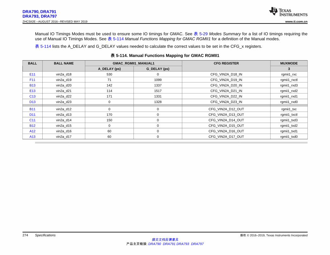
版权 © 2016–2019, Texas Instruments IncorporatedSpecifications提交文档反馈意见
产品主页链接: DRA790 DRA791 DRA793 DRA797
274
DRA790, DRA791DRA793, DRA797ZHCSII2E –AUGUST 2016–REVISED MAY 2019 www.ti.com.cn
Manual IO Timings Modes must be used to ensure some IO timings for GMAC. See 表 5-29 Modes Summary for a list of IO timings requiring theuse of Manual IO Timings Modes. See 表 5-114 Manual Functions Mapping for GMAC RGMII1 for a definition of the Manual modes.
表 5-114 lists the A_DELAY and G_DELAY values needed to calculate the correct values to be set in the CFG_x registers.
表表 5-114. Manual Functions Mapping for GMAC RGMII1
BALL BALL NAME GMAC_RGMII1_MANUAL1 CFG REGISTER MUXMODEA_DELAY (ps) G_DELAY (ps) 3
E11 vin2a_d18 530 0 CFG_VIN2A_D18_IN rgmii1_rxcF11 vin2a_d19 71 1099 CFG_VIN2A_D19_IN rgmii1_rxctlB13 vin2a_d20 142 1337 CFG_VIN2A_D20_IN rgmii1_rxd3E13 vin2a_d21 114 1517 CFG_VIN2A_D21_IN rgmii1_rxd2C13 vin2a_d22 171 1331 CFG_VIN2A_D22_IN rgmii1_rxd1D13 vin2a_d23 0 1328 CFG_VIN2A_D23_IN rgmii1_rxd0
B11 vin2a_d12 0 0 CFG_VIN2A_D12_OUT rgmii1_txcD11 vin2a_d13 170 0 CFG_VIN2A_D13_OUT rgmii1_txctlC11 vin2a_d14 150 0 CFG_VIN2A_D14_OUT rgmii1_txd3B12 vin2a_d15 0 0 CFG_VIN2A_D15_OUT rgmii1_txd2A12 vin2a_d16 60 0 CFG_VIN2A_D16_OUT rgmii1_txd1A13 vin2a_d17 60 0 CFG_VIN2A_D17_OUT rgmii1_txd0
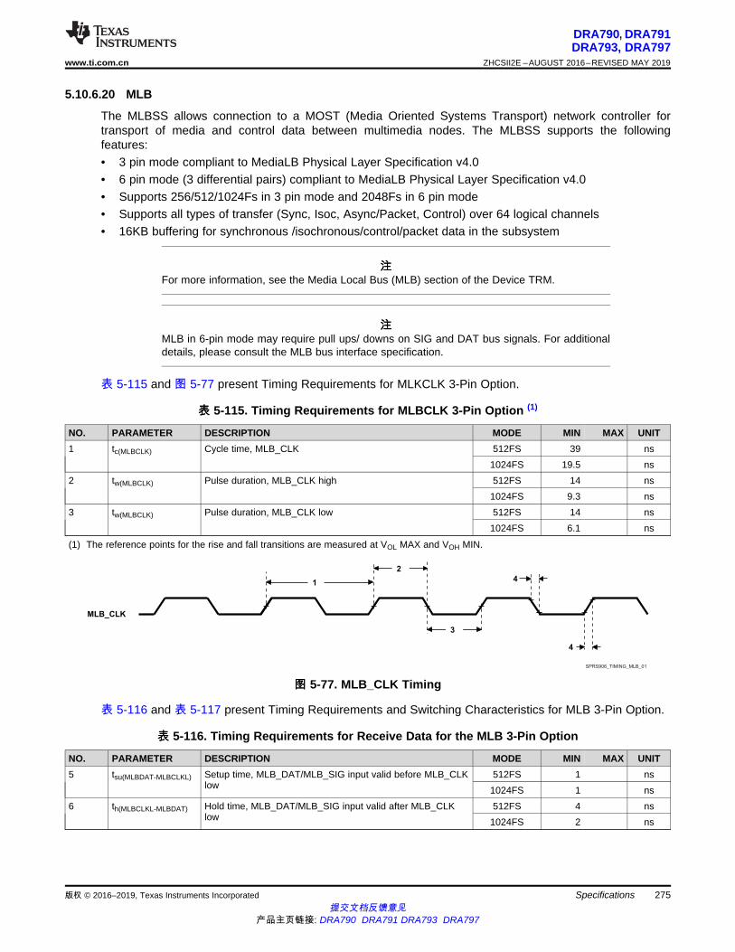
MLB_CLK
1
2
4
4
3
SPRS906_TIMING_MLB_01
275
DRA790, DRA791DRA793, DRA797
www.ti.com.cn ZHCSII2E –AUGUST 2016–REVISED MAY 2019
提交文档反馈意见产品主页链接: DRA790 DRA791 DRA793 DRA797
Specifications版权 © 2016–2019, Texas Instruments Incorporated
5.10.6.20 MLB
The MLBSS allows connection to a MOST (Media Oriented Systems Transport) network controller fortransport of media and control data between multimedia nodes. The MLBSS supports the followingfeatures:• 3 pin mode compliant to MediaLB Physical Layer Specification v4.0• 6 pin mode (3 differential pairs) compliant to MediaLB Physical Layer Specification v4.0• Supports 256/512/1024Fs in 3 pin mode and 2048Fs in 6 pin mode• Supports all types of transfer (Sync, Isoc, Async/Packet, Control) over 64 logical channels• 16KB buffering for synchronous /isochronous/control/packet data in the subsystem
注注For more information, see the Media Local Bus (MLB) section of the Device TRM.
注注MLB in 6-pin mode may require pull ups/ downs on SIG and DAT bus signals. For additionaldetails, please consult the MLB bus interface specification.
表 5-115 and 图 5-77 present Timing Requirements for MLKCLK 3-Pin Option.
表表 5-115. Timing Requirements for MLBCLK 3-Pin Option (1)
NO. PARAMETER DESCRIPTION MODE MIN MAX UNIT1 tc(MLBCLK) Cycle time, MLB_CLK 512FS 39 ns
1024FS 19.5 ns2 tw(MLBCLK) Pulse duration, MLB_CLK high 512FS 14 ns
1024FS 9.3 ns3 tw(MLBCLK) Pulse duration, MLB_CLK low 512FS 14 ns
1024FS 6.1 ns
(1) The reference points for the rise and fall transitions are measured at VOL MAX and VOH MIN.
图图 5-77. MLB_CLK Timing
表 5-116 and 表 5-117 present Timing Requirements and Switching Characteristics for MLB 3-Pin Option.
表表 5-116. Timing Requirements for Receive Data for the MLB 3-Pin Option
NO. PARAMETER DESCRIPTION MODE MIN MAX UNIT5 tsu(MLBDAT-MLBCLKL) Setup time, MLB_DAT/MLB_SIG input valid before MLB_CLK
low512FS 1 ns
1024FS 1 ns6 th(MLBCLKL-MLBDAT) Hold time, MLB_DAT/MLB_SIG input valid after MLB_CLK
low512FS 4 ns
1024FS 2 ns

276
DRA790, DRA791DRA793, DRA797ZHCSII2E –AUGUST 2016–REVISED MAY 2019 www.ti.com.cn
提交文档反馈意见产品主页链接: DRA790 DRA791 DRA793 DRA797
Specifications 版权 © 2016–2019, Texas Instruments Incorporated
表表 5-117. Switching Characteristics Over Recommended Operating Conditions for MLB 3-Pin Option
NO. PARAMETER DESCRIPTION MODE MIN MAX UNIT7 td(MLBCLKH-MLBDATV) Delay time, MLBCLKH rising to MLB_DAT/MLB_SIG valid 512FS 0 10 ns
1024FS 0 7 ns8 tdis(MLBCLKL-
MLBDATZ)
Disable time, MLBCLKH falling to MLB_DAT/MLB_SIG Hi-Z 512FS 0 14 ns1024FS 0 6.1 ns
表 5-118 and 图 5-77 present Timing Requirements for MLKCLK 6-Pin Option.
表表 5-118. Timing Requirements for MLBCLK 6-Pin Option (1)
NO. PARAMETER DESCRIPTION MODE MIN MAX UNIT1 tc(MLBCLKx) Cycle time, MLB_CLKP/N 2048FS, 4096FS 10 ns2 tw(MLBCLKx) Pulse duration, MLB_CLKP/N high 2048FS, 4096FS 4.5 ns3 tw(MLBCLKx) Pulse duration, MLB_CLKP/N low 2048FS, 4096FS 4.5 ns
(1) The reference points for the rise and fall transitions are measured at 20%/80% of Vin+/-.
表 5-119 and 表 5-120 present Timing Requirements and Switching Characteristics for MLB 6-Pin Option.
表表 5-119. Timing Requirements for Receive Data for the MLB 6-Pin Option
NO. PARAMETER DESCRIPTION MODE MIN MAX UNIT5 tsu(DATx-CLKxH) Setup time, MLBP_DATx/MLBP_SIGx input valid before
MLBP_CLKx rising2048FS 1 ns4096FS 0.5 - n ×
P/2(1)(2)ns
6 th(CLKxH-DATx) Hold time, MLBP_DATx/MLBP_SIGx input valid afterMLBP_CLKx rising
2048FS 0.5 ns4096FS 0.6 + n ×
P/2(1)(2)ns
(1) P= tc(MLBCLKx) period.(2) n=0 or 1, corresponding to two captures per clock cycle.
表表 5-120. Switching Characteristics Over Recommended Operating Conditions for MLB 6-Pin Option
NO. PARAMETER DESCRIPTION MODE MIN MAX UNIT7 td(CLKxH-DATxV) Delay time, MLBPCLKxH rising to MLB_DATx/MLB_SIGx valid 2048FS 0.5 7 ns
4096FS 0.6 + n ×P/2(1)(2)
2.5 + n× P/2
ns
8 tdis(CLKPH-DATPZ) Disable time, MLBPCLKxH rising to MLBP_DATx/MLBP_SIGxHi-Z
2048FS 0.5 7 ns4096FS 0.6 + n ×
P/2(1)(2)3.5 + n
× P/2ns
(1) P= tc(MLBCLKx) period.(2) n=0 or 1, corresponding to two captures per clock cycle.
In are presented the specific groupings of signals (IOSET) for use with MLB signals.
5.10.6.21 eMMC/SD/SDIO
The Device includes the following external memory interfaces 4 MultiMedia Card/Secure Digital/SecureDigital Input Output Interface (MMC/SD/SDIO)
注注The eMMC/SD/SDIOi (i = 1 to 4) controller is also referred to as MMCi.

277
DRA790, DRA791DRA793, DRA797
www.ti.com.cn ZHCSII2E –AUGUST 2016–REVISED MAY 2019
提交文档反馈意见产品主页链接: DRA790 DRA791 DRA793 DRA797
Specifications版权 © 2016–2019, Texas Instruments Incorporated
5.10.6.21.1 MMC1—SD Card Interface
MMC1 interface is compliant with the SD Standard v3.01 and it supports the following SD Cardapplications:• Default speed, 4-bit data, SDR, half-cycle• High speed, 4-bit data, SDR, half-cycle• SDR12, 4-bit data, half-cycle• SDR25, 4-bit data, half-cycle• UHS-I SDR50, 4-bit data, half-cycle• UHS-I SDR104, 4-bit data, half-cycle• UHS-I DDR50, 4-bit data
注注For more information, see the eMMC/SD/SDIO chapter of the Device TRM.
5.10.6.21.1.1 Default speed, 4-bit data, SDR, half-cycle
表 5-121 and 表 5-122 present Timing requirements and Switching characteristics for MMC1 - DefaultSpeed in receiver and transmitter mode (see 图 5-78 and 图 5-79).
表表 5-121. Timing Requirements for MMC1 - SD Card Default Speed Mode
NO. PARAMETER DESCRIPTION MIN MAX UNITDSSD5 tsu(cmdV-clkH) Setup time, mmc1_cmd valid before mmc1_clk rising clock edge 5.11 nsDSSD6 th(clkH-cmdV) Hold time, mmc1_cmd valid after mmc1_clk rising clock edge 20.46 nsDSSD7 tsu(dV-clkH) Setup time, mmc1_dat[3:0] valid before mmc1_clk rising clock edge 5.11 nsDSSD8 th(clkH-dV) Hold time, mmc1_dat[3:0] valid after mmc1_clk rising clock edge 20.46 ns
表表 5-122. Switching Characteristics for MMC1 - SD Card Default Speed Mode
NO. PARAMETER DESCRIPTION MIN MAX UNITDSSD0 fop(clk) Operating frequency, mmc1_clk 24 MHzDSSD1 tw(clkH) Pulse duration, mmc1_clk high 0.5 × P-
0.185 (1)ns
DSSD2 tw(clkL) Pulse duration, mmc1_clk low 0.5 × P-0.185 (1)
ns
DSSD3 td(clkL-cmdV) Delay time, mmc1_clk falling clock edge to mmc1_cmd transition -14.93 14.93 nsDSSD4 td(clkL-dV) Delay time, mmc1_clk falling clock edge to mmc1_dat[3:0] transition -14.93 14.93 ns

DSSD2
DSSD1
DSSD0
DSSD3
DSSD4
mmc1_clk
mmc1_cmd
mmc1_dat[3:0]
SPRS906_TIMING_MMC1_02
DSSD2
DSSD1
DSSD0
DSSD6
DSSD5
DSSD8
DSSD7
mmc1_clk
mmc1_cmd
mmc1_dat[3:0]
SPRS906_TIMING_MMC1_01
278
DRA790, DRA791DRA793, DRA797ZHCSII2E –AUGUST 2016–REVISED MAY 2019 www.ti.com.cn
提交文档反馈意见产品主页链接: DRA790 DRA791 DRA793 DRA797
Specifications 版权 © 2016–2019, Texas Instruments Incorporated
(1) P = output mmc1_clk period in ns
图图 5-78. MMC/SD/SDIO in - Default Speed - Receiver Mode
图图 5-79. MMC/SD/SDIO in - Default Speed - Transmitter Mode
5.10.6.21.1.2 High speed, 4-bit data, SDR, half-cycle
表 5-123 and 表 5-124 present Timing requirements and Switching characteristics for MMC1 - High Speedin receiver and transmitter mode (see 图 5-80 and 图 5-81).
表表 5-123. Timing Requirements for MMC1 - SD Card High Speed
NO. PARAMETER DESCRIPTION MIN MAX UNITHSSD3 tsu(cmdV-clkH) Setup time, mmc1_cmd valid before mmc1_clk rising clock edge 5.3 nsHSSD4 th(clkH-cmdV) Hold time, mmc1_cmd valid after mmc1_clk rising clock edge 2.6 nsHSSD7 tsu(dV-clkH) Setup time, mmc1_dat[3:0] valid before mmc1_clk rising clock edge 5.3 nsHSSD8 th(clkH-dV) Hold time, mmc1_dat[3:0] valid after mmc1_clk rising clock edge 2.6 ns
表表 5-124. Switching Characteristics for MMC1 - SD Card High Speed
NO. PARAMETER DESCRIPTION MIN MAX UNITHSSD1 fop(clk) Operating frequency, mmc1_clk 48 MHz
HSSD2H tw(clkH) Pulse duration, mmc1_clk high 0.5 × P-0.185 (1)
ns
HSSD2L tw(clkL) Pulse duration, mmc1_clk low 0.5 × P-0.185 (1)
ns
HSSD5 td(clkL-cmdV) Delay time, mmc1_clk falling clock edge to mmc1_cmd transition -7.6 3.6 nsHSSD6 td(clkL-dV) Delay time, mmc1_clk falling clock edge to mmc1_dat[3:0] transition -7.6 3.6 ns

mmc1_clk
mmc1_cmd
mmc1_dat[3:0]
HSSD1
HSSD2LHSSD2H
HSSD5
HSSD6
HSSD5
HSSD6
SPRS906_TIMING_MMC1_04
mmc1_clk
mmc1_cmd
mmc1_dat[3:0]
HSSD1
HSSD2L HSSD2H
HSSD3 HSSD4
HSSD7 HSSD8
SPRS906_TIMING_MMC1_03
279
DRA790, DRA791DRA793, DRA797
www.ti.com.cn ZHCSII2E –AUGUST 2016–REVISED MAY 2019
提交文档反馈意见产品主页链接: DRA790 DRA791 DRA793 DRA797
Specifications版权 © 2016–2019, Texas Instruments Incorporated
(1) P = output mmc1_clk period in ns
图图 5-80. MMC/SD/SDIO in - High Speed - Receiver Mode
图图 5-81. MMC/SD/SDIO in - High Speed - Transmitter Mode
5.10.6.21.1.3 SDR12, 4-bit data, half-cycle
表 5-125 and 表 5-126 present Timing requirements and Switching characteristics for MMC1 - SDR12 inreceiver and transmitter mode (see 图 5-82 and 图 5-83).
表表 5-125. Timing Requirements for MMC1 - SD Card SDR12 Mode
NO. PARAMETER DESCRIPTION MODE MIN MAX UNITSDR12
5tsu(cmdV-clkH) Setup time, mmc1_cmd valid before mmc1_clk rising
clock edge25.99 ns
SDR126
th(clkH-cmdV) Hold time, mmc1_cmd valid after mmc1_clk risingclock edge
Pad Loopback Clock 1.6 nsInternal Loopback Clock 1.6 ns
SDR127
tsu(dV-clkH) Setup time, mmc1_dat[3:0] valid before mmc1_clkrising clock edge
25.99 ns
SDR128
th(clkH-dV) Hold time, mmc1_dat[3:0] valid after mmc1_clk risingclock edge
Pad Loopback Clock 1.6 nsInternal Loopback Clock 1.6 ns
表表 5-126. Switching Characteristics for MMC1 - SD Card SDR12 Mode
NO. PARAMETER DESCRIPTION MIN MAX UNITSDR120 fop(clk) Operating frequency, mmc1_clk 24 MHzSDR121 tw(clkH) Pulse duration, mmc1_clk high 0.5 × P-
0.185 (1)ns
SDR122 tw(clkL) Pulse duration, mmc1_clk low 0.5 × P-0.185(1)
ns
SDR123 td(clkL-cmdV) Delay time, mmc1_clk falling clock edge to mmc1_cmd transition -19.13 16.93 nsSDR124 td(clkL-dV) Delay time, mmc1_clk falling clock edge to mmc1_dat[3:0] transition -19.13 16.93 ns

SDR122
SDR121
SDR120
SDR123
SDR124
mmc1_clk
mmc1_cmd
mmc1_dat[3:0]
SPRS906_TIMING_MMC1_06
SDR122
SDR121
SDR120
SDR126
SDR125
SDR128
SDR127
mmc1_clk
mmc1_cmd
mmc1_dat[3:0]
SPRS906_TIMING_MMC1_05
280
DRA790, DRA791DRA793, DRA797ZHCSII2E –AUGUST 2016–REVISED MAY 2019 www.ti.com.cn
提交文档反馈意见产品主页链接: DRA790 DRA791 DRA793 DRA797
Specifications 版权 © 2016–2019, Texas Instruments Incorporated
(1) P = output mmc1_clk period in ns
图图 5-82. MMC/SD/SDIO in - High Speed SDR12 - Receiver Mode
图图 5-83. MMC/SD/SDIO in - High Speed SDR12 - Transmitter Mode
5.10.6.21.1.4 SDR25, 4-bit data, half-cycle
表 5-127 and 表 5-128 present Timing requirements and Switching characteristics for MMC1 - SDR25 inreceiver and transmitter mode (see 图 5-84 and 图 5-85).
表表 5-127. Timing Requirements for MMC1 - SD Card SDR25 Mode
NO. PARAMETER DESCRIPTION MODE MIN MAX UNITSDR25
3tsu(cmdV-clkH) Setup time, mmc1_cmd valid before mmc1_clk rising
clock edge5.3 ns
SDR254
th(clkH-cmdV) Hold time, mmc1_cmd valid after mmc1_clk risingclock edge
1.6 ns
SDR257
tsu(dV-clkH) Setup time, mmc1_dat[3:0] valid before mmc1_clkrising clock edge
5.3 ns
SDR258
th(clkH-dV) Hold time, mmc1_dat[3:0] valid after mmc1_clk risingclock edge
Pad Loopback Clock 1.6 nsInternal Loopback Clock 1.6 ns
表表 5-128. Switching Characteristics for MMC1 - SD Card SDR25 Mode
NO. PARAMETER DESCRIPTION MIN MAX UNITSDR251 fop(clk) Operating frequency, mmc1_clk 48 MHzSDR252
Htw(clkH) Pulse duration, mmc1_clk high 0.5 × P-
0.185 (1)ns
SDR252L tw(clkL) Pulse duration, mmc1_clk low 0.5 × P-0.185 (1)
ns
SDR255 td(clkL-cmdV) Delay time, mmc1_clk falling clock edge to mmc1_cmd transition -8.8 6.6 ns

mmc1_clk
mmc1_cmd
mmc1_dat[3:0]
SDR251
SDR252LSDR252H
HSSDR255
SDR256
SDR255
SDR256
SPRS906_TIMING_MMC1_08
mmc1_clk
mmc1_cmd
mmc1_dat[3:0]
SDR254
SDR258
SDR253
SDR257
SDR251
SDR252HSDR252L
SPRS906_TIMING_MMC1_07
281
DRA790, DRA791DRA793, DRA797
www.ti.com.cn ZHCSII2E –AUGUST 2016–REVISED MAY 2019
提交文档反馈意见产品主页链接: DRA790 DRA791 DRA793 DRA797
Specifications版权 © 2016–2019, Texas Instruments Incorporated
表表 5-128. Switching Characteristics for MMC1 - SD Card SDR25 Mode (continued)NO. PARAMETER DESCRIPTION MIN MAX UNIT
SDR256 td(clkL-dV) Delay time, mmc1_clk falling clock edge to mmc1_dat[3:0] transition -8.8 6.6 ns
(1) P = output mmc1_clk period in ns
图图 5-84. MMC/SD/SDIO in - High Speed SDR25 - Receiver Mode
图图 5-85. MMC/SD/SDIO in - High Speed SDR25 - Transmitter Mode
5.10.6.21.1.5 UHS-I SDR50, 4-bit data, half-cycle
表 5-129 and 表 5-130 present Timing requirements and Switching characteristics for MMC1 - SDR50 inreceiver and transmitter mode (see 图 5-86 and 图 5-87).
表表 5-129. Timing Requirements for MMC1 - SD Card SDR50 Mode
NO. PARAMETER DESCRIPTION MODE MIN MAX UNITSDR50
3tsu(cmdV-clkH) Setup time, mmc1_cmd valid before mmc1_clk rising
clock edge1.48 ns
SDR504
th(clkH-cmdV) Hold time, mmc1_cmd valid after mmc1_clk risingclock edge
1.7 ns
SDR507
tsu(dV-clkH) Setup time, mmc1_dat[3:0] valid before mmc1_clkrising clock edge
1.48 ns
SDR508
th(clkH-dV) Hold time, mmc1_dat[3:0] valid after mmc1_clk risingclock edge
Pad Loopback Clock 1.7 nsInternal Loopback Clock 1.6 ns
表表 5-130. Switching Characteristics for MMC1 - SD Card SDR50 Mode
NO. PARAMETER DESCRIPTION MIN MAX UNITSDR501 fop(clk) Operating frequency, mmc1_clk 96 MHzSDR502
Htw(clkH) Pulse duration, mmc1_clk high 0.5 × P-
0.185 (1)ns
SDR502L tw(clkL) Pulse duration, mmc1_clk low 0.5 × P-0.185 (1)
ns
SDR505 td(clkL-cmdV) Delay time, mmc1_clk falling clock edge to mmc1_cmd transition -8.8 6.6 nsSDR506 td(clkL-dV) Delay time, mmc1_clk falling clock edge to mmc1_dat[3:0] transition -3.66 1.46 ns

mmc1_clk
mmc1_cmd
mmc1_dat[3:0]
SDR1044
SDR1048
SDR1043
SDR1047
SDR1041
SDR1042HSDR1042L
SPRS906_TIMING_MMC1_11
mmc1_clk
mmc1_cmd
mmc1_dat[3:0]
SDR501
SDR502LSDR502H
SDR505
SDR506
SDR505
SDR506
SPRS906_TIMING_MMC1_10
mmc1_clk
mmc1_cmd
mmc1_dat[3:0]
SDR504
SDR508
SDR503
SDR507
SDR501
SDR502HSDR502L
SPRS906_TIMING_MMC1_09
282
DRA790, DRA791DRA793, DRA797ZHCSII2E –AUGUST 2016–REVISED MAY 2019 www.ti.com.cn
提交文档反馈意见产品主页链接: DRA790 DRA791 DRA793 DRA797
Specifications 版权 © 2016–2019, Texas Instruments Incorporated
(1) P = output mmc1_clk period in ns
图图 5-86. MMC/SD/SDIO in - High Speed SDR50 - Receiver Mode
图图 5-87. MMC/SD/SDIO in - High Speed SDR50 - Transmitter Mode
5.10.6.21.1.6 UHS-I SDR104, 4-bit data, half-cycle
表 5-131 presents Timing requirements and Switching characteristics for MMC1 - SDR104 in receiver andtransmitter mode (see 图 5-88 and 图 5-89).
表表 5-131. Switching Characteristics for MMC1 - SD Card SDR104 Mode
NO. PARAMETER DESCRIPTION MIN MAX UNITSDR1041 fop(clk) Operating frequency, mmc1_clk 192 MHzSDR1042
Htw(clkH) Pulse duration, mmc1_clk high 0.5 × P-
0.185 (1)ns
SDR1042L
tw(clkL) Pulse duration, mmc1_clk low 0.5 × P-0.185 (1)
ns
SDR1045 td(clkL-cmdV) Delay time, mmc1_clk falling clock edge to mmc1_cmd transition -1.09 0.49 nsSDR1046 td(clkL-dV) Delay time, mmc1_clk falling clock edge to mmc1_dat[3:0] transition -1.09 0.49 ns
(1) P = output mmc1_clk period in ns
图图 5-88. MMC/SD/SDIO in - High Speed SDR104 - Receiver Mode

mmc _clk1
mmc _cmd1
mmc _dat[3:0]1
DDR500
DDR501 DDR502
DDR505 DDR506
DDR508
DDR507 DDR507
DDR508
SPRS906_TIMING_MMC1_13
mmc1_clk
mmc1_cmd
mmc1_dat[3:0]
SDR1041
SDR1042LSDR1042H
SDR1045
SDR1046
SDR1045
SDR1046
SPRS906_TIMING_MMC1_12
283
DRA790, DRA791DRA793, DRA797
www.ti.com.cn ZHCSII2E –AUGUST 2016–REVISED MAY 2019
提交文档反馈意见产品主页链接: DRA790 DRA791 DRA793 DRA797
Specifications版权 © 2016–2019, Texas Instruments Incorporated
图图 5-89. MMC/SD/SDIO in - High Speed SDR104 - Transmitter Mode
5.10.6.21.1.7 UHS-I DDR50, 4-bit data
表 5-132 and 表 5-133 present Timing requirements and Switching characteristics for MMC1 - DDR50 inreceiver and transmitter mode (see 图 5-90 and 图 5-91).
表表 5-132. Timing Requirements for MMC1 - SD Card DDR50 Mode
NO. PARAMETER DESCRIPTION MODE MIN MAX UNIT
DDR505
tsu(cmdV-clk) Setup time, mmc1_cmd valid before mmc1_clktransition
1.79 ns
DDR506
th(clk-cmdV) Hold time, mmc1_cmd valid after mmc1_clk transition 2 ns
DDR507
tsu(dV-clk) Setup time, mmc1_dat[3:0] valid before mmc1_clktransition
Pad Loopback 1.79 nsInternal Loopback 1.79 ns
DDR508
th(clk-dV) Hold time, mmc1_dat[3:0] valid after mmc1_clktransition
Pad Loopback 2 nsInternal Loopback 1.6 ns
表表 5-133. Switching Characteristics for MMC1 - SD Card DDR50 Mode
NO. PARAMETER DESCRIPTION MIN MAX UNITDDR500 fop(clk) Operating frequency, mmc1_clk 48 MHzDDR501 tw(clkH) Pulse duration, mmc1_clk high 0.5 × P-
0.185 (1)ns
DDR502 tw(clkL) Pulse duration, mmc1_clk low 0.5 × P-0.185 (1)
ns
DDR503 td(clk-cmdV) Delay time, mmc1_clk transition to mmc1_cmd transition 1.225 6.6 nsDDR504 td(clk-dV) Delay time, mmc1_clk transition to mmc1_dat[3:0] transition 1.225 6.6 ns
(1) P = output mmc1_clk period in ns
图图 5-90. SDMMC - High Speed SD - DDR - Data/Command Receive
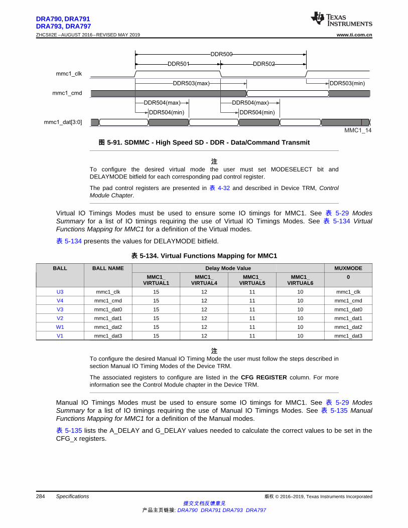
mmc _clk1
mmc _cmd1
mmc _dat[3:0]1
DDR500
DDR501 DDR502
DDR503(max) DDR503(min)
DDR504(max)
DDR504(min) DDR504(min)
DDR504(max)
MMC1_14
284
DRA790, DRA791DRA793, DRA797ZHCSII2E –AUGUST 2016–REVISED MAY 2019 www.ti.com.cn
提交文档反馈意见产品主页链接: DRA790 DRA791 DRA793 DRA797
Specifications 版权 © 2016–2019, Texas Instruments Incorporated
图图 5-91. SDMMC - High Speed SD - DDR - Data/Command Transmit
注注To configure the desired virtual mode the user must set MODESELECT bit andDELAYMODE bitfield for each corresponding pad control register.
The pad control registers are presented in 表 4-32 and described in Device TRM, ControlModule Chapter.
Virtual IO Timings Modes must be used to ensure some IO timings for MMC1. See 表 5-29 ModesSummary for a list of IO timings requiring the use of Virtual IO Timings Modes. See 表 5-134 VirtualFunctions Mapping for MMC1 for a definition of the Virtual modes.
表 5-134 presents the values for DELAYMODE bitfield.
表表 5-134. Virtual Functions Mapping for MMC1
BALL BALL NAME Delay Mode Value MUXMODEMMC1_
VIRTUAL1MMC1_
VIRTUAL4MMC1_
VIRTUAL5MMC1_
VIRTUAL60
U3 mmc1_clk 15 12 11 10 mmc1_clkV4 mmc1_cmd 15 12 11 10 mmc1_cmdV3 mmc1_dat0 15 12 11 10 mmc1_dat0V2 mmc1_dat1 15 12 11 10 mmc1_dat1W1 mmc1_dat2 15 12 11 10 mmc1_dat2V1 mmc1_dat3 15 12 11 10 mmc1_dat3
注注To configure the desired Manual IO Timing Mode the user must follow the steps described insection Manual IO Timing Modes of the Device TRM.
The associated registers to configure are listed in the CFG REGISTER column. For moreinformation see the Control Module chapter in the Device TRM.
Manual IO Timings Modes must be used to ensure some IO timings for MMC1. See 表 5-29 ModesSummary for a list of IO timings requiring the use of Manual IO Timings Modes. See 表 5-135 ManualFunctions Mapping for MMC1 for a definition of the Manual modes.
表 5-135 lists the A_DELAY and G_DELAY values needed to calculate the correct values to be set in theCFG_x registers.

版权 © 2016–2019, Texas Instruments Incorporated Specifications提交文档反馈意见
产品主页链接: DRA790 DRA791 DRA793 DRA797
285
DRA790, DRA791DRA793, DRA797
www.ti.com.cn ZHCSII2E –AUGUST 2016–REVISED MAY 2019
表表 5-135. Manual Functions Mapping for MMC1
BALL BALL NAME MMC1_MANUAL1 MMC1_MANUAL2 CFG REGISTER MUXMODEA_DELAY (ps) G_DELAY (ps) A_DELAY (ps) G_DELAY (ps) 0
U3 mmc1_clk 588 0 - - CFG_MMC1_CLK_IN mmc1_clkV4 mmc1_cmd 1000 0 - - CFG_MMC1_CMD_IN mmc1_cmdV3 mmc1_dat0 1375 0 - - CFG_MMC1_DAT0_IN mmc1_dat0V2 mmc1_dat1 1000 0 - - CFG_MMC1_DAT1_IN mmc1_dat1W1 mmc1_dat2 1000 0 - - CFG_MMC1_DAT2_IN mmc1_dat2V1 mmc1_dat3 1000 0 - - CFG_MMC1_DAT3_IN mmc1_dat3
U3 mmc1_clk 1230 0 520 320 CFG_MMC1_CLK_OUT mmc1_clkV4 mmc1_cmd 0 0 0 0 CFG_MMC1_CMD_OUT mmc1_cmdV3 mmc1_dat0 56 0 40 0 CFG_MMC1_DAT0_OUT mmc1_dat0V2 mmc1_dat1 76 0 83 0 CFG_MMC1_DAT1_OUT mmc1_dat1W1 mmc1_dat2 91 0 98 0 CFG_MMC1_DAT2_OUT mmc1_dat2V1 mmc1_dat3 99 0 106 0 CFG_MMC1_DAT3_OUT mmc1_dat3
V4 mmc1_cmd 0 0 51 0 CFG_MMC1_CMD_OEN mmc1_cmdV3 mmc1_dat0 0 0 0 0 CFG_MMC1_DAT0_OEN mmc1_dat0V2 mmc1_dat1 0 0 363 0 CFG_MMC1_DAT1_OEN mmc1_dat1W1 mmc1_dat2 0 0 199 0 CFG_MMC1_DAT2_OEN mmc1_dat2V1 mmc1_dat3 0 0 273 0 CFG_MMC1_DAT3_OEN mmc1_dat3
5.10.6.21.2 MMC2 — eMMC
MMC2 interface is compliant with the JC64 eMMC Standard v4.5 and it supports the following eMMC applications:• Standard JC64 SDR, 8-bit data, half cycle• High-speed JC64 SDR, 8-bit data, half cycle• High-speed HS200 JEDS84, 8-bit data, half cycle• High-speed JC64 DDR, 8-bit data
注注For more information, see the eMMC/SD/SDIO chapter of the Device TRM.

版权 © 2016–2019, Texas Instruments IncorporatedSpecifications提交文档反馈意见
产品主页链接: DRA790 DRA791 DRA793 DRA797
286
DRA790, DRA791DRA793, DRA797ZHCSII2E –AUGUST 2016–REVISED MAY 2019 www.ti.com.cn
5.10.6.21.2.1 Standard JC64 SDR, 8-bit data, half cycle
表 5-136 and 表 5-137 present Timing requirements and Switching characteristics for MMC2 - Standart SDR in receiver and transmitter mode (see图 5-92 and 图 5-93).
表表 5-136. Timing Requirements for MMC2 - JC64 Standard SDR Mode
NO. PARAMETER DESCRIPTION MIN MAX UNITSSDR5 tsu(cmdV-clkH) Setup time, mmc2_cmd valid before mmc2_clk rising clock edge 13.19 nsSSDR6 th(clkH-cmdV) Hold time, mmc2_cmd valid after mmc2_clk rising clock edge 8.4 nsSSDR7 tsu(dV-clkH) Setup time, mmc2_dat[7:0] valid before mmc2_clk rising clock edge 13.19 nsSSDR8 th(clkH-dV) Hold time, mmc2_dat[7:0] valid after mmc2_clk rising clock edge 8.4 ns

SSDR2
mmc2_clk
mmc2_cmd
mmc2_dat[7:0]
SSDR1
SSDR2
SSDR3
SSDR4
SPRS906_TIMING_MMC2_02
mmc2_clk
mmc2_cmd
mmc2_dat[7:0]
SSDR2
SSDR2
SSDR1
SSDR6
SSDR5
SSDR8
SSDR7
SPRS906_TIMING_MMC2_01
287
DRA790, DRA791DRA793, DRA797
www.ti.com.cn ZHCSII2E –AUGUST 2016–REVISED MAY 2019
提交文档反馈意见产品主页链接: DRA790 DRA791 DRA793 DRA797
Specifications版权 © 2016–2019, Texas Instruments Incorporated
表表 5-137. Switching Characteristics for MMC2 - JC64 Standard SDR Mode
NO. PARAMETER DESCRIPTION MIN MAX UNITSSDR1 fop(clk) Operating frequency, mmc2_clk 24 MHz
SSDR2H tw(clkH) Pulse duration, mmc2_clk high 0.5 × P-0.172 (1)
ns
SSDR2L tw(clkL) Pulse duration, mmc2_clk low 0.5 × P-0.172 (1)
ns
SSDR3 td(clkL-cmdV) Delay time, mmc2_clk falling clock edge to mmc2_cmd transition -16.96 16.96 nsSSDR4 td(clkL-dV) Delay time, mmc2_clk falling clock edge to mmc2_dat[7:0] transition -16.96 16.96 ns
(1) P = output mmc2_clk period in ns
图图 5-92. MMC/SD/SDIO in - Standard JC64 - Receiver Mode
图图 5-93. MMC/SD/SDIO in - Standard JC64 - Transmitter Mode
5.10.6.21.2.2 High-speed JC64 SDR, 8-bit data, half cycle
表 5-138 and 表 5-139 present Timing requirements and Switching characteristics for MMC2 - High speedSDR in receiver and transmitter mode (see 图 5-94 and 图 5-95).
表表 5-138. Timing Requirements for MMC2 - JC64 High Speed SDR Mode
NO. PARAMETER DESCRIPTION MIN MAX UNITJC643 tsu(cmdV-clkH) Setup time, mmc2_cmd valid before mmc2_clk rising clock edge 5.6 nsJC644 th(clkH-cmdV) Hold time, mmc2_cmd valid after mmc2_clk rising clock edge 2.6 nsJC647 tsu(dV-clkH) Setup time, mmc2_dat[7:0] valid before mmc2_clk rising clock edge 5.6 nsJC648 th(clkH-dV) Hold time, mmc2_dat[7:0] valid after mmc2_clk rising clock edge 2.6 ns

mmc _clk2
mmc _cmd2
mmc _dat2 [7:0]
JC645 JC645
JC646 JC646
JC641
JC642HJC642L
MMC2_04
mmc _clk2
mmc _cmd2
mmc _dat2 [7:0]
JC644
JC648
JC643
JC647
JC641
JC642HJC642L
SPRS906_TIMING_MMC2_03
288
DRA790, DRA791DRA793, DRA797ZHCSII2E –AUGUST 2016–REVISED MAY 2019 www.ti.com.cn
提交文档反馈意见产品主页链接: DRA790 DRA791 DRA793 DRA797
Specifications 版权 © 2016–2019, Texas Instruments Incorporated
表表 5-139. Switching Characteristics for MMC2 - JC64 High Speed SDR Mode
NO. PARAMETER DESCRIPTION MIN MAX UNITJC641 fop(clk) Operating frequency, mmc2_clk 48 MHz
JC642H tw(clkH) Pulse duration, mmc2_clk high 0.5 × P-0.172 (1)
ns
JC642L tw(clkL) Pulse duration, mmc2_clk low 0.5 × P-0.172 (1)
ns
JC645 td(clkL-cmdV) Delay time, mmc2_clk falling clock edge to mmc2_cmd transition -6.64 6.64 nsJC646 td(clkL-dV) Delay time, mmc2_clk falling clock edge to mmc2_dat[7:0] transition -6.64 6.64 ns
(1) P = output mmc2_clk period in ns
图图 5-94. MMC/SD/SDIO in - High Speed JC64 - Receiver Mode
图图 5-95. MMC/SD/SDIO in - High Speed JC64 - transmitter Mode
5.10.6.21.2.3 High-speed HS200 JEDS84 SDR, 8-bit data, half cycle
表 5-140 presents Switching characteristics for MMC2 - HS200 in transmitter mode (see 图 5-96).

mmc _clk2
mmc _cmd2
mmc _dat2 [7:0]
HS2005 HS2005
HS2006 HS2006
HS2001
HS2002LHS2002H
MMC2_05
289
DRA790, DRA791DRA793, DRA797
www.ti.com.cn ZHCSII2E –AUGUST 2016–REVISED MAY 2019
提交文档反馈意见产品主页链接: DRA790 DRA791 DRA793 DRA797
Specifications版权 © 2016–2019, Texas Instruments Incorporated
表表 5-140. Switching Characteristics for MMC2 - JEDS84 HS200 Mode
NO. PARAMETER DESCRIPTION MIN MAX UNITHS2001 fop(clk) Operating frequency, mmc2_clk 192 MHz
HS2002H tw(clkH) Pulse duration, mmc2_clk high 0.5 × P-0.172 (1)
ns
HS2002L tw(clkL) Pulse duration, mmc2_clk low 0.5 × P-0.172 (1)
ns
HS2005 td(clkL-cmdV) Delay time, mmc2_clk falling clock edge to mmc2_cmd transition -1.136 0.536 nsHS2006 td(clkL-dV) Delay time, mmc2_clk falling clock edge to mmc2_dat[7:0] transition -1.136 0.536 ns
(1) P = output mmc2_clk period in ns
图图 5-96. eMMC in - HS200 SDR - Transmitter Mode
5.10.6.21.2.4 High-speed JC64 DDR, 8-bit data
表 5-141 and 表 5-142 present Timing requirements and Switching characteristics for MMC2 - High speedDDR in receiver and transmitter mode (see 图 5-97 and 图 5-98).
表表 5-141. Timing Requirements for MMC2 - JC64 High Speed DDR Mode
NO. PARAMETER DESCRIPTION MODE MIN MAX UNITDDR3 tsu(cmdV-clk) Setup time, mmc2_cmd valid before mmc2_clk
transition1.8 ns
DDR4 th(clk-cmdV) Hold time, mmc2_cmd valid after mmc2_clktransition
1.6 ns
DDR7 tsu(dV-clk) Setup time, mmc2_dat[7:0] valid before mmc2_clktransition
1.8 ns
DDR8 th(clk-dV) Hold time, mmc2_dat[7:0] valid after mmc2_clktransition
Pad Loopback (1.8V and 3.3V),Boot
1.6 ns
Internal Loopback (1.8V withMMC2_VIRTUAL2)
1.86 ns
Internal Loopback (3.3V withMMC2_VIRTUAL2)
1.95 ns
Internal Loopback (1.8V withMMC2_MANUAL2)
ns
Internal Loopback (3.3V withMMC2_MANUAL2)
1.6 ns
表表 5-142. Switching Characteristics for MMC2 - JC64 High Speed DDR ModeNO. PARAMETER DESCRIPTION MIN MAX UNIT
DDR1 fop(clk) Operating frequency, mmc2_clk 48 MHzDDR2H tw(clkH) Pulse duration, mmc2_clk high 0.5 × P-
0.172 (1)ns
DDR2L tw(clkL) Pulse duration, mmc2_clk low 0.5 × P-0.172 (1)
ns
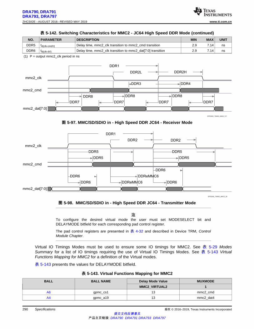
mmc _clk2
mmc _cmd2
mmc _dat2 [7:0]
DDR1
DDR2DDR2
DDR5
DDR5
DDR6
DDR6
DDReMMC6
DDReMMC6
DDR5
DDR5
DDR6
DDR6
SPRS906_TIMING_MMC2_08
mmc _clk2
mmc _cmd2
mmc _dat2 [7:0]
DDR1
DDR2HDDR2L
DDR3 DDR4
DDR7
DDR8
DDR7
DDR8
DDR7
DDR8
DDR7
SPRS906_TIMING_MMC2_07
290
DRA790, DRA791DRA793, DRA797ZHCSII2E –AUGUST 2016–REVISED MAY 2019 www.ti.com.cn
提交文档反馈意见产品主页链接: DRA790 DRA791 DRA793 DRA797
Specifications 版权 © 2016–2019, Texas Instruments Incorporated
表表 5-142. Switching Characteristics for MMC2 - JC64 High Speed DDR Mode (continued)NO. PARAMETER DESCRIPTION MIN MAX UNIT
DDR5 td(clk-cmdV) Delay time, mmc2_clk transition to mmc2_cmd transition 2.9 7.14 nsDDR6 td(clk-dV) Delay time, mmc2_clk transition to mmc2_dat[7:0] transition 2.9 7.14 ns
(1) P = output mmc2_clk period in ns
图图 5-97. MMC/SD/SDIO in - High Speed DDR JC64 - Receiver Mode
图图 5-98. MMC/SD/SDIO in - High Speed DDR JC64 - Transmitter Mode
注注To configure the desired virtual mode the user must set MODESELECT bit andDELAYMODE bitfield for each corresponding pad control register.
The pad control registers are presented in 表 4-32 and described in Device TRM, ControlModule Chapter.
Virtual IO Timings Modes must be used to ensure some IO timings for MMC2. See 表 5-29 ModesSummary for a list of IO timings requiring the use of Virtual IO Timings Modes. See 表 5-143 VirtualFunctions Mapping for MMC2 for a definition of the Virtual modes.
表 5-143 presents the values for DELAYMODE bitfield.
表表 5-143. Virtual Functions Mapping for MMC2
BALL BALL NAME Delay Mode Value MUXMODEMMC2_VIRTUAL2 1
A6 gpmc_cs1 13 mmc2_cmdA4 gpmc_a19 13 mmc2_dat4

291
DRA790, DRA791DRA793, DRA797
www.ti.com.cn ZHCSII2E –AUGUST 2016–REVISED MAY 2019
提交文档反馈意见产品主页链接: DRA790 DRA791 DRA793 DRA797
Specifications版权 © 2016–2019, Texas Instruments Incorporated
表表 5-143. Virtual Functions Mapping for MMC2 (continued)BALL BALL NAME Delay Mode Value MUXMODE
MMC2_VIRTUAL2 1E7 gpmc_a20 13 mmc2_dat5D6 gpmc_a21 13 mmc2_dat6C5 gpmc_a22 13 mmc2_dat7B5 gpmc_a23 13 mmc2_clkD7 gpmc_a24 13 mmc2_dat0C6 gpmc_a25 13 mmc2_dat1A5 gpmc_a26 13 mmc2_dat2B6 gpmc_a27 13 mmc2_dat3
注注To configure the desired Manual IO Timing Mode the user must follow the steps described insection Manual IO Timing Modes of the Device TRM.
The associated registers to configure are listed in the CFG REGISTER column. For moreinformation see the Control Module chapter in the Device TRM.
Manual IO Timings Modes must be used to ensure some IO timings for MMC2. See 表 5-29 ModesSummary for a list of IO timings requiring the use of Manual IO Timings Modes. See 表 5-144 ManualFunctions Mapping for MMC2 for a definition of the Manual modes.
表 5-144 lists the A_DELAY and G_DELAY values needed to calculate the correct values to be set in theCFG_x registers.
表表 5-144. Manual Functions Mapping for MMC2
BALL
BALL NAME MMC2_MANUAL1 MMC2_MANUAL2 MMC2_MANUAL3 CFG REGISTER MUXMODEA_DELAY
(ps)G_DELAY
(ps)A_DELAY
(ps)G_DELAY
(ps)A_DELAY
(ps)G_DELAY
(ps)1
A4 gpmc_a19 0 0 0 14 - - CFG_GPMC_A19_IN mmc2_dat4E7 gpmc_a20 119 0 127 0 - - CFG_GPMC_A20_IN mmc2_dat5D6 gpmc_a21 0 0 22 0 - - CFG_GPMC_A21_IN mmc2_dat6C5 gpmc_a22 18 0 72 0 - - CFG_GPMC_A22_IN mmc2_dat7B5 gpmc_a23 894 0 410 4000 - - CFG_GPMC_A23_IN mmc2_clkD7 gpmc_a24 30 0 82 0 - - CFG_GPMC_A24_IN mmc2_dat0C6 gpmc_a25 0 0 0 0 - - CFG_GPMC_A25_IN mmc2_dat1A5 gpmc_a26 23 0 77 0 - - CFG_GPMC_A26_IN mmc2_dat2B6 gpmc_a27 0 0 0 0 - - CFG_GPMC_A27_IN mmc2_dat3A6 gpmc_cs1 0 0 0 0 - - CFG_GPMC_CS1_IN mmc2_cmd
A4 gpmc_a19 152 0 152 0 285 0 CFG_GPMC_A19_OUT mmc2_dat4E7 gpmc_a20 206 0 206 0 189 0 CFG_GPMC_A20_OUT mmc2_dat5D6 gpmc_a21 78 0 78 0 0 120 CFG_GPMC_A21_OUT mmc2_dat6C5 gpmc_a22 2 0 2 0 0 70 CFG_GPMC_A22_OUT mmc2_dat7B5 gpmc_a23 266 0 266 0 730 360 CFG_GPMC_A23_OUT mmc2_clkD7 gpmc_a24 0 0 0 0 0 0 CFG_GPMC_A24_OUT mmc2_dat0C6 gpmc_a25 0 0 0 0 0 0 CFG_GPMC_A25_OUT mmc2_dat1A5 gpmc_a26 43 0 43 0 70 0 CFG_GPMC_A26_OUT mmc2_dat2B6 gpmc_a27 0 0 0 0 0 0 CFG_GPMC_A27_OUT mmc2_dat3A6 gpmc_cs1 0 0 0 0 0 120 CFG_GPMC_CS1_OUT mmc2_cmd
A4 gpmc_a19 0 0 0 0 0 0 CFG_GPMC_A19_OEN mmc2_dat4

292
DRA790, DRA791DRA793, DRA797ZHCSII2E –AUGUST 2016–REVISED MAY 2019 www.ti.com.cn
提交文档反馈意见产品主页链接: DRA790 DRA791 DRA793 DRA797
Specifications 版权 © 2016–2019, Texas Instruments Incorporated
表表 5-144. Manual Functions Mapping for MMC2 (continued)BAL
LBALL NAME MMC2_MANUAL1 MMC2_MANUAL2 MMC2_MANUAL3 CFG REGISTER MUXMODE
A_DELAY(ps)
G_DELAY(ps)
A_DELAY(ps)
G_DELAY(ps)
A_DELAY(ps)
G_DELAY(ps)
1
E7 gpmc_a20 0 0 0 0 231 0 CFG_GPMC_A20_OEN mmc2_dat5D6 gpmc_a21 0 0 0 0 39 0 CFG_GPMC_A21_OEN mmc2_dat6C5 gpmc_a22 0 0 0 0 91 0 CFG_GPMC_A22_OEN mmc2_dat7D7 gpmc_a24 0 0 0 0 176 0 CFG_GPMC_A24_OEN mmc2_dat0C6 gpmc_a25 0 0 0 0 0 0 CFG_GPMC_A25_OEN mmc2_dat1A5 gpmc_a26 0 0 0 0 101 0 CFG_GPMC_A26_OEN mmc2_dat2B6 gpmc_a27 0 0 0 0 0 0 CFG_GPMC_A27_OEN mmc2_dat3A6 gpmc_cs1 0 0 0 0 360 0 CFG_GPMC_CS1_OE
Nmmc2_cmd
5.10.6.21.3 MMC3 and MMC4—SDIO/SD
MMC3 and MMC4 interfaces are compliant with the SDIO3.0 standard v1.0, SD Part E1 and for genericSDIO devices, it supports the following applications:• MMC3 8-bit data and MMC4 4-bit data, SD Default speed, SDR• MMC3 8-bit data and MMC4 4-bit data, SD High speed, SDR• MMC3 8-bit data and MMC4 4-bit data, UHS-1 SDR12 (SD Standard v3.01), 4-bit data, SDR, half
cycle• MMC3 8-bit data and MMC4 4-bit data, UHS-I SDR25 (SD Standard v3.01), 4-bit data, SDR, half cycle• MMC3 8-bit data, UHS-I SDR50
注注The eMMC/SD/SDIOj (j = 3 to 4) controller is also referred to as MMCj.
注注For more information, see the MMC/SDIO chapter of the Device TRM.
5.10.6.21.3.1 MMC3 and MMC4, SD Default Speed
图 5-99, 图 5-100, and 表 5-145 through 表 5-148 present Timing requirements and Switchingcharacteristics for MMC3 and MMC4 - SD Default speed in receiver and transmitter mode.
表表 5-145. Timing Requirements for MMC3 - Default Speed Mode (1)
NO. PARAMETER DESCRIPTION MIN MAX UNITDS5 tsu(cmdV-clkH) Setup time, mmc3_cmd valid before mmc3_clk rising clock edge 5.11 nsDS6 th(clkH-cmdV) Hold time, mmc3_cmd valid after mmc3_clk rising clock edge 20.46 nsDS7 tsu(dV-clkH) Setup time, mmc3_dat[i:0] valid before mmc3_clk rising clock edge 5.11 nsDS8 th(clkH-dV) Hold time, mmc3_dat[i:0] valid after mmc3_clk rising clock edge 20.46 ns
(1) i in [i:0] = 7
表表 5-146. Switching Characteristics for MMC3 - SD/SDIO Default Speed Mode (2)
NO. PARAMETER DESCRIPTION MIN MAX UNITDS0 fop(clk) Operating frequency, mmc3_clk 24 MHzDS1 tw(clkH) Pulse duration, mmc3_clk high 0.5 × P-
0.270 (1)ns

DS2
DS1
DS0
DS6
DS5
DS8
DS7
mmcj_clk
mmcj_cmd
mmcj_dat[i:0]
SPRS906_TIMING_MMC3_07
293
DRA790, DRA791DRA793, DRA797
www.ti.com.cn ZHCSII2E –AUGUST 2016–REVISED MAY 2019
提交文档反馈意见产品主页链接: DRA790 DRA791 DRA793 DRA797
Specifications版权 © 2016–2019, Texas Instruments Incorporated
表表 5-146. Switching Characteristics for MMC3 - SD/SDIO Default Speed Mode (2) (continued)NO. PARAMETER DESCRIPTION MIN MAX UNITDS2 tw(clkL) Pulse duration, mmc3_clk low 0.5 × P-
0.270 (1)ns
DS3 td(clkL-cmdV) Delay time, mmc3_clk falling clock edge to mmc3_cmd transition -14.93 14.93 nsDS4 td(clkL-dV) Delay time, mmc3_clk falling clock edge to mmc3_dat[i:0] transition -14.93 14.93 ns
(1) P = output mmc3_clk period in ns(2) i in [i:0] = 7
表表 5-147. Timing Requirements for MMC4 - Default Speed Mode (1)
NO. PARAMETER DESCRIPTION MIN MAX UNITDS5 tsu(cmdV-clkH) Setup time, mmc4_cmd valid before mmc4_clk rising clock edge 5.11 nsDS6 th(clkH-cmdV) Hold time, mmc4_cmd valid after mmc4_clk rising clock edge 20.46 nsDS7 tsu(dV-clkH) Setup time, mmc4_dat[i:0] valid before mmc4_clk rising clock edge 5.11 nsDS8 th(clkH-dV) Hold time, mmc4_dat[i:0] valid after mmc4_clk rising clock edge 20.46 ns
(1) i in [i:0] = 3
表表 5-148. Switching Characteristics for MMC4 - Default Speed Mode (2)
NO. PARAMETER DESCRIPTION MIN MAX UNITDS0 fop(clk) Operating frequency, mmc4_clk 24 MHzDS1 tw(clkH) Pulse duration, mmc4_clk high 0.5 × P-
0.270 (1)ns
DS2 tw(clkL) Pulse duration, mmc4_clk low 0.5 × P-0.270 (1)
ns
DS3 td(clkL-cmdV) Delay time, mmc4_clk falling clock edge to mmc4_cmd transition -14.93 14.93 nsDS4 td(clkL-dV) Delay time, mmc4_clk falling clock edge to mmc4_dat[i:0] transition -14.93 14.93 ns
(1) P = output mmc4_clk period in ns(2) i in [i:0] = 3
图图 5-99. MMC/SD/SDIOj in - Default Speed - Receiver Mode

DS2
DS1
DS0
DS3
DS4
mmcj_clk
mmcj_cmd
mmcj_dat[i:0]
SPRS906_TIMING_MMC3_08
294
DRA790, DRA791DRA793, DRA797ZHCSII2E –AUGUST 2016–REVISED MAY 2019 www.ti.com.cn
提交文档反馈意见产品主页链接: DRA790 DRA791 DRA793 DRA797
Specifications 版权 © 2016–2019, Texas Instruments Incorporated
图图 5-100. MMC/SD/SDIOj in - Default Speed - Transmitter Mode
5.10.6.21.3.2 MMC3 and MMC4, SD High Speed
图 5-101, 图 5-102, and 表 5-149 through 表 5-152 present Timing requirements and Switchingcharacteristics for MMC3 and MMC4 - SD and SDIO High speed in receiver and transmitter mode.
表表 5-149. Timing Requirements for MMC3 - SD/SDIO High Speed Mode (1)
NO. PARAMETER DESCRIPTION MIN MAX UNITHS3 tsu(cmdV-clkH) Setup time, mmc3_cmd valid before mmc3_clk rising clock edge 5.3 nsHS4 th(clkH-cmdV) Hold time, mmc3_cmd valid after mmc3_clk rising clock edge 2.6 nsHS7 tsu(dV-clkH) Setup time, mmc3_dat[i:0] valid before mmc3_clk rising clock edge 5.3 nsHS8 th(clkH-dV) Hold time, mmc3_dat[i:0] valid after mmc3_clk rising clock edge 2.6 ns
(1) i in [i:0] = 7
表表 5-150. Switching Characteristics for MMC3 - SD/SDIO High Speed Mode (2)
NO. PARAMETER DESCRIPTION MIN MAX UNITHS1 fop(clk) Operating frequency, mmc3_clk 48 MHz
HS2H tw(clkH) Pulse duration, mmc3_clk high 0.5 × P-0.270 (1)
ns
HS2L tw(clkL) Pulse duration, mmc3_clk low 0.5 × P-0.270 (1)
ns
HS5 td(clkL-cmdV) Delay time, mmc3_clk falling clock edge to mmc3_cmd transition -7.6 3.6 nsHS6 td(clkL-dV) Delay time, mmc3_clk falling clock edge to mmc3_dat[i:0] transition -7.6 3.6 ns
(1) P = output mmc3_clk period in ns(2) i in [i:0] = 7
表表 5-151. Timing Requirements for MMC4 - High Speed Mode (1)
NO. PARAMETER DESCRIPTION MIN MAX UNITHS3 tsu(cmdV-clkH) Setup time, mmc4_cmd valid before mmc4_clk rising clock edge 5.3 nsHS4 th(clkH-cmdV) Hold time, mmc4_cmd valid after mmc4_clk rising clock edge 1.6 nsHS7 tsu(dV-clkH) Setup time, mmc4_dat[i:0] valid before mmc4_clk rising clock edge 5.3 nsHS8 th(clkH-dV) Hold time, mmc4_dat[i:0] valid after mmc4_clk rising clock edge 1.6 ns
(1) i in [i:0] = 3
表表 5-152. Switching Characteristics for MMC4 - High Speed Mode (2)
NO. PARAMETER DESCRIPTION MIN MAX UNITHS1 fop(clk) Operating frequency, mmc4_clk 48 MHz
HS2H tw(clkH) Pulse duration, mmc4_clk high 0.5 × P-0.270 (1)
ns

mmcj_clk
mmcj_cmd
mmcj_dat[i:0]
HS1
HS2LHS2H
HS5
HS6
HS5
HS6
SPRS906_TIMING_MMC3_10
mmcj_clk
mmcj_cmd
mmcj_dat[i:0]
HS1
HS2L HS2H
HS3 HS4
HS7 HS8
SPRS906_TIMING_MMC3_09
295
DRA790, DRA791DRA793, DRA797
www.ti.com.cn ZHCSII2E –AUGUST 2016–REVISED MAY 2019
提交文档反馈意见产品主页链接: DRA790 DRA791 DRA793 DRA797
Specifications版权 © 2016–2019, Texas Instruments Incorporated
表表 5-152. Switching Characteristics for MMC4 - High Speed Mode (2) (continued)NO. PARAMETER DESCRIPTION MIN MAX UNIT
HS2L tw(clkL) Pulse duration, mmc4_clk low 0.5 × P-0.270 (1)
ns
HS5 td(clkL-cmdV) Delay time, mmc4_clk falling clock edge to mmc4_cmd transition -8.8 6.6 nsHS6 td(clkL-dV) Delay time, mmc4_clk falling clock edge to mmc4_dat[i:0] transition -8.8 6.6 ns
(1) P = output mmc4_clk period in ns(2) i in [i:0] = 3
图图 5-101. MMC/SD/SDIOj in - High Speed 3.3V Signaling - Receiver Mode
图图 5-102. MMC/SD/SDIOj in - High Speed 3.3V Signaling - Transmitter Mode
5.10.6.21.3.3 MMC3 and MMC4, SD and SDIO SDR12 Mode
图 5-103, 图 5-104, and 表 5-153, through 表 5-156 present Timing requirements and Switchingcharacteristics for MMC3 and MMC4 - SD and SDIO SDR12 in receiver and transmitter mode.
表表 5-153. Timing Requirements for MMC3 - SDR12 Mode (1)
NO. PARAMETER DESCRIPTION MIN MAX UNITSDR125 tsu(cmdV-clkH) Setup time, mmc3_cmd valid before mmc3_clk rising clock edge 25.99 nsSDR126 th(clkH-cmdV) Hold time, mmc3_cmd valid after mmc3_clk rising clock edge 1.6 nsSDR127 tsu(dV-clkH) Setup time, mmc3_dat[i:0] valid before mmc3_clk rising clock edge 25.99 nsSDR128 th(clkH-dV) Hold time, mmc3_dat[i:0] valid after mmc3_clk rising clock edge 1.6 ns
(1) i in [i:0] = 7
表表 5-154. Switching Characteristics for MMC3 - SDR12 Mode (2)
NO. PARAMETER DESCRIPTION MIN MAX UNITSDR120 fop(clk) Operating frequency, mmc3_clk 24 MHzSDR121 tw(clkH) Pulse duration, mmc3_clk high 0.5 × P-
0.270 (1)ns

SDR122
SDR121
SDR120
SDR126
SDR125
SDR128
SDR127
mmcj_clk
mmcj_cmd
mmcj_dat[i:0]
SPRS906_TIMING_MMC3_11
296
DRA790, DRA791DRA793, DRA797ZHCSII2E –AUGUST 2016–REVISED MAY 2019 www.ti.com.cn
提交文档反馈意见产品主页链接: DRA790 DRA791 DRA793 DRA797
Specifications 版权 © 2016–2019, Texas Instruments Incorporated
表表 5-154. Switching Characteristics for MMC3 - SDR12 Mode (2) (continued)NO. PARAMETER DESCRIPTION MIN MAX UNIT
SDR122 tw(clkL) Pulse duration, mmc3_clk low 0.5 × P-0.270 (1)
ns
SDR123 td(clkL-cmdV) Delay time, mmc3_clk falling clock edge to mmc3_cmd transition -19.13 16.93 nsSDR124 td(clkL-dV) Delay time, mmc3_clk falling clock edge to mmc3_dat[i:0] transition -19.13 16.93 ns
(1) P = output mmc3_clk period in ns(2) i in [i:0] = 7
表表 5-155. Timing Requirements for MMC4 - SDR12 Mode (1)
NO. PARAMETER DESCRIPTION MIN MAX UNITSDR125 tsu(cmdV-clkH) Setup time, mmc4_cmd valid before mmc4_clk rising clock edge 25.99 nsSDR126 th(clkH-cmdV) Hold time, mmc4_cmd valid after mmc4_clk rising clock edge 1.6 nsSDR127 tsu(dV-clkH) Setup time, mmc4_dat[i:0] valid before mmc4_clk rising clock edge 25.99 nsSDR128 th(clkH-dV) Hold time, mmc4_dat[i:0] valid after mmc4_clk rising clock edge 1.6 ns
(1) j in [i:0] = 3
表表 5-156. Switching Characteristics for MMC4 - SDR12 Mode (2)
NO. PARAMETER DESCRIPTION MIN MAX UNITSDR120 fop(clk) Operating frequency, mmc4_clk 24 MHzSDR121 tw(clkH) Pulse duration, mmc4_clk high 0.5 × P-
0.270 (1)ns
SDR122 tw(clkL) Pulse duration, mmc4_clk low 0.5 × P-0.270 (1)
ns
SDR125 td(clkL-cmdV) Delay time, mmc4_clk falling clock edge to mmc4_cmd transition -19.13 16.93 nsSDR126 td(clkL-dV) Delay time, mmc4_clk falling clock edge to mmc4_dat[i:0] transition -19.13 16.93 ns
(1) P = output mmc4_clk period in ns(2) j in [i:0] = 3
图图 5-103. MMC/SD/SDIOj in - SDR12 - Receiver Mode

SDR122
SDR121
SDR120
SDR123
SDR124
mmcj_clk
mmcj_cmd
mmcj_dat[i:0]
SPRS906_TIMING_MMC3_12
297
DRA790, DRA791DRA793, DRA797
www.ti.com.cn ZHCSII2E –AUGUST 2016–REVISED MAY 2019
提交文档反馈意见产品主页链接: DRA790 DRA791 DRA793 DRA797
Specifications版权 © 2016–2019, Texas Instruments Incorporated
图图 5-104. MMC/SD/SDIOj in - SDR12 - Transmitter Mode
5.10.6.21.3.4 MMC3 and MMC4, SD SDR25 Mode
图 5-105, 图 5-106, and 表 5-157, through 表 5-160 present Timing requirements and Switchingcharacteristics for MMC3 and MMC4 - SD and SDIO SDR25 in receiver and transmitter mode.
表表 5-157. Timing Requirements for MMC3 - SDR25 Mode (1)
NO. PARAMETER DESCRIPTION MIN MAX UNITSDR253 tsu(cmdV-clkH) Setup time, mmc3_cmd valid before mmc3_clk rising clock edge 5.3 nsSDR254 th(clkH-cmdV) Hold time, mmc3_cmd valid after mmc3_clk rising clock edge 1.6 nsSDR257 tsu(dV-clkH) Setup time, mmc3_dat[i:0] valid before mmc3_clk rising clock edge 5.3 nsSDR258 th(clkH-dV) Hold time, mmc3_dat[i:0] valid after mmc3_clk rising clock edge 1.6 ns
(1) i in [i:0] = 7
表表 5-158. Switching Characteristics for MMC3 - SDR25 Mode (2)
NO. PARAMETER DESCRIPTION MIN MAX UNITSDR251 fop(clk) Operating frequency, mmc3_clk 48 MHzSDR252
Htw(clkH) Pulse duration, mmc3_clk high 0.5 × P-
0.270 (1)ns
SDR252L tw(clkL) Pulse duration, mmc3_clk low 0.5 × P-0.270 (1)
ns
SDR255 td(clkL-cmdV) Delay time, mmc3_clk falling clock edge to mmc3_cmd transition -8.8 6.6 nsSDR256 td(clkL-dV) Delay time, mmc3_clk falling clock edge to mmc3_dat[i:0] transition -8.8 6.6 ns
(1) P = output mmc3_clk period in ns(2) i in [i:0] = 7
表表 5-159. Timing Requirements for MMC4 - SDR25 Mode (1)
NO. PARAMETER DESCRIPTION MIN MAX UNITSDR255 tsu(cmdV-clkH) Setup time, mmc4_cmd valid before mmc4_clk rising clock edge 5.3 nsSDR256 th(clkH-cmdV) Hold time, mmc4_cmd valid after mmc4_clk rising clock edge 1.6 nsSDR257 tsu(dV-clkH) Setup time, mmc4_dat[i:0] valid before mmc4_clk rising clock edge 5.3 nsSDR258 th(clkH-dV) Hold time, mmc4_dat[i:0] valid after mmc4_clk rising clock edge 1.6 ns
(1) i in [i:0] = 3
表表 5-160. Switching Characteristics for MMC4 - SDR25 Mode (2)
NO. PARAMETER DESCRIPTION MIN MAX UNITSDR251 fop(clk) Operating frequency, mmc4_clk 48 MHzSDR252
Htw(clkH) Pulse duration, mmc4_clk high 0.5 × P-
0.270 (1)ns

mmcj_clk
mmcj_cmd
mmcj_dat[i:0]
SDR251
SDR252LSDR252H
SDR255
SDR256
SDR255
SDR256
SPRS906_TIMING_MMC3_14
mmcj_clk
mmcj_cmd
mmcj_dat[i:0]
SDR254
SDR258
SDR253
SDR257
SDR251
SDR252HSDR252L
SPRS906_TIMING_MMC3_13
298
DRA790, DRA791DRA793, DRA797ZHCSII2E –AUGUST 2016–REVISED MAY 2019 www.ti.com.cn
提交文档反馈意见产品主页链接: DRA790 DRA791 DRA793 DRA797
Specifications 版权 © 2016–2019, Texas Instruments Incorporated
表表 5-160. Switching Characteristics for MMC4 - SDR25 Mode (2) (continued)NO. PARAMETER DESCRIPTION MIN MAX UNIT
SDR252L tw(clkL) Pulse duration, mmc4_clk low 0.5 × P-0.270 (1)
ns
SDR255 td(clkL-cmdV) Delay time, mmc4_clk falling clock edge to mmc4_cmd transition -8.8 6.6 nsSDR256 td(clkL-dV) Delay time, mmc4_clk falling clock edge to mmc4_dat[i:0] transition -8.8 6.6 ns
(1) P = output mmc4_clk period in ns(2) i in [i:0] = 3
图图 5-105. MMC/SD/SDIOj in - SDR25 - Receiver Mode
图图 5-106. MMC/SD/SDIOj in - SDR25 - Transmitter Mode
5.10.6.21.3.5 MMC3 SDIO High-Speed UHS-I SDR50 Mode, Half Cycle
图 5-107, 图 5-108, 表 5-161, and 表 5-162 present Timing requirements and Switching characteristics forMMC3 - SDIO High speed SDR50 in receiver and transmitter mode.
表表 5-161. Timing Requirements for MMC3 - SDR50 Mode (1)
NO. PARAMETER DESCRIPTION MIN MAX UNITSDR503 tsu(cmdV-clkH) Setup time, mmc3_cmd valid before mmc3_clk rising clock edge 1.48 nsSDR504 th(clkH-cmdV) Hold time, mmc3_cmd valid after mmc3_clk rising clock edge 1.6 nsSDR507 tsu(dV-clkH) Setup time, mmc3_dat[i:0] valid before mmc3_clk rising clock edge 1.48 nsSDR508 th(clkH-dV) Hold time, mmc3_dat[i:0] valid after mmc3_clk rising clock edge 1.6 ns
(1) i in [i:0] = 7
表表 5-162. Switching Characteristics for MMC3 - SDR50 Mode (2)
NO. PARAMETER DESCRIPTION MIN MAX UNITSDR501 fop(clk) Operating frequency, mmc3_clk 64 MHzSDR502
Htw(clkH) Pulse duration, mmc3_clk high 0.5 × P-
0.270 (1)ns
SDR502L tw(clkL) Pulse duration, mmc3_clk low 0.5 × P-0.270 (1)
ns

mmcj_clk
mmcj_cmd
mmcj_dat[7:0]
SDR501
SDR502LSDR502H
SDR505
SDR506
SDR505
SDR506
SPRS906_TIMING_MMC3_06
mmcj_clk
mmcj_cmd
mmcj_dat[7:0]
SDR504
SDR508
SDR503
SDR507
SDR501
SDR502HSDR502L
SPRS906_TIMING_MMC3_05
299
DRA790, DRA791DRA793, DRA797
www.ti.com.cn ZHCSII2E –AUGUST 2016–REVISED MAY 2019
提交文档反馈意见产品主页链接: DRA790 DRA791 DRA793 DRA797
Specifications版权 © 2016–2019, Texas Instruments Incorporated
表表 5-162. Switching Characteristics for MMC3 - SDR50 Mode (2) (continued)NO. PARAMETER DESCRIPTION MIN MAX UNIT
SDR505 td(clkL-cmdV) Delay time, mmc3_clk falling clock edge to mmc3_cmd transition -3.66 1.46 nsSDR506 td(clkL-dV) Delay time, mmc3_clk falling clock edge to mmc3_dat[i:0] transition -3.66 1.46 ns
(1) P = output mmc3_clk period in ns(2) i in [i:0] = 7
图图 5-107. MMC/SD/SDIOj in - High Speed SDR50 - Receiver Mode
图图 5-108. MMC/SD/SDIOj in - High Speed SDR50 - Transmitter Mode
注注To configure the desired Manual IO Timing Mode the user must follow the steps described insection Manual IO Timing Modes of the Device TRM.
The associated registers to configure are listed in the CFG REGISTER column. For moreinformation see the Control Module chapter in the Device TRM.
Manual IO Timings Modes must be used to ensure some IO timings for MMC3. See 表 5-29 ModesSummary for a list of IO timings requiring the use of Manual IO Timings Modes. See 表 5-163 ManualFunctions Mapping for MMC3 for a definition of the Manual modes.
表 5-163 lists the A_DELAY and G_DELAY values needed to calculate the correct values to be set in theCFG_x registers.
表表 5-163. Manual Functions Mapping for MMC3
BALL BALL NAME MMC3_MANUAL1 CFG REGISTER MUXMODEA_DELAY (ps) G_DELAY (ps) 0
Y2 mmc3_clk 1085 21 CFG_MMC3_CLK_IN mmc3_clkY2 mmc3_clk 1269 0 CFG_MMC3_CLK_OUT mmc3_clkY1 mmc3_cmd 0 0 CFG_MMC3_CMD_IN mmc3_cmdY1 mmc3_cmd 128 0 CFG_MMC3_CMD_OEN mmc3_cmdY1 mmc3_cmd 98 0 CFG_MMC3_CMD_OUT mmc3_cmdY4 mmc3_dat0 0 0 CFG_MMC3_DAT0_IN mmc3_dat0

300
DRA790, DRA791DRA793, DRA797ZHCSII2E –AUGUST 2016–REVISED MAY 2019 www.ti.com.cn
提交文档反馈意见产品主页链接: DRA790 DRA791 DRA793 DRA797
Specifications 版权 © 2016–2019, Texas Instruments Incorporated
表表 5-163. Manual Functions Mapping for MMC3 (continued)BALL BALL NAME MMC3_MANUAL1 CFG REGISTER MUXMODE
A_DELAY (ps) G_DELAY (ps) 0Y4 mmc3_dat0 362 0 CFG_MMC3_DAT0_OEN mmc3_dat0Y4 mmc3_dat0 0 0 CFG_MMC3_DAT0_OUT mmc3_dat0
AA2 mmc3_dat1 7 0 CFG_MMC3_DAT1_IN mmc3_dat1AA2 mmc3_dat1 333 0 CFG_MMC3_DAT1_OEN mmc3_dat1AA2 mmc3_dat1 0 0 CFG_MMC3_DAT1_OUT mmc3_dat1AA3 mmc3_dat2 0 0 CFG_MMC3_DAT2_IN mmc3_dat2AA3 mmc3_dat2 402 0 CFG_MMC3_DAT2_OEN mmc3_dat2AA3 mmc3_dat2 0 0 CFG_MMC3_DAT2_OUT mmc3_dat2W2 mmc3_dat3 203 0 CFG_MMC3_DAT3_IN mmc3_dat3W2 mmc3_dat3 549 0 CFG_MMC3_DAT3_OEN mmc3_dat3W2 mmc3_dat3 1 0 CFG_MMC3_DAT3_OUT mmc3_dat3Y3 mmc3_dat4 121 0 CFG_MMC3_DAT4_IN mmc3_dat4Y3 mmc3_dat4 440 0 CFG_MMC3_DAT4_OEN mmc3_dat4Y3 mmc3_dat4 206 0 CFG_MMC3_DAT4_OUT mmc3_dat4
AA1 mmc3_dat5 336 0 CFG_MMC3_DAT5_IN mmc3_dat5AA1 mmc3_dat5 283 0 CFG_MMC3_DAT5_OEN mmc3_dat5AA1 mmc3_dat5 174 0 CFG_MMC3_DAT5_OUT mmc3_dat5AA4 mmc3_dat6 320 0 CFG_MMC3_DAT6_IN mmc3_dat6AA4 mmc3_dat6 443 0 CFG_MMC3_DAT6_OEN mmc3_dat6AA4 mmc3_dat6 0 0 CFG_MMC3_DAT6_OUT mmc3_dat6AB1 mmc3_dat7 2 0 CFG_MMC3_DAT7_IN mmc3_dat7AB1 mmc3_dat7 344 0 CFG_MMC3_DAT7_OEN mmc3_dat7AB1 mmc3_dat7 0 0 CFG_MMC3_DAT7_OUT mmc3_dat7
5.10.6.22 GPIO
The general-purpose interface combines eight general-purpose input/output (GPIO) banks. Each GPIOmodule provides up to 32 dedicated general-purpose pins with input and output capabilities; thus, thegeneral-purpose interface supports up to 186 pins.
These pins can be configured for the following applications:• Data input (capture)/output (drive)• Keyboard interface with a debounce cell• Interrupt generation in active mode upon the detection of external events. Detected events are
processed by two parallel independent interrupt-generation submodules to support biprocessoroperations
• Wake-up request generation in idle mode upon the detection of external events
注注For more information, see the General-Purpose Interface chapter of the Device TRM.
注注The general-purpose input/output i (i = 1 to 8) bank is also referred to as GPIOi.

301
DRA790, DRA791DRA793, DRA797
www.ti.com.cn ZHCSII2E –AUGUST 2016–REVISED MAY 2019
提交文档反馈意见产品主页链接: DRA790 DRA791 DRA793 DRA797
Specifications版权 © 2016–2019, Texas Instruments Incorporated
5.10.6.23 PRU-ICSS
The device Programmable Real-Time Unit Subsystem and Industrial Communication Subsystem (PRU-ICSS) consists of dual 32-bit Load / Store RISC CPU cores - Programmable Real-Time Units (PRU0 andPRU1), shared, data, and instruction memories, internal peripheral modules, and an interrupt controller(PRU-ICSS_INTC). The programmable nature of the PRUs, along with their access to pins, events and allSoC resources, provides flexibility in implementing fast real-time responses, specialized data handlingoperations, customer peripheral interfaces, and in off-loading tasks from the other processor cores of thesystem-on-chip (SoC).
The each PRU-ICSS includes the following main features:• 21x Enhanced GPIs (EGPIs) and 21x Enhanced GPOs (EGPOs) with asynchronous capture and serial
support per each PRU CPU core• One Ethernet MII_RT module (PRU-ICSS_MII_RT) with two MII ports and configurable connections to
PRUs• 1 MDIO Port (PRU-ICSS_MII_MDIO)• One Industrial Ethernet Peripheral (IEP) to manage/generate Industrial Ethernet functions• 1 x 16550-compatible UART with a dedicated 192 MHz clock to support 12Mbps Profibus• 1 Industrial Ethernet timer with 7/9 capture and 8 compare events• 1 Enhanced Capture Module (ECAP)• 1 Interrupt Controller (PRU-ICSS_INTC)• A flexible power management support• Integrated switched central resource with programmable priority• Parity control supported by all memories
CAUTION
The I/O timings provided in this section are valid only if signals within a singleIOSET are used. The IOSETs are defined in the 表 5-186 and 表 5-187.
注注For more information about PRU-ICSS subsystems interfaces, please see the device TRM.
注注To configure the desired virtual mode the user must set MODESELECT bit andDELAYMODE bitfield for each corresponding pad control register.
The pad control registers are presented in 表 4-32 and described in Device TRM, ControlModule Chapter.
5.10.6.23.1 Programmable Real-Time Unit (PRU-ICSS PRU)
5.10.6.23.1.1 PRU-ICSS PRU Direct Input/Output Mode Electrical Data and Timing
表表 5-164. PRU-ICSS PRU Timing Requirements - Direct Input ModeNO. PARAMETER DESCRIPTION MIN MAX UNIT
1 tw(GPI) Pulse width, GPI 2 × P (1) ns2 tsk(GPI) Skew between GPI[20:0] signals 4.5 ns

CLOCKIN
DATAIN
13
2
45
SPRS91x_TIMING_PRU_03
GPO[n:0]
2
1
SPRS91x_TIMING_PRU_02
GPI[m:0]
2
1
SPRS91x_TIMING_PRU_01
302
DRA790, DRA791DRA793, DRA797ZHCSII2E –AUGUST 2016–REVISED MAY 2019 www.ti.com.cn
提交文档反馈意见产品主页链接: DRA790 DRA791 DRA793 DRA797
Specifications 版权 © 2016–2019, Texas Instruments Incorporated
(1) ICSS_CLK clock period
图图 5-109. PRU-ICSS PRU Direct Input Timing(1) m in GPI[m:0] = 20
表表 5-165. PRU-ICSS PRU Switching Requirements – Direct Output ModeNO. PARAMETER DESCRIPTION MIN MAX UNIT
1 tw(GPO) Pulse width, GPO 2 × P (1) ns2 tsk(GPO) Skew between GPO[20:0] signals 4.5 ns
(1) ICSS_CLK clock period
图图 5-110. PRU-ICSS PRU Direct Output Timing(1) n in GPO[n:0] = 20
5.10.6.23.1.2 PRU-ICSS PRU Parallel Capture Mode Electrical Data and Timing
表表 5-166. PRU-ICSS PRU Timing Requirements - Parallel Capture ModeNO. PARAMETER DESCRIPTION MIN MAX UNIT
1 tw(CLOCKIN) Cyle time, CLOCKIN 20 ns2 tw(CLOCKIN_L) Pulse duration, CLOCKIN low 9 11 ns3 tw(CLOCKIN_H) Pulse duration, CLOCKIN high 9 11 ns4 tsu(DATAIN-CLOCKIN) Setup time, DATAIN valid before CLOCKIN 4.5 ns5 th(CLOCKIN-DATAIN) Hold time, DATAIN valid after CLOCKIN 0 ns
图图 5-111. PRU-ICSS PRU Parallel Capture Timing - Rising Edge Mode

CLOCKOUT
DATAOUT
12
3SPRS91x_TIMING_PRU_06
DATAIN
12
SPRS91x_TIMING_PRU_05
CLOCKIN
DATAIN
1
23
45
SPRS91x_TIMING_PRU_04
303
DRA790, DRA791DRA793, DRA797
www.ti.com.cn ZHCSII2E –AUGUST 2016–REVISED MAY 2019
提交文档反馈意见产品主页链接: DRA790 DRA791 DRA793 DRA797
Specifications版权 © 2016–2019, Texas Instruments Incorporated
图图 5-112. PRU-ICSS PRU Parallel Capture Timing - Falling Edge Mode
5.10.6.23.1.3 PRU-ICSS PRU Shift Mode Electrical Data and Timing
表表 5-167. PRU-ICSS PRU Timing Requirements – Shift In ModeNO. PARAMETER DESCRIPTION MIN MAX UNIT
1 tc(DATAIN) Cycle time, DATAIN 10.00 ns2 tw(DATAIN) Pulse width, DATAIN 0.45 × P
(1)ns
(1) P = 10.00ns
图图 5-113. PRU-ICSS PRU Shift In Timing
表表 5-168. PRU-ICSS PRU Switching Requirements - Shift Out ModeNO. PARAMETER DESCRIPTION MIN MAX UNIT
1 tc(CLOCKOUT) Cycle time, CLOCKOUT 10.00 ns2 tw(CLOCKOUT) Pulse width, CLOCKOUT 0.45 × P
(1)ns
3 td(CLOCKOUT-DATAOUT) Delay time, CLOCKOUT to DATAOUT Valid -3.00 3.60 ns
(1) P = 10.00ns
图图 5-114. PRU-ICSS PRU Shift Out Timing
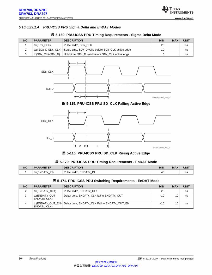
SDx_CLK
SDx_D
1
2 3SPRS91x_TIMING_PRU_08
SDx_CLK
SDx_D
1
2 3SPRS91x_TIMING_PRU_07
304
DRA790, DRA791DRA793, DRA797ZHCSII2E –AUGUST 2016–REVISED MAY 2019 www.ti.com.cn
提交文档反馈意见产品主页链接: DRA790 DRA791 DRA793 DRA797
Specifications 版权 © 2016–2019, Texas Instruments Incorporated
5.10.6.23.1.4 PRU-ICSS PRU Sigma Delta and EnDAT Modes
表表 5-169. PRU-ICSS PRU Timing Requirements - Sigma Delta ModeNO. PARAMETER DESCRIPTION MIN MAX UNIT
1 tw(SDx_CLK) Pulse width, SDx_CLK 20 ns2 tsu(SDx_D-SDx_CLK) Setup time, SDx_D valid before SDx_CLK active edge 10 ns3 th(SDx_CLK-SDx_D) Hold time, SDx_D valid before SDx_CLK active edge 5 ns
图图 5-115. PRU-ICSS PRU SD_CLK Falling Active Edge
图图 5-116. PRU-ICSS PRU SD_CLK Rising Active Edge
表表 5-170. PRU-ICSS PRU Timing Requirements - EnDAT ModeNO. PARAMETER DESCRIPTION MIN MAX UNIT
1 tw(ENDATx_IN) Pulse width, ENDATx_IN 40 ns
表表 5-171. PRU-ICSS PRU Switching Requirements - EnDAT ModeNO. PARAMETER DESCRIPTION MIN MAX UNIT
2 tw(ENDATx_CLK) Pulse width, ENDATx_CLK 20 ns3 td(ENDATx_OUT-
ENDATx_CLK)Delay time, ENDATx_CLK fall to ENDATx_OUT -10 10 ns
4 td(ENDATx_OUT_EN-ENDATx_CLK)
Delay time, ENDATx_CLK Fall to ENDATx_OUT_EN -10 10 ns

EDIO_LATCH_IN
3
1
2
EDIO_DATA_IN[7:0]
SPRS91x_TIMING_PRU_ECAT_01
ENDATx_IN
ENDATx_CLK
2
1
4
ENDATx_OUT
ENDATx_OUT_EN
SPRS91x_TIMING_PRU_09
3
305
DRA790, DRA791DRA793, DRA797
www.ti.com.cn ZHCSII2E –AUGUST 2016–REVISED MAY 2019
提交文档反馈意见产品主页链接: DRA790 DRA791 DRA793 DRA797
Specifications版权 © 2016–2019, Texas Instruments Incorporated
图图 5-117. PRU-ICSS PRU EnDAT Timing
5.10.6.23.2 PRU-ICSS EtherCAT (PRU-ICSS ECAT)
5.10.6.23.2.1 PRU-ICSS ECAT Electrical Data and Timing
表表 5-172. PRU-ICSS ECAT Timing Requirements – Input Validated With LATCH_INNO. PARAMETER DESCRIPTION MIN MAX UNIT
1 tw(EDIO_LATCH_IN) Pulse width, EDIO_LATCH_IN 100.00 ns2 tsu(EDIO_DATA_IN-
EDIO_LATCH_IN)
Setup time, EDIO_DATA_IN valid before EDIO_LATCH_IN activeedge
20.00 ns
3 th(EDIO_LATCH_IN-EDIO_DATA_IN)
Hold time, EDIO_DATA_IN valid after EDIO_LATCH_IN active edge 20.00 ns
图图 5-118. PRU-ICSS ECAT Input Validated with LATCH_IN Timing

EDIO_SOF
3
1
2
EDIO_DATA_IN[7:0]
SPRS91x_TIMING_PRU_ECAT_03
EDC_SYNCx_OUT
3
1
2
EDIO_DATA_IN[7:0]
SPRS91x_TIMING_PRU_ECAT_02
306
DRA790, DRA791DRA793, DRA797ZHCSII2E –AUGUST 2016–REVISED MAY 2019 www.ti.com.cn
提交文档反馈意见产品主页链接: DRA790 DRA791 DRA793 DRA797
Specifications 版权 © 2016–2019, Texas Instruments Incorporated
表表 5-173. PRU-ICSS ECAT Timing Requirements – Input Validated With SYNCxNO. PARAMETER DESCRIPTION MIN MAX UNIT
1 tw(EDC_SYNCx_OUT) Pulse width, EDC_SYNCx_OUT 100.00 ns2 tsu(EDIO_DATA_IN-
EDC_SYNCx_OUT)
Setup time, EDIO_DATA_IN valid before EDC_SYNCx_OUT activeedge
20.00 ns
3 th(EDC_SYNCx_OUT-EDIO_DATA_IN)
Hold time, EDIO_DATA_IN valid after EDC_SYNCx_OUT active edge 20.00 ns
图图 5-119. PRU-ICSS ECAT Input Validated With SYNCx Timing
表表 5-174. PRU-ICSS ECAT Timing Requirements – Input Validated With Start of Frame (SOF)NO. PARAMETER DESCRIPTION MIN MAX UNIT
1 tw(EDIO_SOF) Pulse duration, EDIO_SOF 4 × P (1) 5 × P (1) ns2 tsu(EDIO_DATA_IN-
EDIO_SOF)
Setup time, EDIO_DATA_IN valid before EDIO_SOF active edge 20.00 ns
3 th(EDIO_SOF-EDIO_DATA_IN)
Hold time, EDIO_DATA_IN valid after EDIO_SOF active edge 20.00 ns
(1) ICSS_IEP_CLK clock period
图图 5-120. PRU-ICSS ECAT Input Validated With SOF
表表 5-175. PRU-ICSS ECAT Timing Requirements - LATCHx_INNO. PARAMETER DESCRIPTION MIN MAX UNIT
1 tw(EDC_LATCHx_IN) Pulse duration, EDC_LATCHx_IN 3 × P (1) ns

MDIO_CLK (Output)
1
2
MDIO_DATA (Input)
SPRS91x_TIMING_PRU_MII_RT_01
EDC_LATCHx_IN
1SPRS91x_TIMING_PRU_ECAT_04
307
DRA790, DRA791DRA793, DRA797
www.ti.com.cn ZHCSII2E –AUGUST 2016–REVISED MAY 2019
提交文档反馈意见产品主页链接: DRA790 DRA791 DRA793 DRA797
Specifications版权 © 2016–2019, Texas Instruments Incorporated
(1) ICSS_IEP_CLK clock period
图图 5-121. PRU-ICSS ECAT LATCHx_IN Timing
表表 5-176. PRU-ICSS ECAT Switching Requirements - Digital IOsNO. PARAMETER DESCRIPTION MIN MAX UNIT
1 tw(EDIO_OUTVALID) Pulse duration, EDIO_OUTVALID 14 × P (1) 32 × P (1) ns2 td(EDIO_OUTVALID-
EDIO_DATA_OUT)
Delay time, EDIO_OUTVALID to EDIO_DATA_OUT 0.00 18 × P (1) ns
1 tsk(EDIO_DATA_OUT) EDIO_DATA_OUT skew 8 ns
(1) ICSS_IEP_CLK clock period
5.10.6.23.3 PRU-ICSS MII_RT and Switch
5.10.6.23.3.1 PRU-ICSS MDIO Electrical Data and Timing
表表 5-177. PRU-ICSS MDIO Timing Requirements – MDIO_DATANO. PARAMETER DESCRIPTION MIN MAX UNIT
1 tsu(MDIO-MDC) Setup time, MDIO valid before MDC high 90 ns2 th(MDIO-MDC) Hold time, MDIO valid from MDC high 0 ns
图图 5-122. PRU-ICSS MDIO_DATA Timing - Input Mode
表表 5-178. PRU-ICSS MDIO Switching Characteristics - MDIO_CLKNO. PARAMETER DESCRIPTION MIN MAX UNIT
1 tc(MDC) Cycle time, MDC 400 ns2 tw(MDCH) Pulse duration, MDC high 160 ns3 tw(MDCL) Pulse duration, MDC low 160 ns4 tt(MDC) Transition time, MDC 5 ns

MII_RXCLK
2 3
1 4
4
SPRS91x_TIMING_PRU_MII_RT_04
1
MDIO_CLK (Output)
MDIO_DATA (Output)
SPRS91x_TIMING_PRU_MII_RT_03
MDIO_CLK
2 3
1 4
4
SPRS91x_TIMING_PRU_MII_RT_02
308
DRA790, DRA791DRA793, DRA797ZHCSII2E –AUGUST 2016–REVISED MAY 2019 www.ti.com.cn
提交文档反馈意见产品主页链接: DRA790 DRA791 DRA793 DRA797
Specifications 版权 © 2016–2019, Texas Instruments Incorporated
图图 5-123. PRU-ICSS MDIO_CLK Timing
表表 5-179. PRU-ICSS MDIO Switching Characteristics – MDIO_DATANO. PARAMETER DESCRIPTION MIN MAX UNIT
1 td(MDC-MDIO) Delay time, MDC high to MDIO valid 0 390 ns
图图 5-124. PRU-ICSS MDIO_DATA Timing – Output Mode
5.10.6.23.3.2 PRU-ICSS MII_RT Electrical Data and Timing
注注In order to ensure the MII_RT IO timing values published in the device data manual, theICSS_CLK clock must be configured for 200MHz (default value) and the TX_CLK_DELAYbitfield in the PRUSS_MII_RT_TXCFG0/1 register must be set to 6h (non-default value).
表表 5-180. PRU-ICSS MII_RT Timing Requirements – MII[x]_RXCLKNO. PARAMETER DESCRIPTION SPEED MIN MAX UNIT
1 tc(RX_CLK) Cycle time, RX_CLK 10 Mbps 399.96 400.04 ns100 Mbps 39.996 40.004 ns
2 tw(RX_CLKH) Pulse duration, RX_CLK high 10 Mbps 140 260 ns100 Mbps 14 26 ns
3 tw(RX_CLKL) Pulse duration, RX_CLK low 10 Mbps 140 260 ns100 Mbps 14 26 ns
图图 5-125. PRU-ICSS MII[x]_RXCLK Timing

MII_MRCLK (Input)
1
2
MII_RXD[3:0],MII_RXDV,
MII_RXER (Inputs)
SPRS91x_TIMING_PRU_MII_RT_06
MII_TXCLK
2 3
1 4
4
SPRS91x_TIMING_PRU_MII_RT_05
309
DRA790, DRA791DRA793, DRA797
www.ti.com.cn ZHCSII2E –AUGUST 2016–REVISED MAY 2019
提交文档反馈意见产品主页链接: DRA790 DRA791 DRA793 DRA797
Specifications版权 © 2016–2019, Texas Instruments Incorporated
表表 5-181. PRU-ICSS MII_RT Timing Requirements - MII[x]_TXCLKNO. PARAMETER DESCRIPTION SPEED MIN MAX UNIT
1 tc(TX_CLK) Cycle time, TX_CLK 10 Mbps 399.96 400.04 ns100 Mbps 39.996 40.004 ns
2 tw(TX_CLKH) Pulse duration, TX_CLK high 10 Mbps 140 260 ns100 Mbps 14 26 ns
3 tw(TX_CLKL) Pulse duration, TX_CLK low 10 Mbps 140 260 ns100 Mbps 14 26 ns
4 tt(TX_CLK) Transition time, TX_CLK 10 Mbps 3 ns100 Mbps 3 ns
图图 5-126. PRU-ICSS MII[x]_TXCLK Timing
表表 5-182. PRU-ICSS MII_RT Timing Requirements - MII_RXD[3:0], MII_RXDV, and MII_RXERNO. PARAMETER DESCRIPTION SPEED MIN MAX UNIT
1 tsu(RXD-RX_CLK) Setup time, RXD[3:0] valid before RX_CLK 10 Mbps 8 nstsu(RX_DV-RX_CLK) Setup time, RX_DV valid before RX_CLKtsu(RX_ER-RX_CLK) Setup time, RX_ER valid before RX_CLKtsu(RXD-RX_CLK) Setup time, RXD[3:0] valid before RX_CLK 100 Mbps 8 nstsu(RX_DV-RX_CLK) Setup time, RX_DV valid before RX_CLKtsu(RX_ER-RX_CLK) Setup time, RX_ER valid before RX_CLK
2 th(RX_CLK-RXD) Hold time RXD[3:0] valid after RX_CLK 10 Mbps 8 nsth(RX_CLK-RX_DV) Hold time RX_DV valid after RX_CLKth(RX_CLK-RX_ER) Hold time RX_ER valid after RX_CLKth(RX_CLK-RXD) Hold time RXD[3:0] valid after RX_CLK 100 Mbps 8 nsth(RX_CLK-RX_DV) Hold time RX_DV valid after RX_CLKth(RX_CLK-RX_ER) Hold time RX_ER valid after RX_CLK
图图 5-127. PRU-ICSS MII_RXD[3:0], MII_RXDV, and MII_RXER Timing

2
1
Start
Bit
Data Bits
UART_TXD
3
Data Bits
Bit
Start
4
UART_RXD
SPRS960_TIMING_PRU_UART_01
1
MII_TXCLK (input)
MII_TXD[3:0],MII_TXEN (outputs)
SPRS91x_TIMING_PRU_MII_RT_07
310
DRA790, DRA791DRA793, DRA797ZHCSII2E –AUGUST 2016–REVISED MAY 2019 www.ti.com.cn
提交文档反馈意见产品主页链接: DRA790 DRA791 DRA793 DRA797
Specifications 版权 © 2016–2019, Texas Instruments Incorporated
表表 5-183. PRU-ICSS MII_RT Switching Characteristics - MII_TXD[3:0] and MII_TXENNO. PARAMETER DESCRIPTION SPEED MIN MAX UNIT
1 td(TX_CLK-TXD) Delay time, TX_CLK high to TXD[3:0] valid 10 Mbps 5 25 nstd(TX_CLK-TX_EN) Delay time, TX_CLK to TX_EN validtd(TX_CLK-TXD) Delay time, TX_CLK high to TXD[3:0] valid 100 Mbps 5 25 nstd(TX_CLK-TX_EN) Delay time, TX_CLK to TX_EN valid
图图 5-128. PRU-ICSS MII_TXD[3:0], MII_TXEN Timing
5.10.6.23.4 PRU-ICSS Universal Asynchronous Receiver Transmitter (PRU-ICSS UART)
表表 5-184. Timing Requirements for PRU-ICSS UART ReceiveNO. PARAMETER DESCRIPTION MIN MAX UNIT
3 tw(RX) Pulse duration, receive start, stop, data bit 0.96U (1) 1.05U(1) ns
(1) U = UART baud time = 1/programmed baud rate.
表表 5-185. Switching Characteristics Over Recommended Operating Conditions for PRU-ICSS UARTTransmit
NO. PARAMETER DESCRIPTION MIN MAX UNIT1 ƒbaud(baud) Maximum programmable baud rate 0 12 MHz2 tw(TX) Pulse duration, transmit start, stop, data bit U - 2 (1) U + 2(1) ns
(1) U = UART baud time = 1/programmed baud rate.
图图 5-129. PRU-ICSS UART Timing
5.10.6.23.5 PRU-ICSS IOSETs
In 表 5-186 are presented the specific groupings of signals (IOSET) for use with PRU-ICSS1.

311
DRA790, DRA791DRA793, DRA797
www.ti.com.cn ZHCSII2E –AUGUST 2016–REVISED MAY 2019
提交文档反馈意见产品主页链接: DRA790 DRA791 DRA793 DRA797
Specifications版权 © 2016–2019, Texas Instruments Incorporated
表表 5-186. PRU-ICSS1 IOSETs
SIGNALS IOSET1 IOSET2BALL MUX BALL MUX
PRU-ICSS 1pr1_pru1_gpi20 D13 12pr1_pru1_gpi19 C13 12pr1_pru1_gpi18 E13 12pr1_pru1_gpi17 B13 12pr1_pru1_gpi16 F11 12pr1_pru1_gpi15 E11 12pr1_pru1_gpi14 A13 12pr1_pru1_gpi13 A12 12pr1_pru1_gpi12 B12 12pr1_pru1_gpi11 C11 12pr1_pru1_gpi10 D11 12pr1_pru1_gpo20 D13 13pr1_pru1_gpo19 C13 13pr1_pru1_gpo18 E13 13pr1_pru1_gpo17 B13 13pr1_pru1_gpo16 F11 13pr1_pru1_gpo15 E11 13pr1_pru1_gpo14 A13 13pr1_pru1_gpo13 A12 13pr1_pru1_gpo12 B12 13pr1_pru1_gpo11 C11 13pr1_pru1_gpo10 D11 13pr1_pru1_gpi9 B11 12pr1_pru1_gpi8 C10 12pr1_pru1_gpi7 D10 12pr1_pru1_gpi6 E10 12pr1_pru1_gpi5 B10 12pr1_pru1_gpi4 A10 12pr1_pru1_gpi3 F10 12pr1_pru1_gpi2 A11 12pr1_pru1_gpi1 A8 12pr1_pru1_gpi0 A9 12pr1_pru1_gpo9 B11 13pr1_pru1_gpo8 C10 13pr1_pru1_gpo7 D10 13pr1_pru1_gpo6 E10 13pr1_pru1_gpo5 B10 13pr1_pru1_gpo4 A10 13pr1_pru1_gpo3 F10 13pr1_pru1_gpo2 A11 13pr1_pru1_gpo1 A8 13pr1_pru1_gpo0 A9 13pr1_mii1_crs D13 11
pr1_mii1_rxlink E13 11pr1_mii1_col C13 11

312
DRA790, DRA791DRA793, DRA797ZHCSII2E –AUGUST 2016–REVISED MAY 2019 www.ti.com.cn
提交文档反馈意见产品主页链接: DRA790 DRA791 DRA793 DRA797
Specifications 版权 © 2016–2019, Texas Instruments Incorporated
表表 5-186. PRU-ICSS1 IOSETs (continued)SIGNALS IOSET1 IOSET2
BALL MUX BALL MUXpr1_mii0_col L5 11
pr1_mii0_rxlink L6 11pr1_mii0_crs P4 11
pr1_edio_data_out7 A7 13pr1_edio_data_out6 B9 13pr1_edio_data_out5 C8 13pr1_edio_data_out4 B8 13pr1_edio_data_out3 E8 13pr1_edio_data_out2 C7 13pr1_edio_data_out1 B7 13pr1_edio_data_out0 D8 13pr1_edio_data_in7 A7 12pr1_edio_data_in6 B9 12pr1_edio_data_in5 C8 12pr1_edio_data_in4 B8 12pr1_edio_data_in3 E8 12pr1_edio_data_in2 C7 12pr1_edio_data_in1 B7 12pr1_edio_data_in0 D8 12
pr1_edio_sof A11 11pr1_edc_latch0_in A9 11pr1_edc_sync0_out A8 11
pr1_uart0_cts_n E8 11pr1_uart0_rts_n B8 11pr1_uart0_txd B9 11pr1_uart0_rxd C8 11
pr1_ecap0_ecap_capin_apwm_o
A7 11
PRU-ICSS 1 MIIpr1_mii1_txd3 B10 11pr1_mii1_txd2 E10 11pr1_mii1_txd1 B11 11pr1_mii1_txd0 D11 11pr1_mii1_rxd3 A12 11pr1_mii1_rxd2 A13 11pr1_mii1_rxd1 E11 11pr1_mii1_rxd0 F11 11pr1_mii1_rxdv B12 11pr1_mii1_txen A10 11pr1_mii1_rxer B13 11
pr1_mii_mr1_clk C11 11pr1_mii_mt1_clk F10 11pr1_mii0_txd3 P2 11pr1_mii0_txd2 N1 11pr1_mii0_txd1 N3 11pr1_mii0_txd0 N4 11pr1_mii0_rxd3 T4 11

313
DRA790, DRA791DRA793, DRA797
www.ti.com.cn ZHCSII2E –AUGUST 2016–REVISED MAY 2019
提交文档反馈意见产品主页链接: DRA790 DRA791 DRA793 DRA797
Specifications版权 © 2016–2019, Texas Instruments Incorporated
表表 5-186. PRU-ICSS1 IOSETs (continued)SIGNALS IOSET1 IOSET2
BALL MUX BALL MUXpr1_mii0_rxd2 T5 11pr1_mii0_rxd1 R2 11pr1_mii0_rxd0 R1 11pr1_mii0_rxdv N5 11pr1_mii0_txen P1 11pr1_mii0_rxer P3 11
pr1_mii_mt0_clk N2 11pr1_mii_mr0_clk N6 11pr1_mdio_mdclk D10 11pr1_mdio_data C10 11
In 表 5-187, 表 5-188 and 表 5-189 are presented the specific groupings of signals (IOSET) for use withPRU-ICSS2.
表表 5-187. PRU-ICSS2 IOSETs
SIGNALS IOSET1 IOSET2BALL MUX BALL MUX
PRU-ICSS 2pr2_pru1_gpi16 N4 12 E16 12pr2_pru1_gpi15 N3 12 E17 12pr2_pru1_gpi14 P1 12 A19 12pr2_pru1_gpi13 N1 12 B18 12pr2_pru1_gpi12 P2 12 B16 12pr2_pru1_gpi11 N2 12 B17 12pr2_pru1_gpi10 R1 12 A18 12pr2_pru1_gpi9 R2 12 B14 12pr2_pru1_gpi8 P3 12 D14 12pr2_pru1_gpi7 P4 12 C16 12pr2_pru1_gpi6 T5 12 J24 12pr2_pru1_gpi5 T4 12 J25 12pr2_pru1_gpi4 N6 12 AC4 12pr2_pru1_gpi3 N5 12 AA5 12pr2_pru1_gpi2 P5 12 U6 12pr2_pru1_gpi1 L6 12 AC3 12pr2_pru1_gpi0 L5 12 D23 12
pr2_pru1_gpo16 N4 13 E16 13pr2_pru1_gpo15 N3 13 E17 13pr2_pru1_gpo14 P1 13 A19 13pr2_pru1_gpo13 N1 13 B18 13pr2_pru1_gpo12 P2 13 B16 13pr2_pru1_gpo11 N2 13 B17 13pr2_pru1_gpo10 R1 13 A18 13pr2_pru1_gpo9 R2 13 B14 13pr2_pru1_gpo8 P3 13 D14 13pr2_pru1_gpo7 P4 13 C16 13pr2_pru1_gpo6 T5 13 J24 13

314
DRA790, DRA791DRA793, DRA797ZHCSII2E –AUGUST 2016–REVISED MAY 2019 www.ti.com.cn
提交文档反馈意见产品主页链接: DRA790 DRA791 DRA793 DRA797
Specifications 版权 © 2016–2019, Texas Instruments Incorporated
表表 5-187. PRU-ICSS2 IOSETs (continued)SIGNALS IOSET1 IOSET2
BALL MUX BALL MUXpr2_pru1_gpo5 T4 13 J25 13pr2_pru1_gpo4 N6 13 AC4 13pr2_pru1_gpo3 N5 13 AA5 13pr2_pru1_gpo2 P5 13 U6 13pr2_pru1_gpo1 L6 13 AC3 13pr2_pru1_gpo0 L5 13 D23 13pr2_pru0_gpi20 F16 12pr2_pru0_gpi19 D19 12pr2_pru0_gpi18 E19 12pr2_pru0_gpi17 B21 12pr2_pru0_gpi16 A21 12pr2_pru0_gpi15 B23 12pr2_pru0_gpi14 B22 12pr2_pru0_gpi13 A23 12pr2_pru0_gpi12 A22 12pr2_pru0_gpi11 AB1 12pr2_pru0_gpi10 AA4 12pr2_pru0_gpi9 AA1 12pr2_pru0_gpi8 Y3 12pr2_pru0_gpi7 W2 12pr2_pru0_gpi6 AA3 12pr2_pru0_gpi5 AA2 12pr2_pru0_gpi4 Y4 12pr2_pru0_gpi3 Y1 12pr2_pru0_gpi2 Y2 12pr2_pru0_gpi1 Y6 12pr2_pru0_gpi0 Y5 12
pr2_pru0_gpo20 F16 13pr2_pru0_gpo19 D19 13pr2_pru0_gpo18 E19 13pr2_pru0_gpo17 B21 13pr2_pru0_gpo16 A21 13pr2_pru0_gpo15 B23 13pr2_pru0_gpo14 B22 13pr2_pru0_gpo13 A23 13pr2_pru0_gpo12 A22 13pr2_pru0_gpo11 AB1 13pr2_pru0_gpo10 AA4 13pr2_pru0_gpo9 AA1 13pr2_pru0_gpo8 Y3 13pr2_pru0_gpo7 W2 13pr2_pru0_gpo6 AA3 13pr2_pru0_gpo5 AA2 13pr2_pru0_gpo4 Y4 13pr2_pru0_gpo3 Y1 13pr2_pru0_gpo2 Y2 13

315
DRA790, DRA791DRA793, DRA797
www.ti.com.cn ZHCSII2E –AUGUST 2016–REVISED MAY 2019
提交文档反馈意见产品主页链接: DRA790 DRA791 DRA793 DRA797
Specifications版权 © 2016–2019, Texas Instruments Incorporated
表表 5-187. PRU-ICSS2 IOSETs (continued)SIGNALS IOSET1 IOSET2
BALL MUX BALL MUXpr2_pru0_gpo1 Y6 13pr2_pru0_gpo0 Y5 13pr2_mii1_crs J24 11
pr2_mii1_rxlink B23 11pr2_mii0_crs A22 11
pr2_mii0_rxlink B21 11pr2_mii0_col A23 11pr2_mii1_col J25 11
PRU-ICSS 2 MIIpr2_mii1_txd3 Y2 11pr2_mii1_txd2 Y1 11pr2_mii1_txd1 Y4 11pr2_mii1_txd0 AA2 11pr2_mii1_rxd3 Y3 11pr2_mii1_rxd2 AA1 11pr2_mii1_rxd1 AA4 11pr2_mii1_rxd0 AB1 11
pr2_mii_mr1_clk AA3 11pr2_mii1_rxer B22 11
pr2_mii_mt1_clk Y5 11pr2_mii1_rxdv W2 11pr2_mii1_txen Y6 11pr2_mii0_txd3 B17 11pr2_mii0_txd2 B16 11pr2_mii0_txd1 B18 11pr2_mii0_txd0 A19 11pr2_mii0_rxd3 F16 11pr2_mii0_rxd2 E19 11pr2_mii0_rxd1 D19 11pr2_mii0_rxd0 A21 11
pr2_mii_mr0_clk E17 11pr2_mii0_rxer D14 11
pr2_mii_mt0_clk B14 11pr2_mii0_rxdv E16 11pr2_mii0_txen A18 11
pr2_mdio_mdclk C16 11 AA5 11pr2_mdio_data C17 11 AC4 11
表表 5-188. PRU-ICSS2 IOSETs (EnDAT)(1)
SIGNALS IOSET3 IOSET4BALL MUX BALL MUX
PRU-ICSS 2 EnDATpr2_pru1_endat0_clk L5 13 D23 13pr2_pru1_endat0_out L6 13 AC3 13
pr2_pru1_endat0_out_en P5 13 U6 13pr2_pru1_endat1_clk N5 13 AA5 13

316
DRA790, DRA791DRA793, DRA797ZHCSII2E –AUGUST 2016–REVISED MAY 2019 www.ti.com.cn
提交文档反馈意见产品主页链接: DRA790 DRA791 DRA793 DRA797
Specifications 版权 © 2016–2019, Texas Instruments Incorporated
表表 5-188. PRU-ICSS2 IOSETs (EnDAT)(1) (continued)SIGNALS IOSET3 IOSET4
BALL MUX BALL MUXpr2_pru1_endat1_out N6 13 AC4 13
pr2_pru1_endat1_out_en T4 13 J25 13pr2_pru1_endat2_clk T5 13 J24 13pr2_pru1_endat2_out P4 13 C16 13
pr2_pru1_endat2_out_en P3 13 D14 13pr2_pru1_endat0_in R2 12 B14 12pr2_pru1_endat1_in R1 12 A18 12pr2_pru1_endat2_in N2 12 B17 12
(1) These signals are internally muxed with the PRU GPI/GPO signals. Refer to the PRU chapter in the TRM for more details about thePRU-ICSS internal wrapper multiplexing.
表表 5-189. PRU-ICSS2 IOSETs (Sigma Delta)(1)
SIGNALS IOSET4BALL MUX
PRU-ICSS 2 SDpr2_pru0_sd0_clk Y5 12pr2_pru0_sd0_d Y6 12
pr2_pru0_sd1_clk Y2 12pr2_pru0_sd1_d Y1 12
pr2_pru0_sd2_clk Y4 12pr2_pru0_sd2_d AA2 12
pr2_pru0_sd3_clk AA3 12pr2_pru0_sd3_d W2 12
pr2_pru0_sd4_clk Y3 12pr2_pru0_sd4_d AA1 12
pr2_pru0_sd5_clk AA4 12pr2_pru0_sd5_d AB1 12
pr2_pru0_sd6_clk A22 12pr2_pru0_sd6_d A23 12
pr2_pru0_sd7_clk B22 12pr2_pru0_sd7_d B23 12
pr2_pru0_sd8_clk A21 12pr2_pru0_sd8_d B21 12
(1) These signals are internally muxed with the PRU GPI/GPO signals. Refer to the PRU chapter in the TRM for more details about thePRU-ICSS internal wrapper multiplexing.
5.10.6.23.6 PRU-ICSS Manual Functional Mapping
注注To configure the desired Manual IO Timing Mode the user must follow the steps described insection "Manual IO Timing Modes" of the Device TRM.
The associated registers to configure are listed in the CFG REGISTER column. For moreinformation see the Control Module Chapter in the Device TRM.
Manual IO Timings Modes must be used to ensure some IO timings for PRU-ICSS1 PRU1 Direct Inputmode. See 表 5-29 Modes Summary for a list of IO timings requiring the use of Manual IO Timings Modes.See 表 5-190 Manual Functions Mapping for PRU-ICSS1 PRU1 Direct Input mode for a definition of theManual modes.

317
DRA790, DRA791DRA793, DRA797
www.ti.com.cn ZHCSII2E –AUGUST 2016–REVISED MAY 2019
提交文档反馈意见产品主页链接: DRA790 DRA791 DRA793 DRA797
Specifications版权 © 2016–2019, Texas Instruments Incorporated
表 5-190 lists the A_DELAY and G_DELAY values needed to calculate the correct values to be set in theCFG_x registers.
表表 5-190. Manual Functions Mapping for PRU-ICSS1 PRU1 Direct Input mode
BALL BALL NAME PR1_PRU1_DIR_IN_MANUAL CFG REGISTER MUXMODEA_DELAY (ps) G_DELAY (ps) 12
D10 vin2a_d10 0 800 CFG_VIN2A_D10_IN pr1_pru1_gpi7C10 vin2a_d11 0 0 CFG_VIN2A_D11_IN pr1_pru1_gpi8B11 vin2a_d12 0 200 CFG_VIN2A_D12_IN pr1_pru1_gpi9D11 vin2a_d13 0 0 CFG_VIN2A_D13_IN pr1_pru1_gpi10C11 vin2a_d14 0 0 CFG_VIN2A_D14_IN pr1_pru1_gpi11B12 vin2a_d15 0 400 CFG_VIN2A_D15_IN pr1_pru1_gpi12A12 vin2a_d16 0 300 CFG_VIN2A_D16_IN pr1_pru1_gpi13A13 vin2a_d17 0 400 CFG_VIN2A_D17_IN pr1_pru1_gpi14E11 vin2a_d18 0 900 CFG_VIN2A_D18_IN pr1_pru1_gpi15F11 vin2a_d19 0 1500 CFG_VIN2A_D19_IN pr1_pru1_gpi16B13 vin2a_d20 0 100 CFG_VIN2A_D20_IN pr1_pru1_gpi17E13 vin2a_d21 0 500 CFG_VIN2A_D21_IN pr1_pru1_gpi18C13 vin2a_d22 0 500 CFG_VIN2A_D22_IN pr1_pru1_gpi19D13 vin2a_d23 0 600 CFG_VIN2A_D23_IN pr1_pru1_gpi20A9 vin2a_d3 0 900 CFG_VIN2A_D3_IN pr1_pru1_gpi0A8 vin2a_d4 0 100 CFG_VIN2A_D4_IN pr1_pru1_gpi1A11 vin2a_d5 0 600 CFG_VIN2A_D5_IN pr1_pru1_gpi2F10 vin2a_d6 0 200 CFG_VIN2A_D6_IN pr1_pru1_gpi3A10 vin2a_d7 0 400 CFG_VIN2A_D7_IN pr1_pru1_gpi4B10 vin2a_d8 0 500 CFG_VIN2A_D8_IN pr1_pru1_gpi5E10 vin2a_d9 0 600 CFG_VIN2A_D9_IN pr1_pru1_gpi6
Manual IO Timings Modes must be used to ensure some IO timings for PRU-ICSS1 PRU1 Direct Outputmode. See 表 5-29 Modes Summary for a list of IO timings requiring the use of Manual IO Timings Modes.See 表 5-191 Manual Functions Mapping for PRU-ICSS1 PRU1 Direct Output mode for a definition of theManual modes.
表 5-191 lists the A_DELAY and G_DELAY values needed to calculate the correct values to be set in theCFG_x registers.
表表 5-191. Manual Functions Mapping for PRU-ICSS1 PRU1 Direct Output mode
BALL BALL NAME PR1_PRU1_DIR_OUT_MANUAL CFG REGISTER MUXMODEA_DELAY (ps) G_DELAY (ps) 13
D10 vin2a_d10 0 1000 CFG_VIN2A_D10_OUT pr1_pru1_gpo7C10 vin2a_d11 0 1300 CFG_VIN2A_D11_OUT pr1_pru1_gpo8B11 vin2a_d12 0 2300 CFG_VIN2A_D12_OUT pr1_pru1_gpo9D11 vin2a_d13 0 2200 CFG_VIN2A_D13_OUT pr1_pru1_gpo10C11 vin2a_d14 0 1800 CFG_VIN2A_D14_OUT pr1_pru1_gpo11B12 vin2a_d15 0 1800 CFG_VIN2A_D15_OUT pr1_pru1_gpo12A12 vin2a_d16 0 1600 CFG_VIN2A_D16_OUT pr1_pru1_gpo13A13 vin2a_d17 0 2000 CFG_VIN2A_D17_OUT pr1_pru1_gpo14E11 vin2a_d18 0 700 CFG_VIN2A_D18_OUT pr1_pru1_gpo15F11 vin2a_d19 0 700 CFG_VIN2A_D19_OUT pr1_pru1_gpo16B13 vin2a_d20 0 500 CFG_VIN2A_D20_OUT pr1_pru1_gpo17E13 vin2a_d21 0 400 CFG_VIN2A_D21_OUT pr1_pru1_gpo18

318
DRA790, DRA791DRA793, DRA797ZHCSII2E –AUGUST 2016–REVISED MAY 2019 www.ti.com.cn
提交文档反馈意见产品主页链接: DRA790 DRA791 DRA793 DRA797
Specifications 版权 © 2016–2019, Texas Instruments Incorporated
表表 5-191. Manual Functions Mapping for PRU-ICSS1 PRU1 Direct Output mode (continued)BALL BALL NAME PR1_PRU1_DIR_OUT_MANUAL CFG REGISTER MUXMODE
A_DELAY (ps) G_DELAY (ps) 13C13 vin2a_d22 0 0 CFG_VIN2A_D22_OUT pr1_pru1_gpo19D13 vin2a_d23 0 400 CFG_VIN2A_D23_OUT pr1_pru1_gpo20A9 vin2a_d3 0 2200 CFG_VIN2A_D3_OUT pr1_pru1_gpo0A8 vin2a_d4 540 2800 CFG_VIN2A_D4_OUT pr1_pru1_gpo1A11 vin2a_d5 0 400 CFG_VIN2A_D5_OUT pr1_pru1_gpo2F10 vin2a_d6 0 1500 CFG_VIN2A_D6_OUT pr1_pru1_gpo3A10 vin2a_d7 0 2200 CFG_VIN2A_D7_OUT pr1_pru1_gpo4B10 vin2a_d8 0 2600 CFG_VIN2A_D8_OUT pr1_pru1_gpo5E10 vin2a_d9 0 2300 CFG_VIN2A_D9_OUT pr1_pru1_gpo6
Manual IO Timings Modes must be used to ensure some IO timings for PRU-ICSS1 PRU1 ParallelCapture Mode. See 表 5-29 Modes Summary for a list of IO timings requiring the use of Manual IOTimings Modes. See 表 5-192 Manual Functions Mapping for PRU-ICSS1 PRU1 Parallel Capture Modefor a definition of the Manual modes.
表 5-192 lists the A_DELAY and G_DELAY values needed to calculate the correct values to be set in theCFG_x registers.
表表 5-192. Manual Functions Mapping for PRU-ICSS1 PRU1 Parallel Capture Mode
BALL BALL NAME PR1_PRU1_PAR_CAP_MANUAL CFG REGISTER MUXMODEA_DELAY (ps) G_DELAY (ps) 12
D10 vin2a_d10 1535 0 CFG_VIN2A_D10_IN pr1_pru1_gpi7C10 vin2a_d11 1151 0 CFG_VIN2A_D11_IN pr1_pru1_gpi8B11 vin2a_d12 1173 0 CFG_VIN2A_D12_IN pr1_pru1_gpi9D11 vin2a_d13 970 0 CFG_VIN2A_D13_IN pr1_pru1_gpi10C11 vin2a_d14 1196 0 CFG_VIN2A_D14_IN pr1_pru1_gpi11B12 vin2a_d15 1286 0 CFG_VIN2A_D15_IN pr1_pru1_gpi12A12 vin2a_d16 1354 0 CFG_VIN2A_D16_IN pr1_pru1_gpi13A13 vin2a_d17 1331 0 CFG_VIN2A_D17_IN pr1_pru1_gpi14E11 vin2a_d18 2097 0 CFG_VIN2A_D18_IN pr1_pru1_gpi15F11 vin2a_d19 0 453 CFG_VIN2A_D19_IN pr1_pru1_gpi16A9 vin2a_d3 1566 0 CFG_VIN2A_D3_IN pr1_pru1_gpi0A8 vin2a_d4 1012 0 CFG_VIN2A_D4_IN pr1_pru1_gpi1A11 vin2a_d5 1337 0 CFG_VIN2A_D5_IN pr1_pru1_gpi2F10 vin2a_d6 1130 0 CFG_VIN2A_D6_IN pr1_pru1_gpi3A10 vin2a_d7 1202 0 CFG_VIN2A_D7_IN pr1_pru1_gpi4B10 vin2a_d8 1395 0 CFG_VIN2A_D8_IN pr1_pru1_gpi5E10 vin2a_d9 1338 0 CFG_VIN2A_D9_IN pr1_pru1_gpi6
Manual IO Timings Modes must be used to ensure some IO timings for PRU-ICSS2 PRU0 IOSET2 DirectInput mode. See 表 5-29 Modes Summary for a list of IO timings requiring the use of Manual IO TimingsModes. See 表 5-193 Manual Functions Mapping for PRU-ICSS2 PRU0 IOSET2 Direct Input mode for adefinition of the Manual modes.
表 5-193 lists the A_DELAY and G_DELAY values needed to calculate the correct values to be set in theCFG_x registers.

319
DRA790, DRA791DRA793, DRA797
www.ti.com.cn ZHCSII2E –AUGUST 2016–REVISED MAY 2019
提交文档反馈意见产品主页链接: DRA790 DRA791 DRA793 DRA797
Specifications版权 © 2016–2019, Texas Instruments Incorporated
表表 5-193. Manual Functions Mapping for PRU-ICSS2 PRU0 IOSET2 Direct Input mode
BALL BALL NAME PR2_PRU0_DIR_IN_MANUAL2 CFG REGISTER MUXMODEA_DELAY (ps) G_DELAY (ps) 12
Y5 gpio6_10 1000 3300 CFG_GPIO6_10_IN pr2_pru0_gpi0Y6 gpio6_11 1000 3400 CFG_GPIO6_11_IN pr2_pru0_gpi1F16 mcasp1_axr15 0 1300 CFG_MCASP1_AXR15_IN pr2_pru0_gpi20E19 mcasp2_aclkx 0 800 CFG_MCASP2_ACLKX_IN pr2_pru0_gpi18A21 mcasp2_axr2 0 1900 CFG_MCASP2_AXR2_IN pr2_pru0_gpi16B21 mcasp2_axr3 0 1400 CFG_MCASP2_AXR3_IN pr2_pru0_gpi17D19 mcasp2_fsx 0 1400 CFG_MCASP2_FSX_IN pr2_pru0_gpi19B22 mcasp3_axr0 0 1400 CFG_MCASP3_AXR0_IN pr2_pru0_gpi14B23 mcasp3_axr1 0 1000 CFG_MCASP3_AXR1_IN pr2_pru0_gpi15A23 mcasp3_fsx 0 1300 CFG_MCASP3_FSX_IN pr2_pru0_gpi13Y2 mmc3_clk 1000 3700 CFG_MMC3_CLK_IN pr2_pru0_gpi2Y1 mmc3_cmd 1000 3500 CFG_MMC3_CMD_IN pr2_pru0_gpi3Y4 mmc3_dat0 1000 3500 CFG_MMC3_DAT0_IN pr2_pru0_gpi4
AA2 mmc3_dat1 1000 4000 CFG_MMC3_DAT1_IN pr2_pru0_gpi5AA3 mmc3_dat2 1000 3300 CFG_MMC3_DAT2_IN pr2_pru0_gpi6W2 mmc3_dat3 1000 3900 CFG_MMC3_DAT3_IN pr2_pru0_gpi7Y3 mmc3_dat4 1000 3500 CFG_MMC3_DAT4_IN pr2_pru0_gpi8
AA1 mmc3_dat5 1000 3600 CFG_MMC3_DAT5_IN pr2_pru0_gpi9AA4 mmc3_dat6 1000 3500 CFG_MMC3_DAT6_IN pr2_pru0_gpi10AB1 mmc3_dat7 1000 3100 CFG_MMC3_DAT7_IN pr2_pru0_gpi11A22 mcasp3_aclkx 0 0 CFG_MCASP3_ACLKX_IN pr2_pru0_gpi12
Manual IO Timings Modes must be used to ensure some IO timings for PRU-ICSS2 PRU0 IOSET2 DirectOutput mode. See 表 5-29 Modes Summary for a list of IO timings requiring the use of Manual IO TimingsModes. See 表 5-194 Manual Functions Mapping for PRU-ICSS2 PRU0 IOSET2 Direct Output mode for adefinition of the Manual modes.
表 5-194 lists the A_DELAY and G_DELAY values needed to calculate the correct values to be set in theCFG_x registers.
表表 5-194. Manual Functions Mapping for PRU-ICSS2 PRU0 IOSET2 Direct Output mode
BALL BALL NAME PR2_PRU0_DIR_OUT_MANUAL2 CFG REGISTER MUXMODEA_DELAY (ps) G_DELAY (ps) 13
Y5 gpio6_10 1800 1900 CFG_GPIO6_10_OUT pr2_pru0_gpo0Y6 gpio6_11 2500 2100 CFG_GPIO6_11_OUT pr2_pru0_gpo1F16 mcasp1_axr15 0 400 CFG_MCASP1_AXR15_OUT pr2_pru0_gpo20E19 mcasp2_aclkx 0 400 CFG_MCASP2_ACLKX_OUT pr2_pru0_gpo18A21 mcasp2_axr2 0 500 CFG_MCASP2_AXR2_OUT pr2_pru0_gpo16B21 mcasp2_axr3 0 500 CFG_MCASP2_AXR3_OUT pr2_pru0_gpo17D19 mcasp2_fsx 0 0 CFG_MCASP2_FSX_OUT pr2_pru0_gpo19A22 mcasp3_aclkx 0 500 CFG_MCASP3_ACLKX_OUT pr2_pru0_gpo12B22 mcasp3_axr0 0 0 CFG_MCASP3_AXR0_OUT pr2_pru0_gpo14B23 mcasp3_axr1 0 200 CFG_MCASP3_AXR1_OUT pr2_pru0_gpo15A23 mcasp3_fsx 0 300 CFG_MCASP3_FSX_OUT pr2_pru0_gpo13Y2 mmc3_clk 2100 2200 CFG_MMC3_CLK_OUT pr2_pru0_gpo2Y1 mmc3_cmd 2300 2300 CFG_MMC3_CMD_OUT pr2_pru0_gpo3Y4 mmc3_dat0 2000 1600 CFG_MMC3_DAT0_OUT pr2_pru0_gpo4

320
DRA790, DRA791DRA793, DRA797ZHCSII2E –AUGUST 2016–REVISED MAY 2019 www.ti.com.cn
提交文档反馈意见产品主页链接: DRA790 DRA791 DRA793 DRA797
Specifications 版权 © 2016–2019, Texas Instruments Incorporated
表表 5-194. Manual Functions Mapping for PRU-ICSS2 PRU0 IOSET2 Direct Output mode (continued)BALL BALL NAME PR2_PRU0_DIR_OUT_MANUAL2 CFG REGISTER MUXMODE
A_DELAY (ps) G_DELAY (ps) 13AA2 mmc3_dat1 2000 1700 CFG_MMC3_DAT1_OUT pr2_pru0_gpo5AA3 mmc3_dat2 2050 2200 CFG_MMC3_DAT2_OUT pr2_pru0_gpo6W2 mmc3_dat3 2000 2000 CFG_MMC3_DAT3_OUT pr2_pru0_gpo7Y3 mmc3_dat4 2150 2600 CFG_MMC3_DAT4_OUT pr2_pru0_gpo8
AA1 mmc3_dat5 2400 2600 CFG_MMC3_DAT5_OUT pr2_pru0_gpo9AA4 mmc3_dat6 2200 2300 CFG_MMC3_DAT6_OUT pr2_pru0_gpo10AB1 mmc3_dat7 1800 2400 CFG_MMC3_DAT7_OUT pr2_pru0_gpo11
Manual IO Timings Modes must be used to ensure some IO timings for PRU-ICSS2 PRU1 IOSET1 DirectInput mode. See 表 5-29 Modes Summary for a list of IO timings requiring the use of Manual IO TimingsModes. See 表 5-195 Manual Functions Mapping for PRU-ICSS2 PRU1 IOSET1 Direct Input mode for adefinition of the Manual modes.
表 5-195 lists the A_DELAY and G_DELAY values needed to calculate the correct values to be set in theCFG_x registers.
表表 5-195. Manual Functions Mapping for PRU-ICSS2 PRU1 IOSET1 Direct Input mode
BALL BALL NAME PR2_PRU1_DIR_IN_MANUAL1 CFG REGISTER MUXMODEA_DELAY (ps) G_DELAY (ps) 12
P5 RMII_MHZ_50_CLK
1400 1200 CFG_RMII_MHZ_50_CLK_IN pr2_pru1_gpi2
L6 mdio_d 1300 1600 CFG_MDIO_D_IN pr2_pru1_gpi1L5 mdio_mclk 1400 800 CFG_MDIO_MCLK_IN pr2_pru1_gpi0N2 rgmii0_rxc 1400 500 CFG_RGMII0_RXC_IN pr2_pru1_gpi11P2 rgmii0_rxctl 1400 1800 CFG_RGMII0_RXCTL_IN pr2_pru1_gpi12N4 rgmii0_rxd0 1400 1300 CFG_RGMII0_RXD0_IN pr2_pru1_gpi16N3 rgmii0_rxd1 1400 1650 CFG_RGMII0_RXD1_IN pr2_pru1_gpi15P1 rgmii0_rxd2 1400 1400 CFG_RGMII0_RXD2_IN pr2_pru1_gpi14N1 rgmii0_rxd3 1400 1650 CFG_RGMII0_RXD3_IN pr2_pru1_gpi13T4 rgmii0_txc 1400 900 CFG_RGMII0_TXC_IN pr2_pru1_gpi5T5 rgmii0_txctl 1400 1300 CFG_RGMII0_TXCTL_IN pr2_pru1_gpi6R1 rgmii0_txd0 1400 900 CFG_RGMII0_TXD0_IN pr2_pru1_gpi10R2 rgmii0_txd1 1300 1400 CFG_RGMII0_TXD1_IN pr2_pru1_gpi9P3 rgmii0_txd2 1300 1100 CFG_RGMII0_TXD2_IN pr2_pru1_gpi8P4 rgmii0_txd3 1300 1300 CFG_RGMII0_TXD3_IN pr2_pru1_gpi7N5 uart3_rxd 1300 1000 CFG_UART3_RXD_IN pr2_pru1_gpi3N6 uart3_txd 1300 800 CFG_UART3_TXD_IN pr2_pru1_gpi4
Manual IO Timings Modes must be used to ensure some IO timings for PRU-ICSS2 PRU1 IOSET2 DirectInput mode. See 表 5-29 Modes Summary for a list of IO timings requiring the use of Manual IO TimingsModes. See 表 5-196 Manual Functions Mapping for PRU-ICSS2 PRU1 IOSET2 Direct Input mode for adefinition of the Manual modes.
表 5-196 lists the A_DELAY and G_DELAY values needed to calculate the correct values to be set in theCFG_x registers.

321
DRA790, DRA791DRA793, DRA797
www.ti.com.cn ZHCSII2E –AUGUST 2016–REVISED MAY 2019
提交文档反馈意见产品主页链接: DRA790 DRA791 DRA793 DRA797
Specifications版权 © 2016–2019, Texas Instruments Incorporated
表表 5-196. Manual Functions Mapping for PRU-ICSS2 PRU1 IOSET2 Direct Input mode
BALL BALL NAME PR2_PRU1_DIR_IN_MANUAL2 CFG REGISTER MUXMODEA_DELAY (ps) G_DELAY (ps) 12
C16 mcasp1_aclkx 400 0 CFG_MCASP1_ACLKX_IN pr2_pru1_gpi7D14 mcasp1_axr0 700 200 CFG_MCASP1_AXR0_IN pr2_pru1_gpi8B14 mcasp1_axr1 600 300 CFG_MCASP1_AXR1_IN pr2_pru1_gpi9B16 mcasp1_axr10 600 500 CFG_MCASP1_AXR10_IN pr2_pru1_gpi12B18 mcasp1_axr11 700 500 CFG_MCASP1_AXR11_IN pr2_pru1_gpi13A19 mcasp1_axr12 500 0 CFG_MCASP1_AXR12_IN pr2_pru1_gpi14E17 mcasp1_axr13 600 200 CFG_MCASP1_AXR13_IN pr2_pru1_gpi15E16 mcasp1_axr14 600 0 CFG_MCASP1_AXR14_IN pr2_pru1_gpi16A18 mcasp1_axr8 800 0 CFG_MCASP1_AXR8_IN pr2_pru1_gpi10B17 mcasp1_axr9 600 300 CFG_MCASP1_AXR9_IN pr2_pru1_gpi11D23 mcasp4_axr1 500 0 CFG_MCASP4_AXR1_IN pr2_pru1_gpi0AC3 mcasp5_aclkx 2100 1959 CFG_MCASP5_ACLKX_IN pr2_pru1_gpi1AA5 mcasp5_axr0 2300 2000 CFG_MCASP5_AXR0_IN pr2_pru1_gpi3AC4 mcasp5_axr1 2300 1800 CFG_MCASP5_AXR1_IN pr2_pru1_gpi4U6 mcasp5_fsx 2100 1780 CFG_MCASP5_FSX_IN pr2_pru1_gpi2J25 xref_clk0 0 0 CFG_XREF_CLK0_IN pr2_pru1_gpi5J24 xref_clk1 0 0 CFG_XREF_CLK1_IN pr2_pru1_gpi6
Manual IO Timings Modes must be used to ensure some IO timings for PRU-ICSS2 PRU1 IOSET1 DirectOutput mode. See 表 5-29 Modes Summary for a list of IO timings requiring the use of Manual IO TimingsModes. See 表 5-197 Manual Functions Mapping for PRU-ICSS2 PRU1 IOSET1 Direct Output mode for adefinition of the Manual modes.
表 5-197 lists the A_DELAY and G_DELAY values needed to calculate the correct values to be set in theCFG_x registers.
表表 5-197. Manual Functions Mapping for PRU-ICSS2 PRU1 IOSET1 Direct Output mode
BALL BALL NAME PR2_PRU1_DIR_OUT_MANUAL1 CFG REGISTER MUXMODEA_DELAY (ps) G_DELAY (ps) 13
P5 RMII_MHZ_50_CLK 2306 100 CFG_RMII_MHZ_50_CLK_OUT pr2_pru1_gpo2L6 mdio_d 1900 2000 CFG_MDIO_D_OUT pr2_pru1_gpo1L5 mdio_mclk 2000 1100 CFG_MDIO_MCLK_OUT pr2_pru1_gpo0N2 rgmii0_rxc 2000 1200 CFG_RGMII0_RXC_OUT pr2_pru1_gpo11P2 rgmii0_rxctl 2000 1700 CFG_RGMII0_RXCTL_OUT pr2_pru1_gpo12N4 rgmii0_rxd0 2000 1000 CFG_RGMII0_RXD0_OUT pr2_pru1_gpo16N3 rgmii0_rxd1 2200 1000 CFG_RGMII0_RXD1_OUT pr2_pru1_gpo15P1 rgmii0_rxd2 2200 1300 CFG_RGMII0_RXD2_OUT pr2_pru1_gpo14N1 rgmii0_rxd3 2250 1100 CFG_RGMII0_RXD3_OUT pr2_pru1_gpo13T4 rgmii0_txc 2350 1000 CFG_RGMII0_TXC_OUT pr2_pru1_gpo5T5 rgmii0_txctl 2000 1200 CFG_RGMII0_TXCTL_OUT pr2_pru1_gpo6R1 rgmii0_txd0 2000 1500 CFG_RGMII0_TXD0_OUT pr2_pru1_gpo10R2 rgmii0_txd1 1850 1000 CFG_RGMII0_TXD1_OUT pr2_pru1_gpo9P3 rgmii0_txd2 2100 1100 CFG_RGMII0_TXD2_OUT pr2_pru1_gpo8P4 rgmii0_txd3 2200 1000 CFG_RGMII0_TXD3_OUT pr2_pru1_gpo7N5 uart3_rxd 2000 1600 CFG_UART3_RXD_OUT pr2_pru1_gpo3N6 uart3_txd 2000 1000 CFG_UART3_TXD_OUT pr2_pru1_gpo4

322
DRA790, DRA791DRA793, DRA797ZHCSII2E –AUGUST 2016–REVISED MAY 2019 www.ti.com.cn
提交文档反馈意见产品主页链接: DRA790 DRA791 DRA793 DRA797
Specifications 版权 © 2016–2019, Texas Instruments Incorporated
Manual IO Timings Modes must be used to ensure some IO timings for PRU-ICSS2 PRU1 IOSET2 DirectOutput mode. See 表 5-29 Modes Summary for a list of IO timings requiring the use of Manual IO TimingsModes. See 表 5-198 Manual Functions Mapping for PRU-ICSS2 PRU1 IOSET2 Direct Output mode for adefinition of the Manual modes.
表 5-198 lists the A_DELAY and G_DELAY values needed to calculate the correct values to be set in theCFG_x registers.
表表 5-198. Manual Functions Mapping for PRU-ICSS2 PRU1 IOSET2 Direct Output mode
BALL BALL NAME PR2_PRU1_DIR_OUT_MANUAL2 CFG REGISTER MUXMODEA_DELAY (ps) G_DELAY (ps) 13
C16 mcasp1_aclkx 200 800 CFG_MCASP1_ACLKX_OUT pr2_pru1_gpo7D14 mcasp1_axr0 200 1000 CFG_MCASP1_AXR0_OUT pr2_pru1_gpo8B14 mcasp1_axr1 0 1110 CFG_MCASP1_AXR1_OUT pr2_pru1_gpo9B16 mcasp1_axr10 0 2500 CFG_MCASP1_AXR10_OUT pr2_pru1_gpo12B18 mcasp1_axr11 0 1900 CFG_MCASP1_AXR11_OUT pr2_pru1_gpo13A19 mcasp1_axr12 0 2300 CFG_MCASP1_AXR12_OUT pr2_pru1_gpo14E17 mcasp1_axr13 200 1200 CFG_MCASP1_AXR13_OUT pr2_pru1_gpo15E16 mcasp1_axr14 200 1100 CFG_MCASP1_AXR14_OUT pr2_pru1_gpo16A18 mcasp1_axr8 200 1600 CFG_MCASP1_AXR8_OUT pr2_pru1_gpo10B17 mcasp1_axr9 0 1900 CFG_MCASP1_AXR9_OUT pr2_pru1_gpo11D23 mcasp4_axr1 0 700 CFG_MCASP4_AXR1_OUT pr2_pru1_gpo0AC3 mcasp5_aclkx 1400 4000 CFG_MCASP5_ACLKX_OUT pr2_pru1_gpo1AA5 mcasp5_axr0 1500 3000 CFG_MCASP5_AXR0_OUT pr2_pru1_gpo3AC4 mcasp5_axr1 1500 1900 CFG_MCASP5_AXR1_OUT pr2_pru1_gpo4U6 mcasp5_fsx 1300 2700 CFG_MCASP5_FSX_OUT pr2_pru1_gpo2J25 xref_clk0 0 160 CFG_XREF_CLK0_OUT pr2_pru1_gpo5J24 xref_clk1 0 0 CFG_XREF_CLK1_OUT pr2_pru1_gpo6
Manual IO Timings Modes must be used to ensure some IO timings for PRU-ICSS2 PRU0 IOSET2Parallel Capture Mode. See 表 5-29 Modes Summary for a list of IO timings requiring the use of ManualIO Timings Modes. See 表 5-199 Manual Functions Mapping for PRU-ICSS2 PRU0 IOSET2 ParallelCapture Mode for a definition of the Manual modes.
表 5-199 lists the A_DELAY and G_DELAY values needed to calculate the correct values to be set in theCFG_x registers.
表表 5-199. Manual Functions Mapping for PRU-ICSS2 PRU0 IOSET2 Parallel Capture Mode
BALL BALL NAME PR2_PRU0_PAR_CAP_MANUAL2 CFG REGISTER MUXMODEA_DELAY (ps) G_DELAY (ps) 12
Y5 gpio6_10 4125 481 CFG_GPIO6_10_IN pr2_pru0_gpi0Y6 gpio6_11 3935 997 CFG_GPIO6_11_IN pr2_pru0_gpi1
A21 mcasp2_axr2 0 0 CFG_MCASP2_AXR2_IN pr2_pru0_gpi16A22 mcasp3_aclkx 571 0 CFG_MCASP3_ACLKX_IN pr2_pru0_gpi12B22 mcasp3_axr0 1570 0 CFG_MCASP3_AXR0_IN pr2_pru0_gpi14B23 mcasp3_axr1 1405 0 CFG_MCASP3_AXR1_IN pr2_pru0_gpi15A23 mcasp3_fsx 1946 0 CFG_MCASP3_FSX_IN pr2_pru0_gpi13Y2 mmc3_clk 4093 1066 CFG_MMC3_CLK_IN pr2_pru0_gpi2Y1 mmc3_cmd 4043 921 CFG_MMC3_CMD_IN pr2_pru0_gpi3Y4 mmc3_dat0 4010 864 CFG_MMC3_DAT0_IN pr2_pru0_gpi4
AA2 mmc3_dat1 3817 1643 CFG_MMC3_DAT1_IN pr2_pru0_gpi5

323
DRA790, DRA791DRA793, DRA797
www.ti.com.cn ZHCSII2E –AUGUST 2016–REVISED MAY 2019
提交文档反馈意见产品主页链接: DRA790 DRA791 DRA793 DRA797
Specifications版权 © 2016–2019, Texas Instruments Incorporated
表表 5-199. Manual Functions Mapping for PRU-ICSS2 PRU0 IOSET2 Parallel Capture Mode (continued)BALL BALL NAME PR2_PRU0_PAR_CAP_MANUAL2 CFG REGISTER MUXMODE
A_DELAY (ps) G_DELAY (ps) 12AA3 mmc3_dat2 4040 673 CFG_MMC3_DAT2_IN pr2_pru0_gpi6W2 mmc3_dat3 3923 1478 CFG_MMC3_DAT3_IN pr2_pru0_gpi7Y3 mmc3_dat4 4096 729 CFG_MMC3_DAT4_IN pr2_pru0_gpi8
AA1 mmc3_dat5 3926 1271 CFG_MMC3_DAT5_IN pr2_pru0_gpi9AA4 mmc3_dat6 4004 929 CFG_MMC3_DAT6_IN pr2_pru0_gpi10AB1 mmc3_dat7 3963 666 CFG_MMC3_DAT7_IN pr2_pru0_gpi11
Manual IO Timings Modes must be used to ensure some IO timings for PRU-ICSS2 PRU1 IOSET1Parallel Capture Mode. See 表 5-29 Modes Summary for a list of IO timings requiring the use of ManualIO Timings Modes. See 表 5-200 Manual Functions Mapping for PRU-ICSS2 PRU1 IOSET1 ParallelCapture Mode for a definition of the Manual modes.
表 5-200 lists the A_DELAY and G_DELAY values needed to calculate the correct values to be set in theCFG_x registers.
表表 5-200. Manual Functions Mapping for PRU-ICSS2 PRU1 IOSET1 Parallel Capture Mode
BALL BALL NAME PR2_PRU1_PAR_CAP_MANUAL1 CFG REGISTER MUXMODEA_DELAY (ps) G_DELAY (ps) 12
P5 RMII_MHZ_50_CLK
1717 0 CFG_RMII_MHZ_50_CLK_IN pr2_pru1_gpi2
L5 mdio_d 2088 0 CFG_MDIO_D_IN pr2_pru1_gpi1L6 mdio_mclk 1321 0 CFG_MDIO_MCLK_IN pr2_pru1_gpi0N2 rgmii0_rxc 1287 0 CFG_RGMII0_RXC_IN pr2_pru1_gpi11P2 rgmii0_rxctl 2456 0 CFG_RGMII0_RXCTL_IN pr2_pru1_gpi12N4 rgmii0_rxd0 0 0 CFG_RGMII0_RXD0_IN pr2_pru1_gpi16N3 rgmii0_rxd1 2157 0 CFG_RGMII0_RXD1_IN pr2_pru1_gpi15P1 rgmii0_rxd2 2008 0 CFG_RGMII0_RXD2_IN pr2_pru1_gpi14N1 rgmii0_rxd3 2271 0 CFG_RGMII0_RXD3_IN pr2_pru1_gpi13T4 rgmii0_txc 1851 0 CFG_RGMII0_TXC_IN pr2_pru1_gpi5T5 rgmii0_txctl 1875 0 CFG_RGMII0_TXCTL_IN pr2_pru1_gpi6R1 rgmii0_txd0 1685 0 CFG_RGMII0_TXD0_IN pr2_pru1_gpi10R2 rgmii0_txd1 2131 0 CFG_RGMII0_TXD1_IN pr2_pru1_gpi9P3 rgmii0_txd2 1734 0 CFG_RGMII0_TXD2_IN pr2_pru1_gpi8P4 rgmii0_txd3 1764 0 CFG_RGMII0_TXD3_IN pr2_pru1_gpi7N5 uart3_rxd 1654 0 CFG_UART3_RXD_IN pr2_pru1_gpi3N6 uart3_txd 1242 0 CFG_UART3_TXD_IN pr2_pru1_gpi4
Manual IO Timings Modes must be used to ensure some IO timings for PRU-ICSS2 PRU1 IOSET2Parallel Capture Mode. See 表 5-29 Modes Summary for a list of IO timings requiring the use of ManualIO Timings Modes. See 表 5-201 Manual Functions Mapping for PRU-ICSS2 PRU1 IOSET2 ParallelCapture Mode for a definition of the Manual modes.
表 5-201 lists the A_DELAY and G_DELAY values needed to calculate the correct values to be set in theCFG_x registers.

324
DRA790, DRA791DRA793, DRA797ZHCSII2E –AUGUST 2016–REVISED MAY 2019 www.ti.com.cn
提交文档反馈意见产品主页链接: DRA790 DRA791 DRA793 DRA797
Specifications 版权 © 2016–2019, Texas Instruments Incorporated
表表 5-201. Manual Functions Mapping for PRU-ICSS2 PRU1 IOSET2 Parallel Capture Mode
BALL BALL NAME PR2_PRU1_PAR_CAP_MANUAL2 CFG REGISTER MUXMODEA_DELAY (ps) G_DELAY (ps) 12
C16 mcasp1_aclkx 1928 0 CFG_MCASP1_ACLKX_IN pr2_pru1_gpi7D14 mcasp1_axr0 2413 0 CFG_MCASP1_AXR0_IN pr2_pru1_gpi8B14 mcasp1_axr1 2523 25 CFG_MCASP1_AXR1_IN pr2_pru1_gpi9B16 mcasp1_axr10 2607 0 CFG_MCASP1_AXR10_IN pr2_pru1_gpi12B18 mcasp1_axr11 2669 92 CFG_MCASP1_AXR11_IN pr2_pru1_gpi13A19 mcasp1_axr12 2225 0 CFG_MCASP1_AXR12_IN pr2_pru1_gpi14E17 mcasp1_axr13 2315 0 CFG_MCASP1_AXR13_IN pr2_pru1_gpi15E16 mcasp1_axr14 0 0 CFG_MCASP1_AXR14_IN pr2_pru1_gpi16A18 mcasp1_axr8 2201 0 CFG_MCASP1_AXR8_IN pr2_pru1_gpi10B17 mcasp1_axr9 2293 278 CFG_MCASP1_AXR9_IN pr2_pru1_gpi11D23 mcasp4_axr1 1759 0 CFG_MCASP4_AXR1_IN pr2_pru1_gpi0AC3 mcasp5_aclkx 3732 1810 CFG_MCASP5_ACLKX_IN pr2_pru1_gpi1AA5 mcasp5_axr0 3776 2255 CFG_MCASP5_AXR0_IN pr2_pru1_gpi3AC4 mcasp5_axr1 3886 1923 CFG_MCASP5_AXR1_IN pr2_pru1_gpi4U6 mcasp5_fsx 3800 1449 CFG_MCASP5_FSX_IN pr2_pru1_gpi2J25 xref_clk0 1375 21 CFG_XREF_CLK0_IN pr2_pru1_gpi5J24 xref_clk1 1320 0 CFG_XREF_CLK1_IN pr2_pru1_gpi6

325
DRA790, DRA791DRA793, DRA797
www.ti.com.cn ZHCSII2E –AUGUST 2016–REVISED MAY 2019
提交文档反馈意见产品主页链接: DRA790 DRA791 DRA793 DRA797
Specifications版权 © 2016–2019, Texas Instruments Incorporated
5.10.6.24 System and Miscellaneous interfaces
The Device includes the following System and Miscellaneous interfaces:• Sysboot Interface• System DMA Interface• Interrupt Controllers (INTC) Interface
5.10.7 Emulation and Debug SubsystemThe Device includes the following Test interfaces:• IEEE 1149.1 Standard-Test-Access Port (JTAG)• Trace Port Interface Unit (TPIU)
5.10.7.1 IEEE 1149.1 Standard-Test-Access Port (JTAG)
The JTAG (IEEE Standard 1149.1-1990 Standard-Test-Access Port and Boundary Scan Architecture)interface is used for BSDL testing and emulation of the device. The trstn pin only needs to be releasedwhen it is necessary to use a JTAG controller to debug the device or exercise the device's boundary scanfunctionality. For maximum reliability, the device includes an internal Pulldown (IPD) on the trstn pin toensure that trstn is always asserted upon power up and the device's internal emulation logic is alwaysproperly initialized. JTAG controllers from Texas Instruments actively drive trstn high. However, somethird-party JTAG controllers may not drive trstn high but expect the use of a Pullup resistor on trstn. Whenusing this type of JTAG controller, assert trstn to initialize the device after powerup and externally drivetrstn high before attempting any emulation or boundary-scan operations.
The main JTAG features include:• 32KB embedded trace buffer (ETB)• 5-pin system trace interface for debug• Supports Advanced Event Triggering (AET)• All processors can be emulated via JTAG ports• All functions on EMU pins of the device:
– EMU[1:0] - cross-triggering, boot mode (WIR), STM trace– EMU[4:2] - STM trace only (single direction)
5.10.7.1.1 JTAG Electrical Data/Timing
表 5-202, 表 5-203 and 图 5-130 assume testing over the recommended operating conditions andelectrical characteristic conditions below.
表表 5-202. Timing Requirements for IEEE 1149.1 JTAGNO. PARAMETER DESCRIPTION MIN MAX UNIT
1 tc(TCK) Cycle time, TCK 62.29 ns1a tw(TCKH) Pulse duration, TCK high (40% of tc) 24.92 ns1b tw(TCKL) Pulse duration, TCK low (40% of tc) 24.92 ns
3tsu(TDI-TCK) Input setup time, TDI valid to TCK high 6.23 nstsu(TMS-TCK) Input setup time, TMS valid to TCK high 6.23 ns
4th(TCK-TDI) Input hold time, TDI valid from TCK high 31.15 nsth(TCK-TMS) Input hold time, TMS valid from TCK high 31.15 ns
表表 5-203. Switching Characteristics Over Recommended Operating Conditions for IEEE 1149.1 JTAGNO. PARAMETER DESCRIPTION MIN MAX UNIT
2 td(TCKL-TDOV) Delay time, TCK low to TDO valid 0 30.5 ns

5
6
87
TCK
RTCK
SPRS906_TIMING_JTAG_02
3
TCK
TDO
TDI/TMS
2
4
11a 1b
SPRS906_TIMING_JTAG_01
326
DRA790, DRA791DRA793, DRA797ZHCSII2E –AUGUST 2016–REVISED MAY 2019 www.ti.com.cn
提交文档反馈意见产品主页链接: DRA790 DRA791 DRA793 DRA797
Specifications 版权 © 2016–2019, Texas Instruments Incorporated
图图 5-130. JTAG Timing
表 5-204, 表 5-205 and 图 5-131 assume testing over the recommended operating conditions andelectrical characteristic conditions below.
表表 5-204. Timing Requirements for IEEE 1149.1 JTAG With RTCKNO. PARAMETER DESCRIPTION MIN MAX UNIT
1 tc(TCK) Cycle time, TCK 62.29 ns1a tw(TCKH) Pulse duration, TCK high (40% of tc) 24.92 ns1b tw(TCKL) Pulse duration, TCK low (40% of tc) 24.92 ns
3tsu(TDI-TCK) Input setup time, TDI valid to TCK high 6.23 nstsu(TMS-TCK) Input setup time, TMS valid to TCK high 6.23 ns
4th(TCK-TDI) Input hold time, TDI valid from TCK high 31.15 nsth(TCK-TMS) Input hold time, TMS valid from TCK high 31.15 ns
表表 5-205. Switching Characteristics Over Recommended Operating Conditions forIEEE 1149.1 JTAG With RTCK
NO. PARAMETER DESCRIPTION MIN MAX UNIT
5 td(TCK-RTCK)
Delay time, TCK to RTCK with no selected subpaths (i.e. ICEPick isthe only tap selected - when the Arm is in the scan chain, the delaytime is a function of the Arm functional clock).
0 27 ns
6 tc(RTCK) Cycle time, RTCK 62.29 ns7 tw(RTCKH) Pulse duration, RTCK high (40% of tc) 24.92 ns8 tw(RTCKL) Pulse duration, RTCK low (40% of tc) 24.92 ns
图图 5-131. JTAG With RTCK Timing

TRACECLK
TRACECTL
TRACEDATA[X:0]
TPIU4 TPIU4
TPIU2
TPIU1
TPIU3
TPIU5 TPIU5
SPRS906_TIMING_TIMER_01
327
DRA790, DRA791DRA793, DRA797
www.ti.com.cn ZHCSII2E –AUGUST 2016–REVISED MAY 2019
提交文档反馈意见产品主页链接: DRA790 DRA791 DRA793 DRA797
Specifications版权 © 2016–2019, Texas Instruments Incorporated
5.10.7.2 Trace Port Interface Unit (TPIU)
CAUTION
The I/O timings provided in this section are valid only if signals within a singleIOSET are used. The IOSETs are defined in 表 5-207.
5.10.7.2.1 TPIU PLL DDR Mode
表 5-206 and 图 5-132 assume testing over the recommended operating conditions and electricalcharacteristic conditions below.
表表 5-206. Switching Characteristics for TPIU
NO. PARAMETER DESCRIPTION MIN MAX UNITTPIU1 tc(clk) Cycle time, TRACECLK period 5.56 nsTPIU4 td(clk-ctlV) Skew time, TRACECLK transition to TRACECTL transition -1.61 1.98 nsTPIU5 td(clk-dataV) Skew time, TRACECLK transition to TRACEDATA[17:0] -1.61 1.98 ns
图图 5-132. TPIU—PLL DDR Transmit Mode(1)
(1) In d[X:0], X is equal to 15 or 17.
In 表 5-207 are presented the specific groupings of signals (IOSET) for use with TPIU signals.
表表 5-207. TPIU IOSETs
SIGNALS IOSET1 IOSET2BALL MUX BALL MUX
emu19 E10 5emu18 B10 5emu17 A10 5emu16 F10 5emu15 A11 5emu14 A8 5emu13 A9 5emu12 A7 5emu11 B9 5emu10 C8 5emu9 B8 5emu8 E8 5emu7 C7 5emu6 B7 5

328
DRA790, DRA791DRA793, DRA797ZHCSII2E –AUGUST 2016–REVISED MAY 2019 www.ti.com.cn
提交文档反馈意见产品主页链接: DRA790 DRA791 DRA793 DRA797
Specifications 版权 © 2016–2019, Texas Instruments Incorporated
表表 5-207. TPIU IOSETs (continued)SIGNALS IOSET1 IOSET2
BALL MUX BALL MUXemu5 D8 5emu1 C22 0 C22 0emu0 C21 0 C21 0

329
DRA790, DRA791DRA793, DRA797
www.ti.com.cn ZHCSII2E –AUGUST 2016–REVISED MAY 2019
提交文档反馈意见产品主页链接: DRA790 DRA791 DRA793 DRA797
Detailed Description版权 © 2016–2019, Texas Instruments Incorporated
6 Detailed Description
6.1 DescriptionThe DRA79x processor is offered in a 538-ball, 17×17-mm, 0.65-mm ball pitch (0.8mm spacing rules canbe used on signals) with Via Channel™ Array (VCA) technology, ball grid array (BGA) package.
The architecture is designed to deliver high-performance concurrencies for automotive applications in acost-effective solution, providing full scalability from the DRA75x ("Jacinto 6 EP" and "Jacinto 6 Ex"),DRA74x "Jacinto 6" and DRA72x "Jacinto 6 Eco" family of infotainment processors.
Programmability is provided by a single-core Arm Cortex-A15 RISC CPU with Neon extensions and a TIC66x VLIW floating-point DSP core. The Arm processor lets developers keep control functions separatefrom other algorithms programmed on the DSP and coprocessors, thus reducing the complexity of thesystem software.
Additionally, TI provides a complete set of development tools for the Arm, and DSP, including C compilersand a debugging interface for visibility into source code execution.
Cryptographic acceleration is available in all devices. All other supported security features, includingsupport for secure boot, debug security and support for trusted execution environment are available onHigh-Security (HS) devices. For more information about HS devices, contact your TI representative.
The DRA79x Jacinto 6 Entry processor family is qualified according to the AEC-Q100 standard.
The device features are simplified power supply rail mapping which enables lower cost PMIC solutions.
6.2 Functional Block Diagram图 6-1 is functional block diagram for the device.

Mailbox x13
EDMA
High-Speed Interconnect
Program/Data Storage
ConnectivitySystem
(1x ArmCortex–A15)
PCIe SS x2
MediaLB
(NAND/NOR/Async)
VIP x1
intro-001
GPMC / ELM
256-KB ROM
OCMC
DRA79x
MPU
Serial Interfaces
I2C x6
UART x10
McSPI x4
DCAN x2
Spinlock
GPIO x8
Timers x16
WDT
QSPI EMIF x11x 32-bit
DDR3/DDR3L
sDMA VPE
McASP x8
MMU x2
PWM SS x3
HDQKBD GMAC AVB
MOST150
1x USB 3.0Dual Mode FS/HS/SS
w/ PHY
2x USB 2.0Dual Mode FS/HS1x PHY, 1x ULPI
512-KBRAM with ECC
DMM
MMC / SD x4
PRU-ICSS x2
(1x C66xCo-Processor)
DSP
IPU1
(Dual Cortex–M4) (Dual Cortex–M4)
IPU2
Display Subsystem
1xGFX / 3xVID
Blend / Scale
HDMI 1.4a
LCD3
Secure Boot
Debug
Security
TEE
(HS devices)
CAL CSI2 x1
Radio Accelerators
VCP x2 HD ATL
LCD2
330
DRA790, DRA791DRA793, DRA797ZHCSII2E –AUGUST 2016–REVISED MAY 2019 www.ti.com.cn
提交文档反馈意见产品主页链接: DRA790 DRA791 DRA793 DRA797
Detailed Description 版权 © 2016–2019, Texas Instruments Incorporated
图图 6-1. DRA79x Block Diagram

331
DRA790, DRA791DRA793, DRA797
www.ti.com.cn ZHCSII2E –AUGUST 2016–REVISED MAY 2019
提交文档反馈意见产品主页链接: DRA790 DRA791 DRA793 DRA797
Detailed Description版权 © 2016–2019, Texas Instruments Incorporated
6.3 MPUThe Cortex®-A15 microprocessor unit (MPU) subsystem serves the applications processing role byrunning the high-level operating system (HLOS) and application code.
The MPU subsystem incorporates one Cortex-A15 MPU core (MPU_C0), individual level 1 (L1) caches,level 2 (L2) cache (MPU_L2CACHE) shared between them, and various other shared peripherals. To aidsoftware development, the processor core can be kept cache-coherent with the L2 cache.
The MPU subsystem provides a high-performance computing platform with high peak-computingperformance and low memory latency.
The Arm subsystem supports the following key features:

332
DRA790, DRA791DRA793, DRA797ZHCSII2E –AUGUST 2016–REVISED MAY 2019 www.ti.com.cn
提交文档反馈意见产品主页链接: DRA790 DRA791 DRA793 DRA797
Detailed Description 版权 © 2016–2019, Texas Instruments Incorporated
• Arm Cortex-A15 MP Core™ (MPU_CLUSTER)– One Cortex-A15 MPU core (revision r2p2) which has the following features:
• Superscalar, dynamic multi-issue technology– Out-of-order (OoO) instruction dispatch and completion– Dynamic branch prediction with branch target buffer (BTB), global history buffer (GHB), and
48-entry return stack– Continuous fetch and decoding of three instructions per clock cycle– Dispatch of up to four instructions and completion of eight instructions per clock cycle– Provides optimal performance from binaries compiled for previous Arm processors– Five execution units handle simple instructions, branch instructions, Neon and floating point
instructions, multiply instructions, and load and store instructions.– Simple instructions take two cycles from dispatch, while complex instructions take up to 11
cycles.– Can issue two simple instructions in a cycle– Can issue a load and a store instruction in the same cycle
• Integrated Neon processing engine to include the Arm Neon Advanced SIMD (single instruction,multiple data) support for accelerated media and signal processing computation
• Includes VFPv4-compatible hardware to support single- and double-precision add, subtract,divide, multiply and accumulate, and square root operations
• Extensive support to accelerate virtualization using a hypervisor• 32-KiB L1 instruction (L1I) and 32-KiB L1 data (L1D) cache:
– 64-byte line size– 2-way set associative
• Memory management unit (MMU):– Two-level translation lookaside buffer (TLB) organization
– First level is an 32-entry, fully associative micro-TLB implemented for each of instructionfetch, load, and store.
– Second level is a unified, 4-way associative, 512-entry main TLB– Supports hardware TLB table-walk for backward-compatible and new 64-bit entry page table
formats– New page table format can produce 40-bit physical addresses– Two-stage translation where first stage is HLOS-controlled and the second level may be
controlled by a hypervisor. Second stage always uses the new page table format– Integrated L2 cache (MPU_L2CACHE) and snoop control unit (SCU):
• 1-MiB of unified (instructions and data) cache organized as 16 ways of 1024 sets of 64-bytelines
• Redundant L1 data (cache) tags to perform snoop filtering (L1 instruction cache tags are notduplicated)
• Operates at Cortex-A15 MPU core clock rate• Integrated L2 cache controller (MPU_L2CACHE_CTRL):
– Sixteen 64-byte line buffers that handle evictions, line fills and snoop transfers– One 128-bit AMBA4 Coherent Bus (AXI4-ACE) port– Auto-prefetch buffer for up to 16 streams and detecting forward and backward strides
– Generalized interrupt controller (GIC, also referred to as MPU_INTC): An interrupt controllersupplied by Arm. The single GIC in the MPU_CLUSTER routes interrupts to the MPU core. TheGIC supports:• Number of shared peripheral interrupts (SPI): 160• Number of software generated interrupts (SGI): 16• Number of CPU interfaces: 1

333
DRA790, DRA791DRA793, DRA797
www.ti.com.cn ZHCSII2E –AUGUST 2016–REVISED MAY 2019
提交文档反馈意见产品主页链接: DRA790 DRA791 DRA793 DRA797
Detailed Description版权 © 2016–2019, Texas Instruments Incorporated
• Virtual CPU interface for virtualization support. This allows the majority of guest operatingsystem (OS) interactions with the GIC to be handled in hardware, but with physical interruptsstill requiring hypervisor intervention to assign them to the appropriate virtual machine.
– Integrated timer counter and one timer block– Arm CoreSight™ debug and trace modules. For more information, see chapter On-Chip Debug
Support of the Device TRM..• MPU_AXI2OCP bridge (local interconnect):
– Connected to Memory Adapter (MPU_MA), which routes the non-EMIF address space transactionsto MPU_AXI2OCP
– Single request multiple data (SRMD) protocol on L3_MAIN port– Multiple targets:
• 64-bit port to the L3_MAIN interconnect. Interface frequency is 1/4 or 1/8 of core frequency• MPU_ROM• Internal MPU subsystem peripheral targets, including Memory Adapter LISA Section Manager
(MA_LSM), wake-up generator (MPU_WUGEN), watchdog timer (MPU_WD_TIMER), and localPRCM module (MPU_PRCM) configuration
• Internal AXI target, CoreSight System Trace Module (CS_STM)• Memory adapter (MPU_MA): Helps decrease the latency of accesses between the MPU_L2CACHE
and the external memory interface (EMIF1) by providing a direct path between the MPU subsystemand EMIF1:– Connected to 128-bit AMBA4 interface of MPU_CLUSTER– Direct 128-bit interface to EMIF1– Interface speed between MPU_CLUSTER and MPU_MA is at half-speed of the MPU core
frequency– Quarter-speed interface to EMIF– Uses firewall logic to check access rights of incoming addresses
• Local PRCM (MPU_PRCM):– Handles MPU_C0 power domain– Supports SR3-APG (SmartReflex3 Automatic Power Gating) power management technology inside
the MPU_CLUSTER– MPU subsystem has five power domains
• Wake-up generator (MPU_WUGEN)– Responsible for waking up the MPU core
• Standby controller: Handles the power transitions inside the MPU subsystem• Realtime (master) counter (COUNTER_REALTIME): Produces the count used by the private timer
peripheral in the MPU_CLUSTER• Watchdog timer (MPU_WD_TIMER): Used to generate a chip-level watchdog reset request to global
PRCM• On-chip boot ROM (MPU_ROM): The MPU_ROM size is 48-KiB, and the address range is from
0x4003 8000 to 0x4004 3FFF. For more information about booting from this memory, see chapterInitialization of the Device TRM..

334
DRA790, DRA791DRA793, DRA797ZHCSII2E –AUGUST 2016–REVISED MAY 2019 www.ti.com.cn
提交文档反馈意见产品主页链接: DRA790 DRA791 DRA793 DRA797
Detailed Description 版权 © 2016–2019, Texas Instruments Incorporated
• Interfaces:– 128-bit interface to EMIF1– 64-bit master port to the L3_MAIN interconnect– 32-bit slave port from the L4_CFG_EMU interconnect (debug subsystem) for configuration of the
MPU subsystem debug modules– 32-bit slave port from the L4_CFG interconnect for memory adapter firewall (MPU_MA_NTTP_FW)
configuration– 32-bit ATB output for transmitting debug and trace data– 160 peripheral interrupt inputs
For more information, see section Arm Cortex-A15 Subsystem in chapter Processors and Accelerators ofthe device TRM.
6.4 DSP SubsystemThe device includes a single instance (DSP1) of a digital signal processor (DSP) subsystem, based on theTI's standard TMS320C66x DSP CorePac core.
The TMS320C66x DSP core enhances the TMS320C674x core, which merges the C674x™ floating pointand the C64x+™ fixed-point instruction set architectures. The C66x DSP is object-code compatible withthe C64x+/C674x DSPs.
For more information on the TMS320C66x core CPU, see the TMS320C66x DSP CPU and Instruction SetReference Guide, (SPRUGH7).
The DSP subsystem integrated in the device includes the following components:• A TMS320C66x CorePac DSP core that encompasses:
– L1 program-dedicated (L1P) cacheable memory– L1 data-dedicated (L1D) cacheable memory– L2 (program and data) cacheable memory– Extended Memory Controller (XMC)– External Memory Controller (EMC)– DSP CorePac located interrupt controller (INTC)– DSP CorePac located power-down controller (PDC)
• Dedicated enhanced data memory access engine - EDMA, to transfer data from/to memories andperipherals external to the DSP subsystem and to local DSP memory (most commonly L2 SRAM). Theexternal DMA requests are passed through DSP system level (SYS) wakeup logic, and collected fromthe DSP1 dedicated outputs of the device DMA Events Crossbar for the subsystem.
• A level 2 (L2) interconnect network (DSP NoC) to allow connectivity between different modules of thesubsystem or the remainder of the device via the device L3_MAIN interconnect.
• Two memory management units (on EDMA L2 interconnect and DSP MDMA paths) for accessing thedevice L3_MAIN interconnect address space
• Dedicated system control logic (DSP_SYSTEM) responsible for power management, clock generation,and connection to the device power, reset, and clock management (PRCM) module
The TMS320C66x Instruction Set Architecture (ISA) is the latest for the C6000 family. As with itspredecessors (C64x, C64x+ and C674x), the C66x is an advanced VLIW architecture with 8 functionalunits (two multiplier units and six arithmetic logic units) that operate in parallel. The C66x CPU has a totalof 64 general-purpose 32-bit registers.
Some features of the DSP C6000 family devices are:• Advanced VLIW CPU with eight functional units (two multipliers and six ALUs) which:
– Executes up to eight instructions per cycle for up to ten times the performance of typical DSPs– Allows designers to develop highly effective RISC-like code for fast development time

335
DRA790, DRA791DRA793, DRA797
www.ti.com.cn ZHCSII2E –AUGUST 2016–REVISED MAY 2019
提交文档反馈意见产品主页链接: DRA790 DRA791 DRA793 DRA797
Detailed Description版权 © 2016–2019, Texas Instruments Incorporated
• Instruction packing– Gives code size equivalence for eight instructions executed serially or in parallel– Reduces code size, program fetches, and power consumption
• Conditional execution of most instructions– Reduces costly branching– Increases parallelism for higher sustained performance
• Efficient code execution on independent functional units– Industry's most efficient C compiler on DSP benchmark suite– Industry's first assembly optimizer for fast development and improved parallelization
• 8-/16-/32-bit/64-bit data support, providing efficient memory support for a variety of applications• 40-bit arithmetic options which add extra precision for vocoders and other computationally intensive
applications• Saturation and normalization to provide support for key arithmetic operations• Field manipulation and instruction extract, set, clear, and bit counting support common operation found
in control and data manipulation applications.
The C66x CPU has the following additional features:• Each multiplier can perform two 16 × 16-bit or four 8 × 8 bit multiplies every clock cycle.• Quad 8-bit and dual 16-bit instruction set extensions with data flow support• Support for non-aligned 32-bit (word) and 64-bit (double word) memory accesses• Special communication-specific instructions have been added to address common operations in error-
correcting codes.• Bit count and rotate hardware extends support for bit-level algorithms.• Compact instructions: Common instructions (AND, ADD, LD, MPY) have 16-bit versions to reduce
code size.• Protected mode operation: A two-level system of privileged program execution to support higher-
capability operating systems and system features such as memory protection.• Exceptions support for error detection and program redirection to provide robust code execution• Hardware support for modulo loop operation to reduce code size and allow interrupts during fully-
pipelined code• Each multiplier can perform 32 × 32 bit multiplies• Additional instructions to support complex multiplies allowing up to eight 16-bit multiply/add/subtracts
per clock cycle
The TMS320C66x has the following key improvements to the ISA:• 4x Multiply Accumulate improvement for both fixed and floating point• Improvement of the floating point arithmetic• Enhancement of the vector processing capability for fixed and floating point• Addition of domain-specific instructions for complex arithmetic and matrix operations
On the C66x ISA, the vector processing capability is improved by extending the width of the SIMDinstructions. The C674x DSP supports 2-way SIMD operations for 16-bit data and 4-way SIMDoperations for 8-bit data. C66x enhances this capabilities with the addition of SIMD instructions for 32-bitdata allowing operation on 128-bit vectors. For example the QMPY32 instruction is able to perform theelement to element multiplication between two vectors of four 32-bit data each.
C66x ISA includes a set of specific instructions to handle complex arithmetic and matrix operations.

336
DRA790, DRA791DRA793, DRA797ZHCSII2E –AUGUST 2016–REVISED MAY 2019 www.ti.com.cn
提交文档反馈意见产品主页链接: DRA790 DRA791 DRA793 DRA797
Detailed Description 版权 © 2016–2019, Texas Instruments Incorporated
• TMS320C66x DSP CorePac memory components:– A 32-KiB L1 program memory (L1P) configurable as cache and/or SRAM:
• When configured as a cache, the L1P is a 1-way set-associative cache with a 32-byte cacheline
• The DSP CorePac L1P memory controller provides bandwidth management, memoryprotection, and power-down functions
• The L1P is capable of cache block and global coherence operations• The L1P controller has an Error Detection (ED) mechanism, including necessary SRAM• The L1P memory can be fully configured as a cache or SRAM• Page size for L1P memory is 2KB
– A 32-KiB L1 data memory (L1D) configurable as cache and / or SRAM:• When configured as a cache, the L1D is a 2-way set-associative cache with a 64-byte cache
line• The DSP CorePac L1D memory controller provides bandwidth management, memory
protection, and power-down functions• The L1D memory can be fully configured as a cache or SRAM• No support for error correction or detection• Page size for L1D memory is 2KB
– A 288-KiB (program and data) L2 memory, only part of which is cacheable:• When configured as a cache, the L2 memory is a 4-way set associative cache with a 128-byte
cache line• Only 256 KiB of L2 memory can be configured as cache or SRAM• 32 KiB of the L2 memory is always mapped as SRAM• The L2 memory controller has an Error Correction Code (ECC) and ED mechanism, including
necessary SRAM• The L2 memory controller supports hardware prefetching and also provides bandwidth
management, memory protection, and power-down functions.• Page size for L2 memory is 16KB
• The External Memory Controller (EMC) is a bridge from the C66x CorePac to the rest of the DSPsubsystem and device. It has :– a 32-bit configuration port (CFG) providing access to local subsystem resources (like DSP_EDMA,
DSP_SYSTEM, and so forth) or to L3_MAIN resources accessible via the CFG address range.– a 128-bit slave-DMA port (SDMA) which provides accesses of system masters outside the DSP
subsystem to resources inside the DSP subsystem or C66x DSP CorePac memories, i.e. when theDSP subsystem is the slave in a transaction.
• The Extended Memory Controller (XMC) processes requests from the L2 Cache Controller (whichare a result of CPU instruction fetches, load/store commands, cache operations) to device resourcesvia the C66x DSP CorePac 128-bit master DMA (MDMA) port:– Memory protection for addresses outside C66x DSP CorePac generated over device L3_MAIN on
the MDMA port– Prefetch, multi-in-flight requests
• A DSP local Interrupt Controller (INTC) in the DSP C66x CorePac, interfaces the system events tothe DSP C66x core CPU interrupt and exceptions inputs. The DSP subsystem C66x CorePac interruptcontroller supports up to 128 system events of which 64 interrupts are external to DSP subsystem,collected from the DSP1 dedicated outputs of the device Interrupt Crossbar.

337
DRA790, DRA791DRA793, DRA797
www.ti.com.cn ZHCSII2E –AUGUST 2016–REVISED MAY 2019
提交文档反馈意见产品主页链接: DRA790 DRA791 DRA793 DRA797
Detailed Description版权 © 2016–2019, Texas Instruments Incorporated
• Local Enhanced Direct Memory Access (EDMA) controller features:– Channel controller (CC) : 64-channel, 128 PaRAM, 2 Queues– 2 x Third-party Transfer Controllers (TPTC0 and TPTC1):
• Each TC has a 128-bit read port and a 128-bit write port• 2KiB FIFOs on each TPTC
– 1-dimensional/2-dimensional (1D/2D) addressing– Chaining capability
• DSP subsystem integrated MMUs:– Two MMUs are integrated:
• The MMU0 is located between DSP MDMA master port and the device L3_MAIN interconnectand can be optionally bypassed
• The MMU1 is located between the EDMA master port and the device L3_MAIN interconnect• A DSP local Power-Down Controller (PDC) is responsible to power-down various parts of the DSP
C66x CorePac, or the entire DSP C66x CorePac.• The DSP subsystem System Control logic provides:
– Slave idle and master standby protocols with device PRCM for powerdown– OCP Disconnect handshake for init and target busses– Asynchronous reset– Power-down modes:
• "Clockstop" mode featuring wake-up on interrupt event. The DMA event wake-up is managed insoftware.
• The device DSP subsystem is supplied by a PRCM DPLL, but DSP1 has integrated its own PLLmodule outside the C66x CorePac for clock gating and division.
• The device DSP subsystem has following port instances to connect to remaining part of thedevice. See also :– A 128-bit initiator (DSP MDMA master) port for MDMA/Cache requests– A 128-bit initiator (DSP EDMA master) port for EDMA requests– A 32-bit initiator (DSP CFG master) port for configuration requests– A 128-bit target (DSP slave) port for requests to DSP memories and various peripherals
• C66x DSP subsystem (DSPSS) safety aspects:– Above mentioned memory ECC/ED mechanisms– MMUs enable mapping of only the necessary application space to the processor– Memory Protection Units internal to the DSPSS (in L1P, L1D and L2 memory controllers) and
external to DSPSS (firewalls) to help define legal accesses and raise exceptions on illegalaccesses
– Exceptions: Memory errors, various DSP errors, MMU errors and some system errors are detectedand cause exceptions. The exceptions could be handled by the DSP or by a designated safetyprocessor at the chip level. Note that it may not be possible for the safety processor to completelyhandle some exceptions
Unsupported features on the C66x DSP core for the device are:• The Extended Memory Controller MPAX (memory protection and address extension) 36-bit addressing
is NOT supported
Known DSP subsystem powermode restrictions for the device are:• "Full logic / RAM retention" mode featuring wake-up on both interrupt or DMA event (logic in “always
on” domain). Only OFF mode is supported by DSP subsystem, requiring full boot.

338
DRA790, DRA791DRA793, DRA797ZHCSII2E –AUGUST 2016–REVISED MAY 2019 www.ti.com.cn
提交文档反馈意见产品主页链接: DRA790 DRA791 DRA793 DRA797
Detailed Description 版权 © 2016–2019, Texas Instruments Incorporated
Fore more information about:• C66x debug/trace support, see chapter On-Chip Debug of the device TRM.
6.5 IPUThe device instantiates two dual Cortex-M4 image processor unit (IPU) subsystems
注注The two IPU subsystems are identical from functional point of view. Thus, a unified nameIPUx shall be used throughout the chapter for simplification.
Each IPU subsystem contains two Arm Cortex-M4 processors (IPUx_C0 and IPUx_C1) that share acommon level 1 (L1) cache (called unicache [IPUx_UNICACHE]). The two Cortex-M4 cores arecompletely homogeneous to one another. Any task possible using one Cortex-M4 core is also possibleusing the other Cortex-M4 core. It is software responsibility to distribute the various tasks between eachCortex-M4 core for optimal performance.
The integrated interrupt handling of the IPUx subsystem allows it to function as an efficient control unit.
Each IPU subsystem integrates the following:• Two Arm Cortex-M4 microprocessors (IPUx_C0 and IPUx_C1):
– Armv7-M and Thumb®-2 instruction set architecture (ISA)– Armv6 SIMD and digital signal processor (DSP) extensions– Single-cycle MAC– Integrated nested vector interrupt controller (NVIC) (also called IPUx_Cx_INTC, where x = 0, 1)– Integrated bus matrix– Registers:
• Thirteen general-purpose 32-bit registers• Link register (LR)• Program counter (PC)• Program status register, xPSR• Two banked SP registers
– Integrated power management– Extensive debug capabilities
• Unicache interface:– Instruction and data interface– Supports paralleled accesses
• Level 2 (L2) master interface (MIF) splitter for access to memory or configuration port• Configuration port: Used for unicache maintenance and unicache memory management unit
(IPUx_UNICACHE_MMU) configuration• Unicache:
– 32 KiB divided into 16 banks– 4-way– Cache configuration lock/freeze/preload– Internal MMU:
• 16-entry region-based address translation• Read/write control and access type control• Execute Never (XN) MMU protection policy• Little-endian format
• Subsystem counter timer module (IPUx_UNICACHE_SCTM, or just SCTM)• On-chip ROM (IPUx_ROM) and banked RAM (IPUx_RAM) memory

339
DRA790, DRA791DRA793, DRA797
www.ti.com.cn ZHCSII2E –AUGUST 2016–REVISED MAY 2019
提交文档反馈意见产品主页链接: DRA790 DRA791 DRA793 DRA797
Detailed Description版权 © 2016–2019, Texas Instruments Incorporated
• Emulation/debug: Emulation feature embedded in Cortex-M4• L2 MMU (IPUx_MMU): 32 entries with table walking logic• Wake-up generator (IPUx_WUGEN): Generates wake-up request from external interrupts• Power management:
– Local power-management control: Configurable through the IPUx_WUGEN registers.– Three sleep modes supported, controlled by the local power-management module.– IPUx is clock-gated in all sleep modes.– IPUx_Cx_INTC interrupt interface stays awake.
For more information, see chapter Dual Cortex-M4 IPU Subsystem of the device TRM.
6.6 PRU-ICSSThe device Programmable Real-Time Unit and Industrial Communication Subsystem (PRU-ICSS) consistsof dual 32-bit Load / Store RISC CPU cores - Programmable Real-Time Units (PRU0 and PRU1), shared,data, and instruction memories, internal peripheral modules, and an interrupt controller (PRU-ICSS_INTC).The programmable nature of the PRUs, along with their access to pins, events and all SoC resources,provides flexibility in implementing fast real-time responses, specialized data handling operations,customer peripheral interfaces, and in off-loading tasks from the other processor cores of the system-on-chip (SoC).
The each PRU-ICSS includes the following main features:• 21x Enhanced GPIs (EGPIs) and 21x Enhanced GPOs (EGPOs) with asynchronous capture and serial
support per each PRU CPU core• One Ethernet MII_RT module (PRU-ICSS_MII_RT) with two MII ports and configurable connections to
PRUs• 1 MDIO Port (PRU-ICSS_MII_MDIO)• One Industrial Ethernet Peripheral (IEP) to manage/generate Industrial Ethernet functions• 1 x 16550-compatible UART with a dedicated 192 MHz clock to support 12Mbps Profibus• 1 Industrial Ethernet timer with 7/9 capture and 8 compare events• 1 Enhanced Capture Module (ECAP)• 1 Interrupt Controller (PRU-ICSS_INTC)• A flexible power management support• Integrated switched central resource with programmable priority• Parity control supported by all memories
For more information, see chapter Programmable Real-Time Unit Subsystem and IndustrialCommunication Subsystem (PRU-ICSS) of the device TRM.

340
DRA790, DRA791DRA793, DRA797ZHCSII2E –AUGUST 2016–REVISED MAY 2019 www.ti.com.cn
提交文档反馈意见产品主页链接: DRA790 DRA791 DRA793 DRA797
Detailed Description 版权 © 2016–2019, Texas Instruments Incorporated
6.7 Memory Subsystem
6.7.1 EMIFThe EMIF module provides connectivity between DDR memory types and manages data bus read/writeaccesses between external memory and device subsystems which have master access to the L3_MAINinterconnect and DMA capability.
The EMIF module has the following capabilities:• Supports JEDEC standard-compliant DDR3/DDR3L-SDRAM memory types• 2-GiB SDRAM address range over one chip-select. This range is configurable through the dynamic
memory manager (DMM) module• Supports SDRAM devices with one, two, four or eight internal banks• Supports SDRAM devices with single or dual die packages• Data bus widths:
– 128-bit L3_MAIN (system) interconnect data bus width– 128-bit port for direct connection with MPU subsystem– 32-bit SDRAM data bus width– 16-bit SDRAM data bus width used in narrow mode
• Supported CAS latencies:– DDR3: 5, 6, 7, 8, 9, 10 and 11
• Supports 256-, 512-, 1024-, and 2048-word page sizes• Supported burst length: 8• Supports sequential burst type• SDRAM auto initialization from reset or configuration change• Supports self refresh and power-down modes for low power• Partial array self-refresh mode for low power.• Output impedance (ZQ) calibration for DDR3• Supports on-die termination (ODT) DDR3• Supports prioritized refresh• Programmable SDRAM refresh rate and backlog counter• Programmable SDRAM timing parameters• Write and read leveling/calibration and data eye training for DDR3.
The EMIF module does not support:• Burst chop for DDR3• Interleave burst type• Auto precharge because of better Bank Interleaving performance• DLL disabling from EMIF side• SDRAM devices with more than one die, or topologies which require more than one chip select on a
single EMIF channel
For more information, see section DDR External Memory Interface (EMIF) in chapter Memory Subsystemof the device TRM.
6.7.2 GPMCThe General Purpose Memory Controller (GPMC) is an external memory controller of the device. Its dataaccess engine provides a flexible programming model for communication with all standard memories.
The GPMC supports the following various access types:• Asynchronous read/write access

341
DRA790, DRA791DRA793, DRA797
www.ti.com.cn ZHCSII2E –AUGUST 2016–REVISED MAY 2019
提交文档反馈意见产品主页链接: DRA790 DRA791 DRA793 DRA797
Detailed Description版权 © 2016–2019, Texas Instruments Incorporated
• Asynchronous read page access (4, 8, and 16 Word16)• Synchronous read/write access• Synchronous read/write burst access without wrap capability (4, 8 and 16 Word16)• Synchronous read/write burst access with wrap capability (4, 8 and 16 Word16)• Address-data-multiplexed (AD) access• Address-address-data (AAD) multiplexed access• Little- and big-endian access
The GPMC can communicate with a wide range of external devices:• External asynchronous or synchronous 8-bit wide memory or device (non burst device)• External asynchronous or synchronous 16-bit wide memory or device• External 16-bit non-multiplexed NOR flash device• External 16-bit address and data multiplexed NOR Flash device• External 8-bit and 16-bit NAND flash device• External 16-bit pseudo-SRAM (pSRAM) device
The main features of the GPMC are:• 8- or 16-bit-wide data path to external memory device• Supports up to eight CS regions of programmable size and programmable base addresses in a total
address space of 1 GiB• Supports transactions controlled by a firewall• On-the-fly error code detection using the Bose-ChaudhurI-Hocquenghem (BCH) (t = 4, 8, or 16) or
Hamming code to improve the reliability of NAND with a minimum effect on software (NAND flash with512-byte page size or greater)
• Fully pipelined operation for optimal memory bandwidth use• The clock to the external memory is provided from GPMC functional clock divided by 1, 2, 3, or 4• Supports programmable autoclock gating when no access is detected• Independent and programmable control signal timing parameters for setup and hold time on a per-chip
basis. Parameters are set according to the memory device timing parameters, with a timing granularityof one GPMC functional clock cycle.
• Flexible internal access time control (WAIT state) and flexible handshake mode using external WAITpin monitoring
• Support bus keeping• Support bus turnaround• Prefetch and write posting engine associated with to achieve full performance from the NAND device
with minimum effect on NOR/SRAM concurrent access
For more information, see section General-Purpose Memory Controller (GPMC) in chapter MemorySubsystem of the device TRM.
6.7.3 ELMIn the case of NAND modules with no internal correction capability, sometimes referred to as bare NAND,the correction process can be delegated to the error location module (ELM) used in conjunction with theGPMC.
The ELM supports the following features:• 4, 8, and 16 bits per 512-byte block error location based on BCH algorithm• Eight simultaneous processing contexts• Page-based and continuous modes

342
DRA790, DRA791DRA793, DRA797ZHCSII2E –AUGUST 2016–REVISED MAY 2019 www.ti.com.cn
提交文档反馈意见产品主页链接: DRA790 DRA791 DRA793 DRA797
Detailed Description 版权 © 2016–2019, Texas Instruments Incorporated
• Interrupt generation when error location process completes:– When the full page has been processed in page mode– For each syndrome polynomial (checksum-like information) in continuous mode
For more information, see section Error Location Module (ELM) in chapter Memory Subsystem of thedevice TRM.
6.7.4 OCMCThere is one on-chip memory controller (OCMC) in the device.
The OCM Controller supports the following features:• L3_MAIN data interface:
– Used for maximum throughput performance– 128-bit data bus width– Burst supported
• L4 interface (OCMC_RAM only):– Used for access to configuration registers– 32-bit data bus width– Only single accesses supported– The L4 associated OCMC clock is two times lower than the L3 associated OCMC clock
• Error correction and detection:– Single error correction and dual error detection– 9-bit Hamming error correction code (ECC) calculated on 128-bit data word which is concatenated
with memory address bits– Hamming distance of 4– Enable/Disable mode control through a dedicated register– Single bit error correction on a read transaction– Exclusion of repeated addresses from correctable error address trace history– ECC valid for all write transactions to an enabled region– Sub-128-bit writes supported via read modify write
• ECC Error Status Reporting:– Trace history buffer (FIFO) with depth of 4 for corrected error address– Trace history buffer with depth of 4 for non correctable error address and also including double
error detection– Interrupt generation for correctable and uncorrectable detected errors
• ECC Diagnostics Configuration:– Counters for single error correction (SEC), double error detection (DED) and address error events
(AEE)– Programmable threshold registers for exeptions associated with SEC, DED and AEE counters– Register control for enabling and disabling of diagnostics– Configuration registers and ECC status accessible through L4 interconnect
• Circular buffer for sliced based VIP frame transfers:– Up to 12 programmable circular buffers mapped with unique virtual frame addresses– On the fly (with no additional latency) address translation from virtual to OCMC circular buffer
memory space– Virtual frame size up to 8 MiB and circular buffer size up to 1 MiB– Error handling and reporting of illegal CBUF addressing– Underflow and Overflow status reporting and error handling– Last access read/write address history

343
DRA790, DRA791DRA793, DRA797
www.ti.com.cn ZHCSII2E –AUGUST 2016–REVISED MAY 2019
提交文档反馈意见产品主页链接: DRA790 DRA791 DRA793 DRA797
Detailed Description版权 © 2016–2019, Texas Instruments Incorporated
• Two Interrupt outputs configured independently to service either ECC or CBUF interrupt events
The OCM controller does not have a memory protection logic and does not support endianism conversion.
For more information, see section On-Chip Memory (OCM) in chapter Memory Subsystem of the deviceTRM.
6.8 Interprocessor Communication
6.8.1 MailBoxCommunication between the on-chip processors of the device uses a queued mailbox-interruptmechanism.
The queued mailbox-interrupt mechanism allows the software to establish a communication channelbetween two processors through a set of registers and associated interrupt signals by sending andreceiving messages (mailboxes).
The device implements the following mailbox types:• System mailbox:
– Number of instances: 13– Used for communication between: MPU, DSP1, IPU1, and IPU2 subsystems– Reference name: MAILBOX(1..13)
Each mailbox module supports the following features:• Parameters configurable at design time
– Number of users– Number of mailbox message queues– Number of messages (FIFO depth) for each message queue
• 32-bit message width• Message reception and queue-not-full notification using interrupts• Support of 16-/32-bit addressing scheme• Power management support
For more information, see chapter MailBox of the device TRM.
6.8.2 SpinlockThe Spinlock module provides hardware assistance for synchronizing the processes running on multipleprocessors in the device:• Cortex®-A15 microprocessor unit (MPU) subsystem• Digital signal processor (DSP) subsystem – DSP1• Dual Cortex-M4 image processing unit (IPU) subsystems – IPU1 and IPU2
The Spinlock module implements 256 spinlocks (or hardware semaphores), which provide an efficientway to perform a lock operation of a device resource using a single read-access, avoiding the need ofa readmodify- write bus transfer that the programmable cores are not capable of.
For more information, see chapter Spinlock Module of the device TRM.
6.9 Interrupt ControllerThe device has a large number of interrupts to service the needs of its many peripherals and subsystems.The MPU, DSP, and IPU (x2) subsystems are capable of servicing these interrupts via their integratedinterrupt controllers. In addition, each processor's interrupt controller is preceded by an Interrupt ControllerCrossbar (IRQ_CROSSBAR) that provides flexibility in mapping the device interrupts to processorinterrupt inputs. For more information about IRQ crossbar, see chapter Control Module of the DeviceTRM.
344
DRA790, DRA791DRA793, DRA797ZHCSII2E –AUGUST 2016–REVISED MAY 2019 www.ti.com.cn
提交文档反馈意见产品主页链接: DRA790 DRA791 DRA793 DRA797
Detailed Description 版权 © 2016–2019, Texas Instruments Incorporated
Cortex®-A15 MPU Subsystem Interrupt Controller (MPU_INTC)
The MPU_INTC module (also called Generalized Interrupt Controller [GIC]) is a single functional unit thatis integrated in the Arm® Cortex-A15 multiprocessor core (MPCore) alongside Cortex-A15 processor. Itprovides:• 160 hardware interrupt inputs• Generation of interrupts by software• Prioritization of interrupts• Masking of any interrupts• Distribution of the interrupts to the target Cortex-A15 processor(s)• Tracking the status of interrupts
The Cortex-A15 processor supports three main groups of interrupt sources, with each interrupt sourcehaving a unique ID:• Software Generated Interrupts (SGIs): SGIs are generated by writing to the Cortex-A15 Software
Generated Interrupt Register (GICD_SGIR). A maximum of 16 SGIs (ID0–ID15) can be generated forthe CPU interface. An SGI has edge-triggered properties. The software triggering of the interrupt isequivalent to the edge transition of the interrupt signal on a peripheral input.
• Private Peripheral Interrupts (PPIs): A PPI is an interrupt generated by a peripheral that is specific tothe processor. Although interrupts ID16–ID31 are dedicated to PPIs in general, only seven PPIs areactually used for the CPU interface (ID25–ID31). Interrupts ID16–ID24 are reserved (not used).
• Shared Peripheral Interrupts (SPIs): SPIs are triggered by events generated on associated interruptinput lines. In this device, the GIC is configured to support 160 SPIs corresponding to its externalIRQS[159:0] signals.
For detailed information about this module and description of SGIs and PPIs, see the Arm Cortex-A15MPCore Technical Reference Manual (available at infocenter.arm.com/help/index.jsp).
C66x DSP Subsystem Interrupt Controller (DSP1_INTC)
The DSP1 subsystem integrates an interrupt controller - DSP1_INTC, which interfaces the system eventsto the C66x core interrupt and exceptions inputs. It combines up to 128 interrupts into 12 prioritizedinterrupts presented to the C66x CPU.
For detailed information about this module, see chapter DSP Subsystem of the Device TRM.
Dual Cortex-M4 IPU Subsystem Interrupt Controller (IPUx_Cx_INTC, where x = 1, 2)
There are two Image Processing Unit (IPU) subsystems in the device - IPU1, and IPU2. Each IPUsubsystem integrates two Arm Cortex-M4 cores.
A Nested Vectored Interrupt Controller (NVIC) is integrated within each Cortex-M4. The interrupt mappingis the same (per IPU) for the two cores to facilitate parallel processing. The NVIC supports:• 64 external interrupts (in addition to 16 Cortex-M4 internal interrupts), which are dynamically prioritized
with 16 levels of priority defined for each core• Low-latency exception and interrupt handling• Prioritization and handling of exceptions• Control of the local power management• Debug accesses to the processor core
For detailed information about this module, refer to Arm Cortex-M4 Technical Reference Manual (availableat infocenter.arm.com/help/index.jsp).
6.10 EDMAThe primary purpose of the Enhanced Direct Memory Access (EDMA) controller is to service user-programmed data transfers between two memory-mapped slave endpoints on the device.

345
DRA790, DRA791DRA793, DRA797
www.ti.com.cn ZHCSII2E –AUGUST 2016–REVISED MAY 2019
提交文档反馈意见产品主页链接: DRA790 DRA791 DRA793 DRA797
Detailed Description版权 © 2016–2019, Texas Instruments Incorporated
Typical usage of the EDMA controller includes:• Servicing software-driven paging transfers (for example, data movement between external memory
[such as SDRAM] and internal memory [such as DSP L2 SRAM])• Servicing event-driven peripherals, such as a serial port• Performing sorting or sub-frame extraction of various data structures• Offloading data transfers from the main device CPUs, such as the C66x DSP CorePac or the Arm
CorePac
The EDMA controller consists of two major principle blocks:• EDMA Channel Controller• EDMA Transfer Controller(s)
The EDMA Channel Controller (EDMACC) serves as the user interface for the EDMA controller. TheEDMACC includes parameter RAM (PaRAM), channel control registers, and interrupt control registers.The EDMACC serves to prioritize incoming software requests or events from peripherals and submitstransfer requests (TR) to the EDMA transfer controller.
The EDMA Transfer Controller (EDMATC) is responsible for data movement. The transfer request packets(TRP) submitted by the EDMACC contain the transfer context, based on which the transfer controllerissues read/write commands to the source and destination addresses programmed for a given transfer.
There are two EDMA controllers present on this device:• EDMA_0, integrating:
– 1 Channel Controller, referenced as: EDMACC_0– 2 Transfer Controllers, referenced as: EDMACC_0_TC_0 (or EDMATC_0) and EDMACC_0_TC_1
(or EDMATC_1)• EDMA_1, integrating:
– 1 Channel Controller, referenced as: EDMACC_1– 2 Transfer Controllers, referenced as: EDMACC_1_TC_0 (or EDMATC_2) and EDMACC_1_TC_1
(or EDMATC_3)
The two EDMA channel controllers (EDMACC_0 and EDMACC_1) are functionally identical. Forsimplification, the unified name EDMACC shall be regularly used throughout this chapter when referring toEDMA Channel Controllers functionality and features.
The four EDMA transfer controllers (EDMACC_0_TC_0, EDMACC_0_TC_1, EDMACC_1_TC_0 andEDMACC_1_TC_1) are functionally identical. For simplification, the unified name EDMATC shall beregularly used throughout this chapter when referring to EDMA Transfer Controllers functionality andfeatures.
Each EDMACC has the following features:• Fully orthogonal transfer description
– 3 transfer dimensions:• Array (multiple bytes)• Frame (multiple arrays)• Block (multiple frames)
– Single event can trigger transfer of array, frame, or entire block– Independent indexes on source and destination
• Flexible transfer definition– Increment or constant addressing modes– Linking mechanism allows automatic PaRAM set update– Chaining allows multiple transfers to execute with one event

346
DRA790, DRA791DRA793, DRA797ZHCSII2E –AUGUST 2016–REVISED MAY 2019 www.ti.com.cn
提交文档反馈意见产品主页链接: DRA790 DRA791 DRA793 DRA797
Detailed Description 版权 © 2016–2019, Texas Instruments Incorporated
• 64 DMA channels– Channels triggered by either:
• Event synchronization• Manual synchronization (CPU write to event set register)• Chain synchronization (completion of one transfer triggers another transfer)
– Support for programmable DMA Channel to PaRAM mapping• 8 Quick DMA (QDMA) channels
– QDMA channels are triggered automatically upon writing to PaRAM set entry– Support for programmable QDMA channel to PaRAM mapping
• 512 PaRAM sets– Each PaRAM set can be used for a DMA channel, QDMA channel, or link set
• 2 transfer controllers/event queues– 16 event entries per event queue
• Interrupt generation based on:– Transfer completion– Error conditions
• Debug visibility– Queue water marking/threshold– Error and status recording to facilitate debug
• Memory protection support– Proxied memory protection for TR submission– Active memory protection for accesses to PaRAM and registers
Each EDMATC has the following features:• Supports 2-dimensional (2D) transfers with independent indexes on source and destination (EDMACC
manages the 3rd dimension)• Up to 4 in-flight transfer requests (TR)• Programmable priority levels• Support for increment or constant addressing mode transfers• Interrupt and error support• Supports only little-endian operation in this device• Memory mapped register (MMR) bit fields are fixed position in 32-bit MMR
For more information chapter EDMA Controller of the device TRM.
6.11 Peripherals
6.11.1 VIP
The VIP module provides video capture functions for the device. VIP incorporates a multi-channel rawvideo parser, various video processing blocks, and a flexible Video Port Direct Memory Access (VPDMA)engine to store incoming video in various formats. The device uses a single instantiation of the VIPmodule giving the ability of capturing up to two video streams.
A VIP module includes the following main features:• Two independently configurable external video input capture slices (Slice 0 and Slice 1) each of which
has two video input ports, Port A and Port B, where Port A can be configured as a 24/16/8-bit port, andPort B is a fixed 8-bit port.
• Each video Port A can be operated as a port with clock independent input channels (with interleaved orseparated Y/C data input). Embedded sync and external sync modes are supported for all inputconfigurations.

347
DRA790, DRA791DRA793, DRA797
www.ti.com.cn ZHCSII2E –AUGUST 2016–REVISED MAY 2019
提交文档反馈意见产品主页链接: DRA790 DRA791 DRA793 DRA797
Detailed Description版权 © 2016–2019, Texas Instruments Incorporated
• Support for a single external asynchronous pixel clock, up to 165MHz per port.• Pixel Clock Input Domain Port A supports up to one 24-bit input data bus, including BT.1120 style
embedded sync for 16-bit and 24-bit data.• Embedded Sync data interface mode supports single or multiplexed sources• Discrete Sync data interface mode supports only single source input• 24-bit data input plus discrete syncs can be configured to include:
– 8-bit YUV422 (Y and U/V time interleaved)– 16-bit YUV422 (CbY and CrY time interleaved)– 24-bit YUV444– 16-bit RGB565– 24-bit RGB888– 12/16-bit RAW Capture– 24-bit RAW capture
• Discrete sync modes include:– VSYNC + HSYNC (FID determined by FID signal pin or HSYNC/VSYNC skew)– VSYNC + ACTVID + FID– VBLANK + ACTVID (ACTVID toggles in VBLANK) + FID– VBLANK + ACTVID (no ACTVID toggles in VBLANK) + FID
• Multichannel parser (embedded syncs only)– Embedded syncs only– Pixel (2x or 4x) or Line multiplexed modes supported– Performs demultiplexing and basic error checking– Supports maximum of 9 channels in Line Mux (8 normal + 1 split line)
• Ancillary data capture support– For 16-bit or 24-bit input, ancillary data may be extracted from any single channel– For 8-bit time interleaved input, ancillary data can be chosen from the Luma channel, the Chroma
channel, or both channels– Horizontal blanking interval data capture only supported when using discrete syncs (VSYNC +
HSYNC or VSYNC + HBLANK)– Ancillary data extraction supported on multichannel capture as well as single source streams
• Format conversion and scaling– Programmable color space conversion– YUV422 to YUV444 conversion– YUV444 to YUV422 conversion– YUV422 to YUV420 conversion– YUV444 Source: YUV444 to YUV444, YUV444 to RGB888, YUV444 to YUV422, YUV444 to
YUV420– RGB888 Source: RGB888 to RGB888, RGB888 to YUV444, RGB888 to YUV422, RGB888 to
YUV420– YUV422 Source: YUV422 to YUV422, YUV422 to YUV420, YUV422 to YUV444, YUV422 to
RGB888– Supports RAW to RAW (no processing)– Scaling and format conversions do not work for multiplexed input
• Supports up to 2047 pixels wide input - when scaling is engaged• Supports up to 3840 pixels wide input - when only chroma up/down sampling is engaged, without
scaling• Supports up to 4095 pixels wide input - without scaling and chroma up/down sampling

348
DRA790, DRA791DRA793, DRA797ZHCSII2E –AUGUST 2016–REVISED MAY 2019 www.ti.com.cn
提交文档反馈意见产品主页链接: DRA790 DRA791 DRA793 DRA797
Detailed Description 版权 © 2016–2019, Texas Instruments Incorporated
• The maximum supported input resolution is further limited by:– Pixel clock and feature-dependent constraints– For RGB24-bit format (RAW data), the maximum frame width is limited to 2730 pixels
For more information, see chapter Video Input Port of the device TRM
6.11.2 DSSDisplay Port Interfaces (DPI) is available in DSS named DPI Video Output (VOUT).
VOUT interface consists of:• 24-bit data bus (data[23:0])• Horizontal synchronization signal (HSYNC)• Vertical synchronization signal (VSYNC)• Data enable (DE)• Field ID (FID)• Pixel clock (CLK)
For more information, see section Display Subsystem (DSS) of the device TRM.
6.11.3 TimersThe device includes several types of timers used by the system software, including 16 general-purpose(GP) timers, one watchdog timer, and a 32-kHz synchronized timer (COUNTER_32K).
6.11.3.1 General-Purpose Timers
The device has 16 GP timers: TIMER1 through TIMER16.• TIMER1(1ms tick): has its event capture pin tied to 32KHz clock and can be used to gauge the system
clock input and detects its frequency among 19.2, 20, or 27 MHz. It includes a specific functions togenerate accurate tick interrupts to the operating system and it belongs to the PD_WKUPAON domain
• TIMER2 and TIMER10: (1ms tick timers): they include a specific functions to generate accurate tickinterrupts to the operating system, TIMER2 and TIMER10 belong to the PD_L4PER domain
• TIMER3/4/9/11/13/14/15/16: they belongs to the PD_L4PER domain• TIMER12 belongs to the PD_WKUPAON power domain• TIMER5 trough TIMER8: belong to the PD_IPU module
Each timer (except TIMER12) can be clocked from the system clock (19.2, 20, or 27 MHz) or the 32-kHzclock. The selection of clock source is made at the power, reset, and clock management (PRCM) modulelevel. TIMER12 can be clocked only from the internal oscillator (on-die oscillator)
The following are the main features of the GP timer controllers:• Level 4 (L4) slave interface support:
– 32-bit data bus width– 32-/16-bit access supported– 8-bit access not supported– 10-bit address bus width– Burst mode not supported– Write nonposted transaction mode supported
• Interrupts generated on overflow, compare, and capture• Free-running 32-bit upward counter• Compare and capture modes• Autoreload mode• Start/stop mode

349
DRA790, DRA791DRA793, DRA797
www.ti.com.cn ZHCSII2E –AUGUST 2016–REVISED MAY 2019
提交文档反馈意见产品主页链接: DRA790 DRA791 DRA793 DRA797
Detailed Description版权 © 2016–2019, Texas Instruments Incorporated
• Programmable divider clock source (2n, where n = [0:8])• Dedicated input trigger for capture mode and dedicated output trigger/PWM signal• Dedicated GP output signal for using the TIMERi_GPO_CFG signal• On-the-fly read/write register (while counting)• 1-ms tick with 32.768-Hz functional clock generated (only TIMER1, TIMER2, and TIMER10)
For more information, see section Timers of the device TRM.
6.11.3.2 32-kHz Synchronized Timer (COUNTER_32K)
The 32-kHz synchronized timer (COUNTER_32K) is a 32-bit counter clocked by the falling edge of the 32-kHz system clock.
The main features of the 32-kHz synchronized timer controller are:• L4 slave interface (OCP) support:
– 32-bit data bus width– 32-/16-bit access supported– 8-bit access not supported– 16-bit address bus width– Burst mode not supported– Write nonposted transaction mode not supported
• Only read operations are supported on the module registers; no write operation is supported (noerror/no action on write).
• Free-running 32-bit upward counter• Start and keep counting after power-on reset• Automatic roll over to 0; highest value reached: 0xFFFF FFFF• On-the-fly read (while counting)
For more information, see section Timers of the device TRM.
6.11.3.3 Watchdog Timer
The device includes one instance of the 32-bit watchdog timer: WD_TIMER2.
The watchdog timer is an upward counter capable of generating a pulse on the reset pin and an interruptto the device system modules following an overflow condition. The WD_TIMER2 timer serves resets to thePRCM module (its interrupt outputs are unused).
WD_TIMER2 is located in the PD_WKUPAON power domain, and can run when the device is in lowestpower state (all power domains are off except always-on (AON) and WKUP).
The watchdog timer can be accessed, loaded, and cleared by registers through the L4_WKUP interface.The watchdog timer has the 32-kHz clock for its timer clock input. WD_TIMER2 directly generates a warmreset condition on overflow.
WD_TIMER2 connects to a single target agent port on the L4_WKUP interconnect.
The main features of the watchdog timer controllers are:• L4 slave interface support:
– 32-bit data bus width– 32-/16-bit access supported– 8-bit access not supported– 11-bit address bus width– Burst mode not supported– Write nonposted mode supported
• Free-running 32-bit upward counter

350
DRA790, DRA791DRA793, DRA797ZHCSII2E –AUGUST 2016–REVISED MAY 2019 www.ti.com.cn
提交文档反馈意见产品主页链接: DRA790 DRA791 DRA793 DRA797
Detailed Description 版权 © 2016–2019, Texas Instruments Incorporated
• Programmable divider clock source (2n where n = [0:7])• On-the-fly read/write register (while counting)• Subset programming model of the GP timer• The watchdog timer is reset either on power on or after a warm reset before it starts counting.• Reset or interrupt actions when a timer overflow condition occurs• The watchdog timer generates a reset or an interrupt in its hardware integration.
For more information, see section Timers of the device TRM.
6.11.4 I2CThe device contains five multimaster high-speed (HS) inter-integrated circuit (I2C) controllers (I2Cimodules, where i = 1, 2 ,3, 4, 5, 6) each of which provides an interface between a local host (LH), such asa digital signal processor (DSP), and any I2C-bus-compatible device that connects through the I2C serialbus. External components attached to the I2C bus can serially transmit and receive up to 8 bits of data toand from the LH device through the 2-wire I2C interface.
Each multimaster HS I2C controller can be configured to act like a slave or master I2C-compatible device.
I2C1 and I2C2 controllers have dedicated I2C compliant open drain buffers, and support Fast mode (up to400Kbps). I2C3, I2C4, I2C5 and I2C6 controllers are multiplexed with standard LVCMOS IO and connectedto emulate open drain. I2C emulation is achieved by configuring the LVCMOS buffers to output Hi-Zinstead of driving high when transmitting logic 1. These controllers support HS mode (up to 3.4Mbps).
For more information, see section Multimaster High-Speed I2C Controller (I2C) in chapter SerialCommunication Interfaces of the device TRM.
6.11.5 UARTThe UART is a simple L4 slave peripheral that utilizes the DMA_SYSTEM or EDMA for data transfer orIRQ polling via CPU. There are 10 UART modules in the device. Only one UART supports IrDA features.Each UART can be used for configuration and data exchange with a number of external peripheraldevices or interprocessor communication between devices.
6.11.5.1 UART Features
The UARTi (where i = 1 to 10) include the following features:• 16C750 compatibility• 64-byte FIFO buffer for receiver and 64-byte FIFO for transmitter• Programmable interrupt trigger levels for FIFOs• Baud generation based on programmable divisors N (where N = 1…16,384) operating from a fixed
functional clock of 48 MHz or 192 MHz
Oversampling is programmed by software as 16 or 13. Thus, the baud rate computation is one of twooptions:• Baud rate = (functional clock / 16) / N• Baud rate = (functional clock / 13) / N• This software programming mode enables higher baud rates with the same error amount without
changing the clock source• Break character detection and generation• Configurable data format:
– Data bit: 5, 6, 7, or 8 bits– Parity bit: Even, odd, none– Stop-bit: 1, 1.5, 2 bit(s)
• Flow control: Hardware (RTS/CTS) or software (XON/XOFF)
351
DRA790, DRA791DRA793, DRA797
www.ti.com.cn ZHCSII2E –AUGUST 2016–REVISED MAY 2019
提交文档反馈意见产品主页链接: DRA790 DRA791 DRA793 DRA797
Detailed Description版权 © 2016–2019, Texas Instruments Incorporated
• The 48 MHz functional clock option allows baud rates up to 3.6Mbps• The 192 MHz functional clock option allows baud rates up to 12Mbps• UART1 module has extended modem control signals (DCD, RI, DTR, DSR)• UART3 supports IrDA
6.11.5.2 IrDA Features
UART3 supports the following IrDA key features:• Support of IrDA 1.4 slow infrared (SIR), medium infrared (MIR), and fast infrared (FIR)
communications:– Frame formatting: Addition of variable beginning-of-frame (xBOF) characters and end-of-frame
(EOF) characters– Uplink/downlink cyclic redundancy check (CRC) generation/detection– Asynchronous transparency (automatic insertion of break character)– Eight-entry status FIFO (with selectable trigger levels) to monitor frame length and frame errors– Framing error, CRC error, illegal symbol (FIR), and abort pattern (SIR, MIR) detection
6.11.5.3 CIR Features
The CIR mode uses a variable pulse-width modulation (PWM) technique (based on multiples of aprogrammable t period) to encompass the various formats of infrared encoding for remote-controlapplications. The CIR logic transmits data packets based on a user-definable frame structure and packetcontent.
The CIR (UART3 only) includes the following features to provide CIR support for remote-controlapplications:• Transmit mode only (receive mode is not supported)• Free data format (supports any remote-control private standards)• Selectable bit rate• Configurable carrier frequency• 1/2, 5/12, 1/3, or 1/4 carrier duty cycle
For more information, see section Universal Asynchronous Receiver/Transmitter (UART) in chapter SerialCommunication Interfaces of the device TRM.
6.11.6 McSPIThe McSPI is a master/slave synchronous serial bus. There are four separate McSPI modules (McSPI1,McSPI2, McSPI3, and McSPI4) in the device. All these four modules support up to four external devices(four chip selects) and are able to work as both master and slave.
The McSPI modules include the following main features:• Serial clock with programmable frequency, polarity, and phase for each channel• Wide selection of McSPI word lengths, ranging from 4 to 32 bits• Up to four master channels, or single channel in slave mode• Master multichannel mode:
– Full duplex/half duplex– Transmit-only/receive-only/transmit-and-receive modes– Flexible input/output (I/O) port controls per channel– Programmable clock granularity– McSPI configuration per channel. This means, clock definition, polarity enabling and word width
• Single interrupt line for multiple interrupt source events• Power management through wake-up capabilities• Enable the addition of a programmable start-bit for McSPI transfer per channel (start-bit mode)

352
DRA790, DRA791DRA793, DRA797ZHCSII2E –AUGUST 2016–REVISED MAY 2019 www.ti.com.cn
提交文档反馈意见产品主页链接: DRA790 DRA791 DRA793 DRA797
Detailed Description 版权 © 2016–2019, Texas Instruments Incorporated
• Supports start-bit write command• Supports start-bit pause and break sequence• Programmable timing control between chip select and external clock generation• Built-in FIFO available for a single channel
For more information, see section Serial Peripheral Interface (McSPI) in chapter Serial CommunicationInterfaces of the device TRM.

353
DRA790, DRA791DRA793, DRA797
www.ti.com.cn ZHCSII2E –AUGUST 2016–REVISED MAY 2019
提交文档反馈意见产品主页链接: DRA790 DRA791 DRA793 DRA797
Detailed Description版权 © 2016–2019, Texas Instruments Incorporated
6.11.7 QSPIThe quad serial peripheral interface (QSPI™) module is a kind of SPI module that allows single, dual, orquad read access to external SPI devices. This module has a memory mapped register interface, whichprovides a direct interface for accessing data from external SPI devices and thus simplifying softwarerequirements. The QSPI works as a master only.
The QSPI supports the following features:• General SPI features:
– Programmable clock divider– Six pin interface– Programmable length (from 1 to 128 bits) of the words transferred– Programmable number (from 1 to 4096) of the words transferred– 4 external chip-select signals– Support for 3-, 4-, or 6-pin SPI interface– Optional interrupt generation on word or frame (number of words) completion– Programmable delay between chip select activation and output data from 0 to 3 QSPI clock cycles– Programmable signal polarities– Programmable active clock edge– Software-controllable interface allowing for any type of SPI transfer– Control through L3_MAIN configuration port
• Serial flash interface (SFI) features:– Serial flash read/write interface– Additional registers for defining read and write commands to the external serial flash device– 1 to 4 address bytes– Fast read support, where fast read requires dummy bytes after address bytes; 0 to 3 dummy bytes
can be configured.– Dual read support– Quad read support– Little-endian support only– Linear increment addressing mode only
The QSPI supports only dual and quad reads. Dual or quad writes are not supported. In addition, there isno "pass through" mode supported where the data present on the QSPI input is sent to its output.
For more information, see section Quad Serial Peripheral Interface (QSPI) in chapter SerialCommunication Interfaces of the device TRM.
6.11.8 McASPThe McASP functions as a general-purpose audio serial port optimized to the requirements of variousaudio applications. The McASP module can operate in both transmit and receive modes. The McASP isuseful for time-division multiplexed (TDM) stream, Inter-IC Sound (I2S) protocols reception andtransmission as well as for an intercomponent digital audio interface transmission (DIT). The McASP hasthe flexibility to gluelessly connect to a Sony/Philips digital interface (S/PDIF) transmit physical layercomponent.
Although intercomponent digital audio interface reception (DIR) mode (i.e. S/PDIF stream receiving) is notnatively supported by the McASP module, a specific TDM mode implementation for the McASP receiversallows an easy connection to external DIR components (for example, S/PDIF to I2S format converters).
The device have integrated 8 McASP modules (McASP1-McASP8) with:• McASP1 and McASP2 supporting 16 channels with independent TX/RX clock/sync domain• McASP3 through McASP7 modules supporting 4 channels with independent TX/RX clock/sync domain

354
DRA790, DRA791DRA793, DRA797ZHCSII2E –AUGUST 2016–REVISED MAY 2019 www.ti.com.cn
提交文档反馈意见产品主页链接: DRA790 DRA791 DRA793 DRA797
Detailed Description 版权 © 2016–2019, Texas Instruments Incorporated
• McASP8 module supporting 2 channels with independent TX/RX clock/sync domain
For more information, see section Multichannel Audio Serial Port (McASP) in chapter SerialCommunication Interfaces of the device TRM.
6.11.9 USBSuperSpeed USB DRD Subsystem has three instances in the device providing the following functions:• USB1: SuperSpeed (SS) USB 3.0 Dual-Role-Device (DRD) subsystem with integrated SS (USB3.0)
PHY and HS/FS (USB2.0) PHY• USB2: High-Speed (HS) USB 2.0 Dual-Role-Device (DRD) subsystem with integrated HS/FS PHY• USB3: HS USB 2.0 Dual-Role-Device (DRD) subsystem with ULPI (SDR) interface to external HS/FS
PHYs
SuperSpeed USB DRD Subsystem has the following features:• Dual-role-device (DRD) capability:
– Supports USB Peripheral (or Device) mode at speeds SS (5Gbps)(USB1 only), HS (480 Mbps),and FS (12 Mbps)
– Supports USB Host mode at speeds SS (5Gbps)(USB1 only), HS (480 Mbps), FS (12 Mbps), andLS (1.5 Mbps)
– USB static peripheral operation– USB static host operation– Flexible stream allocation– Stream priority– External Buffer Control
• Each instance contains single xHCI controller with the following features:– Internal DMA controller– Descriptor caching and data prefetching– Interrupt moderation and blocking– Power management USB3.0 states for U0, U1, U2, and U3– Dynamic FIFO memory allocation for all endpoints– Supports all modes of transfers (control, bulk, interrupt, and isochronous)– Supports high bandwidth ISO mode
• Connects to an external charge pump for VBUS 5 V generation• USB-HS PHY (USB2PHY1 and USB2PHY2 for USB1 and USB2, respectively): contain the USB
functions, drivers, receivers, and pads for correct D+/D– signalling• USB3PHY. The USB3PHY is embedded in the USB1 subsystem and contains:
– USB3RX_PHY deserializer to receive data at SuperSpeed mode– USB3TX_PHY serializer to transmit data at SuperSpeed mode– Power sequencer that contains a power control state machine, generating the sequences to power
up/down the USB3RX_PHY/USB3TX_PHY– Dedicated DPLL (DPLL_USB_OTG_SS)
For more information, see section SuperSpeed USB DRD (USB) in chapter Serial CommunicationInterfaces of the device TRM.

355
DRA790, DRA791DRA793, DRA797
www.ti.com.cn ZHCSII2E –AUGUST 2016–REVISED MAY 2019
提交文档反馈意见产品主页链接: DRA790 DRA791 DRA793 DRA797
Detailed Description版权 © 2016–2019, Texas Instruments Incorporated
6.11.10 PCIeThe Peripheral Component Interconnect Express (PCIe) module is a multi-lane I/O interconnect thatprovides low pin-count, high reliability, and high-speed data transfer at rates of up to 5.0 Gbps per lane,per direction, for serial links on backplanes and printed wiring boards. It is a 3-rd Generation I/OInterconnect technology succeeding PCI and ISA bus that is designed to be used as a general-purposeserial I/O interconnect. It is also used as a bridge to other interconnects like USB2/3.0, GbE MAC, and soforth.
The PCI Express standard predecessor - PCI, is a parallel bus architecture that is increasingly difficult toscale-up in bandwidth, which is usually performed by increasing the number of data signal lines. The PCIearchitecture was developed to help minimize I/O bus bottlenecks within systems and to provide thenecessary bandwidth for high-speed, chip-to-chip, and board-to-board communications within a system. Itis designed to replace the PCI-based shared, parallel bus signaling technology that is approaching itspractical performance limits while simplifying the interface design.
The device instantiates two PCIe subsystems (PCIe_SS1 and PCIe_SS2). The PCIe controller is capableto operate either in Root Complex (RC) or in End Point (EP) PCIe mode. The device PCIe_SS1 controllersupports up to two 16-bit data lanes on its PIPE port. The device PCIe_SS2 controller supports only one16-bit data lane on its PIPE port.
When the PCIe_SS1 controller PIPE port is configured to operate in a single-lane mode, it operates on asingle pair of PCIe PHY serializer and deserializer - PCIe1_PHY_TX/PCIe1_PHY_RX. When PCIe_SS1PIPE is configured to operate in dual-lane mode, it operates on two pairs of PCIe PHY serializer anddeserializer - PCIe1_PHY_TX/PCIe1_PHY_RX and PCIe2_PHY_TX/PCIe2_PHY_RX, respectively. Thesingle-lane PCIe_SS2 controller PIPE port (if enabled) can operate only on thePCIe2_PHY_TX/PCIe2_PHY_RX pair. Hereby, if PCIe_SS2 controller is used, the PCIe_SS1 can operateonly in a single-lane mode on the PCIe1_PHY_TX/PCIe1_PHY_RX. In addition, PCIe PHY subsystemencompasses a PCIe PCS (physical coding sublayer), a PCIe power management logic, APLL, a DPLLreference clock generator and an APLL clock low-jitter buffer.• The PCIe Controller implements the transport and link layers of the PCIe interface protocol.• PCIe PCS (a physical coding sublayer component) converts a 8-bit portion of parallel data over a PCIe
lane to a 10-bit parallel data to adapt the process of serialization and deserialization in the TX/RXPHYs to various requirements. At the same time it transforms the transmission rate to maintain thePCIe Gen2 bandwidth (5 Gbps) on both sides (PCIe controller and PHY).
• A multiplexer logic which adds flexibility to connect a PCIe controller hardware mapped PCS logicoutput to a single (for the single-lane PCIe_SS2 controller) or to a couple (for the 2-lane PCIe_SS1controller) of PHY ports at a time
• Physical layer (PHY) serializer/deserializer components with associated power control logic, buildingthe so called PMA (physical media attachment) part of the PCIe_PHY transceiver, as follows:– PCIe physical port 0 associated serializer (TX) - PCIe1_PHY_TX and deserializer (RX) -
PCIe1_PHY_RX– PCIe physical port 1 associated serializer (TX) - PCIe2_PHY_TX and deserializer (RX) -
PCIe2_PHY_RX• DPLL_PCIe_REF is a DPLL clock source, controlled from the device PRCM, that provides a 100-MHz
clock to the PCIe PHY serializer/deserializer components reference clock inputs.• Both the PCIe_SS1 and PCIe_SS2 share the same APLL (APLLPCIe) which by default multiplies the
DPLL_PCIe_REF (typically 100 MHz or 20 MHz) clock to 2.5 GHz.• The APLLPCIe low-jitter buffer (ACSPCIE) and additional logic takes care to provide the PCIe APLL
reference input clock.
PCIe module supports the following features:• PCI Local Bus Specification revision 3.0• PCI Express Base 3.0 Specification, revision 1.0.

356
DRA790, DRA791DRA793, DRA797ZHCSII2E –AUGUST 2016–REVISED MAY 2019 www.ti.com.cn
提交文档反馈意见产品主页链接: DRA790 DRA791 DRA793 DRA797
Detailed Description 版权 © 2016–2019, Texas Instruments Incorporated
At system level the device supports PCI express interface in the following configurations:• Each PCIe subsystem controller has support for PCIe Gen2 mode (5.0 Gbps per lane) and Gen1 mode
(2.5 Gbps per lane).• One PCIe (PCIe_SS1) operates as Gen2 2-lanes supporting in either root-complex (RC) or end-point
EP.• Two PCIe (PCIe_SS1 and PCIe_SS2) operates Gen2 1-lane supporting either RC or EP with the
possibility of one operating in Gen1 and one in Gen2.• PCIe_SS1 can be configured to operate in either 2-Lane (dual lane) or 1-Lane (single lane) mode, as
follows:– Single Lane - lane 0 mapped to the PCIe port 0 of the device– Flexible dual lane configuration - lanes 0 and 1 can be swapped on the two PCIe ports
• PCIe_SS2 can only operate in 1-Lane mode, as follows:– Single Lane - lane 0 mapped to the device PCIe port 1When PCie_SS1 is configured to operate in dual-lane mode, PCIe_SS2 is in-operable as bothPCIe1_PHY_RX/TX and PCIe2_PHY_RX/TX are assigned to PCIe_SS1, and thereby NOT available toPCIe_SS2.
The main features of a device PCIe controller are:• 16-bit operation at 250 MHz on PIPE interface (per 16-bit lane)• One master port on the L3_MAIN supporting 32-bit address and 64-bit data bus.• PCIe_SS1 master port dedicated MMU (device MMU2) on L3_MAIN path, to which PCIe traffic can be
optionally mapped.• One slave port on the L3_MAIN supporting 29-bit address and 64-bit data bus.• Maximum outbound payload size of 64 Bytes (the L3 Interconnect PCIe1/2 target ports split bursts of
size >64 Bytes to the into multiple 64 Byte bursts)• Maximum inbound payload size of 256 Bytes (internally converted to 128 Byte - bursts)• No remote read request size limit: implicit support for 4 KiB-size and greater• Support of EP legacy mode• Support of inbound I/O accesses in EP legacy mode• PIPE interface features fixed-width (16-bit data per lane) and dynamic frequency to switch between
PCIe Gen1 and Gen2.• Ultra-low transmit and receive latency• Automatic Lane reversal as specified in the PCI Express Base 3.0 Specification, revision 1.0 (transmit
and receive)• Polarity inversion on receive• Single Virtual Channel (VC0) and Single Traffic Class (TC0)• Single Function in End point mode• Automatic credit management• ECRC generation and checking• All PCI Device Power Management D-states with the exception of D3cold/L2 state• PCI Express Active State Power Management (ASPM) state L0s and L1 (with exceptions)• PCI Express Link Power Management states except for L2 state• PCI Express Advanced Error Reporting (AER)• PCI Express messages for both transmit and receive• Filtering for Posted, Non-Posted, and Completion traffic• Configurable BAR filtering, I/O filtering, configuration filtering and completion lookup/timeout• Access to configuration space registers and external application memory mapped registers through
ECAM mechanism.

357
DRA790, DRA791DRA793, DRA797
www.ti.com.cn ZHCSII2E –AUGUST 2016–REVISED MAY 2019
提交文档反馈意见产品主页链接: DRA790 DRA791 DRA793 DRA797
Detailed Description版权 © 2016–2019, Texas Instruments Incorporated
• Legacy PCI Interrupts reception (RC) and generation (EP)• 2 x hardware interrupts per PCIe_SS1and PCIe_SS2 controller mapped via the device Interrupt
Crossbar (IRQ_CROSSBAR) to multiple device host (MPU, DSP, and so forth) interrupt controllers inthe device
• MSIs generation and reception• PCIe_PHY Loopback in RC mode
For more information, see section PCIe Controller in chapter Serial Communication Interfaces of thedevice TRM.
6.11.11 DCANThe Controller Area Network (CAN) is a serial communications protocol which efficiently supportsdistributed real-time applications. CAN has high immunity to electrical interference and the ability to self-diagnose and repair data errors. In a CAN network, many short messages are broadcast to the entirenetwork, which provides for data consistency in every node of the system.
The device provides two DCAN interfaces for supporting distributed realtime control with a high level ofsecurity. The DCAN interfaces implement the following features:• Supports CAN protocol version 2.0 part A, B• Bit rates up to 1 MBit/s• 64 message objects• Individual identifier mask for each message object• Programmable FIFO mode for message objects• Programmable loop-back modes for self-test operation• Suspend mode for debug support• Software module reset• Automatic bus on after Bus-Off state by a programmable 32-bit timer• Direct access to Message RAM during test mode• CAN Rx/Tx pins are configurable as general-purpose IO pins• Two interrupt lines (plus additional parity-error interrupts line)• RAM initialization• DMA support
For more information, see section DCAN in chapter Serial Communication Interfaces of the device TRM.
6.11.12 GMAC_SWThe three-port gigabit ethernet switch subsystem (GMAC_SW) provides ethernet packet communicationand can be configured as an ethernet switch. It provides the gigabit media independent interface (G/MII) inMII mode, reduced gigabit media independent interface (RGMII), reduced media independent interface(RMII), and the management data input output (MDIO) for physical layer device (PHY) management.
The GMAC_SW subsystem provides the following features:• Two Ethernet ports (port 1 and port 2) with selectable RGMII, RMII, and G/MII (in MII mode only)
interfaces plus internal Communications Port Programming Interface (CPPI 3.1) on port 0• Synchronous 10/100/1000 Mbit operation• Wire rate switching (802.1d)• Non-blocking switch fabric• Flexible logical FIFO-based packet buffer structure• Four priority level Quality Of Service (QOS) support (802.1p)• CPPI 3.1 compliant DMA controllers• Support for Audio/Video Bridging (P802.1Qav/D6.0)

358
DRA790, DRA791DRA793, DRA797ZHCSII2E –AUGUST 2016–REVISED MAY 2019 www.ti.com.cn
提交文档反馈意见产品主页链接: DRA790 DRA791 DRA793 DRA797
Detailed Description 版权 © 2016–2019, Texas Instruments Incorporated
• Support for IEEE 1588 Clock Synchronization (2008 Annex D and Annex F)– Timing FIFO and time stamping logic embedded in the subsystem
• Device Level Ring (DLR) Support• Energy Efficient Ethernet (EEE) support (802.3az)• Flow Control Support (802.3x)• Address Lookup Engine (ALE)
– 1024 total address entries plus VLANs– Wire rate lookup– Host controlled time-based aging– Multiple spanning tree support (spanning tree per VLAN)– L2 address lock and L2 filtering support– MAC authentication (802.1x)– Receive-based or destination-based multicast and broadcast rate limits– MAC address blocking– Source port locking– OUI (Vendor ID) host accept/deny feature– Remapping of priority level of VLAN or ports
• VLAN support– 802.1Q compliant
• Auto add port VLAN for untagged frames on ingress• Auto VLAN removal on egress and auto pad to minimum frame size
• Ethernet Statistics:– EtherStats and 802.3Stats Remote network Monitoring (RMON) statistics gathering (shared)– Programmable statistics interrupt mask when a statistic is above one half its 32-bit value
• Flow Control Support (802.3x)• Digital loopback and FIFO loopback modes supported• Maximum frame size 2016 bytes (2020 with VLAN)• 8k (2048 × 32) internal CPPI buffer descriptor memory• Management Data Input/Output (MDIO) module for PHY Management• Programmable interrupt control with selected interrupt pacing• Emulation support• Programmable Transmit Inter Packet Gap (IPG)• Reset isolation (switch function remains active even in case of all device resets except for POR pin
reset and ICEPICK cold reset)• Full duplex mode supported in 10/100/1000 Mbps. Half-duplex mode supported only in 10/100 Mbps.• IEEE 802.3 gigabit Ethernet conformant
For more information, see section Gigabit Ethernet Switch (GMAC_SW) in chapter Serial CommunicationInterfaces of the device TRM.
6.11.13 eMMC/SD/SDIOThe eMMC/SD/SDIO host controller provides an interface between a local host (LH) such as amicroprocessor unit (MPU) or digital signal processor (DSP) and either eMMC, SD® memory cards, orSDIO cards and handles eMMC/SD/SDIO transactions with minimal LH intervention.
Optionally, the controller is connected to the L3_MAIN interconnect to have a direct access to systemmemory. It also supports two direct memory access (DMA) slave channels or a DMA master access (inthis case, slave DMA channels are deactivated) depending on its integration.

359
DRA790, DRA791DRA793, DRA797
www.ti.com.cn ZHCSII2E –AUGUST 2016–REVISED MAY 2019
提交文档反馈意见产品主页链接: DRA790 DRA791 DRA793 DRA797
Detailed Description版权 © 2016–2019, Texas Instruments Incorporated
The eMMC/SD/SDIO host controller deals with eMMC/SD/SDIO protocol at transmission level, datapacking, adding cyclic redundancy checks (CRCs), start/end bit, and checking for syntactical correctness.
The application interface can send every eMMC/SD/SDIO command and poll for the status of the adapteror wait for an interrupt request, which is sent back in case of exceptions or to warn of end of operation.
The application interface can read card responses or flag registers. It can also mask individual interruptsources. All these operations can be performed by reading and writing control registers. TheeMMC/SD/SDIO host controller also supports two DMA channels.
There are four eMMC/SD/SDIO host controllers inside the device. gives an overview of theeMMC/SD/SDIOi (i = 1 to 4) controllers.
Each controller has the following data width:• eMMC/SD/SDIO1 - 4-bit wide data bus• eMMC/SD/SDIO2 - 8-bit wide data bus• eMMC/SD/SDIO3 - 4-bit wide data bus• eMMC/SD/SDIO4 - 4-bit wide data bus
The eMMC/SD/SDIOi controller is also referred to as MMCi.
Compliance with standards:• Full compliance with MMC/eMMC command/response sets as defined in the JC64 MMC/eMMC
standard specification, v4.5.• Full compliance with SD command/response sets as defined in the SD Physical Layer specification
v3.01• Full compliance with SDIO command/response sets and interrupt/read-wait suspend-resume
operations as defined in the SD part E1 specification v3.00• Full compliance with SD Host Controller Standard Specification sets as defined in the SD card
specification Part A2 v3.00
Main features of the eMMC/SD/SDIO host controllers:• Flexible architecture allowing support for new command structure• 32-bit wide access bus to maximize bus throughput• Designed for low power• Programmable clock generation• Dedicated DLL to support SDR104 mode (MMC1 only)• Dedicated DLL to support HS200 mode (MMC2 only)• Card insertion/removal detection and write protect detection• L4 slave interface supports:
– 32-bit data bus width– 8/16/32 bit access supported– 9-bit address bus width– Streaming burst supported only with burst length up to 7– WNP supported
• L3 initiator interface Supports:– 32-bit data bus width– 8/16/32 bit access supported– 32-bit address bus width– Burst supported
• Built-in 1024-byte buffer for read or write• Two DMA channels, one interrupt line• Support JC 64 v4.4.1 boot mode operations

360
DRA790, DRA791DRA793, DRA797ZHCSII2E –AUGUST 2016–REVISED MAY 2019 www.ti.com.cn
提交文档反馈意见产品主页链接: DRA790 DRA791 DRA793 DRA797
Detailed Description 版权 © 2016–2019, Texas Instruments Incorporated
• Support SDA 3.00 Part A2 programming model• Support SDA 3.00 Part A2 DMA feature (ADMA2)• Supported data transfer rates:
– MMCi supports the following SD v3.0 data transfer rates:• DS mode (3.3V IOs): up to 12 MBps (24 MHz clock)• HS mode (3.3V IOs): up to 24 MBps (48 MHz clock)• SDR12 (1.8V IOs): up to 12 MBps (24 MHz clock)• SDR25 (1.8V IOs): up to 24 MBps (48 MHz clock)• SDR50 (1.8V IOs): up to 48 MBps (96 MHz clock) - MMC1 and MMC3 only• DDR50 (1.8V IOs): up to 48 MBps (48 MHz clock) - MMC1 only• SDR104 (1.8V IOs) cards can be supported up to 192 MHz clock (96 MBps max) - MMC1 only
– MMCi supports the Default SD mode 1-bit data transfer up to 24Mbps (3MBps)– Only MMC2 supports also the following JC64 v4.5 data transfer rates:
• Up to 192 MBps in eMMC mode, 8-bit SDR mode (192 MHz clock frequency)• Up to 96 MBps in eMMC mode, 8-bit DDR mode (48 MHz clock frequency)
• All eMMC/SD/SDIO controllers are connected to 1,8V/3.3V compatible I/Os to support 1,8V/3.3Vsignaling
注注eMMC functionality is supported fully by MMC2 only. The other MMC modules are capable ofeMMC functionality, but are not timing-optimized for eMMC.
The differences between the eMMC/SD/SDIO host controllers and a standard SD host controller definedby the SD Card Specification, Part A2, SD Host Controller Standard Specification, v3.00 are:• The clock divider in the eMMC/SD/SDIO host controller supports a wider range of frequency than
specified in the SD Memory Card Specifications, v3.0. The eMMC/SD/SDIO host controller supportsodd and even clock ratio.
• The eMMC/SD/SDIO host controller supports configurable busy time-out.• ADMA2 64-bit mode is not supported.• There is no external LED control.
注注Only even ratios are supported in DDR mode.
For more information, see chapter eMMC/SD/SDIO of the device TRM.
361
DRA790, DRA791DRA793, DRA797
www.ti.com.cn ZHCSII2E –AUGUST 2016–REVISED MAY 2019
提交文档反馈意见产品主页链接: DRA790 DRA791 DRA793 DRA797
Detailed Description版权 © 2016–2019, Texas Instruments Incorporated
6.11.14 GPIOThe general-purpose interface combines eight general-purpose input/output (GPIO) banks.
Each GPIO module provides 32 dedicated general-purpose pins with input and output capabilities; thus,the general-purpose interface supports up to 186 pins.
These pins can be configured for the following applications:• Data input (capture)/output (drive)• Keyboard interface with a debounce cell• Interrupt generation in active mode upon the detection of external events. Detected events are
processed by two parallel independent interrupt-generation submodules to support biprocessoroperations.
• Wake-up request generation in idle mode upon the detection of external events
For more information, see chapter General-Purpose Interface (GPIO) of the device TRM.
6.11.15 ePWMAn effective PWM peripheral must be able to generate complex pulse width waveforms with minimal CPUoverhead or intervention. It needs to be highly programmable and very flexible while being easy tounderstand and use. The ePWM unit described here addresses these requirements by allocating allneeded timing and control resources on a per PWM channel basis. Cross coupling or sharing of resourceshas been avoided; instead, the ePWM is built up from smaller single channel modules with separateresources and that can operate together as required to form a system. This modular approach results inan orthogonal architecture and provides a more transparent view of the peripheral structure, helping usersto understand its operation quickly.
Each ePWM module supports the following features:• Dedicated 16-bit time-base counter with period and frequency control• Two PWM outputs (EPWMxA and EPWMxB) that can be used in the following configurations:
– Two independent PWM outputs with single-edge operation– Two independent PWM outputs with dual-edge symmetric operation– One independent PWM output with dual-edge asymmetric operation
• Asynchronous override control of PWM signals through software.• Programmable phase-control support for lag or lead operation relative to other ePWM modules.• Hardware-locked (synchronized) phase relationship on a cycle-by-cycle basis.• Dead-band generation with independent rising and falling edge delay control.• Programmable trip zone allocation of both cycle-by-cycle trip and one-shot trip on fault
conditions.• A trip condition can force either high, low, or high-impedance state logic levels at PWM
outputs.• Programmable event prescaling minimizes CPU overhead on interrupts.• PWM chopping by high-frequency carrier signal, useful for pulse transformer gate drives.
For more information, see section Enhanced PWM (ePWM) Module in chapter Pulse-Width ModulationSubsystem of the device TRM.
6.11.16 eCAPUses for eCAP include:• Sample rate measurements of audio inputs• Speed measurements of rotating machinery (for example, toothed sprockets sensed via Hall sensors)• Elapsed time measurements between position sensor pulses• 4 stage sequencer (Mod4 counter) which is synchronized to external events (ECAPx pin edges)

QEPA
QEPB
QEPI
eqep-001
362
DRA790, DRA791DRA793, DRA797ZHCSII2E –AUGUST 2016–REVISED MAY 2019 www.ti.com.cn
提交文档反馈意见产品主页链接: DRA790 DRA791 DRA793 DRA797
Detailed Description 版权 © 2016–2019, Texas Instruments Incorporated
• Period and duty cycle measurements of pulse train signals• Decoding current or voltage amplitude derived from duty cycle encoded current/voltage sensors
The eCAP module includes the following features:• 32-bit time base counter• 4-event time-stamp registers (each 32 bits)• Edge polarity selection for up to four sequenced time-stamp capture events• Interrupt on either of the four events• Single shot capture of up to four event time-stamps• Continuous mode capture of time-stamps in a four-deep circular buffer• Absolute time-stamp capture• Difference (Delta) mode time-stamp capture• All above resources dedicated to a single input pin• When not used in capture mode, the ECAP module can be configured as a single channel PWM output
For more information, see section Enhanced Capture (eCAP) Module in chapter Pulse-Width ModulationSubsystem of the device TRM.
6.11.17 eQEPA single track of slots patterns the periphery of an incremental encoder disk, as shown in 图 6-2. Theseslots create an alternating pattern of dark and light lines. The disk count is defined as the number ofdark/light line pairs that occur per revolution (lines per revolution). As a rule, a second track is added togenerate a signal that occurs once per revolution (index signal: QEPI), which can be used to indicate anabsolute position. Encoder manufacturers identify the index pulse using different terms such as index,marker, home position, and zero reference.
图图 6-2. Optical Encoder Disk
To derive direction information, the lines on the disk are read out by two different photo-elements that"look" at the disk pattern with a mechanical shift of 1/4 the pitch of a line pair between them. This shift isrealized with a reticle or mask that restricts the view of the photo-element to the desired part of the disklines. As the disk rotates, the two photo-elements generate signals that are shifted 90 degrees out ofphase from each other. These are commonly called the quadrature QEPA and QEPB signals. Theclockwise direction for most encoders is defined as the QEPA channel going positive before the QEPBchannel.
The encoder wheel typically makes one revolution for every revolution of the motor or the wheel may be ata geared rotation ratio with respect to the motor. Therefore, the frequency of the digital signal coming fromthe QEPA and QEPB outputs varies proportionally with the velocity of the motor. For example, a 2000-lineencoder directly coupled to a motor running at 5000 revolutions per minute (rpm) results in a frequency of166.6 KHz, so by measuring the frequency of either the QEPA or QEPB output, the processor candetermine the velocity of the motor.

363
DRA790, DRA791DRA793, DRA797
www.ti.com.cn ZHCSII2E –AUGUST 2016–REVISED MAY 2019
提交文档反馈意见产品主页链接: DRA790 DRA791 DRA793 DRA797
Detailed Description版权 © 2016–2019, Texas Instruments Incorporated
For more information, see section Enhanced Quadrature Encoder Pulse (eQEP) Module in chapter Pulse-Width Modulation Subsystem of the device TRM.
6.12 On-chip DebugDebugging a system that contains an embedded processor involves an environment that connects high-level debugging software running on a host computer to a low-level debug interface supported by thetarget device. Between these levels, a debug and trace controller (DTC) facilitates communicationbetween the host debugger and the debug support logic on the target chip.
The DTC is a combination of hardware and software that connects the host debugger to the target system.The DTC uses one or more hardware interfaces and/or protocols to convert actions dictated by thedebugger user to JTAG® commands and scans that execute the core hardware.
The debug software and hardware components let the user control multiple central processing unit (CPU)cores embedded in the device in a global or local manner. This environment provides:• Synchronized global starting and stopping of multiple processors• Starting and stopping of an individual processor• Each processor can generate triggers that can be used to alter the execution flow of other processors
System topics include but are not limited to:• System clocking and power-down issues• Interconnection of multiple devices• Trigger channels
For more information, see chapter On-chip Debug of the device TRM.
The device deploys Texas Instrument's CTools debug technology for on-chip debug and trace support. Itprovides the following features:• External debug interfaces:
– Primary debug interface - IEEE1149.1 (JTAG) or IEEE1149.7 (complementary superset of JTAG)• Used for debugger connection• Default mode is IEEE1149.1 but debugger can switch to IEEE1149.7 via an IEEE1149.7
adapter module• Controls ICEPick (generic test access port [TAP] for dynamic TAP insertion) to allow the
debugger to access several debug resources through its secondary (output) JTAG ports (formore information, see ICEPick Secondary TAPs section of the Device TRM).
– Debug (trace) port• Can be used to export processor or system trace off-chip (to an external trace receiver)• Can be used for cross-triggering with an external device• Configured through debug resources manager (DRM) module instantiated in the debug
subsystem• For more information about debug (trace) port, see Debug (Trace) Port and Concurrent Debug
Modes sections of the Device TRM.• JTAG based processor debug on:
– Cortex-A15 in MPU– C66x in DSP1– Cortex-M4 (x2) in IPU1, IPU2
• Dynamic TAP insertion– Controlled by ICEPick– For more information, see , Dynamic TAP Insertion.

364
DRA790, DRA791DRA793, DRA797ZHCSII2E –AUGUST 2016–REVISED MAY 2019 www.ti.com.cn
提交文档反馈意见产品主页链接: DRA790 DRA791 DRA793 DRA797
Detailed Description 版权 © 2016–2019, Texas Instruments Incorporated
• Power and clock management– Debugger can get the status of the power domain associated to each TAP.– Debugger may prevent the application software switching off the power domain.– Application power management behavior can be preserved during debug across power transitions.– For more information, see Power and Clock Management section of the Device TRM.
• Reset management– Debugger can configure ICEPick to assert, block, or extend the reset of a given subsystem.– For more information, see Reset Management section of the Device TRM.
• Cross-triggering– Provides a way to propagate debug (trigger) events from one processor, subsystem, or module to
another:• Subsystem A can be programmed to generate a debug event, which can then be exported as a
global trigger across the device.• Subsystem B can be programmed to be sensitive to the trigger line input and to generate an
action on trigger detection.– Two global trigger lines are implemented– Device-level cross-triggering is handled by the XTRIG (TI cross-trigger) module implemented in the
debug subsystem– Various Arm® CoreSight cross-trigger modules implemented to provide support for CoreSight
triggers distribution• CoreSight Cross-Trigger Interface (CS_CTI) modules• CoreSight Cross-Trigger Matrix (CS_CTM) modules
– For more information about cross-triggering, see Cross-Triggering section of the Device TRM.• Suspend
– Provides a way to stop a closely coupled hardware process running on a peripheral module whenthe host processor enters debug state
– For more information about suspend, see Suspend section of the Device TRM.• MPU watchpoint
– Embedded in MPU subsystem– Provides visibility on MPU to EMIF direct paths– For more information, see MPU Memory Adaptor (MPU_MA) Watchpoint section of the Device
TRM.• Processor trace
– Cortex-A15 (MPU) and C66x (DSP) processor trace is supported– Program trace only for MPU (no data trace)– MPU trace supported by a CoreSight Program Trace Macrocell (CS_PTM) module– Three exclusive trace sinks:
• CoreSight Trace Port Interface Unit (CS_TPIU) – trace export to an external trace receiver• CTools Trace Buffer Router (CT_TBR) in system bridge mode – trace export through USB• CT_TBR in buffer mode – trace history store into on-chip trace buffer
– For more information, see Processor Trace section of the Device TRM.

365
DRA790, DRA791DRA793, DRA797
www.ti.com.cn ZHCSII2E –AUGUST 2016–REVISED MAY 2019
提交文档反馈意见产品主页链接: DRA790 DRA791 DRA793 DRA797
Detailed Description版权 © 2016–2019, Texas Instruments Incorporated
• System instrumentation (trace)– Supported by a CTools System Trace Module (CT_STM), implementing MIPI System Trace
Protocol (STP) (rev 2.0)– Real-time software trace
• MPU software instrumentation through CoreSight STM (CS_STM) (STP2.0)• System-on-chip (SoC) software instrumentation through CT_STM (STP2.0)
– OCP watchpoint (OCP_WP_NOC)• OCP target traffic monitoring: OCP_WP_NOC can be configured to generate a trigger upon
watchpoint match (that is, when target transaction attributes match the user-defined attributes).• SoC events trace• DMA transfer profiling
– Statistics collector (performance probes)• Computes traffic statistics within a user-defined window and periodically reports to the user
through the CT_STM interface• Embedded in the L3_MAIN interconnect• 10 instances:
– 1 instance dedicated to target (SDRAM) load monitoring– 9 instances dedicated to master latency monitoring
– Power-management events profiling (PM instrumentation [PMI])• Monitoring major power-management events. The PM state changes are handled as generic
events and encapsulated in STP messages.– Clock-management events profiling (CM instrumentation [CMI])
• Monitoring major clock management events. The CM state changes are handled as genericevents and encapsulated in STP messages.
• Two instances, one per CM– CM1 Instrumentation (CMI1) module mapped in the PD_CORE_AON power domain– CM2 Instrumentation (CMI2) module mapped in the PD_CORE power domain
– For more information, see System Instrumentation section of the Device TRM.• Performance monitoring
– Supported by subsystem counter timer module (SCTM) for IPU– Supported by performance monitoring unit (PMU) for MPU subsystem
For more information, see chapter On-Chip Debug Support of the device TRM.

366
DRA790, DRA791DRA793, DRA797ZHCSII2E –AUGUST 2016–REVISED MAY 2019 www.ti.com.cn
提交文档反馈意见产品主页链接: DRA790 DRA791 DRA793 DRA797
Applications, Implementation, and Layout 版权 © 2016–2019, Texas Instruments Incorporated
7 Applications, Implementation, and Layout
注注Information in the following Applications section is not part of the TI component specification,and TI does not warrant its accuracy or completeness. TI's customers are responsible fordetermining suitability of components for their purposes. Customers should validate and testtheir design implementation to confirm system functionality.
7.1 IntroductionThis chapter is intended to communicate, guide and illustrate a PCB design strategy resulting in a PCBthat can support TI’s latest Application Processor. This Processor is a high-performance processordesigned for automotive Infotainment based on enhanced OMAP™ architecture integrated on a 28-nmCMOS process technology.
These guidelines first focus on designing a robust Power Delivery Network (PDN) which is essential toachieve the desirable high performance processing available on Device. The general principles and step-by-step approach for implementing good power integrity (PI) with specific requirements will be describedfor the key Device power domains.
TI strongly believes that simulating a PCB’s proposed PDN is required for first pass PCB design success.Key Device processor high-current power domains need to be evaluated for Power Rail IR Drop,Decoupling Capacitor Loop-Inductance and Power Rail Target Impedance. Only then can a PCB’s PDNperformance be truly accessed by comparing these model PI parameters vs. TI’s recommended values.Ultimately for any high-volume product, TI recommends conducting a “Processor PDN Validation” test onprototype PCBs across processor “split lots” to verify PDN robustness meets desired performance goalsfor each customer’s worst-case scenario. Please contact your TI representative to receive guidance onPDN PI modeling and validation testing.
Likewise, the methodology and requirements needed to route Device high-speed, differential interfaces(i.e. USB2.0, USB3.0, HDMI, PCI), single-ended interfaces (i.e. DDR3, QSPI) and general purposeinterfaces using LVCMOS drivers that meet timing requirements while minimizing signal integrity (SI)distortions on the PCB’s signaling traces. Signal trace lengths and flight times are aligned with FR-4standard specification for PCBs.
Several different PCB layout stack-up examples have been presented to illustrate a typical number oflayers, signal assignments and controlled impedance requirements. Different Device interface signalsdemand more or less complexity for routing and controlled impedance stack-ups. Optimizing the PCB’sPDN stack-up needs with all of these different types of signal interfaces will ultimately determine the finallayer count and layer assignments in each customer’s PCB design.
This guideline must be used as a supplement in complement to TI’s Application Processor, PowerManagement IC (PMIC) and Audio Companion components along with other TI component technicaldocumentation (i.e. Technical Reference Manual, Data Manual, Data Sheets, Silicon Errata, Pin-OutSpreadsheet, Application Notes, etc.).
注注Notwithstanding any provision to the contrary, TI makes no warranty expressed, implied, orstatutory, including any implied warranty of merchantability of fitness for a specific purpose,for customer boards. The data described in this appendix are intended as guidelines only.
注注These PCB guidelines are in a draft maturity and consequently, are subject to changedepending on design verification testing conducted during IC development and validation.

367
DRA790, DRA791DRA793, DRA797
www.ti.com.cn ZHCSII2E –AUGUST 2016–REVISED MAY 2019
提交文档反馈意见产品主页链接: DRA790 DRA791 DRA793 DRA797
Applications, Implementation, and Layout版权 © 2016–2019, Texas Instruments Incorporated
7.1.1 Initial Requirements and GuidelinesUnless otherwise specified, the characteristic impedance for single-ended interfaces is recommended tobe between 35 Ω and 65 Ω to minimize the overshoot or undershoot on far-end loads.
Characteristic impedance for differential interfaces must be routed as differential traces on the same layer.The trace width and spacing must be chosen to yield the recommended differential impedance. For moreinformation see 节 7.5.1.
The PDN must be optimized for low trace resistance and low trace inductance for all high-current powernets from PMIC to the device.
An external interface using a connector must be protected following the IEC61000-4-2 level 4 systemESD.
7.2 Power OptimizationsThis section describes the necessary steps for designing a robust Power Distribution Network (PDN):• 节节 7.2.1, Step 1: PCB Stack-up• 节节 7.2.2, Step 2: Physical Placement• 节节 7.2.3, Step 3: Static Analysis• 节节 7.2.4, Step 4: Frequency Analysis
7.2.1 Step 1: PCB Stack-upThe PCB stack-up (layer assignment) is an important factor in determining the optimal performance of thepower distribution system. An optimized PCB stack-up for higher power integrity performance can beachieved by following these recommendations:• Power and ground plane pairs must be closely coupled together. The capacitance formed between the
planes can decouple the power supply at high frequencies. Whenever possible, the power and groundplanes must be solid to provide continuous return path for return current.
• Use a thin dielectric between the power and ground plane pair. Capacitance is inversely proportional tothe separation of the plane pair. Minimizing the separation distance (the dielectric thickness)maximizes the capacitance.
• Optimize the power and ground plane pair carrying high current supplies to key component powerdomains as close as possible to the same surface where these components are placed (see 图 7-1).This will help to minimize “loop inductance” encountered between supply decoupling capacitors andcomponent supply inputs and between power and ground plane pairs.
注注1-2oz Cu weight for power / ground plane is preferred to enable better PCB heat spreading,helping to reduce Processor junction temperatures. In addition, it is preferable to have thepower / ground planes be adjacent to the PCB surface on which the Processor is mounted.

Package
DIE
TraceCapacitor
Via
Note: 1. BGA via pair loop inductance
2. Power/Ground net spreading inductance
3. Capacitor trace inductance
Loop inductance
1
2
3
Power/Ground
Ground/Power
SPRS906_PCB_STACKUP_01
368
DRA790, DRA791DRA793, DRA797ZHCSII2E –AUGUST 2016–REVISED MAY 2019 www.ti.com.cn
提交文档反馈意见产品主页链接: DRA790 DRA791 DRA793 DRA797
Applications, Implementation, and Layout 版权 © 2016–2019, Texas Instruments Incorporated
图图 7-1. Minimize Loop Inductance With Proper Layer Assignment
The placement of power and ground planes in the PCB stackup (determined by layer assignment) has asignificant impact on the parasitic inductances of power current path as shown in 图 7-1. For this reason, itis recommended to consider layer order in the early stages of the PCB PDN design cycle, putting high-priority supplies in the top half of the stackup (assuming high load and priority components are mountedon the top-side of PCB) and low-priority supplies in the bottom half of the stackup as shown in theexamples below (vias have parasitic inductances which impact the bottom layers more, so it is advised toput the sensitive and high-priority power supplies on the top/same layers).
7.2.2 Step 2: Physical PlacementA critical step in designing an optimized PDN is that proper care must be taken to making sure that theinitial floor planning of the PCB layout is done with good power integrity design guidelines in mind. Thefollowing points are important for optimizing a PCB’s PDN:• Minimizing the physical distance between power sources and key high load components is the first
step toward optimization. Placing source and load components on the same side of the PCB isdesirable. This will minimize via inductance impact for high current loads and steps
• External trace routing between components must be as wide as possible. The wider the traces, thelower the DC resistance and consequently the lower the static IR drop.
• Whenever possible for the internal layers (routing and plane), wide traces and copper area fills arepreferred for PDN layout. The routing of power nets in plane provide for more interplane capacitanceand improved high frequency performance of the PDN.
• Whenever possible, use a via to component pin/pad ratio of 1:1 or better (i.e. especially decouplingcapacitors, power inductors and current sensing resistors). Do not share vias among multiplecapacitors for connecting power supply and ground planes.
• Placement of vias must be as close as possible or even within a component’s solder pad if the PCBtechnology you are using provides this capability.
• To avoid any “ampacity” issue – maximum current-carrying capacity of each transitional via should beevaluated to determine the appropriate number of vias required to connect components.Adding vias to bring the “via-to-pad” ratio to 1:1 will improve PDN performance.
• For noise sensitive power supplies (i.e. Phase Lock-Loops, analog signals like audio and video), a Gndshield can be used to isolate coplanar supplies that may have high step currents or high frequencyswitching transitions from coupling into low-noise supplies.

L
Wt
The resistance Rs of a plane conductorfor a unit length and unit width is calledthe (ohms per square).surface resistivity
1
σ ×
×
Rs = =t
lR = Rs
w
r
t
SPRS906_PCB_STATIC_01
vdd
vdd_mpu
vss
PCB_PO_8
369
DRA790, DRA791DRA793, DRA797
www.ti.com.cn ZHCSII2E –AUGUST 2016–REVISED MAY 2019
提交文档反馈意见产品主页链接: DRA790 DRA791 DRA793 DRA797
Applications, Implementation, and Layout版权 © 2016–2019, Texas Instruments Incorporated
图图 7-2. Coplanar Shielding of Power Net Using Ground Guard-band
7.2.3 Step 3: Static AnalysisDelivering reliable power to circuits is always of critical importance because voltage drops (also known asIR drops) can happen at every level within an electronic system, on-chip, within a package, and across theboard. Robust system performance can only be ensured by understanding how the system elements willperform under typical stressful Use Cases. Therefore, it is a good practice to perform a Static or DCAnalysis.
Static or DC analysis and design methodology results in a PDN design that minimizes voltage or IR dropsacross power and ground planes, traces and vias. This ensures the application processor’s internaltransistors will be operating within their specified voltage ranges for proper functionality. The amount of IRdrop that will be encounter is based upon amount power drawn for a desired Use Case and PCB trace(widths, geometry and number of parallel traces) and via (size, type and number) characteristics.
Components that are distant from their power source are particularly susceptible to IR drop. Designs thatrely on battery power must minimize voltage drops to avoid unacceptable power loss that can negativelyimpact system performance. Early assessments a PDN’s static (DC) performance helps to determinebasic power distribution parameters such as best system input power point, optimal PCB layer stackup,and copper area needed for load currents.
图图 7-3. Depiction of Sheet Resistivity and Resistance
Ohm’s Law (V = I × R) relates conduction current to voltage drop. At DC, the relation coefficient is aconstant and represents the resistance of the conductor. Even current carrying conductors will dissipatepower at high currents even though their resistance may be very small. Both voltage drop and powerdissipation are proportional to the resistance of the conductor.
图 7-4 shows a PCB-level static IR drop budget defined between the power management device (PMIC)pins and the application processor’s balls when the PMIC is supplying power.• It is highly recommended to physically place the PMIC as close as possible to the processor and on
the same side. The orientation of the PMIC vs. processor should be aligned to minimize distance forthe highest current rail.

BGA pad on PCB
Source Component Load Component
Static IR drop and Effective Resistance
PCB
SPRS906_PCB_STATIC_02
370
DRA790, DRA791DRA793, DRA797ZHCSII2E –AUGUST 2016–REVISED MAY 2019 www.ti.com.cn
提交文档反馈意见产品主页链接: DRA790 DRA791 DRA793 DRA797
Applications, Implementation, and Layout 版权 © 2016–2019, Texas Instruments Incorporated
图图 7-4. Static IR Drop Budget for PCB Only
The system-level IR drop budget is made up of three portions: on-chip, package, and PCB board. Static IRor DC analysis/design methodology consists of designing the PDN such that the voltage drop (under DCoperating conditions) across power and ground pads of the transistors of the application processor deviceis within a specified value of the nominal voltage for proper functionality of the device.
A PCB system-level voltage drop budget for proper device functionality is typically 1.5% of nominalvoltage. For a 1.35-V supply, this would be ≤20 mV.
To accurately analyze PCB static IR drop, the actual geometry of the PDN must be modeled properly andsimulated to accurately characterize long distribution paths, copper weight impacts, electro-migrationviolations of current-carrying vias, and “Swiss-cheese” effects via placement has on power rails. It isrecommended to perform the following analyses:• Lumped resistance/IR drop analysis• Distributed resistance/IR drop analysis
注注The PMIC companion device supporting this processor has been designed with voltagesensing feedback loop capabilities that enable a remote sense of the SMPS output voltage atthe point of use.
The NOTE above means the SMPS feedback signals and returns must be routed across PCB andconnected to the Device input power ball for which a particular SMPS is supplying power. This feedbackloop provides compensation for some of the voltage drop encountered across the PDN within limits. Assuch, the effective resistance of the PDN within this loop should be determined in order to optimizevoltage compensation loop performance. The resistance of two PDN segments are of interest: one fromthe power inductor/bulk power filtering capacitor node to the Processor’s input power and second is theentire PDN route from SMPS output pin/ball to the Processor input power.
In the following sections each methodology is described in detail and an example has been provided ofanalysis flow that can be used by the PCB designer to validate compliance to the requirements on theirPCB PDN design.

Grouped Power/Groundpins to create 1 equivalent
resistive branch
Multiport net
Branch
Port/Pin
Sources
Sinks
Sources
Sinks
SPRS906_PCB_PDN_01
371
DRA790, DRA791DRA793, DRA797
www.ti.com.cn ZHCSII2E –AUGUST 2016–REVISED MAY 2019
提交文档反馈意见产品主页链接: DRA790 DRA791 DRA793 DRA797
Applications, Implementation, and Layout版权 © 2016–2019, Texas Instruments Incorporated
7.2.3.1 PDN Resistance and IR Drop
Lumped methodology consists of grouping all of the power pins on both the PMIC (voltage source) andprocessor (current sink) devices. Then the PMIC source is set to an expected Use Case voltage level andthe processor load has its Use Case current sink value set as well. Now the lumped/effective resistancefor the power rail trace/plane routes can be determine based upon the actual layout’s power rail etch wide,shape, length, via count and placement 图 7-5 illustrates the pin-grouping/lumped concept.
The lumped methodology consists of importing the PCB layout database (from Cadence Allegro tool orany other layout design tool) into the static IR drop modeling and simulation tool of preference for the PCBdesigner. This is followed by applying the correct PCB stack-up information (thickness, materialproperties) of the PCB dielectric and metallization layers. The material properties of dielectric consist ofpermittivity (Dk) and loss tangent (Df).
For the conductor layers, the correct conductivity needs to be programmed into the simulation tool. This isfollowed by pin-grouping of the power and ground nets, and applying appropriate voltage/current sources.The current and voltage information can be obtained from the power and voltage specifications of thedevice under different operating conditions / Use Cases.
图图 7-5. Pin-grouping concept: Lumped and Distributed Methodologies
7.2.4 Step 4: Frequency AnalysisDelivering low noise voltage sources are very important to allowing a system to operate at the lowestpossible Operational Performance Point (OPP) for any one Use Case. An OPP is a combination of thesupply voltage level and clocking rate for key internal processor domains. A SCH and PCB designed toprovide low noise voltage supplies will then enable the processor to enter optimal OPPs for each UseCase that in turn will minimize power dissipation and junction temperatures on-die. Therefore, it is a goodengineering practice to perform a Frequency Analysis over the key power domains.
Frequency analysis and design methodology results in a PDN design that minimizes transient noisevoltages at the processor’s input power balls. This allows the processor’s internal transistors to operatenear the minimum specified operating supply voltage levels. To accomplish this one must evaluate how avoltage supply will change due to impedance variations over frequency. This analysis will focus on thedecoupling capacitor network (VDD_xxx and VSS/Gnd rails) at the load. Sufficient capacitance with adistribution of self-resonant points will provide for an overall lower impedance vs frequency response foreach power domain.
Decoupling components that are distant from their load’s input power are susceptible to encounteringspreading loop inductance from the PCB design. Early analysis of each key power domain’s frequencyresponse helps to determine basic decoupling capacitor placement, optimal footprint, layer assignment,and types needed for minimizing supply voltage noise/fluctuations due to switching and load currenttransients.
注注Evaluation of loop inductance values for decoupling capacitors placed ~300mils closer to theload’s input power balls has shown an 18% reduction in loop inductance due to reduceddistance.

SPRS906_PCB_FREQ_03
1.0e+01
1.0e+00
1.0e–01
1.0e–02
1.0e–03
1.0e–041.00e–002 1.00e+000 1.00e+002
Frequency (MHz)
1.00e+004 1.00e+006 1.00e+008
S-Parameter Magnitude
Job: GCM155R71E153KA55_15NF;
X =1/ CC ω X = LL ω
Resonant frequency(55 MHz) (minimum)
=
where :
æ ö-ç ÷
è ø
w =
2
2 1Z ESR +ωESL
ωC
2π
æ ö-ç ÷
è ø
21
ωESLωC
SPRS906_PCB_FREQ_02
¦
C ESL ESRSPRS906_PCB_FREQ_01
372
DRA790, DRA791DRA793, DRA797ZHCSII2E –AUGUST 2016–REVISED MAY 2019 www.ti.com.cn
提交文档反馈意见产品主页链接: DRA790 DRA791 DRA793 DRA797
Applications, Implementation, and Layout 版权 © 2016–2019, Texas Instruments Incorporated
• Decoupling capacitors must be carefully placed in order to minimize loop inductance impact on supplyvoltage transients. A real capacitor has characteristics not only of capacitance but also inductance andresistance.图 7-6 shows the parasitic model of a real capacitor. A real capacitor must be treated as an RLC circuitwith effective series resistance (ESR) and effective series inductance (ESL).
图图 7-6. Characteristics of a Real Capacitor With ESL and ESRThe magnitude of the impedance of this series model is given as:
图图 7-7. Series Model Impedance Equation
图 7-8 shows the resonant frequency response of a typical capacitor with a self-resonant frequency of 55MHz. The impedance of the capacitor is a combination of its series resistance and reactive capacitanceand inductance as shown in the equation above.
图图 7-8. Typical Impedance Profile of a Capacitor

Trace
Pad
Via
Mounting geometry for reduced inductance
Via-in-pad
SPRS906_PCB_FREQ_04
373
DRA790, DRA791DRA793, DRA797
www.ti.com.cn ZHCSII2E –AUGUST 2016–REVISED MAY 2019
提交文档反馈意见产品主页链接: DRA790 DRA791 DRA793 DRA797
Applications, Implementation, and Layout版权 © 2016–2019, Texas Instruments Incorporated
Because a capacitor has series inductance and resistance that impacts its effectiveness, it is importantthat the following recommendations are adopted in placing capacitors on the PDN.
Wherever possible, mount the capacitor with the geometry that minimizes the mounting inductance andresistance. This was shown earlier in 图 7-1. The capacitor mounting inductance and resistance valuesinclude the inductance and resistance of the pads, trace, and vias. Whenever possible, use footprints thathave the lowest inductance configuration as shown in 图 7-9
The length of a trace used to connect a capacitor has a big impact on parasitic inductance and resistanceof the mounting. This trace must be as short and as wide as possible. wherever possible, minimizedistance to supply and Gnd vias by locating vias nearby or within the capacitor’s solder pad landing.Further improvements can be made to the mounting by placing vias to the side of capacitor lands ordoubling the number of vias as shown in 图 7-9. If the PCB manufacturing processes allow it and if cost-effective, via-in-pad (VIP) geometries are strongly recommended.
In addition to mounting inductance and resistance associated with placing a capacitor on the PCB, theeffectiveness of a decoupling capacitor also depends on the spreading inductance and resistance that thecapacitor sees with respect to the load. The spreading inductance and resistance is strongly dependent onthe layer assignment in the PCB stack-up. Therefore, try to minimize X, Y and Z dimensions where the Zis due to PCB thickness (as shown in 图 7-9).
From left (highest inductance) to right (lowest inductance) the capacitor footprint types shown in 图 7-9 areknown as:• 2-via, Skinny End Exit (2vSEE)• 2-via, Wide End Exit (2vWEE)• 2-via, Wide Side Exit (2vWSE)• 4-via, Wide Side Exit (4vWSE)• 2-via, In-Pad (2vIP)
图图 7-9. Capacitor Placement Geometry for Improved Mounting Inductance
注注Evaluation of loop inductance values for decoupling capacitor footprints 2vSEE (worst case)vs 4vWSE (2nd best) has shown a 30% reduction in inductance when 4vWSE footprint wasused in place of 2vSEE.
Decoupling Capacitor (Dcap) Strategy:

374
DRA790, DRA791DRA793, DRA797ZHCSII2E –AUGUST 2016–REVISED MAY 2019 www.ti.com.cn
提交文档反馈意见产品主页链接: DRA790 DRA791 DRA793 DRA797
Applications, Implementation, and Layout 版权 © 2016–2019, Texas Instruments Incorporated
1. Use lowest inductance footprint and trace connection scheme possible for given PCB technology andlayout area in order to minimize Dcap loop inductance to power pin as much as possible (see 图 7-9).
2. Place Dcaps on “same-side” as component within their power plane outline to minimize “decouplingloop inductance”. Target distance to power pin should be less than ~500mils depending upon PCBlayout characteristics (plane's layer assignment and solid nature). Use PI modeling CAD tool to verifyminimum inductance for top vs bottom-side placement.
3. Place Dcaps on “opposite-side” as component within their power plane outline if “same-side” is notfeasible or if distance to power pin is greater than ~500mils for top-side location. Use PI modeling CADtool to verify minimum inductance for top vs bottom-side placement.
4. Use minimum 10mil trace width for all voltage and gnd planes connections (i.e. Dcap pads, componentpower pins, etc.).
5. Place all voltage and gnd plane vias “as close as possible” to point of use (i.e. Dcap pads, componentpower pins, etc.).
6. Use a “Power/Gnd pad/pin to via” ratio of 1:1 whenever possible. Do not exceed 2:1 ratio for smallnumber of vias within restricted PCB areas (i.e. underneath BGA components).
Frequency analysis for the CORE power domain has yielded the vdd Impedance vs Frequency responseshown in 节 7.3.8.2, vdd Example Analysis. As the example shows the overall CORE PDN Reff meets themaximum recommended PDN resistance of 10mΩ.
7.2.5 System ESD Generic Guidelines
7.2.5.1 System ESD Generic PCB Guideline
Protection devices must be placed close to the ESD source which means close to the connector. Thisallows the device to subtract the energy associated with an ESD strike before it reaches the internalcircuitry of the application board.
To help minimize the residual voltage pulse that will be built-up at the protection device due to its nonzeroturn-on impedance, it is mandatory to route the ESD device with minimum stub length so that the low-resistive, low-inductive path from the signal to the ground is granted and not increasing the impedancebetween signal and ground.
For ESD protection array being railed to a power supply when no decoupling capacitor is available in closevicinity, consider using a decoupling capacitor (≥ 0.1 µF) tight to the VCC pin of the ESD protection. Apositive strike will be partially diverted to this capacitance resulting in a lower residual voltage pulse.
Ensure that there is sufficient metallization for the supply of signals at the interconnect side (VCC andGND in 图 7-10) from connector to external protection because the interconnect may see between 15-A to30-A current in a short period of time during the ESD event.

Minimize suchinductance by
optimizing layout
Keep distancebetween protectedcircuit and external
protection
Keepprotection closed by
connector
external
Externalprotection
Stubinductance
Groundinductance
SignalESDstrike
VCCConnecto
r
Stubinductance
Stubinductance
Bypasscapacitor
0.1 f(minimum)
m
Interconnectioninductance
vcc
VCC
Signal
Protectedcircuit
SPRS906_PCB_ESD_01
375
DRA790, DRA791DRA793, DRA797
www.ti.com.cn ZHCSII2E –AUGUST 2016–REVISED MAY 2019
提交文档反馈意见产品主页链接: DRA790 DRA791 DRA793 DRA797
Applications, Implementation, and Layout版权 © 2016–2019, Texas Instruments Incorporated
图图 7-10. Placement Recommendation for an ESD External Protection
注注To ensure normal behavior of the ESD protection (unwanted leakage), it is better to groundthe ESD protection to the board ground rather than any local ground (example isolated shieldor audio ground).
7.2.5.2 Miscellaneous EMC Guidelines to Mitigate ESD Immunity• Avoid running critical signal traces (clocks, resets, interrupts, control signals, and so forth) near PCB
edges.• Add high frequency filtering: Decoupling capacitors close to the receivers rather than close to the
drivers to minimize ESD coupling.• Put a ground (guard) ring around the entire periphery of the PCB to act as a lightning rod.• Connect the guard ring to the PCB ground plane to provide a low impedance path for ESD-coupled
current on the ring.• Fill unused portions of the PCB with ground plane.• Minimize circuit loops between power and ground by using multilayer PCB with dedicated power and
ground planes.• Shield long line length (strip lines) to minimize radiated ESD.• Avoid running traces over split ground planes. It is better to use a bridge connecting the two planes in
one area.

BAD BETTER
SPRS906_PCB_EMC_01
376
DRA790, DRA791DRA793, DRA797ZHCSII2E –AUGUST 2016–REVISED MAY 2019 www.ti.com.cn
提交文档反馈意见产品主页链接: DRA790 DRA791 DRA793 DRA797
Applications, Implementation, and Layout 版权 © 2016–2019, Texas Instruments Incorporated
图图 7-11. Trace Examples• Always route signal traces and their associated ground returns as close to one another as possible to
minimize the loop area enclosed by current flow:– At high frequencies current follows the path of least inductance.– At low frequencies current flows through the path of least resistance.
7.2.5.3 ESD Protection System Design Consideration
ESD protection system design consideration is covered in 节 7.5.2.2 of this document. The following areadditional considerations for ESD protection in a system.• Metallic shielding for both ESD and EMI• Chassis GND isolation from the board GND• Air gap designed on board to absorb ESD energy• Clamping diodes to absorb ESD energy• Capacitors to divert ESD energy• The use of external ESD components on the DP/DM lines may affect signal quality and are not
recommended.
7.2.6 EMI / EMC Issues PreventionAll high-speed digital integrated circuits can be sources of unwanted radiation, which can affect nearbysensitive circuitry and cause the final product to have radiated emissions levels above the limits allowedby the EMC regulations if some preventative steps are not taken.
Likewise, analog and digital circuits can be susceptible to interference from the outside world and pickedup by the circuitry interconnections.
To minimize the potential for EMI/EMC issues, the following guidelines are recommended to be followed.
7.2.6.1 Signal Bandwidth
To evaluate the frequency of a digital signal, an estimated rule of thumb is to consider its bandwidth fBWwith respect to its rise time, tR:
fBW ≈ 0.35 / tRThis frequency actually corresponds to the break point in the signal spectrum, where the harmonics startto decay at 40 dB per decade instead of 20 dB per decade.

377
DRA790, DRA791DRA793, DRA797
www.ti.com.cn ZHCSII2E –AUGUST 2016–REVISED MAY 2019
提交文档反馈意见产品主页链接: DRA790 DRA791 DRA793 DRA797
Applications, Implementation, and Layout版权 © 2016–2019, Texas Instruments Incorporated
7.2.6.2 Signal Routing
7.2.6.2.1 Signal Routing—Sensitive Signals and Shielding
Keep radio frequency (RF) sensitive circuitry (like GPS receivers, GSM/WCDMA, Bluetooth/WLANtransceivers, frequency modulation (FM) radio) away from high-speed ICs (the device, power and audiomanager, chargers, memories, and so forth) and ideally on the opposite side of the PCB. For improvedprotection it is recommended to place these emission sources in a shield can. If the shield can have aremovable lid (two-piece shield), ensure there is low contact impedance between the fence and the lid.Leave some space between the lid and the components under it to limit the high-frequency currentsinduced in the lid. Limit the shield size to put any potential shield resonances above the frequencies ofinterest; see 图 7-8, Typical Impedance Profile of a Capacitor.
7.2.6.2.2 Signal Routing—Outer Layer Routing
In case there is a need to use the outer layers for routing outside of shielded areas, it is recommended toroute only static signals and ensure that these static signals do not carry any high-frequency components(due to parasitic coupling with other signals). In case of long traces, make provision for a bypass capacitornear the signal source.
Routing of high-frequency clock signals on outer layers, even for a short distance, is discouraged,because their emissions energy is concentrated at the discrete harmonics and can become significanteven with poor radiators.
Coplanar shielding of traces on outer layers (placing ground near the sides of a track along its length) iseffective only if the distance between the trace sides and the ground is smaller that the trace height abovethe ground reference plane. For modern multilayer PCBs this is often not possible, so coplanar shieldingwill not be effective. Do not route high-frequency traces near the periphery of the PCB, as the lack of aground reference near the trace edges can increase EMI: see 节 7.2.6.3, Ground Guidelines.
7.2.6.3 Ground Guidelines
7.2.6.3.1 PCB Outer Layers
Ideally the areas on the top and bottom layers of the PCB that are not enclosed by a shield should befilled with ground after the routing is completed and connected with an adequate number of vias to theground on the inner ground planes.
7.2.6.3.2 Metallic Frames
Ensure that all metallic parts are well connected to the PCB ground (like LCD screens metallic frames,antennas reference planes, connector cages, flex cables grounds, and so forth). If using flex PCB ribboncables to bring high-frequency signals off the PCB, ensure they are adequately shielded (coaxial cables orflex ribbons with a solid reference ground).
7.2.6.3.3 Connectors
For high-frequency signals going to connectors choose a fully shielded connector, if possible (for example,SD card connectors). For signals going to external connectors or which are routed over long distances, itis recommended to reduce their bandwidth by using low-pass filters (resistor, capacitor (RC) combinationsor lossy ferrite inductors). These filters will help to prevent emissions from the board and can also improvethe immunity from external disturbances.
7.2.6.3.4 Guard Ring on PCB Edges
The major advantage of a multilayer PCB with ground-plane is the ground return path below each andevery signal or power trace.
As shown in 图 7-12 the field lines of the signal return to PCB ground as long as an infinite ground isavailable.

Signal
Power
Ground
Signal
SPRS906_PCB_EMC_03
SPRS906_PCB_EMC_02
378
DRA790, DRA791DRA793, DRA797ZHCSII2E –AUGUST 2016–REVISED MAY 2019 www.ti.com.cn
提交文档反馈意见产品主页链接: DRA790 DRA791 DRA793 DRA797
Applications, Implementation, and Layout 版权 © 2016–2019, Texas Instruments Incorporated
Traces near the PCB-edges do not have this infinite ground and therefore may radiate more than theothers. Thus, signals (clocks) or power traces (core power) identified to be critical must not be routed inthe vicinity of PCB edges, or, if not avoidable, must be accompanied by a guard ring on the PCB edge.
图图 7-12. Field Lines of a Signal Above Ground
图图 7-13. Guard Ring Routing
The intention of the guard ring is that HF-energy, that otherwise would have been emitted from the PCBedge, is reflected back into the board where it partially will be absorbed. For this purpose ground traces onthe borders of all layers (including power layer) must be applied as shown in 图 7-13.
As these traces must have the same (HF–) potential as the ground plane they must be connected to theground plane at least every 10 mm.
7.2.6.3.5 Analog and Digital Ground
For the optimum solution, the AGND and the DGND planes must be connected together at the powersupply source in a same point. This ensures that both planes are at the same potential, while the transferof noise from the digital to the analog domain is minimized.
7.3 Core Power DomainsThis section provides boundary conditions and theoretical background to be applied as a guide foroptimizing a PCB design. The decoupling capacitor and PDN characteristics tables shown below giverecommended capacitors and PCB parameters to be followed for schematic and PCB designs. Boarddesigns that meet the static and dynamic PDN characteristics shown in tables below will be aligned to theexpected PDN performance needed to optimize SoC performance.
7.3.1 General Constraints and Theory• Max PCB static/DC voltage drop (IRd) budget of 1.5% of supply voltage when using TI recommended
PMICs without remote sensing as measured from PMIC’s power inductor and filter capacitor node toProcessor input including any ground return losses.
• Max PCB static/DC voltage drop (IRd) budget can be relaxed to 7.5% of supply voltage when usingPMICs with remote sensing at the load as measured from PMIC’s power inductor and filter capacitornode to Device’s supply input including any ground return losses.

379
DRA790, DRA791DRA793, DRA797
www.ti.com.cn ZHCSII2E –AUGUST 2016–REVISED MAY 2019
提交文档反馈意见产品主页链接: DRA790 DRA791 DRA793 DRA797
Applications, Implementation, and Layout版权 © 2016–2019, Texas Instruments Incorporated
• PMIC component DM and guidelines should be referenced for the following:– Routing remote feedback sensing to optimize per each SMPS’s implementation– Selecting power filtering capacitor values and PCB placement.
• Max Effective Resistance (Reff) budget can range from 4 – 100mΩ for key Device power rails notincluding ground returns depending upon maximum load currents and maximum DC voltage dropbudget (as discussed above).
• Max Device supply input voltage difference budget of 5mV under max current loading shall bemaintained across all balls connected to a common power rail. This represents any voltage differencethat may exist between a remote sense point to any power input.
• Max PCB Loop Inductance (LL) budget between Device’s power inputs and local bulk and highfrequency decoupling capacitors including ground returns should range from 0.4 – 2.5nH dependingupon maximum transient load currents.
• Max PCB dynamic/AC peak-to-peak transient noise voltage budgets between PMIC and Deviceincluding ground returns are as follows:– +/-3% of nominal supply voltage for frequencies below the PMIC bandwidth (typ Fpmic ~
200kHz)– +/-5% of nominal supply voltage for frequencies between Fpmic to Fpcb (typ 20 – 100MHz)
• Max PCB Impedance (Z) vs Frequency (F) budget between Device’s power inputs and PMIC’s outputpower filter node including ground return is determined by applying the Frequency Domain TargetImpedance Method to determine the PCB’s maximum frequency of interest (Fpcb). Ideally a properlydesigned and decoupled PDN will exhibit smoothly increasing Z vs. F curve. There are 2 generalregions of interest as can be seen in 图 7-14.– 1st area is from DC (0Hz) up to Fpmic (typ a few 100 kHz) where a PMIC’s transient response
characteristic (i.e. Switching Freq, Compensation Loop BW) dominate. A PDN’s Z is typically verylow due to power filtering & bulk capacitor values when PDN has very low trace resistance (i.e.good Reff performance). The goal is to maintain a smoothly increasing Z that is less than Zt1 overthis low frequency range. This will ensure that a max transient current event will not cause avoltage drop more than the PMIC’s current step response can support (typ 3%).
– 2nd area is from Fpmic up to Fpcb (typ 20-100MHz) where a PCB’s inherent characteristics (i.e.parasitic capacitance, planar spreading inductances) dominate. A PDN’s Z will naturally increasewith frequency. At frequencies between Fpmic up to Fpcb, the goal is to maintain a smoothlyincreasing Z to be less than Zt2. This will ensue that the high frequency content of a max transientcurrent event will not cause a voltage drop to be more than 5% of the min supply voltage.

380
DRA790, DRA791DRA793, DRA797ZHCSII2E –AUGUST 2016–REVISED MAY 2019 www.ti.com.cn
提交文档反馈意见产品主页链接: DRA790 DRA791 DRA793 DRA797
Applications, Implementation, and Layout 版权 © 2016–2019, Texas Instruments Incorporated
图图 7-14. PDN’s Target impedance1.Voltage Rail Drop includes regulation accuracy, voltage distribution drops, and all dynamic eventssuch as transient noise, AC ripple, voltage dips etc.2.Typical max transient current is defined as 50% of max current draw possible.
7.3.2 Voltage DecouplingRecommended power supply decoupling capacitors main characteristics for commercial products whoseambient temperature is not to exceed +85C are shown in table below:
表表 7-1. Commercial Applications Recommended Decoupling Capacitors Characteristics(1)(2)(3)
Value Voltage [V] Package Stability Dielectric Capacitance
Tolerance
Temp Range[°C]
TempSensitivity
[%]
REFERENCE
22µF 6,3 0603 Class 2 X5R - / + 20% -55 to + 85 - / + 15 GRM188R60J226MEA0L10µF 4,0 0402 Class 2 X5R - / + 20% -55 to + 85 - / + 15 GRM155R60G106ME444.7µF 6,3 0402 Class 2 X5R - / + 20% -55 to + 85 - / + 15 GRM155R60J475ME952.2µF 6,3 0402 Class 2 X5R - / + 20% -55 to + 85 - / + 15 GRM155R60J225ME951µF 6,3 0201 Class 2 X5R - / + 20% -55 to + 85 - / + 15 GRM033R60J105MEA2
381
DRA790, DRA791DRA793, DRA797
www.ti.com.cn ZHCSII2E –AUGUST 2016–REVISED MAY 2019
提交文档反馈意见产品主页链接: DRA790 DRA791 DRA793 DRA797
Applications, Implementation, and Layout版权 © 2016–2019, Texas Instruments Incorporated
表表 7-1. Commercial Applications Recommended Decoupling Capacitors Characteristics(1)(2)(3) (continued)Value Voltage [V] Package Stability Dielectric Capacitanc
eTolerance
Temp Range[°C]
TempSensitivity
[%]
REFERENCE
470nF 6,3 0201 Class 2 X5R - / + 20% -55 to + 85 - / + 15 GRM033R60G474ME90220nF 6,3 0201 Class 2 X5R - / + 20% -55 to + 85 - / + 15 GRM033R60J224ME90100nF 6,3 0201 Class 2 X5R - / + 20% -55 to + 85 - / + 15 GRM033R60J104ME19
(1) Minimum value for each PCB capacitor: 100 nF.(2) Among the different capacitors, 470 nF is recommended (not required) to filter at 5-MHz to 10-MHz frequency range.(3) In comparison with the EIA Class 1 dielectrics, Class 2 dielectric capacitors tend to have severe temperature drift, high dependence of
capacitance on applied voltage, high voltage coefficient of dissipation factor, high frequency coefficient of dissipation, and problems withaging due to gradual change of crystal structure. Aging causes gradual exponential loss of capacitance and decrease of dissipationfactor.
Recommended power supply decoupling capacitors main characteristics for automotive products areshown in table below:
表表 7-2. Automotive Applications Recommended Decoupling Capacitors Characteristics (1)(2)
Value Voltage [V] Package AEC-Q200 Dielectric CapacitanceTolerance
TempRange [°C]
TempSensitivity
[%]
REFERENCE
22µF 10 1206 Yes X7R - / + 10% -55 to + 125 - / + 15 GCM31CR71A226KE0210µF 10 0805 Yes X7R - / + 10% -55 to + 125 - / + 15 GCM21BR71A106KE224.7µF 10 0805 Yes X7S - / + 10% -55 to + 125 - / + 22 GCM21BC71A475KA732.2µF 6,3 0603 Yes X7R - / + 10% -55 to + 125 - / + 15 GCM188R70J225KE221µF 10 0402 Yes X7S - / + 10% -55 to + 125 - / + 22 GCM155C71A105KE38
470nF 10 0402 Yes X7S - / + 10% -55 to + 125 - / + 22 GCM155C71A474KE36220nF 25 0603 Yes X7R - / + 10% -55 to + 125 - / + 15 GCM155R71A104KA55100nF 10 0402 Yes X7R - / + 10% -55 to + 125 - / + 15 GCM155R71C104MA55100nF 6.3 0201 Yes X7S - / + 10% -55 to + 125 - / + 15 GCM033C70J104K1.0μF 10 3T-0805(3) Yes - / + 20% -55 to + 125 NFM21HC105R1C3
0.47μF 10 3T-0805(3) Yes - / + 20% -55 to + 125 NFM21HC474R1C30.22μF 10 3T-0805(3) Yes - / + 20% -55 to + 125 NFM21HC224R1C30.1μF 10 3T-0805(3) Yes - / + 20% -55 to + 125 NFM21HC104R1C3
(1) Minimum value for each PCB capacitor: 100 nF.(2) Among the different capacitors, 470 nF is recommended (not required) to filter at 5-MHz to 10-MHz frequency range.(3) 3T designates this as a "3-terminal, low inductance type package”.
7.3.3 Static PDN AnalysisOne power net parameter derived from a PCB’s PDN static analysis is the Effective Resistance (Reff).This is the total PCB power net routing resistance that is the sum of all the individual power net segmentsused to deliver a supply voltage to the point of load and includes any series resistive elements (i.e. currentsensing resistor) that may be installed between the PMIC outputs and Processor inputs.
7.3.4 Dynamic PDN AnalysisThree power net parameters derived from a PCB’s PDN dynamic analysis are the Loop Inductance (LL),Impedance (Z) and PCB Frequency of Interest (Fpcb).• LL values shown are the recommended max PCB trace inductance between a decoupling capacitor’s
power supply and ground reference terminals when viewed from the decoupling capacitor with a“theoretical shorted” applied across the Processor’s supply inputs to ground reference.
• Z values shown are the recommended max PCB trace impedances allowed between Fpmic up to Fpcbfrequency range that limits transient noise drops to no more than 5% of min supply voltage during maxtransient current events.

382
DRA790, DRA791DRA793, DRA797ZHCSII2E –AUGUST 2016–REVISED MAY 2019 www.ti.com.cn
提交文档反馈意见产品主页链接: DRA790 DRA791 DRA793 DRA797
Applications, Implementation, and Layout 版权 © 2016–2019, Texas Instruments Incorporated
• Fpcb (Frequency of Interest) is defined to be a power rail’s max frequency after which adding areasonable number of decoupling capacitors no longer significantly reduces the power rail impedancebelow the desired impedance target (Zt2). This is due to the dominance of the PCB’s parasitic planarspreading and internal package inductances.
表表 7-3. Recommended PDN and Decoupling Characteristics (1)(2)(3)(4)
PDN Analysis: Static Dynamic Number of Recommended Decoupling Capacitorsper Supply
Supply Max Reff(5)
[mΩ]
Dec. Cap.Max LL(6)
[nH]
MaxImpedance
[mΩ]
Frequencyrange
of Interest[MHz]
100nF
220nF
470nF 1μF 2.2
μF4.7μF
10μF
22μF
vdd_dsp 22 2.5 54 ≤20 6 1 1 1 1 1 1vdd 18 2 57 ≤20 6 1 1 1 1 1vdds_ddr1 33 2.5 200 ≤100 8 3 2 2 1cap_vbbldo_dsp N/A 6 N/A N/A 1cap_vbbldo_gpu N/A 6 N/A N/A 1cap_vbbldo_iva N/A 6 N/A N/A 1cap_vbbldo_mpu N/A 6 N/A N/A 1cap_vddram_core1 N/A 6 N/A N/A 1cap_vddram_core3 N/A 6 N/A N/A 1cap_vddram_core4 N/A 6 N/A N/A 1cap_vddram_dsp N/A 6 N/A N/A 1cap_vddram_gpu N/A 6 N/A N/A 1cap_vddram_iva N/A 6 N/A N/A 1cap_vddram_mpu N/A 6 N/A N/A 1
(1) For more information on peak-to-peak noise values, see the Recommended Operating Conditions table of the Specifications chapter.(2) ESL must be as low as possible and must not exceed 0.5 nH.(3) The PDN (Power Delivery Network) impedance characteristics are defined versus the device activity (that runs at different frequency)
based on the Recommended Operating Conditions table of the Specifications chapter.(4) Maximum static voltage drop allowed drives the maximum acceptable power net resistance (Reff) between the PMIC or the external
SMPS and the processor power balls.(5) Maximum Reff (from SMPS to Processor) allows for max supply voltage drop when both remote voltage sensing very close to processor
power balls and TI recommended PMICs are used.(6) Maximum Loop Inductance to each high-frequency (30-70MHz) decoupling capacitor.
7.3.5 Power Supply MappingTPS65919 or LP8733 are the Power Management ICs (PMICs) that should be used for the Devicedesigns. TI requires use of these PMICs for the following reasons:• TI has validated their use with the Device• Board level margins including transient response and output accuracy are analyzed and optimized for
the entire system• Support for power sequencing requirements (refer to Section 5.10.3 Power Supply Sequences)• Support for Adaptive Voltage Scaling (AVS) Class 0 requirements, including TI provided software• Remote sensing at point of load with output voltage compensation allows for the maximum IR drop
budget
Whenever one SMPS supplies multiple SoC voltage domains from a common power rail, the moststringent PDN guideline across the voltage domains being combined should be applied to the commonpower rail.

383
DRA790, DRA791DRA793, DRA797
www.ti.com.cn ZHCSII2E –AUGUST 2016–REVISED MAY 2019
提交文档反馈意见产品主页链接: DRA790 DRA791 DRA793 DRA797
Applications, Implementation, and Layout版权 © 2016–2019, Texas Instruments Incorporated
It is possible that some voltage domains on the device are unused in some systems. In such cases, toensure device reliability, it is still required that the supply pins for the specific voltage domains areconnected to some core power supply output.
These unused supplies though can be combined with any of the core supplies that are used (active) in thesystem. e.g. if the DSP domain is not used, it can be combined with the CORE domain, thereby having asingle power supply driving the combined CORE and DSP domains.
For the combined rail, the following relaxations do apply:• The AVS voltage of active voltage domain in the combined rail needs to be used to set the power
supply• The decoupling capacitance should be set according to the active voltage domain in the combined rail• The PDN guideline should be set according to the active voltage domain in the combined rail
表 7-4 illustrates the approved and validated power supply connections to the Device for the SMPSoutputs of the TPS656919 PMIC.
表表 7-4. TPS65919 Power Supply Connections(1)
SMPS Valid Combination TPS65919 CurrentLimitation(2) (3)
SMPS1 VD_CORE 3.5ASMPS2 Free (DDR Memory) 3.5ASMPS3 VD_DSP 3ASMPS4 VDDS18V 1.5A
(1) Power consumption is highly application-specific. Separate analysis must be performed to ensure output current ratings (average andpeak) is within the limits of the PMIC for all rails of the device.
(2) Refer to the PMIC data manual for the latest TPS65919 specifications.(3) A product’s maximum ambient temperature, thermal system design & heat spreading performance could limit the maximum power
dissipation below the full PMIC capacity in order to not exceed recommended SoC max Tj.
表 7-5 illustrates the approved and validated power supply connections to the Device for the SMPSoutputs of the LP8733 PMIC.
表表 7-5. LP8733 Power Supply Connections
SMPS Valid Combination LP8733 Current Limitation(1)(2)
SMPS1 VD_CORE 3ASMPS2 VD_DSP 3A
(1) Refer to the LP8733 Data Manual for exact current rating limitations, including assumed VIN and other parameters. Values provided inthis table are for comparison purposes.
(2) Highly application-specific. Separate analysis must be performed to ensure average and peak power is within the limits of the PMIC.
7.3.6 DPLL Voltage RequirementThe voltage input to the DPLLs has a low noise requirement. Board designs should supply these voltageinputs with a low noise LDO to ensure they are isolated from any potential digital switching noise. TheTPS65919 PMIC LDOLN output is specifically designed to meet this low noise requirement.
注注For more information about Input Voltage Sources, see Section 5.10.4.3 DPLLs, DLLsSpecifications.
表 7-6 presents the voltage inputs that supply the DPLLs.

384
DRA790, DRA791DRA793, DRA797ZHCSII2E –AUGUST 2016–REVISED MAY 2019 www.ti.com.cn
提交文档反馈意见产品主页链接: DRA790 DRA791 DRA793 DRA797
Applications, Implementation, and Layout 版权 © 2016–2019, Texas Instruments Incorporated
表表 7-6. Input Voltage Power Supplies for the DPLLs
POWER SUPPLY DPLLsvdda_per DPLL_PER and PER HSDIVIDER analog power supplyvdda_ddr DPLL_DDR and DDR HSDIVIDER analog power supply
vdda_debug DPLL_DEBUG analog power supplyvdda_core_gmac DPLL_CORE and HSDIVIDER analog power supply
vdda_gpu DPLL_GPU analog power supplyvdda_video DPLL_VIDEO1 analog power supply
vdda_mpu_abe DPLL_MPU and DPLL_ABE analog power supplyvdda_osc not DPLL input but is required to be supplied by low noise input voltage
vdda_dsp_iva DSP PLL and IVA PLL analog power supply
7.3.7 Loss of Input Power Event
A few key PDN design items needed to enable a controlled and compliant SoC power down sequence fora “Loss of Input Power” event are:• “Loss of Input Power” early warning
– TI EVM and Reference Design Study SCHs and PDNs achieve this by using the First StageConverter’s (i.e. LM536033-Q1) Power Good status output to enable and disable the Second StagePMIC devices (i.e. TPS65917/919, LP8733, and LP8732). If a different First Stage Converter isused, care must be taken to ensure an adequate “PG_Status” or “Vbatt_Status” signal is providedthat can disable Second Stage PMIC to begin a controlled and compliant SoC power downsequence. The total elapsed time from asserting “PG_Status” low until SoC’s PMIC input voltagereaches minimum level of 2.75 V should be minimum of 1.5ms and 2ms preferred.
• Maximize discharge time of First Stage Vout (VSYS_3V3 power rail = input voltage to SoC PMIC).– TI EVM and Reference Design Study SCHs and PDNs achieve this by opening an in-line load
switch immediately upon “PG_Status” low assertion in order to remove the SoC’s 3.3V IO loadcurrent from VSYS_3V3. This will extend the VSYS_3V3 power rail’s discharge time in order tomaximize elapsed time for allowing SoC PMIC to execute a controlled and compliant power downsequence. Care should be taken to either disable or isolate any additional peripheral componentsthat may be loading the VSYS_3V3 rail as well.
• Sufficient bulk decoupling capacitance on the First Stage Vout (VSYS_3V3 per PDN) that allows fordesired 1.5 – 2 ms elapsed time as described above.– TI EVM and Reference Design Study SCHs and PDNs achieve this by using 200 µF of total
capacitance on VSYS_3V3. The First Stage Converter (i.e. LM536033-Q1) can typically drive amax of 400 µF to help extend VSYS_3V3 discharge time for a compliant SoC power downsequence.
• Optimizing the Second Stage SoC PMIC’s OTP settings that determines SoC power up and downsequences and total elapsed time needed for a controlled sequence.– TI EVM and Reference Design Study SCHs and PDNs achieve this by using optimized OTPs per
the SCH and components used. The definition of these OTPs is captured in the detailed timingdiagrams for both power up and down sequences. The PDN diagram typically shows arecommended PMIC OTP ID based upon the SoC and DDR memory types.
7.3.8 Example PCB DesignThe following sections describe an example PCB design and its resulting PDN performance for the vddprocessor power domain.

385
DRA790, DRA791DRA793, DRA797
www.ti.com.cn ZHCSII2E –AUGUST 2016–REVISED MAY 2019
提交文档反馈意见产品主页链接: DRA790 DRA791 DRA793 DRA797
Applications, Implementation, and Layout版权 © 2016–2019, Texas Instruments Incorporated
注注Materials presented in this section are based on generic PDN analysis on PCB boards andare not specific to systems integrating the Device.
7.3.8.1 Example Stack-up
Layer Assignments:• Layer Top: Signal and Segmented Power Plane
– Processor and PMIC components placed on Top-side• Layer 2: Gnd Plane1• Layer 3: Signals• Layer n: Power Plane1• Layer n+1: Power Plane 2• Layer n+2: Signal• Layer n+3: Gnd Plane2• Layer Bottom: Signal and Segmented Power Planes
– Decoupling caps, etc.
Via Technology: Through-hole
Copper Weight:• ½ oz for all signal layers.• 1-2oz for all power plane for improved PCB heat spreading.
7.3.8.2 vdd Example Analysis
Maximum acceptable PCB resistance (Reff) between the PMIC and Processor input power balls should notexceed 10mΩ.
Maximum decoupling capacitance loop inductance (LL) between Processor input power balls anddecoupling capacitances should not exceed 2.0nH (ESL NOT included)
Impedance target for key frequency of interest between Processor input power balls and PMIC’s SMPSoutput power balls should not exceed 57mΩ at 20MHz.
表表 7-7. Example PCB vdd PI Analysis Summary
Parameter Recommendation Example PCBOPP OPP_NOM
Clocking Rate 266 MHzVoltage Level 1 V 1 V
Max Current Draw 1 A 1 AMax Effective Resistance: Power
Inductor Segment Total Reff
10mΩ 9.7 mΩ
Max Loop Inductance 2.0nH 0.97 –1.75nHImpedance Target 57mΩ F<20Mhz 57mΩ F<20Mhz

SMPS2
C1014
47uF, 6.3V, X7R, 1210
GCM32ER70J476ME19
L1002
1.0uH, 4.5A, 1616
IHLP-1616ABER1R0M11CORE_VDD
SoC
VDD
SMPS2_SW
C363, 364, 386, 388,390, 498
0.1uF, 16V, X7R, 0402
GCM155R71C104KA55
C395
0.22uF, 25V, X7R, 0603
GCM188R71E224KA55
C394
0.47uF, 16V, X7R, 0603
GCM188R71C474KA55
C393
1.0uF, 16V, X7R, 0603
GCM188R71C105KA64
C456
2.2uF, 6.3V, X7R, 0603
GCM188R70J225KE22
C487
4.7uF, 16V, X7R, 0805
GCM21BR71C475KA73
PMIC
386
DRA790, DRA791DRA793, DRA797ZHCSII2E –AUGUST 2016–REVISED MAY 2019 www.ti.com.cn
提交文档反馈意见产品主页链接: DRA790 DRA791 DRA793 DRA797
Applications, Implementation, and Layout 版权 © 2016–2019, Texas Instruments Incorporated
图 7-15 show a PCB layout example and the resulting PI analysis results.
图图 7-15. vdd Simplified SCH Diagram
注注PCB Etch Resistance Breakdown, PDN Effective Resistance, and vdd routings are UNDERDEVELOPMENT!
IR Drop: vdd (PCB Rev Oct25, CAD sPSI v13.1.1)• Source Conditions: 1V @ 1A• Power Plane/Trace Effective Resistances
– From PMIC SMPS to SoC load = 9.7mohm– From Power Inductor to SoC load = 6mohm– "Open-Loop" Voltage/IR Drop for 1A = 6mV

387
DRA790, DRA791DRA793, DRA797
www.ti.com.cn ZHCSII2E –AUGUST 2016–REVISED MAY 2019
提交文档反馈意见产品主页链接: DRA790 DRA791 DRA793 DRA797
Applications, Implementation, and Layout版权 © 2016–2019, Texas Instruments Incorporated
图图 7-16. vdd Voltage/IR Drop [All Layers]
Dynamic analysis of this PCB design for the CORE power domain determined the vdd decouplingcapacitor loop inductance and impedance vs frequency analysis shown below. As you can see, the loopinductance values ranged from 0.97 –1.75nH and were less than maximum 2.0nH recommended.
注注Comparing loop inductances for capacitors at different distances from the SoC’s input powerballs shows an 18% reduction for caps placed closer. This was derived by averaging theinductances for the 3 caps with distances over 800mils (Avg LL = 1.33nH) vs the 3 caps withdistances less than 600mils (Avg LL = 1.096nH).
表表 7-8. Rail - vdd
Cap RefDes
Model Port#
Loop Inductacne[nH]
FootprintTypes
PCB Side Distance toBall-Field
[mils]
Value [μF] Size
C487 10 0.97 4vWSE Top 521 4.7 0805C393 6 1.11 4vWSE Bottom 358 1.0 0603C394 7 1.12 4vWSE Bottom 357 0.47 0603C456 9 1.13 4vWSE Bottom 403 2.2 0603C386 3 1.16 2vWSE Bottom 40 0.1 0402C395 8 1.18 4vWSE Bottom 460 0.22 0603C363 1 1.46 2vWSE Bottom 40 0.1 0402C390 5 1.48 2vWSE Bottom 40 0.1 0402C364 2 1.74 2vWSE Bottom 40 0.1 0402C498 11 1.74 2vWSE Bottom 40 0.1 0402C388 4 1.75 2vWSE Bottom 40 0.1 0402

388
DRA790, DRA791DRA793, DRA797ZHCSII2E –AUGUST 2016–REVISED MAY 2019 www.ti.com.cn
提交文档反馈意见产品主页链接: DRA790 DRA791 DRA793 DRA797
Applications, Implementation, and Layout 版权 © 2016–2019, Texas Instruments Incorporated
Loop Inductance range: 0.97 –1.75nH
图图 7-17. vdd Decoupling Cap Loop Inductances
图 7-18 shows vdd Impedance vs Frequency characteristics.

9.9mohm @ 10MHz
27mohm @ 20MHz
173mohm @ 100MHz
87mohm @ 50MHz
389
DRA790, DRA791DRA793, DRA797
www.ti.com.cn ZHCSII2E –AUGUST 2016–REVISED MAY 2019
提交文档反馈意见产品主页链接: DRA790 DRA791 DRA793 DRA797
Applications, Implementation, and Layout版权 © 2016–2019, Texas Instruments Incorporated
图图 7-18. vdd Impedance vs Frequency
7.4 Single-Ended Interfaces
7.4.1 General Routing GuidelinesThe following paragraphs detail the routing guidelines that must be observed when routing the variousfunctional LVCMOS interfaces.
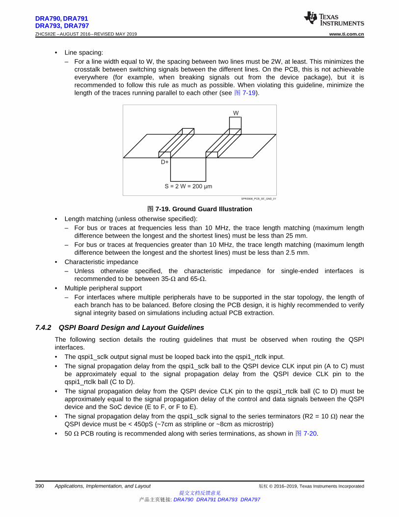
W
D+
S = 2 W = 200 µm
SPRS906_PCB_SE_GND_01
390
DRA790, DRA791DRA793, DRA797ZHCSII2E –AUGUST 2016–REVISED MAY 2019 www.ti.com.cn
提交文档反馈意见产品主页链接: DRA790 DRA791 DRA793 DRA797
Applications, Implementation, and Layout 版权 © 2016–2019, Texas Instruments Incorporated
• Line spacing:– For a line width equal to W, the spacing between two lines must be 2W, at least. This minimizes the
crosstalk between switching signals between the different lines. On the PCB, this is not achievableeverywhere (for example, when breaking signals out from the device package), but it isrecommended to follow this rule as much as possible. When violating this guideline, minimize thelength of the traces running parallel to each other (see 图 7-19).
图图 7-19. Ground Guard Illustration• Length matching (unless otherwise specified):
– For bus or traces at frequencies less than 10 MHz, the trace length matching (maximum lengthdifference between the longest and the shortest lines) must be less than 25 mm.
– For bus or traces at frequencies greater than 10 MHz, the trace length matching (maximum lengthdifference between the longest and the shortest lines) must be less than 2.5 mm.
• Characteristic impedance– Unless otherwise specified, the characteristic impedance for single-ended interfaces is
recommended to be between 35-Ω and 65-Ω.• Multiple peripheral support
– For interfaces where multiple peripherals have to be supported in the star topology, the length ofeach branch has to be balanced. Before closing the PCB design, it is highly recommended to verifysignal integrity based on simulations including actual PCB extraction.
7.4.2 QSPI Board Design and Layout GuidelinesThe following section details the routing guidelines that must be observed when routing the QSPIinterfaces.• The qspi1_sclk output signal must be looped back into the qspi1_rtclk input.• The signal propagation delay from the qspi1_sclk ball to the QSPI device CLK input pin (A to C) must
be approximately equal to the signal propagation delay from the QSPI device CLK pin to theqspi1_rtclk ball (C to D).
• The signal propagation delay from the QSPI device CLK pin to the qspi1_rtclk ball (C to D) must beapproximately equal to the signal propagation delay of the control and data signals between the QSPIdevice and the SoC device (E to F, or F to E).
• The signal propagation delay from the qspi1_sclk signal to the series terminators (R2 = 10 Ω) near theQSPI device must be < 450pS (~7cm as stripline or ~8cm as microstrip)
• 50 Ω PCB routing is recommended along with series terminations, as shown in 图 7-20.

A B C
D
E F
qspi1_sclk
qspi1_rtclk
R2
R2
R1
QSPI deviceclock input
QSPI deviceIOx, CS#
qspi1_d[x], qspi1_cs[y]
0 *Ω 10 Ω
10 Ω
Locate both R2 resistorsclose together near the QSPI device
SPRS906_PCB_QSPI_01
391
DRA790, DRA791DRA793, DRA797
www.ti.com.cn ZHCSII2E –AUGUST 2016–REVISED MAY 2019
提交文档反馈意见产品主页链接: DRA790 DRA791 DRA793 DRA797
Applications, Implementation, and Layout版权 © 2016–2019, Texas Instruments Incorporated
• Propagation delays and matching:– A to C = C to D = E to F.– Matching skew: < 60pS– A to B < 450pS– B to C = as small as possible (<60pS)
图图 7-20. QSPI Interface High Level Schematic
注注*0 Ω resistor (R1), located as close as possible to the qspi1_sclk pin, is placeholder for fine-tuning if needed.
7.5 Differential Interfaces
7.5.1 General Routing GuidelinesTo maximize signal integrity, proper routing techniques for differential signals are important for high-speeddesigns. The following general routing guidelines describe the routing guidelines for differential lanes anddifferential signals.• As much as possible, no other high-frequency signals must be routed in close proximity to the
differential pair.• Must be routed as differential traces on the same layer. The trace width and spacing must be chosen
to yield the differential impedance value recommended.• Minimize external components on differential lanes (like external ESD, probe points).• Through-hole pins are not recommended.• Differential lanes mustn’t cross image planes (ground planes).• No sharp bend on differential lanes.

392
DRA790, DRA791DRA793, DRA797ZHCSII2E –AUGUST 2016–REVISED MAY 2019 www.ti.com.cn
提交文档反馈意见产品主页链接: DRA790 DRA791 DRA793 DRA797
Applications, Implementation, and Layout 版权 © 2016–2019, Texas Instruments Incorporated
• Number of vias on the differential pairs must be minimized, and identical on each line of the differentialpair. In case of multiple differential lanes in the same interface, all lines should have the same numberof vias.
• Shielded routing is to be promoted as much as possible (for instance, signals must be routed oninternal layers that are inside power and/or ground planes).
7.5.2 USB 2.0 Board Design and Layout GuidelinesThis section discusses schematic guidelines when designing a universal serial bus (USB) system.
7.5.2.1 Background
Clock frequencies generate the main source of energy in a USB design. The USB differential DP/DM pairsoperate in high-speed mode at 480 Mbps. System clocks can operate at 12 MHz, 48 MHz, and 60 MHz.The USB cable can behave as a monopole antenna; take care to prevent RF currents from coupling ontothe cable.
When designing a USB board, the signals of most interest are:• Device interface signals: Clocks and other signal/data lines that run between devices on the PCB.• Power going into and out of the cable: The USB connector socket pin 1 (VBUS ) may be heavily
filtered and need only pass low frequency signals of less than ~100 KHz. The USB socket pin 4(analog ground) must be able to return the current during data transmission, and must be filteredsparingly.
• Differential twisted pair signals going out on cable, DP and DM: Depending upon the data transfer rate,these device terminals can have signals with fundamental frequencies of 240 MHz (high speed), 6MHz (full speed), and 750 kHz (low speed).
• External crystal circuit (device terminals XI and X0): 12 MHz, 19.2 MHz, 24 MHz, and 48 MHzfundamental. When using an external crystal as a reference clock, a 24 MHz and higher crystal ishighly recommended.
7.5.2.2 USB PHY Layout Guide
The following sections describe in detail the specific guidelines for USB PHY Layout.
7.5.2.2.1 General Routing and Placement
Use the following routing and placement guidelines when laying out a new design for the USB physicallayer (PHY). These guidelines help minimize signal quality and electromagnetic interference (EMI)problems on a four-or-more layer evaluation module (EVM).• Place the USB PHY and major components on the un-routed board first. For more details, see 节
7.5.2.2.2.3.• Route the high-speed clock and high-speed USB differential signals with minimum trace lengths.• Route the high-speed USB signals on the plane closest to the ground plane, whenever possible.• Route the high-speed USB signals using a minimum of vias and corners. This reduces signal
reflections and impedance changes.• When it becomes necessary to turn 90°, use two 45° turns or an arc instead of making a single 90°
turn. This reduces reflections on the signal traces by minimizing impedance discontinuities.• Do not route USB traces under or near crystals, oscillators, clock signal generators, switching
regulators, mounting holes, magnetic devices or IC’s that use or duplicate clock signals.• Avoid stubs on the high-speed USB signals because they cause signal reflections. If a stub is
unavoidable, then the stub should be less than 200 mils.• Route all high-speed USB signal traces over continuous planes (VCC or GND), with no interruptions.
Avoid crossing over anti-etch, commonly found with plane splits.

AnalogPower Supply
SoC Board
Ferrite Bead
DigitalPower Supply Ferrite Bead
0.1 µF 0.01 µF 0.001 µF 1 µF
0.1 µF 0.01 µF 0.001 µF 1 µF
SPRS906_PCB_USB20_01
AGND
DGND
393
DRA790, DRA791DRA793, DRA797
www.ti.com.cn ZHCSII2E –AUGUST 2016–REVISED MAY 2019
提交文档反馈意见产品主页链接: DRA790 DRA791 DRA793 DRA797
Applications, Implementation, and Layout版权 © 2016–2019, Texas Instruments Incorporated
7.5.2.2.2 Specific Guidelines for USB PHY Layout
The following sections describe in detail the specific guidelines for USB PHY Layout.
7.5.2.2.2.1 Analog, PLL, and Digital Power Supply Filtering
To minimize EMI emissions, add decoupling capacitors with a ferrite bead at power supply terminals forthe analog, phase-locked loop (PLL), and digital portions of the chip. Place this array as close to the chipas possible to minimize the inductance of the line and noise contributions to the system. An analog anddigital supply example is shown in 图 7-21. In case of multiple power supply pins with the same function,tie them up to a single low-impedance point in the board and then add the decoupling capacitors, inaddition to the ferrite bead. This array of caps and ferrite bead improve EMI and jitter performance. Takeboth EMI and jitter into account before altering the configuration.
图图 7-21. Suggested Array Capacitors and a Ferrite Bead to Minimize EMI
Consider the recommendations listed below to achieve proper ESD/EMI performance:• Use a 0.01 μF cap on each cable power VBUS line to chassis GND close to the USB connector pin.• Use a 0.01 μF cap on each cable ground line to chassis GND next to the USB connector pin.• If voltage regulators are used, place a 0.01 μF cap on both input and output. This is to increase the
immunity to ESD and reduce EMI. For other requirements, see the device-specific datasheet.
7.5.2.2.2.2 Analog, Digital, and PLL Partitioning
If separate power planes are used, they must be tied together at one point through a low-impedancebridge or preferably through a ferrite bead. Care must be taken to capacitively decouple each power railclose to the device. The analog ground, digital ground, and PLL ground must be tied together to the low-impedance circuit board ground plane.
7.5.2.2.2.3 Board Stackup
Because of the high frequencies associated with the USB, a printed circuit board with at least four layersis recommended; two signal layers separated by a ground and power layer as shown in 图 7-22.

Signal 1
Power Plane
GND Plane
Signal 2
SPRS906_PCB_USB20_02
394
DRA790, DRA791DRA793, DRA797ZHCSII2E –AUGUST 2016–REVISED MAY 2019 www.ti.com.cn
提交文档反馈意见产品主页链接: DRA790 DRA791 DRA793 DRA797
Applications, Implementation, and Layout 版权 © 2016–2019, Texas Instruments Incorporated
图图 7-22. Four-Layer Board Stack-Up
The majority of signal traces should run on a single layer, preferably SIGNAL1. Immediately next to thislayer should be the GND plane, which is solid with no cuts. Avoid running signal traces across a split inthe ground or power plane. When running across split planes is unavoidable, sufficient decoupling mustbe used. Minimizing the number of signal vias reduces EMI by reducing inductance at high frequencies.
7.5.2.2.2.4 Cable Connector Socket
Short the cable connector sockets directly to a small chassis ground plane (GND strap) that existsimmediately underneath the connector sockets. This shorts EMI (and ESD) directly to the chassis groundbefore it gets onto the USB cable. This etch plane should be as large as possible, but all the conductorscoming off connector pins 1 through 6 must have the board signal GND plane run under. If needed, scoopout the chassis GND strap etch to allow for the signal ground to extend under the connector pins. Notethat the etches coming from pins 1 and 4 (VBUS power and GND) should be wide and via-ed to theirrespective planes as soon as possible, respecting the filtering that may be in place between the connectorpin and the plane. See 图 7-23 for a schematic example.
Place a ferrite in series with the cable shield pins near the USB connector socket to keep EMI from gettingonto the cable shield. The ferrite bead between the cable shield and ground may be valued between 10 Ωand 50 Ω at 100 MHz; it should be resistive to approximately 1 GHz. To keep EMI from getting onto thecable bus power wire (a very large antenna) a ferrite may be placed in series with cable bus power,VBUS, near the USB connector pin 1. The ferrite bead between connector pin 1 and bus power may bevalued between 47 Ω and approximately 1000 Ω at 100 MHz. It should continue being resistive out toapproximately 1 GHz, as shown in 图 7-23.

Trace
3W 3W
W
SPRS906_PCB_USB20_04
U2Ferrite Bead
VBUS
U1
USB Socket
5
4
3
2
1
6
SHIELD_GND
GND
DP
DM
+5 V
SHIELD_GND
Ferrite Bead
SPRS906_PCB_USB20_03
395
DRA790, DRA791DRA793, DRA797
www.ti.com.cn ZHCSII2E –AUGUST 2016–REVISED MAY 2019
提交文档反馈意见产品主页链接: DRA790 DRA791 DRA793 DRA797
Applications, Implementation, and Layout版权 © 2016–2019, Texas Instruments Incorporated
图图 7-23. USB Connector
7.5.2.2.2.5 Clock Routings
To address the system clock emissions between devices, place a ~10 to 130 Ω resistor in series with theclock signal. Use a trial and error method of looking at the shape of the clock waveform on a high-speedoscilloscope and of tuning the value of the resistance to minimize waveform distortion. The value on thisresistor should be as small as possible to get the desired effect. Place the resistor close to the devicegenerating the clock signal. If an external crystal is used, follow the guidelines detailed in the Selectionand Specification of Crystals for Texas Instruments USB 2.0 Devices (SLLA122).
When routing the clock traces from one device to another, try to use the 3W spacing rule. The distancefrom the center of the clock trace to the center of any adjacent signal trace should be at least three timesthe width of the clock trace. Many clocks, including slow frequency clocks, can have fast rise and falltimes. Using the 3W rule cuts down on crosstalk between traces. In general, leave space between each ofthe traces running parallel between the devices. Avoid using right angles when routing traces to minimizethe routing distance and impedance discontinuities. For further protection from crosstalk, run guard tracesbeside the clock signals (GND pin to GND pin), if possible. This lessens clock signal coupling, as shown in图 7-24.
图图 7-24. 3W Spacing Rule

Power Pins
USB PHY
0.1 µF
0.001 µF
X1
X0
XTAL
SPRS906_PCB_USB20_05
396
DRA790, DRA791DRA793, DRA797ZHCSII2E –AUGUST 2016–REVISED MAY 2019 www.ti.com.cn
提交文档反馈意见产品主页链接: DRA790 DRA791 DRA793 DRA797
Applications, Implementation, and Layout 版权 © 2016–2019, Texas Instruments Incorporated
7.5.2.2.2.6 Crystals/Oscillator
Keep the crystal and its load capacitors close to the USB PHY pins, XI and XO (see 图 7-25). Note thatfrequencies from power sources or large capacitors can cause modulations within the clock and shouldnot be placed near the crystal. In these instances, errors such as dropped packets occur. A placeholderfor a resistor, in parallel with the crystal, can be incorporated in the design to assist oscillator startup.
Power is proportional to the current squared. The current is I = C × dv/dt, because dv/dt is a function ofthe PHY, current is proportional to the capacitive load. Cutting the load to 1/2 decreases the current by 1/2and the power to 1/4 of the original value. For more details on crystal selection, see the Selection andSpecification of Crystals for Texas Instruments USB 2.0 Devices (SLLA122).
图图 7-25. Power Supply and Clock Connection to the USB PHY
7.5.2.2.2.7 DP/DM Trace
Place the USB PHY as close as possible to the USB 2.0 connector. The signal swing during high-speedoperation on the DP/DM lines is relatively small (400 mV ± 10%), so any differential noise picked up onthe twisted pair can affect the received signal. When the DP/DM traces do not have any shielding, thetraces tend to behave like an antenna and picks up noise generated by the surrounding components inthe environment. To minimize the effect of this behavior:• DP/DM traces should always be matched lengths and must be no more than 4 inches in length;
otherwise, the eye opening may be degraded (see 图 7-26).• Route DP/DM traces close together for noise rejection on differential signals, parallel to each other and
within two mils in length of each other. The measurement for trace length must be started fromdevice's balls.
• A high-speed USB connection is made through a shielded, twisted pair cable with a differentialcharacteristic impedance of 90 Ω ±15%. In layout, the impedance of DP and DM should each be 45 Ω± 10%.
• DP/DM traces should not have any extra components to maintain signal integrity. For example, tracescannot be routed to two USB connectors.

Minimize
This Distance
USB PHY Connector
D+
D-
VBUS
GND
D-
D+
Cable
Connector
SPRS906_PCB_USB20_06
397
DRA790, DRA791DRA793, DRA797
www.ti.com.cn ZHCSII2E –AUGUST 2016–REVISED MAY 2019
提交文档反馈意见产品主页链接: DRA790 DRA791 DRA793 DRA797
Applications, Implementation, and Layout版权 © 2016–2019, Texas Instruments Incorporated
图图 7-26. USB PHY Connector and Cable Connector
7.5.2.2.2.8 DP/DM Vias
When a via must be used, increase the clearance size around it to minimize its capacitance. Each viaintroduces discontinuities in the signal’s transmission line and increases the chance of picking upinterference from the other layers of the board. Be careful when designing test points on twisted pair lines;through-hole pins are not recommended.
7.5.2.2.2.9 Image Planes
An image plane is a layer of copper (voltage plane or ground plane), physically adjacent to a signal routingplane. Use of image planes provides a low impedance, shortest possible return path for RF currents. For aUSB board, the best image plane is the ground plane because it can be used for both analog and digitalcircuits.• Do not route traces so they cross from one plane to the other. This can cause a broken RF return path
resulting in an EMI radiating loop as shown in 图 7-27. This is important for higher frequency orrepetitive signals. Therefore, on a multi-layer board, it is best to run all clock signals on the signalplane above a solid ground plane.
• Avoid crossing the image power or ground plane boundaries with high-speed clock signal tracesimmediately above or below the separated planes. This also holds true for the twisted pair signals (DP,DM). Any unused area of the top and bottom signal layers of the PCB can be filled with copper that isconnected to the ground plane through vias.

Analog Power Plane
Unwanted Capacitance
Digital Power Plane
SPRS906_PCB_USB20_08
Don't Do
SPRS906_PCB_USB20_07
398
DRA790, DRA791DRA793, DRA797ZHCSII2E –AUGUST 2016–REVISED MAY 2019 www.ti.com.cn
提交文档反馈意见产品主页链接: DRA790 DRA791 DRA793 DRA797
Applications, Implementation, and Layout 版权 © 2016–2019, Texas Instruments Incorporated
图图 7-27. Do Not Cross Plane Boundaries• Do not overlap planes that do not reference each other. For example, do not overlap a digital power
plane with an analog power plane as this produces a capacitance between the overlapping areas thatcould pass RF emissions from one plane to the other, as shown in 图 7-28.
图图 7-28. Do Not Overlap Planes• Avoid image plane violations. Traces that route over a slot in an image plane results in a possible RF
return loop, as shown in 图 7-29.

Slot in Image Plane
RF ReturnCurrent
Bad
Slot in Image Plane
RF ReturnCurrent
BetterSPRS906_PCB_USB20_09
399
DRA790, DRA791DRA793, DRA797
www.ti.com.cn ZHCSII2E –AUGUST 2016–REVISED MAY 2019
提交文档反馈意见产品主页链接: DRA790 DRA791 DRA793 DRA797
Applications, Implementation, and Layout版权 © 2016–2019, Texas Instruments Incorporated
图图 7-29. Do Not Violate Image Planes
7.5.2.2.2.10 Power Regulators
Switching power regulators are a source of noise and can cause noise coupling if placed close to sensitiveareas on a circuit board. Therefore, the switching power regulator should be kept away from the DP/DMsignals, the external clock crystal (or clock oscillator), and the USB PHY.
7.5.2.3 References• USB 2.0 Specification, Intel, 2000, http://www.usb.org/developers/docs/• High Speed USB Platform Design Guidelines, Intel, 2000,
http://www.intel.com/technology/usb/download/usb2dg_R1_0.pdf• Selection and Specification of Crystals for Texas Instruments USB 2.0 Devices (SLLA122)
7.5.3 USB 3.0 Board Design and Layout GuidelinesThis section provides the timing specification for the USB3.0 (USB1 in the device) interface as a PCBdesign and manufacturing specification. The design rules constrain PCB trace length, PCB trace skew,signal integrity, cross-talk, and signal timing. TI has performed the simulation and system design work toensure the USB3.0 interface requirements are met. The design rules stated within this document aretargeted at DEVICE mode electrical compliance. HOST mode and/or systems that do not include the 3mUSB cable and far-end 11-inch PCB trace required by DEVICE mode compliance testing may not needthe complete list of optimizations shown in this document; however, applying these optimizations to HOSTmode systems will lead to optimal DEVICE mode performance.
7.5.3.1 USB 3.0 interface introduction
The USB 3.0 has two unidirectional differential pairs: TXp/TXn pair and RXp/RXn pair. AC coupling capsare needed on the board for TX traces.
图 7-30 present high level schematic diagram for USB 3.0 interface.

CMF
CMF
AC Cap
AC Cap
SoC TX
SoC RX
via
via
via
via
US
B 3
.0 c
onnecto
r
SPRS85x_PCB_USB30_2
Device
usb_txp0
usb_txn0
usb_rxp0
usb_rxn0
CMF
CMF
AC Caps
Place near connector, and keep routing short
Vias (if necessary)
Vias (if necessary)Vias (if necessary)
Vias (if necessary)
US
B 3
.0
GN
DG
ND
GN
DG
ND
US
B 3
.0 c
onnecto
r
SPRS85x_PCB_USB30_1
400
DRA790, DRA791DRA793, DRA797ZHCSII2E –AUGUST 2016–REVISED MAY 2019 www.ti.com.cn
提交文档反馈意见产品主页链接: DRA790 DRA791 DRA793 DRA797
Applications, Implementation, and Layout 版权 © 2016–2019, Texas Instruments Incorporated
图图 7-30. USB 3.0 Interface High Level Schematic
注注ESD components should be on a PCB layer next to a system GND plane layer so theinductance of the via to GND will be minimal.
If vias are used, place the vias near the AC Caps or CMFs and under the SoC BGA, ifnecessary.
图 7-31 present placement diagram for USB 3.0 interface.
图图 7-31. USB 3.0 placement diagram
表表 7-9. USB1 Component Reference
INTERFACE COMPONENT SUPPLIER PART NUMBER
USB3 PHYESD TI TPD1E05U06CMF Murata DLW21SN900HQ2
C - 100nF (typical size: 0201)

401
DRA790, DRA791DRA793, DRA797
www.ti.com.cn ZHCSII2E –AUGUST 2016–REVISED MAY 2019
提交文档反馈意见产品主页链接: DRA790 DRA791 DRA793 DRA797
Applications, Implementation, and Layout版权 © 2016–2019, Texas Instruments Incorporated
7.5.3.2 USB 3.0 General routing rules
Some general routing guidelines regarding USB 3.0:• Avoid crossing splits reference plane(s).• Shorter trace length is preferred.• Minimize the via usage and layer transition• Keep large spacing between TX and RX pairs.• Intra-lane delay mismatch between DP and DM less than 1ps. Same for RXp and RXn.• Distance between common mode filter (CMF) and ESD protection device should be as short as
possible• Distance between ESD protection device and USB connector should be as short as possible.• Distance between AC capacitors (TX only) and CMF should be as short as possible.• USB 3.0 signals should always be routed over an adjacent ground plane.
表 7-10 and 表 7-11 present routing specification and recommendations for USB1 in the device.
表表 7-10. USB1 Routing Specifications
PARAMETER MIN TYP MAX UNITDevice balls to USB 3.0 connector trace
length 3500 Mils
Skew within a differential pair 3 6 MilsNumber of stubs allowed on TX/RX traces 0 Stubs
TX/RX pair differential impedance 83 90 97 Ω
Number of vias on each TX/RX trace 2 ViasDifferential pair to any other trace spacing 2xDS 3xDS
Number of ground plane cuts allowed withinUSB3 routing region (except for specific
ground carving as explained in thisdocument)
0 Cuts
Number of layers between USB3.0 routingregion and reference ground plane 0 Layers
PCB trace width 6 MilsPCB BGA escape via pad size 18 MilsPCB BGA escape via hole size 10 Mils
1. Vias must be used in pairs and spaced equally along a signal path.2. DS = differential spacing of the traces.3. Exceptions may be necessary in the SoC package BGA area.4. GND guard-bands on the same layer may be closer, but should not be allowed to affect the impedance
of the differential pair routing. GND guard-bands to isolate USB3.0 differential pairs from all othersignals are recommended.
表表 7-11. USB1 Routing Recommendations
Item Description Reason
ESD location Place ESD component on same layer as connector (no via or stub toESD component)
Eliminate reflection loss from via& stub to ESD
ESD part number TPD1E05U06 Minimize capacitance (0.42pF)
CMF part number DLW21SN900HQ2 Manufacturer’s recommendeddevice
Connector Use USB3.0 connector with supporting s-parameter model Enable full signal chainsimulation
Carve Ground Carve GND underneath AC Caps, ESD, CMF, and connector Minimize capacitance under ESDand CMF

Layer2, GND: Gaps carved in GND underneathAC Caps, CMF, ESD, and connector.
Layer3, Signal: Implement as keep-outzone underneath carved GND areas.
Layer4, GND Plane underneath AC Caps,CMF, ESD, and connector.
SPRS85x_PCB_USB30_3
Top Layer: Routing from SoC throughAC Caps, CMF, and ESD to connector.
AC Cap
CMF
CMF
AC Cap
via
via
via
via
US
B 3
.0 c
onnecto
r
402
DRA790, DRA791DRA793, DRA797ZHCSII2E –AUGUST 2016–REVISED MAY 2019 www.ti.com.cn
提交文档反馈意见产品主页链接: DRA790 DRA791 DRA793 DRA797
Applications, Implementation, and Layout 版权 © 2016–2019, Texas Instruments Incorporated
表表 7-11. USB1 Routing Recommendations (continued)Item Description Reason
Round pads Minimize pad size and round the corners of the pads for the ESDand CMF components Minimize capacitance
ViasMax 2 vias per signal trace. If vias are required, place vias close to
the AC Caps and CMFs. Vias under the SoC grid array may be usedif necessary to route signals away from BGA pattern.
Vias significantly degrade signalintegrity at 2.5GHz
图 7-32 presents an example layout, demonstrating the “carve GND” concept.
图图 7-32. USB 3.0 Example “carve GND” layout
7.5.4 HDMI Board Design and Layout GuidelinesThis section provides the timing specification for the HDMI interface as a PCB design and manufacturingspecification. The design rules constrain PCB trace length, PCB trace skew, signal integrity, cross-talk,and signal timing. TI has performed the simulation and system design work to ensure the HDMI interfacerequirements are met. The design rules stated within this document are targeted at resolutions less thanor equal to 1080p60 with 8-bit color; deep color (10-bit) requires further signal integrity optimization.
7.5.4.1 HDMI Interface Schematic
The HDMI bus is separated into three main sections (HDMI Ethernet and the optional Audio ReturnChannel are not specifically supported by this Device):

CMF
CMF
CMF
CMF
HD
MI connecto
r
SPRS85x_PCB_HDMI_2
Device
HD
MI
hdmi_tx*-
hdmi_tx*+ CMF
Place near connector, and keep routing short
GN
DG
ND
HD
MI connecto
r
SPRS85x_PCB_HDMI_1
403
DRA790, DRA791DRA793, DRA797
www.ti.com.cn ZHCSII2E –AUGUST 2016–REVISED MAY 2019
提交文档反馈意见产品主页链接: DRA790 DRA791 DRA793 DRA797
Applications, Implementation, and Layout版权 © 2016–2019, Texas Instruments Incorporated
1. Transition Minimized Differential Signaling (TMDS) high speed digital video interface2. Display Data Channel (I2C bus for configuration and status exchange between two devices)3. Consumer Electronics Control (optional) for remote control of connected devices.
The DDC and CEC are low speed interfaces, so nothing special is required for PCB layout of thesesignals.
The TMDS channels are high speed differential pairs and therefore require the most care in layout.Specifications for TMDS layout are below.
图 7-33 shows the HDMI interface schematic.
图图 7-33. HDMI Interface High Level Schematic
图 7-34 presents placement diagram for HDMI interface.
图图 7-34. HDMI Placement Diagram
表表 7-12. HDMI Component Reference
INTERFACE DEVICE SUPPLIER PART NUMBER
HDMIESD TI TPD1E05U06CMF Murata DLW21SN900HQ2

404
DRA790, DRA791DRA793, DRA797ZHCSII2E –AUGUST 2016–REVISED MAY 2019 www.ti.com.cn
提交文档反馈意见产品主页链接: DRA790 DRA791 DRA793 DRA797
Applications, Implementation, and Layout 版权 © 2016–2019, Texas Instruments Incorporated
7.5.4.2 TMDS General Routing Guidelines
The TMDS signals are high speed differential pairs. Care must be taken in the PCB layout of these signalsto ensure good signal integrity.
The TMDS differential signal traces must be routed to achieve 100 Ohms (+/- 10%) differential impedanceand 60 ohms (+/-10%) single ended impedance. Single ended impedance control is required becausedifferential signals can’t be closely coupled on PCBs and therefore single ended impedance becomesimportant.
These impedances are impacted by trace width, trace spacing, distance to reference planes, and dielectricmaterial. Verify with a PCB design tool that the trace geometry for both data signal pairs results in asclose to 60 ohms impedance traces as possible. For best accuracy, work with your PCB fabricator toensure this impedance is met.
In general, closely coupled differential signal traces are not an advantage on PCBs. When differentialsignals are closely coupled, tight spacing and width control is necessary. Very small width and spacingvariations affect impedance dramatically, so tight impedance control can be more problematic to maintainin production.
Loosely coupled PCB differential signals make impedance control much easier. Wider traces and spacingmake obstacle avoidance easier, and trace width variations don’t affect impedance as much, therefore it’seasier to maintain accurate impedance over the length of the signal. The wider traces also show reducedskin effect and therefore often result in better signal integrity.
Some general routing guidelines regarding TMDS:• Avoid crossing splits reference plane(s).• Shorter trace length is preferred.• Distance between common mode filter (CMF) and ESD protection device should be as short as
possible• Distance between ESD protection device and HDMI connector should be as short as possible.
表 7-13 shows the routing specifications for the TMDS signals.
表表 7-13. TMDS Routing Specifications
PARAMETER MIN TYP MAX UNITDevice balls to HDMI header trace length 4000 MilsSkew within a differential pair 3 5 MilsNumber of stubs allowed on TMDS traces 0 stubsTMDS pair differential impedance 90 100 110 Ω
TMDS single-ended impedance 54 60 66 Ω
Number of vias on each TMDS trace 0 ViasTMDS differential pair to any other trace spacing(1) (2) (3) 2×DS 3xDS MilsNumber of ground plane cuts allowed within HDMI routing region (except for specificground carving as explained in this document) 0 Cuts
Number of layers between HDMI routing region and reference ground plane 0 LayersPCB trace width 4.4 Mils
(1) DS = differential spacing of the traces.(2) Exceptions may be necessary in the SoC package BGA area.(3) GND guard-bands may be closer, but should not be allowed to affect the impedance of the differential pair routing. GND guard-bands to
isolate HDMI differential pairs from all other signals is recommended.
表表 7-14. TDMS Routing Recommendations
Item Description ReasonESD part number TPD1E05U06 Minimize capacitance (0.42pF)

Top Layer: Routing from SoC through CMF,and ESD to connector.
Layer2, GND: Gaps carved in GND underneath,CMF, ESD, and connector.
AC Cap
CMF
CMF
via
via
AC Capvia
via
CMF
CMF
CMF
CMF
HD
MI connecto
r
SPRS85x_PCB_HDMI_3
405
DRA790, DRA791DRA793, DRA797
www.ti.com.cn ZHCSII2E –AUGUST 2016–REVISED MAY 2019
提交文档反馈意见产品主页链接: DRA790 DRA791 DRA793 DRA797
Applications, Implementation, and Layout版权 © 2016–2019, Texas Instruments Incorporated
表表 7-14. TDMS Routing Recommendations (continued)Item Description Reason
Carve Ground Carve GND underneath ESD and CMF Minimize capacitance under ESDand CMF
Round pads Reduce pad size and round the corners of the pads for the ESD andCMF components Minimize capacitance
Routing layer Route all signals only on the same layer as SoC Minimize reflection loss
图 7-35presents an example layout, demonstrating the “carve GND” concept.
图图 7-35. HDMI Example “carve GND” layout
7.5.4.3 TPD5S115
The TPD5S115 is an integrated HDMI companion chip solution. The device provides a regulated 5 Voutput (5VOUT) for sourcing the HDMI power line. The TPD5S115 exceeds the IEC61000-4-2 (Level 4)ESD protection level.
7.5.4.4 HDMI ESD Protection Device (Required)
Interfaces that connect to a cable such as HDMI generally require more ESD protection than can be builtinto the processor’s outputs. Therefore this HDMI interface requires the use of an ESD protection chip toprovide adequate ESD.
When selecting an ESD protection chip, choose the lowest capacitance ESD protection available tominimize signal degradation. In no case should be ESD protection circuit capacitance be more than 5pF.
TI manufactures these devices that provide ESD protection for HDMI signals such as the TPDxE05U06.For more information see the www.ti.com website.
7.5.4.5 PCB Stackup Specifications
表 7-15 shows the stackup and feature sizes required for HDMI.
表表 7-15. HDMI PCB Stackup Specifications
PARAMETER MIN TYP MAX UNITPCB Routing/Plane Layers 4 6 - Layers

406
DRA790, DRA791DRA793, DRA797ZHCSII2E –AUGUST 2016–REVISED MAY 2019 www.ti.com.cn
提交文档反馈意见产品主页链接: DRA790 DRA791 DRA793 DRA797
Applications, Implementation, and Layout 版权 © 2016–2019, Texas Instruments Incorporated
表表 7-15. HDMI PCB Stackup Specifications (continued)PARAMETER MIN TYP MAX UNIT
Signal Routing Layers 2 3 - LayersNumber of ground plane cuts allowed within HDMI routing
region - - 0 Cuts
Number of layers between HDMI routing region andreference ground plane - - 0 Layers
PCB Trace width 4 Mils
7.5.4.6 Grounding
Each TMDS channel has its own shield pin and they should be grounded to provide a return current pathfor the TMDS signal.
7.5.5 PCIe Board Design and Layout GuidelinesThe PCIe interface on the device provides support for a 5.0 Gbps lane with polarity inversion.
7.5.5.1 PCIe Connections and Interface Compliance
The PCIe interface on the device is compliant with the PCIe revision 3.0 specification. Please refer to thePCIe specifications for all connections that are described in it. Those recommendations are moredescriptive and exhaustive than what is possible here.
The use of PCIe compatible bridges and switches is allowed for interfacing with more than one otherprocessor or PCIe device.
7.5.5.1.1 Coupling Capacitors
AC coupling capacitors are required on the transmit data pair. 表 7-16 shows the requirements for thesecapacitors.
表表 7-16. PCIe AC Coupling Capacitors Requirements
PARAMETER MIN TYP MAX UNITPCIe AC coupling capacitor value 90 100 110 nF
PCIe AC coupling capacitor package size 0402 0603 EIA(1)(2)
(1) EIA LxW units, i.e., a 0402 is a 40x20 mils surface mount capacitor.(2) The physical size of the capacitor should be as small as practical. Use the same size on both lines in each pair placed side by side.
7.5.5.1.2 Polarity Inversion
The PCIe specification requires polarity inversion support. This means for layout purposes, polarity isunimportant because each signal can change its polarity on die inside the chip. This means polarity withina lane is unimportant for layout.
7.5.5.2 Non-standard PCIe connections
The following sections contain suggestions for any PCIe connection that is NOT described in the officialPCIe specification, such as an on-board Device to Device or Device to other PCIe compliant processorconnection.
7.5.5.2.1 PCB Stackup Specifications
表 7-17 shows the stackup and feature sizes required for these types of PCIe connections.

407
DRA790, DRA791DRA793, DRA797
www.ti.com.cn ZHCSII2E –AUGUST 2016–REVISED MAY 2019
提交文档反馈意见产品主页链接: DRA790 DRA791 DRA793 DRA797
Applications, Implementation, and Layout版权 © 2016–2019, Texas Instruments Incorporated
表表 7-17. PCIe PCB Stackup Specifications
PARAMETER MIN TYP MAX UNITNumber of ground plane cuts allowed within PCIe routing
region - - 0 Cuts
Number of layers between PCIe routing area and referenceplane (1) - - 0 Layers
PCB Routing clearance 4 MilsPCB Trace width 4 Mils
(1) A reference plane may be a ground plane or the power plane referencing the PCIe signals.
7.5.5.2.2 Routing Specifications
7.5.5.2.2.1 Impedance
The PCIe data signal traces must be routed to achieve 100-Ω (±10%) differential impedance and 60-Ω(±10%) single-ended impedance. The single-ended impedance is required because differential signals areextremely difficult to closely couple on PCBs and, therefore, single-ended impedance becomes important.These requirements are the same as those recommended in the PCIe Motherboard Checklist 1.0document, available from PCI-SIG (www.pcisig.com).
These impedances are impacted by trace width, trace spacing, distance between signals and referencingplanes, and dielectric material. Verify with a PCB design tool that the trace geometry for both data signalpairs result in as close to 100-Ω differential impedance and 60-Ω single-ended impedance as possible. Forbest accuracy, work with your PCB fabricator to ensure this impedance is met. See 表 7-18 below.
7.5.5.2.2.2 Differential Coupling
In general, closely coupled differential signal traces are not an advantage on PCBs. When differentialsignals are closely coupled, tight spacing and width control is necessary. Very small width and spacingvariations affect impedance dramatically, so tight impedance control can be more problematic to maintainin production. For PCBs with very tight space limitations (which are usually small) this can work, but formost PCBs, the loosely coupled option is probably best.
Loosely coupled PCB differential signals make impedance control much easier. Wider traces and spacingmake obstacle avoidance easier (because each trace is not so fixed in position relative to the other), andtrace width variations don’t affect impedance as much, therefore it’s easier to maintain an accurateimpedance over the length of the signal. For longer routes, the wider traces also show reduced skin effectand therefore often result in better signal integrity with a larger eye diagram opening.
表 7-18 shows the routing specifications for the PCIe data signals.
表表 7-18. PCI-E Routing Specifications
PARAMETER MIN TYP MAX UNITPCIe signal trace length (device balls to PCIe connector) 4700(1) MilsDifferential pair trace matching 5(2) MilsNumber of stubs allowed on PCIe traces(3) 0 stubsTX/RX pair differential impedance 90 100 110 Ω
TX/RX single-ended impedance 54 60 66 Ω
Pad size of vias on PCIe trace 25(4) MilsHole size of vias on PCIe trace 14 MilsNumber of vias on each PCIe trace 0 ViasPCIe differential pair to any other trace spacing 2×DS(5)
408
DRA790, DRA791DRA793, DRA797ZHCSII2E –AUGUST 2016–REVISED MAY 2019 www.ti.com.cn
提交文档反馈意见产品主页链接: DRA790 DRA791 DRA793 DRA797
Applications, Implementation, and Layout 版权 © 2016–2019, Texas Instruments Incorporated
(1) Beyond this, signal integrity may suffer.(2) For example, RXP0 within 5 Mils of RXN0.(3) Inline pads may be used for probing.(4) 35-Mil antipad maximum recommended.(5) DS = differential spacing of the PCIe traces.
表表 7-19. PCI-E Routing Recommendations
Item Description Reason
ESD part number None ESD suppression generally notused on PCIe
7.5.5.2.2.3 Pair Length Matching
Each signal in the differential pair should be matched to within 5 mils of its matching differential signal.Length matching should be done as close to the mismatch as possible.
7.5.5.3 LJCB_REFN/P Connections
A Common Refclk Rx Architecture is required to be used for the device PCIe interface. Specifically, twomodes of Common Refclk Rx Architecture are supported:• External REFCLK Mode: An common external 100MHz clock source is distributed to both the Device
and the link partner• Output REFCLK Mode: A 100MHz HCSL clock source is output by the device and used by the link
partner
In External REFCLK Mode, a high-quality, low-jitter, differential HCSL 100MHz clock source compliant tothe PCIe REFCLK AC Specifications should be provided on the Device’s ljcb_clkn / ljcb_clkp inputs.Alternatively, an LVDS clock source can be used with the following additional requirements:• External AC coupling capacitors described in 表 7-20 should be populated at the ljcb_clkn / ljcb_clkp
inputs.• All termination requirements (ex. parallel 100ohm termination) from the clock source manufacturer
should be followed.
In Output REFCLK Mode, the 100MHz clock from the Device’s DPLL_PCIE_REF should be output onthe Device’s ljcb_clkn / ljcb_clkp pins and used as the HCSL REFCLK by the link partner. External near-side termination to ground described in 表 7-21 is required on both of the ljcb_clkn / ljcb_clkp outputs inthis mode.
表表 7-20. LJCB_REFN/P Requirements in External LVDS REFCLK Mode
PARAMETER MIN TYP MAX UNITljcb_clkn / ljcb_clkp AC coupling capacitor value 100 nF
ljcb_clkn / ljcb_clkp AC coupling capacitor package size 0402 0603 EIA(1)(2)
(1) EIA LxW units, i.e., a 0402 is a 40x20 mils surface mount capacitor.(2) The physical size of the capacitor should be as small as practical. Use the same size on both lines in each pair placed side by side.
表表 7-21. LJCB_REFN/P Requirements in Output REFCLK Mode
PARAMETER MIN TYP MAX UNITljcb_clkn / ljcb_clkp near-side termination to ground value 47.5 50 52.5 Ohms
7.5.6 CSI2 Board Design and Routing GuidelinesThe MIPI D-PHY signals include the CSI2_0 camera serial interfaces to or from the Device.
For more information regarding the MIPI-PHY signals and corresponding balls, see 表 4-5, CSI2 SignalDescriptions.

409
DRA790, DRA791DRA793, DRA797
www.ti.com.cn ZHCSII2E –AUGUST 2016–REVISED MAY 2019
提交文档反馈意见产品主页链接: DRA790 DRA791 DRA793 DRA797
Applications, Implementation, and Layout版权 © 2016–2019, Texas Instruments Incorporated
For more information, you can also see the MIPI D-PHY specification v1-01-00_r0-03 (specifically theInterconnect and Lane Configuration and Annex B Interconnect Design Guidelines chapters).
In the next section, the PCB guidelines of the following differential interfaces are presented:• CSI2_0 MIPI CSI-2 at 1.5 Gbps
表 7-22 lists the MIPI D-PHY interface signals in the Device.
表表 7-22. MIPI D-PHY Interface Signals in the Device
SIGNAL NAME BOTTOM BALL SIGNAL NAME BOTTOM BALLcsi2_0_dx0 AC1 csi2_0_dy0 AB2csi2_0_dx1 AD1 csi2_0_dy1 AC2csi2_0_dx2 AE2 csi2_0_dy2 AD2
7.5.6.1 CSI2_0 MIPI CSI-2 (1.5 Gbps)
7.5.6.1.1 General Guidelines
The general guidelines for the PCB differential lines are:• Differential trace impedance Z0 = 100 Ω (minimum = 85 Ω, maximum = 115 Ω)• Total conductor length from the Device package pins to the peripheral device package pins is 25 to 30
cm with common FR4 PCB and flex materials.
注注Longer interconnect length can be supported at the expense of detailed simulations of thecomplete link including driver and receiver models.
The general rule of thumb for the space S = 2 × W is not designated (see 图 7-19, Guard Illustration). It isbecause although the S = 2 × W rule is a good rule of thumb, it is not always the best solution. Theelectrical performance will be checked with the frequency-domain specification. Even though the designerdoes not follow the S = 2 × W rule, the differential lines are ok if the lines satisfy the frequency-domainspecification.
Because the MIPI signals are used for low-power, single-ended signaling in addition to their high-speeddifferential implementation, the pairs must be loosely coupled.
7.5.6.1.2 Length Mismatch Guidelines
7.5.6.1.2.1 CSI2_0 MIPI CSI-2 (1.5 Gbps)
The guidelines of the length mismatch for CSI-2 are presented in 表 7-23.
表表 7-23. Length Mismatch Guidelines for CSI-2 (1.5 Gbps)
PARAMETER TYPICAL VALUE UNITOperating speed 1500 MbpsUI (bit time) 667 psIntralane skew Have to satisfy mode-conversion S parameters(1)
Interlane skew (UI / 50) 13.34 psPCB lane-to-lane skew (0.1 UI) 66.7 ps

xi_oscj vssa_oscj
Device
xo_oscj
Cf1
CrystalRd
Cf2
(Optional)
SPRS906_PCB_CLK_OSC_03
410
DRA790, DRA791DRA793, DRA797ZHCSII2E –AUGUST 2016–REVISED MAY 2019 www.ti.com.cn
提交文档反馈意见产品主页链接: DRA790 DRA791 DRA793 DRA797
Applications, Implementation, and Layout 版权 © 2016–2019, Texas Instruments Incorporated
(1) sdc12, scd21, scd12, sdc21, scd11, sdc11, scd22, and sdc22
7.5.6.1.3 Frequency-domain Specification Guidelines
After the PCB design is finished, the S-parameters of the PCB differential lines will be extracted with a 3DMaxwell Equation Solver such as the high-frequency structure simulator (HFSS) or equivalent, andcompared to the frequency-domain specification as defined in the section 7 of the MIPI AllianceSpecification for D-PHY Version v1-01-00_r0-03.
If the PCB lines satisfy the frequency-domain specification, the design is finished. Otherwise, the designneeds to be improved.
7.6 Clock Routing Guidelines
7.6.1 Oscillator Ground ConnectionAlthough the impedance of a ground plane is low it is, of course, not zero. Therefore, any noise current inthe ground plane causes a voltage drop in the ground.
图 7-36 shows the grounding scheme for high-frequency clock.
(1) j in *_osc = 0 or 1
图图 7-36. Grounding Scheme for High-Frequency Clock
7.7 DDR3 Board Design and Layout Guidelines
7.7.1 DDR3 General Board Layout GuidelinesTo help ensure good signaling performance, consider the following board design guidelines:• Avoid crossing splits in the power plane.• Minimize Vref noise.• Use the widest trace that is practical between decoupling capacitors and memory module.• Maintain a single reference.• Minimize ISI by keeping impedances matched.• Minimize crosstalk by isolating sensitive bits, such as strobes, and avoiding return path discontinuities.• Use proper low-pass filtering on the Vref pins.• Keep the stub length as short as possible.• Add additional spacing for on-clock and strobe nets to eliminate crosstalk.• Maintain a common ground reference for all bypass and decoupling capacitors.• Take into account the differences in propagation delays between microstrip and stripline nets when
evaluating timing constraints.

DDR_CLK
1
SPRS906_PCB_DDR3_01
411
DRA790, DRA791DRA793, DRA797
www.ti.com.cn ZHCSII2E –AUGUST 2016–REVISED MAY 2019
提交文档反馈意见产品主页链接: DRA790 DRA791 DRA793 DRA797
Applications, Implementation, and Layout版权 © 2016–2019, Texas Instruments Incorporated
7.7.2 DDR3 Board Design and Layout Guidelines
7.7.2.1 Board Designs
TI only supports board designs using DDR3 memory that follow the guidelines in this document. Theswitching characteristics and timing diagram for the DDR3 memory controller are shown in 表 7-24 and 图7-37.
表表 7-24. Switching Characteristics Over Recommended Operating Conditions for DDR3 MemoryController
NO. PARAMETER MIN MAX UNIT1 tc(DDR_CLK) Cycle time, DDR_CLK 1.5 2.5(1) ns
(1) This is the absolute maximum the clock period can be. Actual maximum clock period may be limited by DDR3 speed grade andoperating frequency (see the DDR3 memory device data sheet).
图图 7-37. DDR3 Memory Controller Clock Timing
7.7.2.2 DDR3 EMIF
The processor contains one DDR3 EMIF with one chip select.
7.7.2.3 DDR3 Device Combinations
Because there are several possible combinations of device counts and single- or dual-side mounting, 表7-25 summarizes the supported device configurations.
表表 7-25. Supported DDR3 Device Combinations
NUMBER OF DDR3 DEVICES DDR3 DATA DEVICE WIDTH(BITS) MIRRORED? DDR3 EMIF WIDTH (BITS)
1 16 N 162 8 Y(1) 162 16 N 322 16 Y(1) 323 16 N(3)(4) 324 8 N 324 8 Y(2) 325 8 N (3)(4) 32
(1) Two DDR3 devices are mirrored when one device is placed on the top of the board and the second device is placed on the bottom ofthe board.
(2) This is two mirrored pairs of DDR3 devices.(3) Three or five DDR3 device combination is not available on this device, but combination types are retained for consistency with the
DRA7xx family of devices.(4) The DDR memory connected to the DDR ECC bus does NOT need to be the same part number as the DDR memories connected to the
DDR data bus. However, some constraints do apply. When selecting a memory for the DDR ECC bus, the following restrictions must beadhered to as compared to the DDR memories on the data bus:– Match the same DDR3 speed grade– Have an equal number of internal banks– Have an equal number of columns– Have a greater or equal number of rows

412
DRA790, DRA791DRA793, DRA797ZHCSII2E –AUGUST 2016–REVISED MAY 2019 www.ti.com.cn
提交文档反馈意见产品主页链接: DRA790 DRA791 DRA793 DRA797
Applications, Implementation, and Layout 版权 © 2016–2019, Texas Instruments Incorporated
7.7.2.4 DDR3 Interface Schematic
7.7.2.4.1 32-Bit DDR3 Interface
The DDR3 interface schematic varies, depending upon the width of the DDR3 devices used and the widthof the bus used (16 or 32 bits). General connectivity is straightforward and very similar. 16-bit DDRdevices look like two 8-bit devices. 图 7-38 and 图 7-39 show the schematic connections for 32-bitinterfaces using x16 devices.
7.7.2.4.2 16-Bit DDR3 Interface
Note that the 16-bit wide interface schematic is practically identical to the 32-bit interface (see 图 7-38 and图 7-39); only the high-word DDR memories are removed and the unused DQS inputs are tied off.
When not using all or part of a DDR interface, the proper method of handling the unused pins is to tie offthe ddrx_dqsi pins to ground via a 1k-Ω resistor and to tie off the ddrx_dqsni pins to the correspondingvdds_ddrx supply via a 1k-Ω resistor. This needs to be done for each byte not used. Although thesesignals have internal pullups and pulldowns, external pullups and pulldowns provide additional protectionagainst external electrical noise causing activity on the signals.
The vdds_ddrx and ddrx_vref0 power supply pins need to be connected to their respective power supplieseven if ddrx is not being used. All other DDR interface pins can be left unconnected. Note that thesupported modes for use of the DDR EMIF are 32-bits wide, 16-bits wide, or not used.

DQ15
DQ8
UDM
UDQS
UDQS
DQ7
DQ0
LDM
LDQS
LDQS
CK
DQ15
UDM
UDQS
UDQS
ddr1_d31
ddr1_d24
16-Bit DDR3Devices
0.1 µF 0.1 µF 0.1 µF
32-bit DDR3 EMIF
ddr1_odt1
ddr1_csn1
ddr1_dqm3
ddr1_dqs3
ddr1_dqsn3
ddr1_d23
ddr1_d16
ddr1_dqm2
ddr1_dqs2
ddr1_dqsn2
ddr1_d15
ddr1_d8
ddr1_dqm1
ddr1_dqs1
ddr1_dqsn1
ddr1_d7
ddr1_d0
ddr1_dqm0
ddr1_dqs0
ddr1_dqsn0
ddr1_ck
ddr1_nck
ddr1_odt0
ddr1_csn0
ddr1_ba0
ddr1_ba1
ddr1_ba2
ddr1_a0
ddr1_a15
ddr1_casn
ddr1_rasn
ddr1_wen
ddr1_cke
ddr1_rst
ddr1_vref0
8
8
8
8
16
DQ8
DQ7
D08
LDM
LDQS
LDQS
CK
ODT
BA1
BA0
BA2
CS
A0
A15
CAS
RAS
WE
RST
CKE
ZQ
VREFDQ
VREFCA
ZQ
CK
CK
ODT
BA1
BA0
BA2
CS
A0
A15
CAS
RAS
WE
RST
CKE
ZQ
VREFDQ
VREFCA
ZQ
Zo
Zo
Zo
Zo
DDR_VREF
DDR_VTT
DDR_1V5
Termination is required. See terminator comments.Zo
Value determined according to the DDR memory device data sheet.ZQ
0.1 µF
SPRS906_PCB_DDR3_02
NC
NC
413
DRA790, DRA791DRA793, DRA797
www.ti.com.cn ZHCSII2E –AUGUST 2016–REVISED MAY 2019
提交文档反馈意见产品主页链接: DRA790 DRA791 DRA793 DRA797
Applications, Implementation, and Layout版权 © 2016–2019, Texas Instruments Incorporated
图图 7-38. 32-Bit, One-Bank DDR3 Interface Schematic Using Two 16-Bit DDR3 Devices

DQ7
DQ0
DM/TQS
DQS
DQS
DQ7
DQ0
DM/TQS
DQS
DQS
CK
ddrx_d31
ddrx_d24
8-Bit DDR3Devices
0.1 µF 0.1 µF 0.1 µF
32-bit DDR3 EMIF
ddrx_dqm3
ddrx_dqs3
ddrx_dqsn3
ddrx_d23
ddrx_d16
ddrx_dqm2
ddrx_dqs2
ddrx_dqsn2
ddrx_d15
ddrx_d8
ddrx_dqm1
ddrx_dqs1
ddrx_dqsn1
ddrx_d7
ddrx_d0
ddrx_dqm0
ddrx_dqs0
ddrx_dqsn0
ddrx_ck
ddrx_nck
ddrx_odt0
ddrx_csn0
ddrx_ba0
ddrx_ba1
ddrx_ba2
ddrx_a0
ddrx_a15
ddrx_casn
ddrx_rasn
ddrx_wen
ddrx_cke
ddrx_rst
ddrx_vref0
ddrx_odt1
ddrx_csn1
8
8
8
8
16
CK
ODT
BA1
BA0
BA2
CS
A0
A15
CAS
RAS
WE
RST
CKE
ZQ
VREFDQ
VREFCA
ZQ
CK
CK
ODT
BA1
BA0
BA2
CS
A0
A15
CAS
RAS
WE
RST
CKE
ZQ
VREFDQ
VREFCA
Termination is required. See terminator comments.Zo
Value determined according to the DDR memory device data sheet.ZQ
DQ7
DQ0
DM/TQS
DQS
DQS
CK
DQ7
DM/TQS
DQS
DQS
8-Bit DDR3Devices
0.1 µF 0.1 µF
DQ0
CK
ODT
BA1
BA0
BA2
CS
A0
A15
CAS
RAS
WE
RST
CKE
ZQ
VREFDQ
VREFCA
CK
CK
ODT
BA1
BA0
BA2
CS
A0
A15
CAS
RAS
WE
RST
CKE
ZQ
VREFDQ
VREFCA
ZQ
Zo
Zo
Zo
Zo
DDR_VREF
DDR_VTT
DDR_1V5
ZQ ZQ
TDQSNC
NC TDQS
TDQSNC
TDQSNC
0.1 µF
SPRS906_PCB_DDR3_03
NC
NC
414
DRA790, DRA791DRA793, DRA797ZHCSII2E –AUGUST 2016–REVISED MAY 2019 www.ti.com.cn
提交文档反馈意见产品主页链接: DRA790 DRA791 DRA793 DRA797
Applications, Implementation, and Layout 版权 © 2016–2019, Texas Instruments Incorporated
图图 7-39. 32-Bit, One-Bank DDR3 Interface Schematic Using Four 8-Bit DDR3 Devices

415
DRA790, DRA791DRA793, DRA797
www.ti.com.cn ZHCSII2E –AUGUST 2016–REVISED MAY 2019
提交文档反馈意见产品主页链接: DRA790 DRA791 DRA793 DRA797
Applications, Implementation, and Layout版权 © 2016–2019, Texas Instruments Incorporated
7.7.2.5 Compatible JEDEC DDR3 Devices
表 7-26 shows the parameters of the JEDEC DDR3 devices that are compatible with this interface.Generally, the DDR3 interface is compatible with DDR3-1333 devices in the x8 or x16 widths.
表表 7-26. Compatible JEDEC DDR3 Devices (Per Interface)
NO.
PARAMETER CONDITION MIN MAX UNIT
1 JEDEC DDR3 device speed grade(1) DDR clock rate = 400MHz DDR3-800 DDR3-1600400MHz< DDR clock rate ≤ 533MHz DDR3-1066 DDR3-1600533MHz< DDR clock rate ≤ 667MHz DDR3-1333 DDR3-1600
2 JEDEC DDR3 device bit width x8 x16 Bits3 JEDEC DDR3 device count(2) 2 4 Devices
(1) Refer to 表 7-24 Switching Characteristics Over Recommended Operating Conditions for DDR3 Memory Controller for the range ofsupported DDR clock rates.
(2) For valid DDR3 device configurations and device counts, see 节 7.7.2.4, 图 7-38, and 图 7-39.
7.7.2.6 PCB Stackup
The minimum stackup for routing the DDR3 interface is a six-layer stack up as shown in 表 7-27.Additional layers may be added to the PCB stackup to accommodate other circuitry, enhance SI/EMIperformance, or to reduce the size of the PCB footprint. Complete stackup specifications are provided in表 7-28.
表表 7-27. Six-Layer PCB Stackup Suggestion
LAYER TYPE DESCRIPTION1 Signal Top routing mostly vertical2 Plane Ground3 Plane Split power plane4 Plane Split power plane or Internal routing5 Plane Ground6 Signal Bottom routing mostly horizontal

416
DRA790, DRA791DRA793, DRA797ZHCSII2E –AUGUST 2016–REVISED MAY 2019 www.ti.com.cn
提交文档反馈意见产品主页链接: DRA790 DRA791 DRA793 DRA797
Applications, Implementation, and Layout 版权 © 2016–2019, Texas Instruments Incorporated
表表 7-28. PCB Stackup Specifications
NO. PARAMETER MIN TYP MAX UNITPS1 PCB routing/plane layers 6PS2 Signal routing layers 3PS3 Full ground reference layers under DDR3 routing region(1) 1PS4 Full 1.5-V power reference layers under the DDR3 routing region(1) 1PS5 Number of reference plane cuts allowed within DDR routing region(2) 0PS6 Number of layers between DDR3 routing layer and reference plane(3) 0PS7 PCB routing feature size 4 MilsPS8 PCB trace width, w 4 MilsPS9 Single-ended impedance, Zo 50 75 ΩPS10 Impedance control(5) Z-5 Z Z+5 Ω
(1) Ground reference layers are preferred over power reference layers. Be sure to include bypass caps to accommodate reference layerreturn current as the trace routes switch routing layers.
(2) No traces should cross reference plane cuts within the DDR routing region. High-speed signal traces crossing reference plane cutscreate large return current paths which can lead to excessive crosstalk and EMI radiation.
(3) Reference planes are to be directly adjacent to the signal plane to minimize the size of the return current loop.(4) An 18-mil pad assumes Via Channel is the most economical BGA escape. A 20-mil pad may be used if additional layers are available
for power routing. An 18-mil pad is required for minimum layer count escape.(5) Z is the nominal singled-ended impedance selected for the PCB specified by PS9.
7.7.2.7 Placement
图 7-40 shows the required placement for the processor as well as the DDR3 devices. The dimensions forthis figure are defined in 表 7-29. The placement does not restrict the side of the PCB on which thedevices are mounted. The ultimate purpose of the placement is to limit the maximum trace lengths andallow for proper routing space. For a 16-bit DDR memory system, the high-word DDR3 devices areomitted from the placement.
图图 7-40. Placement Specifications

417
DRA790, DRA791DRA793, DRA797
www.ti.com.cn ZHCSII2E –AUGUST 2016–REVISED MAY 2019
提交文档反馈意见产品主页链接: DRA790 DRA791 DRA793 DRA797
Applications, Implementation, and Layout版权 © 2016–2019, Texas Instruments Incorporated
表表 7-29. Placement Specifications DDR3
NO. PARAMETER MIN MAX UNITKOD31 X1 500 MilsKOD32 X2 600 MilsKOD33 X3 600 MilsKOD34 Y1 1800 MilsKOD35 Y2 600 MilsKOD36 DDR3 keepout region (1)
KOD37 Clearance from non-DDR3 signalto DDR3 keepout region (2) (3)
4 W
(1) DDR3 keepout region to encompass entire DDR3 routing area.(2) Non-DDR3 signals allowed within DDR3 keepout region provided they are separated from DDR3 routing layers by a ground plane.(3) If a device has more than one DDR controller, the signals from the other controller(s) are considered non-DDR3 and should be
separated by this specification.
7.7.2.8 DDR3 Keepout Region
The region of the PCB used for DDR3 circuitry must be isolated from other signals. The DDR3 keepoutregion is defined for this purpose and is shown in 图 7-41. The size of this region varies with theplacement and DDR routing. Additional clearances required for the keepout region are shown in 表 7-29.Non-DDR3 signals should not be routed on the DDR signal layers within the DDR3 keepout region. Non-DDR3 signals may be routed in the region, provided they are routed on layers separated from the DDRsignal layers by a ground layer. No breaks should be allowed in the reference ground layers in this region.In addition, the 1.5-V DDR3 power plane should cover the entire keepout region. Also note that the twosignals from the DDR3 controller should be separated from each other by the specification in 表 7-29 (seeKOD37).
图图 7-41. DDR3 Keepout Region

418
DRA790, DRA791DRA793, DRA797ZHCSII2E –AUGUST 2016–REVISED MAY 2019 www.ti.com.cn
提交文档反馈意见产品主页链接: DRA790 DRA791 DRA793 DRA797
Applications, Implementation, and Layout 版权 © 2016–2019, Texas Instruments Incorporated
7.7.2.9 Bulk Bypass Capacitors
Bulk bypass capacitors are required for moderate speed bypassing of the DDR3 and other circuitry. 表 7-30 contains the minimum numbers and capacitance required for the bulk bypass capacitors. Note that thistable only covers the bypass needs of the DDR3 controllers and DDR3 devices. Additional bulk bypasscapacitance may be needed for other circuitry.
表表 7-30. Bulk Bypass Capacitors
NO. PARAMETER MIN MAX UNIT1 vdds_ddrx bulk bypass capacitor count(1) 1 Devices2 vdds_ddrx bulk bypass total capacitance 22 μF
(1) These devices should be placed near the devices they are bypassing, but preference should be given to the placement of the high-speed (HS) bypass capacitors and DDR3 signal routing.
7.7.2.10 High-Speed Bypass Capacitors
High-speed (HS) bypass capacitors are critcal for proper DDR3 interface operation. It is particularlyimportant to minimize the parasitic series inductance of the HS bypass capacitors, processor/DDR power,and processor/DDR ground connections. 表 7-31 contains the specification for the HS bypass capacitorsas well as for the power connections on the PCB. Generally speaking, it is good to:1. Fit as many HS bypass capacitors as possible.2. Minimize the distance from the bypass cap to the pins/balls being bypassed.3. Use the smallest physical sized capacitors possible with the highest capacitance readily available.4. Connect the bypass capacitor pads to their vias using the widest traces possible and using the largest
hole size via possible.5. Minimize via sharing. Note the limites on via sharing shown in 表 7-31.
表表 7-31. High-Speed Bypass Capacitors
NO. PARAMETER MIN TYP MAX UNIT1 HS bypass capacitor package size(1) 0201 0402 10 Mils2 Distance, HS bypass capacitor to processor being bypassed(2)(3)(4) 400 Mils3 Processor HS bypass capacitor count per vdds_ddrx rail(12) See 表 7-3 and (11) Devices4 Processor HS bypass capacitor total capacitance per vdds_ddrx rail(12) See 表 7-3 and (11) μF5 Number of connection vias for each device power/ground ball(5) Vias6 Trace length from device power/ground ball to connection via(2) 35 70 Mils7 Distance, HS bypass capacitor to DDR device being bypassed(6) 150 Mils8 DDR3 device HS bypass capacitor count(7) 12 Devices9 DDR3 device HS bypass capacitor total capacitance(7) 0.85 μF10 Number of connection vias for each HS capacitor(8)(9) 2 Vias11 Trace length from bypass capacitor connect to connection via(2)(9) 35 100 Mils12 Number of connection vias for each DDR3 device power/ground ball(10) 1 Vias13 Trace length from DDR3 device power/ground ball to connection via(2)(8) 35 60 Mils
(1) LxW, 10-mil units, that is, a 0402 is a 40x20-mil surface-mount capacitor.(2) Closer/shorter is better.(3) Measured from the nearest processor power/ground ball to the center of the capacitor package.(4) Three of these capacitors should be located underneath the processor, between the cluster of DDR_1V5 balls and ground balls,
between the DDR interfaces on the package.(5) See the Via Channel™ escape for the processor package.(6) Measured from the DDR3 device power/ground ball to the center of the capacitor package.(7) Per DDR3 device.(8) An additional HS bypass capacitor can share the connection vias only if it is mounted on the opposite side of the board. No sharing of
vias is permitted on the same side of the board.

419
DRA790, DRA791DRA793, DRA797
www.ti.com.cn ZHCSII2E –AUGUST 2016–REVISED MAY 2019
提交文档反馈意见产品主页链接: DRA790 DRA791 DRA793 DRA797
Applications, Implementation, and Layout版权 © 2016–2019, Texas Instruments Incorporated
(9) An HS bypass capacitor may share a via with a DDR device mounted on the same side of the PCB. A wide trace should be used for theconnection and the length from the capacitor pad to the DDR device pad should be less than 150 mils.
(10) Up to a total of two pairs of DDR power/ground balls may share a via.(11) The capacitor recommendations in this data manual reflect only the needs of this processor. Please see the memory vendor’s
guidelines for determining the appropriate decoupling capacitor arrangement for the memory device itself.(12) For more information, see 节 7.3, Core Power Domains.
7.7.2.10.1 Return Current Bypass Capacitors
Use additional bypass capacitors if the return current reference plane changes due to DDR3 signalshopping from one signal layer to another. The bypass capacitor here provides a path for the return currentto hop planes along with the signal. As many of these return current bypass capacitors should be used aspossible. Because these are returns for signal current, the signal via size may be used for thesecapacitors.
7.7.2.11 Net Classes
表 7-32 lists the clock net classes for the DDR3 interface. 表 7-33 lists the signal net classes, andassociated clock net classes, for signals in the DDR3 interface. These net classes are used for thetermination and routing rules that follow.
表表 7-32. Clock Net Class Definitions
CLOCK NET CLASS processor PIN NAMESCK ddrx_ck/ddrx_nck
DQS0 ddrx_dqs0 / ddrx_dqsn0DQS1 ddrx_dqs1 / ddrx_dqsn1
DQS2(1) ddrx_dqs2 / ddrx_dqsn2DQS3(1) ddrx_dqs3 / ddrx_dqsn3
(1) Only used on 32-bit wide DDR3 memory systems.
表表 7-33. Signal Net Class Definitions
SIGNAL NET CLASS ASSOCIATED CLOCKNET CLASS processor PIN NAMES
ADDR_CTRL CK ddrx_ba[2:0], ddrx_a[14:0], ddrx_csnj, ddrx_casn, ddrx_rasn, ddrx_wen,ddrx_cke, ddrx_odti
DQ0 DQS0 ddrx_d[7:0], ddrx_dqm0DQ1 DQS1 ddrx_d[15:8], ddrx_dqm1
DQ2(1) DQS2 ddrx_d[23:16], ddrx_dqm2DQ3(1) DQS3 ddrx_d[31:24], ddrx_dqm3
(1) Only used on 32-bit wide DDR3 memory systems.
7.7.2.12 DDR3 Signal Termination
Signal terminators are required for the CK and ADDR_CTRL net classes. The data lines are terminated byODT and, thus, the PCB traces should be unterminated. Detailed termination specifications are covered inthe routing rules in the following sections.
7.7.2.13 VREF_DDR Routing
ddrx_vref0 (VREF) is used as a reference by the input buffers of the DDR3 memories as well as theprocessor. VREF is intended to be half the DDR3 power supply voltage and is typically generated with theDDR3 VDDS and VTT power supply. It should be routed as a nominal 20-mil wide trace with 0.1 µFbypass capacitors near each device connection. Narrowing of VREF is allowed to accommodate routingcongestion.

AS
-
AS
+
AS
-
AS
+
AS
-
AS
+
A1 A2
Processor
Differential Clock
Output Buffer
DDR Differential CK Input Buffers
Routed as Differential Pair
A3 A4 A3 AT
Rcp
Clock Parallel
Terminator
A1 A2 A3 A4 A3 AT
AS
-
AS
+
Rcp
Cac
DDR_1V5
0.1 µF
+
–
+ – + – + – + –
SPRS906_PCB_DDR3_06
420
DRA790, DRA791DRA793, DRA797ZHCSII2E –AUGUST 2016–REVISED MAY 2019 www.ti.com.cn
提交文档反馈意见产品主页链接: DRA790 DRA791 DRA793 DRA797
Applications, Implementation, and Layout 版权 © 2016–2019, Texas Instruments Incorporated
7.7.2.14 VTT
Like VREF, the nominal value of the VTT supply is half the DDR3 supply voltage. Unlike VREF, VTT isexpected to source and sink current, specifically the termination current for the ADDR_CTRL net classThevinen terminators. VTT is needed at the end of the address bus and it should be routed as a powersub-plane. VTT should be bypassed near the terminator resistors.
7.7.2.15 CK and ADDR_CTRL Topologies and Routing Definition
The CK and ADDR_CTRL net classes are routed in a fly-by topology. They are routed in a similar mannerand are length matched to minimize skew between them. CK is a bit more complicated because it runs ata higher transition rate and is differential. The following subsections show the topology and routing forvarious DDR3 configurations for CK and ADDR_CTRL. The figures in the following subsections define theterms for the routing specification detailed in 表 7-34. Balanced-T routing is not recommended.
7.7.2.15.1 Four DDR3 Devices
Four DDR3 devices are supported on the DDR EMIF consisting of four x8 DDR3 devices arranged as onebank (CS). These four devices may be mounted on a single side of the PCB, or may be mirrored in twopairs to save board space at a cost of increased routing complexity and parts on the backside of the PCB.
7.7.2.15.1.1 CK and ADDR_CTRL Topologies, Four DDR3 Devices
图 7-42 shows the topology of the CK net classes and 图 7-43 shows the topology for the correspondingADDR_CTRL net classes.
图图 7-42. CK Topology for Four x8 DDR3 Devices

AS
+
AS
-
=
Rcp
Rcp
Cac
DDR_1V5
0.1 µF
A1
A2 A3 A4 A3
A2 A3 A4 A3
A1
AT
AT
SPRS906_PCB_DDR3_08
A1 A2
Processor
Address and Control
Output Buffer
DDR Address and Control Input Buffers
A3 A4 A3 AT VTT
Address and Control
Terminator
Rtt
AS
AS
AS
AS
SPRS906_PCB_DDR3_07
421
DRA790, DRA791DRA793, DRA797
www.ti.com.cn ZHCSII2E –AUGUST 2016–REVISED MAY 2019
提交文档反馈意见产品主页链接: DRA790 DRA791 DRA793 DRA797
Applications, Implementation, and Layout版权 © 2016–2019, Texas Instruments Incorporated
图图 7-43. ADDR_CTRL Topology for Four x8 DDR3 Devices
7.7.2.15.1.2 CK and ADDR_CTRL Routing, Four DDR3 Devices
图 7-44 shows the CK routing for four DDR3 devices placed on the same side of the PCB. 图 7-45 showsthe corresponding ADDR_CTRL routing.
图图 7-44. CK Routing for Four Single-Side DDR3 Devices

AS
+
AS
-
=
Rcp
Rcp
Cac
DDR_1V5
0.1 µF
A1
A2 A3 A4
A2 A3 A4
A1
AT
AT
A3
A3
SPRS906_PCB_DDR3_10
AS=
Rtt
A1
A2 A3 A4 A3 AT VTT
SPRS906_PCB_DDR3_09
422
DRA790, DRA791DRA793, DRA797ZHCSII2E –AUGUST 2016–REVISED MAY 2019 www.ti.com.cn
提交文档反馈意见产品主页链接: DRA790 DRA791 DRA793 DRA797
Applications, Implementation, and Layout 版权 © 2016–2019, Texas Instruments Incorporated
图图 7-45. ADDR_CTRL Routing for Four Single-Side DDR3 Devices
To save PCB space, the four DDR3 memories may be mounted as two mirrored pairs at a cost ofincreased routing and assembly complexity. 图 7-46 and 图 7-47 show the routing for CK andADDR_CTRL, respectively, for four DDR3 devices mirrored in a two-pair configuration.
图图 7-46. CK Routing for Four Mirrored DDR3 Devices
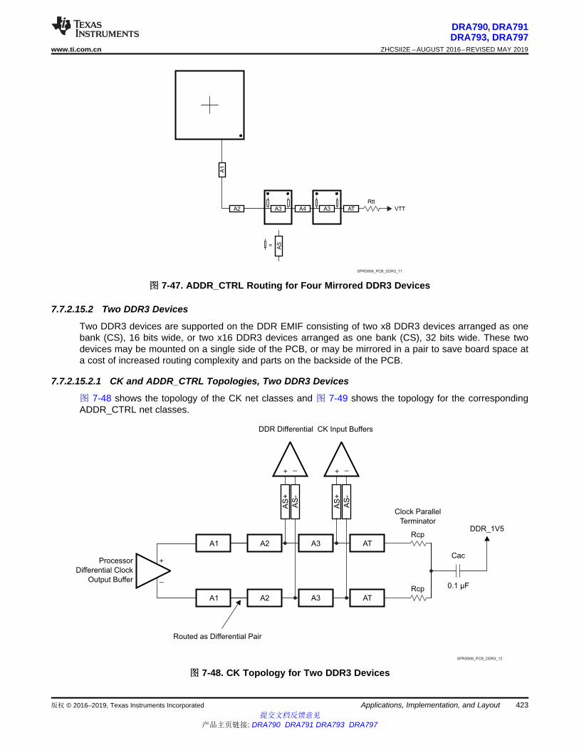
AS
-
AS
+
A1 A2
Processor
Differential Clock
Output Buffer
DDR Differential CK Input Buffers
Routed as Differential Pair
A3 AT
Rcp
Clock Parallel
Terminator
A1 A2 A3 AT
AS
-
AS
+
Rcp
Cac
DDR_1V5
0.1 µF
+
–
+ – + –
SPRS906_PCB_DDR3_12
AS=
Rtt
A1
A2 A3 A4 AT VTTA3
SPRS906_PCB_DDR3_11
423
DRA790, DRA791DRA793, DRA797
www.ti.com.cn ZHCSII2E –AUGUST 2016–REVISED MAY 2019
提交文档反馈意见产品主页链接: DRA790 DRA791 DRA793 DRA797
Applications, Implementation, and Layout版权 © 2016–2019, Texas Instruments Incorporated
图图 7-47. ADDR_CTRL Routing for Four Mirrored DDR3 Devices
7.7.2.15.2 Two DDR3 Devices
Two DDR3 devices are supported on the DDR EMIF consisting of two x8 DDR3 devices arranged as onebank (CS), 16 bits wide, or two x16 DDR3 devices arranged as one bank (CS), 32 bits wide. These twodevices may be mounted on a single side of the PCB, or may be mirrored in a pair to save board space ata cost of increased routing complexity and parts on the backside of the PCB.
7.7.2.15.2.1 CK and ADDR_CTRL Topologies, Two DDR3 Devices
图 7-48 shows the topology of the CK net classes and 图 7-49 shows the topology for the correspondingADDR_CTRL net classes.
图图 7-48. CK Topology for Two DDR3 Devices

AS
+
AS
-
=
Rcp
Rcp
Cac
DDR_1V5
0.1 µF
A1
A2 A3 AT
A2 A3 AT
A1
SPRS906_PCB_DDR3_14
A1 A2
Processor
Address and Control
Output Buffer
DDR Address and Control Input Buffers
A3 AT VTT
Address and Control
Terminator
Rtt
AS
AS
SPRS906_PCB_DDR3_13
424
DRA790, DRA791DRA793, DRA797ZHCSII2E –AUGUST 2016–REVISED MAY 2019 www.ti.com.cn
提交文档反馈意见产品主页链接: DRA790 DRA791 DRA793 DRA797
Applications, Implementation, and Layout 版权 © 2016–2019, Texas Instruments Incorporated
图图 7-49. ADDR_CTRL Topology for Two DDR3 Devices
7.7.2.15.2.2 CK and ADDR_CTRL Routing, Two DDR3 Devices
图 7-50 shows the CK routing for two DDR3 devices placed on the same side of the PCB. 图 7-51 showsthe corresponding ADDR_CTRL routing.
图图 7-50. CK Routing for Two Single-Side DDR3 Devices

AS
+
AS
-
=
Rcp
Rcp
Cac
DDR_1V5
0.1 µF
A1
A2 A3 AT
A2 A3 AT
A1
SPRS906_PCB_DDR3_16
AS=
Rtt
A1
A2 A3 AT VTT
SPRS906_PCB_DDR3_15
425
DRA790, DRA791DRA793, DRA797
www.ti.com.cn ZHCSII2E –AUGUST 2016–REVISED MAY 2019
提交文档反馈意见产品主页链接: DRA790 DRA791 DRA793 DRA797
Applications, Implementation, and Layout版权 © 2016–2019, Texas Instruments Incorporated
图图 7-51. ADDR_CTRL Routing for Two Single-Side DDR3 Devices
To save PCB space, the two DDR3 memories may be mounted as a mirrored pair at a cost of increasedrouting and assembly complexity. 图 7-52 and 图 7-53 show the routing for CK and ADDR_CTRL,respectively, for two DDR3 devices mirrored in a single-pair configuration.
图图 7-52. CK Routing for Two Mirrored DDR3 Devices

A1 A2
Processor
Differential Clock
Output Buffer
DDR Differential CK Input Buffer
Routed as Differential Pair
AT
Rcp
Clock Parallel
Terminator
A1 A2 AT
AS
-
AS
+
Rcp
Cac
DDR_1V5
0.1 µF
+
–
+ –
SPRS906_PCB_DDR3_18
AS=
Rtt
A1
A2 A3 AT VTT
SPRS906_PCB_DDR3_17
426
DRA790, DRA791DRA793, DRA797ZHCSII2E –AUGUST 2016–REVISED MAY 2019 www.ti.com.cn
提交文档反馈意见产品主页链接: DRA790 DRA791 DRA793 DRA797
Applications, Implementation, and Layout 版权 © 2016–2019, Texas Instruments Incorporated
图图 7-53. ADDR_CTRL Routing for Two Mirrored DDR3 Devices
7.7.2.15.3 One DDR3 Device
A single DDR3 device is supported on the DDR EMIF consisting of one x16 DDR3 device arranged asone bank (CS), 16 bits wide.
7.7.2.15.3.1 CK and ADDR_CTRL Topologies, One DDR3 Device
图 7-54 shows the topology of the CK net classes and 图 7-55 shows the topology for the correspondingADDR_CTRL net classes.
图图 7-54. CK Topology for One DDR3 Device

AS
+
AS
-
=
Rcp
Rcp
Cac
DDR_1V5
0.1 µF
A1
A2 AT
A2 AT
A1
SPRS906_PCB_DDR3_20
A1 A2
Processor
Address and Control
Output Buffer
DDR Address and Control Input Buffers
AT VTT
Address and Control
Terminator
Rtt
AS
SPRS906_PCB_DDR3_19
427
DRA790, DRA791DRA793, DRA797
www.ti.com.cn ZHCSII2E –AUGUST 2016–REVISED MAY 2019
提交文档反馈意见产品主页链接: DRA790 DRA791 DRA793 DRA797
Applications, Implementation, and Layout版权 © 2016–2019, Texas Instruments Incorporated
图图 7-55. ADDR_CTRL Topology for One DDR3 Device
7.7.2.15.3.2 CK and ADDR/CTRL Routing, One DDR3 Device
图 7-56 shows the CK routing for one DDR3 device placed on the same side of the PCB. 图 7-57 showsthe corresponding ADDR_CTRL routing.
图图 7-56. CK Routing for One DDR3 Device

Dn
Processor
DQ and DM
IO Buffer
DDR
DQ and DM
IO Buffer
n = 0, 1, 2, 3
SPRS906_PCB_DDR3_23
Processor
DQS
IO Buffer
DDR
DQS
IO Buffer
Routed Differentially
n = 0, 1, 2, 3
DQSn-
DQSn+
SPRS906_PCB_DDR3_22
AS=
Rtt
A1
A2 AT VTT
SPRS906_PCB_DDR3_21
428
DRA790, DRA791DRA793, DRA797ZHCSII2E –AUGUST 2016–REVISED MAY 2019 www.ti.com.cn
提交文档反馈意见产品主页链接: DRA790 DRA791 DRA793 DRA797
Applications, Implementation, and Layout 版权 © 2016–2019, Texas Instruments Incorporated
图图 7-57. ADDR_CTRL Routing for One DDR3 Device
7.7.2.16 Data Topologies and Routing Definition
No matter the number of DDR3 devices used, the data line topology is always point to point, so itsdefinition is simple.
Care should be taken to minimize layer transitions during routing. If a layer transition is necessary, it isbetter to transition to a layer using the same reference plane. If this cannot be accommodated, ensurethere are nearby ground vias to allow the return currents to transition between reference planes if bothreference planes are ground or vdds_ddr. Ensure there are nearby bypass capacitors to allow the returncurrents to transition between reference planes if one of the reference planes is ground. The goal is tominimize the size of the return current loops.
7.7.2.16.1 DQS and DQ/DM Topologies, Any Number of Allowed DDR3 Devices
DQS lines are point-to-point differential, and DQ/DM lines are point-to-point singled ended. 图 7-58 and 图7-59 show these topologies.
图图 7-58. DQS Topology
图图 7-59. DQ/DM Topology

Dn
n = 0, 1, 2, 3
DQ and DM
SPRS906_PCB_DDR3_25
DQSn+
DQSn-
n = 0, 1, 2, 3
Routed Differentially
DQS
SPRS906_PCB_DDR3_24
429
DRA790, DRA791DRA793, DRA797
www.ti.com.cn ZHCSII2E –AUGUST 2016–REVISED MAY 2019
提交文档反馈意见产品主页链接: DRA790 DRA791 DRA793 DRA797
Applications, Implementation, and Layout版权 © 2016–2019, Texas Instruments Incorporated
7.7.2.16.2 DQS and DQ/DM Routing, Any Number of Allowed DDR3 Devices
图 7-60 and 图 7-61 show the DQS and DQ/DM routing.
图图 7-60. DQS Routing With Any Number of Allowed DDR3 Devices
图图 7-61. DQ/DM Routing With Any Number of Allowed DDR3 Devices
7.7.2.17 Routing Specification
7.7.2.17.1 CK and ADDR_CTRL Routing Specification
Skew within the CK and ADDR_CTRL net classes directly reduces setup and hold margin and, thus, thisskew must be controlled. The only way to practically match lengths on a PCB is to lengthen the shortertraces up to the length of the longest net in the net class and its associated clock. A metric to establishthis maximum length is Manhattan distance. The Manhattan distance between two points on a PCB is thelength between the points when connecting them only with horizontal or vertical segments. A reasonabletrace route length is to within a percentage of its Manhattan distance. CACLM is defined as Clock AddressControl Longest Manhattan distance.

AS=
Rtt
A1
A2 A3 A4 A3 AT VTT
A8(A)
A8(A)
A8(A)
A8(A)
A8(A)
CACLMX
CACLMY
SPRS906_PCB_DDR3_26
430
DRA790, DRA791DRA793, DRA797ZHCSII2E –AUGUST 2016–REVISED MAY 2019 www.ti.com.cn
提交文档反馈意见产品主页链接: DRA790 DRA791 DRA793 DRA797
Applications, Implementation, and Layout 版权 © 2016–2019, Texas Instruments Incorporated
Given the clock and address pin locations on the processor and the DDR3 memories, the maximumpossible Manhattan distance can be determined given the placement. 图 7-62 and 图 7-63 show thisdistance for four loads and two loads, respectively. It is from this distance that the specifications on thelengths of the transmission lines for the address bus are determined. CACLM is determined similarly forother address bus configurations; that is, it is based on the longest net of the CK/ADDR_CTRL net class.For CK and ADDR_CTRL routing, these specifications are contained in 表 7-34.
A. It is very likely that the longest CK/ADDR_CTRL Manhattan distance will be for Address Input 8 (A8) on the DDR3memories. CACLM is based on the longest Manhattan distance due to the device placement. Verify the net class thatsatisfies this criteria and use as the baseline for CK/ADDR_CTRL skew matching and length control.
The length of shorter CK/ADDR_CTRL stubs as well as the length of the terminator stub are not included in thislength calculation. Non-included lengths are grayed out in the figure.
Assuming A8 is the longest, CALM = CACLMY + CACLMX + 300 mils.The extra 300 mils allows for routing down lower than the DDR3 memories and returning up to reach A8.
图图 7-62. CACLM for Four Address Loads on One Side of PCB

AS=
Rtt
A1
A2 A3 AT VTT
A8(A)
A8(A)
A8(A)
CACLMX
CACLMY
SPRS906_PCB_DDR3_27
431
DRA790, DRA791DRA793, DRA797
www.ti.com.cn ZHCSII2E –AUGUST 2016–REVISED MAY 2019
提交文档反馈意见产品主页链接: DRA790 DRA791 DRA793 DRA797
Applications, Implementation, and Layout版权 © 2016–2019, Texas Instruments Incorporated
A. It is very likely that the longest CK/ADDR_CTRL Manhattan distance will be for Address Input 8 (A8) on the DDR3memories. CACLM is based on the longest Manhattan distance due to the device placement. Verify the net class thatsatisfies this criteria and use as the baseline for CK/ADDR_CTRL skew matching and length control.
The length of shorter CK/ADDR_CTRL stubs as well as the length of the terminator stub are not included in thislength calculation. Non-included lengths are grayed out in the figure.
Assuming A8 is the longest, CALM = CACLMY + CACLMX + 300 mils.The extra 300 mils allows for routing down lower than the DDR3 memories and returning up to reach A8.
图图 7-63. CACLM for Two Address Loads on One Side of PCB
表表 7-34. CK and ADDR_CTRL Routing Specification(2)(3)
NO. PARAMETER MIN TYP MAX UNITCARS31 A1+A2 length 500(1) psCARS32 A1+A2 skew 29 psCARS33 A3 length 125 psCARS34 A3 skew(4) 6 psCARS35 A3 skew(5) 6 psCARS36 A4 length 125 psCARS37 A4 skew 6 psCARS38 AS length 5 17(1) psCARS39 AS skew 1.3 14(1) psCARS310 AS+/AS- length 5 12 psCARS311 AS+/AS- skew 1 psCARS312 AT length(6) 75 psCARS313 AT skew(7) 14 psCARS314 AT skew(8) 1 psCARS315 CK/ADDR_CTRL trace length 1020 psCARS316 Vias per trace 3(1) viasCARS317 Via count difference 1(15) viasCARS318 Center-to-center CK to other DDR3 trace spacing(9) 4wCARS319 Center-to-center ADDR_CTRL to other DDR3 trace spacing(9)(10) 4wCARS320 Center-to-center ADDR_CTRL to other ADDR_CTRL trace
spacing(9)3w

432
DRA790, DRA791DRA793, DRA797ZHCSII2E –AUGUST 2016–REVISED MAY 2019 www.ti.com.cn
提交文档反馈意见产品主页链接: DRA790 DRA791 DRA793 DRA797
Applications, Implementation, and Layout 版权 © 2016–2019, Texas Instruments Incorporated
表表 7-34. CK and ADDR_CTRL Routing Specification(2)(3) (continued)NO. PARAMETER MIN TYP MAX UNIT
CARS321 CK center-to-center spacing(11)(12)
CARS322 CK spacing to other net(9) 4wCARS323 Rcp(13) Zo-1 Zo Zo+1 Ω
CARS324 Rtt(13)(14) Zo-5 Zo Zo+5 Ω
(1) Max value is based upon conservative signal integrity approach. This value could be extended only if detailed signal integrity analysis ofrise time and fall time confirms desired operation.
(2) The use of vias should be minimized.(3) Additional bypass capacitors are required when using the DDR_1V5 plane as the reference plane to allow the return current to jump
between the DDR_1V5 plane and the ground plane when the net class switches layers at a via.(4) Non-mirrored configuration (all DDR3 memories on same side of PCB).(5) Mirrored configuration (one DDR3 device on top of the board and one DDR3 device on the bottom).(6) While this length can be increased for convenience, its length should be minimized.(7) ADDR_CTRL net class only (not CK net class). Minimizing this skew is recommended, but not required.(8) CK net class only.(9) Center-to-center spacing is allowed to fall to minimum 2w for up to 1250 mils of routed length.(10) The ADDR_CTRL net class of the other DDR EMIF is considered other DDR3 trace spacing.(11) CK spacing set to ensure proper differential impedance.(12) The most important thing to do is control the impedance so inadvertent impedance mismatches are not created. Generally speaking,
center-to-center spacing should be either 2w or slightly larger than 2w to achieve a differential impedance equal to twice the singleendedimpedance, Zo.
(13) Source termination (series resistor at driver) is specifically not allowed.(14) Termination values should be uniform across the net class.(15) Via count difference may increase by 1 only if accurate 3-D modeling of the signal flight times – including accurately modeled signal
propagation through vias – has been applied to ensure all segment skew maximums are not exceeded.
7.7.2.17.2 DQS and DQ Routing Specification
Skew within the DQS and DQ/DM net classes directly reduces setup and hold margin and thus this skewmust be controlled. The only way to practically match lengths on a PCB is to lengthen the shorter tracesup to the length of the longest net in the net class and its associated clock. As with CK and ADDR_CTRL,a reasonable trace route length is to within a percentage of its Manhattan distance. DQLMn is defined asDQ Longest Manhattan distance n, where n is the byte number. For a 32-bit interface, there are fourDQLMs, DQLM0-DQLM3. Likewise, for a 16-bit interface, there are two DQLMs, DQLM0-DQLM1.
注注It is not required, nor is it recommended, to match the lengths across all bytes. Lengthmatching is only required within each byte.
Given the DQS and DQ/DM pin locations on the processor and the DDR3 memories, the maximumpossible Manhattan distance can be determined given the placement. 图 7-64 shows this distance for fourloads. It is from this distance that the specifications on the lengths of the transmission lines for the databus are determined. For DQS and DQ/DM routing, these specifications are contained in 表 7-35.

DQLMX3
DQLMY0
DQLMY3 DQLMY2DB3
DQLMX2
DB2
3 2 1
DQ[23:31]/DM3/DQS3
0
DQ[16:23]/DM2/DQS2
DQLMX1
DB1
DB0
DQLMX0
DQ[8:15]/DM1/DQS1
DQ[0:7]/DM0/DQS0
DQLMY1
DB0 - DB3 represent data bytes 0 - 3.
SPRS906_PCB_DDR3_28
433
DRA790, DRA791DRA793, DRA797
www.ti.com.cn ZHCSII2E –AUGUST 2016–REVISED MAY 2019
提交文档反馈意见产品主页链接: DRA790 DRA791 DRA793 DRA797
Applications, Implementation, and Layout版权 © 2016–2019, Texas Instruments Incorporated
There are four DQLMs, one for each byte (32-bit interface). Each DQLM is the longest Manhattan distance of thebyte; therefore:DQLM0 = DQLMX0 + DQLMY0DQLM1 = DQLMX1 + DQLMY1DQLM2 = DQLMX2 + DQLMY2DQLM3 = DQLMX3 + DQLMY3
图图 7-64. DQLM for Any Number of Allowed DDR3 Devices
表表 7-35. Data Routing Specification(2)
NO. PARAMETER MIN TYP MAX UNITDRS31 DB0 length 340 psDRS32 DB1 length 340 psDRS33 DB2 length 340 psDRS34 DB3 length 340 psDRS35 DBn skew(3) 5 psDRS36 DQSn+ to DQSn- skew 1 psDRS37 DQSn to DBn skew(3)(4) 5(10) psDRS38 Vias per trace 2(1) viasDRS39 Via count difference 0(10) viasDRS310 Center-to-center DBn to other DDR3 trace spacing(6) 4 w(5)
DRS311 Center-to-center DBn to other DBn trace spacing(7) 3 w(5)
DRS312 DQSn center-to-center spacing(8)(9)
DRS313 DQSn center-to-center spacing to other net 4 w(5)
(1) Max value is based upon conservative signal integrity approach. This value could be extended only if detailed signal integrity analysis ofrise time and fall time confirms desired operation.
(2) External termination disallowed. Data termination should use built-in ODT functionality.(3) Length matching is only done within a byte. Length matching across bytes is neither required nor recommended.(4) Each DQS pair is length matched to its associated byte.(5) Center-to-center spacing is allowed to fall to minimum 2w for up to 1250 mils of routed length.(6) Other DDR3 trace spacing means other DDR3 net classes not within the byte.(7) This applies to spacing within the net classes of a byte.(8) DQS pair spacing is set to ensure proper differential impedance.(9) The most important thing to do is control the impedance so inadvertent impedance mismatches are not created. Generally speaking,
center-to-center spacing should be either 2w or slightly larger than 2w to achieve a differential impedance equal to twice the singleendedimpedance, Zo.
(10) Via count difference may increase by 1 only if accurate 3-D modeling of the signal flight times – including accurately modeled signalpropagation through vias – has been applied to ensure DBn skew and DQSn to DBn skew maximums are not exceeded.

434
DRA790, DRA791DRA793, DRA797ZHCSII2E –AUGUST 2016–REVISED MAY 2019 www.ti.com.cn
提交文档反馈意见产品主页链接: DRA790 DRA791 DRA793 DRA797
Device and Documentation Support 版权 © 2016–2019, Texas Instruments Incorporated
8 Device and Documentation Support
TI offers an extensive line of development tools, including methods to evaluate the performance of theprocessors, generate code, develop algorithm implementations, and fully integrate and debug softwareand hardware modules as listed below.
8.1 Device NomenclatureTo designate the stages in the product development cycle, TI assigns prefixes to the part numbers of allmicroprocessors (MPUs) and support tools. Each device has one of three prefixes: X, P, or null (no prefix)(for example, DRA79x). Texas Instruments recommends two of three possible prefix designators for itssupport tools: TMDX and TMDS. These prefixes represent evolutionary stages of product developmentfrom engineering prototypes (TMDX) through fully qualified production devices and tools (TMDS).
Device development evolutionary flow:X Experimental device that is not necessarily representative of the final device's electrical
specifications and may not use production assembly flow.P Prototype device that is not necessarily the final silicon die and may not necessarily meet
final electrical specifications.null Production version of the silicon die that is fully qualified.
Support tool development evolutionary flow:TMDX Development-support product that has not yet completed Texas Instruments internal
qualification testing.TMDS Fully-qualified development-support product.
X and P devices and TMDX development-support tools are shipped against the following disclaimer:
"Developmental product is intended for internal evaluation purposes."
Production devices and TMDS development-support tools have been characterized fully, and the qualityand reliability of the device have been demonstrated fully. TI's standard warranty applies.
Predictions show that prototype devices (X or P) have a greater failure rate than the standard productiondevices. Texas Instruments recommends that these devices not be used in any production systembecause their expected end-use failure rate still is undefined. Only qualified production devices are to beused.
For orderable part numbers of DRA79x devices in the CBD package type, see the Package OptionAddendum of this document, the TI website (ti.com), or contact your TI sales representative.
For additional description of the device nomenclature markings on the die, see the DRA79x SoC forAutomotive Infotainment Silicon Revision 2.1, 2.0.
8.1.1 Standard Package Symbolization
注注Some devices may have a cosmetic circular marking visible on the top of the device packagewhich results from the production test process. In addition, some devices may also show acolor variation in the package substrate which results from the substrate manufacturer.These differences are cosmetic only with no reliability impact.

SPRS906_PACK_01
JACINTO
aBBBBBBrzYPPPQ1
XXXXXXXPIN ONE INDICATOR
O
G1YYY ZZZ
435
DRA790, DRA791DRA793, DRA797
www.ti.com.cn ZHCSII2E –AUGUST 2016–REVISED MAY 2019
提交文档反馈意见产品主页链接: DRA790 DRA791 DRA793 DRA797
Device and Documentation Support版权 © 2016–2019, Texas Instruments Incorporated
图图 8-1. Printed Device Reference
8.1.2 Device Naming Convention
表表 8-1. Nomenclature Description
FIELD PARAMETER FIELD DESCRIPTION VALUE DESCRIPTIONa Device evolution
stage(1)X PrototypeP Preproduction (production test flow, no reliability data)
BLANK ProductionBBBBBB(3) Base production part
numberDRA790 J6RSP Low TierDRA791 J6RSP Mid TierDRA793 J6RSP High TierDRA797 J6RSP Super High Tier
r Device revision BLANK SR 1.0A SR 2.0B SR 2.1
z Device Speed A Indicates the speed grade for each of the cores in the device. For moreinformation see 表 3-1, Device Comparison Table.B
DH
OTHERY Device type G General purpose (Prototype and Production)
E Emulation (E) devicesS High-Security device, Secure Boot SupportedD High security prototype devices with TI Development keys (D)Yn Letter followed by number indicates HS device with customer key
PPP Package designator CBD CBD S-PBGA-N538 (17mm × 17mm) PackageQ1 Automotive Designator BLANK Not meeting automotive qualification
Q1 Meeting Q100 equal requirements, with exceptions as specified in DM.XXXXXXX Lot Trace Code

436
DRA790, DRA791DRA793, DRA797ZHCSII2E –AUGUST 2016–REVISED MAY 2019 www.ti.com.cn
提交文档反馈意见产品主页链接: DRA790 DRA791 DRA793 DRA797
Device and Documentation Support 版权 © 2016–2019, Texas Instruments Incorporated
表表 8-1. Nomenclature Description (continued)FIELD PARAMETER FIELD DESCRIPTION VALUE DESCRIPTION
YYY Production Code, For TI use onlyZZZ Production Code, For TI use onlyO Pin one designatorG1 ECAT—Green package designator
(1) To designate the stages in the product development cycle, TI assigns prefixes to the part numbers. These prefixes representevolutionary stages of product development from engineering prototypes through fully qualified production devices.Prototype devices are shipped against the following disclaimer:“This product is still under development and is intended for internal evaluation purposes.”Notwithstanding any provision to the contrary, TI makes no warranty expressed, implied, or statutory, including any implied warranty ofmerchantability of fitness for a specific purpose, of this device.
(2) Applies to device max junction temperature.(3) X777 base part number with X speed grade indicator is the part number for the superset device. Software should constrain the features
and speed used to match the intended production device.
注注BLANK in the symbol or part number is collapsed so there are no gaps between characters.
8.2 Tools and SoftwareThe following products support development for DRA79x platforms:
Design Kits and Evaluation ModulesDRA79x Evaluation Module
The Jacinto™ DRA79x evaluation module designed to speed up development efforts andreduce time-to-market for applications such as infotainment, reconfigurable digital cluster, orintegrated digital cockpit. To allow scalability and reuse across Jacinto DRA79x InfotainmentSoCs, the EVM is based on the Jacinto DRA797 SoC, which incorporates a heterogeneous,scalable architecture that includes a mixture of the following:• Arm® Cortex®-A15 core• Two Arm Cortex-M4 processing subsystems• One C66x Digital Signal Processors (DSPs)• 2D- and 3D-graphics processing units including the POWERVR™ SGX544 from
Imagination Technologies• High-definition image and video acceleratorThe EVM also integrates a host of peripherals including multicamera interfaces (both paralleland serial) for LVDS-based surround view systems, displays, CAN, and Gigabit EthernetAVB. The main CPU board integrates these key peripherals such as Ethernet or HDMI, whilethe infotainment application daughter board (JAMR3) and LCD/TS daughter board willcomplement the CPU board to deliver complete system to jump start your evaluation andapplication development.
Development toolsClock Tree Tool for Sitara, Automotive, Vision Analytics, & Digital Signal Processors
The Clock Tree Tool (CTT) for Sitara™ Arm®, Automotive, and Digital Signal Processors isan interactive clock tree configuration software that provides information about the clocksand modules in these TI devices. It allows the user to: Visualize the device clock tree.Interact with clock tree elements and view the effect on PRCM registers. Interact with thePRCM registers and view the effect on the device clock tree. View a trace of all the deviceregisters affected by the user interaction with clock tree.
XDS110 JTAG Debug ProbeThe Texas Instruments XDS110 is a new class of debug probe (emulator) for TI embeddedprocessors. The XDS110 replaces the XDS100 family while supporting a wider variety ofstandards (IEEE1149.1, IEEE1149.7, SWD) in a single pod. Also, all XDS debug probessupport Core and System Trace in all Arm and DSP processors that feature an EmbeddedTrace Buffer (ETB).

437
DRA790, DRA791DRA793, DRA797
www.ti.com.cn ZHCSII2E –AUGUST 2016–REVISED MAY 2019
提交文档反馈意见产品主页链接: DRA790 DRA791 DRA793 DRA797
Device and Documentation Support版权 © 2016–2019, Texas Instruments Incorporated
The Texas Instruments XDS110 connects to the target board via a TI 20-pin connector (withmultiple adapters for TI 14-pin and, Arm 10-pin and Arm 20-pin) and to the host PC viaUSB2.0 High Speed (480Mbps). It also features two additional connections: the Auxiliary 14-pin port connector that enables EnergyTrace™, a full duplex UART port and four General-Purpose I/Os, and the Expansion 30-pin connector to connect the XDS110 EnergyTraceHDR add-on.
ModelsDRA71x and DRA79x BSDL Model BSDL ModelDRA71x and DRA79x IBIS Model IBIS ModelDRA71x and DRA79x Thermal Model Thermal Model
For a complete listing of development-support tools for the processor platform, visit the Texas Instrumentswebsite at ti.com. For information on pricing and availability, contact the nearest TI field sales office orauthorized distributor.
8.3 Documentation SupportTo receive notification of documentation updates, navigate to the device product folder on ti.com. In theupper right corner, click on Alert me to register and receive a weekly digest of any product information thathas changed. For change details, review the revision history included in any revised document.
The following documents describe the DRA79x devices.
Technical Reference ManualDRA79x SoC for Automotive Infotainment Silicon Revision 2.1, 2.0
Details the integration, the environment, the functional description, and the programmingmodels for each peripheral and subsystem in the TDA3 family of devices.
ErrataDRA79x SoC for Automotive Infotainment Silicon Revision 2.1, 2.0
Describes the known exceptions to the functional specifications for the device.
8.4 Related LinksThe table below lists quick access links. Categories include technical documents, support and communityresources, tools and software, and quick access to order now.
表表 8-2. Related Links
PARTS PRODUCT FOLDER ORDER NOW TECHNICALDOCUMENTS
TOOLS &SOFTWARE
SUPPORT &COMMUNITY
DRA790 Click here Click here Click here Click here Click hereDRA791 Click here Click here Click here Click here Click hereDRA793 Click here Click here Click here Click here Click hereDRA797 Click here Click here Click here Click here Click here
8.5 Community ResourcesThe following links connect to TI community resources. Linked contents are provided "AS IS" by therespective contributors. They do not constitute TI specifications and do not necessarily reflect TI's views;see TI's Terms of Use.TI E2E™ Online Community The TI engineer-to-engineer (E2E) community was created to foster
collaboration among engineers. At e2e.ti.com, you can ask questions, share knowledge,explore ideas and help solve problems with fellow engineers.
TI Embedded Processors Wiki Established to help developers get started with Embedded Processorsfrom Texas Instruments and to foster innovation and growth of general knowledge about thehardware and software surrounding these devices.

438
DRA790, DRA791DRA793, DRA797ZHCSII2E –AUGUST 2016–REVISED MAY 2019 www.ti.com.cn
提交文档反馈意见产品主页链接: DRA790 DRA791 DRA793 DRA797
Device and Documentation Support 版权 © 2016–2019, Texas Instruments Incorporated
8.6 商商标标
E2E is a trademark of Texas Instruments.CoreSight is a trademark of Arm Limited (or its subsidiaries) in the US and/or elsewhere.Arm, Cortex, Thumb are registered trademarks of Arm Limited (or its subsidiaries) in the US and/orelsewhere.HDQ is a trademark of Benchmarq.HDMI is a trademark of HDMI Licensing, LLC.JTAG is a registered trademark of JTAG Technologies, Inc.单线 is a registered trademark of Maxim Integrated.MIPI is a registered trademark of Mobile Industry Processor Interface (MIPI) Alliance.MMC is a trademark of MultiMediaCard Association.PCI Express is a registered trademark of PCI-SIG.SD is a registered trademark of Toshiba Corporation.All other trademarks are the property of their respective owners.
8.7 静静电电放放电电警警告告ESD 可能会损坏该集成电路。德州仪器 (TI) 建议通过适当的预防措施处理所有集成电路。如果不遵守正确的处理措施和安装程序 , 可能会损坏集成电路。
ESD 的损坏小至导致微小的性能降级 , 大至整个器件故障。 精密的集成电路可能更容易受到损坏 , 这是因为非常细微的参数更改都可能会导致器件与其发布的规格不相符。
8.8 GlossaryTI Glossary This glossary lists and explains terms, acronyms, and definitions.

439
DRA790, DRA791DRA793, DRA797
www.ti.com.cn ZHCSII2E –AUGUST 2016–REVISED MAY 2019
提交文档反馈意见产品主页链接: DRA790 DRA791 DRA793 DRA797
Mechanical, Packaging, and Orderable Information版权 © 2016–2019, Texas Instruments Incorporated
9 Mechanical, Packaging, and Orderable Information
9.1 Packaging InformationThe following pages include mechanical, packaging, and orderable information. This information is themost current data available for the designated devices. This data is subject to change without notice andrevision of this document. For browser-based versions of this data sheet, refer to the left-hand navigation.
The device package has been specially engineered with a technology called Via Channel. The ViaChannel Array technology allows larger than normal PCB via sizes, reduces the number of PCB signallayers required in a PCB design with this package, and will substantially reduce PCB costs compared to afull array 0.65mm pitch package.
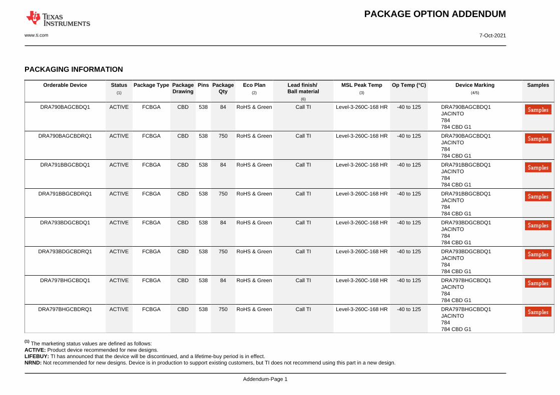
PACKAGE OPTION ADDENDUM
www.ti.com 7-Oct-2021
Addendum-Page 1
PACKAGING INFORMATION
Orderable Device Status(1)
Package Type PackageDrawing
Pins PackageQty
Eco Plan(2)
Lead finish/Ball material
(6)
MSL Peak Temp(3)
Op Temp (°C) Device Marking(4/5)
Samples
DRA790BAGCBDQ1 ACTIVE FCBGA CBD 538 84 RoHS & Green Call TI Level-3-260C-168 HR -40 to 125 DRA790BAGCBDQ1JACINTO784784 CBD G1
DRA790BAGCBDRQ1 ACTIVE FCBGA CBD 538 750 RoHS & Green Call TI Level-3-260C-168 HR -40 to 125 DRA790BAGCBDQ1JACINTO784784 CBD G1
DRA791BBGCBDQ1 ACTIVE FCBGA CBD 538 84 RoHS & Green Call TI Level-3-260C-168 HR -40 to 125 DRA791BBGCBDQ1JACINTO784784 CBD G1
DRA791BBGCBDRQ1 ACTIVE FCBGA CBD 538 750 RoHS & Green Call TI Level-3-260C-168 HR -40 to 125 DRA791BBGCBDQ1JACINTO784784 CBD G1
DRA793BDGCBDQ1 ACTIVE FCBGA CBD 538 84 RoHS & Green Call TI Level-3-260C-168 HR -40 to 125 DRA793BDGCBDQ1JACINTO784784 CBD G1
DRA793BDGCBDRQ1 ACTIVE FCBGA CBD 538 750 RoHS & Green Call TI Level-3-260C-168 HR -40 to 125 DRA793BDGCBDQ1JACINTO784784 CBD G1
DRA797BHGCBDQ1 ACTIVE FCBGA CBD 538 84 RoHS & Green Call TI Level-3-260C-168 HR -40 to 125 DRA797BHGCBDQ1JACINTO784784 CBD G1
DRA797BHGCBDRQ1 ACTIVE FCBGA CBD 538 750 RoHS & Green Call TI Level-3-260C-168 HR -40 to 125 DRA797BHGCBDQ1JACINTO784784 CBD G1
(1) The marketing status values are defined as follows:ACTIVE: Product device recommended for new designs.LIFEBUY: TI has announced that the device will be discontinued, and a lifetime-buy period is in effect.NRND: Not recommended for new designs. Device is in production to support existing customers, but TI does not recommend using this part in a new design.

PACKAGE OPTION ADDENDUM
www.ti.com 7-Oct-2021
Addendum-Page 2
PREVIEW: Device has been announced but is not in production. Samples may or may not be available.OBSOLETE: TI has discontinued the production of the device.
(2) RoHS: TI defines "RoHS" to mean semiconductor products that are compliant with the current EU RoHS requirements for all 10 RoHS substances, including the requirement that RoHS substancedo not exceed 0.1% by weight in homogeneous materials. Where designed to be soldered at high temperatures, "RoHS" products are suitable for use in specified lead-free processes. TI mayreference these types of products as "Pb-Free".RoHS Exempt: TI defines "RoHS Exempt" to mean products that contain lead but are compliant with EU RoHS pursuant to a specific EU RoHS exemption.Green: TI defines "Green" to mean the content of Chlorine (Cl) and Bromine (Br) based flame retardants meet JS709B low halogen requirements of <=1000ppm threshold. Antimony trioxide basedflame retardants must also meet the <=1000ppm threshold requirement.
(3) MSL, Peak Temp. - The Moisture Sensitivity Level rating according to the JEDEC industry standard classifications, and peak solder temperature.
(4) There may be additional marking, which relates to the logo, the lot trace code information, or the environmental category on the device.
(5) Multiple Device Markings will be inside parentheses. Only one Device Marking contained in parentheses and separated by a "~" will appear on a device. If a line is indented then it is a continuationof the previous line and the two combined represent the entire Device Marking for that device.
(6) Lead finish/Ball material - Orderable Devices may have multiple material finish options. Finish options are separated by a vertical ruled line. Lead finish/Ball material values may wrap to twolines if the finish value exceeds the maximum column width.
Important Information and Disclaimer:The information provided on this page represents TI's knowledge and belief as of the date that it is provided. TI bases its knowledge and belief on informationprovided by third parties, and makes no representation or warranty as to the accuracy of such information. Efforts are underway to better integrate information from third parties. TI has taken andcontinues to take reasonable steps to provide representative and accurate information but may not have conducted destructive testing or chemical analysis on incoming materials and chemicals.TI and TI suppliers consider certain information to be proprietary, and thus CAS numbers and other limited information may not be available for release.
In no event shall TI's liability arising out of such information exceed the total purchase price of the TI part(s) at issue in this document sold by TI to Customer on an annual basis.
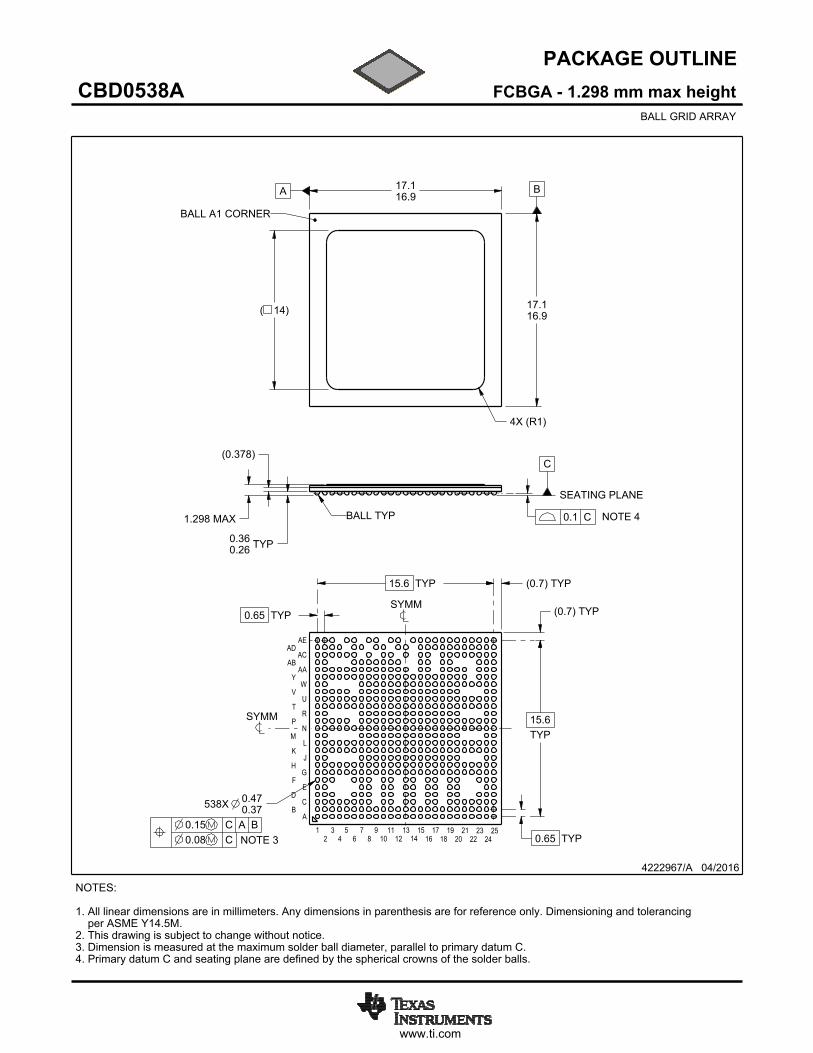
www.ti.com
PACKAGE OUTLINE
C
1.298 MAX
TYP0.360.26
15.6TYP
15.6 TYP
0.65 TYP
0.65 TYP
538X 0.470.37
(0.378)
A 17.116.9
B
17.116.9
(0.7) TYP
( 14)
(0.7) TYP
4X (R )1
FCBGA - 1.298 mm max heightCBD0538ABALL GRID ARRAY
4222967/A 04/2016
NOTES: 1. All linear dimensions are in millimeters. Any dimensions in parenthesis are for reference only. Dimensioning and tolerancing per ASME Y14.5M. 2. This drawing is subject to change without notice.3. Dimension is measured at the maximum solder ball diameter, parallel to primary datum C.4. Primary datum C and seating plane are defined by the spherical crowns of the solder balls.
BALL A1 CORNER
SEATING PLANE
BALL TYP 0.1 C NOTE 4
A
C
E
G
J
L
N
R
U
W
AA
AC
AE
12
30.15 C A B0.08 C
SYMM
SYMM
4NOTE 35
67
89
1011
1213
1415
1617 19 21 23 25
18 20 22 24
B
D
F
H
K
M
P
T
V
Y
AB
AD
SCALE 0.800

www.ti.com
EXAMPLE BOARD LAYOUT
538X ( )0.35
(0.65) TYP
(0.65) TYP
( )METAL
0.35 0.05 MAX
SOLDER MASKOPENING
METAL UNDERSOLDER MASK
( )SOLDER MASKOPENING
0.35
0.05 MIN
FCBGA - 1.298 mm max heightCBD0538ABALL GRID ARRAY
4222967/A 04/2016
NOTES: (continued) 5. Final dimensions may vary due to manufacturing tolerance considerations and also routing constraints. For more information, see Texas Instruments literature number SPRU811 (www.ti.com/lit/spru811).
SYMM
SYMM
LAND PATTERN EXAMPLESCALE:6X
1A
B
C
D
E
F
G
H
J
K
L
M
N
P
2 3 4 5 6 7 8 9 10 11 12 13 14 15 16 17 18 19 20 21 22 23 24 25
R
T
U
V
W
Y
AA
AB
AC
AD
AE
NON-SOLDER MASKDEFINED
(PREFERRED)
SOLDER MASK DETAILSNOT TO SCALE
SOLDER MASKDEFINED

www.ti.com
EXAMPLE STENCIL DESIGN
(0.65)TYP
(0.65) TYP 538X ( )0.35
FCBGA - 1.298 mm max heightCBD0538ABALL GRID ARRAY
4222967/A 04/2016
NOTES: (continued) 6. Laser cutting apertures with trapezoidal walls and rounded corners may offer better paste release.
SOLDER PASTE EXAMPLEBASED ON 0.15 mm THICK STENCIL
SCALE:6X
SYMM
SYMM
1A
B
C
D
E
F
G
H
J
K
L
M
N
P
2 3 4 5 6 7 8 9 10 11 12 13 14 15 16 17 18 19 20 21 22 23 24 25
R
T
U
V
W
Y
AA
AB
AC
AD
AE

重要声明和免责声明TI“按原样”提供技术和可靠性数据(包括数据表)、设计资源(包括参考设计)、应用或其他设计建议、网络工具、安全信息和其他资源,不保证没有瑕疵且不做出任何明示或暗示的担保,包括但不限于对适销性、某特定用途方面的适用性或不侵犯任何第三方知识产权的暗示担保。这些资源可供使用 TI 产品进行设计的熟练开发人员使用。您将自行承担以下全部责任:(1) 针对您的应用选择合适的 TI 产品,(2) 设计、验证并测试您的应用,(3) 确保您的应用满足相应标准以及任何其他功能安全、信息安全、监管或其他要求。这些资源如有变更,恕不另行通知。TI 授权您仅可将这些资源用于研发本资源所述的 TI 产品的应用。严禁对这些资源进行其他复制或展示。您无权使用任何其他 TI 知识产权或任何第三方知识产权。您应全额赔偿因在这些资源的使用中对 TI 及其代表造成的任何索赔、损害、成本、损失和债务,TI 对此概不负责。TI 提供的产品受 TI 的销售条款或 ti.com 上其他适用条款/TI 产品随附的其他适用条款的约束。TI 提供这些资源并不会扩展或以其他方式更改 TI 针对 TI 产品发布的适用的担保或担保免责声明。TI 反对并拒绝您可能提出的任何其他或不同的条款。IMPORTANT NOTICE
邮寄地址:Texas Instruments, Post Office Box 655303, Dallas, Texas 75265Copyright © 2021,德州仪器 (TI) 公司
Copyright © 2022 FDOKUMEN

