


Bahasa
Halaman
Hukum

Charge Transfer and Energy Level Alignment at the Interfacebetween Cyclopentene-Modified Si(001) andTetracyanoquinodimethaneAnzar Khaliq,§,‡ Jean-Jacques Gallet,†,§ Fabrice Bournel,†,§ Debora Pierucci,†,§ Heloïse Tissot,†,§
Mathieu Silly,† Fausto Sirotti,† and Francois Rochet*,†,§
§UMR 7614, Laboratoire de Chimie Physique, Matiere et Rayonnement, UPMC Univ Paris 06, Sorbonne Universites, 11 rue Pierre etMarie Curie, 75231 Paris Cedex, France†Synchrotron SOLEIL, L’Orme des Merisiers, Saint-Aubin, BP 48, 91192 Gif sur Yvette Cedex, France‡Habib University Foundation, 147, Block 7 & 8 Banglore Cooperative Housing Society, Tipu Sultan Road, Karachi 75350, Pakistan
*S Supporting Information
ABSTRACT: We examine how the electronic structure (via synchrotron radiationXPS, UPS, and NEXAFS) and the molecular orientation (via NEXAFS) of astrong acceptor molecule, tetracyanoquinodimethane (TCNQ), change as afunction of thickness when it is deposited on the cyclopentene-covered Si(001)-2×1 substrate. XPS shows that the monomolecular cyclopentene layer acts as anefficient chemical protective barrier. All spectroscopies indicate that anionicTCNQ is formed at (sub)monolayer coverage. However, the transfer should onlyconcern those CN moieties pointing toward the Silicon surface. At higherthicknesses, neutral TCNQ is observed. We do not observe the upward bending ofthe silicon bands associated with electron transfer from the substrate to theacceptor molecular that one would expect for an unpinned Fermi level interface. Infact, donor levels are likely created within the cyclopentene layer or at its interfacewith silicon. The formation of TCNQ− is associated with a strong increase in thework function. The attained value (∼5.7 eV) is independent of the work function of the cyclopentene-modified Si(001) surface(that varies with Si doping), in agreement with the integral charge transfer model. Therefore, ultrathin layers of TCNQ can beused to improve the hole-injection properties of this alkene-modified silicon surface.
■ INTRODUCTION
Charge transfer between inorganic semiconductors (ISCs) andstrong acceptor molecules deposited on their surfaces hasrecently attracted much attention, due to its relevance to(opto)electronic device technology.1−3 It offers an elegant wayto control the carrier concentration in nanostructured ISCmaterials for which dopant implantation is impractical.1−3
Enhancement of the surface work function of ISCs enables theiroptimization as hole injectors.4,5 Charge transfer is also a keyissue in sensor science involving modified surfaces of ISCs.6
The principles of ISC surface-transfer doping have beenreviewed by Chen and co-workers.1 According to those authors,when an acceptor molecule has its electron affinity (EA) in thesolid state larger than the ionization potential (IP) of thesubstrate, then electron charge is transferred spontaneouslyfrom the substrate to the molecule.1 Otherwise stated, chargetransfer occurs when, before level alignment, the lowestunoccupied molecular orbital (LUMO) of the acceptor liesbelow the valence band maximum (EVB) of the ISC.Nevertheless, the straightforward use of concepts like the
energy positioning of the LUMO, or the EA in the molecularsolid, that are then compared to the substrate IP, seems tooschematic and therefore may not be predictive. This prompted
Braun, Salaneck, and Fahlman to propose the integer chargetransfer (ICT) model,7 in which the negative ICT state (ICT−)energy is distinct from the EA. As discussed by Bokdam et al.,8
the ICT− level does not coincide with the EA of the solidorganic material (often larger than EA by ∼1 eV) due toelectrostatic interactions at the interface. For acceptormolecules weakly interacting with the substrate (i.e., makingno covalent bonds), the ICT− is the energy gained when oneelectron is added to the molecule, producing a fully relaxedstate. When ICT− is smaller than the substrate work functionΦsub, a simple thermodynamic argument shows that this levelcannot be filled by electrons coming from substrate. Thenvacuum-level alignment is observed (the so-called Schottky−Mott limit). On the other hand (what is expected for strongacceptors), charge transfer occursi.e., a layer of molecularanions forms at the interfacewhen the ICT− energy is largerthan Φsub. Then the Fermi level in the substrate and the ICT−
level in the molecular solid align. Associated with this Fermi-level pinning, an electrostatic potential step occurs at the
Received: March 18, 2014Revised: September 5, 2014Published: September 8, 2014
Article
pubs.acs.org/JPCC
© 2014 American Chemical Society 22499 dx.doi.org/10.1021/jp502680b | J. Phys. Chem. C 2014, 118, 22499−22508
interface, resulting in an increase in work function. Therefore, inthe Fermi-level pinning case, the work function of the acceptorlayer/substrate system is a measure of ICT−. Bokdam et al.8 haveshown that the value of ICT− is a property of the acceptormolecule layer only, independent of the substrate.Charge transfer to the acceptor molecule means that the
positive charges are left in the substrate to preserve overallcharge neutrality. In the specific case of ISC substrates, theelectric field created by this dipolar layer may induce an upwardband bending, leading to hole accumulation.1,2,9 Although notstated explicitly in ref 1, hole accumulation requires that theFermi level at the ISC is unpinned; i.e., there is an extremelylow density of surface states in the gap, below 10−3 of amonolayer (ML).10−12
A spectacular illustration of charge-transfer doping isprovided by the deposition of tetrafluorotetracyanoquiono-dimethane (F4-TCNQ) on top of p-doped hydrogenateddiamond C(001)-2×1 (H-C(001)-2×1), an electronically well-passivated surface. F4-TCNQ deposition induces an upwardband bending (accumulation), leading the formation of a highareal density of holes.1,2 Chen and co-workers1,2 argue thatcharge transfer occurs because the EA of solid F4-TCNQ (EA= 5.24 eV13) is larger than the IP of H-C(001)-2×1 (4.4 eV).On the same surface, tetracyanoquinodimethane (TCNQ) withEA = 4.0 eV,14 has a weaker p-doping efficiency (manifested bya small upward band bending) compared to that of F4-TCNQ.This is rationalized in refs 1 and 2 on the basis of the EA ofTCNQ, which is now slightly greater than the hydrogenateddiamond IP. Electron transfer is also documented between H-terminated Si(111)-1×1 and acceptor molecules (F4-TCNQ,3
tetracyanoethylene6). Like H-terminated C(001)-2×1, H-terminated Si(111)-1×1 is a well-passivated surface with anextremely low density of gap states.15
As an alternative to H-termination, silicon surfaces can beterminated by an organic buffer layer that is thought to be moreeffective to protect the silicon from chemical reactions with themolecular acceptor.16 Well (electronically) passivated Si(111)surfaces in nearly flat band conditions can be obtained via wetchemistry, for instance, the methylated surface.17 However, thewet chemistry route is not practicable for the Si(001)-2×1surface, and an organic termination is obtained via the reactionof π-bonded molecules, in particular alkene molecules, with thesilicon dimers.18,19 The present work aims at providing furtherexperimental data on charge transfer between silicon and anacceptor molecule across a monomolecular alkene buffer layer.In the wake of a preceding work devoted to the adsorptiongeometries of cyclopentene on Si(001)-2×1,20 we examined,via synchrotron radiation, the electronic structure of TCNQoverlayers deposited on the cyclopentene-modified Si(001)surface (CP-Si(001)-2×1). Cyclopentene was already used asan efficient chemical buffer layer, facilitating the crystallinegrowth of pentacene molecules.21 Aware that the question ofelectrically active defects possibly left after cyclopentene layerformation are critically important, we used Si(001) substrateswith two extreme doping levels (n+ and p+) to examine theissue of Fermi level pinning. The deposition of TCNQ on CP-Si(001)-2×1 was followed by synchrotron radiation ultravioletphotoelectron spectroscopy (UPS), X-ray photoelectron spec-troscopy (XPS), and N 1s near-edge X-ray fine structurespectroscopy (NEXAFS). Information is gathered on chemicalenvironments, molecular charge state, molecular orientation,energy level offsets at the interface, and changes in workfunction. This enabled us to draw a picture of the TCNQ/CP-
Si(001)-2×1 interface energetics and to discuss it in terms ofthe existing models.1,7 Possible applications of ultrathin TCNQfilm in solar cells based on silicon/organics interfaces are alsodiscussed.22−24
■ EXPERIMENTAL SECTIONSample Preparation. Si(001)-2×1 surfaces were produced
in the preparation chamber of the TEMPO beamline end-station at SOLEIL synchrotron facility. Two differently dopedsilicon substrates (phosphorus-doped n+-type Si(001) waferswith a resistivity of 0.003 Ω·cm, ND ≈ 2 × 1019 cm−3, andboron-doped p+-type Si(001) wafers with a resistivity of 0.002Ω·cm, NA ≈ 5.7 × 1019 cm−3) were cleaned from their nativeoxide by flash annealing (Joule effect) at 1100 °C afterprolonged degassing at 600 °C in ultrahigh vacuum (10−10
mbar base pressure).The clean silicon surface was first exposed to 6.75 L of
cyclopentene by dosing for 15 min at room temperature undera pressure of 10−8 mbar (ion gauge uncorrected reading).Doses are expressed in Langmuir (1 L = 10−6 Torr·s).Cyclopentene was purified by several freeze−pump−thawcycles before dosing. In ref 20, we showed that the majorityof cyclopentene molecules attach to the silicon dimer withoutdissociation via a cycloaddition-like reaction. However, we havealso found evidence for a minority product, resulting from anene-like reaction, not detected in previous studies,25,18 andwhose proportion increases with increasing deposition temper-ature. The C 1s XPS spectrum of the starting CP-Si(001)-2×1surface (on which TCNQ is deposited) is that published in ref20 as Figure 2a (corresponding to substrate temperatures≤130° during exposure to cyclopentene).TCNQ was evaporated through a crucible whose back was
heated by a filament. A thick film (∼1015 molecules/cm2) wasdeposited on n+-doped CP-Si(001). Deposits in the range1014−1015 TCNQ molecules/cm2 were obtained for p+-dopedCP-Si(001). The methodology adapted to estimate themolecular thickness for both thin and thick layers is explainedin section S1 of the Supporting Information
Synchrotron Radiation Spectroscopies: X-ray Photo-emission. The X-ray spot (normally focused in a spot 45 μmlong in the horizontal direction by 10 μm wide in the verticaldimension) was defocused on purpose, to a spot of dimensions1 mm × 2 mm, to reduce beam damage, without losingphotoelectron count rate. All photoemission spectra were takenwith a takeoff angle of 35° with respect to the surface normal.Valence band UPS spectra were recorded at hν = 60 eV, whilesurface sensitive Si 2p spectra were measured at hν = 150 eV,with an overall experimental resolution better than 80 meV.The precision on the Si 2p3/2 binding energies of the bulkcomponent is better than 10 meV. N 1s core-level XPS spectrawere recorded at hν = 450 eV with an overall experimentalresolution better than 100 meV. After subtraction of a Shirleybackground, the N 1s spectra were reconstructed with sums ofVoigt functions, whose Lorentzian full-width at half-maximum(fwhm) was fixed to 0.12 eV, and the Gaussian fwhm was set asa free fitting parameter.To quantify the amount of deposited molecule, N 1s spectra
were recorded at hν = 530 eV, at a kinetic energy (KE) of about132 eV, close to that of the Si LVV Auger peak (∼80−88 eVrange). The N 1s photoemission peak integrals werenormalized with respect to an equal Si LVV height. The valueswere compared to the N 1s spectrum for a NH3 saturatedsilicon surface recorded close to the Auger peak and normalized
The Journal of Physical Chemistry C Article
dx.doi.org/10.1021/jp502680b | J. Phys. Chem. C 2014, 118, 22499−2250822500
in the same way as mentioned above. Si(001)-2×1 completelysaturated by NH3 corresponds to a coverage of half amonolayer, i.e., 3.4 × 10¹⁴ atoms/cm2.26 A linear relationbetween N 1s intensities and N surface coverage is expected fordeposits in the monolayer range. For multilayer films, theTCNQ surface density was estimated from the N 1s to Si 2pratio measured at hν = 450 eV (see Supporting Information,Figure S1).Work Function Measurements. The work function is
measured via the kinetic energy of the secondary electron cutoff(KEcutoff). With the knowledge of the kinetic energy of theFermi level (KEFermi) and a precise determination of the photonenergy hν, one gets the work function ,Φ: Φ = hν − (EKFermi −EKcutoff) (see Supporting Information, Figure S2). Theprecision in measuring Φ is 10 meV.NEXAFS Spectroscopy. N 1s NEXAFS spectra of the
adsorbed layer were recorded at different angles θ, between thenormal to the sample surface and the polarization vector E, inthe range from 6° (grazing incidence) to 90° (normalincidence). The orientation of the molecular orbital final statewas derived using these normalized spectra (see SupportingInformation, Figures S5 and S6).27
■ RESULTS AND DISCUSSIONCyclopentene-Covered Si(001)-2×1 Surface (CP-
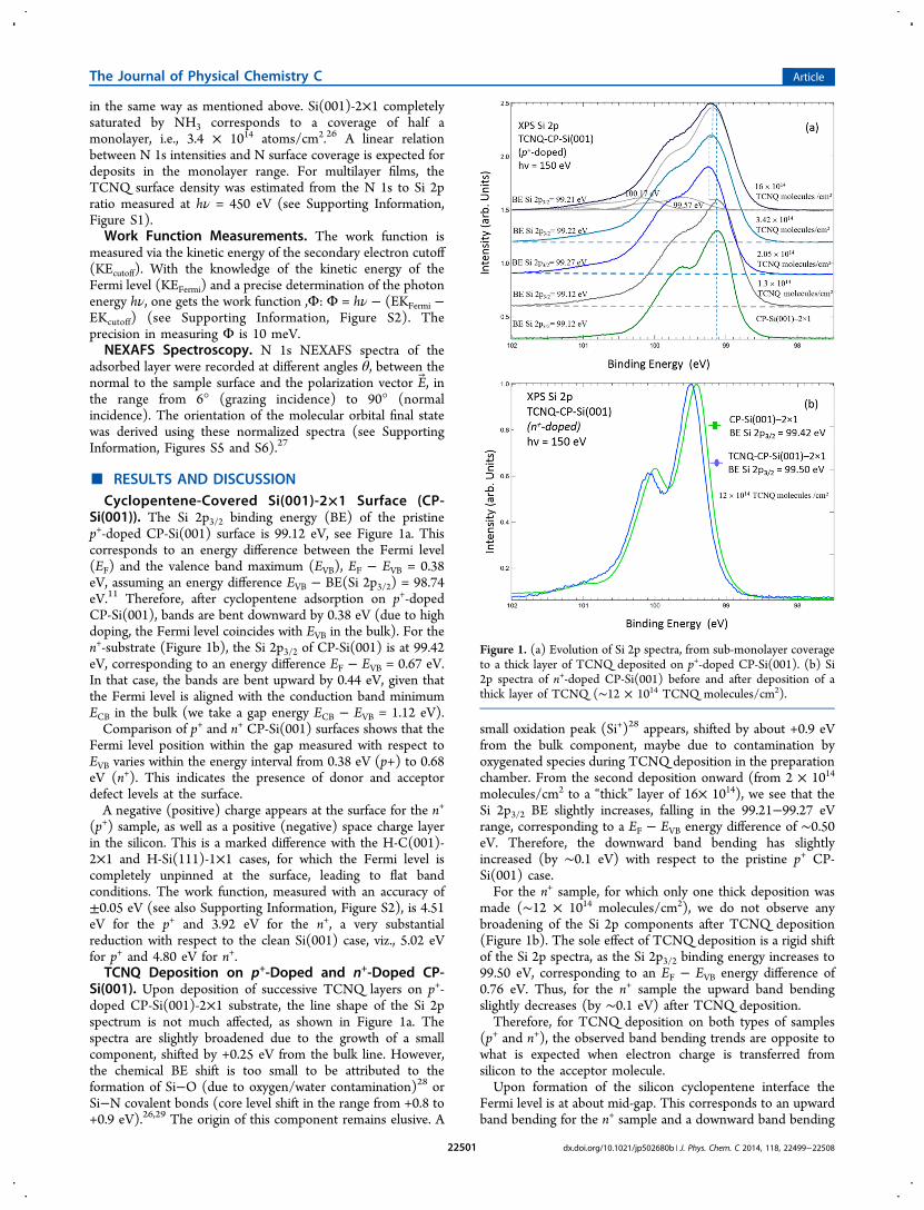
Si(001)). The Si 2p3/2 binding energy (BE) of the pristinep+-doped CP-Si(001) surface is 99.12 eV, see Figure 1a. Thiscorresponds to an energy difference between the Fermi level(EF) and the valence band maximum (EVB), EF − EVB = 0.38eV, assuming an energy difference EVB − BE(Si 2p3/2) = 98.74eV.11 Therefore, after cyclopentene adsorption on p+-dopedCP-Si(001), bands are bent downward by 0.38 eV (due to highdoping, the Fermi level coincides with EVB in the bulk). For then+-substrate (Figure 1b), the Si 2p3/2 of CP-Si(001) is at 99.42eV, corresponding to an energy difference EF − EVB = 0.67 eV.In that case, the bands are bent upward by 0.44 eV, given thatthe Fermi level is aligned with the conduction band minimumECB in the bulk (we take a gap energy ECB − EVB = 1.12 eV).Comparison of p+ and n+ CP-Si(001) surfaces shows that the
Fermi level position within the gap measured with respect toEVB varies within the energy interval from 0.38 eV (p+) to 0.68eV (n+). This indicates the presence of donor and acceptordefect levels at the surface.A negative (positive) charge appears at the surface for the n+
(p+) sample, as well as a positive (negative) space charge layerin the silicon. This is a marked difference with the H-C(001)-2×1 and H-Si(111)-1×1 cases, for which the Fermi level iscompletely unpinned at the surface, leading to flat bandconditions. The work function, measured with an accuracy of±0.05 eV (see also Supporting Information, Figure S2), is 4.51eV for the p+ and 3.92 eV for the n+, a very substantialreduction with respect to the clean Si(001) case, viz., 5.02 eVfor p+ and 4.80 eV for n+.TCNQ Deposition on p+-Doped and n+-Doped CP-
Si(001). Upon deposition of successive TCNQ layers on p+-doped CP-Si(001)-2×1 substrate, the line shape of the Si 2pspectrum is not much affected, as shown in Figure 1a. Thespectra are slightly broadened due to the growth of a smallcomponent, shifted by +0.25 eV from the bulk line. However,the chemical BE shift is too small to be attributed to theformation of Si−O (due to oxygen/water contamination)28 orSi−N covalent bonds (core level shift in the range from +0.8 to+0.9 eV).26,29 The origin of this component remains elusive. A
small oxidation peak (Si+)28 appears, shifted by about +0.9 eVfrom the bulk component, maybe due to contamination byoxygenated species during TCNQ deposition in the preparationchamber. From the second deposition onward (from 2 × 10¹⁴
molecules/cm2 to a “thick” layer of 16× 1014), we see that theSi 2p3/2 BE slightly increases, falling in the 99.21−99.27 eVrange, corresponding to a EF − EVB energy difference of ∼0.50eV. Therefore, the downward band bending has slightlyincreased (by ∼0.1 eV) with respect to the pristine p+ CP-Si(001) case.For the n+ sample, for which only one thick deposition was
made (∼12 × 1014 molecules/cm2), we do not observe anybroadening of the Si 2p components after TCNQ deposition(Figure 1b). The sole effect of TCNQ deposition is a rigid shiftof the Si 2p spectra, as the Si 2p3/2 binding energy increases to99.50 eV, corresponding to an EF − EVB energy difference of0.76 eV. Thus, for the n+ sample the upward band bendingslightly decreases (by ∼0.1 eV) after TCNQ deposition.Therefore, for TCNQ deposition on both types of samples
(p+ and n+), the observed band bending trends are opposite towhat is expected when electron charge is transferred fromsilicon to the acceptor molecule.Upon formation of the silicon cyclopentene interface the
Fermi level is at about mid-gap. This corresponds to an upwardband bending for the n+ sample and a downward band bending
Figure 1. (a) Evolution of Si 2p spectra, from sub-monolayer coverageto a thick layer of TCNQ deposited on p+-doped CP-Si(001). (b) Si2p spectra of n+-doped CP-Si(001) before and after deposition of athick layer of TCNQ (∼12 × 1014 TCNQ molecules/cm2).
The Journal of Physical Chemistry C Article
dx.doi.org/10.1021/jp502680b | J. Phys. Chem. C 2014, 118, 22499−2250822501
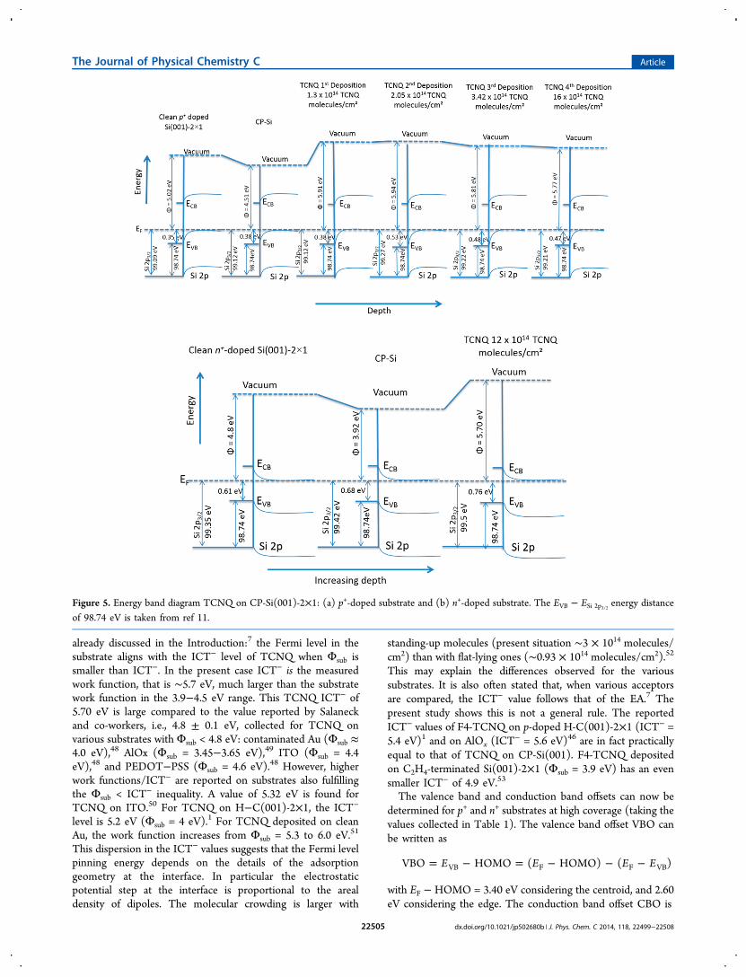
for the p+. If electrons were transferred from silicon to TCNQ,the upward band bending (in absolute value) should haveincreased for the n+ leading eventually to inversion. While forthe p+, the downward band bending (in absolute value) shouldhave decreased (reverting into an upward band bending)leading to hole accumulation. This is also indicated by the bandenergy diagram in Figure 5, below. It seems that the depositionof TCNQ slightly diminishes the surface density of acceptor/donor defects formed at the interface between silicon andcyclopentene, leading to “flatter” band conditions. Because of alarge density of interfacial states (greater than 10−3 ML), thebehavior of CP-Si(001) contrasts with that of p-doped H-C(001)-2×1 for which the Fermi level is unpinned. Indeed, F4-TCNQ deposition leads to hole accumulation.12
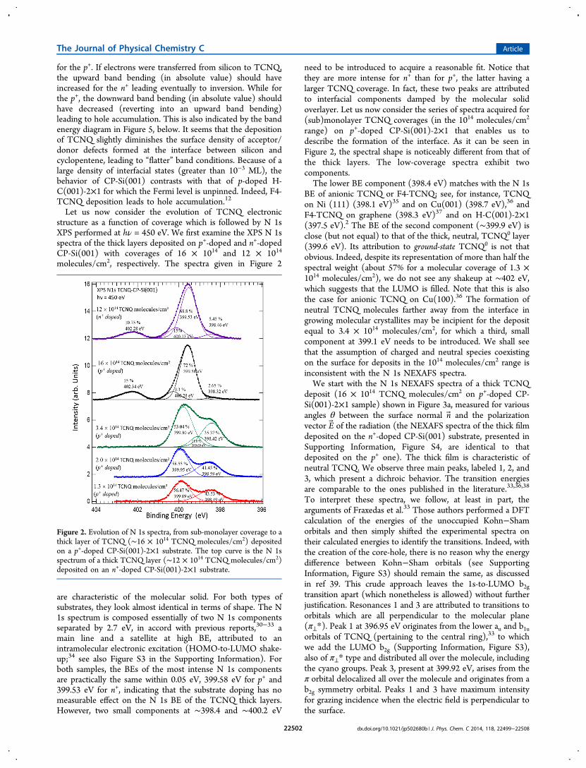
Let us now consider the evolution of TCNQ electronicstructure as a function of coverage which is followed by N 1sXPS performed at hν = 450 eV. We first examine the XPS N 1sspectra of the thick layers deposited on p+-doped and n+-dopedCP-Si(001) with coverages of 16 × 1014 and 12 × 1014
molecules/cm2, respectively. The spectra given in Figure 2
are characteristic of the molecular solid. For both types ofsubstrates, they look almost identical in terms of shape. The N1s spectrum is composed essentially of two N 1s componentsseparated by 2.7 eV, in accord with previous reports,30−33 amain line and a satellite at high BE, attributed to anintramolecular electronic excitation (HOMO-to-LUMO shake-up;34 see also Figure S3 in the Supporting Information). Forboth samples, the BEs of the most intense N 1s componentsare practically the same within 0.05 eV, 399.58 eV for p+ and399.53 eV for n+, indicating that the substrate doping has nomeasurable effect on the N 1s BE of the TCNQ thick layers.However, two small components at ∼398.4 and ∼400.2 eV
need to be introduced to acquire a reasonable fit. Notice thatthey are more intense for n+ than for p+, the latter having alarger TCNQ coverage. In fact, these two peaks are attributedto interfacial components damped by the molecular solidoverlayer. Let us now consider the series of spectra acquired for(sub)monolayer TCNQ coverages (in the 1014 molecules/cm2
range) on p+-doped CP-Si(001)-2×1 that enables us todescribe the formation of the interface. As it can be seen inFigure 2, the spectral shape is noticeably different from that ofthe thick layers. The low-coverage spectra exhibit twocomponents.The lower BE component (398.4 eV) matches with the N 1s
BE of anionic TCNQ or F4-TCNQ; see, for instance, TCNQon Ni (111) (398.1 eV)35 and on Cu(001) (398.7 eV),36 andF4-TCNQ on graphene (398.3 eV)37 and on H-C(001)-2×1(397.5 eV).2 The BE of the second component (∼399.9 eV) isclose (but not equal) to that of the thick, neutral, TCNQ0 layer(399.6 eV). Its attribution to ground-state TCNQ0 is not thatobvious. Indeed, despite its representation of more than half thespectral weight (about 57% for a molecular coverage of 1.3 ×10¹⁴ molecules/cm2), we do not see any shakeup at ∼402 eV,which suggests that the LUMO is filled. Note that this is alsothe case for anionic TCNQ on Cu(100).36 The formation ofneutral TCNQ molecules farther away from the interface ingrowing molecular crystallites may be incipient for the depositequal to 3.4 × 10¹⁴ molecules/cm2, for which a third, smallcomponent at 399.1 eV needs to be introduced. We shall seethat the assumption of charged and neutral species coexistingon the surface for deposits in the 1014 molecules/cm2 range isinconsistent with the N 1s NEXAFS spectra.We start with the N 1s NEXAFS spectra of a thick TCNQ
deposit (16 × 1014 TCNQ molecules/cm2 on p+-doped CP-Si(001)-2×1 sample) shown in Figure 3a, measured for variousangles θ between the surface normal n and the polarizationvector E of the radiation (the NEXAFS spectra of the thick filmdeposited on the n+-doped CP-Si(001) substrate, presented inSupporting Information, Figure S4, are identical to thatdeposited on the p+ one). The thick film is characteristic ofneutral TCNQ. We observe three main peaks, labeled 1, 2, and3, which present a dichroic behavior. The transition energiesare comparable to the ones published in the literature.33,36,38
To interpret these spectra, we follow, at least in part, thearguments of Fraxedas et al.33 Those authors performed a DFTcalculation of the energies of the unoccupied Kohn−Shamorbitals and then simply shifted the experimental spectra ontheir calculated energies to identify the transitions. Indeed, withthe creation of the core-hole, there is no reason why the energydifference between Kohn−Sham orbitals (see SupportingInformation, Figure S3) should remain the same, as discussedin ref 39. This crude approach leaves the 1s-to-LUMO b2gtransition apart (which nonetheless is allowed) without furtherjustification. Resonances 1 and 3 are attributed to transitions toorbitals which are all perpendicular to the molecular plane(π⊥*). Peak 1 at 396.95 eV originates from the lower au and b1uorbitals of TCNQ (pertaining to the central ring),33 to whichwe add the LUMO b2g (Supporting Information, Figure S3),also of π⊥* type and distributed all over the molecule, includingthe cyano groups. Peak 3, present at 399.92 eV, arises from theπ orbital delocalized all over the molecule and originates from ab2g symmetry orbital. Peaks 1 and 3 have maximum intensityfor grazing incidence when the electric field is perpendicular tothe surface.
Figure 2. Evolution of N 1s spectra, from sub-monolayer coverage to athick layer of TCNQ (∼16 × 1014 TCNQ molecules/cm2) depositedon a p+-doped CP-Si(001)-2×1 substrate. The top curve is the N 1sspectrum of a thick TCNQ layer (∼12 × 1014 TCNQ molecules/cm2)deposited on an n+-doped CP-Si(001)-2×1 substrate.
The Journal of Physical Chemistry C Article
dx.doi.org/10.1021/jp502680b | J. Phys. Chem. C 2014, 118, 22499−2250822502
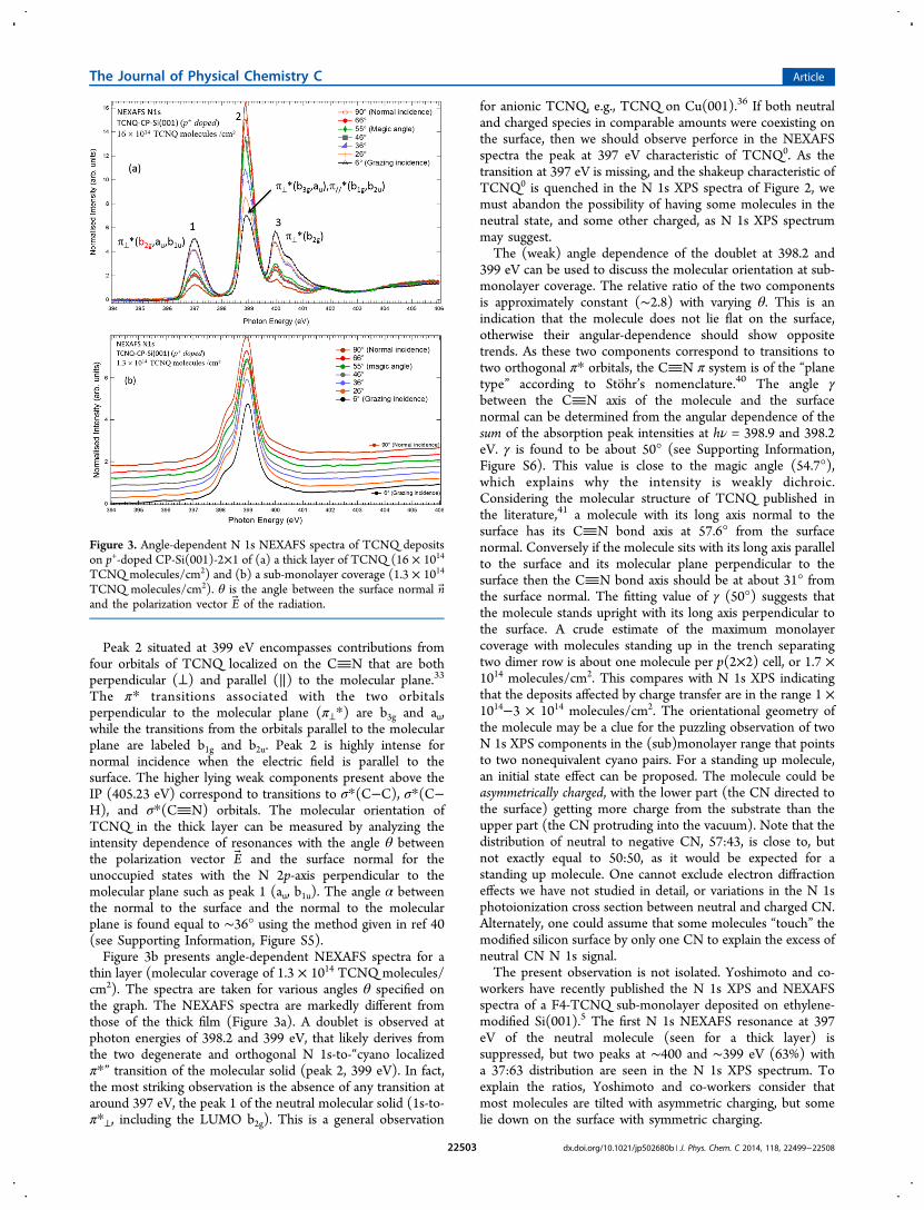
Peak 2 situated at 399 eV encompasses contributions fromfour orbitals of TCNQ localized on the CN that are bothperpendicular (⊥) and parallel (∥) to the molecular plane.33
The π* transitions associated with the two orbitalsperpendicular to the molecular plane (π⊥*) are b3g and au,while the transitions from the orbitals parallel to the molecularplane are labeled b1g and b2u. Peak 2 is highly intense fornormal incidence when the electric field is parallel to thesurface. The higher lying weak components present above theIP (405.23 eV) correspond to transitions to σ*(C−C), σ*(C−H), and σ*(CN) orbitals. The molecular orientation ofTCNQ in the thick layer can be measured by analyzing theintensity dependence of resonances with the angle θ betweenthe polarization vector E and the surface normal for theunoccupied states with the N 2p-axis perpendicular to themolecular plane such as peak 1 (au, b1u). The angle α betweenthe normal to the surface and the normal to the molecularplane is found equal to ∼36° using the method given in ref 40(see Supporting Information, Figure S5).Figure 3b presents angle-dependent NEXAFS spectra for a
thin layer (molecular coverage of 1.3 × 10¹⁴ TCNQ molecules/cm2). The spectra are taken for various angles θ specified onthe graph. The NEXAFS spectra are markedly different fromthose of the thick film (Figure 3a). A doublet is observed atphoton energies of 398.2 and 399 eV, that likely derives fromthe two degenerate and orthogonal N 1s-to-“cyano localizedπ*” transition of the molecular solid (peak 2, 399 eV). In fact,the most striking observation is the absence of any transition ataround 397 eV, the peak 1 of the neutral molecular solid (1s-to-π*⊥, including the LUMO b2g). This is a general observation
for anionic TCNQ, e.g., TCNQ on Cu(001).36 If both neutraland charged species in comparable amounts were coexisting onthe surface, then we should observe perforce in the NEXAFSspectra the peak at 397 eV characteristic of TCNQ0. As thetransition at 397 eV is missing, and the shakeup characteristic ofTCNQ0 is quenched in the N 1s XPS spectra of Figure 2, wemust abandon the possibility of having some molecules in theneutral state, and some other charged, as N 1s XPS spectrummay suggest.The (weak) angle dependence of the doublet at 398.2 and
399 eV can be used to discuss the molecular orientation at sub-monolayer coverage. The relative ratio of the two componentsis approximately constant (∼2.8) with varying θ. This is anindication that the molecule does not lie flat on the surface,otherwise their angular-dependence should show oppositetrends. As these two components correspond to transitions totwo orthogonal π* orbitals, the CN π system is of the “planetype” according to Stohr’s nomenclature.40 The angle γbetween the CN axis of the molecule and the surfacenormal can be determined from the angular dependence of thesum of the absorption peak intensities at hν = 398.9 and 398.2eV. γ is found to be about 50° (see Supporting Information,Figure S6). This value is close to the magic angle (54.7°),which explains why the intensity is weakly dichroic.Considering the molecular structure of TCNQ published inthe literature,41 a molecule with its long axis normal to thesurface has its CN bond axis at 57.6° from the surfacenormal. Conversely if the molecule sits with its long axis parallelto the surface and its molecular plane perpendicular to thesurface then the CN bond axis should be at about 31° fromthe surface normal. The fitting value of γ (50°) suggests thatthe molecule stands upright with its long axis perpendicular tothe surface. A crude estimate of the maximum monolayercoverage with molecules standing up in the trench separatingtwo dimer row is about one molecule per p(2×2) cell, or 1.7 ×10¹⁴ molecules/cm2. This compares with N 1s XPS indicatingthat the deposits affected by charge transfer are in the range 1 ×10¹⁴−3 × 10¹⁴ molecules/cm2. The orientational geometry ofthe molecule may be a clue for the puzzling observation of twoN 1s XPS components in the (sub)monolayer range that pointsto two nonequivalent cyano pairs. For a standing up molecule,an initial state effect can be proposed. The molecule could beasymmetrically charged, with the lower part (the CN directed tothe surface) getting more charge from the substrate than theupper part (the CN protruding into the vacuum). Note that thedistribution of neutral to negative CN, 57:43, is close to, butnot exactly equal to 50:50, as it would be expected for astanding up molecule. One cannot exclude electron diffractioneffects we have not studied in detail, or variations in the N 1sphotoionization cross section between neutral and charged CN.Alternately, one could assume that some molecules “touch” themodified silicon surface by only one CN to explain the excess ofneutral CN N 1s signal.The present observation is not isolated. Yoshimoto and co-
workers have recently published the N 1s XPS and NEXAFSspectra of a F4-TCNQ sub-monolayer deposited on ethylene-modified Si(001).5 The first N 1s NEXAFS resonance at 397eV of the neutral molecule (seen for a thick layer) issuppressed, but two peaks at ∼400 and ∼399 eV (63%) witha 37:63 distribution are seen in the N 1s XPS spectrum. Toexplain the ratios, Yoshimoto and co-workers consider thatmost molecules are tilted with asymmetric charging, but somelie down on the surface with symmetric charging.
Figure 3. Angle-dependent N 1s NEXAFS spectra of TCNQ depositson p+-doped CP-Si(001)-2×1 of (a) a thick layer of TCNQ (16 × 1014
TCNQ molecules/cm2) and (b) a sub-monolayer coverage (1.3 × 10¹⁴
TCNQ molecules/cm2). θ is the angle between the surface normal n and the polarization vector E of the radiation.
The Journal of Physical Chemistry C Article
dx.doi.org/10.1021/jp502680b | J. Phys. Chem. C 2014, 118, 22499−2250822503
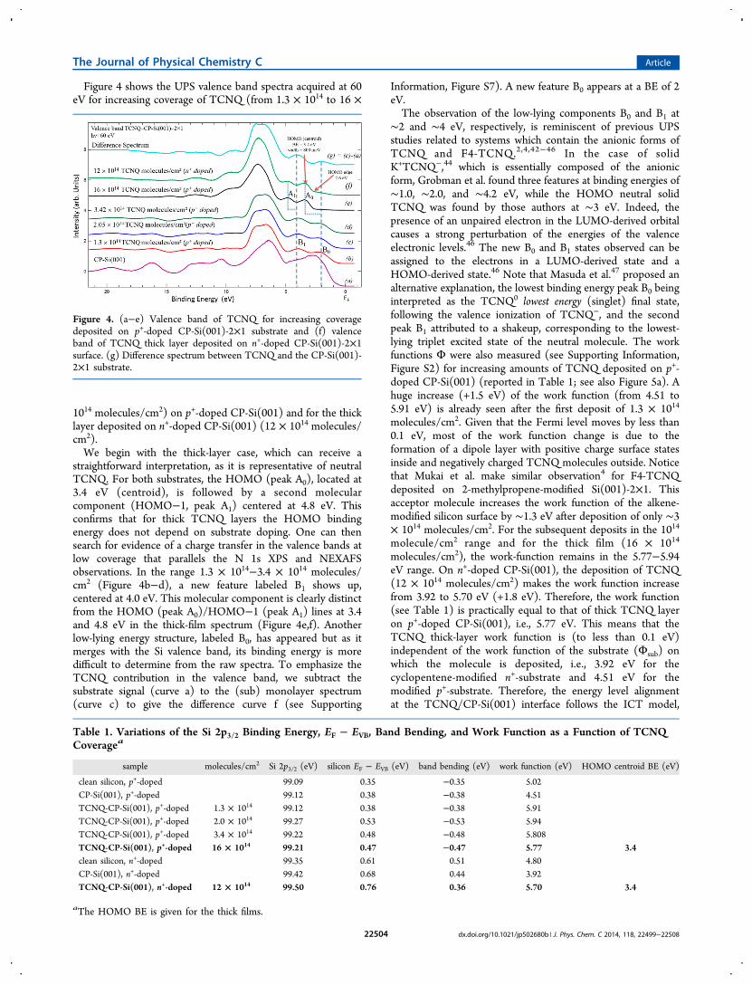
Figure 4 shows the UPS valence band spectra acquired at 60eV for increasing coverage of TCNQ (from 1.3 × 10¹⁴ to 16 ×
1014 molecules/cm2) on p+-doped CP-Si(001) and for the thicklayer deposited on n+-doped CP-Si(001) (12 × 1014 molecules/cm2).We begin with the thick-layer case, which can receive a
straightforward interpretation, as it is representative of neutralTCNQ. For both substrates, the HOMO (peak A0), located at3.4 eV (centroid), is followed by a second molecularcomponent (HOMO−1, peak A1) centered at 4.8 eV. Thisconfirms that for thick TCNQ layers the HOMO bindingenergy does not depend on substrate doping. One can thensearch for evidence of a charge transfer in the valence bands atlow coverage that parallels the N 1s XPS and NEXAFSobservations. In the range 1.3 × 10¹⁴−3.4 × 10¹⁴ molecules/cm2 (Figure 4b−d), a new feature labeled B1 shows up,centered at 4.0 eV. This molecular component is clearly distinctfrom the HOMO (peak A0)/HOMO−1 (peak A1) lines at 3.4and 4.8 eV in the thick-film spectrum (Figure 4e,f). Anotherlow-lying energy structure, labeled B0, has appeared but as itmerges with the Si valence band, its binding energy is moredifficult to determine from the raw spectra. To emphasize theTCNQ contribution in the valence band, we subtract thesubstrate signal (curve a) to the (sub) monolayer spectrum(curve c) to give the difference curve f (see Supporting
Information, Figure S7). A new feature B0 appears at a BE of 2eV.The observation of the low-lying components B0 and B1 at
∼2 and ∼4 eV, respectively, is reminiscent of previous UPSstudies related to systems which contain the anionic forms ofTCNQ and F4-TCNQ.2,4,42−46 In the case of solidK+TCNQ−,44 which is essentially composed of the anionicform, Grobman et al. found three features at binding energies of∼1.0, ∼2.0, and ∼4.2 eV, while the HOMO neutral solidTCNQ was found by those authors at ∼3 eV. Indeed, thepresence of an unpaired electron in the LUMO-derived orbitalcauses a strong perturbation of the energies of the valenceelectronic levels.46 The new B0 and B1 states observed can beassigned to the electrons in a LUMO-derived state and aHOMO-derived state.46 Note that Masuda et al.47 proposed analternative explanation, the lowest binding energy peak B0 beinginterpreted as the TCNQ0 lowest energy (singlet) final state,following the valence ionization of TCNQ−, and the secondpeak B1 attributed to a shakeup, corresponding to the lowest-lying triplet excited state of the neutral molecule. The workfunctions Φ were also measured (see Supporting Information,Figure S2) for increasing amounts of TCNQ deposited on p+-doped CP-Si(001) (reported in Table 1; see also Figure 5a). Ahuge increase (+1.5 eV) of the work function (from 4.51 to5.91 eV) is already seen after the first deposit of 1.3 × 10¹⁴
molecules/cm2. Given that the Fermi level moves by less than0.1 eV, most of the work function change is due to theformation of a dipole layer with positive charge surface statesinside and negatively charged TCNQ molecules outside. Noticethat Mukai et al. make similar observation4 for F4-TCNQdeposited on 2-methylpropene-modified Si(001)-2×1. Thisacceptor molecule increases the work function of the alkene-modified silicon surface by ∼1.3 eV after deposition of only ∼3× 10¹⁴ molecules/cm2. For the subsequent deposits in the 1014
molecule/cm2 range and for the thick film (16 × 1014
molecules/cm2), the work-function remains in the 5.77−5.94eV range. On n+-doped CP-Si(001), the deposition of TCNQ(12 × 1014 molecules/cm2) makes the work function increasefrom 3.92 to 5.70 eV (+1.8 eV). Therefore, the work function(see Table 1) is practically equal to that of thick TCNQ layeron p+-doped CP-Si(001), i.e., 5.77 eV. This means that theTCNQ thick-layer work function is (to less than 0.1 eV)independent of the work function of the substrate (Φsub) onwhich the molecule is deposited, i.e., 3.92 eV for thecyclopentene-modified n+-substrate and 4.51 eV for themodified p+-substrate. Therefore, the energy level alignmentat the TCNQ/CP-Si(001) interface follows the ICT model,
Figure 4. (a−e) Valence band of TCNQ for increasing coveragedeposited on p+-doped CP-Si(001)-2×1 substrate and (f) valenceband of TCNQ thick layer deposited on n+-doped CP-Si(001)-2×1surface. (g) Difference spectrum between TCNQ and the CP-Si(001)-2×1 substrate.
Table 1. Variations of the Si 2p3/2 Binding Energy, EF − EVB, Band Bending, and Work Function as a Function of TCNQCoveragea
sample molecules/cm2 Si 2p3/2 (eV) silicon EF − EVB (eV) band bending (eV) work function (eV) HOMO centroid BE (eV)
clean silicon, p+-doped 99.09 0.35 −0.35 5.02CP-Si(001), p+-doped 99.12 0.38 −0.38 4.51TCNQ-CP-Si(001), p+-doped 1.3 × 10¹⁴ 99.12 0.38 −0.38 5.91TCNQ-CP-Si(001), p+-doped 2.0 × 10¹⁴ 99.27 0.53 −0.53 5.94TCNQ-CP-Si(001), p+-doped 3.4 × 10¹⁴ 99.22 0.48 −0.48 5.808TCNQ-CP-Si(001), p+-doped 16 × 1014 99.21 0.47 −0.47 5.77 3.4clean silicon, n+-doped 99.35 0.61 0.51 4.80CP-Si(001), n+-doped 99.42 0.68 0.44 3.92TCNQ-CP-Si(001), n+-doped 12 × 1014 99.50 0.76 0.36 5.70 3.4
aThe HOMO BE is given for the thick films.
The Journal of Physical Chemistry C Article
dx.doi.org/10.1021/jp502680b | J. Phys. Chem. C 2014, 118, 22499−2250822504
already discussed in the Introduction:7 the Fermi level in thesubstrate aligns with the ICT− level of TCNQ when Φsub issmaller than ICT−. In the present case ICT− is the measuredwork function, that is ∼5.7 eV, much larger than the substratework function in the 3.9−4.5 eV range. This TCNQ ICT− of5.70 eV is large compared to the value reported by Salaneckand co-workers, i.e., 4.8 ± 0.1 eV, collected for TCNQ onvarious substrates with Φsub < 4.8 eV: contaminated Au (Φsub ≈4.0 eV),48 AlOx (Φsub = 3.45−3.65 eV),49 ITO (Φsub = 4.4eV),48 and PEDOT−PSS (Φsub = 4.6 eV).48 However, higherwork functions/ICT− are reported on substrates also fulfillingthe Φsub < ICT− inequality. A value of 5.32 eV is found forTCNQ on ITO.50 For TCNQ on H−C(001)-2×1, the ICT−
level is 5.2 eV (Φsub = 4 eV).1 For TCNQ deposited on cleanAu, the work function increases from Φsub = 5.3 to 6.0 eV.51
This dispersion in the ICT− values suggests that the Fermi levelpinning energy depends on the details of the adsorptiongeometry at the interface. In particular the electrostaticpotential step at the interface is proportional to the arealdensity of dipoles. The molecular crowding is larger with
standing-up molecules (present situation ∼3 × 10¹⁴ molecules/cm2) than with flat-lying ones (∼0.93 × 10¹⁴ molecules/cm2).52
This may explain the differences observed for the varioussubstrates. It is also often stated that, when various acceptorsare compared, the ICT− value follows that of the EA.7 Thepresent study shows this is not a general rule. The reportedICT− values of F4-TCNQ on p-doped H-C(001)-2×1 (ICT− =5.4 eV)1 and on AlOx (ICT
− = 5.6 eV)46 are in fact practicallyequal to that of TCNQ on CP-Si(001). F4-TCNQ depositedon C2H4-terminated Si(001)-2×1 (Φsub = 3.9 eV) has an evensmaller ICT− of 4.9 eV.53
The valence band and conduction band offsets can now bedetermined for p+ and n+ substrates at high coverage (taking thevalues collected in Table 1). The valence band offset VBO canbe written as
= − = − − −E E E EVBO HOMO ( HOMO) ( )VB F F VB
with EF − HOMO = 3.40 eV considering the centroid, and 2.60eV considering the edge. The conduction band offset CBO is
Figure 5. Energy band diagram TCNQ on CP-Si(001)-2×1: (a) p+-doped substrate and (b) n+-doped substrate. The EVB − ESi 2p3/2 energy distanceof 98.74 eV is taken from ref 11.
The Journal of Physical Chemistry C Article
dx.doi.org/10.1021/jp502680b | J. Phys. Chem. C 2014, 118, 22499−2250822505
= −
= − − −
E
E E E
CBO LUMO
( LUMO) ( )CB
vac vac CB
where Evac is the vacuum level energy. CBO can be rewritten as
= − − Φ − − −E E E ECBO LUMO { ( ( ))}vac g F VB
where Eg is the silicon band gap energy (1.12 eV). Inversephotoemission electron spectroscopy (IPES) measurements54
give Evac − LUMO = 3 eV considering the LUMO centroid, or4.2 eV considering the LUMO edge. Therefore, for theTCNQ/p+-doped CP-Si(001) interface, VBO = 2.93 eV (2.13eV) considering the HOMO centroid (edge), and CBO =−2.12 eV (−0.92 eV) considering the LUMO centroid (edge).On the other hand, for the TCNQ/n+-doped CP-Si(001)interface, VBO = 2.64 eV (1.84 eV) considering the HOMOcentroid (edge), and CBO = −2.34 eV (−1.14 eV) consideringthe LUMO centroid (edge).Possible Applications of TCNQ Ultrathin Films on an
Alkene-Modified Si Surface. Recently efficient hybrid solarcells were built based on n-doped Si and p-type polymersheterostructures.22−24 Considering that hole−electron pairs areproduced by illumination in the silicon materials, holes need tobe efficiently separated from electrons and injected into the p-type organic material. The key factors for high efficiency are (i)an upward band bending at the Si/organic interface with anelectric field sweeping the holes toward the polymer, and (ii) ahole injection barrier as low as possible. A high fill factor of∼66% and a power conversion efficiency of ∼11% wereachieved for n-Si(111) (∼1 Ω·cm)/SiOx (1.5 nm)/PE-DOT:PSS planar stacks.22 In this system, the upward bandbending at the interface was estimated to be 0.15 eV. The SiOxlayer thickness was critical, as above 1.5 nm the efficiencydiminishes due to a higher series resistance. If one considers“n+-doped CP-Si(001)/TCNQ/hole-transporting organics”, thehole−electron pair produced in silicon by illumination could beefficiently split due to the large upward band bending at thesilicon surface, with a built-in potential of 0.44 eV (0.36 eV)prior to (after) TCNQ deposition. Then the strong increase inwork function with respect to the pristine CP-Si(001) surface,due the deposition of TCNQ should improve the hole injectionbarrier. In order to optimally use the work function increaseprovided by TCNQ deposition, the hole-conducting layershould align its vacuum level with that of TCNQ (Schottky−Mott limit).55 This would require that the positive ICT (ICT+)level of the hole-conducting material would be greater than theICT− level of TCNQ.56 Hole conductors with a high ICT+ maynot be that common. For instance, Braun et al.55 reported onCBP (4,4′-N,N′-dicarbazolyl-biphenyl) that has an ICT+ of∼5.2 eV, close to but still smaller than the ICT− of TCNQ. In arecent work on the C2H4−Si(001)/F4-TCNQ/pentacenestacking,5,53 no vacuum-level alignment between F4-TCNQand pentacene was observed. In fact there is no surprise, aspentacene has an ICT+ of 4.2 eV,57 smaller than the ICT− levelof F4-TCNQ (4.9 eV in ref 53). However, despite a drop in thework function at the F4-TCNQ/pentacene interface, a netimprovement (by 0.6−0.8 eV) of the hole injection barrier wasobtained when compared to the C2H4−Si(001)/pentacenestack.
■ CONCLUSIONWe have measured changes of the surface work function (viasecondary electron cutoff measurement), band-bending varia-
tions at the p+- and n+-doped CP-Si(001) (via surface sensitiveSi 2p XPS), and possible changes in the chemistry of TCNQ(via N 1s XPS/NEXAFS) as a function of increasing surfacedensity of deposited TCNQ molecules, from (sub)monolayerdeposits (∼1014 molecules/cm2 range) to thick layers (∼1015molecules/cm2 range) on the p+-doped substrate. Only a thicklayer (∼1015 molecules/cm2) was deposited on the n+-dopedsubstrate.With respect to clean reconstructed silicon, the CP-Si(001)
surfaces are characterized by a sizable decrease of the workfunction (that may be detrimental to some application). Si 2pXPS also shows that flat band conditions are not reached due tothe presence of electrically active defects (donors andacceptors) at the interface with a density greater than 10−3 ML.For p+-doped CP-Si(001), the N 1s XPS and NEXAFS
spectral shape at (sub)monolayer coverage is strikingly differentfrom that of the thick layer (made of neutral moleculesTCNQ0). The formation of an anionic species at (sub)-monolayer coverage, the filling of the LUMO, and thearomatization of the central ring are indicated by the absenceof the 1s-to-central ring transition at hν = 397 eV in theNEXAFS N 1s spectra that is observed for TCNQ0. TheLUMO filling is further confirmed by the absence of the π-to-π* shakeup in the N 1s XPS spectra. For their part, the(sub)monolayer N 1s XPS spectra exhibit two components at∼399.9 and ∼398.5 eV, while TCNQ0 in the thick film exhibitsa main N 1s XPS peak at a binding energy of ∼399.6 eV. As amixture of anionic and neutral molecules in the (sub)-monolayer range is not supported by NEXAFS, we proposethat the molecule is asymmetrically charged: the cyano groupsdirected toward the modified surface would become negativelycharged (low binding energy component), while thoseprotruding into the vacuum would remain neutral (highbinding energy component). This hypothesis is all the moresensible, considering that the NEXAFS spectra of (sub)-monolayer molecules indicate that the molecule stands up onthe surface.We note that the huge increase in work function from 4.5 eV
(pristine p+ CP-Si(001)) to ∼5.8 ± 0.1 eV is already obtained at(sub)monolayer coverage (1014 molecules/cm2), which also lendsstrength to the presence of negatively charged TCNQmolecules on CP-Si(001)-2×1. The effect has the sameamplitude as that found for F4-TCNQ on ethylene-modifiedSi(001), although TCNQ is a less strong electron acceptor thanF4-TCNQ.We also observe that the positioning of the Fermi level at the
cyclopentene/Si interface remains blocked due to electricallyactive defects resulting from the alkene passivation, in contrastto the unpinned behavior of H-terminated C(001)-2×1.2 Thenature of the dipolar layer between TNCQ− and someundefined donor levels residing within the top layers of CP-Si(001)-2×1 remains to be understood. When the depositedTCNQ amounts are 1 order of magnitude greater (1015
molecules/cm2 range), XPS and NEXAFS spectra are character-istic of the neutral molecule, where the NEXAFS study furtherindicates a change in molecular orientation, from standing up torecumbent (the molecular plane makes an angle of about 36°with the surface place).The comparison of extreme p+ and n+ doping levels was
thought to be a means to vary the work functions of CP-Si(001)-2×1 surfaces in a wide energy interval, i.e., between 4.5eV (p+) and 3.9 eV (n+). In both cases the work function ofthick films (1015 molecules/cm2 range) was equal to ∼5.7 eV.
The Journal of Physical Chemistry C Article
dx.doi.org/10.1021/jp502680b | J. Phys. Chem. C 2014, 118, 22499−2250822506
We reason that, as the work function of the substrate in bothcases is smaller than that of the molecular layer, the Fermi levelis pinned to a negative integer charge-transfer state, resulting inan organic layer work function independent of the substrate.This study is therefore a further confirmation of Salaneck’sInteger Charge Transfer (ITC) model, leading to a negativeICT energy (ICT−) of ∼5.7 eV. We also conclude that therelative dispersion of TCNQ ICT− values in the literature(from 4.8 to 6 eV) may be due to a different molecular stackingat the interface.From the application point of view, our presentation of the
energy level schemes of the TCNQ/CP-Si(001)-2×1 systemgives estimates of the hole and electron injection barriers forboth doping levels. The possible use of a TCNQ (sub)-monolayer to improve the hole injection barrier in CP-Si(001)/TCNQ/hole-conductor stacks is examined.
■ ASSOCIATED CONTENT*S Supporting InformationMethodology adopted to estimate TCNQ coverage, measure-ment of work function using the secondary electron cutoff,additional NEXAFS spectra of an n+-doped CP-Si(001)-2×1,determination of molecular orientation via NEXAFS, and thedifference curve between valence band spectra of TCNQ-CP-Si(001) and the pristine substrate. This material is available freeof charge via the Internet at http://pubs.acs.org.
■ AUTHOR INFORMATIONCorresponding Author*E-mail: [email protected] ContributionsThe LCPMR team designed the study, developed themethodology, collected the data, performed the analysis, andwrote the manuscript. The SOLEIL team gave a substantialcontribution to instrumental development and data acquisitionand collection.NotesThe authors declare no competing financial interest.
■ ACKNOWLEDGMENTSA.K. gratefully acknowledges the funding received toward hisPh.D. from the UPMC fellowship (Ecole Doctorale ED388).
■ ABBREVIATIONSCP-Si(001)-2×1, cyclopentene-modified Si(001) surface; EA,electron affinity; EVB, valence band maximum; fwhm, full widthat half-maximum; HOMO, highest occupied molecular orbital;ICT, integer charge transfer; IP, ionization potential; ISC,inorganic semiconductors; LUMO, lowest unoccupied molec-ular orbital; ML, monolayer; NEXAFS, near-edge X-rayabsorption fine structure; TCNQ, tetracyanoquinodimethane;UPS, ultraviolet photoelectron spectroscopy; XPS, X-rayphotoelectron spectroscopy
■ REFERENCES(1) Chen, W.; Qi, D.; Gao, X.; Wee, A. T. S. Surface Transfer Dopingof Semiconductors. Prog. Surf. Sci. 2009, 84, 279−321.(2) Qi, D.; Chen, W.; Gao, X.; Wang, L.; Chen, S.; Loh, K. P.; Wee,A. T. S. Surface Transfer Doping of Diamond (100) by Tetrafluoro-Tetracyanoquinodimethane. J. Am. Chem. Soc. 2007, 129, 8084−8085.(3) Furuhashi, M.; Yoshinobu, J. Charge Transfer and MolecularOrientation of Tetrafluoro-Tetracyanoquinodimethane on a Hydro-
gen-Terminated Si(111) Surface Prepared by a Wet ChemicalMethod. J. Phys. Chem. Lett. 2010, 1, 1655−1659.(4) Mukai, K.; Yoshinobu, J. Observation of Charge Transfer Statesof F4-TCNQ on the 2-Methylpropene Chemisorbed Si(100)(2×1)Surface. J. Electron Spectrosc. Relat. Phenom. 2009, 174, 55−58.(5) Yoshimoto, S.; Kameshima, K.; Koitaya, T.; Harada, Y.; Mukai,K.; Yoshinobu, J. Interface State and Energy Level Alignment of F4-TCNQ Sandwiched between a Pentacene Film and the Ethylene-Terminated Si(100) Surface. Org. Electron. 2014, 15, 356−364.(6) Dubey, G.; Rosei, F.; Lopinski, G. P. Highly Sensitive ElectricalDetection of TCNE on Chemically Passivated Silicon-on-Insulator.Chem. Commun. (Camb.) 2011, 47, 10593−10595.(7) Braun, S.; Salaneck, W. R.; Fahlman, M. Energy-Level Alignmentat Organic/Metal and Organic/Organic Interfaces. Adv. Mater. 2009,21, 1450−1472.(8) Bokdam, M.; Cakır, D.; Brocks, G. Fermi Level Pinning byInteger Charge Transfer at Electrode-Organic SemiconductorInterfaces. Appl. Phys. Lett. 2011, 98, 113303.(9) Maier, F.; Riedel, M.; Mantel, B.; Ristein, J.; Ley, L. Origin ofSurface Conductivity in Diamond. Phys. Rev. Lett. 2000, 85, 3472−3475.(10) Himpsel, F. J.; Meyerson, B. S.; Mc Feely, I. R.; Morar, J. F.;Taleb-Ibrahimi, A.; Yarmoff, J. A. Core Level Spectroscopy at SiliconSurfaces and Interfaces. In Proceedings of the Enrico Fermi School onPhotoemission and Absorption Spectroscopy of Solids and Interfaces withSynchrotron Radiation; Campagna, M., Rosei, R., Eds.; North Holland:Amsterdam, 1988; pp 203−236.(11) Himpsel, F. J.; Hollinger, G.; Pollak, R. A. Determination of theFermi-Level Pinning Position at Si(111)surfaces. Phys. Rev. B 1983, 28,7014−7018.(12) Zur, A.; McGill, T.; Smith, D. Fermi-Level Position at aSemiconductor-Metal Interface. Phys. Rev. B 1983, 28, 2060−2067.(13) Gao, W.; Kahn, A. Electronic Structure and Current Injection inZinc Phthalocyanine Doped with Tetrafluorotetracyanoquinodime-thane: Interface versus Bulk Effects. Org. Electron. 2002, 3, 53−63.(14) Sato, N.; Seki, K.; Inokuchi, H. Polarization Energies of OrganicSolids Determined by Ultraviolet Photoelectron Spectroscopy. J.Chem. Soc., Faraday Trans. 2 1981, 77, 1621.(15) Aristov, V. Y.; Le Lay, G.; Hricovini, K.; Taleb-Ibrahimi, A.;Dumas, P.; Gunther, R.; Osvald, J.; Indlekofer, G. Nearly CompleteTuning of the Fermi Level Position at a Prototypical Metal-SiliconInterface: Lead on Unpinned Si(111)1×1-H. J. Electron Spectrosc. Relat.Phenom. 1994, 68, 419−426.(16) Buriak, J. M. Organometallic Chemistry on Silicon andGermanium Surfaces. Chem. Rev. 2002, 102, 1271−1308.(17) Hunger, R.; Fritsche, R.; Jaeckel, B.; Jaegermann, W.; Webb, L.;Lewis, N. Chemical and Electronic Characterization of Methyl-Terminated Si(111) Surfaces by High-Resolution Synchrotron Photo-electron Spectroscopy. Phys. Rev. B 2005, 72.(18) Hamers, R. J.; Hovis, J. S.; Lee, S.; Liu, H.; Shan, J. Formation ofOrdered, Anisotropic Organic Monolayers on the Si(001) Surface. J.Phys. Chem. B 1997, 101, 1489−1492.(19) Bent, S. F. Attaching Organic Layers to Semiconductor Surfaces.J. Phys. Chem. B 2002, 106, 2830−2842.(20) Khaliq, A.; Pierucci, D.; Tissot, H.; Gallet, J.-J.; Bournel, F.;Rochet, F.; Silly, M.; Sirotti, F. Ene-Like Reaction of Cyclopentene onSi(001)-2×1: An XPS and NEXAFS Study. J. Phys. Chem. C 2012, 116,12680−12686.(21) Weidkamp, K. P.; Hacker, C. A.; Schwartz, M. P.; Cao, X.;Tromp, R. M.; Hamers, R. J. Interfacial Chemistry of Pentacene onClean and Chemically Modified Silicon (001) Surfaces. J. Phys. Chem.B 2003, 107, 11142−11148.(22) He, L.; Jiang, C.; Wang, H.; Lai, D. High Efficiency Planar Si/organic Heterojunction Hybrid Solar Cells. Appl. Phys. Lett. 2012, 100,No. 073503.(23) Zhu, Y.; Song, T.; Zhang, F.; Lee, S.-T.; Sun, B. EfficientOrganic-Inorganic Hybrid Schottky Solar Cell: The Role of Built-inPotential. Appl. Phys. Lett. 2013, 102, No. 113504.
The Journal of Physical Chemistry C Article
dx.doi.org/10.1021/jp502680b | J. Phys. Chem. C 2014, 118, 22499−2250822507
(24) Fan, X.; Zhang, M.; Wang, X.; Yang, F.; Meng, X. RecentProgress in Organic−inorganic Hybrid Solar Cells. J. Mater. Chem. A2013, 1, 8694.(25) Yamashita, Y.; Nagao, M.; Machida, S.; Hamaguchi, K.; Yasui,F.; Mukai, K.; Yoshinobu, J. High Resolution Si 2p PhotoelectronSpectroscopy of Unsaturated Hydrocarbon Molecules Adsorbed onSi(100)c(4×2): The Interface Bonding and Charge Transfer betweenthe Molecule and the Si Substrate. J. Electron Spectrosc. Relat. Phenom.2001, 114−116, 389−393.(26) Mathieu, C.; Bai, X.; Bournel, F.; Gallet, J.-J.; Carniato, S.;Rochet, F.; Sirotti, F.; Silly, M.; Chauvet, C.; Krizmancic, D. Nitrogen1s NEXAFS and XPS Spectroscopy of NH3-Saturated Si(001)-2×1:Theoretical Predictions and Experimental Observations at 300 K. Phys.Rev. B 2009, 79, No. 205317.(27) Stohr, J. NEXAFS Spectroscopy; Springer: NewYork, 1992; pp158−159.(28) Himpsel, F.; McFeely, F.; Taleb-Ibrahimi, A.; Yarmoff, J.;Hollinger, G. Microscopic Structure of the SiO2/Si Interface. Phys.Rev. B 1988, 38, 6084−6096.(29) Carniato, S.; Gallet, J.-J.; Rochet, F.; Dufour, G.; Bournel, F.;Rangan, S.; Verdini, A.; Floreano, L. Characterization of HydroxylGroups on Water-Reacted Si(001)-2×1 Using Synchrotron RadiationO 1s Core-Level Spectroscopies and Core-Excited State Density-Functional Calculations. Phys. Rev. B 2007, 76, No. 085321.(30) Zhang, Q.; Kong, L.; Zhang, Q.; Wang, W.; Hua, Z. The Effectof Heat Treatment on Bistable Ag-TCNQ Thin Films. Solid StateCommun. 2004, 130, 799−802.(31) Medjanik, K.; Gloskovskii, A.; Kutnyakhov, D.; Felser, C.;Chercka, D.; Baumgarten, M.; Mullen, K.; Schonhense, G. ChargeTransfer in the Novel Donor−acceptor Complexes Tetra- andHexamethoxypyrene with Tetracyanoquinodimethane Studied byHAXPES. J. Electron Spectrosc. Relat. Phenom. 2012, 185, 77−84.(32) Lindquist, J. M.; Hemminger, J. C.; Lindquist, J. M. High-Resolution Core Level Photoelectron Spectra of Solid TCNQ:Determination of Molecular Orbital Spatial Distribution fromLocalized Shake-up Features. J. Phys. Chem. 1988, 92, 1394−1396.(33) Fraxedas, J.; Lee, Y.; Jimenez, I.; Gago, R.; Nieminen, R.;Ordejon, P.; Canadell, E. Characterization of the Unoccupied andPartially Occupied States of TTF-TCNQ by XANES and First-Principles Calculations. Phys. Rev. B 2003, 68, No. 195115.(34) Aarons, L. J.; Barber, M.; Connor, J. A.; Guest, M. F.; Hillier, I.H.; Ikemoto, I.; Thomas, J. M.; Kuroda, H. Satellite Phenomena in theHigh Energy Photoelectron Spectra of Tetramethyl-P-Phenylenedi-amine (TMPD), Tetracyanoquinodimethane (TCNQ), and TheirDerivatives. Experimental and Theoretical Study. J. Chem. Soc.,Faraday Trans. 2 1973, 69, 270.(35) Giergiel, J.; Wells, S.; Land, T. A.; Hemminger, J. C. Growth andChemistry of TCNQ Films on Nickel (111). Surf. Sci. 1991, 255, 31−40.(36) Tseng, T.-C.; Urban, C.; Wang, Y.; Otero, R.; Tait, S. L.; Alcamí,M.; Ecija, D.; Trelka, M.; Gallego, J. M.; Lin, N.; et al. Charge-Transfer-Induced Structural Rearrangements at Both Sides ofOrganic/metal Interfaces. Nat. Chem. 2010, 2, 374−379.(37) Coletti, C.; Riedl, C.; Lee, D. S.; Krauss, B.; Patthey, L.; vonKlitzing, K.; Smet, J. H.; Starke, U. Band Structure Engineering ofEpitaxial Graphene on SiC by Molecular Doping. Phys. Rev. B 2010,81, No. 235401.(38) Medjanik, K.; Chercka, D.; Nagel, P.; Merz, M.; Schuppler, S.;Baumgarten, M.; Mullen, K.; Nepijko, S. a; Elmers, H.-J.; Schonhense,G.; et al. Orbital-Resolved Partial Charge Transfer from the MethoxyGroups of Substituted Pyrenes in Complexes with Tetracyanoquinodi-methane-A NEXAFS Study. J. Am. Chem. Soc. 2012, 134, 4694−4699.(39) Hua, Weijie; Gao Bin, L. Y. First-Principle Simulation of Soft X-Ray Spectroscopy. Prog. Chem. 2012, 24, 964−980.(40) Stohr, J. NEXAFS Spectroscopy; Springer: NewYork, 1992; p284.(41) Milian, B.; Pou-Amerigo, R.; Viruela, R.; Ortí, E. On theElectron Affinity of TCNQ. Chem. Phys. Lett. 2004, 391, 148−151.
(42) Chen, W.; Chen, S.; Qi, D. C.; Gao, X. Y.; Wee, A. T. S. SurfaceTransfer P-Type Doping of Epitaxial Graphene. J. Am. Chem. Soc.2007, 129, 10418−10422.(43) Koch, N.; Duhm, S.; Rabe, J.; Vollmer, A.; Johnson, R.Optimized Hole Injection with Strong Electron Acceptors at Organic-Metal Interfaces. Phys. Rev. Lett. 2005, 95, No. 237601.(44) Grobman, W.; Pollak, R.; Eastman, D.; Maas, E.; Scott, B.Valence Electronic Structure and Charge Transfer in Tetrathiofulva-linium Tetracyanoquinodimethane (TTF-TCNQ) from Photoem-ission Spectroscopy. Phys. Rev. Lett. 1974, 32, 534−537.(45) Lin, S.; Spicer, W.; Schechtman, B. Electron Escape Depth,Surface Composition, and Charge Transfer in TetrathiafulvaleneTetracyanoquinodimethane (TTF-TCNQ) and Related Compounds:Photoemission Studies. Phys. Rev. B 1975, 12, 4184−4199.(46) Braun, S.; Salaneck, W. R. Fermi Level Pinning at Interfaceswith Tetrafluorotetracyanoquinodimethane (F4-TCNQ): The Role ofInteger Charge Transfer States. Chem. Phys. Lett. 2007, 438, 259−262.(47) Masuda, S.; Hayashi, H.; Harada, Y.; Kato, S. Penning-IonizationElectron Spectroscopy of Tetrafluoro-TCNQ Anion without CounterIon Prepared on Graphite. Chem. Phys. Lett. 1991, 180, 279−282.(48) Murdey, R. J.; Salaneck, W. R. Charge Injection Barrier HeightsAcross Multilayer Organic Thin Films. Jpn. J. Appl. Phys. 2005, 44,3751−3756.(49) Braun, S.; Liu, X.; Salaneck, W. R.; Fahlman, M. Fermi LevelEquilibrium at Donor−acceptor Interfaces in Multi-Layered Thin FilmStack of TTF and TCNQ. Org. Electron. 2010, 11, 212−217.(50) Mayer, T.; Hein, C.; Harter, J.; Mankel, E.; Jaegermann, W. ADoping Mechanism for Organic Semiconductors Derived from SXPSMeasurements on Co-Evaporated Films of CuPc and TCNQ and on aTCNQ/CuPc Interface. In Organic Photovoltaics IX, Proceedings ofSPIE 7052, San Diego, CA, Aug 10, 2008; Kafafi, Z. H., Lane, P. A.,Eds.; International Society for Optics and Photonics: Bellingham, WA,2008; No. 705204.(51) Medjanik, K.; Perkert, S.; Naghavi, S.; Rudloff, M.; Solovyeva,V.; Chercka, D.; Huth, M.; Nepijko, S.; Methfessel, T.; Felser, C.Formation of an Intermolecular Charge-Transfer Compound in UHVCodeposited Tetramethoxypyrene and Tetracyanoquinodimethane.Phys. Rev. B 2010, 82, No. 245419.(52) Qi, Y.; Mazur, U.; Hipps, K. W. Charge Transfer InducedChemical Reaction of Tetracyano-P-Quinodimethane Adsorbed onGraphene. RSC Adv. 2012, 2, 10579.(53) Yoshinobu, J.; Kameshima, K.; Mukai, K.; Yoshimoto, S. ThinFilm Pentacene on the Chemically Modified Si(100) Surfaces:Growth, Energy Level Alignment and Electronic States. Presented atthe 6th Japan-Sweden Workshop on Advanced Spectroscopy ofOrganic Materials for Electronic Applications (ASOMEA-VI); Kaga-Onsen, Ishikawa, Japan, Nov 23−26, 2011.(54) Kanai, K.; Akaike, K.; Koyasu, K.; Sakai, K.; Ouchi, Y.; Seki, K.;Nishi, T. Determination of Electron Affinity of Electron AcceptingMolecules. Appl. Phys. A: Mater. Sci. Process. 2009, 95, 309−313.(55) Braun, S.; Osikowicz, W.; Wang, Y.; Salaneck, W. Energy LevelAlignment Regimes at Hybrid Organic−organic and Inorganic−organic Interfaces. Org. Electron. 2007, 8, 14−20.(56) Meyer zu Heringdorf, F. J.; Reuter, M. C.; Tromp, R. M.Growth Dynamics of Pentacene Thin Films. Nature 2001, 412, 517−520.(57) Koch, N.; Elschner, A.; Rabe, J. P.; Johnson, R. L. WorkFunction Independent Hole-Injection Barriers Between Pentacene andConducting Polymers. Adv. Mater. 2005, 17, 330−335.
The Journal of Physical Chemistry C Article
dx.doi.org/10.1021/jp502680b | J. Phys. Chem. C 2014, 118, 22499−2250822508
Copyright © 2022 FDOKUMEN

