


Bahasa
Halaman
Hukum

Annual Report
2003
Center for Microtechnologies
(ZfM) Editors: Prof. Dr. Thomas Gessner Dr. Wolfgang Seckel Postal address: Reichenhainer Str. 70 D – 09107 Chemnitz ZfM 2004
2
Contents 1
Preface 3
2
Organization 7
3 Memberships & connected institutes: Fraunhofer Institute, Nanotechnology Center of Excellence
9
4 Research activities 12 4.1 Current research projects 13 4.2 Collaborative Research Center No. 379 (Sonderforschungsbereich) 18 “Arrays of micromechanical sensors and actuators” A1: Design of micromechanical components 19 A2: Analysis and simulation MEMS in VHDL-AMS based on reduced order FE-
models 21
A4: Multiple band sensor arrays for vibration monitoring based on near-surface silicon bulk micromechanics
25
A6: Investigation of a micro-electromechanical bandpass filter based on a tongue array
27
B2: Experimental characterization, modell adaption and reliability 31 B6: Force-Sensor Arrays 35 C4: Microelectronic compatible scanner arrays of high frequency 37 C5: Development and characterisation of a high aspect ratio vertical FET sensor
for motion detection 39
4.3 Special reports • Development and characterization of ultrathin CVD WNx diffusion
barriers for Copper metallization • Integration of SiO2 aerogel as ultra low k dielectric (ULK) into Copper Damascene Interconnects for RF devices • Electronic compensation of fabrication tolerances demonstrated for a
novel micromachined gyroscope • Design of complex sensor-actuator-systems • Gratings on MEMS • Tunable Infrared Filter based on a Fabry-Perot-Interferometer • Bonding and contacting of MEMS-structures on wafer level • Device characterization for high-voltage circuits • RIE-textured silicon solar cells with screen printed metallization • Integrated optical waveguide amplifier • Silicon gratings with different profiles: trapezoidal, triangular,
rectangular, arched • First-principle density-functional theory simulations for MOSFET
devices • Application of molecular dynamics to the simulation of deposition
42
45
49
51 54
56 58 61 64
67 69
72
74
5 Cooperations with industry and universities
79
6 Equipment and service offer
81
7 Education 83 7.1 Lectures 83 7.2 Student exchange programmes 85 7.3 Project reports / Diploma theses / PhD
85
8 Colloquia / Workshops at the Institute
88
9 Publications
89
10 Guests & special international relations 96
3
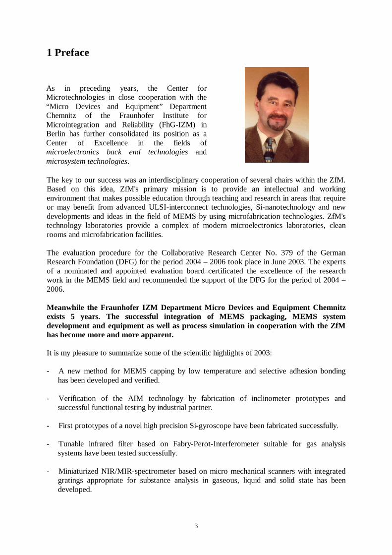
1 Preface The key to our success was an interdisciplinary cooperation of several chairs within the ZfM. Based on this idea, ZfM's primary mission is to provide an intellectual and working environment that makes possible education through teaching and research in areas that require or may benefit from advanced ULSI-interconnect technologies, Si-nanotechnology and new developments and ideas in the field of MEMS by using microfabrication technologies. ZfM's technology laboratories provide a complex of modern microelectronics laboratories, clean rooms and microfabrication facilities. The evaluation procedure for the Collaborative Research Center No. 379 of the German Research Foundation (DFG) for the period 2004 – 2006 took place in June 2003. The experts of a nominated and appointed evaluation board certificated the excellence of the research work in the MEMS field and recommended the support of the DFG for the period of 2004 – 2006. Meanwhile the Fraunhofer IZM Department Micro Devices and Equipment Chemnitz exists 5 years. The successful integration of MEMS packaging, MEMS system development and equipment as well as process simulation in cooperation with the ZfM has become more and more apparent. It is my pleasure to summarize some of the scientific highlights of 2003: - A new method for MEMS capping by low temperature and selective adhesion bonding
has been developed and verified. - Verification of the AIM technology by fabrication of inclinometer prototypes and
successful functional testing by industrial partner. - First prototypes of a novel high precision Si-gyroscope have been fabricated successfully. - Tunable infrared filter based on Fabry-Perot-Interferometer suitable for gas analysis
systems have been tested successfully. - Miniaturized NIR/MIR-spectrometer based on micro mechanical scanners with integrated
gratings appropriate for substance analysis in gaseous, liquid and solid state has been developed.
As in preceding years, the Center for Microtechnologies in close cooperation with the “Micro Devices and Equipment” Department Chemnitz of the Fraunhofer Institute for Microintegration and Reliability (FhG-IZM) in Berlin has further consolidated its position as a Center of Excellence in the fields of microelectronics back end technologies and microsystem technologies.

4
- Measurement and comparison of the thermal conductivity of a variety of low k and ULK dielectrics as well as thermal modelling of low k material containing interconnect schemes
- Development of an ultrathin, amorphous PECVD WN diffusion barrier for Copper
damascene metallization with a thermal stability of up to 600°C - SiO2 aerogel as ultra low k dielectric integrated into 3-level Copper metallization of RF
devices showing decreased capacitive coupling and improved Q-factor of inductors (in close cooperation with Infineon Technologies)
- New reduced order modelling features of MEMS provide efficient means for data
exchange from component models to circuit and system simulation environment. - Novel frequency selective vibration sensor arrays have been successfully integrated into a
user programmable vibration measurement unit for wear state monitoring. The 2003 Annual Report of the Center for Microtechnologies provides an overview of the facilities, staff, faculty and students associated with the ZfM, as well as a description of many of the ongoing research projects which make use of the ZfM facilities. These developments, which are based on close links with industry and cooperation with German as well as international institutes, contribute to an advanced education for our students. We kindly acknowledge the support of the Federal Ministry of Research, the German Research Foundation, the Saxon Ministry of Science and the European Commission. As always, we are driven by our triple aims of excellence in education, scientific and techno-logical research and by providing a comprehensive range of research and development services to industry. I would like to thank all my colleagues, the scientific fellows and technicians for all their dedicated work. I look forward to participating in the promising development of new devices and concepts through the use of silicon technology.
5
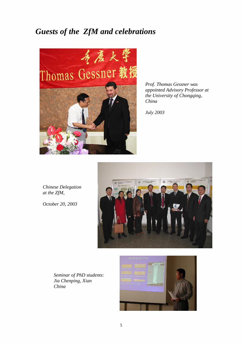
Guests of the ZfM and celebrations
Prof. Thomas Gessner was appointed Advisory Professor at the University of Chongqing, China July 2003
Chinese Delegation at the ZfM, October 20, 2003
Seminar of PhD students: Jia Chenping, Xian China
6
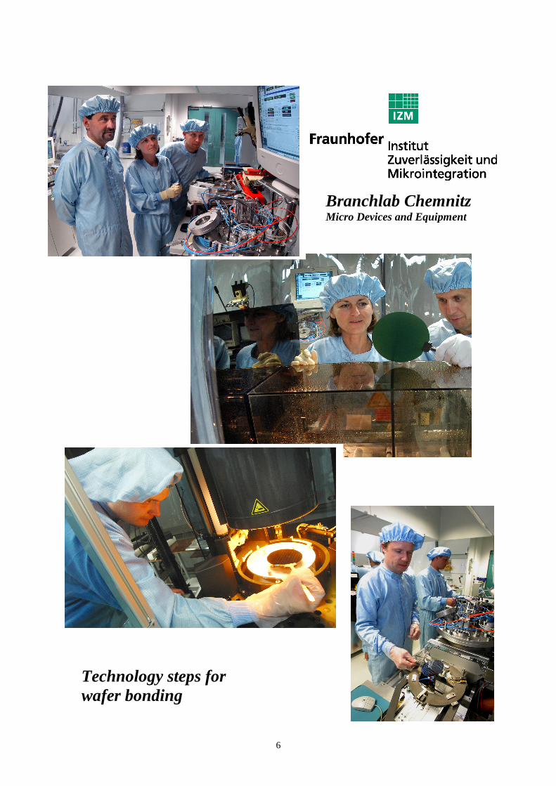
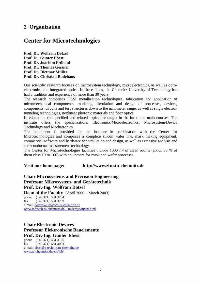
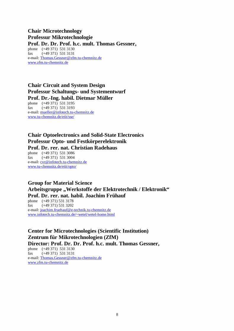
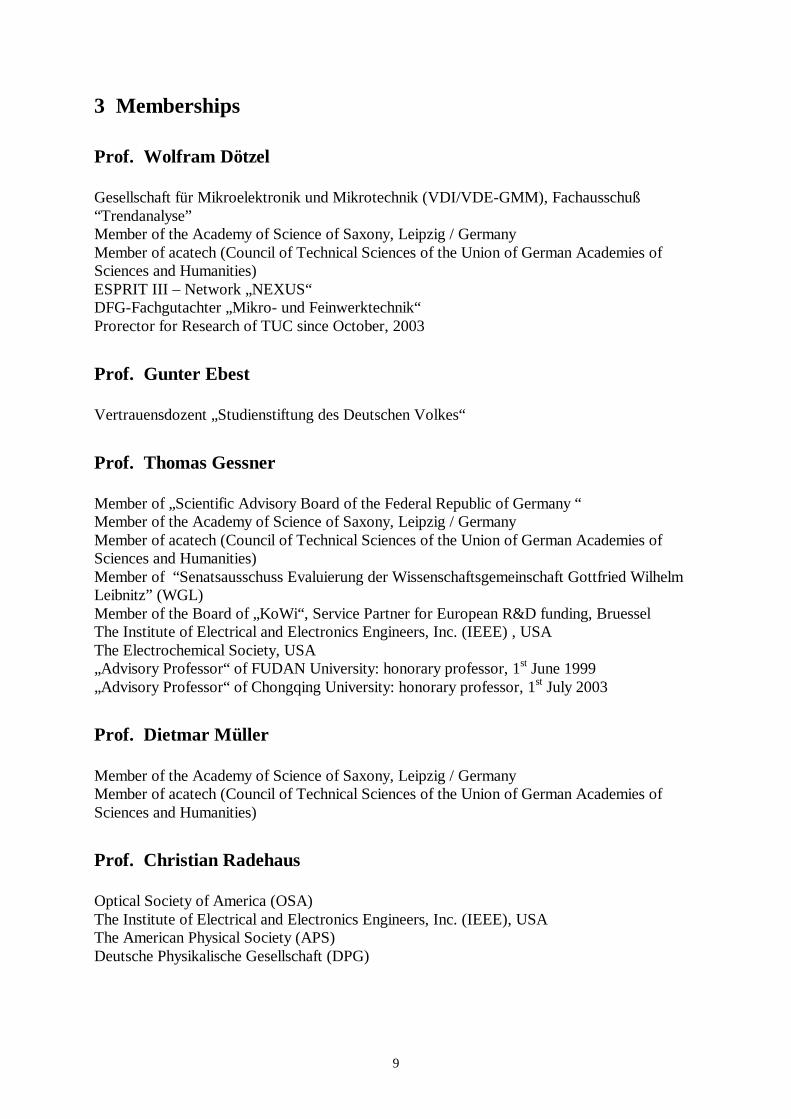
Branchlab Chemnitz Micro Devices and Equipment
Technology steps for wafer bonding
7
2 Organization Center for Microtechnologies Prof. Dr. Wolfram Dötzel Prof. Dr. Gunter Ebest Prof. Dr. Joachim Frühauf Prof. Dr. Thomas Gessner Prof. Dr. Dietmar Müller Prof. Dr. Christian Radehaus Our scientific research focuses on microsystem technology, microelectronics, as well as opto-electronics and integrated optics. In these fields, the Chemnitz University of Technology has had a tradition and experience of more than 30 years. The research comprises ULSI metallization technologies, fabrication and application of micromechanical components, modeling, simulation and design of processes, devices, components, circuits and test structures down to the nanometer range, as well as single electron tunneling technologies, nonlinear photonic materials and fiber optics. In education, the specified and related topics are taught in the basic and main courses. The institute offers the specializations Electronics/Microelectronics, Microsystem/Device Technology and Mechatronics. The equipment is provided for the institute in combination with the Center for Microtechnologies and comprises a complete silicon wafer line, mask making equipment, commercial software and hardware for simulation and design, as well as extensive analysis and semiconductor measurement technology. The Center for Microtechnologies facilities include 1000 m² of clean rooms (about 30 % of them class 10 to 100) with equipment for mask and wafer processes. Visit our homepage: http://www.zfm.tu-chemnitz.de Chair Microsystems and Precision Engineering Professur Mikrosystem- und Gerätetechnik Prof. Dr.-Ing. Wolfram Dötzel Dean of the Faculty (April 2000 – March 2003) phone (+49 371) 531 3264 fax (+49 371) 531 3259 e-mail: [email protected] www.infotech.tu-chemnitz.de/ ~microsys/index.html Chair Electronic Devices Professur Elektronische Bauelemente Prof. Dr.-Ing. Gunter Ebest phone (+49 371) 531 3125 fax (+49 371) 531 3004 e-mail: [email protected] www.tu-chemnitz.de/etit/leb/
8
Chair Microtechnology Professur Mikrotechnologie Prof. Dr. Dr. Prof. h.c. mult. Thomas Gessner, phone (+49 371) 531 3130 fax (+49 371) 531 3131 e-mail: [email protected] www.zfm.tu-chemnitz.de
Chair Circuit and System Design Professur Schaltungs- und Systementwurf Prof. Dr.-Ing. habil. Dietmar Müller phone (+49 371) 531 3195 fax (+49 371) 531 3193 e-mail: [email protected] www.tu-chemnitz.de/etit/sse/ Chair Optoelectronics and Solid-State Electronics Professur Opto- und Festkörperelektronik Prof. Dr. rer. nat. Christian Radehaus phone (+49 371) 531 3086 fax (+49 371) 531 3004 e-mail: [email protected] www.tu-chemnitz.de/etit/opto/
Group for Material Science Arbeitsgruppe „Werkstoffe der Elektrotechnik / Elektronik“ Prof. Dr. rer. nat. habil. Joachim Frühauf phone (+49 371) 531 3178 fax (+49 371) 531 3202 e-mail: [email protected] www.infotech.tu-chemnitz.de/~wetel/wetel-home.html
Center for Microtechnologies (Scientific Institution) Zentrum für Mikrotechnologien (ZfM) Director: Prof. Dr. Dr. Prof. h.c. mult. Thomas Gessner, phone (+49 371) 531 3130 fax (+49 371) 531 3131 e-mail: [email protected] www.zfm.tu-chemnitz.de
9
3 Memberships Prof. Wolfram Dötzel Gesellschaft für Mikroelektronik und Mikrotechnik (VDI/VDE-GMM), Fachausschuß “Trendanalyse” Member of the Academy of Science of Saxony, Leipzig / Germany Member of acatech (Council of Technical Sciences of the Union of German Academies of Sciences and Humanities) ESPRIT III – Network „NEXUS“ DFG-Fachgutachter „Mikro- und Feinwerktechnik“ Prorector for Research of TUC since October, 2003
Prof. Gunter Ebest Vertrauensdozent „Studienstiftung des Deutschen Volkes“
Prof. Thomas Gessner Member of „Scientific Advisory Board of the Federal Republic of Germany “ Member of the Academy of Science of Saxony, Leipzig / Germany Member of acatech (Council of Technical Sciences of the Union of German Academies of Sciences and Humanities) Member of “Senatsausschuss Evaluierung der Wissenschaftsgemeinschaft Gottfried Wilhelm Leibnitz” (WGL) Member of the Board of „KoWi“, Service Partner for European R&D funding, Bruessel The Institute of Electrical and Electronics Engineers, Inc. (IEEE) , USA The Electrochemical Society, USA „Advisory Professor“ of FUDAN University: honorary professor, 1st June 1999 „Advisory Professor“ of Chongqing University: honorary professor, 1st July 2003
Prof. Dietmar Müller Member of the Academy of Science of Saxony, Leipzig / Germany Member of acatech (Council of Technical Sciences of the Union of German Academies of Sciences and Humanities)
Prof. Christian Radehaus Optical Society of America (OSA) The Institute of Electrical and Electronics Engineers, Inc. (IEEE), USA The American Physical Society (APS) Deutsche Physikalische Gesellschaft (DPG)

10
Since 1998 a strong co-operation exists between the Fraunhofer Institute for Reliability and Microintegration (FhG-IZM, Berlin) and the Center for Microtechnologies. Accordingly the department “Micro Devices and Equipment” (MDE) was founded to combine the packaging know-how of the FhG-IZM with the silicon MEMS devices of the Center for Microtechnologies. The research activities of the department MDE are focused on the following topics:
• Development of MEMS: Sensors (kinetic, pressure, force, chemical) and actuators (scanner) are transferred into the system level (e.g. micro spectrometer).
• Development of advanced technologies like CMP (chemical mechanical polishing)
and 3D-patterning by deep silicon etching as well as increasing the core competence in MEMS packaging (chip and wafer bonding including combinations of new materials and bonding at low temperatures)
• Process and equipment simulation: The goal is the improvement of deposition and
etch rates, uniformity and fill behavior of vias and trenches by optimizing process conditions and reactor design.
• MEMS design and simulation:
- New reduced order modelling features of MEMS provide efficient means for data exchange from component models to circuit and system simulation environment. - Novel frequency selective vibration sensor arrays have been successfully integrated into a user programmable vibration measurement unit for wear state monitoring.
One special task of the new assembly technologies development is the combination of silicon micromechanics with down scaled traditional precision mechanics enabling new devices and new low cost fabrication technologies. This is a main challenge in order to push the activities concerning the development and implementation of microsystems for small and medium size enterprises in a short-term period.
In general the strategic alliance between the Fraunhofer Institute for Reliability and Microintegration, department MDE and the Center for Microtechnologies as described ensures strong synergies in the technology and device development.
Fraunhofer Institute Reliability and Microintegration Branchlab Chemnitz Department: Micro Devices and Equipment
Director: Prof. Thomas Gessner Management: Dr. Thomas Otto
11
Nanotechnology Center of Excellence "Ultrathin Functional Films" The Center of Excellence "Ultrathin Functional Films" (UFF), distinguished by the Federal Ministry of Research (BMBF) as a nation-wide center, is coordinated by Fraunhofer-IWS Dresden. It joins 51 enterprises, 10 university institutes, 22 research institutes, and 6 corporations into a common network. Nanotechnology is one of the key technologies of the 21st century. In order to channel the research results already available at institutes and universities as well as the growing demand from industry, the Nanotechnology Centers of Excellence (CE) had been established in 1998. The Center for Microtechnologies is an active member within this center, especially in the field of microelectronics related topics. Contact: Office of Center of Excellence "Ultrathin Functional Films" at Fraunhofer-IWS Dresden Dr. Ralf Jaeckel Phone +49 (0) 351 / 25 83 444, Fax +49 (0) 351 / 25 83 300 Activities within the frame of Nano-CE-UFF are subdivided into 6 Working Groups (WG), every one of which is administered and coordinated by one member:
WG 1: Advanced CMOS WG 2: Novel components WG 3: Biomolecular films for medical and technological purposes WG 4: Mechanical and protective film applications WG 5: Ultrathin films for optics and photonics WG 6: Nano-size actorics and sensorics
The Working Groups, in which the Center for Microtechnologies is mainly involved, are described shortly in the following: Advanced CMOS Structural widths of about 200nm are state-of-the-art in CMOS technology. A reduction down to below 100nm within 10 years, for further miniaturization, is envisaged by the Semiconductor Roadmap (by Semiconductor Industry Association (SIA) and SEMATECH). Along with this trend, higher frequency and reliability are required. This implies novel developments in materials and processes for both the active elements and the interconnect system, including advanced equipment for larger Si-wafer production. Most present-day systems are made of contacts (e.g. titanium or cobalt silicide), barrier layers (TiN, TiW), isolating interlayers (SiO2), interlayer connections and conducting paths (Al-alloys). Copper with its high conductivity and stability with respect to electromigration is being introduced as conductor material leading to higher frequency and reliability. This requires a precise technology of copper deposition (aspect ratio > 3) and patterning and the availability of suitable barrier layers suppressing interdiffusion and reactions. The barrier layers must not affect the conductivity of the paths remarkably, which requires ultra-thin films. Interfaces and nanometer scale effects become increasingly important. Head of the Working Group: Prof. Dr. Thomas Gessner
Chemnitz University of Technology Novel components The continuing trend towards miniaturization of integrated circuits has given rise to increasing efforts to supplement and gradually replace conventional CMOS-technologies by nanotechnologies and nanoelectronics in near future. The latter include magneto-electronics,
12
and single electron devices, nanocluster storage elements, and resonant tunneling elements, among others. There is a new generation of novel components based on the transfer of individual electrons in nanoscale structures. Work centers on memory elements based on the transfer of individual electrons between metal electrodes and on the memory effect of semiconductor nanoclusters in SiO2 films. Head of the Working Group: Prof. Dr. Christian Radehaus Chemnitz University of Technology
4 Research activities of ZfM in cooperation with the FhG-IZM-branchlab Chemnitz Fields of research
• Design and fabrication of microelectronical and micromechanical elements and arrays • ULSI metallization • High temperature stable metallization • Analysis of micromechanical systems • Development and application of design tools and methods for micromechanical
components and systems & coupled field analysis • Experimental analysis of microsystems • Analysis of different interferences on micromechanical systems, reduction or
compensation of these interferences • Coupling of microsystems and instrumentation (mechanical, electrical, thermal and
substantial interfaces) • Function, principles and modelling of electronic devices (test structures, parameter
extraction, model building) • Microelectronic circuit design (read out- and controlling circuits for sensors and actuators) • MIS – solar cells (manufacturing, analysis, measuring and modelling) & multicristalline
solar cells • Electronics for micro-electromechanical systems (MEMS) • Design of reusable modules • Development of infrared measurement systems • Nanoelectronics • Integrated Optics • Colour measurement
Subjects of research
• Microfabricated scanner arrays • Electostatically driven torsion actuators with one or two DOF • High temperature applications of MEMS, e.g. gas sensor for exhaust measurement • Vibration monitoring based on Si-sensor arrays • Sensor / actuator systems for high precision scanning with a large vertical range • Transportation systems by using MEMS-actuators

13
• Gyroscopes • Simulation of micromechanical and microelectronical components, materials databases • Design tools for microsystems and microelectronics • Macromodels for simulation of micromechanical components using PSpice • Design and fabrication of integrated optical waveguides on silicon • Fiber-optical communication systems • Single Electron Tunnelling Technologies • Colour measurement and sensors • Orientation dependent etching of silicon: Development of etchants and determination of
etch rates, design of etch masks and simulation of etch process, development of new structures by multi-step etch processes
• Geometrical measurement on microstructures • Plastic deformation of silicon-microstructures • Copper metallization • Low k dielectrics • Equipment and process simulation for microelectronics • Development of probing equipment for 1/f measurements • Microwave Device and Circuit Design and Simulation • Reliability analyses 4.1 Current research projects BMBF Project „Verbesserung der Performance von Ics durch Integration von Kupfer und low-k Dielektrika - PERFECT“ Project Manager: Prof. T. Gessner Project Leader: Chemnitz University of Technology Partners: Infineon Technologies AG Munich, DaimlerChrysler AG Ulm,
Dresden University of Technology, University of Hannover Project duration: 01.11.2000 - 28.02.2004 Project goal: Application of Copper interconnects for mobile communication IC´s, power devices and micrometer wave devices; Integration of organic
low k dielectrics into Copper Damascene metallization BMBF Project „Herstellung und Charakterisierung ultra-dünner nanostrukturierter Diffusionsbarrieren auf Tantal- und Wolfram-Basis für Metallisierungen in der <0.15 µm Technologie - Ultradünne Barrieren“ Project Leader: AMD Saxony LLC & Co KG, Dresden Partners: Dresden University of Technology, Leibnitz-Institut für Festkörper-
und Werkstoffforschung Dresden Subproject TUC: Diffusionsbarrieren auf Wolfram-Basis (tungsten based diffusion
barriers) Project Manager: Prof. T. Gessner / Dr. S. E. Schulz Project duration: 01.08.2000 - 31.12.2003 Project goal: Process development and characterization of ultrathin diffusion barriers
14
BMBF Project „IPQ (IP Qualification)“ Project Manager: Prof. D. Müller Project duration: 01.07.2001 - 31.03.2004 Project goal: The methodologies and tools developed in the project IPQ are targeted on
significant improvements in quality assurance in the development and ap-plication of Intellectual Property (IP). This includes the development of new methods for IP specification, intelligent IP retrievel, techniques for (semi)automatic IP adaptation as well as contributions to IP standardisa-tion activities.
BMWi Projekt „Optimization of the multicrystalline solar cell process by means of RTP and RIE“ Project manager: Prof. G. Ebest Partners: RWE Schott Solar, Alzenau Project duration: 01. 04. 2001 – 31. 03. 2004 Project goal: Proof of rapid thermal processing and reactive ion etching for solar cell fabrication
BMBF Project „Electronic compensation of fabrication tolerances of microsystem products demonstrated for a multi sensor for navigation (EKOFEM)“ Project Manager: Prof. T. Gessner Partners: LITEF GmbH Freiburg, GEMAC mbh Chemnitz, FhG IZM,
Department Chemnitz Project duration: 01. 10. 2001 – 31. 12. 2004 Project goal: Development of electronic compensation methods of fabrication
tolerances and their application for a high precision silicon multisensor (acceleration and angular rate measurement)
SMWA Project „Spectral tunable infrared sensor“ Project Manager: Prof. T. Gessner Partners: InfraTec GmbH Dresden, FhG IZM, Department Chemnitz Project duration: 01. 01. 2001 – 31. 03. 2003 Project goal: Development of layout and technology for a micromachined Fabry-
Perot-Interferometer for IR applications; Fabrication of prototypes SMWA Project „Mikroelektronisches Zündelement für Insassen - Sicherheitssysteme“ Project Manager: Prof. T. Gessner Partners: Flexiva automation & Anlagenbau GmbH, Amtsberg;
Fahrzeugelektrik Pirna GmbH Project duration: 01.10. 2003 – 31.12. 2004 Project goal: Development of a new airbag igniter SMWA Project „Entwicklung mikromechanischer Spiegel für ein IR-Analysesystem“ Project Manager: Prof. T. Gessner Partners: FhG IZM Abteilung Micro Devices and Equipment COLOUR CONTROL Farbmeßtechnik GmbH OPTUM Umwelttechnik GmbH Project duration: 01.01.2001 – 31.1.2003 Project goal: Development of an IR-Spectrometer with a micromechanical mirror with a special reflective grating on the mirror surface

15
SMWA Project „VIBSENS: Abstimmbares frequenzselektives Sensorsystem zur Messung mechanischer Schwingungen“ Project Manager: Prof. T. Gessner Partners: GEMAC mbh Chemnitz Project duration: 01.01.2002 – 31.12.2003 SMWA Project „Modular measurement system consisting of a tunable FPI and IR sensor - MODUL“ Project Manager: Prof. T. Gessner Partners: Infra Tec GmbH Dresden, GEMAC mbh Chemnitz Project duration: 01.09.2003 – 31.08.2005 Project goal: Development of layout and technology for a micromachined Fabry-
Perot-Interferometer; Fabrication of prototypes DFG Project „Poröse Polymere als low-k Dielektrika für Metallisierungssysteme in der Mikroelektronik“ Project Manager: Prof. T. Gessner Partners: BTU Cottbus Project duration: 01.02.2002 - 31.01.2004 Project goal: Development and characterization of organic ultra low k material with
reduced density; Patterning process development and compatibility with copper interconnect processing.
DFG Project ”Reshaping of silicon microstructures by Laser – a new micro-technological process“ Project Manager: Prof. J. Frühauf Partner: HTW Mittweida Project duration: 04.09.2000 – 31.12.2003 Project goal: Reshaping without tool, minimizing of thermal load, development of new shapes IST-Project “ULISSE : Ultra low k dielectrics for Damascene copper interconnects schemes” Project Manager: Prof. T. Gessner Partners: Infineon Technologies (D), Philips Res. Leuven (B), IMEC Leuven (B),
ST Microelectronics (F), Bull S.A. (F), LETI Grenoble (F) - (Project Leader)
Project duration: 01.09.2001 – 31.10.2003 Project goal: Integration of ultra low k dielectrics Website: www-leti.cea.fr/commun/europe/ulisse/ulisse.htm SEA-Project “ACTION : Advanced CVD tool for integration of organosilicated nanoporous films” Project Manager: Prof. T. Gessner / Dr. S. E. Schulz Project Leader: ST Microelectronics, Crolles (F) Partners: AMD Saxony LLC & Co KG (D), Philips Res. Leuven (B), LETI
Grenoble (F), Sematech (USA), TRIKON Technologies (UK) Project duration: 01.05.2002 – 31.01.2004 Project goal: (selected) Provide organosilicated glass (OSG) material with a k-value
of 2.2 for interconnect applications for the 90 nm node; Prove cluster tool for full inter metal dielectric (IMD) stack; Demonstrate flexibility

16
for customized dual-damascene stack architectures; Show Cost-effectiveness compared to multi-tool Spin-on Dielectrics (SOD) methods; Demonstrate performance within a 300 mm production environment.
www.sea.rl.ac.uk EU-Project Intelligent Manufacturing Systems: “Optical Characterisation Methods for MEMS Manufacturing - OCMMM“ Project Manager: Prof. T. Gessner Partners: GF Messtechnik GmbH (GFM), FhG.IWU, University of Twente-
MESA, Thales Avionique (TH-AV), Yole Développement (YOLE), LioniX (LION), Warsaw University of Technology (WUT)
Project duration: 01. 01. 2001 – 31. 12. 2003 Project goal: Optical Characterisation Methods for MEMS Manufacturing Industrial Research Contract „Fabrication of multi-use acceleration sensors“ Project Manager: Prof. T. Gessner Partners: Fara New Technologies, Xi´an, China, GEMAC mbH Chemnitz Project duration: 01. 09. 2001 – 31. 08. 2003 Project goal: Development of an high precision acceleration sensor system and its
fabrication technology; Fabrication of prototypes Industrial Research Contract „Development of silicon gratings for the assessment of optical and tactile surface measuring instruments“ Project Manager: Prof. J. Frühauf Partners: GEMAC mbH Chemnitz Project duration: 15. 09. 2003 – 31. 01. 2004 Project goal: Etching of silicon gratings with trapezoidal, triangular, rectangular and
arched profiles Stiftung Industrieforschung : „Catalogue of Shape and Functional Elements of Bulk-Silicon Microtechnique“ Project Manager: Prof. Dr. J. Frühauf Project duration: 01. 04. 2002 – 31. 12. 2003 Project goal: Systematical description of shapes and functions realisable by
anisotropic wet etching Project „Design of complex sensor – actuator systems [EKOSAS]“ Project Manager: Prof. W. Dötzel, Dr. J. Mehner Partner: Siemens AG Munich, CAD-FEM GmbH Grafing, GEMAC mbH Chemnitz, AST Dresden, Univ. Erlangen, FhG IIS/EAS Dresden Project duration: 01. 01. 2000 – 31. 03. 2003 Project goal: The goal of the project is to develop methods and tools for modeling and
simulation of complex microelectromechanical systems which are characterized by strong interactions between physical domains and to the electronic circuitry.
DFG Project „VIVA – Low Power System Bus Encoding“ Project Manager: Prof. D. Müller Project duration: 01.07.1999 - 31.03.2005 Project goal: Development and implementation of coder-decoder systems for SOC sy-

17
stem busses which minimize under a set of constraints the total power dissipation on a system bus with its coder and decoder implementation
through reduction of switching activity on this bus.
Project „Interface-based Design of complex digital Systems“ Project Manager: Prof. D. Müller Project duration: 01.07.1999 - 31.03.2003 Project goal: The focus of this project are the development of methods for modelling
communication between modules of highly complex systems at different levels of abstraction in terms of hierarchically layered data communication protocols and the realization of corresponding description formalisms as an extension of the language SystemC.
Project „Solutions in the field of color image processing“ Project Manager: Prof. D. Müller Partners: Siemens A&D Nürnberg, Sächsisches Textilforschungsinstitut STFI
Chemnitz Project duration: 01.12.2003 - 30.06.2004 Project goal: Evaluation of new algorithms in the field of image processing by using
FPGAs and realtime processing, investigation of color spaces and classification for color image analysis.
Service order No. 5 for master agreement research and development, entered by AMD and Technische Universität Chemnitz
Project Manager: Prof. C. Radehaus Project duration: 1. 8. 2003 - 28.02. 2004 Project goal: Automation of the software system GOPI modelling CV-characteristics
of gate-oxide-structures – within the framework of the GOPI model – to estimate the parameters
Nano-Technology Center of Excellence “Ultrathin Functional Films”: Pesticide-Sensors based on Immunochemical Reactions and Nano-Electrodes Project Manager: Prof. C. Radehaus Project duration: 1.3. 2003 - 31.8. 2003 Project goal: Integration of electronic and optical materials in functional plastic Bio-chips Project: "Entwicklung von Packagingtechnologien für Bauelemente in Oberflächen- technologie"
Project Manager: M. Krusche, Amtec GmbH Partners: FhG IWU, TU Chemnitz, Gemac GmbH, Amtec GmbH Project duration: 05/2002 – 04/2004 Project goal: MEMS packaging for surface micro machined devices Project: „Prüf- und Qualitätssicherungssystem für die industrielle Fertigung von wafergebondeten Mikrosystemen“ (Mikroprüf) Project Manager: Dr. H. Reinecke, Steag microParts GmbH Partners: FhG IWM Halle, TU Chemnitz, X-Fab GmbH, Robert Bosch GmbH,
Hegewald & Peschke Mess- und Prüftechnik GmbH Project duration: 11/2002 – 10/2005
18
4.2 Collaborative Research Center No. 379 : (Sonderforschungsbereich SFB Nr. 379) 01. 01. 1995 – 31. 12. 2006 „Arrays of micromechanical sensors and actuators“ The MEMS research field covers several provinces using different microtechnology methods
for the fabrication.
The subject of the SFB deals with the well-defined part of the microsystems research:
“The realization of sensor and actuator arrays consisting of a number of single components”.
Thus, results concerning the behavior and new application fields of the devices would be
expected. As a vision of the future it is aimed toward a system which combines the arrays
with the electronics by microtechnology integration.
Within the focus of interest are the following topics:
• Micromechanical scanning devices (actuators fabricated in bulk and surface micromachining)
• Use of micromechanical basic components, e.g. for ultrasonic arrays and positioning systems, including the application of new materials
• Developing further a SCREAM-based Technology The following institutions are working together Faculty of Electrical Engineering and Information Technology Chair Circuit Technology, Prof. Dr. Reinald Brumme Chair Microsystems and Precision Engineering, Prof. Dr. Wolfram Dötzel Chair Electronic Devices, Prof. Dr. Gunter Ebest Group Material Science, Prof. Dr. Joachim Frühauf Chair Microtechnology, Prof. Dr. Thomas Gessner Chair Measurement and Sensor Technology, Prof. Dr. Wolfgang Manthey Chair Circuit and System Design, Prof. Dr. Dietmar Müller Chair Optoelectronics & Solid-State Electronics, Prof. Dr. Christian Radehaus Faculty of Natural Science Chair Semiconductor Physics, Prof. Dr. Dietrich R. T. Zahn Chair Solid Surfaces Analysis, Prof. Dr. Michael Hietschold Faculty of Mechanical Engineering Chair Production Technology, Prof. Dr. Michael Dietzsch Chair Printmedia Technology, Prof. Dr. Arved Huebler
Fraunhofer Institute „Reliability and Microintegration“, Branchlab Chemnitz Head of the Institute: Prof. Dr. Bernd Michel
Institut für Mechatronik e.V. Chemnitz, Prof. Dr. Peter Maißer
19
Subproject A1: “Design of micromechanical components”
• Prof. Dr. Wolfram Dötzel • Prof. Dr. Joachim Frühauf
Author: Eva Gärtner The goal of the subproject A1 is to design micromechanical components that are used within the SFB 379 and to predict their behaviour. This work comprises the following topics:
• Development of design algorithms and tools to capture the specific behaviour of array structures (coupled electromechanical and fluidmechanical fields, interactions between array cells, warping of thin plates caused by thermomechanical and intrinsic stress)
• Modelling and simulation of new micromechanical components used by other subprojects • Fracture strength of in-plane parallel spring arrays etched from silicon • Design of new shape elements needed for mechanical and optical applications
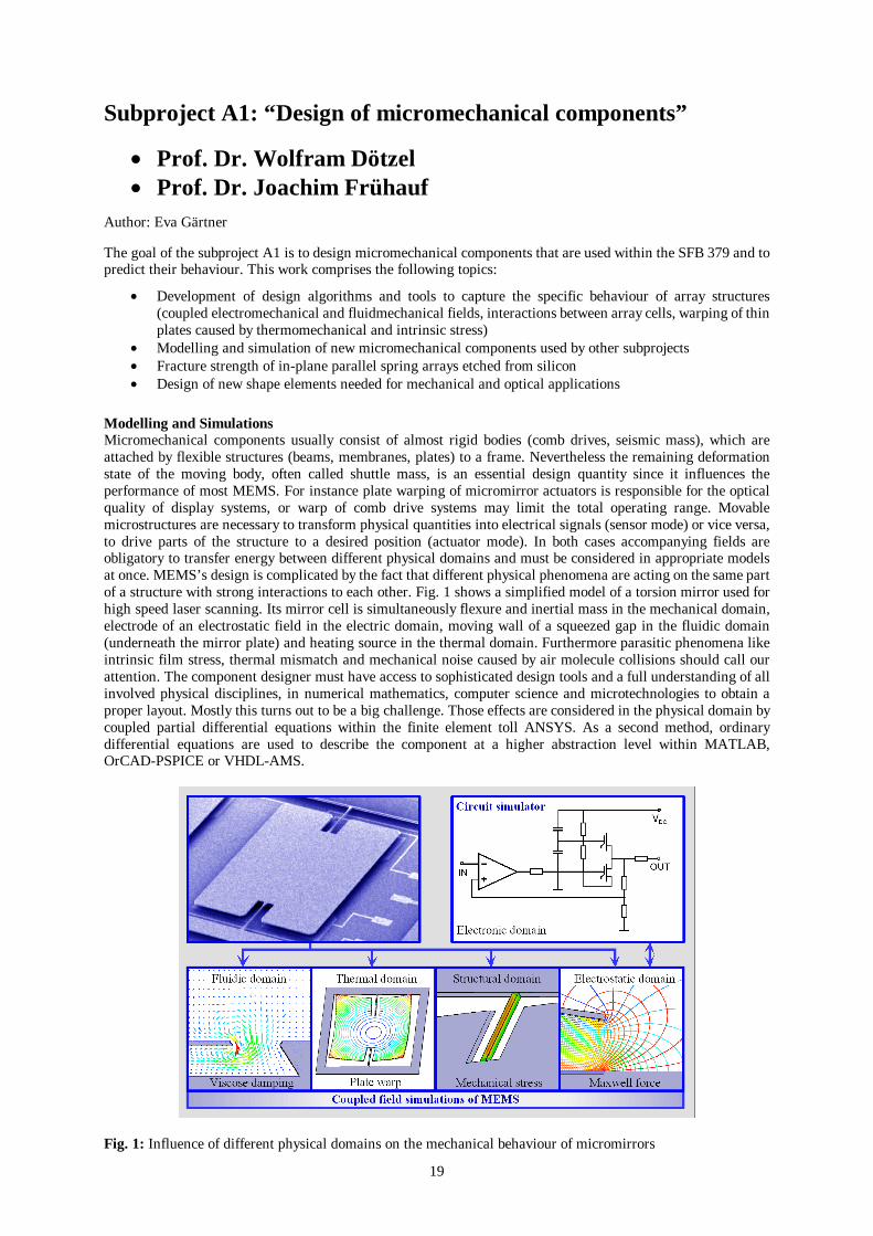
Modelling and Simulations Micromechanical components usually consist of almost rigid bodies (comb drives, seismic mass), which are attached by flexible structures (beams, membranes, plates) to a frame. Nevertheless the remaining deformation state of the moving body, often called shuttle mass, is an essential design quantity since it influences the performance of most MEMS. For instance plate warping of micromirror actuators is responsible for the optical quality of display systems, or warp of comb drive systems may limit the total operating range. Movable microstructures are necessary to transform physical quantities into electrical signals (sensor mode) or vice versa, to drive parts of the structure to a desired position (actuator mode). In both cases accompanying fields are obligatory to transfer energy between different physical domains and must be considered in appropriate models at once. MEMS’s design is complicated by the fact that different physical phenomena are acting on the same part of a structure with strong interactions to each other. Fig. 1 shows a simplified model of a torsion mirror used for high speed laser scanning. Its mirror cell is simultaneously flexure and inertial mass in the mechanical domain, electrode of an electrostatic field in the electric domain, moving wall of a squeezed gap in the fluidic domain (underneath the mirror plate) and heating source in the thermal domain. Furthermore parasitic phenomena like intrinsic film stress, thermal mismatch and mechanical noise caused by air molecule collisions should call our attention. The component designer must have access to sophisticated design tools and a full understanding of all involved physical disciplines, in numerical mathematics, computer science and microtechnologies to obtain a proper layout. Mostly this turns out to be a big challenge. Those effects are considered in the physical domain by coupled partial differential equations within the finite element toll ANSYS. As a second method, ordinary differential equations are used to describe the component at a higher abstraction level within MATLAB, OrCAD-PSPICE or VHDL-AMS.
Fig. 1: Influence of different physical domains on the mechanical behaviour of micromirrors
20
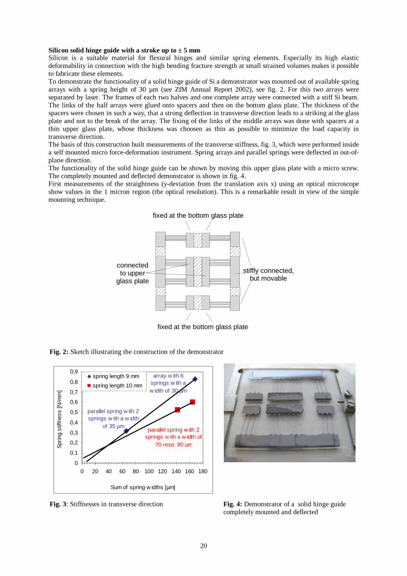
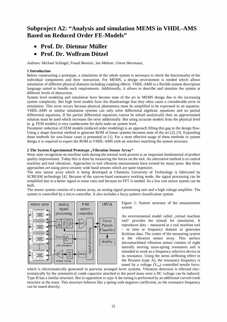
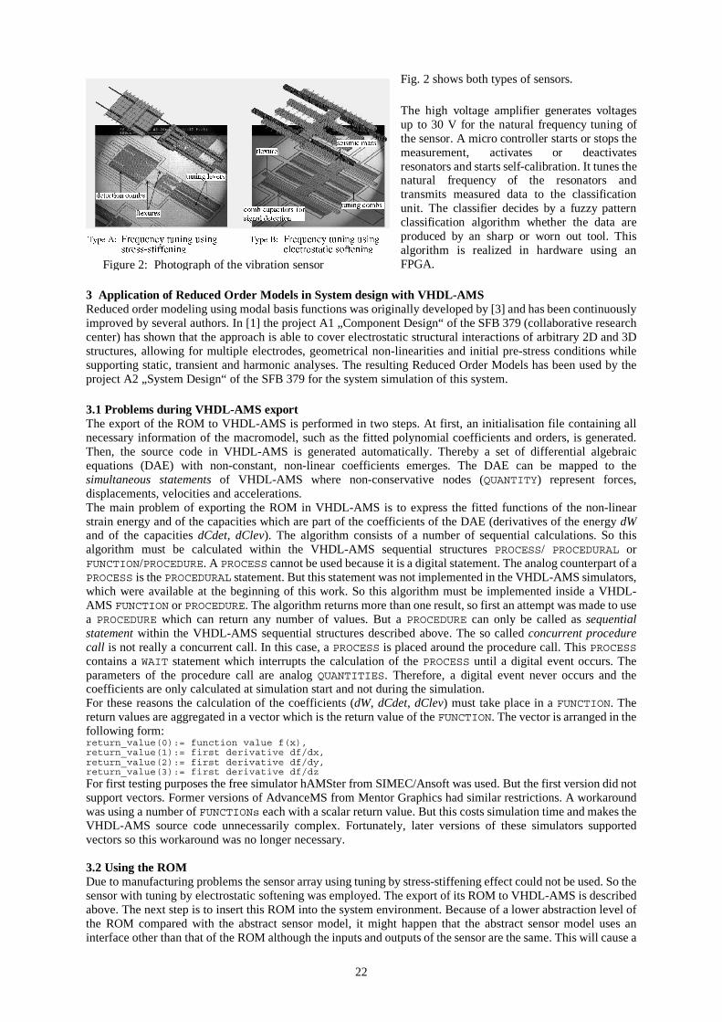
Silicon solid hinge guide with a stroke up to ± 5 mm Silicon is a suitable material for flexural hinges and similar spring elements. Especially its high elastic deformability in connection with the high bending fracture strength at small strained volumes makes it possible to fabricate these elements. To demonstrate the functionality of a solid hinge guide of Si a demonstrator was mounted out of available spring arrays with a spring height of 30 µm (see ZfM Annual Report 2002), see fig. 2. For this two arrays were separated by laser. The frames of each two halves and one complete array were connected with a stiff Si beam. The links of the half arrays were glued onto spacers and then on the bottom glass plate. The thickness of the spacers were chosen in such a way, that a strong deflection in transverse direction leads to a striking at the glass plate and not to the break of the array. The fixing of the links of the middle arrays was done with spacers at a thin upper glass plate, whose thickness was choosen as thin as possible to minimize the load capacity in transverse direction. The basis of this construction built measurements of the transverse stiffness, fig. 3, which were performed inside a self mounted micro force-deformation instrument. Spring arrays and parallel springs were deflected in out-of-plane direction. The functionality of the solid hinge guide can be shown by moving this upper glass plate with a micro screw. The completely mounted and deflected demonstrator is shown in fig. 4. First measurements of the straightness (y-deviation from the translation axis x) using an optical microscope show values in the 1 micron region (the optical resolution). This is a remarkable result in view of the simple mounting technique.
fixed at the bottom glass plate
connected to upper
glass plate
stiffly connected,but movable
fixed at the bottom glass plate Fig. 2: Sketch illustrating the construction of the demonstrator
0
0,1
0,2
0,3
0,4
0,5
0,6
0,7
0,8
0,9
0 20 40 60 80 100 120 140 160 180
Sum of spring w idths [µm]
Spr
ing
stiff
ness
[N/m
m]
spring length 9 mm
spring length 10 mm
array w ith 6 springs w ith a w idth of 30 µm
parallel spring w ith 2 springs w ith a w idth
of 35 µmparallel spring w ith 2
springs w ith a w idth of 70 resp. 80 µm
Fig. 3: Stiffnesses in transverse direction Fig. 4: Demonstrator of a solid hinge guide completely mounted and deflected
21
Subproject A2: “Analysis and simulation MEMS in VHDL-AMS Based on Reduced Order FE-Models”
• Prof. Dr. Dietmar Müller • Prof. Dr. Wolfram Dötzel
Authors: Michael Schlegel, Fouad Bennini, Jan Mehner, Göran Herrmann, 1 Introduction Before constructing a prototype, a simulation of the whole system is necessary to check the functionality of the individual components and their interaction. For MEMS, a design environment is needed which allows simulation of different physical domains including coupling effects. VHDL-AMS is a flexible system description language suited to handle such requirements. Additionally, it allows to describe and simulate the system at different levels of abstraction. System level modeling and simulation have become state of the art in MEMS design due to the increasing system complexity. But high level models have the disadvantage that they often cause a considerable error in simulation. This error occurs because physical phenomena must be simplified to be expressed in an equation. VHDL-AMS or similar simulation systems can only solve differential algebraic equations and no partial differential equations. If the partial differential equations cannot be solved analytically then an approximated solution must be used which increases the error additionally. But using accurate models from the physical level (e. g. FEM models) is very cumbersome for daily tasks on system level. Parameter reduction of FEM models (reduced order modeling) is an approach filling this gap in the design flow. Using a shape function method to generate ROM of linear systems becomes state of the art [2], [3]. Expanding these methods for non-linear cases is presented in [1]. For a most effective usage of these methods in system design it is required to export the ROM to VHDL-AMS with an interface matching the system structure. 2 The System Experimental Prototype „Vibration Sensor Array“ Wear state recognition on machine tools during the normal work process is an important fundamental of product quality improvement. Today this is done by measuring the forces on the tool. An alternative method is to control machine and tool vibrations. Approaches to tool vibration measurement have existed for many years. But these approaches are using pieco ceramic wide band sensors which are quite expensive. The new sensor array which is being developed at Chemnitz University of Technology is fabricated by SCREAM technology [4]. Because of the narrow-band resonance working mode, the signal processing can be simplified due to a better signal to noise ratio and because no FFT is needed. So a low cost sensor system can be built. The sensor system consists of a sensor array, an analog signal processing unit and a high voltage amplifier. The system is controlled by a micro controller. It also includes a fuzzy pattern classification system.
Figure 1: System structure of the measurement system An environmental model called „virtual machine tool“ provides the stimuli for simulation. It reproduces data – measured at a real machine tool – in time or frequency domain or generates fictitious data. The center of the measuring system is the vibration sensor array. This surface micromachined vibration sensor consists of eight laterally moving mass-spring resonators and is intended to work as a frequency selective device at its resonance. Using the stress stiffening effect in the flexures (type A), the resonance frequency is tuned by a voltage (Vtun) controlled tensile force,
which is electrostatically generated in pairwise arranged lever systems. Vibration detection is effected elec-trostatically by the symmetrical comb capacitor attached to the proof mass were a DC voltage can be induced. Type B has a similar structure. But in opposition to type A the tuning is performed by an additional curved comb structure at the mass. This structure behaves like a spring with negative coefficient, so the resonance frequency can be tuned directly.
22
Figure 2: Photograph of the vibration sensor The high voltage amplifier generates voltages up to 30 V for the natural frequency tuning of the sensor. A micro controller starts or stops the measurement, activates or deactivates resonators and starts self-calibration. It tunes the natural frequency of the resonators and transmits measured data to the classification unit. The classifier decides by a fuzzy pattern classification algorithm whether the data are produced by an sharp or worn out tool. This algorithm is realized in hardware using an FPGA.
3 Application of Reduced Order Models in System design with VHDL-AMS Reduced order modeling using modal basis functions was originally developed by [3] and has been continuously improved by several authors. In [1] the project A1 „Component Design“ of the SFB 379 (collaborative research center) has shown that the approach is able to cover electrostatic structural interactions of arbitrary 2D and 3D structures, allowing for multiple electrodes, geometrical non-linearities and initial pre-stress conditions while supporting static, transient and harmonic analyses. The resulting Reduced Order Models has been used by the project A2 „System Design“ of the SFB 379 for the system simulation of this system. 3.1 Problems during VHDL-AMS export The export of the ROM to VHDL-AMS is performed in two steps. At first, an initialisation file containing all necessary information of the macromodel, such as the fitted polynomial coefficients and orders, is generated. Then, the source code in VHDL-AMS is generated automatically. Thereby a set of differential algebraic equations (DAE) with non-constant, non-linear coefficients emerges. The DAE can be mapped to the simultaneous statements of VHDL-AMS where non-conservative nodes (QUANTITY) represent forces, displacements, velocities and accelerations. The main problem of exporting the ROM in VHDL-AMS is to express the fitted functions of the non-linear strain energy and of the capacities which are part of the coefficients of the DAE (derivatives of the energy dW and of the capacities dCdet, dClev). The algorithm consists of a number of sequential calculations. So this algorithm must be calculated within the VHDL-AMS sequential structures PROCESS/ PROCEDURAL or FUNCTION/PROCEDURE. A PROCESS cannot be used because it is a digital statement. The analog counterpart of a PROCESS is the PROCEDURAL statement. But this statement was not implemented in the VHDL-AMS simulators, which were available at the beginning of this work. So this algorithm must be implemented inside a VHDL-AMS FUNCTION or PROCEDURE. The algorithm returns more than one result, so first an attempt was made to use a PROCEDURE which can return any number of values. But a PROCEDURE can only be called as sequential statement within the VHDL-AMS sequential structures described above. The so called concurrent procedure call is not really a concurrent call. In this case, a PROCESS is placed around the procedure call. This PROCESS contains a WAIT statement which interrupts the calculation of the PROCESS until a digital event occurs. The parameters of the procedure call are analog QUANTITIES. Therefore, a digital event never occurs and the coefficients are only calculated at simulation start and not during the simulation. For these reasons the calculation of the coefficients (dW, dCdet, dClev) must take place in a FUNCTION. The return values are aggregated in a vector which is the return value of the FUNCTION. The vector is arranged in the following form: return_value(0):= function value f(x), return_value(1):= first derivative df/dx, return_value(2):= first derivative df/dy, return_value(3):= first derivative df/dz
For first testing purposes the free simulator hAMSter from SIMEC/Ansoft was used. But the first version did not support vectors. Former versions of AdvanceMS from Mentor Graphics had similar restrictions. A workaround was using a number of FUNCTIONs each with a scalar return value. But this costs simulation time and makes the VHDL-AMS source code unnecessarily complex. Fortunately, later versions of these simulators supported vectors so this workaround was no longer necessary. 3.2 Using the ROM Due to manufacturing problems the sensor array using tuning by stress-stiffening effect could not be used. So the sensor with tuning by electrostatic softening was employed. The export of its ROM to VHDL-AMS is described above. The next step is to insert this ROM into the system environment. Because of a lower abstraction level of the ROM compared with the abstract sensor model, it might happen that the abstract sensor model uses an interface other than that of the ROM although the inputs and outputs of the sensor are the same. This will cause a
Figure 2: Photograph of the vibration sensor
Fig. 2 shows both types of sensors.
23
lot of error prone work to adapt the system interface to the ROM interface. To avoid this, it must be assured that the ROM can use the same interface as the abstract model, wherefore a new methodical approach called „Multi Architecture Modeling“ - MAM [5], [6], [7] was created. The main idea of MAM is to use the interface, which will become necessary at a lower abstraction level (e. g., ROM) already at a high abstraction level (e. g., abstract sensor model). This avoids a lot of work because abstract models of a component can be replaced by detailed models or vice versa without any modification to the interface or the surrounding models. This approach was applied in the development of the sensor models. This means:
1. to examine which inputs and outputs, including power supply, the sensor will need, 2. which types of interfaces (conservative/non-conservative analog nodes, digital nodes) the ROM will need, 3. which data types/natures these interfaces will need, 4. development of the abstract sensor model with this collected information, 5. checking the functionality of the sensor in the system context, 6. development of the ROM from the sensor’s FEM model observing the information collected in steps 1 to 3, 7. to insert the ROM in the system model, 8. simulation of the complete system.
Without MAM, steps 1 to 3 would drop out and step 4 would be easier. But then step 7 would cause more work than needed for steps 1 to 4 because the system model must be adapted. If an error occurs after this adaptation it is not sure whether it was caused by the ROM or the adaptation. If MAM is used and the system model with the ROM is not working although it does with the abstract model then the error must be inside the ROM and the system simulation can be continued with the abstract model until a working ROM is available. 3.3 Simulation of the Sensor ROM By using the MAM approach, application of the ROM in the system context is very easy. First, the eight models for the individual resonators were tested separately to verify the method of reduced order modeling and the VHDL-AMS export. The results of these tests allowed to improve to the method of reduced order modeling and VHDL-AMS export. At the end of these tests the eight individual models were joined to the sensor ROM. Then the abstract model was replaced by the ROM simply by changing the name of the architecture which is to be instantiated in the VHDL-AMS system model. No further work was necessary. With the macromodel a complete measurement cycle has been simulated. 4 Results The following simulation has been done on a SUN ULTRA60 workstation with UltraSPARC-II 296 MHz CPU. An AC-simulation with a tuning voltage of 35 V and a stimulation magnitude of 0,6 mm led to the following results: Table 1. Results of AC Simulation
It was a surprise that the more accurate ROM can be simulated faster than the abstract model. But this can be explained simply: The abstract model contains a set of simple equations. The ROM contains less but more complex equations than the abstract model. Obviously, the smaller numbers of complex equations can be simulated faster than larger numbers of simple equations.
The results seem to show that the abstract model is more accurate than the ROM. But this effect occurs due to manufacturing tolerances of the real sensor. If the ROM is compared to the FEM Model the error will be less than 1 %. The simulation results of a transient simulation for 50 ms of the sensor and analog signal processing are shown in Table 2. Table 2. Results of Transient Simulation
Again it can be seen that the simulation with the macromodel is faster than the simulation with the abstract model. The ROM is also more accurate. By simulation of these system parts some side effects were determined, e. g., a „snapping“ of the resonators at high tuning voltages which was taken into account when assembling the prototype.
At last a simulation of the whole system was performed to select stimuli patterns for the fuzzy pattern classifier. This simulation was done on a SUN Blade2 with 900 MHz CPU and 4 GByte RAM. It took about 1 hour and 30 minutes. A simulation plot can be seen in Figure 3.
abstract, analytical
model
ROM Measured
natural frequency 1,8 kHz 1,7 kHz 1,7 kHz output voltage 0,6 V 0,8 V 0,5 V simulation time 7 sec. 2 sec.
abstract model
ROM
tuning voltage for a tuned natural frequency of cell 1 at 1 kHz
36,7 V 36,0 V
output voltage 1,2 V 1,1 V simulation time 15 min. 7 min.
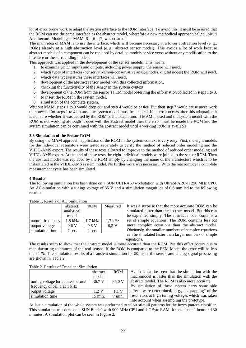
24
Figure 3: Plot of system simulation using sensor ROM The first two curves in this Figure display the applied tuning voltage and the output signal of the analog signal processing during a complete measurement cycle. The last curve shows the data sampled by the microcontroller which are transferred to the fuzzy pattern classifier. The differently grey backgrounds of the curves on the right show which sensor cell of the array is activated. In comparison to the manufactured system the simulation shows an error of approximately 3 % in frequency measurement and 40 % in amplitude measurement. These errors are due to manufacturing tolerances. Regarding the high
amplitude measurement error, it must be noted that the sensor works in a resonant mode, so even small manufacturing tolerances may cause big measurement errors. These errors cannot be predicted, neither by VHDL-AMS nor by FEM simulation. With the results of the system simulation it has been possible to select significant patterns for digital signal processing using the fuzzy pattern algorithm. 5 Conclusion Within this work it was shown that the application of reduced order modelling in system design is a powerful approach to higher accuracy and simulation speed. By using the reduced order model instead of the abstract model [8] the simulation error has been reduced from 20 % to below 1 % and the simulation speed has been doubled. The application of the Multi Architecture Modelling approach within this context assures an easy, fast and safe exchange of abstract and reduced order models. The approach of ROM including VHDL-AMS export is supported by a self developed EDA-Tool in combination with a commercial FEM simulator. In the future, this approach will be able to avoid a good deal of human work for developing abstract, less accurate models. References [1] Bennini, F.; Mehner, J.; Dötzel, W.: “Computational Methods for Reduced Order Modeling of Coupled Domain
Simulations”, 11 International Conference on Solid State Sensors and Actuators (Transducers 01), Germany, 2001 [2] Reitz, S.; Bastian, J.; Haase, J.; Schneider, P.; Schwarz, P.: “System Level Modeling of Microsystems using Order
Reduction Methods”, DTIP 2002, Cannes, France, 2002 [3] Gabbay, L.D.: “Computer-aided Macromodeling for MEMS”, Ph.D. dissertation, MIT Cambridge, MA, USA, 1998 [4] Mehner, J.; Scheibner, D.; Wibbeler, J.: “Silicon Vibration Sensor Arrays with Electrically Tunable Band Selectivity”,
MICRO SYSTEM Technologies 2001, Düsseldorf, Germany, 2001 [5] Schlegel, M.; Herrmann, G.; Müller, D.: “Application of „Multi Architecture Modeling“ design method in system level
MEMS simulation”, DTIP 2003, Mandelieu-La Napoule, France, 2003 [6] Schlegel, M.; Herrmann, G.; Müller, D.: “Multi-Architecture-Modeling: Entwurfsmethode für Mixed-Signal- und Multi-
Domain-Systemsimulation“, GI/ITG/GMM-Workshop: Methoden und Beschreibungssprachen zur Modellierung und Verifikation von Schaltungen und Systemen, Tübingen, Germany, 2002
[7] Schlegel, M.; Herrmann, G.; Müller, D.: “Multi Architecture Modeling Desing Method for Mixed Signal and Multi Domain System Simulation - First Solutions”, International MEMS Workshop, Singapore, 2001
[8] Schlegel, M.; Herrmann, G.; Müller, D.: “A system level model in VHDL-AMS for a micromechanic vibration sensor array”, IEEE International Conference on Sensors 2002, Orlando, USA, 2002
[9] Mehner, J. E. ; Gabbay, L.D.; Senturia, S.D.: “Computer-Aided Generation of Nonlinear Reduced-Order Dynamic Macromodels”, Journal of Microelectromechanical Systems, June 2000
[10] Schlegel, M.; Bennini, F.; Mehner, J.; Herrmann, G.; Müller, D.; Dözel, W.: “Analyzing and Simulation of MEMS in VHDL-AMS Based on Reduced Order FE-Models”, IEEE Sensors 2003, Second IEEE International Conference on Sensors, Toronto, Canada, 2003
25
Subproject A4: „Multiple band sensor arrays for vibration monitoring based on near -surface silicon bulk micromechanics“
• Dr. Jan Mehner • Prof. Thomas Gessner • Prof. Gunter Ebest Author: Dirk Scheibner Vibration monitoring has become an important mean for wear state recognition of cutting
tools, bearings, gears, engines and other highly stressed machine components. The majority of
mechanical vibration used to identify the wear state is found in the frequency range from
several Hertz to 10 kHz. At present vibration measurement systems are usually based on
wide-band piezoelectric transducers combined with sophisticated analyzing electronics to
observe the spectrum. Because of high costs, permanent monitoring is only feasible for ex-
tremely expensive machinery or in safety related applications. To apply permanent vibration
monitoring to a wide range of industrial equipment low-cost vibration sensors are required.
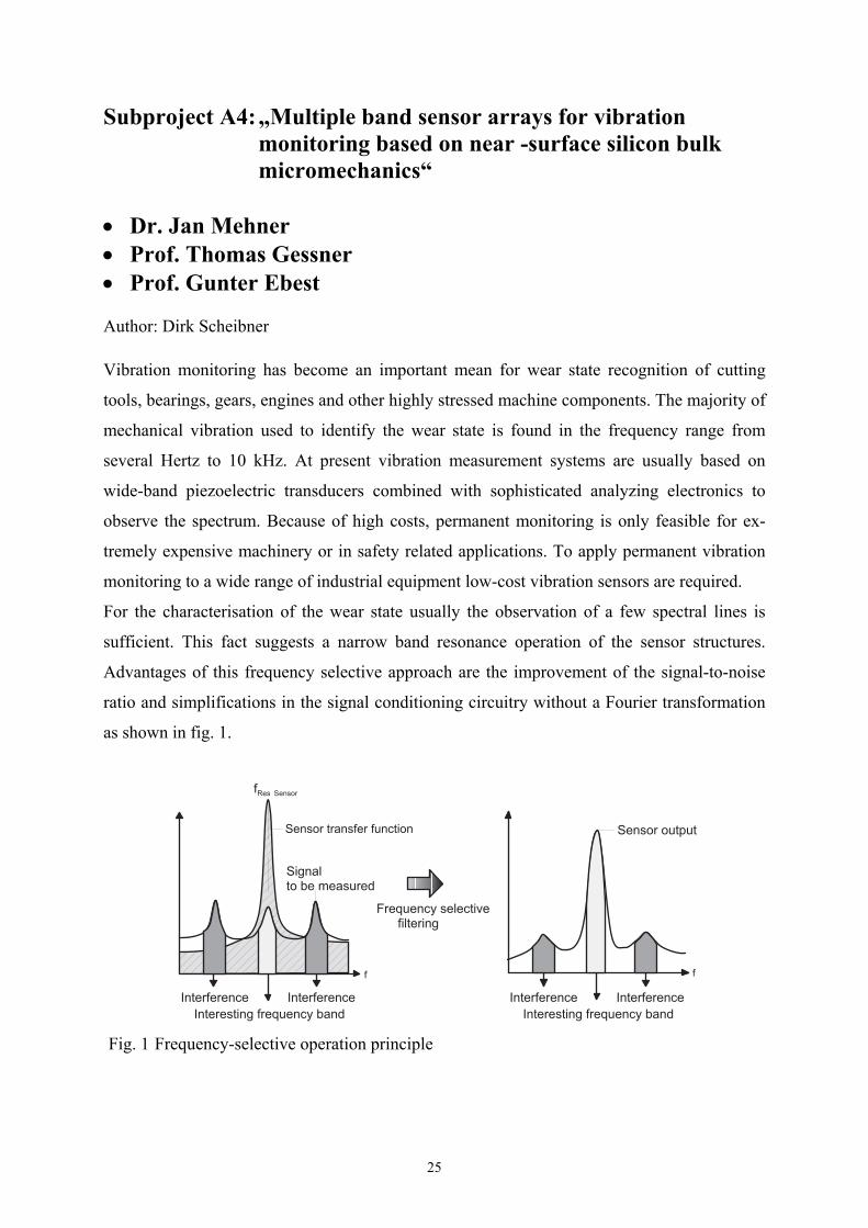
For the characterisation of the wear state usually the observation of a few spectral lines is
sufficient. This fact suggests a narrow band resonance operation of the sensor structures.
Advantages of this frequency selective approach are the improvement of the signal-to-noise
ratio and simplifications in the signal conditioning circuitry without a Fourier transformation
as shown in fig. 1.
Fig. 1 Frequency-selective operation principle
26
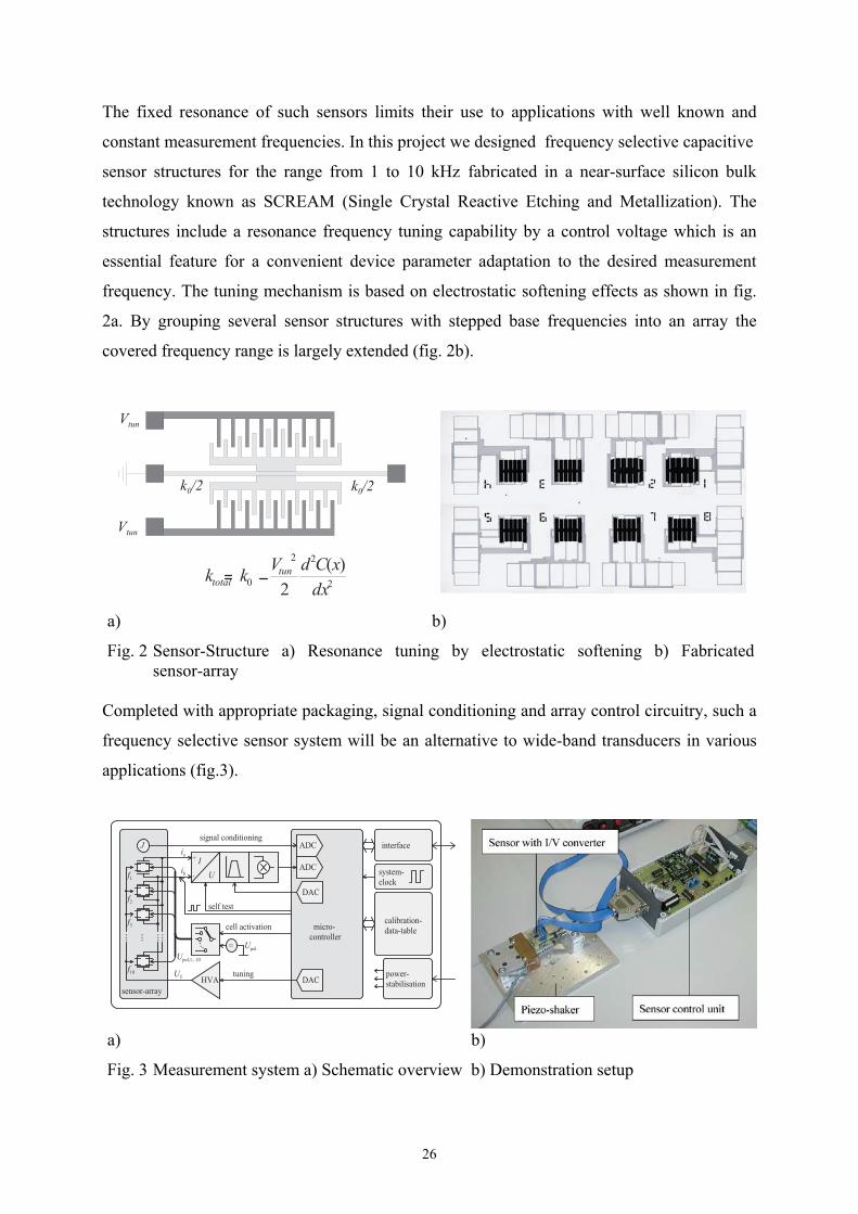
The fixed resonance of such sensors limits their use to applications with well known and
constant measurement frequencies. In this project we designed frequency selective capacitive
sensor structures for the range from 1 to 10 kHz fabricated in a near-surface silicon bulk
technology known as SCREAM (Single Crystal Reactive Etching and Metallization). The
structures include a resonance frequency tuning capability by a control voltage which is an
essential feature for a convenient device parameter adaptation to the desired measurement
frequency. The tuning mechanism is based on electrostatic softening effects as shown in fig.
2a. By grouping several sensor structures with stepped base frequencies into an array the
covered frequency range is largely extended (fig. 2b).
a) b)
Fig. 2 Sensor-Structure a) Resonance tuning by electrostatic softening b) Fabricated sensor-array
Completed with appropriate packaging, signal conditioning and array control circuitry, such a
frequency selective sensor system will be an alternative to wide-band transducers in various
applications (fig.3).
!
"
# " #
$
" %
& #
" "
'
a) b)
Fig. 3 Measurement system a) Schematic overview b) Demonstration setup
27
Subproject A6: „Investigation of a micro-electromechanical band- pass filter based on a tongue array”
• Olaf Enge, Prof. Peter Maißer
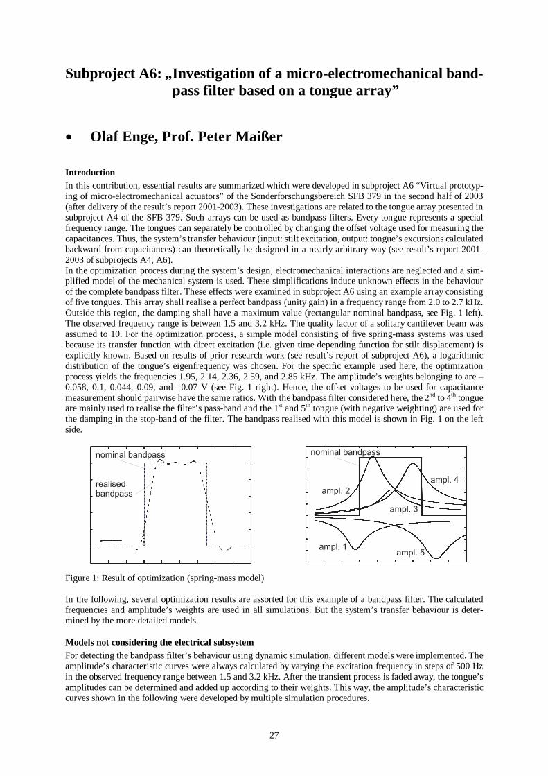
Introduction In this contribution, essential results are summarized which were developed in subproject A6 “Virtual prototyp-ing of micro-electromechanical actuators” of the Sonderforschungsbereich SFB 379 in the second half of 2003 (after delivery of the result’s report 2001-2003). These investigations are related to the tongue array presented in subproject A4 of the SFB 379. Such arrays can be used as bandpass filters. Every tongue represents a special frequency range. The tongues can separately be controlled by changing the offset voltage used for measuring the capacitances. Thus, the system’s transfer behaviour (input: stilt excitation, output: tongue’s excursions calculated backward from capacitances) can theoretically be designed in a nearly arbitrary way (see result’s report 2001-2003 of subprojects A4, A6). In the optimization process during the system’s design, electromechanical interactions are neglected and a sim-plified model of the mechanical system is used. These simplifications induce unknown effects in the behaviour of the complete bandpass filter. These effects were examined in subproject A6 using an example array consisting of five tongues. This array shall realise a perfect bandpass (unity gain) in a frequency range from 2.0 to 2.7 kHz. Outside this region, the damping shall have a maximum value (rectangular nominal bandpass, see Fig. 1 left). The observed frequency range is between 1.5 and 3.2 kHz. The quality factor of a solitary cantilever beam was assumed to 10. For the optimization process, a simple model consisting of five spring-mass systems was used because its transfer function with direct excitation (i.e. given time depending function for stilt displacement) is explicitly known. Based on results of prior research work (see result’s report of subproject A6), a logarithmic distribution of the tongue’s eigenfrequency was chosen. For the specific example used here, the optimization process yields the frequencies 1.95, 2.14, 2.36, 2.59, and 2.85 kHz. The amplitude’s weights belonging to are –0.058, 0.1, 0.044, 0.09, and –0.07 V (see Fig. 1 right). Hence, the offset voltages to be used for capacitance measurement should pairwise have the same ratios. With the bandpass filter considered here, the 2nd to 4th tongue are mainly used to realise the filter’s pass-band and the 1st and 5th tongue (with negative weighting) are used for the damping in the stop-band of the filter. The bandpass realised with this model is shown in Fig. 1 on the left side. Figure 1: Result of optimization (spring-mass model) In the following, several optimization results are assorted for this example of a bandpass filter. The calculated frequencies and amplitude’s weights are used in all simulations. But the system’s transfer behaviour is deter-mined by the more detailed models.
Models not considering the electrical subsystem For detecting the bandpass filter’s behaviour using dynamic simulation, different models were implemented. The amplitude’s characteristic curves were always calculated by varying the excitation frequency in steps of 500 Hz in the observed frequency range between 1.5 and 3.2 kHz. After the transient process is faded away, the tongue’s amplitudes can be determined and added up according to their weights. This way, the amplitude’s characteristic curves shown in the following were developed by multiple simulation procedures.
nominal bandpass
realisedbandpass
nominal bandpass
ampl. 1
ampl. 2
ampl. 5
ampl. 4
ampl. 3
28
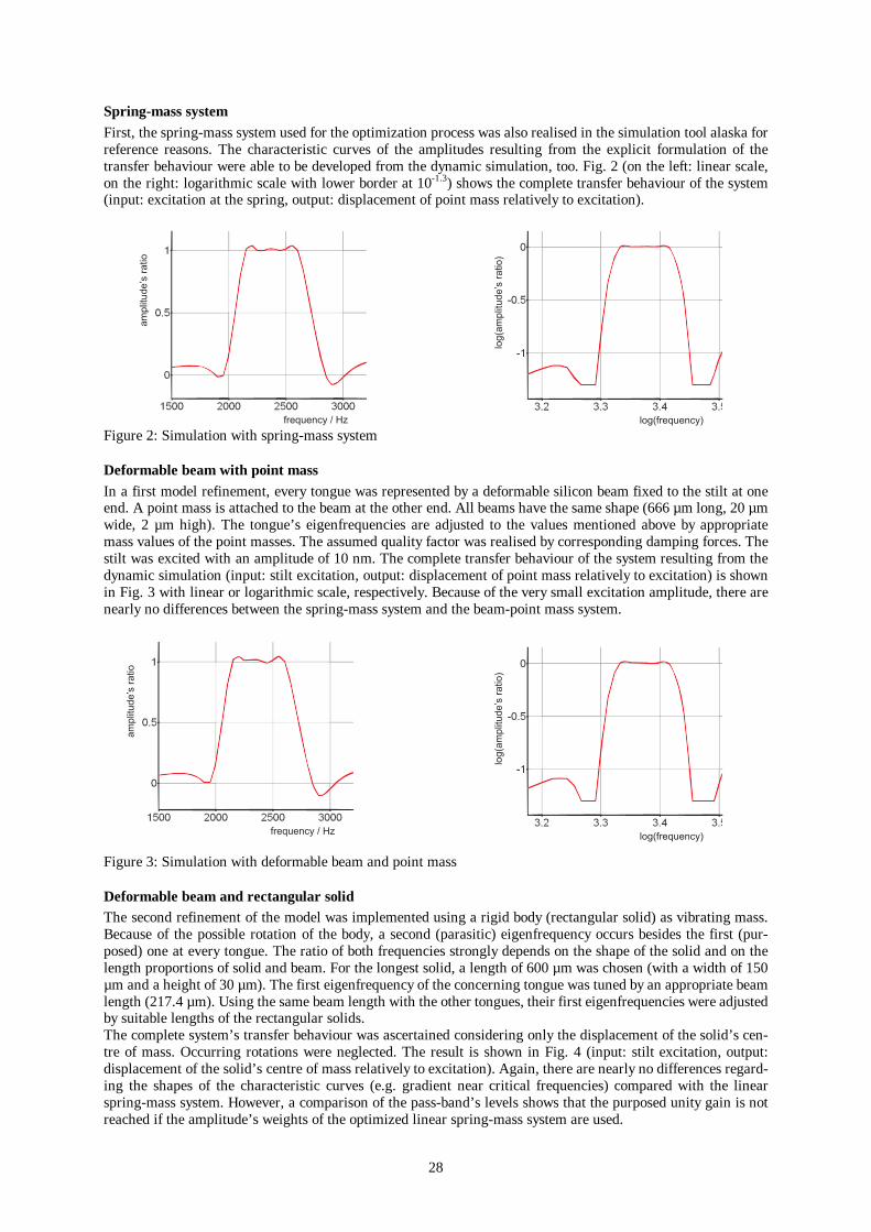
Spring-mass system First, the spring-mass system used for the optimization process was also realised in the simulation tool alaska for reference reasons. The characteristic curves of the amplitudes resulting from the explicit formulation of the transfer behaviour were able to be developed from the dynamic simulation, too. Fig. 2 (on the left: linear scale, on the right: logarithmic scale with lower border at 10-1.3) shows the complete transfer behaviour of the system (input: excitation at the spring, output: displacement of point mass relatively to excitation).
Figure 2: Simulation with spring-mass system
Deformable beam with point mass In a first model refinement, every tongue was represented by a deformable silicon beam fixed to the stilt at one end. A point mass is attached to the beam at the other end. All beams have the same shape (666 µm long, 20 µm wide, 2 µm high). The tongue’s eigenfrequencies are adjusted to the values mentioned above by appropriate mass values of the point masses. The assumed quality factor was realised by corresponding damping forces. The stilt was excited with an amplitude of 10 nm. The complete transfer behaviour of the system resulting from the dynamic simulation (input: stilt excitation, output: displacement of point mass relatively to excitation) is shown in Fig. 3 with linear or logarithmic scale, respectively. Because of the very small excitation amplitude, there are nearly no differences between the spring-mass system and the beam-point mass system.
Figure 3: Simulation with deformable beam and point mass
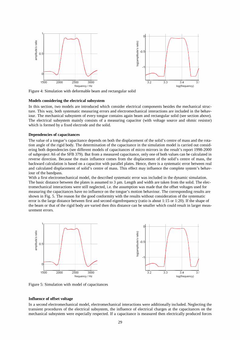
Deformable beam and rectangular solid The second refinement of the model was implemented using a rigid body (rectangular solid) as vibrating mass. Because of the possible rotation of the body, a second (parasitic) eigenfrequency occurs besides the first (pur-posed) one at every tongue. The ratio of both frequencies strongly depends on the shape of the solid and on the length proportions of solid and beam. For the longest solid, a length of 600 µm was chosen (with a width of 150 µm and a height of 30 µm). The first eigenfrequency of the concerning tongue was tuned by an appropriate beam length (217.4 µm). Using the same beam length with the other tongues, their first eigenfrequencies were adjusted by suitable lengths of the rectangular solids. The complete system’s transfer behaviour was ascertained considering only the displacement of the solid’s cen-tre of mass. Occurring rotations were neglected. The result is shown in Fig. 4 (input: stilt excitation, output: displacement of the solid’s centre of mass relatively to excitation). Again, there are nearly no differences regard-ing the shapes of the characteristic curves (e.g. gradient near critical frequencies) compared with the linear spring-mass system. However, a comparison of the pass-band’s levels shows that the purposed unity gain is not reached if the amplitude’s weights of the optimized linear spring-mass system are used.
frequency / Hz
am
plit
ud
e’s
ratio
frequency / Hz
am
plit
ude
’sra
tio
log(frequency)
log(a
mplit
ude
’sra
tio)
log(frequency)
log(a
mplit
ude
’sra
tio)
29
Figure 4: Simulation with deformable beam and rectangular solid
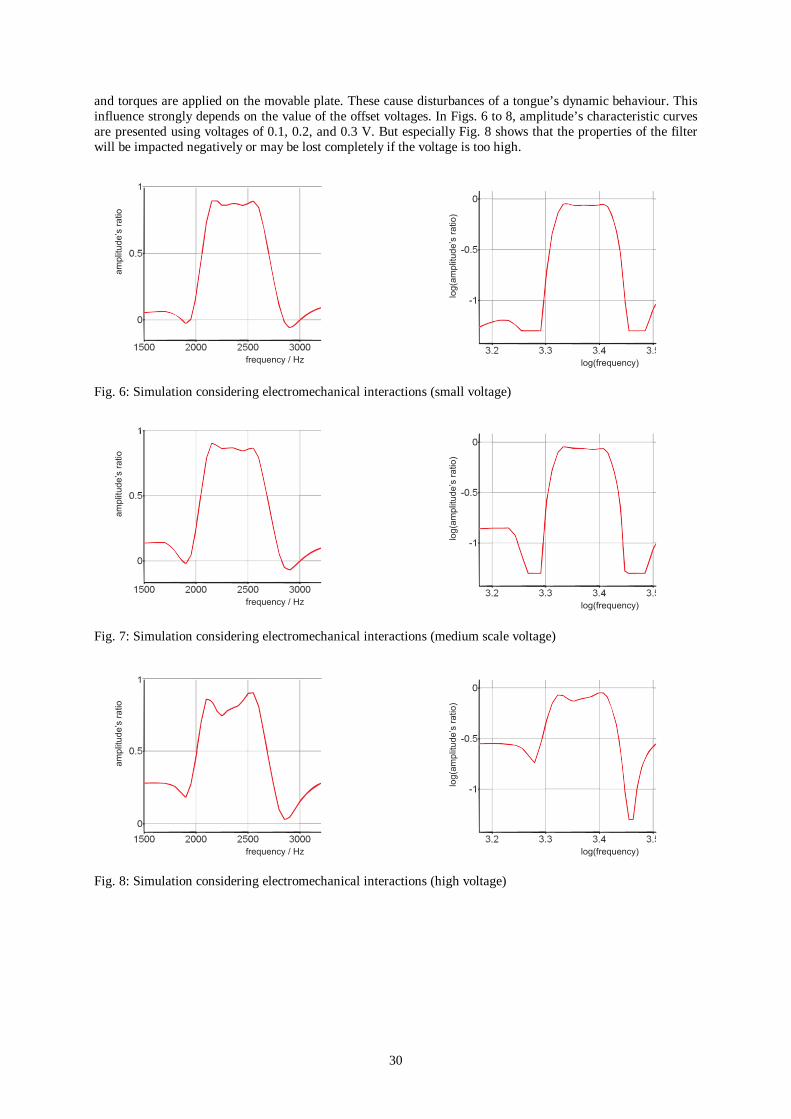
Models considering the electrical subsystem In this section, two models are introduced which consider electrical components besides the mechanical struc-ture. This way, both systematic measuring errors and electromechanical interactions are included in the behav-iour. The mechanical subsystem of every tongue contains again beam and rectangular solid (see section above). The electrical subsystem mainly consists of a measuring capacitor (with voltage source and ohmic resistor) which is formed by a fixed electrode and the solid.
Dependencies of capacitances The value of a tongue’s capacitance depends on both the displacement of the solid’s centre of mass and the rota-tion angle of the rigid body. The determination of the capacitance in the simulation model is carried out consid-ering both dependencies (see different models of capacitances of micro mirrors in the result’s report 1998-2000 of subproject A6 of the SFB 379). But from a measured capacitance, only one of both values can be calculated in reverse direction. Because the main influence comes from the displacement of the solid’s centre of mass, the backward calculation is based on a capacitor with parallel plates. Hence, there is a systematic error between real and calculated displacement of solid’s centre of mass. This effect may influence the complete system’s behav-iour of the bandpass. With a first electromechanical model, the described systematic error was included in the dynamic simulation. The basic distance between the plates is assumed to 3 µm. Length and width are taken from the solid. The elec-tromechanical interactions were still neglected, i.e. the assumption was made that the offset voltages used for measuring the capacitances have no influence on the tongue’s motion behaviour. The corresponding results are shown in Fig. 5. The reason for the good conformity with the results without consideration of the systematic error is the large distance between first and second eigenfrequency (ratio is about 1:15 or 1:20). If the shape of the beam or that of the rigid body are varied then this distance can be smaller which could result in larger meas-urement errors.
Figure 5: Simulation with model of capacitances
Influence of offset voltage In a second electromechanical model, electromechanical interactions were additionally included. Neglecting the transient procedures of the electrical subsystem, the influence of electrical charges at the capacitances on the mechanical subsystem were especially respected. If a capacitance is measured then electrically produced forces
frequency / Hz
1
am
plit
ude
’sra
tio
log(frequency)
log(a
mplit
ude
’sra
tio)
log(frequency)
log
(am
plit
ud
e’s
ratio
)
frequency / Hz
1a
mp
litu
de
’sra
tio
30
and torques are applied on the movable plate. These cause disturbances of a tongue’s dynamic behaviour. This influence strongly depends on the value of the offset voltages. In Figs. 6 to 8, amplitude’s characteristic curves are presented using voltages of 0.1, 0.2, and 0.3 V. But especially Fig. 8 shows that the properties of the filter will be impacted negatively or may be lost completely if the voltage is too high.
Fig. 6: Simulation considering electromechanical interactions (small voltage)
Fig. 7: Simulation considering electromechanical interactions (medium scale voltage)
Fig. 8: Simulation considering electromechanical interactions (high voltage)
log(frequency)
log(a
mplit
ude
’sra
tio)
frequency / Hz
am
plit
ude
’sra
tio
1
log(frequency)
log(a
mplit
ude
’sra
tio)
frequency / Hz
am
plit
ude
’sra
tio
1
frequency / Hz
1
am
plit
ude
’sra
tio
log(frequency)
log(a
mplit
ude
’sra
tio)
31
Subproject B2: “Experimental characterization, modell adaption and reliability: Micromechanical electrostatic field sensor for the detection of remanent charges”
• Prof. Dr. Wolfram Dötzel • Prof. Dr. Bernd Michel, Fraunhofer IZM Berlin / Chemnitz
Author: Marian Hanf
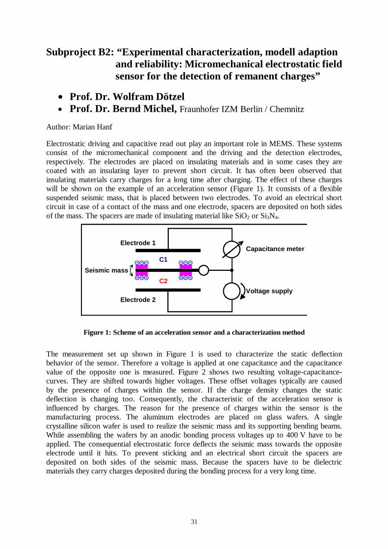
Electrostatic driving and capacitive read out play an important role in MEMS. These systems consist of the micromechanical component and the driving and the detection electrodes, respectively. The electrodes are placed on insulating materials and in some cases they are coated with an insulating layer to prevent short circuit. It has often been observed that insulating materials carry charges for a long time after charging. The effect of these charges will be shown on the example of an acceleration sensor (Figure 1). It consists of a flexible suspended seismic mass, that is placed between two electrodes. To avoid an electrical short circuit in case of a contact of the mass and one electrode, spacers are deposited on both sides of the mass. The spacers are made of insulating material like SiO2 or Si3N4.
Seismic mass
Electrode 1
Electrode 2
C1
C2
Capacitance meter
Voltage supply
Figure 1: Scheme of an acceleration sensor and a characterization method
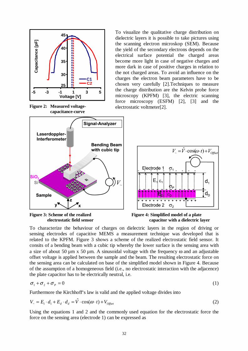
The measurement set up shown in Figure 1 is used to characterize the static deflection behavior of the sensor. Therefore a voltage is applied at one capacitance and the capacitance value of the opposite one is measured. Figure 2 shows two resulting voltage-capacitance-curves. They are shifted towards higher voltages. These offset voltages typically are caused by the presence of charges within the sensor. If the charge density changes the static deflection is changing too. Consequently, the characteristic of the acceleration sensor is influenced by charges. The reason for the presence of charges within the sensor is the manufacturing process. The aluminum electrodes are placed on glass wafers. A single crystalline silicon wafer is used to realize the seismic mass and its supporting bending beams. While assembling the wafers by an anodic bonding process voltages up to 400 V have to be applied. The consequential electrostatic force deflects the seismic mass towards the opposite electrode until it hits. To prevent sticking and an electrical short circuit the spacers are deposited on both sides of the seismic mass. Because the spacers have to be dielectric materials they carry charges deposited during the bonding process for a very long time.
32
25
30
35
40
45
-5 -3 -1 1 3 5Voltage [V]
Cap
acit
ance
[p
F]
C1C2
Figure 2: Measured voltage-capacitance-curve
To visualize the qualitative charge distribution on dielectric layers it is possible to take pictures using the scanning electron microskop (SEM). Because the yield of the secondary electrons depends on the electrical surface potential the charged areas become more light in case of negative charges and more dark in case of positive charges in relation to the not charged areas. To avoid an influence on the charges the electron beam parameters have to be chosen very carefully [2].Techniques to measure the charge distribution are the Kelvin probe force microscopy (KPFM) [3], the electric scanning force microscopy (ESFM) [2], [3] and the electrostatic voltmeter[2].
Figure 3: Scheme of the realized
electrostatic field sensor Figure 4: Simplified model of a plate
capacitor with a dielectric layer
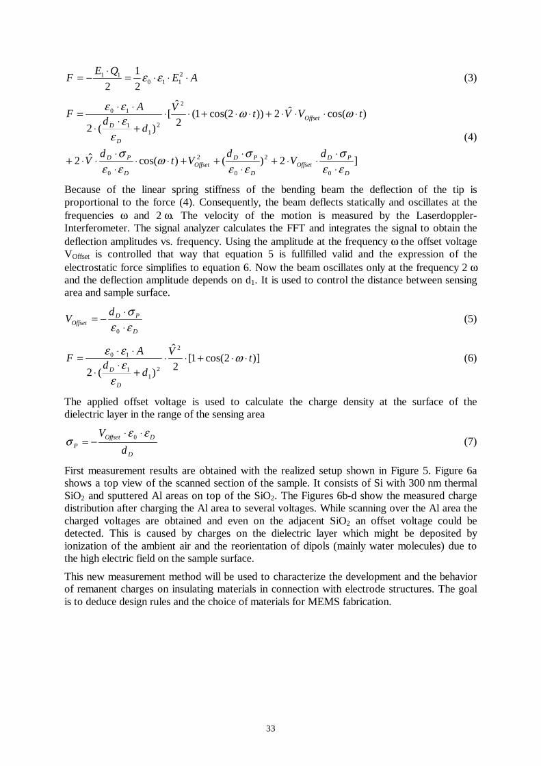
To characterize the behaviour of charges on dielectric layers in the region of driving or sensing electrodes of capacitive MEMS a measurement technique was developed that is related to the KPFM. Figure 3 shows a scheme of the realized electrostatic field sensor. It consits of a bending beam with a cubic tip whereby the lower surface is the sensing area with a size of about 50 µm x 50 µm. A sinusoidal voltage with the frequency ω and an adjustable offset voltage is applied between the sample and the beam. The resulting electrostatic force on the sensing area can be calculated on base of the simplified model shown in Figure 4. Because of the assumption of a homogeneous field (i.e., no electrostatic interaction with the adjacence) the plate capacitor has to be electrically neutral, i.e.
021 =++ Pσσσ (1)
Furthermore the Kirchhoff‘s law is valid and the applied voltage divides into
Offsetdd VtVdEdEV +⋅⋅=⋅+⋅= )cos(ˆ11~ ω (2)
Using the equations 1 and 2 and the commonly used equation for the electrostatic force the force on the sensing area (electrode 1) can be expressed as
33
AEQE
F ⋅⋅⋅=⋅−= 2110
11
2
1
2εε (3)
]2)()cos(ˆ2
)cos(ˆ2))2cos(1(2
ˆ[
)(2
0
2
0
2
0
2
21
1
10
D
PDOffset
D
PDOffset
D
PD
Offset
D
D
dV
dVt
dV
tVVtV
dd
AF
εεσ
εεσω
εεσ
ωω
εεεε
⋅⋅
⋅⋅+⋅⋅
++⋅⋅⋅⋅
⋅⋅+
⋅⋅⋅⋅+⋅⋅+⋅⋅+
⋅⋅
⋅⋅=
(4)
Because of the linear spring stiffness of the bending beam the deflection of the tip is proportional to the force (4). Consequently, the beam deflects statically and oscillates at the frequencies ω and 2 ω. The velocity of the motion is measured by the Laserdoppler-Interferometer. The signal analyzer calculates the FFT and integrates the signal to obtain the deflection amplitudes vs. frequency. Using the amplitude at the frequency ω the offset voltage VOffset is controlled that way that equation 5 is fullfilled valid and the expression of the electrostatic force simplifies to equation 6. Now the beam oscillates only at the frequency 2 ω and the deflection amplitude depends on d1. It is used to control the distance between sensing area and sample surface.
D
PDOffset
dV
εεσ
⋅⋅−=
0
(5)
)]2cos(1[2
ˆ
)(2
2
21
1
10 tV
dd
AF
D
D
⋅⋅+⋅⋅+
⋅⋅
⋅⋅= ω
εεεε
(6)
The applied offset voltage is used to calculate the charge density at the surface of the dielectric layer in the range of the sensing area
D
DOffsetP d
V εεσ
⋅⋅−= 0 (7)
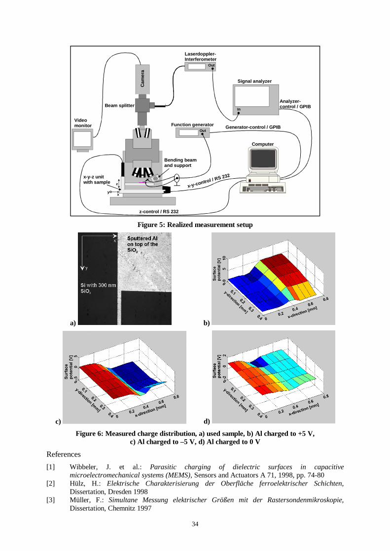
First measurement results are obtained with the realized setup shown in Figure 5. Figure 6a shows a top view of the scanned section of the sample. It consists of Si with 300 nm thermal SiO2 and sputtered Al areas on top of the SiO2. The Figures 6b-d show the measured charge distribution after charging the Al area to several voltages. While scanning over the Al area the charged voltages are obtained and even on the adjacent SiO2 an offset voltage could be detected. This is caused by charges on the dielectric layer which might be deposited by ionization of the ambient air and the reorientation of dipols (mainly water molecules) due to the high electric field on the sample surface.
This new measurement method will be used to characterize the development and the behavior of remanent charges on insulating materials in connection with electrode structures. The goal is to deduce design rules and the choice of materials for MEMS fabrication.
34
Function generator
Signal analyzer
Laserdoppler-Interferometer
Videomonitor
Cam
era
Beam splitter
yx
z
Out
Computer
In
z-control / RS 232
x-y-control / RS 232
Generator-control / GPIB
Analyzer-control / GPIB
Bending beamand support
x-y-z unitwith sample
Out
Figure 5: Realized measurement setup
a)
c)
b)
d)
Figure 6: Measured charge distribution, a) used sample, b) Al charged to +5 V, c) Al charged to –5 V, d) Al charged to 0 V
References
[1] Wibbeler, J. et al.: Parasitic charging of dielectric surfaces in capacitive microelectromechanical systems (MEMS), Sensors and Actuators A 71, 1998, pp. 74-80
[2] Hülz, H.: Elektrische Charakterisierung der Oberfläche ferroelektrischer Schichten, Dissertation, Dresden 1998
[3] Müller, F.: Simultane Messung elektrischer Größen mit der Rastersondenmikroskopie, Dissertation, Chemnitz 1997
35
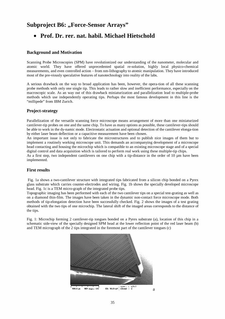
Subproject B6: „Force-Sensor Arrays”
• Prof. Dr. rer. nat. habil. Michael Hietschold Background and Motivation Scanning Probe Microscopies (SPM) have revolutionized our understanding of the nanometer, molecular and atomic world. They have offered unprecedented spatial re-solution, highly local physico-chemical measurements, and even controlled action – from nm-lithography to atomic manipulation. They have introduced most of the pre-viously speculative features of nanotechnology into reality of the labs. A serious drawback on the way to broad application has been, however, the opera-tion of all these scanning probe methods with only one single tip. This leads to rather slow and inefficient performance, especially on the macroscopic scale. As an way out of this drawback miniaturization and parallelization lead to multiple-probe methods which use independently operating tips. Perhaps the most famous development in this line is the “millipede” from IBM Zurich. Project-strategy Parallelization of the versatile scanning force microscope means arrangement of more than one miniaturized cantilever-tip probes on one and the same chip. To have as many options as possible, these cantilever-tips should be able to work in the dy-namic mode. Electrostatic actuation and optional detection of the cantilever elonga-tion by either laser beam deflection or a capacitive measurement have been chosen. An important issue is not only to fabricate the microstructures and to publish nice images of them but to implement a routinely working microscope unit. This demands an accompanying development of a microscope head contacting and housing the microchip which is compatible to an existing microscope stage and of a special digital control and data acquisition which is tailored to perform real work using these multiple-tip chips. As a first step, two independent cantilevers on one chip with a tip-distance in the order of 10 µm have been implemented. First results Fig. 1a shows a two-cantilever structure with integrated tips fabricated from a silicon chip bonded on a Pyrex glass substrate which carries counter-electrodes and wiring. Fig. 1b shows the specially developed microscope head. Fig. 1c is a TEM micro-graph of the integrated probe tips. Topographic imaging has been performed with each of the two cantilever tips on a special test-grating as well as on a diamond thin-film. The images have been taken in the dynamic non-contact force microscope mode. Both methods of tip-elongation detection have been successfully checked. Fig. 2 shows the images of a test grating obtained with the two tips of one microchip. The lateral shift of the imaged areas corresponds to the distance of the tips. Fig. 1: Microchip forming 2 cantilever-tip tongues bonded on a Pyrex substrate (a), location of this chip in a schematic side-view of the specially designed SPM head at the lower reflection point of the red laser beam (b) and TEM micrograph of the 2 tips integrated in the foremost part of the cantilever tongues (c)
a
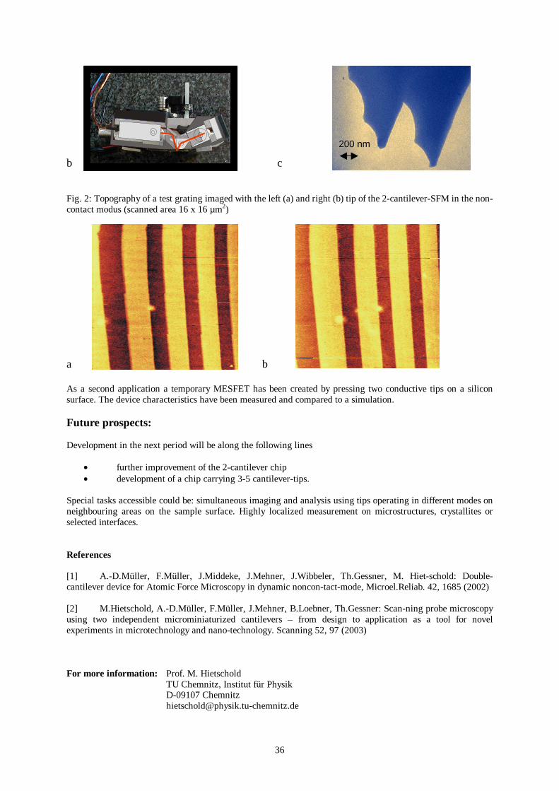
36
b c Fig. 2: Topography of a test grating imaged with the left (a) and right (b) tip of the 2-cantilever-SFM in the non-contact modus (scanned area 16 x 16 µm2) a b As a second application a temporary MESFET has been created by pressing two conductive tips on a silicon surface. The device characteristics have been measured and compared to a simulation. Future prospects: Development in the next period will be along the following lines
• further improvement of the 2-cantilever chip • development of a chip carrying 3-5 cantilever-tips.
Special tasks accessible could be: simultaneous imaging and analysis using tips operating in different modes on neighbouring areas on the sample surface. Highly localized measurement on microstructures, crystallites or selected interfaces. References [1] A.-D.Müller, F.Müller, J.Middeke, J.Mehner, J.Wibbeler, Th.Gessner, M. Hiet-schold: Double-cantilever device for Atomic Force Microscopy in dynamic noncon-tact-mode, Microel.Reliab. 42, 1685 (2002) [2] M.Hietschold, A.-D.Müller, F.Müller, J.Mehner, B.Loebner, Th.Gessner: Scan-ning probe microscopy using two independent microminiaturized cantilevers – from design to application as a tool for novel experiments in microtechnology and nano-technology. Scanning 52, 97 (2003) For more information: Prof. M. Hietschold TU Chemnitz, Institut für Physik D-09107 Chemnitz [email protected]
220000 nnmm
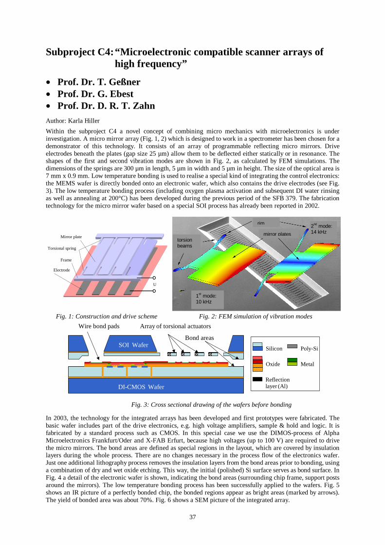
37
Subproject C4: “Microelectronic compatible scanner arrays of high frequency”
• Prof. Dr. T. Geßner • Prof. Dr. G. Ebest • Prof. Dr. D. R. T. Zahn Author: Karla Hiller
Within the subproject C4 a novel concept of combining micro mechanics with microelectronics is under investigation. A micro mirror array (Fig. 1, 2) which is designed to work in a spectrometer has been chosen for a demonstrator of this technology. It consists of an array of programmable reflecting micro mirrors. Drive electrodes beneath the plates (gap size 25 µm) allow them to be deflected either statically or in resonance. The shapes of the first and second vibration modes are shown in Fig. 2, as calculated by FEM simulations. The dimensions of the springs are 300 µm in length, 5 µm in width and 5 µm in height. The size of the optical area is 7 mm x 0.9 mm. Low temperature bonding is used to realise a special kind of integrating the control electronics: the MEMS wafer is directly bonded onto an electronic wafer, which also contains the drive electrodes (see Fig. 3). The low temperature bonding process (including oxygen plasma activation and subsequent DI water rinsing as well as annealing at 200°C) has been developed during the previous period of the SFB 379. The fabrication technology for the micro mirror wafer based on a special SOI process has already been reported in 2002.
U
Torsional spring
Mirror plate
Frame
Electrode
Fig. 1: Construction and drive scheme Fig. 2: FEM simulation of vibration modes
Array of torsional actuators
Bond areasSOI Wafer
Wire bond pads
DI-CMOS Wafer
Silicon
Oxide Metal
Reflectionlayer (Al)
Poly-Si
Fig. 3: Cross sectional drawing of the wafers before bonding In 2003, the technology for the integrated arrays has been developed and first prototypes were fabricated. The basic wafer includes part of the drive electronics, e.g. high voltage amplifiers, sample & hold and logic. It is fabricated by a standard process such as CMOS. In this special case we use the DIMOS-process of Alpha Microelectronics Frankfurt/Oder and X-FAB Erfurt, because high voltages (up to 100 V) are required to drive the micro mirrors. The bond areas are defined as special regions in the layout, which are covered by insulation layers during the whole process. There are no changes necessary in the process flow of the electronics wafer. Just one additional lithography process removes the insulation layers from the bond areas prior to bonding, using a combination of dry and wet oxide etching. This way, the initial (polished) Si surface serves as bond surface. In Fig. 4 a detail of the electronic wafer is shown, indicating the bond areas (surrounding chip frame, support posts around the mirrors). The low temperature bonding process has been successfully applied to the wafers. Fig. 5 shows an IR picture of a perfectly bonded chip, the bonded regions appear as bright areas (marked by arrows). The yield of bonded area was about 70%. Fig. 6 shows a SEM picture of the integrated array.
torsion beams
mirror plates
rim
1st mode: 10 kHz
2nd mode: 14 kHz
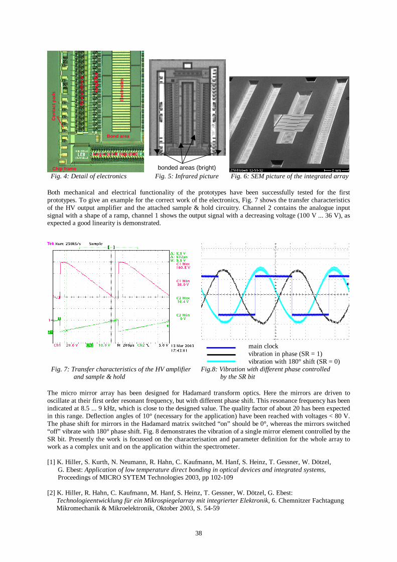
38
Bond area
Ele
ctro
des
Chip frame
Co
ntac
t pad
s
Logic (shift register)
Am
plif
ier
Sam
ple
&H
old
bonded areas (bright)
Fig. 4: Detail of electronics Fig. 5: Infrared picture Fig. 6: SEM picture of the integrated array Both mechanical and electrical functionality of the prototypes have been successfully tested for the first prototypes. To give an example for the correct work of the electronics, Fig. 7 shows the transfer characteristics of the HV output amplifier and the attached sample & hold circuitry. Channel 2 contains the analogue input signal with a shape of a ramp, channel 1 shows the output signal with a decreasing voltage (100 V ... 36 V), as expected a good linearity is demonstrated.
main clock vibration in phase (SR = 1) vibration with 180° shift (SR = 0)
Fig. 7: Transfer characteristics of the HV amplifier and sample & hold
Fig.8: Vibration with different phase controlled by the SR bit
The micro mirror array has been designed for Hadamard transform optics. Here the mirrors are driven to oscillate at their first order resonant frequency, but with different phase shift. This resonance frequency has been indicated at 8.5 ... 9 kHz, which is close to the designed value. The quality factor of about 20 has been expected in this range. Deflection angles of 10° (necessary for the application) have been reached with voltages < 80 V. The phase shift for mirrors in the Hadamard matrix switched “on” should be 0°, whereas the mirrors switched “off” vibrate with 180° phase shift. Fig. 8 demonstrates the vibration of a single mirror element controlled by the SR bit. Presently the work is focussed on the characterisation and parameter definition for the whole array to work as a complex unit and on the application within the spectrometer. [1] K. Hiller, S. Kurth, N. Neumann, R. Hahn, C. Kaufmann, M. Hanf, S. Heinz, T. Gessner, W. Dötzel, G. Ebest: Application of low temperature direct bonding in optical devices and integrated systems, Proceedings of MICRO SYTEM Technologies 2003, pp 102-109 [2] K. Hiller, R. Hahn, C. Kaufmann, M. Hanf, S. Heinz, T. Gessner, W. Dötzel, G. Ebest:
Technologieentwicklung für ein Mikrospiegelarray mit integrierter Elektronik, 6. Chemnitzer Fachtagung Mikromechanik & Mikroelektronik, Oktober 2003, S. 54-59
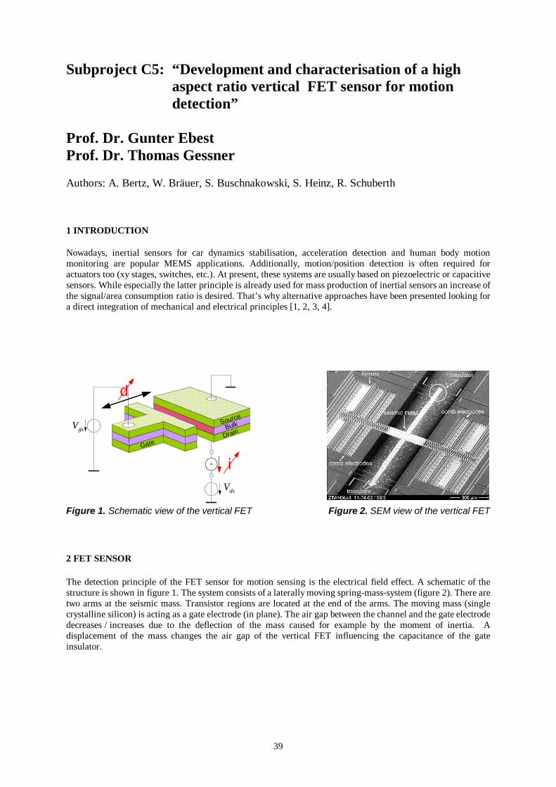
39
Subproject C5: “Development and characterisation of a high aspect ratio vertical FET sensor for motion detection”
Prof. Dr. Gunter Ebest Prof. Dr. Thomas Gessner Authors: A. Bertz, W. Bräuer, S. Buschnakowski, S. Heinz, R. Schuberth 1 INTRODUCTION Nowadays, inertial sensors for car dynamics stabilisation, acceleration detection and human body motion monitoring are popular MEMS applications. Additionally, motion/position detection is often required for actuators too (xy stages, switches, etc.). At present, these systems are usually based on piezoelectric or capacitive sensors. While especially the latter principle is already used for mass production of inertial sensors an increase of the signal/area consumption ratio is desired. That’s why alternative approaches have been presented looking for a direct integration of mechanical and electrical principles [1, 2, 3, 4]. Figure 1. Schematic view of the vertical FET Figure 2. SEM view of the vertical FET 2 FET SENSOR The detection principle of the FET sensor for motion sensing is the electrical field effect. A schematic of the structure is shown in figure 1. The system consists of a laterally moving spring-mass-system (figure 2). There are two arms at the seismic mass. Transistor regions are located at the end of the arms. The moving mass (single crystalline silicon) is acting as a gate electrode (in plane). The air gap between the channel and the gate electrode decreases / increases due to the deflection of the mass caused for example by the moment of inertia. A displacement of the mass changes the air gap of the vertical FET influencing the capacitance of the gate insulator.
d
A
gsV
dsV
i
Source
Bulk
Drain
Gate
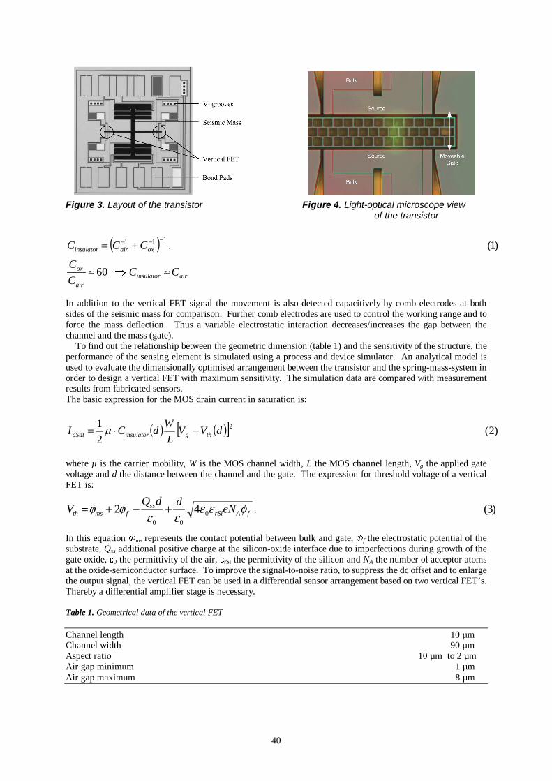
40
Figure 3. Layout of the transistor Figure 4. Light-optical microscope view
of the transistor In addition to the vertical FET signal the movement is also detected capacitively by comb electrodes at both sides of the seismic mass for comparison. Further comb electrodes are used to control the working range and to force the mass deflection. Thus a variable electrostatic interaction decreases/increases the gap between the channel and the mass (gate). To find out the relationship between the geometric dimension (table 1) and the sensitivity of the structure, the performance of the sensing element is simulated using a process and device simulator. An analytical model is used to evaluate the dimensionally optimised arrangement between the transistor and the spring-mass-system in order to design a vertical FET with maximum sensitivity. The simulation data are compared with measurement results from fabricated sensors. The basic expression for the MOS drain current in saturation is:
where µ is the carrier mobility, W is the MOS channel width, L the MOS channel length, Vg the applied gate voltage and d the distance between the channel and the gate. The expression for threshold voltage of a vertical FET is: In this equation Φms represents the contact potential between bulk and gate, Φf the electrostatic potential of the substrate, Qss additional positive charge at the silicon-oxide interface due to imperfections during growth of the gate oxide, ε0 the permittivity of the air, εrSi the permittivity of the silicon and NA the number of acceptor atoms at the oxide-semiconductor surface. To improve the signal-to-noise ratio, to suppress the dc offset and to enlarge the output signal, the vertical FET can be used in a differential sensor arrangement based on two vertical FET’s. Thereby a differential amplifier stage is necessary. Table 1. Geometrical data of the vertical FET Channel length 10 µm Channel width 90 µm Aspect ratio 10 µm to 2 µm Air gap minimum 1 µm Air gap maximum 8 µm
( )
airinsulatorair
ox
oxairinsulator
CCC
C
CCC
≈≈
+=−−−
60
)1(.111
( ) ( )[ ] )2(2
1 2dVVL
WdCI thginsulatordSat −⋅= µ
)3(.42 000
fArSiss
fmsth eNddQ
V φεεεε
φφ +−+=
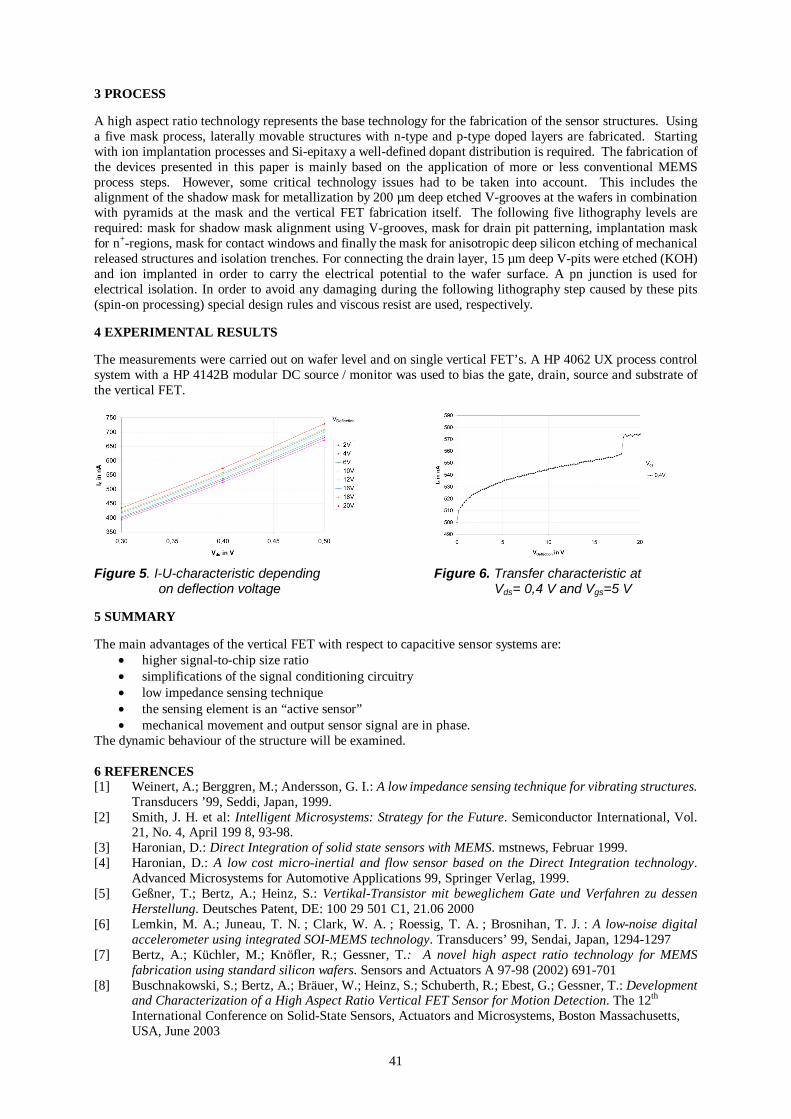
41
3 PROCESS A high aspect ratio technology represents the base technology for the fabrication of the sensor structures. Using a five mask process, laterally movable structures with n-type and p-type doped layers are fabricated. Starting with ion implantation processes and Si-epitaxy a well-defined dopant distribution is required. The fabrication of the devices presented in this paper is mainly based on the application of more or less conventional MEMS process steps. However, some critical technology issues had to be taken into account. This includes the alignment of the shadow mask for metallization by 200 µm deep etched V-grooves at the wafers in combination with pyramids at the mask and the vertical FET fabrication itself. The following five lithography levels are required: mask for shadow mask alignment using V-grooves, mask for drain pit patterning, implantation mask for n+-regions, mask for contact windows and finally the mask for anisotropic deep silicon etching of mechanical released structures and isolation trenches. For connecting the drain layer, 15 µm deep V-pits were etched (KOH) and ion implanted in order to carry the electrical potential to the wafer surface. A pn junction is used for electrical isolation. In order to avoid any damaging during the following lithography step caused by these pits (spin-on processing) special design rules and viscous resist are used, respectively. 4 EXPERIMENTAL RESULTS The measurements were carried out on wafer level and on single vertical FET’s. A HP 4062 UX process control system with a HP 4142B modular DC source / monitor was used to bias the gate, drain, source and substrate of the vertical FET. Figure 5. I-U-characteristic depending Figure 6. Transfer characteristic at
on deflection voltage Vds= 0,4 V and Vgs=5 V
5 SUMMARY The main advantages of the vertical FET with respect to capacitive sensor systems are:
• higher signal-to-chip size ratio • simplifications of the signal conditioning circuitry • low impedance sensing technique • the sensing element is an “active sensor” • mechanical movement and output sensor signal are in phase.
The dynamic behaviour of the structure will be examined. 6 REFERENCES [1] Weinert, A.; Berggren, M.; Andersson, G. I.: A low impedance sensing technique for vibrating structures.
Transducers ’99, Seddi, Japan, 1999. [2] Smith, J. H. et al: Intelligent Microsystems: Strategy for the Future. Semiconductor International, Vol.
21, No. 4, April 199 8, 93-98. [3] Haronian, D.: Direct Integration of solid state sensors with MEMS. mstnews, Februar 1999. [4] Haronian, D.: A low cost micro-inertial and flow sensor based on the Direct Integration technology.
Advanced Microsystems for Automotive Applications 99, Springer Verlag, 1999. [5] Geßner, T.; Bertz, A.; Heinz, S.: Vertikal-Transistor mit beweglichem Gate und Verfahren zu dessen
Herstellung. Deutsches Patent, DE: 100 29 501 C1, 21.06 2000 [6] Lemkin, M. A.; Juneau, T. N. ; Clark, W. A. ; Roessig, T. A. ; Brosnihan, T. J. : A low-noise digital
accelerometer using integrated SOI-MEMS technology. Transducers’ 99, Sendai, Japan, 1294-1297 [7] Bertz, A.; Küchler, M.; Knöfler, R.; Gessner, T.: A novel high aspect ratio technology for MEMS
fabrication using standard silicon wafers. Sensors and Actuators A 97-98 (2002) 691-701 [8] Buschnakowski, S.; Bertz, A.; Bräuer, W.; Heinz, S.; Schuberth, R.; Ebest, G.; Gessner, T.: Development
and Characterization of a High Aspect Ratio Vertical FET Sensor for Motion Detection. The 12th International Conference on Solid-State Sensors, Actuators and Microsystems, Boston Massachusetts, USA, June 2003
42
Development and characterisation of ultrathin CVD WNx diffusion barriers for Copper metallization Ramona Ecke, Stefan E. Schulz Diffusion barriers are fundamental elements in integrated circuits to prevent the interaction of copper interconnects and the dielectric as well as silicon. However, the continuously shrinking device dimensions in the future IC generations require a very thin and efficient barrier. The technical basis to perform WNx CVD is a tungsten CVD chamber at the commercial cluster tool PRECISION 5000 (Applied Materials), which provides the opportunity to integrate barrier and copper CVD. The plasma enhanced CVD using WF6/N2/H2 gas mixture was chosen from a number of possible methods to produce tungsten nitride films. Nitrogen and hydrogen require high temperature to react in thermally excited process. Consequently, it is essential to use plasma enhancement to reduce the deposition temperature. Three WNx layers have been developed with different compositions (RBS and XPS investigations). The compositions result from the variation of the total gas flow and the ratio of the N2 and H2 flow to WF6. In the as-deposited state the layers show no differences for the electrical resistivity (see table 1). They have also an amorphous like microstructure which impedes grains boundary diffusion and is a highly advantageous structure for barrier films (Fig. 4). Table I: Composition of WNx barriers with gas flow parameters and N/W ratio and electrical resistivity
N2/WF6 H2/WF6 Total flow
[sccm]
N/W ρ [µΩcm]
WNx1 80 80 520 0.24 205
WNx2 110 50 520 0.28 220
WNx3 80 80 2500 0.25 210
But after a heat treatment in vacuum the films show different crystallisation behavior, investigated with grazing incidence X-ray diffractometry (see Fig. 1-3). Annealing at 450°C/1h and 550°C/1h did not yield significant structural changes, whereas the 600°C/1h anneal resulted in a crystallisation of WNx1 and WNx2, indicated by the emergence of crystalline Bragg peaks corresponding to α-W and β-W2N. Only minor distinctions occur in the diffraction patterns for WNx1 and WNx2. For films with the composition of WNx1, the crystallisation proceeded during anneals at 600°C/4h and 600°C/16h, i.e. the crystalline peaks continued to grow at the expense of the amorphous socket. In the layer stacks with the WNx2 barrier already after the 1 h anneal at 600°C no further crystallite nucleation/ growth could be inferred from the diffraction patterns. The barrier films of WNx3 composition showed crystalline Bragg peaks of α-W and β-W2N at the amorphous hump not before 600°/4h. Both peaks are broad indicating a very small size of the crystallites. The retarded crystallisation results probably from more pronounced amorphous state because of the high total gas flow realized with a high Ar flow. To give a realistic estimation about the thermal stability of a diffusion barrier on a dielectric it is necessary to prove small amounts of copper migrating into the SiO2. With GI-XRD and cross sectional TEM no Cu diffusion was proved before and after the crystallisation of the amorphous WNx films for all 3 compositions. As real device structures MIS capacitors with the barrier WNx3 were prepared. After different annealing steps the structures have been examined to find electrical irregularities using HF-capacitance-voltage (HF-CV), capacitance-time (Ct) and triangular voltage sweep (TVS) measurements.
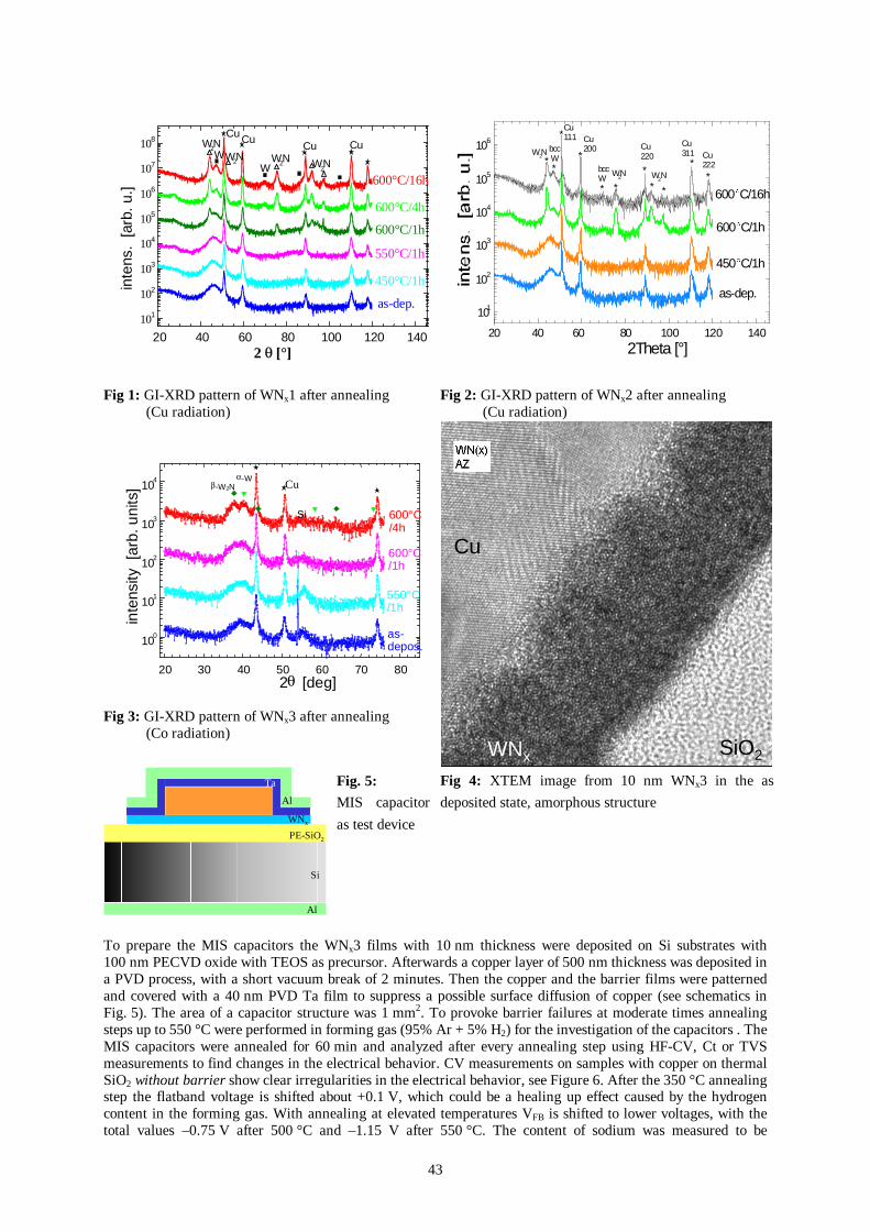
43
20 40 60 80 100 120 140
101
102
103
104
105
106
107
108
600°C/4h
550°C/1h
Cu
W2NWW W2N
W2NW2N CuCu
600°C/1h
450°C/1h
Cu
as-dep.
600°C/16h
inte
ns.
[arb
. u.]
2 θ [°]20 40 60 80 100 120 140
101
102
103
104
105
106
Cu222
Cu311
W2N *
*
* *
*
**
*
*
**
Cu220
W2Nbcc
W
Cu200
Cu111
bcc W
W2N
600C/16h
600C/1h
450C/1h
as-dep.
2Theta [°]
Fig 1: GI-XRD pattern of WNx1 after annealing (Cu radiation)
Fig 2: GI-XRD pattern of WNx2 after annealing (Cu radiation)
20 30 40 50 60 70 80
100
101
102
103
104
Si
as-depos.
550°C/1h
600°C/1h
600°C/4h
β-W2N α-W
inte
nsity
[ar
b. u
nits
]
2θ [deg]
Cu
Fig 3: GI-XRD pattern of WNx3 after annealing (Co radiation)
WNx
Cu
S iO2
Al
Si
PE-SiO2
WNx
Ta
Al
Fig. 5:
MIS capacitor
as test device
Fig 4: XTEM image from 10 nm WNx3 in the as
deposited state, amorphous structure
To prepare the MIS capacitors the WNx3 films with 10 nm thickness were deposited on Si substrates with 100 nm PECVD oxide with TEOS as precursor. Afterwards a copper layer of 500 nm thickness was deposited in a PVD process, with a short vacuum break of 2 minutes. Then the copper and the barrier films were patterned and covered with a 40 nm PVD Ta film to suppress a possible surface diffusion of copper (see schematics in Fig. 5). The area of a capacitor structure was 1 mm2. To provoke barrier failures at moderate times annealing steps up to 550 °C were performed in forming gas (95% Ar + 5% H2) for the investigation of the capacitors . The MIS capacitors were annealed for 60 min and analyzed after every annealing step using HF-CV, Ct or TVS measurements to find changes in the electrical behavior. CV measurements on samples with copper on thermal SiO2 without barrier show clear irregularities in the electrical behavior, see Figure 6. After the 350 °C annealing step the flatband voltage is shifted about +0.1 V, which could be a healing up effect caused by the hydrogen content in the forming gas. With annealing at elevated temperatures VFB is shifted to lower voltages, with the total values –0.75 V after 500 °C and –1.15 V after 550 °C. The content of sodium was measured to be
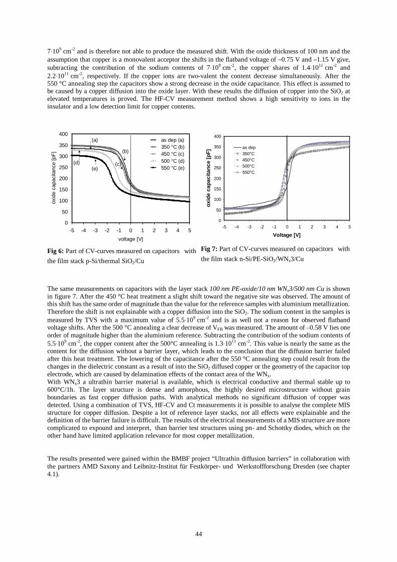
44
7⋅109 cm-2 and is therefore not able to produce the measured shift. With the oxide thickness of 100 nm and the assumption that copper is a monovalent acceptor the shifts in the flatband voltage of −0.75 V and –1.15 V give, subtracting the contribution of the sodium contents of 7⋅109 cm-2, the copper shares of 1.4⋅1011 cm-2 and 2.2⋅1011 cm-2, respectively. If the copper ions are two-valent the content decrease simultaneously. After the 550 °C annealing step the capacitors show a strong decrease in the oxide capacitance. This effect is assumed to be caused by a copper diffusion into the oxide layer. With these results the diffusion of copper into the SiO2 at elevated temperatures is proved. The HF-CV measurement method shows a high sensitivity to ions in the insulator and a low detection limit for copper contents.
0
50
100
150
200
250
300
350
400
-5 -4 -3 -2 -1 0 1 2 3 4 5
voltage [V]
oxi
de c
apac
itanc
e [p
F]
as dep (a) 350 °C (b) 450 °C (c) 500 °C (d) 550 °C (e)
(a)
(b)
(c)(d)(e)
Fig 6: Part of CV-curves measured on capacitors with
the film stack p-Si/thermal SiO2/Cu
0
50
100
150
200
250
300
350
400
-5 -4 -3 -2 -1 0 1 2 3 4 5
Voltage [V]
oxi
de
cap
acit
ance
[p
F] as dep
350°C450°C500°C550°C
Fig 7: Part of CV-curves measured on capacitors with
the film stack n-Si/PE-SiO2/WNx3/Cu
The same measurements on capacitors with the layer stack 100 nm PE-oxide/10 nm WNx3/500 nm Cu is shown in figure 7. After the 450 °C heat treatment a slight shift toward the negative site was observed. The amount of this shift has the same order of magnitude than the value for the reference samples with aluminium metallization. Therefore the shift is not explainable with a copper diffusion into the SiO2. The sodium content in the samples is measured by TVS with a maximum value of 5.5⋅109 cm-2 and is as well not a reason for observed flatband voltage shifts. After the 500 °C annealing a clear decrease of VFB was measured. The amount of –0.58 V lies one order of magnitude higher than the aluminium reference. Subtracting the contribution of the sodium contents of 5.5⋅109 cm-2, the copper content after the 500°C annealing is 1.3⋅1011 cm-2. This value is nearly the same as the content for the diffusion without a barrier layer, which leads to the conclusion that the diffusion barrier failed after this heat treatment. The lowering of the capacitance after the 550 °C annealing step could result from the changes in the dielectric constant as a result of into the SiO2 diffused copper or the geometry of the capacitor top electrode, which are caused by delamination effects of the contact area of the WNx. With WNx3 a ultrathin barrier material is available, which is electrical conductive and thermal stable up to 600°C/1h. The layer structure is dense and amorphous, the highly desired microstructure without grain boundaries as fast copper diffusion paths. With analytical methods no significant diffusion of copper was detected. Using a combination of TVS, HF-CV and Ct measurements it is possible to analyse the complete MIS structure for copper diffusion. Despite a lot of reference layer stacks, not all effects were explainable and the definition of the barrier failure is difficult. The results of the electrical measurements of a MIS structure are more complicated to expound and interpret, than barrier test structures using pn- and Schottky diodes, which on the other hand have limited application relevance for most copper metallization. The results presented were gained within the BMBF project “Ultrathin diffusion barriers” in collaboration with the partners AMD Saxony and Leibnitz-Institut für Festkörper- und Werkstoffforschung Dresden (see chapter 4.1).
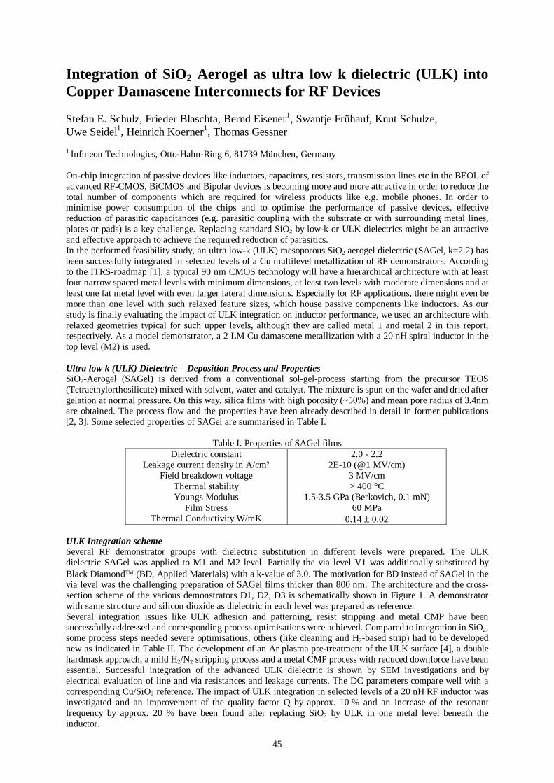
45
Integration of SiO2 Aerogel as ultra low k dielectric (ULK) into Copper Damascene Interconnects for RF Devices Stefan E. Schulz, Frieder Blaschta, Bernd Eisener1, Swantje Frühauf, Knut Schulze, Uwe Seidel1, Heinrich Koerner1, Thomas Gessner 1 Infineon Technologies, Otto-Hahn-Ring 6, 81739 München, Germany On-chip integration of passive devices like inductors, capacitors, resistors, transmission lines etc in the BEOL of advanced RF-CMOS, BiCMOS and Bipolar devices is becoming more and more attractive in order to reduce the total number of components which are required for wireless products like e.g. mobile phones. In order to minimise power consumption of the chips and to optimise the performance of passive devices, effective reduction of parasitic capacitances (e.g. parasitic coupling with the substrate or with surrounding metal lines, plates or pads) is a key challenge. Replacing standard SiO2 by low-k or ULK dielectrics might be an attractive and effective approach to achieve the required reduction of parasitics. In the performed feasibility study, an ultra low-k (ULK) mesoporous SiO2 aerogel dielectric (SAGel, k=2.2) has been successfully integrated in selected levels of a Cu multilevel metallization of RF demonstrators. According to the ITRS-roadmap [1], a typical 90 nm CMOS technology will have a hierarchical architecture with at least four narrow spaced metal levels with minimum dimensions, at least two levels with moderate dimensions and at least one fat metal level with even larger lateral dimensions. Especially for RF applications, there might even be more than one level with such relaxed feature sizes, which house passive components like inductors. As our study is finally evaluating the impact of ULK integration on inductor performance, we used an architecture with relaxed geometries typical for such upper levels, although they are called metal 1 and metal 2 in this report, respectively. As a model demonstrator, a 2 LM Cu damascene metallization with a 20 nH spiral inductor in the top level (M2) is used. Ultra low k (ULK) Dielectric – Deposition Process and Properties SiO2-Aerogel (SAGel) is derived from a conventional sol-gel-process starting from the precursor TEOS (Tetraethylorthosilicate) mixed with solvent, water and catalyst. The mixture is spun on the wafer and dried after gelation at normal pressure. On this way, silica films with high porosity (~50%) and mean pore radius of 3.4nm are obtained. The process flow and the properties have been already described in detail in former publications [2, 3]. Some selected properties of SAGel are summarised in Table I.
Table I. Properties of SAGel films Dielectric constant 2.0 - 2.2
Leakage current density in A/cm² 2E-10 (@1 MV/cm) Field breakdown voltage 3 MV/cm
Thermal stability > 400 °C Youngs Modulus 1.5-3.5 GPa (Berkovich, 0.1 mN)
Film Stress 60 MPa Thermal Conductivity W/mK 0.14 ± 0.02
ULK Integration scheme Several RF demonstrator groups with dielectric substitution in different levels were prepared. The ULK dielectric SAGel was applied to M1 and M2 level. Partially the via level V1 was additionally substituted by Black Diamond (BD, Applied Materials) with a k-value of 3.0. The motivation for BD instead of SAGel in the via level was the challenging preparation of SAGel films thicker than 800 nm. The architecture and the cross-section scheme of the various demonstrators D1, D2, D3 is schematically shown in Figure 1. A demonstrator with same structure and silicon dioxide as dielectric in each level was prepared as reference. Several integration issues like ULK adhesion and patterning, resist stripping and metal CMP have been successfully addressed and corresponding process optimisations were achieved. Compared to integration in SiO2, some process steps needed severe optimisations, others (like cleaning and H2-based strip) had to be developed new as indicated in Table II. The development of an Ar plasma pre-treatment of the ULK surface [4], a double hardmask approach, a mild H2/N2 stripping process and a metal CMP process with reduced downforce have been essential. Successful integration of the advanced ULK dielectric is shown by SEM investigations and by electrical evaluation of line and via resistances and leakage currents. The DC parameters compare well with a corresponding Cu/SiO2 reference. The impact of ULK integration in selected levels of a 20 nH RF inductor was investigated and an improvement of the quality factor Q by approx. 10 % and an increase of the resonant frequency by approx. 20 % have been found after replacing SiO2 by ULK in one metal level beneath the inductor.
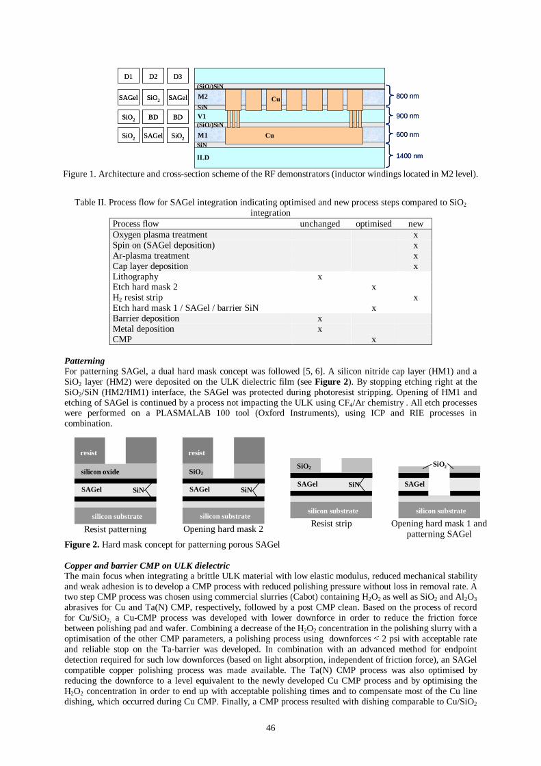
46
SiN
M1
Cu
Cu
(SiO/)SiN
SiN
ILD
V1
M2
(SiO/)SiN
600 nm
900 nm
800 nm
1400 nm
SAGelSAGel SiO2
BDSiO2 BD
SiO2SiO2 SAGel
D3D1 D2
SiN
M1
Cu
Cu
(SiO/)SiN
SiN
ILD
V1
M2
(SiO/)SiN
600 nm
900 nm
800 nm
1400 nm
SAGelSAGel SiO2
BDSiO2 BD
SiO2SiO2 SAGel
D3D1 D2
Figure 1. Architecture and cross-section scheme of the RF demonstrators (inductor windings located in M2 level).
Table II. Process flow for SAGel integration indicating optimised and new process steps compared to SiO2
integration Process flow unchanged optimised new Oxygen plasma treatment x Spin on (SAGel deposition) x Ar-plasma treatment x Cap layer deposition x Lithography x Etch hard mask 2 x H2 resist strip x Etch hard mask 1 / SAGel / barrier SiN x Barrier deposition x Metal deposition x CMP x
Patterning For patterning SAGel, a dual hard mask concept was followed [5, 6]. A silicon nitride cap layer (HM1) and a SiO2 layer (HM2) were deposited on the ULK dielectric film (see Figure 2). By stopping etching right at the SiO2/SiN (HM2/HM1) interface, the SAGel was protected during photoresist stripping. Opening of HM1 and etching of SAGel is continued by a process not impacting the ULK using CF4/Ar chemistry . All etch processes were performed on a PLASMALAB 100 tool (Oxford Instruments), using ICP and RIE processes in combination.
resist
silicon oxide
SAGel SiN
silicon substrate
Resist patterning
resist
SiO2
SAGel SiN
silicon substrate
Opening hard mask 2
SiO2
SAGel SiN
silicon substrate Resist strip
SiO2
SAGel
silicon substrate Opening hard mask 1 and
patterning SAGel Figure 2. Hard mask concept for patterning porous SAGel Copper and barrier CMP on ULK dielectric The main focus when integrating a brittle ULK material with low elastic modulus, reduced mechanical stability and weak adhesion is to develop a CMP process with reduced polishing pressure without loss in removal rate. A two step CMP process was chosen using commercial slurries (Cabot) containing H2O2 as well as SiO2 and Al2O3 abrasives for Cu and Ta(N) CMP, respectively, followed by a post CMP clean. Based on the process of record for Cu/SiO2, a Cu-CMP process was developed with lower downforce in order to reduce the friction force between polishing pad and wafer. Combining a decrease of the H2O2 concentration in the polishing slurry with a optimisation of the other CMP parameters, a polishing process using downforces ≤ 2 psi with acceptable rate and reliable stop on the Ta-barrier was developed. In combination with an advanced method for endpoint detection required for such low downforces (based on light absorption, independent of friction force), an SAGel compatible copper polishing process was made available. The Ta(N) CMP process was also optimised by reducing the downforce to a level equivalent to the newly developed Cu CMP process and by optimising the H2O2 concentration in order to end up with acceptable polishing times and to compensate most of the Cu line dishing, which occurred during Cu CMP. Finally, a CMP process resulted with dishing comparable to Cu/SiO2
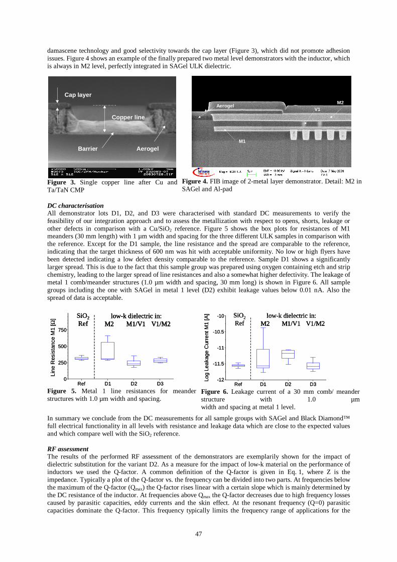
47
damascene technology and good selectivity towards the cap layer (Figure 3), which did not promote adhesion issues. Figure 4 shows an example of the finally prepared two metal level demonstrators with the inductor, which is always in M2 level, perfectly integrated in SAGel ULK dielectric.
Cap layer
Aerogel
Copper line
Barrier
Figure 3. Single copper line after Cu and Ta/TaN CMP
Met-1Via-1
Met-2Aerogel
SiO2Met-1
Via-1Met-2
Aerogel
Met-1Via-1
Met-2Aerogel
SiO2M1
V1M2
Aerogel
Figure 4. FIB image of 2-metal layer demonstrator. Detail: M2 in SAGel and Al-pad
DC characterisation All demonstrator lots D1, D2, and D3 were characterised with standard DC measurements to verify the feasibility of our integration approach and to assess the metallization with respect to opens, shorts, leakage or other defects in comparison with a Cu/SiO2 reference. Figure 5 shows the box plots for resistances of M1 meanders (30 mm length) with 1 µm width and spacing for the three different ULK samples in comparison with the reference. Except for the D1 sample, the line resistance and the spread are comparable to the reference, indicating that the target thickness of 600 nm was hit with acceptable uniformity. No low or high flyers have been detected indicating a low defect density comparable to the reference. Sample D1 shows a significantly larger spread. This is due to the fact that this sample group was prepared using oxygen containing etch and strip chemistry, leading to the larger spread of line resistances and also a somewhat higher defectivity. The leakage of metal 1 comb/meander structures (1.0 µm width and spacing, 30 mm long) is shown in Figure 6. All sample groups including the one with SAGel in metal 1 level (D2) exhibit leakage values below 0.01 nA. Also the spread of data is acceptable.
Ref D1 D2 D30
250
500
750
Line
Res
ista
nce
M1
[Ω] SiO2
Reflow-k dielectric in:
M2 M1/V1 V1/M2
Ref D1 D2 D30
250
500
750
Line
Res
ista
nce
M1
[Ω] SiO2
Reflow-k dielectric in:
M2 M1/V1 V1/M2SiO2
Reflow-k dielectric in:
M2 M1/V1 V1/M2SiO2
Reflow-k dielectric in:
M2 M1/V1 V1/M2M2 M1/V1 V1/M2
Figure 5. Metal 1 line resistances for meander structures with 1.0 µm width and spacing.
Ref D1 D2 D3-12
-11.5
-11
-10.5
-10
Log
Leak
age
Cur
rent
M1
[A] SiO2
Reflow-k dielectric in:
M2 M1/V1 V1/M2
Ref D1 D2 D3-12
-11.5
-11
-10.5
-10
Log
Leak
age
Cur
rent
M1
[A] SiO2
Reflow-k dielectric in:
M2 M1/V1 V1/M2SiO2
Reflow-k dielectric in:
M2 M1/V1 V1/M2M2 M1/V1 V1/M2
Figure 6. Leakage current of a 30 mm comb/ meander structure with 1.0 µm width and spacing at metal 1 level.
In summary we conclude from the DC measurements for all sample groups with SAGel and Black Diamond™ full electrical functionality in all levels with resistance and leakage data which are close to the expected values and which compare well with the SiO2 reference. RF assessment The results of the performed RF assessment of the demonstrators are exemplarily shown for the impact of dielectric substitution for the variant D2. As a measure for the impact of low-k material on the performance of inductors we used the Q-factor. A common definition of the Q-factor is given in Eq. 1, where Z is the impedance. Typically a plot of the Q-factor vs. the frequency can be divided into two parts. At frequencies below the maximum of the Q-factor (Qmax) the Q-factor rises linear with a certain slope which is mainly determined by the DC resistance of the inductor. At frequencies above Qmax the Q-factor decreases due to high frequency losses caused by parasitic capacities, eddy currents and the skin effect. At the resonant frequency (Q=0) parasitic capacities dominate the Q-factor. This frequency typically limits the frequency range of applications for the
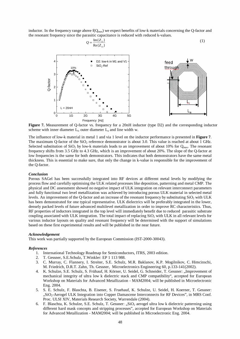
48
inductor. In the frequency range above f(Qmax) we expect benefits of low-k materials concerning the Q-factor and the resonant frequency since the parasitic capacitance is reduced with reduced k-values.
Re
Im
11
11
Z
ZQ = (1)
0 1G 2G 3G 4G 5G0
1
2
3
4
10%
L = 20nH
D2: low-k in M1 and V1 SiO2-Ref
Q-f
acto
r
Frequency [Hz]
Figure 7. Measurement of Q-factor vs. frequency for a 20nH inductor (type D2) and the corresponding inductor scheme with inner diameter Li, outer diameter La and line width w.
The influence of low-k material in metal 1 and via 1 level on the inductor performance is presented in Figure 7. The maximum Q-factor of the SiO2 reference demonstrator is about 3.0. This value is reached at about 1 GHz. Selected substitution of SiO2 by low-k materials leads to an improvement of about 10% for Qmax. The resonant frequency shifts from 3.5 GHz to 4.3 GHz, which is an improvement of about 20%. The slope of the Q-factor at low frequencies is the same for both demonstrators. This indicates that both demonstrators have the same metal thickness. This is essential to make sure, that only the change in k-value is responsible for the improvement of the Q-factor. Conclusion Porous SAGel has been successfully integrated into RF devices at different metal levels by modifying the process flow and carefully optimising the ULK related processes like deposition, patterning and metal CMP. The physical and DC assessment showed no negative impact of ULK integration on relevant interconnect parameters and fully functional two level metallization was achieved by introducing porous ULK material in selected metal levels. An improvement of the Q-factor and an increase of the resonant frequency by substituting SiO2 with ULK has been demonstrated for one typical representative. ULK dielectrics will be preferably integrated in the lower, densely packed levels of future advanced multilevel metallization in order to improve RC characteristics. Thus, RF properties of inductors integrated in the top level will immediately benefit due to reduced parasitic substrate coupling associated with ULK integration. The total impact of replacing SiO2 with ULK in all relevant levels for various inductor layouts on quality and resonant frequency will be determined with the support of simulations based on these first experimental results and will be published in the near future. Acknowledgement This work was partially supported by the European Commission (IST-2000-30043). References
1. International Technology Roadmap for Semiconductors, ITRS, 2003 edition. 2. T. Gessner, S.E.Schulz, T.Winkler: EP 1 113 988. 3. C. Murray, C. Flannery, I. Streiter, S.E. Schulz, M.R. Baklanov, K.P. Mogilnikov, C. Himcinschi,
M. Friedrich, D.R.T. Zahn, Th. Gessner, Microelectronics Engineering 60, p.133-141(2002). 4. K. Schulze, S.E. Schulz, S. Frühauf, H. Körner, U. Seidel, G. Schneider, T. Gessner: „Improvement of
mechanical integrity of ultra low k dielectric stack and CMP compatibility“, accepted for European Workshop on Materials for Advanced Metallization - MAM2004; will be published in Microelectronic Eng. 2004.
5. S. E. Schulz, F. Blaschta, B. Eisener, S. Fruehauf, K. Schulze, U. Seidel, H. Koerner, T. Gessner: „SiO2-Aerogel ULK Integration into Copper Damascene Interconnects for RF Devices”, in MRS Conf. Proc. ULSI XIV, Materials Research Society, Warrendale (2004).
6. F. Blaschta, K. Schulze, S.E. Schulz, T. Gessner: „SiO2 aerogel ultra low k dielectric patterning using different hard mask concepts and stripping processes”, accepted for European Workshop on Materials for Advanced Metallization - MAM2004; will be published in Microelectronic Eng. 2004.
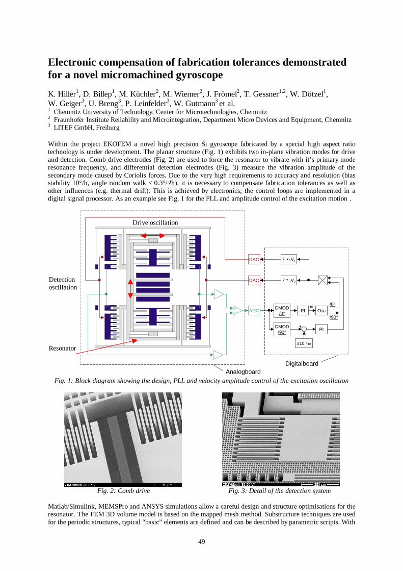
49
Electronic compensation of fabrication tolerances demonstrated for a novel micromachined gyroscope K. Hiller1, D. Billep1, M. Küchler2, M. Wiemer2, J. Frömel2, T. Gessner1,2, W. Dötzel1, W. Geiger3, U. Breng3, P. Leinfelder3, W. Gutmann3 et al. 1 Chemnitz University of Technology, Center for Microtechnologies, Chemnitz 2 Fraunhofer Institute Reliability and Microintegration, Department Micro Devices and Equipment, Chemnitz 3 LITEF GmbH, Freiburg Within the project EKOFEM a novel high precision Si gyroscope fabricated by a special high aspect ratio technology is under development. The planar structure (Fig. 1) exhibits two in-plane vibration modes for drive and detection. Comb drive electrodes (Fig. 2) are used to force the resonator to vibrate with it’s primary mode resonance frequency, and differential detection electrodes (Fig. 3) measure the vibration amplitude of the secondary mode caused by Coriolis forces. Due to the very high requirements to accuracy and resolution (bias stability 10°/h, angle random walk < 0.3°/√h), it is necessary to compensate fabrication tolerances as well as other influences (e.g. thermal drift). This is achieved by electronics; the control loops are implemented in a digital signal processor. As an example see Fig. 1 for the PLL and amplitude control of the excitation motion .
F V1
DMOD/90°
PI
x10 / ω
DMOD/0°
PI Osc/0°
/90°
+-
ω
F V2DAC
DAC
ADC+-
AnalogboardDigitalboard
Fig. 1: Block diagram showing the design, PLL and velocity amplitude control of the excitation oscillation
Fig. 2: Comb drive Fig. 3: Detail of the detection system
Matlab/Simulink, MEMSPro and ANSYS simulations allow a careful design and structure optimisations for the resonator. The FEM 3D volume model is based on the mapped mesh method. Substructure techniques are used for the periodic structures, typical “basic” elements are defined and can be described by parametric scripts. With
Drive oscillation
Detection oscillation
Resonator
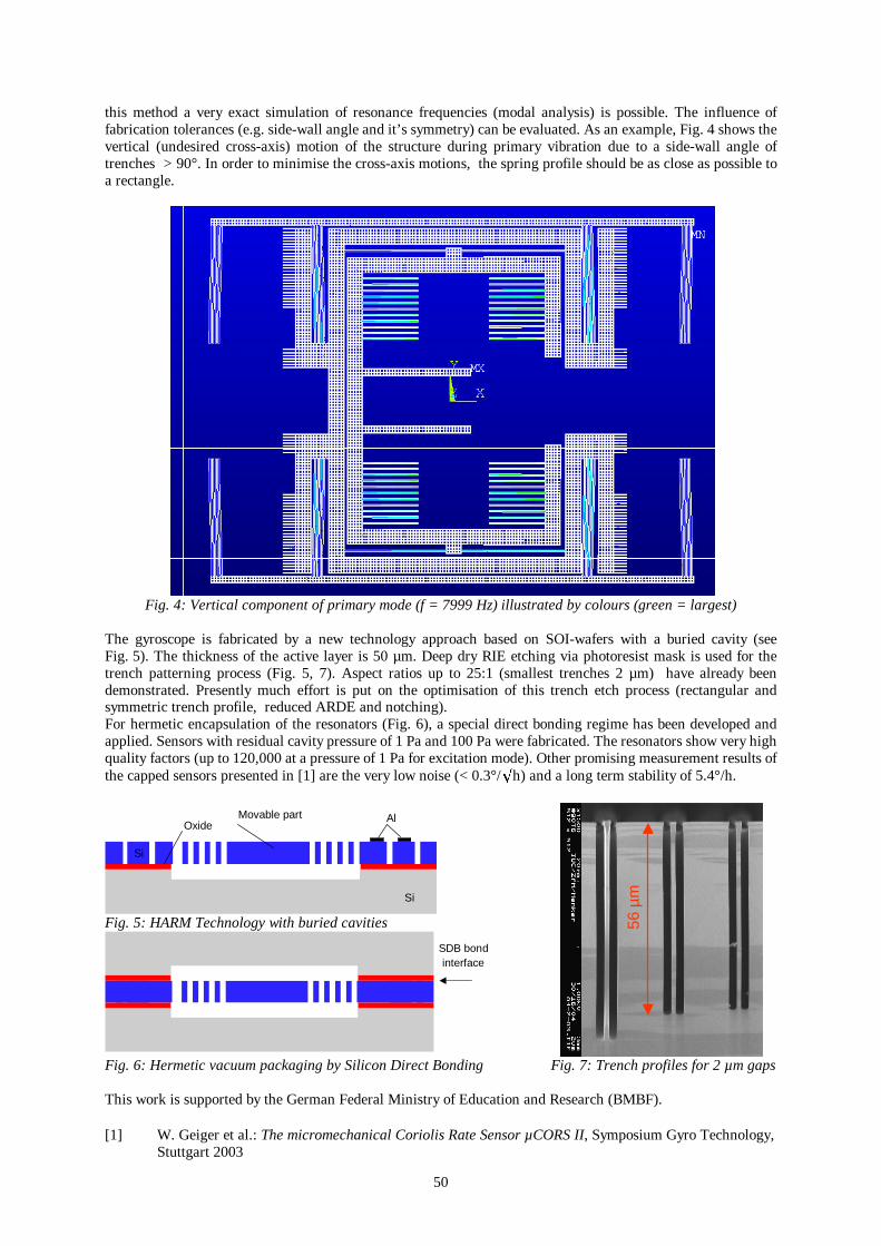
50
this method a very exact simulation of resonance frequencies (modal analysis) is possible. The influence of fabrication tolerances (e.g. side-wall angle and it’s symmetry) can be evaluated. As an example, Fig. 4 shows the vertical (undesired cross-axis) motion of the structure during primary vibration due to a side-wall angle of trenches > 90°. In order to minimise the cross-axis motions, the spring profile should be as close as possible to a rectangle.
Fig. 4: Vertical component of primary mode (f = 7999 Hz) illustrated by colours (green = largest)
The gyroscope is fabricated by a new technology approach based on SOI-wafers with a buried cavity (see Fig. 5). The thickness of the active layer is 50 µm. Deep dry RIE etching via photoresist mask is used for the trench patterning process (Fig. 5, 7). Aspect ratios up to 25:1 (smallest trenches 2 µm) have already been demonstrated. Presently much effort is put on the optimisation of this trench etch process (rectangular and symmetric trench profile, reduced ARDE and notching). For hermetic encapsulation of the resonators (Fig. 6), a special direct bonding regime has been developed and applied. Sensors with residual cavity pressure of 1 Pa and 100 Pa were fabricated. The resonators show very high quality factors (up to 120,000 at a pressure of 1 Pa for excitation mode). Other promising measurement results of the capped sensors presented in [1] are the very low noise (< 0.3°/h) and a long term stability of 5.4°/h.
Si
Oxide Al Movable part
Si
Fig. 5: HARM Technology with buried cavities
SDB bondinterface
56 µ
m
Fig. 6: Hermetic vacuum packaging by Silicon Direct Bonding Fig. 7: Trench profiles for 2 µm gaps This work is supported by the German Federal Ministry of Education and Research (BMBF). [1] W. Geiger et al.: The micromechanical Coriolis Rate Sensor µCORS II, Symposium Gyro Technology,
Stuttgart 2003
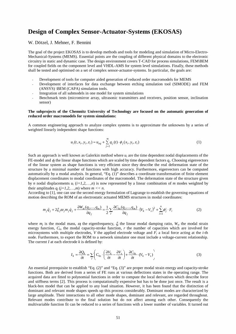
51
Design of Complex Sensor-Actuator-Systems (EKOSAS) W. Dötzel, J. Mehner, F. Bennini The goal of the project EKOSAS is to develop methods and tools for modeling and simulation of Micro-Electro-Mechanical-Systems (MEMS). Essential points are the coupling of different physical domains to the electronic circuitry in static and dynamic case. The design environment covers T-CAD for process simulations, FEM\BEM for coupled fields on the component level and VHDL-AMS for system level simulations. Finally, these methods shall be tested and optimised on a set of complex sensor-actuator-systems. In particular, the goals are:
- Development of tools for computer aided generation of reduced order macromodels for MEMS - Development of interfaces for data exchange between etching simulation tool (SIMODE) and FEM
(ANSYS) \BEM (CAPA) simulation tools. - Integration of all submodels in one model for system simulations - Benchmark tests (micromirror array, ultrasonic transmitters and receivers, position sensor, inclination
sensor) The subprojects of the Chemnitz University of Technology are focused on the automatic generation of reduced order macromodels for system simulations: A common engineering approach to analyze complex systems is to approximate the unknowns by a series of weighted linearly independent shape functions:
=
⋅+≈m
jiiijjeqiiii zyxtquzyxtu
1),,()(),,,( φ (1)
Such an approach is well known as Galerkin method where ui are the time dependent nodal displacements of the FE-model and φj the linear shape functions which are scaled by time dependent factors qj. Choosing eigenvectors of the linear system as shape functions is very efficient since they describe the real deformation state of the structure by a minimal number of functions with high accuracy. Furthermore, eigenvectors can be computed automatically by a modal analysis. In general, “Eq. (1)” describes a coordinate transformation of finite element displacement coordinates to modal coordinates of the macromodel. The deformation state of the structure given by n nodal displacements ui (i=1,2,…,n) is now represented by a linear combination of m modes weighted by their amplitudes qj (j=1,2,…,m) where m << n. According to [1], one can use the second energy formulation of Lagrange to establish the governing equations of motion describing the ROM of an electrostatic actuated MEMS structures in modal coordinates:
( ) i
n
i
ijsk
r j
mks
j
mstjjjjjj FVV
q
qqC
q
qqWqmqm ⋅+−⋅
∂∂=
∂∂++
=1
211 ),...,(
21),...,(
2 φωξ (2)
where mj is the modal mass, ωj the eigenfrequency, ξj the linear modal damping ratio, Wst the modal strain energy function, Cks the modal capacity-stroke function, r the number of capacities which are involved for microsystems with multiple electrodes, V the applied electrode voltage and Fi a local force acting at the i-th node. Furthermore, to export the ROM to a network simulator one must include a voltage-current relationship. The current I at each electrode k is defined by:
−⋅
∂∂+
∂∂−
∂∂⋅=
∂∂=
rsk
ksskks
kk VV
t
C
t
V
t
VC
t
QI )( (3)
An essential prerequisite to establish “Eq. (2)” and “Eq. (3)” are proper modal strain energy and capacity-stroke functions. Both are derived from a series of FE runs at various deflections states in the operating range. The acquired data are fitted to polynomial functions in order to compute the local derivatives which describe force and stiffness terms [2]. This process is computationally expensive but has to be done just once. The result is a black-box model that can be applied to any load situation. However, it has been found that the distinction of dominant and relevant mode shapes speeds up this process considerably. Dominant modes are characterized by large amplitude. Their interactions to all other mode shapes, dominant and relevant, are regarded throughout. Relevant modes contribute to the final solution but do not affect among each other. Consequently the multivariable function fit can be reduced to a series of functions with a lower number of variables. It turned out
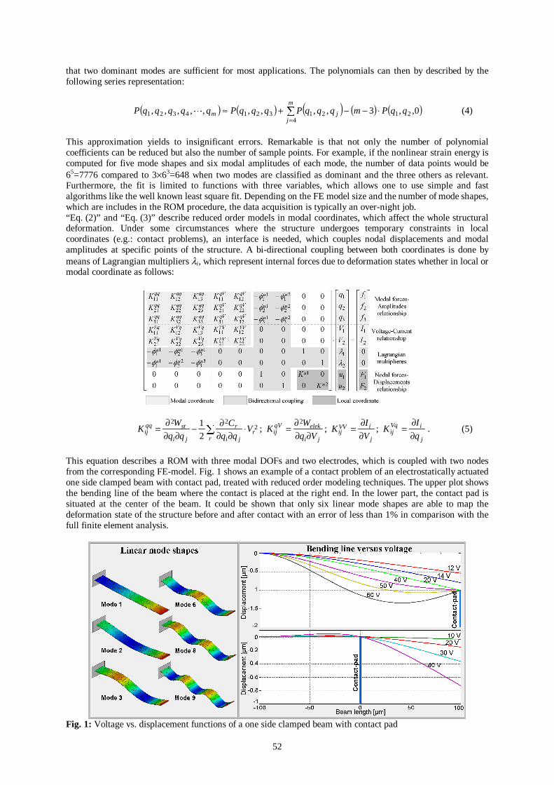
52
that two dominant modes are sufficient for most applications. The polynomials can then by described by the following series representation:
( ) ( ) ( ) ( ) ( )0,,3,,,,,,,,, 214
213214321 qqPmqqqPqqqPqqqqqPm
jjm ⋅−−+≈
= (4)
This approximation yields to insignificant errors. Remarkable is that not only the number of polynomial coefficients can be reduced but also the number of sample points. For example, if the nonlinear strain energy is computed for five mode shapes and six modal amplitudes of each mode, the number of data points would be 65=7776 compared to 3×63=648 when two modes are classified as dominant and the three others as relevant. Furthermore, the fit is limited to functions with three variables, which allows one to use simple and fast algorithms like the well known least square fit. Depending on the FE model size and the number of mode shapes, which are includes in the ROM procedure, the data acquisition is typically an over-night job. “Eq. (2)” and “Eq. (3)” describe reduced order models in modal coordinates, which affect the whole structural deformation. Under some circumstances where the structure undergoes temporary constraints in local coordinates (e.g.: contact problems), an interface is needed, which couples nodal displacements and modal amplitudes at specific points of the structure. A bi-directional coupling between both coordinates is done by means of Lagrangian multipliers λi, which represent internal forces due to deformation states whether in local or modal coordinate as follows:
222
21
rr ji
r
ji
stqqij V
C
WK ⋅
∂∂∂−
∂∂∂= ;
ji
elekqVij Vq
WK
∂∂∂=
2;
j
iVVij V
IK
∂∂= ;
j
iVqij q
IK
∂∂
= . (5)
This equation describes a ROM with three modal DOFs and two electrodes, which is coupled with two nodes from the corresponding FE-model. Fig. 1 shows an example of a contact problem of an electrostatically actuated one side clamped beam with contact pad, treated with reduced order modeling techniques. The upper plot shows the bending line of the beam where the contact is placed at the right end. In the lower part, the contact pad is situated at the center of the beam. It could be shown that only six linear mode shapes are able to map the deformation state of the structure before and after contact with an error of less than 1% in comparison with the full finite element analysis.
Fig. 1: Voltage vs. displacement functions of a one side clamped beam with contact pad
53
Fig. 2: System level simulation in PSPICE using a ROM of a micromirror The ultimate goal of ROM is to obtain an accurate black-box model of the microsystem’s behavior. Interface signals are limited to the voltage-current relationship at each electrode, essential inputs such as external loads (e.g. gravitation, pressure) and significant output quantities (e.g. a subset of displacements at characteristic points of the model). The black-box model can be exported and used for modeling systems as signal flow graphs (e.g. SIMULINK) or as networks (e.g. PSPICE). VHDL-AMS becomes more and more important in analyzing and simulating MEMS on the system level. It is much more flexible, because in addition to the across and through quantities (Network syntax) one can use further relations expressed by analytical terms inside the total system. Fig. 2 illustrates an example of a system simulation performed in PSPICE. It demonstrates a frequently used electronic circuitry to detect the position of electrostatic actuated microstructures. In this example, the ROM of a micromirror presented in [1] is used, where the current alteration on the ground electrodes is evaluated to obtain a proportional signal to the mirror plate position. Since the deflection state of the structure is decomposed in shape functions (Mode 1 the rotation, Mode 2 the translation; Mode7 and 9 the warp of the mirror plate), one can analyze the sensitivity of the circuit with respect to the mirror plate deformation and evaluate the errors. References: [1] F. Bennini, J. Mehner and W. Dötzel, Computational Methods for Reduced Order Modeling of Coupled
Domain Simulations, 11 International Conference on Solid State Sensors and Actuators (Transducers 01), p. 260-263, Germany 2001
[3] J. E. Mehner, L.D. Gabbay and S.D. Senturia, Computer-Aided Generation of Nonlinear Reduced-Order Dynamic Macromodels, Journal of Microelectromechanical Systems, p. 270-277, June 2000
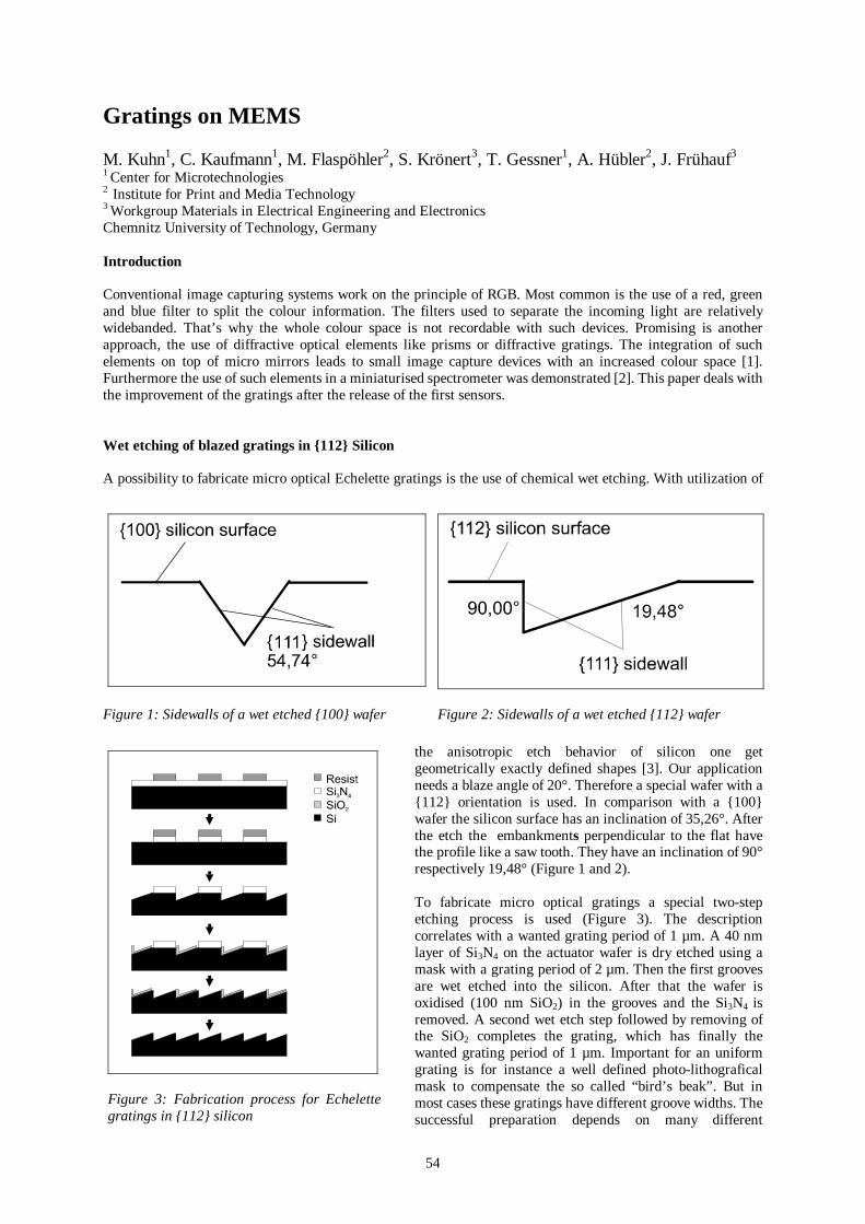
54
Gratings on MEMS M. Kuhn1, C. Kaufmann1, M. Flaspöhler2, S. Krönert3, T. Gessner1, A. Hübler2, J. Frühauf3 1 Center for Microtechnologies 2 Institute for Print and Media Technology 3 Workgroup Materials in Electrical Engineering and Electronics Chemnitz University of Technology, Germany Introduction Conventional image capturing systems work on the principle of RGB. Most common is the use of a red, green and blue filter to split the colour information. The filters used to separate the incoming light are relatively widebanded. That’s why the whole colour space is not recordable with such devices. Promising is another approach, the use of diffractive optical elements like prisms or diffractive gratings. The integration of such elements on top of micro mirrors leads to small image capture devices with an increased colour space [1]. Furthermore the use of such elements in a miniaturised spectrometer was demonstrated [2]. This paper deals with the improvement of the gratings after the release of the first sensors. Wet etching of blazed gratings in 112 Silicon A possibility to fabricate micro optical Echelette gratings is the use of chemical wet etching. With utilization of
the anisotropic etch behavior of silicon one get geometrically exactly defined shapes [3]. Our application needs a blaze angle of 20°. Therefore a special wafer with a 112 orientation is used. In comparison with a 100 wafer the silicon surface has an inclination of 35,26°. After the etch the embankments perpendicular to the flat have the profile like a saw tooth. They have an inclination of 90° respectively 19,48° (Figure 1 and 2). To fabricate micro optical gratings a special two-step etching process is used (Figure 3). The description correlates with a wanted grating period of 1 µm. A 40 nm layer of Si3N4 on the actuator wafer is dry etched using a mask with a grating period of 2 µm. Then the first grooves are wet etched into the silicon. After that the wafer is oxidised (100 nm SiO2) in the grooves and the Si3N4 is removed. A second wet etch step followed by removing of the SiO2 completes the grating, which has finally the wanted grating period of 1 µm. Important for an uniform grating is for instance a well defined photo-lithografical mask to compensate the so called “bird’s beak”. But in most cases these gratings have different groove widths. The successful preparation depends on many different
Figure 1: Sidewalls of a wet etched 100 wafer Figure 2: Sidewalls of a wet etched 112 wafer
Figure 3: Fabrication process for Echelette gratings in 112 silicon
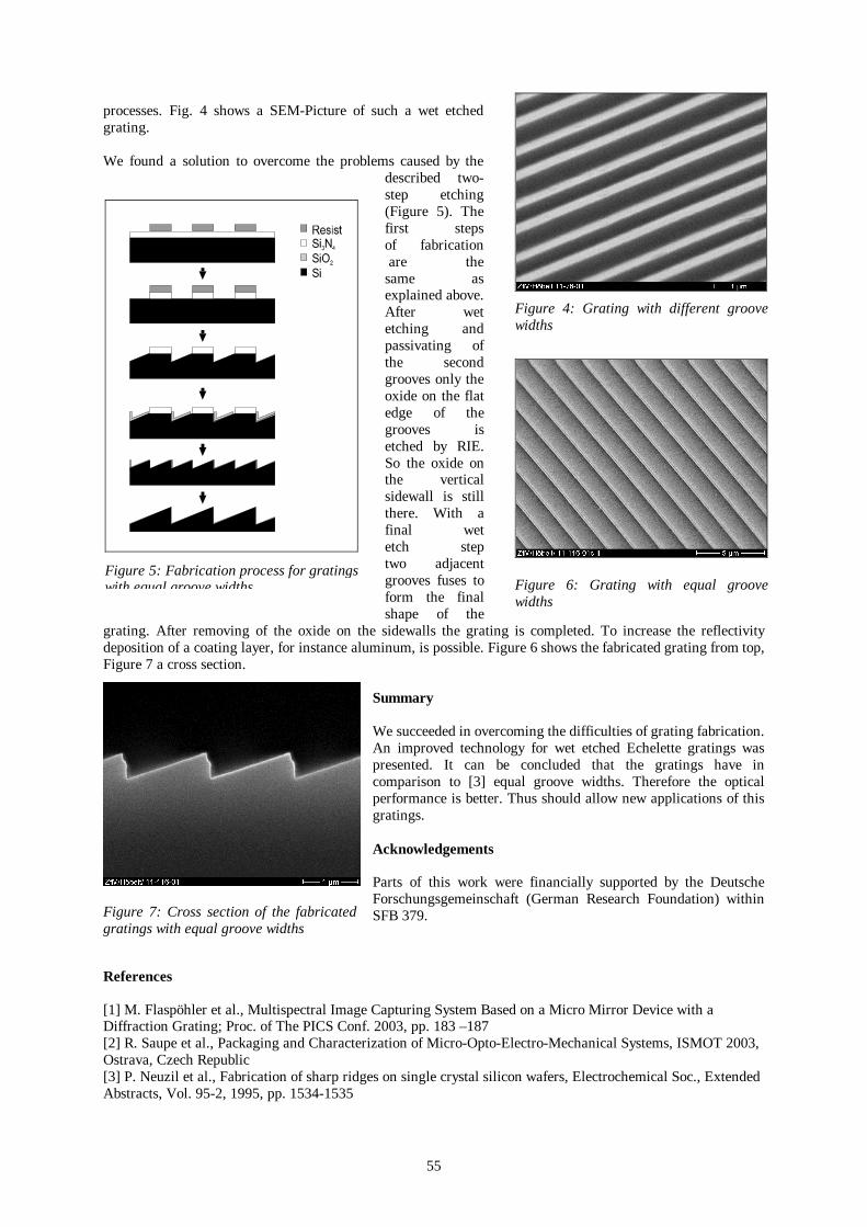
55
processes. Fig. 4 shows a SEM-Picture of such a wet etched grating. We found a solution to overcome the problems caused by the
described two-step etching (Figure 5). The first steps of fabrication are the same as explained above. After wet etching and passivating of the second grooves only the oxide on the flat edge of the grooves is etched by RIE. So the oxide on the vertical sidewall is still there. With a final wet etch step two adjacent grooves fuses to form the final shape of the
grating. After removing of the oxide on the sidewalls the grating is completed. To increase the reflectivity deposition of a coating layer, for instance aluminum, is possible. Figure 6 shows the fabricated grating from top, Figure 7 a cross section.
Summary We succeeded in overcoming the difficulties of grating fabrication. An improved technology for wet etched Echelette gratings was presented. It can be concluded that the gratings have in comparison to [3] equal groove widths. Therefore the optical performance is better. Thus should allow new applications of this gratings. Acknowledgements Parts of this work were financially supported by the Deutsche Forschungsgemeinschaft (German Research Foundation) within SFB 379.
References [1] M. Flaspöhler et al., Multispectral Image Capturing System Based on a Micro Mirror Device with a Diffraction Grating; Proc. of The PICS Conf. 2003, pp. 183 –187 [2] R. Saupe et al., Packaging and Characterization of Micro-Opto-Electro-Mechanical Systems, ISMOT 2003, Ostrava, Czech Republic [3] P. Neuzil et al., Fabrication of sharp ridges on single crystal silicon wafers, Electrochemical Soc., Extended Abstracts, Vol. 95-2, 1995, pp. 1534-1535
Figure 7: Cross section of the fabricated gratings with equal groove widths
Figure 4: Grating with different groove widths
Figure 6: Grating with equal groove widths
Figure 5: Fabrication process for gratings with equal groove widths
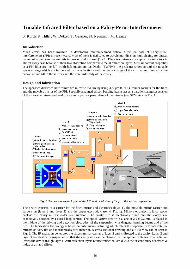
56
Tunable Infrared Filter based on a Fabry-Perot-Interferometer
S. Kurth, K. Hiller, W. Dötzel, T. Gessner, N. Neumann, M. Heinze
Introduction Much effort has been involved in developing micromachined optical filters on base of Fabry-Perot-interferometers (FPI) in recent years. Most of them is dedicated to wavelength division multiplexing for optical communication or to gas analysis in near or mid infrared [1 - 3]. Dielectric mirrors are applied for reflectors in almost every case because of their low absorption compared to metal reflection layers. Most important properties of a FPI filter are the full width half maximum bandwidth (FWHM), the peak transmission and the tunable spectral range which are influenced by the reflectivity and the phase change of the mirrors and limited by the curvature and tilt of the mirrors and the non uniformity of the cavity.
Design and fabrication The approach discussed here minimizes mirror curvature by using 300 µm thick Si mirror carriers for the fixed and the movable mirror of the FPI. Specially arranged silicon bending beams act as a parallel spring suspension of the movable mirror and lead to an almost perfect parallelism of the mirrors (see SEM view in Fig. 1).
Fig. 1. Top view onto the layers of the FPI and SEM view of the parallel spring suspension
The device consists of a carrier for the fixed mirror and electrodes (layer 1), the movable mirror carrier and suspension (layer 2 and layer 3) and the upper electrode (layer 4, Fig. 1). Mirrors of dielectric layer stacks enclose the cavity in first order configuration. The cavity size is electrically tuned and the cavity size capacitively detected by a closed loop control. The optical active area with a size of 2.2 x 2.2 mm² is placed in the middle of the driving and detection electrodes, of the suspension with diagonal bending beams and of the rim. The fabrication technology is based on bulk micromachining which offers the opportunity to fabricate the mirrors on very flat and mechanically stiff material. A cross sectional drawing and a SEM view can be seen in Fig. 2. The IR radiation penetrates the silicon mirror carrier of layer 2 and is directed to the cavity. Layer 2 and layer 3 are elastically suspended so that the cavity size can be changed by the applied voltages. The radiation leaves the device trough layer 1. Anti reflection layers reduce reflection loss due to the in-continuity of refractive index of air and silicon.
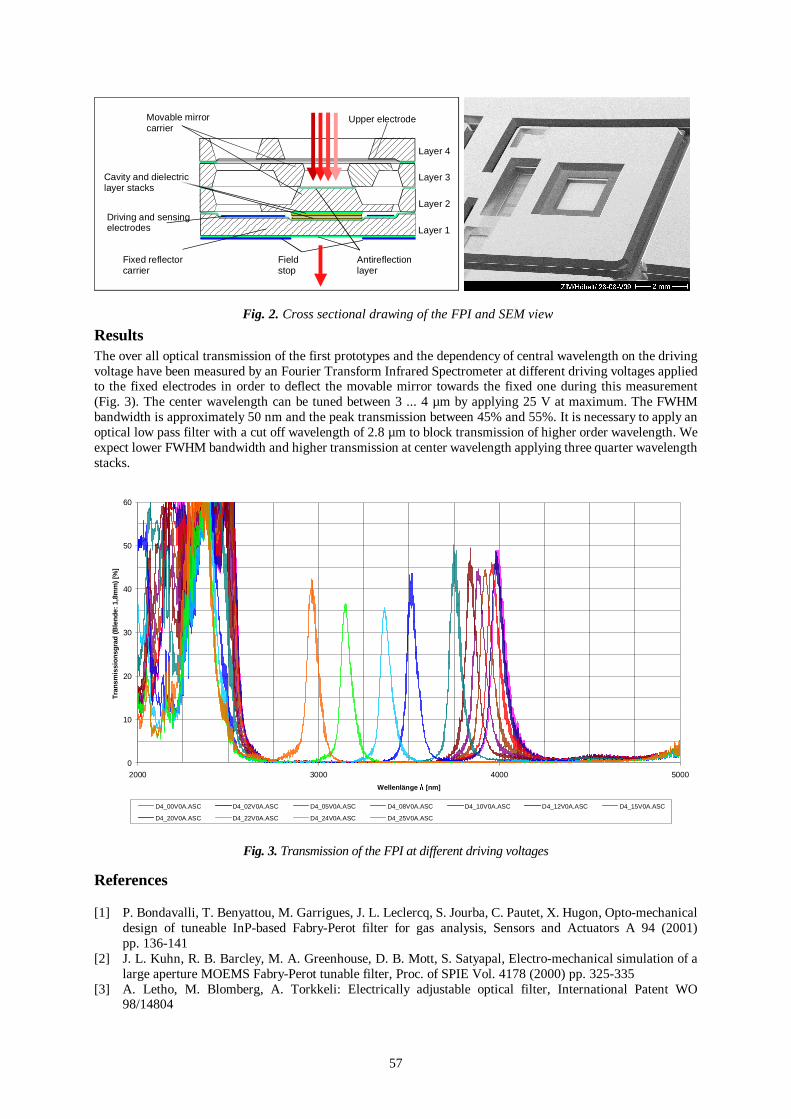
57
Cavity and dielectriclayer stacks
Movable mirrorcarrier
Cavity and dielectriclayer stacks
Antireflectionlayer
Fixed reflectorcarrier
Layer 4
Movable mirrorcarrier
Cavity and dielectriclayer stacks
Antireflectionlayer
Fixed reflectorcarrier
Layer 4
Layer 2
Layer 3
Movable mirrorcarrier
Cavity and dielectriclayer stacks
Driving and sensingelectrodes
Antireflectionlayer
Fixed reflectorcarrier
Upper electrode
Layer 4
Layer 1
Layer 2
Layer 3
Movable mirrorcarrier
Cavity and dielectriclayer stacks
Driving and sensingelectrodes
Antireflectionlayer
Fixed reflectorcarrier
Upper electrode
Fieldstop
Layer 1
Layer 4
Layer 3
Layer 2
Fig. 2. Cross sectional drawing of the FPI and SEM view
Results The over all optical transmission of the first prototypes and the dependency of central wavelength on the driving voltage have been measured by an Fourier Transform Infrared Spectrometer at different driving voltages applied to the fixed electrodes in order to deflect the movable mirror towards the fixed one during this measurement (Fig. 3). The center wavelength can be tuned between 3 ... 4 µm by applying 25 V at maximum. The FWHM bandwidth is approximately 50 nm and the peak transmission between 45% and 55%. It is necessary to apply an optical low pass filter with a cut off wavelength of 2.8 µm to block transmission of higher order wavelength. We expect lower FWHM bandwidth and higher transmission at center wavelength applying three quarter wavelength stacks.
0
10
20
30
40
50
60
2000 3000 4000 5000
Wellenlänge λ [nm]
Tra
nsm
issi
on
sgra
d (
Ble
nd
e: 1
,8m
m)
[%]
D4_00V0A.ASC D4_02V0A.ASC D4_05V0A.ASC D4_08V0A.ASC D4_10V0A.ASC D4_12V0A.ASC D4_15V0A.ASC
D4_20V0A.ASC D4_22V0A.ASC D4_24V0A.ASC D4_25V0A.ASC
Fig. 3. Transmission of the FPI at different driving voltages
References
[1] P. Bondavalli, T. Benyattou, M. Garrigues, J. L. Leclercq, S. Jourba, C. Pautet, X. Hugon, Opto-mechanical design of tuneable InP-based Fabry-Perot filter for gas analysis, Sensors and Actuators A 94 (2001) pp. 136-141
[2] J. L. Kuhn, R. B. Barcley, M. A. Greenhouse, D. B. Mott, S. Satyapal, Electro-mechanical simulation of a large aperture MOEMS Fabry-Perot tunable filter, Proc. of SPIE Vol. 4178 (2000) pp. 325-335
[3] A. Letho, M. Blomberg, A. Torkkeli: Electrically adjustable optical filter, International Patent WO 98/14804
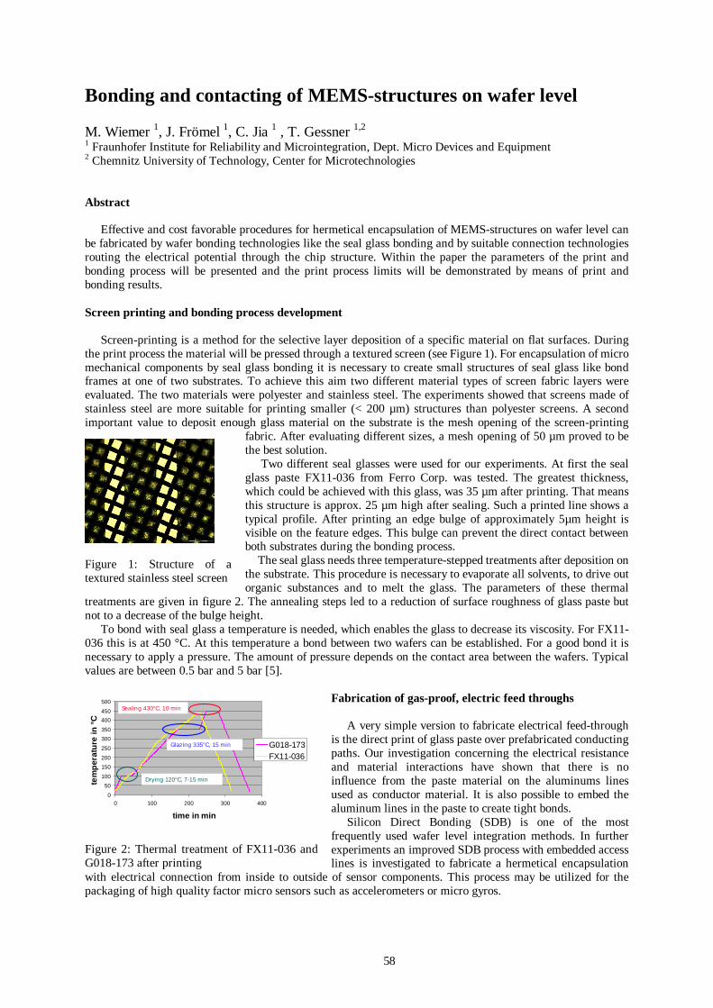
58
Bonding and contacting of MEMS-structures on wafer level M. Wiemer 1, J. Frömel 1, C. Jia 1 , T. Gessner 1,2
1 Fraunhofer Institute for Reliability and Microintegration, Dept. Micro Devices and Equipment 2 Chemnitz University of Technology, Center for Microtechnologies Abstract Effective and cost favorable procedures for hermetical encapsulation of MEMS-structures on wafer level can be fabricated by wafer bonding technologies like the seal glass bonding and by suitable connection technologies routing the electrical potential through the chip structure. Within the paper the parameters of the print and bonding process will be presented and the print process limits will be demonstrated by means of print and bonding results. Screen printing and bonding process development Screen-printing is a method for the selective layer deposition of a specific material on flat surfaces. During the print process the material will be pressed through a textured screen (see Figure 1). For encapsulation of micro mechanical components by seal glass bonding it is necessary to create small structures of seal glass like bond frames at one of two substrates. To achieve this aim two different material types of screen fabric layers were evaluated. The two materials were polyester and stainless steel. The experiments showed that screens made of stainless steel are more suitable for printing smaller (< 200 µm) structures than polyester screens. A second important value to deposit enough glass material on the substrate is the mesh opening of the screen-printing
fabric. After evaluating different sizes, a mesh opening of 50 µm proved to be the best solution. Two different seal glasses were used for our experiments. At first the seal glass paste FX11-036 from Ferro Corp. was tested. The greatest thickness, which could be achieved with this glass, was 35 µm after printing. That means this structure is approx. 25 µm high after sealing. Such a printed line shows a typical profile. After printing an edge bulge of approximately 5µm height is visible on the feature edges. This bulge can prevent the direct contact between both substrates during the bonding process. The seal glass needs three temperature-stepped treatments after deposition on the substrate. This procedure is necessary to evaporate all solvents, to drive out organic substances and to melt the glass. The parameters of these thermal
treatments are given in figure 2. The annealing steps led to a reduction of surface roughness of glass paste but not to a decrease of the bulge height. To bond with seal glass a temperature is needed, which enables the glass to decrease its viscosity. For FX11-036 this is at 450 °C. At this temperature a bond between two wafers can be established. For a good bond it is necessary to apply a pressure. The amount of pressure depends on the contact area between the wafers. Typical values are between 0.5 bar and 5 bar [5].
Fabrication of gas-proof, electric feed throughs A very simple version to fabricate electrical feed-through is the direct print of glass paste over prefabricated conducting paths. Our investigation concerning the electrical resistance and material interactions have shown that there is no influence from the paste material on the aluminums lines used as conductor material. It is also possible to embed the aluminum lines in the paste to create tight bonds. Silicon Direct Bonding (SDB) is one of the most frequently used wafer level integration methods. In further experiments an improved SDB process with embedded access lines is investigated to fabricate a hermetical encapsulation
with electrical connection from inside to outside of sensor components. This process may be utilized for the packaging of high quality factor micro sensors such as accelerometers or micro gyros.
Figure 1: Structure of a textured stainless steel screen
Figure 2: Thermal treatment of FX11-036 and G018-173 after printing
0
50
100
150
200
250
300
350
400
450
500
0 100 200 300 400
time in min
tem
per
atu
re in
°C
G018-173FX11-036
Seal ing 430°C, 10 min
Glaz ing 335°C, 15 min
Drying 120°C, 7-15 min
0
50
100
150
200
250
300
350
400
450
500
0 100 200 300 400
time in min
tem
per
atu
re in
°C
G018-173FX11-036
Seal ing 430°C, 10 min
Glaz ing 335°C, 15 min
Drying 120°C, 7-15 min
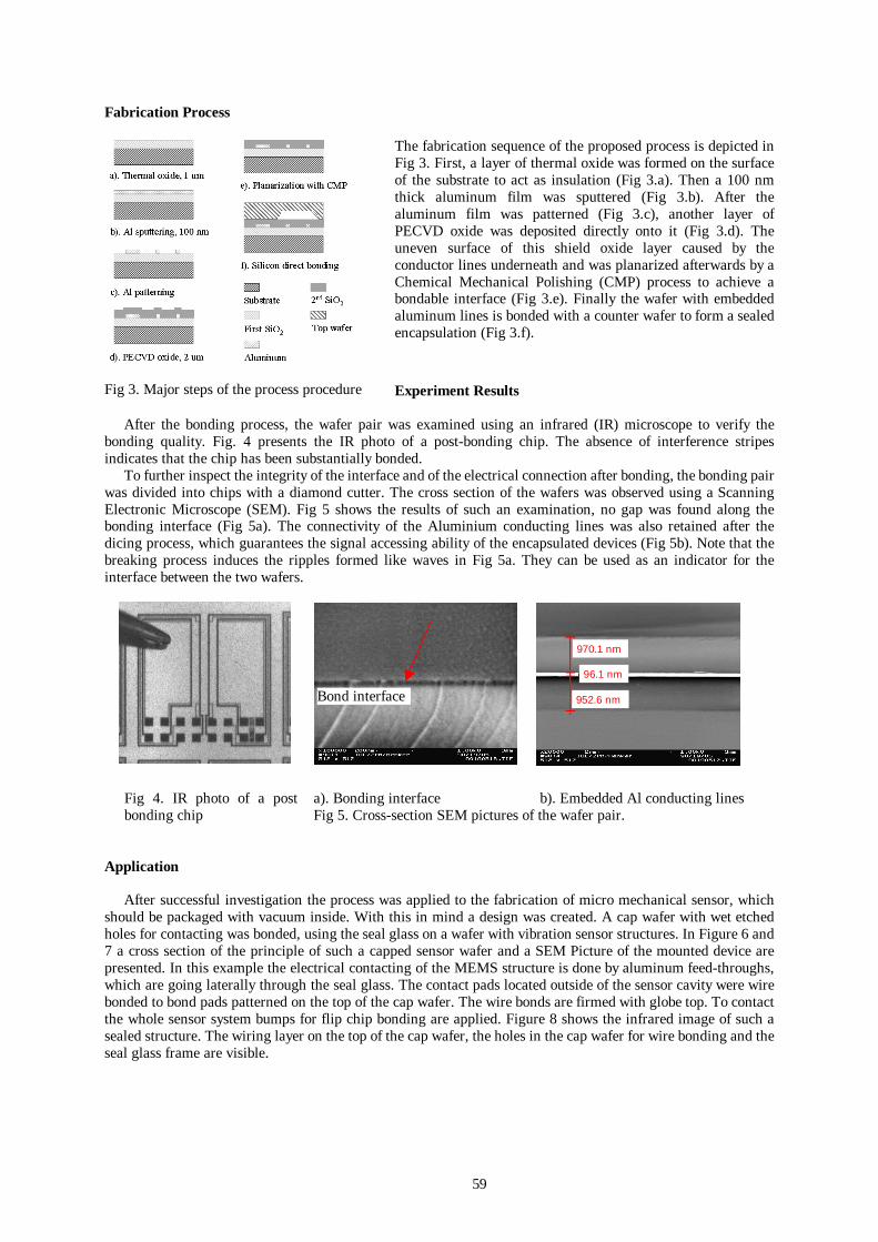
59
Fabrication Process
The fabrication sequence of the proposed process is depicted in Fig 3. First, a layer of thermal oxide was formed on the surface of the substrate to act as insulation (Fig 3.a). Then a 100 nm thick aluminum film was sputtered (Fig 3.b). After the aluminum film was patterned (Fig 3.c), another layer of PECVD oxide was deposited directly onto it (Fig 3.d). The uneven surface of this shield oxide layer caused by the conductor lines underneath and was planarized afterwards by a Chemical Mechanical Polishing (CMP) process to achieve a bondable interface (Fig 3.e). Finally the wafer with embedded aluminum lines is bonded with a counter wafer to form a sealed encapsulation (Fig 3.f). Experiment Results
After the bonding process, the wafer pair was examined using an infrared (IR) microscope to verify the bonding quality. Fig. 4 presents the IR photo of a post-bonding chip. The absence of interference stripes indicates that the chip has been substantially bonded. To further inspect the integrity of the interface and of the electrical connection after bonding, the bonding pair was divided into chips with a diamond cutter. The cross section of the wafers was observed using a Scanning Electronic Microscope (SEM). Fig 5 shows the results of such an examination, no gap was found along the bonding interface (Fig 5a). The connectivity of the Aluminium conducting lines was also retained after the dicing process, which guarantees the signal accessing ability of the encapsulated devices (Fig 5b). Note that the breaking process induces the ripples formed like waves in Fig 5a. They can be used as an indicator for the interface between the two wafers.
a). Bonding interface b). Embedded Al conducting lines Fig 4. IR photo of a post bonding chip Fig 5. Cross-section SEM pictures of the wafer pair.
Application After successful investigation the process was applied to the fabrication of micro mechanical sensor, which should be packaged with vacuum inside. With this in mind a design was created. A cap wafer with wet etched holes for contacting was bonded, using the seal glass on a wafer with vibration sensor structures. In Figure 6 and 7 a cross section of the principle of such a capped sensor wafer and a SEM Picture of the mounted device are presented. In this example the electrical contacting of the MEMS structure is done by aluminum feed-throughs, which are going laterally through the seal glass. The contact pads located outside of the sensor cavity were wire bonded to bond pads patterned on the top of the cap wafer. The wire bonds are firmed with globe top. To contact the whole sensor system bumps for flip chip bonding are applied. Figure 8 shows the infrared image of such a sealed structure. The wiring layer on the top of the cap wafer, the holes in the cap wafer for wire bonding and the seal glass frame are visible.
Fig 3. Major steps of the process procedure
970.1 nm
96.1 nm
952.6 nm
970.1 nm
96.1 nm
952.6 nmBond interface Bond interface
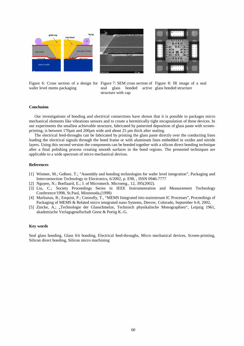
60
Figure 6: Cross section of a design for wafer level mems packaging
Figure 7: SEM cross section of seal glass bonded active structure with cap
Figure 8: IR image of a seal glass bonded structure
Conclusion Our investigations of bonding and electrical connections have shown that it is possible to packages micro mechanical elements like vibrations sensors and to create a hermitically tight encapsulation of these devices. In our experiments the smallest achievable structure, fabricated by patterned deposition of glass paste with screen-printing, is between 170µm and 200µm wide and about 25 µm thick after sealing. The electrical feed-throughs can be fabricated by printing the glass paste directly over the conducting lines leading the electrical signals through the bond frame or with aluminum lines embedded in oxides and nitride layers. Using this second version the components can be bonded together with a silicon direct bonding technique after a final polishing process creating smooth surfaces in the bond regions. The presented techniques are applicable to a wide spectrum of micro mechanical devices. References [1] Wiemer, M.; Geßner, T.; “Assembly and bonding technologies for wafer level integration”, Packaging and
Interconnection Technology in Electronics, 6/2002, p. E98, , ISSN 0946-7777 [2] Nguyen, N.; Boellaard, E.; J. of Micromech. Microeng., 12, 395(2002). [3] Liu, C.; Society Proceedings Series in IEEE Instrumentation and Measurement Technology
Conference/1998, St.Paul, Minnesoda,(1998) [4] Markunas, R.; Enquist, P.; Connolly, T., “MEMS Integrated into mainstream IC Processes”, Proceedings of
Packaging of MEMS & Related micro integrated nano Systems, Denver, Colorado, September 6-8, 2002, [5] Zincke, A.; „Technologie der Glasschmelze, Technisch physikalische Monographien“, Leipzig 1961,
akademische Verlagsgesellschaft Geest & Portig K.-G. Key words Seal glass bonding, Glass frit bonding, Electrical feed-throughs, Micro mechanical devices, Screen-printing, Silicon direct bonding, Silicon micro machining
sensor wafer
cap wafer
globe top bump
seal glass frame
wire bond
sensor wafer
cap wafer
globe top bump
seal glass frame
wire bond
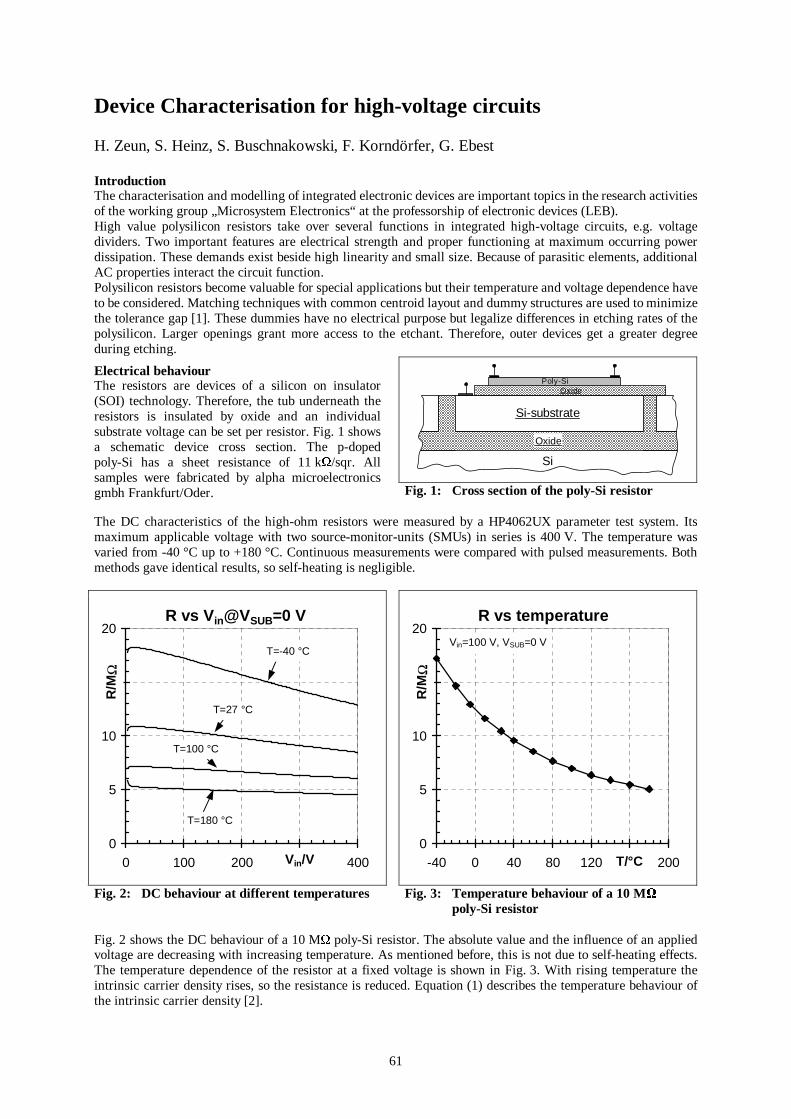
61
Device Characterisation for high-voltage circuits H. Zeun, S. Heinz, S. Buschnakowski, F. Korndörfer, G. Ebest Introduction The characterisation and modelling of integrated electronic devices are important topics in the research activities of the working group „Microsystem Electronics“ at the professorship of electronic devices (LEB). High value polysilicon resistors take over several functions in integrated high-voltage circuits, e.g. voltage dividers. Two important features are electrical strength and proper functioning at maximum occurring power dissipation. These demands exist beside high linearity and small size. Because of parasitic elements, additional AC properties interact the circuit function. Polysilicon resistors become valuable for special applications but their temperature and voltage dependence have to be considered. Matching techniques with common centroid layout and dummy structures are used to minimize the tolerance gap [1]. These dummies have no electrical purpose but legalize differences in etching rates of the polysilicon. Larger openings grant more access to the etchant. Therefore, outer devices get a greater degree during etching.
Si
Si-substrate
Oxide
OxidePoly-Si
Electrical behaviour The resistors are devices of a silicon on insulator (SOI) technology. Therefore, the tub underneath the resistors is insulated by oxide and an individual substrate voltage can be set per resistor. Fig. 1 shows a schematic device cross section. The p-doped poly-Si has a sheet resistance of 11 kΩ/sqr. All samples were fabricated by alpha microelectronics gmbh Frankfurt/Oder. Fig. 1: Cross section of the poly-Si resistor
The DC characteristics of the high-ohm resistors were measured by a HP4062UX parameter test system. Its maximum applicable voltage with two source-monitor-units (SMUs) in series is 400 V. The temperature was varied from -40 °C up to +180 °C. Continuous measurements were compared with pulsed measurements. Both methods gave identical results, so self-heating is negligible.
R vs Vin@VSUB=0 V
0
5
10
15
20
0 100 200 300 400Vin/V
R/M
Ω
T=-40 °C
T=27 °C
T=100 °C
T=180 °C
R vs temperature
0
5
10
15
20
-40 0 40 80 120 160 200T/°C
R/M
Ω
Vin=100 V, VSUB=0 V
Fig. 2: DC behaviour at different temperatures Fig. 3: Temperature behaviour of a 10 MΩ
poly-Si resistor
Fig. 2 shows the DC behaviour of a 10 MΩ poly-Si resistor. The absolute value and the influence of an applied voltage are decreasing with increasing temperature. As mentioned before, this is not due to self-heating effects. The temperature dependence of the resistor at a fixed voltage is shown in Fig. 3. With rising temperature the intrinsic carrier density rises, so the resistance is reduced. Equation (1) describes the temperature behaviour of the intrinsic carrier density [2].
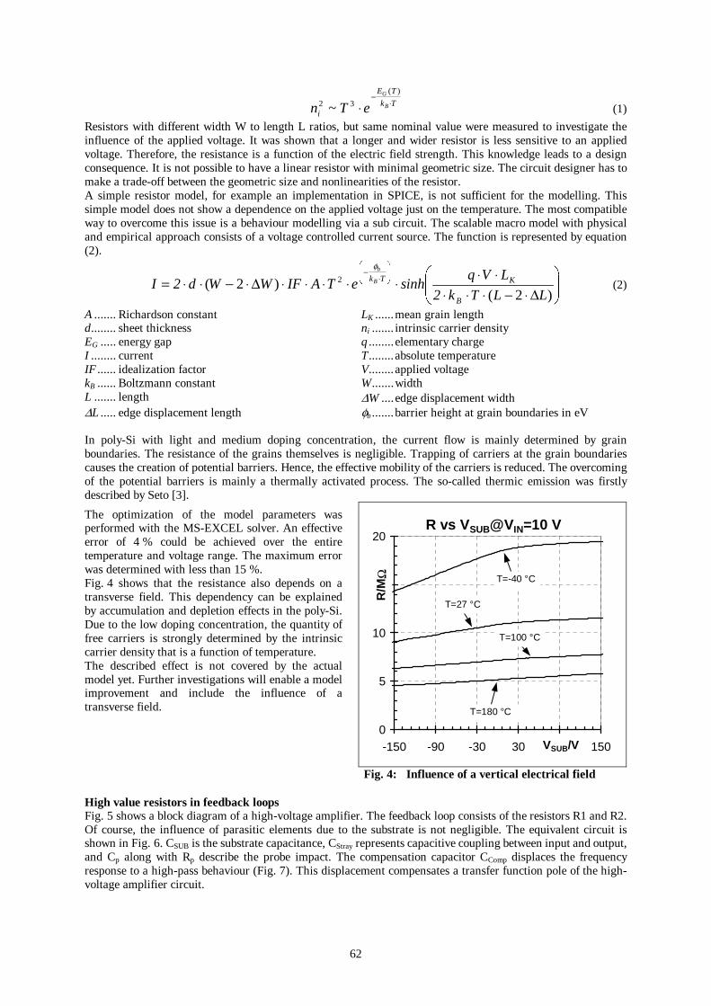
62
Tk
TE
iB
G
eTn ⋅−
⋅)(
32 ~ (1)
Resistors with different width W to length L ratios, but same nominal value were measured to investigate the influence of the applied voltage. It was shown that a longer and wider resistor is less sensitive to an applied voltage. Therefore, the resistance is a function of the electric field strength. This knowledge leads to a design consequence. It is not possible to have a linear resistor with minimal geometric size. The circuit designer has to make a trade-off between the geometric size and nonlinearities of the resistor. A simple resistor model, for example an implementation in SPICE, is not sufficient for the modelling. This simple model does not show a dependence on the applied voltage just on the temperature. The most compatible way to overcome this issue is a behaviour modelling via a sub circuit. The scalable macro model with physical and empirical approach consists of a voltage controlled current source. The function is represented by equation (2).
∆⋅−⋅⋅⋅⋅⋅⋅⋅⋅⋅⋅∆⋅−⋅⋅=
⋅−
)2()2( 2
LLTk2
LVqsinheTAIFWWd2I
B
KTkB
bφ
(2)
A ....... Richardson constant LK ......mean grain length d........ sheet thickness ni ....... intrinsic carrier density EG ..... energy gap q ........ elementary charge I ........ current T........ absolute temperature IF ...... idealization factor V........ applied voltage kB ...... Boltzmann constant W.......width L ....... length ∆W .... edge displacement width ∆L ..... edge displacement length φb .......barrier height at grain boundaries in eV In poly-Si with light and medium doping concentration, the current flow is mainly determined by grain boundaries. The resistance of the grains themselves is negligible. Trapping of carriers at the grain boundaries causes the creation of potential barriers. Hence, the effective mobility of the carriers is reduced. The overcoming of the potential barriers is mainly a thermally activated process. The so-called thermic emission was firstly described by Seto [3].
R vs VSUB@VIN=10 V
0
5
10
15
20
-150 -90 -30 30 90 150VSUB/V
R/M
Ω T=-40 °C
T=27 °C
T=100 °C
T=180 °C
The optimization of the model parameters was performed with the MS-EXCEL solver. An effective error of 4 % could be achieved over the entire temperature and voltage range. The maximum error was determined with less than 15 %. Fig. 4 shows that the resistance also depends on a transverse field. This dependency can be explained by accumulation and depletion effects in the poly-Si. Due to the low doping concentration, the quantity of free carriers is strongly determined by the intrinsic carrier density that is a function of temperature. The described effect is not covered by the actual model yet. Further investigations will enable a model improvement and include the influence of a transverse field.
Fig. 4: Influence of a vertical electrical field
High value resistors in feedback loops Fig. 5 shows a block diagram of a high-voltage amplifier. The feedback loop consists of the resistors R1 and R2. Of course, the influence of parasitic elements due to the substrate is not negligible. The equivalent circuit is shown in Fig. 6. CSUB is the substrate capacitance, CStray represents capacitive coupling between input and output, and Cp along with Rp describe the probe impact. The compensation capacitor CComp displaces the frequency response to a high-pass behaviour (Fig. 7). This displacement compensates a transfer function pole of the high-voltage amplifier circuit.
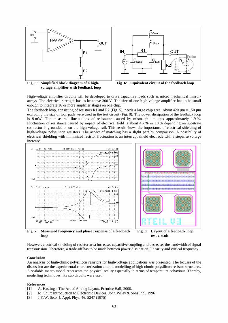
63
Fig. 5: Simplified block diagram of a high-voltage amplifier with feedback loop
Fig. 6: Equivalent circuit of the feedback loop
High-voltage amplifier circuits will be developed to drive capacitive loads such as micro mechanical mirror-arrays. The electrical strength has to be above 300 V. The size of one high-voltage amplifier has to be small enough to integrate 16 or more amplifier stages on one chip. The feedback loop, consisting of resistors R1 and R2 (Fig. 5), needs a large chip area. About 420 µm × 150 µm excluding the size of four pads were used in the test circuit (Fig. 8). The power dissipation of the feedback loop is 9 mW. The measured fluctuations of resistance caused by mismatch amounts approximately 1.9 %. Fluctuation of resistance caused by impact of electrical field is about 4.7 % or 18 % depending on substrate connector is grounded or on the high-voltage rail. This result shows the importance of electrical shielding of high-voltage polysilicon resistors. The aspect of matching has a slight part by comparison. A possibility of electrical shielding with minimized resistor fluctuation is an interrupt shield electrode with a stepwise voltage increase.
Fig. 7: Measured frequency and phase response of a feedback loop
Fig. 8: Layout of a feedback loop test circuit
However, electrical shielding of resistor area increases capacitive coupling and decreases the bandwidth of signal transmission. Therefore, a trade-off has to be made between power dissipation, linearity and critical frequency. Conclusion An analysis of high-ohmic polysilicon resistors for high-voltage applications was presented. The focuses of the discussion are the experimental characterization and the modelling of high-ohmic polysilicon resistor structures. A scalable macro model represents the physical reality especially in terms of temperature behaviour. Thereby, modelling techniques like sub circuits were used. References [1] A. Hastings: The Art of Analog Layout, Prentice Hall, 2000. [2] M. Shur: Introduction to Electronic Devices, John Wiley & Sons Inc., 1996 [3] J.Y.W. Seto: J. Appl. Phys. 46, 5247 (1975)
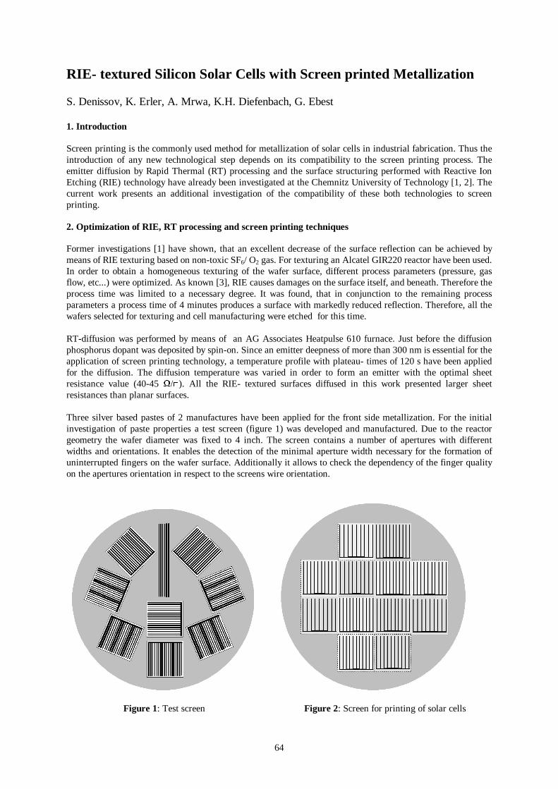
64
RIE- textured Silicon Solar Cells with Screen printed Metallization S. Denissov, K. Erler, A. Mrwa, K.H. Diefenbach, G. Ebest 1. Introduction Screen printing is the commonly used method for metallization of solar cells in industrial fabrication. Thus the introduction of any new technological step depends on its compatibility to the screen printing process. The emitter diffusion by Rapid Thermal (RT) processing and the surface structuring performed with Reactive Ion Etching (RIE) technology have already been investigated at the Chemnitz University of Technology [1, 2]. The current work presents an additional investigation of the compatibility of these both technologies to screen printing. 2. Optimization of RIE, RT processing and screen printing techniques Former investigations [1] have shown, that an excellent decrease of the surface reflection can be achieved by means of RIE texturing based on non-toxic SF6/ O2 gas. For texturing an Alcatel GIR220 reactor have been used. In order to obtain a homogeneous texturing of the wafer surface, different process parameters (pressure, gas flow, etc...) were optimized. As known [3], RIE causes damages on the surface itself, and beneath. Therefore the process time was limited to a necessary degree. It was found, that in conjunction to the remaining process parameters a process time of 4 minutes produces a surface with markedly reduced reflection. Therefore, all the wafers selected for texturing and cell manufacturing were etched for this time. RT-diffusion was performed by means of an AG Associates Heatpulse 610 furnace. Just before the diffusion phosphorus dopant was deposited by spin-on. Since an emitter deepness of more than 300 nm is essential for the application of screen printing technology, a temperature profile with plateau- times of 120 s have been applied for the diffusion. The diffusion temperature was varied in order to form an emitter with the optimal sheet resistance value (40-45 Ω/). All the RIE- textured surfaces diffused in this work presented larger sheet resistances than planar surfaces. Three silver based pastes of 2 manufactures have been applied for the front side metallization. For the initial investigation of paste properties a test screen (figure 1) was developed and manufactured. Due to the reactor geometry the wafer diameter was fixed to 4 inch. The screen contains a number of apertures with different widths and orientations. It enables the detection of the minimal aperture width necessary for the formation of uninterrupted fingers on the wafer surface. Additionally it allows to check the dependency of the finger quality on the apertures orientation in respect to the screens wire orientation.
Figure 1: Test screen Figure 2: Screen for printing of solar cells
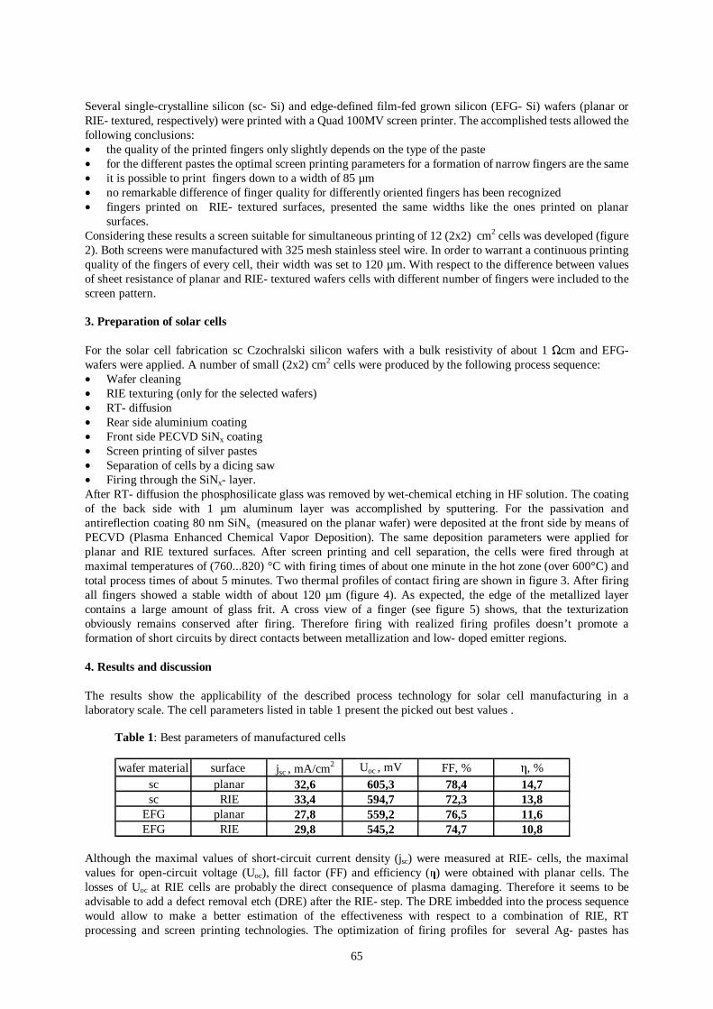
65
Several single-crystalline silicon (sc- Si) and edge-defined film-fed grown silicon (EFG- Si) wafers (planar or RIE- textured, respectively) were printed with a Quad 100MV screen printer. The accomplished tests allowed the following conclusions: • the quality of the printed fingers only slightly depends on the type of the paste • for the different pastes the optimal screen printing parameters for a formation of narrow fingers are the same • it is possible to print fingers down to a width of 85 µm • no remarkable difference of finger quality for differently oriented fingers has been recognized • fingers printed on RIE- textured surfaces, presented the same widths like the ones printed on planar
surfaces. Considering these results a screen suitable for simultaneous printing of 12 (2x2) cm2 cells was developed (figure 2). Both screens were manufactured with 325 mesh stainless steel wire. In order to warrant a continuous printing quality of the fingers of every cell, their width was set to 120 µm. With respect to the difference between values of sheet resistance of planar and RIE- textured wafers cells with different number of fingers were included to the screen pattern. 3. Preparation of solar cells For the solar cell fabrication sc Czochralski silicon wafers with a bulk resistivity of about 1 Ωcm and EFG- wafers were applied. A number of small (2x2) cm2 cells were produced by the following process sequence: • Wafer cleaning • RIE texturing (only for the selected wafers) • RT- diffusion • Rear side aluminium coating • Front side PECVD SiNx coating • Screen printing of silver pastes • Separation of cells by a dicing saw • Firing through the SiNx- layer. After RT- diffusion the phosphosilicate glass was removed by wet-chemical etching in HF solution. The coating of the back side with 1 µm aluminum layer was accomplished by sputtering. For the passivation and antireflection coating 80 nm SiNx (measured on the planar wafer) were deposited at the front side by means of PECVD (Plasma Enhanced Chemical Vapor Deposition). The same deposition parameters were applied for planar and RIE textured surfaces. After screen printing and cell separation, the cells were fired through at maximal temperatures of (760...820) °C with firing times of about one minute in the hot zone (over 600°C) and total process times of about 5 minutes. Two thermal profiles of contact firing are shown in figure 3. After firing all fingers showed a stable width of about 120 µm (figure 4). As expected, the edge of the metallized layer contains a large amount of glass frit. A cross view of a finger (see figure 5) shows, that the texturization obviously remains conserved after firing. Therefore firing with realized firing profiles doesn’t promote a formation of short circuits by direct contacts between metallization and low- doped emitter regions. 4. Results and discussion The results show the applicability of the described process technology for solar cell manufacturing in a laboratory scale. The cell parameters listed in table 1 present the picked out best values . Table 1: Best parameters of manufactured cells
wafer material surface jsc , mA/cm2 Uoc , mV FF, % η, %sc planar 32,6 605,3 78,4 14,7sc RIE 33,4 594,7 72,3 13,8
EFG planar 27,8 559,2 76,5 11,6EFG RIE 29,8 545,2 74,7 10,8
Although the maximal values of short-circuit current density (jsc) were measured at RIE- cells, the maximal values for open-circuit voltage (Uoc), fill factor (FF) and efficiency (η) were obtained with planar cells. The losses of Uoc at RIE cells are probably the direct consequence of plasma damaging. Therefore it seems to be advisable to add a defect removal etch (DRE) after the RIE- step. The DRE imbedded into the process sequence would allow to make a better estimation of the effectiveness with respect to a combination of RIE, RT processing and screen printing technologies. The optimization of firing profiles for several Ag- pastes has
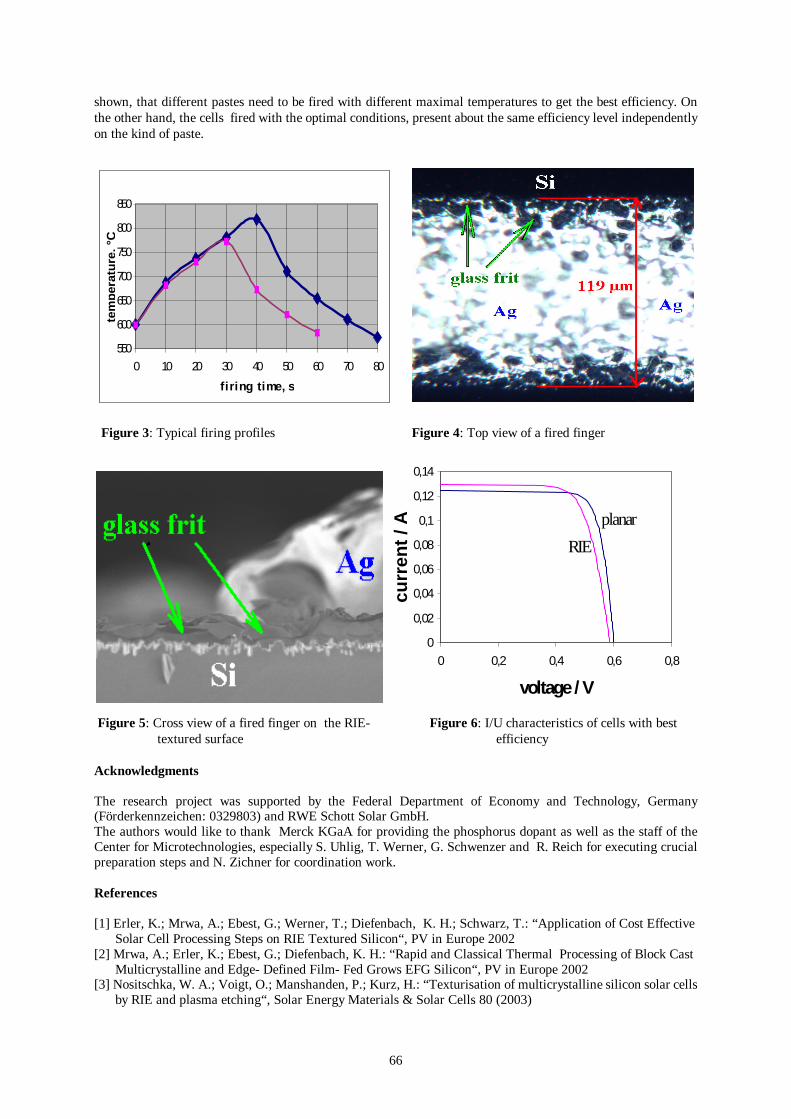
66
shown, that different pastes need to be fired with different maximal temperatures to get the best efficiency. On the other hand, the cells fired with the optimal conditions, present about the same efficiency level independently on the kind of paste.
Figure 3: Typical firing profiles Figure 4: Top view of a fired finger
Figure 5: Cross view of a fired finger on the RIE- Figure 6: I/U characteristics of cells with best textured surface efficiency Acknowledgments The research project was supported by the Federal Department of Economy and Technology, Germany (Förderkennzeichen: 0329803) and RWE Schott Solar GmbH. The authors would like to thank Merck KGaA for providing the phosphorus dopant as well as the staff of the Center for Microtechnologies, especially S. Uhlig, T. Werner, G. Schwenzer and R. Reich for executing crucial preparation steps and N. Zichner for coordination work. References [1] Erler, K.; Mrwa, A.; Ebest, G.; Werner, T.; Diefenbach, K. H.; Schwarz, T.: “Application of Cost Effective Solar Cell Processing Steps on RIE Textured Silicon“, PV in Europe 2002 [2] Mrwa, A.; Erler, K.; Ebest, G.; Diefenbach, K. H.: “Rapid and Classical Thermal Processing of Block Cast Multicrystalline and Edge- Defined Film- Fed Grows EFG Silicon“, PV in Europe 2002 [3] Nositschka, W. A.; Voigt, O.; Manshanden, P.; Kurz, H.: “Texturisation of multicrystalline silicon solar cells by RIE and plasma etching“, Solar Energy Materials & Solar Cells 80 (2003)
550
600
650
700
750
800
850
0 10 20 30 40 50 60 70 80
f i r i n g t i m e , s
tem
per
atu
re, °
C
0
0,02
0,04
0,06
0,08
0,1
0,12
0,14
0 0,2 0,4 0,6 0,8
voltage / V
curr
ent
/ A planar
RIE
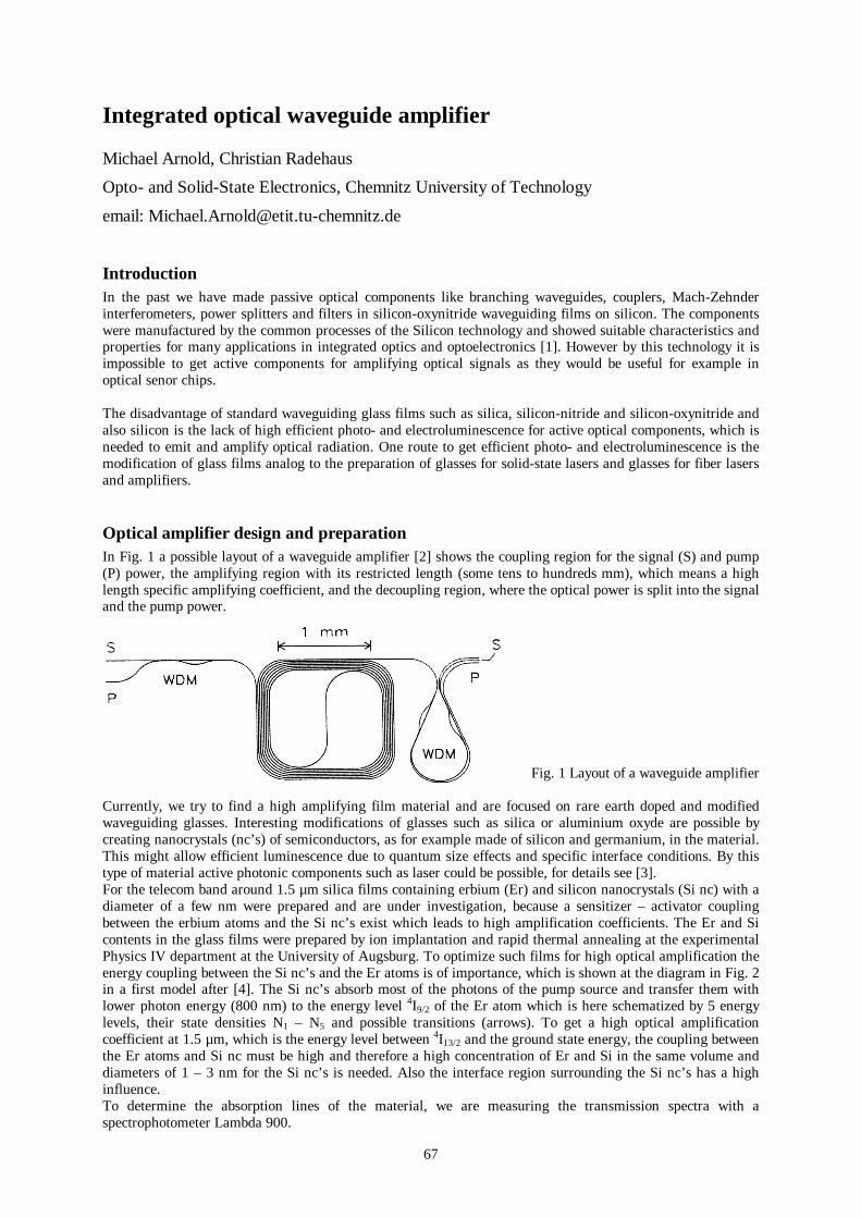
67
Integrated optical waveguide amplifier
Michael Arnold, Christian Radehaus
Opto- and Solid-State Electronics, Chemnitz University of Technology
email: [email protected]
Introduction In the past we have made passive optical components like branching waveguides, couplers, Mach-Zehnder interferometers, power splitters and filters in silicon-oxynitride waveguiding films on silicon. The components were manufactured by the common processes of the Silicon technology and showed suitable characteristics and properties for many applications in integrated optics and optoelectronics [1]. However by this technology it is impossible to get active components for amplifying optical signals as they would be useful for example in optical senor chips. The disadvantage of standard waveguiding glass films such as silica, silicon-nitride and silicon-oxynitride and also silicon is the lack of high efficient photo- and electroluminescence for active optical components, which is needed to emit and amplify optical radiation. One route to get efficient photo- and electroluminescence is the modification of glass films analog to the preparation of glasses for solid-state lasers and glasses for fiber lasers and amplifiers.
Optical amplifier design and preparation In Fig. 1 a possible layout of a waveguide amplifier [2] shows the coupling region for the signal (S) and pump (P) power, the amplifying region with its restricted length (some tens to hundreds mm), which means a high length specific amplifying coefficient, and the decoupling region, where the optical power is split into the signal and the pump power.
Fig. 1 Layout of a waveguide amplifier Currently, we try to find a high amplifying film material and are focused on rare earth doped and modified waveguiding glasses. Interesting modifications of glasses such as silica or aluminium oxyde are possible by creating nanocrystals (nc’s) of semiconductors, as for example made of silicon and germanium, in the material. This might allow efficient luminescence due to quantum size effects and specific interface conditions. By this type of material active photonic components such as laser could be possible, for details see [3]. For the telecom band around 1.5 µm silica films containing erbium (Er) and silicon nanocrystals (Si nc) with a diameter of a few nm were prepared and are under investigation, because a sensitizer – activator coupling between the erbium atoms and the Si nc’s exist which leads to high amplification coefficients. The Er and Si contents in the glass films were prepared by ion implantation and rapid thermal annealing at the experimental Physics IV department at the University of Augsburg. To optimize such films for high optical amplification the energy coupling between the Si nc’s and the Er atoms is of importance, which is shown at the diagram in Fig. 2 in a first model after [4]. The Si nc’s absorb most of the photons of the pump source and transfer them with lower photon energy (800 nm) to the energy level 4I9/2 of the Er atom which is here schematized by 5 energy levels, their state densities N1 – N5 and possible transitions (arrows). To get a high optical amplification coefficient at 1.5 µm, which is the energy level between 4I13/2 and the ground state energy, the coupling between the Er atoms and Si nc must be high and therefore a high concentration of Er and Si in the same volume and diameters of 1 – 3 nm for the Si nc’s is needed. Also the interface region surrounding the Si nc’s has a high influence. To determine the absorption lines of the material, we are measuring the transmission spectra with a spectrophotometer Lambda 900.
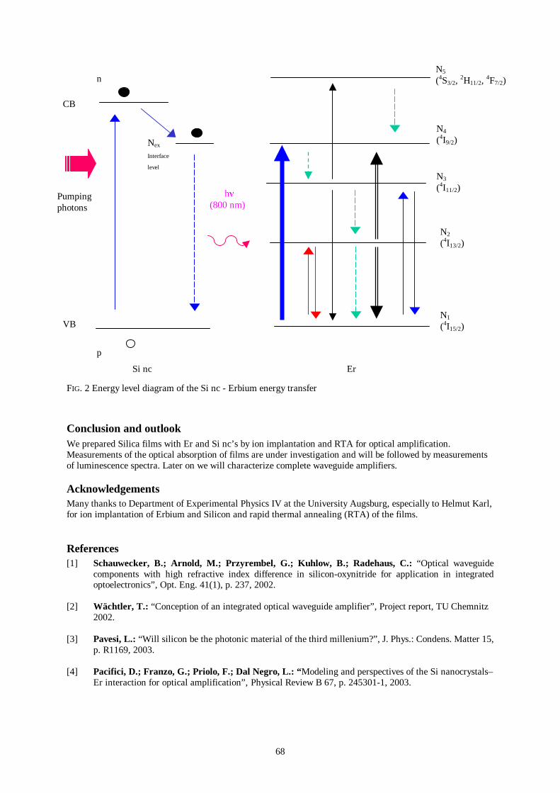
68
FIG. 2 Energy level diagram of the Si nc - Erbium energy transfer
Conclusion and outlook We prepared Silica films with Er and Si nc’s by ion implantation and RTA for optical amplification. Measurements of the optical absorption of films are under investigation and will be followed by measurements of luminescence spectra. Later on we will characterize complete waveguide amplifiers.
Acknowledgements Many thanks to Department of Experimental Physics IV at the University Augsburg, especially to Helmut Karl, for ion implantation of Erbium and Silicon and rapid thermal annealing (RTA) of the films.
References [1] Schauwecker, B.; Arnold, M.; Przyrembel, G.; Kuhlow, B.; Radehaus, C.: “Optical waveguide
components with high refractive index difference in silicon-oxynitride for application in integrated optoelectronics”, Opt. Eng. 41(1), p. 237, 2002.
[2] Wächtler, T.: “Conception of an integrated optical waveguide amplifier”, Project report, TU Chemnitz
2002. [3] Pavesi, L.: “Will silicon be the photonic material of the third millenium?”, J. Phys.: Condens. Matter 15,
p. R1169, 2003. [4] Pacifici, D.; Franzo, G.; Priolo, F.; Dal Negro, L.: “Modeling and perspectives of the Si nanocrystals–
Er interaction for optical amplification”, Physical Review B 67, p. 245301-1, 2003.
N5
(4S3/2, 2H11/2,
4F7/2)
N2
(4I13/2)
N1
(4I15/2)
N3
(4I11/2)
Er
N4
(4I9/2)
VB
CB
Si nc
n
Nex
Interface
level
p
hν (800 nm)
Pumping photons
69
Silicon Gratings with Different Profiles: Trapezoidal, Triangular, Rectangular, Arched J. Frühauf, S. Krönert
Introduction By inspiration from the European Standard EN ISO 5436-1 [1] concerning material measures for the profile method for assessment of the surface texture some investigations are performed to find possibilities for the production of gratings with defined profiles by microtechnological processes using silicon. Silicon is a very suitable material for the realization of material measures because of its high thermomechanical stability [2] and because of the availability of the very precise processes for microstructuring. Different profiles of linear gratings can be etched depending on the used wafer orientation, the groove direction on the wafer and etching procedure. Unfortunately, the production of an unrestricted free shape is impossible or very difficult in any case. Of course, the gratings can also be used otherwise for example for the assessment of optical devices or as optical reflection gratings. Types of profile and principles of their manufacture The types of profiles capable of being produced by silicon etching can be divided into two groups: polygonal profiles and arched profiles, illustrated schematically in figure 1. Combinations of them are included. The horizontal parts of the polygonal and combined profiles correspond with the wafer surface or the etch ground.
111
sw
dV
dTδ
100
sw
bg
d
R
sw
a) Trapezoidal respective V-grooves along <110>
b) Rectangle grooves along <100> at 100-wafer
c) Elliptically arched U-grooves isotropically etched
F
R
d) Triangular profile (typa a) modifyed by mask inversion
e) Parabolic arched profile (type a) modifyed by maskless etching
f) Elliptic arched profile (type a) modifyed by isotropical etching
Figure 1 Manufacturing principles of the profile types w: width of a window; s: spacing between windows; d, dT, dV: etched depth g: width of a groove; b: width of a barrier between grooves; R: isotropically etched depth
δ = 70.5° at 100-wafer; δ = 109.5° at 110-wafer
The straight and inclined sections of the polygonal types result from crystallographically defined planes arising from the orientation dependent etching processes (ODE). These planes are inclined by special angles which can be explained on the base of the pronounced anisotropy of the etch rates in basic solutions (e.g. KOH:H2O-solutions). At windows along <110> the 111-planes arise as sidewalls forming a trapeziodal profile, (figure 1a, dotted lines) or finally a series of V-grooves (“geometrical etch stop”). The angles of inclination of the 111-planes relative to the wafer surface define the characteristical angles of the trapeziums and V-grooves along <110>. These angles have the following values:
100-wafer: γ = arctan √2 = 54.74°; 110-wafer: γ = 90° - 54.74° = 35.26°.
A triangular profile can be made by modifying the V-groove type, figure 1a. Using silicon nitride as the 1st mask the V-grooves are etched followed by a selective thermal oxidation of the free silicon surface inside the grooves. Then the nitride is selectively removed. Now, the spacing is converted into a window suitable for etching a second series of V-grooves, figure 1d. In this way the period is halved. Using an 112-wafer the inclination of the opposite 111-faces is different: 90° respective 19.48°. Consequently, the arising V-grooves have an asymmetric shape. The resulting periodic profile can be converted into an asymmetric triangular profile if w = s analogous to the symmetric case, figure 1d.
70
A groove with vertical 100-sidewalls can be realized along the <100>-directions on the 100-wafer resulting in a rectangular profile, figure 1b. In this case the sidewall face has the same etch rate as the etch ground because of the crystallographic equivalence of both faces. Grooves with approximately vertical bounding planes necessary for rectangular profiles arise also by anisotropical dry reactive ion etching (RIE). In this case the sidewall planes are not crystallographically defined resulting in deviations from a vertical even shape. The deep profiles with arched sections result directly from an isotropical etching process (figure 1c) or from isotropical etching of the polygonal V-groove (figure 1f). A 2nd orientation dependent etching of the V-groove after a complete removing of the mask at first produces very fast etching faces (F) flattening the profile. If the fast etching faces arrive the vertex line of the V-groove the geometrical etch stop is dissolved and a new slightly curved etch ground arises resulting in a shallow arched profile, figure 1e. Preparation of gratings The gratings were produced by etching of different series of long but narrow mask windows of the width w with narrow spacings of the width s in between resulting in grooves of the width g with barriers of the width b in between. The length of the period p is defined by p = w + s = g + b. Mask patterns of the grating fields with periods between 1,6 – 50 µm are realized inside a chip size of 10 mm x 10 mm together with additional guiding grooves. The used technologies for the realization of the passivation layers (thermal SiO2 and Si3N4) and for the transfer of structures into these films depend on the magnitude of the period of the gratings. The use of the projection and step and repeat techniques of lithography was necessary to achieve the extreme precision for the small periods. Especially, by varying of the exposure time the ratio w/s can be adjusted. As mentioned above a special kind of two-step etch process with intermediate oxidation is used to realize the triangular gratings [3]. The choice of the used etchant depends on the wished shape of the grating and was related to the target depth: etchants with low rate for low depth (TMAH 25% - 60 °C: rate = 0.11 µm/min; KOH 30% - 80 °C: rate = 1.1µm/min). The rate of the isotropical etchant HNO3:HF:CH3COOH at room temperature is about 3.3 µm/min. After the wafer preparation the chips were diced by sawing. For the investigation of the profiles of the gratings the chips were broken to achieve cross sections for the obversation by SEM. The determination of the radii of edges was performed by TEM. Results The SEM-pictures figures 2, 3 and 4 give an overview about the cross sections of the prepared gratings. Some preparations result in good aproximation with the expected profiles as the trapezoidal types, the V-groove types and the isotropically etched arched types shown in figures 2a and 3a,b. Other preparations reveal deviations from the target profile as the triangular and the deep or shallow arched profiles, figure 2b, c, d and 3c, d. The neighboured V-grooves of the triangular profiles have a different width because the oxidation of the V-grooves reaches into the interface between the nitride and the silicon.
a) Trapezoidal profile γ = 54.7° b) Triangular profile δ = 70.5°
c) Triangular profile δ = 109.5° d) Asymmetric triangular profile δ = 70.5° Figure 2 Prepared polygonal profiles
The “so called” isotropical etchant produced a week anisotropy which is large enough to miss the ideal target profile [4]. Etching a V-groove the rate is obviously diminished at the vertex which is conserved over a certain time. Later a flat face arises along the vertex, figure 3c.
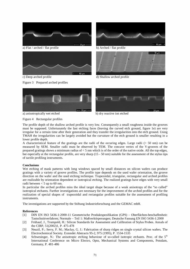
71
a) Flat / arched / flat profile b) Arched / flat profile
c) Deep arched profile d) Shallow arched profile
Figure 3 Prepared arched profiles
a) anisotropically wet etched b) dry reactive ion etched
Figure 4 Rectangular profiles
The profile depth of the shallow arched profile is very low. Consequently a small roughness inside the grooves must be supposed. Unfortunately the fast etching faces (leaving the curved etch ground, figure 1e) are very irregular for a certain time after their generation and they transfer the irregularities into the etch ground. Using TMAH the irregularities can be largely avoided but the curvature of the etch ground is smaller resulting in a lower profile depth. A characteristical feature of the gratings are the radii of the occuring edges. Large radii (> 50 nm) can be measured by SEM. Smaller radii must be observed by TEM. The concave vertex of the V-grooves of the prepared gratings shows a minimum radius of < 5 nm which is of the order of the native oxide. All the top edges, but especially at the rectangular profile, are very sharp (15 - 50 nm) suitable for the assessment of the stylus tips of tactile profiling instruments. Conclusions Wet etching of mask patterns with long windows spaced by small distances on silicon wafers can produce gratings with a variety of groove profiles. The profile type depends on the used wafer orientation, the groove direction on the wafer and the used etching technique. Trapezoidal, triangular, rectangular and arched profiles are realizable by orientation dependent or isotropical etching. The realized gratings have edges with very small radii between < 5 up to 60 nm. In particular the arched profiles miss the ideal target shape because of a weak anisotropy of the “so called” isotropical etchants. Further investigations are necessary for the improvement of the arched profiles and for the realization of special shapes of trapezoidal and rectangular profiles suitable for the assessment of profiling instruments.
The investigations are supported by the Stiftung Industrieforschung and the GEMAC mbH. References [1] DIN EN ISO 5436-1:2000-11 Geometrische Produktspezifikation (GPS) – Oberflächen-beschaffenheit:
Tastschnittverfahren; Normale – Teil 1: Maßverkörperungen; Deutsche Fassung EN ISO 5436-1:2000 [2] Frühauf, J., Trumpold, H.: Silicon Standards for Assessment and Calibration of Stylus Probes. Annals of
the CIRP, 51(2002)1, P. 475-478 [3] Neuzil, P.; Serry, F. M.; Maclay, G. J.: Fabrication of sharp ridges on single crystal silicon wafers. The
Electrochemical Society. Extendet Abstracts 95-2, 975 (1995), P. 1534-1535 [4] Schwesinger, N.: The anisotropic etching behaviour of so-called isotropic etchants. Proc. of the 5th
International Conference on Micro Electro, Opto, Mechanical Systems and Components, Potsdam, Germany, P. 481-486
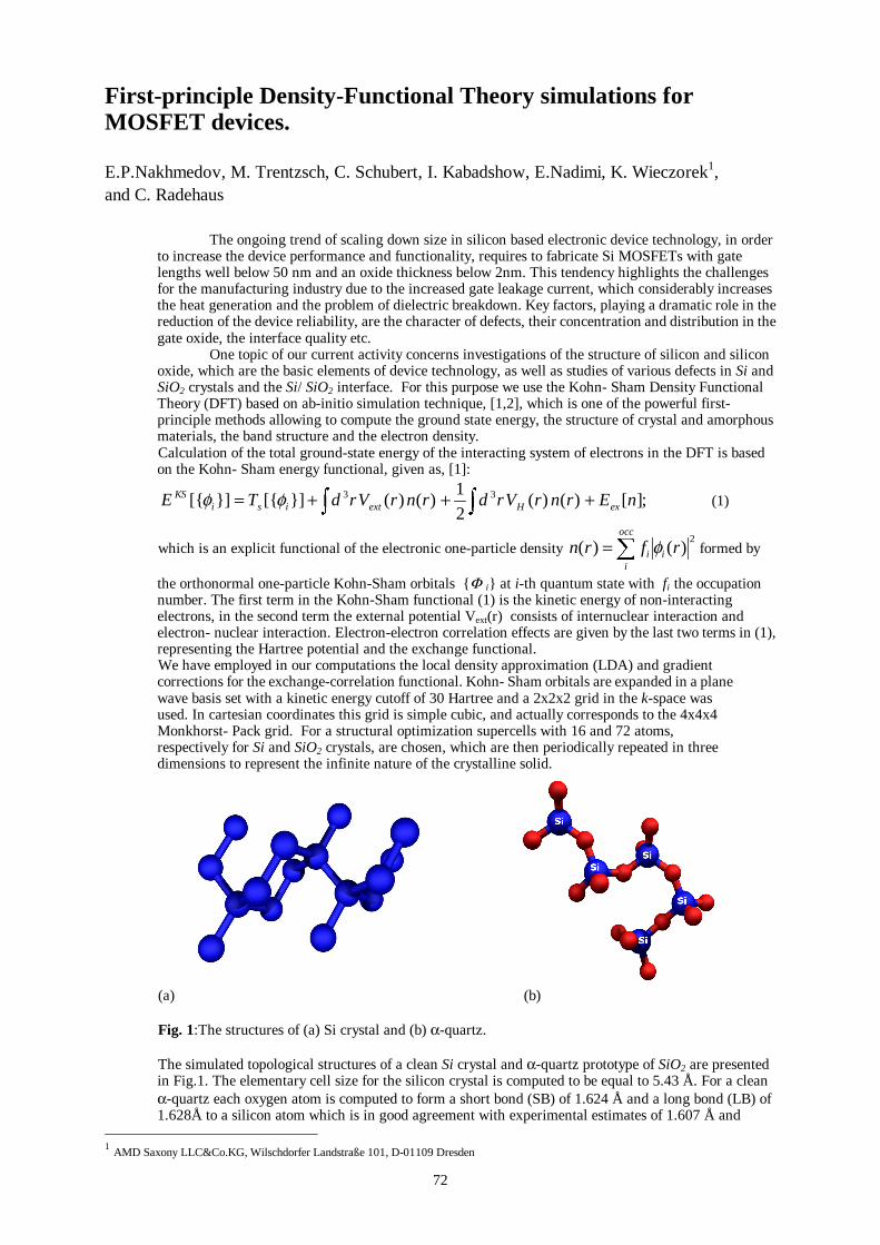
72
First-principle Density-Functional Theory simulations for MOSFET devices.
E.P.Nakhmedov, M. Trentzsch, C. Schubert, I. Kabadshow, E.Nadimi, K. Wieczorek1,)
and C. Radehaus
The ongoing trend of scaling down size in silicon based electronic device technology, in order to increase the device performance and functionality, requires to fabricate Si MOSFETs with gate lengths well below 50 nm and an oxide thickness below 2nm. This tendency highlights the challenges for the manufacturing industry due to the increased gate leakage current, which considerably increases the heat generation and the problem of dielectric breakdown. Key factors, playing a dramatic role in the reduction of the device reliability, are the character of defects, their concentration and distribution in the gate oxide, the interface quality etc.
One topic of our current activity concerns investigations of the structure of silicon and silicon oxide, which are the basic elements of device technology, as well as studies of various defects in Si and SiO2 crystals and the Si/ SiO2 interface. For this purpose we use the Kohn- Sham Density Functional Theory (DFT) based on ab-initio simulation technique, [1,2], which is one of the powerful first-principle methods allowing to compute the ground state energy, the structure of crystal and amorphous materials, the band structure and the electron density. Calculation of the total ground-state energy of the interacting system of electrons in the DFT is based on the Kohn- Sham energy functional, given as, [1]:
;][)()(2
1)()(][][ 33
+++= nErnrVrdrnrVrdTE exHextisiKS φφ (1)
which is an explicit functional of the electronic one-particle density =occ
iii rfrn
2)()( φ formed by
the orthonormal one-particle Kohn-Sham orbitals Φ i at i-th quantum state with fi the occupation number. The first term in the Kohn-Sham functional (1) is the kinetic energy of non-interacting electrons, in the second term the external potential Vext(r) consists of internuclear interaction and electron- nuclear interaction. Electron-electron correlation effects are given by the last two terms in (1), representing the Hartree potential and the exchange functional. We have employed in our computations the local density approximation (LDA) and gradient corrections for the exchange-correlation functional. Kohn- Sham orbitals are expanded in a plane wave basis set with a kinetic energy cutoff of 30 Hartree and a 2x2x2 grid in the k-space was used. In cartesian coordinates this grid is simple cubic, and actually corresponds to the 4x4x4 Monkhorst- Pack grid. For a structural optimization supercells with 16 and 72 atoms, respectively for Si and SiO2 crystals, are chosen, which are then periodically repeated in three dimensions to represent the infinite nature of the crystalline solid.
(a) (b) Fig. 1:The structures of (a) Si crystal and (b) α-quartz. The simulated topological structures of a clean Si crystal and α-quartz prototype of SiO2 are presented in Fig.1. The elementary cell size for the silicon crystal is computed to be equal to 5.43 Å. For a clean α-quartz each oxygen atom is computed to form a short bond (SB) of 1.624 Å and a long bond (LB) of 1.628Å to a silicon atom which is in good agreement with experimental estimates of 1.607 Å and
1 AMD Saxony LLC&Co.KG, Wilschdorfer Landstraße 101, D-01109 Dresden
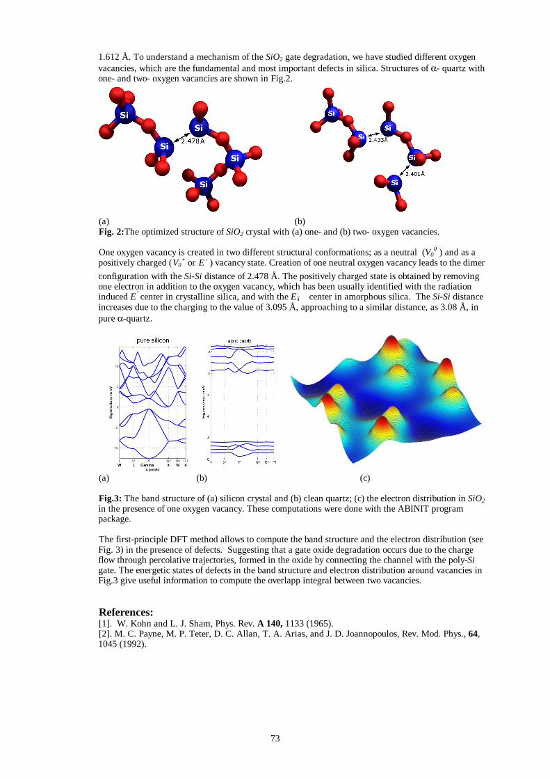
73
1.612 Å. To understand a mechanism of the SiO2 gate degradation, we have studied different oxygen vacancies, which are the fundamental and most important defects in silica. Structures of α- quartz with one- and two- oxygen vacancies are shown in Fig.2.
(a) (b) Fig. 2:The optimized structure of SiO2 crystal with (a) one- and (b) two- oxygen vacancies. One oxygen vacancy is created in two different structural conformations; as a neutral (V0
0 ) and as a positively charged (
+
OV
V0+ or
E ′
E΄ ) vacancy state. Creation of one neutral oxygen vacancy leads to the dimer
configuration with the Si-Si distance of 2.478 Å. The positively charged state is obtained by removing one electron in addition to the oxygen vacancy, which has been usually identified with the radiation induced E΄ center in crystalline silica, and with the Eδ center in amorphous silica. The Si-Si distance increases due to the charging to the value of 3.095 Å, approaching to a similar distance, as 3.08 Å, in pure α-quartz.
(a) (b) (c) Fig.3: The band structure of (a) silicon crystal and (b) clean quartz; (c) the electron distribution in SiO2 in the presence of one oxygen vacancy. These computations were done with the ABINIT program package. The first-principle DFT method allows to compute the band structure and the electron distribution (see Fig. 3) in the presence of defects. Suggesting that a gate oxide degradation occurs due to the charge flow through percolative trajectories, formed in the oxide by connecting the channel with the poly-Si gate. The energetic states of defects in the band structure and electron distribution around vacancies in Fig.3 give useful information to compute the overlapp integral between two vacancies. References: [1]. W. Kohn and L. J. Sham, Phys. Rev. A 140, 1133 (1965). [2]. M. C. Payne, M. P. Teter, D. C. Allan, T. A. Arias, and J. D. Joannopoulos, Rev. Mod. Phys., 64, 1045 (1992).
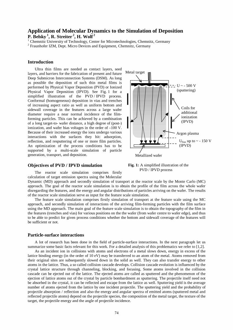
74
Application of Molecular Dynamics to the Simulation of Deposition P. Belsky 1, R. Streiter 2, H. Wolf 2
1 Chemnitz University of Technology, Center for Microtechnologies, Chemnitz, Germany 2 Fraunhofer IZM, Dept. Micro Devices and Equipment, Chemnitz, Germany Introduction
Ultra thin films are needed as contact layers, seed layers, and barriers for the fabrication of present and future Deep Submicron Interconnection Systems (DSM). As long as possible the deposition of such thin metal films is performed by Physical Vapor Deposition (PVD) or Ionized Physical Vapor Deposition (IPVD). See Fig. 1 for a simplified illustration of the PVD / IPVD process. Conformal (homogeneous) deposition in vias and trenches of increasing aspect ratio as well as uniform bottom and sidewall coverage in the features across a large wafer diameter require a near normal incidence of the film-forming particles. This can be achieved by a combination of a long target-to- wafer distance, a high degree of (post-) ionization, and wafer bias voltages in the order of –100 V. Because of their increased energy the ions undergo various interactions with the surfaces they hit: adsorption, reflection, and resputtering of one or more film particles. An optimization of the process conditions has to be supported by a multi-scale simulation of particle generation, transport, and deposition. Objectives of PVD / IPVD simulation
The reactor scale simulation comprises firstly calculation of target emission spectra using the Molecular Dynamic (MD) approach and secondly simulation of transport at the reactor scale by the Monte Carlo (MC) approach. The goal of the reactor scale simulation is to obtain the profile of the film across the whole wafer disregarding the features, and the energy and angular distributions of particles arriving on the wafer. The results of the reactor scale simulation serve as input for the feature scale simulation.
The feature scale simulation comprises firstly simulation of transport at the feature scale using the MC approach, and secondly simulation of interactions of the arriving film-forming particles with the film surface using the MD approach. The main goal of the feature scale simulation is to obtain the topography of the film in the features (trenches and vias) for various positions on the the wafer (from wafer centre to wafer edge), and thus to be able to predict for given process conditions whether the bottom and sidewall coverage of the features will be sufficient or not.
Particle-surface interactions
A lot of research has been done in the field of particle-surface interactions. In the next paragraph let us summarize some basic facts relevant for this work. For a detailed analysis of this problematics we refer to [1,2].
As an incident ion in collisions with atoms and electrons of a metal slows down, energy in excess of the lattice binding energy (in the order of 10 eV) may be transferred to an atom of the metal. Atoms removed from their original sites are subsequently slowed down in the solid as well. They can also transfer energy to other atoms in the lattice. Thus, a so called collision cascade develops. Collision cascade evolution is influenced by the crystal lattice structure through channeling, blocking, and focusing. Some atoms involved in the collision cascade can be ejected out of the lattice. The ejected atoms are called as sputtered and the phenomenon of the ejection of lattice atoms out of the crystal by particle bombardment as sputtering. The projectile itself need not be absorbed in the crystal, it can be reflected and escape from the lattice as well. Sputtering yield is the average number of atoms ejected from the lattice by one incident projectile. The sputtering yield and the probability of projectile absorption / reflection and also the energy and angular spectra of emitted atoms (sputtered metal and reflected projectile atoms) depend on the projectile species, the composition of the metal target, the texture of the target, the projectile energy and the angle of projectile incidence.
Metallized wafer
Metal target
U ~ - 500 V (sputtering)
Ubias up to ~ - 150 V (IPVD)
Argon plasma
Coils for additional ionization (IPVD)
Fig. 1: A simplified illustration of the PVD / IPVD process
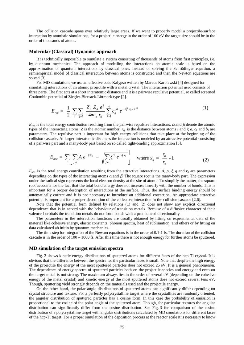
75
The collision cascade spans over relatively large areas. If we want to properly model a projectile-surface interaction by atomistic simulations, for a projectile energy in the order of 100 eV the target size should be in the order of thousands of atoms.
Molecular (Classical) Dynamics approach
It is technically impossible to simulate a system consisting of thousands of atoms from first principles, i.e. by quantum mechanics. The approach of modelling the interactions on atomic scale is based on the approximation of quantum interactions by classical ones. Instead of solving the Schrödinger equation, a semiempirical model of classical interaction between atoms is constructed and then the Newton equations are solved [3].
For MD simulations we use an effective code Kalypso written by Marcus Karolewski [4] designed for simulating interactions of an atomic projectile with a metal crystal. The interaction potential used consists of three parts. The first acts at a short interatomic distance and it is a pairwise repulsive potential, so called screened Coulombic potential of Ziegler-Biersack-Littmark type [2].
(1)
Erep is the total energy contribution resulting from the pairwise repulsive interactions. α and β denote the atomic types of the interacting atoms. Z is the atomic number, rij is the distance between atoms i and j; a, ck and bk are parameters. The repulsive part is important for high energy collisions that take place at the beginning of the collision cascade. At larger interatomic distances the interaction is modeled by an attractive potential consisting of a pairwise part and a many-body part based on so called tight-binding approximation [5]. (2) Eattr is the total energy contribution resulting from the attractive interactions. A, p, ξ, q and r0 are parameters depending on the types of the interacting atoms α and β. The square root is the many-body part. The expression under the radical sign represents the local electron density at the site of atom i. To simplify the matter, the square root accounts for the fact that the total bond energy does not increase linearly with the number of bonds. This is important for a proper description of interactions at the surface. Thus, the surface binding energy should be automatically correct and it is not necessary to introduce an additional correction. An appropriate attractive potential is important for a proper description of the collective interaction in the collision cascade [2,6].
Note that the potential form defined by relations (1) and (2) does not show any explicit directional dependence that is in accord with the behaviour of transition metals. Because of a diffusive character of their valence f-orbitals the transition metals do not form bonds with a pronounced directionality.
The parameters in the interaction functions are usually obtained by fitting on experimental data of the material like cohesive energy, elastic constants, phonon spectra, heat of sublimation, and others or by fitting on data calculated ab initio by quantum mechanics.
The time step for integration of the Newton equations is in the order of 0.1-1 fs. The duration of the collision cascade is in the order of 100 – 1000 fs. After this time there is not enough energy for further atoms be sputtered.
MD simulation of the target emission spectra
Fig. 2 shows kinetic energy distributions of sputtered atoms for different faces of the hcp Ti crystal. It is obvious that the difference between the spectra for the particular faces is small. Note that despite the high energy of the projectile the energy of the most sputtered particles does not exceed 25 eV. It is a general phenomenon. The dependence of energy spectra of sputtered particles both on the projectile species and energy and even on the target metal is not strong. The maximum always lies in the order of several eV (depending on the cohesive energy of the metal crystal) and kinetic energy of the most sputtered atoms does not exceed several tens eV. Though, sputtering yield strongly depends on the materials used and the projectile energy.
On the other hand, the polar angle distributions of sputtered atoms can significantly differ depending on crystal structure and texture. For a perfectly polycrystalline target where the crystallites are randomly oriented, the angular distribution of sputtered particles has a cosine form. In this case the probability of emission is proportional to the cosine of the polar angle of the sputtered atom. Though, for particular textures the angular distribution can significantly differ from the cosine distribution. See Fig. 3 for comparison of the cosine distribution of a polycrystalline target with angular distributions calculated by MD simulations for different faces of the hcp-Ti target. For a proper simulation of the deposition process at the reactor scale it is necessary to know
=
−
≠
=4
1
2
42
1
k
/ a r bαβ
ki ij ijo
βα
rep
αβij
αβk ec
rπε
e ZZ E
2
−=
> ≠
−−
i ij ij
q x p x
attrijij eξ A eE 1 where -
r
r x
o
ijij =
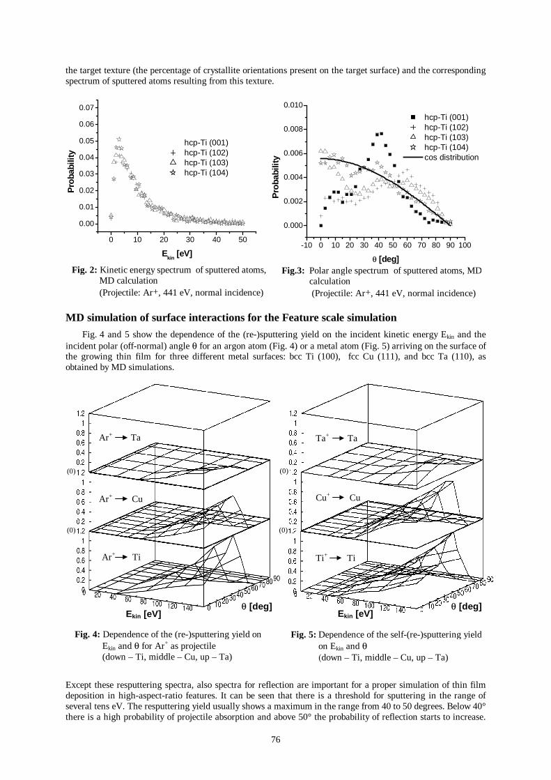
76
the target texture (the percentage of crystallite orientations present on the target surface) and the corresponding spectrum of sputtered atoms resulting from this texture.
MD simulation of surface interactions for the Feature scale simulation
Fig. 4 and 5 show the dependence of the (re-)sputtering yield on the incident kinetic energy Ekin and the incident polar (off-normal) angle θ for an argon atom (Fig. 4) or a metal atom (Fig. 5) arriving on the surface of the growing thin film for three different metal surfaces: bcc Ti (100), fcc Cu (111), and bcc Ta (110), as obtained by MD simulations. Except these resputtering spectra, also spectra for reflection are important for a proper simulation of thin film deposition in high-aspect-ratio features. It can be seen that there is a threshold for sputtering in the range of several tens eV. The resputtering yield usually shows a maximum in the range from 40 to 50 degrees. Below 40° there is a high probability of projectile absorption and above 50° the probability of reflection starts to increase.
Fig. 4: Dependence of the (re-)sputtering yield on Ekin and θ for Ar+ as projectile (down – Ti, middle – Cu, up – Ta)
Fig. 5: Dependence of the self-(re-)sputtering yield on Ekin and θ (down – Ti, middle – Cu, up – Ta)
-10 0 10 20 30 40 50 60 70 80 90 100
0.000
0.002
0.004
0.006
0.008
0.010
hcp-Ti (001) hcp-Ti (102) hcp-Ti (103) hcp-Ti (104) cos distribution
Pro
babi
lity
θ [deg]
0 10 20 30 40 50
0.00
0.01
0.02
0.03
0.04
0.05
0.06
0.07
hcp-Ti (001) hcp-Ti (102) hcp-Ti (103) hcp-Ti (104)
Pro
babi
lity
Ekin
[eV]
Fig.3: Polar angle spectrum of sputtered atoms, MD calculation (Projectile: Ar+, 441 eV, normal incidence)
Fig. 2: Kinetic energy spectrum of sputtered atoms, MD calculation (Projectile: Ar+, 441 eV, normal incidence)
(0)
Ekin [eV] θ [deg]
(0)
Ekin [eV] θ [deg]
(0)
(0)
Ta+ Ta
Cu+ Cu
Ti+ Ti
Ar+ Ta
Ar+ Cu
Ar+ Ti
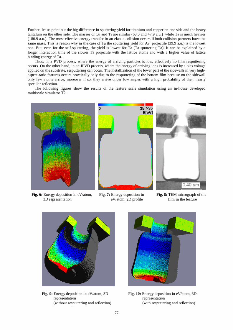
77
Further, let us point out the big difference in sputtering yield for titanium and copper on one side and the heavy tantalum on the other side. The masses of Cu and Ti are similar (63.5 and 47.9 a.u.) while Ta is much heavier (180.9 a.u.). The most effective energy transfer in an elastic collision occurs if both collision partners have the same mass. This is reason why in the case of Ta the sputtering yield for Ar+ projectile (39.9 a.u.) is the lowest one. But, even for the self-sputtering, the yield is lowest for Ta (Ta sputtering Ta). It can be explained by a longer interaction time of the slower Ta projectile with the lattice atoms and with a higher value of lattice binding energy of Ta.
Thus, in a PVD process, where the energy of arriving particles is low, effectively no film resputtering occurs. On the other hand, in an IPVD process, where the energy of arriving ions is increased by a bias voltage applied on the substrate, resputtering can occur. The metallization of the lower part of the sidewalls in very high-aspect-ratio features occurs practically only due to the resputtering of the bottom film because on the sidewall only few atoms arrive, moreover if so, they arrive under low angles with a high probability of their nearly specular reflection.
The following figures show the results of the feature scale simulation using an in-house developed multiscale simulator T2.
Fig. 6: Energy deposition in eV/atom, 3D representation
Fig. 7: Energy deposition in eV/atom, 2D profile
Fig. 8: TEM micrograph of the film in the feature
Fig. 9: Energy deposition in eV/atom, 3D representation (without resputtering and reflection)
Fig. 10: Energy deposition in eV/atom, 3D representation (with resputtering and reflection)
35 >35 E[eV]
0
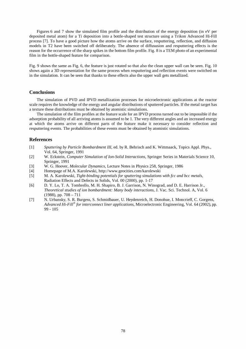
78
Figures 6 and 7 show the simulated film profile and the distribution of the energy deposition (in eV per deposited metal atom) for a Ti deposition into a bottle-shaped test structure using a Trikon Advanced Hi-Fill process [7]. To have a good picture how the atoms arrive on the surface, resputtering, reflection, and diffusion models in T2 have been switched off deliberately. The absence of diffususion and resputtering effects is the reason for the occurrence of the sharp spikes in the bottom film profile. Fig. 8 is a TEM photo of an experimental film in the bottle-shaped feature for comparison. Fig. 9 shows the same as Fig. 6, the feature is just rotated so that also the clean upper wall can be seen. Fig. 10 shows again a 3D representation for the same process when resputtering and reflection events were switched on in the simulation. It can be seen that thanks to these effects also the upper wall gets metallized. Conclusions
The simulation of PVD and IPVD metallization processes for microelectronic applications at the reactor scale requires the knowledge of the energy and angular distributions of sputtered particles. If the metal target has a texture these distributions must be obtained by atomistic simulations.
The simulation of the film profiles at the feature scale for an IPVD process turned out to be impossible if the adsorption probability of all arriving atoms is assumed to be 1. The very different angles and an increased energy at which the atoms arrive on different parts of the feature make it necessary to consider reflection and resputtering events. The probabilities of these events must be obtained by atomistic simulations. References
[1] Sputtering by Particle Bombardment III, ed. by R. Behrisch and K. Wittmaack, Topics Appl. Phys., Vol. 64, Springer, 1991
[2] W. Eckstein, Computer Simulation of Ion-Solid Interactions, Springer Series in Materials Science 10, Springer, 1991
[3] W. G. Hoover, Molecular Dynamics, Lecture Notes in Physics 258, Springer, 1986 [4] Homepage of M.A. Karolewski, http://www.geocities.com/karolewski [5] M. A. Karolewski, Tight-binding potentials for sputtering simulations with fcc and bcc metals,
Radiation Effects and Defects in Solids, Vol. 00 (2000), pp. 1-17 [6] D. Y. Lo, T. A. Tombrello, M. H. Shapiro, B. J. Garrison, N. Winograd, and D. E. Harrison Jr.,
Theoretical studies of ion bombardment: Many body interactions, J. Vac. Sci. Technol. A, Vol. 6 (1988), pp. 708 – 711
[7] N. Urbansky, S. R. Burgess, S. Schmidbauer, U. Heydenreich, H. Donohue, I. Moncrieff, C. Gorgens, Advanced Hi-Fill® for interconnect liner applications, Microelectronic Engineering, Vol. 64 (2002), pp. 99 - 105
79
5 Cooperations with industry and universities Partnerships with the following institutes and companies were continued and / or established in 2003: • Advanced Micro Devices (AMD), Sunnyvale & Austin, USA and Dresden, Germany • Aktiv Sensor GmbH, Stahnsdorf, Germany • Alpha Microelectronics GmbH, Frankfurt (Oder), Germany • AMTEC GmbH, Chemnitz, Germany • Applied Materials, Santa Clara, USA and Dresden, Germany • Atmel GmbH, Germany • BASF AG, Ludwigshafen, Germany • BMW AG München, Germany • Robert Bosch GmbH, Reutlingen, Germany • CAD-FEM GmbH Grafing, Germany • CiS Institut für Mikrosensorik gGmbH, Erfurt, Germany • Colour Control Farbmeßtechnik GmbH, Chemnitz, Germany • Conti Temic microelectronic GmbH , Ingolstadt, Germany • DaimlerCrysler Research Lab Ulm, Germany • Digital Instruments – Veeco Instruments, Mannheim, Germany • DILAS Diodenlaser GmbH • Dynamit Nobel Fürth, Germany • Endress und Hauser • FACRI , Research Institute, Xi´an, China • Fahrzeugelektrik Pirna GmbH, Pirna, Germany • FHR Anlagenbau GmbH, Ottendorf-Okrilla, Germany • First Sensor Technology GmbH, Berlin, Germany • FLEXIVA automation & robotics, Amtsberg, Germany • Forschungszentrum Rossendorf, Germany • Fujitsu Microelectronic GmbH, Dreieich-Buchschlag, Germany • GEMAC mbH Chemnitz, Germany • GF Messtechnik Teltow, Germany • Gesellschaft für Prozeßrechnerprogrammierung mbH (GPP) Chemnitz, Germany • GHF IWM Halle • Heinrich-Hertz-Institut Berlin, Germany • Hitachi Ltd., Japan • Institut für Festkörper- und Werkstoffforschung e.V. IFW Dresden, Germany • IMEC, Leuven, Belgium • Infineon Technologies AG, Munich and Dresden, Germany • InfraTec GmbH, Dresden • ITIM International Training Center for Material Science, Vietnam • Jenoptik-LDT GmbH, Gera , Germany • Kyocera Fineceramics GmbH • L.A.A.S-C.N.R.S Toulouse, Prof. Dr. D. Esteve, France • LETI, Grenoble, France • LG Thermo Technologies GmbH • Lionix, Enschede, Netherlands • LITEF GmbH, Freiburg, Germany • Massachusetts Institute of Technology, Cambridge / Boston, Mass., USA • Material Research Corp. (MRC), Orangeburg N.J. ,USA • Max-Planck-Institut (MPI) für Mikrostrukturphysik Halle, Germany
80
• Mechanical Engineering Laboratory AIST, MITI, Dr. Mitsuro Hattori and Chisato Tsutsumi, Tsukuba, Ibaraki, Japan
• Merck KGaA, Darmstadt, Germany • Mesa Research Institute, Prof. J. Fluitman, Twente, The Netherlands • Mitsui Engineering and shipbuilding Co. Ltd., Japan • Motorola, Phoenix, Arizona ,USA / Munich, Germany • Nex Systems, Wilmington, MA. , USA and Berlin, Germany • NICO Pyrotechnik, Trittau, Germany • NMRC, Cork, Ireland • OEC GmbH, Germany • PANALYTIK GmbH, Dresden, Germany • Physikalisch-Technische Bundesanstalt Braunschweig (PTB), Germany • Roth & Rau Oberflächentechnik GmbH, Wüstenbrand, Germany • RWE Schott Solar GmbH, Alzenau, Germany • Schott Mainz & Schott Glas Landshut, Germany • Seiko Epson, Japan • Sentech Instruments GmbH, Berlin, Germany • SICK AG, Waldkirch & Ottendorf-Okrilla, Germany • Siegert TFT GmbH, Hermsdorf • Siemens AT Regensburg, Germany • Institut für Solarenergieforschung Hameln-Emmerthal, Germany • Solid State Measurements, Pittsburgh, PA., USA • ST Microelectronics, Crolles, France • Suss Microtec AG Vaihingen, Germany • Karl Suss KG GmbH & Co., Munich and Sacka, Germany • Dr. Teschauer AG, Chemnitz, Germany • Thales-Avionics, Valence and Orsay, France • Trikon Technologies, UK • TRW Airbag Systems GmbH & Co. KG, Aschau/Inn, Germany • X-Fab Gesellschaft zur Fertigung von Wafern mbH, Erfurt, Germany • Yole Developpement, Lyon, France • ZMD Dresden, Germany • 3D-Micromac AG, Chemnitz, Germany Universities: • TSINGHUA University, Beijing, China • State University of New York at Binghamton, USA • TU Budapest, Hungary • University of California at Berkeley, Berkeley Sensor and Actuator Center, USA • Case Western Reserve University, Cleveland, Ohio, USA • Chongqing University, Chongqing, China • University of Colorado at Boulder, USA • University of Delaware, Newark, USA • University of Delft, Netherlands • TU Dresden, Germany • Universität Erlangen, Germany • Universität Essen, Institut für anorganische Chemie, Germany • Universität Hannover, Germany • Hanoi University of Technology, Vietnam • University of Hertfordshire, UK • Johannes Kepler Universität Linz, Austria • HTW Mittweida, Laserapplikationszentrum, Germany
81
• University of Nevada, Reno, USA • Nowosibirsk State University, Russia • University of West Bohemia, Pilsen , Czech Republic • Portland State University, Portland, Oregon, USA • Fudan University, Shanghai, China • Technological University Singapore, Singapore • Royal Institute of Technology, Stockholm, Sweden • University of Tokyo, Res. Ctr. for Adv. Science & Technology (RCAST), Japan • Rensselaer Polytechnic Institute (RPI), Troy, N.Y., USA • University of Twente – MESA, Netherlands • Warsaw University of Technology (WUT), Warsaw, Poland • Atominstitut Universität Wien, Austria • Xiamen University, Xiamen, China
6 Equipment and service offer - Laseroptical instrumentation for surfaces utilizing a resolution down to 4 nm (computer
controlled laseroptical measuring system with autofocussensor and interference microscope)
- Light-section microscope - Zeiss-two-coordinate inspection microscope - Instrumentation for recording of oscillations in the direction vertical to the surface (laser
vibrometer) - Two-channel analyzer - Instrumentation for stimulation of micro objects and for measuring of the amplitude-
frequency response - Program system for modal analysis - Instrumentation for recording of electrical values and for generation of stimuli functions
based on VXI- respectively GPIB-Bus - Fischerscope for measuring hardness and recording of spring characteristics - Electronic Speckle Pattern Interferometer for static and dynamic deformation analysis of
microstructures in the nanometer range - Instrumentation for pressure-measuring - Scanning Probe Microscope D 3000 - Nanolithographysystem LEO - Optoelectronic laboratory equipment - Rapid Prototyping with FPGAs - Design of integrated high-voltage circuits - Characterization and modelling of devices from high-voltage microtechnologies - Design of low power and low noise analogue-mixed signal integrated circuits - Characterization of analogue-mixed signal circuits up to 500 MHz - Development of solar cells with appropriate price-performance ratio - Simulator for silicon wet etching SIMODE - Etch mask design tool EMADE - FEM-Analysis with commercial ANSYS-Version on HP-workstation for simulation of
mechanical behaviour and coupled fields - Different CAD tools: EMS, PC- Draft, Microstation PC, ProEngineer, HFSS, EESOF
82
Center for Microtechnologies (ZfM) : The ZfM facilities include 1000m² of clean rooms (about 30% of them class 10 to 100) and modern equipments were installed for processing of 100 mm and 150 mm wafers as well as design and testing laboratories providing the basis for the following processes, partly in cooperation with the Fraunhofer Institute IZM, branchlab Chemnitz: - Design (Workstations) - Mask fabrication 3” ... 7” / Electron beam lithography / Proximity and contact double-side mask aligner - High temperature processes: Diffusion / Thermal oxidation / Annealing / RTP - Etching (dry: Plasma- and RIE-mode & wet: isotropic / anisotropic) ( Alcatel MCM, SECON XPL 251, STS Multiplex ICP-ASE, Metal Etch DPS Centura) - Chemical vapor deposition MOCVD (Precision 5000 [Cu, WN, TiN]) - Chemical vapor deposition PECVD (Precision 5000 [SiO2, Si3N4, CF-Polymer]) - Physical vapor deposition PVD (MRC 643, FHR 150x4, CLC 9000, ... ) - Silicon etching (isotropic and anisotropic) - Chemical mechanical polishing CMP - Silicon fusion bonding / Anodic bonding (Suss) - Testing (SEM, AFM, electrical – hp 4062 UX , HP 4061 A , HP 4339A , ...) The ZfM provides the following services :
R & D (e.g. Si processes, technology, development of sensors and actuators, metallization)
- Thermal oxidation of silicon wafers - PVD (Cr, Au, TiN, Cu , Pt, Al, W, TiW, AlSix ,CrNi, Pyrex ) - CVD: PECVD / LPCVD (600° C ... 900° C)
(SiO2 , Si3N4 , Polysilicon, SixOyNz , Cu-MOCVD, TiN-MOCVD, SiCOH, SiCH) - Dry etching (Si, SiO2 , Si3N4 , Polysilicon, Silicides, Al, Cu, refr. metals, TiN, Cr) - Wet etching (SiO2 , Si3N4 , Si, Polysilicon, Al, Cr, Au, Pt, Cu, Ti, W )
- Wafer lithography / Electron beam lithography / Mask fabrication ( 3“ ...7“ Cr mask) - Design & simulation (technology, process....) Software: ANSYS, SIMODE, PHOENICS, SIMBAD, EVOLVE ,
Etch mask design tool EMADE and in analytical fields such as - Scanning electron microscopy SEM / EDX - Atomic force microscopy AFM (D 3000) - Ellipsometry / Nanospec - Laser profilometry (UBM, TENCOR FLX-2900 ) - Surface profilometer (TENCOR alpha step 200, Dektak 3) - US-Microscope - Zug-/Druckprüfmaschine Zwick 4660 universal - Perkin-Elmer DMA 7e dynamic mechanical analyser
- Micromechanical testing instrument (Sartorius and PI) - Lifetime scanner SEMILAB WT-85
In cooperation with the Fraunhofer Institute IZM, branchlab Chemnitz:
- STS „Multiplex ICP“ etch tool for deep silicon etching - Wafer bonding (silicon fusion bonding, anodic bonding, eutectic bonding, Seal- glass-bonding, adhesive bonding) - CMP MIRRA & ONTREK-cleaner (Copper, Silicon, SiO2 ) - Test measurements for MEMS
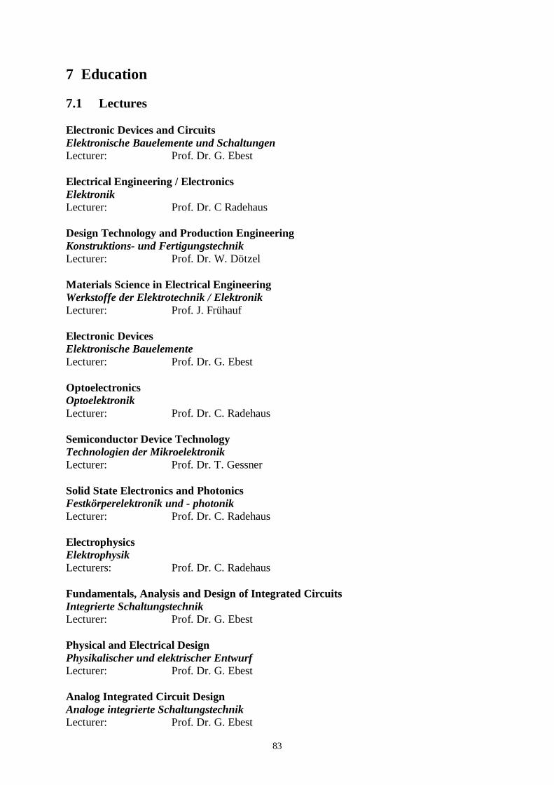
83
7 Education 7.1 Lectures Electronic Devices and Circuits Elektronische Bauelemente und Schaltungen Lecturer: Prof. Dr. G. Ebest Electrical Engineering / Electronics Elektronik Lecturer: Prof. Dr. C Radehaus Design Technology and Production Engineering Konstruktions- und Fertigungstechnik Lecturer: Prof. Dr. W. Dötzel Materials Science in Electrical Engineering Werkstoffe der Elektrotechnik / Elektronik Lecturer: Prof. J. Frühauf Electronic Devices Elektronische Bauelemente Lecturer: Prof. Dr. G. Ebest Optoelectronics Optoelektronik Lecturer: Prof. Dr. C. Radehaus Semiconductor Device Technology Technologien der Mikroelektronik Lecturer: Prof. Dr. T. Gessner Solid State Electronics and Photonics Festkörperelektronik und - photonik Lecturer: Prof. Dr. C. Radehaus Electrophysics Elektrophysik Lecturers: Prof. Dr. C. Radehaus Fundamentals, Analysis and Design of Integrated Circuits Integrierte Schaltungstechnik Lecturer: Prof. Dr. G. Ebest Physical and Electrical Design Physikalischer und elektrischer Entwurf Lecturer: Prof. Dr. G. Ebest Analog Integrated Circuit Design Analoge integrierte Schaltungstechnik Lecturer: Prof. Dr. G. Ebest
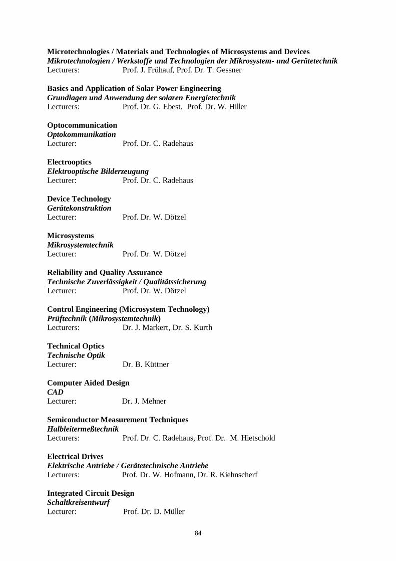
84
Microtechnologies / Materials and Technologies of Microsystems and Devices Mikrotechnologien / Werkstoffe und Technologien der Mikrosystem- und Gerätetechnik Lecturers: Prof. J. Frühauf, Prof. Dr. T. Gessner Basics and Application of Solar Power Engineering Grundlagen und Anwendung der solaren Energietechnik Lecturers: Prof. Dr. G. Ebest, Prof. Dr. W. Hiller Optocommunication Optokommunikation Lecturer: Prof. Dr. C. Radehaus Electrooptics Elektrooptische Bilderzeugung Lecturer: Prof. Dr. C. Radehaus Device Technology Gerätekonstruktion Lecturer: Prof. Dr. W. Dötzel Microsystems Mikrosystemtechnik Lecturer: Prof. Dr. W. Dötzel Reliability and Quality Assurance Technische Zuverlässigkeit / Qualitätssicherung Lecturer: Prof. Dr. W. Dötzel Control Engineering (Microsystem Technology) Prüftechnik (Mikrosystemtechnik) Lecturers: Dr. J. Markert, Dr. S. Kurth Technical Optics Technische Optik Lecturer: Dr. B. Küttner Computer Aided Design CAD Lecturer: Dr. J. Mehner Semiconductor Measurement Techniques Halbleitermeßtechnik Lecturers: Prof. Dr. C. Radehaus, Prof. Dr. M. Hietschold Electrical Drives Elektrische Antriebe / Gerätetechnische Antriebe Lecturers: Prof. Dr. W. Hofmann, Dr. R. Kiehnscherf Integrated Circuit Design Schaltkreisentwurf Lecturer: Prof. Dr. D. Müller
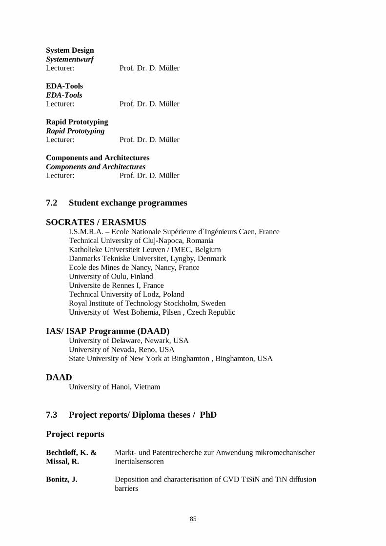
85
System Design Systementwurf Lecturer: Prof. Dr. D. Müller EDA-Tools EDA-Tools Lecturer: Prof. Dr. D. Müller Rapid Prototyping Rapid Prototyping Lecturer: Prof. Dr. D. Müller Components and Architectures Components and Architectures Lecturer: Prof. Dr. D. Müller 7.2 Student exchange programmes SOCRATES / ERASMUS I.S.M.R.A. – Ecole Nationale Supérieure d`Ingénieurs Caen, France Technical University of Cluj-Napoca, Romania Katholieke Universiteit Leuven / IMEC, Belgium Danmarks Tekniske Universitet, Lyngby, Denmark Ecole des Mines de Nancy, Nancy, France University of Oulu, Finland Universite de Rennes I, France Technical University of Lodz, Poland Royal Institute of Technology Stockholm, Sweden University of West Bohemia, Pilsen , Czech Republic IAS/ ISAP Programme (DAAD) University of Delaware, Newark, USA University of Nevada, Reno, USA State University of New York at Binghamton , Binghamton, USA DAAD University of Hanoi, Vietnam 7.3 Project reports/ Diploma theses / PhD Project reports Bechtloff, K. & Markt- und Patentrecherche zur Anwendung mikromechanischer Missal, R. Inertialsensoren Bonitz, J. Deposition and characterisation of CVD TiSiN and TiN diffusion
barriers
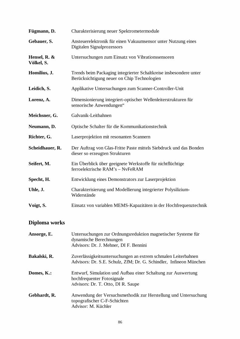
86
Fügmann, D. Charakterisierung neuer Spektrometermodule Gebauer, S. Ansteuerelektronik für einen Vakuumsensor unter Nutzung eines Digitalen Signalprozessors Hensel, R. & Untersuchungen zum Einsatz von Vibrationssensoren Völkel, S. Homilius, J. Trends beim Packaging integrierter Schaltkreise insbesondere unter
Berücksichtigung neuer on Chip Technologien
Leidich, S. Applikative Untersuchungen zum Scanner-Controller-Unit Lorenz, A. Dimensionierung integriert-optischer Wellenleiterstrukturen für
sensorische Anwendungen“ Meichsner, G. Galvanik-Leitbahnen Neumann, D. Optische Schalter für die Kommunikationstechnik Richter, G. Laserprojektion mit resonanten Scannern Scheidhauer, R. Der Auftrag von Glas-Fritte Paste mittels Siebdruck und das Bonden dieser so erzeugten Strukturen Seifert, M. Ein Überblick über geeignete Werkstoffe für nichtflüchtige ferroelektrische RAM’s – NvFeRAM Specht, H. Entwicklung eines Demonstrators zur Laserprojektion Uhle, J. Charakterisierung und Modellierung integrierter Polysilizium-
Widerstände Voigt, S. Einsatz von variablen MEMS-Kapazitäten in der Hochfrequenztechnik Diploma works Ansorge, E. Untersuchungen zur Ordnungsreduktion magnetischer Systeme für
dynamische Berechnungen Advisors: Dr. J. Mehner, DI F. Bennini Bakalski, R. Zuverlässigkeitsuntersuchungen an extrem schmalen Leiterbahnen Advisors: Dr. S.E. Schulz, ZfM; Dr. G. Schindler, Infineon München Domes, K.: Entwurf, Simulation und Aufbau einer Schaltung zur Auswertung
hochfrequenter Fotosignale Advisors: Dr. T. Otto, DI R. Saupe Gebhardt, R. Anwendung der Versuchsmethodik zur Herstellung und Untersuchung topografischer C-F-Schichten Advisor: M. Küchler
87
Günther, M.: Entwicklung eines Verfahrens zum Fügen von Halbleitersubstraten mittels Epoxid- und Polyimid-Klebstoffen Advisor: Dr. M. Wiemer
König, S. Qualitätssicherung wafergebondeter Bauteile Advisor: Dr. M. Wiemer Lehmann, U. Resonante Scanner mit magnetischem Antrieb Advisors: Prof. W. Dötzel, Dr. Kurth Müller, S. Untersuchungen zur Applikation mikromechanischer 2D-Spiegel-
Aktoren für Lasernivellierung Advisor: Dr. J. Markert
Nestler, J. Entwurf, Simulation und messtechnische Bewertung eines fluidischen Mikrosystems Advisor: Dr. T. Otto Schreiter, M. Entwurf eines integrierten Hochvolt-Verstärkers mit Schutzschaltungen zur Anwendung in Arraystrukturen Advisor: DI S. Heinz Sternberger, A. Ansteuerung eines durchstimmbaren Infrarot-Filters mit digitalem Signalprozessor Advisor: Dr. Mehner Tenholdte, D. Einsatz eines Mikroresonators für ein Reibungsvakuummeter Advisor: Dr. J. Mehner Wischnewskij, A. FEM-basierte Entwicklung einphasiger piezoelektrischer Stehwellen- Motoren mit zylindrischen Oszillatoren Advisors: Dr. J. Mehner, Dr. S. Kovalev Weißflog, M. Aufbau eines Schrittmotorversuchsplatzes Advisors: Dr. R. Kiehnscherf, DI K. Löhr PhD Krujatz, Jörg „Herstellung von Spiegelschichtsystemen auf der Basis von Aluminium
oder Silber für den Einsatz in der Mikrosystemtechnik“ 16th January 2003 Baumann, Jens „Herstellung, Charakterisierung und Bewertung von leitfähigen
Diffusionsbarrieren auf Basis von Ta, Ti und W für die Kupfer-metallisierung von Siliziumschaltkreisen“
20th June 2003 Symanzik, „Interface-Elektronik für mikromechanische Sensor- und Aktorarrays“ Horst-Günter 28th November 2003
88
8 Colloquia / Workshops at the Institute 27. Februar 2003 Delan, M. Rennau, ZfM, TU Chemnitz „Messung der thermischen Leitfähigkeit dünner Isolatorschichten“ 3. April 2003 Dr. Hubert Lakner, Fraunhofer IPMS, Dresden „Bildgebende Mikrosysteme: Chips, die mit Licht arbeiten“ 10. April 2003 Dr. Wolfgang Faust, FhG IZM, Chemnitz "Experimentelle Untersuchungen zur Zuverlässigkeit an Komponenten der Mikroelektronik und Mikrosystemtechnik" 8. Mai 2003 Prof . Dr. rer. nat. habil. Klaus Wetzig, Leibnitz-Institut für Festkörperanalytik und Strukturforschung (IFS) im IFW Dresden „Migrationsuntersuchungen in Metallisierungsschichten“ 12. Mai 2003 Prof. Dr. James E. Morris, Dept. Electr. Engn., Portland State University, USA „Nanoparticle Systems for Nanoelectronics" 15. Mai 2003 Dr. Tilmann Schäffer, Universität Münster, Physikalisches Institut „Eigenschaften und Anwendungen von Cantilevern im MHz-Bereich“ 19. Juni 2003 Doc. Dr. Kus, Doc. Dr. Mühlbacher, Doc. Dr. Skocil, TU Plzen « Energetische Störungen im Niederfrequenzbereich“; „Schaltüberspannungen in elektrischen Netzen“; „News in electronics packaging – a technological process control“ 24. Juni 2003 Öffentliches Kolloquium und Gutachtersitzung zum Arbeits- und Ergebnisbericht 2001– 2003 & Finanzierungsantrag 2004 – 2006 des Sonderforschungsbereiches SFB 379 10. Juli 2003 Dr. Claus Ascheron, Springer-Verlag Heidelberg "Wissenschaftliches Publizieren" 10. Juli 2003 Alexej Schaporin , Wladimir Kolchuzhin, Nowosibirsk Technical Univ., Russia „Automatische Erstellung parametrischer Verhaltensmodelle mit FEM für die Optimierung von Mikrostrukturen“ 28. Juli 2003 Shohei Hata, Hitachi Ltd., Japan “Intermediate report of the collaborate research between FhG-IZM and Hitachi Ltd”
89
9 Scientific publications 2003 Authors of 2 book chapters: M.Uhlig, T.Gessner: “Chemical vapor deposition of C-F- low-k materials” and S.E.Schulz, T.Gessner: “Spin-on Si-based low-k materials” Interlayer Dielectrics for Semiconductor Technologies, ed. S.P.Murarka, M. Eizenberg, A.K.Sinha, Elsevier Acad.Press 2003 Bagdahn J.; Knoll H.; Petzold M.; Wiemer M.: “Debonding of directly wafer-bonded silicon after high temperature process steps” The Electrochemical Society - 203 rd meeting, Paris, April 27 – May 2, 2003, in press Bennini, F.; Mehner, J.; Dötzel, W.: "System Level Simulations of MEMS Based on Reduced Order Finite Element Models", International Journal of Computational Engineering Science, Vol. 2, Nr. 2, p. 385-388, June 2003 Bonitz, J.; Schulz, S.E.; Gessner, T.: „CVD TiN layers as diffusion barrier films on porous SiO2 aerogel“, MAM 2003, March 9-12, La Londe Les Maures, France, Proceedings, Microelectronic Eng. 70 (2003) p. 330-336. Buschnakowski, S.; Bertz, A.; Bräuer, W.; Heinz, S.; Schuberth, R.; Ebest, G.; Gessner, T.: „Development and Characterization of a High Aspect Ratio Vertical FET Sensor for Motion Detection”, The 12th International Conference on Solid-State Sensors, Actuators and Microsystems, Transducers 03, Boston, June 8-12 2003 Buschnakowski, S.; Heinz, S.; Zeun, H.; Korndörfer, F.; Ebest, G.: „Integrierter Zweiphasen-Lock-In-Verstärker zur kapazitiven Signaldetektion mikromechanischer Vibrationssensoren“, Informationstagung Mikroelektronik 2003, pp. 343-348, 1.-2.10.2003 Wien, Österreich Delan, A.; Rennau, M.; Schulz, S.E.; Gessner, T.: „Thermal Conductivity of ultra low-k dielectrics“, MAM 2003, March 9-12, La Londe Les Maures, France, Proceedings, Microelectronic Eng. 70 (2003) p. 280-284
Döring, L.; Brand, U.; Peiner, E.; Frühauf, J.; Gärtner, E.: ”Development of micro force setting standards for stylus instruments“, Proceedings of the EUSPEN, p. 407, Aachen 2003 Ecke, R.; Schulz, S.E.; Gessner, T.; Riedel, S.; Lipp, E.; Eizenberg, M.: “Deposition and treatment of titanium based barrier layers by MOCVD”, Proc. Chemical Vapor Deposition XVI and EUROCVD 14, Eds. M.D. Allendorf, F. Maury, F. Teyssandier, The Electrochemical Society, Inc., Pennington, NJ; Proc. Vol. 2003-08, pp. 1224-1230. Ecke, R.; Hecker, M1; Schulz, S.E.; Engelmann, H.-J.2; Gessner, T.; Mattern, N.1; Zschech, E.2: „Properties of as-deposited and annealed PECVD Tungsten Nitride films”, Talk presented at the European Congress on Advanced Materials and Processes EUROMAT 2003, 1-5 Sept. 2003, Lausanne, Switzerland. 1 Institute for Solid State and Materials Research, Helmholzstr. 20, D-01330 Dresden, Germany 2 AMD Saxony LLC & Co. KG, Dresden, Materials Analysis Department, D-01330 Dresden, Germany
90
Ecke, R.; Schulz, S.E.; Hecker, M1; Mattern, N.1; Gessner, T.: „Influence of SiH4 on the WNx-PECVD process”, MAM 2003, March 9-12, La Londe Les Maures, France, Proceedings, Microelectronic Eng. 70 (2003) p. 346-351. 1 Institute for Solid State and Materials Research, Helmholzstr. 20, D-01330 Dresden, Germany Emelianov, V.; Ganesan, G.; Puzic, A.; Schulz, S.; Eizenberg, M.; Habermeier, H.-U.; Stoll, H.: „Investigation of Electromigration in Copper Interconnects by Noise Measurements“, Invited Talk, Conf. Proc."SPIE Fluctuations and Noise 2003". Flaspöhler, M.; Buschnakowski, S.; Kuhn, M.; Kaufmann, C.; Frühauf, J.; Gessner, T.; Ebest, G.; Hübler, A.: „Multispectral Image Capturing System Based on a Micro Mirror Device with a Diffraction Grating”, Proceedings of The PICS Conference - The Digital Photography Conference, Rochester, NY, pg. 183-187 (2003)
Frühauf, J.: “Silicon as a suitable material in precision engineering”, Proceedings of the EUSPEN, p. 39, Aachen 2003
Frühauf, J.; Krönert, S.; Krüger-Sehm, R.: “Precision of etched bulk silicon structures with dimensions up to the mm-range”, Proceedings of the EUSPEN, p. 2, Aachen 2003 Frühauf, S.; Streiter, I.; Rennau, M.; Puschmann, R.; Schulz, S.E.; Gessner, T.; Chudoba, T.; Richter, F., Flannery, C.; Matusche, J.; Schmidt.U. : “Electrical and Mechanical characterization of porous silicon dioxide as an ultra low k dielectric”, Proceedings of Materialsweek, (Sept 30th – Oct 2nd 2002, Munich, Germany ) Werkstoff-Informationsgesellschaft mbH, Frankfurt 2003 ,CD-ROM Frühauf, S.; Streiter, I.; Puschmann, R.; Schulz, S.E.; Himcinschi, C.; Flannery, C.M.; Gessner, T.; Zahn, D.R.T.: „Modified silica aerogel as a low-k dielectric with improved mechanical properties“, in Conf. Proc. ULSI XVIII, , Materials Research Society, Warrendale (2003), p.507-512.
Gärtner, E.; Frühauf, J.; Jänsch, E.; Reuter, D.: “Flexural solid hinges etched from silicon”, Proceedings of the EUSPEN, p. 43, Aachen 2003
Gärtner, E.; Frühauf, J.; Krönert, S.; Jänsch, E.: “Festkörpergelenkführungen aus Si mit bis zu 5 mm Hub”, 6. Chemnitzer Fachtagung Mikromechanik und Mikroelektronik 2003, Proceedings p.118 Geiger, W.; Breng, U.; Leinfelder, P. ; Gutmann, W. ; Ohmberger, R. ; Kunz, J.; Ruf, M.; Huber, M.; Ryrko, B.; Hafen, M.; Spahlinger, G.; Schröder, W.; Handrich E., LITEF GmbH Freiburg ; Hiller, K.; Billep D., TUC: „The micromechanical Coriolis Rate Sensor µCORS II“, Symposium Gyro Technology, Stuttgart 2003 Gessner, T.; Bertz, A.; Lohmann, C.; Kurth, S.; Hiller, K.: „Advanced Silicon Micromachining“, ICMAT Singapore 2003, Intl. J. of Computational Engn. Sc., 4, No. 2 , June 2003, p. 151-156
91
Gessner, T.: „Microelectronics and Microsystems Research within the Center for Microtechnologies and the Fraunhofer IZM Branchlab Chemnitz“, 6. Deutsch-Vietnamesisches Seminar Chemnitz, 25.-30.05.03 Gessner, T.: „Micro- and Nanotechnologies – Challenges for Microelectronics and MEMS”, University of Portland, Oregon, USA, “Portland Area Semiconductor Seminar Series” October 2003 Gessner, T.: “Selected Challenges of Advanced Interconnect Systems”, University of Albany – SUNY”, Albany, New York, USA, October 2003 Gessner, T.: “ MEMS and Microsystems Technologies”, Summer School on Precision Assembly in Eindhoven, Netherlands, July 2003 Gessner, T.: “Werkstoff- und Technologieaspekte der Silizium-Mikromechanik für Anwendungen in der Automobilindustrie“, Fachkongress MicroCar 2003, Leipzig, 26.06.03 Gessner, T.: „MEMS devices fabricated by using advanced Si-micromachining“, Joint Workshop FhG-IZM/The University of Tokyo, 20.02.03, Tokyo, Japan Gessner, T.: “Microsystems Technologies”, Chongqing, China, July 2003 Gottfried K.; Kaufmann C.; Hoffmann R.; Wiemer, M.; Gessner T.: „Temperaturstabile Metallisierungs – und Anschlusssysteme für Sensoranwendungen im Kraftfahrzeug“, Fachkongreß MicroCar 2003, Leipzig 26. Juni 2003 Hanf, M.; Kurth, S.; Billep, D.; Hahn, R.; Faust, W.; Heinz, S.; Dötzel, W.; Gessner, T.: „Application of micro mirror arrays for Hadamard transform optics“, 9th Int. Symp. on Microwave and Optical Technology (ISMOT2003), Ostrava, Czech Republic 2003 Hanf, M.; Dötzel, W.: „Micromechanical electrostatic field sensor for the detection of surface charges“, Proc. of the EUROSENSORS XVII, pp.374-375, Guimaraes, Portugal 2003, in press “Sensors and Actuators 2004“ Hecker, M1; Hübner, R.1; Mattern, N.1; Voss, A.1; Acker, J.1; Ecke, R.; Schulz, S.E.; Gessner, T.; Wenzel, C.3; Bartha, J.3; Engelmann, H.-J.2; Zschech, E.2: „Effect of thermal stressing on the microstructure of tungsten and tantalum based diffusion barrier layers”, Talk presented at the European Congress on Advanced Materials and Processes EUROMAT 2003, 1-5 Sept. 2003, Lausanne, Switzerland. 1 Institute for Solid State and Materials Research, Helmholzstr. 20, D-01330 Dresden, Germany 2 AMD Saxony LLC & Co. KG, Dresden, Materials Analysis Department, D-01330 Dresden, Germany 3 Technical University Dresden, Institute for Semiconductor and Microsystem Technology IHM Heinz, S.; Buschnakowski, S.; Bertz, A.; Bräuer, W.; Schuberth, R.; Ebest, G.; Gessner, T.: „Vertikaler Feldeffekttransistor mit beweglicher Gate-Elektrode für die Bewegungs-detektion“, 6. Chemnitzer Fachtagung Mikromechanik und Mikroelektronik, Chemnitz, 29.-30.10. 2003 Heinz, S.; Buschnakowski, S.; Bertz, A.; Bräuer, W.; Korndörfer, F.; Schuberth, R.; Zeun, H.; Ebest, G.; Gessner, T.: „Vertikaler Feldeffekttransistor mit beweglicher Gate-Elektrode für die Bewegungsdetektion“, Informationstagung Mikroelektronik 2003, pp. 487-492, 1.-2.10.2003 Wien, Österreich
92
Heinz, S.; Buschnakowski, S.; Korndörfer, F.; Zeun, H.; Hiller, K.; Hahn, R.; Ebest, G.: „Integrierter 48-kanaliger Hochvolt-Schalter zur Ansteuerung mikromechanischer Schwenkspiegel“, Informationstagung Mikroelektronik 2003, pp. 493-498, 1.-2.10.2003 Wien, Österreich Heinz, S.; Buschnakowski, S.; Bertz, A.; Bräuer, W.; Schuberth, R.; Ebest, G.; Gessner, T.: „A High Aspect Ratio Vertical FET Sensor for Motion Detection“, MICRO SYSTEM Technologies 2003, Posterpräsentation, München, 7.-8.10.2003; Hiller, K.; Hahn, R.; Kaufmann, C.; Hanf, M.; Heinz, S.; Gessner, T.; Dötzel, W.; Ebest, G.: „Technologieentwicklung für ein Mikrospiegelarray mit integrierter Elektronik“, 6. Chemnitzer Fachtagung Mikromechanik & Mikroelektronik, 29./30. Oktober 2003, S. 54-59 Hiller, K.; Kurth, S.; Neumann, N.; Hahn, R.; Kaufmann, C.; Hanf, M.; Heinz, S.; Gessner, T.; Dötzel, W.; Ebest, G.: “Application of low temperature direct bonding in optical devices and integrated systems”, Proceedings of MICRO SYTEM Technologies 2003, pp 102-109 Himcinschi, C.; Friedrich, M.; Frühauf, S.; Schulz, S.E.; Gessner, T.; Zahn, D.R.T.: ”Contributions to static dielectric constants of low-k xerogels films derived from VASE and IR spectroscopies”, Poster presented at International Conference on Spectroscopic Ellipsometry July 6th - 11th 2003, Vienna, Austria König, D.; Zahn, D. R. T.; Ebest, G.: „Field Effect of Fixed Negative Charges on Oxidized Silicon Induced by AlF3 Layers with Fluorine Deficiency”, accepted at 9th International Conference on the Formation of Semiconductor Interfaces (ICFSI-9), 15-19 September 2003, Madrid, Spain König, D.; Zahn, D. R. T.; Reich, R,; Gottfried, K.; Ebest, G.: „P inversion layer solar cells as test for the I-S structure: results and prospects”, Poster 1P-D3-21, 3rd World Conference on PV Solar Energy Conversion, 11-18 May 2003, Osaka, Japan Korndörfer, F.; Kuschel, B.; Heinz, S.; Zeun, H.; Buschnakowski, S.; Ebest, G.: „Charakterisierung von Bauelementen unter dem Aspekt der Selbsterwärmung“, Informationstagung Mikroelektronik 2003, pp. 419-424, 1.-2.10.2003 Wien, Österreich Kotarsky, U.; Manthey, W.; Dietzsch, M.; Bertz, A.: „Hochauflösender mikromecha-nischer Sensor zur Erfassung von Oberflächenprofilen mit großem Eigenzustellbereich“, 6. Chemnitzer Fachtagung Mikromechanik & Mikroelektronik, 29./30. Oktober 2003
Krüger-Sehm, R.; Häßler-Grohne, W.; Frühauf, J.: “Traceable calibration standard for the lateral axis of contact stylus instruments“, 9th Conference on Metrology and Properties of Engineering Surfaces, Sept. 2003, Halmstad, Proceedings Küchler, M.; T. Otto, T. Gessner, F. Ebling H. Schröder: Hot embossing for MEMS using silicon Tools, ICMAT 2003, Singapore, International Journal of Computational Engineering Science, Vol. 4 No. 3 (2003), pp. 609-612
93
Kuhn, M.; Flaspöhler, M.; Krönert, S.; Kaufmann, C.; Gessner, T.; Hübler, A.; Frühauf, J.: "Herstellung und Charakterisierung von mikromechanischen Scannern mit intergrierten Beugungsgittern", 6. Chemnitzer Fachtagung Mikrosystemtechnik- Mikromechanik & Mikroelektronik, 2003 Kuhn, M.; Flaspöhler, M.; Krönert, S.; Kaufmann, C.; Gessner, T.; Hübler, A.; Frühauf, J.: "Microactuators with Diffraction Grating", Micro System Technologies 2003, Postersession, München, October 7-8, 2003 Kurth, S.,; Hiller, K.; Neumann, N.; Heinze, M.; Dötzel, W.; Gessner, T.: “An electrically tunable infrared filter on base of Fabry-Perot-Interferometer”, 9th International Symposium on Microwave and Optical Technology, ISMOT, Ostrava, Czech Republic, August 11-15, 2003 Kurth, S.,; Hiller, K.; Dötzel, W.; Gessner, T.; Neumann, N.; Heinze, M.: “Tunable infrared filter based on Fabry-Perot-Interferometer”, Proc. of Micro System Technologies 2003, München, 7.-8.10.2003 Kurth, S.,; Hiller, K.; Neumann, N.; Heinze, M.; Dötzel, W.; Gessner, T.: “A tunable Fabry-Perot-Interferometer for 3 – 4.5 µm wavelength with bulk micromachined reflector carrier”, Proc. of SPIE Vol. 4983, pp. 215-226 / Photonics West, SPIE 4983_25, Jan. 2003 Kurth, S.: Zuverlässigkeit und Test von MOEMS Komponenten, Workshop „MEMS / Sensors - from Component Manufactoring to Packaged Functional Components“, FhG IZM Branchlab Chemnitz, 16.09.2003
Löschner, U.: Exner, H.; Gärtner, E.; Frühauf, J.: “Laser bending of silicon”, Proceedings of SPIE Conference Photonics West, Vol. 4977, p. 86-93 San Jose, California, 2003 Lohmann, C.; Bertz, A.; Kuechler, M.; Gessner, T.: A Novel High Aspect Ratio Technology for MEMS Fabrication Using Standard Silicon Wafers, Beitrag in: Advanced Microsystems for Automotive Applications 2003, Seite 59-66, Valldorf, J; Gessner, W.: Springer-Verlag Berlin Heidelberg New York Lohmann, C.; Bertz, A.; Kuechler, M.; Gessner, T.: Mechanical reliability of MEMS fabricatedby a special technology using standard silicon wafers. Presentation at the Photonics West (SPIE Conference 4980), San Jose, USA, Jan. 2003 Mehner, J.; Dötzel, W.; Schauwecker, B.;, D.; Ostergard, D.: " Reduced Order of Fluid Structural Interactions in MEMS Based on Modal Projection Techniques”, 12. Intern. Conf. on Solid State Sensors, Actuators and Microsystems, Boston 2003, pp. 1840 - 1843 Mehner, J.; Schaporin, A.; Dötzel, W.:" Simulation for MEMS – Packaging”, Mems Packaging Workshop 2003, Chemnitz 2003 Mrwa, A.; Erler, K.; Diefenbach, K.H., Denissov, S.; Ebest G.: „Ortsaufgelöste Messung der Minoritätsladungsträgerlebensdauer bei Siliziumsolarzellen mittels MWPCD“, Freiberger Siliziumtage 2003, Freiberger Forschungshefte B 327, p. 91-107
94
Müller, A.-D.; Müller, F.; Mehner, J.; Wibbeler, J.; Gessner, T.; Hietschold, M.: „Electrostatic double-cantilever device for dynamic noncontact-mode Atomic Force Micros-copy“, 6. Chemnitzer Fachtagung Mikromechanik & Mikroelektronik, 29./30. Oktober 2003 Neumann, N.; Heinze, M.; Stegbauer, H.-J.; Hiller, K.; Kurth, S.: Ein mikromechanisches, durchstimmbares Fabry-Perot-Filter für die nichtdispersive Gasanalytik im Spektralbereich (3…5) µm, 6. Dresdner Sensor-Symposium 2003
Otto, T.; Saupe, R.; Gessner, T.: “Novel Possibilities in Physical Analytics Employing Miniaturized Devices” , Proc. of the MST 2003, pp. 565-567, München 2003
Reuter, D.; Frömel, J.; Schwenzer, G.; Bertz, A.; Gessner, T.: „Selektives Niedertemperaturbonden mit SU-8 fuer Wafer-Level-Verkappung von mikromechanischen Strukturen“, 6. Chemnitzer Fachtagung Mikromechanik & Mikroelektronik, 29./30. Oktober 2003
Rinderknecht, J.; Prinz, H.; Kammler, T.; Schell, N.; Zschech, E.; Wetzig, K.; Gessner, T.: „In situ high temperature synchrotron-radiation diffraction studies of silicidation processes in nanoscale Ni layers“, MAM 2003, March 9-12, La Londe Les Maures, France, Proceedings, Microelectronic Engn., Vol. 70 (2003), p. 226-232
Saupe, R.; T. Otto, V. Stock, U. Fritzsch, T. Gessner, “Packaging and Characterization of Micro-Opto-Electro-Mechanical Systems”, 9th International Symposium on Microwave and Optical Technology, Proc. of the ISMOT 2003, Ostrava, in press Saupe, R.: Entwicklung eines auf MOEMS basierten Spektrometers, Beitrag zum Workshop „MEMS /Sensors - from Component Manufactoring to Packaged Functional Components“, FhG IZM Branchlab Chemnitz, 16.09.2003 Scheibner, D.; Mehner, J.; Reuter, D.; Gessner, T.; Dötzel, W.: "Tunable Resonators with Electrostatic Self Test Functionality for Frequency Selective Vibration Measurements", Proceedings of the MEMS 2003, p.526-529, Kyoto, 2003 Scheibner, D.; Mehner, J.; Brämer, B.; Gessner, T.; Dötzel, W.: "Wide Range Tunable Resonators for Vibration Measurements", Microelectronic Engineering 67-68, p. 542-549, 2003 Scheibner, D.; Wibbeler, J.; Mehner, J.; Brämer, B.; Gessner, T.; Dötzel, W.: "A Frequency Selective Silicon Vibration Sensor with Direct Electrostatic Stiffness Modulation", Analog Integrated Circuits and Signal Processing, p. 35-43, 2003 Scheibner, D.; Mehner, J.; Reuter, D.; Kotarsky, U.; Gessner, T.; Dötzel, W.: " CHARACTERIZATION AND SELF TEST OF ELECTROSTATICALLY TUNABLE RESONATORS FOR FREQUENCY SELECTIVE VIBRATION MEASUREMENTS", Sensors and Actuators, 2003, article in press Schulz, S.E.; Blaschta, F., Eisener, B.; Fruehauf,S.; Schulze, K.; Seidel, U.; Koerner,H.; Gessner, T.: “SiO2-Aerogel ULK Integration into Copper Damascene Interconnects for RF Devices”, Talk presented at Advanced Metallization Conference (AMC), 21-23 Oct. 2003, Montreal, Canada Schulz, S.E.; Schulze, K; Matusche, J.1; Schmidt, U.1; Gessner, T.: „Effect of PECVD SiC and SiCN cap layer deposition on mesoporous silica ultra low k dielectric films”, Talk
95
presented at the 14th Annual IEEE/SEMI Advanced Semiconductor Manufacturing Conference and Workshop, 31 March - 1 April 2003, Munich. 1 Applied Materials, European Technology Development, Buchenstraße 16b, D-01097 Dresden, Germany
Schulz, S.E.; Aubel, O.1; Baumann, J.; Hasse, W.1; Gessner, T.: „Copper Alloys for Improved Interconnect Properties“, Poster presented at Advanced Metallization Conference (AMC), 21-23 Oct. 2003, Montreal, Canada. 1 University Hanover, IHW, Appelstrasse 11A, D-30167 Hanover, Germany
Sternberger, A.; Hiller, K.; Gessner, T.; Dötzel, W.; Kurth, S.; Neumann, N.; Heinze, M.: Closed loop controll of a tunable infrared filter, Proc. of the Int. Conf. on Applied Electronics 2003, Pilsen, Czech Republic, 10.-11.09.2003, pp. 197-200 Uhlig, M.; Bertz, A.; Brocke, H.2; Dobler, M.3; Flannery, C.4; Jnawali, G.2; Zeidler, D.1; Gessner, T.: “Integration of Plasma Deposited CF Polymer in a Copper / Low k Damascene Architecture”, in Conf. Proc. ULSI XVIII, , Materials Research Society, Warrendale (2003), p. 629-635 1 Technical University Dresden, Institute for Semiconductor and Microsystem Technology IHM, Germany 2 University of Hanover, Institute of Semiconductor Devices and Materials, Germany 3 Leica Microsystems, Germany 4 Paul-Drude-Institute of Solid State Electronics, Berlin, Germany Uhlig, M.; Bertz, A.; Erben, J.-W.; Schulz, S.E.; Gessner, T.; Zeidler, D.1; Wenzel, C.1; Bartha, J.1: „Experimental results on the integration of copper and CVD ultra low k material”, MAM 2003, March 9-12, La Londe Les Maures, France, Proceedings, Microelectronic Eng. 70 (2003) p. 314-319. 1 Technical University Dresden, Institute for Semiconductor and Microsystem Technology IHM Wenger, Ch.; Hübner, R.; Wenzel, Ch.; Reinicke, M.; Hecker, M.; Mattern, N.; Wetzig, K.; Baumann, J.; Schulz, S.; Bartha, J.W.; Engelmann, H.-J.; Zschech, E.: „Stability of graded Ta-TaN-Ta and single layer TaSiN diffusion barriers for copper interconnect systems“, in Conf. Proc. ULSI XVIII, , Materials Research Society, Warrendale (2003), p. 847-851. Wiemer M.; Frömel J.; Jia C.;, Gessner T.: “Bonding and contacting of MEMS-structures on wafer level”, The Electrochemical Society - 203 rd meeting, Paris, April 27 – May 2, 2003, in press Wiemer, M.: “Wafer bond techniques for MEMS applications“, Suss MEMS seminar 2003 at Pacifico,Yokohama on June 30, 2003 Wiemer, M.; Frömel, J.; Gessner T.; Nowak, B.; Südkamp, W.; Peschka, A.; Bagdahn, J.; Petzold, M.: „Bewertung von Niedertemperaturbondverfahren für Drucksensoren in der Automobiltechnik“, Fachkongreß MicroCar 2003, Leipzig 26. Juni 2003 Wiemer, M.; Frömel, J.; Gessner, T.: “Trends der Technologieentwicklung im Bereich Waferbonden” 6. Chemnitzer Fachtagung Mikromechanik & Mikroelelektronik, 29/30.10.2003, Lichtenwalde/Chemnitz, Tagungsband S. 178 Windhorn, K.; L. Meixner, S. Drost, H. Schröder, E. Kilgus, W. Scheel, F. Ebling, T. Otto, M. Küchler, T. Gessner: “Polymer BioMEMs with integrated optical and fluidic functionality” , Micro System Technologies 2003, pp. 416-423
96
Zeun, H.; Korndörfer, F.; Heinz, S.; Buschnakowski, S.; Ebest, G.: „Summation phasenverschobener Signale“, Informationstagung Mikroelektronik 2003, pp. 529-533, 1.-2.10.2003 Wien, Österreich Zeun, H.; Heinz, S.; Buschnakowski, S.; Korndörfer, F.; Schreiter, M.; Ebest, G.: „High-ohmic poly-Si in high-voltage circuits”, Proceedings Conference Applied Electronics 2003, pp. 244-247, 10.-11.09.2003 Pilsen, Tschechien Zimmermann, S.; Baumann, J.; Kaufmann, C.; Gessner, T.: „Thermal stability of thin Ta and TaNx films as diffusion barriers for copper metallization”, in Conf. Proc. ULSI XVIII, Materials Research Society, Warrendale (2003), p. 859 - 864 Zimmermann, S.; Ecke, R.; Rennau, M.; Schulz, S.E.; Hecker, M1; Voss, A.1; Engelmann, H.-J.2; Acker, J.1; Mattern, N.1; Zschech, E.2; Gessner, T.: „Characterisation of a PECVD WNx Barrier Layer Against Copper Diffusion“, Poster presented at Advanced Metallization Conference (AMC), 21-23 Oct. 2003, Montreal, Canada. 1 Institute for Solid State and Materials Research, Helmholzstr. 20, D-01330 Dresden, Germany 2 AMD Saxony LLC & Co. KG, Dresden, Materials Analysis Department, D-01330 Dresden, Germany
10 Guests & special international relations Guests from: January 22. & 23. ULISSE project technical meeting
Representatives of ST Crolles (F), Bull S.A. Paris (F), Philips Research Leuven (B), IMEC (B), LETI Grenoble (F), Infineon Technologies Munich (D)
Prof. R. Bruch, University of Nevada, Reno 26. & 27. FUDAN University, China:
Prof. Sun Lai-xiang, Vice President Prof. Tong Jia-rong, Deputy Dean Prof. Huang Yi-ping, Chairman Ms. Li Hong, Deputy Chief
April 3rd Applied Materials Europe, Europe Technology Development Dr. Didier Pique (Manager), Dr. Ursula Schmidt (Technologist) May 8th Prof. Wetzig, Direktor des Instituts für Festkörperanalytik und
Strukturforschung (IFS) , Leibnitz-Institut für Festköper- und Werkstoffforschung IFW Dresden
Prof. R. Bruch, University of Nevada, Reno
15th Doz. Dr.-Ing. Jan Mühlbacher, Doz. Dr.-Ing. Vaclav Kus, Doz. Dr.-Ing. Vlastimil Skocil, Dozentenaustausch, TU Pilsen, Tschechien, Mai, 3 Tage
97
June 20th Applied Materials Europe, Europe Technology Development Dr. Didier Pique (Manager), Dr. Ursula Schmidt (Technologist)
European Conversion Center Jean-Marie Longchamp (Director Customer Productivity Support)
Prof. Reinhard Bruch, University of Nevada, Reno, USA October 20th Prof. Wen (October/November) & Delegation from Chongqing / China
Dipl.-Ing. Robert Eichinger-Heue, EV Group Schärding, Österreich Doz. Dr.-Ing. Svetoslav Simeonov, TU Gabrovo, Bulgarien Doz. Dr.-Ing. Stefan Kartunov, TU Gabrovo, Bulgarien Doz. Dr.-Ing. Vladimir Shulgov, State University Minsk, Belarus
and Dr. Jürgen Leib Schott Glas Electronic Packaging Dietrich Mund Schott Glas Electronic Packaging Dr. Toshihiro Itoh University of Tokyo Dipl.-Ing. Winfried Rabe ATMEL Wireless & µC Dipl.-Ing. Roy Knechtel X-Fab Dipl.-Wirtschaftsing. Rolf Wolf Süss Microtec Dr. Wolfram Geiger LITEF Isabelle Thomas Thales Avionics Aiko Saito Hitachi PERL Dr. Yasuo Nakagawa Hitachi PERL Dr. Fumikazu Ito Hitachi PERL Dr. Armin Binneberg ILK Dresden Takahito Uga Ricoh Ikuo Katoh Ricoh Tsukasa Yanagida Kyocera Kunihiko Ueki Kyocera Kohta Uchiyama Kyocera Harry-Geord Juraschek OEC GmbH Dr. Andreas Plössl Osram GmbH Visit to Prof. T. Gessner February 2003, The University of Tokyo, Japan A. Delan, R. Ecke, M. Uhlig March 2003, MAM 2003, Marseille, France St. Buschnakowski, June 2003, Transducers ´03, Boston, USA St. Heinz Dr. T. Otto March 2003, Chongqing University, China
Jiao Tong University, Shanghai, China (Prof. Chen) FUDAN University, Shanghai, China
98
Prof. T. Gessner, July 2003, FUDAN University Shanghai, Dr. R. Streiter Chongqing University, FACRI Xian, China Jiao Tong University, Shanghai, China (Prof. Chen) Prof. T. Gessner, Advanced Metallization Conference, 21-23 Oct. 2003 Dr. S. Frühauf, AMC 2003 , Montreal, Canada S. Zimmermann Prof. T. Gessner November 2003, FACRI Xian, China Dr. R. Streiter Dr. S. Kurth DI R. Schmiedel Scientific coworkers / PhD: DI Alexej Schaporin Novosibirsk Technical University, Russia
November 2002 – December 2003 DI Wladimir Kolchuzhin Novosibirsk Technical University, Russia
November 2002 – December 2003
Ms. Jia Zhou China, FUDAN University, Shanghai August 2002 – July 2003
Prof. Wen University of Chongqing, China October/November 2003 Jang, Chol & DFG - Korea Myong, Ilyong October / November 2003
Hata, Shohei Hitachi, PERL, Yokohama / Japan March 2003 – February 2004 Jun Jun Wang China, FUDAN University, Shanghai October 2003 – August 2004 Hironao Okada University of Toky, May 2003 Jia Chenping University of Xian, China, 1/2003 – 12/2003 Students: Karel Besorna TU Pilsen 03/2002 – 03/2003 Mariusz Patecki TU Lodz 10/2002 – 04/2003 Jaroslav Dousa TU Praha 10/2002 – 03/2003 Lukas Pelant TU Praha 10/2002 – 03/2003 Sumanth R. Katkuri University of Nevada, Reno 02/2003 – 07/2003 Bhanu P. Uppalapati University of Nevada, Reno 02/2003 – 07/2003 Marek Rudnicki TU Lodz 04/2003 – 09/2003 Marek Stefanski TU Lodz 04/2003 – 08/2004 Marcin Suchodolski TU Lodz 04/2003 – 08/2004 Jaroslav Fait TU Pilsen 04/2003 - 09/2003 Jussi Salakka TU Oulu 09/2002 – 03/2003 Nitin Kohli University of Nevada, Reno, USA 10/2003 – 12/2003
Top Related
Copyright © 2022 FDOKUMEN

