


Bahasa
Halaman
Hukum


An integrated temporal partitioning and physical design framework for
static compilation of reconfigurable computing systems
Farhad Mehdipour*, Morteza Saheb Zamani, Mehdi Sedighi
IT and Computer Engineering Department, Amirkabir University of Technology, 424 Hafez Avenue, P. O. Box 15875-4413, Tehran, Iran
Received 2 January 2005; revised 14 March 2005; accepted 18 March 2005
Available online 23 May 2005
Abstract
Lack of appropriate compilers for generating configurations and their scheduling is one of the main challenges in the development of
reconfigurable computing systems. In this paper, a new iterative design flow for reconfigurable computing systems is proposed that integrates
the synthesis and physical design phases to perform a static compilation process. We propose a new temporal partitioning algorithm for
partitioning and scheduling, which attempts to decrease the time of reconfiguration on a partially reconfigurable hardware. In addition, we
perform an incremental physical design process based on similar configurations produced in the partitioning stage. To validate the
effectiveness of our methodology and algorithms, we developed a framework according to the proposed methodology.
q 2005 Elsevier B.V. All rights reserved.
Keywords: Reconfigurable computing; Temporal partitioning; Physical design; Placement; Routing
1. Introduction
Reconfigurable computing systems (RCS) are an emer-
ging alternative to application specific integrated circuits
(ASICs) and general-purpose processors, which attempt to
take advantage of the benefits of both hardware and
software [1,14]. Reconfigurable systems offer a compromise
between the performance advantages of fixed functionality
hardware and the flexibility of general-purpose processors.
Like ASICs, these systems are distinguished by their ability
to directly implement specialized circuitry in hardware [17].
While the origins of RCS go back to the 1960s, the last
few years have witnessed a significant increase in research
activity in this field. As a result, RCS has demonstrated the
potential to achieve high performance implementations in a
wide range of applications, such as image processing,
cryptography, target recognition and digital signal proces-
sing [28]. Availability of high-density VLSI devices with
flexible hardware architectures is one of the important
factors that have made successful RCS implementations
possible. In a Reconfigurable system, reconfiguration can be
0141-9331/$ - see front matter q 2005 Elsevier B.V. All rights reserved.
doi:10.1016/j.micpro.2005.03.002
* Corresponding author. Tel.: C98 6454 2734; fax: C98 6454 2704.
E-mail address: [email protected] (F. Mehdipour).
done statically or dynamically. A Dynamic reconfiguration
is defined as updating of programmable logic blocks and
routing resources at the execution time. In contrast, static
reconfiguration refers to having the ability to reconfigure a
system, but not during the execution time [1,17].
The granularity and size of programmable hardware, the
required memory size, and the communication bandwidth
between memory and processor are some of the design
parameters for a highly abstracted model of RCS [8]. There
are some important challenges in the reconfigurable
computing domain. Lack of appropriate design method-
ology and appropriate compiler, difficulty of modifying
current configurations, long reconfiguration time of pro-
grammable devices and difficulty in identifying proper
application domains are some of the main challenges in
reconfigurable computing [5,6,28]. Currently, it appears that
general-purpose CAD tools for reconfigurable computing
systems that support design and implementation of desired
applications are not readily available. In this paper, we focus
on a static design compiler for reconfigurable systems. Our
contribution is the development of a new design flow for
RCS design, with a new similarity-based temporal parti-
tioning method and incremental physical design.
We explain temporal partitioning and physical design
phases in Section 2. A new design methodology for
reconfigurable computing systems is proposed in Section 3.
Microprocessors and Microsystems 30 (2006) 52–62
www.elsevier.com/locate/micpro

F. Mehdipour et al. / Microprocessors and Microsystems 30 (2006) 52–62 53
Section 4 explains the details of the proposed temporal
partitioning algorithm. Section 5 explains an incremental
physical design approach presented for our iterative design
flow. In Section 6, the details of our tool are explained and
results are presented. Finally, Section 7 concludes the paper.
2. Related works
The idea behind temporal partitioning is that functions
that are too large to fit on a single programmable hardware
(e.g. field programmable gate array-FPGA) can be parti-
tioned into several modules which are then successively
downloaded into the FPGA in accordance with a predefined
schedule. In fact, temporal partitioning divides an appli-
cation into time-exclusive systems that cannot or do not
need to run concurrently [29]. Temporal partitioning targets
partial and non-partial programmable devices [5,25]. In
non-partial devices, temporal partitioning defines for each
module the time at which it will be mapped onto the FPGA
for computation. There will be no processing while a new
module is replacing the previous one. Using partial
reconfiguration devices, on the other hand, parts of the
design can be replaced while other parts are still active. This
is useful in systems that must implement many modules at
different periods of time on a device. Modules should be
exchanged without disturbing the rest of the design.
Although standard partitioning algorithms can be applied
to incremental partially reconfigurable FPGAs, these
algorithms do not exploit the partial reconfigurability of
the target devices. Most of the works proposed to address
the minimization of the reconfiguration time overhead use
multi-context FPGAs and especially coarse grain architec-
tures [20].
Karthikeya et al. [13] proposed algorithms for temporal
partitioning and scheduling of large designs on area
constrained reconfigurable hardware. This approach does
not consider the timing constraints and reconfiguration time
overhead. Bobda [5] proposed two methods to solve
temporal partitioning problem. The first one is an enhance-
ment of the well-known list scheduling method. The second
method uses a spectral placement to position the modules in
a three-dimensional vector space.
Spillane and Owen [24] introduced a partitioning
technique by referring to the process of clustering and
scheduling a design. The clustering algorithm groups the
nodes in the design such that they may be subsequently
scheduled. In [24] authors have focused on decomposing a
design into reconfigurable segments, each of which will be
activated at the appropriate time during operation. Their
algorithm attempts to minimize reconfiguration overhead
and maximize resource usage. After finding a sequence of
conditions for activating an appropriate component at a
particular time, successive configurations are optimized to
achieve the desired trade-offs among reconfiguration time,
operation speed and design size.
In [10] an integrated partitioning and synthesis system
for dynamically reconfigurable multi-FPGA architecture,
called SPARCS, was introduced. SPARCS has a temporal
partitioning tool to temporally divide and schedule the tasks
on a reconfigurable system [19]. It takes a behavioral
specification of an application in the form of a set of tasks.
The temporal partitioning tool heuristically estimates the
upper bound on the number of temporal segments and
formulates the problem as a non-linear programming
system. The temporal partitioning problem is solved by
integer-linear programming solver. However, this approach
suffers from long run-time, and is only worth investigation if
the estimation of cost and performance can be proven to be
highly accurate and the design size is rather small (The main
cost function used in SPARCS is data memory bandwidth
[26]). SPARCS does not perform the physical design with
respect to the partitions generated by the temporal
partitioner.
Luk et al. [16] proposed a methodology to take advantage
of common operators in successive partitions. It attempts to
reduce the configuration time and thus the application
execution time. This model does not consider timing aspects
and does not perform any partitioning but Tanougust et al.
[26] attempt to find the minimum area while meeting timing
constraints. However, they do not try to search for the
minimal memory bandwidth or execution time.
Li [15] proposed a configuration pre-fetching technique
to reduce the configuration overhead. In addition, in [20] a
pre-fetching technique was presented, which prevents miss-
predictions and reduces the overall execution time of the
system. Genesan et al. [9] presented an approach for
overlapping execution and reconfiguration for amortization
of reconfiguration overhead and achieved significant
improvement in design latency. In this approach, a design
is partitioned into a sequence of temporal segments and the
execution of each segment is pipelined with the reconfi-
guration of the next partition. In this way the running time of
each partition overlaps with the reconfiguration time of its
following partition. Most of the above techniques are
appropriate for run-time reconfiguration. Our proposed
algorithm has been used at design time and there is enough
time to satisfy the optimality of design according to existing
criteria.
In this work, we focus on physical design as well as
temporal partitioning. Physical design for reconfigurable
computing systems is often done according to traditional
placement and routing algorithms used for FPGAs [22].
Two major phases of physical design are placement and
routing. In the placement phase, optimal position of
modules on the target device should be determined.
Minimizing the connection length, area and the longest
wire are some of the main objectives in this process [22].
Many different algorithms have been developed for solving
the placement problem [11,22,27]. Placement algorithms
can be classified into randomized (e.g. simulated annealing)
and deterministic [11]. Deterministic placement methods
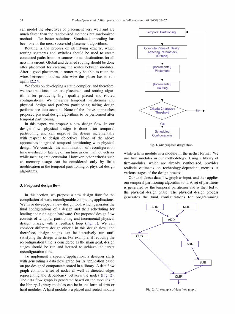
Fig. 1. Our proposed design flow.
F. Mehdipour et al. / Microprocessors and Microsystems 30 (2006) 52–6254
can model the objectives of placement very well and are
much faster than the randomized methods but randomized
methods offer better solutions. Simulated annealing has
been one of the most successful placement algorithms.
Routing is the process of identifying exactly, which
routing segments and switches should be used to create
connected paths from net sources to net destinations for all
nets in a circuit. Global and detailed routing should be done
after placement for creating the routes between modules.
After a good placement, a router may be able to route the
wires between modules; otherwise the placer has to run
again [2,27].
We focus on developing a static compiler, and therefore,
we use traditional iterative placement and routing algor-
ithms for producing high quality placed and routed
configurations. We integrate temporal partitioning and
physical design and perform partitioning taking design
performance into account. None of the above approaches
proposed physical design algorithms to be performed after
temporal partitioning.
In this paper, we propose a new design flow. In our
design flow, physical design is done after temporal
partitioning and can improve the design incrementally
with respect to design objectives. None of the above
approaches integrated temporal partitioning with physical
design. We consider the minimization of reconfiguration
time overhead or latency of run time as our main objectives
while meeting area constraint. However, other criteria such
as memory usage can be considered only by little
modification in the temporal partitioning or physical design
algorithms.
Fig. 2. An example of data flow graph.
3. Proposed design flow
In this section, we propose a new design flow for the
compilation of static reconfigurable computing applications.
We have developed a new design tool, which generates the
final configurations of a design and their scheduling for
loading and running on hardware. Our proposed design flow
consists of temporal partitioning and incremental physical
design phases, with a feedback loop (Fig. 1). We can
consider different design criteria in this design flow, and
therefore, design stages can be iteratively run until
satisfying the design criteria. For example, if reducing the
reconfiguration time is considered as the main goal, design
stages should be run and iterated to achieve the target
reconfiguration time.
To implement a specific application, a designer starts
with generating a data flow graph for its application based
on pre-designed components stored in a library. A data flow
graph contains a set of nodes as well as directed edges
representing the dependency between the nodes (Fig. 2).
The data flow graph is generated based on the modules in
the library. Library modules can be in the form of firm or
hard modules. A hard module is a placed and routed module
while a firm module is a module in the netlist format. We
use firm modules in our methodology. Using a library of
firm-modules, which are already synthesized, provides
realistic estimates on technology-dependent metrics at
various stages of the design process.
Our tool takes a data flow graph as input, and then applies
our temporal partitioning algorithm to it. A set of partitions
is generated by the temporal partitioner and is then fed to
the physical design phase. The physical design process
generates the final configurations for programming

F. Mehdipour et al. / Microprocessors and Microsystems 30 (2006) 52–62 55
the hardware. We used VPR [2,4], one of the popular
physical design tools for FPGAs and modified it for our
incremental design flow.
One of the important features in our proposed design
flow is the integration of higher and lower stages of RCS
design flow. Temporal partitioning, in fact, is performed as a
post-synthesis stage whereas physical design is a stage
related to lower levels of design flow. Such isolation of
design steps can result in blind decisions during temporal
partitioning whereas physical information can guide the
design process if the two steps are integrated as in our flow.
Different criteria can be considered in the proposed design
flow such as reconfiguration time, area and overall run time.
We explain the details of our approach in the following
sections.
4. Temporal partitioning algorithm
For a design that is too large to fit in a specific
programmable device, temporal partitioning partitions the
circuit and determines the scheduling of the partitions to be
loaded and run on hardware. Temporal partitioning problem
can be stated as partitioning a data flow graph into a number
of partitions such that each partition can fit in the device and
also, dependencies among the graph nodes are not violated.
For a partially reconfigurable hardware, parts of the
hardware can be programmed without disturbing the rest
of the design. In other words, common parts of two
successive configurations can remain unchanged.
4.1. The algorithm
We define a new factor, namely similarity value, which
determines the level of similarity (in terms of the
functionality of their nodes) between two succeeding
partitions. Our main goal is to reduce the reconfiguration
time and overall run-time of applications and the area
needed for their implementation. We assume that the target
programmable device is partially programmable. In this
section, first, we introduce a temporal partitioning algor-
ithm, which works based on the similarity factor. Then, the
definition of some terms is presented and finally, we prove
our algorithm efficiency.
Fig. 3. Similarity-based tempor
Our algorithm takes a data flow graph (DFG), the nodes
of which represent pre-designed firm modules in a library.
The temporal partitioning should respect the dependencies
among the DFG nodes to ensure correct execution. Hence a
node can be executed if all its predecessors have already
been executed. It means that the inputs to every node should
be valid and stable before it is executed. In the first stage,
level assignment is performed according to As soon as
possible (ASAP) algorithm [5,18]. ASAP schedules a data
flow graph in an attempt to minimize latency by
topologically sorting of the nodes of the graph. The level
of each node is determined based on its start time or the
depth of the node with respect to primary inputs. For the
nodes with the highest priority of execution which must
therefore have the lowest start time, level number 1 is
assigned and for those that have the maximum depth in the
DFG, the maximum level number is assigned.
In the partitioning stage of DFG, the level number of
modules, their sizes and the size of target hardware are the
most important factors which should be considered. First,
we consider the nodes with the lowest level number and add
these nodes to a partition so that the total size of nodes does
not exceed the target device size. Thus, we attempt to reduce
the wasted area in the programmable array needed for the
implementation of each partition. The nodes with the next
level number are considered when all of the nodes with a
smaller level number are partitioned [5,13].After generating
initial partitions, a greedy iterative algorithm tries to
increase the similarity between two successive partitions.
In each iteration two candidate modules from two
successive partitions are selected and swapped. If this
module swapping results in increasing the similarity of two
adjacent partitions, then this new configuration is accepted;
otherwise it is rejected. The pseudo code of the proposed
algorithm is shown in Fig. 3.
By increasing the similarity of subsequent partitions, the
time needed for partial reconfiguration is reduced. For
example, for the partitioned DFG shown in Fig. 4.a,
similarity of two partitions increases by swapping an
ADD module in the first partition with a SUB module in
the second partition (see Fig. 4.b). Assuming that the sizes
of all the nodes in the DFG are equal, the ratio of the number
of similar pairs to the total number of nodes in the second
partition in Fig. 4.b is 0.67%. Therefore the reconfiguration
al partitioning algorithm.
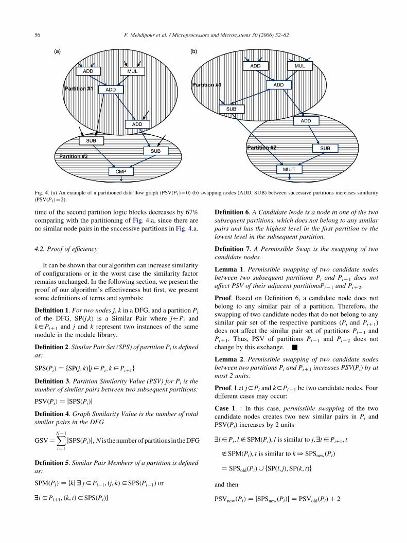
Fig. 4. (a) An example of a partitioned data flow graph (PSV(P1)Z0) (b) swapping nodes (ADD, SUB) between successive partitions increases similarity
(PSV(P1)Z2).
F. Mehdipour et al. / Microprocessors and Microsystems 30 (2006) 52–6256
time of the second partition logic blocks decreases by 67%
comparing with the partitioning of Fig. 4.a, since there are
no similar node pairs in the successive partitions in Fig. 4.a.
4.2. Proof of efficiency
It can be shown that our algorithm can increase similarity
of configurations or in the worst case the similarity factor
remains unchanged. In the following section, we present the
proof of our algorithm’s effectiveness but first, we present
some definitions of terms and symbols:
Definition 1. For two nodes j, k in a DFG, and a partition Pi
of the DFG, SP(j,k) is a Similar Pair where j2Pi and
k2PiC1 and j and k represent two instances of the same
module in the module library.
Definition 2. Similar Pair Set (SPS) of partition Pi is defined
as:
SPSðPiÞ Z fSPðj; kÞjj2Pi; k 2PiC1g
Definition 3. Partition Similarity Value (PSV) for Pi is the
number of similar pairs between two subsequent partitions:
PSVðPiÞ Z jSPSðPiÞj
Definition 4. Graph Similarity Value is the number of total
similar pairs in the DFG
GSVZXNK1
iZ1
jSPSðPiÞj; N is thenumberof partitionsintheDFG
Definition 5. Similar Pair Members of a partition is defined
as:
SPMðPiÞ Z fkjd j2PiK1; ðj; kÞ2SPSðPiK1Þ or
dt 2PiC1; ðk; tÞ2SPSðPiÞg
Definition 6. A Candidate Node is a node in one of the two
subsequent partitions, which does not belong to any similar
pairs and has the highest level in the first partition or the
lowest level in the subsequent partition.
Definition 7. A Permissible Swap is the swapping of two
candidate nodes.
Lemma 1. Permissible swapping of two candidate nodes
between two subsequent partitions Pi and PiC1 does not
affect PSV of their adjacent partitionsPiK1 and PiC2.
Proof. Based on Definition 6, a candidate node does not
belong to any similar pair of a partition. Therefore, the
swapping of two candidate nodes that do not belong to any
similar pair set of the respective partitions (Pi and PiC1)
does not affect the similar pair set of partitions PiK1 and
PiC1. Thus, PSV of partitions PiK1 and PiC2 does not
change by this exchange. &
Lemma 2. Permissible swapping of two candidate nodes
between two partitions Pi and PiC1 increases PSV(Pi) by at
most 2 units.
Proof. Let j2Pi and k2PiC1 be two candidate nodes. Four
different cases may occur:
Case 1. : In this case, permissible swapping of the two
candidate nodes creates two new similar pairs in Pi and
PSV(Pi) increases by 2 units
dl2Pi; l;SPMðPiÞ; l is similar to j;dt 2PiC1; t
;SPMðPiÞ; t is similar to k0SPSnewðPiÞ
Z SPSoldðPiÞg fSPðl; jÞ;SPðk; tÞg
and then
PSVnewðPiÞ Z jSPSnewðPiÞj Z PSVoldðPiÞC2
F. Mehdipour et al. / Microprocessors and Microsystems 30 (2006) 52–62 57
Case 2. Let node l be similar to node j but node k not be
similar to node t. In this case, permissible swapping of the
two candidate nodes causes similar pair (l,j) to be added to
SPS(Pi) and increases PSV(Pi) by 1 unit
dl2Pi; l;SPMðPiÞ; l is similar to j;ct 2PiC1;
t ;SPMðPiÞ; t is not similar to k0SPSnewðPiÞ
Z SPSoldðPiÞg fSPðl; jÞg
and then
PSVnewðPiÞ Z jSPSnewðPiÞj Z PSVoldðPiÞC1
Case 3. : Let node l be not similar to node j but t be similar
to k. Then, SP(k,t) is added to SPS(Pi) and increases
PSV(Pi) by 1 unit
dl2Pi; l;SPMðPiÞ; l is not similar to j;ct 2PiC1;
t ;SPMðPiÞ; t is similar to k0SPSnewðPiÞ
Z SPSoldðPiÞg fSPðk; tÞg
and then
PSVnewðPiÞ Z jSPSnewðPiÞj Z PSVoldðPiÞC1
Case 4. : In this case, permissible swapping of the two
candidate nodes does not add to the similar pair set of Pi,
and therefore, PSV(Pi) remains unchanged
cl2Pi; l;SPMðPiÞ; l is not similar to j;ct 2PiC1;
t ;SPMðPiÞ; t is not similar to k0SPSnewðPiÞ
Z SPSoldðPiÞ
and then
PSVnewðPiÞ Z jSPSnewðPiÞnewnewj Z PSVoldðPiÞ
We find that:
ci2f1;.N K1g;DPSVðPiÞ
Z ðPSVnewðPiÞKPSVoldðPiÞÞR0:
&
Theorem. The proposed similarity-based temporal parti-
tioning algorithm may not decrease the GSV of data flow
graph.
Proof. By Lemma 1, we know that a permissible swap of
nodes between two subsequent partitions may not affect the
PSV of their adjacent partitions, and according to Lemma 2,
it only increases the PSV of the two partitions and in the
worst case, it does not change the PSV. Therefore,
DGSVZPNK1
iZ1 DPSVðPiÞR0, and in the worst case:
DGSVZ0 (GSV remains unchanged) and it may not be
decreased and the theorem is established. &
5. Incremental physical design
As mentioned in Section 2, our approach focuses on
physical design stage as well as temporal partitioning. This
is one of our important contributions in this work. We
attempt to use benefits of our greedy temporal partitioning
approach in physical design process to achieve better
performance in a reconfigurable system.
VPR is a popular tool for placement and routing of
FPGA designs. There are other tools for placement and
routing of FPGAs such as Frontier [27] which is not
readily available. However, like some other researchers
who need open source tools we chose VPR for our
framework. We used this tool as an appropriate option for
developing our framework. VPR uses traditional FPGA
placement and routing algorithms but we have modified
VPR tool for the placement and routing of each
configuration generated by our temporal partitioner. VPR
uses simulated annealing for placement. Placement
problem is NP-Complete [22] and for large designs,
analytical and deterministic algorithms do not usually
result in good solutions in an acceptable time. Iterative
algorithms such as simulated annealing algorithms are
very popular primarily due to the ease of modeling
complex FPGA constraints [2,12].
Our temporal partitioning algorithm generates a number
of configurations in the first stage. Then, we add input and
output registers as data memories for transferring data
between successive configurations. The memory usage of
each configuration depends on the number of output signals
used in the succeeding configuration. Therefore, we define
memory usage of configuration i as follows:
MUiZNumber of output signals of configuration i;
which are used as input signals in subsequent
configurations ði:e: the number of output signals of
configuration i other than primary outputsÞ
For the last configuration, where iZN (N is the number
of configurations), MUNZ0, because all the output signals
are primary outputs. Memory usage for an application is the
maximum number of memory cells is used in two
successive partitions. Hence, maximum memory usage
(MMU) is:
MMU Z MaxðMUiÞiZ1.NK1
For example, in Fig. 4.a, assume that ADD and SUB
modules each has an 8-bit output, thus, maximum memory
usage is:
MMU Z MU1; ðN Z 2Þ MMU Z 16
The number of memory cells, which must be added to the
netlist of each partition, is equal to the memory usage of that
partition. A netlist is then generated for each configuration
and the modified VPR is applied to it. VPR can generate the
final configurations on any FPGA with island-style
architecture [2,4]. This means that the target FPGA contains
a square array of logic blocks called configurable logic

Fig. 5. Two subsequent configurations placed and routed by the modified version of VPR. Black squares are the CLB’s assigned to similar blocks in the two
partitions and therefore, their position must remain unchanged.
F. Mehdipour et al. / Microprocessors and Microsystems 30 (2006) 52–6258
blocks (CLB’s) embedded in a uniform mesh of routing
resources. The FPGA CLB’s contain one or more Look-up
Tables (LUTs), that can be programmed to perform any
logic function of a small number of inputs (typically 4–5), a
small number of simple logic gates and one or more flip-
flops [27].
We modified some parts of the placement algorithm used
in VPR. In our tool, after generating the first configuration,
the placement of subsequent partitions is performed
incrementally. According to our design flow, common
blocks in two subsequent configurations are fixed and
remain unchanged during the placement phase of the second
configuration. Since an incremental placement algorithm is
performed, swapping and moving fixed blocks should be
Fig. 6. Generating library
avoided. In this way, the run time of placement reduces,
accordingly. Fig. 5 shows two configurations generated by
our tool. These configurations are two subsequent partitions
of a DFG. We have fixed positions of the CLB’s
contributing to similar modules of the two partitions.
Black squares in this figure show the similar CLB’s in the
configurations.
6. Experimental results
In our tool, the nodes in the input data flow graphs
are firm-modules. We developed a library consisting of
the required firm modules. Fig. 6 illustrates the CAD
cells in.net format.

Table 1
Some 8-bit operations and the number of CLB’s used in FPGA
Operation type No. of CLB’s used
ADD 8
SUB 16
XOR 8
CMP 8
MUX 4
MULT 172
ROT 8
Fig. 8. Partitions generated for
Fig. 7. Main functions of FEAL algorithm. S0 and S1 are functions
implemented by some ‘Add’ and ‘two-bit Rotate’ operations.
F. Mehdipour et al. / Microprocessors and Microsystems 30 (2006) 52–62 59
flow we used for generating firm-modules. First, each
module was described in VHDL and was then syn-
thesized by Leonardo Spectrum synthesis tool to obtain a
structural description of the module based on logic gates.
The SIS synthesis package [21] was used to perform
technology-independent logic optimization of each mod-
ule circuit. Next, each circuit was technology-mapped
into 4-LUTs and flip flops by FlowMap [7]. The output
of FlowMap is a netlist of LUTs and flip flops in.blif
format. T-VPack [2,4] then packed this netlist of 4-LUTs
and flip flops into more coarse-grained logic blocks, and
generated a netlist in.net format. VPR [2] then placed
and routed the module.
In this way, the data flow graph nodes were generated as
firm-modules and added to our library. The architecture of
the target programmable device was chosen to be an island-
style FPGA. VPR uses an architecture profile in which the
architecture details can be specified. The architecture profile
we used was 4lut_sanitized.arch available in [4]. We assume
that it is a partially reconfigurable device. Table 1 shows
some of the firm-modules stored in the library and their sizes
in terms of the number of CLB’s used. For devices
incorporating hardcore elements, ranging from single
ALU to processors or memory, these hardcore elements
can be part of the DFG or part of the device. In both cases,
FEAL by our framework.

Table 2
Full FPGA versus reconfigurable implementation
Data flow
graph
Reconfigurable implementation Full-FPGA implementation
No. of con-
figurations
Configur-
ation num-
ber
No. of CLBs
used
Critical path
delay (ns)
Routing
channel
width
Memory
usage (%)
No. of CLBs
used
Critical path
delay (ns)
Routing
channel
width
DFG1 2 1 233 60.03 4 24 290 62.3 5
2 81 29.34 3 41
DFG2 2 1 282 62.24 5 17 467 67.5 5
2 258 64.67 5 16
DFG3 2 1 242 53.19 4 27 307 64.13 4
2 49 8.44 3 51
DFG4 3 1 354 60.55 4 27 555 65.97 5
2 338 63.91 4 19
3 57 24.33 3 44
DFG5 2 1 716 69.42 5 16 1244 79.48 6
2 759 72.29 5 14
DFG6
(FEAL)
5 1 193 12.22 3 58 200 25.3 3
2 161 22.25 3 35
3 177 12.82 3 37
4 185 11.65 3 43
5 160 11.50 3 39
F. Mehdipour et al. / Microprocessors and Microsystems 30 (2006) 52–6260
such elements as well as other operations in the input DFG,
can be considered in our framework.
To our knowledge, there is not any common use or
standard benchmarks for static data flow graphs. We chose
six static data flow graphs and applied our tool to them. The
first five of them were selected from [5] and [18]. The sixth
one was a data flow graph for FEAL cryptography algorithm
(Fig. 7) [23]. We generated a data flow graph of the main
functions of this algorithm according to Fig. 7. The main
functions of FEAL algorithm are ADD, 2-bit rotation and
XOR operations. Our Temporal partitioning algorithm
generated five partitions as shown in Fig. 8.
Input DFGs were implemented as full-FPGA and
reconfigurable versions. In the full-FPGA implementation,
we implemented each DFG in a single FPGA regardless
of the reconfiguration capability and area constraint.
Table 2 shows the results of configuration generation
according to our design flow and the results of
reconfigurable and full-FPGA implementations. The
number of CLB’s used for each configuration including
the number of CLB’s allocated to input and output
registers (memory cells) is shown in Table 2. According
Fig. 9. Improvement in device area and running frequency
to Table 2, the reconfigurable implementation needs
smaller area in terms of CLB’s used. Also, each
configuration can run faster than the full-FPGA
implementation for all DFGs. Furthermore, in the
reconfigurable implementation, less routing resources
were used comparing with the full-FPGA implementation.
Fig. 9 shows the percentage of improvement in area and
speed of the reconfigurable implementation.
Consequently, different applications can be
implemented in a smaller target device with less routing
resources and higher frequency by using the reconfigur-
able system. However, for small devices, input and output
registers can have a large overhead in the reconfigurable
implementation. In addition, the overall run time in the
full-FPGA implementation may be less than a reconfigur-
able system, because of the high reconfiguration time
overhead in reconfigurable systems. Furthermore, full-
FPGA implementation does not need memory cells for
transferring intermediate data to succeeding configurations
(Section 5). Table 2 shows the ratio of memory cells to
the total number of logic resources in the reconfigurable
implementation.
of reconfigurable versus full-FPGA implementation.

Fig. 10. Improvement in reconfiguration time overhead and overall run time
of applications by using our integrated framework.
F. Mehdipour et al. / Microprocessors and Microsystems 30 (2006) 52–62 61
Now, we show how our similarity based temporal
partitioning and incremental physical design can affect
the overall performance of the application in a reconfigur-
able system. We assume that the reconfiguration time can be
approximated by a linear function of the total area of
functional units being downloaded, which is realistic in
practice. The full configuration time is constant for a
particular FPGA. For the data flow graph we used for our
experiments, run time of each configuration is much less
than a microsecond, whereas the full reconfiguration of
a programmable device is typically done in several
microseconds. Therefore, reducing the reconfiguration
time decreases the overall run time of the application
accordingly.
To evaluate our incremental approach, we attempted a
non-incremental placement and routing of the designs. In
other words, for a data flow graph, the placement and
routing of each configuration are performed from the scratch
in an attempt to obtain better results.
Results of the experiments show the reduction of
reconfiguration time overhead by using the incremental
approach (Fig. 10). Fig. 10 shows the improvement in the
reconfiguration time, and consequently, the reduction in
overall run time. For all data flow graphs attempted, the
reconfiguration time is reduced due to some common and
similar parts in subsequent configurations. Furthermore, the
time needed to run the placement stage is reduced
accordingly because the CLB’s in similar operations have
fixed positions.
Table 3
Results of incremental and non-incremental compilation
Data flow graph Non-incremental
Placement cost Critical path delay
(ns)
Channel wid
used for rout
DFG1 2.64 29.34 3
DFG2 16.33 64.67 5
DFG 3 1.05 8.44 3
DFG 4 16.50 24.33 4
DFG 5 42.58 72.29 5
DFG 6 (FEAL) 4.54 22.25 3
We compared the incremental and non-incremental
approaches by different criteria such as placement cost
(in terms of wire length [3]), critical path delay and the
number of routing channels used (Tables 3 and 4). The
quality of configurations produced by the incremental
approach is comparable with those obtained using the
non-incremental approach in a shorter time (Table 4). In
other words, increasing the similarity of configurations
and using the incremental approach resulted in less
placement cost and usually higher speed for the
configurations produced. Also, Table 4 shows that for
some of the DFGs, the number of required routing
channels decreases, because of the better quality of
placement achieved in the incremental approach.
7. Conclusion
In this paper, a design flow was proposed as a static
design compiler for reconfigurable computing systems,
which integrates the temporal partitioning and physical
design stages. A new greedy temporal partitioning algor-
ithm was presented for this compiler. The temporal
partitioning algorithm attempts to reduce the reconfigura-
tion time overhead by partitioning a data flow graph in such
a way that the similarity of adjacent partitions increases.
Our experiments show that the presented algorithm
increases the similarity of partitions, and consequently, the
hardware reconfiguration time decreases accordingly. An
iterative incremental approach, developed for the placement
stage, generates good quality configurations in a shorter
time comparing with the non-incremental algorithm. In
addition, this approach reduces the total application run-
time.
Our developed framework can be used as a design tool,
which takes a data flow graph and generates the final
configurations with their scheduling. In our future work
we intend to present a new temporal partitioning
algorithm to consider the node pair similarity rather than
the node similarity in subsequent partitions. In addition,
we attempt to present a new incremental placement
Incremental
th
ing
Placement cost Critical path delay
(ns)
Channel width
used for routing
2.59 36.48 3
14.5 64.67 5
0.97 7.84 2
16.20 27.34 2
41.35 70.01 5
4.43 13.44 3
Table 4
Comparison of incremental and non-incremental approaches
Data flow
Graph
Placement cost
improvement
(%)
Maximum
speed improve-
ment (%)
Routing chan-
nel reduction
(%)
DFG1 C1.9 K9.57 0.0
DFG2 C11.2 0.0 0.0
DFG3 C7.61 C7.10 C33
DFG4 C1.82 K11.0 C50
DFG5 C2.89 C3.15 0.0
DFG6 (FEAL) C2.42 C39.59 0.0
F. Mehdipour et al. / Microprocessors and Microsystems 30 (2006) 52–6262
algorithm and extend our framework to support dynamic
data flow graphs.
Acknowledgements
This Work has been supported by Iran Telecommunica-
tion Research Center (ITRC)
References
[1] M. Barr, A Reconfigurable Computing Primer, Miller Freeman, 1998.
[2] V. Betz, J. Rose, Marquardt, Architecture and CAD for Deep-
submicron FPGAs, Kluwer Academic Publishers, Dordrecht, 1999.
[3] V. Betz, J. Rose, Directional bias and non-uniformity in FPGA global
routing architectures, Proceedings of the International Conference on
Computer Aided Design, 1996 pp. 642–659.
[4] V. Betz, VPR and T-VPack1 User’s Manual (Version 4.30) 2000
http://www.eecg.toronto.edu/wvaughn.
[5] C. Bobda, Synthesis of dataflow graphs for reconfigurable systems
using temporal partitioning and temporal placement, PhD Thesis,
Faculty of Computer Science, Electrical Engineering and Mathemat-
ics, University of Paderborn, 2003.
[6] K. Compton, S. Hauck, Reconfigurable computing: a survey of
systems and software, ACM Computing Surveys 34 (2) (2002) 171–
210.
[7] J. Cong, Y. Ding, Flowmap: an optimal technology mapping
algorithm for delay optimization in lookup-table based FPGA designs,
IEEE Transactions on CAD (1994) 1–12.
[8] R. Enzler, The current status of reconfigurable computing, Swiss
Institute of Technology, Technical report, July 1999.
[9] S. Ganesan, R. Vemuri, An Integrated Temporal Partitioning And
Partial Reconfiguration Technique For Design Latency Improvement,
Design Automation and Test in Europe, Paris-France, March 2000 p.
320.
[10] S. Govindarajan, I. Ouaiss, M. Kaul, V. Srinivasan, R. Vemuri, An
effective design approach for dynamically reconfigurable architec-
tures, IEEE Symposium on FPGAs for Custom Computing Machines
(1998) 312–320.
[11] M. Hossain, B. Thumma, S. Ashtaputre, A new faster algorithm for
iterative placement improvement, Great Lakes Symposium on VLSI
(1996) 44–49.
[12] R. Jayaraman, Physical design for FPGAs, International Symposium
on Physical Design, California, USA, 2001 pp. 214–221.
[13] M. Karthikeya, P. Gajjala, D. Bhatia, Temporal partitioning and
scheduling data flow graphs for reconfigurable computers, IEEE
Transactions on Computers 48 (6) (1999) 579–590.
[14] R. Kastner, A. Kaplan, M. Sarrafzadeh, Synthesis Techniques and
Optimizations for Reconfigurable Systems, Kluwer Academic Pub-
lishers, Dordrecht, 2004.
[15] Z. Li Z Configuration management techniques for reconfigurable
computing, PhD Thesis, Northwestern University, Department of
ECE, 2002.
[16] W. Luk, N. Shirazi, P.Y.K. Cheung, Modeling and optimizing run-
time reconfiguration systems in: K.L. Pocek, J. Arnold (Eds.),
Proceedings of IEEE Symposium on FPGA’s Custom Computing
Machines, IEEE Computer Society Press, 1996, pp. 167–176.
[17] R. Maestre, F.J. Kurdahi, N. Bagherzadeh, H. Singh, R. Hermida,
M. Fernandez, Kernel scheduling in reconfigurable computing,
Proceedings of Design, Automation and Test in Europe Conference
and Exhibition, 1999 pp. 90–96.
[18] G.D. Micheli, Synthesis and Optimization of Digital Circuits,
McGraw-Hill, New York, 1994.
[19] I. Ouaiss, S. Govindarajan, V. Srinivasan, M. Kaul, R. Vemuri, An
integrated partitioning and synthesis system for dynamically reconfi-
gurable multi-FPGA architectures, Proceedings of the Reconfigurable
Architecture Workshop, 1998 pp. 31–36.
[20] J. Resano, D. Verkest, D. Mazos, S. Varnalde, F. Catthoor, A hybrid
design-time/run-time scheduling flow to minimize the reconfiguration
overhead of FPGAs, Microprocessors and Microsystems 28 (2004)
291–301.
[21] E.M. Sentovich, SIS: A system for sequential circuit analysis,
Technical Report No.UCB/ERLM92/41, University of California,
Berkeley, 1992.
[22] N. Sherwani, Algorithms for VLSI Physical Design Automation, third
ed., Kluwer Academic Publishers, Dordrecht, 1999.
[23] A. Shimizu, S. Miyaguchi, Fast data encipherment algorithm FEAL,
Transaction of IECE of Japan J70-D (7) (1987) 1413–1423.
[24] N. Shirazi, W. Luk, P.Y.K. Cheung, Automating production of run-
time reconfigurable designs, IEEE Symposium on FPGAs for Custom
Computing Machines, IEEE Computer Society Press, 1998. pp. 147–
156.
[25] J. Spillane, H. Owen, Temporal partitioning for partially reconfigur-
able field programmable gate arrays, IPPS/SPDP Workshops, 1998
pp. 37–42.
[26] C. Tanougast, Y. Berviller, P. Brunet, S. Weber, H. Rabah, Temporal
partitioning methodology optimizing FPGA resources for dynami-
cally reconfigurable embedded real-time system, Microprocessors and
Microsystems 27 (2003) 115–130.
[27] R. Tessier, Fast place and route approaches for FPGAs, PhD thesis,
Massachussetts Institute of Technology, 1999.
[28] R. Tessier, W. Burleson, Reconfigurable computing for digital signal
processing: a survey, Journal of VLSI Signal Processing28(2001) 7–
27.
[29] X. Zhang, K.Y. NG, A review of high-level synthesis for dynamically
reconfigurable FPGAs, Microprocessors and Microsystems24(2000)
199–221.
Top Related
Copyright © 2022 FDOKUMEN

