Untitled - Omni Ray AG
233
-
Upload
khangminh22 -
Category
Documents
-
view
1 -
download
0
Transcript of Untitled - Omni Ray AG


REVISIONS
Print Date
Nov., 1 993
Jan.,1996
Jan.,1997
' The
*Manual Number
IB (NA) 66446-A
IB (NA) 66446-B
IB (NA) 66446-C
manual number is given on the bottom left of the back cover.
Revision
First edition
Completely revised
bddition of models]
A1 SX41-S1, AISX42-S1, A1 S65B-S1, A1 S68B-S1, A1 S52B-S1, A1 S55B-S1, A1 S58B
pGzEj CONTENTS, SAFETY CAUTIONS, Section 10.4.2
fixmil] Sections 1, 2.2, 4.4.4, 5, 6, 8, 8.1, 8.2, 8.3, 8.4, 10

SAFETY CAUTIONS (You must read these cautions before using the product)
In connection with the use of this product, in addition to carefully reading both this manual and the related manuals indicated in this manual, it is also essential to pay due attention to safety and handle the product correctly. The safety cautions given here apply to this product in isolation. For information on the safety of the PC system as a whole, refer to the CPU module User's Manual. These SAFETY CAUTIONS are classified into two grades: "DANGER" and "CAUTION".
Safety caution given when incorrect handling could result in hazardous @ DANGER situations involving the possibility of death or serious injury.
A CAUTION Safety caution given when incorrect handling could result in hazardous situations involving the possibility of moderate or light injury or damage to property.
Note that, depending on the circumstances, failing to follow a A CAUTION may also have very serious consequences. Both of these classes of safety caution are very important and must be observed. Store this manual carefully in a place where it is accessible for reference whenever necessary, and forward a copy of the manual to the end user.

[System Design Precautions]
@ DANGER
*- Safety circuits should be installed external to the programmable controller to ensure that the system as a whole will continue to operate safely in the event of an external power supply malfunction or a programmable controller failure. Erroneous outputs and operation could result in an accident. 1) The following circuitry should be installed outside the programmable
controller: Interlock circuitry for the emergency stop circuit protective circuit, and for reciprocal operations such as forwardlreverse, etc., and interlock circuitry for upperllower positioning limits, etc., to prevent machine damage.
2) When the programmable controller detects an abnormal condition, processing is stopped and all outputs are switched OFF. This happens in the following cases:
When the power supply module's over-current or over-voltage protection device is activated. When an error (watchdog timer error, etc.) is detected at the PC CPU by the self-diagnosis function.
Some errors, such as inputloutput control errors, cannot be detected by the PC CPU, and there may be cases when all outputs are turned ON when such errors occur. In order to ensure that the machine operates safely in such cases, a failsafe circuit or mechanism should be provided outside the programmable controller. Refer to the CPU module user's manual for an example of such a failsafe circuit.
3) Outputs may become stuck at ON or OFF due to an output module relay or 'transistor failure. An external circuit should therefore be provided to monitor output signals whose incorrect operation could cause serious accidents.
A circuit should be installed which permits the external power supply to be switched ON only after the programmable controller power has been switched ON. Accidents caused by erroneous outputs and motion could result i f the external power supply is switched ON first.
When a data link communication error occurs, the status shown below will be established at the faulty station. In order to ensure that the system operates safely at such times, an interlock circuit should be provided in the sequence program (using the communication status information). Erroneous~outputs and operation could result in an accident. 1) The data link data which existed prior to the error will be held. 2) All outputs will be switched OFF at MELSECNET (11, IB, 110) remote I10
stations. 3) At the MELSECNETIMINI-S3 remote I10 stations, all outputs will be
switched OFF or output statuses will be held, depending on the E.C. mode setting.
For details on procedures for checking faulty stations, and for operation statuses when such errors occur, refer to the appropriate data link manual.
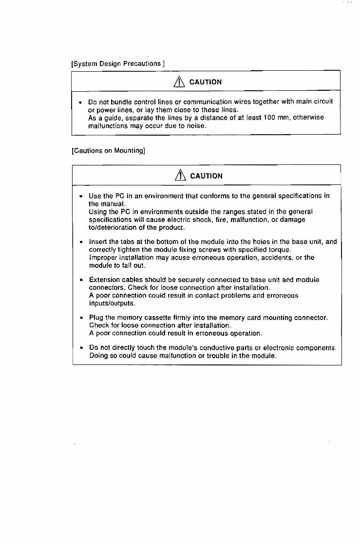
[System Design Precautions ]
a CAUTION
Do not bundle control lines or communication wires together with main circuit or power lines, or lay them close to these lines. As a guide, separate the lines by a distance of at least 100 mm, otherwise malfunctions may occur due to noise.
[Cautions on Mounting]
CAUTION
Use the PC in an environment that conforms to the general specifications in the manual. Using the PC in environments outside the ranges stated in the general specifications will cause electric shock, fire, malfunction, or damage totdeterioration of the product.
Insert the tabs at the bottom of the module into the holes in the base unit, and correctly tighten the module fixing screws with specified torque. Improper installation may acuse erroneous operation, accidents, or the module to fall out.
Extension cables should be securely connected to base unit and module connectors. Check for loose connection after installation. A poor connection could result in contact problems and erroneous inputstoutputs.
Plug the memory cassette firmly into the memory card mounting connector. Check for loose connection after installation. A poor connection could result in erroneous operation.
Do not directly touch the module's conductive parts or electronic components. Doing so could cause malfunction or trouble in the module.

[Cautions on Wiring]
@ DANGER
Switch off the external power supply before staring installation and wiring work. Failure to do so could result in electrical shocks and equipment damage.
After installation and wiring is completed, be-sure to attach the terminal cover before switching the power ON and starting operation. Failure to do so could result in electrical shocks.
A CAUTION
Be sure to ground the FG and LG terminals, carrying out at least class 3 grounding work with a ground exclusive to the PC. Otherwise there will be a danger of electric shock and malfunctions.
Carry out wiring to the PC correctly, checking the rated voltage and terminal arrangement of the product. Using a power supply that does not conform to the rated voltage, or carrying out wiring incorrectly, will cause fire or failure.
Outputs from multiple power supply modules should not be connected in parallel. Failure to do so could cause the power supply module to overheat, resulting in a fire or module failure.
Tighten the terminal screws to the stipulated torque. Loose screws will cause short circuits, fire, or malfunctions.
Make sure that no foreign matter such as chips or wiring offcuts gets inside the module. it will cause fire, failure or malfunction.
Connectors for external connections should be crimped, pressure welded, or soldered in the correct manner using the correct tools. For details regarding crimping and pressure welding tools, refer to the inpuUoutput module user's manual.
- A poor connection could cause shorts, fire, and erroneous operation.

[Cautions on Startup and Maintenance] 7
@ DANGER
Do not touch terminals while the power is ON. This will cause malfunctions.
Make sure that the battery is connected properly. Do not attempt to charge or disassemble the battery, do not heat the battery or place it in a flame, and do not short or solder the battery. lncorrect handling of the battery can cause battery heat generation and ruptures which could result in fire or injury.
switch the power off before cleaning or re-tightening terminal screws. Carrying out this work while the power is ON will cause failure or malfunction of the module.
a CAUTION
In order to ensure safe operation, read the manual carefully to acquaint yourself with procedures for program changes, forced outputs, RUN, STOP, and PAUSE operations, etc., while operation is in progress. lncorrect operation could result in machine failure and injury.
Do not disassemble or modify any module. This will cause failure, malfunction, injuries, or fire.
Switch the power OFF before mounting or removing the module. Mounting or removing it with the power ON can cause failure or malfunction of the module.
When replacing fuses, be sure to use the prescribed fuse. A fuse of the wrong capacity could cause a fire.
[Cautions on Disposal] 0 CAUTION
Dispose of this product as industrial waste.

Thank you for choosing the Mitsubishi MELSEC-A Series of General Purpose Programmable Controllers. Please read this manual carefully so that the product is used t o its optimum. A copy of this manual should be forwarded to the end user.
- - This manual describes specifications and requirements related to safety, installations, wiring and maintenance of the AnS series PC. For functional information, please refer to detail manuals of each module.
Guidelines for the safety of the user and protection of the AnS series PC
This manual provides information for the installation and use of the AnS series PC. The manual has been written to be used by trained and competent personnel. Please read the manual carefully before installation and/or operations of the product. If the product is used in a manner not specified by the manual, the protection provided by the product may be impaired.
@ Note: Definition of 'trained and competent personnel' is as follows:
a) Any engineer who is responsible for the planning, design and construction of automatic equipment using the product associated with this manual should be of a competent nature, (trained and qualified to the local and national standards required to fulfill that role). These engineers shoulc! be fully aware of all aspects of safety with regards to automated equipment.
b) Any commissioning or service engineer must be of a competent nature, trained and qualified to the local and national standards required to fulfill that job. These engineers should also be trained in the use and maintenance of the completed product. This includes being completely familiar with all associated documentation
. for the said product. All maintenance should be carried out in accordance with established safety practices.
c) All operators of the completed product should be trained to use that product in a safe and co-ordinated manner in compliance to established safety practices. The operators should also be familiar with all documentation which is connected with the actual operation of the completed equipment.
Note: the term 'completed equipment' refers to a third party constructed device which contains or uses the product associated with this manual.
Note's on the symbols used in this manual
At variouse times through out this manual, certain symbols are used to highlight points of information which are intended to ensure the users personal safety and protect the integrity of the equipment. Whenever any of the following symbols are encountered, its associated note must be read and understood. Each of the symbols used are listed with a brief description of its meaning.
Indicates that the identified danger possibly cause serious physical injury and/or @ DANGER death.
Indicates that the idetified danger possibly cause physical injury or property A CAuTioN damage.

Notification of CE marking c c The following products have shown compliance through direct testing (to the identified standards) and design analysis (forming a technical construction file) to the European Directive for Electromagnetic Compatibility (891336lEEC)
Products: Type: Programmable Logic Controller (Open Type equipment, installation category II)
Model: AnS-Series (Applicable units listed below)
Harmonised European Standards IEC Standards Reference No. Date of Issue Reference No. Date of Issue EN50081-2 1992 IEC801-2 1984 prEN50082-2 1992 IEC801-3 1984
IEC801-4 1988
AnS-Series Programmable Logic Controllers Range of products:
The products listed above must be used as directed by the associated documentation in order to provide full compliance. Please contact your local. Mitsubishi Sales office or distributor for further details.

CONTENTS
I . GENERAL DESCRIPTION ...................................................... 1-1
1.1 General Description . . . . . . . . . . . . . . . . . . . . . . . . . . . . . . . . . . . . . . . . . . . . . . . . . . . . . . . . 1-1 1.2 Differences Between AISJCPU and AlSJCPU.S3 . . . . . . . . . . . . . . . . . . . . . . . . . . . . . . 1-1
2 . SYSTEM CONFIGURATION .............................................. 2-1 - 2-13
2.1 Overall Configuration . . . . . . . . . . . . . . . . . . . . . . . . . . . . . . . . . . . . . . . . . . . . . . . . . . . . . . . 2-1 2.2 Cautions on System Configurations . . . . . . . . . . . . . . . . . . . . . . . . . . . . . . . . . . . . . . . . . . 2-3
2.2.1 Hardware . . . . . . . . . . . . . . . . . . . . . . . . . . . . . . . . . . . . . . . . . . . . . . . . . . . . . . . . . . . 2-3 2.2.2 Software packages . . . . . . . . . . . . . . . . . . . . . . . . . . . . . . . . . . . . . . . . . . . . . . . . . . . 2-5
2.3 System Equipment . . . . . . . . . . . . . . . . . . . . . . . . . . . . . . . . . . . . . . . . . . . . . . . . . . . . . . . . . 2-7 2.4 Overview of System Configuration . . . . . . . . . . . . . . . . . . . . . . . . . . . . . . . . . . . . . . . . . . . 2-13
. 3 GENERAL SPECIFICATIONS ................................................... 3-1 3.1 General Specifications . . . . . . . . . . . . . . . . . . . . . . . . . . . . . . . . . . . . . . . . . . . . . . . . . . . . . . 3-1
4.1 Performance Specifications . . . . . . . . . . . . . . . . . . . . . . . . . . . . . . . . . . . . . . . . . . . . . . . . . 4-1 . . . . . . . . . . . . . . . . . . . . . . . . . . . . . . . . . . . . . . . . 4.1.1 A1 SJCPU operation processing 4 -4
4.1.2 Operation processing in the RUN, STOP. PAUSE states . . . . . . . . . . . . . . . . . . 4-6 4.1 -3 Operation processing when a momentary power failure occurs . . . . . . . . . . . . . 4-7 4.1.4 Self-diagnosis . . . . . . . . . . . . . . . . . . . . . . . . . . . . . . . . . . . . . . . . . . . . . . . . . . . . . . . 4-8 4.1.5 Devices . . . . . . . . . . . . . . . . . . . . . . . . . . . . . . . . . . . . . . . . . . . . . . . . . . . . . . . . . . . 4-10 4.1.6 parameter setting ranges . . . . . . . . . . . . . . . . . . . . . . . . . . . . . . . . . . . . . . . . . . . . 4-12 4.1.7 Memory capacity settings (main programs. file registers. comments. etc.) . . 4-14
4.2 Functions . . . . . . . . . . . . . . . . . . . . . . . . . . . . . . . . . . . . . . . . . . . . . . . . . . . . . . . . . . . . . . . . 4-16 . . . . . . . . . . . . . . . . . . . . . . . . . . . . . . . . . . . . . . . . . . . . . . . . . . . . . . 4.3 Handling Instructions 4-17
4.4 Names and Purposes of Parts and Settings . . . . . . . . . . . . . . . . . . . . . . . . . . . . . . . . . . . 4-18 4.4.1 Names of parts of A1 SJCPU . . . . . . . . . . . . . . . . . . . . . . . . . . . . . . . . . . . . . . . . . 4-18 4.4.2 110 control switch setting . . . . . . . . . . . . . . . . . . . . . . . . . . . . . . . . . . . . . . . . . . . . 4-24
. . . . . . . . . . . . . . . . . . . . . . . . . . . . . . . . . . . . . . . . . 4.4.3 Memory protect switch setting 4-24 4.4.4 Latch clear . . . . . . . . . . . . . . . . . . . . . . . . . . . . . . . . . . . . . . . . . . . . . . . . . . . . . . . . . . 4-25
5 . POWER SUPPLY MODULE ............................................... 5-1 -5-6 5.1 Specifications . . . . . . . . . . . . . . . . . . . . . . . . . . . . . . . . . . . . . . . . . . . . . . . . . . . . . . . . . . . . . 5-1
5.1.1 Selection of a power supply module . . . . . . . . . . . . . . . . . . . . . . . . . . . . . . . . . . . . 5-2 5.2 Names and Purposes of Parts and Settings .................................... 5 -4
6 . EXTENSION BASE UNIT AND EXTENSION CABLE ......................... 6-1 - 6-11
. . . . . . . . . . . . . . . . . . . . . . . . . . . . . . . . . . . . . . . . . . . . . . . . . . . . . . . . . . . . . 6.1 Specifications 6-1 . . . . . . . . . . . . . . . . . . . . . . . . . . . . . . . . . 6.1.1 Specifications of extension base units 6-1
. . . . . . . . . . . . . . . . . . . . . . . . . . . . . . . . . . . . . 6.1.2 Specifications of extension cables 6-1 6.1.3 Application standards of extension base unit (A1 S52B(S1), A1 SSSB(S1).
. . . . . . . . . . . . . . . . . . . . . . . . . . . . . . . . . . . . . . A1 S58B(S1). A52B. A55B. A58B) 6-2

.................................... 6.2 Names and Purposes of Parts and Settings 6-8 6.3 Extension Base Number Setting (A1 S[ ][ JB-S1 Extension Base Units Only) . ....... 6-9
. . . . . . . . . . . . . . . . . . . . . . . . . . . . . . . . . . . . . . . . . . . . . . . . . . . . . . . 6.4 Installing a DIN Rail 6-10
............................................... 7 . MEMORY ICS AND BATTERY 7-1 -. 7-4
7.1 Memory ICs . . . . . . . . . . . . . . . . . . . . . . . . . . . . . . . . . . . . . . . . . . . . . . . . . . . . . . . . . . . . . . . 7-1 ....................................................... 7.1.1 Specifications 7-1
7.1.2 Handling instructions ................................................. 7-1 7.1.3 Installing and removing a memory cassette .............................. 7-2 7.1.4 Writing a sequence program to an A1 SMCA-8KP ... . . . . . . . . . . . . . . . . . . . . . . 7-3
................................................................... 7.2 Battery 7 4 7.2.1 Specifications ....................................................... 7-4 7.2.2 Handling instructions .. . . . . . . . . . . . . . . . . . . . . . . . . . . . . . . . . . . . . . . . . . . . . . . . 7-4
.......................................................... 7.2.3 Installation 7 4
. 8 . LOADING AND INSTALLATION .......................................... 8-1 8-15
8.1 Installation Environment . . . . . . . . . . . . . . . . . . . . . . . . . . . . . . . . . . . . . . . . . . . . . . . . . . . . 8-1 8.2 Calculation of Heat Generated by the Programmable Controller System ........... 8-1 8.3 Precautions Relating to the Installation of the Base Unit . . . . . . . . . . . . . . . . . . . . . . . . . 8-3 8.4 Mounting and Removing Modules ............................................ 8-6 8.5 Installing and Removing the Dustproof Cover .................................. 8-8 8.6 Failsafe Circuits ........................................................... 8-9 8.7 Power Supply Connection . . . . . . . . . . . . . . . . . . . . . . . . . . . . . . . . . . . . . . . . . . . . . . . . . . 8-13
. 9 . MAINTENANCE AND INSPECTION ........................................ 9-1 9-4
9.1 Daily Inspection . . . . . . . . . . . . . . . . . . . . . . . . . . . . . . . . . . . . . . . . . . . . . . . . . . . . . . . . . . . 9-1 9.2 Periodiclnspection ......................................................... 9-2 9.3 Replacement of Battery . . . . . . . . . . . . . . . . . . . . . . . . . . . . . . . . . . . . . . . . . . . . . . . . . . . . . 9-3
9.3.1 Service life of battery . . . . . . . . . . . . . . . . . . . . . . . . . . . . . . . . . . . . . . . . . . . . . . . . . 9-3 9.3.2 Replacing the battery ................................................. 9 4
10.1 Basic Troubleshooting ..................................................... 10-1 10.2Troubleshooting . . . . . . . . . . . . . . . . . . . . . . . . . . . . . . . . . . . . . . . . . . . . . . . . . . . . . . . . . . . 0-2
10.2.1 Troubleshooting flowcharts ........................................... 10-2 10.2.2 Flowchart used when the POWER LED goes OFF ....................... 10-3 10.2.3 Flowchart used when the RUN LED goes OFF .......................... 10-4 10.2.4 Flowchart used when the RUN LED flashes ............................ 10-5 10.2.5 Flowchart used when the ERROR LED is lit . ........................... 10-6 10.2.6 Flowchart used when the ERROR LED flashes .......................... 10-7 10.2.7 Flowchart used when the output load of the output module does not go ON . 10-8 10.2.8 Flowchart used when a program cannot be written to the PC CPU ......... 10-9
10.3 Error Code List . ......................................................... 10-1 0 10.4 110 Connection Troubleshooting ............................................. 10-1'4
10.4.1 Input circuit troubleshooting . ........................................ 10-1 4 10.4.2 Output circuit failures and corrective actions .......................... 10-1 6

.. 8
....................................................... APPENDICES APP-1 - APP . 39
i . . . . . . . . . . . . . . . . . . . . . . . . . . . . . . . . . . . . . . . . . . . . . . . . . . I APPENDIX 1 INSTRUCTIONS APP-1 I . . . . . . . . . . . . . . . . . . . . . . . . . . . . . . . . . . . . . . . . . . . . . . . I 1 1 Sequence Instructions APP-1
. . . . . . . . . . . . . . . . . . . . . . . . . . . . . . . . . . . . . . . . . . . . . . . . . . . 1.2 Basic Instruction APP-3 . . . . . . . . . . . . . . . . . . . . . . . . . . . . . . . . . . . . . . . . . . . . . 1.3 Application Instructions APP-10
. . . . . . . . . . . . . . . . . . . . . . 1 APPENDIX 2 SPECIAL RELAY. SPECIAL REGISTER LIST APP-16 . . . . . . . . . . . . . . . . . . . . . . . . . . . . . . . . . . . . . . . . . . . . . . . . . 2.1 Special Relay List : APP-16
. . . . . . . . . . . . . . . . . . . . . . . . . . . . . . . . . . . . . . . . . . . . . . . . 2.2 Special Registers D APP-19 . . . . . . . . . . . . . . . . . . . . . . . . . . . . . . . . . . . . . . . . . . APPENDIX 3 OUTSIDE DIMENSIONS APP-25
\ 3.1 CPU Module . . . . . . . . . . . . . . . . . . . . . . . . . . . . . . . . . . . . . . . . . . . . . . . . . . . . . . . APP-25 3.1.1 A1 SJCUP module . . . . . . . . . . . . . . . . . . . . . . . . . . . . . . . . . . . . . . . . . APP-25 3.1.2 AISJCUP-S3 module . . . . . . . . . . . . . . . . . . . . . . . . . . . . . . . . . . . . . . APP-25
3.2 Power Supply Module . . . . . . . . . . . . . . . . . . . . . . . . . . . . . . . . . . . . . . . . . . . . . . APP-26 J 3.2.1 A1 S61 P/A1 S62PlA1 S63P Power Supply Module . . . . . . . . . . . . . . . APP-26
. . . . . . . . . . . . . . . . . I
3.2.2 A1 S61 PEUIA1 S62PEU Power Supply Module APP-26 3.3 Extension Base Units . . . . . . . . . . . . . . . . . . . . . . . . . . . . . . . . . . . . . . . . . . . . . . APP-27
3.3.1 A1 S65B, A1 S65B-S1 extension base unit . . . . . . . . . . . . . . . . . . . . . APP-27 . . . . . . . . . . . . . . . . . . . . . 3.3.2 A1 S68B, A1 S68B-S1 extension base unit APP-27
3.3.3 A1S52B, A1 S52B-S1 extension base unit . . . . . . . . . . . . . . . . . . . . . APP-28 3.3.4 A1 S55B. A1 S55B-S1 extension base unit . . . . . . . . . . . . . . . . . . . . . APP-28 3.3.5 A1 S58B, A1 S58B-S1 extension base unit . . . . . . . . . . . . . . . . . . . . . APP-29
. . . . . . . . . . . . . . . . . . . . . . . . . . . . . . . . . . . . . 3.4 Memory Cassette (A1 SMCA-[ I) APP-30 3.5 A6WA-28P Memory Write Adaptor . . . . . . . . . . . . . . . . . . . . . . . . . . . . . . . . . . . APP-30 3.6 40-Pin Connectors . . . . . . . . . . . . . . . . . . . . . . . . . . . . . . . . . . . . . . . . . . . . . . . . . APP-31
3.6.1 A6CON1 soldering-type 40-pin connector, I A6CON2 crimp-contact-type 40-pin connector . . . . . . . . . . . . . . . . . APP-31
3.6.2 A6CON3 pressure-displacement-type 40-pin connector . . . . . . . . . APP-31 I 3.7 37-Pin D Sub-Connectors APP-32 . . . . . . . . . . . . . . . . . . . . . . . . . . . . . . . . . . . . . . . . . .
3.7.1 A6CON1 E soldering-type 37-pin D sub-connector,
I A6CON2E crimp-contanc-type 37-pin D sub-connector . . . . . . . . . APP-32 3.7.2 A6CON3E pressure-displacement-type 37-pin D sub-connector . . APP-32 e APPENDIX 4 INSTRUCTION PROCESSING TIME . . . . . . . . . . . . . . . . . . . . . . . . . . . . . . APP-33
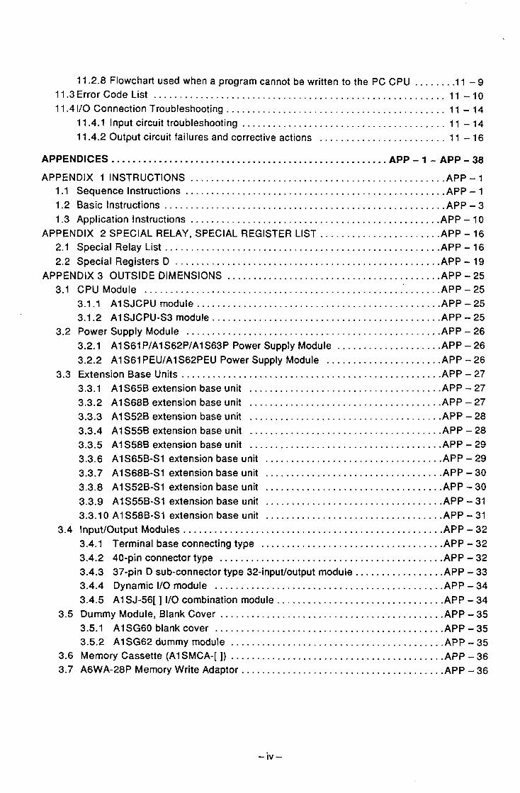
11.2.8 Flowchart used when a program cannot be written to the PC CPU . . . . . . . -1 1 - 9 11.3 Error Code List . . . . . . . . . . . . . . . . . . . . . . . . . . . . . . . . . . . . . . . . . . . . . . . . . . . . . . . 11 - 10 1 1.4 110 Connection Troubleshooting . . . . . . . . . . . . . . . . . . . . . . . . . . . . . . . . . . . . . . . . . . 1 1 - 14
11.4.1 Input circuit troubleshooting . . . . . . . . . . . . . . . . . . . . . . . . . . . . . . . . . . . . . . . 11 - 14 11.4.2 Output circuit failures and corrective actions . . . . . . . . . . . . . . . . . . . . . . . . 11 - 16
. . . APPENDICES ..................................................... APP 1 APP 38
APPENDIX 1 INSTRUCTIONS . . . . . . . . . . . . . . . . . . . . . . . . . . . . . . . . . . . . . . . . . . . . . . . . . APP . 1 1.1 Sequence Instructions . . . . . . . . . . . . . . . . . . . . . . . . . . . . . . . . . . . . . . . . . . . . . . . . . . APP . 1 1.2 Basic Instructions . . . . . . . . . . . . . . . . . . . . . . . . . . . . . . . . . . . . . . . . . . . . . . . . . . . . . . APP . 3 1.3 Application Instructions . . . . . . . . . . . . . . . . . . . . . . . . . . . . . . . . . . . . . . . . . . . . . . . . APP - 10
APPENDIX 2 SPECIAL RELAY, SPECIAL REGISTER LIST . . . . . . . . . . . . . . . . . . . . . . . APP - 16 2.1 Special Relay List . . . . . . . . . . . . . . . . . . . . . . . . . . . . . . . . . . . . . . . . . . . . . . . . . . . . . APP - 16 2.2 Special Registers D . . . . . . . . . . . . . . . . . . . . . . . . . . . . . . . . . . . . . . . . . . . . . . . . . . . APP - 19
APPENDIX 3 OUTSIDE DIMENSIONS .. . . . . . . . . . . . . . . . . . . . . . . . . . . . . . . . . . . . . . . . APP - 25 3.1 CPU Module . . . . . . . . . . . . . . . . . . . . . . . . . . . . . . . . . . . . . . . . . . . . . . . . . . . . . . . . . APP - 25
3.1.1 A1 SJCPU module . . . . . . . . . . . . . . . . . . . . . . . . . . . . . . . . . . . . . . . . . . . . . . . APP - 25 3.1.2 A1 SJCPU-S3 module . . . . . . . . . . . . . . . . . . . . . . . . . . . . . . . . . . . . . . . . . . . . APP - 25
3.2 Power Supply Module . . . . . . . . . . . . . . . . . . . . . . . . . . . . . . . . . . . . . . . . . . . . . . . . . APP - 26 3.2.1 A1 S61 PIA1 S62PlA1 S63P Power Supply Module .................... APP - 26 3.2.2 A1 S61 PEUIA1 S62PEU Power Supply Module . . . . . . . . . . . . . . . . . . . . . . APP - 26
3.3 Extension Base Units .................................................. APP - 27 3.3.1 A1 S65B extension base unit . . . . . . . . . . . . . . . . . . . . . . . . . . . . . . . . . . . . . APP - 27
. . . . . . . . . . . . . . . . . . . . . . . . . . . . . . . . . . . . . 3.3.2 A1 S68B extension base unit APP - 27
. . . . . . . . . . . . . . . . . . . . . . . . . . . . . . . . . . . . . 3.3.3 A1 S52B extension base unit APP - 28
. . . . . . . . . . . . . . . . . . . . . . . . . . . . . . . . . . . . . 3.3.4 A1 S55B extension base unit APP - 28
. . . . . . . . . . . . . . . . . . . . . . . . . . . . . . . . . . . . . 3.3.5 A1 S58B extension base unit APP - 29 . . . . . . . . . . . . . . . . . . . . . . . . . . . . . . . . . . 3.3.6 A1 S65B-S1 extension base unit APP - 29 .................................. 3.3.7 A1 S68B-S1 extension base unit APP - 30
3.3.8 A1S52B-S1 extension base unit .................................. APP - 30 3.3.9 A1 S55B-S1 extension base unit . . . . . . . . . . . . . . . . . . . . . . . . . . . . . . . . . . APP - 31 3.3.1 0 A1 S58B-S1 extension base unit . . . . . . . . . . . . . . . . . . . . . . . . . . . . . . . . . . APP - 31
3.4 InputIOutput Modules .................................................. APP - 32 3.4.1 Terminal base connecting type . . . . . . . . . . . . . . . . . . . . . . . . . . . . . . . . . . . APP - 32 3.4.2 40-pin connector type ........................................... APP - 32 3.4.3 37-pin D sub-connector type 32-inputloutput module ................. APP - 33 3.4.4 Dynamic I10 module . . . . . . . . . . . . . . . . . . . . . . . . . . . . . . . . . . . . . . . . . . . . APP - 34 3.4.5 A1 SJ-56[ ] I10 combination module ................................ APP - 34
3.5 Dummy Module, Blank Cover . . . . . . . . . . . . . . . . . . . . . . . . . . . . . . . . . . . . . . . . . . . APP - 35 3.5.1 A1 SG6O blank cover . . .......................................... APP - 35 3.5.2 A1 SG62 dummy module . . . . . . . . . . . . . . . . . . . . . . . . . . . . . . . . . . . . . . . . . APP - 35
3.6 Memory Cassette (A1 SMCA-[ 1) . . . . . . . . . . . . . . . . . . . . . . . . . . . . . . . . . . . . . . . . . APP - 36 3.7 A6WA-28P Memory Write Adaptor . . . . . . . . . . . . . . . . . . . . . . . . . . . . . . . . . . . . . . . APP - 36

. . . . . . . . . . . . . . . . . . . . . . . . . . . . . . . . . . . . . . . . . . . . . . . . . . . . 3.8 40-Pin Connectors APP - 37 3.8.1 A6CON1 soldering-type 40-pin connector.
A6CON2 crimp-contact-type 40-pin connector . . . . . . . . . . . . . . . . . . . . . . APP - 37 3.8.2 A6CON3 pressure-displacement-type 40-pin connector . . . . . . . . . . . . . . APP - 37
. . . . . . . . . . . . . . . . . . . . . . . . . . . . . . . . . . . . . . . . . . . . . . 3.9 37-Pin D Sub-connectors APP - 38 3.9.1 AGCON1 E soldering-type 37-pin D sub.connector,
A6CON2E crimp-contact-type 37-pin D sub-connector . . . . . . . . . . . . . . . APP - 38 3.9.2 A6CON3E pressure-displacement-type 37-pin D sub-connector . . . . . . . APP - 38-
. . . . . . . . . . . . . . . . . . . . . . . . . . . . . . . APPENDIX 4 INSTRUCTION PROCESSING TIME APP - 39

1. GENERAL DESCRIPTION MELSEC-A
1. GENERAL DESCRIPTION
1.1 General Description
This manual describes the specifications and functions of the AlSJCPU, AlSJCPU-S3 programmable controller (hereinafter referred to as the AlSJCPU) and the specifications of the I10 modules, power supply modules, and extension base units used with the A1 SJCPU. The AlSJCPU has a compact building-block type body in which a CPU module, power supply module, and a base unit are built together to form one solid structure. It is characterized by high cost performance. Since its performance and functions are equal to those of the AlSCPU, the sequence programs (instructions), I10 modules, and special function modules compatible with the A1SCPU are compatible also with the A1 SJCPU. Slim type I10 combination modules (input 32 points, output 24 points) for use exclusively with the AlSJCPU are also available. The three sizes when the slim type is used with the AlSJCPU are 330 mm (W) x 130 mm (H) x 82 mm (D) (13.0 inch x 5.12 inch x 3.23 inch). This user's manual refers to the peripheral devices (AGGPP, AGPHP, AGHGP, IBM PCIAT, A7PU, A7PUS, and A8PUE) as abbreviated as mentioned below.
AGGPP, AGPHP, AGHGP, and IBM PCIAT (started up with SWOIVD-GPPA, MELSEC-MEDOC)
Abbreviated as "GPP function" . . . . . . . . . . . . . . A7PU, A7PUS, and A8PUE.. . . . . . . . . . . . . Abbreviated as "PU".
Refer to the following manuals if necessary:
ACPU Programming Manual (Fundamentals) (IB 66249) Information such as programming procedures, device names, parameters, classification of programs, and memory area allocation which are necessary for programming are described. ACPU Programming Manual (Common Instructions) (1866250) The methods of use of sequence instructions, basic ~nstructions, application instructions, and microcomputer programs are described. AnS Module type I10 User's Mannual (1866541) The specificat~ons of compact building block type I10 modules are de- scribed.
1.2 Differences Between AISJCPU and AISJCPU-S3
The differences between AlSJCPU and AlSJCPU-S3 are indicated in the table below.
Table of Difference
Differences
Operating switches
A1 SJCPU and A1 SJCPU-S3 have identical functions and performance.
Front cover
AlSJCPU
RESET is a pushbutton switch. RUN. STOP, and L.CLR are toggle switches.
A1 SJCPU-S3
RESET, RUN, STOP and L.CLR are incorporated in a single key switch.
Opens the CPU module (power supply part and CPU part).
Opens only part of the CP" module (CPU

2. SYSTEM CONFIGURATION
. . MELSEC-A
2. SYSTEM CONFIGURATION
This section describes the applicable system configuration, cautions on the system conf iguration,_and c o m p o n e n t devices of the A1 SJCPU.
2.1 Overall Configuration
The following figure shows a configuration when the AISJCPU is used independently.
To peripheral device
Output module (AlSY[ I[ I(EU))
Special function
Extension base (AlS6[]B(Sl)): Equipped with a
power supply module. []B(Sl)): W~thout a power
supply module.
Power supply module. power su ply module Special function (A61 &(Eu)) module

2. SYSTEM CONFIGURATION MELSEC-A
To AlSJCPU
AC30R4 AC300R4 Cable t
AGPHP
graphic programmer
SW3GP-GPPAEE SW4GP-GPPAEE
AGHGP * Handy graphic programmer
4 ROM cassette (AISMCASKP)
SWSHGPAEE system disk
+ AGGPP intelligent GPP
SW3GP-GPPAEE
A7PUS AC30R4-PUS cable
- AC20R4-A8PU A8PUE
cable
RS-232C HRS-422 SmVD -GPPA system disk mnverter
compatible MELSEC MEDOC plus
(See the SWVD-GPPA manual, the MELSEC MEDOC manual or the MELSEC MEDOC plus manual.)
2. SYSTEM CONFIGURATION MELSEC-A
2.2 Cautions on System Configurations
The following describes the hardware and software that can be used with the AISJCPU.
2.2.1 Hardware
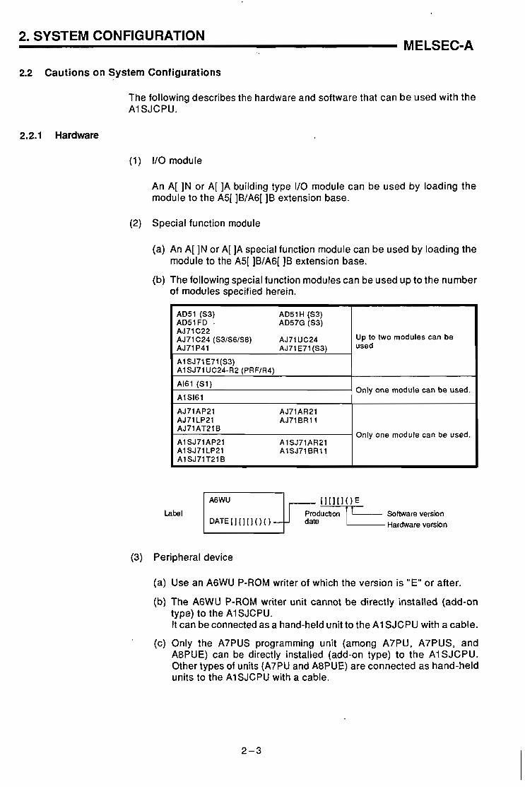
(1) I f 0 module
An A[ IN or A[ ]A building type I10 module can be used by loading the module to the A5[ ]B/A6[ ]B extension base.
(2) Special function module
(a) An A[ IN or A[ ]A special function module can be used by loading the module to the A5[ ]B/A6[ ]B extension base.
(b) The following special function modules can be used up to the number of modules specified herein.
AD51 (S3) AD51 H (S3) AD5lFD . AD57G (S3) AJ71C22 AJ71 C24 (S3IS6lS8) AJ71 UC24 AJ71P41 AJ71 E71 (S3)
A1 SJ71 E71(S3) A1 SJ71 UC24-R2 (PRFIR4)
A161 (S1) -
AlS161
AJ71AP21 AJ71AR21 AJ71 LP21 AJ71BR11 AJ71AT21 B
A1 SJ71AP21 AlSJ71AR21 AlSJ71LP21 AlSJ71BRl1 AlSJ71T21 B
(3) Peripheral device
Up to two modules can be used
Only one module can be used.
Only one module can be used.
Label
(a) Use an AGWU P-ROM writer of which the version is "E" or after.
A6WU
Software version D A T E [ ] [ ] [ ] ( ) ( ) Hardware version
(b) The AGWU P-ROM writer unit cannot be directly installed (add-on type) to the AISJCPU. It can be connected as a hand-held unit to the AISJCPU with a cable.
(c) Only the A7PUS programming unit (among A7PU, A7PUS, and A8PUE) can be directly installed (add-on type) to the AISJCPU. Other types of units (A7PU and A8PUE) are connected as hand-held units to the AISJCPU with a cable.

2. SYSTEM CONFIGURATION MELSEC-A
(4) EPROM memory cassette ROM partition
Partitioning the ROM in the AISMCA-8KP EPROM with an AGGPP (SW4GP-GPPAEE)/AGWU requires an A6WA-28P memory write adapter (option).
(5) Write at RUN when an operation is done with EEPROM (equipped with A1 SMCA-2KElA1 SMCA-8KE).
(a) When an operation is done using the EEPROM, writing at RUN gives to the peripheral devices the following messages:
When the SW3GP-GPPA is used: "PC COMMUNICATIONS ERROR ERROR CODE = 17" is displayed; When the A7PU is used: "PC NOT RESPOND" is displayed.
(b) It is not possible to write a program from a computer link module or a peripheral device connected to another station in a MELSECNET system. Write programs from a peripheral device connected to the RS-422 interface of the AISJCPU.
(c) When writing a program to an A1 SMCA-2KE, set the main sequence program capacity in the parameters to 2K steps or less. If you attempt to write a program with the main sequence program capacity set to 3K steps or greater, the program will not run correctly. Mismatches will also occur in verification between the AISJCPU and a peripheral device.

2. SYSTEM CONFIGURATION MELSEC-A
2.2.2 Software packages
(1) System startup software and module name specification at startup
When using any of the software packages for programming or monitoring on-line, "A2", "AlS" or "AOJ2HW should be set for the PC type selection. If the EPROM write facility is required, then this should be carried out off-line and either "AOJ2HW or "AlS" should be selected as the PC type if the software package has these selections. In the event that the software package does not have any of these two selections, then the EPROM write facility is not available. Please refer to the table below as a reference guide to the software packages available and the correct PC type selection for the AISJCPU.
POINTS 1 (1) When an AGGPP, AGHGP, or AGPHP is used, use an SW3-GPPAEE,
SW3-HGPAEE, SW3GP-GPPAEE, or SW4GP-GPPAEE as the sys- tem startup software. Other old software packages cannot be applied.
(2) Specifying the PC CPU name using the above-mentioned devices allows more than 256 110 signals input from the keyboard. However, those signals cannot be used in the A1 SJCPU.
Remarks
EPROM wrlte not possible.
Set 'A1S" when software of verslon 'R' or later.
EPROM write not possible.
Set 'AlS' when software of version "R' or later.
EPROM write not possible.
EPROM wite not possible.
'AlS' is d~splayed when the system is started up. (Software version "E' or later) Cannot be used. (Software version "D" or before.)
An add-on (direct) installment IS not possible.
'A2" is displayed when the system IS started up. (Software verslon "E' or before). Cannot be used. (Software verslon 'F" or later)
An add-on (direct) installment is not possible.
'A1Sn is displayed the system is started up.
Peripheral device
AGPHP
AGGPP
AGHGP
I BM PClAT
Software package
SW3GP-GPPAEE
SW4GP-GPPAEE
SW3-GPPAEE
SW3GP-GPPAEE
SW4GP-GPPAEE
SW3-HGPAEE
SWOIX-GPPAE
MEDOC
MELSEC-MEDOC
CPU
On-line
A2
AOJ2H
A2
AOJ2H
A2
A1S
A2
A1S
A1S
A2
A l S
AGWU
A7PU
ATPUS, ABPUE .'
Type
Off-line
-
AOJ2H/AlS
-
AOJ2HlAlS
-
AOJ2HIAIS
- -
-
-
-

2. SYSTEM CONFIGURATION MELSEC-A
(2) Utility package
Applicable utility packages are shown below.
SWOGHP-UTLPC-FNI SWOGHP-UTLPC-FNO SWOGHP-UTLP-FD1 SWO-AD57P SW1 GP-AD57P SWOC-UTLP-FID SWOGHP-UTLPC-PID SWOC-UTLP-FNO
(a) Select "A2CPUn when an SWOGHP-UTLPC-FN1 or SWOGHP-UTLP- FD1 is started up.
(b) If both an SW1GP-AD57P and another utility package combined are used, specify "AD57P-COM" as the file name.

2. SYSTEM CONFIGURATION MELSEC-A
2.3 System Equipment
The following table shows the system equipment consisting of various mod- ules and devices which can be used.
: Class 2 power supply specified by the UYCSA Standard must be used.
*
UUCSA
UUCSA
UUCSA
UUCSA
UUCSA
UUCSA
UUCSA
UUCSA
Remarks
RAM memory embedded
Loaded to the slot for power supply for main base or extension base
lnput module
I 132-Input 24 VDC Input module 32 a s 2 1132 inputs] 1 0-08 1 -
Number of Inputs1 Outputs
-
-
Module
CPU module
Power supply module
Model
A l ~ ~ ~ P U -53
AIS61 P
AIS61 PEU
AlS62P
AlS62PEU
AlS63P
Descrlptlon
See the 'Performance Spec~f~cat~ons' in Sect~on 4 (Number of 110 polnts : 256. memory capaclty : 32 Kbytes)
Current
5 VDC. 5 A
5 VDC, 3 A124 VDC. 0.6A
5 VDC. 5 A
5 VDC(A)
0.40
-
lnput 1001200 VAC
Input 200 VAC
lnput 1001200 VAC
lnpul 200 VAC
Input 24 VDC
,,$,, -
d

2. SYSTEM CONFIGURATION MELSEC-A
: Class 2 power supply specified by the UUCSA Standard must be used.
Description
lnputl output combi-
module
110 combi-
~ 1 ~ ~ 4 2
AISX 48Y18
ti$& AISJ- 56DR
nation module 32-polnt 24 VDC input (sunk type) 24-point 24 VDC
32-output 12/24 VDC translstor output module (0.1 A) sink type
&Input 24 VDC Input module (sink type) &output relay contact output rnodule (2 A)
8-Input 24 VDC lnput module (s~nk type) 8-output 12/24 VDC translstor output module (0.5 A)
32-porn1 24 VDC input (slnk type)24-point 24 VDC1240 VAC relay contact output (2 A)
132 inputs! outputs]
16 [8 Inputs/ outputs]
16 [8 inputs/ outputs]
Dynamlc lVut module
Dynamic output module
outputs
0.50
0.085
0.06
Number of set polnts
(Inputs [ 1)
Number of Set points (Outputs
I I)
0.008
0.045
0.06
A1S42Y
translstor output (0.5 A) slnk type
16-. 32-. 48- and 64-po~nt 12/24 VDC dynamlc Input module
16-. 32-, 48-, and 64-polnt 12/24 VDC dynam~c output module
0.08
0.10
-
0.008


2. SYSTEM CONFIGURATION MELSEC-A
: Class 2 power supply specified by the UUCSA Standard must be used.
Item
computer link module
MELSECNET (11) data llnk module
MELSECNET 1B data module
MELSECNET 11 0 network module
Extensron base unlt
Extension ca- ble
Model
AlSJ71 UC24- R2
AlSJ71UC24- PRF
A1SJ71UC24- R4
A1SJ71AP21
A1SJ71AR21
A1SJ71T21
A1SJ71LP21
A1SJ71 BR1
A1S52B(S1)
A1S55B(S1)
A1S58B(S1)
A1 S65B(S1)
A1S68B(S1)
AlSCOlB
A1 SCO3B
AlSC07B
AlSC12B
AISC3OB
A1 SC60B
AlSC05NB
AlSC07NB
AlSMcA-8KP
A1SMCA-2KE
A1 SMCA-8KE
Memory cassene
I
LU
2 8 a Y
Deserlptlon
Computer link function RS-232C: 1 channel
Computer llnk and prlnter funct~ons RS-232C: 1 channel
Computer.llnk and mult~drop lrnk functions US-4221485: 1 channel
For master or local statron of MELSECNET (11) optical data link
For master or local statron of MELSECNET (11) coaxial data link
For master or local statron of MELSECNETIB data link system
For normal statlon of MELSECNETIIO Optical network
For normal statlon of MELSECNETIlO coaxlal network
Up to two 110 modules can be loaded.
Up to five 110 modules can be loaded.
Up to eight 110 modules can be loaded.
Up to flve 110 modules can be loaded.
Up to eight 110 modules can be loaded.
55 mm (2.17 Inch) long flat cable
330 mm (1 1.8 inch) long
700 mm (27.6 Inch) long
1200 mm (47.24 inch) long
3000 mm (118.11 Inch) long
6000 mm (236.22 Inch) long
450 mm (17.72 Inch) long
700 mm (27.6 Inch) long
8K steps equipped with ROM (directly)
2K steps equlpped wlth 4K EROM (directly)
8K steps equipped w ~ t h 16K ROM (dlrectly)
Number of Inputs1 Output
32 [Speclal 32- point]
32 [Special 32- point]-
32 [Special 32- point]
32 [Special 32- pornt]
32 [Special 32- point]
32 [Specral 32- point]
32 [Special 32- point]
32 [Special 32- point]
-
-
-
-
-
-
-
-
-
- -
-
-
-
-
5 VDC(A)
O.l
O.l
O.l
0.5
O.g
0.66
0.65
0.8
-
-
-
-
-
-
-
-
- -
-
-
-
-
Remarks
Power supply module cannot be loaded. (Power is suppl~ed from the main base module.)
Needs a power supply module.
For extension on the rrght side
Extension base unit connection cable
A[ IN, A[ ]A extension base cable
Needs a memory write adapter.
D~rect wri telread from peripheral devices can be done.
Current Consumption
12 VDC(A)
-
-
-
-
-
-
-
-
-
-
-
-
-
-
-
-
-
- -
-
-
-
-
%Ey,",z
U UCSA
UUCSA
UUCSA (except for S1 type)
UUCSA
UUCSA
UUCSA
UUCSA

2. SYSTEM CONFIGURATION MELSEC-A
110 cables w i th connectors for 110 modules o f 40-pin connector spec i f~cat ions (A lSX41 , A lSX42 ,
A l S Y 4 1 , A l S Y 4 2 , etc.) or 37-pin D-sub connector speciftcaions (A lSX81 , A l S Y 8 1 ) are a v a ~ l -
Item
Memory write adapter
Battery r
able.
Consul t the neares t Mitsubishi representative for t he I10 cables with connectors.
Model
A6WA-28P
A6BAT
Appllcable Model
AlSX41(S2). AlSX42(S2), AlSY41. AlSY42. AlSH42
AX42(S1), AY42(SllS3lS4). AH42
AlSX41(S2), A1 SX42(S2), AlSH42, AX42(Sl). AH42
A1 SX81 (S2). AX82
AlSY81. AY82EP
AlSX81(S2). AX82
AlSY81. AY82EP
AlS81(S2). AX82
A6TBXY36
A6TBXY54
A6TBX70
A6TBX36-E
A6TBY36-E
A6TBX54-E
A6TBY54-E
A6TBX70-E
Descrlptlon
Used for memory cassette connectorIEPROM 28-pln.
IC-RAM memory backup
Descrlptlon
For sunk type input module and s~nk type output module (standard type)
For sink type input module and slnk type output module (2-wlre type)
For sink type input module (3-wlre type)
For source type input module (standard type)
For source type output module (standard type)
For source type input module (2-wire type)
For source type output module (2-wlre type)
For source type input module (3-wlre type)
0.5 m (1.64 ft) for source module
1 m (3.28 ft) for source module
2 m (6.56 ft) for source moduel
3 m (9.84 ft) for source module
5 m (16.4 ft) for source module
0.5 m (1 64 ft) for source module
1 m (3.28 ft) for source module
2 m (6.56 ft) for source module
3 m (9.84 11) for source module ,
5 m (16.4 ft) for source module
Item
Connector1 terminal block conversion mod- ule
Cable for connector1 termma1 block converslon rnod- ule
Number of Inputs1 Output
-
-
Model
A6TBXY36
A6TBXY54
A6TBX70
A6TBX36-E
A6TBY36-E
A6TBX54-E
A6TBY54-E
A6TBX70-E
ACO5TB
ACIOTB
AC20TB
AC30TB
AC5°TB
AC05TB-E
AClOTB-E
AC20TB-E
AC30TB-E
AC50TB-E
Current Consumpt~on Remarks
Used to partltlon ROM In EPROM memory cassette.
5 VDC(A)
-
-
ASFf:;;:
U UCSA
12 VDC(A)
-
-

2. SYSTEM CONFIGURATION MELSEC-A
Peripheral devices
Remarks I
Plasma handy graphlc program- mer
lntell~gent GPP
AGPHP-SET
AGGPP-SET
AGPHP
SW[]GP-GPPAEE A-series GPP functlon system dlsk
SW[]GP-GPPKEE K-series GPP functlon system dlsk
SWO-GPPU User dlsk (2DD)
AC30R4 RS-422 cable (3 m (9 84 fl) length)
AGGPP
SW[]GPCPPAEE A-series GPP functlon system dlsk
SW[]GP-GPPAEE K-serces GPP function system dlsk
' SWO-GPPU User dlsk (2DD)
AC30R4 RS-422 cable (3 m (9 84 fl) lenqthl
I AGHGP
SW[]GP-HGPAEE. A-serles GPP functlon system dlsk Handy graphlc
SW[]GP-HGPKEE K-ser~es GPP funct~on system dlsk
I I I SWO-GPPU User disk (2DD) I Compostte vldeo cable
I RS-422 cable
AClOMD
I User dlsk
AC30R4 Used to connect the A7PU to the CPU. I AC3OOR4 ( Length 3 d 3 0 m (9 84198 4 fl)
* AC30R4 RS-422 cable (3 m (9 84 11) length)
Connects between AGGPP and monnor dlsplay (1 m (3 28 11) length)
AC30R4 . AC300R4
Cleaning disk
Programmtng unit
RS-422 cable I AC30R4-PUS Used to connect the A7PUS or A8PUE to the CPU I Lenglh 3 m p 8 4 f t )
SWO-GPPU
SWOS-USER
3 m (9 84 It) length
30 m (98 4 fl) length
SWO-FDC
A7PU
P-ROM wrlter Used for writln a rogram In CPUIAGPHP to ROM, or for readlng a CPU
I module I A6WU I program from h h f
Connects between CPU and MGPPIAGPHP I 2DD - 2HD
1
Used for stortng user program (3 5 Inch, formatted) I Awllcable to AGGPPIAGPHP Used for cleanlng dlsk dr~ve
I I I
AC20R4-A8PU
I
1 RS-422 cable
Connected d~rectly to the CPU wlth an RS-422 cable (AC30R4. AC300R4) to read and wrlte a program. Provlded wlth an MT functlon The product package Includes a cable used to connect to an aud~o cassette recorder
Connected directly to the CPU wllh an RS-422 cable (AC30R4-PUS) to read and wvte a program
Connected directly to the CPU wlth an RS-422 cable (AC3OR4-PUS, AC20R4-ABPU) to read and wtrte a program
Used to connect the ABPUE to the CPU. Length 2 m (6 56 fl)
AC30R4. AC300R4
AC03WU
Connected to CPUIAGPHP using an AC30R4lAC03WU cable
Connects between CPU and AGWU. 3 4 3 0 m (9.84198 4 11) length
Connects between CPU and AGWU 0 3 m (0 98 fl) length

2. SYSTEM CONFIGURATION . . - - v ,
i MELSEC-A
2.4 Overview of System Configuration
This section describes the system configuration, numbers of I10 points, I f0 allocations, etc., for a stand-alone A1 SJCPU system. ,
L
System configuration
Maximum number of extension base units
Maximum number of 110 points
Usable extension base units
Usable extension cables
Restrictions
Allocation of I10 numbers
0 1 2 3 4 5 6 7 '----~i Slot n b m r
To 2nd and 3rd extension
(Can be used by allocating VO points.)
To 2nd and 3rd extension base units (Can be used by allocating VO points.)
In this example, a 16-point module is installed at each slot.
Three
256
AlS52B(S1), AlS55B(Sl), AlS58B(Sl), AlS65B(Sl), AlS68B(Sl), A52B, A55B, A58B, A62B, A65B, A68B
AlSC03B, AlSCO7B. AlSC12B, AlSC3OB. AlSC608, AISCOlB, ACOGB, AC12B, ACSOB, A1 SC05NB, A1 SC07NB
(1) If using a type of extension base unit for A1S use other than the S1 type, only one extension base unit can be installed. (Combined use of S1 type extension base units and extension base units other than the S1 type is not possible.)
(2) When using one or more S1 type extension base units for A1S use in combination with one or more extension base units for A[ IN or ]A use, the final extension base unit must be one for 4 IN or A[ ]A use. (An S1 type extension base for A1S use cannot be connected from an extension base for 4 IN or A[ ]A use.)
(3) Extension base units AlS52B(SI), AlS55B(Sl), AlS58B(Sl), A52B, A55B, A58B are supplied with a 5 VDC power supply from the power supply module on the main base unit; refer to Section 7.1.3 to determine whether or not these extension base units can be used.
(4) The total length of extension cable used must not exceed 6 m.
(1) I10 numbers are allocated in the order of the numbers set in extension base number setting, regardless of the order of connection of extension cables.
(2) When allocating 110 points, all main bases and extension bases are regarded as having 8 slots of 110 points. Accordingly, 16 points per slot are allocated to the part of the system configuration drawing indicated using dotted lines.
(3) 16 points are allocated to vacant slots. (4) If extension base number setting has not been performed at one or more units, I10 points
are allocated by regarding each slot in the total number of slots involved - obtained by multiplying the number of extension bases for which setting was skipped by 8 slots - as occupying 16 points per slot.
(5) The allocations in (2) to (4) above can be changed by performing '110 allocation'. When using two or three extension base units, perform 'I10 allocation' to allocate 0 points to vacant slots of the AlSJCPU and some slots of the first extension base unit, and allocate 110 points to the second and third extension base units. (The total number of I10 points for the AlSJCPU and 1 st, 2nd, and 3rd extension base units is 256.) For details on '110 allocation', refer to the ACPU Programming Manual (Fundamentals).

3. GENERAL SPECIFICATIONS MELSEC-A
3. GENERAL SPECIFICATIONS- -
3.1 General Specifications
Table 3.1 General Specifications
' JIS: Japanese Industrial Standard
ltern
Operating ambient temperature
Storage ambient temperature
Operating ambient humidity
Storage ambient humidity
Vibration resistance
Shock resistance
Operating atomosphere
Altitude
Insulation site
Overvoltage category
Degree of contamination
F
Specifications
0 to 55%
-20 to 75°C
10 to 90%RH, no dewing
10 to 90%RH, no dewing
Conforms to JIS B 3501,
IEC 1131 -2
Conforms to JIS B 3501, IEC 1131-2 (147 m/s2 (15G) x 3 times in 3 directions)
To be free of corrosive gases
Up to 2,000 m
Inside a control cabinet ,
11 or lower
No greater than 2
-- For intermittent vibration
Frequency
10 to 57Hz
57 to 150Hz
Amplitude
0.075mm (0.003 inch)
-
Acceleration
-
9.8 mls2 (1 G)
Sweep Count
10 times each in X, Y and Z directions (80 minutes)
For continuous v~bration
Frequency
10 to 57Hz
57 to 150Hz
Acceleration
-
4.9 mls2{0.5~}
0.035mm (0.001 inch)
-

4. AISJCPU MELSEC-A
4.- AISJCPU-
4.1 Performance Specifications
(1) Performance specifications of A1 SJCPU unit
Table 4.1 Performance specifications of AISJCPU unit
Control system
I10 control method
Programming language
Annunciator (F) (points) 256 (FO to F255)
File register (R) (points) Max. 4096 (RO to R4095)
Accumulator (A) (po~nts) 2 (AO, A l )
Index register (V,Z) (points) 2 (v,z)
Pointer (P) (points) 256 (PO to P255)
Interrupt pointer (I) (po~nts) 32 (10 to 131)
Special relay (M) (points) 256 (M9000 to M9255)
Number Of instructions
AlSJCPU
Repeated operat~on (using stored program)
Refresh modelDirect mode selectable
Language dedicated to sequence control (Combined use of relay symbol type and logic symbolic language, MELSAP-II(SFC)
26
131
104
Direct : 1 .O to 2.3 Refresh : 1.0
256
10 to 2000
32K byte (RAM)
Main sequence program + main microcomputer program = 8K steps max. Internal microcomputer program can be set to 7K steps (14K bytes) max. (subsequence program not available).
Sequence instructions
Basic instructions
Application instructions
1000 (MO to 999)
1048 (L1000 to 2047)
0 (Defaults to no value)
1024 (BO to 3FF)
The number of M + L + S = 2048 (set in parameters)
256
100 msec timer : setting time 0.1 to 3276.7 sec (TO to 199) 10 msec timer : setting timer 0.01 to 327.67 sec (T200 to 255) Set in 100 msec : depending on setting I parameters retentive timer (setting time 0.1 to 3276.7 sec)
256
Normal counter : Setting range 1 to 32767 (CO to 255) Set in Interrupt program counter : Setting range 1 to 32767 para-
I Counter to be used in interrupt program meters
1024 (DO to 01023)
1024 (WO to W3FF)
Processing speed (sequence instructtion) (p seclstep)
110 points
Watchdog timer (WDT)(msec)
Memory capacity '1
Program capacity
Internal relay (M) (point)
Latch relay (L) (point)
Number of step relays (S) (point)
Link relay (8) (point)
Timer (T)
Counter (C)
Number of points
Specif~cations
Number of points
Specifications
Data register (D) (points)
Link register (W) (points)
4. AlSJCPU MELSEC-A
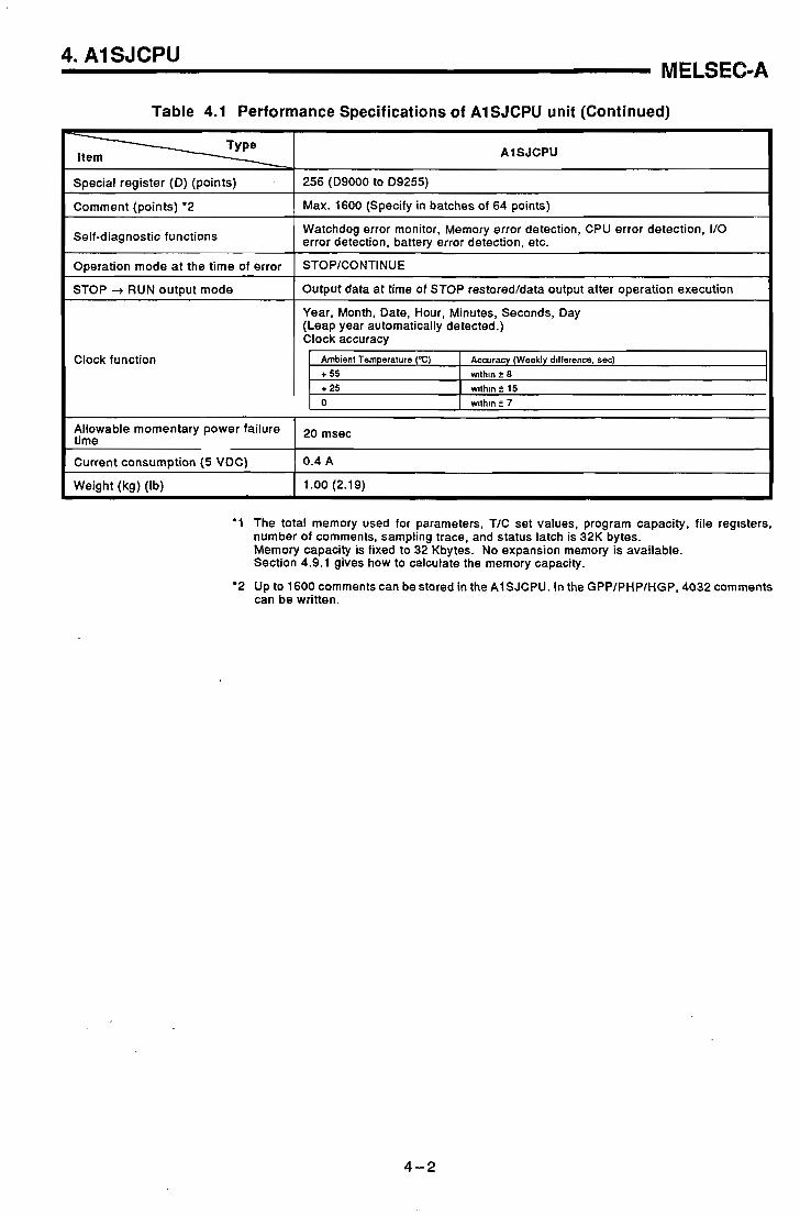
Table 4.1 Performance Specifications of AISJCPU unit (Continued)
'1 The total memory used for parameters, TIC set values, program capacity, file registers, number of comments, sampling trace, and status latch is 32K bytes. Memory capacity is fixed to 32 Kbytes. No expansion memory is available. Section 4.9.1 gives how to calculate the memory capacity.
AlSJCPU
'2 Up to 1600 comments can be stored in the A1SJCPU. In the GPPIPHPIHGP, 4032 comments can be written.
Special register (D) (points) -
Comment (points) '2
Self-diagnostic functions
Operation mode at the time of error
STOP -, RUN output mode
Clock function
Allowable momentary power failure time
Current consumption (5 VDC)
Weight (kg) (Ib)
256 (D9000 to D9255)
Max. 1600 (Specify in batches of 64 points)
Watchdog error monitor. Memory error detection, CPU error detection, 110 error detection, battery error detection, etc.
STOPICONTINUE
Output data at time of STOP restoredldata output after operation execution
Year, Month, Date, Hour, Minutes, Seconds, Day (Leap year automatically detected.) Clock accuracy
Ambient Temperature (OC) + 55 + 25 0
Accuracy (Weekly d~fterence, sec) w~thln 2 8
w~thln t 15 w ~ t h ~ n t 7
20 msec
0.4 A
1 .OO (2.19)

4. AISJCPU MELSEC-A
(2) Performance specifications for the AISJCPU built-in power supply.
Table 4.2 Performance Specifications for the AlSJCPU ~ui l t - ln Power SUDD~V
AlSJCPU I I
I lnput power supply
100-120 VAC lgz (85 to 132 VAC) 200-240 VAC i (1 70 to 264 VAC)
I
Input frequency 50/60 Hz * 3 Hz I I lnput maximum apparent power I 100 VA I
Rush current
Rated output
I Efficiency 1 65 %or over i I
20 A 8 msec or less
5 VDC 3 A
Overcurrent protect~on '1
Overvoltage protection
3.3 A or over
Not provided
Power supply ind~cation
Terminal screw size
Applicable cable size
I '1 : Overcurrent protection
POWER LED indicator
M3.5 X 8
0.3 to 2 mm2
Applicable solderless terminal
Allowable momentary power failure
When a current larger than the specification value flows through the 5 VDC circuit, the overcurrent protection device cuts.off the circuit and stops the system. The POWER LED turns off or lights dimly due to the voltage drop. If this device operated, remove causes of failures such as current capacity shortage and short-circuit and restart the system.
1.25-3.5, V1.25-YS3A, 2-3.5, 2-YS3A, V1.25-M3, V2-YS3A, V2-S3, V2-YS3A
20 msec or less (100 VAG or over)

4. AISJCPU MELSEC-A
4.1.1 AISJCPU operation processing
This section explains the operation processing which takes place from the time the AISJCPU power ON until the sequence program is executed. AISJCPU processing is generally divided into the following four types:
(1) Initial processing
This is the pre-processing for executing sequence operations. Initial processing is executed once at start up or reset.
(a) Initialize by resetting the I10 module.
(b) Initialize the data memory's unset latch range (bit device turned OFF, word device set to 0).
(c) I10 module addresses are automatically assigned in accordance with the I10 module number and where the module is installed in the extension base unit. ('7 /'
(d) Automatic diagnostic check of parameter settings and operation circuits is executed (see Section 4.1.4).
(e) If the AISJCPU is used in the master station of an MELSECNETIB, data linking begins after setting the link parameter data to the data link module.
(2) 110 module refresh processing
If the refresh mode for both input and output is set by the I10 control switch, the 110 module is refreshed. (The ACPU programming manual (Fundamentals) glves details.)
(3) Sequence program operation processing
The sequence program written to the PC CPU is executed from step 0 /
to the END instruction.
(4) END processing
When the sequence program operation processing has been completed, the sequence program is returned to step 0.
(a) Self-diagnosis checks for blown fuses, 110 module verification; low battery voltage, etc. are executed (see Section 4.1.4).
(b) TIC present values are updated and contacts are turned ONIOFF. (The ACPU Programming Manual (Fundamentals) gives details.)
.---
(c) Data is read from computer l ink modules (AlSJ71C24-R2, AJ71C24(S3), AD51(S3), etc.) and PC CPU and computer link mod- ule data is replaced when the write instruction is executed.
(d) Link refresh processing is executed when the link refresh request is given from the MELSECNETIB data link.

4. AISJCPU - . . . MELSEC-A
Start up 1 Initial processing
VO module irutialization Data memo initialization I10 module 70 address assignment Self d~agnosis dwck Link parameter set
-
110 module refresh processin ( M y *n M control nu i ts is set to refresh
pr0cesslng
Sequence program o ration processing KP 0 to
END (FEND) instruction execution
END recessing sefdiagnosls check TIC present values updated and contacts turned ONfOFF Communicabon with computer link modules Link refresh processing
Fig. 4.1 A1 SJCPU Operation Processing

4. AISJCPU MELSEC-A
4.1.2 Operation processing in the RUN, STOP, PAUSE states
The PC CPU can be operated in the RUN, STOP and PAUSE- states as described below.
(1) RUN operation processing
RUN indicates repeated operations of the sequence program from step 0 to the END (FEND) instruction.
When the CPU is set to RUN, the output status at the time of STOP is provided in accordance with the STOP + RUN output mode parameter setting.
The PC CPU needs processing time before starting a sequence program operation. It requires two to three seconds after a power ON or reset, and one to three seconds after the mode is changed from STOP to RUN.
(2) STOP operation processing
STOP indicates a stop of the sequence program operation by executing a STOP instruction or using the remote STOP.
When the CPU is set to STOP, the output status is saved and all outputs are switched OFF. Data other than the outputs (Y) is retained.
(3) PAUSE operat ion processing
PAUSE indicates a stop of the sequence program operation with the output and data memory states retained.
POINT(
The following processing is executed whether or not the A1 SJCPU is in the RUN, STOP, or PAUSE state:
Refresh processing of 110 module when the refresh mode is set, Data communications with computer link modules, Link refresh processing.
Therefore, the following operations are possible even when the AISJCPU is set in the STOP or PAUSE state:
Monitoring I10 status and testing using a peripheral device, Readlwrite with a computer link module, and Communications with other stations in the MELSECNETIB.

4. AISJCPU MELSEC-A
4.1.3 Operation processing when a momentary power failure occurs
When voltage below the specified range is supplied to the power supply module, the AISJCPU detects a momentary power failure.
If the A1 SJCPU detects a momentary power failure for 20 msec (the allowable momentary power failure period) of less, the following operations are exe- cuted:
(1) Momentary power failure within 20 msec
(a) The operation processing is stopped with the output retained.
(b) The operation processing is resumed when the normal status is restored.
(c) The watchdog timer (WDT) keeps timing while the operation is stopped. For example, i f a momentary power failure of 20 msec occurs when the scan time is 190 msec, a watchdog timer error (200 msec) occurs.
(2) Momentary power failure over 20 msec
The AISJCPU will return to the initial start status. The necessary operations are the same as when the CPU power is turned ON or when the CPU is reset.
Momentary power failure occurrence Power
END 0 - /..DO END - Fig. 4.2 Operation Processing When a Momentary Power Failure Occurs

4. AISJCPU -._ --
MELSEC-A --
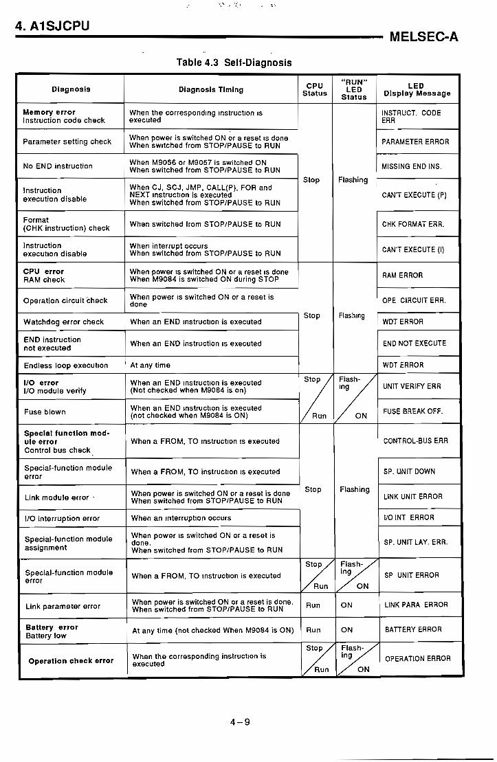
4.1.4 Selfdiagnosis
The self-diagnosis function permits the A1 SJCPU to detect its own errors.
Self-diagnosis is carried out when the PC power supply is turned ON and i f an error occurs while the PC is in the RUN state. If the A1 SJCPU detects an error, it displays an error message and stops to prevent a faulty PC operation.
The AISJCPU may operate in one of two modes when an error is detected by the self-diagnosis function. In the stop mode, the PC operation is stopped when the error is detected; in the continuous mode, the PC operation is continued. In the continuous mode, however, parameters can be set to cause the operation to stop if specified errors occur.
When an error occurs, the error occurrence and the error content are stored in specral relay (M) or special register (D). In the continuous mode, in particular, the program should read the details of the error and take appropri- ate action to prevent faulty PC and machine operations.
Operation stops and all outputs (Y) are turned immediately OFF after the self-diagnosis function detects an error which stops the PC operation. @ If the self-diagnosis function detects an error during which the PC operation continues, the part of the program where the error was detected is skipped and the rest of the program is executed.
If an I10 module verify error is detected, the operation is continued with the I10 addresses at the time the error occurred.
Explanations of the errors detected by the self-diagnosis function are given in Table 4.3.
(1) In Table 4.3, in the I10 error 110 module verify, fuse blown, special-function module error, and operation check error diagnoses, the CPU status can be selected between stop and run; and the RUN LED status between flashing and ON by using peripheral devices.
(2) The LED D~splay Message column in Table 4.3 lists messages displayed by the peripheral devices' PC d~agnosis.
4. AISJCPU MELSEC-A
Table 4.3 Self-Diagnosis
LED Display Message
INSTRUCT. CODE ERR
PARAMETER ERROR
MISSING END INS.
CAN'T EXECUTE (P)
CHK FORMAT ERR.
CAN'T EXECUTE (I)
RAM ERROR
OPE CIRCUIT ERR.
WDT ERROR
END NOT EXECUTE
WDT ERROR
Diagnosis
Memory error Instruction code check
Parameter setting check
No END instruction
lnstruction execution disable
Format (CHK instruction) check
Instruction executlon disable
CPU error RAM check
Operation circuit check
Watchdog error check
END instruction not executed
Endless loop executlon
110 error 110 module verify
Fuse blown
Special function mod- ule error Control bus check,
Speciai-function module error
Link module error -
110 interruption error
assignment
Special-functi0n error
Link parameter error
Battery error Battery low
Operation Check
7
Diagnosis Timing
When the corresponding lnstructlon IS executed
When power is switched ON or a reset IS done When sw~tched from STOPIPAUSE to RUN
When M9056 or M9057 is switched ON When switched from STOPIPAUSE to RUN
When CJ, SCJ, JMP, CALL(P), FOR and NEXT lnstructlon is executed When switched from STOPIPAUSE to RUN
When switched from STOPIPAUSE to RUN
When interrupt occurs When switched from STOPIPAUSE to RUN
When power IS switched ON or a reset IS done When M9084 is switched ON during STOP
When power IS switched ON or a reset is done
When an END lnstruct~on is executed
When an END instruction IS executed
At any time
When an END lnstruct~on is executed
CPU Status
Stop
Stop
(Not checked when M9084 is on) UNlT VERIFY ERR
When an END Instruction is executed (not checked when M9084 is ON)
FUSE BREAK OFF.
"RUN" LED
Status
Flashing
Flashlng
When a FROM, TO lnstructlon IS executed
When a FROM, TO instruct~on IS executed
When power is switched ON or a reset is done When switched from STOPIPAUSE to RUN
When an lnterruptlon occurs
When power IS switched ON or a reset is done. When switched from STOPIPAUSE to RUN
Stop
When a FROM, TO lnstruct~on is executed SP UNlT ERROR
Flashing
When power is switched ON or a reset is done. When switched from STOPIPAUSE to RUN
At any time (not checked When M9084 is ON)
CONTROL-BUS ERR
SP. UNIT DOWN
LlNK UNlT ERROR
I10 INT ERROR
SP. UNIT LAY. ERR.
When the corresponding instruction is OPERATION ERROR executed
Run
Run
ON
ON
LlNK PARA ERROR
BAlTERY ERROR

1 4. AISJCPU , MELSEC-A
4.1.5 Devices
A device is any contact, coil, or timer used In PC program operations.
A1 SJCPU devices and their range of use are shown below. The items marked "*" can be used by setting parameters for peripheral devices or by changing their range of use.
Set parameters which are compatible with the system to be used and its program. Section 4.1.6 gives details about parameter settings.
Table 4.4 Devices
A
Explanation
Provldes the PC command and data from an external device, e.g. pushbutton, select switch, limit swrtch, dlgital swltch.
Provides the program control result to an external device, e.g. solenoid, magnetic switch, signal light, dlgital display.
Redefined auxiliary relay for special purposes and for use in the PC.
Auxiliary relay in the PC which cannot be directly output.
Auxiliary relay in the PC which cannot be directly output. Backed up durlng power failure.
Used ~n the same manner as an Internal relay (M), e.g. as a relay lndlcatlng the stage number of a step-by-step process operation program.
Internal relay for data link which cannot be output. May be used as an internal relay if not set for link initral data.
Used to detect a fault. When switched ON during RUN by a fault detection program, it stores a corresponding number in special register D.
Forward trmers are available in 100 msec, 10 msec and 100 msec retentive types.
Forward counters are available in normal and Interrupt types.
Memory for storing PC data.
Predefined data memory for special purposes.
Data register for use with data link. Any range not set wlth link parameters can be used for data registers.
Extends the data register utilizing the user memory area.
Data register for storing the operation results of basic and application ~nstructions.
Used to modify devices (X, Y, M, L, B, F, T, C, D, W, R, K, H, P).
Indicates the nesting of master controls.
X
Y
M
M
L
S
B
F
T
T
T
C
D
D
W
R
A
V
N
Device
Input
- Output
Special relay
Internal relay'
Latch relay'
Step relay'
Llnk relay
Annunciator
100 msec timer'
10 rnsec timer'
100 msec retentive timer'
Counter'
Interrupt counter'
Data register
Special register
Link register
File reg,ster.
Accumulator
Index register
lndexregister
Nesting
Application Range (Number of points)
X, YO to FF (X, Y total 256 points)
M9000 to M9255 (256 polnts)
MO to M999 (1000 points)
L1000 to L2047 (1 048 points)
Can be used by setting the parameter (0)
Number of +
L + S = 2048
80 to B3FF (1024 points)
FO to F255 (256 points)
TO to TI99 (200 points)
T200 to T255 (56 points)
Can be used by setting the parameter (0 polnt)
CO to C255 (256 points)
Can be used by setting parameter. (0 point)
DO to Dl023 (1024 points)
09000 to D9255 (256 points)
WO to W3FF (1024 polnts)
Can be used by settlng the parameter (0 point)
AO, A1 (2 points)
Z (1 point)
V(1point)
NO to N7 (8 levels)

4. AISJCPU - . - . . . MELSEC-A
,
Table 4.4 Device (Continued)
I Device I Application Range (Number o f points) I Explanation I
P
I
K
\REMARK]
The step relay (S) may be used in the same manner as the internal relay (M). The step relay
is useful when writing a program which has two functions or applications, i.e., the step relay
can be used specifically In accordance w~ th the function or appl~cat~on, ~ndependently of the
internal relay.
Polnter
Po~nter for interrupt~on
~ ~ ~ ~ d ~ ~ i ~ ~ l constant
Decimal constant
PO to P255 (256 points)
10 to 131 (32 points)
L
HO to FFFF (16-bit ~nstruction)
HO to FFFFFFFF (32-bit instruction)
Indicates the destlnat~on of the branch lnstructlon (CJ, SCJ, CALL, JMP).
Indicates the destination of an interrupt program corresponding to the interrupt factor which has occurred
K-32768 to 32767 (1 6-bit instruction)
K-2147483648 to 21 47483647 (32-bit instruction)
Used to specify the bas~c and application instruct~on Values.
Used to specify the timerlcounter set value, pointer number, Interrupt pointer number, the number of b ~ t dev~ce d~glts, and basic and application instruct~on values.

4. AISJCPU MELSEC-A
-._ . 4.1.6 Parameter setting ranges
Parameter setting involves specifying various PC functions and device ranges I
as well as assigning the user memory (32 K bytes). The set data is stored in I
the parameter memory area. i
As shown in Table 4.5, default values-can be used as set in parameter data. Setting ranges shown here can be changed depending on their purpose. Parameters are set with peripheral devices.
1
The operating manual of each peripheral device gives details parameter settings.
Table 4.5 Parameter Setting Ranges I
Main sequence program area
File register capacity
Comment capacity
Default Value
6K steps
Absent
Absent
Absent
Absent
Absent
Only for LlOOO to L2047.
Absent for others.
Absent
Absent
Status latch
trace
Memory capacity
Data memory
File register
Memory capacity
Device setting
Execution condition
Sampling count
Setting Range
' 1 to 8K steps (in unrts of 1 K steps)
1 to 4K points (in units of 1 K points)
0 to 1600 points (in units of 64 points)
018 to 16K bytes
Absentlpresent
Absentl resent (2 to 8fbytes)
018K bytes
Device number
Per scan I Per time
0 to 1024 times (in units of 129 trmes)
, (in %s'tr??l;es)
BO to B3FF (in units of 1 point)
TO to T255 (in units of 1 point)
*
CO to C255 (in units of 1 point)
. DO to Dl023
(in units of 1 point)
WO to W3FF (in units of 1 point)
1 to 64
XO to XFF (in units of 16 points)
YO to YFF (in units of 16 points)
BO to B3FF (in units of 16 points)
WO to W3FF (in units of 1 point)
X N O to XNIFF (in units of 16 polnts)
Microcomputer program capacity
Valid
Setting of latch (power failure compensation) range
Setting of link range
Peripheral Devices
PU
o
o
-
-
-
-
o
-
-
Link relay (B)
Timer (T)
counter (c)
Data register (D)
Link register (W)
Number of link stations
Input (X)
Output (Y)
Link relay (B)
Link register (W)
GPP
o
o
o
o
0
o
0
0
0 I10 assignment

4. AISJCPU
>. ., + .'. ' > '
MELSEC-A
Table 4.5 Parameter Setting Ranges (Continued)
&
Default Value Setting Range
MlUS 0 to 2047 (M, L, S are serial numbers)
10 msec to 2000 msec (in units of 10 msec) \
256 points of 100 msec, 10 msec, and integrating timers (in units of 8 points) Timers have serial numbers.
256 points (in units of 8 points) for counters and interrupt counters Must be consecuttve numbers
XO to XFF 1 point for each of RUN and PAUSE contacts. Setting of only PAUSE contact cannot be done
Stop/continuation
Output before STOP or after operation execution
Up to 128 characters
Max. 6 digits in hexadecimal (0 to 9, A to F)
MO to M999 LlOOO to L2047
Absent for,S
200 msec
100 msec: TO to TI99
10 msec: T200 to T255
Not provided for interrupt counter
Absent
Cont~nuat~on
Stop
c~~~~~~~~~~~
Stop
Operation status prior to STOP IS
re-output
Absent
Absent
Setting of internal relay (M) latch relay (L) step relay (S) setting
Watchdog timer setting
Setting of timer
Setting of counter
Setting of remote RUNIPAUSE contact
Valid
Operation at the
time of error
Peripheral Devices
PU
o
0
0
-
-
-
-
-
o
Fuse blown
110 verify error
Operation error
Special funct~on unit check error
GPP
o
0
0
o
o
o
0
o
o
STOP 4 RUN display mode
Print title entry
Keyword entry

4. AISJCPU MELSEC-A
4.1.7 Memory capacity settings (main programs, file registers, comments, etc.)
The AISJCPU provides 32K bytes of user memory area (RAM). Data for parameters, TIC set values, main programs, sampling trace, status latch, file registers, and comments can be stored in the user memory area.
(1) Calculating memory capacity
The-user-memory area should-be- utilized after setting parameters to determine the type of data to be stored and the memory capacity. Calculate the memory capacity according to Table 4.6.
Table 4.6 Parameter Settings and Memory Capacity
(2) How to store user memory i
All data set by parameters is stored in the following sequence. When the memory protect switch is turned ON, 20K bytes (beginning with the head address) is memory-protected. Make sure that the sampling trace area and the file register areas are not within this 20K byte memory-protected range.
(a) The parameter area, T/C setting area, and main program area are stored in order from the head address of the user memory.
Setting Unit
-
I K steps
2K bytes
Not availablel available
Not available1 available
Not ava~lablel available
points
64 points
Memory Capacity
4K bytes (f~xed)
(Main sequence program capacity) x 2K bytes
(Main microcomputer program capacity) x 1 K byte
018K bytes
018K bytes
(F~le registers' memory capacity) 1 K byte
(File registers' number of points) x 2K bytes
(Number of comments) + 1 K byte
64
I tem
(b) Comments, file registers, status latch, and sampling trace'are stored in order from the last address of the user memory.
Main program
o % ~ M
Possible
impossible
Parameter, TIC set values
Sequence program
Microcomputer program a
Remark
Occupies 4K bytes for parameters and TIC set values
The memory capacity for the file register status latch 1s determined by the number of file register points set using parameters.
1 K byte is occupied by the system when setting comments capacity. .
Sampling trace
Status latch
Data memory
File registers
File registers
Comments

4. AISJCPU j , - / - MELSEC-A
Parameter area
TIC set values area
Main program area
Sampllng trace area
Fig. 4.3 User Memory Assignments
Memory- I protect possible (20K bytes)
Status latch area
POINTI Even if parameters or the main sequence program are stored in ROM, the memory capacity of the sampling trace, status latch, file registers, and comments cannot be increased.
Data area
. File registers
4K bytes
2 to 16K bytes (1 to 8K bytes)
File reg~ster area
Comment area
12 to 26K bytes
User memory area 32K bytes

4. AISJCPU MELSEC-A
4.2 Functions
The following table describes the functions of the AISJCPU. The ACPU programming manual (Fundamentals) gives details.
Table 4.7 List of Functions
The AlSJCPU cannot do 'step operation', "PAUSE using RUNISTOP key switch', and "110 module replacement at online'.
Function
Constant scan
Latch (power failure compensation)
Remote RUNISTOP
PAUSE
Status latch
Sampling trace
Offline switch
Priority setting ER- ROR LED
Clock
Description
Executes the sequence program at the predetermined intervals independently of the scan tlme.
Setting allowed between 10 and 2000 msec.
Retains device data if the PC IS switched OFF or reset or a momentary power failure of 20 msec or longer occurs.
L, B, T, C, D and W can be latched
Allows remote RUNISTOP from external device (e.g. perrpheral, external input, computer) wlth the RUNISTOP switch in RUN position.
Stops operation with the output (Y) status retained.
Pause function may be switched ON by any of the following ways:
Remote PAUSE contact
Peripheral device
Stores all device data in the status latch area in the A1S when the status latch condition is switched ON.
The stored data can be monitored by the peripheral device.
Samples the specified device operating status at predetermined intervals and stores the sampling result in the sampling trace area in the A1 S.
The stored data can be monitored by the peripheral device.
Allows the device (Y, M, L, S, F, 8) used with the OUT instruction to be disconnected from the sequence program operation processing.
Sets ONIOFF of the ERROR LED in case of an error .
Execute clock operation in the CPU module.
Clock data includes the year, month, day, hour, minute, second, and day of the week.
Clock data can be read from special registers D9025 to D9028.

4. AISJCPU , . MELSEC-A
4.3 Handling Instructions
This section gives handling instructions from unpacking to installation of the AISJCPU, I10 modules and extension base unit, etc.
(1) Since the case, terminal block connector, and pin connector of the unit are made of plas6c, do not drop them or subject them to mechanical shock.
(2) Do not remove the printed circuit board of any unit from its case Removal may cause board damage.
(3) When wiring, take care to prevent entry of wire offcuts into the unit. If any conductive debris enters the unit, make sure that it is removed.
(4) Tighten the un~ t mounting screws and terminal screws as indicated below.
Screw
Unit mounting screw (M4 screw)
110 module terminal block terminal screw (M3.5 screw)
Power supply module terminal block term~nal screw (M3.5 screw)
Tightening Torque Range N-crn (Kgocm) [Ib-inch]
78.4(8)[6.93] to 1 17.6(12)[10.39]
58.8(6)[5.2] to 88.2(9)[7.79]
58.8(6)[5.2] to 78.4(8)[6.93]

4. AISJCPU MELSEC-A
4.4 Names and Purposes of Parts and Settings
The names and purposes of parts of the AISJCPU and the switch settings necessary for operating the A1 SJCPU are explained below.
4.4.1 Names of parts of A1 SJCPU
(1) Name of parts of AISJCPU
(9)
~ I f " d a
(8)
- + i
L I
o
I (5) (6) (7)
No.
(1)
(2)
(3)
(4)
(5)
(6)
(7)
(8)
(9)
- n n
Name
Base mountlng hole
Power input terminal
LG terminal
FG terminal
DIN rail hook
RS-422 connector cover
Module connector
Extension cable connector
Base cover
- r O n l
Purpose
Used to mount the base unlt to a control panel. (for M5 screw)
Used to connect to 100 VAC or 200 VAC power supply.
Used to ground the power supply filter. Provided with a potential half the input voltage.
Ground terminal connected to the shield pattern on the PC board.
Used to install the module to the DIN rail. (2 hooks)
Cover for the RS-422 connector
Used to connect to an 110 module or special function module. Put a supplied cover or blank cover (A1 SG6O) on unused connector to protect it from dust.
Used to connect an extension cable to an extension base unit for signal transmissions.
Extension cable connector protective cover. Remove this cover surrounded by grooves below the 'OUT' ind~cation by using a removing tool.
l o o +

4. AISJCPU . - MELSEC-A
L
No.
(10)
. (1 1)
(12)
(13)
(14)
(15)
Name
Module mounting screw
RUN / STOP switch
. RESET switch
POWER LED
RUN LED
ERROR LED
purpose
Used to secure the module to the base. M4 x 12 screw
RUN I STOP: Used to run or stop the sequence program operation. L.CLR (LATCH CLEAR):Used to clear (OFF or 0 ) data in the latch area
designated by parameter setting. (Data in other than the latch area are also cleared by LATCH CLEAR:pSee Section 4.4.4 for the latch clear operation.
Used to perform hardware reset. Used when& operation error occurs and to initialize the operation.
Used to ind~cate the 5 VDC power supply.
Lit: Indicates the execution of sequence program with the RUNISTOP switch set in the RUN position. (When an error which does not cause the sequence program execution to stop occurs (see Section 10.3), this LED remains lit.)
Unlit: The RUN LED does not light in the following cases: The 1001200 VAC power is not supplied to the AlSJCPU. The RUN/STOP switch is set in the STOP position. Remote STOP is executed. Remote PAUSE is executed.
Flash: The RUN LED flashes in the following cases: An error to stop the sequence program execution is detected by the self-diagnosis check. Latch clear is executed.
Lit: A self-diagnosis error is detected. (When an error which has been set for 'unlit' with the LED indication priority setting is detected, this LED remains unlit.)
Unlit: The operation is normal, or when an error is detected by a CHK instruction execution.
Flash: Annunciator (F) is turned ON by the sequence program.

4. AISJCPU MELSEC-A
I
. .
(21) (20)
\ A
0 0 8 0
rrB \ 7
/
. ..
No.
(16)
(1 7)
(18)
(19)
(20)
(21)
Name
Memory cassette connector
RS-422 connector
Battery
Cover
Battery connector
DIP switch
Purpose
Used to install a memory cassette (AlSMCA8KP/[ IKE).
Used to connect a peripheral device to perform reading and writing of main programs, monitoring, and tests. Put a cover when a peripheral device is not connected.
Used to backup the retention of data such as programs, latch range devices, and file registers. (see Section 8.2 for the battery installation)
Used to protect the PC board, memory cassette, RS-422 connector, and battery of the A1 SJCPU.
Used to connect to the connector on the battery.
Used to set the 110 control method and memory protect function. (see Section 4.4.2 and 4.4.3 for-details)

4. AISJCPU
. , .- , . MELSEC-A 1 .
(2) Name of parts of AISJCPU-S3
-
(5)
(6) (7)
Purpose
Used to mount the base unit to a control panel. (for M5 screw)
Used to connect to 100 VAC or 200 VAC power supply.
Used to ground the power supply filter. Provided with a potential half the input voltage.
Ground terminal connected to the sh~eld pattern on the PC board.
Used to install the module to the DIN rail. (2 hooks)
Cover for the RS-422 connector
Used to connect to an I/O module or special function module. Put a supplied cover or blank cover (A1 SG6O) on unused connector to protect i t from dust.
Used to connect an extension cable to an extension base unit for signal transmissions.
Extension cable connector protective cover. Remove this cover surrounded by grooves below the 'OUT' ind~cation by using a removing tool.
No.
(1)
(2)
(3)
(4)
Name
Base mounting hole
Power input terminal
LG terminal
FG terminal
(5) DIN rail hook -
(6) RS-422 connector cover
(7) Module connector
(8) Extension cable connector
(9) Base cover
.

4. AISJCPU MELSECA
No.
(10)
(1 1)
(12)
(13)
(14)
Name
Module mounting screw
RUN I STOP switch
POWER LED
RUN LED
ERROR LED
Purpose
Used to secure the module to the base. M4 x 12 screw
RUN I STOP: Used to run or stop the sequence program operation.
L.CLR (LATCH CLEAR):Used to clear (OFF or 0) data in the latch area designated by parameter setting. (Data in other than the latch area are also cleared by LATCH CLEAR.) See Section 4.4.4 for the latch clear operation.
RESET: Used to perform hardware reset. Used when an operation error occurs and to init~alize the operation.
Used to indicate the 5 VDC power supply.
Lit: Indicates the execution of sequence program with the RUNISTOP switch set in the RUN position. (When an error which does not cause the sequence program execution to stop occurs (see Section 10.3), this LED remains lit.)
Unlit: The RUN LED does not light in the following cases: The 1001200 VAC power is not supplied to the AlSJCPU-S3. The RUNISTOP switch is set in the STOP position. Remote STOP is executed. Remote PAUSE is executed.
Flash: The RUN LED flashes in the following cases: An error to stop the sequence program execution is detected by the self-diagnosis check. Latch clear is executed.
Lit: A self-diagnosis error is detected. (When an error which has been set for 'unlit' with the LED indication priority setting is detected, this LED remains unlit.)
Unlit: The operation is normal, or when an error is detected by a CHK instruction execution.
Flash: Annunciator (F) is turned ON by the sequence program.

4. AISJCPU , MELSEC-A
MELSEC A t h
I I (15) (16)
No.
(15)
(16)
(17)
(18)
(19)
(20)
Name
Memory cassette connector
RS-422 connector
Battery
Cover
Battery connector
DIPsw~tch
Purpose
Used to install a memory cassette (AlSMCA-8KPI[]KE).
Used to connect a peripheral device to perform reading and writing of main programs, monitoring, and tests. Put a cover when a peripheral device is not connected.
Used to backup the retention of data such as programs, latch range devices, and file registers. (see Section 8.2 for the battery installation)
Used to protect the PC board, memory cassette, RS-422 connector, and battery of the AlSJCPU-S3.
Used to connect to the connector on the battery.
Used to set the 110 control method and memory protect function. (see Section 4.4.2 and 4.4.3 for details)

4. A1 SCPU MELSEC-A
4.4.2 110 control switch setting
The I10 control system uses either a direct or a refresh mode. Use the dip switch (SW2-1) to switch the I10 control mode.
When shipment from the factory, both inputs and outputs are set for direct mode (SW2-1: ON).
Controls both inputs and outputs in the di- Controls both inputs and outputs in the re- rect mode fresh mode
..
POINT I Make sure that the power is OFF when the 110 control mode is switched.
4.4.3 Memory protect switch setting
The memory protect switch is used for protecting RAM memory data from being overwritten by a peripheral device malfunction. (When the CPU in- stalled with a memory cassette is operated using ROM or E*PROM, the memory switch setting will be invalid.) Use the DIP switch (SW2-2) to switch the memory protect setting.
This memory protect function protects the first 20K bytes of the user memory area (32K bytes).
The function prevents overwriting and deleting the program once it has been written. When the contents of RAM memory are changed, make sure that the memory protect switch is OFF.
When shipment from the factory, the memory protect function is turned OFF (SW2-2: OFF). 0
POINT]
Do not use the memory protect function when either a sampling trace or a status latch is executed. If the protect function i s used, the data cannot be stored to memory.
Memory protect switch is ON. Memory protect switch is OFF.

4. AISCPU MELSEC-A
4.4.4 Latch clear
Follow the procedures mentioned below to execute latch clear by using the RUNISTOP switch. Devices outside the latch range are also cleared by the latch clear operation.
(1) Operating procedure for latch clear
[RUNISTOP keyswitch] I RUN LED ]
(1) "STOP" position 0 Unlit : Before latch clear operation
(2) Turn several times from L//- High-speed flickering : "STOP" to "L.CLR" position ' ' Ready for latch clear
(approx. 0.2 s ON, + O.* OFF)
(3) Turn once more from 0 Unlit : Latch clear completed "STOP" to "L.CLR1' position
(2) Canceling latch clear part way through
Latch clear can be canceled part way through by using either of the methods (a) and (b) below.
(a) Turn the RUNISTOP keyswitch to "RUN" to set the AlSJCPU to the RUN status.
(b) Turn the RUNISTOP keyswitch to the RESET position to reset the AISJCPU. (Or, press the RESET switch to reset the A1SJCPU.J
piiiiiq It is possible to perform latch clear by uslng the GPP function operation.
For example, when an AGGPP is used, latch clear can be done by using the 'Dev~ce Memory All Clear' of the test function in PC mode
See the GPP function operating manual for the operation procedure.

MEMO

5. POWER SUPPLY MODULE M ELSEC-A
5. POWER SUPPLY MOD~JLE
5.1 Specifications
Table 5.1 shows the specifications of power supply modules.
Table 5.1 Power SUDD~V Module S~ecifications
Base loadlng slot
Rated Input voltage
Rated input frequency
Power supply module loadlng slot
Speclflcatlons
100 to 120/ 100 to 1201 200 to 240 VAC 200 to 240 VAC 200 to 240 VAC
200- 240 VAC +lo%/-1 5% +lo%/-15% +10%1-15% +lo%/-15%
AlS61PEU '4
Max. input apparent power 120 A wrthtn 8 ms 181 A wlthln 1 ms
AlS61P I A1S62PEU '4 I AlS62P I A1 S63P
Inrush current
Overcurrent protection '1
Overvoltage protectlon '2
Rated output current
I~l lowable momentary ~ower failure tlme '3 lwlthln 20 ms ( ~ ~ t h l n 1 rns I
41 W
5 A
- 5 VDC
24 V D C f 1 0%
105 VA
,' 24 VDC
24 VDC
Eff~ciency
-
Applicable wlre slze
Applicable tlghtenlg torque
External dimension mm (lnch)
We~ght kg (Ib)
-- -
'1 : Overcurrent protection
The overcurrent protection dev~ce shuts off the 5 V, 24 VDC circuit and stops the system if
the current flowing in the circuit exceeds the specified value. When this device is activated,
the power supply module LED 1s switched OFF or dimly lit. If this happens, ellminate the
5 A
-
65% or h~gher
Insulation wlthstand voltage
cause of the overcurrent and start up the system again.
3 A
0 6 A
5.5 A or h~gher
-
VAC
-
Between prlmary -and VDC
Between prlmary and 24 VDC
AWG16 to 22
83 to 113 N.cm (8.5 to 11.5 kg.cm) [7.4 to 10.1 Ib Inch]
130 x 55.94 (5 12 x 2.17 x 3 70)
' 2 ' Overvoltage protection
The overvoltage protectlon device shuts off the 5 VDC circuit and stops the system if a
voltage of 5.5 to 6.5 V IS applied to the circu~t When this dev~ce is activated, the
power supply module LED is sw~tched OFF. If this happens, switch the lnput power OFF,
then ON to restart the system. The power supply module must be changed if the
system is not booted and the LED remains OFF.
Noise ~rnmunlty
Power ~nd~cat~on
Term~nal crew slze
3.3 A or h~gher
0.66 A or h~gher
IEC801-4.2 kV
Power LED rnd~cat~on
M3.5 x 7
0.53 (1.17)
5.5 A or h~gher
-
5.5 to 6.5 V
500 VAC
-
1 500 VAC
-
I
0.55 (1.21) 0.5 (1.1) 0.53 (1 17)
7 -
1780 VAC
1780 VAC
0.55 (1.21)
-
1500 VAC
1500 VAC

5. POWER SUPPLY MODULE MELSEC-A
'3: Allowable momentary power tnterruption time This value Indicates the momentary power interruption time allowed for the PC CPU and
varies according to the power supply module used with the PC CPU module. The allow -able momentary power interruptton tlme for a system in which an A1 S63P is used is defined as starting when the primary power supply of the 24 VDC stabilized power supply of the AlS63P is turned OFF and lasttng untll the 24 VDC becomes less than the specifled voltage (15 6 VDC).
'4:AlS61PEU and AlS62PEU comply with EN61010-1 and safety aspects of IEC 1131-2 to meet the Low Voltage Directive which will be mandatory from the 1st of January 1997.
5.1.1 Selection of a power supply module
Select a power supply module by considering the total current consumption of the I10 modules, special function modules and peripheral devices to be supplied with power by the module. In addition, if using an A1S52B (Sl), AlS55B(Sl), AIS58B(S1), A52B, A550, or A58B extension base unit, note that this unit will also draw its power from the power supply module on the main base unit, and this must also be taken into consideration.
For details on the 5 VDC current consumption of I10 modules, special function modules and peripheral devices, refer to Section 2.3.
(1) Selection of a power supply module when using AIS52B(S1), A1 S55B(S1), AIS58B(Sl), A52B, A55B, A58B extension base units When using AlS52B(S1), AlS55B(S1), AlS58B(S1), A52B, A55B, A58B extension base units, the 5 VDC power supply is taken from the main base unit via the extension cable. Accordingly, the following cautions must be observed when using one of these extension base units.
CPU Power supply module
-
-
-
-
For example, if an AD71 TU is con- nected to an AlSD71-S2, the current consumption of the AD71TU must also be taken into account.
I10 module AlSX10, AlSY10, etc.
Special funct~on modules AlSD61, AlSD71-S2 etc.
Peripheral device AD71TU
Peripheral devices, AGWU, etc.
Also consider the current consump- ton of peripheral devices connected to special function modules when making the selection.

5. POWER SUPPLY MODULE " . . . \ * > , M ELSEC-A
(a) Make sure that the 5 VDC capacity of the selected power supply module on the main base unit will cover the 5 VDC current consump- tion of the AlS52B(S1), AlS55B(S1), AlS58(S1), A52B, A55B, or A58B.
[Example] Assume that the 5 VDC current consumption at the main base unit is 3 A, .and the 5 VDC current consumption at the A1 S55B(S1) is 1 A:Since the capacity of the power supply mod- ule on the mairi base unit (3 VDC, 3A) is exceeded, it is necessary to establish a separate power supply using an AlS65B(S1) or A1 S68B(S1).
(b) Since power is supplied to the AlS52B(S1), AlS55B(S1), AlS58B(Sl), A52B, A55B, and A58B through an extension cable, there is some voltage drop. The power supply module and cable length must be selected to ensure that at least 4.75 VDC reaches the receiving terminals.
(c) For details on voltage drop and other topics, see Section 6.1.3 extension base unit.

5. POWER SUPPLY MODULE M ELSEC-A
5.2 Names and Purposes of Parts and Settings
The names and purposes of parts of the power supply module are described below.
(2)
(3) (3)
(4) (4)
(5) (5)
(6) (6)
(9) (9)
No.
(1)
(2)
(3)
(4)
Name
POWER LED
24 VDC and DC24G terminals
FG terminal
Operating "Itage switching terminals
I
Purpose
Used to indicate the 5 VDC power supply.
Used to supply the 24 VDC power to the output module as the internal power supply. ,
(supplied by an external wire)
Grounding terminal connected to the shield pattern on the PC board.
Used to switch the input voltage. Connect these terminals with a shorting strip when a 100 VAC power IS supplied. Leave these terminals open when a 200 VAC power is supplied.
<Setting when a 100 VAC power is supplied>
Connect these terminals with a shorting strip (supplied with the module).

5. POWER SUPPLY MODULE MELSEC-A
(3)
(5)
(9)
Purpose
Used to ground the power supply f~lter. Prov~ded with a potential half the input voltage.
Used to connect to 100 or 200 VAC power supply.
Used to connect to 200 to 240 VAC power supply.
Used to connect to a 24 VDC power supply.
M3.5 x 7
Used to protect the terminal block
Used to secure the module to ihe base un~t.
I
No.
(5)
(6)
(7)
(8)
(9)
(10)
:
Name
LG terminal
Power input terminal
Power input terminal
Power input terminal
Terminal screw
Terminal cover
Module mounting screw
POINT~
If the power supply voltage setting is different from actual power supply voltage, the following problem will occur.
Power Supply Voltage
200 VAC
The power supply module will be destroyed. (The CPU will not cause problem.)
100 VAC
Setting for 100 VAC (the operating voltage switch- ing termlnals are shorted)
Setting for 200 VAC (the operating voltage switch- ing terminals are open)
The power supply module will not cause problem The CPU will not operate.
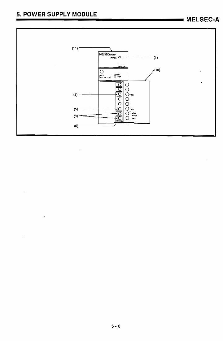
5. POWER SUPPLY MODULE MELSEC-A

5.110 MODULES I a MELSEC-A
(7) The common current of an A1 SY60 varies according to ambient tempera- ture. Select a common current referring to the chart shown below.
4 N l common Ta = 3.6P.11 common 1 Ta = 45°C
3.2Af1 common Ta = 55°C
10 20 30 40 50 55 ("C) Ambient temperature
(8) The A1SX41 and A1SX42 input modules and the A1 SY41 and A1 SY42 output modules are supplied with soldering-type 40-pin connectors. The 40-pin connectors of pressure-displacement type and crimp contact type are also available. Tools for the pressure-displacement and crimp con- tact type connectors must be procured from the following suppliers:
(a) Soldering-type 40-pin connector
Model name : A6CON1
(b) Crimp-contact-type 40-pin connector
Model name : A6CON2
Tool : Fujitsu FCN-363-T005IH
Applicable wire size : AWG #24 to 28
(c) Pressure-displacement-type 40-pin connector
Model name : A6CON3
Tool : Fujitsu FCN-367T-T012lH (locator plate) FCN-707T-T0011H (cable cutter) FCN-707T-TI 0I /H (hand press)
Applicable wire size : AWG #28 (twisted) AWG #30 (single wire)
5.110 MODULES MELSEC-A
(d) Supplier's offices:
Fujitsu Limited
North and South America:
Fujitsu Component of America, Inc. 3545 North First Street, San Jose, CA 95134-1804 U.S.A. Phone: (408) 922-9000 Telex: (91 0) 338-01 90 Fax: (408) 428-0640
Europe:
Fujitsu Microelectronik GmbH
Am Siebestein 6-10 6072, Dreieich-Buchschtag, F.R. Germany Phone: (061) 03-690-0 Telex: 41 1963 Fax: (061) 03-690-1 22
Asia:
Fujitsu Microelectronics Asia PTE, Limited #06-04 to #06-07 Plaza, By The Park, No.51 Bras Basah Road, Singapore 071 9 Phone: 336-1 600 Telex: 55573 Fax: 336-1 609

5. INPUT AND OUTPUT MODULE MELSEC-A
5.2 lnput Module Specifications
5.2.1 A1SX10 AC input module
Appearance'
AC lnput Module
Number of input points
Insulation method Rated ~nput-voltage
Rated input current
Operat~ng voltage range
- Max..sirnultaneous.input points
Inrush current
ON voltage1ON current
OFF voltage/OFF current
Input impedance
R~~~~~~~ OFF + ON time ON -, OFF
Common term~nal arrangement Operating ~nd~cator
External connecttons
Applicable wlre sue
crimp
Accessories
lnsulat~on withstand voltage
No~se immunity
Internal current consurnptlon (5 VDC)
Weight kg (Ib)
AlSX10 16 po~nts Photocoupler
100 to 120 VAC- 50160 Hz
Approx. 6 mA (100 VAC 60 Hz)
85 to 132 VAC (50160 Hz *5%)
100% simultaneously ON (at 11 0 VAC) 60% simultaneously ON (at 132 VAC)
Max. 200 mA, with~n 1 rns (132 VAC)
80 VAC or higher15 mA or h~gher
30 VAC or lower11 mA or lower
Approx 18 kR (60 Hz), Approx. 21 kQ (50 Hz)
20 ms or less (1 00 VAC 60 Hz)
35 rns or less (100 VAC 60 Hz)
16 pointslcommon (common terminals: TB9. TB18)
ON state is ~ndicated (LEDs) 20-point terminal block connector (M3.5 x 7 screws)
0 75 to 1.5 rnm2
1.25-3 5 1.25-YS3A 2-3.5 2-YS3A V1.25-M3 V1.25-YS3A V2-S3 V2-YS3A
None
1500 VAC
1000 VAC
50 mA (TYP, all polnts ON)
0.21 (0 46)
External Connections
Terminal No. TB1
TB2
TS3
TB4
TB5
TS6
TB7
TB8
Signal Name ,
XOO
XO 1
X02
X03
X04
X05
X06
X07
TSlO TB l 1
TB12 TB13
TS14
TB15 TB16
TS17 TB18
TB19
TS20
X08 X09
XOA XOS
XOC
XO D XO E
XOF COM
Vacant Vacant

5. INPUT AND OUTPUT MODULE MELSEC-A
5.2.2 A1 SX1OEU AC input module
Number of input points
Insulation method
Rated input voltage
Rated input current
Operating voltage range Max. simultaneous input points
Inrush current
ON voltagelON current
OFF voltagelOFF current
Input impedance
AC lnput Module
A lSX l OEU 16 points
Photocoupler
100 to 120 VAC 50160 Hz
Approx. 7 mA (1 20 VAC 60 Hz) 85 to 132 VAC (50160 Hz i5%)
simultaneously ON
Max. 200 mA, within 1 ms (132 VAC)
80 VAC or h1gherl5 mA or higher
30 VAC or lower11 mA or lower
Approx. 18 kn (60 Hz), Approx. 21 kR (50 Hz) 20 ms or less (100 VAC 60 Hz)
35 ms or less (100 VAC 60 Hz)
16 pointslcommon (common terminals: TB9, TB18)
ON state IS indicated (LEDs)
20-point terminal block connector (M3.5 x 7 screws)
0.75 to 1.5 mm2 (AWG15 to AWG19) RAV1.25-3.5
None
1780 VAC
1000 VAC
50 mA (TYP, all points ON)
0.21 (0.46)
External Connections
R~~~~~~~ time
Appearance
OFF 4 ON
ON OFF
Internal circuit
Common terminal arrangement
Operating indicator
External connections
Applicable wire size Appl~cable crimp terminals
Accessories Insulation withstand voltage
Noise immunity Internal current consumption (5 VDC)
Weight kg (Ib)
Terminal No. TB1
TB2
TB3
TB4
TB5
TB6
TB7
TB8
TB9
TBIO
T B l l
TB12
TB13
TB14
TB15 TB16
TB17
TB l8
TB19
TB20
Signal Name XOO
XO 1
X02
X03
X04
X05
X06
X07
COM
X08
X09
XO A
XOB
XOC
XOD XOE XOF
COM
Vacant
Vacant
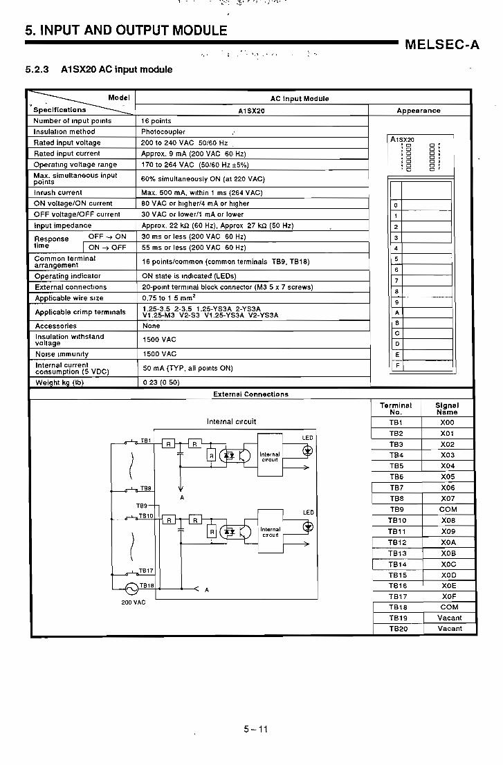
5, INPUT AND OUTPUT MODULE , ,.
a, ' , . , . " . . MELSEC-A
5.2.3 A1SX20 AC input module
AC Input Module
A1 SX2O Appearance Number of lnput polnts 16 points
lnsulat~on method Photocoupler
Rated input voltage 200 to 240 VAC 50160 Hz .
Rated input current Approx. 9 mA (200 VAC 60 Hz)
Operating voltage range 170 to 264 VAC (50160 Hz *5%)
Approx. 22 M (60 Hz). Approx 27 k(2 (50 Hz)
Internal c~rcuit

5. INPUT AND OUTPUT MODULE MELSEC-A
5.2.4 AlSX20EU AC input module
Number of input points
Insulation method
Rated input voltage Rated input current
Operating voltage range
simultaneous input points Inrush current ON voltagelON current
OFF voltagelOFF current
Input impedance
AC lnput Module
AlSX2OEU 16 potnts
Photocoupler
200 to 240 VAC 50160 Hz
Approx 11 mA (240 VAC 60 Hz)
170 to 264 VAC (50160 Hz *5%)
60% simultaneously ON (at 220 VAC)
Max. 500 mA, within 1 ms (264 VAC) 80 VAC or higher14 mA or higher 30 VAC or lower11 mA or lower
Approx. 22 kn (60 Hz), Approx. 27 kR (50 Hz) 30 ms or less (200 VAC 60 HZ)
55 ms or less (200 VAC 60 Hz)
16 pointslcommon (common term~nals: TB9, TB18)
ON state is indicated (LEDs) 20-point terminal block connector (M3.5 x 7 screws)
0.75 to 1 .5 mm2 (AWGIS to A W G ~ ~ )
RAV1.25-3.5
None
2830 VAC
1000 VAC
50 mA (PIP, all po~nts ON)
0.23 (0.50)
External Connections
Response time
Appearance
OFF -t ON
ON + OFF
Internal circuit
Common terminal arrangement
Operating indicator
External connections
Applicable wire size
Applicable crimp terminals
Accessories
Insulation withstand voltage
Noise immunity Internal current consumpt~on (5 VDC)
Weight kg (Ib)
Terminal No. TB 1
TB2
TB3
TB4
TB5 TB6
TB7
TB8
TB9
TBlO
TB l 1
TB12
TB13
TB14
TB15
TB16 TB17
TB18 TB19
TB20
Signal Name XOO
XO 1
X02
X03
X04 X05
X06
X07
COM
X08
X09
XO A
XOB
XOC
XO D XOE XOF
COM Vacant
Vacant

5. INPUT AND OUTPUT MODULE ,
MELSEC-A t I
- >@.., < . * %..* . , , y < :
5.2.5 A1SX30 DCIAC input module
Number of input potnts
lnsulat~on method
Rated lnput voltage Rated lnput current .
Operating voltage range
Max. simultaneous input points ON voltagelON current OFF voltagelOFF current
Input impedance .
DCIAC lnput Module
Response time
OFF -, ON
ON -, OFF
arrangement 16 po~nts/common (common termtnals' TB9, TB18)
Appearance A1 SX3O 16 po~nts
Photocoupler
12/24 VDC 1 12/24 VAC 50160 Hz 4.2 mA (12 VDCIVAC), 8 6 mA (24 VDCIVAC)
Operating Indicator External connections
Appl~cable wire size
Applicable crimp terminals
Accessor~es
lnsulat~on withstand voltage Nose immunity
Internal current consumptton (5 VDC)
Weight kg (Ib)
1 0 2 t o 2 6 4 V D C (rlpple: less than 5%)
1 0 2 t o 2 6 4 V A C (50160 Hz *5%)
ON state is indicated (LEDs) 20-point terminal block connector (M3.5 x 7 screws)
0.75 to 1.5 mm2
1.25-3.5 1.25-YS3A 2-3.5 2-YS3A V1.25-M3 V1.25-YS3A V2-S3 V2-YS3A
None
500 VAC
1500 VAC
50 mA (TYP, all points ON)
0.2 (0 44) -- -
75% simultaneously ON -
7 VDCIAC or higher12 mA or higher
2.7 VDCIAC or lowerl0.7 mA or lower
Approx. 2.7 kR
Signal Name
XOO
XO 1
X02 X03
X04
X05
X06
X07
COM
X08
X09
XO A
XOB
XOC
XO D
XO E XO F COM
Vacant
Vacant
External Connections
'
20 ms or less (12124 VDC )
20 ms or less (12124 VDC )
TecnaI TBI
TB2
TB3
TB4
TB5
TB6
TB7
TB8
TB9
TBIO
T B l l TB12
TB13
TB14
TB15
TB16
TB17 TB18 TB19
TB20
25 ms or less (12124 VAC 60Hz)
20 ms or less (12124 VAC 60Hz)

5. INPUT AND OUTPUT MODULES MELSEC-A
5.2.6 A1SX40 DC input module (sink type)
.
Appearance
DC lnput Module (Sink Type)
AlSX40 16 points
Photocoupler
12 VDC ( 24 VDC Approx. 3 mA I Approx 7 mA
10.2 to 26.4 VDC (ripple: less than 5%)
100% simultaneously ON (at 26.4 VDC)
8 VDC or htgherl2 mA or higher
4 VDC or lower11 mA or lower
Approx. 3.3 kn 10 ms or less (24 VDC)
10 ms or less (24 VDC)
16 pointslcommon (common terminals: TB9, TB18)
ON state is indicated (LEDs)
20-point terminal block connector (M3.5 x 7 screws)
0.75 to 1.5 mm2
1.25-3 .5 1 -25-YS3A 2-3.5 2-YS3A V1.25-M3 V1.25-YS3A V2-S3 V2-YS3A None
500 VAC
500 VAC
50 mA ( N P , all points ON)
0.2(0.44)
External Connections
Number of input points
Insulation method
Rated input voltage
Rated input current
Operating voltage range
Max. simultaneous input points
ON voltagelON current
OFF voltage1OFF current
Input impedance
Terminal No. TB 1
TB2
TB3
TB4
TB5
TB6
TB7
TB8 TB9
TBlO
TBl 1 TB12
TB13
TB14
TB15
TB16
TB17
TB18 TB19 TB20
R~~~~~~~ t~me
Slgnal Name XOO
XO1
X02
X03
X04
X05
X06
X07 COM
X08
XO9
XOA
XOB
XOC
XOD
XOE
XOF
COM Vacant Vacant
OFF -, ON
ON -i OFF
Common terminal arrangement
Operating indicator
External connections
Appl~cable wire size
Appl~cable crimp terminals
Accessories
Insulation withstand voltage Noise immunity
Internal current consumption (5 VDC)
Weight kg (Ib)

5. INPUT AND OUTPUT MODULES MELSEC-A
5.2.7 AlSX40-S1 DC input module (sink type)

5. INPUT AND OUTPUT MODULES MELSEC-A
5.2.8 A1SX40-S2 DC input module (sink type)
Internal circuit

5. INPUT AND OUTPUT MODULES MELSEC-A
5.2.9 A1SX41 DC input module (sink type)
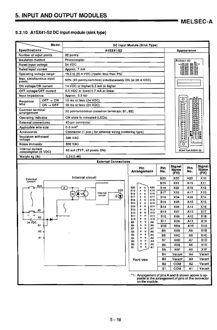
5. INPUT AND OUTPUT MODULES MELSEC-A
5.2.1 0 A1 SX41-S2 DC input module (sink type)
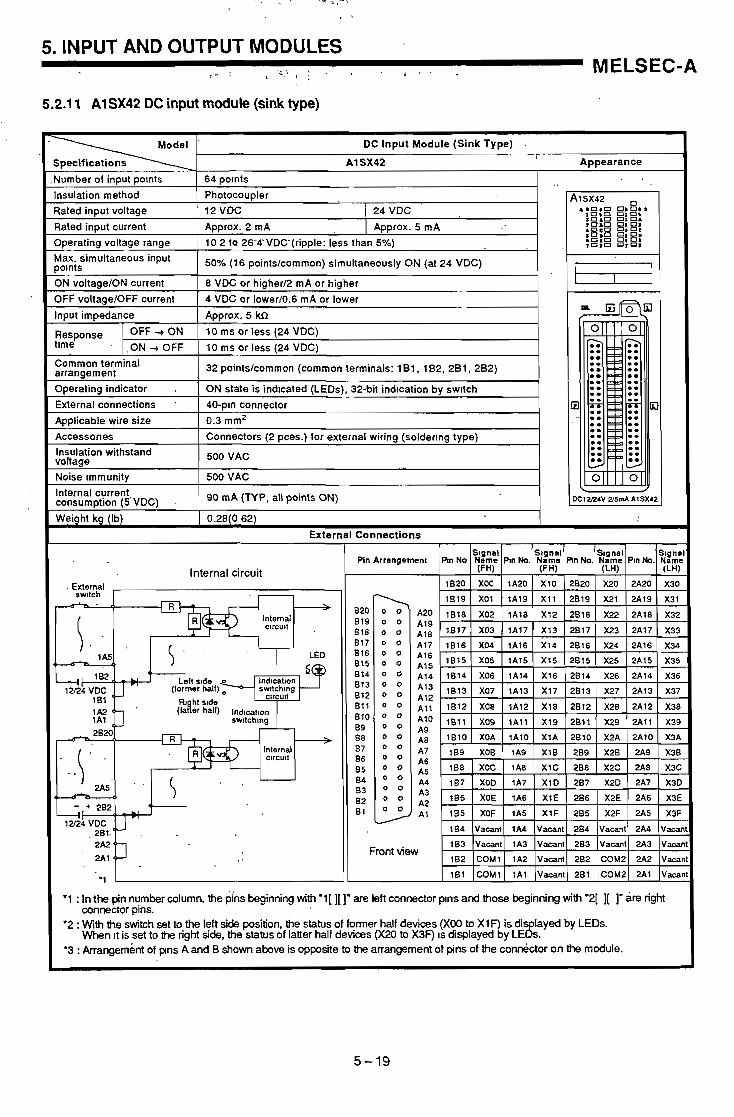
5. INPUT AND OUTPUT MODULES 1 * ! . l : : . . . $ . . MELSEC-A
I s t ,
5.2.1 1 A1SX42 DC input module (sink type)
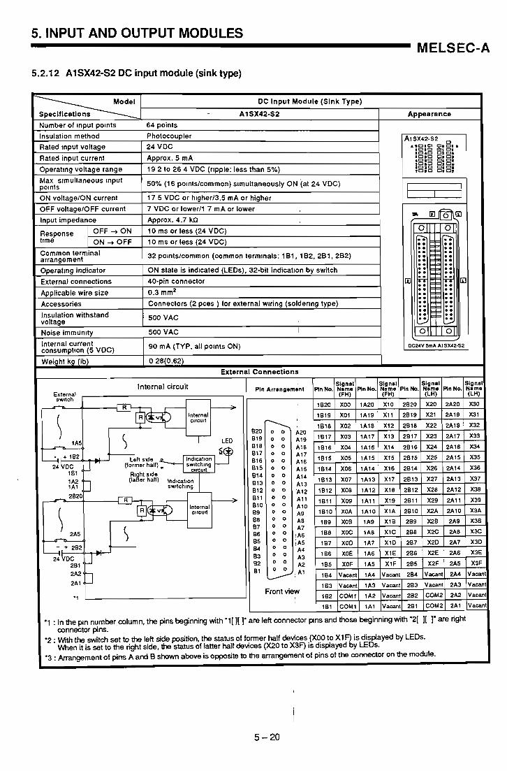
5. INPUT AND OUTPUT MODULES MELSEC-A
5.2.1 2 A1SX42-S2 DC input module (sink type)
r column, the pins beginning with 'l[][]'

5. INPUT AND OUTPUT MODULES MELSEC-A
5.2.1 3 A1 SX71 DC input module (sinWsource common type)
Appearance
AISX~I a 1 0 1 0 0 1 ' 0 , .
:8:8 X:8: BCIID O* 01
:o":o" 3 8 : :B:8 3 8 :
. . . . . . . . . DC5/12V AlSX71
DC lnput Module (Sink Type)
Open collector (Sink) Pin Pin Signal Pin Signal Internal circuit Arrangement No. Name No. Name
820 XOO A20 X I 0 819 X01 A19 X I 1 818 X02 A18 X I 2
B16 X04 A16 X I 4
B9 XOB A9 X I B
B7 XOD A7 X1D
B3 Vacant A3 Vacant TTL, LS-TTL, CMOS buffer (Sink) Sensor (Source) 8 2 COM A2 Vacant
Front view B1 COM A1 Vacant
'1 : Arrangement of pins A and B shown above i s oppos~te to the arrangement of pins of the con-
5 VDC 82 nector on the module.
.
., AlSXPI
32-points
Photocoupler
5 VDC 1 12VDC
1 2 m A 1 3.3 mA 4.5 to 13 2 VDC (ripple. less than 5%)
100% (32 pointslcommon) s~multaneously ON
3.5 VDC or higher11 mA or h~gher
1 0 VDC or lowerl0.1 mA or lower Approx 3 5 k~
1.5 ms or less
3 ms or less
32 pointslcommon (common term~nals: B1, 82)
ON state IS indicated (LEDs)
40-pin connector
0.3 mm2 - Connector ( I pce ) for external wlring (soldering type)
500 VAC
250 VAC
75 mA (TYP, all points ON)
0.19 (0.42)
External Connections
Number of input po~nts
Insulation method Rated Input voltage
Rated input current
Operating voltage range
slmultaneOus Input points ON voltagelON current OFF voltagelOFF current Input impedance
Response time
OFF -, ON
ON -t OFF
Common terminal arrangement
Operating ind~cator
External connectrons
Applicable wire size
Accessories
Insulation withstand voltage Noise immunity Internal current consumption (5 VDC)
Weight kg (Ib)

5. INPUT AND OUTPUT MODULES MELSEC-A
5.2.1 4 A1SX80 DC input module (sinWsource common type)
DC lnput Module (SlnklSource Common Type)
A1 SXBO Appearance I Number of input points
Insulation method Rated input voltage
Rated input current
Operating voltage range
input points
ON voltagelON current
OFF voltagelOFF current
Input impedance OFF -, ON
ON -t OFF
16 points
Photocoupler A~sxeo 12 VDC ) 24 VDC
Approx. 3 mA I Approx. 7 mA $ 0 O D - 0 o r
10.2 to 26.4 VDC (ripple: less than 5%) o 0 6
100% simultaneously ON (at 26.4 VDC)
8 VDC or higher12 mA or higher
4 VDC or lower11 mA or lower
Approx. 3.3 kn 10 ms or less (24 VDC)
10 ms or less (24 VDC)
Common terminal arrangement
Operating indicator External connections
Internal circuit
Applicable wire size
Applicable crimp terminals
Accessories
lnsulation withstand voltage
Noise immunity Internal current consumption (5 VDC)
Weight kg (Ib)
LED
cwcud
16 pointslcommon (common terminals: TB9, TB18)
ON state is ind~cated (LEDs) 20-point terminal block connector (M3.5 x 7 screws)
0.75 to 1.5 mm2 1.25-3.5 1.25-YS3A 2-3.5 2-YS3A V1.25-M3 V1.25-YS3A V2-S3 V2-YS3A
None
500 VAC
1000 VAC
50 mA (TYP, all points ON)
0.2(0.44)
, TBtO t * -
LED
Internal 6 CUCUlt
s 6
7
External Cannectlans
Signal I Teh!'nal I Name
TI39 COM
TB10 TBl 1 TB12 TB13 TB14
X08 X09 XO A XOB XOC
TB15 TB16
TB17 TB18 TB19 TB20
XOD
XOE
XOF COM
Vacant Vacant

5. INPUT AND OUTPUT MODULES MELSEC-A
5.2.15 AlSX80-S1 DC input module (sinklsource common type)
Internal circuit

5. INPUT AND OUTPUT MODULES , MELSEC-A
5.2.1 6 A1 SXWS2 DC input module (sinWsource common type)
Number of input points
lnsulat~on method
Rated input voltage
Rated input current
Operating voltage range
input points
ON voltagelON current
OFF voltagelOFF current Input impedance
DC lnput Module (Slnk/Source Common Type)
R~~~~~~~ time
A1 SX80-S2
16 points
Photocoupler
24 VDC
Approx. 7 mA
19 2 to 26.4 VDC (r~pple: less than 5%)
100% simultaneously ON (at 26.4 VDC)
13 VDC or h1gher13.5 mA or hlgher
6 VDC or lowerll.7 rnA or lower Approx. 3.3 kR
10 rns or less (24 VDC)
10 ms or less (24 VDC)
OFF -r ON
ON -t OFF
Common terminal . arrangement
Operating tnd~cator
External connections
Appl~cable wire size
Appl~cable crlmp term~nals
Accessories
Insulation withstand voltage
Noise lmmunity
Internal current consumption (5 VDC)
Weight kg (Ib)
Appearance
- 16 pointslcommon (common terminals: TB9, TB18)
ON state is indicated (LEDs)
20-point terminal block connector (M3.5 x 7 screws) 0.75 to 1.5 mm2
1.25-3.5 1.25-YS3A 2-3.5 2-YS3A V1.25-3 V1.25-YS3A V2-S3 V2-YS3A None
500 VAC
1000 VAC
50 mA (TYP, all points ON)
0 2(0.44)
External Connections
i
Terminal No.
TB 1 TB2
TB3 TB4
TB5 TB6
TB7 TB8
TB9 TBlO
T B l l TB12 TB13 TB14 TB15 TB16 TB17 TB18
TB19 TB20
Signal Name
XOO XO1
X 02 X03
X04
X05
X06 X07 COM X08
X09 XOA XOB XOC XOD XOE
XO F COM
Vacant Vacant

5. INPUT AND OUTPUT MODULES . . . I, ? . MELSEC-A
5.2.1 7 A1 SX81 DC input module (sinWsource common type)
lnsulat~on method I Photocoupler
Rated input voltage 1 12VDC 1 24 VDC
-- - - --
DC Input Module (SinklSource Common Type)
A1 SX81
Number of input polnts 32 polnts
Appearance
Rated input current
Operating voltage range
Idax input points
I Common terminal arrangement
Approx. 3 mA 1 Approx 7 mA
10 2 to 26 4 VDC (rlpple: less than 5%)
60% s~rnultaneously ON (at 26 4 VDC)
ON voltagelON current
OFF voltagelOFF current
Input impedance
R~~~~~~~ OFF -, ON t~me ON -r OFF
1 32 pointslcornm~n (common terminals: 17. 18, 36)
-
8 VDC or higher12 mA or higher
4 VDC or lower11 mA or lower Approx. 3.3 kR 10 ms or less (24 VDC)
10 ms or less (24 VDC)
1 Operatinp indicator I ON state is ~nd~cated ILEDs) I I External connections I 37-oin D sub-connector I
pp - --
Appl~cable wire size 1 0.3 mm2
Accessories I Connector (1 pce.) for external wirrng (soldering type)
I Insulation withstand vattann ( 500 VAC I Nolse immunity 1 I 1000 VAC I
I External Connections I
Internal current consumpt~on (5 VDC)
Weight kg (Ib)
Internal circuit
80 mA (TYP, all points ON)
0.24(0.53)
- -
P i n Arrangement
Signal P i n Signal Name No. Name
xoo 9 X I0
XO1 28 . X I 1
X02 10 X I 2
External sw~tch , 1 n
LED Internal . ctrcult
17
24 X09 32 X I9 XOA 14 X IA
12/24 VDC
1 25 1 XOB 1 33 1 X1B 7 XOC 15 X IC
26 XOD 34 X1D 8 XOE 16 X IE
27 XOF 35 X IF 17 COM 37 Vacant
1 19 1 Vacant
Front view

5. INPUT AND OUTPUT MODULES MELSEC-A
5.2.18 A1SX81-S2 DC input module (sink/source common type) .
Type)
Appearance
1
DC.lnput Module (SinkISource Common
AlSX81-S2
32 points
Photocoupler 24 VDC
Approx. 7 mA
19.2-to 26.4 VDC (r~pple: less than 5%)
60% simultaneously ON (at 26.4 VDC)
13 VDC or higher13.5 mA or higher
6 VDC or lowerll.7 mA or lower Approx. 3.3 kR 10 ms or less (24 VDC)
10 ms or less (24 VDC)
32 pointslcommon (common terminals: 17, 18, 36)
ON state is indicated (LEDs) 37-pln D sub-connector 0.3 mm2
Connector (1 pce.) for external wlring (soldering type)
500 VAC
1000 VAC
80 mA (TYP, all points ON)
0.24(0.53)
External Connections
Number of input polnts
lnsulat~on method
Rated input voltage Rated input current
Operating voltage range-
s'mu'taneous Input points
ON voltagelON current
OFF voltagelOFF current
Input impedance
Response I OFF + ON
Internal circuit
t~me ON + OFF
Pin Arrangement
Common terminal arrangement
Operating ind~cator External connections
Applicable wire size
Accessories
Insulation withstand voltage
Noise immunity
Internal current consumption (5 VDC)
Weight kg (Ib)
Pin No.
1 20
21
22
23
825 7
26
17 36
XO1
X02 X03
X04 X05 X06 X07 X08 X09
XOA XOB XOC XOD XOE XOF
COM COM
COM
i
Signal Name
XOO
28
10 29
11 30
12 31 13 32 14 33 15 34 16 35
37
19
Front view
XI1
X I 2 X I3
X I4 X I5 X I6 X I7 X I8 X I9 X1A X l B X1C X1D
X1E X1F
Vacant Vacant
&
Pin No.
9
18
Signal Name
XI0

5. INPUT AND OTPUT MODULE . 2 , .
MELSEC-A I ,
5.3 Output Module Specifications
5.3.1 A1SY10 contact output module
Number of output polnts
lnsulat~on method
Switching rated voltage/current
Min swltchlng load
Max switching voltage
Contact Output Module
AlSYlO
16 polnts
Photocoupler
24 VDC 2 A (load resistance) 11 point, 8 N~~~~~ 240 VAC 2 A (COS9 = 1)
5 VDC 1 mA
264 VAC 125 VDC
10 ms or less 12 ms or less
More than 20 rntlllon times or more
Swltchtng rated voltagelcurrent More than 100000 tlmes or more
200 VAC 1.5 A. 240 VAC I A (COS9 = 0 7) More than 100000 times or more
200 VAC, 240 VAC 0 5 A (COSQ = 0.35) More than 100000 ttmes or more
24 VDC 1 A, 100 VDC 0.1 A (UR = 7 ms) More than 100000 tlmes or more
3600 tlmes per hour
None
None
8 po~ntslcornmon (common terminals: TB9. TB18)
ON state is ind~cated (LEDs) 20-point term~nal block connector (M3 5 x 7 screws) 0.75 to 1.5 mm2
1.25-3 5 1.25-YS3A 2-3 5 2-YS3A V1 25-M3 V1.25-YS3A V2-S3 V2-YS3A
None
1500 VAC
1000 VAC
24 VDC *lo%. R~pple voltage 4VP-P or less
90 rnA (TYP 24 VDC all polnts ON)
120 mA (TYP, all polnts ON)
0.25 (0 55)
External Connections
R~~~~~~~ time
Service l ~ f e
Appearance
. O 0. '0 0.
OFF -, ON
ON + OFF
Mechanical
Electrical
Internal clrcult
1200 VAC
1001200 VAC 24 VDC
External ower SUPPPy
Max. sw~tching frequency
Surge absorber
Fuse
Common terminal arrangement
Operating lndlcator External connections
Applicable wlre size
Applicable crimp
Accessories
Insulation withstand voltage
No~se irnmun~ty
Term~nal No
TB 1
TB2 TB3 TB4 TB 5
TB6 TB7 TBB TB9 TBlO TBll TB12 TB13 TB14
TB15 TB16 TB17 TBl8 T619 TB20
External
Signal Name XOO
XO1
X02 X03 XO4
XO5 X06 X07
COM 1
XOB
X09 XO A
XOB XOC
XOD XOE XO F
COM2 24 VDC
OV
Voltage
Power supply , Current
Internal current consumption (5 VDC)
Welght kg (lb)

5. INPUT AND OTPUT MODULE MELSEC-A
5.3.2 AlSYlOEU contact output module

5. INPUT AND OTPUT MODULE MELSEC-A
" . , . . : I : i ,- ..- 5.3.3 AlSY14EU contact output module
. .
Appearance
. D 0 , ' 0 0 .
, O o
Contact Output Module
Terrn~nal No 1 Signal Name Internal clrcutt I
Speclfications
Number of output polnts Insulation method Sw~tching rated voltagelcurrent Min. switching load Max switching voltage
Response time
Servlce life
A1SY14EU
12 points (number of occupled I10 polnts : I 6 points) Photocoupler
24 VDC 2 A (load resistance) poinc A/common 240 VAC 2 A (COS4 = I ) 5 VDC 1 mA 264VAC 125 VDC 10 ms or less 12 ms or less More than 20 mill~on times or more Switching rated voltagelcurrent More than 200000 tlmes or more -
200 VAC 2A, 240VAC 1.8 A (COSq = 0.7) More than 200000 times or more 200 VAC I .1A, 240VAC 0.9 A (COS$ = 0.35) More than 200000 times or more 24 VDC 1 .I A, 100 VDC 0 1 A (LIR = 7 ms) More than 200000 times or more 3600 times per hour None None
4 pointslcommon (common terminals: TB5, TB10, TB15)
ON state is indicated (LEDs) 20-point terminal block connector (M3.5 x 7 screws) 0.75 to 1.5 mm2 (AWG15 to AWG19) RAVI .25-3 5 None AC terminals-Relay coil, SVAC 1 2830 VAC Relay coil, SVAC I 500 VAC 1000 VAC
OFF -t ON ON + OFF Mechanical
Electrical
24 VDC f lo%, Ripple voltage: 4VP-P or less
100 mA (TYP 24 VDC all polnts ON)
SELV power supply must be used
Max. switching frequency Surge absorber Fuse Common terminal arrangement Operating ind~cator External connect~ons Applicable wire size Appllcable crimp terminals Accessor~es
Insulation withstand voltage
Noise immunity
120 mA (TYP, all polnts ON)
0.25 (0 55)
External Connections
External Power supply
Voltage
Current
Internal current consumption (5 VDC) Weight kg (lb)

5. INPUT AND OTPUT MODULE MELSEC-A
5.3.4 A1SY18A contact output module (all points independent)
-
L
Appearance
.
Contact Output Module
AlSYlOA
8 points (number of occupied I10 points : 16 points) Photocoupler
24 VDC 2 Alpoint (load resistance) 240 VAC 2 Alpoint (COSq = 1) 5 VDC 1 mA 264 VAC 125 VDC 10 ms or less 12 ms or less More than 20 m~llion times or more Switching rated voltagelcurrent More than 200000 times or more 200 VAC 1.5 A, 240 VAC 1 A (COSe = 0.7) More than 200000 times or more
' 200 VAC 0.75 A, 240 VAC 0.5 A (COS$ = 0.35) More than 200000 times or more 24 VDC 1 A, 100 VDC 0.1 A (UR = 7 ms) More than 200000 t~mes or more 3600 times per hour None None
None (all points tndependent)
ON state is indicated (LEDs) 20-point terminal block connector (M3.5 x 7 screws) 0.75 to 1.5 mm2 1.25-3.5 I .25-YS3A 2-3.5 2-YS3A V1.25-M3 V1.25-YS3A V2-S3 V2-YS3A None
1500 VAC
1000 VAC
24 VDC *lo%. Ripple voltage: 4VP-P or less 75 mA (TYP, 24 VDC all points ON)
240 mA (TYP, all points ON)
0.25 (0.55)
External Connections
Number of output points Insulation method Switch~ng rated voltagelcurrent Min. switching load Max switching voltage
Internal ctrcutt
R~~~~~~~ time
Service life
OFF + ON ON -t OFF Mechanical
Termlnal No. TB 1
TB2
TB3
TB4
TB5
TB6
T87
TB8
TB9
TBlO
TBl 1
TB12
TB13
TB14
TB15
TB16
TB17
TB18 TB19
TB20
Signal Name
YO0
YO1
Y 02
YO3
Yo4
Y 05
Yo6
Y 07
Vacant
Vacant
24 VDC
0 V
Max, switching frequency Surge absorber Fuse Common terminal arrangement Operating indicator External connections Appl~cable wire size
Applicable crimp terminals
Accessories Insulation withstand voltage Noise immunity
External Power supply
Voltage Current
Internal current consumption (5 VDC) Weight kg (Ib)

5. INPUT AND OTPUT MODULE MELSEC-A
5.3.5 AlSY18AEU contact output module (all points independent)
Number of output polnts Insulation method Switching rated voltagelcurrent Mln. switching load Max. switching voltage
Response tlme .
Service lrfe
Appearance
OFF + ON ON + OFF Mechanical
Electrical
Contact Output Module
A1SY18AEU
8 points (number of occupied 110 points : 16 polnts) Photocoupler 24 VDC 2 A (load resistance) ,, 240 VAC 2 A (COS@ = 1) 5 VDC 1 mA 264VAC 125 VDC 10 ms or less 12 ms or less More than 20 mill~on t~mes or more Switching rated voltagelcurrent More than 200000 t~mes or more 200 VAC 1.5 A. 240VAC 1 A (COS@ = 0.7) More than 200000 t~mes or more 200 VAC 1 A, 240VAC 0.5 A (COSg = 0.35) More than 200000 times or more 24 VDC 1 A, 100 VDC 0 I A (UR = 7 ms) More than 200000 times or more 3600 times per hour None None
None (all polnts independent)
ON state 1s indicated (LEDs) 20-point terminal block connector (M3 5 x 7 screws) 0.75 to 1.5 mm2 (AWG15 to AWG19) RAV1.25-3.5 None AC terminals-Relay coil, 5VAC 1 2830 VAC Relay coil. 5VAC 1 500 VAC 1000 VAC 24 VDC *lo%, Ripple voltage: 4VP-P or less
75 mA (TYP 24 VDC all points ON)
Signal Name
Y 00
YO1
Y 02
YO3
Yo4
YO5
Y 06
YO7
Vacant
Vacant
24 VDC
OV
Internal c~rcun
tarnal power supply (SELV power supply must be used)
SELV power supply must be used
Max. switching frequency Surge absorber Fuse Common termlnal arrangement Operating ~ndicator External connections Applicable wire size Applicable crimp terminals Accessones
Insulation withstand voltage
Noise immunlty
Term~nal No
TB 1
TB2
TB3
TB4
TB5
TB6
TB7
TB8
TB9
TBlO
T B l l
TB12
TB13
TB14
TB15
TB16 TB17
TB18
TB19 TB20
240 mA (TYP, all points ON)
0.25 (0 55) External Connections
External Power supply
Voltage
Current
Internal current consumption (5 VDC) We~ght kg (lb)

5. INPUT AND OTPUT MODULE MELSEC-A
5.3.6 A1SY22 triac output module
Number of input points Insulation method Rated load voltage Max. load voltage Max. load current Min. load voltagelcurrent Max. input current Leakage 'went at OFF circuit Max .voltage drop at ON clrcult
Response I OFF + ON time 1 ON + OFF Surge absorber Fuse rating Fuse capacity Error display Common terminal arrangement Operating indicator External connecttons Applicable wire size
Applicable crimp terminals
Accessories Insulation withstand voltage Noise immun~ty
External 1 Voltage Powersu~~lY I Current Internal current consumpt~on (5 VDC) Weight kg (lb)
Triec Output Module
AlSY22 16 po~nts Photocoupler 100 to 240 VAC 50160 Hz i 3 Hz 264 VAC 0.6 Alpoint, 2.4 Alcommon 24 VAC 100 mA. 100 VAC 10 mA, 240 VAC 20 mA 20 A 10 ms or less. 8 A 100 ms or less
1.5 mA (120 VAC 60 Hz), 3mA (240 VAC 60 Hz)
1.5 VAC or less 0.1 to 0.6 A), 1.8 VAC or less (50 to 100 mA), 2 VAC or less (10 lo 50 mA) 1 ms or less 0.5 CYCLE + 1 ms or less CR absorber (0.01 pF + 47 R) 5 A (1 piecelcommon), not replaceable '1 70 A LED goes ON when fuse blows: signal output to PC CPU '2
8 pointslcommon (common terminals: TB9, TB19)
ON state IS ind~cated (LEDs) 20-point terminal block connector (M3.5 x 7 screws) 0.75 to 1.5 mm2 1.25-3.5 1.25-YS3A 2-3.5 2-YS3A V1.25-M3 V1.25-YS3A V2-S3 V2-YS3A None 1500 VAC 1500 VAC 100 to 240 VAC (85 to 264 VAC) 2 mA (TYP 200 VAClcommon)
270 mA (TYP, all points ON)
0.24 (0.53)
External Connections
Appearance
I
1 m o o VAC
'1 :The fuse in the output module i s provided to prevent the external wiring form burning in case of a short i n the module's output. Therefore, the fuse might not be able to protect output devices. If an output device is damaged in a failure mode other than a short circuit, the fuse might not be blown.
'2 :The ERR. indicating LED will also light when the external power supply is shut OFF.
Tehy"dna' TB 1
TB2
TB3
TB4
TB5
TB6 TB7 TB8 TB9
TB 1 0
TB l 1 TB12
TB13
TB14
TB15
TB16
TB17
TB18 TB19
TB20
Signal Name
YO0
YO1
YO2
YO3
YO4
YO5 YO6
YO7
COM 1
1 001200 VAC
YO8
YO9
YOA
YOB
YOC
YOD
YOE
YOF COM2
1001200 VAC

5. INPUT AND OTPUT MODULE 1 . 1 . ' id- S '. .
MELSEC-A
5.3.7 A1SY28A triac output module (all points independent)
Number of output points Insulation method Rated load voltage Max. load voltage Max. load current Min. load voltagelcurrent Max. input current Leakage current at OFF clrcuit Max. voltage drop at ON circuit
Trlac Output Module
A1 SY28A
8 points (number of occupied 110 points : 16 po~nts) Photocoupler 100 to 240 VAC 50160 Hz 53 Hz 264 VAC 1 Npoint, 4 Nmodule(l32 VAC). 2 A.module(264 VAC) 24 VAC 100 mA. 100 VAC 55 mA, 24 VAC 55 mA 25 A 10 ms or less, 10 A 100 ms or less
1 5 mA (120 VAC 60 Hz), 3 ; ~ (240 VAC 60 Hz)
1.5 VAC or less 0.2 to 1 A) 1.8 VAC or less (0.1 to 0 2 A), 3 VAC or less (5k to 100 mA) 1 ms or less
0.5 CYCLE + 1 ms or less CR absorber (0.01 pF + 47 R), Var~stor (387 to 473 V) None
None (all points independent)
ON state is ~ndicated (LEDs) 20-point terminal block connector (M3.5 x 7 screws) 0.75 to 1.5 mm2 1.25-3.5 1.25-YS3A 2-3.5 2-YS3A V1.25-M3 V1.25-YS3A V2-S3 V2-YS3A None
1500 VAC
1500 VAC None
130 mA (TYP, all points ON)
0.25 (0.55) External Connections
Response time
Appearance
I
OFF -t ON ON -t OFF
Internal c~rcu~t
External load
i
Surge absorber Fuse rat~ng ,
Common terminal arrangement Operating ind~cator External connectrons Applicable wire size
A~~llcable
Accessories Insulation wrthstand voltage Noise immunity External power supply lnternal current consumption (5 VDC) Werght kg (lb)
No.
TB1 TB2 TB3 TB4 TB5 TB6 TB7 TB8 TB9 TBIO '
TB11 TB12 1613 TB14 TB15 TB16 TB17 TB18 TB19 TB20
signal ' ~ a r n e
YO0
YO1
YO2
YO3
YO4
YO5
YO6
YO7
Vacant
Vacant
Vacant
Vacant

5. INPUT AND OTPUT MODULE MELSEC-A
5.3.8 AlSY28EU triac output module
Number of output points Insulation method Rated load voltage Max. load voltage Max. load current Min. load voltagelcurrent Max. inrush current Leakage current at OFF circuit Idax. "Itage drop at ON circuit
Trlac Output Module
AlSY28EU
8 points (number of occupled 110 points : 16 points) Photocoupler 100 to 240 VAC 50160 Hz i 3 Hz 264 VAC 0.6 Alpoint, 1.9 A.common 24 VAC 15 mA, 120 VAC 15 mA, 240 VAC 15 mA 30 A 10 ms or less, 15 A 100 ms or less
1.5 mA (240 VAC 60 Hz)
1.5 VAC or less (1 5mA to 1 A)
1 ms or less
0.5 CYCLE + 1 ms or less Built-in CR absorber (0.01 pF + 47 0) None
4 pointslcommon (common terminals: TB8, TB16)
ON state is indicated (LEDs) 20-point terminal block connector (M3.5 x 7 screws) 0.75 to 1.5 mm2 (AWG1 to AWG19) RAV1.25-3.5 None
2830 VAC
1000 VAC
270 mA (TYP, all points ON)
0.24 (0.53)
External Connections
Response time
Appearance
OFF -t ON ON + OFF
Internal c~rcuit
External load
Surge absorber
1001200 VAC
F
Surge absorber Fuse rating Common terminal arrangement Operating indicator External connections Applicable wire size Applicable crimp terminals Accessories lnsulation withstand voltage Noise immunity Internal current consumpt~on (5 VDC) Weight kg (lb)
No.
TB1
TB2
TB3
TB4
TB5
TB6
TB7
TB8
TB9
TBIO
TB11 TB12
TB13
TB14
TB15
TB16
TB17 TB18
TB19
TB20
Signal Name
YO0
Vacant
YO1
Vacant
YO2
Vacant
YO3
COM 1 YO4
Vacant
YO5 Vacant
YO6
Vacant
YO7
COM2 Vacant
Vacant
Vacant
Vacant

5. INPUT AND OTPUT MODULE MELSEC-A
5.3.9 A1SY40 transistor output module (sink type)
L
Number of ~nput potnts lnsulat~on method Rated load voltage Operat~ng voltage range Max- load current - Max. lnput current Leakage current at OFF cIrcu(1 Max. "Itage at ON circult
R~~~~~~~ OFF + ON tlme I ON -, OFF Surge absorber Fuse ratlng Fuse capacity Error display Common terminal arrangement Operating indicator External connections Appl~cable wtre size
&pltcable crimp terminals
Accessories Insulation withstand voltage No~se ~mmunity
External Voltage power supply Current
Internal current consumption (5 VDC) We~ght kg (lb)
Transistor Output Module (Sink Type)
A1SY40
16 pornts Photocoupler 12/24 VDC 10 2 to 30 VDC (peak voltage 30 VDC) 0.1 Alpoint. 0.8 Alcommon 0 4 A 10 msorless
0.1 mA or less
1.0 VDC (TYP) 0.1 A. 2 5 VDC (MAX) 0 1 A
2 ms or less 2 ms or less (resistive load) Zener diode Fuse 1.6 A (1 ptecelcommon), not replaceable '1
50 A LED goes ON when fuse blows signal output to PC CPU '2
8 po~ntslcommon (common terminals. TB10, TB20)
ON state is lnd~cated (LEDs) 20-po~nt terminal block connector (M3.5 x 7 screws) 0.75 to 1.5 mm2 1.25-3.5 1.25-YS3A 2-3.5 2-YS3A V1.25-M3 V1.25-YS3A V2-S3 V2-YS3A None
500 VAC
500 VAC 12/24 VDC (10.2 to 30 VDC) 8 mA (TYP 24 VDC/common)
270 mA ( P P , all potnts ON)
0.19 (0 42) External Connections
Appearance
Signal Name
YO0
YO1
YO2
YO3
YO4
YO5
YO6
YO7 12/24 VDC
COM 1
YO8
YO9
YOA
YOB
YOC YOD YOE
YOF
12/24 VDC COM2
12/24 VOC
4 voc
'1 :The fuse in the output module is provided to prevent the external wiring form burn- ing in case of a short in the module's output. Therefore, the fuse might not be able to protect output devices. If an output device is damaged in a failure mode other than a short circuit, the fuse might not be blown.
'2 : The ERR. indicating LED will also light when the external power supply IS shut OFF.
No.
TB1
TB2
TB3
TB4
TB5
TB6
TB7
TB8 TB9 TBlO
TB11 TB12
TB13
TB14
TB15 TB16
TB17
TB 18 TB19
TB20

5. INPUT AND OTPUT MODULE MELSEC-A
5.3.10 A1SY41 transistor output module (sink type)
Number of input points Insulation method Rated load voltage Operating voltage range Max. load current
h?ax..vOltage drop at ON 1 1.0 VDC (TYP) 0.1 A, 2.5 VDC (MAX) 0.1 A crrcult I
Max. input current Leakage current at OFF circuit
OFF + ON 1 2 ms or less
Trrnslstor Output Module (slnk type)
0.4 A 10 ms or less
0.1 mA or less
Surge absorber I Zener diode Fuse rating I Fuse 3.2 A (1 piecetcommon), not rwlaceable '3
AlSY41 32 points Photocoupler 1 2/24 VDC 10.2 to 30 VDC (peak voltage 30 VDC) 0.1 Alpoint, 2 Ncommon
Fusecapacity 50 A
Common terminal arrangement Operating indicator ON state is indicated (LEDs) External connections 40-pin connector Applicable wire size 0.3 mm2
Insulation withstand voltage Noise immunity 500 VAC
External Voltage 12/24 VDC (10.2 to 30 VDC) power supply Current 8 mA (TYP 24 VDClcommon)
Appearonce

5. INPUT AND OUTPUT MODULES MELSEC-A
5.3.1 1 A1SY42 photocoupler output module (sink type)

5. INPUT AND OUTPUT MODULES MELSEC-A
When it is set to lhe right side, Ihe status of latter half devices (X20 to X3F) Is displayed by LEDs. 3 : The fuse in the output modyle is provided to prevent Ihe extern+ wiring form burning in case of a short in the module's out-
put. Therefore, the fuse might not be able to protect output devlcea

5. INPUT AND OUTPUT MODULES . 'a:. . .
1 I * I
MELSEC-A
5.3.1 2 A1 SY50 transistor output module (sink type)
If an output device is damaged In a failure mode other than a short arcu~t, the fuse might not

5. INPUT AND OUTPUT MODULES MELSEC-A
5.3.13 A1SY60 transistor output module (sink type)
output &vice is damaged in a failure mode other than a short circuit the fuse might not

5. INPUT AND OUTPUT MODULES ': $,rr<.f :.t . a + c , . I . . - - . MELSEC-A
5.3.1 4 A1 SYGOE transistor output module (source type)
Speciflcetions
Number of output points Insulation method
- Rated load voltage Operating voltage range Max. load current Max. lnput current Leakage current at OFF c~rcuit Max. voltage drop at ON circurt
Transistor Output Module (Source
A1SY6OE
16 points Photocoupler r
5/12/24 VDC 4.5 to 26.4 VDC (peak voltage 26.4 VDC)
2 Alpo~nt (condition t = UR s 2 5 ms), 4 Ncommon 8 A lOms orless 0.1 mA or less 0.2 VDC (MAX) 1 A, 0.4 VDC (MAX) 2 A 3 ms or less 10 ms or less (resistive load) Zener diode
Fuse 7 A (1 piecelcommon), not replaceable '1 300 A LED goes ON when fuse blows s~gnal output to PC CPU '2 8 points/common (common terminals: TB9. TB19) ON state is ind~cated (LEDs) 20-point terminal block connector (M3 5 x 7 screws) 0 75 to 1.5 mm2
1.25-3.5 1.25-YS3A 2-3.5 2-YS3A V1.25-M3 V1.25-YS3A V2-S3 V2-YS3A None 500 VAC 500 VAC
12/24 VDC (1 0.2 to 26.4 VDC)'3 10 mA (TYP 24 VDClcommon) 200 mA (TYP, all points ON)
( 0.2 (0.44)
Response time
Type)
Appearance
.a o
OFF -t ON
External Connections
Internal clrcult
When 5 VDC load voltage IS connected
'1 The Fuse in the output module is provided to prevent the external wiring form burning in case of a short in the module's output. Therefore, the fuse might not be able to protect output de- vices. If an output device is damaged in a failure mode other than a short circuit, the fuse might not be blown.
I ON + OFF Surge absorber Fuse rating Fuse capacity Error display Common terminal arrangement Operating indicator External connections Applicable wire size
Applicable crlmp terminals
Accessories Insulation withstand voltage
Noise immunity
'2 The ERR. indicating LED will also light when the external power supply is shut OFF. '3 When 5 VDC operating load voltage is used, another 12/24 VDC power supply is required for
external power supply.
Terminal No.
TB 1 TB2 TB3 TB4 TB5 TB6 TB7 TB8 TB9 TBlO TB11 TB12 TB13 TB14 TB15 TB16 TB17 TB18
' TB19 TB20
External power supply
Signal Name
YO0 YO1 YO2 YO3 YO4 YO5 YO6 YO7
COM 1 OV YO8 YO9 YOA YOB YOC YOD YOE YOF
COM2 OV
Voltage Current
Internal current consumption (5 VDC) Weight kg (Ib)

5. INPUT AND OUTPUT MODULES MELSEC-A I
5.3.15 A1SY68A transistor output module (sinWsource common type (all points independent))
Transistor Output Module
AlSY68A Appearance
Number of output points 8 points (number of occupied 110 points : 16 po~nts)
Insulation method Photocoupler A1 SY68A
Rated load voltage 511 2/24/48 VDC
Operating voltage range 4.5 to 52.8 VDC : o Max. load current 2 Alpolnt
Max. input current 8 A 10 msorless
Leakage current at OFF circuit 0.1 mA or less
Max. voltage drop at ON circuit 0.4 VDC (MAX) 2 A
OFF + ON 3 ms or less Response time
Surge absorber I Zener diode I Common terminal arrangement I None (all points independent)
Operating indicator I ON state is indicated (LEDs)
External connections 1 20-point terminal block connector (M3.5 x 7 screws)
Applicable wire size 1 0.75 to 1.5 mm2 -- --
Applicable crimp terminals 1.25-3.5 1.25-YS3A 2-3.5 ~ - Y s ~ A - V1.2CM3 V1.25-YS3A V2-S3 V2-YS3A
Insulation withstand voltage I 500 VAC 1 I - Noise immunity 500 V AC
External power supply None
1 Internal current consumotion (5 VDC) 1 110 rnA I I . . I
Weight kg (Ib) 1 0.2 (0.44) 1 External Connections
Terminal Signal No. Name
Internal circu~t ~ l n k
Surge e o r b e r External load
TB 1
TB2
TB3
TB4
TB5
TB6
TB7
TB8
TB9
TBlO
TB11
TB12
TB13
TB14
TB15
TB16
TB17
TB18
TB19
TB20
-
7f lnlelnd C U C U ~
A A
YO0
YO1
YO2
YO3
YO4
, yo5
YO6
YO7
Vacant
Vacant
Vacant
Vacant
, . I 1 + I I
\ ,, Sour- ..2
I ' + -
-
a -
7f
1 -

5. INPUT AND OUTPUT MODULES : * MELSEC-A
5.3.16 A1SY7l transistor output module (sink type)
Internal clrcult
ERR LED
'1 : Arrangement of "ns A and B shown above is opposite to the arrange- ment of pins of f e connector on the module.

5. INPUT AND OUTPUT MODULES MELSEC-A
5.3.17 A1SY80 transistor output module (source type)
Appearance
.O ' 0 o o
7 0 o
Transistor Output Module (Source Type)
AlSY8O
16 points Photocoupler 12/24 V DC 10.2 to ~ O - V D C (peak voltage 30 VDC)
0 8 Alpoint, 3.2 Alcommon 8 A 10 ms or less
0.1 mA or less
1.5 VDC (MAX) 0.8 A
2 ms or less 2 ms or less (resistive load) Zener diode Fuse 5 A (1 prece/common), not replaceable '1
50 A LED goes ON when fuse blows: signal output to PC CPU '2
8 points/common (common terminals: TB9, TB19)
ON state is indicated (LEDs) 20-point terminal block connector (M3.5 x 7 screws) 0.75 to 1.5 mm2 1.25-3.5 1.25-YS3A 2-3.5 2-YS3A Vle25-M?J V1.25-YS3A V2-S3 V2-YS3A None 500 VAC 1000 VAC 12/24 VDC (1 0.2 to 30 VDC) 20 mA (TYP 24 VDClcommon)
120 mA ( T Y ~ , all points ON)
0.2 (0.44)
External Connections
Number of input po~nts Insulation method Rated load voltage Operating voltage range Max. load current Max. ~nput current Leakage current at OFF circuit Max. voltage drop at ON circuit
External load
'1 : The fuse in the o u w t module is provided to prevent the external wiring form burning i n case of a short in the module's output Therefore, the fuse might not be able to protect output devices. If an output device is damaged in a failure mode other than a short arcuit, the fuse might m t be Mom
'2 : The ERR. indicating LED will also light when the external power supply is shut Off. i
R~~~~~~~ OFF 4 ON
Terminal No.
TB1 TB2 TB3 TB4 TB5 TB6 TB7
TBB TB9
TBlO
TB11 TB12 TB13 TB14 TB15 TB16 TB17 TB18 TB 1 g
TB20
t~me , ON -.+ OFF
Surge absorber Fuse rating Fuse capacity Error display Common terminal arrangement Operating indicator External connections Applicable wire size
Applicable terminals
Accessories Insulation withstand voltage Noise immunity
External Voltage Power supply 1 Current
Internal current consumption (5 VDC) Weight kg (Ib)
Signal Name
YO0 YO 1 YO2
YO3 YO4 YO5 YO6 YO7
COM 1
OV
YO8 YO9 YOA YOB YOC YOD YOE YO F
COM2 OV

5. INPUT AND OUTPUT MODULES , * . * ' a .; ;< , 9 * %~
MELSEC-A
5.3.18 A1SY81 transistor output module (source type)

MEMO

5. INPUT AND OUTPUT MODULES MELSEC-A
5.4 InputIOutput Combination Module Specifications
5.4.1 A1SH42 inputloutput module
'1 : The fuse in the out ut module is provided to prevent the exte!nal wiring form burning in case of a short tn ti!e module's output. Therefore, the fuse m~ght not be able to protect output devices. If an out ut device is damaged in a failure mode other than a short circuit, the fuse might not be brown.
'2 : The ERR. indicating LED will also light when the external power supply is shut OFF.
Number of input points lnsulat~on method Rated input voltage Rated input current
Operat~ng voltage range Max. simultaneuos Input polnts ON voltagelON current
OFF voltage/OFF current
Input impedance
R~~~~~~~ OFF + ON tfme ON -P OFF
Common terminal arrangement Insulation withstand voltage Noise immun~ty
Number of input points Insulation method
Rated input voltage Operating voltage range
Max. load current
Max. input current
Leakage current at OFF circuit Max drop at ON circuit
R~~~~~~~ I OFF -P ON time ON + OFF
Surge absorber
Fuse rating Fuse capac~ty Error display Common terminal arrangement Insulation withstand voltage
Noise immunity
InpuUOutput Combination Module
Input Speclflcatlons
32 polnts Photocoupler 12 VDC 1 24 VDC
Approx. 2 mA I Approx. 5 mA 10.2 to 26 4 VDC (ripple' less than 5%)
60% (20 pointslcommon) slmultaneuosly ON (at 24 VDC)
8 VDC or higher12 mA or h~gher
4 VDC or lowerl0.6 mA or lower Approx. 5 kR 10 ms or less (24 VDC) 10 ms or less (24 VDC)
32 pointslcommon (common terminals: 1 B1, 182)
500 VAC 500 VAC
Output Specifications
32 polnts Photocoupler
12/24 VDC 10.2 to 30 VDC (peak voltage 30 VDC)
0.1 Alpoint, 1.6 Ncomrnon
0.4 A 10 ms or less
0.1 mA or less
I .O VDC (TYP) 0.1 A, 2.5 VDC (MAX) 0.1 A
2 ms or less
2 ms or less (resistive load) Zender diode
Fuse 3.2 A (1 piecelcommon), not replaceable '1
50 A LED goes ON when fuse blows: signal output to PC CPU '2
32 pointslcommon (common terminals: 2A1, 2A2)
500 VAC
500 VAC 12/24 VDC (10.2 to 30 VDC) 8 mA (TYP 24 VDClcommon)
Common Speclflcatlons
32 (110 allocation is set as a 32-point output module) ON state IS ~ndicated (LEDs), 32-points ind~cat~on by switch
40-pin connector
0.3 mm2 Connector (2 cps.) for external wiring (soldering type)
500 mA (TYP, all points ON)
, 0.27 (0.59)
External power SUPP~Y
Appearance
A1 SH42 A : 8.8 B 0:o 0;o: : . oCo O D O o s o o 0. o .2 , 0 0 0 0,OD .OCO P . o r 7 O F D O,OF
EEI
DC~.VZ~V z 6 ~ O I A AISW
Current
Number of I10 points -0peratlng indicator External connections
Applicable wire slze
Accessories
Weight kg (lb)

5. INPUT AND OUTPUT MODULES MELSEC-A
External Connections
hknrl wwit
'1 : In the in number co!umn, the pins beginning with 'I[] [I ' are left connector pins and those beginning with '2 [ ] [ I are dgRt connector pins.
'2 : With the switch set to the left side position, the status of former half devices (XOO to X I F) is displayed by LEOS. When i t is set to the right side,the status of latter half devices (X20 to X3F) is displayed by LEOS.
'3 : Set i t as 32 points output module when I f0 assignment is made by the peripheral equipment.

5.110 MODULES MELSEC-A
5.4.2 A1 SJ-56DT 110 module (24 VDC input (sink type), 12/24 VDC transistor output)
Speclfic~tlon8
24 polnts
Photocoupler
24 VDC
19 2 to 30 VDC (peak voltage 30 VDC)
0 5 Npolnt. 4 Ncommon
4 A 10 ms or less
0 1 mA or less
0 9 V (TYP ) 0 5 A 1 5 V (MAX ) 0 5 A
2 ms or less
2 ms or less (reslstwe load)
24 VDC (19 2 to 30 VDC) -
60 mA (PIP 24 VDC per common)
Zener dlode
8 po~ntslcommon (common termlnal T010, T020. TEN)
500 VAC
500 VAC
Prov~ded (The LED I~ghts when the output a ON )
Input
Number of ~nput polnts
lnsulat~on method
Rated Input voltage
Rated tnput current
Operatcng voltage range
ON voltage I ON current
OFF vokage I OFF current
Input resistance
lnput method
Response time OFF -, ON ON -, OFF
Common method
'Operatton lndlcator
Max~mum s~multaneous tnput polnts
Insulatton wtthstand voltage
Noise lmmunlty
Output
Number of output polnts
Insulatton method
Rated load voltage
Operating voltage range
Maximum load current
Maximum tnrush current
Leakage current at OFF ctrcult
Maxtmum drop at ON clrcult
Specif~cationa
32 potnts
Photocoupler
24 VDC
Approx 7 mA
19 2 to 26 4 VDC (r~pple less than 5%)
14 VDC or h1gher13 5 mA or hlgher
6 5 VDC or lower11 7 mA or lower
Approx 3 3 Kn Stnk lnput (method by whlch the tnput current flows out)
10 ms or less (24 VDC)
10 ms or less (24 VDC)
16 pointslcommon (common term~nal TB17. TB34)
Provlded (The LED llghts when the Input IS ON )
60 46 (10 po~ntslcommon) s~multaneously ON
500 VAC
500 VAC
Response tlme OFF -t ON
ON OFF
External power supply
Voltage
Current
Surge absorber
Common method
lnsulatlon withstand voltage
Nolse lmmunlty
Operation ~ndlcator

5.110 MODULES MELSEC-A
5.4.3 A1SJ-56DR I10 module (24 VDC input (sink type), relay contact output)

5.110 MODULES MELSEC-A
5.4.4 AlSX48Y18 110 module (24 VDC input (sink type), relay contact output)
Input Specifications Number of lnput points ) 8 polnts
lnsulat~on method ( Photocoupler
Output Specifications Number of output polnts 18 polnts
lnsulatlon method 1 Photocoupler
Rated Input voltage Rated lnput current
Operating voltage range
ON voltagelON current
OFF voltagelOFF current
Input resistance
I At rated sw~tchlng voltage and current loads 100.000 tlmes of swltchlna or over
24 VDC, approx. 7 mA
lnput method
19.2 to 26 4 VDC (ripple. less than 5%)
14 VDC or hlgherl3.5 mA or h~gher
6.5 VDC or lowerll.7 mA or lower
Approx 3.3 KR
Slnk input (method by whlch the lnput current flows out)
slmu'taneOus 100 % stmultaneous ON (at 26 4 VDC) input points
Rated switchlng voltage and current
R~~~~~~~ tfme
24 VDC A (resistive load) 240 VAC 2A (COS+=l)/po~nt. 8 Alcommon
Mlnimum swltchlng load
Max~mum sw~tching voltage
/ ~ ~ ~ ~ ~ S w l t c h l n g
Mechanical
5 VDC 1 mA
264 VDC 125 VDC
3600 t~meslhour
20,000,000 times of sw~tchlng or over
OFF + ON
ON + OFF
lnsulatlon wrthstand voltage
Nose immunlty
Common method
Operation ind~cator
Response tlme
500 VAC
500 VAC Noise lmmunlty 1000 VAC
supply (relay 4 VP-P or less cod drive)
Common method 8 pointslcommon tcommon terminal: TB18)
10 ms or less (24 VDC)
10 ms or less (24 VDC)
- -
OFF + ON 110 ms or less
ON + OFF 112 ms or less (resistive load)
lnsulatlon w~thstand voltage
Operat~on lndlcator I Prov~ded (The LED llghts when the InpuVoutput 1s ON.) I
8 polntslcommon (common termrnal: TB9)
Prov~ded (The LED llghts when the input is ON.)
1500 VAC
) Number of 110 polnts 116 pocnts (Make 110 allocation as a 16-polnt output module.) I
At 200 VAC 1 A. 240 VAC 0.5 A
(COS+=O.35) 100.000 tlmes of swltchlng or over
At 24 VDC 1 A. 100 VDC 0.1 A (UR = 7 ms) 100.000 trmes of sw~tchlng or over
Servlce l ~ f e
We~ght kg (lb) 10.225 (0.495) I
Electrical
Internal current consumption (5 VDC)
External wlrlng connection method
Applicable cable size
At 200 VAC 1.5 A. 240 VAC 1 A (COS$=O.7) 100.000 times of switching or over
85 mA (TYP all polnts ON)
20-po~nt termlnal block connector (M3.5 x 7 screw)
0.75 to 1.5 mm2
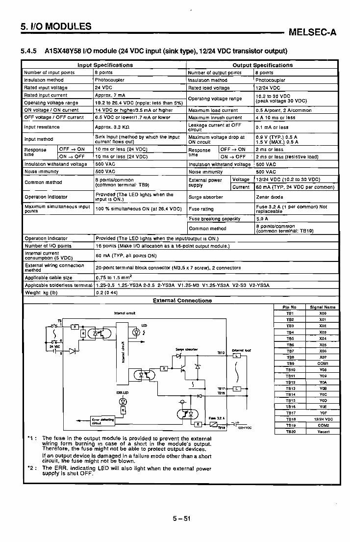
5.110 MODULES MELSEC-A
5.4.5 AlSX48Y58 I10 module (24 VDC input (sink type), 12/24 VDC transistor output)
Specifications 8 polnts
Photocoupler
24 VDC
Approx. 7 mA
19.2 to 26.4 VDC (r~pple: less than 5%)
14 VDC or h1gherl3.5 mA or h~gher
6.5 VDC or lowerll.7 mA or lower
Approx. 3.3 KC2
Slnk input (method by whlch the input current flows out) 10 ms or less (24 VDC)
10 ms or less (24 VDC)
500 VAC
500 VAC
8 p ~ l f l t ~ / c o m m ~ f l (common termcnal TB9)
Prov~ded (The LED l~ghts when the input 1s ON.)
100 46 simultaneous ON (at 26.4 VDC)
Input Number of lnput polnts
lnsulatron method
Rated lnput voltage
Rated Input current
Operating voltage range
ON voltage I ON current
OFF voltage I OFF current
Input res~sfance
lnput method
Specifications 8 polnts
Photocoupler
12124 VDC
10.2 to 30 VDC (peak voltage 30 VDC)
0.5 Npolnt. 2 Ncommon
4 A 10 ms or less
O.i mA or less
0.9 V (TYP.) 0.5 A 1.5 V (MAX.) 0.5 A
2 ms or less
2 ms or less (resistive load)
500 VAC
500 VAC
12/24 VDC (10.2 10 30 VDC)
60 mA (TYP. 24 VDC per common)
Zener d~ode
Fuse 3.2 A (1 per common) Not replaceable
5.0 A
8 porntslcommon (common terminal: TB19)
Response tlme
Output Number of output polnts
Insulatron method
Rated load voltage
OPeratlng voltage range
Max~mum load current
Max~mum inrush current
Leakage current at OFF circuit
Maximum voltage drop at ON c~rcuit
Number of 110 polnts
Internal current consumption (5 VDC)
External wiring method
Applicable cable size
Applicable solderless term~nal
We~ght kg (Ib)
OFF -+ ON
ON + OFF Response t~me
16 points (Make I10 allocat~on as a 16-polnt output module.)
60 mA (TYP. all polnts ON)
20-po~nt termlnal block connector (M3.5 x 7 screw). 2 connectors
0.75 to 1.5 mm2
1.25-3.5 1.25-YS3A 2-3.5 2-YS3A V1.25-M3 V1.25-YS3A V2-S3 V2-YS3A
0.2 (0 44)
Operat~on lnd~cator
lnsulatlon wrthstand voltage
Nolse rmmunrty
Common method
Operat~on indicator
Input polnts
OFF -t ON
ON + OFF '
Provided (The LED llghts when the
External Connections
M m o l w r w i
lnsulat~on withstand voltage
Nose ~rnmunity
External power SUPPlY
'1 : The fuse in the output module is provided to prevent the external wiring form burning In case of a short in the module's output. Therefore, the fuse might not be able to protect output devices. If an out ut device is damaged in a failure mode other than a short circuit. t k fuse might not be blown.
'2 : The ERR. indicating LED will also light when the external power supply is shut OFF.
Pin No TB1
TB2
TB3 -~ ~p
TB4
785
TB6
TB7
TB8
TB9
TBIO
T a l l
1812
TB13
TB14
TBlS
TB16
TB17
TBIB
TBlB
TB20
Voltage
Current
Signal Name XOO
XO1
x02 X03
X04
XO5
X06
X07
COMl
YO8
YO*
YOA
YO0
YOC
YOD
YCE
YOF
12/24 VDC
COM2
Vacant
Surge absorber
Fuse rating
Fuse breaklng capaclty
Common method
~npuWoutput 1s ON.)

5. INPUT AND OUTPUT MODULES I * . + _ .-2 - +,.?%.::.l?.c ... is, < $ , ' . l MELSEC-A
2, 1 . { f , *a;,; 6 . - ' 5
5.4.6 A1S42X dynamic input module
Number of output points '1
Insulation method Rated input voltage
Rated input current Operattng voltage range Max. s~multaneous input pornts ON voltagelON current
OFF voltagelOFF current Input impedance
External Connections
Pin Arrangement
Front view
pin NO. pin NO. Nane
812 XDO A12 XDI
010 XD4 A10 XD5 89 XD6 A9 XD7 B8 XSCNO A8 XSCNl
8 7 X S C N ~ A7 XSCN3
8 6 X S C N ~ A6 XSCN5
8 5 XSCN6 A5 XSCN7
84 Vacant A4 Vacant
'1 Be sure to connect a diode to each switch when there is a case that 2 or more 8 2 OV A2 OV
switches are pressed simultaneously. (Refer to the flgure on the rlght.) B l FG A1 I% F
Response trme
- Dynamic lnput Module
AlS42X
16132148164 potnts (swrtch setting) Photocoupler
12 VDC 1 24 VDC Approx. 4 mA ] Approx. 9 mA 10.2 to 26 4 VDC (ripple : less than 5 %) - .
100 %simultaneously ON (at 26.4 VDC) 8 VDC or higher12 mA or higher 4 VDC or lower11 mA or lower Approx. 2.4 kf2
0.4 ms or less (24 VDC) 0.4 ms or less (24 VDC) 13.3 ms
On state is indicated (LEDs), 32-points indicatron by switch 24-pin connector 0 3 mm2
Connector ( I pce.) for external wiring (soldering type) 500 VAC 500 VAC
80 mA (TYP, all points ON)
0.18 (0.40)
OFF ON ON + OFF
Appearance
Dynamic scan cycle Operating indicator External connections Applicable wire size
Accessones Insulation withstand voltage
Noise immunity Internal current consumption (5 VDC) Weight kg (Ib)

5. INPUT AND OUTPUT MODULES MELSEC-A
(1) Number of occupied I10 points setting
The Number of occupied I10 points is set by the DIP switches on the front surface of the module. It is factory-set to 64 points.
(2) Dynamic scan method
Number of occupied 110 polnts
Switch setting
In the dynamic scan method, the whole number of occupied 110 points is divided into several groups of specified number of points, and proc- - essed in several scans. 64 input points are divided into 8 groups of 8 points, and processed by group as shown in the figure below. Even if the number of occupied I10 points is set at 16, 32, or 48 points, dynamic scan cycle is fixed at 13.3 ms.
16 points 32 points 48 points 64 polnts
W
.=
Scan by AlS42X 1 X X X X I I
1 scan
I I
processing of ; I x30 to x37 I
Prooessing of XO to X7 -
I
Recessing of : XlOtoX17
I
I
I
Procesdngof I 1 Xi8 to XlF .I

5. INPUT AND OUTPUT MODULES MELSEC-A
5.4.7 A1S42Y dynamic output module
Number of output potnts
Insulation method
Rated input voltage
Operating voltage range
Max. load current
Leakage current at OFF c~rcuit
Max volgate drop at ON ctrcult
OFF 4 ON Response time
ON + OFF
Fuse rating
Fuse capacity
Error display
Operating Indicator
External connections
Applicable wire size
Accessories
lnsulatton w~thstand voltage
Nolse immunlty
Transistor Output Module
AlS42Y
16132148164 points (swltch setting) Photocoupler
12/24 VDC
10.2 to 26 4 VDC (rlpple : less than 5 %) 0 1 Alpoint
0.1 mA or less
Source : 1.1 VDC. Sink : 1 5 VDC
2 ms or less (res~st~ve load)
2 ms or less (res~st~ve load)
Fuse 1 6 A, not replaceable '1
50 A
LED goes ON when fuse blows : s~gnal output to PC CPU '2
On state IS lndlcated (LEDs). 32-po~nts ~ndlcat~on by sw~tch 24-pln connector
0.3 mm2
Connector (1 pce ) for external wir~ng (soldering type) 500 VAC
500 VAC
12/24 VDC (1 0.2 to 26.4 VDC)
8 mA (TYP, 24 VDClcommon)
100 mA (TYP, all points ON) P
0.19 (0.42)
External power SUPPlY
Appearance
Volgate
Current
External Connections
Pin NO Output term~nals
*1 The fuse In the output module IS provlded to prevent the external wlrtng from .4 power supply voltage burn~ng In case of a short In the module's output Therefore, the fuse m~ght not (24112 VDC) IS applied be able to protect output devlces I f an output devlce 1s damaged In a failure to the reverse dlrectlon mode other than a short clrcu~t, the fuse mlght not be blown of the LED If opposlte
'2 The ERR lndlcatlng LED will also l ~gh t when the external power supply 1s shut resistance Is
Internal current consumption (5 VDC)
We~ght kg (Ib)
OFF a dlode for serlal protectton to each LED
'3 Install the resistance for restrlctlng LED current outslde the A1S42Y module >
Pin Arrangement
Front vlew
Slgnsl Nane (FH)
YO1 YD3 YD5 YD7
YSCNl
YSCN3
YSCNS
YSCN7
Vacant
\%y OV
Vacant
Pin No.
812 - 811 810 89 88
87
86
85 84
83
82 81
Signal Name (FH)
YDO YD2
YD4 YO6
YSCNO
YSCN2
Y S C N ~
YSCN6
Vacant
b%y OV
Vacant
Pin No.
A12 A l l A10 A9 A8
A7
A6
A5 A4
A3
A2 A1

5. INPUT AND OUTPUT MODULES MELSEC-A
(1) Number of occupied I10 points setting
The number of occupied I10 points is set by the DIP switches on the front surface of the module. It is factory-set to 64 points.
(2) Dynamic scan method and dynamic scan cycle setting f (a) Dynamic scan method
\ In the dynamic scan method, the whole number of occupied I10 points is divided into several groups of specified number of points, and processed in several scans. 64 input points are divided into 8 groups of 8 points, and processed by group as shown in the figure below. Even if the number of occupied 110 points is set at 16, 32,
rl or 48 points, dynamic scan cycle is fixed at 13.311 06.7 ms.
Number of occupied 110 points
S w ~ t c h settlng
Scan by A1 S42Y ~-~-l-x-~~-~-~-~-x-]
16 points 32 points 48 points 64 points
u 1 scan
Processing of fl YO to n I
Processing of i I I YlOtoY17 :
I
Processina of I n Processing of ; Y20toY27 ; I I
I
Processing of Y30 toy37 i
I
Processing of I Y38 to Y3 F
13 3 ms (FAST mode)ll06 7 ms (SLOW mode) *
(b) Dynamic scan cycle setting Dynamic scan cycle is set by the DIP switches on the rear surface of the module. It is factory-set to FAST mode.
FAST mode
M ~ l e top -2
SLOW mode
swFl -2 M ~ e t o p

3 0 .
5. INPUT AND OUTPUT MODULES . $ ,,*;; , ' I , . _ , . 1 . . . 2 . . $
MELSEC-A
5.5 Blank Cover (AISGGO), Dummy Module (A1SG62) Specifications
The A1SG6O blank cover is used to protect base unit vacant slots against dust etc.
The AlSG62 dummy module is used to reserve a specified number of I10 points at any base unit slot.
Table 5.1 Dummy Module, Blank Cover Specifications
Occupying 110 points
I10 allocation spec~f~cat~on
Purpose of use
Other tunctions
Internal current consumption (5 VDC) Outside dimensions (rnrn)(~n) Weight (kg)(lb)
AlSG6O
16 points
16 vacant points
Used as a dust preventive cover of an unused slot where no inpuffoutput module is installed (e. g., a vacant slot between modules).
-
-
130 H) x 34.5(W x 93.6 (D) (5.6 x 1 .36 x3.69)
0 08 (0.18)
AlSG62
Max. 64 (16, 32, 48, or 64 points can be selected b using a select switch on the fron! of the module.)
lnput (X) points eslgnate the number of points L1 '
set with the select sw~tch in the [ I A module used to reserve 16, 32 48. ar 64 po~nts for the 110 module to be installed in the future. Bein equipped with simulation swit&es for 16 oints beginning with the head ofi10 numbers ~nputs can be turned ON/OF~ w~thout using any external switch.
60 mA
130 H) x 34.5(W x 93 6 (D) (5.1 b x 1.36 x 3.19) .
0 13 (0.29)

5.110 MODULES MELSEC-A
5.6 Names of Parts and Settings
The figures and table below describe the names of parts of l/O modules.
Terminal block connecting type - connector type
- --
No. Name Description
(1) 110 indicator LED Indicates the ON1OFF state of input and output. Indicates the ON state when i t is lit.
(2) Terminal block Used to connect a power cable and 110 cables.
(3) Terminal cover Covers the terminals. Terminal symbols can be written on the card attached to the inside of the cover.
(4) 40-pin connector , For 32-110 and 64-110 modules. Used to connect a power cable and I10 cables.
(5) Symbolcardcover Symbol card cover - I Used to switch the LED indication for the first-half 32 110s or for the secondhalf 32 1 (6) 1 Indicator select switch 110s of a 64-110 module. I L
(7) 37-pin D sub connector For 32-110 and 64-110 modules. Used to connect a power cable and 110 signal cables.
(8) Module fixing screw Used to fix the module to the base unit.
(9) Module mounting hook Engages with the mounting hole in the base unit to hook the module. r
When pulling out the terminal symbol card, pick up the edge of the card a little to pull i t out smoothly from the terminal cover.

5.110 MODULES MELSEC-A
37-pin D sub-connector Dummy unit Dynamic scan
tY Pe
A- . 3 D
k 0-
to [3 a m 0.0.. a rn
( 1 =: g (12)-- a (3p a n
1 0 D SB8:8: ,
M
r)
A1-~1SG62
= EJrnW--(6)
(13)
Description
Used for input s~mulat~on. 16 points beginning with the head of 110 numbers of the dummy module are allocated.
16, 32, 48, or 64 points can be selected for the occupying I10 points.
Used to set the dynamic scan cycle at 13.3 msec (FAST mode) or 106.7 msec ( SLOW mode). (This switch is located on the back side of the module.)
Used for the dynamic scan 110 module to connect a power supply cable and I10 signal wires.
. No.
( lo)
(1 1)
(12)
(13)
Name
switches
Occupying 110 points
Dynamic scan cycle
24-pin connector

5.110 MOD W LES MELSEC-A
A1SJ-56[ 1
(2)
1 (4)
I
-
-
7
0 I (3) ~? ( 1
Description
Used to indicate the OWOFF states of inputs and outputs. Lights when the 110 state is ON. 0 to IF: Inputs XO to IF. 20 to 37: Output Y20 to 37
Used to connect the power supply and the input signal wires.
Used to connect the power supply and the output signal wires.
Used to secure the module to the base unit.
Used to insert the module mounting slot in the base unit to install the module.
No.
(1)
(2)
(3)
(4)
(5)
N a m
110 indicator LED
Terminal block
Terminal block
Module mounting screw
Module mounting hook

6. EXTENSION BASE UNlT AND EXTENSION CABLE MELSEC-A
? ,8.
6. EXTENSION BASE UNlT AND EXTENSION CABLE
6.1 Specifications
6.1.1 Specifications of extension base units
Table 6.1 Extension Base Unit Specifications
'1 : For the installation of the dustproof cover, see Section 8.6.
Loaded 110 modules
Power supply module loadlng
Installation hole size
Terminal screw size
Applicable wire size
Applicable solderless terminal size
dimensions mm(inch)
Weight kg(lb)
Accessory
POINT]
When using either base unit AlS52B(S1), AlS52B(S1) or AlS58B(S1) which do not require supply module, refer to Section 6.1.3. -
6.1.2 Specifications of extension cables
AlS65B(Sl)
5 can be loaded
Table 6.2 shows the specifications of extension cables which can be used for the A1 SJCPU system.
Table 6.2 Extension Cable S~eci f icat ions
Cable length m(ft)
Required
AlS68B(Sl)
8 can be loaded
Resistance value of 5 VDC supply
/ line (Q at 55 "C)
AlSSSB(S1)
5 can be loaded
Not requlred
AlS52B(Sl)
2 can be loaded
I Application I Connection between AlSJCPU and AlS5[]B(Sl)IAlS6[]B(Sl)
AlS58B(Sl)
8 can be loaded
Weight kg(1b) 0.025 (0.055)l 0.1 (0.22) 10.14 (0.31) (0.20 (0 44) 1 0.4 (0.88) (0.65 (1.43)
$6-mm (0.24 inch) slot (for M5 screw)
Connection between AISJCPU and A5[ ]BlA6[ ]B
0.2 (0.44) 10.22 (0.48)
- -
-
3 1 5 x 1 3 0 ~ 2 8 (12.40 X 5.12 X 1 10)
0.71 (1.56)
(a) If an extension base unit is installed (by series connection) after the AISJCPU, use an extension cable with a length of 0.7 m (27.56 in.) or greater.
(b) When using an extension cable, do not bundle it together with main circuit (high voltage, large current) wires or allow it to run close to such lines.
- -
-
4 2 0 x 1 3 0 ~ 2 8 (16.54 X 5.12 X 1.10)
0.95 (2.09)
Four mounting screws (M5 x 25) '1 One dustproof cover (for 110 module) Four mountlng screws (M5 x 25)
M4 x 6 (FG terminal)
0.75 to 2 mm2
(V)1.25-4, (V)1.25-YS4, (V)2-YS4A (Applicable tightening torque: 12 kglcm (67.1 Iblinch)
3 6 5 x 1 3 0 ~ 2 8 (14.37 X 5.12 X 1.10)
0.87 (1.91)
1 3 5 x 1 3 0 ~ 2 8 (5.31 X 5 12 X 1.10)
0.38 (0.84)
2 6 0 x 1 3 0 ~ 2 8 (10.24 X 5.12 X 1.10)
0.61 (1.34)
6. EXTENSION BASE UNIT AND EXTENSION CABLE MELSEC-A
6.1.3 Application standards of extension base unit.(AlS52B(Sl), AlS55B(S1), AlS58B(S1), AS2B, A55B, A58B)
When an extension base unit of models AlS52B(S1), AlS55B(Sl) , A1 S58B(S1), A52B, A55B, or A58B is used, make sure a voltage of 4.75 V or above is supplied to the receiving.end (at the module installed in the last slot of the extension base unit).
With the AlS52B(S1), AlS55B(S1), AlS58B(S1), A528, A55B, or A58B extension base unit, 5 VDC is supplied from the power supply module of the main base unit via extension cable. Therefore, some voltage drop occurs over the extension cable and the specified voltage is not supplied to the receiving end , resulting in mis-input and mis-output.
If the voltage at the receiving end is less than 4.75 V, use an extension base unit of models AlS65B(S1), A1 S68B(S1), A65B, or A68B equipped with a power supply unit.
(1) Selection conditions
The voltage received by the module installed in the last slot of an ex- tension base unit AlS52B(S1), AlS55B(S1), AlS58B(Sl), A52B, A55B, or A58B must be 4.75 V or above.
Since the output voltage of the power supply module is set at 5.1 V or above, the voltage drop must be 0.35 V or less.
(2) Classification of voltage drop
Voltage drop is classified into (a), (b), and (c) as follows according to the connecting method and type of extension base units.
(a) Voltage drop of an AISJCPU
(b) Voltage drop of an extension base unit
(c) Voltage drop over an extension cable

i 6. EXTENSION BASE UNIT AND EXTENSION CABLE MELSEC-A
(3) Calculation of the receiving-end voltage
1st extension base unit
Use of extension base units AlS52B(Sl) , AlS55B(Sl), and AlS58B(Sl)
Use of extension base un~ ts A55B and A58B
VCPU, VO to V 4 : Voltage drop at respective slot of the AISJCPU unit
ICPU, 10 to 14 : Current consumption at respective slot o f the AISJCPU unit
V 8 to V15 : Voltage drop at respective slot of the extension base unit la to 115 : Current consumption at respective slot of the
extension base unit
1st extenston 2nd extension 3rd extension base unlt base unit base unit
AlSJCPU (a)
A1 SJCPU
V C ~ U
~ C P U
I
V15
115
V2
12
(c)
Ve
la
i
VO
10
1st extension base unit
V11
111
V3
13
V i
11
AlSS[ ]B-S1 (b)
A1 SJCPU (a)
V9
19
V12
112
V4
14
Vio
110
(c)
-
-
AlS5[ IB-S1
( 1
(c)
V13
113
AlS5[ IB-S1 (b)
V14
114
2nd extension - baseunit ' : Voltage drop at extension base units
(c)
- -
1 st extension base unit
AlSS[]B-Sl (b)
AlSJCPU (a)
AlS5[ ]B-S1
A5[]B -
can be ignored.
3rd extension - base unit
-
( 1
(C)
AlS5[ ]B-S1
2nd extension . base unit
- -
A51 IB : Voltage drop at extension base units
can be ignored.
3rd extension base unit
- A51 IB

6. EXTENSION BASE UNIT AND EXTENSION CABLE MELSEC-A
(a) Voltage drop of the AISJCPU Each slot of an AISJCPU has a resistance of 0.022 SL. Calculate voltage drop of each slot, and obtain the total voltage drop of the unit.
1) Voltage drop of the CPU unit: VCPU
2) Voltage drop of slot 0: Vo
3) Voltage drop of slot 1 : Vr
4) Voltage drop of slot 2: V2 r"
5) Voltage drop of slot 3: V3
6) Voltage drop of slot 4: V4
7) Total voltage drop of the AISJCPU: VK
(b) Voltage drop of an extension base unit (AlS52B(S1), AlS55B(S1), A1 S58B(S1))
Each slot of an extension base unit has a resistance of 0.006 Q.
Calculate voltage drop of each slot, and obtain the total voltage drop of a base unit.
1) Voltage drop of slot 8: Va
2) Voltage drop of slot 9: Vg
V9 = 0.006 x (19 + I r o + 111 + 112 + 113 + 114 + 115)
3) Voltage drop of slot 10: Vio
Vro = 0.006 x (110 + 111 + 112 +. 113 + 114 + 115)
4) Voltage drop of slot 11 : V l i
V11 = 0.006 x ( I l l + I12 + 113 + 114 + 115)
5) Voltage drop of slot 12: V 12
v12 = 0.006 X (112 + 113 + 114 + 115) 6) Voltage drop of slot 13: V13

1 6. EXTENSION BASE UNIT AND EXTENSION CABLE MELSEC-A . ..$ ,
7) Voltage drop of slot 14: V14
V14 = 0.006 x (I14 + 115)
8) Voltage drop of slot 15: V15
9) Voltage drop of an extension base unit: vz VZ = v8 + v9 + v.10 + v11 + v12 + v13 + v14 + Vl5
(c) Voltage drop over extension cables
Vc = (Resistance of an extension cable) x (I8 + 19 + Iio + I l l + 112 + 113 + 114 + 115)
(d) Voltage at the receiving end
(5.1 - VK - Vz - VC) 5 4.75 (V)

6. EXTENSION BASE UNIT AND EXTENSION CABLE MELSEC-A
POINT 1 If 3 extension base units are installed, determine the voltage at the receiv- ing end as follows:
_ (1)- Calculation of voltage drop at the A1 SJCPU Determine the voltage drop at individual slots by multiplying the resis-- tance of one slot (0.022 0 ) by the [sum of current consumptions of all slots in the AISJCPU + sum of current consumptions of all slots in the I st, 2nd and 3rd extension base units], then sum the voltage drops at the individual slots.
(2) Calculation of voltage drop at 1st extension base unit Determine the voltage drop at individual slots by multiplying the resis- tance of one slot (0.006 0 ) by the [sum of current consumptions of all slots in the 1st extension base unit + sum of current consump- tions of all slots in the 2nd and 3rd extension base units], then sum the voltage drops at the individual slots.
(3) Calculation of voltage drop at 2nd extension base unit Determine the voltage drop at individual slots by multiplying the resis- tance of one slot (0.006 !2) by the [sum of current consumptions of all slots in the 2nd extension base unit + sum of current consump- tions of all slots in the 3rd extension base unit], then sum the voltage drops at the individual slots.
(4) Calculation of voltage drop at 3rd extension base unit Determine the voltage drop at individual slots by multiplying the resis- tance of one slot (0.006 0 ) by the [sum of current consumptions of all slots in the 3rd extension base unit], then sum the voltage drops at the individual slots.
(5) Calculation of voltage drop in the extension cable Calculate the sum of (a) + (b) + (cj:
(a) (Resistance of the extension cable that connects the AISJCPU and 1st extension base unit) x (sum of current consumptions of ls t , 2nd and 3rd extension base units)
(b) (Resistance of the extension cable that connects the 1 st extension base unit and 2nd extension base unit) x (sum of current consump- tions of 2nd and 3rd extension base units)
(c) (Resistance of the extension cable that connects the 2nd exten- sion base unit and 3rd extension base unit) x (total current con- sumption of 3rd extension base unit)
(6) Checking the voltage at the receiving end 5.1 - (sum of (1) through (5)) 2 4.75 (V)
I 6. EXTENSION BASE UNIT AND EXTENSION CABLE MELSEC-A
(4) Examples
(a) Voltage drop of an AISJCPU
= 0 0 0 0 0 Q - W W W b W O > t > > >
A1 S07B (0.036 R)
(b) Voltage drop of an extension base unit
. .
(c) Voltage drop over an extension cable
- A1 S58B
0 0 0 0 0 0 0 0 W . r t W W W W W W X X X X X X X X
(d) Voltage at the receiving end
5.1 - 0.1804 - 0.0108 - 0.0144 = 4.8944 (V) Since the voltage at the receiving end is more than 4.75 V, the above system can be put into operation.
I
(5) Minimizing the voltage drop
2 $ 2 2 $ 2 2 2 a < < < < < < <
Try the following to minimize the voltage drop.
(a) Change the positions of modules.
Install the modules beginning with slot 0 of an AISJCPU in the order of current consumption from large to small. Install the modules of small current consumption to extension base units.
(b) Use a short cable for extension.
The shorter an extension cable, the smaller the resistance it has, consequently minimizing its voltage drop. Make extension cables as short as possible.

6. EXTENSION BASE UNIT AND EXTENSION CABLE MELSEC-A
6.2 Names and Purposes of Parts and Settings
The names and purposes of parts of the base units are explained below.
1 Base mounting hole
No.
('1
(2)
(3)
(4)
(5)
DIN rail hook
FG terminal
Name
Extension cable connector (IN) . Extension cable connector (OUT) (for A lS[ I[ ]B-S1 )
Base cover
Module connector
screw
Stage number setting switch (for AIS[][]B-S1)
Purpose
Used to connect an extension cable to an extension base unit or an AlSJCPU for signal transmissions. Remove the connector cover attached to the unit and connect an
cable.
Extension cable connector protective cover.
Used to connect to power supply module, an 110 module or special function module. Put a supplied cover or blank cover (AlSG60) on unused connector to protect i t from dust.
Used to secure a module to the base unit. Screw size: M4 x 12
Used to mount the base unit to a control panel. (for M5 screw)
Used to install the module to the DIN rail. AlS52B(Sl), AlS55B(Sl): One hook AlS65B(S1), A1 S68B(Sl), AlS58B(Sl): Two hooks
Grounding terminal connected to the shield pattern on the PC board.
Switch for setting the stage number of extension base. For the stage number setting procedure, refer to Section 6.3.
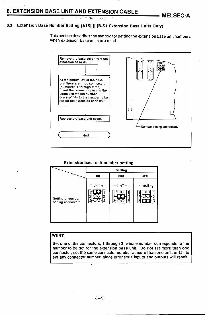
6. EXTENSION BASE UNlT AND EXTENSION CABLE ; . , ,$ .,4 . +,' . A ' ., #
< I t ) > ,
MELSEC-A
6.3 Extension Base Number Setting (A1S[ ][ ]B-S1 Extension Base Units Only)
This section describes the method for setting the extension base unit numbers when extension base units are used.
Remove the base cover from the extension base unit.
At the bottom left of the base unrt there are three connectors (numbered 1 through three). Insert the connector pin into the connector whose number corresponds to the number to be set for the extension base unit.
Replace the base unit cover. li' Num ber-setting connectors t
End
Extension base unit number setting
POINTI Set one of the connectors, 1 through 3, whose number corresponds to the number to be set for the extension base unit. Do not set more than one connector, set the same connector number at more than one unit, or fail to set any connector number, since erroneous inputs and outputs will result.
Setting of number- settlng connectors
Setting
3rd
r UNIT 1
1st
r UNIT 1
2nd .
r UNIT 1
3 3 3 0 0 3

6. EXTENSION BASE UNIT AND EXTENSION CABLE MELSEC-A
6.4 Installing a DIN Rail
Both the main base units and extension base units are equipped with hooks used for mounting to a DIN rail.
The following explains the method of mounting a DIN rail:
(1) Applicable DIN rails type
(a) form and dimentions
(2) Intervals of mounting screws
(b) material
When a dimension 35 x 7.5 rail is mounted, fix it with screws with intervals of 200 mm or less between each of the screws.
Material
Iron
Aluminum
Applicable Dimension ( W x H ) mm(inch)
35 x 7.5(1.38 x 0.30). 35 x 15(1.38 x 0.60)
35 x 7.5(1.38 x 0.30)
DIN mil Mounting screw
(1.38 in)
- - - - - - . - - 6-
I P P P --
P=200 mm (7.87 in) or less
- - -- --
- - - 8 2

6. EXTENSION BASE UNIT AND EXTENSION CABLE MELSEC-A
(3) Mounting to/removal from a DIN rail
(a) Mounting procedure
Mount a base unit to a DIN rail as follows:
1) Engage the hook of the base unit with the rail from above.
2) Push the base unit onto the rail to secure it in position.
DIN rail hook
Appearance when mounted to DIN rail
(b) Removing procedure
Remove a base unit from a DIN rail as follows:
1) Pull down the bottom hook of the base unit using a flat blade screwdriver (6 x 100).
2) Pull the base unit away from the rail while pulling down the bottom hook.
Pull to remove
Bottom hook

MEMO

7. MEMORY ICs AND BATTERY MELSEC-A
7. MEMORY ICs AND BAITERY
7.1 Memory ICs
This section describes specifications, handling instructions and installation of the memory ICs used in the AISJCPU.
7.1 .I Specifications
Table 7.1 shows specifications of the ROMs.
Table 7.1 Mernorv S~ecif icat ions
I Memory specifications I EEP-ROM I EP-ROM I
I Outslde dimension mm (in) 1 15 x 68.6 x 42 (0.59 x 2.7 x 1.65) I
Memory capacity (bytes)
I Weight (kg) (Ib) 1 0.03 (0 06) I
7.1.2 Handling instructions
8 K bytes (max. 2 K steps)
(1) Handle with care memory cassettes and pin connectors since their plastic body cannot resist strong impacts.
(2) Do not remove the printed circuit board from the memory cassette.
32 K bytes (max. 8 K steps)
(3) Use caution not to let chips of wires and other foreign material enter the memory cassette.
32 K bytes (max. 8 K steps)
(4) When installing a memory cassette to an AISJCPU unit, engage the connectors securely.
(5) Never place the memory on metal, which may allow current flow, or on an object which is charged with static electricity, such as wood, plastic vinyl, fiber, cable and paper.
(6) Do not touch or bend the memory leads.
(7) Do not touch by hand the connector of a memory cassette. Touching it by hand may lead to incomplete contact.
IMPORTANTI (1) Always turn OFF the power to the AISJCPU unit when installing or
removing a memory cassette. If a memory cassette is installed or removed with the power to the CPU ON, contents of the memory will be destroyed.
(2) I f the power is turned ON when the memory cassete is installed, the contents of the RAM memory incorporated in the AlSJCPU is overwrit- ten. .
If the contents of the RAM memory needs to be saved, install a memory cassette after making a backup of the contents using a peripheral device.

7. MEMORY ICS AND BATTERY MELSEC-A
7.1.3 Installing and removing a memory cassette
Follow the procedures below when installing or removing a memory cassette.
(1) Installing a memory cassette
(a) Hold a memory cassette vertically so that its model name is right side up and its connector faces the AISJCPU unit. Insert the memory cassette all the way in the AISJCPU unit so that the hooks of the memory cassette are completely engaged (they "click").
(b) Make sure the hooks are completely engaged. (If the memory cas- sette is not inserted all the way, the front lid of the AISJCPU cannot be closed.)
(2) Removing a memory cassette
(a) Pull out the memory cassette while pushing the hook releasing lugs that are provided at the top and the bottom of the memory cassette.

I 7. MEMORY ICS AND BATTERY - ? , - s . < . > * , . . . L,.k", MELSEC-A
7.1.4 Writing a sequence program to an A1SMCA-8KP
A sequence program can be written to, or erased from, an AlSMCA-8KP using a ROM writerleraser.
I f an AISMCA-8KP is installed to the ROM socket of an A6GPP or AGWU, use a memory write adaptor (A6WA-28P).
Use an A6WA-28P as follows:
('1) Install an A1 SMCA-8KP to an A6WA-28P so that their connectors couple correctly with each other.
(2) Install the A6WA-28P that is coupled with an A1SMCA-8KP to the ROM socket of an A6GPP or A6WU. The pin next to the cut corner of the A6WA-28P is pin No. 1. Make sure the A6WA-28P is installed correctly to the ROM socket.
Cut comer
ROM socket
A6 WA-28P
A1 SMCASKP

7. MEMORY ICs AND BATTERY MELSEC-A
7.2 Battery
7.2.1 Specifications
Table 7.2 shows specifications of the battery used to retain memory stored if power failure occurs.
Table 7.2 Battery Specifications
7.2.2 Handling instructions
A6BAT
(1) Do not short circuit.
(2) Do not disassemble.
Normal voltage
Guaranteed life
Application
sion mm(in)
(3) Do not expose to open flame.
3.6 VDC
5 years
For IC-RAM memory backup and power failure compensation function
$16(0.63)~30(1.18)
(4) Do not heat.
(5) Do not solder its terminals.
(6) Route the battery cable as shown below so that the battery connector is- not strained.
7.2.3 Installation
Battery lead connector is disconnected from the battery connector on the AISJCPU board to prevent discharge during transportation and storage.
Before starting the AISJCPU, plug the battery connector into the battery connector on the A1 SJCPU board.
To use a sequence program stored in the user program area in the A1 SJCPU if a power failure occurs. To retain the data if a power failure occurs.
L
AISJCPU Battery connector
A6BAT
Rout8 the battery cable on We bottom of the battery case as shown above.

7. EXTENSION BASE UNIT AND EXTENSION CABLE , . MELSEC-A
7) Voltage drop of slot 14: V14
vie = 0.006 x (114 + 11s)
8) Voltage drop of slot 15: V15
v15 = 0.006 x (115)
9) Voltage drop of an extension base unit: Vz
VZ = v8 + v9 + v10 + v11 + v12 + v13 + v14 + v15
(c) Voltage drop over extension cables
Vc = (Resistance of an extension cable) x (I8 + 19 + 110 + 111 + 112 + 113 + 114 + 115)
(d) Voltage at the receiving end
(5.1 - VK - Vz - Vc) 2 4.75 (V)
7. EXTENSION BASE UNIT AND EXTENSION CABLE MELSEC-A
POINTI If 3 extension base units are installed, determine the voltage at the receiv- ing end as follows:
(1) Calculation of voltage drop at the AISJCPU Determine the voltage drop at individual slots by multiplying the resis- tance of one slot (0.022 R) by the [sum of current consumptions of all slots in the-AISJCPU + sum of current consumptions of all slots in the Ist, 2nd and 3rd extension base units], then sum the voltage drops at the individual slots.
(2) Calculation of voltage drop at 1st extension base unit Determine the voltage drop at individual slots by multiplying the resis- tance of one slot (0.006 R) by the [sum of current consumptions of all slots in the 1st extension base unit + sum of current consump- tions of all slots in the 2nd and 3rd extension base units], then sum the voltage drops at the individual slots.
(3) Calculation of voltage drop at 2nd extension base unit Determine the voltage drop at individual slots by multiplying the resis- tance of one slot (0.006 R) by the [sum of current consumptions of all slots in the 2nd extension base unit + sum of current consump- tions of all slots in the 3rd extension base unit], then sum the voltage drops at the individual slots.
(4) Calculation of voltage drop at 3rd extension base unit Determine the voltage drop at individual slots by multiplying the resis- tance of one slot (0.006 R) by the [sum of current consumptions of all slots in the 3rd extension base unit], then sum the voltage drops at the individual slots.
(5) Calculation of voltage drop in the extension cable Calculate the sum of (a) + (b) + (c):
(a) (Resistance of the extension cable that connects the AISJCPU and 1st extension base unit) x (sum of current consumptions of Is t , 2nd and 3rd extension base units)
(b) (Resistance of the extension cable that connects the 1 st extension base unit and 2nd extension base unit) x (sum of current consump- tions of 2nd and 3rd extension base units)
(c) (Resistance of the extension cable that connects the 2nd exten- sion base unit and 3rd extension base unit) x (total current con- sumption of 3rd extension base unit)
(6) Checking the voltage at the receiving end 5.1 - (sum of (1) through (5)) 2 4.75 (V)

7. EXTENSION BASE UNIT AND-EXTENSIQN CABLE MELSEC-A
.L -. . - ,#. . i-l.*'n ,??&--' '.. , * ?. , , ., t . 4 . L . - , ,..-' . . -
(4) Examples
(a) Voltage drop of an AISJCPU
=
(b) Voltage drop of an extension base unit
(c) Voltage drop over an extension cable
0
(d) Voltage at the receiving end
AlS07B (0.036 R) r A1 S58B
5.1 - 0.1804 - 0.01 08 - 0.0144 = 4.8944 (V) Since the voltage at the receiving end is more than 4.75 V, the above system can be put into operation.
?
(5) Minimizing the voltage drop
0
0 0 0 0 0 0 0 0 b b W c r V b b b X X X X X X X X S n , ? S n , s ? ? I I ? S I < < < a < < < <
Try the following to minimize the voltage drop.
0-0
-
Q b W V W b o > > > > > - ; ; c n c n c n c n c n - h h h h 5 5
(a) Change the positions of modules.
-
0
Install the modules beginning with slot 0 of an AISJCPU in the order of current consumption from large to small. lnstall the modules of small current consumption to extension base units.
(b) Use a short cable for extension.
The shorter an extension cable, the smaller the resistance it has, consequently minimizing its voltage drop. Make extension cables as short as possible.

7. EXTENSION BASE UNIT AND EXTENSION CABLE MELSEC-A
7.2 Names and Purposes of Parts and Settings
The names and purposes of parts of the base units are explained below. L
A1 S65B(Sl), A1 S68B(S1)
(6) (3) (5)
1 / I 0 0 0 0 0 1 0
(4) I A1 S52B(S1), A1 SSSB(Sl), AlS58B(S1) / (6) (3) (5) I / I
(2) 0 0 0 E 1 0 0 3
No.
('1
(2)
(3)
(4)
(5)
(6)
(7)
(8)
(9)
Name
Extension cable connector (IN)
Extension cable connector (OUT) (for AlS[ I [ ]B-S1)
Base cover
Module
Module mounting screw
Base mounting hole
DIN rail hook
FG terminal
Stage number setting switch (for AIS[ I[ lB-S1)
Purpose
Used to connect an extension cable to an extension base unit or an AlSJCPU for signal transmissions. Remove the connector cover attached to the unit and connect an
Extension cable connector protective cover.
Used to connect to power supply module, an I10 module or special function module. Put a supplied cover or blank cover (AlSG6O) on unused connector to protect it from dust.
Used to secure a module to the base unit. Screw site: M4 x 12
Used to mount the base unit to a control panel. (for M5 screw)
Used to install the module to the DIN rail. AlS52B(Si), AlS55B(S1): One hook AlS65B(Sl), AlS68B(Sl). AlS58B(Sl): Two hooks
Grounding terminal connected to the shield pattern on the PC board.
Switch for setting the stage number of extension base. For the stage number setting procedure, refer to Section 7.3.

7. EXTENSION BASE UNlT AND EXTENSION CABLE : r . . -, h ;:?J& ; . > q .s. * - , . . 3 ,
* 1
MELSEC-A
7.3 Extension Base Number Setting (A1S[ I[ ]B-S1 Extension Base Units Only)
This section describes the method for setting the extension base unit numbers when extension base units are used.
Remove the base cover from the extension base unit.
I A; the bottom left of the base unit there are three connectors (numbered 1 through three). Insert the connector pin into the connector whose number corresponds to the number to be set for the extension base unit.
Replace the base unit cover.
I Number-setbng connectors
I End
Extension base unit number setting
POINTI 1
Set one of the connectors, 1 through 3, whose number corresponds to the number to be set for the extension base unit. Do not set more than one connector, set the same connector number at more than one unit, or fail to set any connector number, since erroneous inputs and outputs will result.
setting connectors Setting of number-
Setting
1st
r UNIT 1
2nd
r UNIT 1
3rd
r UNIT 1

7. EXTENSION BASE UNIT AND EXTENSION CABLE MELSEC-A
7.4 Installing a DIN Rail
Both the main base units and extension base units are equipped with hooks used for mounting to a DIN rail.
The following explains the method of mounting a DIN rail:
(1 ) Applicable DIN rails (JIS-C2B12)
TH35-7.5 Fe TH35-7.5 Al TH35-15 Fe
(2) Intervals of mounting screws
When a TH35-7.5 Fe or TH35-7.5 Al rail is mounted, fix it with screws with intervals of 200 mm or less between each of the screws.
DIN rail Mounting screw
(1.38 in)
h - - - I
P P 4
P=200 mm (7.87 in) or less
.
- ---6--'-
- I
.- di-
I - 8
I
I -- -- --
-- --

8. LOADING AND INSTALLATION MELSEC-A
8. LOADING AND INSTALLATION
8.1 Installation Environment
Avoid the following places when installing the A1 SJCPU system:
(1) Places where ambient temperature is out of 0 to 55 "C range. -_
(2) Places where ambient humidity is out of 10 to 90 %RH range.
(3) Places where dewing (condensation) occurs due to sudden temperature changes.
(4) Places where corrosive or inflammable gas exists.
(5) Places where a large amount of dust, iron powder and other conductive power, oil mist, salt, of organic solvent exists.
(6) Places exposed to direct sunlight.
(7) Places where a strong electric or magnetic field exists.
(8) Places where mechanical vibrations of impacts are transmitted directly to the module body.
8.2 Calculation of Heat Generated by the Programmable Controller System
The operating ambient temperature inside the panel in which the programma- ble controller is installed must be kept below 55 "C. In order to design heat-dissipating measures inside the panel where the PC is installed, the average power consumption (amount of heat generated) of the units and equipment inside the panel must be known. The method for determining the average power consumption of the AlSJCPU system is presented here. Calculate the temperature rise inside the panel from this power consumption
Average power consumption
Power is consumed by the following PC parts:
I 1 5 VDC line
power (lout) LOAD
Power
-
r
v * v
Special function module
Power supply
CPU module
24 VDC line .
T - ~ - Output current
External I
1 2 4 V D C I I power supply I - - - - .
'L 'L 'L
Output
Input current (IIN) x E L
output module
Relay transistor
Input module

8. LOADING AND INSTALLATION MELSEC-A
(1) Power consumption of a power supply module
Approximately 70% of the power supply module current is converted into power and 30% of that 70% is dissipated as heat, i.e., 317 of the output power is actually used:
15v : 15V= 5 VDC logic circuit current consumption of each module
1 2 4 ~ : 124V= Average current consumption of 24 VDC for output module internal consumption (with average number of points switche ON)
This is not relevant i f 24 VDC is supplied from an external-source and a power supply module with no 24 VDC output is used.
(2) Total 5 VDC logic circuit power consumption 1 The 5 VDC output circuit power consumption of the power supply mod- ule is the power consumption of each of the modules.
W5v = 15v x 5 (w)
(3) Total 24 VDC average power consumption of output modules (with an 0 average number of points switched ON.
The 24 VDC output circuit average power consumption of the power supply module is the total power consumption of each of the modules:
w24v = I 24V X 24 (w)
(4) Average power consumption due to voltage drop in output circuits of output modules (with an average number of points switched ON)
WOUT = IOUT x Vdrop x number of output points x average number of outputs on at one time (W)
IOUT : Output current (actual operating current) (A)
Vdrop : Voltage drop across each output module (V)
(5) Average power consumption of input circuits of input modules (with an average number of points switched ON)
WIN = IIN x E x X number of input points x average number of inputs on at one time (W)
IIN : lnput current (effective value for AC) (A)
E : Input voltage (actual operating voltage) (V)
(6) Power consumption of special function modules is expressed as follows:
WS = ~ S V X 5 + 1 2 4 ~ ~ 24 + I1 oOV X 100 (w)
The sum of each of the values calculated above is the power con- sumption of the entire PC system.
W = WPW + W ~ V + W 2 4 ~ + WOUT+ WIN + WS (W)
The amount of heat generated and the temperature rise in the panel can be calculated from this total power consumption (W).

8. LOADING AND INSTALLATION MELSEC-A
Generally, the temperature rise in the panel is expressed as follows:
W T = - ["C] U A
W : Power consumption of the entire PC system (obtained as shown above.
A : Panel internal surface area (m2)
U = 6 : i f the temperature inside the panel is controlled by a fan, etc
U = 4 : i f the air in the panel is not circulated
POINTI If the temperature inside the panel exceeds 55 "C, the temperature must be reduced by installing a heat exchanger. If a fan is used, it will suck in dust together with air from outside, with adverse effects on the programmable controller.
I* 8.3 Precautions Relating to the Installation of the Base Unit
The following precautions must be observed when installing a PC to an. operation panel or other bases considering fully the operability, maintainabil- ity, and resistance to the environmnt.
(1) Base unit mounting position
(50 mn (1 97 mch) or less m haght)
Provide a clearance between the top and bottom sides of the unit and the wall of structure or components as given below. This is required for ventilation and replacing ease.
Where:AlSJCPU, AIS5[ ]B(Sl), A1S6[ lB(S1) . . . . . . . . . . . . . 30 mm (1.18 inch) or over
....................... A5[ 19, A6[ 18. 80 mm (3.1 5 inch) or oveR
Represents the m l ~ n g of panel, mnng andrut, or conponent
S-(I 18 in&) or over
30 mm (1 18 mch) or over
inch) or over
I 80mn(315 In&) or over

8. LOADING AND INSTALLATION MELSEC-A
(2) Installing direction
(a) Install the PC in the direction shown below for good ventilation
(b) The following installing directions must be avoided.
(3) lnstall the base unit on a flat surface. It it is mounted on an uneven surface, the PC board in the module is starained and malfunction will occur.
(4) Avoid installing the base unit near a vibrating source such as a large electromagnetic switch and no-fuse circuit breaker. lnstall it to a sepa- rate panel or away form such vibrating source.
(5) Provide a wiring duct i f necessary
However, if the clearance with the toplbottom of the PC is less than 30 mm (1.18 inch), note the following points:
n (a) When the duct is located above the PC, the height of the duct should
be 50 mm (1.97 inch) or less to allow for sufficient ventilation.
Set the distance from the top of the PC so that the hook latch at the top of the module can be pressed. If it cannot be pressed, it will be impossible to replace the module.
(b) When the duct is located under the PC, provide sufficient clearance so that there is no effect on the 1001200 VAC input line of the power supply module, I10 wires of I10 modules, and 12/24 VDC wires. 1

8. LOADING AND INSTALLATION .'.3.i.3 - .-I' I . MELSEC-A
(6) Provide clearances, mentioned below, between the PC and other de- vices (contactors and relays) to avoid the influence of radiating noise and heat.
Between the PC and a device installed in front of the PC: 100 mm (3.94 inch) or over.
Between the PC and devices installed on the right and left sides of the-PC: 50 mm (1.97 inch) or over
relay, etc. inch) or over 50 rnm (1.97 inch) or over

8. LOADING AND INSTALLATION MELSEC-A
8.4 Mounting and Removing Modules
This section explains how to mount power supply modules, PC CPU modules, I/O modules, special function modules, etc., to a base unit, and how to remove them.
(1) Module mounting
The module mounting procedure is as follows.
( 1 ) Before securing the module, make sure the module fixing projections are inserte in the module fixing hole. If the module is forcibly secured without inserting the projections, the pins in the module connector may be bent or damaged.
Insert h e module fixing pro- jections into h e module fixing hole in h e base unit.
b
Install the module onto the base unit by pushing the top forward.
Base
Make sure the h w k is se- curely inserted in the module fixing hole in h e base unit, then secure i t with the mod-
(2) Always turn the power supply OFF before mounting or removing
odule fixing projeo
Module fixing hole

I 8. LOADING AND INSTALLATION
. . MELSEC-A
(2) Module removal
The module removal procedure is as follows.
Remove the module mount- ing screw, then pull the mod- ule toward you while pushing the hook latch
Lift the module upwards so as to disengage the module fix- ing projections from the mod- ule fixing hole.
Module
POINTS 1 (1) When removing a module, be sure to remove the module mounting
screw before attempting to disengage the module fixing projections from the module fixing hole. If the module is forcibly removed, the module fixing projections will be damaged.
(2) Always turn the power supply OFF before mounting or removing any module.
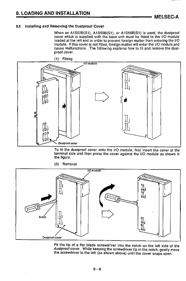
8. LOADING AND INSTALLATION MELSEC-A
8.5 installing and Removing the Dustproof Cover
When an AlS52B(Sl), AlS55B(Sl), or AlS58B(SI) is used, the dustproof cover which is supplied with the base unit must be fitted to the I10 module loaded at the left end in order to prevent foreign matter from entering the 110- module: If this cover is not fitted, foreign-matter will enter the I10 module and cause malfunctions. The following explains how to fit and remove the dust- proof cover.
- - -- --
To fit the dustproof cover onto the I10 module, first insert the cover at the terminal side and then press the cover against the I f 0 module as shown in the figure.
(2) Removal
VO module
Fit the tip of a flat blade screwdriver into the notch on the left side of the dustproof cover. While keeping the screwdriver tip in the notch, gently move the screwdriver to the left (as shown above) until the cover snaps open.

8. LOADING AND INSTALLATION MELSEC-A
. .
8.6 Failsafe Circuits
When the power to the programmable controller is turned ON or OFF, the process output may not perform normally at times due to the difference between the delay time and the rise time of the power supply of the PC CPU module and the external power supply (especially DC). For example, when the PC main power supply is turned on after turning on the process external power supply to a DC output module, the DC output module may momentarily issue faulty outputs when thePC power is turned on. To avoid this problem, the circuit must be configured.so-that.the.PC main power supply is turned on first. Erroneous operation may also occur due to faults of the external power supply or programmable controller. In-order-to prevent faults such as these from causing erroneous operation of the entire system, and also for safety reasons, configure circuits external to the programmable controller (such as emergency stop, protection, and inter- lock circuits) that prevent machine damage and accidents.
An example circuit for a system design based on the above points is pre- sented overpage.
POINT/
Some A1S series output modules detect a blown fuse error when the external power supply is turned OFF.
In the example circuit shown overpage, since the start-up of the AISJCPU takes place earlier than the rise of the external power supply to the output module, a blown fuse error is detected.
To solve this problem, the system is designed to keep M9084 on until the external power supply has risen, so as not to check for blown fuses. (When M9084 is ON, the I10 module verification and battery checks are not performed.)

8. LOADING AND INSTALLATION MELSEC-A
(1) System design circuit example
ALL AC ,Mixed AC and D q
POWER
%& TRANSFORMER
@=@'@-I 8 FUSE
Lx9Q-J TRANSFORMER = rn
4Gm-J TRANSFORMER = fomm
OUTPUT MODULE I \
I I INPUT MODULE
I I RUWSTOP circuit inter- locked with RA1 (run moni- tor relay)
-. . -. ...-""-& I I 4 r '2: Low battery alarm
4 '3: RA1 swltched ON by M9039 (run monitor relay)
'4: Power to output equipment '4 1 n swtched OFF when the
. - a . -. {en.
-5 :
'6: '4
'7: '8:
Vohage relay 1s recomnended
Input swtched when power supply established.
Set time for DC power sup ply to be established.
ON when run by M9039
Interlock circuits as neces- sary,
The power-ON procedure IS as follows:
EadG 1) Set the CPU to RUN.
2) Switch ON the power.
3) Turn ON the start switch.
4) When the magnebc contactor (MC) comes in, the output equipment is powered and may be driven by the program.
EcKAux 1) Set the CPU to RUN
2) Switch ON the power.
3) Turn ON the start switch.
4) When DC power is established, RA2 comes ON.
5) Timer (TM) times out after the DC power reaches 1000/o.
(The TM set value should be the penod of time from when RA2 comes ON to the establishment of 10% DC voltage.. Set thls value to approximately 0.5 seconds.)
6) When the magnebc contractor (MC) comes In, the output equipment is powered and may be driven by the program. (If a voltage relay is used at RA2, no timer (TM) is required in the program.)
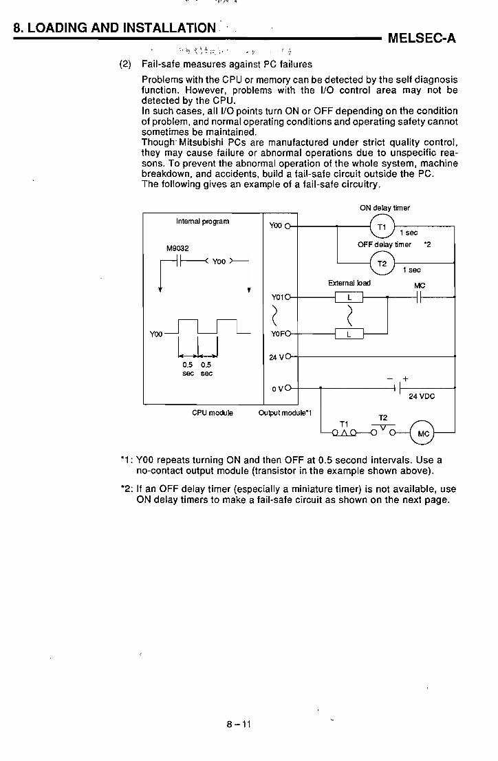
8. LOADING AND INSTALLATION .. . ~
MELSEC-A
(2) Fail-safe measures against PC failures Problems with the CPU or memory can be detected by the self diagnosis function. However, problems with the I f0 control area may not be detected by the CPU. In such cases, all I f0 points turn ON or OFF depending on the condition of problem, and normal operating conditions and operating safety cannot sometimes be maintained. Though- Mitsubishi PCs are manufactured under strict quality control, they may cause failure or abnormal operations due to unspecific rea- sons. To prevent the abnormal operation of the whole system, machine breakdown, and accidents, build a fail-safe circuit outside the PC. The following gives an example of a fail-safe circuitry.
ON d e h v timer
b m e r *2 I 1 sec
lntemal program
I External bad MC I
iO'FrT-\ YOF
Yo0 0
CPU module Ou" moduW1 L: - 4 MC
1
*I : YO0 repeats turning ON and then OFF at 0.5 second intervals. Use a no-contact output module (transistor in the example shown above).
'2: If an OFF delay timer (especially a miniature timer) is not available, use ON delay timers to make a fail-safe circuit as shown on the next page.

8. LOADING AND INSTALLATION MELSEC-A
A fail-safe circuit built with ON delay timers
CPU module Ou$ut module
24 V 0
o v o
*I : Use a solid-state relay for the M I relay.
4
- + I I I
I 24 VDC 4 .

8. LOADING AND INSTALLATION '
MELSEC-A 1 \
8.7 Power Supply Connection
Observe the following precautions when making the power supply wiring.
(1) Power supply connection
(a) Provide separate wiring systems for the PC power, I10 devices, and operating devices as shown below. If the wiring is influenced by intensive noise, connect an insulating transformer.
k i n power PC power Tansformer ImUlabng suppx s u J y ,----
200 VAC 4 1 T I I ) I
& - - - - I
I t O ~ w e r supply 7 - It0 devices Main circuit devices LA- Main circuit devices
(b) Do not connect the 24 VDC outputs from more than one power supply module in parallel to supply to one I10 module. If they are connected in parallel, the power supply modules will break.
(d) Do not bind the 100 VAC and 24 VDC wires together with the main circuit (high tension and large current) wires or I10 signal wires nor place them near each other. Provide a 100 mm ( 3.94 inch) clearance between the wires i f possible.
0
(e) As a measure against surges caused by lightning, insert a lightning surge absorber as shown below.
Lghtning surge absorber
POINTS 1 (1) Provide separate grounding for the lightning surge absorber (E l ) and
the PC (E2).
24 VDC o External power supply 0
(c) The 100 VAC, 200 VAC, and 24 VDC wires should be twisted as tightly as possible, and connect the modules at the shortest distance between them. To minimize the voltage drop, use thick wires (MAX. 2 mm2) as much as possible.
X - a a 3 V)
& 4
(2) Select a lightning surge absorber whose maximum allowable circuit voltage is larger than the circuit voltage at the maximum power supply voltage.
a - 3 '0
E 3,z Q - a a

8. LOADING AND INSTALLATION MELSEC-A
(2) Wiring of I/O equipment
(a) The applicable size of wire to the terminal block connector is 0.75 to 1.5 mm2. However, you arerecommended to use wires of 0.75 mm2 for convenience.
(b) Separate the input and output lines.
(c) I10 signal wires must be at least 100 mrn (3.94 in.) away from high-voltage and large-current main circuit wires.
(d) When the I/O signal wires cannot be separated lrorn main circuit wires and power wires, ground on the PC side with batch-shielded cables. Under some conditions it may be preferable to ground on the other side.
PC Shielded cable
I
(e) If the wiring is routed through piping, ground the piping properly.
Input
C)
Output
(1) Separate the 24 VDC I10 cables from the 100 VAC cables and 200 VAC cables.
(g) If wiring over 200 m (7.87 inch) or a greater distance, problems can be caused by leakage current due to line capacity. Take corrective action as described in Section 10.4.
I 1 - I
(3) Grounding
(-
Grounding must be carried out as described in (a) to (d) below.
\
I Shield sheath
(a) Ground independently i f possible. Class 3 grounding should be used (grounding resistance of 100 R or less). P\
(1-1 - DC - -
Lk' (b) When independent grounding is impossible, use common grounding
as shown in the figure below (2).
grounding
(1) lndependentgroundng ... Best (2) C~mmGn grounding ... Good (3) Common grounding ... Not allowed
(c) The grounding wire used must have a cross sectional area of at least 2 mmz.
Make the grounding point as close as possible to the PC and the grounding wire as short as possible
(d) Should incorrect operation occur due to grounding, disconnect one or both of the LG and FG terminals of the base units from the ground.

8. LOADING AND INSTALLATION MELSEC-A
(4) The following is an example of wiring of the power supply and grounding wires to the AISJCPU and extension base unit.
When the power supply voltage for the power supply module(a1 S61 P, A1S61 PEU, A1S62P, AlS62PEU) is set at 100V, put a shorting strip on the voltage switching terminals of the power supply module.
Since the voltage switching terminals are factory-set for the open state, it is not necessary to put the shorting strip when the power supply boltage 200 VAC is used.
The AISJCPU can operate with the 85 to 264 VAC power supply voltage range without switching the voltavge setting.
(a) Wiring example
Connect to the 24 VDC terninals of an 110 module that requires 24 VDC internally.
POINTS]
(1) Use thick wires (MAX. 2 mm2) as much as possible for the 1001200 VAC and 24 VDC power supply, and twist the wires beginning with the connecting terminal. When a solderless terminal is used, use a solderless terminal with an insulation sleeve to prevent short-circuit when the terminal screw becomes loose.
(2) When the LG and FG terminals are connected, they must be grounded. If they are not grounded, the operation processing will be easily influenced by noise.Use caution not
to touch the LG terminal since it has an electric potentia voltage.
(3) If the voltage switching terminals are shorted for use with 100 VAC and i f a 200 VAC power is supplied to the terminals, the power supply module will break.
- - - -
Ground
8 - 15

9. MAINTENANCE AND INSPECTION MELSEC-A
9. MAINTENANCE AND INSPECTION
This chapter describes items for daily and periodic maintenance and inspec- tion in order to maintain the programmable controller in the normal and best conditions.
9.1 Daily lnspection
Table 9.1 shows the inspection and items which are to be checked daily.
Table 9.1 Daily lnspection L
No.
1
Mounting conditions of 110 module, BtC.
Check for loose terminal screws.
Check distance
Check item
Base unit mounting conditions
Check if the is
Or the hook is securely engaged.
Connecting conditions
I ON - See Section LED is ON. (OFF ind~cates an error.) 10.2.2.
Screws should not be loose.
Proper clearance
I I Check connectors of extension cable.
Check Point
Check 'Or iOOse mounting screws and cover.
The hook should be securely engaged and the module should be posit~vely mounted.
Retighten terminal screws.
~ ~ ~ ~ ~ s s terminals.
Check that the LED is ON when (ON when an error 1 LED 1 an error occurred. 1 occurred.) OFF
Securely engage the hook.
Connections should not be loose.
Check that the LED is ON during ind~cates
See Section 10.2.5. and 10.2.6.
Judgment
The base unit should be securely mounted.
should be provided between solderless terminals.
Retighten connector mountina screws.
See Section 10.2.3 and
I I I ON when input is ON. I
Corrective Action
Retighten screws.
Correct.
I I I indicates an erro;.) I
Check that the LED turns ON and
I I I indicates an error.) I
OFF when input is OFF. (Display, which is not as mentioned above.
Check that the Output LED turns ON and LED OFF.
See Section 10.2.7.
ON when output is ON. OFF when output is OFF. (Display. which is not as mentioned above. -
See Section

9. MAINTENANCE AND INSPECTION MELSEC-A . n . ,
. - 9.2 Periodic lnspection
This section explains the inspection items which are to be checked every six months to one year. If the equipment have been moved or modified or wiring has been changed, also make the inspection.
Table 9.2 Periodic Inspection
Corrective Actlon
When PC is used inside a panel, the temperature in the panel is ambient temperature.
Change supply power. Change transformer tap.
Retighten screws.
Remove and clean.
Retighten.
Correct.
Retighten connector mounting screws.
If battery capacity reduction is not indicated, change the battery when specified service life is exceeded.
Judgment
0 to 55°C
to %RH
There should be no corrosive gases.
85 to 132 VAC
170 to 264 VAC
The module should be mounted securely and positively.
There should be
material, dust Or in the vicinity of the PC.
Connectors should not be loose.
Proper clearance should be provided between solderless term~nals.
Connectors should not be loose.
Preventive maintenance
No.
1
4
5
Checking Method
'
Measure with thermometer and hygrometer. Measure corrosive gas.
Measure voltage across 1001200 VAC terminal.
Move the unlt
Visual check.
Retighten.
Vlsual check.
V~sual check.
Check battery status by mounting spec~al auxiliary relays M9006 and M9007. Ret~ghten battery i f necessary.
Check Item - $ .: - C a 'ij E -x
Ambient temperature
Ambient humidity
Amb~ence
L~ne voltage check.
In C
.P - 5 C o
- = 2 I
In
- - - u
O
- ;; a C C 0 o
Looseness, play
. Ingress of dust or foreign material
Loose terminal screws
distances between solderiess terminals
Loose connector
Battery

9. MAINTENANCE AND INSPECTION MELSEC-A
9.3 Replacement of Battery
M9006 or M9007 turns ON when the voltage of battery for program backup and power failure compensation reduces.
Even i f this special rely turns ON,-the-contents-of-the-program-and power failure compensation are not lost immediately.
However, if the ON state is overlooked, the PC contents may be lost.
Special auxiliary relays M9006 and M9007 are switched ON to indicate that the battery life has reduced to the time (minimum) indicated in Table 9.3 and it must be replaced i f continued power failure RAM and lor data backup is required.
The following sections give the battery service life and the battery changing procedure.
9.3.1 Service life of battery
Table 9.3 shows the service life of battery.
Table 9.3 Battery Life
The actually applied value indicates a typical value and the guaranteed value indicates the minimum value.
Battery Life (Total Power Failure Time) [Hr]
Preventive maintenance is as described below.
Guaranteed value (MIN)
5400
(1) Even i f the total power failure time is less than the guaranteed value in the above table, change the battery after four to five years.
(2) When the total power failure time has exceeded the guaranteed value in the above table and M9006 has turned ON, change the battery.
0
A
Actually applied value (Typ)
13000
After M9006 or M9007 is turned ON
168

INTENANCE AND INSPECTION MELSEC-A
9.3.2 Replacing the battery
Follow the procedure given below when replacing the battery. The data in memory is backed up by a capacitor for several minutes (see Table 9.4 below) after the battery is removed. Memory data will' not be held by the capacitor over the time specified below.
Start 'i 1
Remove the battery connector and then remove the battery from the AISJCPU. I Check the OWOFF state of M9006 with a peripheral
dev~ce. I
I Install a new battery.
A1 SJCPU Peripheral device
I OFF
R 1
Complete
- 6iC7.
0mMQ mmm mmm mmm OOmOO
%EEz fzE?iH
Table 9.4 Memory Backup Time b y Capacitor
Backup Time (minute)
Guaranteed time (MINI
5
Actual backup time (TYP)
15

9. LOADING AND INSTALLATION MELSEC-A
(2) Fail-safe measures against PC failures
Problems with the CPU or memory can be detected by the self diagnosis function. However, problems with the I f0 control area may not be detected by the CPU. In such cases, all I f0 points turn ON or OFF depending on the condition of problem, and normal operating conditions and operating safety cannot sometimes be maintained. Though Mitsubishi PCs are manufactured under strict quality control, they may cause failure or abnormal operations due to unspecific rea- sons. To prevent the abnormal operation of the whole system, machine breakdown, and accidents, build a fail-safe circuit outside . the . PC. The following gives an example of a fail-safe circuitry.
sec sec
1
CPU module ~ u t p u t rnod~le*l 4 MC
'1 : YO0 repeats turning ON and then OFF at 0.5 second intervals. Use a no-contact output module (transistor in the example shown above).
r--,
'2: If an OFF delay timer (especially a miniature timer) is not available, use u ON delay timers to make a fail-safe circuit as shown on the next page.

9. LOADING AND INSTALLATION MELSEC-A
A fail-safe circuit built with ON delay timers
*1: Use a solid-state relay for the M I relay.

9. LOADING AND INSTALLATION MELSEC-A
9.4 Power Supply Connection
Observe the following precautions when making the power supply wiring.
(1) Provide separate wiring systems for the PC power, 110 devices, and operating devices as shown below. If the wiring is influenced by intensive noise, connect an insulating transformer.
Main power PC power Insu'ah'ng transformer supply =wly , - - - -
200 VAC -~-,--o^~lI &-+TI 8 ,
VO power supply - VO devices
Main arcuit devices Ln- Main circuit devices
(4) Do not bind the 100 VAC and 24 VDC wires together with the main circuit ,_* (high tension and large current) wires or It0 signal wires nor place them near each other. Provide a 100 mm ( 3.94 inch) clearance between the wires if possible.
(2) Do not connect the 24 VDC outputs from more than one power supply module in parallel to supply to one I f0 module. If they are connected in parallel, the power supply modules will break.
(5) As a measure against surges caused by lightning, insert a lightning
24 VDC
0
surae absorber as shown below.
device
24 VDC o External power supply c
24 VDC
(3) The 100 VAC, 200 VAC, and 24 VDC wires should be twisted as tightly as possible, and connect the modules at the shortest distance between them. To minimize the voltage drop, use thick wires (MAX. 2 mm2) as much as possible.
)r
B 3
E. J - Lightning surge absorber
POINTS 1 (1) Provide separate grounding for the lightning surge absorber (El) and
the PC (E2).
P) - i
(2) Select a lightning surge absorber whose maximum allowable circuit voltage is larger than the circuit voltage at the maximum power supply voltage.
S \ a ( - 9 E

9. LOADING AND INSTALLATION ..,. ., I . MELSEC-A
(6) The following is an example of wiring of the power supply and grounding wires to the A1 SJCPU and extension base unit.
(a) When the power supply voltage for the power supply module (A1 S61 P, A1 S61 PEU, A1 S62P, A1 S62PEU) is set at 100 V. ~ u t a shorting strip on the voltage switching terminals of the power supply module. Since the voltage switching terminals are factory-set for the open state, it is not necessary to put the shorting strip when the power supply voltage 200 VAC is used. The AISJCPU can operate with the 85 to 264 VAC power supply voltage range without switching the voltage setting.
(b) Wiring example
POINTS]
(1) Use thick wires (MAX. 2 mm2) as much as possible for the 100/200 VAC and 24 VDC power supply, and twist the wires beginning with the connecting terminal. When a solderless terminal is used, use a solderless terminal with an insulation sleeve to prevent short-circuit when
o the terminal screw becomes loose.
(2) When the LG and FG terminals are connected, they must be grounded. If they are not grounded, the operation processing will be easily influenced by noise.Use caution not
to touch the LG terminal since it has an electric potential of half the input voltage.
(3) If the voltage switching terminals are shorted for use with 100 VAC and i f a 200 VAC power is supplied to the terminals, the power supply module will break.
I I I I
Connect to the 24 VDC temimls of an VO module that requires 24 VDC internally.
Grounding wire
** Ground

10. TROUBLESHOOTING MELSEC-A
10. TROUBLESHOOTING
This section describes various procedures for troubleshooting, as well as corrective actions.
10.1 Basic Troubleshooting
System reliability not only depends on reliable equipment but also on short down-times in the event of faults.
The three basic points to be kept in mind in troubleshooting are:
(1) Visual checks
Check the following points
(a) Machine motion (in stop and operating states)
(b) Power ON or OFF
(c) Status of I10 equipment
(d) Condition of wiring (I10 wires, cables)
(e) Display states of various indicators (such as POWER LED, RUN LED, ERROR LED, and I10 LED)
(f) States of various setting switches (such as extension base and power failure compensation)
After checking (a) to (f), connect the peripheral equipment and check the running status of the PC CPU and the program contents.
(2) Trouble check
Observe any changes in the error condition during the following:
(a) Set the RUNISTOP keyswitch to the STOP position.
(b) Reset using the RUNISTOP keyswitch.
(c) Turn the power ON and OFF.
(3) Narrow down the possible causes of the trouble
Deduce where the fault lies, i.e:
(a) Inside or outside the PC CPU.
(b) I10 module or another module.
(c) Sequence program.

10. TROUBLESHOOTING . . MELSEC-A
10.2 Troubleshooting
This section explains the procedure for determining the cause of problems as well as the errors and corrective actions for error codes.
1 0.2.1 Troubleshooting flowcharts
The procedures for troubleshooting are given in the following flowcharts:
Occurrence of error v 1
Is the POWER LED OFF?
1
See Section 10.2.2
Is the RUN LED OFF?
I See Section 10.2.3
Is the RUN LED flashing?
4
See ,Section 10.2.4
I
- See Section 10.2.5 Is the ERROR LED ON?
Is the ERROR LED flashing?
1
•
See Section 10.2.6
110 module does not oper- ate properly.
4
I
See Section 10.2.7
Program cannot be writ- ten. See Section 10.2.8

10. TROUBLESHOOTING MELSEC-A
10.2.2 Flowchart used when the POWER LED goes OFF
( POWER LED is turned OFF.
Correct the power supply.
YES NO YES
POWER LED
NO or 170 to 264
Set the supply voltage to within the rated voltage.
YES
NO YES POWER LED
, Fix the power supply mod- ule correctly.
YES
NO YES POWER LED
YES . (1) Eliminate the excess current.
(2) Switch the input power OFF, then ON.
NO
NO YES POWER LED
Consult your nearest Mitsubishi representative.

10. TROUBLESHOOTING MELSEC-A
10.2.3 Flowchart used when the RUN LED goes OFF
RUN LED goes OFF.
'i YES , Take corrective action according
to the error code list.
Reset the AlSJCPU using RUN LED goes ON. (1) Due to defective PC parts or
the RUNISTOP keyswitch. a connection failure.
(2) Due to excessive noise. 1 I RUN LED remains OFF. I I
keyswitch on the AlSJCPU to STOP and write END to address 0 us- ing a peripheral device.
In case of (1)
In case of (2)
I Consult your nearest Mitsubish~ representative. I
I RUN LED goes ON. I Move the RUNISTOP key
switch to RUN.
Software error. LI RUN LED does not go ON.
Check program with pro- grammer and correct the Connect noise suppression cir-
cuit, such as CR, to noise source.

10. TROUBLESHOOTING MELSEC-A
10.2.4 low chart used when the RUN LED flashes
Reset the AlSJCPU using
Hardware fault
Correct the error.
Check the error with pe- ripheral equipment. (See Sect~on 10.3)
Set the RUNISTOP key-
Consult your nearest Mitsubishi representative.
Complete

10. TROUBLESHOOTING MELSEC-A
10.2.5 Flowchart used when the ERROR LED is lit
The following shows the corrective measures when the ERROR LED is lit at RUN.
ERROR LED is lit. P
~ ~ U S B of the\ Hardware fault I ,,--,. --.---. :..- --.:--- I ERROR LED
bnecn r;urrwr;~~va abilulls I in the fault code list. I Software error
Reset the AlSJCPU using the RUNISTOP keyswitch. I Can i t be corrected? e Set the RUNISTOP key- switch in the STOP posi- Take corrective action. tion.
Correct the cause of the
I Set the RUNISTOP key- switch in RUN position. 1
ERROR LED Consult your nearest Mit- subishi representative.
I Complete I
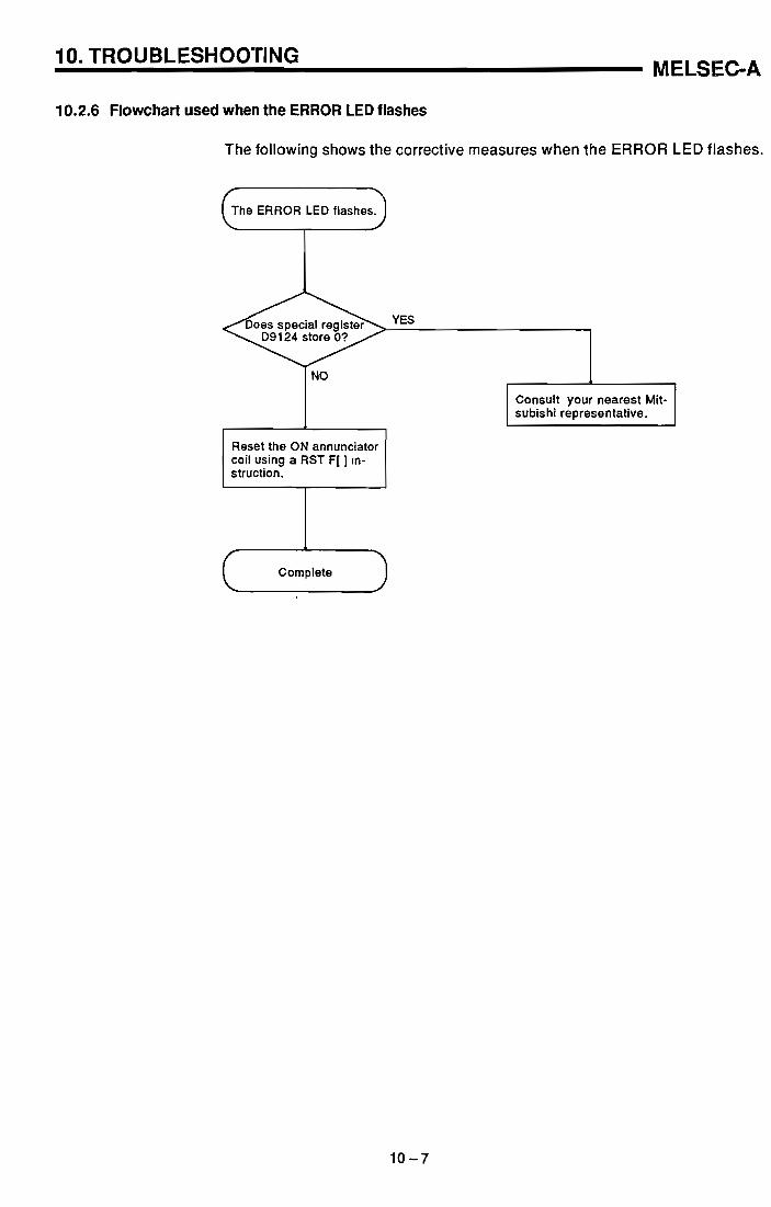
10. TROUBLESHOOTING MELSEC-A
10.2.6 Flowchart used when the ERROR LED flashes
The following shows the corrective measures when the ERROR LED flashes.
The ERROR LED flashes. (-? Consult your nearest Mit- subishi representative.
Reset the ON annunciator coil using a R S T F[ ] in- struction.
Complete

10. TROUBLESHOOTING MELSEC-A
10.2.7 Flowchart used when the output load of the output module does not go ON
Output load does not go T NO
Check rush current when Change the output relay the output load reaches NG number to adjust the rush the maximum number of
' current to comply with simultaneous ON signals specif~cations.
Check the output state in monitor mode with the pro- grammer.
NO
Consult your nearest Mitsubishi representative.
Measure the voltage across module input and COM terminal.
POINT\
If the input or load signals are not switched OFF, see Section 10.4 and take corrective measures.
YES
NO Check the input signal in monitor mode with the pro- - grammer (monitor slgnal
OFF)
YES
module's output COM Check the wiring load of Check external wiring the power supply for load and external input and restore the power. equipment
voltage
> Check the load wiring and Failure of output module. A load and restore the Replace output module. power.
I I
O V Specified voltage

10. TROUBLESHOOTING MELSEC-A
10.2.8 Flowchart used when a program cannot be written to the PC CPU
The following shows the corrective measures when a program cannot be written to the PC CPU.
Program cannot be
Set the RUNISTOP keyswitch to STOP
S T 0 P
Replace the PC CPU.
, Switch OFF the memory protect. (M.PRO OFF)
OFF
, Replace the EEPROM memory cassette (AISMCA-2KE18KE) or use a built-in RAM
Consult your nearest Mit- subishi representative.
J
Complete

10. TROUBLESHOOTING . . , MELSEC-A
10.3 Error Code List
I f an error occurs in the RUN mode, an error display or error code (including a step number) is stored in the special register by the se l f -d iagnos t i c funct ion. The error code reading procedure and the causes of and corrective actions for errors are shown in Table 10.1.
Table 10.1 Error Codes
Error Message
INSTRUCT CODE ERR.
PARAMETER ERROR
MISSING END INS.
CAN'T EXECUTE (P)
Error and Cause
An instruction code, which cannot be decoded by CPU, is included in the program.
(1) A memory cassette containing invalid instruction code, has been loaded.
(2) The occurrence of an error destroyed the memory contents, adding an instruction code that cannot be read to the memory.
The contents of the memory installed in the PC CPU have been destroyed because of (a) the occurrence of noise, or (b) the failure of the memory cassette.
(1) There IS no END(FEND) instruction in the program.
(1) There is no jump destination for plural destinat~ons specified by the CJ, SCJ, CALL, CALLP or JMP ~nstruction.
(2) Although there is no CALL instruction, the RET instruction exists In the program and has been executed.
(3) The CJ, SCJ, CALL, CALLP or JMP instruction has been executed with its jump destination located below the END instruction.
(4) The number of FOR instructions does not match the number of NEXT ~nstructions.
(5) The JMP instruction s ecified between FOR to NEXP has caused the execution to deviate from between FOR to NEXT.
(6) The JMP instructlon has caused the execution to deviate from the subroutine before the RET instruction is executed.
(7) The JMP instruction has caused execution to jump to a step or subroutine between FOR to NEXT.
Contents of Special Register D9008
(BIN value)
10
11
12
13
Corrective Action
(1) Read the error step by use Of peripheral device and correct the program at that step.
(2) In the case of the memory cassette, rewrite the contents of the ROM, or replace with a memory cassette whose contents have been correctly written.
(1) Check the loading of the PC CPU memory cassette and load ~t correctly.
(2) Read the Parameter data from the PC CPU by use of a perlperhal device. Make any necessary corrections and write it agaln to the PC CPU
(1) Write END at the end of the program.
(1) Read the error step by use of a peripheral device and correct the program at that step. (Make corrections such as the Insertion of jump destination or the changing of jump destinations to one )
CPU State
STOP
STOP
STOP
STOP

10. TROUBLESHOOTING MELSEGA
Error Message
CHK FORMAT ERR.
CAN'T EXECUTE (I)
ROM ERR
RAM ERROR
OPE. CIRCUIT ERR.
WDT ERROR
Contents of Special Rogi8ter D9008
(BIN value)
14
15
17
20
21
22
CPU State
STOP
STOP
STOP
STOP
Error and Cause
(1) There are instructions (including NOP other than LDX, LDIX, ANDk and ANIX in the CHK instruction circuit block.
(2) There is more than one CHK instruction.
(3) The number of contact points in the CHK instruction circuit block exceeds 150.
(4) The X device number in the CHK Instruction circuit block exceeds X7FE.
(5) There is no circuit block in front of the CHK instruction circuit block.
(6) D l device (number) of the CH WDlID2 instruction is different from the contact device (number) above the CJ[ ] Instruction.
(7) Pointer P254 is not attached to the start of the CHK instruction circult block.
P2- H H H H CHK I D l 102
(1) Althou h the interrupt module is used, &ere 1s no number for interrupt pointer I, which corresponds to that module, in the program or several numbers of pointer I exist in the program.
(2) No IRET instruction has been entered in the interrupt program.
(3) There is an IRET instruction somewhere besides the interrupt program.
(1) Parameters andlor sequence pro rams are not correctly written to t i e installed memory cassette (EPROM or EEPROM).
(1) The PC CPU has checked if write and read operations can be performed properly to the data memo area of the PC CPU. ~orma7writln and/or readlwrite turned out t o l e impossible.
(1) The operation circuit, whlch performs the sequence processing in the PC CPU, does not operate properly.
Scan time exceeds watchdog monitoring time.
(1) Scan time of user program is excessive.
(2) Scan time has lengthened due to instantaneous power failure which occurred during the scan.
Corrective Action
(1) Check the program of the CHK instruction circuit block (1) to (7) in the left column. Correct errors using a peripheral device and restart the operation.
(2) This error code is only valid when the 110 control uses the direct method.
(1) Check for the presence of interrupt program which corresponds to the interrupt module and create and interrupt
P rogram or reduce the numbers of to one.
(2) Check i f there is IRET instruction in the interrupt program and enter the IRET instruction.
(3) Check if there is an IRET instruction somewhere besides the interrupt program and delete that IRET ~nstruction.
(1) Write parameters and/or sequence programs correctly to the memory cassette (EPROM or EEPROM).
(2) Remove a memory cassette which does not have any parameter andlor sequence program.
Since this is a PC CPU hardware fault, consult your nearest Mitsubishi representative.
(1) Calculate and check the scan time of the user program and reduce the scan time by the use of CJ instructions, etc.
(2) Monitor the content of special register 09005 by use of a
P eripheral device. If the content s other than 0, line volta e is insufficient. Therefore, cieck the
P ower and eliminate the voltage iuctuation.

10. TROUBLESHOOTING . . , 9 . . a. ..* '. ,', .,.* , . MELSEC-A
-
L
Error Message
END NOT EXECUTE
WDT ERROR
UNIT VERIFY ERR.
FUSE BREAK OFF
CONTROL-BUS ERR.
SP. UNIT DOWN
110 INT. ERROR
SP. UNIT LAY. ERR.
SP. UNIT ER- ROR
Contents of Speclal Register D9008
(BIN value)
24
25
3 1
32
40
41
43
44
46
CPU State
STOP
STOP
STOP (RUN)
STOP ,(RUN)
STOP
STOP
'
STOP (RUN)
Error and Cause
(1) When the END instructron is executed, another instruct~on code has been read due to noise, etc.
(2) The END instruction has changed to another instruction code.
The END instruction cannot be executed with the program looped
110 module data is different from that at power ON.
( I ) The I10 module (rncluding the special-function module) is (a) Incorrectly disengaged or has been removed, or (b) a different module has been loaded
(1) There is an output module with a blown fuse.
(2) The external power supply for the output load is OFF or not connected.
The FROM and TO instructions cannot be executed
(1) Error of control bus with special- function module.
When FROM and TO instructions cannot be executed.
(1) Control bus error in the special- function module.
Although the interrupt module is not installed, an interruption has occurred.
(1) Three or more computer link modules are installed Into a single CPU module.
(2) Two or more modules of AlSJ71AP21, AlSJ71AR21, AlSJ71T21B, AlSJ71 LP21, AlSJ71 BR11 are installed.
(3) Two or more interrupt modules are installed.
(4) In the parameter setting of the peripheral device, while an 110 module is actually installed, a special-function module has been set in the I10 assignment, and vice versa.
(1) Access (execution of FROMITO tnstructron) has been made to a location where there is no special- function module.
Corrective Action
(1) Perform reset and RUN. If the- same error is displayed again, i t is a PC CPU hardware fault. Therefore, consult your nearest Mitsubishi representative.
Check for an endless loop and correct the program.
(1) Among special registers D9116 to D9123, the bit corresponding to the module verify error is '1 . Therefore, monitor the registers by use of a peripheral device and check for the module with '1'.
(2) When the fault has been corrected, reset the PC CPU.
(1) Check the blown fuse indicator LED of the output module and change the module whose LED is ON.
(2) Checking the module for a blown fuse can also be done with a peripheral device. Amon special registers D9100 to ~ 9 l O f the bit corresponding to the module of verify error is '1'. Therefore, check by monitoring the registers.
(3) Check the ONlOFF state of the external power supply for the output load
(1) This is a s~eclal-function module, CPU module or base unit hardware fault. Therefore, change the unit and check the defective module. Consult your nearest Mitsubishi representative about the defect~ve module.
This is a special-function module, CPU module or base unit hardware fault. Therefore, change the unit and check the defective Consult your nearest Mrtsubishi representative about the defective module.
(1) This is a certain module hardware fault. Therefore, change the module and check the defective module. Consult your nearest Mitsubishi representative about the defective module.
(1) reduce the computer link modules to two or less.
(2) Use one AlSJ71AP21, AlSJ71AR21, AlSJ71T21 B, AlSJ71 LP21, AlSJ71 BR11.
(3) Use one interrupt module.
(4) Reset the 110 assi nment of parameter setting %y use of peripheral device according to the actually loaded spec~al-function module.
(1) Read the error step by use of peripheral device, and check and correct the content of the FROMITO ~nstruction at that step by using a peripheral device.
L

10. TROUBLESHOOTING MELSEC-A
L
Error Message
SP. UNIT ER- ROR
LINK PARA. ER- ROR
OPERATION ER- ROR
MAIN CPU DOWN
BATTERY ER- ROR
Contents of Speclal Register D9008
(BIN value)
46
47
60
70
CPU State
(RUN)
RUN
RUN
RUN
Error and Cause
(1) Access (execution of FROMITO instruction) has been made to a locatlon where there IS no special- functlon module.
(1) The contents, which have been written to the parameter area of the link by setting the link range in the parameter setting of peripheral device, are different from the link parameter contents.
(2) The setting of the total number of slave stations is 0.
(1) The result of BCD conversion has exceeded the specified range (9999 or 99999999).
(2) A setting has been done whlch exceeds the specified devlce range and the operation cannot be done.
(3) File registers are used in the program wlthout performing the capacity setting of file reglsters.
(1) An interrupt lnstructlon (INT instruction) was used in a microcomputer program.
(2) CPU has malfunctioned due to noise or other cause.
(3) CPU hardware fault. (1) The battery voltage is below 24
VDC. (2) The battery lead is disconnected.
Corrective Action
(1) Read the error step by use of peripheral device, and check and correct the content of the FROM/TO ~nstruction at that step by using a peripheral device.
(1) Write the parameters again and check.
(2) If this messa e is displayed again, i t is a fardware fault. Therefore, consult your nearest Mitsubishi representative.
(1) Use a peripheral device to read the error step and check and correct the program at that step. (Check device setting range, BCD conversion value, etc.)
(1) Do not use INT instructions in microcomputer programs (reomove the INT instructron)
(2) Implement measures against noise
(3) Replace the CPU. (1) Change the battery.
(2) When RAM or power failure compensation IS used, connect the battery.

10. 'TROUBLESHOOTING MELSEGA
10.4 110 Connection Troubleshooting
This section explains possible problems with I10 circuits.
10.4.1 lnput circuit troubleshooting
This section describes possible problems with input circuits, as well as corrective actions.
Table 10.2 lnput Circuit Problems and Corrective Actions I
Leakage current of input switch (such as a drive by non-contact switch).
AC imut
Conditlon
Connect an appropriate register which will make the voltage across the terminals of the input module lower than the OFF voltage value.
Cause
Power supply
Corrective Action
1
Drive by a limit switch with neon lamp.
lnput signal does not turn OFF.
AC input 7
- - -
2 module
-- Power supply
lnput signal does not turn OFF.
Leakage current due to line capacity of wiring cable. Line capacity C of twisted pair wire is approx. 100 PFIm).
Drive by switch with LED indicator.
-pie 3
DC input (sink) - lnput signal does not 4 turn OFF.
I
lnput signal does not turn OFF.
It is recommended to use 0.1 to 0.47 pF + 47 to 120 a (1 R W) for the constant.
--- AC input -
--- Power supply
Same as Example 1. Or make up another independent display circuit.
Same as Example 1. However, leakage current is not generated when power supply is located on the input equipment side as shown below.
-------- AC input - I
t Y
I I I A 1 .Put I - I module
I I
-,,,,,,, J Power Supply
Connect a register which will make the voltage across input module terminal and common higher than the OFF voltage, as shown below.
DC input (sinl --------
I
A sample calculation of a connected resisbr Mkre is g-nren on he'tollowing page.

10. TROUBLESHOOTING MELSEC-A
Table 10.2 lnput Circuit Problems and Corrective Actions (Continued)
Sample calculation for Example 4
The switch with the LED indicator is connected to A1SX40 and there is a 4 mA leakage current.
--------- A1 SX40 C
,-,-------I
Cause Corrective Action
Sneak path due to the use of two power Use only one power.supply. supplies. Connect a sneak path prevention diode.
(Figure below)
El > E2
-Example 5
(1) Since this voltage does not satisfy the OFF voltage of 1 [mA] or lower, the input signal does not go OFF. Therefore, connect a resistor as shown below.
Condition
Input signal does not turn OFF.
----------I 24 VDC
Input impedance 3.3 kR
(2) Calculate the resistance value of R as follows: To obtain the 1 mA OFF current for the A1 SX40, a 3 mA current or larger must flow to R.
C
IR : IZ = Z (input impedance) : R Iz 1 R I - x (input impedance) = - x 3.3 = 1 .1 [kQ] I R 3
If the resistance value of R is 1 kQ, the power capacity W of the resis- tor R is calculated as follows:
W = (current value)2 x R = 0.003~ (A) x 1000 (R) = 0.009 (W)
(3) Since the power capacity of the resistor is usually selected as 3 to 5 times the actual power consumption, a 1 kQ 0.5 W resistor must be connected to the terminals concerned.

10. TROUBLESHOOTING MELSEC-A
10.4.2 Output circuit failures and corrective actions
The load does not turn OFF (triac output).
-Pie 1
When the load IS a C- R type timer, time constant fluctuates (triac output).
Condit ion
When the output is OFF, excessive voltage is applied to the load.
~ b l e 10.3 Output Circuit Failures and
Cause
Load is half-wave rectrfled inside (In some cases, it 1s true of a solenoid).
When the polarity of the power supply is as shown in [I], C IS charged. When the polarity is as shown In [2], the voltage charged in C plus the line voltage are applied across D l . Max. voltage is approx. 2.2E.
Leakage current due to built-~n noise suppression
AlSY22
:orrective Actions
Corrective Action
Connect a resistor of several tens or hundreds of kR across the terminals of the load.
If a resistor is used in this way, i t does not pose a problem to the output element. But i t may cause the diode, which is built in the load, to deterlorate, resulting in a fire, etc.
1 Resister M
,Connect C and R across the load. \
1
I When the wlring distance from the output card to the load is long, there may be a leakage current due to the line capacity.
Load
Resister rn
-
Drive the relay using a contact and drive the C-R type timer using the same (contact. I
I Some timers have half-wave rectified internal circuits. Therefore, take the precautions indicated in the example.
Resister
CR timer S J Calculate the CR constant
depending on the bad.

11. TROUBLESHOOTING MELSEC-A
11. TROUBLESHOOTING
This section describes various procedures for troubleshooting, as well as corrective actions.
11.1 Basic Troubleshooting
System reliability not only depends on reliable equipment but also on short down-times in the event of faults.
The three basic points to be kept in mind in troubleshooting are:
(1) Visual checks
Check the following points
(a) Machine motion (in stop and operating states)
(b) Power ON or OFF
(c) Status of I10 equipment
(d) Condition of wiring (I10 wires, cables)
(e) Display states of various indicators (such as POWER LED, RUN LED, ERROR LED, and I10 LED)
(f) States of various setting switches (such as extension base and power failure compensation)
After checking (a) to (f), connect the peripheral equipment and check the running status of the PC CPU and the program contents.
(2) Trouble check
Observe any changes in the error condition during the following:
(a) Set the RUNISTOP keyswitch to the STOP position.
(b) Reset using the RUN/STOP keyswitch.
(c) Turn the power ON and OFF.
(3) Narrow down the possible causes of the trouble
Deduce where the fault lies, i.e:
(a) Inside or outside the PC CPU.
(b) I10 module or another module.
(c) Sequence program.

11. TROUBLESHOOTING MELSEC-A
11.2 Troubleshooting
This section explains the procedure for determining the cause of problems as well as the errors and corrective actions for error codes.
11.2.1 Troubleshooting flowcharts
The procedures for troubleshooting are given in the following flowcharts:
Occurrence of error
I Is the POWER LED OFF' See Sect~on 11.2.2
I Is the RUN LED OFF? See Sect~on 11.2.3
I Is the RUN LED flashing' - ' See Section 1 1.2.4
I Is the ERROR LED ON? See Sectlon 1 1.2.5
I
Is the ERROR LED flash~ng? See Section 11.2.6
I 1
110 module does not oper- ate properly.
. See Section 11.2.7
I Program cannot be wrtt- ten.
. See Section 1 1.2.8

11. TROUBLESHOOTING MELSEC-A
11.2.2 Flowchart used when the POWER LED goes OFF
POWER LED IS turned m NO
Correct the power supply.
YES
NO YES POWER LED
NO , or 170 to 264
Set the supply voltage to within the rated voltage.
YES
NO YES POWER LED .
, Fix the power supply mod- ule correctly.
YES
NO YES POWER LED
YES , (1) Eliminate the excess current.
(2) Switch the input power OFF, then ON.
NO
NO Does the YES POWER LED
turn ON?
Consult your nearest
Complete :::::-:-A

11. TROUBLESHOOTING MELSEC-A
11.2.3 Flowchart used when the RUN LED goes OFF
RUN LED goes OFF. Y Take corrective action according to the error code list
I
I RUN LED remalns OFF.
Reset the A1 SJCPU us- Ing the RUWSTOP
1 I I In case of (1)
1 I In case of (2) 1
RUN LED goes ON. (1) Due to defective PC parts or a connection failure.
(2) Due to excessive nose.
Move the RUWSTOP keysw~tch on the AlSJCPU to STOP and wrlte END to address 0 us-
, ing a per~pheral device.
Software error. I
Consult your nearest Mitsub~shi
A
Check program w ~ t h pro- grammer and correct the
Move the RUNISTOP key switch to RUN.
Connect noise suppression cir- cuit, such as CR, to noise source.
RUN LED does go ON.
RUN LED goes ON.

11. TROUBLESHOOTING MELSEC-A
11.2.4 Flowchart used when the RUN LED flashes
RUN LED flashes. L--' Check the error with pe- ripheral equipment. (See
Consult your nearest Mrtsub~shr representative.
Reset the AISJCPU us-
Correct the error. (See Section 11.3)
Set the RUNISTOP key-
I Complete 1

11. TROUBLESHOOTING MELSEC-A
11.2.5 Flowchart used when the ERROR LED is lit
The following shows the corrective measures when the ERROR LED is lit at RUN.
ERROR LED IS lit. + Hardware fault
,
ERROR LED
Check corrective actions in the fault code list. -
I Reset the AlSJCPU us- ing the RUNSTOP
NO
Consult your nearest Mlt- subishi representative.
Set the RUNlSTOP key- switch in the STOP posi- t~on.
Complete e3
Take corrective action.
Correct the cause of the error.
Set the RUNlSTOP key- sw~tch in RUN pos~tion.
I I
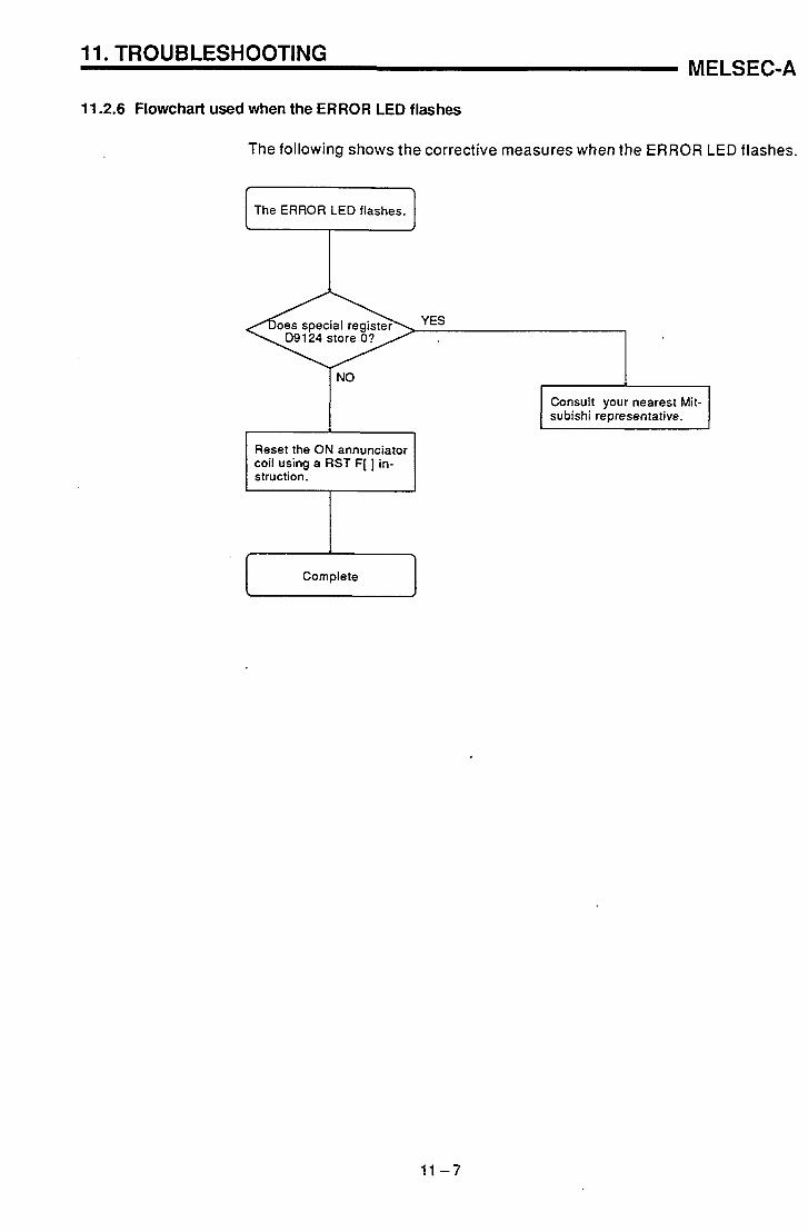
11. TROUBLESHOOTING MELSEC-A
11.2.6 Flowchart used when the ERROR LED flashes
The following shows the corrective measures when the ERROR LED flashes.
eyEs 09124 store O? , Reset the ON annunciator coil using a RST F[ ] in-
I Complete 1
I Consult your nearest Mit- subishi representative.

11. TROUBLESHOOTING MELSEC-A
11.2.7 Flowchart used when the output load of the output module does not go ON
Output load does not go w 'Is the indicator Measure the voltage
LED of the input mod- across module input and ule ON? COM terminal.
n s m c i f i e d
NO LED of the output mod- *
~ 1 YES I 1 voltage
Check the output state in monitor mode with the pro- grammer.
Check the input signal in of power supply for monitor mode with the pro-
load applied?
Check the wiring load of
terminals as the power supply for load
Check the load wiring and Failure of output module. load and restore the Replace output module.
Check rush current when Change the output relay the output load reaches number to adjust the rush the maximum number of current to comply with
Check external wiring and external input equipment.
Consult your nearest Mitsubishi representative.
POINT
If the input or load signals are not switched OFF, see Section 11.4 and take corrective measures.

11. TROUBLESHOOTING MELSEC-A
11.2.8 Flowchart used when a program cannot be written to the PC CPU
The following shows the corrective measures when a program cannot be written to the PC CPU.
Program cannot be

11. TROUBLESHOOTING MELSEC-A
11.3 Error Code List
If an error occurs in the RUN mode, an error display or error code (including a step number) is stored In the special register by the self-diagnostic function. The error code read~ng procedure and the causes of.and corrective actions for errors are shown in Table 11 .l.
Table 11.1 Error Codes
Error Message
INSTRUCT CODE ERR.
PARAMETER ERROR
MISSING END INS.
CAN'T EXECUTE (P)
Contents of Special Register D9008
(BIN value)
10
1 1
12
CPU State
STOP
STOP
STOP
STOP
Error and Cause
An instruction code, which cannot be decoded by CPU, 1s included in the program.
(1) A memory cassette containing ~nvalid instruct~on code, has been loaded.
(2) The occurrence of an error destroyed the memory contents, adding an instruction code that cannot be read to the memory. -
Corrective Action
Read the use per~pheral device and correct the program at that step.
(2 ) In the case of the memory cassette, rewrlte the contents of the ROM, or replace w ~ t h a memory cassette whose contents have been correctly written.
The contents of the memory installed in the PC CPU have been destroyed because of (a) the occurrence of noise, or (b) the failure of the memory cassette.
(1) There IS no END(FEND) Instruction in the program.
(1) There is no jump destination for plural destinations specified by the CJ, SCJ, CALL, CALLP or JMP instruction.
(2) Although there is no CALL instruct~on, the RET instruction exists In the program and has been executed.
(3) The CJ, SCJ, CALL, CALLP or JMP instruction has been executed w ~ t h its jump destination located below the END instruction.
(4) The number of FOR instructions does not match the number of NEXT instructions.
(5) The JMP instruction s ecified between FOR to N E X ~ has caused the execution to deviate from between FOR to NEXT.
(6) The JMP instruction has caused the execution to deviate from the subroutme before the RET instruction is executed.
(7) The JMP instruction has caused execution to jump to a step or subroutine between FOR to NEXT.
(1) Check the loading of the PC CPU rnemor cassette and load it correctry.
(2) Read the Parameter data from the PC CPU by use of a perlperhal device. Make any necessary corrections and write it agaln to the PC CPU.
(1) Write END at the end of the program.
(1) Read the error step by use of a per~pheral device and correct the pro ram at that step.
a e corrections such as the (M Qc insertion of jump destination or the changing of jump destinations to one.)
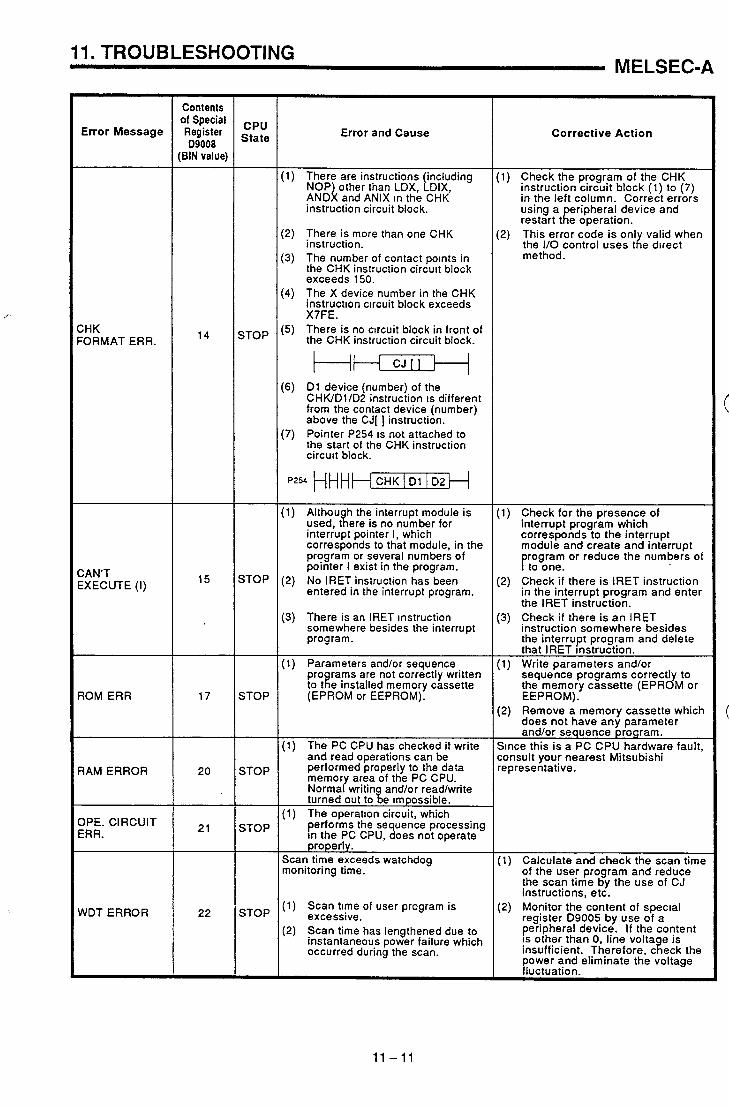
11. TROUBLESHOOTING MELSEC-A
Error Message
CHK FORMAT ERR.
CAN'T EXECUTE (I)
ROM ERR
RAM ERROR
OPE. CIRCUIT ERR.
WDT ERROR
Contents of Special Register D9008
(BIN value)
14
15
17
20
21
22
CPU State
STOP
STOP
STOP
STOP
Error and Cause
(1) There are instructions Including NOP other than LDX, I D I x ANDh and ANlX in the CHK' instruction circuit block.
(2) There is more than one CHK instruction.
(3) The number of contact points in the CHK instruction circult block exceeds 150.
(4) The X device number in the CHK instruct~on ctrcuit block exceeds X7FE.
(5) There is no clrcuit block in front of the CHK instruction circuit block.
(6) D l device (number) of the CHWDllD2 instruction IS different from the contact device (number) above the CJ[ ] instruction.
(7) Pointer P254 IS not attached to the start of the CHK instruction circult block.
~ 2 % H H H H c H K J X H (1) Althou h the interrupt module is
used, Rere is no number for interrupt pointer I, which corresponds to that module, in the program or several numbers of pointer I exist in the program.
(2) No lRET instruction has been entered in the interrupt program.
(3) There is an IRET instruction somewhere besides the interrupt program.
(1) Parameters andlor sequence pro rams are not correctly written to t i e installed memory cassette (EPROM or EEPROM).
(1) The PC CPU has checked i f write and read operations can be performed properly to the data memory area of the PC CPU. Normal wi t in andlor readlwrite turned out to%e tmpossible.
(1) The operatton circuit, which performs the se uence processing In the PC CPU, 2oes not operate properly.
Scan time exceeds watchdog monitoring time.
(1) Scan tlme of user program is excessive.
(2) Scan time has lengthened due to instantaneous power failure which occurred during the scan.
Corrective Act ion
(1) Check the program of the CHK instruction circuit block (1) to (7) in the left column. Correct errors using a eripheral device and restart tt!e operation.
(2) This error code is on1 valid when the 110 control uses t i e direct method.
(1) Check for the presence of interrupt program which corresponds to the interrupt module and create and interrupt
P rogram or reduce the numbers of to one.
(2) Check i f there is IRET instruction in the interrupt program and enter the IRET instruction.
(3) Check i f there is an IRET instruction somewhere besides the interrupt program and delete that IRET Instruction.
(1) Write parameters andlor sequence programs correctly to the memory cassette (EPROM or EEPROM).
(2) Remove a memory cassette which does not have any parameter andlor sequence program.
Slnce this is a PC CPU hardware fault, consult your nearest Mitsubishi representative.
(1) Calculate and check the scan time of the user program and reduce the scan time by the use of CJ instructions, etc.
(2) Monitor the content of speclal register D9005 by use of a peripheral device. If the content IS other than 0 , line volta e is insufficient. Therefore. cfeck the power and eliminate the voltage fluctuation.

11. TROUBLESHOOTING . . . . . MELSEC-A
Error Message
END NOT EXECUTE
WDT ERROR
UNIT VERIFY ERR.
FUSE BREAK OFF
CONTROL-BUS ERR.
SP. UNIT DOWN
110 INT. ERROR
SP. UNlT LAY. ERR.
SP. UNIT ERROR
CPU State
STOP
STOP
STOP (RUN)
STOP (RUN)
STOP
STOP
STOP
STOP (RUN)
Contents of Special Register D9008
(BIN value)
24
25
3 1
32
40
41
43
44
46
Error and Cause
(1) When the END lnstructlon is executed, another ~nstruction code has been read due to nose, etc. -
(2) The END lnstructlon has changed to another lnstructlon code.
The END ~nstruction cannot be executed with the program looped.
110 module data IS different from that at power ON.
(1) The 110 module (mcludlng the specral-funct~on module) is (a) incorrectly d~senga ed or has been removed, or (%) a different module has been loaded.
(1) There is an output module with a blown fuse.
(2) The external power supply for the output load IS OFF or not connected.
The FROM and TO lnstructlons cannot be executed.
(1) Error of control bus with special- function module
When FROM and TO instructions cannot be executed.
(1) Control bus error in the special- function module.
Although the Interrupt module is not installed, an interruption has occurred.
(1) Three or more computer link modules are installed Into a s~ngle CPU module.
(2) Two or more modules of AlSJ71T21B are Installed.
(3) Two or more ~nterrupt modules are installed.
(4) In the parameter setting of the peri heral device, wh~le an 110 rnod)Yle is actually installed, a special-function module has been set in the 110 assignment, and vlce versa.
(1) Access (execution of FROMITO instruct~on) has been made to a locat~on where there is no special- funct~on module.
Corrective Act ion
(1) Perform reset and RUN. If the same error IS displayed again, 11 is a PC CPU hardware fault. Therefore, consult your nearest Mitsubishi representative.
Check for an endless loop and correct the program.
(1) Among special registers 091 16 to D9123, the bit corresponding to the module verify error IS '1 . Therefore, monitor the registers b use of a peripheral device and d e c k for the module w ~ t h '1 .
(2) When the fault has been corrected, reset the PC CPU.
(1) Check the blown fuse ~ndrcator LED of the output module and change the fuse in the module whose LED is ON.
(2) Checking the module for a blown fuse can also be done with a peripheral device. Among special registers D9100 to D9107, the bit corresponding to the module of verify error is '1 . Therefore, check by monitoring the registers.
(3) Check the ONIOFF state of the external power supply for the output load.
(1) This is a s~ecial-functlon module, CPU module or base unit hardware fault. Therefore, change the unlt and check the defective module. Consult your nearest Mitsublshl representatwe about the defectwe module.
Thls is a special-funct~on module, CPU module or base unit hardware fault. Therefore, change the unit and check the defective module. Consult your nearest Mitsub~shi representative about the defective module.
(1) This is a certain module hardware fault. Therefore, change the module and check the defective module. Consult your nearest Mitsub~shi representative about the defective module.
(1) reduce the computer link modules to two or less.
(2) Use one A1 SJ71 T21 B.
(3) Use one interrupt module.
(4) Reset the I10 assi nment of parameter setting %y use of per~pheral device according to the actually loaded special-functlon module.
(1) Read the error step by use of peripheral device, and check and correct the content of the FROMITO instruct~on at that step by using a peripheral device.

11. TROUBLESHOOTING MELSEC-A
Error Message
LINK PARA. ERROR
OPERATION ERROR
BATTERY ERROR
t
Contents of Special Register D9008
(BIN value)
47
'0
CPU State
RUN
RUN ( S T ~ P )
RUN
Error and Cause
(1) The contents, which have been written to the parameter area of the link by setting the link range in the parameter setting of
P eripheral device, are different rom the link parameter contents.
(2) The setting of the total-number of slave stations is 0.
(1) The result of BCD conversion has exceeded the specified range (9999 or 99999999).
(2) A setting has been done which exceeds the specified device range and the operation cannot be done.
(3) File registers are used in the program without performing the capacity setting of file registers.
(1) The battery voltage is below 24 VDC.
(2) The battery lead is disconnected.
Corrective Action
(1) Write the parameters again and check.
(2) If this messa e is displayed a ain, it is a fardware fault. ~ fere fore . consult your nearest Mitsubishi representative.
(1) Use a peripheral device to read the error step and check and correct the program at that step. (Check device setting range. BCD conversion value, etc.)
(1) Change the battery.
(2) When RAM or power failure compensation IS used, connect the battery. .

11. TROUBLESHOOTING MELSEC-A
11.4 110 Connection Troubleshooting
This section explains possible problems with 110 circuits
I 1.1.4.1 Input circuit troubleshooting
This section describes possible problems with input circuits, as well as corrective actions.
b
Corrective Actions
Corrective Action
Connect an appropriate reglster which will make the voltage across the terminals of the input module lower than the OFF voltage value.
AC ~nput
- - - 3 E module - - - -
It IS recommended to use 0.1 to 0.47 pF + 47 to 120 R (112 W) for the constant
Same as Example 1. Or make up another Independent dlsplay clrcuit.
Same as Example 1. . However, leakage current is not generated when power supply is located on the input equipment side as shown below. im I m input
I module I 'L
-------- J Power Supply
Connect a register which will make the voltage across input module terminal and common hlgher than the OFF voltage, as shown below.
DC lnput (sink) ----7F Resistor
- - - - module
A sample calculation of a connected resistor value is given on the follomng page.
Table 11.2 lnput Circuit Problems and
Cause
Leakage current of input swltch (such as a drlve by non-contact switch).
AC input ' *-& module - Power supply
Drlve by a limit swltch with neon lamp.
AC Input
Leakage r r & current module
-- Power supply
Leakage current due to line capaclty of wlring cable. Line CapaClty C of twisted pair wire is approx. 100 PFlm).
-- AC Input
r u t m o d u l e - --
Power supply
Drive by switch with LED Indicator.
-- DC input (slnk)
;-& Input module
--
Ewmple 1
-* 2
Example 3
-- 4
Condition
lnput signal does not turn OFF.
lnput signal does not turn OFF.
lnput signal does not turn OFF.
Input signal doesnot turn OFF.

11. TROUBLESHOOTING MELSEC-A
Table 11.2 lnput Circuit Problems and Corrective Actions (Continued)
Sample calculation for Example 4
The switch with the LED indicator is connected to A1SX40 and there is a 4
Corrective Action . Use only one power supply. Connect a sneak path prevention diode. (F~gure below)
- EllxTut mdule
mA leakage current. - - - - - - - - - A x 4 0
Cause
r Sneak path due to the use of two power ,
supplies.
E l 'TT dFb Input module
E l > E2
Example 5
current mA Input module
Condition
lnput signal does not- turn OFF.
(1) Since this voltage does not satisfy the OFF voltage of 1 [mA] or lower, the input signal does not go OFF. Therefore, connect a resistor as shown below.
lnput impedance 3.3 kR
(2) Calculate the resistance value of R as follows: To obtain the 1 m A OFF current for the A1 SX40, a 3 mA current or larger
0 must flow to R.
IR : IZ = Z (input impedance) : R Iz 1 R 5 - x (input impedance) =- x 3.3 = 1.1 [kR] I R 3
If the resistance value of R is 1 kR, the power capacity W of the resis- tor R is calculated as follows:
W = (current value)2 x R = 0.003~ (A) x 1000 (R) = 0.009 (W)
(3) Since the power capacity of the resistor is usually selected as 3 to 5 times the actual power consumption, a 1 kQ 0.5 W resistor must be connected to the terminals concerned.

11. TROUBLESHOOTING - , , , MELSEC-A
11.4.2 Output circuit failures and corrective actions
Exam* 1
Example 2
Example 3
Table 11.3 Output Circuit Failures and Corrective Actions
Condition
When the output is OFF, excessive voltage is applied to the load.
The load does not turn OFF (tr~ac output).
When the load is a C- R type timer, time constant fluctuates (triac output).
Cause
Load is half-wave rectified inside (in some cases, it is true of a solenoid).
AlSY2.2
When the polarity of the power supply is as shown in [I], C is charged. When the polarity is as shown in [2], the voltage charged in C plus the line voltage are applied across Dl . Max. voltage is approx. 2.2E.
Leakage current due to built-in noise suppression
Corrective Action
Connect a resistor of 10 to 99 kn. across the load.
If a resistor is used in this way, it does not pose a problem to the output element. But it may cause the diode, which is built in the load,
'
to deteriorate, resulting in a fire, etc.
Resister
1
Connect C and R across the load.
When the wiring distance from the
A1 SY22 output card to the load is long, there may be a leakage current due to the
Output module line capacity.
Resister
1
Drive the relay using a contact and drive the C-R type timer using the same contact.
Some timers have half-wave rectified internal circuits. Therefore, take the precautions indicated in the example.
Resister
1 Calculate the CR constant depending on the load.
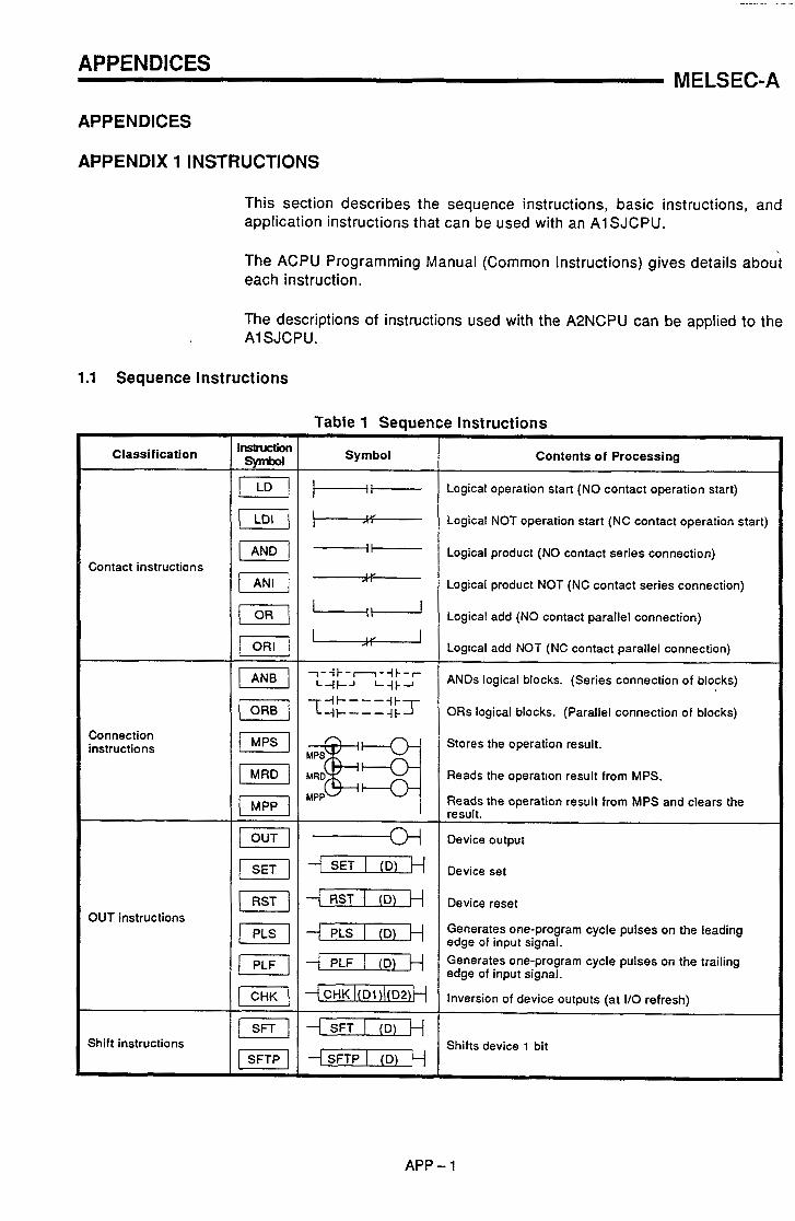
APPENDICES MELSEC-A
APPENDICES
APPENDIX 1 INSTRUCTIONS
This section describes the sequence instructions, basic instructions, and application instructions that can be used with an AISJCPU.
The ACPU Programming Manual (Common Instructions) gives details about each instruction.
The descriptions of instructions used with the A2NCPU can be applied to the AISJCPU.
1.1 Sequence Instructions
APP - 1
_I
Classification
Contact instructions
Connection instructions
OUT instructions
Shift instructions
lnsbuction symbol
( 7 1
(71 IF/ [-I /*Ns]
I] piE-1 [xk-/ [MPP/
I]
I]
1x1 [=I [ X I [SFTPl
Table 1 Sequence
Symbol
I - 1- I-
.̂
L--IC--I 1 - i k - - - i k - r '--IFJ ' - i k - ' -IF---+I- / - - -
g q MPP
I -I -('TI 4 FIST ((D)
3 i P L S x ( D ) PLF
~ C H K
4 SFT
-+SFTP I O H
lnstructions
Contents of Processing
Logical operation start (NO contact operation start)
Logical NOT operation start (NC contact operation start)
Logical product (NO contact series connection)
Logical product NOT (NC contact series connection)
Logical add (NO contact parallel connection)
Loglcal add NOT (NC contact parallel connection)
ANDs logical blocks. (Series connection of blocks)
ORs logical blocks. (Parallel connection of blocks)
Stores the operation result.
Reads the operation result from MPS.
Reads the operation result from MPS and clears the result.
Device output
Device set
Device reset
Generates one-program cycle pulses on the leading edge of input signal.
Generates one-program cycle pulses on the trailing edge of input signal.
Inversion of device outputs (at 110 refresh)
Shifts device 1 bit

APPENDICES MELSEC-A
Table 1 Sequence Instructions (Continued)
Master control
Classification
l i p - ] 4 MC I m 1 Master control start
instructions I I] / 4 MGT'TTH 1 Master control reset I I lmtnrction
symbol Symbol
Termination irrsbuctions
Other instructions
APP - 2
Contents o f Processing
Page change
Program end
Stop
NO operation
I -
[FEND]
[STOP]
I] Changes hard copy pages. Written in the operation list mode.
H FEND H -
--j
-
Always used at the end of the main routine program to termmate processing.
Always used at the end of the sequence program to return to step 0. Resets output after input conditton is enabled, and stops the sequence program. The sequence program is resumed by setting the RUN keysw~tch to RUN. No operation For program erasure or space

APPENDICES MELSEC-A
1.2 Basic lnstructions
Table 2 Basic lnstructions
Classification
Comparison 16-bit data instructions comparison
Symbol
AND- I (St) ((S2) OR- I (Sl) 1 (S2)
--I AND<> I (St) I (S2)
OR<> (St) (S2)
AND> 1 (St) 1 (S2)
Contents of Processing
Continuity when (Sl) = (S2) Non-cont~nuity when (S1) + (S2)
Continuity when (S1) # (S2) Non-continuity when (SI) = (S2)
Continuity when (S1) > (S2) Non-continuity when (S1) s (S2)
Continuity when (Sl) 2 (S2) Non-cont~nu~ty when (Sl) > (S2)
Continuity when (S1) < (S2) Non-continuity when (Sl) 2 (S2)
Continuity when (S1) 2 (S2) Non-continuity when (S1) < (S2)
APP - 3

APPENDICES I
. . , ' MELSEC-A
Table 2 Basic lnstructions (Continued)
Classification Symbol Contents of Processing
Continuity when (S1 + 1. S1) = (S2 + 1, S2) Non-contlnu~ty when (S1 + 1. S l ) lc (S2 + 1, S2)
Comparison lnstructions
Lf ORD- l ( ~ 2 ) p
32-bit data comparison
L D D o (Sl) (S2) I L D D o / Continuity when (S1 + 1, S1) # (S2 + 1, S2) Non-cont~nu~ty when (S1 + 1, S t ) = (52 + 1, S2)
Continuity when (S1 + 1, S1) > (S2 + 1, 52 ) Non-continuity when (S1 + 1, S1) s (S2 + 1, S2)
ANDD> / (S l ) 1 ( S Z ) ~
Contlnuity when (S1 + 1, S1) 5 (S2 + 1. 52) Non-cont~nuity when (S1 + 1, S1) > (S2 + 1, S2)
i ANDDc- ( (Sl) I (S2)
Contlnuity when (S1 + 1. S1) c (S2 + 1, S2) Non-continuity when (S1 + 1. S1) 2 (S2 + 1, S2)
I ANDDc ]
Contlnuity when (S1 + 1, S1) 2 (S2 + 1, S2) Non-continuity when (S1 + 1 , S1) c (S2 + 1, S2)
APP - 4

APPENDICES MELSEC-A
Table 2 Basic Instructions (Continued)
Symbol Contents of Processing
BIN 16-bit additionl subtraction
Arithmetic operation instructions
BIN 32-bit add~tiod subtraction
(Sl) + (S2) -t Quotient (D), Remainder (D + 1) I I subtraction I I I /
D'P (Sl) (S2) (D) I IBIN "-bit 1 1 WP 1 additionl subtraction 7 1 -( I I (") I kI (SI + I , SI ) - (SZ + I, 52) + ~uot ien t
(D + 1, D), Remainder (D + 3, D + 2) DIP I (Sl) (S2) ID)
APP - 5

APPENDICES . * , * % , . %.., .*..-. MELSEC-A
Table 2 Basic Instructions (Continued)
APP - 6

APPENDICES MELSEC-A
Table 2 Basic Instructions (Continued)
APP - 7

APPENDICES % % s ,:.. , MELSEC-A
Table 2 Basic Instructions (Continued)
APP - 8
Classification
- . BCD o BIN conversion instruct~ons
Data transfer instructions
lnstnrction symbol
i] [-I -1 I'TkG-1 I T ] I T / i l 1 F 1 /]
I] /]
/ - E i q
-1 p G q
I]
/I
/ T I
[FMoVpI
j l XCHPI -1 /]
BCD cnmemon
BIN COCIverSiOn
Transfer
Negation transfer
Block transfer
Exchange
Symbol
-lBCDj76-TT-H
+BCD 1 i s ) ( ( 0 ) H - f x ; I ; T ; 6 ; H m BIN (S) (0)
4 81NP 1 (S) I (0 ) H
0 + DBINP I ( ) 1 (D) H -( ~ o v 1 (s) 1 (0) H ( MOVP 1 IS) I (D) H I DMOV I IS) I ID) H ) DMOVP / IS) / ID) H 4 CML / (s) I (D) H
0 q E q F l x H +=TTq+
/i 0 . 0 ~ 1 (s) 1 ~ ) I n H
4
-( FMoV 1 is) I 1DI I n H
4 XCH I X H 4 XCHP-H 4 OXCH 1 (01) I (02) H 4 DXCHP I ( ~ 1 ) / (02) H
Contents of Processing
BCD conversion i
(D)
BIN (0 to 9999)
BCD conversion S1 + 1 S1 (Dl + 1, D)
T B I N (0 to 99999999)
BIN conversion , (Dl Y- BCD (0 to 9999)
S1 + 1 , S l BIN convers~on . (Dl + 1, D)
~ B ~ D (o to 93999999)
(S) + (Dl
(S + 1 , S) -t (D + 1, D)
- (S) -9 0 )
( S + 1 ,s ) + ( D + 1, D)
D ) r j I - - - - - - - - - - - - - n - - -
(s)Lp++j - - - 1 n - - -
(Dl) - (D2)
(Dl + 1, D l ) o (D2 + 1, D2)

APPENDICES MELSEC-A
Table 2 Basic Instructions (Continued) I I I
I I I CJ I I H CJ I p-* H / Jumps to Po* after the input condition is enabled.
Classification
I
I I I JMP I P** H I Unconditionally jumps to P**.
lmtruction symbol
I Jump I I H SCJ I P- H Jumps to P" beginning with the next scan after the input condition is enabled.
Symbol
CALL I '-*
Contents of Processing
Executes the subroutine program at P** after the inout
1 2 7 I I i C A L L P I p- H
Interrupt Execution of an interrupt program is disabled. Valid H when M9053 is OFF.
condition is enabled.
hogram branch instructions
I H Returns operation from an interrupt program to a sequence program.
Link refresh
IF( m H
Executes the microcomputer program specified by n. wl -(SUBP I n H pi-1 CO M H Executes link refresh, general data processing.
Refresh instrudons
RET
El H
Returns execution from the subroutine program to the sequence program.
Cancels execution disable setting of an interrupt program. Valid when M9053 is OFF.
Link refresh enable1 disable
- .
b ! A H
Partial 1 1 1 sEG 1 refresh
El H H Dl H
Corresponding devices are partial-refreshed during one scan. Valid when M9052 is ON.
Enables link refresh. Valid when M9053 is ON.
Disables link refresh. Valid when M9053 is ON.

APPENDICES MELSEC-A
1.3 Application lnstructions
Table 3 ADDlication lnstructions
APP - 10
Classification
Logical operation instructions
Zmflernent 1 1-1 1 NEGP TH (Dl I
Instruction symbol
p q piq I] pq IDAND1 [DANDPI
-1 wonpi -1 1-1 IDOR]
IWXORl
-1 /I [I p i E i - 1
-1 -1 IWXNRP]
-1
pq
-1
Logical product
Logical sum
Exclus~ve log~cal sum
NOT exclusive logical sum
Symbol
IpGq-(s,m 4 WAND I(-
+ DAND 1 (-H
3 WOR 1 ZTi6-H 4 W0.P 1 ( s ) W H
~ W O R P I(si)I*H
0 I x T T H + map 1-H 4 w x o ~ m
4 w x o a ~ I (s)H
3 WXOR /(sl)l(=H
+ x o m
4 0x0.~ 1XTZi-H 4 WXNR I (s) / ID) H + X ~ G R ~ H 4 WXNR /(-H 4 WXNRP / (si) i(*IO)H
+=TGTxH 4 DXNRP 1-H 4 - 7 N EG (Dl
Contents of Processing
(Dl AND (S) -t (Dl
(Sl) AND (S2) + (D)
( D + 1, D)AND(S+ 1,s) -t ( D + 1, D)
(D) OR (S) + (S)
(S1) OR (S2) -t (D)
( D + l , D ) O R ( S + l , S ) - t ( D + 1 , D )
(Dl XOR (S) -t (Dl
(Sl) XOR (52) -t (D)
( D + l , D ) X O R ( S + l , S ) - t ( D + l , D )
(Dl XOR (S) -t (Dl
(S1) XOR (S2) -t (D)
( D + 1, D)XOR(S+ 1,s) -t ( D + 1, D)

APPENDICES MELSEC-A
Table 3 A ~ ~ l i c a t i o n Instructions (Continued)
Classification lnsbuction symbol
Symbol Contents of Processing
ROR n H E i W 'n' b ~ t rotate to r~ght RoRP n H I RORP 1
RCR I
'n' b ~ t rotate to r~ght
Leftward
ROL f-Ea 'n' blt rotate to left
ROLP n H 1 ROLP I
Rotation instructions
Carry
rEs+Eil 'n' b ~ t rotate to left I
A1 A0
Carry - 'n' b ~ t rotate to r~ght
1 DROR I
DRORP
DRcR n H
4 ~ R c R P n H 1 DRCRP I 'n' blt rotate to r~ght
.eftward otation
DRoL n H
DROLP n H 'n' b ~ t rotate to left 1 DROLP I
DRcL n H
DRCLP I I DRCLP I 'n' blt rotate to left

APPENDICES MELSEC-A
Table 3 A ~ ~ l i c a t i o n Instructions (Continued)
In bit shift I . I I
I
15 to 0 Carry - I
Classification
SFLP (D) n I SFLP /
I lnsbuction synaol
/ O t o O LJ I,
Shift instructions
Symbol
1 bit sh~ft
Contents of Processing
I BSFR I
BSFRP I
1 BSFL I
1 ward sh~ft
I DSFR I
/ DSFRP I
I DSFL I
APP - 12

APPENDICES MELSEC-A
Table 3 Application Instructions (Continued)
APP - 13
Classification
Data Processing instructions
,
Instruction
symbol
/I
VI
I\
pGi-1
p K q
i t
pq
/I
p i i E q
/\
pq
-1
VBRSTPj
Data search
Bit check
Decode, Encode
7 segment decode
Bit setireset
Symbol
4 SEE 1 (SI) (5211 n H
j SEEP ~ (s I ) ] ( s~ ) / n H
SUM (s)
3 SUMP I (S)
4 DSUM / ( S )
4 DSUMP I (s) H
+ E m H
4 --cop I (S) 1 /ID 1 H
4 ENCO 115) 110) 1 n H
4 EENOP 1 (S) Ilo,H
4 SEG 1 (S) I (0) H
p E - \ / m
4 B S E ~
+ X j o ) H
- - ( m ) F H
Contents of Processing
( y ) y2) pj - - -
+ \ /
L A O Cotnctdlng number A1 Cotnctdlng quanttty
(S)
I A0 Quanttty of 1
73- and D9003
PI3 73- A0 Quanttty ol 1
8 -t 256 decode
(S) 1 - Decode - - - 2n b~ts n
256+ 8encode
- - - 2. / + , btts Encode c_. '" El: n
(S) , 3 0 I A 1 ~ S E G
(Dl n 0
Val~d for A 0 N. ; \ 3 ~ Decode I ' i when M9052 IS OFF
(Dl
15 n 0
t I 1
(Dl
15 n 0
t
0

APPENDICES MELSEC-A
Table 3 ADDlication instructions (Continued)
APP - 14
Classification
Data Processing instruct~ons
Fl FO instructions
Buffer access instrucbons
instructions
, Instnrction- symbol
/ T I
1
[UNlpJ
)I
Assxaabfls. sodaQon
ASCII conversion
Write
Read
Data read
Data write
Repetition
Symbol
3 DIS 1 (s) 1 (01 / n H
-( DISP / is) / (0) I n H
4 U N - ~
-4
3 1 I D
- - - Potnter + 1
Contents of Processing
All 0 4 b~ts -
piq
I T /
I] /I I] (1 -1 [TI /TOP/
IDTOPI
I r I -1
4 b~ts ri
D
S (0) + 2
/
4 FIFWP I is) I (0) 3
i FlFR / ( D l ) 1 (Dl) Y
3 FlFRP I ( D l ) I (D2i A
-/ FROM 1 n l I n2 I ID) / "3H
4 FROMP / n l I n2 1 ID) I n3 H + DFRO ( n l ( n2 I(D) / "3 H 4 DFROP I n l I n2 1 (D) / n3 H -1 TO I n l 1 n2 1 (s) 1 n3 H 4 TOP / n i / n 2 / ( s ) / n 3 H
DTO / n l 1 n2 I IS) I n3 H 4 DTOP / n i / n2 11) I n 3 H 4 FOR I ' 4 NEXT
Pointer - 1 - - -
Reads data from the special function module.
Write data to the special function module.
Processing between [FOR] and [NEXT] is repeated 'n' times.
whe,!,, .L'<<< / . ( D ) + 2 . I / A ' ,
4 b~ ts 4 b ~ t s A ri
s (S) + 1
( S ) + 2 . When n - 3 A
Converts alphanumeric characters into ASCll codes and stores into 4 points beginning with the device, D.
I (D) I ] 1 ---
\ \

APPENDICES MELSEC-A
Table 3 Application Instructions (Continued)
1-1 1 i LRDP 1 n l / (Si / (01 1 n2 H I Reads data from the local station.
I access 1 instructions I read/wrife I I T / 1 4 LWTP 1-H (
Classification
- - -- -- - -- -
Reads data from the speclal function module in the remote 110 station.
Instruction symbol
Remote PO
access instructions
RFRP n l n2 (0) n3 Remote 110 statron data
readlwrite I RTOP I
Symbol
Outputs 16 ASCll codes beginning with a designated device to an output module.
Contents o f Processing
Outputs ASCll codes beginning with a designated device to NUL(O0H) to an output module. Valid when M9049 is OFF.
ASCll print Display instructions
Converts the comment of a designated device to ASCll code and outputs i t to an output module. Comment of device 1 is also output.
I PRC /
Display reset I LEDR H Resets the display indication.
WDT reset
Resets WDT with a sequence program.
-I WDTP H I WDTP I
Failure check
I
SLTR H Status latch is reset and [SLT] instruction is enabled.
I Status
Omer instructions Set
v/ set 1-1 14 sLT H
. - I trace I I I
I I I
m w H At the condition set by parameter setting, data are stored into memory for status latch.
H
STRAR H Sampling trace is resumed. ([STRA] instruction is enabled.)
Failure + (D l ) : ON, (D2) : Failure NO Normal -t (D l ) : OFF. (02) : 0 When A[]N uses 110 direct method.
At the condition set by parameter setting, sampling data are stored into memory for status latch.
Carry 4 STC H Carry flag contact (M9012) is turned on.
i cLc H Carry flag contact (M9012) is turned off.
APP - 15
Timing clock -1 Timing clock shown below is generated. Spec~al relay (D)

APPENDICES MELSEC-A
- * 1 * . l ' t ..
APPENDIX 2 SPECIAL RELAY, SPECIAL REGISTER LIST
2.1 Special Relay List
(I) Special relay list
The special relays are internal relays used for specific purposes. ,There- fore, they cannot be used as coils in the program. The special relays are used a contacts in the program.
APP - 16
Number
'1 M9000
'1 M9002
'1 M9005
M9006
'1 M9007
'1 M9008
M9009
M9010
'1 M9011
~ 9 0 1 2
M9016
M9017
M9020
M9021
M9022
M9023
M9024
'2 M9025
M9026
Name
Fuse blown
I10 module verify error
AC DOWN detection
Battery low
Battery low latch
Self-diagnostic
Annunciator detectton
Operation error flag
Operation error flag
Carry flag
Data memory clear flag
Data memory clear flag
User timing clock No.0
User timing clock No.1
User timing clock No.2
User timing clock No.3
User tim~ng clock No.4
Clock data set request
Clock data error
Description
OFF: Normal ON: Presence of fuse
blow module
OFF: Normal ON: Presence of error
OFF: AC IS ood ON: AC is %own
OFF: Normal ON: Battery low
OFF: Normal ON:, Battery low
OFF: Absence of error ON: Presence of error
OFF: Absence of ON: Presence of
OFF: Absence of error ON: Presence of error
OFF: Absence of error ON: Presence of error
OFF: Carry off ON: Carry on ---- OFF: No processing ON: Output clear
OFF: No processing ON: Output clear
n2 scan n2 scan
~-4- n l scan
OFF: No processing
ON: Data set request
OFF: No error ON: Error
Details
Turned on when there is one or more output modules of which fuse has been blown. Remains on ~f normal status is restored.
Turned on i f the status of I10 module is different from entered status when power is turned on. Remains on i f normal status IS restored.
-, Turned on ~f power failure of within lOms occurs. Reset when POWER switch is moved from OFF to ON position.
Turned on when battery voltage reduces to less than specified. Turned off when battery voltage becomes normal.
Turned on when battery voltage reduces to less than specifled. Remains on i f battery voltage becomes normal.
Turned on when error is found as a result of self- diagnosis.
Turned on when OUT F or SET F instructron 1s executed. Switched off when 09124 value is set to 0.
Turned on when operation error occurs during execution of application instruct~on. Turned off when error is eliminated.
Turned on when operation error occurs during execution of application instruction. Remains on if normal status is restored.
Carry flag used in application instruction.
Clears all data memory (except special relays and special registers) In remote run mode from computer, etc. when M9016 IS 1.
Clears all unlatched data memory (except special relays and special registers) In remote run mode from computer, etc. when M9017 is 1.
Relay which repeats on/off at intervals of predetermined scan.
When power is turned on or reset is performed, the clock starts with off.
Set the intervals of onloff [DUTY] instruction.
PI [ DUTY I n l I n2 1 ~ 9 0 2 0
Writes clock data from 09025-D9028 to the clock devices after the END instruction is executed at the scan when M9025 is switched on.
Switched on when a clock data error occurs.

APPENDICES MELSEC-A
Number 1 Name 1 Description Details I *2 M9028 1 Clock data read
reauest OFF: No processing reads clock data in BCD to D9025-D9028 when ON: Read request M9028 is switched on. I
M9030 I 0.1 second clock 005 005 0.1 second, 0.2 second, 1 second, 2 second. and 1 seconds seconds minute clocks are generated. - 0 1 0 1 Not turned on and off per scan but turned on and off seconds_ seconds even during scan i f corresponding time has elapsed.
Mg031 1 0.2 second clock
seconds seconds Starts when power is turned on or reset is performed. M9032 1 1 second clock
Mg033 1 2 second clock
Mg034 I 1 minute clock
ON
OFF ON
M9036 1 Normally ON I Used as dummy contacts of initialization and application instructron in sequence program.
M9037 1 Normally OFF M9036 and M9037 are switched onloff independently of the CPU RUNISTOP switch position. M9038 and M9039 are switched onloff in accordance with the RUNISTOP switch position, i.e. switched off when the switch is set to STOP. When the switch is set to other than STOP, M9038 is only switched on during 1 scan and M9039 is only switched off during 1 scan.
When RUN key switch is at PAUSE positron or remote pause contact has turned on and i f M9040 is on, PAUSE mode is set and M9041 is turned on.
OFF ON On only for 1
1 M9038 scan after run = 1 scan
w OFF ON
OFF RUN flag (off only
M9039 1 for 1 scan after run)
PAUSE enable 1 M9040 I coil OFF: ON:
PAUSE disabled PAUSE enabled
1 M9041 I PAUSE status contact
OFF: ON:
During pause Not durrng pause
M9042 I Stop status contact
OFF: During stop ON: Not during stop
Switched on when the RUNISTOP switch is set to STOP.
Turned on upon completion of sampling trace performed the number of times preset by parameter after STRA instruction is executed. Reset when STRAR instruction is executed.
OFF: During sampling trace
ON: Samplrng trace completron
Sampl~ng trace OFF: Except during On during sampling trace. M9046 trace
ON: During trace
Sampling trace OFF: Sampling trace Samplrng trace is not executed until M9047 is turned ~9047 preparation I ON: g%p~ing trace
on. By turning off M9047, sampling trace is stopped.
Number of OFF: Characters up to When M9049 is off, characters up to NULL (OOH) characters output NULL code output code are output.
M9049 switching ON: 16 characters output
When M9049 is on, ASCII codes for 16 characters are output.
SEG instruction switching
'2 M9052
OFF: 7SEG display Serves as an 110 partial refresh instruct~on when M9052 is on.
ON: II0 partial refresh Serves as a 7SEG display instruction when M9052 is
I EIIDI instruction OFF: Sequence Switch on to execute the link refresh enable, disable '2 M9053 switching interrupt control (El, Dl) instructions.
ON: Link interrupt
STEP RUN flag OFF: Not during step Switched on when the RUNISTOP switch is in STEP M9054 I 1 run I RUN. .
ON: During step run
M9055 Status latch OFF: Uncompleted Turned on when status latch is completed. Turned com~letion flaa ON: Completed off bv reset instruction.
I Error check 1 OFF: Error checked Used to set whether or not the following error checks '2 M9084 Setting are made at the execution of the END instruction.
I I ON: unchecked I Fuse blown, I10 unit verify error, batter error
APP - 17

APPENDICES .-. , :t,% b MELSEC-A
POINTS~
(1) All special relays are switched oif by any of the power-off, latch clear and reset operations. The special relays remain unchanged when the RUN/STOP sw~tch is set to STOP.
(2) The above relays with numbers marked *1 remain "on" if-normal status is restored. Therefore, to turn them "off", use the following method:
1) Method by user program
Reset execution command Insert the circuit shown at right into the program and turn on the 1 I RST I M9000 Y reset execution command contact to clear the special relay M.
/ Enter a number desired to be reset
2) Method by peripheral equipment.
Cause forced reset by the test function of peripheral equipment. For the operation procedure, refer to equipment. For the operation procedure, refer to the manual of each peripheral equipment.
3) By moving the RESET key switch at the CPU front to the RESET position, the special relay is turned "off".
(3) Special relays marked *2 are switched onloff in the sequence program.
APP - 18

APPENDICES MELSEC-A
2.2 Special Registers D
The special registers are data registers used'for specific purposes. There- fore, do not write data to the special registers in the program (except the ones with numbers marked in the table):
APP - 19
L
Number
D9000
D9002
'1 D9005
'1 09008
D9009
D90 10
D9011
D9014
Name
Fuse blown
I/O unit verify error
AC DOWN counter
Self - diagnostic error
Annunciator detection
Er~or step
Error step
I10 control
Stored Data
Fuse blow module number
I10 module verify error module number
AC DOWN time count
Self-diagnostic error number
F number at which external tailure has occurred
Step number at which operation error has occurred
Step number at wh~ch operation error has occurred
110 control mode number
Explanation
When fuse flow modules are detected, the lowest number of detected units is stored i n hexadecimal. (Example: When fuses of Y50 to 6F output modules have blown, '50' is stored in hexadecimal) The module number monitored by the peripheral is hexadecimal. (Cleared when all contents of D9100 are reset to 0.)
If I10 module data is different from data entered are detected when the power is turned on, the first 110 number of the lowest number module among the detected modules stored in hexadecimal. (Storing method is the same as that of D9000.) The module number monitored by the peripheral is hexadecimal. (Cleared when all contents of D9116 of D9123 are reset to 0.)
1 is added each time input voltage becomes 80% or less of rating while the CPU unit is performing operation, and the value is stored in BIN code.
When error is found as a result of self-diagnosis, error number is stored in BIN code.
When one of to 255 is turned on by [OUT F] or [SET F], the F number, which has been detected earliest among the F numbers which have turned on, is stored in BIN code.
D9009 can be cleared by [RST F] or [LEDR] instruction. I f another F number has been detected, the clearing of D9009 causes the next number to be stored in D9009.
When operation error has occurred during execution of application instruction, the step number, at which the error has occurred, is stored in Bln code. Thereafter, each time operation error occurs, the contents of 09010 are renewed.
When operation error has occurred during execution of appl~cation instruction, the step number, at which the error has occurred, is stored in Bln code. Since storage into 0901 1 is made when M9011 changes from off to on, the contents of D9010 cannot be renewed unless M9011 is cleared by user program.
The set mode is represented as follows:
0 = I10 in direct mode
3 = 110 in refresh mode

APPENDICES MELSEC-A
APP - 20
Number
D9015
.- -
D9016
D9017
D9018
D9019
Name
CPU operatrng states
ROMIRAM setting
Scan tlme
Scan time
Scan tlme
Stored Data
Operating states of CPU
-
0: ROM
1: RAM
2: E2PROM
Mlnimum scan tlme (per 10ms)
Scan time (per toms)
Maximum scan time (per 1Oms)
Explanation
The operating states of CPU as shown below are stored in 09015.
B15 ... 812 B11 ... B8 87 ... 84 83 ... BO . . I I 3 I
I I
8 I
I ,
I I
I I
I I
I I L-d L-.-, L_-A
CPU RUNISTOP Remains un-
I 1 1
I I
-
-
-
'1 When the CPU IS in RUN mode and M9040 is off, the CPU remains In RUN mode ~f changed to PAUSE mode.
lndlcates the setting of memory select chip. One value of 0 to 2 IS stored ~n BIN code.
I f scan time IS smaller than the content of D9017, the value is newly stored at each END. Namely, the minimum value of scan time is store into D9017 in BIN code.
Scan tlme is stored in BIN code at each END and always rewritten.
If scan tlme 1s larger than the content of D9019, the value is newly stored at each END. Namely, the maxlmum value of scan tlme is stored into D9019 in BIN code.
changed in remote runlstop mode.
0
1
RUN
STOP
Remote RUNISTOP by parameter setting
0
1
2
RUN
STOP
PAUSE'l
Status in program
0
1
Except below
[STOP] instruction execution
Remote RUNISTOP by computer
0
1
2
RUN
STOP
PAUSE'l

APPENDICES MELSEC-A
APP - 21
Number
'2 D9020
'2 D9025
'2 D9026
'2 09027
'2 D9028
:
Name
Constant scan
Clock data
Clock data
Clock data
Clock data
Stored Data
Constant scan time (User specified in lOms increments)
Clock data (Year, month)
Clock data (Day, hour)
Clock data (Minute, second)
Clock data (, day of the week)
Explanation
Sets user program execution intervals In lOms Increments.
0: Constant scan function unused
1 to 200: Constant scan function used, program executed at intervals of (set value) x 10ms.
Stores the year (least significant digits) and month In BCD.
815 ... 812 B l l ... 88 B7 ... 84 83 ... BO I I
I I
I I I t
I I
I I ! I
# L
Year month Example: 1987, July H8707
Stores the day and hour in BCD.
815 ... 812 B l l ... 88 87 ... 84 B3 ... BO
I I
0 I
I I I I
I I I ,
1 1 I I
I
I ,
I I 1 I
I I
I I
I I I
L--*
Day hour Example: 31 st, 10 O'clock, H3110
Stores the minute and second in BCD.
B15 ... 812 81 1 ... 8 8 87 ... 84 83 ... BO
I I I I
I I I I
I I
I I
I I I I
I I
I I
I I 9 I
I I
I I
I I I I
I I
I I
I 1 I
L # L
M~nute second
Example: 35 minutes, 48 seconds, H3548
Stores the day of the week in BCD.
815 ... 812 811 ... 88 87 ... 84 83 ... BO
I
I I
I 1 I I
I I I
I I I I
, LT-
t 0 must be set.
I
I I
I I I I
I I I a
I I I I
I I
I I
I I I I

APPENDICES MELSEC-A
APP - 22
L
Number
'2 D9038
'2 D9039
'1 D9100
'1 09116
2
Name
LED display priority
Fuse blown module
110 module verify error
Stored Data
Pr~ority 1 to 4
-
Prlority 5 to 7
Bit pattern in modules of 16 points of fuse blow modules (YO00 to YOFF)
Bit pattern ~n modules of 16 polnts of verify error modules (YO00 to YOFF)
Explanation
Set the error ltem numbers to the ERROR LED display (flashing) priority settlng registers-(1 -to 4 at D9038 and 5 to 7 at D9039).
815 ... 812 611 ... 88 87 ... 84 83 ... 80 I I
I I
I I I !
- - - 5
815 ... 812 B11 ... 88 87 ... 84 83 ... 80 I
I I
I I 4 1
U I
I I
I I 1 I
4 3 2 1
Priority
1 I
I ,
I I I I
Even when '0' is set, the ERROR LED d~splay is given for those errors with wh~ch the CPU operation stops (parameter setting errors are also included).
Default: D9038 = H4321 D9039 = H0006
1 I
I I
I I I I
Output module numbers (in units of 16 points), of which fuses have blown, are entered in bit pattern. (Preset output number when parameter setting has been performed.)
1 5 1 4 1 3 I 2 11 10 9 8 7 6 5 4 3 2 1 0
gig ~ o ~ o ~ o ~ y ~ o ~ o ~ o / o ~ y ~ o ~ o / o ~ o ~ o ~ o ~ o ~ o ~ o ~
t lndlcated fuse blow.
(If normal status is restored, clear is not performed. Therefore, it is required to perform clear by user program.)
When I10 module data is different from those entered at power-on have been detected, the 110 module numbers ( ~ n units of 16 points) are entered in bit pattern. (Preset 110 module numbers when parameter setting has been performed.)
1 5 l d 1 3 1 2 1 1 1 0 9 8 7 6 5 4 3 2 l o , [ o l o I o I o I o I o I o I o I o I o I o l o l o l o l o l x i d
Indicated 110 unit verify error./
(If normal status is restored, clear is not performed. Therefore, it is required to perform clear by user program.)
Error i tem No.
0.
1.
2.
3.
4.
6.
Content
No display is given.
I10 verify and fuse break errors
Special-function module, link parameter, SFC parameter, and SFC operation errors
CHK instruction error
Annunciator (F) Battery error

APPENDICES MELSEC-A
APP - 23
Number
D9124
D9125 D9126 D9127 D9128 D9129 D9130 D9131 D9132
Name
Annunciator detection quantity
Annunciator detection number
Stored Data
Annunciator detection quantity
Annunciator detection number
Explanation
When one of FO to 255 is turned on by [OUT F] or [SET F], 1 is added to the contents of D9124. When [RST F] or [LED RJ instruction is executed, 1 is subtracted from the contents of 09124.
Quantity, which has been turned on by [OUT F] or [SET F) is stored into D9124 in BIN code. The value of D9124 is maximum 8.
When one of FO to 255 is turned on by [OUT'F] or [SET F), F number, which has turned on, is entered into D9125 to D9132 in due order in BIN code.
F number, which has been turned off by [RST Fj, is erased from D9125 to D9132, and the contents of data registers succeeding the data register, where the erased F number was stored, are shifted to the preceding data registers.
By executing [LED R] instruction, the contents of D9125 to D9132 are shifted upward by one.
When there are 8 annunciator detections, the 9th one is not stored into D9125 to 9132 even if detected.
SET SET SET SET SET SET SET SET SET SET SET F50 F25 F19 F25 Fl5 F70 F65 F38 FllO FlSl F21O "OR
D9009 D9124 09125 D9 126 D9127 09 128 D9129 D9 130 D9131 09132

APPENDICES . . MELSEC-A
(1) All special register data is cleared by any of the power-off, latch clear and reset operations. The data is retained when the RUNISTOP switch is set to STOP.
(2) For the above special r-egisters with numbers marked '1, the contents of register are not cleared if normal status is restored. Therefore, to clear the contents, use the following method:
I 1) Method by user program. I I Insert the circuit shown at Clear execution command I
right into the program and turn on the clear execution I I 4 command contact to clear / the contents of register. Enter a number desired to be clear
1 2) Method by peripheral equipment. I Set the reglster to "0" by changing the present value by the test function of peripheral equipment or set to "0" by forced reset. For the operat~on procedure, refer to the manual of each peripheral equipment.
3) By moving the RESET key switch at the CPU front to the RESET position, the special register is set to "0".
(3) Data is written to the special registers marked *2 by the sequence program.
APP - 24

APPENDICES MELSEC-A
APPENDIX 3 OUTSIDE DIMENSIONS
3.1 CPU Module
3.1.1 AISJCPU module
446 mounting screws (M5 x 25)
Unit: mm (in)
3.1.2 AISJCPU-S3 module
4-$6 mounting screws (M5 x 25)
Unit: mm (in)
APP - 25

APPENDICES - . MELSEC-A
-< t., ,? 'i . 3.2 Power Supply Module
3.2.1 A1 S61 PIA1 S62PlA1 S63P power supply module
6.5 (0.26)
3.2.2 A1S61 PEUlAlS62PEU power supply module
Unit: mm (in)
-
-
AIS~IPEU WWERO
MlTSUBlSHl
0
INPUT WTPUr 200-240VAC DC 5V 5A
IOWA 50/60Hz '
A WARNING
A :Is- - r
MITSUBISHI
0
INPUT OUTPUl K85-132V D C 5 V 5 A AC170U264V
50/6oHz
I
54.5 (2.1 5)
Unit: mm (in)
APP - 26

APPENDICES MELSEC-A
3.3 Extension Base Units
3.3.1 A1S65B, AlS65B-S1 extension base unit
4-mounting screws
Unit: mm (in)
3.3.2 A1 S68B, A1 S68B-S1 extension base unit
4-mounting screws
Unit: mm (in)
APP - 27

APPENDICES ,. . . . , '. ME LS EC-A
3.3.3 A1S52B, A1S52B-S1 extension base unit 4-mounting screws
/T
Unit. rnm (in)
3.3.4 A1S55B, A1 S55B-S1 extension base unit
4-moun ting screws
/7=F
11 0 (4.33)
130 (5.1 2)
16 4 (0.65)
- Unit: rnm (in)
APP - 28

APPENDICES MELSEC-A
3.3.5 A1S58B, A1 S58B-S1 extension base unit
4-mounting screws
7
Unit: mm (in)
APP - 29

APPENDICES MELSEC-A
,* .
3.4 Memory Cassette (A1 SMCA-[ I )
3.5 A6WA-28P Memory Write Adaptor
A1 SMCA c Unit: mm - (inch)
Unit' mm (inch)
APP - 30
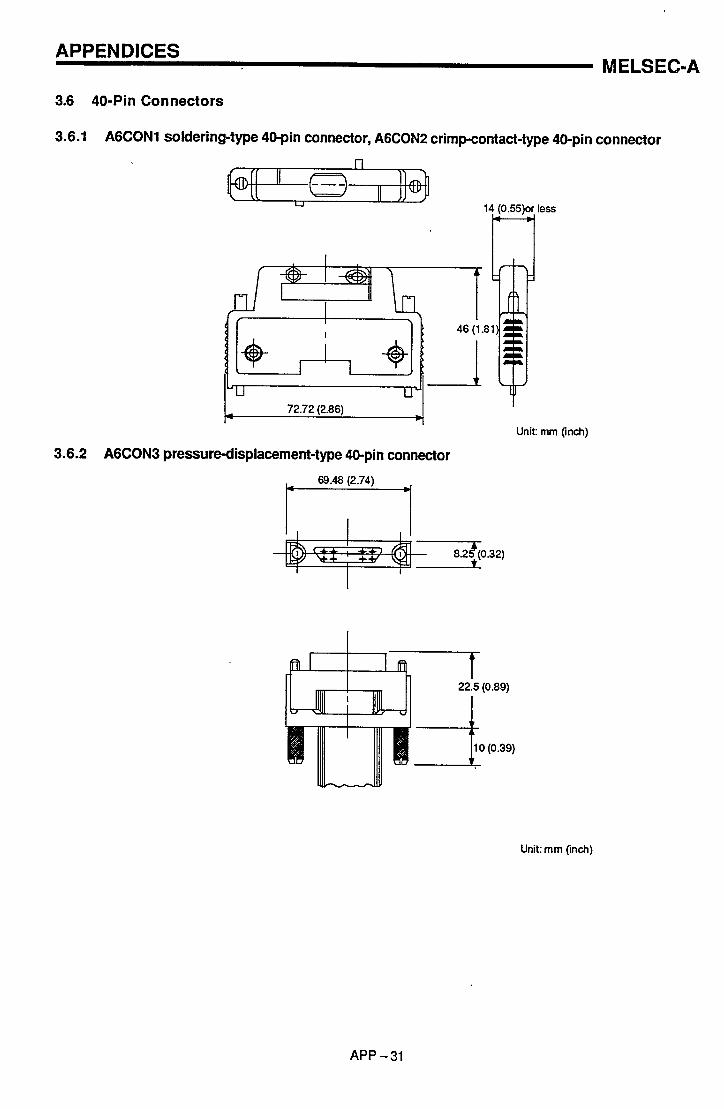
APPENDICES MELSEC-A
3.6 40-Pin Connectors
3.6.1 A6CON1 soldering-type 40pin connector, A6CON2 crimpcontact-type 40-pin connector
I 1
U 14 (0.55)or less
3.6.2 A6CON3 pressure-displacement-type &pin connector
1
Unit: mm (inch)
Unit: mm (inch)
APP - 31

APPENDICES MELSEC-A
3.7 37-Pin D Sub-connectors
3.7.1 A6CON1 E soldering type 37-pin D sub-connector A6CON2E crimp-contact-type 37-pin D sub-connector
Unit: mm (inch)
3.7.2 A6CON3E pressure-displacement-type 37-pin D sub-connector
Unit: mm (inch)
APP - 32

APPENDICES MELSEC-A
An AiSJCPU requires the instruction processing time as much as an An CPU does except the following instructions. See the ACPU Programming Manual (Common Instructions) for the processing time for each instruction.
APP - 33
Instruction
OUT F
SET F
RST F
LEDR
CHK
Condition
When not executed
When executed
When not executed
When executed
When not executed
When executed
When not executed
When executed
With 1 contact condition
With 50 contact conditions
With 100 contact conditions
With 150 contact conditions
Processing
Direct Method
6 1
267
3.2
237
3.0
283
54
283
240
3905
78 20
11470
Time ( p e c )
Refresh Method
6 2
270
2.7
23 2
3.6
296
55
283
-
-
- -

APPENDICES MELSEC-A
3.4.4 Dynamic I10 module
I
Unit: mrn (in)
3.4.5 A1SJ-5611 I10 combination module
Unit: rnrn (in)
APP - 34

APPENDICES MELSEC-A
3.5 Dummy Module, Blank Cover
3.5.1 A1SG6O blank cover
3.5.2 A1 SG62 dummy module
AISGU
INPUT O R
A
C
DUMW FOI
AlSG62
L 34.5 (1.36)
Unit: mm (in)
-
-
Unit: mm (in)
APP - 35

APPENDICES MELSEC-A
3.6 Memory Cassette (A1 SMCA-[ I )
3.7 A6WA-28P Memory Write Adaptor
Unit: mm (inch)
Unit: mm (inch)
APP - 36

APPENDICES MELSEC-A
3.8 40-Pin Connectors
soldering-type 4 W i n connector, A6CON2 crimpcontact-type &pin
u 14 (0.55)or less
A6CON3 pressure-displacement-type &pin connector
Unit: mm (inch)
connector
Unit: mrn (inch)
APP - 37

APPENDICES MELSEC-A
4 , ,
3.9 37-Pin D Sub-connectors
3.9.1 A6CON1 E soldering type 37-pin D subconnector A6CON2E crimmntact-type 37-pin D sub-connector
Unit: mm (inch)
3.9.2 A6CON3E pressure-displacement-type 37-pin D sub-connector
Unit: mm (inch)
APP - 38

APPENDICES MELSEC-A
APPENDIX 4 INSTRUCTION PROCESSING TIME
An AISJCPU requires the instruction processing time as much as an An CPU does except the following instructions. See the ACPU Programming Manual (Common Instructions) for the processing time for each instruction.
APP - 39
A
Instruction
OUT F
SET F
FIST F
LEDR
CHK
i
Condition
When not executed
When executed
When not executed
When executed
When not executed
When executed
When not executed
When executed
With 1 contact condition
With 50 contact cond~tions
With 100 contact conditions
With 150 contact conditions
Processing
Direct Method
61
267
3.2
23 7
3.0
283
54
283
240
3905
7820
11470
Time (psec)
Refresh Method
6 2
270
2.7
232
3.6
296
55
283
-
-
-
-
IMPORTANT/
(1) Design the configuration of a system to provide an external protective or safety inter locking circuit for the PCs.
(2) The components on the printed circuit boards will be damaged by static electrici,ty, so avoid handling them directly. If it is necessary to handle them take the following precautions.
(a) Ground human body and work bench.
(b) Do not touch the conductive areas of the printed circuit board and its electrical parts with and non-grounded tools etc.
*
Under no circumstances will Mitsubishi Electric be liable or responsible for any consequential damage that may arise as a result of the installation or use of this equipment.
All examples and diagrams shown in this manual are intended only as an aid to understanding the text, not to guarantee operation. Mitsubishi Electric will accept no responsibility for actual use of the product based on these illustrative examples.
Owing to the very great variety in possible applications of this equipment, you must satisfy yourself as to its suitability for your specifrc application.

A MJTSUBJSHI ELECTRIC CORPORATION HEAD OFFICE : MITSUBISHI DENKl BLDG MARUNOUCHI TOKYO 100-0005 TELM :J24532 CABLE MELCO TOKYO
NAGOYA WORKS : 1-14. YADA-MINAMI 5 , HIGASHI-W. NAGOYA. JAPAN
MODEL
MODEL CODE
When exported from Japan, this manual does not require application to the Ministry of International Trade and Industry for service transaction pemission. I
Specifications subject to change without notice.
Printed in Japan on recycled paper.
1 ~ ( ~ ~ ) 6 6 4 4 6 - ~ ( 9 7 0 1 )MEE
A I S JCPU-U-E
13J79 1
I