T.O. 33K1-4-1000-1
40
T.O. 33K1-4-1000-1 30 JULY 2000 CHANGE 1 - 30 JANUARY 2001 TECHNICAL MANUAL CALIBRATION PROCEDURE FOR DC POWER SUPPLIES Distribution Statement - Distribution authorized to U. S. Government agencies and their contractors for official use or for administrative or operational purposes only, 30 August 1988. Other requests for this document shall be referred to AFMETCAL Detachment 1/MLLW, 813 Irving-Wick Dr W, Suite 4M, Heath, OH 43056-6116. Destruction Notice - For unclassified, limited documents, destroy by any method that will prevent disclosure of the contents or reconstruction of the document. Published under Authority of the Secretary of the Air Force
-
Upload
khangminh22 -
Category
Documents
-
view
1 -
download
0
Transcript of T.O. 33K1-4-1000-1

T.O. 33K1-4-1000-1
30 JULY 2000CHANGE 1 - 30 JANUARY 2001
TECHNICAL MANUAL
CALIBRATION PROCEDURE
FOR
DC POWER SUPPLIES
Distribution Statement - Distribution authorized to U. S. Government agencies and their contractors forofficial use or for administrative or operational purposes only, 30 August 1988. Other requests for thisdocument shall be referred to AFMETCAL Detachment 1/MLLW, 813 Irving-Wick Dr W, Suite 4M,Heath, OH 43056-6116.
Destruction Notice - For unclassified, limited documents, destroy by any method that will preventdisclosure of the contents or reconstruction of the document.
Published under Authority of the Secretary of the Air Force

T.O. 33K1-4-1000-1
A Change 1 USAF
INSERT LATEST CHANGED PAGES. DESTROY SUPERSEDED PAGES.
NOTE: The portion of the text and illustrations affected by the changes is indicated by a vertical linein the outer margins of the page.
Date of issue for original and changed pages are:
Original ....................0...........................30 July 2000Change......................1..................... 30 January 2001
TOTAL NUMBER OF PAGES IN THIS PUBLICATION IS 40, CONSISTING OF THE FOLLOWING:
Page * Change Page * Change Page * ChangeNo. No. No. No. No. No.
Title................................. 1A ..................................... 11 - 8 ................................. 0A-1 - A-2 ......................... 1A-3 - A-18 ....................... 0A-19 ................................ 1A-20 - A-27...................... 0A-28 - A-30...................... 1
*Zero in this column indicates an original page
LIST OF EFFECTIVE PAGES

T.O. 33K1-4-1000-1
1
DC POWER SUPPLIES
This procedure describes the calibration of Power Supplies listed in Appendix A and supersedes anyand all previously dated calibration procedures for the subject instrument.
1 CALIBRATION DESCRIPTION:
Table 1.
Test Instrument (TI) Performance TestCharacteristics Specifications Method
Voltmeter and Ammeter
DC Voltmeter Range: 0 to 500 VDC Monitored with aDigital Multimeter
Accuracy: As specified inRating column of Appendix A
DC Ammeter Range: 0 to 500 ADC Monitored with a(Constant Voltage) Shunt Box and
Accuracy: As specified in Digital MultimeterRating column of Appendix A
DC Ammeter Range: 0 to 500 ADC Monitored with a(Constant Current) *1 Shunt Box and
Accuracy: As specified in Digital MultimeterRating column of Appendix A
Line and Load Regulation Line: See Appendix A Input voltage varied,(Constant Voltage) output monitored with a
Accuracy: See Appendix A Digital Multimeter
Load: NL to FL
Accuracy: See Appendix A
Ripple and Noise Range: See Appendix A Measured with Digital(Constant Voltage) Multimeter or
Accuracy: See Appendix A Oscilloscope
Line and Load Regulation Line: 105 to 125 VAC or as listed in Input voltage varied,(Constant Current) *1 Appendix A output monitored with a
Shunt Box andAccuracy: See Appendix A Digital Multimeter
Load: NL to FL
Accuracy: See Appendix A
Ripple Range: See Appendix A Measured with Digital(Constant Current) *1 Multimeter or
Accuracy: See Appendix A Oscilloscope
*1 Current Calibration limited to 300 ADC due to equipment capability. See step 3.2.

T.O. 33K1-4-1000-1
2
2 EQUIPMENT REQUIREMENTS:
Minimum Use Calibration Sub-Noun Specifications Equipment Item
2.1 DIGITAL Range: 0 to 500 VDC; FlukeMULTIMETER 40 �V to 300 mV AC, 8840A/AF
60 Hz
Resolution: 100 µV DC;10 µV AC
Accuracy: ±0.0325% of rdg, VDC;N/A, VAC
2.2 DIGITAL Range: 0 to 500 VDC Hewlett-PackardMULTIMETER 3458A
Resolution: 10 �V DC
Accuracy: ±0.03% of rdg, VDC
2.3 MULTIMETER Range: 105 to 125 VAC Fluke87
Accuracy: ±2.5% of rdg
2.4 VARIAC Range: Single phase, 105 to 125 As Availableor 207 to 253 VAC at ratedline current for TI being calibrated
Accuracy: N/A
2.5 VARIAC Range: Three phase, 190 to As Available250 VAC at rated line currentfor TI being calibrated
Accuracy: N/A
2.6 SHUNT BOX Range: 0 to 300 ADC Guildline9211A
Accuracy: ±0.07% of setting
2.7 SPST SWITCH Range: Must be capable of As Availablecarrying up to 300 ADC
Accuracy: N/A
2.8 OSCILLOSCOPE Range: 50 MHz, bandwidth; Tektronix1.0 mV p-p to 1.5 V p-p, 2465Bvoltage range
Accuracy: Min p-p valuebeing verified in 4.3

T.O. 33K1-4-1000-1
3
Minimum Use Calibration Sub-Noun Specifications Equipment Item
2.9 VARIABLE LOAD Range: See step 4.1.2 As AvailableRESISTOR
Accuracy: N/A
2.10 LOAD BANK Range: 30 VDC at Avtron Mfg100 A T242B
Accuracy: N/A
3 PRELIMINARY OPERATIONS:
3.1 Review and become familiar with the entire procedure before beginning the Calibration Process.
WARNING
Unless otherwise designated, and prior to beginning the Calibration Process,ensure that all test equipment voltage and/or current outputs are set to zero (0)or turned off, where applicable. Ensure that all equipment switches are set tothe proper position before making connections or applying power.
WARNING
This Calibration Procedure contains steps whereby voltages up to 500 VDC,230 VAC and currents up to 50 Amps are present on open terminals andcontacts. Care must be exercised not to come in contact with these terminalsand contacts if the TI is operated with the nonconductive terminal coverremoved.
3.2 Current Calibration is limited to 300 ADC due to equipment capability. A Limited Certification Label must beused, annotated: Current Limited to 300 Amps due to test equipment limitations.
3.3 Mechanically zero TI meter/meters, if necessary.
3.4 Connect the TI and test equipment to appropriate power source, set POWER switches to ON and allow warm-up as required by manufacter.
3.5 Customer must determine if both front and rear output terminals are to be used. As appropriate, calibrate bothsets of output terminals or use a Limited Certification Label to limit use to the set of output terminals calibrated.
3.6 Some TIs with front and rear output terminals may have only one output designed to meet Accuracyspecifications stated by the manufacturer. Consult maintenance T.O. or manufacturer data to determine ifAccuracy specifications apply to both front and rear terminals. When commercial/maintenance data indicateswhich terminals have the listed specifications, a Limited Certification Label is not required, however, the specialblock on the Certification Label will be annotated with which terminals were certified.
3.7 Certain equipment listed in Appendix A is operated from power line voltages other than 115 VAC, 60 Hz.Substitute 230 VAC, 60 Hz in all steps and figures for any TI requiring 230 VAC, 60 Hz input.
3.8 If applicable, connect jumpers across appropriate sensing terminals on back of TI for proper operation.
3.9 Some TIs have both Constant Voltage and Constant Current characteristics, others have one or the other. Usecharacteristics as stated in Appendix A or as required by the user for model being calibrated. Use only theseportions of the TI being calibrated.

T.O. 33K1-4-1000-1
4
3.10 Some TIs have meters with full scale markings higher than the rating. Do not exceed these ratingspecifications. Accuracy limits must be computed using the full scale value for the applied rating value (i.e., 50 V±2% FS = 1 V, 40 V rating, limits 39 to 41 on Digital Multimeter (2.1)).
3.11 Some TIs have more than one range on their meters. Applicable section of procedure should be repeated forthe other range/ranges with the applicable control switch/switches set to the appropriate position.
3.12 Ensure TI fuses are of the proper value, if applicable, before beginning calibration.
3.13 For some TIs, the appropriate test equipment must be connected across the Sensing terminals instead of theLoad terminals of the TI. If possible, refer to the manufacturer manual of the TI being calibrated for correctconnections.
3.14 Some meters in various power supplies have no Accuracy stated in Appendix A (rating). These meters needno calibration.
WARNING
Turn TI power OFF prior to disconnecting or adding test equipment.
4 CALIBRATION PROCESS:
NOTE
Unless otherwise specified, verify the results of each test and take correctiveaction whenever the test requirement is not met, before proceeding.
4.1 DC VOLTMETER AND AMMETER CALIBRATION: (Constant Voltage and Current)
4.1.1 Connect test equipment as shown in Figure 1.
V A R I A C
60 Hz- +
TI
M U L T I M E T E R
AC INPUT +
--
+
CLO
SE
D
OP
EN
SPSTS W I T C H
INPUT COMMON
300AMP
100AMP
10 AMP MAX
C O M M O N
POTENTIAL
S H U N T B O X
+
-
* 115 VAC
DIGITAL (2.1)M U L T I M E T E R
DIGITAL (2.2)M U L T I M E T E R
VARIABLE LOAD RESISTOR
* Subs t i tu te 230 VAC/60 Hz or 3 phase input for any TI requir ing a 230 VAC or 3 phase input . NOTE:
Connec t Var iab le Load Res is to r to Shunt Box te rmina ls as needed.
Figure 1.
T.O. 33K1-4-1000-1
5
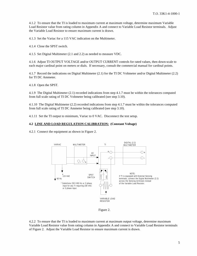
4.1.2 To ensure that the TI is loaded to maximum current at maximum voltage, determine maximum VariableLoad Resistor value from rating column in Appendix A and connect to Variable Load Resistor terminals. Adjustthe Variable Load Resistor to ensure maximum current is drawn.
4.1.3 Set the Variac for a 115 VAC indication on the Multimeter.
4.1.4 Close the SPST switch.
4.1.5 Set Digital Multimeter (2.1 and 2.2) as needed to measure VDC.
4.1.6 Adjust TI OUTPUT VOLTAGE and/or OUTPUT CURRENT controls for rated values, then down-scale toeach major cardinal point on meters or dials. If necessary, consult the commercial manual for cardinal points.
4.1.7 Record the indications on Digital Multimeter (2.1) for the TI DC Voltmeter and/or Digital Multimeter (2.2)for TI DC Ammeter.
4.1.8 Open the SPST.
4.1.9 The Digital Multimeter (2.1) recorded indications from step 4.1.7 must be within the tolerances computedfrom full scale rating of TI DC Voltmeter being calibrated (see step 3.10).
4.1.10 The Digital Multimeter (2.2) recorded indications from step 4.1.7 must be within the tolerances computedfrom full scale rating of TI DC Ammeter being calibrated (see step 3.10).
4.1.11 Set the TI output to minimum, Variac to 0 VAC. Disconnect the test setup.
4.2 LINE AND LOAD REGULATION CALIBRATION: (Constant Voltage)
4.2.1 Connect the equipment as shown in Figure 2.
OPE
N
CLO
SED*
+-
+
-
+
-
TIV A R I A C
ACINPUT
SPSTS W I T C H 115 VAC
60 Hz
DIGITAL (2.2)M U L T I M E T E R
V A R I A B L E L O A D R E S I S T O R
M U L T I M E T E R
* Subst i tu te 230 V/60 Hz or 3 phase input for any TI requi r ing 230 VAC or 3 phase input .
NOTE:I f T I is equipped wi th Externa l Sens ingtermina ls , connect the Dig i ta l Mul t imeter (2 .2)across the Sens ing te rmina ls ins tead o f the Var iab le Load Res is tor .
Figure 2.
4.2.2 To ensure that the TI is loaded to maximum current at maximum output voltage, determine maximumVariable Load Resistor value from rating column in Appendix A and connect to Variable Load Resistor terminalsof Figure 2. Adjust the Variable Load Resistor to ensure maximum current is drawn.

T.O. 33K1-4-1000-1
6
4.2.3 If the TI is constant voltage, constant current supply, adjust the CURRENT control fully CW.
4.2.4 Set the Variac for a 115 VAC indication on the Multimeter.
4.2.5 Adjust the TI VOLTAGE control or set the output of the supply to the rated output voltage.
4.2.6 Close the SPST switch.
4.2.7 Adjust the Variac until the Multimeter indicates 105 VAC then 125 VAC for 115 V input or 207 VAC then253 VAC for 230 V input while recording the indication of the Digital Multimeter for both line voltages.
4.2.8 The Digital Multimeter (2.2) change must indicate within the tolerance listed in the Regulation columnof Appendix A (Line Max).
4.2.9 Set the Variac for a 115 VAC indication on the Multimeter.
4.2.10 Record the Digital Multimeter (2.2) indication.
4.2.11 Open the SPST switch and ensure the Digital Multimeter (2.2) change from the recorded value ofstep 4.2.10 indicates within the tolerance listed under the Regulation column (Load Max) of Appendix A.
4.2.12 Set the Variac for a 115 VAC indication on the Multimeter and close the SPST switch.
4.3 RIPPLE AND NOISE CALIBRATION: (Constant Voltage)
4.3.1 Set Digital Multimeter as needed to measure VAC.
4.3.2 Set TI output to full load and measure the RMS ripple of the output voltage by setting the range switch of theDigital Multimeter for the best possible ripple indication.
4.3.3 The Digital Multimeter (2.2) indication must not exceed the stated RMS ripple specification listed inAppendix A.
4.3.4 Set the TI output to OFF and disconnect the Digital Multimeter (2.2) from the TI.
NOTE
Only accomplish the following steps if ripple and noise specification list p-pvalues in Appendix A.
4.3.5 With the TI at full load, connect the Oscilloscope across the TI output terminals, observing polarity.
4.3.6 Set the output of the TI to ON and measure the p-p noise of the output voltage.
4.3.7 The Oscilloscope p-p noise indications must not exceed the p-p specifications listed in Appendix A.
4.3.8 Set the TI output to OFF and disconnect the test equipment from the TI.

T.O. 33K1-4-1000-1
7
4.4 LINE AND LOAD REGULATION CALIBRATION: (Constant Current)
NOTE
In Appendix A for Constant Current Regulation where the percentage ofregulation is listed in actual current, this value has been converted to percentand listed under the regular value in parenthesis. For example, at a value ofConstant Current: ±250 µA DC at a full scale range of 10 ADC would be listedas ±(0.0025% FS).
4.4.1 Connect the equipment as shown in Figure 3.
- +
-
+
+
-
TI
CLO
SE
D
OP
EN
INPUT C O M M O N
300AMP
100AMP
10 AMP MAX
C O M M O N
POTENTIAL
S H U N T B O X
* Substi tute 230 VAC/60 Hz or 3 phase input for any TI requiring a 230 VAC or 3 phase input.
VARIAC
AC INPUT
60 Hz
SPSTS W I T C H
DIGITAL (2.2) MULTIMETER
MULTIMETER
VARIABLE LOAD RESISTOR
Note:Connect to Shunt Boxterminals as needed.
Figure 3.
4.4.2 To ensure that the TI is loaded to maximum current at maximum output voltage, determine maximumVariable Load Resistor (resistance connected across SPST shorting switch plus resistance of Shunt Box) value fromrating column in Appendix A and connect to load resistor terminals of Figure 3. Adjust the Variable Load Resistorto ensure maximum current is drawn.
4.4.3 If the TI is a constant voltage, constant current supply, adjust the VOLTAGE control fully CW. If the TI is aconstant current supply equipped with a VOLTAGE control, adjust for rated output voltage.
WARNING
Do not exceed the TI rated output current in step 4.4.5.
4.4.4 For a Digital Precision power supply, lower the load resistance by about 10%. Adjust the output voltage forrated output only.
4.4.5 Adjust the TI CURRENT control or set the output of the supply to the rated output current.
4.4.6 Set the Variac for a of 115 VAC indication on the Multimeter.

T.O. 33K1-4-1000-1
8
4.4.7 Set Digital Multimeter (2.2) as needed to measure VDC, record indication and calculate the current.
4.4.8 Adjust the Variac until the Multimeter indicates 105 VAC then 125 VAC for 115 V input or 207 VAC then253 VAC for 230 V input while recording the indication of the Digital Multimeter (2.2) for both line voltages andcalculate the current for both line voltages.
4.4.9 The Digital Multimeter (2.2) change must indicate within the tolerance listed under the Regulation Line (Max)column of Appendix A.
4.4.10 Set the Variac for a 115 VAC indication on the Multimeter.
4.4.11 Close the SPST Switch.
4.4.12 Record the Digital Multimeter (2.2) indication and calculate the current.
4.4.13 Open the SPST Switch.
4.4.14 The difference between steps 4.4.7 and 4.4.12 must indicate within the tolerance listed under theRegulation Load (Max) column of Appendix A.
4.4.15 Set the TI to OFF.
4.5 RIPPLE CALIBRATION: (Constant Current)
4.5.1 Set Digital Multimeter (2.1) as needed to measure VAC.
4.5.2 With TI at full load, connect Digital Multimeter (2.1) or the Oscilloscope across the TI OUTPUT terminals.
4.5.3 Set output of TI to ON and measure the ripple content of the OUTPUT current by setting the RANGE switchof Digital Multimeter (2.1) or adjusting the SENSITIVITY controls of the Oscilloscope for best possible rippleindication.
4.5.4 The Digital Multimeter (2.1) or Oscilloscope indication must not exceed (the stated ripple specificationslisted in Appendix A Times Load) Load = DC Volts
DC Current
4.5.5 If applicable, attach a Limited Certification Label as per step 3.2, 3.5 or 3.6.
4.5.6 Set all POWER switches to OFF or STANDBY, disconnect and secure all equipment.
CALIBRATION PERFORMANCE TABLE
Not Required

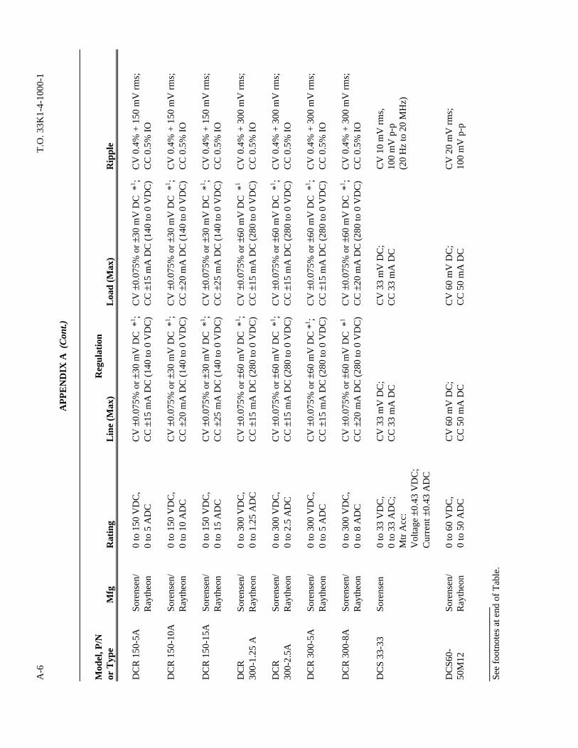
T.O. 33K1-4-1000-1APPENDIX A
DC POWER SUPPLIES
Table A-1.
SPECIFICATIONS LISTING
Part Number Page Part Number Page Part Number Page
Change 1 A-1
AP2H............................. A-3BHK 500-0.4M .............. A-3BPA 40 CV.................... A-3CB12A........................... A-3CPS250.......................... A-3CRS36-20 ...................... A-3DCR 20 -125A ............... A-3DCR 20-250A ................ A-4DCR 40-10A.................. A-4DCR 40-20A.................. A-4DCR 40-25B .................. A-4DCR 40-35A.................. A-4DCR 40-60A.................. A-4DCR 40-125A ................ A-4DCR 40-250A ................ A-4DCR 40-500A ................ A-4DCR 60-90B .................. A-4DCR 60-13A.................. A-5DCR 60-25A.................. A-5DCR 60-40A.................. A-5DCR 80-5A.................... A-5DCR 80-6B .................... A-5DCR 80-10A.................. A-5DCR 80-18A.................. A-5DCR 80-30A.................. A-5DCR 150-2.5A ............... A-5DCR 150-5A.................. A-6DCR 150-10A ................ A-6DCR 150-15A ................ A-6DCR 300-1.25A ............. A-6DCR 300-2.5A ............... A-6DCR 300-5A.................. A-6DCR 300-8A.................. A-6DCR 33-33..................... A-6DCS60-50M12............... A-6EMS300-16.................... A-7ESS125-125-2................ A-7E3610A.......................... A-7E3611A.......................... A-7E3612A.......................... A-7E3614A.......................... A-8E3615A.......................... A-8
E3616A..........................A-8E3617A..........................A-8E3620A..........................A-8E3630A..........................A-8E3631A..........................A-9GPR-7550D....................A-9GPS-3030D ....................A-28HCR20-13-111 ...............A-9HCR 150-2 .....................A-9HPD60-5 ........................A-9HR160-3C ......................A-10HR20-5A........................A-10HWD60-3A ....................A-10IP-27 ..............................A-10KS60-10M......................A-10LA200............................A-10LA250............................A-10LCS-A-04.......................A-10LDS-X-03.......................A-10LE101 ( )........................A-11LGS-FA-5-0V-R.............A-28LJS-13-5-OV..................A-11LLS5018 ........................A-11LLS-6060 .......................A-29LLS8040 ........................A-11LLS9040 ........................A-11LND-W-152 ...................A-11LND-Y-152-8562 ...........A-11LNSP28..........................A-11LNS-W-28......................A-11LPD-421FM ...................A-12LRS53-2.........................A-12LS 30-3 ..........................A-12LS40-25-06 ....................A-12MPS-20-1.5 ....................A-12MSK 10-10M .................A-12MSK 20-5M ...................A-12PAB160-0.4....................A-12PAD 55-3L.....................A-12PD56-10 .........................A-13PD56-6D ........................A-13PE1649...........................A-13
PPS-4A...........................A-13PPS-50-1.5......................A-13PR40-5-01-09 .................A-13PR40-10A-06 SPB998 ....A-13PSV-5 .............................A-14PS2521G.........................A-14PS280 .............................A-14PS281 .............................A-14PS402 .............................A-14PVC50-0.5......................A-15PW18-1T ........................A-15PW18-3A........................A-15P030PX4.........................A-15QRD 20-4 .......................A-15RAX28-6.2K...................A-29RE40-5 ...........................A-16RS20-20B .......................A-16RS40-15B .......................A-16RS60-12B .......................A-16RS160-4B .......................A-16R6127 .............................A-16SBC 519 .........................A-16SYR36-25-5133 ..............A-16SYR75-6.5PD .................A-16SYR75-6.5-55139 ...........A-17TCR 30...........................A-17TCR 300S2 .....................A-17TCR 40S25-1D ...............A-17TCR 500T10-D-0V.........A-17TCR 60S10-1..................A-17TP340.............................A-18TP343B ..........................A-29TP840.............................A-18TW5005D.......................A-18TW6050D.......................A-19V28PT10FH....................A-19WP-704A........................A-19WP-707B........................A-19WP718............................A-19WP-75 ............................A-19WP-78 ............................A-20XTS60-1.........................A-20

T.O. 33K1-4-1000-1APPENDIX A (Cont.)
DC POWER SUPPLIES
Table A-1. (Cont.)
SPECIFICATIONS LISTING
Part Number Page Part Number Page Part Number Page
A-2 Change 1
XTS120-0.5 ....................A-201101 ...............................A-29150-2-110 .......................A-201630 ...............................A-201635 ...............................A-201635A.............................A-211646 ...............................A-211651 ...............................A-211660 ...............................A-211686 ...............................A-211711 ...............................A-221730 ...............................A-221735 ...............................A-221743 ...............................A-221760 ...............................A-2220300B...........................A-2320320B...........................A-23212AMK ........................A-2328PT10AF ......................A-2330-33-1-D-TC.................A-233005B.............................A-233032B.............................A-243101-3610 ......................A-243101A-3610....................A-243300D-4015....................A-243300D-6010....................A-243300D-7.575...................A-243302D.............................A-243303D.............................A-243306D.............................A-243410D-4025....................A-253413D-1202.5.................A-2540-125-2-D.....................A-2540S25-1 ..........................A-254010 ...............................A-255030 ...............................A-256010D.............................A-256023A.............................A-266028A.............................A-266106A.............................A-266212C.............................A-276214C.............................A-27
6216C ............................ A-276479C ............................ A-2772-2010.......................... A-2772-2075.......................... A-2772-2080.......................... A-2872-4045A....................... A-3072-6615.......................... A-28832-210.......................... A-288609............................... A-2890074-2.......................... A-28

AP
PE
ND
IX A
(C
ont.)
Mod
el, P
/NR
egul
atio
nor
Typ
eM
fgR
atin
gL
ine
(Max
)L
oad
(Max
)R
ippl
e
A-3
T.O
. 33K
1-4-
1000
-1
AP-
2HB
erke
ley
± 24
VD
C, 0
to 1
AD
C;
CV
Bet
ter
than
0.1
%;
CV
Bet
ter
than
0.1
%;
CV
Les
s th
an 3
mV
p-p
whe
nN
ucle
onic
s± 1
2 V
DC
, 0 to
0.5
AD
CV
olta
ge V
aria
tion
±12
%no
load
to f
ull l
oad
obse
rved
with
a 5
0 M
Hz
band
wid
th o
scill
osco
pe
BH
K 5
00-0
.4M
Kep
co0
to 5
00 V
DC
,C
V <
0.00
5%C
V <
0.01
%C
V <
1 m
V r
ms;
0.4
AD
C;
or 1
mV
DC
*1 ;
or 1
mV
DC
*1 ;
CC
<10
0 �
A r
ms
Mtr
Acc
: ±2%
FS
CC
<10
0 �
A D
CC
C <
100 �
A D
C
BPA
40
CV
Pow
er
0 to
40
VD
C,
CV
0.0
1% +
1 m
V D
CC
V 0
.01%
+ 1
mV
DC
CV
Les
s th
an 5
00 �
V r
ms
Mou
nt0
to 0
.75
AD
C
CB
12A
*2
Tin
ker
6 to
32
VD
C,
N/A
N/A
N/A
0 to
5 A
DC
;M
tr A
cc:
± 0.2
5 V
DC
, ±0.
25 A
DC
CPS
250
Tek
tron
ix5
VD
C, 2
AD
C;
CV
5 V
, ±10
mV
DC
;C
V 5
VD
C, ±
0.1%
+ 5
mV
DC
;C
V 5
VD
C, 2
mV
rm
s;D
ual,
0 to
20
VD
C,
CV
0 to
20
VD
C,
CV
0 to
20
VD
C, 0
.01%
+C
V 0
to 2
0 V
DC
, 2 m
V r
ms;
500
mA
DC
;0.
01%
+ 3
mV
DC
;3
mV
DC
; CC
0.2
% +
CC
3 m
A r
ms
Mtr
Acc
: ±2.
5% F
SC
C 0
.2%
+ 3
mA
DC
6 m
A D
C
CR
S36-
20N
JE0
to 3
6 V
DC
,C
V 0
.02%
or
1 m
V D
C *
1C
V 0
.02%
or
2 m
V D
C *
1C
V 1
mV
rm
s0
to 2
0 A
DC
;M
tr A
cc: ±
2% F
S
DC
R 2
0-12
5A
Sore
nsen
/0
to 2
0 V
DC
,C
V ±
0.07
5% o
r ± 8
mV
DC
*1 ;
CV
±0.
075%
or
± 8 m
V D
C *
1 ;C
V 0
.4%
+ 2
0 m
V r
ms
Ray
theo
n0
to 1
25 A
DC
CC
±12
5 m
A D
C (
19 to
0 V
DC
)C
C ±
125
mA
DC
(19
to 0
VD
C)
CC
0.5
% I
O
See
foot
note
s at
end
of
Tab
le.

A-4
T.O
. 33K
1-4-
1000
-1
AP
PE
ND
IX A
(C
ont.)
Mod
el, P
/NR
egul
atio
nor
Typ
eM
fgR
atin
gL
ine
(Max
)L
oad
(Max
)R
ippl
e
DC
R 2
0-25
0ASo
rens
en/
0 to
20
VD
C,
CV
±0.
10%
or
± 8 m
V D
C *
1 ;C
V ±
0.10
% o
r ± 8
mV
DC
*1 ;
CV
0.8
% +
60
mV
rm
s or
Ray
theo
n0
to 2
50 A
DC
CC
±50
0 m
A D
C (
19 to
0 V
DC
)C
C ±
500
mA
DC
, (19
to 0
VD
C)
160
mV
rm
s *
3 ; CC
0.5
% I
O
DC
R 4
0-10
ASo
rens
en/
0 to
40
VD
C,
CV
±0.
075%
CV
±0.
075%
CV
0.4
% +
40
mV
rm
s;R
ayth
eon
0 to
10
AD
Cor
±15
mV
DC
*1 ;
or ±
15 m
V D
C *
1 ;C
C 0
.5%
IO
CC
±20
mA
DC
(38
to 0
VD
C)
CC
±20
mA
DC
(38
to 0
VD
C)
DC
R 4
0-20
ASo
rens
en/
0 to
40
VD
C,
CV
±0.
075%
CV
±0.
075%
CV
0.4
% +
40
mV
rm
s;R
ayth
eon
0 to
20
AD
Cor
±15
mV
DC
*1 ;
or ±
15 m
V D
C *
1C
C 0
.5%
IO
CC
±25
mA
DC
(38
to 0
VD
C)
CC
±25
mA
DC
(38
to 0
VD
C)
DC
R 4
0-25
BSo
rens
en/
0 to
40
VD
C,
CV
0.0
3%;
CV
0.0
3%;
CV
0.1
% +
90
mV
rm
s;R
ayth
eon
0 to
25
AD
CC
C 0
.25%
CC
0.2
5%C
C 0
.15%
+ 5
6 m
A r
ms
IO
DC
R 4
0-35
ASo
rens
en/
0 to
40
VD
C,
CV
±0.
075%
or
± 15
mV
DC
*1 ;
CV
±0.
075%
or
± 15
mV
DC
*1 ;
CV
0.0
4% +
40
mV
rm
s;R
ayth
eon
0 to
35
AD
CC
C ±
35 m
A D
C (
38 to
0 V
DC
)C
C ±
35 m
A D
C (
38 to
0 V
DC
)C
C 0
.5%
IO
DC
R 4
0-60
ASo
rens
en/
0 to
40
VD
C,
CV
±0.
075%
or
± 15
mV
DC
*1 ;
CV
±0.
075%
or
± 15
mV
DC
*1 ;
CV
0.0
4% +
40
mV
rm
s;R
ayth
eon
0 to
60
AD
CC
C ±
60 m
A D
C (
38 to
0 V
DC
)C
C ±
60 m
A D
C (
38 to
0 V
DC
)C
C 0
.5%
IO
DC
R 4
0-12
5ASo
rens
en/
0 to
40
VD
C,
CV
±0.
10%
or
± 15
mV
DC
*1 ;
CV
±0.
10%
or
± 15
mV
DC
*1 ;
CV
0.4
% +
60
mV
rm
s or
Ray
theo
n0
to 1
25 A
DC
CC
±25
0 m
A D
C (
38 to
0 V
DC
)C
C ±
250
mA
DC
(38
to 0
VD
C)
150
mV
rm
s *
3 ; CC
0.5
% I
O
DC
R 4
0-25
0ASo
rens
en/
0 to
40
VD
C,
CV
±0.
10%
or
± 15
mV
DC
*1 ;
CV
±0.
10%
or
± 15
mV
DC
*1 ;
CV
0.4
% +
60
mV
rm
sR
ayth
eon
0 to
250
AD
CC
C ±
500
mA
DC
(38
to 0
VD
C)
CC
±50
0 m
A D
C (
38 to
0 V
DC
)or
160
mV
*3 ; C
C 0
.5%
IO
DC
R 4
0-50
0ASo
rens
en/
0 to
40
VD
C,
CV
±0.
10%
or
± 15
mV
DC
*1 ;
CV
±0.
10%
or
± 15
mV
DC
*1 ;
CV
0.4
% +
60
mV
DC
or
Ray
theo
n0
to 5
00 A
DC
CC
±10
00 m
A D
C (
38 to
0 V
DC
)C
C ±
500
mA
DC
(38
to 0
VD
C)
160
mV
DC
*3 ; C
C 0
.5%
IO
DC
R 6
0-9B
Sore
nsen
/0
to 6
0 V
DC
,C
V 1
8 m
V D
C;
CV
18
mV
DC
;C
V 1
25 m
V r
ms
Ray
theo
n0
to 9
AD
CC
C 2
2.5
mA
DC
C
C 2
2.5
mA
DC
See
foot
note
s at
end
of
Tab
le.

AP
PE
ND
IX A
(C
ont.)
Mod
el, P
/NR
egul
atio
nor
Typ
eM
fgR
atin
gL
ine
(Max
)L
oad
(Max
)R
ippl
e
A-5
T.O
. 33K
1-4-
1000
-1
DC
R 6
0-13
ASo
rens
en/
0 to
60
VD
C,
CV
±0.
075%
or
± 15
mV
DC
*1 ;
CV
±0.
075%
or
± 15
mV
DC
*1 ;
CV
0.4
% +
60
mV
rm
s;R
ayth
eon
0 to
13
AD
CC
C ±
20 m
A D
C (
57 to
0 V
DC
)C
C ±
20 m
A D
C (
57 to
0 V
DC
)C
C 0
.5%
IO
DC
R 6
0-25
ASo
rens
en/
0 to
60
VD
C,
CV
±0.
075%
or
± 15
mV
DC
*1
CV
±0.
075%
or
± 15
mV
DC
*1 ;
CV
0.4
% +
60
mV
rm
s;R
ayth
eon
0 to
25
AD
CC
C ±
25 m
A D
C (
57 to
0 V
DC
)C
C ±
25 m
A D
C (
57 to
0 V
DC
)C
C 0
.5%
IO
DC
R 6
0-40
ASo
rens
en/
0 to
60
VD
C,
CV
±0.
075%
or
± 15
mV
DC
*1 ;
CV
±0.
075%
or
± 15
mV
DC
*1 ;
CV
0.4
% +
60
mV
rm
s;R
ayth
eon
0 to
40
AD
CC
C ±
40 m
A D
C (
57 to
0 V
DC
)C
C ±
40 m
A D
C (
57 to
0 V
DC
)C
C 0
.5%
IO
DC
R 8
0-5A
Sore
nsen
/0
to 8
0 V
DC
,C
V ±
0.07
5% o
r ± 2
0 m
V D
C *
1 ;C
V ±
0.07
5% o
r ± 2
0 m
V D
C *
1 ;C
V 0
.4%
+ 8
0 m
V r
ms;
Ray
theo
n0
to 5
AD
CC
C ±
15 m
A D
C (
75 to
0 V
DC
)C
C ±
15 m
A D
C (
75 to
0 V
DC
)C
C 0
.5%
IO
DC
R 8
0-6B
Sore
nsen
/0
to 8
0 V
DC
,C
V 0
.03%
;C
V 0
.03%
;C
V 1
50 m
V r
ms;
Ray
theo
n0
to 6
AD
CC
C 0
.25%
(0
to 9
5%C
C 0
.25%
(0
to 9
5%C
C 1
2 m
A r
ms
com
plia
nce-
volta
ge c
hang
e)co
mpl
ianc
e-vo
ltage
cha
nge)
DC
R 8
0-10
ASo
rens
en/
0 to
80
VD
C,
CV
±0.
075%
or
± 20
mV
DC
*1 ;
CV
±0.
075%
or
± 20
mV
DC
*1 ;
CV
0.4
% +
80
mV
rm
s;R
ayth
eon
0 to
10
AD
CC
C ±
20 m
A D
C (
75 to
0 V
DC
)C
C ±
20 m
A D
C (
75 to
0 V
DC
)C
C 0
.5%
IO
DC
R 8
0-18
ASo
rens
en/
0 to
80
VD
C,
CV
±0.
075%
or
± 20
mV
DC
*1 ;
CV
±0.
075%
or
± 20
mV
DC
*1 ;
CV
0.4
% +
80
mV
rm
s;R
ayth
eon
0 to
18
AD
CC
C ±
25 m
A D
C (
75 to
0 V
DC
)C
C ±
25 m
A D
C (
75 to
0 V
DC
)C
C 0
.5%
IO
DC
R 8
0-30
ASo
rens
en/
0 to
80
VD
C,
CV
±0.
075%
or
± 20
mV
DC
*1 ;
CV
±0.
075%
or
± 20
mV
DC
*1 ;
CV
0.4
% +
80
mV
rm
s;R
ayth
eon
0 to
30
AD
CC
C ±
30 m
A D
C (
75 to
0 V
DC
)C
C ±
30 m
A D
C (
75 to
0 V
DC
)C
C 0
.5%
IO
DC
R 1
50-2
.5A
Sore
nsen
/0
to 1
50 V
DC
,C
V ±
0.07
5% o
r ± 3
0 m
V D
C *
1 ;C
V ±
0.07
5% o
r ± 3
0 m
V D
C *
1 ;C
V 0
.4%
+ 1
50 m
V r
ms;
Ray
theo
n0
to 2
.5 A
DC
CC
±15
mA
DC
(14
0 to
0 V
DC
)C
C ±
15 m
A D
C (
140
to 0
VD
C)
CC
0.5
% I
O
See
foot
note
s at
end
of
Tab
le.
A-6
T.O
. 33K
1-4-
1000
-1
AP
PE
ND
IX A
(C
ont.)
Mod
el, P
/NR
egul
atio
nor
Typ
eM
fgR
atin
gL
ine
(Max
)L
oad
(Max
)R
ippl
e
DC
R 1
50-5
ASo
rens
en/
0 to
150
VD
C,
CV
±0.
075%
or
± 30
mV
DC
*1 ;
CV
±0.
075%
or
± 30
mV
DC
*1 ;
CV
0.4
% +
150
mV
rm
s;R
ayth
eon
0 to
5 A
DC
CC
±15
mA
DC
(14
0 to
0 V
DC
)C
C ±
15 m
A D
C (
140
to 0
VD
C)
CC
0.5
% I
O
DC
R 1
50-1
0ASo
rens
en/
0 to
150
VD
C,
CV
±0.
075%
or
± 30
mV
DC
*1 ;
CV
±0.
075%
or
± 30
mV
DC
*1 ;
CV
0.4
% +
150
mV
rm
s;R
ayth
eon
0 to
10
AD
CC
C ±
20 m
A D
C (
140
to 0
VD
C)
CC
±20
mA
DC
(14
0 to
0 V
DC
)C
C 0
.5%
IO
DC
R 1
50-1
5ASo
rens
en/
0 to
150
VD
C,
CV
±0.
075%
or
± 30
mV
DC
*1 ;
CV
±0.
075%
or
± 30
mV
DC
*1 ;
CV
0.4
% +
150
mV
rm
s;R
ayth
eon
0 to
15
AD
CC
C ±
25 m
A D
C (
140
to 0
VD
C)
CC
±25
mA
DC
(14
0 to
0 V
DC
)C
C 0
.5%
IO
DC
RSo
rens
en/
0 to
300
VD
C,
CV
±0.
075%
or
± 60
mV
DC
*1 ;
CV
±0.
075%
or
± 60
mV
DC
*1
CV
0.4
% +
300
mV
rm
s;30
0-1.
25 A
R
ayth
eon
0 to
1.2
5 A
DC
CC
±15
mA
DC
(28
0 to
0 V
DC
)C
C ±
15 m
A D
C (
280
to 0
VD
C)
CC
0.5
% I
O
DC
R
Sore
nsen
/0
to 3
00 V
DC
,C
V ±
0.07
5% o
r ± 6
0 m
V D
C *
1 ;C
V ±
0.07
5% o
r ± 6
0 m
V D
C *
1 ;C
V 0
.4%
+ 3
00 m
V r
ms;
300-
2.5A
Ray
theo
n0
to 2
.5 A
DC
CC
±15
mA
DC
(28
0 to
0 V
DC
)C
C ±
15 m
A D
C (
280
to 0
VD
C)
CC
0.5
% I
O
DC
R 3
00-5
ASo
rens
en/
0 to
300
VD
C,
CV
±0.
075%
or
± 60
mV
DC
*1 ;
CV
±0.
075%
or
± 60
mV
DC
*1 ;
CV
0.4
% +
300
mV
rm
s;R
ayth
eon
0 to
5 A
DC
CC
±15
mA
DC
(28
0 to
0 V
DC
)C
C ±
15 m
A D
C (
280
to 0
VD
C)
CC
0.5
% I
O
DC
R 3
00-8
ASo
rens
en/
0 to
300
VD
C,
CV
±0.
075%
or
± 60
mV
DC
*1
CV
±0.
075%
or
± 60
mV
DC
*1 ;
CV
0.4
% +
300
mV
rm
s;R
ayth
eon
0 to
8 A
DC
CC
±20
mA
DC
(28
0 to
0 V
DC
)C
C ±
20 m
A D
C (
280
to 0
VD
C)
CC
0.5
% I
O
DC
S 33
-33
Sore
nsen
0 to
33
VD
C,
CV
33
mV
DC
;C
V 3
3 m
V D
C;
CV
10
mV
rm
s,0
to 3
3 A
DC
;C
C 3
3 m
A D
CC
C 3
3 m
A D
C10
0 m
V p
-p
Mtr
Acc
: (2
0 H
z to
20
MH
z)V
olta
ge ±
0.43
VD
C;
Cur
rent
±0.
43 A
DC
DC
S60-
Sore
nsen
/0
to 6
0 V
DC
,C
V 6
0 m
V D
C;
CV
60
mV
DC
;C
V 2
0 m
V r
ms;
50M
12R
ayth
eon
0 to
50
AD
CC
C 5
0 m
A D
CC
C 5
0 m
A D
C10
0 m
V p
-p
See
foot
note
s at
end
of
Tab
le.

AP
PE
ND
IX A
(C
ont.)
Mod
el, P
/NR
egul
atio
nor
Typ
eM
fgR
atin
gL
ine
(Max
)L
oad
(Max
)R
ippl
e
A-7
T.O
. 33K
1-4-
1000
-1
EM
S30
0-16
Ele
ctro
nic
30
0 V
DC
,C
V 0
.1%
;C
V 0
.1%
;C
V 4
0 m
V r
ms;
200
mV
p-p
Mea
sure
-16
AD
CC
C 0
.1%
CC
0.1
%m
ents
ESS
125-
125-
2L
ambd
a0
to 1
25 V
DC
,C
V <
0.1%
;C
V <
0.1%
;C
V 1
20 m
V p
-p0
to 1
25 A
DC
CC
<0.
1%C
C <
0.1%
E36
10A
Hew
lett-
0 to
8 V
DC
, 0 to
3 A
DC
CV
0.0
1% +
2 m
V D
C;
CV
0.0
1% +
2 m
V D
C;
CV
200
�V
rm
s an
d 2
mV
p-p
Pac
kard
or 0
to 1
5 V
DC
,C
C 0
.01%
+ 1
mA
DC
CC
0.0
1% +
1 m
A D
C(1
0 H
z to
10
MH
z);
0 to
2 A
DC
;C
C 2
00 �
A r
ms
and
1 m
A p
-pM
tr A
cc:
(10
Hz
to 1
0 M
Hz)
± (0.
5% r
dg +
2 d
gts)
E36
11A
Hew
lett-
0 to
20
V, 0
to 1
.5 A
DC
CV
0.0
1% +
2 m
V D
C;
CV
0.0
1% +
2 m
V D
C;
CV
200
�V
rm
s an
d 2
mV
p-p
Pac
kard
or 0
to 3
5 V
DC
,C
C 0
.01%
+ 1
mA
DC
CC
0.0
1% +
1 m
A D
C(1
0 H
z to
10
MH
z);
0 to
0.8
5 A
DC
;C
C 2
00 �
A r
ms
and
1 m
A p
-pM
tr A
cc: ±
(0.5
% r
dg(1
0 H
z to
10
MH
z)+
2 d
gts)
E36
12A
Hew
lett-
0 to
60
VD
C,
CV
<0.
01%
+ 2
mV
DC
;C
V <
0.01
% +
2 m
V D
C;
CV
<20
0 �
V r
ms
and
Pac
kard
0 to
0.5
AD
C o
rC
C <
0.01
% +
1 m
A D
CC
C <
0.01
% +
1 m
A D
C2
mV
p-p
(10
Hz
to 1
0 M
Hz)
;0
to 1
20 V
DC
,C
C <
200 �
A r
ms
0 to
0.2
5 A
DC
;an
d <
1 m
A p
-pM
tr A
cc: ±
(0.5
% r
dg(1
0 H
z to
10
MH
z)+
2 d
gts)

A-8
T.O
. 33K
1-4-
1000
-1
AP
PE
ND
IX A
(C
ont.)
Mod
el, P
/NR
egul
atio
nor
Typ
eM
fgR
atin
gL
ine
(Max
)L
oad
(Max
)R
ippl
e
E36
14A
Hew
lett-
0 to
8 V
DC
,C
V 0
.01%
+ 2
mV
DC
;C
V 0
.01%
+ 2
mV
DC
;C
V 2
00 m
V r
ms
and
Pac
kard
0 to
6 A
DC
;C
C 0
.01%
+ 2
50 m
A D
CC
C 0
.01%
+ 2
50 m
A D
C1
mV
p-p
, (20
Hz
to 2
0 M
Hz)
;M
tr A
cc: ±
(0.5
% r
dgC
C 5
mA
rm
s+
2 d
gts)
E36
15A
Hew
lett-
0 to
20
VD
C,
CV
0.0
1% +
2 m
V D
C;
CV
0.0
1% +
2 m
V D
C;
CV
200
�V
rm
s an
dP
acka
rd0
to 3
AD
C;
CC
0.0
1% +
250
�A
DC
CC
0.0
1% +
250
�A
DC
1 m
V p
-p (
20 H
z to
20
MH
z);
Mtr
Acc
: ±(0
.5%
rdg
CC
2 m
A r
ms
+ 2
dgt
s)
E36
16A
Hew
lett-
0 to
35
VD
C,
CV
0.0
1% +
2 m
V D
C;
CV
0.0
1% +
2 m
V D
C;
CV
200
�V
rm
s an
dP
acka
rd0
to 1
.7 A
DC
;C
C 0
.01%
+ 2
50 �
A D
CC
C 0
.01%
+ 2
50 �
A D
C1
mV
p-p
(20
Hz
to 2
0 M
Hz)
;M
tr A
cc: ±
(0.5
% r
dgC
C 5
00 �
A r
ms
+ 2
dgt
s)
E36
17A
Hew
lett-
0 to
60
VD
C,
CV
<0.
01%
+ 2
mV
DC
;C
V <
0.01
% +
2 m
V D
C;
CV
<20
0 �
V r
ms
and
Pac
kard
0 to
1 A
DC
;C
C <
0.01
% +
250
�A
DC
CC
<0.
01%
+ 2
50 �
A D
C1
mV
p-p
(20
Hz
to 2
0 M
Hz)
;M
tr A
cc: ±
(0.5
% r
dgC
C <
500 �
A r
ms
+ 2
dgt
s)
E36
20A
Hew
lett-
V1
+ V
2 ou
tput
sC
V 0
.01%
+ 2
mV
DC
CV
0.0
1% +
2 m
V D
CC
V 0
.35
mV
rm
sPa
ckar
d(B
oth)
(20
Hz
to 2
0 M
Hz)
0 to
25
VD
C, 1
AD
C;
Mtr
Acc
: ±(0
.5%
rdg
+ 2
dgt
s)
E36
30A
Hew
lett-
0 to
6 V
DC
, 2.5
AD
C;
CV
0.0
1% +
2 m
V D
CC
V 0
.01%
+ 2
mV
DC
CV
350
�V
rm
s,P
acka
rd0
to 2
0 V
DC
, 0.5
AD
C;
1.5
mV
p-p
0 to
-20
VD
C, 0
.5 A
DC

AP
PE
ND
IX A
(C
ont.)
Mod
el, P
/NR
egul
atio
nor
Typ
eM
fgR
atin
gL
ine
(Max
)L
oad
(Max
)R
ippl
e
A-9
T.O
. 33K
1-4-
1000
-1
E36
31A
Hew
lett-
0 to
6 V
DC
, 5 A
DC
;C
V 0
.01%
+ 2
mV
DC
;C
V 0
.01%
+ 2
mV
DC
;C
V 3
50 �
V D
C, 2
mV
p-p
;P
acka
rdM
tr A
cc:
CC
0.0
1% +
250
�A
DC
CC
0.0
1% +
250
�A
DC
CC
2 m
A r
ms
V, ±
(0.1
% +
5 m
V D
C);
C, ±
(0.2
% +
10
mA
DC
)
0 to
+25
VD
C, 1
AD
C;
CV
0.0
1% +
2 m
V D
C;
CV
0.0
1% +
2 m
V D
C;
CV
350
�V
DC
, 2 m
V p
-p;
0 to
-25
VD
C, 1
AD
C;
CC
0.0
1% +
250
�A
DC
CC
0.0
1% +
250
�A
DC
CC
500
�A
rm
sM
tr A
cc:
V, ±
(0.0
5% +
20
mV
DC
);C
±(0
.15%
+ 4
mA
DC
)
GPR
-755
0DG
oodw
ill0
to 7
5 V
DC
,C
V 0
.01%
+ 3
mV
DC
;C
V 0
.01%
+ 5
mV
DC
;C
V 1
mV
rm
s;0
to 5
AD
C;
CC
0.2
% +
3 m
A D
CC
C 0
.2%
+ 5
mA
DC
CC
5 m
A r
ms
Mtr
Acc
: ±(0
.5%
rdg
+ 2
dgt
s)
HC
RE
lect
roni
c
0 to
300
VD
C,
CV
0.1
%;
CV
0.2
5%;
CV
500
mV
rm
s;20
-13-
111
Mea
sure
-0
to 0
.9 A
DC
CC
0.2
5%C
C 0
.1%
CC
2.5
mA
rm
sm
ents
HC
R 1
50-2
Ele
ctro
nic
0 to
150
VD
C,
CV
±0.
1%C
V ±
0.1%
CV
300
mV
rm
s;M
easu
re-
0 to
2 A
DC
CC
3 m
A r
ms
men
ts
HPD
60-5
Sore
nson
0 to
60
VD
C,
CV
8 m
V D
C;
CV
8 m
V D
C;
CV
5 m
V r
ms,
0 to
5 A
DC
;C
C 1
.5 m
A D
CC
C 1
.5 m
A D
C10
0 m
V p
-pM
tr A
cc:
0.7
VD
C, 0
.06
AD
C

A-1
0T
.O. 3
3K1-
4-10
00-1
AP
PE
ND
IX A
(C
ont.)
Mod
el, P
/NR
egul
atio
nor
Typ
eM
fgR
atin
gL
ine
(Max
)L
oad
(Max
)R
ippl
e
HR
160-
3CT
rygo
n0
to 1
60 V
DC
,C
V 0
.01%
or
2 m
V D
C *
1;C
V 0
.01%
or
3 m
V D
C *
1 ;C
V <
0.5
mV
rm
s0
to 5
AD
CC
C 0
.01%
or
2 m
A D
C *
1C
C 0
.01%
or
3 m
A D
C *
1
HR
20-5
AT
rygo
n0
to 2
0 V
DC
,C
V 0
.01%
or
2 m
V D
C *
1 ;C
V 0
.01%
or
3 m
V D
C *
1 ;C
V <
0.5
mV
rm
s0
to 5
AD
CC
C 0
.01%
or
2 m
A D
C *
1C
C 0
.01%
or
3 m
A D
C *
1
HW
D60
-3A
Mid
- 0
to 6
0 V
DC
,C
V 0
.01%
;C
V 0
.01%
or
4 m
V D
C *
1 ;C
V 1
mV
rm
s;E
aste
rn
0 to
3 A
DC
CC
0.5
% F
ull
CC
0.5
% F
ull
CC
6 m
A r
ms
Indu
stri
esC
ompl
ianc
eC
ompl
ianc
eIn
c.
IP-2
7H
eath
kit
50 V
DC
, 1.5
AD
CC
V 0
.05%
wit
h 5%
line
vol
tsC
V le
ss th
an ±
15 m
V D
CC
V 2
50 µ
V r
ms
max
imum
Inc.
chan
ge. 1
05 to
125
from
no-
load
to f
ull-
load
KS6
0-10
MK
epco
60 V
DC
, 10
AD
C;
CV
0.0
05%
;C
V 0
.01%
or
mV
DC
*1 ;
CV
51
mV
rm
sM
tr A
cc: ±
2% F
SC
C 0
.01%
or
1 m
A D
C *
1C
C 0
.01
A to
0.0
1%
LA
200
Lam
bda
1.0
to 1
6.5
VD
C,
CV
20
mV
DC
, Var
iati
ons
85 to
CV
20
mV
DC
CV
60
mV
p-p
0 to
4 A
DC
132
VA
C
LA
250
Lam
bda
10 to
32.
5 V
DC
,C
V 4
0 m
V D
C V
aria
tion
s 85
toC
V 4
0 m
V D
CC
V 8
0 m
V p
-p0
to 2
AD
C13
2 V
AC
LC
S-A
-04
Lam
bda
0 to
60
VD
C,
CV
±0.
01 +
1 m
V D
CC
V ±
0.01
+ 1
mV
DC
CV
250
�V
rm
s, 1
mV
p-p
0.37
AD
C
LD
S-X
-03
Lam
bda
0 to
32
VD
C,
CV
0.0
05%
+ 0
.5 m
V D
CC
V 0
.005
% +
0.5
mV
DC
CV
150
�V
rm
s, 1
mV
p-p
0 to
1.2
5 A
DC
, in
put v
aria
tion
105
to 1
27 V
AC
w/c
over
inst
alle
d
See
foot
note
s at
end
of
Tab
le.

AP
PE
ND
IX A
(C
ont.)
Mod
el, P
/NR
egul
atio
nor
Typ
eM
fgR
atin
gL
ine
(Max
)L
oad
(Max
)R
ippl
e
A-1
1T
.O. 3
3K1-
4-10
00-1
LE
101
( )
Lam
bda
0 to
36
VD
C,
CV
0.0
5% o
r 8
mV
DC
*1
CV
0.0
5% o
r 8
mV
DC
*1 ;
CV
<0.
5 m
V r
ms;
0 to
5 A
DC
inpu
t var
iati
onC
C 0
.2%
or
15 m
A D
C *
1C
C 1
0 m
A r
ms
105
to 1
35 V
AC
;C
C 0
.2%
or
15 m
A D
C *
1
inpu
t var
iati
on 1
05 to
135
VA
C
LJS
-13-
5-O
VL
ambd
a5
VD
C, 5
AD
CC
V 0
.4 V
DC
CV
0.4
VD
CC
V 1
0 m
V r
ms
LL
S501
8L
ambd
a0
to 1
8 V
DC
,C
V 0
.05%
;C
V 0
.05%
;C
V 5
mV
rm
s, 3
5 m
V p
-p;
0 to
4.5
AD
CC
C 0
.03%
CC
0.0
3%C
C 1
.0%
LL
S804
0L
ambd
a0
to 4
0 V
DC
,C
V 0
.05%
;C
V 0
.05%
;C
V 1
0 m
V r
ms,
75
mV
p-p
;0
to 1
0 A
DC
CC
0.3
%C
C 0
.3%
CC
1.0
%
LL
S904
0L
ambd
a0
to 4
0 V
DC
;C
V 0
.05%
;C
V 0
.05%
;C
V 1
0 m
V, 7
5 m
V p
-p;
0 to
10
AD
CC
C 0
.3%
CC
0.3
%C
C 1
.0%
LN
D-W
-152
Lam
bda
± 12
VD
C, 3
.1 A
DC
;C
V 0
.1%
(10
5 to
127
VA
C)
CV
0.1
%C
V 1
.5 m
V r
ms,
5 m
V p
-p± 1
5 V
DC
, 3.3
AD
C(2
10 to
254
VA
C)
LN
D-Y
-152
-L
ambd
a0
to 1
5 V
DC
;C
V 0
.1%
CV
0.1
%C
V 1
.5 m
V r
ms,
5 m
V p
-p85
620
to 1
.4 A
DC
CC
0.1
%C
C 0
.1%
LN
SP28
Lam
bda
28 V
DC
±5%
,C
V 0
.1%
, inp
ut li
ne v
olta
geC
V 0
.1%
CV
1.5
mV
rm
s m
axim
um8.
0 A
DC
105
to 1
27 V
AC
LN
S-W
-28
Lam
bda
0 to
28
VD
C;
CV
0.1
%;
CV
0.1
%;
CV
1.5
mV
rm
s, 5
mV
p-p
0 to
4.7
AD
CC
C 0
.1%
CC
0.1
%
See
foot
note
s at
end
of
Tab
le.

A-1
2T
.O. 3
3K1-
4-10
00-1
AP
PE
ND
IX A
(C
ont.)
Mod
el, P
/NR
egul
atio
nor
Typ
eM
fgR
atin
gL
ine
(Max
)L
oad
(Max
)R
ippl
e
LPD
-421
FML
ambd
a0
to 2
0 V
DC
;C
V 0
.01%
+ 1
mV
DC
;C
V 0
.01%
+ 1
mV
DC
;C
V L
ess
than
500
�V
rm
sE
lect
roni
cs0
to 1
.7A
DC
CC
5 m
A D
CC
C 5
mA
DC
posi
tive
or n
egat
ive
grou
nd
LR
S53-
2L
ambd
a2
VD
C ±
5%
,C
V ±
0.1%
;C
V ±
0.1%
;C
V 1
0 m
V r
ms;
25 A
DC
CC
±0.
1%
CC
±0.
1%
35 m
V p
-p
LS
30-3
Sore
nsen
0 to
30
VD
C,
CV
≤0.
01%
+ 3
mV
DC
;C
V ≤
0.01
% +
3 m
V D
C;
CV
≤0.
5 m
V r
ms;
0 to
3 A
DC
;C
C ≤
0.2%
+ 3
mA
DC
CC
≤0.
2% +
3 m
A D
CC
C ≤
3 m
A r
ms
Mtr
Acc
: ±(0
.5%
of
rdg
+ 2
dgt
s)
LS4
0-25
-06
M
id-
0 to
40
VD
C,
CV
0.0
05%
;C
V 0
.01%
;C
V 5
00 �
V r
ms
Eas
tern
0
to 2
5 A
DC
CC
0.0
1%C
C 0
.1%
Indu
stri
esIn
c.
MP
S-2
0-1.
5
Ele
ctro
- 0
to 2
0 V
DC
,C
V 0
.01%
+ 4
mV
DC
;C
V 0
.01%
+ 4
mV
DC
;C
V 2
00 �
V r
ms,
1 m
V p
-p;
dyne
0 to
1.5
AD
C;
CC
0.0
4% +
250
�A
DC
CC
0.2
% +
250
�A
DC
CC
500
�A
rm
sSy
stem
s0
to 3
5 V
DC
, 0.8
5 A
DC
;M
tr A
cc: ±
3% F
S
MSK
10-
10M
Kep
co0
to 1
0 V
DC
,C
V ≤
0.01
%;
CV
≤0.
01%
;C
V 0
.2 m
V r
ms,
3 m
V p
-p;
0 to
10
AD
CC
C ≤
0.01
%
CC
≤0.
05%
CC
0.0
2% r
ms,
0.1
% p
-p
MSK
20-
5MK
epco
0 to
20
VD
C,
CV
≤0.
01%
;C
V ≤
0.01
%;
CV
0.2
mV
rm
s, 3
mV
p-p
;0
to 5
AD
CC
C ≤
0.01
%
CC
≤0.
05%
CC
0.0
2% r
ms,
0.1
% p
-p
PA
B16
0-0.
4K
ikus
ui0
to 1
60 V
DC
,C
V 0
.02%
+ 2
mV
DC
;C
V 0
.02%
+ 3
mV
DC
;C
V 2
mV
rm
s0
to 0
.4 A
DC
CC
0.0
2% +
2 m
A D
CC
C 0
.02%
+ 3
mA
DC
PA
D 5
5-3L
Kik
usui
0 to
55
VD
C,
CV
0.0
05%
+ 1
mV
DC
;C
V 0
.005
% +
1 m
V D
C;
CV
500
mV
rm
s;0
to 3
AD
CC
C 1
mA
DC
CC
2 m
A D
CC
C 1
mA
rm
s

AP
PE
ND
IX A
(C
ont.)
Mod
el, P
/NR
egul
atio
nor
Typ
eM
fgR
atin
gL
ine
(Max
)L
oad
(Max
)R
ippl
e
A-1
3T
.O. 3
3K1-
4-10
00-1
PD56
-10
Ken
woo
d0
to 5
6 V
DC
,C
V 0
.005
% +
1 m
V D
C;
CV
0.0
05%
+ 2
mV
DC
;C
V 0
.5 m
V r
ms;
0 to
10
AD
CC
C 3
mA
DC
CC
5 m
A D
CC
C 3
mA
rm
s
PD56
-6D
Ken
woo
d0
to 5
6 V
DC
,C
V 0
.005
% +
1 m
V D
C;
CV
0.0
05%
+ 1
mV
DC
;C
V 0
.5 m
V r
ms;
0 to
6 A
DC
CC
5 m
A D
CC
C 5
mA
DC
CC
2 m
A r
ms
PE16
49Ph
illi
ps0
to 1
50 V
DC
,C
V ±
15 m
V D
C;
CV
±15
mV
DC
;C
V 1
0 m
V r
ms
max
imum
0 to
23
AD
CC
C ±
2 m
A D
CC
C ±
2 m
A D
C
PPS-
4AA
stro
n0
to 1
6 V
DC
,C
V <
± 0.0
2% +
2 m
V D
C;
CV
<± 0
.02%
+ 2
mV
DC
;C
V <
1 m
V r
ms
0 to
4 A
DC
;C
C <
± 0.5
% +
250
µA
DC
CC
<± 0
.05%
+ 2
50 �
A D
C(2
0 H
z to
20
MH
z);
Mtr
Acc
: ±3
dgts
CC
<4
mA
rm
s
PPS-
50-1
.5PP
M I
nc.
0 to
50
VD
C,
CV
≤0.
01%
+ 2
mV
DC
;C
V ≤
0.01
% +
2 m
V D
C;
CV
≤20
0 �
V r
ms,
1 m
V p
-p;
0 to
1.5
AD
C;
CC
≤0.
01%
+ 2
50 �
A D
CC
C ≤
0.01
% +
250
�A
DC
CC
≤50
0 �
A r
ms
Mtr
Acc
: ±3%
FS
PR40
-5-0
1-09
Mid
-0
to 4
0 V
DC
,C
V 0
.01%
;C
V 0
.01%
;C
V 1
mV
rm
sE
aste
rn0
to 5
AD
C;
CC
0.0
1%C
C 0
.25%
Indu
stri
esM
tr A
cc: ±
2% F
SIn
c.
PR40
-10A
-M
id-
0 to
40
VD
C;
CV
0.0
1%;
CV
0.0
1%;
CV
1 m
V r
ms
06 S
PB99
8E
aste
rn
0 to
10
AD
CC
C 0
.01%
CC
0.2
5%In
dust
ries
Inc.

A-1
4T
.O. 3
3K1-
4-10
00-1
AP
PE
ND
IX A
(C
ont.)
Mod
el, P
/NR
egul
atio
nor
Typ
eM
fgR
atin
gL
ine
(Max
)L
oad
(Max
)R
ippl
e
PSV
-5C
Si/S
peco
0 to
30
VD
C,
(108
to 1
32 V
AC
)(1
to 1
00%
Loa
d)C
V L
ess
than
5 m
V p
-p,
3 A
DC
;C
V ±
0.02
5% +
2 m
V D
CC
V ±
0.25
% +
3 m
V D
Cto
10
kHz
Mtr
Acc
: ±2.
5% F
S
PS
2521
GT
ektr
onix
0 to
6 V
DC
,C
V 3
mV
DC
;C
V 3
mV
DC
;C
V 1
mV
rm
s or
3 m
V p
-p;
0 to
5 A
DC
CC
3 m
A D
CC
C 3
mA
DC
CC
5 m
A r
ms
Dua
l:0
to 2
0 V
DC
,C
V 3
mV
DC
;C
V 3
mV
DC
;C
V 1
mV
rm
s or
3 m
V p
-p;
0 to
25
AD
CC
C 3
mA
DC
CC
3 m
A D
CC
C 3
mA
rm
sM
tr A
cc:
V ±
(0.0
5% +
25
mV
DC
);C
±(0
.2%
+ 1
0 m
A D
C)
PS
280
Tek
tron
ixD
ual
(108
to 1
32 V
AC
)C
V 0
.01%
+ 3
mV
DC
;C
V 1
mV
rm
s;0
to 3
0 V
DC
,C
V 0
.01%
+ 3
mV
DC
;C
C 0
.2%
+ 3
mA
DC
CC
3 m
A r
ms
0 to
2 A
DC
;C
C 0
.2%
+ 3
mA
DC
Mtr
Acc
: ±(0
.5%
rdg
+ 2
dgt
s);
5 V
DC
, 3 A
DC
CV
5 m
V D
CC
V 0
.2%
CV
2 m
V r
ms
PS
281
Tek
tron
ix0
to 3
0 V
DC
,(1
08 to
132
VA
C)
CV
0.0
1% +
3 m
V D
C;
CV
0.5
mV
rm
s;0
to 3
AD
C;
CV
0.0
1% +
3 m
V D
C;
CC
0.2
% +
3 m
A D
CC
C 3
mA
rm
sM
tr A
cc:
CC
0.2
% +
3 m
A D
C± (
0.5%
rdg
+ 2
dgt
s)
PS40
2Se
ncor
e0
to 3
0 V
DC
,(1
08 to
132
VA
C)
CV
≤0.
01%
+ 3
mV
DC
;C
V ≤
1 m
V r
ms,
0 to
3 A
DC
;C
V ≤
0.01
% +
3 m
V D
C;
CC
≤0.
02%
+ 3
mA
DC
5 H
z to
1 M
Hz;
Mtr
Acc
:C
C ≤
0.2%
+ 3
mA
DC
CC
≤3
mA
rm
s± (
0.5%
rdg
+ 2
dgt
s);
5 V
DC
, 3 A
DC
:O
utpu
t Acc
: ±0.
25 V
DC
CV
≤5
mV
DC
CV
≤10
mV
DC
CV
≤2
mV
rm
s

AP
PE
ND
IX A
(C
ont.)
Mod
el, P
/NR
egul
atio
nor
Typ
eM
fgR
atin
gL
ine
(Max
)L
oad
(Max
)R
ippl
e
A-1
5T
.O. 3
3K1-
4-10
00-1
PVC
50-0
.5N
JED
ual
(105
to 1
30 V
AC
)C
V <
0.01
% +
1 m
V D
C;
CV
250
µV
rm
s0
to 5
0 V
DC
,C
V <
0.00
5%;
CC
<0.
01%
or
6 m
A D
C *
1(D
C to
10
MH
z)0
to 0
.5 A
DC
;C
C <
0.01
% o
r 50
µA
DC
*1
Mtr
Acc
: ±3%
FS
PW18
-1T
Ken
woo
d0
to ±
18 V
DC
,C
V 1
mV
DC
;C
V 2
mV
DC
;C
V 2
.8 m
V r
ms;
0 to
±1
AD
C;
CC
N/A
;C
C N
/A;
CC
N/A
;0
to +
6 V
DC
,C
V 2
mV
DC
;5
mV
DC
;C
V 5
.6 m
V r
ms;
0 to
+5
AD
C;
CC
N/A
N/A
CC
N/A
Mtr
Acc
:V
DC
±(0
.5%
rdg
+ 2
dgt
s);
AD
C ±
(1.0
%rd
g +
2 d
gts)
PW18
-3A
Ken
woo
d0
to ±
18 V
DC
,C
V 3
.8 m
V D
CC
V 3
.8 m
V D
CC
V 0
.5 m
V r
ms,
0 to
±3
AD
C;
CC
2 m
A D
CC
C 1
0 m
A D
C2
mV
p-p
;M
tr A
cc:
CC
6 m
A r
ms,
VD
C ±
2.5%
FS
12 m
A p
-pA
DC
±2.
5% F
S
P030
PX4
Aco
pian
0 to
30
VD
C,
CV
±0.
005%
or
2 m
V D
C *
1 ;C
V ±
0.00
5% o
r 2
mV
DC
*1 ;
CV
0.2
5 m
V r
ms;
0 to
4 A
DC
CC
±0.
1% o
r 2
mA
DC
*1
CC
±0.
2% o
r 5
mA
DC
*1
CC
0.1
%
QR
D 2
0-4
*5
Sore
nsen
0 to
20
VD
C,
CV
±0.
005%
or
CV
±0.
005%
(50
to 6
0 H
z on
ly)
0 to
4 A
DC
;± 0
.75
mV
DC
*1 ;
or ±
0.75
mV
DC
*1 ;
CV
≤0.
5 m
V r
ms;
Mtr
Acc
: ±3%
FS
CC
±0.
01%
+ 2
50 µ
A D
CC
C ±
0.01
% +
250
µA
DC
CC
400
µA
rm
s(1
0 H
z to
7 M
Hz)
;2
mA
p-p
(0 to
25
MH
z)
See
foot
note
s at
end
of
Tab
le.

A-1
6T
.O. 3
3K1-
4-10
00-1
AP
PE
ND
IX A
(C
ont.)
Mod
el, P
/NR
egul
atio
nor
Typ
eM
fgR
atin
gL
ine
(Max
)L
oad
(Max
)R
ippl
e
RE
40-5
Ele
ctro
nic
0
to 3
6 V
DC
,C
V 0
.01%
or
2 m
V D
C *
1C
V 0
.01%
or
2 m
V D
CC
V L
ess
than
500
�V
rm
sM
easu
re-
0 to
5 A
DC
;N
L to
FL
*1
posi
tive
or n
egat
ive
grou
ndm
ents
Mtr
Acc
: ±2%
FS
RS2
0-20
BSy
stro
n0
to 2
0 V
DC
;C
V 0
.01%
or
3 m
V D
C *
1C
V 0
.01%
or
3 m
V D
C *
1 ;C
V le
ss th
an 0
.5 m
V r
ms;
Don
ner
0 to
20
AD
CC
C 0
.5%
CC
0.5
%C
C 0
.25%
or
5 m
A r
ms
*1
RS4
0-15
BSy
stro
n0
to 4
0 V
DC
,C
V 0
.01%
or
3 m
V D
C *
1 ;C
V 0
.01%
or
3 m
V D
C *
1 ;C
V le
ss th
an 0
.5 m
V r
ms;
Don
ner
0 to
15
AD
CC
C 0
.5%
CC
0.5
%C
C 0
.25%
or
5 m
A r
ms
*1 ;
RS6
0-12
BSy
stro
n0
to 6
0 V
DC
,C
V 0
.01%
or
3 m
V D
C *
1 ;C
V 0
.01%
or
3 m
V D
C *
1 ;C
V le
ss th
an 0
.5 m
V r
ms;
Don
ner
0 to
12
AD
CC
C 0
.5%
CC
0.5
%C
C 0
.25%
or
5 m
A r
ms
*1
RS1
60-4
BSy
stro
n0
to 1
60 V
DC
,C
V 0
.01%
or
3 m
V D
C *
1 ;C
V 0
.01%
or
3 m
V D
C *
1 ;C
V le
ss th
an 0
.5 m
V r
ms;
Don
ner
0 to
4 A
DC
CC
0.5
%C
C 0
.5%
CC
0.2
5% o
r 5
mA
rm
s *
1
R61
27A
copi
an0
to 2
8 V
DC
,C
V ±
0.05
%;
CV
±0.
05%
;C
V 1
mV
rm
s0
to 2
5 A
DC
C
C ±
0.05
%
CC
±0.
05%
SBC
519
Phil
ips
0 to
27
VD
C,
CV
0.5
% a
t 27
VD
C/2
.5 A
DC
CV
<0.
05%
NL
to F
LC
V <
10 m
V r
ms
0 to
3 A
DC
± 1 in
put l
ine
vari
atio
n;0
to 3
AD
C, n
orm
al li
ne v
olta
ge
SYR
36-2
5-Sy
stro
n0
to 4
0 V
DC
,C
V ±
0.05
% +
2 m
V D
CC
V ±
0.05
% +
2 m
V D
C;
CV
95
mV
rm
s51
330
to 2
5 A
DC
CC
±0.
25%
C
C ±
0.25
%
SYR
75-6
.5PD
Sy
stro
n0
to 7
5 V
DC
,C
V 0
.5%
+ 2
mV
DC
ove
rC
V 0
.5%
+ 2
mV
DC
CV
150
mV
rm
s;0
to 6
.5 A
DC
full
AC
inpu
t ran
ge;
over
0 to
ful
l loa
d ra
nge;
CC
15
mA
rm
sC
C 0
.25%
ove
r fu
ll A
C in
put
CC
0.2
5% o
ver
0 to
ful
l loa
dra
nge
rang
e
See
foot
note
s at
end
of
Tab
le.

AP
PE
ND
IX A
(C
ont.)
Mod
el, P
/NR
egul
atio
nor
Typ
eM
fgR
atin
gL
ine
(Max
)L
oad
(Max
)R
ippl
e
A-1
7T
.O. 3
3K1-
4-10
00-1
SYR
75-6
.5-5
Syst
ron
0 to
75
VD
C;
CV
0.5
% +
2 m
V D
C o
ver
CV
0.0
5% +
2 m
V D
C o
ver
CV
150
mV
rm
s;51
390
to 6
.5 A
DC
full
AC
inpu
t;0
to f
ull l
oad
rang
e;C
C 1
3 m
A r
ms
CC
0.2
5% o
ver
full
AC
ran
geC
C 0
.25%
ove
r0
to f
ull l
oad
rang
e
TC
R 3
0E
lect
roni
c
0 to
30
VD
C;
CV
±0.
1%;
CV
±0.
1%;
CV
15
mV
rm
s or
less
Mea
sure
-0
to 1
00 A
DC
CC
±0.
1%
CC
±0.
1%m
ents
, Inc
.
TC
R 3
00S2
Ele
ctro
nic
0
to 3
00 V
DC
,C
V ±
0.1%
;C
V ±
0.1%
;C
V 5
00 m
V r
ms;
Mea
sure
-0
to 2
AD
CC
C ±
0.25
%
CC
±0.
25%
CC
3 m
A r
ms
men
ts, I
nc.
TC
R
Ele
ctro
nic
0
to 4
0 V
DC
,C
V <
0.1%
;C
V <
0.1%
;C
V 6
0 m
V r
ms;
40S2
5-1D
Mea
sure
-0
to 2
5 A
DC
CC
<0.
25%
CC
<0.
25%
CC
60
mA
rm
sm
ents
, Inc
.
TC
RE
lect
roni
c
0 to
500
VD
C,
CV
0.1
% o
f m
axim
umC
V 0
.1%
of
max
imum
vol
tage
CV
125
mV
rm
s50
0T10
-M
easu
re-
0 to
5 A
DC
volta
ge r
atin
g L
ine
Vol
tsra
ting
;D
-0V
men
ts, I
nc.
190
to 2
53;
CC
0.1
% o
f m
axim
umC
C 0
.1%
of
max
imum
curr
ent r
atin
gcu
rren
t rat
ing
TC
R 6
0S10
-1E
lect
roni
c
0 to
60
VD
C,
CV
<0.
1%;
CV
<.1
%;
CV
120
mV
rm
sM
easu
re-
0 to
10
AD
CC
C <
0.25
%C
C <
0.25
%C
C 1
8 m
A r
ms
men
ts, I
nc.

A-1
8T
.O. 3
3K1-
4-10
00-1
AP
PE
ND
IX A
(C
ont.)
Mod
el, P
/NR
egul
atio
nor
Typ
eM
fgR
atin
gL
ine
(Max
)L
oad
(Max
)R
ippl
e
TP3
40Po
wer
A &
B O
utpu
tsC
V 0
.01%
+ 0
.5 m
V D
CC
V 0
.01%
+ 1
mV
DC
/Am
p,C
V 1
mV
p-p
Des
ign
DC
+ to
CO
M;
Cur
rent
Lim
it 2
% to
105
%C
urre
nt L
imit
2%
to 1
05%
0 to
32
VD
C,
0 to
1 A
DC
;D
C-
to C
OM
;0
to -
32 V
DC
,0
to -
1 A
DC
C O
utpu
tC
Out
put
C O
utpu
tC
Out
put
0 to
6 V
DC
,C
V 0
.01%
+ 0
.5 m
V D
CC
V 0
.01%
+ 1
mV
DC
/Am
p,C
V 1
mV
p-p
0 to
5 A
DC
;C
urre
nt L
imit
2%
to 1
05%
Cur
rent
Lim
it 2
% to
105
%0
to 1
5 V
DC
,0
to 2
.5 A
DC
TP8
40Po
wer
A &
B O
utpu
tsC
V ±
0.01
% +
0.5
mV
DC
CV
±0.
01%
+ 1
mV
DC
/Am
pC
V 1
mV
p-p
Des
ign
0 to
32
VD
C,
0 to
1 A
DC
C O
utpu
tC
V ±
0.02
% +
0.5
mV
DC
CV
±0.
01%
+ 1
mV
DC
/Am
pC
V 1
mv
p-p
0 to
6 V
DC
,0
to 5
AD
C;
0 to
15
VD
C,
0 to
2.5
AD
C
TW
5005
DPo
wer
A
and
B O
utpu
tsC
V 0
.005
% +
1 m
V D
CC
V 0
.005
% +
1 m
V D
CC
V 3
50 µ
Vrm
s/ 1
mV
p-p
;D
esig
n0
to 5
0 V
DC
,at
fro
nt a
nd r
ear
term
inal
s;at
fro
nt a
nd r
ear
term
inal
s;C
C 0
.3 m
A p
-p0
to 5
00 m
A D
C;
CC
0.0
6%C
C 0
.06%
Met
er A
cc: ±
2% F
S

AP
PE
ND
IX A
(C
ont.)
Mod
el, P
/NR
egul
atio
nor
Typ
eM
fgR
atin
gL
ine
(Max
)L
oad
(Max
)R
ippl
e
A-1
9
Cha
nge
1T
.O. 3
3K1-
4-10
00-1
TW
6050
DPo
wer
D
ual E
ach
CV
0.0
05%
;C
V 0
.005
%;
CV
1 m
V p
-p;
Des
ign
0 to
60
VD
C, 1
AD
CC
C 0
.02%
CC
0.0
2%C
C 5
mA
p-p
or 0
to 2
5 V
DC
, 2 A
DC
or 0
to 1
5 V
DC
, 3 A
DC
or
0 to
6 V
DC
, 5 A
DC
;M
tr A
cc: ±
3% F
S
V28
PT10
FHA
copi
an28
VD
C ±
0.5
VD
C,
CV
±0.
005%
or
2 m
V D
C *
1C
V ±
0.00
5% o
r 2
mV
DC
*1
CV
<0.
25 V
rm
s0
to 1
0 A
DC
;M
tr A
cc: ±
2% F
S
WP-
704A
Vec
tor-
Vid
0 to
40
VD
C,
(110
to 1
35 V
AC
)C
V <
20 m
V D
C c
hang
e fo
r a
CV
<50
0 µ V
rm
s0
to 2
50 m
A D
CC
V 1
5 m
V D
C25
0 m
A D
C lo
ad c
hang
e
WP-
707B
Vec
tor-
Vid
0 to
32
VD
C,
CV
±0.
02%
+ 2
mV
DC
;C
V ±
0.02
% +
2 m
V D
CC
V 1
mV
rm
s m
ax;
0 to
5 A
DC
;C
C ±
0.5%
+ 2
50 µ
A D
C,
CC
±0.
5% +
250
�A
DC
C
C 2
mA
rm
s m
axM
tr A
cc: ±
3 dg
tsL
ine
Var
iati
on ±
10%
WP7
18V
ecto
r-V
id0
to 3
6 V
DC
,C
V <
± (0.
01%
+ 2
mV
DC
);C
V <
± (0.
01%
+ 2
mV
DC
);C
V <
1 m
V r
ms
max
0 to
20
AD
C;
CC
<± (
0.05
% +
10
mA
DC
)C
C <
± (0.
05%
+ 1
0 m
A D
C)
(20
Hz
to 2
0 M
Hz)
Mtr
Acc
: ±3
dgts
Lin
e V
aria
tion
±10
%C
C <
5 m
A r
ms
max
WP-
75V
ecto
r-V
id0
to 5
0 V
DC
,C
V ±
0.05
% +
3 m
V D
C;
CV
±0.
05%
+ 3
mV
DC
;C
V <
1 m
V r
ms
0 to
2 A
DC
;C
C ±
0.05
% +
500
µA
DC
,C
C ±
0.05
% +
300
�A
DC
C
C <
1 m
A r
ms
Mtr
Acc
: ±(0
.5%
FS
Lin
e V
aria
tion
±10
%+
1 d
gt)
See
foot
note
s at
end
of
Tab
le.

A-2
0T
.O. 3
3K1-
4-10
00-1
AP
PE
ND
IX A
(C
ont.)
Mod
el, P
/NR
egul
atio
nor
Typ
eM
fgR
atin
gL
ine
(Max
)L
oad
(Max
)R
ippl
e
WP-
78V
ecto
r-V
idD
ual:
0 to
30
VD
C, 0
to 5
AD
C;
CV
0.0
2% +
3 m
V D
C;
CV
0.0
2% +
3 m
V D
C;
CV
0.0
5 m
V r
ms;
0 to
5 V
DC
, 0 to
3 A
DC
;C
V 0
.02%
+ 3
mV
DC
CV
0.0
2% +
3 m
V D
C
CV
0.5
mV
rm
sM
tr A
cc: (
V &
C)
± (0.
5% r
dg +
2 d
gts)
XT
S60
-1S
oren
sen/
0 to
60
VD
C,
CV
0.0
1% +
2 m
V D
C;
CV
0.0
1% +
2 m
V D
C;
CV
1 m
V r
ms
max
imum
;R
ayth
eon
1.0
AD
C;
CC
0.0
1% +
250
�A
DC
;C
C 0
.01%
+ 2
50 �
A D
C;
CC
2 m
A r
ms
Mtr
Acc
: ±(1
% F
S(1
03.5
to 1
26.5
VA
C)
(Rem
ote
Sens
e 0
to 1
00%
)+
1 d
gt)
(Loc
al S
ense
10
to 1
00%
)
XT
S12
0-0.
5S
oren
sen/
0 to
120
VD
C,
CV
0.0
1% +
2 m
V D
C;
CV
0.0
1% +
2 m
V D
C;
CV
1 m
V r
ms
max
imum
;R
ayth
eon
0.5
AD
C;
CC
0.0
1% +
250
�A
DC
;C
C 0
.01%
+ 2
50 �
A D
C;
CC
2 m
A r
ms
Mtr
Acc
: ±(1
% F
S (1
03.5
to 1
26.5
VA
C)
(Rem
ote
Sens
e 0
to 1
00%
)+
1 d
gt)
(Loc
al S
ense
10
to 1
00%
)
150-
2-11
0E
lect
roni
c
0 to
150
VD
C,
CV
0.1
%;
CV
0.1
%;
CV
300
mV
rm
s or
0.1
% *
1 ;M
easu
re-
0 to
2 A
DC
CC
0.2
5%C
C 0
.25%
CC
4.5
mA
rm
s or
0.2
5% *
1
men
ts, I
nc.
1630
B &
K0
to 3
0 V
DC
,(1
10 to
130
VA
C)
Prec
isio
n0
to 3
AD
C;
CV
≤0.
02%
+ 2
mV
DC
;C
V ≤
0.02
% +
3 m
V D
C;
CV
≤1
mV
rm
s,M
tr A
cc: (
V &
A)
CC
≤9
mA
DC
CC
≤9
mA
DC
≤ 2 m
V p
-p± 2
.5%
FS
1635
B &
K0
to 3
0 V
DC
,(1
10 to
130
VA
C)
Prec
isio
n0
to 3
AD
C;
CV
≤0.
02%
+ 2
mV
DC
;C
V ≤
0.02
% +
3 m
V D
C;
CV
≤1
mV
rm
s,M
tr A
cc: ±
(0.5
% r
dgC
C 9
mA
DC
max
CC
9 m
A D
C m
ax≤ 2
mV
p-p
+ 2
dgt
s)

AP
PE
ND
IX A
(C
ont.)
Mod
el, P
/NR
egul
atio
nor
Typ
eM
fgR
atin
gL
ine
(Max
)L
oad
(Max
)R
ippl
e
A-2
1T
.O. 3
3K1-
4-10
00-1
1635
AB
& K
0 to
30
VD
C,
(108
to 1
32 V
AC
)P
reci
sion
0 to
3 A
DC
;C
V 0
.01%
+ 3
mV
DC
;C
V 0
.01%
+ 3
mV
DC
;C
V ≤
1 m
V r
ms,
Mtr
Acc
: ±(0
.5%
rdg
CC
0.2
% +
3 m
A D
CC
C 0
.2%
+ 3
mA
DC
≤ 2 m
V p
-p+
2 d
gts)
1646
B &
K0
to 1
6 V
DC
,(1
08 to
132
VA
C)
CV
±(0
.04%
+ 2
mV
DC
);C
V ≤
1 m
V r
ms
(8 m
V p
-p);
Prec
isio
n0
to 1
0 A
DC
;C
V ±
(0.2
% +
2 m
V D
C);
CC
±(0
.4%
+ 5
mA
DC
)C
C ≤
1 m
A r
ms
(8 m
A p
-p)
Mtr
Acc
: (V
& A
)(1
08 to
132
): C
C ±
(0.4
%± 5
% F
S+
5 m
A D
C)
1651
B &
KA
& B
(108
to 1
32 V
AC
)P
reci
sion
0 to
24
VD
C,
CV
0.0
1% +
3 m
V D
C;
CV
0.0
1% +
3 m
V D
C;
CV
1 m
V r
ms;
0 to
0.5
AD
C;
CC
0.2
% +
3 m
A D
CC
C 0
.2%
+ 6
mA
DC
CC
3 m
A r
ms
C 5 V
DC
±10
0 m
V D
C,
CV
5 m
V D
CC
V 1
0 m
V D
C
CV
2 m
V r
ms
0 to
4 A
DC
;M
tr A
cc: A
& B
(on
ly)
(V &
A)
2.5%
FS
1660
B &
KD
ual 0
to 3
0 V
DC
,0
to 3
0 V
DC
:0
to 3
0 V
DC
:0
to 3
0 V
DC
:Pr
ecis
ion
0 to
2 A
DC
;(1
08 to
132
VA
C):
CV
≤0.
01%
+ 3
mV
DC
;C
V ≤
3 m
V r
ms;
4 to
6.5
VD
C,
CV
≤0.
01%
+ 3
mV
DC
;C
C ≤
0.2%
+ 3
mA
DC
;4
to 6
.5 V
DC
:0
to 5
AD
C;
CC
≤0.
2% +
3 m
A D
C;
4 to
6.5
VD
C:
CV
≤2
mV
rm
sM
tr A
cc: ±
(0.5
% r
dg4
to 6
.5 V
DC
: (10
8 to
132
VA
C):
CV
(0
to 5
AD
C)
≤ 10
mV
DC
+ 2
dgt
s)C
V ≤
10 m
V D
C
1686
B &
K3
to 1
4 V
DC
,(1
08 to
132
VA
C)
CV
≤0.
8%C
V <
10 m
V r
ms
Prec
isio
n0
to 1
2 A
DC
;C
V ≤
0.8%
Mtr
Acc
: ±7%
FS

A-2
2T
.O. 3
3K1-
4-10
00-1
AP
PE
ND
IX A
(C
ont.)
Mod
el, P
/NR
egul
atio
nor
Typ
eM
fgR
atin
gL
ine
(Max
)L
oad
(Max
)R
ippl
e
1711
B &
K0
to 6
0 V
DC
,(1
08 to
132
VA
C)
Pre
cisi
on0
to 2
AD
C;
CV
0.0
1% +
3 m
V D
C;
CV
<0.
01%
+ 3
mV
DC
CV
<1
mV
rm
s0
to 0
.5 A
DC
;C
C 0
.2%
+ 3
mA
DC
CC
<0.
2% +
3 m
A D
CM
tr A
cc: ±
2.5%
FS
1730
B &
K0
to 3
0 V
DC
,(1
08 to
132
VA
C)
Pre
cisi
on0
to 3
AD
C;
CV
0.0
1% +
3 m
V D
C;
CV
0.0
1% +
3 m
V D
C;
CV
1 m
V r
ms
0 to
0.5
AD
C;
CC
0.2
% +
3 m
A D
CC
C 0
.2%
+ 3
mA
DC
Mtr
Acc
: (V
& A
)± 2
.5%
FS
1735
B &
K0
to 3
0 V
DC
,C
V 0
.01%
+ 3
mV
DC
;C
V 0
.01%
+ 3
mV
DC
CV
1 m
V r
ms
Pre
cisi
on0
to 3
AD
CC
C 0
.2%
+ 3
mA
DC
CC
0.2
% +
3 m
A D
CM
tr A
cc: (
V a
nd A
)± (
0.5%
rdg
+ 2
dgt
s)
1743
B &
K0
to 3
5 V
DC
, (1
08 to
132
VA
C)
(108
to 1
32 V
AC
)C
V ≤
1 m
V r
ms
Prec
isio
n0
to 6
AD
CC
V ≤
0.2%
+ 2
mV
DC
CV
≤0.
04%
+ 2
mV
DC
Mtr
Acc
: (V
and
A)
CC
≤0.
4% +
5 m
A D
CC
C ≤
0.4%
+ 5
mA
DC
± (0.
5% r
dg +
2 d
gts)
1760
B &
KA
& B
:(1
08 to
132
VA
C)
Pre
cisi
on0
to 3
0 V
DC
,C
V 0
.01%
+ 3
mV
DC
;C
V 0
.01%
+ 3
mV
DC
;C
V 1
mV
rm
s0
to 2
AD
C;
CC
0.2
% +
3 m
A D
CC
C 0
.2%
+ 3
mA
DC
CC
3 m
A r
ms
at 1
08 V
AC
C:
4 to
6.5
VD
C,
CV
10
mV
DC
CV
10
mV
DC
CV
2 m
V r
ms
0 to
5 A
DC
;M
tr A
cc: (
V &
A)
A, B
, C± (
0.5%
rdg
+ 2
dgt
s)
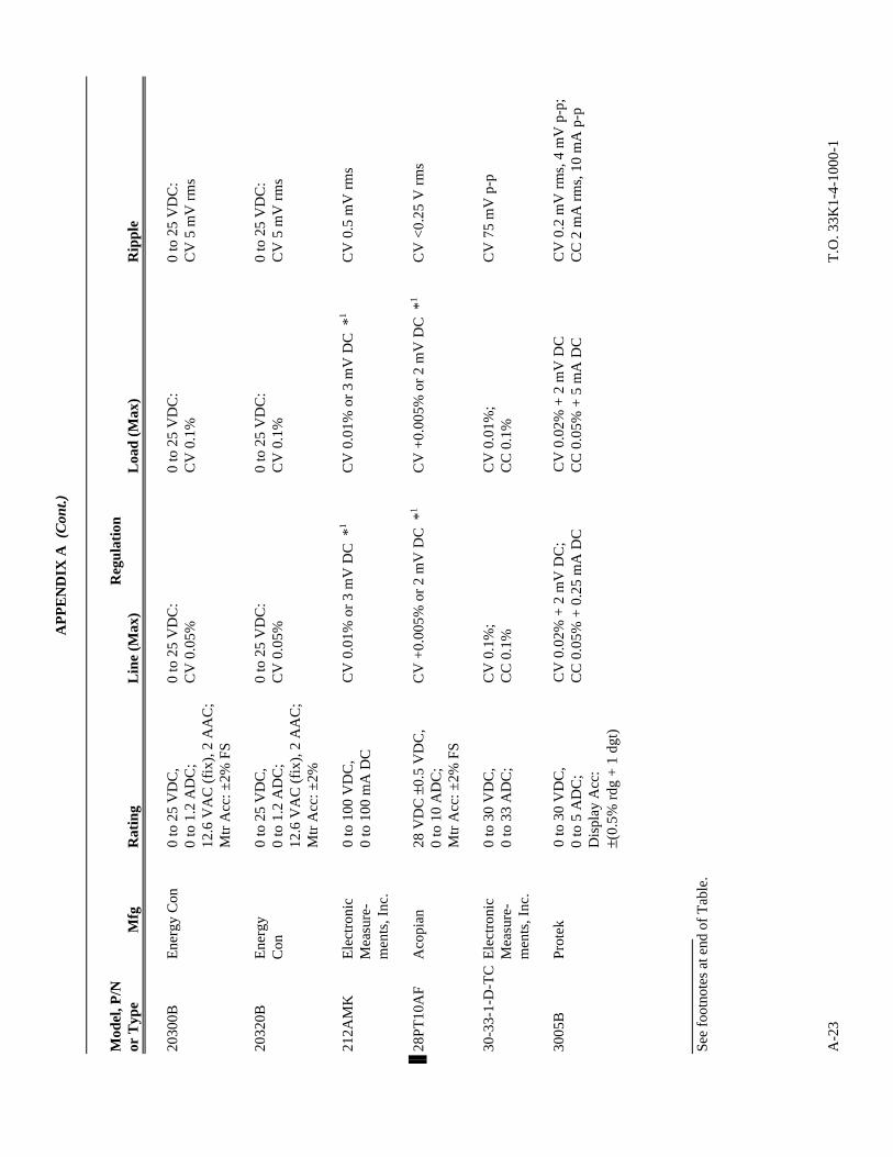
AP
PE
ND
IX A
(C
ont.)
Mod
el, P
/NR
egul
atio
nor
Typ
eM
fgR
atin
gL
ine
(Max
)L
oad
(Max
)R
ippl
e
A-2
3T
.O. 3
3K1-
4-10
00-1
2030
0BE
nerg
y C
on0
to 2
5 V
DC
,0
to 2
5 V
DC
:0
to 2
5 V
DC
:0
to 2
5 V
DC
:0
to 1
.2 A
DC
;C
V 0
.05%
CV
0.1
%C
V 5
mV
rm
s12
.6 V
AC
(fi
x), 2
AA
C;
Mtr
Acc
: ±2%
FS
2032
0BE
nerg
y 0
to 2
5 V
DC
,0
to 2
5 V
DC
:0
to 2
5 V
DC
:0
to 2
5 V
DC
:C
on0
to 1
.2 A
DC
;C
V 0
.05%
CV
0.1
%C
V 5
mV
rm
s12
.6 V
AC
(fi
x), 2
AA
C;
Mtr
Acc
: ±2%
212A
MK
Ele
ctro
nic
0 to
100
VD
C,
CV
0.0
1% o
r 3
mV
DC
*1
CV
0.0
1% o
r 3
mV
DC
*1
CV
0.5
mV
rm
sM
easu
re-
0 to
100
mA
DC
men
ts, I
nc.
28PT
10A
FA
copi
an28
VD
C ±
0.5
VD
C,
CV
+0.
005%
or
2 m
V D
C *
1C
V +
0.00
5% o
r 2
mV
DC
*1
CV
<0.
25 V
rm
s0
to 1
0 A
DC
;M
tr A
cc: ±
2% F
S
30-3
3-1-
D-T
CE
lect
roni
c0
to 3
0 V
DC
,C
V 0
.1%
;C
V 0
.01%
;C
V 7
5 m
V p
-pM
easu
re-
0 to
33
AD
C;
CC
0.1
%C
C 0
.1%
men
ts, I
nc.
3005
BP
rote
k0
to 3
0 V
DC
,C
V 0
.02%
+ 2
mV
DC
;C
V 0
.02%
+ 2
mV
DC
CV
0.2
mV
rm
s, 4
mV
p-p
;0
to 5
AD
C;
CC
0.0
5% +
0.2
5 m
A D
CC
C 0
.05%
+ 5
mA
DC
CC
2 m
A r
ms,
10
mA
p-p
Dis
play
Acc
:± (
0.5%
rdg
+ 1
dgt
)
See
foot
note
s at
end
of
Tab
le.
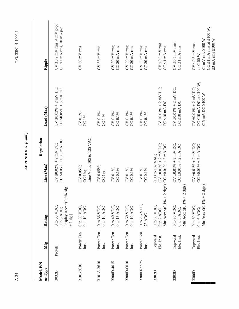
A-2
4T
.O. 3
3K1-
4-10
00-1
AP
PE
ND
IX A
(C
ont.)
Mod
el, P
/NR
egul
atio
nor
Typ
eM
fgR
atin
gL
ine
(Max
)L
oad
(Max
)R
ippl
e
3032
BPr
otek
0 to
30
VD
C,
CV
≤0.
02%
+ 2
mV
DC
;C
V ≤
0.02
% +
2 m
V D
C;
CV
≤0.
2 m
V r
ms,
4 m
V p
-p;
0 to
3 A
DC
;C
C ≤
0.05
% +
0.2
5 m
A D
CC
C ≤
0.05
% +
5 m
A D
CC
C ≤
2 m
A r
ms,
10
mA
p-p
Dis
play
Acc
: ±(0
.5%
rdg
+ 1
dgt
)
3101
-361
0Po
wer
Ten
0
to 3
6 V
DC
,C
V 0
.05%
;C
V 0
.1%
;C
V 3
6 m
V r
ms
Inc.
0 to
10
AD
CC
C 1
%;
CC
1%
Lin
e V
olts
, 105
to 1
25 V
AC
3101
A-3
610
Po
wer
Ten
0 to
36
VD
C,
CV
0.0
5%;
CV
0.1
%;
CV
36
mV
rm
sIn
c.0
to 1
0 A
DC
CC
1%
CC
1 %
3300
D-4
015
Po
wer
Ten
0 to
40
VD
C,
CV
0.1
%;
CV
0.1
%;
CV
30
mV
rm
s;In
c.0
to 1
5 A
DC
CC
0.1
%C
C 0
.1%
CC
30
mA
rm
s
3300
D-6
010
Po
wer
Ten
0 to
60
VD
C,
CV
0.1
%;
CV
0.1
%;
CV
30
mV
rm
s;In
c.0
to 1
0 A
DC
CC
0.1
%C
C 0
.1%
CC
30
mA
rm
s
3300
D-7
.575
Po
wer
Ten
0 to
7.5
VD
C,
CV
0.1
%;
CV
0.1
%;
CV
30
mV
rm
s;In
c.75
AD
CC
C 0
.1%
CC
0.1
%C
C 3
0 m
A r
ms
3302
D
Top
war
d0
to 3
0 V
DC
,(1
08 to
132
VA
C)
Ele
. Ins
t.0
to 2
AD
CC
V ±
0.01
% +
2 m
V D
C;
CV
±0.
01%
+ 2
mV
DC
;C
V ≤
0.5
mV
rm
s;M
tr A
cc: ≤
(0.1
% +
2 d
gts)
CC
±0.
01%
+ 2
mA
DC
CC
≤10
mA
DC
CC
≤1
mA
rm
s
3303
D
Top
war
d0
to 3
0 V
DC
,C
V ±
0.01
% +
2 m
V D
C;
CV
±0.
01%
+ 2
mV
DC
;C
V ≤
0.5
mV
rm
s;E
le. I
nst.
0 to
3 A
DC
;C
C ±
0.01
% +
2 m
A D
CC
C ≤
10 m
A D
CC
C ≤
1 m
A r
ms
Mtr
Acc
: ≤(0
.1%
+ 2
dgt
s)
3306
D
Top
war
d0
to 3
0 V
DC
,C
V ±
0.01
% +
2 m
V D
C;
CV
±0.
01%
+ 2
mV
DC
;C
V ≤
0.5
mV
rm
sE
le. I
nst.
0 to
6 A
DC
;C
C ±
0.01
% +
2 m
A D
CC
C ≤
10 m
A D
C a
t ≤10
0 W
,at
≤10
0 W
,M
tr A
cc: ≤
(0.1
% +
2 d
gts)
≤ 15
mA
DC
≥10
0 W
≤ 1 m
V r
ms
≥ 100
WC
C ≤
1 m
A r
ms
at ≤
100
W,
≤ 3 m
A r
ms
≥ 100
W

AP
PE
ND
IX A
(C
ont.)
Mod
el, P
/NR
egul
atio
nor
Typ
eM
fgR
atin
gL
ine
(Max
)L
oad
(Max
)R
ippl
e
A-2
5T
.O. 3
3K1-
4-10
00-1
3410
D-4
025
Pow
er T
en0
to 4
5 V
DC
,C
V 0
.1%
;C
V 0
.1%
;C
V 3
0 m
V r
ms
0 to
25
AD
CC
C 0
.1%
CC
0.1
%
3413
D-
Pow
er T
en
0 to
5 V
DC
,C
V 0
.1%
of
max
out
put;
CV
0.1
% o
f m
ax o
utpu
t;C
V 5
0 m
V m
axim
um12
02.5
Inc.
0 to
1 m
A D
CC
C 0
.1%
of
max
out
put v
olta
geC
C 0
.1%
of
max
vol
tage
out
put
40-1
25-2
-DE
lect
roni
c 0
to 4
0 V
DC
*4 ,
CV
<0.
1%;
CV
<0.
1%;
CV
75
mV
p-p
;M
easu
re-
0 to
125
AD
C;
CC
<0.
1%C
C <
0.1%
men
ts I
nc.
Mtr
Acc
: ±2%
FS
40S
25-1
Ele
ctro
nic
0 to
40
VD
C,
CV
1%
;C
V 1
%;
CV
60
mV
rm
s;M
easu
re-
0 to
25
AD
C;
CC
25%
CC
25%
CC
60
mA
rm
sm
ents
Inc
.M
tr A
cc: ±
2%
4010
Pow
er T
en0
to 4
0 V
DC
,C
V 0
.01%
+ 2
00 �
V D
C;
CV
0.0
1% +
200
�V
DC
;C
V 2
00 �
V r
ms;
Inc.
0 to
10
AD
CC
C 0
.02%
+ 5
00 �
A D
CC
V 0
.01%
+ 5
00 �
A D
CC
C 3
mA
rm
s
5030
Pow
er
0 to
50
VD
C,
(50
VD
C a
t 2 A
DC
)C
V <
3 m
V p
-pD
esig
n0
to 3
AD
C;
CV
±0.
01%
+ (
1.5
mV
per
am
pM
tr A
cc: ±
2% F
Sof
load
cur
rent
)
6010
DPo
wer
0
to 6
0 V
DC
,C
V ±
0.00
5% +
1 m
V D
C f
orC
V ±
0.00
5%;
CV
1 m
V p
-p;
Des
ign
0 to
0.5
AD
C;
line
vol
tage
var
iati
on ±
10%
;C
C ±
0.03
%
CC
0.5
mA
p-p
0 to
50
VD
C,
CC
±0.
03%
0 to
1 A
DC
;0
to 2
0 V
DC
,0
to 1
.5 A
DC
;M
tr A
cc: ±
1%
See
foot
note
s at
end
of
Tab
le.
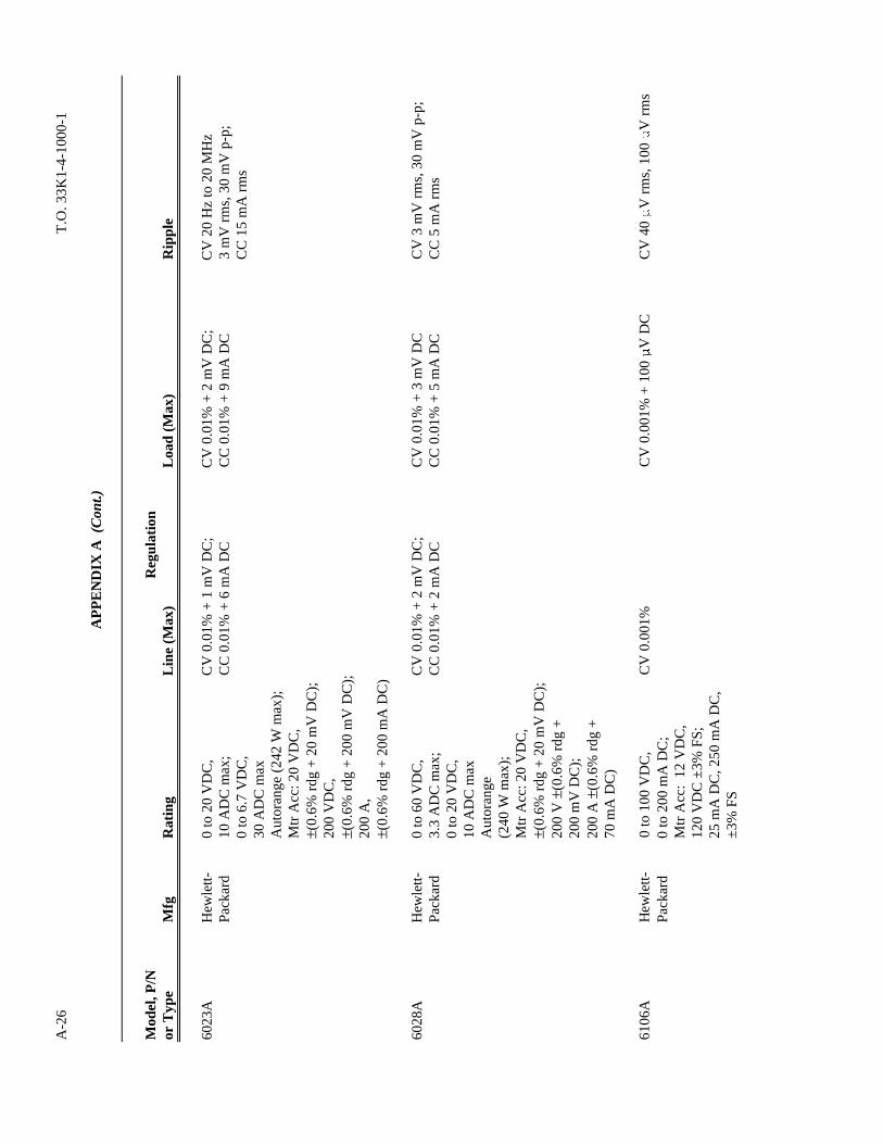
A-2
6T
.O. 3
3K1-
4-10
00-1
AP
PE
ND
IX A
(C
ont.)
Mod
el, P
/NR
egul
atio
nor
Typ
eM
fgR
atin
gL
ine
(Max
)L
oad
(Max
)R
ippl
e
6023
AH
ewle
tt-0
to 2
0 V
DC
,C
V 0
.01%
+ 1
mV
DC
;C
V 0
.01%
+ 2
mV
DC
;C
V 2
0 H
z to
20
MH
zP
acka
rd10
AD
C m
ax;
CC
0.0
1% +
6 m
A D
CC
C 0
.01%
+ 9
mA
DC
3 m
V r
ms,
30
mV
p-p
;0
to 6
.7 V
DC
,C
C 1
5 m
A r
ms
30 A
DC
max
Aut
oran
ge (
242
W m
ax);
Mtr
Acc
: 20
VD
C,
± (0.
6% r
dg +
20
mV
DC
);20
0 V
DC
,± (
0.6%
rdg
+ 2
00 m
V D
C);
200
A,
± (0.
6% r
dg +
200
mA
DC
)
6028
AH
ewle
tt-0
to 6
0 V
DC
,C
V 0
.01%
+ 2
mV
DC
;C
V 0
.01%
+ 3
mV
DC
CV
3 m
V r
ms,
30
mV
p-p
;P
acka
rd3.
3 A
DC
max
;C
C 0
.01%
+ 2
mA
DC
CC
0.0
1% +
5 m
A D
CC
C 5
mA
rm
s0
to 2
0 V
DC
,10
AD
C m
axA
utor
ange
(240
W m
ax);
Mtr
Acc
: 20
VD
C,
± (0.
6% r
dg +
20
mV
DC
);20
0 V
±(0
.6%
rdg
+20
0 m
V D
C);
200
A ±
(0.6
% r
dg +
70 m
A D
C)
6106
AH
ewle
tt-0
to 1
00 V
DC
,C
V 0
.001
%C
V 0
.001
% +
100
�V
DC
CV
40 �
V r
ms,
100
�V
rm
sP
acka
rd0
to 2
00 m
A D
C;
Mtr
Acc
: 12
VD
C,
120
VD
C ±
3% F
S;25
mA
DC
, 250
mA
DC
,±
3% F
S

AP
PE
ND
IX A
(C
ont.)
Mod
el, P
/NR
egul
atio
nor
Typ
eM
fgR
atin
gL
ine
(Max
)L
oad
(Max
)R
ippl
e
A-2
7T
.O. 3
3K1-
4-10
00-1
6212
CH
ewle
tt-0
to 1
00 V
DC
,C
V 4
mV
DC
CV
8 m
V D
CC
V 2
00 �
V r
ms,
1 m
V p
-pP
acka
rd0
to 1
00 m
A D
C;
Mtr
Acc
: ±3%
FS
6214
CH
ewle
tt-0
to 1
0 V
DC
,C
V 4
mV
DC
;C
V 4
mV
DC
;C
V 2
00 �
V r
ms,
1 m
V p
-p;
Pac
kard
0 to
1 A
DC
;C
C 7
50 µ
A D
CC
C 5
00 �
A D
CC
C 1
50 �
A r
ms,
500
µA
p-p
Mtr
Acc
: 12
VD
C,
1.2
AD
C, ±
4% F
S
6216
CH
ewle
tt-
0 to
25
VD
C,
CV
4 m
V D
C;
CV
4 m
V D
CC
V 2
00 µ
V r
ms,
1 m
V p
-pP
acka
rd0.
4 A
DC
;C
C 5
00 �
A D
CC
C 5
00 �
A D
CM
tr A
cc: 3
0 V
DC
,50
0 m
A D
C;
± 3%
FS
6479
CH
ewle
tt-0
to 3
00 V
DC
,C
V 0
.05
+ 1
00 m
V D
C;
CV
0.0
5% +
100
mV
DC
;C
V 3
30 m
V r
ms,
3 V
p-p
Pac
kard
0 to
35
AD
C;
CC
0.1
% +
35
mA
DC
CC
0.1
% +
35
mA
DC
Mtr
Acc
: 350
VD
C,
40 A
DC
, ±2%
FS
72-2
010
Ten
ma
0 to
30
VD
C,
CV
0.0
1% +
3 m
V D
C;
CV
0.0
1% +
3 m
V D
C;
CV
≤0.
5 m
V r
ms
0 to
3 A
DC
;C
C 0
.2%
+ 3
mA
DC
CC
0.2
% +
3 m
A D
C(5
Hz
to 1
MH
z);
Mtr
Acc
: Dig
ital
,C
C ≤
3 m
A r
ms
±(0
.5%
rdg
+ 2
dgt
s)A
nalo
g, N
/A
72-2
075
Ten
ma
0 to
30
VD
C,
CV
0.0
1% +
3 m
V D
C;
CV
0.0
1% +
3 m
V D
C;
CV
0.5
mV
rm
s;0
to 3
AD
C;
CC
0.2
% +
3 m
A D
CC
C 0
.2%
+ 3
mA
DC
CC
3 m
A r
ms
Mtr
Acc
: Dig
ital
,±
(0.5
% r
dg +
2 d
gts)
Ana
log,
N/A

A-2
8
Cha
nge
1T
.O. 3
3K1-
4-10
00-1
AP
PE
ND
IX A
(C
ont.)
Mod
el, P
/NR
egul
atio
nor
Typ
eM
fgR
atin
gL
ine
(Max
)L
oad
(Max
)R
ippl
e
72-2
080
Ten
ma
0 to
30
VD
C,
CV
0.0
1% +
3 m
V D
C;
CV
0.0
1% +
3 m
V D
C;
CV
1 m
V r
ms;
0 to
3 A
DC
;C
C 0
.2%
+ 3
mA
DC
CC
0.2
% +
3 m
A D
CC
C 3
mA
rm
sM
tr A
cc:
±(0
.5%
rdg
+ 2
dgt
s);
Ana
log,
N/A
;5
VD
C ±
0.25
VD
C,
CV
5 m
V D
CC
V 1
0 m
V D
CC
V 2
mV
rm
s3
AD
C
72-6
615
Ten
ma
Dua
l0
to 3
0 V
DC
,C
V ≤
0.01
% +
3 m
V D
C;
CV
≤3
AD
C, ≤
0.01
% +
CV
≤1
mV
rm
s0
to 3
AD
C;
CC
≤0.
2% +
3 m
A D
C3
mV
DC
; >3
AD
C,
(5 H
z to
1 M
Hz)
;M
tr A
cc:
≤ 0.0
2% +
5 m
V D
C;
CC
≤3
mA
rm
s±
(0.5
% r
dg +
2 d
gts)
;C
C 0
.2%
+ 3
mA
DC
;5
VD
C ±
0.25
VD
C,
CV
≤5
mV
DC
CV
≤10
mV
DC
CV
≤2
mV
rm
s3
AD
C
832-
210
Ext
ech
0 to
30
VD
C,
CV
≤0.
02%
+ 3
mV
DC
;C
V ≤
0.02
% +
3 m
V D
C;
CV
≤2
mV
rm
s;0
to 3
AD
C;
CC
≤0.
02%
+ 3
mA
DC
CC
≤0.
02%
+ 3
mA
DC
CC
≤3
mA
DC
Mtr
Acc
:±
(0.5
% r
dg +
2 d
gts)
8609
Wat
co0
to 5
0 V
DC
,C
V 0
.01%
+ 2
mV
DC
;C
V 0
.01
% +
2 m
V D
C;
CV
1 m
V p
-p;
1.5
AD
C ±
5%C
C 0
.01%
+ 3
00 m
A D
CC
C 0
.01%
+ 3
00 m
A D
CC
C 1
mA
p-p
9007
4-2
Lam
bda
24 to
38
VD
C;
CV
0.1
%C
V 0
.1%
CV
35
mV
rm
s;0
to 1
0 A
DC
CC
150
mV
p-p
GPS
-303
0DIn
stek
0 to
30
VD
C,
CV
≤0.
01%
+ 3
mV
DC
CV
≤0.
01%
+ 3
mV
DC
CV
≤0.
5 m
V r
ms
at0
to 3
AD
C;
CC
≤0.
2% +
3 m
AC
C ≤
0.2%
+ 3
mA
5 H
z to
1 M
Hz;
Mtr
Acc
: D
igit
alC
C ≤
3 m
A r
ms
± (0.
5% r
dg +
2 d
gts)
LG
S-FA
-5-0
V-R
Lam
bda
5 V
at 1
90 A
CV
0.1
%C
V 0
.1%
10 m
V r
ms
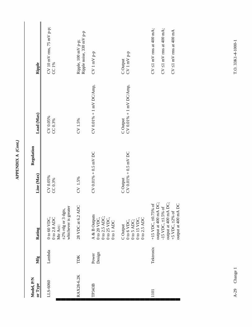
AP
PE
ND
IX A
(C
ont.)
Mod
el, P
/NR
egul
atio
nor
Typ
eM
fgR
atin
gL
ine
(Max
)L
oad
(Max
)R
ippl
e
A-2
9
Cha
nge
1T
.O. 3
3K1-
4-10
00-1
LL
S-60
60L
ambd
a0
to 6
0 V
DC
,C
V 0
.05%
CV
0.0
5%C
V 1
0 m
V r
ms,
75
mV
p-p
;0
to 2
.8 A
DC
CC
0.3
%C
C 0
.3%
CC
1%
Mtr
Acc
:±
2% r
dg o
r 3
dgts
,w
hich
ever
is g
reat
er
RA
X28
-6.2
KT
DK
28 V
DC
at 6
.2 A
DC
CV
1.5
%C
V 1
.5%
Rip
ple,
100
mV
p-p
;R
ippl
e no
ise,
330
mV
p-p
TP3
43B
Pow
erA
& B
Out
puts
CV
0.0
1% +
0.5
mV
DC
CV
0.0
1% +
1 m
V D
C/A
mp,
CV
1 m
V p
-pD
esig
n0
to 2
0 V
DC
,0
to 2
.5 A
DC
;0
to 2
5 V
DC
,0
to 1
AD
C
C O
utpu
tC
Out
put
C O
utpu
tC
Out
put
0 to
6 V
DC
,C
V 0
.01%
+ 0
.5 m
V D
CC
V 0
.01%
+ 1
mV
DC
/Am
p,C
V 1
mV
p-p
0 to
5 A
DC
;0
to 1
5 V
DC
,0
to 2
.5 A
DC
1101
Tek
tron
ix+
15 V
DC
, ±0.
75%
of
CV
≤1
mV
rm
s at
400
mA
;ou
tput
at 4
00 m
A D
C;
-15
VD
C, ±
1.5%
of
CV
≤1
mV
rm
s at
400
mA
;ou
tput
at 4
00 m
A D
C;
+5
VD
C, ±
2% o
fC
V ≤
1 m
V r
ms
at 4
00 m
Aou
tput
at 4
00 m
A D
C

A-3
0
Cha
nge
1T
.O. 3
3K1-
4-10
00-1
AP
PE
ND
IX A
(C
ont.)
Mod
el, P
/NR
egul
atio
nor
Typ
eM
fgR
atin
gL
ine
(Max
)L
oad
(Max
)R
ippl
e
72-4
045A
Ten
ma
A &
B O
utpu
ts0
to 2
4 V
DC
,C
V ≤
0.01
% +
3 m
V D
CC
V ≤
0.01
% +
3 m
V D
CC
V ≤
2 m
V r
ms,
0 to
0.5
AD
C;
CC
≤0.
2% +
3 m
A D
CC
C ≤
0.2%
+ 6
mA
DC
5 H
z to
1 M
Hz;
Mtr
Acc
: ±
2.5%
FS
CC
≤3
mA
rm
s
C O
utpu
t5
VD
C, ±
100
mV
DC
CV
≤5
mV
DC
CV
≤10
mV
DC
CV
≤2
mV
rm
s,at
≥2
AD
C5
Hz
to 1
MH
z;
*
1 Whi
chev
er is
gre
ater
.
*
2 Set
TI s
witc
h A
to th
e U
P po
sitio
n an
d co
nnec
t the
load
bet
wee
n JI
-A a
nd J
1-J.
*
3 Whi
chev
er is
sm
alle
r.
*
4 For
an
min
imum
inpu
t lin
e cu
rren
t of 2
4.0
AA
C th
e in
put l
ine
volta
ge is
190
to 2
50 V
AC
.Fo
r a
min
imum
inpu
t lin
e cu
rren
t of 2
5.3
AA
C th
e in
put l
ine
volta
ge is
180
to 2
20 V
AC
.
*
5 All
mea
sure
men
ts m
ust b
e m
ade
at T
I rea
r te
rmin
als.