
Smaller is Faster and More Sensitive: The Effect of Wire Size on the Detection of Hydrogen by Single...
12
Smaller is Faster and More Sensitive: The Effect of Wire Size on the Detection of Hydrogen by Single Palladium Nanowires Fan Yang, Sheng-Chin Kung, Ming Cheng, John C. Hemminger, and Reginald M. Penner* Department of Chemistry, University of California, Irvine, California 92697-2025 A lthough it has been known for more than 100 years that the absorption of hydrogen by palladium hydride, PdH x , increases its electrical resistivity, 1 it was not until 1992 that Hughes and Schubert 2 demonstrated that palladium al- loy resistors consisting of ultrathin palladiumnickel alloy films could be used as H 2 sensors. In that work, PdNi(820%) films with thicknesses in the 50 nm range produced response times of 10 s at 4% H 2 and 20 s at 1% H 2 while achieving a limit of detection (LOD H 2 ) below 0.1%. 2 The pres- ence of nickel in the palladium sensing ele- ment suppresses the - to -phase transi- tion that is responsible, in pure palladium films, for irreproducibility and hysteresis in the detection of hydrogen at concentra- tions above 1% H 2 (at 300 K). The PdNi thin film resistor achieves many design ob- jectives for hydrogen safety sensors includ- ing a low manufacturing cost, high sensitiv- ity and accuracy, good stability, and a simple, rugged design, but its response times (1020 s) are too slow by approxi- mately an order of magnitude, based upon recent Department of Energy mandated performance metrics. 3 Several innovative resistive sensor de- signs have improved upon the response time of the Hughes thin film sensor at the expense of additional device complexity. For example, Wang and co-workers 4 pre- pared hydrogen-sensitive resistors by deco- rating nanoporous alumina surfaces with palladium nanoparticles. The resulting de- vices produced a response at 1% H 2 of 1 s and a LOD H 2 of 500 ppm. 4 Dimeo et al. 5 de- scribed a MEMS-based hydrogen sensor in which thin films of a rare earth were em- ployed as resistors on a microfabricated sili- con platform 6 that facilitated the heating of these films to 50 80 °C. This device pro- duced response times of 0.5 s and a LOD H 2 of less than 200 ppm. 5 A distinct subcategory of resistive hydro- gen sensors involves ultrathin palladium film resistors that operate at the percola- tion threshold for electrical conduction. These sensors transduce the presence of hy- drogen as a resistance decrease (R H 2 0), in contrast to the resistance increase (R H 2 0) normally seen for palladium resistors. Decreased resistance within the film is in- duced by volumetric swelling of -phase PdH x by 10% as compared with the -phase, 1 opening new electrical pathways for transport within the film. Kaltenpoth et al. 7 were the first to observe this mecha- nism in ultrathin palladium films prepared within microfabricated silicon channels, but the performance of these devices was *Address correspondence to [email protected]. Received for review June 29, 2010 and accepted July 30, 2010. Published online August 13, 2010. 10.1021/nn101475c © 2010 American Chemical Society ABSTRACT Palladium nanowires prepared using the lithographically patterned nanowire electrodeposition (LPNE) method are used to detect hydrogen gas (H 2 ). These palladium nanowires are prepared by electrodepositing palladium from EDTA-containing solutions under conditions favoring the formation of -phase PdH x . The Pd nanowires produced by this procedure are characterized by X-ray diffraction, transmission electron microscopy, scanning electron microscopy, atomic force microscopy, and X-ray photoelectron spectroscopy. These nanowires have a mean grain diameter of 15 nm and are composed of pure Pd with no XPS-detectable bulk carbon. The four- point resistance of 50100 m segments of individual nanowires is used to detect H 2 in N 2 and air at concentrations ranging from 2 ppm to 10%. For low [H 2 ] < 1%, the response amplitude increases by a factor of 23 with a reduction in the lateral dimensions of the nanowire. Smaller nanowires show accelerated response and recovery rates at all H 2 concentrations from, 5 ppm to 10%. For 12 devices, response and recovery times are correlated with the surface area/volume ratio of the palladium detection element. We conclude that the kinetics of hydrogen adsorption limits the observed response rate seen for the nanowire, and that hydrogen desorption from the nanowire limits the observed recovery rate; proton diffusion within PdH x does not limit the rates of either of these processes. KEYWORDS: hydrogen · sensor · electrodeposition · palladium · hydride ARTICLE www.acsnano.org VOL. 4 ▪ NO. 9 ▪ 5233–5244 ▪ 2010 5233
-
Upload
independent -
Category
Documents
-
view
0 -
download
0
Transcript of Smaller is Faster and More Sensitive: The Effect of Wire Size on the Detection of Hydrogen by Single...
Smaller is Faster and More Sensitive: TheEffect of Wire Size on the Detection ofHydrogen by Single PalladiumNanowiresFan Yang, Sheng-Chin Kung, Ming Cheng, John C. Hemminger, and Reginald M. Penner*
Department of Chemistry, University of California, Irvine, California 92697-2025
Although it has been known for morethan 100 years that the absorptionof hydrogen by palladium hydride,
PdHx, increases its electrical resistivity,1 it
was not until 1992 that Hughes and
Schubert2 demonstrated that palladium al-
loy resistors consisting of ultrathin
palladium�nickel alloy films could be used
as H2 sensors. In that work, Pd�Ni(8�20%)
films with thicknesses in the 50 nm range
produced response times of �10 s at 4% H2
and �20 s at 1% H2 while achieving a limit
of detection (LODH2) below 0.1%.2 The pres-
ence of nickel in the palladium sensing ele-
ment suppresses the �- to �-phase transi-
tion that is responsible, in pure palladium
films, for irreproducibility and hysteresis in
the detection of hydrogen at concentra-
tions above 1% H2 (at 300 K). The Pd�Ni
thin film resistor achieves many design ob-
jectives for hydrogen safety sensors includ-
ing a low manufacturing cost, high sensitiv-
ity and accuracy, good stability, and a
simple, rugged design, but its response
times (10�20 s) are too slow by approxi-
mately an order of magnitude, based upon
recent Department of Energy mandated
performance metrics.3
Several innovative resistive sensor de-
signs have improved upon the response
time of the Hughes thin film sensor at the
expense of additional device complexity.
For example, Wang and co-workers4 pre-
pared hydrogen-sensitive resistors by deco-
rating nanoporous alumina surfaces with
palladium nanoparticles. The resulting de-
vices produced a response at 1% H2 of �1
s and a LODH2of 500 ppm.4 Dimeo et al.5 de-
scribed a MEMS-based hydrogen sensor in
which thin films of a rare earth were em-
ployed as resistors on a microfabricated sili-
con platform6 that facilitated the heatingof these films to 50� 80 °C. This device pro-duced response times of 0.5 s and a LODH2
of less than 200 ppm.5
A distinct subcategory of resistive hydro-gen sensors involves ultrathin palladiumfilm resistors that operate at the percola-tion threshold for electrical conduction.These sensors transduce the presence of hy-drogen as a resistance decrease (�RH2
� 0),in contrast to the resistance increase (�RH2
� 0) normally seen for palladium resistors.Decreased resistance within the film is in-duced by volumetric swelling of �-phasePdHx by 10% as compared with the�-phase,1 opening new electrical pathwaysfor transport within the film. Kaltenpothet al.7 were the first to observe this mecha-nism in ultrathin palladium films preparedwithin microfabricated silicon channels, butthe performance of these devices was
*Address correspondence [email protected].
Received for review June 29, 2010and accepted July 30, 2010.
Published online August 13, 2010.10.1021/nn101475c
© 2010 American Chemical Society
ABSTRACT Palladium nanowires prepared using the lithographically patterned nanowire electrodeposition
(LPNE) method are used to detect hydrogen gas (H2). These palladium nanowires are prepared by electrodepositing
palladium from EDTA-containing solutions under conditions favoring the formation of �-phase PdHx. The Pd
nanowires produced by this procedure are characterized by X-ray diffraction, transmission electron microscopy,
scanning electron microscopy, atomic force microscopy, and X-ray photoelectron spectroscopy. These nanowires
have a mean grain diameter of 15 nm and are composed of pure Pd with no XPS-detectable bulk carbon. The four-
point resistance of 50�100 �m segments of individual nanowires is used to detect H2 in N2 and air at
concentrations ranging from 2 ppm to 10%. For low [H2] < 1%, the response amplitude increases by a factor of
2�3 with a reduction in the lateral dimensions of the nanowire. Smaller nanowires show accelerated response
and recovery rates at all H2 concentrations from, 5 ppm to 10%. For 12 devices, response and recovery times are
correlated with the surface area/volume ratio of the palladium detection element. We conclude that the kinetics
of hydrogen adsorption limits the observed response rate seen for the nanowire, and that hydrogen desorption
from the nanowire limits the observed recovery rate; proton diffusion within PdHx does not limit the rates of either
of these processes.
KEYWORDS: hydrogen · sensor · electrodeposition · palladium · hydride
ARTIC
LE
www.acsnano.org VOL. 4 ▪ NO. 9 ▪ 5233–5244 ▪ 2010 5233
improved upon by Xu et al.,8 who used palladium is-land films evaporated onto glass surfaces modified witha siloxane self-assembled monolayer as the resistivesensing element. Their “monolayer enhanced” sensorsachieved a response time of 70 ms at 2% and a LODH2
of25 ppm.8 A systematic study of this hydrogen detec-tion mode by Ramanathan et al.9 concluded, however,that an extremely narrow range of palladium coverages,corresponding to palladium layer thickness of 2�3nm, are required in order to obtain this hydrogen sens-ing response.
Resistive sensors based upon palladium nanowiresretain the simplicity of Hughes’ palladium film resistorswhile offering the possibility for accelerated sensor re-sponse and recovery. Work in this direction dates to2000 when we10 reported an investigation of the prop-erties of �200 nm diameter palladium nanowires fordetecting H2 and found that these nanowires spontane-ously fractured upon exposure to H2 above 1�2%.Such fractured nanowire ensembles were neverthelessable to detect hydrogen gas because, like thepercolation-based sensors described above, swellingof �-phase PdHx grains mechanically closes these frac-
tures, causing the resistance of Pd nanowire ensemblesto decrease in the presence of hydrogen above 1�2%.10
This LODH2is, of course, much too high for safety sen-
sors given that the lower explosion limit for H2 in air is4%.3 More recently, microfabricated versions of this“fractured-wire” device11,12 have been described. Since2000, we12�16 and others11,14,17�20 have studied singlepalladium nanowire sensors with an eye to improvingboth LODH2
and the temporal properties of H2 detec-tion, and progress has been made on both fronts. Forexample, both Offermans et al.20 and Yang et al.12,15
have reported LODH2in the low parts per million range
and response/recovery times of a few seconds at H2
concentrations of a few percent using Pd nanowiresthat do not fracture upon exposure to H2, even at highconcentrations.
In this paper, we examine the influence of the lat-eral wire dimensions on the function of single nano-wire hydrogen sensors. Our conclusions are based onan examination of data for 14 hydrogen sensors: 11single palladium nanowire sensors and three palladiumfilm resistors. The nanowires in these devices were pre-pared using the lithographically patterned nanowireelectrodeposition (LPNE) method.21�23 LPNE producespalladium nanowires with a rectangular cross sectionhaving well-defined thickness (defined here as the wiredimension perpendicular to the surface) and width. Inpreliminary work,12 we discovered that the addition ofEDTA to the Pd plating solution produced nanowiresthat did not fracture during exposure to hydrogen,whereas in the absence of EDTA, wire fracture occurredin virtually every device.10,12,13 Here, we undertake thechemical characterization of these nanowires by XPSdepth profiling in order to ascertain whether carbon in-corporation into the palladium lattice occurs duringwire growth from these solutions. The thickness of thethree palladium films (of 11, 22, and 49(�1) nm) was se-lected to match that of nine nanowires, allowing us tomake a direct comparison of films to nanowires in termsof their respective H2 sensing performance. We alsocompare the properties of nanowires for detectinghydrogen in air and nitrogen backgrounds for twonanowire-based devices. Data compiled for these 14sensors, coupled with recent experiments in which thetemperature dependence of the sensing behavior hasbeen probed,15 provide a basis for identifying thechemical processes that are rate-limiting in terms ofthe response and recovery of Pd nanowires tohydrogen.
RESULTS AND DISCUSSIONPalladium Nanowire Fabrication and Characterization. The
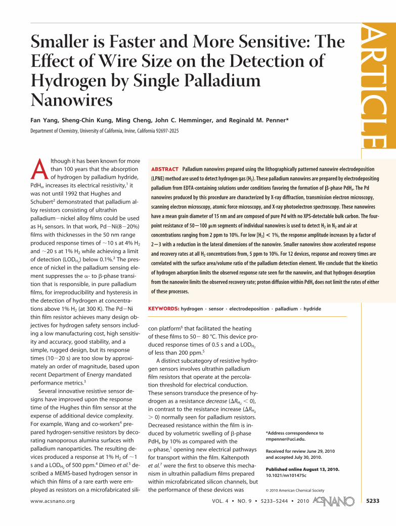
LPNE method involves the fabrication of a temporary,sacrificial template on a glass or oxidized silicon surface(Figure 1).21,22 This template is formed by first vapor de-positing a nickel layer with a thickness of 5�100 nm,covering the nickel layer with a photoresist (PR), photo-
Figure 1. Fabrication of palladium nanowires using the LPNE method. (a)Nickel layer is evaporated onto a glass surface and covered with a layer ofphotoresist (step i). The PR layer is photopatterned using a contact mask(step ii), and the exposed nickel is etched in nitric acid to produce a horizon-tal trench along the perimeter of the exposed region (step iii). A Pd nano-wire is electrodeposited into this horizontal trench (step iv). The photo-resist and remaining nickel are removed using acetone and nitric acid,respectively (step v). (b) Cyclic voltammograms of a Pd plating solution con-taining 0.2 mM Pd2� (black and gray) and a Pd plating solution containing0.2 mM Pd2� and 0.22 mM ethylenediamine tetraacetic acid (EDTA, red andorange) showing the potentials used for potentiostatic Pd deposition. Bothof these CVs were obtained at microfabricated nickel edges with 60 nmheight. (c) Current versus time for the potentiostatic electrodeposition ofPd nanowires, both of which had a final thickness and width of 20 nm � 150nm and identical length, within an LPNE template using the same two solu-tions and deposition potentials indicated in (b).
ART
ICLE
VOL. 4 ▪ NO. 9 ▪ YANG ET AL. www.acsnano.org5234

patterning the PR layer using a contact mask, and then
removing the exposed nickel using nitric acid. The
nickel layer is intentionally “over etched” so that the
PR layer is undercut by approximately 300�500 nm
(Figure 1a, iv) at the perimeter of the exposed region.
This undercut produces a horizontal trench along the
entire perimeter of the patterned region. A nanowire is
formed within this trench by electrodeposition: The
template is first immersed into an aqueous plating so-
lution, and nanowires of the desired composition and
width are produced by electrodeposition using the
nickel edge within the trench as a working electrode.
Finally, the template, consisting of the PR and nickel lay-
ers, is removed by dissolution in acetone and nitric
acid, respectively, to expose the electrodeposited
nanowires (Figure 1a, v). Useful features of the LPNE
method include the following: (1) the position and two-
dimensional trajectory of nanowires on the glass sur-
face are controlled using photolithography; (2) the
nanowire thicknesses, perpendicular to the surface, is
determined by the thickness of the evaporated nickel
layer; and (3) the nanowire width is determined by the
electrodeposition parameters including the applied
voltage, the solution composition, and the deposition
duration.
The nanowire-based hydrogen sensors studied in
this paper were all produced from palladium plating so-
lutions containing a slight stoichiometric excess of
ethylenediamine tetraacetic acid (EDTA, aq 0.2 mM
PdCl2, 0.22 mM EDTA). Previously, EDTA has often been
used to modify the morphology of electrodeposited
metal films.24�26 In earlier work,12 we discovered that
the Pd nanowires deposited from solutions containing
EDTA (henceforth, “EDTA” nanowires) are resistant to
fracture upon exposure to high concentrations of H2,
whereas “�EDTA” nanowires, grown from EDTA-free
plating solutions, consistently fractured upon exposure
to H2 above 2%. We did not speculate on the origin of
this increased toughness of EDTA nanowires earlier,
and the origin of this disparate behavior remains under
investigation in our laboratory. Additional information
pertaining to the structure and chemical composition of
both types of nanowires is disclosed here. On the basis
of these data, our hypothesis is that, in the presence of
EDTA, �-phase PdHx, not palladium metal, is the prod-
uct of the electrodeposition reaction. This hypothesis is
supported by electrochemical data: The voltammetry
of an LPNE-templated nickel electrode in this solution
(Figure 1b) and in an identical solution without EDTA re-
veal that, in the EDTA solution, the onset for palladium
deposition is shifted to more negative potentials by
�500 mV, just as expected for strong complexation of
the Pd2 by EDTA. In the absence of EDTA at 0.18 V vs
SCE, Pd deposition occurs with high current efficiency:
The current plateau seen at negative potentials in the
EDTA-free plating solution affords an estimate of the Pd2
diffusion-controlled current of 10�12 A. In the EDTA-
containing solution, deposition at �0.80 V vs SCE pro-
duces a total current of 100�110 A for an identical
LPNE-templated electrodeOlarger than the Pd2
diffusion-controlled current by a factor of about 10. The
two nanowires prepared in the experiments of Figure 1c
were both 20 � 150 nm in lateral dimensions (henceforth:
height � width), so the additional deposition charge
(QEDTA � 0.465 C versus Q�EDTA � 0.132 C) is not ex-
plained by the deposition of additional Pd. Instead, the
larger deposition current seen in the EDTA solution is pro-
duced by the availability at these more negative poten-
tials of two new reactions in addition to Pd2 deposition:
Both of these reactions can contribute to the formation
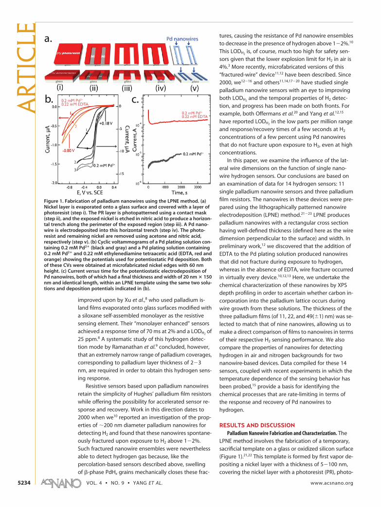
Figure 2. Characterization of Pd nanowires using X-ray diffraction (XRD)and transmission electron microscopy (TEM). (a) Optical micrographshowing an array of Pd nanowires deposited at 2 �m pitch on quartz.Samples like this one were used to acquire data for XRD and X-ray photo-electron spectroscopy (XPS). (b) XRD data were acquired using grazing in-cidence with a fixed incident angle of 0.3°. (c) XRD patterns for Pd nano-wires prepared from plating solutions that either contained added EDTA(�EDTA; aq 0.2 mM PdCl2, 0.22 mM EDTA) or without added EDTA(�EDTA; aq 0.2 mM PdCl2); (d,e) TEM images at low and high magnifica-tion, respectively, of �EDTA Pd nanowires, and (f,g) TEM images of�EDTA Pd nanowires.
Pd2+(aq) + 2e- f Pd(s) (1)
H+(aq) + e- f H2(g) (2)
xH+(aq) + xe- + Pd(s) f PdHx(s) (3)
ARTIC
LE
www.acsnano.org VOL. 4 ▪ NO. 9 ▪ 5233–5244 ▪ 2010 5235
of �-phase PdHx. The PdHx formed by electrodeposition
in EDTA solution will spontaneously convert to Pd metal
as soon as the potentiostat releases the nanowires to
open-circuit, and the EDTA nanowires are exposed to
air, but these nanowires will retain a “built-in” tensile
stress because the �-phase PdHx has a volume 10% larger
than that of Pd metal. It is possible, but still unproven,
that this residual tensile stress counteracts the compres-
sive stress that is imposed upon exposure of Pd nano-
wires to [H2] above 2% and the formation of �-phase
PdHxOa process that reproducibly fractures the �EDTA
Pd nanowires.
EDTA and �EDTA nanowires are remarkably simi-
lar in terms of their microstructure and grain diameter
(Figure 2). Grazing incidence X-ray diffraction analysis
(Figure 2a,b) shows that both types of nanowires are
single phase, fcc Pd (JCPDS 01-088-2335). GIXRD per-
mits the out-of-plane grain diameter, D�, to be esti-
mated from the X-ray line widths using the Scherrer
equation, D� � 0.89( )/(B cos �). For EDTA and
�EDTA nanowires, we measure virtually identical D�
values of 12 � 1 and 14 � 1 nm, respectively. Transmis-sion electron microscopy (TEM) can be used to visual-ize the in-plane grain dimension for these same nano-wires,12 and these D� values are 15 � 1 and 6 � 3 nm forEDTA and �EDTA nanowires, respectively.12 Thus,both EDTA and �EDTA nanowires are phase-purefcc palladium with similar nanoscopic grain dimensions.
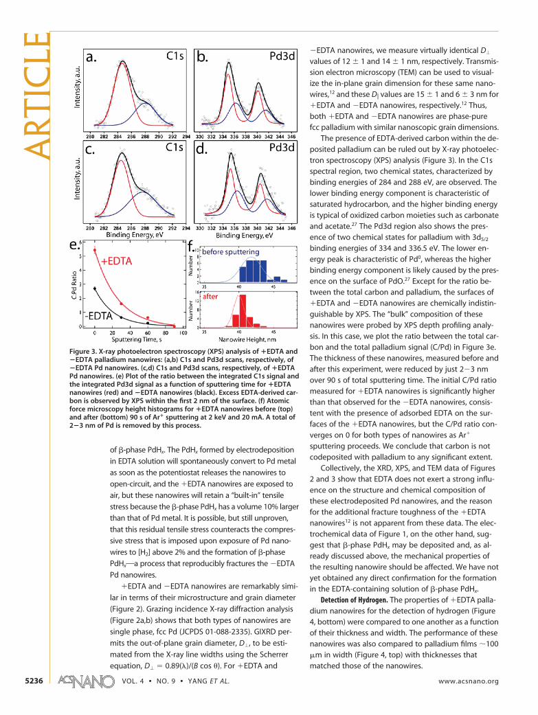
The presence of EDTA-derived carbon within the de-posited palladium can be ruled out by X-ray photoelec-tron spectroscopy (XPS) analysis (Figure 3). In the C1sspectral region, two chemical states, characterized bybinding energies of 284 and 288 eV, are observed. Thelower binding energy component is characteristic ofsaturated hydrocarbon, and the higher binding energyis typical of oxidized carbon moieties such as carbonateand acetate.27 The Pd3d region also shows the pres-ence of two chemical states for palladium with 3d5/2
binding energies of 334 and 336.5 eV. The lower en-ergy peak is characteristic of Pd0, whereas the higherbinding energy component is likely caused by the pres-ence on the surface of PdO.27 Except for the ratio be-tween the total carbon and palladium, the surfaces ofEDTA and �EDTA nanowires are chemically indistin-guishable by XPS. The “bulk” composition of thesenanowires were probed by XPS depth profiling analy-sis. In this case, we plot the ratio between the total car-bon and the total palladium signal (C/Pd) in Figure 3e.The thickness of these nanowires, measured before andafter this experiment, were reduced by just 2�3 nmover 90 s of total sputtering time. The initial C/Pd ratiomeasured for EDTA nanowires is significantly higherthan that observed for the �EDTA nanowires, consis-tent with the presence of adsorbed EDTA on the sur-faces of the EDTA nanowires, but the C/Pd ratio con-verges on 0 for both types of nanowires as Ar
sputtering proceeds. We conclude that carbon is notcodeposited with palladium to any significant extent.
Collectively, the XRD, XPS, and TEM data of Figures2 and 3 show that EDTA does not exert a strong influ-ence on the structure and chemical composition ofthese electrodeposited Pd nanowires, and the reasonfor the additional fracture toughness of the EDTAnanowires12 is not apparent from these data. The elec-trochemical data of Figure 1, on the other hand, sug-gest that �-phase PdHx may be deposited and, as al-ready discussed above, the mechanical properties ofthe resulting nanowire should be affected. We have notyet obtained any direct confirmation for the formationin the EDTA-containing solution of �-phase PdHx.
Detection of Hydrogen. The properties of EDTA palla-dium nanowires for the detection of hydrogen (Figure4, bottom) were compared to one another as a functionof their thickness and width. The performance of thesenanowires was also compared to palladium films �100m in width (Figure 4, top) with thicknesses thatmatched those of the nanowires.
Figure 3. X-ray photoelectron spectroscopy (XPS) analysis of �EDTA and�EDTA palladium nanowires: (a,b) C1s and Pd3d scans, respectively, of�EDTA Pd nanowires. (c,d) C1s and Pd3d scans, respectively, of �EDTAPd nanowires. (e) Plot of the ratio between the integrated C1s signal andthe integrated Pd3d signal as a function of sputtering time for �EDTAnanowires (red) and �EDTA nanowires (black). Excess EDTA-derived car-bon is observed by XPS within the first 2 nm of the surface. (f) Atomicforce microscopy height histograms for �EDTA nanowires before (top)and after (bottom) 90 s of Ar� sputtering at 2 keV and 20 mA. A total of2�3 nm of Pd is removed by this process.
ART
ICLE
VOL. 4 ▪ NO. 9 ▪ YANG ET AL. www.acsnano.org5236
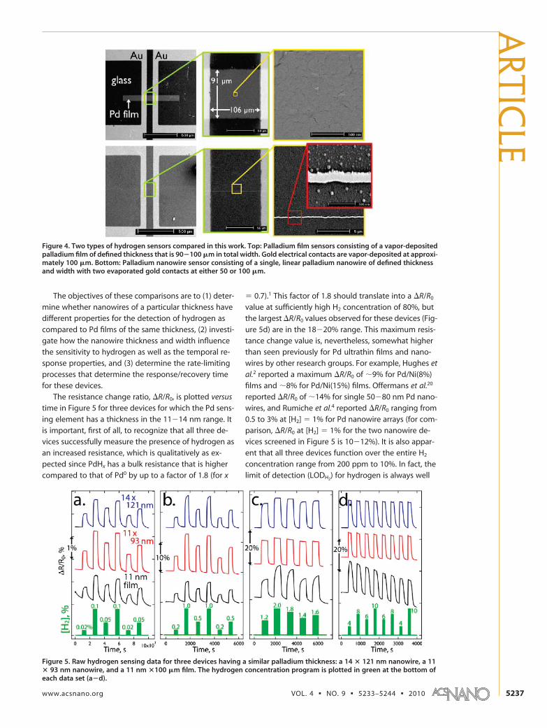
The objectives of these comparisons are to (1) deter-mine whether nanowires of a particular thickness havedifferent properties for the detection of hydrogen ascompared to Pd films of the same thickness, (2) investi-gate how the nanowire thickness and width influencethe sensitivity to hydrogen as well as the temporal re-sponse properties, and (3) determine the rate-limitingprocesses that determine the response/recovery timefor these devices.
The resistance change ratio, �R/R0, is plotted versustime in Figure 5 for three devices for which the Pd sens-ing element has a thickness in the 11�14 nm range. Itis important, first of all, to recognize that all three de-vices successfully measure the presence of hydrogen asan increased resistance, which is qualitatively as ex-pected since PdHx has a bulk resistance that is highercompared to that of Pd0 by up to a factor of 1.8 (for x
� 0.7).1 This factor of 1.8 should translate into a �R/R0
value at sufficiently high H2 concentration of 80%, butthe largest �R/R0 values observed for these devices (Fig-ure 5d) are in the 18�20% range. This maximum resis-tance change value is, nevertheless, somewhat higherthan seen previously for Pd ultrathin films and nano-wires by other research groups. For example, Hughes etal.2 reported a maximum �R/R0 of �9% for Pd/Ni(8%)films and �8% for Pd/Ni(15%) films. Offermans et al.20
reported �R/R0 of �14% for single 50�80 nm Pd nano-wires, and Rumiche et al.4 reported �R/R0 ranging from0.5 to 3% at [H2] � 1% for Pd nanowire arrays (for com-parison, �R/R0 at [H2] � 1% for the two nanowire de-vices screened in Figure 5 is 10�12%). It is also appar-ent that all three devices function over the entire H2
concentration range from 200 ppm to 10%. In fact, thelimit of detection (LODH2
) for hydrogen is always well
Figure 4. Two types of hydrogen sensors compared in this work. Top: Palladium film sensors consisting of a vapor-depositedpalladium film of defined thickness that is 90�100 �m in total width. Gold electrical contacts are vapor-deposited at approxi-mately 100 �m. Bottom: Palladium nanowire sensor consisting of a single, linear palladium nanowire of defined thicknessand width with two evaporated gold contacts at either 50 or 100 �m.
Figure 5. Raw hydrogen sensing data for three devices having a similar palladium thickness: a 14 � 121 nm nanowire, a 11� 93 nm nanowire, and a 11 nm �100 �m film. The hydrogen concentration program is plotted in green at the bottom ofeach data set (a�d).
ARTIC
LE
www.acsnano.org VOL. 4 ▪ NO. 9 ▪ 5233–5244 ▪ 2010 5237
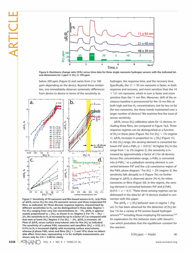
below 200 ppm (Figure 6) and varies from 2 to 100
ppm depending on the device. Beyond these similari-
ties, one immediately observes systematic differences
from device to device in terms of the sensitivity to
hydrogen, the response time, and the recovery time.
Specifically, the 11 � 93 nm nanowire is faster, in both
response and recovery, and more sensitive than the 14
� 121 nm nanowire, which in turn is faster and more
sensitive than the 11 nm film. Moreover, drift of the re-
sistance baseline is pronounced for the 10 nm film at
both high and low H2 concentrations, but far less so for
the two nanowires. Are these trends maintained over a
larger number of devices? We examine first the issue of
sensor sensitivity.
�R/R0 versus [H2] calibration plots for 12 devices, in-
cluding three films, are compared in Figure 7a,b. Three
response regimes can be distinguished as a function
of [H2] in these plots (Figure 7b): For [H2] � 1% (regime
1), �R/R0 increases in proportion to �[H2] (Figure 7c).
In this [H2] range, the sensing element is converted be-
tween Pd0 and �-PdHx (x � 0.015).1 At higher [H2] in the
range from 1 to 2% (regime 2), the sensitivity is in-
creased by approximately a factor of 2 for all devices.
Across this concentration range, �-PdHx is converted
into �-PdHx,1 so a palladium sensing element is con-
verted between Pd0 and the �/� coexistence region of
the PdHx phase diagram.1 For [H2] � 2% (regime 3), the
sensitivity falls abruptly to 0 (Figure 7b); no further
change in �R/R0 is observed above 2% H2 for either
nanowires or films (Figure 5d). In this regime, the sens-
ing element is converted between Pd0 and �-PdHx
(0.015 � x � 0.7).1 These three sensing regimes can be
delineated in the data for all 14 devices studied in con-
nection with this paper.
The �R/R0 � �[H2] behavior seen in regime 1 (Fig-
ure 7c) has been observed for the detection of [H2] be-
low 1% for a variety of Pd resistor-based hydrogen
sensors28,29 including those employing Pd nanowires.4,20
An explanation for this behavior starts with Sievert’s
Law which postulates that the equilibrium constant for
the reaction:
Figure 6. Resistance change ratio (R/R0) versus time data for three single nanowire hydrogen sensors with the indicated lat-eral dimensions for 2 ppm > [H2] > 100 ppm.
Figure 7. Sensitivity of Pd nanowire and film-based sensors to H2. (a,b) Plotsof �R/R0 versus [H2] for nine Pd nanowire sensors and three evaporated Pdfilms, as indicated. (b) Three discrete response regimes, characterized bydifferent sensitivities to H2, can be distinguished in these data: Regime 1:For [H2] ranging from very low concentrations to �1%, �R/R0 is approxi-mately proportional to �[H2], as shown in (c). Regime 2: For 1% � [H2] �2%, the sensitivity to H2 is increased by up to a factor of 2 as compared withthat seen at lower [H2]. Regime 3: For [H2] � 2%, �R/R0 is invariant. (d)Plots of �R/R0 versus surface area/volume ratio for five [H2] as indicated.The sensitivity of �-phase PdHx nanowires and nanofilms ([H2] � 0.02, 0.1,0.5%) to H2 is increased slightly with increasing surface area/volume,whereas �-phase PdHx wires and films ([H2] � 2 and 10%) show no detect-able effect. Error bars, representing 1 for multiple measurements, areshown only for S/A � 0.08 for clarity.
0.5H2(gas) f H(ads) (4)
ART
ICLE
VOL. 4 ▪ NO. 9 ▪ YANG ET AL. www.acsnano.org5238
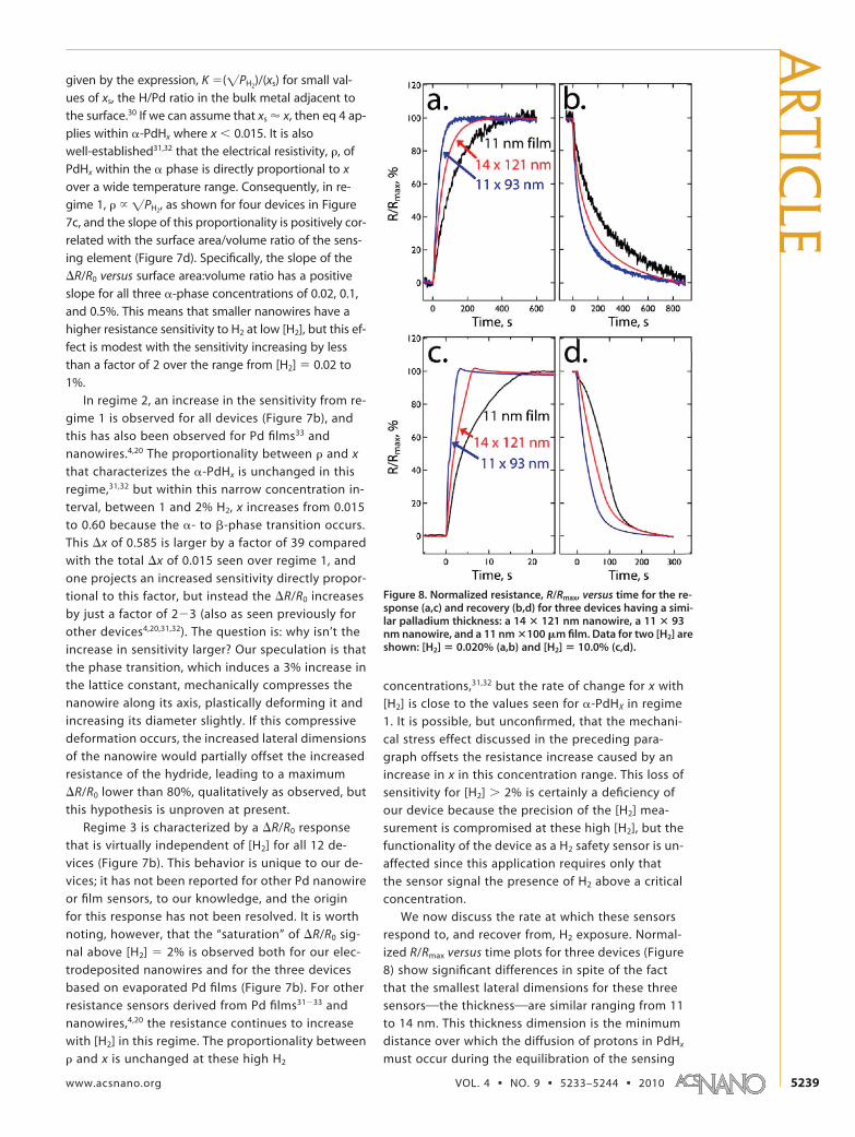
given by the expression, K �(�PH2)/(xs) for small val-
ues of xs, the H/Pd ratio in the bulk metal adjacent to
the surface.30 If we can assume that xs � x, then eq 4 ap-
plies within �-PdHx where x � 0.015. It is also
well-established31,32 that the electrical resistivity, �, of
PdHx within the � phase is directly proportional to x
over a wide temperature range. Consequently, in re-
gime 1, � � �PH2, as shown for four devices in Figure
7c, and the slope of this proportionality is positively cor-
related with the surface area/volume ratio of the sens-
ing element (Figure 7d). Specifically, the slope of the
�R/R0 versus surface area:volume ratio has a positive
slope for all three �-phase concentrations of 0.02, 0.1,
and 0.5%. This means that smaller nanowires have a
higher resistance sensitivity to H2 at low [H2], but this ef-
fect is modest with the sensitivity increasing by less
than a factor of 2 over the range from [H2] � 0.02 to
1%.
In regime 2, an increase in the sensitivity from re-
gime 1 is observed for all devices (Figure 7b), and
this has also been observed for Pd films33 and
nanowires.4,20 The proportionality between � and x
that characterizes the �-PdHx is unchanged in this
regime,31,32 but within this narrow concentration in-
terval, between 1 and 2% H2, x increases from 0.015
to 0.60 because the �- to �-phase transition occurs.
This �x of 0.585 is larger by a factor of 39 compared
with the total �x of 0.015 seen over regime 1, and
one projects an increased sensitivity directly propor-
tional to this factor, but instead the �R/R0 increases
by just a factor of 2�3 (also as seen previously for
other devices4,20,31,32). The question is: why isn’t the
increase in sensitivity larger? Our speculation is that
the phase transition, which induces a 3% increase in
the lattice constant, mechanically compresses the
nanowire along its axis, plastically deforming it and
increasing its diameter slightly. If this compressive
deformation occurs, the increased lateral dimensions
of the nanowire would partially offset the increased
resistance of the hydride, leading to a maximum
�R/R0 lower than 80%, qualitatively as observed, but
this hypothesis is unproven at present.
Regime 3 is characterized by a �R/R0 response
that is virtually independent of [H2] for all 12 de-
vices (Figure 7b). This behavior is unique to our de-
vices; it has not been reported for other Pd nanowire
or film sensors, to our knowledge, and the origin
for this response has not been resolved. It is worth
noting, however, that the “saturation” of �R/R0 sig-
nal above [H2] � 2% is observed both for our elec-
trodeposited nanowires and for the three devices
based on evaporated Pd films (Figure 7b). For other
resistance sensors derived from Pd films31�33 and
nanowires,4,20 the resistance continues to increase
with [H2] in this regime. The proportionality between
� and x is unchanged at these high H2
concentrations,31,32 but the rate of change for x with
[H2] is close to the values seen for �-PdHX in regime
1. It is possible, but unconfirmed, that the mechani-
cal stress effect discussed in the preceding para-
graph offsets the resistance increase caused by an
increase in x in this concentration range. This loss of
sensitivity for [H2] � 2% is certainly a deficiency of
our device because the precision of the [H2] mea-
surement is compromised at these high [H2], but the
functionality of the device as a H2 safety sensor is un-
affected since this application requires only that
the sensor signal the presence of H2 above a critical
concentration.
We now discuss the rate at which these sensors
respond to, and recover from, H2 exposure. Normal-
ized R/Rmax versus time plots for three devices (Figure
8) show significant differences in spite of the fact
that the smallest lateral dimensions for these three
sensorsOthe thicknessOare similar ranging from 11
to 14 nm. This thickness dimension is the minimum
distance over which the diffusion of protons in PdHx
must occur during the equilibration of the sensing
Figure 8. Normalized resistance, R/Rmax, versus time for the re-sponse (a,c) and recovery (b,d) for three devices having a simi-lar palladium thickness: a 14 � 121 nm nanowire, a 11 � 93nm nanowire, and a 11 nm �100 �m film. Data for two [H2] areshown: [H2] � 0.020% (a,b) and [H2] � 10.0% (c,d).
ARTIC
LE
www.acsnano.org VOL. 4 ▪ NO. 9 ▪ 5233–5244 ▪ 2010 5239
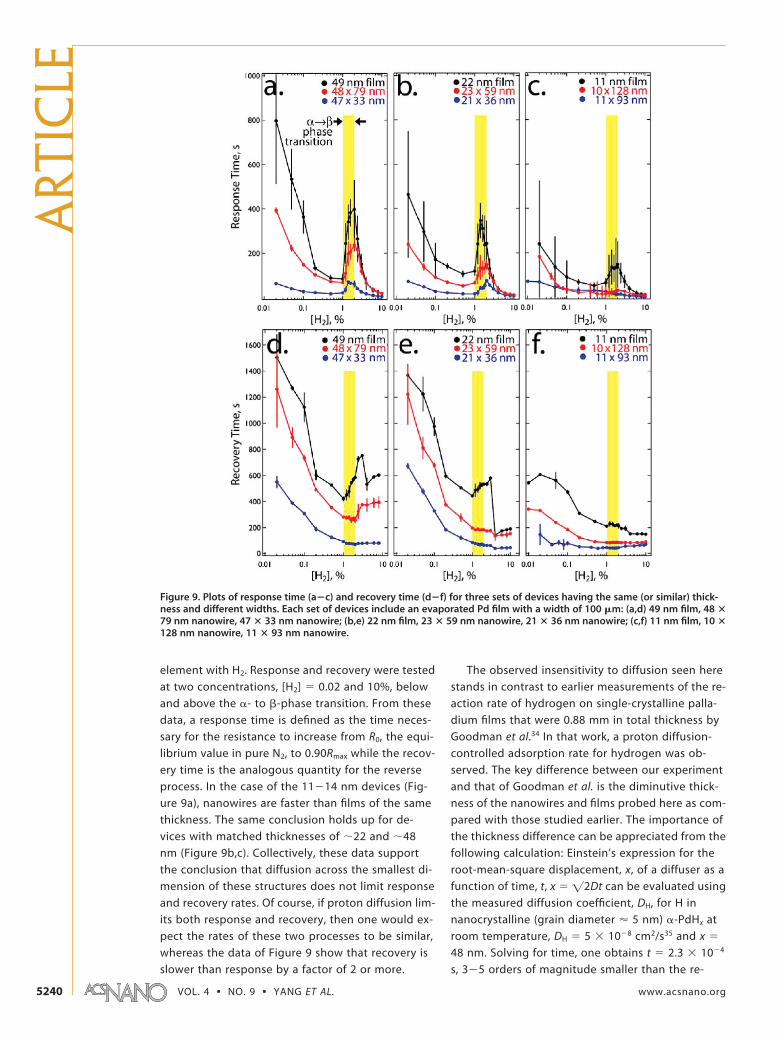
element with H2. Response and recovery were tested
at two concentrations, [H2] � 0.02 and 10%, below
and above the �- to �-phase transition. From these
data, a response time is defined as the time neces-
sary for the resistance to increase from R0, the equi-
librium value in pure N2, to 0.90Rmax while the recov-
ery time is the analogous quantity for the reverse
process. In the case of the 11�14 nm devices (Fig-
ure 9a), nanowires are faster than films of the same
thickness. The same conclusion holds up for de-
vices with matched thicknesses of �22 and �48
nm (Figure 9b,c). Collectively, these data support
the conclusion that diffusion across the smallest di-
mension of these structures does not limit response
and recovery rates. Of course, if proton diffusion lim-
its both response and recovery, then one would ex-
pect the rates of these two processes to be similar,
whereas the data of Figure 9 show that recovery is
slower than response by a factor of 2 or more.
The observed insensitivity to diffusion seen here
stands in contrast to earlier measurements of the re-
action rate of hydrogen on single-crystalline palla-
dium films that were 0.88 mm in total thickness by
Goodman et al.34 In that work, a proton diffusion-
controlled adsorption rate for hydrogen was ob-
served. The key difference between our experiment
and that of Goodman et al. is the diminutive thick-
ness of the nanowires and films probed here as com-
pared with those studied earlier. The importance of
the thickness difference can be appreciated from the
following calculation: Einstein’s expression for the
root-mean-square displacement, x, of a diffuser as a
function of time, t, x � �2Dt can be evaluated using
the measured diffusion coefficient, DH, for H in
nanocrystalline (grain diameter � 5 nm) �-PdHx at
room temperature, DH � 5 � 10�8 cm2/s35 and x �
48 nm. Solving for time, one obtains t � 2.3 � 10�4
s, 3�5 orders of magnitude smaller than the re-
Figure 9. Plots of response time (a�c) and recovery time (d�f) for three sets of devices having the same (or similar) thick-ness and different widths. Each set of devices include an evaporated Pd film with a width of 100 �m: (a,d) 49 nm film, 48 �79 nm nanowire, 47 � 33 nm nanowire; (b,e) 22 nm film, 23 � 59 nm nanowire, 21 � 36 nm nanowire; (c,f) 11 nm film, 10 �128 nm nanowire, 11 � 93 nm nanowire.
ART
ICLE
VOL. 4 ▪ NO. 9 ▪ YANG ET AL. www.acsnano.org5240
sponse and recovery times measured for thesenanowires at room temperature (Figure 9a,d). If thethickness of the palladium sample is increased to0.88 mm, a factor of �104, the time required forequilibration increases by �108 to more than 20 h,fully accounting for the diverging conclusions of ourtwo studies.34
If diffusion does not limit the response and recov-ery rates for these devices, then what process does?Recently,15 we examined the temperature depen-dence of the response and recovery rates for singlenanowire sensors in flowing N2. The measured acti-vation energies, Ea, supported the conclusion that H2
adsorption limits the response rate of these sensorsfor [H2] � �1% (i.e., �-PdHx) and that at higher H2
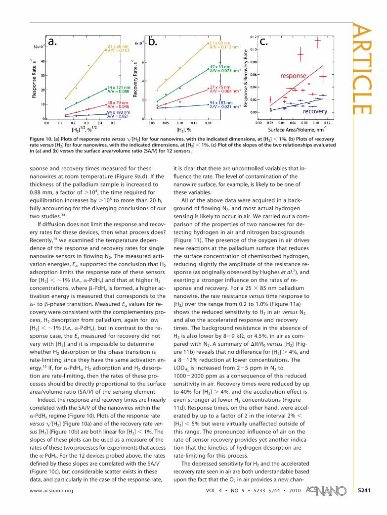
concentrations, where �-PdHx is formed, a higher ac-tivation energy is measured that corresponds to the�- to �-phase transition. Measured Ea values for re-covery were consistent with the complementary pro-cess, H2 desorption from palladium, again for low[H2] � �1% (i.e., �-PdHx), but in contrast to the re-sponse case, the Ea measured for recovery did notvary with [H2] and it is impossible to determinewhether H2 desorption or the phase transition israte-limiting since they have the same activation en-ergy.15 If, for �-PdHx, H2 adsorption and H2 desorp-tion are rate-limiting, then the rates of these pro-cesses should be directly proportional to the surfacearea/volume ratio (SA/V) of the sensing element.
Indeed, the response and recovery times are linearlycorrelated with the SA/V of the nanowires within the�-PdHx regime (Figure 10). Plots of the response rateversus �[H2] (Figure 10a) and of the recovery rate ver-sus [H2] (Figure 10b) are both linear for [H2] � 1%. Theslopes of these plots can be used as a measure of therates of these two processes for experiments that accessthe �-PdHx. For the 12 devices probed above, the ratesdefined by these slopes are correlated with the SA/V(Figure 10c), but considerable scatter exists in thesedata, and particularly in the case of the response rate,
it is clear that there are uncontrolled variables that in-fluence the rate. The level of contamination of thenanowire surface, for example, is likely to be one ofthese variables.
All of the above data were acquired in a back-ground of flowing N2, and most actual hydrogensensing is likely to occur in air. We carried out a com-parison of the properties of two nanowires for de-tecting hydrogen in air and nitrogen backgrounds(Figure 11). The presence of the oxygen in air drivesnew reactions at the palladium surface that reducesthe surface concentration of chemisorbed hydrogen,reducing slightly the amplitude of the resistance re-sponse (as originally observed by Hughes et al.2), andexerting a stronger influence on the rates of re-sponse and recovery. For a 25 � 85 nm palladiumnanowire, the raw resistance versus time response to[H2] over the range from 0.2 to 1.0% (Figure 11a)shows the reduced sensitivity to H2 in air versus N2
and also the accelerated response and recoverytimes. The background resistance in the absence ofH2 is also lower by 8�9 k�, or 4.5%, in air as com-pared with N2. A summary of �R/R0 versus [H2] (Fig-ure 11b) reveals that no difference for [H2] � 4%, anda 8�12% reduction at lower concentrations. TheLODH2
is increased from 2�5 ppm in N2 to1000�2000 ppm as a consequence of this reducedsensitivity in air. Recovery times were reduced by upto 40% for [H2] � 4%, and the acceleration effect iseven stronger at lower H2 concentrations (Figure11d). Response times, on the other hand, were accel-erated by up to a factor of 2 in the interval 2% �
[H2] � 5% but were virtually unaffected outside ofthis range. The pronounced influence of air on therate of sensor recovery provides yet another indica-tion that the kinetics of hydrogen desorption arerate-limiting for this process.
The depressed sensitivity for H2 and the acceleratedrecovery rate seen in air are both understandable basedupon the fact that the O2 in air provides a new chan-
Figure 10. (a) Plots of response rate versus �[H2] for four nanowires, with the indicated dimensions, at [H2] � 1%. (b) Plots of recoveryrate versus [H2] for four nanowires, with the indicated dimensions, at [H2] � 1%. (c) Plot of the slopes of the two relationships evaluatedin (a) and (b) versus the surface area/volume ratio (SA/V) for 12 sensors.
ARTIC
LE
www.acsnano.org VOL. 4 ▪ NO. 9 ▪ 5233–5244 ▪ 2010 5241
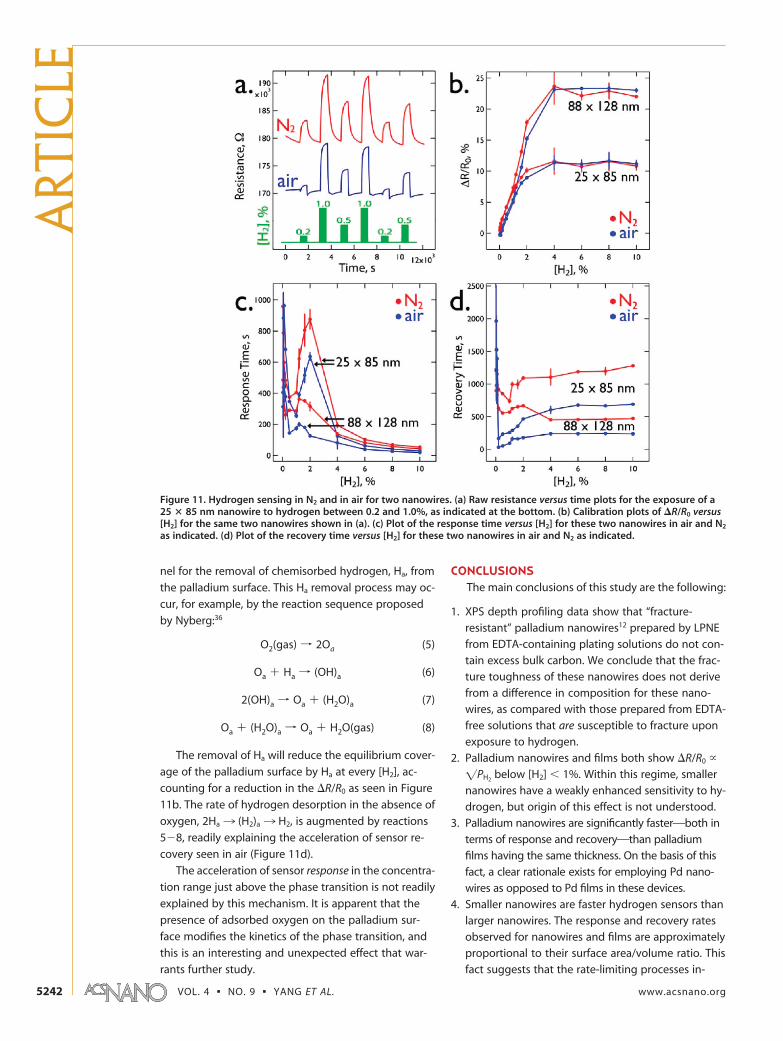
nel for the removal of chemisorbed hydrogen, Ha, from
the palladium surface. This Ha removal process may oc-
cur, for example, by the reaction sequence proposed
by Nyberg:36
The removal of Ha will reduce the equilibrium cover-
age of the palladium surface by Ha at every [H2], ac-
counting for a reduction in the �R/R0 as seen in Figure
11b. The rate of hydrogen desorption in the absence of
oxygen, 2Ha ¡ (H2)a ¡ H2, is augmented by reactions
5�8, readily explaining the acceleration of sensor re-
covery seen in air (Figure 11d).
The acceleration of sensor response in the concentra-
tion range just above the phase transition is not readily
explained by this mechanism. It is apparent that the
presence of adsorbed oxygen on the palladium sur-
face modifies the kinetics of the phase transition, and
this is an interesting and unexpected effect that war-
rants further study.
CONCLUSIONSThe main conclusions of this study are the following:
1. XPS depth profiling data show that “fracture-
resistant” palladium nanowires12 prepared by LPNE
from EDTA-containing plating solutions do not con-
tain excess bulk carbon. We conclude that the frac-
ture toughness of these nanowires does not derive
from a difference in composition for these nano-
wires, as compared with those prepared from EDTA-
free solutions that are susceptible to fracture upon
exposure to hydrogen.
2. Palladium nanowires and films both show �R/R0 �
�PH2below [H2] � 1%. Within this regime, smaller
nanowires have a weakly enhanced sensitivity to hy-
drogen, but origin of this effect is not understood.
3. Palladium nanowires are significantly fasterOboth in
terms of response and recoveryOthan palladium
films having the same thickness. On the basis of this
fact, a clear rationale exists for employing Pd nano-
wires as opposed to Pd films in these devices.
4. Smaller nanowires are faster hydrogen sensors than
larger nanowires. The response and recovery rates
observed for nanowires and films are approximately
proportional to their surface area/volume ratio. This
fact suggests that the rate-limiting processes in-
Figure 11. Hydrogen sensing in N2 and in air for two nanowires. (a) Raw resistance versus time plots for the exposure of a25 � 85 nm nanowire to hydrogen between 0.2 and 1.0%, as indicated at the bottom. (b) Calibration plots of �R/R0 versus[H2] for the same two nanowires shown in (a). (c) Plot of the response time versus [H2] for these two nanowires in air and N2
as indicated. (d) Plot of the recovery time versus [H2] for these two nanowires in air and N2 as indicated.
O2(gas) f 2Oa (5)
Oa + Ha f (OH)a (6)
2(OH)a f Oa + (H2O)a (7)
Oa + (H2O)a f Oa + H2O(gas) (8)
ART
ICLE
VOL. 4 ▪ NO. 9 ▪ YANG ET AL. www.acsnano.org5242
volved in response and recovery are surface-limitedreactions, likely hydrogen adsorption and desorp-tion. This conclusion is supported by our previousmeasurements of the activation energies associatedwith response and recovery.
5. Palladium nanowires have approximately the samesensitivity to H2 in air as in N2, but the absolute resis-
tance change is reduced at all H2 concentrations cul-minating in an increased LODH2
to 1000�2000 ppmfrom 2�5 ppm seen in N2. Recovery times, on theother hand, are significantly reduced by factors of upto 100 for measurements carried out in an air back-ground, and a slight decrease in response times arealso observed in the [H2] � 2�5% range.
METHODSChemicals. Optical glass slides (1 in. � 1 in.) were purchased
from Fisher and used as substrates. Nickel wire (Ni, 99.99%) andpalladium granule (Pd, 99.99%) were used as received from Ald-rich. Positive photoresists S1808 and S1827 and developer F319were purchased from Microchem. Palladium chloride (PdCl2,99.999%, certified ACS), potassium chloride (99.3%, certifiedACS), EDTA (disodium ethylenediaminetetraacetate, 99.8%), andacetone (GR, ACS) were used as received from Fisher.
Nanowire Fabrication. The electrodeposition of palladium wascarried out in a 50 mL, one-compartment, three-electrode cell.Pd nanowires were obtained from two different solutions, differ-entiated only by the presence of a slight stoichiometric excessof EDTA in one of them. The composition of the EDTA-containingsolution was 0.1 M KCl, 0.2 mM PdCl2, 0.22 mM EDTA (pH �4.9), whereas the EDTA-free solution was identical except forthe absence of added EDTA. Both plating solutions were pre-pared using Millipore Milli-Q water (� � 18 M� cm). Pd nano-wire growth from the EDTA plating solution was carried out at�0.80 V vs SCE, whereas a potential of 0.18 V vs SCE was usedin the EDTA-free solution. Nanowire deposition was controlledusing a Gamry Instruments model G300 potentiostat/gal-vanostat.
XRD (X-ray Diffraction). GIXRD (grazing incidence X-raydiffraction)37,38 technique was employed to analyze the crystallin-ity of Pd nanowires. A fixed, low angle of incidence for the X-raybeam makes the analysis more sensitive to the sample surfaceand thus leads to higher diffraction intensities. GIXRD was per-formed using a Rigaku Ultima III (Rigaku, Tokyo, Japan) high-resolution X-ray diffractometer with Cu K� irradiation and an in-cident angle of 0.6°.
TEM (Transmission Electron Miscroscope) and SAED (Selective-AreaElectron Diffraction). Linear Pd nanowires were first deposited ontoglass by LPNE at either 5 or 2 m interwire pitch. These nano-wires were then released from the glass by etching in 2% HF so-lution for 5 min. A stream of water was then directed onto theglass surface, and the released Pd nanowires were washed ontocarbon-coated copper grids (Ted Pella, Inc.) that were dried over-night before examination by TEM. Images and SAED measure-ments were obtained using a Philips CM20 TEM at an operatingvoltage of 200 KeV.
SEM (Scanning Electron Microscope). SEM images were collectedon Philips XL-30 FEGSEM (field emission gun scanning electronmicroscope) using an accelerating voltage of 10 kV. The sampleswere mounted on aluminum stubs (Ted Pella) using adhesivecarbon tape.
AFM (Atomic Force Microscope). Intermittent contact mode AFMimages were acquired in air using an Asylum Research MFP-3Dmicroscope and Olympus AC240TS tips.
XPS (X-ray Photoelectron Spectroscopy). XPS spectra were acquiredwith an ESCALAB MKII photoelectron spectrometer. The instru-ment is an ultrahigh vacuum system equipped with a Al/Mg twinanode X-ray source and a 150 mm hemispherical electron en-ergy analyzer. Spectra were taken by using the Al K� radiation(1486.6 eV), and the base pressure in the camber was 1 � 10�9
Torr throughout the experiment. The constant analyzer energymode was used during the experiment, and constant pass en-ergy for narrow scans was 20 eV. The photoelectron peaks of C1sand Pd3d were collected, and all peak positions were calibratedby using adventitious hydrocarbon at binding energy of 284.5eV. Ar ion beam sputtering (2 keV) was used for depth profileanalysis.
Hydrogen Sensing. H2 sensors were prepared by evaporating afour-probe gold electrode of 60 nm thickness onto single, linearnanowires using a contact shadow mask. The four-contact elec-trical resistivity was measured using a source meter (Keithley In-struments, model 2400) in conjunction with a digital multimeter(Keithley Instruments, model 2000). Sensor measurements werecarried out by placing the sensor in a sealed flow cell with a to-tal dead volume of 120 L. H2 gas (Airgas, purity �99.998%) waspremixed with N2 (Airgas, purity �99.995%) to a predeterminedconcentration using flow controllers (MKS Inc., model 1479A),and pulses of this gas mixture were switched (Parker Valve, cycletime � 25 ms) into a steam of pure N2 (Airgas, purity �99.995%)while maintaining a total flow rate of 1500 sccm. Instrument con-trol and data acquisition were both coordinated by a computerequipped with Labview in conjunction with a National Instru-ments interface (model BNC 2110). All H2 sensing measurementswere carried out using dry gases at ambient laboratory temper-ature (�20 °C) and atmospheric pressure.
Acknowledgment. This work was supported by the NationalScience Foundation (Grant CHE-0956524) and the UCI School ofPhysical Sciences Center for Solar Energy. J.C.H. and M.C. ac-knowledge funding from the DOE Office of Basic Energy Sci-ences (DE-FG02-96ER45576).
REFERENCES AND NOTES1. Lewis, F. A. The Palladium Hydrogen System; Academic
Press: London, 1967.2. Hughes, R. C.; Schubert, W. K. Thin-Films of Pd/Ni Alloys for
Detection of High Hydrogen Concentrations. J. Appl. Phys.1992, 71, 542–544.
3. Funding Opportunity AnnouncementDE-PS36-09GO99004; Department of Energy Golden FieldOffice, Office of Energy Efficiency and Renewable Energy(EERE), 2009.
4. Rumiche, F.; Wang, H. H.; Hu, W. S.; Indacochea, J. E.;Wang, M. L. Anodized Aluminum Oxide (AAO) NanowellSensors for Hydrogen Detection. Sens. Actuators, B 2008,134, 869–877.
5. DiMeo, J., Frank; Chen, I.-S.; Chen, P.; Neuner, J.; Roerhl, A.;Welch, J. MEMS-Based Hydrogen Gas Sensors. Sens.Actuators, B 2006, 117, 10–16.
6. Semancik, S.; Cavicchi, R.; Wheeler, M.; Tiffany, J.; Poirier,G.; Walton, R.; Suehle, J.; Panchapakesan, B.; DeVoe, D.Microhotplate Platforms for Chemical Sensor Research.Sens. Actuators, B 2001, 77, 579–591.
7. Kaltenpoth, G.; Schnabel, P.; Menke, E.; Walter, E.; Grunze,M.; Penner, R. Multimode Detection of Hydrogen GasUsing Palladium-Covered Silicon mu-Channels. Anal.Chem. 2003, 75, 4756–4765.
8. Xu, T.; Zach, M.; Xiao, Z.; Rosenmann, D.; Welp, U.; Kwok,W.; Crabtree, G. Self-Assembled Monolayer-EnhancedHydrogen Sensing with Ultrathin Palladium Films. Appl.Phys. Lett. 2005, 86, 203104.
9. Ramanathan, M.; Skudlarek, G.; Wang, H. H.; Darling, S. B.Crossover Behavior in the Hydrogen Sensing Mechanismfor Palladium Ultrathin Films. Nanotechnology 2010, 21,125501.
10. Favier, F.; Walter, E.; Zach, M.; Benter, T.; Penner, R.Hydrogen Sensors and Switches from ElectrodepositedPalladium Mesowire Arrays. Science 2001, 293, 2227–2231.
11. Kiefer, T.; Favier, F.; Vazquez-Mena, O.; Villanueva, G.;
ARTIC
LE
www.acsnano.org VOL. 4 ▪ NO. 9 ▪ 5233–5244 ▪ 2010 5243
Brugger, J. A Single Nanotrench in a Palladium Microwirefor Hydrogen Detection. Nanotechnology 2008, 19,125502.
12. Yang, F.; Taggart, D. K.; Penner, R. M. Fast, SensitiveHydrogen Gas Detection Using Single PalladiumNanowires That Resist Fracture. Nano Lett. 2009, 9, 2177–2182.
13. Walter, E.; Favier, F.; Penner, R. Palladium Mesowire Arraysfor Fast Hydrogen Sensors and Hydrogen-ActuatedSwitches. Anal. Chem. 2002, 74, 1546–1553.
14. Im, Y.; Lee, C.; Vasquez, R.; Bangar, M.; Myung, N.; Menke,E.; Penner, R.; Yun, M. Investigation of a Single PdNanowire for Use as a Hydrogen Sensor. Small 2006, 2,356–358.
15. Yang, F.; Taggart, D.; Penner, R. Joule-Heating a PalladiumNanowire Sensor for Accelerated Response and Recoveryto Hydrogen Gas. Small 2010, 6, 1422–1429.
16. Yun, M.; Myung, N.; Vasquez, R.; Lee, C.; Menke, E.; Penner,R. Electrochemically Grown Wires for IndividuallyAddressable Sensor Arrays. Nano Lett. 2004, 4, 419–422.
17. Kim, K.; Sim, S.; Cho, S. Hydrogen Gas Sensor Using PdNanowires Electro-deposited into Anodized AluminaTemplate. IEEE Sens. J. 2006, 6, 509–513.
18. Jeon, K. J.; Jeun, M.; Lee, E.; Lee, J. M.; Lee, K.-I.; von Allmen,P.; Lee, W. Finite Size Effect on Hydrogen Gas SensingPerformance in Single Pd Nanowires. Nanotechnology2008, 19, 495501.
19. Jeon, K. J.; Lee, J. M.; Lee, E.; Lee, W. Individual PdNanowire Hydrogen Sensors Fabricated by Electron-BeamLithography. Nanotechnology 2009, 20, 135502.
20. Offermans, P.; Tong, H. D.; van Rijn, C. J. M.; Merken, P.;Brongersma, S. H.; Crego-Calama, M. Ultralow-PowerHydrogen Sensing with Single Palladium Nanowires. Appl.Phys. Lett. 2009, 94, 223110.
21. Menke, E. J.; Thompson, M. A.; Xiang, C.; Yang, L. C.;Penner, R. M. Lithographically Patterned NanowireElectrodeposition. Nat. Mater. 2006, 5, 914–919.
22. Xiang, C.; Kung, S. C.; Taggart, D.; Yang, F.; Thompson,M. A.; Guell, A. G.; Yang, Y.; Penner, R. M. LithographicallyPatterned Nanowire Electrodeposition: A Method forPatterning Electrically Continuous Metal Nanowires onDielectrics. ACS Nano 2008, 2, 1939–1949.
23. Xiang, C.; Yang, Y.; Penner, R. M. Cheating the DiffractionLimit: Electrodeposited Nanowires Patterned byPhotolithography. Chem. Commun. 2009, 859–873.
24. Kabanov, S.; Perelygin, Y. Electrodeposition of Palladium�Zinc Alloy from the Ammonium Chloride-Na(2)EDTAElectrolyte. Russ. J. Appl. Chem. 2001, 74, 1958–1959.
25. de Oliveira, G.; Barbosa, L.; Broggi, R.; Carlos, I.Voltammetric Study of the Influence of EDTA on the SilverElectrodeposition and Morphological and StructuralCharacterization of Silver Films. J. Electroanal. Chem. 2005,578, 151–158.
26. de Oliveira, G. M.; Carlos, I. A. Silver�ZincElectrodeposition from a Thiourea Solution with AddedEDTA or HEDTA. Electrochim. Acta 2009, 54, 2155–2163.
27. Moulder, J. F. Handbook of X-ray PhotoelectronSpectroscopy: A Reference Book of Standard Spectra forIdentification; Physical Electronics: Eden Prairie, MN, 1995.
28. Cabrera, A.; AguayoSoto, R. Hydrogen Absorption inPalladium Films Sensed by Changes in Their Resistivity.Catal. Lett. 1997, 45, 79–83.
29. Volkening, F.; Naidoo, M.; Candela, G.; Holtz, R.;Provenzano, V. Characterization of NanocrystallinePalladium for Solid-State Gas Sensor Applications.Nanostruct. Mater. 1995, 5, 373–382.
30. Ward, T.; Dao, T. Model of Hydrogen Permeation Behaviorin Palladium Membranes. J. Membr. Sci. 1999, 153,211–231.
31. Bambakid, G.; Smith, R.; Otterson, D. Electrical Resistivity ofthe Palladium�Deuterium System. Bull. Am. Phys. Soc.1968, 13, 957.
32. Smith, R.; Otterson, D. Electrical Resistivity of the PdHxSystem for H/Pd Atom Ratios to 0.97. J. Phys. Chem. Solids1970, 31, 187.
33. Hughes, R. C.; Schubert, W. K.; Zipperian, T. E.; Rodriguez,J. L.; Plut, T. A. Thin-Film Palladium and Silver Alloys andLayers for Metal-Insulator-Semiconductor Sensors. J. Appl.Phys. 1987, 62, 1074–1083.
34. Kay, B.; Peden, C.; Goodman, D. Kinetics of HydrogenAbsorption by Pd(110). Phys. Rev. B 1986, 34, 817–821.
35. Mutschele, T.; Kirchheim, R. Segregation and Diffusion ofHydrogen in Grain-Boundaries of Palladium. Scripta Metal1987, 21, 135–140.
36. Nyberg, C.; Tengstal, C. Adsorption and Reaction of Water,Oxygen, and Hydrogen on Pd(100)OIdentification ofAdsorbed Hydroxyl and Implications for the Catalytic H2�O2 Reaction. J. Chem. Phys. 1984, 80, 3463–3488.
37. Marra, W. C.; Eisenberger, P.; Cho, A. Y. X-ray-Total-External-Reflection-Bragg-Diffraction Structural Study ofthe GAAS-AL Interface. J. Appl. Phys. 1979, 50, 6927–6933.
38. Bontempi, E.; Colombi, P.; Depero, L.; Cartechini, L.;Presciutti, F.; Brunetti, B.; Sgamellotti, A. Glancing-Incidence X-ray Diffraction of Ag Nanoparticles in GoldLustre Decoration of Italian Renaissance Pottery. Appl.Phys. A: Mater. Sci. Process. 2006, 83, 543–546.
ART
ICLE
VOL. 4 ▪ NO. 9 ▪ YANG ET AL. www.acsnano.org5244