electrical machines - ii - Jawaharlal Nehru Engineering College
Upload
khangminh22Category
view
3download
0
JAWAHARLAL NEHRU TECHNOLOGICAL UNIVERSITY KAKINADA
KAKINADA – 533 001 , ANDHRA PRADESH
Analog Communication
26-05-2020 to 06-07-2020
Prof. Ch. Srinivasa Rao
Dept. of ECE, JNTUK-UCE Vizianagaram
GATE Coaching Classes as per the Direction of
Ministry of Education
GOVERNMENT OF ANDHRA PRADESH

Analog Communication-Day 10, 04-06-2020
Presentation Outline
Pulse Analog Modulation:
– Sampling Theory and applications
– Pulse Analog Modulation- PAM, PWM, PPM
– Time Division Multiplexing
– Problems
Prof.Ch.Srinivasa Rao - JNTUK - UCEV 26/5/2020

Prof.Ch.Srinivasa Rao - JNTUK - UCEV 3
• At the end of this Session, Student will be able to learn:
• LO 1 : Applications of Sampling Theory
• LO 2 : Pulse Analog Modulation
• LO 3 : Time Division Multiplexing
Learning Outcomes
6/5/2020

PULSE ANALOG MODULATION
6/5/2020 Prof.Ch.Srinivasa Rao - JNTUK - UCEV 4

Definition:
An analog signal is converted into a corresponding
sequence of samples that are usually spaced
uniformly in time.
Sampling Process
Figure: Illustration of sampling process. (a) Analog waveform (b) Instantaneously sampled representation of the analog Signal
6/5/2020 Prof.Ch.Srinivasa Rao - JNTUK - UCEV 5

• Where G(f) is the Fourier Transform of the original
signal g(t), and is the sampling rate.
• The above equation states that the process of
uniformly sampling a continuous time signal of finite
energy results in a periodic spectrum with a period
equal to sampling rate.
(1)
(2)
(3)
6/5/2020 Prof.Ch.Srinivasa Rao - JNTUK - UCEV 6

• Suppose, that the signal g(t) is strictly band-limited, with no
frequency components higher than W Hertz. That is, the
Fourier transform of g(t) has the property that G(f) is zero for
, as illustrated in below figure. Also we choose, Ts =
1/2W, then the corresponding spectrum shown in figure b.
Sampling Process Contd.,
Figure: (a)Spectrum of a strictly band-limited signal g(t)(b) Spectrum of the sampled version of g(t) for a sampling period Ts=1/2W
6/5/2020 Prof.Ch.Srinivasa Rao - JNTUK - UCEV 7

Hence, under the following two conditions,
1.
2.
We find from equation (5) that
The Fourier Transform of may also be expressed as
(4)
(5)
Sampling Process Contd.,
(6)
substitute equation (4) into the above equation, wemay also write
6/5/2020 Prof.Ch.Srinivasa Rao - JNTUK - UCEV 8

• Therefore, if the sampled values of g(n/2W) of a signal g(t)
are specified for all n, then the Fourier transform G(f) of the
signal is uniquely determined using eq (7). Because the
sequence g(n/2W) has all the information contained in g(t).
• The expression for reconstructing the original signal g(t) from
the sequence of sample values {g(n/2W)} is
• playing the role of an interpolation function. Each
sample is multiplied by a delayed version of interpolation
function, and all the resulting waveforms are added to obtain
g(t)
Sampling Process Contd.,
(7)
(8)
6/5/2020 Prof.Ch.Srinivasa Rao - JNTUK - UCEV 9

Sampling Theorem
• A band-limited signal of finite energy, which has no frequency
components higher than W Hertz, is completely described by
specifying the values of the signal at instants of time seperated
by 1/2W seconds.
OR
• A band-limited signal of finite energy, which has no frequency
components higher than W Hertz, may be completely
recovered from a knowledge of its samples taken at the rate of
2W samples per second.
• The sampling rate of 2W samples per second, for a signal
bandwidth of W Hertz, is called Nyquist rate; its reciprocal
1/2W is called Nyquist interval.
6/5/2020 Prof.Ch.Srinivasa Rao - JNTUK - UCEV 10

Aliasing Effect• If , an information bearing signal is not strictly band-limited,
some aliasing is produced by the sampling process.
• Aliasing refers to the phenomenon of a high frequency
component in the spectrum of the signal seemingly taking on
the identity of a lower frequency in the spectrum of its
sampled version, as illustrated in below figure.
Figure: (a)Spectrum of a signal (b) Spectrum of an undersampled version of the signal exhibiting the aliasing phenomenon
6/5/2020 Prof.Ch.Srinivasa Rao - JNTUK - UCEV 11

Corrective Measures for Aliasing
1. Prior to sampling, a low-pass anti-aliasing filter is used to
attenuate those high frequency components of the signal that
are not essential to the information being conveyed by the
signal.
2. The filtered signal is sampled at a rate slightly higher than the
Nyquist rate. Also, it has the beneficial effect of easing the
design of the reconstruction filter used to recover the original
signal from its sampled version.
6/5/2020 Prof.Ch.Srinivasa Rao - JNTUK - UCEV 12

Figure: (a) Anti-alias filtered spectrum of an information bearing signal (b) Spectrum of instantaneously sampled version of the signal, assuming the use of a sampling rate greater than the Nyquist rate (c) Magnitude response of reconstruction filter
6/5/2020 Prof.Ch.Srinivasa Rao - JNTUK - UCEV 13

Pulse Analog Modulation
• In analog modulation systems, some parameter of a sinusoidal
carrier is varied according to the instantaneous value of the
modulating signal.
• In Pulse modulation methods, the carrier is no longer a
continuous signal but consists of a pulse train. Some parameter
of which is varied according to the instantaneous value of the
modulating signal.
6/5/2020 Prof.Ch.Srinivasa Rao - JNTUK - UCEV 14
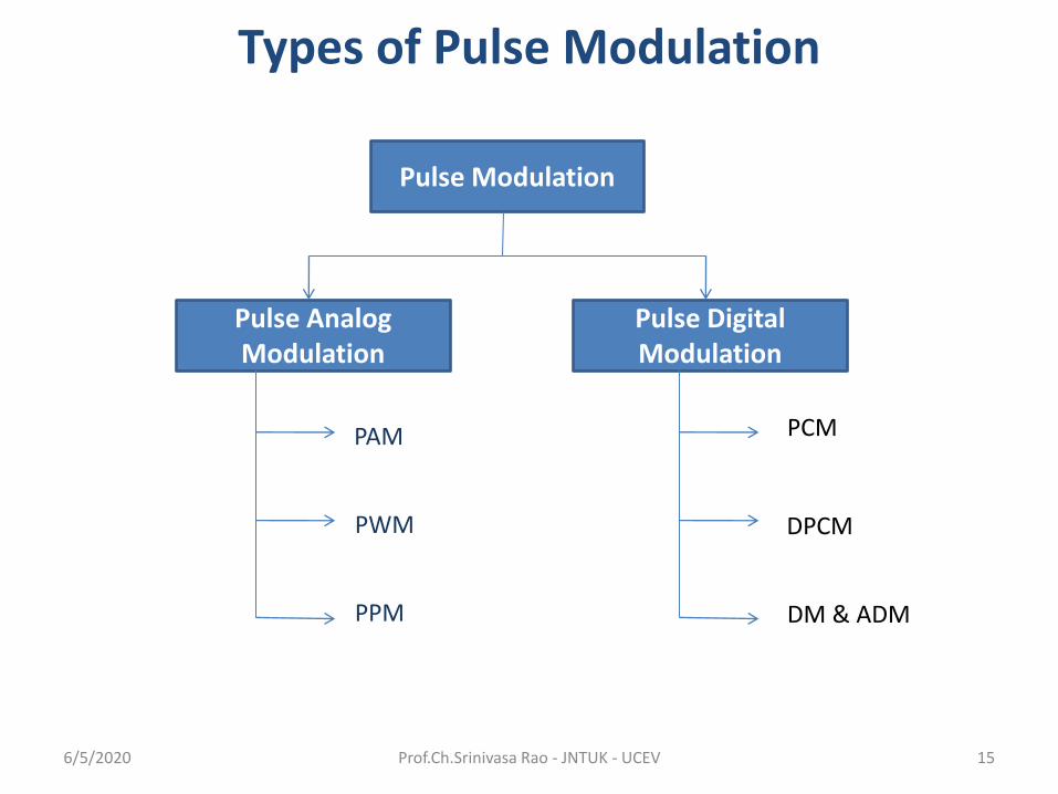
Types of Pulse Modulation
Pulse Modulation
Pulse Digital Modulation
Pulse Analog Modulation
PAM
PPM
PWM
PCM
DPCM
DM & ADM
6/5/2020 Prof.Ch.Srinivasa Rao - JNTUK - UCEV 15

Pulse Amplitude Modulation
• The amplitude of the pulses of the carrier pulse train is
varied in accordance with the modulating signal, that is
amplitude of the pulses depends on the value of m(t)
during the time of pulse.
6/5/2020 Prof.Ch.Srinivasa Rao - JNTUK - UCEV 16
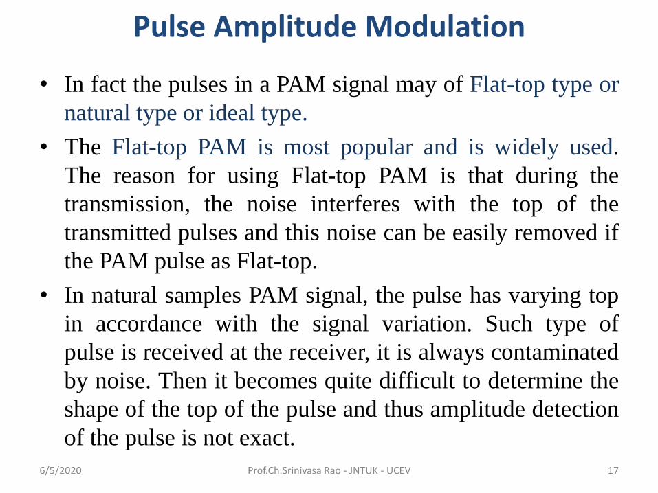
Pulse Amplitude Modulation
• In fact the pulses in a PAM signal may of Flat-top type or
natural type or ideal type.
• The Flat-top PAM is most popular and is widely used.
The reason for using Flat-top PAM is that during the
transmission, the noise interferes with the top of the
transmitted pulses and this noise can be easily removed if
the PAM pulse as Flat-top.
• In natural samples PAM signal, the pulse has varying top
in accordance with the signal variation. Such type of
pulse is received at the receiver, it is always contaminated
by noise. Then it becomes quite difficult to determine the
shape of the top of the pulse and thus amplitude detection
of the pulse is not exact.
6/5/2020 Prof.Ch.Srinivasa Rao - JNTUK - UCEV 17

Generation of PAM
• There are two operations involved in the generation of PAM
signal
1. Instantaneous sampling of the message signal m(t) every Ts
seconds, where the sampling rate fs = 1/Ts is chosen in
accordance with the sampling theorem.
2. Lengthening the duration of each sample so obtained to some
constant value T.
Figure: PAM signal6/5/2020 Prof.Ch.Srinivasa Rao - JNTUK - UCEV 18

Sample and Hold Circuit for Generating Flat-top sampled PAM
Figure: (a) Sample and hold circuit generating flat top sampled PAM
(b) Waveforms of flat top sampled PAM6/5/2020 Prof.Ch.Srinivasa Rao - JNTUK - UCEV 19

• The sample and hold circuit consists of two Field Effect
Transistor switches and a capacitor.
• The sampling switch is closed for a short duration by a short
pulse applied to the gate G1 of the transistor. During this
period, the capacitor C is quickly charged up to a voltage equal
to the instantaneous sample value of the incoming signal.
• Now, the sampling switch is opened and the capacitor holds
the charge. The discharge switch is then closed by a pulse
applied to gate G2 of the other transistor. Due to this, the
capacitor is discharged to zero volts. The discharges switch is
then opened and thus capacitor has no voltage. Hence the
output of the sample and hold circuit consists of a sequence of
flat-top samples as shown in figure.
Sample and Hold Circuit for Generating Flat-top sampled PAM
6/5/2020 Prof.Ch.Srinivasa Rao - JNTUK - UCEV 20

Mathematical Representation of PAM
• We may express the PAM signal as
where
Ts = sampling period
m(nTs) = sample value of m(t) obtained at t = nTs
h(t) = standard rectangular pulse of unit amplitude and duration
T and it is defined as
The spectrum of flat-top PAM signal is
6/5/2020 Prof.Ch.Srinivasa Rao - JNTUK - UCEV 21

Naturally Sampled PAM signal
• The natural sampling is basically pulse amplitude modulation.
Therefore it is called naturally sampled PAM signal.
• The time-domain representation of a naturally sampled PAM
signal will be given as
• The frequency spectrum of naturally sampled PAM signal will
be given as
6/5/2020 Prof.Ch.Srinivasa Rao - JNTUK - UCEV 22

• The instantaneous sampling is basically PAM. It is called
ideally or instantaneously sampled PAM signal.
• The time-domain representation of a ideally sampled
PAM signal will be given as
• The frequency domain representation i.e., frequency
spectrum of a ideally sampled PAM signal will be given
as
Ideally Sampled PAM signal
6/5/2020 Prof.Ch.Srinivasa Rao - JNTUK - UCEV 23

Transmission Bandwidth of PAM
• In PAM signal the pulse duration τ is assumed to be very small
compared to time period Ts between the two samples i.e τ< Ts
• If the maximum frequency in the modulating signal x(t) is fm
then sampling frequency fs is given by fs>=2fm Or 1/Ts >=
2fm or Ts <= 1/2fm
Therefore, τ < < Ts <= 1/2fm
• If ON and OFF time of PAM pulse is equal then maximum
frequency of PAM pulse will be fmax = 1/ τ+ τ = 1/2 τ
Therefore, transmission bandwidth >=fmax
But fmax=1/2 τ
B.W>=1/2 τ
B.W>=1/2 τ >>fm
6/5/2020 Prof.Ch.Srinivasa Rao - JNTUK - UCEV 24

Demodulation of PAM
• The distortion caused by the use of PAM to transmit an analog
information bearing signal is referred to as the aperture effect.
This distortion may be corrected by connecting an equalizer in
cascade with the low-pass reconstruction filter as shown in fig.
• The equalizer has the effect of decreasing the in-band loss of
the reconstruction filter as the frequency increases in such a
manner as to compensate for the aperture effect.
Reconstruction Filter
EqualizerPAM signal
s(t)
Message signalm(t)
Figure: System for recovering message signal m(t) from PAM signal s(t)
6/5/2020 Prof.Ch.Srinivasa Rao - JNTUK - UCEV 25

• Ideally, the magnitude response of the equalizer is given by
• The amount of equalization needed in practice is usually
small.
Advantages of PAM :
• It is the simple and simple process for modulation and
demodulation
• Transmitter and receiver circuits are simple and easy to
construct.
Demodulation of PAM
6/5/2020 Prof.Ch.Srinivasa Rao - JNTUK - UCEV 26

Drawbacks of PAM signal
• The bandwidth required for the transmission of a PAM
signal is very large in comparison to the maximum
frequency present in the modulating signal.
• Since the amplitude of the PAM pulses varies in
accordance with the modulating signal therefore the
interference of noise is maximum in a PAM signal. This
noise cannot be removed easily.
• Since the amplitude of the PAM pulses varies, therefore,
this also varies the peak power required by the transmitter
with modulating signal.
6/5/2020 Prof.Ch.Srinivasa Rao - JNTUK - UCEV 27

Pulse Time Modulation (PTM)
• In pulse time modulation, amplitude of pulse is held
constant, whereas position of pulse or width of pulse is
made proportional to the amplitude of signal at the
sampling instant.
• There are two types of pulse time modulation.
i. Pulse Width Modulation
ii. Pulse Position Modulation
6/5/2020 Prof.Ch.Srinivasa Rao - JNTUK - UCEV 28

Pulse Width Modulation
• PWM is also called Pulse Duration Modulation (PDM), Pulse
Length Modulation (PLM) and
Definition:
In PWM, Width of the pulses of the carrier pulse train is varied
in accordance with the modulating signal.
Figure: Illustration of PWM (a) Modulating signal (b) Pulse Carrier (c) PWM signal6/5/2020 Prof.Ch.Srinivasa Rao - JNTUK - UCEV 29

PWM Generation
Direct Method of PWM generation using Monostable
Multivibrator
6/5/2020 Prof.Ch.Srinivasa Rao - JNTUK - UCEV 30

• We know that stable state for this type of multivibrator is T1
Off and T2 On.
• The applied trigger pulse switches T1 ON, whereupon the
voltage at C1 falls as T1 now begins to draw collector current.
• The voltage at B2 follows C1 and T2 is switched off by
regenerative action.
• As soon as this happens, C begins to charge up to the collector
supply potential through R.
• After a time determined by the supply voltage and RC time
constant of the charging network, B2 becomes sufficiently
positive to switch T2 on.
• T1 is simultaneously switched off by regenerative action and
stays OFF until the arrival of the next trigger pulse.
6/5/2020 Prof.Ch.Srinivasa Rao - JNTUK - UCEV 31

• The voltage at the base of T2 must reach to allow T2 to turn
on, is slightly more positive than the voltage across the
common emitter resistor Rk. This voltage depends on the
current flowing through the circuit, which at the time is the
collector current of T1(at that
time T1 ON)
• The collector current depends on the base bias, which is
controlled by the instantaneous changes in the applied signal
voltage.
• The applied modulating voltage control the voltage to which
B2 must rise to switch T2 ON. Since the voltage rise is linear,
the modulating voltage is seen to control the period of time
during which T2 is OFF.
6/5/2020 Prof.Ch.Srinivasa Rao - JNTUK - UCEV 32

PWM Demodulation
PWM to PAM
converter
Low-Pass Filter
PWM signal
Messagesignal
Figure: PWM Demodulator Circuit
6/5/2020 Prof.Ch.Srinivasa Rao - JNTUK - UCEV 33

• The transistor T1 works as an inverter. Hence during the time
interval A –B, when the PWM signal is high, the input to the
transistor T2 is low.Therefore, during this time interval, the
transistor T2 is cut-off and the capacitor C gets charged
through an R-C combination.
• During the time interval B –C when the PWM signal is low,
the input to the transistor T2 is high, and it gets saturated.The
capacitor C then discharges very rapidly through T2. The
collector voltage of T2 during the interval B-C is then low.
Thus the waveform at the collector of T2 is more or less a saw-
tooth waveform whose envelope is the modulating signal.
• When this is passed through a second – order OP-AMP low
pass filter, we get the desired demodulated output
6/5/2020 Prof.Ch.Srinivasa Rao - JNTUK - UCEV 34

PWM Demodulation
Schmitt Trigger
Ramp Generator
LPFSynchronization Pulse Generator
AdderLevel
ShifterRectifier
Demodulated Output
PWM signal
Figure: PWM Detector6/5/2020 Prof.Ch.Srinivasa Rao - JNTUK - UCEV 35

PWM Demodulation Contd.,
Figure: Waveforms for PWM detection circuit
6/5/2020 Prof.Ch.Srinivasa Rao - JNTUK - UCEV 36

• The received PWM signal is applied to the schmitt trigger
circuit. This schmitt trigger circuit removes the noise in the
PWM waveform.
• The regenerated PWM is then applied to the ramp generator
and the synchronization pulse detector. The ramp generator
produces ramps for the duration of pulses such that height of
ramps are proportional to the width of PWM pulses.
• The maximum ramp voltage is retained till the next pulse. On
the other hand, synchronous pulse detector produces reference
pulses with constant amplitude and pulse width. These pulses
are delayed for specific amount of delay as shown in figure.
• The delayed reference pulses and the output of ramp generator
is added with the help of adder. The output of adder is given
to the level shifter. Here, negative offset shifts the waveform
as shown in figure.
PWM Demodulation
6/5/2020 Prof.Ch.Srinivasa Rao - JNTUK - UCEV 37

• The negative part of the waveform is clipped by rectifier.
• Finally, the output of rectifier is passed through lowpass filter
to recover the modulating signal.
Advantages of PWM:
• Noise is less, since in PWM, amplitude is held constant.
• Signal and noise separation is very easy
• PWM communication does not required synchronization
between transmitter and receiver.
Disadvantages of PWM:
• In PWM, pulses are varying in width and therefore their power
contents are variable this requires that the transmitter must be
able to handle the power content of the pulse having maximum
pulse width.
• Large bandwidth is required for the PWM as compared to
PAM
PWM Demodulation
6/5/2020 Prof.Ch.Srinivasa Rao - JNTUK - UCEV 38

Pulse Position Modulation (PPM)Definition:
In PPM, the position of the pulse relative to its un-modulated
time occurrence is varied in accordance with the message
signal.
Modulating wave
PWM wave
Pulse carrier
PPM wave6/5/2020 Prof.Ch.Srinivasa Rao - JNTUK - UCEV 39

PPM Generation
6/5/2020 Prof.Ch.Srinivasa Rao - JNTUK - UCEV 40

PPM Generation
• PPM generator consists of differentiator and monostable
multivibrator.
• The differentiator generates positive and negative spikes
corresponding to leading and trailing edges of the PWM
waveform.
• Diode D1 is used to bypass the positive spikes
• The negative spikes are used to trigger the multivibrator.
• The monostable multivibrator then generates the pulses of
same width and amplitude with reference to the trigger to give
PPM waveform as shown in figure.
6/5/2020 Prof.Ch.Srinivasa Rao - JNTUK - UCEV 41

Demodulation of PPM
PPM to PAM converter
Low-Pass Filter
PPM signal
Messagesignal
Figure: PWM Demodulator Circuit
6/5/2020 Prof.Ch.Srinivasa Rao - JNTUK - UCEV 42

• This utilizes the fact that the gaps between the pulses of a PPM
signal contain the information regarding the modulating signal.
• During the gap A- B between the pulses, the transmitter is cut-
off, and the capacitor C gets charged through the R-C
combination. During the pulse duration B-C, the capacitor
discharges through the transistor, and the collector voltage
becomes low.
• Thus the waveform at the collector is approximately a saw
tooth waveform whose envelope is the modulating signal.
• When this is passed through a second order OP- AMP low pass
filter, we get the desired demodulated output.
Demodulation of PPM
6/5/2020 Prof.Ch.Srinivasa Rao - JNTUK - UCEV 43

PPM
Advantages of PPM:
• Like PWM, in PPM, amplitude is held constant thus less noise
interference.
• Signal and noise separation is very easy
• Because of constant pulse widths and amplitudes, transmission
power for each pulse is same
Disadvantages of PWM:
• Synchronization between transmitter and receiver is required.
• Large bandwidth is required for the PPM as compared to PAM
6/5/2020 Prof.Ch.Srinivasa Rao - JNTUK - UCEV 44
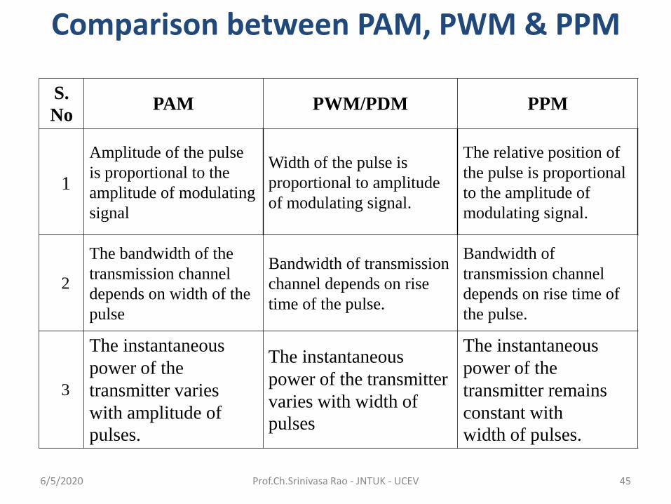
Comparison between PAM, PWM & PPM
S.
No PAM PWM/PDM PPM
1
Amplitude of the pulse
is proportional to the
amplitude of modulating
signal
Width of the pulse is
proportional to amplitude
of modulating signal.
The relative position of
the pulse is proportional
to the amplitude of
modulating signal.
2
The bandwidth of the
transmission channel
depends on width of the
pulse
Bandwidth of transmission
channel depends on rise
time of the pulse.
Bandwidth of
transmission channel
depends on rise time of
the pulse.
3
The instantaneous
power of the
transmitter varies
with amplitude of
pulses.
The instantaneous
power of the transmitter
varies with width of
pulses
The instantaneous
power of the
transmitter remains
constant with
width of pulses.
6/5/2020 Prof.Ch.Srinivasa Rao - JNTUK - UCEV 45

S.
No PAM PWM/PDM PPM
4 Noise interference is
high
Noise interference is
minimum
Noise interference is
minimum
5 System is complex Simple is implement Simple is implement
6 Similar to Amplitude
modulation
Similar to frequency
modulation
Simple to Phase
modulation
Comparison between PAM, PWM & PPM Contd.,
6/5/2020 Prof.Ch.Srinivasa Rao - JNTUK - UCEV 46

SYNCHRONIZATION
• PAM
• PWM
• PPM
6/5/2020 Prof.Ch.Srinivasa Rao - JNTUK - UCEV 47

Time Division Multiplexing (TDM)
• An important feature of the sampling process is a conservation
of time. That is, the transmission of the message samples
engages the communication channel for only a fraction of the
sampling interval on a periodic basis, and in this way some of
the time interval between adjacent samples is cleared for use
by other independent message sources on a time-shared basis.
• Time Division Multiplex (TDM) is a system, which enables
the joint utilization of common communication channel by a
plurality of independent message sources without mutual
interference among them.
• The concept of TDM is illustrated by the block diagram shown
below.
6/5/2020 Prof.Ch.Srinivasa Rao - JNTUK - UCEV 48
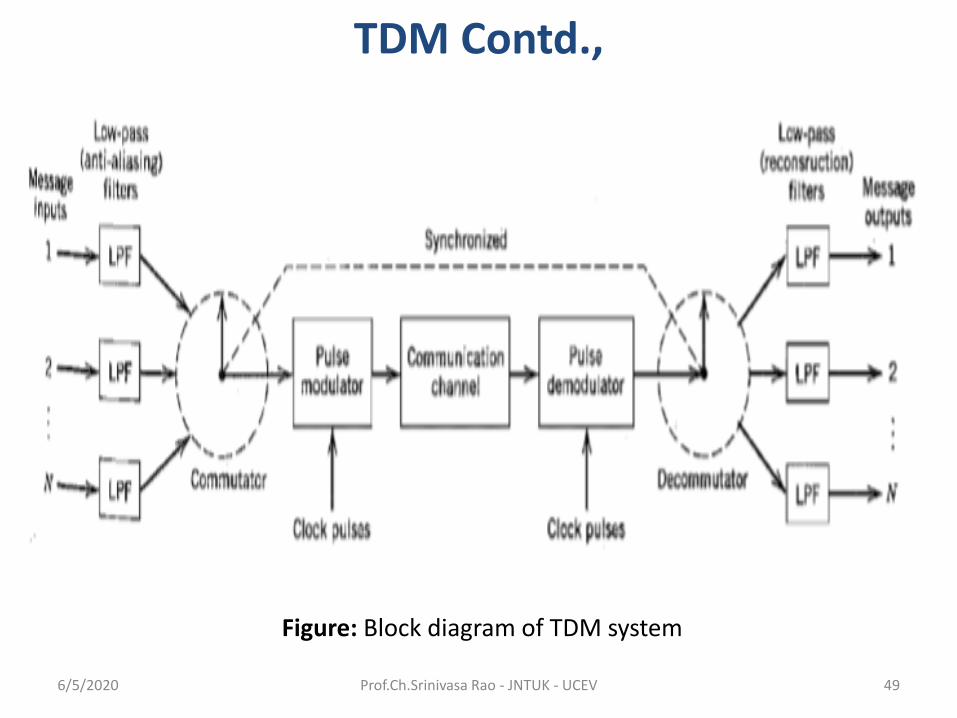
TDM Contd.,
Figure: Block diagram of TDM system
6/5/2020 Prof.Ch.Srinivasa Rao - JNTUK - UCEV 49

• Each input message signal is first restricted in bandwidth by a
low-pass anti-aliasing filter to remove the frequencies that are
nonessential to an adequate signal representation.
• The LPF outputs are applied to commutator. The function of
the commutator is two fold
1. To take a narrow sample of each of the N input messages at a
rate fs that is slightly higher than 2W, where W is the cutoff
frequency of the anti-aliasing filter.
2. To sequentially interleave these N samples inside the
sampling interval Ts.
• The multiplexed signal is applied to a pulse modulator, the
purpose of which is to transform the multiplexed signal into a
form suitable for transmission over the common channel.
TDM Contd.,
6/5/2020 Prof.Ch.Srinivasa Rao - JNTUK - UCEV 50

• At the receiving end of the system, the received signal is
applied to the pulse demodulator, which performs the reverse
operation of the pulse modulator.
• The narrow samples produced at the pulse demodulator output
are distributed to the appropriate low-pass reconstruction
filters by means of a decommutator, which operates in
synchronism with the commutator in the transmitter.
Synchronization depends on the method of pulse modulation
used to transmit the multiplexed sequence of samples.
TDM Contd.,
6/5/2020 Prof.Ch.Srinivasa Rao - JNTUK - UCEV 51

1 rotation
6/5/2020 Prof.Ch.Srinivasa Rao - JNTUK - UCEV 52

6/5/2020 Prof.Ch.Srinivasa Rao - JNTUK - UCEV 53

Problem
• 5 message signals, each having frequency of 2KHz are multiplexed using TDM. Number ofquantization levels used are 256. Findtransmission bandwidth of the system.
6/5/2020 Prof.Ch.Srinivasa Rao - JNTUK - UCEV 54

• Given that N = 5, fm = 2 KHz,
L = 256 levels then n = 8
We know that NR = 2fm
fs = NR = 2fm = 4 KHz
Solution
6/5/2020 Prof.Ch.Srinivasa Rao - JNTUK - UCEV 55

Problems on TDM
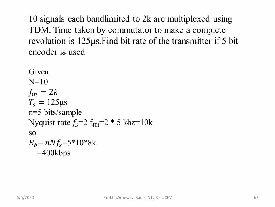
• 10 signals, each band limited to 2KHz are multiplexed usingTDM. Time taken by commutator to make one completerotation is 125 microseconds. Find bit rate of the transmitterif 5 bit encoder is used.
6/5/2020 Prof.Ch.Srinivasa Rao - JNTUK - UCEV 56
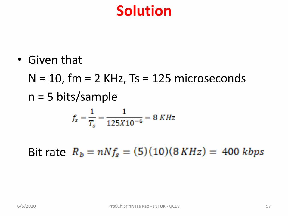
Solution
• Given that
N = 10, fm = 2 KHz, Ts = 125 microseconds
n = 5 bits/sample
Bit rate
6/5/2020 Prof.Ch.Srinivasa Rao - JNTUK - UCEV 57

Problem
10 sinusoidal message signals, each havingfrequency of 10 KHz are multiplexed usingTDM. Sampling rate is 25% higher than theNR. Maximum quantization error can be atmost of 1% of peak to peak amplitude ofmessage signal. 5 number of synchronizationbits are transmitted at the end of each frame.Find Bit rate of the transmitter?
6/5/2020 Prof.Ch.Srinivasa Rao - JNTUK - UCEV 58

Solution
• Given that
N = 10, fm = 10 KHz, fs = 1.25NR , a = 5
Now
6/5/2020 Prof.Ch.Srinivasa Rao - JNTUK - UCEV 59

Solution contd.,
• Bit rate
6/5/2020 Prof.Ch.Srinivasa Rao - JNTUK - UCEV 60

6/5/2020 Prof.Ch.Srinivasa Rao - JNTUK - UCEV 61
6/5/2020 Prof.Ch.Srinivasa Rao - JNTUK - UCEV 62

6/5/2020 Prof.Ch.Srinivasa Rao - JNTUK - UCEV 63

6/5/2020 Prof.Ch.Srinivasa Rao - JNTUK - UCEV 64

Three message signals each bandlimited to 5 KHz are multiplexed
using FDM. Guard band is 1 Khz. Find multiplexed signal
bandwidth ,if the modulation schemes used are AM,DSB and SSB
respectively.
6/5/2020 Prof.Ch.Srinivasa Rao - JNTUK - UCEV 65

6/5/2020 Prof.Ch.Srinivasa Rao - JNTUK - UCEV 66

6/5/2020 Prof.Ch.Srinivasa Rao - JNTUK - UCEV 67

References
Prof.Ch.Srinivasa Rao - JNTUK - UCEV 68
❑ Communication Systems by Simon Haykin, Wiley, 2nd Edition.
❑ Principle of Communication System by Taub ,Schilling & Saha,
TMH.
❑ Modern digital and Analog Communications system by BP Lathi,
Ding and Gupta, Oxford.
❑ Electronic Communication Systems by Kennedy and Davis, TMH.
❑ Communication Systems Analog and Digital by Singh and Sapre,
TMH
6/5/2020

Prof.Ch.Srinivasa Rao - JNTUK - UCEV 696/5/2020
Copyright © 2022 FDOKUMEN