
Performance of a longitudinally-segmented CsI(T1) array suitable for a detector in a low or medium...
23
SLAC-PUB-6319 December 1993 03 Performance of a longitudinally-segmented CsI(T1) array *suitable for a detector in a low or medium energy e+e- storage ring R. Baggs,a E. Church,b V. Cook,b D. Coward,a R. Coxe,a K. Curtis,c R. S. Davis,d J. Dyke,C A. Foland,e R. Frey,f D. Freytaga G. Gladding,o J. M. Izen,d R. A. Johnson,c M. E. King,a W. Lockman,g G. Niemi,a G. Putallaz,a R. H. Schindler,a D. P. Stoker,h F. Toevs,b E. Vokurka,ate E. Weiss b aStanford Linear Accelerator Center, Stanford, CA 94309 bUniversity of Washington, Seattle, WA 98195 Wniversity of Cincinnati, Cincinnati, OH 45221 dUniversity of Texas, Dallas, TX 75083 euniversity of Illinois, Champaign -Urbana, IL 61802 fUniversity of Oregon, Eugene, OR 97403 gUniversity of California, Santa Cruz, CA 95064 hllniversity of California, Irvine, CA 92717 We present results on energy resolution and linearity, and position resolution, from a test of an array of CsI(T1) crystals in a x /e /p beam (120 to 400 MeV) at TRIUMF. The crystal array was designed to study the effects of longitudinal and transverse crystal segmentation on energy and position resolution and background rejection. We also studied the feasibility of a wavelength-shifter and multi-photodiode readout system, suitable for use in magnetic detectors at low and medium ener storage rings. $y, high-luminosity e+ei Energy resolutions of (1.69 f 0.08)%/ E(GeV) and (1.83 0.05)%/ ,/E(GeV) were obtained for two different crystal tower configurations. Position resolution of 6.5 (9.0) mm was obtained at 300 (120) MeV for a 2 x 2 square array of four 4 x 4 x 7.4 cm3 crystals transverse to the beam. Submitted to Nuclear Instruments & Methods in Physics Research - A * Work supported in part by Department of Energy Contract DE-AC03-76SFOO515, DE-FG03- 91ER40679, and DE-FG05-92ER40736. -- _ ,’
-
Upload
independent -
Category
Documents
-
view
3 -
download
0
Transcript of Performance of a longitudinally-segmented CsI(T1) array suitable for a detector in a low or medium...

SLAC-PUB-6319 December 1993 03
Performance of a longitudinally-segmented CsI(T1) array *suitable for a detector in a low or medium energy e+e- storage ring
R. Baggs,a E. Church,b V. Cook,b D. Coward,a R. Coxe,a K. Curtis,c
R. S. Davis,d J. Dyke,C A. Foland,e R. Frey,f D. Freytaga G. Gladding,o
J. M. Izen,d R. A. Johnson,c M. E. King,a W. Lockman,g G. Niemi,a
G. Putallaz,a R. H. Schindler,a D. P. Stoker,h F. Toevs,b E. Vokurka,ate E. Weiss b
aStanford Linear Accelerator Center, Stanford, CA 94309 bUniversity of Washington, Seattle, WA 98195
Wniversity of Cincinnati, Cincinnati, OH 45221
dUniversity of Texas, Dallas, TX 75083 euniversity of Illinois, Champaign -Urbana, IL 61802
fUniversity of Oregon, Eugene, OR 97403
gUniversity of California, Santa Cruz, CA 95064 hllniversity of California, Irvine, CA 92717
We present results on energy resolution and linearity, and position resolution, from a test of an array of CsI(T1) crystals in a x / e /p beam (120 to 400 MeV) at TRIUMF. The crystal array was designed to study the effects of longitudinal and transverse crystal segmentation on energy and position resolution and background rejection. We also studied the feasibility of a wavelength-shifter and multi-photodiode readout system, suitable for use in magnetic detectors at low and medium ener storage rings.
$y, high-luminosity e+ei Energy resolutions of (1.69 f 0.08)%/ E(GeV) and (1.83
0.05)%/ ,/E(GeV) were obtained for two different crystal tower configurations. Position resolution of 6.5 (9.0) mm was obtained at 300 (120) MeV for a 2 x 2 square array of four 4 x 4 x 7.4 cm3 crystals transverse to the beam.
Submitted to Nuclear Instruments & Methods in Physics Research - A
* Work supported in part by Department of Energy Contract DE-AC03-76SFOO515, DE-FG03- 91ER40679, and DE-FG05-92ER40736.
--
_ ,’

I ‘T. .
1. Introduction
Several high-luminosity, low and medium-energy e+e- storage rings are presently being built or are under consideration for future construction; e.g., the so-called Phi, Tau-Charm, and B-Factories. Each of these facilities will require a state-of-the-art detector with high precision electromagnetic calorimetry. Numerous studies [I] of requirements for these detectors suggest that many characteristics of CsI crystal calorimetry are necessary to achieve their physics goals. Notably, the high light yield (-50,000 photons/MeV) of CsI(T1) or CsI(Na) facilitates excellent energy resolution and efficient detection of photons with energies down to a few MeV. Excellent position and angular resolution is also obtainable at these energies. The large light output makes feasible the use of low-gain or unity-gain devices, such as photodiodes, for readout. The dominant drawbacks of CsI scintillators are low radiation hardness, poor mechanical properties, and relatively long decay times (-1 pus for Tl-doped crystals) which integrate scintillation light over many beam crossings. This results in serious sources of low-energy “fake” photons from the pileup of backgrounds from lost beam particles, nuclear interactions of hadrons, and albedo within an event. While radiation hardness is not an issue at Phi and Tau-Charm Factories [PI, evidence from experiments with large CsI arrays suggests that albedo and pileup may limit the use of the lowest energy photons (I 20 MeV) if these backgrounds are not adequately suppressed. Hence, these crystals should not be considered for such future colliders unless these problems are addressed [3]. We present herein results of detailed studies of an array of CsI(T1) crystals designed to
overcome some of these limitations by use of alternative crystal geometries, crystal segmentation, and photodiode/wavelength-shifting plastic readout techniques.
2. Calorimeter and Test Design
We tested an array of 14 CsI(Tl) crystal towers which could be scaled to a full-sized cylindrical detector suitable for use at low and medium energy “factories”. Physics and cost considerations imply that such a CsI calorimeter would typically contain about 10,000 projective towers in a cylinder -3.5 meters long with -1 meter inner radius, for a total of 8-10 m3 of crystals. The towers would be of transverse size (40-80 mr) x (40-80 mr), and 16-18 radiation lengths (rl) (29.6-33.3 cm) long, tapered along their major axis to form truncated pyramids. To enhance n/ e /fi separation and improve the rejection of fake photons, each tower can be segmented longitudinally into two or more parts. Depending on the average energy in the collisions, a break near shower
--
2
! ‘T. -
maximum, at -3 to 4 rl (5.6-7.4 cm), would be chosen. To improve position resolution, the short, front section can also be divided transversely.
The electronics for the calorimeter has strict limits on inherent noise, as discussed in Section 2.6 and Section 3.3. It is desirable to locate close to the source most of the signal processing, such as amplification, pulse shaping, calibration, and drivers. Since these electronics would be inaccessible during an experimental run, a high degree of reliability is needed. Spatial constraints and
heat dissipation are also considerations in the design. Semi-custom arrays of bipolar transistors, which are compact, and have reliable interconnections, and have low heat dissipation due to low internal capacitive loads, are effective in this environment. The electronics used in this beam test was a first approach to a system realized in semi-custom bipolar transistor technology. To allow energy
to be unambiguously associated with a beam crossing, we also anticipate a need to incorporate coarse timing information into the readout of a final device; however, this was not addressed by our test.
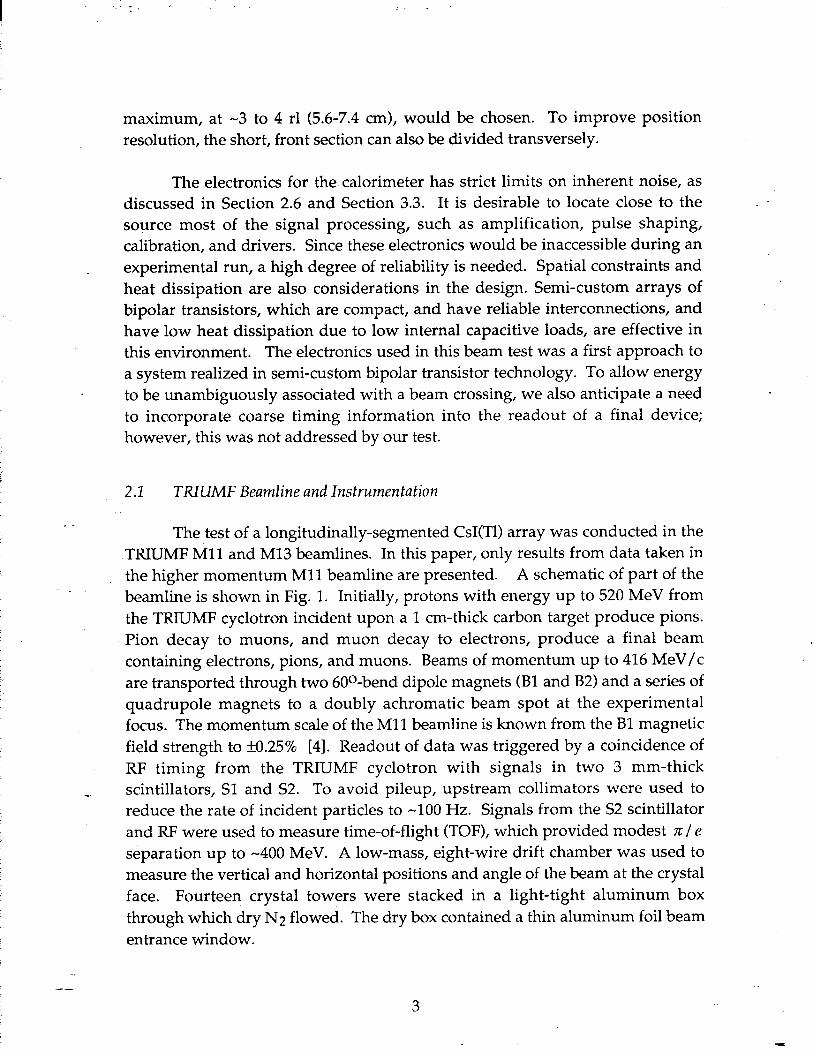
2.1 TRIUMF Beamline and Instrumentation
The test of a longitudinally-segmented CsI(T1) array was conducted in the TRIUMF Ml1 and Ml3 beamlines. In this paper, only results from data taken in the higher momentum Ml1 beamline are presented. A schematic of part of the beamline is shown in Fig. 1. Initially, protons with energy up to 520 MeV from
the TRIUMF cyclotron incident upon a 1 cm-thick carbon target produce pions. Pion decay to muons, and muon decay to electrons, produce a final beam containing electrons, pions, and muons. Beams of momentum up to 416 MeV/c
are transported through two 60o-bend dipole magnets (Bl and B2) and a series of quadrupole magnets to a doubly achromatic beam spot at the experimental focus. The momentum scale of the Ml1 beamline is known from the Bl magnetic
field strength to +0.25% [4]. Readout of data was triggered by a coincidence of RF timing from the TRIUMF cyclotron with signals in two 3 mm-thick scintillators, Sl and S2. To avoid pileup, upstream collimators were used to reduce the rate of incident particles to -100 Hz. Signals from the S2 scintillator
and RF were used to measure time-of-flight (TOF), which provided modest x / e separation up to -400 MeV. A low-mass, eight-wire drift chamber was used to measure the vertical and horizontal positions and angle of the beam at the crystal
face. Fourteen crystal towers were stacked in a light-tight aluminum box
through which dry N2 flowed. The dry box contained a thin aluminum foil beam entrance window.
3
Bend & Momentum
XY Beam-Defining Drift Chamber. 4X & 4Y Wires. Mylar Windows.
Defining Slits.
Ml1 - Mylar Channel Window Scintillator TOF
Trig. Stint.
s-93 2.0 m 0.55 m
Dry Box with Foil Front Window Containing Crystal Array.
Fig. 1. A portion of the TRIUMF Ml1 beamline with trigger scintillators Sl and S2,
beam-defining drift chamber, and CsI crystal tower array in dry box. The locations of
Towers A, B, and C discussed in the text are indicated.
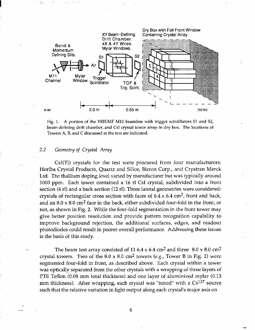
2.2 Geometry of Crystal Array
CsI(T1) crystals for the test were procured from four manufacturers: Horiba Crystal Products, Quartz and Silice, Bicron Corp., and Crystran Merck Ltd. The thallium doping level varied by manufacturer but was typically around 1000 ppm. Each tower contained a 16 rl CsI crystal, subdivided into a front section (4 rl) and a back section (12 rl). Three lateral geometries were considered:
crystals of rectangular cross section with faces of 6.4 x 6.4 cm2, front and back, and an 8.0 x 8.0 cm2 face in the back, either subdivided four-fold in the front, or not, as shown in Fig. 2. While the four-fold segmentation in the front tower may
give better position resolution and provide pattern recognition capability to improve background rejection, the additional surfaces, edges, and readout photodiodes could result in poorer overall performance. Addressing these issues
is the basis of this study.
The beam test array consisted of 11 6.4 x 6.4 cm2 and three 8.0 x 8.0 cm2 crystal towers. Two of the 8.0 x 8.0 cm2 towers (e.g., Tower B in Fig. 2) were segmented four-fold in front, as described above. Each crystal within a tower was optically separated from the other crystals with a wrapping of three layers of PTE Teflon (0.08 mm total thickness) and one layer of aluminized mylar (0.13
mm thickness). After wrapping, each crystal was “tuned” with a Cs1s7 source such that the relative variation in light output along each crystal’s major axis on
4
9-93
Preamplifier, Line Drivers, and Calibration Network
f
Photodiode
Wavelength
Tower A Tower B Tower C
7327Al
Fig. 2. Schematics of the three configurations of CsI crystal towers tested, showing
longitudinal and transverse segmentation of crystals, and wavelength shifter-
photodiode-preamplifier readout.
all four sides was 52%. Tuning involved an iterative process of polishing,
selective roughening of the polished surfaces, and subsequent re-wrapping and testing of the crystals. For the short 4.0 x 4.0 cm2 crystals, we achieved about 1% nonuniformity over most of the length. One of the drawbacks of the 6.4 x 6.4 cm2 and 8 x 8 cm2 4 rl front crystals is that their aspect ratio exhibited a larger fractional longitudinal nonuniformity near their ends. However, to compensate,
the front and back crystals can be tuned together.
2.3 Wavelength Shifter and Photodiode Construction
The light collection for the readout of each crystal was accomplished using a 3 mm-thick square piece of wavelength-shifting acrylic plastic (WLS) that covered about 70% of one face of the crystal. (In a given tower, one WLS covered
the front face of (each of) the front crystal(s) and one WLS covered the back face of the back crystal.) The WLS absorbs direct and internally reflected light from
5

- 0 c
0 0
0 0
II 0
/
/
1 0-4
1 2 3 4 11-93 7534A10 Photodiodes
Fig. 3. a) The total signal in units of electrons/MeV of deposited energy versus the number of PD’s on a wavelength shifter (one per WLS edge). b) Signal-to-noise ratio. These data were obtained using cosmic ray signals in a single, 16 rl-long crystal.
2.4 Crystal Tower Housing
The crystals within each tower and their associated electronics were isolated from neighboring crystals by enclosing them in a 0.5 mm-thick, copper- clad G-10 box. In a real detector, the box material can be reduced by using, for example, a nickel-plated, carbon-fiber epoxy laminate material. Monte Carlo studies have shown that tilting the boxes by as little as 25 mr to the incident
particle direction eliminates the deleterious effects of the box’s thickness on resolution. In the beam test, the boxes also served to mechanically position the
front and back crystals within a tower, and to maintain a fixed WLS-to-crystal air
gap.
2.5 Overview of Readout Electronics
The circuitry on each preamplifier board, as shown in Figs. 4-5, consisted of a FET and an ASIC-based buffer amplifier, a calibration network, and CLEO- II-style differential line-drivers [6]. Bias voltage for the I’D, power, and calibration signals were also routed on the board. To reduce pickup, all PD signals were carried to the preamplifiers on 0.3 mm-diameter micro-coaxial cable of 1.5 pF/cm capacitance. The cables were placed along the inner edges of the G- 10 boxes containing the crystals and preamplifier boards.
Differential signals were transmitted out of the crystal dry box on 5 m-
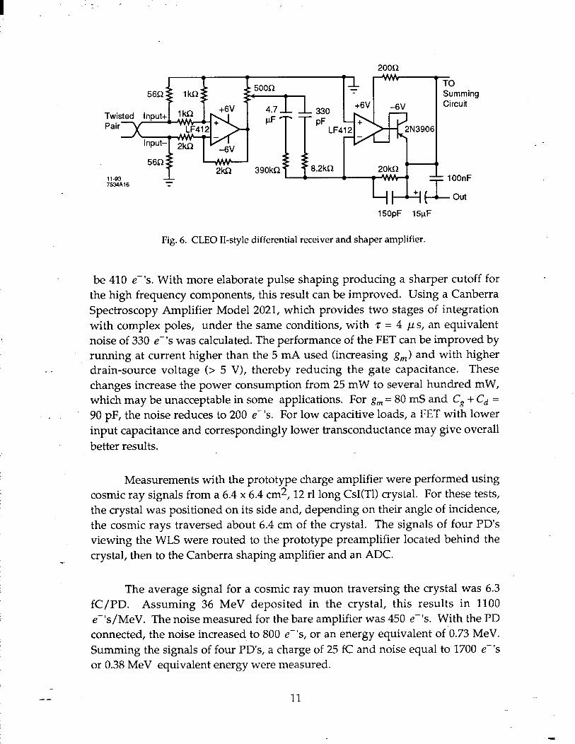
long ribbon cables. They were received differentially by CLEO-II-style shaping amplifiers [6] (Fig. 6) which performed a single integration with shaping and peaking times of 3 p s. Shaped signals were sampled with a -200 ns gate around the peak, and digitized by LRS 2249A ADC’s. There were a total of 120 readout channels. The preamplifier and shaping amplifier gains were separately preadjusted to give equal signals for a fixed charge injected at the inputs. Each calibration circuit was trimmed to produce a constant charge for a fixed input calibration pulse. The final electronic calibration was performed taking 100
repeated readings of all ADC’s at 15 distinct DAC values. (The DAC values
define the calibration charge, and span the energy range of interest in the beam test.) The calibration data were fit piecewise with a linear function and, to remove a small nonlinearity at the low end of the ADC range, a quadratic function.
2.6 Preamplifier / Shaper Amplifier Description and Noise Limitations
The desired performance for light collection and electronic readout is
determined by the lowest energy photons of experimental interest. Considering the experience of other detectors in similar operating conditions, the flux and spectrum of background showers places a lower limit of about -10 MeV on
showers that will be useful for physics analyses. Intrinsic shower fluctuations at 10 MeV are -1.2 MeV in CsI (refer to Section 3.3), suggesting that electronic noise performance should be maintained below this value in order that it not contribute significantly to the resolution for these low energy showers.
A signal from a single PD is typically small, between 1000-2000 e- ‘s/MeV
deposited in a large CsI(T1) crystal. To facilitate detection of photons with energies at the lo-20 MeV level, the preamplifier’s contribution to the electronic noise must be minimized. As the first amplification stage in a preamplifier, a
-- 8
Bias loom
Calibration
T NE5534 2N3906
0
62pF
2.2kn 10kR 5kn 11-93 7534A12
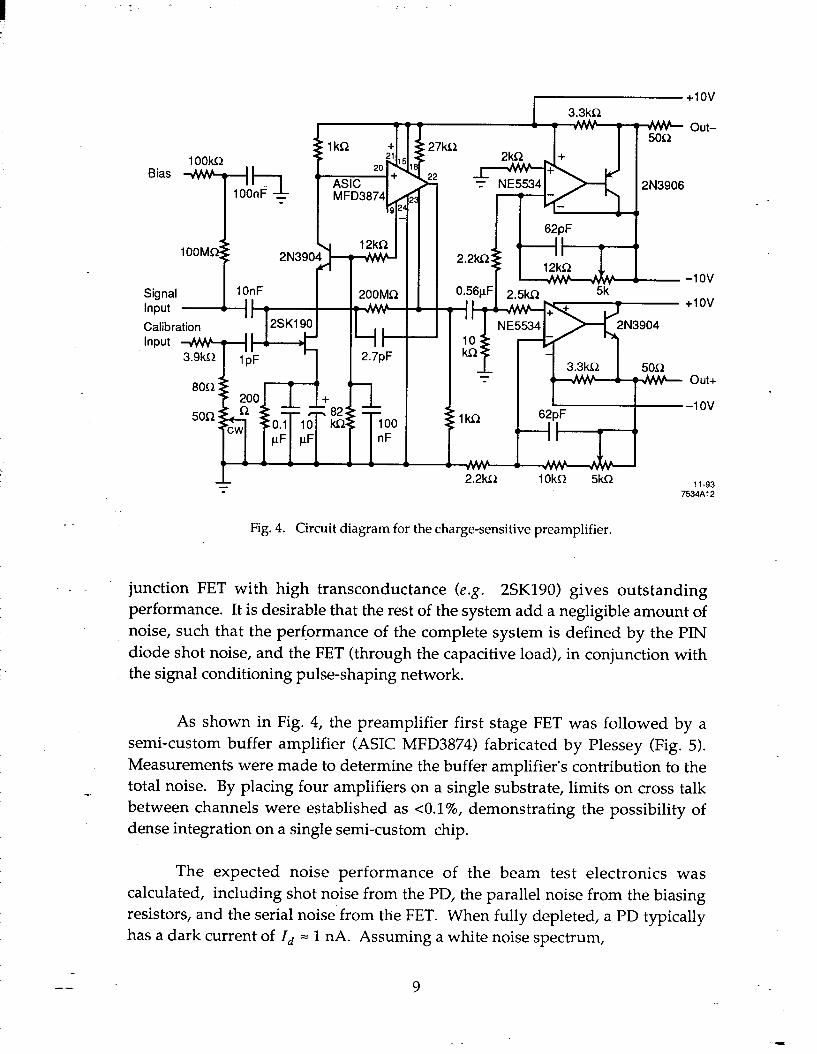
Fig. 4. Circuit diagram for the charge-sensitive preamplifier.
. junction FET with high transconductance (e.g. 2X190) gives outstanding performance. It is desirable that the rest of the system add a negligible amount of noise, such that the performance of the complete system is defined by the PIN
diode shot noise, and the FET (through the capacitive load), in conjunction with the signal conditioning pulse-shaping network.
As shown in Fig. 4, the preamplifier first stage FET was followed by a
semi-custom buffer amplifier (ASIC MFD3874) fabricated by Plessey (Fig. 5).
Measurements were made to determine the buffer amplifier’s contribution to the total noise. By placing four amplifiers on a single substrate, limits on cross talk between channels were established as <O.l%, demonstrating the possibility of dense integration on a single semi-custom chip.
The expected noise performance of the beam test electronics was
calculated, including shot noise from the PD, the parallel noise from the biasing resistors, and the serial noise from the FET. When fully depleted, a PD typically has a dark current of I, = 1 nA. Assuming a white noise spectrum,
9
I :. -
11-93 7534A16
-
56R Summing
4 t-b&u~ 15OpF 15pF
Fig. 6. CLEO II-style differential receiver and shaper amplifier.
be 410 e-k. With more elaborate pulse shaping producing a sharper cutoff for the high frequency components, this result can be improved. Using a Canberra
Spectroscopy Amplifier Model 2021, which provides two stages of integration with complex poles, under the same conditions, with r = 4 p s, an equivalent
noise of 330 e-‘s was calculated. The performance of the FET can be improved by running at current higher than the 5 mA used (increasing g,) and with higher drain-source voltage (> 5 V), thereby reducing the gate capacitance. These changes increase the power consumption from 25 mW to several hundred mW, which may be unacceptable in some applications. For g, = 80 mS and Cg + Cd =
90 pF, the noise reduces to 200 e-k. For low capacitive loads, a FET with lower
input capacitance and correspondingly lower transconductance may give overall
better results.
.
Measurements with the prototype charge amplifier were performed using cosmic ray signals from a 6.4 x 6.4 cm 2,12 rl long CsI(T1) crystal. For these tests,
the crystal was positioned on its side and, depending on their angle of incidence, the cosmic rays traversed about 6.4 cm of the crystal. The signals of four PD’s viewing the WLS were routed to the prototype preamplifier located behind the
crystal, then to the Canberra shaping amplifier and an ADC.
The average signal for a cosmic ray muon traversing the crystal was 6.3
fC/PD. Assuming 36 MeV deposited in the crystal, this results in 1100 e-‘s/MeV. The noise measured for the bare amplifier was 450 e-Is. With the I’D connected, the noise increased to 800 em’s, or an energy equivalent of 0.73 MeV.
Summing the signals of four I’D’s, a charge of 25 fC and noise equal to 1700 e-k or 0.38 MeV equivalent energy were measured.
-- 11

-.
The measured noise for the bare amplifier (450 em’s) is higher than would be estimated from the previous analysis, where parallel noise from the PD biasing resistors on the preamplifier (140 e-Is> and serial noise from the FET (230 em’s, with Ci = 0 in the absence of the I’D) add in quadrature to 270 e-Is. This indicates that the buffer amplifier contributes to the noise and that there may be some electronic pick-up. A systematic investigation [7] showed that under conditions where pick-up was excluded, the theoretical noise for the FET alone could be achieved by a reduction in the standing currents in the buffer amplifier. Alternately, by replacing the Wilson current source used in the present design by a simpler structure or by a junction FET, a reduction in shot noise should be
achievable at the larger standing currents, which may be needed to reach the required slew rates.
However, the increase (to 800 e-Is> after connecting the PD cannot be explained by added shot noise and capacitive load from the PD. The prediction for PD plus FET noise is 470 e-Is. Cabling to the PD acts as an antenna, and was
observed to pick up signals generated in the lab. In the beam test, the average noise/PD was even higher (0.5-1.5 MeV) owing to poorer shielding, noise pickup, and higher leakage current caused by non-uniform cooling of the PD’s and electronics within the dry-box. Integration of the FET preamplification stage with the PD may be a future option to reduce Ci and the potential for this pick-
UP*
3. Test Results
Results are presented for three crystal towers, each having a different geometrical configuration. As indicated in Fig. 1, Tower A refers to a contained 6.4 x 6.4 cm2 crystal tower, Tower B refers to a contained 8 x 8 cm2 crystal tower segmented into a 2 x 2 square array of four-4 x 4 cm2,4 rl crystals in front and an 8 x 8 cm2 12 rl crystal in back, and Tower C refers to an uncontained 8 x 8 cm2 crystal tower. A contained tower is one that is surrounded on all sides by other
towers, so that energy shared with adjoining towers can be taken into account in determining resolutions. To determine the energy resolution and test linearity,
we evaluated data taken at three beam energies for each of the three tower configurations (120,250, and 400 MeV for Towers A and B, and 120,200, and 400 MeV for Tower C). Position resolution was studied for Towers B and C at four beam energies (120,200,250, and 300 MeV).
12

3.1 Calibrations
After electronic calibrations have been applied, single monolithic crystal
towers, such as are used in the CLEO-II and Crystal Barrel detectors, require a single overall gain constant to relate light output to energy. In contrast, the longitudinal segmentation of crystals within a tower introduces an additional calibration constant for each tower, so the beam test data for each tower were calibrated in two steps. First each PD signal on each crystal in a tower was adjusted, then a weighting constant relating the signals from the front and back crystals in a tower was determined. The calibration was performed at the highest beam energy for which data were available (I 400 MeV).
As the first step, the gain constant of each PD signal was adjusted so that all I’D’s viewing a single crystal (either front or rear) read the same average signal at the beam calibration energy. Since the beam contains e-‘s, x’-‘s, and p”-‘s, this calibration can be done using either the distinct peaks of minimum- ionizing-particles or the averages of the showering-particle spectra.
The second step in the calibration involved the relative weighting of signals from I’D’s associated with the front and back crystals in the tower. At
this stage, the following selection criteria, also used for energy and position resolution studies, were applied. A time-of-flight cut was made to select em’s, and minimum energy cuts were made to reject minimum ionizing particles.
. Additionally, to guarantee a single well-defined trajectory, using the beam- defining drift chamber, track quality cuts were made, requiring at least two hits
in one dimension and at least three hits in the other dimension. A fiducial cut limiting the beam profile to 3 x 3 cm2 was then imposed.
After applying the above criteria, to find the front-to-back (F/B) weighting constant, signals from all PD’s on each crystal in a tower were summed and the average taken. As an example, the average energy spectra measured by the PD’s in the back and front crystals for Tower A are shown in Figs. 7a and 7c [8], respectively [9]. The average signals from the front and back crystals in the tower were scaled separately such that on average, the sum of the front and back
signals for an event is equal to the beam energy. This is illustrated in Fig. 7b [8], where the line through the x and y intercepts at the beam energy is not a fit but only to guide the eye. Finally, the spectra peak for the sum of energy in the front and back crystals in the tower was adjusted to the beam energy.
13
0.05 iii YiJ 9
g 0.04 .- 3
:
cz 0.03
0.8 1.0 1.2 Front-to-Back Weighting Ratio
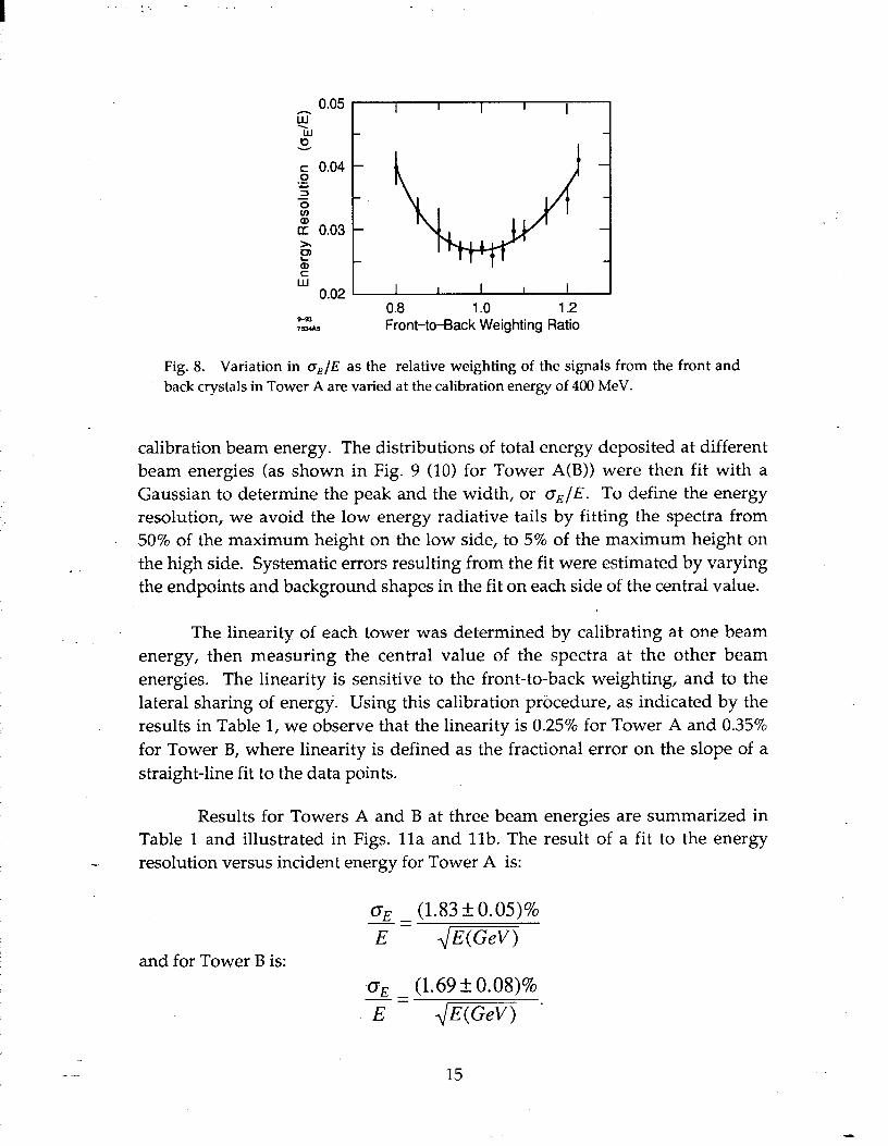
Fig. 8. Variation in a,/E as the relative weighting of the signals from the front and
back crystals in Tower A are varied at the calibration energy of 400 MeV.
calibration beam energy. The distributions of total energy deposited at different beam energies (as shown in Fig. 9 (10) for Tower A(B)) were then fit with a Gaussian to determine the peak and the width, or cr,/E. To define the energy resolution, we avoid the low energy radiative tails by fitting the spectra from
. -
50% of the maximum height on the low side, to 5% of the maximum height on
the high side. Systematic errors resulting from the fit were estimated by varying the endpoi-nts and background shapes in the fit on each side of the central value.
. The linearity of each tower was determined by calibrating at one beam
energy, then measuring the central value of the spectra at the other beam
energies. The linearity is sensitive to the front-to-back weighting, and to the
lateral sharing of energy. Using this calibration procedure, as indicated by the results in Table 1, we observe that the linearity is 0.25% for Tower A and 0.35%
for Tower B, where linearity is defined as the fractional error on the slope of a
straight-line fit to the data points.
Results for Towers A and B at three beam energies are summarized in Table 1 and illustrated in Figs. lla and lib. The result of a fit to the energy resolution versus incident energy for Tower A is:
0, _ (1.83 k 0.05)% -- E
and for Tower B is:
OE _ (1.69k O.OS)%
-- $@aq E
15

I
100 I’ 1’1’ 1’1’1
80
60
40
20
0
125
100
25
l-l
60 80 100 120 140 160
I I I I I I 1
200 250 300
I I I I I I I
30 I- -l
300 350 400 450 500
9-93 Energy (MeV) 7534A21
Fig. 9. Spectra of total energy, including energy shared with adjoining towers, for beam
incident into center of Tower A at a) 120, b) 250, and c) 400 MeV. Data are fit to Monte
Carlo (histogram) described in Sec. 3.3.
-- 16
60
40
20
0 60 80 100 120 140 160
I I I I I
lb) 60
200 250 300
40 1 I I I J
I I I
30
20
10
0 300 350 400 450 500
11-93 Energy (MeV) 7534A20
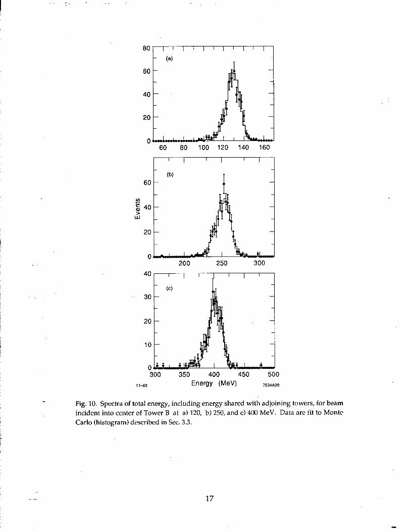
Fig. 10. Spectra of total energy, including energy shared with adjoining towers, for beam
incident into center of Tower B at a) 120, b) 250, and c) 400 MeV. Data are fit to Monte
Carlo (histogram) described in Sec. 3.3.
17
-_
--
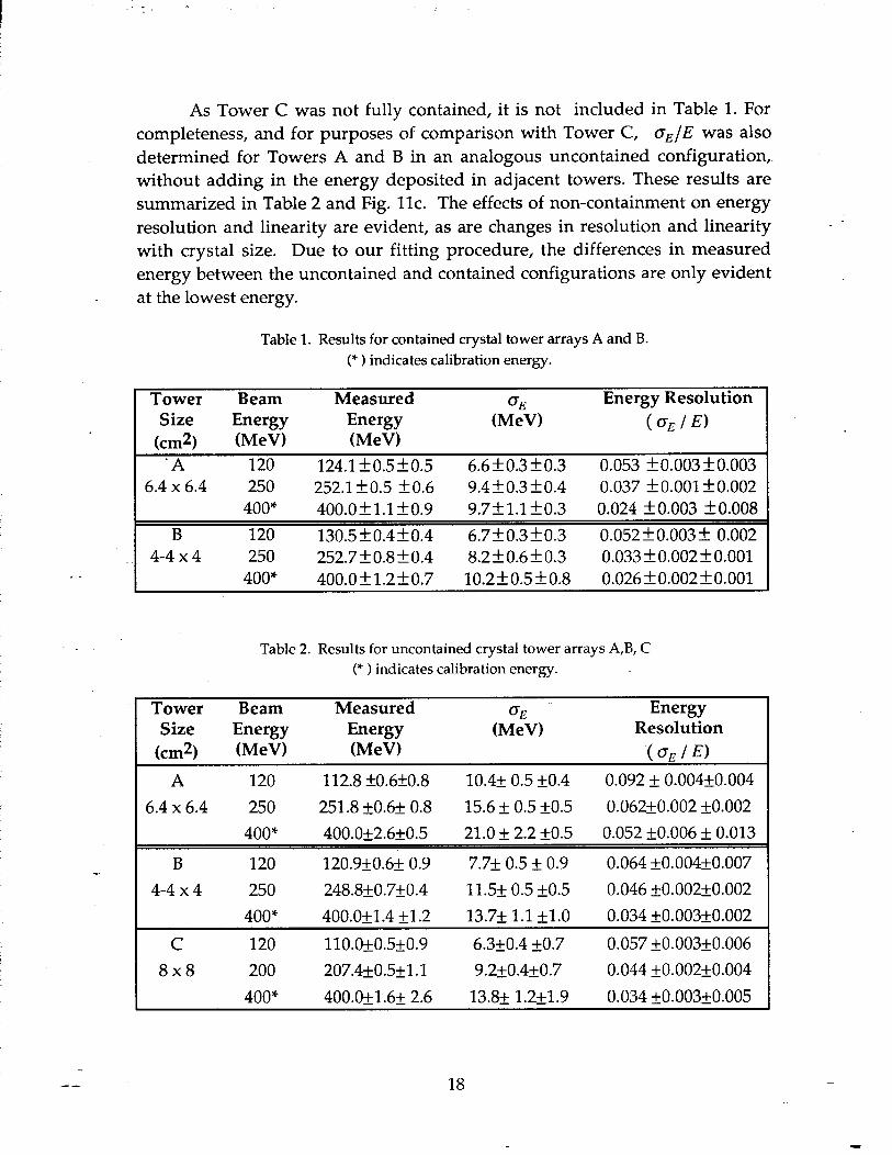
As Tower C was not fully contained, it is not included in Table 1. For completeness, and for purposes of comparison with Tower C, oE/E was also
determined for Towers A and B in an analogous uncontained configuration,. without adding in the energy deposited in adjacent towers. These results are summarized in Table 2 and Fig. llc. The effects of non-containment on energy
resolution and linearity are evident, as are changes in resolution and linearity with crystal size. Due to our fitting procedure, the differences in measured
energy between the uncontained and contained configurations are only evident at the lowest energy.
Table 1. Results for contained crystal tower arrays A and B.
(* ) indicates calibration energy.
Tower Beam Measured Energy Resolution Size Energy Energy (o,lE)
(cm2) (MeW (MeV)
‘A 120 124.1 kO.5kO.5 6.6f0.3k0.3 0.053 ~0.003z!z0.003 6.4 x 6.4 250 252.1kO.5 f0.6 9.4kO.3IkO.4 0.037 fO.OO1 kO.002
400* 400.0f1.1f0.9 9.7fl.lk0.3 0.024 kO.003 kO.008
B 120 130.5f0.4k0.4 6.7f0.3k0.3 0.052_+0.003+ 0.002 4-4 x4 250 252.7+0.8kO.4 8.2kO.6kO.3 0.033~0.002+0.001
400* 400.0k1.2f0.7 10.2f0.5rt0.8 0.0261!10.002+0.001
Table 2. Results for uncontained crystal tower arrays A,B, C
(* ) indicates calibration energy.
Tower Beam Measured Energy Size Energy Energy (MO%) Resolution
km2) (MeV) (MeW (a,@)
A 120 112.8 f0.6f0.8 10.4k 0.5 +0.4 0.092+ 0.004+0.004
6.4 x6.4 250 251.8+0.6f 0.8 15.6 k 0.5 ~10.5 0.062~0.002f0.002
400* 4OO.Ok2.6kO.5 21.0 f 2.2kO.5 0.052+0.006 f 0.013
B 120 120.9+0.6& 0.9 7.7* 0.5 + 0.9 0.064+0.004f0.007
4-4 x4 250 248.8f0.7k0.4 11.5f 0.5 f0.5 0.046 f0.002f0.002
400* 400.0+1.4 k1.2 13.7+ 1.1 +l.O 0.034f0.003f0.002
C 120 110.0+0.5~0.9 6.3f0.4 +0.7 0.057f0.003+0.006
8x8 200 207.4+0.5fl.l 9.2+0.4+0.7 0.044f0.002+0.004
400* 400.0+1.6+ 2.6 13.8+ 1.2k1.9 0.034f0.003f0.005
18

0.06 I I I I I I I I I
0.02
0 I I I I I I I I I
‘27
-ii’ L
6 0.04
‘Y= 3 5 % lx 0.02 6 b 5
0 I I I I I I I I I
(4 a,lE
0.16 -
A
0.08 -
0 II,1 I I I I I 0 0.1 0.2 0.3 0.4 0.5
9-93 Energy (GeV) 7534A8
Fig. 11. a) Energy resolution for contained Towers A at 120,250, and 400 MeV. b) Energy resolution for contained Tower B at 120, 250, and 400 MeV. c) Energy resolution for
uncontained Tower C at 120, 200, and 400 MeV. For purposes of comparison only,
uncontained resolution for Towers A and B is also shown.
19
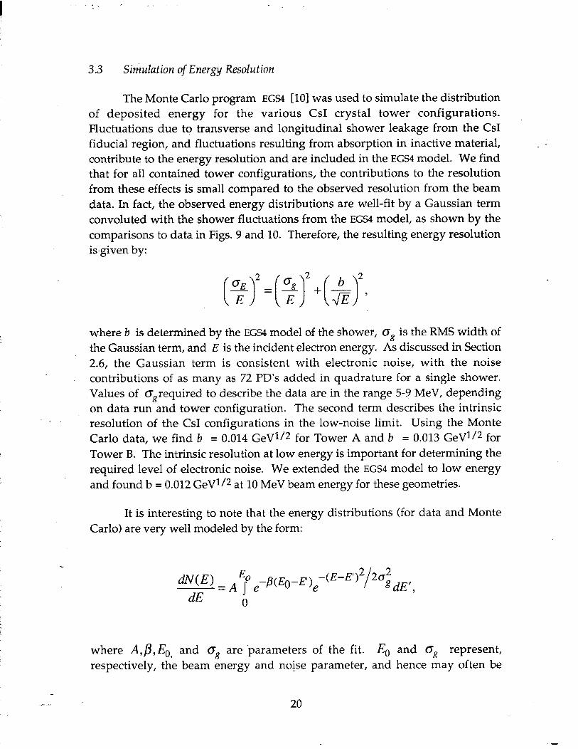
3.3 Simulation of Energy Resolution
The Monte Carlo program EGS~ [lo] was used to simulate the distribution of deposited energy for the various CsI crystal tower configurations. Fluctuations due to transverse and longitudinal shower leakage from the CsI fiducial region, and fluctuations resulting from absorption in inactive material, contribute to the energy resolution and are included in the EGS4 model. We find that for all contained tower configurations, the contributions to the resolution from these effects is small compared to the observed resolution from the beam
data. In fact, the observed energy distributions are well-fit by a Gaussian term convoluted with the shower fluctuations from the EGS~ model, as shown by the comparisons to data in Figs. 9 and 10. Therefore, the resulting energy resolution is given by:
_ J
p) =($+(-g,
.
where b is determined by the EGS~ model of the shower, og is the RMS width of
the Gaussian term, and E is the incident electron energy. As discussed in Section
2.6, the Gaussian term is consistent with electronic noise, with the noise contributions of as many as 72 I’D’s added in quadrature for a single shower. Values of ogrequired to describe the data are in the range 5-9 MeV, depending on data run and tower configuration. The second term describes the intrinsic
resolution of the CsI configurations in the low-noise limit. Using the Monte Carlo data, we find b = 0.014 GeV1/2 for Tower A and b = 0.013 GeV1i2 for
Tower B. The intrinsic resolution at low energy is important for determining the required level of electronic noise. We extended the EGS4 model to low energy
and found b = 0.012 GeV1/2 at 10 MeV beam energy for these geometries.
It is interesting to note that the energy distributions (for data and Monte
Carlo) are very well modeled by the form:
~(Eo-E”),(~-~)~/~~~~~, ,
where A,P,Eo, and CT, are ‘parameters of the fit. E. and og represent,
respectively, the beam energy and noise parameter, and hence may often be
20
known independently, leaving a two-parameter fit. The first term in the above equation represents energy loss by absorption or bremsstrahlung, while in our case, the second term is dominated by the electronic noise. By integration of the equation, one sees that p is related to the resolution parameter b by l/b = p&.
4. Position Resolution
Above -100 MeV, for crystals with transverse dimensions comparable to their Moliere radius (-3.8 cm for CsI(Tl)), one can take advantage of the spreading of showers into neighboring crystals to accurately measure position. At very low incident energies, single Compton scattering and pair production dominate, reducing shower sharing significantly. At modest energies, a position calculation using a simple center-of-gravity (CG) method consists in taking the energy-weighted average of the central and neighboring crystals’ positions using the formula:
where xi is the center of crystal i, and Ei is the energy deposited in crystal i. For showers contained largely within the central crystal tower, this expression is
. dominated by the position of the central tower, and varies little with incident beam position until the edges of the crystal are approached, where shower sharing starts to take place. This is illustrated in Fig. 12, where the variation in the center-of-gravity (CG) position with the true beam position measured by the beam-defining drift chamber is shown. The steep slopes near the crystal edges
indicate good spatial sensitivity, while the flatter slope in the middle of the crystal reflects the lack of energy sharing.
This basic CG method can be augmented to obtain improved position
resolution. We calculated, for each measured CG bin, the average of the true beam positions (from the drift chamber) that contribute to the bin. This average
beam position was then defined to be the “corrected” CG value for the measured
CG value. This technique gives an improved position estimate, as shown in Fig. 13, and is based on a mathematically equivalent technique used by CLEO 161.
The position resolution is defined as the difference between the true incident
position measured by the drift chamber and the position reconstructed from the
21

I :. -
crystal CG with these average corrections applied. The position resolutions we quote were obtained by fitting these residuals to a Gaussian function.
Crystal Edge
Crystal Edge
-60 -40 -20 0 20
II-93 Track Position from Drift Chamber (mm) 7534Ag
Fig. 12. Average center-of-gravity position as a function of true track position.
I I I I I
-10
-20
-30
-40 -30 -20 -10 0 11-93 7534A19 Track Position from Drift Chamber (mm)
Fig. 13. Average corrected center of gravity as a function of track position.
Position resolution was determined for Towers B and C only. Insufficient
data were accumulated to evaluate the resolution over the full face of Tower A. Resolutions were determined using em’s, with the same time-of-flight and energy
-- 22
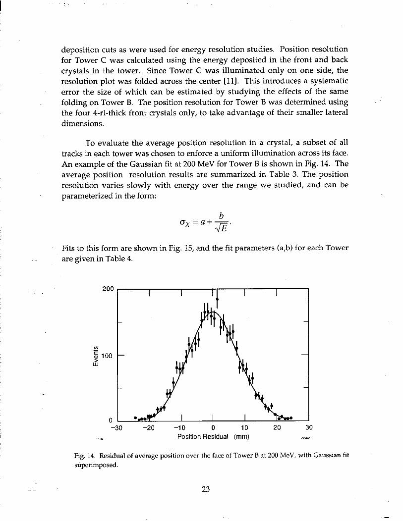
I :.
deposition cuts as were used for energy resolution studies. Position resolution for Tower C was calculated using the energy deposited in the front and back
crystals in the tower. Since Tower C was illuminated only on one side, the
resolution plot was folded across the center [ll]. This introduces a systematic error the size of which can be estimated by studying the effects of the same folding on Tower B. The position resolution for Tower B was determined using the four 4-rl-thick front crystals only, to take advantage of their smaller lateral dimensions.
To evaluate the average position resolution in a crystal, a subset of all
tracks in each tower was chosen to enforce a uniform illumination across its face. An example of the Gaussian fit at 200 MeV for Tower B is shown in Fig. 14. The average position resolution results are summarized in Table 3. The position resolution varies slowly with energy over the range we studied, and can be parameterized in the form:
Fits to this form are shown in Fig. 15, and the fit parameters (a,b) for each Tower are given in Table 4.
200
v) E a 100 3
-30 -20 -10 0 10 20 30
11-W Position Residual (mm) ISLUA~ 1
Fig. 14. Residual of average position over the face of Tower B at 200 MeV, with Gaussian fit
superimposed.
23
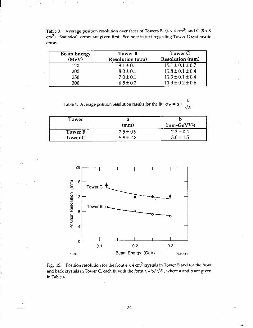
Table 3. Average position resolution over faces of Towers B (4 x 4 cm2) and C (8 x 8
cm2). Statistical errors are given first. See note in text regarding Tower C systematic
errors.
Beam Energy Tower B (MeV) Resolution (mm) 120 9.lf 0.1 200 8.0 k 0.1 250 7.0 zk 0.1 300 6.5 f 0.2
Tower C Resolution (mm) 15.lf 0.1 f 0.7 11.8f 0.1 f 0.4 11.9 * 0.1 f 0.4 11.9 f 0.2+ 0.6
Table 4. Average position resolution results for the fit: 0, = a + - A*
Tower
Tower B Tower C
a (mm) 2.5f 0.9 5.8 f 2.8
b (mm-GeV1’2) 2.3 I!Z 0.4 3.0 k1.5
20 I I I I
Tower C t .-
-+ ITowerB C-I-- o
I I I
0.1 0.2 0.3
1 Beam Energy (GeV) 7534A14
Fig. 15. Position resolution for the front 4 x 4 cm2 crystals in Tower B and for the front
and back crystals in Tower C, each fit with the form a + b/ 16, where a and b are given
in Table 4.
24

5. Conclusions
We have presented results on energy resolution and linearity, and position resolution, for specific crystal tower configurations in an array of longitudinally- segmented CsI(T1) crystals, where each crystal is readout with a wavelength shifter and from two to four photodiodes. These measurements demonstrate that linearity and energy resolution are preserved in the presence of a longitudinal division near shower maximum, and additional transverse division of the front section, of the crystals. Crystal segmentation can be easily achieved with PD/ WLS readout techniques. The segmentation of crystals within the towers can provide additional information on particle identification, range, and direction. This additional information may be necessary for background rejection in high luminosity e+e- and hadron colliders.
When energy shared with adjoining towers is taken into account, the energy resolution achieved appears independent of the type of tower configuration. We find an energy resolution consistent with (1.83 +
0.05)%/ dm for Tower A and (1.69 f O.OB>%/ dm for Tower B. The EGS4-based simulation indicates that the energy resolution measured in our data is well-described by an intrinsic shower fluctuation term (b/G) added in quadrature with a Gaussian term consistent with electronic noise (og/E). We find b = 0.013 GeV1/2 and b = 0.014 GeV1/2 for Towers A and B, respectively. The position resolution improves with finer crystal segmentation and can be parameterized as a + b/ fi , where (a,b) = (2.5 _+ 0.9 mm, 2.3 + 0.4 mm-GeVl/2) for Tower B and (a,b) = (5.8 + 2.8 mm, 3.0 + 1.5 mm-GeV1/2) for Tower C.
Acknowledgments
For their gracious assistance during the beam test of our CsI crystal array at TRIUMF, we thank the TRIUMF physicists and staff, particularly D. Ottewell and D. Diel. One of us (A.D.F.) would like to thank the University of Illinois Campus Honors Program for support.
-- 25
I :.
References
1. See for example, R. H. Schindler, Proceedings of the Tuu-Charm Factory Workshop, SLAC, Ed. L. Beers, SLAC REPORT-343 (1989) 127.
2. D. Stoker, Proceedings of the Tuu-Charm Factory Workshop, Universidad de Sevilla, Andalucia, Spain (May 1991).
3. R. Schindler, in Proceedings of the Tuu-Charm Factory Workshop, Universidad de Sevilla, Andalucia, Spain (May 1991).
4. TRIUMF Users Handbook, IV-11 to IV-15, (1987). 5. Crystal Barrel Collaboration (E. Aker, et al.), NIM A 321,69 (1992). 6. E. Blucher, et al, Test of Cesium Iodide Crystals for an Electromagnetic
Calorimeter. NIM A 249,201 (1986).
7. D. R. Freytag and G. M. Haller, SLAC-PUB-6351 (September 1993) (to be submitted to Nuclear Znstruments t3 Methods).
8. The minimum ionizing signal seen in Figs. 7b-7c is removed by the selection
criteria described previously in this section. It is plotted here only to allow comparison of the minimum ionizing and showering particle signals.
9. Tower A was calibrated using data taken at 400 MeV. Data taken at 250 MeV is shown in Fig. 7 because the relative abundances of minimum ionizing and showering particles available at this energy better illustrates the particle separation attainable with longitudinally-segmented crystals.
10.W.R. Nelson, H. Hirayama, and W.O. Rogers, SLAC-Report-265 (1985). 11. Only half of Tower C was illuminated. Therefore, to evaluate the position
resolution of Tower C, Tower B (which adjoins Tower C) was taken to be the
center and, in addition to Tower C, the crystal tower on the opposite side of Tower B was also used. This technique assumes that the position resolution is symmetrical, so a systematic error is introduced to take into account the fact that the resolution may not be centered.
--
26