pdis – print data insertion system - George Mason University
70
GEORGE MASON UNIVERSITY PDIS – PRINT DATA INSERTION SYSTEM Final Report Many of the items received in mail, from telephone bills to bank statements, are generated by high-speed production printers. Companies which build these printers are not only concerned with the printing speed, but also with the printing quality. A control unit inside each production printer directly controls the printing quality by the print algorithm it uses. Normally, in order to test a new printing algorithm to determine whether or not it has any positive effect on the print quality, a new control unit has to be built for that specific algorithm. Developing a new control unit is expensive, costing a company large amounts of time and resources. PDIS (Print Data Insertion System) is a tool which eliminates the need to develop a new control unit for every algorithm a company wants to test for print quality. PDIS can easily be re-used for multiple algorithms. The system inserts print data which has been altered by PC software utilizing the new algorithm directly into a production printer. The printer uses the data it receives to print pages which reflect the new algorithm. The printed pages can then be examined to determine whether or not the new algorithm offers a significant improvement to print quality. Faculty Supervisor: Jens-Peter Kaps Jenny Higgins Pinal Patel Paul Anderson
-
Upload
khangminh22 -
Category
Documents
-
view
1 -
download
0
Transcript of pdis – print data insertion system - George Mason University
GEORGE MASON UNIVERSITY
PDIS – PRINT DATA INSERTION SYSTEM
Final Report
Many of the items received in mail, from telephone bills to bank statements, are generated by
high-speed production printers. Companies which build these printers are not only concerned
with the printing speed, but also with the printing quality. A control unit inside each production
printer directly controls the printing quality by the print algorithm it uses. Normally, in order to
test a new printing algorithm to determine whether or not it has any positive effect on the print
quality, a new control unit has to be built for that specific algorithm. Developing a new control
unit is expensive, costing a company large amounts of time and resources.
PDIS (Print Data Insertion System) is a tool which eliminates the need to develop a new control
unit for every algorithm a company wants to test for print quality. PDIS can easily be re-used for
multiple algorithms. The system inserts print data which has been altered by PC software utilizing
the new algorithm directly into a production printer. The printer uses the data it receives to print
pages which reflect the new algorithm. The printed pages can then be examined to determine
whether or not the new algorithm offers a significant improvement to print quality.
Faculty Supervisor: Jens-Peter Kaps Jenny Higgins
Pinal Patel Paul Anderson
1 | P a g e
Table of Contents 1. Approach
1.1 Overview 1.2 Specifications 1.3 USB vs. Serial 1.4 DLL vs. VCP Driver 1.5 Visual C++.NET vs. Standard C++ 1.6 Contributions
2. Technical Section 2.1 PDIS Xfer a. Versions 1.0 and 2.0 b. Visual Studio C++.NET c. FTD2XX.DLL d. PDIS Xfer Operation e. Limitations 2.2 DLP-TXRX-G USB Adapter (USB Converter) a. Output Pins b. Voltage Select Jumper c. Atmel 93C46 EEPROM d. RS-232 Output Scheme e. Location on PDIS 2.3 Verilog HDL Design Overview a. Micro-UART b. prepareData c. mig_control_v2 d. MIG e. laserData 2.4 Printer Emulator
3. Experimentation and Validation 3.1 PDIS Xfer 3.2 PDIS Xfer and DLP-TXRX-G USB Adapter 3.3 Verilog HDL Modules 3.4 Printer Emulator
4. Benefit 5. Potential Uses 6. Costs 7. Alternatives 8. Maintainability 9. Replacement 10. Administrative 11. Lessons Learned 12. References Appendix A - Proposal Appendix B – Design Document
226899
101010111112141415161617171819222629293133333535383940404142424244454758
2 | P a g e
1. Approach
1.1 Overview
High-speed production printers are vital to businesses such as cell phone companies,
electric companies, credit card companies, and banks. Each of these businesses has something in
common: they all need a way to print out mass amounts of paper on demand quickly. Production
printers are able to meet that need.
However, speed is not the only thing important to these companies. The quality of the
printing is also an important factor. As a result, engineers who work on developing the
technology behind the production printers are concerned not only with maximizing the printing
speed, but also with maximizing the quality of the printing. The printing quality is directly
affected by the algorithms used to process a page of data. Unfortunately, these algorithms are
hard coded within the control unit of the printer, making it extremely costly and time consuming
to test out new algorithms because in order to do so, a new control unit must be made. As a
result, there is a need for a device which can bypass the control unit of an existing printer and
insert data directly into the pulse width modulators (PWMs) which control the lasers of the
printer. Instead of using the algorithm hard coded within the control unit of the production
printer, a changeable algorithm on a personal computer would be used to process the page of
data. The device would need to be capable of sending up to 185 MB of data and meeting the
rigorous high-speed requirements of a production printer.
1.2 Specifications
3 | P a g e
The sponsor of this project, InfoPrint Soultions Company, specifically requested this
device to be developed for one of their high-speed production printers: the InfoPrint 4100. This
printer contains five printing lasers which expect nine bits of data each. Each laser has an
associated clock and active low enable. Whenever the enable is low and a rising edge of the
clock occurs, nine bits of valid data need to be available for that laser. The laser clocks each run
at approximately 50 MHz. However, the five different clocks and enables are not synced, and
are offset by a considerable amount. This fact had to be carefully considered in our design.
Since the five clocks run at 50 MHz and each expect 9 bits of data available for each
clock cycle, data must be able to be sent by the device at a speed of at least 2.25 Gb/s. None of
the considered connections available from a personal computer were fast enough to meet this
requirement. However, if the page of data were able to be stored on an external device’s DDR2
memory, then sent to the printer through high-speed IO, the speed requirement could be met.
As a result, InfoPrint Solutions Company provided us with a ML505 Evaluation Board.
This board, available from Xilinx, contains a top of the line Virtex 5 FPGA. The board also
comes with 256 MB of DDR2 SO-DIMM memory and has numerous IO pins. The idea behind
PDIS (Print Data Insertion System), is to process a page of data using an algorithm on the
computer, send the processed data to the ML505 evaluation board, store the data in DDR2
memory, then read the data from DDR2 memory at high speeds in response to the control signals
provided by the production printer. The company specified that modules designed for the FPGA
should be written in Verilog HDL.
InfoPrint Solutions Company is located in Boulder, CO. As a result, it was not possible
to test the design on an actual production printer. As a solution to this problem, a printer
4 | P a g e
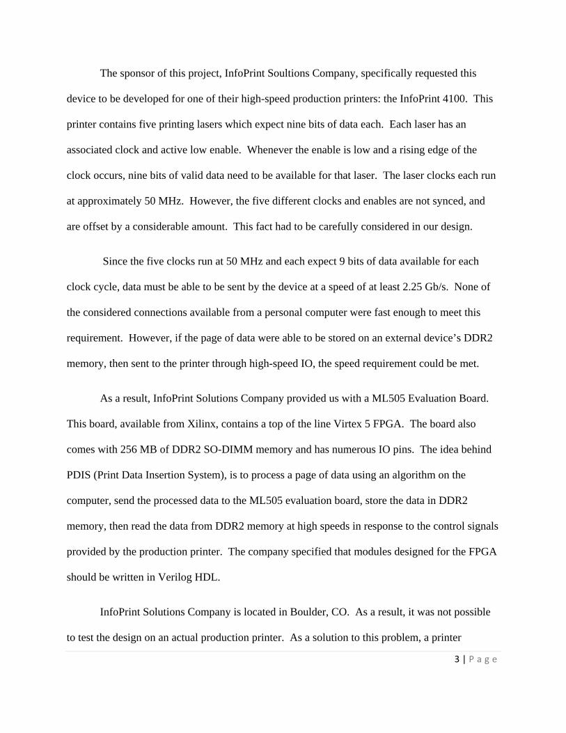
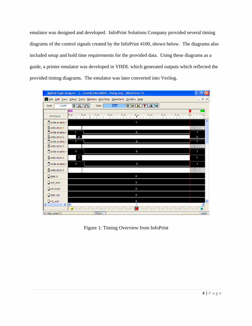
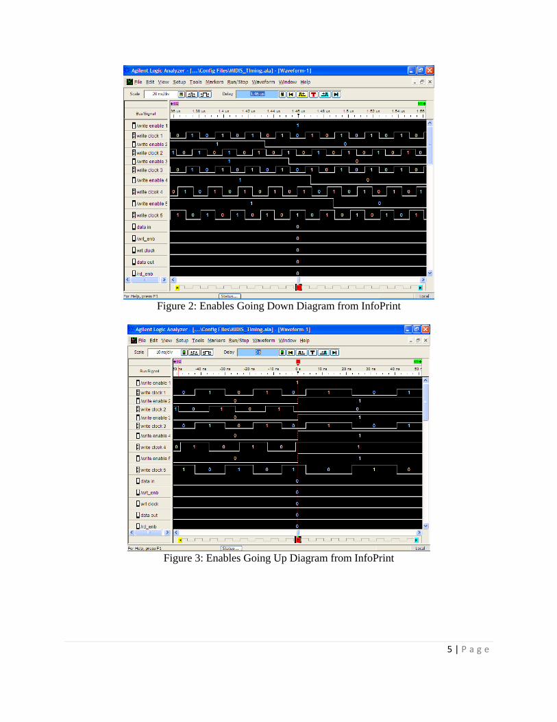
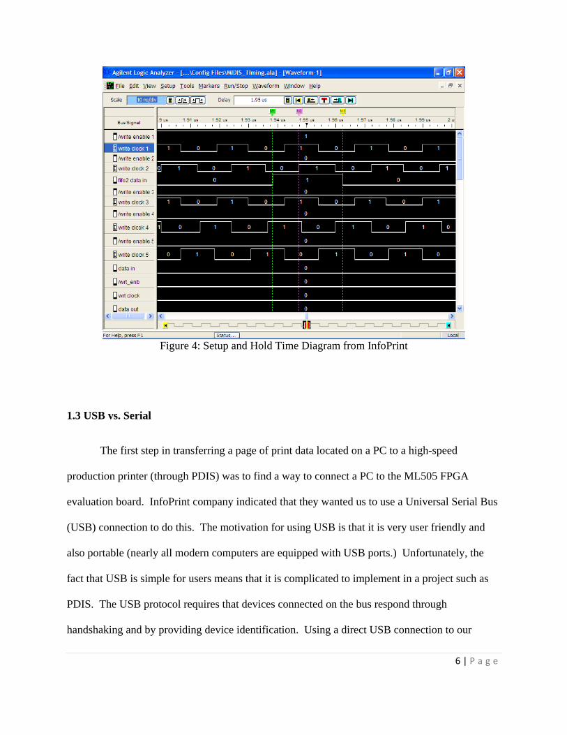
emulator was designed and developed. InfoPrint Solutions Company provided several timing
diagrams of the control signals created by the InfoPrint 4100, shown below. The diagrams also
included setup and hold time requirements for the provided data. Using these diagrams as a
guide, a printer emulator was developed in VHDL which generated outputs which reflected the
provided timing diagrams. The emulator was later converted into Verilog.
Figure 1: Timing Overview from InfoPrint
5 | P a g e
Figure 2: Enables Going Down Diagram from InfoPrint
Figure 3: Enables Going Up Diagram from InfoPrint
6 | P a g e
Figure 4: Setup and Hold Time Diagram from InfoPrint
1.3 USB vs. Serial
The first step in transferring a page of print data located on a PC to a high-speed
production printer (through PDIS) was to find a way to connect a PC to the ML505 FPGA
evaluation board. InfoPrint company indicated that they wanted us to use a Universal Serial Bus
(USB) connection to do this. The motivation for using USB is that it is very user friendly and
also portable (nearly all modern computers are equipped with USB ports.) Unfortunately, the
fact that USB is simple for users means that it is complicated to implement in a project such as
PDIS. The USB protocol requires that devices connected on the bus respond through
handshaking and by providing device identification. Using a direct USB connection to our

7 | P a g e
FPGA would mean that the receiver unit on our FPGA would have to follow the USB protocol,
making it very complicated. Our other option was to use another common data transmission
scheme—serial RS-232. Serial RS-232 is much easier to implement in an FPGA receiver than
USB. A free, complete, open core RS-232 receiver (this type of receiver is called a Universal
Asynchronous Receiver/Transmitter, or UART) called Micro-UART was found online, which
would eliminate the need for us to design and implement the receiver ourselves (if we used RS-
232.) The down side to using RS-232 is that it isn’t as user friendly as USB or as portable (many
modern computers no longer have serial ports.) This led us to the decision to use both USB and
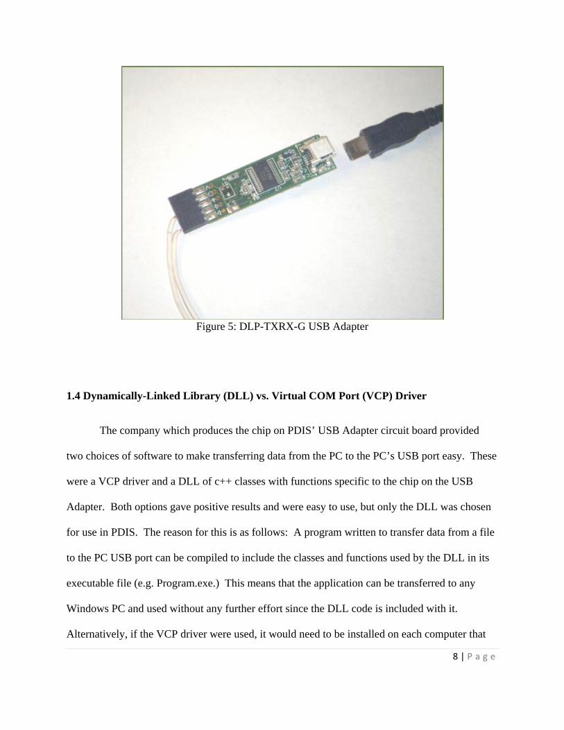
RS-232 for PDIS. To accomplish this, a circuit board (DLP-TXRX-G USB Adapter) made by
DLP Design was purchased for a small amount to convert USB signals to RS-232. This solution
gives PDIS the best of both worlds. The PC is connected to the ML505 board through the USB
Adapter with USB, which means that PDIS is portable and easy to connect to any PC. The serial
output of the USB Adapter is connected to the FPGA evaluation board, allowing us to use the
simple, free UART design found online. The USB Adapter also came packaged with software
(see DLL vs. VCP Driver section) which made transferring data from the PC via a c++ program
to the USB port simple.
8 | P a g e
Figure 5: DLP-TXRX-G USB Adapter
1.4 Dynamically-Linked Library (DLL) vs. Virtual COM Port (VCP) Driver
The company which produces the chip on PDIS’ USB Adapter circuit board provided
two choices of software to make transferring data from the PC to the PC’s USB port easy. These
were a VCP driver and a DLL of c++ classes with functions specific to the chip on the USB
Adapter. Both options gave positive results and were easy to use, but only the DLL was chosen
for use in PDIS. The reason for this is as follows: A program written to transfer data from a file
to the PC USB port can be compiled to include the classes and functions used by the DLL in its
executable file (e.g. Program.exe.) This means that the application can be transferred to any
Windows PC and used without any further effort since the DLL code is included with it.
Alternatively, if the VCP driver were used, it would need to be installed on each computer that
9 | P a g e
the program runs on, adding an extra step to the use of PDIS. In addition, the VCP driver may
need to be continuously installed and uninstalled on certain computers if the VCP driver
interferes with other USB/Serial applications running on that computer. The third option of
using both VCP driver and DLL is not possible: they are not compatible.
1.5 Visual C++.NET vs. Standard c++
A c++ program was written to transfer a data file located on a PC hard drive to the USB
port of the PC. This program is called PDIS Xfer, and makes use of the DLL supplied by the
maker of the USB Adapter used by PDIS. PDIS Xfer was written using c++ because of its
familiarity among the PDIS team and the control it provides to the user in computer memory
management (as opposed to JAVA.) The decision was made to code PDIS Xfer in Visual
C++.NET rather than standard c/c++ due to its support in creating Windows Graphical User
Interfaces (GUIs.)
1.6 Contributions
Paul Anderson was responsible for the Visual C++.NET program on the computer which sent a
file of data over the USB port. Paul also completed Verilog modules which wrote requested
characters to the ML505 Evaluation Board’s 2-line LED display.
Jenny Higgins was responsible for developing the Verilog HDL modules on the FPGA which
received the serial data, stored it in memory, read it from memory, and provided the appropriate
output to the printer in response to printer control signals. She was also the project manager.
10 | P a g e
Pinal Patel was responsible for developing the printer emulator in VHDL which provided the
appropriate control signals.
2. Technical Section
2.1 PDIS Xfer
2.1.a Versions 1.0 and 2.0
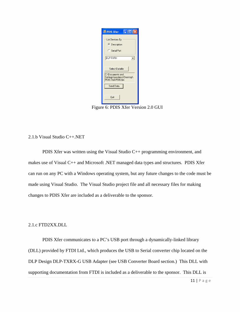
PDIS Xfer is a PC program written in Visual Studio C++.NET, which transfers a page of
print data to a PC’s Universal Serial Bus (USB). For Version 2.0, the data must be in binary
“.bin” or “.fil” (FILE) format. An early version of PDIS Xfer (Version 1.0) is capable of
transferring text “.txt” files, but is not recommended for transferring files with sizes greater than
tens of megabytes. Version 1.0 allocates a single block of memory for the data file, which may
cause Windows to crash if the file size is too large, especially on systems with little memory or
which are running several applications. Version 1.0 is mentioned here (and included as a
deliverable to our sponsor) for its potential use in quickly testing small data file transfers (there is
no need to prepare a .bin file—a sequence of 0s and 1s can simply be typed into Windows
Notepad.) PDIS Xfer Version 2.0 uses a buffered input stream reader rather than allocating a
block of memory to store and read from the data file. This effectively eliminates size restrictions
in Version 2.0 on the binary data file being transmitted.
11 | P a g e
Figure 6: PDIS Xfer Version 2.0 GUI
2.1.b Visual Studio C++.NET
PDIS Xfer was written using the Visual Studio C++ programming environment, and
makes use of Visual C++ and Microsoft .NET managed data types and structures. PDIS Xfer
can run on any PC with a Windows operating system, but any future changes to the code must be
made using Visual Studio. The Visual Studio project file and all necessary files for making
changes to PDIS Xfer are included as a deliverable to the sponsor.
2.1.c FTD2XX.DLL
PDIS Xfer communicates to a PC’s USB port through a dynamically-linked library
(DLL) provided by FTDI Ltd., which produces the USB to Serial converter chip located on the
DLP Design DLP-TXRX-G USB Adapter (see USB Converter Board section.) This DLL with
supporting documentation from FTDI is included as a deliverable to the sponsor. This DLL is
12 | P a g e
located in the same folder as the Visual Studio project file for PDIS Xfer. The DLL greatly
simplifies the effort necessary to deliver data to the PC’s USB port. With the DLL, the
complicated details of the USB protocol are abstracted from the programmer. Sending data to
the USB is done in a similar manner as sending data to a serial COM port, without the need to
open or close a port. A function provided by the DLL, FT_Write, can be used to send data in
any data type (included Microsoft managed types) to the USB port. The data is passed into the
FT_Write function as type LPVOID, meaning that any type of data can be passed in, with the
details of correctly interpreting and formatting the data type abstracted from the programmer.
For PDIS Xfer Version 2.0, the managed type __int64 was used to pass a single byte of data to
FT_Write at a time. Version 1.0 passes in data of type Byte (a derived class of type Char.)
2.1.d PDIS Xfer Operation
The user first runs the PDIS.exe application, which opens a Graphical User Interface
(GUI) window. After the GUI and its components (buttons, labels, etc.) have loaded, PDIS Xfer
scans the USB to determine if the USB converter is connected. PDIS Xfer recognizes the
converter through the DLL, which handshakes with devices on the USB and returns their device
identifications. PDIS Xfer opens a handle to the first instance of a DLP-TXRX-G USB
converter on the USB, which it recognizes by the device ID “DLP-TXRX.” If there is a DLP
USB converter on the USB, its device ID is displayed to the user in the GUI drop down list under
“List Devices By.” The user can choose to select the USB converter by device ID or USB
address (“Serial Port.”) PDIS Xfer will not transfer data if a DLP USB converter is not found on
the bus.
13 | P a g e
When the user clicks the “Select Datafile” GUI button, an instance of OpenFileDialog (a
managed VC++ class) is created, which opens a GUI window that allows the user to select a data
file from the PC’s hard drive. The files shown in the OpenFileDialog window can be filtered by
.bin file type by selecting “.bin” in the “List File Types” drop down window. Once the user has
opened a data file, the type of the file is verified to make sure that it is compatible (Version 2.0:
.bin, .fil. Version 1.0: .txt.) PDIS Xfer attempts to open the file, sending a message box with an
error warning to the user if unsuccessful. The path and file name of the data file is saved as a
String pointer and displayed in a label in the GUI. The OpenFileDialog instance passes back a
stream to the selected data file, which is used to read data from the file.
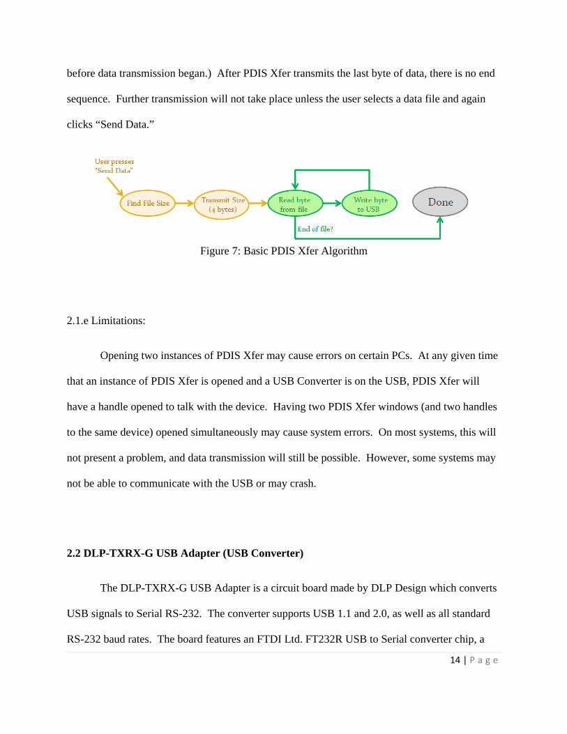
The user clicks “Send Data” to begin the process of transmission of data from the PC to
the USB converter. If the user has not selected a file at this point, a message box is displayed to
the user which indicates this error. Before data is transferred, the transfer rate (9600 baud) is
sent to the USB converter. This speed determines how fast the Serial RS-232 data sent from the
USB converter to the FPGA Evaluation Board (see ML505 FPGA Evaluation Board section.)
This step also confirms that the USB converter has not been disconnected since the handle to it
was first created (the rate set function returns an error status code if a USB converter is not
reached.) Following this, the size of the data file is determined by placing the stream file pointer
at file end and reading the pointer position (in bytes). The file size is sent to the USB converter
(and subsequently sent to the FPGA board) before data. The file size is sent as a 32-bit (4 byte)
little-endian word. Next, the Read function of the managed Stream class is used to read a byte of
data from the data file, which is then sent immediately to the USB. This process reiterates until
the end of the file is reached. PDIS Xfer knows that the end of the file has been reached by
comparing the number of bytes read/written to the total number of bytes in the file (determined
14 | P a g e
before data transmission began.) After PDIS Xfer transmits the last byte of data, there is no end
sequence. Further transmission will not take place unless the user selects a data file and again
clicks “Send Data.”
Figure 7: Basic PDIS Xfer Algorithm
2.1.e Limitations:
Opening two instances of PDIS Xfer may cause errors on certain PCs. At any given time
that an instance of PDIS Xfer is opened and a USB Converter is on the USB, PDIS Xfer will
have a handle opened to talk with the device. Having two PDIS Xfer windows (and two handles
to the same device) opened simultaneously may cause system errors. On most systems, this will
not present a problem, and data transmission will still be possible. However, some systems may
not be able to communicate with the USB or may crash.
2.2 DLP-TXRX-G USB Adapter (USB Converter)
The DLP-TXRX-G USB Adapter is a circuit board made by DLP Design which converts
USB signals to Serial RS-232. The converter supports USB 1.1 and 2.0, as well as all standard
RS-232 baud rates. The board features an FTDI Ltd. FT232R USB to Serial converter chip, a
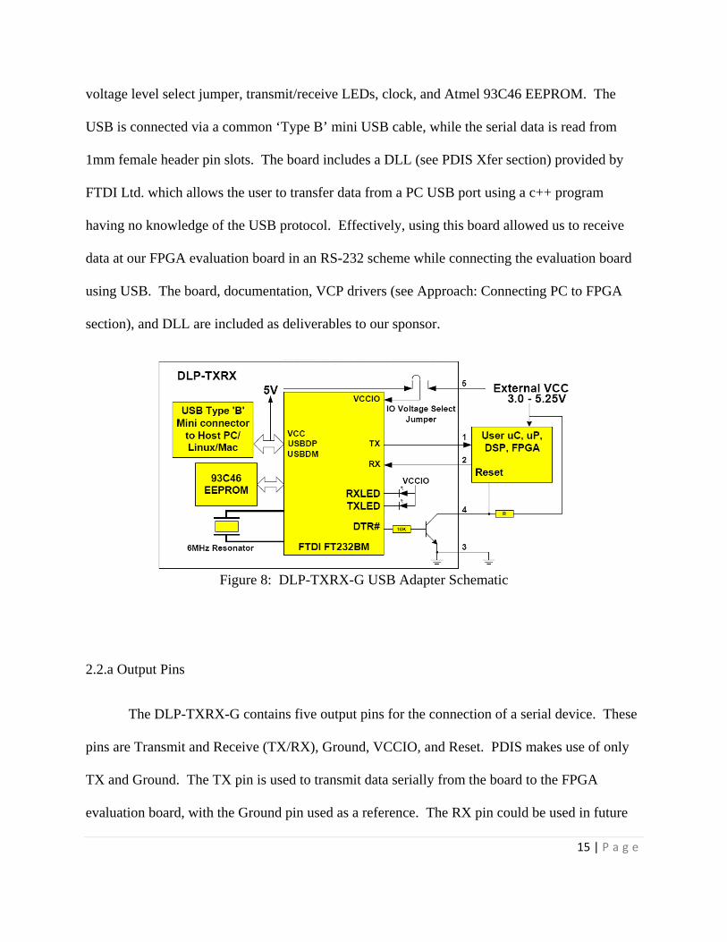
15 | P a g e
voltage level select jumper, transmit/receive LEDs, clock, and Atmel 93C46 EEPROM. The
USB is connected via a common ‘Type B’ mini USB cable, while the serial data is read from
1mm female header pin slots. The board includes a DLL (see PDIS Xfer section) provided by
FTDI Ltd. which allows the user to transfer data from a PC USB port using a c++ program
having no knowledge of the USB protocol. Effectively, using this board allowed us to receive
data at our FPGA evaluation board in an RS-232 scheme while connecting the evaluation board
using USB. The board, documentation, VCP drivers (see Approach: Connecting PC to FPGA
section), and DLL are included as deliverables to our sponsor.
Figure 8: DLP-TXRX-G USB Adapter Schematic
2.2.a Output Pins
The DLP-TXRX-G contains five output pins for the connection of a serial device. These
pins are Transmit and Receive (TX/RX), Ground, VCCIO, and Reset. PDIS makes use of only
TX and Ground. The TX pin is used to transmit data serially from the board to the FPGA
evaluation board, with the Ground pin used as a reference. The RX pin could be used in future
16 | P a g e
improvements to PDIS, so that the PC on the other end of the USB converter could receive data
from the FPGA. The VCCIO pin can be used to power the serial data pins when an output
voltage level other than 5 volts is necessary (see Voltage Select Jumper.) Finally, the Reset pin
can be used to asynchronously reset the on-board USB to Serial converter chip.
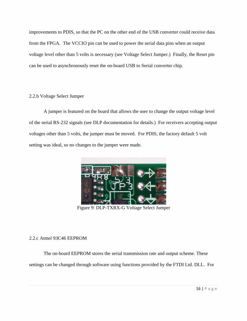
2.2.b Voltage Select Jumper
A jumper is featured on the board that allows the user to change the output voltage level
of the serial RS-232 signals (see DLP documentation for details.) For receivers accepting output
voltages other than 5 volts, the jumper must be moved. For PDIS, the factory default 5 volt
setting was ideal, so no changes to the jumper were made.
Figure 9: DLP-TXRX-G Voltage Select Jumper
2.2.c Atmel 93C46 EEPROM
The on-board EEPROM stores the serial transmission rate and output scheme. These
settings can be changed through software using functions provided by the FTDI Ltd. DLL. For
17 | P a g e
PDIS, we set the transmission rate to 9600 baud and used the default RS-232 output scheme (see
RS-232 Scheme section.)
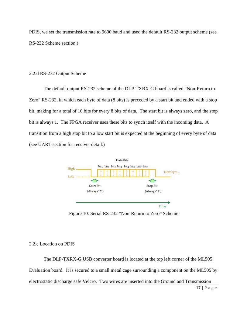
2.2.d RS-232 Output Scheme
The default output RS-232 scheme of the DLP-TXRX-G board is called “Non-Return to
Zero” RS-232, in which each byte of data (8 bits) is preceded by a start bit and ended with a stop
bit, making for a total of 10 bits for every 8 bits of data. The start bit is always zero, and the stop
bit is always 1. The FPGA receiver uses these bits to synch itself with the incoming data. A
transition from a high stop bit to a low start bit is expected at the beginning of every byte of data
(see UART section for receiver detail.)
Figure 10: Serial RS-232 “Non-Return to Zero” Scheme
2.2.e Location on PDIS
The DLP-TXRX-G USB converter board is located at the top left corner of the ML505
Evaluation board. It is secured to a small metal cage surrounding a component on the ML505 by
electrostatic discharge safe Velcro. Two wires are inserted into the Ground and Transmission
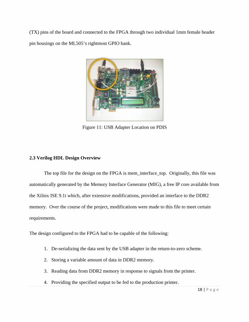
18 | P a g e
(TX) pins of the board and connected to the FPGA through two individual 1mm female header
pin housings on the ML505’s rightmost GPIO bank.
Figure 11: USB Adapter Location on PDIS
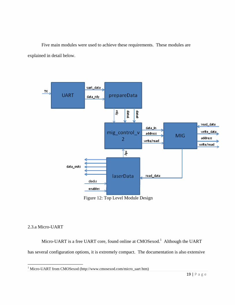
2.3 Verilog HDL Design Overview
The top file for the design on the FPGA is mem_interface_top. Originally, this file was
automatically generated by the Memory Interface Generator (MIG), a free IP core available from
the Xilinx ISE 9.1i which, after extensive modifications, provided an interface to the DDR2
memory. Over the course of the project, modifications were made to this file to meet certain
requirements.
The design configured to the FPGA had to be capable of the following:
1. De-serializing the data sent by the USB adapter in the return-to-zero scheme.
2. Storing a variable amount of data in DDR2 memory.
3. Reading data from DDR2 memory in response to signals from the printer.
4. Providing the specified output to be fed to the production printer.
19 | P a g e
Five main modules were used to achieve these requirements. These modules are
explained in detail below.
Figure 12: Top Level Module Design
2.3.a Micro-UART
Micro-UART is a free UART core, found online at CMOSexod.1 Although the UART
has several configuration options, it is extremely compact. The documentation is also extensive
1 Micro-UART from CMOSexod (http://www.cmosexod.com/micro_uart htm)
20 | P a g e
and informative. The UART is capable of acting both as a receiver and a transmitter. However,
for this project, only the receiver functionality was utilized.
Micro-UART consists of five files: uart.v, u_xmit.v, u_rec.v, baud.v, and inc.h. uart.v is
the top level module which appears as a component in the top module of the overall project. The
ports of this module are as follows:
input sys_clk: 200 MHz clock.
input sys_rst_l: Active low reset.
output uart_clk: Sampling clock generated by the UART.
output uart_XMIT_dataH: Transmitter signal. Serialized data for transmission.
input xmitH: Transmitter signal. Data ready signal for xmit_dataH.
input [7:0] xmit_dataH: Transmitter signal. Data to be serialized.
output xmit_doneH: Transmitter signal. Indicates completion of transmission.
input uart_REC_dataH: Receiver signal. Serial data input.
output [7:0] rec_dataH: Receiver signal. Contains de-serialized data.
output rec_readyH: Receiver signal. Indicates valid data on rec_dataH.
21 | P a g e
inc.h contains variables which can be used to configure the UART. The following
configurations were used:
WORD_LEN: This parameter sets the size of the output register of the receiver with a minimum
of 0 and a maximum. Its configuration for this project is 8.
XTAL_CLK: A parameter which specifies the speed of the on-board clock. The generated clock
used to sample the incoming data is based off of this clock. Its configuration for this project is
200000000, or 200 MHz.
BAUD: This parameter specifies the Baud rate at which the computer sends the data. Its
configuration is 9600.
CW: This parameter determines the width of counters within the UART which are used to
generate the sampling clock. The value must be greater than log2( XTAL_CLK/(BAUD*16*2)).
The current setting is
Except for configuration of the inc.h file, the UART was added in its original form to PDIS.
22 | P a g e
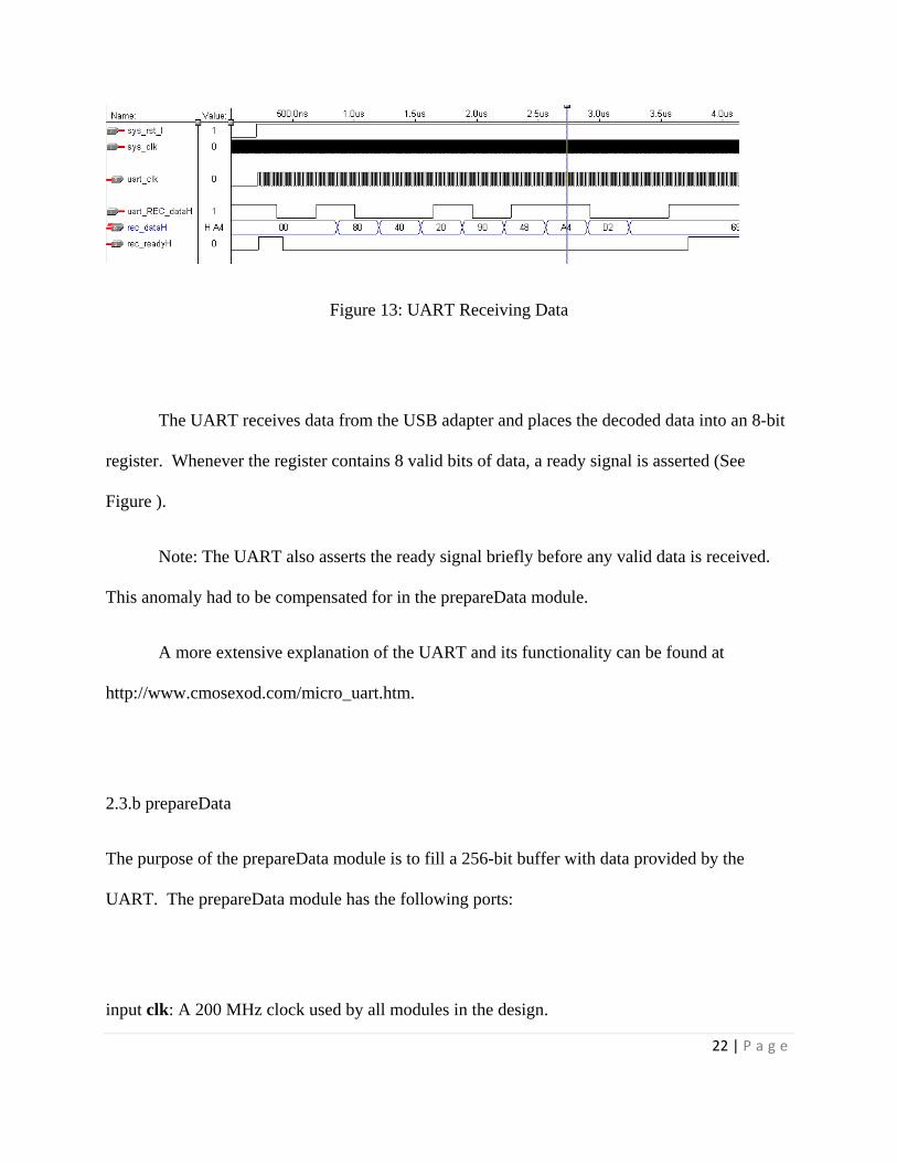
Figure 13: UART Receiving Data
The UART receives data from the USB adapter and places the decoded data into an 8-bit
register. Whenever the register contains 8 valid bits of data, a ready signal is asserted (See
Figure ).
Note: The UART also asserts the ready signal briefly before any valid data is received.
This anomaly had to be compensated for in the prepareData module.
A more extensive explanation of the UART and its functionality can be found at
http://www.cmosexod.com/micro_uart.htm.
2.3.b prepareData
The purpose of the prepareData module is to fill a 256-bit buffer with data provided by the
UART. The prepareData module has the following ports:
input clk: A 200 MHz clock used by all modules in the design.

23 | P a g e
input reset0: Active low reset. Note that the reset input to the entire design through
mem_interface_top is actually active high. The reset wired to reset0 is the inverse of that reset.
input [7:0] datain: 8-bits of de-serialized data from the output of the UART.
input dataready: Ready signal from UART which indicates that valid data is available on the 8-
bit register, datain.
output [127:0] word_falling: Contains the upper 128-bits of the 256-bit buffer. Will be written
to memory second.
output [127:0] word_rising: Contains the lower 128-bits of the 256-bit buffer. Will be written
to memory first.
output writeword: Signal which indicates that the two 128-bit words (derived from the 256-bit
buffer) contain valid data.
output [23:0] file_size: Contains the expected file size in 256 bit chunks. Wired to the
mig_control_v2 to be used as a condition for completing all writes and reads.
The logic within prepareData consists of a counter, called [5:0] bytes_written, which
counts how many valid bytes of data have been received from the UART. However, the first
five pulses of the dataready signal from the UART are treated in a special way. The first pulse is
completely disregarded, as the UART asserts dataready once before it receives any data to
indicate the start of its generated sampling clock. The next four pulses are stored in a 24-bit
buffer which is treated as the page size. The reason the buffer is 24 bits instead of 32 bits is
24 | P a g e
because the page size is stored in 128-bit chunks to make it immediately usable by the control
unit.
After the first five pulses of dataready have been accounted for, the prepareData module
uses any subsequent pulses of dataready to fill its internal 256-bit buffer. The prepareData
module fills the buffer by shifting the 256-bit buffer to the right by 8 bits and by placing the new
byte of data in the most significant byte of data (bit location 255 through 248). As a result, data
received first ends up in the least significant byte of data (bit location 7 through 0), data received
last ends up in the most significant bye of data, and data received in between the two end up
sequentially throughout the 256-bit buffer.
As previously mentioned, a counter keeps track of how many bytes of valid data have
been stored in the 256-bit buffer. Once the counter reaches 31, the buffer has been completely
filled, and an internal ready signal, write_word_long, is asserted and the counter is reset to zero.
When the next pulse of dataready, the UART’s ready signal, is received, write_word_long is
unasserted and the module starts to fill the 256-bit buffer again.
When write_word_long is asserted, the outputs [127:0] word_falling and [127:0]
word_rising are filled with data from the internal 256-bit buffer. word_rising is filled with the
last most significant 128 bits of data from the buffer, from location 127 to 0. word_falling is
filled with the most significant 128 bits of data from the buffer, from location 255 to 128. These
outputs hold their value until write_word_long is again asserted.
25 | P a g e
It is important to note that the prepareData module is only compatible with file sizes that
are integer multiples of 128. This is a discrepancy which should be addressed in further
development of the project.
write_word_long is used as a control signal for the state machine in the mig_control_v2
module. The state machine runs off of a 200 MHz clock. However, since the Baud rate used for
transmission through USB is set to 9600, the effective clock for the dataready module is roughly
1 kHz, which is 200,000 times slower than the 200 MHz clock. As a result, write_word_long
stays high for approximately 200,000 of the state machine’s clock cycles. To fix this problem, it
was necessary to shorten the write_word_long signal so that its maximum length was one of the
200 MHz clock cycles.
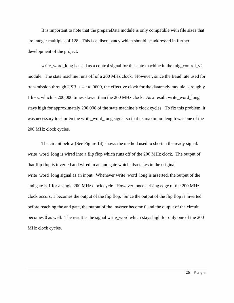
The circuit below (See Figure 14) shows the method used to shorten the ready signal.
write_word_long is wired into a flip flop which runs off of the 200 MHz clock. The output of
that flip flop is inverted and wired to an and gate which also takes in the original
write_word_long signal as an input. Whenever write_word_long is asserted, the output of the
and gate is 1 for a single 200 MHz clock cycle. However, once a rising edge of the 200 MHz
clock occurs, 1 becomes the output of the flip flop. Since the output of the flip flop is inverted
before reaching the and gate, the output of the inverter become 0 and the output of the circuit
becomes 0 as well. The result is the signal write_word which stays high for only one of the 200
MHz clock cycles.
26 | P a g e
Figure 14: Circuit to shorten ready signal
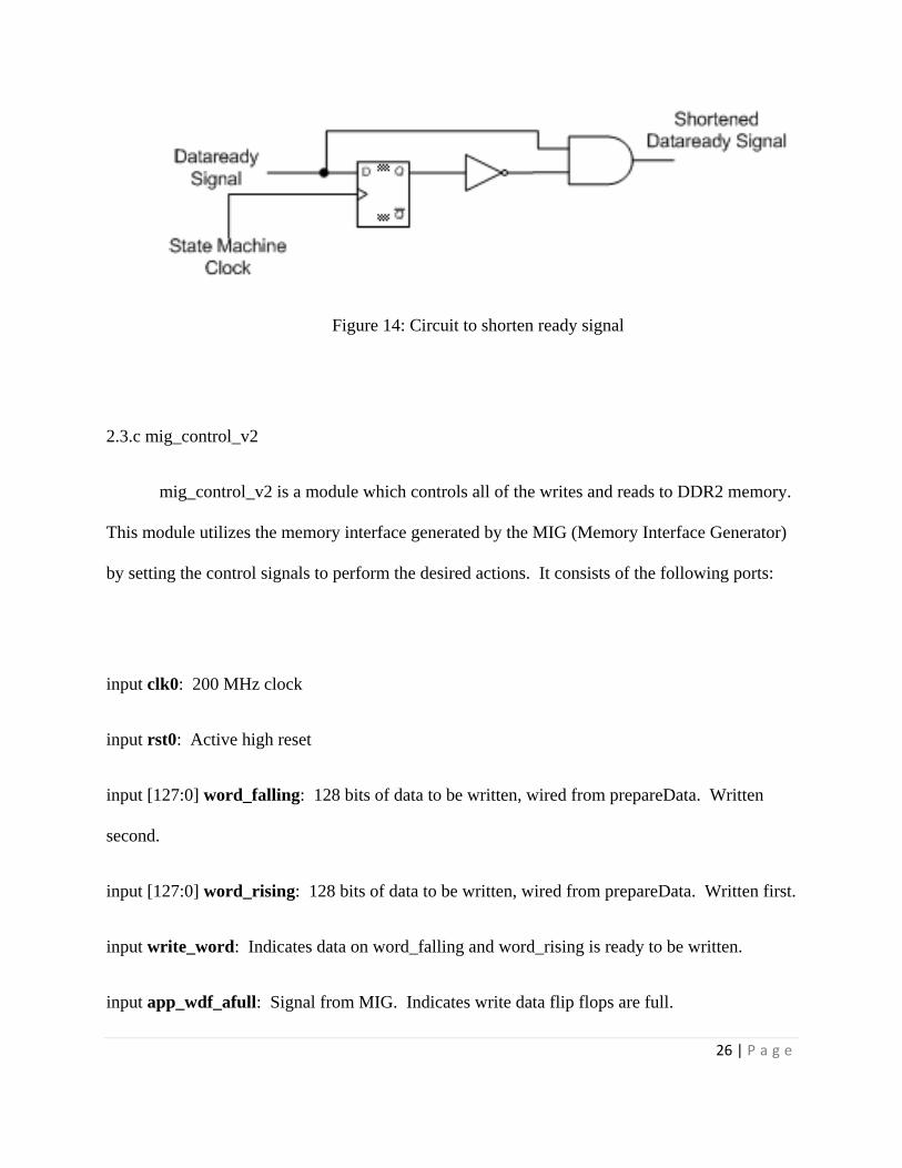
2.3.c mig_control_v2
mig_control_v2 is a module which controls all of the writes and reads to DDR2 memory.
This module utilizes the memory interface generated by the MIG (Memory Interface Generator)
by setting the control signals to perform the desired actions. It consists of the following ports:
input clk0: 200 MHz clock
input rst0: Active high reset
input [127:0] word_falling: 128 bits of data to be written, wired from prepareData. Written
second.
input [127:0] word_rising: 128 bits of data to be written, wired from prepareData. Written first.
input write_word: Indicates data on word_falling and word_rising is ready to be written.
input app_wdf_afull: Signal from MIG. Indicates write data flip flops are full.
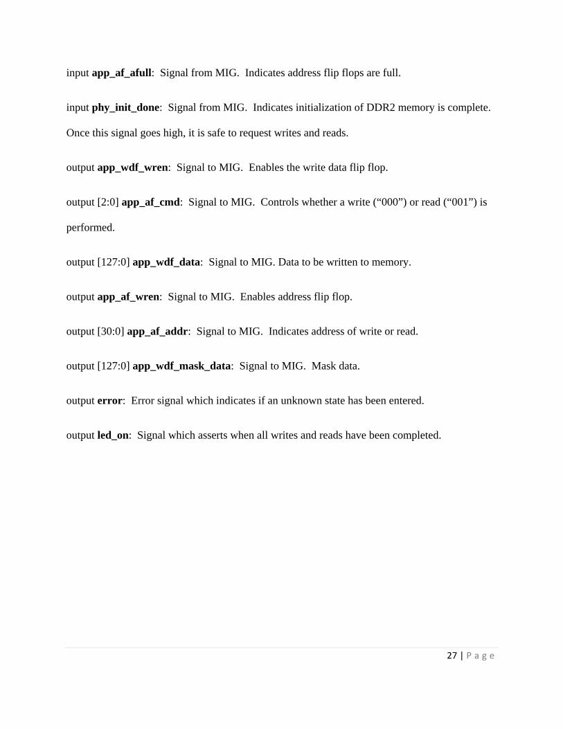
27 | P a g e
input app_af_afull: Signal from MIG. Indicates address flip flops are full.
input phy_init_done: Signal from MIG. Indicates initialization of DDR2 memory is complete.
Once this signal goes high, it is safe to request writes and reads.
output app_wdf_wren: Signal to MIG. Enables the write data flip flop.
output [2:0] app_af_cmd: Signal to MIG. Controls whether a write (“000”) or read (“001”) is
performed.
output [127:0] app_wdf_data: Signal to MIG. Data to be written to memory.
output app_af_wren: Signal to MIG. Enables address flip flop.
output [30:0] app_af_addr: Signal to MIG. Indicates address of write or read.
output [127:0] app_wdf_mask_data: Signal to MIG. Mask data.
output error: Error signal which indicates if an unknown state has been entered.
output led_on: Signal which asserts when all writes and reads have been completed.
28 | P a g e
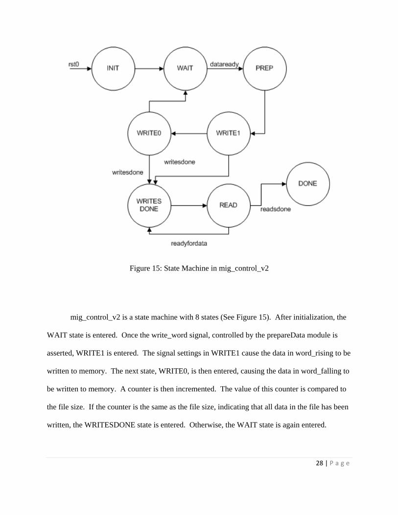
Figure 15: State Machine in mig_control_v2
mig_control_v2 is a state machine with 8 states (See Figure 15). After initialization, the
WAIT state is entered. Once the write_word signal, controlled by the prepareData module is
asserted, WRITE1 is entered. The signal settings in WRITE1 cause the data in word_rising to be
written to memory. The next state, WRITE0, is then entered, causing the data in word_falling to
be written to memory. A counter is then incremented. The value of this counter is compared to
the file size. If the counter is the same as the file size, indicating that all data in the file has been
written, the WRITESDONE state is entered. Otherwise, the WAIT state is again entered.
29 | P a g e
Once the readnext signal from laserData is asserted, the module exits the WRITESDONE
state and enters the READ state. Another counter keeps track of how many reads have been
completed. If this number is equal to the file size, the DONE state is entered and led_on is
asserted. Otherwise, WRITESDONE is again entered.
2.3.d MIG
The MIG, or Memory Interface Generator, is a free IP core available from the Xilinx ISE.
It acts as an interface between mig_control_v2 and the DDR2 memory, handling the
initialization and timing required for successful writes and reads to DDR2 memory.
Configuration settings, available in mem_interface_top, can be altered to meet various
requirements. The settings are currently set to match the requirements of the ML505 evaluation
board’s DDR2 SO-DIMM 256 MB memory.
For more detailed information on the MIG, refer to the MIG documentation, available on
the project CD.
2.3.e laserData
This module is responsible for controlling the output to the printer’s lasers (See Figure
16).
30 | P a g e
Figure 16: Block Diagram of laserData
When a read from a single memory address is requested, 4 64-bit words are returned.
Therefore, 36 (4*9) bits of data are available to each of the 5 lasers for a single read. Thus, when
a read is made, 5 36-bit registers are loaded, each with 4 9-bit words. The 5 36-bit registers are
loaded into 5 separate instances of a module (called bitSelector) which controls which 9-bit
chunks are output to the printer. Each bitSelector has a 2 bit counter which increments when it
sees a rising edge of a printer clock and a low enable. The counter determines which 9-bit chunk
31 | P a g e
of the 36-bit register is output. Each time the counter hits 0, the next word is loaded into the 36-
bit register and another read is requested so that when the counter hits 0 again, 36 more bits will
be ready.
2.4. Printer Emulator
Production printer and FPGA board are interfaced with each other, but it is very hard to
run the tests since it is not possible to have the big production printer bring in at the station, we
needed to generate the same signals sent by the “Printer Card” to the FPGA. So one of the parts
of the project was to generate VHDL modules to generate several clocks and enable signals.
During the remaining period of time, the signals for the specified criteria have been
generated. There were five clocked and enable signals. The data clock frequency provided by
the board is 200 MHz and the actual frequency of the clocks specified is 50 MHZ.
Different counters have been generated in order to get the desired frequency. Also, the
enable signals needed some kind of scheme to be generated in VHDL to have specified output.
Clock 1 can be generated using the main clock of 200 MHZ. Clock 2 is a sifted version of Clock
1, and all other clocks can be derived from Clock 1. It is very important to note that all the enable
signals are active low. Data is passed on each clock enable. Each enable becomes active low
after the previous enable has been active low after few clock cycles. But they all become active
low at the same time. Data is being sent on each falling edge of the enable signal. FPGA reads
a byte until all the enables go up. When the enables go up, any data that has been sent after that
gets destroyed. When the enables go up the clock speed s do not change.
32 | P a g e
Designing VHDL modules was challenging in the beginning just as to get grasp of the
pattern the signals followed and figure out a scheme to implement them. VHDL Xilinx software
although provides better and easier environment to work with than using any other active HDL
environments. The only challenging part in implementing the modules was to debug the code for
many hours and try to manipulate then code in order for it to give required part. Finally, the code
has been designed to generate all the required outputs. The reason that the code is written in
“VHDL” and not in “Verilog” is the familiarity with the language one better than the other.
The following figure 1 shows simulated output of the waveforms. It shows all the clocks and enables
signals in desired format

33 | P a g e
Figure 17: Timing Simulation Results from Printer Emulator
3. Experimentation and Validation
3.1 PDIS Xfer
34 | P a g e
PDIS Xfer contains several error checking devices and algorithms to ensure that the
program always works as expected. In most cases, if an error is detected the user is notified with
a message box. If the error is severe, the program also shuts down. In order to determine that
PDIS Xfer always operates correctly, several “beta testing” sessions were held throughout the
development of the program. In these tests, various combinations of user input were employed
to attempt to “break” the program. These tests also served to prove that the error checking
devices in the program worked correctly. The main tests were as follows:
1. PDIS Xfer should not attempt to write data to the USB port if the user hasn’t selected
a data file
2. The user cannot send data from a file with the wrong format (not .bin or .fil)
3. The user can’t use PDIS Xfer to communicate with a device on the USB which does
not have the device identification “DLP-TXRX”
4. Once the user has selected a data file and has clicked “Send Data,” the user must
reselect the file from the hard drive if they want to send it again. This eliminates the
possibility of accidentally clicking the “Send Data” button twice unintentionally.
In all of the above cases, PDIS Xfer successfully avoided incorrect operation and
informed the user of all error situations.
35 | P a g e
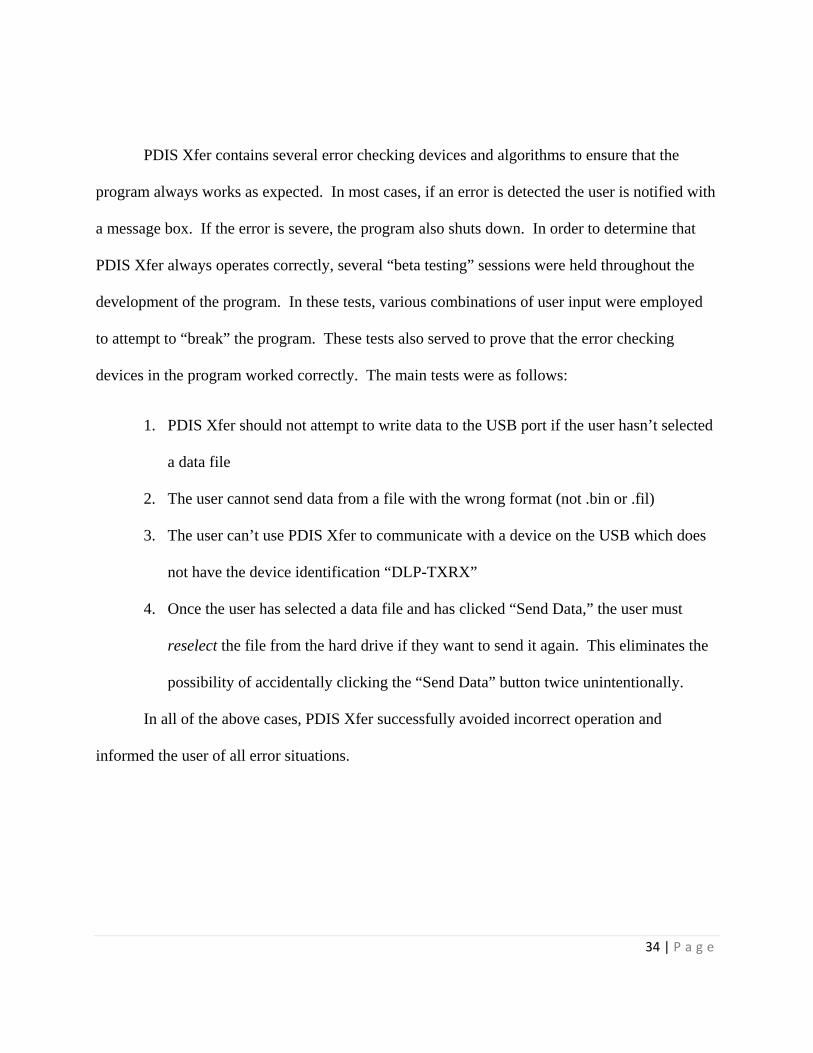
Figure 18: PDIS Xfer Displaying an Error Message
3.2 PDIS Xfer and DLP-TXRX-G USB Adapter
To check that the PC data file was being correctly sent to the FPGA evaluation board, a
logic analyzer was used to view the serial data output by the USB converter board. By sending
data from the PC with known sequences and characteristic patterns, it was possible to determine
that PDIS Xfer and the USB Adapter worked correctly.
3.3 Verilog HDL Modules
The Verilog HDL modules were carefully tested as they were developed. Each module,
with the exception of the MIG, was tested separately in simulation to verify its correct operation.
In many cases, separate modules were synthesized and placed in hardware to verify their

36 | P a g e
individual operation in hardware, utilizing LEDs as well as the logic analyzer to ensure correct
outputs. The MIG was unable to be tested in simulation due to the lack of a workable DDR2
memory emulator. However, at the start of this senior design project, the MIG and control unit
had already been developed and tested.
Timing diagrams from testing of the individual modules are shown below.
Figure 19: Accurate bitSelector Timing Simulation
The timing diagram shown in the figure above shows working operation of the
bitSelector module. Dataout represents the 9 bits of data sent to one of the printing lasers. Five
instantiations of the bitSelector module are used.
37 | P a g e
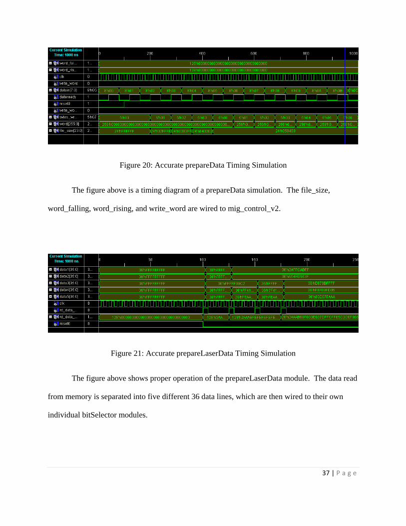
Figure 20: Accurate prepareData Timing Simulation
The figure above is a timing diagram of a prepareData simulation. The file_size,
word_falling, word_rising, and write_word are wired to mig_control_v2.
Figure 21: Accurate prepareLaserData Timing Simulation
The figure above shows proper operation of the prepareLaserData module. The data read
from memory is separated into five different 36 data lines, which are then wired to their own
individual bitSelector modules.
38 | P a g e
3.4 Printer Emulator
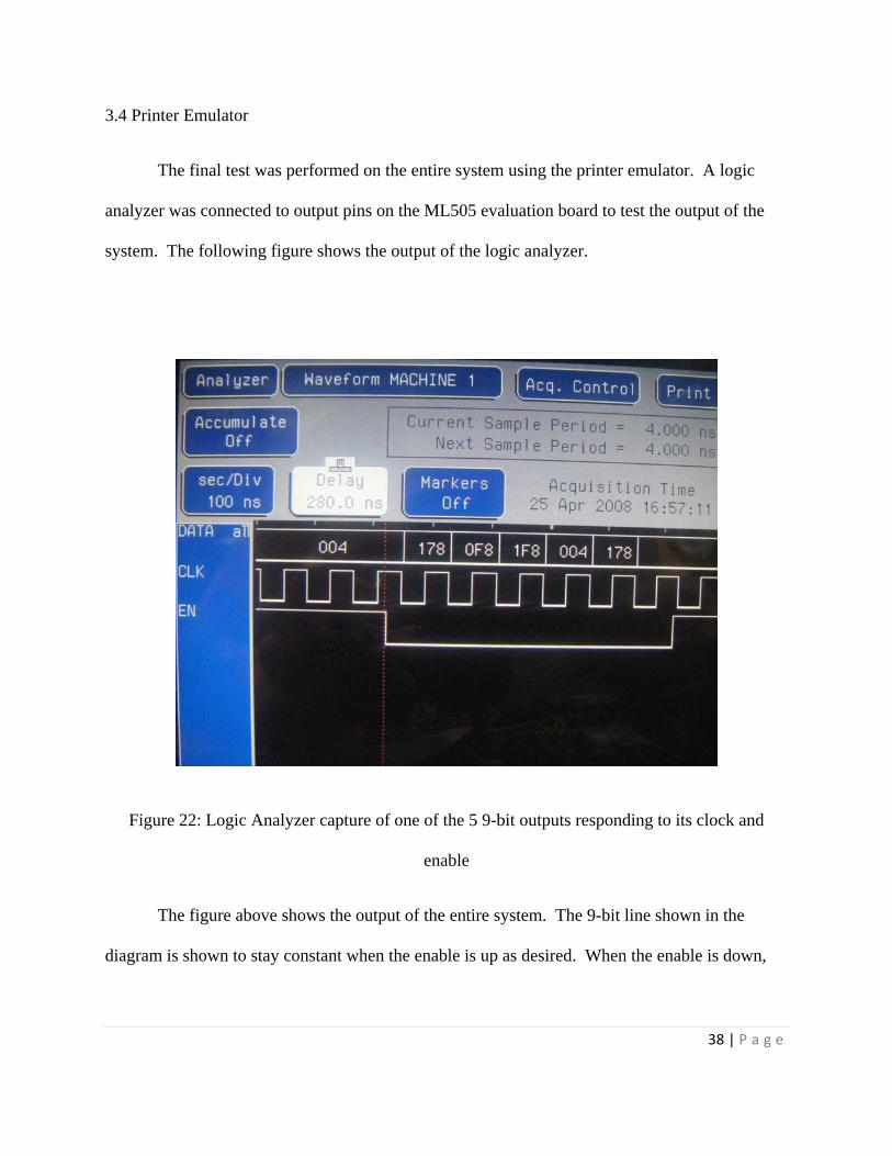
The final test was performed on the entire system using the printer emulator. A logic
analyzer was connected to output pins on the ML505 evaluation board to test the output of the
system. The following figure shows the output of the logic analyzer.
Figure 22: Logic Analyzer capture of one of the 5 9-bit outputs responding to its clock and
enable
The figure above shows the output of the entire system. The 9-bit line shown in the
diagram is shown to stay constant when the enable is up as desired. When the enable is down,
39 | P a g e
the data changes sequentially, while meeting the setup and hold time requirements specified by
InfoPrint. This diagram is conclusive evidence of the successful operation of PDIS.
4. Benefit
Many of the items received in mail, from telephone bills to bank statements, are
generated by high-speed production printers. Companies which build these printers are not only
concerned with the printing speed, but also with the printing quality. A control unit inside each
production printer directly controls the printing quality by the print algorithm it uses. Normally,
in order to test a new printing algorithm to determine whether or not it has any positive effect on
the print quality, a new control unit would have to be built for that specific algorithm.
Developing a new control unit is expensive, costing a company large amounts of time and
resources.
PDIS, or Print Data Insertion System, is a tool which eliminates the need to develop a
new control unit for every algorithm a company needs to test for print quality. PDIS acts as an
interface between a PC and a high-speed production printer. The system inserts print data which
has been altered by the new algorithm directly into a production printer. The printer uses the
data it receives to print pages which reflect the new algorithm. The printed pages can then be
examined to determine whether or not the new algorithm offers a significant improvement to
print quality.
40 | P a g e
5. Potential Uses
The need for this project was determined by InfoPrint Solutions Company, who has need
for a system that can test many different kinds of print quality algorithms. A page processed by
these new algorithms would need to be printed on an existing print engine, to test the algorithm’s
capability. Our system would do so by eliminating the need to construct a separate printer
control unit for every new print algorithm or set of parameters, which would otherwise require a
complete new design cycle.
PDIS is a piece of hardware which can send printing data from a computer to a high-speed
production printer with the speed and formatting required. The test data will consist of one page
to be printed which has been processed by a printing algorithm. The processed page of data can
then be sent to the control unit of a printer for repeated printing. To insert a new page of test
print data, the printer will be stopped, the new data will be loaded into memory, and the printer
will be restarted. The timing and format of the output data of our hardware will need to fit the
requirements of a printer which is printing in real-time.
6. Costs
Hardware Costs:
ML505 Evaluation Board: $1195
TX/RX USB Adapter: $20
USB Cable: $10

41 | P a g e
Miscellaneous Wires: $2
Total Hardware Cost: $1227
Software Costs:
Xilinx ISE: $0 (WebPACK available online)
Total Software Cost: $0
Development Costs:
Development Time: 400 hours
Total Development Cost: $20 /hr * 400 hours = $8000
Total Cost: $9227
7. Alternatives
The ML505 board was chosen and supplied to us by InfoPrint Solutions Company.
However, a less expensive board could probably be used as long as the board contained DDR2
memory, a Virtex 5 FPGA, and sufficient IO pins.
Reproduction costs would extend only to the cost of the board and the USB adapter
device. Although the total cost of the project was $9227, the cost of reproduction would be

42 | P a g e
closer to $1227, a price which could be reduced even further by selecting a less expensive
evaluation board.
8. Maintainability
If , Visual C++, the software behind the application which sends the file of data to the
USB adapter, were to be upgraded, some compatibility issues may arise if changes were made to
the application. Similar issues may result from upgrading the Xilinx ISE from 9.1i to a later
version. However, these are only issues if the consumer desires to make changes to the
application or the Verilog modules.
9. Replacements
In order to replace a defunct board, a new ML505 evaluation board can be ordered from
xilinx.com.
10. Administrative
Initially, the project was delayed due to difficulties with the USB controller on the ML505
Evaluation Board. The initial plan to connect the computer to the ML505 Evaluation Board was
to directly connect the computer and the board with a USB cable, making use of the Cypress
USB controller available on the board. However, after several weeks of investigation and
43 | P a g e
attempts to integrate the USB controller into the project, it was realized that the controller is hard
coded into a host mode. The project requires the board to receive USB data in peripheral mode.
Therefore, we had to prepare an alternative solution. The USB adapter provided a workable,
cheap, and easy solution to this dilemma.
All tasks were completed successfully. However, more rigorous testing must be done to
ensure proper operation of the entire system with a production printer. Another remaining task is
to determine which pins to use as outputs and inputs for signals to and from the production
printer. It is assumed that InfoPrint Solutions Company, which will continue work on this
project to integrate it with their printers, will complete this task.
Work was also done on writing to the 2 line LED display provided on the ML505 Evaluation
Board. Enough progress was made so that desired characters could be written to the display on
request. Unfortunately, we did not have enough time to implement the code with the core
system.
The expenses of this project for our team were minimal due to the sponsorship by InfoPrint
Solutions Company. The adapter was a necessary and effective purchase. The various cables
and wires used were already available to us. The only other expenses were headers for the IO
pins, which were a minimal expense.
The hours spent on the project were concentrated on the last half of the semester. During the
first few weeks of the project, we struggled to work out how to implement the USB controller
into our project. As a result, minimal progress was made. However, once the USB adapter was
44 | P a g e
purchased, progress was made at full speed and we made up for the time lost. Progress was also
improved by effective delegation of the various tasks.
11. Lessons Learned
Visual C++ is an Integrated Development Environment (IDE) which makes use of special
classes and data types known as “managed” c++. The support provided by this environment can
be invaluable for certain projects, particularly those which make use of Windows GUIs (such as
PDIS Xfer.) Unfortunately, managed c++ data types are often very different from their standard
c++ counterparts, and in many cases have no direct analogs in standard c++. Therefore, it is
crucial when considering the use of Visual C++ in a project to determine (before coding begins)
if the program will be written in all Visual C++, or all standard c++. Mixing Visual C++ and
standard c++ code can be time-consuming, frustrating, or impossible because many data types,
objects, and classes simply can’t be converted from one type of c++ to the other. In the
beginning of PDIS Xfer’s development, a simple command line program was written in standard
c++ to transfer a small text file of data to the USB port. When this code was ported into Visual
C++, it was impossible to integrate the control of the file transfer with the Visual C++ GUI code.
From that point on, every aspect of the program was written completely in Visual C++. In
general, it’s important to use the tools you have available to you, but you must understand how
to use them! Otherwise, they may turn out to be unwieldy and impede you progress more than
they further it.
45 | P a g e
Just because something works in simulation does not mean it will work in hardware.
Even careful simulation of Verilog HDL on the computer does not guarantee success once
implemented in the FPGA. It pays to be aware of issues that may work fine when simulated, but
not in hardware.
Work in parallel, not in series! During the first few weeks of the project, the mistake was
made of assigning every member of the group to the task of figuring out how the USB controller
would work. Due to this, very little progress was made. However, once Dr. Kaps suggested that
we divide the tasks up in a different manner, our rate of progress increased dramatically.
It pays to ask for help early. There were several instances when several days were spent
trying to find the cause of a bug. Once the advice of a professor was finally requested, the bug
usually was quickly fixed.
12. References
ML505 Evaluation Platform Documentation:
http://www.xilinx.com/support/documentation/ml505.htm
MIG Documentation:
http://www.xilinx.com/support/documentation/ipmeminterfacestorelement_meminterfacecontrol
_mig.htm
Micro UART Documentation:
46 | P a g e
http://www.cmosexod.com/micro_uart.htm
DLP-TXRX-G USB Adapter Documentation:
http://www.dlpdesign.com/usb/txrx.shtml
FTDI FT232R USB to Serial Converter IC Documentation:
http://www.ftdichip.com/Products/FT232R.htm

47 | P a g e
Appendix A: Proposal (ECE 492)
Proposal
Team Members: Paul Anderson Jenny Higgins Pinalben Patel
Faculty Supervisor: Jens‐Peter Kaps
PDIS Print Data Insertion System
Submitted: October 19th, 2007
48 | P a g e
I. Executive Summary
Many of the items received in mail, from telephone bills to bank statements, are
generated by high-speed production printers. Companies which build these printers are not only
concerned with the printing speed, but also with the printing quality. A control unit inside each
production printer directly controls the printing quality by the print algorithm it uses. Normally,
in order to test a new printing algorithm to determine whether or not it has any positive effect on
the print quality, a new control unit would have to be built for that specific algorithm.
Developing a new control unit is expensive, costing a company large amounts of time and
resources.
PDIS, or Print Data Insertion System, is a tool which eliminates the need to develop a
new control unit for every algorithm a company needs to test for print quality. PDIS can also be
re-used for multiple algorithms. The system inserts print data which has been altered by the new
algorithm directly into a production printer. The printer uses the data it receives to print pages
which reflect the new algorithm. The printed pages can then be examined to determine whether
or not the new algorithm offers a significant improvement to print quality.
II. Problem Statement
The purpose of our project is to create a piece of hardware which can send printing data
from a computer to a high-speed production printer with the speed and formatting required. The
test data will consist of one page to be printed which has been processed by a printing algorithm.
49 | P a g e
The processed page of data can then be sent to the control unit of a printer for repeated printing.
To insert a new page of test print data, the printer will be stopped, the new data will be loaded
into memory, and the printer will be restarted. The timing and format of the output data of our
hardware will need to fit the requirements of a printer which is printing in real-time.
The need for this project was determined by InfoPrint Solutions Company, who has need
for a system that can test many different kinds of print quality algorithms. A page processed by
these new algorithms would need to be printed on an existing print engine, to test the algorithm’s
capability. Our system would do so by eliminating the need to construct a separate printer
control unit for every new print algorithm or set of parameters, which would otherwise require a
complete new design cycle.
In addition to the basic functionality of our system stated above, an optional task handed
down by InfoPrint Solutions Company would be to create a display system to show data our
system would be sending to the printer. This would be helpful for testing purposes as well as to
allow users to ensure the data being sent to the printer is accurate before an actual printing test.
A display system would also make debugging our tool easier.
III. Approach
PDIS will need to interface with a computer and an existing production printer control
unit. PDIS will use a unit with a FPGA, large memory, and sufficient IO ports, which will be
connected to a computer using USB. A program will need to be written to control the flow of
50 | P a g e
data from the computer to the USB port. PDIS will be connected to the printer control unit using
custom IO pins. Verilog modules will be written to control the interaction of the FPGA with the
USB and the printer control unit.
IV. Requirements
Evaluation Board:
An evaluation board called “XILINX HW_VSML505-UNI-G” that has a very large
memory, ports to connect to the laptop, enough output pins for the print data, and a
programmable Xilinx Vertex 5 FPGA which can contain the control logic needed for the
interfacing.
USB:
USB will be the connection between the laptop and evaluation board. Since USB is fast,
easy to use, and also a standard type, it is a good choice in this particular system where a laptop
has to be connected with an evaluation board.
Compact Flash:
Xilinx Vertex 5 module will be programmed using the Compact Flash system provided
on the ML505 evaluation board. Compact Flash requires less power than other available
devices. CF is robust in that it is nonvolatile and solid state.

51 | P a g e
Logic Analyzer:
A logic analyzer will be used to aid debugging the system.
Xilinx ISE 9.1i:
Xilinx ISE 9.1i is a program which allows the development of Verilog HDL modules.
The program can also translate the modules into a .ACE file which can be loaded on the
Compact Flash to program the FPGA.
Verilog HDL:
Knowledge of Verilog is one of the key requirements to implement the design. As
requested by InfoPrint Solutions Company, Verilog HDL will be used to program the Xilinx
FPGA.
USB Control:
USB is used as the connection between the laptop and evaluation board. A custom
program will be used to control the flow of data between the computer and the evaluation board.
52 | P a g e
V. Preliminary Design
From a top level perspective, PDIS needs to have a way to transfer data from a computer
to a printer card with the appropriate formatting and timing. A direct connection between a
computer and a printer card, with a program on the computer controlling the timing, would not
be feasible because of the high speeds required for production printing. Hence, a middle step is
needed between the computer and the printer card.
The ML505 evaluation board includes an FPGA, DDR2 memory, customizable IO pins,
and various ports, including USB and CompactFlash. The data will be transferred from the
computer to the FPGA. The FPGA will then store the data in DDR2 memory. The FPGA will
await signals from the printer card which inform the FPGA when the data is needed. The FPGA
will read data from the DDR2 memory in response to these signals. The DDR2 memory is fast
enough to meet the speed demands of a production printer. The FPGA will direct that data out
through the custom IO pins and into the printer card.
USB has been chosen as the connection between the computer and the ML505 evaluation
board. This type of connection was requested by InfoPrint Solutions Company for this project to
facilitate ease of use since employees are familiar with USB and have the ports on their
computers.
There are two major pieces in implementing USB as the connection between the
computer and the FPGA. One piece is to create a program, preferably in C, which can format
and send data out through the USB port on a computer. The second piece is to write a USB
interface in Verilog HDL so that the FPGA is able to retrieve data from the USB port.
53 | P a g e
In order for the FPGA to read and write to the DDR2 memory on the ML505 evaluation
board, a memory interface is needed. This interface has, for the most part, already been
developed. The interface is currently capable of writing up to 256 MB of data to memory, which
is the size of the DDR2 memory stick included with the ML505 board. The interface is also
capable of reading data from the DDR2 memory. Currently, a simple state machine controls the
writes and reads to the memory. This state machine will need to be altered to account for the
data the USB will send to be written to DDR2 memory as well as the commands the printer card
will send to request a read from DDR2 memory.
The connection between the FPGA and the printer card will also require a custom
interface of some sort. The project’s sponsor will provide timing diagrams which depict when
and how the printer card expects to receive data.
If time allows, the USB connection may be made to not only send data from the computer
to the FPGA, but also to send data read from the DDR2 memory from the FPGA to the
computer. A C program could collect this data and display it, either in text format or in the form
of dots across the computer screen, in an attempt to ensure that the data sent to the printer card
was accurate.
One concern about this project is the eventual testing and ensuring that PDIS provides the
functionality needed by the project’s sponsor. The company plans to have an identical setup in
Boulder, Colorado. One option for testing would be to send the company the completed Verilog
HDL modules so that they could load those modules on their evaluation board and provide us
with feedback.

54 | P a g e
VI. Testing Plans
USB Interface (PC to Evaluation Board)
Once the program which controls the PC’s USB port has been written, a logic analyzer
will be attached to each of the four wires in a USB cable. The output signals will be observed to
ensure the interface is working as expected.
USB Interface (Evaluation Board to PC)
The Verilog modules which control receiving the signals from the USB port will be
tested using waveform simulations in the Xilinx ISE 9.1i. After the operation of the modules has
been verified, a USB cable will be connected between the PC and the evaluation board. The four
signals received from the USB cable will be sent to four LEDs as well as four output pins. The
logic analyzer will be connected to these four pins to ensure the FPGA to USB interface is
working correctly.
Memory Interface Controller
The memory interface controller will consist of states which control the writes and reads
to the memory. A test bench, written in Verilog, will test the functionality of the state machine
within the memory interface controller.
Memory Interface (FPGA to DDR2 and DDR2 to FPGA)
55 | P a g e
Test data will be written to the DDR2 memory using the memory interface via the
memory interface controller. Data will be read from the same location the data was written to.
The data read will be sent to the logic analyzer using IO pins to ensure the functionality of the
memory interface.
Page Storage (PC to USB to FPGA to Memory to FPGA)
A small sample page will be sent from the PC to the USB. The FPGA will read the
information from the USB and write the data to the DDR2 memory. The FPGA will then read
the data from the DDR2 memory and place the information on IO pins which can be accessed by
the logic analyzer.
Control Unit Interface (FPGA to Control Unit (PWM))
A logic analyzer can be used to test the signals sent by the FPGA to the Control Unit and
ensure the signals match the specifications.
Page Insertion (Memory to FPGA to Control Unit (PWM))
To test the signals sent by the memory to the FPGA to the Control Unit, a logic analyzer
will be used to ensure the signals match the requirements.
Full Process (PC to USB to FPGA to Memory to FPGA to Control Unit (PWM))
To test the entire process, a logic analyzer will be used to confirm that the page sent from
the PC is reproduced at the IO pins of the FPGA with proper timing and format. PDIS will not
be able to be tested on a real printer, so the final test will consist of comparing the signals on the
IO pins with the given specifications.
56 | P a g e
VII. Tasks
C/Java/C++ Programming: Paul Anderson and Pinal Patel
Verilog Programming: Paul Anderson, Jenny Higgins, Pinal Patel
Testing: Paul Anderson, Jenny Higgins, Pinal Patel
Note: Further task allocations will be determined as the project progresses.
57 | P a g e
VIII. Milestones
58 | P a g e
Appendix B: Design Document (ECE 492)
PDIS:
Print Data Insertion System Design Document
ECE 492: Senior Design Project
November 30, 2007
Faculty Supervisor:
Jens-Peter Kaps
Team Members:
Paul Anderson
Pinal Patel
Jenny Higgins
59 | P a g e
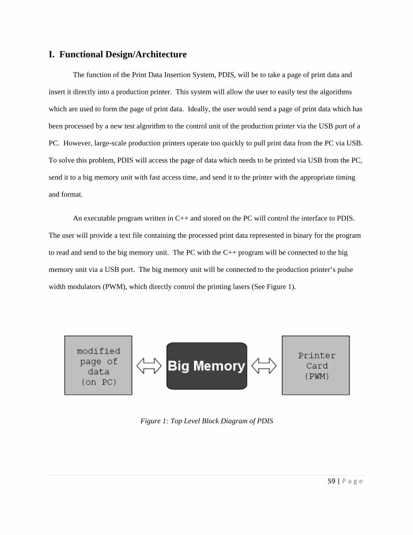
I. Functional Design/Architecture
The function of the Print Data Insertion System, PDIS, will be to take a page of print data and
insert it directly into a production printer. This system will allow the user to easily test the algorithms
which are used to form the page of print data. Ideally, the user would send a page of print data which has
been processed by a new test algorithm to the control unit of the production printer via the USB port of a
PC. However, large-scale production printers operate too quickly to pull print data from the PC via USB.
To solve this problem, PDIS will access the page of data which needs to be printed via USB from the PC,
send it to a big memory unit with fast access time, and send it to the printer with the appropriate timing
and format.
An executable program written in C++ and stored on the PC will control the interface to PDIS.
The user will provide a text file containing the processed print data represented in binary for the program
to read and send to the big memory unit. The PC with the C++ program will be connected to the big
memory unit via a USB port. The big memory unit will be connected to the production printer’s pulse
width modulators (PWM), which directly control the printing lasers (See Figure 1).
Figure 1: Top Level Block Diagram of PDIS
60 | P a g e
In order to store a page of print data in the big memory unit, the unit will be turned on. A
“START” button will be pressed in the C++ program on the PC to initiate data transmission through the
USB port to the big memory unit. Once all of the data has been stored in the big memory unit, a message
will appear in C++ program and a “DONE” LED on the big memory unit will turn on. The user will then
push a “START PRINTING” button on the big memory unit to initiate printing. The printer will
repeatedly print the same page of data until a “STOP” button is pressed. A “RESET” button will be
available during each phase of the process.
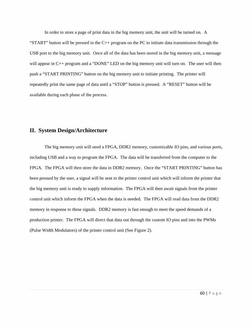
II. System Design/Architecture
The big memory unit will need a FPGA, DDR2 memory, customizable IO pins, and various ports,
including USB and a way to program the FPGA. The data will be transferred from the computer to the
FPGA. The FPGA will then store the data in DDR2 memory. Once the “START PRINTING” button has
been pressed by the user, a signal will be sent to the printer control unit which will inform the printer that
the big memory unit is ready to supply information. The FPGA will then await signals from the printer
control unit which inform the FPGA when the data is needed. The FPGA will read data from the DDR2
memory in response to these signals. DDR2 memory is fast enough to meet the speed demands of a
production printer. The FPGA will direct that data out through the custom IO pins and into the PWMs
(Pulse Width Modulators) of the printer control unit (See Figure 2).
61 | P a g e
Figure 2: System Level Block Diagram for PDIS
USB has been chosen as the connection between the computer and the big memory unit. This
type of connection was requested by InfoPrint Solutions Company for this project to facilitate ease of use
since employees are familiar with USB and have the ports on their computers.
There are two major pieces in implementing USB as the connection between the computer and
the FPGA. One piece is to create a program, preferably in C++, which can format and send data out
through the USB port on a computer. The second piece is to write a USB interface in Verilog HDL so
that the FPGA is able to retrieve data from the USB port.
In order for the FPGA to read and write to the DDR2 memory on the big memory unit, a memory
interface is needed. This interface has, for the most part, already been developed. The interface is
currently capable of writing up to 256 MB of data to memory, which is the size of the DDR2 memory
62 | P a g e
stick being used. The interface is also capable of reading data from the DDR2 memory. Currently, a
simple state machine controls the writes and reads to the memory. This state machine will need to be
altered to account for the data the USB will send to be written to DDR2 memory as well as the commands
the printer card will send to request a read from DDR2 memory.
The connection between the FPGA and the printer card will also require a custom interface of
some sort. The project’s sponsor will provide timing diagrams which depict when and how the printer
card expects to receive data.
If time allows, the USB connection may be made to not only send data from the computer to the
FPGA, but also to send data read from the DDR2 memory from the FPGA to the computer. A C++
program could collect this data and display it either in text format or in the form of dots across the
computer screen in an attempt to ensure that the data sent to the printer card is accurate.
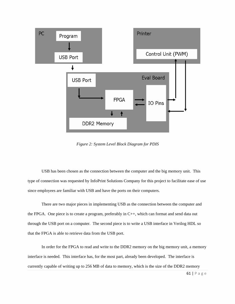
III. Detailed Design
In order to implement the interfaces between the PC’s USB port and the big memory unit, as well
as the interface between the big memory unit and the printer control unit, an FPGA will be needed. The
Xilinx ML505 evaluation board, which contains a Virtex 5 FPGA, meets this requirement.
ML505 Evaluation Board:
63 | P a g e
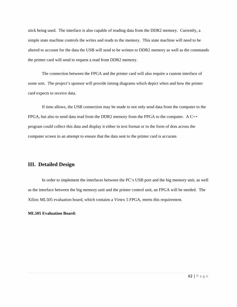
The XILINX HW_VSML505-UNI-G, or
ML505 evaluation board (See Figure 3), has a
Virtex 5 LXT FPGA, which is connected to DDR2
memory, a USB controller, and 64 I/O pins. The
ML505 board also contains a JTAG port which will
allow us to easily program the FPGA. The ML505
block diagram is shown in Figure 4.
Figure 4: ML505 Block Diagram
(Source: http://www.xilinx.com)
Figure 3: ML505 Evaluation Board
(Source: http://www.xilinx.com)
64 | P a g e
Virtex 5 LXT FPGA:
The Virtex 5 LXT FPGA is produced by
Xilinx. According to the Xilinx website, the Virtex
5 contains up to 330,000 logic cells, 1200 I/O pins
for high-bandwidth memory interfacing, and 24 low-
power transceivers for high-speed serial interfaces.
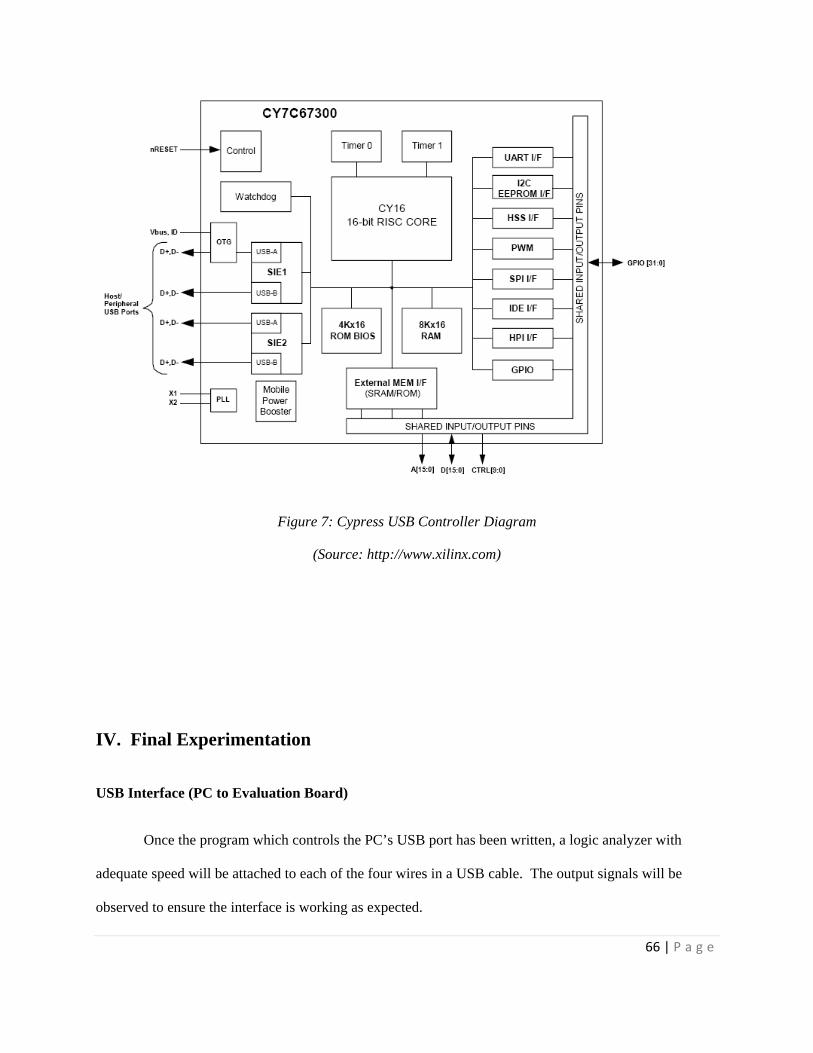
DDR2 Memory:
DDR2 memory meets the speed
requirements of the production printers.
The ML505 board includes a 256 MB stick of
DDR2 SO-DIMM memory. The DDR2 memory
slot on the board is upgradeable.
USB:
USB will be the connection between the
laptop and evaluation board. Since USB is fast, easy
to use, and also a standard type, it is a good choice in this particular system where a laptop has to be
connected with an evaluation board.
Compact Flash:
Figure 5: Virtex 5 Logo
(Source: http://www.xilinx.com)
Figure 6: SO-DIMM DDR2
(Source: http://www.ocztechnology.com)

65 | P a g e
Xilinx Virtex 5 module will be programmed using the Compact Flash system provided on the
ML505 evaluation board. Compact Flash requires less power than other available devices. CF is robust in
that it is nonvolatile and solid state.
Logic Analyzer:
A logic analyzer will be used to aid debugging the system.
Xilinx ISE 9.1i:
Xilinx ISE 9.1i is a program which allows the development of Verilog HDL modules. The
program can also translate the modules into a .ACE file which can be loaded on the Compact Flash to
program the FPGA.
Verilog HDL:
Knowledge of Verilog is one of the key requirements to implement the design. As requested by
InfoPrint Solutions Company, Verilog HDL will be used to program the Xilinx FPGA.
USB Control:
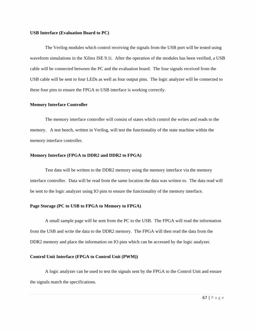
USB is used as the connection between the laptop and evaluation board. A custom program
written in C++ will be used to control the flow of data between the computer and the evaluation board.
USB is a serial connection with data represented by a differential voltage between two pins. Two
additional pins are used for power. The ML505 board includes a Cypress USB Controller (figure 5)
which is connected between the USB port on the board and the FPGA.
66 | P a g e
Figure 7: Cypress USB Controller Diagram
(Source: http://www.xilinx.com)
IV. Final Experimentation
USB Interface (PC to Evaluation Board)
Once the program which controls the PC’s USB port has been written, a logic analyzer with
adequate speed will be attached to each of the four wires in a USB cable. The output signals will be
observed to ensure the interface is working as expected.
67 | P a g e
USB Interface (Evaluation Board to PC)
The Verilog modules which control receiving the signals from the USB port will be tested using
waveform simulations in the Xilinx ISE 9.1i. After the operation of the modules has been verified, a USB
cable will be connected between the PC and the evaluation board. The four signals received from the
USB cable will be sent to four LEDs as well as four output pins. The logic analyzer will be connected to
these four pins to ensure the FPGA to USB interface is working correctly.
Memory Interface Controller
The memory interface controller will consist of states which control the writes and reads to the
memory. A test bench, written in Verilog, will test the functionality of the state machine within the
memory interface controller.
Memory Interface (FPGA to DDR2 and DDR2 to FPGA)
Test data will be written to the DDR2 memory using the memory interface via the memory
interface controller. Data will be read from the same location the data was written to. The data read will
be sent to the logic analyzer using IO pins to ensure the functionality of the memory interface.
Page Storage (PC to USB to FPGA to Memory to FPGA)
A small sample page will be sent from the PC to the USB. The FPGA will read the information
from the USB and write the data to the DDR2 memory. The FPGA will then read the data from the
DDR2 memory and place the information on IO pins which can be accessed by the logic analyzer.
Control Unit Interface (FPGA to Control Unit (PWM))
A logic analyzer can be used to test the signals sent by the FPGA to the Control Unit and ensure
the signals match the specifications.

68 | P a g e
Page Insertion (Memory to FPGA to Control Unit (PWM))
To test the signals sent by the memory to the FPGA to the Control Unit, a logic analyzer will be
used to ensure the signals match the requirements.
Full Process (PC to USB to FPGA to Memory to FPGA to Control Unit (PWM))
To test the entire process, a logic analyzer will be used to confirm that the page sent from the PC
is reproduced at the IO pins of the FPGA with proper timing and format. PDIS will not be able to be
tested on a real printer, so the final test will consist of comparing the signals on the IO pins with the given
specifications.
VI. Milestones and Tasks

69 | P a g e
Task CompletionName Rate 1 2 3 4 5 6 7 8 9 10 11 12 13 14
1. USB Interface
PC Program 0%
Program Testing 0%
FPGA to USB Interaction 0%
Testing 0%
2. Memory Interface 0%
Modify Control Unit for USB Data 0%
Testing 0%
3. Printer Card Interface 0%
Develop Timing Scheme 0%
Modify Control Unit for Printer Requests 0%
Testing 0%
4. Final Testing 0%
5. Demonstration (milestones)
6. Reporting
Weeks
Figure 8: Milestones