MVME6100 Installation and Use - Penguin Solutions
118
MVME6100 Single Board Computer Installation and Use P/N: 6806800D58K September 2019
-
Upload
khangminh22 -
Category
Documents
-
view
0 -
download
0
Transcript of MVME6100 Installation and Use - Penguin Solutions
MVME6100 Single Board ComputerInstallation and Use
P/N: 6806800D58KSeptember 2019

© 2019 SMART Embedded Computing™, Inc.
All Rights Reserved.
Trademarks
The stylized "S" and "SMART" is a registered trademark of SMART Modular Technologies, Inc. and “SMART Embedded
Computing” and the SMART Embedded Computing logo are trademarks of SMART Modular Technologies, Inc. All other names
and logos referred to are trade names, trademarks, or registered trademarks of their respective owners. These materials are
provided by SMART Embedded Computing as a service to its customers and may be used for informational purposes only.
Disclaimer*
SMART Embedded Computing (SMART EC) assumes no responsibility for errors or omissions in these materials. These
materials are provided "AS IS" without warranty of any kind, either expressed or implied, including but not limited to,
the implied warranties of merchantability, fitness for a particular purpose, or non-infringement. SMART EC further does
not warrant the accuracy or completeness of the information, text, graphics, links or other items contained within these
materials. SMART EC shall not be liable for any special, indirect, incidental, or consequential damages, including without
limitation, lost revenues or lost profits, which may result from the use of these materials. SMART EC may make changes to
these materials, or to the products described therein, at any time without notice. SMART EC makes no commitment to update
the information contained within these materials.
Electronic versions of this material may be read online, downloaded for personal use, or referenced in another document as a
URL to a SMART EC website. The text itself may not be published commercially in print or electronic form, edited, translated,
or otherwise altered without the permission of SMART EC.
It is possible that this publication may contain reference to or information about SMART EC products, programming, or services
that are not available in your country. Such references or information must not be construed to mean that SMART EC intends
to announce such SMART EC products, programming, or services in your country.
Limited and Restricted Rights Legend
If the documentation contained herein is supplied, directly or indirectly, to the U.S. Government, the following notice shall apply
unless otherwise agreed to in writing by SMART Embedded Computing.
Use, duplication, or disclosure by the Government is subject to restrictions as set forth in subparagraph (b)(3) of the Rights in
Technical Data clause at DFARS 252.227-7013 (Nov. 1995) and of the Rights in Noncommercial Computer Software and
Documentation clause at DFARS 252.227-7014 (Jun. 1995).
SMART Embedded Computing, Inc.
2900 S. Diablo Way, Suite 190
Tempe, Arizona 85282
USA
*For full legal terms and conditions, visit www.smartembedded.com/ec/legal

Table of Contents
MVME6100 Single Board Computer Installation and Use (6806800D58K) 3
About this Manual . . . . . . . . . . . . . . . . . . . . . . . . . . . . . . . . . . . . . . . . . . . . . . . . . . . . . . . . . . . . . . . 11
Safety Notes. . . . . . . . . . . . . . . . . . . . . . . . . . . . . . . . . . . . . . . . . . . . . . . . . . . . . . . . . . . . . . . . . . . . 17
Sicherheitshinweise . . . . . . . . . . . . . . . . . . . . . . . . . . . . . . . . . . . . . . . . . . . . . . . . . . . . . . . . . . . . . 21
1 Hardware Preparation and Installation . . . . . . . . . . . . . . . . . . . . . . . . . . . . . . . . . . . . . . . . . . . 25
1.1 Overview . . . . . . . . . . . . . . . . . . . . . . . . . . . . . . . . . . . . . . . . . . . . . . . . . . . . . . . . . . . . . . . 25
1.2 Description . . . . . . . . . . . . . . . . . . . . . . . . . . . . . . . . . . . . . . . . . . . . . . . . . . . . . . . . . . . . . 25
1.3 Ordering and Support Information . . . . . . . . . . . . . . . . . . . . . . . . . . . . . . . . . . . . . . . . . . . 26
1.4 Getting Started . . . . . . . . . . . . . . . . . . . . . . . . . . . . . . . . . . . . . . . . . . . . . . . . . . . . . . . . . . 27
1.4.1 Overview of Startup Procedures . . . . . . . . . . . . . . . . . . . . . . . . . . . . . . . . . . . . . . . 27
1.4.2 Unpacking Guidelines . . . . . . . . . . . . . . . . . . . . . . . . . . . . . . . . . . . . . . . . . . . . . . . 27
1.5 Configuring the Hardware . . . . . . . . . . . . . . . . . . . . . . . . . . . . . . . . . . . . . . . . . . . . . . . . . . 28
1.5.1 SCON Header (J7). . . . . . . . . . . . . . . . . . . . . . . . . . . . . . . . . . . . . . . . . . . . . . . . . . 31
1.5.2 PMC/IPMC Selection Headers (J10, J15-J18, J25-J28) . . . . . . . . . . . . . . . . . . . . . 31
1.5.3 PMC I/O Voltage Configuration . . . . . . . . . . . . . . . . . . . . . . . . . . . . . . . . . . . . . . . . 32
1.5.4 Front/Rear Ethernet and Transition Module Options Header (J30) . . . . . . . . . . . . . 33
1.5.5 SROM Configuration Switch (S3). . . . . . . . . . . . . . . . . . . . . . . . . . . . . . . . . . . . . . . 33
1.5.6 Flash Boot Bank Select Configuration Switch (S4) . . . . . . . . . . . . . . . . . . . . . . . . . 34
1.6 Installing the Blade . . . . . . . . . . . . . . . . . . . . . . . . . . . . . . . . . . . . . . . . . . . . . . . . . . . . . . . 35
1.7 Connecting to Peripherals . . . . . . . . . . . . . . . . . . . . . . . . . . . . . . . . . . . . . . . . . . . . . . . . . 36
1.8 Completing the Installation . . . . . . . . . . . . . . . . . . . . . . . . . . . . . . . . . . . . . . . . . . . . . . . . . 36
2 Startup and Operation . . . . . . . . . . . . . . . . . . . . . . . . . . . . . . . . . . . . . . . . . . . . . . . . . . . . . . . . 37
2.1 Introduction . . . . . . . . . . . . . . . . . . . . . . . . . . . . . . . . . . . . . . . . . . . . . . . . . . . . . . . . . . . . . 37
2.2 Applying Power . . . . . . . . . . . . . . . . . . . . . . . . . . . . . . . . . . . . . . . . . . . . . . . . . . . . . . . . . . 37
2.3 Switches and Indicators . . . . . . . . . . . . . . . . . . . . . . . . . . . . . . . . . . . . . . . . . . . . . . . . . . . 37
3 MOTLoad Firmware . . . . . . . . . . . . . . . . . . . . . . . . . . . . . . . . . . . . . . . . . . . . . . . . . . . . . . . . . . 39
3.1 Overview . . . . . . . . . . . . . . . . . . . . . . . . . . . . . . . . . . . . . . . . . . . . . . . . . . . . . . . . . . . . . . . 39
3.2 Implementation and Memory Requirements . . . . . . . . . . . . . . . . . . . . . . . . . . . . . . . . . . . . 39
3.3 MOTLoad Commands . . . . . . . . . . . . . . . . . . . . . . . . . . . . . . . . . . . . . . . . . . . . . . . . . . . . 39
3.3.1 Utilities . . . . . . . . . . . . . . . . . . . . . . . . . . . . . . . . . . . . . . . . . . . . . . . . . . . . . . . . . . . 39

4 MVME6100 Single Board Computer Installation and Use (6806800D58K)
Table of Contents
3.3.2 Tests . . . . . . . . . . . . . . . . . . . . . . . . . . . . . . . . . . . . . . . . . . . . . . . . . . . . . . . . . . . . 40
3.3.3 Command List . . . . . . . . . . . . . . . . . . . . . . . . . . . . . . . . . . . . . . . . . . . . . . . . . . . . . 41
3.4 Using the Command Line Interface . . . . . . . . . . . . . . . . . . . . . . . . . . . . . . . . . . . . . . . . . . 46
3.4.1 Command Line Rules. . . . . . . . . . . . . . . . . . . . . . . . . . . . . . . . . . . . . . . . . . . . . . . . 47
3.4.2 Command Line Help . . . . . . . . . . . . . . . . . . . . . . . . . . . . . . . . . . . . . . . . . . . . . . . . 48
3.5 Firmware Settings . . . . . . . . . . . . . . . . . . . . . . . . . . . . . . . . . . . . . . . . . . . . . . . . . . . . . . . . 48
3.5.1 Default VME Settings . . . . . . . . . . . . . . . . . . . . . . . . . . . . . . . . . . . . . . . . . . . . . . . . 48
3.5.2 Control Register/Control Status Register Settings . . . . . . . . . . . . . . . . . . . . . . . . . . 52
3.5.3 Displaying VME Settings . . . . . . . . . . . . . . . . . . . . . . . . . . . . . . . . . . . . . . . . . . . . . 52
3.5.4 Editing VME Settings . . . . . . . . . . . . . . . . . . . . . . . . . . . . . . . . . . . . . . . . . . . . . . . . 53
3.5.5 Deleting VME Settings . . . . . . . . . . . . . . . . . . . . . . . . . . . . . . . . . . . . . . . . . . . . . . . 53
3.5.6 Restoring Default VME Settings. . . . . . . . . . . . . . . . . . . . . . . . . . . . . . . . . . . . . . . . 54
3.6 Remote Start . . . . . . . . . . . . . . . . . . . . . . . . . . . . . . . . . . . . . . . . . . . . . . . . . . . . . . . . . . . . 54
3.7 Alternate Boot Images and Safe Start . . . . . . . . . . . . . . . . . . . . . . . . . . . . . . . . . . . . . . . . 55
3.8 Firmware Startup Sequence Following Reset . . . . . . . . . . . . . . . . . . . . . . . . . . . . . . . . . . 55
3.9 Firmware Scan for Boot Image . . . . . . . . . . . . . . . . . . . . . . . . . . . . . . . . . . . . . . . . . . . . . . 56
3.10 Boot Images . . . . . . . . . . . . . . . . . . . . . . . . . . . . . . . . . . . . . . . . . . . . . . . . . . . . . . . . . . . . 57
3.10.1 Checksum Algorithm . . . . . . . . . . . . . . . . . . . . . . . . . . . . . . . . . . . . . . . . . . . . . . . . 58
3.10.2 Image Flags . . . . . . . . . . . . . . . . . . . . . . . . . . . . . . . . . . . . . . . . . . . . . . . . . . . . . . . 59
3.10.3 User Images. . . . . . . . . . . . . . . . . . . . . . . . . . . . . . . . . . . . . . . . . . . . . . . . . . . . . . . 60
3.10.4 Alternate Boot Data Structure . . . . . . . . . . . . . . . . . . . . . . . . . . . . . . . . . . . . . . . . . 60
3.10.5 Alternate Boot Images and Safe Start . . . . . . . . . . . . . . . . . . . . . . . . . . . . . . . . . . . 61
3.10.6 Boot Image Firmware Scan . . . . . . . . . . . . . . . . . . . . . . . . . . . . . . . . . . . . . . . . . . . 61
3.11 Startup Sequence . . . . . . . . . . . . . . . . . . . . . . . . . . . . . . . . . . . . . . . . . . . . . . . . . . . . . . . . 62
4 Functional Description. . . . . . . . . . . . . . . . . . . . . . . . . . . . . . . . . . . . . . . . . . . . . . . . . . . . . . . . 65
4.1 Overview . . . . . . . . . . . . . . . . . . . . . . . . . . . . . . . . . . . . . . . . . . . . . . . . . . . . . . . . . . . . . . . 65
4.2 Features . . . . . . . . . . . . . . . . . . . . . . . . . . . . . . . . . . . . . . . . . . . . . . . . . . . . . . . . . . . . . . . 65
4.3 Block Diagram . . . . . . . . . . . . . . . . . . . . . . . . . . . . . . . . . . . . . . . . . . . . . . . . . . . . . . . . . . 67
4.4 Processor . . . . . . . . . . . . . . . . . . . . . . . . . . . . . . . . . . . . . . . . . . . . . . . . . . . . . . . . . . . . . . 67
4.5 L3 Cache . . . . . . . . . . . . . . . . . . . . . . . . . . . . . . . . . . . . . . . . . . . . . . . . . . . . . . . . . . . . . . 68
4.6 System Controller . . . . . . . . . . . . . . . . . . . . . . . . . . . . . . . . . . . . . . . . . . . . . . . . . . . . . . . . 68
4.6.1 CPU Bus Interface . . . . . . . . . . . . . . . . . . . . . . . . . . . . . . . . . . . . . . . . . . . . . . . . . . 69
4.6.2 Memory Controller Interface. . . . . . . . . . . . . . . . . . . . . . . . . . . . . . . . . . . . . . . . . . . 69
4.6.3 Device Controller Interface. . . . . . . . . . . . . . . . . . . . . . . . . . . . . . . . . . . . . . . . . . . . 70
4.6.4 PCI/PCI-X Interfaces . . . . . . . . . . . . . . . . . . . . . . . . . . . . . . . . . . . . . . . . . . . . . . . . 70
4.6.5 Gigabit Ethernet MACs . . . . . . . . . . . . . . . . . . . . . . . . . . . . . . . . . . . . . . . . . . . . . . 70
4.6.6 SRAM. . . . . . . . . . . . . . . . . . . . . . . . . . . . . . . . . . . . . . . . . . . . . . . . . . . . . . . . . . . . 71

Table of Contents
MVME6100 Single Board Computer Installation and Use (6806800D58K) 5
4.6.7 General-Purpose Timers/Counters . . . . . . . . . . . . . . . . . . . . . . . . . . . . . . . . . . . . . 71
4.6.8 Watchdog Timer. . . . . . . . . . . . . . . . . . . . . . . . . . . . . . . . . . . . . . . . . . . . . . . . . . . . 71
4.6.9 I2O Message Unit . . . . . . . . . . . . . . . . . . . . . . . . . . . . . . . . . . . . . . . . . . . . . . . . . . 71
4.6.10 Four Channel Independent DMA Controller. . . . . . . . . . . . . . . . . . . . . . . . . . . . . . . 72
4.6.11 I2C Serial Interface and Devices . . . . . . . . . . . . . . . . . . . . . . . . . . . . . . . . . . . . . . . 72
4.6.12 Interrupt Controller . . . . . . . . . . . . . . . . . . . . . . . . . . . . . . . . . . . . . . . . . . . . . . . . . . 72
4.6.13 PCI Bus Arbitration. . . . . . . . . . . . . . . . . . . . . . . . . . . . . . . . . . . . . . . . . . . . . . . . . . 73
4.7 VMEbus Interface . . . . . . . . . . . . . . . . . . . . . . . . . . . . . . . . . . . . . . . . . . . . . . . . . . . . . . . . 73
4.8 PMCspan Interface . . . . . . . . . . . . . . . . . . . . . . . . . . . . . . . . . . . . . . . . . . . . . . . . . . . . . . . 73
4.9 Flash Memory . . . . . . . . . . . . . . . . . . . . . . . . . . . . . . . . . . . . . . . . . . . . . . . . . . . . . . . . . . . 74
4.10 System Memory . . . . . . . . . . . . . . . . . . . . . . . . . . . . . . . . . . . . . . . . . . . . . . . . . . . . . . . . . 74
4.11 Asynchronous Serial Ports . . . . . . . . . . . . . . . . . . . . . . . . . . . . . . . . . . . . . . . . . . . . . . . . . 74
4.12 PCI Mezzanine Card Slots . . . . . . . . . . . . . . . . . . . . . . . . . . . . . . . . . . . . . . . . . . . . . . . . . 74
4.13 Real-Time Clock/NVRAM/Watchdog Timer . . . . . . . . . . . . . . . . . . . . . . . . . . . . . . . . . . . . 75
4.14 IDSEL Routing . . . . . . . . . . . . . . . . . . . . . . . . . . . . . . . . . . . . . . . . . . . . . . . . . . . . . . . . . . 76
4.15 Reset Control Logic . . . . . . . . . . . . . . . . . . . . . . . . . . . . . . . . . . . . . . . . . . . . . . . . . . . . . . 76
4.16 Debug Support . . . . . . . . . . . . . . . . . . . . . . . . . . . . . . . . . . . . . . . . . . . . . . . . . . . . . . . . . . 76
4.17 Processor JTAG/COP Headers . . . . . . . . . . . . . . . . . . . . . . . . . . . . . . . . . . . . . . . . . . . . . 76
5 Pin Assignments. . . . . . . . . . . . . . . . . . . . . . . . . . . . . . . . . . . . . . . . . . . . . . . . . . . . . . . . . . . . . 77
5.1 Overview . . . . . . . . . . . . . . . . . . . . . . . . . . . . . . . . . . . . . . . . . . . . . . . . . . . . . . . . . . . . . . . 77
5.2 Connectors . . . . . . . . . . . . . . . . . . . . . . . . . . . . . . . . . . . . . . . . . . . . . . . . . . . . . . . . . . . . . 77
5.2.1 PMC Expansion Connector (J4). . . . . . . . . . . . . . . . . . . . . . . . . . . . . . . . . . . . . . . . 78
5.2.2 Gigabit Ethernet Connectors (J9, J93). . . . . . . . . . . . . . . . . . . . . . . . . . . . . . . . . . . 81
5.2.3 PCI Mezzanine Card (PMC) Connectors (J11-J14, J21-J24) . . . . . . . . . . . . . . . . . 81
5.2.4 COM1 Connector (J19) . . . . . . . . . . . . . . . . . . . . . . . . . . . . . . . . . . . . . . . . . . . . . . 92
5.2.5 VMEbus P1 Connector. . . . . . . . . . . . . . . . . . . . . . . . . . . . . . . . . . . . . . . . . . . . . . . 93
5.2.6 VMEBus P2 Connector (PMC Mode). . . . . . . . . . . . . . . . . . . . . . . . . . . . . . . . . . . . 95
5.2.7 VMEbus P2 Connector (IPMC Mode) . . . . . . . . . . . . . . . . . . . . . . . . . . . . . . . . . . . 97
5.3 Headers . . . . . . . . . . . . . . . . . . . . . . . . . . . . . . . . . . . . . . . . . . . . . . . . . . . . . . . . . . . . . . 101
5.3.1 SCON Header (J7). . . . . . . . . . . . . . . . . . . . . . . . . . . . . . . . . . . . . . . . . . . . . . . . . 101
5.3.2 Boundary Scan Header (J8). . . . . . . . . . . . . . . . . . . . . . . . . . . . . . . . . . . . . . . . . . 101
5.3.3 PMC/IPMC Selection Headers (J10, J15-J18, J25-J28) . . . . . . . . . . . . . . . . . . . . 102
5.3.4 COM2 Header (J29). . . . . . . . . . . . . . . . . . . . . . . . . . . . . . . . . . . . . . . . . . . . . . . . 102
5.3.5 Front/Rear Ethernet and Transition Module Options Header (J30) . . . . . . . . . . . . 103
5.3.6 Processor JTAG/COP Header (J42) . . . . . . . . . . . . . . . . . . . . . . . . . . . . . . . . . . . 104

6 MVME6100 Single Board Computer Installation and Use (6806800D58K)
Table of Contents
A Specifications . . . . . . . . . . . . . . . . . . . . . . . . . . . . . . . . . . . . . . . . . . . . . . . . . . . . . . . . . . . . . . 105
A.1 Power Requirements . . . . . . . . . . . . . . . . . . . . . . . . . . . . . . . . . . . . . . . . . . . . . . . . . . . . 105
A.1.1 Supply Current Requirements . . . . . . . . . . . . . . . . . . . . . . . . . . . . . . . . . . . . . . . . 105
A.2 Environmental Specifications . . . . . . . . . . . . . . . . . . . . . . . . . . . . . . . . . . . . . . . . . . . . . . 106
B Thermal Validation . . . . . . . . . . . . . . . . . . . . . . . . . . . . . . . . . . . . . . . . . . . . . . . . . . . . . . . . . . 107
B.1 Overview . . . . . . . . . . . . . . . . . . . . . . . . . . . . . . . . . . . . . . . . . . . . . . . . . . . . . . . . . . . . . . 107
B.2 Thermally Significant Components . . . . . . . . . . . . . . . . . . . . . . . . . . . . . . . . . . . . . . . . . . 107
B.3 Component Temperature Measurement . . . . . . . . . . . . . . . . . . . . . . . . . . . . . . . . . . . . . . 109
B.3.1 Preparation. . . . . . . . . . . . . . . . . . . . . . . . . . . . . . . . . . . . . . . . . . . . . . . . . . . . . . . 109
B.3.2 Measuring Junction Temperature . . . . . . . . . . . . . . . . . . . . . . . . . . . . . . . . . . . . . 110
B.3.3 Measuring Case Temperature . . . . . . . . . . . . . . . . . . . . . . . . . . . . . . . . . . . . . . . . 110
B.3.4 Measuring Local Air Temperature . . . . . . . . . . . . . . . . . . . . . . . . . . . . . . . . . . . . . 112
C Related Documentation . . . . . . . . . . . . . . . . . . . . . . . . . . . . . . . . . . . . . . . . . . . . . . . . . . . . . . 113
C.1 SMART Embedded Computing Documentation . . . . . . . . . . . . . . . . . . . . . . . . . . . . . . . . 113
C.2 Manufacturers’ Documents . . . . . . . . . . . . . . . . . . . . . . . . . . . . . . . . . . . . . . . . . . . . . . . . 113
C.3 Related Specifications . . . . . . . . . . . . . . . . . . . . . . . . . . . . . . . . . . . . . . . . . . . . . . . . . . . 115
List of Figures
MVME6100 Single Board Computer Installation and Use (6806800D58K) 7
Figure 1-1 Component Layout . . . . . . . . . . . . . . . . . . . . . . . . . . . . . . . . . . . . . . . . . . . . . . . . . 30
Figure 1-2 SCON Header Settings . . . . . . . . . . . . . . . . . . . . . . . . . . . . . . . . . . . . . . . . . . . . . 31
Figure 1-3 PMC/IPMC Header Settings . . . . . . . . . . . . . . . . . . . . . . . . . . . . . . . . . . . . . . . . . 31
Figure 1-4 Front/Rear Ethernet Option Settings . . . . . . . . . . . . . . . . . . . . . . . . . . . . . . . . . . . 33
Figure 4-1 MVME6100 Block Diagram . . . . . . . . . . . . . . . . . . . . . . . . . . . . . . . . . . . . . . . . . . 67
Figure B-1 Thermally Significant Component - Primary Side . . . . . . . . . . . . . . . . . . . . . . . . 108
Figure B-2 Thermally Significant Component - Secondary Side . . . . . . . . . . . . . . . . . . . . . . 109
Figure B-3 Mounting a Thermocouple Under a Heatsink . . . . . . . . . . . . . . . . . . . . . . . . . . . 111
Figure B-4 Measuring Local Air Temperature . . . . . . . . . . . . . . . . . . . . . . . . . . . . . . . . . . . . 112

List of Figures
8 MVME6100 Single Board Computer Installation and Use (6806800D58K)

List of Tables
MVME6100 Single Board Computer Installation and Use (6806800D58K) 9
Table 1-1 Startup Overview . . . . . . . . . . . . . . . . . . . . . . . . . . . . . . . . . . . . . . . . . . . . . . . . . . . . 27
Table 1-2 Jumper and Switch Settings . . . . . . . . . . . . . . . . . . . . . . . . . . . . . . . . . . . . . . . . . . . . 29
Table 1-3 SROM Configuration Switch (S3) . . . . . . . . . . . . . . . . . . . . . . . . . . . . . . . . . . . . . . . . 34
Table 1-4 Configuration Switch (S4) . . . . . . . . . . . . . . . . . . . . . . . . . . . . . . . . . . . . . . . . . . . . . . 35
Table 1-5 MVME6100 Connectors . . . . . . . . . . . . . . . . . . . . . . . . . . . . . . . . . . . . . . . . . . . . . . . 36
Table 2-1 Front-Panel LED Status Indicators . . . . . . . . . . . . . . . . . . . . . . . . . . . . . . . . . . . . . . . 37
Table 3-1 MOTLoad Commands . . . . . . . . . . . . . . . . . . . . . . . . . . . . . . . . . . . . . . . . . . . . . . . . . 41
Table 3-2 MOTLoad Image Flags . . . . . . . . . . . . . . . . . . . . . . . . . . . . . . . . . . . . . . . . . . . . . . . . 59
Table 4-1 MVME6100 Features Summary . . . . . . . . . . . . . . . . . . . . . . . . . . . . . . . . . . . . . . . . . 65
Table 4-2 Device Bus Parameters . . . . . . . . . . . . . . . . . . . . . . . . . . . . . . . . . . . . . . . . . . . . . . . . 70
Table 5-1 PMC Expansion Connector (J4) Pin Assignments . . . . . . . . . . . . . . . . . . . . . . . . . . . 78
Table 5-2 Gigabit Ethernet Connectors (J9, J93) Pin Assignment . . . . . . . . . . . . . . . . . . . . . . . 81
Table 5-3 PMC Slot 1 Connector (J11) Pin Assignments . . . . . . . . . . . . . . . . . . . . . . . . . . . . . . 82
Table 5-4 PMC Slot 1 Connector (J12) Pin Assignments . . . . . . . . . . . . . . . . . . . . . . . . . . . . . . 83
Table 5-5 PMC Slot 1 Connector (J13) Pin Assignments . . . . . . . . . . . . . . . . . . . . . . . . . . . . . . 84
Table 5-6 PMC Slot 1 Connector (J14) Pin Assignments . . . . . . . . . . . . . . . . . . . . . . . . . . . . . . 86
Table 5-7 PMC Slot 2 Connector (J21) Pin Assignments . . . . . . . . . . . . . . . . . . . . . . . . . . . . . . 87
Table 5-8 PMC Slot 2 Connector (J22) Pin Assignments . . . . . . . . . . . . . . . . . . . . . . . . . . . . . . 88
Table 5-9 PMC Slot 2 Connector (J23) Pin Assignments . . . . . . . . . . . . . . . . . . . . . . . . . . . . . . 90
Table 5-10 PMC Slot 2 Connector (J24) Pin Assignments . . . . . . . . . . . . . . . . . . . . . . . . . . . . . . 91
Table 5-11 COM1 Connector (J19) Pin Assignments . . . . . . . . . . . . . . . . . . . . . . . . . . . . . . . . . . 92
Table 5-12 VMEbus P1 Connector Pin Assignments . . . . . . . . . . . . . . . . . . . . . . . . . . . . . . . . . . 93
Table 5-13 VMEbus P2 Connector Pin Assignments (PMC Mode) . . . . . . . . . . . . . . . . . . . . . . . . 95
Table 5-14 VME P2 Connector Pinouts with IPMC712 . . . . . . . . . . . . . . . . . . . . . . . . . . . . . . . . . 97
Table 5-15 VME P2 Connector Pinouts with IPMC761 . . . . . . . . . . . . . . . . . . . . . . . . . . . . . . . . . 99
Table 5-16 SCON Header (J7) Pin Assignments . . . . . . . . . . . . . . . . . . . . . . . . . . . . . . . . . . . . 101
Table 5-17 Boundary Scan Header (J8) Pin Assignments . . . . . . . . . . . . . . . . . . . . . . . . . . . . . 101
Table 5-18 PMC/IPMC Configuration Jumper Block . . . . . . . . . . . . . . . . . . . . . . . . . . . . . . . . . . 102
Table 5-19 COM2 Planar Serial Port Header (J29) Pin Assignments . . . . . . . . . . . . . . . . . . . . . 102
Table 5-20 Front/Rear Ethernet and Transition Module Options Header (J30) Pin Assignment . 103
Table 5-21 Processor JTAG/COP (RISCWatch) Header (J42) Pin Assignments . . . . . . . . . . . . 104
Table A-1 Power Requirements . . . . . . . . . . . . . . . . . . . . . . . . . . . . . . . . . . . . . . . . . . . . . . . . . 105
Table A-2 MVME6100 Specifications . . . . . . . . . . . . . . . . . . . . . . . . . . . . . . . . . . . . . . . . . . . . 106
Table B-1 Thermally Significant Components . . . . . . . . . . . . . . . . . . . . . . . . . . . . . . . . . . . . . . 107
Table C-1 SMART EC Publications . . . . . . . . . . . . . . . . . . . . . . . . . . . . . . . . . . . . . . . . . . . . . . 113
Table C-2 Manufacturers’ Documents . . . . . . . . . . . . . . . . . . . . . . . . . . . . . . . . . . . . . . . . . . . . 113
Table C-3 Related Specifications . . . . . . . . . . . . . . . . . . . . . . . . . . . . . . . . . . . . . . . . . . . . . . . 115

List of Tables
10 MVME6100 Single Board Computer Installation and Use (6806800D58K)

MVME6100 Single Board Computer Installation and Use (6806800D58K) 11
About this Manual
Overview of ContentsThis manual is divided into the following chapters and appendices:
Safety Notes on page 17 summarizes the safety instructions in the manual.
Sicherheitshinweise on page 21 is a German translation of the Safety Notes chapter.
Chapter 1, Hardware Preparation and Installation on page 25, provides MVME6100 board
preparation and installation instructions, as well as ESD precautionary notes.
Chapter 2, Startup and Operation on page 37, provides the power-up procedure and
identifies the switches and indicators on the MVME6100.
Chapter 3, MOTLoad Firmware on page 39, describes the basic features of the MOTLoad
firmware product.
Chapter 4, Functional Description on page 65, describes the MVME6100 on a block
diagram level.
Chapter 5, Pin Assignments on page 77, provides pin assignments for various headers and
connectors on the MVME6100 single board computer.
Appendix A, Specifications on page 105, provides power requirements and environmental
specifications.
Appendix B, Thermal Validation on page 107, provides information to conduct thermal
evaluations and identifies thermally significant components along with their maximum
allowable operating temperatures.
Appendix C, Related Documentation on page 113, provides a listing of related SMART EC
manuals, vendor documentation, and industry specifications.
The MVME6100 Single Board Computer Installation and Use manual provides the
information you will need to install and configure your MVME61006E single board computer
(hereinafter referred to as MVME6100). It provides specific preparation and installation
information, and data applicable to the board.

12 MVME6100 Single Board Computer Installation and Use (6806800D58K)
About this ManualAbout this Manual
AbbreviationsThis document uses the following abbreviations:
Term Definition
CPLD Complex Programmable Logic Device
DDR Double Data Rate
DDR3 Double Data Rate 3
DMI Direct Media Interface
DUART Dual UART
EEPROM Erasable Programmable Read-Only Memory
FCC Federal Communications Commission
GB GigaByte
Gbit Gigabit
Gbps Gigabits per second
I/O Input/Output
IEEE Institute of Electrical and Electronics Engineers
LED Light Emitting Diode
MHz Megahertz
MCP Multi-Chip Package
MRAM Magnetoresistive Random Access Memory
PCB Printed Circuit Board
PCI Peripheral Component Interconnect
PCI-E PCI Express
PCI-X Peripheral Component Interconnect eXtended
PIM PCI Mezzanine Card Input/Output Module
PLD Programmable Logic Device
PMC PCI Mezzanine Card (IEEE P1386.1)
PrPMC Processor PCI Mezzanine Card
RTC Real-Time Clock

About this Manual
MVME6100 Single Board Computer Installation and Use (6806800D58K) 13
ConventionsThe following table describes the conventions used throughout this manual.
RTM Rear Transition Module
SATA Serial AT Attachment
SDR Single Data Rate
UART Universal Asynchronous Receiver-Transmitter
VITA VMEbus International Trade Association
VME Versa Module Eurocard
XMC PCI Express Mezzanine Card
Term Definition
Notation Description
0x00000000 Typical notation for hexadecimal numbers (digits are 0 through F), for
example used for addresses and offsets
0b0000 Same for binary numbers (digits are 0 and 1)
bold Used to emphasize a word
Screen Used for on-screen output and code related elements or commands.
Sample of Programming used in a table (9pt)
Courier + Bold Used to characterize user input and to separate it from system output
Reference Used for references and for table and figure descriptions
File > Exit Notation for selecting a submenu
<text> Notation for variables and keys
[text]Notation for software buttons to click on the screen and parameter
description
... Repeated item for example node 1, node 2, ..., node 12
.
.
.
Omission of information from example/command that is not necessary at
the time

14 MVME6100 Single Board Computer Installation and Use (6806800D58K)
About this ManualAbout this Manual
..Ranges, for example: 0..4 means one of the integers 0,1,2,3, and 4 (used
in registers)
| Logical OR
Indicates a hazardous situation which, if not avoided, could result in death
or serious injury
Indicates a hazardous situation which, if not avoided, may result in minor
or moderate injury
Indicates a property damage message
Indicates a hot surface that could result in moderate or serious injury
Indicates an electrical situation that could result in moderate injury or death
Indicates that when working in an ESD environment care should be taken
to use proper ESD practices
No danger encountered, pay attention to important information
Notation Description

About this Manual
MVME6100 Single Board Computer Installation and Use (6806800D58K) 15
Summary of ChangesThis manual has been revised and replaces all previous editions. .
Part Number Date Description
6806800D58K September 2019
Re-branded to SMART Embedded Computing template,
updated conventions table, light edits. Removed Model
Number table in About this Manual; added Ordering and
Support Information in Chapter 1. Updated Manufacturers’
Documentation table in Appendix C.
6806800D58J May 2016 Removed Declaration of Conformity.
6806800D58H June 2014
Replaced "DDR" with "SDR" in Features on page 65, L3Cache on page 68, and in the Figure 4-1.
Re-branded to Artesyn template.
6806800D58G December 2012 Added Declaration of Conformity on page 19.
6806800D58F August 2011Added Safety Notes on page 17 and
Sicherheitshinweise on page 21.
6806800D58E March 2009Added csUserAltBoot command to MOTLoad Commandson page 41, editorial changes
6806800D58D April 2008 Updated to Emerson publications style.
6806800D58C January 2008
Updated to remove two incorrect sources of reset. See
Reset Control Logic on page 76. Table 5-13 on page95 was updated to indicate both possible uses of pins C1,
C2, C3, C4, Z25, Z27, Z29, and Z31 (when J30 is configured
for rear Ethernet and when J30 is configured for full PMC
mode).
6806800D58B November 2007
Updated to better describe how to configure the VIO keying
pins for the PMC sites. See PMC I/O VoltageConfiguration on page 32. Also, Table 5-12 on page 93was updated to identify the Geographical Addressing pins on
Row D of the P1 connector and minor updates were made to
correct the hot link to the literature catalog web site and
update the reader comments link.

16 MVME6100 Single Board Computer Installation and Use (6806800D58K)
About this ManualAbout this Manual

MVME6100 Single Board Computer Safety Notes Summary (6806800M94C) 17
Safety Notes
This section provides warnings that precede potentially dangerous procedures throughout
this manual. Instructions contained in the warnings must be followed during all phases of
operation, service, and repair of this equipment. You should also employ all other safety
precautions necessary for the operation of the equipment in your operating environment.
Failure to comply with these precautions or with specific warnings elsewhere in this manual
could result in personal injury or damage to the equipment.
SMART Embedded Computing intends to provide all necessary information to install and
handle the product in this manual. Because of the complexity of this product and its various
uses, we do not guarantee that the given information is complete. If you need additional
information, ask your SMART EC representative.
This product is a Safety Extra Low Voltage (SELV) device designed to meet the EN60950-1
requirements for Information Technology Equipment. The use of the product in any other
application may require safety evaluation specific to that application.
Only personnel trained by SMART EC or persons qualified in electronics or electrical
engineering are authorized to install, remove or maintain the product.
The information given in this manual is meant to complete the knowledge of a specialist and
must not be used as replacement for qualified personnel.
Keep away from live circuits inside the equipment. Operating personnel must not remove
equipment covers. Only Factory Authorized Service Personnel or other qualified service
personnel may remove equipment covers for internal subassembly or component
replacement or any internal adjustment.
Do not install substitute parts or perform any unauthorized modification of the equipment or
the warranty may be voided. Contact your local SMART EC representative for service and
repair to make sure that all safety features are maintained.
EMC (Results pending testing)
This equipment has been tested and found to comply with the limits for a Class A digital
device, pursuant to Part 15 of the FCC Rules. These limits are designed to provide
reasonable protection against harmful interference when the equipment is operated in a
commercial environment. This equipment generates, uses, and can radiate radio frequency
energy and, if not installed and used in accordance with the instruction manual, may cause
harmful interference to radio communications.
Operation of this equipment in a residential area is likely to cause harmful interference in
which case the user will be required to correct the interference at his own expense.
Changes or modifications not expressly approved by SMART EC could void the user's
authority to operate the equipment. Board products are tested in a representative system

18 MVME6100 Single Board Computer Safety Notes Summary (6806800M94C)
Safety NotesSafety Notes
to show compliance with the above mentioned requirements. A proper installation in a
compliant system will maintain the required performance. Use only shielded cables when
connecting peripherals to assure that appropriate radio frequency emissions compliance is
maintained.
Operation
Product Damage
High humidity and condensation on the board surface causes short circuits.
Do not operate the board outside the specified environmental limits.
Make sure the board is completely dry and there is no moisture on any surface before
applying power.
Damage of Circuits
Electrostatic discharge and incorrect installation and removal can damage circuits or
shorten its life.
Before touching the board or electronic components, make sure that you are working in an
ESD-safe environment.
Board Malfunction
Switches marked as “reserved” might carry production-related functions and can cause the
board to malfunction if their setting is changed.
Do not change settings of switches marked as “reserved”. The setting of switches which
are not marked as “reserved” has to be checked and changed before board installation.
Installation
Data Loss
Powering down or removing a board before the operating system or other software running
on the board has been properly shut down may cause corruption of data or file systems.
Make sure all software is completely shut down before removing power from the board or
removing the board from the chassis.
Product Damage
Only use injector handles for board insertion to avoid damage to the front panel and/or
PCB. Deformation of the front panel can cause an electrical short or other board
malfunction.

Safety Notes
MVME6100 Single Board Computer Safety Notes Summary (6806800M94C) 19
Product Damage
Inserting or removing modules with power applied may result in damage to module
components.
Before installing or removing additional devices or modules, read the documentation that
came with the product.
Cabling and Connectors
Product Damage
RJ-45 connectors on modules are either twisted-pair Ethernet (TPE) or E1/T1/J1 network
interfaces. Connecting an E1/T1/J1 line to an Ethernet connector may damage your
system.
Make sure that TPE connectors near your working area are clearly marked as
network connectors.
Verify that the length of an electric cable connected to a TPE bushing does not
exceed 100 meters.
Make sure the TPE bushing of the system is connected only to safety extra low
voltage circuits (SELV circuits).
If in doubt, ask your system administrator.
Battery
Board/System Damage
Incorrect exchange of lithium batteries can result in a hazardous explosion.
When exchanging the on-board lithium battery, make sure that the new and the old battery
are exactly the same battery models.
If the respective battery model is not available, contact your local SMART EC sales
representative for the availability of alternative, officially approved battery models.
Data Loss
Exchanging the battery can result in loss of time settings. Backup power prevents the loss
of data during exchange.
Quickly replacing the battery may save time settings.

20 MVME6100 Single Board Computer Safety Notes Summary (6806800M94C)
Safety NotesSafety Notes
Data Loss
If the battery has low or insufficient power the RTC is initialized.
Exchange the battery before seven years of actual battery use have elapsed.
PCB and Battery Holder Damage
Removing the battery with a screw driver may damage the PCB or the battery holder. To
prevent damage, do not use a screw driver to remove the battery from its holder.

MVME6100 Single Board Computer Safety Notes Summary (6806800M94C) 21
Sicherheitshinweise
Dieses Kapitel enthält Hinweise, die potentiell gefährlichen Prozeduren innerhalb dieses
Handbuchs vorrangestellt sind. Beachten Sie unbedingt in allen Phasen des Betriebs, der
Wartung und der Reparatur des Systems die Anweisungen, die diesen Hinweisen
enthalten sind. Sie sollten außerdem alle anderen Vorsichtsmaßnahmen treffen, die für den
Betrieb des Produktes innerhalb Ihrer Betriebsumgebung notwendig sind. Wenn Sie diese
Vorsichtsmaßnahmen oder Sicherheitshinweise, die an anderer Stelle diese Handbuchs
enthalten sind, nicht beachten, kann das Verletzungen oder Schäden am Produkt zur Folge
haben.
SMART Embedded Computing ist darauf bedacht, alle notwendigen Informationen zum
Einbau und zum Umgang mit dem Produkt in diesem Handbuch bereit zu stellen. Da es
sich jedoch um ein komplexes Produkt mit vielfältigen Einsatzmöglichkeiten handelt,
können wir die Vollständigkeit der im Handbuch enthaltenen Informationen nicht
garantieren. Falls Sie weitere Informationen benötigen sollten, wenden Sie sich bitte an die
für Sie zuständige Geschäftsstelle von SMART EC.
Das Produkt wurde entwickelt, um die Sicherheitsanforderungen für SELV Geräte nach der
Norm EN 60950-1 für informationstechnische Einrichtungen zu erfüllen. Die Verwendung
des Produkts in einer anderen Anwendung erfordert eine Sicherheitsüberprüfung für diese
spezifische Anwendung.
Einbau, Wartung und Betrieb dürfen nur von durch SMART EC ausgebildetem oder im
Bereich Elektronik oder Elektrotechnik qualifiziertem Personal durchgeführt werden. Die in
diesem Handbuch enthaltenen Informationen dienen ausschließlich dazu, das Wissen von
Fachpersonal zu ergänzen, können dieses jedoch nicht ersetzen.
Halten Sie sich von stromführenden Leitungen innerhalb des Produktes fern. Entfernen Sie
auf keinen Fall Abdeckungen am Produkt. Nur werksseitig zugelassenes
Wartungspersonal oder anderweitig qualifiziertes Wartungspersonal darf Abdeckungen
entfernen, um Komponenten zu ersetzen oder andere Anpassungen vorzunehmen.
Installieren Sie keine Ersatzteile oder führen Sie keine unerlaubten Veränderungen am
Produkt durch, sonst verfällt die Garantie. Wenden Sie sich für Wartung oder Reparatur
bitte an die für Sie zuständige Geschäftsstelle von SMART EC. So stellen Sie sicher, dass
alle sicherheitsrelevanten Aspekte beachtet werden.
EMV
Das Produkt wurde in einem SMART EC Standardsystem getestet. Es erfüllt die für digitale
Geräte der Klasse A gültigen Grenzwerte in einem solchen System gemäß den FCC-
Richtlinien Abschnitt 15 bzw. EN 55022 Klasse A. Diese Grenzwerte sollen einen
angemessenen Schutz vor Störstrahlung beim Betrieb des Produktes in Gewerbe- sowie
Industriegebieten gewährleisten.

22 MVME6100 Single Board Computer Safety Notes Summary (6806800M94C)
SicherheitshinweiseSicherheitshinweise
Das Produkt arbeitet im Hochfrequenzbereich und erzeugt Störstrahlung. Bei
unsachgemäßem Einbau und anderem als in diesem Handbuch beschriebenen Betrieb
können Störungen im Hochfrequenzbereich auftreten.
Wird das Produkt in einem Wohngebiet betrieben, so kann dies mit grosser
Wahrscheinlichkeit zu starken Störungen führen, welche dann auf Kosten des
Produktanwenders beseitigt werden müssen. Änderungen oder Modifikationen am
Produkt, welche ohne ausdrückliche Genehmigung von SMART EC durchgeführt werden,
können dazu führen, dass der Anwender die Genehmigung zum Betrieb des Produktes
verliert. Boardprodukte werden in einem repräsentativen System getestet, um zu zeigen,
dass das Board den oben aufgeführten EMV-Richtlinien entspricht. Eine
ordnungsgemässe Installation in einem System, welches die EMV-Richtlinien erfüllt, stellt
sicher, dass das Produkt gemäss den EMV-Richtlinien betrieben wird. Verwenden Sie nur
abgeschirmte Kabel zum Anschluss von Zusatzmodulen. So ist sichergestellt, dass sich die
Aussendung von Hochfrequenzstrahlung im Rahmen der erlaubten Grenzwerte bewegt.
Warnung! Dies ist eine Einrichtung der Klasse A. Diese Einrichtung kann im Wohnbereich
Funkstörungen verursachen. In diesem Fall kann vom Betreiber verlangt werden,
angemessene Maßnahmen durchzuführen.
Betrieb
Beschädigung des Produktes
Hohe Luftfeuchtigkeit und Kondensat auf der Oberfläche des Produktes können zu
Kurzschlüssen führen.
Betreiben Sie das Produkt nur innerhalb der angegebenen Grenzwerte für die relative
Luftfeuchtigkeit und Temperatur. Stellen Sie vor dem Einschalten des Stroms sicher, dass
sich auf dem Produkt kein Kondensat befindet.
Beschädigung von Schaltkreisen
Elektrostatische Entladung und unsachgemäßer Ein- und Ausbau des Produktes kann
Schaltkreise beschädigen oder ihre Lebensdauer verkürzen.
Bevor Sie das Produkt oder elektronische Komponenten berühren, vergewissern Sie sich,
daß Sie in einem ESD-geschützten Bereich arbeiten.
Fehlfunktion des Produktes
Schalter, die mit 'Reserved' gekennzeichnet sind, können mit produktionsrelevanten
Funktionen belegt sein. Das Ändern dieser Schalter kann im normalen Betrieb Störungen
auslösen.
Verstellen Sie nur solche Schalter, die nicht mit 'Reserved' gekennzeichnet sind. Prüfen
und ggf. ändern Sie die Einstellungen der nicht mit 'Reserved' gekennzeichneten Schalter,
bevor Sie das Produkt installieren.

Sicherheitshinweise
MVME6100 Single Board Computer Safety Notes Summary (6806800M94C) 23
Installation
Datenverlust
Das Herunterfahren oder die Deinstallation eines Boards bevor das Betriebssystem oder
andere auf dem Board laufende Software ordnungsmemäss beendet wurde, kann zu
partiellem Datenverlust sowie zu Schäden am Filesystem führen.
Stellen Sie sicher, dass sämtliche Software auf dem Board ordnungsgemäss beendet
wurde, bevor Sie das Board herunterfahren oder das Board aus dem Chassis entfernen.
Beschädigung des Produktes
Fehlerhafte Installation des Produktes kann zu einer Beschädigung des Produktes führen.
Verwenden Sie die Handles, um das Produkt zu installieren/deinstallieren. Auf diese Weise
vermeiden Sie, dass das Face Plate oder die Platine deformiert oder zerstört wird.
Beschädigung des Produktes und von Zusatzmodulen
Fehlerhafte Installation von Zusatzmodulen, kann zur Beschädigung des Produktes und
der Zusatzmodule führen.
Lesen Sie daher vor der Installation von Zusatzmodulen die zugehörige Dokumentation.
Kabel und Stecker
Beschädigung des Produktes
Bei den RJ-45-Steckern, die sich an dem Produkt befinden, handelt es sich
entweder um Twisted-Pair-Ethernet (TPE) oder um E1/T1/J1-Stecker. Beachten
Sie, dass ein versehentliches Anschließen einer E1/T1/J1-Leitung an einen TPE-
Stecker das Produkt zerstören kann.
Kennzeichnen Sie deshalb TPE-Anschlüsse in der Nähe Ihres Arbeitsplatzes
deutlich als Netzwerkanschlüsse.
Stellen Sie sicher, dass die Länge eines mit Ihrem Produkt verbundenen TPE-
Kabels 100 m nicht überschreitet.
Das Produkt darf über die TPE-Stecker nur mit einem Sicherheits-
Kleinspannungs-Stromkreis (SELV) verbunden werden.
Bei Fragen wenden Sie sich an Ihren Systemverwalter.

24 MVME6100 Single Board Computer Safety Notes Summary (6806800M94C)
SicherheitshinweiseSicherheitshinweise
Batterie
Beschädigung des Blades
Ein unsachgemäßer Einbau der Batterie kann gefährliche Explosionen und
Beschädigungen des Blades zur Folge haben.
Verwenden Sie deshalb nur den Batterietyp, der auch bereits eingesetzt wurde und
befolgen Sie die Installationsanleitung.
Datenverlust
Wenn Sie die Batterie austauschen, können die Zeiteinstellungen verloren gehen. Eine
Backupversorgung verhindert den Datenverlust während des Austauschs.
Wenn Sie die Batterie schnell austauschen, bleiben die Zeiteinstellungen möglicherweise
erhalten.
Datenverlust
Wenn die Batterie wenig oder unzureichend mit Spannung versorgt wird, wird der RTC
initialisiert.
Tauschen Sie die Batterie aus, bevor sieben Jahre tatsächlicher Nutzung vergangen sind.
Schäden an der Platine oder dem Batteriehalter
Wenn Sie die Batterie mit einem Schraubendreher entfernen, können die Platine oder der
Batteriehalter beschädigt werden.
Um Schäden zu vermeiden, sollten Sie keinen Schraubendreher zum Ausbau der Batterie
verwenden.
Umweltschutz
Entsorgen Sie alte Batterien und/oder Blades/Systemkomponenten/RTMs stets gemäß der
in Ihrem Land gültigen Gesetzgebung, wenn möglich immer umweltfreundlich.

MVME6100 Single Board Computer Installation and Use (6806800D58K) 25
Chapter 1
Hardware Preparation and Installation
1.1 OverviewThis chapter contains the following information:
Board preparation and installation instructions
ESD precautionary notes
1.2 DescriptionThe MVME6100 is a single-slot, single-board computer based on the MPC7457 processor,
the MV64360 system controller, the Tsi148 VME Bridge ASIC, up to 1 GB of ECC-protected
DDR DRAM, up to 128MB of flash memory, and a dual Gigabit Ethernet interface.
Front panel connectors on the MVME6100 board include: two RJ-45 connectors for the
Gigabit Ethernet, one RJ-45 connector for the asynchronous serial port with integrated
LEDs for BRDFAIL and CPU run indication, and a combined reset and abort switch.
The MVME6100 is shipped with one additional asynchronous serial port routed to an on-
board header.
The MVME6100 contains two IEEE1386.1 PCI, PCI-X capable mezzanine card slots. The
PMC slots are 64-bit capable and support both front and rear I/O. All I/O pins of PMC slot
1 and 46 I/O pins of PMC slot 2 are routed to the 5-row DIN, P2 connector. I/O pins 1
through 64 from J14 of PMC slot 1 are routed to row C and row A of P2. I/O pins 1 through
46 from J24 of PMC slot 2 are routed to row D and row Z of P2.
The MVME6100 has two planar PCI buses (PCI0 and PCI1). In order to support a more
generic PCI bus hierarchy nomenclature, the MV64360 PCI buses will be referred to in this
document as PCI bus 0 (root bridge instance 0, bus 0) and PCI bus 1 (root bridge instance
1, bus 0). PCI bus 1 connects to PMC slots 1 and 2 of the board. PCI bus 0 connects to the
Tsi148 VME Bridge ASIC and PMCspan bridge (PCI6520). This interface operates at PCI-
X (133 MHz) speed. Both PCI planar buses are controlled by the MV64360 system
controller.
Voltage Input/Output (VIO) for PCI bus 1 is set by the location of the PMC keying pins; both
pins should be set to designate the same VIO, either +3.3V or +5V.
The MVME6100 board interfaces to the VMEbus via the P1 and P2 connectors, which use
5-row 160-pin connectors as specified in the VME64 Extension Standard. It also draws
+12V and +5V power from the VMEbus backplane through these two connectors. The
+3.3V, +2.5V, +1.8V, and processor core supplies are regulated on-board from the +5V
power.

26 MVME6100 Single Board Computer Installation and Use (6806800D58K)
Hardware Preparation and InstallationHardware Preparation and Installation
For maximum VMEbus performance, the MVME6100 should be mounted in a VME64x
compatible backplane (5-row). 2eSST transfers are not supported when a 3-row backplane
is used.
The MVME6100 supports multiple modes of I/O operation. By default, the board is
configured for Ethernet port 2 to the front panel (non-specific transition module), and PMC
slot 1 in IPMC mode. The board can be configured to route Ethernet port 2 to P2 and
support MVME712M or MVME761 transition modules. The front/rear Ethernet and
transition module options are configured by jumper block J30.
Selection of PMC slot 1 in PMC or IPMC mode is done by the jumper blocks J10, J15-J18,
and J25-J28 (see Table 1-1 on page 27). IPMC mode is selected when an IPMC712 or
IPMC761 module is used. If an IPMC is used, J30 should be configured for the appropriate
transition module (see J30 configuration options as illustrated in Front/Rear Ethernet and
Transition Module Options Header (J30) on page 33).
The IPMC712 and IPMC761 use AD11 as the IDSEL line for the Winbond PCI-ISA bridge
device. This device supplies the four serial and one parallel port of the IPMC7xx module.
The Discovery II PHB (MV64360) does not recognize address lines below AD16. For this
reason, although an IPMC7xx module may be used on an MVME6100, the serial and
parallel ports are not available, nor addressable. This issue will be resolved at a later date.
Other functions, such as Ethernet and SCSI interfaces, are function independent of the
Winbond IDSEL line. The wide SCSI interface can only be supported through IPMC
connector J3.
PMC mode is backwards compatible with the MVME5100 and MVME5500 and is
accomplished by configuring the on-board jumpers.
1.3 Ordering and Support InformationRefer to the MVME6100 data sheet for a complete list of available variants and accessories.
Refer to Appendix C, Related Documentation or consult your local SMART Embedded
Computing sales representative for the availability of other variants.
For technical assistance, documentation, or to report product damage or shortages,
contact your local SMART Embedded Computing sales representative or visit
https://www.smartembedded.com/ec/support/

Hardware Preparation and Installation
MVME6100 Single Board Computer Installation and Use (6806800D58K) 27
1.4 Getting StartedThis section provides an overview of the steps necessary to install and power up the
MVME6100 and a brief section on unpacking and ESD precautions.
1.4.1 Overview of Startup Procedures
The following table lists the things you will need to do before you can use this board and
tells where to find the information you need to perform each step. Be sure to read this entire
chapter, including all Caution and Warning notes, before you begin.
1.4.2 Unpacking Guidelines
Unpack the equipment from the shipping carton. Refer to the packing list and verify that all
items are present. Save the packing material for storing and reshipping of equipment.
If the shipping carton is damaged upon receipt, request that the carrier’s agent be present
during the unpacking and inspection of the equipment.
Table 1-1 Startup Overview
What you need to do... Refer to...
Unpack the hardware. Unpacking Guidelines on page 27
Configure the hardware by setting jumpers
on the board.Configuring the Hardware on page 28
Install the MVME6100 board in a chassis. Installing the Blade on page 35
Connect any other equipment you will be
usingConnecting to Peripherals on page 36
Verify the hardware is installed. Completing the Installation on page 36
Dangerous voltages, capable of causing death, are present in this equipment. Use
extreme caution when handling, testing, and adjusting.

28 MVME6100 Single Board Computer Installation and Use (6806800D58K)
Hardware Preparation and InstallationHardware Preparation and Installation
1.5 Configuring the HardwareThis section discusses certain hardware and software tasks that may need to be performed
prior to installing the board in a chassis.
To produce the desired configuration and ensure proper operation of the MVME6100, you
may need to carry out certain hardware modifications before installing the module.
Most options on the MVME6100 are software configurable. Configuration changes are
made by setting bits in control registers after the board is installed in a system.
Jumpers/switches are used to control those options that are not software configurable.
These jumper settings are described further on in this section. If you are resetting the board
jumpers from their default settings, it is important to verify that all settings are reset properly.
Figure 1-1 illustrates the placement of the jumpers, headers, connectors, switches, and
various other components on the MVME6100. There are several manually configurable
headers on the MVME6100 and their settings are shown in Table 1-2. Each header’s
default setting is enclosed in brackets. For pin assignments on the MVME6100, refer to
Chapter 5, Pin Assignments.
NOTICEAvoid touching areas of integrated circuitry; static discharge can damage circuits.
SMART EC strongly recommends that you use an antistatic wrist strap and a
conductive foam pad when installing or upgrading a system. Electronic
components, such as disk drives, computer boards, and memory modules can be
extremely sensitive to electrostatic discharge (ESD). After removing the component
from its protective wrapper or from the system, place the component flat on a
grounded, static-free surface (and, in the case of a board, component side up). Do
not slide the component over any surface.
If an ESD station is not available, you can avoid damage resulting from ESD by
wearing an antistatic wrist strap (available at electronics stores) that is attached to
an active electrical ground. Note that a system chassis may not be grounded if it is
unplugged.
Inserting or removing modules with power applied may result in damage to module
components.
Hardware Preparation and Installation
MVME6100 Single Board Computer Installation and Use (6806800D58K) 29
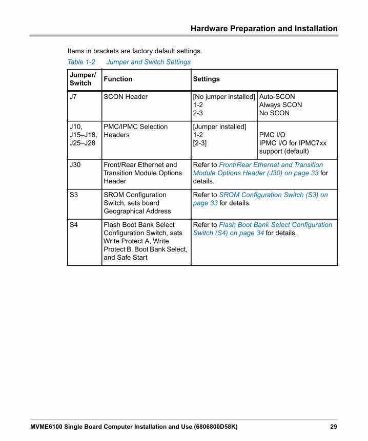
Items in brackets are factory default settings.
Table 1-2 Jumper and Switch Settings
Jumper/
SwitchFunction Settings
J7 SCON Header [No jumper installed]
1-2
2-3
Auto-SCON
Always SCON
No SCON
J10,
J15–J18,
J25–J28
PMC/IPMC Selection
Headers
[Jumper installed]
1-2
[2-3]
PMC I/O
IPMC I/O for IPMC7xx
support (default)
J30 Front/Rear Ethernet and
Transition Module Options
Header
Refer to Front/Rear Ethernet and Transition
Module Options Header (J30) on page 33 for
details.
S3 SROM Configuration
Switch, sets board
Geographical Address
Refer to SROM Configuration Switch (S3) on
page 33 for details.
S4 Flash Boot Bank Select
Configuration Switch, sets
Write Protect A, Write
Protect B, Boot Bank Select,
and Safe Start
Refer to Flash Boot Bank Select Configuration
Switch (S4) on page 34 for details.

30 MVME6100 Single Board Computer Installation and Use (6806800D58K)
Hardware Preparation and InstallationHardware Preparation and Installation
The MVME6100 is factory tested and shipped with the configuration described in the
following sections.
Figure 1-1 Component Layout
4296 0604
10/100/1000D
EB
UG
ABT/RST
LAN
1LA
N 2
J42 J8
J30
J3
J19
J13 J14
J11 J12
J23 J24
J21 J22
P1
P2
PC
I ME
ZZ
AN
INE
CA
RD
PC
I ME
ZZ
AN
INE
CA
RD
J4
U12
10/100/1000
J93
J9
J29J7
PMCIPMC
U32
S2
1 2
3 4
5 6
7 8
1 2 3 4
1 2
3 4
5 6
7 8
S4
S1 S3

Hardware Preparation and Installation
MVME6100 Single Board Computer Installation and Use (6806800D58K) 31
1.5.1 SCON Header (J7)
A 3-pin planar header allows the choice for auto/enable/disable SCON VME configuration.
A jumper installed across pins 1 and 2 configures for SCON always enabled. A jumper
installed across pins 2 and 3 configures for SCON disabled. No jumper installed configures
for auto SCON.
1.5.2 PMC/IPMC Selection Headers (J10, J15-J18, J25-J28)
Nine 3-pin planar headers are for PMC/IPMC mode I/O selection for PMC slot 1. These
nine headers can also be combined into one single header block where a block shunt can
be used as a jumper.
A jumper installed across pins 1 and 2 on all nine headers selects PMC1 for PMC I/O mode.
A jumper across pins 2 and 3 on all nine headers selects IPMC I/O mode.
Figure 1-2 SCON Header Settings
J7
1
2
3
1
2
3
Always SCON
J7 J7
1
2
3
(factory configuration)
No SCONAuto-SCON
Figure 1-3 PMC/IPMC Header Settings
J10
1
2
3
PMC1 P2 I/O for PMC Mode
J16
1
2
3
J15
1
2
3
J17
1
2
3
J18
1
2
3
J25
1
2
3
J26
1
2
3
J27
1
2
3
J28
1
2
3
J10
1
2
3
IPMC P2 I/O for IPMC Mode
J16
1
2
3
J15
1
2
3
J17
1
2
3
J18
1
2
3
J25
1
2
3
J26
1
2
3
J27
1
2
3
J28
1
2
3
(factory configuration)

32 MVME6100 Single Board Computer Installation and Use (6806800D58K)
Hardware Preparation and InstallationHardware Preparation and Installation
1.5.3 PMC I/O Voltage Configuration
The on-board PMC sites may be configured to support 3.3V or 5.0V I/O PMC modules. To
support 3.3V or 5.0V I/O PMC modules, both PMC sites on the MVME6100 have I/O keying
pins. One pin must be installed in each PMC site and both PMC sites must have their
keying pins configured he same way. If both keying pins are not in the same location or if
the keying pins are not installed, the PMC sites will not function. Note that setting the PMC
I/O voltage to 5.0V forces the PMC sites to operate in PCI mode instead of PCI-X mode.
The VIO keying pins are the silver colored pins located either in the middle of each set of
four PMC site connectors or just in front of those connectors. They serve two functions on
the MVME6100: both as jumpers to select the PCIbus VIO signaling voltage for the PMC
sites, and as keys to permit mounting of PMC cards that are compatible with that VIO
signaling voltage (or to exclude incompatible PMC cards). In the default position in the
middle of the four PMC site connectors, the signaling voltage for the PMC sites is set to
5.0V. When the keying pins are moved to the alternate location in front of their set of four
PMC connectors, the signaling voltage for the PMC sites is set for 3.3V.
A PMC card that requires 5.0V VIO only signaling has a hole in the middle of its four PMC
connectors, such that it fits over the MVME6100's keying pin in that location. With the
MVME6100's keying pin in the 3.3V location, that PMC card would be physically unable to
be mounted. Similarly, a PMC card that requires 3.3V VIO-only signaling has its keying hole
located just to the front of its four PMC connectors, and will only fit to the MVME6100 when
the keying pin is located there. However, most modern PMC cards are universal with
respect to the VIO signaling voltage they support, and have keying holes in both locations;
that is, they will fit on the MVME6100's PMC site with the key in either location. For these
PMC cards, it is recommended setting the MVME6100's keying pins to the 3.3V VIO
signaling position, to allow the maximum PCIbus clock speed.
The keying pins for both PMC sites must be set to the same signaling voltage. Note
also that the signaling voltage has an effect on the PCI bus clock speed for the PMC
sites. At 5.0V signaling, the PCI bus clock speed is limited to 33 MHz, whereas 3.3V
signaling voltage supports conventional PCIbus clock speeds of 33 or 66 MHz, and
PCIx clock speeds of 66 or 100MHz.

Hardware Preparation and Installation
MVME6100 Single Board Computer Installation and Use (6806800D58K) 33
1.5.4 Front/Rear Ethernet and Transition Module Options Header(J30)
A 40-pin planar header allows for selecting P2 options. Jumpers installed across Row A
pins 3-10 and Row B pins 3-10 enable front Ethernet access. Jumpers installed across Row
B pins 3-10 and Row C pins 3-10 enable P2 (rear) Gigabit Ethernet. Only when front
Ethernet is enabled can the jumpers be installed across Row C and Row D on pins 1-10 to
enable P2 (rear) PMC I/O. Note that all jumpers must be installed across the same two rows
(all between Row A and Row B and/or Row C and Row D, or all between Row B and Row
C).
The following illustration shows jumper setting options for J30. The factory default is shown
where applicable:
Refer to Front/Rear Ethernet and Transition Module Options Header (J30) on page 103 for
connector pin assignments.
1.5.5 SROM Configuration Switch (S3)
A part of the 8-position SMT switch, S3 enables/disables the MV64360 SROM initialization
and all I2C EEPROM write protection.
The SROM Init switch is OFF to disable the MV64360 device initialization via the I2C
SROM. The switch is ON to enable this sequence.
Figure 1-4 Front/Rear Ethernet Option Settings
4294 0
1112131
10203040
Front Ethernet(Default)
1112131
10203040
Rear Ethernet
1112131
1234
Non-Specific Transition Module(Default)
1112131
10203040
PMC I/O TO P2(Default)
1112131
10203040
MVME 712MTransition Module
1112131
1234
MVME 761Transition Module
J30 Options

34 MVME6100 Single Board Computer Installation and Use (6806800D58K)
Hardware Preparation and InstallationHardware Preparation and Installation
The SROM WP switch is OFF to enable write protection on all I2C. The switch is ON to
disable the I2C EEPROM write protection.
S3 position 3-8 defines the VME Geographical Address if the MVME6100 is installed in a
3-row backplane. The following is the pinout:
Setting the individual position to ON forces the corresponding signal to zero. If the board is
installed in a 5-row backplane, the geographical address is defined by the backplane and
positions 3-8 of S3 should be set to OFF. The default setting is OFF.
1.5.6 Flash Boot Bank Select Configuration Switch (S4)
A 4-position SMT configuration switch is located on the board to control Flash Bank B Boot
block write-protect and Flash Bank A write-protect. Select the Flash Boot bank and the
programmed/safe start ENV settings.
The Bank B Boot WP switch is OFF to indicate that the Flash Bank B Boot block is write-
protected. The switch is ON to indicate no write-protection of Bank B Boot block.
The Bank A WP switch is OFF to indicate that the entire Flash Bank A is write-protected.
The switch is ON to indicate no write-protection of Bank A Boot block.
Table 1-3 SROM Configuration Switch (S3)
Position 2 1
FUNCTION SROM WP SROM_INIT
DEFAULT (OFF) WP No SROM_INIT
Position Function
3 VMEGAP_L
4 VMEGA4_L
5 VMEGA3_L
6 VMEGA2_L
7 VMEGA1_L
8 VMEGA0_L
It is recommended that Bank B Write Protect always be enabled.

Hardware Preparation and Installation
MVME6100 Single Board Computer Installation and Use (6806800D58K) 35
When the Boot Bank Sel Switch is ON, the board boots from Bank B, when OFF, the board
boots from Bank A. Default is ON (boot from Bank B).
When the Safe Start switch is set OFF, normal boot sequence should be followed by
MOTLoad. When ON, MOTLoad executes Safe Start, during which the user can select the
Alternate Boot Image.
1.6 Installing the Blade
Procedure
Use the following steps to install the MVME6100 into your computer chassis.
1. Attach an ESD strap to your wrist. Attach the other end of the ESD strap to an electrical
ground (refer to Unpacking Guidelines). The ESD strap must be secured to your wrist
and to ground throughout the procedure.
2. Remove any filler panel that might fill that slot.
3. Install the top and bottom edge of the MVME6100 into the guides of the chassis.
4. Ensure that the levers of the two injector/ejectors are in the outward position.
5. Slide the MVME6100 into the chassis until resistance is felt.
6. Simultaneously move the injector/ejector levers in an inward direction.
Table 1-4 Configuration Switch (S4)
Position 4 3 2 1
FUNCTION
BA
NK
BB
OO
TW
P
BA
NK
AW
P
BO
OT
BA
NK
SE
L
SA
FE
STA
RT
FACTORY DEFAULT OFF
WP
ON
No WP
ON
Bank B
OFF
Norm ENV
Only use injector handles for board insertion to avoid damage/deformation to the
front panel and/or PCB. Deformation of the front panel can cause an electrical short
or other board malfunction.

36 MVME6100 Single Board Computer Installation and Use (6806800D58K)
Hardware Preparation and InstallationHardware Preparation and Installation
7. Verify that the MVME6100 is properly seated and secure it to the chassis using the two
screws located adjacent to the injector/ejector levers.
8. Connect the appropriate cables to the MVME6100.
To remove the board from the chassis, press the red locking tabs (IEEE handles only) and
reverse the procedure.
1.7 Connecting to PeripheralsWhen the MVME6100 is installed in a chassis, you are ready to connect peripherals and
apply power to the board.
Figure 1-1 on page 30 shows the locations of the various connectors while Table 1-5 lists
them for you. Refer to Chapter 5, Pin Assignments for the pin assignments of the
connectors listed below.
1.8 Completing the InstallationVerify that hardware is installed and the power/peripheral cables connected are appropriate
for your system configuration.
Replace the chassis or system cover, reconnect the system to the AC or DC power source,
and turn the equipment power on.
Table 1-5 MVME6100 Connectors
Connector Function
J3 IPMC761/712 connector
J4 PMC expansion connector
J9, J93 Gigabit Ethernet connectors
J11, J12, J13, J14 PCI mezzanine card (PMC) slot 1 connector
J19 COM1 connector
J21, J22, J23, J24 PCI mezzanine card (PMC) slot 2 connector
J29 COM2 planar connector
P1, P2 VME rear panel connectors

MVME6100 Single Board Computer Installation and Use (6806800D58K) 37
Chapter 2
Startup and Operation
2.1 IntroductionThis chapter gives you information about the:
Power-up procedure
Switches and indicators
2.2 Applying PowerAfter you verify that all necessary hardware preparation is complete and all connections are
made correctly, you can apply power to the system.
When you are ready to apply power to the MVME6100:
Verify that the chassis power supply voltage setting matches the voltage present in
the country of use (if the power supply in your system is not auto-sensing)
On powering up, the MVME6100 brings up the MOTLoad prompt, MVME6100>
2.3 Switches and IndicatorsThe MVME6100 board provides a single pushbutton switch that provides both abort and
reset (ABT/RST) functions. When the switch is depressed for less than three seconds, an
abort interrupt is generated to the processor. If the switch is held for more than three
seconds, a board hard reset is generated. The board hard reset will reset the MPC7457,
MV64360, Tsi148 VME Bridge ASIC, PCI6520, PMC1/2 slots, both Ethernet PHYs, serial
ports, PMCspan slot, both flash banks, and the device bus control PLD. If the MVME6100
is enabled for VME system controller, the VME bus will be reset and local reset input is sent
to the Tsi148 VME controller.
The MVME6100 has two front-panel indicators:
BDFAIL, software controlled and asserted by firmware (or other software) to
indicate a configuration problem (or other failure)
CPU, connected to a CPU bus control signal to indicate bus transfer activity
The following table describes these indicators:
Table 2-1 Front-Panel LED Status Indicators
Function Label Color Description
CPU Bus Activity CPU Green CPU bus is busy
Board Fail BDFAIL Yellow Board has a failure

38 MVME6100 Single Board Computer Installation and Use (6806800D58K)
Startup and OperationStartup and Operation

MVME6100 Single Board Computer Installation and Use (6806800D58K) 39
Chapter 3
MOTLoad Firmware
3.1 OverviewThe MOTLoad firmware package serves as a board power-up and initialization package,
as well as a vehicle from which user applications can be booted. A secondary function of
the MOTLoad firmware is to serve in some respects as a test suite providing individual tests
for certain devices. This chapter includes a list of standard MOTLoad commands, the
default VME and firmware settings that are changeable by the user, remote start, and the
alternate boot procedure.
MOTLoad is controlled through an easy-to-use, UNIX-like, command line interface. The
MOTLoad software package is similar to many end-user applications designed for the
embedded market, such as the real time operating systems currently available.
Refer to the MOTLoad Firmware Package User’s Manual, listed in Appendix C, Related
Documentation, for more details.
3.2 Implementation and Memory RequirementsThe implementation of MOTLoad and its memory requirements are product specific. The
MVME6100 single-board computer (SBC) is offered with a wide range of memory (for
example, DRAM, external cache, flash). Typically, the smallest amount of on-board DRAM
that an SMART EC SBC has is 32 MB. Each supported product line has its own unique
MOTLoad binary image(s). Currently the largest MOTLoad compressed image is less than
1 MB in size.
3.3 MOTLoad CommandsMOTLoad supports two types of commands (applications): utilities and tests. Both types of
commands are invoked from the MOTLoad command line in a similar fashion. Beyond that,
MOTLoad utilities and MOTLoad tests are distinctly different.
3.3.1 Utilities
The definition of a MOTLoad utility application is very broad. Simply stated, it is considered
a MOTLoad command, if it is not a MOTLoad test. Typically, MOTLoad utility applications
are applications that aid the user in some way (that is, they do something useful). From the
perspective of MOTLoad, examples of utility applications are: configuration, data/status
displays, data manipulation, help routines, data/status monitors, etc.

40 MVME6100 Single Board Computer Installation and Use (6806800D58K)
MOTLoad FirmwareMOTLoad Firmware
Operationally, MOTLoad utility applications differ from MOTLoad test applications in
several ways:
Only one utility application operates at any given time (that is, multiple utility
applications cannot be executing concurrently)
Utility applications may interact with the user. Most test applications do not.
3.3.2 Tests
A MOTLoad test application determines whether or not the hardware meets a given
standard. Test applications are validation tests. Validation is conformance to a
specification. Most MOTLoad tests are designed to directly validate the functionality of a
specific SBC subsystem or component. These tests validate the operation of such SBC
modules as: dynamic memory, external cache, NVRAM, real time clock, etc.
All MOTLoad tests are designed to validate functionality with minimum user interaction.
Once launched, most MOTLoad tests operate automatically without any user interaction.
There are a few tests where the functionality being validated requires user interaction (that
is, switch tests, interactive plug-in hardware modules, etc.). Most MOTLoad test results
(error-data/status-data) are logged, not printed. All MOTLoad tests/commands have
complete and separate descriptions (refer to the MOTLoad Firmware Package User’s
Manual for this information).
All devices that are available to MOTLoad for validation/verification testing are represented
by a unique device path string. Most MOTLoad tests require the operator to specify a test
device at the MOTLoad command line when invoking the test.
A listing of all device path strings can be displayed through the devShow command. If an
SBC device does not have a device path string, it is not supported by MOTLoad and can
not be directly tested. There are a few exceptions to the device path string requirement, like
testing RAM, which is not considered a true device and can be directly tested without a
device path string. Refer to the devShow command description page in the MOTLoad
Firmware Package User’s Manual.
Most MOTLoad tests can be organized to execute as a group of related tests (a testSuite)
through the use of the testSuite command. The expert operator can customize their testing
by defining and creating a custom testSuite(s). The list of built-in and user-defined
MOTLoad testSuites, and their test contents, can be obtained by entering testSuite -d at
the MOTLoad prompt. All testSuites that are included as part of a product specific
MOTLoad firmware package are product specific. For more information, refer to the
testSuite command description page in the MOTLoad Firmware Package User’s Manual.
Test results and test status are obtained through the testStatus, errorDisplay, and
taskActive commands. Refer to the appropriate command description page in the
MOTLoad Firmware Package User’s Manual for more information.

MOTLoad Firmware
MVME6100 Single Board Computer Installation and Use (6806800D58K) 41
3.3.3 Command List
The following table provides a list of all current MOTLoad commands. Products supported
by MOTLoad may or may not employ the full command set. Typing help at the MOTLoad
command prompt will display all commands supported by MOTLoad for a given product.
For a detailed description of these commands refer to the MOTLoad Firmware Package
User’s Manual.
Table 3-1 MOTLoad Commands
Command Description
as One-Line Instruction Assembler
bcb
bch
bcw
Block Compare Byte/Halfword/Word
bdTempShow Display Current Board Temperature
bfb
bfh
bfw
Block Fill Byte/Halfword/Word
blkCp Block Copy
blkFmt Block Format
blkRd Block Read
blkShow Block Show Device Configuration Data
blkVe Block Verify
blkWr Block Write
bmb
bmh
bmw
Block Move Byte/Halfword/Word
br Assign/Delete/Display User-Program Break-Points
bsb
bsh
bsw
Block Search Byte/Halfword/Word
bvb
bvh
bvw
Block Verify Byte/Halfword/Word

42 MVME6100 Single Board Computer Installation and Use (6806800D58K)
MOTLoad FirmwareMOTLoad Firmware
cdDir ISO9660 File System Directory Listing
cdGet ISO9660 File System File Load
clear Clear the Specified Status/History Table(s)
cm Turns on Concurrent Mode
csb
csh
csw
Calculates a Checksum Specified by Command-line Options
csUserAltBootChecksums user boot images specified in the alternete boot image
header at the beginning of files to be programmed into flash memory.
devShow Display (Show) Device/Node Table
diskBoot Disk Boot (Direct-Access Mass-Storage Device)
downLoad Down Load S-Record from Host
ds One-Line Instruction Disassembler
echo Echo a Line of Text
elfLoader ELF Object File Loader
errorDisplay Display the Contents of the Test Error Status Table
eval Evaluate Expression
execProgram Execute Program
fatDir FAT File System Directory Listing
fatGet FAT File System File Load
fdShow Display (Show) File Discriptor
flashLock Flash Memory Sector Lock
flashProgram Flash Memory Program
flashShow Display Flash Memory Device Configuration Data
flashUnlock Flash Memory Sector Unlock
gd Go Execute User-Program Direct (Ignore Break-Points)
gevDelete Global Environment Variable Delete
Table 3-1 MOTLoad Commands (continued)
Command Description

MOTLoad Firmware
MVME6100 Single Board Computer Installation and Use (6806800D58K) 43
gevDump Global Environment Variable(s) Dump (NVRAM Header + Data)
gevEdit Global Environment Variable Edit
gevInit Global Environment Variable Area Initialize (NVRAM Header)
gevList Global Environment Variable Labels (Names) Listing
gevShow Global Environment Variable Show
gn Go Execute User-Program to Next Instruction
go Go Execute User-Program
gt Go Execute User-Program to Temporary Break-Point
hbd Display History Buffer
hbx Execute History Buffer Entry
help Display Command/Test Help Strings
l2CacheShow Display state of L2 Cache and L2CR register contents
l3CacheShow Display state of L3 Cache and L3CR register contents
mdb
mdh
mdw
Memory Display Bytes/Halfwords/Words
memShow Display Memory Allocation
mmb
mmh
mmw
Memory Modify Bytes/Halfwords/Words
mpuFork Execute program from idle processor
mpuShow Display multi-processor control structure
mpuStart Start the other MPU
netBoot Network Boot (BOOT/TFTP)
netShow Display Network Interface Configuration Data
netShut Disable (Shutdown) Network Interface
netStats Display Network Interface Statistics Data
Table 3-1 MOTLoad Commands (continued)
Command Description

44 MVME6100 Single Board Computer Installation and Use (6806800D58K)
MOTLoad FirmwareMOTLoad Firmware
noCm Turns off Concurrent Mode
pciDataRd Read PCI Device Configuration Header Register
pciDataWr Write PCI Device Configuration Header Register
pciDump Dump PCI Device Configuration Header Register
pciShow Display PCI Device Configuration Header Register
pciSpace Display PCI Device Address Space Allocation
ping Ping Network Host
portSet Port Set
portShow Display Port Device Configuration Data
rd User Program Register Display
reset Reset System
rs User Program Register Set
set Set Date and Time
sromRead SROM Read
sromWrite SROM Write
sta Symbol Table Attach
stl Symbol Table Lookup
stop Stop Date and Time (Power-Save Mode)
taskActive Display the Contents of the Active Task Table
tc Trace (Single-Step) User Program
td Trace (Single-Step) User Program to Address
testDisk Test Disk
testEnetPtP Ethernet Point-to-Point
testNvramRd NVRAM Read
testNvramRdWr NVRAM Read/Write (Destructive)
testRam RAM Test (Directory)
Table 3-1 MOTLoad Commands (continued)
Command Description

MOTLoad Firmware
MVME6100 Single Board Computer Installation and Use (6806800D58K) 45
testRamAddr RAM Addressing
testRamAlt RAM Alternating
testRamBitToggle RAM Bit Toggle
testRamBounce RAM Bounce
testRamCodeCopy RAM Code Copy and Execute
testRamEccMonitor Monitor for ECC Errors
testRamMarch RAM March
testRamPatterns RAM Patterns
testRamPerm RAM Permutations
testRamQuick RAM Quick
testRamRandom RAM Random Data Patterns
testRtcAlarm RTC Alarm
testRtcReset RTC Reset
testRtcRollOver RTC Rollover
testRtcTick RTC Tick
testSerialExtLoop Serial External Loopback
testSeriallntLoop Serial Internal Loopback
testStatus Display the Contents of the Test Status Table
testSuite Execute Test Suite
testSuiteMake Make (Create) Test Suite
testWatchdogTimer Tests the Accuracy of the Watchdog Timer Device
tftpGet TFTP Get
tftpPut TFTP Put
time Display Date and Time
transparentMode Transparent Mode (Connect to Host)
tsShow Display Task Status
Table 3-1 MOTLoad Commands (continued)
Command Description

46 MVME6100 Single Board Computer Installation and Use (6806800D58K)
MOTLoad FirmwareMOTLoad Firmware
3.4 Using the Command Line InterfaceInteraction with MOTLoad is performed via a command line interface through a serial port
on the SBC, which is connected to a terminal or terminal emulator (for example, Window’s
Hypercomm). The default MOTLoad serial port settings are: 9600 baud, 8 bits, no parity.
The MOTLoad command line interface is similar to a UNIX command line shell interface.
Commands are initiated by entering a valid MOTLoad command (a text string) at the
MOTLoad command line prompt and pressing the carriage-return key to signify the end of
input. MOTLoad then performs the specified action. An example of a MOTLoad command
line prompt is shown below. The MOTLoad prompt changes according to what product it is
used on (for example, MVME5500, MVME6100).
Example:
MVME6100>
If an invalid MOTLoad command is entered at the MOTLoad command line prompt,
MOTLoad displays a message that the command was not found.
Example:
MVME6100> mytest"mytest" not foundMVME6100>
If the user enters a partial MOTLoad command string that can be resolved to a unique valid
MOTLoad command and presses the carriage-return key, the command will be executed
as if the entire command string had been entered. This feature is a user-input shortcut that
minimizes the required amount of command line input. MOTLoad is an ever changing
firmware package, so user-input shortcuts may change as command additions are made.
upLoad Up Load Binary Data from Target
version Display Version String(s)
vmeCfg Manages user specified VME configuration parameters
vpdDisplay VPD Display
vpdEdit VPD Edit
wait Wait for Test Completion
waitProbe Wait for I/O Probe to Complete
Table 3-1 MOTLoad Commands (continued)
Command Description

MOTLoad Firmware
MVME6100 Single Board Computer Installation and Use (6806800D58K) 47
Example:
MVME6100> versionCopyright: Motorola Inc.1999-2002, All Rights ReservedMOTLoad RTOS Version 2.0PAL Version 0.1 (Motorola MVME6100)
Example:
MVME6100> verCopyright: Motorola Inc. 1999-2002, All Rights ReservedMOTLoad RTOS Version 2.0PAL Version 0.1 (Motorola MVME6100)
If the partial command string cannot be resolved to a single unique command, MOTLoad
will inform the user that the command was ambiguous.
Example:
MVME6100> te"te" ambiguousMVME6100>
3.4.1 Command Line Rules
There are a few things to remember when entering a MOTLoad command:
Multiple commands are permitted on a single command line, provided they are
separated by a single semicolon (;)
Spaces separate the various fields on the command line
(command/arguments/options)
The argument/option identifier character is always preceded by a hyphen (-)
character
Options are identified by a single character
Option arguments immediately follow (no spaces) the option
All commands, command options, and device tree strings are case sensitive
Example:
MVME6100> flashProgram –d/dev/flash0 –n00100000For more information on MOTLoad operation and function, refer to the MOTLoad Firmware
Package User’s Manual.

48 MVME6100 Single Board Computer Installation and Use (6806800D58K)
MOTLoad FirmwareMOTLoad Firmware
3.4.2 Command Line Help
Each MOTLoad firmware package has an extensive, product-specific help facility that can
be accessed through the help command. The user can enter help at the MOTLoad
command line to display a complete listing of all available tests and utilities.
Example:
MVME6100> helpFor help with a specific test or utility the user can enter the following at the MOTLoad
prompt:
help <command_name>The help command also supports a limited form of pattern matching. Refer to the help command page.
Example:
MVME6100> help testRamUsage: testRam [-aPh] [-bPh] [-iPd] [-nPh] [-tPd] [-v]Description: RAM Test [Directory]Argument/Option Description-a Ph: Address to Start (Default = Dynamic Allocation)-b Ph: Block Size (Default = 16KB)-i Pd: Iterations (Default = 1)-n Ph: Number of Bytes (Default = 1MB)-t Ph: Time Delay Between Blocks in OS Ticks (Default = 1)-v O : Verbose OutputMVME6100>
3.5 Firmware SettingsThe following sections provide additional information pertaining to the VME firmware
settings of the MVME6100. A few VME settings are controlled by hardware jumpers while
the majority of the VME settings are managed by the firmware command utility vmeCfg.
3.5.1 Default VME Settings
As shipped from the factory, the MVME6100 has the following VME configuration
programmed via Global Environment Variables (GEVs) for the Tsi148 VME controller. The
firmware allows certain VME settings to be changed in order for the user to customize the
environment. The following is a description of the default VME settings that are changeable
by the user. For more information, refer to the MOTLoad User’s Manual and Tundra’s
Tsi148 User Manual, listed in Appendix C, Related Documentation.

MOTLoad Firmware
MVME6100 Single Board Computer Installation and Use (6806800D58K) 49
MVME6100> vmeCfg -s -mDisplaying the selected Default VME Setting- interpreted as follows:VME PCI Master Enable [Y/N] = YMVME6100>
The PCI Master is enabled.
MVME6100> vmeCfg –s –r234Displaying the selected Default VME Setting- interpreted as follows:VMEbus Master Control Register = 00000003MVME6100>
The VMEbus Master Control Register is set to the default (RESET) condition.
MVME6100> vmeCfg –s –r238Displaying the selected Default VME Setting- interpreted as follows:VMEbus Control Register = 00000008MVME6100>
The VMEbus Control Register is set to a Global Timeout of 2048 seconds.
MVME6100> vmeCfg –s –r414Displaying the selected Default VME Setting- interpreted as follows:CRG Attribute Register = 00000000CRG Base Address Upper Register = 00000000CRG Base Address Lower Register = 00000000MVME6100>
The CRG Attribute Register is set to the default (RESET) condition.
MVME6100> vmeCfg –s –i0Displaying the selected Default VME Setting- interpreted as follows:Inbound Image 0 Attribute Register = 000227AFInbound Image 0 Starting Address Upper Register = 00000000

50 MVME6100 Single Board Computer Installation and Use (6806800D58K)
MOTLoad FirmwareMOTLoad Firmware
Inbound Image 0 Starting Address Lower Register = 00000000Inbound Image 0 Ending Address Upper Register = 00000000Inbound Image 0 Ending Address Lower Register = 1FFF0000Inbound Image 0 Translation Offset Upper Register = 00000000Inbound Image 0 Translation Offset Lower Register = 00000000MVME6100>
Inbound window 0 (ITAT0) is not enabled; Virtual FIFO at 256 bytes, 2eSST timing at
SST320, respond to 2eSST, 2eVME, MBLT, and BLT cycles, A32 address space, respond
to Supervisor, User, Program, and Data cycles. Image maps from 0x00000000 to
0x1FFF0000 on the VMbus, translates 1x1 to the PCI-X bus (thus 1x1 to local memory). To
enable this window, set bit 31 of ITAT0 to 1.
MVME6100> vmeCfg –s –o1Displaying the selected Default VME Setting- interpreted as follows:Outbound Image 1 Attribute Register = 80001462Outbound Image 1 Starting Address Upper Register = 00000000Outbound Image 1 Starting Address Lower Register = 91000000Outbound Image 1 Ending Address Upper Register = 00000000Outbound Image 1 Ending Address Lower Register = AFFF0000Outbound Image 1 Translation Offset Upper Register = 00000000Outbound Image 1 Translation Offset Lower Register = 70000000Outbound Image 1 2eSST Broadcast Select Register = 00000000MVME6100>
Outbound window 1 (OTAT1) is enabled, 2eSST timing at SST320, transfer mode of
2eSST, A32/D32 Supervisory access. The window accepts transfers on the PCI-X Local
Bus from 0x91000000-0xAFFF0000 and translates them onto the VMEbus using an offset
of 0x70000000, thus an access to 0x91000000 on the PCI-X Local Bus becomes an access
to 0x01000000 on the VMEbus.
MVME6100> vmeCfg –s –o2Displaying the selected Default VME Setting- interpreted as follows:Outbound Image 2 Attribute Register = 80001061Outbound Image 2 Starting Address Upper Register = 00000000
For Inbound Translations, the Upper Translation Offset Register needs to be set to
0xFFFFFFFF to ensure proper translations to the PCI-X Local Bus.

MOTLoad Firmware
MVME6100 Single Board Computer Installation and Use (6806800D58K) 51
Outbound Image 2 Starting Address Lower Register = B0000000Outbound Image 2 Ending Address Upper Register = 00000000Outbound Image 2 Ending Address Lower Register = B0FF0000Outbound Image 2 Translation Offset Upper Register = 00000000Outbound Image 2 Translation Offset Lower Register = 40000000Outbound Image 2 2eSST Broadcast Select Register = 00000000MVME6100>
Outbound window 2 (OTAT2) is enabled, 2eSST timing at SST320, transfer mode of SCT,
A24/D32 Supervisory access. The window accepts transfers on the PCI-X Local Bus from
0xB0000000-0xB0FF0000 and translates them onto the VMEbus using an offset of
0x40000000, thus an access to 0xB0000000 on the PCI-X Local Bus becomes an access
to 0xF0000000 on the VMEbus.
MVME6100> vmeCfg –s –o3Displaying the selected Default VME Setting- interpreted as follows:Outbound Image 3 Attribute Register = 80001061Outbound Image 3 Starting Address Upper Register = 00000000Outbound Image 3 Starting Address Lower Register = B3FF0000Outbound Image 3 Ending Address Upper Register = 00000000Outbound Image 3 Ending Address Lower Register = B3FF0000Outbound Image 3 Translation Offset Upper Register = 00000000Outbound Image 3 Translation Offset Lower Register = 4C000000Outbound Image 3 2eSST Broadcast Select Register = 00000000MVME6100>
Outbound window 3 (OTAT3) is enabled, 2eSST timing at SST320, transfer mode of SCT,
A16/D32 Supervisory access. The window accepts transfers on the PCI-X Local Bus from
0xB3FF0000-0xB3FF0000 and translates them onto the VMEbus using an offset of
0x4C000000, thus an access to 0xB3FF0000 on the PCI-X Local Bus becomes an access
to 0xFFFF0000 on the VMEbus.
MVME6100> vmeCfg –s –o7Displaying the selected Default VME Setting- interpreted as follows:Outbound Image 7 Attribute Register = 80001065Outbound Image 7 Starting Address Upper Register = 00000000Outbound Image 7 Starting Address Lower Register = B1000000Outbound Image 7 Ending Address Upper Register = 00000000Outbound Image 7 Ending Address Lower Register = B1FF0000

52 MVME6100 Single Board Computer Installation and Use (6806800D58K)
MOTLoad FirmwareMOTLoad Firmware
Outbound Image 7 Translation Offset Upper Register = 00000000Outbound Image 7 Translation Offset Lower Register = 4F000000Outbound Image 7 2eSST Broadcast Select Register = 00000000MVME6100>
Outbound window 7 (OTAT7) is enabled, 2eSST timing at SST320, transfer mode of SCT,
CR/CSR Supervisory access. The window accepts transfers on the PCI-X Local Bus from
0xB1000000-0xB1FF0000 and translates them onto the VMEbus using an offset of
0x4F000000, thus an access to 0xB1000000 on the PCI-X Local Bus becomes an access
to 0x00000000 on the VMEbus.
3.5.2 Control Register/Control Status Register Settings
The CR/CSR base address is initialized to the appropriate setting based on the
Geographical address; that is, the VME slot number. See the VME64 Specification and the
VME64 Extensions for details. As a result, a 512K byte CR/CSR area can be accessed
from the VMEbus using the CR/CSR AM code.
3.5.3 Displaying VME Settings
To display the changeable VME setting, type the following at the firmware prompt:
vmeCfg –s –mDisplays Master Enable state
vmeCfg –s –i(0 - 7)Displays selected Inbound Window state
vmeCfg –s –o(0 - 7)Displays selected Outbound Window state
vmeCfg –s –r184Displays PCI Miscellaneous Register state
vmeCfg –s –r188Displays Special PCI Target Image Register state
vmeCfg –s –r400Displays Master Control Register state
vmeCfg –s –r404Displays Miscellaneous Control Register state
vmeCfg –s –r40CDisplays User AM Codes Register state
vmeCfg –s –rF70Displays VMEbus Register Access Image Control Register state

MOTLoad Firmware
MVME6100 Single Board Computer Installation and Use (6806800D58K) 53
3.5.4 Editing VME Settings
To edit the changeable VME setting, type the following at the firmware prompt:
vmeCfg –e –mEdits Master Enable state
vmeCfg –e –i(0 - 7)Edits selected Inbound Window state
vmeCfg –e –o(0 - 7)Edits selected Outbound Window state
vmeCfg –e –r184Edits PCI Miscellaneous Register state
vmeCfg –e –r188Edits Special PCI Target Image Register state
vmeCfg –e –r400Edits Master Control Register state
vmeCfg –e –r404Edits Miscellaneous Control Register state
vmeCfg –e –r40CEdits User AM Codes Register state
vmeCfg –e –rF70Edits VMEbus Register Access Image Control Register state
3.5.5 Deleting VME Settings
To delete the changeable VME setting (restore default value), type the following at the
firmware prompt:
vmeCfg –d –mDeletes Master Enable state
vmeCfg –d –i(0 - 7)Deletes selected Inbound Window state
vmeCfg –d –o(0 - 7)Deletes selected Outbound Window state
vmeCfg –d –r184Deletes PCI Miscellaneous Register state
vmeCfg –d –r188Deletes Special PCI Target Image Register state
vmeCfg –d –r400Deletes Master Control Register state

54 MVME6100 Single Board Computer Installation and Use (6806800D58K)
MOTLoad FirmwareMOTLoad Firmware
vmeCfg –d –r404Deletes Miscellaneous Control Register state
vmeCfg –d –r40CDeletes User AM Codes Register state
vmeCfg –d –rF70Deletes VMEbus Register Access Image Control Register state
3.5.6 Restoring Default VME Settings
To restore all of the changeable VME setting back to their default settings, type the
following at the firmware prompt:
vmeCfg –z
3.6 Remote StartAs described in the MOTLoad Firmware Package User's Manual, listed in Appendix C,
Related Documentation, remote start allows the user to obtain information about the target
board, download code and/or data, modify memory on the target, and execute a
downloaded program. These transactions occur across the VMEbus in the case of the
MVME6100. MOTLoad uses one of four mailboxes in the Tsi148 VME controller as the
inter-board communication address (IBCA) between the host and the target.
CR/CSR slave addresses configured by MOTLoad are assigned according to the
installation slot in the backplane, as indicated by the VME64 Specification. For reference,
the following values are provided:
Slot Position CS/CSR Starting Address
1 0x0008.0000
2 0x0010.0000
3 0x0018.0000
4 0x0020.0000
5 0x0028.0000
6 0x0030.0000
7 0x0038.0000
8 0x0040.0000
9 0x0048.0000

MOTLoad Firmware
MVME6100 Single Board Computer Installation and Use (6806800D58K) 55
For further details on CR/CSR space, please refer to the VME64 Specification, listed in
Appendix C, Related Documentation.
The MVME6100 uses a Discovery II for its VME bridge. The offsets of the mailboxes in the
Discovery II are defined in the Discovery II User Manual, listed in Appendix C, Related
Documentation, but are noted here for reference:
Mailbox 0 is at offset 7f348 in the CR/CSR space
Mailbox 1 is at offset 7f34C in the CR/CSR space
Mailbox 2 is at offset 7f350 in the CR/CSR space
Mailbox 3 is at offset 7f354 in the CR/CSR space
The selection of the mailbox used by remote start on an individual MVME6100 is
determined by the setting of a global environment variable (GEV). The default mailbox is
zero. Another GEV controls whether remote start is enabled (default) or disabled. Refer to
the Remote Start appendix in the MOTLoad Firmware Package User's Manual for remote
start GEV definitions.
The MVME6100’s IBCA needs to be mapped appropriately through the master’s VMEbus
bridge. For example, to use remote start using mailbox 0 on an MVME6100 installed in slot
5, the master would need a mapping to support reads and writes of address 0x002ff348 in
VME CR/CSR space (0x280000 + 0x7f348).
3.7 Alternate Boot Images and Safe StartSome later versions of MOTLoad support Alternate Boot Images and a Safe Start recovery
procedure. If Safe Start is available on the MVME6100, Alternate Boot Images are
supported. With Alternate Boot Image support, the bootloader code in the boot block
examines the upper 8MB of the flash bank for Alternate Boot images. If an image is found,
control is passed to the image.
3.8 Firmware Startup Sequence Following ResetThe firmware startup sequence following reset of MOTLoad is to:
Initialize cache, MMU, FPU, and other CPU internal items
Initialize the memory controller
A 0x0050.0000
B 0x0058.0000
C 0x0060.0000
Slot Position CS/CSR Starting Address

56 MVME6100 Single Board Computer Installation and Use (6806800D58K)
MOTLoad FirmwareMOTLoad Firmware
Search the active flash bank, possibly interactively, for a valid POST image. If
found, the POST images executes. Once completed, the POST image returns and
startup continues.
Search the active flash bank, possibly interactively, for a valid USER boot image.
If found, the USER boot image executes. A return to the boot block code is not
anticipated.
If a valid USER boot image is not found, search the active flash bank, possibly
interactively, for a valid MCG boot image; anticipated to be upgrade of MCG
firmware. If found, the image is executed. A return to the boot block code is not
anticipated.
Execute the recovery image of the firmware in the boot block if no valid USER or
MCG image is found
During startup, interactive mode may be entered by either setting the Safe Start
jumper/switch or by sending an <ESC> to the console serial port within five seconds of the
board reset. During interactive mode, the user has the option to display locations at which
valid boot images were discovered, specify which discovered image is to be executed, or
specify that the recovery image in the boot block of the active Flash bank is to be executed.
3.9 Firmware Scan for Boot ImageThe scan is performed by examining each 1MB boundary for a defined set of flags that
identify the image as being Power On Self Test (POST), USER, or MCG. MOTLoad is an
MCG image. POST is a user-developed Power On Self Test that would perform a set of
diagnostics and then return to the bootloader image. User would be a boot image, such as
the VxWorks bootrom, which would perform board initialization. A bootable VxWorks kernel
would also be a USER image. Boot images are not restricted to being MB or less in size;
however, they must begin on a 1MB boundary within the 8MB of the scanned flash bank.
The Flash Bank Structure is shown below:
Address Usage
0xFFF00000 to 0xFFFFFFFF Boot block. Recovery code.
0xFFE00000 to 0XFFFFFFFF Reserved for MCG use. (MOTLoad update image)
0xFFD00000 to 0xFFDFFFFF
(FBD00000 or F7D00000)First possible alternate image (Bank B / Bank A actual)
0xFFC00000 to 0xFFCFFFFF
(FBC00000 or F7C00000)Second possible alternate image (Bank B / Bank A actual)
.... Alternate boot images
0xFF899999 to 0xFF8FFFFF
(Fb800000 or F3800000)Last possible alternate image (Bank B / Bank A actual)

MOTLoad Firmware
MVME6100 Single Board Computer Installation and Use (6806800D58K) 57
The scan is performed downwards from boot block image and searches first for POST, then
USER, and finally MCG images. In the case of multiple images of the same type, control is
passed to the first image encountered in the scan.
Safe Start, whether invoked by hitting ESC on the console within the first five seconds
following power-on reset or by setting the Safe Start jumper, interrupts the scan process.
The user may then display the available boot images and select the desired image. The
feature is provided to enable recovery in cases when the programmed Alternate Boot
Image is no longer desired. The following output is an example of an interactive Safe Start:
ABCDEInteractive Boot Mode Enteredboot> ?Interactive boot commands:'d':show directory of alternate boot images'c':continue with normal startup'q':quit without executing any alternate boot image'r [address]':execute specified (or default) alternate image'p [address]':execute specified (or default) POST image'?':this help screen'h':this help screenboot> dAddr FFE00000 Size 00100000 Flags 00000003 Name: MOTLoadAddr FFD00000 Size 00100000 Flags 00000003 Name: MOTLoadboot> cNOPQRSTUVabcdefghijk#lmn3opqrsstuvxyzaWXZCopyright Motorola Inc. 1999-2004, All Rights ReservedMOTLoad RTOS Version 2.0, PAL Version 0.b EA02
...
MVME6100>
3.10 Boot ImagesValid boot images whether POST, USER, or MCG, are located on 1MB boundaries within
flash. The image may exceed 1MB in size. An image is determined valid through the
presence of two "valid image keys" and other sanity checks. A valid boot image begins with
a structure as defined in the following table:
Name Type Size Notes
UserDefined unsigned integer 8 User defined
ImageKey 1 unsigned integer 1 0x414c5420

58 MVME6100 Single Board Computer Installation and Use (6806800D58K)
MOTLoad FirmwareMOTLoad Firmware
3.10.1 Checksum Algorithm
The checksum algorithm is a simple unsigned word add of each word (4 byte) location in
the image. The image must be a multiple of 4 bytes in length (word-aligned). The content
of the checksum location in the header is not part of the checksum calculation. The
calculation assumes the location to be zero. The algorithm is implemented using the
following code:
Unsigned int checksum( Unsigned int *startPtr,/* starting address */ Unsigned int endPtr/* ending address */ ) {unsigned int checksum=0;while (startPtr < endPtr) { checksum += *startPtr; startPtr++;}return(checksum);}
ImageKey 2 unsigned integer 1 0x424f4f54
ImageChecksum unsigned integer 1 Image checksum
ImageSize unsigned integer 1 Must be a multiple of 4
ImageName unsigned character 32 User defined
ImageRamAddress unsigned integer 1 RAM address
ImageOffset unsigned integer 1 Offset from header start to entry
ImageFlags unsigned integer 1 Refer to Image Flags on page 59
ImageVersion unsigned integer 1 User defined
Reserved unsigned integer 8 Reserved for expansion
Name Type Size Notes

MOTLoad Firmware
MVME6100 Single Board Computer Installation and Use (6806800D58K) 59
3.10.2 Image Flags
The image flags of the header define various bit options that control how the image will be
executed.
COPY_TO_RAM
If set, this flag indicates that the image is to be copied to RAM at the address
specified in the header before control is passed. If not set, the image will be
executed in flash. In both instances, control will be passed at the image offset
specified in the header from the base of the image.
IMAGE_MCG
If set, this flag defines the image as being an Alternate MOTLoad, as opposed to
USER, image. This bit should not be set by developers of alternate boot images.
IMAGE_POST
If set, this flag defines the image as being a power-on self-test image. This bit flag
is used to indicate that the image is a diagnostic and should be run prior to running
either USER or MCG boot images. POST images are expected, but not required,
to return to the boot block code upon completion.
DONT_AUTO_RUN
If set, this flag indicates that the image is not to be selected for automatic
execution. A user, through the interactive command facility, may specify the image
to be executed.
Table 3-2 MOTLoad Image Flags
Name Value Interpretation
COPY_TO_RAM 0x00000001
Copy image to RAM at
ImageRamAddress
before execution
IMAGE_MCG 0x00000002 MCG-specific image
IMAGE_POST 0x00000004 POST image
DONT_AUTO_RUN 0x00000008 Image not to be executed
MOTLoad currently uses an Image Flag value of 0x3, which identifies itself as an
Alternate MOTLoad image that executes from RAM. MOTLoad currently does not
support execution from flash.
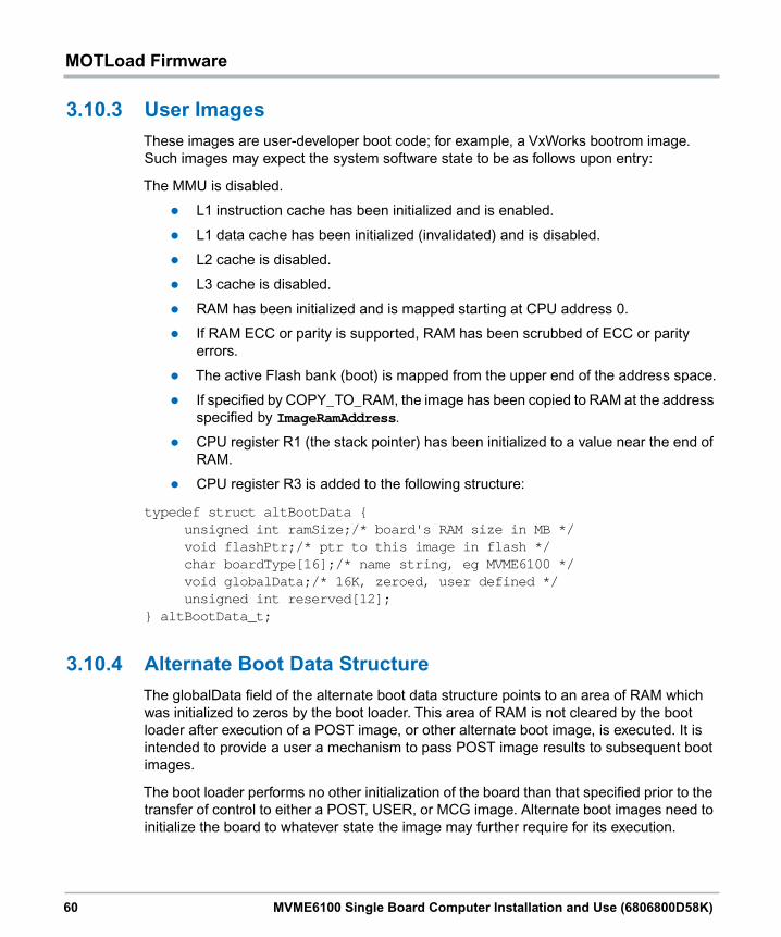
60 MVME6100 Single Board Computer Installation and Use (6806800D58K)
MOTLoad FirmwareMOTLoad Firmware
3.10.3 User Images
These images are user-developer boot code; for example, a VxWorks bootrom image.
Such images may expect the system software state to be as follows upon entry:
The MMU is disabled.
L1 instruction cache has been initialized and is enabled.
L1 data cache has been initialized (invalidated) and is disabled.
L2 cache is disabled.
L3 cache is disabled.
RAM has been initialized and is mapped starting at CPU address 0.
If RAM ECC or parity is supported, RAM has been scrubbed of ECC or parity
errors.
The active Flash bank (boot) is mapped from the upper end of the address space.
If specified by COPY_TO_RAM, the image has been copied to RAM at the address
specified by ImageRamAddress.
CPU register R1 (the stack pointer) has been initialized to a value near the end of
RAM.
CPU register R3 is added to the following structure:
typedef struct altBootData { unsigned int ramSize;/* board's RAM size in MB */ void flashPtr;/* ptr to this image in flash */ char boardType[16];/* name string, eg MVME6100 */ void globalData;/* 16K, zeroed, user defined */ unsigned int reserved[12];} altBootData_t;
3.10.4 Alternate Boot Data Structure
The globalData field of the alternate boot data structure points to an area of RAM which
was initialized to zeros by the boot loader. This area of RAM is not cleared by the boot
loader after execution of a POST image, or other alternate boot image, is executed. It is
intended to provide a user a mechanism to pass POST image results to subsequent boot
images.
The boot loader performs no other initialization of the board than that specified prior to the
transfer of control to either a POST, USER, or MCG image. Alternate boot images need to
initialize the board to whatever state the image may further require for its execution.

MOTLoad Firmware
MVME6100 Single Board Computer Installation and Use (6806800D58K) 61
POST images are expected, but not required, to return to the boot loader. Upon return, the
boot loader proceeds with the scan for an executable alternate boot image. POST images
that return control to the boot loader must ensure that upon return, the state of the board is
consistent with the state that the board was in at POST entry. USER images should not
return control to the boot loader.
3.10.5 Alternate Boot Images and Safe Start
Some later versions of MOTLoad support alternate boot images and a safe start recovery
procedure. If safe start is available on the MVME6100, alternate boot images are
supported. With alternate boot image support, the boot loader code in the boot block
examines the upper 8 MB of the flash bank for alternate boot images. If an image is found,
control is passed to the image.
3.10.6 Boot Image Firmware Scan
The scan is performed by examining each 1 MB boundary for a defined set of flags that
identify the image as being POST, USER, or Alternate MOTLoad. POST is a user-
developed Power On Self Test that would perform a set of diagnostics and then return to
the boot loader image. USER would be a boot image, such as the VxWorks bootrom, which
would perform board initialization. A bootable VxWorks kernel would also be a USER
image. Boot images are not restricted to being 1 MB or less in size; however, they must
begin on a 1 MB boundary within the 8 MB of the scanned flash bank. The flash bank
structure is shown below:
The scan is performed downwards beginning at the location of the first possible alternate
image and searches first for POST, then USER, and finally Alternate MOTLoad images. In
the case of multiple images of the same type, control is passed to the first image
encountered in the scan.
Address Usage
0xFFF00000 to 0xFFFFFFFF Boot block. Recovery code.
0xFFE00000 to 0XFFFFFFFF Backup MOTLoad image
0xFFD00000 to 0xFFDFFFFF First possible alternate image
0xFFC00000 to 0xFFCFFFFF Second possible alternate image
.... Alternate boot images
0xFF899999 to 0xFF8FFFFF Bottom of flash (flash size varies per product)

62 MVME6100 Single Board Computer Installation and Use (6806800D58K)
MOTLoad FirmwareMOTLoad Firmware
Safe Start, whether invoked by hitting ESC on the console within the first five seconds
following power-on reset or by setting the Safe Start jumper, interrupts the scan process.
The user may then display the available boot images and select the desired image. The
feature is provided to enable recovery in cases when the programmed Alternate Boot
Image is no longer desired. The following output is an example of an interactive Safe Start:
ABCDEInteractive Boot Mode Enteredboot> ?Interactive boot commands:'d':show directory of alternate boot images'c':continue with normal startup'q':quit without executing any alternate boot image'r [address]':execute specified (or default) alternate image'p [address]':execute specified (or default) POST image'?':this help screen'h':this help screenboot> dAddr FFE00000 Size 00100000 Flags 00000003 Name: MOTLoadAddr FFD00000 Size 00100000 Flags 00000003 Name: MOTLoadboot> cNOPQRSTUVabcdefghijk#lmn3opqrsstuvxyzaWXZCopyright Motorola Inc. 1999-2004, All Rights ReservedMOTLoad RTOS Version 2.0, PAL Version 0.b EA02
...
MVME6100>
3.11 Startup SequenceThe firmware startup sequence following reset of MOTLoad is to:
Initialize cache, MMU, FPU, and other CPU internal items
Initialize the memory controller
Search the active flash bank, possibly interactively, for a valid Power On Self Test
(POST) image. If found, the POST images executes. Once completed, the POST
image returns and startup continues.
Search the active flash bank, possibly interactively, for a valid USER boot image.
If found, the USER boot image executes. A return to the boot block code is not
anticipated.

MOTLoad Firmware
MVME6100 Single Board Computer Installation and Use (6806800D58K) 63
If a valid USER boot image is not found, search the active flash bank, possibly
interactively, for a valid Alternate MOTLoad boot image; anticipated to be an
upgrade of alternate MOTLoad firmware. If found, the image is executed. A return
to the boot block code is not anticipated.
Execute the recovery image of the firmware in the boot block if no valid USER or
alternate MOTLoad image is found
During startup, interactive mode may be entered by either setting the Safe Start
jumper/switch or by sending an <ESC> to the console serial port within five seconds of the
board reset. During interactive mode, the user has the option to display locations at which
valid boot images were discovered, specify which discovered image is to be executed, or
specify that the recovery image in the boot block of the active flash bank is to be executed.

64 MVME6100 Single Board Computer Installation and Use (6806800D58K)
MOTLoad FirmwareMOTLoad Firmware

MVME6100 Single Board Computer Installation and Use (6806800D58K) 65
Chapter 4
Functional Description
4.1 OverviewThis chapter describes the MVME6100 on a block diagram level.
4.2 FeaturesThe following table lists the features of the MVME6100.
Table 4-1 MVME6100 Features Summary
Feature Description
Processor
– Single 1.267 GHz MPC7457 processor
– Bus clock frequency at 133 MHz
– 36-bit address, 64-bit data buses
– Integrated L1 and L2 cache
L3 Cache– Bus clock frequency at 211 MHz (when supported by processor)
– Up to 2MB using SDR SRAM
Flash
– Two banks (A & B) of soldered Intel StrataFlash devices
– 8 to 64MB supported on each bank
– Boot bank is switch selectable between banks
– Bank A has combination of software and hardware write-protect
scheme
– Bank B top 1MB block can be write-protected through
software/hardware write-protect control
System Memory– Two banks on board for up to 1Gb using 256Mb or 512Mb devices
– Bus clock frequency at 133 MHz
Memory Controller
PCI Host Bridge
Dual 10/100/1000 Ethernet
Interrupt Controller
PCI Interface
I2C Interface
– Provided by Marvell MV64360 system controller
NVRAM
Real-Time Clock
Watchdog Timer
– 32KB provided by MK48T37 with SnapHat battery backup

66 MVME6100 Single Board Computer Installation and Use (6806800D58K)
Functional DescriptionFunctional Description
On-board Peripheral Support
– Dual 10/100/1000 Ethernet ports routed to front panel RJ-45
connectors, one optionally routed to P2 backplane
– Two asynchronous serial ports provided by an ST16C554D; one
serial port is routed to a front panel RJ-45 connector and the
second serial port is routed to an on-board header (J29, as factory
default build configuration).
PCI/PMC
– Two 32/64-bit PMC slots with front-panel I/O plus P2 rear I/O as
specified by IEEE P1386
– 33/66 MHz PCI or 66/100 MHz PCI-X
VME Interface
– Tsi148 VME 2eSST ASIC provides:
Eight programmable VMEbus map decoders
A16, A24, A32, and A64 address
8-bit, 16-bit, and 32-bit single cycle data transfers
8-bit, 16-bit, 32-bit, and 64-bit block transfers
Supports SCT, BLT, MBLT, 2eVME, and 2eSST protocols
8 entry command and 4KB data write post buffer
4KB read ahead buffer
PMCspan Support
– One PMCspan slot
– Supports 33/66 MHz, 32/64-bit PCI bus
– Access through PCI6520 bridge to PMCspan
Form Factor – Standard 6U VME
Miscellaneous
– Combined reset and abort switch
– Status LEDs
– 8-bit software-readable switch (S1)
– VME geographical address switch (S3)
– Boundary Scan header (J8)
– CPU RISCWatch COP header (J42)
Table 4-1 MVME6100 Features Summary (continued)
Feature Description

Functional Description
MVME6100 Single Board Computer Installation and Use (6806800D58K) 67
4.3 Block DiagramFigure 4-1 shows a block diagram of the overall board architecture.
4.4 ProcessorThe MVME6100 supports the MPC7457 with adjustable core voltage supply. The maximum
external processor bus speed is 133 MHz. The processor core frequency runs at 1.267
GHz or the highest speed MPC7457 can support, which is determined by the processor
core voltage, the external speed, and the internal VCO frequency. MPX bus protocols are
supported on the board. The MPC7457 has integrated L1 and L2 caches (as the factory
build configuration) and supports an L3 cache interface with on-chip tags to support up to
2MB of off-chip cache. +2.5V signal levels are used on the processor bus.
Figure 4-1 MVME6100 Block Diagram
64-bit/33/66/100 MHz PCI-X
L3 Cache2MB
MPC74571.267 GHz
211 MHz SDR
133 MHzProcessor Bus
133 MHzMemory Bus
RTCNVRAM
VMETSI148
SolderedFlash Bank A64MB
64-bit/133 MHz PCI-X
DDR RAM512MB-1GB
DDR RAM512MB-1GB
Rows D&Z46-pins
GigabitEthernet
RJ-45
JumperSelectable
SolderedFlash Bank B64MB
32/64-bit,33/66 MHz PC
4250 0604
Discovery IIHost
Bridge Device Bus
GigabitEthernet
RJ-45
IPMC Slot 2
FP I/O
P2 P1
PMC SpanConnector
P-P Bridge
Serial
RJ-45
header
Rows A&C64-pins
PMC Slot 1
FP I/O

68 MVME6100 Single Board Computer Installation and Use (6806800D58K)
Functional DescriptionFunctional Description
4.5 L3 CacheThe MVME6100 external L3 cache is implemented using two 8Mb SDR SRAM devices.
The L3 cache bus is 72-bits wide (64 bits of data and 8 bits of parity) and operates at 211
MHz. The L3 cache interface is implemented with an on-chip, 8-way, set-associative tag
memory. The external SRAMs are accessed through a dedicated L3 cache port that
supports one bank of SRAM. The L3 cache normally operates in copyback mode and
supports system cache coherency through snooping. Parity generation and checking may
be disabled by programming the L3CR register. Refer to the PowerPC Apollo
Microprocessor Implementation Definition Book IV listed in Appendix C, Related
Documentation.
4.6 System ControllerThe MV64360 is an integrated system controller for high performance embedded control
applications. The following features of the MV64360 are supported by the MVME6100:
The MV64360 has a five-bus architecture comprised of:
A 72-bit interface to the CPU bus (includes parity)
A 72-bit interface to DDR SDRAM (double data rate-synchronous DRAM) with
ECC
A 32-bit interface to devices
Two 64-bit PCI/PCI-X interfaces
In addition to the above, the MV64360 integrates:
Three Gigabit Ethernet MACs (only two are used on the MVME6100)
2Mb SRAM
Interrupt controller
Four general-purpose 32-bit timers/counters
I2C interface
Four channel independent DMA controller
All of the above interfaces are connected through a cross bar fabric. The cross bar enables
concurrent transactions between units. For example, the cross bar can simultaneously
control:
A Gigabit Ethernet MAC fetching a descriptor from the integrated SRAM
The CPU reading from the DRAM
The DMA moving data from the device bus to the PCI bus

Functional Description
MVME6100 Single Board Computer Installation and Use (6806800D58K) 69
4.6.1 CPU Bus Interface
The CPU interface (master and slave) operates at 133 MHz and +2.5V signal levels using
MPX bus modes. The CPU bus has a 36-bit address and 64-bit data buses. The MV64360
supports up to eight pipelined transactions per processor. There are 21 address windows
supported in the CPU interface:
Four for SDRAM chip selects
Five for device chip selects
Five for the PCI_0 interface (four memory + one I/O)
Five for the PCI_1 interface (four memory + one I/O)
One for the MV64360 integrated SRAM
One for the MV64360 internal registers space
Each window is defined by base and size registers and can decode up to 4GB space
(except for the integrated SRAM, which is fixed to 256KB). Refer to the MV64360 Data
Sheet, listed in Appendix C, Related Documentation, for additional information and
programming details.
4.6.2 Memory Controller Interface
The MVME6100 supports two banks of DDR SDRAM using 256Mb/512Mb DDR SDRAM
devices on-board. 1Gb DDR non-stacked SDRAM devices may be used when available.
133 MHz operation should be used for all memory options. The SDRAM supports ECC and
the MV64360 supports single-bit and double-bit error detection and single-bit error
correction of all SDRAM reads and writes.
The SDRAM controller supports a wide range of SDRAM timing parameters. These
parameters can be configured through the SDRAM Mode register and the SDRAM Timing
Parameters register. Refer to the MV64360 Data Sheet, listed in Appendix C, Related
Documentation, for additional information and programming details.
The DRAM controller contains four transaction queues—two write buffers and two read
buffers. The DRAM controller does not necessarily issue DRAM transactions in the same
order that it receives the transactions. The MV64360 is targeted to support full PowerPC
cache coherency between CPU L1/L2 caches and DRAM.

70 MVME6100 Single Board Computer Installation and Use (6806800D58K)
Functional DescriptionFunctional Description
4.6.3 Device Controller Interface
The device controller supports up to five banks of devices, three of which are used for Flash
Banks A and B, NVRAM/RTC. Each bank supports up to 512MB of address space,
resulting in total device space of 1.5GB. Serial ports are the fourth and fifth devices on the
MVME6100. Each bank has its own parameters register as shown in the following table.
4.6.4 PCI/PCI-X Interfaces
The MVME6100 provides two 32/64-bit PCI/PCI-X buses, operating at a maximum
frequency of 100 MHz when configured to PCI-X mode, and run at 33 or 66 MHz when
running conventional PCI mode. PCI bus 1 is connected to the PMC slots 1 and 2.
The maximum PCI-X frequency of 100 MHz supported by PCI bus 1 may be reduced
depending on the number and/or type of PMC/PrPMC installed. If PCI bus 1 is set to +5V
VIO, it runs at 33 MHz. VIO is set by the keying pins (they are both a keying pin and jumper).
Both pins must be set for the same VIO on the PCI-X bus.
PCI bus 0 is connected to the Tsi148 device and PMCspan bridge. PCI bus 0 is configured
for 133 MHz PCI-X mode.
The MV64360 PCI interfaces are fully PCI rev. 2.2 and PCI-X rev 1.0 compliant and support
both address and data parity checking. The MV64360 contains all of the required PCI
configuration registers. All internal registers, including the PCI configuration registers, are
accessible from the CPU bus or the PCI buses.
4.6.5 Gigabit Ethernet MACs
The MVME6100 supports two 10/100/1000Mb/s full duplex Ethernet ports connected to the
front panel via the MV64360 system controller. Ethernet access is provided by front panel
RJ-45 connectors with integrated magnetics and LEDs. Port 1 is a dedicated Gigabit
Ethernet port while a configuration header is provided for port 2 front or rear P2 access
Refer to Front/Rear Ethernet and Transition Module Options Header (J30) for more
information.
Table 4-2 Device Bus Parameters
Device Bank Description
Flash Bank A Device Bus Bank 0 Bank width 32-bit, parity disabled
Flash Bank B Device Bus Boot Bank Bank width 32-bit, parity disabled
Real-Time Clock
Serial Ports
Board Specific Registers
Device Bus Bank 1 Bank width 8-bit, parity disabled

Functional Description
MVME6100 Single Board Computer Installation and Use (6806800D58K) 71
Each Ethernet interface is assigned an Ethernet Station Address. The address is unique
for each device. The Ethernet Station Addresses are displayed on labels attached to the
PMC front-panel keep-out area.
The MV64360 is not integrated with a PHY for the Ethernet interfaces. External PHY is the
Broadcom BCM5461S 10/100/1000BaseT Gigabit transceiver with SERDES interface.
Refer to Appendix C, Related Documentation for more information.
4.6.6 SRAM
The MV64360 integrates 2Mb of general-purpose SRAM. It is accessible from the CPU or
any of the other interfaces. It can be used as fast CPU access memory (6 cycles latency)
and for off loading DRAM traffic. A typical usage of the SRAM can be a descriptor RAM for
the Gigabit Ethernet ports.
4.6.7 General-Purpose Timers/Counters
There are four 32-bit wide timers/counters on the MV64360. Each timer/counter can be
selected to operate as a timer or as a counter. The timing reference is based on the
MV64360 Tclk input, which is set at 133 MHz. Each timer/counter is capable of generating
an interrupt. Refer to the MV64360 Data Sheet, listed in Appendix C, Related
Documentation, for additional information and programming details.
4.6.8 Watchdog Timer
The MV64360 internal watchdog timer is a 32-bit count-down counter that can be used to
generate a non-maskable interrupt or reset the system in the event of unpredictable
software behavior. After the watchdog timer is enabled, it becomes a free running counter
that must be serviced periodically to keep it from expiring. Refer to the MV64360 Data
Sheet, listed in Appendix C, Related Documentation, for additional information and
programming details.
4.6.9 I2O Message Unit
I2O compliant messaging for the MVME6100 board is provided by an I2O messaging unit
integrated into the MV64360 system controller. The MV64360 messaging unit includes
hardware hooks for message transfers between PCI devices and the CPU. This includes
all of the registers required for implementing the I2O messaging, as defined in the Intelligent
I/O (I2O) Standard specification. For additional details regarding the I2O messaging unit,
refer to the MV64360 Data Sheet, listed in Appendix C, Related Documentation.
72 MVME6100 Single Board Computer Installation and Use (6806800D58K)
Functional DescriptionFunctional Description
4.6.10 Four Channel Independent DMA Controller
The MV64360 incorporates four independent direct memory access (IDMA) engines. Each
IDMA engine has the capability to transfer data between any two interfaces. Refer to the
MV64360 Data Sheet, listed in Appendix C, Related Documentation, for additional
information and programming details.
4.6.11 I2C Serial Interface and Devices
A two-wire serial interface for the MVME6100 board is provided by a master/slave capable
I2C serial controller integrated into the MV64360 device. The I2C serial controller provides
two basic functions. The first function is to optionally provide MV64360 register initialization
following a reset. The MV64360 can be configured (by switch setting) to automatically read
data out of a serial EEPROM following a reset and initialize any number of internal
registers. In the second function, the controller is used by the system software to read the
contents of the VPD EEPROM contained on the MVME6100 board, along with the SPD
EEPROMs for on-board memory to further initialize the memory controller and other
interfaces.
The MVME6100 board contains the following I2C serial devices:
8KB EEPROM for user-defined MV64360 initialization
8KB EEPROM for VPD
8KB EEPROM for user data
Two 256 byte EEPROMs for SPD
DS1621 temperature sensor
One 256 byte EEPROM for PMCspan PCIx-PCIx bridge use
The 8KB EEPROM devices are implemented using Atmel AT24C64A devices or similar
parts. These devices use two byte addressing to address the 8KB of the device.
4.6.12 Interrupt Controller
The MVME6100 uses the interrupt controller integrated into the MV64360 device to
manage the MV64360 internal interrupts as well as the external interrupt requests. The
interrupts are routed to the MV64360 MPP pins from on-board resources as shown in the
MVME6100 Programmer’s Guide. The external interrupt sources include the following:
On-board PCI device interrupts
PMC slot interrupts
VME interrupts
RTC interrupt

Functional Description
MVME6100 Single Board Computer Installation and Use (6806800D58K) 73
Watchdog timer interrupts
Abort switch interrupt
External UART interrupts
Ethernet PHY interrupts
IPMC761 interrupts
PMCspan interrupts
For additional details regarding the external interrupt assignments, refer to the MVME6100
Programmer’s Guide.
4.6.13 PCI Bus Arbitration
PCI arbitration is performed by the MV64360 system controller. The MV64360 integrates
two PCI arbiters, one for each PCI interface (PCI bus 0/1). Each arbiter can handle up to
six external agents plus one internal agent (PCI bus 0/1 master). The internal PCI arbiter
REQ#/GNT# signals are multiplexed on the MV64360 MPP pins. The internal PCI arbiter
is disabled by default (the MPP pins function as general-purpose inputs). Software
configures the MPP pins to function as request/grant pairs for the internal PCI arbiter. The
arbitration pairs for the MVME6100 are assigned to the MPP pins as shown in the
MVME6100 Programmer’s Guide.
4.7 VMEbus InterfaceThe VMEbus interface is provided by the Tsi148 ASIC. Refer to the Tsi148 User’s Manual
available from Tundra Semiconductor for additional information as listed in Appendix C,
Related Documentation. 2eSST operations are not supported on 3-row backplanes. You
must use VME64x (VITA 1.5) compatible backplanes, such as 5-row backplanes, to
achieve maximum VMEbus performance.
4.8 PMCspan InterfaceThe MVME6100 provides a PCI expansion connector to add more PMC interfaces than the
two on the MVME6100 board. The PMCspan interface is provided through the PCI6520
PCIx/PCIx bridge.

74 MVME6100 Single Board Computer Installation and Use (6806800D58K)
Functional DescriptionFunctional Description
4.9 Flash MemoryThe MVME6100 contains two banks of flash memory accessed via the device controller
bus contained within the MV64360 device. Both banks are soldered on board and have
different write-protection schemes.
4.10 System MemoryMVME6100 system memory consists of double-data-rate SDRAMs. The DDR SDRAMs
support two data transfers per clock cycle. The memory device is a standard monolithic
(32M x 8 or 64M x 8) DDR, 8-bit wide, 66-pin, TSSOPII package. Both banks are provided
on board the MVME6100 and operate at 133 MHz clock frequency with both banks
populated.
4.11 Asynchronous Serial PortsThe MVME6100 board contains one EXAR ST16C554D quad UART (QUART) device
connected to the MV64360 device controller bus to provide asynchronous debug ports. The
QUART supports up to four asynchronous serial ports, two of which are used on the
MVME6100.
COM1 is an RS-232 port and the TTL- level signals are routed through appropriate EIA-232
drivers and receivers to an RJ-45 connector on the front panel. Unused control inputs on
COM1 and COM2 are wired active. The reference clock frequency for the QUART is
1.8432MHz. All UART ports are capable of signaling at up to 115 Kbaud.
4.12 PCI Mezzanine Card SlotsThe MVME6100 board supports two PMC slots. Two sets of four EIA-E700 AAAB
connectors are located on the MVME6100 board to interface to the 32-bit/64-bit IEEE
P1386.1 PMC to add any desirable function. The PMC slots are PCI/PCI-X 33/66/100
capable.
PMC/IPMC slot 1 supports:
Mezzanine Type: PMC/IPMC = PCI Mezzanine Card
Mezzanine Size: S1B = Single width and standard depth
(75mm x 150mm) with front panel
PMC Connectors: J11, J12, J13, and J14 (32/64-bit PCI with front and rear I/O)
Signaling Voltage: VIO = +3.3V (+5V tolerant) or +5V, selected by keying pin

Functional Description
MVME6100 Single Board Computer Installation and Use (6806800D58K) 75
PMC slot 2 supports:
In addition, the PMC connectors are located such that a double-width PMC may be installed
in place of the two single-width PMCs.
In this case, the MVME6100 supports:
4.13 Real-Time Clock/NVRAM/Watchdog TimerThe real-time clock/NVRAM/watchdog timer is implemented using an integrated SGS-
Thompson M48T37V Timekeeper SRAM and Snaphat battery. The minimum M48T37V
watchdog timer time-out resolution is 62.5 msec (1/16s) and maximum time-out period is
124 seconds. The interface for the Timekeeper and SRAM is connected to the MV64360
device controller bus on the MVME6100 board. Refer to the MV64360 Data Sheet, listed in
Appendix C, Related Documentation, for additional information and programming details.
Mezzanine Type: PMC = PCI Mezzanine Card
Mezzanine Size: S1B = Single width and standard depth
(75mm x 150mm) with front panel
PMC Connectors: J21, J22, J23, and J24 (32/64-bit PCI with front and rear I/O)
Signalling Voltage: VIO = +3.3V (+5V tolerant) or +5V, selected by keying pin
You cannot use 3.3V and 5.0V PMCs together; the voltage keying pin on slots 1 and
2 must be identical. When in 5.0V mode, the bus runs at 33 MHz.
Mezzanine Type: PMC = PCI Mezzanine Card
Mezzanine Size: Double width and standard depth
(150mm x 150mm) with front panel
PMC Connectors: J11, J12, J13, J14, J21, J22, J23, and J24
(32/64-bit PCI with front and rear I/O)
Signaling Voltage: VIO = +3.3V (+5.0V tolerant) or +5.0V, selected by keying pin
On either PMC site, the user I/O – Jn4 signals will only support the low-current, high-
speed signals and not for any current bearing power supply usage. The maximum
current rating of each pin/signal is 250 mA.

76 MVME6100 Single Board Computer Installation and Use (6806800D58K)
Functional DescriptionFunctional Description
4.14 IDSEL RoutingPCI device configuration registers are accessed by using the IDSEL signal of each PCI
agent to an A/D signal as defined in version 2.2 of the PCI specification. IDSEL
assignments to on-board resources are specified in the MVME6100 Programmer’s Guide.
4.15 Reset Control LogicThe sources of reset on the MVME6100 are the following:
Power up
Reset Switch
NVRAM Watchdog Timer
MV64360 Watchdog Timer
VMEbus controller – Tsi148 ASIC
System Control register bit
4.16 Debug SupportThe MVME6100 provides JTAG/COP headers for debug capability for Processor as well
as PCI0 bus use. These connectors are not populated as factory build configuration.
4.17 Processor JTAG/COP HeadersThe MVME6100 provides JTAG/COP connectors for JTAG/COP emulator support
(RISCWatch COP J42), as well as supporting board boundary scan capabilities (Boundary
Scan header J8).

MVME6100 Single Board Computer Installation and Use (6806800D58K) 77
Chapter 5
Pin Assignments
5.1 OverviewThis chapter provides pin assignments for various headers and connectors on the
MMVE6100 single-board computer.
Gigabit Ethernet Connectors (J9, J93)
PCI Mezzanine Card (PMC) Connectors (J11-J14, J21-J24)
COM1 Connector (J19)
VMEbus P1 Connector
VMEBus P2 Connector (PMC Mode)
The following headers are described in this chapter:
SCON Header (J7)
Boundary Scan Header (J8)
PMC/IPMC Selection Headers (J10, J15-J18, J25-J28)
COM2 Header (J29)
Front/Rear Ethernet and Transition Module Options Header (J30)
Processor JTAG/COP Header (J42)
5.2 ConnectorsThe following tables provide a brief description of the connector, the pin assignments, and
signal descriptions for standard and nonstandard connectors on the MVME6100.

78 MVME6100 Single Board Computer Installation and Use (6806800D58K)
Pin AssignmentsPin Assignments
5.2.1 PMC Expansion Connector (J4)
One 114-pin Mictor connector with a center row of power and ground pins is used to provide
PCI expansion capability. The pin assignments for this connector are as follows:
Table 5-1 PMC Expansion Connector (J4) Pin Assignments
Pin Signal Signal Pin
1 +3.3V
GND
+3.3V 2
3 PCICLK PMCINTA# 4
5 GND PMCINTB# 6
7 PURST# PMCINTC# 8
9 HRESET# PMCINTD# 10
11 TDO TDI 12
13 TMS TCK 14
15 TRST# PCIXP# 16
17 PCIXGNT# PCIXREQ# 18
19 +12V -12V 20
21 PERR# SERR# 22
23 LOCK# SDONE 24
25 DEVSEL# SBO# 26
27 GND GND 28
29 TRDY# IRDY# 30
31 STOP# FRAME# 32
33 GND M66EN 34
35 ACK64# Reserved 36
37 REQ64# Reserved 38
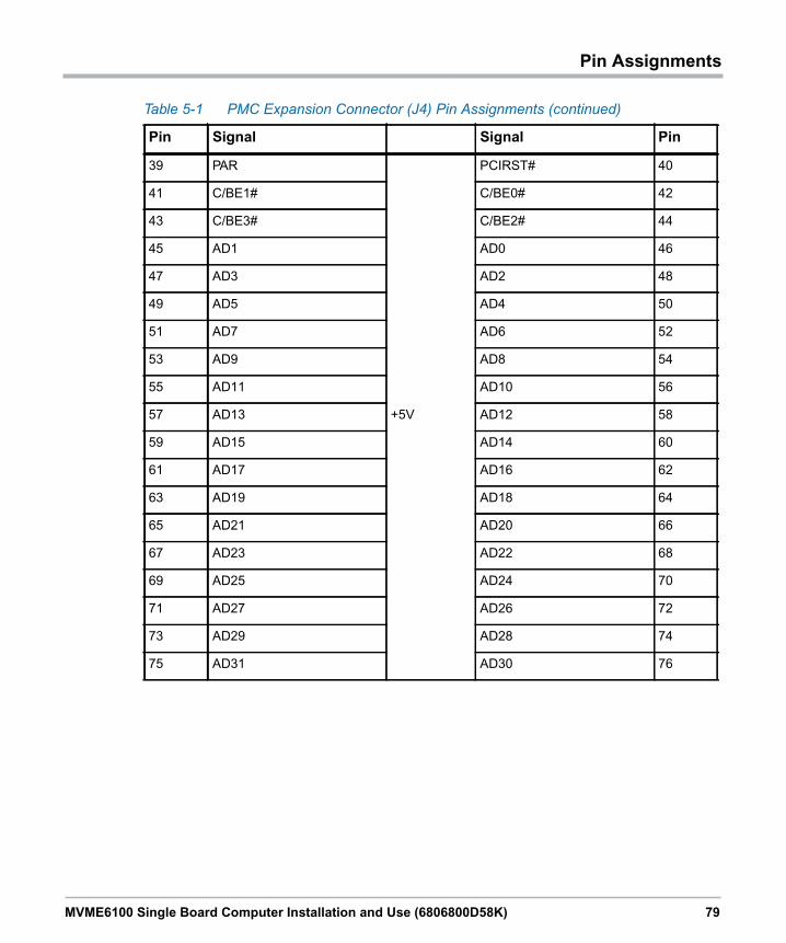
Pin Assignments
MVME6100 Single Board Computer Installation and Use (6806800D58K) 79
39 PAR
+5V
PCIRST# 40
41 C/BE1# C/BE0# 42
43 C/BE3# C/BE2# 44
45 AD1 AD0 46
47 AD3 AD2 48
49 AD5 AD4 50
51 AD7 AD6 52
53 AD9 AD8 54
55 AD11 AD10 56
57 AD13 AD12 58
59 AD15 AD14 60
61 AD17 AD16 62
63 AD19 AD18 64
65 AD21 AD20 66
67 AD23 AD22 68
69 AD25 AD24 70
71 AD27 AD26 72
73 AD29 AD28 74
75 AD31 AD30 76
Table 5-1 PMC Expansion Connector (J4) Pin Assignments (continued)
Pin Signal Signal Pin

80 MVME6100 Single Board Computer Installation and Use (6806800D58K)
Pin AssignmentsPin Assignments
All PMC expansion signals are dedicated PMC expansion PCI bus signals.
77 PAR64
GND
Reserved 78
79 C/BE5# C/BE4# 80
81 C/BE7# C/BE6# 82
83 AD33 AD32 84
85 AD35 AD34 86
87 AD37 AD36 88
89 AD39 AD38 90
91 AD41 AD40 92
93 AD43 AD42 94
95 AD45 AD44 96
97 AD47 AD46 98
99 AD49 AD48 100
101 AD51 AD50 102
103 AD53 AD52 104
105 AD55 AD54 106
107 AD57 AD56 108
109 AD59 AD58 110
111 AD61 AD60 112
113 AD63 AD62 114
Table 5-1 PMC Expansion Connector (J4) Pin Assignments (continued)
Pin Signal Signal Pin
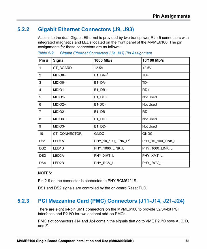
Pin Assignments
MVME6100 Single Board Computer Installation and Use (6806800D58K) 81
5.2.2 Gigabit Ethernet Connectors (J9, J93)
Access to the dual Gigabit Ethernet is provided by two transpower RJ-45 connectors with
integrated magnetics and LEDs located on the front panel of the MVME6100. The pin
assignments for these connectors are as follows:
NOTES:
Pin 2-9 on the connector is connected to PHY BCM5421S.
DS1 and DS2 signals are controlled by the on-board Reset PLD.
5.2.3 PCI Mezzanine Card (PMC) Connectors (J11-J14, J21-J24)
There are eight 64-pin SMT connectors on the MVME6100 to provide 32/64-bit PCI
interfaces and P2 I/O for two optional add-on PMCs.
PMC slot connectors J14 and J24 contain the signals that go to VME P2 I/O rows A, C, D,
and Z.
Table 5-2 Gigabit Ethernet Connectors (J9, J93) Pin Assignment
Pin # Signal 1000 Mb/s 10/100 Mb/s
1 CT_BOARD +2.5V +2.5V
2 MDIO0+ B1_DA+1 TD+
3 MDIO0- B1_DA- TD-
4 MDIO1+ B1_DB+ RD+
5 MDIO1- B1_DC+ Not Used
6 MDIO2+ B1-DC- Not Used
7 MDIO2- B1_DB- RD-
8 MDIO3+ B1_DD+ Not Used
9 MDIO3- B1_DD- Not Used
10 CT_CONNECTOR GNDC GNDC
DS1 LED1A PHY_10_100_LINK_L2 PHY_10_100_LINK_L
DS2 LED1B PHY_1000_LINK_L PHY_1000_LINK_L
DS3 LED2A PHY_XMT_L PHY_XMT_L
DS4 LED2B PHY_RCV_L PHY_RCV_L

82 MVME6100 Single Board Computer Installation and Use (6806800D58K)
Pin AssignmentsPin Assignments
The pin assignments for these connectors are as follows.
Table 5-3 PMC Slot 1 Connector (J11) Pin Assignments
Pin Signal Signal Pin
1 TCK -12V 2
3 GND INTA# 4
5 INTB# INTC# 6
7 PMCPRSNT1# +5V 8
9 INTD# PCI_RSVD 10
11 GND +3.3Vaux 12
13 CLK GND 14
15 GND PMCGNT1# 16
17 PMCREQ1# +5V 18
19 +3.3V (VIO) AD31 20
21 AD28 AD27 22
23 AD25 GND 24
25 GND C/BE3# 26
27 AD22 AD21 28
29 AD19 +5V 30
31 +3.3V (VIO) AD17 32
33 FRAME# GND 34
35 GND IRDY# 36
37 DEVSEL# +5V 38
39 PCIXCAP LOCK# 40
41 PCI_RSVD PCI_RSVD 42
43 PAR GND 44
45 +3.3V (VIO) AD15 46
47 AD12 AD11 48
49 AD09 +5V 50

Pin Assignments
MVME6100 Single Board Computer Installation and Use (6806800D58K) 83
51 GND C/BE0# 52
53 AD06 AD05 54
55 AD04 GND 56
57 +3.3V (VIO) AD03 58
59 AD02 AD01 60
61 AD00 +5V 62
63 GND REQ64# 64
Table 5-3 PMC Slot 1 Connector (J11) Pin Assignments (continued)
Pin Signal Signal Pin
Table 5-4 PMC Slot 1 Connector (J12) Pin Assignments
Pin Signal Signal Pin
1 +12V TRST# 2
3 TMS TDO 4
5 TDI GND 6
7 GND Not Used 8
9 Not Used Not Used 10
11 Pull-up +3.3V 12
13 RST# Pull-down 14
15 +3.3V Pull-down 16
17 Not Used GND 18
19 AD30 AD29 20
21 GND AD26 22
23 AD24 +3.3V 24
25 IDSEL1 AD23 26
27 +3.3V AD20 28
29 AD18 GND 30
31 AD16 C/BE2# 32

84 MVME6100 Single Board Computer Installation and Use (6806800D58K)
Pin AssignmentsPin Assignments
33 GND IDSEL1B 34
35 TRDY# +3.3V 36
37 GND STOP# 38
39 PERR# GND 40
41 +3.3V SERR# 42
43 C/BE1# GND 44
45 AD14 AD13 46
47 M66EN AD10 48
49 AD08 +3.3V 50
51 AD07 REQ1B# 52
53 +3.3V GNT1B# 54
55 Not Used GND 56
57 Not Used EREADY0 58
59 GND Not Used 60
61 ACK64# +3.3V 62
63 GND No Connect (MONARCH#) 64
Table 5-4 PMC Slot 1 Connector (J12) Pin Assignments (continued)
Pin Signal Signal Pin
Table 5-5 PMC Slot 1 Connector (J13) Pin Assignments
Pin Signal Signal Pin
1 Reserved GND 2
3 GND C/BE7# 4
5 C/BE6# C/BE5# 6
7 C/BE4# GND 8
9 +3.3V (VIO) PAR64 10
11 AD63 AD62 12
13 AD61 GND 14

Pin Assignments
MVME6100 Single Board Computer Installation and Use (6806800D58K) 85
15 GND AD60 16
17 AD59 AD58 18
19 AD57 GND 20
21 +3.3V (VIO) AD56 22
23 AD55 AD54 24
25 AD53 GND 26
27 GND AD52 28
29 AD51 AD50 30
31 AD49 GND 32
33 GND AD48 34
35 AD47 AD46 36
37 AD45 GND 38
39 +3.3V (VIO) AD44 40
41 AD43 AD42 42
43 AD41 GND 44
45 GND AD40 46
47 AD39 AD38 48
49 AD37 GND 50
51 GND AD36 52
53 AD35 AD34 54
55 AD33 GND 56
57 +3.3V (VIO) AD32 58
59 Reserved Reserved 60
61 Reserved GND 62
63 GND Reserved 64
Table 5-5 PMC Slot 1 Connector (J13) Pin Assignments (continued)
Pin Signal Signal Pin

86 MVME6100 Single Board Computer Installation and Use (6806800D58K)
Pin AssignmentsPin Assignments
Table 5-6 PMC Slot 1 Connector (J14) Pin Assignments
Pin Signal Signal Pin
1 PMC0_1 (P2-C1) PMC0_2 (P2-A1) 2
3 PMC0_3 (P2-C2) PMC0_4 (P2-A2) 4
5 PMC0_5 (P2-C3) PMC0_6 (P2-A3) 6
7 PMC0_7 (P2-C4) PMC0_8 (P2-A4) 8
9 PMC1 _9 (P2-C5) PMC0_10 (P2-A5) 10
11 PMC0_11 (P2-C6) PMC0_12 (P2-A6) 12
13 PMC0_13 (P2-C7) PMC0_14 (P2-A7) 14
15 PMC0_15 (P2-C8) PMC0_16 (P2-A8) 16
17 PMC0_17 (P2-C9) PMC0_18 (P2-A9) 18
19 PMC0_19 (P2-C10) PMC0_20 (P2-A10) 20
21 PMC0_21 (P2-C11) PMC0_22 (P2-A11) 22
23 PMC0_23 (P2-C12) PMC0_24 (P2-A12) 24
25 PMC0_25 (P2-C13) PMC0_26 (P2-A13) 26
27 PMC0_27 (P2-C14) PMC0_28 (P2-A14) 28
29 PMC0_29 (P2-C15) PMC0_30 (P2-A15) 30
31 PMC0_31 (P2-C16) PMC0_32 (P2-A16) 32
33 PMC0_33 (P2-C17) PMC0_34 (P2-A17) 34
35 PMC0_35 (P2-C18) PMC0_36 (P2-A18) 36
37 PMC0_37 (P2-C19) PMC0_38 (P2-A19) 38
39 PMC0_39 (P2-C20) PMC0_40 (P2-A20) 40
41 PMC0_41 (P2-C21) PMC0_42 (P2-A21) 42
43 PMC0_43 (P2-C22) PMC0_44 (P2-A22) 44
45 PMC0_45 (P2-C23) PMC0_46 (P2-A23) 46
47 PMC0_47 (P2-C24) PMC0_48 (P2-A24) 48
49 PMC0_49 (P2-C25) PMC0_50 (P2-A25) 50
51 PMC0_51 (P2-C26) PMC0_52 (P2-A26) 52

Pin Assignments
MVME6100 Single Board Computer Installation and Use (6806800D58K) 87
53 PMC0_53 (P2-C27) PMC0_54 (P2-A27) 54
55 PMC0_55 (P2-C28) PMC0_56 (P2-A28) 56
57 PMC0_57 (P2-C29) PMC0_58 (P2-A29) 58
59 PMC0_59 (P2-C30) PMC0_60 (P2-A30) 60
61 PMC0_61 (P2-C31) PMC0_62 (P2-A31) 62
63 PMC0_63 (P2-C32) PMC0_64 (P2-A32) 64
Table 5-6 PMC Slot 1 Connector (J14) Pin Assignments (continued)
Pin Signal Signal Pin
Table 5-7 PMC Slot 2 Connector (J21) Pin Assignments
Pin Signal Signal Pin
1 TCK -12V 2
3 GND INTC# 4
5 INTD# INTA# 6
7 PMCPRSNT1# +5V 8
9 INTB# PCI_RSVD 10
11 GND +3.3Vaux 12
13 CLK GND 14
15 GND PMCGNT1# 16
17 PMCREQ1# +5V 18
19 +3.3V (VIO) AD31 20
21 AD28 AD27 22
23 AD25 GND 24
25 GND C/BE3# 26
27 AD22 AD21 28
29 AD19 +5V 30
31 +3.3V (VIO) AD17 32
33 FRAME# GND 34

88 MVME6100 Single Board Computer Installation and Use (6806800D58K)
Pin AssignmentsPin Assignments
35 GND IRDY# 36
37 DEVSEL# +5V 38
39 PCIXCAP LOCK# 40
41 PCI_RSVD PCI_RSVD 42
43 PAR GND 44
45 +3.3V (VIO) AD15 46
47 AD12 AD11 48
49 AD09 +5V 50
51 GND C/BE0# 52
53 AD06 AD05 54
55 AD04 GND 56
57 +3.3V (VIO) AD03 58
59 AD02 AD01 60
61 AD00 +5V 62
63 GND REQ64# 64
Table 5-7 PMC Slot 2 Connector (J21) Pin Assignments (continued)
Pin Signal Signal Pin
Table 5-8 PMC Slot 2 Connector (J22) Pin Assignments
Pin Signal Signal Pin
1 +12V TRST# 2
3 TMS TDO 4
5 TDI GND 6
7 GND Not Used 8
9 Not Used Not Used 10
11 Pull-up +3.3V 12
13 RST# Pull-down 14
15 +3.3V Pull-down 16

Pin Assignments
MVME6100 Single Board Computer Installation and Use (6806800D58K) 89
17 Not Used GND 18
19 AD30 AD29 20
21 GND AD26 22
23 AD24 +3.3V 24
25 IDSEL1 AD23 26
27 +3.3V AD20 28
29 AD18 GND 30
31 AD16 C/BE2# 32
33 GND IDSEL1B 34
35 TRDY# +3.3V 36
37 GND STOP# 38
39 PERR# GND 40
41 +3.3V SERR# 42
43 C/BE1# GND 44
45 AD14 AD13 46
47 M66EN AD10 48
49 AD08 +3.3V 50
51 AD07 REQ1B# 52
53 +3.3V GNT1B# 54
55 Not Used GND 56
57 Not Used EREADY1 58
59 GND Not Used 60
61 ACK64# +3.3V 62
63 GND No Connect (MONARCH#) 64
Table 5-8 PMC Slot 2 Connector (J22) Pin Assignments (continued)
Pin Signal Signal Pin

90 MVME6100 Single Board Computer Installation and Use (6806800D58K)
Pin AssignmentsPin Assignments
Table 5-9 PMC Slot 2 Connector (J23) Pin Assignments
Pin Signal Signal Pin
1 Reserved GND 2
3 GND C/BE7# 4
5 C/BE6# C/BE5# 6
7 C/BE4# GND 8
9 +3.3V (VIO) PAR64 10
11 AD63 AD62 12
13 AD61 GND 14
15 GND AD60 16
17 AD59 AD58 18
19 AD57 GND 20
21 +3.3V (VIO) AD56 22
23 AD55 AD54 24
25 AD53 GND 26
27 GND AD52 28
29 AD51 AD50 30
31 AD49 GND 32
33 GND AD48 34
35 AD47 AD46 36
37 AD45 GND 38
39 +3.3V (VIO) AD44 40
41 AD43 AD42 42
43 AD41 GND 44
45 GND AD40 46
47 AD39 AD38 48
49 AD37 GND 50
51 GND AD36 52

Pin Assignments
MVME6100 Single Board Computer Installation and Use (6806800D58K) 91
53 AD35 AD34 54
55 AD33 GND 56
57 +3.3V (VIO) AD32 58
59 Reserved Reserved 60
61 Reserved GND 62
63 GND Reserved 64
Table 5-9 PMC Slot 2 Connector (J23) Pin Assignments (continued)
Pin Signal Signal Pin
Table 5-10 PMC Slot 2 Connector (J24) Pin Assignments
Pin Signal Signal Pin
1 PMC1_1 (P2-D1) PMC1_2 (P2-Z1) 2
3 PMC1_3 (P2-D2) PMC1_4 (P2-D3) 4
5 PMC1_5 (P2-Z3) PMC1_6 (P2-D4) 6
7 PMC1_7 (P2-D5) PMC1_8 (P2-Z5) 8
9 PMC1_9 (P2-D6) PMC1_10 (P2-D7) 10
11 PMC1_11 (P2-Z7) PMC1_12 (P2-D8) 12
13 PMC1_13 (P2-D9) PMC1_14 (P2-Z9) 14
15 PMC1_15 (P2-D10 PMC1_16 (P2-D11) 16
17 PMC1_17 (P2-Z11) PMC1_18 (P2-D12) 18
19 PMC1_19 (P2-D13) PMC1_20 (P2-Z13) 20
21 PMC1_21 (P2-D14) PMC1_22 (P2-D15) 22
23 PMC1_23 (P2-Z15) PMC1_24 (P2-D16) 24
25 PMC1_25 (P2-D17) PMC1_26 (P2-Z17) 26
27 PMC1_27 (P2-D18) PMC1_28 (P2-D19) 28
29 PMC1_29 (P2-Z19) PMC1_30 (P2-D20) 30
31 PMC1_31 (P2-D21) PMC1_32 (P2-Z21) 32
33 PMC1_33 (P2-D22 PMC1_34 (P2-D23) 34

92 MVME6100 Single Board Computer Installation and Use (6806800D58K)
Pin AssignmentsPin Assignments
5.2.4 COM1 Connector (J19)
A standard RJ-45 connector located on the front panel of the MVME6100 provides the
interface to the asynchronous serial debug port. The pin assignments for this connector are
as follows:
35 PMC1_35 (P2-Z23) PMC1_36 (P2-D24) 36
37 PMC1_37 (P2-D25) PMC1_38 (P2-Z25 38
39 PMC1_39 (P2-D26) PMC1_40 (P2-D27) 40
41 PMC1_41 (P2-Z27) PMC1_42 (P2-D28) 42
43 PMC1_43 (P2-D29) PMC1_44 (P2-Z29) 44
45 PMC1_45 (P2-D30) PMC1_46 (P2-Z31) 46
47 Not Used Not Used 48
49 Not Used Not Used 50
51 Not Used Not Used 52
53 Not Used Not Used 54
55 Not Used Not Used 56
57 Not Used Not Used 58
59 Not Used Not Used 60
61 Not Used Not Used 62
63 Not Used Not Used 64
Table 5-10 PMC Slot 2 Connector (J24) Pin Assignments (continued)
Pin Signal Signal Pin
Table 5-11 COM1 Connector (J19) Pin Assignments
Pin Signal
1 DCD
2 RTS
3 GNDC
4 TX
5 RX

Pin Assignments
MVME6100 Single Board Computer Installation and Use (6806800D58K) 93
5.2.5 VMEbus P1 Connector
The VME P1 connector is an 160-pin DIN. The P1 connector provides power and VME
signals for 24-bit address and 16-bit data. The pin assignments for the P1 connector is as
follows:
6 GNDC
7 CTS
8 DTR
Table 5-11 COM1 Connector (J19) Pin Assignments (continued)
Pin Signal
Table 5-12 VMEbus P1 Connector Pin Assignments
ROW Z ROW A ROW B ROW C ROW D
1 Reserved D00 BBSY* D08 Reserved 1
2 GND D01 BCLR* D09 Reserved 2
3 Reserved D02 ACFAIL* D10 Reserved 3
4 GND D03 BG0IN* D11 Reserved 4
5 Reserved D04 BG0OUT* D12 Reserved 5
6 GND D05 BG1IN* D13 Reserved 6
7 Reserved D06 BG1OUT* D14 Reserved 7
8 GND D07 BG2IN* D15 Reserved 8
9 Reserved GND BG2OUT* GND
Reserved
(Geographical
Address, parity)
9
10 GND SYSCLK BG3IN* SYSFAIL* Reserved (GA0) 10
11 Reserved GND BG3OUT* BERR* Reserved (GA1) 11
12 GND DS1* BR0* SYSRESET* Reserved 12
13 Reserved DS0* BR1* LWORD* Reserved (GA2) 13
14 GND WRITE* BR2* AM5 Reserved 14
15 Reserved GND BR3* A23 Reserved (GA3) 15
16 GND DTACK* AM0 A22 Reserved 16

94 MVME6100 Single Board Computer Installation and Use (6806800D58K)
Pin AssignmentsPin Assignments
17 Reserved GND AM1 A21 Reserved (GA4) 17
18 GND AS* AM2 A20 Reserved 18
19 Reserved GND AM3 A19 Reserved 19
20 GND IACK* GND A18 Reserved 20
21 Reserved IACKIN* SERA A17 Reserved 21
22 GND IACKOUT* SERB A16 Reserved 22
23 Reserved AM4 GND A15 Reserved 23
24 GND A07 IRQ7* A14 Reserved 24
25 Reserved A06 IRQ6* A13 Reserved 25
26 GND A05 IRQ5* A12 Reserved 26
27 Reserved A04 IRQ4* A11 Reserved 27
28 GND A03 IRQ3* A10 Reserved 28
29 Reserved A02 IRQ2* A09 Reserved 29
30 GND A01 IRQ1* A08 Reserved 30
31 Reserved -12V +5VSTDBY +12V Reserved 31
32 GND +5V +5V +5V Reserved 32
Table 5-12 VMEbus P1 Connector Pin Assignments (continued)
ROW Z ROW A ROW B ROW C ROW D

Pin Assignments
MVME6100 Single Board Computer Installation and Use (6806800D58K) 95
5.2.6 VMEBus P2 Connector (PMC Mode)
The VME P2 connector is an 160-pin DIN. Row B of the P2 connector provides power to
the MVME6100 and to the upper eight VMEbus address lines and additional 16 VMEbus
data lines. The pin assignments for the P2 connector are as follows:
Table 5-13 VMEbus P2 Connector Pin Assignments (PMC Mode)
ROW Z ROW A ROW B ROW C ROW D
1PMC1_2
(J24-2)
PMC0_2
(J14-2)+5V
PMC0_1 (J30 D6-C6) or
P2_IO_GLAN1_MDIO_1-
(J30 B6-C6)
PMC1_1
(J24-1)1
2 GNDPMC0_4
(J14-4)GND
PMC0_3 (J30 D5-C5) or
P2_IO_GLAN1_MDIO_1+
(J30 B5-C5)
PMC1_3
(J24-3)2
3PMC1_5
(J4-5)
PMC0_6
(J14-6)RETRY#
PMC0_5 (J30 D4-C4) or
P2_IO_GLAN1_MDIO_0-
(J30 B4-C4)
PMC1_4
(J24-4)3
4 GNDPMC0_8
(J14-8)VA24
PMC0_7 (J30 D3-C3) or
P2_IO_GLAN1_MDIO_0+
(J30 B3-C3)
PMC1_6
(J24-6)4
5PMC1_8
(J24-8)
PMC0_10
(J14-10)VA25
PMC0_9
(J14-9)
PMC1_7
(J24-7)5
6 GNDPMC0_12
(J14-12)VA26
PMC0_11
(J14-11)
PMC1_9
(J24-9)6
7PMC1_11
(J24-11)
PMC0_14
(J14-14)VA27
PMC0_13
(J14-13)
PMC1_10
(J24-10)7
8 GNDPMC0_16
(J14-16)VA28
PMC0_15
(J14-15)
PMC1_12
(J24-12)8
9PMC1_14
(J24-14)
PMC0_18
(J14-18)VA29
PMC0_17
(J14-17)
PMC1_13
(J24-13)9
10 GNDPMC0_20
(J14-20)VA30
PMC0_19
(J14-19)
PMC1_15
(J24-15)10
11PMC1_17
(J24-17)
PMC0_22
(J14-22)VA31
PMC0_21
(J14-21)
PMC1_16
(J24-16)11
12 GNDPMC0_24
(J14-24)GND
PMC0_23
(J14-23)
PMC1_18
(J24-18)12
13PMC1_20
(J24-20)
PMC0_26
(J14-26)+5V
PMC0_25
(J14-25)
PMC1_19
(J24-19)13

96 MVME6100 Single Board Computer Installation and Use (6806800D58K)
Pin AssignmentsPin Assignments
14 GNDPMC0_28
(J14-28)VD16
PMC0_27
(J14-27)
PMC1_21
(J24-21)14
15PMC1_23
(J24-J23)
PMC0_30
(J14-30)VD17
PMC0_29
(J14-29)
PMC1_22
(J24-22)15
16 GNDPMC0_32
(J14-32)VD18
PMC0_31
(J14-31)
PMC1_24
(J24-24)16
17PMC1_26
(J24-J26)
PMC0_34
(J14-34)VD19
PMC0_33
(J14-33)
PMC1_25
(J24-25)17
18 GNDPMC0_36
(J14-36)VD20
PMC0_35
(J14-35)
PMC1_27
(J24-27)18
19PMC1_29
(J24-29)
PMC0_38
(J14-38)VD21
PMC0_37
(J14-37)
PMC1_28
(J24-28)19
20 GNDPMC0_40
(J14-40)VD22
PMC0_39
(J14-39)
PMC1_30
(J24-30)20
21PMC1_32
(J24-32)
PMC0_42
(J14-42)VD23
PMC0_41
(J14-41)
PMC1_31
(J24-31)21
22 GNDPMC0_44
(J14-44)GND
PMC0_43
(J14-43)
PMC1_33
(J24-33)22
23PMC1_35
(J24-35)
PMC0_46
(J14-46)VD24
PMC0_45
(J14-45)
PMC1_34
(J24-34)23
24 GNDPMC0_48
(J14-48)VD25
PMC0_47
(J14-47)
PMC1_36
(J24-36)24
25
PMC1_38 (J30 D7-
C7) or
P2_IO_GLAN1_M
DIO_2+ (J30 B7-
C7)
PMC0_50
(J14-50)VD26
PMC0_49
(J14-49)
PMC1_37
(J24-37)25
26 GNDPMC0_52
(J14-52)VD27
PMC0_51
(J14-51)
PMC1_39
(J24-39)26
27
PMC1_41 (J30 D8-
C8) or
P2_IO_GLAN1_M
DIO_2- (J30 B8-
C8)
PMC0_54
(J14-54)VD28
PMC0_53
(J14-53)/TXB
PMC1_40
(J24-40)27
Table 5-13 VMEbus P2 Connector Pin Assignments (PMC Mode) (continued)
ROW Z ROW A ROW B ROW C ROW D

Pin Assignments
MVME6100 Single Board Computer Installation and Use (6806800D58K) 97
The default configuration for P2, C27-C30 are connected to PMC0_IO (53,55,57,59).
5.2.7 VMEbus P2 Connector (IPMC Mode)
The VME P2 connector is an 160-pin DIN. Row B of the P2 connector provides power to
the MVME6100 and to the upper eight VMEbus address lines and additional 16 VMEbus
data lines. The pin assignments for the P2 connector are as follows:
28 GNDPMC0_56
(J14-56)VD29
PMC0_55
(J14-55)/RXB
PMC1_42
(J24-42)28
29
PMC1_44 (J30 D9-
C9) or
P2_IO_GLAN1_M
DIO_3- (J30 B9-
C9)
PMC0_58
(J14-58)VD30
PMC0_57
(J14-57)/RTSB
PMC1_43
(J24-43)29
30 GNDPMC0_60
(J14-60)VD31
PMC0_59
(J14-59)/CTSB
PMC1_45
(J24-45)30
31
PMC1_46 (J30
D10-C10) or
P2_IO_GLAN1_M
DIO_3+ (J30 B10-
C10)
PMC0_62
(J14-62)GND
PMC0_61
(J14-61)GND 31
32 GNDPMC0_64
(J14-64)+5V
PMC0_63
(J14-63)VPC 32
Table 5-13 VMEbus P2 Connector Pin Assignments (PMC Mode) (continued)
ROW Z ROW A ROW B ROW C ROW D
Table 5-14 VME P2 Connector Pinouts with IPMC712
Pin Row Z Row A Row B Row C Row D
1 PMC2_2 DB0# +5V RD- PMC2_1 (J24-1)
2 GND DB1# GND RD+ PMC2_3 (J24-3)
3 PMC2_5 DB2# N/C TD- PMC2_4 (J24-4)
4 GND DB3# VA24 TD+ PMC2_6 (J24-6)
5 PMC2_8 DB4# VA25 NOT USED PMC2_7 (J24-7)
6 GND DB5# VA26 NOT USED PMC2_9 (J24-9)
7 PMC2_11 DB6# VA27 +12V (LAN) PMC2_10 (J24-10)

98 MVME6100 Single Board Computer Installation and Use (6806800D58K)
Pin AssignmentsPin Assignments
8 GND DB7# VA28 PRSTB# PMC2_12 (J24-12)
9 PMC2-14 DBP# VA29 P DB0 PMC2_13 (J24-13)
10 GND ATN# VA30 P DB1 PMC2_15 (J24-15)
11 PMC2_17 BSY# VA31 P DB2 PMC2_16 (J24-16)
12 GND ACK# GND P DB3 PMC2_18 (J24-18)
13 PMC2_20 RST# +5V P DB4 PMC2_19 (J24-19)
14 GND MSG# VD16 P DB5 PMC2_21 (J24-21)
15 PMC2_23 SEL# VD17 P DB6 PMC2_22 (J24-22)
16 GND D/C# VD18 P DB7 PMC2_24 (J24-24)
17 PMC2_26 REQ# VD19 P ACK# PMC2_25 (J24-25)
18 GND I/O# VD20 P BSY PMC2_27 (J24-27)
19 PMC2_29 (J24-29) TXD3 VD21 P PE PMC2_28 (J24-28)
20 GND RXD3 VD22 P SEL PMC2_30 (J24-30)
21 PMC2_32 (J24-32) RTS3 VD23 P IME PMC2_31 (J24-31)
22 GND CTS3 GND P FAULT# PMC2_33 (J24-33)
23 PMC2_35 (J24-35) DTR3 VD24 TXD1_232 PMC2_34 (J24-34)
24 GND DCD3 VD25 RXD1 PMC2_36 (J24-36)
25 PMC2_38 (J24-38) TXD4 VD26 RTS1 PMC2_37 (J24-37)
26 GND RXD4 VD27 CTS1 PMC2_39 (J24-39)
27 PMC2_41 (J24-41) RTS4 VD28 TXD2 PMC2_40 (J24-40)
28 GND TRXC4 VD29 RXD2 PMC2_42 (J24-42)
29 PMC2_44 (J24-44) CTS4 VD30 RTS2 PMC2_43 (J24-43)
30 GND DTR4 VD31 CTS2 PMC2_45 (J24-45)
31 PMC2_46 (J24-46) DCD4 GND DTR2 GND
32 GND RTXC4 +5V DCD2 VPC
Table 5-14 VME P2 Connector Pinouts with IPMC712 (continued)
Pin Row Z Row A Row B Row C Row D
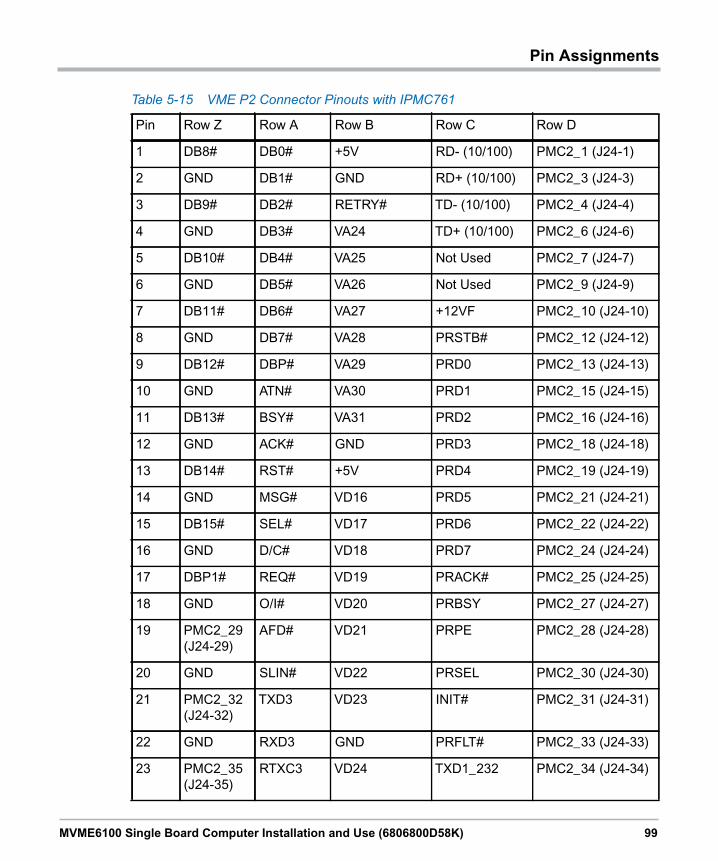
Pin Assignments
MVME6100 Single Board Computer Installation and Use (6806800D58K) 99
Table 5-15 VME P2 Connector Pinouts with IPMC761
Pin Row Z Row A Row B Row C Row D
1 DB8# DB0# +5V RD- (10/100) PMC2_1 (J24-1)
2 GND DB1# GND RD+ (10/100) PMC2_3 (J24-3)
3 DB9# DB2# RETRY# TD- (10/100) PMC2_4 (J24-4)
4 GND DB3# VA24 TD+ (10/100) PMC2_6 (J24-6)
5 DB10# DB4# VA25 Not Used PMC2_7 (J24-7)
6 GND DB5# VA26 Not Used PMC2_9 (J24-9)
7 DB11# DB6# VA27 +12VF PMC2_10 (J24-10)
8 GND DB7# VA28 PRSTB# PMC2_12 (J24-12)
9 DB12# DBP# VA29 PRD0 PMC2_13 (J24-13)
10 GND ATN# VA30 PRD1 PMC2_15 (J24-15)
11 DB13# BSY# VA31 PRD2 PMC2_16 (J24-16)
12 GND ACK# GND PRD3 PMC2_18 (J24-18)
13 DB14# RST# +5V PRD4 PMC2_19 (J24-19)
14 GND MSG# VD16 PRD5 PMC2_21 (J24-21)
15 DB15# SEL# VD17 PRD6 PMC2_22 (J24-22)
16 GND D/C# VD18 PRD7 PMC2_24 (J24-24)
17 DBP1# REQ# VD19 PRACK# PMC2_25 (J24-25)
18 GND O/I# VD20 PRBSY PMC2_27 (J24-27)
19 PMC2_29
(J24-29)
AFD# VD21 PRPE PMC2_28 (J24-28)
20 GND SLIN# VD22 PRSEL PMC2_30 (J24-30)
21 PMC2_32
(J24-32)
TXD3 VD23 INIT# PMC2_31 (J24-31)
22 GND RXD3 GND PRFLT# PMC2_33 (J24-33)
23 PMC2_35
(J24-35)
RTXC3 VD24 TXD1_232 PMC2_34 (J24-34)

100 MVME6100 Single Board Computer Installation and Use (6806800D58K)
Pin AssignmentsPin Assignments
Rows A and C and Zs (Z1, 3, 5, 7, 9, 11, 13, 15, and 17) functionality is provided by the
IPMC761 in slot 1 and the MVME6100 Ethernet port 2.
24 GND TRXC3 VD25 RXD1_232 PMC2_36 (J24-36)
25 PMC2_38
(J24-38)
TXD4 VD26 RTS1_232 PMC2_37 (J24-37)
26 GND RXD4 VD27 CTS1_232 PMC2_39 (J24-39)
27 PMC2_41
(J24-41)
RTXC4 VD28 TXD2_232 PMC2_40 (J24-40)
28 GND TRXC4 VD29 RXD2_232 PMC2_42 (J24-42)
29 PMC2_44
(J24-44)
VD30 RTS2_232 PMC2_43 (J24-43)
30 GND -12VF VD31 CTS2_232 PMC2_45 (J24-45)
31 PMC2_46
(J24-46)
MSYNC# GND MDO GND
32 GND MCLK +5V MDI VPC
Table 5-15 VME P2 Connector Pinouts with IPMC761 (continued)
Pin Row Z Row A Row B Row C Row D

Pin Assignments
MVME6100 Single Board Computer Installation and Use (6806800D58K) 101
5.3 HeadersThe next subsections provide a description of each header and its settings and/or pin
assignments. Refer to Configuring the Hardware on page 28 for details on setting the
headers.
5.3.1 SCON Header (J7)
A 3-pin planar header allows the choice for auto/enable/disable SCON VME configuration.
A jumper installed across pins 1 and 2 configures for SCON always enabled. A jumper
installed across pins 2 and 3 configures for SCON disabled. No jumper installed configures
for auto SCON. The pin assignments for this connector are as follows:
5.3.2 Boundary Scan Header (J8)
The 14-pin boundary scan header provides an interface for programming the on-board
PLDs and for boundary scan testing/debug purposes. The pin assignments for this header
are as follows:
Table 5-16 SCON Header (J7) Pin Assignments
Pin Signal
1 SCONEN_L
2 GND
3 SCONDIS_L
Table 5-17 Boundary Scan Header (J8) Pin Assignments
Pin Signal Signal Pin
1 TRST_L GND 2
3 TDO GND 4
5 TDI GND 6
7 TMS GND 8
9 TCLK GND 10
11 NC CPU_BSCAN_L 12
13 AW_L GND 14

102 MVME6100 Single Board Computer Installation and Use (6806800D58K)
Pin AssignmentsPin Assignments
5.3.3 PMC/IPMC Selection Headers (J10, J15-J18, J25-J28)
Nine 3-pin 2mm planar headers allow for PMC/IPMC I/O selection. These nine headers can
also be combined into one single header block where a block shunt can be used as a
jumper. The pin assignments for these connectors are as follows:
A jumper installed across pins 2 and 3 on all nine headers selects PMC1 I/O for IPMC
mode.
5.3.4 COM2 Header (J29)
A 10-pin 0.100" planar header provides the interface to a second asynchronous serial
debug port. COM2 only goes to the on-board header as the default configuration. The pin
assignments for this header are as follows:
Table 5-18 PMC/IPMC Configuration Jumper Block
Pin/Row 1
(PMC I/O)
Pin/Row 2
(P2 Pins)
Pin/Row 3
(IPMC Pins)
J28 PMC1_IO(2) P2_PMC1_IO(2) IPMC DB8_L
J16 PMC1_IO(5) P2_PMC1_IO(5) IPMC DB9_L
J18 PMC1_IO(8) P2_PMC1_IO(8) IPMC DB10_L
J25 PMC1_IO(11) P2_PMC1_IO(11) IPMC DB11_L
J27 PMC1_IO(14) P2_PMC1_IO(14) IPMC DB12_L
J26 PMC1_IO(17) P2_PMC1_IO(17) IPMC DB13_L
J17 PMC1_IO(20) P2_PMC1_IO(20) IPMC DB14_L
J10 PMC1_IO(23) P2_PMC1_IO(23) IPMC DB15_L
J15 PMC1_IO(26) P2_PMC1_IO(26) IPMC DBP1_L
Table 5-19 COM2 Planar Serial Port Header (J29) Pin Assignments
Pin Signal Signal Pin
1 COM2_DCD COM2_DSR 2
3 COM2_RX COM2_RTS 4
5 COM2_TX COM2_CTS 6
7 COM2_DTR COM2_RI 8
9 GND KEY (no pin) 10

Pin Assignments
MVME6100 Single Board Computer Installation and Use (6806800D58K) 103
5.3.5 Front/Rear Ethernet and Transition Module Options Header(J30)
The pin assignments for this connector are as follows:
Table 5-20 Front/Rear Ethernet and Transition Module Options Header (J30) PinAssignment
PinRow D
(From PMC I/O)
Row C
(To P2 Connector)
Row B
(From LAN2
Controller)
Row A
(To Front Panel
Ethernet)
1 PMC0_IO(13) P2a_C7 Fused +12V No Connect
2 PMC0_IO(60) P2_A30 Fused -12V No Connect
3 PMC0_IO(7) P2_C4 magnetic T2b-23 MDI_0P (J9c-2)
4 PMC0_IO(5) P2_C3 magnetic T2-22 MDI_0N (J9-3)
5 PMC0_IO(3) P2_C2 magnetic T2-20 MDI_1P (J9-4)
6 PMC0_IO(1) P2_C1 magnetic T2-19 MDI_1N (J9-5)
7 PMC1_IO(38) P2_Z25 magnetic T2-17 MDI_2P (J9-6)
8 PMC1_IO(41) P2_Z27 magnetic T2-16 MDI_2N (J9-7)
9 PMC1_IO(44) P2_Z29 magnetic T2-14 MDI_3P (J9-8)
10 PMC1_IO(46) P2_Z31 magnetic T2-13 MDI_3N (J9-9)
a. VME P2.
b. Transformer for Ethernet port #2.
c. Ethernet port #2 front connector.
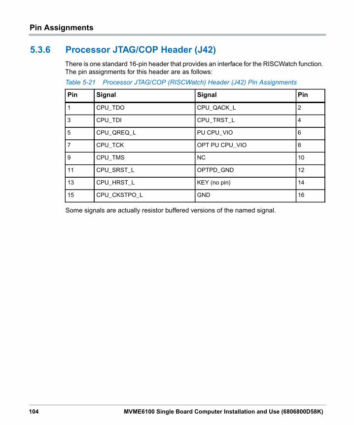
104 MVME6100 Single Board Computer Installation and Use (6806800D58K)
Pin AssignmentsPin Assignments
5.3.6 Processor JTAG/COP Header (J42)
There is one standard 16-pin header that provides an interface for the RISCWatch function.
The pin assignments for this header are as follows:
Some signals are actually resistor buffered versions of the named signal.
Table 5-21 Processor JTAG/COP (RISCWatch) Header (J42) Pin Assignments
Pin Signal Signal Pin
1 CPU_TDO CPU_QACK_L 2
3 CPU_TDI CPU_TRST_L 4
5 CPU_QREQ_L PU CPU_VIO 6
7 CPU_TCK OPT PU CPU_VIO 8
9 CPU_TMS NC 10
11 CPU_SRST_L OPTPD_GND 12
13 CPU_HRST_L KEY (no pin) 14
15 CPU_CKSTPO_L GND 16

MVME6100 Single Board Computer Installation and Use (6806800D58K) 105
Appendix A
Specifications
A.1 Power RequirementsIn its standard configuration, the MVME6100 requires +5V, +12V, and –12V for operation.
On-board converters supply the processor core voltage, +3.3V, +1.8V, and +2.5V.
A.1.1 Supply Current Requirements
Table A-1 provides an estimate of the typical and maximum current required from each of
the input supply voltages.
In a 3-row chassis, PMC current should be limited to 19.8 watts (total of both PMC slots).
In a 5-row chassis, PMC current should be limited to 46.2 watts (total of both PMC slots).
Table A-1 Power Requirements
Model Power
MVME6100-0163Typical: 42W @ +5V
Maximum: 51W@ +5V
MVME6100-0163 with IPMC712/761Typical: 46W @ +5V
Maximum: 55W @ +5V

106 MVME6100 Single Board Computer Installation and Use (6806800D58K)
SpecificationsSpecifications
A.2 Environmental SpecificationsTable A-2 lists the environmental specifications, along with the board dimensions.
Table A-2 MVME6100 Specifications
Characteristics Specifications
Operating Temperature
0° to +55° C (32° to 131° F) (forced air cooling required)
400 LFM (linear feet per minute) of forced air cooling is
recommended for operation in the upper temperature range.
Storage Temperature –40° to +85° C (–40° to +185° F)
Relative HumidityOperating: 5% to 90% noncondensing
Non-operating: 5% to 90% noncondensing
VibrationNon-operating: 1 G sine sweep, 5–100 Hz,
horizontal and vertical (NEBS1)
Physical Dimensions6U, 4HP wide (233 mm x 160 mm x 20 mm) (9.2 in. x 6.3 in.
x 0.8 in)
MTBF
328,698 hours, calculated based on BellCore Issue 6,
Method 1, case 3 for the central office or environmentally
controlled remote shelters or customer premise areas.

MVME6100 Single Board Computer Installation and Use (6806800D58K) 107
Appendix B
Thermal Validation
B.1 OverviewBoard component temperatures are affected by ambient temperature, air flow, board
electrical operation, and software operation. In order to evaluate the thermal performance
of a circuit board assembly, it is necessary to test the board under actual operating
conditions. These operating conditions vary depending on system design.
While SMART EC performs thermal analysis in a representative system to verify operation
within specified ranges, refer to Appendix A, Specifications, you should evaluate the
thermal performance of the board in your application.
This appendix provides systems integrators with information which can be used to conduct
thermal evaluations of the board in their specific system configuration. It identifies thermally
significant components and lists the corresponding maximum allowable component
operating temperatures. It also provides example procedures for component-level
temperature measurements.
B.2 Thermally Significant ComponentsThe following table summarizes components that exhibit significant temperature rises.
These are the components that should be monitored in order to assess thermal
performance. The table also supplies the component reference designator and the
maximum allowable operating temperature.
You can find components on the board by their reference designators as shown in Figure
B-1 and Figure B-2. Versions of the board that are not fully populated may not contain
some of these components.
The preferred measurement location for a component may be junction, case, or air as
specified in the table. Junction temperature refers to the temperature measured by an on-
chip thermal device. Case temperature refers to the temperature at the top, center surface
of thecomponent.Air temperature refers to theambient temperaturenear thecomponent.
Table B-1 Thermally Significant Components
Reference
DesignatorGeneric Description
Max. Allowable
Component
Temperature
(deg. C)
Measurement
Location
U3-U11, U64-
U72DDR SDRAM 70 Air
U84, U95 Gigabit Ethernet Transceiver 129 Case
U82, U83 Cache 115 Case

108 MVME6100 Single Board Computer Installation and Use (6806800D58K)
Thermal ValidationThermal Validation
U45, U46 Programmable Logic Device 70 Air
U32 PCI Bridge 70 Air
U20 Discovery II 110 Case
U15 Clock Generator 85 Air
U14, U22 Clock Buffer 85 Air
U12 MC7457RX, 1.267 GHz Processor 103 Case
U21 Tsi148 VME Bridge ASIC 100
Figure B-1 Thermally Significant Component - Primary Side
Table B-1 Thermally Significant Components (continued)
Reference
DesignatorGeneric Description
Max. Allowable
Component
Temperature
(deg. C)
Measurement
Location

Thermal Validation
MVME6100 Single Board Computer Installation and Use (6806800D58K) 109
B.3 Component Temperature MeasurementThe following sections outline general temperature measurement methods. For the specific
types of measurements required for thermal evaluation of this board, see Table B-1.
B.3.1 Preparation
We recommend 40 AWG (American wire gauge) thermocouples for all thermal
measurements. Larger gauge thermocouples can wick heat away from the components
and disturb air flowing past the board.
Allow the board to reach thermal equilibrium before taking measurements. Most circuit
boards will reach thermal equilibrium within 30 minutes. After the warm up period, monitor
a small number of components over time to assure that equilibrium has been reached.
Figure B-2 Thermally Significant Component - Secondary Side

110 MVME6100 Single Board Computer Installation and Use (6806800D58K)
Thermal ValidationThermal Validation
B.3.2 Measuring Junction Temperature
Some components have an on-chip thermal measuring device such as a thermal diode. For
instructions on measuring temperatures using the on-board device, refer to the component
manufacturer’s documentation listed in Appendix A, Specifications.
B.3.3 Measuring Case Temperature
Measure the case temperature at the center of the top of the component. Make sure there
is good thermal contact between the thermocouple junction and the component. We
recommend you use a thermally conductive adhesive such as Loctite 384.
If components are covered by mechanical parts such as heatsinks, you will need to
machine these parts to route the thermocouple wire. Make sure that the thermocouple
junction contacts only the electrical component. Also make sure that heatsinks lay flat on
electrical components. The following figure shows one method of machining a heatsink
base to provide a thermocouple routing path.
Machining a heatsink base reduces the contact area between the heatsink and the
electrical component. You can partially compensate for this effect by filling the machined
areas with thermal grease. The grease should not contact the thermocouple junction.

Thermal Validation
MVME6100 Single Board Computer Installation and Use (6806800D58K) 111
Figure B-3 Mounting a Thermocouple Under a Heatsink

112 MVME6100 Single Board Computer Installation and Use (6806800D58K)
Thermal ValidationThermal Validation
B.3.4 Measuring Local Air Temperature
Measure local component ambient temperature by placing the thermocouple downstream
of the component. This method is conservative since it includes heating of the air by the
component. The following figure illustrates one method of mounting the thermocouple.
Figure B-4 Measuring Local Air Temperature

MVME6100 Single Board Computer Installation and Use (6806800D58K) 113
Appendix C
Related Documentation
C.1 SMART Embedded Computing DocumentationThe documentation listed is referenced in this manual. Technical documentation can be
found by using the Documentation Search at https://www.smartembedded.com/ec/support/
or you can obtain electronic copies of SMART EC documentation by contacting your local
sales representative.
C.2 Manufacturers’ DocumentsFor additional information, refer to the following table for manufacturers’ data sheets or
user’s manuals. As an additional help, a source for the listed document is provided. Please
note that, while these sources have been verified, the information is subject to change
without notice.
Table C-1 SMART EC Publications
Document TitlePublication
Number
MVME6100 Data Sheet MVME6100-DS
MVME61006E Series Single-Board Computer Programmer’s Reference
Guide6806800D59
MOTLoad Firmware Package User’s Manual 6806800C24
IPMC712/761 I/O Module Installation and Use VIPMCA/IH
PMCspan PMC Adapter Carrier Board Installation and Use PMCSPANA/IH
Table C-2 Manufacturers’ Documents
Document Title and Source Publication Number
MPC7457 RISC Microprocessor Hardware Specification
http://www.nxp.comMPC7457EC/D
Rev. 1.3,3/2003
Tsi148 PCI/X to VME Bus Bridge User Manual
www.idt.com80A3020_MA001_02
PowerPC™ Apollo Microprocessor Implementation Definition Book IV
http://www.nxp.com
Addendum to SC-Vger
Book IV Version - 1.0
04/21/00
MV64360 System Controller for PowerPC Processors Data Sheet
Marvell Technologies. Ltd.
http://www.marvell.com/
MV-S100414-00C

114 MVME6100 Single Board Computer Installation and Use (6806800D58K)
Related Documentation
BCM5461S 10/100/1000BASE-T Gigabit Transceiver with SERDES
Interface
Broadcom Corporation
http://www.broadcom.com
5461S-DS09-R
3 Volt Intel StrataFlash Memory
Intel Corporation
http://developer.intel.com/design/flcomp/datashts/290737.htm
48F3300J0Z00S
PCI6520 (HB7) Transparent PCIx/PCIx Bridge Preliminary Data Book
Broadcom Corporation
http://www.broadcom.com
PCI6520
Ver. 0.992
ST16C554/554D, ST68C554 Quad UART with 16-Byte FIFOs
MaxLinear
http://www.maxlinear.com
ST16C554/554D
Rev. 3.10
3.3V-5V 256Kbit (32Kx8) Timekeeper SRAM
ST Microelectronics
http://www.st.com/
M48T37V
2-Wire Serial CMOS EEPROM
Microchip Technology Inc.
http://www.microchip.com
AT24C02N
AT24C64A
DS1621Digital Thermometer and Thermostat
Maxim Integrated
http://www.maximintegrated.com/
DS1621
TSOP Type I Shielded Metal Cover SMT
Yamaichi Electronics USA
http://www.yeu.com
Table C-2 Manufacturers’ Documents (continued)
Document Title and Source Publication Number

MVME6100 Single Board Computer Installation and Use (6806800D58K) 115
C.3 Related SpecificationsFor additional information, refer to the following table for related specifications. As an
additional help, a source for the listed document is provided. Please note that, while these
sources have been verified, the information is subject to change without notice.
Table C-3 Related Specifications
Document Title and Source Publication Number
VITA
http://www.vita.com/
VME64 Specification ANSI/VITA 1-1994
VME64 Extensions ANSI/VITA 1.1-1997
2eSST Source Synchronous Transfer VITA 1.5-199x
PCI Special Interest Group (PCI SIG)
http://www.pcisig.com/
Peripheral Component Interconnect (PCI) Local Bus Specification,
Revision 2.0, 2.1, 2.2
PCI Local Bus
Specification
PCI-X Addendum to the PCI Local Bus Specification Rev 1.0b
IEEE
http://standards.ieee.org
IEEE - Common Mezzanine Card Specification (CMC) Institute of
Electrical and Electronics Engineers, Inc.P1386 Draft 2.0
IEEE - PCI Mezzanine Card Specification (PMC)
Institute of Electrical and Electronics Engineers, Inc.P1386.1 Draft 2.0

116 MVME6100 Single Board Computer Installation and Use (6806800D58K)
Related Documentation

1

© 2019 SMART Embedded Computing™, Inc. All rights reserved. The stylized “S” and “SMART” is a registered trademark of SMART Modular Technologies, Inc.and “SMART Embedded Computing” and the SMART Embedded Computing logo are trademarks of SMART Modular Technologies, Inc. All other names and logosreferred to are trade names, trademarks, or registered trademarks of their respective owners.